Compaq Deskpro En Series Users Manual Technical Reference Guide
EN Series to the manual 6c24062c-92e6-4fbe-a2b8-2c74ec6295b3
2015-02-03
: Compaq Compaq-Deskpro-En-Series-Users-Manual-468386 compaq-deskpro-en-series-users-manual-468386 compaq pdf
Open the PDF directly: View PDF ![]() .
.
Page Count: 237 [warning: Documents this large are best viewed by clicking the View PDF Link!]
- NOTICE
- TABLE OF CONTENTS
- LIST OF FIGURES
- LIST OF TABLES
- INTRODUCTION
- SYSTEM OVERVIEW
- PROCESSOR/MEMORY SUBSYSTEM
- SYSTEM SUPPORT
- INPUT/OUTPUT INTERFACES
- AUDIO SUBSYSTEM
- POWER and SIGNAL DISTRIBUTION
- BIOS ROM
- ERROR MESSAGES AND CODES
- ASCII CHARACTER SET
- KEYBOARD
- COMPAQ 10/100 TX PCI INTEL WOL UTP CONTROLLER CARD
- WIDE ULTRA SCSI HOST ADAPTER
- ATI RAGE PRO AGP GRAPHICS CARDS
- INDEX
Technical
Reference
Guide
For the
Compaq Deskpro EN Series of Personal Computers
Desktop and Minitower Form Factors

This hardcopy is designed to be placed into a standard 3-ring binder. Provided below is a title block that
can be copied and cut out and placed into the slip or taped onto the edge of the binder.
Deskpro EN Series of Personal Computers
Deskto
p
and Minitower Form Factors
TRG

Reader Feedback
Please feel free to send any questions, suggestions, corrections, or comments regarding this
document please to the following email address:
Desktop.training.feedback@Compaq.com
When responding, please state the title of the referenced document.

Technical Reference Guide
Compaq Deskpro EN Series of Personal Computers
Desktop and Minitower Form Factors
Third Edition - September 1998
i
NOTICE
The information in this document is subject to change without notice.
COMPAQ COMPUTER CORPORATION SHALL NOT BE LIABLE FOR TECHNICAL OR
EDITORIAL ERRORS OR OMISSIONS HEREIN; NOR FOR INCIDENTAL OR
CONSEQUENTIAL DAMAGES RESULTING FROM THE FURNISHING, PERFORMANCE,
OR USE OF THIS MATERIAL. IT IS THE RESPONSIBILITY OF MANUFACTURERS TO
ENSURE THAT DEVICES DESIGNED TO BE USED WITH COMPAQ PRODUCTS
COMPLY WITH FCC CLASS B EMISSIONS REQUIREMENTS.
This guide contains information protected by copyright. No part of this document may be
photocopied or reproduced in any form without prior written consent from Compaq Computer
Corporation.
1998 Compaq Computer Corporation
All rights reserved. Printed in the USA
Compaq, Deskpro, LTE, Contura, Presario, ProLinea
Registered U.S. Patent and Trademark Office
Product names mentioned in this document may be trademarks and/or registered trademarks of other companies.
“Pentium” and “MMX” are trademarks of Intel Corporation.
“Windows” is a trademark of Microsoft Corporation.
For more information regarding specifications and Compaq-specific parts please contact Compaq
Computer Corporation.
Technical Reference Guide
for
Compaq Deskpro EN Series of Personal Computers, Desktop and Minitower Form Factors
Third Edition - September 1998
Document Number DSK-113C/0498

Technical Reference Guide
Compaq Deskpro EN Series of Personal Computers
Desktop and Minitower Form Factors
Third Edition–- September1998
ii

Technical Reference Guide
Compaq Deskpro EN Series of Personal Computers
Desktop and Minitower Form Factors
Third Edition - September 1998
iii
TABLE OF CONTENTS
CHAPTER 1 INTRODUCTION.............................................................................................................
1.1 ABOUT THIS GUIDE ........................................................................................................... 1-1
1.1.1 USING THIS GUIDE ..................................................................................................... 1-1
1.1.2 ADDITIONAL INFORMATION SOURCES.................................................................. 1-1
1.2 NOTATIONAL CONVENTIONS.......................................................................................... 1-2
1.2.1 VALUES........................................................................................................................ 1-2
1.2.2 RANGES........................................................................................................................ 1-2
1.2.3 SIGNAL LABELS.......................................................................................................... 1-2
1.2.4 REGISTER NOTATION AND USAGE ......................................................................... 1-2
1.2.5 BIT NOTATION............................................................................................................ 1-2
1.3 COMMON ACRONYMS AND ABBREVIATIONS.............................................................. 1-3
CHAPTER 2 SYSTEM OVERVIEW.....................................................................................................
2.1 INTRODUCTION.................................................................................................................. 2-1
2.2 FEATURES AND OPTIONS................................................................................................. 2-2
2.2.1 STANDARD FEATURES.............................................................................................. 2-2
2.2.2 OPTIONS....................................................................................................................... 2-3
2.3 MECHANICAL DESIGN...................................................................................................... 2-4
2.3.1 CABINET LAYOUTS.................................................................................................... 2-4
2.3.2 CHASSIS LAYOUTS..................................................................................................... 2-6
2.3.3 BOARD LAYOUTS ....................................................................................................... 2-8
2.4 SYSTEM ARCHITECTURE................................................................................................2-10
2.4.1 PROCESSOR............................................................................................................... 2-12
2.4.2 SYSTEM MEMORY.................................................................................................... 2-13
2.4.3 SUPPORT CHIPSET.................................................................................................... 2-13
2.4.4 MASS STORAGE........................................................................................................ 2-13
2.4.5 SERIAL AND PARALLEL INTERFACES .................................................................. 2-14
2.4.6 UNIVERSAL SERIAL BUS INTERFACE................................................................... 2-14
2.4.7 GRAPHICS SUBSYSTEM........................................................................................... 2-14
2.4.8 AUDIO SUBSYSTEM ................................................................................................. 2-14
2.5 SPECIFICATIONS.............................................................................................................. 2-15
CHAPTER 3 PROCESSOR/MEMORY SUBSYSTEM........................................................................
3.1 INTRODUCTION.................................................................................................................. 3-1
3.2 PROCESSOR/MEMORY SUBSYSTEM .............................................................................. 3-2
3.2.1 PROCESSOR................................................................................................................. 3-3
3.2.2 PROCESSOR CHANGING/UPGRADING..................................................................... 3-5
3.2.3 SYSTEM MEMORY...................................................................................................... 3-6
3.2.4 SUBSYSTEM CONFIGURATION................................................................................. 3-9

Technical Reference Guide
Compaq Deskpro EN Series of Personal Computers
Desktop and Minitower Form Factors
Third Edition–- September1998
iv
CHAPTER 4 SYSTEM SUPPORT.........................................................................................................
4.1 INTRODUCTION.................................................................................................................. 4-1
4.2 PCI BUS OVERVIEW........................................................................................................... 4-2
4.2.1 PCI CONNECTOR......................................................................................................... 4-3
4.2.2 PCI BUS MASTER ARBITRATION.............................................................................. 4-4
4.2.3 PCI BUS TRANSACTIONS........................................................................................... 4-5
4.2.4 OPTION ROM MAPPING ............................................................................................. 4-8
4.2.5 PCI INTERRUPT MAPPING......................................................................................... 4-9
4.2.6 PCI POWER MANAGEMENT SUPPORT..................................................................... 4-9
4.2.7 PCI CONFIGURATION............................................................................................... 4-10
4.3 AGP BUS OVERVIEW ....................................................................................................... 4-11
4.3.1 BUS TRANSACTIONS................................................................................................ 4-11
4.3.2 AGP CONFIGURATION ............................................................................................. 4-14
4.3.3 AGP CONNECTOR..................................................................................................... 4-15
4.4 ISA BUS OVERVIEW......................................................................................................... 4-16
4.4.1 ISA CONNECTOR ...................................................................................................... 4-17
4.4.2 ISA BUS TRANSACTIONS......................................................................................... 4-18
4.4.3 DIRECT MEMORY ACCESS...................................................................................... 4-20
4.4.4 INTERRUPTS.............................................................................................................. 4-23
4.4.5 INTERVAL TIMER..................................................................................................... 4-27
4.4.6 ISA CONFIGURATION............................................................................................... 4-27
4.5 SYSTEM CLOCK DISTRIBUTION.................................................................................... 4-28
4.6 REAL-TIME CLOCK AND CONFIGURATION MEMORY............................................... 4-29
4.7 I/O MAP AND REGISTER ACCESSING............................................................................ 4-46
4.7.1 SYSTEM I/O MAP ...................................................................................................... 4-46
4.7.2 GPIO UTILIZATION................................................................................................... 4-47
4.8 SYSTEM MANAGEMENT SUPPORT ............................................................................... 4-51
4.8.1 FLASH ROM WRITE PROTECT ................................................................................ 4-52
4.8.2 PASSWORD PROTECTION........................................................................................ 4-52
4.8.3 I/O SECURITY............................................................................................................ 4-53
4.8.4 USER SECURITY........................................................................................................ 4-53
4.8.5 TEMPERATURE SENSING........................................................................................ 4-54
4.8.6 SMART COVER LOCK............................................................................................... 4-55
4.8.7 SMART COVER REMOVAL SENSOR....................................................................... 4-55
4.8.8 POWER MANAGEMENT........................................................................................... 4-56
CHAPTER 5 INPUT/OUTPUT INTERFACES.....................................................................................
5.1 INTRODUCTION.................................................................................................................. 5-1
5.2 ENHANCED IDE INTERFACE ............................................................................................ 5-1
5.2.1 IDE PROGRAMMING................................................................................................... 5-1
5.2.2 IDE CONNECTOR ........................................................................................................ 5-8
5.3 DISKETTE DRIVE INTERFACE.......................................................................................... 5-9
5.3.1 DISKETTE DRIVE PROGRAMMING ........................................................................ 5-10
5.3.2 DISKETTE DRIVE CONNECTOR.............................................................................. 5-13
5.4 SERIAL INTERFACES....................................................................................................... 5-14
5.4.1 RS-232 INTERFACE ................................................................................................... 5-14
5.4.2 SERIAL INTERFACE PROGRAMMING.................................................................... 5-15

Technical Reference Guide
Compaq Deskpro EN Series of Personal Computers
Desktop and Minitower Form Factors
Third Edition - September 1998
v
5.5 PARALLEL INTERFACE ................................................................................................... 5-20
5.5.1 STANDARD PARALLEL PORT MODE ..................................................................... 5-20
5.5.2 ENHANCED PARALLEL PORT MODE..................................................................... 5-21
5.5.3 EXTENDED CAPABILITIES PORT MODE ............................................................... 5-21
5.5.4 PARALLEL INTERFACE PROGRAMMING.............................................................. 5-22
5.5.5 PARALLEL INTERFACE CONNECTOR ................................................................... 5-26
5.6 KEYBOARD/POINTING DEVICE INTERFACE ............................................................... 5-27
5.6.1 KEYBOARD INTERFACE OPERATION ................................................................... 5-27
5.6.2 POINTING DEVICE INTERFACE OPERATION .......................................................5-29
5.6.3 KEYBOARD/POINTING DEVICE INTERFACE PROGRAMMING ......................... 5-29
5.6.4 KEYBOARD/POINTING DEVICE INTERFACE CONNECTOR................................ 5-33
5.7 UNIVERSAL SERIAL BUS INTERFACE........................................................................... 5-34
5.7.1 USB KEYBOARD CONSIDERATIONS...................................................................... 5-34
5.7.2 USB CONFIGURATION.............................................................................................. 5-34
5.7.3 USB CONTROL........................................................................................................... 5-35
5.7.4 USB CONNECTOR ..................................................................................................... 5-35
CHAPTER 6 AUDIO SUBSYSTEM ......................................................................................................
6.1 INTRODUCTION.................................................................................................................. 6-1
6.2 FUNCTIONAL DESCRIPTION............................................................................................. 6-2
6.2.1 PCM AUDIO PROCESSING.......................................................................................... 6-4
6.2.2 FM SYNTHESIS AUDIO PROCESSING....................................................................... 6-7
6.3 PROGRAMMING.................................................................................................................. 6-8
6.3.1 CONFIGURATION........................................................................................................ 6-8
6.3.2 CONTROL..................................................................................................................... 6-9
6.4 SPECIFICATIONS.............................................................................................................. 6-11
CHAPTER 7 POWER SUPPLY AND DISTRIBUTION.......................................................................
7.1 INTRODUCTION.................................................................................................................. 7-1
7.2 POWER SUPPLY ASSEMBLY/CONTROL.......................................................................... 7-1
7.2.1 POWER SUPPLY ASSEMBLY..................................................................................... 7-2
7.2.2 POWER CONTROL....................................................................................................... 7-3
7.3 POWER DISTRIBUTION...................................................................................................... 7-5
7.3.1 3.5/5/12 VDC DISTRIBUTION...................................................................................... 7-5
7.3.2 LOW VOLTAGE DISTRIBUTION................................................................................ 7-6
7.4 SIGNAL DISTRIBUTION ..................................................................................................... 7-7
CHAPTER 8 BIOS ROM .......................................................................................................................
8.1 INTRODUCTION.................................................................................................................. 8-1
8.2 BOOT/RESET FUNCTIONS................................................................................................. 8-2
8.2.1 BOOT BLOCK............................................................................................................... 8-2
8.2.2 QUICKBOOT................................................................................................................. 8-2
8.2.3 SILENTBOOT ............................................................................................................... 8-2
8.2.4 RESET........................................................................................................................... 8-2

Technical Reference Guide
Compaq Deskpro EN Series of Personal Computers
Desktop and Minitower Form Factors
Third Edition–- September1998
vi
8.3 MEMORY DETECTION AND CONFIGURATION.............................................................. 8-3
8.4 DESKTOP MANAGEMENT SUPPORT ............................................................................... 8-4
8.4.1 SYSTEM ID................................................................................................................... 8-6
8.4.2 SYSTEM INFORMATION TABLE ............................................................................... 8-6
8.4.3 EDID RETRIEVE ........................................................................................................ 8-13
8.4.4 DRIVE FAULT PREDICTION..................................................................................... 8-13
8.4.5 SYSTEM MAP RETRIEVAL....................................................................................... 8-14
8.4.6 FLASH ROM FUNCTIONS......................................................................................... 8-15
8.4.7 POWER BUTTON FUNCTIONS................................................................................. 8-15
8.4.8 ACCESSING CMOS.................................................................................................... 8-16
8.4.9 ACCESSING CMOS FEATURE BITS......................................................................... 8-16
8.4.10 SECURITY FUNCTIONS............................................................................................ 8-18
8.5 PNP SUPPORT.................................................................................................................... 8-19
8.5.1 SMBIOS....................................................................................................................... 8-20
8.6 POWER MANAGEMENT FUNCTIONS ............................................................................ 8-21
8.6.1 INDEPENDENT PM SUPPORT .................................................................................. 8-21
8.6.2 ACPI SUPPORT........................................................................................................... 8-21
8.6.3 APM SUPPORT ........................................................................................................... 8-22
8.7 USB LEGACY SUPPORT ................................................................................................... 8-24
8.8 BIOS UPGRADING............................................................................................................. 8-24
APPENDIX A ERROR MESSAGES AND CODES...............................................................................
A.1 INTRODUCTION.................................................................................................................A-1
A.2 POWER-ON MESSAGES..................................................................................................... A-1
A.3 BEEP/KEYBOARD LED CODES........................................................................................ A-1
A.4 POWER-ON SELF TEST (POST) MESSAGES.................................................................... A-2
A.5 PROCESSOR ERROR MESSAGES (1XX-XX) ...................................................................... A-3
A.6 MEMORY ERROR MESSAGES (2XX-XX)........................................................................... A-4
A.7 KEYBOARD ERROR MESSAGES (30X-XX) ....................................................................... A-4
A.8 PRINTER ERROR MESSAGES (4XX-XX) ............................................................................ A-5
A.9 VIDEO (GRAPHICS) ERROR MESSAGES (5XX-XX).......................................................... A-5
A.10 DISKETTE DRIVE ERROR MESSAGES (6XX-XX) ......................................................... A-6
A.11 SERIAL INTERFACE ERROR MESSAGES (11XX-XX) ................................................... A-6
A.12 MODEM COMMUNICATIONS ERROR MESSAGES (12XX-XX).................................... A-7
A.13 HARD DRIVE ERROR MESSAGES (17XX-XX) ............................................................... A-8
A.14 HARD DRIVE ERROR MESSAGES (19XX-XX) ............................................................... A-9
A.15 VIDEO (GRAPHICS) ERROR MESSAGES (24XX-XX) .................................................... A-9
A.16 AUDIO ERROR MESSAGES (3206-XX)......................................................................... A-10
A.17 NETWORK INTERFACE ERROR MESSAGES (60XX-XX) ........................................... A-10
A.18 SCSI INTERFACE ERROR MESSAGES (65XX-XX, 66XX-XX, 67XX-XX) ....................... A-11
A.19 POINTING DEVICE INTERFACE ERROR MESSAGES (8601-XX).............................. A-11
A.20 CEMM PRIVILEDGED OPS ERROR MESSAGES........................................................ A-12
A.21 CEMM EXCEPTION ERROR MESSAGES ................................................................... A-12
APPENDIX B ASCII CHARACTER SET .............................................................................................
B.1 INTRODUCTION..................................................................................................................B-1

Technical Reference Guide
Compaq Deskpro EN Series of Personal Computers
Desktop and Minitower Form Factors
Third Edition - September 1998
vii
APPENDIX C KEYBOARD...................................................................................................................
C.1 INTRODUCTION..................................................................................................................C-1
C.2 KEYSTROKE PROCESSING................................................................................................C-2
C.2.1 TRANSMISSIONS TO THE SYSTEM ..........................................................................C-3
C.2.2 KEYBOARD LAYOUTS ...............................................................................................C-4
C.2.3 KEYS.............................................................................................................................C-6
C.2.4 KEYBOARD COMMANDS...........................................................................................C-9
C.2.5 SCAN CODES ...............................................................................................................C-9
APPENDIX D COMPAQ 10/100 TX PCI INTEL WOL UTP CONTROLLER CARD.......................
D.1 INTRODUCTION.................................................................................................................D-1
D.2 FUNCTIONAL DESCRIPTION............................................................................................ D-2
D.2.1 STATUS INDICATORS................................................................................................ D-2
D.2.2 CARD POWER AND CLOCK...................................................................................... D-3
D.2.3 82558 CONTROLLER .................................................................................................. D-3
D.2.4 POWER MANAGEMENT SUPPORT........................................................................... D-4
D.3 CONFIGURATION/CONTROL ........................................................................................... D-5
D.4 RJ-45 CONNECTOR............................................................................................................ D-5
D.5 SPECIFICATIONS...............................................................................................................D-5
APPENDIX E WIDE ULTRA SCSI HOST ADAPTER ........................................................................
E.1 INTRODUCTION..................................................................................................................E-1
E.2 FUNCTIONAL DESCRIPTION.............................................................................................E-2
E.3 SCSI ADAPTER PROGRAMMING ......................................................................................E-3
E.3.1 SCSI ADAPTER CONFIGURATION ............................................................................E-3
E.3.2 SCSI ADAPTER CONTROL .........................................................................................E-3
E.4 SPECIFCATIONS .................................................................................................................E-3
E.5 USER GUIDELINES .............................................................................................................E-4
E.6 SCSI CONNECTORS ............................................................................................................E-5
APPENDIX F ATI RAGE PRO AGP 1X/2X GRAPHICS CARDS.......................................................
F.1 INTRODUCTION..................................................................................................................F-1
F.2 FUNCTIONAL DESCRIPTION.............................................................................................F-2
F.2.1 ATI RAGE PRO TURBO AGP GRAPHICS CONTROLLER .........................................F-3
F.3 DISPLAY MODES ................................................................................................................F-4
F.4 PROGRAMMING..................................................................................................................F-5
F.4.1 CONFIGURATION........................................................................................................F-5
F.4.2 CONTROL.....................................................................................................................F-5
F.5 MONITOR POWER MANAGEMENT CONTROL...............................................................F-6
F.6 CONNECTORS.....................................................................................................................F-6
F.6.1 MEMORY EXPANSION CONNECTOR.......................................................................F-6
F.6.2 MONITOR CONNECTOR.............................................................................................F-7
F.6.3 ATI MULTIMEDIA CHANNEL CONNECTOR............................................................F-8

Technical Reference Guide
Compaq Deskpro EN Series of Personal Computers
Desktop and Minitower Form Factors
Third Edition–- September1998
viii
LIST OF FIGURES
FIGURE 2–1. COMPAQ DESKPRO EN PERSONAL COMPUTER WITH MONITOR ........................................... 2-1
FIGURE 2–2. CABINET LAYOUTS, FRONT VIEW...................................................................................... 2-4
FIGURE 2–3. CABINET LAYOUTS, REAR VIEW........................................................................................ 2-5
FIGURE 2–4. DESKTOP CHASSIS LAYOUT, TOP VIEW.............................................................................. 2-6
FIGURE 2–5. MINITOWER CHASSIS LAYOUT, LEFT SIDE VIEW ................................................................ 2-7
FIGURE 2–6. SYSTEM BOARD CONNECTOR AND SWITCH LOCATIONS ...................................................... 2-8
FIGURE 2–7. BACKLPANE BOARD CONNECTOR, HEADER, AND SWITCH LOCATIONS ................................ 2-9
FIGURE 2–8. SYSTEM ARCHITECTURE, BLOCK DIAGRAM...................................................................... 2-11
FIGURE 2–9. PROCESSOR PACKAGE COMPARISON ................................................................................ 2-12
FIGURE 3–1. PROCESSOR/MEMORY SUBSYSTEM ARCHITECTURE ............................................................ 3-2
FIGURE 3–2. PENTIUM II PROCESSOR INTERNAL ARCHITECTURE ............................................................ 3-3
FIGURE 3–3. CELERON PROCESSOR INTERNAL ARCHITECTURE............................................................... 3-4
FIGURE 3–4. SYSTEM MEMORY MAP..................................................................................................... 3-8
FIGURE 4–1. PCI BUS DEVICES AND FUNCTIONS.................................................................................... 4-2
FIGURE 4–2. PCI BUS CONNECTOR (32-BIT TYPE)................................................................................. 4-3
FIGURE 4–3. TYPE 0 CONFIGURATION CYCLE........................................................................................ 4-6
FIGURE 4–4. PCI CONFIGURATION SPACE MAP...................................................................................... 4-7
FIGURE 4–5. AGP 1X DATA TRANSFER (PEAK TRANSFER RATE: 266 MB/S) ........................................ 4-12
FIGURE 4–6. AGP 2X DATA TRANSFER (PEAK TRANSFER RATE: 532 MB/S) ........................................ 4-13
FIGURE 4–7. AGP BUS CONNECTOR ................................................................................................... 4-15
FIGURE 4–8. ISA BUS BLOCK DIAGRAM............................................................................................. 4-16
FIGURE 4–9. ISA EXPANSION CONNECTOR.......................................................................................... 4-17
FIGURE 4–10. MASKABLE INTERRUPT PROCESSING, BLOCK DIAGRAM .................................................. 4-23
FIGURE 4–11. CONFIGURATION MEMORY MAP .................................................................................... 4-29
FIGURE 5–1. 40-PIN IDE CONNECTOR. ................................................................................................. 5-8
FIGURE 5–2. 34-PIN DISKETTE DRIVE CONNECTOR.............................................................................. 5-13
FIGURE 5–3. SERIAL INTERFACES BLOCK DIAGRAM ............................................................................. 5-14
FIGURE 5–4. SERIAL INTERFACE CONNECTOR (MALE DB-9 AS VIEWED FROM REAR OF CHASSIS) ........... 5-14
FIGURE 5–5. PARALLEL INTERFACE CONNECTOR (FEMALE DB-25 AS VIEWED FROM REAR OF CHASSIS) .. 5-26
FIGURE 5–6. 8042-TO-KEYBOARD TRANSMISSION OF CODE EDH, TIMING DIAGRAM............................ 5-27
FIGURE 5–7. KEYBOARD OR POINTING DEVICE INTERFACE CONNECTOR............................................... 5-33
FIGURE 5–8. UNIVERSAL SERIAL BUS CONNECTOR (ONE OF TWO AS VIEWED FROM REAR OF CHASSIS)..... 5-35
FIGURE 6–1. AUDIO SUBSYSTEM BLOCK DIAGRAM ................................................................................ 6-3
FIGURE 6–2. ANALOG SIGNAL SAMPLING/QUANTIZING .......................................................................... 6-4
FIGURE 6–3. DAC OPERATION ............................................................................................................. 6-5
FIGURE 6–4. AUDIO SUBSYSTEM-TO-ISA BUS PCM AUDIO DATA FORMATS / BYTE ORDERING .............. 6-6
FIGURE 6–5. FM SYNTHESIS PATCH...................................................................................................... 6-7
FIGURE 6–6. AUDIO CAR-TO-ISA BUS FM AUDIO DATA FORMAT.......................................................... 6-7
FIGURE 7–1. POWER DISTRIBUTION AND CONTROL, BLOCK DIAGRAM.................................................... 7-1
FIGURE 7–2. POWER CABLE DIAGRAM .................................................................................................. 7-5
FIGURE 7–3. LOW VOLTAGE SUPPLY, BLOCK DIAGRAM......................................................................... 7-6
FIGURE 7–4. SIGNAL DISTRIBUTION DIAGRAM....................................................................................... 7-7
FIGURE 7–5. BACKPLANE HEADER PINOUTS........................................................................................... 7-8

Technical Reference Guide
Compaq Deskpro EN Series of Personal Computers
Desktop and Minitower Form Factors
Third Edition - September 1998
ix
FIGURE C–1. KEYSTROKE PROCESSING ELEMENTS, BLOCK DIAGRAM ....................................................C-2
FIGURE C–2. KEYBOARD-TO-SYSTEM TRANSMISSION OF CODE 58H, TIMING DIAGRAM..........................C-3
FIGURE C–3. U.S. ENGLISH (101-KEY) KEYBOARD KEY POSITIONS.......................................................C-4
FIGURE C–4. NATIONAL (102-KEY) KEYBOARD KEY POSITIONS............................................................C-4
FIGURE C–5. U.S. ENGLISH WINDOWS (101W-KEY) KEYBOARD KEY POSITIONS ...................................C-5
FIGURE C–6. NATIONAL WINDOWS (102W-KEY) KEYBOARD KEY POSITIONS ........................................C-5
FIGURE D–1. COMPAQ 10/100 TX WOL CONTROLLER CARD LAYOUT (PCA# 323550-001) ................. D-1
FIGURE D–2. COMPAQ 10/100 TX PCI INTEL WOL UTP CONTROLLER CARD BLOCK DIAGRAM ........... D-2
FIGURE D–3. 82558 CONTROLLER INTERNAL ARCHITECTURE............................................................... D-3
FIGURE D–4. ETHERNET TPE CONNECTOR (RJ-45, VIEWED FROM CARD EDGE) ..................................... D-5
FIGURE E–1. WIDE ULTRA SCSI HOST ADAPTER CARD LAYOUT ...........................................................E-1
FIGURE E–2. ADAPTEC AHA-2940U ULTRA SCSI ADAPTER CARD BLOCK DIAGRAM.............................E-2
FIGURE E–3. ULTRA SCSI CONNECTOR (50-PIN, AS SEEN FROM REAR OF CARD)........................................E-5
FIGURE E–4. WIDE ULTRA SCSI CONNECTOR (68-PIN, AS SEEN FROM TOP OF CARD).................................E-6
FIGURE F–1. ATI RAGE PRO AGP GRAPHICS CARD LAYOUT (NLX VERSION SHOWN) ...........................F-1
FIGURE F–2. ATI RAGE PRO AGP GRAPHICS CARD BLOCK DIAGRAM .................................................F-2
FIGURE F–3. ATI 3DRAGE PRO GRAPHICS CONTROLLER INTERNAL ARCHITECTURE...............................F-3
FIGURE F–4. VGA MONITOR CONNECTOR, (FEMALE DB-15, AS VIEWED FROM REAR)..............................F-7
FIGURE F–5. AMC CONNECTOR (40-PIN HEADER P1) ...........................................................................F-8

Technical Reference Guide
Compaq Deskpro EN Series of Personal Computers
Desktop and Minitower Form Factors
Third Edition–- September1998
x
LIST OF TABLES
TABLE 1–1. ACRONYMS AND ABBREVIATIONS....................................................................................... 1-3
TABLE 2–1. MODEL DIFFERENCES....................................................................................................... 2-10
TABLE 2–2. SUPPORT CHIPSETS .......................................................................................................... 2-13
TABLE 2–3. GRAPHICS SUBSYSTEM COMPARISON ................................................................................ 2-14
TABLE 2–4. ENVIRONMENTAL SPECIFICATIONS.................................................................................... 2-15
TABLE 2–5. ELECTRICAL SPECIFICATIONS ........................................................................................... 2-15
TABLE 2–6. PHYSICAL SPECIFICATIONS............................................................................................... 2-15
TABLE 2–7. DISKETTE DRIVE SPECIFICATIONS..................................................................................... 2-16
TABLE 2–8. 24X CD-ROM DRIVE SPECIFICATIONS.............................................................................. 2-16
TABLE 2–9. HARD DRIVE SPECIFICATIONS........................................................................................... 2-17
TABLE 3–1. PROCESSOR COMPARISON................................................................................................... 3-3
TABLE 3–2. BUS/CORE SPEED SWITCH SETTINGS................................................................................... 3-5
TABLE 3–3. SPD ADDRESS MAP (SDRAM DIMM)............................................................................... 3-7
TABLE 3–4. HOST/PCI BRIDGE CONFIGURATION REGISTERS (443BX, FUNCTION 0) ............................... 3-9
TABLE 4–1. PCI BUS CONNECTOR PINOUT............................................................................................ 4-3
TABLE 4–2. PCI BUS MASTERING DEVICES ........................................................................................... 4-4
TABLE 4–3. PCI DEVICE CONFIGURATION ACCESS ................................................................................ 4-6
TABLE 4–4. PCI FUNCTION CONFIGURATION ACCES.............................................................................. 4-7
TABLE 4–5. PCI DEVICE IDENTIFICATION ............................................................................................. 4-8
TABLE 4–6. PCI/ISA BRIDGE CONFIGURATION REGISTERS (82371, FUNCTION 0)................................. 4-10
TABLE 4–7. PCI/AGP BRIDGE CONFIGURATION REGISTERS (82371, FUNCTION 1)............................... 4-14
TABLE 4–8. AGP BUS CONNECTOR PINOUT ....................................................................................... 4-15
TABLE 4–9. ISA EXPANSION CONNECTOR PINOUT............................................................................. 4-17
TABLE 4–10. DEFAULT DMA CHANNEL ASSIGNMENTS ....................................................................... 4-20
TABLE 4–11. DMA PAGE REGISTER ADDRESSES ................................................................................. 4-21
TABLE 4–12. DMA CONTROLLER REGISTERS...................................................................................... 4-22
TABLE 4–13. MASKABLE INTERRUPT PRIORITIES AND ASSIGNMENTS.................................................... 4-24
TABLE 4–14. MASKABLE INTERRUPT CONTROL REGISTERS.................................................................. 4-24
TABLE 4–15. INTERVAL TIMER FUNCTIONS ......................................................................................... 4-27
TABLE 4–16. INTERVAL TIMER CONTROL REGISTERS........................................................................... 4-27
TABLE 4–17. CLOCK GENERATION AND DISTRIBUTION ........................................................................ 4-28
TABLE 4–18. CONFIGURATION MEMORY (CMOS) MAP....................................................................... 4-30
TABLE 4–19. SYSTEM I/O MAP........................................................................................................... 4-46
TABLE 4–20. 82371 SOUTH BRIDGE GENERAL PURPOSE INPUT PORT UTILIZATION ............................... 4-47
TABLE 4–21. 82371 SOUTH BRIDGE GENERAL PURPOSE OUTPUT PORT UTILIZATION ............................ 4-48
TABLE 4–22. 87307 I/O CONTROLLER PNP STANDARD CONTROL REGISTERS ...................................... 4-49
TABLE 4–23. SYSTEM MANAGEMENT CONTROL REGISTERS ................................................................. 4-51
TABLE 5–1. IDE PCI CONFIGURATION REGISTERS .............................................................................. 5-2
TABLE 5–2. IDE BUS MASTER CONTROL REGISTERS ........................................................................... 5-2
TABLE 5–3. IDE ATA CONTROL REGISTERS....................................................................................... 5-3
TABLE 5–4. IDE CONTROLLER COMMANDS ........................................................................................ 5-6
TABLE 5–5. 40-PIN IDE CONNECTOR PINOUT ...................................................................................... 5-8
TABLE 5–6. DISKETTE DRIVE CONTROLLER CONFIGURATION REGISTERS ............................................ 5-10
TABLE 5–7. DISKETTE DRIVE CONTROLLER REGISTERS ...................................................................... 5-11
TABLE 5–8. 34-PIN DISKETTE DRIVE CONNECTOR PINOUT.................................................................. 5-13

Technical Reference Guide
Compaq Deskpro EN Series of Personal Computers
Desktop and Minitower Form Factors
Third Edition - September 1998
xi
TABLE 5–9. DB-9 SERIAL CONNECTOR PINOUT.................................................................................. 5-14
TABLE 5–10. SERIAL INTERFACE CONFIGURATION REGISTERS.............................................................. 5-15
TABLE 5–11. SERIAL INTERFACE CONTROL REGISTERS ........................................................................ 5-16
TABLE 5–12. PARALLEL INTERFACE CONFIGURATION REGISTERS......................................................... 5-22
TABLE 5–13. PARALLEL INTERFACE CONTROL REGISTERS ................................................................... 5-23
TABLE 5–14. DB-25 PARALLEL CONNECTOR PINOUT .......................................................................... 5-26
TABLE 5–15. 8042-TO-KEYBOARD COMMANDS .................................................................................. 5-28
TABLE 5–16. KEYBOARD/MOUSE INTERFACE CONFIGURATION REGISTERS ........................................... 5-29
TABLE 5–17. CPU COMMANDS TO THE 8042...................................................................................... 5-31
TABLE 5–18. KEYBOARD/POINTING DEVICE CONNECTOR PINOUT ........................................................ 5-33
TABLE 5–19. USB INTERFACE CONFIGURATION REGISTERS ................................................................. 5-34
TABLE 5–20. USB CONTROL REGISTERS............................................................................................. 5-35
TABLE 5–21. USB CONNECTOR PINOUT.............................................................................................. 5-35
TABLE 6–1. AUDIO MODE DIFFERENCES ............................................................................................... 6-6
TABLE 6–2. AUDIO SUBSYSTEM I/O MAP .............................................................................................. 6-9
TABLE 6–3. COMPATIBILITY MODE AUDIO MIXER CONTROL REGISTER MAPPING ................................... 6-9
TABLE 6–4. EXTENDED MODE AUDIO MIXER CONTROL REGISTER MAPPING ........................................ 6-10
TABLE 6–5. FM SYNTHESIZER CONTROL REGISTER MAPPING.............................................................. 6-10
TABLE 6–6. AUDIO SUBSYSTEM SPECIFICATIONS ................................................................................. 6-11
TABLE 7–1. POWER SUPPLY ASSEMBLY SPECIFICATIONS........................................................................ 7-2
TABLE 8–1. DESKTOP MANAGEMENT FUNCTIONS (INT15) .................................................................... 8-4
TABLE 8–1. PNP BIOS FUNCTIONS..................................................................................................... 8-19
TABLE 8–2. APM BIOS FUNCTIONS (INT15) ..................................................................................... 8-23
TABLE A–1. POWER-ON MESSAGES ..................................................................................................... A-1
TABLE A–2. BEEP/KEYBOARD LED CODES.......................................................................................... A-1
TABLE A–3. POWER-ON SELF TEST (POST) MESSAGES........................................................................ A-2
TABLE A–4. PROCESSOR ERROR MESSAGES ......................................................................................... A-3
TABLE A–5. MEMORY ERROR MESSAGES............................................................................................. A-4
TABLE A–6. KEYBOARD ERROR MESSAGES.......................................................................................... A-4
TABLE A–7. PRINTER ERROR MESSAGES.............................................................................................. A-5
TABLE A–8. VIDEO (GRAPHICS) ERROR MESSAGES .............................................................................. A-5
TABLE A–9. DISKETTE DRIVE ERROR MESSAGES.................................................................................. A-6
TABLE A–10. SERIAL INTERFACE ERROR MESSAGES ............................................................................. A-6
TABLE A–11. SERIAL INTERFACE ERROR MESSAGES............................................................................. A-7
TABLE A–12. HARD DRIVE ERROR MESSAGES...................................................................................... A-8
TABLE A–13. HARD DRIVE ERROR MESSAGES...................................................................................... A-9
TABLE A–14. HARD DRIVE MESSAGES ................................................................................................. A-9
TABLE A–15. AUDIO ERROR MESSAGES............................................................................................. A-10
TABLE A–16. NETWORK INTERFACE ERROR MESSAGES ...................................................................... A-10
TABLE A–17. SCSI INTERFACE ERROR MESSAGES ............................................................................. A-11
TABLE A–18. POINTING DEVICE INTERFACE ERROR MESSAGES........................................................... A-11
TABLE A–19. CEMM PRIVILEGED OPS ERROR MESSAGES.................................................................. A-12
TABLE A–20. CEMM EXCEPTION ERROR MESSAGES ......................................................................... A-12
TABLE B–1. ASCII CHARACTER SET ....................................................................................................B-1
TABLE C–1. KEYBOARD-TO-SYSTEM COMMANDS .................................................................................C-9
TABLE C–2. KEYBOARD SCAN CODES.................................................................................................C-10

Technical Reference Guide
Compaq Deskpro EN Series of Personal Computers
Desktop and Minitower Form Factors
Third Edition–- September1998
xii
TABLE D–1. OPERATING SPECIFICATIONS............................................................................................. D-5
TABLE E–1. ULTRA SCSI HOST ADAPTER CARD CONTROL REGISTER MAPPING ......................................E-3
TABLE E–2. ULTRA SCSI HOST ADAPTER CARD SPECIFICATIONS...........................................................E-3
TABLE E–3. WIDE ULTRA SCSI ADAPTER CARD TYPICAL CONFIGURATION ............................................E-4
TABLE E–4. SCSI CONNECTOR PINOUT ................................................................................................E-5
TABLE E–5. WIDE ULTRA SCSI CONNECTOR PINOUT............................................................................E-6
TABLE F–1. 2D GRAPHICS DISPLAY MODES (W/SGRAM)......................................................................F-4
TABLE F–2. 3D GRAPHICS DISPLAY MODES ..........................................................................................F-4
TABLE F–3. ATI RAGE PRO PCI CONFIGURATION SPACE REGISTERS ..................................................F-5
TABLE F–4. STANDARD VGA MODE I/O MAPPING................................................................................F-5
TABLE F–5. MONITOR POWER MANAGEMENT CONDITIONS....................................................................F-6
TABLE F–6. DB-15 MONITOR CONNECTOR PINOUT...............................................................................F-7
TABLE F–7. MULTIMEDIA INTERFACE CONNECTOR PINOUT ...................................................................F-8

Technical Reference Guide
Compaq Deskpro EN Series of Personal Computers
Desktop and Minitower Form Factors
Third Edition - September 1998
1-1
Chapter 1
INTRODUCTION
1. Chapter 1 INTRODUCTION
1.1 ABOUT THIS GUIDE
This guide provides technical information about the Compaq Deskpro EN Series of Personal
Computers in desktop and minitower form factors. This document includes information
regarding system design, function, and features that can be used by programmers, engineers,
technicians, and system administrators.
This and other support documentation is available online and can be downloaded in .PDF format
from the following WEB site: http://www.compaq.com/support/index.htm.
1.1.1 USING THIS GUIDE
This guide consists of chapters and appendices. The chapters primarily describe the hardware
and firmware elements contained within the chassis and specifically deal with the system board
and the power supply assembly. The appendices contain general information about standard
peripheral devices such as the keyboard as well as separate audio or other interface cards, as well
as other general information in tabular format.
1.1.2 ADDITIONAL INFORMATION SOURCES
This guide does not describe in detail other manufacturer’s components used in the product
covered. For more information on individual commercial-off-the-shelf (COTS) components refer
to the indicated manufacturers’ documentation. The products covered by this guide use
architecture based on industry-standard specifications that can be referenced for detailed
information.
Hardcopy documentation sources:
♦ The Lotus/Intel/Microsoft Expanded Memory Specification, Ver. 4.0
♦ PCI Local Bus Specification Revision 2.1
Online information sources:
♦ Compaq Computer Corporation: http://www.compaq.com
♦ Intel Corporation: http://www.intel.com
♦ National Semiconductor Incorporated: http://www.national.com
♦ ATI Incorporated: http://www.atitech.com

Chapter 1 Introduction
Compaq Deskpro EN Series of Personal Computers
Desktop and Minitower Form Factors
Third Edition – September 1998
1-2
1.2 NOTATIONAL CONVENTIONS
1.2.1 VALUES
Hexadecimal values are indicated by the letter “h” following an alpha-numerical value. Binary
values are indicated by the letter “b” following a value of ones and zeros. Memory addresses
expressed as “SSSS:OOOO” (SSSS = 16-bit segment, OOOO = 16-bit offset) can be assumed as
a hexadecimal value. Values that have no succeeding letter can be assumed to be decimal.
1.2.2 RANGES
Ranges or limits for a parameter are shown as a pair of values separated by two dots:
Example: Bits <7..4> = bits 7, 6, 5, and 4.
1.2.3 SIGNAL LABELS
Signal names are indicated using abbreviations, acronyms, or, if possible, the full signal name in
all capital letters. Signals that are meant to be active low are indicated with a dash immediately
following the name.
1.2.4 REGISTER NOTATION AND USAGE
This guide uses standard Intel naming conventions in discussing the microprocessor’s (CPU)
internal registers. Registers that are accessed through programmable I/O using an indexing
scheme are indicated using the following format:
03C5.17h
Index port
Data port
In the example above, register 03C5.17h is accessed by writing the index port value 17h to the
index address (03C4h), followed by a write to or a read from port 03C5h.
1.2.5 BIT NOTATION
Bit values are labeled with bit <0> representing the least-significant bit (LSb) and bit <7>
representing the most-significant bit (MSb) of a byte. Bytes, words, double words, and quad
words are typically shown with most-significant portions on the left or top and the least-
significant portions on the right or bottom respectively.

Technical Reference Guide
Compaq Deskpro EN Series of Personal Computers
Desktop and Minitower Form Factors
Third Edition - September 1998
1-3
1.3 COMMON ACRONYMS AND ABBREVIATIONS
Table 1-1 lists the acronyms and abbreviations used in this guide.
Table 1–1. Acronyms and Abbreviations
Table 1-1.
Acronyms and Abbreviations
Acronym/Abbreviation Description
A ampere
AC alternating current
ACPI Advanced Configuration and Power Interface
A/D analog-to-digital
AGP Accelerated graphics port
API application programming interface
APM advanced power management
ASIC application-specific integrated circuit
AT 1. attention (commands) 2. 286-based PC architecture
ATA AT attachment (mode)
AVI audio-video interleaved
AVGA Advanced VGA
BCD binary-coded decimal
BIOS basic input/output system
bis second/new revision
BitBLT bit block transfer
BNC Bayonet Neill-Concelman (connector)
bps or b/s bits per second
BSP Bootstrap processor
BTO Built to order
CAS column address strobe
CD compact disk
CD-ROM compact disk read-only memory
CDS compct disk system
CF carry flag
CGA color graphics adapter
Ch channel
CLUT color look-up table (pallete)
cm centimeter
CMC cache/memory controller
CMOS complimentary metal-oxide semiconductor (configuration memory)
Cntlr controller
codec compressor/decompressor
CPQ Compaq
CPU central processing unit
CRT cathode ray tube
CSM Compaq system management / Compaq server management
CTO Configure to order
DAA direct access arrangement
DAC digital-to-analog converter
db decibel
DC direct current
DCH DOS compatibility hole
DDC Display Data Channel
DF direction flag
Continued

Chapter 1 Introduction
Compaq Deskpro EN Series of Personal Computers
Desktop and Minitower Form Factors
Third Edition – September 1998
1-4
Table 1-1. Acronyms and Abbreviations
Continued
Acronym/Abbreviation Description
DIMM dual inline memory module
DIN Deutche IndustriNorm (connector standard)
DIP dual inline package
DMA direct memory access
DMI Desktop management interface
dpi dots per inch
DRAM dynamic random access memory
DRQ data request
EDID extended display identification data
EDO extended data out (RAM type)
EEPROM electrically eraseable PROM
EGA enhanced graphics adapter
EIA Electronic Industry Association
EISA extended ISA
EPP enhanced parallel port
EIDE enhanced IDE
ESCD Extended System Configuration Data (format)
EV Environmental Variable (data)
ExCA Exchangeable Card Architecture
FIFO first in / first out
FL flag (register)
FM frequency modulation
FPM fast page mode (RAM type)
FPU Floating point unit (numeric or math coprocessor)
ft foot
GB gigabyte
GND ground
GPIO general purpose I/O
GPOC general purpose open-collector
GART Graphics address re-mapping table
GUI graphics user interface
h hexadecimal
HW hardware
hex hexadecimal
Hz hertz
IDE integrated drive element
IEEE Institute of Electrical and Electronic Engineers
IF interrupt flag
I/F interface
in inch
INT interrupt
I/O input/output
IPL initial program loader
IrDA InfraRed Data Association
IRQ interrupt request
ISA industry standard architecture
JEDEC Joint Electron Device Engineering Council
Kb / KB kilobits / kilobytes (x 1024 bits / x 1024 bytes)
Kb/s kilobits per second
kg kilogram
KHz kilohertz
kv kilovolt
Continued

Technical Reference Guide
Compaq Deskpro EN Series of Personal Computers
Desktop and Minitower Form Factors
Third Edition - September 1998
1-5
Table 1-1. Acronyms and Abbreviations
Continued
Acronym/Abbreviation Description
lb pound
LAN local area network
LCD liquid crystal display
LED light-emitting diode
LIF low insertion force (socket)
LSI large scale integration
LSb / LSB least significant bit / least significant byte
LUN logical unit (SCSI)
MMX multimedia extensions
MPEG Motion Picture Experts Group
ms millisecond
MSb / MSB most significant bit / most significant byte
mux multiplex
MVA motion video acceleration
MVW motion video window
n
variable parameter/value
NIC network interface card/controller
NiCad nickel cadmium
NiMH nickel-metal hydride
NMI non-maskable interrupt
ns nanosecond
NT nested task flag
NTSC National Television Standards Committee
NVRAM non-volatile random access memory
OEM original equipment manufacturer
OS operating system
PAL 1. programmable array logic 2. phase altering line
PC personal computer
PCI peripheral component interconnect
PCM pulse code modulation
PCMCIA Personal Computer Memory Card International Association
PF parity flag
PIN personal identification number
PIO Programmed I/O
POST power-on self test
PROM programmable read-only memory
PTR pointer
RAM random access memory
RAS row address strobe
rcvr receiver
RF resume flag
RGB red/green/blue (monitor input)
RH Relative humidity
RMS root mean square
ROM read-only memory
RPM revolutions per minute
RTC real time clock
R/W read/write
Continued

Chapter 1 Introduction
Compaq Deskpro EN Series of Personal Computers
Desktop and Minitower Form Factors
Third Edition – September 1998
1-6
Table 1-1. Acronyms and Abbreviations
Continued
Acronym/Abbreviation Description
SCSI small computer system interface
SDRAM Synchronous Dynamic RAM
SEC Single Edge-Connector
SECAM sequential colour avec memoire (sequential color with memory)
SF sign flag
SGRAM Synchronous Graphics RAM
SIMM single in-line memory module
SIT system information table
SMART Self Monitor Analysis Report Technology
SMI system management interrupt
SMM system management mode
SMRAM system management RAM
SPD serial presence detect
SPP standard parallel port
SRAM static RAM
STN super twist pneumatic
SVGA super VGA
SW software
TAD telephone answering device
TAM telephone answering machine
TCP tape carrier package
TF trap flag
TFT thin-film transistor
TIA Telecommunications Information Administration
TPE twisted pair ethernet
TPI track per inch
TTl transistor-transistor logic
TV television
TX transmit
UART universal asynchronous receiver/transmitter
UDMA Ultra DMA
us / µs microsecond
USB Universal Serial Bus
UTP unshielded twisted pair
Vvolt
VESA Video Electronic Standards Association
VGA video graphics adapter
vib vibrato
VLSI very large scale integration
VRAM Video RAM
Wwatt
WOL Wake on LAN
WRAM Windows RAM
ZF zero flag
ZIF zero insertion force (socket)
Technical Reference Guide
Compaq Deskpro EN Series of Personal Computers
Desktop and Minitower Form Factors
Third Edition - September 1998
2-1
Chapter 2
SYSTEM OVERVIEW
2. Chapter 2 SYSTEM OVERVIEW
2.1 INTRODUCTION
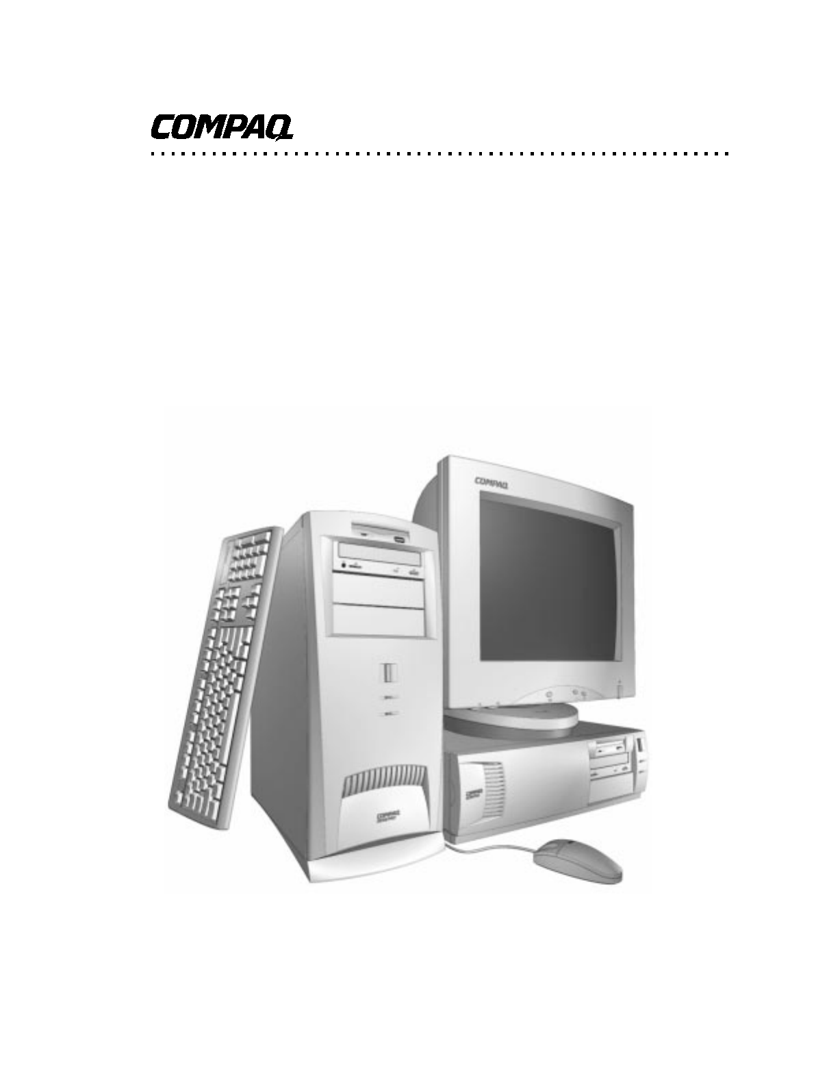
The Compaq Deskpro EN Series of desktop and minitower Personal Computers (Figure 2-1)
delivers an outstanding combination of manageability, serviceability, and consistency for
enterprise environments. Based on Intel Pentium II and Celeron processors, the Deskpro EN
Series emphasizes performance and industry compatibility. These models feature architectures
incorporating the PCI, AGP, and ISA buses. All models are easily upgradable and expandable to
keep pace with the needs of the office enterprise.
Figure 2–1. Compaq Deskpro EN Desktop Personal Computers with Monitor
This chapter includes the following topics:
♦ Features and options (2.2) page 2-2
♦ Mechanical design (2.3) page 2-4
♦ System architecture (2.4) page 2-8
♦ Specifications (2.5) page 2-13

Chapter 2 System Overview
Compaq Deskpro EN Series of Personal Computers
Desktop and Minitower Form Factors
Third Edition – September 1998
2-2
2.2 FEATURES AND OPTIONS
This section describes the standard features and available options.
2.2.1 STANDARD FEATURES
The following standard features are included on all models:
♦ Pentium II or Celeron processor
♦ High-performance 2D/3D AGP graphics card
♦ Embedded 16-bit full-duplex audio with Compaq Premier Sound
♦ 3.5 inch, 1.44-MB diskette drive
♦ Extended IDE controller support for up to four IDE drives
♦ Hard drive fault prediction
♦ Two serial interfaces
♦ Parallel interface
♦ Two universal serial bus ports
♦ Two PCI slots
♦ Two combo PCI/ISA slots
♦ 10/100 NIC card
♦ Compaq Enhanced keyboard w/Windows support
♦ Mouse
♦ APM 1.2 power management support
♦ Plug ’n Play compatible (with ESCD support)
♦ Intelligent Manageability support
♦ Energy Star compliant
♦ Security features including:
• Flash ROM Boot Block
• Diskette drive disable, boot disable, write protect
• Power-on password
• Administrator password
• QuickLock/QuickBlank
• Smart Cover lock
• Smart Cover removal sense
• Serial port disable
• Parallel port disable

Technical Reference Guide
Compaq Deskpro EN Series of Personal Computers
Desktop and Minitower Form Factors
Third Edition - September 1998
2-3
2.2.2 OPTIONS
The following items are available as options for all models and may be included in the standard
configuration of some models:
♦ System Memory: 16-MB DIMM (ECC and non-ECC)
32-MB DIMM (ECC and non-ECC)
64-MB DIMM (ECC and nonECC)
128-MB DIMM (ECC and non-ECC)
♦ Hard drives/controllers: 3.2 GB UATA
4.3 GB Wide Ultra SCSI
9.1 GB Wide Ultra SCSI
Wide Ultra SCSI PCI controller
6.4 GB UATA
♦ Removeable media drives: 1.44 MB diskette drive
32x CD-ROM drive
PS-120 Power Drive
♦ Communications cards: Compaq 10/100TX PCI Intel with WOL UTP
Netelligent 10/100, TX PCI UTP TLAN
3COM Fast EtherLink XL 10/100TX PCI
Compaq Netelligent 56.6 Baud ISA Modem
♦ Graphics cards/memory: ATI RAGE PRO Turbo AGP card
ATI RAGE PRO Turbo AGP 2X card
4-MB SGRAM SODIMM (for RAGE PRO AGP 2X card)
Matrox MGA-G100A card
Matrox Millennium G200-SD card
8-MB SDRAM SODIMM (for Millennium G200-SD card)
Compaq Deskpro Computers are easily upgraded and enhanced with peripheral devices designed
to meet PCI and ISA standards. The Compaq Deskpro Personal Computers are compatible with
peripherals designed for Plug ’n Play operation.
Chapter 2 System Overview
Compaq Deskpro EN Series of Personal Computers
Desktop and Minitower Form Factors
Third Edition – September 1998
2-4
2.3 MECHANICAL DESIGN
The Compaq Deskpro EN Series uses a desktop form factor. This section illustrates the
mechanical particulars of the bezel, chassis, and major board assemblies.
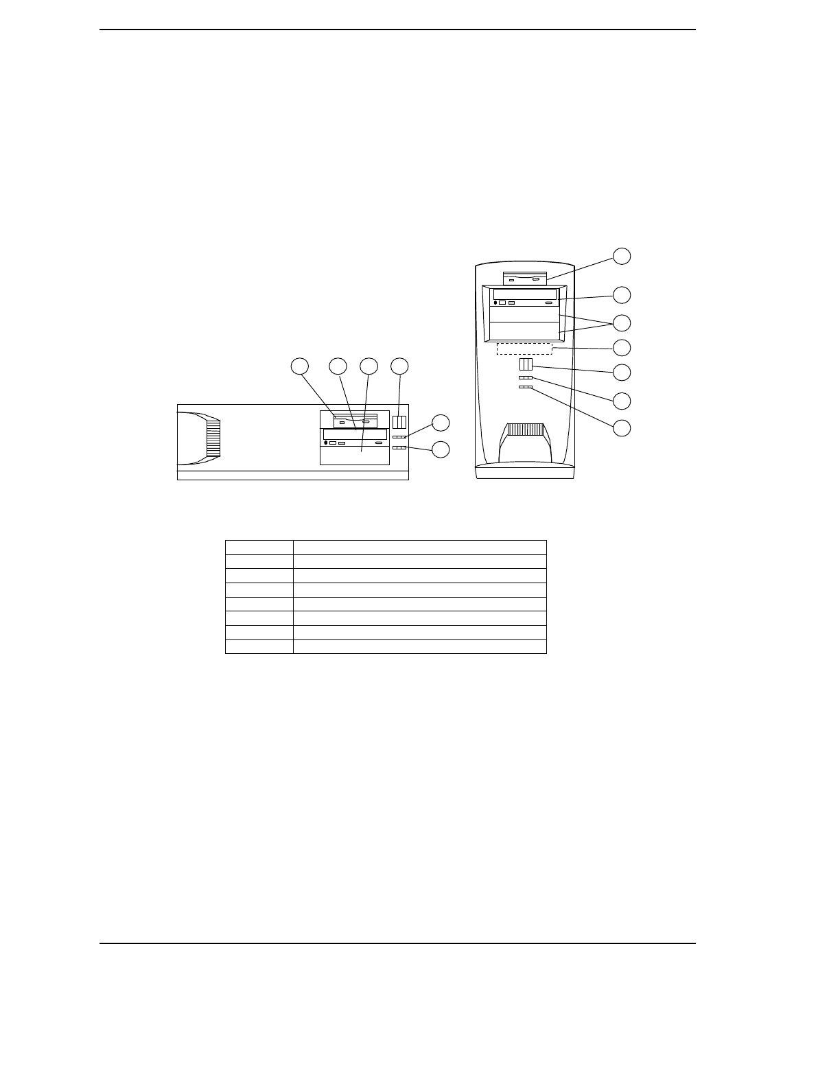
2.3.1 CABINET LAYOUTS
Item Function
1 1.44 MB Diskette Drive (5.25” drive bay)
2 CD-ROM Drive (CDS models) (5.25“ drive bay)
3 Internal Drive (5.25”) bay
4 Internal Drive (3.5”) bay
5 Power Button
6 Power On/Sleep Indicator
7 Hard Drive Activity Indicator
Figure 2–2. Cabinet Layouts, Front View
31 52
6
7
1
2
3
5
6
7
Desktop Minitower
4
Technical Reference Guide
Compaq Deskpro EN Series of Personal Computers
Desktop and Minitower Form Factors
Third Edition - September 1998
2-5
Item Function
1 AC Line In Connector
2 Smart Cover Lock Screws
3 Line Voltage Switch
4 USB Interface Port B
5 USB Interface Port A
6 100TX speed LED
7 Activity LED
8Link LED
9 NIC Connector
10 SCSI connector
11 Audio Headphone Input
12 Audio Microphone Input
13 Audio Line Output
14 Audio Line Input
15 Keyboard Connector
16 Mouse Connector
17 Parallel Interface Connector
18 Serial Interface Connector (COM1)
19 Serial Interface Connector (COM2)
20 Graphics Monitor Connector
Figure 2–3. Cabinet Layouts, Rear View
Minitower
1
8
7
6
54
2
3
9
11
12
13
15
2
3 5 7
894
116
11 13
10 12 14
6
15
Desktop
17 18 19
20
10
14
16
20
17
18
19
Chapter 2 System Overview
Compaq Deskpro EN Series of Personal Computers
Desktop and Minitower Form Factors
Third Edition – September 1998
2-6
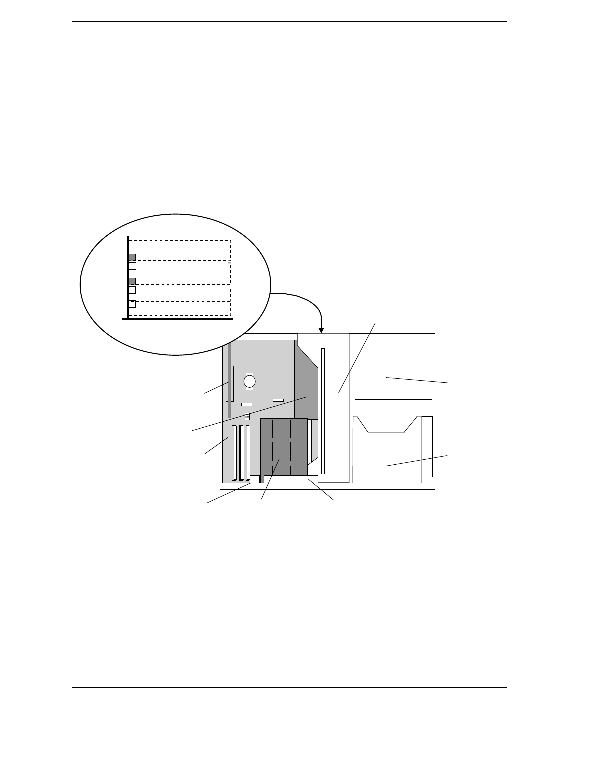
2.3.2 CHASSIS LAYOUTS
Figures 2-4 and 2-5 show the layout of key assemblies within the desktop and minitower chassis
respectively. For serviceability this system features an expansion card cage that allows easy
removal of the backplane and expansion cards as a single assembly. The tilt drive cage tilts up for
easy removal/replacement of drives. For detailed information on servicing the chassis refer to the
multimedia training CD-ROM and/or the maintenance and service guide for this system.
Figure 2–4. Desktop Chassis Layout, Top View
Front
Back
Power Supply
Tilt Drive Cage
System Board
Expansion Card Cage
Chassis Fan
AGP NLX
Graphics Card
Processor
PCI Slot 4 (SCSI Card)
ISA Slot
PCI Slot 1 (NIC Card)
Slots On Backplane,
Rear View
PCI Slot 2
PCI Slot 3
ISA Slot
Wide-Ultra
SCSI Card
Speaker
Technical Reference Guide
Compaq Deskpro EN Series of Personal Computers
Desktop and Minitower Form Factors
Third Edition - September 1998
2-7
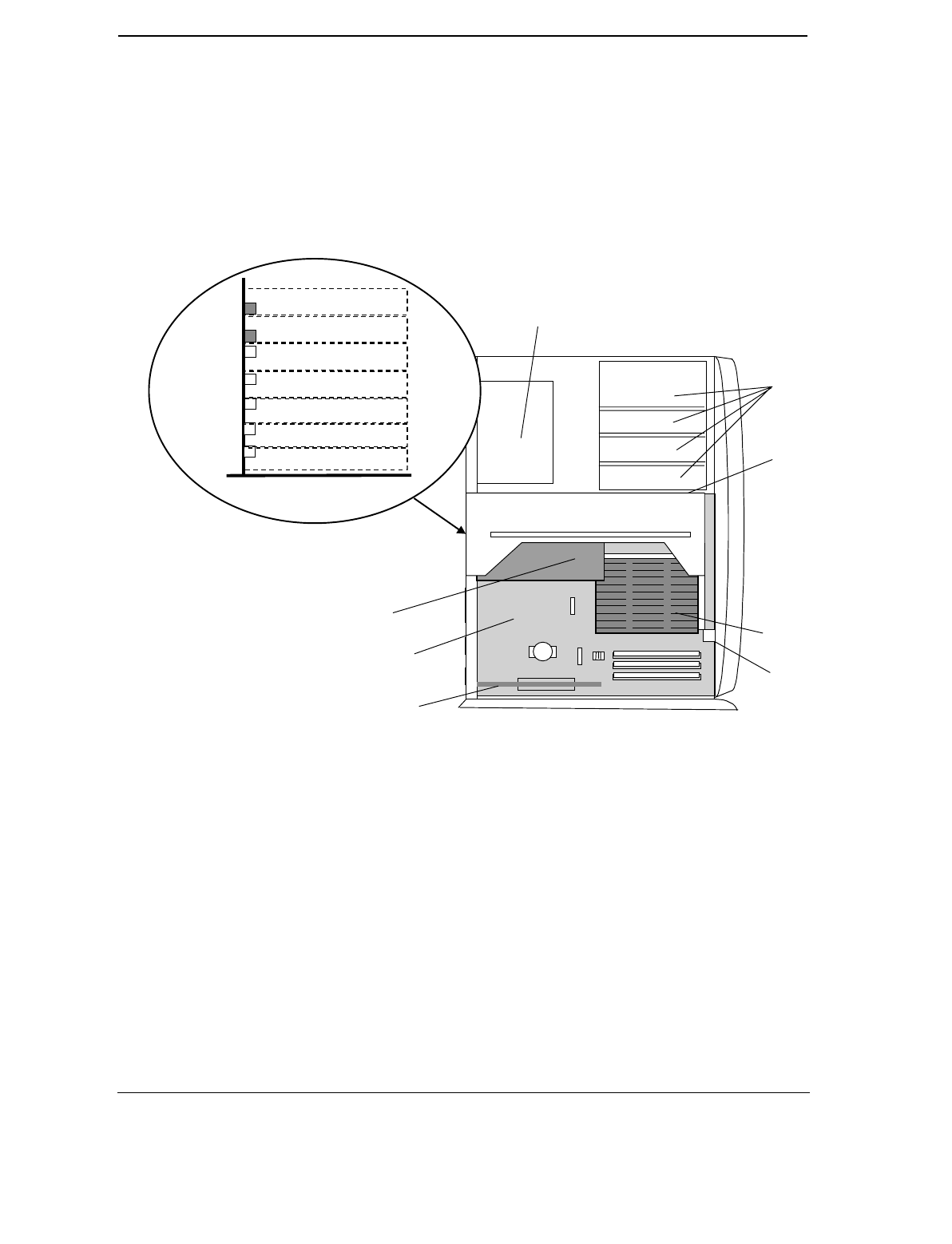
Figure 2–5. Minitower Chassis Layout, Left Side View
Front
Back
Power Supply
Drive Bays
System Board
Speaker
AGP NLX
Graphics Card
Processor
Wide-Ultra
SCSI Card
PCI Slot 1 (NIC Card)
Slots On Backplane,
Rear View @ 90°
PCI Slot 2 (SCSI Card)
PCI Slot 3
PCI Slot 4
PCI Slot 5
ISA Slot
ISA Slot
Expansion Card Cage
Chapter 2 System Overview
Compaq Deskpro EN Series of Personal Computers
Desktop and Minitower Form Factors
Third Edition – September 1998
2-8
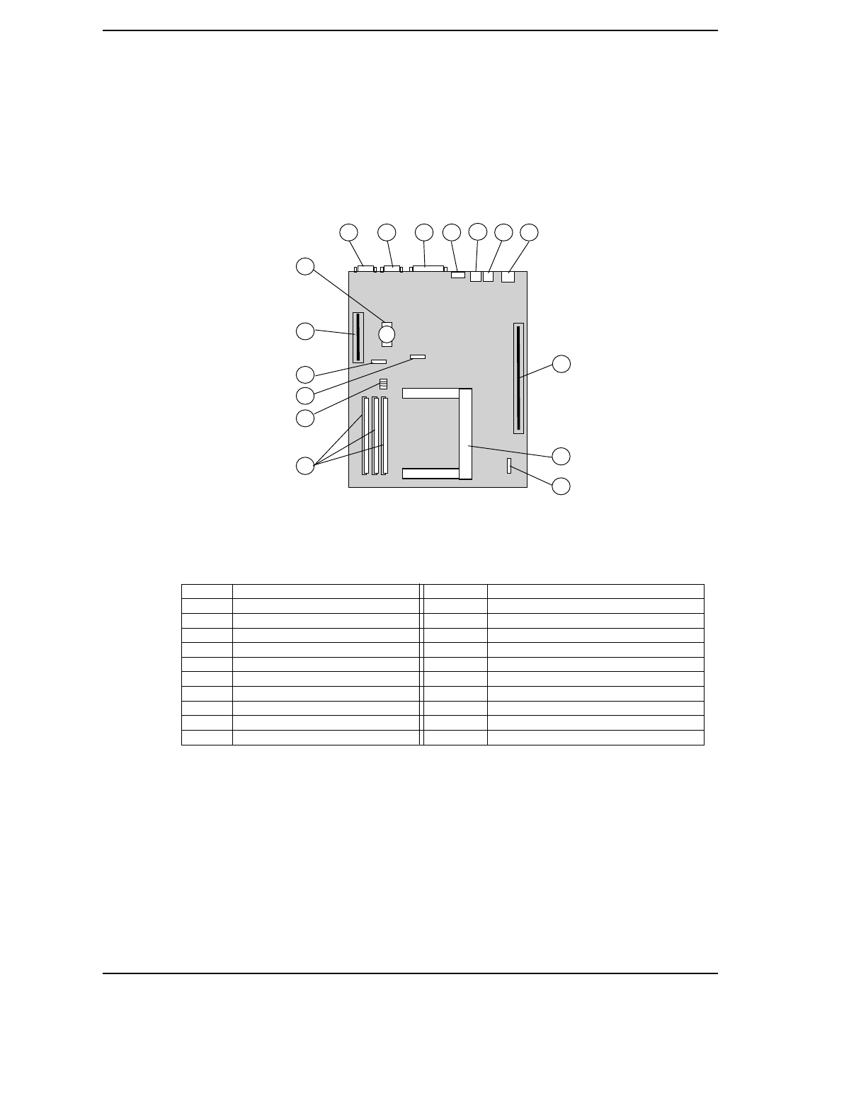
2.3.3 BOARD LAYOUTS
Figure 2-6 shows the location of connectors and switches for the system board, which is the same
for all models and both formfactors.
Item Function Item Function
1 Serial I/F (COM2) 7 (bottom) USB Port A I/F
2 Serial I/F (COM1) 8 Backplane Connector
3 Parallel I/F 9 Processor Slot 1
4 (top) Mouse connector 10 Heat Sink Thermal Diode Connector [2]
4 (bottom) Keyboard connector 11 DIMM Sockets
5 (top) Audio Line Input 12 Frequency/Password DIP Switch
5 (bottom) Audio Line Output 13 Heat Sink Thermal Diode Connector [3]
6 (top) Audio Mic Input 14 CMOS Clear Jumper
6 (bottom) Audio Headphone Output 15 AGP Slot (NLX-type)
7 (top) USB Port B I/F 16 Battery
NOTE:
[1] The two system boards are electrically identical. There are slight differences in the location of some
components. Later production units use the 008123-xxx board.
[2] PCA # 008123
[3] PCA # 007998
Figure 2–6. System Board Connector and Switch Locations
System Board (NLX-Type)
1 3 45
2
8
9
6 7
(P/N 007998-xxx
or 008123-xxx [1])
11
12
13
14
15
16
10
Technical Reference Guide
Compaq Deskpro EN Series of Personal Computers
Desktop and Minitower Form Factors
Third Edition - September 1998
2-9
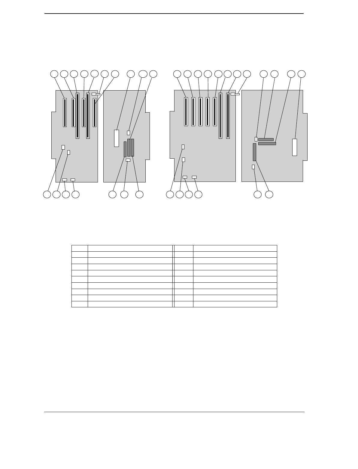
Figure 2-7 shows the connector and switch locations for the two types of backplane boards.
Item Function Item Function
1 PCI connector J20 (slot 1) 10 CD audio input header P7
2 PCI connector J21 (slot 2) 11 Secondary EIDE connector P21
3 ISA connector J10 [1] 12 Diskette drive connector P10
4 PCI connector J22 (slot 3) [2] 13 Primary EIDE connector P20
5 ISA connector J11 [3] 14 Power button/LED header P5
6 Smart Cover sensor switch 15 Fan header P8
7 PCI connector J23 (slot 4) [4] 16 Speaker header P6
8 PCI connector J24 (slot 5) 17 SCSI LED header P29
9 Power supply connector P1 18 NIC WOL header P9
NOTES:
[1] Shares slot with item 4 on desktop backplane (combo slot 1)
[2] Shares slot with item 3 on desktop backplane (combo slot 1)
[3] Shares slot with item 7 on desktop backplane (combo slot 2)
[4] Shares slot with item 5 on desktop backplane (combo slot 2)
[5] Later production units use the 009663-001 board
Figure 2–7. Backplane Board Connector, Header, and Switch Locations
1 3 45
2 8
1312
11
9
15
10
16
1210
6 7
14
11
Desktop Backplane Board
(P/N 008001-xxx
or 009663-xxx [5])
System Board Side Power Supply Side
17
Power Supply SideSystem Board Side
Minitower Backplane Board
(P/N 008058-xxx)
1 2 47 3 5 9
18 131415161718
6

Chapter 2 System Overview
Compaq Deskpro EN Series of Personal Computers
Desktop and Minitower Form Factors
Third Edition – September 1998
2-10
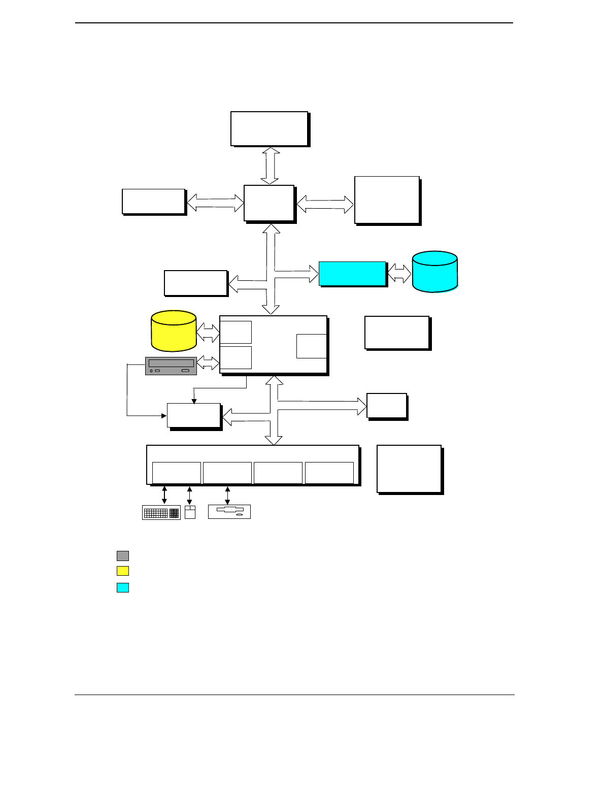
2.4 SYSTEM ARCHITECTURE
The Compaq Deskpro EN Series of Personal Computers is based on an Intel Pentium II processor
matched with the Intel 440BX AGPset. The basic architecture (Figure 2-8), uses three main
buses: the Host bus, the Peripheral Component Interconnect (PCI) bus, and the Industry Standard
Architecture (ISA) bus.
The Host and memory buses provide high performance support for CPU, cache and system
memory accesses, and operate at 66 or 100 MHz, depending on the speed of the microprocessor.
The PCI bus provides support for the UATA controllers, USB ports, and PCI expansion devices.
The PCI bus operates at 33 MHz. This system also includes an Accelerated Graphics Port (AGP)
slot for an AGP graphics card. The AGP bus is closely associated with the PCI bus but operates at
66 MHz and allows data pipelining, sideband addressing, and frame mode transfers for increased
3D graphics performance.
The ISA bus provides a standard 8-MHz interface for the input/output (I/O) devices such as the
keyboard, diskette drive, serial and parallel interfaces, as well as the addition of 16- or 8-bit
expansion devices.
The north and south bridge functions are provided by the 440BX AGPset designed to compliment
the processor. The support chipset also provides memory controller and data buffering functions
as well as bus control and arbitration functions.
The I/O interfaces and diskette drive controller are integrated into the PC87307 I/O Controller.
This component also includes the real time clock and battery-backed configuration memory
(CMOS).
Table 2-1 lists differences between system models:
Table 2–1. Model Differences
Table 2-1.
Model Differences
Model 3200 Model 4300 Model 6400 Model 9100
Form Factor DT/MT DT/MT DT/MTMT
CPU Speed (MHz) 266/300/333 333/350/400 300/333/350/400 400/450
Host Bus Speed (MHz) 66 66/100/100 66/66/100/100 100
Hard Drive 3.2 GB UATA 4.3 GB SCSI 6.4 GB UATA 9.1 GB SCSI
System Memory:
Standard
Maximum installable
16/32 MB SDRAM
384 MB
32/64 MB ECC
384 MB
32/64 MB SDRAM
384 MB
64 MB ECC
384 MB
Graphics Controller ATI RAGE PRO
Turbo
AGP 1X Card
ATI RAGE PRO
Turbo
AGP 2X Card
ATI RAGE PRO
Turbo
AGP 1X/2X Card
ATI RAGE PRO
Turbo
AGP 2X Card
NOTE:
Only BTO configurations shown.
The following subsections provide a description of the key functions and subsystems.
Technical Reference Guide
Compaq Deskpro EN Series of Personal Computers
Desktop and Minitower Form Factors
Third Edition - September 1998
2-11
Figure 2–8. Compaq Deskpro EN System Architecture, Block diagram
Pentium II or
Celeron
Processor
82443BX
(North
Bridge)
82371
(South
Bridge)
33-MHz
32-Bit
PCI Bus
Pri.
IDE I/F USB
I/F (2)
System
Memory
66-/100-MHz
64-Bit
Mem. Bus
Power
Supply
BIOS
ROM
Sec.
IDE I/F
Graphics
Cntlr. Card
3200 and 6400 models onl
y
.
CDS Desktops and all Minitower models.
87307 I/O Controller
Diskette
I/F
Keyboard/
Mouse I/F
Serial
I/F
(
2
)
Parallel
I/F
Audio
Subsystem
16-Bit ISA Bus
66-/100- MHz 64-Bit Host Bus
66-MHz
32-Bit
AGP Bus
CD Audio
IDE
Hard Drive
Wide Ultra
SCSI
Hard Drive
Wide Ultra SCSI
Cntlr. Card
10/100 NIC
Card
4300 and 9100 models onl
y
.
System
Security
Lo
g
ic
Beep Audio
Chapter 2 System Overview
Compaq Deskpro EN Series of Personal Computers
Desktop and Minitower Form Factors
Third Edition – September 1998
2-12
2.4.1 PROCESSOR
The Deskpro EN Series includes models based on Pentium II and Celeron processors. The
processor and heat sink is mounted as an assembly (Figure 2-9) in a slot (Slot 1) on the system
board. The Pentium II processor includes a microprocessor and a secondary (L2) cache contained
in a single edge connector (SEC) cartridge to which a heat sink is attached. The Celeron
processor includes a microprocessor mounted on a single edge processor package (SEPP) board.
On these systems the SEPP board of the Celeron processor is contained within a SEPP board
housing and heat sink.
Figure 2–9. Processor Assembly Comparison
The Pentium II and Celeron processors are backward-compatible with software written for the
Pentium MMX, Pentium Pro, Pentium, and x86 microprocessors. The integrated microprocessor
provides performance enhancements for multi-byte and floating-point processing.
SEC Cartridge
Microprocessor Secondary (L2) Cache
Heat Sink
Microprocessor
SEPP Board
Pentium II Processor
Assembly Celeron Processor
Assembly
SEPP Board
Housing

Technical Reference Guide
Compaq Deskpro EN Series of Personal Computers
Desktop and Minitower Form Factors
Third Edition - September 1998
2-13
2.4.2 SYSTEM MEMORY
This system provides three 168-pin DIMM sockets with 16, 32 or 64 megabytes of RAM
installed depending on model. System memory can be expanded up to 384 megabytes using 16-,
32-, 64-, and 128-MB DIMMs. This system supports SDRAM, EDO, and ECC DIMMs. Models
3200 and 6400 come with SDRAM installed while models 4300 and 9100 come with ECC
DIMMs installed. Non-parity DIMMs are installed as standard but parity DIMMs are supported.
2.4.3 SUPPORT CHIPSETS
Table 2-2 shows the functions provided by the key components on the system board.
Table 2–2. Support Chipsets
Table 2-2.
Support Chipsets
Component Name Component Type Function
PCI Arbitration Controller (PAC) North Bridge 82443BX Memory Controller
Host/PCI Bridge
PCI-ISA/IDE eXcelerator (PIIX4E) South Bridge 82371 PCI/ISA Bridge
EIDE Controller
DMA Controller
Interrupt Controller
Timer/Counter
NMI Registers
Reset Control Reg.
USB I/F (2)
Super I/O Controller 87307 Keyboard I/F
Diskette I/F
Serial I/F
Parallel I/F
RTC/CMOS Mem.
GPIO Ports
Clock Generator CY2280 Clock Generator
System Security ASIC Compaq ASIC Super I/O Security
Smart Cover Lock
ROM Write Protect
Temperature Shutdown
SM/WOL Interrupts
Diskette Write Disable
Pwr LED Blink Cntrl.
PS On sig. Cntrl.
2.4.4 MASS STORAGE
All models include a 3.5 inch 1.44-MB diskette drive installed. Either an EIDE or SCSI hard
drive is also installed, depending on model. All models include a PCI bus mastering Enhanced
IDE (EIDE) controller that provides two EIDE interfaces supporting up to four IDE devices.
Models equipped with a SCSI drive include a Wide Ultra SCSI adapter board. A 32x CD-ROM is
included on desktop CDS models and on all MT models.

Chapter 2 System Overview
Compaq Deskpro EN Series of Personal Computers
Desktop and Minitower Form Factors
Third Edition – September 1998
2-14
2.4.5 SERIAL AND PARALLEL INTERFACES
All models include two serial ports and a parallel port accessible at the rear of the chassis. The
serial and parallel ports are integrated into a PC87307 I/O Controller component. The serial port
is RS-232-C/16550-compatible and operates at baud rates up to 115,200. The parallel interface is
Enhanced Parallel Port (EPP1.9) and Enhanced Capability Port (ECP) compatible, and supports
bi-directional data transfers.
2.4.6 UNIVERSAL SERIAL BUS INTERFACE
All models feature two Universal Serial Bus (USB) ports that provide a high speed interface for
future systems and/or peripherals. The USB operates at 12 Mbps and provides hot
plugging/unplugging (Plug ’n Play) functionality.
2.4.7 GRAPHICS SUBSYSTEM
The graphics subsystem is conatained on a card installed into the AGP slot. Two types of
graphics controllers are used, depending on the microprocessor employed on the system board as
indicated in Table 2-3.
Table 2–3. Graphics Subsystem Comparison
Table 2-3.
Graphics Subsystem Comparison
266-/300-/333-MHz Processor 350-/400-/4500 MHz Processor
Graphics Controller ATI Rage Pro Turbo AGP ATI Rage Pro Turbo AGP 2X
Graphics Memory
Standard installed:
Expandable to:
4 MB SGRAM
N/A
4 MB SGRAM
8 MB SGRAM
Maximum Resolution
w/ standard mem.
w/ max. mem.
1600 x 1200 @ 65K colors
--
1600 x 1200 @ 65K colors
1600 x 1200 @ 16.7M colors
2.4.8 AUDIO SUBSYSTEM
All models feature the Compaq Premier Sound system. The system board includes an embedded
16-bit full-duplex subsystem based on the ES1869 graphics controller. The audio output is
processed through a six-level equalizer designed to work with the chassis acoustics. A low-
distortion 5-watt amplifier drives a long-excursion speaker for optimum sound. The audio
subsystem is compatible with software written for industry-common sound hardware.

Technical Reference Guide
Compaq Deskpro EN Series of Personal Computers
Desktop and Minitower Form Factors
Third Edition - September 1998
2-15
2.5 SPECIFICATIONS
This section includes the environmental, electrical, and physical specifications for the Compaq
DESKPRO EN Series Personal Computers.
Table 2–4. Environmental Specifications
Table 2-4.
Environmental Specifications
Parameter Operating Nonoperating
Air Temperature 50o to 95o F (10o to 35o C) -24o to 140o F (-30o to 60o C)
Shock N/A 60.0 g for 2 ms half-sine pulse
Vibration 0.000215g^ 2/hz, 10-300 Hz [1] 0.0005g^ 2/Hz, 10-500 Hz [1]
Humidity 90% RH @ 36o C (no hard drive) 95% RH @ 36o C
Maximum Altitude 10,000 ft (3048 m) 30,000 ft (9,144 m)
NOTE:
Values are subject to change without notice.
[1] 0.5 grms nominal
Table 2–5. Electrical Specifications
Table 2-5.
Electrical Specifications
Parameter U.S. International
Input Line Voltage:
Nominal:
Maximum:
110 - 120 VAC
90 - 132 VAC
200 - 240 VAC
180 - 264 VAC
Input Line Frequency Range:
Nominal:
Maximum:
50 - 60 Hz
47 - 63 Hz
50 - 60 Hz
47 - 63 Hz
Power Supply:
Maximum Continuous Power
Maximum Peak Power
Maximum Line Current Draw
200 watts
200 watts
5.5 A
200 watts
200 watts
3.0 A
Table 2–6. Physical Specifications
Table 2-6.
Physical Specifications
Parameter Desktop Minitower
Height 5.88 in (14.93 cm) 20.25 in (51.44 cm)
Width 19.16 in (48.66 cm) 8.38 in (21.29 cm)
Depth 16.82 in (42.72 cm) 18.60 in (47.24 cm)
Weight [1] 32.0 lb (14.50 kg) 40.0 lb (18.20 kg)
NOTES:
Metric figures in parenthesis.
[1] System weight may differ depending on installed drives/peripherals.

Chapter 2 System Overview
Compaq Deskpro EN Series of Personal Computers
Desktop and Minitower Form Factors
Third Edition – September 1998
2-16
Table 2–7. Diskette Drive Specifications
Table 2-7.
Diskette Drive Specifications
(Compaq SP# 179161-001)
Parameter Measurement
Media Type 3.5 in 1.44 MB/720 KB diskette
Height 1/3 bay (1 in)
Bytes per Sector 512
Sectors per Track:
High Density
Low Density
18
9
Tracks per Side:
High Density
Low Density
80
80
Read/Write Heads 2
Average Access Time:
Track-to-Track (high/low)
Average (high/low)
Settling Time
Latency Average
3 ms/6 ms
94 ms/173ms
15 ms
100 ms
Table 2–8. 24x CD-ROM Drive Specifications
Table 2-8.
32x CD-ROM Drive Specifications
(SP# 327659-001)
Parameter Measurement
Interface Type IDE
Transfer Rate:
Max. Sustained
Burst
4800 KB/s
16.6 MB/s
Media Type Mode 1,2, Mixed Mode, CD-DA,
Photo CD, Cdi, CD-XA
Capacity:
Mode 1, 12 cm
Mode 2, 12 cm
8 cm
550 MB
640 MB
180 MB
Center Hole Diameter 15 mm
Disc Diameter 8/12 cm
Disc Thickness 1.2 mm
Track Pitch 1.6 um
Laser
Beam Divergence
Output Power
Type
Wave Length
53.5 +/- 1.5 °
53.6 0.14 mW
GaAs
790 +/- 25 nm
Average Access Time:
Random
Full Stroke
<100 ms
<150 ms
Audio Output Level 0.7 Vrms
Cache Buffer 128 KB

Technical Reference Guide
Compaq Deskpro EN Series of Personal Computers
Desktop and Minitower Form Factors
Third Edition - September 1998
2-17
Table 2–9. Hard Drive Specifications
Table 2-9.
Hard Drive Specifications
Parameter 3.2 GB
(# 166873-001) 4.3 GB
(# 179287-001) 6.4 GB
(# 166973-001) 9.1 GB
(# 179288-001)
Interface EIDE-UATA Wide-Ultra SCSI EIDE-UATA Wide-Ultra SCSI
Drive Type 65 65 65 65
Drive Size 5.25 in 5.25 in 5.25 in 5.25 in
Transfer Rate 33.3 MB/s 40.0 MB/s 33.3 MB/s 40.0 MB/s
Seek Time (w/settling)
Single Track
Average
Full Stroke
<1.0 ms
<9.7 ms
<18.0 ms
.76 ms
7.5 ms
17.0 ms
2.0 ms
<9.7 ms
20.0 ms
.76 ms
7.5 ms
15.0 ms
Disk Format:
# of Cylinders
# of Data Heads
# of Sectors per Track
6697
15
63
8420
8
165-264
13325
15
63
8420
10
165-264
Buffer Size 256 KB 512 KB 256 KB 512 KB
Drive Fault Prediction SMART II SMART II SMART II SMART II

Chapter 2 System Overview
Compaq Deskpro EN Series of Personal Computers
Desktop and Minitower Form Factors
Third Edition – September 1998
2-18
This page is intentionally blank.

Technical Reference Guide
Compaq Deskpro EN Series of Personal Computers
Desktop and Minitower Form Factors
Third Edition - September 1998
3-1
Chapter 3
PROCESSOR/
MEMORY SUBSYSTEM
3. Chapter 3 PROCESSOR/MEMORY SUBSYSTEM
3.1 INTRODUCTION
This chapter describes the processor/cache memory subsystem of the Compaq Deskpro EN Series
of desktop and minitower Personal Computers. These systems are shipped either with an Intel
Pentium II or Celeron processor and either 32 or 64 megabytes of system memory, depending on
configuration.
This chapter includes the following topics:
♦ Processor/memory subsystem [3.2] page 3-2
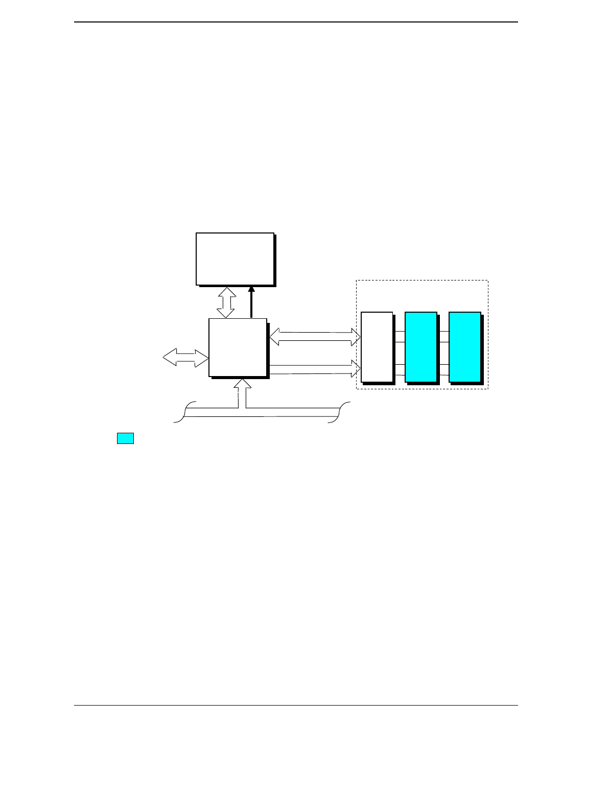
Chapter 3 Processor/Memory Subsystem
Compaq Deskpro EN Series of Personal Computers
Desktop and Minitower Form Factors
Third Edition - September 1998
3-2
66-/100-MHz
Mem. Data Bus
Mem. Addr.
Graphics
Subsystem
3.2 PROCESSOR/MEMORY SUBSYSTEM
The subsystem features an Intel Pentium II or Celeron processor with the North Bridge
(82443BX), and either 32 or 64 megabytes of system memory (Figure 3-1). The 64-bit Host and
memory buses operate at either 66- or 100-MHz depending on the speed of the processor. The 32-
bit PCI bus operates at 33-MHz.
Figure 3–1. Processor/Memory Subsystem Architecture
The processor is mounted in a slot 1-type connector that facilitates easy changing/upgrading.
Replacing the processor may require reconfiguring DIP switch SW1 to select the correct bus
frequency/core frequency combination. Frequency selection is described in detail later in this
section.
The North Bridge (82443BX) provides Host/memory/PCI bridge functions and controls data
transfers with system memory over the 64-bit memory data bus. The 443BX supports SDRAM,
EDO, FPM, and ECC DIMM modules. Three DIMM sockets allow the system memory to be
expanded to 384 megabytes.
Processor
(in Slot 1)
33-MHz 32-Bit PCI Bus
Optional module
32-MB
DIMM DIMM
J1 J2
System Memory
66-/100-MHz
64-Bit Host Bus
North
Bridge
(82443BX)
Cntl
DIMM
J3
66-MHz
32-Bit
AGP Bus
Technical Reference Guide
Compaq Deskpro EN Series of Personal Computers
Desktop and Minitower Form Factors
Third Edition - September 1998
3-3
3.2.1 PROCESSOR
The system board includes a Slot 1-type interface that accommodates a Pentium II or Celeron
processor. Table 3-1 provides a comparison between the key parameters of the Pentium II and
Celeron processors.
Table 3–1. Processor Comparison
Table 3-1.
Processor Comparsion
Pentium II
266-333 Celeron
266/300 Celeron
300A/333 Pentium II
350 Pentium II
400 Pentium II
450
CPU Freq. 266-333 MHz 300 MHz 300/333 MHz 350 MHz 400 MHz 450 MHz
L2 Cache 512 KB 0 KB 128 KB 512 KB 512 KB 512 KB
L2 Cache Freq. 133-166 MHz -- 300/333 MHz 175 MHz 200 MHz 225 MHz
Host Bus Freq. 66 MHz 66 MHz 66 MHz 100 MHz 100 MHz 100 MHz
3.2.1.1 Pentium II Processor
The Intel Pentium II processor is packaged in a Single Edge Connector (SEC) cartridge that
contains the microprocessor and a 512-KB ECC secondary (L2) cache. The processor’s
architecture (Figure 3-2) includes a dual-ALU MMX-supporting CPU, branch prediction logic,
dual-pipeline floating point unit (FPU) coprocessor, and a 32-KB L1 cache that is split into two
16-KB 4-way, set-associative caches for handling code and data separately. These functions
operate at core processing speed (Figure 3-2), which ranges from 266 to 400 megahertz
depending on version.
Figure 3–2. Pentium II Processor Internal Architecture
The Pentium II processor includes 512 kilobytes of SRAM for the write-through L2 cache.
Accesses with the L2 cache occur at 50% of the core processing speed. The front side bus (FSB,
also referred to as the Host bus) interface of the 266-, 300-, and 333-MHz processors operates at
66-MHz. The FSB interface of the 350- and 400-MHz processors operates at 100 MHz. The
Pentium II processor is software-compatible with earlier generation x86 microprocessors.
NOTE: Later versions of the Pentium II processor require updated BIOS firmware.
Refer to section 3.2.2 for upgrading information.
Pentium II Processor
CPU
Branch
Prediction
FPU 32-KB
L1
Cache
512-KB
L2
Cache
FSB
I/F
Core processin
g
speed ½ Core processin
g
speed Host bus speed
Chapter 3 Processor/Memory Subsystem
Compaq Deskpro EN Series of Personal Computers
Desktop and Minitower Form Factors
Third Edition - September 1998
3-4
3.2.1.2 Celeron Processor
Select systems are shipped with the Intel Celeron processor. The Celeron processor (Figure 3-3)
uses a CPU/FPU core that is functionally the same as that of the Pentium II described previously
and provides the same level of branch prediction, math co-processing, MMX support, and L1
cache operation. Processing and Host bus speed ratios follow those of the Pentium II processors
and are set and determined with the same methods. Note that the Celeron 300 does not include
an L2 cache. The L2 cache of the Celeron 300A and 333 operates at processor (CPU) speed.
[1] Not present on Celeron 266 or 300 processors.
Figure 3–3. Celeron Processor Internal Architecture
Like the Pentium II processor, the Celeron processor is software-compatible with earlier
generation Pentium MMX, Pentium, and x86 processors.
NOTE: Later versions of the Celeron processor require updated BIOS firmware. Refer
to section 3.2.2 for upgrading information.
Celeron Processor
CPU
Branch
Prediction
FPU 32-KB
L1
Cache
128-KB
L2
Cache [1]
FSB
I/F
Core processin
g
speed
Host bus speed

Technical Reference Guide
Compaq Deskpro EN Series of Personal Computers
Desktop and Minitower Form Factors
Third Edition - September 1998
3-5
3.2.2 PROCESSOR CHANGING/UPGRADING
The slot 1 design allows for easy changing and/or upgrading of the processor/cache complex.
Changing the processor requires disconnection/re-connection of the heat sink sensor cable and
may require upgrading the BIOS firmware and re-configuration of the bus/core speed switch
discussed in the following paragraphs.
3.2.2.1 BIOS Upgrading
The Pentium II 450 and Celeron 300A/333 processors require BIOS firmware dated 7/30/98 or
later. Installing and running one of these processors in a system with BIOS dated earlier than
7/30/98 will likely cause the system to halt (lockup).
The BIOS (ROM) version may be checked using either the Compaq Diagnostics or Compaq
Insight utility.
3.2.2.2 Processor Speed Selection
Changing the processor may require re-configuration of the bus/core frequency ratio. The system
board includes a six-position DIP switch (SW), of which positions 2-5 are read by the processor
(while RESET- is active) to select the bus-to-core frequency ratio. Table 3-2 shows the possible
switch configurations for this system and the resultant core (or processing) frequency, based on
the front side bus (FSB or Host bus) frequency.
Table 3–2. Bus/Core Speed Switch Settings
Table 3-2.
Bus/Core Speed Switch Settings
DIP SW1 Settings
2 3 4 5 [1] Bus/Core
Freq. Ratio w/66-MHz FSB w/100-MHz FSB
1 0 0 0 1/3 200 300
1 1 0 0 2/7 233 350
0 0 1 0 1/4 266 400
0 1 1 0 2/9 300 450
1 0 1 0 1/5 333 500
NOTES:
Shipping configurations are unshaded.
[1] 0 = Switch Closed (On), 1 = Switch Open (Off)
The DIP switch settings should be set to match the processor installed.
Configuring for a speed higher than that which the processor is
designed could result in unreliable operation and possible system damage.
The processor sets the clock generator to the appropriate bus frequency. Software can determine
the operating speed by reading the bus speed from an MSR register in the processor.
Core Frequency

Chapter 3 Processor/Memory Subsystem
Compaq Deskpro EN Series of Personal Computers
Desktop and Minitower Form Factors
Third Edition - September 1998
3-6
3.2.3 SYSTEM MEMORY
The system board contains three 168-pin DIMM sockets for system memory. This system is
designed for using SDRAM or ECC DIMMs. As shipped from the factory the standard
configuration has 16, 32, or 64 megabytes of memory installed. The system memory is
expandable up to a maximum of 384 megabytes. Single or double-sided DIMMs may be used. In
expanding the standard memory using modules from third party suppliers the following DIMM
type is recommended: 66- or 100-MHz unbuffered RAM supporting CAS latency (CL) 2 or 3
with a data access time (clock-to-data out) of 9.0 ns or less @ CL=2 or CL=3.
NOTE: The DIMM speed should compliment the host bus speed of the processor (i.e.,
use 66-MHz DIMMs in a system with a 266/66 processor and 100-MHz DIMMs in a
system with a 350/100 processor). All systems are factory-shipped with 100-MHz
DIMMs.
The RAM type and operating parameters are detected during POST by the system BIOS using the
serial presence detect (SPD) method. This method employs an I2C bus to communicate with an
EEPROM on each installed DIMM. The EEPROM holds the type and operating parameter data.
The supported format complies with the JEDEC specification for 128-byte EEPROMs. This
system also provides support for 256-byte EEPROMs to include additional Compaq-added
features such as part number and serial number. The SPD format as supported in this system is
shown in Table 3-3.
The key SPD bytes that BIOS checks for compatibility are 2, 9, 10, 18, 23, and 24. If BIOS
detects EDO DIMMs a “memory incompatible” message will be displayed and the system
will halt. If ECC DIMMs are used, all DIMMs installed must be ECC for ECC benefits (error
logging) to be realized.
Once BIOS determines the DIMM type the DRAM speed and CAS latency is checked based on
the following criteria:
Access
from
Bus Speed Cycle Time Clock
66 MHz 15 ns 9 ns @ 50 pf loading
100 MHz 10 ns 6 ns @ 50 pf loalding
NOTE: Refer to chapter 8 for a description of the BIOS procedure of interrogating
DIMMs.
Only CAS latencies of 2 or 3 are supported. If DIMMs with unequal CAS latencies are installed
then operation will occur based on the DIMM with the greatest latency.
If an incompatible DIMM is detected the NUM LOCK will blink for a short period of time during
POST and an error message may or may not be displayed before the system hangs.
The system memory map is shown in Figure 3-3.

Technical Reference Guide
Compaq Deskpro EN Series of Personal Computers
Desktop and Minitower Form Factors
Third Edition - September 1998
3-7
Table 3–3. SPD Address Map (SDRAM DIMM)
Table 3-3.
SPD Address Map (SDRAM DIMM)
Byte Description Notes Byte Description Notes
0 No. of Bytes Written Into EEPROM [1] 27 Min. Row Prechge. Time [7]
1 Total Bytes (#) In EEPROM [2] 28 Min. Row Active to Delay [7]
2 Memory Type 29 Min. RAS to CAS Delay [7]
3 No. of Row Addresses On DIMM [3] 30, 31 Reserved
4 No. of Column Addresses On DIMM 32..61 Superset Data [7]
5 No. of Module Banks On DIMM 62 SPD Revision [7]
6, 7 Data Width of Module 63 Checksum Bytes 0-62
8 Voltage Interface Standard of DIMM 64-71 JEP-106E ID Code [8]
9 Cycletime @ Max CAS Latency (CL) [4] 72 DIMM OEM Location [8]
10 Access From Clock [4] 73-90 OEM’s Part Number [8]
11 Config. Type (Parity, Nonparity, etc.) 91, 92 OEM’s Rev. Code [8]
12 Refresh Rate/Type [4] [5] 93, 94 Manufacture Date [8]
13 Width, Primary DRAM 95-98 OEM’s Assembly S/N [8]
14 Error Checking Data Width 99-125 OEM Specific Data [8]
15 Min. Clock Delay [6] 126, 127 Reserved
16 Burst Lengths Supported 128-131 Compaq header “CPQ1” [9]
17 No. of Banks For Each Mem. Device [4] 132 Header checksum [9]
18 CAS Latencies Supported [4] 133-145 Unit serial number [9] [10]
19 CS# Latency [4] 146 DIMM ID [9] [11]
20 Write Latency [4] 147 Checksum [9]
21 DIMM Attributes 148-255 Reserved [9]
22 Memory Device Attributes
23 Min. CLK Cycle Time at CL X-1 [7]
24 Max. Acc. Time From CLK @ CL X-1 [7]
25 Min. CLK Cycle Time at CL X-2 [7]
26 Max. Acc. Time From CLK @ CL X-2 [7]
NOTES:
[1] Programmed as 128 bytes by the DIMM OEM
[2] Must be programmed to 256 bytes.
[3] High order bit defines redundant addressing: if set (1), highest order RAS# address must be
re-sent as highest order CAS# address.
[4] Refer to memory manufacturer’s datasheet
[5] MSb is Self Refresh flag. If set (1), assembly supports self refresh.
[6] Back-to-back random column addresses.
[7] Field format proposed to JEDEC but not defined as standard at publication time.
[8] Field specified as optional by JEDEC but required by this system.
[9] Compaq usage. This system requires that the DIMM EEPROM have this
space available for reads/writes.
[10] Serial # in ASCII format (MSB is 133). Intended as backup identifier in case vender data is invalid.
Can also be used to indicate s/n mismatch and flag system adminstrator of possible system
Tampering.
[11] Contains the socket # of the module (first module is “1”). Intended as backup identifier (refer to
note [10]).

Chapter 3 Processor/Memory Subsystem
Compaq Deskpro EN Series of Personal Computers
Desktop and Minitower Form Factors
Third Edition - September 1998
3-8
Figure 3-3 shows the system memory map for the system.
NOTE: All locations in memory are cacheable. Base memory is always mapped to DRAM. The next 128 KB fixed
memory area can, through the north bridge, be mapped to DRAM or to PCI space. Graphics RAM area is mapped
to PCI or AGP locations.
Figure 3–4. System Memory Map
High BIOS Area
(
2 MB
)
Host/PCI Memory
Expansion
(1008 MB)
FFFF FFFFh
1 MB
Graphics/SMRAM
RAM (128 KB)
System BIOS Area
(64 KB)
Fixed Mem. Area
(128 KB)
Base Memory
(512 KB)
Extended BIOS Area
(64 KB)
Extended Memory
(
15 MB
)
FFE0 0000h
0100 0000h
00FF FFFFh
0010 0000h
000F 0000h
000E FFFFh
000F FFFFh
0000 0000h
0007 FFFFh
0008 0000h
0009 FFFFh
000B FFFFh
000A 0000h
512 KB
640 KB
16 MB
4 GB
Host, PCI,
ISA Area
DOS Compatibility
Area
Option ROM
(128 KB)
000E 0000h
000D FFFFh
000C 0000h
1 GB
Host,
PCI, AGP Area
PCI Memory
(18 MB)
FFDF FFFFh
FEC1 0000h
FEC0 FFFFh APIC Config. Space
(64 KB)
FEBF FFFFh
FEC0 0000h
PCI Memory
Expansion
(2548 MB)
3FFF FFFFh
4000 0000h

Technical Reference Guide
Compaq Deskpro EN Series of Personal Computers
Desktop and Minitower Form Factors
Third Edition - September 1998
3-9
3.2.4 SUBSYSTEM CONFIGURATION
The 443BX north bridge component provides the configuration function for the
processor/memory subsystem. Table 3-4 lists the configuration registers used for setting and
checking such parameters as memory control and PCI bus operation. These registers reside in the
PCI Configuration Space and accessed using the methods described in Chapter 4, section 4.2.
Table 3–4. Host/PCI Bridge Configuration Registers (443BX, Function 0)
Table 3-4.
Host/PCI Bridge Configuration Registers (82443BX, Function 0)
PCI Config.
Addr. Register Reset
Value PCI Config.
Addr. Register Reset
Value
00, 01h Vender ID 8086h 6A, 6Bh DRAM Control Reg. 00h
02, 03h Device ID 7190h 6C..6Fh Memory Buffer Strength 55h
04, 05h Command 0006h 70h Multi-Transaction Timer 00h
06, 07h Status 0210h 71h CPU Latency Timer 10h
08h Revision ID -- 72h SMRAM Control 02h
09..0Bh Class Code -- 90h Error Command 00h
0Dh Latency Timer 00h 91h Error Status Register 0 00h
0Eh Header Type 00h 92h Error Status Register 1 00h
10..13h Aperture Base Config. 8 93h Reset Control 00h
50, 51h PAC Config. Reg. 00h A0..A3h AGP Capability Identifier N/A
53h Data Buffer Control 83h A4..A7h AGP Status N/A
55..56h DRAM Row Type 00h A8..ABh AGP Command 00h
57h DRAM Control 01h B0..B3h AGP Control 00h
58h DRAM Timing 00h B4h Aperture Size 0000h
59..5Fh PAM 0..6 Registers 00h B8..BBh Aperture Translation Table 0000h
60..67h DRAM Row Boundary 01h BCh Aperture I/F Timer 00h
68h Fixed DRAM Hole 00h BDh Low Priority Timer 00h
NOTES:
Refer to Intel Inc. documentation for detailed description of registers.
Assume unmarked locations/gaps as reserved.

Chapter 3 Processor/Memory Subsystem
Compaq Deskpro EN Series of Personal Computers
Desktop and Minitower Form Factors
Third Edition - September 1998
3-10
This page is intentionally blank.

Technical Reference Guide
Compaq Deskpro EN Series of Personal Computers
Desktop and Minitower Form Factors
Third Edition - September 1998
4-1
Chapter 4
SYSTEM SUPPORT
4. Chapter 4 SYSTEM SUPPORT
4.1 INTRODUCTION
This chapter covers subjects dealing with basic system architecture and covers the following
topics:
♦ PCI bus overview (4.2) page 4-2
♦ AGP bus overview (4.3) page 4-11
♦ ISA bus overview (4.4) page 4-16
♦ System clock distribution (4.5) page 4-28
♦ Real-time clock and configuration memory (4.6) page 4-29
♦ I/O map and register accessing (4.7) page 4-46
♦ System management (4.8) page 4-51
This chapter covers functions provided by off-the-shelf chipsets and therefore describes only basic
aspects of these functions as well as information unique to the Compaq Deskpro EN Series of
Personal Computers. For detailed information on specific components, refer to the applicable
manufacturer’s documentation.
Chapter 4 System Support
Compaq Deskpro EN Series of Personal Computers
Desktop and Minitower Form Factors
Third Edition - September 1998
4-2
4.2 PCI BUS OVERVIEW
NOTE: This section describes the PCI bus in general and highlights bus
implementation in this particular system. For detailed information regarding PCI bus
operation, refer to the PCI Local Bus Specification Revision 2.1.
This system implements a 5-V, 32-bit Peripheral Component Interconnect (PCI) bus operating at
33 MHz. The PCI bus uses a shared address/data bus design. On the first clock cycle of a PCI bus
transaction the bus carries address information. On subsequent cycles, the bus carries data. PCI
transactions occur synchronously with the Host bus at 33 MHz. All I/O transactions involve the
PCI bus. All ISA transactions involving the microprocessor, cache, and memory also involve the
PCI bus. Memory cycles will involve the PCI if the access is initiated by a device or subsystem
other than the microprocessor.
The PCI bus handles address/data transfers through the identification of devices and functions on
the bus (Figure 4-1). A device is defined as a component or slot that resides on the PCI bus. A
function is defined as the end source or target of the bus transaction. A device (component or
slot) may contain one or more functions (i.e., in this system the PCI/ISA Bridge function, EIDE
controller function, USB function, and ACPI function are contained within the South Bridge
component).
Figure 4–1. PCI Bus Devices and Functions
32-Bit PCI Bus
ISA Bus
PCI Connector Slot 1
Host Bus
PCI Connector Slot 2
PCI Connector Slot 3
PCI Connector Slot 4
82371 South Brid
g
e
EIDE
Controller
Function
PCI/ISA
Bridge
Function
USB
I/F
Function
Power
Manage
Function
82443 North Bridge
Host/PCI
Bridge
Function
PCI/AGP
Bridge
Function
Minitower onl
y
PCI Connector Slot 5
Technical Reference Guide
Compaq Deskpro EN Series of Personal Computers
Desktop and Minitower Form Factors
Third Edition - September 1998
4-3
4.2.1 PCI CONNECTOR
Figure 4–2. PCI Bus Connector (32-Bit Type)
Table 4–1. PCI Bus Connector Pinout
Table 4-1.
PCI Bus Connector Pinout
Pin B Signal A Signal Pin B Signal A Signal Pin B Signal A Signal
01 -12 VDC TRST- 32 AD17 AD16 63 Reserved GND
02 TCK +12 VDC 33 C/BE2- +3.3 VDC 64 GND C/BE7-
03 GND TMS 34 GND FRAME- 65 C/BE6- C/BE5-
04 TDO TDI 35 IRDY- GND 66 C/BE4- +5 VDC
05 +5 VDC +5 VDC 36 +3.3 VDC TRDY- 67 GND PAR64
06 +5 VDC INTA- 37 DEVSEL- GND 68 AD63 AD62
07 INTB- INTC- 38 GND STOP- 69 AD61 GND
08 INTD- +5 VDC 39 LOCK- +3.3 VDC 70 +5 VDC AD60
09 PRSNT1- Reserved 40 PERR- SDONE 71 AD59 AD58
10 RSVD +5 VDC 41 +3.3 VDC SBO- 72 AD57 GND
11 PRSNT2- Reserved 42 SERR- GND 73 GND AD56
12 GND GND 43 +3.3 VDC PAR 74 AD55 AD54
13 GND GND 44 C/BE1- AD15 75 AD53 +5 VDC
14 RSVD Reserved 45 AD14 +3.3 VDC 76 GND AD52
15 GND RST- 46 GND AD13 77 AD51 AD50
16 CLK +5 VDC 47 AD12 AD11 78 AD49 GND
17 GND GNT- 48 AD10 GND 79 +5 VDC AD48
18 REQ- GND 49 GND AD09 80 AD47 AD46
19 +5 VDC PME- 50 Key Key 81 AD45 GND
20 AD31 AD30 51 Key Key 82 GND AD44
21 AD29 +3.3 VDC 52 AD08 C/BE0- 83 AD43 AD42
22 GND AD28 53 AD07 +3.3 VDC 84 AD41 +5 VDC
23 AD27 AD26 54 +3.3 VDC AD06 85 GND AD40
24 AD25 GND 55 AD05 AD04 86 AD39 AD38
25 +3.3 VDC AD24 56 AD03 GND 87 AD37 GND
26 C/BE3- IDSEL 57 GND AD02 88 +5 VDC AD36
27 AD23 +3.3 VDC 58 AD01 AD00 89 AD35 AD34
28 GND AD22 59 +5 VDC +5 VDC 90 AD33 GND
29 AD21 AD20 60 ACK64- REQ64- 91 GND AD32
30 AD19 GND 61 +5 VDC +5 VDC 92 Reserved Reserved
31 +3.3 VDC AD18 62 +5 VDC +5 VDC 93 Reserved GND
-- -- -- -- -- -- 94 GND Reserved
B94
A94 A1
B1
B62
A62 A52
B52
A49
B49

Chapter 4 System Support
Compaq Deskpro EN Series of Personal Computers
Desktop and Minitower Form Factors
Third Edition - September 1998
4-4
4.2.2 PCI BUS MASTER ARBITRATION
The PCI bus supports a bus master/target arbitration scheme. A bus master is a device that has
been granted control of the bus for the purpose of initiating a transaction. A target is a device that
is the recipient of a transaction. Request (REQ), Grant (GNT), and FRAME signals are used by
PCI bus masters for gaining access to the PCI bus. When a PCI device needs access to the PCI
bus (and does not already own it), the PCI device asserts it’s REQn signal to the PCI bus arbiter
(a function of the system controller component). If the bus is available, the arbiter asserts the
GNTn signal to the requesting device, which then asserts FRAME and conducts the address
phase of the transaction with a target. If the PCI device already owns the bus, a request is not
needed and the device can simply assert FRAME and conduct the transaction. Table 4-1 shows
the grant and request signals assignments for the devices on the PCI bus.
Table 4–2. PCI Bus Mastering Devices
Table 4-2.
PCI Bus Mastering Devices
REQ/GNT Line Device
REQ0/GNT0 PCI Connector Slot 1
REQ1/GNT1 PCI Connector Slot 2
REQ2/GNT2 PCI Connector Slot 3
REQ3/GNT3 PCI Connector Slot 4
REQ4/GNT4 PCI Connector Slot 5 [1]
GREQ/GGNT AGP Slot
NOTE:
[1] Minitower only.
PCI bus arbitration is based on a round-robin scheme that complies with the fairness algorithm
specified by the PCI specification. The bus parking policy allows for the current PCI bus owner
(excepting the PCI/ISA bridge) to maintain ownership of the bus as long as no request is asserted
by another agent. Note that most CPU-to-DRAM and AGP-to-DRAM accesses can occur
concurrently with PCI traffic, therefore reducing the need for the Host/PCI bridge to compete for
PCI bus ownership.
The PCI bus arbiter of the 443BX includes a Multi-Transaction Timer (MTT) that provides
additional control for bus agents that perform fragmented accesses or have real-time access
requirements. The MTT allows the use of lower-cost peripherals (by the reduction of data
buffering) for multimedia applications such as video capture, serial bus, and RAID SCSI
controllers.
The 82443 and the 82371 support the passive release mechanism, which reduces PCI bus latency
caused by an ISA initiator owning the bus for long periods of time.
Technical Reference Guide
Compaq Deskpro EN Series of Personal Computers
Desktop and Minitower Form Factors
Third Edition - September 1998
4-5
4.2.3 PCI BUS TRANSACTIONS
The PCI bus consists of a 32-bit path (AD31-00 lines) that uses a multiplexed scheme for
handling both address and data transfers. A bus transaction consists of an address cycle and one
or more data cycles, with each cycle requiring a clock (PCICLK) cycle. High performance is
realized during burst modes in which a transaction with contiguous memory locations requires
that only one address cycle be conducted and subsequent data cycles are completed using auto-
incremented addressing. Four types of address cycles can take place on the PCI bus; I/O,
memory, configuration, and special. Address decoding is distributed (left up to each device on
the PCI bus).
4.2.3.1 I/O and Memory Cycles
For I/O and memory cycles, a standard 32-bit address decode (AD31..0) for byte-level addressing
is handled by the appropriate PCI device. For memory addressing, PCI devices decode the
AD31..2 lines for dword-level addressing and check the AD1,0 lines for burst (linear-
incrementing) mode. In burst mode, subsequent data phases are conducted a dword at a time with
addressing assumed to increment accordingly (four bytes at a time).
4.2.3.2 Configuration Cycles
Devices on the PCI bus must comply with PCI protocol that allows configuration of that device
by software. In this system, configuration mechanism #1 (as described in the PCI Local Bus
specification Rev. 2.1) is employed. This method uses two 32-bit registers for initiating a
configuration cycle for accessing the configuration space of a PCI device. The configuration
address register (CONFIG_ADDRESS) at 0CF8h holds a value that specifies the PCI bus, PCI
device, and specific register to be accessed. The configuration data register (CONFIG_DATA) at
0CFCh contains the configuration data.
Bit Function Bit Function
31 Configuration Enable
0 = Disabled
1 = Enable
31..0 Configuration Data.
30..24 Reserved - read/write 0s
23..16 Bus Number. Selects PCI bus
15..11 PCI Device Number. Selects PCI
device for access
10..8 Function Number. Selects function of
selected PCI device.
7..2 Register Index. Specifies config. reg.
1,0 Configuration Cycle Type ID.
00 = Type 0
01 = Type 1
PCI Configuration Address Register
I/O Port 0CF8h, R/W, (32-bit access only) PCI Configuration Data Register
I/O Port 0CFCh, R/W, (8-, 16-, 32-bit access)
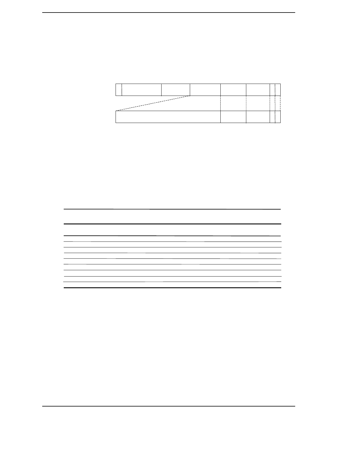
Chapter 4 System Support
Compaq Deskpro EN Series of Personal Computers
Desktop and Minitower Form Factors
Third Edition - September 1998
4-6
Figure 4-3 shows how the loading of 0CF8h results in a Type 0 configuration cycle on the PCI
bus. The Device Number (bits <15..11> determines which one of the AD31..11 lines is to be
asserted high for the IDSEL signal, which acts as a “chip select” function for the PCI device to be
configured.
Figure 4–3. Type 0 Configuration Cycle
Type 0 configuration cycles are used for configuring devices on PCI bus # 0. Type 1
configuration cycles (reg. 0CF8h bits <1,0> = 01b) are passed on to PCI bus # 1 (if present).
Table 4-3 shows the standard configuration of device numbers and IDSEL connections for
components and slots residing on a PCI bus.
Table 4–3. PCI Device Configuration Access
Table 4-3.
PCI Component Configuration Access
PCI Component Bus Device
No. [1] IDSEL
Wired to:
82443 (North Bridge) 0 0 AD11
AGP slot 1 0 AD16
USB 0 9 AD20
PCI Connector 1 (PCI slot 1) 0 13 AD24
PCI Connector 2 (PCI slot 2) 0 14 AD25
PCI Connector 3 (PCI slot 3) 0 15 AD26
PCI Connector 4 (PCI slot 4) 0 16 AD27
PCI Connector 5 (PCI slot 5) [2] 0 17 AD29
82371 (South Bridge) 0 20 AD31
NOTES
[1] CF8h bits <15..11>
[2] Minitower only.
The function number (CF8h, bits <10..8>) is used to select a particular function within a
multifunction device. Configurable functions present in system as shipped from the factory are
listed in Table 4-4.
AD31..0
w/Type 0
Config. Cycle
Reserved Device
Number
Function
Number
Register
Index
Bus
Number
3130 24 23 16 15 11 10 8 721 0
0 0
IDSEL (only one signal line asserted) Function
Number
Register
Index
31 11 10 8 721 0
Register 0CF8h
Results in:
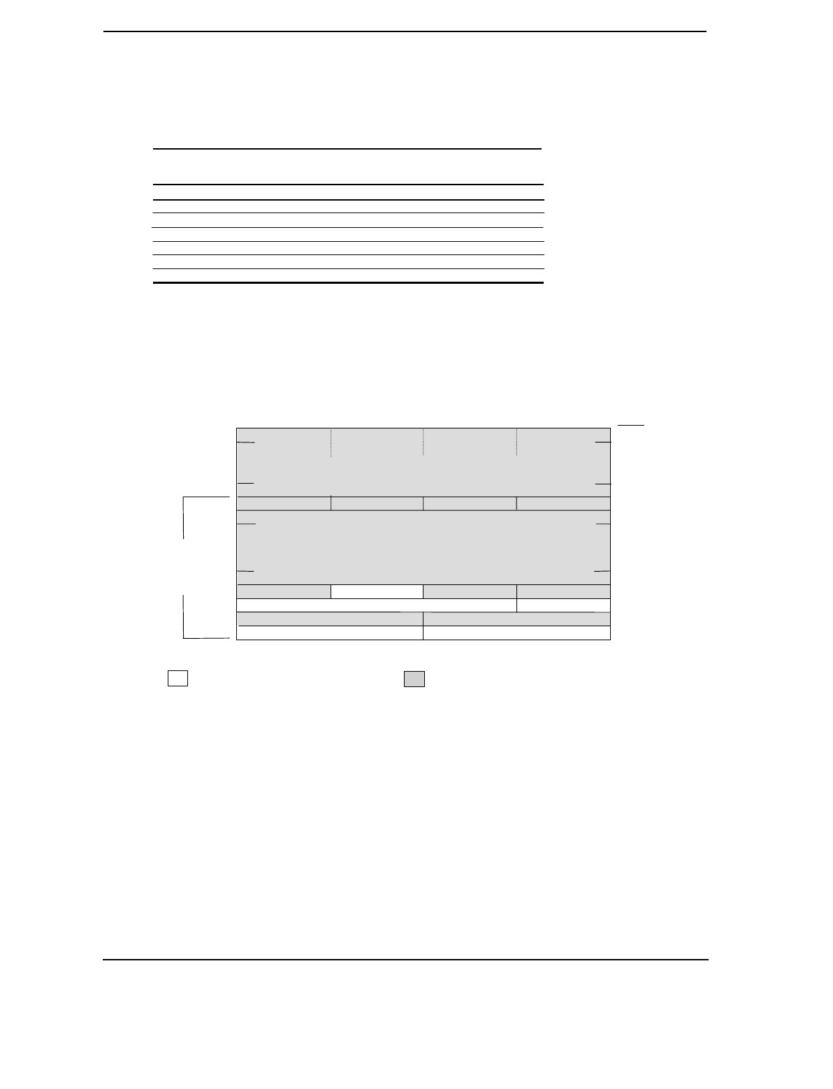
Technical Reference Guide
Compaq Deskpro EN Series of Personal Computers
Desktop and Minitower Form Factors
Third Edition - September 1998
4-7
Not required
Table 4–4. PCI Function Configuration Acces
Table 4-4.
PCI Function Configuration Access
PCI Function Device No. Function No.
Host/PCI Bridge (82443) 0 0
PCI/AGP Bridge (82443) 0 1
PCI/ISA Bridge (82371) 20 0
IDE Interface (82371) 20 1
USB Interface (82371) 20 2
Power Management Cntlr. (82371) 20 3
The register index (CF8h, bits <7..2>) identifies the 32-bit location within the configuration
space of the PCI device to be accessed. All PCI devices can contain up to 256 bytes of
configuration data (see Figure 4-4), of which the first 64 bytes comprise the configuration space
header.
Figure 4–4. PCI Configuration Space Map
Each PCI device is identified with a vender ID (assigned to the vender by the PCI Special Interest
Group) and a device ID (assigned by the vender). The device and vender IDs for the devices on
the system board are listed in Table 4-5.
00h
Configuration
Space
Header
Vender ID
Data required by PCI protocol
Base Address Registers and Exp. ROM Address
Register
Index
31
Cache Line Size
Latency Timer
Device ID
Command
Status
Revision IDClass Code
Header T
y
pe
BIST
Device-Specific Area
Interrupt LineInterrupt PinMin_GNTMin_Lat
24 23 16 15 8 7 0
04h
08h
0Ch
3Ch
40h
FCh

Chapter 4 System Support
Compaq Deskpro EN Series of Personal Computers
Desktop and Minitower Form Factors
Third Edition - September 1998
4-8
Table 4–5. System Board PCI Device Identification
Table 4-5.
System Board PCI Device Identification
PCI Device Vender ID Device ID
North Bridge (82443 PAC):
Host/PCI Bridge (Function 0)
PCI/AGP Bridge (Function 1) [1]
8086h
8086h
7190h
7191h
South Bridge (82371 PIIX4):
PCI/ISA Bridge (Function 0)
EIDE Controller (Function 1)
USB I/F (Function 2)
Power Mngmt. Cntlr (Function 3)
8086h
8086h
8086h
8086h
7110h
7111h
7112h
7113h
NOTES:
[1] Graphics Address Remapping Table (GART) used on all systems.
4.2.3.3 Special Cycles
There are two types of special cycles that may occur on the PCI bus. The first type is initiated by
the host and is used to perform the following functions: Shutdown, Flush, Halt, Write Back,
Flush Acknowledge, Branch Trace Message, and Stop/Grant. These cycles start like all other PCI
cycles and terminate with a master abort.
The second type of special cycle is initiated by writing to 0CF8h, Bus # = all 0s, Device = all 1s,
(Function # all 1s, and Register = all 0s) and 0CFCh to generate a Type 0 configuration cycle.
This Type 0 cycle, however, does not assert any of the IDSEL lines and therefore results in a
master abort with FFFFh returned to the microprocessor.
4.2.4 OPTION ROM MAPPING
During POST, the PCI bus is scanned for devices that contain their own specific firmware in
ROM. Such option ROM data, if detected, is loaded into system memory’s DOS compatibility
area (refer to the system memory map shown in chapter 3).

Technical Reference Guide
Compaq Deskpro EN Series of Personal Computers
Desktop and Minitower Form Factors
Third Edition - September 1998
4-9
4.2.5 PCI INTERRUPT MAPPING
The PCI bus provides for four interrupt signals; INTA-, INTB-, INTC-, and INTD-. These
signals may be generated by on-board PCI devices or by devices installed in the PCI slots. In
order to minimize latency, INTA-..INTD- signal routing from the interrupt controller of the
82371south bridge to PCI slots/devices is distributed evenly as shown below:
Interrupt Cntlr. PCI Slot 1 PCI Slot 2 PCI Slot 3 PCI Slot 4 PCI Slot 5 AGP Slot USB
INTA- INTA- INTD- INTC- INTB- INTD- -- --
INTB- INTB- INTA- INTD- INTC- INTA- -- --
INTC- INTC- INTB- INTA- INTD- INTB- INTA- --
INTD- INTD- INTC- INTB- INTA- INTC- INTB- INTD-
NOTE: PCI Slot 5 on minitower only.
Interrupts generated by PCI devices can be configured to share the standard AT (IRQn) interrupt
lines. Two devices that share a single PCI interrupt must also share the corresponding AT
interrupt.
4.2.6 PCI POWER MANAGEMENT SUPPORT
This system complies with the PCI Power Management Interface Specification (rev 1.0). The PCI
Power Management Enable (PME-) signal is supported by the 440BX chipset and allows
compliant PCI and AGP peripherals to initiate the power management routine.

Chapter 4 System Support
Compaq Deskpro EN Series of Personal Computers
Desktop and Minitower Form Factors
Third Edition - September 1998
4-10
4.2.7 PCI CONFIGURATION
PCI bus operations, especially those that involve ISA bus interaction, require the configuration of
certain parameters such as PCI IRQ routing, top of memory accessible by ISA, SMI generation,
and clock throttling characteristics. These parameters are handled by the PCI/ISA bridge
function (PCI function #0) of the South Bridge component and configured through the PCI
configuration space registers listed in Table 4-6. Configuration is provided by BIOS at power-up
but re-configurable by software.
Table 4–6. PCI/ISA Bridge Configuration Registers (82371, Function 0)
Table 4-6.
PCI/ISA Bridge Configuration Registers
(82371, Function 0)
PCI Config.
Addr. Register Reset
Value PCI Config.
Addr. Register Reset
Value
00, 01h Vender ID 8086h 63h PCI Interrupt Routing 80h
02, 03h Device ID 7111h 64h Serial Interrupt Control
04, 05h Command 69h Memory Map Control 02h
06, 07h Status 6A, 6Bh SERR-/PCI Cycle Retry 00h
08h Revision ID 76, 77h DMA Enable/Ch. Routing
09-0Bh Class Code 80h A12 Mask/X-Y Base Addr. 00h
0Eh Header Type 82h USB Passive Rel. Enable 00h
4Ch DMA Aliasing Control 00h 90, 91h DMA Channel Select 00h
4E-4Fh APIC/BIOS Control 0003h 92, 93h DMA 0-3 Base PTR 00h
60h PCI Interrupt Routing 80h 94, 95h DMA 4-7 Base PTR 00h
61h PCI Interrupt Routing 80h B0-B3h GPIO/Misc. Funct. Select 00h
62h PCI Interrupt Routing 80h CBh RTC/RAM Control 21h
NOTE: Assume unmarked locations/gaps as reserved.

Technical Reference Guide
Compaq Deskpro EN Series of Personal Computers
Desktop and Minitower Form Factors
Third Edition - September 1998
4-11
4.3 AGP BUS OVERVIEW
NOTE: This section describes the AGP bus in general. For a detailed description of
AGP bus operations refer to the AGP Interface Specification available at the following
AGP forum web site: http://www.agpforum.org/index.htm
The Accelerated Graphics Port (AGP) bus is specifically designed as an economical yet high-
performance interface for 3D graphics adapters. The AGP interface is designed to give graphics
adapters dedicated pipelined access to system memory for the purpose of off-loading texturing, z-
buffering, and alpha blending used in 3D graphics operations. By off-loading a large portion of
3D data to system memory the AGP graphics adapter only requires enough memory for frame
buffer (display image) refreshing.
4.3.1 BUS TRANSACTIONS
The operation of the AGP bus is based on the 66-MHz PCI specification but includes additional
mechanisms to increase bandwidth. During the configuration phase the AGP bus acts in
accordance with PCI protocol. Once operation with the AGP adapter involves graphics data
handling, AGP-defined protocols take effect. The AGP graphics adapter acts generally as the
AGP master, but can also behave as a “PCI” target during fast writes from the north bridge.
Key differences between the AGP interface and the PCI interface are as follows:
♦ Address phase and associated data transfer phase are disconnected transactions. Addressing
and data transferring occur as contiguous actions on the PCI bus. On the AGP bus a request
for data and the transfer of data may be separated by other operations.
♦ Commands on the AGP bus specify system memory accesses only. Unlike the PCI bus,
commands involving I/O and configuration are not required or allowed. The system memory
address space used in AGP operations is the same linear space used by PCI memory space
commands, but is further specified by the graphics address re-mapping table (GART) of the
north bridge component.
♦ Data transactions on the AGP bus involve eight bytes or multiples of eight bytes. The AGP
memory addressing protocol uses 8-byte boundaries as opposed to PCI’s 4-byte boundaries. If
a transfer of less than eight bytes is needed, the remaining bytes are filled with arbitrary data
that is discarded by the target.
♦ Pipelined requests are defined by length or size on the AGP bus. The PCI bus defines
transfer lengths with the FRAME- signal.
There are two basic types of transactions on the AGP bus: data requests (addressing) and data
transfers. These actions are separate from each other.
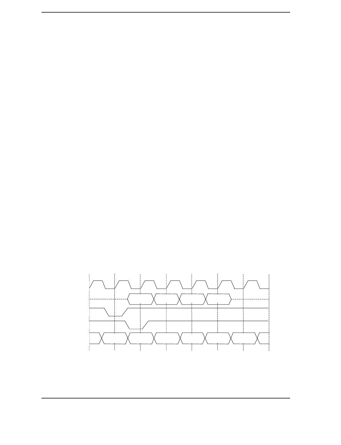
Chapter 4 System Support
Compaq Deskpro EN Series of Personal Computers
Desktop and Minitower Form Factors
Third Edition - September 1998
4-12
4.3.1.1 Data Request
Requesting data is accomplished in one of two ways; either multiplexed addressing (using the
AD lines for addressing/data) or demultiplexed (“sideband”) addressing (using the SBA lines for
addressing only and the AD lines for data only). Even though there are only eight SBA lines (as
opposed to the 32 AD lines) sideband addressing maximizes efficiency and throughput by
allowing the AD lines to be exclusively used for data transfers. Sideband addressing occurs at
the same rate (1X or 2X) as data transfers. The differences in rates will be discussed in the next
section describing data transfers. Note also that sideband addressing is limited to 48 bits (address
bits 48-63 are assumed zero).
The north bridge supports both SBA and AD addressing methods and all three data transfer
rates, but the method and rate is selected by the AGP graphics adapter.
4.3.1.2 Data Transfers
Data transfers use the AD lines and occur as the result of data requests described previously.
Each transaction resulting from a request involves at least eight bytes, requiring the 32 AD lines
to handle at least two transfers per request. The 443BX supports two transfer rates: 1X and 2X.
Regardless of the rate used, the speed of the bus clock is constant at 66 MHz. The following
subsections describe how the use of additional strobe signals makes possible higher transfer rates.
AGP 1X Transfers
In AGP 1X transfers the 66-MHz CLK signal is used to qualify the control and data signals.
Each 4-byte data transfer is synchronous with one CLK cycle so it takes two CLK cycles for a
minimum 8-byte transfer (Figure 4-5 shows two 8-byte transfers). The GNT- and TRDY- signals
retain their traditional PCI functions. The ST0..3 signals are used for priority encoding, with
“000” for low priority and “001” indicating high priority.
Figure 4–5. AGP 1X Data Transfer (Peak Transfer Rate: 266 MB/s)
T1 T2 T
3
T4 T5
T6
T7
TRDY
-
GNT
-
CLK
AD D1A
D2A
D2B
D1B
ST0..2 00x xxx xxx xxx xxx xxx
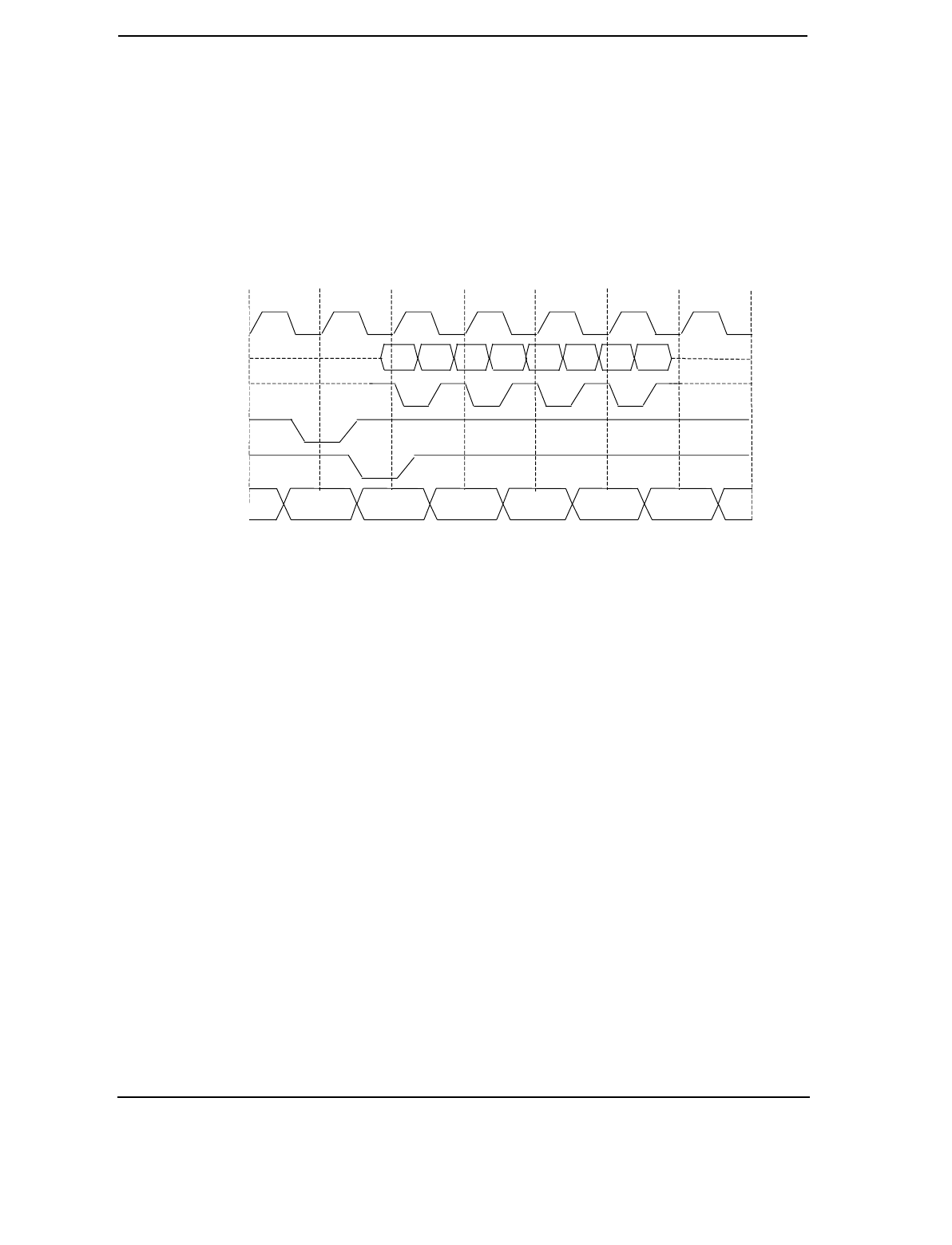
Technical Reference Guide
Compaq Deskpro EN Series of Personal Computers
Desktop and Minitower Form Factors
Third Edition - September 1998
4-13
AGP 2X Transfers
In AGP 2X transfers, clocking is basically the same as in 1X transfers except that the 66-MHz
CLK signal is used to qualify only the control signals. The data bytes are latched by an additional
strobe (AD_STBx) signal so that an 8-byte transfer occurs in one CLK cycle (Figure 4-6). The
first four bytes (DnA) are latched by the receiving agent on the falling edge of AD_STBx and the
second four bytes (DnB) are latched on the rising edge of AD_STBx.
Figure 4–6. AGP 2X Data Transfer (Peak Transfer Rate: 532 MB/s)
AGP 4X Transfers
The AGP 4X transfer rate allows sixteen bytes of data to be transferred in one clock cycle. As in
2X transfers the 66-MHz CLK signal is used only for qualifying control signals while strobe
signals are used to latch each 4-byte transfer on the AD lines. In Figure 4-7, 4-byte transfer D1A
is latched by the falling edge of AD_STBx while D1B is latched by the falling edge of
AD_STBx-.
AGP 4X Data Transfer (Peak Transfer Rate: 1064 MB/s)
T1 T2 T3 T4
AD_STBx
AD
D1A
D2A
D3A
D1B
D2B
D3B
D4A
D4B
CLK
AD_STBx-
00xxxx xxx
xxx
ST0..2
T1 T2 T3 T4 T5 T6 T7
TRDY-
GNT
-
CLK
AD_STBx
AD
D1A
D2A
D3A
D1B
D2B
D3B
D4A
D4B
ST0..2 00x xxx xxx xxx xxx xxx

Chapter 4 System Support
Compaq Deskpro EN Series of Personal Computers
Desktop and Minitower Form Factors
Third Edition - September 1998
4-14
4.3.2 AGP CONFIGURATION
AGP bus operations require the configuration of certain parameters involving system memory
access by the AGP graphics adapter. The AGP bus interface is configured as a PCI device
integrated within the north bridge (82443, device 1) component. The AGP function is, from the
PCI bus perspective, treated essentially as a PCI/PCI bridge and configured through PCI
configuration registers (Table 4-7). Configuration is accomplished by BIOS during POST.
NOTE: Configuration of the AGP bus interface involves functions 0 and 1 of the
82443. Function 0 registers (listed in Table 3-4) include functions that affect basic
control (GART) of the AGP.
Table 4–7. PCI/AGP Bridge Configuration Registers (82371, Function 1)
Table 4-7.
PCI/AGP Bridge Function Configuration Registers
(82443BX, Function 1)
PCI Config.
Addr. Register Reset
Value PCI Config.
Addr. Register Reset
Value
00, 01h Vender ID 8086h 1Bh Sec. Master Latency Timer 00h
02, 03h Device ID 7191h 1Ch I/O Base Address F0h
04, 05h Command 0000h 1Dh I/O Limit Address 00h
06, 07h Status 0220h 1E, 1Fh Sec. PCI/PCI Status 02A0h
08h Revision ID 00h 20, 21h Memory Base Address FFF0h
0A, 0Bh Class Code 0406h 22, 23h Memory Limit Address 0000h
0Eh Header Type 01h 24, 25h Prefetch Mem. Base Addr. FFF0h
18h Primary Bus Number 00h 26, 27h Prefetch Mem. Limit Addr. 0000h
19h Secondary Bus Number 00h 3Eh PCI/PCI Bridge Control 80h
1Ah Subordinate Bus Number 00h 3F-FFh Reserved 00h
NOTE:
Assume unmarked locations/gaps as reserved. Refer to Intel documentation for detailed
register descriptions.
The AGP graphics adapter (actually its resident controller) is configured as a standard PCI
device.
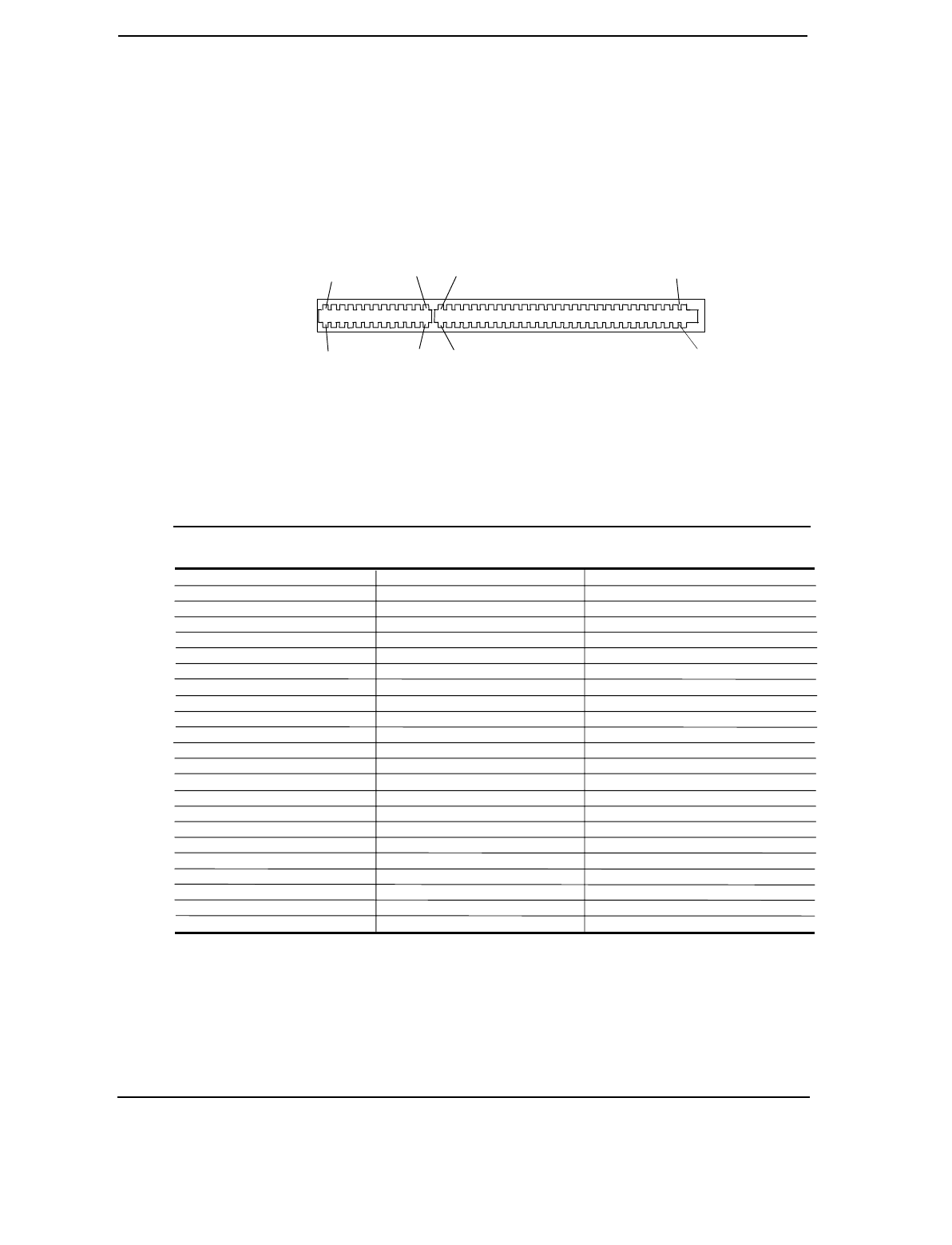
Technical Reference Guide
Compaq Deskpro EN Series of Personal Computers
Desktop and Minitower Form Factors
Third Edition - September 1998
4-15
4.3.3 AGP CONNECTOR
Figure 4–7. AGP Bus Connector
Table 4–8. AGP Bus Connector Pinout
Table 4-8.
AGP Bus Connector Pinout
Pin A Signal B Signal Pin A Signal B Signal Pin A Signal B Signal
01 +12 VDC OVRCNT- 23 (Key) (Key) 45 VDD3 VDD3
02 RSVD VDD 24 (Key) (Key) 46 TRDY- DEVSEL-
03 GND VDD 25 (Key) (Key) 47 STOP- NC
04 USBN USBF 26 PAD30 PAD31 48 PME- PERR-
05 GND GND 27 PAD28 PAD29 49 GND GND
06 INTA- INTB- 28 VDD3 VDD3 50 PAR SERR-
07 RESET CLK 29 PAD26 PAD27 51 PAD15 CBE1-
08 GNT- REQ- 30 PAD24 PAD25 52 NC NC
09 VDD3 VDD3 31 GND GND 53 PAD13 PAD14
10 ST1 ST0 32 RSVD AD_STB1 54 PAD11 PAD12
11 RSVD ST2 33 CBE3- PAD23 55 GND GND
12 PIPE- RBF- 34 NC NC 56 PAD09 PAD10
13 GND GND 35 PAD22 PAD21 57 CBE0- PAD08
14 RSVD RSVD 36 PAD20 PAD19 58 NC NC
15 SBA1 SBA0 37 GND GND 59 RSVD AD_STB0
16 VDD3 VDD3 38 PAD18 PAD17 60 PAD06 PAD07
17 SBA3 SBA2 39 PAD16 CBE2- 61 GND GND
18 RSVD SB_STB 40 NC NC 62 PAD04 PAD05
19 GND GND 41 FRAME- IRDY- 63 PAD02 PAD03
20 SBA5 SBA4 42 RSVD RSVD 64 NC NC
21 SBA7 DBA6 43 GND GND 65 PAD00 PAD01
22 (Key) (Key) 44 RSVD RSVD 66 RSVD RSVD
B94
A94 B66
A66
A1
B1
A21 A26
B21 B26
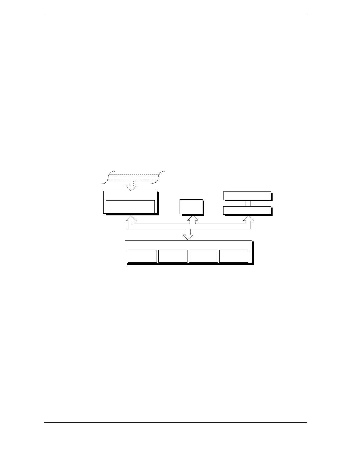
Chapter 4 System Support
Compaq Deskpro EN Series of Personal Computers
Desktop and Minitower Form Factors
Third Edition - September 1998
4-16
4.4 ISA BUS OVERVIEW
NOTE: This section describes the ISA bus in general and highlights bus
implementation in this particular system. For detailed information regarding ISA bus
operation, refer to the Compaq Extended Industry Standard Architecture (EISA)
Technical Reference Guide.
The industry standard architecture (ISA) bus provides an 8-/16-bit path for standard I/O
peripherals as well as for optional devices that can be installed in the ISA expansion slots. Figure
4-8 shows the key functions and devices that reside on the ISA bus.
Figure 4–8. ISA Bus Block Diagram
8-/16-Bit ISA Bus
BIOS
ROM
PCI Bus
PC 87307B I/O Controller
Diskette
I/F
Keyboard/
Mouse I/F
Serial
I/F
(
2
)
Parallel
I/F
ISA Connector 2
ISA Connector 1
66-MHz slot 1 system only
82371 South Bridge
PCI/ISA
Brid
g
e Function
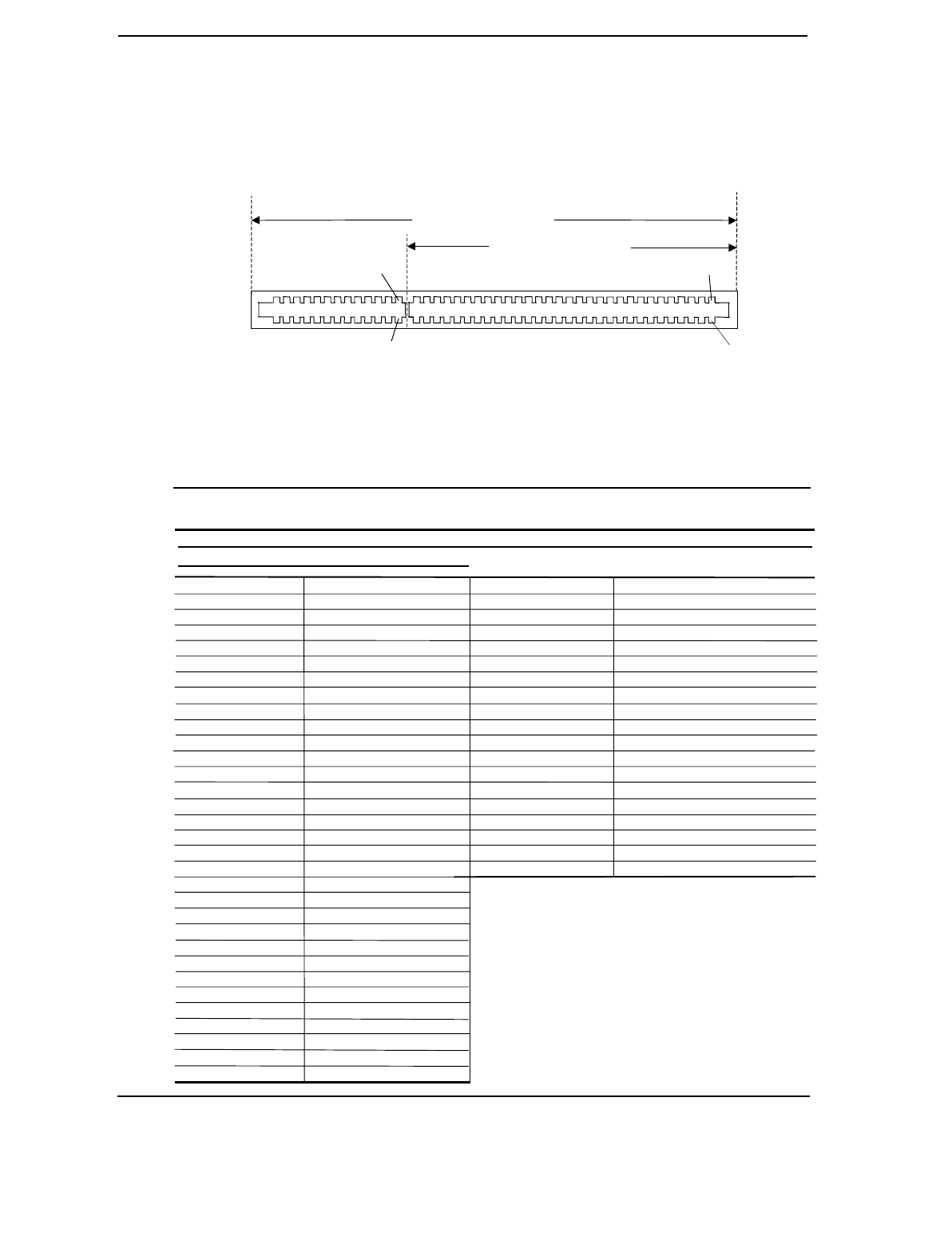
Technical Reference Guide
Compaq Deskpro EN Series of Personal Computers
Desktop and Minitower Form Factors
Third Edition - September 1998
4-17
4.4.1 ISA CONNECTOR
Figure 4–9. ISA Expansion Connector
Table 4–9. ISA Expansion Connector Pinout
Table 4-9.
ISA Expansion Connector Pinout
Pin Signal Pin Signal Pin Signal Pin Signal
B01 GND A01 I/O CHK- D01 M16- C01 SBHE-
B02 RESDRV A02 SD7 D02 I/O16- C02 LA23
B03 +5 VDC A03 SD6 D03 IRQ10 C03 LA22
B04 IRQ9 A04 SD5 D04 IRQ11 C04 LA21
B05 -5 VDC A05 SD4 D05 IRQ12 C05 LA20
B06 DRQ2 A06 SD3 D06 IRQ15 C06 LA19
B07 -12 VDC A07 SD2 D07 IRQ14 C07 LA18
B08 NOWS- A08 SD1 D08 DAK0- C08 LA17
B09 +12 VDC A09 SD0 D09 DRQ0 C09 MRDC-
B10 GND A10 BUSRDY D10 DAK5- C10 MWTC-
B11 SMWTC- A11 DMA D11 DRQ5 C11 SD8
B12 SMRDC- A12 SA19 D12 DAK6- C12 SD9
B13 IOWC- A13 SA18 D13 DRQ6 C13 SD10
B14 IORC- A14 SA17 D14 DAK7- C14 SD11
B15 DAK3- A15 SA16 D15 DRQ7 C15 SD12
B16 DRQ3 A16 SA15 D16 +5 VDC C16 SD13
B17 DAK1 A17 SA14 D17 GRAB- C17 SD14
B18 DRQ1 A18 SA13 D18 GND C18 SD15
B19 REFRESH- A19 SA12
B20 BCLK A20 SA11
B21 IRQ7 A21 SA10
B22 IRQ6 A22 SA9
B23 IRQ5 A23 SA8
B24 IRQ4 A24 SA7
B25 IRQ3 A25 SA6
B26 DAK2- A26 SA5
B27 T-C A27 SA4
B28 BALE A28 SA3
B29 +5 VDC A29 SA2
B30 OSC A30 SA1
B31 GND A31 SA0
A1
B1D1
C1
8-Bit ISA Connection
16-Bit ISA Connection
8-Bit ISA Interface
16-Bit ISA Interface

Chapter 4 System Support
Compaq Deskpro EN Series of Personal Computers
Desktop and Minitower Form Factors
Third Edition - September 1998
4-18
4.4.2 ISA BUS TRANSACTIONS
The ISA bus supports 8- and 16-bit transfers at an 8-MHz rate. Devices limited to 8-bit transfers
use the lower byte portion (data lines 7..0) while 16-bit transfers use the full bandwidth (data
lines 15..0). Addressing is handled by two classifications of address signals: latched and
latchable. Latched address signals ( SA19..0) select the specific byte within the 1-MB section of
memory defined by address lines LA23..17. Latchable address lines (LA23..17) provide a longer
setup time for pre-chip selection or for pre-address decoding for high-speed memory and allow
access to up to 16 megabytes of physical memory on the ISA bus. The SA19..17 signals have the
same values as the LA19..17 signals for all memory cycles. The I/O cycles use only the SA15..0
signals.
The key control signals are described as follows:
♦ MRDC- (Memory Read Cycle): MRDC- is active on all ISA memory reads accessing
memory from 000000h to FFFFFFh.
♦ SMEMR- (System Memory Read): SMEMR- is asserted by the PCI/ISA bridge to request an
ISA memory device to drive data onto the data lines for accesses below one megabyte.
SMEMR- is a delayed version of MRDC-.
♦ MWTC- (Memory Write Cycle): MWTC- is active on all ISA memory write cycles accessing
memory from 000000h to FFFFFFh.
♦ SMEMW- (System Memory Write): SMEMW- is asserted by the PCI/ISA bridge to request
an ISA memory device to accept data from the data lines for access below one megabyte.
SMEMW- is a delayed version of MWTC-.
♦ IORC- (Input/Output Read Cycle): IORC- commands an ISA I/O device to drive data onto
the data lines.
♦ IOWC- (Input/Output Write Cycle): IOWC- commands an ISA I/O device to accept data
from the data lines.
♦ SBHE- (System Byte High Enable): SBHE- indicates that a byte is being transferred on the
upper half (D15..8) of the data lines.
♦ SA0- (System Address Bit <0>): This bit is the complement of SBHE- and indicates that a
byte is being transferred on the lower half (D7..0) of the data lines.
♦ M16- (16-bit Memory Cycle): M16- is asserted by 16-bit ISA devices to indicate 16-bit
memory cycle capability.
♦ IO16- (16-bit I/O Cycle): IO16- is asserted by 16-bit ISA devices to indicate 16-bit I/O cycle
transfer capability.
If the address on the SA lines is above one megabyte, SMRDC- and SMWTC- will not be active.
The MRDC- and MWTC- signals are active for memory accesses up to 16 megabytes and can be
used by any device that uses the full 16-bit ISA bus. To request a 16-bit transfer, a device asserts
either the M16- (memory) or IO16- (I/O) signal when the device is addressed.
When another device (such as a DMA device or another bus master) takes control of the ISA, the
Bus Address Latch Enable (BALE) signal is held active for the duration of the operation. As a
result, signals LA23..17 are always enabled and must be held stable for the duration of each bus
cycle.

Technical Reference Guide
Compaq Deskpro EN Series of Personal Computers
Desktop and Minitower Form Factors
Third Edition - September 1998
4-19
When the address changes, devices on the bus may decode the latchable address (LA23..17) lines
and then latch them. This arrangement allows devices to decode chip selects and M16- before the
next cycle actually begins.
The following guidelines apply to optional ISA devices installed in the system:
♦ On bus lines that can be driven by a controller board, the driver should be able to sink a
minimum of 20 ma at 0.5 VDC and source 2 ma at 3.75 VDC.
♦ On bus lines that are driven in the low direction only (open collector), the driver should be
able to sink 20 ma at 0.5 VDC.
♦ The load on any logic line from a single bus slot should not exceed 2.0 ma in the low state
(at 0.5 VDC) or 0.1 ma in the high state (at 3.75 VDC).
♦ The logic-high voltage at the bus ranges from 3.75 VDC to 5.5 VDC. The logic low voltage
ranges from 0 VDC to 0.8 VDC.

Chapter 4 System Support
Compaq Deskpro EN Series of Personal Computers
Desktop and Minitower Form Factors
Third Edition - September 1998
4-20
4.4.3 DIRECT MEMORY ACCESS
Direct Memory Access (DMA) is a method by which an ISA device accesses system memory
without involving the microprocessor. DMA is normally used to transfer blocks of data to or from
an ISA I/O device. DMA reduces the amount of CPU interactions with memory, freeing the CPU
for other processing tasks.
NOTE: This section describes DMA in general. For detailed information regarding
DMA operation, refer to the Compaq Extended Industry Standard Architecture (EISA)
Technical Reference Guide. Note, however, that EISA enhancements as described in the
referenced document are not supported in this (ISA only) system.
The South Bridge component includes the equivalent of two 8237 DMA controllers cascaded
together to provide eight DMA channels. Table 4-10 lists the default configuration of the DMA
channels.
Table 4–10. Default DMA Channel Assignments
Table 4-10.
Default DMA Channel Assignments
DMA Channel Device ID
Controller 1 (byte transfers)
0
1
2
3
Spare & ISA conn. pins D8, D9
Audio subsystem & ISA conn. pins B17, B18
Diskette drive & ISA conn. pins B6, B26
ECP LPT1 & ISA conn. pins B15, B16
Controller 2 (word transfers)
4
5
6
7
Cascade for controller 1
Spare & ISA conn. pins D10, D11
Spare & ISA conn. pins D12, D13
Spare & ISA conn. pins. D14, D15
All channels in DMA controller 1 operate at a higher priority than those in controller 2. Note
that channel 4 is not available for use other than its cascading function for controller 1. The
DMA controller 2 can transfer words only on an even address boundary. The DMA controller
and page register define a 24-bit address that allows data transfers within the address space of
the CPU. The DMA controllers operate at 8 MHz.
The DMA logic is accessed through two types of I/O mapped registers; page registers and
controller registers. The mapping is the same regardless of the support chipset used.

Technical Reference Guide
Compaq Deskpro EN Series of Personal Computers
Desktop and Minitower Form Factors
Third Edition - September 1998
4-21
4.4.3.1 Page Registers
The DMA page register contains the eight most significant bits of the 24-bit address and works
in conjunction with the DMA controllers to define the complete (24-bit)address for the DMA
channels. Table 4-11 lists the page register port addresses.
Table 4–11. DMA Page Register Addresses
Table 4-11.
DMA Page Register Addresses
DMA Channel Page Register I/O Port
Controller 1 (byte transfers)
Ch 0
Ch 1
Ch 2
Ch 3
087h
083h
081h
082h
Controller 2 (word transfers)
Ch 4
Ch 5
Ch 6
Ch 7
n/a
08Bh
089h
08Ah
Refresh 08Fh [see note]
NOTE:
The DMA memory page register for the refresh channel must be
programmed with 00h for proper operation.
The memory address is derived as follows:
24-Bit Address - Controller 1 (Byte Transfers)
8-Bit Page Register 8-Bit DMA Controller
A23..A16 A15..A00
24-Bit Address - Controller 2 (Word Transfers)
8-Bit Page Register 16-Bit DMA Controller
A23..A17 A16..A01, (A00 = 0)
Note that address line A16 from the DMA memory page register is disabled when DMA
controller 2 is selected. Address line A00 is not connected to DMA controller 2 and is always 0
when word-length transfers are selected.
By not connecting A00, the following applies:
♦ The size of the the block of data that can be moved or addressed is measured in 16-bits
(words) rather than 8-bits (bytes).
♦ The words must always be addressed on an even boundary.
DMA controller 1 can move up to 64 Kbytes of data per DMA transfer. DMA controller 2 can
move up to 64 Kwords (128 Kbytes) of data per DMA transfer. Word DMA operations are only
possible between 16-bit memory and 16-bit peripherals.

Chapter 4 System Support
Compaq Deskpro EN Series of Personal Computers
Desktop and Minitower Form Factors
Third Edition - September 1998
4-22
The RAM refresh is designed to perform a memory read cycle on each of the 512 row addresses
in the DRAM memory space. Refresh operations are used to refresh memory on the 32-bit
memory bus and the ISA bus. The refresh address is provided on lines SA00 through SA08.
Address lines LA23..17, SA18,19 are driven low.
The remaining address lines are in an undefined state during the refresh cycle. The refresh
operations are driven by a 69.799-KHz clock generated by Interval Timer 1, Counter 1. The
refresh rate is 128 refresh cycles in 2.038 ms.
4.4.3.2 DMA Controller Registers
Table 4-12 lists the DMA Controller Registers and their I/O port addresses. Note that there is a
set of registers for each DMA controller.
Table 4–12. DMA Controller Registers
Table 4-12.
DMA Controller Registers
Register Controller 1 Controller 2 R/W
Status 008h 0D0h R
Command 008h 0D0h W
Mode 00Bh 0D6h W
Write Single Mask Bit 00Ah 0D4h W
Write All Mask Bits 00Fh 0DEh W
Software DRQx Request 009h 0D2h W
Base and Current Address - Ch 0 000h 0C0h W
Current Address - Ch 0 000h 0C0h R
Base and Current Word Count - Ch 0 001h 0C2h W
Current Word Count - Ch 0 001h 0C2h R
Base and Current Address - Ch 1 002h 0C4h W
Current Address - Ch 1 002h 0C4h R
Base and Current Word Count - Ch 1 003h 0C6h W
Current Word Count - Ch 1 003h 0C6h R
Base and Current Address - Ch 2 004h 0C8h W
Current Address - Ch 2 004h 0C8h R
Base and Current Word Count - Ch 2 005h 0CAh W
Current Word Count - Ch 2 005h 0CAh R
Base and Current Address - Ch 3 006h 0CCh W
Current Address - Ch 3 006h 0CCh R
Base and Current Word Count - Ch 3 007h 0CEh W
Current Word Count - Ch 3 007h 0CEh R
Temporary (Command) 00Dh 0DAh R
Reset Pointer Flip-Flop (Command) 00Ch 0D8h W
Master Reset (Command) 00Dh 0DAh W
Reset Mask Register (Command) 00Eh 0DCh W
NOTE:
For a detailed description of the DMA registers, refer to the
Compaq EISA Technical Reference Guide
.
Technical Reference Guide
Compaq Deskpro EN Series of Personal Computers
Desktop and Minitower Form Factors
Third Edition - September 1998
4-23
4.4.4 INTERRUPTS
The microprocessor uses two types of interrupts; maskable and nonmaskable. A maskable
interrupt can be enabled or disabled within the microprocessor by the use of the STI and CLI
instructions. A nonmaskable interrupt cannot be masked off within the microprocessor but may
be inhibited by hardware or software means external to the microprocessor.
4.4.4.1 Maskable Interrupts
The maskable interrupt is a hardware-generated signal used by peripheral functions within the
system to get the attention of the microprocessor. Peripheral functions produce a unique INTA-D
(PCI) or IRQ0-15 (ISA) signal that is routed to interrupt processing logic that asserts the
interrupt (INTR) input to the microprocessor. The microprocessor halts execution to determine
the source of the interrupt and then services the peripheral as appropriate.
Figure 4–10. Maskable Interrupt Processing, Block Diagram
The South Bridge component, which includes the equivalent of two 8259 interrupt controllers
cascaded together, handles the standard AT-type (ISA) interrupt signals (IRQn). The South
Bridge also receives the PCI interrupt signals (PINTA-..PINTD-) from PCI devices. The PCI
interrupts can be configured by PCI Configuration Registers 60h..63h to share the standard ISA
interrupts (IRQn). The power-up default configuration has the PIRQn disabled. Table 4-13 lists
the standard source configuration for maskable interrupts and their priorities. If more than one
interrupt is pending, the highest priority (lowest number) is processed first.
Interrupt
Cntlr. 1
Interrupt
Cntlr. 2
IRQ2
IRQ1,3..7
IRQ9..12,
14,15
PCI IRQ
Routing
INTA-..D-
IRQ1,3..7,
9..12,
14,15
South Brid
g
e Component
INTR Microprocessor
ISA Peripherals
& SM Functions
PCI Peripherals

Chapter 4 System Support
Compaq Deskpro EN Series of Personal Computers
Desktop and Minitower Form Factors
Third Edition - September 1998
4-24
Table 4–13. Maskable Interrupt Priorities and Assignments
Table 4-13.
Maskable Interrupt Priorities and Assignments
Priority Signal Label Source (Typical)
1 IRQ0 Interval timer 1, counter 0
2 IRQ1 Keyboard
3 IRQ8- Real-time clock
4 IRQ9 Spare and ISA connector pin B04
5 IRQ10 Spare and ISA connector pin D03
6 IRQ11 Spare and ISA connector pin D04
7 IRQ12 Mouse and ISA connector pin D05
8 IRQ13 Coprocessor (math)
9 IRQ14 IDE primary I/F and ISA connector pin D07
10 IRQ15 IDE secondary I/F and ISA connector pin D06
11 IRQ3 Serial port (COM2) and ISA connector pin B25
12 IRQ4 Serial port (COM1) and ISA connector pin B24
13 IRQ5 Audio subsystem and ISA connector pin B23
14 IRQ6 Diskette drive controller and ISA connector pin B22
15 IRQ7 Parallel port (LPT1)
-- IRQ2 NOT AVAILABLE (Cascade from interrupt controller 2)
Interrupts generated by PCI devices can be configured to share the standard AT (IRQn) interrupt
lines. Refer to section 4.2.5 “PCI Interrupt Mapping” for information on PCI interrupts.
Maskable Interrupt processing is controlled and monitored through standard AT-type I/O-
mapped registers. These registers are listed in Table 4-14.
Table 4–14. Maskable Interrupt Control Registers
Table 4-14.
Maskable Interrupt Control Registers
I/O Port Register
020h Base Address, Int. Cntlr. 1
021h Initialization Command Word 2-4, Int. Cntlr. 1
0A0h Base Address, Int. Cntlr. 2
0A1h Initialization Command Word 2-4, Int. Cntlr. 2
The initialization and operation of the interrupt control registers follows standard AT-type
protocol.
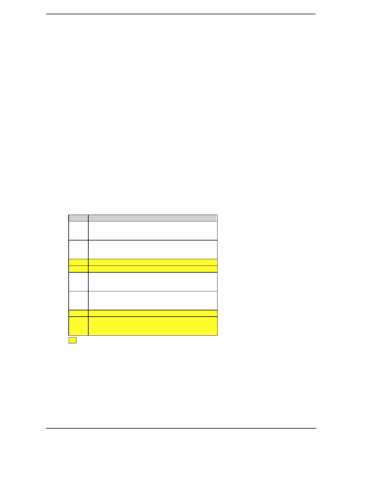
Technical Reference Guide
Compaq Deskpro EN Series of Personal Computers
Desktop and Minitower Form Factors
Third Edition - September 1998
4-25
4.4.4.2 Non-Maskable Interrupts
Non-maskable interrupts cannot be masked (inhibited) within the microprocessor itself but may
be maskable by software using logic external to the microprocessor. There are two non-maskable
interrupt signals: the NMI- and the SMI-. These signals have service priority over all maskable
interrupts, with the SMI- having top priority over all interrupts including the NMI-.
NMI- Generation
The Non-Maskable Interrupt (NMI-) signal can be generated by one of the following actions:
♦ Parity errors detected on the ISA bus (activating IOCHK-).
♦ Parity errors detected on a PCI bus (activating SERR- or PERR-).
♦ Microprocessor internal error (activating IERRA or IERRB)
The IOCHK-, SERR-, and PERR- signals are routed through the south bridge component, which
in turn activates the NMI to the microprocessor.
The NMI Status Register at I/O port 061h contains NMI source and status data as follows:
NMI Status Register 61h
Bit Function
7 NMI Status:
0 = No NMI from system board parity error.
1 = NMI requested, read only
6 IOCHK- NMI:
0 = No NMI from IOCHK-
1 = IOCHK- is active (low), NMI requested, read only
5 Interval Timer 1, Counter 2 (Speaker) Status
4 Refresh Indicator (toggles with every refresh)
3 IOCHK- NMI Enable/Disable:
0 = NMI from IOCHK- enabled
1 = NMI from IOCHK- disabled and cleared (R/W)
2 System Board Parity Error (PERR/SERR) NMI Enable:
0 = Parity error NMI enabled
1 = Parity error NMI disabled and cleared (R/W)
1 Speaker Data (R/W)
0 Inteval Timer 1, Counter 2 Gate Signal (R/W)
0 = Counter 2 disabled
1 = Counter 2 enabled
After the active NMI has been processed, status bits <7> or <6> are cleared by pulsing bits <2>
or <3> respectively.
The NMI Enable Register (070h, <7>) is used to enable/disable the NMI signal. Writing 80h to
this register masks generation of the NMI-. Note that the lower six bits of register at I/O port 70h
affect RTC operation and should be considered when changing NMI- generation status.
Functions not related to NMI activity.

Chapter 4 System Support
Compaq Deskpro EN Series of Personal Computers
Desktop and Minitower Form Factors
Third Edition - September 1998
4-26
SMI- Generation
The SMI- (System Management Interrupt) is typically used for power management functions.
When power management is enabled, inactivity timers are monitored. When a timer times out,
SMI- is asserted and invokes the microprocessor’s SMI handler. The SMI- handler works with
the APM BIOS to service the SMI- according to the cause of the timeout.
Although the SMI- is primarily used for power managment the interrupt is also employed for the
QuickLock/QuickBlank functions as well.

Technical Reference Guide
Compaq Deskpro EN Series of Personal Computers
Desktop and Minitower Form Factors
Third Edition - September 1998
4-27
4.4.5 INTERVAL TIMER
The interval timer generates pulses at software (programmable) intervals. A 8254-compatible
timer is integrated into the South Bridge chip. The timer function provides three counters, the
functions of which are listed in Table 4-15.
Table 4–15. Interval Timer Functions
Table 4-15.
Interval Timer Functions
Counter Function Gate Clock In Clock Out
0 System Clock Always on 1.193 MHz IRQ0
1 Refresh Always on 1.193 MHz Refresh Req.
2 Speaker Tone Port 61, bit<0> 1.193 MHz Speaker Input
The interval timer is controlled through the I/O mapped registers listed in Table 4-16.
Table 4–16. Interval Timer Control Registers
Table 4-16.
Interval Timer Control Registers
I/O Port Register
040h Read or write value, counter 0
041h Read or write value, counter 1
042h Read or write value, counter 2
043h Control Word
Interval timer operation follows standard AT-type protocol. For a detailed description of timer
registers and operation, refer to the Compaq Extended Industry Standard Architecture Expansion
Bus Technical Reference Guide.
4.4.6 ISA CONFIGURATION
The working relationship between the PCI and ISA buses requires that certain parameters be
configured. The PC/ISA bridge function of the South Bridge component includes configuration
registers to set parameters such as PCI IRQ routing and top-of-memory available to ISA/DMA
devices. These parameters are programmed by BIOS during power-up, using registers listed
previously in Table 4-6.

Chapter 4 System Support
Compaq Deskpro EN Series of Personal Computers
Desktop and Minitower Form Factors
Third Edition - September 1998
4-28
4.5 SYSTEM CLOCK DISTRIBUTION
The system uses a Cypress CY2280 or compatible part for generation of most clock signals.
Table 4-17 lists the system board clock signals and how they are distributed.
Table 4–17. Clock Generation and Distribution
Table 4-17.
Clock Generation and Distribution
Frequncy/Signal Source Destination
66, 100 MHz
(CPUCLK) [1]
CY2280 Processor, 82443 N. Bridge
66 MHz North Bridge AGP Slot
48 MHz “ 82371 S. Bridge, 87307 I/O Cntlr.
33 MHz (PCICLK) “ PCI Slots, 82371 S. Bridge
14.31818 MHz Crystal W48C67
14.31818 MHz CY2280 South Bridge, ISA slots
8.33 MHz (BCLK) South Bridge ISA slots
32.77 KHz Crystal South Bridge
NOTE:
[1] Depending on processor speed (refer to
Chapter 3, “Processor/Memory Subsystem”).
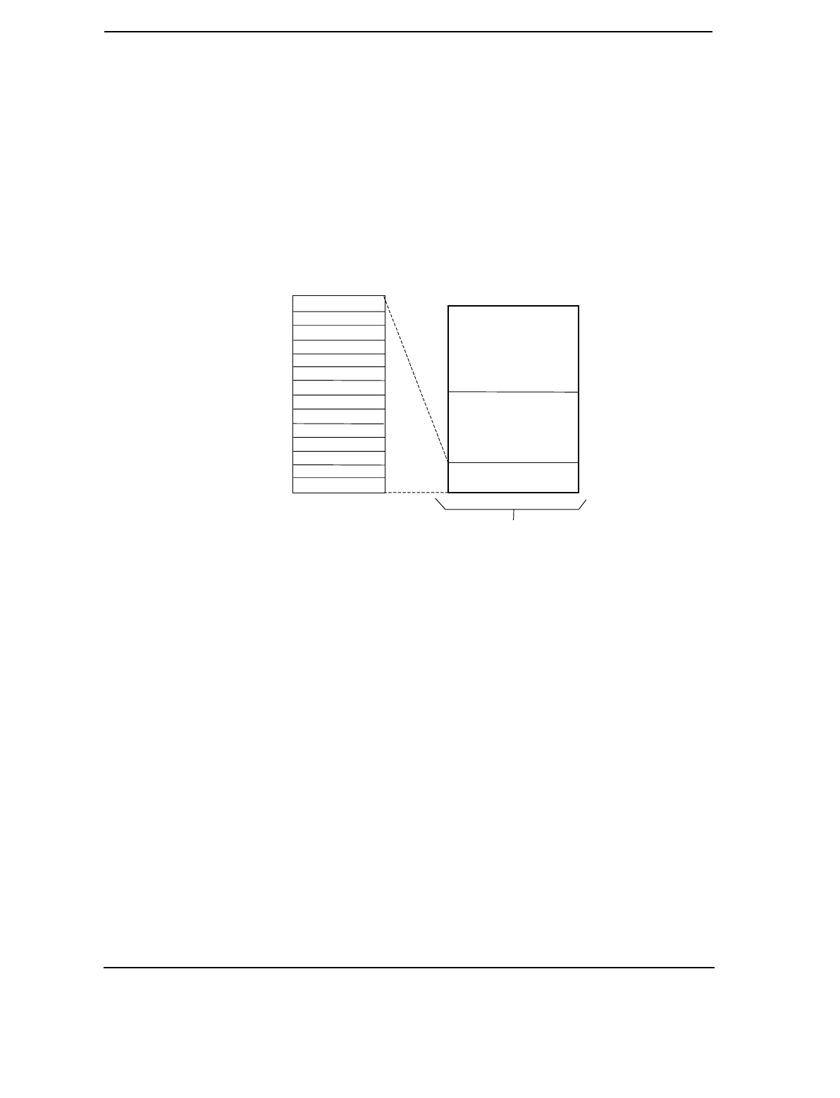
Technical Reference Guide
Compaq Deskpro EN Series of Personal Computers
Desktop and Minitower Form Factors
Third Edition - September 1998
4-29
4.6 REAL-TIME CLOCK AND CONFIGURATION MEMORY
The Real-time clock (RTC) and configuration memory functions are provided by the PC87307
I/O controller. The RTC uses the first 14 of 256 bytes of configuration memory and is
MC146818-compatible. As shown in the following figure, the 87307 controller provides 256
bytes of configuration memory, divided into two 128-byte banks. The RTC/configuration memory
can be accessed using conventional OUT and IN assembly language instructions using I/O ports
70h/71h, although the suggested method is to use the INT15 AX=E823h BIOS call.
Figure 4–11. Configuration Memory Map
A lithium 3-VDC battery is used for maintaining the RTC and configuration memory while the
system is powered down. During system operation a wire-Ored circuit allows the RTC and
configuration memory to draw power from the power supply.
The battery is located in a battery holder on the system board and has a life expectancy of four to
eight years. When the battery has expired it is replaced with a Renata CR2032 or equivalent 3-
VDC lithium battery.
RTC Area
(14 bytes)
Lower Config.
Memory Area
(114 bytes)
Upper Config.
Memory Area
(128 bytes)
00h
0Dh
0Eh
80h
FFh
7Fh
Seconds (Timer)
Minutes (Timer)
Seconds (Alarm)
Hours (Alarm)
Hours (Timer)
Minutes (Alarm)
Day of Week
Date of Month
Month
Year
Register A
Register B
Register C
Register D
00h
0Bh
01h
02h
03h
04h
05h
06h
07h
08h
09h
0Ah
0Dh
0Ch
87307
CMOS

Chapter 4 System Support
Compaq Deskpro EN Series of Personal Computers
Desktop and Minitower Form Factors
Third Edition - September 1998
4-30
Table 4-18 lists the mapping of the configuration memory. Locations 00h-3Fh may be accessed
using OUT/IN assembly language instructions or BIOS function INT15, AX=E823h. All other
locations should be accessed using the INT15, AX=E845h function (refer to Chapter 8 for BIOS
function descriptions).
Table 4–18. Configuration Memory (CMOS) Map
Table 4-18.
Configuration Memory (CMOS) Map
Location Function Location Function
00-0Dh Real-time clock 41h-44h Hood Removal Time Stamp
0Eh Diagnostic status 45h Keyboard snoop byte
0Fh System reset code 46h Diskette drive status
10h Diskette drive type 47h Last IPL device
11h Reserved 48h-4Bh IPL priority
12h Hard drive type 4Ch-4Fh BVC priority
13h Security functions 51h ECC DIMM status
14h Equipment installed 52h Board revision (from boot block)
15h Base memory size, low byte/KB 53h SWSMI command
16h Base memory size, high byte/KB 54h SWSMI data
17h Extended memory, low byte/KB 55h APM command
18h Extended memory, high byte/KB 56h Erase-Ease keyboard byte
19h Hard drive 1, primary controller 57h-76H Saved CMOS location 10h-2Fh
1Ah Hard drive 2, primary controller 77h-7Fh Administrator password
1Bh Hard drive 1, secondary controller 80h ECMOS diagnostic byte
1Ch Hard drive 2, secondary controller 81h-82h Total super ext. memory tested good
1Dh Enhanced hard drive support 83h Microprocessor chip ID
1Eh Reserved 84h Microprocessor chip revision
1Fh Power management functions 85h Hood removal status byte
24h System board ID 86h Fast boot date
25h System architecture data 87h Fast boot status byte
26h Auxiliary peripheral configuration 8Dh-8Fh POST error logging
27h Speed control external drive 90h-91h Total super extended memory configured
28h Expanded/base mem. size, IRQ12 92h Miscellaneous configuration byte
29h Miscellaneous configuration 93h Miscellaneous PCI features
2Ah Hard drive timeout 94h ROM flash/power button status
2Bh System inactivity timeout 97h Asset/test prompt byte
2Ch Monitor timeout, Num Lock Cntrl 9Bh Ultra-33 DMA enable byte
2Dh Additional flags 9Ch Mode-2 Configuration
2Eh-2Fh Checksum of locations 10h-2Dh 9Dh ESS audio configuration
30h-31h Total extended memory tested 9Eh ECP DMA configuration
32h Century 9Fh-AFh Serial number
33h Miscellaneous flags set by BIOS B0h-C3h Custom drive types 65, 66, 68, 15
34h International language C7h Serial port 1 address
35h APM status flags C8h Serial port 2 address
36h ECC POST test single bit C9h COM1/COM2 port configuration
37h-3Fh Power-on password DEh-DFh Checksum of locations 90h to DDh
40h Miscellaneous Disk Bits E0h-FFh Client Management error log
NOTE:
Assume unmarked gaps are reserved.
The contents of configuration memory (including the password) can be cleared by the following
procedure:
1. Turn off unit and disconnect AC power cord from the rear chassis connector.
2. Remove jumper from pins 1 and 2 of header E50 and place on pins 2 and 3 for 15 seconds.
3. Replace jumper to original configuration (pins 1 and 2).
4. Re-connect AC power cord to the chassis and turn unit on.
Technical Reference Guide
Compaq Deskpro EN Series of Personal Computers
Desktop and Minitower Form Factors
Third Edition - September 1998
4-31
RTC Control Register A, Byte 0Ah
Bit Function
7 Update in Progress. Read only.
0 = Time update will not occur before 2444 us
1 = Time update will occur within 2444 us
6..4 Divider Chain Control. R/W.
00x = Oscillator disabled.
010 = Normal operation (time base frequency = 32.768 KHz).
11x = Divider chain reset.
3..0 Periodic Interrupt Control. R/W. Specifies the periodic interrupt interval.
0000 = none 1000 = 3.90625 ms
0001 = 3.90625 ms 1001 = 7.8125 ms
0010 = 7.8125 ms 1010 = 15. 625 ms
0011 = 122.070 us 1011 = 31.25 ms
0100 = 244.141 us 1100 = 62.50 ms
0101 = 488.281 us 1101 = 125 ms
0110 = 976.562 us 1110 = 250 ms
0111 = 1.953125 ms 1111 = 500 ms
RTC Control Register B, Byte 0Bh
Bit Function
7 Time Update Enable/disable
0 = Normal operation, 1 = Disable time updating for time set
6 Periodic Interrupt Enable/Disable.
0 = Disable, 1 = Enable interval specified by Register A
5 Alarm Interrupt Enable/disable
0 = Disabled, 1 = Enabled
4 End-of-Update Interrupt Enable/Disable
0 = Disabled, 1 = Enabled
3 Reserved (read 0)
2 Time/Date Format Select
0 = BCD format, 1 = Binary format
1 Time Mode
0 = 12-hour mode, 1 = 24-hour mode
0 Automatic Daylight Savings Time Enable/Disable
0 = Disable
1 = Enable (Advance 1 hour on 1st Sunday in April, retreat 1 hour on last Sunday in October).
RTC Status Register C, Byte 0Ch
Bit Function
7 If set, interrupt output signal active (read only)
6 If set, indicates periodic interrupt flag
5 If set, indicates alarm interrupt
4 If set, indicates end-of-update interrupt
3..0 Reserved
RTC Status Register D, Byte 0Dh
Bit Function
7 RTC Power Status
0 = RTC has lost power
1 = RTC has not lost power
Chapter 4 System Support
Compaq Deskpro EN Series of Personal Computers
Desktop and Minitower Form Factors
Third Edition - September 1998
4-32
6..0 Reserved
Configuration Byte 0Eh, Diagnostic Status
Default Value = 00h
This byte contains diagnostic status data.
Configuration Byte 0Fh, System Reset Code
Default Value = 00h
This byte contains the system reset code.
Configuration Byte 10h, Diskette Drive Type
Bit Function
7..4 Primary (Drive A) Diskette Drive Type
3..0 Secondary (Drive B) Diskette Drive Type
Valid values for bits <7..4> and bits <3..0>:
0000 = Not installed
0001 = 360-KB drive
0010 = 1.2-MB drive
0011 = 720-KB drive
0100 = 1.44-MB/1.25-MB drive
0110 = 2.88-MB drive
(all other values reserved)
Configuration Byte 12h, Hard Drive Type
Bit Function
7..4 Primary Controller 1, Hard Drive 1 Type:
0000 = none 1000 = Type 8
0001 = Type 1 1001 = Type 9
0010 = Type 2 1010 = Type 10
0011 = Type 3 1011 = Type 11
0100 = Type 4 1100 = Type 12
0101 = Type 5 1101 = Type 13
0110 = Type 6 1110 = Type 14
0111 = Type 7 1111 = other (use bytes 19h)
3..0 Primary Controller 1, Hard Drive 2 Type:
0000 = none 1000 = Type 8
0001 = Type 1 1001 = Type 9
0010 = Type 2 1010 = Type 10
0011 = Type 3 1011 = Type 11
0100 = Type 4 1100 = Type 12
0101 = Type 5 1101 = Type 13
0110 = Type 6 1110 = Type 14
0111 = Type 7 1111 = other (use bytes 1Ah)
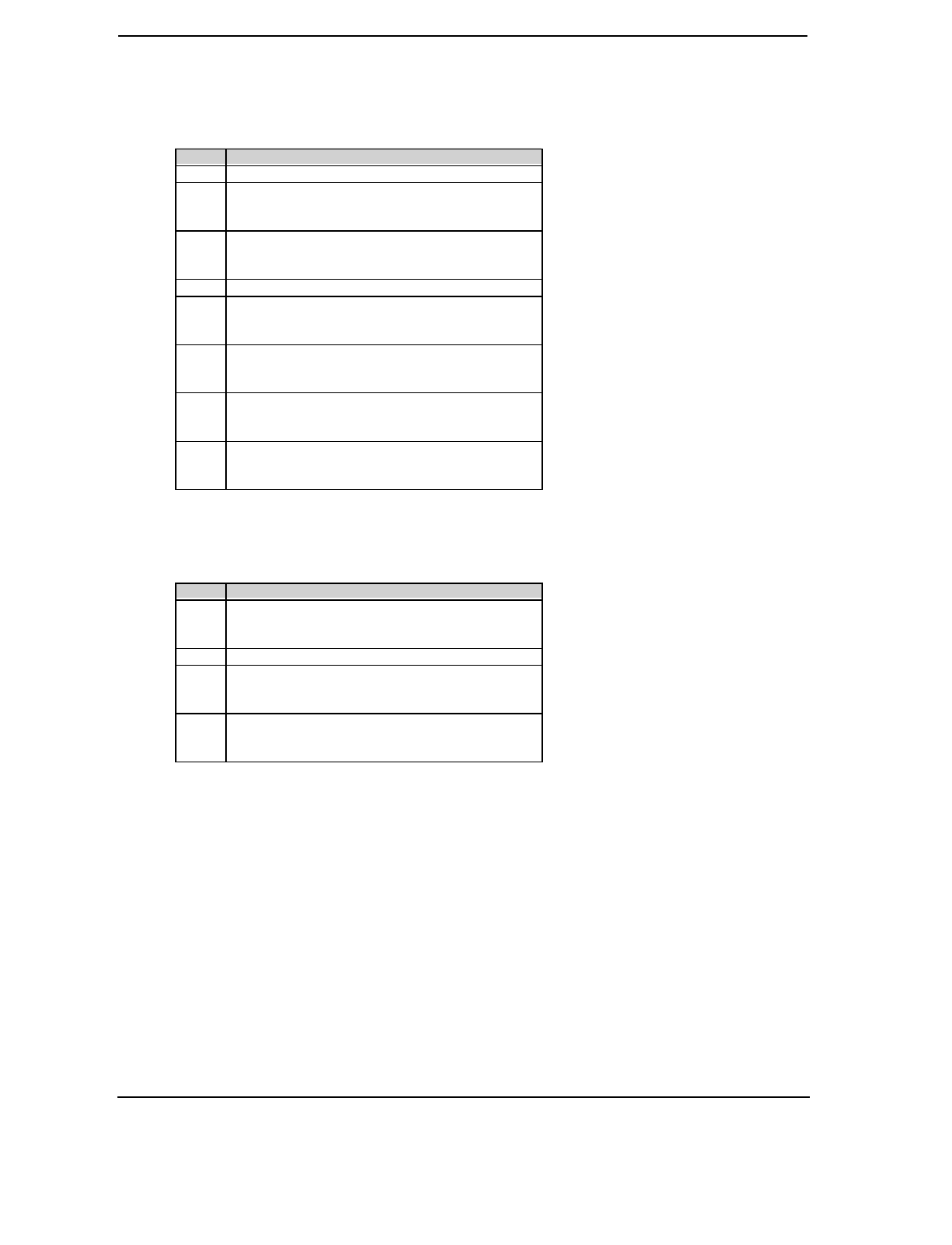
Technical Reference Guide
Compaq Deskpro EN Series of Personal Computers
Desktop and Minitower Form Factors
Third Edition - September 1998
4-33
Configuration Byte 13h, Security Functions
Default Value = 00h
Bit Function
7 Reserved
6 QuickBlank Enable After Standby:
0 = Disable
1 = Enable
5 Administrator Password:
0 = Not present
1 = Present
4 Reserved
3 Diskette Boot Enable:
0 = Enable
1 = Disable
2 QuickLock Enable:
0 = Disable
1 = Enable
1 Network Server Mode/Security Lock Override:
0 = Disable
1 = Enable
0 Password State (Set by BIOS at Power-up)
0 = Not set
1 = Set
Configuration Byte 14h, Equipment Installed
Default Value (standard configuration) = 03h
Bit Function
7,6 No. of Diskette Drives Installed:
00 = 1 drive 10 = 3 drives
01 = 2 drives 11 = 4 drives
5..2 Reserved
1 Coprocessor Present
0 = Coprocessor not installed
1 = Coprocessor installed
0 Diskette Drives Present
0 = No diskette drives installed
1 = Diskette drive(s) installed
Configuration Bytes 15h and 16h, Base Memory Size
Default Value = 280h
Bytes 15h and 16h hold a 16-bit value that specifies the base memory size in 1-KB (1024)
increments. Valid base memory sizes are 512 and 640 kilobytes .
Configuration Bytes 17h and 18h, Extended Memory Size
Bytes 17h and 18h hold a 16-bit value that specifies the extended memory size in 1-KB
increments.
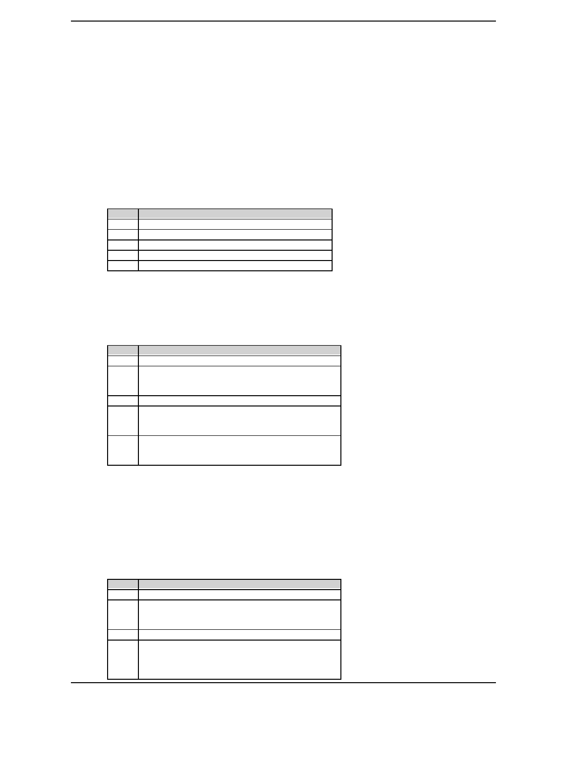
Chapter 4 System Support
Compaq Deskpro EN Series of Personal Computers
Desktop and Minitower Form Factors
Third Edition - September 1998
4-34
Configuration Bytes 19h-1Ch, Hard Drive Types
Byte 19h contains the hard drive type for drive 1 of the primary controller if byte 12h bits <7..4>
hold 1111b. Byte 1Ah contains the hard drive type for drive 2 of the primary controller if byte
12h bits <3..0> hold 1111b. Bytes1Bh and 1Ch contain the hard drive types for hard drives 1 and
2 of the secondary controller.
Configuration Byte 1Dh, Enhanced IDE Hard Drive Support
Default Value = F0h
Bit Function
7 EIDE - Drive C (83h)
6 EIDE - Drive D (82h)
5 EIDE - Drive E (81h)
4 EIDE - Drive F (80h)
3..0 Reserved
Values for bits <7..4> :
0 = Disable
1 = Enable for auto-configure
Configuration Byte 1Fh, Power Management Functions
Default Value = 00h
Bit Function
7..4 Reserved
3 Slow Processor Clock for Low Power Mode
0 = Processor runs at full speed
1 = Processor runs at slow speed
2 Reserved
1 Monitor Off Mode
0 = Turn monitor power off after 45 minutes in standby
1 = Leave monitor power on
0 Energy Saver Mode Indicator (Blinking LED)
0 = Disable
1 = Enable
Configuration Byte 24h, System Board Identification
Default Value = 7Eh
Configuration memory location 24h holds the system board ID.
Configuration Byte 25h, System Architecture Data
Default Value = 0Bh
Bit Function
7..4 Reserved
3 Unmapping of ROM:
0 = Allowed
1 = Not allowed
2 Reserved
1,0 Diagnostic Status Byte Address
00 = Memory locations 80C00000h-80C00004h
01 = I/O ports 878h-87Ch
11 = neither place

Technical Reference Guide
Compaq Deskpro EN Series of Personal Computers
Desktop and Minitower Form Factors
Third Edition - September 1998
4-35
Configuration Byte 26h, Auxiliary Peripheral Configuration
Default Value = 00h
Bit Function
7,6 I/O Delay Select
00 = 420 ns (default)
01 = 300 ns
10 = 2600 ns
11 = 540 ns
5 Alternative A20 Switching
0 = Disable port 92 mode
1 = Enable port 92 mode
4 Bi-directional Print Port Mode
0 = Disabled
1 = Enabled
3 Graphics Type
0 = Color
1 = Monochrome
2 Hard Drive Primary/Secondary Address Select:
0 = Primary
1 = Secondary
1 Diskette I/O Port
0 = Primary
1 = Secondary
0 Diskette I/O Port Enable
0 = Primary
1 = Secondary
Configuration Byte 27h, Speed Control/External Drive
Default Value = 00h
Bit Function
7 Boot Speed
0 = Max MHz
1 = Fast speed
6..0 Reserved
Configuration Byte 28h, Expanded and Base Memory, IRQ12 Select
Default Value = 00h
Bit Function
7 IRQ12 Select
0 = Mouse
1 = Expansion bus
6,5 Base Memory Size:
00 = 640 KB
01 = 512 KB
10 = 256 KB
11 = Invalid
4..0 Internal Compaq Memory:
00000 = None
00001 = 512 KB
00010 = 1 MB
00011 = 1.5 MB
.
.
11111 = 15.5 MB

Chapter 4 System Support
Compaq Deskpro EN Series of Personal Computers
Desktop and Minitower Form Factors
Third Edition - September 1998
4-36
Configuration Byte 29h, Miscellaneous Configuration Data
Default Value = 00h
Bit Function
7..5 Reserved
4 Primary Hard Drive Enable (Non-PCI IDE Controllers)
0 = Disable
1 = Enable
3..0 Reserved
Configuration Byte 2Ah, Hard Drive Timeout
Default Value = 02h
Bit Function
7..5 Reserved
4..0 Hard Drive Timeout
00000 = Disabled
00001 = 1 minute
00010 = 2 minutes
.
.
10101 = 21 minutes
Configuration Byte 2Bh, System Inactivity Timeout
Default Value = 23h
Bit Function
7 Reserved
6,5 Power Conservation Boot
00 = Reserved
01 = PC on
10 = PC off
11 = Reserved
4..0 System Inactive Timeout. (Index to SIT system timeout record)
00000 = Disabled
Configuration Byte 2Ch, ScreenSave and NUMLOCK Control
Default Value = 00h
Bit Function
7 Reserved
6 Numlock Control
0 = Numlock off at power on
1 = Numlock on at power on
5 Screen Blank Control:
0 = No screen blank
1 = Screen blank w/QuickLock
4..0 ScreenSave Timeout. (Index to SIT monitor timeout record)
000000 = Disabled
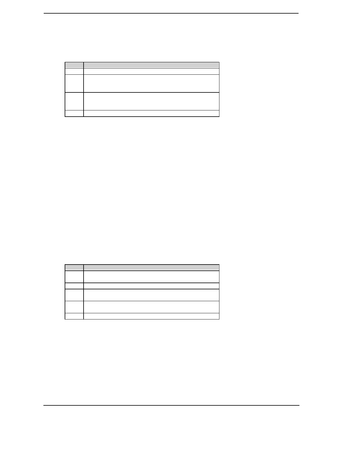
Technical Reference Guide
Compaq Deskpro EN Series of Personal Computers
Desktop and Minitower Form Factors
Third Edition - September 1998
4-37
Configuration Byte 2Dh, Additional Flags
Default Value = 00h
Bit Function
7..5 Reserved
4 Memory Test
0 = Test memory on power up only
1 = Test memory on warm boot
3 POST Error Handling (BIOS Defined)
0 = Display “Press F1 to Continue” on error
1 = Skip F1 message
2..0 Reserved
Configuration Byte 2Eh, 2Fh, Checksum
These bytes hold the checksum of bytes 10h to 2Dh.
Configuration Byte 30h, 31h, Total Extended Memory Tested
This location holds the amount of system memory that checked good during the POST.
Configuration Byte 32h, Century
This location holds the Century value in a binary coded decimal (BCD) format.
Configuration Byte 33h, Miscellaneous Flags
Default Value = 80h
Bit Function
7 Memory Above 640 KB
0 = No, 1 = Yes
6 Reserved
5 Weitek Numeric Coprocessor Present:
0 = Not installed, 1 = Installed
4 Standard Numeric Coprocessor Present:
0 = Not installed, 1 = Installed
3..0 Reserved
Configuration Byte 34h, International Language Support
Default Value = 00h
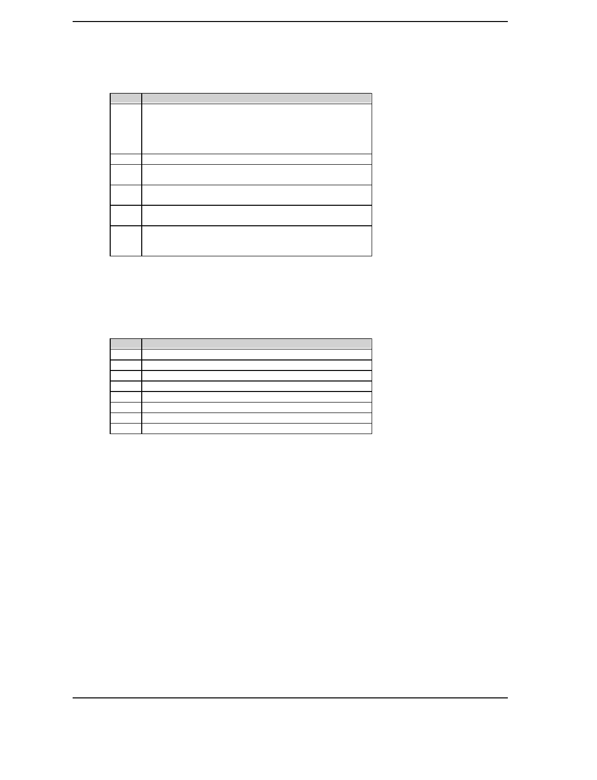
Chapter 4 System Support
Compaq Deskpro EN Series of Personal Computers
Desktop and Minitower Form Factors
Third Edition - September 1998
4-38
Configuration Byte 35h, APM Status Flags
Default Value = 11h
Bit Function
7..6 Power Conservation State:
00 = Ready
01 = Standby
10 = Suspend
11 = Off
5,4 Reserved
3 32-bit Connection:
0 = Disconnected, 1 = Connected
2 16-bit Connection
0 = Disconnected, 1 = Connected
1 Real Mode Connection
0 = Disconnected, 1 = Connected
0 Power Management Enable:
0 = Disabled
1 = Enabled
Configuration Byte 36h, ECC POST Test Single Bit Errors
Default Value = 01h
Bit Function
7 Row 7 Error Detect
6 Row 6 Error Detect
5 Row 5 Error Detect
4 Row 4 Error Detect
3 Row 3 Error Detect
2 Row 2 Error Detect
1 Row 1 Error Detect
0 Row 0 Error Detect
0 = No single bit error detected.
1 = Single bit error detected.
Configuration Byte 37h-3Fh, Power-On Password
These eight locations hold the power-on password.
Configuration Byte 40h, Miscellaneous Disk Data
Configuration Bytes 41h-44h, Hood Removal Time Stamp
These four bytes record the time at which the hood of the system was removed:
Byte 41h, month & day
Byte 42h, year and month
Byte 43h, minutes and seconds
Byte 44h, removal flag and minutes
Technical Reference Guide
Compaq Deskpro EN Series of Personal Computers
Desktop and Minitower Form Factors
Third Edition - September 1998
4-39
Configuration Byte 45h, Keyboard Snoop Data
Default Value = xxh
Bit Function
7 Cntrl/F10 Key Status:
0 = Cntrl & F10 keys not pressed
1 = Cntrl & F10 keys pressed
6 F10 Key Status:
0 = F10 key not pressed
1 = F10 key pressed
5..1 Reserved
0 Key Pressed Flag:
0 = Key not pressed
1 = Key pressed
Configuration Byte 46h, Diskette/Hard Drive Status
Default Value = xxh
Bit Function
7,6 Reserved
5 Partition On HD:
0 = Not set, 1 = Set
4 Setup Disk:
0 = Not present, 1 = Present
3 ROMPAQ or DIAGS Diskette:
0 = Not present, 1 = Present
2 Boot Diskette in Drive A:
0 = No, 1 = Yes
1 Drive B: Present:
0 = Not present, 1 = Present
0 Drive A: Present:
0 = Not present, 1 = Present
Configuration Bytes 47h-4Fh, IPL Data
These bytes hold initial program load (IPL) data for boot purposes:
Byte 47h, last IPL device
Bytes 48h-4Bh, IPL priority
Byte 4Ch-4Fh, BCV priority
Configuration Byte 51h, ECC Status Byte
Default Value = xxh
Bit Function
7 ECC Status for DIMM 3
6 ECC Status for DIMM 2
5 ECC Status for DIMM 1
4 ECC Status for DIMM 0
3..0 Reserved
Chapter 4 System Support
Compaq Deskpro EN Series of Personal Computers
Desktop and Minitower Form Factors
Third Edition - September 1998
4-40
Configuration Byte 52h, Board Revision
This byte holds the board revision as copied from the boot block sector.
Configuration Byte 53h, 54h, SW SMI Command/Data Bytes
Configuration Byte 55h, APM Command Byte
Configuration Byte 56h, Miscellaneous Flags Byte
Bit Function
7 CAS Latency:
0 = 2, 1 = 3
6 IR Port Enable Flag:
0 = Disabled (COM2 config. for standard serial port)
1 = Enabled (COM2 config. for IrDA)
5 Warm Boot Enable Flag:
0 = Disable, 1 = Enable
4 POST Terse/Verbose Mode
0 = Verbose, 1 = Terse
3..1 Erase Ease Keyboard Mode:
000 = Backspace/Spacebar
001 = Spacebar/Backspace
010 = Spacebar/Spacebar
011-111 = Invalid
0 Configurable Power Supply:
0 = Power switch active
1 = Power switch inhibited
Configuration Byte 57h-76h, CMOS Copy
Configuration Bytes 77h-7Fh, Administrator Password
Configuration Byte 80h, CMOS Diagnostic Flags Byte
Default Value = 00h. Set bit indicates function is valid.
Bit Function
7 CMOS Initialization (Set CMOS to Default)
6 Setup password locked
5 PnP should not reject SETs because Diags is active
4 Reserved
3 Manufacturing diagnostics diskette found
2 Invalid electronic serial number
1 Boot maintenance partition once
0 Invalid CMOS checksum
Configuration Byte 81h, 82h, Total Super Extended Memory Tested
This byte holds the value of the amount of extended system memory that tested good during
POST. The amount is given in 64-KB increments.
Technical Reference Guide
Compaq Deskpro EN Series of Personal Computers
Desktop and Minitower Form Factors
Third Edition - September 1998
4-41
Configuration Byte 83h, Microprocessor Identification
This byte holds the component ID and chip revision of the microprocessor.
Configuration Byte 84h, Microprocessor Revision
Configuration Byte 85h, Administration Mode
Bit Function
7,6 Reserved
5 ESCD Buffering:
0 = No buffering, 1 = ESCD buffered at F000h.
4 Hood Lock Enable:
0 = Disabled, 1 = Enabled
3 User Mode Flag
2 Administration Mode Flag
1 Level Support:
0 = Level 1, 1 = Level 2
0 Feature Support Bit
0 = Disabled, 1 = Enabled
Configuration Byte 86h, Fast Boot Date
Configuration Byte 87h, Fast Boot Select
Bit Function
7..3
2
1
0
Configuration Byte 88h, Fast Boot Date (Year/Century)
Configuration Byte 89h, APM Resume Timer
Bit <7> indicates the timer status: 0 = disabled, 1 = timer set.
Configuration Byte 8Ah-8Fh, APM Resume Timer
These bytes hold the APM timer values:
Byte 8Ah, minutes
Byte 8Bh, hours
Byte 8Ch, day
Byte 8Dh, month
Byte 8Eh, year
Byte 8Fh, century
Chapter 4 System Support
Compaq Deskpro EN Series of Personal Computers
Desktop and Minitower Form Factors
Third Edition - September 1998
4-42
Configuration Byte 90h, 91h, Total Super Extended Memory Configured
This byte holds the value of the amount of extended system memory that is configured.
The amount is given in 64-KB increments.
Configuration Byte 92h, Miscellaneous Configuration Byte
Default Value = 18h
Bit Function
7..5 Reserved
4 Diskette Write Control:
0 = Disable
1 = Enable
3..1 Reserved
0 Diskette Drive Swap Control:
0 = Don’t swap
1 = Swap drive A: and B:
Configuration Byte 93h, PCI Configuration Byte
Default Value = 00h
Bit Function
7 Onboard SCSI Status:
0 = Hidden
1 = Active
6 Onboard NIC Status:
0 = Hidden
1 = Active
5 Onboard USB Status:
0 = Hidden
1 = Active
3 Reserved
2 ISA Passive Release:
0 = Enabled
1 = Disabled
1 PCI Bus Master Enable
0 = Enabled
1 = Disabled
0 PCI VGA Palette Snoop
0 = Disable
1 = Enable
If palette snooping is enabled, then a primary PCI graphics card may share a common palette
with the ISA graphics card. Palette snooping should only be enabled if all of the following
conditions are met:
♦ An ISA card connects to a PCI graphics card through the VESA connector.
♦ The ISA card is connected to a color monitor.
♦ The ISA card uses the RAMDAC on the PCI card
♦ The palette snooping feature (sometimes called “RAMDAC shadowing”) on the PCI card is
enabled and functioning properly.

Technical Reference Guide
Compaq Deskpro EN Series of Personal Computers
Desktop and Minitower Form Factors
Third Edition - September 1998
4-43
Configuration Byte 94h, ROM Flash/Power Button Status
Default Value = 00h
Bit Function
7..5 Reserved
4 ROM Flash In Progress (if set)
3 Reserved
2 Power Button Inhibited (if set)
1 User-Forced Bootblock (if set)
0 ROM Flash In Progress (if set)
Configuration Byte 97h, Asset/Test Prompt Byte
Default Value = 00h
Bit Function
7,6 Test Prompt:
01 = Fake F1
10 = Fake F2
11 = Fake F10
5..0 Asset Value
Configuration Byte 9Bh, Ultra-33 DMA Enable Byte
Default Value = 00h
Bit Function
7..4 Reserved
3 Secondary Slave Enabled for U-33 if Set
2 Secondary Master Enabled for U-33 if Set
1 Primary Slave Enabled for U-33 if Set
0 Primary Master Enabled for U-33 if Set
Configuration Byte 9Ch, Mode-2 Configuration Byte
Default Value = 1Ch
Bit Function
7,6 Reserved
5 Mode 2 Support
0 = Disable
1 = Enable
4 Secondary Hard Drive Controller
0 = Disable
1 = Enable
3,2 Secondary Hard Drive Controller IRQ
00 = IRQ10
01 = IRQ11
10 = IRQ12
11 = IRQ15
1,0 Reserved
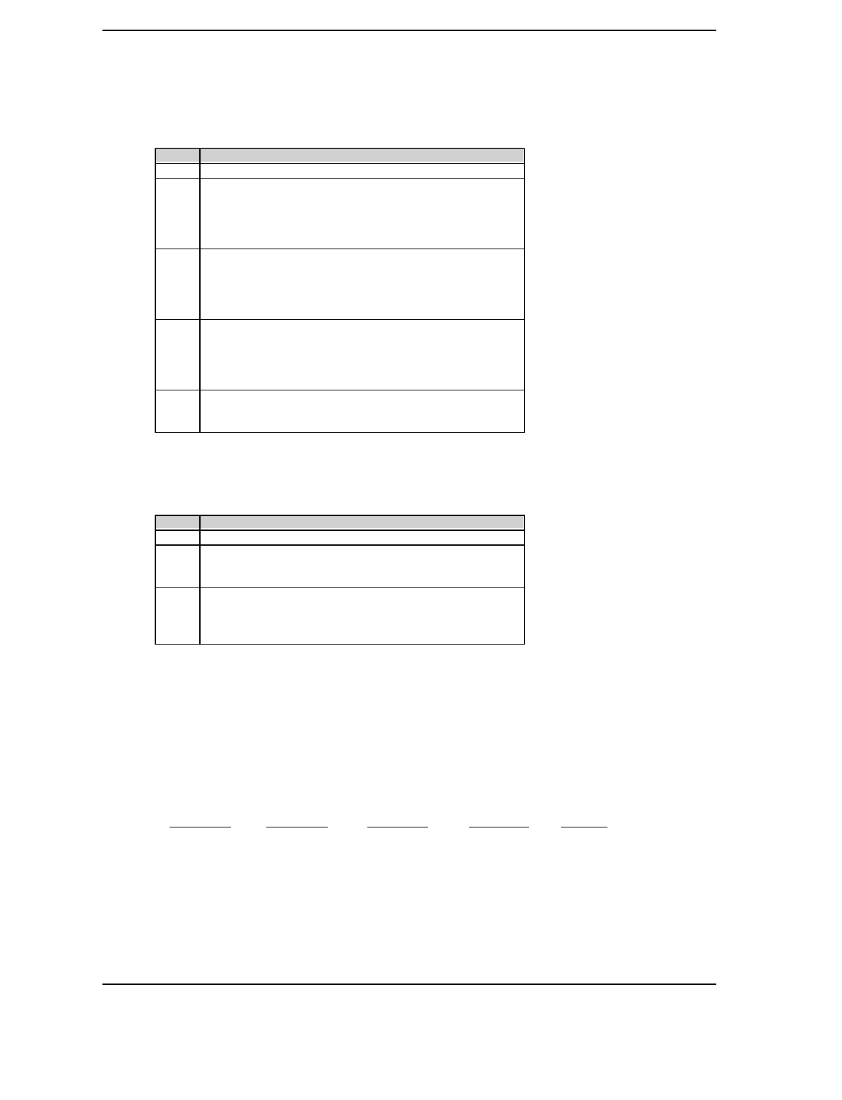
Chapter 4 System Support
Compaq Deskpro EN Series of Personal Computers
Desktop and Minitower Form Factors
Third Edition - September 1998
4-44
Configuration Byte 9Dh, ESS Audio Configuration Byte
Default Value = 12h
Bit Function
7 Reserved for Game Port Enable
6,5 Audio Address
00 = 22xh
01 = 23xh
10 = 24xh
11 = 25xh
4,3 DMA Channel
00 = Disabled
01 = DMA0
10 = DMA1
11 = DMA3
2,1 IRQ Select
00 = IRQ9
01 = IRQ5
10 = IRQ7
11 = IRQ10
0 ESS Audio Chip Enable
0 = Enabled
1 = Disabled
Configuration Byte 9Eh, ECP DMA Configuration Byte
Default Value = 03h
Bit Function
7..4 Reserved
3 SafeStart Control:
0 = Disable
1 = Enable
2..0 ECP DMA Channel
000 = Invalid
100 = Disabled
All other values (001-011, 101-111) refer to channel no.
Configuration Byte 9Fh-AFh, Asset Tag Serial Number
Configuration Bytes B0h-C3h; Custom Hard Drive Information
These bytes contain the number of cylinders, heads, and sectors per track for hard drives C, D, E,
and F respectively. The mapping for each drive is as follows:
Drive 65 (C) Drive 66 (D) Drive 68 (E) Drive 15 (F) Function
B0h B5h BAh BFh No. of Cylinders, Low Byte
B1h B6h BBh C0h No. of Cylinders, High Byte
B2h B7h BCh C1h No. of Heads
B3h B8h BDh C2h Max ECC Bytes
B4h B9h BEh C3h No. of Sectors Per Track

Technical Reference Guide
Compaq Deskpro EN Series of Personal Computers
Desktop and Minitower Form Factors
Third Edition - September 1998
4-45
Configuration Byte C7h, C8h, Serial Ports 1 and 2 (Respectively) Configuration Bytes
Default Value = FEh, 7Dh
Bit Function
7..2 Base I/O Address (in packed format)
(Algorithm: [Addr. - 200h] / 8)
(i.e., 3Fh = 3F8h, 1Fh = 2F8h, 00 = 200h)
1..0 Interrupt:
00 = Reserved
01 = IRQ3
10 = IRQ4
11 = Reserved
Configuration Bytes CAh, DBh; Chassis Serial Number
Configuration Bytes DEh, DFh; Checksum of Locations 90h-DDh
Configuration Bytes E0h-FFh; Client Management Error Log

Chapter 4 System Support
Compaq Deskpro EN Series of Personal Computers
Desktop and Minitower Form Factors
Third Edition - September 1998
4-46
4.7 I/O MAP AND REGISTER ACCESSING
4.7.1 SYSTEM I/O MAP
Table 4–19. System I/O Map
Table 4-19.
System I/O Map
I/O Port Function
0000..000Fh DMA Controller 1
0020..0021h Interrupt Controller 1
0040..0043h Timer 1
0060h Keyboard Controller Data Byte
0061h NMI, Speaker Control
0064h Keyboard Controller Command/Status Byte
0070h NMI Enable, RTC/Lower CMOS Index
0071h RTC Data
0078h-007Bh GPIO Port 1 Control (87307 I/O controller)
007Ch-007Fh GPIO Port 2 Control (87307 I/O controller)
0080..008Fh DMA Page Registers
0092h Port A, Fast A20/Reset
00A0..00A1h Interrupt Controller 2
00B2h, 00B3h APM Control/Status Ports
00C0..00DFh DMA Controller 2
00F0h Math Coprocessor Busy Clear
015C, 015Dh 87307 I/O Controller Configuration Registers (Index, Data)
0170..0177h Hard Drive (IDE) Controller 2
01F0..01FFh Hard Drive (IDE) Controller 1
0201..024Fh Audio subsystem control (primary & secondary addresses)
0278..027Bh Parallel Port (LPT2)
02F8..02FFh Serial Port (COM2)
0371.. 0375h Diskette Drive Controller Alternate Addresses
0376h IDE Controller Alternate Address
0377h IDE Controller Alternate Address, Diskette Drive Controller Alternate Address
0378..037Fh Parallel Port (LPT1)
0388..038Bh FM synthesizer (alias addresses)
03B0..03DFh Graphics Controller
03E8..03EFh Serial Port (COM3)
03F0..03F5h Diskette Drive Controller Primary Addresses
03F6, 03F7h Diskette Drive Controller Primary Addresses, Hard Drive Controller Primary Addresses
03F8..03FFh Serial Port (COM1)
04D0, 04D1h Master, Slave Edge/Level INTR Control Register
0C00, 0C01h PCI IRQ Mapping Index, Data
0C06, 0C07h Reserved - Compaq proprietary use only
0C50, 0C51h System Management Configuration Registers (Index, Data)
0C52h General Purpose Port
0C7Ch Machine ID
0CF8h PCI Configuration Address (dword access)
0CF9h Reset Control Register
0CFCh PCI Configuration Data (byte, word, or dword access)
FF00..FF07h IDE Bus Master Register
NOTE: Assume unmarked gaps are reserved/unused.

Technical Reference Guide
Compaq Deskpro EN Series of Personal Computers
Desktop and Minitower Form Factors
Third Edition - September 1998
4-47
4.7.2 GPIO UTILIZATION
This section describes the utilization of general purpose input/output (GPIO) ports provided by
the south bridge (82371) and I/O controller (87307) components used in this system.
4.7.2.1 82371 South Bridge GPIO Utilization
The 82371 South Bridge component includes a number of single and dual purpose pins available
as general purpose input/output (GPIO) ports. The GPIO ports are configured during POST by
BIOS through the PCI configuration registers B0-B3h (82371, function 0). The GPI ports are
monitored through registers of the Power Management function (function 3) at I/O address PM
base +30h. The GPO ports are controlled through a register of function 3 at I/O address PM base
+34h.
Tables 4-20 and 4-21 list the utilization of the GPI and GPO ports respectively in this system.
Table 4–20. 82371 South Bridge General Purpose Input Port Utilization
Table 4-20.
82371 South Bridge General Purpose Input Port Utilization
GP Input Port Function
GPI #0 IOCHK- function for ISA bus.
GPI #1 SCI- event status.
GPI #2..5 Not used.
GPI #6 Interrupt (IRQ8) for RTC (in 87307 I/O controller).
GPI #7 Not used.
GPI #8 Magic packet SMI event status. When read low, magic packet has occurred.
GPI #9 Not used.
GPI #10 Wakeup w/ IRQ12. Will, in S1 state, be high if an IRQ12 (mouse interrupt) occurred.
GPI #11 Not used
GPI #12 Wake up w/ IRQ1. Will, in S1 state, be high if an IRQ1 (keyboard interrupt) occurred.
GPI #13 PME status.
GPI #14, 15 Backplane revision bits <0, 1>
GPI #16 Not used.
GPI #17 Primary IDE cable type: 0 = 80-pin cable attached, 1 = 40-pin cable attached.
GPI #18 Secondary IDE cable type: 0 = 80-pin cable attached, 1 = 40-pin cable attached.
GPI #19 Chassis fan status: 0 = fan not connected, 1 = fan connected.
GPI #20 Processor thermal caution status: 0 = not occurred, 1 = occurred.
GPI #21 Themal sensor: 0 = diode connected, 1 = diode not connected.

Chapter 4 System Support
Compaq Deskpro EN Series of Personal Computers
Desktop and Minitower Form Factors
Third Edition - September 1998
4-48
Table 4–21. 82371 South Bridge General Purpose Output Port Utilization
Table 4-21.
82371 South Bridge General Purpose Output Port Utilization
GP Output Port Function
GPO #0 PCI reset. When low will generate a PCI RST- to PCI slots.
GPO #1-7 ISA bus address signals LA17-23.
GPO #8 Not used.
GPO #9 Not used.
GPO #10 Not used.
GPO #11 Not used.
GPO #12 Not used.
GPO #13 Not used.
GPO #14 Not used
GPO #15 Not used.
GPO #16 Power management suspend control signal.
GPO #17 CPU clock stop. When cleared inhibits the clock generator from producing CPU clock.
GPO #18 PCI clock stop. When cleared inhibits the clock generator from producing PCI clock.
GPO #19 Not used.
GPO #20 Power management suspend control signal.
GPO #21 Not used.
GPO #22, 23 X-bus control signals.
GPO #24 Not used.
GPO #25 Not used.
GPO #26 Not used.
GPO #27 Chassis fan control. When cleared (0) shuts down the chassis fan.
GPO #28-30 Not used.

Technical Reference Guide
Compaq Deskpro EN Series of Personal Computers
Desktop and Minitower Form Factors
Third Edition - September 1998
4-49
4.7.2.2 87307 I/O Controller Functions
The 87307 I/O controller contains various functions such as the keyboard/mouse interfaces,
diskette interface, serial interfaces, and parallel interface. While the control of these interfaces
uses standard AT-type I/O addressing, the configuration of these functions uses indexed ports
unique to the 87307. In this system, hardware strapping selects I/O addresses 015Ch and 015Dh
at reset as the Index/Data ports for accessing the logical devices within the 87307. The hardware
strapping also places the 87307 into PnP motherboard mode. The integrated logical devices are
listed as follows:
Table 4-22 lists the PnP standard control registers for the 87307.
Table 4–22. 87307 I/O Controller PnP Standard Control Registers
Table 4-22.
87307 I/O Controller PnP Standard Control Registers
Index Function Reset Value
00h Set RD_DATA Port 00h
01h Serial Isolation
02h Configuration Control
03h Wake (CSN) 00h
04h Resource Data
05h Status
06h Card Select Number (CSN) 00h
07h Logical Device Select:
00h = 8042 Controller (Keyboard I/F)
01h = 8042 Controller (Mouse I/F)
02h = RTC/APC Configuration
03h = Diskette Controller
04h = Parallel Port
05h = UART 2 (Serial Port B / IrDA)
06h = UART 1 (Serial Port A)
07h = GPIO Ports
08h = Power Management
00h
20h Super I/O ID Register (SID) A0h
21h SIO Configuration 1 Register 16h
22h SIO Configuration 1 Register 02h
23h Programmable Chip Select Configuration Index 00h
24h Programmable Chip Select Configuration Data 00h
NOTE:
For a detailed description of registers refer to appropriate National documentation.
The configuration registers are accessed by writing the appropriate logical device’s number to
index 07h and writing the desired offset to the index register. The data is then either written to or
read from the data register.
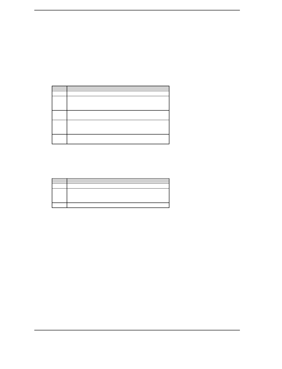
Chapter 4 System Support
Compaq Deskpro EN Series of Personal Computers
Desktop and Minitower Form Factors
Third Edition - September 1998
4-50
87307 GPIO Utilization
The 87307 I/O Controller provides 11 general purpose pins that can be individually configured as
either inputs or outputs. These pins are mapped as two general purpose ports and utilized as
shown below.
GPIO Port 1 Data, I/O Addr. 078h, (87307 I/O Controller),
Bit Function
7 GPIO17 (not used)
6 GPIO16 (config. as input): Cover Lock Detect.
Read 0, no solenoid
Read 1, solenoid
5 GPIO15 (config. as output): Cover Alarm Clear.
Write 0 to clear alarm.
4 GPIO14 (config. as input): Cover Removed Detect.
Read 0, cover has been removed
Read 1, cover is secure
3..0 GPIO13-10 (config. as input):
Backplane identification (BP_ID3-0)
GPIO Port 1 Direction/Output Type/PU Cntrl., I/O Addr. 079-07Bh, (87307 I/O
Controller)
GPIO Port 2 Data, I/O Addr. 07Ch, (87307 I/O Controller),
Bit Function
7..4 GPIO27..24 Not Available
3 GPIO23 (config. as input): Ring Detect
Read 0, no ring received
Write 1, ring detected
2..0 GPIO22..20 Not Available
GPIO Port 2 Direction/Output Type/PU Cntrl., I/O Addr. 07D-07Fh, (87307 I/O
Controller)

Technical Reference Guide
Compaq Deskpro EN Series of Personal Computers
Desktop and Minitower Form Factors
Third Edition - September 1998
4-51
4.8 SYSTEM MANAGEMENT SUPPORT
This section describes the hardware support of functions involving security, safety, identification,
and power consumption of the system. System management functions are handled largely by a
System Security ASIC. Most functions are controlled through registers (Table 4-23) accessed
using the indexed method through I/O ports 0C50h (index) and 0C51h (Data).
Table 4–23. System Management Control Registers
Table 4-23.
System Management Control Registers
Index Function
00h Identification
02h Temperature Status / Clear
03h Temperature Interrupt / SMI Enable
05h Power On LED Blink Control
12h General Purpose Open Collector (GPOC) Bits
13h Secured GPOC Bits
20h Power Button Control
21h SMI / SCI Source
22h SMI / SCI Mapping
30h REQ/GNT Control
80h Super I/O Security Control
81h Super I/O Index Address Low
82h Super I/O Index Address High
83h Super I/O Index Data
84h Super I/O Data Address Low
85h Super I/O Data Address High
86h Super I/O Write Block 0
87h Super I/O Write Block 1
88h Super I/O Write Block 2
89h Super I/O Write Block 3
The following subsections describe the system management functions. Any BIOS interaction
required of these functions is described in Chapter 8, “BIOS” or in the Compaq BIOS Technical
Reference Guide.

Chapter 4 System Support
Compaq Deskpro EN Series of Personal Computers
Desktop and Minitower Form Factors
Third Edition - September 1998
4-52
4.8.1 FLASH ROM WRITE PROTECT
The system BIOS firmware is contained in a flash ROM device that can be re-written with
updated code if necessary. The ROM is write-protected with a Black Box* security feature. The
Black Box feature uses the Administrator password to protect against unauthorized writes to the
flash ROM. During the boot sequence, the BIOS checks for the presence of the ROMPAQ
diskette. If ROMPAQ is detected and the password is locked into the Black Box with the Protect
Resources command, an Access Resources command followed by Administrator password entry
must occur before the ROM can be flashed. If the Permanently Lock Resources command has
been invoked, the power must be cycled before the ROM can be flashed. The system ROM is
write-protected as follows:
Start Addr. End Addr. Data Type Protection
C0000h EFFFFh Option ROM Password write-protected
F0000h F7FFFh System BIOS Password write-protected
F8000h F9FFFh ESCD Never write-protected
FA000h FFFFFh Boot Block Always write-protected
The flashing functions are handled using the INT15 AX-E822h BIOS interface.
4.8.2 PASSWORD PROTECTION
When enabled, the user is prompted to enter the power-on password during POST. If an
incorrect entry is made, the system halts and does not boot. The Power-On password is stored in
eight bytes at configuration memory locations 37h-3Fh. These locations are physically located
within the 87307. At the time a new password is written into 37h-3Fh, the password is also
written into Black Box* logic contained within the System Security ASIC. The Black Box logic
is used for power-on password protection support instead of the port 92 sequence used on other
systems. The Black Box logic prevents inadvertent or unauthorized access to the password bytes
of the 87307 by monitoring I/O ports 70/71h for access to the 37h-3Fh CMOS range and
inhibiting the AEN signal to the 87307 if such access is detected. Slot 1 of the Black Box logic
can be written to at runtime, allowing the user to change the power on password without cycling
power and going through the F10 method. The Black Box password cannot be read.
The power-on password function can be disabled by setting DIP SW1 position 1 to on (closed).
The administrator password is stored in eight bytes at configuration memory locations 78h-7Fh.
If the administrator password function is enabled, the user is prompted to enter the password
before running F10-Setup or before booting from a ROMPAQ diskette. If an incorrect entry is
made, the system halts and does not boot. The administrator password is also stored in the Black
Box* logic. Black Box logic acting as the sentry for the administrator password by preventing
inadvertent or unauthorized writing to the Flash ROM.
* Black Box logic is Compaq-proprietary and controlled exclusively through the BIOS ROM.

Technical Reference Guide
Compaq Deskpro EN Series of Personal Computers
Desktop and Minitower Form Factors
Third Edition - September 1998
4-53
4.8.3 I/O SECURITY
The 87307 I/O controller allows various I/O functions to be disabled through configuration
registers. In addition, the configuration registers of the 87307 are further protected by Client
Management (CM) logic (contained within a Compaq ASIC) that can be set (using BIOS call
INT 15 AX=E829h) to block access to the 87307 configuration registers of the following
functions:
♦ Diskette drive
♦ Serial port
♦ Parallel port
In blocking 87307 functions, the CM logic monitors ISA I/O cycles and can detect, through
index address-matching, when an attempt is made to access a function provided by the 87307. If
the CM logic has been set to block access, then ISA bus signal AEN or IOWC-, both which the
CM logic provides to the 87307, is disabled, effectively inhibiting the I/O access.
The USB controller can also be blocked from access by the CM logic. In this case the CM logic
can be set to block the routing of the REQ/GNT signals to the USB controller, thereby disabling
the interface.
4.8.4 USER SECURITY
When enabled, the user is prompted to enter the power-on password during POST. If an
incorrect entry is made, the system halts and does not boot. The Power-On password is stored in
eight bytes at configuration memory locations 37h-3Fh. These locations are physically located
within the 87307.
The power-on password function can be disabled by setting DIP SW1 position 1 to on (closed).
The administrator password is stored in eight bytes at configuration memory locations 78h-7Fh.
If the administrator password function is enabled, the user is prompted to enter the password
before running F10-Setup or before booting from a ROMPAQ diskette. If an incorrect entry is
made, the system halts and does not boot.
The QuickLock feature allows, if enabled in F10-Setup through CMOS location 13h bit <2>, the
user to lock the keyboard by invoking the Ctrl-Alt-L keystrokes. This initiates an SMI and the
SMI handler then takes the action required to lock the keyboard. If the QuickBlank feature is
enabled at that time then the screen will be blanked as well. The user then must enter the power-
on password to re-activate the keyboard and/or display .
NOTE: Although the SMI is used for initiating QuickLock/QuickBlank functions, these
functions are not considered power management features.
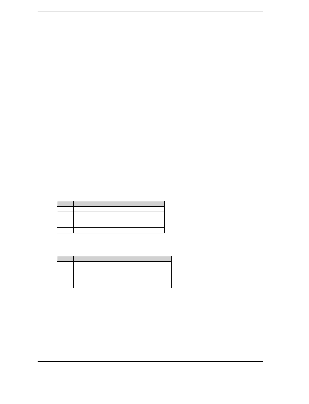
Chapter 4 System Support
Compaq Deskpro EN Series of Personal Computers
Desktop and Minitower Form Factors
Third Edition - September 1998
4-54
4.8.5 TEMPERATURE SENSING
This system employs two sensors for monitoring the temperature inside the chassis. A thermister
attached to the heat sink of the Pentium II SEC cartridge is used to detect the caution level. This
thermister, connected to the system board through header P15, is part of sensing logic that
provides input to a Compaq ASIC. The sensing logic is set to trip when 179.6 °F (82 °C) is
reached. At that time the Compaq ASIC can generate an SMI (if so configured, see registers
below) resulting in a warning to the user and/or the chassis fan being turned on. Three general
purpose input ports of the 82371south bridge monitor status of the Thermal Caution circuitry.
They are listed below with their default values:
1. 82371 GPI #19 – Chassis fan connection (1 = fan connected)
2. 82371 GPI #20 – Thermal Caution event status (0 = caution event has not occurred)
3. 82371 GPI #21 – Thermal sensor connection status (0 = connected)
The Pentium II processor contains a sensor utilized to detect a deadly condition. When the
processor temperature reaches 135 °F the THERMTRIP- signal is asserted and recorded in a
Compaq ASIC (see following registers). Assertion of THERMTRIP- also results in turning off
the system’s clock generator, effectively shutting down the system.
The following two indexed registers are used by BIOS and available to software for controlling
the temperature sense function.
I/O Port C51.02h, Temperature Status/Clear Register
Bit Function
7..2 Reserved
1 Temperature Deadly (RO)
0 = Normal
1 = Critical temperature detected
0 Reserved
NOTE: Bits 1,0 are cleared when read but will be instantly reset if condition remains.
I/O Port C51.03h, Temperature Interrupt/SMI Enable Register
Bit Function
7..3 Reserved
2 Temperature Deadly Shutdown Disable:
0 = Initiate shutdown w/deadly condition.
1 = Do not initiate shutdown.
1,0 Reserved

Technical Reference Guide
Compaq Deskpro EN Series of Personal Computers
Desktop and Minitower Form Factors
Third Edition - September 1998
4-55
4.8.6 SMART COVER LOCK
The chassis cover (also known as the “hood”) can be locked to prevent unauthorized personnel
from removing the cover and changing the system hardware. The locking mechanism consists of
a solenoid controlled by the Setup utility through the Client Management logic in a Compaq
ASIC. The presence of the Smart Cover Lock (actually of the solenoid) is detected by logic and
readable by software at 87307 GPIO port 1 bit <6>.
The cover lock mechanism can be bypassed in an emergency by removing three screws on the
rear of the chassis with the Smart Cover Lock Failsafe Key.
4.8.7 SMART COVER REMOVAL SENSOR
This system includes a cover removal indication function. The system can, upon power-up,
notify the user if the computer cover has been removed. The sensor consists of a plunger switch
mounted on the backplane (riser card) that comes in contact with the chassis cover. When the
cover is removed, the switch is activated and the battery-backed logic places a high at 87307
GPIO port 1 bit <4>. This bit will remain set (whether or not the cover is replaced) until the
system is powered up and the user completes the boot sequence successfully, at which time the
hood alarm bit <5> will be cleared. Through Setup, the user can set this function to one of three
levels of support for a “hood removed” condition:
Level 0 - Hood removal indication is essentially disabled at this level. During POST, Bit <4> is
cleared and no other action is taken by BIOS.
Level 1 - During POST the message “The computer’s cover has been removed since the last
system start up” is displayed and time stamps in CMOS and SIT are updated.
Level 2 - During POST the “The computer’s cover has been removed since the last system start
up” message is displayed, time stamps in CMOS and SIT are updated, and user is prompted for
administrator password.
NOTE: If the user invokes Setup through F10 the administrator password is not
requested again.

Chapter 4 System Support
Compaq Deskpro EN Series of Personal Computers
Desktop and Minitower Form Factors
Third Edition - September 1998
4-56
4.8.8 POWER MANAGEMENT
This system provides baseline hardware support of ACPI- and APM-compliant firmware and
software. The major power-consuming components (processor, chipset, I/O controller, and fan)
can be placed into a reduced power mode upon software command either automatically or by user
control. The system can then be brought back up (“wake-up”) by events defined by the ACPI
specification. The ACPI wake-up events supported by this system are listed as follows:
ACPI Wake-Up Event System Wakes From
Power Button Sleep/Soft-Off
RTC Alarm Sleep/Soft-Off
Wake on LAN (w/NIC) Sleep/Soft-Off
PME Sleep/Soft-Off
Serial port Ring Sleep/Soft-Off
USB Sleep
Keyboard Sleep
Mouse Sleep
4.8.8.1 Power Button
This system uses an ACPI-compliant power button that also provides a legacy mode as well. In
legacy mode the system is alternately powered on or off each time the button is pressed and
released. In ACPI mode the power supply, when on, will turn off only after the button is pressed
and held for over four seconds. The power button mode is controlled by ROM-based Setup
through a Compaq ASIC. A detailed description of system power control is provided in Chapter 7
“Power and Signal Distribution.”
4.8.8.2 Fan Control
The system contains two fans; a power supply fan (contained within the power supply assembly)
and a chassis fan mounted in the front of the chassis. The operation of both fans involves
temperature conditions and energy conservation but different logic is used for each.
The power supply fan is on during normal operation. In sleep mode the power supply fan is
(normally) shut down by software using logic in a Compaq ASIC, which asserts a FAN OFF
signal routed to the power supply assembly. The power supply assembly, however, includes a
temperature sensor that can override the FAN OFF signal if necessary.
The chassis fan is controlled by the thermister attached to the processor heat sink as well as shut
down logic. The temperature-sensing operation is discussed in section 4.8.5. To conserve energy
during sleep mode 82371 GPO port #27 is cleared resulting in the chassis fan being shut down.

Technical Reference Guide
Compaq Deskpro EN Series of Personal Computers
Desktop and Minitower Form Factors
Third Edition - September 1998
4-57
4.8.8.3 Hard Drive Spindown Control
The timeout parameter stored in the SIT record 04h and indexed through CMOS location 2Ah
(bits <4..0>) represents the period of hard drive inactivity required to elapse before the hard drive
is allowed to spin down. The timeout value is downloaded from CMOS to a timer on the hard
drive. The timeout period can be set in incremental values of 0 (timeout disabled), 10, 15
(default), 20, 30, and 60 minutes. A timed-out and spun-down hard drive will automatically spin
back up upon the next drive access. It is normal for the user to detect a certain amount of access
latency in this situation.
4.8.8.4 Monitor Power Control
The VESA display power management signaling protocol defines different power consumption
conditions and uses the HSYNC and VSYNC signals of the monitor interface to select a
monitor’s power condition. This capability is dependent on the graphics controller employed in
the system. For compliance to the monitor power control feature refer to the applicable appendix
of the installed graphics controller card.

Chapter 4 System Support
Compaq Deskpro EN Series of Personal Computers
Desktop and Minitower Form Factors
Third Edition - September 1998
4-58
This page is intentionally blank.

Technical Reference Guide
Compaq Deskpro EN Series of Personal Computers
Desktop and Minitower Form Factors
Third Edition - September 1998
5-1
Chapter 5
INPUT/OUTPUT INTERFACES
5. Chapter 5 INPUT/OUTPUT INTERFACES
5.1 INTRODUCTION
This chapter describes the standard (i.e., system board) interfaces that provide input and output
(I/O) porting of data and specifically discusses interfaces that are controlled through I/O-mapped
registers. The I/O interfaces are integrated functions of the south bridge (82371) and the I/O
controller (87307). The following I/O interfaces are covered in this chapter:
♦ Enhanced ID interface (5.2) page 5-1
♦ Diskette drive interface (5.3) page 5-9
♦ Serial interfaces (5.4) page 5-14
♦ Parallel interface (5.5) page 5-20
♦ Keyboard/pointing device interface (5.6) page 5-27
♦ Universal serial bus interface (5.7) page 5-34
5.2 ENHANCED IDE INTERFACE
The enhanced IDE (EIDE) interface consists of primary and secondary controllers (integrated
into the south bridge component) that can support IDE devices each. Devices that may connect to
the IDE interface include hard drives, CD-ROM drives, PD-CD-ROM drives, and 120-MB
floptical drives.
Two 40-pin keyed IDE data connectors (one for each controller) are provided on the system
board. Each connector can support two devices and can be configured independently for PIO
modes 1-4, DMA modes 1-2, or Ultra ATA modes 0-2. In standard configuration an IDE drive is
attached to the primary connector and the CD-ROM (if installed) is attached to the secondary
connector.
NOTE: With only one device connected to a controller, a 40-conductor cable 10 inches
or shorter will allow UATA mode 2 operation. Two devices on the same 40-pin/10”cable
will limit operation to UATA mode 1 (25 MB/s). For a controller to provide UATA
mode 2 operation with two devices connected requires an optional 80-conductor cable.
Pin 34 is used by BIOS for 40-/80-conductor cable detection. On the 40-conductor cable,
pin 34 is high (+5 VDC). On the 80-conductor cable, pin 34 is low (grounded).
5.2.1 IDE PROGRAMMING
The IDE interface is configured as a PCI device and controlled through standard I/O mapped
registers.

Chapter 5 Input/Output Interfaces
5-2 Compaq Deskpro EN Series of Personal Computers
Desktop and Minitower Form Factors
Third Edition – September 1998
5.2.1.1 IDE Configuration Registers
The IDE controller is integrated into the south bridge (82371) component and configured as a
PCI device with bus mastering capability. The PCI configuration registers for the IDE controller
function (PCI device #20, function #1) are listed in Table 5-1.
Table 5–1. IDE PCI Configuration Registers
Table 5-1.
EIDE PCI Configuration Registers (82371 Function 1)
PCI
Conf.
Addr. Register
Value
on
Reset
PCI
Conf.
Addr. Register
Value
on
Reset
00-01h Vender ID 8086h 24-3Fh Reserved
02-03h Device ID 7111h 40, 41h IDE Timing (Primary)
04-05h PCI Command 0000h 42, 43h IDE Timing (Secondary)
06-07h PCI Status 0000h 44h Slave IDE Timing
08h Revision ID 0Ah 45-47h Reserved
09h Programming 01h 48h UDMA Timing
0Ah Sub-Class 01h 49h Reserved
0Bh Base Class Code 80h 4A, 4Bh UDMA Timing
0Dh Master Latency Timer 0000h 4C-F7h Reserved
0Eh Header Type 80h F8-FBh Manufacturer’s ID
0F-1Fh Reserved 00h FC-FFh Reserved
20-23h BMIDE Base Address 00h -- -- --
NOTE:
Assume unmarked gaps are reserved and/or not used.
5.2.1.2 IDE Bus Master Control Registers
The IDE interface can perform PCI bus master operations using the I/O mapped control registers
listed in Table 5-2.
Table 5–2. IDE Bus Master Control Registers
Table 5-2.
IDE Bus Master Control Registers
I/O Addr.
Offset Size
(Bytes) Register Default
Value
00h 2 Bus Master IDE Command (Primary) 00h
02h 2 Bus Master IDE Status (Primary) 00h
04h 4 Bus Master IDE Descriptor Ptr (Pri.) 0000 0000h
08h 2 Bus Master IDE Command (Secondary) 00h
0Ah 2 Bus Master IDE Status (Secondary) 00h
0Ch 4 Bus Master IDE Descriptor Ptr (Sec.) 0000 0000h

Technical Reference Guide
Compaq Deskpro EN Series of Personal Computers
Desktop and Minitower Form Factors
Third Edition - September 1998
5-3
5.2.1.3 IDE ATA Control Registers
The IDE controller of the 82586 decodes the addressing of the standard AT attachment (ATA)
registers for the connected drive, which is where the ATA control registers actually reside. The
primary and secondary interface connectors are mapped as shown in Table 5-3.
Table 5–3. IDE ATA Control Registers
Table 5-3.
IDE ATA Control Registers
Primary
I/O Addr. Secondary
I/O Addr. Register R/W
1F0h 170h Data R/W
1F1h 171h Error R
1F1h 171h Features W
1F2h 172h Sector Count R/W
1F3h 173h Sector Number R/W
1F4h 174h Cylinder Low R/W
1F5h 175h Cylinder High R/W
1F6h 176h Drive/Head R/W
1F7h 177h Status R
1F7h 177h Command W
3F6h 376h Alternate Status R
3F6h 376h Drive Control W
3F7h 377h Drive Address R
3F7h 377h n/a for hard drive W
The following paragraphs describe the IDE ATA control registers.
Data Register, I/O Port 1F0h/170h
This register is used for transferring all data to and from the hard drive controller. This register
is also used for transferring the sector table during format commands. All transfers are high-
speed 16-bit I/O operation except for Error Correction Code (ECC) bytes during Read/Write
Long commands.
Error Register, I/O Port 1F1h/171h (Read Only)
The Error register contains error status from the last command executed by the hard drive
controller. The contents of this register are valid when the following conditions exist:
♦ Error bit is set in the Status register
♦ Hard drive controller has completed execution of its internal diagnostics
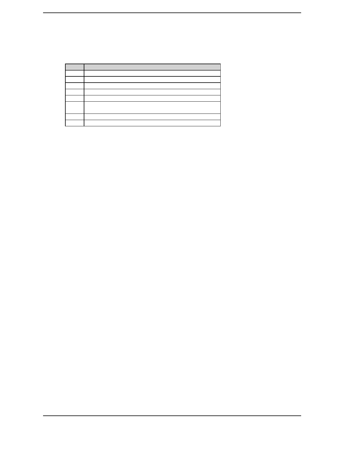
Chapter 5 Input/Output Interfaces
5-4 Compaq Deskpro EN Series of Personal Computers
Desktop and Minitower Form Factors
Third Edition – September 1998
The contents of the Error register are interpreted as a diagnostic status byte after the execution of
a diagnostic command or when the system is initialized.
Bit Function
7 Bad Block Mark Detected in Requested Sector ID Field (if set)
6 Non-correctable Data Error (if set)
5 Reserved
4 Requested Sector ID Field Not Found (if set)
3 Reserved
2 Requested Command Aborted Due To Invalid Hard Drive
Status or Invalid Command Code (if set)
1 Track 0 Not Found During Re-calibration Command (if set)
0 Data Address Mark Not Found After Correct ID Field (if set)
Set Features Register, I/O Port 1F1h/171h (Write Only)
This register is command-specific and may be used to enable and disable features of the interface.
Sector Count Register, I/O Port 1F2h/172h
This register defines either:
♦ the number of sectors of data to be read or written
or
♦ the number of sectors per track for format commands
If the value in this register is zero, a count of 256 sectors is specified. The sector count is
decremented as each sector is accessed, so that the value indicates the number of sectors left to
access when an error occurs in a multi-sector operation. During the Initialize Drive Parameters
command, this register contains the number of sectors per track.
Sector Number Register, I/O Port 1F3h/173h
The Sector Number register contains the starting sector number for a hard drive access.
Cylinder Low, Cylinder High Registers, I/O Port 1F4h, 1F5h/174h, 175h
These registers contain the starting cylinder number for each hard drive access. The three most-
significant bits of the value are held in byte address 1F5h (bits <2..0>) while the remaining bits
are held in location 1F4h.

Technical Reference Guide
Compaq Deskpro EN Series of Personal Computers
Desktop and Minitower Form Factors
Third Edition - September 1998
5-5
Drive Select/Head Register, I/O Port 1F6h/176h
Bit Function
7 Reserved
6,5 Sector Size:
00 = Reserved
01 = 512 bytes/sector
10, 11 = Reserved
4 Drive Select:
0 = Drive 1
1 = Drive 2
3..0 Head Select Number:
0000 = 0 1000 = 8
0001 = 1 1001 = 9
0010 = 2 1010 = 10
0011 = 3 1011 = 11
0100 = 4 1100 = 12
0101 = 5 1101 = 13
0110 = 6 1110 = 14
0111 = 7 1111 = 15
NOTE:
Setting bit <4> to 1 when Drive 2 is not present may cause remaining
controller registers to not respond until Drive 1 is selected again.
Status Register, I/O Port 1F7h/177h (Read Only)
The contents of this register are updated at the completion of each command. If the Busy bit is
set, no other bits are valid. Reading this register clears the IRQ14 interrupt.
Bit Function
7 Controller Busy. If set, controller is executing a command.
6 READY- Signal Active (if set).
5 WRITE FAULT- Signal Active (if set).
4 SEEK COMPLETE- Signal Active (if set)
3 Data Request. If set, the controller is ready for a byte or word-
length data transfer. Bit should be verified before each transfer.
2 Correctable Data Error Flag. If set, data error has occurred and
has been corrected.
1 INDEX- Signal Active (if set).
0 Error Detected. When set, indicates error has occurred. Other
bits in register should be checked to determine error source.
NOTE:
Register status of an error condition does not change
until register is read.
The alternate Status register at location 3F6h holds the same status data as location 1F7h but
does not clear hardware conditions when read.

Chapter 5 Input/Output Interfaces
5-6 Compaq Deskpro EN Series of Personal Computers
Desktop and Minitower Form Factors
Third Edition – September 1998
Command Register, I/O Port 1F7h/177h (Write Only)
The IDE controller commands are written to this register. The command write action should be
prefaced with the loading of data into the appropriate registers. Execution begins when the
command is written to 1F7h/177h. Table 5-4 lists the standard IDE commands.
Table 5–4. IDE Controller Commands
Table 5-4.
IDE Controller Commands
Command Value
Initialize Drive Parameters 91h
Seek 7xh
Recalibrate 1xh
Read Sectors with Retries 20h*
Read Long with Retries 22h*
Write Sectors with Retries 30h*
Write Long with Retries 32h*
Verify Sectors with Retries 40h
Format Track 50h
Execute Controller Diagnostic 90h
Idle 97h, E3h
Idle Immediate 95h, E1h
Enter Low Power and Enable/Disable Timeout 96h
Enter Idle and Enable/Disable Timeout 97h
Check Status 98h
Identify ECh
Read Buffer E4h
Write Buffer E8h
NOP 00h
Read DMA with Retry C8h
Read DMA without Retry C9h
Read Multiple C4h
Set Features EFh
Set Multiple Mode C6h
Sleep 99h, E6h
Standby 96h, E2h
Standby Immediate 94h, E0h
Write DMA with Retry CAh
Write DMA without Retry CBh
Write Multiple C5h
Write Same E9h
Write Verify 3Ch
* Without retries, add one to the value.
Alternate Status Register, I/O Port 3F6h/376h (Read Only)
The alternate Status register at location 3F6h holds the same status data as location 1F7h but
does not clear hardware conditions when read.

Technical Reference Guide
Compaq Deskpro EN Series of Personal Computers
Desktop and Minitower Form Factors
Third Edition - September 1998
5-7
Drive Control Register, I/O Port 3F6h/376h (Write Only)
Bit Function
7..3 Reserved
2 Controller Control:
0 = Re-enable
1 = Reset
1 Interrupt Enable/Disable
0 = Disable interrupts
1 = Enable interrupts
0 Reserved
Drive Access Register, I/O Port 3F7h/377h (Read Only)
Bit Function
7 Reserved
6 WRITE GATE- Signal Active (if set)
5..2 Head Select:
0000 = 15 1000 = 7
0001 = 14 1001 = 6
0010 = 13 1010 = 5
0011 = 12 1011 = 4
0100 = 11 1100 = 3
0101 = 10 1101 = 2
0110 = 9 1110 = 1
0111 = 8 1111 = 0
1,0 Drive Select:
00 = Disabled
01 = Drive 1 selected
10 = Drive 0 selected
11 = Invalid
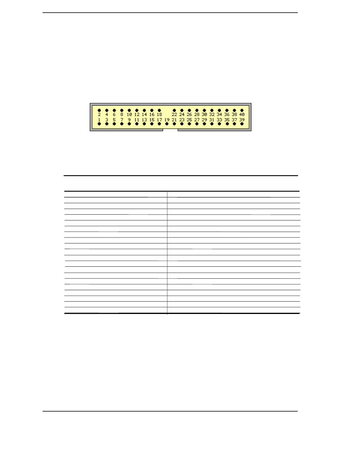
Chapter 5 Input/Output Interfaces
5-8 Compaq Deskpro EN Series of Personal Computers
Desktop and Minitower Form Factors
Third Edition – September 1998
5.2.2 IDE CONNECTOR
This system uses a standard 40-pin connector for IDE devices. Device power is supplied through
a separate connector.
Figure 5–1. 40-Pin IDE Connector.
Table 5–5. 40-Pin IDE Connector Pinout
Table 5-5.
40-Pin IDE Connector Pinout
Pin Signal Description Pin Signal Description
1 RESET- Reset 21 DRQ DMA Request
2 GND Ground 22 GND Ground
3 DD7 Data Bit <7> 23 IOW- I/O Write
4 DD8 Data Bit <8> 24 GND Ground
5 DD6 Data Bit <6> 25 IOR- I/O Read
6 DD9 Data Bit <9> 26 GND Ground
7 DD5 Data Bit <5> 27 IORDY I/O Channel Ready
8 DD10 Data Bit <10> 28 CSEL Cable Select
9 DD4 Data Bit <4> 29 DAK- DMA Acknowledge
10 DD11 Data Bit <11> 30 GND Ground
11 DD3 Data Bit <3> 31 IRQn Interrupt Request [1]
12 DD12 Data Bit <12> 32 IO16- 16-bit I/O
13 DD2 Data Bit <2> 33 DA1 Address 1
14 DD13 Data Bit <13> 34 DSKPDIAG Pass Diagnostics
15 DD1 Data Bit <1> 35 DA0 Address 0
16 DD14 Data Bit <14> 36 DA2 Address 2
17 DD0 Data Bit <0> 37 CS0- Chip Select
18 DD15 Data Bit <15> 38 CS1- Chip Select
19 GND Ground 39 HDACTIVE- Drive Active (front panel LED) [2]
20 -- Key 40 GND Ground
NOTES:
[1] Primary connector wired to IRQ14, secondary connector wired to IRQ15.
[2] Pin 39 is used for spindle sync and drive activity (becomes SPSYNC/DACT-)
when synchronous drives are connected.

Technical Reference Guide
Compaq Deskpro EN Series of Personal Computers
Desktop and Minitower Form Factors
Third Edition - September 1998
5-9
5.3 DISKETTE DRIVE INTERFACE
The diskette drive interface supports up to two diskette drives, each of which connect to a
standard 34-pin diskette drive connector. All models come standard with a 3.5-inch 1.44-MB
diskette drive installed as drive A. An additional diskette drive (either a 3.5-inch 720-KB, 1.44-
MB, or 2.88-MB drive or a 5.25-inch 360-KB or 1.2-MB drive) may also be installed as drive B.
The drive designation is determined by which connector is used on the diskette drive cable. The
drive attached to the end connector is drive A while the drive attached to the second (next to the
end) connector) is drive B.
On all models, the diskette drive interface function is integrated into the 87307 I/O controller
component. The internal logic of the I/O controller is software-compatible with standard 82077-
type logic. The diskette drive controller has three operational phases in the following order:
♦ Command phase - The controller receives the command from the system.
♦ Execution phase - The controller carries out the command.
♦ Results phase - Status and results data is read back from the controller to the system.
The Command phase consists of several bytes written in series from the CPU to the data register
(3F5h/375h). The first byte identifies the command and the remaining bytes define the
parameters of the command. The Main Status register (3F4h/374h) provides data flow control
for the diskette drive controller and must be polled between each byte transfer during the
Command phase.
The Execution phase starts as soon as the last byte of the Command phase is received. An
Execution phase may involve the transfer of data to and from the diskette drive, a mechnical
control function of the drive, or an operation that remains internal to the diskette drive controller.
Data transfers (writes or reads) with the diskette drive controller are by DMA, using the DRQ2
and DACK2- signals for control.
The Results phase consists of the CPU reading a series of status bytes (from the data register
(3F5h/375h)) that indicate the results of the command. Note that some commands do not have a
Result phase, in which case the Execution phase can be followed by a Command phase.
During periods of inactivity, the diskette drive controller is in a non-operation mode known as
the Idle phase.

Chapter 5 Input/Output Interfaces
5-10 Compaq Deskpro EN Series of Personal Computers
Desktop and Minitower Form Factors
Third Edition – September 1998
5.3.1 DISKETTE DRIVE PROGRAMMING
5.3.1.1 Diskette Drive Interface Configuration
The diskette drive controller must be configured for a specific address and also must be enabled
before it can be used. Address selection and enabling of the diskette drive interface are affected
by firmware through the PnP configuration registers of the 87307 I/O controller.
The PnP configuration registers are accessed through I/O registers 15Ch (index) and 15Dh
(data). The diskette drive I/F is initiated by firmware selecting logical device 3 of the 87307. This
is accomplished by the following sequence:
1. Write 07h to I/O register 15Ch.
2. Write 03h to I/O register 15Dh (this selects the diskette drive I/F).
3. Write 30h to I/O register 15Ch.
4. Write 01h to I/O register 15Dh (this activates the interface).
The diskette drive I/F configuration registers are listed in the following table:
Table 5–6. Diskette Drive Controller Configuration Registers
Table 5-6.
Diskette Drive Interface Configuration Registers
Index
Address Function R/W Reset
Value
30h Activate R/W 01h
31h I/O Range Check R/W 00h
60h Base Address MSB R/W 03h
61h Base Address LSB R/W F0h
70h Interrupt Select R/W 06h
71h Interrupt Type R/W 03h
74h DMA Channel Select R/W 02h
75h Report DMA Assignment RO 04h
F0h Configuration Data R/W --
F1h Drive ID R/W --

Technical Reference Guide
Compaq Deskpro EN Series of Personal Computers
Desktop and Minitower Form Factors
Third Edition - September 1998
5-11
5.3.1.2 Diskette Drive Interface Control
The BIOS function INT 13 provides basic control of the diskette drive interface. The diskette
drive interface can be controlled by software through I/O-mapped registers listed in Table 5-7.
Table 5–7. Diskette Drive Controller Registers
Table 5-7.
Diskette Drive Interface Control Registers
Primary
Address Alternate
Address Register R/W
3F1h 371h Media ID R
3F2h 372h Drive Control W
3F4h 374h Main Status R
3F5h 375h Data R/W
3F7h 377h Drive Status
Data Transfer Rate
R
W
The base address (3F1h or 371h) and enabling of the diskette drive controller is selected through
the Function Enable Register (FER, addr. 399.00h) of the 87307 I/O controller. Address selection
and enabling is automatically done by the BIOS during POST but can also be accomplished with
the Setup utility and other software.
The following paragraphs describe the diskette drive interface control registers.
Media ID Register, I/O Port 3F1h/371h (Read Only)
Bit Function
7..5 Media Type:
xx1 = Invalid
000 = 5.25 inch drive
010 = 2.88 MB (3.5 inch drive)
100 = 1.44 MB (3.5 inch drive)
110 = 720 KB (3.5 inch drive)
4..2 Reserved
1,0 Tape Select:
00 = None 10 = Drive 2
01 = Drive 1 11 = Drive 3
Drive Control Register, I/O Port 3F2h/372h (Write Only)
Bit Function
7,6 Reserved
5 Drive 2 Motor
0 = Off, 1 = On
4 Drive 1 Motor
0 = Off, 1 = On
3 Interrupt / DMA Enable
0 = Disabled, 1 = Enabled
2 Controller Enable
0 = Reset controller, 1 = Enable controller
1,0 Drive Select
00 = Drive 1
01 = Drive 2
10 = Reserved
11 = Tape drive

Chapter 5 Input/Output Interfaces
5-12 Compaq Deskpro EN Series of Personal Computers
Desktop and Minitower Form Factors
Third Edition – September 1998
Main Status Register, I/O Port 3F4h/374h (Read Only)
Bit Function
7 Request for Master. When set, indicates the controller is ready
to send or receive data from the CPU. Cleared immediately
after a byte transfer. Indicates interrupt pin status during non-
DMA phase.
6 Data I/O Direction.
0 = Expecting a write
1 = Expecting a read
5 Non-DMA Execution. When set, indicates controller is in the
execution phase of a byte transfer in non-DMA mode.
4 Command In Progress. When set, indicates that first byte of
command phase has been received. Cleared when last byte in
result phase is read.
3..0 Drive Busy Indicators. Bit is set after the last byte of the
command phase of a seek or recalibrate command is given by
the corresponding drive:
<3>, Drive 3
<2>, Drive 2
<1>, Drive 1
<0>, Drive 0
Data Register, I/O Port 3F5h/375h
Data commands are written to, and data and status bytes are read from this register.
Data Transfer Rate Register, I/O Port 3F7h/377h (Write Only)
Bit Function
7 Software Reset
6 Low Power Mode (if set)
5 Reserved
4..2 Write Precompensation Delay
000 = Default values for selected data rate (default)
1,0 Data Rate Select:
00 = 500 Kb/s
01 = 300 Kb/s
10 = 250 Kb/s
11 = 1 or 2 Mb/s (depending on TUP reg. Bit <1>)
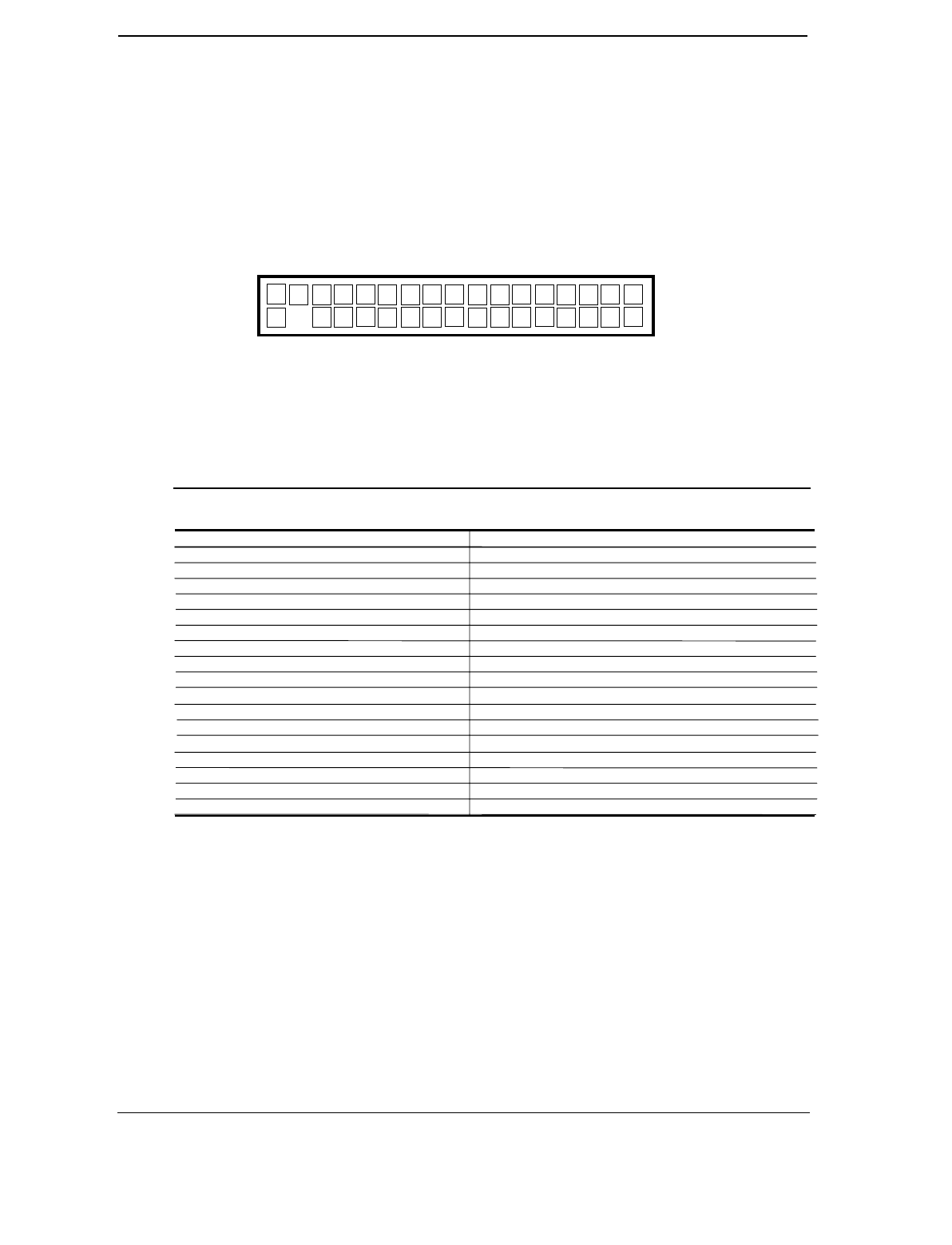
Technical Reference Guide
Compaq Deskpro EN Series of Personal Computers
Desktop and Minitower Form Factors
Third Edition - September 1998
5-13
5.3.2 DISKETTE DRIVE CONNECTOR
This system uses a standard 34-pin connector (refer to Figure 5-2 and Table 5-8 for the pinout)
for diskette drives. Drive power is supplied through a separate connector.
Figure 5–2. 34-Pin Diskette Drive Connector.
Table 5–8. 34-Pin Diskette Drive Connector Pinout
Table 5-8.
34-Pin Diskette Drive Connector Pinout
Pin Signal Description Pin Signal Description
1 GND Ground 18 DIR- Drive head direction control
2 LOW DEN- Low density select 19 GND Ground
3 --- (KEY) 20 STEP- Drive head track step control
4 MEDIA ID- Media identification 21 GND Ground
5 GND Ground 22 WR DATA- Write data
6 DRV 4 SEL- Drive 4 select 23 GND Ground
7 GND Ground 24 WR ENABLE- Enable for WR DATA-
8 INDEX- Media index is detected 25 GND Ground
9 GND Ground 26 TRK 00- Heads at track 00 indicator
10 MTR 1 ON- Activates drive motor 27 GND Ground
11 GND Ground 28 WR PRTK- Media write protect status
12 DRV 2 SEL- Drive 2 select 29 GND Ground
13 GND Ground 30 RD DATA- Data and clock read off disk
14 DRV 1 SEL- Drive 1 select 31 GND Ground
15 GND Ground 32 SIDE SEL- Head select (side 0 or 1)
16 MTR 2 ON- Activates drive motor 33 GND Ground
17 GND Ground 34 DSK CHG- Drive door opened indicator
2 34
33
32
31
30
29
28
27
26
25
24
23
22
21
20
19
18
17
16
15
14
13
12
11
10
9
8
7
6
5
4
1
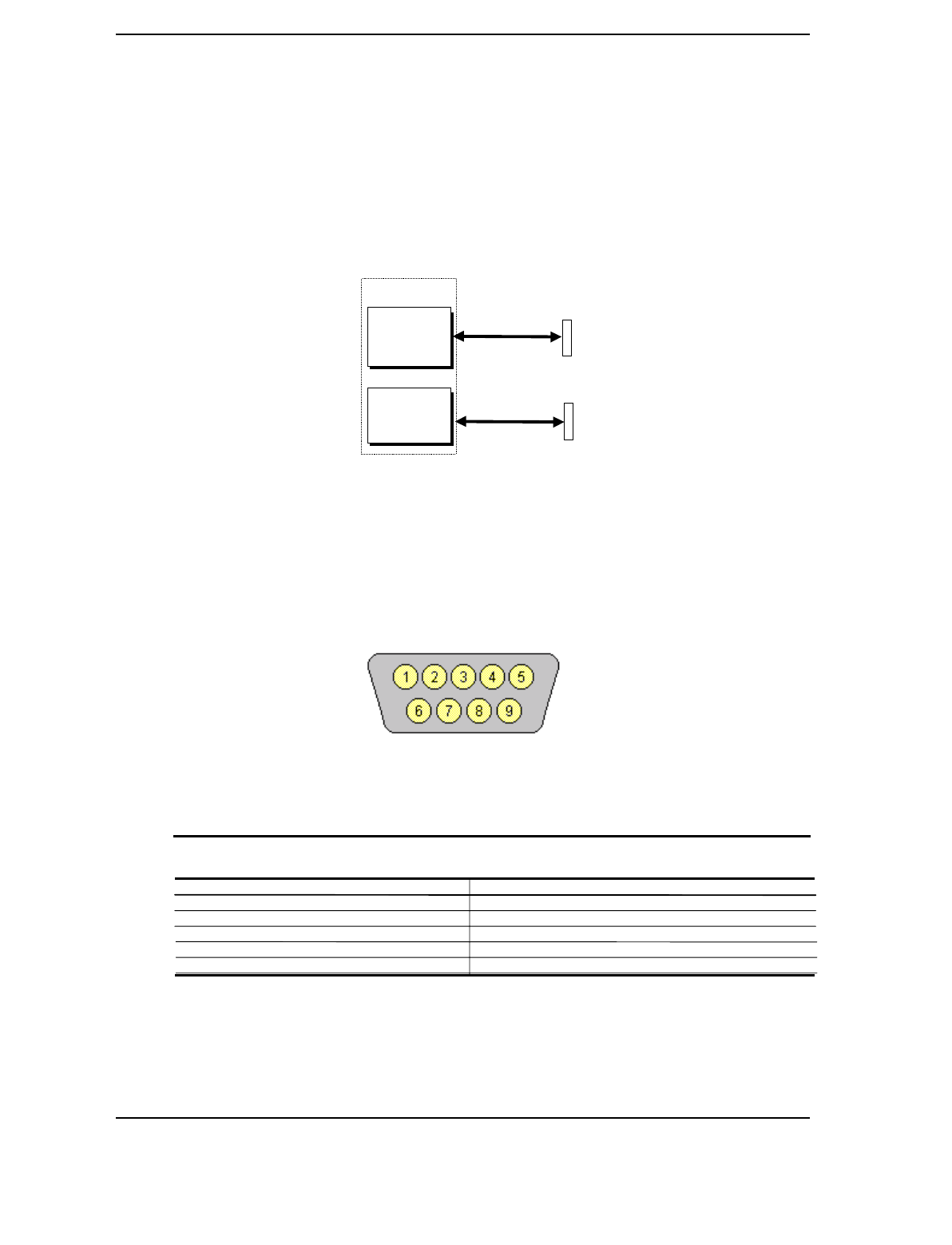
Chapter 5 Input/Output Interfaces
5-14 Compaq Deskpro EN Series of Personal Computers
Desktop and Minitower Form Factors
Third Edition – September 1998
5.4 SERIAL INTERFACES
The serial interfaces transmit and receive asynchronous serial data with external devices. The
serial interface function is provided by the 87307 I/O controller component, which includes two
16550/16450-compatible UARTs. Each UART is supported by a DB-9 connector on the rear of
the chassis.
Figure 5–3. Serial Interfaces Block Diagram
5.4.1 RS-232 INTERFACE
The DB-9 connector-based interface complies with EIA standard RS-232-C, which includes
modem control signals and supports baud rates up to 115.2 Kbps. The DB-9 connector is shown
in the following figure and the pinout of the connector is listed in Table 5-9.
Figure 5–4. Serial Interface Connector (Male DB-9 as viewed from rear of chassis)
Table 5–9. DB-9 Serial Connector Pinout
Table 5-9.
DB-9 Serial Connector Pinout
Pin Signal Description Pin Signal Description
1 CD Carrier Detect 6 DSR Data Set Ready
2 RX Data Receive Data 7 RTS Request To Send
3 TX Data Transmit Data 8 CTS Clear To Send
4 DTR Data Terminal Ready 9 RI Ring Indicator
5 GND Ground -- -- --
Each DB-9 port is independently configurable as to it’s COMn (address) designation.
UART1
(Log. Dev. 6)
UART2
(Log. Dev. 5)
DB-9 A (RS-232)
DB-9 B (RS-232)
TX/RX/CNTRL
TX/RX/CNTRL
87307

Technical Reference Guide
Compaq Deskpro EN Series of Personal Computers
Desktop and Minitower Form Factors
Third Edition - September 1998
5-15
5.4.2 SERIAL INTERFACE PROGRAMMING
5.4.2.1 Serial Interface Configuration
The serial interfaces must be configured for a specific address range (COM1, COM2, etc.) and
also must be activated before it can be used. Address selection and activation of the serial
interface are affected through the PnP configuration registers of the 87307 I/O controller.
The PnP configuration registers are accessed through I/O registers 15Ch (index) and 15Dh
(data). Each serial interface is initiated by firmware selecting logical device 5 or 6 of the 87307.
This is accomplished by the following sequence:
1. Write 07h to I/O register 15Ch.
2. Write 05h or 06h to I/O register 15Dh (for selecting UART2 or UART1).
3. Write 30h to I/O register 15Ch.
4. Write 01h to I/O register 15Dh (this activates the interface).
The serial interface configuration registers are listed in the following table:
Table 5–10. Serial Interface Configuration Registers
Table 5-10.
Serial Interface Configuration Registers
Index
Address Function R/W Reset
Value [1]
30h Activate R/W 00h / 00h
31h I/O Range Check R/W 00h / 00h
60h Base Address MSB R/W 02h / 03h
61h Base Address LSB R/W F8h / F8h
70h Interrupt Select R/W 03h / 04h
71h Interrupt Type R/W 03h / 03h
74h DMA Channel Select R/W 04h / 04h
75h Report DMA Assignment RO 04h / 04h
F0h Configuration Data R/W --
NOTES:
[1] Device 5 (UART2) / Device 6 (UART1)

Chapter 5 Input/Output Interfaces
5-16 Compaq Deskpro EN Series of Personal Computers
Desktop and Minitower Form Factors
Third Edition – September 1998
5.4.2.2 Serial Interface Control
The BIOS function INT 14 provides basic control of the serial interface. The serial interface can
be controlled by software through the registers listed in Table 5-11.
Table 5–11. Serial Interface Control Registers
Table 5-11.
Serial Interface Control Registers
Address Register R/W
Base Receive Buffer / Transmit Holding [1] R/W
Base, Base + 1 Baud Rate Divisor Latch [2] R/W
Base + 1 Interrupt Enable R/W
Base + 2 Interrupt ID RO
Base + 3 Line Control R/W
Base + 4 Modem Control R/W
Base + 5 Line Status RO
Base + 6 Modem Status RO
Base + 7 Scratch Pad R/W
NOTES:
Base Address:
COM1 = 3F8h
COM2 = 2F8h
[1] This register holds receive data when read from and transmit data when written to.
[2] When bit <7> of the Line Control register is set (1), writing to 3F8h and 3F9h
programs the divisor rate for the baud rate generator.
Receive Buffer / Transmit Holding Register, I/O Port 3F8h/2F8h
When read by the CPU, this byte contains receive data. When written to by the CPU, the byte
contains data to be transmitted.
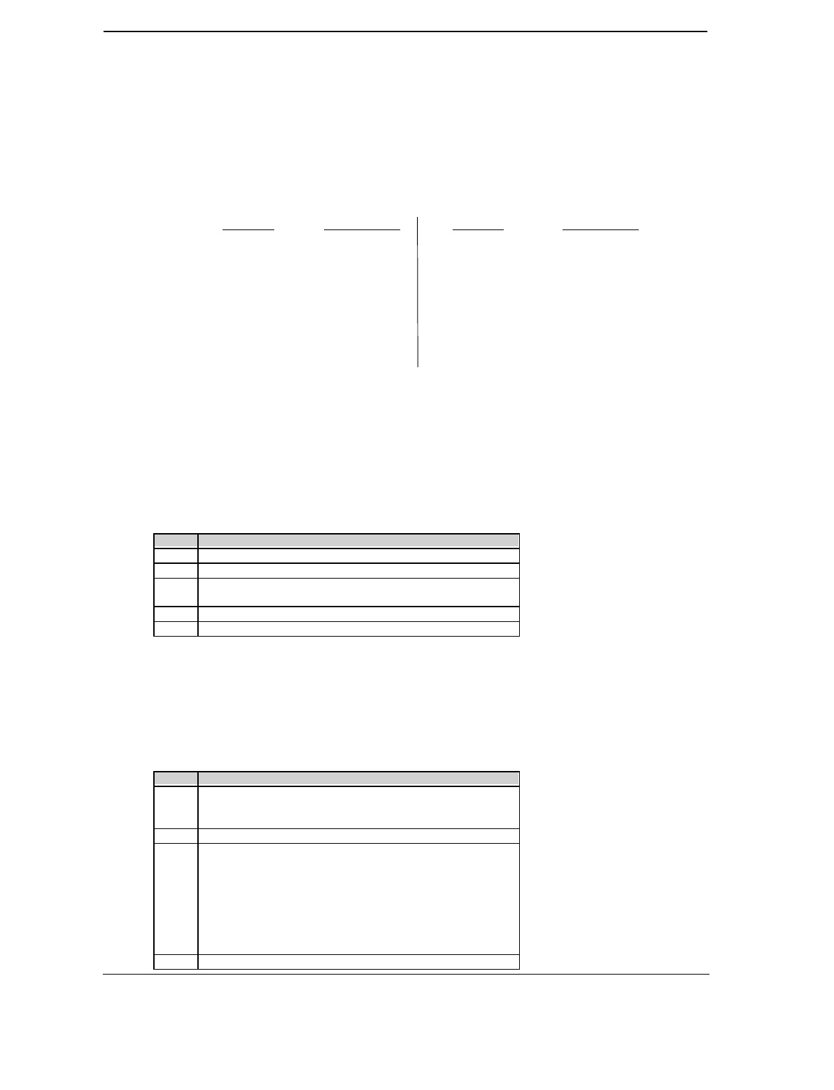
Technical Reference Guide
Compaq Deskpro EN Series of Personal Computers
Desktop and Minitower Form Factors
Third Edition - September 1998
5-17
Baud Rate Divisor Latch Register, I/O Port 3F8h, 3F9h/2F8, 2F9h
When bit <7> of the Line Control register is set (1), a write to this pair of locations loads the
decimal value used to divide the 1.8462-MHz clock to create the desired baud rate for serial
transmission. The possible baud rates are shown as follows:
Baud Rate Decimal Divisor Baud Rate Decimal Divisor
50 2304 2400 48
75 1536 3600 32
110 1047 4800 24
134.5 857 7200 16
150 768 9600 12
300 384 19200 6
600 192 38400 3
1200 96 57600 2
1800 64 115200 1
2000 58
Divisor = 1846200 / (Desired baud rate X 16)
Interrupt Enable Register, I/O Port 3F9h/2F9h
Bits <3..0> of this register are used for enabling interrupt sources. A set bit enables interrupt
generation by the associated source.
Bit Function
7..4 Reserved
3 Modem Status Interrupt Enable (if set) (CTS, DSR, RI, CD)
2 Receiver Line Status Interrupt Enable (if set) (Overrun error,
parity error, framing error, break)
1 Transmitter Holding Register Empty Interrupt Enable (if set)
0 Baud Rate Divisor Interrupt Enable (if set)
Interrupt ID Register, I/O Port 3FAh/2FAh (Read Only)
This read-only register indicates the serial controller as the source of the interrupt (bit <0>) as
well as the reason (bits <3..1>) for the interrupt. Reading this register clears the interrupt and
sets bit <0>.
Bit Function
7,6 FIFO Enable/Disable
0 = Disabled
1 = Enabled
5,4 Reserved
3..1 Interrupt Source:
000 = Modem status (lowest priority)
001 = Transmitter holding reg. Empty
010 = Received data available
011 = Receiver line status reg.
100,101 = Reserved
110 = Character time-out (highest priority)
111 = Reserved
0 Interrupt Pending (if cleared)
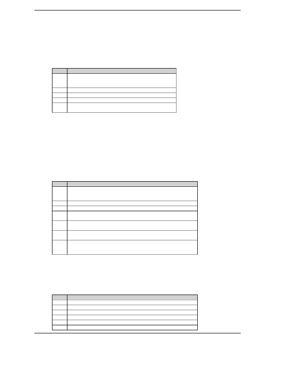
Chapter 5 Input/Output Interfaces
5-18 Compaq Deskpro EN Series of Personal Computers
Desktop and Minitower Form Factors
Third Edition – September 1998
FIFO Control Register, I/O Port 3FAh/2FAh (Write Only)
This write-only register enables and clears the FIFOs and sets the trigger level and DMA mode.
Bit Function
7,6 Receiver Trigger Level
00 = 1 byte 10 = 8 bytes
01 = 4 bytes 11 = 14 bytes
5..3 Reserved
2 Transmit FIFO Reset (if set)
1 Receive FIFO Reset (if set)
0 FIFOs Enable/Disable
0 = Disable TX/RX FIFOs, 1 = Enable TX/RX FIFOs
Line Control Register, I/O Port 3FBh/2FBh
This register specifies the data transmission format.
Bit Function
7 RX Buffer / TX Holding Reg. And Divisor Rate Reg. Access
0 = RX buffer, TX holding reg., and Interrupt En. Reg. Are accessable.
1 = Divisor Latch reg. is accessable.
6 Break Control (forces SOUT signal low if set)
5 Stick Parity. If set, even parity bit is logic 0, odd parity bit is logic 1
4 Parity Type
0 = Odd, 1 = Even
3 Parity Enable:
0 = Disabled, 1 = Enabled
2 Stop Bit:
0 = 1 stop bit, 1 = 2 stop bits
1,0 Word Size:
00 = 5 bits 10 = 7 bits
01 = 6 bits 11 = 8 bits
Modem Control Register, I/O Port 3FCh/2FCh
This register controls the modem signal lines
Bit Function
7..5 Reserved
4 Internal Loopback Enabled (if set)
3 Serial Interface Interrupts Enabled (if set)
2 Reserved
1 RTS Signal Active (if set)
0 DTR Signal Active (if set)
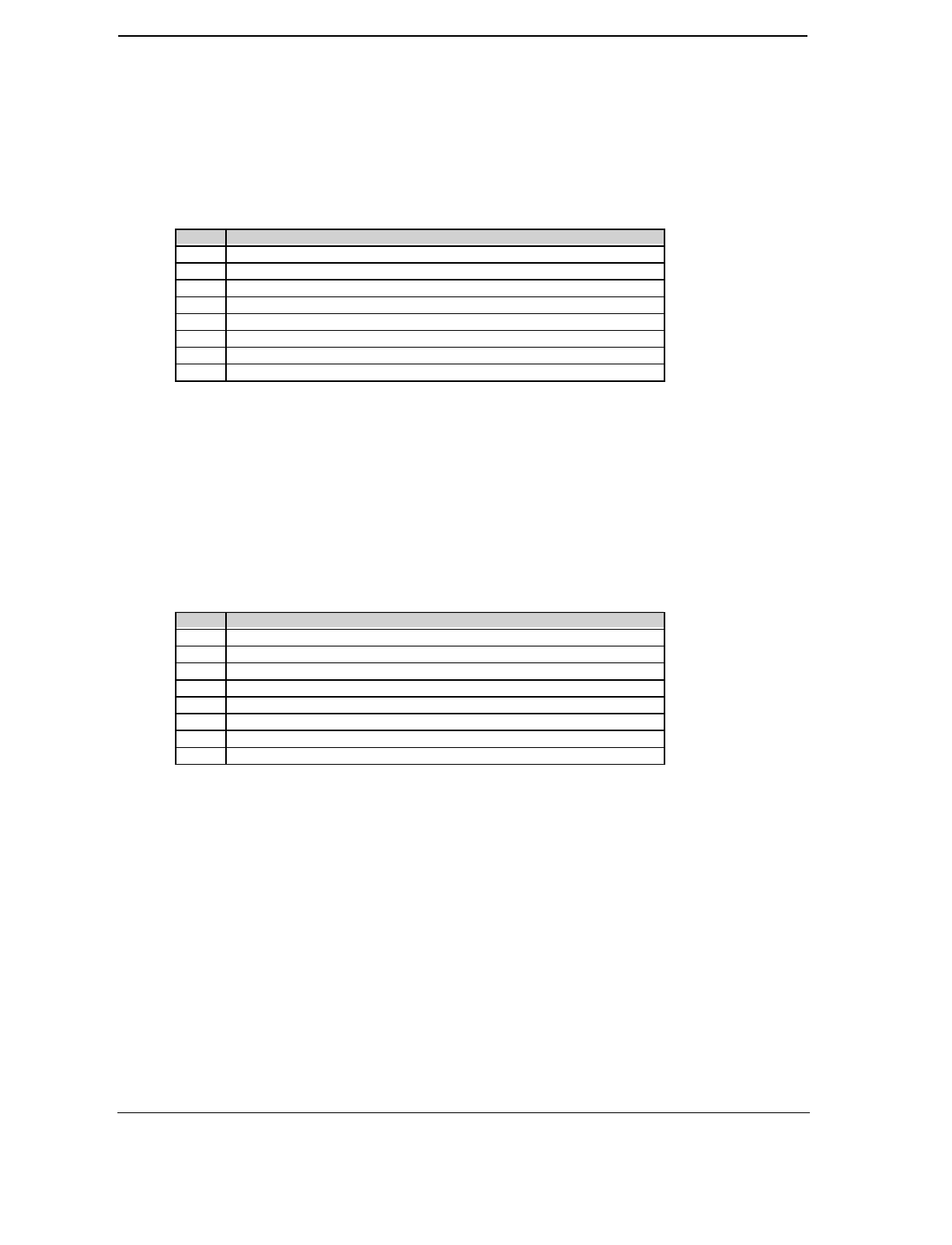
Technical Reference Guide
Compaq Deskpro EN Series of Personal Computers
Desktop and Minitower Form Factors
Third Edition - September 1998
5-19
Line Status Register, I/O Port 3FDh/2FDh (Read Only)
This register contains the status of the current data transfer. Bits <2..0> are cleared when read.
Bit Function
7 Parity Error, Framing Error, or Break Cond. Exists (if set)
6 TX Holding Reg. and Transmitter Shift Reg. Are Empty (if set)
5 TX Holding Reg. Is Empty (if set)
4 Break Interrupt Has Occurred (if set)
3 Framing Error Has Occurred (if set)
2 Parity Error Has Occurred (if set)
1 Overrun Error Has Occurred (if set)
0 Data Register Ready To Be Read (if set)
Modem Status Register, I/O Port 3FEh/2FEh (Read Only)
This register contains the status of the modem signal lines. A set bit indicates that the associated
signal is active.
Bit Function
7 DCD- Active
6 RI- Active
5 DSR Active
4 CTS Active
3 DCD- Changed Since Last Read
2 RI- Changed From Low to High Since Last Read
1 DSR- Has Changed State Since Last Read
0 CTS- Has Changed State Since Last Read
Scratch Pad Register, I/O Port 3FFh/2FFh
This register is not used in this system.

Chapter 5 Input/Output Interfaces
5-20 Compaq Deskpro EN Series of Personal Computers
Desktop and Minitower Form Factors
Third Edition – September 1998
5.5 PARALLEL INTERFACE
The parallel interface provides connection to a peripheral device that has a compatible interface,
the most common being a printer. The parallel interface function is integrated into the 87307 I/O
controller component and provides bi-directional 8-bit parallel data transfers with a peripheral
device. The parallel interface supports three main modes of operation:
♦ Standard Parallel Port (SPP) mode
♦ Enhanced Parallel Port (EPP) mode
♦ Extended Capabilities Port (ECP) mode
These three modes (and their submodes) provide complete support as specified for an IEEE 1284
parallel port.
5.5.1 STANDARD PARALLEL PORT MODE
The Standard Parallel Port (SPP) mode uses software-based protocol and includes two sub-modes
of operation, compatible and extended, both of which can provide data transfers up to 150 KB/s.
In the compatible mode, CPU write data is simply presented on the eight data lines. A CPU read
of the parallel port yields the last data byte that was written.
The following steps define the standard procedure for communicating with a printing device:
1. The system checks the Printer Status register. If the Busy, Paper Out, or Printer Fault signals
are indicated as being active, the system either waits for a status change or generates an error
message.
2. The system sends a byte of data to the Printer Data register, then pulses the printer STROBE
signal (through the Printer Control register) for at least 500 ns.
3. The system then monitors the Printer Status register for acknowledgment of the data byte
before sending the next byte.
In extended mode, a direction control bit (CTR 37Ah, bit <5>) controls the latching of output
data while allowing a CPU read to fetch data present on the data lines, thereby providing bi-
directional parallel transfers to occur.
The SPP mode uses three registers for operation: the Data register (DTR), the Status register
(STR) and the Control register (CTR). Address decoding in SPP mode includes address lines A0
and A1.

Technical Reference Guide
Compaq Deskpro EN Series of Personal Computers
Desktop and Minitower Form Factors
Third Edition - September 1998
5-21
5.5.2 ENHANCED PARALLEL PORT MODE
In Enhanced Parallel Port (EPP) mode, increased data transfers are possible (up to 2 MB/s) due
to a hardware protocol that provides automatic address and strobe generation. EPP revisions 1.7
and 1.9 are both supported. For the parallel interface to be initialized for EPP mode, a
negotiation phase is entered to detect whether or not the connected peripheral is compatible with
EPP mode. If compatible, then EPP mode can be used. In EPP mode, system timing is closely
coupled to EPP timing. A watchdog timer is used to prevent system lockup.
Five additional registers are available in EPP mode to handle 16- and 32-bit CPU accesses with
the parallel interface. Address decoding includes address lines A0, A1, and A2.
5.5.3 EXTENDED CAPABILITIES PORT MODE
The Extended Capabilities Port (ECP) mode, like EPP, also uses a hardware protocol-based
design that supports transfers up to 2 MB/s. Automatic generation of addresses and strobes as
well as Run Length Encoding (RLE) decompression is supported by ECP mode. The ECP mode
includes a bi-directional FIFO buffer that can be accessed by the CPU using DMA or
programmed I/O. For the parallel interface to be initialized for ECP mode, a negotiation phase is
entered to detect whether or not the connected peripheral is compatible with ECP mode. If
compatible, then ECP mode can be used.
Ten control registers are available in ECP mode to handle transfer operations. In accessing the
control registers, the base address is determined by address lines A2-A9, with lines A0, A1, and
A10 defining the offset address of the control register. Registers used for FIFO operations are
accessed at their base address + 400h (i.e., if configured for LPT1, then 378h + 400h = 778h).
The ECP mode includes several sub-modes as determined by the Extended Control register. Two
submodes of ECP allow the parallel port to be controlled by software. In these modes, the FIFO
is cleared and not used, and DMA and RLE are inhibited.
NOTE: The 87307 does not support ECP v1.7 submode of ECP mode 4.

Chapter 5 Input/Output Interfaces
5-22 Compaq Deskpro EN Series of Personal Computers
Desktop and Minitower Form Factors
Third Edition – September 1998
5.5.4 PARALLEL INTERFACE PROGRAMMING
5.5.4.1 Parallel Interface Configuration
The parallel interface must be configured for a specific address range (LPT1, LPT2, etc.) and
also must be enabled before it can be used. When configured for EPP or ECP mode, additional
considerations must be taken into account. Address selection, enabling, and EPP/ECP mode
parameters of the parallel interface are affected through the PnP configuration registers of the
87307 I/O controller. Address selection and enabling are automatically done by the BIOS during
POST but can also be accomplished with the Setup utility and other software.
The PnP configuration registers are accessed through I/O registers 15Ch (index) and 15Dh
(data). The parallel interface is initiated by firmware selecting logical device 4 of the 87307. This
is accomplished by the following sequence:
1. Write 07h to I/O register 15Ch.
2. Write 04h to I/O register 15Dh (for selecting the parallel interface).
3. Write 30h to I/O register 15Ch.
4. Write 01h to I/O register 15Dh (this activates the interface).
The parallel interface configuration registers are listed in the following table:
Table 5–12. Parallel Interface Configuration Registers
Table 5-12.
Parallel Interface Configuration Registers
Index
Address Function R/W Reset
Value
30h Activate R/W 01h
31h I/O Range Check R/W 00h
60h Base Address MSB R/W 02h
61h Base Address LSB R/W 78h
70h Interrupt Select R/W 07h
71h Interrupt Type R/W 00h
74h DMA Channel Select R/W 04h
75h Report DMA Assignment RO 04h
F0h Configuration Data R/W --

Technical Reference Guide
Compaq Deskpro EN Series of Personal Computers
Desktop and Minitower Form Factors
Third Edition - September 1998
5-23
5.5.4.2 Parallel Interface Control
The BIOS function INT 17 provides simplified control of the parallel interface. Basic functions
such as initialization, character printing, and printer status are provide by subfunctions of INT
17. The parallel interface is controllable by software through a set of I/O mapped registers. The
number and type of registers available depends on the mode used (SPP, EPP, or ECP). Table 5-13
lists the parallel registers and associated functions based on mode.
Table 5–13. Parallel Interface Control Registers
Table 5-13.
Parallel Interface Control Registers
Register I/O
Address SPP Mode
Ports EPP Mode
Ports ECP Mode
Ports
Data Base LPT1,2,3 LPT1,2 LPT1,2,3
Status Base + 1h LPT1,2,3 LPT1,2 LPT1,2,3
Control Base + 2h LPT1,2,3 LPT1,2 LPT1,2,3
Address Base + 3h -- LPT1,2 --
Data Port 0 Base + 4h -- LPT1,2 --
Data Port 1 Base + 5h -- LPT1,2 --
Data Port 2 Base + 6h -- LPT1,2 --
Data Port 3 Base + 7h -- LPT1,2 --
Parallel Data FIFO Base + 400h -- -- LPT1,2,3
ECP Data FIFO Base + 400h -- -- LPT1,2,3
Test FIFO Base + 400h -- -- LPT1,2,3
Configuration Register A Base + 400h -- -- LPT1,2,3
Configuration Register B Base + 401h -- -- LPT1,2,3
Extended Control Register Base + 402h -- -- LPT1,2,3
Base Address:
LPT1 = 378h
LPT2 = 278h
LPT3 = 3BCh
The following paragraphs describe the individual registers. Note that only the LPT1-based
addresses are given in these descriptions.
Data Register, I/O Port 378h
Data written to this register is presented to the data lines D0-D7. A read of this register when in
SPP-compatible mode yields the last byte written. A read while in SPP-extended or ECP mode
yields the status of data lines D0-D7 (i.e., receive data).
In ECP mode in the forward (output) direction, a write to this location places a tagged command
byte into the FIFO and reads have no effect.
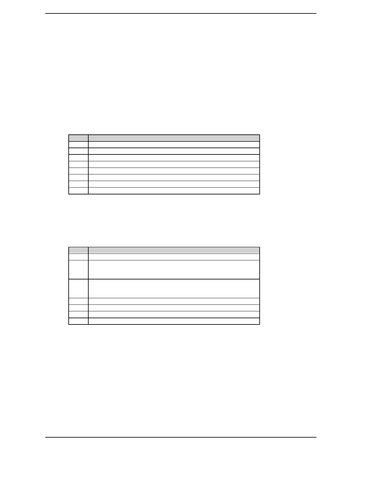
Chapter 5 Input/Output Interfaces
5-24 Compaq Deskpro EN Series of Personal Computers
Desktop and Minitower Form Factors
Third Edition – September 1998
Status Register, I/O Port 379h, Read Only
This register contains the current printer status. Reading this register clears the interrupt
condition of the parallel port.
Bit Function
7 Printer Busy (if 0)
6 Printer Acknowledgment Of Data Byte (if 0)
5 Printer Out Of Paper (if 1)
4 Printer Selected/Online (if 1)
3 Printer Error (if 0)
2 Reserved
1 EPP Interrupt Occurred (if set while in EPP mode)
0 EPP Timeout Occurred (if set while in EPP mode)
Control Register, I/O Port 37Ah
This register provides the printer control functions.
Bit Function
7,6 Reserved
5 Direction Control for PS/2 and ECP Modes:
0 = Forward. Drivers enabled. Port writes to peripheral (default)
1 = Backward. Tristates drivers and data is read from peripheral
4 Acknowledge Interrupt Enable
0 = Disable ACK interrupt
1 = Enable interrupt on rising edge of ACK
3 Printer Select (if 0)
2 Printer Initialize (if 1)
1 Printer Auto Line Feed (if 0)
0 Printer Strobe (if 0)
Address Register, I/O Port 37Bh (EPP Mode Only)
This register is used for selecting the EPP register to be accessed.
Data Port Registers 0-3, I/O Ports 37C-Fh (EPP Mode Only)
These registers are used for reading/writing data. Port 0 is used for all transfers. Ports 1-3 are
used for transferring the additional bytes of 16- or 32-bit transfers through port 0.
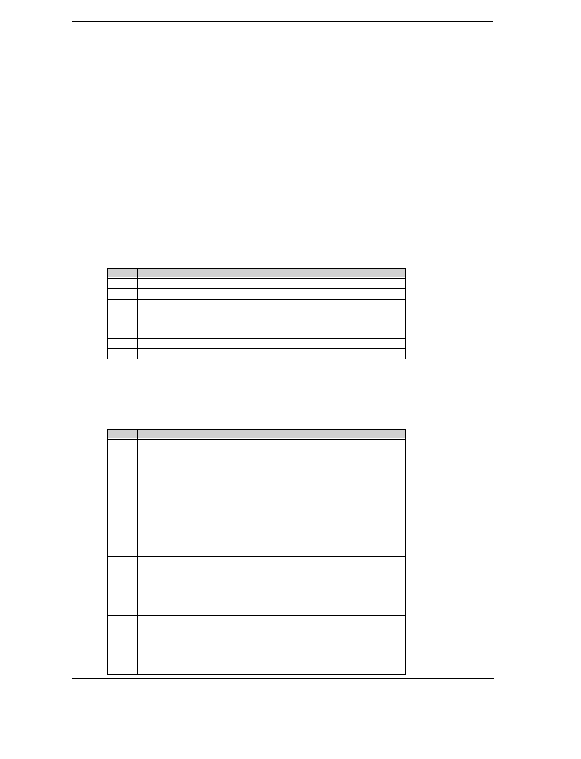
Technical Reference Guide
Compaq Deskpro EN Series of Personal Computers
Desktop and Minitower Form Factors
Third Edition - September 1998
5-25
FIFO Register, I/O Port 7F8h (ECP Mode Only)
While in ECP/forward mode, this location is used for filling the 16-byte FIFO with data bytes.
Reads have no effect (except when used in Test mode). While in ECP/backward mode, reads
yield data bytes from the FIFO.
Configuration Register A, I/O Port 7F8h (ECP Mode Only)
A read of this location yields 10h, while writes have no effect.
Configuration Register B, I/O Port 7F9h (ECP Mode, Read Only)
A read of this location yields the status defined as follows:
Bit Function
7 Reserved (always 0)
6 Status of Selected IRQ
n
.
5,4 Selected IRQ Indicator:
00 = IRQ7
11 = IRQ5
All other values invalid.
3 Reserved (always 1)
2..0 Reserved (always 000)
Extended Control Register B, I/O Port 7FAh (ECP ModeOnly)
This register defines the ECP mode functions.
Bit Function
7..5 ECP Submode Select:
000 = Standard forward mode (37Ah <5> forced to 0). Writes are
controlled by software and FIFO is reset.
001 = PS/2 mode. Reads and writes are software controlled and
FIFO is reset.
010 = Parallel Port FIFO forward mode (37Ah <5> forced to 0). Writes are
hardware controlled.
011 = ECP FIFO mode. Direction determined by 37Ah, <5>. Reads and
writes are hardware controlled.
4 ECP Interrupt Mask:
0 = Interrupt is generated on ERR- assertion.
1 = Interrupt is inhibited.
3 ECP DMA Enable/Disable.
0 = Disabled
1 = Enabled
2 ECP Interrupt Generation with DMA
0 = Enabled
1 = Disabled
1 FIFO Full Status (Read Only)
0 = Not full (at least 1 empty byte)
1 = Full
0 FIFO Empty Status (Read Only)
0 = Not empty (contains at least 1 byte)
1 = Empty
Chapter 5 Input/Output Interfaces
5-26 Compaq Deskpro EN Series of Personal Computers
Desktop and Minitower Form Factors
Third Edition – September 1998
5.5.5 PARALLEL INTERFACE CONNECTOR
Figure 5-5 and Table 5-14 show the connector and pinout of the parallel interface connector.
Figure 5–5. Parallel Interface Connector (Female DB-25 as viewed from rear of chassis)
Table 5–14. DB-25 Parallel Connector Pinout
Table 5-14.
DB-25 Parallel Connector Pinout
Pin Signal Description Pin Signal Description
1 STB- Strobe 14 LF- Line Feed
2 D0 Data 0 15 ERR- Error
3 D1 Data 1 16 INIT- Initialize Paper
4 D2 Data 2 17 SLCTIN- Select In
5 D3 Data 3 18 GND Ground
6 D4 Data 4 19 GND Ground
7 D5 Data 5 20 GND Ground
8 D6 Data 6 21 GND Ground
9 D7 Data 7 22 GND Ground
10 ACK- Acknowledge 23 GND Ground
11 BSY Busy 24 GND Ground
12 PE Paper End 25 GND Ground
13 SLCT Select -- -- --

Technical Reference Guide
Compaq Deskpro EN Series of Personal Computers
Desktop and Minitower Form Factors
Third Edition - September 1998
5-27
5.6 KEYBOARD/POINTING DEVICE INTERFACE
The keyboard/pointing device interface provides the connection of an enhanced keyboard and a
mouse using PS/2-type connections. The keyboard/pointing device interface function is provided
by the 87307 I/O controller component, which integrates 8042-compatible keyboard controller
logic (hereafter referred to as simply the “8042”) to communicate with the keyboard and pointing
device using bi-directional serial data transfers. The 8042 handles scan code translation and
password lock protection for the keyboard as well as communications with the pointing device.
This section describes the interface itself. The keyboard is discussed in the Appendix C.
5.6.1 KEYBOARD INTERFACE OPERATION
The data/clock link between the 8042 and the keyboard is uni-directional for Keyboard Mode 1
and bi-directional for Keyboard Modes 2 and 3. (These modes are discussed in detail in
Appendix C). This section describes Mode 2 (the default) mode of operation.
Communication between the keyboard and the 8042 consists of commands (originated by either
the keyboard or the 8042) and scan codes from the keyboard. A command can request an action
or indicate status. The keyboard interface uses IRQ1 to get the attention of the CPU.
The 8042 can send a command to the keyboard at any time. When the 8042 wants to send a
command, the 8042 clamps the clock signal from the keyboard for a minimum of 60 us. If the
keyboard is transmitting data at that time, the transmission is allowed to finish. When the 8042 is
ready to transmit to the keyboard, the 8042 pulls the data line low, causing the keyboard to
respond by pulling the clock line low as well, allowing the start bit to be clocked out of the 8042.
The data is then transferred serially, LSb first, to the keyboard (Figure 5-6). An odd parity bit is
sent following the eighth data bit. After the parity bit is received, the keyboard pulls the data line
low and clocks this condition to the 8042. When the keyboard receives the stop bit, the clock line
is pulled low to inhibit the keyboard and allow it to process the data.
Parameter Minimum Maximum
Tcy (Cycle Time) 0 us 80 us
Tcl (Clock Low) 25 us 35 us
Tch (Clock High) 25 us 45 us
Th (Data Hold) 0 us 25 us
Tss (Stop Bit Setup) 8 us 20 us
Tsh (Stop Bit Hold) 15 us 25 us
Figure 5–6. 8042-To-Keyboard Transmission of Code EDh, Timing Diagram
Start
Bit
D0
(LSb)
D1 D2 D3 D4 D5 D6 D7
(MSb)
Parity Stop
Bit
01011011110
Data
Clock
Th Tcl TchTcy Tss Tsh

Chapter 5 Input/Output Interfaces
5-28 Compaq Deskpro EN Series of Personal Computers
Desktop and Minitower Form Factors
Third Edition – September 1998
Control of the data and clock signals is shared by the 8042and the keyboard depending on the
originator of the transferred data. Note that the clock signal is always generated by the keyboard.
After the keyboard receives a command from the 8042, the keyboard returns an ACK code. If a
parity error or timeout occurs, a Resend command is sent to the 8042.
Table 5-15 lists and describes commands that can be issued by the 8042 to the keyboard.
Table 5–15. 8042-To-Keyboard Commands
Table 5-15.
8042-To-Keyboard Commands
Command Value Description
Set/Reset Status Indicators EDh Enables LED indicators. Value EDh is followed by an option
byte that specifies the indicator as follows:
Bits <7..3> not used
Bit <2>, Caps Lock (0 = off, 1 = on)
Bit <1>, NUM Lock (0 = off, 1 = on)
Bit <0>, Scroll Lock (0 = off, 1 = on)
Echo EEh Keyboard returns EEh when previously enabled.
Invalid Command EFh/F1h These commands are not acknowledged.
Select Alternate Scan Codes F0h Instructs the keyboard to select another set of scan codes
and sends an option byte after ACK is received:
01h = Mode 1
02h = Mode 2
03h = Mode 3
Read ID F2h Instructs the keyboard to stop scanning and return two
keyboard ID bytes.
Set Typematic Rate/Display F3h Instructs the keyboard to change typematic rate and delay
to specified values:
Bit <7>, Reserved - 0
Bits <6,5>, Delay Time
00 = 250 ms
01 = 500 ms
10 = 750 ms
11 = 1000 ms
Bits <4..0>, Transmission Rate:
00000 = 30.0 ms
00001 = 26.6 ms
00010 = 24.0 ms
00011 = 21.8 ms
:
11111 = 2.0 ms
Enable F4h Instructs keyboard to clear output buffer and last typematic
key and begin key scanning.
Default Disable F5h Resets keyboard to power-on default state and halts
scanning pending next 8042 command.
Set Default F6h Resets keyboard to power-on default state and enable
scanning.
Set Keys - Typematic F7h Clears keyboard buffer and sets default scan code set. [1]
Set Keys - Make/Brake F8h Clears keyboard buffer and sets default scan code set. [1]
Set Keys - Make F9h Clears keyboard buffer and sets default scan code set. [1]
Set Keys - Typematic/Make/Brake FAh Clears keyboard buffer and sets default scan code set. [1]
Set Type Key - Typematic FBh Clears keyboard buffer and prepares to receive key ID. [1]
Set Type Key - Make/Brake FCh Clears keyboard buffer and prepares to receive key ID. [1]
Set Type Key - Make FDh Clears keyboard buffer and prepares to receive key ID. [1]
Resend FEh 8042 detected error in keyboard transmission.
Reset FFh Resets program, runs keyboard BAT, defaults to Mode 2.
Note:
[1] Used in Mode 3 only.

Technical Reference Guide
Compaq Deskpro EN Series of Personal Computers
Desktop and Minitower Form Factors
Third Edition - September 1998
5-29
5.6.2 POINTING DEVICE INTERFACE OPERATION
The pointing device (typically a mouse) connects to a 6-pin DIN-type connector that is identical
to the keyboard connector both physically and electrically. The operation of the interface (clock
and data signal control) is the same as for the keyboard. The pointing device interface uses the
IRQ12 interrupt.
5.6.3 KEYBOARD/POINTING DEVICE INTERFACE PROGRAMMING
5.6.3.1 8042 Configuration
The keyboard/pointing device interface must be enabled and configured for a particular speed
before it can be used. Enabling and speed parameters of the 8042 logic are affected through the
PnP configuration registers of the 87307 I/O controller. Enabling and speed control are
automatically set by the BIOS during POST but can also be accomplished with the Setup utility
and other software.
The PnP configuration registers are accessed through I/O registers 15Ch (index) and 15Dh
(data). The keyboard and mouse interfaces are initiated by firmware selecting logical device 0 or
1 of the 87307. This is accomplished by the following sequence:
1. Write 07h to I/O register 15Ch.
2. Write 00h or 01h to I/O register 15Dh (for selecting the keyboard or mouse interface).
3. Write 30h to I/O register 15Ch.
4. Write 01h to I/O register 15Dh (this activates the interface).
The parallel interface configuration registers are listed in the following table:
Table 5–16. Keyboard/Mouse Interface Configuration Registers
Table 5-16.
Keyboard/Mouse Interface Configuration Registers
Index
Address Function R/W Reset
Value [2]
30h Activate R/W 01h / 00h
31h I/O Range Check [1] R/W 00h / na
60h Base Address MSB [1] R/W 02h / na
61h Base Address LSB [1] R/W 78h / na
62h Command Base Address MSB [1] R/W 00h / na
63h Command Base Address LSB [1] R/W 00h / na
70h Interrupt Select R/W 01h / 0Ch
71h Interrupt Type R/W 01h / 01h
74h DMA Channel Select R/W 04h / 04h
75h Report DMA Assignment RO 04h / 04h
F0h Configuration Data [1] R/W -- / na
NOTES:
[1] Keyboard I/F only.
[2] Keyboard I/F / Mouse I/F
Chapter 5 Input/Output Interfaces
5-30 Compaq Deskpro EN Series of Personal Computers
Desktop and Minitower Form Factors
Third Edition – September 1998
5.6.3.2 8042 Control
The BIOS function INT 16 is typically used for controlling interaction with the keyboard. Sub-
functions of INT 16 conduct the basic routines of handling keyboard data (i.e., translating the
keyboard’s scan codes into ASCII codes). The keyboard/pointing device interface is accessed by
the CPU through I/O mapped ports 60h and 64h, which provide the following functions:
♦ Output buffer reads
♦ Input buffer writes
♦ Status reads
♦ Command writes
Ports 60h and 64h can be accessed using the IN instruction for a read and the OUT instruction
for a write. Prior to reading data from port 60h, the “Output Buffer Full” status bit (64h, bit <0>)
should be checked to ensure data is available. Likewise, before writing a command or data, the
“Input Buffer Empty” status bit (64h, bit <1>) should also be checked to ensure space is
available.
I/O Port 60h
I/O port 60h is used for accessing the input and output buffers. This register is used to send and
receive data from the keyboard and the pointing device. This register is also used to send the
second byte of multi-byte commands to the 8042 and to receive responses from the 8042 for
commands that require a response.
A read of 60h by the CPU yields the byte held in the output buffer. The output buffer holds data
that has been received from the keyboard and is to be transferred to the system.
A CPU write to 60h places a data byte in the input byte buffer and sets the CMD/ DATA bit of
the Status register to DATA. The input buffer is used for transferring data from the system to the
keyboard. All data written to this port by the CPU will be transferred to the keyboard except
bytes that follow a multibyte command that was written to 64h
I/O Port 64h
I/O port 64h is used for reading the status register and for writing commands. A read of 64h by
the CPU will yield the status byte defined as follows:
Bit Function
7..4 General Purpose Flags.
3 CMD/DATA Flag (reflects the state of A2 during a CPU write).
0 = Data
1 = Command
2 General Purpose Flag.
1 Input Buffer Full. Set (to 1) upon a CPU write. Cleared by
IN A, DBB instruction.
0 Output Buffer Full (if set). Cleared by a CPU read of the buffer.
A CPU write to I/O port 64h places a command value into the input buffer and sets the
CMD/DATA bit of the status register (bit <3>) to CMD.

Technical Reference Guide
Compaq Deskpro EN Series of Personal Computers
Desktop and Minitower Form Factors
Third Edition - September 1998
5-31
Table 5-18 lists the commands that can be sent to the 8042 by the CPU. The 8042 uses IRQ1 for
gaining the attention of the CPU.
Table 5–17. CPU Commands To The 8042
Table 5-17.
CPU Commands To The 8042
Value Command Description
20h Put current command byte in port 60h.
60h Load new command byte. This is a two-byte operation described as follows:
1. Write 60h to port 64h.
2. Write the command byte to port 60h as follows:
Bit <7> Reserved
<6> Keyboard Code Conversion
0 = Do not convert codes
1 = Convert codes to 9-bit 8088/8086-compatible format
Bit <5> Pointing Device Enable
0 = Enable pointing device
1 = Disable pointing device
Bit <4> Keyboard Enable
0 = Enable keyboard
1 = Disable keyboard
Bit <3> Reserved
Bit <2> System Flag
0 = Cold boot
1 = CPU reset (exit from protected mode)
Bit <1> Pointing Device Interrupt Enable
0 = Disable interrupt
1 = Enable interrupt
Bit <0> Keyboard Interrupt Enable
0 = Disable interrupt
1 = Enable interrupt
A4h Test password installed. Tests whether or not a password is installed in the 8042:
If FAh is returned, password is installed.
If F1h is returned, no password is installed.
A5h Load password. This multi-byte operation places a password in the 8042 using the following manner:
1. Write A5h to port 64h.
2. Write each character of the password in 9-bit scan code (translated) format to port 60h.
3. Write 00h to port 60h.
A6h Enable security. This command places the 8042 in password lock mode following the A5h command.
The correct password must then be entered before further communication with the 8042 is allowed.
A7h Disable pointing device. This command sets bit <5> of the 8042 command byte, pulling the clock line
of the pointing device interface low.
A8h Enable pointing device. This command clears bit <5> of the 8042 command byte, activating the clock
line of the pointing device interface.
A9h Test the clock and data lines of the pointing device interface and place test results in the output buffer.
00h = No error detected
01h = Clock line stuck low
02h = Clock line stuck high
03h = Data line stuck low
04h = Data line stuck high
AAh Initialization. This command causes the 8042 to inhibit the keyboard and pointing device and places
55h into the output buffer.
ABh Test the clock and data lines of the keyboard interface and place test results in the output buffer.
00h = No error detected
01h = Clock line stuck low
02h = Clock line stuck high
03h = Data line stuck low
04h = Data line stuck high
ADh Disable keyboard command (sets bit <4> of the 8042 command byte).
AEh Enable keyboard command (clears bit <4> of the 8042 command byte).
Continued

Chapter 5 Input/Output Interfaces
5-32 Compaq Deskpro EN Series of Personal Computers
Desktop and Minitower Form Factors
Third Edition – September 1998
Table 5-17. CPU Commands To The 8042
(Continued)
Value Command Description
C0h Read input port of the 8042. This command directs the 8042 to transfer the contents of the input port
to the output buffer so that they can be read at port 60h. The contents are as follows:
Bit <7> Password Enable:
0 = Disabled
1 = Enabled
Bit <6> External Boot Enable:
0 = Enabled
1 = Disabled
Bit <5> Setup Enable:
0 = Enabled
1 = Disabled
Bit <4> VGA Enable:
0 = Enabled
1 = Disabled
Bit <3> Diskette Writes:
0 = Disabled
1 = Enabled
Bit <2> Reserved
Bit <1> Pointing Device Data Input Line
Bit <0> Keyboard Data Input Line
C2h Poll Input Port High. This command directs the 8042 to place bits <7..4> of the input port into the
upper half of the status byte on a continous basis until another command is received.
C3h Poll Input Port Low. This command directs the 8042 to place bits <3..0> of the input port into the lower
half of the status byte on a continous basis until another command is received.
D0h Read output port. This command directs the 8042 to transfer the contents of the output port to the
output buffer so that they can be read at port 60h. The contents are as follows:
Bit <7> Keyboard data stream
Bit <6> Keyboard clock
Bit <5> IRQ12 (pointing device interrupt)
Bit <4> IRQ1 (keyboard interrupt)
Bit <3> Pointing device clock
Bit <2> Pointing device data
Bit <1> A20 Control:
0 = Hold A20 low
1 = Enable A20
Bit <0> Reset Line Status;
0 = Inactive
1 = Active
D1h Write output port. This command directs the 8042 to place the next byte written to port 60h into the
output port (only bit <1> can be changed).
D2h Echo keyboard data. Directs the 8042 to send back to the CPU the next byte written to port 60h as if
it originated from the keyboard. No 11-to-9 bit translation takes place but an interrupt (IRQ1) is
generated if enabled.
D3h Echo pointing device data. Directs the 8042 to send back to the CPU the next byte written to port 60h
as if it originated from the pointing device. An interrupt (IRQ12) is generated if enabled.
D4h Write to pointing device. Directs the 8042 to send the next byte written to 60h to the pointing device.
E0h Read test inputs. Directs the 8042 to transfer the test bits 1 and 0 into bits <1,0> of the output buffer.
F0h-
FFh
Pulse output port. Controls the pulsing of bits <3..0> of the output port (0 = pulse, 1 = don’t pulse).
Note that pulsing bit <0> will reset the system.
Technical Reference Guide
Compaq Deskpro EN Series of Personal Computers
Desktop and Minitower Form Factors
Third Edition - September 1998
5-33
5.6.4 KEYBOARD/POINTING DEVICE INTERFACE CONNECTOR
There are separate connectors for the keyboard and pointing device. Both connectors are identical
both physically and electrically. Figure 5-7 and Table 5-18 show the connector and pinout of the
keyboard/pointing device interface connectors.
Figure 5–7. Keyboard or Pointing Device Interface Connector
(as viewed from rear of chassis)
Table 5–18. Keyboard/Pointing Device Connector Pinout
Table 5-18.
Keyboard/Pointing Device Connector Pinout
Pin Signal Description Pin Signal Description
1 DATA Data 4 + 5 VDC Power
2 NC Not Connected 5 CLK Clock
3 GND Ground 6 NC Not Connected

Chapter 5 Input/Output Interfaces
5-34 Compaq Deskpro EN Series of Personal Computers
Desktop and Minitower Form Factors
Third Edition – September 1998
5.7 UNIVERSAL SERIAL BUS INTERFACE
The Universal Serial Bus (USB) interface provides up to 12 Mb/s data transfers between the host
system and peripherals designed with a compatible USB interface. This high speed interface
supports hot-plugging of compatible devices, making possible system configuration changes
without powering down or even rebooting systems. The USB interface supports both
isochronous and asynchronous communications, and integrates a 5 VDC power bus that can
eliminate the need for external powering of small remote peripherals.
5.7.1 USB KEYBOARD CONSIDERATIONS
The BIOS ROM checks the USB port, during POST, for the presence of a USB keyboard. This
allows a system with only a USB keyboard to be used during ROM-based setup and also on a
system with an OS that does not include a USB driver.
On such a system a keystroke will generate an SMI and the SMI handler will retrieve the data
from the device and convert it to PS/2 data. The data will be passed to the keyboard controller
and processed as in the PS/2 interface. Changing the delay and/or typematic rate of a USB
keyboard though BIOS function INT 16 is not supported.
The system does not support hot-plugging of a USB keyboard, nor is a keyboard attached to a
USB hub supported. A PS/2 keyboard and a USB keyboard can, however, be connected and used
simultaneously.
5.7.2 USB CONFIGURATION
The USB interface functions as a PCI device (7) within the 82371AB component (function 2) and
is configured using PCI Configuration Registers as listed in Table 5-19.
Table 5–19. USB Interface Configuration Registers
Table 5-19.
USB Interface Configuration Registers
PCI Config.
Addr. Register Reset
Value PCI Config.
Addr. Register Reset
Value
00, 01h Vender ID 8086h 0Dh Latency Timer 00h
02, 03h Device ID 7112h 0Eh Header Type 80h
04, 05h PCI Command 0000h 20-23h I/O Space Base Address All 0’s
06, 07h PCI Status 0280h 3Ch Interrupt Line 00h
08h Revision ID 00h 3Dh Interrupt Pin 04h
09h Programming I/F 00h 60h Miscellaneous Control 1 10h
0Ah Sub Class Code 03h C0, C1h Miscellaneous Control 2 2000h
0Bh Base Class Code 0Ch -- -- --
NOTES:
Assume unmarked locations/gaps as reserved.
Refer to applicable Intel documentation for detailed descriptions of registers.
Technical Reference Guide
Compaq Deskpro EN Series of Personal Computers
Desktop and Minitower Form Factors
Third Edition - September 1998
5-35
5.7.3 USB CONTROL
The USB is controlled through I/O registers as listed in table 5-20.
Table 5–20. USB Control Registers
Table 5-20.
USB Control Registers
I/O Addr. Register
00, 01h Command
02, 03h Status
04, 05h Interupt Enable
06, 07 Frame No.
08, 0B Frame List Base Address
0Ch Start of Frame Modify
10, 11h Port 1 Status/Control
12, 13h Port 2 Status/Control
5.7.4 USB CONNECTOR
The USB interface provides two identical connectors (ports A and B).
Figure 5–8. Universal Serial Bus Connector (one of two as viewed from rear of chassis)
Table 5–21. USB Connector Pinout
Table 5-21.
USB Connector Pinout
Pin Signal Description Pin Signal Description
1 Vcc +5 VDC 3 USB+ Data (plus)
2 USB- Data (minus) 4 GND Ground
1 2 3 4

Chapter 5 Input/Output Interfaces
5-36 Compaq Deskpro EN Series of Personal Computers
Desktop and Minitower Form Factors
Third Edition – September 1998
This page is intentionally blank.

Technical Reference Guide
Compaq Deskpro EN Series of Personal Computers
Desktop and Minitower Form Factors
Third Edition–- September1998
6-1
Chapter 6
AUDIO SUBSYSTEM
6. Chapter 6 Audio Subsystem
6.1 INTRODUCTION
This chapter describes the audio subsystem, which features Compaq Premier Sound. The audio
subsystem is compatible with software written for industry-standard sound subsystems. The audio
subsystem can capture and playback .WAV files (as used in most Windows applications). Support
for FM synthesis for playback of MIDI (.MID) files is also included.
This chapter covers the following subjects:
♦ Functional description (6.2) page 6-2
♦ Programming (6.3) page 6-8
♦ Specifications (6.4) page 6-11

Chapter 6 Audio Subsystem
Compaq Deskpro EN Series of Personal Computers
Desktop and Minitower Form Factors
Third Edition - September 1998
6-2
6.2 FUNCTIONAL DESCRIPTION
A block diagram of the audio subsystem is shown in Figure 6-1. The architecture is based on the
ES1869 audio controller that provides the ADC, DAC, FM synthesis, spatializer 3D audio, and
mixing functions. The audio output is processed though a six-level equalizer designed to
compensate for chassis acoustics. A 5-watt low-distortion amplifier (TDA7056A) drives a long-
excursion speaker for optimum sound. All audio functions are controlled by software. The
software volume control uses 6-bit resolution providing 64 levels.
In addition to the connections provided for CD-ROM, four analog interfaces are provided to
connect to external audio devices and are discussed in the following paragraphs.
Line In - This input uses a three-conductor (stereo) mini-jack for connecting left and right
channel line-level signals (20-K ohm impedance). A typical connection would be to a tuner’s
Line Out or Record Out jacks, or to a tape deck’s Line Out or Playback Output jacks. A less
optimum but acceptable connection would be to the headphone output of the tape deck or CD
player.
Line Out - This output uses a three-conductor (stereo) mini-jack for connecting left and right
channel line-level signals (20-K ohm impedance). A typical connection would be to a tape
recorder’s Line In or Record In jacks, to an amplifier’s Line In jacks, or to “powered” computer
speakers that contain amplifiers. Plugging into the Line Out mutes the internal speaker.
Mic In - This input uses a three-conductor (stereo) mini-jack that is specifically designed for
connecting a condenser microphone with an impedance of 1-K ohms. This is the default
recording input after a system reset.
Headphone Out - This output uses a three-conductor (stereo) mini-jack for connecting a pair of
stereo headphones with a minimum impedance of 16 ohms. This jack can also be used to connect
a pair of un-powered or powered speakers of the type designed to be used with portable
radio/cassette/CD players). Using this connector defeats (mutes) the internal speaker and Line
Out signals.
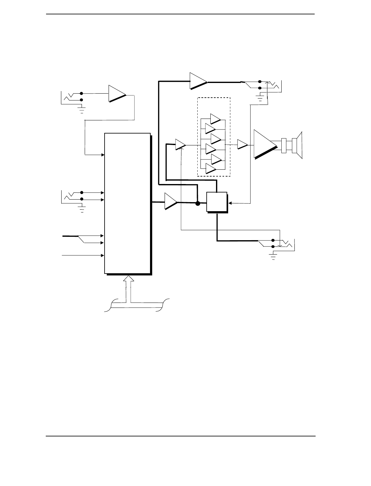
Technical Reference Guide
Compaq Deskpro EN Series of Personal Computers
Desktop and Minitower Form Factors
Third Edition–- September1998
6-3
Figure 6–1. Audio Subsystem Block Diagram
ISA Bus
ES1869
Audio
Controller
Mic In
Line In
CD Audio
(L)
(R)
(L)
(R)
Headphones
Out
(L)
(R)
Line
Out
(L)
(R)
Mute
(L/R)
(L/R)
(L/R)
(L/R)
Splitter
Equalizer
Circuit
Backplane
Connector
(L+R) Power
Amp
Mute
Beep Audio
82371
North Bridge
P6
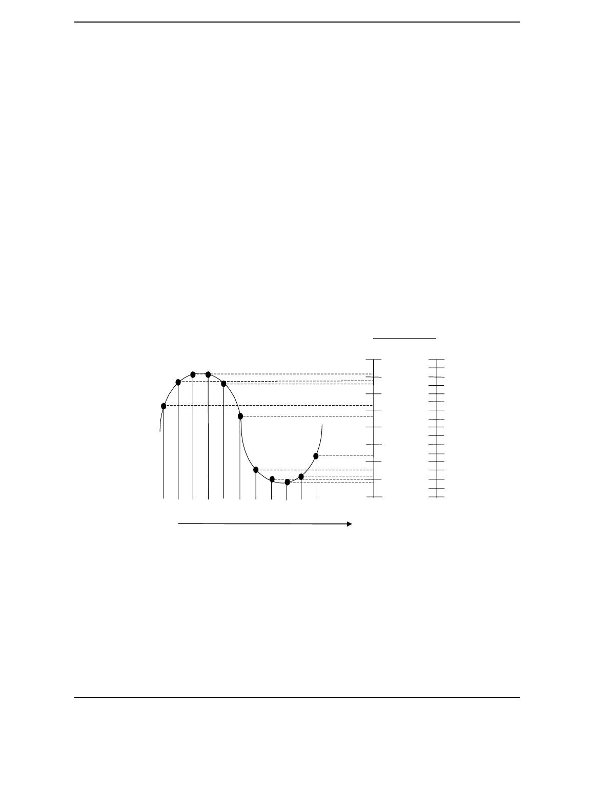
Chapter 6 Audio Subsystem
Compaq Deskpro EN Series of Personal Computers
Desktop and Minitower Form Factors
Third Edition - September 1998
6-4
6.2.1 PCM AUDIO PROCESSING
The audio subsystem uses pulse code modulation (PCM) for processing audio that is applied from
external sources to the Mic In and Line In input jacks, as well as audio from an installed CD-
ROM drive. The PCM method is also used in playback of .WAV file data commonly used in
Windows applications.
6.2.1.1 ADC Operation
The Analog-to-Digital Converter (ADC) receives an analog signal and, using pulse code
modulation (PCM) converts it into digital data that can be handled by normal logic circuitry. The
conversion process consists of measuring (sampling) the analog signal at intervals to determine
the amplitude and frequency (see Figure 6-2). The frequency of sampling intervals is a
programmable parameter known as the sampling rate. The higher the sampling rate, the more
accurate the digital representation will be.
Figure 6–2. Analog Signal Sampling/Quantizing
Each sample is quantized into a digital code that specifies the voltage level of the analog signal at
that particular time. The quantizing format options are as follows:
Mono or stereo
8- or 16-bit
Signed or unsigned
S0 S1 S2 S3 S4 S5 S6 S7 S8 S9 S10
Time
8-Bit
FFh
80h
00h
16-Bit
FFFF
8000h
0000h
Quantized Values
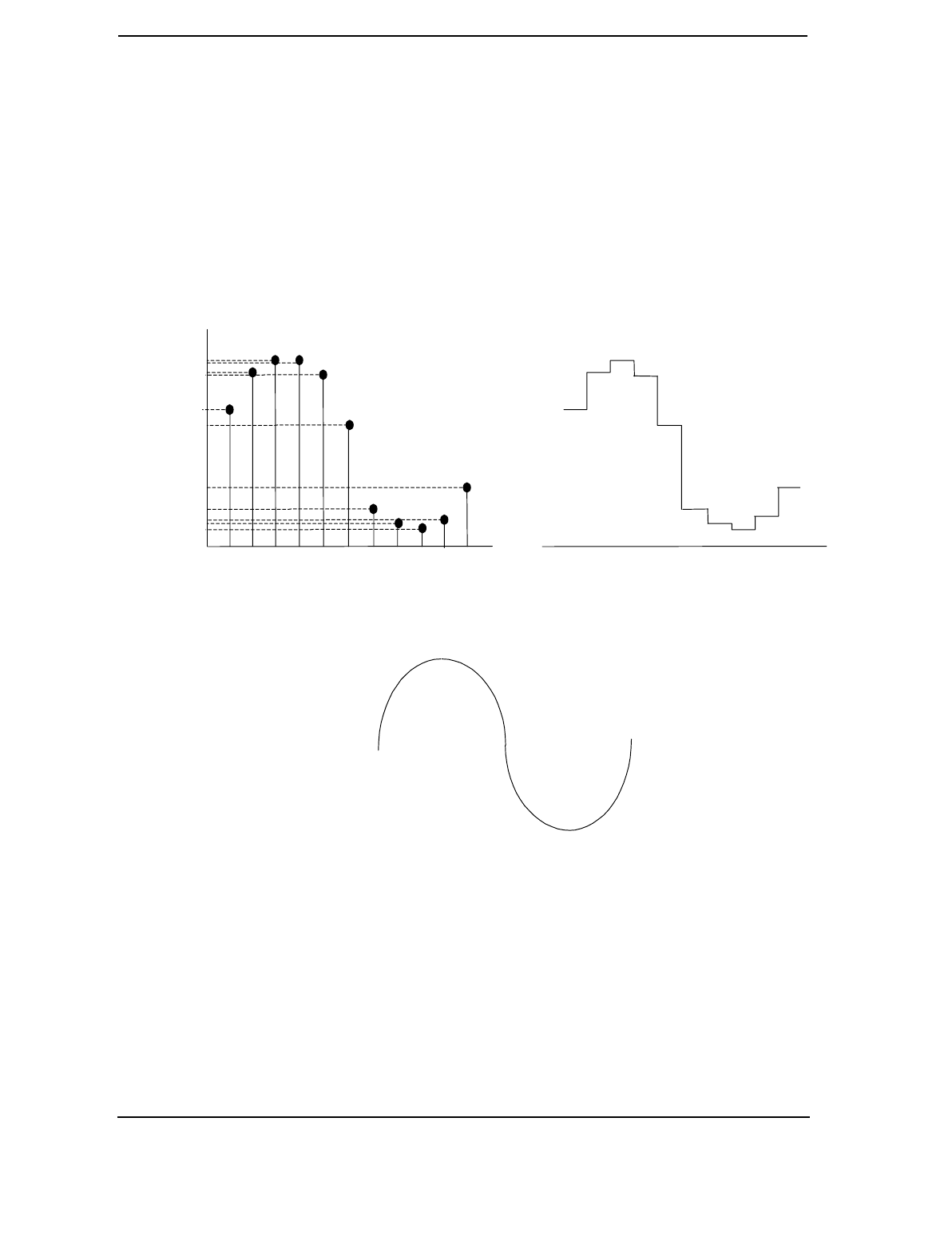
Technical Reference Guide
Compaq Deskpro EN Series of Personal Computers
Desktop and Minitower Form Factors
Third Edition–- September1998
6-5
6.2.1.2 DAC Operation
The digital-to-analog conversion (DAC) simply reverses the procedure of the ADC. The digital
audio data stream is received by the DAC and the quantized values are decoded at the sampling
rate (Figure 6-3A) into DC levels, resulting in a discrete level wave form (Figure 6-3B). A filter
provides the final shaping of the wave (Figure 6-3C) before it is applied to the analog output
circuitry.
Figure 6–3. DAC Operation
Compressed sound formats efficiently use space by concentrating sampling/quantizing in the
middle of the sound spectrum and are suited for voice capture/playback. The DAC of the ES1869
controller supports two type of compressed sound; ADPCM and ESPCM. The ADPCM
compressed format is compatible with common industry sound subsystems while ESPCM is a
proprietary format that offers greater performance.
S0 S1 S2 S3 S4 S5 S6 S7 S8 S9 S10
Quantized
Values
A. Quantized Value Decoding B. Discrete Level Waveform
C. Final Analog Output
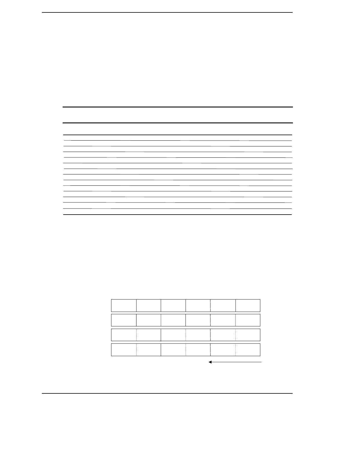
Chapter 6 Audio Subsystem
Compaq Deskpro EN Series of Personal Computers
Desktop and Minitower Form Factors
Third Edition - September 1998
6-6
6.2.1.3 PCM Configuration Modes
PCM operation can be configured for compatible ( common sound board functionality) mode or
set up for extended mode, which has some performance advantages. Table 6-1 lists the
differences between the modes of operation.
Table 6–1. Audio Mode Differences
Table 6-1.
Audio Mode Differences
Function Compatibility
Mode Extended
Mode
FIFO Size Available 64 bytes (SW Control) 256 bytes (HW Control)
Mono 8-bit ADC, DAC 44 KHz Max Sampling 44 KHz Max Sampling
Mono 16-bit ADC, DAC 22 KHz Max Sampling 44 KHz Max Sampling
Stereo 8-bit ADC, DAC 22 KHz Max Sampling 44 KHz Max Sampling
Stereo 16-bit ADC n/a 44 KHz Max Sampling
Stereo 16-bit DAC 11 KHz Max Sampling 44 KHz Max Sampling
Signed/Unsigned Control No Yes
AGC During Capture Mono Only (22 KHz) No
Programmed I/O Block Transfer No Yes
FIFO Status Flags No Yes
Auto Reload DMA Yes Yes
Time Base for Programmable Time 1 MHz or 1.5 MHz 800 KHz or 400 KHz
ADC/DAC Jitter +/- 2 usec None
Sound Blaster Pro Compatible Yes No
6.2.1.4 PCM Bus Cycles
The I/O and DMA cycles used by PCM operations to process .WAV data follow standard ISA bus
conventions. All bus transfers occur at the bytes level. Programmed I/O cycles are always used
for programming the control registers and may also be used for transferring audio data to and
from the audio subsystem as well. Quantized audio data is built using the “little endian” format
(LSB occupies the lowest memory address). Data transfers over the ISA occur as shown below.
Figure 6–4. Audio Subsystem-to-ISA Bus PCM Audio Data Formats / Byte Ordering
8-bit Mono
8-bit Stereo
16-bit Mono
16-bit Stereo
Sample 6 Sample 5 Sample 4 Sample 2Sample 3 Sample 1
Sample 3 Sample 3 Sample 2 Sample 1Sample 2 Sample 1
Sample 3 Sample 2 Sample 1
Right Left Right RightLeft Left
Mono Hi
Left Hi
Sample 3 Sample 2 Sample 1
Mono LoMono HiMono LoMono HiMono Lo
Left LoLeft LoLeft Hi Right Hi Right Lo
0824 1631
Time
Technical Reference Guide
Compaq Deskpro EN Series of Personal Computers
Desktop and Minitower Form Factors
Third Edition–- September1998
6-7
6.2.2 FM SYNTHESIS AUDIO PROCESSING
The audio subsystem supports playback of MIDI (.MID) files. A .MID file does not contain
audio information in the same way that .WAV files do. In .MID files, audio data consists of note
on/off, tone type, and amplification information. Audio stored in the .MID file format has the
benefit of taking up far less space than audio stored as .WAV files.
The ES1869 controller includes a 20-voice, four-operator frequency modulated (FM) synthesizer.
In FM synthesis, one signal (the carrier) is forced to vary from it’s center frequency by another
signal (the modulator) resulting in a sideband or “harmonic” frequency. The frequency of the
harmonic is determined by the original carrier frequency and the modulating frequency. The
number of harmonics generated is determined by the strength (amplitude) of the modulating
signal. The microsystem that produces the FM signal is called a patch (Figure 6-5).
Figure 6–5. FM Synthesis Patch
Note that while an analog representation is shown in Figure 6-6. Synthesis occurs as a digital
operation with the results being sent to the DAC.
The FM synthesis process is a playback-only operation involving the writing of .MID data to the
audio subsystem over the ISA bus. The only reads involve checking the controller for status.
Figure 6-6 shows the ISA bus transaction for FM synthesis. Note that if a succeeding data byte is
meant for the same location as the previous byte, the address does not need to be re-written.
Figure 6–6. Audio Car-to-ISA Bus FM Audio Data Format
Modulator
Oscillator Carrier
Oscillator
Frequency Cntrl
Amplitude Cntrl
Frequency Cntrl Modulating Signal FM Signal
Address Data
Address
or
Data
A0
IOR-
or
IOC-
Data 7..0

Chapter 6 Audio Subsystem
Compaq Deskpro EN Series of Personal Computers
Desktop and Minitower Form Factors
Third Edition - September 1998
6-8
6.3 PROGRAMMING
All programming aspects of the audio subsystem relate directly to the programmability of the
ES1869 controller, upon which the audio subsystem is based. This section describes only the
basic mapping of the audio functions. For a detailed description of the ES1869s registers and
capabilities refer to the ES1869 AudioDrive Data Sheet, ESS Technology, Inc.
6.3.1 CONFIGURATION
The audio subsystem is automatically configured as to base address, DMA, and interrupts
following installation and power up through an on-board EEPROM that provides Plug ‘n Play
support. Software can identify the ES1869 controller by reading indexed address 2n5.40h
successively (where n = 2 for primary address or 4 for secondary address), which should yield the
values 18h, 69h, followed by the base address of the ES1869.
The typical reset/power-up configuration for the audio subsystem is as follows:
Base Address: 220h
Interrupt: IRQ5
DMA Channel: 1
Power Management: Automatic
The audio subsystem can be configured or either single DMA channel mode or dual DMA
channel mode. Single DMA channel mode means that capture and playback operations share the
same (playback) DMA channel and only one operation, capture or playback, is possible at a time.
Dual DMA channel operation allows simultaneous capture/playback (full duplex) operation to
occur if desired, but requires the use of two DMA channels. Typically, dual DMA operation
would use DMA channel 1 for capture (recording) and DMA channel 0 or 3 for playback.
Technical Reference Guide
Compaq Deskpro EN Series of Personal Computers
Desktop and Minitower Form Factors
Third Edition–- September1998
6-9
6.3.2 CONTROL
The audio subsystem is controlled through I/O mapped registers listed in Table 6-2.
Table 6–2. Audio Subsystem I/O Map
Table 6-2.
Audio Subsystem I/O Map
I/O
Address Function I/O
Address Function
201h Joystick 2nAh Read Buffer Input Data
2n0-2n3 FM Synthesizer Address/Data [1] 2nCh (Read) Status
2n4h Mixer Address 2nCh (Write) Command/Data
2n5h Mixer Data 2nEh Data Available Status
2n6h (Read) Activity/Power Status 2nFh FIFO I/O Address (Extended Mode)
2n6h (Write) Reset Control 3n0, 3n1h MPU-401 Port
2n7h Power Management 388-38Bh FM Synthesizer (alias of 2n0-2n3h)
2n8, 2n9h FM Synthesizer Address/Data [2] -- --
NOTES:
n = 2 for primary address (default), = 4 for secondary address.
[1] 20-voice operation
[2] 11-voice operation
Not supported
6.3.2.1 PCM Control
The audio subsystem can operate in either Sound Blaster-compatible mode (the default) or in
extended capability mode.
Table 6-3 lists the audio mixer control registers used by software written for Sound Blaster and
other common audio peripherals. These registers are accessed by writing the index value to I/O
port 2n4h and reading the value from or writing the value to I/O port 2n5h.
Table 6–3. Compatibility Mode Audio Mixer Control Register Mapping
Table 6-3.
Compatibility Mode Audio Mixer Control Register Mapping
Index Function Index Function
00h Mixer Reset 22h Master Volume
04h Voice Volume 26h FM Volume
0Ah Mic Volume 28h CD Volume
0Ch ADC Recording Source [1] 2Eh Line Volume
0Eh Stereo/Mono Switch [1] -- --
NOTE: Refer to OEM’s ES1869 data sheet for detailed register descriptions.
[1] The filter functions used in Sound Blaster subsystems are not used in the audio subsystem.
Chapter 6 Audio Subsystem
Compaq Deskpro EN Series of Personal Computers
Desktop and Minitower Form Factors
Third Edition - September 1998
6-10
The Extended Mode registers are listed in Table 6-4. Like the compatibility registers listed
previously, these registers are accessed by writing the index value to I/O port 2n4h and reading
the value from or writing the value to I/O port 2n5h. Extended mode offers better performance by
providing more precise (higher bit resolution) control of audio levels and more control of audio
processing.
Table 6–4. Extended Mode Audio Mixer Control Register Mapping
Table 6-4.
Extended Mode Audio Mixer Control Register Mapping
Index Function Index Function
14h Voice Volume 60, 62h Master Volume (Left, Right)
1Ah Mic Volume 64h Master Volume Control
1Ch ADC (recording) Source 66h Volume Int. Req. Clear
1Eh Stereo/Mono Switch 74h DMA Transfer( 2nd) Count Reload (Low)
32h Master Volume 76h DMA Transfer (2nd) Count Reload (Hi)
36h FM Volume 78h 2nd DMA Control 1
38h CD Volume 7Ah 2nd DMA Control 2
3Eh Line Volume 7Eh Test Register
NOTE: Refer to OEM’s ES1869 data sheet for detailed registers descriptions.
6.3.2.2 FM Synthesis Control
The FM synthesis logic is typically mapped at 388h-38Bh. A total of 243 registers in two banks
are available. Accessing the registers is accomplished by first writing the index to register 388h
(for bank 0) or 38Ah (for bank 1) followed by writing the data to either 389h or 38Bh (for bank 0
or bank 1 respectively). If a succeeding data byte is destined for the same location then the
address need not be re-written. Location 388h can be read for FM synthesizer status. Table 6-5
lists the FM synthsizer control registers.
Table 6–5. FM Synthesizer Control Register Mapping
Table 6-5.
FM Synthesizer Control Register Mapping
Index Bank 0 Function Bank 1 Function
01h Test - all 0s Test - all 0s
02h Timer 1 Not Used
03h Timer 2 Not Used
04h Timer Mask/Timer Start 4-Operator Configure
05h Not Used 4-Operator Enable
08h Key Scale (KSR) # Determiner Not Used
20-35h AM, Vib, EG Type, KSR, Mult. Same as bank 0
40-55h Key Scale Level, Tone Level Same as bank 0
60-75h Attack Rate, Decay Rate Same as bank 0
80-95h Sustain Level, Release Rate Same as bank 0
A0-A8h Frequency Number Same as bank 0
B0-B8h Key On, Block Octave, Frequency No. Same as bank 0
BDh Depth of Block Octave, Frequency No. Not Used
C0-C8h Stereo Left/Right, Feedback, Connection Same as bank 0
E0-F5h Wave Select Same as bank 0
NOTE: Refer to OEM’s ES1869 data sheet for detailed registers descriptions.
Abbreviations:
AM Amplitude Modulation (tremolo)
Vib Vibrato

Technical Reference Guide
Compaq Deskpro EN Series of Personal Computers
Desktop and Minitower Form Factors
Third Edition–- September1998
6-11
6.4 SPECIFICATIONS
Table 6–6. Audio Subsystem Specifications
Table 6-6.
Audio Subsystem Specifications
Paramemter Measurement
Sampling Rate 5.51 KHz to 44 KHz (prgmbl)
Maximum Input Voltage:
Mic In
Line In
.125 Vp-p
1.4 Vrms
Impedance
Mic In
Line In
Line Out
Headphone Out
1 K ohms (nom)
30 K ohms (nom)
30 K ohms (nom)
16 ohms (min)
Power output (max):
Headphone output
Power amp
60 mW into 16 ohms
5 watts into 8 ohms
Total Harmonic Distortion (power amp):
@ 0.5 watts
@ 5 watts
1 %
10 %
Mic Preamp Gain 26 db
Volume Range
Input
Output
0 - 22.5 db
-46.5 - +10 db
Frequency Response (speaker) 450 - 4000 Hz

Chapter 6 Audio Subsystem
Compaq Deskpro EN Series of Personal Computers
Desktop and Minitower Form Factors
Third Edition - September 1998
6-12
This page is intentionally blank.
Technical Reference Guide
Compaq Deskpro EN Series of Personal Computers
Desktop and Minitower Form Factors
Third Edition - September 1998
7-1
Drives
110/220 VAC
Chapter 7
POWER and SIGNAL
DISTRIBUTION
7. Chapter 7 POWER SUPPLY AND DISTRIBUTION
7.1 INTRODUCTION
This chapter describes the power supply and method of general power and signal distribution in
the Compaq Deskpro INDY Personal Computer. Topics covered in this chapter include:
♦ Power supply assembly/control (7.2) page 7-1
♦ Power distribution (7.3) page 7-5
♦ Signal distribution (7.4) page 7-7
7.2 POWER SUPPLY ASSEMBLY/CONTROL
This system features a power supply assembly that is controlled through programmable logic
(Figure 7-1).
NOTE:
All signals shown entering and exiting the system board pass through the backplane card.
Figure 7–1. Power Distribution and Control, Block Diagram
Power Supply
Assembly
+5 VDC
-5 VDC
+12 VDC
-12 VDC
+5 AUX
Slots, Chipsets, Logic
& Voltage Regulators
PS
On
Fan
Off
+3.3 VDC
System Board
Power On/Off
Front Bezel
Power On

Chapter 7 Power and Signal Distribution
Compaq Deskpro EN Series of Personal Computers
Desktop and Minitower Form Factors
Third Edition - September 1998
7-2
7.2.1 POWER SUPPLY ASSEMBLY
The power supply assembly is contained in a single unit that features a selectable input voltage:
90-132 VAC and 180-264 VAC. The power supply assembly provides +3.3 VDC, +5 VDC, -5
VDC, +12 VDC, and -12 VDC potentials for the system board, expansion board(s), and installed
drives. These voltages are controlled through the power button on the front panel of the system
unit. Pressing and releasing the power button results in system board logic asserting the PS On
signal, which activates the power supply assembly.
The power supply also produces an auxiliary voltage (+5 AUX). The +5 AUX voltage is used for
powering the power button and other logic required for wake-up operation and is produced as
long as the unit is plugged into a live AC outlet.
NOTE: Minimum loading requirements for the power supply must be met at all times to
ensure normal operation and to meet specifications.
Table 7-1 shows the specifications for the power supply.
Table 7–1. Power Supply Assembly Specifications
Table 7-1.
Power Supply Assembly Specifications
(P/N 334112-xxx)
Parameter Range/
Tolerance Min. Current
Loading [1] Max.
Current Surge
Current [2] Max.
Ripple
Input Line Voltage:
110 VAC Setting
220 VAC Setting
90 - 132 VAC
180-264 VAC
--
--
--
--
--
--
--
--
Line Frequency 47 - 63 Hz -- -- -- --
Steady State Input (VAC) Current: -- -- 5.50 A -- --
+3.3 VDC Output +/- 1% 1.40 A 10.0 A 10.0 A 50 mV
+5 VDC Output +/- 5 % 1.40 A 25.0 A 25.0 A 50 mV
-5 VDC Output +/- 10 % 0.00 A 0.15 A 0.15 A 100 mV
+5 AUX Output +/- 5 % 0.10 A 2.00 A 2.00 A 50 mV
+12 VDC Output +/- 5 % 0.07 A 4.50 A 7.00 A 120 mV
-12 VDC Output +/- 10 % 0.00 A 0.15 A 0.15 A 200 mV
NOTES:
[1] Minimum loading requirements must be met at all times to ensure normal operation
and specification compliance.
[2] Surge duration no longer than 10 seconds and +12 tolerance +/- 10%.
The power supply assembly contains a fan that can be shut down by the Fan Off signal, which is
asserted from the system board logic during sleep (suspend) states. The power supply can
override the Fan Off signal if the temperature in the power supply assembly is too high.

Technical Reference Guide
Compaq Deskpro EN Series of Personal Computers
Desktop and Minitower Form Factors
Third Edition - September 1998
7-3
7.2.2 POWER CONTROL
The power supply assembly is controlled digitally by the PS On signal (Figure 6-1). When PS On
is asserted, the Power Supply Assembly is activated and all voltage outputs (+3 VDC, +5 AUX,
+/-5 VDC, +/-12 VDC) are produced. When PS On is de-asserted, the Power Supply Assembly is
off and all voltages (except +5 AUX) are not generated. Note that +5 AUX is always produced as
long as the system is connected to a live AC source (as indicated by an illuminated system board
LED).
7.2.2.1 Power Button
The PS On signal is typically controlled through the Power Button which, when pressed and
released, applies a negative (grounding) pulse to the power control logic. (Refer to section 7.2.2.3
for PS On control select.) The resultant action of pressing the power button depends on the state
and mode of the system at that time and is described as follows:
System State Pressed Power Button Results In:
Off Negative pulse, of which the falling edge results in power control logic asserting
PS On signal to Power Supply Assembly, which then initializes. ACPI four-
second counter is not active.
On, ACPI Disabled Negative pulse, of which the falling edge causes power control logic to de-assert
the PS On signal. ACPI four-second counter is not active.
On, ACPI Enabled Pressed and Released Under Four Seconds:
Negative pulse, of which the falling edge causes power control logic to
generate SMI-, set a bit in the SMI source register, set a bit for button status,
and start four-second counter. Software should clear the button status bit
within four seconds and the Suspend state is entered. If the status bit is
not cleared by software in four seconds PS On is de-asserted and the
power supply assembly shuts down (this operation is meant as a guard if
the OS is hung).
Pressed and Held At least Four Seconds Before Release:
If the button is held in for at least four seconds and then released, PS On is
negated, de-activating the power supply.
7.2.2.2 Power LED Indications
Two LEDs are used to indicate system power status. The front panel (bezel) power LED provides
a visual indication of three key system conditions listed as follows:
Power LED Condition
Steady On Normal full-on operation
Blinking @ 1 Hz Sleep (suspend) state
Blinking @ 4 Hz Thermal condition: processor has overheated and shut down
An additional LED is mounted on the system board. This LED is connected to the +5 AUX bus
and will be on as long as the system unit is connected to live AC power regardless of the status
of the PS On signal. The AC line cord should always be disconnected and the system board LED
should not be illuminated before servicing the unit.

Chapter 7 Power and Signal Distribution
Compaq Deskpro EN Series of Personal Computers
Desktop and Minitower Form Factors
Third Edition - September 1998
7-4
7.2.2.3 PS On Control Select
The assertion of the PS On signal can be controlled through DIP switch SW1-6 as follows:
SW1-6 Closed (on) – PS On signal is asserted when unit is plugged into a live AC socket and
power supply assembly produces all voltages (system boots immediately).
SW1-6 Open (off) – PS On signal asserted by pressed power button.
7.2.2.4 Wake Up Events
The PS On signal can also be activated with a power “wake-up” of the system due to the
occurrence of a magic packet, serial port ring, or PCI power management (PME) event. These
events can be individually enabled by the Setup utility through the GPIO of the system security
ASIC to wake up the system from a sleep (low power) state. The wake up sequence for each event
occurs as follows:
♦ Wake On LAN (WOL) - If a compliant network interface controller is installed and enabled
for remote wake-up, reception of a “Magic Packet” results in the assertion of the high R-
MPKT pulse signal (received through the WOL header P9) to the power control logic, which
will assert PS On. Note that the NIC adapter must be able to draw five volts power from
header P9 during the system sleep state.
♦ Modem Ring – A ring indication on serial port A (COM1) will, if enabled, be detected by the
power control logic and cause the PS On signal to be asserted.
♦ PME Event – A power management event that asserts the PME- signal on the PCI bus can
be enabled to cause the power control logic to generate the PS On signal. Note that the PCI
card must have a second source of power to operate during the system unit’s sleep state.
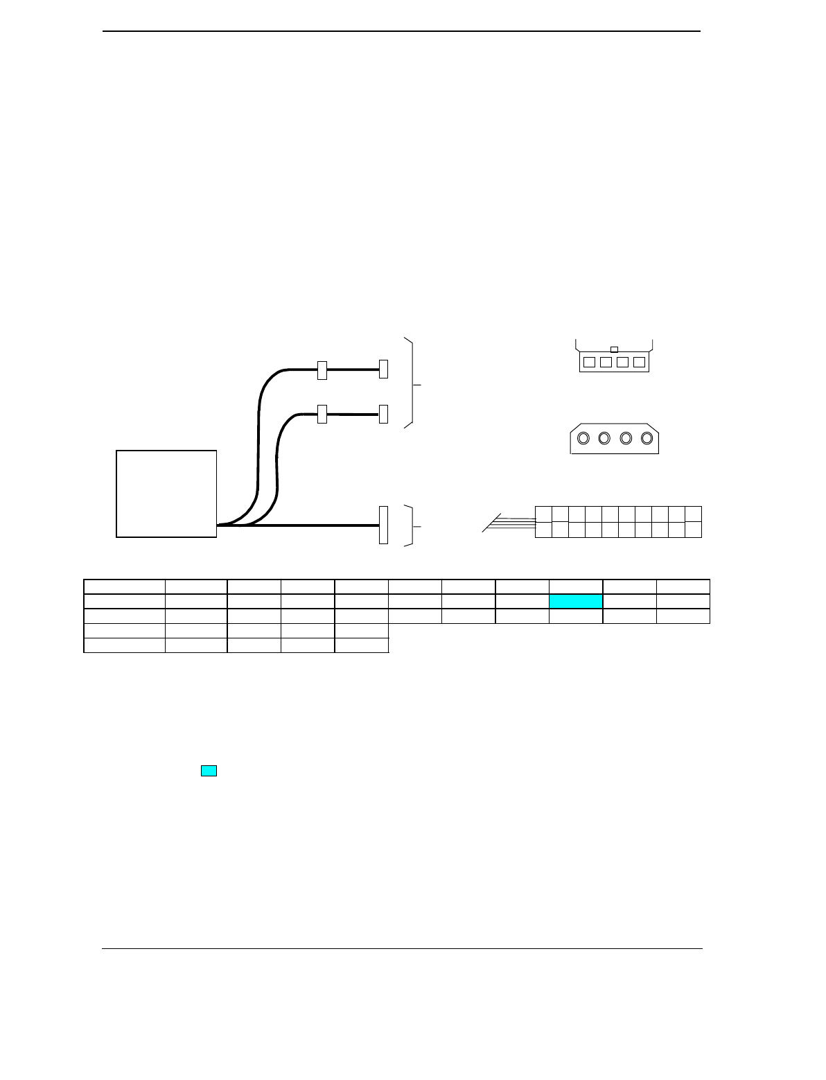
Technical Reference Guide
Compaq Deskpro EN Series of Personal Computers
Desktop and Minitower Form Factors
Third Edition - September 1998
7-5
7.3 POWER DISTRIBUTION
7.3.1 3.5/5/12 VDC DISTRIBUTION
The power supply assembly includes a multi-connector cable assembly that routes +3.3 VDC, +5
VDC, -5 VDC, +12 VC, and -12 VDC to the system board as well as to the individual drive
assemblies.
Connector Pin 1 Pin 2 Pin 3 Pin 4 Pin 5 Pin 6 Pin 7 Pin 8 Pin 9 Pin 10
P1 +3.3 +3.3RS RTN +5 RTN +5 RTN Fan Off +5AUX +12
P1 [1] +3.3 -12 RTN PS On RTN RSRTN RTN -5 +5 +5
P3-P5 +12 GND GND +5
P6 +5 GND GND +12
NOTES:
[1] This row represents pins 11-20 of the P1 connector.
All + and - values are VDC.
RTN = Return (signal ground)
GND = Power ground
RS = Remote sense
= Deviation from ATX standard. PWR GD signal is produced by the south bridge component.
Figure 7–2. Power Cable Diagram
Power Supply
Assembly
(SP# 334112-001)
Drive
Assemblies
P1
P6
P3
P3
Backplane
Board
1 2 3 4
P3-P5
P6
4 3 2 1
P4
P5
P1 (ATX-type)
1
12 2011
2 5 4 3 7 8 6 9
14
10
13 16 1715 18 19
P2
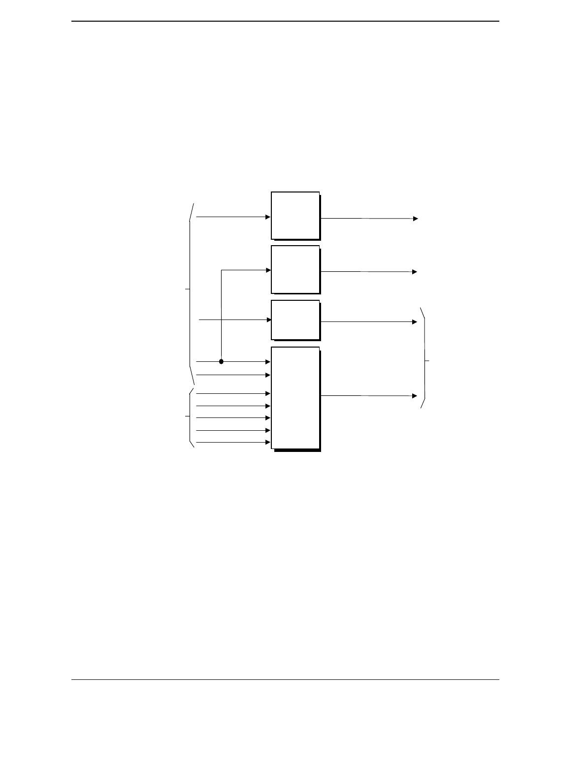
Chapter 7 Power and Signal Distribution
Compaq Deskpro EN Series of Personal Computers
Desktop and Minitower Form Factors
Third Edition - September 1998
7-6
7.3.2 LOW VOLTAGE DISTRIBUTION
Voltages less than 3.3 VDC and processor core voltage are produced through regulator circuitry
on the system board.
Figure 7–3. Low Voltage Supply, Block Diagram
The VccP regulator produces the VccP (processor core) voltage according to the state of the
VID4..0 signals from the processor. This allows automatic selection of the proper core voltage
depending on the installed processor component. The possible voltages available are listed as
follows:
VID4..0 VccP VID4..0 VccP VID4..0 VccP
10000 3.5 VDC 11011 2.4 VDC 00111 1.70 VDC
10001 3.4 VDC 11100 2.3 VDC 01000 1.65 VDC
10010 3.3 VDC 11101 2.2 VDC 01001 1.60 VDC
10011 3.2 VDC 11110 2.1 VDC 01010 1.55 VDC
10100 3.1 VDC 00000 2.05 VDC 01011 1.50 VDC
10101 3.0 VDC 00001 2.00 VDC 01100 1.45 VDC
10110 2.9 VDC 00010 1.95 VDC 01101 1.40 VDC
10111 2.8 VDC 00011 1.90 VDC 01110 1.35 VDC
11000 2.7 VDC 00100 1.85 VDC 01111 1.30 VDC
11001 2.6 VDC 00101 1.80 VDC 11111 CPU not installed
11010 2.5 VDC 00110 1.75 VDC
VccP (see text)
Regulator
Circuit
+12 VDC
VID0
Processor
VID1
VID2
VID3
+5 AUX
VTT
(
+1.5 VDC
)
Regulator
Circuit
Power Supply
Power Button and
Wake Up Logic
+5 VDC
VID4
+5 VDC LM317
Regulator
Circuit
+3.3 VDC
2.5 VDC
LM317
Regulator
Circuit
+3 AUX
Pull-Up Logic
Processor
Technical Reference Guide
Compaq Deskpro EN Series of Personal Computers
Desktop and Minitower Form Factors
Third Edition - September 1998
7-7
7.4 SIGNAL DISTRIBUTION
Figure 7-4 shows general signal distribution between the main subassemblies of the system unit.
NOTES:
[1] CDS models and minitowers. 3200 and 6400 models 4300 and 9100 models
[1] See Figure 7-5 for header pinout.
Figure 7–4. Signal Distribution Diagram
System
Board
PCI Bus
ISA Bus
Backplane
Board
PCI
Slot
Power
Supply
Assembly
3.3, 5
12 VDC
IDE I/F 5, 12 VDC
Riser
Card
Conn
Power
Conn
Pri. IDE
Conn
Sec. IDE
Conn
IDE I/F CD-ROM
Ke
y
board
Mouse
Dsk.
Conn
Dsk I/F Diskette Drive
J50
P1
P20
P21
P10
CD Audio
5, 12 VDC
5, 12 VDC
Kybd/
Mouse
Conn
J6
IDE I/F
Fan Off
Audio
Conn
P7 [1]
CD
Audio
3/5/12
VDC
PS On
Fan/PS
Cntrl
Fan
Conn
P8 [1] Chassis Fan
Fan Pwr
Spkr
Conn
P6 Audio Chassis Spkr
Audio
Pwr Btn
Blk LED
PCI Bus
10/100
NIC
Card
WOL
Conn
P9 [1] WOL
+5AUX
Fan Sens.
Dsk. I/F
WOL
LED
Conn
P5 [1]
Pwr On
HD Activity
Pwr/HD LEDs, Pwr Btn Power On/Off
Hood Sw
AGP
Slot
Graphics
Card
AGP Bus
Wide Ultra
SCSI
Hard Drive
Wide Ultra SCSI
Controller Card
IDE
Hard Drive
PCI
Slot
PCI Bus
5,
12 VDC
LED
Conn
HD Activity
P29
Chapter 7 Power and Signal Distribution
Compaq Deskpro EN Series of Personal Computers
Desktop and Minitower Form Factors
Third Edition - September 1998
7-8
Pins Function
1,3 Cover Lock & 12 VDC
2,3 Cover Unlock & 12 VDC
4 Not connected
5 Power LED (-)
6 HD LED (-)
7 Power LED (+)
8 HD LED (+)
9,10 Power Button
Pins Function
1,3 Signal ground
2 Left Audio Channel
4 Right Audio Channel
Pins Function
1 Fan present sense
2 Fan Power (-)
3Key
4 Fan Power (+)
Pins Function
1 +5 AUX
2 Ground
3 WOL signal
NOTE:
No polarity consideration required for cable connection to
header P6 (speaker) or P29 (SCSI HD LED).
Figure 7–5. Backplane Header Pinouts
Header P5
(Panel LEDs, Pwr Btn)
1
5
7
9
3
2
6
8
10
4
Header P7
(
CD Audio
)
1
3
4
2
Header P8
(
Chassis Fan
)
1
4
2
1
2
3
Header P9
(Wake On LAN)

Technical Reference Guide
Compaq Deskpro EN Series of Personal Computers
Desktop and Minitower Form Factors
Third Edition - September 1998
8-1
Chapter 8
BIOS ROM
8. Chapter 8 BIOS ROM
8.1 INTRODUCTION
The Basic Input/Output System (BIOS) of the computer is a collection of machine language
programs stored as firmware in read-only memory (ROM). The BIOS ROM includes such
functions as Power-On Self Test (POST), PCI device initialization, Plug ‘n Play support, power
management activities, and Setup. This chapter includes the following topics:
♦ Boot/reset functions (8.2) page 8-2
♦ Memory detection and configuration (8.3) page 8-3
♦ Desktop management support (8.4) page 8-4
♦ PnP support (8.5) page 8-19
♦ Power management functions (8.6) page 8-21
The firmware contained in the BIOS ROM supports the following operating systems and
specifications:
♦ DOS 6.2
♦ Windows 3.1
♦ Windows for Workgroups 3.11
♦ Windows 95
♦ Windows 98
♦ Windows NT 3.5 and 4.0
♦ OS/2 ver 2.1
♦ OS/2 Warp
♦ SCO Unix
♦ DMI 2.0
♦ Intel Wired for Management (WfM) initiative
The microprocessor accesses the BIOS ROM as a 128-KB block from E0000h to FFFFFh. The
BIOS data is shadowed in a 64-KB block in the upper memory area. The BIOS segments are
dynamically paged in and out of the 64-KB block as they are needed.
NOTE: This chapter describes BIOS in general and focuses on aspects of BIOS unique
to this particular system. For detailed information regarding the BIOS, refer to the
Compaq Basic Input/Output System Technical Reference Guide.

Chapter 8 BIOS ROM
Compaq Deskpro EN Series of Personal Computers
Desktop and Minitower Form Factors
Third Edition - September 1998
8-2
8.2 BOOT/RESET FUNCTIONS
The system supports new system boot functions to support remote ROM flashing and PC97
requirements. This system also supports the EL Torito specification for bootable CDs.
8.2.1 BOOT BLOCK
This system includes 24 KB of write-protected boot block ROM that provides a way to recover
from a failed remote flashing of the system BIOS ROM. Early during the boot process, the boot
block code checks the system ROM. If validated, the system BIOS continues the boot sequence.
If the system ROM fails the check, the boot block code provides the minimum amount of support
necessary to allow booting the system from the diskette drive (bypassing the security measures)
re-flashing the system ROM with a ROMPAQ diskette. Since video is not available during the
initial boot sequence the boot block routine uses the keyboard LEDs to communicate status as
follows:
Num Lock Caps Lock Scroll Lock Meaning
Off On Off Administrator password required.
On Off Off Boot failed. Reset required for retry.
Off Off On Flash failed (set by ROMPAQ).
On On On Flash complete (set by ROMPAQ).
8.2.2 QUICKBOOT
The QuickBoot mode (programmable through the INT 15, AX=E845h call) skips certain portions
of the POST (such as the memory count) during the boot process unless the hood has been
detected as being removed. The QuickBoot mode is programmable as to be invoked always, never
(default) or every x-number of days.
8.2.3 SILENTBOOT
When in the SilentBoot mode, the boot process skips certain audio and visual aspects of POST
(such as the speed beeps and screen messages). Error messages are still displayed. The
QuickBoot mode is programmable by the Setup utility (through the INT 15, AX=E845h call) as
to either TERSE (default) or VERBOSE mode.
8.2.4 RESET
There are two types of system resets: hard and soft. A hard reset is traditionally generated after
power-up and produced by the circuitry generating the PWRGOOD signal. The 82371 south
bridge, however, allows software to generate a hard reset. This is accomplished by first writing a
one (1) to bit <1> of I/O port 0CF9h. A one is then written to bit <2> of 0CF9h. This causes the
82371 to create a hard reset by asserting CPURST#, PCIRST#, and RSTDRV for at least 1 ms.
After the reset the 82371 automatically clears bit <2> of 0CF9h.

Technical Reference Guide
Compaq Deskpro EN Series of Personal Computers
Desktop and Minitower Form Factors
Third Edition - September 1998
8-3
8.3 MEMORY DETECTION AND CONFIGURATION
This system uses the Serial Presence Detect (SPD) method of determining the installed DIMM
configuration. The BIOS communicates with an EEPROM on each DIMM through an I2C-type
bus to obtain data on the following DIMM parameters:
♦ Presence
♦ Size
♦ Type
♦ Timing/CAS latency
NOTE: Refer to Chapter 3, “Processor/Memory Subsystem” for the SPD format and DIMM
data specific to this system.
The BIOS performs memory detection and configuration with the following steps:
1. Set Memory Buffer Strength – The memory controller must be configured for correct buffer
drive strength. The BIOS provides this function by reading the number of module banks,
ECC enable/disable status, and SDRAM width data from the DIMMs and transferring that
data to the memory controller. SPD bytes checked: 5, 11, 13
2. Determine DIMM Presence/Type – The BIOS checks each memory socket for DIMM
presence. If present, the DIMM type and CAS latency is determined. SPD bytes checked: 2,
9, 10, 18, 23, 24.
Check Sequence:
a. SPD byte 2 is read for all slots first. A failed read or returned value of other than 02h
(EDO) or 04h (SDRAM) results in the slot marked as empty. If mixed types are detected
then only SDRAMs are used (see chapter 3 for details).
b. SPD byte 18 is read for maximum CAS latency, followed by reads of bytes 9 and 10 for
bus speed compatibility. A DIMM detected as too-slow results in an error.
c. If the DIMM can handle the memory bus speed at maximum CAS latency then bytes 23
and 24 are checked to see if the DIMM can work maximum CAS latency minus 1. Once
all slots are checked, the greatest CAS latency (2 or 3) is used. A DIMM detected as
incompatible will result in a bit in CMOS being set and the Num Lock LED on the
keyboard will blink for a short time. Depending on the progress of the BIOS routine a
POST message may be displayed before the system locks up.
3. Initialize SDRAM – If SDRAM are installed then each row containing SDRAM will be
initialized. This step includes pre-charging all banks, sending a CAS-before-RAS command,
sending a Mode-Register-Set-Enable command, reading DIMM location/CAS latency data,
and sending a Normal Op command.
4. Memory Sizing – The SPD bytes 3, 4, and 17 are checked for number of row and column
addresses and (for SDRAM) the number of internal banks.
5. Memory Timing – For SDRAM, the memory controller requires the RAS pre-charge time
and the RAS-to-CAS delay time. SPD bytes checked: 27and 29.

Chapter 8 BIOS ROM
Compaq Deskpro EN Series of Personal Computers
Desktop and Minitower Form Factors
Third Edition - September 1998
8-4
8.4 DESKTOP MANAGEMENT SUPPORT
Desktop Management deals with issues of security, identification, and system management
functions. Desktop Management is provided by BIOS INT 15 functions listed Table 8-1.
Table 8–1. Desktop Management Functions (INT15)
Table 8-1.
Desktop Management Functions (INT15)
AX Function Mode
E800h Get system ID Real, 16-, & 32-bit Prot.
E807h Get System Information Table Real, 16-, & 32-bit Prot.
E813h Get monitor information Real, 16-, & 32-bit Prot.
E814h Get system revision Real, 16-, & 32-bit Prot.
E816h Get temperature status Real, 16-, & 32-bit Prot.
E817h Get drive attribute Real
E818h Get drive off-line test Real
E819h Get chassis serial number Real, 16-, & 32-bit Prot.
E81Ah Write chassis serial number Real
E81Bh Get drive threshold Real
E81Eh Get drive ID Real
E820h System Memory Map Real
E822h Flash ROM/Sys. Admin. Fnc. Real, 16-, & 32-bit Prot.
E827h DIMM EEPROM Access Real, 16-, & 32-bit Prot.
E828h Inhibit power button Real, 16-, & 32-bit Prot.
E845h Access CMOS Feature Bits Real, 16-, & 32-bit Prot.
E846h Security Functions Real, 16-, & 32-bit Prot.
All 32-bit protected mode calls are accessed by using the industry-standard BIOS32 Service
Directory. Using the service directory involves three steps:
1. Locating the service directory.
2. Using the service directory to obtain the entry point for the client management functions.
3. Calling the client management service to perform the desired function.
The BIOS32 Service Directory is a 16-byte block that begins on a 16-byte boundary between the
physical address range of 0E0000h-0FFFFFh. The format is as follows:
Offset No. Bytes Description
00h 4 Service identifier (four ASCII characters)
04h 4 Entry point for the BIOS32 Service Directory
08h 1 Revision level
09h 1 Length of data structure (no. of 16-byte units)
0Ah 1 Checksum (should add up to 00h)
0Bh 5 Reserved (all 0s)

Technical Reference Guide
Compaq Deskpro EN Series of Personal Computers
Desktop and Minitower Form Factors
Third Edition - September 1998
8-5
To support Windows NT an additional table to the BIOS32 table has been defined to contain 32-
bit pointers for the DDC and SIT locations. The Windows NT extension table is as follows:
; Extension to BIOS SERVICE directory table (next paragraph)
db “32OS” ; sig
db 2 ; number of entries in table
db “$DDC” ; DDC POST buffer sig
dd ? ; 32-bit pointer
dw ? ; byte size
db “$SIT” ; SIT sig
dd ? ; 32-bit pointer
dw ? ; byte size
db “$ERB” ; ESCD sig
dd ? ; 32-bit pointer
dw ? ; bytes size
The service identifier for Desktop Management functions is “$CLM.” Once the service identifier
is found and the checksum verified, a FAR call is invoked using the value specified at offset 04h
to retrieve the CM services entry point. The following entry conditions are used for calling the
Desktop Management service directory:
INPUT:
EAX = Service Identifier [$CLM]
EBX (31..8) = Reserved
EBX (7..0) = Must be set to 00h
CS = Code selector set to encompass the physical page holding
entry point as well as the immediately following physical page.
It must have the same base. CS is execute/read.
DS = Data selector set to encompass the physical page holding
entry point as well as the immediately following physical page.
It must have the same base. DS is read only.
SS = Stack selector must provide at least 1K of stack space and be 32-bit.
(I/O permissions must be provided so that the BIOS can support as necessary)
OUTPUT:
AL = Return code:
00h, requested service is present
80h, requested service is not present
81h, un-implemented function specified in BL
86h and CF=1, function not supported
EBX = Physical address to use as the selector BASE for the service
ECX = Value to use as the selector LIMIT for the service
EDX = Entry point for the service relative to the BASE returned in EBX
The following subsections describe aspects of Desktop Management unique to this system. For a
general description of these BIOS functions refer to the Compaq BIOS Technical Reference
Guide.
Chapter 8 BIOS ROM
Compaq Deskpro EN Series of Personal Computers
Desktop and Minitower Form Factors
Third Edition - September 1998
8-6
8.4.1 SYSTEM ID
The INT 15, AX=E800h BIOS function can be used to identify the system board. This function
will return the system ID in the BX register.
System Board CMOS ID ROM Type System ID
007998 or 008123 7Eh 686T3 0400h
8.4.2 SYSTEM INFORMATION TABLE
The System Information Table (SIT) is a comprehensive list of fixed configuration information
arranged into records. The INT 15 AX=E807h BIOS function accesses the SIT by returning a
pointer in ES:BX to indicate the location of the SIT. This section lists the default values that
should be read from the SIT. For specific bit descriptions and more detailed information on the
SIT refer to the Compaq Basic Input/Output System (BIOS) Technical Reference Guide.
Power Conservation Record, SIT Record 01h
Byte Function Default
Value
00h Record ID 01h
01h No. of Data Bytes in Record 0Bh
02h Volume, CPU Speed, Screensave, PWR Consv. Mode 07h
03h LED Blink, Popup, APM, PC Level, MAXBRIGHT Control C4h
04h SW Power Cntrl., Screensave/Hard Drive Timeouts, PWR 90h
05h Magic Packet Flag, SMI, Modem Installed [1]
06h-0Bh Popup Location [2]
0Ch Quick Engy. Save, Magic Packet PWR, Suspend, CPU Sp. 39h
NOTES:
[1] Will be determined at runtime
[2] Unsupported function - read all 0s.
Timeout Counter Record (System Standby), SIT Record 02h
Byte Function Default
Value
00h Record ID for System Standby Timeout 02h
01h No. of Data Bytes in Record 09h
02h First Value 0
03h 10
04h 15
05h 20
06h 30
07h 60
08h 120
09h 180
0Ah Last Value 240
Technical Reference Guide
Compaq Deskpro EN Series of Personal Computers
Desktop and Minitower Form Factors
Third Edition - September 1998
8-7
Timeout Counter Record (Video Screensave), SIT Record 03h
Byte [1] Function Default
Value
00h Record ID for Video Screensave Timeout 03h
01h No. of Data Bytes in Record 0Ch
02h First Value 0
03h 5
04h 10
05h 15
06h 20
07h 30
08h 40
09h 50
0Ah 60
0Bh 120
0Ch 180
0Dh Last Value 240
NOTE:
[1] Offset from byte 00h of timeout record 02h.
Timeout Counter Record (Hard Drive), SIT Record 04h
Byte [1] Function Default
Value
15h Record ID for Hard Drive Timeout 04h
16h No. of Data Bytes in Record 06h
17h First Value 0
18h 10
19h 15
1Ah 20
1Bh 30
1Ch Last Value 60
NOTE:
[1] Offset from byte 00h of timeout record 02h.
Security Record, SIT Record 05h
Byte Function Default
Value
00h Record ID 05h
01h No. of Data Bytes in Record 04h
02h NVRAM/HD Lock, QuickLock/QuickBlank, FD Boot, PWR Pwd 7Fh
03h Virus Detect, Serial/Parallel Cntrl., FD Drive Cntl., Stby Cntrl. 1Fh
04h Diskette Drive Fnct., Password Functions 7Ah
05h Password Locking, Ownership Tag Length [1]
NOTE:
[1] Determined by system at runtime.
Chapter 8 BIOS ROM
Compaq Deskpro EN Series of Personal Computers
Desktop and Minitower Form Factors
Third Edition - September 1998
8-8
Processor/Memory/Cache Record, SIT Record 06h
Byte Function Default
Value
00h Record ID 06h
01h No. of Data Bytes in Record 0Eh
02h, 03h Installed Microprocessor Speed [1]
04h Cache Configuration 07h
05h L2 Cache Size 20h
06h L2 Cache Speed 00h
07h Total Memory Amount Adjustment 06h
08h, 09h Total Soldered Memory 0000h
0Ah, 0Bh Maximum Memory Installable 8001h
0Ch, 0Dh Reserved 0000h
0Eh Processor Designer 00h
0Fh System Cache Error Correction 01h
NOTE: [1] Determined by system at runtime.

Technical Reference Guide
Compaq Deskpro EN Series of Personal Computers
Desktop and Minitower Form Factors
Third Edition - September 1998
8-9
Peripheral and Input Device Record, SIT Record 07h
Byte Function Default
Value
00h Record ID 07h
01h No. of Data Bytes in Record 3Ah
02h DMA Functions, SCSI Support, Flashable ROM, Setup
Partition, 101 Keyboard
27h
03h Erase-Eaze Kybd. Support in ROM, El Torito CD Boot
Support, QuickBoot, ROM Functions
53h
04h Formfactor [1]
05h Softdrive 1 & 2 Data FFh
06h Softdrive 3 & 4 Data FFh
07h-0Ah Softdrive 1-4 Starting Address B0 B5 BA BFh
0Bh Panel ID 00h
0Ch Integrated Monitor, ROM Socket, No. of Prog. Serial Ports 12h
0Dh Parallel Port Mode, Modem Type 00h
0Eh Drive Fault Prediction Support for Drives 0-3 [1]
0Fh, 10h PCI Bus Master CMOS Data 0000h
11h, 12h VGA Palette Snoop Function 0000h
13h Misc. PCI Information 01h
14h, 15h I/O Address for I2C Device 0000h
16h I2C Information Byte 00h
17h ATAPI Device Information (Logical Devices 1 & 2) [1]
18h ATAPI Device Information (Logical Devices 3 & 4) [1]
19h 3-D Audio Support 00h
1Ah BIOS Supported Features 01h
1Bh Misc. Features (Power Inhibit Support) 01h
1Ch, 1Dh Back-to-Back I/O Delay Index 0 [1]
1Eh, 1Fh Back-to-Back I/O Delay Index 1 [1]
20h, 21h Back-to-Back I/O Delay Index 2 [1]
22h, 23h Back-to-Back I/O Delay Index 3 [1]
24h Back-to-Back I/O Delay NVRAM Location n/a
25h Bit Mask for Byte 24h n/a
26h O/S Boot NVRAM Location 00h
27h Bit Mask for Byte 26h 00h
28h-2Bh IDE Drive 0-3 Max DMA/PIO Mode [1]
2Ch-2Dh Offset Address in EBDA for Bezel Button n/a
2Eh Processor Upgrade Mounting 06h
2Fh Parallel Port Connector Type/Pinout 41h
30h Serial Port Connector Type 01h
31h Serial Port Maximum Speed 01h
32h Serial Port Maximum Speed C2h
33h Serial Port Maximum Speed 00h
34h DMA Burst Mode Support [1]
35h Keyboard Connector Type 03h
36h System UDMA Capabilities 0Fh
37h Diskette Type Installed 01h
38h On-Board NIC Speed 00h
39h On-Board NIC Attributes 00h
3Ah General Purpose Software Support [1]
3Bh System EDMA Support 0Fh
NOTE:
[1] Determined at run time.
Chapter 8 BIOS ROM
Compaq Deskpro EN Series of Personal Computers
Desktop and Minitower Form Factors
Third Edition - September 1998
8-10
Memory Module Information Record, SIT Record 08h
Byte Function Default
Value
00h Record ID 08h
01h No. of Data Bytes in Record 0Dh
02h No. of Sockets 03h
03h Memory Socket Location 0 00h
04h Memory Installed In Location 0 [1]
05h Memory Speed In Location 0 [1]
06h Memory Form Factor 0 03h
07h Memory Socket Location 1 01h
08h Memory Installed In Location 1 [1]
09h Memory Speed In Location 1 [1]
0Ah Memory Form Factor 1 03h
0Bh Memory Socket Location 2 02h
0Ch Memory Installed In Location 2 [1]
0Dh Memory Speed In Location 2 [1]
0Eh Memory Form Factor 2 03h
NOTE: [1] Determined at runtime.
Timeout Default Record, SIT Record 09h
Byte Function Default
Value
00h Record ID 09h
01h No. of Data Bytes in Record 0Ah
02h High Power - Standby 15 min
03h High Power - Hard Drive/System Idle 15 min
04h High Power - Screensave 15 min
05h High Power - Maximum Brightness 100 min
06h High Power - Processor Speed 100 min
07h Medium Power - Standby 15 min
08h Medium Power - Hard Drive/System Idle 15 min
09h Medium Power - Screensave 15 min
0Ah Medium Power - Maximum Brightness 100 min
0Bh Medium Power - Processor Speed 100 min
CMOS/NVRAM Information Record, SIT Record 0Ah
Byte Function Default
Value
00h Record ID 0Ah
01h No. of Data Bytes in Record 05h
02h Size of EISA NVRAM or Extended CMOS (Low Byte) 00h
03h Size of EISA NVRAM or Extended CMOS (High Byte) 00h
04h Size of High CMOS (Low Byte) 00h
05h Size of High CMOS (High Byte) 00h
06h NVRAM Storage Device Access Type 00h
Automatic Server Recovery Record, SIT Record 0Bh (Not Used)
Memory Banks Information Record, SIT Record 0Ch (Not Used)
Multiprocessor Feature Information Record, SIT Record 0Dh (Not Used)
Technical Reference Guide
Compaq Deskpro EN Series of Personal Computers
Desktop and Minitower Form Factors
Third Edition - September 1998
8-11
Extended Disk Support Record, SIT Record 0Eh
Byte Function Default
Value
00h Record ID 0Eh
01h No. of Data Bytes in Record 02h
02h Pointer To Extended Disk table (High Byte) [1]
03h Pointer To Extended Disk table (Low Byte) [1]
NOTE: [1] Determined at runtime.
System Record, SIT Record 0Fh (Not Used)
Product Name Header Record, SIT Record 10h
Byte Function Default
Value
00h Record ID 10h
01h No. of Data Bytes in Record 12h
02h-12 Product Name “Compaq Deskpro EN”
13h Terminator Byte 00h
DC-DC Converter Record, SIT Record 11h (Not Used)
Processor Microcode Patch Record, SIT Record 12h
Byte Function Default
Value
00h Record ID 12h
01h No. of Data Bytes in Record 3Ch
02h-05h Patch 1 Version 00000020h
06h-09h Patch 1 Date 09031996h
0Ah-0Dh Patch 1 Family/Model/Stepping 00000632h
0Eh-11h Patch 2 Version 00000032h
12h-15h Patch 2 Date 12121996h
16h-19h Patch 2 Family/Model/Stepping 00000633h
1Ah-1Dh Patch 3 Version 00000033h
1Eh-21h Patch 3 Date 06161997h
22h-25h Patch 3 Family/Model/Stepping 00000634h
26h-29h Patch 4 Version 00000005h
2Ah-2Dh Patch 4 Date 08151997h
2Eh-31h Patch 4 Family/Model/Stepping 00000650h
32h-35h Patch 5 Version 00000015h
36h-39h Patch 5 Date 11241997h
3Ah-3Dh Patch 5 Family/Model/Stepping 00000650h
System Hood Removal Record, SIT Record 13h
Byte Function Default
Value
00h Record ID 13h
01h No. of Data Bytes in Record 09h
02h-05h Hood Removed Time Stamp (Year/Month/Day/Hours/Min/Sec [1]
06h Hood Removal Support CMOS Byte Offset 00h
07h Hood Removal Support Bit Location 30h
08h Hood Removal NOBOOT CMOS Byte Offset 00h
09h Hood Removal NOBOOT CMOS Bit Location 00h
0Ah Software Hood Lock [1]

Chapter 8 BIOS ROM
Compaq Deskpro EN Series of Personal Computers
Desktop and Minitower Form Factors
Third Edition - September 1998
8-12
NOTE: [1] Determined at runtime.
DMI System Slots Support Record, SIT Record 16h
Byte Function Default
Value
00h Record ID 16h
01h No. of Data Bytes in Record 1Ah
02h Number of Slots [1]
03h Type of Slot 0Fh
04h Data Width of Slot 05h
05h Slot Usage/Length/Virtual [1]
06h Slot Category 03h
07h Slot ID 00h
08h Type of Slot 06h
09h Data Width of Slot 05h
0Ah Slot Usage/Length/Virtual [1]
0Bh Slot Category 03h
0Ch Slot ID 01h
0Dh Type of Slot 06h
0Eh Data Width of Slot 05h
0Fh Slot Usage/Length/Virtual [1]
10h Slot Category 03h
11h Slot ID 02h
12h Type of Slot 06h
13h Data Width of Slot 05h
14h Slot Usage/Length/Virtual [1]
15h Slot Category 03h
16h Slot ID 03h
17h Type of Slot 06h
18h Data Width of Slot 05h
19h Slot Usage/Length/Virtual [1]
1Ah Slot Category 03h
1Bh Slot ID 04h
NOTE:
[1] Determined at runtime.

Technical Reference Guide
Compaq Deskpro EN Series of Personal Computers
Desktop and Minitower Form Factors
Third Edition - September 1998
8-13
8.4.3 EDID RETRIEVE
The BIOS function INT 15, AX=E813h is a tri-modal call that retrieves the VESA extended
display identification data (EDID). Two subfunctions are provided: AX=E813h BH=00h retrieves
the EDID information while AX=E813h BX=01h determines the level of DDC support.
Input: AX = E813h
BH = 00 Get EDID .
BH = 01 Get DDC support level
If BH = 00 then
DS:(E)SI = Pointer to a buffer (128 bytes) where ROM will return block
If 32-bit protected mode then
DS:(E)SI = Pointer to $DDC location
Output:
(Successful)
If BH = 0:
DS:SI=Buffer with EDID file.
CX = Number of bytes written
CF = 0
AH =00h Completion of command
If BH = 1:
BH = System DDC support
<0>=1 DDC1 support
<1>=1 DDC2 support
BL = Monitor DDC support
<0>=1 DDC1 support
<1>=1 DDC2 support
<2>=1 Screen blanked during transfer
(Failure)CF = 1
AH = 86h or 87h
8.4.4 DRIVE FAULT PREDICTION
The Compaq BIOS provides direct Drive Fault Prediction support for IDE-type hard drives. This
feature is provided through two BIOS calls. Function INT 15, AX=E817h is used to retrieve a
512-byte block of drive attribute data while the INT 15, AX=E81Bh is used to retrieve the drive’s
warranty threshold data. If data is returned indicating possible failure then the following
message is displayed:
“1720-Intellisafe Hard Drive detects imminent failure”

Chapter 8 BIOS ROM
Compaq Deskpro EN Series of Personal Computers
Desktop and Minitower Form Factors
Third Edition - September 1998
8-14
8.4.5 SYSTEM MAP RETRIEVAL
The BIOS function INT 15, AX=E820h will return base memory and ISA/PCI memory
contiguous with base memory as normal memory ranges. This real mode call will indicate
chipset-defined address holes that are not in use, motherboard memory-mapped devices, and all
occurrences of the system BIOS as reserved. Standard PC address ranges will not be reported.
Input: EBX = continuation value or 00000000h to start at beginning of map
ECX = number of bytes to copy (>=20)
EDX = 534D4150h ('SMAP')
ES:DI = buffer for result (see below)
Offset Size Description
00h QWORD base address
08h QWORD length in bytes
10h DWORD type of address range
01h memory, available to OS
02h reserved, not available (e.g. system ROM, memory-mapped device)
other: not defined
Output:
If CF=0 (success)
EAX = 534D4150h ('SMAP')
EBX = next offset from which to copy or 00000000h if finished
ECX = actual length returned in bytes
ES:DI buffer filled
If CF=1 (failure)
AH = Error Code (86h)
In order to determine the entire memory map, multiple calls must be made.
For example, the first call would be:
Input: EDX = 534D4150h
EBX = 00h
ECX = 14h
ES:DI = some buffer to store information.
Output: EAX = 534D4150h
EBX = 01h
ECX = 14h
ES:DI = 00 00 00 00 00 00 00 00 00 FC 09 00 00 00 00 00 01 00 00 00
(indicates 0-639k is available to the OS)
Consecutive calls would continue until EBX returns with 0, indicating that the memory map is
complete.

Technical Reference Guide
Compaq Deskpro EN Series of Personal Computers
Desktop and Minitower Form Factors
Third Edition - September 1998
8-15
8.4.6 FLASH ROM FUNCTIONS
The system BIOS may be upgraded by flashing the ROM using the INT 15, AX=E822h BIOS
interface, which includes the necessary subfunctions. An upgrade utility is provided on a
ROMPAQ diskette. The upgrade procedure is described at the end of this chapter. Corrupted
BIOS code will be indicated by the keyboard LEDs during the boot sequence as described
previously in section 8.2.1.
8.4.7 POWER BUTTON FUNCTIONS
The BIOS includes an interface for controlling the system unit’s power button. The power button
can be disabled and enabled.
The INT 15, AX=E822h, BL=08h function can be invoked to disable the power button,
preventing a user from inadvertently powering down the system. This tri-modal function is
typically used in the ROM flashing procedure to reduce the chance of an accidental power down
while the BIOS is being upgraded.
Entry: AX = E822h
BL = 08h
Return:
(Successful)
CF = 0
AH = 00
(Failure)CF = 1
AH = 86, not supported
NOTE: With the Disable function invoked the system can still be powered down by
holding the power button in for four seconds or more.
The INT 15, AX=E822h, BL=09h function is used to restore the power button to the state it was
in prior to invoking the Disable (BL=08h) function.
Entry: AX = E822h
BL = 09h
R
Re
et
tu
ur
rn
n:
:
(
(S
Su
uc
cc
ce
es
ss
sf
fu
ul
l)
)
CF = 0
AH = 00
(Failure)CF = 1
AH = 86, call not supported

Chapter 8 BIOS ROM
Compaq Deskpro EN Series of Personal Computers
Desktop and Minitower Form Factors
Third Edition - September 1998
8-16
8.4.8 ACCESSING CMOS
Configuration memory data can be retrieved with the BIOS call INT 15, AX=E823h. This tri-
modal function retrieves a single byte from the CMOS map described in Chapter 4. The function
is described as follows:
INPUT: EAX = E823h
BH = 0, Read
= 1, Write
BL = Value to write (if a write is specified)
CX = Bytes number (zero-based)
OUTPUT:
(Successful)
CF = 0
AH = 00h
AL = Byte value (on a read)
(Failure)CF = 1
AH = 86h, Function not supported
= FFh, byte does not exist
8.4.9 ACCESSING CMOS FEATURE BITS
The BIOS function INT 15, AX=E845h is a tri-modal call for accessing areas in non-volatile
memory (CMOS) used for storing variables for various features. Note that this function differs
from the previously discussed call since data blocks of varying lengths are retrieved.
INPUT: EAX = E845h
BL = 0, Read
= 1, Write
BH = Value Read/to Write
CX = Feature Bits Number (refer to following description box)
DS:SI = Pointer to buffer passing multiple byte features
OUTPUT:
(Successful)
CF = 0
EAX = Reserved
BH = Value read (on a read)
(Failure)CF = 1
AH = 86h, Function not supported

Technical Reference Guide
Compaq Deskpro EN Series of Personal Computers
Desktop and Minitower Form Factors
Third Edition - September 1998
8-17
CX Function Default
Value
0000h PCI 2.1 Mode (Enabled) 1b
0001h Erase Eaze Keyboard (off) 11b
0002h Comm/IR Port Designation (Comm port) 0b
0003h No Rejection of SETs By PnP (reject SETs) 0b
0004h PCI VGA Snoop (snoop disabled) 0b
0005h PCI Bus Mastering BIOS Support (enabled) 1b
0006h Auto Prompt for Auto Setup (prompt for F1, F2, F10) 00b
0007h Mode 2 Configuration Support (enabled) 1b
0008h Secondary Hard Drive Controller Enabled (enabled) 1b
0009h Secondary Hard Drive Controller IRQ (IRQ15) 11b
000Ah Custom Drive Type #1 40 bits, all 0s
000Bh Custom Drive Type #2 40 bits, all 0s
000Ch Custom Drive Type #3 40 bits, all 0s
000Dh Custom Drive Type #4 40 bits, all 0s
000Eh POST Verbose/Terse or “Silent Boot” Mode (Terse) 1b
000Fh Drive Translation Mode (translate) 0b
0010h Mfg. Process Number Bytes 30 bits, [1]
0011h Administrator Password 72 bits, [1]
0012h Power-On Password 32 bits, [1]
0013h Ownership Tag 640 bits, [1]
0014h Warm Boot Password Mode (disabled) 0b
0015h Hood Lock (enabled) 0b
0016h Hood Removal (disabled) 00b
0017h USB Security (disabled) 1b
0018h Configurable Power Supply (legacy mode) 1b
0019h QuickBoot Mode (full boot always) 11111b
001A-001Ch Onboard NIC (1A)/SCSI (1B)/Pri. IDE (1C) Enables 1b/1b/1b
001Dh Ultra SCSI Mode 1b
001E, 001Fh QuickLock/QuickBlank Enables 0b/0b
0020, 0021h Serial Port 1/Port 2 Security 1b/1b
0022h Parallel Port Security 1b
0023, 0024h Diskette Drive Bootability/Writeability 0b/0b
0025h Asset Tag [1]
0026h Back-to-Back I/O Delay 00b
0027h CMOS /10h-2Fh Backup [1]
0028h QuickLock after Standby Enable 0b
0029-002Ch Audio Enable/IRQ/DMA/Address 1b/01b/10b/00b
002Dh ECP DMA Configuration 011b
002E, 002Fh Serial Port 1 Base I/O Address/Interrupt 3Fh/00b
0030, 0031h Serial Port 2 Base I/O Address/Interrupt 1Fh/00b
0032h Ultra DMA-33 Enable 1111b
0033h Network Server Mode Enable 0b
0034h CIA BOM No. Bytes [1]
0035h Copy Standard CMOS to Backup Location [1]
0036h AGP Monochrome Adapter Search Enable 1b
0037h APM Fan Throttle 1b
0038h Manufacturing Diags Mode 0b
0039h RIPL ROM Boot Mode 0b
003Ah Exit Clean Boot Screen [1]
003B-003Dh Ethernet Speed/Mode/Connector Type 000b/00b/001b
003Eh ACPI Enable 1b
003Fh S/W BOM Serial Number of Bytes [1]
0040h Select ECP Mode 1b
NOTE:
For full bit definitions refer to the
Compaq BIOS Technical Reference Guide
.

Chapter 8 BIOS ROM
Compaq Deskpro EN Series of Personal Computers
Desktop and Minitower Form Factors
Third Edition - September 1998
8-18
[1] Determined at runtime.
8.4.10 SECURITY FUNCTIONS
The INT 15 AX=E846h BIOS function is used to control various security features of the system.
This function may be issued by a remote system (over a network). The issuing driver must build a
request buffer for each security feature prior to making the call. This system supports the
following security features:
♦ QuickLock
♦ QuickBlank
♦ Diskette drive boot disable
♦ Diskette drive write disable
♦ IDE controller disable
♦ Serial ports disable
♦ Parallel port disable
♦ Change administrator password
♦ QuickLock on suspend
♦ Ownership tag
♦ USB disable
The write-protect function that determines diskette write control is extended to cover all drives
that use removable read/write media (i.e., if diskette write protect is invoked, then any diskette
drive, power drive (SCSI and/or ATAPI), and floptical drive installed will be inaccessible for
(protected from) writes). Client management software should check the following bytes of SIT
record 07h for the location and access method for this bit:
System Information Table, Peripheral and Input Device Record (07h) (partial listing)
Byte Bit Function
1Fh 7-0 Removable Read/Write Media Write Protect Enable Byte Offset (0-255)
20h
7..4
3..0
Removable Read/Write Media Write Protect Enable Bit Location:
CMOS Type:
0000 = CMOS
0001 = High CMOS
0010 = NVRAM
0011 = Flat model NVRAM
Bit Location:
0000 = Bit 0 0100 = Bit 4
0001 = Bit 1 0101 = Bit 5
0010 = Bit 2 0110 = Bit 6
0011 = Bit 3 0111 = Bit 7

Technical Reference Guide
Compaq Deskpro EN Series of Personal Computers
Desktop and Minitower Form Factors
Third Edition - September 1998
8-19
8.5 PNP SUPPORT
The BIOS includes Plug ’n Play (PnP) support for PnP version 1.0A.
NOTE: For full PnP functionality to be realized, all peripherals used in the system must
be designed as “PnP ready.” Any installed ISA peripherals that are not “PnP ready” can
still be used in the system, although configuration parameters may need to be considered
(and require intervention) by the user.
Table 8-2 shows the PnP functions supported (for detailed PnP information refer to the Compaq
BIOS Technical Reference Guide):
Table 8–1. PnP BIOS Functions
Table 8-2.
PnP BIOS Functions
Function Register
00h Get number of system device nodes
01h Get system device node
02h Set system device node
03h Get event
04h Send message
50h Get SMBIOS Structure Information
51h Get Specific SMBIOS Structure
The BIOS call INT 15, AX=E841h, BH=01h can be used by an application to retrieve the default
settings of PnP devices for the user. The application should use the following steps for the display
function:
1. Call PnP function 01(get System Device Node) for each devnode with bit 1 of the control
flag set (get static configuration) and save the results.
2. Call INT 15, AX=E841h, BH=01h.
3. Call PnP “Get Static Configuration” for each devnode and display the defaults.
4. If the user chooses to save the configuration, no further action is required. The system board
devices will be configured at the next boot. If the user wants to abandon the changes, then
the application must call PnP function 02 (Set System Device Node) for each devnode (with
bit 1 of the control flag set for static configuration) with the results from the calls made prior
to invoking this function.

Chapter 8 BIOS ROM
Compaq Deskpro EN Series of Personal Computers
Desktop and Minitower Form Factors
Third Edition - September 1998
8-20
8.5.1 SMBIOS
In support of the DMI specification the PnP functions 50h and 51h are used to retrieve the
SMBIOS data. Function 50h retrieves the number of structures, size of the largest structure, and
SMBIOS version. Function 51h retrieves a specific structure. This system supports SMBIOS
version 2.1 and the following structure types:
Type Data
0 BIOS Information
1 System Information
3 System Enclosure or Chassis
4 Processor Information
5 Memory Controller Information
6 Memory Module Information
7 Cache Information
8 Port Connector Information
9 System Slots
10 On Board Device Information
12 System Configuration Options
13 BIOS Language Information
16 Physical Memory Array
17 Memory Devices
18 Memory Error Information
19 Memory Array Mapped Addresses
20 Memory Device Mapped Addresses

Technical Reference Guide
Compaq Deskpro EN Series of Personal Computers
Desktop and Minitower Form Factors
Third Edition - September 1998
8-21
8.6 POWER MANAGEMENT FUNCTIONS
The BIOS ROM provides three types of power management support: independent PM support;
APM support, and ACPI support.
8.6.1 INDEPENDENT PM SUPPORT
The BIOS ROM can provide power management of the system independently from any software
(OS or application) that is running on the system. In this mode the BIOS uses a timer to
determine when to switch the system to a different power state. State switching is not reported to
the OS and occurs as follows:
On – The computer is running normally and is drawing full power.
Standby – The computer is in a low power state. In this state the processor and chipset are still
running and the VSYNC signal to the monitor is turned off. Returning to the On state requires
very little time and will be initiated by any of the following actions:
a. key stroke
b. mouse movement
Off – The computer is not running and drawing practically no power at all.
8.6.2 ACPI SUPPORT
This system meets the hardware and firmware requirements for being ACPI compliant. The
BIOS function INT 15 AX=E845h can be used to check or set the ACPI enable/disable status of
the system, which defaults to the “ACPI enabled” state. The setup option for ACPI should be
disabled if APM/PnP is to be used with Windows 98 or when disabling power management and
PnP support for NT5.0. A hardware redetection should be made with Windows 98 and a reinstall
of Windows NT5.0 should be performed when an ACPI switch is made.
This system supports the following ACPI functions:
♦ PM timer
♦ Power button
♦ Power button override
♦ RTC alarm
♦ Sleep/Wake logic (S1, S4 (NT), S5
♦ Legacy/ACPI select
♦ C1 state (Halt)
♦ C2 state (STOPGRANT)
♦ C3 state (no clock)
♦ PCI PME

Chapter 8 BIOS ROM
Compaq Deskpro EN Series of Personal Computers
Desktop and Minitower Form Factors
Third Edition - September 1998
8-22
8.6.3 APM SUPPORT
Advanced Power Management (APM) BIOS support provides interaction between the BIOS
ROM and the operating system (OS). The BIOS advises the OS when a power state transition
should occur. The OS then notifies the appropriate driver(s) and reports back to the BIOS.
For maximum energy-conservation benefit, APM functionality should be implemented using the
following three layers:
♦ BIOS layer (APM BIOS (ver. 1.2, 1.1, 1.0))
♦ Operating system (OS) layer (APM driver)
♦ Application layer (APM-aware application or device driver)
The process starts with the OS or driver making a connection with the BIOS through an APM
BIOS call. In a DOS environment POWER.EXE makes a Real mode connection. In Windows 3.1
and in Windows 95, a 32-bit connection is made. Currently Windows NT does not make an APM
connection.
With power management enabled, inactivity timers are monitored. When an inactivity timer
times out, an SMI is sent to the microprocessor to invoke the SMI handler. The SMI handler
works with the APM driver and APM BIOS to take appropriate action based on which inactivity
timer timed out.
Two I/O ports are used for APM communication with the SMI handler:
Port Address Name
0B2h APM Control
0B3h APM Status
Three power states are defined under power management:
On - The computer is running, all subsystems are on and drawing full power. Any activity in the
following subsystems will reset the activity timer, which has a default setting of 15 minutes
before Standby entered:
a. Keyboard
b. Mouse
c. Serial port
d. Diskette drive
e. Hard drive

Technical Reference Guide
Compaq Deskpro EN Series of Personal Computers
Desktop and Minitower Form Factors
Third Edition - September 1998
8-23
Standby - The computer is in a low power state: video is off, some subsystems may be drawing
less power, and the microprocessor is halted except for servicing interrupts. Video graphics
controller is under driver control and/or VSYNC is off and the power supply fan is turned off.
Any of the following activities will generate a wake-up SMI and return the system to On:
a. Keyboard
b. Mouse
c. Serial port
d. Diskette drive
e. Hard drive
f. RTC Alarm
If no APM connection is present, the BIOS will set an APM timer to 45 minutes, at which
time the Suspend will be entered if no activity has occurred. This function can be defeated (so
that Suspend will not be achieved). If an APM connection is present, the BIOS APM timer is
not used and Suspend is entered only by user request either through an icon in Windows 95 or
by pressing and releasing the power button under 4 seconds.
Suspend - The computer is in a low power state: video graphics controller is under driver control
and/or HSYNC and VSYNC are off, some subsystems may be drawing less power, and the
microprocessor is halted except for servicing interrupts. Any of the following activities will
generate a wake-up SMI and return the system to On:
a. Keyboard
b. Mouse
c. Serial port
d. Diskette drive
e. Hard drive
f. RTC Alarm
g. Network interface controller
The APM BIOS for this system supports APM 1.2 as well as previous versions 1.1 and 1.0. The
APM BIOS functions are listed in Table 8-3.
Table 8–2. APM BIOS Functions (INT15)
Table 8-3.
APM BIOS Functions (INT15)
AX Function
5300h APM Installation Check
5301h APM Connect (Real Mode)
5302h APM Connect (16-bit Protected Mode)
5303h APM Connect (32-bit Protected Mode)
5304h Interface Disconnect
5305h CPU Idle
5306h CPU Busy
5307h Set Power State [1]
5308h Enable/Disable Power Management
5309h Restore Power On Defaults
530Ah Get Power Status
530Bh Get PM Event
530Ch Get Power State
530Dh Enable/Disable Device Power Management
530Eh APM Driver Version
530Fh Engage/Disengage Power Management
5380h OEM (Compaq) Specific APM Function

Chapter 8 BIOS ROM
Compaq Deskpro EN Series of Personal Computers
Desktop and Minitower Form Factors
Third Edition - September 1998
8-24
8.7 USB LEGACY SUPPORT
The BIOS ROM checks the USB port, during POST, for the presence of a USB keyboard. This
allows a system with only a USB keyboard to be used during ROM-based setup and also on a
system with an OS that does not include a USB driver.
On such a system a keystroke will generate an SMI and the SMI handler will retrieve the data
from the device and convert it to PS/2 data. The data will be passed to the keyboard controller
and processed as in the PS/2 interface. Changing the delay and/or typematic rate of a USB
keyboard though BIOS function INT 16 is not supported.
The system does not support hot-plugging of a USB keyboard, nor is a keyboard attached to a
USB hub supported. A PS/2 keyboard and a USB keyboard can, however, be connected and used
simultaneously.
8.8 BIOS UPGRADING
The flash ROM device can be re-written with updated BIOS code if necessary. The flashing
procedure is as follows:
1. Create a system (bootable) diskette using the FORMAT A: /S command in DOS.
2. Download the appropriate BIOS firmware from the Compaq web site.
3. Copy the downloaded BIOS file and the flash utility file onto the boot diskette.
4. Unzip the BIOS and flash utility files, which should result in an .exe file and a .bin file.
5. Place the boot diskette into drive A: and reboot the system.
6. At the A: prompt, type in “
filename
.exe
filename
.bin” (there is a space between the file
names) and press Enter.
7. At the Flash Memory Write menu, to the question “Do you want to save BIOS?” select Y. If
you want to save the current BIOS then type the current BIOS name and the extension after
“File name to save” (example: type in 613j900.bin). Alternately, select N if you do not want
to save the current BIOS.
8. To the question “Are you sure to program?” select Y.
9. Wait until the message “Power Off or Reset the system,” indicating the BIOS has been
loaded successfully. Then remove the boot diskette. Should power be lost or the system
reset during this time (before the message is displayed) the BIOS code in ROM will
likely be corrupted and the procedure will have to be repeated (starting at step 5).
10. Turn off (power down) the system.
11. While holding the End key down, turn on (power up) the system, making sure the End key
is held down until the Setup utility is entered.
12. Complete the Setup utility as appropriate.
13. Re-boot the system.
If the BIOS code is corrupted due to a failed ROM flash the keyboard LEDs provide an indication
of the problem during the boot process as described in section 8.2.1.

Technical Reference Guide
Compaq Personal Computers
Changed – April 1998
A-1
Appendix A
ERROR MESSAGES AND CODES
A. Appendix A ERROR MESSAGES AND CODES
A.1 INTRODUCTION
This appendix lists the error codes and a brief description of the probable cause of the error. Note
that not all errors listed in this appendix may be applicable to a particular system depending on
the model and/or configuration.
A.2 POWER-ON MESSAGES
Table A–1. Power-On Messages
Table A-1.
Power-On Messages
Message Beeps Probable Cause
CMOS Time and Date Not Set (None) Invalid time or date
(none) 2 short Power-On successful
Run Setup (None) Any failure
A.3 BEEP/KEYBOARD LED CODES
Table A–2. Beep/Keyboard LED Codes
Table A-2.
Beep/Keyboard LED Codes
Beeps LED Blinking [1] Probable Cause
1 short, 2 long NUM Lock Base memory failure.
1 long, 2 short CAP Lock Video/graphics controller failure.
2 long, 1 short Scroll Lock System failure (prior to video initialization).
NOTE:
[1] PS/2 keyboard only.

Appendix A Error Messages and Codes
Compaq Personal Computers
Changed - April 1998
A-2
A.4 POWER-ON SELF TEST (POST) MESSAGES
Table A–3. Power-On Self Test (POST) Messages
Table A-3.
Power-On Self Test (POST) Messages
Error Message Probable Cause
Bad PnP Serial ID Checksum Serial ID checksum of PnP card was invalid.
Address Lines Short! Error in address decoding circuitry on system board.
Cache Memory Failure, Do Not Enable
Cache!
Defective cache memory, CPU has failed.
CMOS Battery Failed Low RTC/CMOS battery
CMOS Checksum Invalid Previous and current checksum value mismatch.
CMOS System Options Not Set Corrupt or non-existant CMOS values.
CMOS Display Type Mismatch Graphics/video type in CMOS does not match type detected by
BIOS.
CMOS Memory Size Mismatch Memory amount detected does not match value stored in CMOS.
CMOS Time and Date Not Set Time and date are invalid.
Diskette Boot Failure Boot disk in drive A: is corrupt.
DMA Bus Timeout Bus driven by device for more than 7.8 us
DMA Controller Error Error in one or both DMA controllers.
Drive Not Ready Error BIOS cannot access the diskette drive.
Diskette Drive Controller Failure BIOS cannot communicate with diskette drive controller.
Diskette Drive Controller Resource
Conflict
Diskette drive controller has requested a resource already in use.
Diskette Drive A: Failure BIOS cannot access drive A:.
Diskette Drive B: Failure BIOS cannot access drive B:
Gate A20 Failure Gate A20 of keyboard controller not working.
Invalid Boot Diskette BIOS can read but cannot boot system from drive A:.
Keyboard Controller Error Keyboard controller failure.
Keyboard is Locked…Please Unlock It Locked keyboard.
Keyboard Stuck Key Detected Key pressed down.
Master DMA Controller Error Error exists in master DMA controller.
Master Interrupt Controller Error Master interrupt controller failure.
Memory Size Decreased Amount of memory detected is less than stated value in CMOS.
NVRAM Checksum Error, NVRAM
Cleared
ESCD data was re-initialized due to NVRAM checksum error.
NVRAM Cleared By Jumper NVRAM has been cleared by removal of jumper.
NVRAM Data Invalid, NVRAM Cleared Invalid entry in ESCD.
Off Board Parity Error Addr. (HEX) = X Parity error occurred in expansion memory, x= address of error.
Parallel Port Resource Conflict Parallel port has requested a resource already in use.
PCI Error Log is Full PCI conflict error limit (15) has been reached.
PCI I/O Port Conflict Two devices requested the same resource.
PCI Memory Conflict Two devices requested the same resource.
Primary Boot Device Not Found Designated primary boot device could not be found.
Primary IDE Cntrl. Resource Conflict Primary IDE controller requested a resource already in use.
Primary Input Device Not Found Designated primary input device could not be found.
Secondary IDE Controller Resource Secondary IDE controller has requested a resource already in use.
Serial Port 1 Resource Conflict Serial port 1 requested a resource already in use.
Serial Port 2 Resource Conflict Serial port 2 requested a resource already in use.
Slave DMA Controller Error Error exists in slave DMA controller.
Slave Interrupt Controller Error Slave interrupt controller failure.
Static Device Resource Conflict A non-PnP ISA card has requested a resource already in use.
System Board Device Resource
Conflict
A non-PnP ISA card has requested a resource already in use.
System Memory Size Mismatch Amount of memory detected on system board is different from
amount indicated in CMOS.
NOTE:
PCI and PnP messages are displayed with bus, device, and function information.

Technical Reference Guide
Compaq Personal Computers
Changed – April 1998
A-3
A.5 PROCESSOR ERROR MESSAGES (1xx-xx)
Table A–4. Processor Error Messages
Table A-4.
Processor Error Messages
Message Probable Cause Message Probable Cause
101-01 CPU test failed 105-08 Port 61 bit <1> not at one
101-02 32-bit CPU test failed 105-09 Port 61 bit <0> not at one
101-91..94 Multiplication test failed 105-10 Port 61 I/O test failed
102-01 FPU initial sts. word incorrect 105-11 Port 61 bit <7> not at zero
102-02 FPU initial cntrl. Word incorrect 105-12 Port 61 bit <2> not at zero
102-03 FPU tag word not all ones 105-13 No interrupt generated by failsafe timer
102-04 FPU tag word not all zeros 105-14 NMI not triggered by failsafe timer
102-05 FPU exchange command failed 106-01 Keyboard controller test failed
102-06 FPU masked exception error 107-01 CMOS RAM test failed
102-07 FPU unmasked exception error 108-02 CMOS interrupt test failed
102-08 FPU wrong mask status bit set 108-03 CMOS not properly initialized (interrupt test)
102-09 FPU unable to store real number 109-01 CMOS clock load data test failed
102-10 FPU real number calc test failed 109-02 CMOS clock rollover test failed
102-11 FPU speed test failed 109-03 CMOS not properly initialized (clock test)
102-12 FPU pattern test failed 110-01 Programmable timer load data test failed
102-15 FPU is inoperative or not present 110-02 Programmable timer dynamic test failed
102-16 Weitek not responding 110-03 Program timer 2 load data test failed
102-17 Weitek failed register trnsfr. Test 111-01 Refresh detect test failed
102-18 Weitek failed arithemetic ops test 112-01 Speed test Slow mode out of range
102-19 Weitek failed data conv. Test 112-02 Speed test Mixed mode out of range
102-20 Weitek failed interrupt test 112-03 Speed test Fast mode out of range
102-21 Weitek failed speed test 112-04 Speed test unable to enter Slow mode
103-01 DMA page registers test failed 112-05 Speed test unable to enter Mixed mode
103-02 DMA byte controller test failed 112-06 Speed test unable to enter Fast mode
103-03 DMA word controller test failed 112-07 Speed test system error
104-01 Master int. cntlr. test fialed 112-08 Unable to enter Auto mode in speed test
104-02 Slave int. cntlr. test failed 112-09 Unable to enter High mode in speed test
104-03 Int. cntlr. SW RTC inoperative 112-10 Speed test High mode out of range
105-01 Port 61 bit <6> not at zero 112-11 Speed test Auto mode out of range
105-02 Port 61 bit <5> not at zero 112-12 Speed test variable speed mode inoperative
105-03 Port 61 bit <3> not at zero 113-01 Protected mode test failed
105-04 Port 61 bit <1> not at zero 114-01 Speaker test failed
105-05 Port 61 bit <0> not at zero 116-xx Way 0 read/write test failed
105-06 Port 61 bit <5> not at one 199-00 Installed devices test failed
105-07 Port 61 bit <3> not at one -- --

Appendix A Error Messages and Codes
Compaq Personal Computers
Changed - April 1998
A-4
A.6 MEMORY ERROR MESSAGES (2xx-xx)
Table A–5. Memory Error Messages
Table A-5.
Memory Error Messages
Message Probable Cause
200-04 Real memory size changed
200-05 Extended memory size changed
200-06 Invalid memory configuration
200-07 Extended memory size changed
200-08 CLIM memory size changed
201-01 Memory machine ID test failed
202-01 Memory system ROM checksum failed
202-02 Failed RAM/ROM map test
202-03 Failed RAM/ROM protect test
203-01 Memory read/write test failed
203-02 Error while saving block in read/write test
203-03 Error while restoring block in read/write test
204-01 Memory address test failed
204-02 Error while saving block in address test
204-03 Error while restoring block in address test
204-04 A20 address test failed
204-05 Page hit address test failed
205-01 Walking I/O test failed
205-02 Error while saving block in walking I/O test
205-03 Error while restoring block in walking I/O test
206-xx Increment pattern test failed
210-01 Memory increment pattern test
210-02 Error while saving memory during increment pattern test
210-03 Error while restoring memory during increment pattern test
211-01 Memory random pattern test
211-02 Error while saving memory during random memory pattern test
211-03 Error while restoring memory during random memory pattern test
213-xx Incompatible DIMM in slot x
214-xx Noise test failed
215-xx Random address test
A.7 KEYBOARD ERROR MESSAGES (30x-xx)
Table A–6. Keyboard Error Messages
Table A-6.
Keyboard Error Messages
Message Probable Cause Message Probable Cause
300-xx Failed ID test 303-05 LED test, LED command test failed
301-01 Kybd short test, 8042 self-test failed 303-06 LED test, LED command test failed
301-02 Kybd short test, interface test failed 303-07 LED test, LED command test failed
301-03 Kybd short test, echo test failed 303-08 LED test, command byte restore test failed
301-04 Kybd short test, kybd reset failed 303-09 LED test, LEDs failed to light
301-05 Kybd short test, kybd reset failed 304-01 Keyboard repeat key test failed
302-xx Failed individual key test 304-02 Unable to enter mode 3
302-01 Kybd long test failed 304-03 Incorrect scan code from keyboard
303-01 LED test, 8042 self-test failed 304-04 No Make code observed
303-02 LED test, reset test failed 304-05 Cannot /disable repeat key feature
303-03 LED test, reset failed 304-06 Unable to return to Normal mode
303-04 LED test, LED command test failed -- --

Technical Reference Guide
Compaq Personal Computers
Changed – April 1998
A-5
A.8 PRINTER ERROR MESSAGES (4xx-xx)
Table A–7. Printer Error Messages
Table A-7.
Printer Error Messages
Message Probable Cause Message Probable Cause
401-01 Printer failed or not connected 402-10 Interrupt test and control reg. failed
402-01 Printer data register failed 402-11 Interrupt test, data/cntrl. reg. failed
402-02 Printer control register failed 402-12 Interrupt test and loopback test failed
402-03 Data and control registers failed 402-13 Int. test, LpBk. test., and data register failed
402-04 Loopback test failed 402-14 Int. test, LpBk. test., and cntrl. register failed
402-05 Loopback test and data reg. failed 402-15 Int. test, LpBk. test., and data/cntrl. reg. failed
402-06 Loopback test and cntrl. reg. failed 402-16 Unexpected interrupt received
402-07 Loopback tst, data/cntrl. reg. failed 402-01 Printer pattern test failed
402-08 Interrupt test failed 498-00 Printer failed or not connected
402-09 Interrupt test and data reg. failed -- --
A.9 VIDEO (GRAPHICS) ERROR MESSAGES (5xx-xx)
Table A–8. Video (Graphics) Error Messages
Table A-8.
Video (Graphics) Error Messages
Message Probable Cause Message Probable Cause
501-01 Video controller test failed 508-01 320x200 mode, color set 0 test failed
502-01 Video memory test failed 509-01 320x200 mode, color set 1 test failed
503-01 Video attribute test failed 510-01 640x200 mode test failed
504-01 Video character set test failed 511-01 Screen memory page test failed
505-01 80x25 mode, 9x14 cell test failed 512-01 Gray scale test failed
506-01 80x25 mode, 8x8 cell test failed 514-01 White screen test failed
507-01 40x25 mode test failed 516-01 Noise pattern test failed

Appendix A Error Messages and Codes
Compaq Personal Computers
Changed - April 1998
A-6
A.10 DISKETTE DRIVE ERROR MESSAGES (6xx-xx)
Table A–9. Diskette Drive Error Messages
Table A-9.
Diskette Drive Error Messages
Message Probable Cause Message Probable Cause
6xx-01 Exceeded maximum soft error limit 6xx-20 Failed to get drive type
6xx-02 Exceeded maximum hard error limit 6xx-21 Failed to get change line status
6xx-03 Previously exceeded max soft limit 6xx-22 Failed to clear change line status
6xx-04 Previously exceeded max hard limit 6xx-23 Failed to set drive type in ID media
6xx-05 Failed to reset controller 6xx-24 Failed to read diskette media
6xx-06 Fatal error while reading 6xx-25 Failed to verify diskette media
6xx-07 Fatal error while writing 6xx-26 Failed to read media in speed test
6xx-08 Failed compare of R/W buffers 6xx-27 Failed speed limits
6xx-09 Failed to format a tract 6xx-28 Failed write-protect test
6xx-10 Failed sector wrap test -- --
600-xx = Diskette drive ID test 608-xx = Diskette drive write-protect test
601-xx = Diskette drive format 609-xx = Diskette drive reset controller test
602-xx = Diskette read test 610-xx = Diskette drive change line test
603-xx = Diskette drive R/W compare test 694-00 = Pin 34 not cut on 360-KB drive
604-xx = Diskette drive random seek test 697-00 = Diskette type error
605-xx = Diskette drive ID media 698-00 = Drive speed not within limits
606-xx = Diskette drive speed test 699-00 = Drive/media ID error (run Setup)
607-xx = Diskette drive wrap test
A.11 SERIAL INTERFACE ERROR MESSAGES (11xx-xx)
Table A–10. Serial Interface Error Messages
Table A-10.
Serial Interface Error Messages
Message Probable Cause Message Probable Cause
1101-01 Port test, UART DLAB bit failure 1101-12 Port test, DRVR/RCVR cntrl. signal failure
1101-02 Port test, line input or UART fault 1101-13 Port test, UART cntrl. signal interrupt failure
1101-03 Port test, address line fault 1101-14 Port test, DRVR/RCVR data failure
1101-04 Port test, data line fault 1109-01 Clock register initialization failure
1101-05 Port test, UART cntrl. signal failure 1109-02 Clock register rollover failure
1101-06 Port test, UART THRE bit failure 1109-03 Clock reset failure
1101-07 Port test, UART Dta RDY bit failure 1109-04 Input line or clock failure
1101-08 Port test, UART TX/RX buffer failure 1109-05 Address line fault
1101-09 Port test, interrupt circuit failure 1109-06 Data line fault
1101-10 Port test, COM1 set to invalid INT 1150-xx Comm port setup error (run Setup)
1101-11 Port test, COM2 set to invalid INT -- --

Technical Reference Guide
Compaq Personal Computers
Changed – April 1998
A-7
A.12 MODEM COMMUNICATIONS ERROR MESSAGES (12xx-xx)
Table A–11. Serial Interface Error Messages
Table A-11.
Serial Interface Error Messages
Message Probable Cause Message Probable Cause
1201-XX Modem internal loopback test 1204-03 Data block retry limit reached [4]
1201-01 UART DLAB bit failure 1204-04 RX exceeded carrier lost limit
1201-02 Line input or UART failure 1204-05 TX exceeded carrier lost limit
1201-03 Address line failure 1204-06 Time-out waiting for dial tone
1201-04 Data line fault 1204-07 Dial number string too long
1201-05 UART control signal failure 1204-08 Modem time-out waiting for remote response
1201-06 UART THRE bit failure 1204-09 Modem exceeded maximum redial limit
1201-07 UART DATA READY bit failure 1204-10 Line quality prevented remote response
1201-08 UART TX/RX buffer failure 1204-11 Modem time-out waiting for remote connection
1201-09 Interrupt circuit failure 1205-XX Modem auto answer test
1201-10 COM1 set to invalid inturrupt 1205-01 Time-out waiting for SYNC [5]
1201-11 COM2 set to invalid 1205-02 Time-out waiting for response [5]
1201-12 DRVR/RCVR control signal failure 1205-03 Data block retry limit reached [5]
1201-13 UART control signal interrupt failure 1205-04 RX exceeded carrier lost limit
1201-14 DRVR/RCVR data failure 1205-05 TX exceeded carrier lost limit
1201-15 Modem detection failure 1205-06 Time-out waiting for dial tone
1201-16 Modem ROM, checksum failure 1205-07 Dial number string too long
1201-17 Tone detect failure 1205-08 Modem time-out waiting for remote response
1202-XX Modem internal test 1205-09 Modem exceeded maximum redial limit
1202-01 Time-out waiting for SYNC [1] 1205-10 Line quality prevented remote response
1202-02 Time-out waiting for response [1] 1205-11 Modem time-out waiting for remote connection
1202-03 Data block retry limit reached [1] 1206-XX Dial multi-frequency tone test
1202-11 Time-out waiting for SYNC [2] 1206-17 Tone detection failure
1202-12 Time-out waiting for response [2] 1210-XX Modem direct connect test
1202-13 Data block retry limit reached [2] 1210-01 Time-out waiting for SYNC [6]
1202-21 Time-out waiting for SYNC [3] 1210-02 Time-out waiting for response [6]
1202-22 Time-out waiting for response [3] 1210-03 Data block retry limit reached [6]
1202-23 Data block retry limit reached [3] 1210-04 RX exceeded carrier lost limit
1203-XX Modem external termination test 1210-05 TX exceeded carrier lost limit
1203-01 Modem external TIP/RING failure 1210-06 Time-out waiting for dial tone
1203-02 Modem external data TIP/RING fail 1210-07 Dial number string too long
1203-03 Modem line termination failure 1210-08 Modem time-out waiting for remote response
1204-XX Modem auto originate test 1210-09 Modem exceeded maximum redial limit
1204-01 Time-out waiting for SYNC [4] 1210-10 Line quality prevented remote response
1204-02 Time-out waiting for response [4] 1210-11 Modem time-out waiting for remote connection
NOTES:
[1] Local loopback mode
[2] Analog loopback originate mode
[3] Analog loopback answer mode
[4] Modem auto originate test
[5] Modem auto answer test
[6] Modem direct connect test

Appendix A Error Messages and Codes
Compaq Personal Computers
Changed - April 1998
A-8
A.13 HARD DRIVE ERROR MESSAGES (17xx-xx)
Table A–12. Hard Drive Error Messages
Table A-12.
Hard Drive Error Messages
Message Probable Cause Message Probable Cause
17xx-01 Exceeded max. soft error limit 17xx-51 Failed I/O read test
17xx-02 Exceeded max. Hard error limit 17xx-52 Failed file I/O compare test
17xx-03 Previously exceeded max. soft error limit 17xx-53 Failed drive/head register test
17xx-04 Previously exceeded max.hard error limit 17xx-54 Failed digital input register test
17xx-05 Failed to reset controller 17xx-55 Cylinder 1 error
17xx-06 Fatal error while reading 17xx-56 Failed controller RAM diagnostics
17xx-07 Fatal error while writing 17xx-57 Failed controller-to-drive diagnostics
17xx-08 Failed compare of R/W buffers 17xx-58 Failed to write sector buffer
17xx-09 Failed to format a track 17xx-59 Failed to read sector buffer
17xx-10 Failed diskette sector wrap during read 17xx-60 Failed uncorrectable ECC error
17xx-19 Cntlr. failed to deallocate bad sectors 17xx-62 Failed correctable ECC error
17xx-40 Cylinder 0 error 17xx-63 Failed soft error rate
17xx-41 Drive not ready 17xx-65 Exceeded max. bad sectors per track
17xx-42 Failed to recalibrate drive 17xx-66 Failed to initialize drive parameter
17xx-43 Failed to format a bad track 17xx-67 Failed to write long
17xx-44 Failed controller diagnostics 17xx-68 Failed to read long
17xx-45 Failed to get drive parameters from ROM 17xx-69 Failed to read drive size
17xx-46 Invalid drive parameters from ROM 17xx-70 Failed translate mode
17xx-47 Failed to park heads 17xx-71 Failed non-translate mode
17xx-48 Failed to move hard drive table to RAM 17xx-72 Bad track limit exceeded
17xx-49 Failed to read media in file write test 17xx-73 Previously exceeded bad track limit
17xx-50 Failed I/O write test -- --
1700-xx = Hard drive ID test 1710-xx = Hard drive park head test
1701-xx = Hard drive format test 1714-xx = Hard drive file write test
1702-xx = Hard drive read test 1715-xx = Hard drive head select test
1703-xx = Hard drive read/write compare test 1716-xx = Hard drive conditional format test
1704-xx = Hard drive random seek test 1717-xx = Hard drive ECC test
1705-xx = Hard drive controller test 1719-xx = Hard drive power mode test
1706-xx = Hard drive ready test 1721-xx = SCSI hard drive imminent failure
1707-xx = Hard drive recalibrate test 1724-xx = Net work preparation test
1708-xx = Hard drive format bad track test 1736-xx = Drive monitoring test
1709-xx = Hard drive reset controller test 1799-xx = Invalid hard drive type

Technical Reference Guide
Compaq Personal Computers
Changed – April 1998
A-9
A.14 HARD DRIVE ERROR MESSAGES (19xx-xx)
Table A–13. Hard Drive Error Messages
Table A-13.
Hard Drive Error Messages
Message Probable Cause Message Probable Cause
19xx-01 Drive not installed 19xx-21 Got servo pulses second time but not first
19xx-02 Cartridge not installed 19xx-22 Never got to EOT after servo check
19xx-03 Tape motion error 19xx-23 Change line unset
19xx-04 Drive busy erro 19xx-24 Write-protect error
19xx-05 Track seek error 19xx-25 Unable to erase cartridge
19xx-06 Tape write-protect error 19xx-26 Cannot identify drive
19xx-07 Tape already Servo Written 19xx-27 Drive not compatible with controller
19xx-08 Unable to Servo Write 19xx-28 Format gap error
19xx-09 Unable to format 19xx-30 Exception bit not set
19xx-10 Format mode error 19xx-31 Unexpected drive status
19xx-11 Drive recalibration error 19xx-32 Device fault
19xx-12 Tape not Servo Written 19xx-33 Illegal command
19xx-13 Tape not formatted 19xx-34 No data detected
19xx-14 Drive time-out error 19xx-35 Power-on reset occurred
19xx-15 Sensor error flag 19xx-36 Failed to set FLEX format mode
19xx-16 Block locate (block ID) error 19xx-37 Failed to reset FLEX format mode
19xx-17 Soft error limit exceeded 19xx-38 Data mismatch on directory track
19xx-18 Hard error limit exceeded 19xx-39 Data mismatch on track 0
19xx-19 Write (probably ID ) error 19xx-40 Failed self-test
19xx-20 NEC fatal error 19xx-91 Power lost during test
1900-xx = Tape ID test failed 1904-xx = Tape BOT/EOT test failed
1901-xx = Tape servo write failed 1905-xx = Tape read test failed
1902-xx = Tape format failed 1906-xx = Tape R/W compare test failed
1903-xx = Tape drive sensor test failed 1907-xx = Tape write-protect failed
A.15 VIDEO (GRAPHICS) ERROR MESSAGES (24xx-xx)
Table A–14. Hard Drive Messages
Table A-14.
Hard Drive Error Messages
Message Probable Cause Message Probable Cause
2402-01 Video memory test failed 2418-02 EGA shadow RAM test failed
2403-01 Video attribute test failed 2419-01 EGA ROM checksum test failed
2404-01 Video character set test failed 2420-01 EGA attribute test failed
2405-01 80x25 mode, 9x14 cell test failed 2421-01 640x200 mode test failed
2406-01 80x25 mode, 8x8 cell test failed 2422-01 640x350 16-color set test failed
2407-01 40x25 mode test failed 2423-01 640x350 64-color set test failed
2408-01 320x200 mode color set 0 test failed 2424-01 EGA Mono. text mode test failed
2409-01 320x200 mode color set 1 test failed 2425-01 EGA Mono. graphics mode test failed
2410-01 640x200 mode test failed 2431-01 640x480 graphics mode test failed
2411-01 Screen memory page test failed 2432-01 320x200 256-color set test failed
2412-01 Gray scale test failed 2448-01 Advanced VGA controller test failed
2414-01 White screen test failed 2451-01 132-column AVGA test failed
2416-01 Noise pattern test failed 2456-01 AVGA 256-color test failed
2417-01 Lightpen text test failed, no response 2458-xx AVGA BitBLT test failed
2417-02 Lightpen text test failed, invalid response 2468-xx AVGA DAC test failed
2417-03 Lightpen graphics test failed, no resp. 2477-xx AVGA data path test failed
2417-04 Lightpen graphics test failed, invalid resp. 2478-xx AVGA BitBLT test failed
2418-01 EGA memory test failed 2480-xx AVGA linedraw test failed
Appendix A Error Messages and Codes
Compaq Personal Computers
Changed - April 1998
A-10
A.16 AUDIO ERROR MESSAGES (3206-xx)
Table A–15. Audio Error Messages
Table A-15.
Audio Error Message
Message Probable Cause
3206-xx Audio subsystem internal error
A.17 NETWORK INTERFACE ERROR MESSAGES (60xx-xx)
Table A–16. Network Interface Error Messages
Table A-16.
Network Interface Error Messages
Message Probable Cause Message Probable Cause
6000-xx Pointing device interface error 6054-xx Token ring configuration test failed
6014-xx Ethernet configuration test failed 6056-xx Token ring reset test failed
6016-xx Ethernet reset test failed 6068-xx Token ring int. loopback test failed
6028-xx Ethernet int. loopback test failed 6069-xx Token ring ext. loopback test failed
6029-xx Ethernet ext. loopback test failed 6089-xx Token ring open

Technical Reference Guide
Compaq Personal Computers
Changed – April 1998
A-11
A.18 SCSI INTERFACE ERROR MESSAGES (65xx-xx, 66xx-xx, 67xx-xx)
Table A–17. SCSI Interface Error Messages
Table A-17.
SCSI Interface Error Messages
Message Probable Cause Message Probable Cause
6nyy-02 Drive not installed 6nyy-33 Illegal controller command
6nyy-03 Media not installed 6nyy-34 Invalid SCSI bus phase
6nyy-05 Seek failure 6nyy-35 Invalid SCSI bus phase
6nyy-06 Drive timed out 6nyy-36 Invalid SCSI bus phase
6nyy-07 Drive busy 6nyy-39 Error status from drive
6nyy-08 Drive already reserved 6nyy-40 Drive timed out
6nyy-09 Reserved 6nyy-41 SSI bus stayed busy
6nyy-10 Reserved 6nyy-42 ACK/REQ lines bad
6nyy-11 Media soft error 6nyy-43 ACK did not deassert
6nyy-12 Drive not ready 6nyy-44 Parity error
6nyy-13 Media error 6nyy-50 Data pins bad
6nyy-14 Drive hardware error 6nyy-51 Data line 7 bad
6nyy-15 Illegal drive command 6nyy-52 MSG, C/D, or I/O lines bad
6nyy-16 Media was changed 6nyy-53 BSY never went busy
6nyy-17 Tape write-protected 6nyy-54 BSY stayed busy
6nyy-18 No data detected 6nyy-60 Controller CONFIG-1 register fault
6nyy-21 Drive command aborted 6nyy-61 Controller CONFIG-2 register fault
6nyy-24 Media hard error 6nyy-65 Media not unloaded
6nyy-25 Reserved 6nyy-90 Fan failure
6nyy-30 Controller timed out 6nyy-91 Over temperature condition
6nyy-31 Unrecoverable error 6nyy-92 Side panel not installed
6nyy-32 Controller/drive not connected 6nyy-99 Autoloader reported tape not loaded properly
n = 5, Hard drive
= 6, CD-ROM drive
= 7, Tape drive.
yy = 00, ID
= 03, Power check
= 05, Read
= 06, SA/Media
= 08, Controller;
= 23, Random read
= 28, Media load/unload
A.19 POINTING DEVICE INTERFACE ERROR MESSAGES (8601-xx)
Table A–18. Pointing Device Interface Error Messages
Table A-18.
Pointing Device Interface Error Messages
Message Probable Cause Message Probable Cause
8601-01 Mouse ID fails 8601-06 Left block not selected
8601-02 Left mouse button is inoperative 8601-07 Right block not selected
8601-03 Left mouse button is stuck closed 8601-08 Timeout occurred
8601-04 Right mouse button is inoperative 8601-09 Mouse loopback test failed
8601-05 Right mouse button is stuck closed 8601-10 Pointing device is inoperative

Appendix A Error Messages and Codes
Compaq Personal Computers
Changed - April 1998
A-12
A.20 CEMM PRIVILEDGED OPS ERROR MESSAGES
Table A–19. CEMM Privileged Ops Error Messages
Table A-19.
CEMM Privileged Ops Error Messages
Message Probable Cause Message Probable Cause
00 LGDT instruction 04 LL3 instruction
01 LIDT instruction 05 MOV CRx instruction
02 LMSW instruction 06 MOV DRx instruction
03 LL2 instruction 07 MOV TRx instruction
A.21 CEMM EXCEPTION ERROR MESSAGES
Table A–20. CEMM Exception Error Messages
Table A-20.
CEMM Exception Error Messages
Message Probable Cause Message Probable Cause
00 Divide 10 Invalid TSS
01 Debug 11 Segment not present
02 NMI or parity 12 Stack full
03 INT 0 (arithmetic overflow) 13 General protection fault
04 INT 3 14 Page fault
05 Array bounds check 16 Coprocessor
06 Invalid opcode 32 Attempt to write to protected area
07 Coprocessor device not available 33 Reserved
08 Double fault 34 Invalid software interrupt
09 Coprocessor segment overrun -- --
Technical Reference Guide
Compaq Personal Computers
Original - July 1996
B-1
Appendix B
ASCII CHARACTER SET
B. Appendix B ASCII CHARACTER SET
B.1 INTRODUCTION
This appendix lists, in Table B-1, the 256-character ASCII code set including the decimal and
hexadecimal values. All ASCII symbols may be called while in DOS or using standard text-
mode editors by using the combination keystroke of holding the Alt key and using the Numeric
Keypad to enter the decimal value of the symbol. The extended ASCII characters (decimals 128-
255) can only be called using the Alt + Numeric Keypad keys.
NOTE: Regarding keystrokes, refer to notes at the end of the table. Applications may interpret
multiple keystroke accesses differently or ignore them completely.
Figure B–1. ASCII Character Set
Table B-1.
ASCII Character Set
Dec Hex Symbol Dec Hex Symbol Dec Hex Symbol Dec Hex Symbol
0 00 Blank 32 20 Space 64 40 @ 96 60 ‘
1 01 33 21 ! 65 41 A 97 61 a
2 02 34 22 “ 66 42 B 98 62 b
303♥35 23 # 67 43 C 99 63 c
404♦36 24 $ 68 44 D 100 64 d
505♣37 25 % 69 45 E 101 65 e
606♠38 26 & 70 46 F 102 66 f
707●39 27 ‘ 71 47 G 103 67 g
808❍40 28 ( 72 48 H 104 68 h
9 09 41 29 ) 73 49 I 105 69 I
10 0A 42 2A * 74 4A J 106 6A j
11 0B 43 2B + 75 4B K 107 6B k
12 0C 44 2C ` 76 4C L 108 6C l
13 0D 45 2D - 77 4D M 109 6D m
14 0E 46 2E . 78 4E N 110 6E n
15 0F 47 2F / 79 4F O 111 6F o
16 10 48 30 0 80 50 P 112 70 p
17 11 49 31 1 81 51 Q 113 71 q
18 12 ↕50 32 2 82 52 R 114 72 r
19 13 !! 51 33 3 83 53 S 115 73 s
20 14 ¶ 52 34 4 84 54 T 116 74 t
21 15 § 53 35 5 85 55 U 117 75 u
22 16 54 36 6 86 56 V 118 76 v
23 17 ↕55 37 7 87 57 W 119 77 w
24 18 ↑56 38 8 88 58 X 120 78 x
25 19 ↓57 39 9 89 59 Y 121 79 y
26 1A →58 3A : 90 5A Z 122 7A z
27 1B ←59 3B ; 91 5B [ 123 7B {
28 1C 60 3C < 92 5C \ 124 7C |
29 1D ↔61 3D = 93 5D ] 125 7D }
30 1E ▲62 3E > 94 5E ^ 126 7E ~
31 1F ▼63 3F ? 95 5F _ 127 7F [1]
Continued

Appendix B ASCII Character Set
Compaq Personal Computers
Original - July 1996
B-2
Table B-1. ASCII Code Set
(Continued)
Dec Hex Symbol Dec Hex Symbol Dec Hex Symbol Dec Hex Symbol
128 80 Ç160 A0 á192 C0 •224 E0 •
129 81 ü161 A1 í193 C1 •225 E1 ß
130 82 é162 A2 ó194 C2 •226 E2 •
131 83 â163 A3 ú195 C3 •227 E3 •
132 84 ä164 A4 ñ196 C4 •228 E4 •
133 85 à165 A5 Ñ197 C5 •229 E5 •
134 86 å166 A6 ª198 C6 •230 E6 µ
135 87 ç167 A7 º199 C7 •231 E7 •
136 88 ê168 A8 ¿200 C8 •232 E8 •
137 89 ë169 A9 •201 C9 •233 E9 •
138 8A è170 AA ¬202 CA •234 EA •
139 8B ï171 AB ½203 CB •235 EB •
140 8C î172 AC ¼204 CC •236 EC •
141 8D ì173 AD ¡205 CD •237 ED •
142 8E Ä174 AE «206 CE •238 EE •
143 8F Å175 AF »207 CF •239 EF •
144 90 É176 B0 •208 D0 •240 F0 •
145 91 æ177 B1 •209 D1 •241 F1 ±
146 92 Æ178 B2 •210 D2 •242 F2 •
147 93 ô179 B3 •211 D3 •243 F3 •
148 94 ö180 B4 •212 D4 •244 F4 •
149 95 ò181 B5 •213 D5 •245 F5 •
150 96 û182 B6 •214 D6 •246 F6 ÷
151 97 ù183 B7 •215 D7 •247 F7 •
152 98 ÿ184 B8 •216 D8 •248 F8 °
153 99 Ö185 B9 •217 D9 •249 F9 ·
154 9A Ü186 BA •218 DA •250 FA ·
155 9B ¢187 BB •219 DB •251 FB •
156 9C £188 BC •220 DC •252 FC •
157 9D ¥189 BD •221 DD •253 FD ²
158 9E •190 BE •222 DE •254 FE •
159 9F ƒ191 BF •223 DF •255 FF Blank
NOTES:
[1] Symbol not displayed.
Keystroke Guide:
Dec # Keystroke(s)
0 Ctrl 2
1-26 Ctrl A thru Z respectively
27 Ctrl [
28 Ctrl
29 Ctrl ]
30 Ctrl 6
31 Ctrl -
32 Space Bar
33-43 Shift and key w/corresponding symbol
44-47 Key w/corresponding symbol
48-57 Key w/corresponding symbol, numerical keypad w/Num Lock active
58 Shift and key w/corresponding symbol
59 Key w/corresponding symbol
60 Shift and key w/corresponding symbol
61 Key w/corresponding symbol
62-64 Shift and key w/corresponding symbol
65-90 Shift and key w/corresponding symbol or key w/corresponding symbol and
Caps Lock active
91-93 Key w/corresponding symbol
94, 95 Shift and key w/corresponding symbol
96 Key w/corresponding symbol
97-126 Key w/corresponding symbol or Shift and key w/corresponding symbol
and Caps Lock active
127 Ctrl -
128-255 Alt and decimal digit(s) of desired character

Technical Reference Guide
Compaq Personal Computers
Change –- April 1998
C-1
Appendix C
KEYBOARD
C. Appendix C KEYBOARD
C.1 INTRODUCTION
This appendix describes the Compaq keyboard that is included as standard with the system unit.
The keyboard complies with the industry-standard classification of an “enhanced keyboard” and
includes a separate cursor control key cluster, twelve “function” keys, and enhanced
programmability for additional functions.
This appendix covers the following keyboard types:
♦ Standard enhanced keyboard.
♦ Space-Saver Windows-version keyboard featuring three additional keys for specific support
of the Windows operating system.
Only one type of keyboard is supplied with each system. Other types may be available as an
option.
NOTE: This appendix discusses only the keyboard unit. The keyboard interface is a
function of the system unit and is discussed in Chapter 5, Input/Output Interfaces.
Topics covered in this appendix include the following:
♦ Keystroke processing (C.2) page C-2
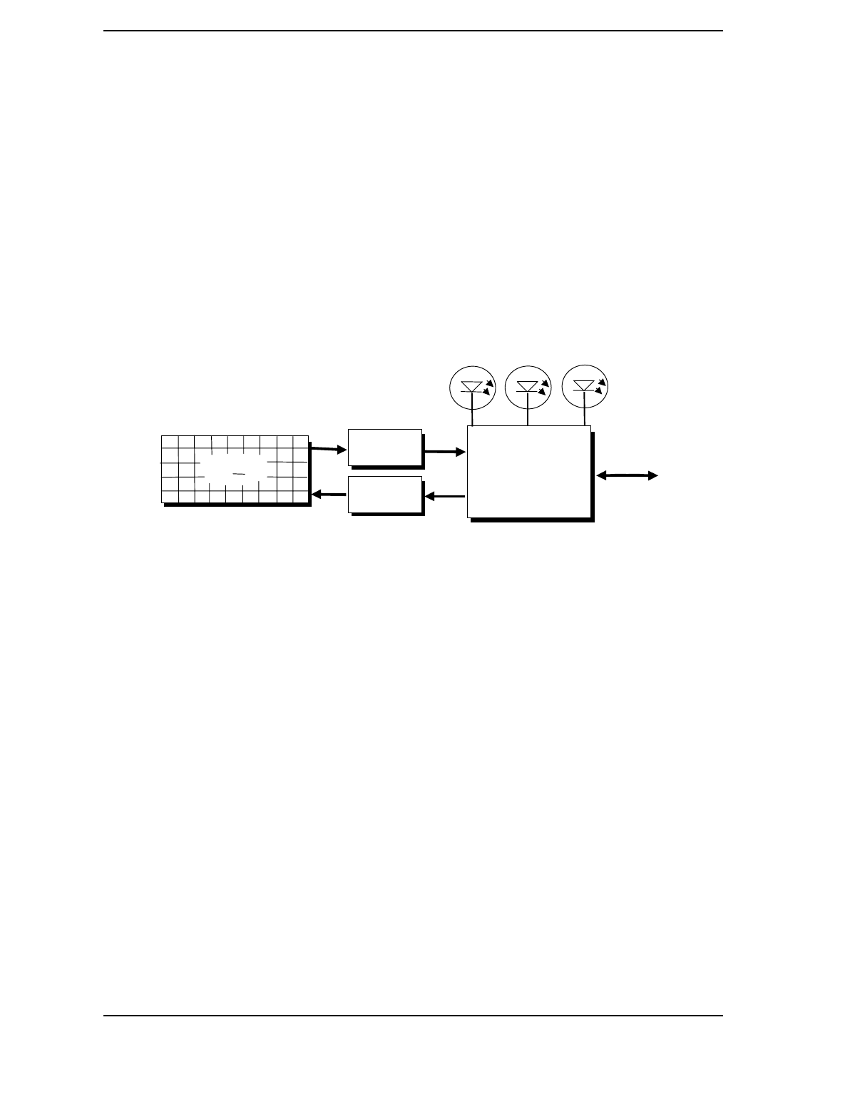
Appendix C Keyboard
Compaq Personal Computers
Changed - April 1998
C-2
Keyboard
Interface
(System Unit)
Data/
CLK
C.2 KEYSTROKE PROCESSING
A functional block diagram of the keystroke processing elements is shown in Figure C-1. Power
(+5 VDC) is obtained from the system through the PS/2-type interface. The keyboard uses a
Z86C14 (or equivalent) microprocessor. The Z86C14 scans the key matrix drivers every 10 ms
for pressed keys while at the same time monitoring communications with the keyboard interface
of the system unit. When a key is pressed, a Make code is generated. A Break code is generated
when the key is released. The Make and Break codes are collectively referred to as scan codes.
All keys generate Make and Break codes with the exception of the Pause key, which generates a
Make code only.
Figure C–1. Keystroke Processing Elements, Block Diagram
When the system is turned on, the keyboard processor generates a Power-On Reset (POR) signal
after a period of 150 ms to 2 seconds. The keyboard undergoes a Basic Assurance Test (BAT)
that checks for shorted keys and basic operation of the keyboard processor. The BAT takes from
300 to 500 ms to complete.
If the keyboard fails the BAT, an error code is sent to the CPU and the keyboard is disabled until
an input command is received. After successful completion of the POR and BAT, a completion
code (AAh) is sent to the CPU and the scanning process begins.
The keyboard processor includes a 16-byte FIFO buffer for holding scan codes until the system is
ready to receive them. Response and typematic codes are not buffered. If the buffer is full (16
bytes held) a 17th byte of a successive scan code results in an overrun condition and the overrun
code replaces the scan code byte and any additional scan code data (and the respective key
strokes) are lost. Multi-byte sequences must fit entirely into the buffer before the respective
keystroke can be registered.
Num
Lock
Caps
Lock
Scroll
Lock
Keyboard
Processor
Matrix
Drivers
Matrix
Receivers
Keyswitch
Matrix

Technical Reference Guide
Compaq Personal Computers
Change –- April 1998
C-3
C.2.1 TRANSMISSIONS TO THE SYSTEM
The keyboard processor sends two main types of data to the system; commands (or responses to
system commands) and keystroke scan codes. Before the keyboard sends data to the system
(specifically, to the 8042-type logic within the system), the keyboard verifies the clock and data
lines to the system. If the clock signal is low (0), the keyboard recognizes the inhibited state and
loads the data into a buffer. Once the inhibited state is removed, the data is sent to the system.
Keyboard-to-system transfers consist of 11 bits as shown in Figure C-2.
Parameter Minimum Maximum
Tcy (Cycle Time) 60 us 80 us
Tcl (Clock Low) 30 us 35 us
Tch (clock High) 30 us 45 us
Th (Data Hold) 45 us 62 us
Ts (Data Setup) 8 us 14 us
Figure C–2. Keyboard-To-System Transmission of Code 58h, Timing Diagram
The system can halt keyboard transmission by setting the clock signal low. The keyboard checks
the clock line every 60 us to verify the signal state. If a low is detected, the keyboard will finish
the current transmission if the rising edge of the clock pulse for the parity bit has not occurred.
The enhanced keyboard has three operating modes:
♦ Mode 1 - PC-XT compatible
♦ Mode 2 - PC-AT compatible (default)
♦ Mode 3 - Select mode (keys are programmable as to make-only, break-only, typematic)
Modes can be selected by the user or set by the system. Mode 2 is the default mode. Each mode
produces a different set of scan codes. When a key is pressed, the keyboard processor sends that
key’s make code to the 8042 logic of the system unit. The When the key is released, a release
code is transmitted as well (except for the Pause key, which produces only a make code). The
8042-type logic of the system unit responds to scan code reception by asserting IRQ1, which is
processed by the interrupt logic and serviced by the CPU with an interrupt service routine. The
service routine takes the appropriate action based on which key was pressed.
Start
Bit
D0
(LSb)
D1 D2 D3 D4 D5 D6 D7
(MSb)
Parity Stop
Bit
00001111100
Data
Clock
Ts Tcl TchTcy Th
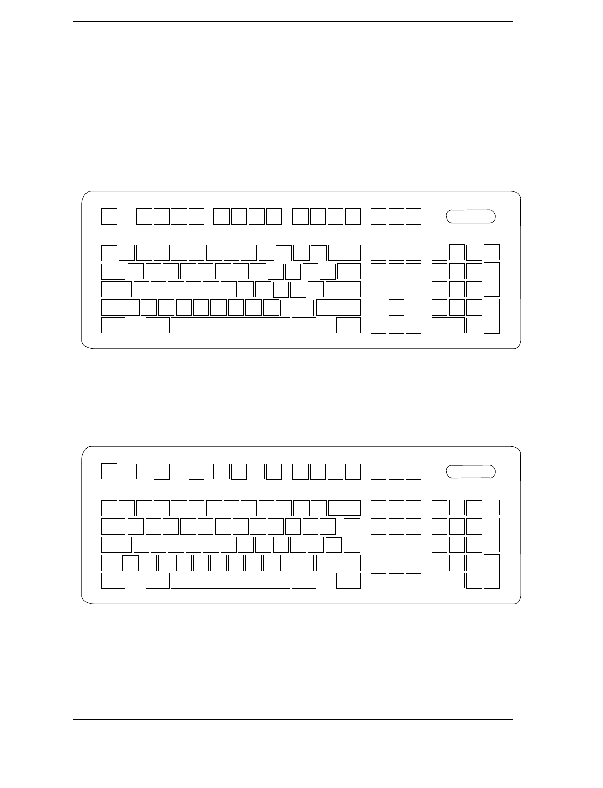
Appendix C Keyboard
Compaq Personal Computers
Changed - April 1998
C-4
C.2.2 KEYBOARD LAYOUTS
C.2.2.1 Standard Enhanced Keyboards
Figure C–3. U.S. English (101-Key) Keyboard Key Positions
Figure C–4. National (102-Key) Keyboard Key Positions
1
1
2
2
3
3
4
4
5
5
6
6
7
7
8
8
9
9
10
10
11
11
12
12
13
13
14
14
15
15
16
16
17
17
18
18
19
19
20
20
21
21
22
22
23
23
24
24
25
25
26
26
27
27
28
28
29
29
31
31
39
39
32
32
33
33
34
34
35
35
36
36
37
37
38
38
40
40
41
41
42
42
43
43
44
44
45
45
46
46
47
47
48
48
30
49
49
50
50
51
51
59
59
60
60
61
61
62
62
63
63
64
64
65
65
66
66
67
67
68
68
69
69
70
70
71
75
75
76
76
77
77
78
78
79
79
80
80
81
81
82
82
83
83
84
84
85
85
86
86
92
92
93
93
94
94
95
95
96
96
52
52
53
53
54
54
55
55
56
56
57
57
72
72
73
73
74
74
88
88
89
89
90
90
100
100
58
58
91
91
87
87
97
97
98
98
99
99
101
101
104
71
103
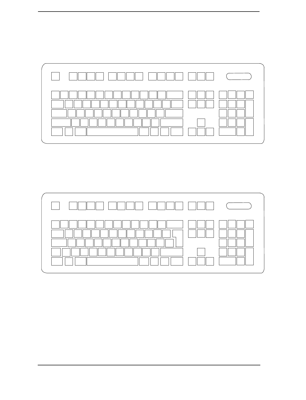
Technical Reference Guide
Compaq Personal Computers
Change –- April 1998
C-5
C.2.2.2 Windows Enhanced Keyboards
Figure C–5. U.S. English Windows (101W-Key) Keyboard Key Positions
Figure C–6. National Windows (102W-Key) Keyboard Key Positions
1
1
2
2
3
3
4
4
5
5
6
6
7
7
8
8
9
9
10
10
11
11
12
12
13
13
14
14
15
15
16
16
17
17
18
18
19
19
20
20
21
21
22
22
23
23
24
24
25
25
26
26
27
27
28
28
29
29
31
31
39
39
32
32
33
33
34
34
35
35
36
36
37
37
38
38
40
40
41
41
42
42
43
43
44
44
45
45
46
46
47
47
48
48
30
49
49
50
50
51
51
59
59
60
60
61
61
62
62
63
63
64
64
65
65
66
66
67
67
68
68
69
69
70
70
71
75
75
76
76
77
77
78
78
79
79
80
80
81
81
82
82
83
83
84
84
85
85
86
86
92 93 94 95 96
52
52
53
53
54
54
55
55
56
56
57
57
72
72
73
73
74
74
88
88
89
89
90
90
100
100
58
58
91
91
87
87
97
97
98
98
99
99
101
101
104
103
110 111 112
92 93 94 95 96
110 111 112
71

Appendix C Keyboard
Compaq Personal Computers
Changed - April 1998
C-6
C.2.3 KEYS
All keys generate a make code (when pressed) and a break code (when released) with the
exception of the Pause key (pos. 16), which produces a make code only. All keys, again, with
the exception of the Pause key, are also typematic, although the typematic action of the Shift,
Ctrl, Alt, Num Lock, Scroll Lock, Caps Lock, and Ins keys is suppressed by the BIOS.
Typematic keys, when held down, send the make code repetitively at a predetermined rate until
the key is released. If two keys are held down, the last key pressed will be typematic.
C.2.3.1 Special Single-Keystroke Functions
The following keys provide the intended function in most applications and environments.
Caps Lock - The Caps Lock key (pos. 59), when pressed and released, invokes a BIOS
routine that turns on the caps lock LED and shifts into upper case key positions 40-49, 60-68,
and 76-82. When pressed and released again, these keys revert to the lower case state and the
LED is turned off. Use of the Shift key will reverse which state these keys are in based on the
Caps Lock key.
Num Lock - The Num Lock key (pos. 32), when pressed and released, invokes a BIOS routine
that turns on the num lock LED and shifts into upper case key positions 55-57, 72-74, 88-90,
100, and 101. When pressed and released again, these keys revert to the lower case state and the
LED is turned off.
The following keys provide special functions that require specific support by the application.
Print Scrn - The Print Scrn (pos. 14) key can, when pressed, generate an interrupt that
initiates a print routine. This function may be inhibited by the application.
Scroll Lock - The Scroll Lock key (pos. 15) when pressed and released, , invokes a BIOS
routine that turns on the scroll lock LED and inhibits movement of the cursor. When pressed and
released again, the LED is turned off and the function is removed. This keystroke is always
serviced by the BIOS (as indicated by the LED) but may be inhibited or ignored by the
application.
Pause - The Pause (pos. 16) key, when pressed, can be used to cause the keyboard interrupt to
loop, i.e., wait for another key to be pressed. This can be used to momentarily suspend an
operation. The key that is pressed to resume operation is discarded. This function may be ignored
by the application.
The Esc, Fn (function), Insert, Home, Page Up/Down, Delete, and End keys operate at the
discretion of the application software.

Technical Reference Guide
Compaq Personal Computers
Change –- April 1998
C-7
C.2.3.2 Multi-Keystroke Functions
Shift - The Shift key (pos. 75/86), when held down, produces a shift state (upper case) for keys
in positions 17-29, 30, 39-51, 60-70, and 76-85 as long as the Caps Lock key (pos. 59) is
toggled off. If the Caps Lock key is toggled on, then a held Shift key produces the lower
(normal) case for the identified pressed keys. The Shift key also reverses the Num Lock state of
key positions 55-57, 72, 74, 88-90, 100, and 101.
Ctrl - The Ctrl keys (pos. 92/96) can be used in conjunction with keys in positions 1-13, 16, 17-
34, 39-54, 60-71, and 76-84. The application determines the actual function. Both Ctrl key
positions provide identical functionality. The pressed combination of Ctrl and Break (pos. 16)
results in the generation of BIOS function INT 1Bh. This software interrupt provides a method of
exiting an application and generally halts execution of the current program.
Alt - The Alt keys (pos. 93/95) can be used in conjunction with the same keys available for use
with the Ctrl keys with the exception that position 14 (SysRq) is available instead of position
16 (Break). The Alt key can also be used in conjunction with the numeric keypad keys (pos. 55-
57, 72-74, and 88-90) to enter the decimal value of an ASCII character code from 1-255. The
application determines the actual function of the keystrokes. Both Alt key positions provide
identical functionality.
The combination keystroke of Alt and SysRq results in software interrupt 15h, AX=8500h
being executed. It is up to the application to use or not use this BIOS function.
The Ctrl and Alt keys can be used together in conjunction with keys in positions 1-13, 17-34, 39-
54, 60-71, and 76-84. The Ctrl and Alt key positions used and the sequence in which they are
pressed make no difference as long as they are held down at the time the third key is pressed. The
Ctrl, Alt, and Delete keystroke combination (required twice if in the Windows environment)
initiates a system reset (warm boot) that is handled by the BIOS.

Appendix C Keyboard
Compaq Personal Computers
Changed - April 1998
C-8
C.2.3.3 Windows Keystrokes
Windows-enhanced keyboards include three additional key positions. Key positions 110 and 111
(marked with the Windows logo ) have the same functionality and are used by themselves
or in combination with other keys to perform specific “hot-key” type functions for the Windows
operating system. The defined functions of the Windows logo keys are listed as follows:
Keystroke Function
Window Logo Open Start menu
Window Logo + F1 Display pop-up menu for the selected object
Window Logo + TAB Activate next task bar button
Window Logo + E Explore my computer
Window Logo + F Find document
Window Logo + CTRL + F Find computer
Window Logo + M Minimize all
Shift + Window Logo + M Undo minimize all
Window Logo + R Display Run dialog box
Window Logo + PAUSE Perform system function
Window Logo + 1-0 Reserved for OEM use (see following text)
The combination keystroke of the Window Logo + 1-0 keys are reserved for OEM use for
auxiliary functions (speaker volume, monitor brightness, password, etc.).
Key position 112 (marked with an application window icon ) is used in combination with
other keys for invoking Windows application functions.

Technical Reference Guide
Compaq Personal Computers
Change –- April 1998
C-9
C.2.4 KEYBOARD COMMANDS
Table C-1 lists the commands that the keyboard can send to the system (specifically, to the 8042-
type logic).
Table C–1. Keyboard-to-System Commands
Table C-1.
Keyboard-to-System Commands
Command Value Description
Key Detection Error/Over/run 00h [1]
FFh [2]
Indicates to the system that a switch closure couldn’t be
identified.
BAT Completion AAh Indicates to the system that the BAT has been successful.
BAT Failure FCh Indicates failure of the BAT by the keyboard.
Echo EEh Indicates that the Echo command was received by the
keyboard.
Acknowledge (ACK) FAh Issued by the keyboard as a response to valid system
inputs (except the Echo and Resend commands).
Resend FEh Issued by the keyboard following an invalid input.
Keyboard ID 83ABh Upon receipt of the Read ID command from the system, the
keyboard issues the ACK command followed by the two IDS
bytes.
Note:
[1] Modes 2 and 3.
[2] Mode 1 only.
C.2.5 SCAN CODES
The scan codes generated by the keyboard processor are determined by the mode the keyboard is
operating in.
♦ Mode 1: In Mode 1 operation, the keyboard generates scan codes compatible with 8088-
/8086-based systems. To enter Mode 1, the scan code translation function of the keyboard
controller must be disabled. Since translation is not performed, the scan codes generated in
Mode 1 are identical to the codes required by BIOS. Mode 1 is initiated by sending command
F0h with the 01h option byte. Applications can obtain system codes and status information
by using BIOS function INT 16h with AH=00h, 01h, and 02h.
♦ Mode 2: Mode 2 is the default mode for keyboard operation. In this mode, the 8042 logic
translates the make codes from the keyboard processor into the codes required by the BIOS.
This mode was made necessary with the development of the Enhanced III keyboard, which
includes additional functions over earlier standard keyboards. Applications should use BIOS
function INT 16h, with AH=10h, 11h, and 12h for obtaining codes and status data. In Mode
2, the keyboard generates the Break code, a two-byte sequence that consists of a Make code
immediately preceded by F0h (i.e., Break code for 0Eh is “F0h 0Eh”).
♦ Mode 3: Mode 3 generates a different scan code set from Modes 1 and 2. Code
translation must be disabled since translation for this mode cannot be done.

Appendix C Keyboard
Compaq Personal Computers
Changed - April 1998
C-10
Table C–2. Keyboard Scan Codes
Table C-2.
Keyboard Scan Codes
Key
Pos. Legend Mode 1 Mode 2 Mode 3
1 Esc 01/81 76/F0 76 08/na
2 F1 3B/BB 05/F0 05 07/na
3 F2 3C/BC 06/F0 06 0F/na
4 F3 3D/BD 04/F0 04 17/na
5 F4 3E/BE 0C/F0 0C 1F/na
6 F5 3F/BF 03/F0 03 27/na
7 F6 40/C0 0B/F0 0B 2F/na
8 F7 41/C1 83/F0 83 37/na
9 F8 42/C2 0A/F0 0A 3F/na
10 F9 43/C3 01/FO 01 47/na
11 F10 44/C4 09/F0 09 4F/na
12 F11 57/D7 78/F0 78 56/na
13 F12 58/D8 07/F0 07 5E/na
14 Print Scrn E0 2A E0 37/E0 B7 E0 AA
E0 37/E0 B7 [1] [2]
54/84 [3]
E0 2A E0 7C/E0 F0 7C E0 F0 12
E0 7C/E0 F0 7C [1] [2]
84/F0 84 [3]
57/na
15 Scroll Lock 46/C6 7E/F0 7E 5F/na
16 Pause E1 1D 45 E1 9D C5/na
E0 46 E0 C6/na [3]
E1 14 77 E1 F0 14 F0 77/na
E0 7E E0 F0 7E/na [3]
62/na
17 ` 29/A9 0E/F0 E0 0E/F0 0E
18 1 02/82 16/F0 16 46/F0 46
19 2 03/83 1E/F0 1E 1E/F0 1E
20 3 04/84 26/F0 26 26/F0 26
21 4 05/85 25/F0 25 25/F0 25
22 5 06/86 2E/F0 2E 2E/F0 2E
23 6 07/87 36/F0 36 36/F0 36
24 7 08/88 3D/F0 3D 3D/F0 3D
25 8 09/89 3E/F0 3E 3E/F0 3E
26 9 0A/8A 46/F0 46 46/F0 46
27 0 0B/8B 45/F0 45 45/F0 45
28 - 0C/8C 4E/F0 4E 4E/F0 4E
29 = 0D/8D 55/F0 55 55/F0 55
30 \ 2B/AB 5D/F0 5D 5C/F0 5C
31 Backspace 0E/8E 66/F0 66 66/F0 66
32 Insert E0 52/E0 D2
E0 AA E0 52/E0 D2 E0 2A [4]
E0 2A E0 52/E0 D2 E0 AA [6]
E0 70/E0 F0 70
E0 F0 12 E0 70/E0 F0 70 E0 12 [5]
E0 12 E0 70/E0 F0 70 E0 F0 12 [6]
67/na
33 Home E0 47/E0 D2
E0 AA E0 52/E0 D2 E0 2A [4]
E0 2A E0 47/E0 C7 E0 AA [6]
E0 6C/E0 F0 6C
E0 F0 12 E0 6C/E0 F0 6C E0 12 [5]
E0 12 E0 6C/E0 F0 6C E0 F0 12 [6]
6E/na
34 Page Up E0 49/E0 C7
E0 AA E0 49/E0 C9 E0 2A [4]
E0 2A E0 49/E0 C9 E0 AA [6]
E0 7D/E0 F0 7D
E0 F0 12 E0 7D/E0 F0 7D E0 12 [5]
E0 12 E0 7D/E0 F0 7D E0 F0 12 [6]
6F/na
35 Num Lock 45/C5 77/F0 77 76/na
36 / E0 35/E0 B5
E0 AA E0 35/E0 B5 E0 2A [1]
E0 4A/E0 F0 4A
E0 F0 12 E0 4A/E0 F0 4A E0 12 [1]
77/na
37 * 37/B7 7C/F0 7C 7E/na
38 - 4A/CA 7B/F0 7B 84/na
39 Tab 0F/8F 0D/F0 0D 0D/na
40 Q 10/90 15/F0 15 15/na
Continued
([x] Notes listed at end of table.)
Make / Break Codes (Hex)

Technical Reference Guide
Compaq Personal Computers
Change –- April 1998
C-11
Table C-2. Keyboard Scan Codes
(Continued)
Key
Pos Legend Mode 1 Mode 2 Mode 3
41 W 11/91 1D/F0 1D 1D/F0 1D
42 E 12/92 24/F0 24 24/F0 24
43 R 13/93 2D/F0 2D 2D/F0 2D
44 T 14/94 2C/F0 2C 2C/F0 2C
45 Y 15/95 35/F0 35 35/F0 35
46 U 16/96 3C/F0 3C 3C/F0 3C
47 I 17/97 43/F0 43 43/F0 43
48 O 18/98 44/F0 44 44/F0 44
49 P 19/99 4D/F0 4D 4D/F0 4D
50 [ 1A/9A 54/F0 54 54/F0 54
51 ] 1B/9B 5B/F0 5B 5B/F0 5B
52 Delete E0 53/E0 D3
E0 AA E0 53/E0 D3 E0 2A [4]
E0 2A E0 53/E0 D3 E0 AA [6]
E0 71/E0 F0 71
E0 F0 12 E0 71/E0 F0 71 E0 12 [5]
E0 12 E0 71/E0 F0 71 E0 F0 12 [6]
64/F0 64
53 End E0 4F/E0 CF
E0 AA E0 4F/E0 CF E0 2A [4]
E0 2A E0 4F/E0 CF E0 AA [6]
E0 69/E0 F0 69
E0 F0 12 E0 69/E0 F0 69 E0 12 [5]
E0 12 E0 69/E0 F0 69 E0 F0 12 [6]
65/F0 65
54 Page Down E0 51/E0 D1
E0 AA E0 51/E0 D1 E0 2A [4]
E0 @a E0 51/E0 D1 E0 AA [6]
E0 7A/E0 F0 7A
E0 F0 12 E0 7A/E0 F0 7A E0 12 [5]
E0 12 E0 7A/E0 F0 7A E0 F0 12 [6]
6D/F0 6D
55 7 47/C7 [6] 6C/F0 6C [6] 6C/na [6]
56 8 48/C8 [6] 75/F0 75 [6] 75/na [6]
57 9 49/C9 [6] 7D/F0 7D [6] 7D/na [6]
58 + 4E/CE [6] 79/F0 79 [6] 7C/F0 7C
59 Caps Lock 3A/BA 58/F0 58 14/F0 14
60 A 1E/9E 1C/F0 1C 1C/F0 1C
61 S 1F/9F 1B/F0 1B 1B/F0 1B
62 D 20/A0 23/F0 23 23/F0 23
63 F 21/A1 2B/F0 2B 2B/F0 2B
64 G 22/A2 34/F0 34 34/F0 34
65 H 23/A3 33/F0 33 33/F0 33
66 J 24/A4 3B/F0 3B 3B/F0 3B
67 K 25/A5 42/F0 42 42/F0 42
68 L 26/A6 4B/F0 4B 4B/F0 4B
69 ; 27/A7 4C/F0 4C 4C/F0 4C
70 ‘ 28/A8 52/F0 52 52/F0 52
71 Enter 1C/9C 5A/F0 5A 5A/F0 5A
72 4 4B/CB [6] 6B/F0 6B [6] 6B/na [6]
73 5 4C/CC [6] 73/F0 73 [6] 73/na [6]
74 6 4D/CD [6] 74/F0 74 [6] 74/na [6]
75 Shift (left) 2A/AA 12/F0 12 12/F0 12
76 Z 2C/AC 1A/F0 1A 1A/F0 1A
77 X 2D/AD 22/F0 22 22/F0 22
78 C 2E/AE 21/F0 21 21/F0 21
79 V 2F/AF 2A/F0 2A 2A/F0 2A
80 B 30/B0 32/F0 32 32/F0 32
Continued
([x] Notes listed at end of table.)
Make / Break Codes (Hex)

Appendix C Keyboard
Compaq Personal Computers
Changed - April 1998
C-12
Table C-2. Keyboard Scan Codes
(Continued)
Key
Pos. Legend Mode 1 Mode 2 Mode 3
81 N 31/B1 31/F0 31 31/F0 31
82 M 32/B2 3A/F0 3A 3A/F0 3A
83 , 33/B3 41/F0 41 41/F0 41
84 . 34/B4 49/F0 49 49/F0 49
85 / 35/B5 4A/F0 4A 4A/F0 4A
86 Shift (right) 36/B6 59/F0 59 59/F0 59
87 E0 48/E0 C8
E0 AA E0 48/E0 C8 E0 2A [4]
E0 2A E0 48/E0 C8 E0 AA [6]
E0 75/E0 F0 75
E0 F0 12 E0 75/E0 F0 75 E0 12 [5]
E0 12 E0 75/E0 F0 75 E0 F0 12 [6]
63/F0 63
88 1 4F/CF [6] 69/F0 69 [6] 69/na [6]
89 2 50/D0 [6] 72/F0 72 [6] 72/na [6]
90 3 51/D1 [6] 7A/F0 7A [6] 7A/na [6]
91 Enter E0 1C/E0 9C E0 5A/F0 E0 5A 79/F0 79[6]
92 Ctrl (left) 1D/9D 14/F0 14 11/F0 11
93 Alt (left) 38/B8 11/F0 11 19/F0 19
94 (Space) 39/B9 29/F0 29 29/F0 29
95 Alt (right) E0 38/E0 B8 E0 11/F0 E0 11 39/na
96 Ctrl (right) E0 1D/E0 9D E0 14/F0 E0 14 58/na
97 E0 4B/E0 CB
E0 AA E0 4B/E0 CB E0 2A [4]
E0 2A E0 4B/E0 CB E0 AA [6]
E0 6B/Eo F0 6B
E0 F0 12 E0 6B/E0 F0 6B E0 12[5]
E0 12 E0 6B/E0 F0 6B E0 F0 12[6]
61/F0 61
98 E0 50/E0 D0
E0 AA E0 50/E0 D0 E0 2A [4]
E0 2A E0 50/E0 D0 E0 AA [6]
E0 72/E0 F0 72
E0 F0 12 E0 72/E0 F0 72 E0 12[5]
E0 12 E0 72/E0 F0 72 E0 F0 12[6]
60/F0 60
99 E0 4D/E0 CD
E0 AA E0 4D/E0 CD E0 2A [4]
E0 2A E0 4D/E0 CD E0 AA [6]
E0 74/E0 F0 74
E0 F0 12 E0 74/E0 F0 74 E0 12[5]
E0 12 E0 74/E0 F0 74 E0 F0 12[6]
6A/F0 6A
100 0 52/D2 [6] 70/F0 70 [6] 70/na [6]
101 . 53/D3 [6] 71/F0 71 [6] 71/na [6]
102 na 7E/FE 6D/F0 6D 7B/F0 7B
103 na 2B/AB 5D/F0 5D 53/F0 53
104 na 36/D6 61/F0 61 13/F0 13
110 (Win95) [7] E0 5B/E0 DB
E0 AA E0 5B/E0 DB E0 2A [4]
E0 2A E0 5B/E0 DB E0 AA [6]
E0 1F/E0 F0 1F
E0 F0 12 E0 1F/E0 F0 1F E0 12 [5]
E0 12 E0 1F/E0 F0 1F E0 F0 12 [6]
8B/F0 8B
111 (Win95) [7] E0 5C/E0 DC
E0 AA E0 5C/E0 DC E0 2A [4]
E0 2A E0 5C/E0 DC E0 AA [6]
E0 2F/E0 F0 27
E0 F0 12 E0 27/E0 F0 27 E0 12 [5]
E0 12 E0 27/E0 F0 27 E0 F0 12 [6]
8C/F0 8C
112 (Win Apps)
[7]
E0 5D/E0 DD
E0 AA E0 5D/E0 DD E0 2A [4]
E0 2A E0 5D E0 DD E0 AA [6]
E0 2F/E0 F0 2F
E0 F0 12 E0 2F/E0 F0 2F E0 12 [5]
E0 12 E0 2F/E0 F0 2F E0 F0 12 [6
8D/F0 8D
NOTES:
All codes assume Shift, Ctrl, and Alt keys inactive unless otherwise noted.
NA = Not applicable
[1] Shift (left) key active.
[2] Ctrl key active.
[3] Alt key active.
[4] Left Shift key active. For active right Shift key, substitute AA/2A make/break codes for B6/36 codes.
[5] Left Shift key active. For active right Shift key, substitute F0 12/12 make/break codes
for F0 59/59 codes.
[6] Num Lock key active.
[7] Windows keyboards only
Make / Break Codes (Hex)
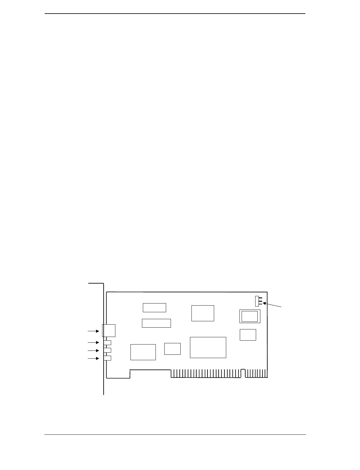
Technical Reference Guide
Compaq Personal Computers
Changed - June 1998 D-1
Appendix D
COMPAQ 10/100 TX PCI INTEL
WOL UTP CONTROLLER CARD
D. Appendix D Compaq 10/100 TX PCI Intel WOL UTP Controller Card
D.1 INTRODUCTION
This appendix describes the Compaq 10/100 TX PCI Intel WOL UTP Controller card (# 323550-
001). Key features of this card include:
♦ Intel 82558 Fast LAN controller with 32-bit architecture and 3-KB TX/RX buffers.
♦ Dual-mode support with auto-switching between 10BASE-T and 100BASE-TX PHY.
♦ Power down and Wake up support in both APM and ACPI environments (PME- and WOL).
♦ LED indicators for link, activity, and speed status.
♦ LanDesk Service Agent (LSA) ver 2.0 boot code contained in on-board flash memory.
The card installs into a PCI slot and provides Wake-On-LAN (WOL) support.
This appendix covers the following subjects:
♦ Functional description (D.2) page D-2
♦ Configuration/control (D.3) page D-5
♦ RJ-45 connector (D.4) page D-5
♦ Specifications (D.5) page D-5
Figure D–1. Compaq 10/100 TX WOL Controller Card Layout (PCA# 323550-001)
WOL Header
RJ-45
Connector
Link LED
Activit
y
LED
100TX LED
82558
LAN
Controller
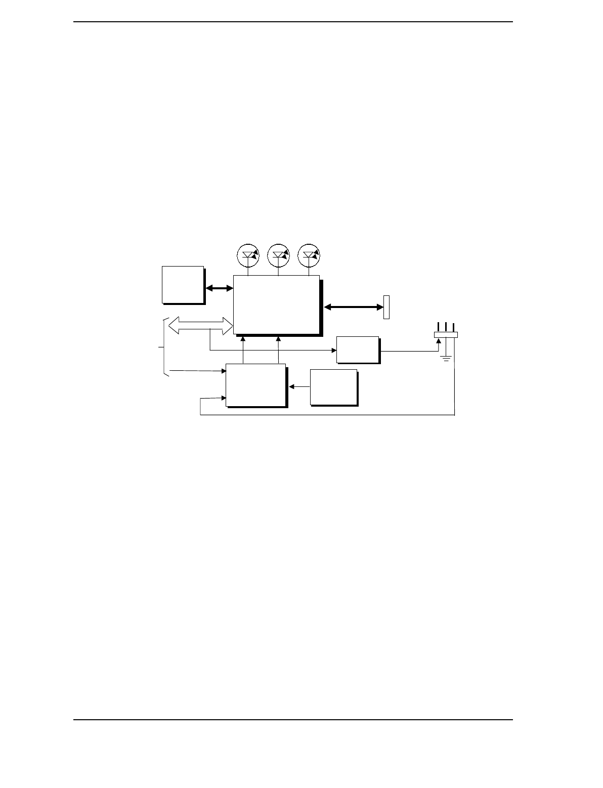
Appendix D Compaq 10/100 TX PCI Intel WOL UTP Controller Card
Compaq Personal Computers
Changed - June 1998
D-2
D.2 FUNCTIONAL DESCRIPTION
The Compaq 10/100 TX PCI Intel WOL UTP Controller card contains the 82558 controller (with
ROMs and support logic), three LED status indicators, a WOL header connector, a RJ-45
network connector, and power switching logic (Figure D-2).
Figure D–2. Compaq 10/100 TX PCI Intel WOL UTP Controller Card Block Diagram
D.2.1 STATUS INDICATORS
The LEDs provide the following indications:
Link LED (yellow) – Indicates reception of link pulses in 10 MB/s mode, scrambler lock in 100
MB/s mode.
Activity LED (green) – Indicates network activity.
100 TX LED (green) – Indicates connection with 100 MB/s network.
RJ-45
Connector
TX/RX
82558
Ethernet
Controller
PCI Bus
WOL
Header
Active
(
Green
)
Link
(
Yellow
)
100TX
(
Green
)
Power/
Clock
Transition
Lo
g
ic
+5AUX
PCI
Connector WAKEUP
+5VDC
31
25 MHz
Clock
Circuitry
EEP/
Flash
ROM
PME- Pulse
Generator
PCI CLK
CLK
CLK
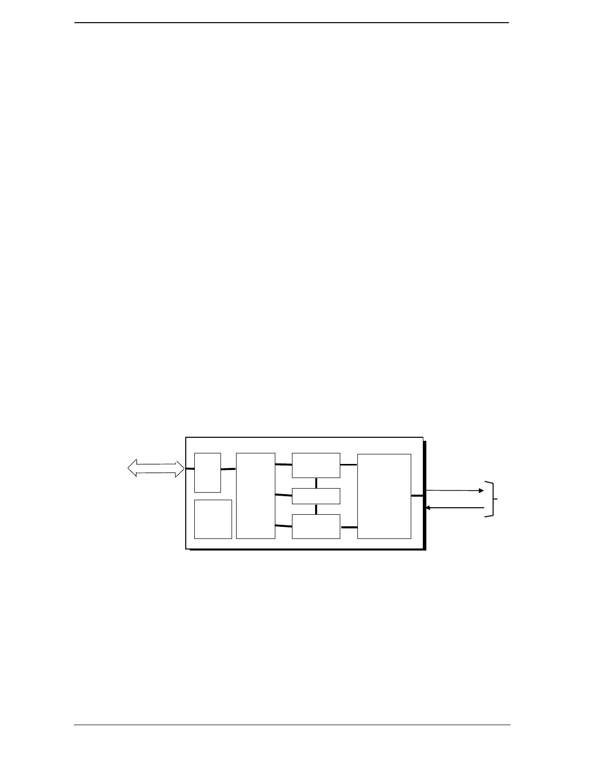
Technical Reference Guide
Compaq Personal Computers
Changed - June 1998 D-3
TX Data
TX/RX
Filters
D.2.2 CARD POWER AND CLOCK
The controller card includes on-board power logic that receives +5 VDC power from the PCI
connector or the WOL header. The PCI CLK signal provides the clock source for the controller
when the system is up and active. When the system is off or in Standby the on-board clock
generator provides the clock signal.
NOTE: Lack of a WOL header connection with the main system will result in the
controller board not receiving power at any time. Therefore the WOL header cable
should always be installed even if Wake-On-LAN functionality is not required.
D.2.3 82558 CONTROLLER
The Intel 82558 Fast Ethernet LAN controller provides most of the functionality of the card
(Figure D-3). The 82558 provides the following features:
♦ Dual-mode support with auto-switching between 10BASE-T to 100BASE-TX PHY.
♦ Digitally controlled adaptive equalization of transmission
♦ Optimized PCI bandwidth with enhanced support of PCI commands.
♦ ACPI support of power-down and wake-up states.
♦ Wake On LAN (WOL) support.
♦ LANDesk Service Agent (LSA) support.
Figure D-3 shows the internal architecture of the 82558 Ethernet controller.
Figure D–3. 82558 Controller Internal Architecture
The 82558 controller features auto-negotiation of both speed and direction (half/full duplex). The
82558 provides high-level command support for minimum Host CPU intervention and uses 3-KB
FIFOs for both transmit and receive buffers.
82558 Ethernet Controller
Bus
I/F
3-KB
TX FIFO
10BASE-TX/
100BASE-T
PHY
AD31..0
PCI Bus
RX Data
Micro
Machine FIFO Cntrl
3-KB
RX FIFO
4-Ch
DMA
Cntlr.

Appendix D Compaq 10/100 TX PCI Intel WOL UTP Controller Card
Compaq Personal Computers
Changed - June 1998
D-4
D.2.4 POWER MANAGEMENT SUPPORT
The controller card provides system wake up using network events and supports both APM and
ACPI power management environments.
NOTE: The APM and ACPI environments use different methods to implement the
Wake-On-LAN function. The cable connection between the controller card’s WOL
header and the system’s WOL header should be complete to insure that the wake up
feature will occur for both the APM and ACPI environments.
D.2.4.1 APM Environment
The Advanced Power Management (APM) functionality of system wake up is implemented
through the system’s APM-compliant BIOS and the controller card’s Magic Packet-compliant
hardware. This environment bypasses operating system (OS) intervention allowing a plugged in
unit to be turned on remotely over the network (i.e., “remote wake up”). In APM mode the
controller, powered by the +5AUX voltage through the WOL header, will respond upon receiving
a Magic Packet, which is a packet where the node’s address is repeated 16 times. Upon Magic
packet detection, the controller card asserts the WAKEUP signal (for about 50 milliseconds) that
is routed through the WOL header and cable to the system board where power control logic turns
on the system and intitiates the boot sequence. After the boot sequence the BIOS clears the PME-
signal (from which WAKEUP is derived) so that subsequent wakeup events will be detected.
D.2.4.2 ACPI Environment
The Advanced Configuration and Power Interface (ACPI) functionality of system wake up is
implemented through an ACPI-compliant OS such as Windows NT 5.0 and hardware that is
compliant to the PCI power management specification. The following wakeup events may be
individually enabled/disabled through the supplied software driver:
♦ Magic Packet – Packet with node address repeated 16 times in data portion
NOTE: The following functions are supported in NDIS5 drivers but implemented through
remote management software applications (such as LanDesk).
♦ Individual address match – Packet with matching user-defined byte mask
♦ Multicast address match – Packet with matching user-defined sample frame
♦ ARP (address resolution protocol) packet
♦ Flexible packet filtering – Packets that match defined CRC signature
When an enabled event is received the controller card asserts the PME- signal that is used by the
system board to initiate its wakeup sequence. Note that the WAKEUP signal is also asserted but
not required in the ACPI environment.

Technical Reference Guide
Compaq Personal Computers
Changed - June 1998 D-5
D.3 CONFIGURATION/CONTROL
The 82558 controller is a PCI device and configured though PCI configuration space registers
using PCI protocol described in chapter 4.
Vender ID Device ID
8086h 1229h
Control is through I/O registers mapped in the 300h-30Fh range.
D.4 RJ-45 CONNECTOR
Figure D–4. Ethernet TPE Connector (RJ-45, viewed from card edge)
D.5 SPECIFICATIONS
Table D–1. Operating Specifications
Table D-1.
Operating Specifications
Parameter
Modes Supported Half or full duplex for 10BASE-T, 100BASE-TX
Power Management Support APM, ACPI, PCI Power Management Spec.
Power Consumption (nominal):
Standby
Full On
2.41 watts
2.61 watts
12438765
Pin Description
1 Transmit
2 Receive
3 Receive Low
6 Transmit Low

Appendix D Compaq 10/100 TX PCI Intel WOL UTP Controller Card
Compaq Personal Computers
Changed - June 1998
D-6
This page is intentionally blank.
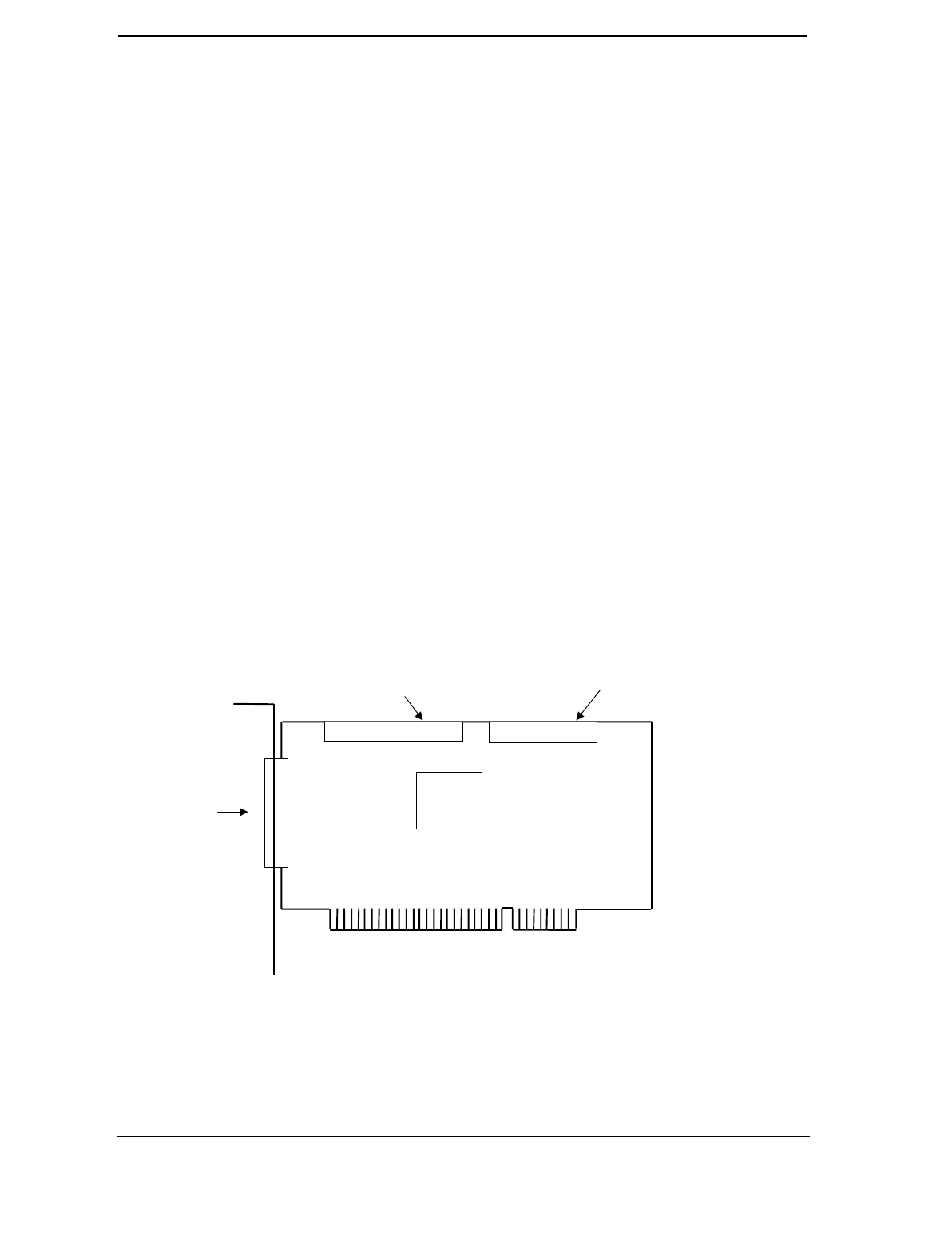
Technical Reference Guide
Compaq Personal Computers
Original - April 1998
E-1
Appendix E
WIDE ULTRA SCSI HOST ADAPTER
E. Appendix E Wide Ultra SCSI Host Adapter
E.1 INTRODUCTION
The Adaptec AHA-2940UW SCSI Host Adapter (Compaq p/n 334136-001) is a PCI peripheral
that provides high performance interfacing with compatible SCSI peripherals, specifically hard
drives. The card installs in a PCI slot and supports full bus mastering capability.
NOTE: This appendix describes the Wide Ultra SCSI Adapter in general. For detailed
information on the Ultra SCSI Adapter card refer to Adaptec, Inc documentation.
This appendix covers the following subjects:
♦ Functional description (E.2) page E-2
♦ SCSI adapter programming (E.3) page E-3
♦ Specifications (E.4) page E-3
♦ User guidelines (E.5) page E-4
♦ SCSI connectors (E.6) page E-5
Figure E–1. Wide Ultra SCSI Host Adapter Card Layout
External
Wide Ultra
SCSI Connector
AIC7880
Internal
Wide Ultra SCSI Connector
Internal
Ultra SCSI Connector
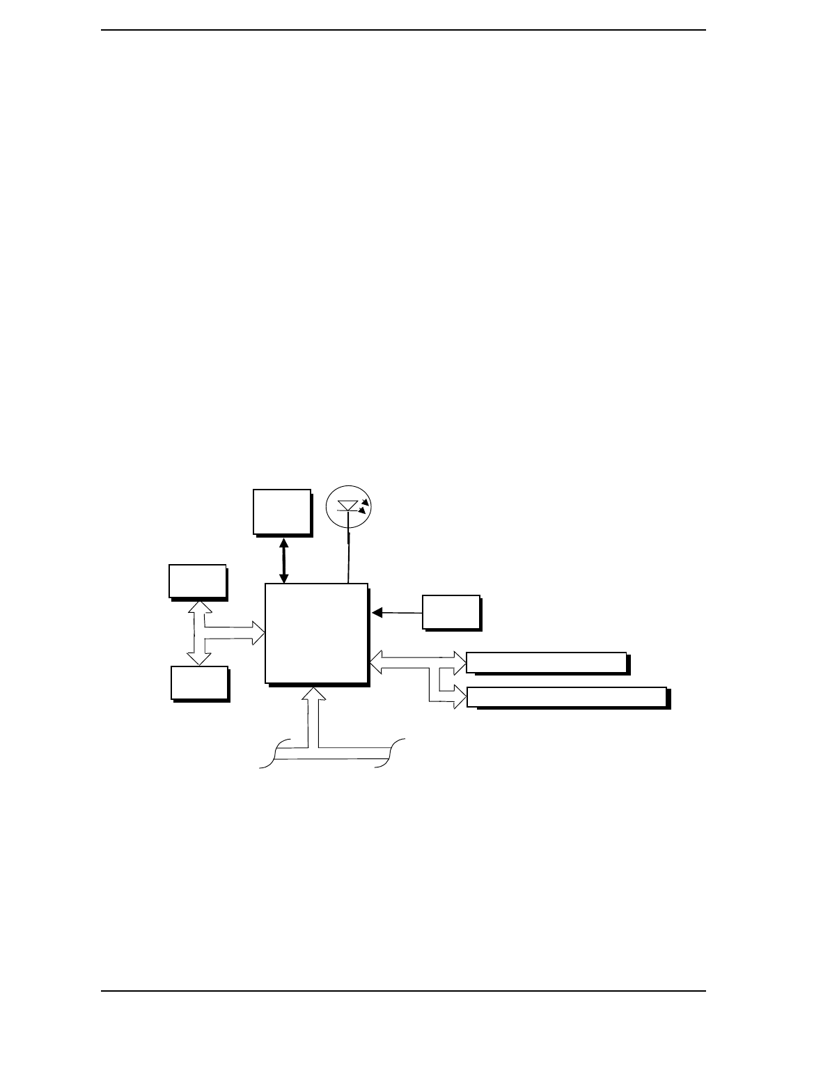
Appendix E Wide Ultra SCSI Host Adapter Card
Compaq Personal Computers
Original – April 1998
E-2
E.2 FUNCTIONAL DESCRIPTION
A block diagram of the Wide Ultra SCSI Card is shown in Figure E-2. The card’s architecture is
based on the AIC-7880 SCSI controller. The AIC-7880 controller includes an on-board SCSI
sequencer that can process SCSI commands without intervention from the host microprocessor.
The sequencer uses micro-code that is downloaded from the host during initialization. Single-
ended SCSI drivers are built into the controller and a 256-byte FIFO in the data path allowing up
to 15-byte synchronous offsets. An LED is provided to indicate SCSI bus activity.
The AIC provides a memory interface that is used by the Serial EEPROM and the BIOS ROM.
The serial EEPROM stores non-volatile configuration data and the BIOS ROM (which is a flash
ROM) contains additional configuration data and SCSI functions. The programmable array logic
(PAL) controls the Serial EEPROM-to-AIC7880 interface.
SCSI operations include the processing of 32-byte SCSI command blocks (SCBs). The AIC-7880
can execute up to 254 SCBs by swapping the blocks in and out of 8-KB of system memory as
there is no on-board memory. The SCBs can be handled on the byte level or as an entire block.
Figure E–2. Adaptec AHA-2940U Ultra SCSI Adapter Card Block Diagram
PCI Bus
AIC7880
SCSI
Controller
Serial
EEPROM
SCSI
Activity
BIOS
ROM
Ultra SCSI Connector (Ext)
Wide Ultra SCSI Connector (Int. & Ext.)
PAL
Mem. I/F 40-MHz
Clock

Technical Reference Guide
Compaq Personal Computers
Original - April 1998
E-3
E.3 SCSI ADAPTER PROGRAMMING
E.3.1 SCSI ADAPTER CONFIGURATION
The Adaptec AHA-2940U SCSI Adapter Card is a PCI device and configured using PCI protocol
and PCI Configuration Space registers (PCI addresses 00h-FFh) as discussed in Chapter 4.
Configuration is accomplished by BIOS during POST and re-configurable with software.
E.3.2 SCSI ADAPTER CONTROL
Control of the SCSI host adapter is affected through I/O mapped registers mapped as listed in
Table E-1.
Table E–1. Ultra SCSI Host Adapter Card Control Register Mapping
Table E-1.
Ultra SCSI Host Adapter Card
Control Register Mapping
I/O Addr. Function
n00h-n1Fh SCSI Register Array
n20h-n5Fh Scratch RAM
n60h-n7Fh Phase Engine (Sequencer)
n80h-n9Fh Host Registers
n00h-nFFh SCB Array
n = prefix address supplied by the BASEADR0 PCI Config. Reg.
E.4 SPECIFCATIONS
The operating specifications are listed in Table E-2.
Table E–2. Ultra SCSI Host Adapter Card Specifications
Table E-2.
Ultra SCSI Host Adapter Card Specifications
Operating Voltage +5 VDC
Maximum Current Draw 2 A
Operating Temperature 32°F (0°C) to 131°F (55°C)

Appendix E Wide Ultra SCSI Host Adapter Card
Compaq Personal Computers
Original – April 1998
E-4
E.5 USER GUIDELINES
The adapter card follows standard SCSI guidelines in supporting up to SCSI devices using SCSI
identification numbers 0-6 (ID #7 is reserved for the adapter card). Each SCSI device chain must
be terminated at both ends.
NOTE: The adapter card includes an external connector and two internal connectors.
All connectors may be in use at the same time. However, if two or more SCSI hard
drives are connected, they must all be either internal or external. Other SCSI
peripherals (tape/CD-ROM drives can be mixed (internal and external). The device
using the external connector must be terminated.
Table E-3 lists the typical parameter configuration for the SCSI adapter card installed in a system
Table E–3. Wide Ultra SCSI Adapter Card Typical Configuration
Table E-3.
Wide Ultra SCSI Adapter Card
Typical Configuration
Paramemter Setting
SCSI Identification Numbers
0
1-4
5
6
7
Hard Drive
available
CD-ROM (if installed)
available
Adapter Card
Parity checking Enabled
Adapter SCSI Termination Automatic
Boot Device Options
Boot Target ID
Boot LUN Number
0
0
SCSI Configuration Boot Device Options:
Initiate Sync Negotiation
Maximum Sync Transfer Rate
Enable Disconnection
Initiate Wide Negotiation
Send Start Unit
Include BIOS Scan
Yes
40.0 MB/s
Yes
Yes
Yes
Yes
Advanced Configuration Options:
PnP SCAM Support
Reset SCSI BIOS at IC Initialization
Host Adapter BIOS (Config. Utility Reserves)
Support Removable Fixed Disks Under BIOS
Extended BIOS Translation for >1GB Drives
Display <Ctlr A> Message During BIOS Init.
Multiple LUN Support
BIOS Support for Bootable CD-ROM
BIOS Support for INT 13 Extensions
Support for Ultra SCSI Speed
Disabled
Enabled
Enabled
Disabled
Enabled
Enabled
Disabled
Disabled
Enabled
Enabled
Silent/Verbose Mode Setting Silent
POST Speedup Feature Enabled
Write Cache Enabled
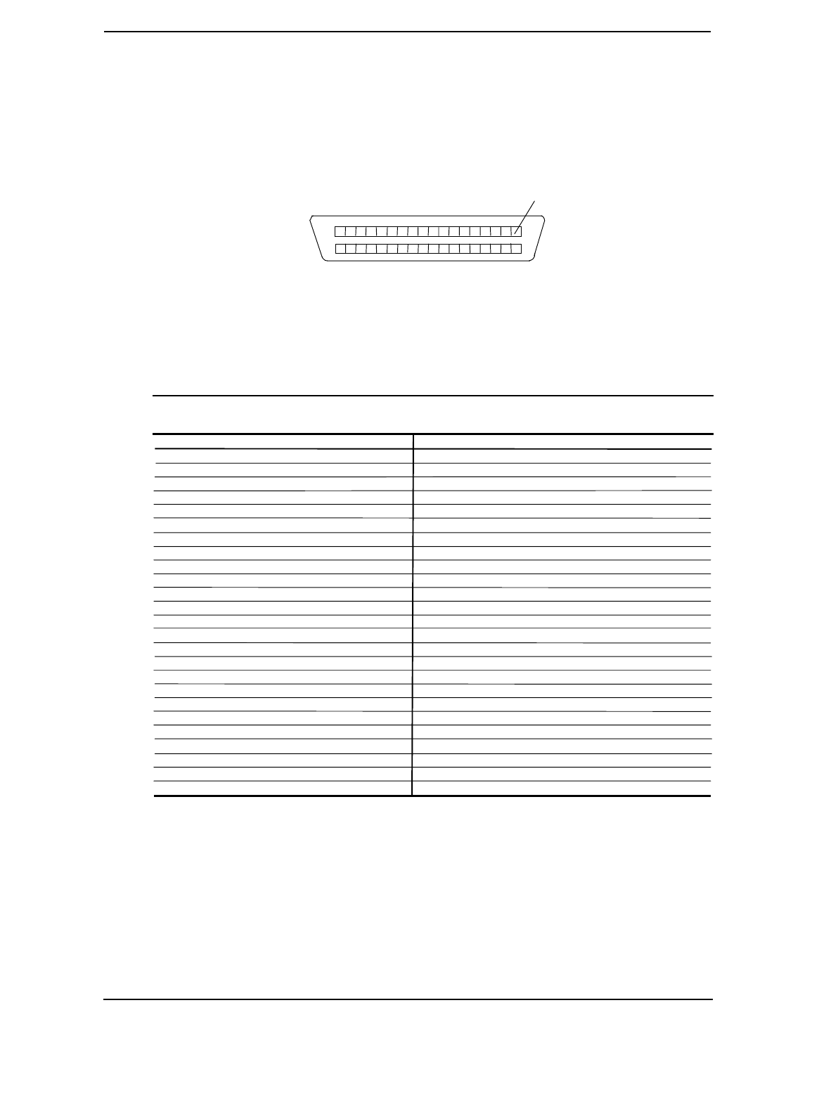
Technical Reference Guide
Compaq Personal Computers
Original - April 1998
E-5
E.6 SCSI CONNECTORS
Figure E–3. Ultra SCSI Connector (50-pin, as seen from rear of card)
Table E–4. SCSI Connector Pinout
Table E-3.
SCSI Connector Pinout
Pin Signal Function Pin Signal Function
1 GND Ground 26 DB0- Data Bit 0
2 GND Ground 27 DB1- Data Bit 1
3 GND Ground 28 DB2- Data Bit 2
4 GND Ground 29 DB3- Data Bit 3
5 GND Ground 30 DB4- Data Bit 4
6 GND Ground 31 DB5- Data Bit 5
7 GND Ground 32 DB6- Data Bit 6
8 GND Ground 33 DB7- Data Bit 7
9 GND Ground 34 DBP Data Bus Pulse
10 GND Ground 35 GND Ground
11 GND Ground 36 GND Ground
12 GND Ground 37 GND Ground
13 RSVD Reserved 38 TERMPWR Termination Power
14 GND Ground 39 GND Ground
15 GND Ground 40 GND Ground
16 GND Ground 41 ATN- Attention
17 GND Ground 42 GND Ground
18 GND Ground 43 BSY- Busy
19 GND Ground 44 ACK- Acknowledge
20 GND Ground 45 SBRST- Burst
21 GND Ground 46 MSG- Message Activity
22 GND Ground 47 SEL- Select
23 GND Ground 48 C-/D Control/Data Transfer Indicator
24 GND Ground 49 REQ- Request
25 GND Ground 50 I-/O Input/Output Indicator
Pin 1
Appendix E Wide Ultra SCSI Host Adapter Card
Compaq Personal Computers
Original – April 1998
E-6
Figure E–4. Wide Ultra SCSI Connector (68-pin, as seen from top of card)
Table E–5. Wide Ultra SCSI Connector Pinout
Table E-4.
Wide-Ultra SCSI Connector Pinout
Pin Signal Function Pin Signal Function
1 GND Ground 35 DB12 Data Bit 12
2 GND Ground 36 DB13 Data Bit 13
3 GND Ground 37 DB14 Data Bit 14
4 GND Ground 38 DB15 Data Bit 15
5 GND Ground 39 DBP- Data Bus Parity
6 GND Ground 40 DB0- Data Bit 0
7 GND Ground 41 DB1- Data Bit 1
8 GND Ground 42 DB2- Data Bit 2
9 GND Ground 43 DB3- Data Bit 3
10 GND Ground 44 DB4- Data Bit 4
11 GND Ground 45 DB5- Data Bit 5
12 GND Ground 46 DB6- Data Bit 6
13 GND Ground 47 DB7- Data Bit 7
14 GND Ground 48 DBP- Data Bus Parity
15 GND Ground 49 GND Ground
16 GND Ground 50 GND Ground
17 TERMPWR Termination Power 51 TERMPWR Termination Power
18 TERMPWR Termination Power 52 TERMPWR Termination Power
19 GND Ground 53 Int_Out- Interrupt Out
20 GND Ground 54 SBRST- Burst
21 GND Ground 55 ATN- Attention
22 GND Ground 56 GND Ground
23 GND Ground 57 BSY- Busy
24 GND Ground 58 ACK- Acknowledge
25 GND Ground 59 RESET- Reset
26 GND Ground 60 MSG- Message Activity
27 GND Ground 61 SEL- Select
28 GND Ground 62 C-/D Control/Data Transfer Indicator
29 GND Ground 63 REQ- Request
30 GND Ground 64 I-/O Input/Output Indicator
31 GND Ground 65 DB8- Data Bit 8
32 GND Ground 66 DB9- Data Bit 9
33 GND Ground 67 DB10- Data Bit 10
34 GND Ground 68 DB11- Data Bit 11
Pin 1
Technical Reference Guide
Compaq Personal Computers
Original - April 1998
F-1
Appendix F
ATI RAGE PRO AGP GRAPHICS CARDS
F. Appendix F ATI RAGE PRO AGP 1X/2X Graphics Cards
F.1 INTRODUCTION
This appendix describes ATI RAGE PRO AGP Graphics Cards used in some models. These
graphics cards are based on the ATI RAGE PRO graphics controller. This appendix covers the
following subjects:
♦ Functional description (F.2) page F-2
♦ Display modes (F.3) page F-4
♦ Programming (F.4) page F-5
♦ Monitor power management (F.5) page F-6
♦ Connectors (F.6) page F-6
NOTES:
ATI RAGE PRO AGP Card PCA# 008061-001 (ATX) & -002 (NLX)
ATI RAGE PRO AGP 2X Card P/N 334134-001 (ATX) & -002 (NLX)
Figure F–1. ATI RAGE PRO AGP Graphics Card Layout (NLX version shown)
Monitor
Connector SODIMM
Expansion
Connector
ATI Multimedia Channel
Connector (P1)
ATI
Rage Pro
Turbo
Appendix F ATI RAGE PRO AGP Graphics Cards
Compaq Personal Computers
Original - April 1998
F-2
64-Bit Graphics
Memory Bus
RGB Data,
Hsync, Vsync Monitor
Multimedia
Data
F.2 FUNCTIONAL DESCRIPTION
The ATI RAGE PRO AGP Graphics Cards are based on the ATI RAGE PRO controller. The
AGP design provides an economical approach to 3D processing by off-loading 3D effects such as
texturing, z-buffering and alpha blending to the system memory while the on-board SGRAM
stores the main display image. Both cards implement side band addressing for high 3D
performance. The AGP 1X card, providing a peak bandwidth of 133 MB/s, comes standard with
four megabytes of 100-MHz SGRAM installed. The AGP 2X card, providing a peak bandwidth
of 500 MB/s, includes four megabytes of 100-MHz SGRAM on the board and an optional 4-MB
SGRAM module may be added to expand the frame buffer memory to eight megabytes.
NOTES:
[1] 2 megabytes on AGP 1X card, 4 megabytes on AGP 2x card.
2-MB module installed as standard on AGP 1X card. 4-MB module optional on AGP 2X card.
Figure F–2. ATI RAGE PRO AGP Graphics Card Block diagram
The ATI RAGE PRO AGP Graphics Card includes the following software support:
♦ Accelerated drive support for Windows 3.x, Win95, and WinNT
♦ MS DirectDraw support for Win95
♦ MS ActiveMovie support for Win95
♦ MPEG-1 software playback for DOS, Windows 3.x, and Win95
♦ MPEG-2 software playback Win95
♦ MS Direct3D support for Win95
♦ QuickDraw 3D RAVE support for Win95 and WinNT
♦ OpenGL support for Win95 and WinNT
♦ Heidi support for WinNT
♦ ATI 3D CIF support for Win95
ATI
RAGE PRO Turbo
AGP Graphics
Controller
32-Bit AGP Bus
AGP
Connector
AMC
Connector
On-Board
SGRAM [1]
BIOS
ROM
SGRAM
Module
Technical Reference Guide
Compaq Personal Computers
Original - April 1998
F-3
VESA
Connector
HSync
Graphics
Data
Display
Monitor
Red
Green
Blue
F.2.1 ATI RAGE PRO TURBO AGP GRAPHICS CONTROLLER
The ATI RAGE PRO Turbo AGP graphics controller provides most of the functionality of the
integrated graphics subsystem and contains the features listed below:
♦ 230-MHz DAC
♦ 2D accelerator with:
• Hardware BitBLT, line draw, polygon fill, h/w cursor
• MS DirectDraw support (double buffering, virtual sprites, transparent BitBLT
• 8-/16-/24-/32-bpp acceleration
• 24-bpp true color w/1 MB memory
♦ 3D accelerator with:
• Integrated 4-KB texture cache for improved large triangle performance
• 3D primitive support for points, lines, triangle, lists, strips, and quadrilaterals
• Full screen/window double buffering
• Hidden surface removal with 16-bit Z-buffering
• Single pass bi- and tri-linear filtering support
• Full Direct3D texture lighting support
• Dithering support in 16-bpp for near-24-bpp quality in less memory
♦ VESA DDC1 and DDC2B support
♦ Video processor/accelerator supporting the following formats:
• YCrCb 4:2:2
• RGB 5-5-5
• RGB 5-6-5
• Cirrus AcciPak 91m)
♦ Power management for full VESA DPMS and EPA Energy Star compliance
♦ Supports DDC2B+ PnP monitors
Figure F-3 shows the basic architecture of the ATI 3D RAGE PRO controller. Both the AGP and
AGP 2X cards feature the RAGE PRO Turbo controller, with the AGP 2X card using an
enhanced version of the controller that supports AGP 2X operation. The VGA core of the
controller is compatible with VGA, EGA, and CGA software. Extended graphics modes are
supported through video BIOS in flash ROM, which can be easily updated if necessary.
Figure F–3. ATI 3DRage Pro Graphics Controller Internal Architecture
3D RAGE PRO
Host
Bus
I/F
Drawing
Coprocessor
VGA
Controller
RAM
DAC
CRT
Controller
Memory
I/F
AGP Bus
AGP
Connector
VD7..0
VSync
Memory
Video
Processor

Appendix F ATI RAGE PRO AGP Graphics Cards
Compaq Personal Computers
Original - April 1998
F-4
F.3 DISPLAY MODES
The graphics modes supported by the ATI RAGE PRO AGP1X/2X card with the standard four
megabytes are listed in Tables F-1 and F-2. To expand display mode support will require memory
expansion and may also require a video BIOS upgrade.
Table F–1. 2D Graphics Display Modes (w/SGRAM)
Table F-1.
2D Graphics Display Modes (w/SGRAM)
Resolution Color Depth Horizontal
Refresh Freq. SGRAM Used
640 x 480 256 200 Hz 512 KB
640 x 480 65K 200 Hz 1 MB
640 x 480 16.7M 200 Hz 1 MB
800 x 600 256 200 Hz 512 KB
800 x 600 65K 200 Hz 1 MB
800 x 600 16.7M 160 Hz 1.5 MB
1024 x 768 256 150 Hz 1 MB
1024 x 768 65K 150 Hz 1.5 MB
1024 x 768 16.7M 120 Hz 2.5 MB
1152 x 864 256 120 Hz 3 MB
1152 x 864 65K 120 Hz 3.5 MB
1152 x 864 16.7M 85 Hz 4 MB
1280 x 1024 256 100 Hz 1.5 MB
1280 x 1024 65K 100 Hz 2.5 MB
1280 x 1024 16.7M 85 Hz 4 MB
1600 x 1200 256 85 Hz 2 MB
1600 x 1200 65K 85 Hz 4 MB
1920 x 1080 256 75 Hz 2 MB
1920 x 1080 65K 75 Hz 4 MB
1920 x 1200 256 75 Hz 4 MB
NOTE:
Modes not supported with supplied driver.
Table F-2 lists the 3D graphics display modes and how the frame buffer is used.
Table F–2. 3D Graphics Display Modes
Table F-2.
3D Graphics Display Modes
Resolution Color Depth Frame
Buffer Front
Buffer Back
Buffer Z
Buffer w/Z w/o Z
512 x 384 65K 2 MB 0.38 MB 0.38 MB 0.38 MB 0.88 MB 1.25 MB
640 x 480 65K 2 MB 0.59 MB 0.59 MB 0.59 MB 0.24 MB 0.83 MB
640 x 480 65K 4 MB 0.59 MB 0.59 MB 0.59 MB 2.24 MB 2.83 MB
640 x 480 16.7M 4 MB 1.17 MB 1.17 MB 0.59 MB 1.07 MB 1.66 MB
800 x 600 65K 4 MB 0.92 MB 0.92 MB 0.92 MB 1.25 MB 2.17 MB
Texture Memory
Technical Reference Guide
Compaq Personal Computers
Original - April 1998
F-5
F.4 PROGRAMMING
F.4.1 CONFIGURATION
The graphics card works off the AGP bus and is configured through PCI configuration space
registers using PCI protocol. These registers (Table F-3) are configured by BIOS during POST
Table F–3. ATI RAGE PRO PCI Configuration Space Registers
Table F-3.
ATI RAGE PRO PCI Configuration Space Registers
PCI Config.
Address Function PCI Config.
Address Function
00h Vender ID (1002h)/Device ID (4744h) 14h Relocateable I/O Base Address
04h PCI Command 30h Expansion ROM Base Address
08h Status 3Ch Interrupt Line / Interrupt Pin
10h Display Memory Base Address -- --
For a discussion of accessing PCI configuration space registers refer to chapter 4. For a detailed
description of registers refer to applicable ATI Technologies, Inc. documentation.
F.4.2 CONTROL
F.4.2.1 Standard VGA Modes
Table F-4 list the control registers used for operating in standard VGA mode. No special drivers
are required for VGA, EGA, and CGA modes. For a detailed description of the registers refer to
applicable ATI Technologies, Inc. documentation.
Table F–4. Standard VGA Mode I/O Mapping
Table F-4.
Standard VGA Mode I/O Mapping
I/O
Address Function I/O
Address Function
3B5.00..26h* CRT Controller (mono) 3C6h..3C9h RAMDAC
3BAh VSYNC Control, Display Status 3CAh Read VSYNC Status
3C1.00..14h* Attribute Controller 3CCh Misc. Control, Read
3C2h Misc. Control / Status 3CF.00..08h Graphics Controller
3C5h.00..04h* Sequencer 3D5.00..26h* CRT Controller (color)
-- -- 3DAh VSYNC Control, Display Status (color)
* Index at base minus 1 (i.e., if base is 3B5h, index is at 3B4h.
F.4.2.2 Extended VGA Modes
Extended modes use the on-board video BIOS (contained in a flash ROM) and the supplied
driver (which is the same for both cards).

Appendix F ATI RAGE PRO AGP Graphics Cards
Compaq Personal Computers
Original - April 1998
F-6
F.5 MONITOR POWER MANAGEMENT CONTROL
This controller provides monitor power control for monitors that conform to the VESA display
power management signaling (DPMS) protocol. This protocol defines different power
consumption conditions and uses the HSYNC and VSYNC signals to select a monitor’s power
condition. Table F-5 lists the monitor power conditions.
Table F–5. Monitor Power Management Conditions
Table F-5.
Monitor Power Management Conditions
HSYNC VSYNC Power Mode Description
Active Active On Monitor is completely powered up. If activated, the inactivity
counter counts down during system inactivity and if allowed to
tiemout, generates an SMI to initiate the Suspend mode.
Active Inactive Suspend Monitor’s high voltage section is turned off and CRT heater
(filament) voltage is reduced from 6.6 to 4.4 VDC. The Off mode
inactivity timer counts down from the preset value and if allowed to
timeout, another SMI is generated and serviced, resulting in the
monitor being placed into the Off mode. Wake up from Suspend
mode is typically a few seconds.
Inactive Inactive Off Monitor’s high voltage section and heater circuitry is turned off.
Wake up from Off mode is a little longer than from Suspend.
F.6 CONNECTORS
There are three connectors associated with the graphics subsystem; the display/monitor
connector, the ATI Multimedia Channel (AMC) connector (which includes the VESA Standard
Feature Connector (VSFC)), and a SODIMM connector for frame buffer memory expansion.
NOTE: The graphic card’s edge connector mates with the AGP connector on the system
board. This interface is described in chapter 4.
F.6.1 MEMORY EXPANSION CONNECTOR
A memory expansion connector is included allowing the expansion of frame buffer memory. This
connector accepts an industry-standard 144-pin SODIMM. The SODIMM socket on the AGP 1X
card has a 2-MB SGRAM module installed as standard. The SODIMM socket on the AGP 2X
card is not populated and can accept a 4-MB SGRAM module for expansion to eight megabytes.
Technical Reference Guide
Compaq Personal Computers
Original - April 1998
F-7
F.6.2 MONITOR CONNECTOR
Figure F–4. VGA Monitor Connector, (Female DB-15, as viewed from rear).
Table F–6. DB-15 Monitor Connector Pinout
Table F-6.
DB-15 Monitor Connector Pinout
Pin Signal Description Pin Signal Description
1 R Red Analog 9 PWR +5 VDC (fused) [1]
2 G Blue Analog 10 GND Ground
3 B Green Analog 11 NC Not Connected
4 NC Not Connected 12 SDA DDC2-B Data
5 GND Ground 13 HSync Horizontal Sync
6 R GND Red Analog Ground 14 VSync Vertical Sync
7 G GND Blue Analog Ground 15 SCL DDC2-B Clock
8 B GND Green Analog Ground -- -- --
NOTES:
[1] Fuse automatically resets when excessive load is removed.
9
Appendix F ATI RAGE PRO AGP Graphics Cards
Compaq Personal Computers
Original - April 1998
F-8
F.6.3 ATI MULTIMEDIA CHANNEL CONNECTOR
The ATI Multimedia Channel (AMC) is provided through a 40-pin header (Figure F-5) that
includes the VESA standard feature (VSFC) connector (also known as the VGA pass-through
connector) and additional signal interface. The AMC interface can operate in one of the
following three modes:
VSFC Mode – The VESA Standard Feature Connector (VFSC) mode supports an overlay
peripheral such as an MPEG or TV card. This mode, available in all VGA modes and accelerated
modes, receives video data through the VSFC I/F and overlays the data onto the graphics display
(display clock < 80 Hz).
DVS Mode – The Digital Video Stream (DVS) mode supports connection to a video decoder.
MPP Mode – The Multimedia Peripheral Port (MPP) mode supports data streaming from Host
memory out of the multimedia interface.
Figure F–5. AMC Connector (40-Pin Header P1)
Table F–7. Multimedia Interface Connector Pinout
Table F-7.
Multimedia Interface Connector Pinout
Pin Signal Description Pin Signal Description
Z1 GND Ground Y1 P0 Pixel Data 0
Z2 GND Ground Y2 P1 Pixel Data 1
Z3 GND Ground Y3 P2 Pixel Data 2
Z4 EVIDEO- Overlay Enable Y4 P3 Pixel Data 3
Z5 ESYNC- External Sync Enable Y5 P4 Pixel Data 4
Z6 EDCLK External Clock Enable Y6 P5 Pixel Data 5
Z7 SDA Serial Data Y7 P6 Pixel Data 6
Z8 GND Ground Y8 P7 Pixel Data 7
Z9 GND Ground Y9 DCLK Pixel Data Clock
Z10 GND Ground Y10 BLANK DAC Output Blanking
Z11 GND Ground Y11 HSYNC Horizontal Sync
Z12 SCL Serial Clock Y12 VSYNC Vertical Sync
Z13 -- KEY Y13 GND Ground
Z14 -- KEY Y14 AZY
Z15 + 5 VDC +5 volts DC Y15 SAD3 SA Data Bit 3
Z16 RESET- Reset Y16 SAD7 SA Data Bit 7
Z17 SAD6 SA Data Bit 6 Y17 SAD5 SA Data Bit 5
Z18 RESVD Reserved Y18 REV
Z19 A. GND Ground Y19 +12 VDC +12 volt DC
Z20 AUD R Right Audio Y20 AUD L Left Audio
NOTE: VESA standard interface is unshaded.
Y1
Z1
Y13
Z12
Y20
Z20
Multimedia Interface
VESA Standard Feature I/F

INDEX
I.
3D effects, F-2
87307 I/O controller, 4-49
abbreviations, 1-3
Accelerated Graphics Port (AGP), 4-11
ACPI, D-4
acronyms, 1-3
administrator password, 4-52, 4-53
AGP, 4-11
AGP bus, 2-10
analog-to-digital converter (ADC), 6-4
APM, D-4
APM BIOS functions, 8-23
APM BIOS support, 8-22
architecture, system, 2-10
ASCII character set, B-1
AT attachment (ATA), 5-3
audio subsystem, 2-14, 6-1
backplane, 2-6
battery replacement, 4-29
BIOS ROM, 2-13
BIOS upgrading, 3-5, 8-24
BIOS, ROM, 8-1
Black Box logic, 4-52
boot block ROM, 8-2
cache, L1, L2, 2-13
cartridge, SEC, 2-12
Celeron processor, 2-12, 3-4
chipsets, support, 2-13
clock distribution, 4-28
CMOS, 4-29
CMOS, clearing, 4-30
configuration (ISA), 4-27
Configuration Cycle, 4-6
configuration memory, 4-29
Connector
AGP bus, 4-15
AMC (multimedia/VESA), F-8
Audio, CD, 6-3
Audio, Headphone Out, 6-2
Audio, Line In, 6-2
Audio, Line Out, 6-2
Audio, Mic In, 6-2
Audio, Speaker, 6-3
diskette drive interface, 5-13
display (VGA monitor), F-7
IDE interface, 5-8
IDE/diskette drive power, 7-5
ISA bus, 4-17
keyboard/pointing device interface, 5-33
parallel interface, 5-26
PCI bus, 4-3
RJ-45, D-5
serial interface (RS-232), 5-14
Ultra SCSI (50-pin), E-5
Universal Serial Bus interface, 5-35
VGA pass-through (feature), F-8
Wide Ultra SCSI (68-pin), E-6
cover lock, 4-55
Desktop management, 4-51
Desktop Management, 8-4
digital-to-analog converter (DAC), 6-5
DIMM detection, 8-3
DIMM support, 8-13
DIP switch, D-4
DIP switch, power-on password disable, 4-52, 4-
53
disabling I/O, 4-53
diskette drive interface, 5-9
display modes, F-4
DMA, 4-20
DMI, 8-20
drive fault prediction, 8-13, 8-14, 8-15, 8-16
effects, 3D, F-2
EIDE interface, 5-1
Enhanced Parallel Port (EPP), 5-21
error codes, A-1
error messages, A-1
Ethernet, D-1
events, wake up, 7-4
expansion card cage, 2-6
Extended Capabilities Port (ECP), 5-21
fan control, 4-56
features, standard, 2-2
flash ROM, 4-52
FM synthesis, 6-7
general purpose I/O, 4-47
GPIO, 3-5, 4-47
I/O controller, 4-50
south bridge, 4-47
graphics card, ATI RAGE PRO AGP, F-1

graphics subsystem, 2-14
graphics, 3D, F-2
guidelines, SCSI user, E-4
hard drive spindown, 4-57
heat sink (processor), 2-12, 3-5
Host bus, 2-10
I/O controller (87307), 4-49
I/O map, 4-46
IDE interface, 5-1
index addressing, 1-2
interrupts
maskable (IRQn), 4-23
nonmaskable (NMI, SMI), 4-25
interrupts, PCI, 4-9
interval timer, 4-27
ISA bus, 2-10
ISA bus, overview, 4-16
key (keyboard) functions, C-6
keyboard, C-1
keyboard (micro)processor, C-2
keyboard layouts, C-4
keyboard/pointing device interface, 5-27
L2 (secondary) cache, 3-3
LAN, D-1
LED indicatons, power, 7-3
low voltages, 7-6
Magic Packet, 7-4, D-4
media write protect function (BIOS), 8-18
memory detection, 8-3
memory map, 3-8
memory, cache (SRAM), 2-13
memory, ROM (BIOS), 2-13
memory, system, 3-6
memory, system (RAM), 2-13
mixing, 6-2
MMX technology, 3-3
monitor power control, 4-57, F-6
mouse interface, 5-29
NIC card, D-1
NLX card, F-1
notational conventions, 1-2
options, 2-3
parallel interface, 5-20
password, administrator, 4-52, 4-53
password, clearing, 4-30
password, power-on, 4-52, 4-53
PCI bus, 2-10, 2-13
PCI bus, overview, 4-2
PCI Configuration Space, 4-7
PCI interrupts, 4-9
PCM audio processing, 6-4
Pentium II, 2-13, 3-3
Pentium II processor, 2-12, 3-3
Plug ’n Play, 2-2, 2-3, 2-14, 8-19
Plug 'n Play BIOS function, 8-19
power button, 4-56, 7-3
power distribution, 7-5
power management, 4-56
Power Management BIOS function, 8-21
power supply, 7-1
power-on password, 4-52, 4-53
processing speed, selecting, 3-5
processor upgrading, 3-5
processor, Celeron, 2-12, 3-4
processor, Pentium II, 2-12, 3-3
QuickBoot, 8-2
QuickLock/QuickBlank, 4-53
RAM, 2-13
reference sources, 1-1
remote flashing, 8-2
remote wake up, D-4
reset, 8-2
ROM BIOS, 8-1
RTC, 4-29
scan codes (keyboard), C-9
SCSI adapter card, wide ultra, E-1
SCSI user guidelines, E-4
SEC cartridge, 2-12, 3-2
secondary (L2) cache, 3-3
security functions (BIOS), 8-18
security, I/O, 4-53
sensor, cover removal, 4-55
sensor, tempurature, 4-54
serial interface, 5-14
sideband addressing, 4-12
signal distribution, 7-7
SilentBoot, 8-2
single edge connector, 3-2
Smart Cover Lock, 4-55
Smart Cover removal sensor, 4-55
SMBIOS, 8-20
SMI, 4-26
spatializer, 6-2
speaker, 6-2
special cycles (PCI), 4-8
specifications
electrical, 2-15
environmental, 2-15
physical, 2-15
power supply, 7-7
Specifications
8x CD-ROM Drive, 2-16
Audio subsystem, 6-11
Diskette Drive, 2-16
Hard Drive, 2-18
SCSI Host Adapter, E-3
specifications, system, 2-15
system board, 2-9

system ID, 8-6
system information table (SIT), 8-6
system management, 4-51
system memory, 2-13, 3-6
system ROM, 2-13, 8-1
tempurature sensor, 4-54
thermal considerations, 3-5
thermister, 4-56
timer, interval, 4-27
UART, 5-14
Universal Serial Bus (USB) interface, 5-34
upggrading BIOS, 8-24
upgrading, Ethernet interface, D-4
upgrading, processor, 3-5
USB interface, 5-34
USB legacy support, 8-24
USB ports, 2-14
VESA connector, F-8
wake up (power), 7-4
wake up events, 7-4
wake up, remote, D-4
Wake-On-LAN (WOL), D-1
WOL, 7-4

This page is intentionally blank.
