Compaq Microspace Msebx800 Users Manual 900_Detailed
MSEBX900 to the manual a0d515b5-1b39-4e65-9ef0-8730b9a0558b
2015-02-03
: Compaq Compaq-Microspace-Msebx800-Users-Manual-467903 compaq-microspace-msebx800-users-manual-467903 compaq pdf
Open the PDF directly: View PDF ![]() .
.
Page Count: 53
- 1 Preface
- 1.1 Trademarks
- 1.2 Disclaimer
- 1.3 Environmental Protection Statement
- 1.4 Who should use this Product
- 1.5 Recycling Information
- 1.6 Technical Support
- 1.7 Limited Two Year Warranty
- 1.8 Explanation of Symbols
- 1.9 Applicable Documents and Standards
- 1.10 For Your Safety
- 1.11 RoHS Commitment
- 1.12 Swiss Quality
- 1.13 The Swiss Association for Quality and Management Systems
- 2 Overview
- 2.1 Standard Features
- 2.2 Unique Features
- 2.3 Standards
- 2.4 Block Diagrams
- 2.5 MSEBX800/900 Specifications
- 2.6 Examples of Ordering Codes
- 2.7 Dimensions & Diagrams
- 2.8 Incompatibilities to a Standard PC/AT
- 2.9 MSEBX800/900 Related Application Notes
- 2.10 High Frequency Radiation (to meet EN55022/EN61000)
- 2.11 Thermoscan
- 2.12 RTC Battery Lifetime
- 3 Preparation
- 4 Bus Signals
- 5 Detailed System Description
- 6 Description and Location of the Connectors
- 7 Jumper Locations on the Board
- 8 Index
DIGITAL-LOGIC AG MSEBX800/900 Detailed Manual V1.0
2
For internal use only:
File: MSEBX800-900_Detailed_V1.0.doc
Path: R:\HANDBUCH\MSEBX\MSEBX800\MSEBX800-900_Detailed_V1.0.doc
COPYRIGHT
2008 BY DIGITAL-LOGIC AG
This publication is protected by copyright and all rights are reserved. No part of this document may be
reproduced, transmitted, transcribed or stored in a retrieval system, in any form or by any means, electronic,
mechanical, optical, manual, or otherwise, without the prior written permission of DIGITAL-LOGIC AG.
The software described herein, together with this document, are furnished under a license agreement and
may be used or copied only in accordance with the terms of that agreement.
About this Manual and How to Use It
This manual is written for the original equipment manufacturer (OEM) who plans to build computer systems
based on the single board MICROSPACE-PC. It is for integrators and programmers of systems based on the
MICROSPACE-Computer family. This manual provides instructions for installing and configuring the board,
and describes the system and setup requirements. This document contains information on hardware
requirements, interconnections, and details of how to program the system. Please check the Product CD for
further information and manuals.
REVISION HISTORY:
Product
Version
Document
Version
Date/Initials: Modification:
Remarks, News, Attention:
V0.3 V1.0 05.2008 WAS Initial Version
Attention!
1. All information in this manual, and the product, are subject to change without prior notice.
2. Read this manual prior to installation of the product.
3. Read the security information carefully prior to installation of the product.

DIGITAL-LOGIC AG MSEBX800/900 Detailed Manual V1.0
3
Table of Contents
1. PREFACE .....................................................................................................................................................5
1.1. Trademarks ..................................................................................................................................... 5
1.2. Disclaimer ....................................................................................................................................... 5
1.3. Environmental Protection Statement ........................................................................................... 5
1.4. Who should use this Product ....................................................................................................... 5
1.5. Recycling Information.................................................................................................................... 6
1.6. Technical Support .......................................................................................................................... 6
1.7. Limited Two Year Warranty........................................................................................................... 6
1.8. Explanation of Symbols................................................................................................................. 7
1.9. Applicable Documents and Standards ........................................................................................ 8
1.10. For Your Safety............................................................................................................................... 9
1.11. RoHS Commitment......................................................................................................................... 9
1.11.1. RoHS Compatible Product Design ........................................................................................ 10
1.11.2. RoHS Compliant Production Process ................................................................................... 10
1.11.3. WEEE Application.................................................................................................................. 10
1.12. Swiss Quality ................................................................................................................................ 11
1.13. The Swiss Association for Quality and Management Systems............................................... 11
2. OVERVIEW .................................................................................................................................................12
2.1. Standard Features........................................................................................................................ 12
2.2. Unique Features ........................................................................................................................... 12
2.3. Standards ...................................................................................................................................... 12
2.4. Block Diagrams ............................................................................................................................ 13
2.4.1. MSEBX800 ............................................................................................................................ 13
2.4.2. SM800 ................................................................................................................................... 14
2.5. MSEBX800/900 Specifications .................................................................................................... 15
2.6. Examples of Ordering Codes...................................................................................................... 18
2.7. Dimensions & Diagrams .............................................................................................................. 19
2.8. Incompatibilities to a Standard PC/AT ....................................................................................... 22
2.9. MSEBX800/900 Related Application Notes................................................................................ 22
2.10. High Frequency Radiation (to meet EN55022/EN61000) .......................................................... 22
2.11. Thermoscan .................................................................................................................................. 23
2.12. RTC Battery Lifetime.................................................................................................................... 23
3. PREPARATION............................................................................................................................................24
3.1. Important Information .................................................................................................................. 24
3.2. Mounting the smartModule ......................................................................................................... 25
3.3. RAM Assembly/Disassembly ...................................................................................................... 26
3.4. Power & Reset Buttons................................................................................................................ 28
4. BUS SIGNALS ............................................................................................................................................29
4.1. PC104 Bus..................................................................................................................................... 29
4.2. Addressing PCI Devices on the MSEBX800:............................................................................. 31
5. DETAILED SYSTEM DESCRIPTION ................................................................................................................32
5.1. Boot Time...................................................................................................................................... 32
5.2. Interfaces ...................................................................................................................................... 33
5.2.1. PS/2 Keyboard (AT Compatible) and PS/2 Mouse .............................................................. 33
5.2.2. Line Printer Port LPT1 ........................................................................................................... 33
5.2.3. Serial Ports COM1 - COM2 ................................................................................................... 33
5.2.4. Floppy Disk Interface............................................................................................................. 34
5.3. Controllers .................................................................................................................................... 35
5.3.1. Interrupt Controllers ............................................................................................................... 35
5.3.2. Timers and Counters ............................................................................................................. 35
5.3.3. Core BIOS Download ............................................................................................................ 35
5.4. BIOS Recovery ............................................................................................................................. 36
6. DESCRIPTION AND LOCATION OF THE CONNECTORS ....................................................................................37
6.1. Connector Plan............................................................................................................................. 38
6.2. Connector Descriptions............................................................................................................... 39
7. JUMPER LOCATIONS ON THE BOARD ...........................................................................................................50
7.1. The 2pin Jumpers......................................................................................................................... 50

DIGITAL-LOGIC AG MSEBX800/900 Detailed Manual V1.0
4
7.2. The 3pin Jumpers......................................................................................................................... 50
7.3. Jumpers on the MSEBX800......................................................................................................... 51
8. INDEX ........................................................................................................................................................52

DIGITAL-LOGIC AG MSEBX800/900 Detailed Manual V1.0
5
1. PREFACE
The information contained in this manual has been carefully checked and is believed to be accurate; it is
subject to change without notice. Product advances mean that some specifications may have changed.
DIGITAL-LOGIC AG assumes no responsibility for any inaccuracies, or the consequences thereof, that may
appear in this manual. Furthermore, DIGITAL-LOGIC AG does not accept any liability arising from the use or
application of any circuit or product described herein.
1.1. Trademarks
DIGITAL-LOGIC, DIGITAL-LOGIC-Logo, MICROSPACE, and smartModule are registered trademarks
owned worldwide by DIGITAL-LOGIC AG, Luterbach (Switzerland). In addition, this document may include
names, company logos, and registered trademarks which are, therefore, proprietary to their respective
owners.
1.2. Disclaimer
DIGITAL-LOGIC AG makes no representations or warranties with respect to the contents of this manual, and
specifically disclaims any implied warranty of merchantability or fitness, for any particular purpose. DIGITAL-
LOGIC AG shall, under no circumstances, be liable for incidental or consequential damages or related
expenses resulting from the use of this product, even if it has been notified of the possibility of such damage.
1.3. Environmental Protection Statement
This product has been manufactured to satisfy environmental protection requirements wherever possible.
Many of the components used (structural parts, printed circuit boards, connectors, batteries, etc.) are
capable of being recycled. Final disposal of this product after its service life must be accomplished in
accordance with applicable country, state, or local laws or regulations.
1.4. Who should use this Product
Electrical engineers with know-how in PC-technology.
Because of the complexity and the variability of PC-technology, we cannot guarantee that the product
will work in any particular situation or set-up. Our technical support will try to help you find a solution.
Pay attention to electrostatic discharges; use a CMOS protected workplace.
Power supply must be OFF when working on the board or connecting any cables or devices.

DIGITAL-LOGIC AG MSEBX800/900 Detailed Manual V1.0
6
1.5. Recycling Information
All components within this product fulfill the requirements of the RoHS (Restriction of Hazardous Substances
Directive). The product is soldered with a lead free process.
1.6. Technical Support
1. Contact your local DIGITAL-LOGIC Technical Support, in your country.
2. Use the Internet Support Request form at http://support.digitallogic.ch/ embedded products New
Support Request
Support requests are only accepted with detailed information about the product (i.e., BIOS-, Board-
version)!
1.7. Limited Two Year Warranty
DIGITAL-LOGIC AG guarantees the hardware and software products it manufactures and produces to be
free from defects in materials and workmanship for two years following the date of shipment from DIGITAL-
LOGIC AG, Switzerland. This warranty is limited to the original purchaser of the product and is not
transferable.
During the two year warranty period, DIGITAL-LOGIC AG will repair or replace, at its discretion, any
defective product or part at no additional charge, provided that the product is returned, shipping prepaid, to
DIGITAL-LOGIC AG. All replaced parts and products become property of DIGITAL-LOGIC AG.
Before returning any product for repair, direct customers of DIGITAL-LOGIC AG, Switzerland
are required to register a RMA (Return Material Authorization) number in the Support Center at
http://support.digitallogic.ch/
All other customers must contact their local distributors for returning defective materials.
This limited warranty does not extend to any product which has been damaged as a result of accident,
misuse, abuse (such as use of incorrect input voltages, wrong cabling, wrong polarity, improper or
insufficient ventilation, failure to follow the operating instructions that are provided by DIGITAL-LOGIC AG or
other contingencies beyond the control of DIGITAL-LOGIC AG), wrong connection, wrong information or as
a result of service or modification by anyone other than DIGITAL-LOGIC AG. Nor if the user has insufficient
knowledge of these technologies or has not consulted the product manuals or the technical support of
DIGITAL-LOGIC AG and therefore the product has been damaged.
Empty batteries (external and onboard), as well as all other battery failures, are not covered by this
manufacturer’s limited warranty.
Except, as directly set forth above, no other warranties are expressed or implied, including, but not limited to,
any implied warranty of merchantability and fitness for a particular purpose, and DIGITAL-LOGIC AG
expressly disclaims all warranties not stated herein. Under no circumstances will DIGITAL-LOGIC AG be
liable to the purchaser or any user for any damage, including any incidental or consequential damage,
expenses, lost profits, lost savings, or other damages arising out of the use or inability to use the product.
DIGITAL-LOGIC AG MSEBX800/900 Detailed Manual V1.0
7
1.8. Explanation of Symbols
CE Conformity
This symbol indicates that the product described in this manual is in compliance with all
applied CE standards.
Caution, Electric Shock!
This symbol and title warn of hazards due to electrical shocks (> 60V) when touching
products or parts of them. Failure to observe the precautions indicated and/or prescribed by
the law may endanger your life/health and/or result in damage to your equipment.
Caution, Electric Shock!
This symbol and title warn of hazards due to electrical shocks (> 32V) when touching
products or parts of them. Failure to observe the precautions indicated and/or prescribed by
the law may endanger your life/health and/or result in damage to your equipment
Warning, ESD Sensitive Device!
This symbol and title inform that electronic boards and their components are sensitive to
Electro Static Discharge (ESD). In order to ensure product integrity at all times, care must
always be taken while handling and examining this product.
Attention!
This symbol and title emphasize points which, if not fully understood and taken into
consideration by the reader, may endanger your health and/or result in damage to your
equipment.
Note...
This symbol and title emphasize aspects the user should read through carefully for his, or
her, own advantage.
Warning, Heat Sensitive Device!
This symbol indicates a heat sensitive component.
Safety Instructions
This symbol shows safety instructions for the operator to follow.
This symbol warns of general hazards from mechanical, electrical, and/or
chemical failure. This may endanger your life/health and/or result in damage
to your equipment.

DIGITAL-LOGIC AG MSEBX800/900 Detailed Manual V1.0
8
1.9. Applicable Documents and Standards
The following publications are used in conjunction with this manual. When any of the referenced
specifications are superseded by an approved revision, that revision shall apply. All documents may be
obtained from their respective organizations.
Advanced Configuration and Power Interface Specification Revision 2.0c, August 25, 2003 Copyright
© 1996-2003 Compaq Computer Corporation, Intel Corporation, Microsoft Corporation, Phoenix
Technologies Ltd., Toshiba Corporation. All rights reserved. http://www.acpi.info/
ANSI/TIA/EIA-644-A-2001: Electrical Characteristics of Low Voltage Differential Signaling (LVDS)
Interface Circuits, January 1, 2001. http://www.ansi.org/
ANSI INCITS 361-2002: AT Attachment with Packet Interface - 6 (ATA/ATAPI-6), November 1, 2002.
http://www.ansi.org/
ANSI INCITS 376-2003: American National Standard for Information Technology – Serial Attached
SCSI (SAS), October 30, 2003. http://www.ansi.org/
Audio Codec ’97 Revision 2.3 Revision 1.0, April 2002 Copyright © 2002 Intel Corporation. All rights
reserved. http://www.intel.com/labs/media/audio/
Display Data Channel Command Interface (DDC/CI) Standard (formerly DDC2Bi) Version 1, August
14, 1998 Copyright © 1998 Video Electronics Standards Association. All rights reserved.
http://www.vesa.org/summary/sumddcci.htm
ExpressCard Standard Release 1.0, December 2003 Copyright © 2003 PCMCIA. All rights reserved.
http://www.expresscard.org/
IEEE 802.3-2002, IEEE Standard for Information technology, Telecommunications and information
exchange between systems–Local and metropolitan area networks–Specific requirements – Part 3:
Carrier Sense Multiple Access with Collision Detection (CSMA/CD) Access Method and Physical
Layer Specifications. http://www.ieee.org
IEEE 802.3ae (Amendment to IEEE 802.3-2002), Part 3: Carrier Sense Multiple Access with Collision
Detection (CSMA/CD) Access Method and Physical Layer Specifications, Amendment: Media Access
Control (MAC) Parameters, Physical Layers, and Management Parameters for 10 GB/s Operation.
http://www.ieee.org
Intel Low Pin Count (LPC) Interface Specification Revision 1.1, August 2002 Copyright © 2002 Intel
Corporation. All rights reserved. http://developer.intel.com/design/chipsets/industry/lpc.htm
PCI Express Base Specification Revision 1.1, March 28, 2005, Copyright © 2002-2005 PCI Special
Interest Group. All rights reserved. http://www.pcisig.com/
PCI Express Card Electromechanical Specification Revision 1.1, March 28, 2005, Copyright © 2002-
2005 PCI Special Interest Group. All rights reserved. http://www.pcisig.com/
PCI Local Bus Specification Revision 2.3, March 29, 2002 Copyright © 1992, 1993, 1995, 1998, 2002
PCI Special Interest Group. All rights reserved. http://www.pcisig.com/
PCI-104 Specification, Version V1.0, November 2003. All rights reserved. http://www.pc104.org
PICMG® Policies and Procedures for Specification Development, Revision 2.0, September 14, 2004,
PCI Industrial Computer Manufacturers Group (PICMG®), 401 Edgewater Place, Suite 500,
Wakefield, MA 01880, USA, Tel: 781.224.1100, Fax: 781.224.1239. http://www.picmg.org/
Serial ATA: High Speed Serialized AT Attachment Revision 1.0a January 7, 2003 Copyright © 2000-
2003, APT Technologies, Inc, Dell Computer Corporation, Intel Corporation, Maxtor Corporation,
Seagate Technology LLC. All rights reserved. http://www.sata-io.org/
DIGITAL-LOGIC AG MSEBX800/900 Detailed Manual V1.0
9
Smart Battery Data Specification Revision 1.1, December 11, 1998. www.sbs-forum.org
System Management Bus (SMBus) Specification Version 2.0, August 3, 2000 Copyright © 1994, 1995,
1998, 2000 Duracell, Inc., Energizer Power Systems, Inc., Fujitsu, Ltd., Intel Corporation, Linear
Technology Inc., Maxim Integrated Products, Mitsubishi Electric Semiconductor Company, Power-
Smart, Inc., Toshiba Battery Co. Ltd., Unitrode Corporation, USAR Systems, Inc. All rights reserved.
http://www.smbus.org/
Universal Serial Bus Specification Revision 2.0, April 27, 2000 Copyright © 2000 Compaq Computer
Corporation, Hewlett-Packard Company, Intel Corporation, Lucent Technologies Inc., Microsoft
Corporation, NEC Corporation, Koninklijke Philips Electronics N.V. All rights reserved.
http://www.usb.org/
1.10. For Your Safety
Your new DIGITAL-LOGIC product was developed and tested carefully to provide all features
necessary to ensure its compliance with electrical safety requirements. It was also designed for a
long, fault-free life. However, this life expectancy can be drastically reduced by improper treatment
during unpacking and installation. Therefore, in the interest of your own safety and for the correct
operation of your new DIGITAL-LOGIC product, please comply with the following guidelines.
Attention!
All work on this device must only be carried out by sufficiently skilled personnel.
Caution, Electric Shock!
Before installing your new DIGITAL-LOGIC product, always ensure that your mains power is
switched off. This applies also to the installation of piggybacks or peripherals. Serious
electrical shock hazards can exist during all installation, repair and maintenance operations
with this product. Therefore, always unplug the power cable and any other cables which
provide external voltage before performing work.
Warning, ESD Sensitive Device!
Electronic boards and their components are sensitive to static electricity. In order to ensure
product integrity at all times, be careful during all handling and examinations of this product.
1.11. RoHS Commitment
DIGITAL-LOGIC AG is committed to develop and produce environmentally friendly products according to the
Restriction of Hazardous Substances (RoHS) Directive (2002/95/EC) and the Waste Electrical and Electronic
Equipment (WEEE) Directive (2002/96/EC) established by the European Union. The RoHS directive was
adopted in February 2003 by the European Union and came into effect on July 1, 2006. It is not a law but a
directive, which restricts the use of six hazardous materials in the manufacturing of various types of
electronic and electrical equipment. It is closely linked with the Waste Electrical and Electronic Equipment
Directive (WEEE) 2002/96/EC, which has set targets for collection, recycling and recovery of electrical goods
and is part of a legislative initiative to solve the problem of huge amounts of toxic e-waste.
Each European Union member state is adopting its own enforcement and implementation policies using the
directive as a guide. Therefore, there could be as many different versions of the law as there are states in
the EU. Additionally, non-EU countries like China, Japan, or states in the U.S. such as California may have
their own regulations for green products, which are similar, but not identical, to the RoHS directive.

DIGITAL-LOGIC AG MSEBX800/900 Detailed Manual V1.0
10
RoHS is often referred to as the "lead-free" directive but it restricts the use of the following substances:
Lead
Mercury
Cadmium
Chromium VI
PBB and PBDE
The maximum allowable concentration of any of the above mentioned substances is 0.1% (except for
Cadmium, which is limited to 0.01%) by weight of homogeneous material. This means that the limits do not
apply to the weight of the finished product, or even to a component but to any single substance that could
(theoretically) be separated mechanically.
1.11.1. RoHS Compatible Product Design
All DIGITAL-LOGIC standard products comply with RoHS legislation.
Since July 1, 2006, there has been a strict adherence to the use of RoHS compliant electronic and
mechanical components during the design-in phase of all DIGITAL-LOGIC standard products.
1.11.2. RoHS Compliant Production Process
DIGITAL-LOGIC selects external suppliers that are capable of producing RoHS compliant devices. These
capabilities are verified by:
1. A confirmation from the supplier indicating that their production processes and resulting devices are
RoHS compliant.
2. If there is any doubt of the RoHS compliancy, the concentration of the previously mentioned
substances in a produced device will be measured. These measurements are carried out by an
accredited laboratory.
1.11.3. WEEE Application
The WEEE directive is closely related to the RoHS directive and applies to the following devices:
Large and small household appliances
IT equipment
Telecommunications equipment (although infrastructure equipment is exempt in some countries)
Consumer equipment
Lighting equipment – including light bulbs
Electronic and electrical tools
Toys, leisure and sports equipment
Automatic dispensers
It does not apply to fixed industrial plants and tools. The compliance is the responsibility of the company that
brings the product to market, as defined in the directive. Components and sub-assemblies are not subject to
product compliance. In other words, since DIGITAL-LOGIC does not deliver ready-made products to end
users the WEEE directive is not applicable for DIGITAL-LOGIC. Users are nevertheless encouraged to
properly recycle all electronic products that have reached the end of their life cycle.

DIGITAL-LOGIC AG MSEBX800/900 Detailed Manual V1.0
11
1.12. Swiss Quality
100% Made in Switzerland
DIGITAL-LOGIC is a member of "Swiss-Label"
This product was not manufactured by employees earning
piecework wages
This product was manufactured in humane work conditions
All employees who worked on this product are paid
customary Swiss market wages and are insured
ISO 9000:2001 (quality management system)
1.13. The Swiss Association for Quality and Management
Systems
The Swiss Association for Quality and Management Systems (SQS) provides certification and assessment
services for all types of industries and services. SQS certificates are accepted worldwide thanks to
accreditation by the Swiss Accreditation Service (SAS), active membership in the International Certification
Network, IQNet, and co-operation contracts/agreements with accredited partners.
www.sqs.ch
The SQS Certificate ISO 9001:2000 has been issued to DIGITAL-LOGIC AG, the entire company, in the field
of development, manufacturing and sales of embedded computer boards, embedded computer modules and
computer systems. The certification is valid for three years at which time an audit is performed for
recertification.

DIGITAL-LOGIC AG MSEBX800/900 Detailed Manual V1.0
12
2. OVERVIEW
2.1. Standard Features
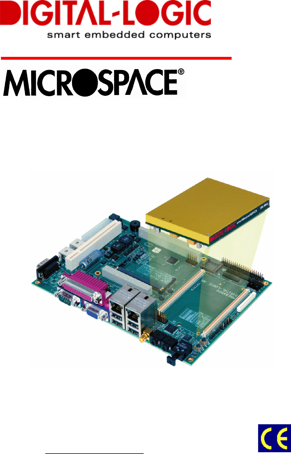
The MICROSPACE EBX is a miniaturized modular device incorporating the major elements of a PC/AT
compatible computer. It includes standard PC/AT compatible elements, such as:
Powerful GEODE LX800/900 with 500/600MHz
DDRAM 128-1024MByte SODIMM 200pin
Real-time clock with CMOS-RAM and 10-year battery buffer
LPT1 parallel port
COM1-, COM2- RS232 serial port 16C550 comp.
Speaker interface
PS/2-keyboard and mouse interface
Floppy disk interface
AT-IDE hard disk interface
VGA video interface, LCD, LVDS
6-channel sound interface AC97-V2.3
100/10-Base-T LAN
PC/104 (ISA) BUS optional
4 Ports USB V2.0
PC/104plus (PCI) BUS optional
2.2. Unique Features
The MICROSPACE MSEBX800 includes all standard PC/AT functions plus unique DIGITAL-LOGIC AG
enhancements, such as:
Single 8V to 30V supply
Watchdog
EEPROM for setup and configuration
2nd LAN Port 100Base-T
PATA ports optional
UL approved parts
Console redirection
2.3. Standards
The MICROSPACE product meet all standards for personal computer architecture.
Standard Contact to the organisation Remarks
PC/104BUS www.pc104.org
USB www.usb.org
PCI www.pcisig.com
SMB www.smbus.org
WfM www.intel.com/labs/manage/wfm Wired for management baseline
AC97 www.developer.intel.com/ial/scalableplatforms/
audio
LPC www.developer.intel.com/design/chipsets/
industry/lpc.htm
ATA/ATAPI-6 www.t13.org
ACPI www.acpi.info Power management
DIGITAL-LOGIC AG MSEBX800/900 Detailed Manual V1.0
13
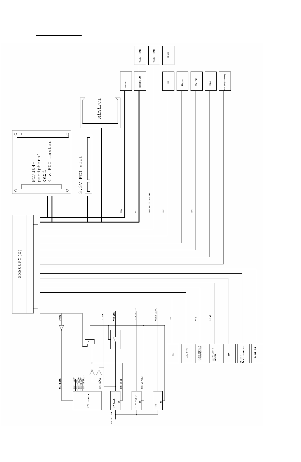
2.4. Block Diagrams
2.4.1. MSEBX800
DIGITAL-LOGIC AG MSEBX800/900 Detailed Manual V1.0
14
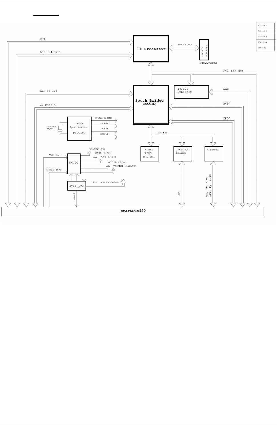
2.4.2. SM800
DIGITAL-LOGIC AG MSEBX800/900 Detailed Manual V1.0
15
2.5. MSEBX800/900 Specifications
CPU Specification
CPU SM800 AMD GEODE LX800/900 located in the smartModule800/900
CPU Core Supply 1.25V very low powered
1st Level Cache 32k data and 32k code
2nd Level Cache 128kByte
Performance
SM800PCX
SM900PCX
P2 Equivalent Performance:
500MHz
600MHz
Clock
SM800PCX
SM900PCX
The CPU Clock is defined with the ordered SM800/900-xxx
500MHz
600MHz
Chipset Specification
Northbridge AMD LX800/900
Southbridge AMD CS5536
LAN 2x 10/100Mbit Intel 82551ER (LAN A), Intel 82551ER (LAN B)
Audio Stereo In and Stereo Line-Out
Codec AD1985 up to 96kHz sampling rate, 16bit (Analog Devices)
Firewire IEEE1394 Not on board
Video 16MByte Video-DDRAM
Memory Specification
SODIMM SODIMM200pin DDR PC2700 333MHz 256-1024MByte
Flash-BIOS 8MByte Flash
Setup EEPROM 2kByte for CMOS-backup in battery-less applications
Flash-Video BIOS Combined in the core BIOS
Video RAM 16MByte to 64MByte DDRAM
Video Controller Specification
Controller AMD graphics integrated in the LX800/900 chipset
Video Memory 16MB
Channel 1 CRT VGA up to 2048x1600 pixels
Channel 2 LVDS, TV-Out, CRT
Bootup-Resolution 640x480 / 800x600 / 1024x768
2D-Graphics Integrated accelerator
3D-Graphics None
Direct-X Version -
PnP Integrated
DIGITAL-LOGIC AG MSEBX800/900 Detailed Manual V1.0
16
External Interfaces Specification
Video Interfaces CRT1, DVO
USB V1.1/2.0 4 Ports
LPT IEEE1293 Printer
COM1 RS232
COM2 RS232
COM3 -
COM4 -
Keyboard PS/2
Mouse PS/2
Floppy 26pin FCC Interface for TEAC Mini-Floppy
Parallel-Hard disk 2.5” 2 x 44pin RM2.0mm ATAIDE-cable
Parallel-Hard disk 3.5” 2 x 40pin RM2.5mm PATA-IDE cable
Speaker 0.1Watt Speaker
ISA-Bus PC/104
PCI-Bus PC/104plus
PCI-Riser-Bus PCI-Slot
Power Supply Specification
Input voltage Nominal 8V-30V, maximum Ripple=200mVpp
Input inrush current t.b.d.
Protection EMI filtered
Spec. None
3.3Volt Power Output Not available
Power Consumption Specification
With 256MByte Typical (10W) at 500MHz
Typical (11W) at 600MHz
Standby Typical 0.5 Amp.
Power off (if VCC 12V) Typical 7.3mA
Power off (if VCC 19V) Typical 8.6mA
Power off (if VCC 24V) Typical 9.6mA
Physical Characteristics
Specification PC/104plus
Dimensions Length: 203mm
Depth: 146mm
Height: 33mm
Weight 300gr
Operating Environment Specification
Relative Humidity 5 - 90% non-condensing
IEC68-2-30 at -20° to +50°C operating
Vibration operating IEC68-2-6 10-50Hz, 0.075mm and 55-500Hz, 1.0G
Vibration non-operating IEC68-2-6 10-50Hz, 0.15mm and 55-500Hz, 2.0G
Shock operating IEC68-2-27 10G, 11ms ½ sine
Shock non-operating IEC68-2-27 50G, 11ms, ½ sine
Altitude IEC68-2-13 4571meter operating
Temperature operating IEC68-2-1,2,14: MSEBX800 Standard -20°C to +60°C
Extended Temp. option MIL-810-501/502 see separate table below
Temperature storage IEC68-2-1,2,14-65°C to +125°C
The backup battery is limited on -40°C to +80°C
operating and storage temperature!
DIGITAL-LOGIC AG MSEBX800/900 Detailed Manual V1.0
17
Operating Temperature Specification:
MIL-810-501
MIL-810-502
Extended temperature range:
SM800PCX (500MHz)
-40°C to +70°C
Security
e1 Not planned
UL Not planned
ETS 301 Not planned
CE/SEV Yes
Safety AR385-16
If all signals are externally filtered and assembled into an enclosed metallic case!
EMI / EMC Tests Specification
EMC emission EN61000-6-2:2001
Conducted disturbance EN55022 Class B
Radiated disturbance EN55022 Class B
EMC immunity EN61000-6-2
Electrostatic discharge (ESD) EN61000-4-2
Voltage = 4kV contact / 8kV air, Criteria A
Radiated RF-Field EN61000-4-3
Level = 10V/m, Criteria A
Electrical fast transients (Burst) EN61000-4-4
Grade 2: DC-Power lines = 1000V (5/50ns)
Grade 2: AC-Power lines = 2000V (5/50ns)
Grade 2: Signal lines = 500V (5/50ns)
Criteria B
Surge EN61000-4-5
Grade 2: DC-Power lines = 1kV, (1.2/50us)
Grade 2: AC-Power lines = 2kV, (1.2/50us)
Criteria B
Conducted disturbances EN61000-4-6
Voltage = 10V coupled by case, Criteria A
All information is subject to change without notice.
DIGITAL-LOGIC AG MSEBX800/900 Detailed Manual V1.0
18
2.6. Examples of Ordering Codes
The MSEBX800 system is combined from:
Baseboard MSEBX800
smartModule 800/900-xxx (must be ordered separately)
Memory: SODIMM200-DDRAM (must be ordered separately)
Article Part No. Description
MSEBX800 811060 EBX board without SM800/900-xxx, 0MB RAM,
no PC/104-Plus connector
SM800PCX 805212 LX800
SM900PCX 805242 LX900
Accessories Part No. Description
MSFloppy 891001 3.5” Micro-Floppy drive (26Pin)
MSFDCK 802600 Micro-Floppy cable (26Pin)
MSEBX800-DK 811210 Aluminium housing with 20GB HDD, FDD, CD-R, PSU
Options Part No. Description
Option L+ 807006 PC/104- Plus, connector long (without option CF)
DDRAM256M 890670 DDR-SODIMM Module 256MB
DDRAM512M 890671 DDR-SODIMM Module 512MB
DDRAM1G 890672 DDR-SODIMM Module 1GB
These are only examples; for current ordering codes, please see the current price list.
DIGITAL-LOGIC AG MSEBX800/900 Detailed Manual V1.0
19
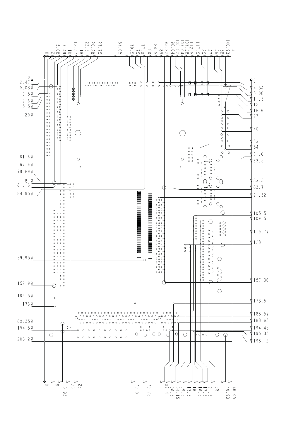
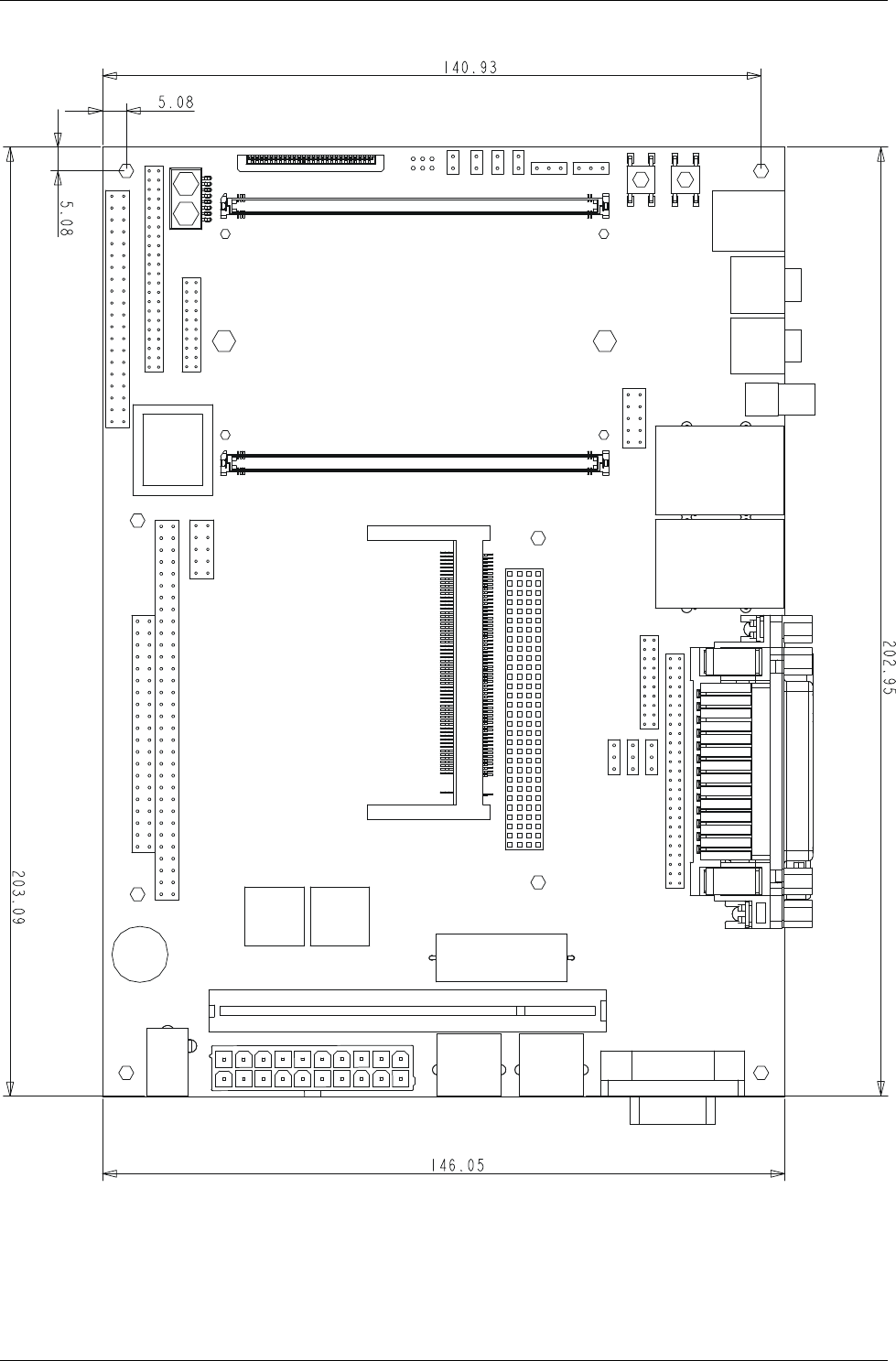
2.7. Dimensions & Diagrams
MSEBX800
DIGITAL-LOGIC AG MSEBX800/900 Detailed Manual V1.0
20
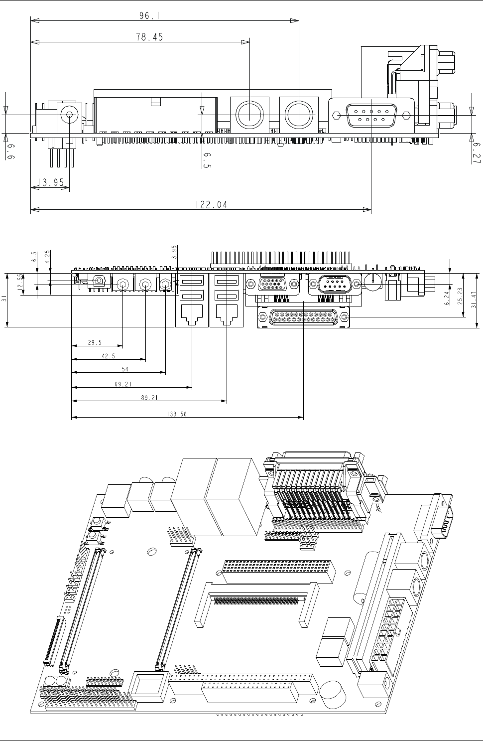
DIGITAL-LOGIC AG MSEBX800/900 Detailed Manual V1.0
21

DIGITAL-LOGIC AG MSEBX800/900 Detailed Manual V1.0
22
2.8. Incompatibilities to a Standard PC/AT
None.
2.9. MSEBX800/900 Related Application Notes
# Description
80 High frequency Radiation (to meet EN55022)
Application Notes are availble at http://www.digitallogic.com
support, or on any Application CD from
DIGITAL-LOGIC.
2.10. High Frequency Radiation (to meet EN55022/EN61000)
All peripheral interfaces are filtered to meet the EMI/EMC standards EN55022.
DIGITAL-LOGIC AG MSEBX800/900 Detailed Manual V1.0
23
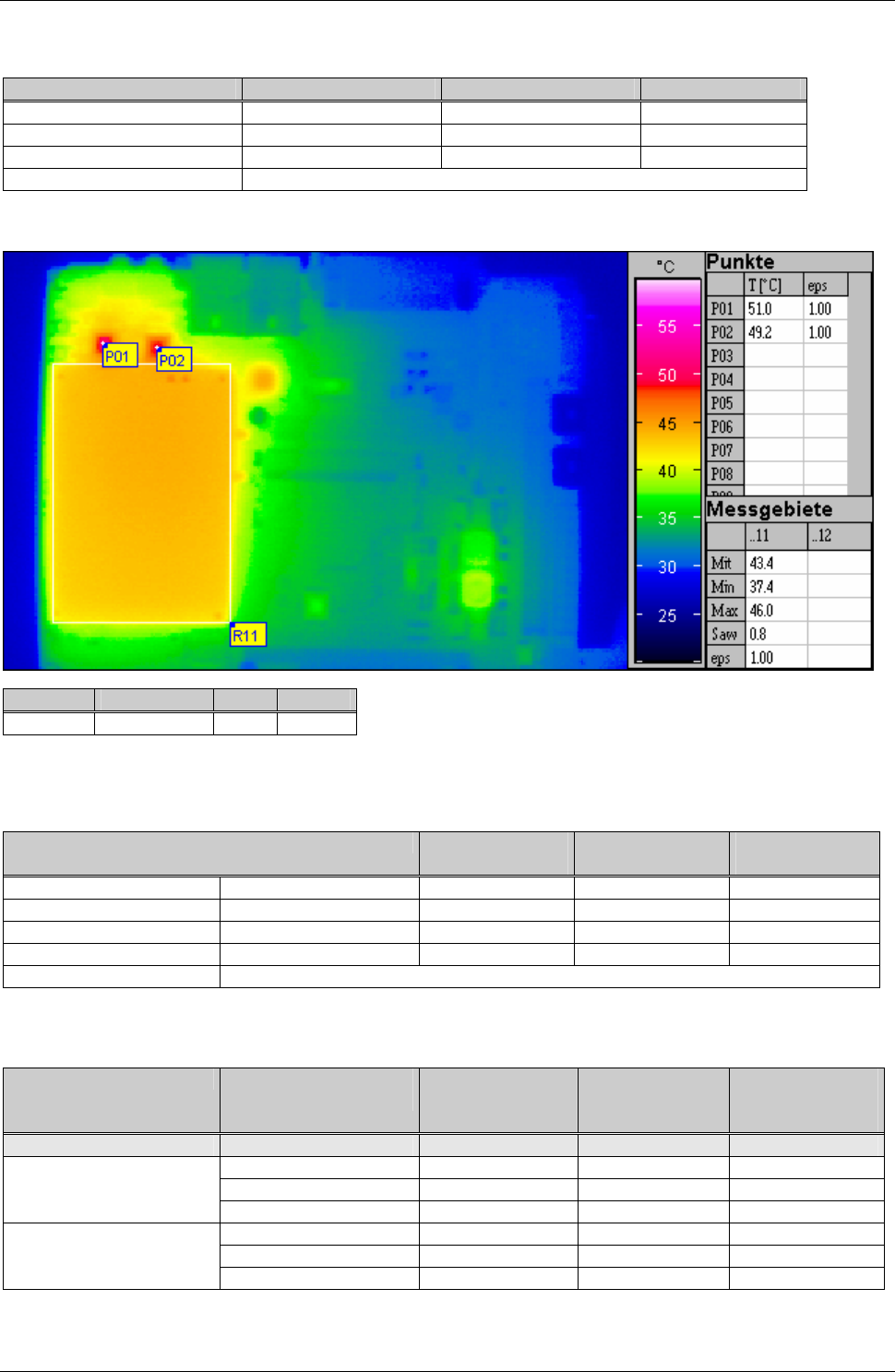
2.11. Thermoscan
Product Part Number Serial Number Version
MSEBX800 811202 45320210010 0.2
SM800PCX 805164 45316410032 2.1
SODIMM DDR 1GB 870672 - -
Software Windows XP SP2 running desktop
Top view, passive cooled:
t [min] fCPU [MHz]
I [A] P [W]
60 500 0.5 9.5
2.12. RTC Battery Lifetime
Battery Specifications Lowest Temp.
-40°C
Nominal Temp.
+20°C
Highest Temp.
+85°C
Manufacturer pbq
Type ER10280
Capacity versus Temp. 8uA 850mAh 910mAh 850mAh
Voltage versus Temp. 8uA 3.5V 3.6V Ca. 3.6V
Nominal Values 3.6V / 450mAh / -40°C...~+85°C
Information is taken from the data sheet of the pbq ER10280.
Product Temperature
°C
Battery Voltage
V
VCC (+12V)
switched ON
µA
VCC (+12V)
switched off
µA
MSEBX800
+25°C 3.6 15 18
-40°C 3.5 15 14
Battery Current
+85°C 3.8 15 30
+25°C >10 years >10 years
-40°C >10 years >10 years
Battery Lifetime
+85°C >10 years Ca. 6 years

DIGITAL-LOGIC AG MSEBX800/900 Detailed Manual V1.0
24
3. PREPARATION
3.1. Important Information
Warning, ESD Sensitive Device!
Place the embedded computer board on an isolated, ESD-protected surface. Also ensure that all
equipment, tools and people are fully protected against ESD.
Attention!
The smartModule must be firmly attached to the board with screws. Do not attempt to
power-up the system without taking this step or the system may not work and you risk damaging
the equipment! See Section 3.2 for assembly instructions.
DIGITAL-LOGIC AG MSEBX800/900 Detailed Manual V1.0
25
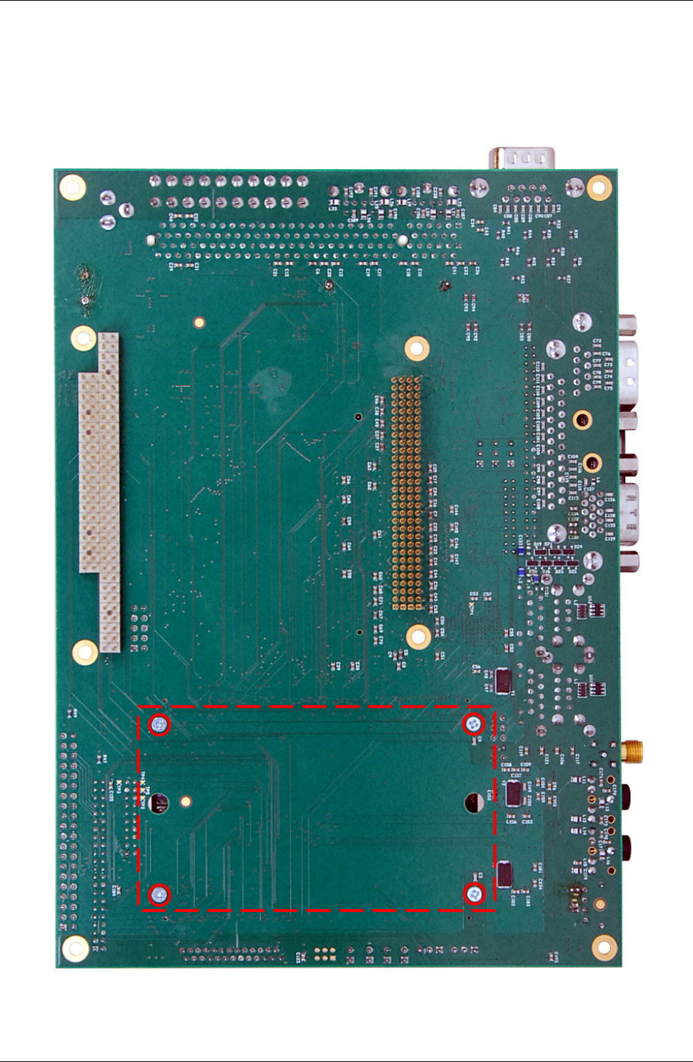
3.2. Mounting the smartModule
Line up the holes in the smartModule on the MSEBX board (top side). Then on the reverse side, attach the
smartModule using 4 Phillips head screws (circled in red, within the red frame marking the approximate
location of the smartModule). The screws are delivered with the smartModule but if lost may be ordered: Part
Nr. 502528, description: M2x 5 galvanized machine screw.
DIGITAL-LOGIC AG MSEBX800/900 Detailed Manual V1.0
26
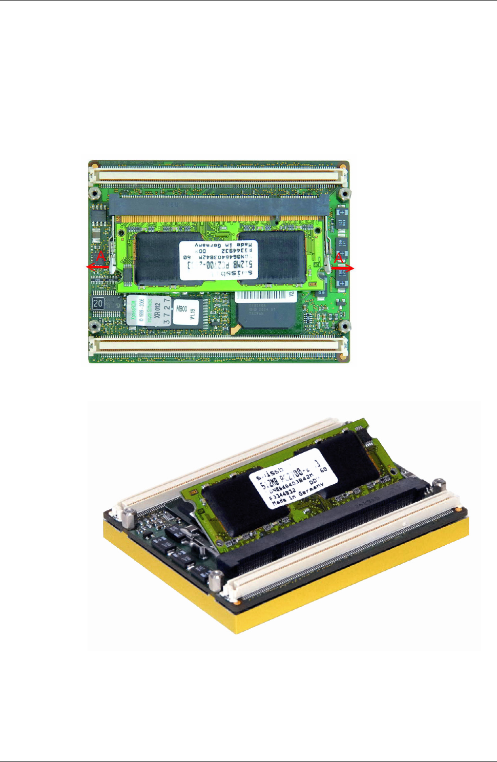
3.3. RAM Assembly/Disassembly
To install or change the RAM, follow these steps:
1. Unmount the smartModule by removing the 4 screws marked in red (see the photo from the previous
page).
2. To change the RAM:
a. Using your thumbnails, gently push the clips holding the RAM module in place toward the
outside (Photo 1, marked "A").
Photo 1
b. There will be a slight "click" and the RAM will flip up at an angle (Photo 2).
Photo 2
c. Remove the original RAM.
d. With the new RAM, carefully place the side with the connectors into the slot. There is only one
correct way to place the RAM in the slot due to a notch between the connectors which matches
up to a tab in the slot. Do not force the RAM into the slot, it should fit very easily.
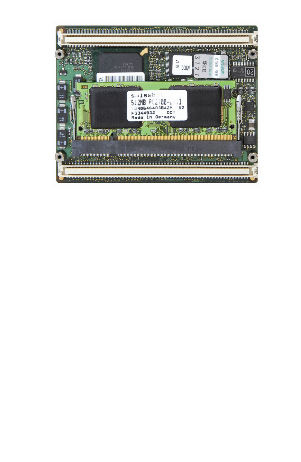
DIGITAL-LOGIC AG MSEBX800/900 Detailed Manual V1.0
27
e. Slowly push the RAM down until the clips "click" into place (Photo 3).
Photo 3
3. To install a RAM:
a. Carefully place the side of the RAM with the connectors into the slot. There is only one correct
way to place the RAM in the slot due to a notch between the connectors which matches up to a
tab in the slot. Do not force the RAM into the slot, it should fit very easily.
b. Slowly push the RAM down until the clips "click" into place (Photo 3).
DIGITAL-LOGIC AG MSEBX800/900 Detailed Manual V1.0
28
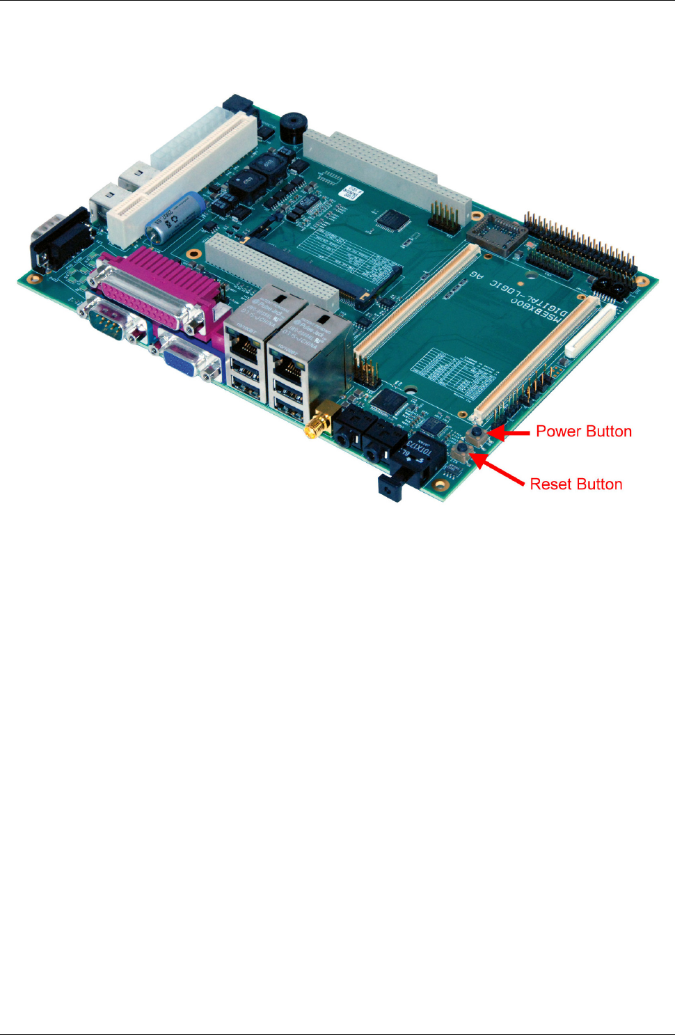
3.4. Power & Reset Buttons
Power Button: Push the Power Button for 2 seconds to start up the system.
Reset Button: Should the system hang, press the Reset Button.

DIGITAL-LOGIC AG MSEBX800/900 Detailed Manual V1.0
29
4. BUS SIGNALS
4.1. PC104 Bus
Note...
The ISA-Bus may have some minor incompatibilities, see Chapter 6.
AEN, output
Address Enable: used to degate the microprocessor and other devices from the I/O channel to allow
DMA transfers to take place. low = CPU Cycle, high = DMA Cycle
BALE, output
Address Latch Enable: provided by the bus controller and used on the system board to latch valid
addresses and memory decodes from the microprocessor. This signal is used so that devices on the
bus can latch LA17-23. The SA0-19 address lines latch internally according to this signal. BALE is
forced high during DMA cycles.
/DACK[0-3, 5-7], output
DMA Acknowledge: 0 to 3 and 5 to 7 are used to acknowledge DMA requests (DRQ0 through DRQ7).
They are active low. This signal indicates that the DMA operation can begin.
DRQ[0-3, 5-7], input
DMA Requests: 0 through 3 and 5 through 7 are asynchronous channel requests used by peripheral
devices and the I/O channel microprocessors to gain DMA service (or control of the system). A
request is generated by bringing a DRQ line to an active level. A DRQ line must be held high until the
corresponding DMA Request Acknowledge (DACK/) line goes active. DRQ0 through DRQ3 will
perform 8bit DMA transfers; DRQ5-7 are used for 16 accesses.
/IOCHCK, input
IOCHCK/: provides the system board with parity (error) information about memory or devices on the
I/O channel. low = parity error, high = normal operation
IOCHRDY, input
I/O Channel Ready: pulled low (not ready) by a memory or I/O device to lengthen I/O or memory
cycles. Any slow device using this line should drive it low immediately upon detecting its valid address
and a Read or Write command. Machine cycles are extended by an integral number of one clock cycle
(67 nanoseconds). This signal should be held in the range of 125-15600nS. low = wait, high =
normal operation
/IOCS16, input
I/O 16 Bit Chip Select: signals the system board that the present data transfer is a 16bit, 1 wait-state,
I/O cycle. It is derived from an address decode. /IOCS16 is active low and should be driven with an
open collector (300 Ohm pull-up) or tri-state driver capable of sinking 20mA. The signal is driven
based only on SA15-SAO (not /IOR or /IOW) when AEN is not asserted. In the 8bit I/O transfer, the
default transfers a 4 wait-state cycle.
/IOR, input/output
I/O Read: instructs an I/O device to drive its data onto the data bus. It may be driven by the system
microprocessor or DMA controller, or by a microprocessor or DMA controller resident on the I/O
channel. This signal is active low.
/IOW, input/output
I/O Write: instructs an I/O device to read the data on the data bus. It may be driven by any
microprocessor or DMA controller in the system. This signal is active low.
IRQ [3-7, 9-12, 14, 15], input
These signals are used to tell the microprocessor that an I/O device needs attention. An interrupt
request is generated when an IRQ line is raised from low to high. The line must be held high until
the microprocessor acknowledges the interrupt request.

DIGITAL-LOGIC AG MSEBX800/900 Detailed Manual V1.0
30
/Master, input
This signal is used with a DRQ line to gain control of the system. A processor or DMA controller on the
I/O channel may issue a DRQ to a DMA channel in cascade mode and receive a /DACK.
/MEMCS16, input
MEMCS16 Chip Select: signals the system board if the present data transfer is a 1 wait-state, 16bit,
memory cycle. It must be derived from the decode of LA17 through LA23. /MEMCS16 should be
driven with an open collector (300 Ohm pull-up) or tri-state driver capable of sinking 20mA.
/MEMR, input/output
These signals instruct the memory devices to drive data onto the data bus. /MEMR is active on all
memory read cycles. /MEMR may be driven by any microprocessor or DMA controller in the system.
When a microprocessor on the I/0 channel wishes to drive /MEMR, it must have the address lines
valid on the bus for one system clock period before driving /MEMR active. These signals are active
low.
/MEMW, input/output
These signals instruct the memory devices to store the data present on the data bus. /MEMW is active
in all memory read cycles. /MEMW may be driven by any microprocessor or DMA controller in the
system. When a microprocessor on the I/O channel wishes to drive /MEMW, it must have the address
lines valid on the bus for one system clock period before driving /MEMW active. Both signals are
active low.
OSC, output
Oscillator (OSC): a high-speed clock with a 70 nanosecond period (14.31818 MHz). This signal is not
synchronous with the system clock. It has a 50% duty cycle. OSC starts 100µs after reset is inactive.
RESETDRV, output
Reset Drive: used to reset or initiate system logic at power-up time or during a low line-voltage outage.
This signal is active high. When the signal is active all adapters should turn off or tri-state all drivers
connected to the I/O channel. This signal is driven by the permanent Master.
/REFRESH, input/output
These signals are used to indicate a refresh cycle and can be driven by a microprocessor on the I/O
channel. These signals are active low.
SA0-SA19, LA17 - LA23 input/output
Address bits 0 through 19 are used to address memory and I/0 devices within the system. These 20
address lines allow access of up to 1MByte of memory. SAO through SA19 are gated on the system
bus when BALE is high and are latched on the falling edge of BALE. LA17 to LA23 are not latched and
addresses the full 16MByte range. These signals are generated by the microprocessors or DMA
controllers. They may also be driven by other microprocessor or DMA controllers that reside on the I/0
channel. The SA17-SA23 are always LA17-LA23 address timings for use with the MSCS16 signal.
This is advanced AT96 design. The timing is selectable with jumpers LAxx or SAxx.
/SBHE, input/output
Bus High Enable (system): indicates a transfer of data on the upper byte of the data bus, XD8 through
XD15. Sixteen-bit devices use /SBHE to condition data-bus buffers tied to XD8 through XD15.
SD[0-15], input/output
These signals provide bus bits 0 through 15 for the microprocessor, memory, and I/O devices. D0 is
the least significant bit and D15 is the most significant bit. All 8bit devices on the I/O channel should
use D0 through D7 for communications to the microprocessor. The 16bit devices will use D0 through
D15. To support 8bit devices, the data on D8 through D15 will be gated to D0 through D7 during 8bit
transfers to these devices; 16bit microprocessor transfers to 8bit devices will be converted to two 8bit
transfers.
/SMEMR, input/output
These signals instruct the memory devices to drive data onto the data bus for the first MByte. /SMEMR
is active on all memory read cycles. /SMEMR may be driven by any microprocessor or DMA controller
in the system. When a microprocessor on the I/0 channel wishes to drive /SMEMR, it must have the
address lines valid on the bus for one system clock period before driving /SMEMR active. The signal is
active low.
DIGITAL-LOGIC AG MSEBX800/900 Detailed Manual V1.0
31
/SMEMW, input/output
These signals instruct the memory devices to store the data present on the data bus for the first
MByte. /SMEMW is active in all memory read cycles. /SMEMW may be driven by any microprocessor
or DMA controller in the system. When a microprocessor on the I/O channel wishes to drive /SMEMW,
it must have the address lines valid on the bus for one system clock period before driving /SMEMW
active. Both signals are active low.
SYSCLK, output
This is an 8MHz system clock. It is a synchronous microprocessor cycle clock with a cycle time of 167
nanoseconds. The clock has a 66% duty cycle. This signal should only be used for synchronization.
TC, output
Terminal Count: provides a pulse when the terminal count for any DMA channel is reached. The TC
completes a DMA-Transfer. This signal is expected by the onboard floppy disk controller. Do not use
this signal because it is internally connected to the floppy controller.
/0WS, input
The Zero Wait State (/0WS) signal tells the microprocessor that it can complete the present bus cycle
without inserting any additional wait cycles. In order to run a memory cycle to a 16bit device without
wait cycles, /0WS is derived from an address decode gated with a Read or Write command. In order to
run a memory cycle to an 8bit device with a minimum of one-wait states, /0WS should be driven active
one system clock after the Read or Write command is active, gated with the address decode for the
device. Memory Read and Write commands to an 8bit device are active on the falling edge of the
system clock. /0WS is active low and should be driven with an open collector or tri-state driver
capable of sinking 20mA.
12V, +/- 5%
This signal is used only for the flat panel supply.
GROUND = 0V
This is used for the entire system.
VCC, +5V +/- 0.25V
This is used to supply other PC/104 peripheral cards. Maximum current is 2Amp.
For further information about PC/104 and PC/104plus, please refer to the PC/104 Specification
Manual which is available on the internet: http://www.digitallogic.com (manuals).
4.2. Addressing PCI Devices on the MSEBX800:
PCI Slot Assignment
The following definitions for the peripherals correspond with the BIOS:
Device IDSEL PIRQ REQ# GNT# Comments
SLOT 1 AD20 A, B, C, D 3 3
SLOT 2 AD21 B, C, D, A 4 4
SLOT 3 AD22 C, D, A, B 5 5
SLOT 4 AD23 D, A, B, C 6 6
LAN Controller AD29 A 7 7
ISA-Bridge AD24 -- 8 8
CS5536 AD25 --- 2 2 For VGA, IDE and USB
Arbiter 0 --- --- 0 0
Arbiter 1 --- --- 1 1
DIGITAL-LOGIC AG MSEBX800/900 Detailed Manual V1.0
32
5. DETAILED SYSTEM DESCRIPTION
5.1. Boot Time
System Boot Times
Definitions/Boot-Medium Quick
Boot*
Normal
Boot
MSEBX800-500MHz with RTC-Backup Battery
Memory 256MB shared 8MB for Video
time [s]
From Floppy disk
Boot from Setup-Disk1 MS-DOS v6.22 to "Starting MS-DOS"-Prompt. 10 26
Boot from Setup-Disk1 MS-DOS v6.22 to "Welcome Setup Screen"-Prompt. 30 45
Boot from "(Sys a:)-Disk“ to "A:/>“-Prompt. 18 33
From Hard disk-Toshiba MK2110MAF
Boot from Hard disk to "Starting MS-DOS"-Prompt. 10 26
Boot from Hard disk to "Win2000: Windows-Login"-Prompt. 80 95
From CompactFlash SanDisk SDCFB-64-101-00 64MB
Boot from CF to "Starting MS-DOS"-Prompt. 10 26
Boot from CF to "C:\>"-Prompt. 13 29
DIGITAL-LOGIC AG MSEBX800/900 Detailed Manual V1.0
33
5.2. Interfaces
5.2.1. PS/2 Keyboard (AT Compatible) and PS/2 Mouse
X31 Keyboard
Pin Signal Pin Signal
1 KB_Data 2 -
3 GND 5 +5Volt / 100mA
6 KB_Clk 8 -
X32 Mouse
Pin Signal Pin Signal
1 MB_Data 2 -
3 GND 5 +5Volt / 100mA
6 MB_Clk 8 -
5.2.2. Line Printer Port LPT1
A standard bi-directional LPT port is integrated into the MICROSPACE PC.
Further information about these signals is available in numerous publications, including the IBM technical
reference manuals for the PC and AT computers and from other reference documents.
The current is: IOH = 12mA IOL = 24mA
The SMC 37C672 may be programmed via software commands.
In the new BIOS version, this selection may be controlled with the BIOS setup screen.
5.2.3. Serial Ports COM1 - COM2
The serial channels are fully compatible with 16C550 UARTS.
X30B / X39 Serial Port Connectors COM1, COM2
Pin Signal Name
Function in/out DB25 Pin DB9 Pin
1 CD Data Carrier Detect in 8 1
2 RXD Data Receive Data in 6 6
3 TXD Transmit Data out 3 2
4 DTR Data Terminal Ready out 4 7
5 GND System Ground - 2 3
6 DSR Data Set Ready In 5 8
7 RTS Request to Send out 20 4
8 CTS Clear to Send in 22 9
9 RI Ring Indicator in 7 5
DIGITAL-LOGIC AG MSEBX800/900 Detailed Manual V1.0
34
5.2.4. Floppy Disk Interface
Supported Floppy Formats
Capacity Drive size Tracks Data rate DOS version
1.2 MB 5-1/4" 80 500 KHz 3.0 - 6.22
720 K 3-1/2" 80 250 KHz 3.2 - 6.22
1.44 M 3-1/2" 80 500 KHz 3.3 - 6.22
Floppy Interface Configuration
The desired configuration of floppy drives (number and type) must be properly initialized in the board's
CMOS – configuration memory. This is generally done by using DEL or F2 at bootup time.
Floppy Interface Connector
The table shows the pin-out and signal definitions of the board's floppy disk interface connector. It is
identical in pin-out to the floppy connector of a standard AT. Note that, as in a standard PC or AT, both
floppy drives are jumpered to the same drive select: as the 'second' drive. The drives are uniquely
selected as a result of a swapping of a group of seven wires (conductors 10-16) that must be in the
cable between the two drives. The seven-wire swap goes between the computer board and drive 'A';
the wires to drive 'B' are unswapped (or swapped a second time). The 26pin high density (1mm pitch
FCC) connector has only one drive and motor select. The onboard jumper defines the drive A: or B:.
Default is always A:.
Floppy Disk Interface Technology
Only CMOS drives are supported. This means the termination resistors are 1 KOhm and 5 1/4“-drives
are not recommended (TTL interface).
The 26pin connector: FFC/FPC 0.3mm thick 1.0mm (0.039") pitch (MOLEX 52030 Series)
Floppy Disk Interface Connector
FD26: Pin Signal Name Function in/out
1 VCC +5Volt
2 IDX Index Pulse in
3 VCC +5Volt
4 DS2 Drive Select 2 out
5 VCC +5Volt
6 DCHG Disk Change in
10 MO2 Motor On 2 out
12 DIRC Direction Select out
14 STEP Step out
16 WD Write Data out
17 GND Signal grounds
18 WE Write Enable out
19 GND Signal grounds
20 TRKO Track 0 in
21 GND Signal grounds
22 WP Write Protect in
23 GND Signal grounds
24 RDD Read Data in
25 GND Signal grounds
26 HS Head Select out
DIGITAL-LOGIC AG MSEBX800/900 Detailed Manual V1.0
35
5.3. Controllers
5.3.1. Interrupt Controllers
An 8259A compatible interrupt controller, within the chipset, provides seven prioritized interrupt levels. Of
these, several are normally associated with the board's onboard device interfaces and controllers, and
several are available on the AT expansion bus.
Interrupt Sources Used Onboard
IRQ0 ROM-BIOS clock tick function, from timer 0 Yes
IRQ1 Keyboard controller output buffer full Yes
IRQ2 Used for cascade 2. 8259 Yes
IRQ3 COM2 serial port Yes
IRQ4 COM1 serial port Yes
IRQ5 LPT2 parallel printer (if present) No
IRQ6 Floppy controller Yes
IRQ7 LPT1 parallel printer Yes
IRQ8 Battery backed clock Yes
IRQ9 Free for user No
IRQ10 Free for user No
IRQ11 Free for user No
IRQ12 PS/2 mouse Yes
IRQ13 Math. coprocessor Yes
IRQ14 Hard disk IDE / SCSI Yes
IRQ15 Free for user No
It may depend on the LAN configuration.
IRQ 15 = if option CF is not assembled, then free for user.
5.3.2. Timers and Counters
5.3.2.1. Programmable Timers
An 8253 compatible timer/counter device is also included in the board's ASIC device. This device is utilized
in precisely the same manner as in a standard AT implementation. Each channel of the 8253 is driven by a
1.190MHz clock, derived from a 14.318MHz oscillator, which can be internally divided in order to provide a
variety of frequencies.
Timer 2 can also be used as a general purpose timer if the speaker function is not required.
Timer Assignment
Timer Function
0 ROM-BIOS clock tick (18.2Hz)
1 DRAM refresh request timing (15µs)
2 Speaker tone generation time base
5.3.2.2. Watchdog
The watchdog timer detects a system crash and performs a hardware reset. After power up, the watchdog is
always disabled as the BIOS does not send strobes to the watchdog. In case the user wants to take
advantage of the watchdog, the application must produce a strobe at least every 800ms. If no strobe occurs
within the 800ms, the watchdog resets the system.
5.3.3. Core BIOS Download
See the separate driver/software/BIOS manual, GEODE_LX800-900.
DIGITAL-LOGIC AG MSEBX800/900 Detailed Manual V1.0
36
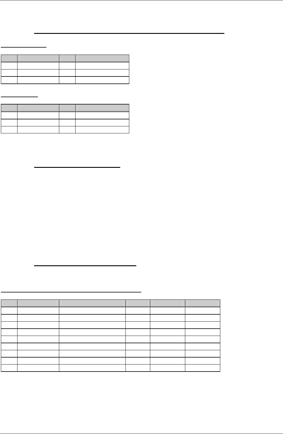
5.4. BIOS Recovery
In case the BIOS needs to be recovered:
1. Set Jumper J9.
2. Start the MSEBX800/900.
3. Open the BIOS.
4. Remove Jumper J9.
5. Load the default BIOS settings.
6. Save the settings.
7. Restart the MSEBX800/900.
Jumper J9
DIGITAL-LOGIC AG MSEBX800/900 Detailed Manual V1.0
37
6. DESCRIPTION AND LOCATION OF THE CONNECTORS
Connector
Structure Pin Remarks
X1 Power Input 2 Power Jack
X2 ATX Power Connector 20
X11 LVDS 2x 10 RM2.54
X14 Video IN 2 SMA
X15 LCD 2x 25 RM2.54
X20 MIC IN - Phone Jack
X22 Line Out Front - Phone Jack
X27 SPDIF OUT - SPDIF
X30A LPT 25 D-Sub25
X30B COM 1 9 D-Sub 9
X30C VGA 15 HDsub 15
X31 Keyboard - PS/2
X32 Mouse - PS/2
X33A LAN A (LAN interface of SM800PCX) 8 RJ45
X33B USB 0 4 -
X33C USB 1 4 -
X34A LAN B (82551ER – SM800DK) 8 RJ45
X34B USB 2 4 -
X34C USB 3 4 -
X36 ISA POD CPLD 2x 5 RM2.54
X39 COM 2 9 D-Sub 9
X51 JTAG 2x 5 RM2.54
X52 AVR Programming 2x 3 RM2.54
X53 Utility / Extension 2x 10 RM2.54
X60 HDD 2.5” 2x 22 RM2.54
X62 HDD 3.5” 2x 20 RM2.54
X70 Floppy 26 FCC
X100 PC/104 PC/104 PC/104
X101 PC/104+ PC/104+ PC/104+
X120 Mini PCI Mini PCI Mini PCI
X130 PCI Slot (standard PCI slot) - PCI
Special Connectors
LS1 Buzzer - -
Onboard Switches
SW1 Main Switch / Power Button (Pwrbtn)
SW2 Reset Switch
DIGITAL-LOGIC AG MSEBX800/900 Detailed Manual V1.0
38
6.1. Connector Plan
DIGITAL-LOGIC AG MSEBX800/900 Detailed Manual V1.0
39
6.2. Connector Descriptions
X1 Power Input
Pin Signal Pin Signal
1 8-30V DC-Input 2 Ground
X2 ATX Connector
Pin Signal Pin Signal
1 +3.3V 2 +3.3V
3 GND 4 +5V
5 GND 6 +5V
7 GND 8 PWR-OK
9 +5VSB 10 +12V
11 +3.3V 12 -12V
13 GND 14 PS-ON#
15 GND 16 GND
17 GND 18 -5V
19 +5V 20 +5V
X11 LVDS
Pin Signal Pin Signal
1 LVDS_A0- 2 LVDS_A0+
3 GND 4 GND
5 LVDS_A1- 6 LVDS_A1+
7 LCD BKL (dep. J5) 8 LCD BKL (dep. J5)
9 LVDS_A2- 10 LVDS_A2+
11 LCD VDD (dep 3) 12 LCD VDD (dep 3)
13 LVDS_A3- 14 LVDS_A3+
15 NC 16 NC
17 NC 18 NC
19 LVDS_Clock- 20 LVDS_Clock+
The LVDS interface works only if the J6 Jumper is not installed.
X14 Video Input Channel
Pin Signal Name Function in/out
1 Video Signal CVBS In
2 Ground
The Video IN interface works only if the J6 Jumper is installed.
DIGITAL-LOGIC AG MSEBX800/900 Detailed Manual V1.0
40
X15 LCD Connector
Pin Signal Pin Signal
1 DE_SPLIT 2 VSYNC
3 BLK 4 HSYNC
5 VCCLCD_SB 6 Ground
7 NC 8 SHFCLK
9 VDD 10 D0
11 D1 12 D2
13 D3 14 D4
15 D5 16 D6
17 D7 18 D8
19 D9 20 D10
21 D11 22 D12
23 D13 24 D14
25 D15 26 Ground
27 D16 28 D17
29 D18 30 D19
31 D20 32 NC
33 D21 34 D22
35 D23 36 NC
37 NC 38 NC
39 NC 40 NC
41 NC 42 NC
43 NC 44 Ground
45 NC 46 NC
47 NC 48 NC
49 VCC 50 NC
The LCD interface works only if the J6 Jumper is not installed.
X20 Microphone Input Audio Connector
Pin Signal Pin Signal
1 NC 2 Sense
3 Audio Ground 4 Channel R
5 Channel L 6 NC
X22 Front (Stereo Output) Audio Connector
Pin Signal Pin Signal
1 NC 2 Sense
3 Audio Ground 4 Channel R
5 Channel L 6 NC
X27 SPDif Connector
Pin Signal Pin Signal
1 Digital Audio Data Out 2 GND
DIGITAL-LOGIC AG MSEBX800/900 Detailed Manual V1.0
41
X30A Printer Port (Centronics, EMI-Filtered)
D-SUB Connector: Signal
Pin 1 Strobe
Pin 2 Data 0
Pin 3 Data 1
Pin 4 Data 2
Pin 5 Data 3
Pin 6 Data 4
Pin 7 Data 5
Pin 8 Data 6
Pin 9 Data 7
Pin 10 Acknowledge
Pin 11 Busy
Pin 12 paper end
Pin 13 select
Pin 14 autofeed
Pin 15 error
Pin 16 init printer
Pin 17 shift in (SI)
Pins 18-25 GND
X30B Serial Port COM1 RS232 (EMI-Filtered)
D-SUB connector: Signal
Pin 1 DCD
Pin 2 RXD
Pin 3 TXD
Pin 4 DTR
Pin 5 GND
Pin 6 DSR
Pin 7 RTS
Pin 8 CTS
Pin 9 RI
X30C VGA
Pin Signal
1 Red
2 Green
3 Blue
13 H-Synch
14 V-Synch
5, 6, 7, 8, 10 GND
4, 9, 11, 12, 15 NC
DIGITAL-LOGIC AG MSEBX800/900 Detailed Manual V1.0
42
X31 PS/2Keyboard (AT Compatible)
Pin Signal Pin Signal
1 KB_Data 2 -
3 GND 5 +5Volt / 100mA
6 KB_Clk 8 -
X32 PS/2Mouse
Pin Signal Pin Signal
1 MB_Data 2 -
3 GND 5 +5Volt / 100mA
6 MB_Clk 8 -
X33A Ethernet LAN
RJ-45 Pin Signal RJ-45 Pin Signal
1 TX+ 2 TX-
3 RX+ 4 GND
5 GND 6 RX-
7 GND 8 GND
X33B / X33C USB 0/1
Pin Signal Pin Signal
1 VCC 5 VCC
2 USB-Px- 6 USB-Px-
3 USB-Px+ 7 USB-Px+
4 GND 8 GND
X34A Ethernet LAN
RJ-45 Pin Signal RJ-45 Pin Signal
1 TX+ 2 TX-
3 RX+ 4 GND
5 GND 6 RX-
7 GND 8 GND
X34B / X34C USB 2/3
Pin Signal Pin Signal
1 VCC 5 VCC
2 USB-Px- 6 USB-Px-
3 USB-Px+ 7 USB-Px+
4 GND 8 GND
DIGITAL-LOGIC AG MSEBX800/900 Detailed Manual V1.0
43
RJ45 Connector 10BaseT (IEEE 802.3i), 100BaseTX (IEEE 802.3u):
MDI-Pin EIA/TIA 568A colors
(wire/line)
Pin
Twisted
Pair
TX+ White / Green 1 3
TX- Green 2 3
RX+ White / Orange 3 2
GND .. 4 1
GND .. 5 1
RX- Orange 6 2
GND .. 7 4
GND .. 8 4
Cabling: Do not exceed 100m (328 feet); minimum quality of CAT5, preferably S/FTP or STP CAT6.
Be careful to have a well balanced shield/ground concept.
X36 CPLD
Pin Signal Pin Signal
1 CPLD TCK 2 GND
3 CPLD TDO 4 VCC5SB
5 CPLD TMS 6 NC
7 SYS RST# 8 NC
9 CPLD TDI 10 GND
Only for internal use.
X39 Serial Port
D-SUB connector: Signal
Pin 1 DCD
Pin 2 RXD
Pin 3 TXD
Pin 4 DTR
Pin 5 GND
Pin 6 DSR
Pin 7 RTS
Pin 8 CTS
Pin 9 RI
X51 JTAG
Pin Signal Pin Signal
1 TCK 6 NC
2 GND 7 RESET_IN (RST)
3 TDO 8 NC
4 VCCSUS 9 TDI
5 TMS 10 GND
DIGITAL-LOGIC AG MSEBX800/900 Detailed Manual V1.0
44
X52 AVR
Pin Signal Pin Signal
1 AVR VCC 2 GND
3 AVR SCL 4 AVR RST
5 AVR MISO 6 AVR MOSI
Only for internal use
X53 Utility
Pin Signal Pin Signal
1 SUSC 2 VCCBat TP
3 PS ON ATX 4 VCC5SB TP
5 System Reset 6 VCC3 TP
7 PWRBTN 8 VCC TP
9 GPIO 30 10 VCC12 TP
11 GPIO 31 12 GND
13 GPIO 34 14 GND
15 SMB SDA 16 NC
17 SMB SCL 18 NC
19 NC 20 NC
X60 2.5" Hard Disk
Pin Signal Pin Signal
1 Reset (active low) 2 NC
3 D7 4 D8
5 D6 6 D9
7 D5 8 D10
9 D4 10 D11
11 D3 12 D12
13 D2 14 D13
15 D1 16 D14
17 D0 18 D15
19 GND 20 (keypin) NC
21 DRQ 22 GND
23 IOW(active low) 24 GND
25 IOR(active low) 26 GND
27 IOCHRDY 28 ALE / Master-Slave NC
29 DACK 30 GND
31 IRQ14 (pri) IRQ15 (sec)
32 IOCS16 (active low)
33 ADR1 34 DIAG
35 ADR0 36 ADR2
37 CS0 (active low) 38 CS1 (active low)
39 LED (active low) 40 GND
41 VCC Logic 42 VCC Motor
43 GND 44 NC
DIGITAL-LOGIC AG MSEBX800/900 Detailed Manual V1.0
45
X62 3.5" Hard Disk
Pin Signal Pin Signal
1 Reset (active low) 2 GND
3 D7 4 D8
5 D6 6 D9
7 D5 8 D10
9 D4 10 D11
11 D3 12 D12
13 D2 14 D13
15 D1 16 D14
17 D0 18 D15
19 GND 20 (keypin) NC
21 DRQ 22 GND
23 IOW(active low) 24 GND
25 IOR(active low) 26 GND
27 IOCHRDY 28 ALE / Master-Slave NC
29 DACK 30 GND
31 IRQ14 (pri) IRQ15 (sec)
32 IOCS16 (active low)
33 ADR1 34 DIAG
35 ADR0 36 ADR2
37 CS0 (active low) 38 CS1 (active low)
39 LED (active low) 40 GND
X70 Floppy Disk
FD26:
Pin
Signal Name
Function
in/out
1 VCC +5Volt
2 IDX Index Pulse in
3 VCC +5Volt
4 DS2 Drive Select * out
5 VCC +5Volt
6 DCHG Disk Change in
10 M02 Motor on * out
12 DIRC Direction Select out
14 STEP Step out
16 WD Write Data out
17 GND Signal grounds
18 WE Write Enable out
19 GND Signal grounds
20 TRKO Track 0 in
21 GND Signal grounds
22 WP Write Protect in
23 GND Signal grounds
24 RDD Read Data in
25 GND Signal grounds
26 HS Head Select out
DIGITAL-LOGIC AG MSEBX800/900 Detailed Manual V1.0
46
X100 PC/104 Connector (ISA)
Pin A: B: C: D:
0 Ground Ground
1 IOCHCK Ground SBHE MEMCS16
2 SD7 RESET LA23 IOCS16
3 SD6 +5V LA22 IRQ10
4 SD5 IRQ9 LA21 IRQ11
5 SD4 NC LA20 IRQ12
6 SD3 DRQ2 LA19 IRQ15
7 SD2 (-12V) NC LA18 IRQ14
8 SD1 0WS LA17 DACK0
9 SD0 +12V MEMR DRQ0
10 IOCHRDY Ground NC MEMW DACK5
11 AEN SMEMW SD8 DRQ5
12 SA19 SMEMR SD9 DACK6
13 SA18 SIOW SD10 DRQ6
14 SA17 SIOR SD11 DACK7
15 SA16 DACK3 SD12 DRQ7
16 SA15 DRQ3 SD13 +5 Volt
17 SA14 DACK1 SD14 MASTER
18 SA13 DRQ1 SD15 Ground
19 SA12 REF Ground Ground
20 SA11 SYSCLK
21 SA10 IRQ7
22 SA9 IRQ6
23 SA8 IRQ5
24 SA7 IRQ4
25 SA6 IRQ3
26 SA5 DACK2
27 SA4 TC
28 SA3 ALE
29 SA2 +5 Volt
30 SA1 OSC
31 SA0 Ground
32 Ground Ground
DIGITAL-LOGIC AG MSEBX800/900 Detailed Manual V1.0
47
X101 PC/104+ Connector (PCI)
Pin A: B: C: D:
1 GND/5.0V KEY2 Reserved +5 AD00
2 VI/O AD02 AD01 +5V
3 AD05 GND AD04 AD03
4 C/BE0* AD07 GND AD06
5 GND AD09 AD08 GND
6 AD11 VI/O AD10 M66EN
7 AD14 AD13 GND AD12
8 +3.3V C/BE1* AD15 +3.3V
9 SERR* GND SB0* PAR
10 GND PERR* +3.3V SDONE
11 STOP* +3.3V LOCK* GND
12 +3.3V TRDY* GND DEVSEL*
13 FRAME* GND IRDY* +3.3V
14 GND AD16 +3.3V C/BE2*
15 AD18 +3.3V AD17 GND
16 AD21 AD20 GND AD19
17 +3.3V AD23 AD22 +3.3V
18 IDSEL0 GND IDSEL1 IDSEL2
19 AD24 C/BE3* VI/O IDSEL3
20 GND AD26 AD25 GND
21 AD29 +5V AD28 AD27
22 +5V AD30 GND AD31
23 REQ0* GND REQ1* VI/O
24 GND REQ2* +5V GNT0*
25 GNT1* VI/O GNT2* GND
26 +5V CLK0 GND CLK1
27 CLK2 +5V CLK3 GND
28 GND INTD* +5V RST*
29 +12V INTA* INTB* INTC*
30 -12V Reserved Reserved GND/3.3V KEY2
DIGITAL-LOGIC AG MSEBX800/900 Detailed Manual V1.0
48
X120 MiniPCI Interface
Pin Signal Pin Signal Pin Signal Pin Signal
1 TIP 2 RING 63 3.3V 64 FRAME#
3 8PMJ-3 4 8PMJ-1 65 CLKRUN# 66 TRDY#
5 8PMJ-6 6 8PMJ-2 67 SERR# 68 STOP#
7 8PMJ-7 8 8PMJ-4 69 GROUND 70 3.3V
9 8PMJ-8 10 8PMJ-5 71 PERR# 72 DEVSEL#
11 LED1_GRNP 12 LED2_YELP 73 C/BE[1]# 74 GROUND
13 LED1_GRNN 14 LED2_YELN 75 AD[14] 76 AD[15]
15 CHSGND 16 RESERVED 77 GROUND 78 AD[13]
17 INTB# 18 5V 79 AD[12] 80 AD[11]
19 3.3V 20 INTA# 81 AD[10] 82 GROUND
21 RESERVED 22 RESERVED 83 GROUND 84 AD[09]
23 GROUND 24 3.3VAUX 85 AD[08] 86 C/BE[0]#
25 CLK 26 RST# 87 AD[07] 88 3.3V
27 GROUND 28 3.3V 89 3.3V 90 AD[06]
29 REQ# 30 GNT# 91 AD[05] 92 AD[04]
31 3.3V 32 GROUND 93 RESERVED 94 AD[02]
33 AD[31] 34 PME# 95 AD[03] 96 AD[00]
35 AD[29] 36 RESERVED 97 5V 98 RESERVED_WIP5
37 GROUND 38 AD[30] 99 AD[01] 100 RESERVED_WIP5
39 AD[27] 40 3.3V 101 GROUND 102 GROUND
41 AD[25] 42 AD[28] 103 AC_SYNC 104 M66EN
43 RESERVED 44 AD[26] 105 AC_SDATA_IN 106 AC_SDATA_OUT
45 C/BE[3]# 46 AD[24] 107 AC_BIT_CLK 108 AC_CODEC_ID0#
47 AD[23] 48 IDSEL 109 AC_CODEC_ID1# 110 AC_RESET#
49 GROUND 50 GROUND 111 MOD_AUDIO_MON 112 RESERVED
51 AD[21] 52 AD[22] 113 AUDIO_GND 114 GROUND
53 AD[19] 54 AD[20] 115 SYS_AUDIO_OUT 116 SYS_AUDIO_IN
55 GROUND 56 PAR 117 SYS_AUDIO_OUT GND 118 SYS_AUDIO_IN GND
57 AD[17] 58 AD[18] 119 AUDIO_GND 120 AUDIO_GND
59 C/BE[2]# 60 AD[16] 121 RESERVED 122 MPCIACT#
61 IRDY# 62 GROUND 123 VCC5VA 124 3.3VAUX

DIGITAL-LOGIC AG MSEBX800/900 Detailed Manual V1.0
49
X130 PCI Slot (Standard PCI Slot)
Pin Name PCI Pin Description Pin Name PCI Pin Description
A1 TRST Test Logic Reset B1 -12V -12 VDC
A2 +12V +12 VDC B2 TCK Test Clock
A3 TMS Test Mde Select B3 GND Ground
A4 TDI Test Data Input B4 TDO Test Data Output
A5 +5V +5 VDC B5 +5V +5 VDC
A6 INTA Interrupt A B6 +5V +5 VDC
A7 INTC Interrupt C B7 INTB Interrupt B
A8 +5V +5 VDC B8 INTD Interrupt D
A9 ----- Reserved B9 PRSNT1 Present
A10 +5V Power (+5 V or +3.3 V) B10 ----- Reserved
A11 ----- Reserved B11 PRSNT2 Present
A12 GND03 Ground or Keyway for 3.3/Universal PWB B12 GND Ground or Keyway for 3.3/Universal PWB
A13 GND05 Ground or Keyway for 3.3/Universal PWB B13 GND Ground or Open (Key) for 3.3/Universal PWB
A14 3.3Vaux ----- B14 RES Reserved
A15 RESET Reset B15 GND Ground
A16 +5V Power (+5 V or +3.3 V) B16 CLK Clock
A17 GNT Grant PCI use B17 GND Ground
A18 GND08 Ground B18 REQ Request
A19 PME# Power Managment Event B19 +5V Power (+5 V or +3.3 V)
A20 AD30 Address/Data 30 B20 AD31 Address/Data 31
A21 +3.3V01 +3.3 VDC B21 AD29 Address/Data 29
A22 AD28 Address/Data 28 B22 GND Ground
A23 AD26 Address/Data 26 B23 AD27 Address/Data 27
A24 GND10 Ground B24 AD25 Address/Data 25
A25 AD24 Address/Data 24 B25 +3.3V +3.3VDC
A26 IDSEL Initialization Device Select B26 C/BE3 Command, Byte Enable 3
A27 +3.3V03 +3.3 VDC B27 AD23 Address/Data 23
A28 AD22 Address/Data 22 B28 GND Ground
A29 AD20 Address/Data 20 B29 AD21 Address/Data 21
A30 GND12 Ground B30 AD19 Address/Data 19
A31 AD18 Address/Data 18 B31 +3.3V +3.3 VDC
A32 AD16 Address/Data 16 B32 AD17 Address/Data 17
A33 +3.3V05 +3.3 VDC B33 C/BE2 Command, Byte Enable 2
A34 FRAME Address or Data phase B34 GND13 Ground
A35 GND14 Ground B35 IRDY# Initiator Ready
A36 TRDY# Target Ready B36 +3.3V06 +3.3 VDC
A37 GND15 Ground B37 DEVSEL Device Select
A38 STOP Stop Transfer Cycle B38 GND16 Ground
A39 +3.3V07 +3.3 VDC B39 LOCK# Lock bus
A40 ----- Reserved B40 PERR# Parity Error
A41 ----- Reserved B41 +3.3V08 +3.3 VDC
A42 GND17 Ground B42 SERR# System Error
A43 PAR Parity B43 +3.3V09 +3.3 VDC
A44 AD15 Address/Data 15 B44 C/BE1 Command, Byte Enable 1
A45 +3.3V10 +3.3 VDC B45 AD14 Address/Data 14
A46 AD13 Address/Data 13 B46 GND18 Ground
A47 AD11 Address/Data 11 B47 AD12 Address/Data 12
A48 GND19 Ground B48 AD10 Address/Data 10
A49 AD9 Address/Data 9 B49 GND20 Ground
A50 Keyway Open or Ground for 3.3V PWB B50 Keyway Open or Ground for 3.3V PWB
A51 Keyway Open or Ground for 3.3V PWB B51 Keyway Open or Ground for 3.3V PWB
A52 C/BE0 Command, Byte Enable 0 B52 AD8 Address/Data 8
A53 +3.3V11 +3.3 VDC B53 AD7 Address/Data 7
A54 AD6 Address/Data 6 B54 +3.3V12 +3.3 VDC
A55 AD4 Address/Data 4 B55 AD5 Address/Data 5
A56 GND21 Ground B56 AD3 Address/Data 3
A57 AD2 Address/Data 2 B57 GND22 Ground
A58 AD0 Address/Data 0 B58 AD1 Address/Data 1
A59 +5V Power (+5 V or +3.3 V) B59 VCC08 Power (+5 V or +3.3 V)
A60 REQ64 Request 64 bit B60 ACK64 Acknowledge 64 bit
A61 VCC11 +5 VDC B61 VCC10 +5 VDC
A62 VCC13 +5 VDC B62 VCC12 +5 VDC
DIGITAL-LOGIC AG MSEBX800/900 Detailed Manual V1.0
50
7. JUMPER LOCATIONS ON THE BOARD
The following tables show the location of the jumper blocks on the MSEBX800/900 board. The numbers
shown in these tables are silk screened on the board so that the pins can be easily located. This chapter
refers to the individual pins for these jumpers.
Be careful: some jumpers are soldering bridges; you will need a miniature soldering station with a vacuum
pump.
Settings written in bold are defaults!
7.1. The 2pin Jumpers
Jumper Structure Open Closed
1 - 2
J2 LAN B (SM800DK LAN) isolate Enable LAN B Disable LAN B
J6 Select Video Out- or Input Enable LCD/LVDS
Enable Video-In
J8 Disable write protection of local FWH
(FirmWareHub)
FWH read only FHW read / write
J9 Boot FWH from SM800PCX or from
the MSEBX800-Board
Boot SM800PCX
FWH
Boot local FWH
7.2. The 3pin Jumpers
Jumper Structure Open Closed
1 - 2
Closed
2 - 3
J1 PCI X130 slot in JTAG chain JTAG w/ JTAG w/o
J3 LCD VDD voltage +3.3V +5V
J4 LVDS transmitter LVDS on LVDS auto on LVDS off
J5 LCD Backlight voltage +5V +12V 1)
J7 RTC enable / disable Enable RTC batt
Disable RTC batt 2)
1.) The 12V are only available if an ATX-Supply is connected.
2.) It's possible to connect an external RTC back-up battery to pin 2-3 of J7.
DIGITAL-LOGIC AG MSEBX800/900 Detailed Manual V1.0
51
7.3. Jumpers on the MSEBX800
DIGITAL-LOGIC AG MSEBX800/900 Detailed Manual V1.0
52
8. INDEX
A
Addressing PCI Devices............................................. 31
B
BIOS Recovery .......................................................... 36
Block Diagrams.......................................................... 13
Boot Time................................................................... 32
Bus Signals ................................................................ 29
C
Connector Descriptions.............................................. 39
Connector Plan .......................................................... 38
Connectors................................................................. 37
2.5" Hard Disk ....................................................... 44
3.5" Hard Disk ....................................................... 45
ATX ....................................................................... 39
Ethernet LAN......................................................... 42
Floppy Disk............................................................ 45
JTAG ..................................................................... 43
Keyboard PS/2 ...................................................... 42
LCD ....................................................................... 40
LVDS..................................................................... 39
Microphone............................................................ 40
MiniPCI Interface................................................... 48
Mouse PS/2........................................................... 42
PC/104 .................................................................. 46
PC/104+ Slot ......................................................... 47
PCI Slot ................................................................. 49
Power Input ........................................................... 39
Printer Port ............................................................ 41
RJ45...................................................................... 43
Serial Port........................................................ 41, 43
SPDif ..................................................................... 40
Stereo Output ........................................................ 40
USB....................................................................... 42
Utility...................................................................... 44
VGA....................................................................... 41
Video Input Channel.............................................. 39
Controllers.................................................................. 35
Core BIOS Download................................................. 35
D
Dimensions & Diagrams............................................. 19
Disclaimer .................................................................... 5
E
Environmental Protection Statement............................ 5
F
Features, Standard .................................................... 12
Features, Unique........................................................ 12
Floppy Disk ................................................................ 34
Floppy Disk Interface Connector ................................ 34
H
High Frequency Radiation .......................................... 22
I
Important Information ................................................. 24
Interfaces.................................................................... 33
ISO 9001:2000 ........................................................... 11
J
Jumper Locations ....................................................... 50
Jumpers...................................................................... 51
2pin........................................................................ 50
3pin........................................................................ 50
K
Keyboard.................................................................... 33
L
LPT1........................................................................... 33
M
Manual, How to Use It .................................................. 2
Mouse......................................................................... 33
O
Ordering Codes .......................................................... 18
P
PC104 Bus ................................................................. 29
PCI Slot Assignment................................................... 31
Power & Reset Buttons .............................................. 28
Preparation................................................................. 24
Printer......................................................................... 33
Programmable Timers................................................ 35
R
RAM Assembly/Disassembly...................................... 26
Recycling Information................................................... 6
Related Application Notes .......................................... 22
RoHS Commitment....................................................... 9
RTC Battery Lifetime .................................................. 23
S
Safety Precautions ....................................................... 9
Security ...................................................................... 17
Serial Ports................................................................. 33
smartModule

DIGITAL-LOGIC AG MSEBX800/900 Detailed Manual V1.0
53
Mounting................................................................ 25
Specifications............................................................. 15
SQS............................................................................ 11
Standards..................................................................... 8
Swiss Association for Quality and Management
Systems................................................................. 11
Swiss Quality.............................................................. 11
Symbols ....................................................................... 7
T
Technical Support ........................................................ 6
Thermoscan ............................................................... 23
Timers and Counters.................................................. 35
Trademarks .................................................................. 5
W
Warranty....................................................................... 6
Watchdog ................................................................... 35
