Computime CTL3575 Moudle User Manual
Computime Ltd. Moudle
User manual

Copyrig
h
The repro
d
contained
i
previously
document.
h
t © 2015 C
o
d
uction of this
i
n this datash
e
supplied. Co
m
o
mputime L
i
Zig
B
datasheet is
N
e
et are subje
c
m
putime has
n
i
mited. All r
B
ee-
R
N
OT allowed
w
c
t to change
w
n
o responsibil
i
ights reser
v
R
eady
w
ithout appro
v
w
ithout notice.
i
ty to the con
s
v
ed.
RF T
r
v
al of Compu
t
This publicati
o
s
equence of u
s
Rev.3
r
ansc
e
(IE
E
t
ime Limited.
o
n supersede
s
ing the infor
m
e
iver
M
E
E 80
C
T
C
T
All informatio
n
s and replac
e
m
ation descri
b
M
odu
l
2.15.
4
T
L35
8
T
L35
7
n
and data
e
s all informati
o
b
ed in this
l
e
4
)
8
5
7
5
o
n

ZigBee-
R
Copyrig
h
Revision
Rev.
(
D
1
2
3
R
eady RF Tr
a
h
t © 2015 C
o
Date
D
D-MM-YYY
Y
21-01-201
5
05-08-201
5
08-06-201
8
a
nsceiver M
o
o
mputime L
i
Y
)
5
First Re
5
Change
8
Add CT
L
o
dule CTL3
5
i
mited. All r
leased
d the PCB si
z
L
3575 in the
P
5
85
_
CTL35
7
ights reser
v
Hist
o
z
e, Power sett
P
RD
7
5
v
ed.
o
ry
ings and etc.
Rev. 3

ZigBee-
R
Copyrig
h
Table
1.Gen
e
2.
A
ppli
3.Feat
u
4.
A
bso
5.Rec
o
6.Elect
7.Typi
c
8.Pin
A
9.Pin
D
10.Bl
o
11.R
F
12.P
C
13.M
e
R
eady RF Tr
a
h
t © 2015 C
o
of Con
e
ral Descript
i
cations .......
.
u
res ............
.
lute Maximu
o
mmended
O
rical Specifi
c
c
al applicati
o
A
ssignment ..
.
D
escription ..
.
o
ck Diagram
.
F
Frequency
C
B Layout R
e
e
chanical Di
m
a
nsceiver M
o
o
mputime L
i
tents
i
on ...............
.
...................
.
...................
m Ratings ...
O
perating Co
c
ations .........
o
n block .......
.
...................
.
...................
.
...................
Detail ..........
e
commenda
t
m
ensions .....
o
dule CTL3
5
i
mited. All r
...................
.
...................
.
...................
.
...................
.
nditions ......
.
...................
.
...................
.
...................
.
...................
.
...................
.
...................
.
t
ions ............
.
...................
.
5
85
_
CTL35
7
ights reser
v
.
...................
.
...................
.
...................
.
...................
.
...................
.
...................
.
...................
.
...................
.
...................
.
...................
.
...................
.
...................
.
...................
7
5
v
ed.
...................
.
...................
.
...................
.
...................
.
...................
.
...................
.
...................
.
...................
.
...................
.
...................
.
...................
.
...................
.
...................
.
.
...................
.
...................
.
...................
.
...................
.
...................
.
...................
.
...................
.
...................
.
...................
.
...................
.
...................
.
...................
.
...................
...................
...................
...................
...................
...................
...................
...................
...................
...................
...................
...................
...................
...................
Re
v
....................
....................
....................
....................
....................
....................
....................
....................
....................
....................
....................
....................
....................
v
.3
.. 1
.. 1
.. 1
.. 2
.. 2
.. 2
.. 3
.. 4
.. 5
.. 9
10
11
12
ZigBee-
R
Copyrig
h
1. Gen
e
The CTL
specially
IEEE 80
2
24.5 x 1
7
network
and inte
g
powerful
2. App
l
Ho
m
automa
t
building
c
3. Feat
Com
p
Integ
Non-
SPI i
n
(EZS
Inter
n
High
16 c
h
On-c
Thre
e
32-bi
256
K
128
K
+20d
-100
d
Smal
Extr
e
R
eady RF Tr
a
h
t © 2015 C
o
e
ral Desc
r
3585/CTL
3
designed
f
2
.15.4 sta
n
7
x 2.8 mm
.
processor
g
rated RA
M
software d
e
l
ications
m
e
t
ion &
c
ontrol
a
ures
p
lete ZigB
e
rated IEEE
intrusive d
e
n
terface fo
r
P)
n
al RC osci
performan
c
h
annels in t
h
hip regulat
o
e
deep low
t ARM® C
o
K
B or 512K
B
K
B or 192K
B
Bm Max. tr
d
Bm sensiti
l footprint:
2
e
mely low
D
a
nsceiver M
o
o
mputime L
i
r
iption
3
575 are co
f
or Ember
Z
n
dard in th
e
.
It integrat
e
(ARM Cort
e
M
for prog
r
e
bugging a
Home
a
ppliances
&
alarms
e
e-ready m
o
802.15.4
P
e
bug interfa
r
communi
c
llator for ti
m
c
e direct se
h
e 2.4 GH
z
o
r for 2.1-3.
power mo
d
o
rtex™-M3
B
FLASH,w
B
FLASH,w
ansmissio
n
vity
2
4.5x17x2.
8
D
eep Sleep
o
dule CTL3
5
i
mited. All r
mpact surf
a
Z
igBee™ p
r
e
2.4GHz
w
e
d a 2.4G
H
e
x-M3 Pro
c
r
am and d
a
nd progra
m
&
Monit
o
re
m
sys
o
dule with i
n
P
HY and M
A
ce (SIF)
c
ation and
c
m
e
r
quence sp
r
z
ISM band
6V operati
o
d
es
processo
r
ith optional
ith optional
n
powe
r
8
mm
Current.
5
85
_
CTL35
7
ights reser
v
a
ce mount
e
r
otocol sta
c
w
orld-wide
H
z, IEEE 80
c
essor) to
r
a
ta storag
e
m
ming of th
e
o
ring of
m
ote
tems
n
tegrated
P
A
C laye
r
c
ontrolled b
y
r
ead spectr
u
o
n.
read prote
c
read prote
c
7
5
v
ed.
e
d High Po
w
c
k for wirel
e
ISM band.
2.15.4-200
3
r
un Ember
Z
e
. It utilize
e
network p
Securit
y
systems
&
lighting
control
s
P
CB antenn
a
y
the Host
u
u
m (DSSS)
c
tion and 3
2
c
tion and 1
2
w
er Wireles
s
e
ss networ
k
The size
o
3
complian
t
Z
Net. It co
n
s the non-
rocessor.
y
&
s
Se
n
ca
e
m
n
e
a
u
sing the E
m
RF transc
e
2
or 64KB
R
2
KB RAM(
C
s
RF Trans
k
s, EmberZ
N
o
f CTL358
5
t
transceiv
e
n
tains emb
e
intrusive S
n
sor data
pture in
m
bedded
e
tworks
m
berZNet
S
e
ive
r
R
AM(CTL3
5
C
TL3575)
Re
v
ceiver Mod
N
et, based
5
(CTL3575
)
e
r with a 32
-
e
dded FLA
S
IF module
S
erial Prot
o
5
85)
v
. 3
ule
on
)
is
-
bit
S
H
for
o
col
ZigBee-
R
Copyrig
h
4. Abs
o
Regulatorinp
u
Voltageon a
n
PC[7:0]),SW
C
Voltageon a
n
PB7, PC1),
w
general pur
p
range select
e
Voltageon O
S
Storage tem
p
5. Rec
o
Regulator in
p
Operating te
m
Moisture Sen
6. Elec
T=25℃, V
C
Parameter
RF Operatin
g
Number of c
h
Channel spa
c
Frequency s
t
Transmit po
w
Sensitivity
Adjacent ch
a
Adjacent ch
a
R
eady RF Tr
a
h
t © 2015 C
o
o
lute Max
Parame
t
u
tvoltage(VD
D
n
yGPIO (PA[
7
C
LK,nRESET
,
n
yGPIO pin (
P
w
hen used
a
p
ose ADC
e
d
S
CA,OSCB,
N
p
erature
o
mmende
Paramet
e
p
ut voltage (V
D
m
perature ran
sitivity Level(
M
trical Spe
C
C = 3.0V, F
o
g
frequency
h
annels
c
ing
t
ability
w
er
a
nnel rejection
a
nnel rejection
a
nsceiver M
o
o
mputime L
i
imum Ra
t
t
e
r
D
_PADS)
7
:0], PB[7:0],
,
VREG_OUT
P
A4, PA5, PB
5
a
s an input
with thelo
w
v
N
C
d Operati
er
D
D_PADS)
ge
M
SL)
cification
s
o
=2450MHz,
i
+/-5 MHz
+/-10 MHz
o
dule CTL3
5
i
mited. All r
t
ings
5
, PB6,
tothe
v
oltage
ng Condi
t
s
i
f nothing els
e
Con
d
Prog
r
steps
For I
E
For I
E
Prog
r
PER
defin
e
mod
e
IEEE
dBm
IEEE
dBm
5
85
_
CTL35
7
ights reser
v
Test C
o
t
ions
Test Co
e
stated.
d
ition / Note
r
ammable in
5
for IEEE 802
E
EE 802.15.4
E
EE 802.15.4
r
ammable fro
m
= 1% PE
R
e
d by IEE
E
e
802.15.4
c
802.15.4
c
7
5
v
ed.
o
nditions
nditions
5
MHz steps,
5
.15.4 complia
compliance
compliance
m
firmware
R
, 20byte
p
E
802.15.4
c
ompliance a
c
ompliance a
Mi
n
-0.3
-0.3
-0.3
-0.3
-40
Min
2.1
-40
Min
5
MHz
nce 2.4
p
acket
Boost
t -82
t -82
n
. Ma
x
+3
.
VDD_
P
+0
.
2.
0
VDD_P
A
+0
.
+85
. Typ.
MSL3
Typ.
16
5
+
-100
35/35
40/40
Re
v
x
. Uni
t
.
6 V
P
ADS
.
3
V
0
V
A
DSA
.
3
V
°C
Max. Uni
t
3.6 V
+85 °C
Max Uni
t
2.5 GH
z
MH
z
+
/-40 ppm
+20 dB
m
dB
m
dB
dB
v
. 3
t
t
t
z
z
m
m
ZigBee-
R
Copyrig
h
Parameter
Supply volta
g
Current cons
RX mode
Current cons
TX mode
Deep sleep
c
Flash Memo
r
MCU clock f
r
MCU Low S
p
7. Typi
R
eady RF Tr
a
h
t © 2015 C
o
g
e
umption,
umption,
c
urrent
r
y
r
equency
p
eed Clock
cal appli
c
Debug and
programmin
interface
HOST
MCU
a
nsceiver M
o
o
mputime L
i
c
ation blo
c
Fi
g
VB
R
P
C
P
C
P
C
G
N
JT
C
P
C
NRE
S
P
A
P
A
o
dule CTL3
5
i
mited. All r
Con
d
Max
R
FLA
S
FLA
S
Exter
clock
c
k
gure 1: E
x
R
D
C
2
C
0
C
3
N
D
C
K
C
4
S
ET
A
4
A
5
5
85
_
CTL35
7
ights reser
v
d
ition / Note
R
X sensitivity
S
H memory in
S
H memory in
nal crystal
o
x
ample of
a
CT
CTL
3
M
7
5
v
ed.
EM3585
EM357
o
r Ext 32.7
6
a
pplication
L3585
/
3
575 R
F
odule
VDD_P
A
Min
2.1
6
8KHz
circuit
F
A
DS=2.1- 3.6
V
Typ.
30
150
2.8
512
192
24
32.768
V
LINK_ACTI
32.768
k
Re
v
Max Unit
3.6 V
mA
mA
uA
KB
KB
MH
z
KHz
VITY
k
Hz
v
. 3
z
ZigBee-
R
Copyrig
h
8. Pin
A
R
eady RF Tr
a
h
t © 2015 C
o
A
ssignm
e
Pin
9
Pin 18
a
nsceiver M
o
o
mputime L
i
e
nt
F
9
o
dule CTL3
5
i
mited. All r
F
igure 2: C
T
5
85
_
CTL35
7
ights reser
v
T
L3585/C
T
7
5
v
ed.
T
L3575 pin
assignme
n
Pi
n
n
t
Pin 1
n
29
Pin 8
Re
v
v
. 3

ZigBee-
R
Copyrig
h
9. Pin
D
Moduel
Pin#
1
2
3
4
5
R
eady RF Tr
a
h
t © 2015 C
o
D
escripti
o
EM3585
/
EM357
Pin#
36
49
40
41
42
a
nsceiver M
o
o
mputime L
i
o
n
Pin
Name
PB0
VREF
VREF
IRQA
TRACECLK
TIM1CLK
TIM2MSK
GND
PC0
JRST
IRQD
TRACEDATA1
PB7
ADC2
IRQC
TIM1C2
TIM1C2
PB6
ADC1
IRQB
TIM1C1
TIM1C1
o
dule CTL3
5
i
mited. All r
Direction
I/O
Analog O
Analog I
I
O
I
I
I/O High curre
n
I
I
O
I/OHighcurren
t
Analog
I
O
1
I/O High curre
n
Analog
I
O
I
5
85
_
CTL35
7
ights reser
v
Digital I/O
ADC refere
ADC refere
External int
Synchrono
u
Timer 1 ext
Timer 2 ext
n
t Digital I/O
E
JTAG rese
t
Default ext
e
Synchrono
u
t
Digital I/O
ADC input
2
Default ext
e
Timer 1 ch
a
Timer 1 ch
a
n
t Digital I/O
ADC input
1
External int
Timer 1 ch
a
Timer 1 ch
a
7
5
v
ed.
nce output
nce input
errupt source A
u
s CPU trace clock
ernal clock input
ernal clock mask i
n
E
ither Enable with
G
t
input from debug
g
e
rnal interrupt sour
c
u
s CPU trace data
2
e
rnal interrupt sour
c
a
nnel 2 output
a
nnel 2 input
1
errupt source B
a
nnel 1 output
a
nnel 1 input
Descriptio
n
n
put
G
PIO_DBGCFG[5]
g
e
r
c
e D
bit 1
c
e C
n
Re
v
v
. 3

ZigBee-
R
Copyrig
h
Moduel
Pin#
E
6
7
8
9
10
11
12
13
14
15
R
eady RF Tr
a
h
t © 2015 C
o
E
M3585
/
EM3
Pin#
43
49
49
49
12
13
14
16,23,28,37
18
19
a
nsceiver M
o
o
mputime L
i
57 Pin Na
m
PB5
ADC0
TIM2CL
K
TIM1CL
K
GND
GND
GND
nRESET
PC6
OSC32B
NTX_ACTI
V
PC7
OSC32A
OSC32_E
X
VDD_PAD
PA7
TIM1C4
TIM1C4
REG_EN
PB3
TIM2C3
TIM2C3
SC1nCT
S
SC1SCL
K
SC1SCL
K
o
dule CTL3
5
i
mited. All r
m
e Directi
o
I/O
Analo
g
K
I
K
I
I
I/O
I/O
V
E O
I/O
I/O
X
T I
S Powe
r
I/O Hig
h
curren
t
O
I
O
I/O
O
I
S
I
K
O
K
I
5
85
_
CTL35
7
ights reser
v
o
n
Digital I/O
g
ADC inpu
t
Timer 2 e
x
Timer 1 e
x
Active low
Digital I/O
32.768KH
z
Inverted T
Digital I/O
32.768KH
z
Digital 32.
7
r
Pads sup
p
h
t
Digital I/O
Timer 1 c
h
Timer 1 c
h
External r
e
Digital I/O
Timer 2 c
h
Timer 2 c
h
UART CT
S
SPI mast
e
SPI slave
7
5
v
ed.
t
0
x
ternal clock input
x
ternal clock mask
i
chip reset(internal
z
crystal oscillator.
X
_ACTIVE signal
z
crystal oscillator.
7
68KHz clock inpu
t
p
ly(2.1-3.6V)
Disable REG_EN
w
h
annel 4 output
h
annel 4 input
e
gulator open drai
n
h
annel 3 output
h
annel 3 input
S
handshake of Se
e
r clock of serial C
o
clock of serial Con
t
Descript
i
i
nput
pull-up)
t
source
w
ith GPIO_DBGC
F
n
output
rial Controller 1
o
ntroller 1
t
roller 1
i
on
F
G [4]
Re
v
v
. 3
ZigBee-
R
Copyrig
h
Moduel
Pin#
E
16
17
18
19
20
R
eady RF Tr
a
h
t © 2015 C
o
E
M3585
/
EM3
Pin#
20
21
22
24
25
a
nsceiver M
o
o
mputime L
i
57 Pin Na
m
PB4
TIM2C4
TIM2C4
SC1nRT
S
SC1nSSE
L
PA0
TIM2C1
TIM2C1
SC2MOS
SC2MOS
PA1
TIM2C3
TIM2C3
SC2SDA
SC2MIS
O
SC2MIS
O
PA2
TIM2C4
TIM2C4
SC2SCL
SC2SCL
K
SC2SCL
K
PA3
SC2Nsse
l
TIM2C2
TIM2C2
o
dule CTL3
5
i
mited. All r
m
e Directi
o
I/O
O
i
S
O
L
I
I/O
O
I
I O
I I
I/O
O
I
I/O
O
O
O
I
I/O
O
I
I/O
K
O
K
I
I/O
l
I
O
I
5
85
_
CTL35
7
ights reser
v
o
n
Digital I/O
Timer 2 c
h
Timer 2 c
h
UART RT
S
SPI slave
s
Digital I/O
Timer 2 c
h
Timer 2 c
h
SPI maste
SPI slave
d
Digital I/O
Timer 2 c
h
Timer 2 c
h
TWI data
o
SPI slave
d
SPI maste
Digital I/O
Timer 2 c
h
Timer 2 c
h
TWI clock
SPI maste
SPI slave
c
Digital I/O
SPI slave
s
Timer 2 c
h
Timer 2 c
h
7
5
v
ed.
annel 4 output
annel 4 input
S
handshake of se
r
s
elect of serial con
t
annel 1 output
annel 1 input
r data out of serial
d
ata in of serial co
n
annel 3 output
annel 3 input
o
f serial controller
2
d
ata out of serial c
o
r data in of serial c
o
annel 4 output
annel 4 input
of serial controller
2
r clock of serial co
n
c
lock of serial cont
r
s
elect of serial con
t
annel 2 output
annel 2 input
Descripti
r
ial controller 1
t
roller 1
controller 2
n
troller 2
2
o
ntroller 2
o
ntroller 2
2
n
troller 2
r
oller 2
t
roller 2
on
Re
v
v
. 3
ZigBee-
R
Copyrig
h
Moduel
Pin#
E
21
22
23
24
25
26
R
eady RF Tr
a
h
t © 2015 C
o
E
M3585
/
EM3
Pin#
26
27
29
30
31
32
a
nsceiver M
o
o
mputime L
i
57 Pin Na
m
PA4
ADC4
PTI_EN
TRACEDA
T
PA5
ADC5
PTI_DAT
A
NBOOTMO
D
TRACEDA
T
PA6
TIM1C3
TIM1C3
PB1
SC1MIS
O
SC1MOS
SC1SD
A
SC1TXD
TIM2C1
TIM2C1
PB2
SC1MIS
O
SC1MOS
SC1SCL
SC1RX
D
TIM2C2
TIM2C2
JTCK
SWCLK
o
dule CTL3
5
i
mited. All r
m
e Directi
I/O
Analo
g
O
T
A2 O
I/O
Analo
g
A
O
D
E I
T
A3 O
I/O Hig
curren
t
O
I
I/O
O
O
I O
A
I/O
O
O
I
I/O
O
I
I I
I/O
D
I
O
I
I
I/O
5
85
_
CTL35
7
ights reser
v
on
Digital I/O
g
ADC inpu
t
Frame sig
Synchron
o
Digital I/O
g
ADC inpu
t
Data sign
a
Embedde
d
Synchron
o
h
t
Digital I/O
Timer 1 c
h
Timer 1 c
h
Digital I/O
SPI slave
SPI mast
e
TWI data
o
UART tra
n
Timer 2 c
h
Timer 2 c
h
Digital I/O
SPI mast
e
SPI slave
TWI clock
UART rec
e
Timer 2 c
h
Timer 2 c
h
JTAG clo
c
Serial Wir
e
7
5
v
ed.
t
4
nal of packet trace
o
us CPU trace dat
a
t
5
a
l of packet trace i
n
d
serial bootloade
r
o
us CPU trace dat
a
h
annel 3 output
h
annel 3 input
data out of serial c
o
e
r data out of serial
o
f serial controller
1
n
smit data of serial
h
annel 1 output
h
annel 1 input
e
r data in of serial
c
data in of serial co
n
of serial controller
e
ive data of serial
c
h
annel 2 output
h
annel 2 input
c
k input from debu
g
e
Clock input/outp
u
Descript
i
interface
a
bit 2
n
terface
activation out of re
s
a
bit 3
o
ntroller 1
controller 1
1
controller 1
c
ontroller 1
n
troller 1
1
c
ontroller 1
g
ge
r
u
t with debugge
r
i
on
s
et
Re
v
v
. 3
ZigBee-
R
Copyrig
h
Mod
uel
Pin#
E
M
M
3
27
28
29
10. Blo
c
UART/S
P
Commu
n
R
eady RF Tr
a
h
t © 2015 C
o
M
3585/E
3
57 Pin# P
i
33
TR
A
34
T
R
35
c
k Diagra
m
P
I/I2C
n
ication
a
nsceiver M
o
o
mputime L
i
i
n Name
D
PC2
JTDO
SWO
A
CEDATA0
PC3
JTDI
R
ACECLK
PC4
JTMS
SWDIO
m
Us
e
Z
i
N
IEE
E
32 Bit
A
o
dule CTL3
5
i
mited. All r
D
irection
D
I/O
D
O J
T
O S
O S
I/O
D
I J
T
O S
I/O
D
I J
T
I/O S
C
Figu
e
rApplicati
on
i
gbee
TM
N
etwork
E
802.15.4
MAC
2.
A
RM Process
o
5
85
_
CTL35
7
ights reser
v
D
escription
D
igital I/O Enable w
i
T
AG data out to d
e
erial Wire Output
a
ynchronous CPU t
r
D
igital I/O Enable w
i
T
AG data in from d
ynchronous CPU t
r
D
igital I/O Either En
a
T
AG mode select f
r
erial Wire bidirecti
o
TL3585/C
T
re 3: Bloc
k
IE
E
RF
1– 3.6V
o
r
24M
H
7
5
v
ed.
i
th GPIO_DBGCF
G
e
bugge
r
a
synchronous trace
r
ace data bit3
i
th GPIO_DBGCF
G
ebugge
r
r
ace clock
a
ble with GPIO_D
B
r
om debugge
r
o
nal data to/from d
e
T
L3575
k
Diagram
E
E 802.15.4
Transceiver
H
z
G
[5]
output to debugg
e
G
[5]
B
GCFG[5]
e
bugge
r
FE
M
er
M
PCB anten
n
Re
v
n
a
v
. 3
ZigBee-
R
Copyrig
h
11. RF
F
The follo
w
Note: t
h
2480M c
The use
regulatio
2.4GHz I
The follo
w
The follo
w
Cha
n
Fre
q
Em
b
ALL
RX
B
LN
A
TX
R
eady RF Tr
a
h
t © 2015 C
o
F
requenc
y
w
ing table
s
h
e output
p
hannel to
C
of RF freq
u
ns. The C
T
SM band.
w
ing table
i
w
ing table
i
n
nel
q
(MHz)
b
er settin
g
OFF
B
Y PASS
A
a
nsceiver M
o
o
mputime L
i
y
Detail
s
hows the
R
R
p
ower of
C
C
omply F
C
u
encies an
d
T
L3585/CT
L
i
s the settin
i
s the settin
g
o
dule CTL3
5
i
mited. All r
R
F channel
R
F channel
11
12
13
14
15
16
17
18
19
20
21
22
23
24
25
26
C
TL3585/C
T
C
C require
m
d
maximu
m
L
3575 are c
o
g for the C
T
g for the P
A
PB3
0
0
1
X
5
85
_
CTL35
7
ights reser
v
s as define
d
T
L3575 s
h
m
ent.
m
allowed
R
o
mplying
w
T
L3585 an
d
A
:
FCC
CH1
1
2405
~
-4dBm +
N
PA SETTI
N
7
5
v
ed.
d
by the IE
E
Frequen
c
2405M
H
2410M
H
2415M
H
2420M
H
2425M
H
2430M
H
2435M
H
2440M
H
2445M
H
2450M
H
2455M
H
2460M
H
2465M
H
2470M
H
2475M
H
2480M
H
h
ould be c
o
R
F power s
h
w
ith the app
l
d
CTL3575
1
~25
~
2475
N
o boost
N
GS
PC1
0
1
1
1
E
E 802.15.
4
c
y
H
z
H
z
H
z
H
z
H
z
H
z
H
z
H
z
H
z
H
z
H
z
H
z
H
z
H
z
H
z
H
z
o
nfigured
h
ould acco
r
l
icable reg
u
to US mar
k
-
2
4
standard.
lower tha
n
r
ding to dif
f
u
lations for
t
k
et:
CH2
6
248
0
2
4dBm +
N
PC5
0
0
0
1
Re
v
n
-24dBm
f
erent natio
t
he world
w
6
0
N
o boost
v
. 3
for
nal
w
ide
ZigBee-
R
Copyrig
h
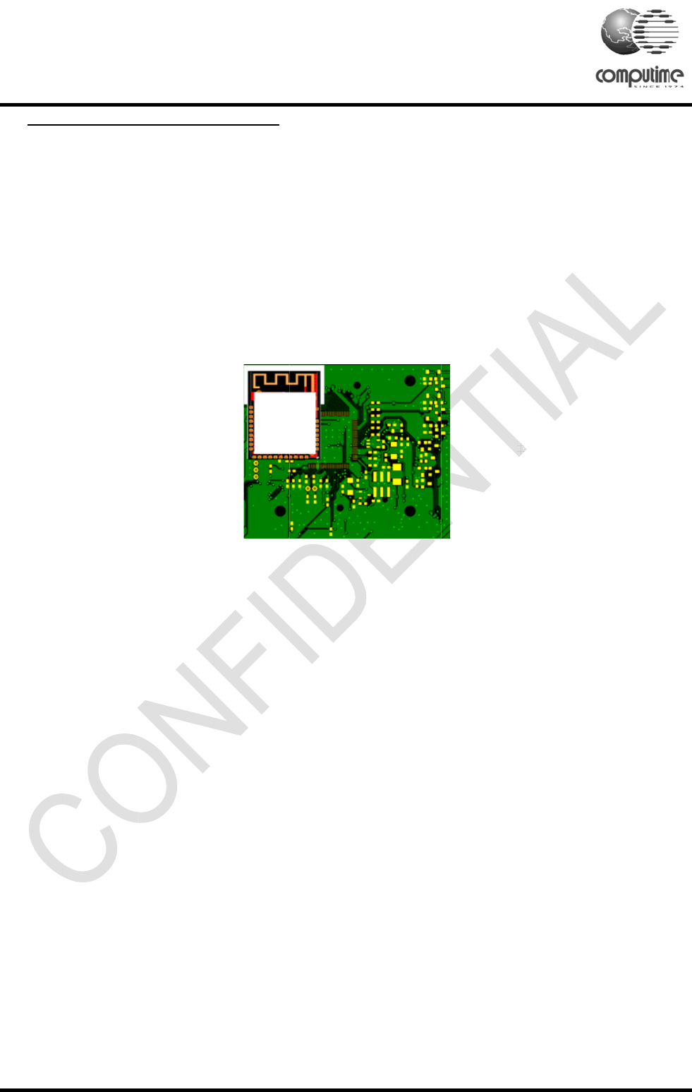
12. PC
B
Please r
e
The are
a
circuit o
n
preferre
d
A
s the
m
have gre
part und
e
example
R
eady RF Tr
a
h
t © 2015 C
o
B
Layout
R
e
ference M
e
a
undernea
t
n
the test p
a
d
.
m
odule inte
g
at impact o
e
rneath or
n
how the m
o
Figur
e
a
nsceiver M
o
o
mputime L
i
R
ecomme
n
e
chanical
D
t
h the mod
u
a
ds on the
b
g
rated with
o
n the RF p
e
n
earby the
a
o
dule posit
i
e
4: A rec
o
o
dule CTL3
5
i
mited. All r
n
dations
D
imensions
u
le should
b
b
ack side o
f
o
nboard P
C
e
rformance
a
rea of the
i
oned on th
e
o
mmende
d
5
85
_
CTL35
7
ights reser
v
shown in n
b
e covered
w
f
the modul
e
C
B trace an
t
. There sh
o
onboard P
C
e
mother P
C
d
placeme
n
7
5
v
ed.
ext section
w
ith solder
e
. A solid g
t
enna, the
m
o
uld not be
a
C
B trace a
n
C
B.
n
t of the m
o
for PCB la
y
mask in or
d
round plan
e
m
ounting p
o
a
ny trace,
g
n
tenna. Th
e
o
dule on a
y
out.
d
er to prev
e
e
under the
o
sition of th
g
round pla
n
e
figure bel
o
main PC
B
Re
v
e
nt short
module is
e module
w
n
e or metal
o
w shows a
n
B
v
. 3
w
ill
n
ZigBee-
R
Copyrig
h
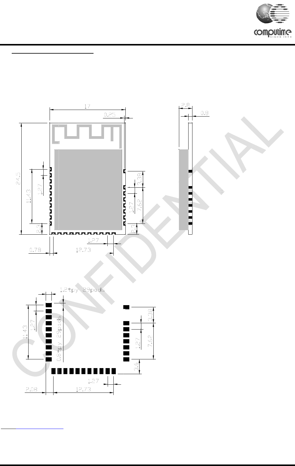
13. Mec
h
For furt
h
http://ww
w
R
eady RF Tr
a
h
t © 2015 C
o
h
anical D
i
h
er details
w
.silabs.co
m
a
nsceiver M
o
o
mputime L
i
i
mension
s
Figure 5:
on the So
m
o
dule CTL3
5
i
mited. All r
s
Mechanic
a
C transcei
v
5
85
_
CTL35
7
ights reser
v
a
l Dimensi
o
v
er (EM35
8
7
5
v
ed.
o
ns of CT
L
8
5/EM357)
,
L
3585/CTL
3
,
please c
o
3
575
o
nsult the
d
Re
v
d
ata sheet
v
. 3
at

ZigBee-
R
Copyrig
h
Regulato
This devi
c
(1) This d
(2) This d
operation
Changes
user's au
t
FCC Rad
The mod
u
any porta
b
This mod
u
transmitt
e
modular
m
body.
If the FC
C
outside o
f
module.
T
2AAUQ-
C
When the
warning s
1. This d
e
(1) This d
(2) This d
operation
2. Chang
e
user's au
t
The devi
c
in the us
e
R
eady RF Tr
a
h
t © 2015 C
o
ry Informat
i
c
e complies
w
evice may n
o
evice must
a
.
or modificati
t
hority to op
e
iation Expo
u
lar can be i
n
b
le device, f
o
u
lar complie
s
e
r must not b
m
ust be inst
a
C
identificati
o
f
the device i
T
his exterior
C
TL3575 or
C
module is i
n
tatements;
e
vice compli
e
evice may n
o
evice must
a
.
e
s or modifi
c
t
hority to op
e
c
es must be
i
e
r document
a
a
nsceiver M
o
o
mputime L
i
i
on
w
ith part 15
o
t cause ha
r
a
ccept any i
n
ons not exp
r
e
rate the eq
u
sure State
m
n
stalled or in
o
r example,
s
with FCC
R
e co-locate
d
a
lled and op
e
o
n number i
s
nto which th
label can us
e
C
ontains FC
C
n
stalled insi
d
e
s with Part
1
o
t cause ha
r
a
ccept any i
n
c
ations not e
x
e
rate the eq
u
i
nstalled an
d
a
tion that co
m
o
dule CTL3
5
i
mited. All r
of the FCC
R
r
mful interfer
e
n
terference r
e
r
essly appro
v
u
ipment.
m
ent
tegrated in
m
USB dongle
R
F radiation
d
or operatin
g
e
rated with
a
s
not visible
w
e module is
e
wording s
u
C
ID: 2AAU
Q
d
e another d
e
1
5 of the FC
r
mful interfer
e
n
terference r
e
x
pressly ap
p
u
ipment.
d
used in stri
c
m
es with the
5
85
_
CTL35
7
ights reser
v
R
ules. Oper
a
e
nce, and
e
ceived, incl
v
ed by the p
m
obile or fix
like transmi
t
exposure li
m
g
in conjunc
t
a
minimum d
i
w
hen the mo
installed mu
u
ch as the fo
Q
-CTL3575”
e
vice, the us
C Rules. Op
e
nce.
e
ceived, incl
p
roved by th
e
c
t accordan
c
product.
7
5
v
ed.
a
tion is subj
e
uding interf
e
arty respon
s
devices onl
y
t
ters is forbi
d
m
its set forth
t
ion with any
i
stance of 2
0
dule is insta
l
st also displ
a
llowing: “Co
n
er manual o
f
eration is su
uding interf
e
e
party resp
o
c
e with the
m
e
ct to the foll
o
e
rence that
m
s
ible for com
p
y
. This modu
d
den.
for an unco
n
other anten
n
0
cm betwee
n
l
led inside a
n
a
y a label re
f
n
tains Trans
f
this device
bject to the
f
e
rence that
m
o
nsible for c
o
m
anufacturer'
o
wing two c
o
m
ay cause u
n
p
liance coul
d
lar cannot b
e
n
trolled envi
r
n
a or trans
m
n
the radiat
o
n
other devic
e
f
erring to th
e
mitter Modu
l
must contai
n
f
ollowing tw
o
m
ay cause u
n
o
mpliance c
o
s instruction
Re
v
o
nditions:
n
desired
d
void the
e
installed in
r
onment. Thi
m
itter. This
o
r and user
e
, then the
e
enclosed
l
e FCC ID:
n
below
o
conditions:
n
desired
o
uld void the
s as describ
e
v
. 3
s
e
d

ZigBee-
R
Copyrig
h
IC State
m
This devi
c
condition
s
(1) This d
(2) This d
device.
Cet appa
r
aux deux
( 1 ) Ce d
i
( 2 ) Ce d
i
fonctionn
e
IC Radia
t
The mod
u
any porta
b
This mod
u
transmitt
e
modular
m
body.
Cette mo
d
utilisé à u
If the IC
n
device int
exterior l
a
IC: 1700
A
when the
warning s
1. This d
e
two condi
t
(1) This d
(2) This d
device.
2. Cet ap
p
soumis a
u
( 1 ) Ce d
i
( 2 ) Ce d
i
fonctionn
e
The devi
c
in the us
e
R
eady RF Tr
a
h
t © 2015 C
o
m
ent:
c
e complies
w
s
:
evice may n
o
evice must
a
r
eil est conf
o
conditions s
i
spositif ne
p
i
spositif doit
e
ment de l'a
p
t
ion Expos
u
u
lar can be i
n
b
le device, f
o
u
lar complie
s
e
r must not b
m
ust be inst
a
d
ulaire doit
ê
ne distance
n
umber is no
t
o which the
a
bel can use
A
-CTL3575”
module is in
tatements;
e
vice compli
e
t
ions:
evice may n
o
evice must
a
p
areil est co
n
u
x deux con
d
i
spositif ne
p
i
spositif doit
e
ment de l'a
p
c
es must be
i
e
r document
a
a
nsceiver M
o
o
mputime L
i
w
ith Industr
y
o
t cause int
e
a
ccept any i
n
o
rme aux CN
uivantes :
p
eut causer
d
accepter to
u
p
pareil.
u
re Stateme
n
n
stalled or in
o
r example,
s
with IC RF
e co-locate
d
a
lled and op
e
ê
tre installé
e
minimum d
e
t
visible whe
module is in
s
wording su
c
stalled insid
e
e
s with Indu
s
o
t cause int
e
a
ccept any i
n
n
forme aux
C
d
itions suiva
n
p
eut causer
d
accepter to
u
p
pareil.
i
nstalled an
d
a
tion that co
m
o
dule CTL3
5
i
mited. All r
y
Canada's li
e
rference; a
n
n
terference,
i
R exemptes
d
'interférenc
e
u
te interfére
n
n
t
tegrated in
m
USB dongle
radiation e
x
d
or operatin
g
e
rated with
a
et
e
20 cm entr
e
n the modul
e
s
talled must
c
h as the foll
o
e
another d
e
s
try Canada'
s
e
rference; a
n
n
terference,
i
C
NR exemp
t
n
tes :
d
'interférenc
e
u
te interfére
n
d
used in stri
c
m
es with the
5
85
_
CTL35
7
ights reser
v
cence-exem
n
d
i
ncluding int
e
de licence
d
e
s ; et
n
ce , y comp
r
m
obile or fix
like transmi
t
x
posure limit
s
g
in conjunc
t
a
minimum d
i
e
le radiateu
r
e
is installed
also display
o
wing: “Con
t
e
vice, the us
e
s
licence-ex
e
n
d
i
ncluding int
e
t
es de licenc
e
s ; et
n
ce , y comp
r
c
t accordan
c
produc
t
7
5
v
ed.
pt RSSs. O
p
e
rference th
a
d
'Industrie C
a
r
is les interf
é
devices onl
y
t
ters is forbi
d
s
set forth fo
r
t
ion with any
i
stance of 2
0
r
et le corps
d
inside anot
h
a label refe
r
t
ains
e
r manual o
f
e
mpt RSSs.
e
rference th
a
e d'Industrie
r
is les interf
é
c
e with the
m
p
eration is s
u
a
t may caus
e
a
nada. Son
f
é
rences qui
p
y
. This modu
d
den.
r
an uncontr
o
other anten
n
0
cm betwee
n
d
e l'utilisate
u
h
er device, t
h
r
ring to the
e
f
this device
m
Operation is
a
t may caus
e
Canada. S
o
é
rences qui
p
m
anufacturer'
u
bject to the
e
undesired
o
f
onctionnem
p
euvent cau
s
lar cannot b
e
o
lled enviro
n
n
a or trans
m
n
the radiat
o
u
r.
h
en the outs
i
e
nclosed mo
d
m
ust contai
n
s
subject to t
h
e
undesired
o
o
n fonctionn
e
p
euvent cau
s
s instruction
Re
v
following tw
o
o
peration of
ent est sou
m
s
er un mauv
a
e
installed in
n
ment. This
m
itter. This
o
r and user
i
de of the
d
ule. This
n
below
h
e following
o
peration of
e
ment est
s
er un mauv
a
s as describ
e
v
. 3
o
the
m
is
a
is
the
a
is
e
d

ZigBee-
R
Copyrig
h
Abou
t
Founde
d
providin
g
and con
The Co
m
lives m
o
R
eady RF Tr
a
h
t © 2015 C
o
t
Comp
d
in 1974,
g
innovati
v
sumer ma
m
pany pro
v
o
re produc
t
a
nsceiver M
o
o
mputime L
i
utime
Computi
m
v
e automa
t
rkets.
v
ides tech
t
ive and c
o
o
dule CTL3
5
i
mited. All r
m
e is a glo
t
ion and c
o
nologies
a
o
mfortable
.
5
85
_
CTL35
7
ights reser
v
bal techn
o
o
ntrol solu
t
a
nd produ
c
.
7
5
v
ed.
COM
o
logy, bran
t
ions to cu
c
ts that sa
v
Co
n
COMPUT
9/F To
w
e-ma
PUTIME
N
e-ma
Ci
n
e-mail:
d and ma
n
stomers i
n
v
e energy
a
n
tact in
f
IME COR
P
w
er One,
L
89
Tel: +8
5
Fax: +8
5
il: hq@co
m
N
ORTH A
M
4
7
Mas
o
Tel: +1(5
1
Fax: +1(5
1
il: na@co
m
n
cinnati T
e
4
7
Mas
o
Tel: +1(5
1
Fax: +1(5
1
ctws@co
m
n
ufacturin
g
n
commer
c
a
nd make
Re
v
f
ormati
o
P
ORATE
H
L
ippo Cen
t
Queensw
a
Hong K
o
5
2.2260.0
3
5
2.2790.3
9
m
putime.c
o
M
ERICA
H
7
00 Duke
D
Suite
2
o
n OH 45
0
U
S
1
3).398.2
5
1
3).754.8
9
m
putime.c
o
e
chnolog
i
7
00 Duke
D
Suite
2
o
n OH 45
0
U
S
1
3).754.8
9
1
3).754.8
9
m
putime.c
o
g
compan
y
c
ial, indust
r
people's
v
. 3
o
n
H
Q
t
re,
a
y,
o
ng
3
00
9
96
o
m
H
Q,
D
r.
2
00
0
40
S
A
5
79
9
55
o
m
i
es
D
r.
2
00
0
40
S
A
9
35
9
55
o
m
y
r
ial