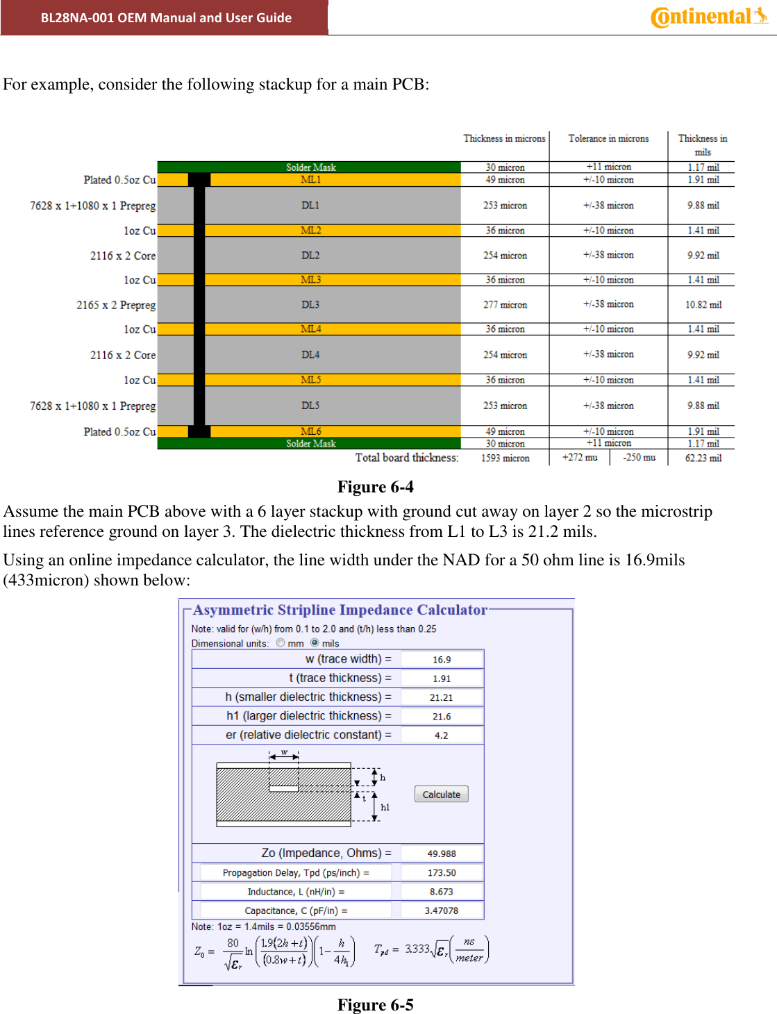
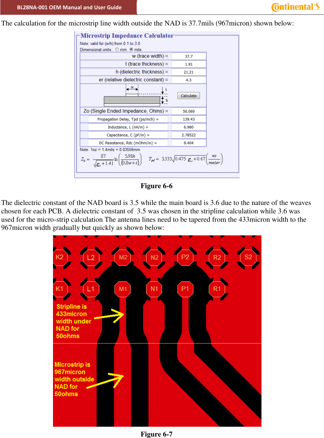
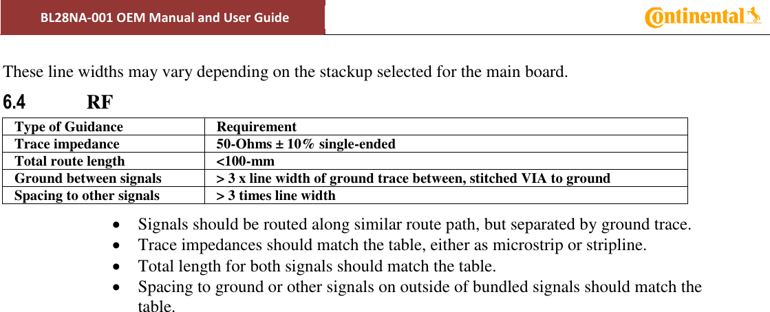
Continental Automotive Systems BL28NA001 Module with Multi-Band LTE, WCDMA, GSM User Manual LTE NAD

Continental Automotive Systems, Inc. Module with Multi-Band LTE, WCDMA, GSM LTE NAD

Contents

User Manual

BL28NA-001 OEM Manual and User Guide    BL28NA-001 OEM Manual and User Guide  v 4.0  (to be used for certification)  FCC ID: LHJ-BL28NA001 IC: LHJ-BL28NA001
BL28NA-001 OEM Manual and User Guide   Change History Revision Date Change Description Owner (s) 2.0 09-27-2016 Initial Release for certification, based off of HW Spec version 2.0 I. Shmagin 3.0 11-02-2016 Updated  to address comments from TCB I. Shmagin 4.0 11-11-2016 Removed “-“ from FCC ID and IC ID I.Shmagin
BL28NA-001 OEM Manual and User Guide   Terms and Acronyms  CDMA  Code Division Multiple Access  DCM    Data Connectivity Module  DRX    Discontinuous Reception  ES    Engineering Sample  FDD    Frequency Division Duplex  GLONASS  GLOBal’naya NAVigatsionnaya Sputnikovaya Sistema  GNSS   Global Navigation Satellite System  GPIO    General Purpose Input Output  GSM    Global System for Mobile  HU    Head Unit  HSIC    High Speed Inter-Chip  LTE    Long Term Evolution  MP      Mass Production  NAD    Network Access Device  OEM    Original Equipment Manufacturer   PCB    Printed Circuit Board  PHY    Physical Layer  SIM    Subscriber Identity Module  TCU    Telematics Control Unit  TDD    Time Division Duplex  TSP    Telematics Service Provider  UMTS  Universal Mobile Telecommunication System  WCDMA  Wideband Code Division Multiple Access
BL28NA-001 OEM Manual and User Guide   BL28NA-001 Module The BL28NA-001  NAD is a proprietary modem module designed by Continental Automotive Systems, Inc.   The modem will be integrated into Data Connectivity Modules (DCMs) or Head Units (HUs) designed and produced by Continental or by a 3rd party for use by automotive OEMs.  DCMs will be installed into vehicles during the OEM’s factory assembly process and will not be accessible without use of special tools.  Primary use-cases are data-centric with data and voice connections to Telematics Service Providers (TSP). 1 Key Features 1.1 LTE CAT4 NAD Module  Air Interface Support  LTE FDD/TDD: 3GPP Rel 10  LTE FDD CAT4 (up to 150-Mbps UL/50-Mbps DL)  LTE TDD CAT4 (up to 90-Mbps UL/27-Mbps DL) for TDD Configuration 1  UMTS: HSUPA CAT 6 (up to 5.76-Mbps), HSPA CAT14 (up to 21-Mbps), HSPA CAT24 (up to 42-Mbps)  2 Regulatory Compliance Notes FCC: This device complies with Part 15, Part 22(H), Part 24(E) and Part 27 of the FCC Rules. The FCC ID for this device is LHJ-BL28NA001. Operation is subject to the following two conditions: 1. This device may not cause harmful interference. 2. This device must accept any interference received, including interference that may cause undesired operation.  Industry of Canada: This device complies with Industry Canada’s license-exempt RSSs. Operation is subject to the following two conditions: (1) This device may not cause interference; and (2) This device must accept any interference, including interference that may cause undesired operation of the device.”  « Le présent appareil est conforme aux CNR d'Industrie Canada applicables aux appareils radio exempts de licence. L'exploitation est autorisée aux deux conditions suivantes : (1) l'appareil ne doit pas produire de brouillage, et (2) l'utilisateur de l'appareil doit accepter tout brouillage radioélectrique subi, même si le brouillage est susceptible d'en compromettre le fonctionnement. » This radio transmitter (2807E-BL28NA001) has been approved by Industry Canada to operate with the antenna types listed below with the maximum permissible gain indicated. Antenna types not included in this list, having a gain greater than the maximum gain indicated for that type, are strictly prohibited for use with this device.
BL28NA-001 OEM Manual and User Guide   « Le présent émetteur radio (2807E-BL28NA001) a été approuvé par Industrie Canada pour fonctionner avec les types d'antenne énumérés ci-dessous et ayant un gain admissible maximal. Les types d'antenne non inclus dans cette liste, et dont le gain est supérieur au gain maximal indiqué, sont strictement interdits pour l'exploitation de l'émetteur.».  3 Device Installation and User Manual  The BL28NA-001 module is a proprietary product designed and manufactured by Continental Automotive Systems, Inc. for integration into telematics control units manufactured by Continental Automotive Systems, Inc. for automotive OEMs. i. The module is limited to installation ONLY in an integrated device manufactured by Continental Automotive Systems, Inc. ii. During manufacturing process of the integrated device, the module is soldered onto the pcb of the integrated device. iii. The integrated device must provide RF connectors to external antennas or RF traces to connect the BL28NA-001 modules to antennas inside the integrated device. The typical reference design for the RF trace layout, including pcb stack-up and trace length is described in Section 6 of this document. iv. Automotive OEM is responsible for ensuring that the end-user has no manual instructions to remove or install module. v. The module is limited to installation in mobile applications, according to Part 2.1091(b). vi. No other operation configurations are allowed. vii. Changes or modifications to this system by other than a facility authorized by Continental could void authorization to use this equipment. viii. The module must be installed to provide a separation distance of at least 20 cm from all persons and must not be co-located or operate in conjunction with any other antenna or transmitter. ix. The integrator is responsible for fulfilling FCC and IC requirements for the integrated device.  If Continental chooses to re-use modular approval, then the TCU shall be clearly labeled with an external label containing the integrated modem’s FCC ID. For example, the label can include text “Contains device with FCC ID: LHJ-BL28NA001 and IC: 2807E-BL28NA001”.  4 Antenna requirements for use with BL28NA-001 module:  The module must be installed to provide a separation distance of at least 20cm from all persons and must not be co-located or operating in conjunction with any other antenna or transmitter.  The BL28NA-001 module is for use with external antennas ONLY.  For all LTE/WCDMA operating bands the maximum antenna gain is 5 dBi including cable loss.  The maximum gain of the antenna path (cable loss + antenna gain) shall not exceed the above mentioned values.  This radio transmitter (FCC ID: LHJ-BL28NA001; IC: 2807E-BL28NA001) has been approved by FCC and Industry Canada to operate with the antenna types listed below with the maximum permissible gain indicated. Antenna types not included in this list, having a gain greater than the maximum gain indicated for that type, are strictly prohibited for use with this device.
BL28NA-001 OEM Manual and User Guide     « Le présent émetteur radio (ID: LHJ-BL28NA001; IC: 2807E-BL28-001) a été approuvé par Industrie Canada pour fonctionner avec les types d'antenne énumérés ci-dessous et ayant un gain admissible maximal. Les types d'antenne non inclus dans cette liste, et dont le gain est supérieur au gain maximal indiqué, sont strictement interdits pour l'exploitation de l'émetteur.»  5 Instructions to OEMs:  Continental must instruct the automotive OEM and provide them to include the following information into the car user’s manual (i.e. for the DCM): 1. End-users must be provided with transmitter/antenna installation requirements and operating conditions for satisfying RF exposure compliance: 2. A separate section should clearly state “FCC RF Exposure requirements:” 3. Required operating conditions for end users. 4. The antenna used with this device must be installed to provide a separation distance of at least 20cm from all persons, and must not transmit simultaneously with any other transmitter, except in accordance with FCC multi-transmitter product procedures. 5. The Maximum ERP/EIRP and maximum antenna gain required for compliance with Parts 15, 22H, 24E, and 27. 6. Clear instructions describing the other party’s responsibility to obtain station licensing.   6 Layout and Routing Recommendations  6.1 Module Specific The pad spacing of 1mm should allow the placement of a 600um finished VIA between pads, while maintaining a 200um Via- to-trace or Via-pad spacing, to facilitate the breakout of inner row signals.  The 1mm spacing is also large enough to route two 200um traces between pads.  Figure 6-1 Vias placed between Pads
BL28NA-001 OEM Manual and User Guide   6.2 Power Pins Application note - External decoupling capacitors requirements for the critical NAD internal power supplies  For each of the four NAD supply pins, place two external decoupling capacitors, a 1 uF and a 10uF, as close as possible to each of these four power pins (G14, H14, J14, and K15).  Figure 6-1shows the four power pins on the NAD  NEEDS TO BE UPDATED  Figure 6-1.  Through the part view of pads on the module.  Keep routing of these capacitors, both to the power pins and to the grounds, direct and as short as possible.  Use minimum 3 VIA pairs (minimum 3 VIAs for power and minimum3 VIAs for ground), placed close to the pins and routed with a wide trace or area fill.  Figure 6-2 depicts the recommended placement and routing for these decoupling capacitors on the TCU board.   Figure 6-2: External Decoupling Capacitors on TCU with Routing
BL28NA-001 OEM Manual and User Guide   6.3 RF Traces for antennas The NAD has five antenna pins.  PRIMARY_ANT  SECONDARY_ANT  WIFI_ANT_0  WIFI_ANT_1  GNSS_ANT The figure below shows the general breakout of the LTE-A NAD:  The LTE_A NAD should be oriented on the main board to optimize the length of the PRIMARY_LTE antenna pin. This line should be as short as possible.  The RF traces from the NAD antenna pins on the main board can be stripline or microstrip. If stripline is chosen, the VIA should be placed as close as possible to the NAD antenna pads to minimize any impedance discontinuity. If microstrip is chosen, the PCB insertion loss will be less, but the short route under the NAD must be treated as stripline.   The NAD has ground cleared out under the RF antenna routes as shown below:   Figure 6-3  These ground cutouts need to be accounted for in the stripline calculation underneath the NAD. The height and dielectric constant of the NAD board are shown below: H = 21.6 mils (553 micron) Dielectric Constant = 4.1
BL28NA-001 OEM Manual and User Guide    For example, consider the following stackup for a main PCB:   Figure 6-4 Assume the main PCB above with a 6 layer stackup with ground cut away on layer 2 so the microstrip lines reference ground on layer 3. The dielectric thickness from L1 to L3 is 21.2 mils.  Using an online impedance calculator, the line width under the NAD for a 50 ohm line is 16.9mils (433micron) shown below:  Figure 6-5
BL28NA-001 OEM Manual and User Guide   The calculation for the microstrip line width outside the NAD is 37.7mils (967micron) shown below:  Figure 6-6  The dielectric constant of the NAD board is 3.5 while the main board is 3.6 due to the nature of the weaves chosen for each PCB. A dielectric constant of  3.5 was chosen in the stripline calculation while 3.6 was used for the micro-strip calculation The antenna lines need to be tapered from the 433micron width to the 967micron width gradually but quickly as shown below:  Figure 6-7
BL28NA-001 OEM Manual and User Guide    These line widths may vary depending on the stackup selected for the main board. 6.4 RF Type of Guidance Requirement Trace impedance 50-Ohms ± 10% single-ended Total route length <100-mm Ground between signals > 3 x line width of ground trace between, stitched VIA to ground  Spacing to other signals > 3 times line width  Signals should be routed along similar route path, but separated by ground trace.  Trace impedances should match the table, either as microstrip or stripline.  Total length for both signals should match the table.  Spacing to ground or other signals on outside of bundled signals should match the table.

Navigation menu