Continental Automotive TIS-03 Tire Pressure Monitoring System User Manual TG1D Chrysler Functional Description V4
Continental Automotive GmbH Tire Pressure Monitoring System TG1D Chrysler Functional Description V4
UserManual.wiki
>
Continental Automotive
>
TIS 03 User Manual
User Manual
Navigation menu
Upload a User Manual
Namespaces
Wiki Guide
HTML
PDF
Info
Views
User Manual
Discussion / Help
Navigation


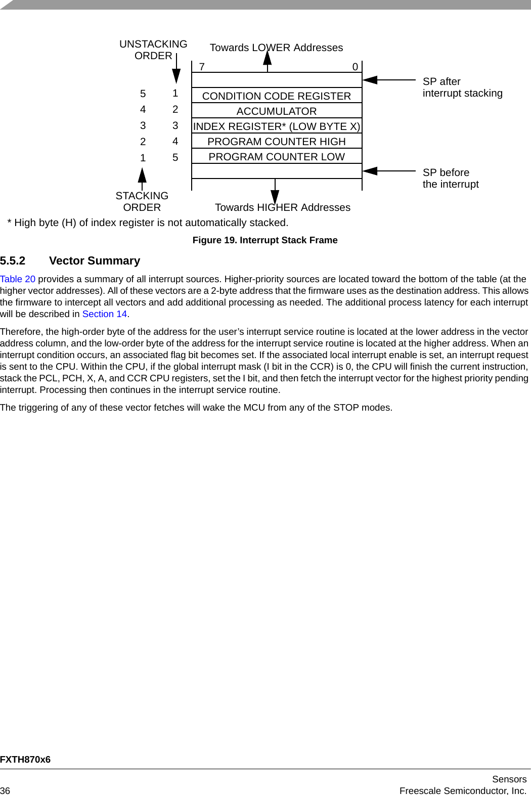
![FXTH870x6Sensors4Freescale Semiconductor, Inc.9 Timer Pulse-Width Module. . . . . . . . . . . . . . . . . . . . . . . . . . . . . . . . . . . . . . . . . . . . . . . . . . . . . . . . . . . . . . . . . . . . . . . . 709.1 Features . . . . . . . . . . . . . . . . . . . . . . . . . . . . . . . . . . . . . . . . . . . . . . . . . . . . . . . . . . . . . . . . . . . . . . . . . . . . . . . . . . 709.2 TPM1 Configuration Information. . . . . . . . . . . . . . . . . . . . . . . . . . . . . . . . . . . . . . . . . . . . . . . . . . . . . . . . . . . . . . . . 709.3 External Signal Description . . . . . . . . . . . . . . . . . . . . . . . . . . . . . . . . . . . . . . . . . . . . . . . . . . . . . . . . . . . . . . . . . . . 719.4 Register Definition . . . . . . . . . . . . . . . . . . . . . . . . . . . . . . . . . . . . . . . . . . . . . . . . . . . . . . . . . . . . . . . . . . . . . . . . . . 729.5 Functional Description . . . . . . . . . . . . . . . . . . . . . . . . . . . . . . . . . . . . . . . . . . . . . . . . . . . . . . . . . . . . . . . . . . . . . . . 779.6 TPM1 Interrupts . . . . . . . . . . . . . . . . . . . . . . . . . . . . . . . . . . . . . . . . . . . . . . . . . . . . . . . . . . . . . . . . . . . . . . . . . . . . 8010 .Other MCU Resources. . . . . . . . . . . . . . . . . . . . . . . . . . . . . . . . . . . . . . . . . . . . . . . . . . . . . . . . . . . . . . . . . . . . . . . . . . . 8210.1 Pressure Measurement . . . . . . . . . . . . . . . . . . . . . . . . . . . . . . . . . . . . . . . . . . . . . . . . . . . . . . . . . . . . . . . . . . . . . . 8210.2 Temperature Measurements . . . . . . . . . . . . . . . . . . . . . . . . . . . . . . . . . . . . . . . . . . . . . . . . . . . . . . . . . . . . . . . . . . 8310.3 Voltage Measurements. . . . . . . . . . . . . . . . . . . . . . . . . . . . . . . . . . . . . . . . . . . . . . . . . . . . . . . . . . . . . . . . . . . . . . . 8310.4 Optional Acceleration Measurements. . . . . . . . . . . . . . . . . . . . . . . . . . . . . . . . . . . . . . . . . . . . . . . . . . . . . . . . . . . . 8310.5 Optional Battery Condition Check . . . . . . . . . . . . . . . . . . . . . . . . . . . . . . . . . . . . . . . . . . . . . . . . . . . . . . . . . . . . . . 8310.6 Measurement Firmware . . . . . . . . . . . . . . . . . . . . . . . . . . . . . . . . . . . . . . . . . . . . . . . . . . . . . . . . . . . . . . . . . . . . . . 8510.7 Thermal Shutdown . . . . . . . . . . . . . . . . . . . . . . . . . . . . . . . . . . . . . . . . . . . . . . . . . . . . . . . . . . . . . . . . . . . . . . . . . . 8711 Periodic Wakeup Timer . . . . . . . . . . . . . . . . . . . . . . . . . . . . . . . . . . . . . . . . . . . . . . . . . . . . . . . . . . . . . . . . . . . . . . . . . . 8911.1 Block Diagram . . . . . . . . . . . . . . . . . . . . . . . . . . . . . . . . . . . . . . . . . . . . . . . . . . . . . . . . . . . . . . . . . . . . . . . . . . . . . 8911.2 Wakeup Divider Register - PWUDIV . . . . . . . . . . . . . . . . . . . . . . . . . . . . . . . . . . . . . . . . . . . . . . . . . . . . . . . . . . . . 9011.3 PWU Control/Status Register 0 - PWUCS0 . . . . . . . . . . . . . . . . . . . . . . . . . . . . . . . . . . . . . . . . . . . . . . . . . . . . . . . 9011.4 PWU Control/Status Register 1 - PWUCS1 . . . . . . . . . . . . . . . . . . . . . . . . . . . . . . . . . . . . . . . . . . . . . . . . . . . . . . . 9111.5 PWU Wakeup Status Register - PWUS . . . . . . . . . . . . . . . . . . . . . . . . . . . . . . . . . . . . . . . . . . . . . . . . . . . . . . . . . . 9211.6 Functional Modes . . . . . . . . . . . . . . . . . . . . . . . . . . . . . . . . . . . . . . . . . . . . . . . . . . . . . . . . . . . . . . . . . . . . . . . . . . . 9212 LF Receiver . . . . . . . . . . . . . . . . . . . . . . . . . . . . . . . . . . . . . . . . . . . . . . . . . . . . . . . . . . . . . . . . . . . . . . . . . . . . . . . . . . . . 9312.1 Features . . . . . . . . . . . . . . . . . . . . . . . . . . . . . . . . . . . . . . . . . . . . . . . . . . . . . . . . . . . . . . . . . . . . . . . . . . . . . . . . . . 9412.2 Modes of Operation . . . . . . . . . . . . . . . . . . . . . . . . . . . . . . . . . . . . . . . . . . . . . . . . . . . . . . . . . . . . . . . . . . . . . . . . . 9412.3 Power Management . . . . . . . . . . . . . . . . . . . . . . . . . . . . . . . . . . . . . . . . . . . . . . . . . . . . . . . . . . . . . . . . . . . . . . . . . 9412.4 Input Amplifier. . . . . . . . . . . . . . . . . . . . . . . . . . . . . . . . . . . . . . . . . . . . . . . . . . . . . . . . . . . . . . . . . . . . . . . . . . . . . . 9512.5 LFR Data Mode States. . . . . . . . . . . . . . . . . . . . . . . . . . . . . . . . . . . . . . . . . . . . . . . . . . . . . . . . . . . . . . . . . . . . . . . 9512.6 Carrier Detect . . . . . . . . . . . . . . . . . . . . . . . . . . . . . . . . . . . . . . . . . . . . . . . . . . . . . . . . . . . . . . . . . . . . . . . . . . . . . . 9512.7 Auto-Zero Sequence . . . . . . . . . . . . . . . . . . . . . . . . . . . . . . . . . . . . . . . . . . . . . . . . . . . . . . . . . . . . . . . . . . . . . . . . 9712.8 Data Recovery . . . . . . . . . . . . . . . . . . . . . . . . . . . . . . . . . . . . . . . . . . . . . . . . . . . . . . . . . . . . . . . . . . . . . . . . . . . . . 9712.9 Data Clock Recovery and Synchronization . . . . . . . . . . . . . . . . . . . . . . . . . . . . . . . . . . . . . . . . . . . . . . . . . . . . . . . 9712.10 Manchester Decode . . . . . . . . . . . . . . . . . . . . . . . . . . . . . . . . . . . . . . . . . . . . . . . . . . . . . . . . . . . . . . . . . . . . . . . . . 9712.11 Duty-Cycle For Data Mode. . . . . . . . . . . . . . . . . . . . . . . . . . . . . . . . . . . . . . . . . . . . . . . . . . . . . . . . . . . . . . . . . . . . 9812.12 Input Signal Envelope. . . . . . . . . . . . . . . . . . . . . . . . . . . . . . . . . . . . . . . . . . . . . . . . . . . . . . . . . . . . . . . . . . . . . . . . 9912.13 Telegram Verification . . . . . . . . . . . . . . . . . . . . . . . . . . . . . . . . . . . . . . . . . . . . . . . . . . . . . . . . . . . . . . . . . . . . . . . 10012.14 Error Detection and Handling . . . . . . . . . . . . . . . . . . . . . . . . . . . . . . . . . . . . . . . . . . . . . . . . . . . . . . . . . . . . . . . . . 10112.15 Continuous ON Mode. . . . . . . . . . . . . . . . . . . . . . . . . . . . . . . . . . . . . . . . . . . . . . . . . . . . . . . . . . . . . . . . . . . . . . . 10112.16 Initialization Information . . . . . . . . . . . . . . . . . . . . . . . . . . . . . . . . . . . . . . . . . . . . . . . . . . . . . . . . . . . . . . . . . . . . . 10112.17 LFR Register Definition . . . . . . . . . . . . . . . . . . . . . . . . . . . . . . . . . . . . . . . . . . . . . . . . . . . . . . . . . . . . . . . . . . . . . 10213 RF Module . . . . . . . . . . . . . . . . . . . . . . . . . . . . . . . . . . . . . . . . . . . . . . . . . . . . . . . . . . . . . . . . . . . . . . . . . . . . . . . . . . . . 11313.1 RF Data Modes . . . . . . . . . . . . . . . . . . . . . . . . . . . . . . . . . . . . . . . . . . . . . . . . . . . . . . . . . . . . . . . . . . . . . . . . . . . 11313.2 RF Output Buffer Data Frame . . . . . . . . . . . . . . . . . . . . . . . . . . . . . . . . . . . . . . . . . . . . . . . . . . . . . . . . . . . . . . . . 11413.3 Transmission Randomization . . . . . . . . . . . . . . . . . . . . . . . . . . . . . . . . . . . . . . . . . . . . . . . . . . . . . . . . . . . . . . . . . 11613.4 RFM in STOP1 Mode . . . . . . . . . . . . . . . . . . . . . . . . . . . . . . . . . . . . . . . . . . . . . . . . . . . . . . . . . . . . . . . . . . . . . . . 11913.5 Data Encoding . . . . . . . . . . . . . . . . . . . . . . . . . . . . . . . . . . . . . . . . . . . . . . . . . . . . . . . . . . . . . . . . . . . . . . . . . . . . 11913.6 RF Output Stage. . . . . . . . . . . . . . . . . . . . . . . . . . . . . . . . . . . . . . . . . . . . . . . . . . . . . . . . . . . . . . . . . . . . . . . . . . . 12113.7 RF Interrupt . . . . . . . . . . . . . . . . . . . . . . . . . . . . . . . . . . . . . . . . . . . . . . . . . . . . . . . . . . . . . . . . . . . . . . . . . . . . . . 12213.8 Datagram Transmission Times. . . . . . . . . . . . . . . . . . . . . . . . . . . . . . . . . . . . . . . . . . . . . . . . . . . . . . . . . . . . . . . . 12213.9 RFM Registers . . . . . . . . . . . . . . . . . . . . . . . . . . . . . . . . . . . . . . . . . . . . . . . . . . . . . . . . . . . . . . . . . . . . . . . . . . . . 12313.10 RFM Control Register 1 - RFCR1. . . . . . . . . . . . . . . . . . . . . . . . . . . . . . . . . . . . . . . . . . . . . . . . . . . . . . . . . . . . . . 12313.11 RFM Control Register 2 - RFCR2. . . . . . . . . . . . . . . . . . . . . . . . . . . . . . . . . . . . . . . . . . . . . . . . . . . . . . . . . . . . . . 12413.12 RFM Control Register 3 - RFCR3. . . . . . . . . . . . . . . . . . . . . . . . . . . . . . . . . . . . . . . . . . . . . . . . . . . . . . . . . . . . . . 12713.13 RFM Control Register 4 - RFCR4. . . . . . . . . . . . . . . . . . . . . . . . . . . . . . . . . . . . . . . . . . . . . . . . . . . . . . . . . . . . . . 12813.14 RFM Control Register 5 - RFCR5. . . . . . . . . . . . . . . . . . . . . . . . . . . . . . . . . . . . . . . . . . . . . . . . . . . . . . . . . . . . . . 12813.15 RFM Control Register 6 - RFCR6. . . . . . . . . . . . . . . . . . . . . . . . . . . . . . . . . . . . . . . . . . . . . . . . . . . . . . . . . . . . . . 12913.16 RFM Control Register 7 - RFCR7. . . . . . . . . . . . . . . . . . . . . . . . . . . . . . . . . . . . . . . . . . . . . . . . . . . . . . . . . . . . . . 12913.17 PLL Control Registers A- PLLCR[1:0], RPAGE = 0 . . . . . . . . . . . . . . . . . . . . . . . . . . . . . . . . . . . . . . . . . . . . . . . . 13013.18 PLL Control Registers B- PLLCR[3:2], RPAGE = 0 . . . . . . . . . . . . . . . . . . . . . . . . . . . . . . . . . . . . . . . . . . . . . . . . 13113.19 EPR Register - EPR (RPAGE = 1) . . . . . . . . . . . . . . . . . . . . . . . . . . . . . . . . . . . . . . . . . . . . . . . . . . . . . . . . . . . . . 13213.20 RF DATA Registers - RFD[31:0] . . . . . . . . . . . . . . . . . . . . . . . . . . . . . . . . . . . . . . . . . . . . . . . . . . . . . . . . . . . . . . 13313.21 VCO Calibration Machine . . . . . . . . . . . . . . . . . . . . . . . . . . . . . . . . . . . . . . . . . . . . . . . . . . . . . . . . . . . . . . . . . . . . 134](https://usermanual.wiki/Continental-Automotive/TIS-03/User-Guide-2718164-Page-8.png)
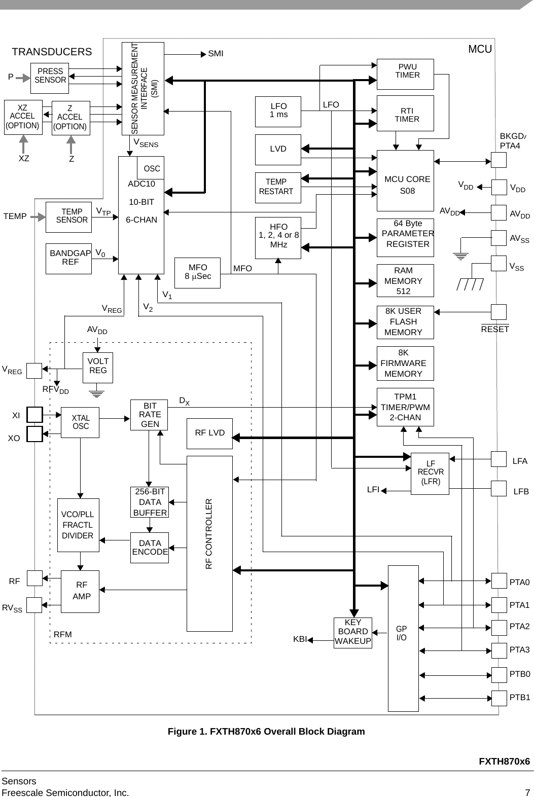
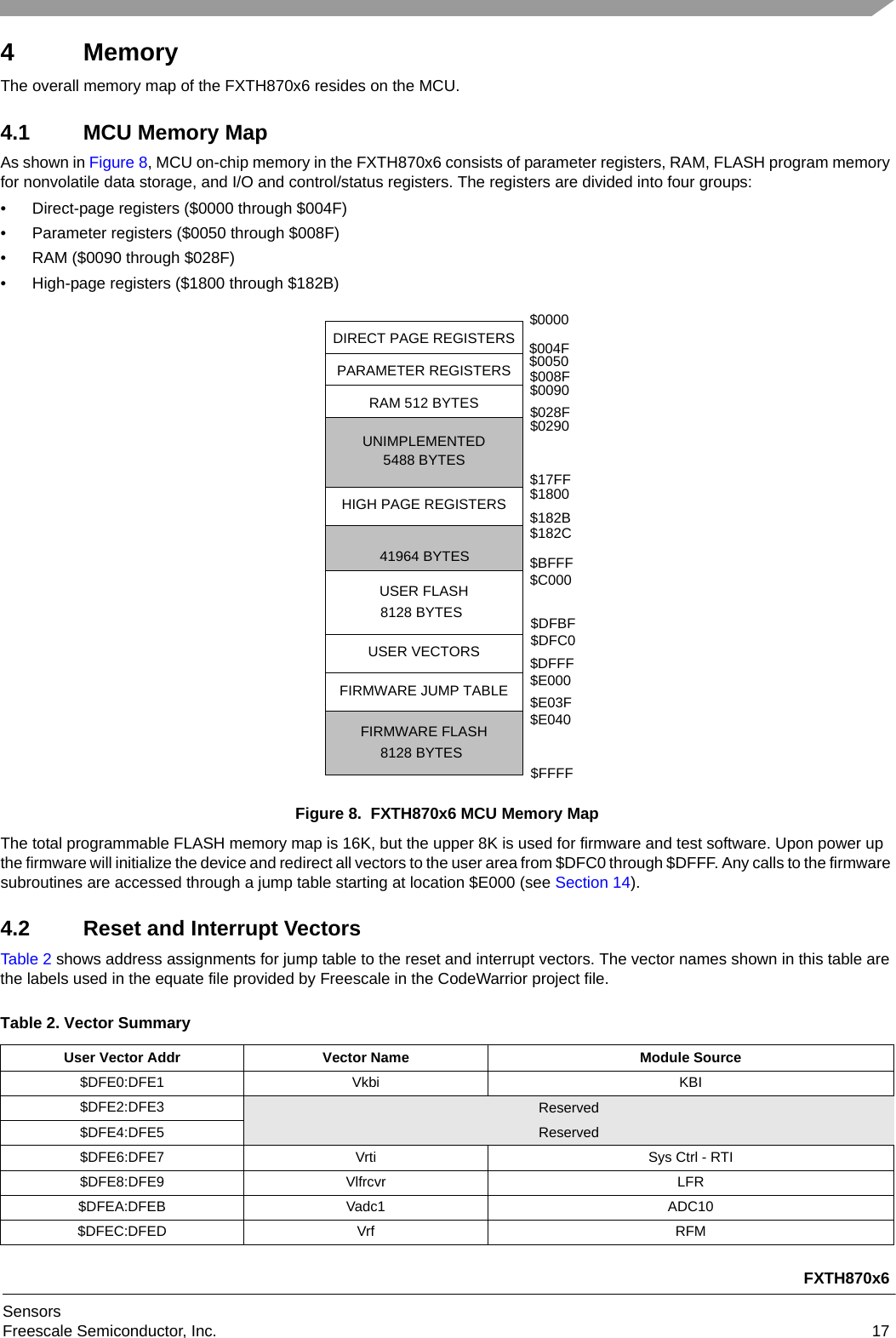
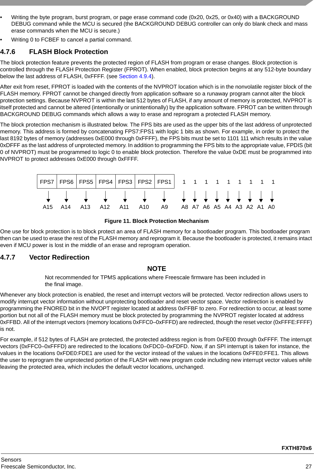
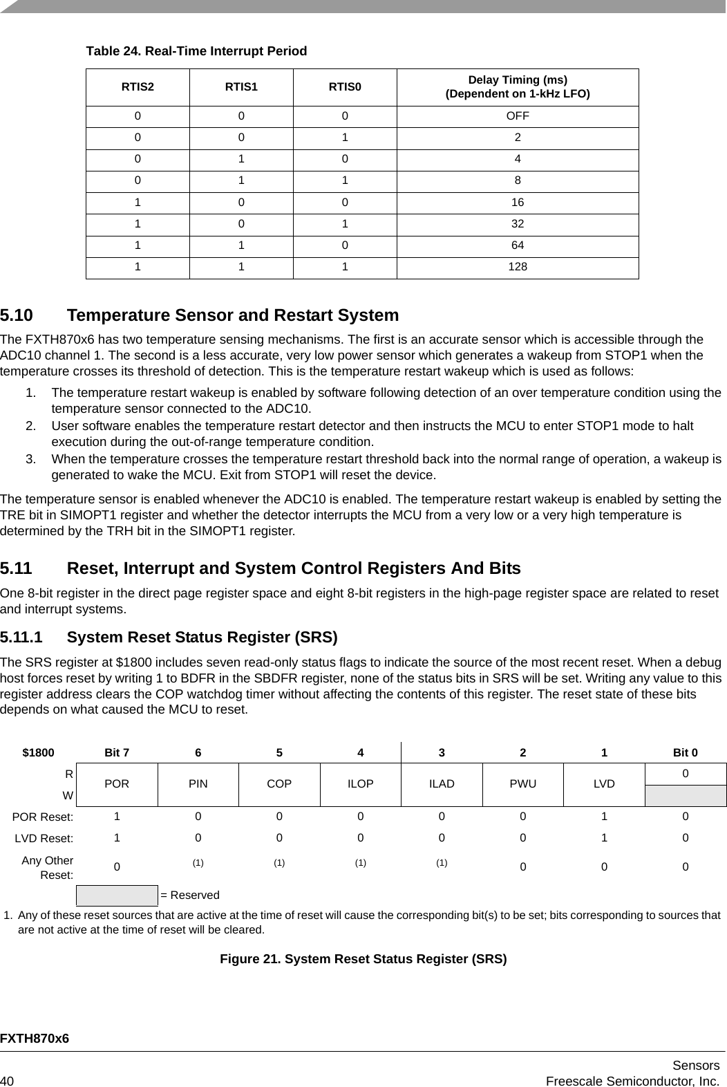
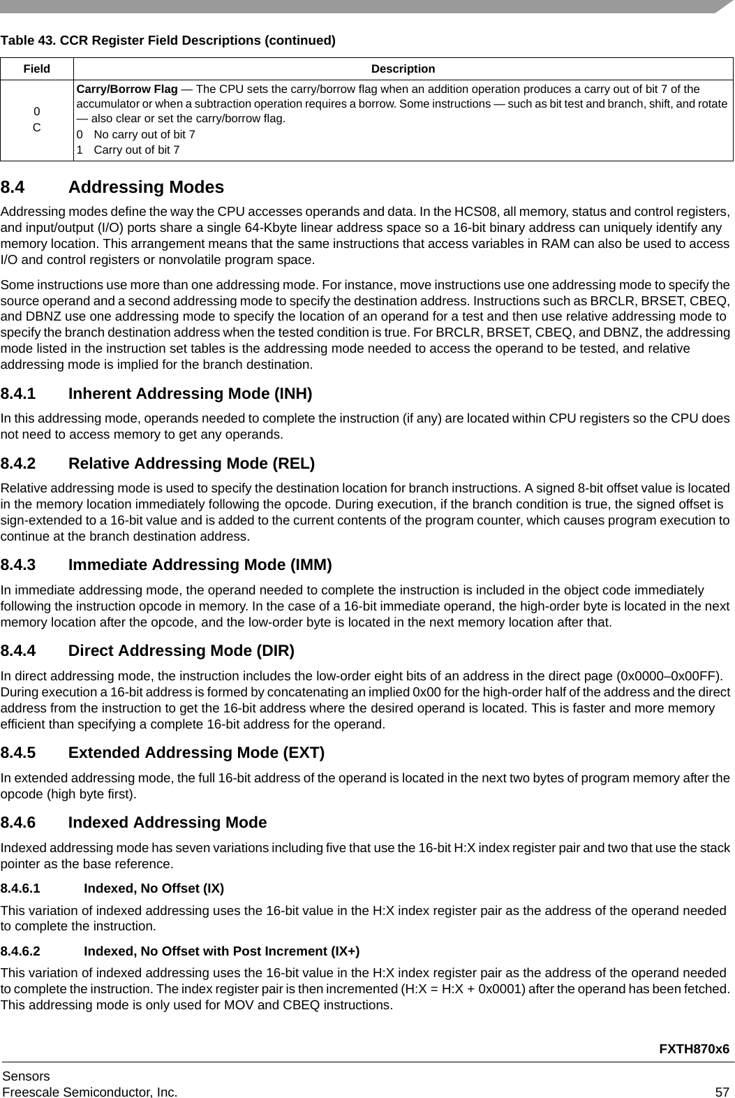
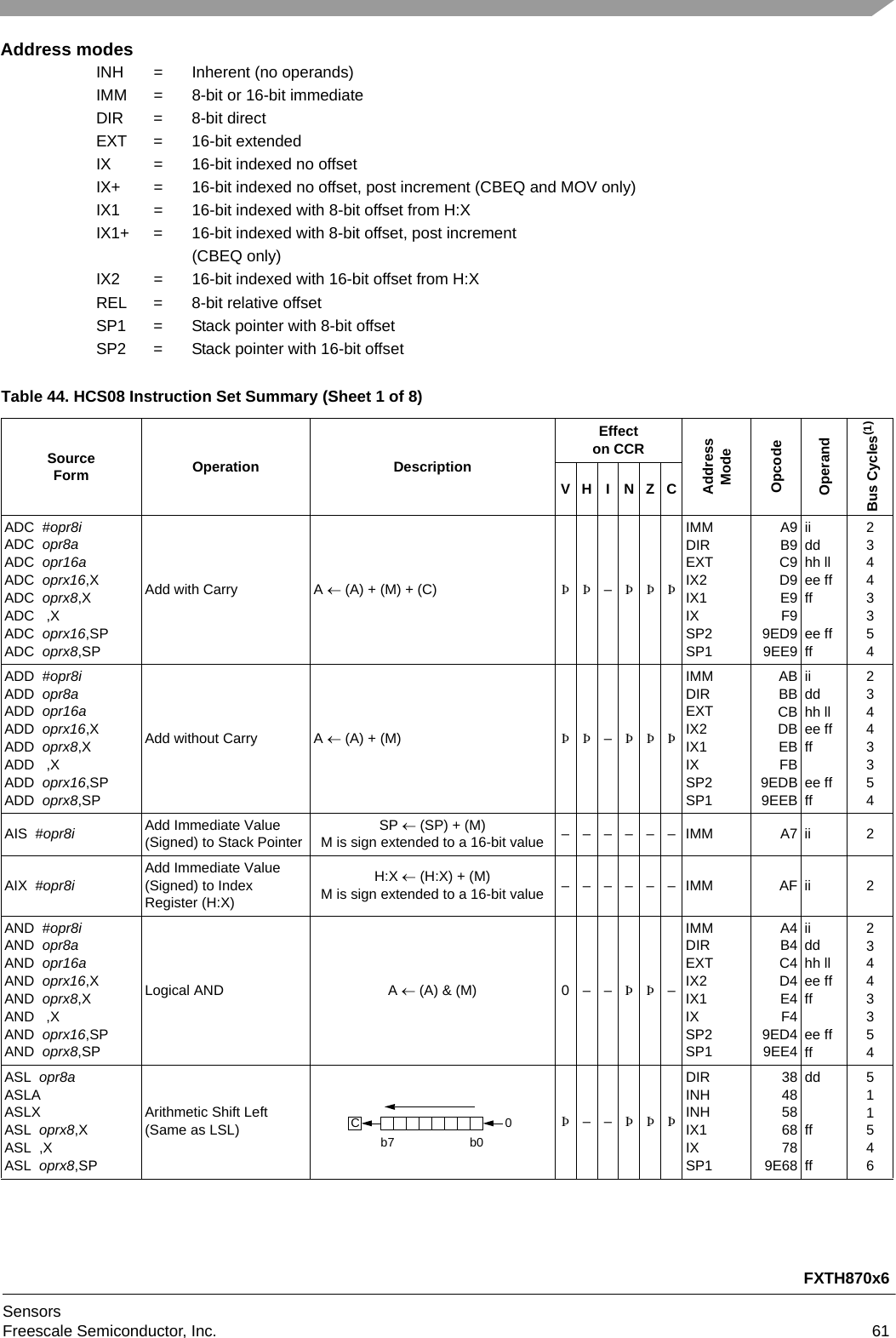
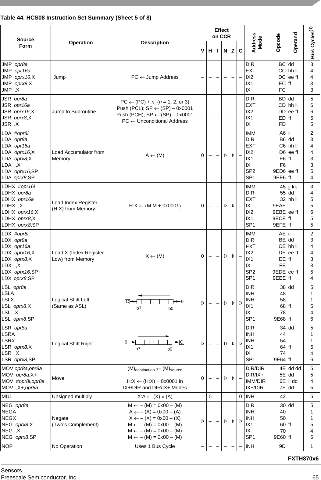
![FXTH870x6Sensors8Freescale Semiconductor, Inc.Figure 2. Clock Distribution1.4 Reference DocumentsThe FXTH870x6 utilizes the standard product MC9S08 CPU core. The user can obtain further detail on the full capabilities of this core by referring to the HCS08 Family Reference Manual (HCS08RMV1).RTISYSTEMCONTROLLOGIC 2HFO OSC1, 2, 4, fOSC fBUSCPUBDCTPM1RAM FLASHLFRADC10MFOOSC8 SecPWUCLSA, CLKSBfLFO (1 kHz)XTLOSC26 MHzXI XO PLL VCOBITRATEDATABUFFERPRESSURESENSORTRANSDUCERSMCURTICLKSPARREGfMFOfXCOGENDX (500 kHz)LFOOSC1 mSPERIODSENSOR MEASUREMENTINTERFACEADC10CLOCKADCCLK ADC10BUSCLKS[1:0]WATCHDOGCOPCLKSZ-AXISSENSORLF4 kbps(125 kHz)RF STATEMACHINELFROOSCILL 8TCLKDIVLFOSELfMFOPTA3PTA2fLFO (1 kHz)CH0 CH1RANDOM(0 - 1 MHz)RANDOM(0 - 1 MHz)RFOUT 41.67 kHzSampling41.67 kHzSamplingand 8 MHzX-AXISSENSOR41.67 kHzSampling](https://usermanual.wiki/Continental-Automotive/TIS-03/User-Guide-2718164-Page-12.png)
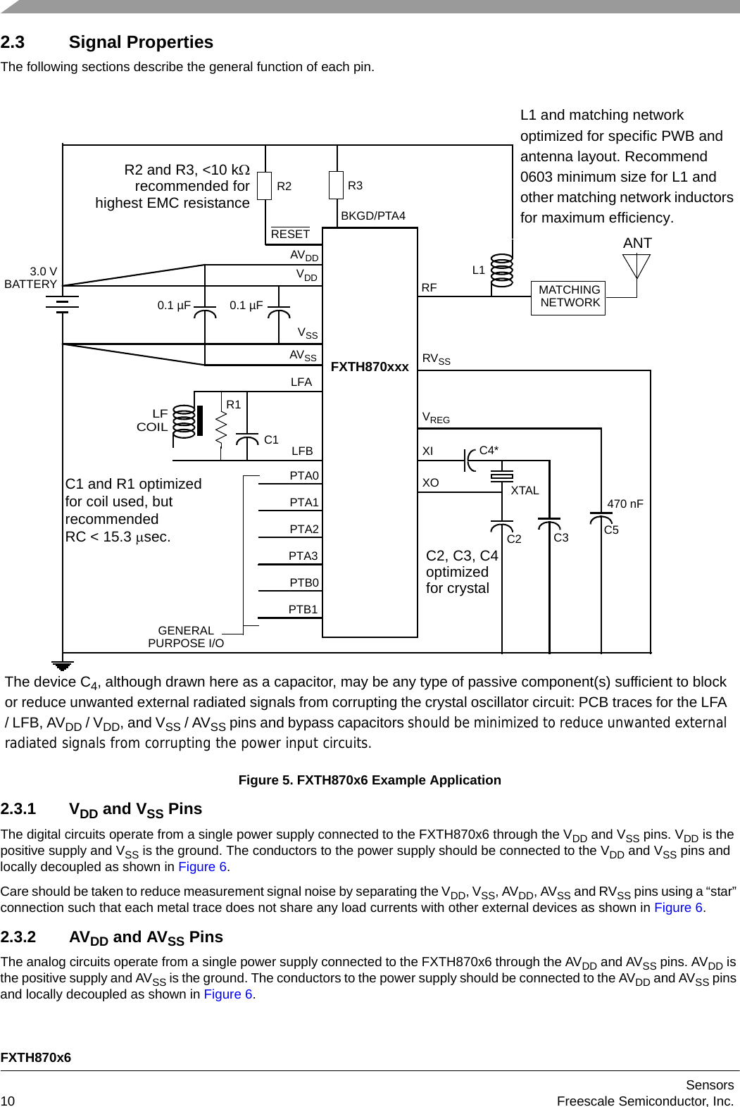
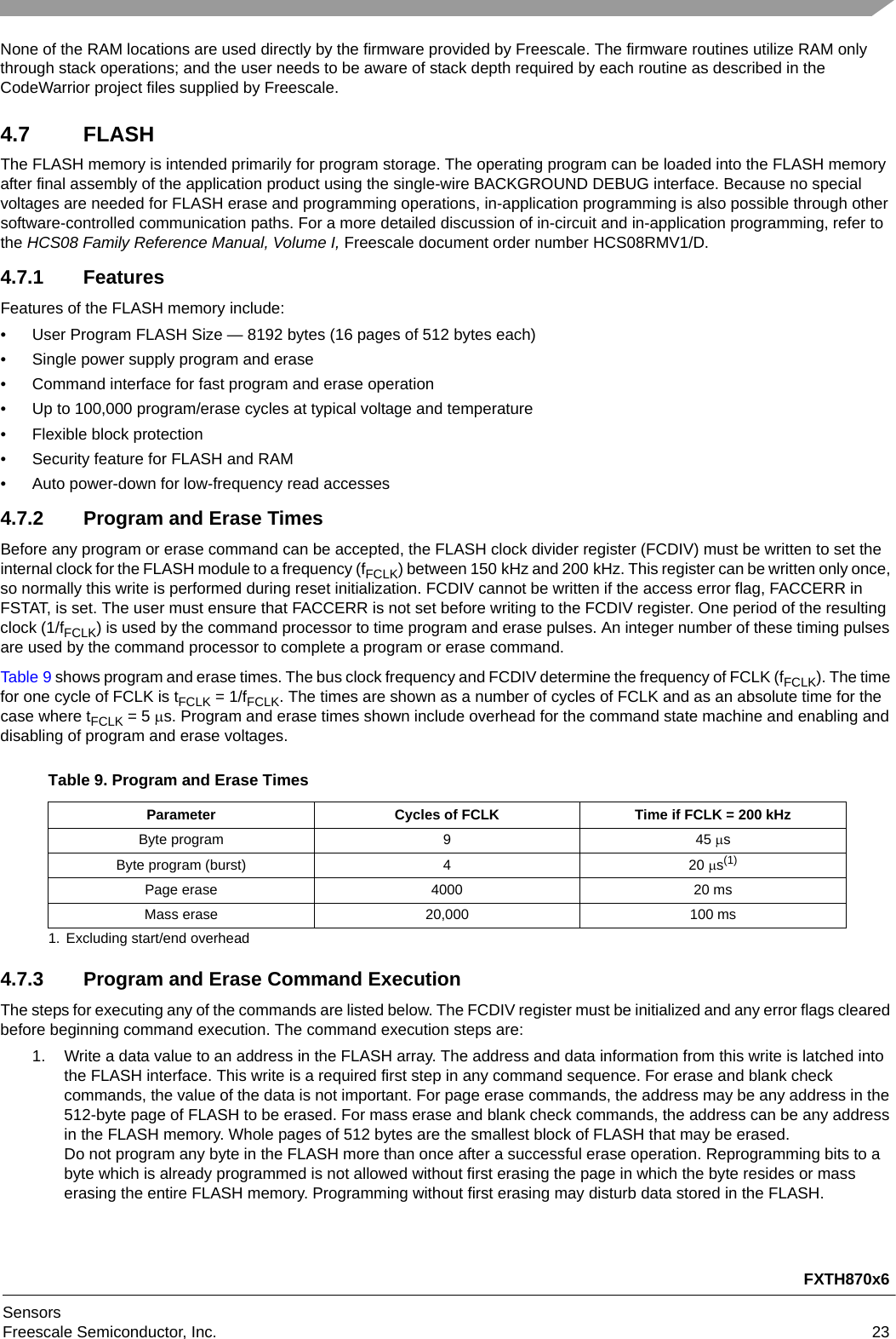
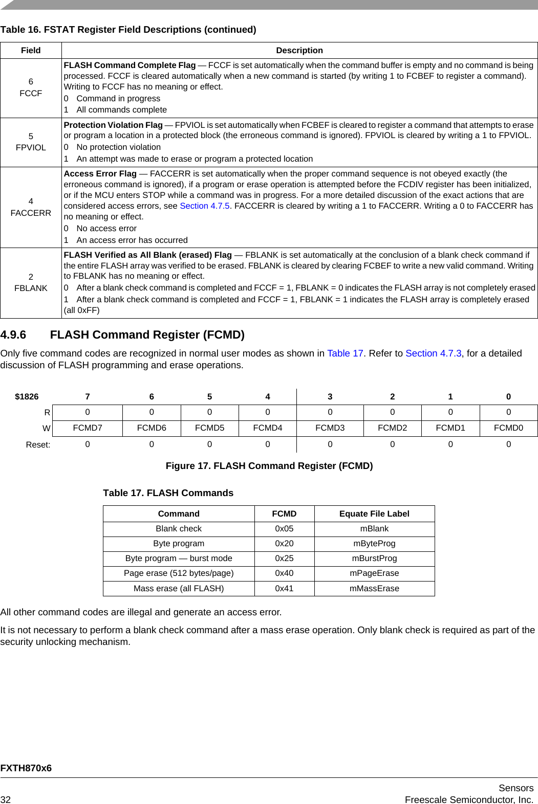
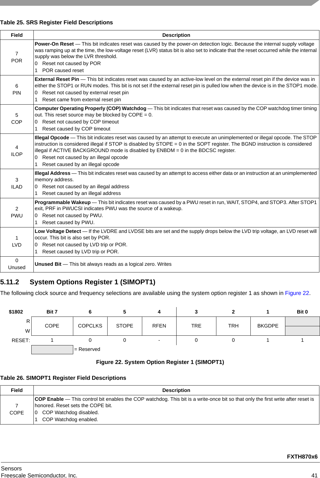
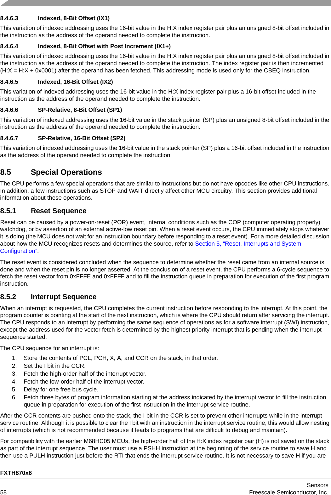
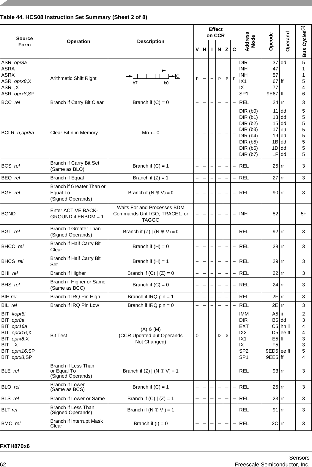
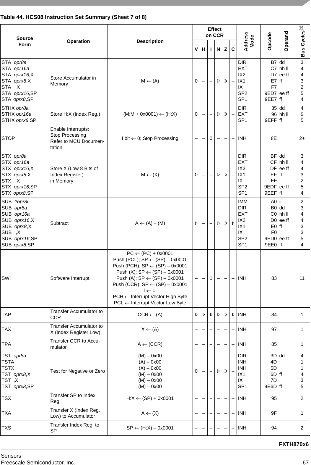
![FXTH870x6SensorsFreescale Semiconductor, Inc. 92 Pins and ConnectionsThis section describes the pin layout and general function of each pin.2.1 Package PinoutThe pinout for the FXTH870x6 device QFN package is shown in Figure 3 for the orientation of the pressure port up. The orientation of the internal Z-axis accelerometer is shown in Figure 4.Figure 3. FXTH870x6 QFN Package PinoutFigure 4. FXTH870x6 QFN Optional Z-axis Accelerometer Orientation2.2 Recommended ApplicationExample of a simple OOK/FSK tire pressure monitors using the internal PLL-based RF output stage is shown in Figure 5. Any of the PTA[3:0] pins can also be used as general purpose I/O pins. Any of the PTA[3:0] pins that are not used in the application should be handled as described in Section 6.1.202122232418 PTA3LFALFBBKGD/PTA4X0X11719234567PTB1PTA2PTA181RESET101112131415VDDVDDAVSSAVREGRF169PTB0N/CN/CN/CN/CN/CID Featureon top lidPTA0VSSRFVSSN/C = No Connect: Do not connect PCB pads to signal traces, power/ground or multi-layer via.Top ViewBKGD/PTA4X-AXISORIENTATION+X-XY-AXISORIENTATION+Y-YSide ViewPressurePortPOSITIVE ACCELERATION MOVES MASSIN +Z DIRECTION (VALUE INCREASES)Z-AXISORIENTATION+Z-Z](https://usermanual.wiki/Continental-Automotive/TIS-03/User-Guide-2718164-Page-13.png)
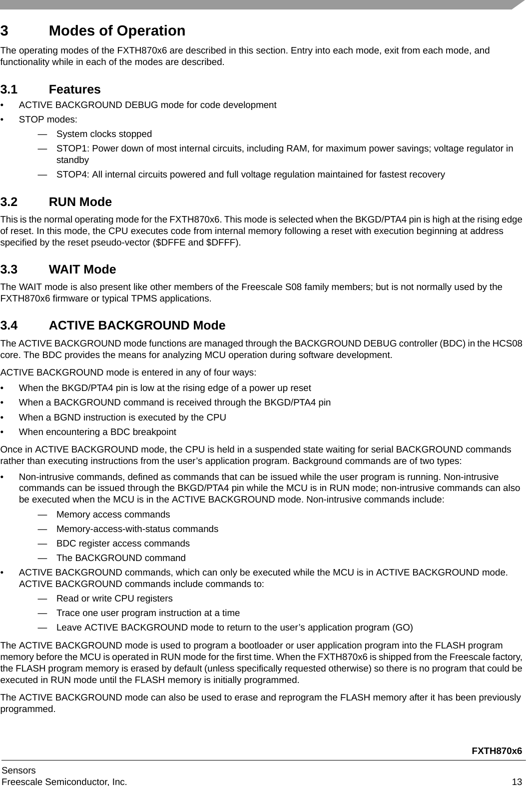
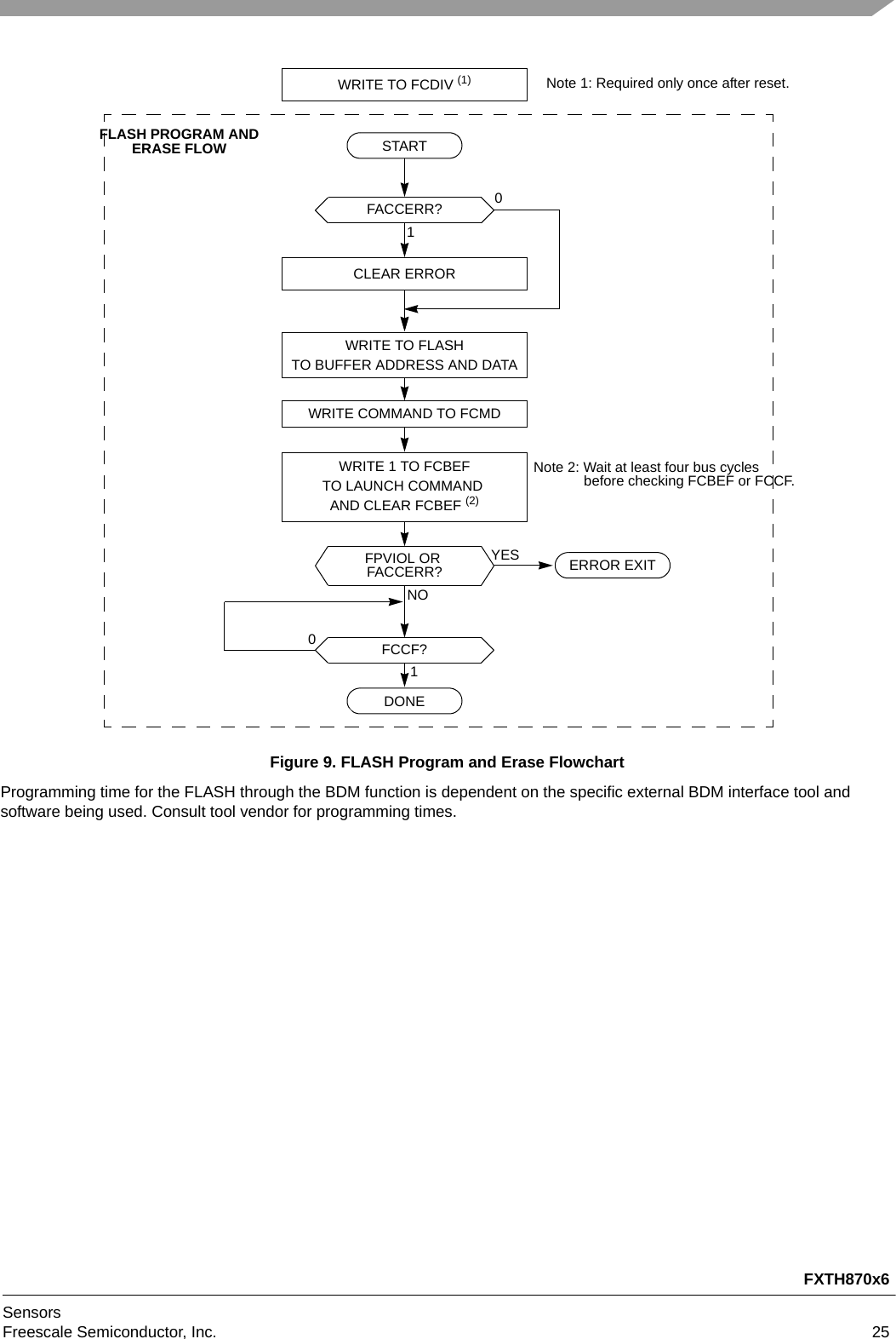
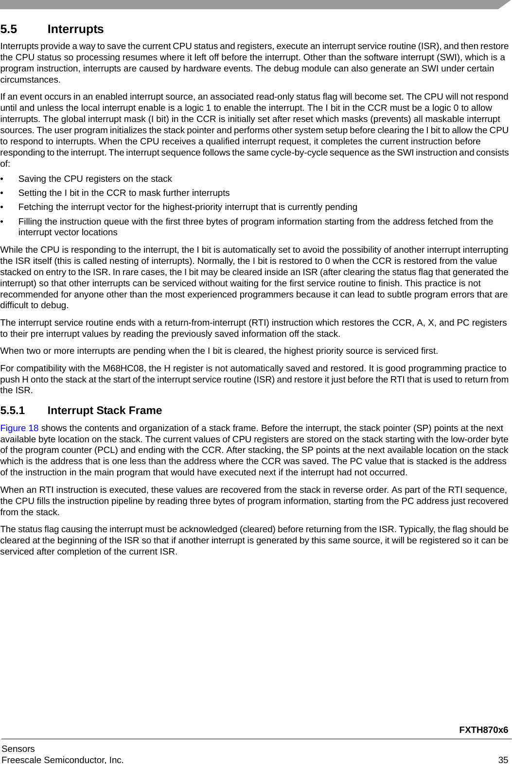
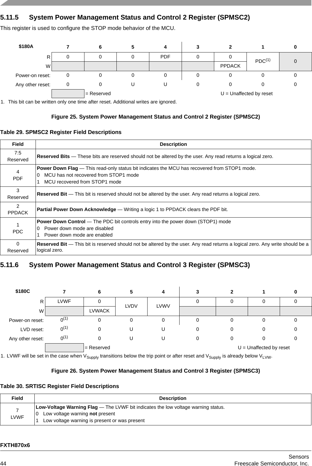
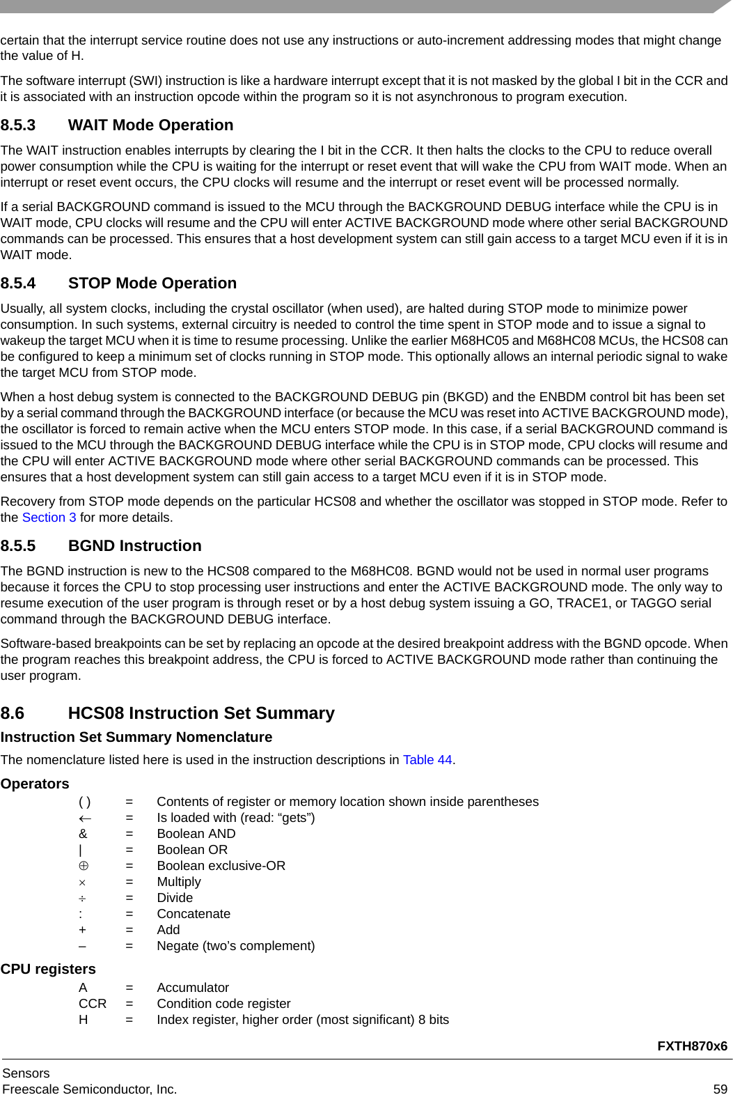
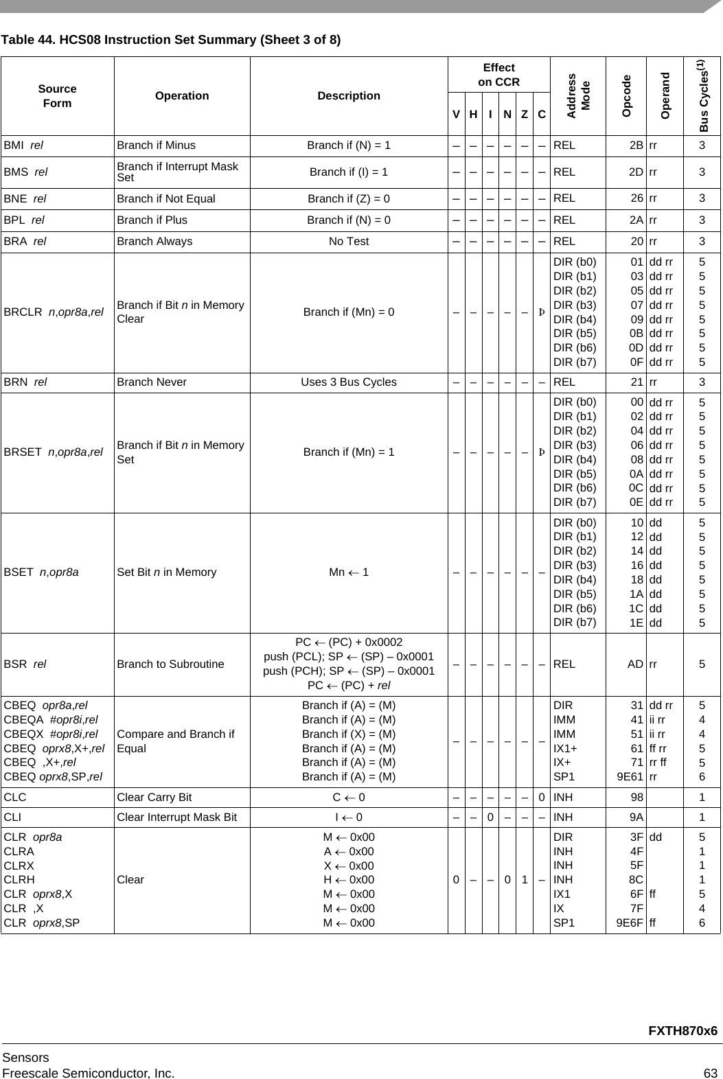
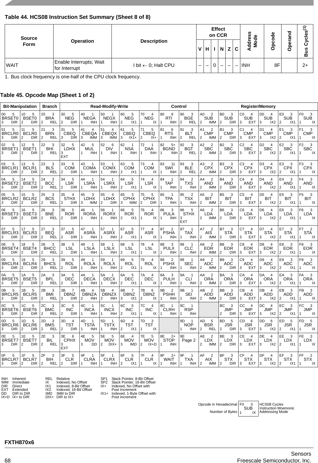
![FXTH870x6SensorsFreescale Semiconductor, Inc. 11Care should be taken to reduce measurement signal noise by separating the VDD, VSS, AVDD, AVSS and RVSS pins using a “star” connection such that each metal trace does not share any load currents with other external devices as shown in Figure 6.Figure 6. Recommended Power Supply Connections2.3.3 VREG PinThe internal regulator for the analog circuits requires an external stabilization capacitor to AVSS.2.3.4 RVSS PinPower in the RF output amplifier is returned to the supply through the RVSS pin. This conductor should be connected to the power supply as shown in Figure 6 using a “star” connection such that each metal trace does not share any load currents with other supply pins.2.3.5 RF PinThe RF pin is the RF energy data supplied by the FXTH870x6 to an external antenna.2.3.6 XO, XI PinsThe XO and XI pins are for an external crystal to be used by the internal PLL for creating the carrier frequencies and data rates for the RF pin.2.3.7 LF[A:B] PinsThe LF[A:B] pins can be used by the LF receiver (LFR) as one differential input channel for sensing low level signals from an external low frequency (LF) coil. The external LF coil should be connected between the LFA and the LFB pins.Signaling into the LFR pins can place the FXTH870x6 into various diagnostic or operational modes. The LFR is comprised of the detector and the decoder.Each LF[A:B] pin will always have an impedance of approximately 500 k to VSS due to the LFR input circuitry. The LFA/LFB pins are used by the LFR when the LFEN control bit is set and are not functional when the LFEN control bit is clear.2.3.8 PTA[1:0] PinsThe PTA[1:0] pins are general purpose I/O pins. These two pins can be configured as normal bidirectional I/O pins with programmable pullup or pulldown devices and/or wakeup interrupt capability; or one or both can be connected to the two input channels of the A/D converter module. The pulldown devices can only be activated if the wakeup interrupt capability is enabled. User software must configure the general purpose I/O pins so that they do not result in “floating” inputs as described in Section 6.1. PTA[1:02] map to keyboard Interrupt function bits [1:0].0.1 µFFXTH870xxxVDDVSSto otherBatteryIDD ILOADBypass capacitorsclosely coupled to the package pinsFXTH870xxx and Other Load Currents star connected to battery terminalsloads0.1 µFAVDDAVSSRVSSThe decoupling devices, although drawn here as 0.1 F capacitors, may be any type of passive component(s)sufficient to block or reduce unwantedexternal radiated signals from corruptingthe power input protection circuits; application tuning may be required.](https://usermanual.wiki/Continental-Automotive/TIS-03/User-Guide-2718164-Page-15.png)
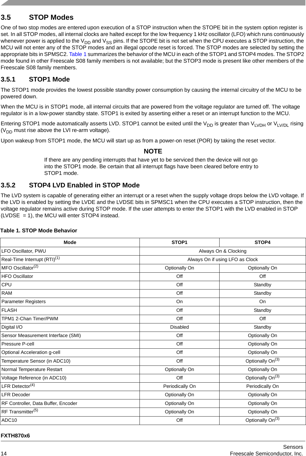
![FXTH870x6Sensors12 Freescale Semiconductor, Inc.2.3.9 PTA[3:2] PinsThe PTA[3:2] pins are general purpose I/O pin. These two pins can be configured as normal bidirectional I/O pin with programmable pullup or pulldown devices and/or wakeup interrupt capability; or one or both can be connected to the two input channels of the Timer Pulse Width (TPM1) module. The pulldown devices can only be activated if the wakeup interrupt capability is enabled. User software must configure the general purpose I/O pins so that they do not result in “floating” inputs as described in Section 6.1. PTA[3:2] map to keyboard Interrupt function bits [3:2].2.3.10 BKGD/PTA4 PinThe BKGD/PTA4 pin is used to place the FXTH870x6 in the BACKGROUND DEBUG mode (BDM) to evaluate MCU code and to also transfer data to/from the internal memories. If the BKGD/PTA4 pin is held low when the FXTH870x6 comes out of a power-on reset the device will go into the ACTIVE BACKGROUND DEBUG mode (BDM).The BKGD/PTA4 pin has an internal pullup device and can connected to VDD in the application unless there is a need to enter BDM operation after the device as been soldered into the PWB. If in-circuit BDM is desired the BKGD/PTA4 pin can be left unconnected, but should be connected to VDD through a low impedance resistor (< 10 k) which can be over-driven by an external signal. This low impedance resistor reduces the possibility of getting into the debug mode in the application due to an EMC event.2.3.11 RESET PinThe RESET pin is used for test and establishing the BDM condition and providing the programming voltage source to the internal FLASH memory. This pin can also be used to direct to the MCU to the reset vector as described in Section 5.2.The RESET pin has an internal pullup device and can connected to VDD in the application unless there is a need to enter BDM operation after the device as been soldered to the PWB. If in-circuit BDM is desired the RESET pin can be left unconnected; but should be connected to VDD through a low impedance resistor (< 10 k) which can be over-driven by an external signal. This low impedance resistor reduces the possibility of getting into the debug mode in the application due to an EMC event.Activation of the external reset function occurs when the voltage on the RESET pin goes below 0.3 x VDD for at least 100 nsec before rising above 0.7 x VDD as shown in Figure 7.Figure 7. RESET Pin Timing2.3.12 PTB[1:0] PinsThe PTB[1:0] pins are general purpose I/O pins. These two pins can be configured as nominal bidirectional I/O pins with programmable pullup. User software must configure the general purpose I/O pins so that they do not result in “floating” inputs as described in Section 6.1RESET0.7 VDD0.3 VDD> 100 nsecResetInitiated](https://usermanual.wiki/Continental-Automotive/TIS-03/User-Guide-2718164-Page-16.png)
![FXTH870x6Sensors18 Freescale Semiconductor, Inc.4.3 MCU Register Addresses and Bit AssignmentsThe registers in the FXTH870x6 are divided into these four groups:• Direct-page registers are located in the first 80 locations in the memory map; these are accessible with efficient direct addressing mode instructions.• The parameter registers begin at address $0050; these are also accessible with efficient direct addressing mode instructions.• High-page registers are used less often, so they are located above $1800 in the memory map. This leaves more room in the direct page for more frequently used registers and variables.• The nonvolatile register area consists of a block of 16 locations in FLASH memory at $FFB0:FFBF. Nonvolatile register locations include:— Three values that are loaded into working registers at reset— An 8-byte back door comparison key that optionally allows the user to gain controlled access to secure memory.Because the nonvolatile register locations are FLASH memory, they must be erased and programmed like other FLASH memory locations.Direct page registers are located within the first 256 locations in the memory map, so they are accessible with efficient direct addressing mode instructions, which requires only the lower byte of the address. Bit manipulation instructions can be used to access any bit in any direct-page register. Table 3 is a summary of all user-accessible direct-page registers and control bits. Those related to the TPMS application and modules are described in detail in this specification.The register names in column two of the following tables are shown in bold to set them apart from the bit names to the right. Cells that are not associated with named bits are shaded. A shaded cell with a 0 indicates this unused bit always reads as a 0. Shaded cells with dashes indicate unused or reserved bit locations that could read as 1s or 0s.$DFEE:DFEF Vsm SMI$DFF0:DFF1 Vtpm1ovf TPM1$DFF2:DFF3 Vtpm1ch1 TPM1$DFF4:DFF5 Vtpm1ch0 TPM1$DFF6:DFF7 Vwuktmr PWU$DFF8:DFF9 Vlvd Sys Ctrl - LVD$DFFA:DFFB Reserved$DFFC:DFFD Vswi SWI opcode$DFFE:DFFF Vreset Sys Ctrl - POR, PRF, COP, LVDTemp Restart, Illegal opcode or addressTable 3. MCU Direct Page Register SummaryAddressRegister NameBit 7654321Bit 0$0000 PTAD PTAD[4:0]$0001 PTAPE PTAPE[3:0]$0002 Reserved$0003 PTADD PTADD[3:0]$0004 PTBD PTBD[1:0]$0005 PTBPE PTBPE[1:0]$0006 Reserved$0007 PTBDD PTBDD[1:0]$0008 Reserved$0009 Reserved$000A Reserved$000B Reserved$000C KBISC 0000 KBF KBACK KBIE KBIMODTable 2. Vector Summary (continued)User Vector Addr Vector Name Module Source](https://usermanual.wiki/Continental-Automotive/TIS-03/User-Guide-2718164-Page-22.png)
![FXTH870x6SensorsFreescale Semiconductor, Inc. 19$000D KBIPE KBIPE[3:0]$000E KBIES KBEDG[3:0]$000F Reserved$0010 TPM1SC TOF TOIE CPWMS CLKSB CLKSA PS2 PS1 PS0$0011 TPM1CNTH Bit [15:8]$0012 TPM1CNTL Bit [7:0]$0013 TPM1MODH Bit [15:8]$0014 TPM1MODL Bit [7:0]$0015 TPM1C0SC CH0F CH0IE MS0B MS0A ELS0B ELS0A 0 0$0016 TPM1C0VH Bit [15:8]$0017 TPM1C0VL Bit [7:0]$0018 TPM1C1SC CH1F CH1IE MS1B MS1A ELS1B ELS1A 0 0$0019 TPM1C1VH Bit [15:8]$001A TPM1C1VL Bit [7:0]$001B Reserved$001C PWUDIV WDIV[5:0]$001D PWUCS0 WUF WUFAK WUT[5:0]$001E PWUCS1 PRF PRFAK PRST[5:0]$001F PWUS PSEL 0 CSTAT[5:0]$0020-27 LFR Registers LFR Registers, see Table 4 and Ta ble 5$0028 ADSC1 COCO AIEN ADCO ADCH[4:0]$0029 ADSC2 ADACT ADTRG ACFE ADCFGT 0 0 0 0$002A ADRH 0000 ADR[11:8]$002B ADRL ADR[7:0]$002C ADCVH 0000 ADCV[11:8]$002D ADCVL ADCV[7:0]$002E ADCFG ADLPC ADIV[1:0] ADLSMP MODE[1:0] ADICLK[1:0]$002F ADPCTL1 ADPC[7:0]$0030-4F RFM Registers RFM Registers, see Table 6 and Table 7$0050-8F Parameter Reg PARAM[63:0]Note: Shaded bits are recommended to only be controlled by firmware or factory test.Table 4. LFR Register Summary - LPAGE = 0AddressRegister NameBit 7654321Bit 0$0020 LFCTL1 LFEN SRES CARMOD LPAGE IDSEL[1:0] SENS[1:0]$0021 LFCTL2 LFSTM[3:0] LFONTM[3:0]$0022 LFCTL3 LFDO TOGMOD SYNC[1:0] LFCDTM[3:0]$0023 LFCTL4 LFDRIE LFERIE LFCDIE LFIDIE DECEN VALEN TIMOUT[1:0]$0024 LFS LFDRF LFERF LFCDF LFIDF LFOVF LFEOMF LPSM LFIAK$0025 LFDATA RXDATA[7:0]$0026 LFIDL ID[7:0]$0027 LFIDH ID[15:8]Table 3. MCU Direct Page Register Summary (continued)AddressRegister NameBit 7654321Bit 0](https://usermanual.wiki/Continental-Automotive/TIS-03/User-Guide-2718164-Page-23.png)
![FXTH870x6Sensors20 Freescale Semiconductor, Inc.Table 5. LFR Register Summary - LPAGE = 1AddressRegister NameBit 7654321Bit 0$0020 LFCTL1 LFEN SRES CARMOD LPAGE IDSEL[1:0] SENS[1:0]$0021 LFCTRLE TRIMEE AZSC[2:0]$0022 LFCTRLD AVFOF[1:0} DEQS AZDC[1:0] ONMODE CHK125[1:0]$0023 LFCTRLC AMPGAIN[1:0] FINSEL[1:0] AZEN LOWQ[1:0] DEQEN$0024 LFCTRLB HYST[1:0] LFFAF LFCAF LFPOL LFCPTAZ[2:0]$0025 LFCTRLA TESTSEL[3:0] LFCC[3:0]$0026 Reserved$0027 ReservedNote: Shaded bits are recommended to only be controlled by firmware or factory test.Table 6. RFM Register Summary - RPAGE = 0AddressRegister NameBit 7654321Bit 0$0030 RFCR0 BPS[7:0]$0031 RFCR1 FRM[7:0]$0032 RFCR2 SEND RPAGE EOM PWR[4:0]$0033 RFCR3 DATA IFPD ISPC IFID FNUM[3:0]$0034 RFCR4 RFBT[7:0]$0035 RFCR5 BOOST LFSR[6:0]$0036 RFCR6 VCO_GAIN[1:0] RFFT[5:0]$0037 RFCR7 RFIF RFEF RFVF RFIAK RFIEN RFLVDEN RCTS RFMRST$0038 PLLCR0 AFREQ[12:5]$0039 PLLCR1 AFREQ[4:0] POL CODE[1:0]$003A PLLCR2 BFREQ[12:5]$003B PLLCR3 BFREQ[4:0] CF MOD CKREF$003C RFD0 RFD[7:0]$003D RFD1 RFD[15:8]$003E RFD2 RFD[23:16]$003F RFD3 RFD[31:24]$0040 RFD4 RFD[39:32]$0041 RFD5 RFD[47:40]$0042 RFD6 RFD[55:48]$0043 RFD7 RFD[63:56]$0044 RFD8 RFD[71:64]]$0045 RFD9 RFD[79:72]$0046 RFD10 RFD[87:80]$0047 RFD11 RFD[95:88]$0048 RFD12 RFD[103:96] $0049 RFD13 RFD[111:104]$004A RFD14 RFD[119:112]$004B RFD15 RFD[127:120]$004C Reserved$004D Reserved$004E Reserved$004F ReservedNote: Shaded bits are recommended to only be controlled by firmware or factory test.](https://usermanual.wiki/Continental-Automotive/TIS-03/User-Guide-2718164-Page-24.png)
![FXTH870x6SensorsFreescale Semiconductor, Inc. 21Table 7. RFM Register Summary - RPAGE = 1AddressRegister NameBit 7654321Bit 0$0030 RFCR0 BPS[7:0]$0031 RFCR1 FRM[7:0]$0032 RFCR2 SEND RPAGE EOM PWR[4:0]$0033 RFCR3 DATA IFPD ISPC IFID FNUM[3:0]$0034 RFCR4 RFBT[7:0]$0035 RFCR5 BOOST LFSR[6:0]$0036 RFCR6 VCO_GAIN[1:0] RFFT[5:0]$0037 RFCR7 RFIF RFEF RFVF RFIAK RFIEN RFLVDEN RCTS RFMRST$0038 EPR —/VCD3 PLL_LPF_[2:0]/VCD[2:0] PA_SLOPE VCD_EN$0039 Reserved$003A Reserved$003B Reserved$003C RFD0 RFD[135:128]$003D RFD1 RFD[143:136]$003E RFD2 RFD[151:144]$003F RFD3 RFD[159:152]$0040 RFD4 RFD[167:160]$0041 RFD5 RFD[175:168]$0042 RFD6 RFD[183:176]$0043 RFD7 RFD[191:184]$0044 RFD8 RFD[199:192]$0045 RFD9 RFD[207:200]$0046 RFD10 RFD[215:208]$0047 RFD11 RFD[223:216]$0048 RFD12 RFD[231:224]$0049 RFD13 RFD[239:232]$004A RFD14 RFD[247:240]$004B RFD15 RFD[255:248]$004C Reserved$004D Reserved$004E Reserved$004F ReservedNote: Shaded bits are recommended to only be controlled by firmware or factory test.](https://usermanual.wiki/Continental-Automotive/TIS-03/User-Guide-2718164-Page-25.png)
![FXTH870x6Sensors22 Freescale Semiconductor, Inc.4.4 High Address RegistersHigh-page registers are used much less often, so they are located above $1800 in the memory map. This leaves more room in the direct page for more frequently used registers and variables. The registers control system level features as given in Table 8.4.5 MCU Parameter RegistersThe 64 bytes of parameter registers are located at addresses $0050 through $008F. These registers are powered up at all times and may be used to store temporary or history data during the times that the MCU is in any of the STOP modes. The parameter register at $008F is used by the firmware for interrupt flags.4.6 MCU RAMThe FXTH870x6 includes static RAM. The locations in RAM below $0100 can be accessed using the more efficient direct addressing mode, and any single bit in this area can be accessed with the bit-manipulation instructions (BCLR, BSET, BRCLR, and BRSET). Locating the most frequently accessed program variables in this area of RAM is preferred.The RAM retains data when the MCU is in low-power WAIT, STOP3 or STOP4 modes. At power-on or after wakeup from STOP1, the contents of RAM are not initialized. RAM data is unaffected by any reset provided that the supply voltage does not drop below the minimum value for RAM retention (VRAM).When security is enabled, the RAM is considered a secure memory resource and is not accessible through BDM or through code executing from non-secure memory. See Section 4.8 for a detailed description of the security feature.Table 8. MCU High Address Register SummaryAddressRegister NameBit 7654321Bit 0$1800 SRS POR PIN COP ILOP ILAD PWU LVD 0$1801 SBDFR 0000000BDFR$1802 SIMOPT1 COPE COPCLKS STOPE RFEN TRE TRH BKGDPE 1$1803 SIMOPT2 0 COPT[2:0] LFOSEL TCLKDIV BUSCLKS[1:0]$1804 Reserved$1805 Reserved$1806 SDIDH REV[3:0] ID[11:8]$1807 SDIDL ID[7:0]$1808 SRTISC RTIF RTIACK RTICLKS RTIE 0RTIS{2:0]$1809 SPMSC1 LVDF LVDACK LVDIE LVDRE LVDSE LVDE 0BGBE$180A SPMSC2 000PDF0 PPDACK PDC 0$180B Reserved$180C SPMSC3 LVWF LVWACK LVDV LVWV 0000$180D SIMSES KBF IRQF TRF PWUF LFF RFF$180E SOTRM SOTRM[7:0]$180F SIMTST TRH[2:0] TRO$1810-1F Reserved$1820 FCDIV DIVLD PRDIV8 DIV[5:0]$1821 FOPT KEYEN FNORED 0000 SEC0[1:0}$1822 Reserved$1823 FCNFG 00 KEYACC 00000$1824 FPROT FPS[7:1] FPDIS$1825 FSTAT FCBEF FCCF FPVIOL FACCERR 0 FBLANK 0 0$1826 FCMD FERASE FCMD[6:0]$1827-3F ReservedNote: Reserved bits shown as 0 must always be written to 0.Reserved bits shown as 1 must always be written to 1.Shaded bits are recommended to only be controlled by firmware or factory test.](https://usermanual.wiki/Continental-Automotive/TIS-03/User-Guide-2718164-Page-26.png)

![FXTH870x6Sensors28 Freescale Semiconductor, Inc.4.8 SecurityThe FXTH870x6 includes circuitry to prevent unauthorized access to the contents of FLASH and RAM memory. When security is engaged, FLASH and RAM are considered secure resources. Direct-page registers, high-page registers, and the BACKGROUND DEBUG controller are considered unsecured resources. Programs executing within secure memory have normal access to any MCU memory locations and resources. Attempts to access a secure memory location with a program executing from an unsecured memory space or through the BACKGROUND DEBUG interface are blocked (writes are ignored and reads return all 0s).Security is engaged or disengaged based on the state of two nonvolatile register bits (SEC0[1:0]) in the FOPT register. During reset, the contents of the nonvolatile location NVOPT are copied from FLASH into the working FOPT register in high-page register space. A user engages security by programming the NVOPT location, which can be done at the same time the FLASH memory is programmed. The 1:0 state disengages security and the other three combinations engage security. Notice the erased state (1:1) makes the MCU secure. During development, whenever the FLASH is erased, it is good practice to immediately program the SEC00 bit to 0 in NVOPT so SEC[1:0] = 1:0. This would allow the MCU to remain unsecured after a subsequent reset.The on-chip debug module cannot be enabled while the MCU is secure. The separate BACKGROUND DEBUG controller can still be used for background memory access commands, but the MCU cannot enter ACTIVE BACKGROUND mode except by holding BKGD/MS low at the rising edge of reset.A user can choose to allow or disallow a security unlocking mechanism through an 8-byte backdoor security key. If the nonvolatile KEYEN bit in NVOPT/FOPT is 0, the backdoor key is disabled and there is no way to disengage security without completely erasing all FLASH locations. If KEYEN is 1, a secure user program can temporarily disengage security by:1. Writing 1 to KEYACC in the FCNFG register. This makes the FLASH module interpret writes to the backdoor comparison key locations (NVBACKKEY through NVBACKKEY+7) as values to be compared against the key rather than as the first step in a FLASH program or erase command.2. Writing the user-entered key values to the NVBACKKEY through NVBACKKEY+7 locations. These writes must be done in order starting with the value for NVBACKKEY and ending with NVBACKKEY+7. STHX must not be used for these writes because these writes cannot be done on adjacent bus cycles. User software normally would get the key codes from outside the MCU system through a communication interface such as a serial I/O.3. Writing 0 to KEYACC in the FCNFG register. If the 8-byte key that was just written matches the key stored in the FLASH locations, SEC[1:0] are automatically changed to 1:0 and security will be disengaged until the next reset.The security key can be written only from secure memory (either RAM or FLASH), so it cannot be entered through BACKGROUND commands without the cooperation of a secure user program.The backdoor comparison key (NVBACKKEY through NVBACKKEY+7) is located in FLASH memory locations in the nonvolatile register space so users can program these locations exactly as they would program any other FLASH memory location. The nonvolatile registers are in the same 512-byte block of FLASH as the reset and interrupt vectors, so block protecting that space also block protects the backdoor comparison key. Block protects cannot be changed from user application programs, so if the vector space is block protected, the backdoor security key mechanism cannot permanently change the block protect, security settings, or the backdoor key.Security can always be disengaged through the BACKGROUND DEBUG interface by taking these steps:1. Disable any block protections by writing FPROT. FPROT can be written only with BACKGROUND DEBUG commands, not from application software.2. Mass erase FLASH if necessary.3. Blank check FLASH. Provided FLASH is completely erased, security is disengaged until the next reset.To avoid returning to secure mode after the next reset, program NVOPT so SEC[1:0] = 1:0.NOTEEnabling the security feature disables Freescale ability to perform failure analysis without first completely erasing all flash memory contents. If the security feature is implemented, customer shall be responsible for providing to Freescale unsecured parts for any failure analysis to begin or supplying the entire contents of the device flash memory data as part of the return process, to allow Freescale to erase and subsequently restore the device to its original condition.](https://usermanual.wiki/Continental-Automotive/TIS-03/User-Guide-2718164-Page-32.png)
![FXTH870x6SensorsFreescale Semiconductor, Inc. 294.9 FLASH Registers and Control BitsThe FLASH module has nine 8-bit registers in the high-page register space, three locations in the nonvolatile register space in FLASH memory which are copied into three corresponding high-page control registers at reset. There is also an 8-byte comparison key in FLASH memory. Refer to Table 8 and Table 9 for the absolute address assignments for all FLASH registers. This section refers to registers and control bits only by their names. A Freescale Semiconductor-provided equate or header file normally is used to translate these names into the appropriate absolute addresses.4.9.1 FLASH Clock Divider Register (FCDIV)Bit 7 of this register is a read-only status flag. Bits 6 through 0 can be read at any time but can be written only once. Before any erase or programming operations are possible, write to this register to set the frequency of the clock for the nonvolatile memory system within acceptable limits.$1820 7 6 5 4 3 2 1 0RDIVLD PRDIV8 DIV5 DIV4 DIV3 DIV2 DIV1 DIV0WReset: 0 0000000= ReservedFigure 12. FLASH Clock Divider Register (FCDIV)Table 10. FCDIV Register Field DescriptionsField Description7DIVLDDivisor Loaded Status Flag — When set, this read-only status flag indicates that the FCDIV register has been written since reset. Reset clears this bit and the first write to this register causes this bit to become set regardless of the data written.0 FCDIV has not been written since reset; erase and program operations disabled for FLASH1 FCDIV has been written since reset; erase and program operations enabled for FLASH6PRDIV8Prescale (Divide) FLASH Clock by 80 Clock input to the FLASH clock divider is the bus rate clock1 Clock input to the FLASH clock divider is the bus rate clock divided by 85:0DIV[5:0]Divisor for FLASH Clock Divider — The FLASH clock divider divides the bus rate clock (or the bus rate clock divided by 8 if PRDIV8 = 1) by the value in the 6-bit DIV5:DIV0 field plus one. The resulting frequency of the internal FLASH clock must fall within the range of 200 kHz to 150 kHz for proper FLASH operations. Program/Erase timing pulses are one cycle of this internal FLASH clock which corresponds to a range of 5 s to 6.7 s. The automated programming logic uses an integer number of these pulses to complete an erase or program operation.• if PRDIV8 = 0 — fFCLK = fBus ([DIV5:DIV0] + 1)• if PRDIV8 = 1 — fFCLK = fBus (8 ([DIV5:DIV0] + 1))Table 11 shows the appropriate values for PRDIV8 and DIV5:DIV0 for selected bus frequencies.Table 11. FLASH Clock Divider SettingsfBus PRDIV8(Binary) DIV5:DIV0(Decimal) fFCLK Program/Erase Timing Pulse(5 s Min, 6.7s Max)20 MHz 1 12 192.3 kHz 5.2 s10 MHz 0 49 200 kHz 5 s8 MHz 0 39 200 kHz 5 s4 MHz 0 19 200 kHz 5 s2 MHz 0 9 200 kHz 5 s1 MHz 0 4 200 kHz 5 s200 kHz 0 0 200 kHz 5 s150 kHz 0 0 150 kHz 6.7 s](https://usermanual.wiki/Continental-Automotive/TIS-03/User-Guide-2718164-Page-33.png)
![FXTH870x6Sensors30 Freescale Semiconductor, Inc.4.9.2 FLASH Options Register (FOPT and NVOPT)During reset, the contents of the nonvolatile location NVOPT are copied from FLASH into FOPT. Bits 5 through 2 are not used and always read 0. This register may be read at any time, but writes have no meaning or effect. To change the value in this register, erase and reprogram the NVOPT location in FLASH memory as usual and then issue a new MCU reset.4.9.3 FLASH Configuration Register (FCNFG)Bits 7 through 5 can be read or written at any time. Bits 4 through 0 always read 0 and cannot be written.$1821 7 6 5 4 3 2 1 0RKEYEN FNORED 0 0 0 0 SEC01 SEC00WReset: This register is loaded from nonvolatile location NVOPT during reset.= ReservedFigure 13. FLASH Options Register (FOPT)Table 12. FOPT Register Field DescriptionsField Description7KEYENBackdoor Key Mechanism Enable — When this bit is 0, the backdoor key mechanism cannot be used to disengage security. The backdoor key mechanism is accessible only from user (secured) firmware. BDM commands cannot be used to write key comparison values that would unlock the backdoor key. For more detailed information about the backdoor key mechanism, refer to Section 4.8.”0 No backdoor key access allowed1 If user firmware writes an 8-byte value that matches the nonvolatile backdoor key (NVBACKKEY through NVBACKKEY+7 in that order), security is temporarily disengaged until the next MCU reset6FNOREDVector Redirection Disable — When this bit is 1, then vector redirection is disabled.0 Vector redirection enabled1 Vector redirection disabled1:0SEC0[1:0]Security State Code — This 2-bit field determines the security state of the MCU as shown in Table 13. When the MCU is secure, the contents of RAM and FLASH memory cannot be accessed by instructions from any unsecured source including the BACKGROUND DEBUG interface. For more detailed information about security, refer to Section 4.8. SEC01:SEC00 changes to 1:0 after successful backdoor key entry or a successful blank check of FLASH.Table 13. Security StatesSEC01:SEC00 Description0:0 secure0:1 secure1:0 unsecured1:1 secure$1823 7 6 5 4 3 2 1 0R00KEYACC 00000WReset: 0 000 0 000= ReservedFigure 14. FLASH Configuration Register (FCNFG)](https://usermanual.wiki/Continental-Automotive/TIS-03/User-Guide-2718164-Page-34.png)
![FXTH870x6SensorsFreescale Semiconductor, Inc. 314.9.4 FLASH Protection Register (FPROT and NVPROT)During reset, the contents of the nonvolatile location NVPROT is copied from FLASH into FPROT. Bits 0, 1, and 2 are not used and each always reads as 0. This register can be read at any time, but user program writes have no meaning or effect. BACKGROUND DEBUG commands can write to FPROT.Figure 15. FLASH Protection Register (FPROT)4.9.5 FLASH Status Register (FSTAT)Bits 3, 1, and 0 always read 0 and writes have no meaning or effect. The remaining five bits are status bits that can be read at any time. Writes to these bits have special meanings that are discussed in the bit descriptions.Table 14. FCNFG Register Field DescriptionsField Description5KEYACCEnable Writing of Access Key — This bit enables writing of the backdoor comparison key. For more detailed information about the backdoor key mechanism, refer to Section 4.8.0 Writes to 0xFFB0–0xFFB7 are interpreted as the start of a FLASH programming or erase command1 Writes to NVBACKKEY (0xFFB0–0xFFB7) are interpreted as comparison key writes$1824 7 6 5 4 3 2 1 0RFPS7 FPS6 FPS5 FPS4 FPS3 FPS2 FPS1 FPDISW(1)1. Background commands can be used to change the contents of these bits in FPROT.(1) (1) (1) (1) (1) (1) (1)Reset: This register is loaded from nonvolatile location NVPROT during reset.Table 15. FPROT Register Field DescriptionsField Description7:1FPS[7:1]FLASH Protect Select Bits — When FPDIS = 0, this 7-bit field determines the ending address of unprotected FLASH locations at the high address end of the FLASH. Protected FLASH locations cannot be erased or programmed.0FPDISFLASH Protection Disable0 FLASH block specified by FPS[7:1] is block protected (program and erase not allowed)1 No FLASH block is protected$1825 7 6 5 4 3 2 1 0RFCBEF FCCF FPVIOL FACCERR 0 FBLANK 0 0WReset: 1 1000000= ReservedFigure 16. FLASH Status Register (FSTAT)Table 16. FSTAT Register Field DescriptionsField Description7FCBEFFLASH Command Buffer Empty Flag — The FCBEF bit is used to launch commands. It also indicates that the command buffer is empty so that a new command sequence can be executed when performing burst programming. The FCBEF bit is cleared by writing a one to it or when a burst program command is transferred to the array for programming. Only burst program commands can be buffered.0 Command buffer is full (not ready for additional commands)1 A new burst program command can be written to the command buffer](https://usermanual.wiki/Continental-Automotive/TIS-03/User-Guide-2718164-Page-35.png)
![FXTH870x6SensorsFreescale Semiconductor, Inc. 335 Reset, Interrupts and System ConfigurationThis section discusses basic reset and interrupt mechanisms and the various sources of reset and interrupts in the FXTH870x6. Some interrupt sources from peripheral modules are discussed in greater detail within other sections of this product specification. This section gathers basic information about all reset and interrupt sources in one place for easy reference. A few reset and interrupt sources, including the computer operating properly (COP) watchdog and real-time interrupt (RTI), are not part of on-chip peripheral systems, but are part of the system control logic.5.1 FeaturesReset and interrupt features include:• Multiple sources of reset for flexible system configuration and reliable operation• Reset status register (SRS) to indicate source of most recent reset• Separate interrupt vectors for each module (reduces polling overhead)5.2 MCU ResetResetting the MCU provides a way to start processing from a known set of initial conditions. During reset, most control and status registers are forced to initial values and the program counter is loaded from the reset vector ($DFFE:$DFFF). On-chip peripheral modules are disabled and any I/O pins are initially configured as general-purpose high-impedance inputs with any pullup devices disabled. The I bit in the condition code register (CCR) is set to block maskable interrupts so the user program has a chance to initialize the stack pointer (SP) and system control settings. The SP is forced to $00FF at reset. The FXTH870x6 has seven sources for reset:• Power-on reset (POR)• Low-voltage detect (LVD)• Computer operating properly (COP) timer• Periodic hardware reset (PRST)• Illegal opcode detect• Illegal address detect• BACKGROUND DEBUG forced resetEach of these sources has an associated bit in the system reset status register with the exception of the BACKGROUND DEBUG forced reset and the periodic hardware reset, PRST, that is indicated by the PRF bit in the PWUCS1 register.5.3 Computer Operating Properly (COP) WatchdogThe COP watchdog is intended to force a system reset when the application software fails to execute as expected. To prevent a system reset from the COP timer (when it is enabled), application software must reset the COP timer periodically. If the application program gets lost and fails to reset the COP before it times out, a system reset is generated to force the system back to a known starting point. The COP watchdog is enabled by the COPE bit in SIMOPT1 register. The COP timer is reset by writing any value to the address of SRS. This write does not affect the data in the read-only SRS. Instead, the act of writing to this address is decoded and sends a reset signal to the COP timer.The timeout period can be selected by the COPCLKS and the COPT[2:0] bits as shown in Table 18. The COPCLKS bit selects either the LFO or the CPU bus clock as the clocking source and the COPT[2:0] bits select the clock count required for a timeout. The tolerances of these timeout periods is dependent on the selected clock source (LFO or HFO). Table 18. COP Watchdog Timeout PeriodCOPCLKS COPT Clock SourceCOPOverflowCountCOP Overflow Time(ms, nominal)2100 000 LFO 25320 001 LFO 26640 010 LFO 271280 011 LFO 282560 100 LFO 295120 101 LFO 210 1024](https://usermanual.wiki/Continental-Automotive/TIS-03/User-Guide-2718164-Page-37.png)
![FXTH870x6Sensors34 Freescale Semiconductor, Inc.After any reset, the COP timer is enabled. This provides a reliable way to detect code that is not executing as intended. If the COP watchdog is not used in an application, it can be disabled by clearing the COPE bit in the write-once SIMOPT1 register. Even if the application will use the reset default settings in COPE, COPCLKS and COPT[2:0], the user should still write to write-once SIMOPT1 during reset initialization to lock in the settings. That way, they cannot be changed accidentally if the application program gets lost.The write to SRS that services (clears) the COP timer should not be placed in an interrupt service routine (ISR) because the ISR could continue to be executed periodically even if the main application program fails. When the MCU is in ACTIVE BACKGROUND DEBUG mode, the COP timer is temporarily disabled.5.4 SIM Test Register (SIMTST)The output of the temperature monitor is available using the SIM Test register as shown in Figure 18.0 110 LFO 211 20480 111 LFO 211 2048BUSCLKS[1:0]1:1 (0.5 MHz) 1:0 (1 MHz) 0:1 (2 MHz) 0:0 (4MHz)1 000Bus Clock 213 16.384 8.192 4.096 2.0481 001Bus Clock 214 32.768 16.384 8.192 4.0961 010Bus Clock 215 65.536 32.768 16.384 8.1921 011Bus Clock 216 131.072 65.536 32.768 16.3841 100Bus Clock 217 262.144 131.072 65.536 32.7681 101Bus Clock 218 524.288 262.144 131.072 65.5361 110Bus Clock 219 1048.576 524.288 262.144 131.0721 111Bus Clock 219 1048.576 524.288 262.144 131.072$180F Bit 7 654321Bit 0RTRH TROWRESET: 00111001= ReservedFigure 18. SIM Test Register (SIMTST)Table 19. SIMTST Register Field DescriptionsField Description7reserved Reserved Bit — These bits are reserved for factory trim and should not be altered by the user.6:4TRHTemperature Restart High threshold — Binary coded from 0x00 to 0x07; recommend applications overwrite to 0x06 at each wakeup cycle.3:1reserved Reserved Bit — These bits are reserved for factory trim and should not be altered by the user.0TROTemperature Restart Outside 1 TR module is outside the TREARM temperature range and will restart the MCU if the TRE bit is set andtemperature falls back within the TRESET temperature range.0 TR module is within the TRESET temperature range and the MCU cannot be armed to restart whentemperature falls back to the TRESET range. The TRE bit cannot be set.Table 18. COP Watchdog Timeout Period (continued)COPCLKS COPT Clock SourceCOPOverflowCountCOP Overflow Time(ms, nominal)210](https://usermanual.wiki/Continental-Automotive/TIS-03/User-Guide-2718164-Page-38.png)
![FXTH870x6SensorsFreescale Semiconductor, Inc. 37Table 20. Vector SummaryVector Priority VectorNo.Jump Table Vector Addr(High/Low)VectorName ModuleSource Flags Enables DescriptionLowerHigher15 $DFE0 - $DFE1 Vkbi KBI KBF KBIE Keyboard interrupt pins PTA[3:0]14 $DFE2 - $DFE3 Reserved13 $DFE4 - $DFE5 Reserved12 $DFE6 - $DFE7 Vrti Sys Ctrl RTIF RTIE Interrupt from the RTI when the periodic wakeup timer has timed out.11 $DFE8 - $DFE9 Vlfrcvr LFRLFIDF LFIDIE Interrupt from LFR in data mode when a valid wake ID has been received.LFCDF LFCDIE Interrupt from LFR in carrier mode when a carrier present for the required time.LFERF LFERIE Interrupt from LFR in the manchester decode mode when an error is detected.LFDRF LFDRIEInterrupt from LFR in the manchester decode mode when an 8-bit data byte has been successfully received.10 $DFEA - $DFEB Reserved9 $DFEC - $DFED Vrf RFMRFIFRFIENInterrupt from the RFM when the data buffer has been completely sent.RFEF Interrupt from the RFM when transmission error detected.8$DFEE - $DFEF Reserved7 $DFF0 - $DFF1 Vtpm1ovf TPM1 TOF TOIE Interrupt from the TPM1 when the timer overflows.6 $DFF2 - $DFF3 Vtpm1ch1 TPM1 CH1F CH1IE Interrupt from the TPM1 when the selected event for channel 1 occurs.5 $DFF4 - $DFF5 Vtpm1ch0 TPM1 CH0F CH0IE Interrupt from the TPM1 when the selected event for channel 0 occurs.4 $DFF6 - $DFF7 Vwuktmr PWU WUKI WUK[5:0] Interrupt from the PWU when the wakeup time interval has elapsed.3 $DFF8 - $DFF9 Vlvd Sys Ctrl LVDF LVDIE Interrupt from the LVD when the supply voltage has dropped below the LVD threshold.2$DFFA - $DFFB Reserved1 $DFFC - $DFFD Vswi SWI opcode — — Interrupt from the CPU when an SWI instruction has been executed.0 $DFFE -$DFFF VresetSys Ctrl - POR — — Reset from power on sequence.Sys Ctrl - PRF PRF PRST[5:0] Reset from PWU when the reset interval elapsed.Sys Ctrl - COP — COPE Reset when COP watchdog times out.Sys Ctrl - LVD — LVDRE Reset from the LVD when the supply voltage has dropped below the LVD threshold.Temp Restart — TRE Reset when the temperature falls below the temperature restart thresholdIllegal opcode — — Reset from the CPU when trying to execute an illegal opcode.Illegal address — — Reset from the CPU when trying to access an illegal address.](https://usermanual.wiki/Continental-Automotive/TIS-03/User-Guide-2718164-Page-41.png)
![FXTH870x6Sensors38 Freescale Semiconductor, Inc.5.6 Low-Voltage Detect (LVD) SystemThe FXTH870x6 includes a system to detect low voltage conditions in order to protect memory contents and control MCU system states during supply voltage variations. The system is comprised of a power-on reset (POR) circuit and an LVD circuit with a user selectable trip voltage, either high (VLVDH) or low (VLVDL). The LVD circuit is enabled when LVDE in SPMSC1 is high and the trip voltage is selected by LVDV in SPMSC3. The LVD is disabled upon entering any of the STOP modes unless the LVDSE bit is set. If LVDSE and LVDE are both set, then the MCU cannot enter STOP1.5.6.1 Power-On Reset OperationWhen power is initially applied to the FXTH870x6, or when the supply voltage drops below the VPOR level, the POR circuit will cause a reset condition. As the supply voltage rises, the LVD circuit will hold the chip in reset until the supply has risen above the level determined by LVDV bit. Both the POR bit and the LVD bit in SRS are set following a POR.5.6.2 LVD Reset OperationThe LVD can be configured to generate a reset upon detection of a low voltage condition has occurred by setting LVDRE to 1 when the supply voltage has fallen below the level determined by LVDV bit. After an LVD reset has occurred, the LVD system will hold the FXTH870x6 in reset until the supply voltage has risen above the level determined by LVDV bit. The threshold for falling and rising differ by a small amount of hysteresis. The LVD bit in the SRS register is set following either an LVD reset or POR.5.6.3 LVD Interrupt OperationWhen a low voltage condition is detected and the LVD circuit is configured for interrupt operation (LVDE set, LVDIE set, and LVDRE clear), then LVDF will be set and an LVD interrupt will occur.5.6.4 Low-Voltage Warning (LVW)The LVD system has a low voltage warning flag, LVWF, to indicate to the user that the supply voltage is approaching, but is still above, the LVD reset voltage. The LVWF can be reset by writing a logical one to the LVWACK bit. The LVW does not have an interrupt associated with it. There are two user selectable trip voltages for the LVW as selected by LVWV in SPMSC3. The LVWF is set when the supply voltage falls below the selected level and cannot be reset until the supply voltage has risen above the selected level. The threshold for falling and rising differ by a small amount of hysteresis.5.7 System Clock ControlSeveral clock rate selections are possible with the FXTH870x6 using the BUSCLKS[1:0] control bits to select the clock frequency division of the HFO as given in Table 21. These bits are cleared by any MCU reset.5.8 Keyboard InterruptsThe keyboard interrupts can be used to wake the MCU. These are assigned to specific general I/O pins as given in Table 22. Table 21. HFO Frequency SelectionsBUSCLKS1 BUSCLKS0 HFO Frequency(MHz) CPU Bus Frequency (MHz)00 8 401 4 210 2 111 1 0.5Table 22. Keyboard Interrupt AssignmentsKBI Pin Pin Function0 PTA0 General I/O1 PTA1 General I/O2 PTA2 General I/O3 PTA3 General I/O](https://usermanual.wiki/Continental-Automotive/TIS-03/User-Guide-2718164-Page-42.png)
![FXTH870x6SensorsFreescale Semiconductor, Inc. 395.9 Real Time InterruptThe RTI uses the internal low frequency oscillator (LFO) as its clock source. The RTI can be used as a periodic interrupt in MCU RUN mode, or can be used as a periodic wakeup from all low power modes. The LFO is always active and cannot be powered off by any software control. The control bits for the RTI are shown in Figure 20.$1808 Bit 7 6 5 4 3 2 1 Bit 0RRTIF 0 RTICLKS RTIE 0 RTIS[2:0]WRTIACKRESET: 00000000POR: 00000000= ReservedFigure 20. RTI Status/Control Register (SRTISC)Table 23. SRTISC Register Field DescriptionsField Description7RTIFRTI Interrupt Flag — The RTIF bit indicates when a wakeup interrupt has been generated by the RTI. This bit is cleared by writing a one to the RTIACK bit. Writing a zero to this bit has no effect. Reset clears this bit.0 Wakeup interrupt not generated or was previously acknowledged.1 Wakeup interrupt generated.6RTIACKAcknowledge RTIF Interrupt Flag — The RTIACK bit clears the RTIF bit if written with a one. Writing a zero to the RTIACK bit has no effect on the RTIF bit. Reading the RTIACK bit returns a zero. Reset has no effect on this bit.0 No effect.1 Clear RTIF bit.5RTICLKSRTI Interrupt Clock Select — This read-write bit selects the clock source for the real-time interrupt request0 Real-time interrupt request clock source is the LFO.1 Real-time interrupt request clock source is the HFO (MCU must be in the RUN mode).4RTIERTIF Interrupt Enable — The RTIE bit enables RTI interrupts if written with a one. Reset clears this bit.0 Disable RTI interrupts.1 Enable RTI interrupts.3Unused Unused2:0RTIS[2:0]RTI Interrupt Delay Selects — The RTIS[2:0] bits select the timing of the RTI interrupts as givenin Table 24. Reset clears these bits.](https://usermanual.wiki/Continental-Automotive/TIS-03/User-Guide-2718164-Page-43.png)
![FXTH870x6Sensors42 Freescale Semiconductor, Inc.5.11.3 System Operation Register 2 (SIMOPT2)The following clock source and frequency selections are available using the system option register 2 as shown in Figure 23.6COPCLKSCOP Clock Select — This control bit selects the clock source for the COP watchdog timer. This bit is a write-once bit so that only the first write after reset is honored. This bit is cleared by an MCU reset.0 Select the LFO oscillator output.1 Select the CPU bus clock.5STOPESTOP Mode Select — This control bit enables/disables the STOP instruction to enter a STOP mode defined by the SPMSCR2 register. This bit is a write-once bit so that only the first write after reset is honored. This bit is cleared by an MCU reset.0 Disable STOP modes.1 Enable STOP modes.4RFENRF Module Enable — This bit enables or disables the RF module. This bit is not affected by any reset or power on after STOP exit. It is only initialized at the first power up. This bit can be written anytime.1 RF module enabled.0 RF module disabled.3TRETemperature Restart Enable — This control bit enables the temperature restart circuit to interrupt the MCU after being shutdown at either a very high or very low temperature. This bit is cleared by an MCU reset.0 Temperature restart disabled.1 Temperature restart enabled.2TRHTemperature Restart Level — This control bit selects whether the temperature restart circuit will interrupt the MCU after being shutdown on returning from either a very high or very low temperature. This bit is cleared by an MCU reset.0 Temperature restart interrupts MCU on return from a very low temperature.1 Temperature restart interrupts MCU on return from a very high temperature.1BKGDPEBKGD Pin Enable — BKGDPE can be used to allow the BKGD/PTA4 pin to be shared in applications as an input-only general purpose I/O pin:0 BKGD function disabled, PTA4 enabled.1 BKGD function enabled, PTA4 disabled.0Reserved Reserved register bit, always reads 1.$1803 Bit 7 6 5 4 3 2 1 Bit 0R0 COPT[2:0] LFOSEL TCLKDIV BUSCLKS[1:0]WRESET: 01110000Figure 23. System Option Register 2 (SIMOPT2)Table 27. SIMOPT2 Register Field DescriptionsField Description7Unused Unused Bit — This bit is unused and reads as a logic zero.6:4COPT[2:0]COP Watchdog Time Out — These control bits select the timeout period for the COP watchdog timer as given in Table 18. These bits are set by an MCU reset to select the longest watchdog timeout period. These bits are write-once after power up.3LFOSELTPM1 Channel 0 Clock Source — This bit determines which signal is connected to the TPM1 Channel 0, see Section 9.0 Select clock input driven by PTA2.1 Select clock input driven by the LFO.2TCLKDIVTPM1 Channel 0 CLock Source Divider — The divider for the clock Source for TPM1 Channel 0, see Section 9.0 Select RFM Dx clock source divided by 1.1 Select RFM Dx clock source divided by 8.Table 26. SIMOPT1 Register Field Descriptions (continued)Field Description](https://usermanual.wiki/Continental-Automotive/TIS-03/User-Guide-2718164-Page-46.png)
![FXTH870x6SensorsFreescale Semiconductor, Inc. 435.11.4 System Power Management Status and Control 1 Register (SPMSC1)Figure 24. System Power Management Status and Control 1 Register (SPMSC1)1:0BUSCLKS[1:0]Bus Clock Select — Bus clock frequency selection by changing HFO FLL ratio as shown in Figure 2. The bus clock frequency is always the HFO frequency divided by two. These bits are cleared by a reset and can be written at any time.00 Bus Frequency = 4 MHz (HFO = 8 MHz)01 Bus Frequency = 2 MHz (HFO = 4 MHz)10 Bus Frequency = 1 MHz (HFO = 2 MHz)11 Bus Frequency = 0.5 MHz (HFO = 1 MHz)$1809 7 654321(1)1. Bit 1 is a reserved bit that must always be written to 0.0RLVDF 0 LVDIE LVDRE(2)2. This bit can be written only one time after reset. Additional writes are ignored.LVDSE LVDE(2) 0BGBEWLVDACKReset: 0 0011100= ReservedTable 28. SPMSC1 Register Field DescriptionsField Description7LVDF Low-Voltage Detect Flag — Provided LVDE = 1, this read-only status bit indicates a low-voltage detect event. 6LVDACKLow-Voltage Detect Acknowledge — This write-only bit is used to acknowledge low voltage detection errors (write 1 to clear LVDF). Reads always return logic 0. 5LVDIELow-Voltage Detect Interrupt Enable — This read/write bit enables hardware interrupt requests for LVDF. 0 Hardware interrupt disabled (use polling)1 Request a hardware interrupt when LVDF = 14LVDRELow-Voltage Detect Reset Enable — This read/write bit enables LVDF events to generate a hardware reset (provided LVDE = 1). 0 LVDF does not generate hardware resets1 Force an MCU reset when LVDF = 13LVDSELow-Voltage Detect Stop Enable — Provided LVDE = 1, this read/write bit determines whether the low-voltage detect function operates when the MCU is in STOP mode.0 Low-voltage detect disabled during STOP mode1 Low-voltage detect enabled during STOP mode2LVDELow-Voltage Detect Enable — This read/write bit enables low-voltage detect logic and qualifies the operation of other bits in this register. 0 LVD logic disabled1 LVD logic enabled0ReservedReserved Bit — This bit is reserved should not be altered by the user. Any read returns a logical zero. Any write should be a logical zero.0BGBEBandgap Buffer Enable — The BGBE bit is used to enable an internal buffer for the bandgap voltage reference for use by the ADC module on one of its internal channels.0 Bandgap buffer disabled1 Bandgap buffer enabledTable 27. SIMOPT2 Register Field Descriptions (continued)Field Description](https://usermanual.wiki/Continental-Automotive/TIS-03/User-Guide-2718164-Page-47.png)
![FXTH870x6Sensors46 Freescale Semiconductor, Inc.6 General Purpose I/OThis section explains software controls related to general purpose input/output (I/O) and pin control. The FXTH870x6 has seven general-purpose I/O pins which are comprised of a general use 5-bit port A and a 2-bit port B.PTA[4:0] pins are shared with on-chip peripheral functions. PTB[1:0] pins are GPIO only and are mutually exclusive with the LF receiver, such that PTB[1:0] pins become high impedance when the LF is enabled (see Section 6.5 for additional details regarding mutually exclusive operations). The peripheral modules have priority over the general purpose I/O so that when a peripheral is enabled, the general purpose I/O functions associated with the shared pins are disabled. After reset, the shared peripheral functions are disabled so that the pins are controlled by the general purpose I/O. All of the general purpose I/O are configured as inputs (PTxDDn = 0) with pullup devices disabled (PTxPEn = 0).To avoid extra current drain from floating input pins, the user’s application software must configure these pins so that they do not float (see Section 6.1).Reading and writing of general purpose I/O is performed through the port data registers. The direction, either input or output, is controlled through the port data direction registers. The general purpose I/O port function for an individual pin is illustrated in the block diagram in Figure 28.Figure 28. General Purpose I/O Block DiagramQDQD10Port ReadPTxDDnPTxDnOutput EnableOutput DataInput DataSynchronizerDataBUSCLKS](https://usermanual.wiki/Continental-Automotive/TIS-03/User-Guide-2718164-Page-50.png)
 PTADD[3:0](data direction) KBIPE[3:0](KBI pin enable) KBEDG[3:0](KBI Edge Select) Pullup Pulldown0 0 x x disabled disabled1 0 0 x enabled disabledx 1 x x disabled disabled1 0 1 0 enabled disabled1 0 1 1 disabled enabledPTBPE[1:0](pull enable) PTBDD[1:0](data direction)0 0 x x disabled x1 0 x x enabled xx 1 x x disabled xPTxPEnKBEDEyKBIPGyVDDPTxDnRPURPDPTxDDnWritePTxDnReadPTxPEnKBEDGyKBIPEyKBI interruptKBACK KBMODPort pinPTA[3:0]onlyPTA[3:0]only](https://usermanual.wiki/Continental-Automotive/TIS-03/User-Guide-2718164-Page-51.png)
![FXTH870x6Sensors48 Freescale Semiconductor, Inc.An internal pullup device can be enabled for each port pin by setting the corresponding bit in one of the pullup enable registers (PTxPEn). The pullup device is disabled if the pin is configured as an output by the general purpose I/O control logic or any shared peripheral function regardless of the state of the corresponding pullup enable register bit. The pullup device is also disabled if the pin is controlled by an analog function.6.1 Unused Pin ConfigurationAny general purpose I/O pins which are not used in the application must be properly configured to avoid a floating input that could cause excessive supply current, IDD. When the device comes out of the reset state the Freescale supplied firmware will not configure any of the general purpose I/O pins.Recommended configuration methods are:1. Configure the general purpose I/O pin as an input (PTxDDn = 0) with the pin connected to the VDD source; use a pullup resistor of 10-51 k to assure sufficient noise immunity.2. Configure the general purpose I/O pin as an input (PTxDDn = 0) with the internal pullup activated (PTxPEn = 1) and leave the pin disconnected.3. Configure the general purpose I/O pin as an output (PTxDDn = 1) and drive the pin low (PTxDn = 0) and leave the pin disconnected.In cases where GPIOs are directly connected to AVDD, VDD, AVSS, VSS or RVSS, user application should configure the GPIO as an input with the internal pull-up disabled, in order to prevent software code faults from causing excessive supply current states should these pins become outputs.6.2 Pin Behavior in STOP ModesPin behavior following execution of a STOP instruction depends on the STOP mode that is entered. An explanation of pin behavior for the various STOP modes follows:• In STOP1 mode, all internal registers including general purpose I/O control and data registers are powered off. Each of the pins assumes its default reset state (input buffer, output buffer and internal pullup disabled). Upon exit from STOP1, all pins must be reconfigured the same as if the MCU had been reset.• In STOP4 mode, all pin states are maintained because internal logic stays powered up. Upon recovery, all pin functions are the same as before entering STOP4.6.3 General Purpose I/O RegistersThis section provides information about the registers associated with the general purpose I/O ports and pin control functions. These general purpose I/O registers are located in page zero of the memory map and the pin control registers are located in the high page register section of memory.6.4 Port A RegistersPort A general purpose I/O function is controlled by the registers described in this section.$0000 Bit 7 654321Bit 0RPTAD[4:0]WReset: 00000000= ReservedFigure 30. Port A Data Register (PTAD)](https://usermanual.wiki/Continental-Automotive/TIS-03/User-Guide-2718164-Page-52.png)
![FXTH870x6SensorsFreescale Semiconductor, Inc. 496.5 Port B RegistersPort B PTB[1:0] functions are multiplexed with the LF receiver block such that the port B GPIOs become high impedance when the LF block has been enabled. When the LF block is disabled, port B pins operate as described here.Table 33. Port A Data Register Field DescriptionsField Description4:0PTAD[4:0]Port A Data Register Bit — For port A pins that are inputs, reads return the logic level on the pin. For port A pins that are configured as outputs, reads return the last value written to this register.Writes are latched into all bits of this register. For port A pins that are configured as outputs, the logic level is driven out the corresponding MCU pin.Reset forces PTAD to all 0s, but these 0s are not driven out the corresponding pins because reset also configures all port pins as high-impedance inputs with pullups disabled.$0001 Bit 7 654321Bit 0RPTAPE[3:0]WReset: 00000000= ReservedFigure 31. Internal Pullup Enable for Port A Register (PTAPE)Table 34. Port A Register Pullup Enable Field DescriptionsField Description3:0PTAPE[3:0]Internal Pullup Enable for Port A Bit n — Each of these control bits determines if the internal pullup device is enabled for the associated PTA pin. For port A pins that are configured as outputs, these bits have no effect and the internal pullup devices are disabled.0 Internal pullup device disabled for port A bit n.1 Internal pullup device enabled for port A bit n.$0003 Bit 7 654321Bit 0RPTADD[3:0]WReset: 00000000= ReservedFigure 32. Data Direction for Port A Register (PTADD)Table 35. Port A Data Direction Field DescriptionsField Description3:0PTADD[3:0]Data Direction for Port A Bit n — These read/write bits control the direction of port A pins and what is read for PTADD reads.0 Input (output driver disabled) and reads return the pin value.1 Output driver enabled for port A bit n and PTADD reads return the contents of PTADDn. PTA4 is input-only, therefore bit 4 will always be 0.$0004 Bit 7 654321Bit 0RPTBD[1:0]WReset: 00000000= ReservedFigure 33. Port B Data Register (PTBD)](https://usermanual.wiki/Continental-Automotive/TIS-03/User-Guide-2718164-Page-53.png)
![FXTH870x6Sensors50 Freescale Semiconductor, Inc.Table 36. Port B Data Register Field DescriptionsField Description1:0PTBD[1:0]Port B Data Register Bit n — For port B pins that are inputs, reads return the logic level on the pin. For port B pins that are configured as outputs, reads return the last value written to this register.Writes are latched into all bits of this register. For port B pins that are configured as outputs, the logic level is driven out the corresponding MCU pin.Reset forces PTBD to all 0s, but these 0s are not driven out the corresponding pins because reset also configures all port pins as high-impedance inputs with pullups disabled.$0005 Bit 7 654321Bit 0RPTBPE[1:0]WReset: 00000000= ReservedFigure 34. Internal Pullup Enable for Port B Register (PTBPE)Table 37. Port B Register Pullup Enable Field DescriptionsField Description1:0PTBPE[1:0]Internal Pullup Enable for Port B Bit n — Each of these control bits determines if the internal pullup device is enabled for the associated PTB pin. For port B pins that are configured as outputs, these bits have no effect and the internal pullup devices are disabled.0 Internal pullup device disabled for port B bit n.1 Internal pullup device enabled for port B bit n.$0007 Bit 7 654321Bit 0RPTBDD[1:0]WReset: 00000000= ReservedFigure 35. Data Direction for Port B Register (PTBDD)Table 38. Port B Data Direction Field DescriptionsField Description1:0PTBDD[1:0]Data Direction for Port B Bit n — These read/write bits control the direction of port B pins and what is read for PTBDD reads.0 Input (output driver disabled) and reads return the pin value.1 Output driver enabled for port B bit n and PTBDD reads return the contents of PTBDDn.](https://usermanual.wiki/Continental-Automotive/TIS-03/User-Guide-2718164-Page-54.png)
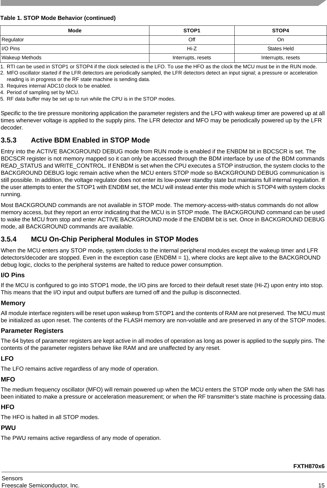
![FXTH870x6SensorsFreescale Semiconductor, Inc. 517 Keyboard InterruptThe FXTH870x6 has a KBI module with general purpose I/O pins. 7.1 FeaturesThe KBI features include:• Up to four keyboard interrupt pins with individual pin enable bits.• Each keyboard interrupt pin is programmable as falling edge (or rising edge) only, or both falling edge and low level (or both rising edge and high level) interrupt sensitivity.• One software enabled keyboard interrupt.• Exit from low-power modes.7.2 Modes of OperationThis section defines the KBI operation in WAIT, STOP, and BACKGROUND DEBUG modes.7.2.1 KBI in STOP ModesThe KBI operates asynchronously in STOP4 mode if enabled before executing the STOP instruction. Therefore, an enabled KBI pin (KBPE[3:0]) can be used to bring the MCU out of STOP4 mode if the KBI interrupt is enabled (KBIE = 1).During STOP1 mode, the KBI is disabled. In some systems, the pins associated with the KBI may be sources of wakeup from STOP1, see the STOP modes section in the Section 3. Upon wakeup from STOP1 mode, the KBI module will be in the reset state.7.2.2 KBI in ACTIVE BACKGROUND modeWhen the microcontroller is in ACTIVE BACKGROUND mode, the KBI will continue to operate normally.7.3 Block DiagramThe block diagram for the keyboard interrupt module is shown Figure 36.Figure 36. KBI Block Diagram7.4 External Signal DescriptionThe KBI input pins can be used to detect either falling edges, or both falling edge and low level interrupt requests. The KBI input pins can also be used to detect either rising edges, or both rising edge and high level interrupt requests. PTA[3:0] map to KBIPE and KBEDG function bits [3:0].The signal properties of KBI are shown in Table 39.Table 39. Signal PropertiesSignal Function I/OKBIPn Keyboard interrupt pins IDQCKCLRVDDKBMODKBIEKEYBOARDINTERRUPT FFKBACKRESETSYNCHRONIZERKBFSTOP BYPASSSTOPBUSCLKKBIPEn01SKBEDGnKBIPE001SKBEDG0KBIP0KBIPnKBIINTERRUP](https://usermanual.wiki/Continental-Automotive/TIS-03/User-Guide-2718164-Page-55.png)
![FXTH870x6SensorsFreescale Semiconductor, Inc. 537.5.3 KBI Edge Select Register (KBIES)KBIES contains the edge select control bits.7.6 Functional DescriptionThis on-chip peripheral module is called a keyboard interrupt (KBI) module because originally it was designed to simplify the connection and use of row-column matrices of keyboard switches. However, these inputs are also useful as extra external interrupt inputs and as an external means of waking the MCU from STOP or WAIT low-power modes.The KBI module allows up to eight pins to act as additional interrupt sources. Writing to the KBIPE[3:0] bits in the keyboard interrupt pin enable register (KBIPE) independently enables or disables each KBI pin. Each KBI pin can be configured as edge sensitive or edge and level sensitive based on the KBMOD bit in the keyboard interrupt status and control register (KBISC). Edge sensitive can be software programmed to be either falling or rising; the level can be either low or high. The polarity of the edge or edge and level sensitivity is selected using the KBEDG[3:0] bits in the keyboard interrupt edge select register (KBIES).Synchronous logic is used to detect edges. Prior to detecting an edge, enabled keyboard inputs must be at the reset logic level. A falling edge is detected when an enabled keyboard input signal is seen as a logic 1 (the reset level) during one bus cycle and then a logic 0 (the asserted level) during the next cycle. A rising edge is detected when the input signal is seen as a logic 0 during one bus cycle and then a logic 1 during the next cycle.7.6.1 Edge Only SensitivityA valid edge on an enabled KBI pin will set KBF in KBISC. If KBIE in KBISC is set, an interrupt request will be presented to the CPU. Clearing of KBF is accomplished by writing a 1 to KBACK in KBISC.7.6.2 Edge and Level SensitivityA valid edge or level on an enabled KBI pin will set KBF in KBISC. If KBIE in KBISC is set, an interrupt request will be presented to the CPU. Clearing of KBF is accomplished by writing a 1 to KBACK in KBISC provided all enabled keyboard inputs are at their reset levels. KBF will remain set if any enabled KBI pin is asserted while attempting to clear by writing a 1 to KBACK.7.6.3 KBI Pullup/Pulldown ResistorsThe KBI pins can be configured to use an internal pullup/pulldown resistor using the associated I/O port pullup enable register. If an internal resistor is enabled, the KBIES register is used to select whether the resistor is a pullup (KBEDG[3:0] = 0) or a pulldown (KBEDG[3:0] = 1).7.6.4 KBI InitializationWhen a keyboard interrupt pin is first enabled it is possible to get a false keyboard interrupt flag. To prevent a false interrupt request during keyboard initialization, the user should do the following:1. Mask keyboard interrupts by clearing KBIE in KBISC.2. Enable the KBI polarity by setting the appropriate KBEDGn bits in KBIES.3. If using internal pullup/pulldown device, configure the associated pullup enable bits in PTAPE[3:0].4. Enable the KBI pins by setting the appropriate KBIPE[3:0] bits in KBIPE.5. Write to KBACK in KBISC to clear any false interrupts.6. Set KBIE in KBISC to enable interrupts.$000E 7 6 5 4 3 2 1 0RKBEDG3 KBEDG2 KBEDG1 KBEDG0WReset: 00000000Figure 39. KBI Edge Select RegisterTable 42. KBIES Register Field DescriptionsField Description3:0KBEDGnKeyboard Edge Selects — Each of the KBEDGn bits selects the falling edge/low level or rising edge/high level function of the corresponding pin).0 Falling edge/low level.1 Rising edge/high level.](https://usermanual.wiki/Continental-Automotive/TIS-03/User-Guide-2718164-Page-57.png)
![FXTH870x6Sensors66 Freescale Semiconductor, Inc.NSA Nibble Swap Accumulator A (A[3:0]:A[7:4]) – – – – – – INH 62 1ORA #opr8iORA opr8aORA opr16aORA oprx16,XORA oprx8,XORA ,XORA oprx16,SPORA oprx8,SPInclusive OR Accumulator and Memory A (A) | (M) 0 – – ÞÞ–IMMDIREXTIX2IX1IXSP2SP1AABACADAEAFA9EDA9EEAiiddhh llee ffffee ffff23443354PSHA Push Accumulator onto Stack Push (A); SP (SP) – 0x0001 – – – – – – INH 87 2PSHH Push H (Index Register High) onto Stack Push (H); SP (SP) – 0x0001 – – – – – – INH 8B 2PSHX Push X (Index Register Low) onto Stack Push (X); SP (SP) – 0x0001 – – – – – – INH 89 2PULA Pull Accumulator from Stack SP (SP + 0x0001); PullA––––––INH 86 3PULH Pull H (Index Register High) from Stack SP (SP + 0x0001); PullH––––––INH 8A 3PULX Pull X (Index Register Low) from Stack SP (SP + 0x0001); PullX––––––INH 88 3ROL opr8aROLAROLXROL oprx8,XROL ,XROL oprx8,SPRotate Left through Carry Þ––ÞÞÞDIRINHINHIX1IXSP139495969799E69ddffff511546ROR opr8aRORARORXROR oprx8,XROR ,XROR oprx8,SPRotate Right through Carry Þ––ÞÞÞDIRINHINHIX1IXSP136465666769E66ddffff511546RSP Reset Stack Pointer SP 0xFF(High Byte Not Affected) ––––––INH 9C 1RTI Return from InterruptSP (SP) + 0x0001; Pull (CCR)SP (SP) + 0x0001; Pull (A)SP (SP) + 0x0001; Pull (X)SP (SP) + 0x0001; Pull (PCH)SP (SP) + 0x0001; Pull (PCL)ÞÞÞÞÞÞINH 80 9RTS Return from Subroutine SP SP + 0x0001PullPCH)SP SP + 0x0001; Pull (PCL) ––––––INH 81 6SBC #opr8iSBC opr8aSBC opr16aSBC oprx16,XSBC oprx8,XSBC ,XSBC oprx16,SPSBC oprx8,SPSubtract with Carry A (A) – (M) – (C) Þ––ÞÞÞIMMDIREXTIX2IX1IXSP2SP1A2B2C2D2E2F29ED29EE2iiddhh llee ffffee ffff23443354SEC Set Carry Bit C 1 –––––1INH 99 1SEI Set Interrupt Mask Bit I 1 ––1–––INH 9B 1Table 44. HCS08 Instruction Set Summary (Sheet 6 of 8)SourceForm Operation DescriptionEffecton CCRAddressModeOpcodeOperandBus Cycles(1)VH I NZCCb0b7b0b7C](https://usermanual.wiki/Continental-Automotive/TIS-03/User-Guide-2718164-Page-70.png)
![FXTH870x6Sensors70 Freescale Semiconductor, Inc.9 Timer Pulse-Width ModuleThe timer pulse-width module (TPM1) is a two channel timer system that supports traditional input capture, output compare, or edge-aligned PWM on each channel. All the features and functions of the TPM1 are as described in the MC9S08RC16 product specification. The user has the option to connect the two timer channels to the PTA[3:2] pins, if those pins are not needed for an LFR channel or other general purpose I/O function. The following clock source and frequency selections are available using the system option register 2 as shown in Figure 23 and Table 27.In addition one channel of the TPM1 can be connected to a 500 kHz clock (DX) derived from the crystal oscillator on the RFM. This selection is made by setting the TPM1 to use an external clock. This clock source allows time calibration of the LFO as described in the Section 14.9.1 FeaturesThe TPM1 has the following features:• May be configured for buffered, center-aligned pulse-width modulation (CPWM) on all channels• Clock sources independently selectable• Selectable clock sources (device dependent): bus clock, fixed system clock• Clock prescaler taps for divide by 1, 2, 4, 8, 16, 32, 64, or 128• 16-bit free-running or up/down (CPWM) count operation• 16-bit modulus register to control counter range• Timer system enable• One interrupt per channel plus a terminal count interrupt• Channel features:— Each channel may be input capture, output compare, or buffered edge-aligned PWM— Rising-edge, falling-edge, or any-edge input capture trigger— Set, clear, or toggle output compare action— Selectable polarity on PWM outputs9.2 TPM1 Configuration InformationThe device provides one two-channel timer/pulse-width modulator (TPM1).An easy way to measure the low frequency oscillator (LFO) is to connect the LFO directly to TPM1 channel 0. The LFOSEL bit in the SOPTZ determines whether TPM1CH0 is connected to PTAZ or the LFO.TPM1 clock source selection for the TPM1 is shown in the table below.Table 46. TPM1 Clock Source SelectionCLKSB CLKSA Clock Source0 0 No source; TPM1 disabled01 BUSCLK1 0 unused1 1 Internal DX pin](https://usermanual.wiki/Continental-Automotive/TIS-03/User-Guide-2718164-Page-74.png)
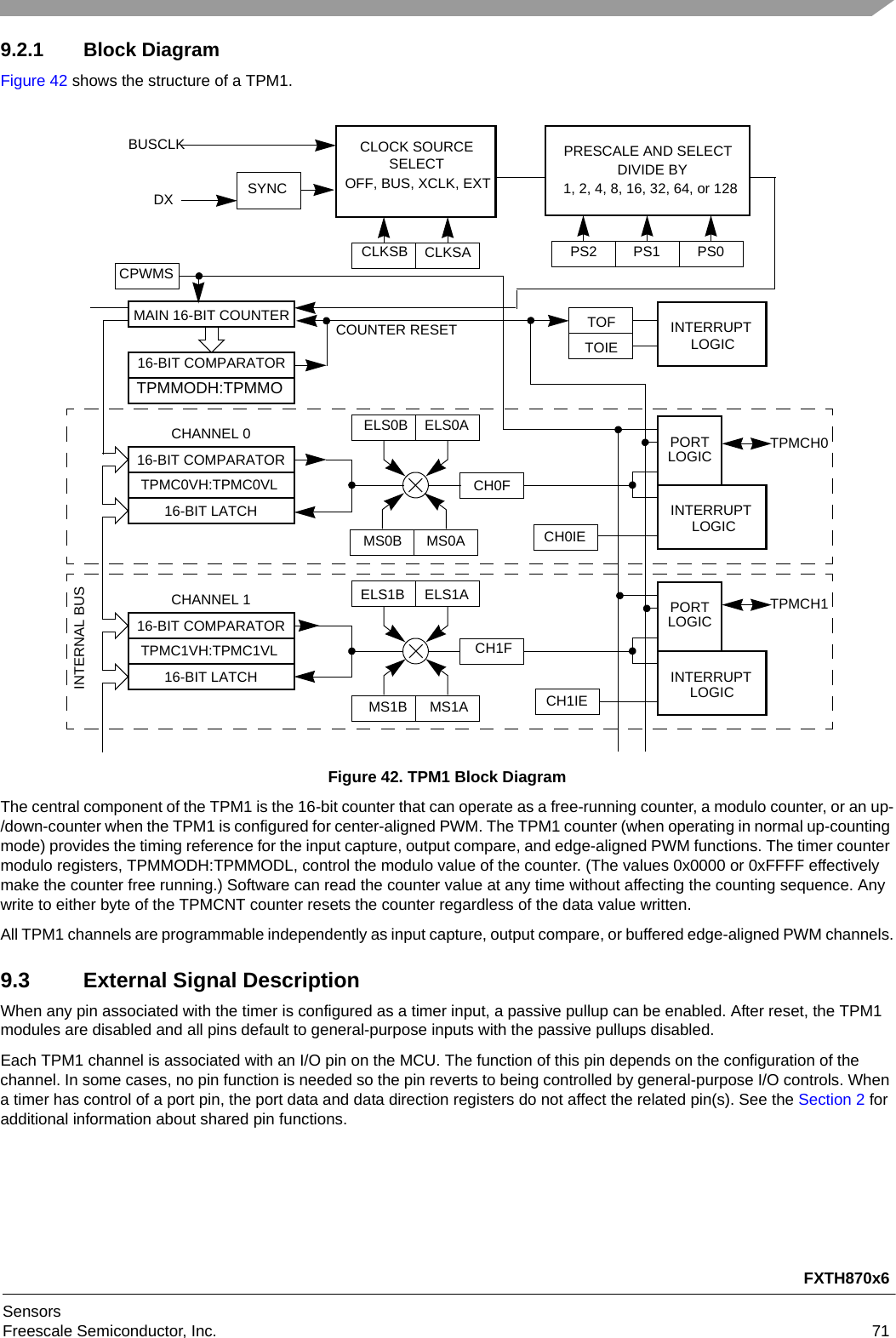
![FXTH870x6Sensors72 Freescale Semiconductor, Inc.9.4 Register DefinitionThe TPM1 includes:• An 8-bit status and control register (TPMSC)• A 16-bit counter (TPMCNTH:TPMCNTL)• A 16-bit modulo register (TPMMODH:TPMMODL)Each timer channel has:• An 8-bit status and control register (TPMCnSC)• A 16-bit channel value register (TPMCnVH:TPMCnVL)9.4.1 Timer Status and Control Register (TPM1SC)TPM1SC contains the overflow status flag and control bits that are used to configure the interrupt enable, TPM1 configuration, clock source, and prescale divisor. These controls relate to all channels within this timer module.$0010 76543210RTOF TOIE CPWMS CLKSB CLKSA PS2 PS1 PS0WReset 00000000= ReservedFigure 43. Timer Status and Control Register (TPM1SC)Table 47. TPM1SC Register Field DescriptionsField Description7TOFTimer Overflow Flag — This flag is set when the TPM1 counter changes to 0x0000 after reaching the modulo value programmed in the TPM1 counter modulo registers. When the TPM1 is configured for CPWM, TOF is set after the counter has reached the value in the modulo register, at the transition to the next lower count value. Clear TOF by reading the TPM1 status and control register when TOF is set and then writing a 0 to TOF. If another TPM1 overflow occurs before the clearing sequence is complete, the sequence is reset so TOF would remain set after the clear sequence was completed for the earlier TOF. Reset clears TOF. Writing a 1 to TOF has no effect.0 TPM1 counter has not reached modulo value or overflow1 TPM1 counter has overflowed6TOIETimer Overflow Interrupt Enable — This read/write bit enables TPM1 overflow interrupts. If TOIE is set, an interrupt is generated when TOF equals 1. Reset clears TOIE.0 TOF interrupts inhibited (use software polling)1 TOF interrupts enabled5CPWMSCenter-Aligned PWM Select — This read/write bit selects CPWM operating mode. Reset clears this bit so the TPM1 operates in up-counting mode for input capture, output compare, and edge-aligned PWM functions. Setting CPWMS reconfigures the TPM1 to operate in up-/down-counting mode for CPWM functions. Reset clears CPWMS.0 All TPM channels operate as input capture, output compare, or edge-aligned PWM mode as selected by the MSnB:MSnA control bits in each channel’s status and control register1 All TPM channels operate in center-aligned PWM mode4:3CLKS[B:A]Clock Source Select — As shown in Table 46, this 2-bit field is used to disable the TPM1 system or select one of three clock sources to drive the counter prescaler. The internal DX source is synchronized to the bus clock by an on-chip synchronization circuit.2:0PS[2:0]Prescale Divisor Select — This 3-bit field selects one of eight divisors for the TPM1 clock input as shown in Table 48. This prescaler is located after any clock source synchronization or clock source selection, so it affects whatever clock source is selected to drive the TPM1 system.](https://usermanual.wiki/Continental-Automotive/TIS-03/User-Guide-2718164-Page-76.png)
![FXTH870x6Sensors74 Freescale Semiconductor, Inc.It is good practice to wait for an overflow interrupt so both bytes of the modulo register can be written well before a new overflow. An alternative approach is to reset the TPM1 counter before writing to the TPM1 modulo registers to avoid confusion about when the first counter overflow will occur.9.4.4 Timer Channel 0 Status and Control Register (TPM1C0SC)TPM1C0SC contains the channel interrupt status flag and control bits that are used to configure the interrupt enable, channel configuration, and pin function.$001476543210RBit 7654321Bit 0WReset 00000000Figure 47. Timer Counter Modulo Register Low (TPM1MODL)$0015 76543210RCH0F CH0IE MS0B MS0A ELS0B ELS0A 00WReset 00000000= ReservedFigure 48. Timer Channel 0 Status and Control Register (TPM1C0SC)Table 49. TPM1C0SC Register Field DescriptionsField Description7CH0FChannel 0 Flag — When channel n is configured for input capture, this flag bit is set when an active edge occurs on the channel n pin. When channel 0 is an output compare or edge-aligned PWM channel, CH0F is set when the value in the TPM1 counter registers matches the value in the TPM1 channel 0 value registers. This flag is seldom used with center-aligned PWMs because it is set every time the counter matches the channel value register, which correspond to both edges of the active duty cycle period.A corresponding interrupt is requested when CH0F is set and interrupts are enabled (CH0IE = 1). Clear CH0F by reading TPM1C0SC while CH0F is set and then writing a 0 to CH0F. If another interrupt request occurs before the clearing sequence is complete, the sequence is reset so CH0F would remain set after the clear sequence was completed for the earlier CH0F. This is done so a CH0F interrupt request cannot be lost by clearing a previous CH0F. Reset clears CH0F. Writing a 1 to CH0F has no effect.0 No input capture or output compare event occurred on channel 01 Input capture or output compare event occurred on channel 06CH0IEChannel 0 Interrupt Enable — This read/write bit enables interrupts from channel 0. Reset clears CH0IE.0 Channel 0 interrupt requests disabled (use software polling)1 Channel 0 interrupt requests enabled5MS0BMode Select B for TPM1 Channel 0 — When CPWMS = 0, MS0B = 1 configures TPM1 channel 0 for edge-aligned PWM mode. For a summary of channel mode and setup controls, refer to Table 50.4MS0AMode Select A for TPM1 Channel 0 — When CPWMS = 0 and MS0B = 0, MS0A configures TPM1 channel 0 for input capture mode or output compare mode. Refer to Table 50 for a summary of channel mode and setup controls.3:2ELS0[B:A]Edge/Level Select Bits — Depending on the operating mode for the timer channel as set by CPWMS:MS0B:MSnA and shown in Table 50, these bits select the polarity of the input edge that triggers an input capture event, select the level that will be driven in response to an output compare match, or select the polarity of the PWM output.Setting ELS0B:ELS0A to 0:0 configures the related timer pin as a general-purpose I/O pin unrelated to any timer channel functions. This function is typically used to temporarily disable an input capture channel or to make the timer pin available as a general-purpose I/O pin when the associated timer channel is set up as a software timer that does not require the use of a pin.](https://usermanual.wiki/Continental-Automotive/TIS-03/User-Guide-2718164-Page-78.png)
![FXTH870x6Sensors76 Freescale Semiconductor, Inc.9.4.6 Timer Channel 1 Status and Control Register (TPM1C1SC)TPM1C1SC contains the channel interrupt status flag and control bits that are used to configure the interrupt enable, channel configuration, and pin function.$0018 76543210RCH1F CH1IE MS1B MS1A ELS1B ELS1A 00WReset 00000000= ReservedFigure 51. Timer Channel 1 Status and Control Register (TPM1C1SC)Table 51. TPM1C1SC Register Field DescriptionsField Description7CH1FChannel 1 Flag — When channel n is configured for input capture, this flag bit is set when an active edge occurs on the channel n pin. When channel 1 is an output compare or edge-aligned PWM channel, CH1F is set when the value in the TPM1 counter registers matches the value in the TPM1 channel 1 value registers. This flag is seldom used with center-aligned PWMs because it is set every time the counter matches the channel value register, which correspond to both edges of the active duty cycle period.A corresponding interrupt is requested when CH1F is set and interrupts are enabled (CH1IE = 1). Clear CH1F by reading TPM1C1SC while CH1F is set and then writing a 0 to CH1F. If another interrupt request occurs before the clearing sequence is complete, the sequence is reset so CH1F would remain set after the clear sequence was completed for the earlier CH1F. This is done so a CH1F interrupt request cannot be lost by clearing a previous CH1F. Reset clears CH1F. Writing a 1 to CH1F has no effect.0 No input capture or output compare event occurred on channel 11 Input capture or output compare event occurred on channel 16CH1IEChannel 1 Interrupt Enable — This read/write bit enables interrupts from channel 1. Reset clears CH1IE.0 Channel 1 interrupt requests disabled (use software polling)1 Channel 1 interrupt requests enabled5MS1BMode Select B for TPM1 Channel 1 — When CPWMS = 0, MS1B = 1 configures TPM1 channel 1 for edge-aligned PWM mode. For a summary of channel mode and setup controls, refer to Table 50.4MS1AMode Select A for TPM1 Channel 1 — When CPWMS = 0 and MS1B = 0, MS1A configures TPM1 channel 1 for input capture mode or output compare mode. Refer to Table 50 for a summary of channel mode and setup controls.3:2ELS1[B:A]Edge/Level Select Bits — Depending on the operating mode for the timer channel as set by CPWMS:MS1B:MS1A and shown in Table 50, these bits select the polarity of the input edge that triggers an input capture event, select the level that will be driven in response to an output compare match, or select the polarity of the PWM output.Setting ELS1B:ELS1A to 0:0 configures the related timer pin as a general-purpose I/O pin unrelated to any timer channel functions. This function is typically used to temporarily disable an input capture channel or to make the timer pin available as a general-purpose I/O pin when the associated timer channel is set up as a software timer that does not require the use of a pin.Table 52. Mode, Edge, and Level SelectionCPWMS MS1B:MS1A ELS1B:ELS1A Mode ConfigurationXXX 00Pin not used for TPM1 channel; use as an external clock for the TPM1 or revert to general-purpose I/O00001Input captureCapture on rising edge only10 Capture on falling edge only11 Capture on rising or falling edge0100Output compareSoftware compare only01 Toggle output on compare10 Clear output on compare11 Set output on compare1X 10 Edge-aligned PWMHigh-true pulses (clear output on compare)X1 Low-true pulses (set output on compare)](https://usermanual.wiki/Continental-Automotive/TIS-03/User-Guide-2718164-Page-80.png)
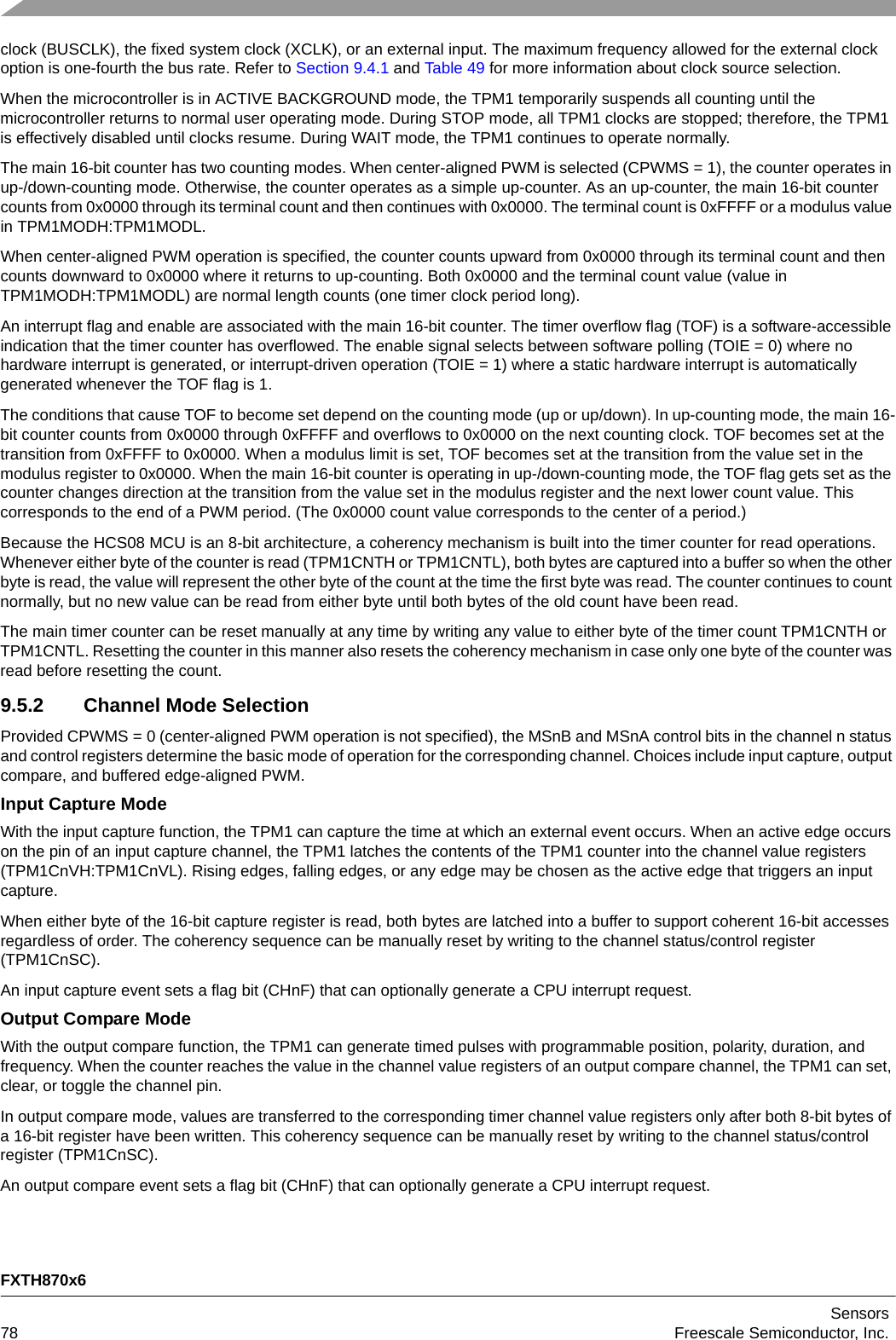
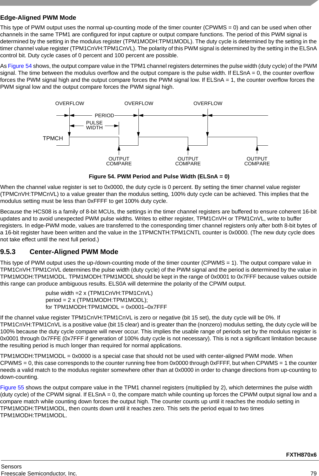
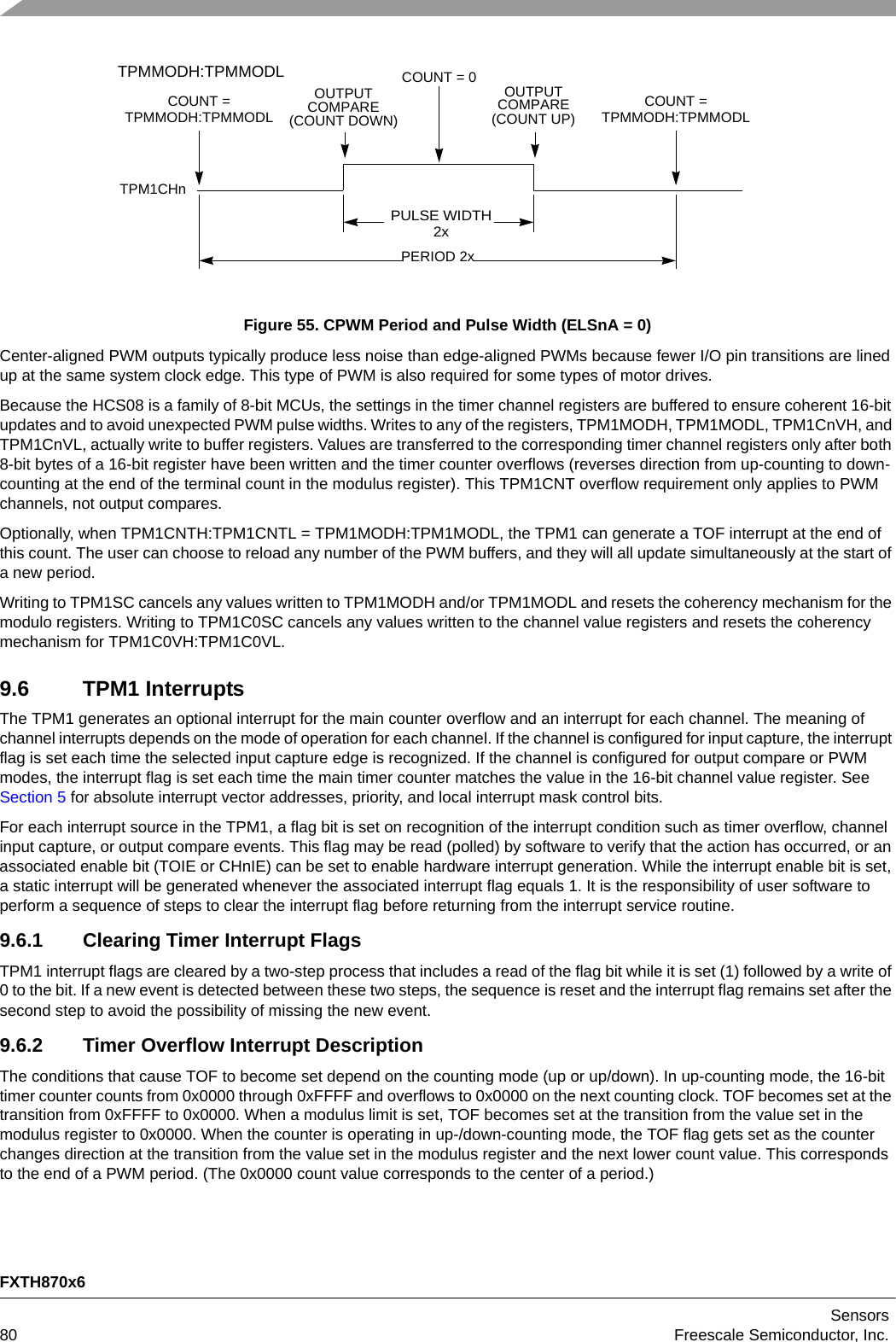
![FXTH870x6SensorsFreescale Semiconductor, Inc. 8310.2 Temperature MeasurementsThe temperature is measured from a VB sensor built into channel 1 of the ADC10 in the same manner as is done in the FXTH870x6 devices with the resulting transfer equation:Eqn. 310.3 Voltage MeasurementsVoltage measurements can be made on the internal bandgap to estimate the supply voltage on VDD. 10.3.1 Internal BandgapAn internal bandgap voltage reference is provided to take measurements of the supply voltage. The resulting transfer equation:Eqn. 410.3.2 External VoltagesMeasurements of an external voltage on either the PTA0 or PTA1 pins can be made and referenced to the internal bandgap voltage. The resulting transfer equation: Eqn. 5where x = 0, 1 refers to PTA0 or PTA1.10.4 Optional Acceleration MeasurementsThe acceleration measurement consists of an interface to an optional acceleration sensing element. Control bits on the MCU operate the SMI to power up the g-Cell and capture a voltage which is converted by the ADC10. The data from the ADC10 is then pre-processed by a dynamic range firmware routine that will return the two values necessary to calculate the acceleration, Ay, (y = X-axis or Z-axis, depending on selection) in conjunction with values taken from the table in Section 17.10.1.The first value from the firmware routine is the offset step identifier, STEP, with integer values 0 to 15 (i.e. the 16 offset steps). The other value is the ADC10 data, AyCODE, with integer values 0 to 511. AyCODE values 1 through 510 are usable; values 0 and 511 indicate fault conditions. The X-axis acceleration is scaled for ~20g range within each of the 16 offset steps, ~10g per step. The Z-axis acceleration is scaled for ~80g range within each of the 16 offset steps, ~80g or ~60g. The steps are at ~40g or ~30g increments, allowing for adequate overlaps. Section 17.10.1 provides a table of acceleration values resulting from characterizations.Acceleration sensitivity, Ay-STEP, varies between each offset step, and should be calculated by dividing the range of g’s for each offset step by the usable AyCODE range (i.e. 510): Eqn. 6Once the sensitivity Ay-STEP has been calculated, the acceleration Ay can be calculated by the re-using the Ay-STEP @ AyCODE 1 value of the offset step and the returned AyCODE value with the following transfer function: Eqn. 7The pressure, and optional X or Z-axis accelerometer also share the same signal path in the Transducer interface and all the sensors share the same ADC. Therefore only one of the sensors can be accessed at a given moment.NOTEThe included accelerometers are designed with a self-test feature. Consult sales/application support for information regarding the recommended use of the accelerometer self-test features.10.5 Optional Battery Condition CheckThe condition of the battery can be periodically checked to determine the battery’s internal impedance, RBATT, which is a function of both temperature and the remaining battery capacity. This can be performed by user supplied software routine and an external load resistor, RLOAD, connected from the PTA0 pin to VSS as shown in Figure 56 (any of the PTA[3:0] can be used for this purpose).TTTCODE 55–=VINT VINT VCODE 1.22+=VPTAx VEXT GxCODE=Ay-STEP Ay-STEP @ AyCODE510 Ay-STEP @ AyCODE1–510=AyAy-STEP AyCODE Ay-STEP @ AyCODE1Ay-STEP–+=](https://usermanual.wiki/Continental-Automotive/TIS-03/User-Guide-2718164-Page-87.png)
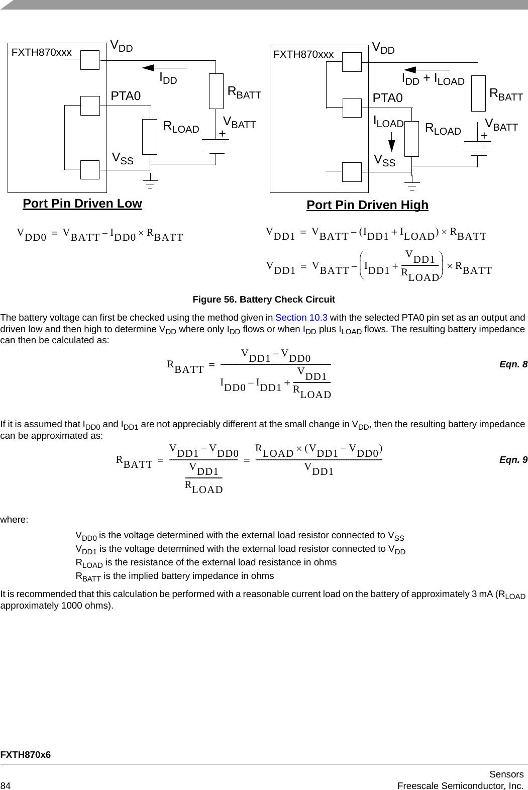
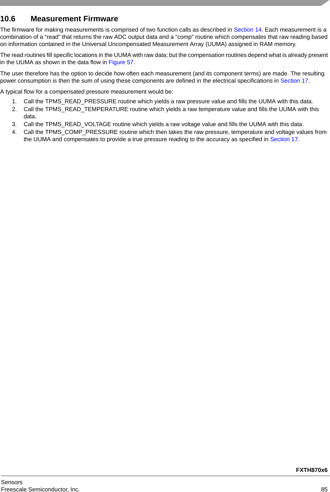
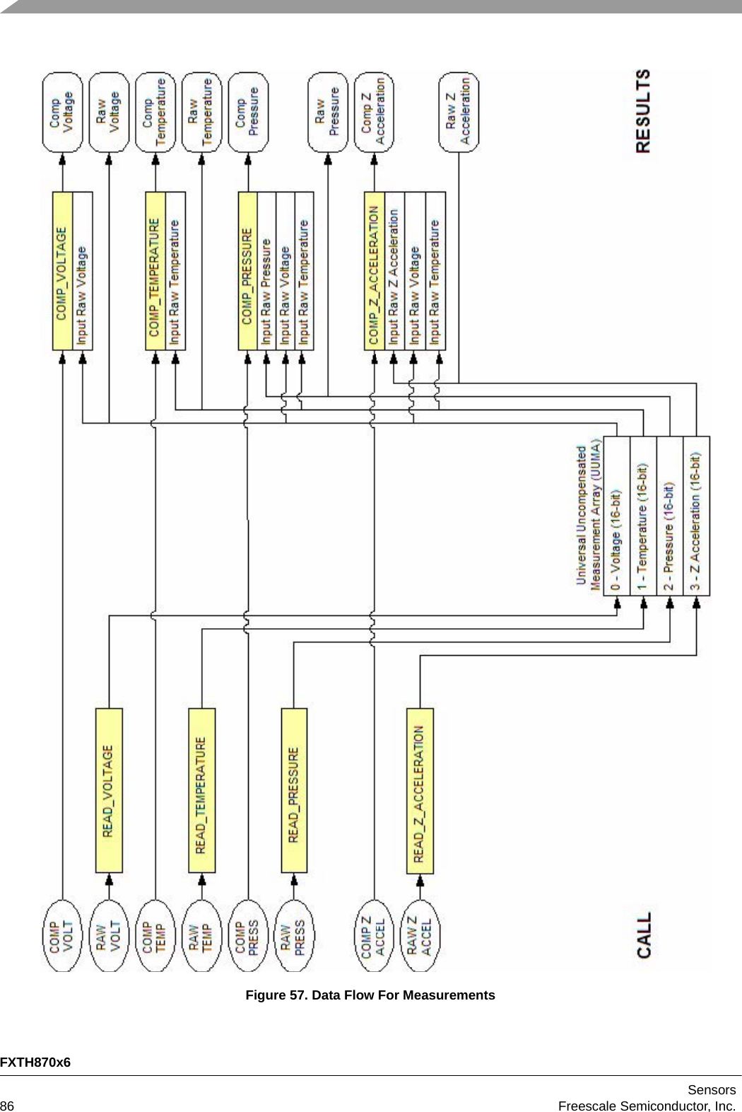
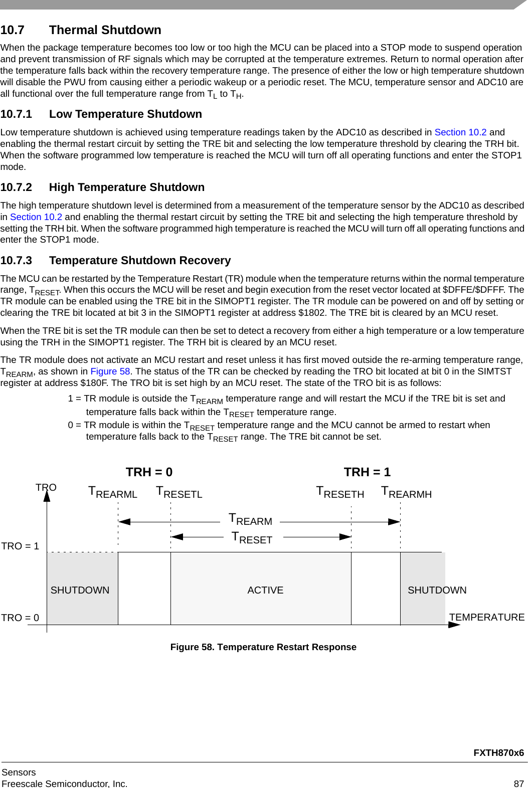
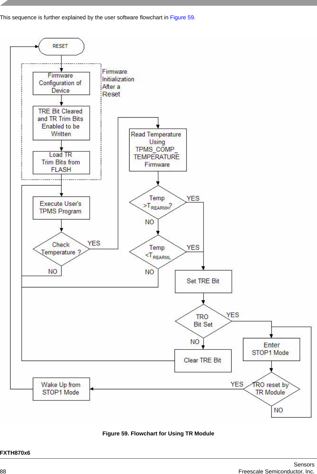
![FXTH870x6SensorsFreescale Semiconductor, Inc. 8911 Periodic Wakeup TimerThe periodic wakeup timer (PWU) generates a periodic interrupt to wakeup the MCU from any of the STOP modes. It also has an optional periodic reset to restart the MCU. It is driven by the LFO oscillator in the RTI module which generates a clock at a nominal one millisecond interval. The LFO and the wakeup timer are always active and cannot be powered off by any software control. The control bits are set so that there is either a periodic wakeup, a periodic reset, or both a wakeup interrupt and a periodic reset. No combination of control bits will disable both the wakeup interrupt and the periodic reset. In addition, there is no hardware control that can mask a wakeup interrupt once it is generated by the PWU.11.1 Block DiagramThe block diagram of the wakeup timer is shown in Figure 60. This consists of a programmable prescaler with 64 steps that can be used to adjust for variations in the value of the LFO period. Finally there are two cascaded programmable 6-bit dividers to set wakeup and/or reset time intervals.Figure 60. Wakeup Timer Block DiagramThe wakeup divider (PWUDIV) register selects a division of the incoming 1 ms clock to generate a wakeup clock, WCLK. The WCLK frequency can be calibrated against the more precise external oscillator using the TPMS_LFOCOL firmware subroutine as described in Section 14. This subroutine turns on the RFM crystal oscillator and feeds a 500 kHz clock to the TPM1 for one cycle of the LFO. The measured time is used to calculate the correct value for the WDIV[5:0] bits for a WCLK period of 1 second. The TPMS_LFOCOL subroutine cannot be used while the RFM is transmitting or the TPM1 is being used for another task.The wakeup time register (PWUSC0) selects the number of WCLK pulses that are needed to generate a wakeup interrupt to the MCU. The periodic reset register (PWUSC1) selects the number of wakeup pulses that are needed to generate a periodic reset of the MCU. Both the wakeup time counter and the periodic reset timer are incrementing counters that generate their interrupt or reset when the desired count is reached and are then reset to zero. Reading the status of either of these counters will return a zero content if done immediately after the interrupt or reset is generated.If both the reset and the interrupt occur on the same clock cycle the reset will have precedence and the interrupt will not be generated.In order to prevent wakeup or reset from an extreme temperature event both the wakeup interrupt or periodic reset are disabled if the thermal restart is activated and the TRO bit indicates that the device is still outside of the TRESET range. The wakeup and periodic reset counters will still run. The state of these counters can be read using the PSEL bit in the PWUS register.The wakeup interrupt (WUKI) cannot be masked by clearing the I-bit.CONTROLLOGICLFO 6-BITWAKEUPWUFPROGRAMMBLEPRESCALERWDIV[5:0] WUT[5:0]WUKIPRST[5:0]DIVIDER6-BITPERIODICRESETWCLK RCLKDIVIDERPRFPRSTWUFAKTROPRFAKTRE](https://usermanual.wiki/Continental-Automotive/TIS-03/User-Guide-2718164-Page-93.png)
![FXTH870x6Sensors90 Freescale Semiconductor, Inc.11.2 Wakeup Divider Register - PWUDIVThe PWUDIV register contains six bits to select the division of the incoming 1 ms clock period as described in Figure 61.11.3 PWU Control/Status Register 0 - PWUCS0The PWUCS0 register contains six bits to select the division of the incoming WCLK clock period and provide interrupt flag and acknowledge bits as described in Figure 62. The period of the resulting interrupt also generates the clock, RCLK, for the periodic reset timing.$0038 Bit 7 654321Bit 0R0 0 WDIV[5:0]WRESET: ————————POR: 00011111= ReservedFigure 61. PWU Divider Register (PWUDIV)Table 54. PWUDIV Register Field DescriptionsField Description7:6UnusedUnused5:0WDIV[5:0]Wakeup Divider Value — The WDIV[5:0] bits select an incoming prescaler for the incoming 1 ms clock period from 504 to 1512. This results in a clocking of the 6-bit wakeup divider at rates from a nominal 0.504 to 1.512 sec per wakeup clock, WCLK. The user can use this prescaler to fine tune the wakeup time based on the variation in the LFO frequency. The conversion from the decimal value of the WDIV bits to the nominal WCLK period is given as:A power on reset presets these bits to a value of $1F (decimal 31) which yields a nominal 1 second output period for WCLK. Other resets have no effect on these bits.$0039 Bit 7 6 5 4 3 2 1 Bit 0RWUF 0WUT[5:0]WWUFAKRESET: 0—111111Figure 62. PWU Control/Status Register 0 (PWUCS0)Table 55. PWUSC0 Register Field DescriptionsField Description7WUFWakeup Interrupt Flag — The WUF bit indicates when a wakeup interrupt has been generated by the PWU. This bit is cleared by writing a one to the WUFAK bit. Writing a zero to this bit has no effect. Reset clears this bit.0 Wakeup interrupt not generated or was previously acknowledged.1 Wakeup interrupt generated.6WUFAKAcknowledge WUF Interrupt Flag — The WUFAK bit clears the WUF bit if written with a one. Writing a zero to the WUFAK bit has no effect on the WUF bit. Reading the WUFAK bit returns a zero. Reset has no effect on this bit.0 No effect.1 Clear WUF bit.tWCLK 504 16 WDIV+fLFO-------------------------------------------------=](https://usermanual.wiki/Continental-Automotive/TIS-03/User-Guide-2718164-Page-94.png)
![FXTH870x6SensorsFreescale Semiconductor, Inc. 91 11.4 PWU Control/Status Register 1 - PWUCS1The PWUSC1 register contains six bits to select the division of the incoming RCLK clock period and provide interrupt flag and acknowledge bits as described in Figure 63.5:0WUT[5:0]WUF Time Interval — These control bits select the number of WCLK clocks that are needed before the next wakeup interrupt is generated. The count gives a range of wakeup times from 1 to 63 WCLK clocks.Depending on the value of the bits for the WDIV[5:0] this time interval can nominally be from 1 to 63 seconds in 1 second steps. Whenever the WUT[5:0] bits are changed the timeout period is restarted. Writing the same data to the WUT[5:0] bits has no effect.Writing zeros to all of the WUT[5:0] bits forces the wakeup divider to a value of $3F and disables the wakeup interrupt. However, writing all zeros to the WUT[5:0] bits is inhibited if all of the PRST[5:0] bits are already cleared to zero. This prevents disabling both the periodic wakeup and the periodic reset at the same time. See Table 56.The WUT[5:0] bits are preset to a value of $3F (decimal 63) by any resets.Table 56. Limitations on Clearing WUT/PRSTControl Bits State of Control Bits Control Bits to be Cleared Resulting Action Resulting Wakeup Interrupt Resulting Periodic ResetWUT[5:0] non-zero PRST[5:0] Allowed Enabled(1)1. Using previous values.Disabledall zero Inhibited Disabled(2)2. Wakeup divider preset to $3F.Enabled(1)PRST[5:0] non-zero WUT[5:0] Allowed Disabled Enabled(1)all zero Inhibited Enabled(1) Disabled$003A Bit 7 6 5 4 3 2 1 Bit 0RPRF 0PRST[5:0]WPRFAKRESET: 00111111= ReservedFigure 63. PWU Control/Status Register 1 (PWUCS1)Table 57. PWUSC1 Register Field DescriptionsField Description7PRFPeriodic Reset Flag — The PRF bit indicates when a periodic reset has been generated by the PWU. MCU writes to this bit have no effect. This bit is cleared by writing a one to the PRFAK bit. This bit is cleared by a power on reset, but is unaffected by other resets.0 Periodic reset not generated or previously acknowledged.1 Periodic reset generated.6PRFAKAcknowledge PRF Interrupt Flag — The PRFAK bit clears the PRF bit if written with a one. Writing a zero to the PRFAK bit has no effect on the PRF bit. Reading the PRFAK bit returns a zero. Reset has no effect on this bit.0 No effect.1 Clear PRF bit.5:0PRST[5:0]Periodic Reset Time Interval — These control bits select the number of wakeup interrupts that are needed before the next periodic reset is generated. The decimal count gives a range of periodic reset times from 1 to 63 wakeup interrupts. Depending on the value of the bits for the WDIV[5:0] and WUT[5:0] this time interval can nominally be from 1 second to 66 minutes with steps from 1 to 63 seconds. Whenever the PRST[5:0] bits are changed the timeout period is restarted. Writing the same data to the PRST[5:0] bits has no effect.Writing zeros to all of the PRST[5:0] bits forces the periodic reset to be disabled if at least one of the WUT[5:0] bits is set to a one. This assures that there will be at least a wakeup interrupt. However, writing all zeros to the PRST[5:0] bits is inhibited if all of the WUT[5:0] bits are already cleared to zero. This prevents disabling both the periodic wakeup and the periodic reset at the same time. See Table 56. The PRST[5:0] bits are preset to a value of 63 by any resets.Table 55. PWUSC0 Register Field Descriptions (continued)Field Description](https://usermanual.wiki/Continental-Automotive/TIS-03/User-Guide-2718164-Page-95.png)
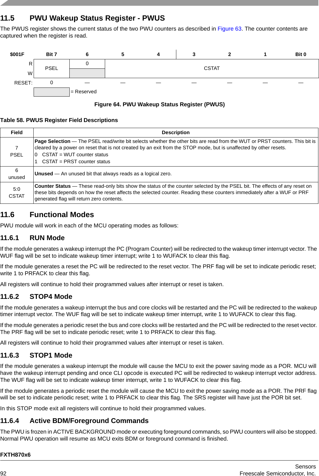
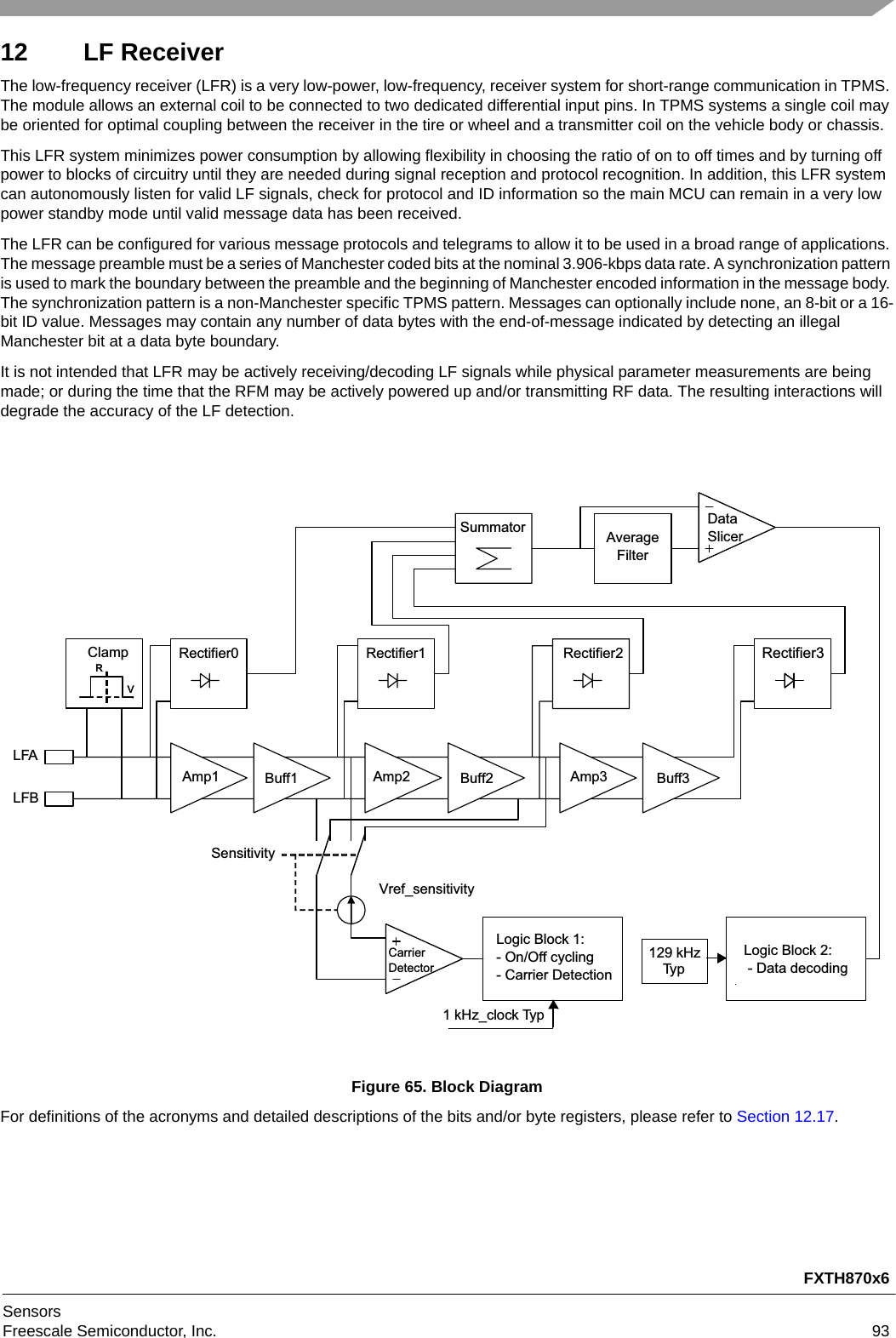
![FXTH870x6Sensors94 Freescale Semiconductor, Inc.12.1 FeaturesMajor features of the LFR module include:• Differential input LF detector (two dedicated pins):— Selectable sensitivity (two levels: Low Sens (LS) and High Sens (HS)).— Thresholds trimmed at the factory with trim setting saved in nonvolatile memory.— LFR has a reference oscillator (LFRO) trimmed at the factory with trim setting saved in nonvolatile memory.— Selectable signal sampling time interval and on-time.— Sample interval and on times controlled by LFR state machine or directly by the MCU.• Configurable receive mode:— Simple LF carrier detection/Telegram decode. (CARMOD)• Configurable message protocol (telegram structure):— Various SYNC decoding (SYNC[1:0])6-bit time SYNC requirements7.5-bit time SYNC requirements9-bit time SYNC requirements— Optional ID (ID[1:0])8-bit or 16-bit ID On or off— 0-n bytes of message data. End-of-data marked by loss of Manchester at a byte boundary.• Optional continuous monitoring and decode of the LF detector.• Selectable MCU interrupt when a received data byte is ready in an LFR buffer, when a Manchester error is detected in the frame, when an ID is received or when a valid carrier has been detected.12.2 Modes of OperationThe LFR is a peripheral module on an MCU. After being configured by application software, the LFR can operate autonomously to detect and verify incoming LF messages. When a valid message or carrier pulse is received and verified the LFR can wake the MCU from standby modes to read received data or act upon a carrier detection.The primary modes of operation for the LFR are:• Disabled. Everything off and drawing minimal leakage current. LFR register contents will be retained.• Carrier detect/listen. Minimum circuitry enabled to detect any incoming LF signal, check it for the appropriate signal level, frequency and duration.• TPMS protocol verification.• Data reception.12.3 Power ManagementIn addition to using low power circuit design techniques, the LFR module provides system-level features to minimize system energy requirements. In an MCU that includes the LFR module, all MCU circuitry except a very low current 1-kHz oscillator (LFO) and minimum regulator circuitry can be disabled. After a reset, the MCU would initialize the LFR module and then enter a very low power standby mode (depending upon the MCU, this could be lower than 1 uA for the MCU portion). The LFR module includes everything it needs to periodically listen for LF messages, perform Manchester decoding, verify the message telegram, and assemble incoming data into 8-bit bytes. The LFR does not wake the MCU unless a valid message is being received and a data byte is ready to be read.The LFR cycles between an off state, where everything is disabled, and an on state, where it listens for a carrier signal. The on time is controlled by LFONTM[3:0] control bits in the LFCTL2 register. The time between the start of each sample on time is controlled by LFSTM[3:0] control bits in the LFCTL2 register. Even lower duty cycles can be achieved by using the MCU to wake once per second and maintain a software counter to delay for an arbitrarily long time before enabling the LFR to perform a series of carrier detect cycles.Within the LFR, circuits remain disabled until they are needed. When the LFR is listening for a carrier signal, only a 1-kHz clock source, a portion of the input amplifier and a periodic auto-zero are running. After a carrier signal is detected, with high enough amplitude, frequency and duration the LFRO oscillator is enabled so the LFR can begin to decode the incoming information.The LFR module has a power up settling time of 2-LFO period before any active operations. In the ON/OFF cycle, those 2 ms are hidden in the sampling time during the off time.](https://usermanual.wiki/Continental-Automotive/TIS-03/User-Guide-2718164-Page-98.png)
![FXTH870x6SensorsFreescale Semiconductor, Inc. 9512.4 Input AmplifierThe LFR module receives LF modulated signals through a dedicated differential pair of inputs which is connected to an external coil. The enable control (LFEN) allows the user to enable the LF input depending on the application requirements. The SENS[1:0] bits in the LFCTL1 register allows the user to select one of two input sensitivity thresholds which determines the signal level required before the input carrier will be detected. The sensitivity setting is used during carrier detection but does not affect reception after the carrier has been detected. When the CARMOD bit is cleared, after a carrier with sufficient amplitude, frequency and duration has been detected the output stage of the amplifier is turned on to allow data reception.12.5 LFR Data Mode StatesThe modes of operation the LFR state machine will sequence as shown in Figure 66.12.6 Carrier DetectCarrier detection includes a check for a certain number of edges on a signal that is greater than the input sensitivity threshold. During the check for carrier edges, only the 1kHz low frequency oscillator (LFO) clock source is running so power consumption remains very low. During carrier detection the incoming signal is amplified and passed through a sensitivity threshold comparator. The SENS[1:0] bits in the LFCTL1 register selects two levels of sensitivity and determines the signal amplitude that is needed to allow edges to be seen at the output of the sensitivity threshold comparator. When a carrier is above this threshold, a block is powered on and validates the carrier. This frequency and duration check function can be disabled by clearing the VALEN bit. If VALEN is set, the block checks for the carrier duration and the carrier frequency. The time needed to validate a carrier is programmed by the LFCDTM register. The carrier frequency should be 125 kHz. If the signal above the threshold is not within the frequency range or not present during enough time, then the carrier will not be validated and the validation block will turn off.If no carrier signal is validated within the on time of the LFR, the state machine returns to the off state and the alternating cycle of on time and off time continues. Carrier edge counts start at zero when a new on time begins. In the data mode (CARMOD = 0), if the required number of carrier edges are detected before the end of the ON time, the LFR will remain ON to complete the reception of a message telegram.In the carrier detect mode (CARMOD = 1) there is no need to enable other LFR circuitry to evaluate any other message components after the required number of carrier edges are detected. One or several consecutive carriers can be validated by this process before the LFCDF flag is set. The LFCC control bits are used to program the number of consecutive ON times where a complete carrier validation is needed before interrupting the MCU. In this case, the LFCDF flag is set and, provided the LFCDIE interrupt enable is also set, an interrupt is issued to wake the MCU. In carrier detect mode, the LFCDIE control bit should always be set because the intended purpose of the carrier detect mode is to wake the MCU when a carrier is detected. When LFCDF is set, the LFR waits until it is cleared before it continues the alternating cycle of on time and off time, starting with an off time.In data mode, when a carrier is detected the averaging filter is powered on and the LFR continues to the next state to look for the rest of a message telegram; and the LFR module will search for valid SYNC word (with length programmed through the SYNC bits in the LFCTL3 register depending on preamble type). If the external LF field is not a TPMS frame, a timeout will turn off the LFR module. This timeout can be program through TIMOUT bit the LFCTL4 register.](https://usermanual.wiki/Continental-Automotive/TIS-03/User-Guide-2718164-Page-99.png)
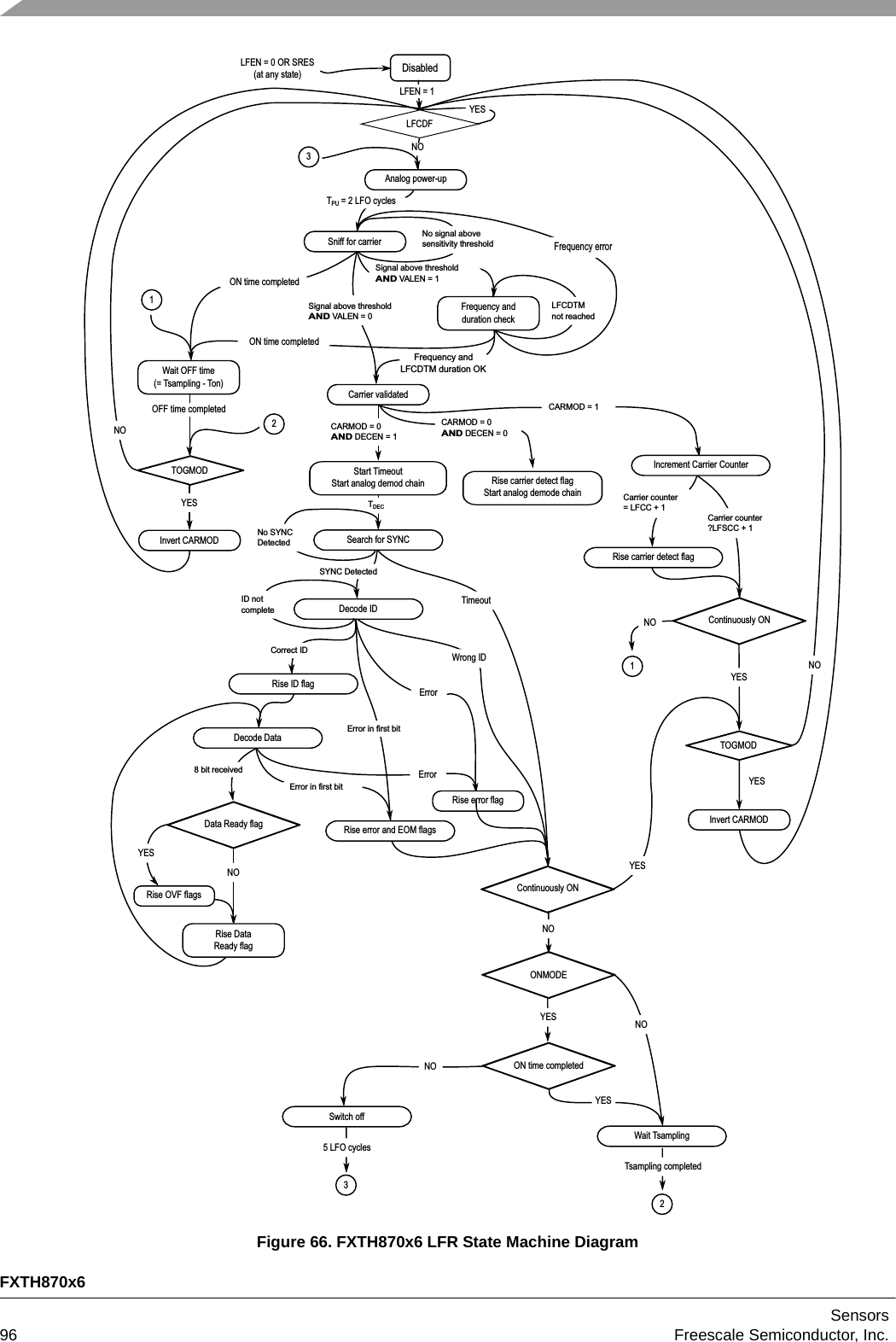
![FXTH870x6SensorsFreescale Semiconductor, Inc. 9712.7 Auto-Zero SequenceAn auto-zero sequence is performed periodically on the input amplifier to cancel offset errors. During reception of the SYNC pattern and body of the message, auto-zero operations are synchronized to data edges of the incoming signal to avoid interfering with normal reception. During the auto-zero sequence, the input amplifier is temporarily disconnected from the external coil and connected to ground. The auto-zero sequence takes roughly 64 sec. It is performed at each LFO period in carrier mode and on one over four decoded data edges in data mode.When the DECEN bit is cleared, the auto-zero sequence is performed at each LFO period. During the 64 sec of the auto-zero sequence, the receiver is holding the state “0” or “1”' previously decoded. Since the LFR receiver is not active during this time, the possible data-rate that the analog can detect is at least limited by this duration.12.8 Data RecoveryRectified signals from the amplifier output are connected to the input of an averaging filter and data slicer. The slicer thus compares the rectified signal with its own average value to decode the data. When a carrier is present, the slicer output voltage rises and when the carrier stops the slicer output voltage falls. The output of this comparator provides a binary digital signal that indicates whether the carrier is present or not. This digital signal is connected to the data clock recovery circuit, the SYNC detect circuit, and the Manchester decoder circuit.The Manchester decoder uses the digital output of the data slicer to detect the logic level of each incoming data bit and to synchronize the decoder state machine. The LFPOL polarity bit in the LFCTRLA register selects the expected encoding of the Manchester data bit.If a strong signal (above roughly 100 mV p-p differential) is entered into the LFR, the input impedance will switch instantaneously to a lower programmed value (the LOWQ[1:0] bits in the LFCTRLC) and be maintained during the current data packet if the DEQEN bit is set. At the next ON time, the default high input impedance will be set again. The strong signal detection and the automatic impedance change can be disabled by clearing the DEQEN bit.12.9 Data Clock Recovery and SynchronizationData clock recovery and synchronization takes place during the SYNC portion of an incoming message. The preamble must be modulated Manchester data. The type of required SYNC pattern determines the allowed preamble type depending on the SYNC[1:0] control bits.The design data rate is 3.906 kbps which gives a bit time equivalent to about 32 cycles of the LF carrier frequency. In a Manchester encoded bit time, the carrier should be present for either the first half or the second half of the bit time depending on whether the bit is a logic zero or a logic one.The LFRO clock source is 32 times the target data rate. The LFRO is used for decoding data and also sequencing auto-zero operations.12.10 Manchester DecodeWhen the LFPOL bit is clear, a logic one bit is defined as no LF carrier present for the first half of the bit time; and a logic zero bit is defined as LF carrier present for the first half of the bit time as shown in Figure 67. Another way to say this from the point of view of the data slicer output is that a logic zero bit has a falling edge at the middle of the bit time and a logic one bit has a rising edge at the middle of the bit time. The data slicer threshold is dynamically adjusted to the midpoint between the carrier-present and no-carrier levels at the summing node for the rectified output of the LF input amplifier.](https://usermanual.wiki/Continental-Automotive/TIS-03/User-Guide-2718164-Page-101.png)
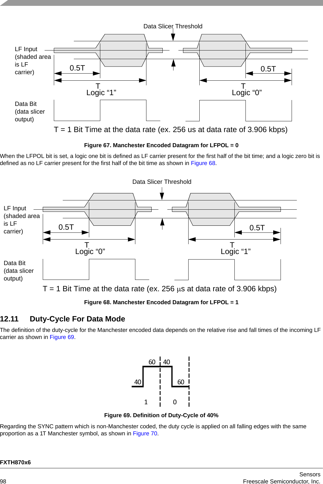
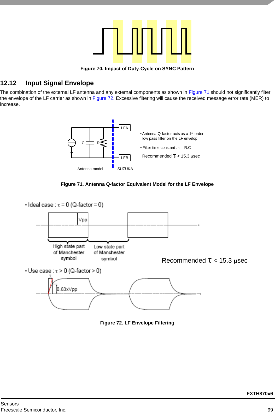
![FXTH870x6Sensors100 Freescale Semiconductor, Inc.12.13 Telegram VerificationThe LFR has control bits to allow flexibility in the telegram format and protocol to allow the LFR to adapt to a variety of systems. The LFR can operate in a normal data receive mode where it receives complete telegrams, or in a carrier detect mode where it only checks for a carrier. In the carrier detect mode, as soon as a carrier is detected, the LFCDF flag is set. If LFCDIE is also set, an interrupt request is sent to wake the MCUThe format of the complete Manchester encoded datagram is comprised of a Manchester data preamble (series of Manchester 1’s or 0’s), a synchronization period, an optional ID, and zero to n data bytes. The synchronization period can be used for synchronizing the beginning of the data packet. The SYNC pattern that follows the preamble can be either a 6-, 7.5- or 9 bit-time non-Manchester pattern as shown in Figure 73.Figure 73. SYNC PatternsThese patterns would normally not appear anywhere in the Manchester encoded portion of a message so there is no possibility that the LFR could accidentally synchronize to a message that was already in progress when the LFR started listening for a message. These patterns are also complex enough so that it is very unlikely that noise or interference could be mistaken for these SYNC patterns. In the data mode and after the detection of a valid carrier, the LFR will decode the data stream waiting for the SYNC word. Should this carrier not be an accepted TPMS type, no SYNC will be received and the LFR module will stay in data receive mode forever. A timeout counter is thus started after a carrier detection and will stop the receiver if reaching the programmed value selected by the TIMOUT[1:0] bits in the LFCTL4 register. This timeout counter is clocked by the internal LFRO clock.The LFR can be configured to have an optional 0, 8-bit or 16-bit ID after the SYNC pattern. If the ID value matches the received ID, the message is accepted. The ID value can be used to identify a specific receiver, a message type, or some other identifier as defined by application software.Any number of data bytes can be included after the ID. The LFR begins to assemble data bytes from the incoming signal as soon as the ID check is complete. If the first bit-time after the last bit of the ID does not conform to Manchester coding requirements, the LFR considers the message complete and terminates the LFR operation without setting the data ready flag (LFDRF). If data follows the ID, it is serially received and when 8 bits have been received the LFR copies this byte into the LFDATA register and sets the LFDRF flag. If the LFDRIE interrupt enable is also set (and it should be), an interrupt request is sent to wake the MCU so it can read the data and process it according to the instructions in the application program. Additional bytes are received until a bit time that is not Manchester encoded is found. If a non-Manchester bit time is found, the LFERF bit will be set and indicates a Manchester coding error. If this happens on the first bit of the next byte of the message the LFEOMF bit will also be set. The preamble is a period of Manchester bits before the SYNC pattern as shown in Figure 74. The SYNC pattern will only be matched for the bit times specified by the SYNC[1:0] control bits. Depending on the expected SYNC pattern the allowed preambles is as described for the SYNC[1:0] bits in the LFCTL3 register.TTTT2T 2T1.5TTTTT2T 2T1.5T3T TTTT2T 2T6-bit(6T)Pattern7.5-bit(7.5T)Pattern9-bit(9T)PatternSYNC[1:0] = 01SYNC[1:0] = 10SYNC[1:0] = 11](https://usermanual.wiki/Continental-Automotive/TIS-03/User-Guide-2718164-Page-104.png)
![FXTH870x6SensorsFreescale Semiconductor, Inc. 101Figure 74. Telegram Format (Carrier Preamble)12.14 Error Detection and HandlingWhen the DECEN bit is set, LFR messages are monitored for data rate or SYNC errors, incorrect message ID, and Manchester coding errors. When an error is detected the LFR goes back to sniff mode until the end of ON time completion, if ONMODE is set; or turns off until the start of the next scheduled sampling interval, if ONMODE is cleared. Because the MCU uses more power than the LFR module, it is desirable to keep the MCU in low power standby modes as much as possible. Therefore the handling of these errors will be performed by the LFR and not require additional software processing by the MCU.When the DECEN bit is clear, there is no monitoring on data. The MCU needs to poll the state of the LFDO bit and create its own decoding scheme within software on the detected signal. To be able to start the polling only when data are received, the carrier detection flag is enabled in data mode when DECEN = 0. During data reception, the auto-zero sequence is performed at each LFO period. The MCU needs also to determine the end of the telegram and turn off the LFR (LFEN = 0) during two LFO cycles before any other operations.12.15 Continuous ON ModeIn the Continuously ON mode, the LFR module will remain on continuously while the LFEN bit is set. The Continuously ON mode is controlled by setting the LFSTM[3:0] bits.In the Continuously ON mode, if a signal is successfully processed by the digital, the LFR module will stop and restart automatically. The gap is 2-3 LFO periods. Also if TOGMOD bit is set, the LFR module will stop after the ON time cycle and re-start automatically, after having changed the CARMOD bit.12.16 Initialization InformationWhen power is applied to the MCU, the LFR must be initialized and configured before it can begin to receive LF messages. Several systems in the LFR require factory trimming to ensure operation within specified limits. After these trim values are written, they remain constant until the next MCU reset.The application program must set up control bits and registers to configure the LFR to determine the structure of the message telegram, the input sensitivity, and other LFR options. It is good practice to clear the flags in the LFS register before enabling interrupt sources in order to avoid any immediate interrupt requests.PREAMBLE SYNC HIGH ID DATA DATA6, 7.5 or 9T 0, 8T or 16T 8TtLFPRE IDSEL[1:0] Repeat for 0-n bytesLOW ID](https://usermanual.wiki/Continental-Automotive/TIS-03/User-Guide-2718164-Page-105.png)
![FXTH870x6Sensors102 Freescale Semiconductor, Inc.12.17 LFR Register DefinitionThe LFR module uses eight addresses in the MCU memory map for data, control, and status registers.This section consists of register descriptions. Each control register (LFCTLx) should be modify when the LF is off (LFEN = 0). Modification of the control registers “on-the-fly” might lead to unknown state. Each turn off of the LFR (LFEN = 0) should be followed by at least two LFO cycles before trying to restart the LFR (LFEN = 1).12.17.1 LF Control Register 1 (LFCTL1)LFCTL1 contains the main LF enable control, detection protocol format controls, and input sensitivity controls. The LFCTL1 register also contains a register select bit, LPAGE. $0020 Bit 7 6 5 4 3 2 1 Bit 0RLFEN 0CARMOD LPAGE IDSEL[1:0] SENS[1:0]WSRESReset: 00000000Figure 75. LFR Control Register 1 (LFCTL1)Table 59. LFCTL1 Register Field DescriptionsField Description7LFENLF Enable — This read-write control bit is used to enable or disable the LF receiver. Once this bit is set the LFR will go through a power-up sequence that starts on the next rising edge of the LFO clock. The first complete cycle of the LFO is used to power up the LFR circuits. Following this startup time the auto-zero sequence is performed for 64sec and then the LFR is ready to receive signals.0 LF receiver in standby.1 LF receiver active.Note: Enabling the LF receiver function disables the GPIO Port B functions - see Section 6.5.6SRESSoft Reset — This read/write bit controls the soft reset of the LFR. The bit is self reset and always reads as a logical zero.0 Reset completed1 Start a soft reset.5CARMODCarrier Mode — This read/write control bit selects the basic operating mode for the LFR.0 Data receive mode.1 Carrier detect mode - wake the MCU when a carrier signal is detected if LFCDIE is set.4LPAGELFR Page Select — This read/write bit is used is used to select the register page access. The LPAGE bit has no effect on the LFCTL1 and LFCTL2 registers. This bit is cleared by LFR reset.0 Access page 0.1 Access page 1.3:2IDSEL[1:0]Wakeup ID Selection — Selects the existence and length of the wakeup ID. Reset clears these bits.00 No ID expected01 8-bit ID based on the contents of the LFIDL register10 16-bit ID based on the contents of the LFIDH and LFIDL registers11 8-bit ID matches the contents of either the LFIDH or LFIDL registers1:0SENS[1:0]Sensitivity Control — These two read/write control bits select the sensitivity thresholds for the LFR input. These thresholds apply to the detection portion of a message. If the input level is below the SNODET_x level, no signal will be detected. If the level is above SDET_x, the signal will be detected. Sensitivity settings are only used in the carrier detect path and do not affect reception of the message body.00 Performance not specified.01 Low sensitivity (SDET_L; SNODET_L)10 High sensitivity (SDET_H; SNODET_H)11 Performance not specified.](https://usermanual.wiki/Continental-Automotive/TIS-03/User-Guide-2718164-Page-106.png)
![FXTH870x6SensorsFreescale Semiconductor, Inc. 10312.17.2 LF Control Register 2 (LFCTL2)LFCTL2 contains the selection bits for the length of the LF sampling ON time and the time interval between samples as shown in Figure 76.$0021 Bit 7 6 5 4 3 2 1 Bit 0RLFSTM[3:0] LFONTM[3:0]WReset: 01100000Figure 76. LFR Control Register 2 (LFCTL2)Table 60. LFCTL2 Register Field DescriptionsField Description7:4LFSTM[3:0]LF Sampling Time Interval Select— These read/write control bits select the length of time between when the LFR input detector is turned on as set by the LFONTM bits in LFCTL2 register. The initial sampling interval starts with the LFO clock following a write to these bits. A reset of the LFR results in the value being set to binary 0110.0000 Continuous ON mode (see Section 12.15)0001 Sampled decoding mode every 16 LFO clock periods (16 milliseconds nominal)0010 Sampled decoding mode every 32 LFO clock periods (32 milliseconds nominal)0011 Sampled decoding mode every 64 LFO clock periods (64 milliseconds nominal)0100 Sampled decoding mode every 128 LFO clock periods (128 milliseconds nominal)0101 Sampled decoding mode every 256 LFO clock periods (256 millisecond nominal)0110 Sampled decoding mode every 512 LFO clock periods (512 milliseconds nominal)0111 Sampled decoding mode every 1024 LFO clock periods (1024 milliseconds nominal)1000 Sampled decoding mode every 2048 LFO clock periods (2048 milliseconds nominal)1001 Sampled decoding mode every 4096 LFO clock periods (4096 milliseconds nominal)1010-1xxxContinuous ON mode (see Section 12.15)3:0LFONTM[3:0]LF Sampling ON Time Select — These read/write control bits select the length of time that the LFR inputdetector is turned on at the beginning of each sampling interval set by the LFSTM bits. This ON time is the net sampling time with any initialization time (maximum of 2 ms) included in the OFF time prior to the sample ON time (see Figure 77). If a signal is successfully detected, the length of time the detector remains ON depends on the operating mode. In carrier detect mode (CARMOD = 1) the detector will be turned off early if the evaluation of the carrier signal is completed before the end of the scheduled ON time. In data receive mode (CARMOD = 0) the detector will remain ON until the end of the message, an error is detected or timeout occurrence. Reset forces the LFONTM bits to 0:0:0.0000 1 LFO clock cycle (1 millisecond nominal)0001 2 LFO clock cycle (2 milliseconds nominal)0010 4 LFO clock cycle (4 milliseconds nominal)0011 8 LFO clock cycle (8 milliseconds nominal)0100 16 LFO clock cycle (16 milliseconds nominal)0101 32 LFO clock cycle (32 milliseconds nominal)0110 64 LFO clock cycle (64 milliseconds nominal)0111 128 LFO clock cycle (128 milliseconds nominal)1000 256 LFO clock cycle (256 milliseconds nominal)1001 512 LFO clock cycle (512 milliseconds nominal)1010 1024 LFO clock cycles (1024 milliseconds nominal)1011 1024 LFO clock cycles (1024 milliseconds nominal)11xx 1024 LFO clock cycles (1024 milliseconds nominal)Note: The LFONTM selected time must be less than the LFSTM selected time, otherwise the Continuously ON mode is present.](https://usermanual.wiki/Continental-Automotive/TIS-03/User-Guide-2718164-Page-107.png)
![FXTH870x6Sensors104 Freescale Semiconductor, Inc.Figure 77. LF Detector Sampling Timing12.17.3 LF Control Register 3 (LFCTL3)LFCTL3 contains the control bits for the LF sampling interval and the minimum required carrier detection time when using the carrier detect mode.$0022 Bit 7 6 5 4 3 2 1 Bit 0RLFDO TOGMOD SYNC[1:0] LFCDTM[3:0]WReset: —0010000= ReservedFigure 78. LFR Control Register 3 (LFCTL3)Table 61. LFCTL3 Register Field DescriptionsField Description7LFDOLF Detector Output — This read-only bit follows the bit slicer output signal that goes high during the presence of a carrier. It may change at any time. This bit is read only and unaffected by any reset.0 LF detector output low (no signal above threshold)1 LF detector output high (received signal above threshold)6TOGMODLFR Mode Toggle — This read/write bit enables the toggling of the CARMOD bit at each new LFON sequence. Reset clears this bit.0 CARMOD bit does not change and determines detector mode.1 CARMOD bit will be toggled every LFON detection sequence, starting by CARMOD selection.Therefore the reception chain will alternately look for a carrier frame or for a data frame.5:4SYNC[1:0]LF SYNC Selection — Selects the type of SYNC pattern as described in Figure 73. Reset presets these bits to the 01 (6T SYNC) option. Compatible with preamble consisting of minimum 2 ms Manchester data to allow for proper averaging filter operation.00 For factory test purposes, not intended for use in any application.01 6T SYNC pattern10 7.5T SYNC pattern11 9T SYNC patternLFR Detector ActiveLFONTMLFSTMPower UpSettling Time Power UpSettling TimeLFONTMtime segments not to scaletDECLF searching forSYNC pattern](https://usermanual.wiki/Continental-Automotive/TIS-03/User-Guide-2718164-Page-108.png)
![FXTH870x6SensorsFreescale Semiconductor, Inc. 105NOTEThe auto-zero sequence needs to be performed every 1 ms. Therefore LFR detection times of 1024, 2048, 4096 and 8192 sec the auto-zero sequence will be done at each 1 ms interval. This auto-zero sequence lasts for 64 sec. If the carrier is detected again at the end of the auto-zero sequence it is assumed that the carrier was there for the complete 64 sec period of the auto-zero.3:0LFCDTM[3:0]LF Carrier Detect Time — These read/write control bits select the length of time which the LFR input detector must detect a carrier before validating it. In carrier mode (CARMOD = 1), if the carrier is active for at least the time selected by the LFCDTM[3:0] bits and the LFCC counter value is reached, the LFCDF flag in the LFS register will be set; and if the LFCDIE control bit is also set, the MCU will be interrupted (wakeup). In the data receive mode (CARMOD = 0) the LFCDTM[3:0] bits select the length of time which the LFR input detector must detect a carrier before the effective receive chain is powered on. Once the carrier has been validated the LFCDTM[3:0] bits ignored during the decode of the rest of the data.Reset of the LFR results in LFCDTM[3:0] being reset to 0:0:0:0. The resulting carrier detect times are defined by the following number of carrier periods needed to validate the carrier, with the corresponding time for a carrier at 125 kHz in parenthesis:0000 Carrier detect = 8 (64 sec)Data mode detect = 8 (64 sec)0001 Carrier detect = 16 (128 sec)Data mode detect = 8 (64 sec)0010 Carrier detect = 32 (256 sec)Data mode detect = 8 (64 sec)0011 Carrier detect = 64 (512 sec)Data mode detect = 8 (64 sec)0100 Carrier detect = 128 (1024 sec)Data mode detect = 8 (64 sec)0101 Carrier detect = 256 (2048 sec)Data mode detect = 8 (64 sec)0110 Carrier detect = 512 (4096 sec)Data mode detect = 8 (64 sec)0111 Carrier detect = 1024 (8192 sec)Data mode detect = 8 (64 sec)1000 Carrier detect = 8 (64 sec)Data mode detect = 8 (64 sec)1001 Carrier detect = 16 (128 sec)Data mode detect = 16 (128 sec)1010 Carrier detect = 32 (256 sec)Data mode detect = 32 (256 sec)1011 Carrier detect = 64 (512 sec)Data mode detect = 64 (512 sec)1100 Carrier detect = 128 (1024 sec)Data mode detect = 128 (1024 sec) (see note)1101 Carrier detect = 256 (2048 sec)Data mode detect = 256 (2048 sec) (see note)1110 Carrier detect = 512 (4096 sec)Data mode detect = 512 (4096 sec) (see note)1111 Carrier detect = 1024 (8192 sec)Data mode detect = 1024 (8192 sec) (see note)Table 61. LFCTL3 Register Field Descriptions (continued)Field Description](https://usermanual.wiki/Continental-Automotive/TIS-03/User-Guide-2718164-Page-109.png)
![FXTH870x6Sensors106 Freescale Semiconductor, Inc.12.17.4 LFR Control Register 4 (LFCTL4)LFCTL4 contains local interrupt enable control bits. The provided I-interrupts are not globally masked by the I bit in the CPU’s CCR, setting one or more of these interrupt enable control bits will cause a CPU interrupt to be requested whenever the flag bit associated with the corresponding LFR interrupt source becomes set. It is good practice to clear any flag bits in the LFS register before setting interrupt enable bits in this register in order to avoid an immediate interrupt request.$0023 Bit 7 654321Bit 0RLFDRIE LFERIE LFCDIE LFIDIE DECEN VALEN TIMOUT[1:0]WReset: 00001100Figure 79. LFR Control Register 4 (LFCTL4)Table 62. LFCTL4 Register Field DescriptionsField Description7LFDRIELFR Data Register Full Interrupt Enable — This read/write bit enables interrupts to be requested when the LFR data register is full. Reset clears LFDRIE.0 LFDRF interrupts disabled. Use software polling.1 LFR Data Register Full interrupts are enabled. If LFDRIE is set, then an interrupt is requested when LFDRF = 1.6LFERIELFR Error Interrupt Enable — This read/write bit enables interrupts to be requested when the LFR detects an error in reception of a non-Manchester encoded bit time following the SYNC time. Reset clears LFERIE.0 LFERF interrupts disabled. Use software polling.1 LFERF interrupts are enabled. If LFERIE is set, then an interrupt is requested when LFERF = 1.5LFCDIELFR Carrier Detect Interrupt Enable — This read/write bit enables the LFCDF interrupt when the LFR detects the number of samples with an LF signal defined by the LFCDTM bits in the LFCTL3 register. The LFCDIE is ignored when the LFR is operating in the data mode (CARMOD = 0), except when DECEN is cleared. Reset clears LFCDIE.0 LFCDF interrupts disabled.1 LFR LFCDF interrupts are enabled. If LFCDIE is set, then an interrupt is requested when LFCDF = 1.4LFIDIELFR ID Detect Interrupt Enable — This read/write bit enables interrupts to be requested when the LFR detects a match to the ID code selected in the LFIDH:L registers. Reset clears LFIDIE.0 LFIDF interrupts disabled.1 LFIDF interrupts are enabled. If LFIDIE is set, then an interrupt is requested when LFIDF = 1.3DECENLF Digital Decode Enable — This read/write bit enables the data processing by the digital decoder. Whendisabled, the frame format (Manchester, data-rate, SYNC, data) is not checked. There is no more error flag assertion (data, error, ID). The MCU should then poll the LFDO bit to extract from the analog detector the bit stream. Reset sets the DECEN bit.0 Digital decoder is disabled.1 Digital decoder is enabled.2VALENLF Validation Enable — This read/write bit enables the carrier validation process. Reset sets this bit.0 Carrier Validation disabled.1 Carrier Validation enabled.1:0TIMOUT[1:0]SYNC Time Out Select — These two read/write bits select the period of time that the LFR will search for a SYNC pattern in the data mode. If the SYNC pattern is not detected the LFR will be turned off after this delay time. These time intervals are clocked by the internal LFRO clock. Reset clears TIMOUT bit.00 SYNC word is continuously searched — no timeout.01 SYNC search time set to nominal 8 milliseconds.10 SYNC search time set to nominal 24 milliseconds.11 SYNC search time set to nominal 48 milliseconds.](https://usermanual.wiki/Continental-Automotive/TIS-03/User-Guide-2718164-Page-110.png)
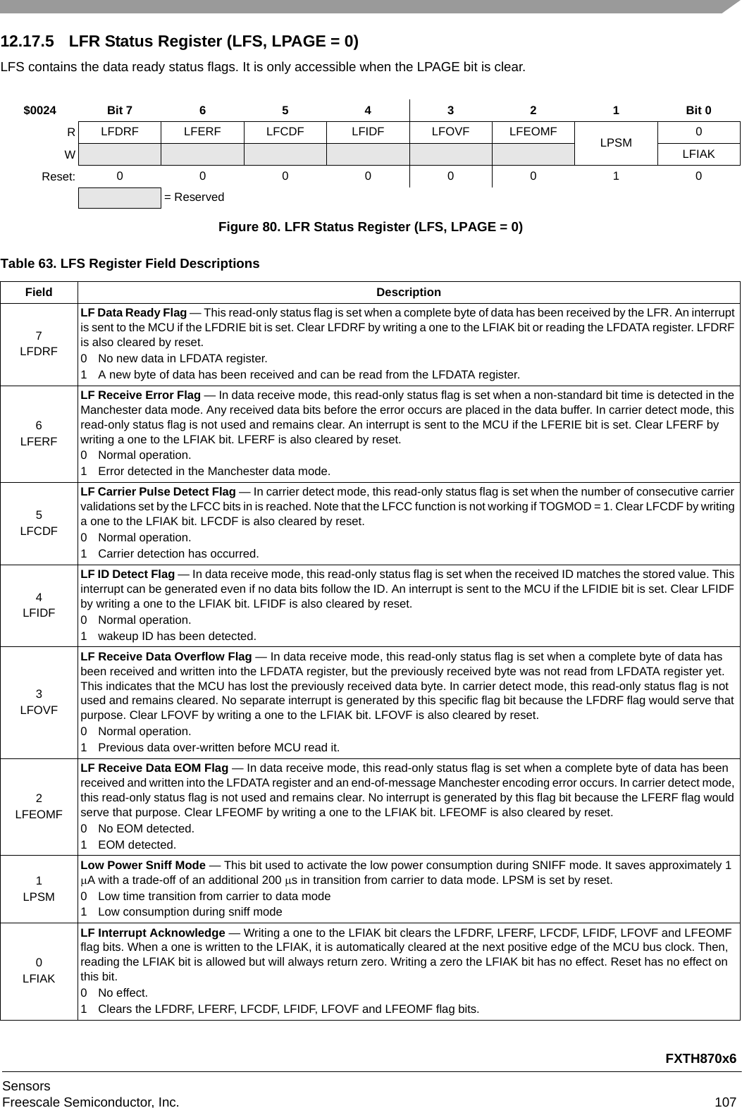
![FXTH870x6Sensors108 Freescale Semiconductor, Inc.12.17.6 LFR Data Register (LFDATA, LPAGE = 0)The LFDATA is a read-only register that contains the most recent received data value. It is only accessible when the LPAGE bit is clear. As data is serially received by the LFR, it is assembled into 8-bit values. When a new complete 8-bit value is received, it is moved into the LFDATA register, over-writing any previous value, and the LFDRF data ready flag is set to indicate a value is available for the MCU to read. If a previous value was ready but was not read out of the LFDATA register before a new data byte is ready, the LFOVF overflow flag is also set to indicate this overflow condition. Writes to LFDATA have no meaning or effect.12.17.7 LFR ID Registers (LFIDH:LFIDL, LPAGE = 0)These two 8-bit read/write registers hold one of two ID values for LF messages. They are only accessible when the LPAGE bit is clear. The type of ID checking can be selected or disabled by using the IDSEL[1:0] bits in the LFCTL1 register. When ID checking is enabled, the ID value received through the LFR must match the contents of the LFIDH and/or LFIDL registers depending on the IDSEL bits or the message will be ignored and the MCU will remain in standby mode to minimize power consumption. All these bits are cleared by a reset.$0025 Bit 7 654321Bit 0RRXDATA[7:0]WReset: 00000000= ReservedFigure 81. LFR Data Register (LFDATA) when LPAGE = 0Table 64. LFDATA Register Field DescriptionsField Description7:0RXDATA[7:0]Receive Data [7:0] — This is the received data from the LFR when in the data mode. All bits are read-only and any writes to these bits will be ignored. Reading this register will clear the LFDRF.$0026 Bit 7 6 5 4 3 2 1 Bit 0RID[0:7]WReset: 00000000Figure 82. LFR ID Low Byte (LFIDL)$0027 Bit 7 6 5 4 3 2 1 Bit 0RID[15:8]WReset: 00000000Figure 83. LFR ID High Byte (LFIDH)Table 65. LFR ID Register Field DescriptionField DescriptionID[15:0] ID bits 15 through 0 — These read/write bits contain bits 15 through 0 of the 16-bit ID value.](https://usermanual.wiki/Continental-Automotive/TIS-03/User-Guide-2718164-Page-112.png)
![FXTH870x6SensorsFreescale Semiconductor, Inc. 10912.17.7.1 LF Control E - LFCTRLE12.17.8 LFR Control Register D (LFCTRLD, LPAGE = 1)The LFCTRLD register contains two control bits for the LF detector and decoder. It is only accessible when the LPAGE bit is set.$0021 Bit 7 6 5 4 3 2 1 Bit 0RAZSC2 AZSC1 AZSC0WReset: 00000000= ReservedFigure 84. LF Control E (LFCTRLE)Table 66. LFCTRLE Register Field DescriptionField Description7-3Reserved Reserved bits — Not for user access.2-0AZSCLOGAMP AZ Sequencer Control — Control bits for AZ and trim within the LOGAMP.X00 Nominal AZ sequence - recommended settingX01 Short amp output release, max delay with RectsX10 Short amp output release, max delay with Amp input X11 All short, max delay with end of AZ 0XX Nominal sensitivity trim - recommended setting 1XX Sensitivities shifted by - 4 trim steps $0022 Bit 7 6 5 4 3 2 1 Bit 0RAVFOF[1:0] DEQS AZDC[1:0] ONMODE CHK125[1:0]WReset: 00000000Figure 85. LFR Control Register D (LFCTRLD, LPAGE = 1)Table 67. LFCTRLD Register Field DescriptionsField Description7-6AVFOF[1:0]SUM AZ release delay — Control the delay between falling edge of SUM d_az_en input and falling edge of internal AZ control line.00 No delay01 No delay10 One-half of 125 kHz clock period delay - recommended setting11 One and one-half of 125 kHz clock periods delay5DEQSDeQing status register — This read-only status bit allows the reading of the effective activation of the DeQing System.0 DeQing system not activated 1 DeQing system activated 4-3AZDC[1:0]AZ Digital Control of AZ triggering — In data receive mode, this bits control the triggering of AZ sequence with respect to both LFCPTAZ value (ref. LFCTRLB register) and the state of the demodulation input data state. 00 AZ starts after LFCPTAZ numbers of input data edges. 01 Z starts randomly adding -1, 0 or 1 to LFCPTAZ value between each AZ.10 AZ starts after LFCPTAZ numbers of input data edges and when the input data (d_data) state is 0. 11 AZ starts after LFCPTAZ numbers of input data edges and when the input data (d_data) state is 1 - recommended setting. 2ONMODEON Behavior Mode — This read/write bit selects how an error will affect the ON time. This bit is cleared by reset.0 Any error will stop the ON time.1 If remaining ON time, the LFR will go back to sniff mode at any error - recommended setting.](https://usermanual.wiki/Continental-Automotive/TIS-03/User-Guide-2718164-Page-113.png)
![FXTH870x6Sensors110 Freescale Semiconductor, Inc.NOTESetting CHK125[1:0] to either 0x01 or 0x10 increases the immunity to noise and therefore carries the side effect of narrowing the 125 kHz carrier bandwidth tolerance.12.17.9 LFR Control Register C (LFCTRLC, LPAGE = 1)The LFCTRLC register contains control bits for the LF detector and decoder. It is only accessible when the LPAGE bit is set.1-0CHK125[1:0]Accurate 125 kHz Check — The bit controls the CARVAL frequency check method.00 CARVAL validates on n (2*32 s packets), n depending on LFCDTM value - recommended setting for LowSensitivity mode.01 CARVAL validates on n (1*32 s packet + 4*8 s packets), n depending on LFCDTM value - optional recommendedsetting for High Sensitivity mode.10 CARVAL validates on n (8*8 s packet), n depending on LFCDTM value - optional recommendedsetting for High Sensitivity mode.11 Same as 00.$0023 Bit 7 6 5 4 3 2 1 Bit 0RAMPGAIN[1:0] FINSEL[1:0] AZEN LOWQ[1:0] DEQENWReset: 1100100 1Figure 86. LFR Control Register C (LFCTRLC, LPAGE = 1)Table 68. LFCTRLC Register Field DescriptionsField Description7-6AMPGAIN[1:0]3rd Amplifier gain — These bits controls the 3rd amplifier gain.00 Gain of 2 - recommended setting01 Gain of 310 Gain of 411 Gain of 65-4FINSEL[1:0]Final stage select — These bits select the final stage of the LOGAMP.00 Continuous time biasing - Fixed Gain 601 Continuous time biasing - Programmable Gain - recommended setting10 4th rectifier disabled11 4th rectifier disabled3AZENData AZ enable — This bit allows the AZ sequence during data frame.0 AZ during data disabled1 AZ during data enabled - recommended setting 2-1LOWQ[1:0]DeQing Resistor — These bits select the resistor added in parallel to the input network.00 4 k01 2 k10 1 k11 500 0DEQENDeQing System enable — The bit controls the DeQing system.0 DeQing disabled. 1 DeQing enabled.Table 67. LFCTRLD Register Field Descriptions (continued)Field Description](https://usermanual.wiki/Continental-Automotive/TIS-03/User-Guide-2718164-Page-114.png)
![FXTH870x6SensorsFreescale Semiconductor, Inc. 11112.17.10 LFR Control Register B (LFCTRLB, LPAGE = 1)The LFCTRLB register contains control bits for the LF detector and decoder. It is only accessible when the LPAGE bit is set.$0024 Bit 7 6 5 4 3 2 1 Bit 0RHYST[1:0] LFFAF LFCAF LFPOL LCPTAZ[2:0]WReset: 11000100Figure 87. LFR Control Register B (LFCTRLB, LPAGE = 1)Table 69. LFCTRLB Register Field DescriptionsField Description7-6HYST[1:0]Control slicer hysteresis 00 20 mV hysteresis01 40 mV hysteresis10 50 mV hysteresis11 30 mV hysteresis - recommended setting5-4LFFAF;LFCAFAverage filter bi-phase filtering control — Activates bi-phase filtering and control offset value00 Standard low pass filtering activated - recommended setting01 Standard low pass filtering activated10 Bi-phase filtering activated - Low offset from input signal low level11 Bi-phase filtering activated - High offset from input signal low level3LFPOLLF Manchester Polarity Select — This read/write bit selects the polarity of the transition in the middle of the bit time. The LFPOL is not used in Carrier mode. Reset clears LFPOL bit.0 Zero is falling edge in middle of a bit time, one is a rising edge in the middle of bit time.1 Zero is rising edge in middle of a bit time, one is a falling edge in the middle of bit time.2-0 LFCPTAZ[2:0] LF auto-zero counter — Applications to set these bits to 0x06 for proper LF operation. These bits tune the minimum number of data edges between two auto-zero requests during a data frame.](https://usermanual.wiki/Continental-Automotive/TIS-03/User-Guide-2718164-Page-115.png)
![FXTH870x6Sensors112 Freescale Semiconductor, Inc.12.17.11 LFR Control Register A (LFCTRLA, LPAGE = 1)The LFCTRLA register contains control bits for the LF detector and factory test selects. It is only accessible when the LPAGE bit is set.$0025 Bit 7 6 5 4 3 2 1 Bit 0RLFCC[3:0]WReset: 00000000= ReservedFigure 88. LFR Control Register A (LFCTRLA, LPAGE = 1)Table 70. LFCTRLA Register Field DescriptionsField Description7-4Reserved Reserved bits — Not for user access.3-0LFCC[3:0]LF Successive Carrier Validations Counter — The value of the LFCC[3:0] bits define how many times the carrier detect sample ON time detected an LF carrier signal before the LFCDF flag bit set. The flag will be risen when the number of ON samples with a detected carrier greater than the LFCDTM[3:0] reaches the value of the LFCC[3:0] bits plus one. The internal count of detected carrier pulses will increment the count as long as they are consecutive samples. When a sample is encountered without any detected carrier the count will be reset.The LFCC register is considered reset in data mode. The first carrier validation will lead to start up of the receiver chain.This feature allows the user to define a number of consecutive carrier detections are required before the flag is risen; and is useful in detecting long duration carrier pulses. This counter is disabled if TOGMOD = 1.](https://usermanual.wiki/Continental-Automotive/TIS-03/User-Guide-2718164-Page-116.png)
![FXTH870x6SensorsFreescale Semiconductor, Inc. 11313 RF ModuleIt is not intended that the RFM may be actively powered up and/or transmitting RF data while physical parameter measurements are being made; or during the time that the LFR may be actively receiving/decoding LF signals. The resulting interactions will degrade the performance of the RF output spectrum.The FXTH870x6 consists of an RF module (RFM) with external crystal-driven oscillator, VCO, fractal-n PLL and RF output amplifier (PA) for an antenna. It also contains a small state machine controller, random time generator and hardware data buffer for automated output or direct control from the MCU. The overall block diagram is shown in Figure 89.Figure 89. RF Transmitter Block Diagram13.1 RF Data ModesThere are two modes of operation in using the RF output in either the data buffer mode or MCU direct mode.13.1.1 RF Data Buffer ModeIn the RF data buffer mode the transmissions are sent by dedicated logic hardware while the MCU can be put into a low power mode until the transmission is completed. This RF state machine is clocked by the MFO which is enabled when the SEND bit is set and when any of the LFR, SMI or MCU are operating.The RF data buffer consists of a dedicated RFM state machine and a 256-bit data buffer. The RF data buffer is loaded with whatever data pattern the user software creates. The number of data bits to be sent is selected by the FRM[7:0] control bits. The control logic is triggered by the SEND control bit when it is time to transmit the data which is sent to the RF stage after being encoded as either Manchester, Bi-Phase or NRZ data according to the method selected by the CODE[1:0] bits as described in Section 13.17.Before the data can be transmitted the RFM control logic enables the external crystal oscillator and phase-locked-loop to initialize before the RF output stage can begin transmission.CRYSTALCONTROLREGISTERSRFAMPVCOXIXOPHASEDETECTORRFLOW-PASSFILTERFRACTIONAL-NDIVIDEROSCILLATORAND LOGIC256-BITDATA BUFFERMODULATIONCONTROLRFSTATEMACHINEMCUAVDDAVSSVREGRINT LFSRRANDOMGENMFODX500 kHzVOLTREGRFAVDDRFLVD](https://usermanual.wiki/Continental-Automotive/TIS-03/User-Guide-2718164-Page-117.png)
![FXTH870x6Sensors114 Freescale Semiconductor, Inc.The external crystal connected to the X0 and XI pins provides the carrier frequency as well as the data rate clock needed for the data rates associated with the OOK or FSK modulation. Therefore the tolerance on the data rate will depend on the characteristics of the external crystal.Once the data buffer is emptied the data transfer stops; the RF output stage is turned off; and the SEND control bit is cleared and an interrupt of the MCU may be generated to wake it from the STOP1 mode. The user can test that the transmission has completed by reading back the state of the SEND control bit or the RFIF status bit. There is also the option to send the same data frame from 1 to 16 times with interlaced time intervals when the RF transmitter PA output stage is off. If multiple frames of data are to be transmitted within a datagram the spacing before the first frame and between subsequent frames can be controlled by the RFM state machine in several ways:1. Use of a programmable timer (random, base time, time adder).2. No time delays.In addition, the RFM crystal oscillator, VCO and PLL can be turned off during any interframe timing by use of the IFPD bit.When using the data buffer mode the user’s software should not change any bits in the RFM registers after the SEND has been set and the transmission is still in progress. Changing RFM register contents during a transmission can lead to data faults or errors.13.1.2 MCU Direct ModeWhen the CODE[1:0] bits are both set the encoding is controlled directly by the MCU where the data to the RF output depends on the state of the DATA bit and the selected modulation scheme. In this mode the user software must control the RF output stage to power up (using the SEND control bit), WAIT for the RF output stage to stabilize (monitor the RCTS status bit) and clock the DATA to the RF output stage. In this mode the data rate and its stability will depend on the internal HFO oscillator.Any transfers of data from the MCU will use the DATA bit which will be reflected as modulated data on the RF pin once the RF output stage is set up to transmit. The maximum data rate in this mode will depend on the complexity of the user software and the MCU clock rate. The POL bit in this case simply inverts the state of the DATA bit before it drives the RF output stage.The accuracy of the data rate in the MCU direct mode is directly dependant on the HFO accuracy.13.2 RF Output Buffer Data FrameWhen using the RF data buffer mode each frame of data is sent as 2 to 256 bits per frame with a possible two trailing bits for an end-of-message, EOM, as shown in Figure 90. The actual data being transmitted in a given data frame and any combinations of data frames into a single datagram is dependent on the user software.The number of frames sent in a given datagram can be from 1 to 16 based on the FNUM[3:0] bits in the RFCR3. The 256-bit buffer is divided into two pages of 128 bits as selected by the RPAGE bit in the RFCR2.The data buffer is unloaded to the RF output starting with the least significant bit (RFD0) in the least significant byte (RFB0) up through the most significant bit (RFD127) in the most significant byte (RFB15). This is often referred to as “little-endian” data ordering.](https://usermanual.wiki/Continental-Automotive/TIS-03/User-Guide-2718164-Page-118.png)
![FXTH870x6SensorsFreescale Semiconductor, Inc. 115Figure 90. Data Frame Formats13.2.1 Data Buffer LengthThe number of bits sent in a given transmission frame is selected by the FRM[7:0] control bits encoded as a direct binary number plus one. This gives a range of 2 through 256 bits. Data written to data buffer bits above the highest bit number will be ignored. Transmission always begins with the data written in the RFB0 location. When the requested number of bits have been transmitted an interrupt to the MCU can be generated if the RFIE bit is set.13.2.2 End of Message (EOM)If the EOM control bit is set, then at the end of the data frame there will be carrier for a period of two bit times at level high for the OOK modulation modes or fDATA1 for the FSK modulation modes. Following the EOM period there will be no carrier for either the OOK or FSK modes. If the EOM control bit is clear, no EOM period will be added to the transmission.2EOM2562Maximum258-Bit Format80-Bit Format53-Bit Format2-Bit Format Data in each byte defined by user softwareOptional EOMRFB0 RFB1 RFB2 RFB3 RFB4 RFB5 RFBA RFBB RFBC RFBD RFBE RFBF80RFB0 RFB1 RFB2 RFB3 RFB4 RFB5 RFB6 RFB7 RFB8 RFB953RFB0 RFB1 RFB2 RFB3 RFB4 RFB5RFB62EOMBits [2:0]with all byte lengthsMinimumRFB0Bits [1:0]](https://usermanual.wiki/Continental-Automotive/TIS-03/User-Guide-2718164-Page-119.png)
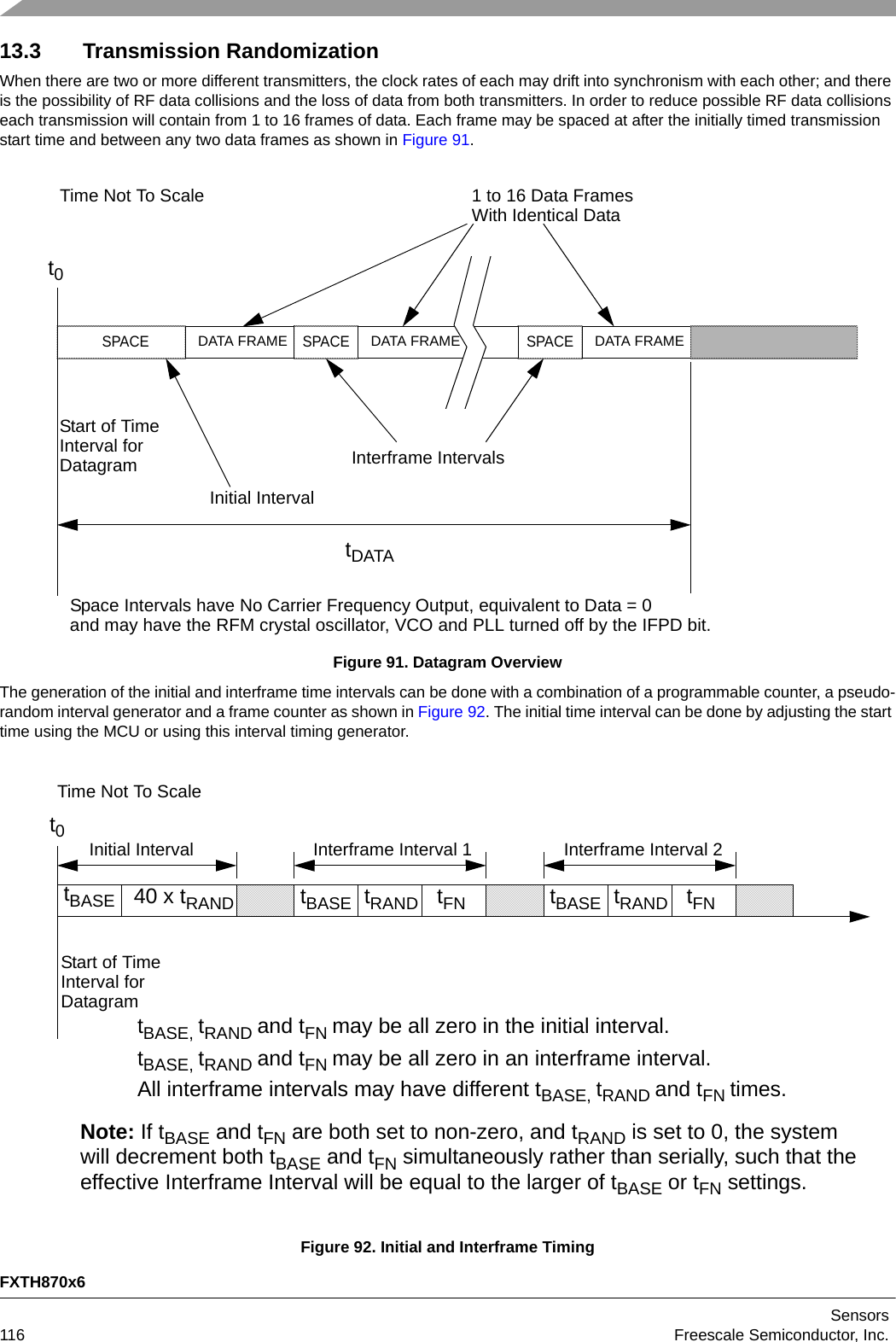
![FXTH870x6SensorsFreescale Semiconductor, Inc. 11713.3.1 Initial Time IntervalWhen generating an initial time interval the MCU loads the RFM interval generator variables and then goes into the STOP1 mode. When the initial time interval ends the data in the RFM data buffer is automatically sent and the MCU will wake at the end of the transmission. The initial time interval is made up of two components:Eqn. 10where:tINIT = Total time interval before first frame is transmitted in mstBASE = Base time in ms; 5 ms not recommendedtRAND = Pseudo-random time in ms based on a Galois 7-bit LFSRThe components of this time are described in the following sections.13.3.2 Interframe Time IntervalsWhen generating an interframe time interval the MCU loads the RFM interval generator variables and then goes to the STOP1 mode. When the interframe time interval ends the data in the RFM data buffer is automatically sent and the MCU will wake at the end of the transmission. The interframe time interval is made up of three components:Eqn. 11where:tIFRM = Total time interval between each transmitted frame in mstBASE = Base time in ms; 5 ms not recommendedtFN = Time adder in ms for frame numbertRAND = Pseudo-random time in ms based on a Galois 7-bit LFSRThe components of this time are described in the following sections.13.3.3 Base Time IntervalThe base time interval, tBASE, is used in the initial time interval and in datagram transmissions with two or more frames. The programmable frame space interval is based on a simple 8-bit, count-down timer as described by the RFBT[7:0] control bits in the RFCR4 register. This time interval is forced to zero when the RFBT[7:0] are all clear.The range of the base time must be set to 0 or between 5 and 255 ms using a clock generated from the MFO divided by 125.13.3.4 Pseudo-Random Time IntervalThe pseudo-random time interval, tRAND, is used both in the initial and the interframe time intervals if the LFSR[6;0] bits are set to something other than all zeros. When the ISPC bit is set the pseudo-random initial time interval before the first data frame will be 40 times the value of tRAND.When the LFSR[6:0] bits are used the tRAND time will vary based on a pseudo-random generated binary number using a Galois linear feedback shift register (LFSR) implemented using the primitive polynomial for a 7-stage register as shown in Figure 93.This LFSR creates a sequence of 127 binary numbers including $01 through $3F which are each repeated only once in each sequence of 127 clocks of the shift register. The LFSR is initialized to $40 during power up of the device. When a random interval is to be determined the contents of the LFSR are sampled as the “random number” for calculating the required interval time. Following the use of the random interval the LFSR is clocked once to advance it to the next pseudo-random number.The range of the pseudo-random time is 1 to 127 ms using a clock generated from the MFO divided by 125. The current value of the LFSR can be changed and/or read by the LFSR[6:0] bits in the RFCR5 register.tINIT tBASE 40 tRAND+=tIFRM tBASE tRAND tFN++=](https://usermanual.wiki/Continental-Automotive/TIS-03/User-Guide-2718164-Page-121.png)
![FXTH870x6Sensors118 Freescale Semiconductor, Inc.Figure 93. LFSR ImplementationA value of all zeros in the LFSR will remain unchanged with every clock input and cannot be used as a starting “seed.”The resulting range of times for the initial and interframe pseudo-random time will be as given in Table 71 for both the design center and the variation resulting from the tolerance of the MFO clock.13.3.5 Frame Number TimeThe frame number time, tFN, is only used between frames and is based on a selectable time from 0 to 63 ms and the number of the frame that was just transmitted as given in Table 72. If the frame number time is not used, the value of the selected time should be set to zero. The maximum number of frames is defined by the FNUM[3:0] control bits.The range of the frame number time is a multiple of 0 to 63 ms using a clock generated from the MFO divided by 125. The value of this time multiple can be changed by the RFFT[5:0] bits in the RFCR6 register.Table 71. Randomization Interval TimesTimeInterval RandomizationNumber Ideal Time Interval (ms) Time Interval Including MFO Tolerance (ms)Minimum MaximumInitial 1 40 37.2 42.8127 5080 4347.2 5434.6Interframe 1 1 0.93 1.07127 127 118.1 135.9Table 72. Frame Number Interval TimesValue ofFNUM[3:0] Number ofFrames Frame Interval Where Time AddedNominal Frame Number Time Interval Added (ms)Minimum Maximum0 1 None n/a n/a121 - 21 632 3 2 - 3 2 1263 4 3 - 4 3 1894 5 4 - 5 4 2525 6 5 - 6 5 3156 7 6 - 7 6 3787 8 7 - 8 7 4418 9 8 - 9 8 504DQRDQRDQRDQRDQRDQRDQSS0S1S2S3S4S5S6CLKRFMRST7-BIT Random NumberGalois Primitive Polynomial = X7 + X3 + 1](https://usermanual.wiki/Continental-Automotive/TIS-03/User-Guide-2718164-Page-122.png)
![FXTH870x6SensorsFreescale Semiconductor, Inc. 11913.4 RFM in STOP1 ModeThe entire RF transmitter digital section can remain powered up, if enabled by the RFEN bit (see Section 5.3), when the MCU goes into the STOP1 mode.13.5 Data EncodingThe CODE[1:0] control bits select either Manchester, Bi-Phase, NRZ or MCU direct data encoding of each data bit being transferred from the RF data buffer to the RF output stage. Further, the polarity of the selected encoding method can be inverted using the POL control bit.13.5.1 Manchester EncodingWhen the CODE[1:0] bits are both clear the data is Manchester encoded format, with data transmitted as a transition in voltage occurring in the middle of the bit time. The polarity of this transition is selected by the POL bit. When the POL bit is cleared, then a logical LOW is defined as an increase in signal in the middle of a bit time and a logical HIGH is defined as a decrease in signal in the middle of a bit time as shown in Figure 94. When the POL bit is set, then a logical LOW is defined as an decrease in signal in the middle of a bit time and a logical HIGH is defined as a increase in signal in the middle of a bit time as shown in Figure 95. Since there is always a transition in the middle of the bit time there must also be a transition at the start of a bit time if consecutive “1” or “0” data are present.13.5.2 Bi-Phase EncodingWhen the CODE[1:0] bits are 0:1 then the data is Bi-Phase encoded format, with data transmitted as the presence or absence of a transition in signal in the middle of the bit time. The polarity of this transition is selected by the POL bit. Unlike Manchester coding there is always a signal transition at the boundaries of each bit time. When the POL bit is cleared, then a logical HIGH is defined as no change in signal in the middle of a bit time and a logical LOW is defined as a change in the signal in the middle of a bit time as shown in Figure 96. When the POL bit is set, then a logical HIGH is defined as a change in signal in the middle of a bit time and a logical LOW is defined as no change in the signal in the middle of a bit time as shown in Figure 97. Since there is always a transition at the ends of the bit time consecutive bits of the same state may have two signal states (high or low) during the middle of the bit time.13.5.3 NRZ EncodingWhen the CODE[1:0] bits are 1:0 then the data is NRZ encoded format, with data transmitted as either a high or low for the complete bit time. The polarity of this state is selected by the POL bit. The Manchester and Bi-Phase encoding can actually be created using NRZ encoding running at twice the desired data rate.9 10 9 - 10 9 56710 11 10 - 11 10 63011 12 11 - 12 11 69312 13 12 - 13 12 75613 14 13 - 14 13 81914 15 14 - 15 14 88215 16 15 - 16 15 945Table 72. Frame Number Interval Times (continued)Value ofFNUM[3:0] Number ofFrames Frame Interval Where Time AddedNominal Frame Number Time Interval Added (ms)Minimum Maximum](https://usermanual.wiki/Continental-Automotive/TIS-03/User-Guide-2718164-Page-123.png)
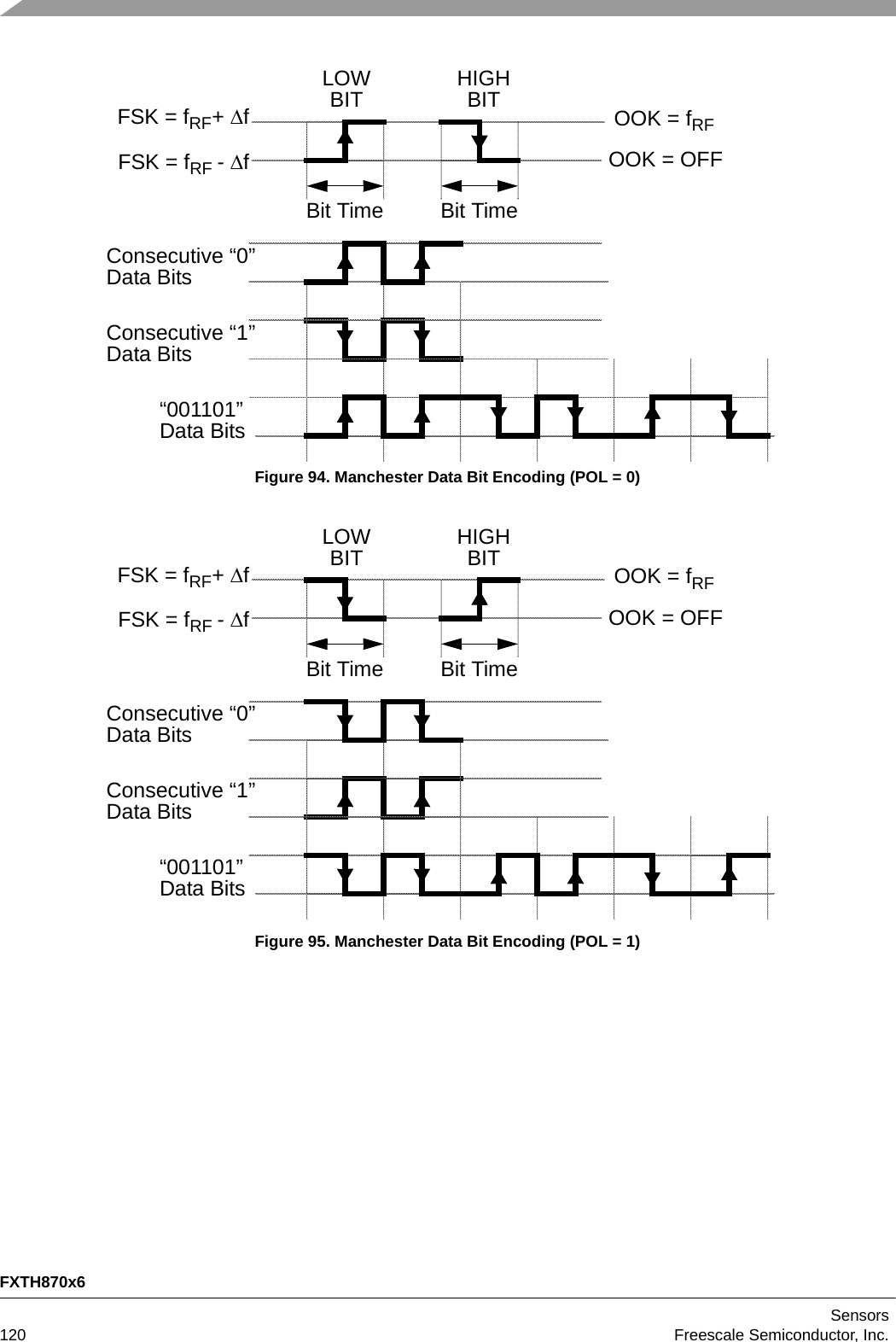
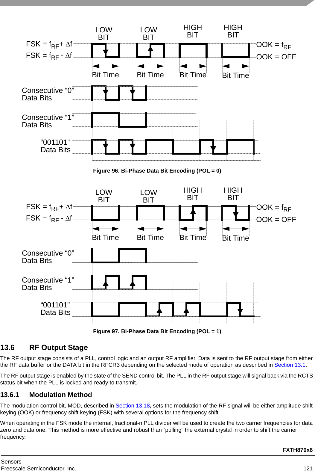
![FXTH870x6Sensors122 Freescale Semiconductor, Inc.13.6.2 Carrier FrequencyThe carrier frequency is established mainly by the external crystal used, but a centering of the fractional-n PLL provides more precise control. If the CF control bit is clear the PLL will be configured for a carrier center frequency of the 315 MHz. If the CF control bit is set the PLL will be configured for a carrier center frequency of the 434 MHz.13.6.3 RF Power OutputThe maximum power output from the RF pin can be adjusted to one of 21 levels using the PWR[4:0] bits.13.6.4 Transmission ErrorAny transmission will be aborted if one of the following occurs:1. The RCTS signal does not become active within the tLOCK time.2. The PLL falls out of lock after once being set and the SEND bit is still active.3. The XCO monitor output falls.If either of these cases occurs the RF output will be turned off; the SEND control bit will be cleared; and the transmission error status flag, RFEF, will be set. The RFEF bit triggers an interrupt of the MCU if the RFIEN is set. The RFEF bit is cleared by writing a logical one to the RFIAK bit.13.6.5 Supply Voltage Check During RF TransmissionA separate low voltage detector can be enabled during the RF transmission and a status bit checked for low voltage drops due to a weak battery during the higher transmission currents. This RF LVD can be enabled by setting the RFLVDEN bit and the resulting status is reported on the RFVF bit. The RFVF bit can be cleared by writing a logical one to the RFIAK bit if the supply voltage has risen above the detect threshold. Further, if the voltage falls far enough for the VCO and PLL to fall out-of-lock, then the RF output will be turned off and the transmission will be terminated.13.6.6 RF Reset (RFMRST)The RF state machine, crystal oscillator, PLL and VCO can be reset to the initial off state by the RFMRST signal generated by one of the following methods:1. Internal RFM power-on reset (RFPOR).2. Writing a one to the RFMRST bit in the RFCR7. Any of these reset methods will not alter any data stored in the data buffer.13.7 RF InterruptThe RFM will interrupt the MCU when the SEND bit is cleared at the end of a data buffer transmission. This interrupt occurs at the end of a programmed set of frames. If the number of frame count FNUM[3:0] is set to zero, then only one frame is sent and the interrupt occurs at the end of that first frame transmitted. If the number of the frame count is greater than zero, then the interrupt will be generated depending on the state of the IFID bit.The interrupt will also create a flag bit, RFIF, which can be cleared by writing a logical one to the RFIAK bit. The interrupt can be enabled/disabled by the RFIEN bit.13.8 Datagram Transmission TimesIn order to comply with FCC requirements in the US market the periodically transmitted datagram must be less than 1 second in length and be separated by an off time that is at least 10 seconds or at least 30 times longer than the transmission time, whichever is longer. The user software must adhere to this ruling for products intended for the US market.](https://usermanual.wiki/Continental-Automotive/TIS-03/User-Guide-2718164-Page-126.png)
![FXTH870x6SensorsFreescale Semiconductor, Inc. 12313.9 RFM RegistersThe RFM contains twelve registers to control its functions and 32 registers to provide access to the output data buffer.13.9.1 RFM Control Register 0 - RFCR0The RFCR0 register contains eight control bits for setting the output data rate of the RFM as described in Figure 98.The BPS[7:0] bits are set to $34 by an RFMRST signal which results in a default data rate of approximately 9600 bps.13.10 RFM Control Register 1 - RFCR1The RFCR1 register contains eight control bits for the RFM as described in Figure 99.$0030 Bit 7 654321Bit 0RBPS[7:0]WRFMRST: 00110100Figure 98. RFM Control Register 0 (RFCR0)Table 73. RFCR0 Field DescriptionsField Description7–0BPS[7:0]Data Rate - The BPS[7:0] control bits select the data rate for the transmitted datagrams as described by the following equation:where:fDATA= Data rate in bits/secondfXTAL= External crystal frequency in Hz = 26 MHzBPS= Value of data rate code (BPS[7:0])Examples of the value for common data rates are given in Table 74. The BPS[7:0] control bits are set to $34 by the RFMRST signal which results in a default data rate of 9600 bits/sec.Table 74. Data Rate Option ExamplesData Rate BPS[7:0]Decimal Value Data Rate BPS[7:0]Decimal ValueTarget Nominal fXTAL = 26 MHz Target Nominal fXTAL = 26 MHz2000 bps 2000.0 249 4800 bps 4807.7 1032400 bps 2403.8 207 5000 bps 5000.0 994000 bps 4000.0 124 9600 bps 9615.4 514500 bps 4504.5 110 19200 bps 19230.8 25$0031 Bit 7 6 5 4 3 2 1 Bit 0RFRM[7:0]WRFMRST: 00000000Figure 99. RFM Control Register 1 (RFCR1)fDATAfXTAL52 BPS 1+------------------------------------- 5x10⁵BPS 1+-------------------------==](https://usermanual.wiki/Continental-Automotive/TIS-03/User-Guide-2718164-Page-127.png)
![FXTH870x6Sensors124 Freescale Semiconductor, Inc.13.11 RFM Control Register 2 - RFCR2The RFCR2 register contains eight control bits for the RFM as described in Figure 100.Table 75. RFCR1 Field DescriptionsField Description7-0FRM[7:0]Frame Bit Length - The FRM[7:0] control bits select the number of bits in each datagram. The number of bits is determined by the binary value of the FRM[7:0] bits plus one. This makes the range of bits from 2 to 256. A value of $00 for the FRM[7:0] control bits will result in no frames being sent. The FRM[7:0] control bits are cleared by RFMRST signal.$0032 Bit 7 654321Bit 0RSEND RPAGE EOM PWR[4:0]WRFMRST: 00000000Figure 100. RFM Control Register 2 (RFCR2)Table 76. RFCR2 Field DescriptionsField Description7SENDTransmission Start Control- The SEND control bit starts the transmission of data held in the RFM data buffer according to the bit length specified by the FRM[7:0] bits. The SEND control bit is automatically cleared when the data buffer transmission has ended or by the RFMRST signal. A transmission can be prematurely interrupted by writing a logical zero to the SEND bit.0 Data transmission ended or transmission not in progress.1 Start data transmission or transmission in progress.6RPAGEBuffer Page Select — The RPAGE bit will select the lower or upper 16 bytes of the RFM data buffer when writing/reading to the RFD0-RD15 registers. This bit also selects between the lower and upper banks of RFM registers at addresses $0038 through $003B. This bit is cleared by a reset of the MCU.0 Select the lower 16 bytes of the RFM data buffer.1 Select the upper 16 bytes of the RFM data buffer.5EOMEnd Of Message - The EOM control bit selects whether there will be two data bit times of data 1 carrier state at the end of each datagram. The EOM control bit is cleared by a RFMRST.0 EOM bit times not added.1 EOM bit times added.](https://usermanual.wiki/Continental-Automotive/TIS-03/User-Guide-2718164-Page-128.png)
![FXTH870x6SensorsFreescale Semiconductor, Inc. 1254:0PWR[4:0]RF Amplifier Power Level - The PWR[4:0] control bits select the optimum power output of the RF power amplifier. These power output levels assume optimal matching network to the RF pin. The PWR[4:0] control bits are cleared a RFM reset. The PWR control bits are initially set to 0x00. This setting targets -10 dBm typical power output. The PWR control bits scale the typical output power level from -1.5 to 8 dBm in steps of 0.5 dB and fixes the low power level mode to -10 dBm, The power control range is defined as follows:00000 set output power level to -10 dBm (Default Value)00001 set output power level to -1.5 dBm00010 set output power level to -1.0 dBm00011 set output power level to -0.5 dBm00100 set output power level to 0.0 dBm00101 set output power level to 0.5 dBm00110 set output power level to 1.0 dBm00111 set output power level to 1.5 dBm01000 set output power level to 2.0 dBm01001 set output power level to 2.5 dBm01010 set output power level to 3.0 dBm01011 set output power level to 3.5 dBm01100 set output power level to 4.0 dBm01101 set output power level to 4.5 dBm01110 set output power level to 5.0 dBm01111 set output power level to 5.5 dBm10000 set output power level to 6.0 dBm10001 set output power level to 6.5 dBm10010 set output power level to 7.0 dBm10011 set output power level to 7.5 dBm10100 set output power level to 8.0 dBmCodes greater than 10100 are reserved for test purposes and should not be used.Table 76. RFCR2 Field Descriptions (continued)Field Description](https://usermanual.wiki/Continental-Automotive/TIS-03/User-Guide-2718164-Page-129.png)
![FXTH870x6SensorsFreescale Semiconductor, Inc. 12713.12 RFM Control Register 3 - RFCR3The RFCR3 register contains five control bits for the RFM as described in Figure 102 which sets the number of frames in each RF datagram.$0033 Bit 7 654321Bit 0RDATA IFPD ISPC IFID FNUM[3:0WRFMRST 00000000Figure 102. RFM Control Register 3 (RFCR3)Table 77. RFCR3 Field DescriptionsField Description7DATAData State - The DATA bit determines the output state of the RF power amplifier when the RFM is in the MCU direct control mode (CODE[1:0] = 11)0 RF output state low.1 RF output state high.6IFPDInterframe Power Down — The IFPD control bit selects whether the XCO and associated analog blocks are powered down during interframe timing caused by the RFM. The IFPD control bit is cleared by the RFMRST signal.0 The XCO remains powered up as long as the SEND bit is set.1 The XCO is powered down during RFM controlled interframe timing events. The restart of these functions will start 1 ms before the end of the timing interval if anotherframe is to be transmitted.5ISPCInitial Random Space— When the ISPC bit is set the initial time delay before the first frame will be enabled. This bit is cleared by an RFM reset.0 No initial time interval.1 Initial time interval enabled.4IFIDInterframe Interrupt Delay — The IFID control bit selects whether the RFIF bit is set and the MCU is interrupted at the end of each frame sent or at the end of the last frame in a multiple frame message. The IFID control bit is cleared by the RFMRST signal.0 The RFIF bit is set and the MCU interrupted if the RFIEN bit is set, after the last frame transmitted.1 The RFIF bit is set and the MCU interrupted if the RFIEN bit is set, only after the last frameplus an additional interframe message is transmitted.3-0FNUM[3:0]FNUM[3:0] — The FNUM[3:0] bits set the number of frames transmitted in each RF datagram. The frames will be randomly spaced apart as described it Section 13.3.These bits are cleared by an RFM reset. The number of frame transmitted is the binary number plus one.](https://usermanual.wiki/Continental-Automotive/TIS-03/User-Guide-2718164-Page-131.png)
![FXTH870x6Sensors128 Freescale Semiconductor, Inc.13.13 RFM Control Register 4 - RFCR4The RFCR4 register contains eight control bits to set the initial and interframe timing base timing variable as described in Figure 103. A RFMRST signal clears the RFBT[7:0] bits.13.14 RFM Control Register 5 - RFCR5The RFCR5 register contains eight control bits to set the initial and interframe random timing variable as described in Figure 104. A RFMRST signal clears the LFSR[6:0] bits causing the random time variable to be ignored.NOTEIf RFBT[7:0] and RFFT[5:0] are both set to non-zero, and LFSR[6:0] is set to 0x00, the system will decrement both RFBT and RFFT simultaneously rather than serially, such that the effective Interframe Interval will be equal to the larger of RFBT or RFFT settings.$0034 Bit 7 654321Bit 0RRFBT[7:0]WRFMRST: 10000000Figure 103. RFCR4 Register - Base Time VariableTable 78. RFCR4 Field DescriptionsField Description7:0RFBT[7:0]Base Timer - The RFBT[7:0] control bits select the interframe timing between multiple frames of transmission. The base time value is equal to a nominal one millisecond for each count of the RFBT[7:0] bits. The RFBT[7:0] control bits are cleared by the RFMRST signal and must be set to either 0 or between 5 and 255.$0035 Bit 7 654321Bit 0RBOOST LFSR[6:0]WRFMRST: 00000000Figure 104. RFCR5 Register - Pseudo-Random Time VariableTable 79. RFCR5 Field DescriptionsField Description7BOOSTBOOST - This bit controls the VCO power consumption in order to decrease the phase noise required by the Japanese regulation. The BOOST control bit is cleared by the RFMRST signal.0 The VCO runs at its lower power consumption level (higher phase noise).1 The VCO runs at its higher power consumption level (lower phase noise).6:0LFSR[6:0]Pseudo-Random Timer- The LFSR[6:0] bits select the current seed value of the LFSR when enabling pseudo-random timing intervals when any of the LFSR[6:0] bits are set. The value written to this register is loaded into the actual LFSR when the SEND bit is set. The time value is equal to a nominal one millisecond for each count of the resulting LFSR[6:0] bits.A value of $00 placed in the LFSR causes the LFSR to stay at the $00 state on each clocking of the LFSR. To cause the LFSR to cycle through its pseudo-random number sequence requires that any value other than $00 be written to the LFSR[6:0] bits.](https://usermanual.wiki/Continental-Automotive/TIS-03/User-Guide-2718164-Page-132.png)
![FXTH870x6SensorsFreescale Semiconductor, Inc. 12913.15 RFM Control Register 6 - RFCR6The RFCR6 register contains eight control bits to set the initial and interframe frame number timing variable as described in Figure 105. A RFMRST signal clears the RFFT[5:0] bits.13.16 RFM Control Register 7 - RFCR7The RFCR7 register contains four control bits and four status bits for the RFM as described in Figure 106.$0036 Bit 7 654321Bit 0RVCO_GAIN[1:0] RFFT[5:0}WRFMRST: 10000000Figure 105. RFCR6 Register - Frame Number Time - RFTS[1:0] = 1:0Table 80. RFCR6 Field DescriptionsField Description7:6VCO_GAIN[1:0]VCO Gain Selection - These bits control the VCO gain. The VCO_GAIN[1] bit is set and the VCO_GAIN[0] bit is cleared by the RFMRST signal. Not normally need to be adjusted by the end user.5:0RFFT[5:0]Frame Number Timer - The RFFT[5:0] control bits select the interframe timing between multiple frames of transmission. The time value is equal to a nominal one millisecond for each count of the RFFT[5:0] bits multiplied by the frame number of the last transmitted frame. The RFFT[5:0] control bits are cleared by the RFMRST signal.$0037 Bit 7 6 5 4 3 2 1 Bit 0RRFIF RFEF RFVF 0RFIEN RFLVDEN RCTS 0WRFIAK RFMRSTRFMRST: 00000000= ReservedFigure 106. RFM Transmit Control Registers (RFCR7)Table 81. RFCR7 Field DescriptionsField Description7RFIFRF Interrupt Flag— The read-only RFIF status bit indicates if the RF transmission has ended properly when using the data buffer mode and the SEND bit has been cleared. Writes to this bit will be ignored. The RFIF status bit is cleared by writing a logical one to the RFIAK bit or the RFMRST bit. RFMRST signal clears this bit.0 RF transmission in progress or not in the data buffer mode.1 RF transmission completed in the data buffer mode.6RFEFRF Transmission Error Flag— The read-only RFEF status bit indicates if there was an error in the current or prior RF transmission as described in Section 13.6.4. Writes to this bit will be ignored. The RFEF status bit is cleared by writing a logical one to the RFIAK bit or the RFMRST bit. RFMRST signal clears this bit.0 No RF transmission error occurred.1 RF transmission error occurred.5RFVFRF LVD Trigger Flag— When the RF LVD is enabled and the supply voltage falls below the threshold, the read-only RFVF flag will be set if the RFLVDEN bit is set. Writes to this bit will be ignored. The RFVF status bit is cleared by writing a logical one to the RFIAK bit or the RFMRST bit. RFMRST signal clears this bit0 Voltage is and has been above RF LVD rising threshold or the RF LVD is disabled.1 Voltage has dropped below the RF LVD falling threshold since last reset of this bit.4RFIAKAcknowledge RF Interrupt Flags— Writing a one to the RFIAK bit clears the RFIF, RFEF and RFVF flag bits. Writing a zero to the RFIAK bit has no effect on the RFIF, RFEF and RFVF flag bits. The RFMRST signal has no effect on this bit.0 No effect.1 Clear the RFIF, RFEF, and RFVF bits.](https://usermanual.wiki/Continental-Automotive/TIS-03/User-Guide-2718164-Page-133.png)
![FXTH870x6Sensors130 Freescale Semiconductor, Inc.13.17 PLL Control Registers A- PLLCR[1:0], RPAGE = 0The PLLCR[1:0] registers contain 16 control bits for the RFM as described in Figure 107. These bits are only accessible when the RPAGE bit is cleared.3RFIENRF Interrupt Enable— The RFIEN bit enables the RFIF, the RFEF and the RFVF bits to generate an interrupt to the MCU. The RFMRST signal clears this bit. 0 RF interrupts disabled.1 RF interrupts enabled.2RFLVDENRF LVD Enable — When the RFLVDEN bit is set, the RF LVD circuit will be enabled, and the RF LVD events are routed to the RF LVD Trigger Flag. This bit is cleared by the RFMRST signal.0 RF LVD disabled.1 RF LVD enabled.1RCTSRF Clear To Send Status— When the RCTS bit is set the RF XCO, VCO and PLL have started and locked and the RFM is ready to send data. This bit is cleared by the RFMRST signal.0 RFM not ready to send.1 RFM ready to send.0RFMRSTRFM Reset — Writing a one to the RFMRST bit will completely reset the RFM and its registers. This bit is not affected by a reset of the MCU. This bit will always read as a zero.0 No effect.1 Reset RFM.$0038 Bit 7 654321Bit 0RAFREQ[12:5]WRFMRST: 00000000$0039RAFREQ[4:0] POL CODEWRFMRST: 00000000Figure 107. PLL Control Registers A (PLLCR[1:0], RPAGE = 0)Table 82. PLLCR[1:0] Field DescriptionsField DescriptionPLLCR07:0AFREQ12:5PLLCR17:3AFREQ4:0PLL Divider Ratio A- The AFREQ[12:0] control bits select the PLL divider ratio for a data zero in the FSK mode of modulation as described by the following equation:where:fDATA0 = RF Carrier frequency for a data zero in MHzfXTAL = External crystal frequency in MHz, 26 MHzCF = State of the CF carrier select bitAFREQ = Decimal value of the AFREQ[12:0] binary weighted bitsThe AFREQ[12:0] control bits are cleared by the RFMRST signal. 1 LSB of AFREQ[12:0] = 3.17 kHz.2POLData Polarity - The POL control bit selects the polarity of the data encoding selected by the CODE[1:0] bits. The POL control bit is cleared by the RFMRST signal.0 NRZ and MCU direct DATA bit data non-inverted and Manchester encoding polarityas in Figure 95 and Bi-Phase encoding polarity as in Figure 97.1 NRZ and MCU direct DATA bit data inverted and Manchester encoding polarityas in Figure 94 and Bi-Phase encoding polarity as in Figure 96.Table 81. RFCR7 Field Descriptions (continued)Field DescriptionfDATA0 fXTAL 12 4 CF+AFREQ8192---------------------+=](https://usermanual.wiki/Continental-Automotive/TIS-03/User-Guide-2718164-Page-134.png)
![FXTH870x6SensorsFreescale Semiconductor, Inc. 13113.18 PLL Control Registers B- PLLCR[3:2], RPAGE = 0The PLLCR[3:2] registers contain 16 control bits for the RFM as described in Figure 108. These bits are only accessible when the RPAGE bit is cleared.1:0CODE[1:0]Data Encoding and Source- The CODE[1:0] control bits select the type of data encoding and source of data for the RF output. The CODE[1:0] control bits are cleared by the RFMRST signal.00 Manchester encoded data from the RFM data buffer.01 Bi-Phase encoded data from the RFM data buffer.10 NRZ direct data from the RFM data buffer (can be mixed NRZ and Manchester at 2X the data rate).11 MCU direct mode with RF output driven by the state of the DATA bit.$003A Bit 7 654321Bit 0RBFREQ[12:5]WRFMRST: 00000000$003BRBFREQ[4:0] CF MOD CKREFWRFMRST: 00000000Figure 108. PLL Control Registers B (PLLCR[3:2], RPAGE = 0)Table 83. PLLCR[3:2] Field DescriptionsField DescriptionPLLCR27:0BFREQ12:5PLLCR37:3BFREQ4:0PLL Divider Ratio B- The BFREQ[12:0] control bits select the PLL divider ratio for a data one in either the OOK or FSK modes of modulation as described by the following equation:where:fCARRIER = RF Carrier frequency in MHzfXTAL = External crystal frequency in MHzCF = State of the CF carrier select bitBFREQ = Decimal value of the BFREQ[12:0] binary weighted bitsThe BFREQ[12:0] control bits are cleared by the RFMRST signal. 1 LSB of BFREQ[12:0] = 3.17 kHz.2CFCarrier Frequency - The CF control bit selects the optimal VCO setup and correct divider for the 500 kHz reference clock to the MCU on DX based on the external crystals required for the desired carrier frequency. The CF control bit is cleared by the RFMRST signal.0 Configured for 315 MHz, 12.1154 PLL divider using a 26.000 MHz external crystal.1 Configured for 434 MHz, 16.6923 PLL divider using a 26.000 MHz external crystal.1MODRF Modulation Method - The MOD control bit selects the method of modulating the RF. The MOD control bit is cleared by the RFMRST signal.0 Configured for OOK.1 Configured for FSK.0CKREFGenerated Clock Reference - Generates the DX signal to the TPM1 module for determining the otherclock frequencies:0DX signal not generated.1DX 500 kHz signal connected to the TPM1 module.Table 82. PLLCR[1:0] Field Descriptions (continued)Field DescriptionfDATA1 fXTAL 12 4 CF+BFREQ8192--------------------+=](https://usermanual.wiki/Continental-Automotive/TIS-03/User-Guide-2718164-Page-135.png)
![FXTH870x6Sensors132 Freescale Semiconductor, Inc.13.19 EPR Register - EPR (RPAGE = 1)The EPR register contains eight control bits for the RFM as described in Figure 109. The function of the upper 4 bits depends on the state of the VCD_EN bit.$0038 Bit 7 654321Bit 0RPLL_LPF_[2:0] PA_SLOPE VCD_ENWRFMRST: 00110010= ReservedFigure 109. RFM EPR Registers (EPR, RPAGE = 1, VCD_EN = 0)$0038 Bit 7 654321Bit 0RVCD[3:0] PA_SLOPE VCD_ENWRFMRST: ———— 0010= ReservedFigure 110. RFM EPR Registers (EPR, RPAGE = 1, VCD_EN = 1)Table 84. EPR Field DescriptionsField Description7Reserved Reserved bit — Not for user access if the VCD_EN bit is clear.6-4PLL_LPF_[2:0]Low Pass Filter Selection - These read/write bits select the PLL low pass filter. A reset sets these bits to $03. These bits are only accessible if the VCD_EN bit is clear.7-4VCD[3:0]VCO Calibration Count Difference - These read-only bits show the count difference from “ideal” when the VCO calibration machine is finished (see Section 13.21). These bits are only accessible when the VCD_EN bit is set. Writing to these bits when the VCD_EN bit is set has no effect. The reset state is undefined.3-2Reserved Reserved bits — Not for user access.1PA_SLOPEPA Output Slope Selection — This read/write bit controls the output slope of the RFM PA output. This bit is set by the RFMRST signal.0VCD_ENVCD Enable bit — This bit allows access to the VCD[3:0] bits. This bit is cleared by the RFMRST signal.0 PLL_LPF_[2:0] bits accessed.1 VCD[3:0] bits accessed.](https://usermanual.wiki/Continental-Automotive/TIS-03/User-Guide-2718164-Page-136.png)
![FXTH870x6SensorsFreescale Semiconductor, Inc. 13313.20 RF DATA Registers - RFD[31:0]The RFD registers contain 256 read/write bits for the RFM to use when outputting data as described in Section 13.2. The 256-bit buffer is divided into two pages of 128 bits as selected by the RPAGE bit in the RFCR2. These as described in Figure 111. These bits are unaffected by any reset.The data buffer is unloaded to the RF output starting with the least significant bit (RFD0) in the least significant byte (RFB0) up through the most significant bit (RFD255) in the most significant byte (RFB31). This is often referred to as “little-endian” data ordering. The output of this data by the RFM in all 256 bits locations is not dependent on the state of the RPAGE bit.Bit 7654321Bit 0$003C RFD[7:0] for RPAGE = 0, RFD[135:128] for RPAGE = 1$003D RFD[15:8] for RPAGE = 0, RFD[143:136] for RPAGE = 1$003E RFD[23:16] for RPAGE = 0, RFD[151:144] for RPAGE = 1$003F RFD[31:24] for RPAGE = 0, RFD[159:152] for RPAGE = 1$0040 RFD[39:32] for RPAGE = 0, RFD[167:160] for RPAGE = 1$0041 RFD[47:40] for RPAGE = 0, RFD[175:168] for RPAGE = 1$0042 RFD[55:48] for RPAGE = 0, RFD[183:176] for RPAGE = 1$0043 RFD[63:56] for RPAGE = 0, RFD[191:184] for RPAGE = 1$0044 RFD[71:64] for RPAGE = 0, RFD[199:192] for RPAGE = 1$0045 RFD[79:72] for RPAGE = 0, RFD[207:200] for RPAGE = 1$0046 RFD[87:80] for RPAGE = 0, RFD[215:208] for RPAGE = 1$0047 RFD[95:88] for RPAGE = 0, RFD[223:216] for RPAGE = 1$0048 RFD[103:96] for RPAGE = 0, RFD[231:224] for RPAGE = 1$0049 RFD[111:104] for RPAGE = 0, RFD[239:232] for RPAGE = 1$004A RFD[119:112] for RPAGE = 0, RFD[247:240] for RPAGE = 1$004B RFD[127:120] for RPAGE = 0, RFD[255:248] for RPAGE = 1Figure 111. RF Data Registers (RFD[31:0])Table 85. RFD[31:0] Field DescriptionsField DescriptionRFD15:0RPAGE = 0RFD[127:0]RF Data Registers Lower 128 bits - These are read/write bits that hold the lower 128 bits of possible data to be sent by the RFM. Access to the lower 128 bits occurs when the RPAGE bit is clear. These bits are unaffected by any reset.RFD31:16RPAGE = 1RFD[255:128]RF Data Registers Upper 128 bits - These are read/write bits that hold the upper 128 bits of possible data to be sent by the RFM. Access to the lower 128 bits occurs when the RPAGE bit is clear. These bits are unaffected by any reset.](https://usermanual.wiki/Continental-Automotive/TIS-03/User-Guide-2718164-Page-137.png)
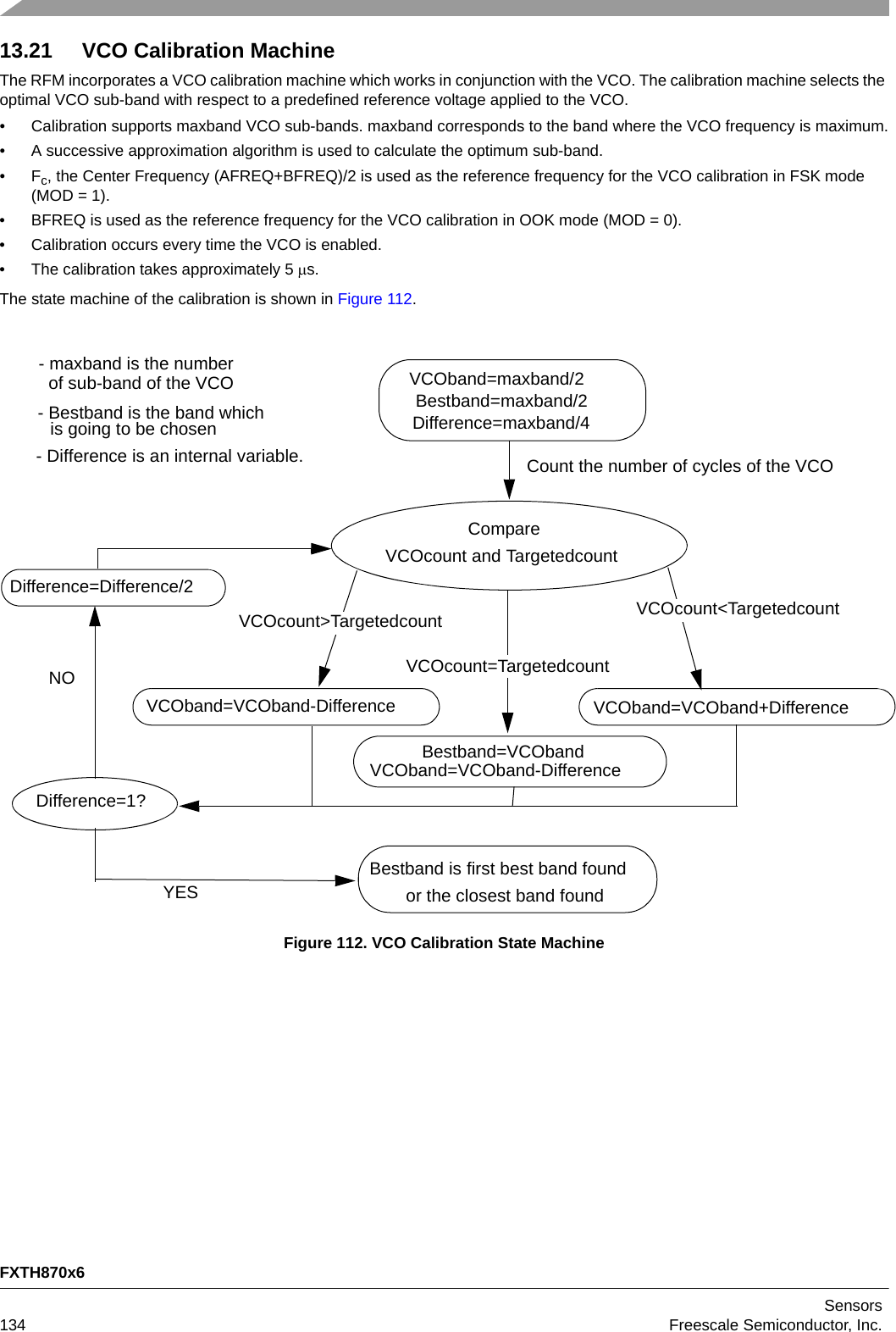
![FXTH870x6SensorsFreescale Semiconductor, Inc. 13514 FirmwareThis section describes the software subroutines contained in the firmware section of the FLASH memory that the user can call for various tasks and to reduce the software development time for the main internal operations.14.1 Software Jump TableAll subroutines are accessed through a jump table located at the bottom of the firmware FLASH memory as described in Table 86. This allows upgrades in firmware without changing the software code of the user. All subroutines should be accessed with the JSR instruction.14.2 Function DocumentationThe following subsections describe the details of the firmware routines. Further details can be found in the latest version of the FXTH870x6 Embedded Firmware User Guide.14.2.1 General Rules1. No output parameter can use the extreme codes (all zero’s or all one’s).2. The all zero’s output code will always indicate a fault and the status byte will indicate the source of the error.3. While firmware is processing, CPU resources are unavailable for application.4. Each measured parameter will return a limit code ($00, $FF or $1FF) if an error occurs in its acquisition, except for the external ADC voltage measurements on the PTA[1:0] pins.5. External ADC voltage measurements on the PTA[1:0] pins will return a full range code that is ratiometric to the supply voltage.14.2.1.1 FXTH870x02 Single Z-axis Firmware RoutinesThe details on the use and execution of each firmware routine is documented in the CodeWarrior project file that is supplied by Freescale. Any future updates to these firmware routines will be contained in that file. A summary of the firmware routines available is given in Table 86.The firmware table is comprised of 3-byte entries where the first byte is the operational code for the JMP instruction, and the following two bytes are the absolute address pointing to the location of the firmware function.Table 86. FXTH870x02 Single Z-axis Firmware Summary and Jump TableAddress Routine DescriptionE000 TPMS_RESET Master reset of complete deviceE003 TPMS_READ_VOLTAGE 10-bit uncompensated bandgap voltage readingE006 TPMS_COMP_VOLTAGE 8-bit compensation of 10-bit voltage readingE009 TPMS_READ_TEMPERATURE 10-bit uncompensated temperature readingE00C TPMS_COMP_TEMPERATURE 8-bit compensation of 10-bit temperature readingE00F TPMS_READ_PRESSURE 10-bit uncompensated pressure readingE012 TPMS_COMP_PRESSURE 9-bit compensation of 10-bit pressure readingE015 TPMS_READ_ACCELERATION 10-bit uncompensated acceleration readingE018 TPMS_COMP_ACCELERATION 9-bit compensation of 10-bit acceleration readingE01B TPMS_READ_V0 10-bit uncompensated voltage reading on PTA0 pinE01E TPMS_READ_V1 10-bit uncompensated voltage reading on PTA1 pinE021 TPMS_LFOCAL LFO clock calibrationE024 TPMS_MFOCAL MFO clock calibrationE027 TPMS_WAVG Weighted average (2, 4, 8, 16 or 32)E02A TPMS_RF_RESET Master reset of RFME02D TPMS_RF_READ_DATA Read RFM data bufferE030 TPMS_RF_READ_DATA_REVERSE Read RFM data buffer in reverse bit orderE033 TPMS_RF_WRITE_DATA Write RFM data bufferE036 TPMS_RF_WRITE_DATA_REVERSE Write RFM data buffer in reverse bit orderE039 TPMS_RF_CONFIG_DATA Configure RFM](https://usermanual.wiki/Continental-Automotive/TIS-03/User-Guide-2718164-Page-139.png)
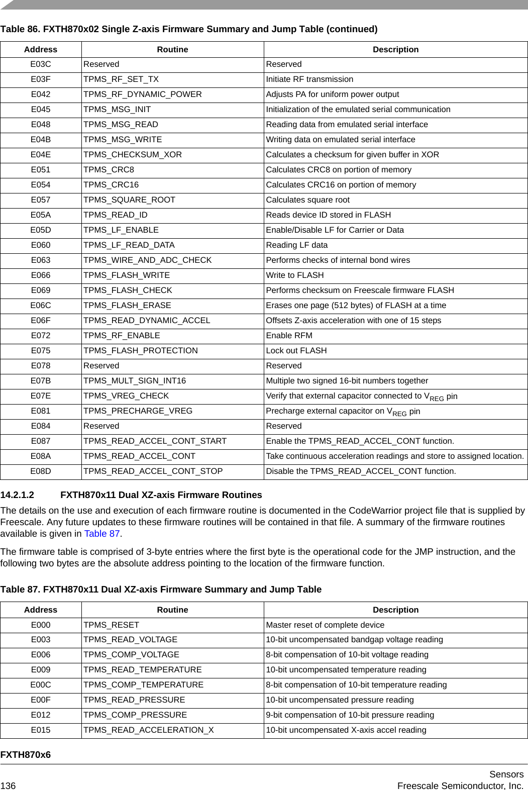
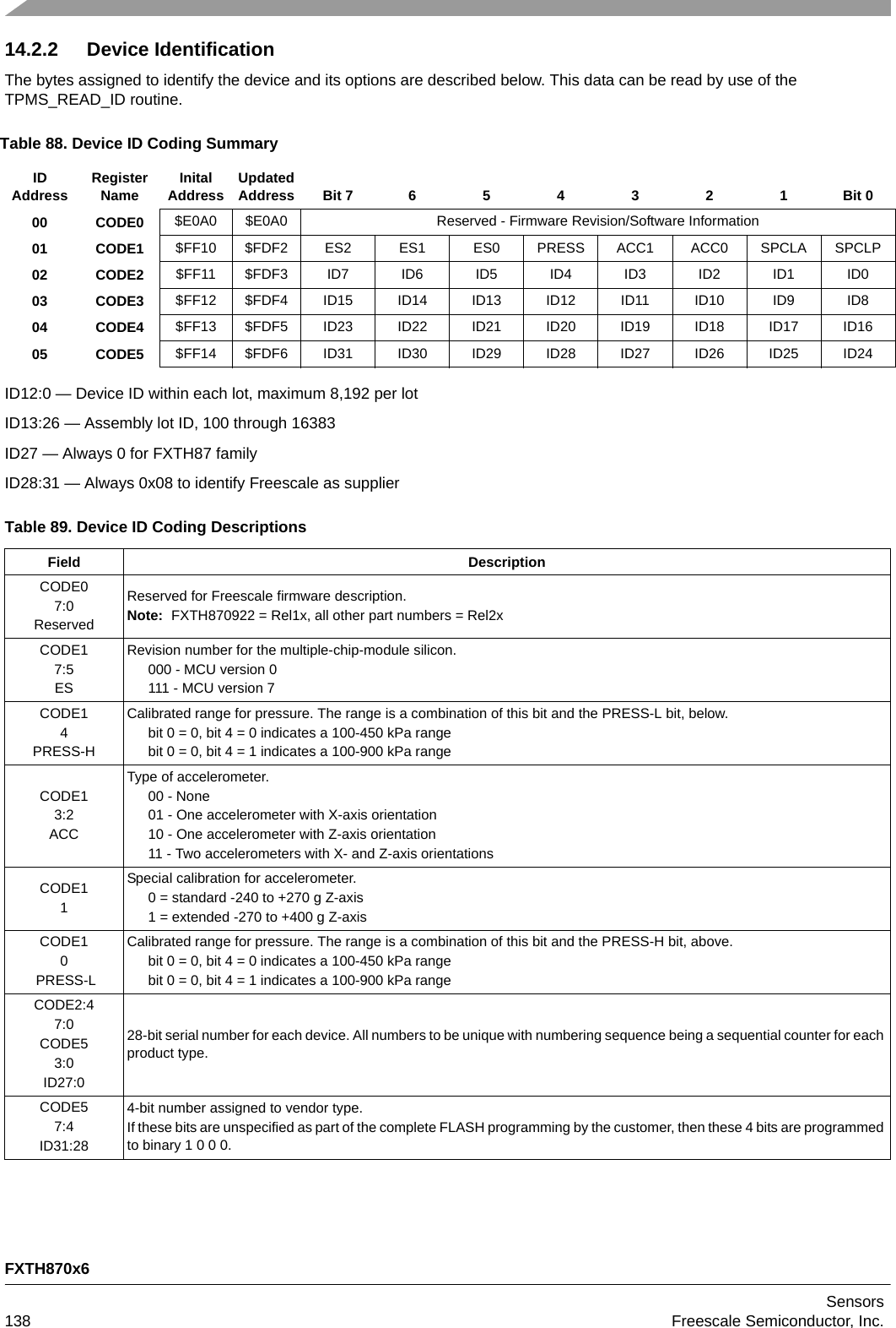
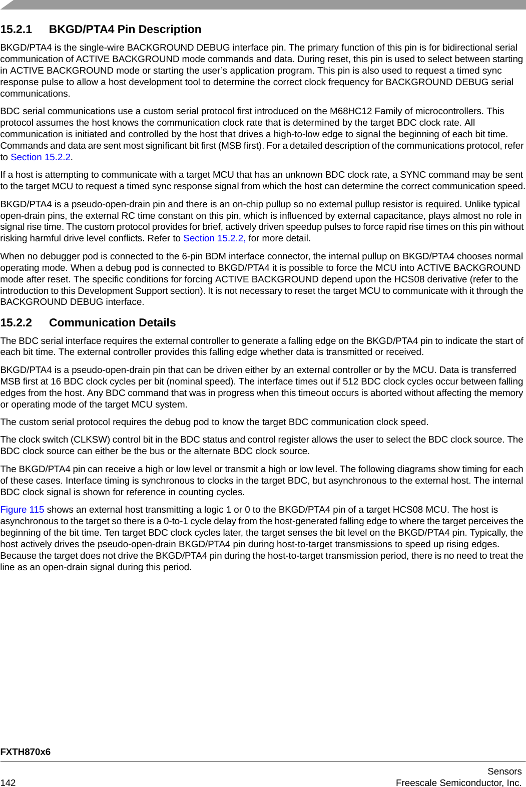
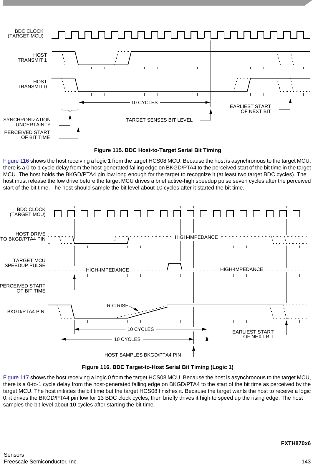
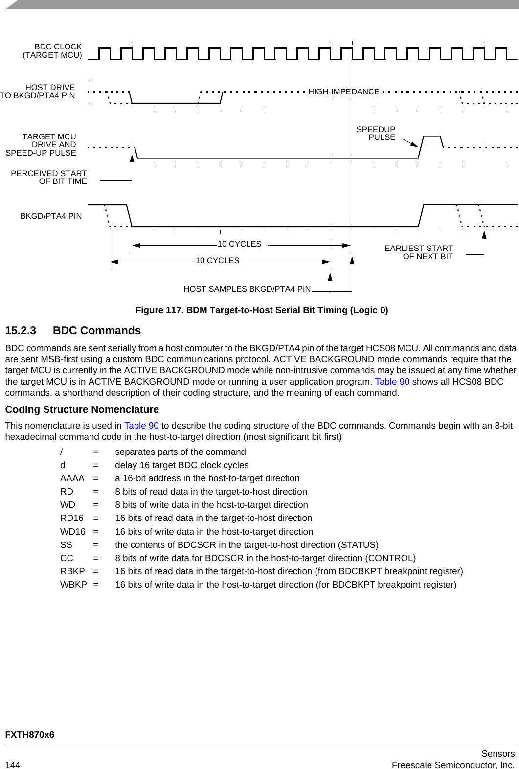
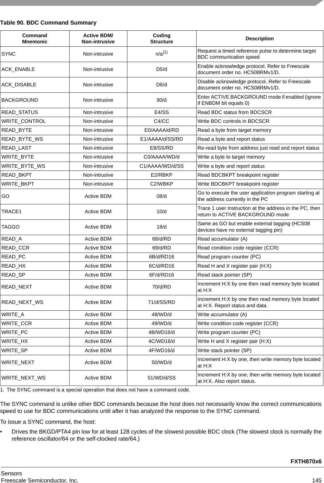
![FXTH870x6Sensors152 Freescale Semiconductor, Inc.17.4 Power Consumption (MCU)1.8 VDD 3.6, TA 0 to 125 °C unless otherwise specified.Note: Refer to page 169 for description of notes.# Characteristic Symbol Min Typ Max Units400401402403404405406Standby Supply CurrentSTOP1 mode, LFR, LVD and TR all offTA = -40 °C, VDD = 3.0 VTA = 0 °C, VDD = 3.0 VTA = 25 °C, VDD = 1.8 VTA = 25 °C, VDD = 3.0 VTA = 25 °C, VDD = 3.6 VTA = 70 °C, VDD = 3.0 VTA = 125 °C, 3.0 V VDD 3.6 VISTDBY1ISTDBY1ISTDBY1ISTDBY1ISTDBY1ISTDBY1ISTDBY1——————————0.5———0.90.90.80.70.91.513µAµAµAµAµAµAµA(3)(3)(3)(2)(3)(3)(3)407408409410411412Standby Supply CurrentSTOP4 mode, LFR and TR off, LVD or RFLVD onTA = -40 °C, VDD = 3.0 VTA = 0 °C, VDD = 3.0 VTA = 25 °C, VDD = 1.8 VTA = 25 °C, VDD 3.0 VTA = 70 °C, VDD = 3.0 VTA = 125 °C, 3.0 V VDD 3.6 VISTDBY4ISTDBY4ISTDBY4ISTDBY4ISTDBY4ISTDBY4—————————73——1001009595100140µAµAµAµAµAµA(3)(3)(3)(2)(3)(3)413414415416MCU Operate Current (1.8 VDD 3.0 V, -40 °C TA 125 °C)Instruction Speed = 0.333 MIP/fBUS0.5 MHz fBUS, BUSCLKS[1:0] = 111 MHz fBUS, BUSCLKS[1:0] = 102 MHz fBUS, BUSCLKS[1:0] = 014 MHz fBUS, BUSCLKS[1:0] = 00IDDIDDIDDIDD————0.720.941.462.501.01.11.72.9mAmAmAmA(3)(3)(3)(1)417418Standby Current Adder for Temperature RestartVDD = 1.8 V, TA = 125 °CVDD = 3.0 V, TA = 125 °CIDDIDD——10101515µAµA(3)(3)419MCU Wakeup Consumption (+25 °C, 3 V)From STOP1 to first instruction, fBUS = 4 MHz QWAKE 0 0.05 0.1 µA-sec (3)420421External Battery ModelSeries impedance at end-of-lifeOpen circuit voltage at end-of-lifeZEOLVEOL—2.7——60—V(4)(4)](https://usermanual.wiki/Continental-Automotive/TIS-03/User-Guide-2718164-Page-156.png)
![FXTH870x6Sensors154 Freescale Semiconductor, Inc.17.6 Voltage Measurement Characteristics1.8 VDD 3.6, TL TA TH, unless otherwise specified.Note: Refer to page 169 for description of notes# Characteristic Symbol Min Typ Max Units600601602Lower LVD detect threshold (note 15)VDD fallingVDD risingVoltage drop detection time (note 16)VLVDLVLVDLtLVDL1.791.87—1.88——1.962.0310VVsec(2)(3)(3)603604605Higher LVD detect threshold (note 15)VDD fallingVDD risingVoltage drop detection time (note 16)VLVDHVLVDHtLVDH2.052.12————2.32.310VVsec(1)(3)(3)606607608Lower LVW detect threshold (LVWV = 0, note 15)VDD fallingVDD risingVoltage drop detection time (note 16)VLVWLVLVWLtLVWL2.052.12————2.32.310VVsec(1)(3)(3)609610611Higher LVW detect threshold (LVWV = 1, note 15)VDD fallingVDD risingVoltage drop detection time (note 16)VLVWHVLVWHtLVWH2.282.34————2.542.6110VVsec(1)(3)(3)612 RF LVD detect threshold, VDD falling (note 15)VLVDRF 1.60 1.79 1.95 V (2)613 Voltage drop detection time (note 16)tLVDRF ——10sec (3)614615Power-On Reset Voltage (note 15)Rising Voltage to RecoverFalling Voltage to ResetVPORRVPORF—0.8——2.1—VV(3)(3)616617618619620621622623624625Internal Voltage (VDD, monotonic response).VCODE = 0 = 58 = 88 = 108 = 128= 158= 208= 238 = 255Voltage sensitivityVINTVINTVINTVINTVINTVINTVINTVINTVINTVINT—1.62.02.22.42.73.23.5——FAULT1.82.12.32.52.83.33.6FAULT10—2.02.22.42.62.93.43.7——VVVVVVVVVmV/count(3)(3)(3)(3)(3)(1)(3)(3)(3)(3)626627628629External Voltage (PTA[1:0], monotonic response, conversion is ratiometric to VDD)GxCODE, where x = 0, 1 refers to PTA0 or PTA1Voltage sensitivityADC INLADC DNLnVEXTINLDNL——-1-11023 (VIN/VDD)VDD/1023————+1+1countV/countLSBLSB(4)(4)(3)(3)630631632633634635Voltage Measurement(internal voltage or external pin)Sensor measurement time (note 7)Peak current (note 8)Power consumption (note 22)Raw measurement, 10-bitCompensation, 8-bitBasic compensated reading, 8-bitFull compensated reading, 8-bittVMIVQVQVQVQV——————0.453.20.130.400.530.530.533.90.30.640.90.9msmAµA-secµA-secµA-secµA-sec(3)(3)(3)(3)(3)(3)](https://usermanual.wiki/Continental-Automotive/TIS-03/User-Guide-2718164-Page-158.png)
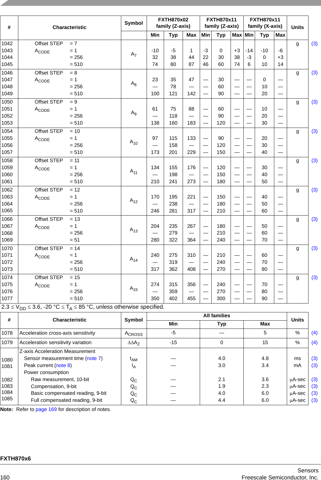
![FXTH870x6SensorsFreescale Semiconductor, Inc. 16117.11 LFR Sensitivity2.3 VDD 3.6, -20 °C TA 85 °C, unless otherwise specified. Detection and no detection criteria defined by notes 19 and 20.Note: Refer to page 169 for description of notes.# Characteristic Symbol Min Typ Max Units11001101110211031104110511061107LFR Input Sensitivity in carrier mode, 125 kHz carrier, LFCDTM = 256 s UOSVery Low Sensitivity, SENS(1:0) = 00Detect level, LFA:B No detect level, LFA:BLow Sensitivity, SENS(1:0) = 00Detect level, LFA:BNo detect level, LFA:BHigh Sensitivity, SENS[1:0] = 10, CHK125 = 01Detect level, LFA:BNo detect level, LFA:BSensitivity Shift in High Sensitivity, SENS[1:0] = 10, CHK125 = 00Detect level, LFA:B, (typical difference observedbetween CHK125 = 00 and 01No detect level, LFA:B, No detect level, LFA:B (typical difference observed between CHK125 = 00 and 01)SDET_VLSNODET_VLSDET_LSNODET_LSDET_HSNODET_HSDET_HSNODET_H—24—2—0.5————————-0.12-0.1260—14—3.5———mV p-pmV p-pmV p-pmV p-pmV p-pmV p-pmV p-pmV p-p(4)(4)(4)(4)(2)(2)(3)(3)11081109LFR Input Sensitivity in data mode125 kHz carrier, LFCDTM = 64 secValid reception of 10 consecutive frames of 16-bit Manchester bit preamble + 9T SYNC +16-bit ID + 4 bytes of data. Continuously ONHigh Sensitivity, SENS[1:0] = 10, CHK125 = 01Data detect levelData no detect levelSPER_HSNOPER_H—0.25——3.5—mV p-pmV p-p(2)(2)11101111LFR Input Sensitivity in data mode125 kHz carrier, LFCDTM = 64 secValid reception of 10 consecutive frames of 16-bit Manchester bit preamble + 9T SYNC +16-bit ID + 4 bytes of data. Continuously ONLow Sensitivity, SENS[1:0] = 01, CHK125 = 00Data detect levelData no detect levelSPER_LSNOPER_L—2——14—mV p-pmV p-p(3)(3)](https://usermanual.wiki/Continental-Automotive/TIS-03/User-Guide-2718164-Page-165.png)
![FXTH870x6Sensors162 Freescale Semiconductor, Inc.17.12 LFR Characteristics2.3 VDD 3.6, -20 °C TA 85 °C, unless otherwise specified.Note: Refer to page 169 for description of notes.17.13 LFR Power Consumption2.3 VDD 3.6, -20 °C TA 85 °C, unless otherwise specified. All parameters based upon DEQEN = 0 setting.Note: Refer to page 169 for description of notes.# Characteristic Symbol Min Typ Max Units1200LF Input Signal CharacteristicsRelative to High Sensitivity Data Mode Always Detect, SPER_HDynamic Range, DEQEN = 0 VIN 56 — — dB (3)120112021203LFR Input Signal Characteristics(Manchester Data Mode)Modulation Depth (Data 1 - Data 0)/Data 1Data bit timeBit Duty CycleMRtDATAMDC7024845—256—10026455%sec%(3)(3)(3)12041205LFR Differential Input (LFA to LFB, Figure 122)Differential Resistance Differential Capacitance (C3)RLFDFCLFDF12—3.846MpF(3)(3)1206120712081209LFR Carrier Frequency Range VALEN = 1, LFCDTM = 256 secAlways accepted carrierAlways rejected carrier, rejected frequencies upper limitAlways rejected carrier, rejected frequencies lower limitVALEN = 0, LFCDTM = 256 msHigh Cutoff Freq, 5 mV p-p input, SENS[1:0] = 00fLFCfLFCHfLFCLfLFCO121.25—210———— 350128.7580——kHzkHzkHzkHz(3)(3)(3)(4)1210 LFR Detector Power Up Settling Time (2 LFO cycles) tPU 1.4 2.0 2.6 ms (4)12111212LFR Preamble Decoder Settling TimeData Mode Only, LFCDTM plus tDECLPSM = 0LPSM = 1tDECtDEC————200400sec sec (4)(4)# Characteristic Symbol Min Typ Max Units130013011302130313041305LFR Supply Current, Carrier Detect ModeMonitor for carrier with VALEN = 0, LPSM = 1TA = 25 °C, 3.0 V VDDTA = -40 °C to 125 °C, 2.3 to 3.6 V VDDFrequency validation withVALEN = 1, LPSM = 1 and CHK125 = 00TA = 25 °C, 3.0 V VDDTA = -40 °C to 125 °C, 2.3 to 3.6 V VDDFrequency validation withVALEN = 1, LPSM = 1 and CHK125 = 01TA = 25 °C, 3.0 V VDDTA = -40 °C to 125 °C, 2.3 to 3.6 V VDDILFRILFRILFR——————3.9—5.6—5.8——5.5—7.5—8.0µAµAµA(3)(3)(1)13061307LFR Supply Current, Manchester Data ModeDecoding of data stream after carrier detectedTA = 25 °C, 3.0 V VDDTA = -40 °C to 125 °C, 2.3 to 3.6 V VDD ILFR——11.8——13.5 µA (3)](https://usermanual.wiki/Continental-Automotive/TIS-03/User-Guide-2718164-Page-166.png)
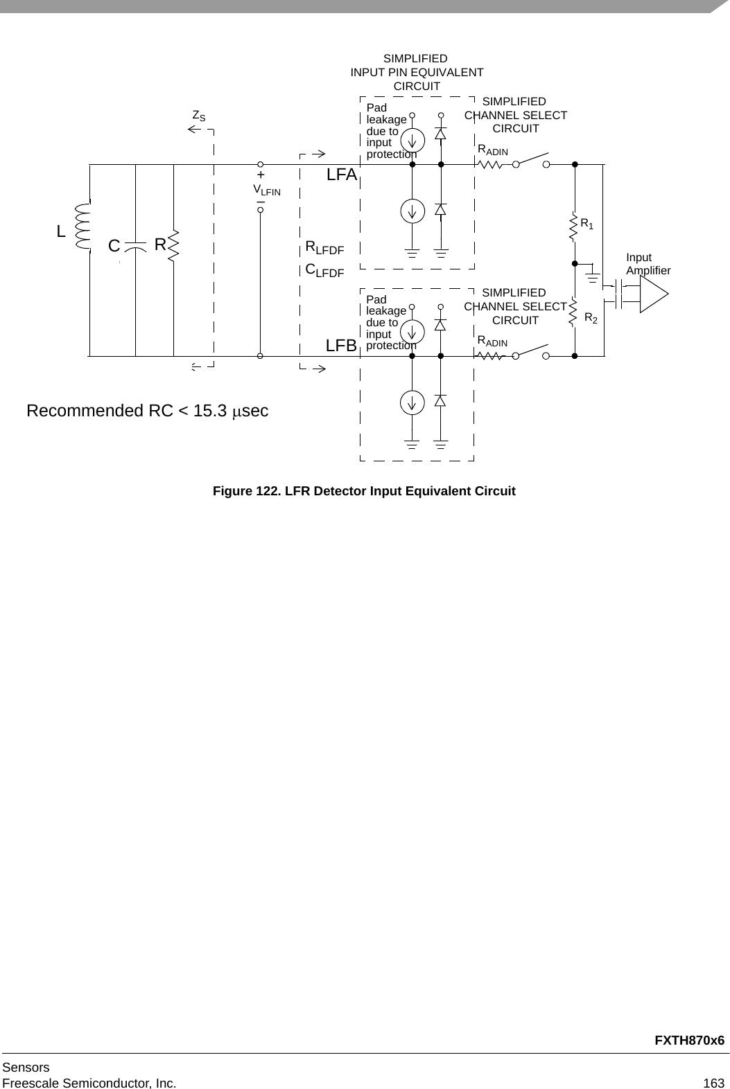
![FXTH870x6Sensors164 Freescale Semiconductor, Inc.17.14 RF Output Stage1.8 VDD 3.6, TL TA TH, unless otherwise specified.Power output based on using Dynamic RF Power Correction firmware routine.Output load of 50 resistance as shown in Figure 125 unless otherwise specified.MCU in STOP1 mode during all RF tests.RF output will shutdown when the total RF IDD causes VDD to fall below 1.8 V (VDD = VBATT - IBATT x RBATT). See Figure 126.# Characteristic Symbol Min Typ Max Units14001401Nominal Output Power with 50 matching network (note 21)315 MHz, TA = 25 °C, VDD = 3 V, PWR[4:0] = 01110434 MHz, TA = 25 °C, VDD = 3 V, PWR[4:0] = 01111PRFPRF4.03.55.24.96.06.0dBmdBm(1)(1)1402*Nominal Output Power with 50 matching networkat maximum power step, PWR[4:0] = 10100.Temperature and voltage range definedby Figure 123 and Figure 124.PRF 3——dBm(3)140314041405Programmable Power AdjustmentPWR[4:0] = 00000 through 11111Low Power Mode (PWR[4:0] = 00000)Range (nominal, (PWR[4:0] > 00000)Adjustment step (-1.5 to +8 dBm)PLPMPRFPADJ—-1.5—-10—0.5—8.0—dBmdBmdBm(3)(3)(3)1406Programmable Frequency StepsCarrier & FSK Deviation(AFREQ[12:0] and BFREQ[12:0]) fSTEP — 3.174 — kHz (3)1407 External Crystal Frequency (note 14)fXTAL — 26.000 — MHz (3)1408 Fixed portion of RF start process, tS-RCTS — — 300 sec (3)1409 Variable portion of RF start process Bits — 3 — bit times (4)1410 Total RF transmit start time from write of SEND bit to start of RF @ 2,000 bps tRF = tS-RCTS + (Bits * bps-1)tRF2 ——1.8ms(3)1411 Total RF transmit start time from write of SEND bit to start of RF @ 9,600 bps tRF = tS-RCTS + (Bits * bps-1)tRF9.6 — — 613 sec (3)1412 Total RF transmit start time from write of SEND bit to start of RF @ 20,000 bps tRF = tS-RCTS + (Bits * bps-1)tRF20 — — 450 sec (3)1413 OOK Modulation Depth MOOK 50 — — dBc (3)1414Manchester Encoding Data RateBit Rate Dependent on accuracy of MFO (note 18). DR — — ±5 % (3)1415 Modulation Duty-Cycle (OOK and FSK) DC 45 50 55 % (3)1416 XTAL Oscillator Margin (over 26 MHz) (note 17)ML600——(4)14171418Harmonic 2 Level (315 and 434 MHz bands, with matching reference network)VDD = 3 V, TA = 25 °C, PWR[4:0] = 011101.8 VDD 3.6, TL TA TH, power step adjusted toreach the targeted power in each domainH2H2——-35-25-22-20dBcdBc(3)(3)14191420Harmonic 4 Level and above (315 and 434 MHz bands, with matching reference network)VDD = 3 V, TA = 25 °C, PWR[4:0] = 011101.8 VDD 3.6, TL TA TH, power step adjusted toreach the targeted power in each domainH4H4————-30-30dBcdBc(3)(3)](https://usermanual.wiki/Continental-Automotive/TIS-03/User-Guide-2718164-Page-168.png)
![FXTH870x6SensorsFreescale Semiconductor, Inc. 165* FSL D-FMEA class 306.Note: Refer to page 169 for description of notes.14211422Harmonic 3 Level (315 and 434 MHz bands, with matching reference network)VDD = 3 V, TA = 25 °C, PWR[4:0] = 011101.8 VDD 3.6, TL TA TH, power step adjusted toreach the targeted power in each domainH3H3——-31-27-28-25dBcdBc(3)(3)14231424142514261427142814291430Noise for BOOST = 0Phase Noise (315 MHz)fRF 10 kHzfRF 100 kHzfRF 1 MHzPhase Noise (434 MHz)fRF 10 kHzfRF 100 kHzfRF 1 MHzSpurious Noise (315 and 434 MHz bands)fRF fREFOccupied Bandwidth (Korea, MIC 2007-63)For FSK up to 45 kHz and 9600 bit/sec andfor OOK up to 9600 bit/secAnalyzed setup: RBW = VBW up to 10 kHz,Span up to 1.25 MHz, and MaxHoldNPHNPHNPHNPHNPHNPHNSPUROBWK————————-86-92-84-84-89-82-45—-78-86-82-76-83-80-40180dBc/HzdBc/HzdBc/HzdBc/HzdBc/HzdBc/HzdBckHz(3)(3)(3)(3)(3)(3)(3)(3)143114321433143414351436Noise for BOOST = 1Phase Noise (315 MHz)fRF 10 kHzfRF 100 kHzfRF 1 MHzSpurious Noise (315 MHz bands)fRF fREFOccupied Bandwidth (Japan, ARIB STD-T93)For FSK up to 45 kHz and 9600 bit/sec For OOK up to 9600 bit/secAnalyzed setup: RBW = VBW up to 30 kHz,Span up to 3.5 MHz, and MaxHoldNPHNPHNPHNSPUROBWJOBWJ——————-75-80-95-45——-67-76-93-40400600dBc/HzdBc/HzdBc/HzdBckHzkHz(3)(3)(3)(3)(3)(3)1437 RF Oscillator Frequency Accuracy, XCO (note 21) excluding external crystal and component variations fXCO -30 — +30 ppm (3)# Characteristic Symbol Min Typ Max Units](https://usermanual.wiki/Continental-Automotive/TIS-03/User-Guide-2718164-Page-169.png)
![FXTH870x6Sensors166 Freescale Semiconductor, Inc.17.15 Power Consumption RF Transmissions1.8 VDD 3.6, TA 25 °C unless otherwise specified.Note: Refer to page 169 for description of notes.Using the TPMS_RF_DYNAMIC_POWER firmware routine (see Section 14) allows adjusting power step in order to compensate variations of output power versus temperature and voltage. This routine will be associated to a part to part trimming that initially adjusts the power step to compensate for process variations.Both these trim and look-up table allow to guarantee by characterization the typical values of power consumption as presented below (average values among 100 parts plus improvements prediction from design).Figure 123. Dynamic Power Adjustment - 315 MHz# Characteristic Symbol Min Typ Max Units15001501150215031504150515061507RF Supply Transmission CurrentVDD = 3.0 V, PWR[4:0] set for nominal 5 dBm315 MHZ Power delta for BOOST = 1315 MHZ Carrier Frequency, BOOST = 0Data 1, FSK or OOK434 MHZ Carrier Frequency, BOOST = 0Data 1, FSK or OOKInterframe period, IFPD = 0. Interframe period, IFPD = 0, 1.8 VDD 3.6,TL TA THInterframe period, IFPD = 1, DRLPEN = 1,1.8 VDD 3.6, TL TA THInterframe period, IFPD = 1, DRLPEN = 0Interframe period, IFPD = 1, DRLPEN = 0, 1.8 VDD 3.6, TL TA THIDDIDDIDDIDDIDDIDDIDDIDD—————————6.06.6617—2077—0.55 7.07.66967892996125mAmAmAAAAAA(2)(1)(1)(3)(3)(3)(3)(3) 3dBm5dBm-40°C 125°C25°C 60°C0°C1.8V2.5V3.6V3dBm3dBm.3V5.3mA 5.5mA5.3mA 5.5mA 6mA 6.2mA6.6mA6.3mA5.8mA5.7mA6mA3dBm5dBm-40°C 125°C25°C 60°C0°C1.8V2.5V3.6V3dBm3dBm.3V5.3mA 5.5mA5.3mA 5.5mA 6mA 6.2mA6.6mA6.3mA5.8mA5.7mA6mA3dBm5.0mA 5.3mA 6.2mA 6.4mA5dBm5.2mA 5.4mA6.2mA6.4mA 6.5mA 5.8mA5.8mA](https://usermanual.wiki/Continental-Automotive/TIS-03/User-Guide-2718164-Page-170.png)
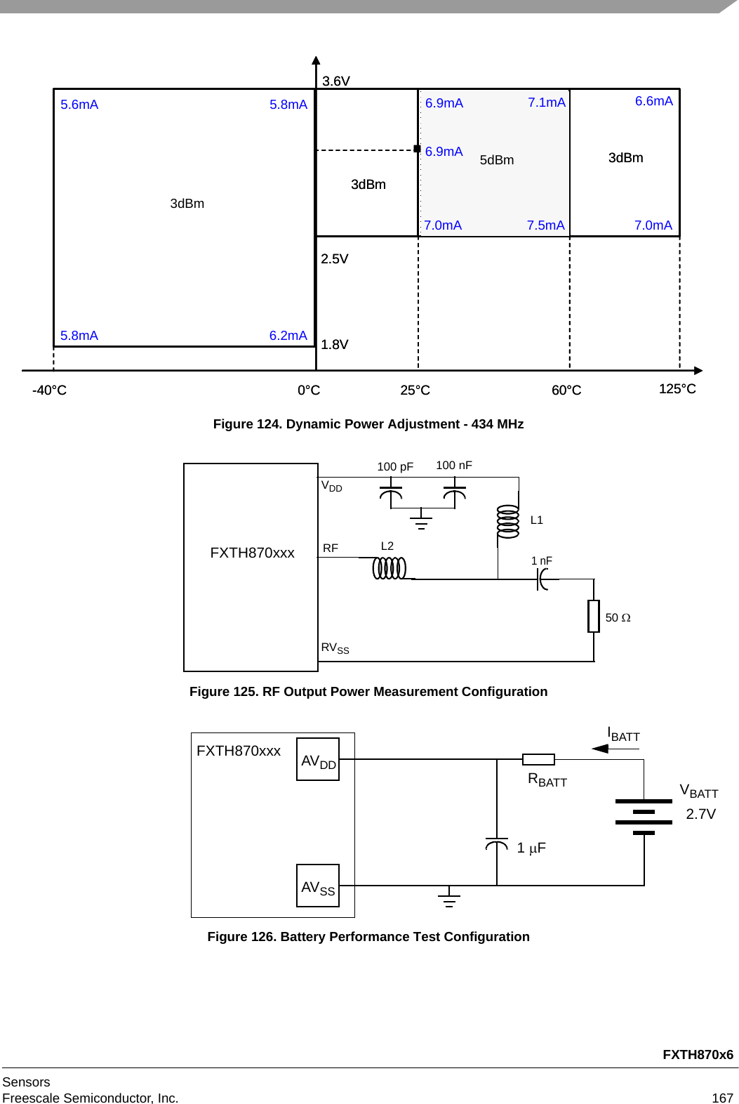
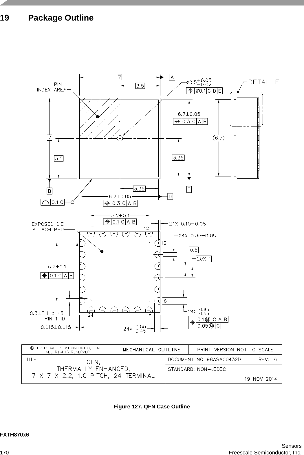
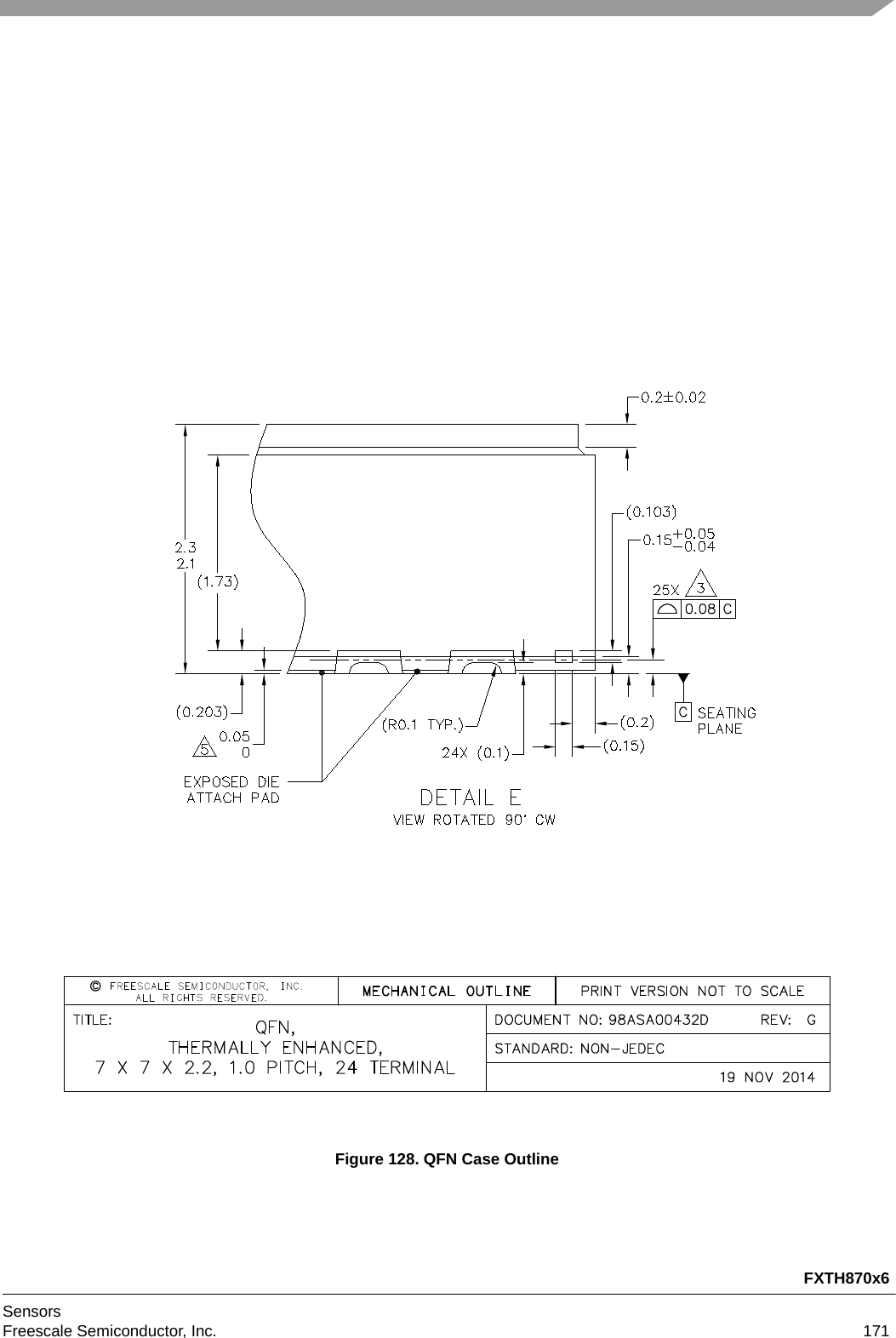

![FXTH870x6Sensors174 Freescale Semiconductor, Inc.20 Revision HistoryRev. 0, 05/2014• Initial data sheet.Rev. 1, 07/2014• Corrected Ordering Information table.• Figure 5: Updated paragraph in figure to include PCB traces for the LFA/LFB and note regarding L1. • Section 5.4: Updated register figure to include TRO bit on Bit 0. Added Description to Table 19 and update reserved bit fields.• Section 6.1: Updated last paragraph in section.• Section 10.1: Added NOTE.• Section 10.4: Added NOTE.• Section 14.2.2: Added definitions for ID codes.• Section 17.10.2: Changed column content reference from See lines 1042-1045 to See Offset STEP = 7. Corrected Min, Typ and Max values for lines 1042-1045 for FXTH870x11 family (X-Axis).• Section 17.12: Updated Characteristic and Min Value for line 1200. Updated Characteristic and note reference for line 1210.Rev. 1.1, 07/2014• Section 17.4: Updated Symbols for lines 400 through 412 and lines 417 and 418.• Section 17.6: Updated Max value for line 612 and updated note reference and Symbol for line 613. • Section 17.7: Updated note references for lines 711-714.• Section 17.9: Updated Typ and Max values for line 924. Updated Typ values for lines 927 through 930. • Section 17.10.2: Deleted line 1078 and updated Typ values for lines 1083 through 1086.• Section 17.11: Updated Typ value for line 1106. Deleted lines 1108-1113, duplicated information.• Section 17.12: Updated Symbols for lines 1208 through 1210 and updated Characteristics for lines 1208 and 1209.• Section 17.13: Update Max value for line 1301.• Section 18.1: Updated Max value for line 1800.Rev. 1.2, 08/2014• First page: Updated bullet “Six multipurpose GPIO pins” to “Seven multipurpose GPIO pins” and sub-bullets• Section 2.3.8: Updated paragraph with additional content.• Section 2.3.9: Updated title and paragraphs with corrected pin numbers and added text to paragraph.• Section 2.3.12: Updated content in paragraph.• Section 3.5.4: Updated header title for I/O Pins, deleted (Optional PTA[3:0]).• Section 4.3: Table 3, updated Bit contents for Address columns $0000, $0001 and $0003.• Section 6: Updated content in first two paragraphs. Updated Figure 29, added boxes and note for emphasis on PTA[3:0] usage. Updated title and column heads in Table 32 and added rows for PTAPE, PTBPE, PTADD and PTBDD. Updated first paragraph in Section 6.5.• Section 7: Section 7.1: Updated 1st bullet. Section 7.2.1: Updated content in first paragraph. Section 7.5: Updated bulleted text. Sections 7.5.2 and 7.5.3: Updated tables and figures to show bits reserved for firmware or factory test. Section 7.6: Updated content in second paragraph. Section 7.6.3: Updated content in paragraph. Section 7.6.4: Updated list number 3 and 4.• Section 12.17.1: Updated LF Enable description in Table 59. Section 12.17.8: Added Note after Table 67 regarding setting the CHK125 bits and updated Description for Field 1-0, CHK125[1:0].• Section 17.3: Updated Characteristic for line 311.• Section 17.12: Updated Min and Max values for line 1206 and updated Characteristic.• Section 17.14: Redefined lines 1408 through 1411 and added line 1412, • Section 18.1: Updated Value for line 1802. • Notes page: Updated Notes 18,19, 20 and added note 25.](https://usermanual.wiki/Continental-Automotive/TIS-03/User-Guide-2718164-Page-178.png)
![FXTH870x6SensorsFreescale Semiconductor, Inc. 175Rev. 1.3, 09/2014• Section 4.3: Table 3, updated Addresses $0001 and $0003 Bit 4 column to reserved and text corrected to [3:0].• Section 5.11.2: Table 26, updated Description for BKGDPE Field• Section 6: Updated 2nd paragraph. Updated column heads for Table 32. Figure 31 and Table 34, updated Bit 4 to Reserved and updated Field name. Figure 32 and Table 35, updated Bit 4 to Reserved and updated Field name.• Section 7.6.3: Updated paragraph contents.• Section 12.17.4: Table 62, removed “Use Software polling” from LFCDIE and LFIDIE Descriptions.• Section 12.17.8: Table 67, updated Description for CHK125.• Section 14.2.1.1: Table 86, changed Routine and Description columns for E084 to Reserved. Table 87, changed Routine and Description columns for E090 to Reserved.• Section 17.1: Added Value to line 108.• Section 17.4: Updated Characteristic for line 412.• Section 17.6 Updated Value for line 631.• Section 17.8: Added asterisk notes to lines 821 and 822.• Section 17.9: Added asterisk notes to lines 921 and 922.• Section 17.13: Updated introduction paragraph.• Section 17.14: Added asterisk note to line 1402.• Section 17.15: Updated Characteristic for line 1500. Updated Typ value for line 1505. • Notes page: Updated note 2.Rev. 1.4, 01/2015• Section 17.3: Updated Characteristic column for lines 303, 305, 307, 308, 310, and 311. Changed note reference for lines 306 and 309. Updated Min and Max values for lines 308 and 311.• Section 17.6: Changed note reference for lines 603, 606, and 609.• Section 17.6: Updated Max value for line 711. Updated Min Value for line 712.• Section 17.15: Changed note reference for lines 1502 and 1504. Replaced Figures 123 and 124.• Notes page: Updated note 13.• Replaced case outline with current version.Rev. 1.5, 02/2015• Section 14.2.2: Table 88, added two columns, “Initial Address” and “Updated Address”.](https://usermanual.wiki/Continental-Automotive/TIS-03/User-Guide-2718164-Page-179.png)