Cypress Semiconductor 0737 This product is a Bluetooth wireless EZ-BT WICED SIP Module User Manual CYW20732S Bluetooth Low Energy SiP Module
Cypress Semiconductor This product is a Bluetooth wireless EZ-BT WICED SIP Module CYW20732S Bluetooth Low Energy SiP Module
Contents
- 1. User Manual_CYW20732S - 0514
- 2. User Manual_CYW20736S - 0514
- 3. User Manual_CYW20737S - 0514
User Manual_CYW20732S - 0514

Cypress Semiconductor
198 Champion Court
San Jose, CA 95134-1709
Phone (USA): 800.858.1810
Phone (Intnl): +1.408.943.2600
www.cypress.com
CYW20732S
Bluetooth Low Energy SiP Module
Doc. # 002-15222 Rev. *G

CYW20732S Bluetooth Low Energy SiP Module, Doc. # 002-15222 Rev. *G 2
Copyrights
Copyrights
© Cypress Semiconductor Corporation, 2013-2017. This document is the property of Cypress Semiconductor Corporation
and its subsidiaries, including Spansion LLC ("Cypress"). This document, including any software or firmware included or refer-
enced in this document ("Software"), is owned by Cypress under the intellectual property laws and treaties of the United
States and other countries worldwide. Cypress reserves all rights under such laws and treaties and does not, except as spe-
cifically stated in this paragraph, grant any license under its patents, copyrights, trademarks, or other intellectual property
rights. If the Software is not accompanied by a license agreement and you do not otherwise have a written agreement with
Cypress governing the use of the Software, then Cypress hereby grants you a personal, non-exclusive, nontransferable
license (without the right to sublicense) (1) under its copyright rights in the Software (a) for Software provided in source code
form, to modify and reproduce the Software solely for use with Cypress hardware products, only internally within your organi-
zation, and (b) to distribute the Software in binary code form externally to end users (either directly or indirectly through
resellers and distributors), solely for use on Cypress hardware product units, and (2) under those claims of Cypress's patents
that are infringed by the Software (as provided by Cypress, unmodified) to make, use, distribute, and import the Software
solely for use with Cypress hardware products. Any other use, reproduction, modification, translation, or compilation of the
Software is prohibited.
TO THE EXTENT PERMITTED BY APPLICABLE LAW, CYPRESS MAKES NO WARRANTY OF ANY KIND, EXPRESS OR
IMPLIED, WITH REGARD TO THIS DOCUMENT OR ANY SOFTWARE OR ACCOMPANYING HARDWARE, INCLUDING,
BUT NOT LIMITED TO, THE IMPLIED WARRANTIES OF MERCHANTABILITY AND FITNESS FOR A PARTICULAR PUR-
POSE. To the extent permitted by applicable law, Cypress reserves the right to make changes to this document without fur-
ther notice. Cypress does not assume any liability arising out of the application or use of any product or circuit described in
this document. Any information provided in this document, including any sample design information or programming code, is
provided only for reference purposes. It is the responsibility of the user of this document to properly design, program, and test
the functionality and safety of any application made of this information and any resulting product. Cypress products are not
designed, intended, or authorized for use as critical components in systems designed or intended for the operation of weap-
ons, weapons systems, nuclear installations, life-support devices or systems, other medical devices or systems (including
resuscitation equipment and surgical implants), pollution control or hazardous substances management, or other uses where
the failure of the device or system could cause personal injury, death, or property damage ("Unintended Uses"). A critical
component is any component of a device or system whose failure to perform can be reasonably expected to cause the failure
of the device or system, or to affect its safety or effectiveness. Cypress is not liable, in whole or in part, and you shall and
hereby do release Cypress from any claim, damage, or other liability arising from or related to all Unintended Uses of Cypress
products. You shall indemnify and hold Cypress harmless from and against all claims, costs, damages, and other liabilities,
including claims for personal injury or death, arising from or related to any Unintended Uses of Cypress products.
Cypress, the Cypress logo, Spansion, the Spansion logo, and combinations thereof, WICED, PSoC, CapSense, EZ-USB, F-
RAM, and Traveo are trademarks or registered trademarks of Cypress in the United States and other countries. For a more
complete list of Cypress trademarks, visit cypress.com. Other names and brands may be claimed as property of their respec-
tive owners.

3 CYW20732S Bluetooth Low Energy SiP Module, Doc. # 002-15222 Rev. *G
Preface
This document provides descriptions of the interfaces, pin assignments, and specifications of Cypress CYW20732S Bluetooth
Low Energy (BLE) System-in-Package (SiP) module. It is intended for designers who are responsible for adding the
CYW20732S module to wireless input devices including heart-rate monitors, blood pressure monitors, proximity sensors,
temperature sensors, and battery monitors.
Cypress Part Numbering Scheme
Cypress is converting the acquired IoT part numbers from Broadcom to the Cypress part numbering scheme. Due to this con-
version, there is no change in form, fit, or function as a result of offering the device with Cypress part number marking. The
table provides Cypress ordering part number that matches an existing IoT part number.
Acronyms and Abbreviations
In most cases, acronyms and abbreviations are defined on first use.
For a comprehensive list of acronyms and other terms used in Cypress documents, go to
http://www.cypress.com/glossary.
Document Conventions
The following conventions may be used in this document:
Technical Support
Cypress provides a wealth of data at http://www.cypress.com/internet-things-iot to help you to select the right IoT device for
your design, and quickly and effectively integrate the device into your design. Cypress provides customer access to a wide
range of information, including technical documentation, schematic diagrams, product bill of materials, PCB layout informa-
tion, and software updates. Customers can acquire technical documentation and software from the Cypress Support Commu-
nity website (http://community.cypress.com/).
Table 2-1. Mapping Table for Part Number between Broadcom and Cypress
Broadcom Part Number Cypress Part Number
BCM20732 CYW20732
BCM20732S CYW20732S
Convention Description
Bold User input and actions: for example, type exit, click OK, press Alt+C
Monospace
Code: #include <iostream>
HTML: <td rowspan = 3>
Command line commands and parameters: wl [-l] <command>
< > Placeholders for required elements: enter your <username> or wl <command>
[] Indicates optional command-line parameters: wl [-l]
Indicates bit and byte ranges (inclusive): [0:3] or [7:0]

CYW20732S Bluetooth Low Energy SiP Module, Doc. # 002-15222 Rev. *G 4
Preface

5 CYW20732S Bluetooth Low Energy SiP Module, Doc. # 002-15222 Rev. *G
Contents
1. Introduction 7
1.1 Overview...................................................................................................................................7
1.1.1 Features ........................................................................................................................7
1.1.2 Application Profiles........................................................................................................7
1.1.3 Block Diagram...............................................................................................................8
1.1.4 External Reset...............................................................................................................8
1.1.5 32.768 kHz Oscillator ....................................................................................................9
1.2 Pin Map and Signal Descriptions............................................................................................10
1.3 Electrical Specifications ..........................................................................................................14
1.4 RF Specifications....................................................................................................................15
1.5 ADC Specifications .................................................................................................................16
1.6 Timing and AC Characteristics ...............................................................................................17
1.6.1 SPI Timing...................................................................................................................17
1.6.2 BSC Interface Timing ..................................................................................................18
1.6.3 UART Timing ...............................................................................................................19
1.7 PCB Design and Manufacturing Recommendations ..............................................................20
1.7.1 Pad and Solder Mask Opening Dimensions ...............................................................20
1.7.2 PCB Layout Recommendations for Configuration A ...................................................20
1.7.3 PCB Layout Recommendations for Configuration B ...................................................23
1.7.4 Common Guidelines for CYW20732S.........................................................................24
1.7.5 PCB Stencil .................................................................................................................25
1.7.6 Solder Reflow..............................................................................................................26
1.8 Packaging and Storage Information .......................................................................................27
1.9 Mechanical Information...........................................................................................................29
1.10 Ordering Information...............................................................................................................31
Revision History 33

CYW20732S Bluetooth Low Energy SiP Module, Doc. # 002-15222 Rev. *G 6
Contents

7 CYW20732S Bluetooth Low Energy SiP Module, Doc. # 002-15222 Rev. *G
1. Introduction
1.1 Overview
The CYW20732S is a compact, highly-integrated Bluetooth low-energy (BLE) system-in-package (SiP) module. The
CYW20732S SiP includes an embedded BLE antenna, 24 MHz clock, and 512 Kb EEPROM, so only a minimal set of exter-
nal components is needed to create a standalone BLE device.
The CYW20732S is designed to accelerate time-to-market. The Bluetooth stack and several application profiles are built into
the module, allowing customers to focus on their core applications. To further reduce application development time, the
CYW20732S includes integrated software support, with one-click installation of the complete environment and a one-click
compile/build/link/load cycle. All this, coupled with an ultra-small form factor and support for a wide voltage range, makes the
CYW20732S well suited for virtually any Bluetooth Smart application.
1.1.1 Features
■ARM Cortex-M3 microcontroller unit (MCU)
■Embedded 512 Kb EEPROM
■Broadcom Serial Control (BSC), SPI, and UART interfaces
■FCC and CE compliant
■RoHS compliant, certified lead- and halogen-free
■Moisture Sensitivity Level (MSL) 3 compliant
■6.5 mm × 6.5 mm × 1.2 mm Land Grid Array (LGA) 48-pin package
1.1.2 Application Profiles
The following profiles are supported in CYW20732S ROM:
■Battery status
■Blood pressure monitor
■Find me
■Heart rate monitor
■Proximity
■Thermometer
■Weight scale
■Time
■Blood glucose monitor
Additional profiles that can be supported in CYW20732S RAM include:
■Blood glucose monitor
■Temperature alarm
■Location
■Other custom profiles
CYW20732S Bluetooth Low Energy SiP Module, Doc. # 002-15222 Rev. *G 8
Introduction
1.1.3 Block Diagram
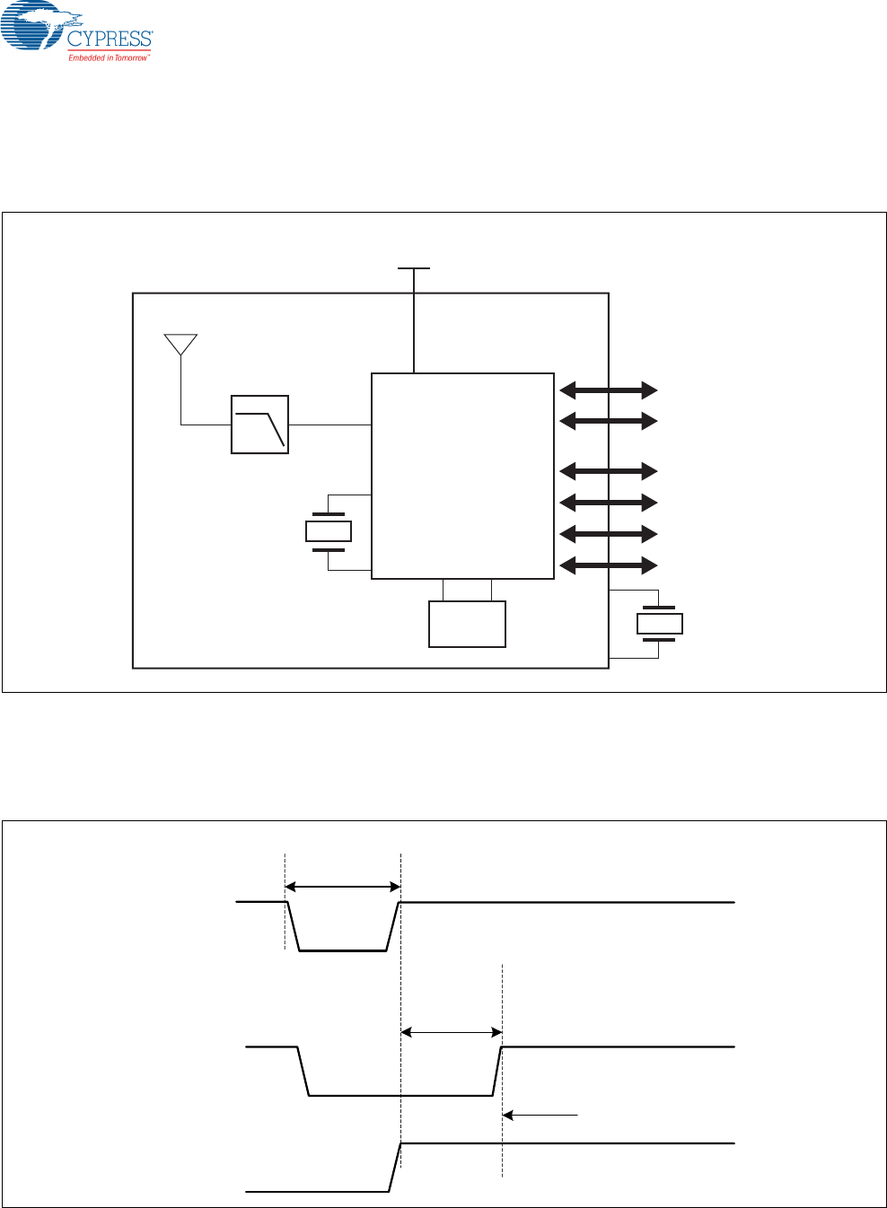
A block diagram of the CYW20732S BLE SiP is shown in Figure 1-1.
Figure 1-1. CYW20732S BLE SiP Block Diagram
1.1.4 External Reset
External reset timing for the CYW20732S is illustrated in Figure 1-2.
Figure 1-2. External Reset Timing
VBAT/VDDIO
CYW20732
Bluetooth Low Energy
System-on-Chip with
ARM ® Cortex™ M3-based
Microprocessor Core
Antenna
Bandpass
Filter UART
SPI/I2C
Infrared
ADC
GPIOs
PWM
32.768 kHz
Oscillator
(optional)
24 MHz
XTAL
EEPROM
512 Kb I2C
CYW20732S
RESET_N
Pulsewidth
>20µs
CrystalEnable
BasebandReset
StartreadingEEPROMand
firmwareboot
Crystal
warm‐up
delay:
~5ms

9 CYW20732S Bluetooth Low Energy SiP Module, Doc. # 002-15222 Rev. *G
Introduction
1.1.5 32.768 kHz Oscillator
The CYW20732S includes a standard Pierce oscillator. The oscillator circuit includes a comparator with hysteresis on the out-
put to create a single-ended digital output. The hysteresis eliminates chatter when the input is near the comparator threshold
(~100 mV). The oscillator circuit can is designed for a 32 kHz or 32.768 kHz crystal oscillator, and can also be driven by an
external clock input with a similar frequency. Characteristics for a 32 kHz oscillator are defined in Table 1-1.
Table 1-1. 32 kHz Crystal Oscillator Characteristics
Parameter Symbol Conditions Min. Typ. Max. Unit
Output frequency Foscout – – 32.768 – kHz
Frequency tolerance Ftol Crystal-dependent – 100 – ppm
Start-up time Tstartup – – – 500 µs
Crystal drive level Pdrv For crystal selection 0.5 – – µW
Crystal series resistance Rseries For crystal selection – – 70 k
Crystal shunt capacitance Cshunt For crystal selection – – 1.3 pF
CYW20732S Bluetooth Low Energy SiP Module, Doc. # 002-15222 Rev. *G 10
Introduction
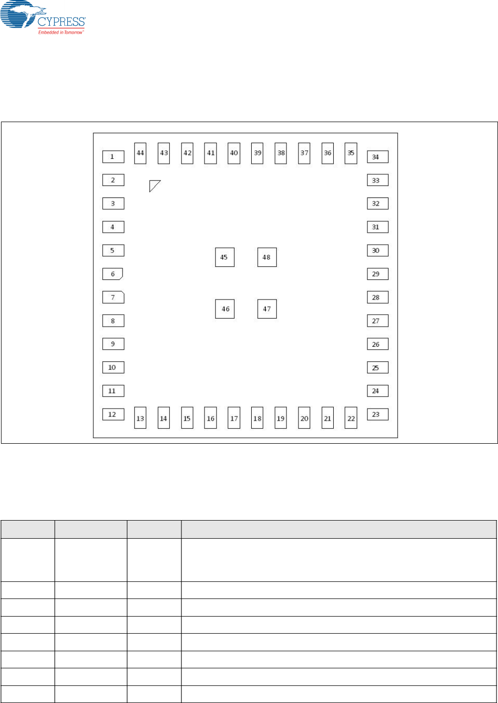
1.2 Pin Map and Signal Descriptions
The CYW20732S pin map is shown in Figure 1-3.
Figure 1-3. CYW20732S (TOP View)
The signal name, type, and description of each pin in the CYW20732S is listed in Table 1-2. The symbols shown under I/O
Type indicate pin directions (I/O = bidirectional, I = input, O = output) and the internal pull-up/pull-down characteristics (PU =
weak internal pull-up resistor and PD = weak internal pull-down resistor), if any.
Table 1-2. Pin Descriptions
Pin Name I/O Type Description
1 GPIO: P27
PWM1
I Default direction: Input.
After POR state: Input floating.
Drain current: 16 mA
Alternate function: MOSI (master and slave) for SPI_2
2GND GNDGND
3 VBAT I Battery supply input.
4GND GNDGND
5GND GNDGND
6GND GNDGND
7GND GNDGND
8GND GNDGND

11 CYW20732S Bluetooth Low Energy SiP Module, Doc. # 002-15222 Rev. *G
Introduction
9GND GNDGND
10 Reserved – Leave floating
11 GND GND GND
12 GND GND GND
13 GND GND GND
14 GND GND GND
15 GND GND GND
16 GND GND GND
17 GND GND GND
18 UART_RX I UART_RX. This pin is pulled low through an internal 10 k resistor.
19 UART_TX O, PU UART_TX
20 GND GND GND
21 SCL I/O, PU SCL I/O, PU clock signal for an external I2C device
22 SDA I/O, PU SDA I/O, PU data signal for an external I2C device
23 GND GND GND
24 GND GND GND
25 GPIO: P1 I Default direction: Input.
After POR state: Input floating.
This pin is tied to the WP pin of the embedded EEPROM.
Requires an external 10K pull-up
26 TMC I Test mode control. Pull this pin high to invoke test mode; leave it floating if not used.
This pin is connected to GND through an internal 10 k resistor.
27 RESET_N I/O PU Active-low system reset with open-drain output
28 GPIO: P0 I Default direction: Input.
After POR state: Input floating.
Alternate functions:
■A/D converter input
■Peripheral UART TX (PUART_TX)
■MOSI (master and slave) for SPI_2
■IR_RX
■60Hz_main
29 GND GND GND
30 GPIO: P3 I Default direction: Input.
After POR state: Input floating.
Alternate functions:
■Peripheral UART CTS (PUART_CTS)
■SPI_CLK (master and slave) for SPI_2
31 GPIO: P2 I Default direction: Input.
After POR state: Input floating.
Alternate functions:
■Peripheral UART RX (PUART_RX)
■SPI_CS (slave only) for SPI_2
■SPI_MOSI (master only) for SPI_2
Table 1-2. Pin Descriptions (continued)
Pin Name I/O Type Description

CYW20732S Bluetooth Low Energy SiP Module, Doc. # 002-15222 Rev. *G 12
Introduction
32 GPIO: P4 I Default direction: Input.
After POR state: Input floating.
Alternate functions:
■Peripheral UART RX (PUART_RX)
■MOSI (master and slave) for SPI_2.
■IR_TX
33 GPIO: P8 I Default direction: Input.
After POR state: Input floating.
Alternate functions: A/D converter input
34 GPIO: P33 I Default direction: Input.
After POR state: Input floating.
Alternate functions:
■A/D converter input
■MOSI (slave only) for SPI_2
■Auxiliary clock output (ACLK1)
■Peripheral UART RX (PUART_RX)
35 GPIO: P32 I Default direction: Input.
After POR state: Input floating.
Alternate functions:
■A/D converter input
■SPI_CS (slave only) for SPI_2.
■Auxiliary clock output (ACLK0)
■Peripheral UART TX (PUART_TX)
36 GPIO: P25 I Default direction: Input.
After POR state: Input floating.
Alternate functions:
■MISO (master and slave) for SPI_2
■Peripheral UART RX (PUART_RX)
37 GPIO: P24 I Default direction: Input.
After POR state: Input floating.
Alternate functions:
■SPI_CLK (master and slave) for SPI_2
■Peripheral UART TX (PUART_TX)
38 N/C N/C N/C
39 GPIO: P13
PWM3
I Default Direction: Input
After POR State: Input Floating
Drain current: 16 mA
Alternate function: A/D converter input
GPIO: P28
PWM2
I Default direction: Input.
After POR state: Input floating.
Drain current: 16 mA
Alternate functions:
■A/D converter input
■LED1
■IR_TX
40 GPIO: P14
PWM2
I Default direction: Input.
After POR state: Input floating.
Alternate function: A/D converter input
GPIO: P38 I Default direction: Input.
After POR state: Input floating.
Alternate functions:
■A/D converter input
■MOSI (master and slave) for SPI_2
■IR_TX
Table 1-2. Pin Descriptions (continued)
Pin Name I/O Type Description

13 CYW20732S Bluetooth Low Energy SiP Module, Doc. # 002-15222 Rev. *G
Introduction
41 GPIO: P15 I Default direction: Input.
After POR state: Input floating.
Alternate functions:
■A/D converter input
■IR_RX
■60 Hz_main
42 GPIO: P26
PWM0
I Default direction: Input.
After POR state: Input floating.
Drain current: 16 mA
Alternate function: SPI_CS (slave only) for SPI_2
43aGPIO: P12 I Default direction: Input.
After POR state: Input floating.
Alternate functions:
■A/D converter input
■XTALO32K
XTALO32K O Low-power oscillator (LPO) output.
Alternate functions:
P12
P26
44bGPIO: P11 I Default direction: Input.
After POR state: Input floating.
Alternate functions:
■A/D converter input
■XTALI32K
XTALI32K I Low-power oscillator (LPO) input.
Alternate functions:
■P11
■P27
45 GND GND GND
46 GND GND GND
47 GND GND GND
48 GND GND GND
a. When pin 43 (XTALO32K) is used, ADC/GPIO:P12 is unavailable. P26 may still be available.
b. When pin 44 (XTALI32K) is used, ADC/GPIO:P11 is unavailable. P27 may still be available.
Table 1-2. Pin Descriptions (continued)
Pin Name I/O Type Description
CYW20732S Bluetooth Low Energy SiP Module, Doc. # 002-15222 Rev. *G 14
Introduction
1.3 Electrical Specifications
Absolute maximum ratings are defined in Ta ble 1-3.
Power for the CYW20732S module is provided by the host through the power pins.
Based on the current measurements in Table 1-5 , CYW20732S peak power values are:
■RX: 101.6 mW
■TX: 101.6 mW
■Sleep mode: 217.8 µW
■Deep Sleep mode: 9.1 µW
Table 1-3. Absolute Maximum Ratings
Parameter Min. Max. Unit
Supply power NA 3.63 V
Storage temperature –40 125 °C
Voltage ripple 0±2%
Power supply (VBAT absolute maximum rating) 1.62 3.63 V
Table 1-4. Voltage
Symbol Parameter Min. Typ. Max. Unit
VBAT Battery voltage 1.62 – 3.63 V
Table 1-5. Current Consumption
Operating Mode Condition Nominal Maximum Unit
Receive Receiver and baseband are both operating, 100% 24.0 28.0 mA
Transmit Transmitter and baseband are both operating, 100% 24.0 28.0 mA
Sleep Wake in < 5 ms 55.0 60.0 µA
Deep Sleep Wake on interrupt 2.0 2.5 µA
Note: All measurements taken at 25°C
15 CYW20732S Bluetooth Low Energy SiP Module, Doc. # 002-15222 Rev. *G
Introduction
1.4 RF Specifications
CYW20732S receiver specifications are defined in Ta b l e 1 - 6 .
RF transmitter specifications are defined in Ta b le 1-7.
Table 1-6. Receiver Specifications
Parameter Mode and Conditions Min. Typ. Max. Unit
Frequency range – 2402 – 2480 MHz
RX sensitivity (standard) Packets: 200
Payload: PRBS 9
Length: 37 Bytes
Dirty Transmitter: off.
PER: 30.8%
– –94 – dBm
Maximum input – –10 – – dBm
Note: All measurements taken at 3.0V (default voltage)
Table 1-7. Transmitter Specifications
Parameter Min. Typ. Max. Unit
Transmitter
Frequency rangea
a. This parameter is taken from the Bluetooth 4.0 specification.
2402 – 2480 MHz
Output power adjustment range –20 – 4 dBm
Output power –2–dBm
Output power variation – 2.5 – dB
LO Performance
Initial carrier frequency tolerance – – ±150 kHz
Frequency Drift
Frequency drift – – ±50 kHz
Drift rate ––20kHz/50µs
Frequency Deviation
Average deviation in payload
(sequence: 00001111)
225 – 275 kHz
Average deviation in payload
(sequence: 10101010)
185 – – kHz
Channel spacing –2–MHz

CYW20732S Bluetooth Low Energy SiP Module, Doc. # 002-15222 Rev. *G 16
Introduction
1.5 ADC Specifications
CYW20732S ADC specifications are defined in Table 1-8.
Table 1-8. ADC Specifications
Parameter Symbol Conditions Min. Typ. Max. Unit
Number of input channels – – – 9 – -
Channel switching rate fch – – – 133.33 Kch/s
Input signal range Vinp –0–3.63V
Reference settling time – Charging refsel 7.5 – – µs
Input resistance Rinp Effective, single-ended – 500 – k
Input capacitance Cinp –––5pF
Conversion rate Fc– 5.859 – 187 kHz
Conversion time Tc– 5.35 – 170.7 µs
Resolution R – 16 Bits
Absolute voltage measurement error – Using on–chip ADC
firmware driver
–±2–%
Current I Iavdd1p2 + Iavdd3p3 ––1mA
Power P – – 1.5 – mW
Leakage Current Ileakage T = 25°C – – 100 nA
Power-up time Tpowerup – – – 200 µs
Integral nonlinearity INL In the guaranteed
performance range
–1 – 1 LSBa
a. LSBs are expressed at the 10-bit level.
Differential nonlinearity DNL In the guaranteed
performance range
–1 – 1 LSB<S
upersc
ript>a
17 CYW20732S Bluetooth Low Energy SiP Module, Doc. # 002-15222 Rev. *G
Introduction
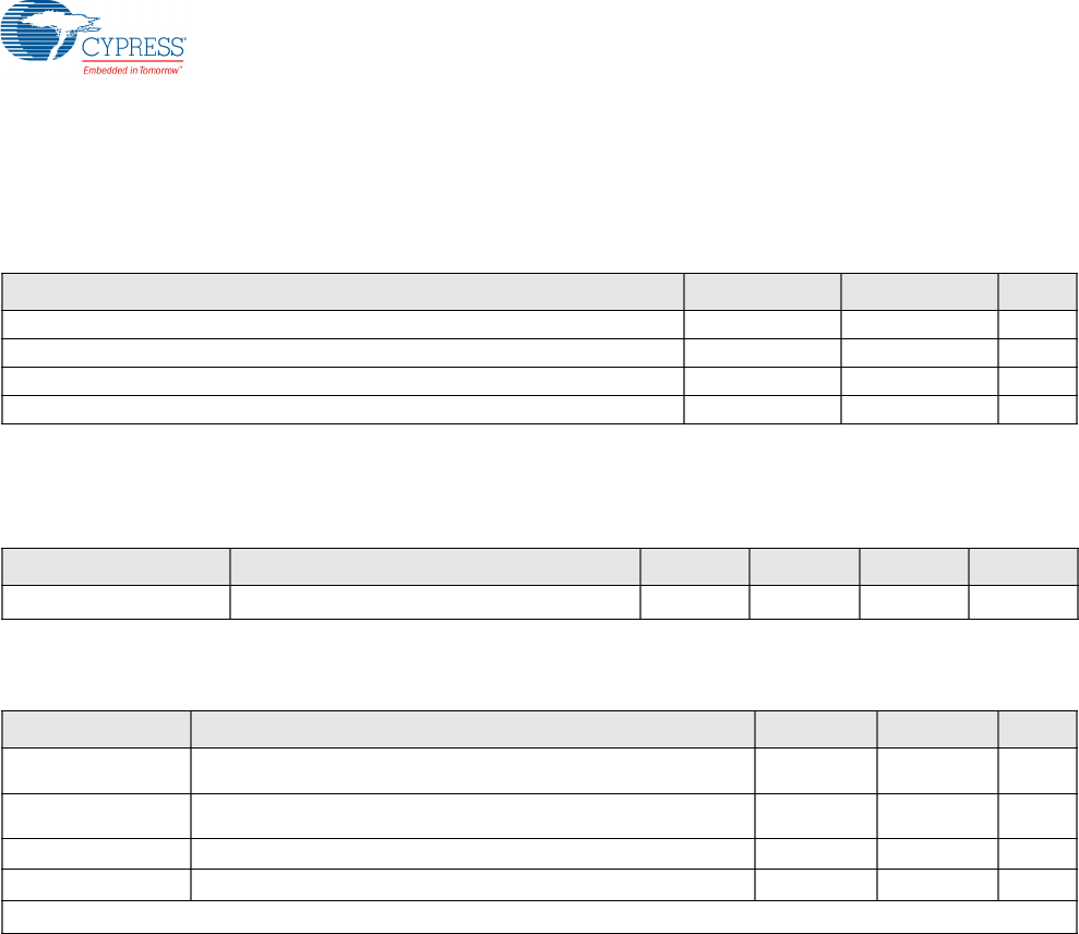
1.6 Timing and AC Characteristics
1.6.1 SPI Timing
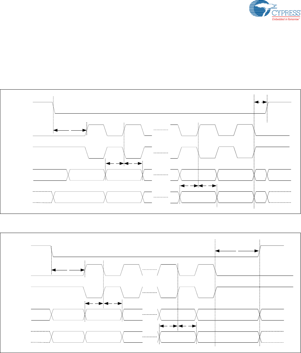
SPI interface timing is illustrated in Figure 1-4 and Figure 1-5 and are defined in Ta b l e 1-9 .
Figure 1-4. SPI Timing—Modes 0 and 2
Figure 1-5. SPI Timing—Modes 1 and 3
3
SPI_CSN
SPI_CLK
(Mode0)
SPI_MOSI ‐FirstBit
SPI_MISO NotDriven FirstBit
SecondBit
SecondBit
Lastbit
Lastbit
1
2
6
SPI_CLK
(Mode2)
NotDriven
‐
54
3
SPI_CSN
SPI_CLK
(Mode1)
SPI_MOSI ‐Invalidbit
SPI_MISO NotDriven Invalidbit
Firstbit
Firstbit
Lastbit
Lastbit
1
2
6
‐
NotDriven
SPI_CLK
(Mode3)
54
CYW20732S Bluetooth Low Energy SiP Module, Doc. # 002-15222 Rev. *G 18
Introduction
1.6.2 BSC Interface Timing
BSC interface timing is illustrated in Figure 1-6 and is defined in Table 1-10.
Figure 1-6. BSC Interface Timing
Table 1-9. SPI Interface Timing Specifications
Reference Characteristics Min. Typ. Max.
1 Time from CSN asserted to first clock edge 1 SCK 100
2 Master setup time – 1/2SCK –
3 Master hold time 1/2SCK - –
4 Slave setup time – 1/2 SCK –
5 Slave hold time 1/2 SCK – –
6 Time from last clock edge to CSN deasserted SCK 10 SCK 100
Table 1-10. BSC Interface Timing Specifications
Reference Characteristics Min. Max. Unit
1 Clock frequency – 100, 400, 800, 1000 kHz
2 START condition setup time 650 – ns
3 START condition hold time 280 – ns
4 Clock low time 650 – ns
5 Clock high time 280 – ns
6 Data input hold time 0 – ns
7 Data input setup time 100 – ns
8 STOP condition setup time 280 – ns
9 Output valid from clock – 400 ns
10 Bus free time 650 – ns
19 CYW20732S Bluetooth Low Energy SiP Module, Doc. # 002-15222 Rev. *G
Introduction
1.6.3 UART Timing
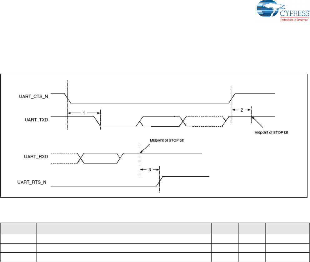
UART timing is illustrated in Figure 1-7 and defined in Ta b l e 1 - 11.
Figure 1-7. UART Timing
Table 1-11. UART Timing Specifications
Reference Characteristics Min. Max. Unit
1 Delay time, UART_CTS_N low to UART_TXD valid – 24 Baudout cycles
2 Setup time, UART_CTS_N high before midpoint of stop bit – 10 ns
3 Delay time, midpoint of stop bit to UART_RTS_N high – 2 Baudout cycles

CYW20732S Bluetooth Low Energy SiP Module, Doc. # 002-15222 Rev. *G 20
Introduction
1.7 PCB Design and Manufacturing Recommendations
1.7.1 Pad and Solder Mask Opening Dimensions
CYW20732S pad and solder mask opening dimensions are defined in Ta ble 1-12.
1.7.2 PCB Layout Recommendations for Configuration A
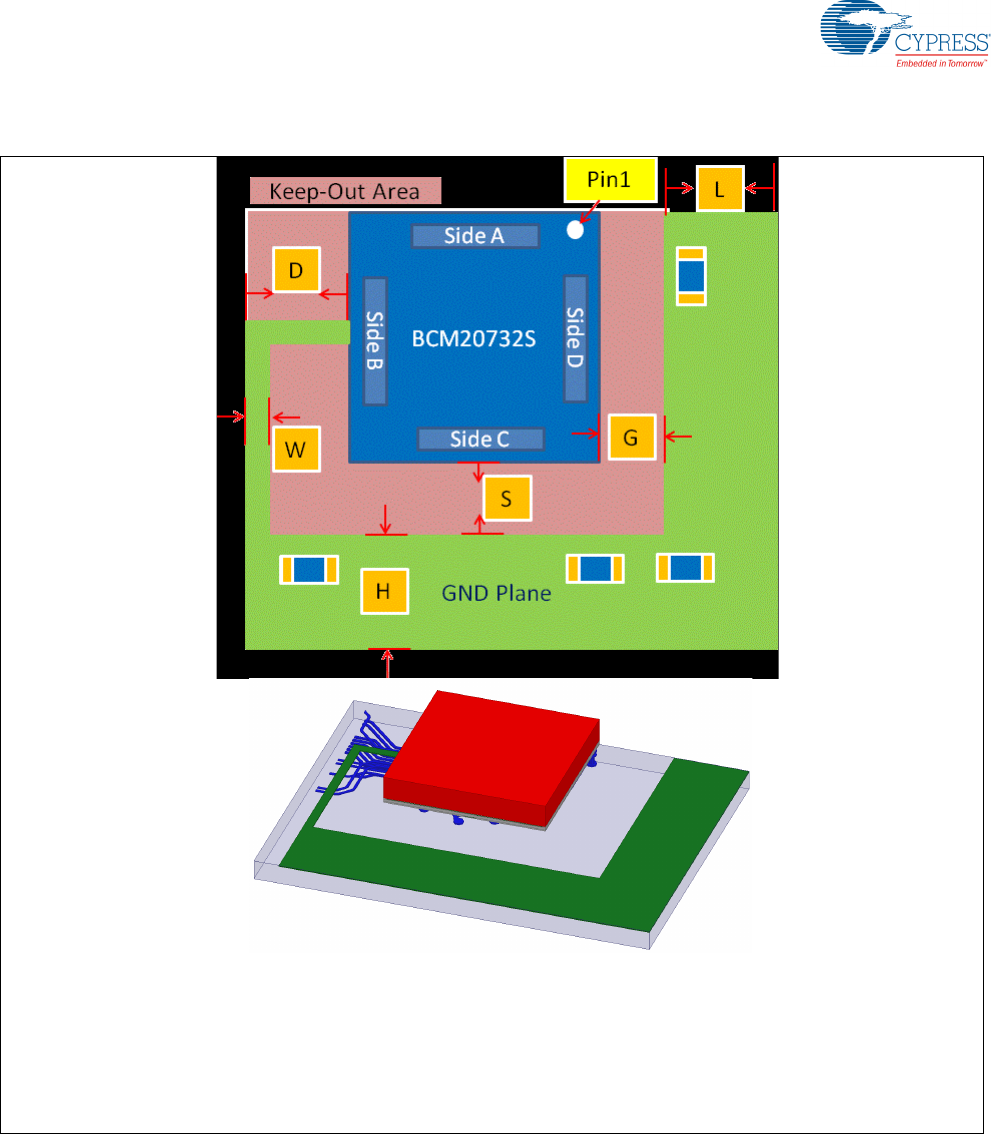
The following layout recommendations are referenced to Figure 1-8:
■Connect to system ground from side B of the module (pins 13–22).
■An L-shaped ground plane is required for the embedded BLE antenna. Keep the GND continuous. Do not cut off the GND
shape to accommodate trace routes.
■If the L-shaped GND plane is located on the top layer of the PCB, do not place components on the ground plane. If this
cannot be avoided, move the L-shaped ground plane to another layer.
■Antenna efficiency of 31–41% can be achieved based on the layout in Figure 1-8 and the dimensions listed below. Follow-
ing these layout recommendations is expected to yield 50+ meters of usable range; deviating from these recommenda-
tions may reduce the range of the antenna.
❐D: 4.5 mm (typical)
❐G, H, S: 3 mm (typical)
❐L: 3 mm (minimum)
❐W: 0.4 mm (typical)
■Route signal traces out of the module from side C (between pins 27 and 30) or side B (between pins 16 and 19) of the
module. Traces can be overlapped to avoid routing through the keep-out area.
■Do not route traces from side A or sideD.
Table 1-12. Pad and Solder Mask Dimensions
Pad Type Pad Dimensions Solder Mask Opening Dimensions Unit
Type A 0.6 × 0.25 0.7 × 0.35 mm
Type B 0.55 × 0.3 0.65 × 0.4
Type C 0.4 × 0.4 0.5 × 0.5
21 CYW20732S Bluetooth Low Energy SiP Module, Doc. # 002-15222 Rev. *G
Introduction
Figure 1-8. PCB Layout Example, Configuration A
Notes:
■Side A indicates the side of Pin #1 - Pin #12 of the CYW20732S.
■Side B indicates the side of Pin #13 - Pin #22 of the CYW20732S.
■Side C indicates the side of Pin #23 - Pin #34 of the CYW20732S.
■Side D indicates the side of Pin #35 - Pin #44 of the CYW20732S.
CYW20732S Bluetooth Low Energy SiP Module, Doc. # 002-15222 Rev. *G 22
Introduction
1.7.2.1 Example of an L-Shaped Ground Plane
Figure 1-9 shows an L-shaped ground arrangement in the 2nd layer (purple color) and the top-side component placement
and trace routing (blue color). We can see that some components and routings are placing in the L-shaped area on the top
layer and the “L -shaped” ground is connected to system ground in the 2nd layer.
Figure 1-9 also indicates the clearance area (marked in yellow) and L-shaped GND area (marked in green).
Figure 1-9. L-Shaped Ground Plane
Figure 1-10 shows an L -shaped ground (arranged in the 2nd layer) only.
Figure 1-10. L-Shaped Ground Plane, 2nd Layer
23 CYW20732S Bluetooth Low Energy SiP Module, Doc. # 002-15222 Rev. *G
Introduction
1.7.3 PCB Layout Recommendations for Configuration B
The following layout recommendations are referenced to Figure 1-11:
■Connect to system ground from side B of the module (pins 13–22).
■An L-shaped ground plane is required for the embedded BLE antenna. Keep the GND continuous. Do not cut off the GND
shape to accommodate trace routes.
■If the L-shaped GND plane is located on the top layer of the PCB, do not place components on the ground plane. If this
cannot be avoided, move the L-shaped ground plane to another layer.
■Antenna efficiency of 31–41% can be achieved based on the layout in Figure 1-11 and the dimensions listed below. Fol-
lowing these layout recommendations is expected to yield 50+ meters of usable range; deviating from these recommen-
dations may reduce the range of the antenna.
❐D: 4.5 mm (typical)
❐G, H, S: 3 mm (typical)
❐L: 3 mm (minimum)
❐W: 0.4 mm (typical)
■Route signal traces out of the module from side C (between pins 27 and 30) or side B (between pins 16 and 19) of the
module. Traces can be overlapped to avoid routing through the keep-out area.
■Do not route traces from side A or sideD.
Figure 1-11. PCB Layout Example, Configuration B
Notes:
■Side A indicates the side of Pin #1 - Pin #12 of the CYW20732S.
■Side B indicates the side of Pin #13 - Pin #22 of the CYW20732S.
■Side C indicates the side of Pin #23 - Pin #34 of the CYW20732S.
■Side D indicates the side of Pin #35 - Pin #44 of the CYW20732S.
CYW20732S Bluetooth Low Energy SiP Module, Doc. # 002-15222 Rev. *G 24
Introduction
1.7.4 Common Guidelines for CYW20732S
It is recommended to have a 0.4 mm gap between the chip's upper surface and the plastic housing (Figure 1-12).
Figure 1-12. Gap Between Chip’s Upper Surface and Plastic Housing
Arrange the GND plane under the module and connect the GND pins of the module to the GND plane as shown in
Figure 1-14.
Figure 1-13. Example of Ground Plane Under the Module
Note: Do not route the GND plane under the RF pin.
If you are unable to reserve such a large GND plane, then use the minimal required area as shown in Figure 1-14.
25 CYW20732S Bluetooth Low Energy SiP Module, Doc. # 002-15222 Rev. *G
Introduction
Figure 1-14. Minimum Required Ground Plane
1.7.5 PCB Stencil
The recommended PCB stencil is shown in Figure 1-15 (all measurements in mm). Use an unsolder mask to set the module
footprint.
Figure 1-15. CYW20732S Stencil (Bottom View)
CYW20732S Bluetooth Low Energy SiP Module, Doc. # 002-15222 Rev. *G 26
Introduction
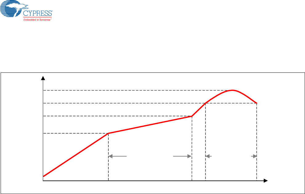
1.7.6 Solder Reflow
The recommended solder reflow profile for the CYW20732S is defined in Figure 1-16.
Figure 1-16. Solder Reflow Profile
245°C
217°C
200°C
150°C
Time
Temperature
Pre‐Heating:90~120sec. Soldering:60~90sec.
27 CYW20732S Bluetooth Low Energy SiP Module, Doc. # 002-15222 Rev. *G
Introduction
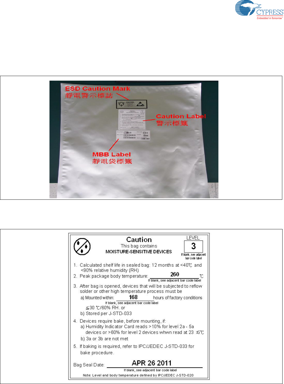
1.8 Packaging and Storage Information
The CYW20732S is available in a tape and reel package and is shipped in an ESD-protected moisture-resistant (MSL-3) bag
as shown in Figure 1-17. The storage temperature range is –40°C to +125°C.
Figure 1-17. CYW20732S ESD/Moisture Packaging
The moisture sensitivity label on the CYW20732S shipping bag is shown in Figure 1-18.
Figure 1-18. CYW20732S Moisture Sensitivity Label
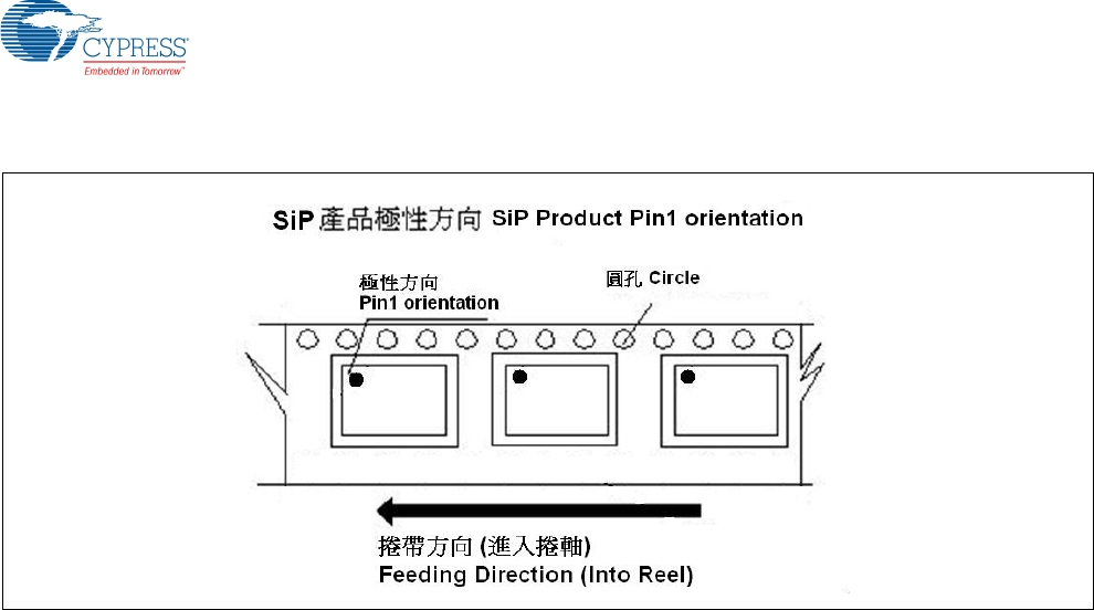
Figure 1-19 shows the location of pin 1 on the CYW20732S relative to its orientation on the tape packaging.
CYW20732S Bluetooth Low Energy SiP Module, Doc. # 002-15222 Rev. *G 28
Introduction
Figure 1-19. CYW20732S Tape and Reel Pin 1 Location
29 CYW20732S Bluetooth Low Energy SiP Module, Doc. # 002-15222 Rev. *G
Introduction
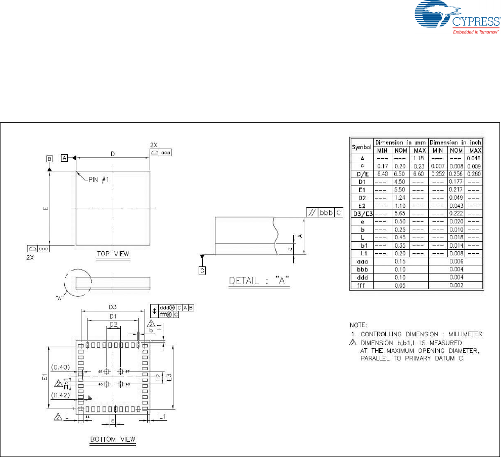
1.9 Mechanical Information
Package dimensions for the CYW20732S are shown in Figure 1-20.
Figure 1-20. CYW20732S Package Dimensions
Additional CYW20732Spackage dimensions are shown in Figure 1-21.
CYW20732S Bluetooth Low Energy SiP Module, Doc. # 002-15222 Rev. *G 30
Introduction
Figure 1-21. CYW20732S Pin Dimensions (Bottom View)

31 CYW20732S Bluetooth Low Energy SiP Module, Doc. # 002-15222 Rev. *G
Introduction
1.10 Ordering Information
Table 1-13. Ordering Information
Part Number Package Operating Temperature Humidity
CYW20732S 48-pin LGA –40°C to +85°C 95% max., noncondensing

PRELIMINARY
'RFXPHQW1XPEHU5HY$ 3DJHRI
5HJXODWRU\,QIRUPDWLRQ
)&&
)&&127,&(
WKH)&&5XOHV7KHGHYLFHPHHWVWKHUHTXLUHPHQWVIRUPRGXODUWUDQVPLWWHU
DSSURYDODVGHWDLOHGLQ)&&SXEOLF1RWLFH'$WUDQVPLWWHU2SHUDWLRQLVVXEMHFWWRWKHIROORZLQJWZRFRQGLWLRQV7KLVGHYLFH
PD\QRWFDXVHKDUPIXOLQWHUIHUHQFHDQG7KLVGHYLFHPXVWDFFHSWDQ\LQWHUIHUHQFHUHFHLYHGLQFOXGLQJLQWHUIHUHQFHWKDWPD\FDXVH
XQGHVLUHGRSHUDWLRQ
&$87,21
7KH)&&UHTXLUHVWKHXVHUWREHQRWLILHGWKDWDQ\FKDQJHVRUPRGLILFDWLRQVPDGHWRWKLVGHYLFHWKDWDUHQRWH[SUHVVO\DSSURYHGE\
&\SUHVV6HPLFRQGXFWRUPD\YRLGWKHXVHUVDXWKRULW\WRRSHUDWHWKHHTXLSPHQW
7KLVHTXLSPHQWKDVEHHQWHVWHGDQGIRXQGWRFRPSO\ZLWKWKHOLPLWVIRUD&ODVV%GLJLWDOGHYLFHSXUVXDQWWR3DUWRIWKH)&&5XOHV
7KHVHOLPLWVDUHGHVLJQHGWRSURYLGHUHDVRQDEOHSURWHFWLRQDJDLQVWKDUPIXOLQWHUIHUHQFHLQDUHVLGHQWLDOLQVWDOODWLRQ7KLVHTXLSPHQW
JHQHUDWHVXVHVDQGFDQUDGLDWHUDGLRIUHTXHQF\HQHUJ\DQGLIQRWLQVWDOOHGDQGXVHGLQDFFRUGDQFHZLWKWKHLQVWUXFWLRQVrPD\FDXVH
KDUPIXOLQWHUIHUHQFHWRUDGLRFRPPXQLFDWLRQV+RZHYHUWKHUHLVQRJXDUDQWHHWKDWLQWHUIHUHQFHZLOOQRWRFFXULQDSDUWLFXODULQVWDOODWLRQ
,IWKLVHTXLSPHQWGRHVFDXVHKDUPIXOLQWHUIHUHQFHWRUDGLRRUWHOHYLVLRQUHFHSWLRQZKLFKFDQEHGHWHUPLQHGE\WXUQLQJWKHHTXLSPHQW
RIIDQGRQWKHXVHULVHQFRXUDJHGWRWU\WRFRUUHFWWKHLQWHUIHUHQFHE\RQHRUPRUHRIWKHIROORZLQJPHDVXUHV
n5HRULHQWRUUHORFDWHWKHUHFHLYLQJDQWHQQD
n,QFUHDVHWKHVHSDUDWLRQEHWZHHQWKHHTXLSPHQWDQGUHFHLYHU
n&RQQHFWWKHHTXLSPHQWLQWRDQRXWOHWRQDFLUFXLWGLIIHUHQWIURPWKDWWRZKLFKWKHUHFHLYHULVFRQQHFWHG
n&RQVXOWWKHGHDOHURUDQH[SHULHQFHGUDGLR79WHFKQLFLDQIRUKHOS
/$%(/,1*5(48,5(0(176
7KH2ULJLQDO(TXLSPHQW0DQXIDFWXUHU2(0PXVWHQVXUHWKDW)&&ODEHOOLQJUHTXLUHPHQWVDUHPHW7KLVLQFOXGHVDFOHDUO\YLVLEOH
ODEHORQWKHRXWVLGHRIWKH2(0HQFORVXUHVSHFLI\LQJWKHDSSURSULDWH&\SUHVV6HPLFRQGXFWRU)&&LGHQWLILHUIRUWKLVSURGXFWDVZHOO
DVWKH)&&1RWLFHDERYH7KH)&&LGHQWLILHULV)&&,'
,QDQ\FDVHWKHHQGSURGXFWPXVWEHODEHOHGH[WHULRUZLWK&RQWDLQV)&&,'
$17(11$:$51,1*
7KLVGHYLFHLVWHVWHGZLWKDVWDQGDUG60$FRQQHFWRUDQGZLWKWKHDQWHQQDVOLVWHGEHORZ:KHQLQWHJUDWHGLQWKH2(0VSURGXFWWKHVH
IL[HGDQWHQQDVUHTXLUHLQVWDOODWLRQSUHYHQWLQJHQGXVHUVIURPUHSODFLQJWKHPZLWKQRQDSSURYHGDQWHQQDV$Q\DQWHQQDQRWLQWKH
IROORZLQJWDEOHPXVWEHWHVWHGWRFRPSO\ZLWK)&&6HFWLRQIRUXQLTXHDQWHQQDFRQQHFWRUVDQG6HFWLRQIRUHPLVVLRQV
5)(;32685(
7RFRPSO\ZLWK)&&5)([SRVXUHUHTXLUHPHQWVWKH2ULJLQDO(TXLSPHQW0DQXIDFWXUHU2(0PXVWHQVXUHWRLQVWDOOWKHDSSURYHG
DQWHQQDLQWKHSUHYLRXV
7KHSUHFHGLQJVWDWHPHQWPXVWEHLQFOXGHGDVD&$87,21VWDWHPHQWLQPDQXDOVIRUSURGXFWVRSHUDWLQJZLWKWKHDSSURYHGDQWHQQDV
LQ7DEOHRQSDJHWRDOHUWXVHUVRQ)&&5)([SRVXUHFRPSOLDQFH$Q\QRWLILFDWLRQWRWKHHQGXVHURILQVWDOODWLRQRUUHPRYDO
LQVWUXFWLRQVDERXWWKHLQWHJUDWHGUDGLRPRGXOHLVQRWDOORZHG
7KHUDGLDWHGRXWSXWSRZHURI DQWHQQD)&&,' LVIDUEHORZWKH)&&UDGLRIUHTXHQF\
H[SRVXUHOLPLWV1HYHUWKHOHVVXVH VXFKDPDQQHUWKDWPLQLPL]HVWKHSRWHQWLDOIRUKXPDQFRQWDFWGXULQJQRUPDO
RSHUDWLRQ
(QGXVHUVPD\ QRW EH SURYLGHG ZLWK WKH PRGXOHLQVWDOODWLRQLQVWUXFWLRQV 2(0 LQWHJUDWRUV DQG HQGXVHUVPXVWEH SURYLGHGZLWK
WUDQVPLWWHURSHUDWLQJFRQGLWLRQVIRUVDWLVI\LQJ5)H[SRVXUHFRPSOLDQFH
The device complies with part 15 of
WAP-0737
WAP-0737
the device with the PCB WAP-0737
the device
PRELIMINARY &<%7
&HUWLILFDWLRQ
LVOLFHQVHGWRPHHWWKHUHJXODWRU\U HTXLUHPHQWVRI,QGXVWU\&DQDGD,&
/LFHQVH,&
0DQXIDFWXUHUVRIPRELOHIL[HGRUSRUWDEOHGHYLFHVLQFRUSRUDWLQJWKLVPRGXOHDUHDGYLVHGWRFODULI\DQ\UHJXODWRU\TXHVWLRQVDQGHQVXUH
FRPSOLDQFH IRU 6$5 DQGRU 5) H[SRVXUH OLPLWV 8VHUV FDQ REWDLQ &DQDGLDQ LQIRUPDWLRQ RQ 5) H[SRVXUH DQG FRPSOLDQFH IURP
ZZZLFJFFD
7KLVGHYLFHKDVEHHQGHVLJQHGWRRSHUDWHZLWKWKHDQWHQQDVOLVWHGLQ7DEOHRQSDJHKDYLQJDPD[LPXPJDLQRI QQDV
QRWLQFOXGHGLQWKLVOLVWRUKDYLQJDJDLQJUHDWHU G%LDUHVWULFWO\SURKLELWHGIRUXVHZLWKWKLVGHYLFH7KHUHTXLUHGDQWHQQD
LPSHGDQFHLVRKPV7KHDQWHQQDXVHGIRUWKLVWUDQVPLWWHUPXVWQRWEHFRORFDWHGRURSHUDWLQJLQFRQMXQFWLRQZLWKDQ\RWKHUDQWHQQD
RUWUDQVPLWWHU
,&127,&(
7KH GHYLFHLQFOXGLQJ WKH EXLOWLQ WUDFH DQWHQQD FRPSOLHV ZLWK &DQDGD 566*(1 5XOHV 7KH GHYLFH PHHWVWKH
UHTXLUHPHQWVIRUPRGXODUWUDQVPLWWHUDSSURYDODVGHWDLOHGLQ566*(12SHUDWLRQLVVXEMHFWWRWKHIROORZLQJWZRFRQGLWLRQV7KLV
GHYLFHPD\QRWFDXVHKDUPIXOLQWHUIHUHQFHDQG7KLVGHYLFHPXVWDFFHSWDQ\LQWHUIHUHQFHUHFHLYHGLQFOXGLQJLQWHUIHUHQFHWKDW
PD\FDXVHXQGHVLUHGRSHUDWLRQ
,&5$',$7,21(;32685(67$7(0(17)25&$1$'$
7KLVGHYLFHFRPSOLHVZLWK,QGXVWU\&DQDGDOLFHQFHH[HPSW566VWDQGDUGV2SHUDWLRQLVVXEMHFWWRWKHIROORZLQJWZRFRQGLWLRQV
WKLVGHYLFHPD\ QRW FDXVH LQWHUIHUHQFH DQG WKLVGHYLFHPXVWDFFHSWDQ\LQWHUIHUHQFHLQFOXGLQJLQWHUIHUHQFHWKDWPD\FDXVH
XQGHVLUHGRSHUDWLRQRIWKHGHYLFH
/HSUpVHQWDSSDUHLOHVWFRQIRUPHDX[&15G,QGXVWULH&DQDGDDSSOLFDEOHVDX[DSSDUHLOVUDGLRH[HPSWVGHOLFHQFH/H[SORLWDWLRQHVW
DXWRULVpHDX[GHX[FRQGLWLRQVVXLYDQWHVODSSDUHLOQHGRLWSDVSURGXLUHGHEURXLOODJHHWOXWLOLVDWHXUGHODSSDUHLOGRLWDFFHSWHU
WRXWEURXLOODJHUDGLRpOHFWULTXHVXELPrPHVLOHEURXLOODJHHVWVXVFHSWLEOHGHQFRPSURPHWWUHOHIRQFWLRQQHPHQW
/$%(/,1*5(48,5(0(176
7KH2ULJLQDO(TXLSPHQW0DQXIDFWXUHU2(0PXVWHQVXUHWKDW,&ODEHOOLQJUHTXLUHPHQWVDUHPHW7KLVLQFOXGHVDFOHDUO\YLVLEOHODEHO
RQWKHRXWVLGHRIWKH2(0HQFORVXUHVSHFLI\LQJWKHDSSURSULDWH&\SUHVV6HPLFRQGXFWRU,&LGHQWLILHUIRUWKLVSURGXFWDVZHOODVWKH,&
1RWLFHDERYH7KH,&LGHQWLILHULV ,QDQ\FDVHWKHHQGSURGXFWPXVWEHODEHOHGLQL WVH[WHULRUZLWK&RQWDLQV,&
(XURSHDQ577('HFODUDWLRQRI&RQIRUPLW\
+HUHE\&\SUHVV6HPLFRQGXFWRUGHFODUHVWKDWWKH%OXHWRRWKPRGXOHFRPSOLHVZLWKWKHHVVHQWLDOUHTXLUHPHQWVDQG
RWKHUUHOHYDQWSURYLVLRQVRI'LUHFWLYH(&$VDUHVXOWRIWKHFRQIRUPLW\DVVHVVPHQWSURFHGXUHGHVFULEHGLQ$QQH[,,,RIWKH
'LUHFWLYH(&WKHHQGFXVWRPHUHTXLSPHQWVKRXOGEHODEHOHGDVIROORZV
$OOYHUVLRQVRIWKH UHIHUHQFHGHVLJQFDQEHXVHGLQWKHIROORZLQJFRXQWULHV$XVWULD%HOJLXP&\SUXV
&]HFK5HSXEOLF'HQPDUN(VWRQLD)LQODQG)UDQFH*HUPDQ\*UHHFH+XQJDU\,UHODQG,WDO\/DWYLD/LWKXDQLD/X[HPERXUJ0DOWD
3RODQG3RUWXJDO6ORYDNLD6ORYHQLD6SDLQ6ZHGHQ7KH1HWKHUODQGVWKH8QLWHG.LQJGRP6ZLW]HUODQGDQG1RUZD\
ISED
The device
7922A-0737
-1.5dBi, ante
than -1.5
(3) No SAR evaluation is required since maximum transmitter Pout is below IC threshold
(3) Aucune évaluation SAR n'est requise étant donné que la puissance maximale de l'émetteur est inférieure au seuil IC.
7922A-0737
7922A-0737
device in the specified
33 CYW20732S Bluetooth Low Energy SiP Module, Doc. # 002-15222 Rev. *G
Revision History
Document Revision History
Document Title: CYW20732S Bluetooth Low Energy SiP Module
Document Number: 002-15222
Revision ECN# Issue Date Origin of
Change Description of Change
** - 10/02/2013 - MMP20732S-TRM100-R:
Initial Release
*A - 01/15/2014 - MMP20732S-TRM101-R
Update document template
*B - 03/04/2014 -
MMP20732S-TRM102-R
Updated:
■Table 2: “Pin Descriptions”.
■“Technical Support” (added link to the WICED support community).
■Section: Electrical Specifications, Table 4: “Voltage”
*C - 05/13/2014 -
MMP20732S-TRM103-R
Added:
■Footnotes for pins 43 and 44 of Table 2: “Pin Descriptions”
■“PCB Layout Recommendations for Configuration A”
■“PCB Layout Recommendations for Configuration B”
■“Common Guidelines for CYW20732S”
*D - 08/22/2014 -
MMP20732S-TRM104-R
Updated:
Table 2: “Pin Descriptions,” (pins 33 and 38).
*E - 09/11/2014 -
MMP20732S-TRM105-R
Updated:
■Table 2: “Pin Descriptions”, pin 37 alternate functions.
■“PCB Layout Recommendations for Configuration A”.
■“PCB Layout Recommendations for Configuration B”.
Removed:
Appendix A: “Acronyms and Abbreviations”.
*F - 03/24/2016 -
MMP20732S-TRM106-R
Updated:
Table 5, “Current Consumption”
*G 5560143 01/27/2017 UTSV Updated to Cypress Template.