Cypress Semiconductor 3027 This product is a Bluetooth wireless EZ-BT WICED Module User Manual CYBT 013033 01 EZ BT Module
Cypress Semiconductor This product is a Bluetooth wireless EZ-BT WICED Module CYBT 013033 01 EZ BT Module
UserManual.wiki
>
Cypress Semiconductor
>
3027 User Manual
User Manual - 0502
Navigation menu
Upload a User Manual
Namespaces
Wiki Guide
HTML
PDF
Info
Views
User Manual
Discussion / Help
Navigation
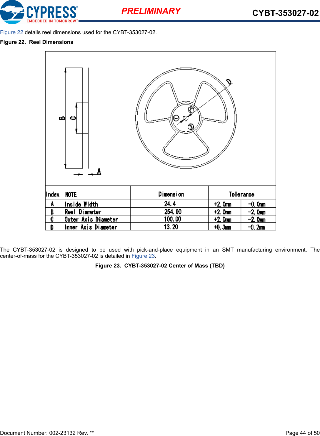
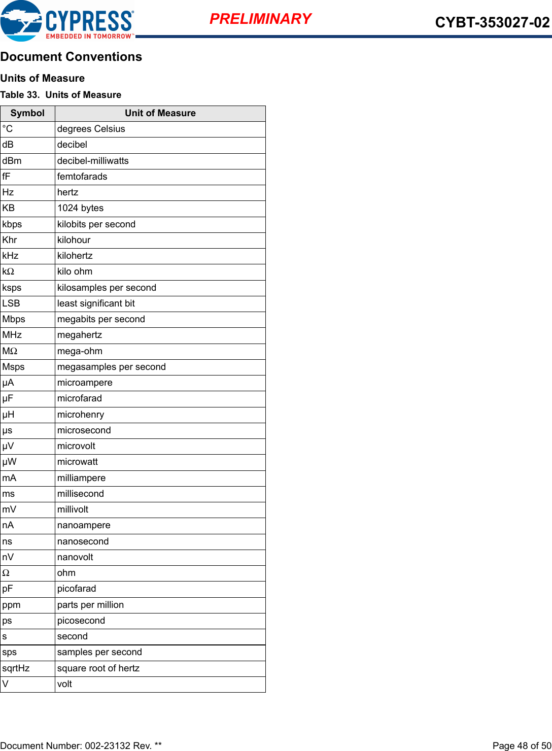
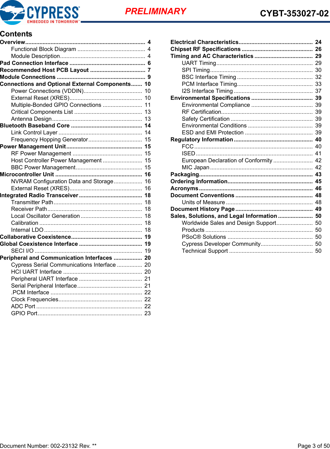
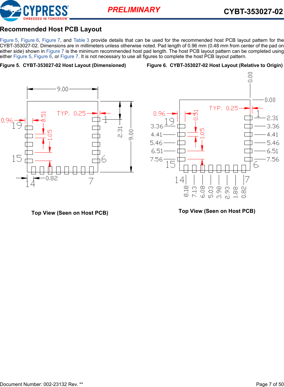
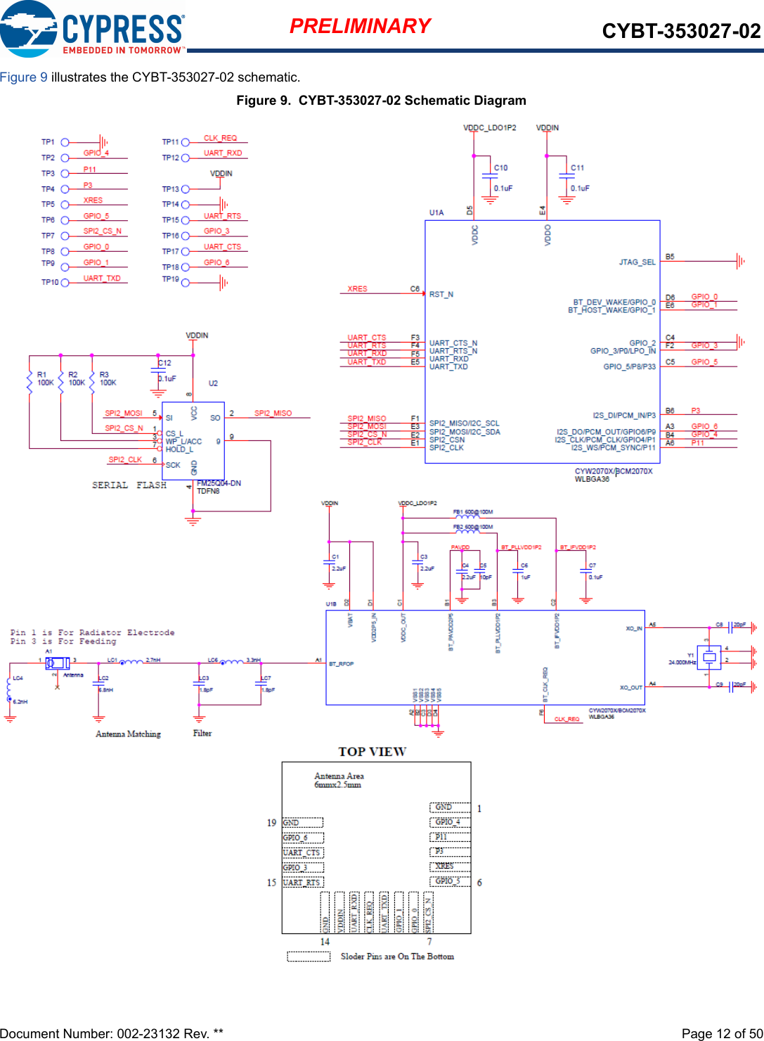
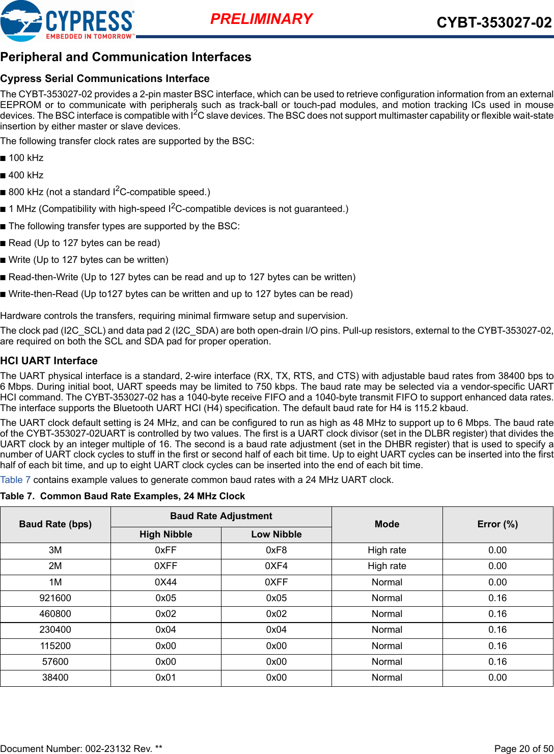
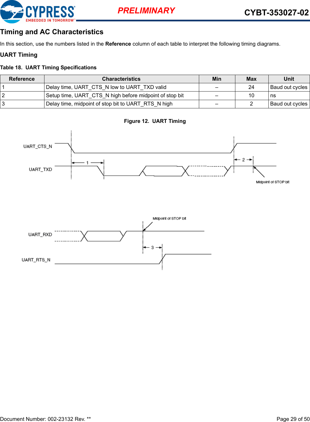
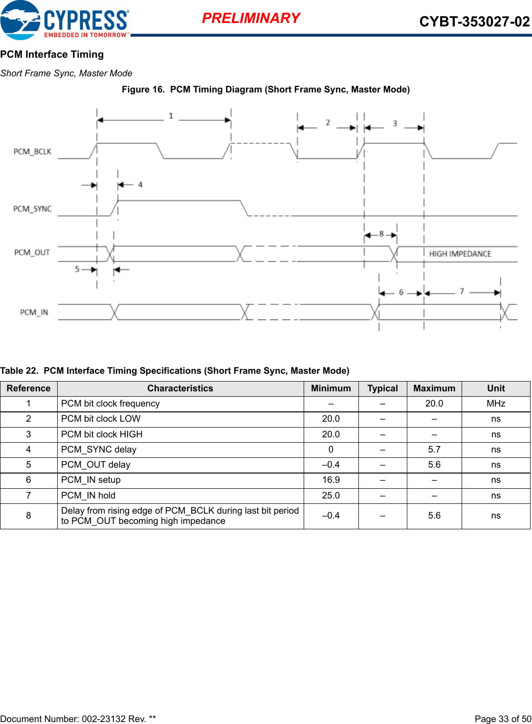
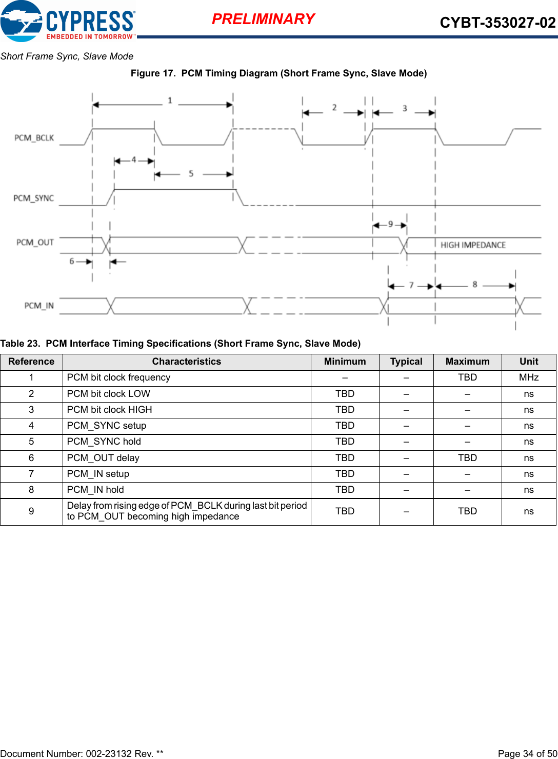
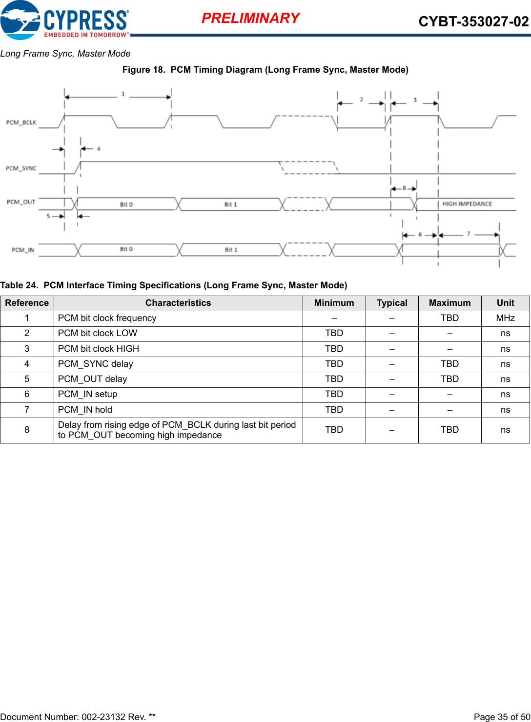
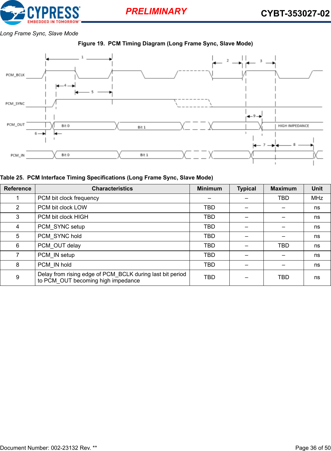
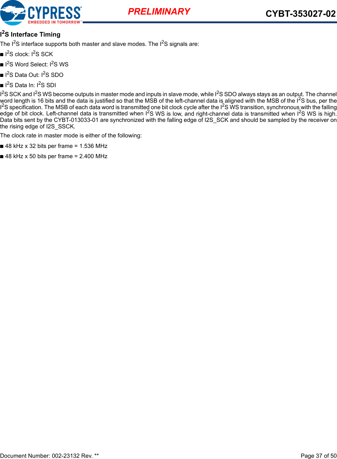
![PRELIMINARY CYBT-353027-02EZ-BT™ WICED ModuleCypress Semiconductor Corporation • 198 Champion Court • San Jose,CA 95134-1709 • 408-943-2600Document Number: 002-23132 Rev. ** Revised March 14, 2018General DescriptionThe CYBT-353027-02 is a fully integrated Bluetooth SmartReady wireless module. The CYBT-353027-02 includes anonboard crystal oscillator, passive components, flash memory,and the Cypress CYW2070x silicon device. The CYBT-353027-02 supports peripheral functions (ADC,timers), UART, I2C, and SPI communication, and a Bluetoothaudio interface. The CYBT-353027-02 includes a royalty-freeBLE stack compatible with Bluetooth 5.0 in a 9.0 × 9.0 × 1.75 mmSMT package.The CYBT-353027-02 includes 512 KB of onboard serial flashmemory and is designed for standalone operation. TheCYBT-353027-02 uses an integrated power amplifier to achieveClass I or Class II output power capability. The CYBT-353027-02 is fully qualified by Bluetooth SIG and istargeted at space constrained applications. Module DescriptionnModule size: 9.00 mm × 9.00 mm × 1.75 mm nBluetooth 5.0 Qualified Smart Ready modulepQDID: TBDpDeclaration ID: TBDnCertified to FCC, ISED, MIC, and CE regulationsnCastelated solder pad connections for ease-of-usen512-KB on-module serial flash memorynUp to 8 GPIOsnTemperature range: -30 °C to +85 °CnCortex-M3 32-bit processor nMaximum TX output power: p+12 dbm for Bluetooth Classicp+9 dBm for Bluetooth Low EnergynRX Receive Sensitivity: p–93.5 dBm for Bluetooth Classic p–96.5 dBm for Bluetooth Low EnergyPower Consumption[1]nTX average current consumption: 52.5 mA (EDR) at 8 dBmnRX average current consumption: 26.4 mA (EDR)nLow power mode supportpDeep Sleep: 2.69 uA Functional CapabilitiesnΣ-Δ ADC for audio (12 bits) and DC measurement (10 bits)nSerial Communications interface compatible with I2C slavesnMaster Serial Peripheral Interface (SPI) support nHCI interface through UARTnPCM/I2S Audio interfacenTwo-wire Global Coexistence Interface (GCI)nProgrammable output power controlnSupports extended synchronous connections (eSCO), for enhanced voice quality by allowing for retransmission of dropped packetsnBluetooth wideband speech supportBenefitsCYBT-353027-02 provides all necessary components requiredto operate BLE and/or BR/EDR communication standards. nProven hardware design ready to usenDual-mode operation eliminates the need for multiple modulesnCost optimized for applications without space constraintsnNonvolatile memory for self-sufficient operation and Over-the-air updatesnBluetooth SIG Listed with QDID and Declaration ID nFully certified module eliminates the time needed for design, development and certification processesnWICED™ STUDIO provides an easy-to-use integrated design environment (IDE) to configure, develop, and program a Bluetooth applicationNote1. The values in this section were calculated for a 90% efficient DC-DC at 3V in HCI mode, and based on a Class I configuration bench-marked at Class II. Lower values are expected for a class II configuration using an external LPO and corresponding PA configuration.](https://usermanual.wiki/Cypress-Semiconductor/3027/User-Guide-3837334-Page-1.png)
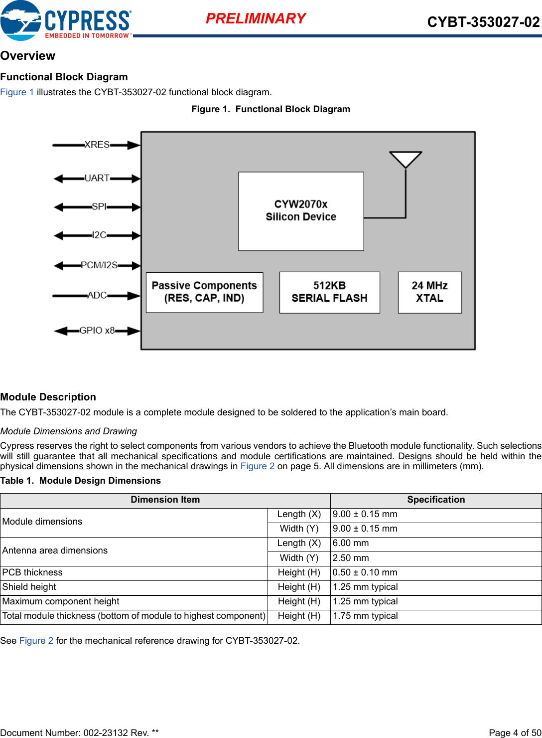
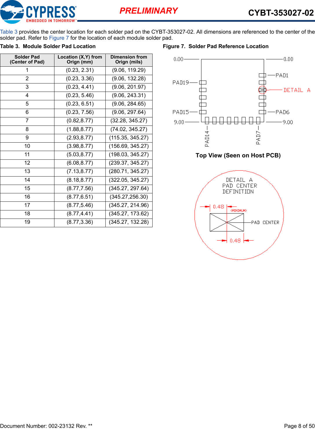
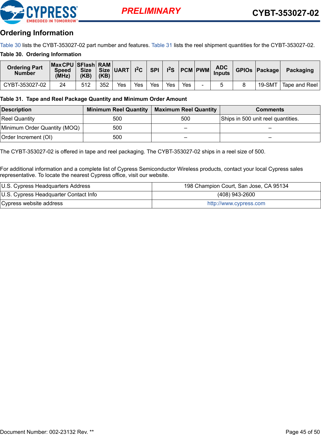
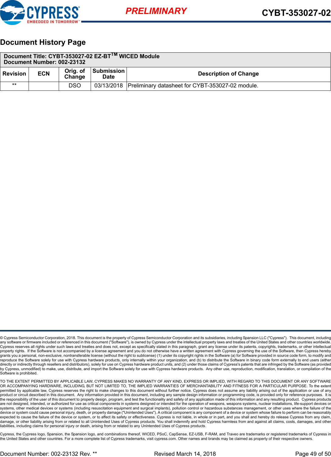
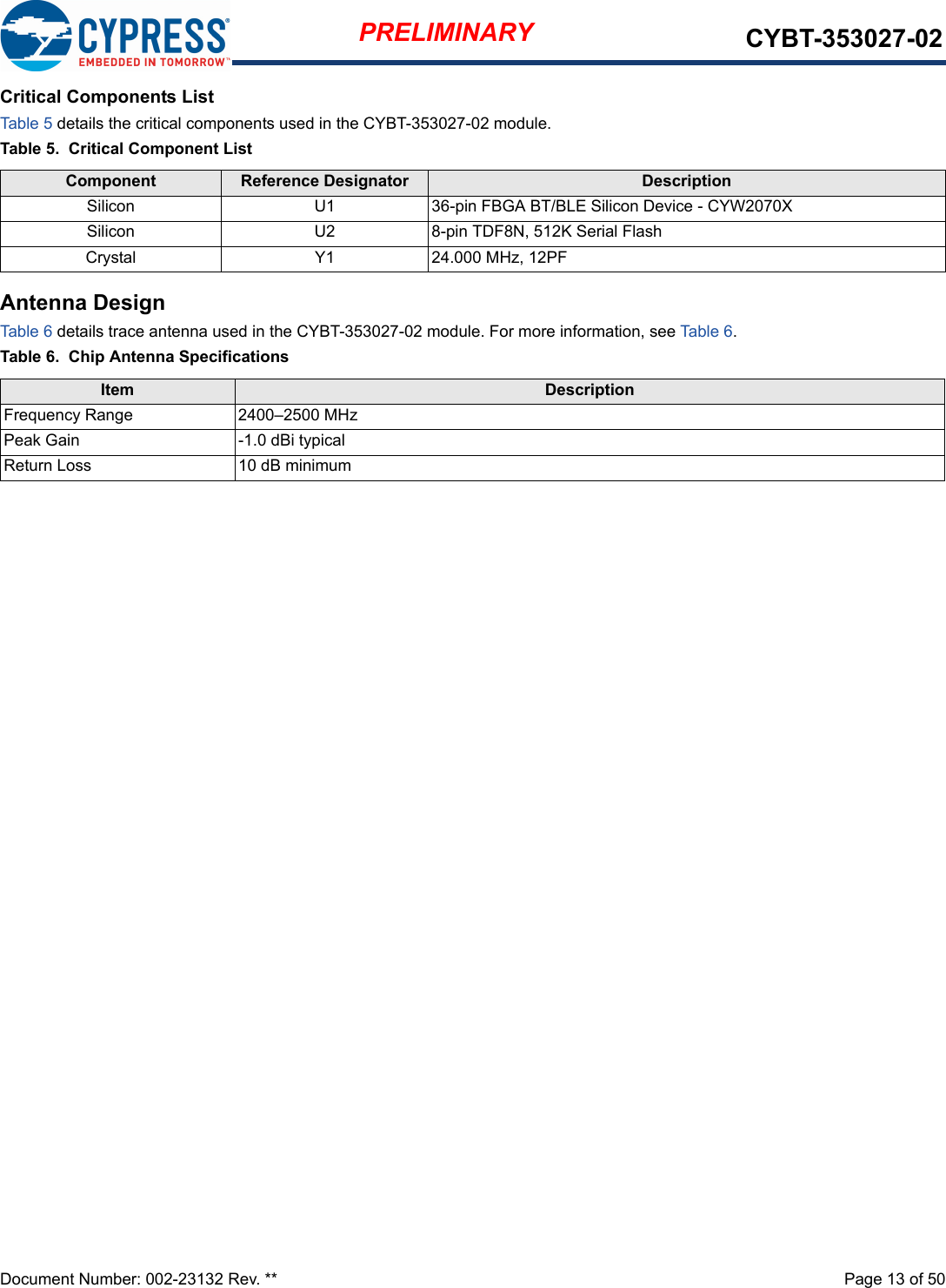
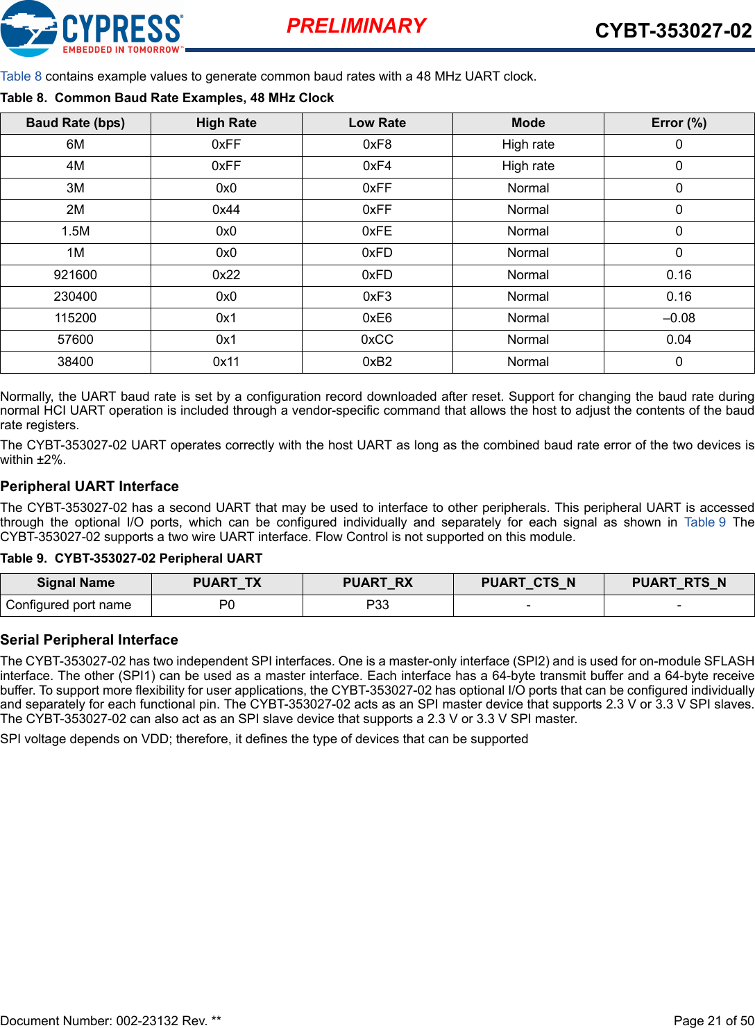
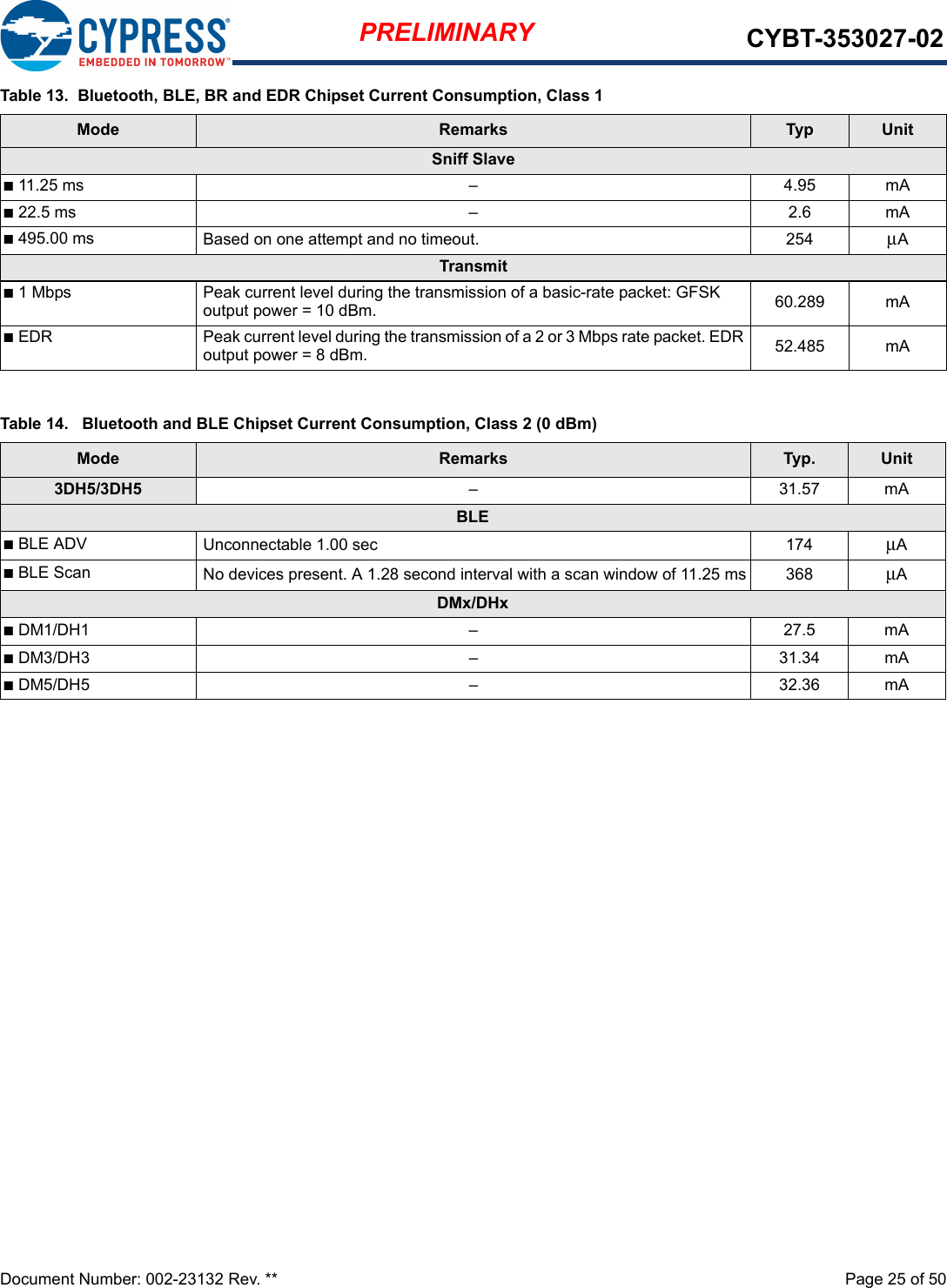
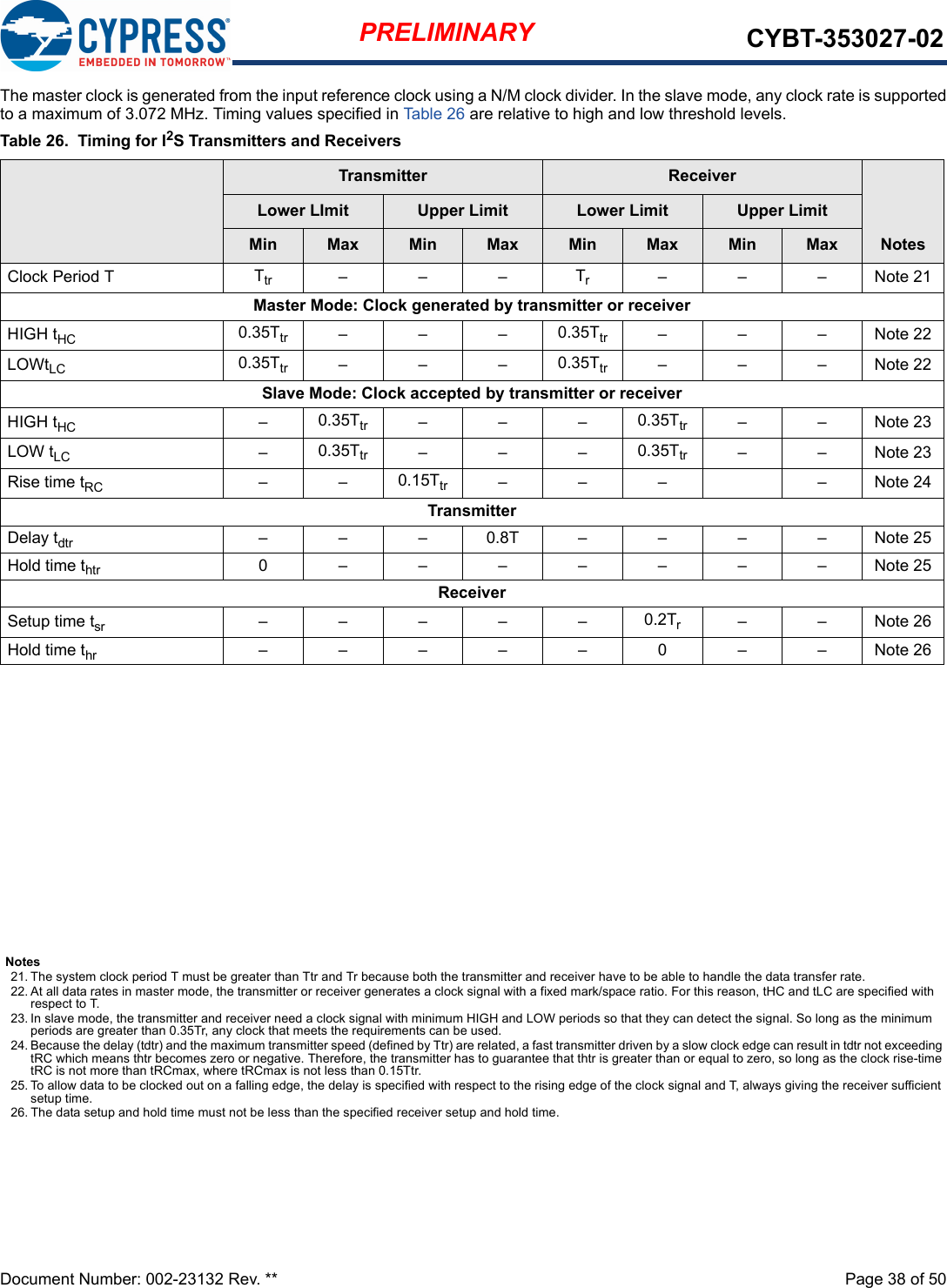
![Document Number: 002-23132 Rev. ** Page 9 of 50PRELIMINARY CYBT-353027-02Module ConnectionsTab le 4 details the solder pad connection definitions and available functions for the pad connections for the CYBT-353027-02 module.Tab le 4 lists the solder pads on the CYBT-353027-02 module, the silicon device pin, and denotes what functions are available for eachsolder pad.Table 4. CYBT-353027-02 Solder Pad Connection Definitions Pad Pad Name Silicon Port Pin Name(s) UART SPI[3] I2C ADC COEX CLK/XTAL GPIO Other1 GND GND Ground2GPIO_4GPIO_4/P1/I2S_CLK/PCM_CLK SPI1_MISO/P1(master) IN28/P1 3PCM_CLKI2S_CLK3P11P11/I2S_WS/PCM_SYNC IN24 3PCM_SyncI2S_WS4P3P3/I2S_DI/PCM_INSPI1_CLK (master) SDA 3PCM_DII2S_DI5 XRES RST_N External Reset (Active Low)6GPIO_5BT_GPIO_5/P8/P33PUART_RX/P33 IN27/P8IN6/P333(GCI_SECI_OUT) ACK1/P33 37 SPI2_CS_N SPI2_CSN[4] SPI2_CS_N8GPIO_0 BT_GPIO_03(Dev Wake)9GPIO_1 BT_GPIO_13(Host Wake)10 UART_TXD BT_UART_TXD HCI UART Transmit Data11 CLK_REQ BT_CLK_REQ Used for shared-clock applications12 UART_RXD BT_UART_RXD HCI UART Receive Data13 VDDIN VDDO VDDIN (2.3V ~ 3.6V)14 GND GND Ground15 UART_RTS BT_UART_RTS_N HCI UART Request To Send Output16 GPIO_3 BT_GPIO_3/P0 PUART_TX/P0 SPI1_MOSI/P0(master) IN29/P0 3 17 UART_CTS BT_UART_CTS_N HCI UART Clear To Send Input18 GPIO_6 BT_GPIO_6/P9/I2S_DO/PCM_OUT SCL IN26/P93(GCI_SECI_IN)3 I2S_DOPCM_Out19 GND GND GroundNote3. The CYBT-353027-02 contains a single SPI (SPI1) peripheral supporting master configuration. SPI2 is used for on-module serial memory interface. 4. SPI2_CS_N is internally routed on the module to on-board serical flash memory. SPI2_CS_N is made available on module pad 7 to be used for Recover Mode operation only.](https://usermanual.wiki/Cypress-Semiconductor/3027/User-Guide-3837334-Page-9.png)
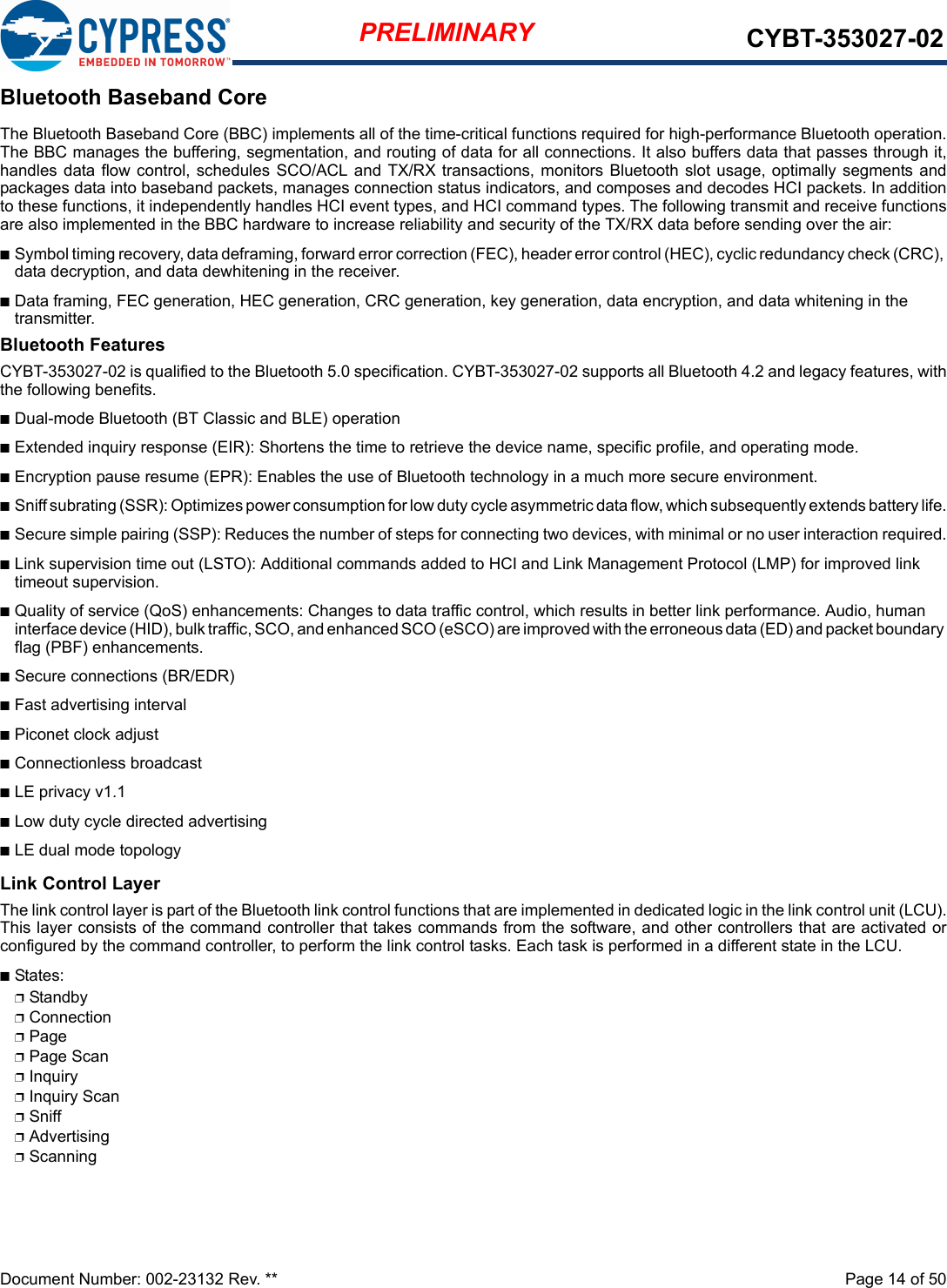
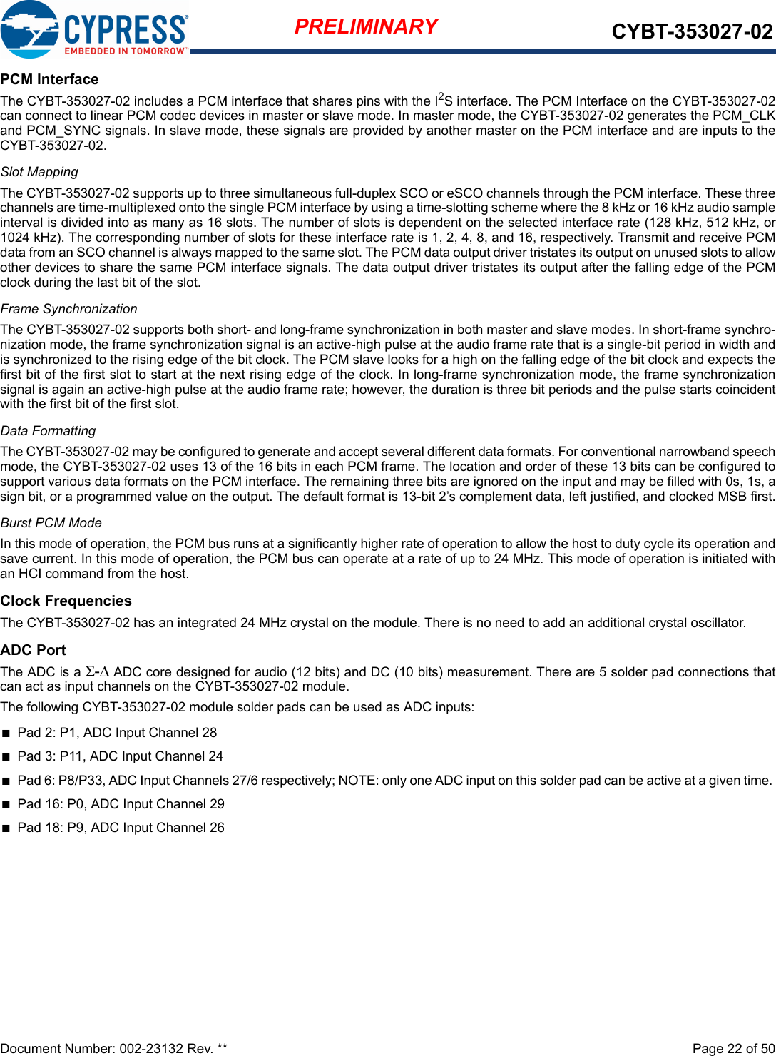
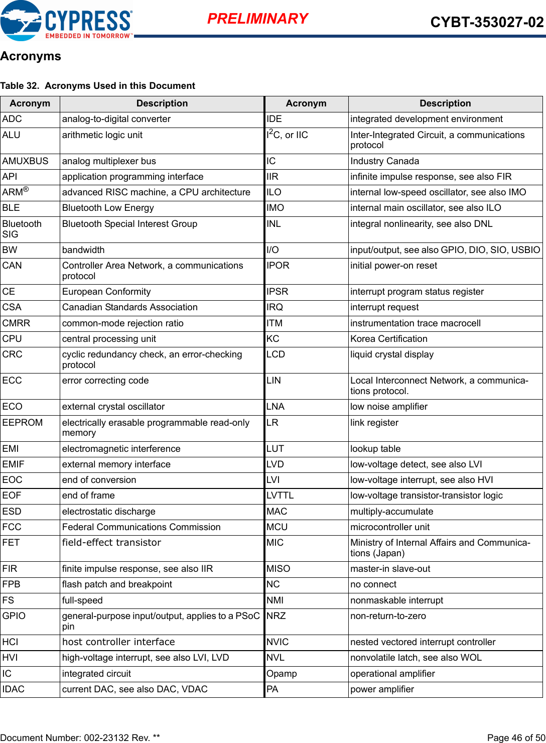
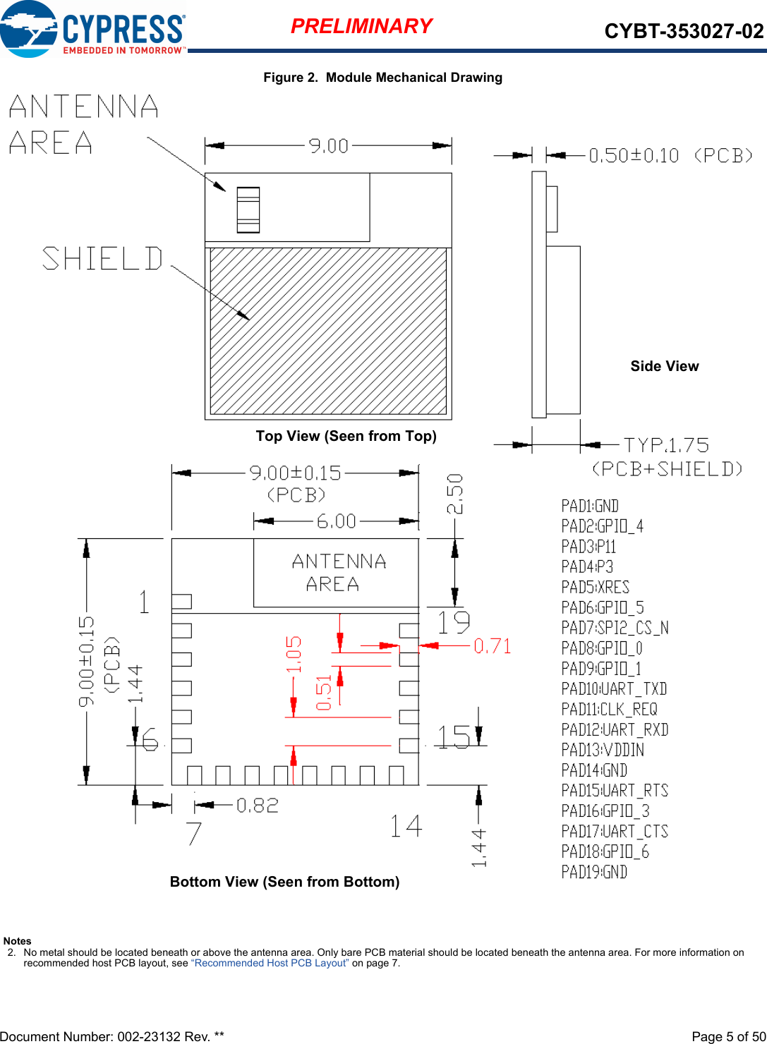
![Document Number: 002-23132 Rev. ** Page 24 of 50PRELIMINARY CYBT-353027-02Electrical CharacteristicsTab le 10 shows the maximum electrical rating for voltages referenced to VDD pin.Tab le 11 shows the power supply characteristics for the range TJ = 0 to 125 °C.Tab le 12 shows the specifications for the digital voltage levels.Tab le 13 shows the current consumption measurements Table 10. Maximum Electrical RatingRating Symbol Value UnitVDDIN – 3.795 VVoltage on input or output pin – VSS – 0.3 to VDD + 0.3 VOperating ambient temperature range Topr -30 to +85 °CStorage temperature range Tstg –40 to +85 °CTable 11. Power SupplyParameter Description Minimum[5] Typical Maximum[5] UnitVDDIN Power Supply Input (CYBT-353027-02) 2.3 – 3.6 VTable 12. Digital LevelsCharacteristics Symbol Min Typ Max UnitInput low voltage VIL ––0.8VInput high voltage VIH 2.0 – – VOutput low voltage VOL ––0.4VOutput high voltage VOH VDD – 0.4 – – VInput capacitance (VDDMEM domain) CIN ––0.4pFTable 13. Bluetooth, BLE, BR and EDR Chipset Current Consumption, Class 1Mode Remarks Typ Unit3DH5/3DH5 –37.10mABLEnBLE Connected 600-ms interval 211 μAnBLE ADV Unconnectable 1.00 sec 176 μAnBLE Scan No devices present. A 1.28 second interval with a scan window of 11.25 ms 355 μADMx/DHxnDM1/DH1 – 32.15 mAnDM3/DH3 – 38.14 mAnDM5/DH5 – 38.46 mAHIDOFF Deep sleep 2.69 μAPage scan Periodic scan rate is 1.28 sec 0.486 mAReceiven1 Mbps Peak current level during reception of a basic-rate packet. 26.373 mAnEDR Peak current level during the reception of a 2 or 3 Mbps rate packet. 26.373 mANote5. Overall performance degrades beyond minimum and maximum supply voltages.The voltage range specified is determined by the minimum and maximum operating voltage of the SPI Serial Flash included on the module.](https://usermanual.wiki/Cypress-Semiconductor/3027/User-Guide-3837334-Page-24.png)
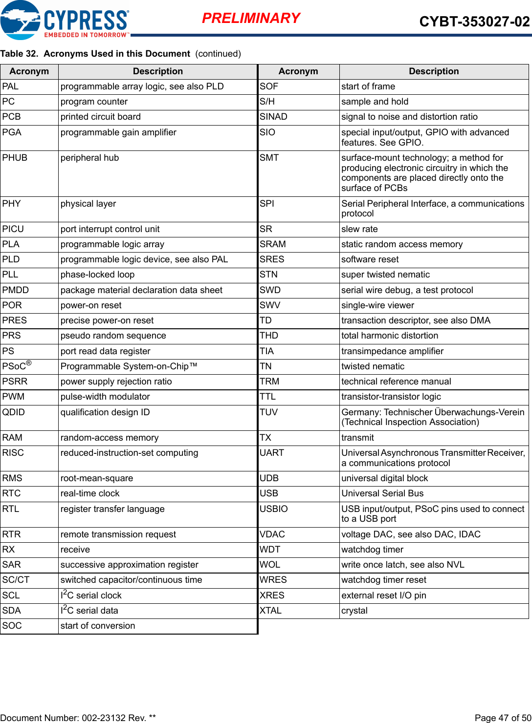
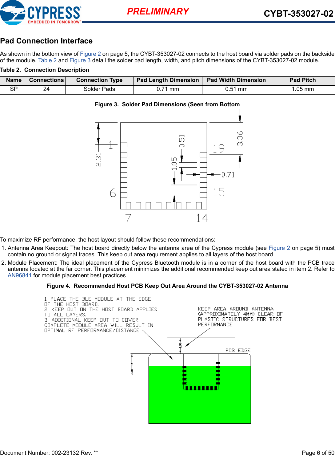
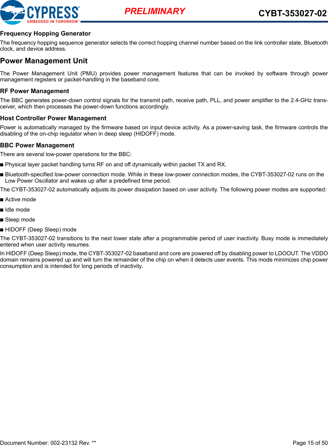
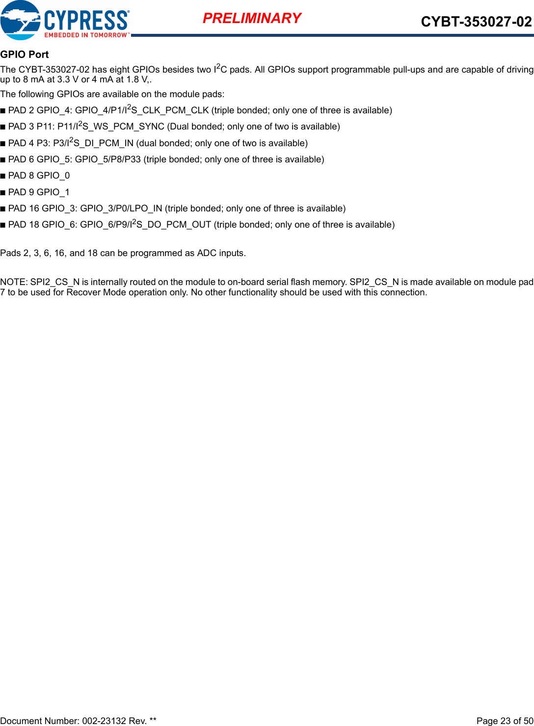
![Document Number: 002-23132 Rev. ** Page 26 of 50PRELIMINARY CYBT-353027-02Chipset RF SpecificationsAll specifications in Table 15 are for industrial temperatures and are single-ended. Unused inputs are left open.Table 15. Chipset Receiver RF SpecificationsParameter Conditions Minimum Typical[6] Maximum UnitGeneralFrequency range – 2402 – 2480 MHzRX sensitivity[7]GFSK, 0.1% BER, 1 Mbps – –93.5 – dBmLE GFSK, 0.1% BER, 1 Mbps – –96.5 – dBmπ/4-DQPSK, 0.01% BER, 2 Mbps – –95.5 – dBm8-DPSK, 0.01% BER, 3 Mbps – –89.5 – dBmMaximum input GFSK, 1 Mbps – – –20 dBmMaximum input π/4-DQPSK, 8-DPSK, 2/3 Mbps – – –20 dBmInterference PerformanceC/I cochannel GFSK, 0.1% BER – 9.5 11 dBC/I 1 MHz adjacent channel GFSK, 0.1% BER – –5 0 dBC/I 2 MHz adjacent channel GFSK, 0.1% BER – –40 –30.0 dBC/I > 3 MHz adjacent channel GFSK, 0.1% BER – –49 –40.0 dBC/I image channel GFSK, 0.1% BER – –27 –9.0 dBC/I 1 MHz adjacent to image channel GFSK, 0.1% BER – –37 –20.0 dBC/I cochannel π/4-DQPSK, 0.1% BER – 11 13 dBC/I 1 MHz adjacent channel π/4-DQPSK, 0.1% BER – –8 0 dBC/I 2 MHz adjacent channel π/4-DQPSK, 0.1% BER – –40 –30.0 dBC/I > 3 MHz adjacent channel 8-DPSK, 0.1% BER – –50 –40.0 dBC/I image channel π/4-DQPSK, 0.1% BER – –27 –7.0 dBC/I 1 MHz adjacent to image channel π/4-DQPSK, 0.1% BER – –40 –20.0 dBC/I cochannel 8-DPSK, 0.1% BER – 17 21 dBC/I 1 MHz adjacent channel 8-DPSK, 0.1% BER – –5 5 dBC/I 2 MHz adjacent channel 8-DPSK, 0.1% BER – –40 –25.0 dBC/I > 3 MHz adjacent channel 8-DPSK, 0.1% BER – –47 –33.0 dBC/I Image channel 8-DPSK, 0.1% BER – –20 0 dBC/I 1 MHz adjacent to image channel 8-DPSK, 0.1% BER – –35 –13.0 dBOut-of-Band Blocking Performance (CW)[8]30 MHz–2000 MHz 0.1% BER – –10.0 – dBm2000–2399 MHz 0.1% BER – –27 – dBmNotes6. Typical operating conditions are 1.22-V operating voltage and 25°C ambient temperature.7. The receiver sensitivity is measured at BER of 0.1% on the device interface.8. Meets this specification using front-end band pass filter.](https://usermanual.wiki/Cypress-Semiconductor/3027/User-Guide-3837334-Page-26.png)
![Document Number: 002-23132 Rev. ** Page 27 of 50PRELIMINARY CYBT-353027-022498–3000 MHz 0.1% BER – –27 – dBm3000 MHz–12.75 GHz 0.1% BER – –10.0 – dBmOut-of-Band Blocking Performance, Modulated Interferer776–764 MHz CDMA – –10[9] –dBm824–849 MHz CDMA – –10[9] –dBm1850–1910 MHz CDMA – –23[9] –dBm824–849 MHz EDGE/GSM – –10[9] –dBm880–915 MHz EDGE/GSM – –10[9] –dBm1710–1785 MHz EDGE/GSM – –23[9] –dBm1850–1910 MHz EDGE/GSM – –23[9] –dBm1850–1910 MHz WCDMA – –23[9] –dBm1920–1980 MHz WCDMA – –23[9] –dBmIntermodulation Performance[10]BT, Df = 5 MHz – –39.0 – – dBmSpurious Emissions[11]30 MHz to 1 GHz – – – –62 dBm1 GHz to 12.75 GHz – – – –47 dBm65 MHz to 108 MHz FM Rx – –147 – dBm/Hz746 MHz to 764 MHz CDMA – –147 – dBm/Hz851–894 MHz CDMA – –147 – dBm/Hz925–960 MHz EDGE/GSM – –147 – dBm/Hz1805–1880 MHz EDGE/GSM – –147 – dBm/Hz1930–1990 MHz PCS – –147 – dBm/Hz2110–2170 MHz WCDMA – –147 – dBm/HzTable 15. Chipset Receiver RF Specifications (continued)Parameter Conditions Minimum Typical[6] Maximum UnitNotes9. Numbers are referred to the pin output with an external BPF filter.10. f0 = -64 dBm Bluetooth-modulated signal, f1 = –39 dBm sine wave, f2 = –39 dBm Bluetooth-modulated signal, f0 = 2f1 – f2, and |f2 – f1| = n*1 MHz, where n is 3, 4, or 5. For the typical case, n = 4.11. Includes baseband radiated emissions.](https://usermanual.wiki/Cypress-Semiconductor/3027/User-Guide-3837334-Page-27.png)
![Document Number: 002-23132 Rev. ** Page 28 of 50PRELIMINARY CYBT-353027-02Table 16. Chipset Transmitter RF SpecificationsTable 17. Chipset BLE RF SpecificationsParameter Conditions Minimum Typical Maximum UnitGeneralFrequency range – 2402 – 2480 MHzClass1: GFSK Tx power[12] ––12–dBmClass1: EDR Tx power[13] ––9–dBmClass 2: GFSK Tx power – – 2 – dBmPower control step – 2 4 8 dBModulation Accuracyπ/4-DQPSK Frequency Stability – –10 – 10 kHzπ/4-DQPSK RMS DEVM – – – 20 %π/4-QPSK Peak DEVM – – – 35 %π/4-DQPSK 99% DEVM – – – 30 %8-DPSK frequency stability – –10 – 10 kHz8-DPSK RMS DEVM – – – 13 %8-DPSK Peak DEVM – – – 25 %8-DPSK 99% DEVM – – – 20 %In-Band Spurious Emissions1.0 MHz < |M – N| < 1.5 MHz – – – –26 dBc1.5 MHz < |M – N| < 2.5 MHz – – – –20 dBm|M – N| > 2.5 MHz – – – –40 dBmOut-of-Band Spurious Emissions30 MHz to 1 GHz – – – –36.0[14] dBm1 GHz to 12.75 GHz – – – –30.0[14, 15] dBm1.8 GHz to 1.9 GHz – – – –47.0 dBm5.15 GHz to 5.3 GHz – – – –47.0 dBmParameter Conditions Minimum Typical Maximum UnitFrequency range N/A 2402 – 2480 MHzRx sense[16] GFSK, 0.1% BER, 1 Mbps – –96.5 – dBmTx power[17] N/A –9–dBmMod Char: Delta F1 average N/A 225 255 275 kHzMod Char: Delta F2 max[18] N/A 99.9 – – %Mod Char: Ratio N/A 0.8 0.95 – %12. TBD dBm output for GFSK measured with PAVDD = 2.5 V.13. TBD dBm output for EDR measured with PAVDD = 2.5 V.14. Maximum value is the value required for Bluetooth qualification.15. Meets this spec using a front-end band-pass filter.16. Dirty Tx is Off.17. The BLE Tx power can be increased to compensate for front-end losses such as BPF, diplexer, switch, etc. The output is capped at 12 dBm out. The BLE Tx power at the antenna port cannot exceed the 10 dBm EIRP specification limit.18. At least 99.9% of all delta F2 max frequency values recorded over 10 packets must be greater than 185 kHz.](https://usermanual.wiki/Cypress-Semiconductor/3027/User-Guide-3837334-Page-28.png)
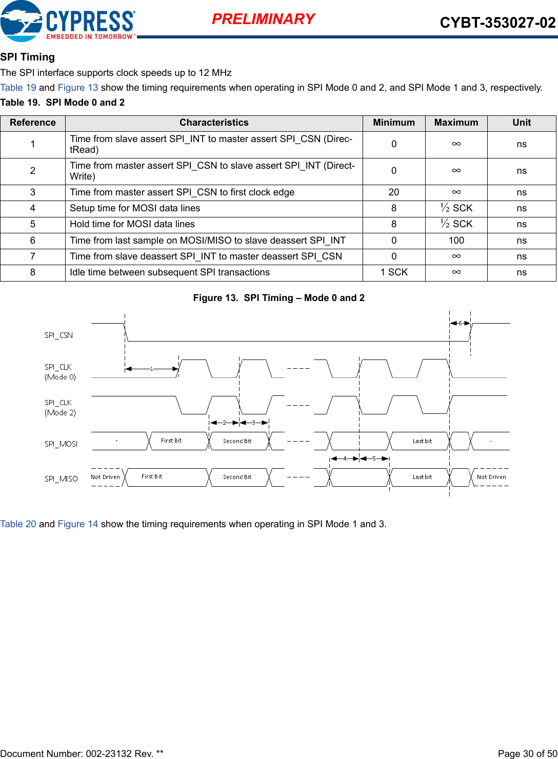
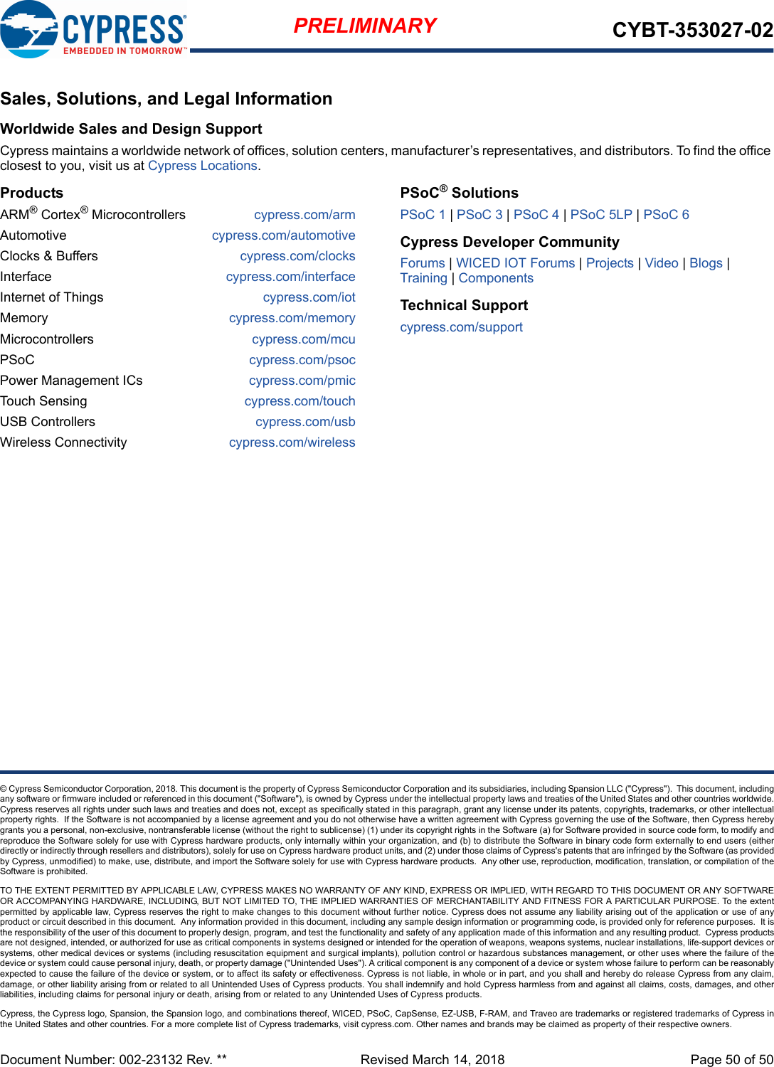
![Document Number: 002-23132 Rev. ** Page 32 of 50PRELIMINARY CYBT-353027-02BSC Interface TimingFigure 15. BSC Interface Timing DiagramTable 21. BSC Interface Timing SpecificationsReference Characteristics Min Max Unit1 Clock frequency – 100 kHz40080010002 START condition setup time 650 – ns3 START condition hold time 280 – ns4 Clock low time 650 – ns5 Clock high time 280 – ns6 Data input hold time[19] 0 – ns7 Data input setup time 100 – ns8 STOP condition setup time 280 – ns9 Output valid from clock – 400 ns10 Bus free time[20] 650 – nsNotes19. As a transmitter, 125 ns of delay is provided to bridge the undefined region of the falling edge of SCL to avoid unintended generation of START or STOP conditions.20. Time that the cbus must be free before a new transaction can start.](https://usermanual.wiki/Cypress-Semiconductor/3027/User-Guide-3837334-Page-32.png)
![Document Number: 002-23132 Rev. ** Page 39 of 50PRELIMINARY CYBT-353027-02Environmental SpecificationsEnvironmental ComplianceThis CYBT-353027-02 BLE module is produced in compliance with the Restriction of Hazardous Substances (RoHS) andHalogen-Free (HF) directives. The Cypress module and components used to produce this module are RoHS and HF compliant.RF CertificationThe CYBT-353027-02 module will be certified under the following RF certification standards at production release.nFCC: WAP3027nCEnIC: 7922A-3027nMIC: TBDSafety CertificationThe CYBT-353027-02 module complies with the following safety regulations:nUnderwriters Laboratories, Inc. (UL): Filing E331901nCSAnTUVEnvironmental ConditionsTab le 27 describes the operating and storage conditions for the Cypress BLE module.ESD and EMI ProtectionExposed components require special attention to ESD and electromagnetic interference (EMI).A grounded conductive layer inside the device enclosure is suggested for EMI and ESD performance. Any openings in the enclosurenear the module should be surrounded by a grounded conductive layer to provide ESD protection and a low-impedance path to ground. Device Handling: Proper ESD protocol must be followed in manufacturing to ensure component reliability.Table 27. Environmental Conditions for CYBT-353027-02Description Minimum Specification Maximum SpecificationOperating temperature -30 °C 85 °COperating humidity (relative, non-condensation) 5% 85%Thermal ramp rate – 3 °C/minuteStorage temperature –40 °C 85 °CStorage temperature and humidity – 85 °C at 85%ESD: Module integrated into end system Components[27] –15 kV Air2.0 kV ContactNote27. This does not apply to the RF pins (ANT).](https://usermanual.wiki/Cypress-Semiconductor/3027/User-Guide-3837334-Page-39.png)