Cypress Semiconductor 3136 This product is a Bluetooth wireless EZ-BLE Module with HomeKit User Manual CYBT 013033 01 EZ BT Module
Cypress Semiconductor This product is a Bluetooth wireless EZ-BLE Module with HomeKit CYBT 013033 01 EZ BT Module
Contents
User Manual_CYBLE-413136-01

PRELIMINARY CYBLE-413136-01
EZ-BLE™ Module with HomeKit
Cypress Semiconductor Corporation • 198 Champion Court • San Jose,CA 95134-1709 • 408-943-2600
Document Number: 002-19043 Rev. PRELIMINARY Revised May 12, 2017
General Description
The CYBLE-413136-01 is a Bluetooth Low Energy (BLE)
wireless module solution with integrated Apple HomeKit support,
including the authentication co-processor. The
CYBLE-413136-01 includes onboard crystal oscillators, passive
components, and the Cypress CYW20719 silicon device.
The CYBLE-413136-01 supports a number of peripheral
functions (ADC and PWM), as well as UART serial
communication protocol. The CYBLE-413136-01 includes a
royalty-free BLE stack compatible with Bluetooth 4.2 in a 14.7 ×
20.0 × 1.40mm package.
The CYBLE-413136-01 includes an integrated PCB trace
antenna. The CYBLE-413136-01 is qulaified by Bluetooth SIG,
and includes regulatory certification approval for FCC, ISED, and
CE.
Module Description
nModule size: 14.70 mm × 20.00 mm × 2.60 mm
nExtended Range:
pUp to 400 meters bi-directional communication[1,2]
pUp to 450 meters in beacon only mode[1]
nBluetooth LE 4.2 single-mode module
nCertified to FCC, IED, and CE standards
nCastelated solder pad connections for ease-of-use
n1024-KB flash memory, 512-KB SRAM memory
nExtended Industrial temperature range: –30 °C to +105 °C
nCortex-M4F 32-bit processor operating up to 96MHz
nWatchdog timer with dedicated internal low-speed oscillator
Power Consumption
nMaximum TX output power: +8.0 dbm[3]
nRX Receive Sensitivity: –93 dbm
nReceived signal strength indicator (RSSI) with 1-dB resolution
nTX current consumption
pBLE silicon: 5.7 mA (radio only, –16 dbm)
pRFX2401C: 27 mA (PA/LNA only, module +8 dBm)
nRX current consumption
pBLE silicon: 5.8 mA (radio only)
pRFX2401C: 7.5 mA (PA/LNA only)
nCypress CYW20719 silicon low power mode support
pPDS: 70 μA with 512 KB SRAM retention
pDeep Sleep: 1 μA with 16 KB SRAM retention
pHIDOFF: 350 nA with XRES wakeup
Functional Capabilities
nApple HomeKit compliant with on-board authentication
co-processor
nSwitched-cap Sigma-Delta ADC with internal reference
nUART serial communication block (PUART)
nFour dedicated PWM blocks
nBLE protocol stack supporting generic access profile (GAP)
Central, Peripheral, Observer, or Broadcaster roles
Benefits
CYBLE-413136-01 is fully integrated and certified solution that
provides all necessary components required to operate BLE
communication standards.
nProven hardware design ready to use
nLarge non-volatile memory for complex application devel-
opment
nOver-the-air update capable for development or field updates
nBluetooth SIG qualified with QDID and Declaration ID
nWICED™ Studio provides an easy-to-use integrated design
environment (IDE) to configure, develop, program, and test a
BLE application
Notes
1. Connection range tested module-to-module in full line-of-sight environment, free of obstacles or interferance sources with output power of +8.0 dBm.
2. Specified as module-to-module range. Mobile phone connection range will decrease based on the PA/LNA performance of the mobile phone used.
3. The CYBLE-413136-01 is capable of higher output power than specified, but is intentionally limited to +8.0dBm due to regulatory requirements for European Standards.

Document Number: 002-19043 Rev. PRELIMINARY Page 2 of 33
PRELIMINARY CYBLE-413136-01
Contents
Overview 3
Functional Block Diagram ........................................... 3
Module Description...................................................... 3
Pad Connection Interface ................................................ 5
Recommended Host PCB Layout ................................... 6
Module Connections ........................................................ 7
Connections and Optional External Components ....... 7
Power Connections (VCC) .......................................... 7
External Reset (XRES)................................................ 7
UART Connections...................................................... 7
External Component Recommendation ...................... 7
Critical Components List ............................................. 9
Antenna Design........................................................... 9
Bluetooth Baseband Core ............................................. 10
Bluetooth Low Energy ............................................... 10
Power Management Unit................................................ 11
RF Power Management ............................................ 11
Host Controller Power Management ......................... 11
BBC Power Management.......................................... 11
Microprocessor Unit....................................................... 12
Floating Point Unit..................................................... 12
On-Chip Flash ........................................................... 12
OTP........................................................................... 12
External Reset........................................................... 12
Integrated Radio Transceiver ........................................ 13
Transmitter Path........................................................ 13
Digital Modulator ....................................................... 13
Power Amplifier ......................................................... 13
Receiver Path............................................................ 13
Digital Demodulator and Bit Synchronizer................. 13
Receiver Signal Strength Indicator............................ 13
Calibration ................................................................. 14
Internal LDO Regulator ............................................. 14
Peripheral Transport Unit .............................................. 14
UART Interface.......................................................... 14
Peripheral UART Interface ........................................ 15
ADC Port.......................................................................... 15
PWM................................................................................. 15
Triac Control ................................................................... 16
Security Engine .............................................................. 16
Electrical Characteristics............................................... 17
Core Buck Regulator................................................. 18
Digital LDO................................................................ 19
RF LDO ..................................................................... 20
Digital I/O Characteristics.......................................... 21
Current Consumption ................................................ 21
RF Specifications ........................................................... 22
Timing and AC Characteristics ..................................... 23
UART Timing............................................................. 23
Environmental Specifications ....................................... 24
Environmental Compliance ....................................... 24
RF Certification.......................................................... 24
Safety Certification .................................................... 24
Environmental Conditions ......................................... 24
ESD and EMI Protection ........................................... 24
Regulatory Information.................................................. 25
FCC........................................................................... 25
ISED.......................................................................... 26
European R&TTE Declaration of Conformity ............ 27
Packaging........................................................................ 28
Ordering Information...................................................... 30
Acronyms........................................................................ 31
Document Conventions ................................................. 31
Units of Measure ....................................................... 31
Document History Page................................................. 32
Sales, Solutions, and Legal Information ...................... 33
Worldwide Sales and Design Support....................... 33
Products .................................................................... 33
PSoC® Solutions ...................................................... 33
Cypress Developer Community................................. 33
Technical Support ..................................................... 33
Document Number: 002-19043 Rev. PRELIMINARY Page 3 of 33
PRELIMINARY CYBLE-413136-01
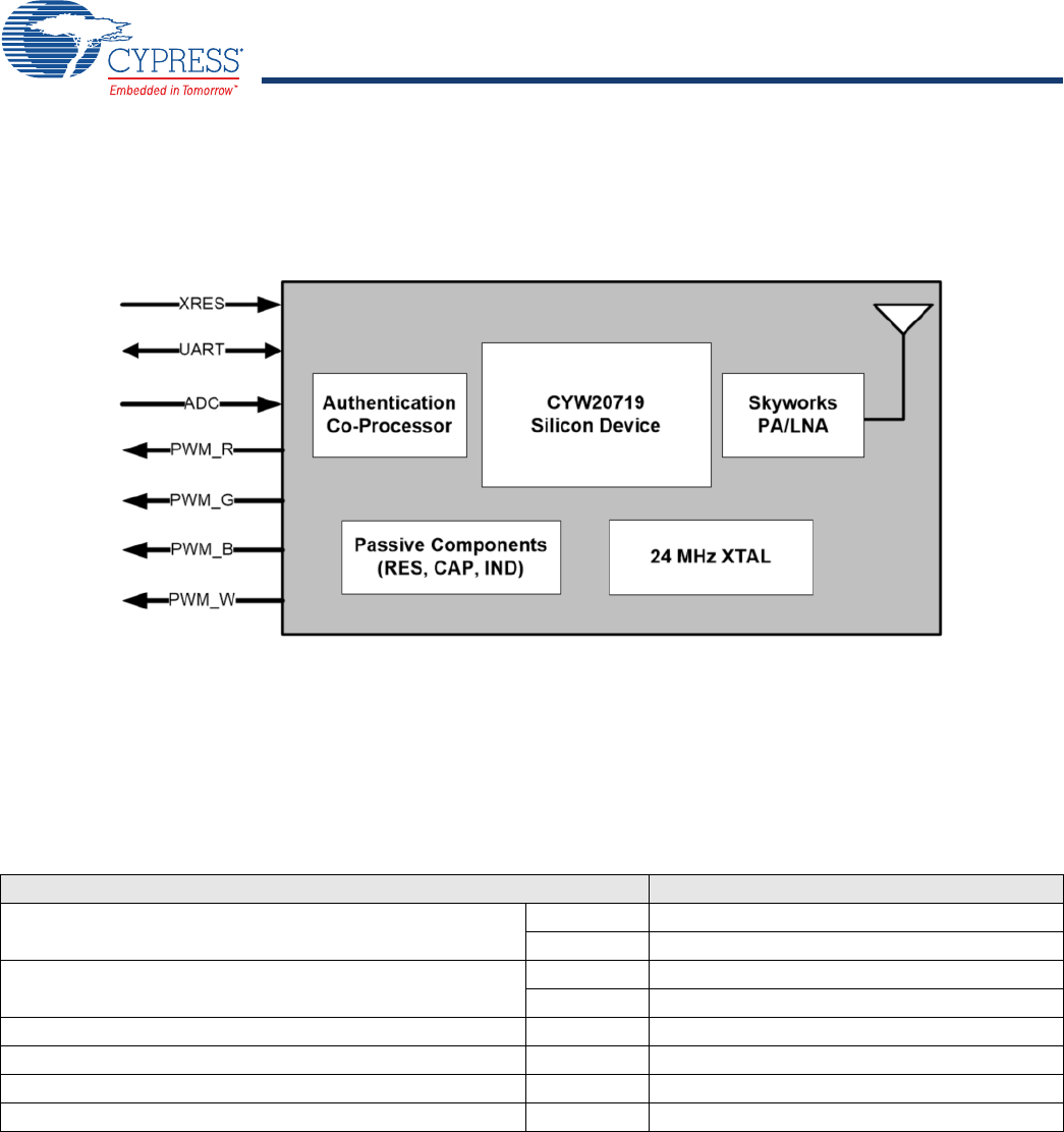
Overview
Functional Block Diagram
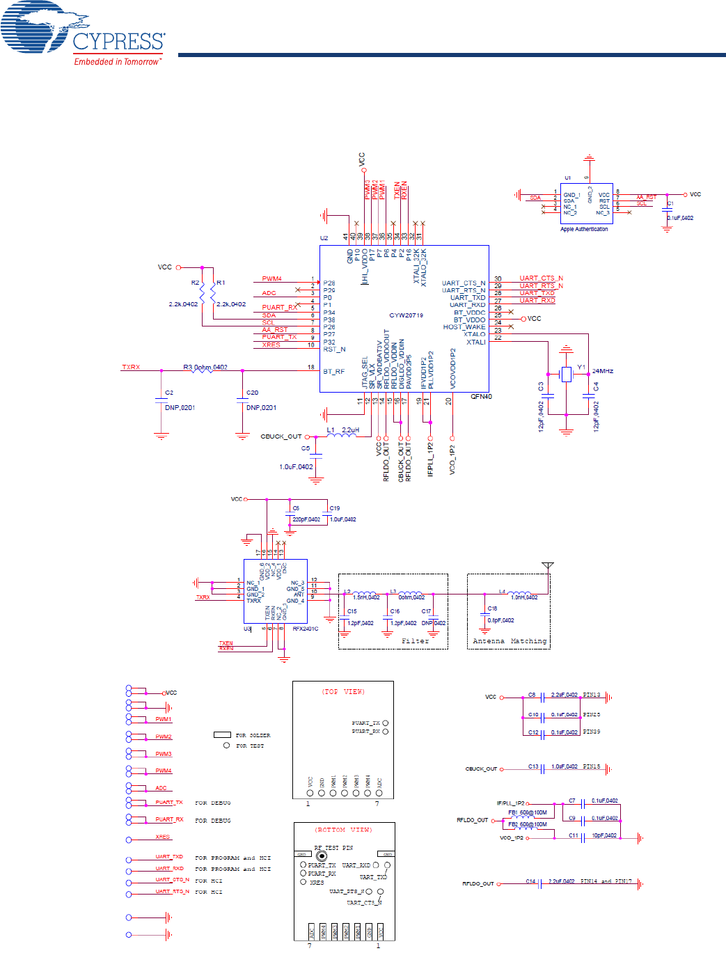
Figure 1 illustrates the CYBLE-413136-01 functional block diagram.
Figure 1. Functional Block Diagram
Module Description
The CYBLE-413136-01 module is a complete module designed to be soldered to the applications main board.
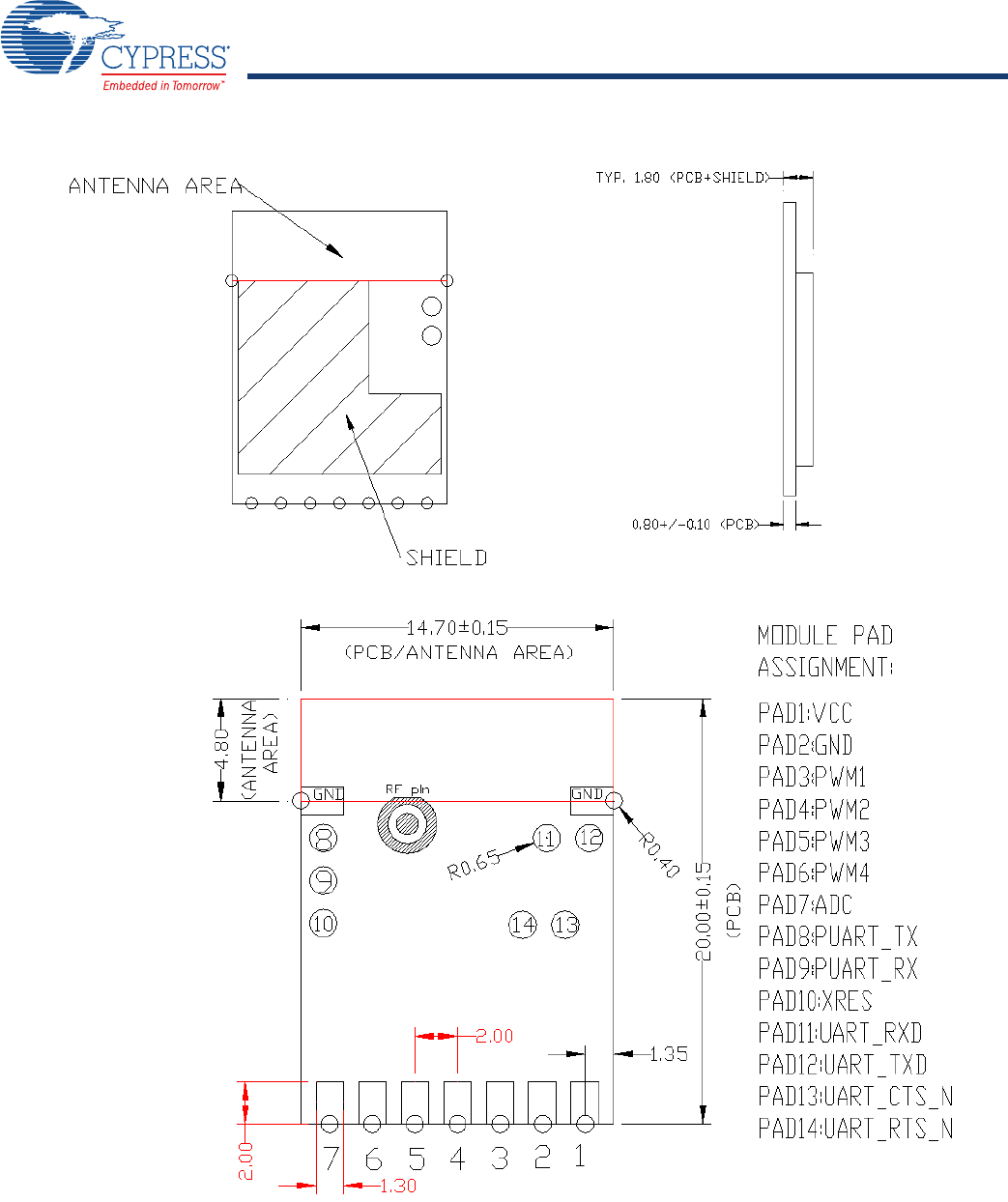
Module Dimensions and Drawing
Cypress reserves the right to select components from various vendors to achieve the Bluetooth module functionality. Such selections
will still guarantee that all mechanical specifications and module certifications are maintained. Designs should be held within the
physical dimensions shown in the mechanical drawings in Figure 2 on page 4. All dimensions are in millimeters (mm).
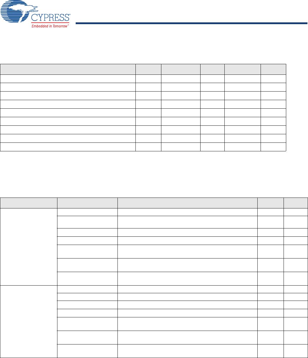
Table 1. Module Design Dimensions
See Figure 2 for the mechanical reference drawing for CYBLE-413136-01.
Dimension Item Specification
Module dimensions Length (X) 14.70 ± 0.15 mm
Width (Y) 20.00 ± 0.15 mm
Antenna location dimensions Length (X) 14.70 mm
Width (Y) 4.80 mm
PCB thickness Height (H) 0.80 ± 0.10 mm
Shield height Height (H) 1.80 mm
Maximum component height Height (H) 0.60 mm typical
Total module thickness (bottom of module to highest component) Height (H) 2.60 mm typical
Document Number: 002-19043 Rev. PRELIMINARY Page 4 of 33
PRELIMINARY CYBLE-413136-01
Figure 2. Module Mechanical Drawing
Bottom View (Seen from Bottom)
Side View
Top View (See from Top)
Notes
4. No metal should be located beneath or above the antenna area. Only bare PCB material should be located beneath the antenna area. For more information on
recommended host PCB layout, see “Recommended Host PCB Layout” on page 6.
5. The CYBLE-413136-01 includes castellated pad connections, denoted as the circular openings at the pad location above.
Document Number: 002-19043 Rev. PRELIMINARY Page 5 of 33
PRELIMINARY CYBLE-413136-01
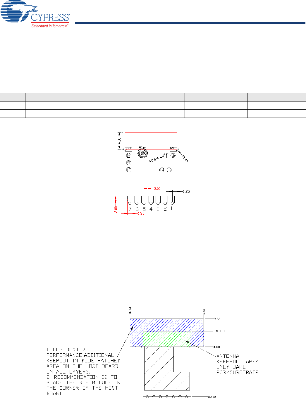
Pad Connection Interface
As shown in the bottom view of Figure 2 on page 4, the CYBLE-413136-01 has seven main connections that are connected to the
host board via castellated solder pads (“CSP”). The CYBLE-413136-01 also includes additional solder pad connections (“SP”) used
for debug or testing on the bottom side of the module. Table 2 and Figure 3 detail the solder pad length, width, and pitch dimensions
of the CYBLE-413136-01 module.
Figure 3. Solder Pad Dimensions (Seen from Bottom)
To maximize RF performance, the host layout should follow these recommendations:
1. Antenna Area Keepout: The host board directly below the antenna area of the Cypress module (see Figure 2 on page 4) must
contain no ground or signal traces. This keep out area requirement applies to all layers of the host board.
2. Module Placement: The ideal placement of the Cypress Bluetooth module is in a corner of the host board with the PCB trace
antenna located at the far corner. This placement minimizes the additional recommended keep out area stated in item 2. Please
refer to AN96841 for module placement best practices.
3. Optional Keepout: To maximize RF performance, the area immediately around the Cypress Bluetooth module PCB trace antenna
may contain an additional keep out area, where no grounding or signal traces are contained. The keep out area applies to all layers
of the host board. The recommended dimensions of the host PCB keep out area are shown in Figure 4 (dimensions are in mm).
Figure 4. Optional Additional Host PCB Keep Out Area Around the CYBLE-413136-01 PCB Trace Antenna
Table 2. Connection Description
Name Connections Connection Type Pad Length Dimension Pad Width Dimension Pad Pitch
CSP 7 Castellated Solder Pads 2.00 mm 1.30 mm 2.00 mm
SP 7 Solder Pads 0.65 mm (Radius) 0.65 mm (Radius) N/A
Castellated Solder Pad (CSP) and Solder Pad (SP) Connection (Seen from Bottom)
Optional Host PCB Keep Out Area Around Chip Antenna
Document Number: 002-19043 Rev. PRELIMINARY Page 6 of 33
PRELIMINARY CYBLE-413136-01
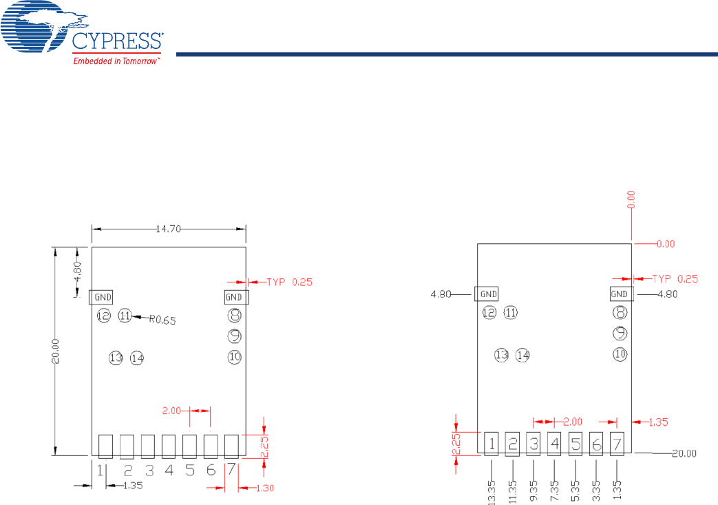
Recommended Host PCB Layout
Figure 5 (Dimensioned) and Figure 6 (Relative to Origin) provide the recommended host PCB layout pattern for the
CYBLE-413136-01. Pad length of 1.27 mm (0.655 mm from center of the pad on either side) shown in Figure 6 is the minimum
recommended host pad length. All dimensions are in millimeters.
Figure 5. CYBLE-413136-01 Host Layout (Dimensioned) Figure 6. CYBLE-413136-01 Host Layout (Relative to Origin)
Top View (Seen on Host PCB)
Top View (Seen on Host PCB)
Document Number: 002-19043 Rev. PRELIMINARY Page 7 of 33
PRELIMINARY CYBLE-413136-01
Module Connections
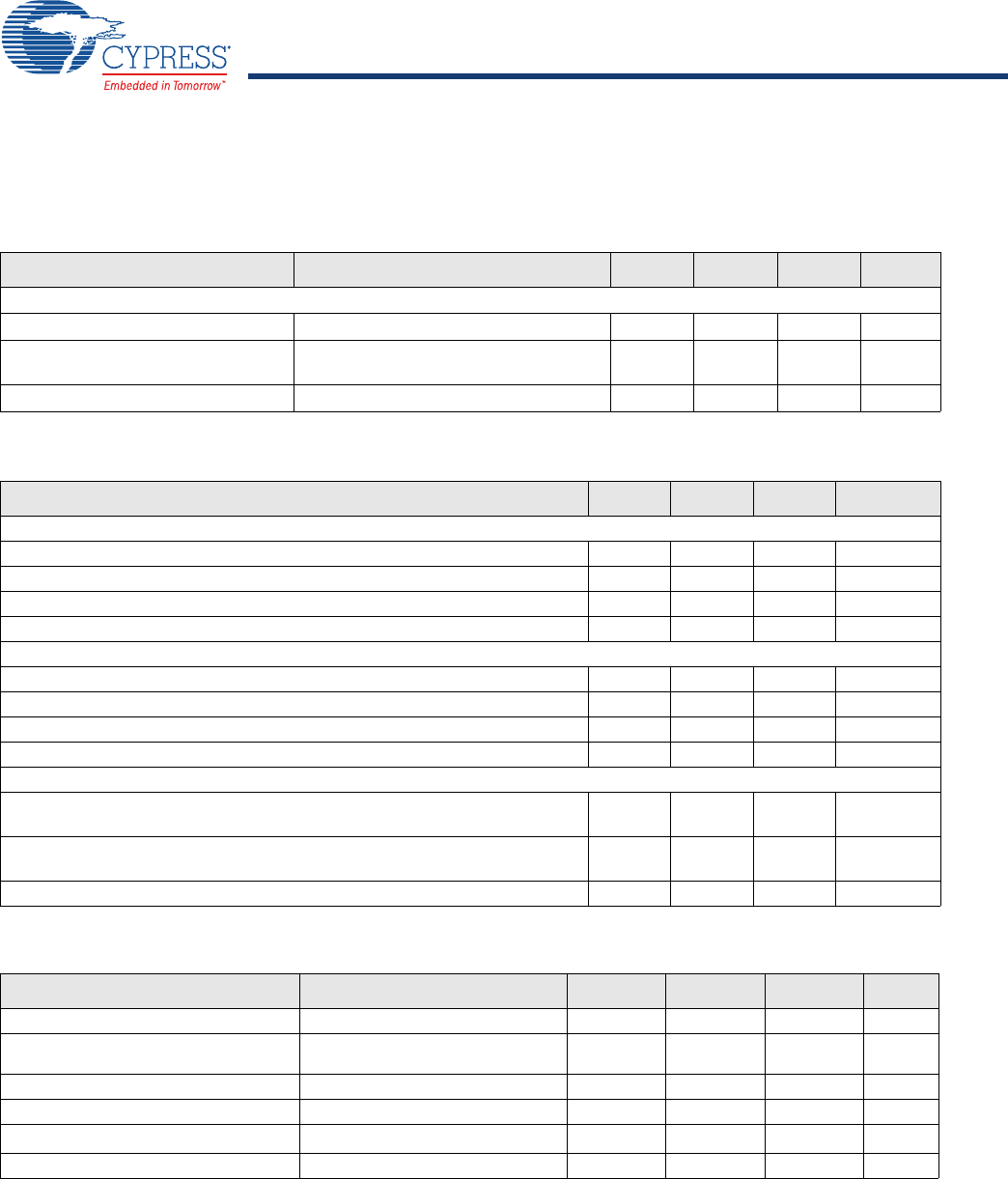
Tab le 3 details the solder pad connection definitions and available functions for each connection pad. Table 3 lists the solder pads on
the CYBLE-413136-01, the silicon device pin, and denotes what functions are available for each solder pad. Ta ble 3 also lists the
primary/intended function for each solder pad for the application this module was specifically designed for.
Connections and Optional External Components
Power Connections (VCC)
The CYBLE-413136-01 contains one power supply connection,
VCC.
VCC accepts a supply input of 3.30 V. Table 9 provides this
specification. The maximum power supply ripple for this power
connection is 100 mV, as shown in Table 9.
External Reset (XRES)
The CYBLE-413136-01 has an integrated power-on reset circuit
which completely resets all circuits to a known power on state.
This action can also be driven by an external reset signal, which
can be used to externally control the device, forcing it into a
power-on reset state. The XRES signal is an active-low signal,
which is an input to the CYBLE-413136-01 module.
UART Connections
For full UART functionality, all UART signals must be connected
to the Host device. If full UART functionality is not being used,
and only UART RXD and TXD are desired or capable, then the
following connection considerations should be followed for
UART RTS and CTS:
nUART RTS: Can be left floating, pulled low, or pulled high. RTS
is not critical for initial firmware uploading at power on.
nUART CTS: Must by pulled low to bypass flow control and to
ensure that continuous data transfers are made from the host
to the module.
External Component Recommendation
Power Supply Circuitry
It is not required to place any power supply decoupling or noise
reduction circuitry on the host PCB. If desired, an external ferrite
bead between the supply and the module connection can be
included, but is not necessary. If used, the ferrite bead should be
positioned as close as possible to the module pin connection.
If used, the recommended ferrite bead value is 330Ω, 100 MHz.
(Murata BLM21PG331SN1D).
Apple MFi Authentication Coprocessor Interface
The CYBLE-413136-01 comes with an integrated MFi authenti-
cation co-processor. No additoinal connections are required to
be made to the module to enable Apple HomeKit functionality. All
connections required are internally routed on the module PCB.
Table 3. Solder Pad Connection Definitions
Pad Num-
ber Pad Name UART PWM GPIO Primary Function
1 VCC Power Supply Input (3.30V) Power Supply Input
2 GND Ground Connection Ground Connection
3PWM1 33PWM R, G, B, or W Function
4PWM2 33PWM R, G, B, or W Function
5PWM3 33PWM R, G, B, or W Function
6PWM4 33PWM R, G, B, or W Function
7ADC ADC Input
8PUART_TX 3(UART_TXD) Peripheral UART TXD
9PUART_RX 3(UART_RXD) Peripheral UART RXD
10 XRES External Reset Hardware Connection Input External Reset (Active Low)
11 UART_RXD 3(UART_RXD) UART RXD
12 UART_TXD 3(UART_TXD) UART TXD
13 UART_CTS 3(UART_CTS) UART CTS
14 UART_RTS 3(UART_RTS) UART RTS
GND GND Ground Connection Ground Connections
Must be soldered to host board
GND GND Ground Connection
Document Number: 002-19043 Rev. PRELIMINARY Page 9 of 33
PRELIMINARY CYBLE-413136-01
Critical Components List
Tab le 4 details the critical components used in the CYBLE-413136-01 module.
Table 4. Critical Component List
Antenna Design
Tab le 5 details the PCB trace antenna used in the CYBLE-413136-01 module.
Table 5. Trace Antenna Specifications
Component Reference Designator Description
Authentication Co-Processor U1 Apple Authentication Co-processor
Silicon U2 40-pin QFN BLE Silicon Device - CYW20719
PA/LNA U3 17-pin QFN - Skyworks RFX2401C
Crystal Y1 24.000 MHz, 12PF
Item Description
Frequency Range 2402 – 2480 MHz
Peak Gain –0.5 dBi maximum

Document Number: 002-19043 Rev. PRELIMINARY Page 10 of 33
PRELIMINARY CYBLE-413136-01
Bluetooth Baseband Core
The Bluetooth Baseband Core (BBC) implements all of the time-critical functions required for high-performance Bluetooth operation.
The BBC manages the buffering, segmentation, and routing of data for all connections. It also buffers data that passes through it,
handles data flow control, schedules TX/RX transactions, monitors Bluetooth slot usage, optimally segments and packages data into
baseband packets, manages connection status indicators, and composes and decodes HCI packets. In addition to these functions, it
independently handles host controller interface (HCI) event types, and HCI command types.
The following transmit and receive functions are also implemented in the BBC hardware to increase reliability and security of the
TX/RX data before sending over the air:
nSymbol timing recovery, data deframing, forward error correction (FEC), header error control (HEC), cyclic redundancy check (CRC),
data decryption, and data dewhitening in the receiver.
nData framing, FEC generation, HEC generation, CRC generation, key generation, data encryption, and data whitening in the
transmitter.
Bluetooth Low Energy
The CYBLE-413136-01 supports single-mode Bluetooth LE operation. The CYBLE-413136-01 supports all Bluetooth 4.2 and legacy
LE features, with the following benefits:
nLE data packet length extension
nLE secure connections
nLink layer privacy
nEnables Bluetooth Smart sensors to access the Internet directly via IPv6/6LoWPAN
Link Control Layer
The link control layer is part of the Bluetooth link control functions that are implemented in dedicated logic in the link control unit (LCU).
This layer consists of the command controller that takes commands from the software, and other controllers that are activated or
configured by the command controller, to perform the link control tasks. Each task performs a different state in the Bluetooth® Link
Controller.
nMajor states:
pStandby
pConnection
Document Number: 002-19043 Rev. PRELIMINARY Page 11 of 33
PRELIMINARY CYBLE-413136-01
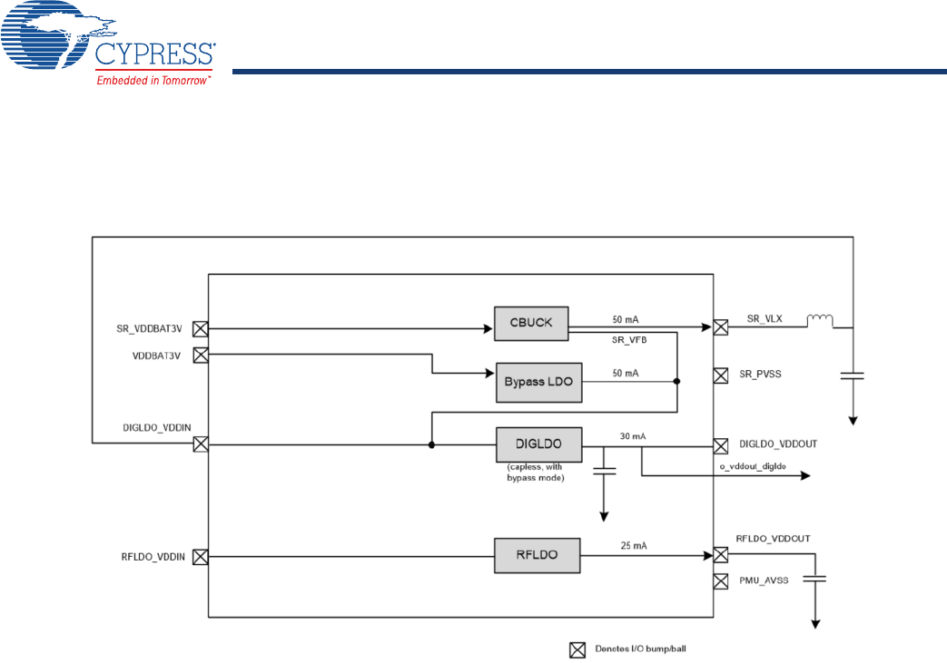
Power Management Unit
The Power Management Unit (PMU) provides power management features that can be invoked through power management registers
or packet handling in the baseband core. This section contains descriptions of the PMU features.
Figure 8. Power Management Unit of CYW20719
RF Power Management
Figure 8 shows the CYBLE-413136-01 power management unit (PMU) block diagram that is contained in the CYW20719 silicon
device. The CYW20719 includes an integrated buck regulator, a bypass LDO, a capless LDO, and an additional 1.2 V LDO for RF.
Host Controller Power Management
Power is automatically managed by the firmware based on input device activity. As a power-saving task, the firmware controls the
disabling of the on-chip regulator when in HIDOFF (deep sleep) mode.
BBC Power Management
There are several low-power operations for the BBC:
nPhysical layer packet handling turns RF on and off dynamically within packet TX and RX.
nBluetooth-specified low-power connection mode. While in these low-power connection modes, the CYBLE-413136-01 runs on the
Low Power Oscillator and wakes up after a predefined time period.
The CYBLE-413136-01 automatically adjusts its power dissipation based on user activity. It supports the following power modes:
nActive mode
nIdle mode
nSleep mode
nHIDOFF (deep sleep) mode
The CYBLE-413136-01 transitions to the next lower state after a programmable period of user inactivity. When user activity
resumes, the CYBLE-413136-01 immediately enters Active mode.
In HIDOFF mode, the CYBLE-413136-01 baseband and core are powered off by disabling power to VDDC_OUT and PAVDD. The
VDDO domain remains powered up and will turn the remainder of the chip on when it detects user events. This mode minimizes chip
power consumption and is used for extended periods of inactivity.

Document Number: 002-19043 Rev. PRELIMINARY Page 12 of 33
PRELIMINARY CYBLE-413136-01
Microprocessor Unit
The CYBLE-413136-01 microprocessor unit runs software from the link control (LC) layer up to the host controller interface (HCI).
The microprocessor is a Cortex<Superscript>®-M4 32-bit RISC processor with embedded ICE-RT debug and serial wire debug
(SWD) interface units. The microprocessor also includes 2 MB of ROM memory for program storage and 512 KB of RAM for data
scratch-pad.
The internal ROM provides flexibility during power-on reset to enable the same device to be used in various configurations. At
power-up, the lower layer protocol stack is executed from the internal ROM.
External patches can be applied to the ROM-based firmware to provide flexibility for bug fixes and features additions. The device
also supports the integration of user applications and profiles. Patches and applications can be stored in on-chip flash.
Floating Point Unit
The CYBLE-413136-01 includes the CM4 single precision IEEE-754 compliant floating point unit. For additional details, see the Cor-
tex-M4 manual.
On-Chip Flash
The silicon device used in the CYBLE-413136-01 module includes 1 MB of on-chip flash. This flash can be used for direct program
execution or for non-volatile data. Typical usage for the on-chip flash includes:
nChip configuration
nPatches
nPeer addresses and link keys
nApplication code
nApplication non-volatile data
nProduct information
OTP
The CYBLE-413136-01 includes 2 KB of one-time programmable (OTP) memory. This memory can be used by the factory to store
product specific information.
Note: Use of OTP requires a 3 V supply to be present at all times.
External Reset
An external active-low reset signal, XRES, can be used to put the CYBLE-413136-01 in the reset state. An external voltage detector
reset IC with 50 ms delay is needed on the XRES. The XRES should be released only after the VDDO supply voltage level has been
stabilized for 50 ms.
Document Number: 002-19043 Rev. PRELIMINARY Page 13 of 33
PRELIMINARY CYBLE-413136-01
Figure 9. Reset Timing
Integrated Radio Transceiver
The CYBLE-413136-01 has an integrated radio transceiver that is optimized for 2.4 GHz Bluetooth wireless systems. It has been
designed to provide low power, low cost, and robust communications for applications operating in the globally available 2.4 GHz unli-
censed ISM band. It is fully compliant with Bluetooth Radio Specification 3.0 and meets or exceeds the requirements to provide the
highest communication link quality of service.
Transmitter Path
The CYBLE-413136-01 features a fully integrated transmitter. The baseband transmit data is GFSK modulated in the 2.4 GHz ISM
band.
Digital Modulator
The digital modulator performs the data modulation and filtering required for the GFSK signal. The fully digital modulator minimizes
any frequency drift or anomalies in the modulation characteristics of the transmitted signal.
Power Amplifier
The CYBLE-413136-01 has an integrated power amplifier (PA) on the silicon device as well as a high power external power amplifier
(PA) integrated on the module. The total output power that this module is designed to achieve is +8 dBm.
Receiver Path
The receiver path uses a low IF scheme to down convert the received signal for demodulation in the digital demodulator and bit syn-
chronizer. The receiver path provides a high degree of linearity, and an extended dynamic range to ensure reliable operation in the
noisy 2.4 GHz ISM band. The front-end topology, which has built-in out-of-band attenuation, enables the CYBLE-413136-01 to be
used in most applications without off-chip filtering.
Digital Demodulator and Bit Synchronizer
The digital demodulator and bit synchronizer take the low-IF received signal and perform an optimal frequency tracking and bit syn-
chronization algorithm.
Receiver Signal Strength Indicator
The radio portion of the CYBLE-413136-01 provides a receiver signal strength indicator (RSSI) to the baseband. This enables the
controller to take part in a Bluetooth power-controlled link by providing a metric of its own receiver signal strength to determine
whether the transmitter should increase or decrease its output power.
Document Number: 002-19043 Rev. PRELIMINARY Page 14 of 33
PRELIMINARY CYBLE-413136-01
Calibration
The CYBLE-413136-01 radio transceiver features a self-contained automated calibration scheme. No user interaction is required
during normal operation or during manufacturing to provide optimal performance. Calibration compensates for filter, matching net-
work, and amplifier gain and phase characteristics to yield radio performance within 2% of what is optimal. Calibration takes process
and temperature variations into account, and it takes place transparently during normal operation and hop setting times.
Internal LDO Regulator
The CYBLE-413136-01 has an integrated 1.2 V LDO regulator that provides power to the digital and RF circuits. The 1.2V LDO reg-
ulator operates from a 1.425 V to 3.63 V input supply with a 30 mA maximum load current.
Peripheral Transport Unit
UART Interface
The CYBLE-413136-01 includes a UART interface for factory programming as well as when operating as a BT HCI device in a sys-
tem with an external host. The UART physical interface is a standard, 4-wire interface (RX, TX, RTS, and CTS) with adjustable baud
rates from 9600 bps to 6 Mbps. During initial boot, UART speeds may be limited to 750 kbps. The baud rate may be selected via a
vendor-specific UART HCI command. The CYBLE-413136-01 has a 1040-byte receive FIFO and a 1040-byte transmit FIFO to sup-
port enhanced data rates. The interface supports the Bluetooth UART HCI (H4) specification. The default baud rate for H4 is 115.2
kbaud.
The UART clock default setting is 24 MHz. The baud rate of the CYBLE-413136-01 UART is controlled by two values. The first is a
UART clock divisor (set in the DLBR register) that divides the UART clock by an integer multiple of 16. The second is a baud rate
adjustment (set in the DHBR register) that is used to specify a number of UART clock cycles to stuff in the first or second half of each
bit time. Up to eight UART cycles can be inserted into the first half of each bit time, and up to eight UART clock cycles can be
inserted into the end of each bit time. Table 6 contains example values to generate common baud rates with a 24 MHz UART clock.
Tab le 7 contains example values to generate common baud rates with a 48 MHz UART clock.
Table 6. Common Baud Rate Examples, 24 MHz Clock
Baud Rate (bps) DHBR DLBR Mode Error (%)
3M 0xFF 0xF8 High rate 0.00
2M 0XFF 0XF4 High rate 0.00
1.5M 0X00 0XFF Normal 0.00
1M 0x44 0xFF Normal 0.00
921600 0x55 0xFF Normal 0.16
460800 0x22 0xFD Normal 0.16
230400 0x44 0xFA Normal 0.16
115200 0x00 0xF3 Normal 0.16
38400 0x01 0xD9 Normal 0.00
Table 7. Common Baud Rate Examples, 48 MHz Clock
Baud Rate (bps) High Rate Low Rate Mode Error (%)
6M 0xFF 0xF8 High rate 0.00
4M 0xFF 0xF4 High rate 0.00
3M 0x0 0xFF Normal 0.00
2M 0x44 0xFF Normal 0.00
1.5M 0x00 0xFE Normal 0.00
1M 0x00 0xFD Normal 0.00
921600 0x22 0xFD Normal 0.16
460800 0x44 0xFA Normal 0.16
Document Number: 002-19043 Rev. PRELIMINARY Page 15 of 33
PRELIMINARY CYBLE-413136-01
Support for changing the baud rate during normal HCI UART operation is included through a vendor-specific command that allows
the host to adjust the contents of the baud rate registers.
The CYBLE-413136-01 UART operates correctly with the host UART as long as the combined baud rate error of the two devices is
within ±5%.
Peripheral UART Interface
The CYBLE-413136-01 has a second UART that may be used to interface to peripherals. This peripheral UART is accessed through
the optional I/O ports, which can be configured individually and separately for each functional pin.
ADC Port
The ADC block is a single switched-cap Σ-Δ ADC core for audio and DC measurement. It operates at the 12 MHz clock rate. The
internal bandgap reference has ±5% accuracy without calibration. Different calibration and digital correction schemes can be applied
to reduce ADC absolute error and improve measurement accuracy in DC mode.
PWM
The CYBLE-413136-01 has four PWMs. The PWM module consists of the following:
nPWM1–4. Each of the four PWM channels contains the following registers:
p16-bit initial value register (read/write)
p16-bit toggle register (read/write)
p16-bit PWM counter value register (read)
nPWM configuration register shared among PWM1–4 (read/write). This 18-bit register is used:
pTo configure each PWM channel
pTo select the clock of each PWM channel
pTo change the phase of each PWM channel
Figure 10 shows the structure of one PWM.
230400 0x0 0xF3 Normal 0.16
115200 0x1 0xE6 Normal –0.08
57600 0x1 0xCC Normal 0.04
38400 0x11 0xB2 Normal 0.00
19200 0x22 0x64 Normal 0.00
Table 7. Common Baud Rate Examples, 48 MHz Clock (continued)
Baud Rate (bps) High Rate Low Rate Mode Error (%)
Document Number: 002-19043 Rev. PRELIMINARY Page 16 of 33
PRELIMINARY CYBLE-413136-01
Figure 10. PWM Block Diagram
Triac Control
The CYBLE-413136-01 includes hardware support for zero-crossing detection and trigger control for up to four triacs. The
CYBLE-413136-01 detects zero-crossing on the AC zero detection line and uses that to provide a pulse that is offset from the zero
crossing. This allows the CYBLE-413136-01 to be used in dimmer applications, as well as any other applications that require a con-
trol signal that is offset from an input event.
The zero-crossing hardware includes an option to suppress glitches.
Security Engine
The CYBLE-413136-01 includes a hardware security accelerator which greatly decreases the time required to perform typical secu-
rity operations. Access to the hardware block is provided via a firmware interface (see firmware documentation for details).Thie
security engine includes:
nPublic key acceleration (PKA) cryptography
nAES-CTR/CBC-MAC/CCM acceleration
nSHA2 message hash and HMAC acceleration
nRSA encryption and decryption of modulus sizes up to 2048 bits
nElliptic curve Diffie-Hellman in prime field GF(p)
nGeneric modular math functions
Document Number: 002-19043 Rev. PRELIMINARY Page 17 of 33
PRELIMINARY CYBLE-413136-01
Electrical Characteristics
Note: All voltages listed in Table 8 are referenced to VCC.
Tab le 9 shows the power supply characteristics for the range TJ = 0°C to 125°C.
Table 8. Absolute Maximum Voltages
Requirement Parameter
Specification
UnitMinimum Nominal Maximum
Ambient Temperature of Operation –30 25 105 °C
Storage temperature –30 – 110 °C
ESD Tolerance HBM (Silicon) –2000 – 2000 V
ESD Tolerance MM (Silicon) –100 – 100 V
ESD Tolerance CDM (Silicon) –500 – 500 V
Latch-up (Silicon) – 200 – mA
Table 9. Power Supply Specifications
Parameter Conditions Min. Typical Max. Unit
VCC input Module Input 3.0 3.3 3.6 V
VCC Ripple Module Input – – 100 mV
VBAT Input Internal to Module (not accessible) 1.62 3.3 3.6 V
PMU turn-on time VBAT is ready. – – 300 μs
Document Number: 002-19043 Rev. PRELIMINARY Page 18 of 33
PRELIMINARY CYBLE-413136-01
Core Buck Regulator
nMinimum capacitor value refers to residual capacitor value after taking into account part-to-part tolerance, DC-bias, temperature,
and aging.
nMaximum capacitor value refers to the total capacitance seen at a node where the capacitor is connected. This also includes any
decoupling capacitors connected at the load side, if any.
Table 10. Core Buck Regulator (Internal to Module)
Parameter Conditions Min. Typ. Max. Unit
Input supply voltage DC, VBAT DC voltage range inclusive of disturbances 2.1 3.3 3.63 V
CBUCK output current LPOM only – – 65 mA
Output over-current limit Peak inductor current TBD – – mA
Output voltage range Programmable, 30mV/step
default = 1.2V (bits=0000)
1.2 1.2 1.5 V
Output voltage DC accuracy Includes load and line regulation:
• Before trimming
• After trimming
–4
–2
–+4
+2
%
%
LPOM ripple voltage, static Measured with 20 MHz bandwidth limit, static load.
Max ripple based on VBAT=3V, Vout=1.2V
Inductor:
0806 inch-size, Tmax=1 mm,
2.2 μH ±25%, DCR=114 mW ±20%, ACR<1W (for
frequency <1 MHz)
Capacitor:
1 μF ±10%, 6.3V, 0603 inch, X5R, MLCC capacitor
+ board total-ESR < 20 mW
– – 30 mVpp
LPOM efficiency (high load) 10–50 mA load current, Vout=1.2V, Vbat=3V
@25°C
Inductor:
0806 inch-size, Tmax=1 mm,
2.2 μH ±25%, DCR=114 mW ±20%, ACR<1W (for
frequency<1 MHz)
Capacitor:
1 μF ±10%, 6.3V, 0603 inch, X5R, MLCC capacitor
+board total-ESR < 20 mW
TBD 85 – %
LPOM efficiency (low load) 1–5 mA load current, Vout=1.2V, Vbat=3V @25°C
Inductor:
0806 inch-size, Tmax=1 mm,
2.2 ?H ±25%, DCR=114 mW ±20%, ACR<1W (for
frequency<1 MHz)
Capacitor:
1 μF ±10%, 6.3V, 0603 inch, X5R, MLCC capacitor
+board total-ESR < 20 mW
TBD 80 – %
Startup time see Table 11 on page 19.––––
External inductor L 2.2 μH ±25%, DCR=114 mW ±20%, ACR<1W (for
frequency<1 MHz)
–2.2–
μH
External output capacitor, Cout 1 μF ±10%, 6.3V, 0603 inch, X5R, MLCC capacitor
+board total-ESR < 20 mW
0.7 1 1.1 μF
External input capacitor, Cin For SR_VDDBAT pin
Ceramic, X5R, 0402, ESR<30 mW at
4 MHz, +/-20%, 6.3V, 4.7 μF
0.7 4.7 5.64 μF
Input supply voltage ramp-up time 0 to 3.3V 40 – – μs
Document Number: 002-19043 Rev. PRELIMINARY Page 19 of 33
PRELIMINARY CYBLE-413136-01
Digital LDO
Table 11. Digital LDO (Internal to Module)
Parameter Conditions Min. Typ. Max. Unit
Input supply voltage, Vin Minimum Vin=Vo+0.12V requirement must be met
under maximum load. 1.2 1.2 1.6 V
Nominal output voltage,Vo Internal default bit setting – 1.1 – V
Output voltage programmability Range
Step size
Accuracy at any step (including line/load regulation)
before trimming
Accuracy at any step (including line/load regulation)
after trimming
0.9
–
–4
–2
–
10
–
–
1.25
–
+4
+2
V
mV
%
%
Dropout voltage At maximum load – – 120 mV
Output current DC load 0.21
1. By default, an internal loading of ~0.2 mA resides inside the LDO. This is to ensure the LDO is stable with zero loading from the core. After the
core is up, digital logic can disable this internal loading by setting i_ldo_cntl<8:7> to 00.
–40mA
Output loading capacitor Internal, including the decoupling capacitor to be placed
next to the load and the equivalent loading capacitor by
the core.
4–10nF
Quiescent current At no load, excluding main bandgap Iq – 90 120 μA
Line regulation Vin from (Vo+0.12V) to 1.5V; 40 mA load – – 5 mV/V
Load regulation Load from 1 mA to 25 mA; Vin (Vo+0.12V) – 0.025 0.045 mV/mA
Leakage current In full power-down mode or bypass mode:
• Junction temperature: 25°C
• Junction temperature: 125°C
–
–
0.05
1.1
0.2
5.0
μA
μA
PSRR @1 kHz, Vin, Vo+0.12V
Output cap of 4 nF~10 nF
40 – – dB
PMU startup time VBAT is up and steady. Time from HID_OFF falling
edge to DIGLDO reaching 99% of Vo. – 100 – μs
LDO turn-on time LDO turn-on time when balance of chip is up – – 22 μs
External input capacitor Only use an external input capacitor at VDD_DIGLDO
pin if it is not supplied from CBUCK output. –12.2
μF
Document Number: 002-19043 Rev. PRELIMINARY Page 20 of 33
PRELIMINARY CYBLE-413136-01
RF LDO
Table 12. RF LDO (Internal to Module)
Parameter Conditions Min. Typ. Max. Unit
Input supply voltage, Vin Min Vin=Vo+0.15V = 1.35V (for Vo=1.2V)
Dropout voltage requirement must be met under
maximum load.
1.2 1.35 1.5 V
Nominal output voltage,Vo Internal default bit setting 000 – 1.2 – V
Output voltage programmability Range
Step size
Accuracy at any step (including line/load regulation)
Accuracy at any step (including line/load regulation)
after trimming
1.1
–
–4
–2
–
25
–
–
1.275
–
+4
+2
V
mV
%
%
Dropout voltage At maximum load – – 150 mV
Output current TBD 0.1 – 25 mA
Quiescent current No load – 44 – μA
Line regulation Vin from (Vo+0.15V) to 1.5V; 25 mA load – – 5.5 mV/V
Load regulation Load from 1 mA to 25 mA; Vin ≥ (Vo+0.15V) – 0.025 0.045 mV/mA
Load step error Load step from 1 mA–25 mA in 1 μs and
25 mA–1 mA in 1μs; Vin(Vo+0.15V);
Co=2.2 μF
––35mV
Leakage current Power-down junction temperature: 85°C – – 10 μA
Output noise @30 kHz, 25 mA load, Co= 2.2 μF
@100 kHz, 25 mA load, Co= 2.2 μF
––60
35
nV/√Hz
nV/√Hz
PSRR @1kHz, Input > 1.35V, Co= 2.2 μF, Vo=1.2V 20 – – dB
LDO turn-on time LDO turn-on time when balance of chip is up – 140 180 μs
In-rush current Vin=Vo+0.15V to 1.5V, Co=2.2 μF, no load – – 100 mA
External output capacitor, Co Total ESR (trace/cap): 5 m–240 mW 0.5 2.2 4.7 μF
External input capacitor Only use an external input capacitor at VDD_DIGLDO
pin if it is not supplied from CBUCK output. –12.2μF
Note: Minimum capacitor value refers to residual capacitor value after taking into account part-to-part tolerance, DC-bias, temperature, and
aging.
Document Number: 002-19043 Rev. PRELIMINARY Page 21 of 33
PRELIMINARY CYBLE-413136-01
Digital I/O Characteristics
Current Consumption
In Tab le 14, current consumption measurements are taken at VBAT with the assumption that VBAT is connected to VDDIO and
LDOIN.
Table 13. Digital I/O Characteristics
Characteristics Symbol Minimum Typical Maximum Unit
Input low voltage (VDDO = 3.3V) VIL ––0.8V
Input high voltage (VDDO = 3.3V) VIH 2.0 – – V
Output low voltage VOL ––0.4V
Output high voltage VOH VDDO – 0.4V – – V
Input low current IIL ––1.0
μA
Input high current IIH ––1.0
μA
Output low current (VDDO = 3.3V, VOL = 0.4V) IOL ––2.0mA
Output high current (VDDO = 3.3V, VOH = 2.9V) IOH ––4.0mA
Input capacitance CIN ––0.4pF
Table 14. BLE Current Consumption
Product Operational Mode Conditions Typical Unit
CYW20719
(Silicon)
Receiving Receiver and baseband are both operating, 100% ON, silicon only. 5.8 mA
Transmitting Transmitter and baseband are both operating, 100% ON, silicon
only. 5.7 mA
PDS 512 KB SRAM memory retention, silicon only. 70 μA
Deep Sleep 16 KB SRAM memory retention, silicon only. 1 μA
HIDOFF Wakeup only from XRES.
No SRAM memory retention, silicon only.
350 nA
Connection, 1-s Avg. Average Power, 1-second connection interval, silicon only.
Deep Sleep mode enabled during non-TX/RX
17 μA
Connection, 4-s Avg. Average Power, 4-second connection interval, silicon only.
Deep Sleep mode enabled during non-TX/RX
5μA
CYBLE-413136-01
(Module)
Receiving Receiver and baseband are both operating, 100% ON, module. TBD mA
Transmitting Transmitter and baseband are both operating, 100% ON, module.. TBD mA
PDS 512 KB SRAM memory retention, module. TBD μA
Deep Sleep 16 KB SRAM memory retention, module. TBD μA
HIDOFF Wakeup only from XRES.
No SRAM memory retention, module.
TBD nA
Connection, 1-s Avg. Average Power, 1-second connection interval, module.
Deep Sleep mode enabled during non-TX/RX
TBD μA
Connection, 4-s Avg. Average Power, 4-second connection interval, module.
Deep Sleep mode enabled during non-TX/RX
TBD μA
Document Number: 002-19043 Rev. PRELIMINARY Page 22 of 33
PRELIMINARY CYBLE-413136-01
RF Specifications
Note: Table 15 and Table 16 apply to single-ended industrial temperatures. Unused inputs are left open.
Table 15. Receiver RF Specifications
Parameter Mode and Conditions Min Typ Max Unit
Receiver Section
Frequency range – 2402 – 2480 MHz
RX sensitivity GFSK, BDR GFSK 0.1% BER, 1 Mbps
Module
– –93.0 – dBm
Maximum input – –20 – – dBm
Table 16. Transmitter RF Specifications
Parameter Min Typ Max Unit
Transmitter Section
Frequency range 2402 – 2480 MHz
Class 2: GFSK Tx power (silicon) – 4 – dBm
Class 2: GFSK Tx power (module) – 8 – dBm
20 dB bandwidth – 930 1000 kHz
Frequency Drift
DH1 packet –25 – +25 kHz
DH3 packet –40 – +40 kHz
DH5 packet –40 – +40 kHz
Drift rate –20 20 kHz/50 µs
Frequency Deviation
Average deviation in payload
(sequence used is 00001111)
140 – 175 kHz
Maximum deviation in payload
(sequence used is 10101010)
115 – – kHz
Channel spacing – 1 – MHz
Table 17. BLE RF Specifications
Parameter Conditions Minimum Typical Maximum Unit
Frequency range N/A 2402 – 2480 MHz
Rx sensitivity1
1. Dirty Tx is Off.
GFSK, BDR GFSK 0.1% BER 0.1%
BER, 1 Mbps – –93.0 – dBm
Tx power N/A – 4 – dBm
Mod Char: Delta F1 average N/A 225 255 275 kHz
Mod Char: Delta F2 max2
2. At least 99.9% of all delta F2 max frequency values recorded over 10 packets must be greater than 185 kHz.
N/A 99.9 – – %
Mod Char: Ratio N/A 0.8 0.95 – %
Document Number: 002-19043 Rev. PRELIMINARY Page 23 of 33
PRELIMINARY CYBLE-413136-01
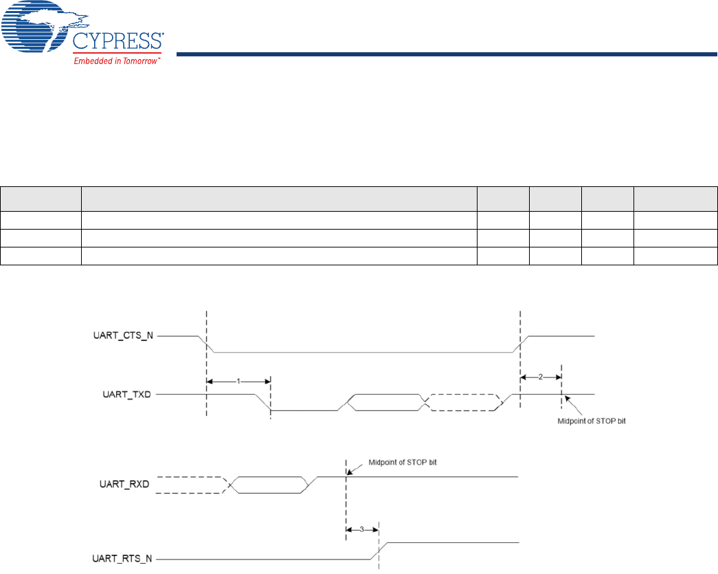
Timing and AC Characteristics
In this section, use the numbers listed in the Reference column of each table to interpret the following timing diagrams.
UART Timing
Figure 11. UART Timing
Table 18. UART Timing Specifications
Reference Characteristics Min. Typ. Max. Unit
1 Delay time, UART_CTS_N low to UART_TXD valid. – – 1.50 Bit periods
2 Setup time, UART_CTS_N high before midpoint of stop bit. – – 0.67 Bit periods
3 Delay time, midpoint of stop bit to UART_RTS_N high. – – 1.33 Bit periods
Document Number: 002-19043 Rev. PRELIMINARY Page 24 of 33
PRELIMINARY CYBLE-413136-01
Environmental Specifications
Environmental Compliance
This Cypress BLE module is produced in compliance with the Restriction of Hazardous Substances (RoHS) and Halogen-Free (HF)
directives. The Cypress module and components used to produce this module are RoHS and HF compliant.
RF Certification
The CYBLE-413136-01 module is certified under the following RF certification standards:
nFCC: WAP3136 (pending)
nIC: 7922A-3136 (pending)
nCE (pending)
Safety Certification
The CYBLE-413136-01 module complies with the following safety regulations:
nUnderwriters Laboratories, Inc. (UL): Filing E331901
nCSA
nTUV
Environmental Conditions
Tab le 19 describes the operating and storage conditions for the Cypress BLE module.
ESD and EMI Protection
Exposed components require special attention to ESD and electromagnetic interference (EMI).
A grounded conductive layer inside the device enclosure is suggested for EMI and ESD performance. Any openings in the enclosure
near the module should be surrounded by a grounded conductive layer to provide ESD protection and a low-impedance path to ground.
Device Handling: Proper ESD protocol must be followed in manufacturing to ensure component reliability.
Table 19. Environmental Conditions for CYBLE-413136-01
Description Minimum Specification Maximum Specification
Operating temperature −30 °C 105 °C
Operating humidity (relative, non-condensation) 5% 85%
Thermal ramp rate – 3 °C/minute
Storage temperature –30 °C 110 °C
Storage temperature and humidity – 110 °C at 85%
ESD: Module integrated into system Components[6] –15 kV Air
2.0 kV Contact
Note
6. This does not apply to the RF pins (ANT).

Document Number: 002-19043 Rev. PRELIMINARY Page 25 of 33
PRELIMINARY CYBLE-413136-01
Regulatory Information
FCC
FCC NOTICE:
The device CYBLE-413136-01 complies with Part 15 of the FCC Rules. The device meets the requirements for modular transmitter
approval as detailed in FCC public Notice DA00-1407.transmitter Operation is subject to the following two conditions: (1) This device
may not cause harmful interference, and (2) This device must accept any interference received, including interference that may cause
undesired operation.
CAUTION:
The FCC requires the user to be notified that any changes or modifications made to this device that are not expressly approved by
Cypress Semiconductor may void the user's authority to operate the equipment.
This equipment has been tested and found to comply with the limits for a Class B digital device, pursuant to Part 15 of the FCC Rules.
These limits are designed to provide reasonable protection against harmful interference in a residential installation. This equipment
generates uses and can radiate radio frequency energy and, if not installed and used in accordance with the instructions,ê may cause
harmful interference to radio communications. However, there is no guarantee that interference will not occur in a particular installation.
If this equipment does cause harmful interference to radio or television reception, which can be determined by turning the equipment
off and on, the user is encouraged to try to correct the interference by one or more of the following measures:
nReorient or relocate the receiving antenna.
nIncrease the separation between the equipment and receiver.
nConnect the equipment into an outlet on a circuit different from that to which the receiver is connected.
nConsult the dealer or an experienced radio/TV technician for help
LABELING REQUIREMENTS:
The Original Equipment Manufacturer (OEM) must ensure that FCC labelling requirements are met. This includes a clearly visible
label on the outside of the OEM enclosure specifying the appropriate Cypress Semiconductor FCC identifier for this product as well
as the FCC Notice above. The FCC identifier is FCC ID: WAP3136.
In any case the end product must be labeled exterior with “Contains FCC ID: WAP3136”.
ANTENNA WARNING:
This device is tested with a standard SMA connector and with the antennas listed in Table 5 on page 9. When integrated in the OEMs
product, this fixed antenna requires installation preventing end-users from replacing them with non-approved antennas. Any antenna
not in Table 5 on page 9 must be tested to comply with FCC Section 15.203 for unique antenna connectors and Section 15.247 for
emissions.
RF EXPOSURE:
To comply with FCC RF Exposure requirements, the Original Equipment Manufacturer (OEM) must ensure to install the approved
antenna in the previous.
The preceding statement must be included as a CAUTION statement in manuals, for products operating with the approved antennas
in Table 5 on page 9, to alert users on FCC RF Exposure compliance. Any notification to the end user of installation or removal
instructions about the integrated radio module is not allowed.
The radiated output power of CYBLE-413136-01 with the chip antenna mounted (FCC ID: WAP3136) is far below the FCC radio
frequency exposure limits. Nevertheless, use CYBLE-413136-01 in such a manner that minimizes the potential for human contact
during normal operation.
End users may not be provided with the module installation instructions. OEM integrators and end users must be provided with
transmitter operating conditions for satisfying RF exposure compliance.

Document Number: 002-19043 Rev. PRELIMINARY Page 26 of 33
PRELIMINARY CYBLE-413136-01
Innovation, Science and Economic Development (ISED) Canada Certification
CYBLE-413136-01 is licensed to meet the regulatory requirements of Innovation, Science and Economic Development (ISED)
Canada.
License: IC: 7922A-3136
Manufacturers of mobile, fixed or portable devices incorporating this module are advised to clarify any regulatory questions and ensure
compliance for SAR and/or RF exposure limits. Users can obtain Canadian information on RF exposure and compliance from
www.ic.gc.ca.
This device has been designed to operate with the antennas listed in Tab le 5 on page 9, having a maximum gain of -0.5 dBi. Antennas
not included in Table 5 on page 9 or having a gain greater than -0.5 dBi are strictly prohibited for use with this device. The required
antenna impedance is 50 ohms. The antenna used for this transmitter must not be co-located or operating in conjunction with any
other antenna or transmitter.
ISED NOTICE:
The device CYBLE-413136-01 including the built-in trace antenna complies with Canada RSS-GEN Rules. The device meets the
requirements for modular transmitter approval as detailed in RSS-GEN. Operation is subject to the following two conditions: (1) This
device may not cause harmful interference, and (2) This device must accept any interference received, including interference that
may cause undesired operation.
L'appareil CYBLE-413136-01, y compris l'antenne intégrée, est conforme aux Règles RSS-GEN de Canada. L'appareil répond aux
exigences d'approbation de l'émetteur modulaire tel que décrit dans RSS-GEN. L'opération est soumise aux deux conditions
suivantes: (1) Cet appareil ne doit pas causer d'interférences nuisibles, et (2) Cet appareil doit accepter toute interférence reçue, y
compris les interférences pouvant entraîner un fonctionnement indésirable.
ISED INTERFERENCE STATEMENT FOR CANADA
This device complies with Innovation, Science and Economic Development (ISED) Canada licence-exempt RSS standard(s).
Operation is subject to the following two conditions: (1) this device may not cause interference, and (2) this device must accept any
interference, including interference that may cause undesired operation of the device.
Cet appareil est conforme à la norme sur l'innovation, la science et le développement économique (ISED) norme RSS exempte de
licence. L'exploitation est autorisée aux deux conditions suivantes : (1) l'appareil ne doit pas produire de brouillage, et (2) l'utilisateur
de l'appareil doit accepter tout brouillage radioélectrique subi, même si le brouillage est susceptible d'en compromettre le fonction-
nement.
ISED RADIATION EXPOSURE STATEMENT FOR CANADA
This equipment complies with ISED radiation exposure limits set forth for an uncontrolled environment. This equipment should be
installed and operated with a minimum distance 15mm between the radiator and the operator.
Cet équipement est conforme aux limites d'exposition aux radiations ISED prévues pour un environnement incontrôlé. Cet équipement
doit être installé et utilisé avec une distance minimale de 15 mm entre le radiateur et l'opérateur.
LABELING REQUIREMENTS:
The Original Equipment Manufacturer (OEM) must ensure that ISED labelling requirements are met. This includes a clearly visible
label on the outside of the OEM enclosure specifying the appropriate Cypress Semiconductor ISED identifier for this product as well
as the ISED Notice above. The IC identifier is 7922A-3136. In any case, the end product must be labeled in its exterior with
"Contains IC: 7922A-3136".
Le fabricant d'équipement d'origine (OEM) doit s'assurer que les exigences d'étiquetage ISED sont respectées. Cela comprend une
étiquette clairement visible à l'extérieur de l'enceinte OEM, en précisant l'identifiant Cypress Semiconductor approprié pour ce produit
ainsi que l'avis ISED ci-dessus. L'identifiant ID est 7922A-3136. En tout cas, le produit final doit être étiqueté dans son extérieur avec
"Contient IC: 7922A-3136".

Document Number: 002-19043 Rev. PRELIMINARY Page 27 of 33
PRELIMINARY CYBLE-413136-01
European R&TTE Declaration of Conformity
Hereby, Cypress Semiconductor declares that the Bluetooth module CYBLE-413136-01 complies with the essential requirements and
other relevant provisions of Directive 1999/5/EC. As a result of the conformity assessment procedure described in Annex III of the
Directive 1999/5/EC, the end-customer equipment should be labeled as follows:
All versions of the CYBLE-413136-01 in the specified reference design can be used in the following countries: Austria, Belgium,
Cyprus, Czech Republic, Denmark, Estonia, Finland, France, Germany, Greece, Hungary, Ireland, Italy, Latvia, Lithuania, Luxem-
bourg, Malta, Poland, Portugal, Slovakia, Slovenia, Spain, Sweden, The Netherlands, the United Kingdom, Switzerland, and Norway.
Document Number: 002-19043 Rev. PRELIMINARY Page 28 of 33
PRELIMINARY CYBLE-413136-01
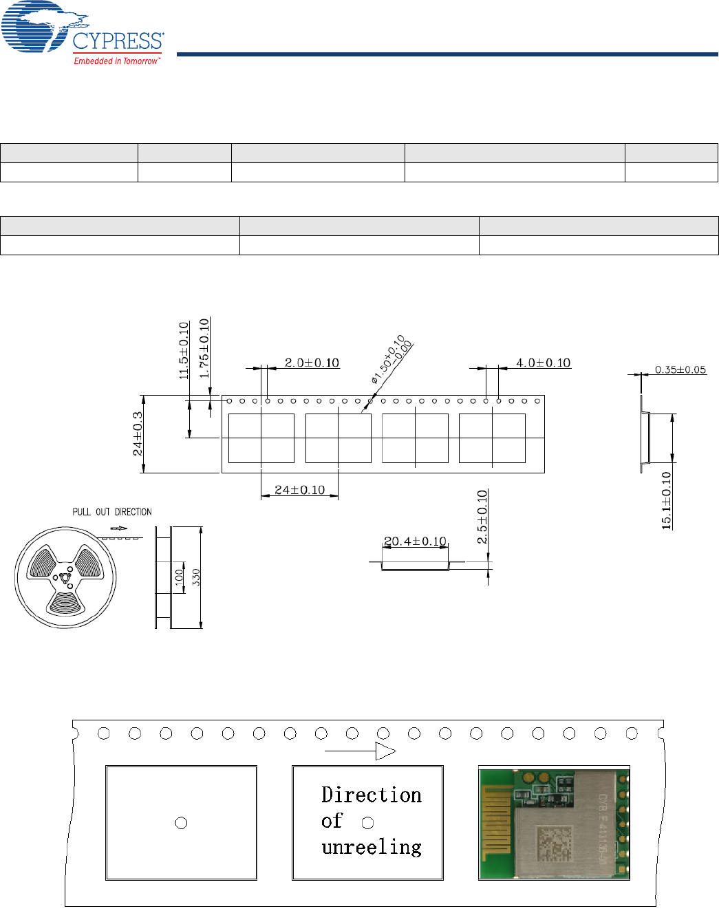
Packaging
The CYBLE-413136-01 is offered in tape and reel packaging. Figure 12 details the tape dimensions used for the CYBLE-413136-01.
Figure 12. CYBLE-413136-01 Tape Dimensions
Figure 13 details the orientation of the CYBLE-413136-01 in the tape as well as the direction for unreeling.
Figure 13. Component Orientation in Tape and Unreeling Direction
Table 20. Solder Reflow Peak Temperature
Module Part Number Package Maximum Peak Temperature Maximum Time at Peak Temperature No. of Cycles
CYBLE-413136-01 14-pad SMT 260 °C 30 seconds 2
Table 21. Package Moisture Sensitivity Level (MSL), IPC/JEDEC J-STD-2
Module Part Number Package MSL
CYBLE-413136-01 14-pad SMT MSL 3
Document Number: 002-19043 Rev. PRELIMINARY Page 29 of 33
PRELIMINARY CYBLE-413136-01
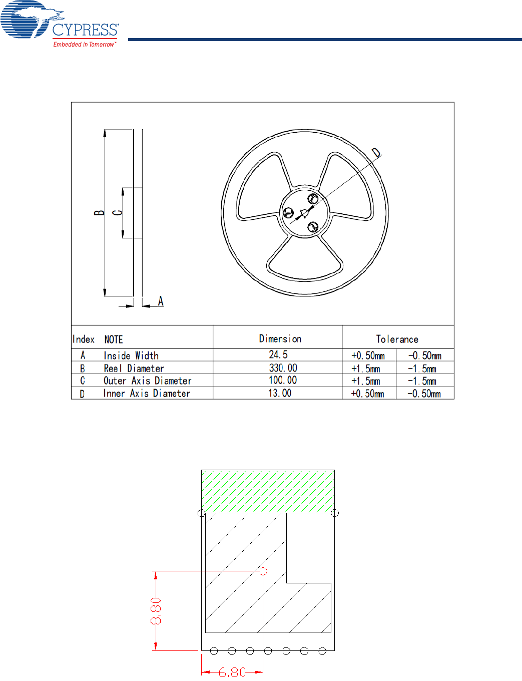
Figure 14 details reel dimensions used for the CYBLE-413136-01.
Figure 14. Reel Dimensions
The CYBLE-413136-01 is designed to be used with pick-and-place equipment in an SMT manufacturing environment. The
center-of-mass for the CYBLE-413136-01 is detailed in Figure 15.
Figure 15. CYBLE-413136-01 Center of Mass
Document Number: 002-19043 Rev. PRELIMINARY Page 30 of 33
PRELIMINARY CYBLE-413136-01
Ordering Information
Tab le 22 lists the CYBLE-413136-01 part number and features. Table 22 also lists the target program for the respective module
ordering codes. Table 23 lists the reel shipment quantities for the CYBLE-413136-01.
The CYBLE-413136-01 is offered in tape and reel packaging. The CYBLE-413136-01 ships in a reel size of 800 units.
For additional information and a complete list of Cypress Semiconductor BLE products, contact your local Cypress sales
representative. To locate the nearest Cypress office, visit our website.
Table 22. Ordering Information
Ordering Part
Number
Base Part Number
(Marking)
CPU
Speed
(MHz)
Flash
Size
(KB)
RAM
Size
(KB)
UART PWM Apple MFi
Coprocessor Package Packaging Program
CYBLE-413136-01 CYBLE-413136-01 24 1024 512 Yes 4 Yes 14-SMT Tape and Reel A19W
CP8745AT CYBLE-413136-01 24 1024 512 Yes 4 Yes 14-SMT Tape and Reel FlexC
CP8746AT CYBLE-413136-01 24 1024 512 Yes 4 Yes 14-SMT Tape and Reel Plug
CP8747AT CYBLE-413136-01 24 1024 512 Yes 4 Yes 14-SMT Tape and Reel A60Ce
CP8748AT CYBLE-413136-01 24 1024 512 Yes 4 Yes 14-SMT Tape and Reel FlexCe
Table 23. Tape and Reel Package Quantity and Minimum Order Amount
Description Minimum Reel Quantity Maximum Reel Quantity Comments
Reel Quantity 800 800 Ships in 800 unit reel quantities.
Minimum Order Quantity (MOQ) 800 – –
Order Increment (OI) 800 – –
U.S. Cypress Headquarters Address 198 Champion Court, San Jose, CA 95134
U.S. Cypress Headquarter Contact Info (408) 943-2600
Cypress website address http://www.cypress.com
Document Number: 002-19043 Rev. PRELIMINARY Page 31 of 33
PRELIMINARY CYBLE-413136-01
Acronyms Document Conventions
Units of Measure
Table 24. Acronyms Used in this Document
Acronym Description
BLE Bluetooth Low Energy
Bluetooth SIG Bluetooth Special Interest Group
CE European Conformity
CSA Canadian Standards Association
EMI electromagnetic interference
ESD electrostatic discharge
FCC Federal Communications Commission
GPIO general-purpose input/output
ISED Innovation, Science and Economic Devel-
opment (Canada)
IDE integrated design environment
KC Korea Certification
MIC Ministry of Internal Affairs and Communications
(Japan)
PCB printed circuit board
RX receive
QDID qualification design ID
SMT
surface-mount technology; a method for
producing electronic circuitry in which the
components are placed directly onto the surface
of PCBs
TCPWM timer, counter, pulse width modulator (PWM)
TUV Germany: Technischer Überwachungs-Verein
(Technical Inspection Association)
TX transmit
Table 25. Units of Measure
Symbol Unit of Measure
°C degree Celsius
kV kilovolt
mA milliamperes
mm millimeters
mV millivolt
μA microamperes
μm micrometers
MHz megahertz
GHz gigahertz
Vvolt
Document Number: 002-19043 Rev. PRELIMINARY Page 32 of 33
PRELIMINARY CYBLE-413136-01
Document History Page
Document Title: CYBLE-413136-01 EZ-BLE™ Module with HomeKit
Document Number: 002-19043
Revision ECN Orig. of
Change
Submission
Date Description of Change
** PRELIM-
INARY
DSO Preliminary datasheet for CYBLE-413136-01 module.
Document Number: 002-19043 Rev. PRELIMINARY Revised May 12, 2017 Page 33 of 33
PRELIMINARY CYBLE-413136-01
© Cypress Semiconductor Corporation, 2017. This document is the property of Cypress Semiconductor Corporation and its subsidiaries, including Spansion LLC ("Cypress"). This document, including
any software or firmware included or referenced in this document ("Software"), is owned by Cypress under the intellectual property laws and treaties of the United States and other countries worldwide.
Cypress reserves all rights under such laws and treaties and does not, except as specifically stated in this paragraph, grant any license under its patents, copyrights, trademarks, or other intellectual
property rights. If the Software is not accompanied by a license agreement and you do not otherwise have a written agreement with Cypress governing the use of the Software, then Cypress hereby
grants you a personal, non-exclusive, nontransferable license (without the right to sublicense) (1) under its copyright rights in the Software (a) for Software provided in source code form, to modify and
reproduce the Software solely for use with Cypress hardware products, only internally within your organization, and (b) to distribute the Software in binary code form externally to end users (either
directly or indirectly through resellers and distributors), solely for use on Cypress hardware product units, and (2) under those claims of Cypress's patents that are infringed by the Software (as provided
by Cypress, unmodified) to make, use, distribute, and import the Software solely for use with Cypress hardware products. Any other use, reproduction, modification, translation, or compilation of the
Software is prohibited.
TO THE EXTENT PERMITTED BY APPLICABLE LAW, CYPRESS MAKES NO WARRANTY OF ANY KIND, EXPRESS OR IMPLIED, WITH REGARD TO THIS DOCUMENT OR ANY SOFTWARE
OR ACCOMPANYING HARDWARE, INCLUDING, BUT NOT LIMITED TO, THE IMPLIED WARRANTIES OF MERCHANTABILITY AND FITNESS FOR A PARTICULAR PURPOSE. To the extent
permitted by applicable law, Cypress reserves the right to make changes to this document without further notice. Cypress does not assume any liability arising out of the application or use of any
product or circuit described in this document. Any information provided in this document, including any sample design information or programming code, is provided only for reference purposes. It is
the responsibility of the user of this document to properly design, program, and test the functionality and safety of any application made of this information and any resulting product. Cypress products
are not designed, intended, or authorized for use as critical components in systems designed or intended for the operation of weapons, weapons systems, nuclear installations, life-support devices or
systems, other medical devices or systems (including resuscitation equipment and surgical implants), pollution control or hazardous substances management, or other uses where the failure of the
device or system could cause personal injury, death, or property damage ("Unintended Uses"). A critical component is any component of a device or system whose failure to perform can be reasonably
expected to cause the failure of the device or system, or to affect its safety or effectiveness. Cypress is not liable, in whole or in part, and you shall and hereby do release Cypress from any claim,
damage, or other liability arising from or related to all Unintended Uses of Cypress products. You shall indemnify and hold Cypress harmless from and against all claims, costs, damages, and other
liabilities, including claims for personal injury or death, arising from or related to any Unintended Uses of Cypress products.
Cypress, the Cypress logo, Spansion, the Spansion logo, and combinations thereof, WICED, PSoC, CapSense, EZ-USB, F-RAM, and Traveo are trademarks or registered trademarks of Cypress in
the United States and other countries. For a more complete list of Cypress trademarks, visit cypress.com. Other names and brands may be claimed as property of their respective owners.
Sales, Solutions, and Legal Information
Worldwide Sales and Design Support
Cypress maintains a worldwide network of offices, solution centers, manufacturer’s representatives, and distributors. To find the office
closest to you, visit us at Cypress Locations.
Products
ARM® Cortex® Microcontrollers cypress.com/arm
Automotive cypress.com/automotive
Clocks & Buffers cypress.com/clocks
Interface cypress.com/interface
Internet of Things cypress.com/iot
Memory cypress.com/memory
Microcontrollers cypress.com/mcu
PSoC cypress.com/psoc
Power Management ICs cypress.com/pmic
Touch Sensing cypress.com/touch
USB Controllers cypress.com/usb
Wireless Connectivity cypress.com/wireless
PSoC® Solutions
PSoC 1 | PSoC 3 | PSoC 4 | PSoC 5LP
Cypress Developer Community
Forums | WICED IOT Forums | Projects | Video | Blogs |
Training | Components
Technical Support
cypress.com/support