Cypress Semiconductor 4110 Bluetooth Module User Manual CYBLE 224110 00 EZ BLE TM PSoC XT XR Module
Cypress Semiconductor Bluetooth Module CYBLE 224110 00 EZ BLE TM PSoC XT XR Module
Contents
- 1. User Manual
- 2. User Manual II
User Manual

CYBLE-224110-00
EZ-BLE™ PSoC® XT/XR Module
PRELIMINARY
Cypress Semiconductor Corporation • 198 Champion Court • San Jose,CA 95134-1709 • 408-943-2600
Document Number: 002-11264 Rev. *A Revised May 16, 2016
General Description
The Cypress CYBLE-224110-00 is a fully certified and qualified
module supporting Bluetooth Low Energy (BLE) wireless
communication. The CYBLE-224110-00 is a turnkey solution
that includes onboard power amplifier (PA), low noise amplifier
(LNA), crystal oscillators, chip antenna, passive components,
and the Cypress PSoC® 4 BLE. Refer to the PSoC 4 BLE
datasheet for additional details on the capabilities of the PSoC 4
BLE device used on this module.
The EZ-BLE PSoC® XT/XR module provides extended
industrial temperature operation (XT) and extended
communication range (XR). The EZ-BLE XT/XR module is a
scalable and reconfigurable platform architecture, combining
programmable and reconfigurable analog and digital blocks with
flexible automatic routing. The CYBLE-224110-00 also includes
digital programmable logic, high-performance analog-to-digital
conversion (ADC), opamps with comparator mode, and standard
communication and timing peripherals.
The CYBLE-224110-00 includes a royalty-free BLE stack
compatible with Bluetooth 4.1 and provides up to 25 GPIOs in a
small 9.5 × 15.4 × 1.80 mm footprint.
Module Description
nModule size: 9.5 mm × 15.4 mm × 1.80 mm (with shield)
nExtended Range: Up to 400 meters line-of-sight
nExtended industrial temperature range: –40 °C to +105 °C
nUp to 25 GPIOs
n256-KB flash memory, 32-KB SRAM memory
nBluetooth 4.1 qualified single-mode module
nCertified to FCC, CE, MIC, KC, and IC regulations
n32-bit processor (0.9 DMIPS/MHz) with single-cycle 32-bit
multiply, operating at up to 48 MHz
nWatchdog timer with dedicated internal low-speed oscillator
nTwo-pin SWD for programming
Power Consumption
nTX output power: –18 dbm to +9.5 dbm
nRX Receive Sensitivity: –95 dbm
nReceived signal strength indicator (RSSI) with 1-dB resolution
n1 Second connection interval with PA/LNA active: 26.3 µA
nTX current consumption:
pBLE silicon: 15.6 mA (radio only, 0 dbm)
pSE2438T: 20 mA (PA/LNA only, +9.5 dBm)
nRX current consumption of 16.4 mA (radio only)
pBLE silicon: 16.4 mA (radio only)
pSE2438T: 5.5 mA (PA/LNA only)
nLow power mode support
pDeep Sleep: 1.3 µA with watch crystal oscillator (WCO) on
pHibernate: 150 nA with SRAM retention
pStop: 60 nA with XRES wakeup
Integrated PA/LNA
nSupports output power up to +9.5 dBm and RXS of -95 dBm
Programmable Analog
nFour opamps with reconfigurable high-drive external and
high-bandwidth internal drive, comparator modes, and ADC
input buffering capability; can operate in Deep-Sleep mode
n12-bit, 1-Msps SAR ADC with differential and single-ended
modes; channel sequencer with signal averaging
nTwo current DACs (IDACs) for general-purpose or capacitive
sensing applications on any pin
nOne low-power comparator that operate in Deep-Sleep mode
Programmable Digital
nFour programmable logic blocks called universal digital blocks,
(UDBs), each with eight macrocells and datapath
nCypress-provided peripheral Component library, user-defined
state machines, and Verilog input
Capacitive Sensing
nCypress CapSense Sigma-Delta (CSD) provides best-in-class
SNR (> 5:1) and liquid tolerance
nCypress-supplied software component makes
capacitive-sensing design easy
nAutomatic hardware-tuning algorithm (SmartSense™)
Segment LCD Drive
nLCD drive supported on all GPIOs (common or segment)
nOperates in Deep-Sleep mode with four bits per pin memory
Serial Communication
nTwo independent runtime reconfigurable serial communication
blocks (SCBs) with I2C, SPI, or UART functionality
Timing and Pulse-Width Modulation
nFour 16-bit timer, counter, pulse-width modulator (TCPWM)
blocks
nCenter-aligned, Edge, and Pseudo-random modes
nComparator-based triggering of Kill signals for motor drive and
other high-reliability digital logic applications
Up to 25 Programmable GPIOs
nAny GPIO pin can be CapSense, LCD, analog, or digital
nTwo overvoltage-tolerant (OVT) pins; drive modes, strengths,
and slew rates are programmable

PRELIMINARY CYBLE-224110-00
Document Number: 002-11264 Rev. *A Page 2 of 43
More Information
Cypress provides a wealth of data at www.cypress.com to help you to select the right module for your design, and to help you to
quickly and effectively integrate the module into your design.
nOverview: EZ-BLE Module Portfolio, Module Roadmap
nEZ-BLE PSoC Product Overview
nPSoC 4 BLE Silicon Datasheet
nApplication notes: Cypress offers a number of BLE application
notes covering a broad range of topics, from basic to advanced
level. Recommended application notes for getting started with
EZ-BLE modules are:
pAN96841 - Getting Started with EZ-BLE Module
pAN94020 - Getting Started with PSoC® 4 BLE
pAN97060 - PSoC® 4 BLE and PRoC™ BLE - Over-The-Air
(OTA) Device Firmware Upgrade (DFU) Guide
pAN91162 - Creating a BLE Custom Profile
pAN91184 - PSoC 4 BLE - Designing BLE Applications
pAN92584 - Designing for Low Power and Estimating Battery
Life for BLE Applications
pAN85951 - PSoC® 4 CapSense® Design Guide
pAN95089 - PSoC® 4/PRoC™ BLE Crystal Oscillator Selec-
tion and Tuning Techniques
pAN91445 - Antenna Design and RF Layout Guidelines
nTechnical Reference Manual (TRM):
pPSoC® 4 BLE Technical Reference Manual
pPSOC(R) 4 BLE Registers Technical Reference Manual
(TRM)
nDevelopment Kits:
pCYBLE-224110-EVAL, CYBLE-224110-00 Evaluation Board
pCY8CKIT-042-BLE, Bluetooth® Low Energy (BLE) Pioneer
Kit
pCY8CKIT-002, PSoC® MiniProg3 Program and Debug Kit
nTest and Debug Tools:
pCYSmart, Bluetooth® LE Test and Debug Tool (Windows)
pCYSmart Mobile, Bluetooth® LE Test and Debug Tool
(Android/iOS Mobile App)
PSoC® Creator™ Integrated Design Environment (IDE)
PSoC Creator is an Integrated Design Environment (IDE) that enables concurrent hardware and firmware editing, compiling and
debugging of PSoC 3, PSoC 4, PSoC 5LP, PSoC 4 BLE, PRoC BLE and EZ-BLE module systems with no code size limitations. PSoC
peripherals are designed using schematic capture and simple graphical user interface (GUI) with over 120 pre-verified,
production-ready PSoC Components™.
PSoC Components are analog and digital “virtual chips,” represented by an icon that users can drag-and-drop into a design and
configure to suit a broad array of application requirements.
Blutooth Low Energy Component
The Bluetooth Low Energy Component inside PSoC Creator provides a comprehensive GUI-based configuration window that lets you
quickly design BLE applications. The Component incorporates a Bluetooth Core Specification v4.1 compliant BLE protocol stack and
provides API functions to enable user applications to interface with the underlying Bluetooth Low Energy Sub-System (BLESS)
hardware via the stack.
Technical Support
nFrequently Asked Questions (FAQs): Learn more about our BLE ECO System.
nForum: See if your question is already answered by fellow developers on the PSoC 4 BLE and PRoC BLE forums.
nVisit our support page and create a technical support case or contact a local sales representatives. If you are in the United States,
you can talk to our technical support team by calling our toll-free number: +1-800-541-4736. Select option 2 at the prompt.

PRELIMINARY CYBLE-224110-00
Document Number: 002-11264 Rev. *A Page 3 of 43
Contents
Overview ............................................................................ 4
Module Description ......................................................4
Pad Connection Interface ................................................ 6
Recommended Host PCB Layout ...................................8
Power Supply Connections and Recommended
External Components .................................................... 12
Connection Options ...................................................12
External Component Recommendation ....................12
Critical Components List ...........................................15
Antenna Design .........................................................15
Electrical Specifications ................................................ 16
GPIO .........................................................................18
XRES .........................................................................19
Analog Peripherals ....................................................20
Digital Peripherals .....................................................24
Serial Communication ...............................................26
Memory .....................................................................27
System Resources ....................................................27
Environmental Specifications ....................................... 33
Environmental Compliance .......................................33
RF Certification ..........................................................33
Environmental Conditions ......................................... 33
ESD and EMI Protection ........................................... 33
Regulatory Information .................................................. 34
FCC ........................................................................... 34
Industry Canada (IC) Certification .............................35
European R&TTE Declaration of Conformity ............35
MIC Japan ................................................................. 36
KC Korea ................................................................... 36
Packaging ........................................................................ 37
Ordering Information ...................................................... 38
Part Numbering Convention ......................................38
Acronyms ........................................................................ 39
Document Conventions ................................................. 41
Units of Measure ....................................................... 41
Document History Page ................................................. 42
Sales, Solutions, and Legal Information ...................... 43
Worldwide Sales and Design Support ....................... 43
Products .................................................................... 43
PSoC® Solutions ...................................................... 43
Cypress Developer Community ................................. 43
Technical Support ..................................................... 43
PRELIMINARY CYBLE-224110-00
Document Number: 002-11264 Rev. *A Page 4 of 43
Overview
Module Description
The CYBLE-224110-00 is an integrated wireless module designed to be soldered to the main host board.
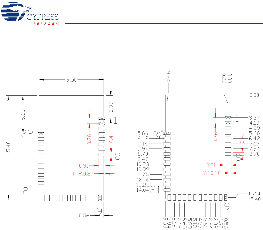
Module Dimensions and Drawing
Cypress reserves the right to select components (including the appropriate BLE device) from various vendors to achieve the BLE
module functionality. Such selections will guarantee that all height restrictions of the component area are maintained. Designs should
be completed with the physical dimensions provided in the mechanical drawings (see Figure 1). All dimensions are in millimeters (mm).
See Figure 1 on page 5 for the mechanical reference drawing for CYBLE-224110-00.
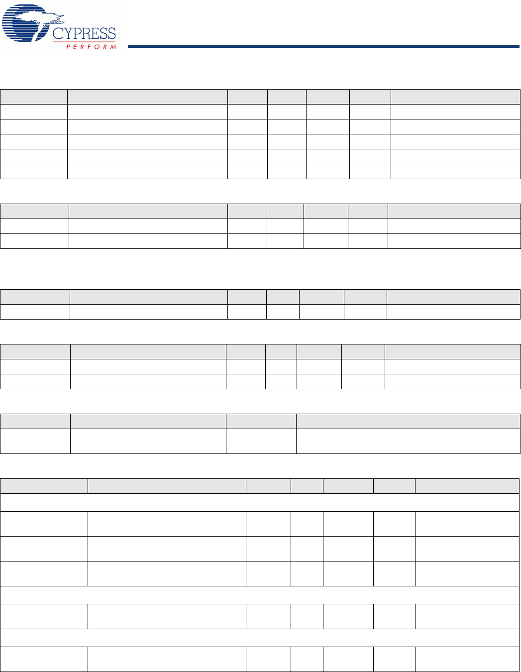
Table 1. Module Design Dimensions
Dimension Item Specification
Module dimensions Length (X) 9.50 ± 0.15 mm
Width (Y) 15.40 ± 0.15 mm
Antenna location dimensions Length (X) 7.00 mm
Width (Y) 5.00 mm
PCB thickness Height (H) 0.50 ± 0.10 mm
Shield height Height (H) 1.10 ± 0.10 mm
Maximum component height Height (H) 1.30 mm typical (chip antenna)
Total module thickness (bottom of module to highest component) Height (H) 1.80 mm typical
PRELIMINARY CYBLE-224110-00
Document Number: 002-11264 Rev. *A Page 5 of 43
Figure 1. Module Mechanical Drawing
Top View
Bottom View
Side View
Note
1. No metal should be located beneath or above the antenna area. Only bare PCB material should be located beneath the antenna area. For more information on
recommended host PCB layout, see Figure 3 on page 7, Figure 4 and Figure 5 on page 8, Figure 6 and Table 3 on page 9.
PRELIMINARY CYBLE-224110-00
Document Number: 002-11264 Rev. *A Page 6 of 43
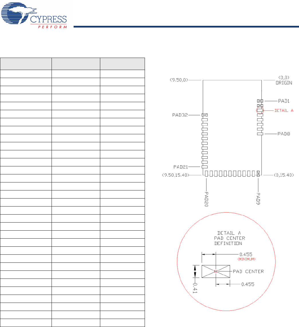
Pad Connection Interface
As shown in the bottom view of Figure 1, the CYBLE-224110-00 connects to the host board via solder pads on the back of the module.
Table 2 and Figure 2 detail the solder pad length, width, and pitch dimensions of the CYBLE-224110-00 module.
Figure 2. Solder Pad Dimensions (Bottom View)
Table 2. Solder Pad Connection Description
Name Connection Connection Type Pad Length Dimension Pad Width Dimension Pad Pitch
SP 32 Solder Pads 0.71 mm 0.41 mm 0.76 mm
PRELIMINARY CYBLE-224110-00
Document Number: 002-11264 Rev. *A Page 7 of 43
To maximize RF performance, the host layout should follow these recommendations:
1. The ideal placement of the Cypress BLE module is in a corner of the host board with the antenna located on the edge of the host
board. This placement minimizes the additional recommended keep-out area shown in item 2. Please refer to AN96841 for module
placement best practices.
2. To maximize RF performance, the area immediately around the Cypress BLE module trace antenna should contain an additional
keep-out area, where no grounding or signal traces are contained. The keep-out area applies to all layers of the host board. The
recommended dimensions of the host PCB keep-out area are shown in Figure 3 (dimensions are in mm).
Figure 3. Recommended Host PCB Keep-Out Area around CYBLE-224110-00 Trace Antenna
Host PCB Keep-Out Area around Trace Antenna
PRELIMINARY CYBLE-224110-00
Document Number: 002-11264 Rev. *A Page 8 of 43
Recommended Host PCB Layout
Figure 4 through Figure 6 and Ta ble 3 provide details that can be used for the recommended host PCB layout pattern for the
CYBLE-224110-00. Dimensions are in millimeters unless otherwise noted. The minimum recommended host PCB pad length is 0.91
mm (0.455 mm from center of the pad to either side) is recommended as shown in Figure 6. The host PCB layout pattern can be
completed using either Figure 4, Figure 5, or Figure 6. It is not necessary to use all figures to complete the host PCB layout pattern.
Figure 4. Host Layout Pattern for CYBLE-224110-00 Figure 5. Module Pad Location from Origin
PRELIMINARY CYBLE-224110-00
Document Number: 002-11264 Rev. *A Page 9 of 43
Table 3 provides the center location for each solder pad on the CYBLE-224110-00. All dimensions reference the to the center of the
solder pad. Figure 6 provides the location of each module solder pad.
Table 3. Module Solder Pad Location
Figure 6. Solder Pad Reference Location
Solder Pad
(Center of Pad)
Location (X,Y) from
Orign (mm)
Dimension from
Orign (mils)
1 (0.26, 3.37) (10.24, 132.68)
2 (0.26, 4.13) (10.24, 162.68)
3 (0.26, 4.89) (10.24, 192.68)
4 (0.26, 5.66) (10.24, 222.68)
5 (0.26, 6.42) (10.24, 252.68)
6 (0.26, 7.18) (10.24, 282.68)
7 (0.26, 7.94) (10.24, 312.68)
8 (0.26, 8.70) (10.24, 342.68)
9 (0.56, 15.14) (22.05, 596.06)
10 (1.32,15.14) (51.97, 596.06)
11 (2.08, 15.14) (81.89, 596.06)
12 (2.84,15.14) (111.81, 596.06)
13 (3.61, 15.14) (142.13, 596.06)
14 (4.37, 15.14) (172.13, 596.06)
15 (5.13, 15.14) (202.13, 596.06)
16 (5.89, 15.14) (231.89, 596.06)
17 (6.65,15.14) (261.81, 596.06)
18 (7.42, 15.14) (292.13, 596.06)
19 (8.18, 15.14) (322.05, 596.06)
20 (8.94, 15.14) (351.97, 596.06)
21 (9.24, 14.04) (363.78, 552.76)
22 (9.24, 13.28) (363.78, 522.83)
23 (9.24, 12.51) (363.78,492.52)
24 (9.24, 11.75) (363.78, 462.60)
25 (9.24,10.99) (363.78, 432.68)
26 (9.24,10.23) (363.78, 402.76)
27 (9.24, 9.47) (363.78, 372.83)
28 (9.24, 8.70) (363.78, 342.52)
29 (9.24, 7.94) (363.78, 312.60)
30 (9.24, 7.18) (363.78, 282.68)
31 (9.24, 6.42) (363.78, 252.76)
32 (9.24,5.66) (363.78, 222.83)
PRELIMINARY CYBLE-224110-00
Document Number: 002-11264 Rev. *A Page 10 of 43
Table 4 and Table 5 detail the solder pad connection definitions and available functions for each connection pad. Table 5 lists the
solder pads on CYBLE-224110-00, the BLE device port-pin, and denotes whether the digital function shown is available for each
solder pad. Table 5 denotes whether the analog function shown is available for each solder pad. Each connection is configurable for
a single option shown with a 3.
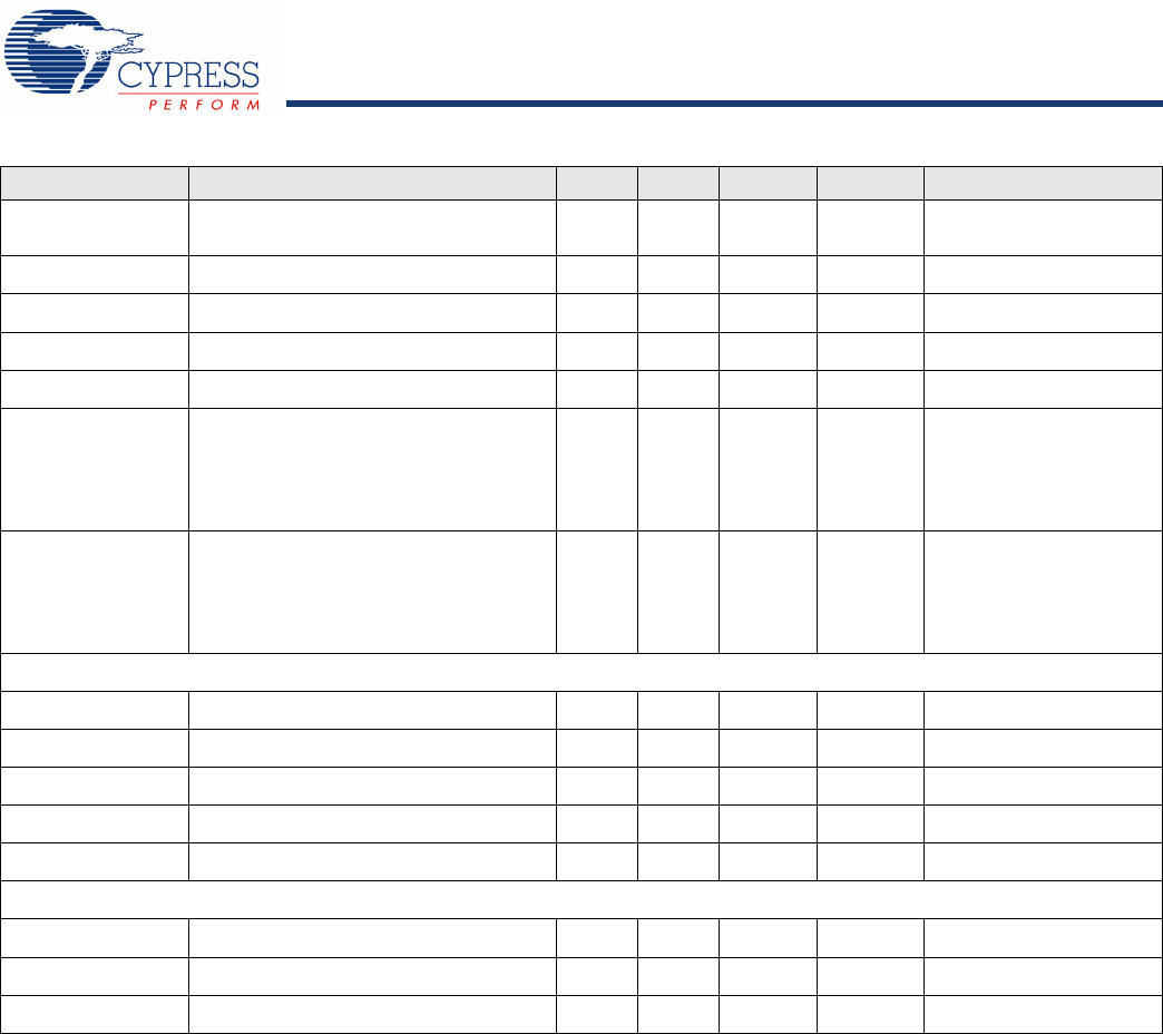
Table 4. Digital Peripheral Capabilities
Pad
Number
Device
Port Pin UART SPI I2CTCPWM[2] Cap
Sense
WCO
Out
ECO
OUT LCD SWD GPIO
1GND
[3] Ground Connection
2 XRES External Reset Hardware Connection Input
3P1.5
3(SCB0_TX) 3(SCB0_MISO) 3(SCB0_SCL) 3(TCPWM2_N) 333
4P1.1 3(SCB1_SS1) 3(TCPWM0_N) 333
5P1.0 3(TCPWM0_P) 333
6P0.13(SCB1_TX) 3(SCB1_MISO) 3(SCB1_SCL) 3(TCPWM0_N) 333
7P0.43(SCB0_RX) 3(SCB0_MOSI) 3(SCB0_SDA) 3(TCPWM1_P) 333 3
8P0.53(SCB0_TX) 3(SCB0_MISO) 3(SCB0_SCL) 3(TCPWM1_N) 333
9P0.73(SCB0_CTS) 3(SCB0_SCLK) 3(TCPWM2_N) 33
3
(SWDCLK) 3
10 P1.3 3(SCB1_SS3) 3(TCPWM1_N) 333
11 VDDR Radio Power Supply (2.0V to 3.6V)
12 P0.6 3(SCB0_RTS) 3(SCB0_SS0) 3(TCPWM2_P) 33
3
(SWDIO) 3
13 P1.2 3(SCB1_SS2) 3(TCPWM1_P) 333
14 VDD Digital Power Supply Input (1.71 to 5.5V)
15 P1.4 3(SCB0_RX) 3(SCB0_MOSI) 3(SCB0_SDA) 3(TCPWM2_P) 333
16 P2.1 3(SCB0_SS2) 333
17 VDDA Analog Power Supply Input (1.71 to 5.5V)
18 P2.2 3(SCB0_SS3) 333
19 P2.6 333
20 P3.0 3(SCB0_RX) 3(SCB0_SDA) 3(TCPWM0_P) 333
21 P2.3 33 3 3
22 VREF Reference Voltage Input
23 P3.4 3(SCB1_RX) 3(SCB1_SDA) 3(TCPWM2_P) 333
24 P3.5 3(SCB1_TX) 3(SCB1_SCL) 3(TCPWM2_N) 333
25 P3.7 3(SCB1_CTS) 3(TCPWM3_N) 33 3 3
26 P3.1 3(SCB0_TX) 3(SCB0_SCL) 3(TCPWM0_N) 333
27 P3.6 3(SCB1_RTS) 3(TCPWM3_P) 333
28 P2.5 333
29 P5.0 3(SCB1_RX) 3(SCB1_SS0) 3(SCB1_SDA) 3(TCPWM3_P) 333
30 P5.1 3(SCB1_TX) 3(SCB1_SCLK) 3(SCB1_SCL) 3(TCPWM3_N) 333 3
31 P2.4 333
32 GND[3] Ground Connection
PRELIMINARY CYBLE-224110-00
Document Number: 002-11264 Rev. *A Page 11 of 43
Notes
2. TCPWM stands for timer, counter, and PWM. If supported, the pad can be configured to any of these peripheral functions.
3. The main board needs to connect both GND connections (Pad 1 and Pad 32) on the module to the common ground of the system.
Table 5. Analog Peripheral Capabilities
Pad Number Device Port Pin SARMUX OPAMP LPCOMP
1GND
[3] Ground Connection
2 XRES External Reset Hardware Connection Input
3P1.5 −3(CTBm1_OA1_INP) −
4P1.1 −3(CTBm1_OA0_INN) −
5P1.0 −3(CTBm1_OA0_INP) −
6P0.1 −−3(COMP0_INN)
7P0.4 −−3(COMP1_INP)
8P0.5 −−3(COMP1_INN)
9P0.7 −− −
10 P1.3 −3(CTBm1_OA1_OUT) −
11 VDDR Radio Power Supply (2.0V to 3.6V)
12 P0.6 −− −
13 P1.2 −3(CTBm1_OA0_OUT) −
14 VDD Digital Power Supply Input (1.71 to 5.5V)
15 P1.4 −3(CTBm1_OA1_INN) −
16 P2.1 −3(CTBm1_OA0_INN) −
17 VDDA Analog Power Supply Input (1.71 to 5.5V)
18 P2.2 −3(CTBm1_OA0_OUT) −
19 P2.6 −3(CTBm1_OA0_INP) −
20 P3.0 3−−
21 P2.3 −3(CTBm1_OA1_OUT) −
22 VREF Reference Voltage Input (Optional)
23 P3.4 3−−
24 P3.5 3−−
25 P3.7 3−−
26 P3.1 3−−
27 P3.6 3−−
28 P2.5 −3(CTBm0_OA1_INP) −
29 P5.0 −− −
30 P5.1 −− −
31 P2.4 −3(CTBm0_OA1_INN) −
32 GND Ground Connection
PRELIMINARY CYBLE-224110-00
Document Number: 002-11264 Rev. *A Page 12 of 43
Power Supply Connections and Recommended External Components
Power Connections
The CYBLE-224110-00 contains three power supply
connections, VDD, VDDA, and VDDR. The VDD and VDDA
connections supply power for the digital and analog device
operation respectively. VDDR supplies power for the device
radio and PA/LNA.
VDD and VDDA accept a supply range of 1.71V to 5.5V. VDDR
accepts a supply range of 2.0V to 3.6 V. These specifications can
be found in Table 12. The maximum power supply ripple for both
power connections on the module is 100 mV, as shown in
Table 10.
The power supply ramp rate of VDD and VDDA must be equal
to or greater than that of VDDR when the radio is used.
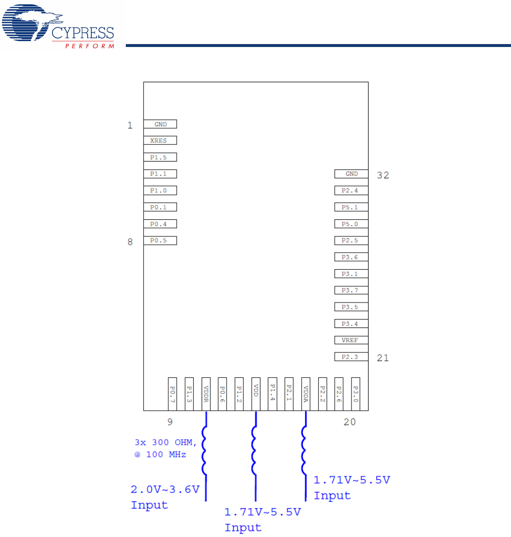
Connection Options
Two connection options are available for any application:
1. Single supply: Connect VDD, VDDA, and VDDR to the same
supply.
2. Independent supply: Power VDD, VDDA, and VDDR
separately.
External Component Recommendation
In either connection scenario, it is recommended to place an
external ferrite bead between the supply and the module
connection. The ferrite bead should be positioned as close as
possible to the module pin connection.
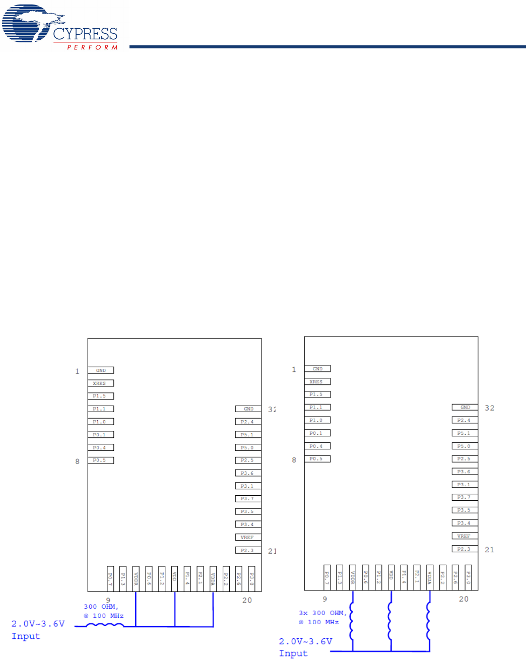
Figure 7 details the recommended host schematic options for a
single supply scenario. The use of one or three ferrite beads will
depend on the specific application and configuration of the
CYBLE-224110-00.
Figure 8 details the recommended host schematic for an
independent supply scenario.
The recommended ferrite bead value is 330 Ω, 100 MHz (Murata
BLM21PG331SN1D).
Figure 7. Recommended Host Schematic Options for Single Supply Option
Three Ferrite Bead Option
Single Ferrite Bead Option
PRELIMINARY CYBLE-224110-00
Document Number: 002-11264 Rev. *A Page 13 of 43
Figure 8. Recommended Host Schematic for Independent Supply Option
PRELIMINARY CYBLE-224110-00
Document Number: 002-11264 Rev. *A Page 15 of 43
Critical Components List
Table 6 provides the critical components used in the CYBLE-224110-00 module.
Antenna Design
Table 7 details the antenna used on the CYBLE-224110-00 module. The Cypress module performance improves many of these
characteristics. For more information, see Tab le 11.
Table 7. Chip Antenna Specifications
Power Amplifier (PA) and Low Noise Amplifier (LNA)
Table 8 details the PA/LNA that is used on the CYBLE-224110-00 module. For more information, see Table 11.
Table 9 details the power consumption of the integrated PA/LNA used on the CYBLE-224110-00 module. Ta ble only details the current
consumption of the SE2438T PA/LNA. VCC = VCC1 = VCC2 = 3 V, TA = +25°C, measured on the SE2438T evaluation board, unless
otherwise noted.
Table 6. Critical Component List
Component Reference Designator Description
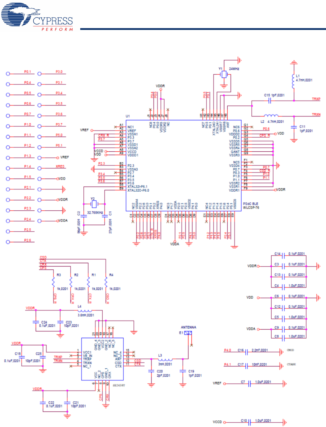
Silicon U1 76-pin WLCSP Programmable System-on-Chip (PSoC) with BLE
Crystal Y1 24.000 MHz, 10PF
Crystal Y2 32.768 kHz, 12.5PF
Item Description
Chip Antenna Manufacturer Johanson Technology Inc.
Chip Antenna Part Number 2450AT18B100
Frequency Range 2400 – 2500 MHz
Peak Gain 0.5 dBi typical
Average Gain –0.5 dBi typical
Return Loss 9.5 dB minimum
Table 8. Power Amplifier/Low Noise Amplifier Details
Item Description
PA/LNA Manufacturer Skyworks Inc.
PA/LNA Part Number SE2438T
Power Supply Range 2.0V ~ 3.6V
Table 9. Power Amplifier/Low Noise Amplifier Current Consumption Specifications
Parameter Symbol Test Condition Min Typ Max Unit
Total supply current ICC_Tx14 Tx mode POUT = +14 dBm – 33 – mA
Total supply current ICC_Tx12 Tx mode POUT = +12 dBm – 25 – mA
Total supply current ICC_Tx10 Tx mode POUT = +10 dBm – 20 – mA
Quiescent current ICQ_Tx No RF – 6 – mA
Total supply current ICC_RXHG Rx Low Noise Amplifier (LNA) High Gain mode – 5.5 – mA
Total supply current ICC_RXLG Rx LNA Low Gain mode – 2.7 – mA
Total supply current ICC_RXBypass Rx Bypass mode – – 10 µA
Sleep supply current ICC_OFF No RF – 0.05 1.0 µA
PRELIMINARY CYBLE-224110-00
Document Number: 002-11264 Rev. *A Page 16 of 43
Electrical Specifications
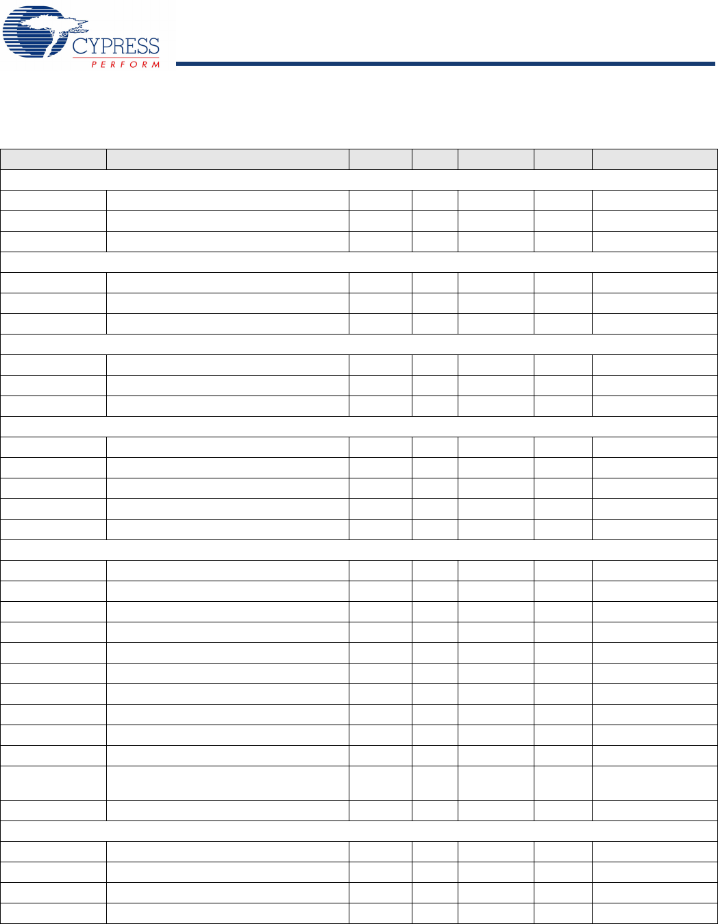
Table 10 provides the absolute maximum electrical characteristics for the Cypress BLE module.
Table 10. CYBLE-224110-00 Absolute Maximum Ratings
Table 11 provides the RF characteristics for the Cypress BLE module.
Table 12 through Table 53 list the module level electrical characteristics for the CYBLE-224110-00. All specifications are valid for
–40 °C ≤ TA ≤ 85 °C and TJ ≤ 100 °C, except where noted. Specifications are valid for 1.71V to 5.5V, except where noted.
Parameter Description Min Typ Max Unit Details/Conditions
VDDD_ABS VDD or VDDA supply relative to VSS (VSSD = VSSA) –0.5 – 6 V Absolute maximum
VDDR_ABS VDDR supply relative to VSS (VSSD = VSSA) -0.3 – 3.6 V Restricted by SE2438T
VCCD_ABS Direct digital core voltage input relative to VSSD –0.5 – 1.95 V Absolute maximum
VDDD_RIPPLE Maximum power supply ripple for VDD, VDDA and
VDDR input voltage – – 100 mV
3.0V supply
Ripple frequency of 100 kHz
to 750 kHz
VGPIO_ABS GPIO voltage –0.5 – VDD +0.5 V Absolute maximum
IGPIO_ABS Maximum current per GPIO –25 – 25 mA Absolute maximum
IGPIO_injection GPIO injection current: Maximum for VIH > VDD
and minimum for VIL < VSS –0.5 – 0.5 mA Absolute maximum current
injected per pin
LU Pin current for latch up –200 – 200 mA –
Table 11. CYBLE-224110-00 RF Performance Characteristics
Parameter Description Min Typ Max Unit Details/Conditions
RFO1 RF output power on ANT
PA active –8.5 0 9.5 dBm Configurable through register
settings. PA active.
RFO2 RF output power on ANT
PA bypassed -18 0 3 dBm Configurable through register
settings. PA in bypass mode.
RXS1 RF receive sensitivity on ANT
LNA active – –95 – dBm Measured value
RXS2 RF receive sensitivity on ANT
LNA bypassed – –87 – dBm Measured value
FRModule frequency range 2400 – 2480 MHz –
GPPeak gain – 0.5 – dBi –
GAvg Average gain – –0.5 – dBi –
RL Return loss – –10 – dB –
Table 12. CYBLE-224110-00 DC Specifications
Parameter Description Min Typ Max Unit Details/Conditions
VDD1 Power supply input voltage (VDD = VDDA )1.71–5.5V –
VDD2 Power supply input voltage unregulated (VDD =
VDDA)1.71 1.8 1.89 V Internally unregulated
supply
VDD3 Power supply input voltage (VDD = VDDA = VDDR) 2.0 – 3.6 V Restricted by SE2438T
VDDR1 Radio supply voltage (radio on) 2.0 – 3.6 V Restricted by SE2438T
VDDR2 Radio supply voltage (radio off) 2.0 – 3.6 V –
Active Mode, VDD = 1.71V to 5.5V
IDD3 Execute from flash; CPU at 3 MHz – 1.7 – mA T = 25 °C,
VDD = 3.3V
PRELIMINARY CYBLE-224110-00
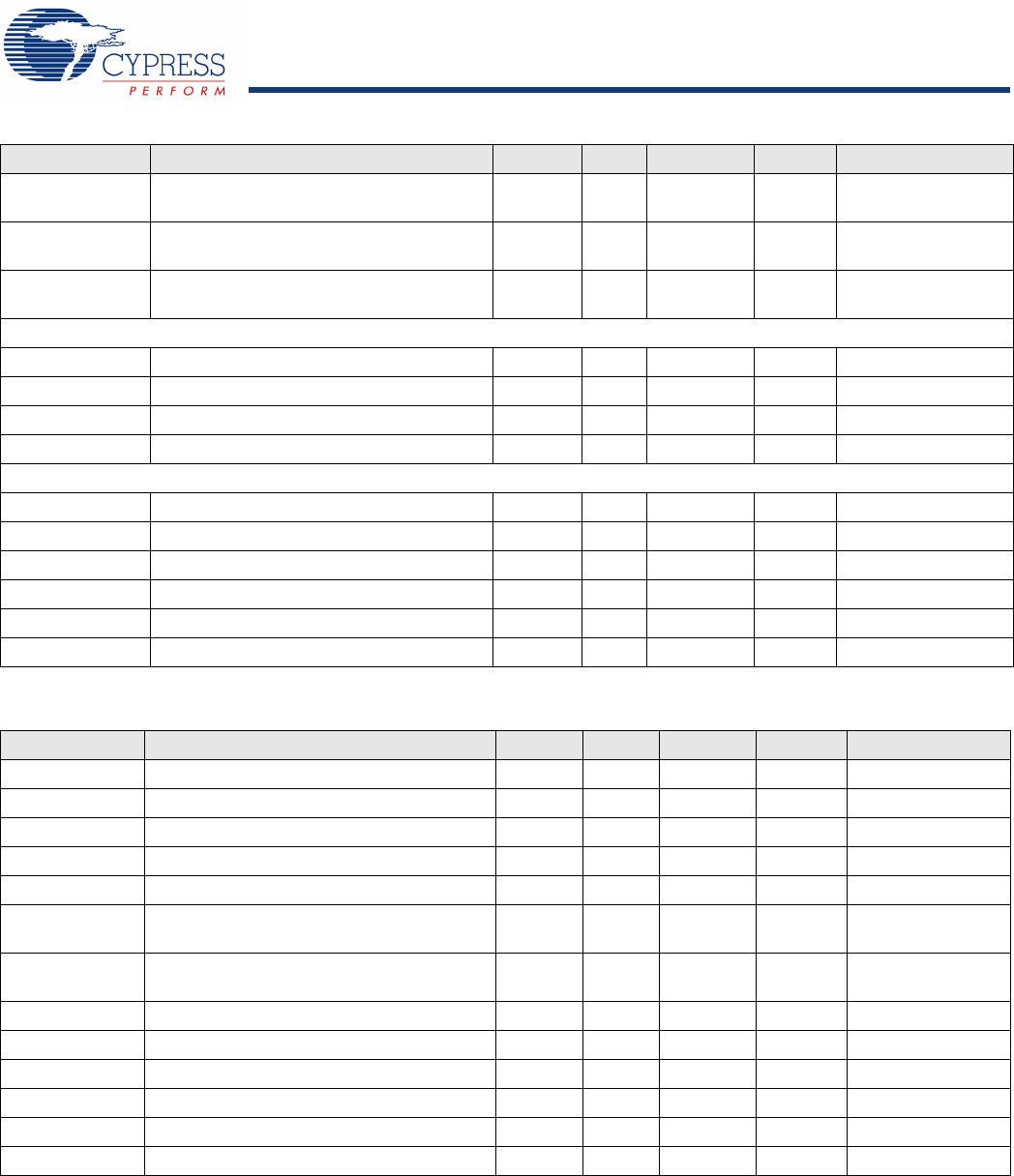
Document Number: 002-11264 Rev. *A Page 17 of 43
IDD4 Execute from flash; CPU at 3 MHz – – – mA T = –40 °C to 85 °C
IDD5 Execute from flash; CPU at 6 MHz – 2.5 – mA T = 25 °C,
VDD = 3.3V
IDD6 Execute from flash; CPU at 6 MHz – – – mA T = –40 °C to 85 °C
IDD7 Execute from flash; CPU at 12 MHz – 4 – mA T = 25 °C,
VDD = 3.3V
IDD8 Execute from flash; CPU at 12 MHz – – – mA T = –40 °C to 85 °C
IDD9 Execute from flash; CPU at 24 MHz – 7.1 – mA T = 25 °C,
VDD = 3.3V
IDD10 Execute from flash; CPU at 24 MHz – – – mA T = –40 °C to 85 °C
IDD11 Execute from flash; CPU at 48 MHz – 13.4 – mA T = 25 °C,
VDD = 3.3V
IDD12 Execute from flash; CPU at 48 MHz – – – mA T = –40 °C to 85 °C
Sleep Mode, VDD = 1.71 to 5.5V
IDD13 IMO on – – – mA T = 25 °C, VDD = 3.3V,
SYSCLK = 3 MHz
Sleep Mode, VDD and VDDR = 1.9 to 5.5V
IDD14 ECO on – – – mA T = 25 °C, VDD = 3.3V,
SYSCLK = 3 MHz
Deep-Sleep Mode, VDD = 1.71 to 3.6V
IDD15 WDT with WCO on – 1.3 – µA T = 25 °C,
VDD = 3.3V
IDD16 WDT with WCO on – – – µA T = –40 °C to 85 °C
IDD17 WDT with WCO on – – – µA T = 25 °C,
VDD = 5V
IDD18 WDT with WCO on – – – µA T = –40 °C to 85 °C
Deep-Sleep Mode, VDD = 1.71 to 1.89V (Regulator Bypassed)
IDD19 WDT with WCO on – – – µA T = 25 °C
IDD20 WDT with WCO on – – – µA T = –40 °C to 85 °C
Hibernate Mode, VDD = 1.71 to 3.6V
IDD27 GPIO and reset active – 150 – nA T = 25 °C,
VDD = 3.3V
IDD28 GPIO and reset active – – – nA T = –40 °C to 85 °C
Hibernate Mode, VDD = 3.6 to 5.5V
IDD29 GPIO and reset active – – – nA T = 25 °C,
VDD = 5V
IDD30 GPIO and reset active – – – nA T = –40 °C to 85 °C
Stop Mode, VDD = 1.71 to 3.6V
IDD33 Stop-mode current (VDD)–20–nA
T = 25 °C,
VDD = 3.3V
IDD34 Stop-mode current (VDDR)–40–- nA
T = 25 °C,
VDDR = 3.3V
IDD35 Stop-mode current (VDD) – – – nA T = –40 °C to 85 °C
Table 12. CYBLE-224110-00 DC Specifications (continued)
Parameter Description Min Typ Max Unit Details/Conditions
PRELIMINARY CYBLE-224110-00
Document Number: 002-11264 Rev. *A Page 18 of 43
GPIO
IDD36 Stop-mode current (VDDR)–––nA
T = –40 °C to 85 °C,
VDDR = 1.9V to 3.6V
Stop Mode, VDD = 3.6 to 5.5V
IDD37 Stop-mode current (VDD)–––nA
T = 25 °C,
VDD = 5V
IDD38 Stop-mode current (VDDR)–––nA
T = 25 °C,
VDDR = 5V
IDD39 Stop-mode current (VDD) – – – nA T = –40 °C to 85 °C
IDD40 Stop-mode current (VDDR) – – – nA T = –40 °C to 85 °C
Table 12. CYBLE-224110-00 DC Specifications (continued)
Parameter Description Min Typ Max Unit Details/Conditions
Note
4. VIH must not exceed VDD + 0.2V.
Table 13. AC Specifications
Parameter Description Min Typ Max Unit Details/Conditions
FCPU CPU frequency DC – 48 MHz 1.71V ≤ VDD ≤ 5.5V
TSLEEP Wakeup from Sleep mode – 0 – µs Guaranteed by characterization
TDEEPSLEEP Wakeup from Deep-Sleep mode – – 25 µs 24-MHz IMO. Guaranteed by
characterization
THIBERNATE Wakeup from Hibernate mode – – 800 µs Guaranteed by characterization
TSTOP Wakeup from Stop mode – – 2 ms XRES wakeup
Table 14. GPIO DC Specifications
Parameter Description Min Typ Max Unit Details/Conditions
VIH[4]
Input voltage HIGH threshold 0.7 × VDD – – V CMOS input
LVTTL input, VDD < 2.7V 0.7 × VDD – – V –
LVTTL input, VDD ≥ 2.7V 2.0 – – V –
VIL
Input voltage LOW threshold – – 0.3 × VDD VCMOS input
LVTTL input, VDD < 2.7V – – 0.3 × VDD V–
LVTTL input, VDD ≥ 2.7V – – 0.8 V –
VOH
Output voltage HIGH level VDD –0.6 – – V IOH = 4 mA at 3.3-V VDD
Output voltage HIGH level VDD –0.5 – – V IOH = 1 mA at 1.8-V VDD
VOL
Output voltage LOW level – – 0.6 V IOL = 8 mA at 3.3-V VDD
Output voltage LOW level – – 0.6 V IOL = 4 mA at 1.8-V VDD
Output voltage LOW level – – 0.4 V IOL = 3 mA at 3.3-V VDD
RPULLUP Pull-up resistor 3.5 5.6 8.5 kΩ–
RPULLDOWN Pull-down resistor 3.5 5.6 8.5 kΩ–
IIL Input leakage current (absolute value) – – 2 nA 25 °C, VDD = 3.3 V
IIL_CTBM Input leakage on CTBm input pins – – 4 nA –
CIN Input capacitance – – 7 pF –
VHYSTTL Input hysteresis LVTTL 25 40 – mV VDD > 2.7 V
PRELIMINARY CYBLE-224110-00
Document Number: 002-11264 Rev. *A Page 19 of 43
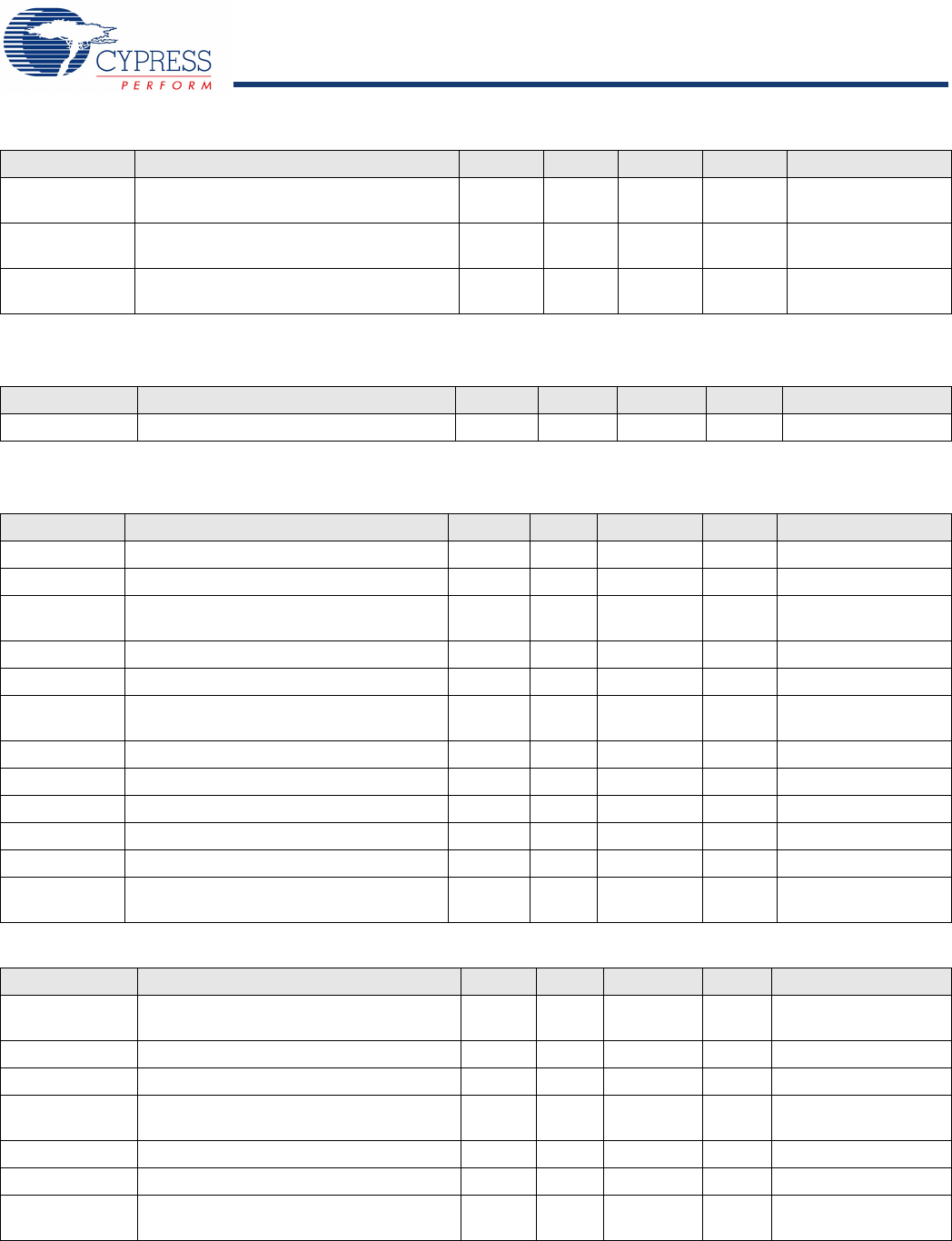
XRES
VHYSCMOS Input hysteresis CMOS 0.05 × VDD – – 1 –
IDIODE Current through protection diode to
VDD/VSS – – 100 µA –
ITOT_GPIO Maximum total source or sink chip
current – – 200 mA –
Table 14. GPIO DC Specifications (continued)
Parameter Description Min Typ Max Unit Details/Conditions
Table 15. GPIO AC Specifications
Parameter Description Min Typ Max Unit Details/Conditions
TRISEF Rise time in Fast-Strong mode 2 – 12 ns 3.3-V VDDD, CLOAD = 25 pF
TFALLF Fall time in Fast-Strong mode 2 – 12 ns 3.3-V VDDD, CLOAD = 25 pF
TRISES Rise time in Slow-Strong mode 10 – 60 ns 3.3-V VDDD, CLOAD = 25 pF
TFALLS Fall time in Slow-Strong mode 10 – 60 ns 3.3-V VDDD, CLOAD = 25 pF
FGPIOUT1 GPIO Fout; 3.3V ≤ VDD ≤ 5.5V
Fast-Strong mode ––33MHz
90/10%, 25 pF load, 60/40 duty
cycle
FGPIOUT2 GPIO Fout; 1.7V≤ VDD ≤ 3.3V
Fast-Strong mode – – 16.7 MHz 90/10%, 25 pF load, 60/40 duty
cycle
FGPIOUT3 GPIO Fout; 3.3V ≤ VDD ≤ 5.5V
Slow-Strong mode –– 7 MHz
90/10%, 25 pF load, 60/40 duty
cycle
FGPIOUT4 GPIO Fout; 1.7V ≤ VDD ≤ 3.3V
Slow-Strong mode ––3.5MHz
90/10%, 25 pF load, 60/40 duty
cycle
FGPIOIN GPIO input operating frequency
1.71V ≤ VDD ≤ 5.5V – – 48 MHz 90/10% VIO
Table 16. XRES DC Specifications
Parameter Description Min Typ Max Unit Details/Conditions
VIH Input voltage HIGH threshold 0.7 × VDDD – – V CMOS input
VIL Input voltage LOW threshold – – 0.3 × VDDD V CMOS input
RPULLUP Pull-up resistor 3.5 5.6 8.5 kΩ–
CIN Input capacitance – 3 – pF –
VHYSXRES Input voltage hysteresis – 100 – mV –
IDIODE Current through protection diode to
VDD/VSS – – 100 µA –
Table 17. XRES AC Specifications
Parameter Description Min Typ Max Unit Details/Conditions
TRESETWIDTH Reset pulse width 1 – – µs –
PRELIMINARY CYBLE-224110-00
Document Number: 002-11264 Rev. *A Page 20 of 43
Analog Peripherals
Opamp
Table 18. Opamp Specifications
Parameter Description Min Typ Max Unit Details/Conditions
IDD (Opamp Block Current. VDD = 1.8V. No Load)
IDD_HI Power = high – 1000 1300 µA –
IDD_MED Power = medium – 500 – µA –
IDD_LOW Power = low – 250 350 µA –
GBW (Load = 20 pF, 0.1 mA. VDDA = 2.7V)
GBW_HI Power = high 6 – – MHz –
GBW_MED Power = medium 4 – – MHz –
GBW_LO Power = low – 1 – MHz –
IOUT_MAX (VDDA ≥ 2.7V, 500 mV from Rail)
IOUT_MAX_HI Power = high 10 – – mA –
IOUT_MAX_MID Power = medium 10 – – mA –
IOUT_MAX_LO Power = low – 5 – mA –
IOUT (VDDA = 1.71V, 500 mV from Rail)
IOUT_MAX_HI Power = high 4 – – mA –
IOUT_MAX_MID Power = medium 4 – – mA –
IOUT_MAX_LO Power = low – 2 – mA –
VIN Charge pump on, VDDA ≥ 2.7V –0.05 – VDDA – 0.2 V –
VCM Charge pump on, VDDA ≥ 2.7V –0.05 – VDDA – 0.2 V –
VOUT (VDDA ≥ 2.7V)
VOUT_1 Power = high, ILOAD = 10 mA 0.5 – VDDA – 0.5 V –
VOUT_2 Power = high, ILOAD = 1 mA 0.2 – VDDA – 0.2 V –
VOUT_3 Power = medium, ILOAD = 1 mA 0.2 – VDDA – 0.2 V –
VOUT_4 Power = low, ILOAD = 0.1 mA 0.2 – VDDA – 0.2 V –
VOS_TR Offset voltage, trimmed 1 ±0.5 1 mV High mode
VOS_TR Offset voltage, trimmed – ±1 – mV Medium mode
VOS_TR Offset voltage, trimmed – ±2 – mV Low mode
VOS_DR_TR Offset voltage drift, trimmed –10 ±3 10 µV/C High mode
VOS_DR_TR Offset voltage drift, trimmed – ±10 – µV/C Medium mode
VOS_DR_TR Offset voltage drift, trimmed – ±10 – µV/C Low mode
CMRR DC 65 70 – dB VDDD = 3.6V,
High-power mode
PSRR At 1 kHz, 100-mV ripple 70 85 – dB VDDD = 3.6V
Noise
VN1 Input referred, 1 Hz–1 GHz, power = high – 94 – µVrms –
VN2 Input referred, 1 kHz, power = high – 72 – nV/rtHz –
VN3 Input referred, 10 kHz, power = high – 28 – nV/rtHz –
VN4 Input referred, 100 kHz, power = high – 15 – nV/rtHz –
PRELIMINARY CYBLE-224110-00
Document Number: 002-11264 Rev. *A Page 21 of 43
CLOAD Stable up to maximum load. Performance
specs at 50 pF ––125 pF –
Slew_rate Cload = 50 pF, Power = High,
VDDA ≥ 2.7V 6– –V/µsec –
T_op_wake From disable to enable, no external RC
dominating – 300 – µsec –
Comp_mode (Comparator Mode; 50-mV Drive, TRISE = TFALL (Approx.)
TPD1 Response time; power = high – 150 – nsec –
TPD2 Response time; power = medium – 400 – nsec –
TPD3 Response time; power = low – 2000 – nsec –
Vhyst_op Hysteresis – 10 – mV –
Deep-Sleep Mode (Deep-Sleep mode operation is only guaranteed for VDDA > 2.5V)
GBW_DS Gain bandwidth product – 50 – kHz –
IDD_DS Current – 15 – µA –
Vos_DS Offset voltage – 5 – mV –
Vos_dr_DS Offset voltage drift – 20 – µV/°C –
Vout_DS Output voltage 0.2 – VDD–0.2 V –
Vcm_DS Common mode voltage 0.2 – VDD–1.8 V –
Table 18. Opamp Specifications (continued)
Parameter Description Min Typ Max Unit Details/Conditions
Table 19. Comparator DC Specifications
Parameter Description Min Typ Max Unit Details/Conditions
VOFFSET1 Input offset voltage, Factory trim – – ±10 mV –
VOFFSET2 Input offset voltage, Custom trim – – ±6 mV –
VOFFSET3 Input offset voltage, ultra-low-power mode – ±12 – mV –
VHYST Hysteresis when enabled – 10 35 mV –
VICM1 Input common mode voltage in normal mode 0 – VDDD–0.1 V Modes 1 and 2
VICM2 Input common mode voltage in low-power
mode 0– V
DDD V–
VICM3 Input common mode voltage in ultra
low-power mode 0–V
DDD–1.15 V –
CMRR Common mode rejection ratio 50 – – dB VDDD ≥ 2.7V
CMRR Common mode rejection ratio 42 – – dB VDDD ≤ 2.7V
ICMP1 Block current, normal mode – – 400 µA –
ICMP2 Block current, low-power mode – – 100 µA –
ICMP3 Block current in ultra-low-power mode – 6 – µA –
ZCMP DC input impedance of comparator 35 – – MΩ–
PRELIMINARY CYBLE-224110-00
Document Number: 002-11264 Rev. *A Page 22 of 43
Temperature Sensor
SAR ADC
Table 20. Comparator AC Specifications
Parameter Description Min Typ Max Unit Details/Conditions
TRESP1 Response time, normal mode, 50-mV
overdrive –38– ns50-mV overdrive
TRESP2 Response time, low-power mode, 50-mV
overdrive –70– ns50-mV overdrive
TRESP3 Response time, ultra-low-power mode,
50-mV overdrive – 2.3 – µs 200-mV overdrive
Table 21. Temperature Sensor Specifications
Parameter Description Min Typ Max Unit Details/Conditions
TSENSACC Temperature-sensor accuracy –5 ±1 5 °C –40 to +85 °C
Table 22. SAR ADC DC Specifications
Parameter Description Min Typ Max Unit Details/Conditions
A_RES Resolution – – 12 bits –
A_CHNIS_S Number of channels - single-ended – – 8 – 8 full-speed
A-CHNKS_D Number of channels - differential – – 4 – Diff inputs use
neighboring I/O
A-MONO Monotonicity – – – – Yes
A_GAINERR Gain error – – ±0.1 % With external reference
A_OFFSET Input offset voltage – – 2 mV Measured with 1-V
VREF
A_ISAR Current consumption – – 1 mA –
A_VINS Input voltage range - single-ended VSS –V
DDA V–
A_VIND Input voltage range - differential VSS – VDDA V–
A_INRES Input resistance – – 2.2 kΩ–
A_INCAP Input capacitance – – 10 pF –
VREFSAR Trimmed internal reference to SAR –1 – 1 % Percentage of Vbg
(1.024 V)
Table 23. SAR ADC AC Specifications
Parameter Description Min Typ Max Unit Details/Conditions
A_PSRR Power-supply rejection ratio 70 – – dB Measured at 1-V
reference
A_CMRR Common-mode rejection ratio 66 – – dB –
A_SAMP Sample rate – – 1 Msps –
Fsarintref SAR operating speed without external ref.
bypass – – 100 Ksps 12-bit resolution
A_SNR Signal-to-noise ratio (SNR) 65 – – dB FIN = 10 kHz
A_BW Input bandwidth without aliasing – – A_SAMP/2 kHz –
A_INL Integral nonlinearity. VDD = 1.71V to 5.5V, 1
Msps –1.7 – 2 LSB VREF = 1V to VDD
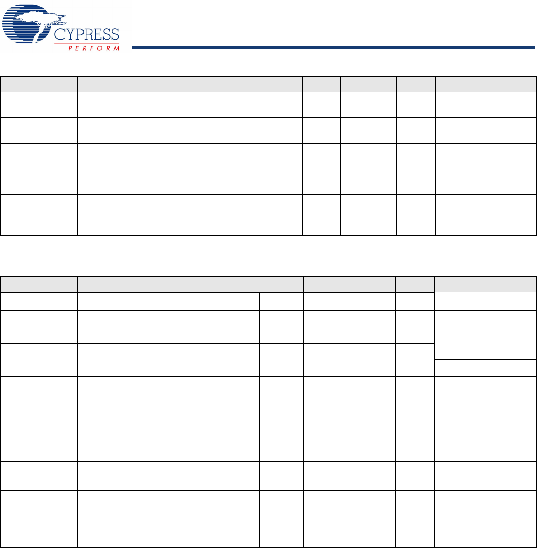
PRELIMINARY CYBLE-224110-00
Document Number: 002-11264 Rev. *A Page 23 of 43
CSD
A_INL Integral nonlinearity. VDDD = 1.71V to 3.6V,
1 Msps –1.5 – 1.7 LSB VREF = 1.71V to VDD
A_INL Integral nonlinearity. VDD = 1.71V to 5.5V,
500 Ksps –1.5 – 1.7 LSB VREF = 1V to VDD
A_dnl Differential nonlinearity. VDD = 1.71V to 5.5V,
1 Msps –1 – 2.2 LSB VREF = 1V to VDD
A_DNL Differential nonlinearity. VDD = 1.71V to 3.6V,
1 Msps –1 – 2 LSB VREF = 1.71V to VDD
A_DNL Differential nonlinearity. VDD = 1.71V to 5.5V,
500 Ksps –1 – 2.2 LSB VREF = 1V to VDD
A_THD Total harmonic distortion – – –65 dB FIN = 10 kHz
Table 23. SAR ADC AC Specifications (continued)
Parameter Description Min Typ Max Unit Details/Conditions
Table 24. CSD Block Specifications
Parameter Description Min Typ Max Unit Details/Conditions
VCSD Voltage range of operation 1.71 – 5.5 V –
IDAC1 DNL for 8-bit resolution –1 – 1 LSB –
IDAC1 INL for 8-bit resolution –3 – 3 LSB –
IDAC2 DNL for 7-bit resolution –1 – 1 LSB –
IDAC2 INL for 7-bit resolution –3 – 3 LSB
SNR Ratio of counts of finger to noise 5 – – Ratio
Capacitance range of
9 pF to 35 pF, 0.1-pF
sensitivity. Radio is not
operating during the
scan
IDAC1_CRT1 Output current of IDAC1 (8 bits) in High
range –612 – µA –
IDAC1_CRT2 Output current of IDAC1 (8 bits) in Low
range –306 – µA –
IDAC2_CRT1 Output current of IDAC2 (7 bits) in High
range –305 – µA –
IDAC2_CRT2 Output current of IDAC2 (7 bits) in Low
range –153 – µA –
PRELIMINARY CYBLE-224110-00
Document Number: 002-11264 Rev. *A Page 24 of 43
Digital Peripherals
Timer
Counter
Pulse Width Modulation (PWM)
Table 25. Timer DC Specifications
Parameter Description Min Typ Max Unit Details/Conditions
ITIM1 Block current consumption at 3 MHz – – 42 µA 16-bit timer
ITIM2 Block current consumption at 12 MHz – – 130 µA 16-bit timer
ITIM3 Block current consumption at 48 MHz – – 535 µA 16-bit timer
Table 26. Timer AC Specifications
Parameter Description Min Typ Max Unit Details/Conditions
TTIMFREQ Operating frequency FCLK –48MHz –
TCAPWINT Capture pulse width (internal) 2 × TCLK ––ns –
TCAPWEXT Capture pulse width (external) 2 × TCLK ––ns –
TTIMRES Timer resolution TCLK ––ns –
TTENWIDINT Enable pulse width (internal) 2 × TCLK ––ns –
TTENWIDEXT Enable pulse width (external) 2 × TCLK ––ns –
TTIMRESWINT Reset pulse width (internal) 2 × TCLK ––ns –
TTIMRESEXT Reset pulse width (external) 2 × TCLK ––ns –
Table 27. Counter DC Specifications
Parameter Description Min Typ Max Unit Details/Conditions
ICTR1 Block current consumption at 3 MHz – – 42 µA 16-bit counter
ICTR2 Block current consumption at 12 MHz – – 130 µA 16-bit counter
ICTR3 Block current consumption at 48 MHz – – 535 µA 16-bit counter
Table 28. Counter AC Specifications
Parameter Description Min Typ Max Unit Details/Conditions
TCTRFREQ Operating frequency FCLK –48MHz –
TCTRPWINT Capture pulse width (internal) 2 × TCLK ––ns –
TCTRPWEXT Capture pulse width (external) 2 × TCLK ––ns –
TCTRES Counter Resolution TCLK ––ns –
TCENWIDINT Enable pulse width (internal) 2 × TCLK ––ns –
TCENWIDEXT Enable pulse width (external) 2 × TCLK ––ns –
TCTRRESWINT Reset pulse width (internal) 2 × TCLK ––ns –
TCTRRESWEXT Reset pulse width (external) 2 × TCLK –– ns –
Table 29. PWM DC Specifications
Parameter Description Min Typ Max Unit Details/Conditions
IPWM1 Block current consumption at 3 MHz – – 42 µA 16-bit PWM
IPWM2 Block current consumption at 12 MHz – – 130 µA 16-bit PWM
IPWM3 Block current consumption at 48 MHz – – 535 µA 16-bit PWM

PRELIMINARY CYBLE-224110-00
Document Number: 002-11264 Rev. *A Page 25 of 43
LCD Direct Drive
Table 30. PWM AC Specifications
Parameter Description Min Typ Max Unit Details/Conditions
TPWMFREQ Operating frequency FCLK –48MHz –
TPWMPWINT Pulse width (internal) 2 × TCLK ––ns –
TPWMEXT Pulse width (external) 2 × TCLK ––ns –
TPWMKILLINT Kill pulse width (internal) 2 × TCLK ––ns –
TPWMKILLEXT Kill pulse width (external) 2 × TCLK ––ns –
TPWMEINT Enable pulse width (internal) 2 × TCLK ––ns –
TPWMENEXT Enable pulse width (external) 2 × TCLK ––ns –
TPWMRESWINT Reset pulse width (internal) 2 × TCLK ––ns –
TPWMRESWEXT Reset pulse width (external) 2 × TCLK ––ns –
Table 31. LCD Direct Drive DC Specifications
Spec ID Parameter Description Min Typ Max Unit Details/Conditions
SID228 ILCDLOW Operating current in low-power mode – 17.5 – µA 16 × 4 small segment
display at 50 Hz
SID229 CLCDCAP LCD capacitance per segment/common
driver – 500 5000 pF –
SID230 LCDOFFSET Long-term segment offset – 20 – mV –
SID231 ILCDOP1 LCD system operating current
VBIAS = 5V –2–mA
32 × 4 segments.
50 Hz at 25 °C
SID232 ILCDOP2 LCD system operating current
VBIAS = 3.3V –2–mA
32 × 4 segments
50 Hz at 25 °C
Table 32. LCD Direct Drive AC Specifications
Spec ID Parameter Description Min Typ Max Unit Details/Conditions
SID233 FLCD LCD frame rate 10 50 150 Hz –
PRELIMINARY CYBLE-224110-00
Document Number: 002-11264 Rev. *A Page 26 of 43
Serial Communication
Table 33. Fixed I2C DC Specifications
Table 35. Fixed UART DC Specifications
Parameter Description Min Typ Max Unit Details/Conditions
II2C1 Block current consumption at 100 kHz – – 50 µA –
II2C2 Block current consumption at 400 kHz – – 155 µA –
II2C3 Block current consumption at 1 Mbps – – 390 µA –
II2C4 I2C enabled in Deep-Sleep mode – – 1.4 µA –
Table 34. Fixed I2C AC Specifications
Parameter Description Min Typ Max Unit Details/Conditions
FI2C1 Bit rate – – 400 kHz
Parameter Description Min Typ Max Unit Details/Conditions
IUART1 Block current consumption at 100 kbps – – 55 µA –
IUART2 Block current consumption at 1000 kbps – – 312 µA –
Table 36. Fixed UART AC Specifications
Parameter Description Min Typ Max Unit Details/Conditions
FUART Bit rate – – 1 Mbps –
Table 37. Fixed SPI DC Specifications
Parameter Description Min Typ Max Unit Details/Conditions
ISPI1 Block current consumption at 1 Mbps – – 360 µA –
ISPI2 Block current consumption at 4 Mbps – – 560 µA –
ISPI3 Block current consumption at 8 Mbps – – 600 µA –
Table 38. Fixed SPI AC Specifications
Parameter Description Min Typ Max Unit Details/Conditions
FSPI SPI operating frequency (master; 6x over sampling) – – 8 MHz –
Table 39. Fixed SPI Master Mode AC Specifications
Parameter Description Min Typ Max Unit Details/Conditions
TDMO MOSI valid after SCLK driving edge – – 18 ns –
TDSI MISO valid before SCLK capturing edge
Full clock, late MISO sampling used 20 – – ns Full clock, late MISO sampling
THMO Previous MOSI data hold time 0 – – ns Referred to Slave capturing edge
Table 40. Fixed SPI Slave Mode AC Specifications
Parameter Description Min Typ Max Unit
TDMI MOSI valid before SCLK capturing edge 40 – – ns
TDSO MISO valid after SCLK driving edge – – 42 + 3 × TCPU ns
TDSO_ext MISO Valid after SCLK driving edge in
external clock mode. VDD < 3.0V – – 50 ns
THSO Previous MISO data hold time 0 – – ns
PRELIMINARY CYBLE-224110-00
Document Number: 002-11264 Rev. *A Page 27 of 43
Memory
System Resources
Power-on-Reset (POR)
TSSELSCK SSEL valid to first SCK valid edge 100 – – ns
Table 40. Fixed SPI Slave Mode AC Specifications (continued)
Parameter Description Min Typ Max Unit
Note
5. It can take as much as 20 ms to write to flash. During this time, the device should not be reset, or flash operations will be interrupted and cannot be relied on to have
completed. Reset sources include the XRES pin, software resets, CPU lockup states and privilege violations, improper power supply levels, and watchdogs. Make
certain that these are not inadvertently activated.
Table 41. Flash DC Specifications
Parameter Description Min Typ Max Unit Details/Conditions
VPE Erase and program voltage 1.71 – 5.5 V –
TWS48 Number of Wait states at 32–48 MHz 2 – – – CPU execution from flash
TWS32 Number of Wait states at 16–32 MHz 1 – – – CPU execution from flash
TWS16 Number of Wait states for 0–16 MHz 0 – – – CPU execution from flash
Table 42. Flash AC Specifications
Parameter Description Min Typ Max Unit Details/Conditions
TROWWRITE[5] Row (block) write time (erase and program) – – 20 ms Row (block) = 256 bytes
TROWERASE[5] Row erase time – – 13 ms –
TROWPROGRAM[5] Row program time after erase – – 7 ms –
TBULKERASE[5] Bulk erase time (256 KB) – – 35 ms –
TDEVPROG[5] Total device program time – – 25 seconds –
FEND Flash endurance 100 K – – cycles –
FRET Flash retention. TA ≤ 55 °C, 100 K P/E cycles 20 – – years –
FRET2 Flash retention. TA ≤ 85 °C, 10 K P/E cycles 10 – – years –
Table 43. POR DC Specifications
Parameter Description Min Typ Max Unit Details/Conditions
VRISEIPOR Rising trip voltage 0.80 – 1.45 V –
VFALLIPOR Falling trip voltage 0.75 – 1.40 V –
VIPORHYST Hysteresis 15 – 200 mV –
Table 44. POR AC Specifications
Parameter Description Min Typ Max Unit Details/Conditions
TPPOR_TR Precision power-on reset (PPOR) response
time in Active and Sleep modes ––1µs –
Table 45. Brown-Out Detect
Parameter Description Min Typ Max Unit Details/Conditions
VFALLPPOR BOD trip voltage in Active and Sleep modes 1.64 – – V –
VFALLDPSLP BOD trip voltage in Deep Sleep 1.4 – – V –
PRELIMINARY CYBLE-224110-00
Document Number: 002-11264 Rev. *A Page 28 of 43
Voltage Monitors (LVD)
SWD Interface
Table 46. Hibernate Reset
Parameter Description Min Typ Max Unit Details/Conditions
VHBRTRIP BOD trip voltage in Hibernate 1.1 – – V –
Table 47. Voltage Monitor DC Specifications
Parameter Description Min Typ Max Unit Details/Conditions
VLVI1 LVI_A/D_SEL[3:0] = 0000b 1.71 1.75 1.79 V –
VLVI2 LVI_A/D_SEL[3:0] = 0001b 1.76 1.80 1.85 V –
VLVI3 LVI_A/D_SEL[3:0] = 0010b 1.85 1.90 1.95 V –
VLVI4 LVI_A/D_SEL[3:0] = 0011b 1.95 2.00 2.05 V –
VLVI5 LVI_A/D_SEL[3:0] = 0100b 2.05 2.10 2.15 V –
VLVI6 LVI_A/D_SEL[3:0] = 0101b 2.15 2.20 2.26 V –
VLVI7 LVI_A/D_SEL[3:0] = 0110b 2.24 2.30 2.36 V –
VLVI8 LVI_A/D_SEL[3:0] = 0111b 2.34 2.40 2.46 V –
VLVI9 LVI_A/D_SEL[3:0] = 1000b 2.44 2.50 2.56 V –
VLVI10 LVI_A/D_SEL[3:0] = 1001b 2.54 2.60 2.67 V –
VLVI11 LVI_A/D_SEL[3:0] = 1010b 2.63 2.70 2.77 V –
VLVI12 LVI_A/D_SEL[3:0] = 1011b 2.73 2.80 2.87 V –
VLVI13 LVI_A/D_SEL[3:0] = 1100b 2.83 2.90 2.97 V –
VLVI14 LVI_A/D_SEL[3:0] = 1101b 2.93 3.00 3.08 V –
VLVI15 LVI_A/D_SEL[3:0] = 1110b 3.12 3.20 3.28 V –
VLVI16 LVI_A/D_SEL[3:0] = 1111b 4.39 4.50 4.61 V –
LVI_IDD Block current – – 100 µA –
Table 48. Voltage Monitor AC Specifications
Parameter Description Min Typ Max Unit Details/Conditions
TMONTRIP Voltage monitor trip time – – 1 µs –
Table 49. SWD Interface Specifications
Parameter Description Min Typ Max Unit Details/Conditions
F_SWDCLK1 3.3V ≤ VDD ≤ 5.5V – – 14 MHz SWDCLK ≤ 1/3 CPU clock frequency
F_SWDCLK2 1.71V ≤ VDD ≤ 3.3V – – 7 MHz SWDCLK ≤ 1/3 CPU clock frequency
T_SWDI_SETUP T = 1/f SWDCLK 0.25 × T – – ns –
T_SWDI_HOLD T = 1/f SWDCLK 0.25 × T – – ns –
T_SWDO_VALID T = 1/f SWDCLK – – 0.5 × T ns –
T_SWDO_HOLD T = 1/f SWDCLK 1 – – ns –
PRELIMINARY CYBLE-224110-00
Document Number: 002-11264 Rev. *A Page 29 of 43
Internal Main Oscillator
Internal Low-Speed Oscillator
Table 50. IMO DC Specifications
Parameter Description Min Typ Max Unit Details/Conditions
IIMO1 IMO operating current at 48 MHz – – 1000 µA –
IIMO2 IMO operating current at 24 MHz – – 325 µA –
IIMO3 IMO operating current at 12 MHz – – 225 µA –
IIMO4 IMO operating current at 6 MHz – – 180 µA –
IIMO5 IMO operating current at 3 MHz – – 150 µA –
Table 51. IMO AC Specifications
Parameter Description Min Typ Max Unit Details/Conditions
FIMOTOL3 Frequency variation from 3 to 48 MHz – – ±2 % With API-called calibration
FIMOTOL3 IMO startup time – 12 – µs –
Table 52. ILO DC Specifications
Parameter Description Min Typ Max Unit Details/Conditions
IILO2 ILO operating current at 32 kHz – 0.3 1.05 µA –
Table 53. ILO AC Specifications
Parameter Description Min Typ Max Unit Details/Conditions
TSTARTILO1 ILO startup time – – 2 ms –
FILOTRIM1 32-kHz trimmed frequency 15 32 50 kHz –
Table 54. ECO Trim Value Specification
Parameter Description Value Details/Conditions
ECOTRIM 24-MHz trim value
(firmware configuration) 0x00003FFA Optimum trim value that needs to be loaded to register
CY_SYS_XTAL_BLERD_BB_XO_CAPTRIM_REG
Table 55. UDB AC Specifications
Parameter Description Min Typ Max Unit Details/Conditions
Data Path Performance
FMAX-TIMER Max frequency of 16-bit timer in a UDB
pair ––48MHz –
FMAX-ADDER Max frequency of 16-bit adder in a UDB
pair ––48MHz –
FMAX_CRC Max frequency of 16-bit CRC/PRS in a
UDB pair ––48MHz –
PLD Performance in UDB
FMAX_PLD Max frequency of 2-pass PLD function
in a UDB pair ––48MHz –
Clock to Output Performance
TCLK_OUT_UDB1 Prop. delay for clock in to data out at
25 °C, Typical –15 – ns –

PRELIMINARY CYBLE-224110-00
Document Number: 002-11264 Rev. *A Page 30 of 43
TCLK_OUT_UDB2 Prop. delay for clock in to data out,
Worst case –25 – ns –
Table 56. BLE Subsystem
Parameter Description Min Typ Max Unit Details/Conditions
RF Receiver Specification
RXS, DIRTY RX sensitivity with dirty transmitter – –95 – dBm With LNA active
RXS, LOWGAIN RX sensitivity in low-gain mode with idle
transmitter – –87 – dBm LNA in bypass mode
RXS, HIGHGAIN RX sensitivity in high-gain mode with idle
transmitter – –95 – dBm With LNA active
PRXMAX Maximum input power –10 –1 – dBm RF-PHY Specification
(RCV-LE/CA/06/C)
CI1
Cochannel interference,
Wanted signal at –67 dBm and Interferer
at FRX
– 9 21 dB RF-PHY Specification
(RCV-LE/CA/03/C)
CI2
Adjacent channel interference
Wanted signal at –67 dBm and Interferer
at FRX ±1 MHz
–TBD –dB RF-PHY Specification
(RCV-LE/CA/03/C)
CI3
Adjacent channel interference
Wanted signal at –67 dBm and Interferer
at FRX ±2 MHz
–TBD –dB RF-PHY Specification
(RCV-LE/CA/03/C)
CI4
Adjacent channel interference
Wanted signal at –67 dBm and Interferer
at ≥FRX ±3 MHz
–TBD –dB RF-PHY Specification
(RCV-LE/CA/03/C)
CI5
Adjacent channel interference
Wanted Signal at –67 dBm and Interferer
at Image frequency (FIMAGE)
–TBD –dB RF-PHY Specification
(RCV-LE/CA/03/C)
CI3
Adjacent channel interference
Wanted signal at –67 dBm and Interferer
at Image frequency (FIMAGE ± 1 MHz)
–TBD –dB RF-PHY Specification
(RCV-LE/CA/03/C)
OBB1
Out-of-band blocking,
Wanted signal at –67 dBm and Interferer
at F = 30–2000 MHz
–TBD –dBm RF-PHY Specification
(RCV-LE/CA/04/C)
OBB2
Out-of-band blocking,
Wanted signal at –67 dBm and Interferer
at F = 2003–2399 MHz
–TBD –dBm RF-PHY Specification
(RCV-LE/CA/04/C)
OBB3
Out-of-band blocking,
Wanted signal at –67 dBm and Interferer
at F = 2484–2997 MHz
–TBD –dBm RF-PHY Specification
(RCV-LE/CA/04/C)
OBB4
Out-of-band blocking,
Wanted signal a –67 dBm and Interferer
at F = 3000–12750 MHz
–TBD –dBm RF-PHY Specification
(RCV-LE/CA/04/C)
IMD
Intermodulation performance
Wanted signal at –64 dBm and 1-Mbps
BLE, third, fourth, and fifth offset channel
–TBD –dBm RF-PHY Specification
(RCV-LE/CA/05/C)
Table 55. UDB AC Specifications (continued)
Parameter Description Min Typ Max Unit Details/Conditions

PRELIMINARY CYBLE-224110-00
Document Number: 002-11264 Rev. *A Page 31 of 43
RXSE1 Receiver spurious emission
30 MHz to 1.0 GHz –TBD –dBm
100-kHz measurement
bandwidth
ETSI EN300 328 V1.8.1
RXSE2 Receiver spurious emission
1.0 GHz to 12.75 GHz –TBD –dBm
1-MHz measurement
bandwidth
ETSI EN300 328 V1.8.1
RF Transmitter Specifications
TXP, ACC RF power accuracy – ±1 – dB –
TXP, RANGE RF power control range – 30 – dB –
TXP, 0dBm Output power, 0-dB Gain setting (PA7) – – -6 dBm –
TXP, MAX Output power, maximum power setting
(PA10) –9.5 – dBm –
TXP, MIN Output power, minimum power setting
(PA1) – –18 – dBm –
F2AVG Average frequency deviation for
10101010 pattern 185 – – kHz RF-PHY Specification
(TRM-LE/CA/05/C)
F1AVG Average frequency deviation for
11110000 pattern 225 250 275 kHz RF-PHY Specification
(TRM-LE/CA/05/C)
EO Eye opening = ΔF2AVG/ΔF1AVG TBD – – RF-PHY Specification
(TRM-LE/CA/05/C)
FTX, ACC Frequency accuracy –150 – 150 kHz RF-PHY Specification
(TRM-LE/CA/06/C)
FTX, MAXDR Maximum frequency drift –50 – 50 kHz RF-PHY Specification
(TRM-LE/CA/06/C)
FTX, INITDR Initial frequency drift –20 – 20 kHz RF-PHY Specification
(TRM-LE/CA/06/C)
FTX, DR Maximum drift rate –20 – 20 kHz/
50 µs
RF-PHY Specification
(TRM-LE/CA/06/C)
IBSE1 In-band spurious emission at 2-MHz
offset ––TBDdBm
RF-PHY Specification
(TRM-LE/CA/03/C)
IBSE2 In-band spurious emission at ≥3-MHz
offset ––TBDdBm
RF-PHY Specification
(TRM-LE/CA/03/C)
TXSE1 Transmitter spurious emissions
(average), <1.0 GHz – – TBD dBm FCC-15.247
TXSE2 Transmitter spurious emissions
(average), >1.0 GHz – – TBD dBm FCC-15.247
RF Current Specifications
IRX Receive current in normal mode – 18.7 – mA Radio only
IRX_RF Radio receive current in normal mode – 16.4 – mA Radio only
IRX, HIGHGAIN Receive current in high-gain mode – 21.5 – mA Radio only
ITX, 3dBm TX current at 3-dBm setting (PA10) – 20 – mA Radio only
ITX, 0dBm TX current at 0-dBm setting (PA7) – 16.5 – mA Radio only
ITX_RF, 0dBm Radio TX current at 0 dBm setting (PA7) – 15.6 – mA Radio only
Table 56. BLE Subsystem (continued)
Parameter Description Min Typ Max Unit Details/Conditions
PRELIMINARY CYBLE-224110-00
Document Number: 002-11264 Rev. *A Page 32 of 43
ITX_RF, 0dBm Radio TX current at 0 dBm excluding
Balun loss – 14.2 – mA Guaranteed by design
simulation
ITX,-3dBm TX current at –3-dBm setting (PA4) – 15.5 – mA Radio only
ITX,-6dBm TX current at –6-dBm setting (PA3) – 14.5 – mA Radio only
ITX,-12dBm TX current at –12-dBm setting (PA2) – 13.2 – mA Radio only
ITX,-18dBm TX current at –18-dBm setting (PA1) – 12.5 – mA Radio only
Iavg_1sec, 0dBm Average current at 1-second BLE
connection interval – 26.3 – µA
TXP: +9.5 dBm; ±20-ppm
master and slave clock
accuracy.
For empty PDU exchange
PA/LNA active
Iavg_4sec, 0dBm Average current at 4-second BLE
connection interval –TBD – µA
TXP: +9.5 dBm; ±20-ppm
master and slave clock
accuracy.
For empty PDU exchange
PA/LNA active
General RF Specifications
FREQ RF operating frequency 2400 – 2482 MHz –
CHBW Channel spacing – 2 – MHz –
DR On-air data rate – 1000 – kbps –
IDLE2TX BLE.IDLE to BLE. TX transition time – 120 140 µs –
IDLE2RX BLE.IDLE to BLE. RX transition time – 75 120 µs –
RSSI Specifications
RSSI, ACC RSSI accuracy – ±5 – dB –
RSSI, RES RSSI resolution – 1 – dB –
RSSI, PER RSSI sample period – 6 – µs –
Table 56. BLE Subsystem (continued)
Parameter Description Min Typ Max Unit Details/Conditions
PRELIMINARY CYBLE-224110-00
Document Number: 002-11264 Rev. *A Page 33 of 43
Environmental Specifications
Environmental Compliance
This Cypress BLE module is built in compliance with the Restriction of Hazardous Substances (RoHS) and Halogen Free (HF)
directives. The Cypress module and components used to produce this module are RoHS and HF compliant.
RF Certification
The CYBLE-224110-00 module is certified under the following RF certification standards:
nFCC ID: WAP4110
nCE
nIC: 7922A-4110
nMIC
nKC
Environmental Conditions
Table 57 describes the operating and storage conditions for the Cypress BLE module.
ESD and EMI Protection
Exposed components require special attention to ESD and electromagnetic interference (EMI).
A grounded conductive layer inside the device enclosure is suggested for EMI and ESD performance. Any openings in the enclosure
near the module should be surrounded by a grounded conductive layer to provide ESD protection and a low-impedance path to ground.
Device Handling: Proper ESD protocol must be followed in manufacturing to ensure component reliability.
Table 57. Environmental Conditions for CYBLE-224110-00
Description Minimum Specification Maximum Specification
Operating temperature –40 °C 105 °C
Operating humidity (relative, non-condensation) 5% 85%
Thermal ramp rate – 3 °C/minute
Storage temperature –40 °C 105 °C
Storage temperature and humidity – 105 ° C at 85%
ESD: Module integrated into system Components[6] –15 kV Air
2.2 kV Contact
Note
6. This does not apply to the RF pins (ANT, XTALI, and XTALO). RF pins (ANT, XTALI, and XTALO) are tested for 500-V HBM.

PRELIMINARY CYBLE-224110-00
Document Number: 002-11264 Rev. *A Page 34 of 43
Regulatory Information
FCC
FCC NOTICE:
The device CYBLE-224110-00 complies with Part 15 of the FCC Rules. The device meets the requirements for modular transmitter
approval as detailed in FCC public Notice DA00-1407. Transmitter Operation is subject to the following two conditions: (1) This device
may not cause harmful interference, and (2) This device must accept any interference received, including interference that may cause
undesired operation.
CAUTION:
The FCC requires the user to be notified that any changes or modifications made to this device that are not expressly approved by
Cypress Semiconductor may void the user's authority to operate the equipment.
This equipment has been tested and found to comply with the limits for a Class B digital device, pursuant to Part 15 of the FCC Rules.
These limits are designed to provide reasonable protection against harmful interference in a residential installation. This equipment
generates and can radiate radio frequency energy and, if not installed and used in accordance with the instructions,ê may cause
harmful interference to radio communications. However, there is no guarantee that interference will not occur in a particular installation.
If this equipment does cause harmful interference to radio or television reception, which can be determined by turning the equipment
off and on, the user is encouraged to try to correct the interference by one or more of the following measures:
nReorient or relocate the receiving antenna.
nIncrease the separation between the equipment and receiver.
nConnect the equipment into an outlet on a circuit different from that to which the receiver is connected.
nConsult the dealer or an experienced radio/TV technician for help
LABELING REQUIREMENTS:
The Original Equipment Manufacturer (OEM) must ensure that FCC labelling requirements are met. This includes a clearly visible
label on the outside of the OEM enclosure specifying the appropriate Cypress Semiconductor FCC identifier for this product as well
as the FCC Notice above. The FCC identifier is FCC ID: WAP4110.
In any case the end product must be labeled exterior with "Contains FCC ID: WAP4110"
ANTENNA WARNING:
This device is tested with a standard SMA connector and with the antennas listed in Table 7 on page 15. When integrated in the OEMs
product, these fixed antennas require installation preventing end-users from replacing them with non-approved antennas. Any antenna
not in the following table must be tested to comply with FCC Section 15.203 for unique antenna connectors and Section 15.247 for
emissions.
RF EXPOSURE:
To comply with FCC RF Exposure requirements, the Original Equipment Manufacturer (OEM) must ensure to install the approved
antenna in the previous.
The preceding statement must be included as a CAUTION statement in manuals, for products operating with the approved antennas
in Table 7 on page 15, to alert users on FCC RF Exposure compliance. Any notification to the end user of installation or removal
instructions about the integrated radio module is not allowed.
The radiated output power of CYBLE-224110-00 is far below the FCC radio frequency exposure limits. Nevertheless, use
CYBLE-224110-00 in such a manner that minimizes the potential for human contact during normal operation.
End users may not be provided with the module installation instructions. OEM integrators and end users must be provided with
transmitter operating conditions for satisfying RF exposure compliance.
PRELIMINARY CYBLE-224110-00
Document Number: 002-11264 Rev. *A Page 35 of 43
Industry Canada (IC) Certification
CYBLE-224110-00 is licensed to meet the regulatory requirements of Industry Canada (IC),
License: IC: 7922A-4110
Manufacturers of mobile, fixed or portable devices incorporating this module are advised to clarify any regulatory questions and ensure
compliance for SAR and/or RF exposure limits. Users can obtain Canadian information on RF exposure and compliance from
www.ic.gc.ca.
This device has been designed to operate with the antennas listed in Table 7 on page 15, having a maximum gain of 0.5 dBi. Antennas
not included in this list or having a gain greater than 0.5 dBi are strictly prohibited for use with this device. The required antenna
impedance is 50 ohms. The antenna used for this transmitter must not be co-located or operating in conjunction with any other antenna
or transmitter.
IC NOTICE:
The device CYBLE-224110-00 complies with Canada RSS-GEN Rules. The device meets the requirements for modular transmitter
approval as detailed in RSS-GEN. Operation is subject to the following two conditions: (1) This device may not cause harmful
interference, and (2) This device must accept any interference received, including interference that may cause undesired operation.
IC RADIATION EXPOSURE STATEMENT FOR CANADA
This device complies with Industry Canada licence-exempt RSS standard(s). Operation is subject to the following two conditions: (1)
this device may not cause interference, and (2) this device must accept any interference, including interference that may cause
undesired operation of the device.
Le présent appareil est conforme aux CNR d'Industrie Canada applicables aux appareils radio exempts de licence. L'exploitation est
autorisée aux deux conditions suivantes : (1) l'appareil ne doit pas produire de brouillage, et (2) l'utilisateur de l'appareil doit accepter
tout brouillage radioélectrique subi, même si le brouillage est susceptible d'en compromettre le fonctionnement.
LABELING REQUIREMENTS:
The Original Equipment Manufacturer (OEM) must ensure that IC labelling requirements are met. This includes a clearly visible label
on the outside of the OEM enclosure specifying the appropriate Cypress Semiconductor IC identifier for this product as well as the IC
Notice above. The IC identifier is 7922A-4110. In any case, the end product must be labeled in its exterior with "Contains IC:
7922A-4110".
European R&TTE Declaration of Conformity
Hereby, Cypress Semiconductor declares that the Bluetooth module CYBLE-224110-00 complies with the essential requirements and
other relevant provisions of Directive 1999/5/EC. As a result of the conformity assessment procedure described in Annex III of the
Directive 1999/5/EC, the end-customer equipment should be labeled as follows:
All versions of the CYBLE-224110-00 in the specified reference design can be used in the following countries: Austria, Belgium,
Cyprus, Czech Republic, Denmark, Estonia, Finland, France, Germany, Greece, Hungary, Ireland, Italy, Latvia, Lithuania, Luxem-
bourg, Malta, Poland, Portugal, Slovakia, Slovenia, Spain, Sweden, The Netherlands, the United Kingdom, Switzerland, and Norway.
PRELIMINARY CYBLE-224110-00
Document Number: 002-11264 Rev. *A Page 36 of 43
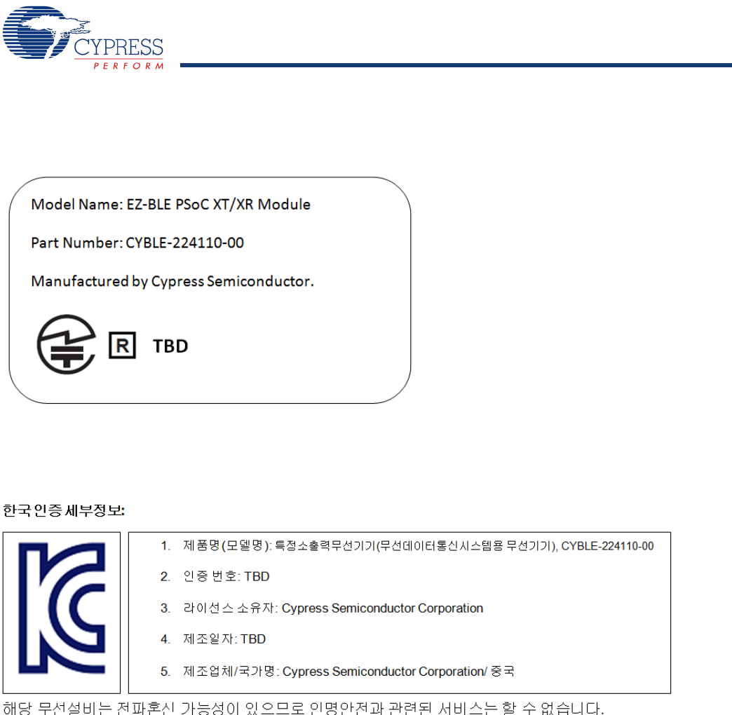
MIC Japan
CYBLE-224110-00 is certified as a module with type certification number TBD. End products that integrate CYBLE-224110-00 do not
need additional MIC Japan certification for the end product.
End product can display the certification label of the embedded module.
KC Korea
CYBLE-224110-00 is certified for use in Korea with certificate number TBD.

PRELIMINARY CYBLE-224110-00
Document Number: 002-11264 Rev. *A Page 37 of 43
Packaging
Table 58. Solder Reflow Peak Temperature
Module Part Number Package Maximum Peak Temperature Maximum Time at PeakTemperature No. of Cycles
CYBLE-224110-00 32-pad SMT 260 °C 30 seconds 2
Table 59. Package Moisture Sensitivity Level (MSL), IPC/JEDEC J-STD-2
Module Part Number Package MSL
CYBLE-224110-00 32-pad SMT MSL 3
PRELIMINARY CYBLE-224110-00
Document Number: 002-11264 Rev. *A Page 38 of 43
Ordering Information
Table 60 lists the CYBLE-224110-00 part number and features.
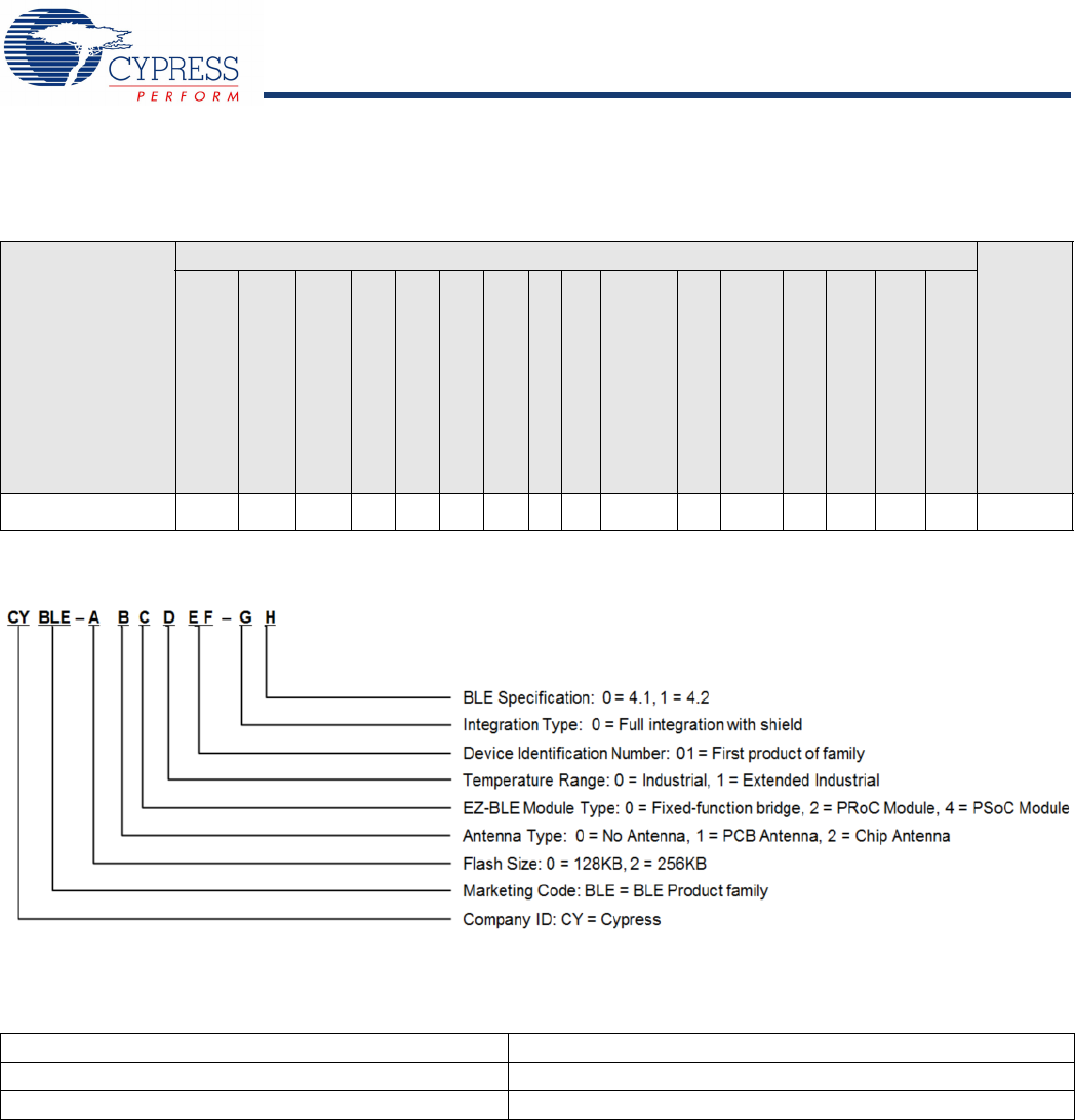
Part Numbering Convention
The part numbers are of the form CYBLE-ABCDEF-GH where the fields are defined as follows.
For additional information and a complete list of Cypress Semiconductor BLE products, contact your local Cypress sales
representative. To locate the nearest Cypress office, visit our website.
Table 60. Ordering Information
MPN
Features
Package
Max CPU Speed (MHz)
Flash (KB)
SRAM (KB)
Power Amplier (PA)
Low Noise Amplifier (LNA)
UDB
Opamp (CTBm)
CapSense
Direct LCD Drive
12-bit SAR ADC
LP Comparators
TCPWM Blocks
SCB Blocks
PWMs (using UDBs)
I2S (using UDB)
GPIO
CYBLE-224110-00 48 256 32 3 3 4 4 3 3 1 Msps 1 4 2 4 325 32-SMT
U.S. Cypress Headquarters Address 198 Champion Court, San Jose, CA 95134
U.S. Cypress Headquarter Contact Info (408) 943-2600
Cypress website address http://www.cypress.com
PRELIMINARY CYBLE-224110-00
Document Number: 002-11264 Rev. *A Page 39 of 43
Acronyms
Table 61. Acronyms Used in this Document
Acronym Description
ABUS analog local bus
ADC analog-to-digital converter
AG analog global
AHB
AMBA (advanced microcontroller bus
architecture) high-performance bus, an ARM data
transfer bus
ALU arithmetic logic unit
AMUXBUS analog multiplexer bus
API application programming interface
APSR application program status register
ARM®advanced RISC machine, a CPU architecture
ATM automatic thump mode
BLE Bluetooth Low Energy
Bluetooth
SIG Bluetooth Special Interest Group
BW bandwidth
CAN Controller Area Network, a communications
protocol
CE European Conformity
CSA Canadian Standards Association
CMRR common-mode rejection ratio
CPU central processing unit
CRC cyclic redundancy check, an error-checking
protocol
DAC digital-to-analog converter, see also IDAC, VDAC
DFB digital filter block
DIO digital input/output, GPIO with only digital
capabilities, no analog. See GPIO.
DMIPS Dhrystone million instructions per second
DMA direct memory access, see also TD
DNL differential nonlinearity, see also INL
DNU do not use
DR port write data registers
DSI digital system interconnect
DWT data watchpoint and trace
ECC error correcting code
ECO external crystal oscillator
EEPROM electrically erasable programmable read-only
memory
EMI electromagnetic interference
EMIF external memory interface
EOC end of conversion
EOF end of frame
EPSR execution program status register
ESD electrostatic discharge
ETM embedded trace macrocell
FCC Federal Communications Commission
FET field-effect transistor
FIR finite impulse response, see also IIR
FPB flash patch and breakpoint
FS full-speed
GPIO general-purpose input/output, applies to a PSoC
pin
HCI host controller interface
HVI high-voltage interrupt, see also LVI, LVD
IC integrated circuit
IDAC current DAC, see also DAC, VDAC
IDE integrated development environment
I2C, or IIC Inter-Integrated Circuit, a communications protocol
IC Industry Canada
IIR infinite impulse response, see also FIR
ILO internal low-speed oscillator, see also IMO
IMO internal main oscillator, see also ILO
INL integral nonlinearity, see also DNL
I/O input/output, see also GPIO, DIO, SIO, USBIO
IPOR initial power-on reset
IPSR interrupt program status register
IRQ interrupt request
ITM instrumentation trace macrocell
KC Korea Certification
LCD liquid crystal display
LIN Local Interconnect Network, a communications
protocol.
LNA low noise amplifier
LR link register
LUT lookup table
LVD low-voltage detect, see also LVI
LVI low-voltage interrupt, see also HVI
LVTTL low-voltage transistor-transistor logic
Table 61. Acronyms Used in this Document (continued)
Acronym Description
PRELIMINARY CYBLE-224110-00
Document Number: 002-11264 Rev. *A Page 40 of 43
MAC multiply-accumulate
MCU microcontroller unit
MIC Ministry of Internal Affairs and Communications
(Japan)
MISO master-in slave-out
NC no connect
NMI nonmaskable interrupt
NRZ non-return-to-zero
NVIC nested vectored interrupt controller
NVL nonvolatile latch, see also WOL
Opamp operational amplifier
PA power amplifier
PAL programmable array logic, see also PLD
PC program counter
PCB printed circuit board
PGA programmable gain amplifier
PHUB peripheral hub
PHY physical layer
PICU port interrupt control unit
PLA programmable logic array
PLD programmable logic device, see also PAL
PLL phase-locked loop
PMDD package material declaration data sheet
POR power-on reset
PRES precise power-on reset
PRS pseudo random sequence
PS port read data register
PSoC®Programmable System-on-Chip™
PSRR power supply rejection ratio
PWM pulse-width modulator
QDID qualification design ID
RAM random-access memory
RISC reduced-instruction-set computing
RMS root-mean-square
RTC real-time clock
RTL register transfer language
RTR remote transmission request
RX receive
SAR successive approximation register
SC/CT switched capacitor/continuous time
Table 61. Acronyms Used in this Document (continued)
Acronym Description
SCL I2C serial clock
SDA I2C serial data
S/H sample and hold
SINAD signal to noise and distortion ratio
SIO special input/output, GPIO with advanced features.
See GPIO.
SMT
surface-mount technology; a method for producing
electronic circuitry in which the components are
placed directly onto the surface of PCBs
SOC start of conversion
SOF start of frame
SPI Serial Peripheral Interface, a communications
protocol
SR slew rate
SRAM static random access memory
SRES software reset
STN super twisted nematic
SWD serial wire debug, a test protocol
SWV single-wire viewer
TD transaction descriptor, see also DMA
THD total harmonic distortion
TIA transimpedance amplifier
TN twisted nematic
TRM technical reference manual
TTL transistor-transistor logic
TUV Germany: Technischer Überwachungs-Verein
(Technical Inspection Association)
TX transmit
UART Universal Asynchronous Transmitter Receiver, a
communications protocol
UDB universal digital block
USB Universal Serial Bus
USBIO USB input/output, PSoC pins used to connect to a
USB port
VDAC voltage DAC, see also DAC, IDAC
WDT watchdog timer
WOL write once latch, see also NVL
WRES watchdog timer reset
XRES external reset I/O pin
XTAL crystal
Table 61. Acronyms Used in this Document (continued)
Acronym Description

PRELIMINARY CYBLE-224110-00
Document Number: 002-11264 Rev. *A Page 41 of 43
Document Conventions
Units of Measure
Table 62. Units of Measure
Symbol Unit of Measure
°C degrees Celsius
dB decibel
dBm decibel-milliwatts
fF femtofarads
Hz hertz
KB 1024 bytes
kbps kilobits per second
Khr kilohour
kHz kilohertz
kΩkilo ohm
ksps kilosamples per second
LSB least significant bit
Mbps megabits per second
MHz megahertz
MΩmega-ohm
Msps megasamples per second
µA microampere
µF microfarad
µH microhenry
µs microsecond
µV microvolt
µW microwatt
mA milliampere
ms millisecond
mV millivolt
nA nanoampere
ns nanosecond
nV nanovolt
Ωohm
pF picofarad
ppm parts per million
ps picosecond
s second
sps samples per second
sqrtHz square root of hertz
Vvolt
PRELIMINARY CYBLE-224110-00
Document Number: 002-11264 Rev. *A Page 42 of 43
Document History Page
Document Title: CYBLE-224110-00, EZ-BLE™ PSoC® XT/XR Module
Document Number: 002-11264
Revision ECN Orig. of
Change
Submission
Date Description of Change
** 5144379 DSO 02/19/2016 Preliminary datasheet for CYBLE-224110-00 module.
*A Prelim-
inary
DSO 05/16/2016 Update datasheet to add FCC and IC certification numbers.

PRELIMINARY CYBLE-224110-00
© Cypress Semiconductor Corporation 2016. This document is the property of Cypress Semiconductor Corporation and its subsidiaries, including Spansion LLC ("Cypress"). This document, including
any software or firmware included or referenced in this document ("Software"), is owned by Cypress under the intellectual property laws and treaties of the United States and other countries worldwide.
Cypress reserves all rights under such laws and treaties and does not, except as specifically stated in this paragraph, grant any license under its patents, copyrights, trademarks, or other intellectual
property rights. If the Software is not accompanied by a license agreement and you do not otherwise have a written agreement with Cypress governing the use of the Software, then Cypress hereby
grants you under its copyright rights in the Software, a personal, non-exclusive, nontransferable license (without the right to sublicense) (a) for Software provided in source code form, to modify and
reproduce the Software solely for use with Cypress hardware products, only internally within your organization, and (b) to distribute the Software in binary code form externally to end users (either
directly or indirectly through resellers and distributors), solely for use on Cypress hardware product units. Cypress also grants you a personal, non-exclusive, nontransferable, license (without the right
to sublicense) under those claims of Cypress's patents that are infringed by the Software (as provided by Cypress, unmodified) to make, use, distribute, and import the Software solely to the minimum
extent that is necessary for you to exercise your rights under the copyright license granted in the previous sentence. Any other use, reproduction, modification, translation, or compilation of the Software
is prohibited.
CYPRESS MAKES NO WARRANTY OF ANY KIND, EXPRESS OR IMPLIED, WITH REGARD TO THIS DOCUMENT OR ANY SOFTWARE, INCLUDING, BUT NOT LIMITED TO, THE IMPLIED
WARRANTIES OF MERCHANTABILITY AND FITNESS FOR A PARTICULAR PURPOSE. Cypress reserves the right to make changes to this document without further notice. Cypress does not
assume any liability arising out of the application or use of any product or circuit described in this document. Any information provided in this document, including any sample design information or
programming code, is provided only for reference purposes. It is the responsibility of the user of this document to properly design, program, and test the functionality and safety of any application
made of this information and any resulting product. Cypress products are not designed, intended, or authorized for use as critical components in systems designed or intended for the operation of
weapons, weapons systems, nuclear installations, life-support devices or systems, other medical devices or systems (including resuscitation equipment and surgical implants), pollution control or
hazardous substances management, or other uses where the failure of the device or system could cause personal injury, death, or property damage ("Unintended Uses"). A critical component is any
component of a device or system whose failure to perform can be reasonably expected to cause the failure of the device or system, or to affect its safety or effectiveness. Cypress is not liable, in whole
or in part, and Company shall and hereby does release Cypress from any claim, damage, or other liability arising from or related to all Unintended Uses of Cypress products. Company shall indemnify
and hold Cypress harmless from and against all claims, costs, damages, and other liabilities, including claims for personal injury or death, arising from or related to any Unintended Uses of Cypress
products.
Cypress, the Cypress logo, Spansion, the Spansion logo, and combinations thereof, PSoC, CapSense, EZ-USB, F-RAM, and Traveo are trademarks or registered trademarks of Cypress in the United
States and other countries. For a more complete list of Cypress trademarks, visit cypress.com. Other names and brands may be claimed as property of their respective owners.
Document Number: 002-11264 Rev. *A Revised May 16, 2016 Page 43 of 43
Sales, Solutions, and Legal Information
Worldwide Sales and Design Support
Cypress maintains a worldwide network of offices, solution centers, manufacturer’s representatives, and distributors. To find the office
closest to you, visit us at Cypress Locations.
Products
ARM® Cortex® Microcontrollers cypress.com/arm
Automotive cypress.com/automotive
Clocks & Buffers cypress.com/clocks
Interface cypress.com/interface
Lighting & Power Control cypress.com/powerpsoc
Memory cypress.com/memory
PSoC cypress.com/psoc
Touch Sensing cypress.com/touch
USB Controllers cypress.com/usb
Wireless/RF cypress.com/wireless
PSoC® Solutions
cypress.com/psoc
PSoC 1 | PSoC 3 | PSoC 4 | PSoC 5LP
Cypress Developer Community
Community | Forums | Blogs | Video | Training
Technical Support
cypress.com/support