Cypress Semiconductor 6045 EZ-BLE PSoC Module User Manual CYBLE 214009 00 EZ BLE PSoC Module
Cypress Semiconductor EZ-BLE PSoC Module CYBLE 214009 00 EZ BLE PSoC Module
Users Manual

PRELIMINARY CYBLE-416045-02
EZ-BLE™ Creator™ Module
Cypress Semiconductor Corporation • 198 Champion Court • San Jose,CA 95134-1709 • 408-943-2600
Document Number: 002-24085 Rev. ** Revised May 30, 2018
General Description
The Cypress CYBLE-416045-02 is a fully certified and qualified
module supporting Bluetooth Low Energy (BLE) wireless
communication. The CYBLE-416045-02 is a turnkey solution
and includes onboard crystal oscillators, trace antenna, passive
components, and the Cypress PSoC® 63 BLE silicon device.
Refer to the PSoC® 63 BLE datasheet for additional details on
the capabilities of the PSoC 63 BLE device used on this module.
The EZ-BLE Creator module is a scalable and reconfigurable
platform architecture. It combines programmable and
reconfigurable analog and digital blocks with flexible automatic
routing. The CYBLE-416045-02 also includes digital
programmable logic, high-performance analog-to-digital
conversion (ADC), low-power comparators, and standard
communication and timing peripherals.
The CYBLE-416045-02 includes a royalty-free BLE stack
compatible with Bluetooth 5.0 and provides up to 36 GPIOs in a
14 × 18.5 × 2.00 mm package.
The CYBLE-416045-02 is a complete solution and an ideal fit for
applications seeking a high performance BLE wireless solution.
Module Description
nModule size: 14.0 mm × 18.5 mm × 2.00 mm (with shield)
n1 MB Application Flash with 32-KB EEPROM area and 32-KB
Secure Flash
n288-KB SRAM with Selectable Retention Granularity
nUp to 36 GPIOs with programmable drive modes, strengths,
and slew rates
nBluetooth 5.0 qualified single-mode module
pQDID: TBD
pDeclaration ID:TBD
nCertified to FCC, CE, MIC, and ISED regulations
nIndustrial temperature range: –40 °C to +85 °C
n150-MHz Arm Cortex-M4F CPU with single-cycle multiply
(Floating Point and Memory Protection Unit)
n100-MHz Cortex M0+ CPU with single-cycle multiply and MPU.
nOne-Time-Programmable (OTP) E-Fuse memory for validation
and security
Power Consumption
nTX output power: –20 dbm to +4 dbm
nReceived signal strength indicator (RSSI) with 4-dB resolution
nTX current consumption of 5.7 mA (radio only, 0 dbm)
nRX current consumption of 6.7 mA (radio only)
Low power 1.7-V to 3.6-V Operation
nActive, Low-power Active, Sleep, Low-power Sleep, Deep
Sleep, and Hibernate modes for fine-grained power
management
nDeep Sleep mode current with 64K SRAM retention is 7 µA
with 3.3-V external supply and internal buck
nOn-chip Single-In Multiple Out (SIMO) DC-DC Buck converter,
<1 µA quiescent current
nBackup domain with 64 bytes of memory and Real-Time-Clock-
Programmable Analog
Serial Communication
nNine independent run-time reconfigurable serial communi-
cation blocks (SCBs), each is software configurable as I2C,
SPI, or UART
Timing and Pulse-Width Modulation
nThirty-two Timer/Counter Pulse-Width Modulator (TCPWM)
blocks
nCenter-aligned, Edge, and Pseudo-random modes
nComparator-based triggering of Kill signals
Capacitive Sensing
nCypress CapSense Sigma-Delta (CSD) provides best-in-class
SNR (> 5:1) and liquid tolerance
nCypress-supplied software component makes
capacitive-sensing design easy
nAutomatic hardware-tuning algorithm (SmartSense™)
Serial Communication
nTwo independent runtime reconfigurable serial communication
blocks (SCBs) with I2C, SPI, or UART functionality
Timing and Pulse-Width Modulation
nFour 16-bit timer, counter, pulse-width modulator (TCPWM)
blocks
nCenter-aligned, Edge, and Pseudo-random modes
nComparator-based triggering of Kill signals for motor drive and
other high-reliability digital logic applications
Up to 36 Programmable GPIOs
nAny GPIO pin can be CapSense, analog, or digital

PRELIMINARY CYBLE-416045-02
Document Number: 002-24085 Rev. ** Page 2 of 60
Audio Subsystem
nI2S Interface; up to 192 kilosamples (ksps) Word Clock
nTwo PDM channels for stereo digital microphones
Programmable Analog
n12-bit 1 Msps SAR ADC with differential and single-ended
modes and Sequencer with signal averaging
nOne 12-bit voltage mode DAC with < 5 µs settling time
nTwo opamps with low-power operation modes
nTwo low-power comparators that operate in Deep Sleep and
Hibernate modes.
nBuilt-in temp sensor connected to ADC
Programmable Digital
n12 programmable logic blocks, each with 8 Macrocells and an
8-bit data path (called universal digital blocks or UDBs)
nUsable as drag-and-drop Boolean primitives (gates, registers),
or as Verilog programmable blocks
nCypress-provided peripheral component library using UDBs to
implement functions such as Communication peripherals (for
example, LIN, UART, SPI, I2C, S/PDIF and other protocols),
Waveform Generators, Pseudo-Random Sequence (PRS)
generation, and many other functions.
nSmart I/O (Programmable I/O) blocks enable Boolean
operations on signals coming from, and going to, GPIO pins
nTwo ports with Smart_IO blocks, capability are provided; these
are available during Deep Sleep
Capacitive Sensing
nCypress Capacitive Sigma-Delta (CSD) provides best-in-class
SNR, liquid tolerance, and proximity sensing
nMutual Capacitance sensing (Cypress CSX) with dynamic
usage of both Self and Mutual sensing
nWake on Touch with very low current
nCypress-supplied software component makes capacitive
sensing design fast and easy
nAutomatic hardware tuning (SmartSense)
Energy Profiler
nBlock that provides history of time spent in different power
modes
nAllows software energy profiling to observe and optimize
energy consumption
Security Built into Platform Architecture
nMulti-faceted secure architecture based on ROM-based root of
trust
nSecure Boot uninterruptible until system protection attributes
are established
nAuthentication during boot using hardware hashing
nStep-wise authentication of execution images
nSecure execution of code in execute-only mode for protected
routines
nAll Debug and Test ingress paths can be disabled
Cryptography Accelerators
nHardware acceleration for Symmetric and Asymmetric
cryptographic methods (AES, 3DES, RSA, and ECC) and Hash
functions (SHA-512, SHA-256)
nTrue Random Number Generator (TRNG) function
PRELIMINARY CYBLE-416045-02
Document Number: 002-24085 Rev. ** Page 3 of 60
More Information
Cypress provides a wealth of data at www.cypress.com to help you to select the right module for your design, and to help you to
quickly and effectively integrate the module into your design.
nOverview: Module Roadmap
nPSoC 63 BLE Silicon Datasheet
nApplication Notes:
pAN96841 - Getting Started with EZ-BLE Module
pAN210781 - Getting Started with PSoC 6 MCU BLE
pAN215656 - PSoC 6 MCU Dual-CPU System Design
pAN91162 - Creating a BLE Custom Profile
pAN217666 - PSoC 6 MCU Interrupts
pAN91445 - Antenna Design and RF Layout Guidelines
pAN213924 - PSoC 6 MCU Bootloader Guide
pAN219528 - PSoC 6 MCU Power Reduction Techniques
nTechnical Reference Manual (TRM):
pPSoC 63 with BLE Architecture Technical Reference Manual
pPSoC 63 with BLE Registers Technical Reference Manual
nKnowledge Base Articles
pKBA97095 - EZ-BLE™ Module Placement
pKBA213976 - FAQ for BLE and Regulatory Certifications with
EZ-BLE modules
pKBA210802 - Queries on BLE Qualification and Declaration
Processes
nDevelopment Kits:
pCYBLE-416045-EVAL, CYBLE-416045-02 Evaluation Board
pCY8CKIT-062-BLE, PSoC 63 BLE Pioneer Kit
nTest and Debug Tools:
pCYSmart, Bluetooth® LE Test and Debug Tool (Windows)
pCYSmart Mobile, Bluetooth® LE Test and Debug Tool
(Android/iOS Mobile App)
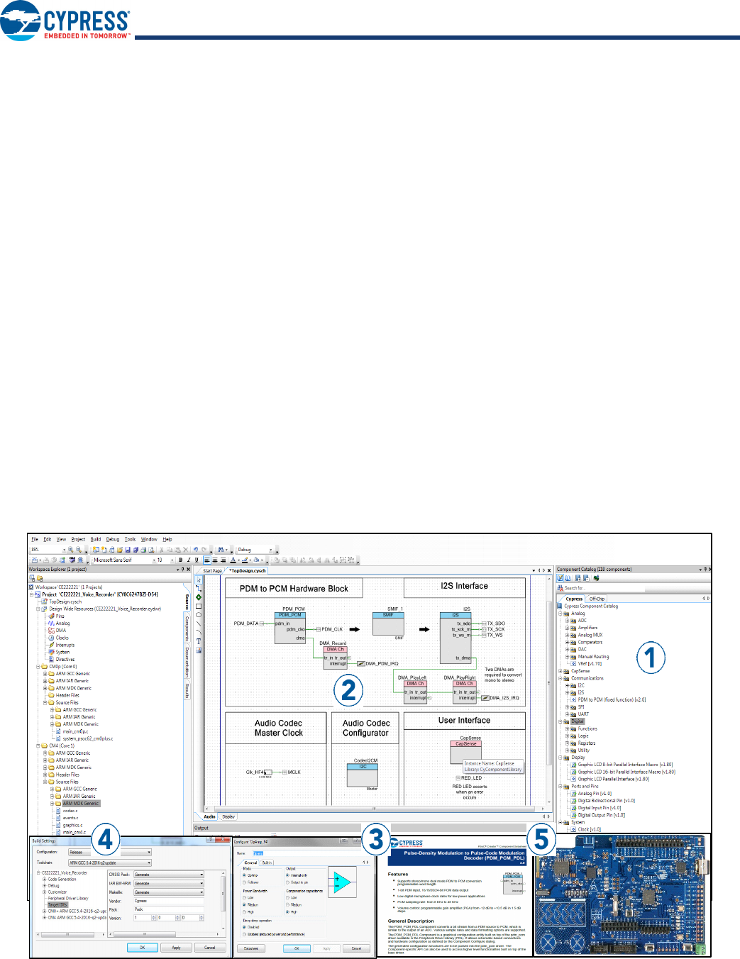
PSoC® Creator™ Integrated Design Environment (IDE)
PSoC Creator is a free Windows-based Integrated Design Environment (IDE). It enables you to design hardware and firmware
systems concurrently, based on PSoC 6 MCU. As shown below, with PSoC Creator, you can:
1. Explore the library of 200+ Components in PSoC Creator
2. Drag and drop Component icons to complete your hardware
system design in the main design workspace
3. Configure Components using the Component Configuration
Tools and the Component datasheets
4. Co-design your application firmware and hardware in the
PSoC Creator IDE or build project for 3rd party IDE
5. Prototype your solution with the PSoC 6 Pioneer Kits.If a
design change is needed, PSoC Creator and Components
enable you to make changes on the fly without the need for
hardware revisions.
Figure 1. PSoC Creator Schematic Entry and Components

PRELIMINARY CYBLE-416045-02
Document Number: 002-24085 Rev. ** Page 4 of 60
Contents
Functional Definition........................................................ 5
CPU and Memory Subsystem ..................................... 5
System Resources ...................................................... 5
BLE Radio and Subsystem ......................................... 6
Analog Blocks.............................................................. 6
Programmable Digital.................................................. 7
Fixed-Function Digital.................................................. 7
GPIO ........................................................................... 8
Special-Function Peripherals ...................................... 8
Module Overview .............................................................. 9
Module Description...................................................... 9
Pad Connection Interface .............................................. 11
Recommended Host PCB Layout ................................. 12
Digital and Analog Capablities and Connections........ 14
Power............................................................................... 17
Critical Components List ........................................... 19
Antenna Design......................................................... 19
Electrical Specification .................................................. 20
Device-Level Specifications ...................................... 20
Analog Peripherals .................................................... 28
Digital Peripherals ..................................................... 36
Memory ..................................................................... 38
System Resources .................................................... 39
Environmental Specifications ....................................... 49
Environmental Compliance ....................................... 49
RF Certification.......................................................... 49
Environmental Conditions ......................................... 49
ESD and EMI Protection ........................................... 49
Regulatory Information.................................................. 50
FCC........................................................................... 50
ISED.......................................................................... 51
European Declaration of Conformity ......................... 52
MIC Japan................................................................. 52
Packaging........................................................................ 53
Ordering Information...................................................... 55
Part Numbering Convention...................................... 55
Acronyms........................................................................ 56
Document Conventions ................................................. 58
Units of Measure ....................................................... 58
Document History Page................................................. 59
Sales, Solutions, and Legal Information ...................... 60
Worldwide Sales and Design Support....................... 60
Products .................................................................... 60
PSoC® Solutions ...................................................... 60
Cypress Developer Community................................. 60
Technical Support ..................................................... 60

PRELIMINARY CYBLE-416045-02
Document Number: 002-24085 Rev. ** Page 5 of 60
Functional Definition
CPU and Memory Subsystem
CPU
The CPU subsystem in the More Part Numbers consists of two
Arm Cortex cores and their associated busses and memories:
M4 with Floating-point unit and Memory Protection Units (FPU
and MPU) and an M0+ with an MPU. The Cortex M4 and M0+
have 8-KB Instruction Caches (I-Cache) with 4-way set associa-
tivity. This subsystem also includes independent DMA
controllers with 32 channels each, a Cryptographic accelerator
block, 1 MB of on-chip Flash, 288 KB of SRAM, and 128 KB of
ROM.
The Cortex M0+ provides a secure, un-interruptible Boot
function. This guarantees that post-Boot, system integrity is
checked and privileges enforced. Shared resources can be
accessed through the normal Arm multi-layer bus arbitration and
exclusive accesses are supported by an Inter-Processor
Communication (IPC) scheme, which implements hardware
semaphores and protection. Active power consumption for the
Cortex M4 is 22 µA/MHz and 15 µA/MHz for the Cortex M0+,
both at 3.3 V chip supply voltage with the internal buck enabled
and at 0.9 V internal supply. Note that at Cortex M4 speeds
above 100 MHz, the M0+ and Peripheral subsystem are limited
to half the M4 speed. If the M4 is running at 150 Mhz, the M0+and
peripheral subsystem is limited to 75 MHz.
DMA Controllers
There are two DMA controllers with 16 channels each. They
support independent accesses to peripherals using the AHB
Multi-layer bus.
Flash
CYBLE-416045-02 has 1-MB of flash with additional 32K of
Flash that can be used for EEPROM emulation for longer
retention and a separate 32-KB block of Flash that can be
securely locked and is only accessible via a key lock that cannot
be changed (One Time Programmable).
SRAM with 32-KB Retention Granularity
There is 288 KB of SRAM memory, which can be fully retained
or retained in increments of user-designated 32-KB blocks.
SROM
There is a supervisory 128-KB ROM that contains boot and
configuration routines. This ROM will guarantee Secure Boot if
authentication of User Flash is required.
One-Time-Programmable (OTP) eFuse
The 1024-bit OTP memory can provide a unique and unalterable
Identifier on a per-chip basis. This unalterable key can be used
to access Secured Flash.
System Resources
Power System
The power system provides assurance that voltage levels are as
required for each respective mode and will either delay mode
entry (on power-on reset (POR), for example) until voltage levels
are as required for proper function or generate resets (Brown-Out
Detect (BOD)) when the power supply drops below specified
levels. The design will guaranteed safe chip operation between
power supply voltage dropping below specified levels (for
example, below 1.7 V) and the Reset occurring. There are no
voltage sequencing requirements. The VDD core logic supply
(1.7 to 3.6 V) will feed an on-chip buck, which will produce the
core logic supply of either 1.1 V or 0.9 V selectable. Depending
on the frequency of operation, the buck converter will have a
quiescent current of <1 µA. A separate power domain called
Backup is provided; note this is not a power mode. This domain
is powered from the VBACKUP domain and includes the 32-kHz
WCO, RTC, and backup registers. It is connected to VDD when
not used as a backup domain. Port 0 is powered from this supply.
Pin 5 of Port 0 (P0.5) can be assigned as a PMIC wakeup output
(timed by the RTC); P0.5 is driven to the resistive pull-up mode
by default.
Clock System
The Part Number clock system is responsible for providing
clocks to all subsystems that require clocks and for switching
between different clock sources without glitching. In addition, the
clock system ensures that no metastable conditions occur.
The clock system for the CYBLE-416045-02 consists of the
Internal Main Oscillator (IMO) and the Internal Low-speed Oscil-
lator (ILO), crystal oscillators (ECO and WCO), PLL, FLL, and
provision for an external clock. An FLL will provide fast wake-up
at high clock speeds without waiting for a PLL lock event (which
can take up to 50 µs). Clocks may be buffered and brought out
to a pin on a Smart I/O port.
The 32-kHz oscillator is trimmable to within 2 ppm using a higher
accuracy clock. The ECO will deliver ±20-ppm accuracy and will
use an external crystal.
IMO Clock Source
The IMO is the primary source of internal clocking in More Part
Numbers. It is trimmed during testing to achieve the specified
accuracy. The IMO default frequency is 8 MHz. IMO tolerance is
±2% and its current consumption is less than 10 µA.
ILO Clock Source
The ILO is a very low power oscillator, nominally 32 kHz, which
may be used to generate clocks for peripheral operation in Deep
Sleep mode. ILO-driven counters can be calibrated to the IMO
to improve accuracy. Cypress provides a software component,
which does the calibration.

PRELIMINARY CYBLE-416045-02
Document Number: 002-24085 Rev. ** Page 6 of 60
Watchdog Timer
A watchdog timer is implemented in the clock block running from
the ILO or from the WCO; this allows watchdog operation during
Deep Sleep and Hibernate modes, and generates a watchdog
reset if not serviced before the timeout occurs. The watchdog
reset is recorded in the Reset Cause register.
Clock Dividers
Integer and Fractional clock dividers are provided for peripheral
use and timing purposes. There are eight 8-bit integer and
sixteen 16-bit integer clock dividers. There is also one 24.5-bit
fractional and four 16.5-bit fractional clock dividers.
Reset
The More Part Numbers can be reset from a variety of sources
including a software reset. Reset events are asynchronous and
guarantee reversion to a known state. The reset cause is
recorded in a register, which is sticky through reset and allows
software to determine the cause of the Reset. An XRES pin is
reserved for external reset to avoid complications with
configuration and multiple pin functions during power-on or
reconfiguration.
BLE Radio and Subsystem
Part Number incorporates a Bluetooth Smart subsystem that
contains the Physical Layer (PHY) and Link Layer (LL) engines
with an embedded security engine. The physical layer consists
of the digital PHY and the RF transceiver that transmits and
receives GFSK packets at 2 Mbps over a 2.4-GHz ISM band,
which is compliant with Bluetooth Smart Bluetooth Specification
5.0. The baseband controller is a composite hardware and
firmware implementation that supports both master and slave
modes. Key protocol elements, such as HCI and link control, are
implemented in firmware. Time-critical functional blocks, such as
encryption, CRC, data whitening, and access code correlation,
are implemented in hardware (in the LL engine).
The RF transceiver contains an integrated balun, which provides
a single-ended RF port pin to drive a 50-Ω antenna via a
matching/filtering network. In the receive direction, this block
converts the RF signal from the antenna to a digital bit stream
after performing GFSK demodulation. In the transmit direction,
this block performs GFSK modulation and then converts a digital
baseband signal to a radio frequency before transmitting it to air
through the antenna.
Key features of BLESS are as follows:
nMaster and slave single-mode protocol stack with logical link
control and adaptation protocol (L2CAP), attribute (ATT), and
security manager (SM) protocols
nAPI access to generic attribute profile (GATT), generic access
profile (GAP), and L2CAP
nL2CAP connection-oriented channel (Bluetooth 4.1 feature)
nGAP features
pBroadcaster, Observer, Peripheral, and Central roles
pSecurity mode 1: Level 1, 2, and 3
pUser-defined advertising data
pMultiple bond support
nGATT features
pGATT client and server
pSupports GATT sub-procedures
p32-bit universally unique identifier (UUID) (Bluetooth 4.1
feature)
nSecurity Manager (SM)
pPairing methods: Just works, Passkey Entry, and Out of Band
pLE Secure Connection Pairing model
pAuthenticated man-in-the-middle (MITM) protection and data
signing
nLink Layer (LL)
pMaster and Slave roles
p128-bit AES engine
pLow-duty cycle advertising
pLE Ping
nSupports all SIG-adopted BLE profiles
nPower levels for Adv (1.28s, 31 bytes, 0 dBm) and Con
(300 ms, 0 byte, 0 dBm) are 42 µW and 70 µW respectively
Analog Blocks
12-bit SAR ADC
The 12-bit, 1-Msps SAR ADC can operate at a maximum clock
rate of 18 MHz and requires a minimum of 18 clocks at that
frequency to do a 12-bit conversion.
The block functionality is augmented for the user by adding a
reference buffer to it (trimmable to ±1%) and by providing the
choice of three internal voltage references, VDD, VDD/2, and
VREF (nominally 1.024 V), as well as an external reference
through a GPIO pin. The Sample-and-Hold (S/H) aperture is
programmable; it allows the gain bandwidth requirements of the
amplifier driving the SAR inputs, which determine its settling
time, to be relaxed if required. System performance will be 65 dB
for true 12-bit precision provided appropriate references are
used and system noise levels permit it. To improve the perfor-
mance in noisy conditions, it is possible to provide an external
bypass (through a fixed pin location) for the internal reference
amplifier.
The SAR is connected to a fixed set of pins through an 8-input
sequencer. The sequencer cycles through the selected channels
autonomously (sequencer scan) and does so with zero switching
overhead (that is, the aggregate sampling bandwidth is equal to
1 Msps whether it is for a single channel or distributed over
several channels). The sequencer switching is effected through
a state machine or through firmware-driven switching. A feature
provided by the sequencer is the buffering of each channel to
reduce CPU interrupt-service requirements. To accommodate
signals with varying source impedances and frequencies, it is
possible to have different sample times programmable for each
channel. Also, the signal range specification through a pair of
range registers (low and high range values) is implemented with
a corresponding out-of-range interrupt if the digitized value
exceeds the programmed range; this allows fast detection of
out-of-range values without having to wait for a sequencer scan
to be completed and the CPU to read the values and check for
out-of-range values in software. There are 16 channels of which
any 13 can be sampled in a single scan.

PRELIMINARY CYBLE-416045-02
Document Number: 002-24085 Rev. ** Page 7 of 60
The SAR is able to digitize the output of the on-chip temperature
sensor for calibration and other temperature-dependent
functions. The SAR is not available in Deep Sleep and Hibernate
modes as it requires a high-speed clock (up to 18 MHz). The
SAR operating range is 1.71 V to 3.6 V.
Temperature Sensor
Part Number has an on-chip temperature sensor. This consists
of a diode, which is biased by a current source that can be
disabled to save power. The temperature sensor is connected to
the ADC, which digitizes the reading and produces a temper-
ature value by using a Cypress-supplied software that includes
calibration and linearization.
12-bit Digital-Analog Converter
There is a 12-bit voltage mode DAC on the chip, which can settle
in less than 5 µs. The DAC may be driven by the DMA controllers
to generate user-defined waveforms. The DAC output from the
chip can either be the resistive ladder output (highly linear near
ground) or a buffered output.
Continuous Time Block (CTBm) with Two Opamps
This block consists of two opamps, which have their inputs and
outputs connected to fixed pins and have three power modes
and a comparator mode. The outputs of these opamps can be
used as buffers for the SAR inputs. The non-inverting inputs of
these opamps can be connected to either of two pins, thus
allowing independent sensors to be used at different times. The
pin selection can be made via firmware. The opamps can be set
to one of the four power levels; the lowest level allowing
operation in Deep Sleep mode in order to preserve lower perfor-
mance Continuous-Time functionality in Deep Sleep mode. The
DAC output can be buffered through an opamp.
Low-Power Comparators
CYBLE-416045-02 has a pair of low-power comparators, which
can also operate in Deep Sleep and Hibernate modes. This
allows the analog system blocks to be disabled while retaining
the ability to monitor external voltage levels during Deep Sleep
and Hibernate modes. The comparator outputs are normally
synchronized to avoid metastability unless operating in an
asynchronous power mode (Hibernate) where the system
wake-up circuit is activated by a comparator-switch event.
Programmable Digital
Smart I/O
There are two Smart I/O blocks, which allow Boolean operations
on signals going to the GPIO pins from the subsystems of the
chip or on signals coming into the chip. Operation can be
synchronous or asynchronous and the blocks operate in
low-power modes, such as Deep Sleep and Hibernate.This
allows, for example, detection of logic conditions that can
indicate that the CPU should wake up instead of waking up on
general I/O interrupts, which consume more power and can
generate spurious wake-ups.
Universal Digital Blocks (UDBs) and Port Interfaces
The CYBLE-416045-02 has 12 UDBs; the UDB array also
provides a switched Digital System Interconnect (DSI) fabric that
allows signals from peripherals and ports to be routed to and
through the UDBs for communication and control.
Fixed-Function Digital
Timer/Counter/PWM Block
The timer/counter/PWM block consists of 32 counters with
user-programmable period length. There is a Capture register to
record the count value at the time of an event (which may be an
I/O event), a period register which is used to either stop or
auto-reload the counter when its count is equal to the period
register, and compare registers to generate compare value
signals which are used as PWM duty cycle outputs. The block
also provides true and complementary outputs with
programmable offset between them to allow the use as
deadband programmable complementary PWM outputs. It also
has a Kill input to force outputs to a predetermined state; for
example, this is used in motor-drive systems when an
overcurrent state is indicated and the PWMs driving the FETs
need to be shut off immediately with no time for software
intervention. There are eight 32-bit counters and 24 16-bit
counters.
Serial Communication Blocks (SCB)
Part Number has nine SCBs, which can each implement an I2C,
UART, or SPI interface. One SCB will operate in Deep Sleep with
an external clock, this SCB will only operate in Slave mode
(requires external clock).
I2C Mode: The hardware I2C block implements a full
multi-master and slave interface (it is capable of multimaster
arbitration). This block is capable of operating at speeds of up to
1 Mbps (Fast Mode Plus) and has flexible buffering options to
reduce the interrupt overhead and latency for the CPU. It also
supports EzI2C that creates a mailbox address range in the
memory of Part Number and effectively reduces the I2C commu-
nication to reading from and writing to an array in the memory. In
addition, the block supports a 256 byte-deep FIFO for receive
and transmit, which, by increasing the time given for the CPU to
read the data, greatly reduces the need for clock stretching
caused by the CPU not having read the data on time. The FIFO
mode is available in all channels and is very useful in the
absence of DMA.
The I2C peripheral is compatible with I2C Standard-mode,
Fast-mode, and Fast-Mode Plus devices as defined in the NXP
I2C-bus specification and user manual (UM10204). The I2C bus
I/O is implemented with GPIO in open-drain modes.
UART Mode: This is a full-feature UART operating at up to
8 Mbps. It supports automotive single-wire interface (LIN),
infrared interface (IrDA), and SmartCard (ISO7816) protocols, all
of which are minor variants of the basic UART protocol. In
addition, it supports the 9-bit multiprocessor mode that allows the
addressing of peripherals connected over common RX and TX
lines. Common UART functions such as parity error, break
detect, and frame error are supported. A 256 byte-deep FIFO
allows much greater CPU service latencies to be tolerated.
SPI Mode: The SPI mode supports full Motorola SPI, TI Secure
Simple Pairing (SSP) (essentially adds a start pulse that is used
to synchronize SPI Codecs), and National Microwire (half-duplex
form of SPI). The SPI block can use the FIFO and supports an
EzSPI mode in which the data interchange is reduced to reading
and writing an array in memory. The SPI interface will operate
with a 25-MHz SPI Clock.

PRELIMINARY CYBLE-416045-02
Document Number: 002-24085 Rev. ** Page 8 of 60
GPIO
CYBLE-416045-02 has up to 36 GPIOs. The GPIO block imple-
ments the following:
nEight drive strength modes:
pAnalog input mode (input and output buffers disabled)
pInput only
pWeak pull-up with strong pull-down
pStrong pull-up with weak pull-down
pOpen drain with strong pull-down
pOpen drain with strong pull-up
pStrong pull-up with strong pull-down
pWeak pull-up with weak pull-down
nInput threshold select (CMOS or LVTTL)
nHold mode for latching previous state (used for retaining the
I/O state in Deep Sleep and Hibernate modes)
nSelectable slew rates for dV/dt-related noise control to improve
EMI
The pins are organized in logical entities called ports, which are
8-bit in width. During power-on and reset, the blocks are forced
to the disable state so as not to crowbar any inputs and/or cause
excess turn-on current. A multiplexing network known as a
high-speed I/O matrix (HSIOM) is used to multiplex between
various signals that may connect to an I/O pin. Data output and
pin state registers store, respectively, the values to be driven on
the pins and the states of the pins themselves.
Every I/O pin can generate an interrupt if so enabled and each
I/O port has an interrupt request (IRQ) and interrupt service
routine (ISR) vector associated with it. Six GPIO pins are capable
of overvoltage tolerant (OVT) operation where the input voltage
may be higher than VDD (these may be used for I2C functionality
to allow powering the chip off while maintaining physical
connection to an operating I2C bus without affecting its function-
ality).
GPIO pins can be ganged to sink 16 mA or higher values of sink
current. GPIO pins, including OVT pins, may not be pulled up
higher than 3.6 V.
Special-Function Peripherals
CapSense
CapSense is supported on all pins in the Part Number through a
CapSense Sigma-Delta (CSD) block that can be connected to an
analog multiplexed bus. Any GPIO pin can be connected to this
AMUX bus through an analog switch. CapSense function can
thus be provided on any pin or a group of pins in a system under
software control. Cypress provides a software component for the
CapSense block for ease-of-use.
Shield voltage can be driven on another mux bus to provide
water-tolerance capability. Water tolerance is provided by driving
the shield electrode in phase with the sense electrode to keep
the shield capacitance from attenuating the sensed input.
Proximity sensing can also be implemented.
The CapSense block is an advanced, low-noise, programmable
block with programmable voltage references and current source
ranges for improved sensitivity and flexibility. It can also use an
external reference voltage. It has a full-wave CSD mode that
alternates sensing to VDDA and ground to null out power-supply
related noise.
The CapSense block has two 7-bit IDACs, which can be used for
general purposes if CapSense is not being used (both IDACs are
available in that case) or if CapSense is used without water
tolerance (one IDAC is available). A (slow) 10-bit Slope ADC
may be realized by using one of the IDACs.
The block can implement Swipe, Tap, Wake-up on Touch
(< 3 µA at 1.8 V), mutual capacitance, and other types of sensing
functions.
Audio Subsystem
This subsystem consists of an I2S block and two PDM channels.
The PDM channels interface to a PDM microphone's bit-stream
output. The PDM processing channel provides droop correction
and can operate with clock speeds ranging from 384 kHz to
3.072 MHz and produce word lengths of 16 to 24 bits at audio
sample rates of up to 48 ksps.
The I2S interface supports both Master and Slave modes with
Word Clock rates of up to 192 ksps (8-bit to 32-bit words).
PRELIMINARY CYBLE-416045-02
Document Number: 002-24085 Rev. ** Page 9 of 60
Module Overview
Module Description
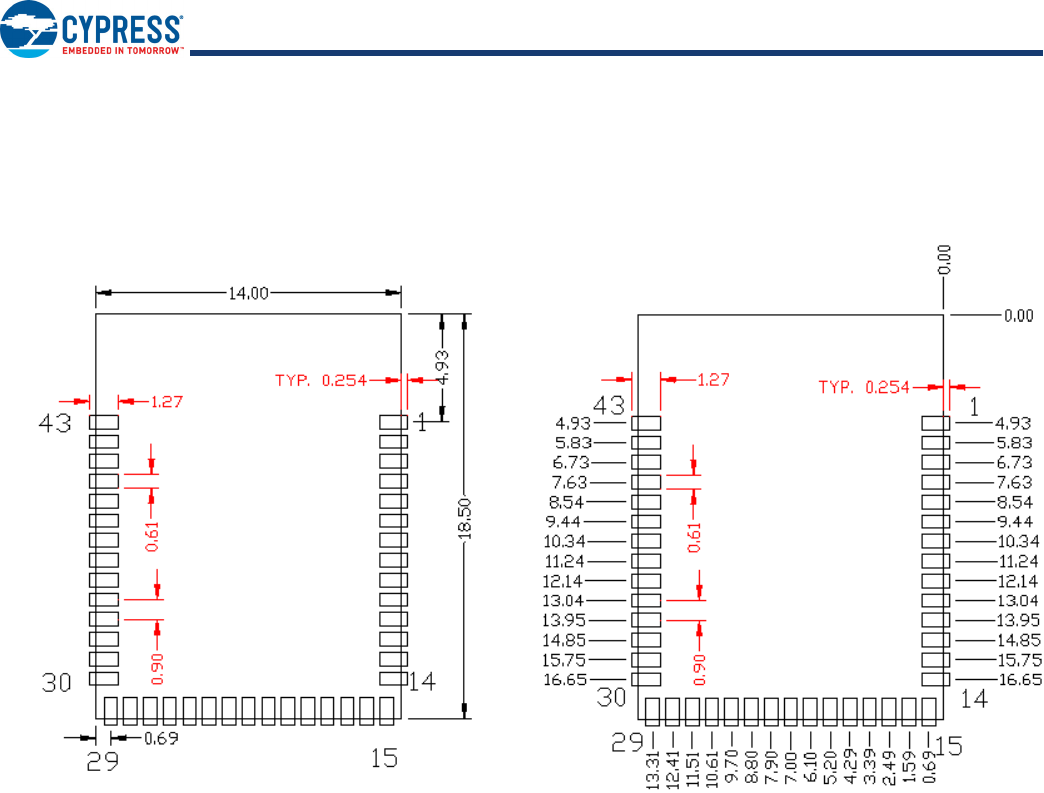
The CYBLE-416045-02 module is a complete module designed to be soldered to the main host board.
Module Dimensions and Drawing
Cypress reserves the right to select components (including the appropriate BLE device) from various vendors to achieve the BLE
module functionality. Such selections will guarantee that all height restrictions of the component area are maintained. Designs should
be completed with the physical dimensions shown in the mechanical drawings in Figure 2. All dimensions are in millimeters (mm).
Table 1. Module Design Dimensions
See Figure 2 on page 10 for the mechanical reference drawing for CYBLE-416045-02.
Dimension Item Specification
Module dimensions Length (X) 14.00 ± 0.15 mm
Width (Y) 18.50 ± 0.15 mm
Antenna location dimensions Length (X) 14.00 ± 0.15 mm
Width (Y) 4.62 ± 0.15 mm
PCB thickness Height (H) 0.80 ± 0.10 mm
Shield height Height (H) 1.20 ± 0.10 mm
Maximum component height Height (H) 1.20 mm typical (shield)
Total module thickness (bottom of module to highest component) Height (H) 2.00 mm typical
PRELIMINARY CYBLE-416045-02
Document Number: 002-24085 Rev. ** Page 10 of 60
Figure 2. Module Mechanical Drawing
Top View
Bottom View (Seen from Bottom)
Side View
Note
1. No metal should be located beneath or above the antenna area. Only bare PCB material should be located beneath the antenna area. For more information on
recommended host PCB layout, see Figure 4 on page 11, Figure 5 and Figure 6 on page 12, and Figure 7 and Tab le 3 on page 13.
PRELIMINARY CYBLE-416045-02
Document Number: 002-24085 Rev. ** Page 11 of 60
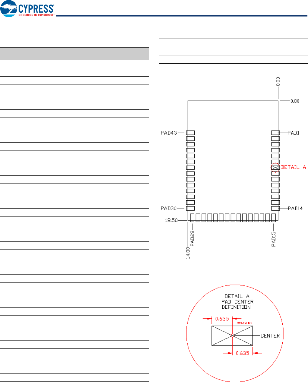
Pad Connection Interface
As shown in the bottom view of Figure 2 on page 10, the CYBLE-416045-02 connects to the host board via solder pads on the back
of the module. Table 2 and Figure 3 detail the solder pad length, width, and pitch dimensions of the CYBLE-416045-02 module.
Figure 3. Solder Pad Dimensions (Seen from Bottom)
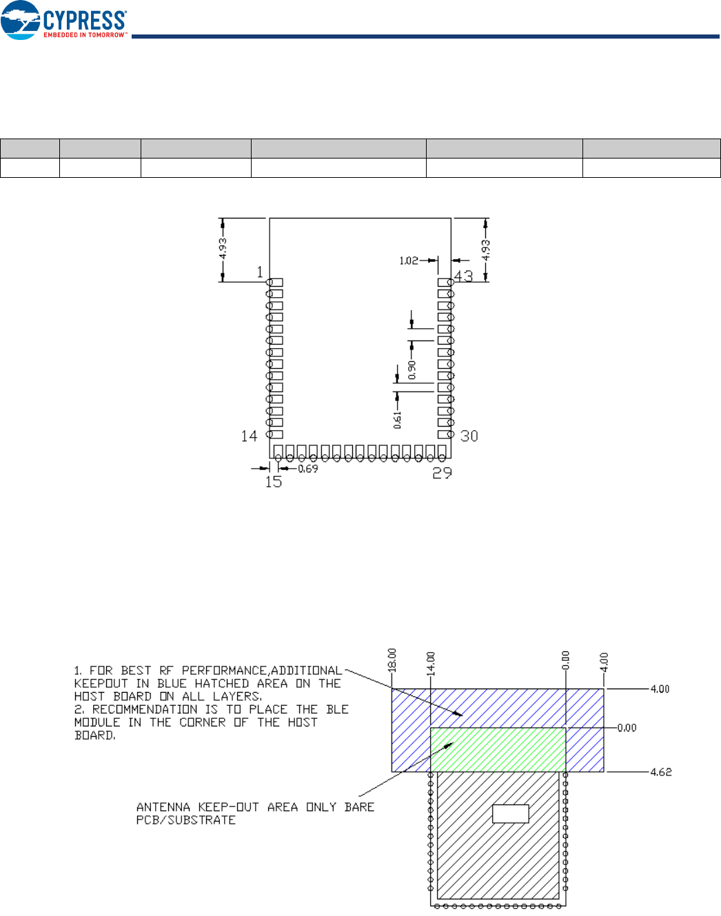
To maximize RF performance, the host layout should follow these recommendations:
1. The ideal placement of the Cypress BLE module is in a corner of the host board with the antenna located on the edge of the host
board. This placement minimizes the additional recommended keep-out area stated in item 2. Please refer to AN96841 for module
placement best practices.
2. To maximize RF performance, the area immediately around the Cypress BLE module trace antenna should contain an additional
keep-out area, where no grounding or signal traces are contained. The keep-out area applies to all layers of the host board. The
recommended dimensions of the host PCB keep-out area are shown in Figure 4 (dimensions are in mm).
Figure 4. Recommended Host PCB Keep-Out Area Around the CYBLE-416045-02 Trace Antenna
Table 2. Solder Pad Connection Description
Name Connections Connection Type Pad Length Dimension Pad Width Dimension Pad Pitch
SP 43 Solder Pads 1.02 mm 0.61 mm 0.90 mm
Host PCB Keep-Out Area Around Trace Antenna
PRELIMINARY CYBLE-416045-02
Document Number: 002-24085 Rev. ** Page 12 of 60
Recommended Host PCB Layout
Figure 5 through Figure 7 and Ta ble 3 provide details that can be used for the recommended host PCB layout pattern for the
CYBLE-416045-02. Dimensions are in millimeters unless otherwise noted. Pad length of 0.99 mm (0.494 mm from center of the pad
on either side) shown in Figure 7 is the minimum recommended host pad length. The host PCB layout pattern can be completed using
either Figure 5, Figure 6, or Figure 7. It is not necessary to use all figures to complete the host PCB layout pattern.
Figure 5. Host Layout Pattern for CYBLE-416045-02 Figure 6. Module Pad Location from Origin
Top View (Seen on Host PCB)
Top View (Seen on Host PCB)
PRELIMINARY CYBLE-416045-02
Document Number: 002-24085 Rev. ** Page 13 of 60
Table 3 provides the center location for each solder pad on the CYBLE-416045-02. All dimensions reference the to the center of the
solder pad. Refer to Figure 7 for the location of each module solder pad.
Table 3. Module Solder Pad Location
Figure 7. Solder Pad Reference Location
Solder Pad
(Center of Pad)
Location (X,Y) from
Orign (mm)
Dimension from
Orign (mils)
1 (0.38, 4.93) (14.96, 194.09)
2 (0.38, 5.83) (14.96, 229.53)
3 (0.38, 6.73) (14.96, 264.96)
4 (0.38, 7.63) (14.96, 300.39)
5 (0.38, 8.54) (14.96, 336.22)
6 (0.38, 9.44) (14.96, 371.65)
7 (0.38, 10.34) (14.96, 407.09)
8 (0.38, 11.24) (14.96, 442.52)
9 (0.38, 12.14) (14.96, 477.95)
10 (0.38, 13.04) (14.96, 513.38)
11 (0.38, 13.95) (14.96, 549.21)
12 (0.38, 14.85) (14.96, 584.64)
13 (0.38, 15.75) (14.96, 620.08)
14 (0.38, 16.65) (14.96, 655.51)
15 (0.69, 18.12) (27.17, 713.38)
16 (1.59, 18.12) (62.60, 713.38)
17 (2.49, 18.12) (98.03, 713.38)
18 (3.39, 18.12) (133.46, 713.38)
19 (4.29, 18.12) (168.90, 713.38)
20 (5.20, 18.12) (204.72, 713.38)
21 (6.10, 18.12) (240.16, 713.38)
22 (7.00, 18.12) (275.59, 713.38)
23 (7.90, 18.12) (311.02, 713.38)
24 (8.80, 18.12) (346.46, 713.38)
25 (9.70, 18.12) (381.89, 713.38)
26 (10.61, 18.12) (417.72, 713.38)
27 (11.51, 18.12) (453.15, 713.38)
28 (12.41, 18.12) (488.58, 713.38)
29 (13.31, 18.12) (524.01, 713.38)
30 (13.62, 16.65) (536.22, 655.51)
31 (13.62, 15.75) (536.22, 620.08)
32 (13.62, 14.85) (536.22, 584.64)
33 (13.62, 13.95) (536.22, 549.21)
34 (13.62, 13.04) (536.22, 513.38)
35 (13.62, 12.14) (536.22, 477.95)
36 (13.62, 11.24) (536.22, 442.52)
37 (13.62, 10.34) (536.22, 407.09)
38 (13.62, 9.44) (536.22, 371.65)
39 (13.62, 8.54) (536.22, 336.22)
40 (13.62, 7.63) (536.22, 300.39)
41 (13.62, 6.73) (536.22, 264.96)
42 (13.62, 5.83) (536.22, 229.53)
43 (13.62, 4.93) (536.22, 194.09)
Top View (Seen on Host PCB)
PRELIMINARY CYBLE-416045-02
Document Number: 002-24085 Rev. ** Page 14 of 60
Digital and Analog Capablities and Connections
Table 4 and Ta ble 5 detail the solder pad connection definitions and available functions for each connection pad. Table 4 lists the
solder pads on CYBLE-416045-02, the BLE device port-pin, and denotes whether the digital function shown is available for each
solder pad. Table 5 denotes whether the analog function shown is available for each solder pad. Each connection is configurable for
a single option shown with a 3.
Table 4. Digital Peripheral Capabilities
Pad
Number
Device
Port Pin UART SPI I2CTCPWM[2,3] Cap
Sense
EXT_CLK
_IN AUDIO CMP Dig-
ital Out SWD/JTAG GPIO
1GND
[4] Ground Connection
2P0.53(scb0_CTS) 3(scb0_SS0) tcpwm[0].line_compl[2]
tcpwm[1].line_compl[2]
33 3
3 VBACKUP Battery Backup Domain Input Voltage (1.71 V to 3.6 V)
4 VDD Power Supply Input Voltage (1.71 V to 3.6 V)
5P0.0 3(scb0_SS1) tcpwm[0].line[0]
tcpwm[1].line[0]
33 3
6P0.1 3(scb0_SS2) tcpwm[0].line_compl[0]
tcpwm[1].line_compl[0]
33(JTAG RST) 3
7 P10.3 3(scb1_CTS) 3(scb1_SS0) tcpwm[0].line_compl[7]
tcpwm[1].line_compl[23]
33
8 P10.4 3(scb1_SS1) tcpwm[0].line[0]
tcpwm[1].line[0]
33PDM_CLK 3
9P9.33(scb2_CTS) 3(scb2_SS0) tcpwm[0].line_compl[5]
tcpwm[1].line_compl[21]
3ctb_cmp1 3
10 P10.6 3(scb1_SS3) tcpwm[0].line[1]
tcpwm[1].line[2]
33
11 P10.5 3(scb1_SS2) tcpwm[0].line_compl[0]
tcpwm[1].line_compl[0]
33PDM_DATA 3
12 P10.1 3(scb1_TX) 3(scb1_MISO) 3(scb1_SDA) tcpwm[0].line_compl[6]
tcpwm[1].line_compl[22]
33
13 P10.0 3(scb1_RX) 3(scb1_MOSI) 3(scb1_SCL) tcpwm[0].line[6]
tcpwm[1].line[22]
33
14 P9.4 3(scb2_SS1) tcpwm[0].line[7]
tcpwm[1].line[0]
33
15 GND Ground Connection
16 VREF Voltage Reference Input (Optional)
17 P9.0 3(scb2_RX) 3(scb2_MOSI) 3(scb2_SCL) tcpwm[0].line[4]
tcpwm[1].line[20]
33
18 P9.1 3(scb2_TX) 3(scb2_MISO) 3(scb2_SDA) tcpwm[0].line_compl[4]
tcpwm[1].line_compl[20]
33
19 P9.5 3(scb2_SS2) tcpwm[0].line_compl[7]
tcpwm[1].line_compl[0]
33
20 P9.6 3(scb2_SS3) tcpwm[0].line[0]
tcpwm[1].line[1]
33
21 P9.2 3(scb2_RTS) 3(scb2_SCLK) tcpwm[0].line[5]
tcpwm[1].line[21]
3ctb_cmp0 3
22 P7.2 3(scb4_RTS) 3(scb4_SCLK) tcpwm[0].line[5]
tcpwm[1].line[13]
33
23 P7.1 3(scb4_TX) 3(scb4_MISO) 3(scb4_SDA) tcpwm[0].line_compl[4]
tcpwm[1].line_compl[12]
33
24 P6.4 3(SCB6_RX) 3(scb6_MOSI)
(scb8_MOSI)
3(scb8_SCL)
(scb6_SCL) tcpwm[0].line[2]
tcpwm[1].line[10]
33(JTAG TDO) 3
25 P5.4 3(scb5_SS1) tcpwm[0].line[6]
tcpwm[1].line[6]
33I2S_SCK_RX 3
26 P6.7 3(scb6_CTS) 3(scb6_SS0)
(scb8_SS0) tcpwm[0].line_compl[3]
tcpwm[1].line_compl[11
33(SWDCLK)
(JTAG TCLK)
3
27 P6.6 3(scb6_RTS) 3(scb6_SCLK)
(scb8_SCLK) tcpwm[0].line[3]
tcpwm[1].line[11]
33(SWDIO)
(JTAG TMS)
3
28 P6.2 3(scb3_RTS) 3(scb3_SCLK)
(scb8_SCLK) tcpwm[0].line[1]
tcpwm[1].line[9]
33
29 P6.5 3(scb6_TX) 3(scb6_MISO)
(scb8_MISO)
3(scb8_SDA)
3(scb6_SDA) tcpwm[0].line_compl[2]
tcpwm[1].line_compl[10]
33(JTAG TDI) 3
PRELIMINARY CYBLE-416045-02
Document Number: 002-24085 Rev. ** Page 15 of 60
30 P6.3 3(scb3_CTS) 3(scb3_SS0)
(scb8_SS0) tcpwm[0].line_compl[1]
tcpwm[1].line_compl[9]
33
31 P7.7 3(scb3_SS1) tcpwm[0].line_compl[7]
tcpwm[1].line_compl[15]
33
32 P5.6 3(scb5_SS3) tcpwm[0].line[7]
tcpwm[1].line[7]
33I2S_SDI_RX 3
33 P10.2 3(scb1_RTS) 3(scb1_SCLK) tcpwm[0].line[7]
tcpwm[1].line[23]
33
34 P12.6 3(scb6_SS3) tcpwm[0].line[7]
tcpwm[1].line[7]
33
35 P12.7 tcpwm[0].line_compl[7]
tcpwm[1].line_compl[7]
33
36 P5.5 3(scb5_SS2) tcpwm[0].line_compl[6]
tcpwm[1].line_compl[6]
33I2S_WS_RX 3
37 P5.3 3(scb5_CTS) 3(scb5_SS0) cpwm[0].line_compl[5]
tcpwm[1].line_compl[5]
33I2S_SDO_TX 3
38 P5.2 3(scb5_RTS) 3(scb5_SCLK) tcpwm[0].line[5]
tcpwm[1].line[5]
33I2S_WS_TX 3
39 P5.0 3(scb5_RX) 3(scb5_MOSI) 3(scb5_SCL) tcpwm[0].line[4]
tcpwm[1].line[4]
33I2S_EXT_CLK 3
40 P5.1 3(scb5_TX) 3(scb5_MISO) 3(scb5_SDA) tcpwm[0].line_compl[4]
tcpwm[1].line_compl[4]
33I2S_CLK_TX 3
41 P0.4 3(scb0_RTS) 3(scb0_SCLK) tcpwm[0].line[2]
tcpwm[1].line[2]
33
42 XRES External Reset (Active Low)
43 GND[4] Ground Connection
Table 4. Digital Peripheral Capabilities
Notes
2. TCPWM stands for timer, counter, and PWM. If supported, the pad can be configured to any of these peripheral functions.
3. TCPWM connections on ports 0, 1, 2, and 3 can be routed through the Digital Signal Interconnect (DSI) to any of the TCPWM blocks and can be either positive
or negative polarity.
4. The main board needs to connect both GND connections (Pad 1 and Pad 32) on the module to the common ground of the system.
PRELIMINARY CYBLE-416045-02
Document Number: 002-24085 Rev. ** Page 16 of 60
Table 5. Additional Analog and Digital Functional Capabilities
Pad Number Device Port Pin Analog Functionality Digital HV Universal Digital
Block (UDB) SMARTIO
1 GND Ground Connection
2P0.5 3(pmic_wakeup_out) 3(UDB0[5])
3 VBACKUP Battery Backup Domain Input Voltage (1.71 V to 3.6 V)
4 VDD Power Supply Input Voltage (1.71 V to 3.6 V)
5P0.0 wco_in 3(UDB0[0])
6 P0.1 wco_out 3(UDB0[1])
7 P10.3 sarmux[3] 3(UDB9[3])
8 P10.4 sarmux[4] 3(UDB9[4])
9 P9.3 ctb_oa1_out 3(UDB10[3]) SMARTIO10[3]
10 P10.6 sarmux[6] 3(UDB9[6])
11 P10.5 sarmux[5] 3(UDB9[5])
12 P10.1 sarmux[1] 3(UDB9[1])
13 P10.0 sarmux[0] 3(UDB9[0])
14 P9.4 ctb_oa1- 3(UDB10[4]) SMARTIO9[4]
15 GND Ground Connection
16 VREF Reference Voltage Input (Optional)
17 P9.0 ctb_oa0+ 3(UDB10[0]) SMARTIO9[0]
18 P9.1 ctb_oa0- 3(UDB10[1]) SMARTIO9[1]
19 P9.5 ctb_oa1+ 3(UDB10[5]) SMARTIO9[5]
20 P9.6 ctb_oa0+ 3(UDB10[6]) SMARTIO9[6]
21 P9.2 ctb_oa0_out 3(UDB10[2]) SMARTIO9[2]
22 P7.2 csd.csh_tankpadd
csd.csh_tankpads
3(UDB5[2])
23 P7.1 csd.cmodpadd
csd.cmodpads
3(UDB5[1])
24 P6.4 3(UDB4[4])
25 P5.4 3(UDB3[5])
26 P6.7 swd_clk 3(UDB4[7])
27 P6.6 swd_data 3(UDB4[6])
28 P6.2 lpcomp.inp_comp1 3(UDB4[2])
29 P6.5 3(UDB4[5])
30 P6.3 lpcomp.inn_comp1 3(UDB4[3])
31 P7.7 csd.cshieldpads 3(UDB5[7])
32 P5.6 lpcomp.inp_comp0 3(UDB3[6])
33 P10.2 sarmux[2] 3(UDB9[2])
34 P12.6 ECO_IN 3(UDB7[6])
35 P12.7 ECO_OUT 3(UDB7[7])
36 P5.5 3(UDB3[5])
37 P5.3 3(UDB3[3])
38 P5.2 3(UDB3[2])
39 P5.0 3(UDB3[0])
40 P5.1 3(UDB3[1])
41 P0.4 pmic_wakeup_in
hibernate_wakeup[1]
3(UDB0[4])
42 XRES External Reset (Active Low)
43 GND Ground Connection
PRELIMINARY CYBLE-416045-02
Document Number: 002-24085 Rev. ** Page 17 of 60
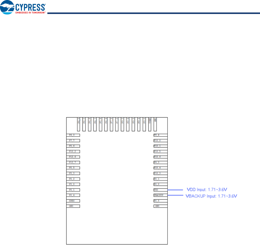
Power
The power connection diagram (see Figure 8) shows the general requirements for power pins on the CYBLE-416045-02. The
CYBLE-416045-02 contains a single power supply connection (VDD) and a backup voltage input (VBACKUP).
Description of the power pins is as follows:
1. VBACKUP is the supply to the backup domain. The backup domain includes the 32 kHz WCO, RTC, and backup registers. It
can generate a wake-up interrupt to the chip via the RTC timers or an external input. It can also generate an output to wakeup
external circuitry. It is connected to VDD when not used as a separate battery backup domain. VBACKUP provides the supply
for Port 0.
2. VDD is the main power supply input (1.7 to 3.6V). It provides the power input to the digital, analog and radio domains. Isolation
required for these domains is integrated on-module, therefore no additional isloation is required for the CYBLE-416045-02.
The supply voltage range is 1.71 to 3.6 V with all functions and circuits operating over that range. All ground connections specified
must be connected to system ground.
VDD and VBACKUP may be shorted together externally. They are not required to be seperate inputs voltages.
Figure 8. CYBLE-416045-02 Power Connections
PRELIMINARY CYBLE-416045-02
Document Number: 002-24085 Rev. ** Page 19 of 60
Critical Components List
Table 6 details the critical components used in the CYBLE-416045-02 module.
Table 6. Critical Component List
Antenna Design
Table 7 details the PCB trace antenna used on the CYBLE-416045-02 module. The Cypress module performance improves many of
these characteristics. For more information, see Table 10 on page 26.
Table 7. Trace Antenna Specifications
Component Reference Designator Description
Silicon U1 116-pin BGA Programmable System-on-Chip (PSoC6) with BLE
Crystal Y1 32.000 MHz, 10PF
Item Description
Frequency Range 2400 – 2500 MHz
Peak Gain -0.5 dBi typical
Return Loss 10 dB minimum
PRELIMINARY CYBLE-416045-02
Document Number: 002-24085 Rev. ** Page 20 of 60
Electrical Specification
Table 8 details the absolute maximum electrical characteristics for the Cypress BLE module.
Table 8. CYBLE-416045-02 Absolute Maximum Ratings[5]
Device-Level Specifications
All specifications are valid for –40 °C ≤ TA ≤ 85 °C and for 1.71 V to 3.6 V except where noted.
Parameter Description Min Typ Max Unit Details/Conditions
VDDD_ABS VDD, VDDA and VDDR supply relative to VSS
(VSSD = VSSA)–0.5 – 4 V Absolute maximum
VCCD_ABS Direct digital core voltage input relative to VSSD –0.5 – 1.2 V Absolute maximum
VDDD_RIPPLE Maximum power supply ripple for VDD, VDDA and
VDDR input voltage – – 100 mV
3.0V supply
Ripple frequency of 100 kHz
to 750 kHz
VGPIO_ABS GPIO voltage –0.5 – VDD +0.5 V Absolute maximum
IGPIO_ABS Maximum current per GPIO –25 – 25 mA Absolute maximum
IGPIO_injection GPIO injection current per pin –0.5 – 0.5 mA Absolute maximum current
injected per pin
LU Pin current for latch up –100 100 mA Absolute maximum
Table 9. Power Supply Range, CPU Current, and Transition Time Specifications
Parameter Description Min Typ Max Units Details / Conditions
DC Specifications
VDDD Internal regulator and Port 1 GPIO supply 1.7 – 3.6 V
VDDA Analog power supply voltage. Shorted to
VDDIOA on PCB. 1.7 – 3.6 V Internally unregulated Supply
VDDIO1 GPIO Supply for Ports 5 to 8 when present 1.7 – 3.6 V VDDIO_1 must be ≥ to VDDA.
VDDIO0 GPIO Supply for Ports 11 to 13 when
present 1.7 – 3.6 V
VDDIO0 Supply for E-Fuse Programming 2.38 2.5 2.62 V E-Fuse Programming Voltage
VDDIOR GPIO supply for Ports 2 to 4 on BGA 124
only 1.7 – 3.6 V
VDDIOA GPIO Supply for Ports 9 to 10. Shorted to
VDDA on PCB. 1.7 – 3.6 V
VDDUSB Supply for Port 14 (USB or GPIO) when
present 1.7 – 3.6 V Min supply is 2.85 V for USB
VBACKUP Backup Power and GPIO Port 0 supply
when present 1.7 – 3.6 V Min. is 1.4 V in Backup mode
VCCD1 Output voltage (for core logic bypass) – 1.1 – V High-speed mode
VCCD2 Output voltage (for core logic bypass) – 0.9 – ULP mode. Valid for –20 to 85 °C
CEFC External regulator voltage (VCCD) bypass 3.8 4.7 5.6 µF X5R ceramic or better
CEXC Power supply decoupling capacitor – 10 – µF X5R ceramic or better
Note
5. Usage above the absolute maximum conditions listed in Table 8 may cause permanent damage to the device. Exposure to absolute maximum conditions for extended
periods of time may affect device reliability. The maximum storage temperature is 150 °C in compliance with JEDEC Standard JESD22-A103, High Temperature
Storage Life. When used below absolute maximum conditions but above normal operating conditions, the device may not operate to specification.
PRELIMINARY CYBLE-416045-02
Document Number: 002-24085 Rev. ** Page 21 of 60
LP RANGE POWER SPECIFICATIONS (for VCCD = 1.1 V with Buck and LDO)
Cortex M4. Active Mode
Execute with Cache Disabled (Flash)
IDD1
Execute from Flash; CM4 Active 50 MHz,
CM0+ Sleep 25 MHz. With IMO & FLL.
While(1).
–2.33.2mAV
DDD = 3.3 V, Buck ON, Max at 60 °C
–3.13.6 V
DDD = 1.8 V, Buck ON, Max at 60 °C
–4.25.1 V
DDD = 1.8 to 3.3 V, LDO, max at 60 °C
IDD2 Execute from Flash; CM4 Active 8 MHz,
CM0+ Sleep 8 MHz.With IMO. While(1)
–0.91.5mAV
DDD = 3.3 V, Buck ON, Max at 60 °C
–1.21.6 V
DDD = 1.8 V, Buck ON, Max at 60 °C
–1.62.4 V
DDD = 1.8 to 3.3 V, LDO, max at 60 °C
Execute with Cache Enabled
IDD3
Execute from Cache;CM4 Active150 MHz,
CM0+ Sleep 75 MHz. IMO & FLL.
Dhrystone.
–6.3 7 mAV
DDD = 3.3 V, Buck ON, Max at 60 °C
–9.711.2 V
DDD = 1.8 V, Buck ON, Max at 60 °C
– 13.2 13.7 VDDD = 1.8 to 3.3 V, LDO, max at 60 °C
IDD4
Execute from Cache;CM4 Active100 MHz,
CM0+ Sleep 100MHz. IMO & FLL.
Dhrystone.
–4.85.8mAV
DDD = 3.3 V, Buck ON, Max at 60 °C
–7.48.4 V
DDD = 1.8 V, Buck ON, Max at 60 °C
– 10.1 10.7 VDDD = 1.8 to 3.3 V, LDO, max at 60 °C
IDD5
Execute from Cache;CM4 Active 50 MHz,
CM0+ Sleep 25MHz. IMO & FLL.
Dhrystone
–2.43.4mAV
DDD=3.3 V, Buck ON, Max at 60 °C
–3.74.1 V
DDD = 1.8V, Buck ON, Max at 60 °C
–5.15.8 V
DDD = 1.8 to 3.3 V, LDO, max at 60 °C
IDD6 Execute from Cache;CM4 Active 8 MHz,
CM0+ Sleep 8 MHz. IMO. Dhrystone
– 0.90 1.5 mA VDDD = 3.3 V, Buck ON, Max at 60 °C
– 1.27 1.75 VDDD = 1.8 V, Buck ON, Max at 60 °C
–1.82.6 V
DDD = 1.8 to 3.3 V, LDO, max at 60 °C
Cortex M0+. Active Mode
Execute with Cache Disabled (Flash)
IDD7 Execute from Flash;CM4 Off, CM0+ Active
50 MHz. With IMO & FLL. While (1).
–2.43.3mAV
DDD = 3.3 V, Buck ON, Max at 60 °C
–3.23.7 V
DDD = 1.8 V, Buck ON, Max at 60 °C
–4.14.8 V
DDD = 1.8 to 3.3 V, LDO, max at 60 °C
IDD8 Execute from Flash;CM4 Off, CM0+ Active
8 MHz. With IMO. While (1)
–0.81.5mAV
DDD = 3.3 V, Buck ON, Max at 60 °C
–1.11.6 V
DDD = 1.8 V, Buck ON, Max at 60 °C
– 1.45 1.9 VDDD = 1.8 to 3.3 V, LDO, max at 60 °C
Execute with Cache Enabled
IDD9
Execute from Cache;CM4 Off, CM0+
Active 100 MHz. With IMO & FLL.
Dhrystone.
–3.84.5mAV
DDD = 3.3V, Buck ON, Max at 60 °C
–5.96.5 V
DDD = 1.8 V, Buck ON, Max at 60 °C
–7.78.2 V
DDD = 1.8 to 3.3 V, LDO, max at 60 °C
IDD10 Execute from Cache;CM4 Off, CM0+
Active 8 MHz. With IMO. Dhrystone
– 0.80 1.3 mA VDDD = 3.3 V, Buck ON, Max at 60 °C
–1.21.7 V
DDD = 1.8 V, Buck ON, Max at 60 °C
–1.41 2 V
DDD = 1.8 to 3.3 V, LDO, max at 60 °C
Cortex M4. Sleep Mode
IDD11 CM4 Sleep 100 MHz, CM0+ Sleep 25
MHz. With IMO & FLL.
–1.52.2mAV
DDD = 3.3 V, Buck ON, Max at 60 °C
–2.22.7 V
DDD = 1.8 V, Buck ON, Max at 60 °C
–2.93.5 V
DDD = 1.8 to 3.3 V, LDO, max at 60 °C
IDD12 CM4 Sleep 50 MHz, CM0+ Sleep 25 MHz.
With IMO & FLL
– 1.20 1.9 mA VDDD = 3.3 V, Buck ON, Max at 60 °C
– 1.70 2.2 VDDD = 1.8 V, Buck ON, Max at 60 °C
– 2.20 2.8 VDDD = 1.8 to 3.3 V, LDO, max at 60 °C
Table 9. Power Supply Range, CPU Current, and Transition Time Specifications
Parameter Description Min Typ Max Units Details / Conditions
PRELIMINARY CYBLE-416045-02
Document Number: 002-24085 Rev. ** Page 22 of 60
IDD13 CM4 Sleep 8 MHz, CM0+ Sleep 8 MHz.
With IMO.
–0.71.3mAV
DDD = 3.3 V, Buck ON, Max at 60 °C
– 0.96 1.5 VDDD = 1.8 V, Buck ON, Max at 60 °C
–1.22 2 V
DDD = 1.8 to 3.3 V, LDO, max at 60 °C
Table 9. Power Supply Range, CPU Current, and Transition Time Specifications
Parameter Description Min Typ Max Units Details / Conditions
PRELIMINARY CYBLE-416045-02
Document Number: 002-24085 Rev. ** Page 23 of 60
Cortex M0+. Sleep Mode
IDD14 CM4 Off, CM0+ Sleep 50 MHz. With IMO
& FLL.
–1.3 2 mAV
DDD = 3.3 V, Buck ON, Max at 60 °C
– 1.94 2.4 VDDD = 1.8 V, Buck ON, Max at 60 °C
– 2.57 3.2 VDDD = 1.8 to 3.3 V, LDO, max at 60 °C
IDD15 CM4 Off, CM0+ Sleep 8 MHz. With IMO.
–0.71.3mAV
DDD = 3.3V, Buck ON, Max at 60 °C
– 0.95 1.5 VDDD = 1.8 V, Buck ON, Max at 60 °C
–1.25 2 V
DDD = 1.8 to 3.3 V, LDO, max at 60 °C
Cortex M4. Low Power Active (LPA) Mode
IDD16 Execute from Flash; CM4 LPA 8 MHz,
CM0+ Sleep 8 MHz. With IMO. While (1).
– 0.85 1.5 mA VDDD = 3.3 V, Buck ON, Max at 60 °C
– 1.18 1.65 VDDD = 1.8 V, Buck ON, Max at 60 °C
– 1.63 2.4 VDDD = 1.8 to 3.3 V, LDO, max at 60 °C
IDD17 Execute from Cache; CM4 LPA 8 MHz,
CM0+ Sleep 8 MHz. With IMO. Dhrystone.
– 0.90 1.5 mA VDDD = 3.3 V, Buck ON, Max at 60 °C
– 1.27 1.75 VDDD = 1.8 V, Buck ON, Max at 60 °C
– 1.77 2.5 VDDD = 1.8 to 3.3 V, LDO, max at 60 °C
Cortex M0+. Low Power Active (LPA) Mode
IDD18 Execute from Flash; CM4 Off, CM0+ LPA
8 MHz. With IMO. While (1)
–0.81.4mAV
DDD = 3.3 V, Buck ON, Max at 60 °C
– 1.14 1.6 VDDD = 1.8 V, Buck ON, Max at 60 °C
–1.62.4 V
DDD = 1.8 to 3.3 V, LDO, max at 60 °C
IDD19 Execute from Cache; CM4 Off, CM0+ LPA
8 MHz. With IMO. Dhrystone.
–0.81.4mAV
DDD = 3.3 V, Buck ON, Max at 60 °C
– 1.15 1.65 VDDD = 1.8 V, Buck ON, Max at 60 °C
– 1.62 2.4 VDDD = 1.8 to 3.3 V, LDO, max at 60 °C
Cortex M4. Low Power Sleep (LPS) Mode
IDD20 CM4 LPS 8 MHz, CM0+ LPS 8 MHz. With
IMO.
– 0.65 1.1 mA VDDD=3.3 V, Buck ON, Max at 60 °C
– 0.95 1.5 VDDD=1.8 V, Buck ON, Max at 60 °C
– 1.31 2.1 VDDD = 1.8 to 3.3 V, LDO, max at 60 °C
Table 9. Power Supply Range, CPU Current, and Transition Time Specifications
Parameter Description Min Typ Max Units Details / Conditions
Cortex M0+. Low Power Sleep (LPS) Mode
Table 9. Power Supply Range, CPU Current, and Transition Time Spe
c
Parameter Description Min Typ
M
PRELIMINARY CYBLE-416045-02
Document Number: 002-24085 Rev. ** Page 24 of 60
IDD22 CM4 Off, CM0+ LPS 8 MHz. With IMO.
– 0.64 1.1 mA VDDD = 3.3 V, Buck ON, Max at 60 °C
– 0.93 1.45 VDDD = 1.8 V, Buck ON, Max at 60 °C
–1.29 2 V
DDD = 1.8 to 3.3 V, LDO, max at 60 °C
ULP RANGE POWER SPECIFICATIONS (for VCCD = 0.9 V using the Buck). ULP mode is valid from -20 to +85 °C.
Cortex M4. Active Mode
Execute with Cache Disabled (Flash)
IDD3
Execute from Flash; CM4 Active 50 MHz,
CM0+ Sleep 25 MHz. With IMO & FLL.
While(1).
–1.72.2mAV
DDD = 3.3 V, Buck ON, Max at 60 °C
–2.12.4 V
DDD = 1.8 V, Buck ON, Max at 60 °C
IDD4 Execute from Flash; CM4 Active 8 MHz,
CM0+ Sleep 8 MHz. With IMO. While (1)
– 0.56 0.8 mA VDDD = 3.3 V, Buck ON, Max at 60 °C
–0.75 1 V
DDD = 1.8 V, Buck ON, Max at 60 °C
Execute with Cache Enabled
IDD10
Execute from Cache; CM4 Active 50 MHz,
CM0+ Sleep 25 MHz. With IMO & FLL.
Dhrystone.
–1.62.2mAV
DDD = 3.3 V, Buck ON, Max at 60 °C
–2.42.7 V
DDD = 1.8 V, Buck ON, Max at 60 °C
IDD11 Execute from Cache; CM4 Active 8 MHz,
CM0+ Sleep 8 MHz. With IMO. Dhrystone.
– 0.65 0.8 mA VDDD = 3.3 V, Buck ON, Max at 60 °C
–0.81.1 V
DDD = 1.8 V, Buck ON, Max at 60 °C
Cortex M0+. Active Mode
Execute with Cache Disabled (Flash)
IDD16 Execute from Flash; CM4 Off, CM0+
Active 25 MHz. With IMO & FLL. Write(1).
– 1.00 1.4 mA VDDD = 3.3 V, Buck ON, Max at 60 °C
– 1.34 1.6 VDDD = 1.8 V, Buck ON, Max at 60 °C
IDD17 Execute from Flash; CM4 Off, CM0+
Active 8 MHz. With IMO. While(1)
– 0.54 0.75 mA VDDD = 3.3 V, Buck ON, Max at 60 °C
–0.73 1 V
DDD = 1.8 V, Buck ON, Max at 60 °C
Execute with Cache Enabled
IDD18
Execute from Cache; CM4 Off, CM0+
Active 25 MHz. With IMO & FLL.
Dhrystone.
– 0.91 1.25 mA VDDD = 3.3 V, Buck ON, Max at 60 °C
– 1.34 1.6 VDDD = 1.8 V, Buck ON, Max at 60 °C
IDD19 Execute from Cache; CM4 Off, CM0+
Active 8 MHz. With IMO. Dhrystone.
– 0.51 0.72 mA VDDD = 3.3 V, Buck ON, Max at 60 °C
– 0.73 0.95 VDDD = 1.8 V, Buck ON, Max at 60 °C
Table 9. Power Supply Range, CPU Current, and Transition Time Specifications
Parameter Description Min Typ Max Units Details / Conditions
Cortex M4. Sleep Mode
Table 9. Power Supply Range, CPU Current, and Transition Time Spe
c
Parameter Description Min Typ
M
PRELIMINARY CYBLE-416045-02
Document Number: 002-24085 Rev. ** Page 25 of 60
Table 10 details the RF characteristics for the Cypress BLE module.
IDD21 CM4 Sleep 50 MHz, CM0+ Sleep 25 MHz.
With IMO & FLL
– 0.76 1.1 mA VDDD = 3.3 V, Buck ON, Max at 60 °C
–1.11.4 V
DDD = 1.8 V, Buck ON, Max at 60 °C
IDD22 CM4 Sleep 8 MHz, CM0+ Sleep 8 MHz.
With IMO
– 0.42 0.65 mA VDDD = 3.3 V, Buck ON, Max at 60 °C
– 0.59 0.8 VDDD = 1.8 V, Buck ON, Max at 60 °C
Cortex M0+. Sleep Mode
IDD23 CM4 Off, CM0+ Sleep 25 MHz. With IMO
& FLL.
– 0.62 0.9 mA VDDD = 3.3 V, Buck ON, Max at 60 °C
– 0.88 1.1 VDDD = 1.8 V, Buck ON, Max at 60 °C
IDD24 CM4 Off, CM0+ Sleep 8 MHz. With IMO. – 0.41 0.6 mA VDDD = 3.3 V, Buck ON, Max at 60 °C
– 0.58 0.8 VDDD = 1.8¬×V, Buck ON, Max at 60 °C
Cortex M4. Ultra Low Power Active (ULPA) Mode
IDD25 Execute from Flash. CM4 ULPA 8 MHz,
CM0+ ULPS 8 MHz. With IMO. While(1).
– 0.52 0.75 mA VDDD = 3.3 V, Buck ON, Max at 60 °C
–0.76 1 V
DDD = 1.8 V, Buck ON, Max at 60 °C
IDD26 Execute from Cache. CM4 ULPA 8 MHz,
CM0+ ULPS 8 MHz. With IMO. Dhrystone.
– 0.54 0.76 mA VDDD = 3.3 V, Buck ON, Max at 60 °C
–0.78 1 V
DDD = 1.8 V, Buck ON, Max at 60 °C
Cortex M0+. Ultra Low Power Active (ULPA) Mode
IDD27 Execute from Flash. CM4 Off, CM0+ ULPA
8 MHz. With IMO. While (1).
– 0.51 0.75 mA VDDD = 3.3 V, Buck ON, Max at 60 °C
–0.75 1 V
DDD = 1.8 V, Buck ON, Max at 60 °C
IDD28 Execute from Cache. CM4 Off, CM0+
ULPA 8 MHz. With IMO. Dhrystone.
– 0.48 0.7 mA VDDD = 3.3 V, Buck ON, Max at 60 °C
– 0.7 0.95 VDDD = 1.8 V, Buck ON, Max at 60 °C
Cortex M4. Ultra Low Power Sleep (ULPS) Mode
IDD29 CM4 ULPS 8 MHz, CM0 ULPS 8 MHz.
With IMO.
–0.40.6mAV
DDD = 3.3 V, Buck ON, Max at 60 °C
– 0.57 0.8 VDDD = 1.8 V, Buck ON, Max at 60 °C
Cortex M0+. Ultra Low Power Sleep (ULPS) Mode
IDD31 CM4 Off, CM0+ ULPS 8 MHz. With IMO. – 0.39 0.6 mA VDDD = 3.3 V, Buck ON, Max at 60 °C
– 0.56 0.8 VDDD = 1.8 V, Buck ON, Max at 60 °C
Deep Sleep Mode
IDD33A With internal Buck enabled and 64K SRAM
retention – 7 – µA Max value is at 85 °C
IDD33A_B With internal Buck enabled and 64K SRAM
retention – 7 – µA Max value is at 60 °C
IDD33B With internal Buck enabled and 256K
SRAM retention – 9 – µA Max value is at 85 °C
IDD33B_B With internal Buck enabled and 256K
SRAM retention – 9 – µA Max value is at 60 °C
Hibernate Mode
IDD34 VDDD = 1.8 V – 300 – nA No clocks running
IDD34A VDDD = 3.3 V – 800 – nA No clocks running
Power Mode Transition Times
TLPACT_ACT Low Power Active to Active transition time – – 35 µs Including PLL lock time
TDS_LPACT Deep Sleep to LP Active transition time – – 25 µs Guaranteed by design
TDS_ACT Deep Sleep to Active transition time – – 25 µs Guaranteed by design
THIB_ACT Hibernate to Active transition time – 500 – µs Including PLL lock time
Table 9. Power Supply Range, CPU Current, and Transition Time Specifications
Parameter Description Min Typ Max Units Details / Conditions
PRELIMINARY CYBLE-416045-02
Document Number: 002-24085 Rev. ** Page 26 of 60
Table 10. CYBLE-416045-02 RF Performance Characteristics
XRES
Parameter Description Min Typ Max Unit Details/Conditions
RFO RF output power on ANT –20 0 4 dBm Configurable via register
settings
RXSRF receive sensitivity on ANT – –87 – dBm Guaranteed by design
simulation
FRModule frequency range 2400 – 2480 MHz –
GPPeak gain – 0.5 – dBi –
GAvg Average gain – –0.5 – dBi –
RL Return loss – –10 – dB –
Notes
6. Cypress-supplied software wakeup routines take approximately 100 CPU clock cycles after hardware wakeup (the 25 µs) before transition to Application code.
With an 8-MHz CPU clock (LP Active), the time before user code executes is 25 + 12.5 = 37.5 µs.
7. Cypress-supplied software wakeup routines take approximately 100 CPU clock cycles after hardware wakeup (the 25 µs) before transition to Application code.
With a 25-MHz CPU clock (FLL), the time before user code executes is 25 + 4 = 29 µs. With a 100-MHz CPU clock, the time is 25 + 1 = 26 µs.
Table 11. XRES
Parameter Description Min Typ Max Units Details / Conditions
XRES (Active Low) Specifications
XRES AC Specifications
TXRES_ACT POR or XRES release to Active transition time – 750 – µs Normal mode, 50 MHz M0+.
TXRES_PW XRES Pulse width 5 – – µs
XRES DC Specifications
TXRES_IDD IDD when XRES asserted – 300 – nA VDDD = 1.8 V
TXRES_IDD_1 IDD when XRES asserted – 800 – nA VDDD = 3.3 V
VIH Input Voltage high threshold 0.7*
VDD
– – V CMOS Input
VIL Input Voltage low threshold – – 0.3*
VDD
V CMOS Input
CIN Input Capacitance – 3 – pF
VHYSXRES Input voltage hysteresis – 100 – mV
IDIODE Current through protection diode to VDD/VSS – – 100 µA
PRELIMINARY CYBLE-416045-02
Document Number: 002-24085 Rev. ** Page 27 of 60
GPIO
Table 12. GPIO Specifications
Parameter Description Min Typ Max Units Details / Conditions
GPIO DC Specifications
VIH Input voltage high threshold 0.7*VDD – – V CMOS Input
IIHS Input current when Pad > VDDIO for OVT inputs – – 10 µA Per I2C Spec
VIL Input voltage low threshold – – 0.3*VDD VCMOS Input
VIH LVTTL input, VDD < 2.7 V 0.7*VDD – – V
VIL LVTTL input, VDD < 2.7 V – – 0.3*VDD V
VIH LVTTL input, VDD ≥ 2.7 V 2.0 – – V
VIL LVTTL input, VDD³≥ 2.7 V – – 0.8 V
VOH Output voltage high level VDD-0.5 – – V IOH = 8 mA
VOL Output voltage low level – – 0.4 V IOL = 8 mA
RPULLUP Pull-up resistor 3.5 5.6 8.5 kΩ
RPULLDOWN Pull-down resistor 3.5 5.6 8.5 kΩ
IIL Input leakage current (absolute value) – – 2 nA 25 °C, VDD = 3.0 V
IIL_CTBM Input leakage on CTBm input pins – – 4 nA
CIN Input Capacitance – – 5 pF
VHYSTTL Input hysteresis LVTTL VDD > 2.7 V 100 0 - mV
VHYSCMOS Input hysteresis CMOS 0.05*VDD – - mV
IDIODE Current through protection diode to VDD/VSS – – 100 µA
ITOT_GPIO Maximum Total Source or Sink Chip Current – – 200 mA
GPIO AC Specifications
TRISEF Rise time in Fast Strong Mode. 10% to 90% of
VDD
– – 2.5 ns Cload = 15 pF, 8 mA drive
strength
TFALLF Fall time in Fast Strong Mode. 10% to 90% of
VDD
–– 2.5 ns Cload = 15 pF, 8 mA drive
strength
TRISES_1 Rise time in Slow Strong Mode. 10% to 90% of
VDD
52 –142 ns Cload = 15 pF, 8 mA drive
strength, VDD ≤ 2.7 V
TRISES_2 Rise time in Slow Strong Mode. 10% to 90% of
VDD
48 –102 ns Cload = 15 pF, 8 mA drive
strength, 2.7 V < VDD ≤
3.6 V
TFALLS_1 Fall time in Slow Strong Mode. 10% to 90% of
VDD
44 –211 ns Cload = 15 pF, 8 mA drive
strength, VDD ≤ 2.7 V
TFALLS_2 Fall time in Slow Strong Mode. 10% to 90% of
VDD
42 –93 ns Cload = 15 pF, 8 mA drive
strength, 2.7 V < VDD ≤
3.6 V
TFALL_I2C Fall time (30% to 70% of VDD) in Slow Strong
mode
20*VDDIO/
5.5
–250 ns Cload = 10 pF to 400 pF,
8-mA drive strength
FGPIOUT1 GPIO Fout. Fast Strong mode. – – 100 MHz 90/10%, 15-pF load,
60/40 duty cycle
FGPIOUT2 GPIO Fout; Slow Strong mode. – – 16.7 MHz 90/10%, 15-pF load,
60/40 duty cycle
FGPIOUT3 GPIO Fout; Fast Strong mode. – – 7 MHz 90/10%, 25-pF load,
60/40 duty cycle
FGPIOUT4 GPIO Fout; Slow Strong mode. – – 3.5 MHz 90/10%, 25-pF load,
60/40 duty cycle
PRELIMINARY CYBLE-416045-02
Document Number: 002-24085 Rev. ** Page 28 of 60
Analog Peripherals
Opamp
FGPIOIN GPIO input operating frequency;1.71 V ≤ VDD ≤
3.6 V
– – 100 MHz 90/10% VIO
Table 12. GPIO Specifications (continued)
Parameter Description Min Typ Max Units Details / Conditions
Table 13. Opamp Specifications
Parameter Description Min Typ Max Units Details/Conditions
IDD Opamp Block current. No load. – – – –
IDD_HI Power = Hi – 1300 1500 μA–
IDD_MED Power = Med – 450 600 μA–
IDD_LOW Power = Lo – 250 350 μA–
GBW Load = 20 pF, 0.1 mA.
VDDA = 2.7 V –– – –
GBW_HI Power = Hi 6 – – MHz –
GBW_MED Power = Med 4 – – MHz –
GBW_LO Power = Lo – 1 – MHz –
IOUT_MAX VDDA ≥ 2.7 V, 500 mV from rail – – – –
IOUT_MAX_HI Power = Hi – – – mA –
IOUT_MAX_MID Power = Mid 10 – – mA –
IOUT_MAX_LO Power = Lo – 5 – mA –
IOUT VDDA = 1.71 V, 500 mV from rail – – – –
IOUT_MAX_HI Power = Hi 4 – – mA –
IOUT_MAX_MID Power = Mid 4 – – mA –
IOUT_MAX_LO Power = Lo – 2 – mA –
VIN Input voltage range 0 – VDDA-0.2 V –
VCM Input common mode voltage 0 – VDDA-0.2 V –
VOUT VDDA ≥ 2.7V – – – –
VOUT_1 Power = hi, Iload = 10 mA 0.5 – VDDA-0.5 V –
VOUT_2 Power = hi, Iload = 1 mA 0.2 – VDDA-0.2 V –
VOUT_3 Power = med, Iload = 1 mA 0.2 – VDDA-0.2 V –
VOUT_4 Power = lo, Iload = 0.1 mA 0.2 – VDDA-0.2 V –
VOS_UNTR Offset voltage, untrimmed – – – mV –
VOS_TR Offset voltage, trimmed – ±0.5 – mV High mode, 0.2 to
VDDA - 0.2
VOS_TR Offset voltage, trimmed – ±1 – mV Medium mode
VOS_TR Offset voltage, trimmed – ±2 – mV Low mode
VOS_DR_UNTR Offset voltage drift, untrimmed – – – μV/°C –
VOS_DR_TR Offset voltage drift, trimmed –10 ±3 10 μV/°C High mode, 0.2 to VDDA-0.2
VOS_DR_TR Offset voltage drift, trimmed – ±10 – μV/°C Medium mode
VOS_DR_TR Offset voltage drift, trimmed – ±10 – μV/°C Low mode
CMRR DC Common mode rejection ratio 67 80 – dB VDDD = 3.3 V
PSRR Power supply rejection ratio at 1 kHz,
10-mV ripple 70 85 – dB VDDD = 3.3 V
PRELIMINARY CYBLE-416045-02
Document Number: 002-24085 Rev. ** Page 29 of 60
Noise –– – –
VN1 Input-referred, 1 Hz - 1 GHz, power = Hi – 100 – μVrms –
VN2 Input-referred, 1 kHz,
power = Hi – 180 – nV/rtHz –
VN3 Input-referred, 10 kHz,
power = Hi –70 – nV/rtHz –
VN4 Input-referred, 100kHz,
power = Hi –38 – nV/rtHz –
CLOAD Stable up to max. load.
Performance specs at 50 pF. – – 125 pF –
SLEW_RATE Output slew rate 6 – – V/μs
Cload = 50 pF,
Power = High,
VDDA ≥ 2.7 V
T_OP_WAKE From disable to enable, no external RC
dominating –25 – μs–
COMP_MODE Comparator mode; 50-mV overdrive,
Trise = Tfall (approx.) –– –
TPD1 Response time; power = hi – 150 – ns –
TPD2 Response time; power = med – 400 – ns –
TPD3 Response time; power = lo – 2000 – ns –
VHYST_OP Hysteresis – 10 – mV –
Deep Sleep Mode Mode 2 is lowest current range. Mode 1
has higher GBW.
Deep Sleep mode operation:
VDDA ≥ 2.7 V.
VIN is 0.2 to VDDA -1.5
IDD_HI_M1 Mode 1, High current – 1300 1500 μA Typ at 25 °C
IDD_MED_M1 Mode 1, Medium current – 460 600 μA Typ at 25 °C
IDD_LOW_M1 Mode 1, Low current – 230 350 μA Typ at 25 °C
IDD_HI_M2 Mode 2, High current – 120 – μA25°C
IDD_MED_M2 Mode 2, Medium current – 60 – μA25°C
IDD_LOW_M2 Mode 2, Low current – 15 – μA25°C
GBW_HI_M1 Mode 1, High current – 4 – MHz 25 °C
GBW_MED_M1 Mode 1, Medium current – 2 – MHz 25 °C
GBW_LOW_M1 Mode 1, Low current – 0.5 – MHz 25 °C
GBW_HI_M2 Mode 2, High current – 0.5 – MHz 20-pF load, no DC load 0.2 V to
VDDA-1.5 V
GBW_MED_M2 Mode 2, Medium current – 0.2 – MHz 20-pF load, no DC load 0.2 V to
VDDA-1.5 V
GBW_LOW_M2 Mode 2, Low current – 0.1 – MHz 20-pF load, no DC load 0.2 V to
VDDA-1.5 V
VOS_HI_M1 Mode 1, High current – 5 – mV With trim 25 °C, 0.2 V to
VDDA-1.5 V
VOS_MED_M1 Mode 1, Medium current – 5 – mV With trim 25 °C, 0.2 V to
VDDA-1.5 V
VOS_LOW_M1 Mode 1, Low current – 5 – mV With trim 25 °C, 0.2 V to
VDDA-1.5 V
VOS_HI_M2 Mode 2, High current – 5 – mV With trim 25 °C, 0.2 V to
VDDA-1.5 V
Table 13. Opamp Specifications (continued)
Parameter Description Min Typ Max Units Details/Conditions
PRELIMINARY CYBLE-416045-02
Document Number: 002-24085 Rev. ** Page 30 of 60
VOS_MED_M2 Mode 2, Medium current – 5 – mV With trim 25 °C, 0.2 V to
VDDA-1.5 V
VOS_LOW_M2 Mode 2, Low current – 5 – mV With trim 25 °C, 0.2 V to
VDDA-1.5 V
IOUT_HI_M1 Mode 1, High current – 10 – mA Output is 0.5 V to VDDA-0.5 V
IOUT_MED_M1 Mode 1, Medium current – 10 – mA Output is 0.5 V to VDDA-0.5 V
IOUT_LOW_M1 Mode 1, Low current – 4 – mA Output is 0.5 V to VDDA-0.5 V
IOUT_HI_M2 Mode 2, High current – 1 – mA Output is 0.5 V to VDDA-0.5 V
IOUT_MED_M2 Mode 2, Medium current – 1 – mA Output is 0.5 V to VDDA-0.5 V
IOUT_LOW_M2 Mode 2, Low current – 0.5 – mA Output is 0.5 V to VDDA-0.5 V
Table 13. Opamp Specifications (continued)
Parameter Description Min Typ Max Units Details/Conditions
Table 14. Low-Power (LP) Comparator Specifications
Parameter Description Min Typ Max Units Details/Conditions
LP Comparator DC Specifications
VOFFSET1 Input offset voltage for COMP1. Normal power
mode. –10 – 10 mV COMP0 offset is ±25 mV
VOFFSET2 Input offset voltage. Low-power mode. –25 ±12 25 mV –
VOFFSET3 Input offset voltage. Ultra low-power mode. –25 ±12 25 mV –
VHYST1 Hysteresis when enabled in Normal mode – – 60 mV –
VHYST2 Hysteresis when enabled in Low-power mode – – 80 mV –
VICM1 Input common mode voltage in Normal mode 0 – VDDIO1-0.1 V –
VICM2 Input common mode voltage in Low power
mode 0–V
DDIO1-0.1 V –
VICM3 Input common mode voltage in Ultra low power
mode 0–V
DDIO1-0.1 V –
CMRR Common mode rejection ratio in Normal power
mode 50 – – dB –
ICMP1 Block Current, Normal mode – – 150 µA –
ICMP2 Block Current, Low power mode – – 10 µA –
ICMP3 Block Current in Ultra low-power mode – 0.3 0.85 µA –
ZCMP DC Input impedance of comparator 35 – – MΩ–
LP Comparator AC Specifications
TRESP1 Response time, Normal mode, 100 mV
overdrive – – 100 ns –
TRESP2 Response time, Low power mode, 100 mV
overdrive – – 1000 ns –
TRESP3 Response time, Ultra-low power mode, 100
mV overdrive –– 20 µs –
T_CMP_EN1 Time from Enabling to operation – – 10 µs Normal and Low-power
modes
T_CMP_EN2 Time from Enabling to operation – – 50 µs Ultra low-power mode
PRELIMINARY CYBLE-416045-02
Document Number: 002-24085 Rev. ** Page 31 of 60
SAR ADC
Table 15. Temperature Sensor Specifications
Parameter Description Min Typ Max Units Details/Conditions
TSENSACC Temperature sensor accuracy – ±1 5 °C –40 to +85 °C
Table 16. Internal Reference Specification
Parameter Description Min Typ Max Units Details/Conditions
VREFBG – 1.188 1.2 1.212 V –
Table 17. 12-bit SAR ADC DC Specifications
Parameter Description Min Typ Max Units Details/Conditions
A_RES SAR ADC Resolution – – 12 bits –
A_CHNLS_S Number of channels - single
ended – – 16 – 8 full speed.
A-CHNKS_D Number of channels - differential – – 8 – Diff inputs use neighboring I/O
A-MONO Monotonicity – – - – Yes
A_GAINERR Gain error – – ±0.2 % With external reference.
A_OFFSET Input offset voltage – – 2 mV Measured with 1-V reference
A_ISAR_1 Current consumption at 1 Msps – – 1 mA At 1 Msps. External Bypass Cap.
A_ISAR_2 Current consumption at 1 Msps.
Reference = VDD – – 1.25 mA At 1 Msps. External Bypass Cap.
A_VINS Input voltage range - single-ended Vss – VDDA V–
A_VIND Input voltage range - differential Vss – VDDA V–
A_INRES Input resistance – – 2.2 KΩ–
A_INCAP Input capacitance – – 10 pF –
Table 18. 12-bit SAR ADC AC Specifications
Parameter Description Min Typ Max Units Details / Conditions
12-bit SAR ADC AC Specifications
A_PSRR Power supply rejection ratio 70 – – dB
A_CMRR Common mode rejection ratio 66 – – dB Measured at 1 V
One Megasample per second mode:
A_SAMP_1 Sample rate with external reference
bypass cap.
– – 1 Msps
A_SAMP_2 Sample rate with no bypass cap;
Reference = VDD
– – 250 Ksps
A_SAMP_3 Sample rate with no bypass cap.
Internal reference.
– – 100 Ksps
A_SINAD Signal-to-noise and Distortion ratio
(SINAD). VDDA = 2.7 to 3.6 V,
1 Msps.
64 – – dB Fin = 10 kHz
A_INL Integral Non Linearity. VDDA = 2. 7 to
3.6 V, 1 Msps
–2 – 2 LSB Measured with internal VREF =1.2 V and
bypass cap.
PRELIMINARY CYBLE-416045-02
Document Number: 002-24085 Rev. ** Page 32 of 60
A_INL Integral Non Linearity. VDDA = 2. 7 to
3.6 V, 1 Msps
–4 – 4 LSB Measured with external VREF ≥ 1 V and VIN
common mode < 2*Vref
A_DNL Differential Non Linearity. VDDA =
2.7 to 3.6 V, 1 Msps
–1 – 1.4 LSB Measured with internal VREF = 1.2 V and
bypass cap.
A_DNL Differential Non Linearity. VDDA =
2.7 to 3.6 V, 1 Msps
–1 – 1.7 LSB Measured with external VREF ≥ 1 V and VIN
common mode < 2*Vref
A_THD Total harmonic distortion. VDDA =
2.7 to 3.6 V, 1 Msps.
– – –65 dB Fin = 10 kHz
Table 18. 12-bit SAR ADC AC Specifications (continued)
Parameter Description Min Typ Max Units Details / Conditions
Table 19. 12-bit DAC Specifications
Parameter Description Min Typ Max Units Details / Conditions
12-bit DAC DC Specifications
DAC_RES DAC resolution ––12 bits
DAC_INL Integral Non-Linearity –4–4LSB
DAC_DNL Differential Non Linearity –2–2 LSB Monotonic to 11 bits.
DAC_OFFSET Output Voltage zero offset error –10 –10 mV For 000 (hex)
DAC_OUT_RES DAC Output Resistance –15 –kΩ
DAC_IDD DAC Current ––
125 µA
DAC_QIDD DAC Current when DAC stopped –– 1µA
12-bit DAC AC Specifications
DAC_CONV DAC Settling time –– 2µs Driving through CTBm buffer; 25 pF load
DAC_Wakeup Time from Enabling to ready for
conversion ––
10 µs
PRELIMINARY CYBLE-416045-02
Document Number: 002-24085 Rev. ** Page 33 of 60
CSD
Table 20. CapSense Sigma-Delta (CSD) Specifications
Parameter Description Min Typ Max Units Details / Conditions
CSD V2 Specifications
VDD_RIPPLE Max allowed ripple on power supply,
DC to 10 MHz
– – ±50 mV VDDA > 2 V (with ripple), 25 °C TA,
Sensitivity = 0.1 pF
VDD_RIPPLE_1.8 Max allowed ripple on power supply,
DC to 10 MHz
– – ±25 mV VDDA > 1.75 V (with ripple), 25 °C TA,
Parasitic Capacitance (CP) < 20 pF,
Sensitivity ≥ 0.4 pF
ICSD Maximum block current 4500 µA
VREF Voltage reference for CSD and
Comparator
0.6 1.2 VDDA -
0.6
V VDDA – VREF ≥ 0.6 V
VREF_EXT External Voltage reference for CSD
and Comparator
0.6 VDDA -
0.6
V VDDA – VREF ≥ 0.6 V
IDAC1IDD IDAC1 (7-bits) block current – – 1900 µA
IDAC2IDD IDAC2 (7-bits) block current – – 1900 µA
VCSD Voltage range of operation 1.7 –3.6 V1.71 to 3.6 V
VCOMPIDAC Voltage compliance range of IDAC 0.6 – VDDA
–0.6
V VDDA – VREF ≥ 0.6 V
IDAC1DNL DNL –1 – 1 LSB
IDAC1INL INL –3 – 3 LSB If VDDA < 2 V then for LSB of 2.4 µA or
less
IDAC2DNL DNL –1 – 1 LSB
IDAC2INL INL –3 – 3 LSB If VDDA < 2 V then for LSB of 2.4 µA or
less
SNRC of the following is Ratio of counts of finger to noise. Guaranteed by characterization
SNRC_1 SRSS Reference. IMO + FLL Clock
Source. 0.1-pF sensitivity
5 – – Ratio 9.5-pF max. capacitance
SNRC_2 SRSS Reference. IMO + FLL Clock
Source. 0.3-pF sensitivity
5 – – Ratio 31-pF max. capacitance
SNRC_3 SRSS Reference. IMO + FLL Clock
Source. 0.6-pF sensitivity
5 – – Ratio 61-pF max. capacitance
SNRC_4 PASS Reference. IMO + FLL Clock
Source. 0.1-pF sensitivity
5 – – Ratio 12-pF max. capacitance
SNRC_5 PASS Reference. IMO + FLL Clock
Source. 0.3-pF sensitivity
5 – – Ratio 47-pF max. capacitance
SNRC_6 PASS Reference. IMO + FLL Clock
Source. 0.6-pF sensitivity
5 – – Ratio 86-pF max. capacitance
SNRC_7 PASS Reference. IMO + PLL Clock
Source. 0.1-pF sensitivity
5 – – Ratio 27-pF max. capacitance
SNRC_8 PASS Reference. IMO + PLL Clock
Source. 0.3-pF sensitivity
5 – – Ratio 86-pF max. capacitance
SNRC_9 PASS Reference. IMO + PLL Clock
Source. 0.6-pF sensitivity
5 – – Ratio 168-pF Max. capacitance
IDAC1CRT1 Output current of IDAC1 (7 bits) in low
range
4.2 5.7 µA LSB = 37.5-nA typ
IDAC1CRT2 Output current of IDAC1(7 bits) in
medium range
33.7 45.6 µA LSB = 300 nA typ.
PRELIMINARY CYBLE-416045-02
Document Number: 002-24085 Rev. ** Page 34 of 60
IDAC1CRT3 Output current of IDAC1(7 bits) in high
range
270 365 µA LSB = 2.4 uA typ.
IDAC1CRT12 Output current of IDAC1 (7 bits) in low
range, 2X mode
811.4 µA LSB = 37.5nA typ. 2X output stage
IDAC1CRT22 Output current of IDAC1(7 bits) in
medium range, 2X mode
67 91 µA LSB = 300 nA typ. 2X output stage
IDAC1CRT32 Output current of IDAC1(7 bits) in high
range, 2X mode. VDDA > 2 V
540 730 µA LSB = 2.4 uA typ. 2X output stage
IDAC2CRT1 Output current of IDAC2 (7 bits) in low
range
4.2 5.7 µA LSB = 37.5nA typ.
IDAC2CRT2 Output current of IDAC2 (7 bits) in
medium range
33.7 45.6 µA LSB = 300 nA typ.
IDAC2CRT3 Output current of IDAC2 (7 bits) in high
range
270 365 µA LSB = 2.4 uA typ.
IDAC2CRT12 Output current of IDAC2 (7 bits) in low
range, 2X mode
811.4 µA LSB = 37.5 nA typ. 2X output stage
IDAC2CRT22 Output current of IDAC2(7 bits) in
medium range, 2X mode
67 91 µA LSB = 300 nA typ. 2X output stage
IDAC2CRT32 Output current of IDAC2(7 bits) in high
range, 2X mode. VDDA > 2V
540 730 µA LSB = 2.4 uA typ. 2X output stage
IDAC3CRT13 Output current of IDAC in 8-bit mode
in low range
811.4 µA LSB = 37.5nA typ.
IDAC3CRT23 Output current of IDAC in 8-bit mode
in medium range
67 91 µA LSB = 300 nA typ.
IDAC3CRT33 Output current of IDAC in 8-bit mode
in high range. VDDA > 2V
540 730 µA LSB = 2.4 µA typ.
IDACOFFSET All zeroes input – – 1 LSB Polarity set by Source or Sink
IDACGAIN Full-scale error less offset – – ±15 %LSB = 2.4 µA typ.
IDACMISMATCH1 Mismatch between IDAC1 and IDAC2
in Low mode
– – 9.2 LSB LSB = 37.5-nA typ.
IDACMISMATCH2 Mismatch between IDAC1 and IDAC2
in Medium mode
– – 6 LSB LSB = 300-nA typ.
IDACMISMATCH3 Mismatch between IDAC1 and IDAC2
in High mode
– – 5.8 LSB LSB = 2.4 µA typ.
IDACSET8 Settling time to 0.5 LSB for 8-bit IDAC ––10 µs Full-scale transition. No external load.
IDACSET7 Settling time to 0.5 LSB for 7-bit IDAC ––10 µs Full-scale transition. No external load.
CMOD External modulator capacitor. –2.2 –nF 5-V rating, X7R or NP0 cap.
Table 20. CapSense Sigma-Delta (CSD) Specifications (continued)
Parameter Description Min Typ Max Units Details / Conditions
Table 21. CSD ADC Specifications
Parameter Description Min Typ Max Units Details / Conditions
CSDv2 ADC Specifications
A_RES Resolution –– 10 bits Auto-zeroing is required every millisecond
A_CHNLS_S Number of channels - single
ended
– – –16
A-MONO Monotonicity ––Yes –V
REF mode
PRELIMINARY CYBLE-416045-02
Document Number: 002-24085 Rev. ** Page 35 of 60
A_GAINERR_VREF Gain error –0.6– % Reference Source: SRSS
(VREF = 1.20 V, VDDA < 2.2 V),
(VREF = 1.6V, 2.2V < V
DDA<2.7 V), (VREF = 2.13 V,
VDDA>2.7 V)
A_GAINERR_VDDA Gain error –0.2– % Reference Source: SRSS
(VREF=1.20 V, VDDA< 2.2V),
(VREF=1.6 V, 2.2 V < VDDA < 2.7 V),
(VREF = 2.13 V, VDDA >2.7V)
A_OFFSET_VREF Input offset voltage –0.5– lsb After ADC calibration, Ref. Src = SRSS, (VREF =
1.20 V, VDDA < 2.2 V), (VREF=1.6 V, 2.2 V<VDDA <
2.7 V),
(VREF = 2.13 V, VDDA > 2.7 V)
A_OFFSET_VDDA Input offset voltage –0.5– lsb After ADC calibration, Ref. Src = SRSS, (VREF =
1.20 V, VDDA < 2.2 V), (VREF=1.6 V, 2.2 V<VDDA <
2.7 V),
(VREF = 2.13 V, VDDA > 2.7 V)
A_ISAR_VREF Current consumption –0.3– mA CSD ADC Block current
A_ISAR_VDDA Current consumption –0.3– mA CSD ADC Block current
A_VINS_VREF Input voltage range - single
ended
VSSA –V
REF V(V
REF = 1.20 V, VDDA < 2.2 V), (VREF=1.6 V,
2.2 V<VDDA < 2.7 V),
(VREF = 2.13 V, VDDA > 2.7 V)
A_VINS_VDDA Input voltage range - single
ended
VSSA –V
DDA V(V
REF = 1.20 V, VDDA < 2.2 V), (VREF=1.6 V,
2.2 V<VDDA < 2.7 V),
(VREF = 2.13 V, VDDA > 2.7 V)
A_INRES Input charging resistance –15–kΩ
A_INCAP Input capacitance –41–pF
A_PSRR Power supply rejection ratio
(DC)
–60–dB
A_TACQ Sample acquisition time –10– µs Measured with 50 Œ© source impedance. 10 µs is
default software driver acquisition time setting.
Settling to within 0.05%.
A_CONV8 Conversion time for 8-bit
resolution at conversion rate
= Fhclk/(2"(N+2)). Clock
frequency = 50 MHz.
–25– µs Does not include acquisition time.
A_CONV10 Conversion time for 10-bit
resolution at conversion rate
= Fhclk/(2"(N+2)). Clock
frequency = 50 MHz.
–60– µs Does not include acquisition time.
A_SND_VRE Signal-to-noise and
Distortion ratio (SINAD)
–57– dB Measured with 50 Ω source impedance
A_SND_VDDA Signal-to-noise and
Distortion ratio (SINAD)
–52– dB Measured with 50 Ω source impedance
A_INL_VREF Integral Non Linearity.
11.6 ksps
–– 2 LSB Measured with 50 Ω source impedance
A_INL_VDDA Integral Non Linearity.
11.6 ksps
–– 2 LSB Measured with 50 Ω source impedance
A_DNL_VREF Differential Non Linearity.
11.6 ksps
–– 1 LSB Measured with 50 Ω source impedance
Table 21. CSD ADC Specifications (continued)
Parameter Description Min Typ Max Units Details / Conditions
PRELIMINARY CYBLE-416045-02
Document Number: 002-24085 Rev. ** Page 36 of 60
Digital Peripherals
A_DNL_VDDA Differential Non Linearity.
11.6 ksps
–– 1 LSB Measured with 50 Ω source impedance
Table 21. CSD ADC Specifications (continued)
Parameter Description Min Typ Max Units Details / Conditions
Table 22. Timer/Counter/PWM (TCPWM) Specifications
Parameter Description Min Typ Max Units Details/Conditions
ITCPWM1 Block current consumption at 8 MHz ––70µA All modes (TCPWM)
ITCPWM2 Block current consumption at 24 MHz ––180µA All modes (TCPWM)
ITCPWM3 Block current consumption at 50 MHz ––270µA All modes (TCPWM)
ITCPWM4 Block current consumption at 100 MHz ––540µA All modes (TCPWM)
TCPWMFREQ Operating frequency ––100MHz
Fc max = Fcpu
Maximum = 100 MHz
TPWMENEXT Input Trigger Pulse Width for all Trigger
Events 2/Fc ––ns
Trigger Events can be Stop, Start, Reload, Count,
Capture, or Kill depending on which mode of
operation is selected.
TPWMEXT Output Trigger Pulse widths 1.5/F
c––ns
Minimum possible width of Overflow, Underflow,
and CC (Counter equals Compare value) trigger
outputs
TCRES Resolution of Counter 1/Fc –– ns Minimum time between successive counts
PWMRES PWM Resolution 1/Fc –– ns Minimum pulse width of PWM Output
QRES Quadrature inputs resolution 2/Fc ––ns
Minimum pulse width between Quadrature phase
inputs. Delays from pins should be similar.
Table 23. Serial Communication Block (SCB) Specifications
Parameter Description Min Typ Max Units Details / Conditions
Fixed I2C DC Specifications
II2C1 Block current consumption at 100 kHz – – 30 µA
II2C2 Block current consumption at 400 kHz – – 80 µA
II2C3 Block current consumption at 1 Mbps – – 180 µA
II2C4 I2C enabled in Deep Sleep mode – – 1.7 µA At 60 °C
Fixed I2C AC Specifications
FI2C1 Bit Rate – – 1 Mbps
Fixed UART DC Specifications
IUART1 Block current consumption at 100 Kbps – – 30 µA
IUART2 Block current consumption at 1000 Kbps – – 180 µA
Fixed UART AC Specifications
FUART1 Bit Rate – – 3 Mbps ULP Mode
FUART2 – – 8 LP Mode
Fixed SPI DC Specifications
ISPI1 Block current consumption at 1Mbps – – 220 µA
ISPI2 Block current consumption at 4 Mbps – – 340 µA
PRELIMINARY CYBLE-416045-02
Document Number: 002-24085 Rev. ** Page 37 of 60
ISPI3 Block current consumption at 8 Mbps – – 360 µA
ISP14 Block current consumption at 25 Mbps – – 800 µA
Fixed SPI AC Specifications for LP Mode (1.1 V) unless noted otherwise
FSPI SPI Operating frequency Master and Externally
Clocked Slave
– – 25 MHz 14-MHz max for ULP (0.9 V) mode
FSPI_IC SPI Slave Internally Clocked – – 15 MHz 5 MHz max for ULP (0.9 V) mode
Fixed SPI Master mode AC Specifications for LP Mode (1.1 V) unless noted otherwise
TDMO MOSI Valid after SClock driving edge – – 12 ns 20ns max for ULP (0.9 V) mode
TDSI MISO Valid before SClock capturing edge 5 – – ns Full clock, late MISO sampling
THMO MOSI data hold time 0 – – ns Referred to Slave capturing edge
Fixed SPI Slave mode AC Specifications for LP Mode (1.1 V) unless noted otherwise
TDMI MOSI Valid before Sclock Capturing edge 5 – – ns
TDSO_EXT MISO Valid after Sclock driving edge in Ext. Clk.
mode
– – 20 ns 35ns max. for ULP (0.9 V) mode
TDSO MISO Valid after Sclock driving edge in Internally
Clk. Mode
– – TDSO_
EXT +
3*Tscb
ns Tscb is Serial Comm Block clock
period.
TDSO MISO Valid after Sclock driving edge in Internally
Clk. Mode with Median filter enabled.
– – TDSO_
EXT +
4*Tscb
ns Tscb is Serial Comm Block clock
period.
THSO Previous MISO data hold time 5 – – ns
TSSELSCK1 SSEL Valid to first SCK Valid edge 65 – – ns
TSSELSCK2 SSEL Hold after Last SCK Valid edge 65 – – ns
Table 23. Serial Communication Block (SCB) Specifications (continued)
Parameter Description Min Typ Max Units Details / Conditions
PRELIMINARY CYBLE-416045-02
Document Number: 002-24085 Rev. ** Page 38 of 60
LCD Specifications
Memory
Table 24. LCD Direct Drive DC Specifications
Parameter Description Min Typ Max Units Details/Conditions
ILCDLOW Operating current in low-power mode – 5 – µA 16 x 4 small segment display at
50 Hz
CLCDCAP LCD capacitance per segment/common
driver – 500 5000 pF –
LCDOFFSET Long-term segment offset – 20 – mV –
ILCDOP1 PWM Mode current.
3.3-V bias. 8-MHz IMO. 25 °C. – 0.6 – mA 32 Ðó 4 segments 50 Hz
ILCDOP2 PWM Mode current.
3.3-V bias. 8-MHz IMO. 25 °C. – 0.5 – mA 32 Ðó 4 segments 50 Hz
Table 25. LCD Direct Drive AC Specifications
Parameter Description Min Typ Max Units Details/Conditions
FLCD LCD frame rate 10 50 150 Hz –
Table 26. Flash Specifications
Parameter Description Min Typ Max Units Details / Conditions
Flash DC Specifications
VPE Erase and program voltage 1.71 – 3.6 V
Flash AC Specifications
TROWWRITE Row (Block) write time (erase & program) – – 16 ms Row (Block) = 512 bytes
TROWERASE Row erase time – – 11 ms
TROWPROGRAM Row program time after erase – – 5 ms
TBULKERASE Bulk erase time (1024K bytes) – – 11 ms
TSECTORERASE Sector erase time (256K bytes) – – 11 ms 512 rows per sector
TSSERIAE Sub-sector erase time – – 11 ms 8 rows per sub-sector
TSSWRITE Sub-sector write time; 1 erase plus 8 program times – – 51 ms
TSWRITE Sector write time; 1 erase plus 512 program times – – 2.6 seconds
TDEVPROG Total device program time – – 15 seconds
FEND Flash Endurance 100K – – cycles
FRET1 Flash Retention. Ta ≤ 25 °C, 100K P/E cycles 10 – – years
FRET2 Flash Retention. Ta ≤ 85 °C, 10K P/E cycles 10 – – years
FRET3 Flash Retention. Ta ≤ 55 °C, 20K P/E cycles 20 – – years
TWS100 Number of Wait states at 100 MHz 3 – –
TWS50 Number of Wait states at 50 MHz 2 – –
Note
8. It can take as much as 16 milliseconds to write to flash. During this time, the device should not be reset, or flash operations will be interrupted and cannot be relied
on to have completed. Reset sources include the XRES pin, software resets, CPU lockup states and privilege violations, improper power supply levels, and watchdogs.
Make certain that these are not inadvertently activated.
PRELIMINARY CYBLE-416045-02
Document Number: 002-24085 Rev. ** Page 39 of 60
System Resources
Table 27. CYBLE-416045-02 System Resources
Parameter Description Min Typ Max Units Details/Conditions
Power-On-Reset with Brown-out DC Specifications
Precise POR(PPOR)
VFALLPPOR BOD trip voltage in Active and Sleep
modes. VDDD 1.54 – – V BOD Reset guaranteed for levels below
1.54 V
VFALLDPSLP BOD trip voltage in Deep Sleep. VDDD 1.54 – – V –
VDDRAMP Maximum power supply ramp rate (any
supply) – – 100 mV/µs Active Mode
POR with Brown-out AC Specification
VDDRAMP_DS Maximum power supply ramp rate (any
supply) in Deep Sleep – – 10 mV/µs BOD operation guaranteed
Voltage Monitors DC Specifications
VHVD0 1.18 1.23 1.27 V –
VHVDI1 1.38 1.43 1.47 V –
VHVDI2 1.57 1.63 1.68 V –
VHVDI3 1.76 1.83 1.89 V –
VHVDI4 1.95 2.03 2.1 V –
VHVDI5 2.05 2.13 2.2 V –
VHVDI6 2.15 2.23 2.3 V –
VHVDI7 2.24 2.33 2.41 V –
VHVDI8 2.34 2.43 2.51 V –
VHVDI9 2.44 2.53 2.61 V –
VHVDI10 2.53 2.63 2.72 V –
VHVDI11 2.63 2.73 2.82 V –
VHVDI12 2.73 2.83 2.92 V –
VHVDI13 2.82 2.93 3.03 V –
VHVDI14 2.92 3.03 3.13 V –
VHVDI15 3.02 3.13 3.23 V –
LVI_IDD Block current – 5 15 µA –
Voltage Monitors AC Specification
TMONTRIP Voltage monitor trip time – – 170 ns –
PRELIMINARY CYBLE-416045-02
Document Number: 002-24085 Rev. ** Page 40 of 60
SWD Interface
Internal Main Oscillator
Internal Low-Speed Oscillator
External Clock Specifications
Table 28. SWD and Trace Specifications
Parameter Description Min Typ Max Units Details / Conditions
SWD and Trace Interface
F_SWDCLK2 1.7 V ≤ VDDD ≤ 3.6 V – – 25 MHz LP Mode; VCCD = 1.1 V
F_SWDCLK2L 1.7 V ≤ VDDD ≤ 3.6 V – – 12 MHz ULP Mode. VCCD = 0.9 V.
T_SWDI_SETUP T = 1/f SWDCLK 0.25*T – – ns
T_SWDI_HOLD T = 1/f SWDCLK 0.25*T – – ns
T_SWDO_VALID T = 1/f SWDCLK – – 0.5*T ns
T_SWDO_HOLD T = 1/f SWDCLK 1––ns
F_TRCLK_LP1 With Trace Data setup/hold times of
2/1 ns respectively ––
75 MHz LP Mode. VDD = 1.1 V
F_TRCLK_LP2 With Trace Data setup/hold times of
3/2 ns respectively ––
70 MHz LP Mode. VDD = 1.1 V
F_TRCLK_ULP With Trace Data setup/hold times of
3/2 ns respectively ––
25 MHz ULP Mode. VDD = 0.9 V
Table 29. IMO DC Specifications
Parameter Description Min Typ Max Units Details/Conditions
IIMO1 IMO operating current at 8 MHz – 9 15 µA –
Table 30. IMO AC Specifications
Parameter Description Min Typ Max Units Details/Conditions
FIMOTOL1 Frequency variation centered on 8 MHz – – ±2 % –
TJITR Cycle-to-Cycle and Period jitter – 250 – ps –
Table 31. ILO DC Specification
Parameter Description Min Typ Max Units Details/Conditions
IILO2 ILO operating current at 32 kHz – 0.3 0.7 µA –
Table 32. ILO AC Specifications
Parameter Description Min Typ Max Units Details/Conditions
TSTARTILO1 ILO startup time – – 7 µs Startup time to 95% of final
frequency
TLIODUTY ILO Duty cycle 45 50 55 % –
FILOTRIM1 32-kHz trimmed frequency 28.8 32 35.2 kHz ±10% variation
Table 33. External Clock Specifications
Parameter Description Min Typ Max Units Details/Conditions
EXTCLKFREQ External Clock input Frequency 0 Р100 MHz –
EXTCLKDUTY Duty cycle; Measured at VDD/2 45 Р55 % –
PRELIMINARY CYBLE-416045-02
Document Number: 002-24085 Rev. ** Page 41 of 60
Table 34. PLL Specifications
Parameter Description Min Typ Max Units Details/Conditions
PLL_LOCK Time to achieve PLL Lock – 16 35 µs –
PLL_OUT Output frequency from PLL Block – – 150 MHz –
PLL_IDD PLL Current – 0.55 1.1 mA Typ at 100 MHz out.
PLL_JTR Period Jitter – – 150 ps 100 MHz output frequency
Table 35. Clock Source Switching Time
Parameter Description Min Typ Max Units Details/Conditions
TCLKSWITCH Clock switching from clk1 to clk2 in clock periods – – 4 clk1 +
3 clk2 periods –
Table 36. Frequency Locked Loop (FLL) Specifications
Parameter Description Min Typ Max Units Details / Conditions
Frequency Locked Loop (FLL) Specifications
FLL_RANGE Input frequency range. 0.001 – 100 MHz Lower limit allows lock to USB SOF
signal (1 kHz). Upper limit is for
External input.
FLL_OUT_DIV2 Output frequency range.
VCCD = 1.1 V
24.00 – 100.00 MHz Output range of FLL divided-by-2
output
FLL_OUT_DIV2 Output frequency range.
VCCD = 0.9 V
24.00 – 50.00 MHz Output range of FLL divided-by-2
output
FLL_DUTY_DIV2 Divided-by-2 output; High or Low 47.00 – 53.00 %
FLL_WAKEUP Time from stable input clock to 1% of
final value on deep sleep wakeup
– – 7.50 us With IMO input, less than 10 °C
change in temperature while in
Deep Sleep, and Fout ≥ 50 MHz.
FLL_JITTER Period jitter (1 sigma at 100 MHz) – – 35.00 ps 50 ps at 48 MHz, 35 ps at 100 MHz
FLL_CURRENT CCO + Logic current – – 5.50 µA/MHz
Table 37. UDB AC Specifications
Parameter Description Min Typ Max Units Details/Conditions
Data Path Performance
FMAX-TIMER Max frequency of 16-bit timer in a UDB pair – – 100 MHz –
FMAX-ADDER Max frequency of 16-bit adder in a UDB pair – – 100 MHz –
FMAX_CRC Max frequency of 16-bit CRC/PRS in a UDB pair – – 100 MHz –
PLD Performance in UDB
FMAX_PLD Max frequency of 2-pass PLD function in a UDB
pair ––100MHz –
Clock to Output Performance
TCLK_OUT_UDB1 Prop. delay for clock in to data out – 5 – ns –
PRELIMINARY CYBLE-416045-02
Document Number: 002-24085 Rev. ** Page 42 of 60
UDB Port Adaptor Specifications
Conditions: 10-pF load, 3-V VDDIO and VDDD
TLCLKDO LCLK to Output delay – – 11 ns –
TDINLCLK Input setup time to LCLCK rising edge – – 7 ns –
TDINLCLKHLD Input hold time from LCLK rising edge 5 – – ns –
TLCLKHIZ LCLK to Output tristated – – 28 ns –
TFLCLK LCLK frequency – – 33 MHz –
TLCLKDUTY LCLK duty cycle (percentage high) 40% – 60% % –
Table 37. UDB AC Specifications (continued)
Table 38. Audio Subsystem Specifications
Parameter Description Min Typ Max Units Details / Conditions
Audio Subsystem specifications
PDM Specifications
PDM_IDD1 PDM Active current, Stereo operation, 1-MHz
clock –175 – µA16-bit audio at 16 ksps
PDM_IDD2 PDM Active current, Stereo operation, 3-MHz
clock –600 – µA24-bit audio at 48 ksps
PDM_JITTER RMS Jitter in PDM clock –200 –200 ps
PDM_CLK PDM Clock speed 0.384 –3.072 MHz
PDM_BLK_CLK PDM Block input clock 1.024 –49.152 MHz
PDM_SETUP Data input set-up time to PDM_CLK edge 10 – – ns
PDM_HOLD Data input hold time to PDM_CLK edge 10 – – ns
PDM_OUT Audio sample rate 8 – 48 ksps
PDM_WL Word Length 16 –24 bits
PDM_SNR Signal-to-Noise Ratio (A-weighted0 –100 –dB PDM input, 20 Hz to 20 kHz
BW
PDM_DR Dynamic Range (A-weighted) –100 –dB 20 Hz to 20 kHz BW, -60 dB
FS
PDM_FR Frequency Response –0.2 –0.2 dB DC to 0.45. DC Blocking
filter off.
PDM_SB Stop Band –0.566 – f
PDM_SBA Stop Band Attenuation –60 –dB
PDM_GAIN Adjustable Gain –12 –10.5 dB PDM to PCM, 1.5 dB/step
PDM_ST Startup time –48 –WS (Word Select) cycles
I2S Specifications. The same for LP and ULP modes unless stated otherwise.
I2S_WORD Length of I2S Word 8 – 32 bits
I2S_WS Word Clock frequency in LP mode – – 192 kHz 12.288-MHz bit clock with
32-bit word
I2S_WS_U Word Clock frequency in ULP mode – – 48 kHz 3.072-MHz bit clock with
32-bit word
I2S_WS_TDM Word Clock frequency in TDM mode for LP – – 48 kHz 8 32-bit channels
I2S_WS_TDM_U Word Clock frequency in TDM mode for ULP – – 12 kHz 8 32-bit channels
I2S Slave Mode
TS_WS WS Setup Time to the Following Rising Edge
of SCK for LP Mode 5 – – ns
PRELIMINARY CYBLE-416045-02
Document Number: 002-24085 Rev. ** Page 43 of 60
TS_WS WS Setup Time to the Following Rising Edge
of SCK for ULP Mode 11 – – ns
TH_WS WS Hold Time to the Following Edge of SCK TMCLK_S
OC+5 – – ns
TD_SDO Delay Time of TX_SDO Transition from Edge
of TX_SCK for LP mode
-(TMCLK_
SOC+25) –TMCLK_
SOC+25 ns
Associated clock edge
depends on selected
polarity
TD_SDO Delay Time of TX_SDO Transition from Edge
of TX_SCK for ULP mode
-(TMCLK_
SOC+70) –TMCLK_
SOC+70 ns
Associated clock edge
depends on selected
polarity
TS_SDI RX_SDI Setup Time to the Following Edge of
RX_SCK in Lp Mode 5 – – ns
TS_SDI RX_SDI Setup Time to the Following Edge of
RX_SCK in ULP mode 11 – – ns
TH_SDI RX_SDI Hold Time to the Rising Edge of
RX_SCK
TMCLK_S
OC+5 – – ns
TSCKCY TX/RX_SCK Bit Clock Duty Cycle 45 –55 %
I2S Master Mode
TD_WS WS Transition Delay from Falling Edge of SCK
in LP mode –10 –20 ns
TD_WS_U WS Transition Delay from Falling Edge of SCK
in ULP mode –10 –40 ns
TD_SDO SDO Transition Delay from Falling Edge of
SCK in LP mode –10 –20 ns
TD_SDO SDO Transition Delay from Falling Edge of
SCK in ULP mode –10 –40 ns
TS_SDI SDI Setup Time to the Associated Edge of
SCK 5 – – ns
Associated clock edge
depends on selected
polarity
TH_SDI SDI Hold Time to the Associated Edge of SCK TMCLK_S
OC+5 – – ns
T is TX/RX_SCK Bit Clock
period. Associated clock
edge depends on selected
polarity.
TSCKCY SCK Bit Clock Duty Cycle 45 –55 %
FMCLK_SOC MCLK_SOC Frequency in LP mode 1.024 –98.304 MHz FMCLK_SOC = 8*Bit-clock
FMCLK_SOC_U MCLK_SOC Frequency in ULP mode 1.024 –24.576 MHz FMCLK_SOC_U =
8*Bit-clock
TMCLKCY MCLK_SOC Duty Cycle 45 –55 %
TJITTER MCLK_SOC Input Jitter –100 –100 ps
Table 38. Audio Subsystem Specifications (continued)
Parameter Description Min Typ Max Units Details / Conditions
PRELIMINARY CYBLE-416045-02
Document Number: 002-24085 Rev. ** Page 44 of 60
Table 39. Smart I/O Specifications
Parameter Description Min Typ Max Units Details/Conditions
SMIO_BYP Smart I/O Bypass delay – – 2ns –
SMIO_LUT Smart I/O LUT prop delay – TBD – ns –
PRELIMINARY CYBLE-416045-02
Document Number: 002-24085 Rev. ** Page 45 of 60
Table 40. BLE Subsystem Specifications
Parameter Description Min Typ Max Units Details / Conditions
BLE Subsystem specifications
RF Receiver Specifications (1 Mbps)
RXS,IDLE RX Sensitivity with Ideal Trans-
mitter – –95 – dBm Across RF Operating Frequency Range
RXS,IDLE RX Sensitivity with Ideal Trans-
mitter – –93 – dBm 255-byte packet length, across
Frequency Range
RXS,DIRTY RX Sensitivity with Dirty Transmitter – –92 – dBm RF-PHY Specification
(RCV-LE/CA/01/C)
PRXMAX Maximum received signal strength
at < 0.1% PER –0 –dBm
RF-PHY Specification
(RCV-LE/CA/06/C)
CI1
Co-channel interference,
Wanted Signal at -67dBm and Inter-
ferer at FRX
–921dB
RF-PHY Specification
(RCV-LE/CA/03/C)
CI2
Adjacent channel interference
Wanted Signal at -67dBm and Inter-
ferer at FRX ± 1 MHz
–315dB
RF-PHY Specification
(RCV-LE/CA/03/C)
CI3
Adjacent channel interference
Wanted Signal at -67dBm and Inter-
ferer at FRX ± 2 MHz
– –26 –17 dB RF-PHY Specification
(RCV-LE/CA/03/C)
CI4
Adjacent channel interference
Wanted Signal at -67dBm and Inter-
ferer at ≥ FRX ± 3 MHz
– –33 –27 dB RF-PHY Specification
(RCV-LE/CA/03/C)
CI5
Adjacent channel interference
Wanted Signal at -67dBm and Inter-
ferer at Image frequency (FIMAGE)
– –20 –9 dB RF-PHY Specification
(RCV-LE/CA/03/C)
CI6
Adjacent channel interference
Wanted Signal at -67dBm and Inter-
ferer at Image frequency (FIMAGE
± 1 MHz )
– –28 –15 dB RF-PHY Specification
(RCV-LE/CA/03/C)
RF Receiver Specifications (2 Mbps)
RXS,IDLE RX Sensitivity with Ideal Trans-
mitter – –92 – dBm Across RF Operating Frequency Range
RXS,IDLE RX Sensitivity with Ideal Trans-
mitter – –90 – dBm ¬†255-byte packet length, across
Frequency Range
RXS,DIRTY RX Sensitivity with Dirty Transmitter – –89 – dBm RF-PHY Specification
(RCV-LE/CA/01/C)
PRXMAX Maximum received signal strength
at < 0.1% PER –0 –dBm
RF-PHY Specification
(RCV-LE/CA/06/C)
CI1
Co-channel interference,
Wanted Signal at -67dBm and Inter-
ferer at FRX
–921dB
RF-PHY Specification
(RCV-LE/CA/03/C)
CI2
Adjacent channel interference
Wanted Signal at -67dBm and Inter-
ferer at FRX ± 2 MHz
–315dB
RF-PHY Specification
(RCV-LE/CA/03/C)
CI3
Adjacent channel interference
Wanted Signal at -67dBm and Inter-
ferer at FRX ± 4 MHz
–-26-17dB
RF-PHY Specification
(RCV-LE/CA/03/C)
CI4
Adjacent channel interference
Wanted Signal at -67dBm and Inter-
ferer at ‚â• FRX ± 6 MHz
– –33 -27 dB RF-PHY Specification
(RCV-LE/CA/03/C)
PRELIMINARY CYBLE-416045-02
Document Number: 002-24085 Rev. ** Page 46 of 60
CI5
Adjacent channel interference
Wanted Signal at -67dBm and Inter-
ferer at Image frequency (FIMAGE)
– –20 –9 dB RF-PHY Specification
(RCV-LE/CA/03/C)
CI6
Adjacent channel interference
Wanted Signal at -67dBm and Inter-
ferer at Image frequency (FIMAGE
± 2MHz)
– –28 –15 dB RF-PHY Specification
(RCV-LE/CA/03/C)
RF Receiver Specification (1 & 2 Mbps)
OBB1
Out of Band Blocking
Wanted Signal at -67dBm and Inter-
ferer at F = 30 -2000 MHz
–30 –27 – dBm RF-PHY Specification
(RCV-LE/CA/04/C)
OBB2
Out of Band Blocking
Wanted Signal at -67dBm and Inter-
ferer at F = 2003 -2399 MHz
–35 –27 – dBm RF-PHY Specification
(RCV-LE/CA/04/C)
OBB3
Out of Band Blocking,
Wanted Signal at -67dBm and Inter-
ferer at F= 2484-2997MHz
–35 –27 – dBm RF-PHY Specification
(RCV-LE/CA/04/C)
OBB4
Out of Band Blocking
Wanted Signal at -67dBm and Inter-
ferer at F= 3000-12750 MHz
–30 –27 – dBm RF-PHY Specification
(RCV-LE/CA/04/C)
IMD
Intermodulation Performance
Wanted Signal at -64dBm amd 1
Mbps BLE, 3rd, 4th and 5th offset
channel
–50 – – dBm RF-PHY Specification
(RCV-LE/CA/05/C)
RXSE1 Receiver Spurious emission
30 MHz to 1.0 GHz – – –57 dBm 100 kHz measurement bandwidth
ETSI EN300 328 V2.1.1
RXSE2 Receiver Spurious emission
1.0 GHz to 12.75 GHz – – –53 dBm 1 MHz measurement bandwidth
ETSI EN300 328 V2.1.1
RF Transmitter Specifications – – – –
TXP,ACC RF Power Accuracy – – 1 dB
TXP,RANGE Frequency Accuracy – 24 – dB -20dBm to +4dBm
TXP,0dBm Output Power, 0 dB Gain setting – 0 – dBm
TXP,MAX Output Power, Maximum Power
Setting –4 –dBm
TXP,MIN Output Power, Minimum Power
Setting – –20 – dBm
F2AVG Average Frequency deviation for
10101010 pattern 185 – – kHz RF-PHY Specification
(TRM-LE/CA/05/C)
F2AVG_2M Average Frequency deviation for
10101010 pattern for 2Mbps 370 – – kHz RF-PHY Specification
(TRM-LE/CA/05/C)
F1AVG Average Frequency deviation for
11110000 pattern 225 250 275 kHz RF-PHY Specification
(TRM-LE/CA/05/C)
F1AVG_2M Average Frequency deviation for
11110000 pattern for 2Mbps 450 500 550 kHz RF-PHY Specification
(TRM-LE/CA/05/C)
EO Eye opening = ΔF2AVG/ΔF1AVG 0.8 – – – RF-PHY Specification
(TRM-LE/CA/05/C)
FTX,ACC Frequency Accuracy –150 – 150 kHz RF-PHY Specification
(TRM-LE/CA/06/C)
FTX,MAXDR Maximum Frequency Drift –50 – 50 kHz RF-PHY Specification
(TRM-LE/CA/06/C)
Table 40. BLE Subsystem Specifications (continued)
Parameter Description Min Typ Max Units Details / Conditions
PRELIMINARY CYBLE-416045-02
Document Number: 002-24085 Rev. ** Page 47 of 60
FTX,INITDR Initial Frequency drift –20 – 20 kHz RF-PHY Specification
(TRM-LE/CA/06/C)
FTX,DR Maximum Drift Rate –20 – 20 kHz/
50 µs
RF-PHY Specification
(TRM-LE/CA/06/C)
IBSE1
In Band Spurious Emission at
2MHz offset (1Mbps)
In Band Spurious Emission at
4MHz offset (2Mbps)
––-20dBm
RF-PHY Specification
(TRM-LE/CA/03/C)
IBSE2
In Band Spurious Emission at ‚â•
3MHz offset (1Mbps)
In Band Spurious Emission at ‚â•
6MHz offset (2Mbps)
––-30dBm
RF-PHY Specification
(TRM-LE/CA/03/C)
TXSE1 Transmitter Spurious Emissions
(Averaging), < 1.0 GHz – – -55.5 dBm FCC-15.247
TXSE2 Transmitter Spurious Emissions
(Averaging), > 1.0 GHz -41.5 dBm FCC-15.247
RF Current Specification
IRX1_wb Receive Current (1 Mbps) – 6.7 – mA VDD_NS = VDDD = 3.3 V current with
buck
ITX1_wb_0dBm TX Current at 0 dBm setting
(1 Mbps) –5.7 –mA
VDD_NS = VDDD = 3.3 V current with
buck
IRX1_nb Receive Current (1 Mbps) – 11 – mA VDDD current without buck
ITX1_nb_0dBm TX Current at 0-dBm setting
(1 Mbps) – 10 – mA VDDD current without buck
ITX1_nb_4dBm TX Current at 4-dBm setting
(1Mbps) –13 –mAV
DDD current without buck
ITX1_wb_4dBm TX Current at 4-dBm setting
(1Mbps) –8.5 –mA
VDD_NS = VDDD = 3.3 V current with
buck
ITX1_nb_20dBm TX Current at -20-dBm setting
(1Mbps) –7 –mAV
DDD current without buck
IRX2_wb Receive Current (2 Mbps) – 7 – mA VDD_NS = VDDD = 3.3 V current with
buck
ITX2_wb_0dBm TX Current at 0 dBm setting
(2Mbps) –5.7 –mA
VDD_NS = VDDD = 3.3 V current with
buck
IRX2_nb Receive Current (2Mbps) – 11.3 – mA VDDD current without buck
ITX2_nb_0dBm TX Current at 0 dBm setting
(2Mbps) –10 –mAV
DDD current without buck
ITX2_nb_4dBm TX Current at 4 dBm setting
(2Mbps) –13 –mAV
DDD current without buck
ITX2_wb_4dBm TX Current at 4 dBm setting
(2Mbps) –8.5 –mA
VDD_NS = VDDD = 3.3 V current with
buck
ITX2_nb_20dBm TX Current at -20 dBm setting
(2Mbps) –7 –mAV
DDD current without buck
General RF Specification – – –
FREQ RF operating frequency 2400 – 2482 MHz
CHBW Channel spacing – 2 – MHz
DR1 On-air Data Rate (1Mbps) – 1000 – Kbps
DR2 On-air Data Rate (2Mbps) – 2000 – Kbps
TXSUP Transmitter Startup time – 80 82 µs
RXSUP Receiver Startup time – 80 82 µs
Table 40. BLE Subsystem Specifications (continued)
Parameter Description Min Typ Max Units Details / Conditions
PRELIMINARY CYBLE-416045-02
Document Number: 002-24085 Rev. ** Page 48 of 60
RSSI Specification
RSSI,ACC RSSI Accuracy –4 – 4 dB -95 dBm to -20 dBm measurement range
RSSI,RES RSSI Resolution – 1 – dB
RSSI,PER RSSI Sample Period – 6 – µs
System-Level BLE Specifications
Adv_Pwr 1.28s, 32 bytes, 0 dBm – 42 – µW 3.3 V, Buck, w/o Deep Sleep current
Conn_Pwr_300 300 ms, 0 byte, 0 dBm – 70 – µW 3.3 V, Buck, w/o Deep Sleep current
Conn_Pwr_1S 1000 ms, 0 byte, 0 dBm – 30 – µW 3.3 V, Buck, w/o Deep Sleep current
Conn_Pwr_4S 4000 ms, 0 byte, 0 dBm – 4 – µW 3.3 V, Buck, w/o Deep Sleep current
Table 41. Precision ILO (PILO) Specifications
Parameter Description Min Typ Max Units Details/Conditions
IPILO Operating current – 1.2 4 µA –
F_PILO PILO nominal frequency – 32768 – Hz T = 25 °C with 20-ppm crystal
ACC_PILO PILO accuracy with periodic calibration –500 – 500 ppm –
Table 40. BLE Subsystem Specifications (continued)
Parameter Description Min Typ Max Units Details / Conditions
PRELIMINARY CYBLE-416045-02
Document Number: 002-24085 Rev. ** Page 49 of 60
Environmental Specifications
Environmental Compliance
This Cypress BLE module is built in compliance with the Restriction of Hazardous Substances
(RoHS) and Halogen Free (HF)
directives. The Cypress module
and components used to produce this module are RoHS and HF compliant.
RF Certification
The CYBLE-416045-02 module is certified under the following RF
certification standards:
n
FCC ID: WAP6045
n
CE
n
IC: 7922A-6045
n
MIC: TBD
Environmental Conditions
Table
42
describes the operating and storage conditions for the Cypress
BLE module.
Table 42. Environmental Conditions for CYBLE-416045-02
ESD and EMI Protection
Exposed components require special attention to ESD and electromagnetic interference (EMI).
A grounded conductive layer inside the device enclosure is suggested for EMI and ESD performance. Any openings in the enclosure
near the module should be surrounded by a grounded conductive layer to provide ESD protection and a low-impedance path to ground.
Device Handling: Proper ESD protocol must be followed in manufacturing to ensure component reliability.
Description Minimum Specification Maximum Specification
85 °C–40 °COperating temperature
85%5%Operating humidity (relative, non-condensation)
Thermal ramp rate 3 °C/minute–
Storage temperature 85 °C–40 °C
Storage temperature and humidity 85 ° C at 85%–
ESD: Module integrated into system
Components[9] –15 kV Air
2.2 kV Contact
Note
9. This does not apply to the RF pins (ANT, XTALI, and XTALO). RF pins (ANT, XTALI, and XTALO) are tested for 500-V HBM.

PRELIMINARY CYBLE-416045-02
Document Number: 002-24085 Rev. ** Page 50 of 60
Regulatory Information
FCC
FCC NOTICE:
The device CYBLE-416045-02 complies with Part 15 of the FCC Rules. The device meets the requirements for modular transmitter
approval as detailed in FCC public Notice DA00-1407. Transmitter Operation is subject to the following two conditions: (1) This device
may not cause harmful interference, and (2) This device must accept any interference received, including interference that may
cause
undesired operation.
CAUTION:
The FCC requires the user to be
notified that any changes or modifications made to this device
that are not expressly approved
by
Cypress Semiconductor may void
the user's authority to operate
the equipment.
This equipment has been tested and found to comply with the limits for a Class B digital device, pursuant to Part 15 of the FCC Rules.
These limits are designed to provide reasonable
protection against harmful interference in a residential installation. This equipment
generates and can radiate radio frequency energy and, if not installed and used in accordance with the instructions,ê may cause
harmful interference to radio communications. However, there is
no guarantee that interference
will not occur in a particular
installation.
If this equipment does cause harmful interference to radio or television reception, which can be determined by turning the equipment
off and on, the user is encouraged to try to
correct the interference by one or more of
the following measures:
n
Reorient or relocate the receiving antenna.
n
Increase the separation between
the equipment and receiver.
n
Connect the equipment into an outlet on a circuit different from that to which the receiver is connected.
n
Consult the dealer or an experienced radio/TV technician for help
LABELING REQUIREMENTS:
The Original Equipment Manufacturer (OEM) must ensure that FCC
labelling requirements are met. This includes a clearly visible
label on the outside
of the OEM enclosure
specifying the appropriate Cypress Semiconductor FCC identifier for this product as
well
as the FCC Notice above. The FCC
identifier is FCC ID: WAP6045.
In any case the end product must
be labeled exterior with "Contains FCC ID: WAP6045"
ANTENNA WARNING:
This device is tested with a standard SMA connector and with the antennas listed in
Table 7
on page 19. When integrated in the OEMs
product, these fixed antennas require installation preventing end-users from replacing them with non-approved antennas. Any antenna
not in the following table must
be tested to comply with FCC Section 15.203 for unique antenna connectors and Section 15.247 for
emissions.
RF EXPOSURE:
To comply with FCC RF Exposure requirements, the Original Equipment Manufacturer (OEM) must ensure to install the approved
antenna in the previous.
The preceding statement must be included as a CAUTION statement
in manuals, for products operating with the approved antennas
in
Table 7
on page 19, to alert users on FCC RF Exposure compliance. Any
notification to the end user of installation or removal
instructions about the integrated radio module is not allowed.
The radiated output power of CYBLE-416045-02 is far below the FCC radio frequency exposure limits. Nevertheless, use
CYBLE-416045-02 in such a manner that minimizes the potential for human contact during normal operation.
End users may not be provided with the module installation instructions. OEM integrators and end users must be provided with
transmitter operating conditions
for satisfying RF exposure compliance.

PRELIMINARY CYBLE-416045-02
Document Number: 002-24085 Rev. ** Page 51 of 60
ISED
Innovation, Science and Economic Development (ISED) Canada Certification
CYBLE-416045-02
is
licensed
to
meet
the
regulatory
requirements
of
Innovation,
Science
and
Economic
Development
(ISED)
Canada.
License: IC: 7922A-6045
Manufacturers of mobile, fixed or portable devices incorporating this module are advised to clarify any regulatory questions and ensure
compliance
for
SAR
and/or
RF
exposure
limits.
Users
can
obtain
Canadian
information
on
RF
exposure
and
compliance
from
www.ic.gc.ca.
This device has been designed to operate with the antennas listed in
Table 7
on page 19, having a maximum gain of -0.5 dBi. Antennas
not included in
Table 7
on page 19 or having a gain greater than -0.5 dBi are strictly
prohibited for use with this device. The required
antenna impedance is 50 ohms. The antenna used for this transmitter must not be co-located or operating in conjunction with any
other antenna or transmitter.
ISED NOTICE:
The device CYBLE-416045-02 including the built-in trace antenna
complies with Canada RSS-GEN Rules. The device meets the
requirements for modular transmitter approval as detailed in RSS-GEN. Operation is subject to
the following two conditions: (1) This
device may not cause harmful interference, and (2) This device
must accept any interference received, including interference that
may cause undesired operation.
L'appareil CYBLE-416045-02, y compris l'antenne intégrée, est conforme aux Règles RSS-GEN de Canada. L'appareil répond aux
exigences
d'approbation
de
l'émetteur
modulaire
tel
que
décrit
dans
RSS-GEN.
L'opération
est
soumise
aux
deux
conditions
suivantes: (1) Cet appareil ne doit pas causer d'interférences
nuisibles, et (2) Cet appareil
doit accepter toute interférence
reçue, y
compris les interférences pouvant entraîner un fonctionnement indésirable.
ISED INTERFERENCE STATEMENT FOR CANADA
This
device
complies
with
Innovation,
Science
and
Economic
Development
(ISED)
Canada
licence-exempt
RSS
standard(s).
Operation is subject to the following two conditions: (1) this
device may not cause interference, and (2) this device must accept any
interference, including interference that may cause undesired operation of the device.
Cet appareil est conforme à la norme sur l'innovation, la science et le développement économique (ISED) norme RSS exempte de
licence. L'exploitation est autorisée aux deux conditions suivantes : (1) l'appareil ne doit pas produire de brouillage, et (2) l'utilisateur
de l'appareil doit accepter tout brouillage radioélectrique subi, même si le brouillage est susceptible d'en compromettre le fonction-
nement.
ISED RADIATION EXPOSURE STATEMENT FOR CANADA
This equipment complies with ISED
radiation exposure limits set
forth for an uncontrolled environment.
Cet équipement est conforme aux
limites d'exposition aux radiations ISED prévues
pour un environnement incontrôlé.
LABELING REQUIREMENTS:
The Original Equipment Manufacturer (OEM) must ensure that ISED
labelling requirements are met. This includes a clearly visible
label on the outside of the OEM
enclosure specifying the appropriate Cypress Semiconductor IC identifier for this product as well as
the ISED Notices above. The IC identifier is 7922A-6045. In any case,
the end product must be labeled in its exterior with "Contains
IC: 7922A-6045".
Le fabricant d'équipement d'origine (OEM) doit s'assurer que les exigences d'étiquetage ISED sont respectées. Cela comprend une
étiquette clairement visible à l'extérieur de l'enceinte OEM spécifiant l'identifiant Cypress Semiconductor IC approprié pour
ce produit
ainsi que l'avis ISED ci-dessus.
L'identificateur IC est 7922A-6045. En tout cas, le produit final doit être étiqueté dans son
extérieur avec "Contient IC: 7922A-6045".

PRELIMINARY CYBLE-416045-02
Document Number: 002-24085 Rev. ** Page 52 of 60
European Declaration of Conformity
Hereby, Cypress Semiconductor declares that the Bluetooth module CYBLE-416045-02 complies with the essential requirements and
other relevant provisions of Directive 2014. As a result of the conformity assessment procedure described in Annex III of the Directive
2014, the end-customer equipment should be labeled as follows:
All versions of the CYBLE-416045-02 in the specified reference design can be used in the following countries: Austria, Belgium,
Cyprus, Czech Republic, Denmark, Estonia, Finland, France, Germany, Greece, Hungary, Ireland, Italy, Latvia, Lithuania, Luxem-
bourg, Malta, Poland, Portugal, Slovakia, Slovenia, Spain, Sweden, The Netherlands, the United Kingdom, Switzerland, and Norway.
MIC Japan
CYBLE-416045-02 is certified as a module with type certification number TBD. End products that integrate CYBLE-416045-02 do not
need additional MIC Japan certification for the end product.
End product can display the certification label of the embedded module.
PRELIMINARY CYBLE-416045-02
Document Number: 002-24085 Rev. ** Page 53 of 60
Packaging
The CYBLE-416045-02 is offered in tape and reel packaging. Figure 10 details the tape dimensions used for the CYBLE-416045-02.
Figure 10. CYBLE-416045-02 Tape Dimensions (TBD)
Figure 11 details the orientation of the CYBLE-416045-02 in the tape as well as the direction for unreeling.
Figure 11. Component Orientation in Tape and Unreeling Direction (TBD)
Table 43. Solder Reflow Peak Temperature
Module Part Number Package Maximum Peak Temperature Maximum Time at PeakTemperature No. of Cycles
CYBLE-416045-02 43-pad SMT 260 °C 30 seconds 2
Table 44. Package Moisture Sensitivity Level (MSL), IPC/JEDEC J-STD-2
Module Part Number Package MSL
CYBLE-416045-02 43-pad SMT MSL 3
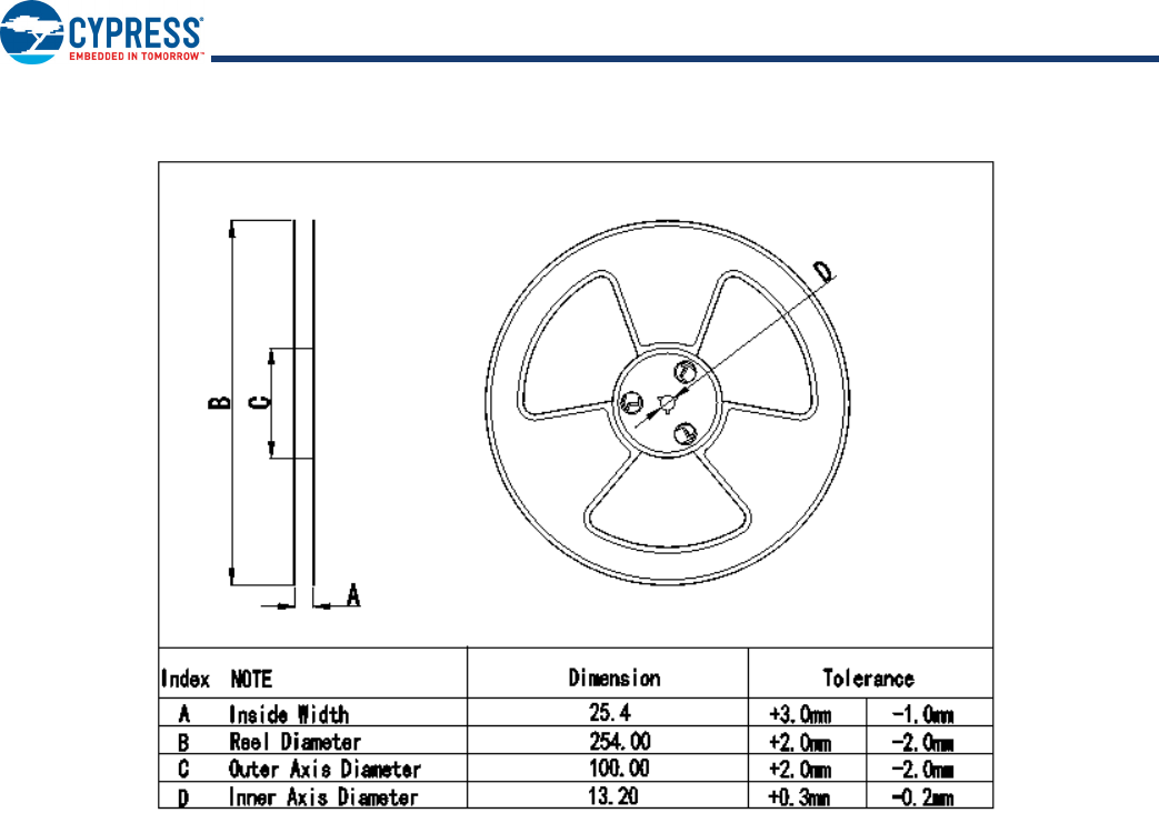
PRELIMINARY CYBLE-416045-02
Document Number: 002-24085 Rev. ** Page 54 of 60
Figure 12 details reel dimensions used for the CYBLE-416045-02.
Figure 12. Reel Dimensions
The CYBLE-416045-02 is designed to be used with pick-and-place equipment in an SMT manufacturing environment. The
center-of-mass for the CYBLE-416045-02 is detailed in Figure 13.
Figure 13. CYBLE-416045-02 Center of Mass (TBD)
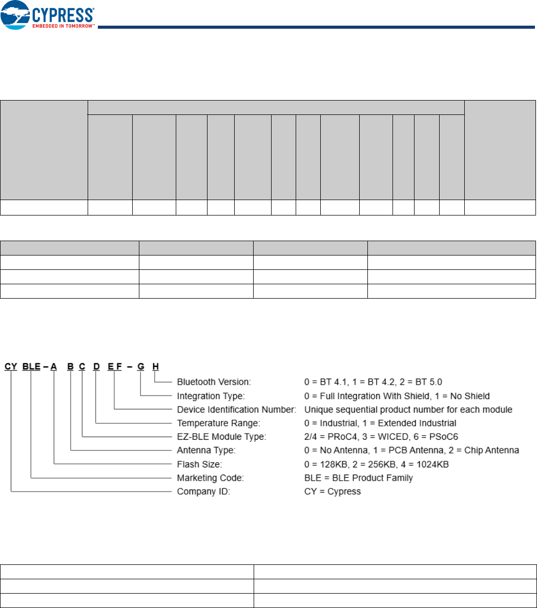
PRELIMINARY CYBLE-416045-02
Document Number: 002-24085 Rev. ** Page 55 of 60
Ordering Information
Table 45 lists the CYBLE-416045-02 part number and features. Tab le 4 6 lists the reel shipment quantities for the CYBLE-416045-02.
Table 46. Tape and Reel Package Quantity and Minimum Order Amount
The CYBLE-416045-02 is offered in tape and reel packaging. The CYBLE-416045-02 ships with a maximum of 500 units/reel.
Part Numbering Convention
The part numbers are of the form CYBLE-ABCDEF-GH where the fields are defined as follows.
For additional information and a complete list of Cypress Semiconductor BLE products, contact your local Cypress sales
representative. To locate the nearest Cypress office, visit our website.
Table 45. Ordering Information
MPN
Features
Package
CPU Speed (M4)
CPU Speed (M0+)
Flash (KB)
SRAM (KB)
UDB
CapSense
Direct LCD Drive
12-bit SAR ADC
LP Comparators
SCB Blocks
I2S/PDM
GPIO
CYBLE-416045-02 150/50 100/25 1024 288 12 3 3 1 Msps 2 2 336 43-SMT
Description Minimum Reel Quantity Maximum Reel Quantity Comments
Reel Quantity 500 500 Ships in 500 unit reel quantities.
Minimum Order Quantity (MOQ) 500 –
Order Increment (OI) 500 –
U.S. Cypress Headquarters Address 198 Champion Court, San Jose, CA 95134
U.S. Cypress Headquarter Contact Info (408) 943-2600
Cypress website address http://www.cypress.com
PRELIMINARY CYBLE-416045-02
Document Number: 002-24085 Rev. ** Page 56 of 60
Acronyms
Table 47. Acronyms Used in this Document
Acronym Description
abus analog local bus
ADC analog-to-digital converter
AG analog global
AHB
AMBA (advanced microcontroller bus
architecture) high-performance bus, an Arm data
transfer bus
ALU arithmetic logic unit
AMUXBUS analog multiplexer bus
API application programming interface
APSR application program status register
Arm® advanced RISC machine, a CPU architecture
ATM automatic thump mode
BW bandwidth
CAN Controller Area Network, a communications
protocol
CMRR common-mode rejection ratio
CPU central processing unit
CRC cyclic redundancy check, an error-checking
protocol
DAC digital-to-analog converter, see also IDAC, VDAC
DFB digital filter block
DIO digital input/output, GPIO with only digital
capabilities, no analog. See GPIO.
DMIPS Dhrystone million instructions per second
DMA direct memory access, see also TD
DNL differential nonlinearity, see also INL
DNU do not use
DR port write data registers
DSI digital system interconnect
DWT data watchpoint and trace
ECC error correcting code
ECO external crystal oscillator
EEPROM electrically erasable programmable read-only
memory
EMI electromagnetic interference
EMIF external memory interface
EOC end of conversion
EOF end of frame
EPSR execution program status register
ESD electrostatic discharge
ETM embedded trace macrocell
FIR finite impulse response, see also IIR
FPB flash patch and breakpoint
FS full-speed
GPIO general-purpose input/output, applies to a PSoC
pin
HVI high-voltage interrupt, see also LVI, LVD
IC integrated circuit
IDAC current DAC, see also DAC, VDAC
IDE integrated development environment
I2C, or IIC Inter-Integrated Circuit, a communications
protocol
IIR infinite impulse response, see also FIR
ILO internal low-speed oscillator, see also IMO
IMO internal main oscillator, see also ILO
INL integral nonlinearity, see also DNL
I/O input/output, see also GPIO, DIO, SIO, USBIO
IPOR initial power-on reset
IPSR interrupt program status register
IRQ interrupt request
ITM instrumentation trace macrocell
LCD liquid crystal display
LIN Local Interconnect Network, a communications
protocol.
LR link register
LUT lookup table
LVD low-voltage detect, see also LVI
LVI low-voltage interrupt, see also HVI
LVTTL low-voltage transistor-transistor logic
MAC multiply-accumulate
MCU microcontroller unit
MISO master-in slave-out
NC no connect
NMI nonmaskable interrupt
NRZ non-return-to-zero
NVIC nested vectored interrupt controller
NVL nonvolatile latch, see also WOL
opamp operational amplifier
PAL programmable array logic, see also PLD
PC program counter
Table 47. Acronyms Used in this Document (continued)
Acronym Description
PRELIMINARY CYBLE-416045-02
Document Number: 002-24085 Rev. ** Page 57 of 60
PCB printed circuit board
PGA programmable gain amplifier
PHUB peripheral hub
PHY physical layer
PICU port interrupt control unit
PLA programmable logic array
PLD programmable logic device, see also PAL
PLL phase-locked loop
PMDD package material declaration data sheet
POR power-on reset
PRES precise power-on reset
PRS pseudo random sequence
PS port read data register
PSoC Programmable System-on-Chip
PSRR power supply rejection ratio
PWM pulse-width modulator
RAM random-access memory
RISC reduced-instruction-set computing
RMS root-mean-square
RTC real-time clock
RTL register transfer language
RTR remote transmission request
RX receive
SAR successive approximation register
SC/CT switched capacitor/continuous time
SCL I2C serial clock
SDA I2C serial data
S/H sample and hold
SINAD signal to noise and distortion ratio
SIO special input/output, GPIO with advanced
features. See GPIO.
SOC start of conversion
SOF start of frame
SPI Serial Peripheral Interface, a communications
protocol
SR slew rate
SRAM static random access memory
SRES software reset
SWD serial wire debug, a test protocol
SWV single-wire viewer
Table 47. Acronyms Used in this Document (continued)
Acronym Description
TD transaction descriptor, see also DMA
THD total harmonic distortion
TIA transimpedance amplifier
TRM technical reference manual
TTL transistor-transistor logic
TX transmit
UART Universal Asynchronous Transmitter Receiver, a
communications protocol
UDB universal digital block
USB Universal Serial Bus
USBIO USB input/output, PSoC pins used to connect to
a USB port
VDAC voltage DAC, see also DAC, IDAC
WDT watchdog timer
WOL write once latch, see also NVL
WRES watchdog timer reset
XRES external reset I/O pin
XTAL crystal
Table 47. Acronyms Used in this Document (continued)
Acronym Description
PRELIMINARY CYBLE-416045-02
Document Number: 002-24085 Rev. ** Page 58 of 60
Document Conventions
Units of Measure
Table 48. Units of Measure
Symbol Unit of Measure
°C degrees Celsius
dB decibel
dBm decibel-milliwatts
fF femtofarads
Hz hertz
KB 1024 bytes
kbps kilobits per second
Khr kilohour
kHz kilohertz
kΩkilo ohm
ksps kilosamples per second
LSB least significant bit
Mbps megabits per second
MHz megahertz
MΩmega-ohm
Msps megasamples per second
µA microampere
µF microfarad
µH microhenry
µs microsecond
µV microvolt
µW microwatt
mA milliampere
ms millisecond
mV millivolt
nA nanoampere
ns nanosecond
nV nanovolt
Ωohm
pF picofarad
ppm parts per million
ps picosecond
s second
sps samples per second
sqrtHz square root of hertz
Vvolt
PRELIMINARY CYBLE-416045-02
Document Number: 002-24085 Rev. ** Page 59 of 60
Document History Page
Document Title: CYBLE-416045-02 EZ-BLE™ Creator™ Module
Document Number: 002-24085
Revision ECN Orig. of
Change
Submission
Date Description of Change
PRELIM PRELIM DSO 05/29/2018 Preliminary datasheet for CYBLE-416045-02 module.

PRELIMINARY CYBLE-416045-02
Document Number: 002-24085 Rev. ** Revised May 30, 2018 Page 60 of 60
© Cypress Semiconductor Corporation, 2018. This document is the property of Cypress Semiconductor Corporation and its subsidiaries, including Spansion LLC ("Cypress"). This document, including
any software or firmware included or referenced in this document ("Software"), is owned by Cypress under the intellectual property laws and treaties of the United States and other countries worldwide.
Cypress reserves all rights under such laws and treaties and does not, except as specifically stated in this paragraph, grant any license under its patents, copyrights, trademarks, or other intellectual
property rights. If the Software is not accompanied by a license agreement and you do not otherwise have a written agreement with Cypress governing the use of the Software, then Cypress hereby
grants you a personal, non-exclusive, nontransferable license (without the right to sublicense) (1) under its copyright rights in the Software (a) for Software provided in source code form, to modify and
reproduce the Software solely for use with Cypress hardware products, only internally within your organization, and (b) to distribute the Software in binary code form externally to end users (either
directly or indirectly through resellers and distributors), solely for use on Cypress hardware product units, and (2) under those claims of Cypress's patents that are infringed by the Software (as provided
by Cypress, unmodified) to make, use, distribute, and import the Software solely for use with Cypress hardware products. Any other use, reproduction, modification, translation, or compilation of the
Software is prohibited.
TO THE EXTENT PERMITTED BY APPLICABLE LAW, CYPRESS MAKES NO WARRANTY OF ANY KIND, EXPRESS OR IMPLIED, WITH REGARD TO THIS DOCUMENT OR ANY SOFTWARE
OR ACCOMPANYING HARDWARE, INCLUDING, BUT NOT LIMITED TO, THE IMPLIED WARRANTIES OF MERCHANTABILITY AND FITNESS FOR A PARTICULAR PURPOSE. To the extent
permitted by applicable law, Cypress reserves the right to make changes to this document without further notice. Cypress does not assume any liability arising out of the application or use of any
product or circuit described in this document. Any information provided in this document, including any sample design information or programming code, is provided only for reference purposes. It is
the responsibility of the user of this document to properly design, program, and test the functionality and safety of any application made of this information and any resulting product. Cypress products
are not designed, intended, or authorized for use as critical components in systems designed or intended for the operation of weapons, weapons systems, nuclear installations, life-support devices or
systems, other medical devices or systems (including resuscitation equipment and surgical implants), pollution control or hazardous substances management, or other uses where the failure of the
device or system could cause personal injury, death, or property damage ("Unintended Uses"). A critical component is any component of a device or system whose failure to perform can be reasonably
expected to cause the failure of the device or system, or to affect its safety or effectiveness. Cypress is not liable, in whole or in part, and you shall and hereby do release Cypress from any claim,
damage, or other liability arising from or related to all Unintended Uses of Cypress products. You shall indemnify and hold Cypress harmless from and against all claims, costs, damages, and other
liabilities, including claims for personal injury or death, arising from or related to any Unintended Uses of Cypress products.
Cypress, the Cypress logo, Spansion, the Spansion logo, and combinations thereof, WICED, PSoC, CapSense, EZ-USB, F-RAM, and Traveo are trademarks or registered trademarks of Cypress in
the United States and other countries. For a more complete list of Cypress trademarks, visit cypress.com. Other names and brands may be claimed as property of their respective owners.
Sales, Solutions, and Legal Information
Worldwide Sales and Design Support
Cypress maintains a worldwide network of offices, solution centers, manufacturer’s representatives, and distributors. To find the office
closest to you, visit us at Cypress Locations.
Products
ARM® Cortex® Microcontrollers cypress.com/arm
Automotive cypress.com/automotive
Clocks & Buffers cypress.com/clocks
Interface cypress.com/interface
Internet of Things cypress.com/iot
Memory cypress.com/memory
Microcontrollers cypress.com/mcu
PSoC cypress.com/psoc
Power Management ICs cypress.com/pmic
Touch Sensing cypress.com/touch
USB Controllers cypress.com/usb
Wireless Connectivity cypress.com/wireless
PSoC® Solutions
PSoC 1 | PSoC 3 | PSoC 4 | PSoC 5LP | PSoC 6
Cypress Developer Community
Forums | WICED IOT Forums | Projects | Video | Blogs |
Training | Components
Technical Support
cypress.com/support