D Link WM800BA1 DC-HSPA+ module User Manual DWM 800B Hardware User Guide
D Link Corporation DC-HSPA+ module DWM 800B Hardware User Guide
D Link >
user guide DWM-final.pdf

DWM-800B
HW User
Guide

2
CONTENT
1. INTRODUCTION ............................................................................................................................................... 3
1.1. OVERVIEW ............................................................................................................................................................................3
1.2. APPLICATION TYPE ...............................................................................................................................................................3
1.3. INSTALLATION GUIDELINES .................................................................................................................................................4
1.4. APPLICATION SCENARIO .......................................................................................................................................................4
2. DWM-800B INTERFACES ........................................................................................................................... 5
2.1. DWM-800B INTERFACE SUMMARY.....................................................................................................................................5
2.1.1. RF interface ...............................................................................................................................................................5
2.2. APPLICATION NOTE OF DWM-800B INTERFACES ..............................................................................................................7
2.2.1. Power supply and Ground ............................................................................................................................................7
2.2.2. USB interface ...............................................................................................................................................................8
2.2.2.1. Description ...................................................................................................................................................................8
2.2.3. USIM interface ............................................................................................................................................................9
2.2.4. PCM interface ...........................................................................................................................................................10
2.2.5. SD card tntreface .......................................................................................................................................................11
2.2.6. Others .........................................................................................................................................................................11
3. ELECTRICAL CHARACTERISTICS AND SAFETY INFORMATION ..................................................... 12
3.1. ABSOLUTE MAXIMUM RATINGS .........................................................................................................................................12
3.2. POWER-UP AND POWER-DOWN SEQUENCE .......................................................................................................................12
3.3. OPERATING CONDITIONS ...................................................................................................................................................13
3.4. RF EXPOSURE COMPLIANCE .............................................................................................................................................14
4. PINS DESCRIPTION OF MINI PCIE CONNECTOR ................................................................................. 15
FEDERAL COMMUNICATION COMMISSION INTERFERENCE STATEMENT ......................................... 16
3
1. Introduction
1.1. Overview
The DC-HSPA+ Mini PCIe module DWM-800B , powered by MT6280 chipset, can be integrated into any devices
for 3G mobile applications. It provides SMS, MMS, Call as well as high speed internet access to DC-HSPA+and
UMTS networks worldwide. Main features of DWM-800B is listed in table 1-1
Table 1-1 Main Features of DWM-800B
Item
Description
Air Interface
DC-HSPA+/UMTS/EDGE/GPRS/GSM/WCDMA
Transmit speed
DL 42 Mbps, UL 11 Mbps
Frequency
GSM Band : 850/900/1800/1900MHz
UMTS Band: 2100/1900/850 MHz
Operating temperature range
Normal Operation: 0°C to +45°C
Storage: -20°C to +65°C
Size
51mm*30mm*4.7mm
Voltage range
Power Supply: 3.3V-3.6V
1.2. Application Type
The application type of the module is shown as bellow:
All instructions relating to the integration of the module described on the FCC Grant notes must be followed.
4
1.3. Installation Guidelines
Careful planning and preparation of any installation will always benefit the end result, always read and follow all installation
instructions. Follow ESD precautions and prepare an SD safe workspace for installation. Turn the power to the host off and ground
yourself to dissipate static charge.
Mount only in sockets and locations intended for Mini PCIe cards consult manufacturer on thermal management
recommendations for the module mounted within the host.
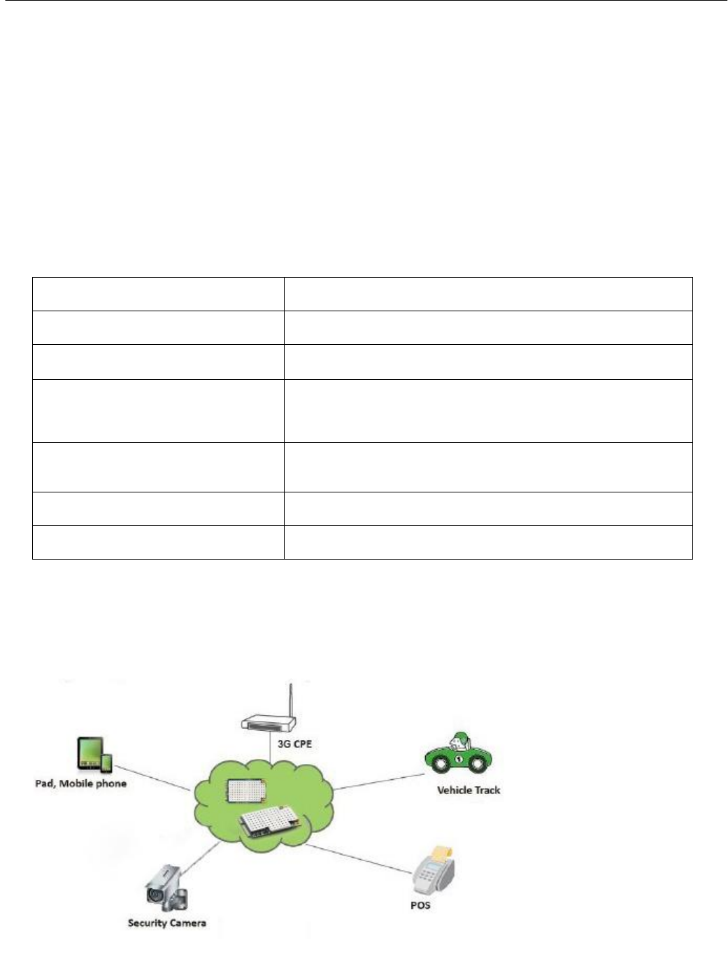
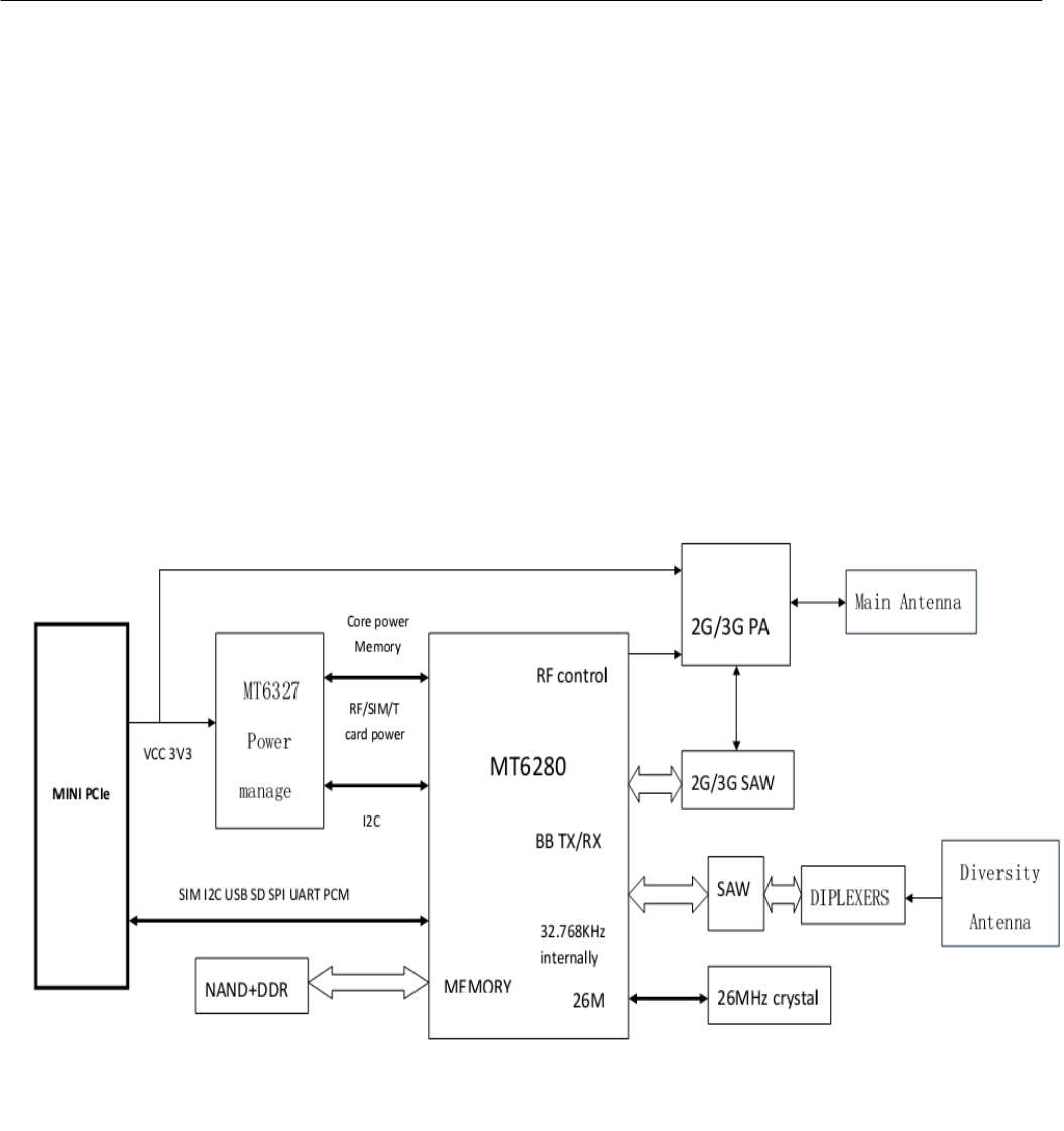
1.4. Application scenario
The HSPA module DWM-800B supports Voice Call, SMS, MMS and internet access functions. The block diagram of
DWM-800B is as follows:
Figure1-1 DWM-800B block diagram
5
2. DWM-800B interfaces
2.1.
DWM-800B interface summary
The module DWM-800B supports multimode operation: DC-HSPA+, UMTS (850/1900/2100 MHz) and quad-band
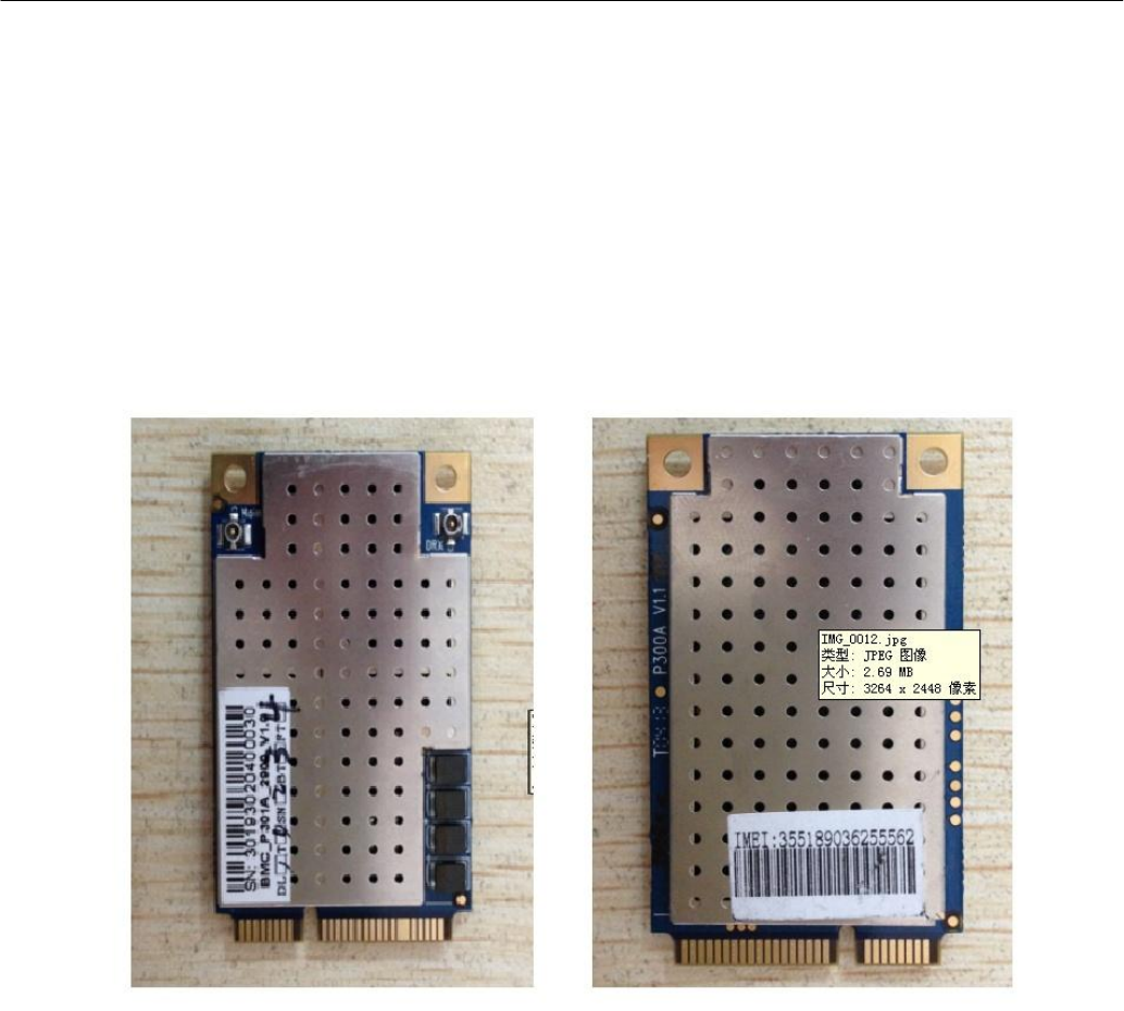
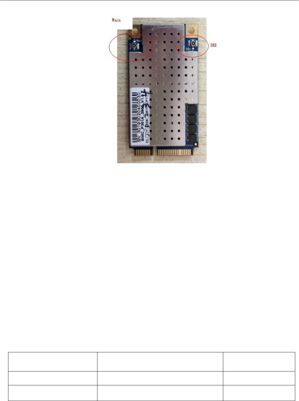
GSM (850/900/1800/1900 MHz). The size of DWM-800B is 51mm*30mm*4.7mm. The appearance is shown in Figure
2-1 and Figure 2-2.
Figure 2-1 The front view of DWM-800B Figure 2-2 The rear view of DWM-800B
The MINI PCI-E is shown as in Figure , which is the main interface for application. RF antenna pad connector is
shown as in Figure 2-1 .
2.1.1. RF interface
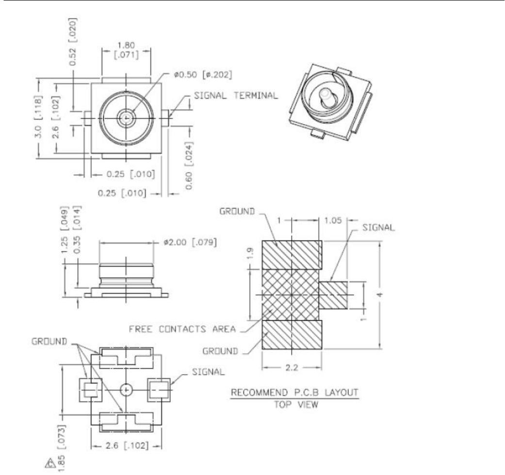
The DWM-800B module provides an interface for RF antenna by Connector: DWM-800B uses HRS’s U.FL-R-SMT
RF connector on the rear side.
Solder pad mode: The antenna can also be soldered to the pad on the module which has a ground pad close to the
antenna pad.
The ground impedance of RF antenna is 50Ω. The RF connector is shown in Figure 2-3.
6
Figure 2-3 The sketch map of RF connector
It’s required to use RF cable of which the insertion loss should comply with:
• GSM850/900<1dB
• DCS1800/PCS1900<1.5dB
• UMTS2100/ UMTS1900/ UMTS850<1.5Db
There are two RF connectors in DWM-800B ,the description of them is shown in Figure 2-4 below:
7
Figure 2-4 description of DWM-800B RF connectors
2.2. Application note of DWM-800B interfaces
DWM-800B provides rich interfaces for secondary development by the MINI PCI-E, such as USIM card interface,
USB interface, UART interface, PCM(Pulse Code Modulation) interface, I2C interface, power supply interface and so
on. The detailed information will be described in the following sections.
2.2.1. Power supply and Ground
The power supply input for DWM-800B module is listed as
follows: DC +3.3V~+3.6V, for DWM-800B working voltage;
The description of DWM-800B Power supply and GND pins is shown in Table 2-1 below.
Table 2-1 The description of DWM-800B Power supply and GND pins
Power input
The correlative pins in MINI PCI-E
SN. of the MINI
PCI-E
DC: +3.3V~+3.6V input
VDD3V3
2,24,39,41,52
GND
GND
4,9,15,18,21,26,27,29,34,35,37,
43,50
8
2.2.2. USB interface
2.2.2.1. Description
DWM-800B provides a high-speed USB interface by MINI PCI-E, which supports USB 2.0 protocol. The detailed
information is given in Table 2-2.
Table 2-2 DWM-800B USB interface description
Signals of
USB interface
The correlative pins in
MINI PCI-E
SN. of MINI PCI-E
Description
DM
USB_HS_DM
36
USB Data-
DP
USB_HS_DP
38
USB Data+
GND
GND
4,9,15,18,21,26,27,29,34,35,37,
43,50
GND
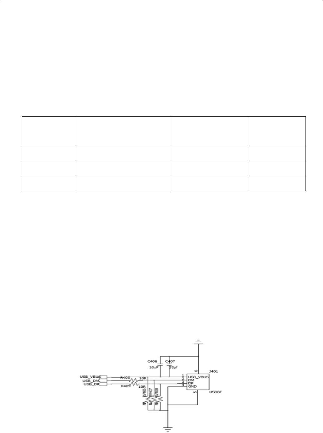
2.2.2.2. Reference circuit
The reference circuit of USB interface is shown in Figure 2-5 below.
1) To get the reliable USB power supply, it is recommended to use a 10uF(C406) filter capacitor and a 22pF(C407)
filter capacitor which need to be grounded.
2) To reduce the reflection caused by the high frequency alternating signal in the transmission, it is recommended to
add a resistor with value below 10Ω to the DM and DP in USB interface to ensure correct transmission for USB
data. Just like the resistors R408 and R409 in Figure 2-5.
3) To avoid static electricity in USB interface, it is recommended to use the ESD protection device. Just like the
varistor RV406, RV407 and RV408 with capacitor values below 3pF.
4) To ensure USB working reliably, it is recommended to use additional protection device.
Figure 2-5 The reference circuit of USB interface

9
2.2.3. USIM interface
DWM-800B supports USIM card in UMTS mode as well as SIM card in GSM/GPRS/EDGE mode,and UIM card in
WCDMA mode.
2.2.3.1. Description
DWM-800B provides USIM card interface by MINI PCI-E which can be used in both UMTS and
GSM/GPRS/EDGE networks. The Table 2-3 gives more detailed information.
Table 2-3 DWM-800B USIM card interface description
Signals offered
by
USIM interface
The name of the correlative
pins in
MINI PCI-E
SN. of the MINI
PCI-E
Description
DATA
USIM_DATA
10
USIM card data
CLK
USIM_CLK
12
USIM card CLK
RST
USIM_RESET
14
Reset signal
VCC
VREG_EXTUSIM
8
USIM card power
GND
GND
4,9,15,18,21,26,27,29,34,3
5,37,43,50
GND
2.2.3.2. Reference circuit
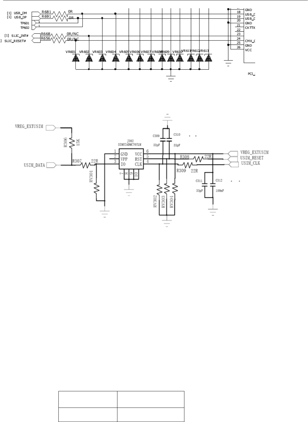
The reference circuit of USIM interface is shown in Figure 2-6 below.
1) The DATA line of USIM is connected to SIM power supply by a pull-up resistor with reference value 15KΩ.
2) To avoid the instantaneous voltage overflowing, the resistor with reference value 22Ω can be used for the DATA,
CLK and RST line. Just like the resistors R307, R308 and R309 in Figure 2-6.
3) To avoid the static electricity in USIM socket, it is recommended to use the ESD protection device for the DATA,
CLK and VCC line. Just like the varistors RV301, RV302, RV303 and RV304 in Figure 2-6 this should be close to the
USIM socket as possible.
4) To get more flat USIM power supply, it is recommended to use the filter capacitors. Just like C311 and C312 in
Figure 2-6with reference value 33pF and 100nF.
5) To eliminate the peak interference and high frequency interference signal on RST and CLK line, the filter capacities
(C310, C309) can be placed in RST and CLK line, the reference value is 33pF.
10
Figure 2-6 The reference circuit of USIM interface
2.2.4. PCM interface
It can just support PCM(Optional). It can provide voice call by PCM ,using external audio codec . DWM-800B provides a
UART interface by MINI PCI-E for debug.
2.2.4.1. Description
PCM interfaces on the DWM-800B have been designed to be compatible with others so as to meet different needs. And we
can make corresponding configuration for interfaces on the DWM-800B according to customer's requirements. The
information about UART and PCM interfaces provided by DWM-800B is described in Table 2-4
Table 2-4 The connection between phone handle and the MINI PCI-E
SN. of MINI PCI-E
Compatible definition
45
PCM_CLK

11
47
PCM_SYNC/PCM_IN
49
PCM_OUT/PCM_IN
51
PCM_IN/PCM_SYNC
2.2.5. SD card tntreface
2.2.5.1. Description
There are seven pins for SD card in the MINI PCI-E. And the detailed information is given in Table 2-5 below.
Table 2-5 DWM-800B SD card interface description
pcie
Pin.NO
Signal name
Description
13
SDC1_CMD
SD Command/Response
17
SDC1_DATA0
SD Data 0
19
SDC1_DATA1
SD Data 1
23
SDC1_DATA2
SD Data 2
25
SDC1_DATA3
SD Data 3
31
SDC1_CLK
SD Clock
32
VREG_SD
SD Supply voltage
2.2.6. Others
DWM-800B also provides some other interfaces listed in Table 2-7.
Table 2-7
pins in
MINI PCI-E
SN. of the MINI
PCI-E
Volt
Description
W_DISABLE_N
20
2.6
The W_DISABLE# signal is an active low signal that
when asserted (driven low) by the system shall disable
radio operation.
WAKE_N
1
2.6
The WAKE# signal is an open drain, active low signal that
is driven low by a PCI Express Mini Card function to
reactivate the PCI Express Link hierarchy’s main power
rails and reference clocks.
I2C_SCL
30
2.6
I2C Interface
12
I2C_SDA
32
2.6
I2C Interface
SPI_SDI
3
Serial port control data input
SPI_SDO
5
2.6
Serial port control data output
SPI_CS#
6
2.6
Serial port control Chip Select
SPI_SCLK
7
2.6
Serial Port Bit Clock
3. Electrical Characteristics and Safety Information
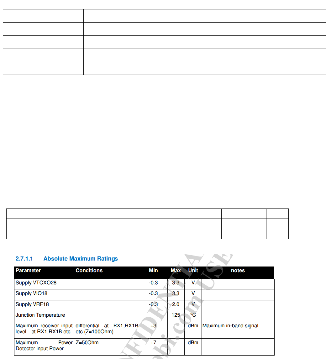
3.1. Absolute Maximum Ratings
Absolute maximum rating for power supply and voltage on I/O pins of DWM-800B are list in table1 as
follows.
Table 3-1 Absolute maximum ratings
Symbol
Description
Min
Max
Units
VIO
Voltage on any input or output pin
-0.5
VPAD*+0.5
V
VBAT
POWER SUPPLY
3.3
3.9
V
*VPAD=1.8V
3.2. Power-Up and Power-Down Sequence
DWM-800B is Auto Power On when VBAT is ready. The system would be turned on. The pmic(MT6327) power on
sequence is as below:
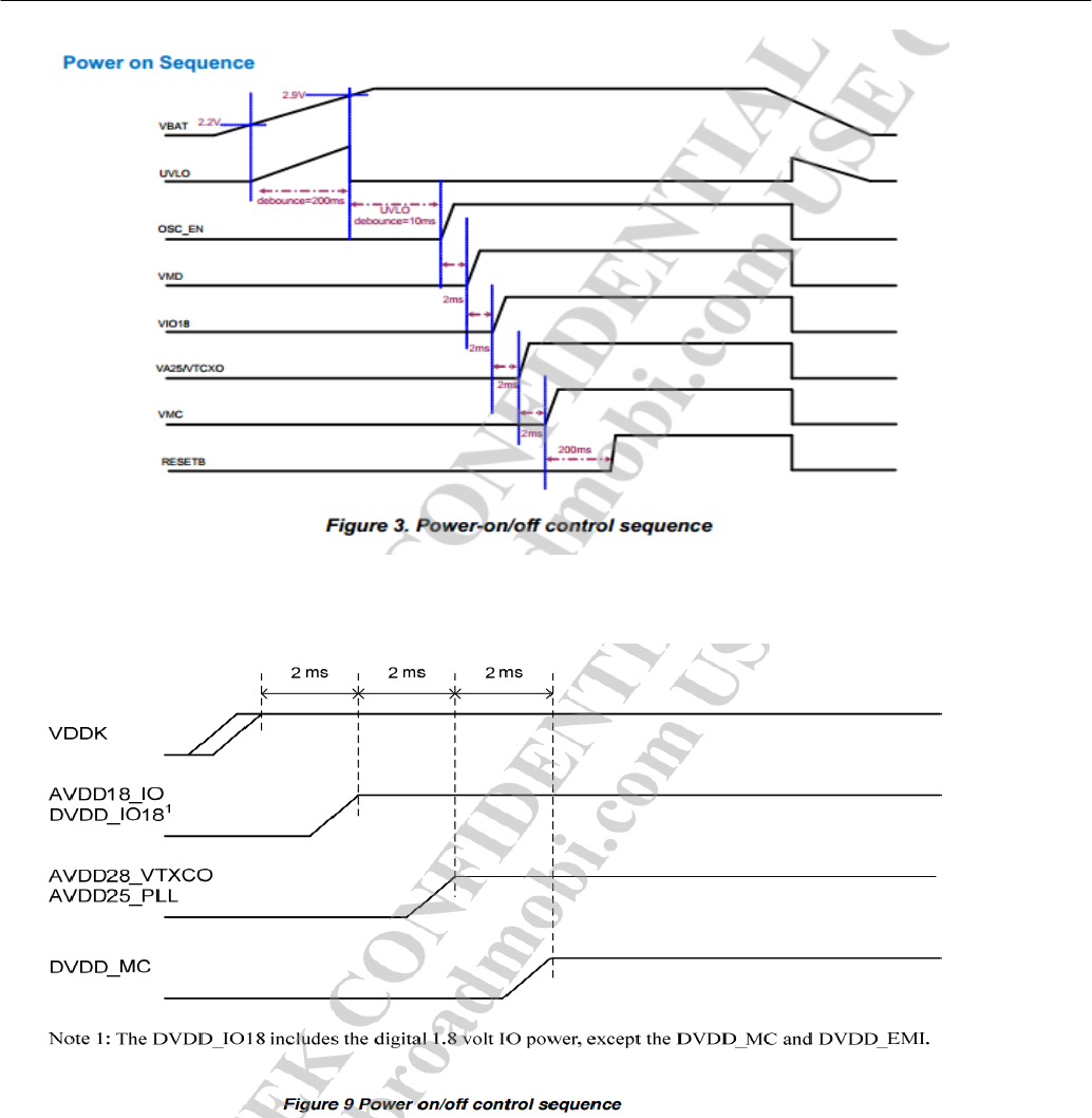
13
The CPU(MT6280) power on sequence is as below:
3.3. Operating conditions
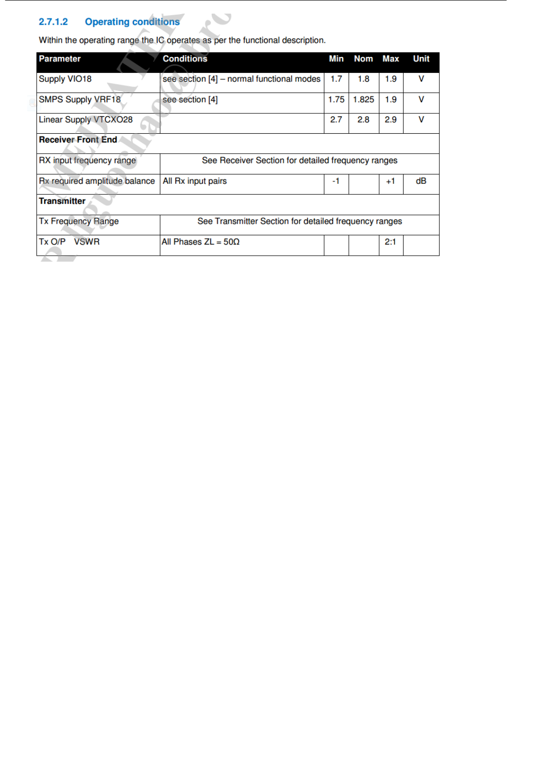
14
3.4. RF Exposure Compliance
The antenna(s) used for this transmitter must be installed to provide a separation distance of at least
20 cm from all persons and must not be co-located or operating in conjunction with any other antenna or
Transmitter.
This device is intended only for OEM integrators under the following conditions:
1) The antenna must be installed such that 20 cm is maintained between the antenna and users, and
2) The transmitter module may not be co-located with any other transmitter or antenna.
As long as 2 conditions above are met, further transmitter test will not be required. However, the OEM integrator
is still responsible for testing their end-product for any additional compliance requirements required with this
module installed
IMPORTANT NOTE: In the event that these conditions can not be met (for example certain laptop
configurations or co-location with another transmitter), then the FCC authorization is no longer considered valid
and the FCC ID can not be used on the final product. In these circumstances, the OEM integrator will be
responsible for re-evaluating the end product (including the transmitter) and obtaining a separate FCC
authorization.
End Product Labeling:
This transmitter module is authorized only for use in device where the antenna may be installed such that 20 cm
may bemaintained between the antenna and users. The final end product must be labeled in a visible area with
the following: “Contains
FCC ID: KA2WM800BA1”. The grantee's FCC ID can be used only when all FCC compliance requirements
are met.
Manual Information To the End User
The OEM integrator has to be aware not to provide information to the end user regarding how to install or
remove this RF module in the user’s manual of the end product which integrates this module.

15
The end user manual shall include all required regulatory information/warning as show in this manual.
4. Pins description of mini PCIE connector
SN
Definition
Description
Volt
Remark
1
WAKE_N
OUTPUT
1.8
The WAKE# signal is an open drain, active low signal that
is driven low by a PCI Express Mini Card function to
reactivate the PCI Express Link hierarchy’s main power rails
and reference clocks.
3
SPI_SDI
Serial port control data input
1.8
5
SPI_SDO
Serial port control data output
1.8
7
SPI_SCLK
Serial Port Bit Clock
1.8
9
GND
Ground
11
Reserved
Reserved
Reserved For Future Use
13
SDC1_CMD
SD Command/Response
1.8
15
GND
Ground
17
SDC1_DATA0
SD Data 0
1.8
19
SDC1_DATA1
SD Data 1
1.8
21
GND
Ground
23*
SDC1_DATA2
SD Data 2
1.8
25*
SDC1_DATA3
SD Data 3
1.8
27
GND
Ground
29
GND
Ground
31*
SDC1_CLK
SD Clock
1.8
33*
Reserved
Reserved
Reserved For Future Use
35
GND
Ground
37
GND
Ground
39
VDD3V3
POWER
3.3
Power Supply
41
VDD3V3
POWER
3.3
Power Supply
43
GND
Ground
45*
PCM_CLK
PCM Clock
1.8
47*
PCM_SYNC
PCM data strobe
1.8
49*
PCM_OUT
PCM data output
1.8
51*
PCM_IN
PCM data input
1.8
2
VDD3V3
POWER
3.3
Power Supply
4
GND
Ground
6
SPI_CS#
Serial port control Chip Select
1.8
8
VREG_USIM
USIM Power
1.8
USIM Interface, USIM power
10
USIM_DATA
USIM_DATA
1.8
USIM Interface
12
USIM_CLK
USIM CLK
1.8
USIM Interface
14
USIM_RESET
USIM_RESET
1.8
USIM Interface
16
Reserved
Reserved
Reserved For Future Use

16
18
GND
Ground
20
W_DISABLE_N
2.6
The W_DISABLE# signal is an active low signal that when
asserted (driven low) by the system shall disable radio
operation.
22
EXT_RST_IN
Reset
2.6
Reset module
24
VDD3V3
POWER
3.3
Power Supply
26
GND
Ground
28
Reserved
Reserved
Reserved For Future Use
30
I2C_SCL
I2C Clock
2.6
I2C Interface
32*
**
I2C_SDA/VMC_PMU
I2C Data/VMC_PMU
2.6
I2C Interface and SD power combine
34
GND
Ground
36
USB_HS_DP
USB Data+
USB Interface
38
USB_HS_DM
USB Data-
USB Interface
40
GND
Ground
42*
Reserved
Reserved
Reserved For Future Use
44*
Reserved
Reserved
Reserved For Future Use
46*
SLIC_INT#
SLIC_RESET#
SLIC INT
48
SLIC_RESET#
SLIC_RESET#
SLIC RESET
50
GND
Ground
52
VDD3V3
POWER
3.3
Power Supply
* UART and PCM interfaces on the DWM-800B have been designed to be compatible with others so as to meet different
needs.
And we can make corresponding configuration for interfaces on the DWM-800B according to customer's requirements.
* Please contact us to make sure if this pins could be used.
Federal Communication Commission Interference
Statement
This device complies with Part 15 of the FCC Rules. Operation is subject to the following two conditions: (1)
This device may not cause harmful interference, and (2) this device must accept any interference received,
including interference that may cause undesired operation.
This equipment has been tested and found to comply with the limits for a Class B digital device, pursuant to
Part 15 of the FCC Rules. These limits are designed to provide reasonable protection against harmful
interference in a residential installation. This equipment generates, uses and can radiate radio frequency
energy and, if not installed and used in accordance with the instructions, may cause harmful interference to
radio communications. However, there is no guarantee that interference will not occur in a particular
installation. If this equipment does cause harmful interference to radio or television reception, which can
be determined by turning the equipment off and on, the user is encouraged to try to correct the interference
by one of the following measures:

17
- Reorient or relocate the receiving antenna.
- Increase the separation between the equipment and receiver.
- Connect the equipment into an outlet on a circuit different from that
to which the receiver is connected.
- Consult the dealer or an experienced radio/TV technician for help.
FCC Caution: Any changes or modifications not expressly approved by the party responsible for compliance
could void the user's authority to operate this equipment.
This transmitter must not be co-located or operating in conjunction with any other antenna or transmitter.
This equipment complies with FCC radiation exposure limits set forth for an uncontrolled environment. This
equipment should be installed and operated with minimum distance 20cm between the radiator & your body.
FCC Caution: Any changes or modifications not expressly approved by the party responsible for compliance could void the
user's authority to operate this equipment.
This transmitter must not be co-located or operating in conjunction with any other antenna or transmitter.