DENON Compact Disc Manual 98020206
User Manual: DENON DENON Compact Disc Manual DENON Compact Disc Owner's Manual, DENON Compact Disc installation guides
Open the PDF directly: View PDF ![]() .
.
Page Count: 24
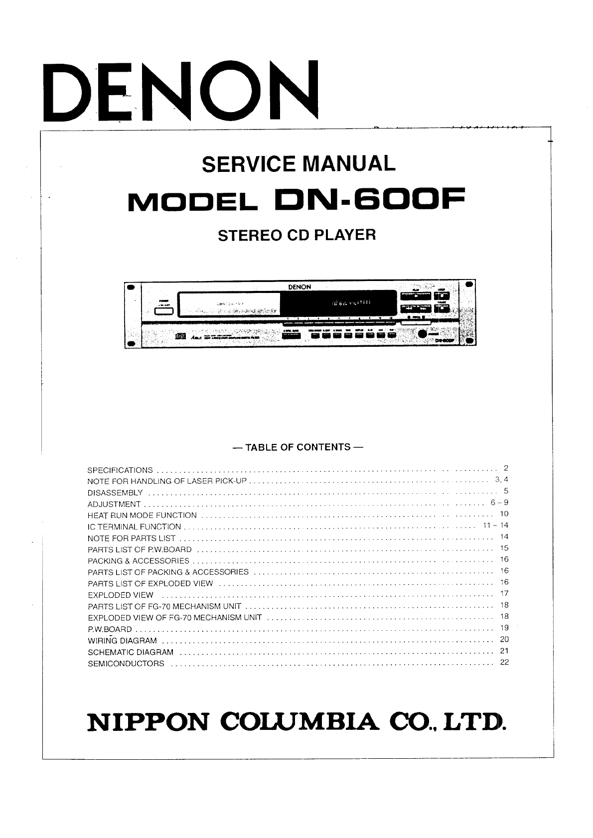
DENON
SERVICE MANUAL
MODEL DN-6OOF
STEREO CD PLAYER
-- TABLE OF CONTENTS --
SPECIFICATIONS ............................................................................ 2
NOTE FOR HANDLING OF LASER PICK-UP ..................................................... 3, 4
DISASSEMBLY .............................................................................. 5
ADJUSTMEN-[ .............................................................................. 6-- 9
HFAT RUN MODE FUNCTION ................................................................. 10
IC TERMINAL FUNCTION ................................................................... 11 - 14
NOTE FOR PARTS LIST ....................................................................... 14
PARTS LIST OF RW.BOARD .................................................................... 15
PACKING & ACCESSORIES ..................................................................... 16
PARTS LIST OF PACKING & ACCESSORIES ....................................................... t6
PARTS LIST OF EXPLODED VIEW ............................................................... 16
EXPLODED VIEW ............................................................................ 17
PARTS LIST C,F FG-70 MECHANISM UNIT ......................................................... 18
EXPLODED VIEW OF FG-70 MECHANISM UNIT .................................................... 18
P.W.BOARD .................................................................................. 19
WIRING DIAGRAM ............................................................................ 20
SCHEMATIC OIAGRAM ........................................................................ 21
SEMICONDUCTORS .......................................................................... 22
NIPPON COI_MBIA CO.. LTD.
III DN-6OOF
SPECIFICATIONS
--AUDIO ....
No.of.Chan_ neJs::.io_.._. '_2 channels-
Frequency Respon'_e: 2 -20,000 Hz. .
--Dynamic Range: _ _ --98 dB "
Signa!rto-noise Ratio:- 107 dB:"
Harmonic Distortion 0.003 % (,1kHz) _
" SeparatiOn: ......... 103 dB (1 kHz)
Wow & Flutter: Below measurable limit:
(_+0.001% W.peak)
Output Voltage: 2 V
FUNCTIONS AND DISPLAY
Functions: Automatic search, progra.mmed
playback, repeat playback,
manual search, auto space,
time mode, auto edit.
Display: Track number, time, music caTendar,
emphasis feature and engaged
modes.
Others: Headphones jack
DISCS Compact Disc format SUPPLIED ACCESSORIES Pin-plug connection cord
GENERAL CHARACTERISTICS
Power Supply: Voltage is shown on rating label
Power ConsumptionS-- _10W
Dimensions: 482 (19") W × 88 (3-15/32") H ×
-280 (11-1/32") Dmm
Weight: 4.2 kg
* Design and specifications are subject to change without notice in the course of product improvement.
NOTE FOR HANDLING OF LASER PICK-UP
Caution for Handling the Laser Pick-up
The laser pick-up KSS-240A is assembled and precisely adjusted
using a sophisticated manufacturing process in our plant• Do not
disassemble or attempt to-readjust it. Please keep the following
instructions carefully in handling pick-up.
4. Metal Bearing
As the metal bearing of Cu-compound sintered alloy is impregnated
with FROIL946P (*Part No. 529 0054 007), never fail to supply the
bushing with the same lubricant at the time of replacing the pick-up.
1. Handle with Care
(1) Storage
Do not store the pick-up in dusty, high-temperatured or high-hu-
midity environments.
(2) Please take care for preventing from shock by falling down or
careless handling.
2. Laser Diode (LD)
(1) Protect your eyes
The laser beam may_lamage the human eye, since the intensity
of the focuseds:l_ot'm_i reach 7 x 10³ W/cr_ 2 even if the intensity
at the objective lens is 400 ,_W maximum. As the light beam
spreads alter focused through the objective lens, it does not effect
you in the place as far as more than 30 cms. However, do not
look at the laser light beam either through the objective Iens
directly nor another lens or a mirror.
(2) Poison of As
Since the LD chip contains As (Arsenic), as GaAs + GaAIAs, as
known as the poison, although the poison is relatively weak, in
comparing with others, e.g.As203, AsCI3 etc., and the amount is
small, avoid putting the chip in acid or an alkali solution, heating
it over 200°C or puttinc it into your mouth.
" (3) Avoid surge current or electrostatic discharge
The LD may be damaged or deteriorated by its own strong light
it a large current is supplied to it, even if only a short pulse.
Make sure that there is no surge current in the LD driving circuit
by switches or else. Be careful to handle pick-up as it may be
damaged in a moment by human electrostatic discharge. The
pins of the LD are short-circuited by solder for protection during
shipment.
For safety handling of an LD, grounding the human body, meas-
uring equipments and jig is strongly recommended. And still it is
further desirable to make use of mat on the platform and floor for
handling the LD.
To open the short-circuit, remove the soldering quickly with a
soldering iror_ whose metal part is grounded.
The temperature of the; soldering iron should be less than 320°C
(30W).
5. Handling
Please handle the laser pick-up with holding the side base (rosin
molded part).
When either a part of human body or some other things may happen
to touch directly with the circuit part of F:W.Board, it may cause
deterioration, take careful attention in handling this base.
6. Deterioration
As KSS-240 comprises built-in RF Amp and APC curcuit, it resists
stronger against external electrostatJc damages than the former
typed pickup. However, there is possibility of pickup deterioration in
the following cases.
(1) Low HF level, or with great numbers of jitters.
(2) Tracking offset (EF Balance) is out of order (Refer to "Confirma-
tion Method of Adjustment" far cortirmation on (1) and (2)).
3. Actuator
(1) The performance of the actuator may be effected if magnetic
material is located nearby, since the actuator has a strong mag-
netic circuit. Do not permit dust to enter through the clearance of
the cover.
(2) Cleaning the lens
It may change.the specifications by attaching dust or ash on the
objective lens. Clean the lens with a cleaning paper dampened
with a little water, not pressing lens with so much strength by the
cleaning paper.
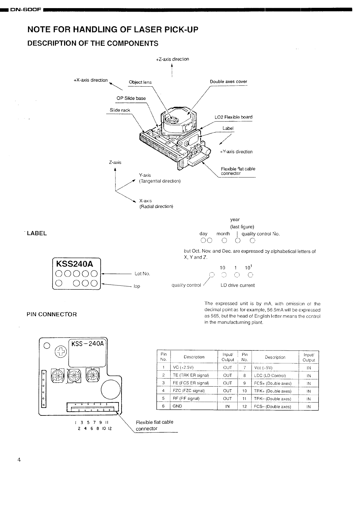
NOTE FOR HANDLING OF LASER PICK-UP
DESCRIPTION OF THE COMPONENTS
+X-axis direction
+Z-axis direction
Object lens \
OP Slide base
\
Slide rack
Z-axis
A Y-axis
(Tangential direction)
X-axis
(Radial direction)
Double axes cover
/
LO2 Flexible board
Label
//
+Y-axis direction
Flexible fiat cable
connecter
-LABEL
KSS240A
(D O O () O Lot No.
C_) O (_) O lop
year
(last figure)
day month I quality con[rol XIo.
O O 0 0 C'
but Oct. Nov. and Dec. are expressed ay alphabetical letters of
X, YandZ.
quality control /_
I 0 I 101
() _" C,
LD drive current
PIN CONNECTOR
The expressed unit is by mA, with omission ol the
decimal point as for example, 56 5mA will be expressed
as 565, but the head of English letter means tile ccntrol
in the manufacturning plant.
o
If t T t _ _ +
1357911
2 4 681012
Pin
No. Description
1 VC (+2.5V}
2 TE (TRK ER signal)
3 FE (FCS ER signal)
4 ! FZC (FZC signal)
5 RF (RF signal)
6 GND
I
InPut'/ l
Output i
OUT
OUT
QUT
OUT
OUT
! iN
Pin
No.
7 Vc
8 LC
9FC
10 TF
11 TIq
12 FC
Input/
Description ! Output
l-- vi
(LD C.ontral) IN
(Doable axes) IN
(DoJble axes) IN
(Double axes)
(Double axes) IN
_, lexible flat cable
connector
II_llV-ldLlUl- I
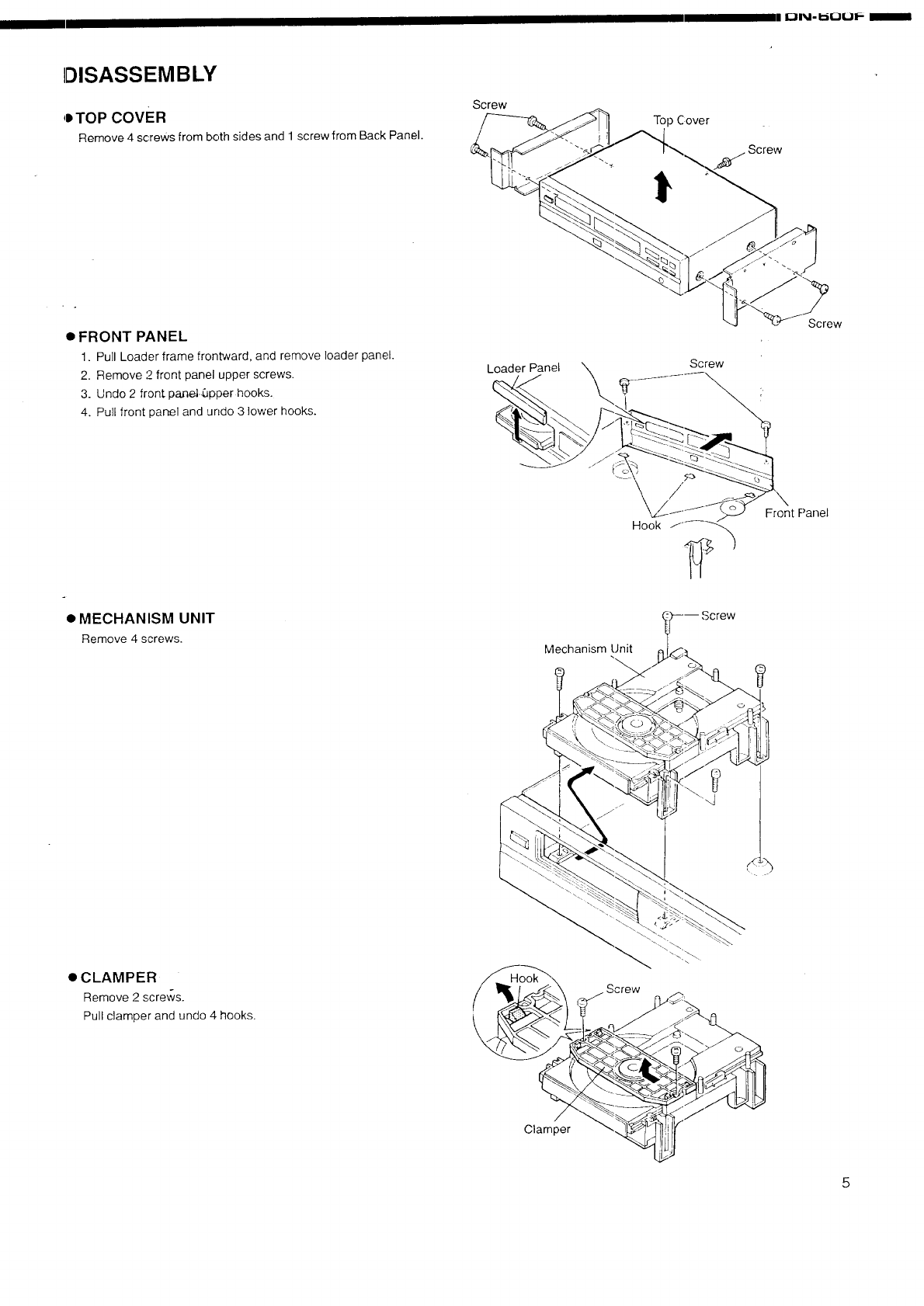
IDISASSEMBLY
,DTOP COVER
Remove 4 screws from both sides and 1 screw from Back Panel.
Screw
Top Cover
t
Screw
• FRONT PANEL
1. Pull Loader frame frontward, and remove loader panel.
2. Remove 2 front panel upper screws.
3. Undo 2 front panel 5pper hooks.
4. Pull front panel and undo 3 lower hooks.
Loader Panel Screw
Screw
•MECHANISM UNIT
Remove 4 screws.
• CLAMPER
Remove 2 screws.
Pull cJamper and undo 4 hooks.
Clamper
Mechanism Unit
Few
Front Panel
5
ION-6OOF
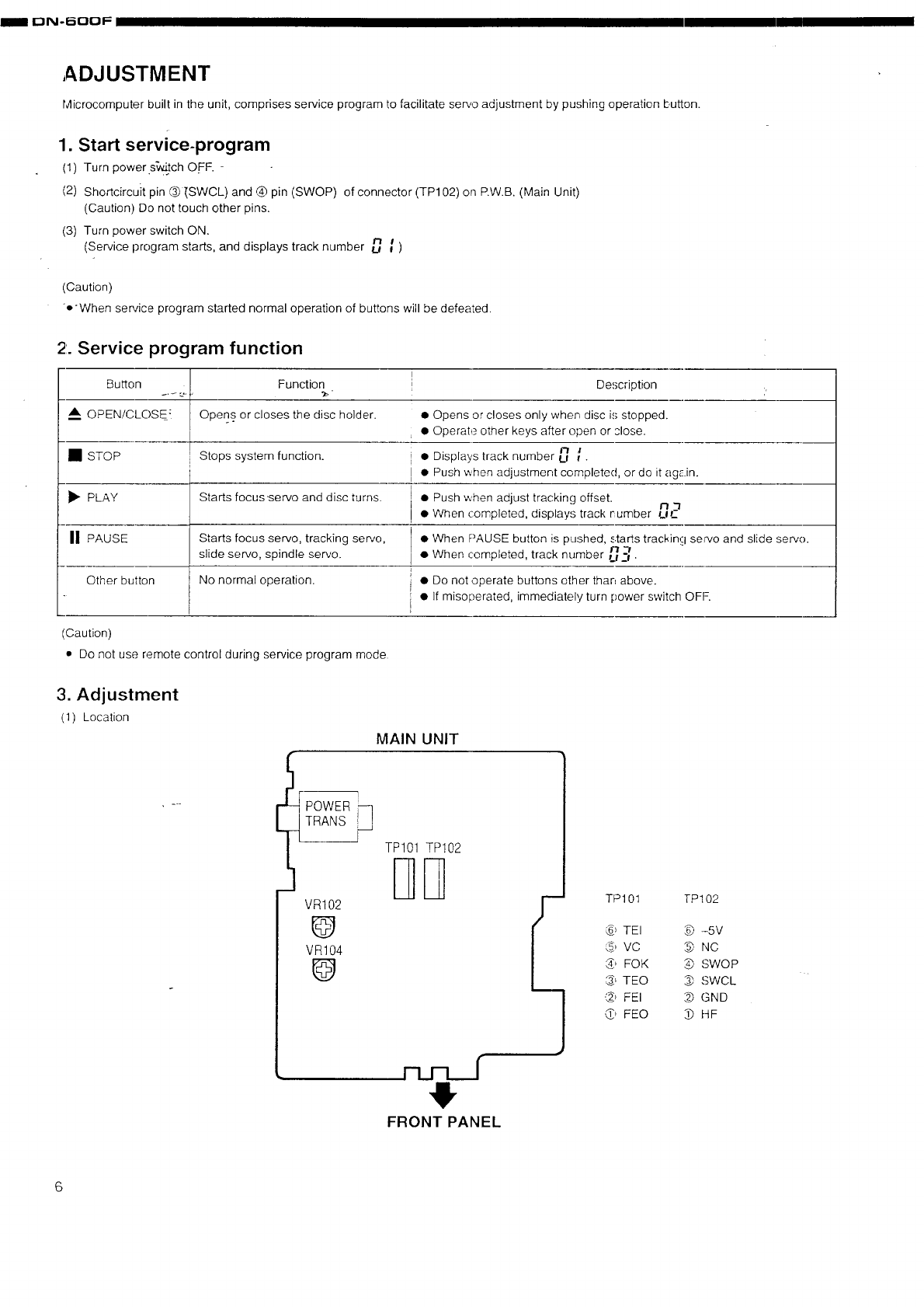
,ADJUSTMENT
k,licrocomputer built in the unit, comprises service program to facilitate servo adjustment by pushing operation button.
1. Start service-program
(1) Turn power s_tch OFF. -
(2) Shortcircuit pin (_ [SWCL) and (_ pin (SWOP) of connector (TP102) on RW.B. (Main Unit)
(Caution) Do not touch other pins.
(3) Turn power switch ON.
(Service program starts, and displays track number D_ )
(Caution)
o'When service program started normal operation of buttons will be defeated.
21.Service program function
_A
Button .... ..,
OPEN/CLOSE: [
Function
Opens or closes the disc holder.
I
• STOP Stops system function.
_" PLAY Starts focusservo and disc turns.
Hi PAUSE Starts focus servo, tracking servo,
slide servo, spindle servo.
Other button No normal operation.
Description
• Opens or closes only when disc is stopped.
• Operate other keys after open or close.
• Displays track number _j _.
• Rush when adjustment completed, or do it ag_.in.
• Push when adjust tracking offset. rl-i
• When completed, displays track rumber LI C
• When PAUSE button is pushed, starts tracking se_vo and slide servo.
n-t
• When completed, track number U-'#.
• Do not operate buttons other than above.
• If misoperated, immediately turn power switch OFF--.
(Caution)
• Do not use remote control during service program mode.
3. Adjustment
(1) Location
MAIN UNIT
!
POWER_
TRANS
VR102
@
VR104
@
TP101 TP102
SD
FRONT PANEL
TP10I ]-P102
L_ TEl _ -5V
_, VC _, NC
_, FOK _ SWOP
,_, TEO _ SWCL
._, FEI _ GND
_, FEO _ HF
ii_P i_il. L.--JLj LJ it- mmmm
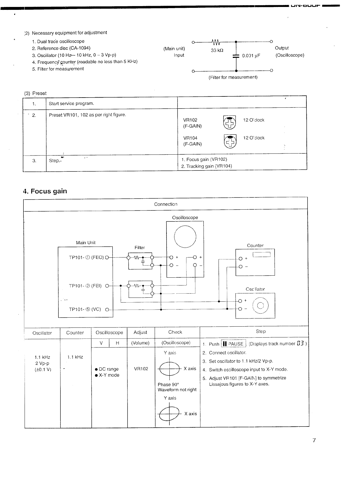
:2) Necessary equipment for adjustment
1. Dual tracie oscilloscope
2. Reference disc (CA-1094)
3. Oscillator (10 Hz,-- 10 kHz, 0 - 3 Vp-p)
4. Frequen,?_._ounte_r (_r_adable no less than 5 KHz)
5. Filter for measu.rement
(Main unit)
Input
33 k_Q Output
0.091 pF (Oscilloscope)
T o
o
(Filter for measuren'lent)
(3) Preset
1.
" " 2,
Start service program.
Preset VR101, 102 as per right figure.
VR102
(F-GAIN)
3. Step.- 1. Focus gain (VR 102)
2. Tracking gain (VR104)
VR 104 kL2J
(F-GAIN)
12 O'clock
12 O'ciock
4. Focus gain
Connection
Main Unit
TP101- L[-')(FEO) O--
TP101- (_ (FEI) 0--
TPI01- @ (VC) 0
Filter
Oscilloscope
C'ounter
! C'sc Ilator
Oscillator
1.1 kHz
2 Vp-p
(_+0.1V)
Counter Oscilloscope
V H
Adjust
(Volume)
Check
(Oscilloscope)
1.1 kHz
•DC range
•X-Y mode
VR102
Y axis
C)
Phase 90 °
X axis
Step
1. Push [11#AUSE '1(Displays track number
2. Connect oscillator.
3. Set oscillator to 1.1 kHz/2 Vp-p.
4. Switch oscilloscope input to X-Y mode.
5. Adjust VR101 [F-G to symmetrize
: Lissajous figures tc X-Y axes.
Waveform not right
Y axis
7
I I1,_11| %11,, Q II,,,JUIt--
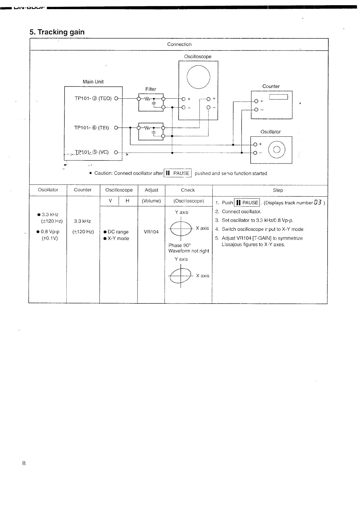
5. Tracking gain
Connection
Oscilloscope
Main Unit
TP101- (_) (TEO) O_
TP101- 0 (TEl) O--
......T,P.t01.:.®(VC) 0
Filter Counter
Oscillator
• Caution: Connect oscillator afterhl PAUSE] pushed and sewo function started
Oscillator Counter Oscilloscope Adjust
V H (Volume)
•3.3 kHz
(_+120Hz)
• 0.8 Vp-p
(±011V)
3.3 kHz
(+_120Hz) • DC range
•X-Y mode
VR 104
Check
(Osci !oscope)
Y ax_s
'_ x axis
Phase 90 °
Waveform not right
Y axis
Step
1. Push [_ PAUSE I . (Displays track number _.._ )
2. Connect oscillator.
3. Set oscillator to 3,3 kHz/0.8 Vp-p.
4. Switch oscilloscope ir put to X-Y mode
5. Adjust V [T-GAIN] to symmetrize
Lissajou figures to X-Y axes.
nN-6OOF
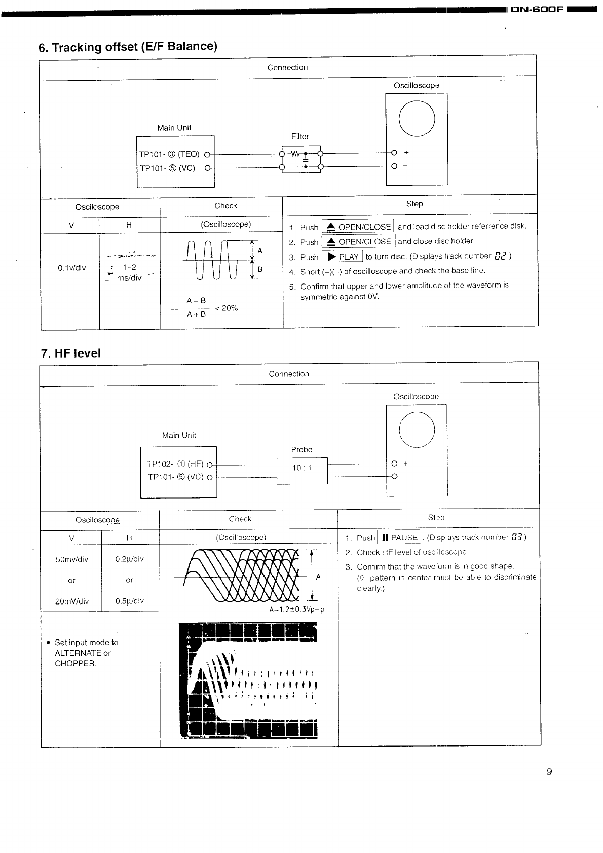
6. Tracking offset (E/F Balance)
Connection
Oscilloscope
Osciloscope
V H
0.1v/div :1-2
ms/div
Main Unit
/
TP101- O (TEO) O I
1
TP101- O (VC)
Check
(Oscilloscope)
k
A-B
< 20%
A+B
Filter O
O +
O-
A
B
Step
1. Push _ OPENICLOSE] and load dsc hoMer referrence disk.
2. Push Am OPEN/CLOSE ]and close, holder.
3. Push I • PLAY Ito turn disc. (Displays tracknumber r_-iuC )
4. Short (+)(-) of oscilloscope and check the base line.
5. Confirm that upper and Iower amplituc of the waveform is
symmetric against 0V.
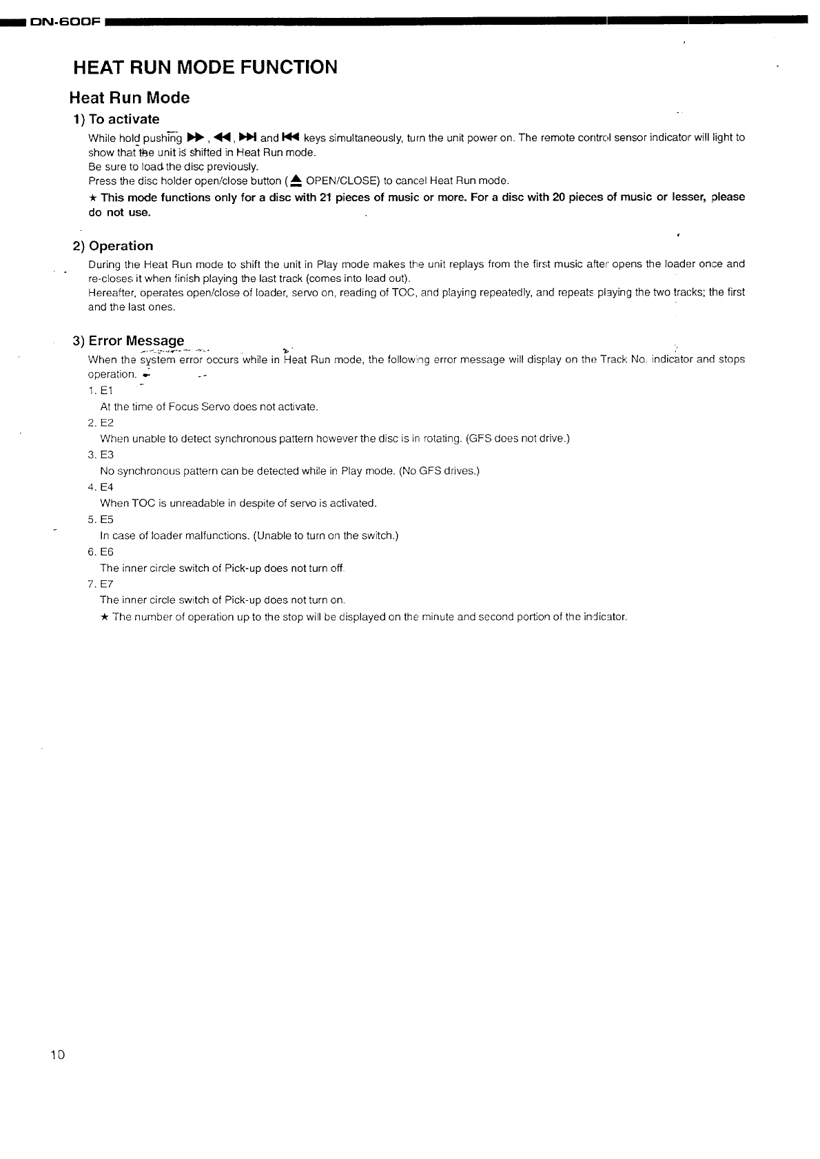
7. HF level
Connection
Main Unit
Probe
TP102- d_ (HF) O 10 1
TP101- @ (VC) O_J
Oscilloscope
© +
Oscilosc ,op,e
v
50mv/div
o_
20mV/div
H
0.2p/div
or
0.5(_L/ally
• Set input mode to
ALTERNATE or
CHOPPER.
Check
(Oscilloscope)
-/ iA
L
A=l.2±0.3Vp-p
II WJm
S p
Ii
1. Push[ II PAUSEJ.(D _aystracknumberu_n_)
2. Check HF level of osc llcscope.
3. Confirm that the wave is in good shape.
(0 pattern ia center must be able to discriminate
clearly.)
mmlL . _..m.i mllll ,llmlll .....
. mmmiiimm_!
9
I ON-6OOF
HEAT RUN MODE FUNCTION
Heat Run Mode
1)To activate
While hold pushin"-g DH_, _1_, _ and _ keys simultaneously, turn the unit power on. The remote control sensor indicator will light to
show that _e unit i¢ shifted in Heat Run mode.
Be sure to Ioadthe disc previously.
Press the disc holder open/close button ( ,,A.AOPENICLOSE) to cancel Heat Run mode.
This mode functions only for a disc with 21 pieces of music or more. For a disc with 20 pieces of music or lesser, please
do not use.
2) Operation
During the Heat Run mode to shift the unit in Play mode makes the unit replays from the first music after opens the loader once and
re-closes it when finish playing the last track (comes into lead out).
Hereafter, operates open/close of loader, servo on, reading of TOC, and playing repeatedly, and repeats playing the two tracks; the first
and the last ones.
3) Error Message
When the system error occurs While in Heat Run mode, the following error message will display on the Track No. indicator and stops
operation ....
1.E1 -
At the time of Focus Servo does not activate.
2. E2
When unable to detect synchronous pattern however the disc is in rotating. (GFS does not drive.)
3. E3
No synchronous pattern can be detected while in Play mode. (No GFS drives.)
4. E4
When TOC is unreadable in despite of servo is activated.
5. E5
In case of loader malfunctions. (Unable to turn on the switch.)
6. E6
The inner circle switch of Pick-up does not turn off.
7. E7
The inner circle switch of Pick-up does not turn on.
-JrThe number of operation up to the stop will be displayed on the minute and second portion of the indicator.
10
I I I I ON-6OOF n
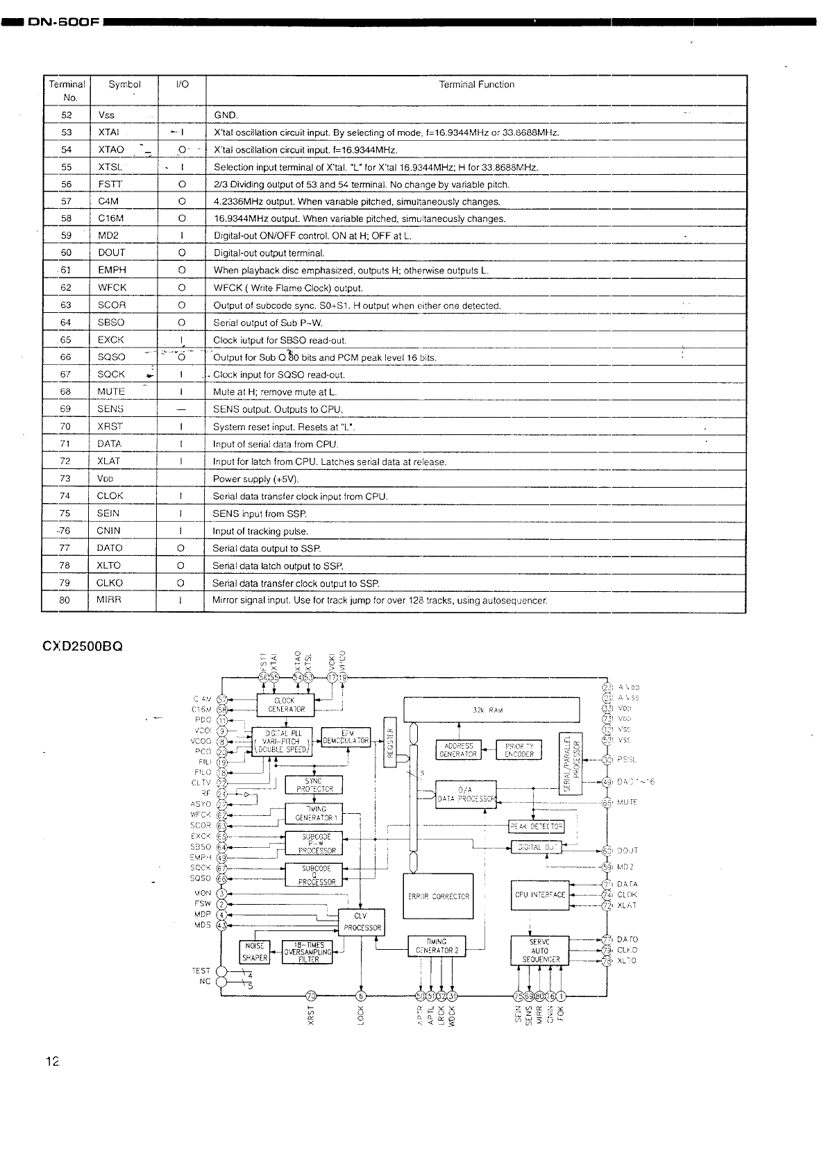
IC TERMINAL FUNCTION LIST
CXD2500BQ Terminal Function
Terminal Symbol
No.
1 FOK -
Fsw "
2
3 MON
4 MDP
5 MDS
6 LOCK
7 NC
8 VCOO
9 VCOI
10 TEST
11 PDO
12 Vss
13 NC
14 NC _
15 NC -
16 VPCO
17 VCKI
18 FILO
19 FILl
20 PCO
21 AVss
22 CLI_7
23 AVDD
24 RF
25 TEST2
26 TEST3
27 ASYO
28 TEST4
29 NC
30 PSSL
31 WDCK
32 LRCK
33 VDD
34 DA16. "--
35 DA15
36 DA14
37 DA13
38 DA12
39 DA11
4O DA10
41 DA09
42 D_08
43 DA07
44 DA06
45 DA05
46 DA04
47 DA03
48 DA02
49 DA01
50 APTR
51 APTL
I/O
I
O
O
O
O
O
O
I
I
O
Terminal Function
lnp.ut terminal for OK focussing. Use for Servo-autosequencer.
Output to shift time constant of output filter for spindle motor.
ON/OFF control output for spindle motor.
Servo control for spindle motor.
Servo control for spindle motor..
Sampling GFS by 460 Hz and if it is "H", delivers "H" ; if it is continuously "L" 8 times, deliw;rs "1_".
Oscillation current output for analog EFM PLL.
Oscillation current output for analog EFM PLL. f LOCK=8.6436MHz.
TEST output. Normally GND.
Charge pump output for analog EFM PLL.
GND.
[
0
0
0
I
0
I
I
I
0
I
I
0
0
o
o
o
o
o
0
o
o
o
o
o
0
0
0
0
o
0
o
Charge pump output for variable pitch PLL.
Clock input from extemal VCO lot vadabTe pitch, fc center=16.9344MHz.
Filter output for master PLL. (slave-digital PLL)
Filter input for master PLL.
Charge pump output for master PLL.
Analog GND.
Control voltage output for master VCO.
Analog power supply (+5V).
EFM signal input.
Put to GND.
Put to GND.
Full swing output for EFM. (L=Vss, H:VDD).
Put to GND.
Input to shift output mode of audio data. Serial output at L; parallel output at H.
DiA Interface for 48 bit slot. Word-clock f-2 Fs.
D/A Inlerface for 48 bit slot. LR-dock f- Fs.
Power supply ( _SV ).
At PSSL=I for DA16 (MBS) output: PSSL=0 for serial data of 48 bit slot. (2s'COMP, MSB first).
At PSSL=t for DA15 output; PSSL 0 for bit clock of 48 bit slot.
At PSSL=I
At PSSL=I
At PSSL=I
At PSSL=I
At PSSL-1
At PSSL-1
At PSSL=I
At PSSL=I
At PSSL=I
At PSSL=I
At PSSL=I
At PSSL=I
At PSSL=I for DA02 output; PSSL=0 for MNT1 output.
At PSSL=I for DA01 output; PSSL=0 for MNT0 output.
Control output for aperture compensation. In H for R-oh.
Control output for aperture compensation. In H for L-oh.
for DA14 output; PSSL-0 for serial data of 64 bit slot. (_4s'COMP, LSB first',.
for DA13 output; PSSL:0 for bit clock of 64 bit slot.
for DA12 output; PSSL-0 fDr LR clock of 64 bit slot.
for DA11 output; PSSL=0 for GTOP output.
for DA10 output; PSSL=0 for XUGF output.
for DA09 output; PSSL=0 for XPLCK output.
for DA08 output; PSSL=0 for GFS output.
for DA07 output; PSSL=0 for RFCK output.
for DA06 output; PSSL=0 for C2PO output.
for DA05 output; PSSL=0 for XRAOF output.
for DA04 output; PSSL=0 for MNT3 output.
for DAO3 output; PSSL=0 for MNT2 output.
11
ON-BOOF
rminal Symbol
No.
52 Vss
53 XTAI
54 XTAO _
55 XTSL
56 FS-Ui-
57 C4M
58 C16M
59 MD2
60 DOUT
61 EMPH
62 WFCK
63 SCOR
64 SBSO
65 EXCK
66 SQSO
67 SQCK ,_
68 MUTE
69 SENS
70 XRST
71 DATA
72 XLAT
73 Voo
74 CLOK
75 SEIN
76 CNIN
77 DATe
78 XLTO
79 CLKO
80 MIRR
I/O
O-
I
O
O
O
I
O
O
O
O
O
I
I
I
I
I
I
I
I
I
o
o
0
I
Terminal Function
GND.
X'tal oscillation circuit input. By selecting of mode, f=16.9344MHz or 33.8688MIqz.
X'tal oscillation circuit input, f=t6.9344MHz.
Selection input terminal of X'tal. "L" for X'ta116.9344MHz; H for 33.8688MHz.
2/3 Dividing output of 53 and 54 terminal. No change by variable pitch.
4.2336MHz output. When variable pitched, simultaneously changes.
16.9344MHz output. When variable pitched, simu Itaneously changes.
Digital-out ON/OFF control. ON at H; OFF at L.
Digital-out output terminal.
When playback disc emphasized, outputs H; otherwise outputs h
WFCK ( Write Flame Clock) output.
Output of subcode sync. S0+S1. H output when either one detected.
Serial output of Sub P-W.
Clock iutput for SBSO read-out.
I-Output for Sub Q_O bits and PCM peak level 16 bits.
i. Clock input for SQSO read-out.
Mute at H; remove mute at L.
SENS output. Outputs to CPU.
System reset input. Resets at "1._".
Input of serial data from CPU.
Input for latch from CPU. Latches serial data at release.
Power supply (+5V).
Serial data transfer clock input from CPU.
SENS input from SSR
Input of tracking pulse.
Serial data output to SSR
Serial data latch output to SSP.
Serial data transfer clock output to SSR
Mirror signal input. Use for track jump for over 128 tracks, using autosequencer.
CXD2500BQ
C 4M
(:i 6')
PDO
VCOl
VCOO
_CO
FILl
FPL(?
CLTV
Rf
ASY()
WFC<
seer
EXCK
5'350
EMPH
SQCK
SQSO
MON
FSW
MDP
MDS
TEST
NC
32k RA_
91G:TALPLL i
i
i
ERROR CORRECTER
!SERVC DA re
AUTO CLKO
SEQUENCER XL_O
?-
Ca g_#
12
nN.6OOF
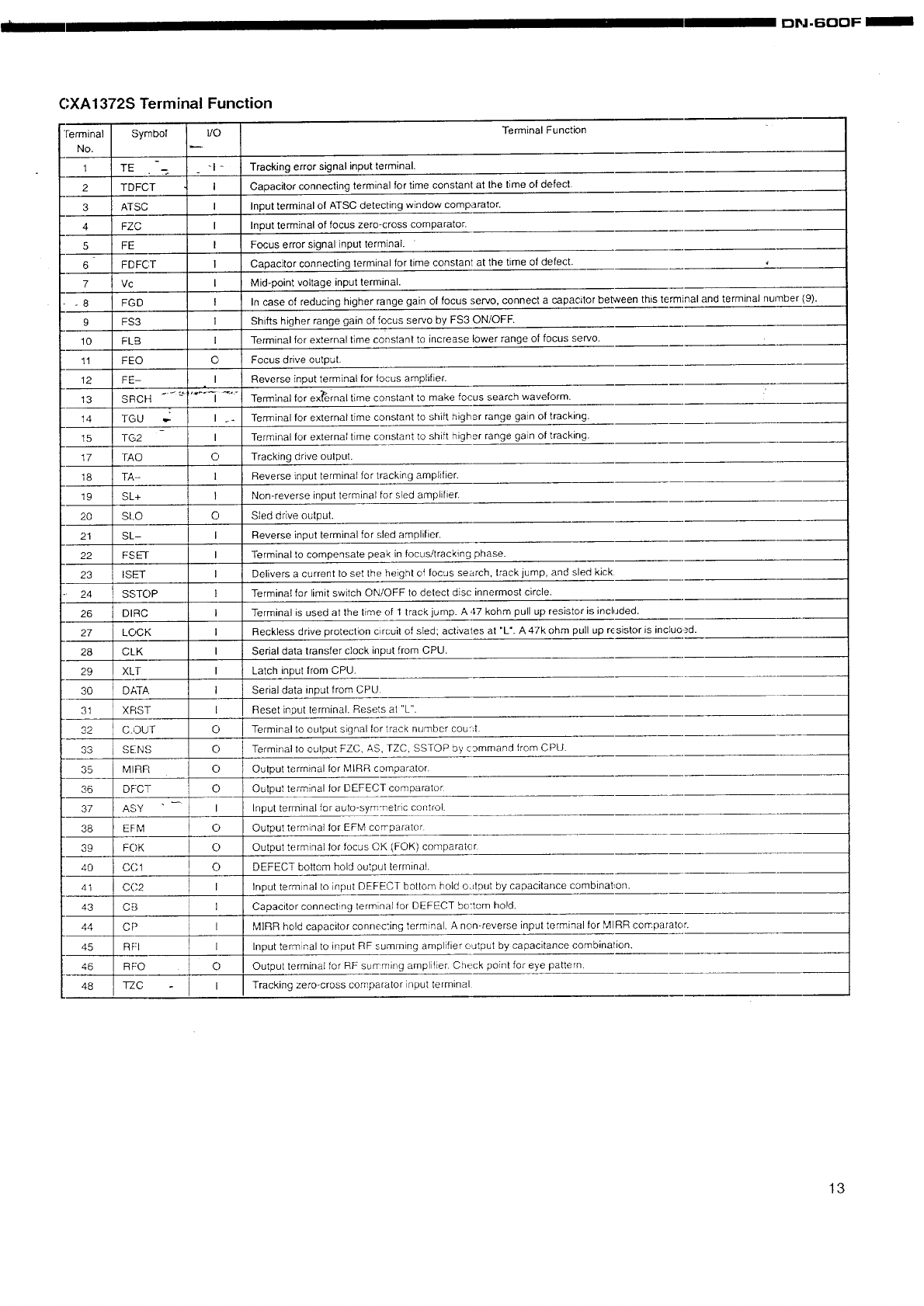
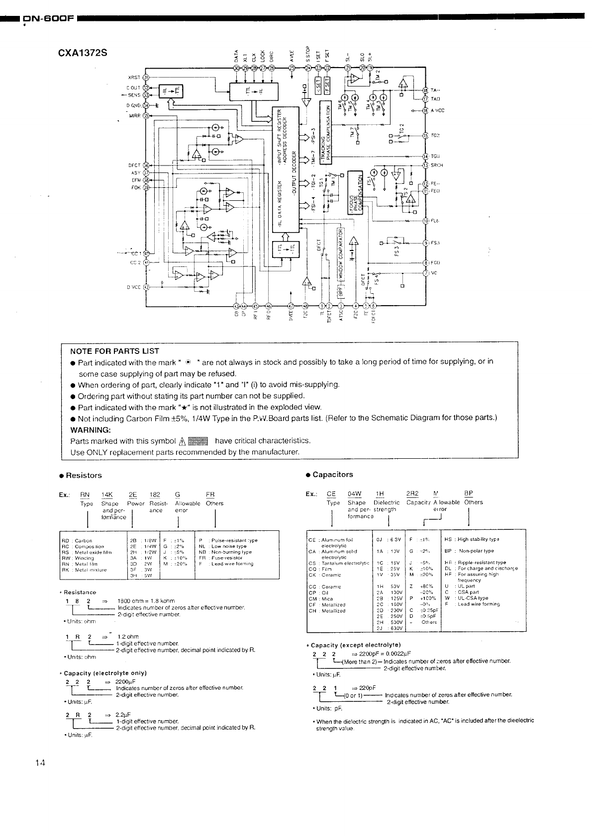
C;XA1372S Terminal Function
l-erminal
No.
1
2
3
4
5
6
7
-8
9
10
11
12
13
14
15
17
18
19
20
21
22
23
24
26
27
28
29
30
31
32
33
35
36
37
38
39
40
41
43
44
45
46
48
Symbol
TE -;
TDFCT
ATSC
FZC
FE
FDFCT
Vc
FGD
FS3
FLB
FEO
FE-
SRCH
TGU
TG2
TAO
TA-
SL+
SLQ
SL-
FSET
ISET
SSTOP
DIRC
LOCK
CLK
XLT
DATA
XRST
C.OUT
SENS
MIRR
DFCT
ASY
EFM
FOK
C(" 1
CC2
CB
CP
RF:I
RFO
]_C
I/O
I
I
I
I
I
I
I
I
I
C,
I
I
C,
I
I
0
I
I
I
I
I
I
I
I
I
I
0
0
0
0
I
O
0
0
I
I
I
1
0
I
Terminal Function
Tracking error signal input terminal.
Capacitor connecting terminal for time constant at the time of defect
Input terminal of ATSC detecting window comparator.
Input terminal of focus zero-cross comparator.
Focus error signal input terminal. "
Capacitor connecting terminal for time constant at the time of defect.
Mid-point voltage input terminal.
In case of reducing higher range gain of focus servo, connect a capacitor between this te
Shifts higher range gain of focus servo by FS3 ON/OFF.
Terminal for external time constant to increase lower range of focus servo.
Focus drive output.
Reverse input terminal for locus amplifier.
Terminal for external time constant to make focus search waveform.
Terminal for external time constant to shift higher range gain of tracking.
Terminal for external time constant to shift higher range gain of tracking.
Tracking drive output.
Reverse input terminal for tracking amplifier.
Non-reverse input terminal for sled amplifier.
Sled drive output.
Reverse input terminal for sled amplifier.
Terminal to compensate peak in locus/tracking phase.
Delivers a current to set the height of focus search, track jump, and sled kick
Terminal for limit switch ON/OFF to detect disc innermost circle.
Terminal is used at the lime of 1 track jump. A 4.7 kohm pull up resistor is included.
Reckless drive protection circuit of sted; activates at "L'. A 47k ohm pull up resistor is inc
Serial data transfer clock input from CPU.
Latch input from CPU.
Serial data input from CPU
Reset input terminal. Resets at "L".
Terminal to output signal lor track number cou:-4.
Terminal to oulput FZC, AS, TZC, SSTOP by cammand from CPU.
Oulput terminal for MIRR camparator.
Output terminal for DEFECT comparator
Input terminal for auto-symmetric control.
Output terminal for EFM comparator
Output terminal for focus OK (FOK) comparator
DEFECT bottom hold output terminal.
Input terminal to input DEFECT bottom held o_t_ut by capacitance combination.
Capacitor connecting terminal for DEFECT bo:tom hold.
MIRR hold capacitor connec:ing terminal. A non-reverse input terminal for MIRR comparator.
Input terminal to input RF summing amplifier output by capacitance combination.
Output terminal for RF summing amplifier. Check point for eye pattern.
Tracking zero-cross comparator input terminal
and terminal number (9).
13
ON,.6OOF
€
CXA1372S
XRST
C OUT
SEN S
DG,_D
MIRF'
DFCI"
ASY (
EFkl !
FOK !
cc 2 1
D VCC I
,
_ g° _= < _ __ _ _,d,
-Ill: I:Z- I
TA--
TAO
A VCC
TG:!
,TGU
,SRCH
,FEO
J FS5
FCD
I VC
NOTE FOR PARTS LIST
• Part indicated with the mark " _') " are not always in stock and possibly to take a long period of time for supplying, or nn
some case supplying of part may be refused.
• When ordering of part, clearly indicate "1" and '1" (i) to avoid rots-supplying.
• Ordering part without stating its part number can not be supplied.
• Part indicated with the mark "-k" is not illustrated in the exploded view.
• Not including Carbon Film _+5%,1/4W Type in the P.W.Board parts list. (Refer to the Schematic Diagram for those parts.)
WARNING:
Parts marked with this symbol _ _ have critical characteristics.
Use ONLY replacement parts recommended by the manufacturer.
• Resistors • Capacitors
Ex.:
and per- Iance 7rror
Iforrnance
RD : Carbon 2B : 1/8W F : _t%.
RC : Cornpostion 2E l_4W G : z2%
RS : Melal oxide lilm 3H2H fiWI'2W J : :5%
RW : Wincing 3A : 1W K : ±10%
RN : Metal tim 3D 2W M : _20%
RK : Metal mixlure 3; 3W
RN 14K 2E 182 G FR Ex.: CE
Type Shape Power Resist- Allowable Others Type
1 1
P : Pulse-resislanl :ype
NL : Low noise lype
NB : Non-bLIrning lype
FR : Fuse-resislor
F : Lead wire forming
* Resistance
1 8 2 = 1800 ohr,'n = 1.8 kohm
T [---- Indicates number of zeros after effective number.
2-digit effective number.
•Units: ohm
1 R 2 ==. 1.2 ohm
-- ---- 1-digit effective number.
2-digit effective number, decimal poinl indicated by R.
• Units: ohm
*Capacity (electrolyte only)
2 2 2 _ 2200_F
_[_ T..___ Indicates number of zeros after effective number.
2-digit effective number.
• Units: pF.
2R2 =::, 2.2pF
T -___ 1-digit effective number.
2-digit effective number, decimal point indicated by R.
•Units: HF.
CE : Aluminum foil
eleclrolytic
CA : Aluminum sol,d
ele¢lrolylic
CS : Tantalum electrolytic
CQ : Film
CK : Ceramic
CC : Ceramic
CP : Oil
CM : Mica
CF Metat_ized
CH Metallized
04W 1 H 2R2 M BP
Shape Dielectric Capacity A Iowable Olhers
and per- strength euror I
formance l ['---J 1
F : =1%
0J : 6 3V I
1A : 13V I
1C 15V I
1E 25V I
tV 35V
1H 53V
2A 130V
2B 125V
2C lS0V
2D 230V
2E 250V
2H 530V
2J : 630V
G :2%
J -5%
K :10%
M ::20%
Z +8C %
20%
P +1C0%
-0%
C :0 25pF
D ::0 5pF
- Oelers
HS : High stability typ,_=
BP : Non-polar type
HF : Ripple resistant type
DL : For charge al_d cischar(je
HF : For assubng high
frequency
U : UL part
C : CSA part
W : UL-CSA lype
F Lead wire forming
* Capacity (except electrolyte)
2 2 2 _ 2200pF = 0.0022pF
- T.---(More than 2)-- Indicates numbe_ of ;:eros after effective nurnber.
2-digit effective number.
• Units: #F.
221 =_, 2_OpF
TT"--"(0 or 1)----
• Units: pF.
Indicates number of zeros after effective number.
2-digit effective number.
• When the dielectric strength is indicated in AC. "AC" is included afterthe dieelectric
strength value
14
QN.6OOF
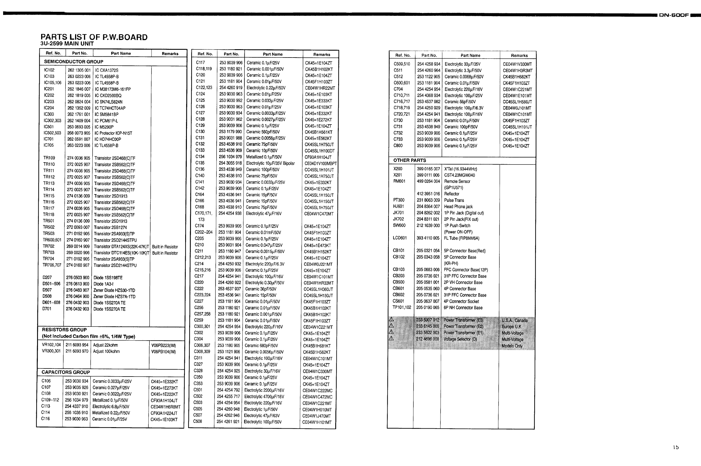
PARTS LIST OF P.W.BOARD
3U-2599 MAIN UNIT
Ref. No. I Part No. I
SEMICONDUCTOR GROUP
{C102
IC103
IC105,106
IC201
1(;202
IC203
IC204
IC300
IC302,303
IC501
IC502,503
IC701
IC705
TR109
TR110
TR111
TRl12
TRl13
TRl14
TRl15
TRl16
TRl17
TR118
TR501
TR502
TR503
TR600,601
TR702
TR703
TR704
TR706,707
D207
D501-506
D507
D508
D601-608
D701
Part Name I Remarks
262 1305001
263 0223006
263 0223006
262 1846007
262 1819005
262 0824004
262 1352009
262 1761001
262 1409004
263 0693005
2680073905
2620591007
263 0223006
274 0036905
272 0025907
2740036 905
272OO25907
274 0036905
272 0025907
274 0136009
272 0025907
274 0036905
272 0025907
274 0136009
272 0093007
271 0192905
2740160 907
269 0014909
2690020 906
2710192 905
2740160 907
276 0503 900
2"/60613 900
276 0483 907
276 0464900
2760432 903
276 0432903
ICCXA1372S
ICTL4558P-B
ICTL4558P-B
ICM38173M6-161FP
ICCXD25OOBQ
ICSN74LS624N
ICTC74HCT04AP
ICSM5841BP
IC PCM61P-L
IC M5290P
IC ProtectorICP-N15T
IC HD74HC00P
ICTL4558P-B
Transistor2SD468(C)TF
Transistor2SB562(C)TF
Transistor2SD468(C)TF
Transistor2SB562(C)TF
Transistor2SD468(C)TF
Transistor2SB562(C)TF
Transistor2SD1913
Transistor2SB562(C)TF
Transistor2SD468(C)TF
Transistor2SB562(C)TF
Transistor2SD1913
Transistor2SB1274
Transistor2SA933(S)TP
Transistor2SD2144STPU
TransistorDTA124XS(22K-47K)'r
TransistorDTC114ES(1OK-10K)T
Transistor2SA933(S)TP
Transistor2SD2144STPU
Diode1SS198TE
Diode1A3-1
ZanerDiodeHZS30-1TD
ZonerDiodeHZS7A-1TD
Diode1SS270ATE
Diode1SS270ATE
Built in Resistor
Builtin Resistor
RESISTORS GROUP
(Not included Carbon film +5%, 1/4W "_jpe)
VR102,104 2116093954 /Adjust22kohm +V06PB223(IM)
VR300,301 2116093970 1Adjust100kohm V06PB104(IM)
CAPACITORS GROUP
C106
C107
C108
C109-112
C113
Cl14
Cl16
253 9030934
253 9035926
253 9030921
256 1034979
254 4337910
256 1035910
253 9030963
CeramicO.O0331.tFt25V
CeramicO.027pF/25V
CeramicO.O022pFt25V
MetallizedO.IHF/50V
Electrolytic6.8pF/50V
Metatlized0.22pF/50V
Ceramic0.01uFI25V
CK45=1E332KT
CK45=1E273KT
CK45=1E222KT
CF93A1HlO4JT
CE04W1H6R8MT
CF93A1H224JT
CK45=1E103KT
Ref. No.
C117
C118,119
C120
C121
C122,123
C124
C125
C126
C127
C128
C129
C130
C131
0132
C1&3
0134
C135
C136
C140
C141
C142
C164
C166
C168
C170,171,
173
C174
C202-204
(:;2O5
C210
C211
C212,213
C214
C215,216
C217
C220
C222
C223,224
C227
C256
C257,258
C259
C300,30t
C302
C304
C306,307
C308,309
C311
C327
C328
C350
C353
C501
C502
C503
C505
C507
C508
Part No.
2539039 906
253 1180921
253 9039906
253 1181904
254 4260919
253 9030963
253 9030992
253 9030963
253 9030934
253 9031962
253 9039906
253 1179990
253 9031988
253 4538910
253 4536909
256 1034979
2543055918
2534538 949
2534538 910
253 9030934
253 9039906
253 4536941
2534536 941
253 4538910
254 4254938
Part Name
Ceramic0.1p.F/25V
Ceramic0.001pF/50V
Ceramic0.1pR25V
Ceramic0.01p.F/50V
Electrolytic0.22pF/50V
Ceramic0.01p_F/25V
Ceramic0.038pF/25V
Ceramic0.01p.F/25V
Ceramic0.OO33pF/25V
Ceramic0.0027pF/25V
Ceramic0.1p.F/25V
Ceramic560pF/50V
Ceramic0.0056pF/25V
Ceramic75pF/50V
Ceramic10pF/50V
Metallized0.1pF/50V
Electrolytic10pF/35VBipolar
Ceramic100pF/50V
Ceramic75pF/50V
Ceramic0.0033_F/25V
Ceramic0.1pF/25V
Ceramic15pF/50V
Ceramic15pF/50V
Ceramic75pF/50V
Electrolytic47pF/16V
253 9039906 Ceramic0.1pF/25V
253 1181904 _,eramicO.01mFl50V
253 9039906 Ceramic0.1pF/25V
253 9031904 CeramicO.047p_F/25V
253 1180947 CeramicO.O015uF/50V
253 9039906 CeramicO.lpF/25V
2544250932 Electrolytic220pF/6.3V
253 9039906 CeramicO.lpF/25V
254 4254941 Electrolytic100pF/16V
254 4260922 ElectrolyticO.33#F/50V
2534537937 Ceramic36pF/50V
2534536941 Ceramic15pF/50V
253 1181904 CeramicO.01p.F/50V
253 1180921 CeramicO.011JF/50V
253 1180921 CeramicO.O01pF/50V
253 1181904 CeramicO.01_.=F/50V
2544254954 Electrolytic220pF/16V
253 9039906 Ceramic0.1pF/25V
253 9039906 Ceramic0.1pF/25V
253 1180905 Ceramic680pF/50V
253 1121906 CeramicO.O056pF/50V
254 4254941 Electrolytic100pF/16V
253 9039906 CeramicO.lpF/25V
254 4254925 Electrolytic33BFI16V
253 9039906 Ceramic0.1pF/25V
253 9039906 CeramicO.lp.F/25V
254 4254792 i Electrolytic2200pF/16V
264 4255717 Electrolytic4700pF/16V
254 4254954 i Electrolytic220p.F/16V
254 4260948 ElectrolyticlpF/50V
254 4262946 I Electrolytic47p.F/63V
254 4261921 IElectrolyticIO0,uF/50V
Remarks
CK45=1EIO4ZT
CK45B1HIO2KT
CK45=1E104ZT
CK45F1HIO3ZT"
CEO4W1HR22MT
CK45=1E103KT
CK45=1E333KT
CK45=1E103KT
CK45=1E332KT
CK45=1E272KT
CK45=1EIO4ZT
CK45BlI"1561KT
CK45=1E562KT
CK45SL1H750JT
CC45SL1H100DT
CF93A1Hi04JT
CE04D1V100MBP'[
CCA5SL1H101JT
CC45SL1H750JT
CK45=1E332KT
CK45=1E104Z1"
CC45SL1H150JT
CC45SL1H150JT
CC45SL1H750JT
CEO4W1C470MT
CK45=1E104ZT
GK45F1H103ZT
CK45=1EIO4ZT
CK45=1E473KT
CK45B11,1152KT
GK45=1EIO4ZT
CEO4WOJ221MT
CK45=1E104z'r
CEO4W1C101MT
CE04W1HR33MT
CC45SL1H360JT
CC45SL1H150JT
CK45F1H103ZT
CK45B1H102KT
CK45B1H102KT
CK45F1H103ZT
CE04W1C221MT
CK45=lE104ZT
CK45=1E104ZT
CK45B1H631KT
CK45B1H562KT
CE04W1C101MT
CK45=1EIO4ZT
CEO4W1C330MT
CK45=1EIO4ZT
CK45=1EIO4ZT
CEO4W1C222MC
CE04W1C472MC
CEO4W1C221MT
CEO4W1HOIOMT
CEO4W1J470MT
CEO4W1HIO1MT
Ref. No. Part Name Remarks
C509,510
C511
C512
C600,601
C704
C710,711
C716,717
C718,719
C720,721
C730
C731
C732
C733
C800
Part No.
254 4258934
2544260 964
253 1122905
253 1181904
254 4254954
254 4368934
253 4537982
254 4250929
254 4254941
253 1181904
253 4538 949
253 9039906
253 9039906
253 9039906
Electrotytic33pF/35V
Electrolytic3.3pF/50V
CeramicO.O068pF/50V
CeramicO.01pF/50V
Electrolytic220p.F/16V
Electrolytic100p.F/25V
Ceramic56pF/50V
ElectrolyticIOOp.F/6.3V
Electrolytic100p.F/16V
Ceramic0.01pF/50V
CeramicIOOpF/50V
Ceramic0.1pF/25V
CeramicO.lpF/25V
Ceramic0.1p.F/25V
CE04W1V330MT
CE04W1H3R3MT
CK45B1H682KT
CK45F1H103Zi-
CE04W10221MT
CE04W1E101MT
CC45SL1H560JT
CE04W0J101MT
CE04W1C101MT
CK45F1H103ZT
CCA5SL1H101JT
CK45=1E104ZT
CK45=1E104ZT
CK45=lE104ZT
OTHER PARTS
)(200 399 0165007
X201 399 0111006
RM601 499 0264004
4123951016
PT300 2318063 009
HJ601 204 8364007
JK701 204 8262002
JK702 2048311021
SW600 212 1039000
LCD601 393 4110005
CB101 205 0321054
CB102 205 0343058
CB103 205 0683006
CB2O3 205 0736021
CB500 2050581 001
CB601 2050535 060
cB602 2050736021
cs601 2050837007
TP101,102 2050190065
+++++++++ii++ +++
iiiii ! ii i+ ! i+i
i+,iiii+,+++,ii iii iiiii!iiiiiiiii+ i++i+ +,
X'Tal(16.9344MHz)
CST4.23MGW040
RemoteSensor
(GP1U571)
Reflector
PulseTrans
Head Phonejack
1PPinJack(Digitalout)
2P PinJack(FIXout)
1PPushSwitch
(PowerON-OFF)
FLTube(FIPBNM6A)
5PConnectorBase(Red)
5PConnectorBase
(KR-PH)
FFCConnectorBase(12P)
31PFFC ConnectorBase
2P VH ConnectorBase
4P ConnectorBase
31P FFCConnectorBase
4P ConnectorSocket
6P NHConnectorBase
+iiii ! @ iiii+,iii+!ii'+i+',+i
iiiii!!!!iii iii iii iiiii!!ii+!
15
IUNI_U_ llIllll II IIIIIIIIIIII
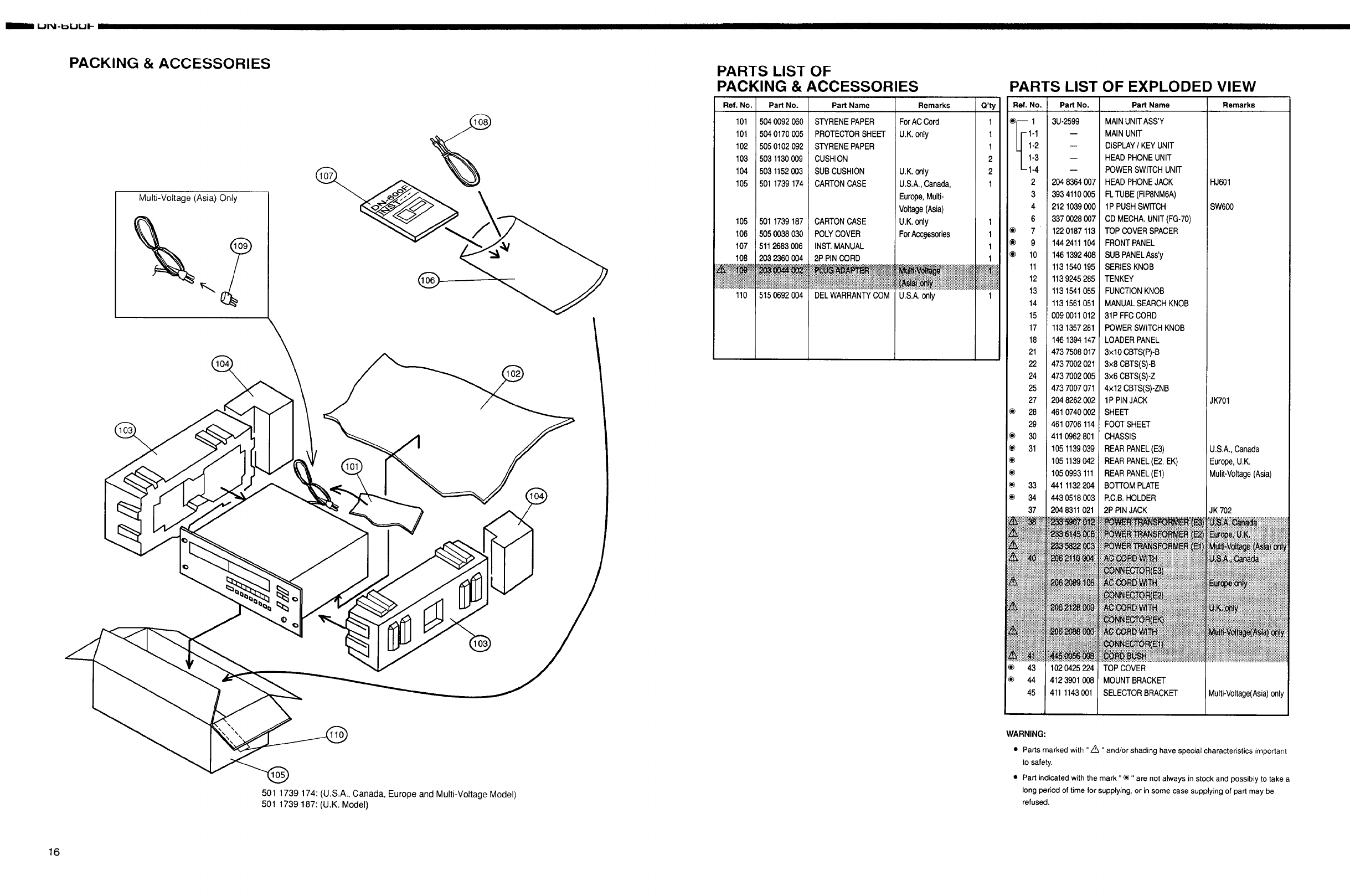
PACKING & ACCESSORIES
Multi-Voltage (Asia) Only
r....
16
!
-@
501 1739 174: (U.S.A., Canada, Europe and Multi-Voltage Model)
501 1739 187: (U.K. Model)
PARTS LIST OF
PACKING & ACCESSORIES PARTS LIST OF EXPLODED VIEW
Ref. No. Part No. Part Name
101 504 0092060 STYRENEPAPER
101 504 0170005 PROTECTORSHEET
102 505 0102092 STYRENEPAPER
103 503 1130009 CUSHION
104 503 1152003 SUBCUSHION
105 501 1739174 CARTONCASE
105 501 1739187 CARTONCASE
106 5050038 030 POLYCOVER
107 5112683 006 INST,MANUAL
108 2032360 004 2P PINCORD
Remarks
ForACCord
U.K.onty
U.K.only
U.S.A.,Canada,
Europe,Multi-
Voltage(Asia)
U.K.only
ForAcc_sories
O'ty
1
1
1
2
2
1
1
1
1
1
1!0 5150692 004 DELWARRANTYCOM U.S.A.only 1
Ref. No, Part No. Part Name Remarks
r-- 1 3u-2599 MAINUNITASS'Y
[- 1-1 -- MAIN UNIT
1-2 -- DISPLAY/KEYUNIT
1-3 -- HEAD PHONEUNIT
-1-4 -- POWERSWITCHUNIT
2 204 8364007 HEAD PHONEJACK HJ601
3 3934110005 FLTUBE(FIP8NM6A)
4 212 1039000 1PPUSHSWITCH SW600
6 387 0028007 CD MECHA.UNIT(FG-70)
®71220187113 TOPCOVERSPACER
® 9 144 2411104 FRONTPANEL
® 10 146 1392408 SUBPANELAss'y
11 113 1540195 SERIESKNOB
12 1139245285 TENKEY
13 113 1541055 FUNCTIONKNOB
14 113 1561051 MANUALSEARCHKNOB
15 009 0011012 31P FFCCORD
17 113 1357281 POWERSWITCHKNOB
18 146 1394147 LOADERPANEL
21 4737508017 3x10 CBTS(P)-B
22 4737002 021 3x8 CBTS(S)-B
24 4737002 005 3x6 CBTS(S)-Z
25 473 7007 071 4x12 CBTS(S)-ZNB
27 2048262002 1P PINJACK JK701
®28 461 0740 002 SHEET
29 461 0706 114 FOOTSHEET
30 411 0962801 CHASSIS
31 105 1139039 REARPANEL(E3) U.S.A.,Canada
@105 1139042 REARPANEL(E2, EK) Europe,U.K.
® 1050993 111 REARPANEL(El) Mulit-Voltage(Asia)
® 33 441 1132204 BO'FrOMPLATE
34 4430518003 P.C.B.HOLDER
37 204 8311021 2P PIN JACK JK 702
Nii i
® 4,3 102 0425 224 TOP COVER
=® 44 4123901 008 MOUNTBRACKET
45 4111143001 SELECTORBRACKET Multi-Voltage(Asia)only
WARNING:
•Parts marked with ",A, "and/or shading have special characteristics important
to safety.
Part indicated with the mark "®" are not always in stock and possibly to take a
long pedod of time for supplying, or in some case supplying of part may be
refused.
1
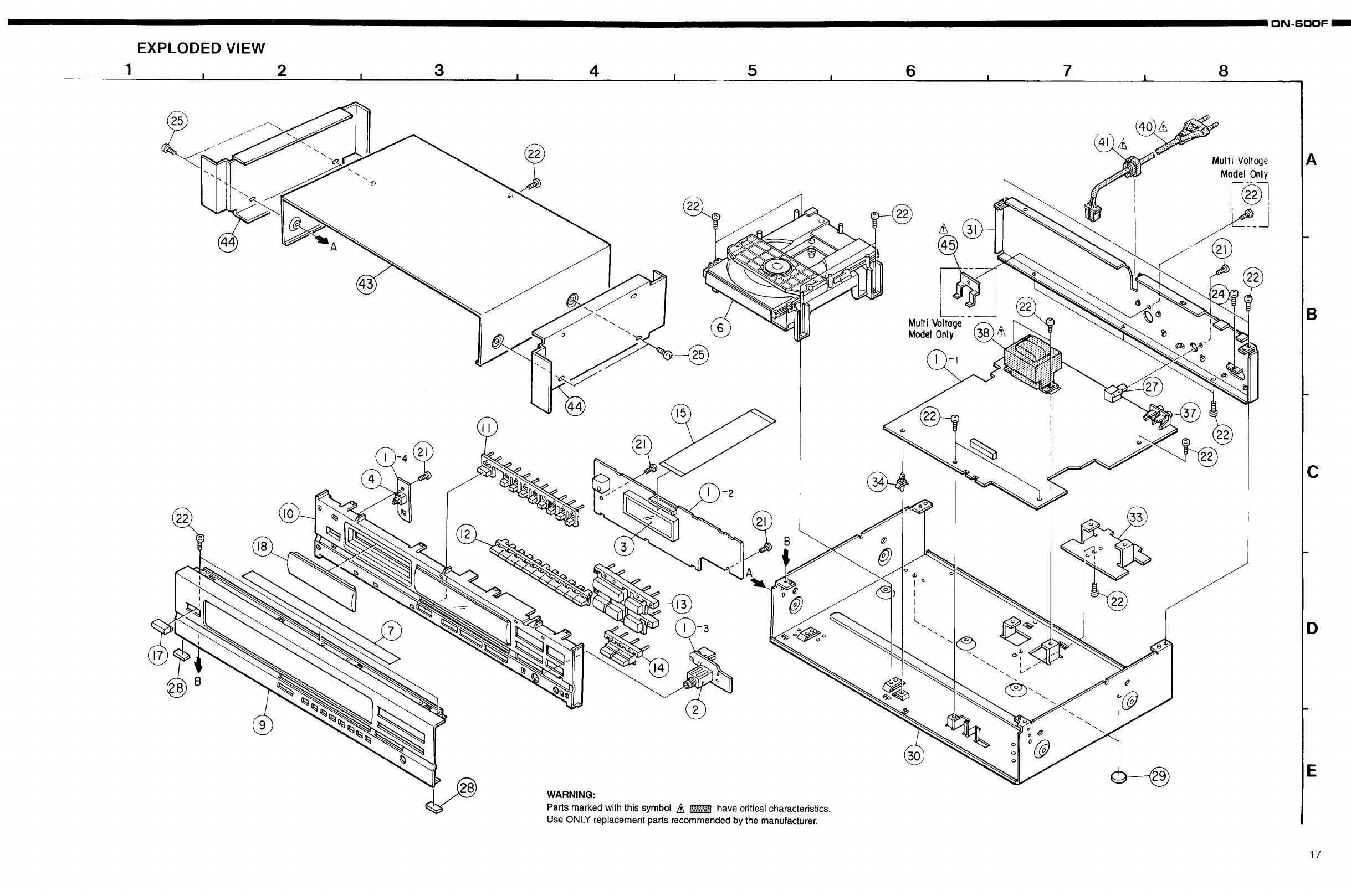
EXPLODED VIEW
i2345 6 7
\
I
L____
MultiVoltage
Model0nly
8
i °
I
I
I
L
WARNING:
Parts marked withthis symbol z_ _ have critical characteristics.
Use ONLY replacement parts recommended by the manufacturer.
8
1
Multi Voltoge
Model Only
DN-6OOF
A
B
C
D
E
17
DN-6OOF
18
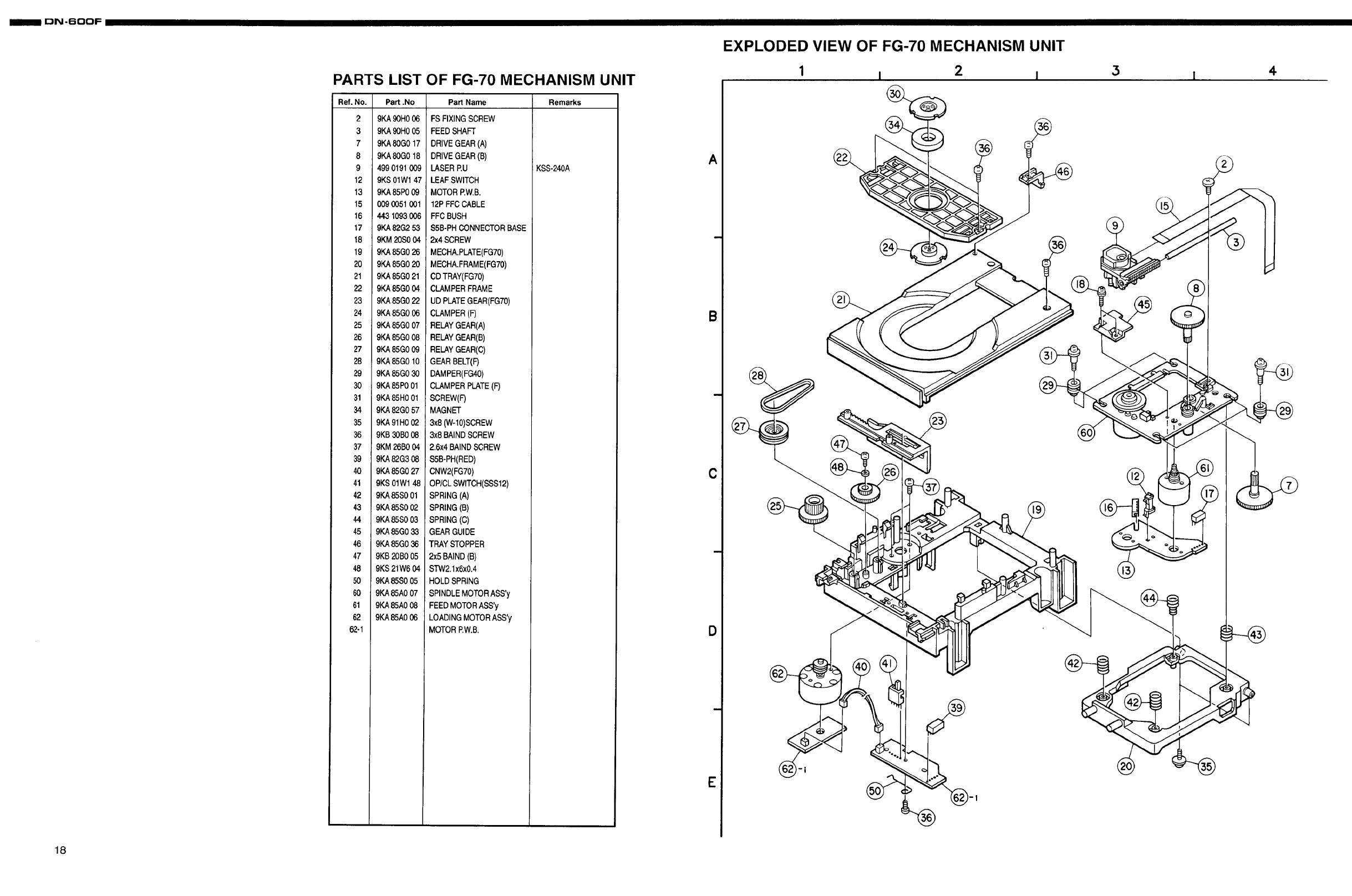
PARTS LIST OF FG-70 MECHANISM UNIT
Ref.No. Part .No
2 9KA90H006
3 9KA9OH005
7 9KA80G017
8 9KA80G018
9 4990191 009
12 9KS01Wl 47
13 9KA85P009
15 0090051 001
16 443 1093006
17 9KA82G253
18 9KM 20S004
19 9KA85G026
20 9KA85G020
21 9KA85G021
22 9KA85G004
23 9KA85G022
24 9KA85G006
25 9KA85G007
26 9KA85G008
27 9KA85G009
28 9KA85G010
29 9KA85G030
30 9KA85P001
31 9KA85H001
34 9KA82G057
35 9KA91H0 02
36 9KB30B008
37 9KM26B004
39 9KA82G308
40 9KA85G027
41 9KS01Wl 48
42 9KA85S001
43 9KA85S002
44 9KA85S003
45 9KA85G033
46 9KA85G036
47 9KB20B005
48 9KS21W604
50 9KA85S005
60 9KA85A007
61 9KA85A008
62 9KA85A008
62-1
Part Name Remarks
FSFIXINGSCREW
FEEDSHAFT
DRIVEGEAR(A)
DRIVEGEAR(B)
LASERP.U
LEAFSWITCH
MOTORP.W.B.
12P FFCCABLE
FFCBUSH
SEB-PHCONNECTORBASE
2x4SCREW
MECHA.PLATE(FG70)
MECHA.FRAME(FG70)
CDTRAY(FG70)
CLAMPERFRAME
UDPLATEGEAR(FG70)
CLAMPER(F)
RELAYGEAR(A)
RELAYGEAR(B)
RELAYGEAR(C)
GEAR BELT(F)
DAMPER(FG40)
CLAMPERPLATE(F)
SCREW(F)
MAGNET
3x8 (W-10)SCREW
3x8 BAINDSCREW
2.6x4BAINDSCREW
SEB-PH(RED)
CNW2(FG70)
OP/CLSWITCH(SSS12)
SPRING(A)
SPRING(B)
SPRING(C)
GEARGUIDE
TRAYSTOPPER
2x5 BAIND(B)
STW2.1x6x0.4
HOLDSPRING
SPINDLEMOTORASS'y
FEEDMOTORASS'y
LOADINGMOTORASS'y
MOTORP.W.B.
KSS-240A
EXPLODED VIEW OF FG-70 MECHANISM UNIT
1I 2 I 3 4.
A
B
C
D
E
, ,......................................................................................... nN.6OOF
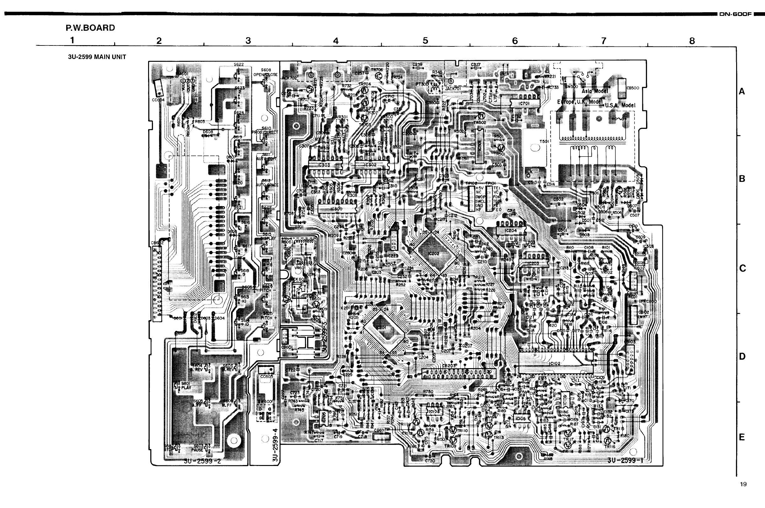
P.W.BOARD
1I
3U-2599 MAIN UNIT
234
$608
!
56 7 8
A
B
C
D
E
19
ON-6OOF
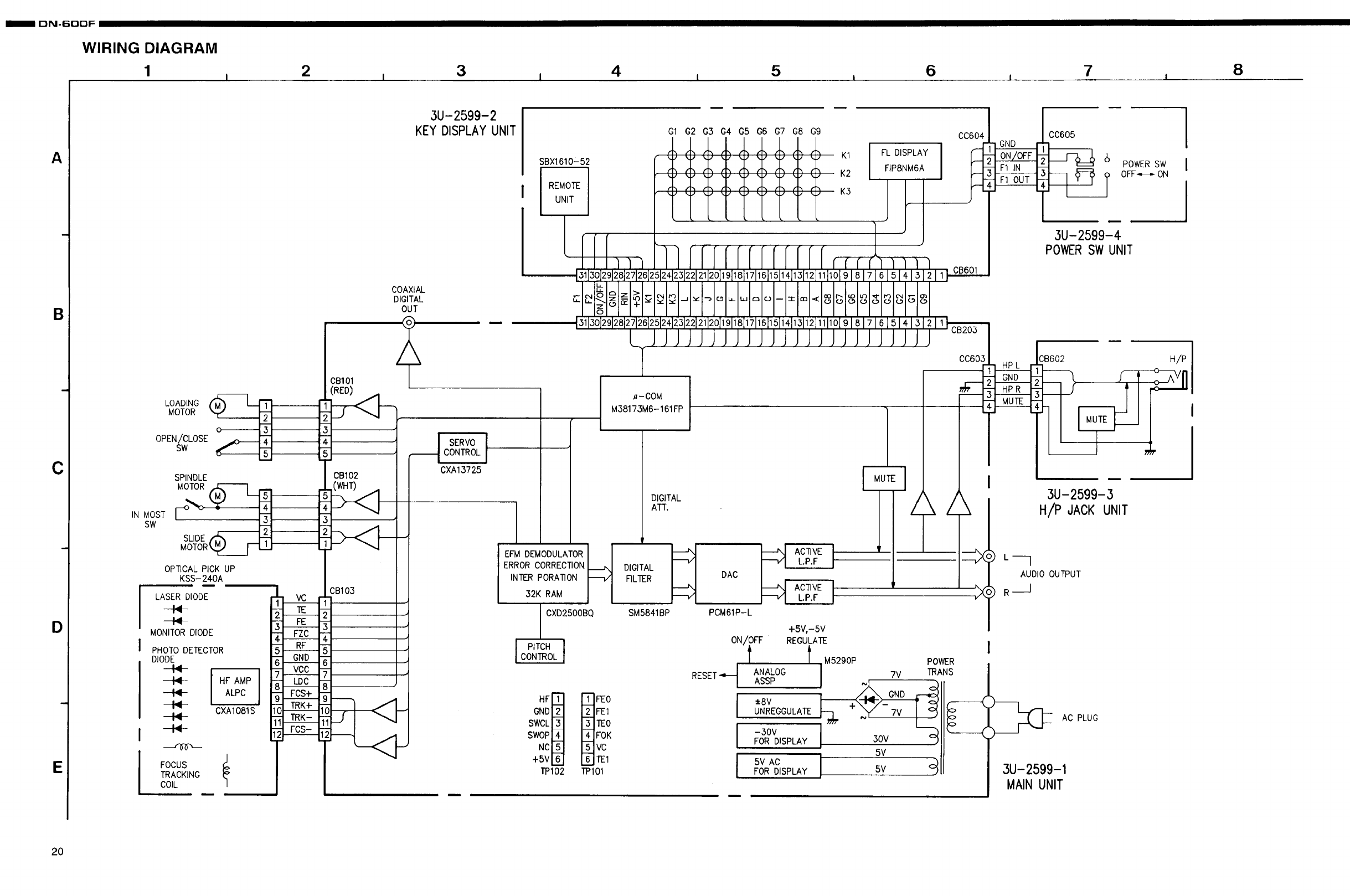
WIRING DIAGRAM
1 2 34 5 678
A
B
C
D
E
IN MOST
SW
LOADING
MOTOR _
OPEN/CLOSE _o._
sw
SPINDLE
MOTOR
SLIDE
MOTORk,____FI2J
OPTICAL PICK UP
KSS-240A
LASER DIODE
MONITOR DIODE
PHOTO DETECTOR
DIODE
I
I HF AMP
IALPC
CXAIO81S
M
I
FOCUS I
TRACKING
COIL
VC
TE
FE
FZC
RF
GND
VCC
LDC
FCS+
TRK+
TRK-
FCS-
3U-2599-2
KEY DISPLAYUNIT
SBX1610-52
IREMOTE
UNIT
COAXIAL
DIGITAL
OUT
CB101
(RED)
CB102
111
4: 7126
_ ,.,,p _ z__> !
I,.L- _, r,__ .,'r' 4.-
'[31130129128127126
,._ SERVO }
CONTROL
0XA13725
EFM DEMODULATOR
ERROR CORRECTION
INTER PORA_ON
32K RAM
I CXD2500BQ
PITCH JCONTROL
o.;R
I-_ FE1
_wc,m _oO
SWOP
+_C_J _J_C 1
1"P102 T'PlOl
G1 G2 G3 G4 G5 G6 07 G8 G9 CC604
_'J _J _'_ "" "" "/ "" " " ") "' l FL DISPLAY _l-
r_ r', _', ,,", ,,',, r,, t",, ,",, r', lFIPBNM6A
_.) (.) (,) () () () (._ () (.) K3
!
!
11rrlrfrFrl
312 o1,.1oo1-;
517[_31_21111_0'i9[?[i71 ?'?1 ? ?li2]i1'T[i ' i 1_
1111 Ill CB601
C0603
#-COM
M3817,.3M6-161FP
DIGITAL
ATT.
DIGITAL
FILTER
SM5841BP
DAC
PCM61P-L
ACTIVE
L.P.F
ACTIVE
LP.F
]/I
L
ON/OFF
t
RESET "_ ANALOGAssP
+SV,-SV
REGULATE I
t M529OP POWER
I 7V _TRANS
I30V _ (
5V
I _v o}
±SV
UNREOOULATE
-3OV
FOR DISPLAY
5V AC
FOR DISPLAY
GND
ON/OFF
F1 IN
F1 OUT
CC605
_=_
3U-2599-4
POWERSW UNIT
I
I
I
HP L
GND
HPR
MUTE
CB602 H/P
3U-2599-3
./P JACKUNIT
L-- 1
AUDIO OUTPUT
R _
AC PLUG
3U-2599-1
MAINUNIT
20
I DN-6OOF i
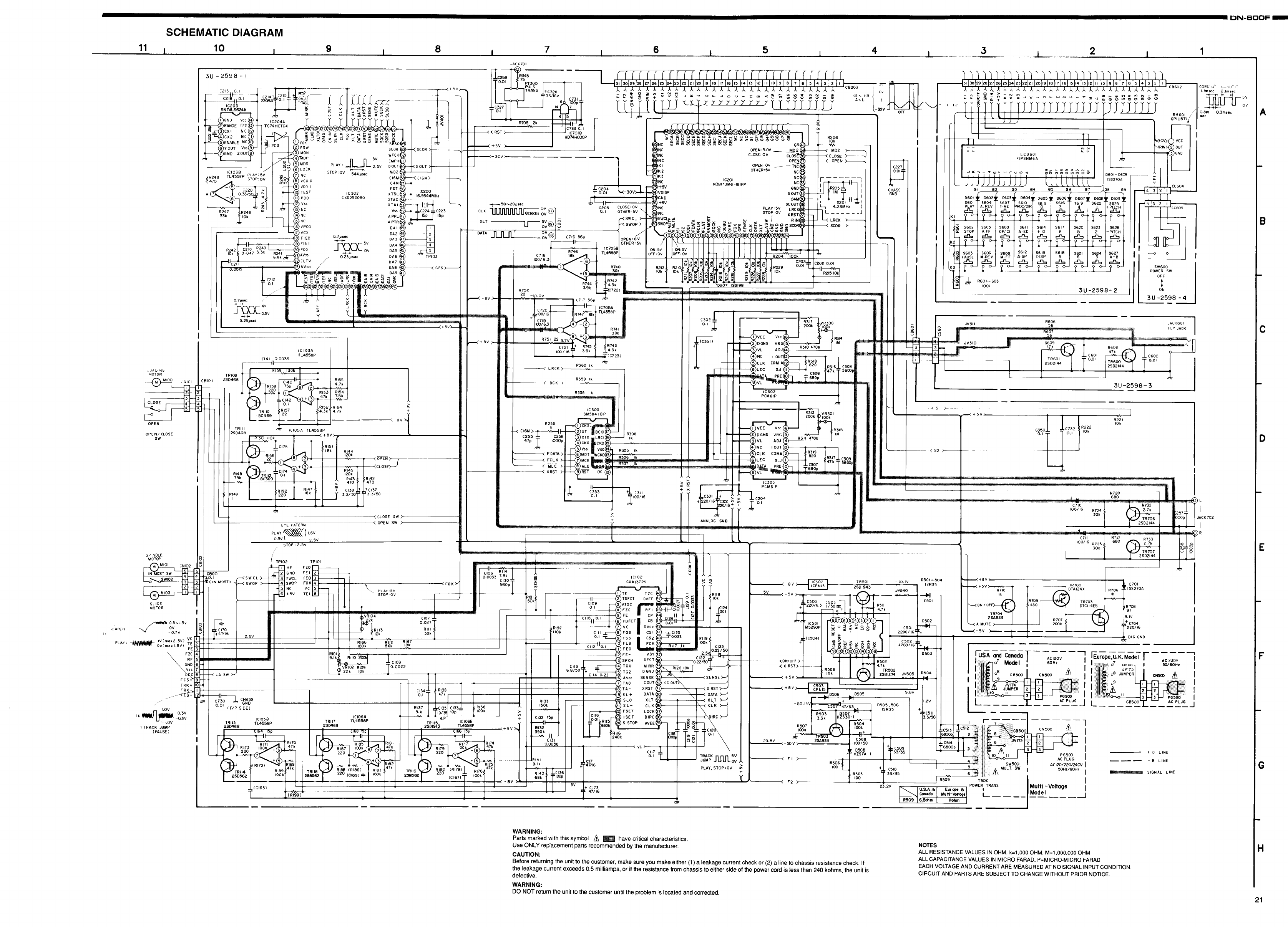
SCHEMATIC DIAGRAM
11 I
OPEN
OPEN/CLOSE
SW
SPINDLE
MOTOR
IN MOST SW
SLIDE
MOTOR
FCS
TRK+
/ I
I,OV o.3v
ID __. -03V
ITRACK JUMP
(PAUSE )
10
3U - 259 8 - I
IC203
SN 74LS624N
I
ICI03B
R248 TL455SP PLAY: 5V
STOP: OV
R247
33k
IC204A
TC74HCT04
6.8k
C211
C212
)FSW
MON
CBIOI
C800
MDS
LOCK
NC
VCO 0
I
TEST
PDO
Vss
NC
)NC
VPCO
VCXI
FIEO
FILl
PCO
9I8 I 7
SCOR
WFCK_
$21
PLAY: .V DOUTI
STOP:OV 544.SEC MD2
CI6M_
FST_
IC 202 XTSLI
CXD2500BQ XTAOI
XTAII
VSSl
DAI
DA2 q
O.7JJ$_ OA3
SV DA4
OV DA5
O.23psw=c OA6
DA7
DA8
IC 103A I
TL4558P
r-_qA_- _ I
I 4 7k
RIS8 75p "
220 RI54
4.3k 4.7k
(8V
TRill
IF I_0468 RI50 ilOk (+BY)
" - 18k RI44
_, i__ ,_o_ OREN
RI4 - - CI74
751(8 TR 12 "- 0.1
I 'l" I.2_o I T_,'_OTT'.''5°
II/ -- ,I11
EYE PATERN
o.3v_ 2.5v
STOP :2.5V
,/
/
TPI02 TPIOI
<CLOSE SW>
<OPEN SW >
2.5V
CHASS
0,01 GND
(F/P SIDE)
ICi058
TR113 TL45.SG P
2S0_.68
\_ PL AY;SV
STOP :O V
VRI04
All3
lOW
RI66 RII2 RI67
lOOk S6k IOk
w.
C108
102 RIO9 ,022
22k IOk
ICI06A
TRI IT TL4558P
2SD_68
RI?I
RIBS:
lOOk' 220 (CI69) :
(CI65]
T ( RI99 )
x 2OO
16.9344MHz
TPI03
GFS
CI07
O.02TT
B.P
TRII5 ICI06B
2SDI913 TL4_8P
CI66 15p
RI80 (R_78)
220
(CI67)"
JACK701
IT°°Llj.Zm o • T •
II I_ 1TRANSJ__c_oI /
I I I _ _ I _,,ov I c_,J.
6 IO0'p
>I' ,c_o,i_
IMO741..ICOOP
-F5V >I
CL,lJmtlJlJlJlJ_."--,_V
XLT L_ 5V
ova>
DATA 5V
I
C718
I00/6.3
C130 "
560p
RI74
47k
6 I 5 I 4 3j2
C716 56p
R746
R750
RT44
3.9k
)NC
)NC CLOSE: OV
)NC OPEN,
)KI OPeN : OV
)K 2OTHER: 5V NCI
)K3 NC'
)NC it201
M38173M6-161FP NC_
+SV GNDI
XOUTI
)GND C4M_
) t-5V
CLOSE :OV )NC PLAY :5V
OThWER: 5V I NG STOP: OV
R740
30k
C720 f
t_O/16
C719
C721,
I00/16'
C205
0. I
R359 Ik
( BCK
R358 ik
R30B
Ik
R_05 Ik
..,_R3p§_j_ ......................................
,_C3H
I00/16
÷x
R255
Ik
< C,OM>--_1-
C255 "=" C256
47p Z IOOOp
FDATA >-
"_FCLK >-
"_MLE
XRST
031
0.0056
CI09
0.1
)1,111
CII2
113
150=
CII4 0.22
IC102
CXAI372S
TE TZC
TDFCT DVEE
FOF,CT I CB
VC DVcc
FGD CSI
FS3
FLB
FEO
F E- ASY
SRCH OFCT
TGU MIRR
TG2 DGND
AV¢c SENSE
TAO LOUT
TA - X RST
SL'P DATA
SLO XLT
SL- ELK
FSET LOCK
ISET DIRC
S STOP AVEE
Ril6
:40k
Ell7
0.1
RI41
9.1k
D207 ISS198
lOOk
C203.
o.oi
lOk
_CLK COM
)LEE
IC302
PCM61P
)DGND
)VL
IC303
PCM61P
ANALOG GNO
RIm7 Ik
..1-]__:
iool
R206
IOk
MD2
OPEN
4.23MHz I
_L ...... J
LRCK
C202 O.Oi
VR300
R310 4TOk
VR301
)lOOk
R315
IM
RSII 470k
_2T..L
.01_
SS
)
C 122
DATA
TRACKI'1n n 5v
•JUMP JUULov '
PLAY, STOP :OV +
29.8V
43130292'8272625242'3222 20 9 8 T 6 54 312 II10 9 8 T654 3 2I
" [ CB602 COIRI) u Lv_L> I r'
lli_..K_ ,kl,k,t_,k_,k.t..t..k_.,k,k,L,',,ti_,i,L..k,kI,.,,,,,_ 2.1....
____z_ > - o., ,.,., _ ® ,._ ,.,_ _ ,..,_ ,_ _..
_z o '" LlUU Uov
u- __ LED601 _ ,,N RIN
FIPSNM6A
............ _,_ ,_,__ ,__ _ _
ri;T,,,,,,,,,, I_,_,,,I ooo,-ooo _Cll
\!LLLLL(!-.
G ;8 G! ,,-I 4 I 3 I Z I I I,,_,_...--
ooo, o.o2: .o,: DOO., o.oT o.oo,;COOT: £
S601 $604 SE07 ' "S610 " $613 $616 " " $619 ' "S622
PLAY A. REV T IME _ROCY01R IO 7 I CC605
'1 _--, o- o--_ o--, o-- o
,_ y o_,y _ _ _L_°d'? Y _ t? _ I Lt--t------
t soo21s.o5.oo so,,so,.Iso,Ts .oso2.Fso2.1 I
1,T,- STOP I AFF OP/CL AED lid I8szI-reTCHI I I I
L,._n..l,_n_,,_r,._,,-,'L.'-"-'I"-"-'_ '-"-'l'-"'-"I I,',',_ I
soo, soo,s0,2so,s.sss s,, .2,rSO2T. o
1~1 PAUSE I M.REV M.FF A-SP DISP I 9 6 3 A-B I [ ....
._17 _ o- o- ? o- ? o= o- o- l_ swooo
- _ _ 'i _. c,_ 2 2o_ POWER SW
°i'
oRGOI_ 603
lOOk 3U-2598- 2 ON
3U -2598 -4
I R606 JACK6Ol
_JVSI I 56 H.P JACK
$2
-8V _ TR5OI IO. IV 0501 _504( 2SDI94_ ISR35
JV540
RSOI
4,7k
Jr505
9.BY
C503 C505
t'220/6.3 1/50m
}' ICSOI
M52_P
.(C504)
X
0501
'503
5O4
,.2V
+
I:C511
$, 3/50
R502
4.7k
TRS02
2SBI274
D505,506
15R35
; R!
' I
JVSlO R609
RG08
47k
.C60t C600
_D506 _,0505
.100150
(Ft >L
R506
I00
.RS05
iO0
F2 >
+5V:
+BY),
RTIO
IW
C3S01
O'i TL
L [ R22,
lOW
C732 R222
"OI ]iOk
R720
680
C710
100/16 R724
50k
C711
100/16 R72S
30k
TR704
2SA933
TR702
DTAI24X
TR703
DTCII4ES
O701
ISS27OA
R708
91
9. IV
DIG GND
ir
1
AC I20V I
GOHz I
CN_OO _ I
I
- -- AC PLUG J
Europe,U.K. Model I ACz_v I
iiii:i:i:i_i_.Z_[I7 I 50/60HZ i
I
c.sooT -- __ _uLj
PGSO0
AC PLUG
SW500 ACI20/220/240V
MULT. SW 50Hz/6Oib
Multi -Voltage
Model
+ B LINE
BLINE
SIGNAL LINE
)L
I
JAG K 702
I
R
WARNING:
Pans marked with this symbol Z_ _ have critical characteristics.
Use ONLY replacement parts recommended by the manufacturer.
CAUTION:
Before returning the unit to the customer, make sure you make either (1) a leakage current check or (2) a line to chassis resistance check• If
the leakage current exceeds 0.5 milliamps, or if the resistance from chassis to either side of the power cord is less than 240 kohms, the unit is
defective.
WARNING:
DO NOT return the unit to the customer until the problem is located and corrected.
NOTES
ALL RESISTANCE VALUES IN OHM. k=1,000 OHM, M=1,000,000 OHM
ALL CAPACITANCE VALUES IN MICRO FARAD. P=MICRO-MICRO FARAD
EACH VOLTAGE AND CURRENT ARE MEASURED AT NO SIGNAL INPUT CONDITION.
CIRCUIT AND PARTS ARE SUBJECT TO CHANGE WITHOUT PRIOR NOTICE.
A
m
B
C
D
E
F
G
H
21
IDN-6OOF I
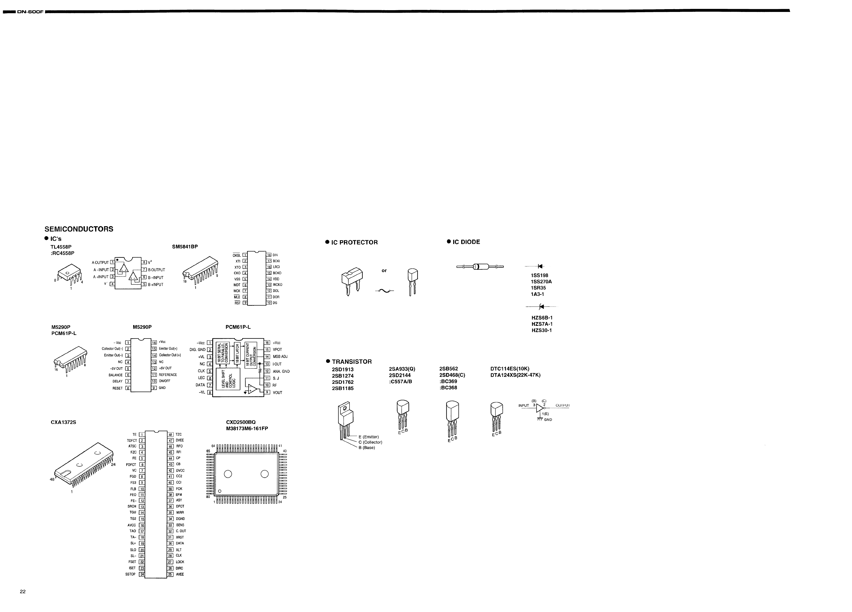
SEMICONDUCTORS
•IC's
TL4558P
:RC4558P
1
A OUTPUT I_v I[_] V+
A-,NPUT X--I BOUTPUT
A+,NPOT__ B-,NPUT
v-H =--p ÷,NPUT
SM5841BP
1
OKSL IT"
XTI I-_
XTO I_-
CKOI-Z
vss E
MOTE
MCK i-7
MLE I-@-
RS--_I_
"_DIN
BCKI
LRCI
[] BCKO
[] VDD
WCKO
DOL
___ DOR
DG
M5290P
PCM61P-L
-vcc Iq-
Collector Out(-) r2
EmitterOut(-)
NC1"-4-
-5V OUT I_"
BALANCE
DELAY
RESET
M5290P
'_1 +Vcc
Emitter Out(+)
1-_ CollectorOut (+)
NC
+5V OUT
REFERENCE
ON/OFF
GND
-Vcc E
DIG. GND
+VL I_"
NC
CLK
LEC 16"
DATA
-VL
PCM61 P-L
z
_I I_I_
5_z
:p,o
+Vcc
VPOT
1-T1 MSB ADJ
I OUT
ANA. GND
1--_ S.J
RF
VOUT
CXA1372S
TE
TDFCT
ATSC
FZC
FE
FDFCT
VC
FGD
FS3
FLB
FEO
FE-
SRCH
TGU
TG2
AVCC
TAO
TA-
SL+
SLO
SL-
FSET
ISET
SSTOP
IT
FZ
E
IT
rT
FT
rT
lnT
E
E
E
E
TZC
DVEE
RFO
4-_ RFI
cP
CB
DVCC
4-_ CC2
CCl
FOK
EFM
3-71 ASY
DFCT
MIRR
DGND
_'_ SENS
3-_ C. OUT
31--7 XRST
DATA
2-_ XLT
2-_ CLK
LOCK
DIRC
AVEE
CXD2500BQ
M38173M6-161 FP
HflHRn flflflflflflAH flHflflflH H
64
65
i1_11=:
_1=:=
¢=z==:
=_==:
=© ©
=::=m: o
,HHHHHHHHHHHHHHHHHHHHHH
41
40
=
:=E=_
=
=
=
=
=
=
=
=
=
=
::=E==
=
=
25
.M
• IC PROTECTOR
or
•TRANSISTOR
2SD1913
2SB1274
2SD1762
2SB 1185
E (Emitter)
C (Collector)
B (Base)
2SA933(Q)
2SD2144
:C557A/B
E( B
•IC DIODE
___=
lSS198
1SS270A
lSR35
1A3-1
L,=
HZS6B-1
HZS7A-1
HZS30-1
2SB562
2SD468(C)
:BC369
:BC368
E CB
DTC114ES(10K)
DTA124XS(22K-47K)
E CB
INPUT
(B) (C)
31_1_E) OUIPUI
III GND
22

DN-6OOF
NIPPON COLUMBIA CO.. LTD.
14-14, AKASAKA 4-CHOME, MINATO-KU, TOKYO 107-I 1, ,JAPAN
Telephone: 03 (3584) 8111
Cable: NIPPON COLUMBIA TOKYO Telex: JAPANOLA J22591
Printed Jr,Japan 407 _B_ 0438
