Daintree Networks DT357 DT357 ZIGBEE RF MODULE User Manual DN00DC0018 03 DT357
Daintree Networks PTY LTD DT357 ZIGBEE RF MODULE DN00DC0018 03 DT357
Users Manual
1
DT357 Series User Manual
Description
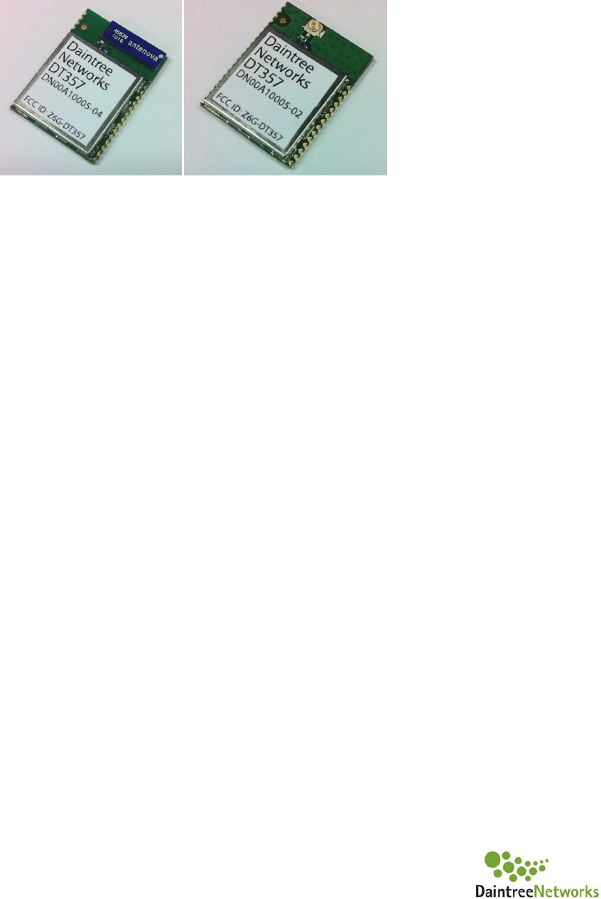
The DT357 and DT357-U.FL Daintree ZigBee® modules provide a cost-effective RF transceiver
solution for 2.4GHz Zigbee and IEEE 802.15.4 data links and wireless networks.
The modules are available either with an on-board chip antenna (DT357) or alternatively with a U.FL
connector (DT357-U.FL) for attaching an external antenna.
These modules have been designed to be easily integrated into another device and to provide a fast,
simple and low cost wireless mesh networking interface.
The DT357 series module is based on the Ember ZigBee® platform consisting of the EM357
combined with the ZigBee PRO compliant EmberZNet meshing stack. Integration into a wide range of
applications is made easy using a simple AT style command interface and advanced hardware
design.
Module Features
• Small physical footprint, SMD module 25mm x 19mm
• Integrated PCB chip antenna
• Optional U.FL connector for use with an external antenna
• -100dBm normal RX sensitivity
• Industry-leading ARM® Cortex™-M3 processor
• 16 RF Channels (Top channel 1A operates at a reduced power level)
• JTAG Programming and real time debugging via the Ember InSight Port
• Very low power consumption: less than 1uA in deep sleep mode.
• +3dBm nominal power output increased to 8dBm in boost mode.
• Wide supply voltage range (2.1 to 3.6V)
• 192kB flash and 12kbytes of RAM
• 24 GPIO lines
• FCC modular compliance.
• RoHS compliant
• Operating temperature range: -40°
C to +85°
C
Applications
• Wireless lighting controls
• Wireless alarms and security
• Home automation and control
• Building automation and control
• Security and monitoring
• Thermostats
• Traffic management
• General Zigbee wireless networking

2
Table of Contents
DT357 SERIES USER MANUAL ..................................................................................... 1
DESCRIPTION ................................................................................................................... 1
1. HARDWARE DESCRIPTION ...................................................................................... 3
2. ABSOLUTE MAXIMUM RATINGS ............................................................................. 4
3. RECOMMENDED OPERATING CONDITIONS ......................................................... 4
4. DC ELECTRICAL CHARACTERISTICS@ 25°C, VCC = 3.0V, NORMAL MODE UNLESS
OTHERWISE STATED ................................................................................................................ 4
5. DIGITAL I/O ................................................................................................................. 4
6. RF ELECTRICAL CHARACTERISTICS ...................................................................... 5
7. ENVIRONMENTAL CHARACTERISTICS .................................................................. 5
8. DT357 PIN DESCRIPTION ......................................................................................... 6
9. DT357 DIMENSIONS ................................................................................................... 7
10. PCB KEEP-OUT AREAS ............................................................................................ 8
11. PRODUCT APPROVALS ........................................................................................... 9
11.1 FCC PART 15.247 CERTIFICATION ..................................................................................................................... 9
11.2 FCC LABELLING REQUIREMENTS ....................................................................................................................... 10
11.3 CANADA IC CERTIFICATION .............................................................................................................................. 10
11.4 EUROPEAN CERTIFICATION .............................................................................................................................. 10
3
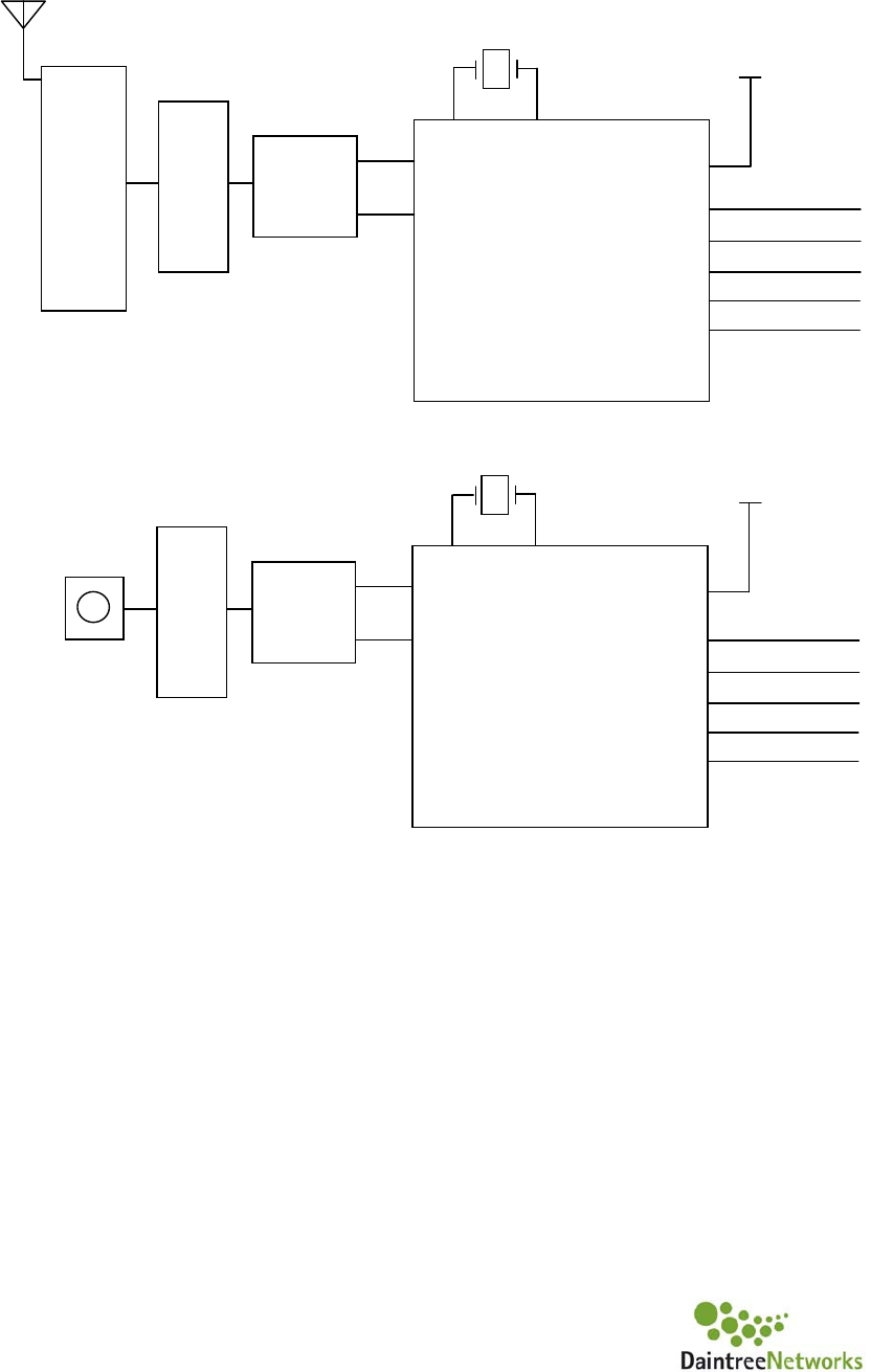
1. Hardware Description
BLOCK DIAGRAM OF DT357
BLOCK DIAGRAM OF DT357-UFL
PROCESSOR
The DT357 series module utilises an Ember EM357 S.O.C (System on Chip) which has an integrated
32-bit ARM® Cortex™-M3 processor, flash (196kB) and RAM (12kB) memory and peripherals. This
is interfaced by standard serial wiring (UART) and includes JTAG programming interface. This allows
for powerful software debugging and programming of the ARM Cortex ™-M3 core.
The EM357 has built in 1.8V and 1.25V regulators as well as a power-on-reset circuit which reduces
the amount of external circuitry required.
ANTENNA
The DT357 module includes an integrated chip antenna (Antenova Rufa) which is compact in size but
has a uni-directional radiation pattern allowing a gain of 2.1dBi. Further details of the antenna can be
found on the Antenova website.
The DT357-U.FL module includes a U.FL connector instead of a chip antenna that allows for the
connection of an external antenna up to a gain of 2.0dBi.
24MHz
24MHz
JTAG
A/D
UART
RESET
JTAG
I/O
U.FL Connector
Ceramic
Balun
Harmonic
Filter
Chip Antenna
EM357
VBRD
Ceramic
Balun
EM357
Harmonic
Filter
VBRD
A/D
UART
RESET
I/O

4
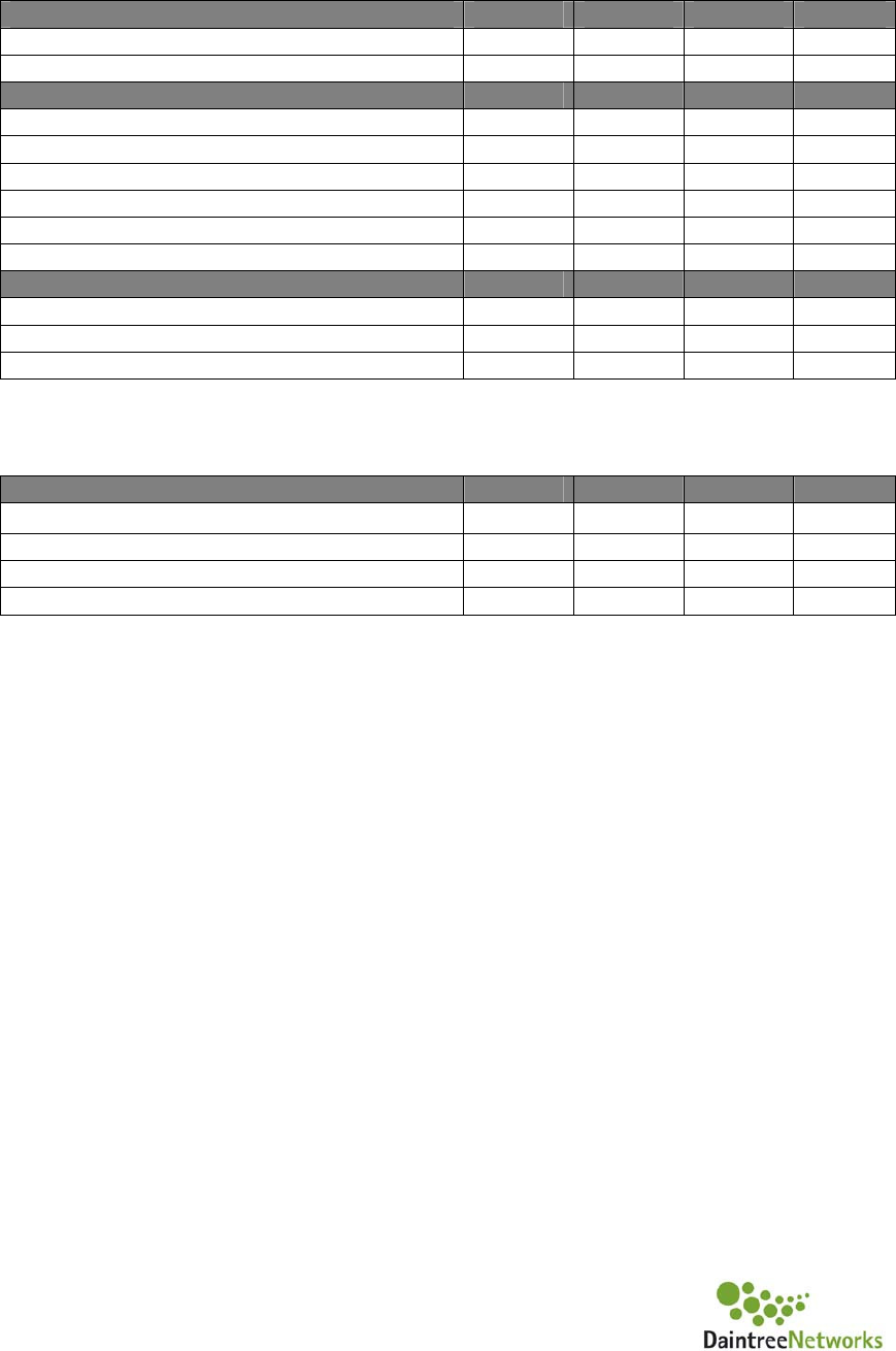
2. Absolute Maximum Ratings
Rating
Value
Unit
Power Supply Voltage
3.6
Vdc
Voltage on any Digital I/O
-
0.3 to V
CC
+0.3
Vdc
RF Input level
15
dBm
Storage Temperature Range
-
40 to +105
°C
Note: Exceeding the maximum ratings may cause permanent damage to the module or devices
3. Recommended Operating Conditions
Characteristic
Min
Typ
Max
Unit
Power
Supply Voltage
2.1
3.6
Vdc
Input Frequency
2405
2480
MHz
Operating Temperature
-
40
85
°C
RF
I
nput Power
0
dBm
4. DC Electrical Characteristics@ 25°C, VCC = 3.0V, NORMAL MODE unless otherwise stated
Parameter
Min
Typ
Max
Unit
Ambient Temperature
Range
-
40
25
85
°C
Power Consumption
Min
Typ
Max
Unit
Transmit Mode at 3dBm Output Power
31
mA
Transmit Mode at 8dBm Boost Output Power
42
mA
Receive Mode
26.5
mA
Standby Mode
1
uA
5. Digital I/O
Digital I/O
Min
Typ
Max
Unit
Logic Low
Schmitt Input Switching Threshold
0.42 x Vcc
0.5 x Vcc
V
Logic High Schmitt Input Switching Threshold
0.62 x Vcc
0.8 x Vcc
V
Logic Low Output
0
0.18 x Vcc
V
Logic High Output
0.82 x Vcc
Vcc
V
Output Sink Current (Std Pad)
4
uA
Output Source
Current (Std Pad)
4
uA
Output Sink Current (High I Pad)
8
uA
Output Source Current (High I Pad)
8
uA
Input Current For Logic 0
-
0.5
uA
Input Current For Logic 1
0.5
uA
Total Output Current (I/O Pads)
40
mA
5
6. RF Electrical Characteristics
Parameter
Min
Typ
Max
Unit
RF Frequency Range
2400
2500
MHz
RF Data Rate
250
Kbps
Receive Characteristics
Min
Typ
Max
Unit
Receiver Sensitivity (1% PER) NORMAL
-
100
-
94
dBm
Receiver Sensitivity (1% PER) BOOST
-
102
-
96
dBm
High
-
Side Adjacent Channel Rejection
35
dB
Low
-
Side Adjacent Channel Rejection
35
dB
2
nd
High
-
Side Adjacent Channel Rejection
46
dB
2
nd
Low
-
Side Adjacent Channel Rejection
46
dB
Transmit Characteristics
Min
Typ
Max
Unit
Transmitter Output
Power NORMAL
1
5
dBm
Transmitter Output Power BOOST
8
dBm
Minimum Output Power
-
55
dBm
7. Environmental Characteristics
Environmental Characteristics
Min
Typ
Max
Unit
ESD (human body model)
±2
kV
ESD (charged device model) Non
-
RF pins
±400
V
ESD (charged device model) RF Pins
±225
V
Moisture Sensitivity Level (MSL)
MSL3

6
8. DT357 Pin Description
Pin
No
Name
D
irection
Description
1
GND
GND
2
PC5
I/O, O
Digital I/O
, Logic
C
ontrol for
E
xternal Rx/Tx switch
3
PC6
I/O
, O
Digital I/O, 32.768 kHz OSC
, Inverted TX_ACTIVE signal
4
PC7
I/O, I
Digital I/O, 32.768 kHz OSC, Digital 32.768 kHz
C
lock
I
nput
source
5
PA7
I/O, I, O
Digital I/O, Timer 1 Ch4 Out
/
In, Ext
R
eg
ulator
O
pen drain Out
6
PB3
I/O, O, I
Digital I/O, Timer 2
Ch3 Out/In, UART CTS1, SPI1 MCLK/SCLK
7
NRESET
I
Active
L
ow
C
hip
R
eset
8
PB4
I/O, O, I
Digital I/O, Timer 2 Ch4 Out/In, UART RTS1, SPI
S
lave
S
el
ect
1
9
PA0
I/O, I, O
SPI2 MOSI,
Timer 2 Ch1 Out/In
10
PA1
I/O, O, I
SPI2 MISO,
Digital I/O, Timer 2 Ch3 Out/In, TWI
SDA
2
11
PA2
I/O, O, I
SPI2 MCLK/SCLK,
Digital I/O, Timer 2 Ch4 Out/In, TWI
SCL
2
12
PA3
I/O, O, I
SPI2 Slave Sel,
Digital I/O, CPU
T
race
C
lk,
T
imer 2 Ch2 Out/In
13
GND
GND
14
PA4
I/O, O
Digital I/O, ADC In4, PTI
F
rame
S
ignal, CPU
T
race
D
ata
B
it 2
15
PA5
I/O, An, O, I
Digital I/O, ADC In5, PTI
D
at
a
S
ignal, Embed
B
oot
A
ctiv
ate
, CPU
Trace 3
16
PA6
I/O, O, I
Digital I/O, Timer 1 Ch3 Out/In
17
PB1
I/O, O, I
UART1 Tx,
Digital I/O, SPI1 MISO/MOSI,
TWI SDA1,
Timer2 Ch1
I/O
18
PB2
I/O, I, O
UART1 Rx,
Digital I/O, SPI1 MISO/MOSI,
TWI SCL1, Timer2 Ch1
I/O
19
GND
GND
20
GND
GND
21
JTCK
I, I/O
JTAG CLK In Debug, SW
CLK In/Out
22
PC2
I/O, O
Digital I/O, JTAG Data Out Debug, SW Out Debug
23
PC3
I/O, I
Digital I/O, JTAG
Data In Debug
24
PC4
I/O, I
Digital I/O, JTAG
M
ode
S
el, SW Data In/Out Debug
25
PB0
I/O, An, I, O
Digital I/O, ADC
R
ef Out/In, Ext IntA, CPU
C
lk
T
race, Timer1 Ext
CLK In, Timer2 Clk Mask In
26
PC1
I/O, An, O
ADC In3,
Digital I/O, SW Out Debug, CPU
T
race
D
ata
B
it 0
27
PC0
I/O, I, O
Digital I/O, JTAG
R
eset In Debug, Ext In
tD,
CPU
T
race
D
ata
B
it 1
28
PB7
I/O, An, I, O
Digital I/O, ADC In2, Ext IntC, Timer1 Ch2 Out/In
29
PB6
I/O, An, I, O
Digital I/O, ADC In1, Ext Int
B, Timer1 Ch1 Out/In
30
PB5
I/O,
An, I
Digital I/O, ADC In0, Timer2 Ext Clk In, Timer1 Ext Clk Mask In
31
GND
GND
32
VBRD
POWER
Analogue
P
ad
S
upply (1.8V)
33
GND
GND
7
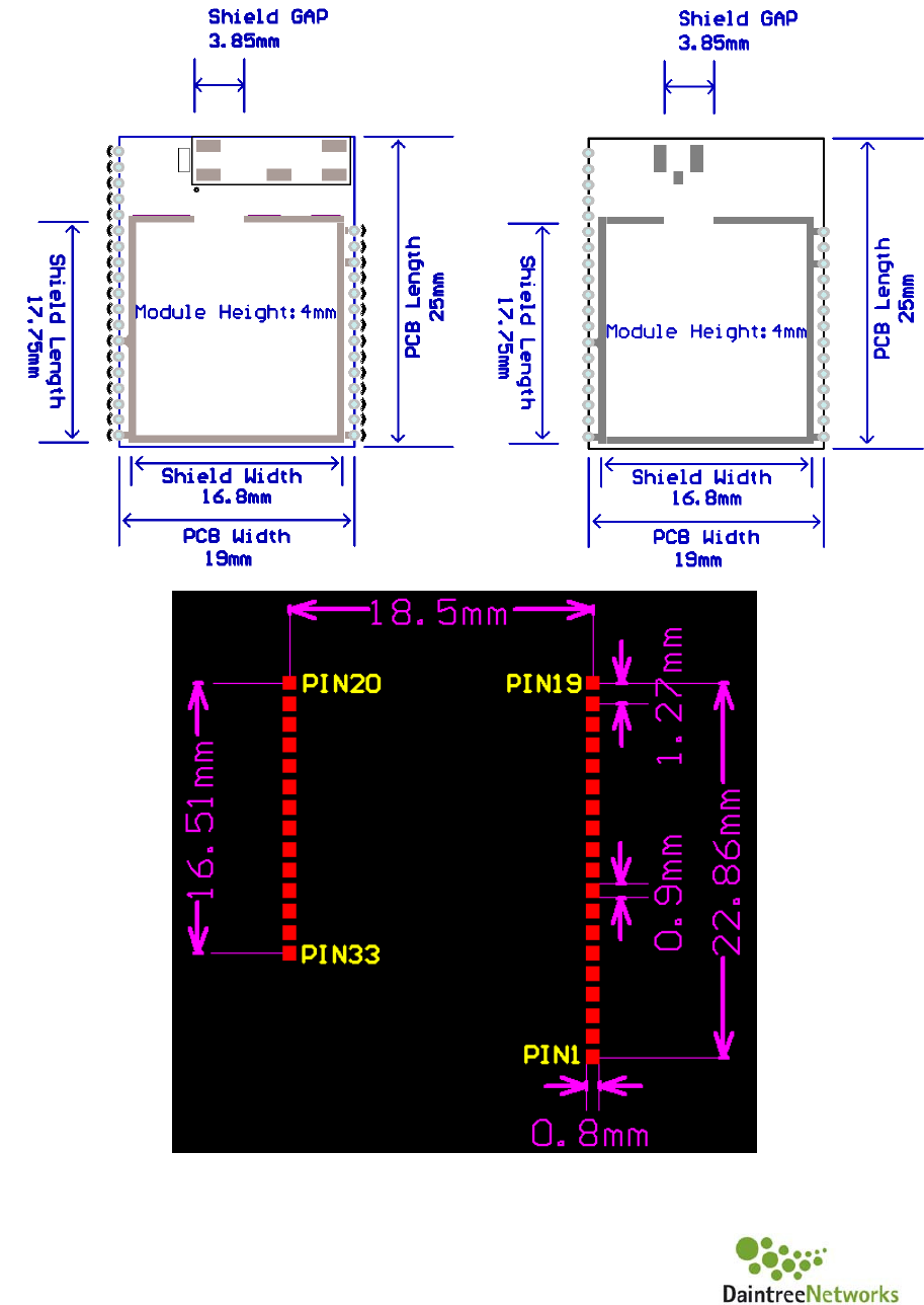
9. DT357 Dimensions
Recommended PCB Footprint
DT357
DT357
-
U.FL

8
10. PCB Keep-Out Areas
For optimum RF performance when using the DT357 module (Chip Antenna version) the module
should be placed so that the antenna is located on the edge of the mating PCB. No tracks or planes
or components should be located in the keep-out area. When using the DT357-UFL module (external
antenna version) the keep-out area does not need to be adhered to.
Keep Out Area for Chip Antenna (DT357 only)

9
11. Product Approvals
The DT357 and DT357-U.FL have been designed for modular compliance into USA (FCC), Canada
(IC), Australia (C-Tick) and Europe (CE). Full FCC, IC and C-Tick compliance have been obtained
and European compliance (CE) has been part completed with full compliance to follow in the future.
11.1 FCC Part 15.247 Certification
The DT357 and DT357-U.FL modules including the antennas listed in Table 1 below have been
tested and have been found to comply with FCC CFR Part 15 (USA). The DT357-U.FL has
compliance for an external antenna with a maximum gain of 2.0dBi.
To meet the section 12.209 emission requirements in the restricted bands of section 15.205, the
transceiver transmitter power for the DT357 and DT357-U.FL modules needs to be reduced from
8dBm to 7dBm on the top channel 1A (2480 MHz).
The software Daintree will release with the DT357 and DT357-U.FL modules will limit the end
user to a maximum of 7dBm on the top channel 1A (2480 MHz) to ensure compliance.
These devices meet the requirements for modular transmitter approval as detailed in the FCC public
notice DA00.1407.transmitter. These additional requirements can allow the DT357/DT357-U.FL
modules to be installed in a new device without subsequent new equipment authorisation to be
obtained.
This device complies with Part 15 of the FCC rules. Operation is subject to the following two
conditions: (1) this device may not cause harmful interference, and (2) this device must accept
any interference received, including interference that may cause undesired operation.
Item Part No Manufacturer Type Gain
1 S131CL2-L-XXX-
2450
Nearson 1/2 Wave 2.0dBi
The Daintree DT357 and DT357-U.FL modules have been tested and found to comply with the limits
for a digital device, pursuant to part 15 of the FCC Rules. These limits are designed to provide
reasonable protection against harmful interference in a residential installation. The Daintree modules
generate, use and can radiate radio frequency energy and, if not installed and used in accordance
with the instructions, may cause harmful interference to radio communications. However there is no
guarantee that interference will not occur in a particular installation. If the Daintree module does
cause harmful interference to radio or television reception, which can be determined by turning the
Daintree module off and on, the user is encouraged to try and correct the interference by one or more
of the following measures:
• Reorient or relocate the receiving antenna.
• Increase the separation between the Daintree module and receiver.
• Connect the Daintree module into an outlet on a circuit different from that to which the
receiver is connected.
• Consult the dealer or an experienced radio/TV technician for help.
The DT357 and DT357-U.FL modules with their antennas comply with FCC/IC RF exposure limits for
general population/uncontrolled exposure.
While the applicant for a device into which the DT357 and DT357-U.FL with an approved antenna in
Table 1 is to be installed is not required to obtain a new authorization for the module, this does not
ensure that some other form of testing may be required for the end product.
Any changes or modifications made to this device that are not expressly approved by Daintree may
void the user's authority to operate the equipment.
When using the DT357-U.FL with approved antennae, it is required to prevent end-users from
replacing them with non-approved ones.

10
To comply with FCC and Industry Canada RF radiation exposure limits for general population
the antennas used for the DT357 and DT357-U.FL must be installed such that a minimum
separation distance of 20cm is maintained between the antenna and all persons at all times
and must not be co-located or operating in conjunction with any other antenna or transmitter.
11.2 FCC Labelling Requirements
When integrating the DT357 and DT357-U.FL into a product it is necessary that the FCC labelling
requirements are met. This includes a clearly visible label on the outside of the finished product
specifying the Daintree FCC identifier (FCC ID: Z6G-DT357) as well as the statement above. This
label can use wording such as “Contains Transmitter Module FCC ID: Z6G-DT357” or “Contains
FCC ID: Z6G-DT357” or similar words which convey the same information.
FCC ID: Z6G-DT357
11.3 Canada IC Certification
The DT357 and DT357-U.FL comply with Industry Canada License-exempt RSS standards.
• Operation is subject to the following two conditions: 1) this device may not cause interference,
and 2) this device must accept any interference that may cause undesired operation of the
device.
• To reduce potential radio interference to other users, the antenna type and its gain should be
so chosen that the equivalent isotropically radiated power (e.i.r.p.) is not more than is
necessary for successful communication.
• This radio transmitter DT357-U.FL has been approved by Industry Canada to operate with the
antennas listed in Table 1 with a maximum permissible gain of up to 2.0dBi. Antenna types
having a gain greater than the maximum gain indicated for that type are strictly prohibited for
use with this device. The antenna impedance required is 50 ohms.
The labelling requirements are similar to those of FCC. A visible label displaying the IC number must
be shown. The end user is responsible for the final product to comply with IC ICES-003
(Unintentional radiators).
11.4 European Certification
The DT357 and DT357-U.FL have been certified to the following standards:
• Radio: EN 300 328 v1.7.1 (10/2006)
• EMC: EN 301 489-17 v2.1.1 (09/2008). EN 301 489 compliance to be completed in the future.
The DT357 will be tested with its integrated chip antenna with a gain of 2.1dBi. The DT357-U.FL will
be tested with an antenna listed in Table 1 with a maximum gain of 2.0dBi.
The ‘CE’ marking must be applied to a visible location on the user’s product and must be legible. For
more information please refer to http://ec.europa.eu/enterprise/faq/ce-mark.htm. Customers assume
full responsibility for meeting the required guidelines for each country for their product distribution
market.