Daviscomms DC3500 GSM/GPRS Module User Manual
Daviscomms (S) Pte Ltd GSM/GPRS Module
User manual
iSR3500 Series
GSM / GPRS Module
Pre-Release Rev 0.3
2008. 03. 28
Sirius Mobility
31 International Business Park
#02-05 Creative Resource Bldg,
Singapore 609921
www.sirius-mobility.com
email: sales@i-sirius.com.sg
iSR3500 Series 2 / 11 Pre-rev 0.3
Mobile SolutionsMobile Solutions
1 Introduction
1.1 General Description
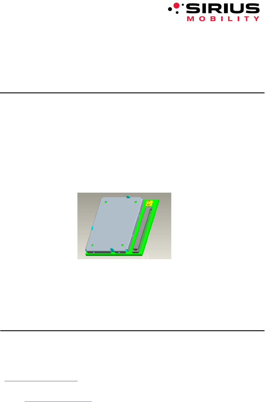
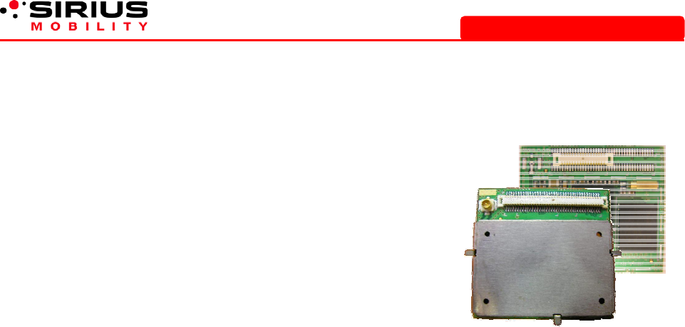
iSR3500 series is a product line of single-module platform optimized for
ultra low cost GSM/GPRS modem and generic mobile applications. It
integrates all the functions necessary for a dual-band GSM/GPRS wireless
communication, including baseband, mixed signal, power amplifier, power
management, RF transceiver, front-end switch and memory in a single
monolithic module with board-to-board connector
The highly integrated module is ideal for application requiring GSM, and is
capable of working on 2-layer motherboard with no further RF calibration
required.
1.2 Key Features
GSM or GPRS Dual Band 900/1800 MHz or 850/1900 MHz,
Protocol Stack GSM Rel.97. STK Rel.99
GPRS Rel4.0 Class 10
Speech Codec EFR / FR / HR / AMR
Security Hardware support for IMEI, SIM-Lock, Flash Software Protection and
Secure Boot
Messaging SMS concatenated
EMS, Smart messaging (GPRS)
Browsing CSD, Jataayu WAP 1.2 (GPRS)
Text Input T9 and/or Z8 library word recognition
Output Power Class 4 (2W) at 850/900 MHz
Class 1 (1W) at 1800/1900 MHz
Supply Voltage 3.4V ~ 4.2V, Nominal : 3.7V
Power consumption Power off < 200uA
Idle mode < 4mA
GSM Sensitivity -110 dBm (typ) at 850/900 MHz
-109 dBm (typ) at 1800/1900 MHz
LCD feature up to 96x64 FSTN (iSR35<b>16)
up to 128x128 FSTN (iSR35<b>32)
up to 160x128 65K CSTN (iSR35<b>3204)
Clock 26MHz reference clock
26MHz for MCU sub-system
78MHz for DSP
Interface 8 bit parallel interface
SSC / SPI interface
I2C Bus
UART
Communication Extendable AT Commands (GPRS)
ADC 1 open ADC
1 ADC (TBAT) is reserved for battery temperature monitoring
Headset hook detection
Audio Analog audio for ring tone (balanced and unbalanced)
Analog audio for receiver (balanced and unbalanced)
Balanced analog microphone interface
Unbalanced external microphone interface for headset
LED backlight White LED buck-booster embedded, requires only external FET and diode
for switching
Debug JTAG support
Charging Pulse charging support for both Ni-MH and Li-ion battery
Vibrator Support Vibrator control output
Keypad Support 6 x 4 key inputs
26.8 x 28.0 x 2.826.8 x 28.0 x 2.8
iSR3500 Series 3 / 11 Pre-rev 0.3
Mobile SolutionsMobile Solutions
1.3 Ordering Information
iSR35<b><nnnn>-<c><p>
<b> = GSM band option, E or U
<nnnn> = memory option, 16, 32, 3204, 3208 or 6416
please note that other RAM configuration will be incorporated in the future
<c> = b2b connector size option, C1, C2 or C3
<p> = packaging option, R or T
1.4 Product part number
iSR35E16 GSM 900/1800MHz band, 16Mbit Flash
iSR35E32 GSM 900/1800MHz band, 32Mbit Flash
iSR35E3204 GSM 900/1800MHz band, 32Mbit Flash + 4Mbit static RAM
iSR35E3208 GPRS 900/1800MHz band, 32Mbit Flash + 8Mbit static RAM
iSR35E6416 GPRS 900/1800MHz band, 64Mbit Flash + 16Mbit static RAM
iSR35U16 GSM 850/1900MHz band, 16Mbit Flash
iSR35U32 GSM 850/1900MHz band, 32Mbit Flash
iSR35U3204 GSM 850/1900MHz band, 32Mbit Flash + 4Mbit static RAM
iSR35U3208 GPRS 850/1900MHz band, 32Mbit Flash + 8Mbit static RAM
iSR35U6416 GPRS 850/1900MHz band, 64Mbit Flash + 16Mbit static RAM
Connector Option
C1 = 34 pins
C2 = 60 pins
C3 = 80 pins
2 Electrical Specification
2.1 Absolute Maximum Rating
The maximum rating may not be exceeded under any circumstances as permanent damage to the module will result
Limit Values
Parameter Pin
Minimum Maximum
Unit
Battery Supply Vbat1, Vbat2, Vbat3 -0.15 - +5.5 V
Output Load VSWR ANT 10:1
Storage Temperature -55 +150 ˚C
ESD 1000 V
Digital I/O sink current 20 mA
Digital I/O Level 3.6 V
2.2 Electrical Characteristics
At operating Temperature: -20˚C ~ 60˚C
Parameter Pin Min. Typ. Max Unit
Battery Power supply Vbat1,Vbat2,Vbat3 3.4 3.8 4.2 V
Charger Detection Voltage CDT 0 2.5 V
iSR3500 Series 4 / 11 Pre-rev 0.3
Mobile SolutionsMobile Solutions
Battery charging protection voltage Vbat1,Vbat2,Vbat3 4.47 / 5.5 V
Supported Battery Voltage for charging Ni-MH
Li-ion
3.1
3.1 5.1
4.2 V
VSIM -3% 1.8/2.85 +3%
VIO Voltage VIO,VDDP_IO -3% 2.85 +3% V
VIO Output current IVIO 30 mA
VDDP_MEM Domain VDDP_MEM -3% 2.85 +3% V
VRTC Voltage VRTC,VDDP_RTC 1.86 2 2.14 V
VRTC Output Current 4 mA
VSIM Voltage VSIM -3% 1.8/2.85 +3% V
VSIM Output Current IVSIM 30 mA
VMIC VMIC 2.2 V
Digital I/O range GPIO, -0.3 2.85 3 V
Digital I/O Low level VI/OL -0.2 0.3 V
Digital I/O High level VI/OH 2.55 2.85V 3 V
Audio
Receiver Max differential Output EPP1,EPN1 3.3 3.7 4.1 Vpp
Headset Max single-ended output EPPA 1.65 1.85 2.05 Vpp
Receiver Output Load resistance EPP1,EPN1 16 Ω
Headset Output Load resistance EPPA 32 Ω
Ringer Output Load resistance LOUD1,LOUD2 8 Ω
ADC Input Voltage
(External input voltage case) TBAT,ADC1 2.4
V
2.3 GSM 850 Electrical characteristics
Nominal Conditions (unless otherwise specified): Vbatt=3.8V Ta=25˚C
Parameter Conditions Min. Typ. Max. Unit
Frequency 824 849 MHz
Maximum Output Power Nominal conditions 32.5 33 dBm
2nd Harmonic
3rd Harmonic
All other harmonics up to 13 GHz
Pout≤33dBm
-40
dBm
Sensitivity -108 dBm
Off current 150 uA
Idle current Average at DRX=5 2.5 mA
Traffic mode current 250 mA
2.4 GSM 900 Electrical characteristics
Nominal Conditions (unless otherwise specified): Vbatt=3.8V Ta=25˚C
Parameter Conditions Min. Typ. Max. Unit
Frequency 880 915 MHz
Maximum Output Power Nominal conditions 32.5 33 dBm
2nd Harmonic
3rd Harmonic
All other harmonics up to 13 GHz
Pout≤33dBm -40 dBm
Sensitivity -106 dBm
Off current 150 uA
Idle current Average at DRX=5 2.5 mA
Traffic mode current 250 mA
iSR3500 Series 5 / 11 Pre-rev 0.3
Mobile SolutionsMobile Solutions
2.5 DCS Electrical characteristics
Nominal Conditions (unless otherwise specified): Vbatt=3.8V Ta=25˚C
Parameter Conditions Min. Typ. Max. Unit
Frequency 1710 1880 MHz
Maximum Output Power Nominal conditions 30 dBm
2nd Harmonic
3rd Harmonic
All other harmonics up to 13 GHz
Pout≤33dBm -40 dBm
Sensitivity -106 dBm
Off current 150 uA
Idle current Average at DRX=5 2.5 mA
Traffic mode current 250 mA
2.6 PCS Electrical characteristics
Nominal Conditions (unless otherwise specified): Vbatt=3.8V Ta=25˚C
Parameter Conditions Min. Typ. Max. Unit
Frequency 1850 1990 MHz
Maximum Output Power Nominal conditions 30 dBm
2nd Harmonic
3rd Harmonic
All other harmonics up to 13 GHz
Pout≤33dBm
-40 dBm
Sensitivity -108 dBm
Off current 150 uA
Idle current Average at DRX=5 2.5 mA
Traffic mode current 250 mA
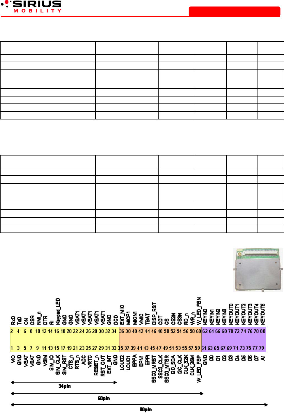
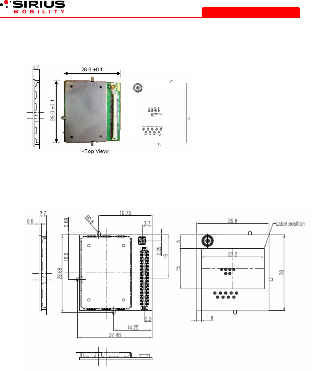
3 Pin Diagram
Pin numbering from top view of module
iSR3500 Series 6 / 11 Pre-rev 0.3
Mobile SolutionsMobile Solutions
4 iSR35xx Module Pin description
Pin# Name Description Dir Category GPIO Supply Domain
1 VIO VDDP_IO Power supply
3 GND GND
5 VBAT Vbatt for PMU Power supply VBAT
7 VBAT Vbatt for PMU Power supply VBAT
9 GND GND
11 VSIM VDD SIM SIM Card VDDP_SIM
13 SIM_IO SIM Data I/O SIM Card VDDP_SIM
15 SIM_CLK SIM Clock O SIM Card VDDP_SIM
17 SIM_RST SIM Reset O SIM Card VDDP_SIM
19 CTS_n Clear To Send I UART GPIO 13
21 RTS_n Headset Detection (mobile), or
Request To Send (modem) O UART GPIO 12 VDDP_IO
23 ADC ADC
25 VRTC VRTC Power supply
27 RESET_n RESET/ I/O Peripheral interface VDDP_RTC
29 RST_OUT Reset Out O GPIO 32 VDDP_IO
31 EXT_INT External Interrupt I/O GPIO GPIO 33 VDDP_IO
33 GND GND
35 LOUD2 Loud Speaker N O Speaker LBUF
37 LOUD1 Loud Speaker P O Speaker LBUF
39 EPPA External earpiece O Speaker VDDA_ VANA
41 EPN1 Earpiece N O Speaker
43 EPP1 Earpiece P O Speaker
45 SSC0_ MRST SSC0 MRST I/O SSC GPIO 15 VDDP_IO
47 SSC0_ CLK SSC0 CLK I/O SSC GPIO 14 VDDP_IO
49 SSC0_ MTSR SSC0 MTSR I/O SSC GPIO 16 VDDP_IO
51 I2C_SDA I2C Data I/O I2C GPIO 19 VDDP_IO
53 I2C_CLK I2C Clock I/O I2C GPIO 18 VDDP_IO
55 CLK_32K Clock 32K Output O GPIO GPIO 28 VDDP_IO
57 CLK_26M Clock 26M Output O GPIO GPIO 30 VDDP_IO
59 W_LED_FBP White LED feedback P I white LED
61 GND GND
63 D0 Data 0 I/O Data VDDP_ MEM
65 D1 Data 1 I/O Data VDDP_ MEM
67 D2 Data 2 I/O Data VDDP_ MEM
69 D3 Data 3 I/O Data VDDP_ MEM
71 D4 Data 4 I/O Data VDDP_ MEM
73 D5 Data 5 I/O Data VDDP_ MEM
75 D6 Data 6 I/O Data VDDP_ MEM
77 D7 Data 7 I/O Data VDDP_ MEM
79 A1 Address 1 O Peripheral interface VDDP_ MEM

iSR3500 Series 7 / 11 Pre-rev 0.3
Mobile SolutionsMobile Solutions
Pin# Name Description Dir Category GPIO Supply Domain
2 RXD RX Data I/O UART GPIO 10 VDDP_IO
4 TXD TX Data O UART GPIO 11 VDDP_IO
6 ON Switch On I VDDP_RTC
8 DSR Data Set Ready O UART GPIO 20 VDDP_IO
10 NMI_n Non-Maskable Interrupt I Interrupt GPIO 38 VDDP_IO
12 DTR Data Terminal Ready I UART GPIO 37 VDDP_IO
14 VIB_CTRL / RI Vibrator control (mobile)
Ring Indicator (modem) I/O GPIO GPIO 36 VDDP_IO
16 KEYPAD_LED
Keypad LED control (mobile)
HS_DET (modem) O GPIO GPIO 35 VDDP_IO
18 GND GND
20 GND GND
22 VBAT1 Vbatt for PA
24 VBAT1 Vbatt for PA
26 VBAT1 Vbatt for PA
28 VBAT1 Vbatt for PA
30 VBAT1 Vbatt for PA
32 GND GND
34 DCD /
W_LED_DRV
White LED DRV (mobile)
Data Carrier Detect (modem) O GPIO White LED GPIO 34 VDDP_IO
36 EXT_ MIC External Mic I MIC
38 MICP1 MIC P I MIC VDDA_ VBT
40 MICN1 MIC N I MIC VDDA_ VBT
42 VMIC MIC Bias MIC Power supply VDDA_ VBT
44 TBAT Battery Temperature
46 DISP_ REST Display Reset O Display GPIO 17 VDDP_IO
48 CDT Charger Detect Charger
50 CS Charger Switch Charger
52 CS2_n Chip select 2 (CS2/) O Peripheral interface GPIO 24 VDDP_ MEM
54 CS3_n Chip select 3 (CS3/) O Peripheral interface GPIO 39 VDDP_ MEM
56 RD_n READ/ O Peripheral interface
58 WR_n Write/ Peripheral interface
60 W_LED_FBN White LED feedback N I White LED
62 KEYIN0 Keypad Input 0 I Keypad GPIO 6 VDDP_IO
64 KEYIN1 Keypad Input 1 I Keypad GPIO 7 VDDP_IO
66 KEYIN2 Keypad Input 2 I Keypad GPIO 8 VDDP_IO
68 KEYIN3 Keypad Input 3 I Keypad GPIO 9 VDDP_IO
70 KEYOUT0 Keypad Out 0 O Keypad GPIO 0 VDDP_IO
72 KEYOUT1 Keypad Out 1 O Keypad GPIO 1 VDDP_IO
74 KEYOUT2 Keypad Out 2 O Keypad GPIO 2 VDDP_IO
76 KEYOUT3 Keypad Out 3 O Keypad GPIO 3 VDDP_IO
78 KEYOUT4 Keypad Out 4 O Keypad GPIO 4 VDDP_IO
80 KEYOUT5 Keypad Out 5 I/O Keypad GPIO 5 VDDP_IO
iSR3500 Series 8 / 11 Pre-rev 0.3
Mobile SolutionsMobile Solutions
5 iSR35xx Module GPIO Pins and Function
Pin# Name Description GPIO Supply
Domain Reset
Value GPIO guide
19 CTS_n Clear to Send GPIO13 VDDP_IO T/PU GPIO or CTR function
21 RTS_n Request to Send GPIO12 VDDP_IO T GPIO or RTS function
29 RST_OUT Reset Out GPIO32 VDDP_IO T/PD Can be used for GPIO
31 EXT_INT Ext. Interrupt GPIO33 VDDP_IO T/PD Can be used for GPIO
45 SSC0_ MRST SSC0_ MRST GPIO15 VDDP_IO T GPIO or SSCO / SPI function
47 SSC0_ CLK SSC0_ CLK GPIO14 VDDP_IO T GPIO or SSCO / SPI function
49 SSC0_ MTSR SSC0_ MTSR GPIO16 VDDP_IO T GPIO or SSCO / SPI function
51 I2C_SDA I2C Data GPIO19 VDDP_IO T/OD GPIO or I2C function
53 I2C_CLK I2C Clock GPIO18 VDDP_IO T/OD GPIO or I2C function
55 CLK_32K Clock 32K GPIO28 VDDP_IO T/PU GPIO or 32Khz clock output
57 CLK_26M Clock output GPIO30 VDDP_IO T/PD GPIO or 26Mhz clock output
2 RXD RX Data GPIO10 VDDP_ IO T Reserved for UART
4 TXD TX Data GPIO11 VDDP_IO T Reserved for UART
8 DSR Data Set Ready GPIO20 VDDP_IO T/PD GPIO or DSR function
10 NMI_n Non-maskable Int. GPIO38 VDDP_IO T/PU Reserved for NMI function
12 DTR Data Terminal Ready GPIO37 VDDP_IO T/PD GPIO or DTR function
14 RI / VIB_ CTRL Vibrator control GPIO36 VDDP_IO T/PD GPIO or Ring Indicator
16 KEYPAD_LED Keypad LED GPIO35 VDDP_IO T/PD GPIO or Keypad LED
34 DCD /
W_LED_DRV
Data Carrier Det.
White LED DRV GPIO34 VDDP_IO T/PD GPIO or Data Carrier Detect
46 DISP_ REST Display Reset GPIO17 VDDP_IO T Reserved for LCD Reset
52 CS2n Chip select2 GPIO24 VDDP_MEM T/PU GPIO or Chip Select
54 CS3n Chip select3 GPIO39 VDDP_MEM T/PU GPIO or Chip Select
62 KEYIN0 Keypad Input GPIO 6 VDDP_IO T GPIO or Keypad
64 KEYIN1 Keypad Input GPIO 7 VDDP_IO T GPIO or Keypad
66 KEYIN2 Keypad Input GPIO 8 VDDP_IO T GPIO or Keypad
68 KEYIN3 Keypad In GPIO 9 VDDP_ IO T GPIO or Keypad
70 KEYOUT0 Keypad Out GPIO 0 VDDP_IO T GPIO or Keypad
72 KEYOUT1 Keypad Out GPIO 1 VDDP_IO T GPIO or Keypad
74 KEYOUT2 Keypad Out GPIO 2 VDDP_IO T GPIO or Keypad
76 KEYOUT3 Keypad Out GPIO 3 VDDP_IO T GPIO or Keypad
78 KEYOUT4 Keypad Out GPIO 4 VDDP_IO T GPIO or Keypad
80 KEYOUT5 Keypad Out GPIO 5 VDDP_IO T GPIO or Keypad
6 iSR35xx Module Test Points on the Bottom
The following test points are available at the bottom centre (refer to 9.2) for JTAG debug (labels are marked on PCB):
VIO TDI TDO TCK TRST_n TMS
For factory test purpose, the following signals are made available at the back of the module (refer to 9.2):
RTS_n CTS_n TXD RXD VRTC ON VBAT VBAT1 GND
iSR3500 Series 9 / 11 Pre-rev 0.3
Mobile SolutionsMobile Solutions
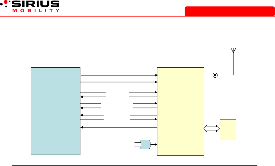
7 Application as GSM modem with host processor
Refer to Design Guide for Industrial Applications for more detailed reference design.
8 Packaging Information
8.1 Tray (Option T)
(Dimensions to be finalized)
8.2 Tape and Reel (option R)
(Dimensions to be finalized)
Host
Processor
TxD
RxD
RING0
iSR35xx
DSR
RxD
DTR
RI (Ring Inidcator)
Intrr
UART RxTx
Reset/
Baseband Reset
Baseband On Switch On
NMI
USB Detect
SD card Detect
etc
TxD
RTS
CTS
UART Handshake
Device Ready
ANT
SIM
Card
Host
Processor
TxD
RxD
RING0
iSR35xx
DSR
RxD
DTR
RI (Ring Inidcator)
Intrr
UART RxTx
Reset/
Baseband Reset
Baseband On Switch On
NMI
USB Detect
SD card Detect
etc
TxD
RTS
CTS
UART Handshake
Device Ready
ANT
SIM
Card
SIM
Card
iSR3500 Series 10 / 11 Pre-rev 0.3
Mobile SolutionsMobile Solutions
9 Module Dimension (mm)
9.1 Physical size
※ iSR3500 GSM/GPRS Module weight approx 2.4 gram.
9.2 Mechanical Dimension
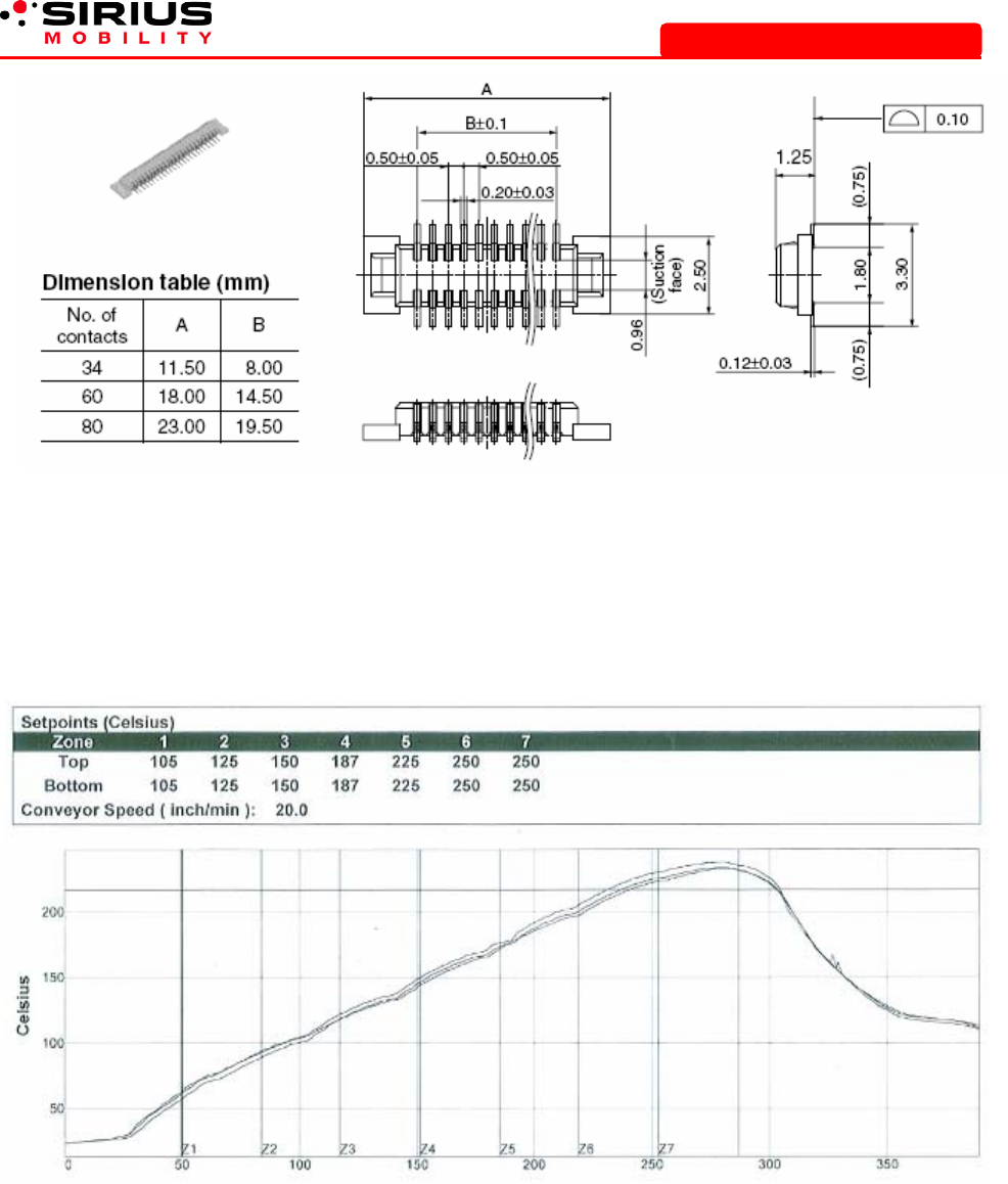
9.3 Board-to-Board Connector
The module uses Panasonic narrow pitch (0.5mm) connector AXK6F34347YG (34pin header), AXK6F60347YG
(60pin header) or AXK6F80347YG (80pin header). They have the mated height 1.5mm and 2.0mm, without
positioning bosses.
Note: The recommended socket connectors on user’s mother board are AXK5F34547YG, AXK5F60547YG and
AXK5F80547YG respectively.
iSR3500 Series 11 / 11 Pre-rev 0.3
Mobile SolutionsMobile Solutions
10 Reflow temperature profile

User’s Information ---- Additional information
Cautions
Modifications not expressly approved by the party responsible for compliance could
void the user’s authority to operate the equipment.
FCC compliance Information
This device complies with part 15 of FCC Rules. Operation is subject to the following two
conditions: 1. This device may not cause harmful interference, and 2. This device must
accept any interference received. Including interference that may cause undesired
operation.
Information to User
This equipment has been tested and found to comply with the limits for a Class B digital
device, Pursuant to part 15 of the FCC Rules. These limits are designed to provide
reasonable protection against harmful interference in a residential installation. This
equipment generates, uses and can radiate radio Frequency energy and, if not installed
and used in accordance with the instructions, may cause harmful interference to radio
communications. However, there is no guarantee that interference will not occur in a
particular installation. If this equipment does cause harmful interference to radio or
television reception, which can be determined by turning the equipment off and on, the
user is encouraged to try to correct the interference by one or more of the following
measures:
- Reorient or relocate the receiving antenna.
- Increase the separation between the equipment and receiver- Connect the equipment
into an outlet on a circuit different from that to which the receiver is connected.
- Consult the dealer or an experienced radio/TV technician for help.
NOTE: Required Minimum distance between antenna and the user is 20cm.
The FCC requires that a label must be placed on the outside of the final product stating:
“Contains FCC ID: VDQDC3500” depending of the module to be integrated.