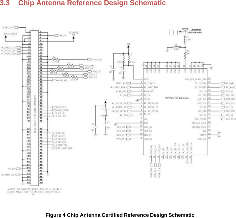
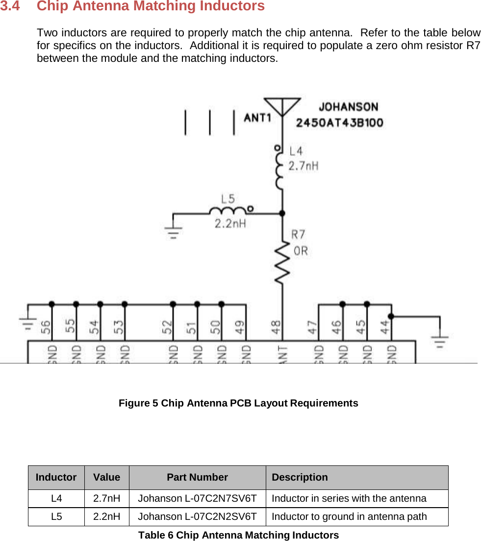
DeFelsko BLEATA BLEATA Module User Manual Antenna Design Guide

DeFelsko Corporation BLEATA Module Antenna Design Guide

Contents

Antenna Design Guide

     ANTENNA DESIGN GUIDE  Last updated June 16th, 2015 
1 Introduction 1.1 Purpose & Scope The purpose of this document is to provide details regarding the design and integration of the certified chip antenna for the module.  It will inform the designer as to the required PCB layout details, and provide expected performance specifications. 
2 Chip Antenna The Johanson Technology ceramic chip antenna is a passive, surface mount component, based on Low Temperature Co-fired Ceramic (LTCC) technology.  This antenna exhibits linear polarization and provides a near omni-directional radiation pattern.  It is matched to 50 ohm impedance and is well suited for integration to the radio module. The chip antenna is used external to the module, as part of an overall solution. Johanson Part Number Description  2450AT43B100 2.4 GHz Ceramic Chip Antenna Table 2 Chip Antenna Overview 2.1  Chip Antenna Specifications Specification Value Peak Gain  +1.3 dBi Impedance 50 ohms, Nominal Type Chip Polarization Linear Frequency 2400-2500 MHz Input Power  2W max Size  7 mm × 2 mm Operating Temperature  -40 to +85°C Table 3 Chip Antenna Specifications
2.2 Mechanical Dimensions  Table 4 Chip Antenna Mechanical Dimensions 2.3 Terminal Configuration  Table 5 Chip Antenna Terminal Configuration
2.4 Typical Radiation Patterns Figure 1 Chip Antenna Radiation Patterns 
3  PCB Layout Requirements Since the module and its associated approved antenna have been certified by the FCC and Industry Canada (IC) as a Modular Radio, the end user is authorized to integrate this module into an end-product, and is solely responsible for the Unintentional Emissions levels produced by the end-product. In order to preserve the Modular Radio certification, the integrator of the module must abide by the PCB layout recommendations outlined in the following paragraphs.  Any divergence from these recommendations will invalidate the modular radio certifications and require the integrator to re-certify the modules and/or end-product. The modules must be used with one of the approved antennas: 1.   Johnson 2450AT43B100 2.4 GHz ceramic chip antenna.
3.1  Chip Antenna PCB Layout Requirements  Figure 2 Chip Antenna PCB Layout Requirements
3.2 Chip Antenna Reference Design PCB Figure 3 Chip Antenna Certified Reference Design PCB
3.3  Chip Antenna Reference Design Schematic  Figure 4 Chip Antenna Certified Reference Design Schematic
3.4 Chip Antenna Matching Inductors Two inductors are required to properly match the chip antenna.  Refer to the table below for specifics on the inductors.  Additional it is required to populate a zero ohm resistor R7 between the module and the matching inductors.  Figure 5 Chip Antenna PCB Layout Requirements Inductor Value Part Number Description L4  2.7nH  Johanson L-07C2N7SV6T  Inductor in series with the antenna L5  2.2nH  Johanson L-07C2N2SV6T  Inductor to ground in antenna path Table 6 Chip Antenna Matching Inductors
4 EMC Compliance 4.1 Summary The module has been tested and approved as a Modular Radio in accordance with the appropriate FCC and IC standards.  The supporting test data may be found in the modular test report. Since the module and its associated approved antenna has been certified as a Modular Radio, this allows the end user to integrate these modules into an end-product without the requirement of re-certifying the radio module.  The module-integrator is responsible for the unintentional conducted and radiated emissions and must verify that the integrated product is compliant with the rules associated with unintentional radiators. The module integrator is also required to maintain an engineering record of the verification testing and declare on the product through proper labeling and marking that the device is compliant with these particular rules. The installed module’s FCC ID and IC numbers need to be clearly marked on the product with the following verbiage “contains FCC ID: OEJ-MAPWIFI, 15.247” and "contains IC: 297A-MAPWIFI, RSS 210". The module has been certified for use in a mobile configuration, which employs a minimum separation distance of 20 cm from the antenna to the human body or another transmitting radio.  For separation distances of 20 cm or less, the module integrator must have the module certification re-evaluated, which will include a modification to the existing certification and additional testing for exposure and SAR requirements. 4.2  Module Integration Considerations – Antenna Systems The modules must be used with one of the approved antennas: 1.   Johnson 2450AT43B100 2.4 GHz ceramic chip antenna. The antenna should be placed such that it is minimally disturbed by the product’s packaging material.  The incorporation of the largest practical free-space clearance around the antenna is important for maximizing overall performance.  Further, the antenna must be placed such that at least a 20 cm separation distance is maintained from the human body to the antenna and all other radio transmitters.
4.3  Module Integration Considerations – Substitute Antenna Systems The modules’ certification is only valid for the list of approved antennas presented in section 4.2.  However, substitute antennas may be used in place of the approved antenna only if the antennas are of the same type and the peak gain is less than or equal to the peak gain of the similar approved antenna.  Also the antennas should have similar in-band and out-of-band characteristics. 4.4  Module Integration Considerations – Circuit Implementation It is recommended that all connection PCB (printed circuit board) traces to the power supply and digital control terminal be as short as possible.  Though not necessarily required in all cases, it is a best practice to provide an optional shunt capacitor placement at the module pin on all active and routed power supply and digital control lines.  Further, a series damping resistor placement should be incorporated between the module pin/shunt capacitor node and the source/sink of the digital control signals. This provides for effective bypassing and decoupling of digital lines from the radio module, in the event that the application circuit has longer power supply and digital routing. 4.5  Module Integration Considerations - Top Assembly In addition to the recommendations given for the antenna systems and the module placement onto a product PCB, it is recommended that all wiring and interconnect systems within the product be not routed anywhere close the module and its associated circuitry on the PCB, doing so could change the emission characteristics of the module. 4.6 Testing Requirements for End-Product Once the module is integrated and the product realized in a mobile configuration, the product must be tested and follow the verification process for Unintentional Conducted and Radiated Emissions in accordance to the FCC and IC guidelines. The module needs to be powered and placed in the receive mode for this test.  The receiver must be tuned to its lowest frequency channel, mid-frequency channel, and highest frequency channel.  The supporting test data does not need to be submitted to the FCC or IC. 4.7 SAR Testing Requirements for End-Product Since the radio modules were certified in a mobile configuration, the end- product does not require SAR testing if the end-product is not used within 20cm of the human body, nor used in conjunction with another radio transmitter. For portable configurations (antenna-to-body separations of less than 20 cm), the module integrator must have the module’s certification re-evaluated, which will include a modification to the existing certification and additional testing for exposure and SAR requirements.

Navigation menu