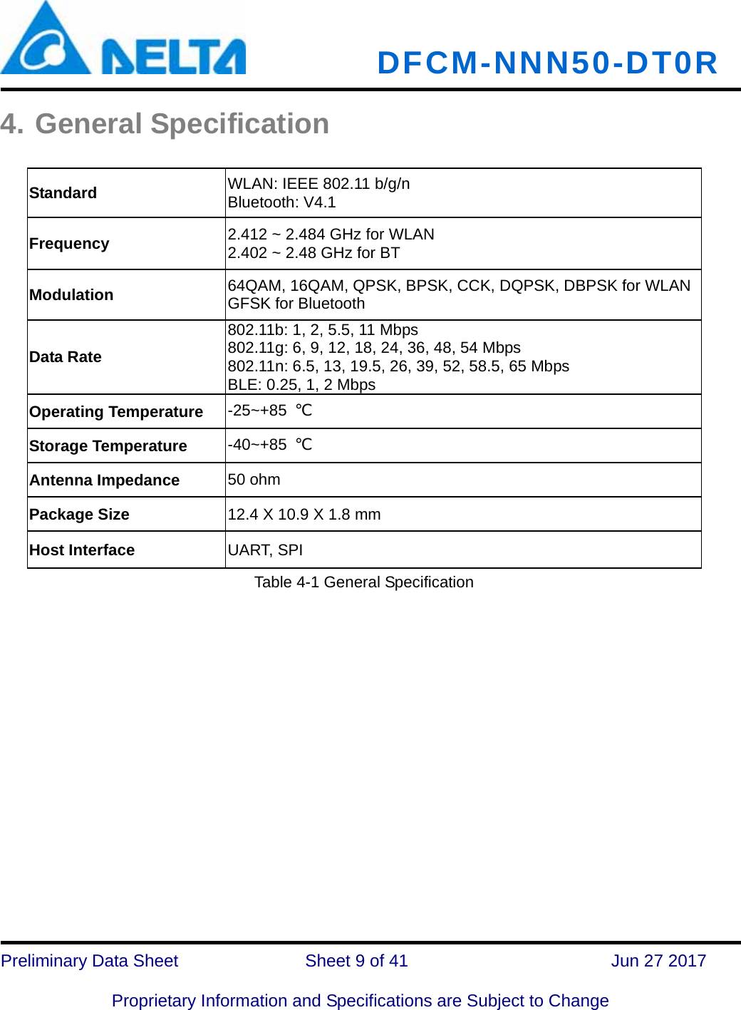
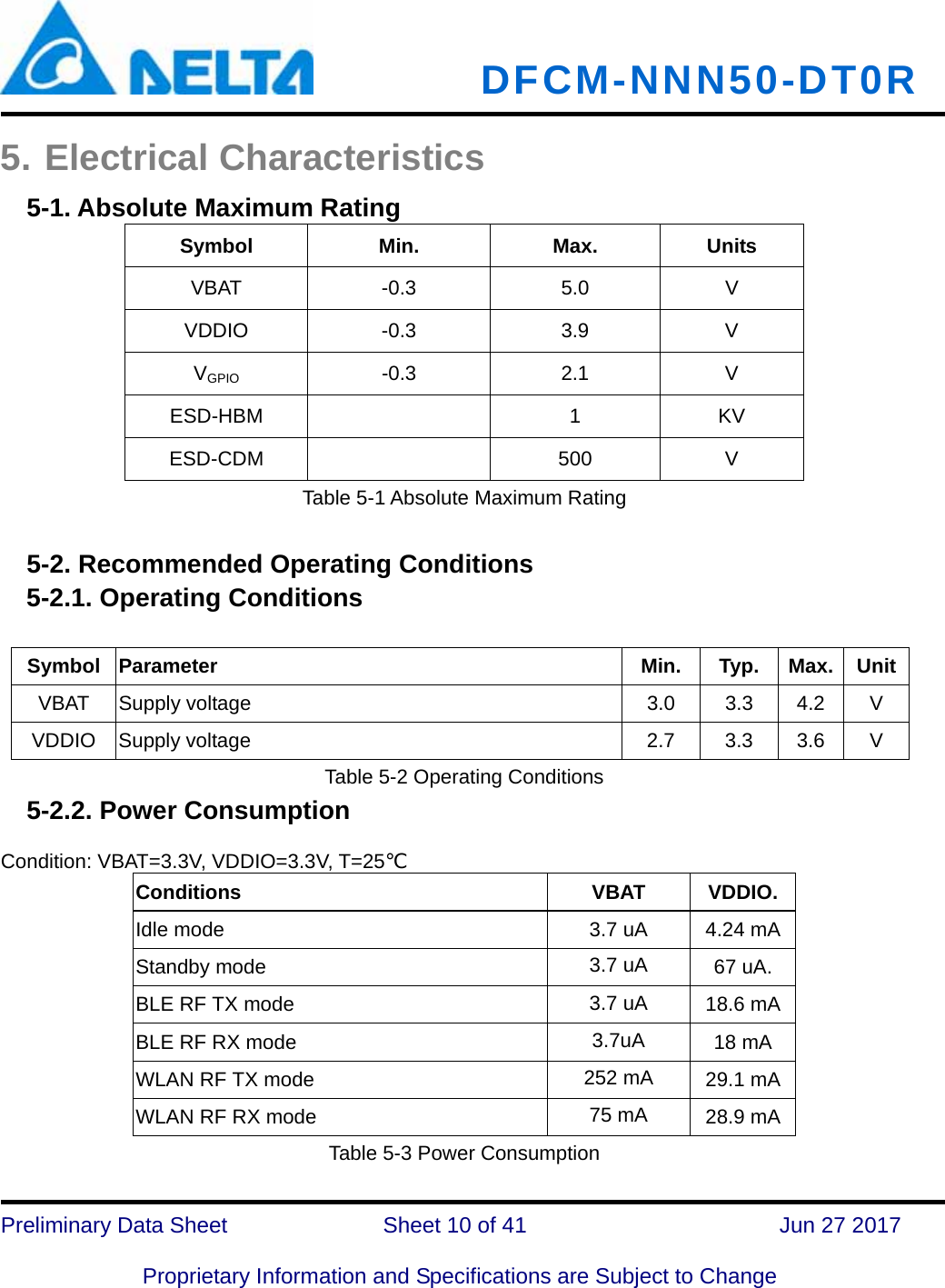
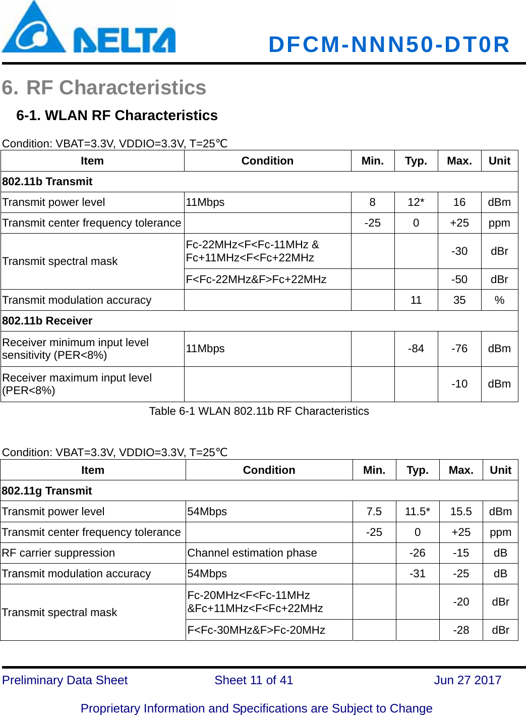
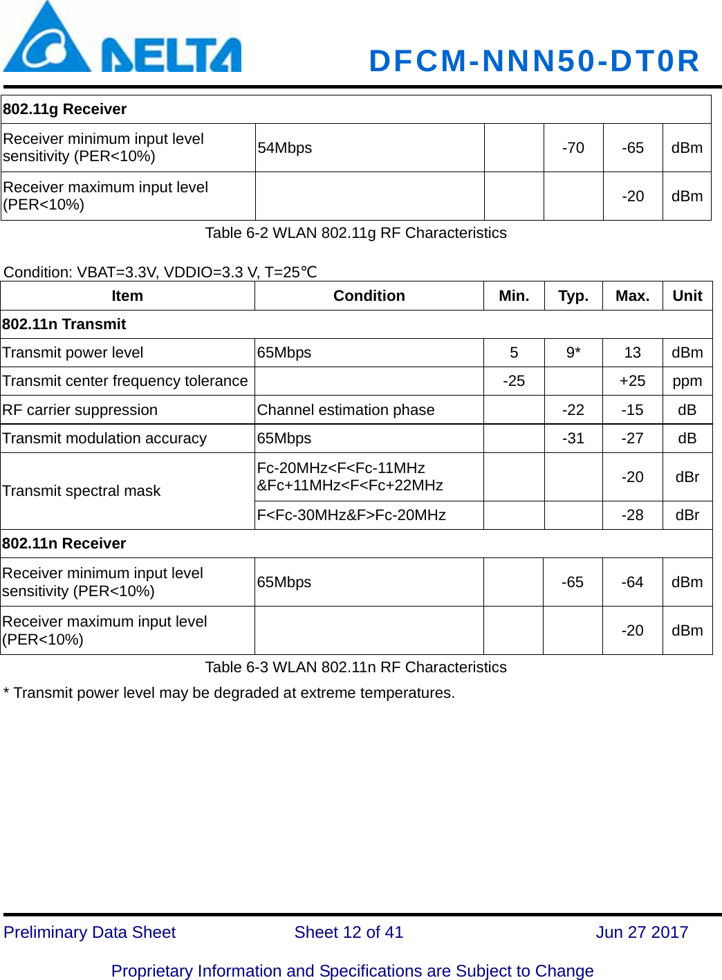
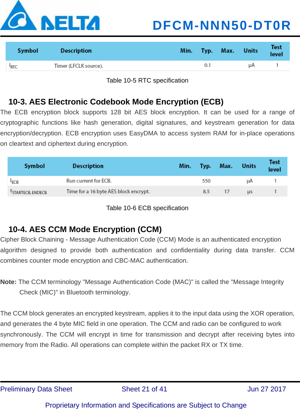
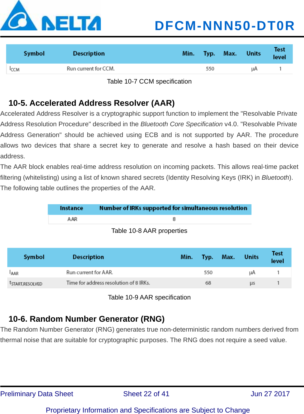
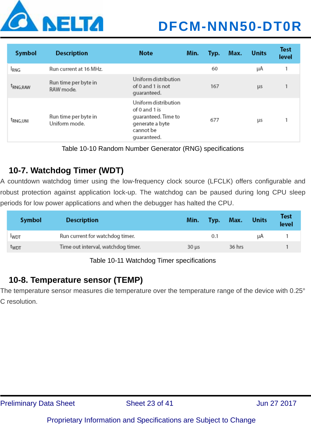
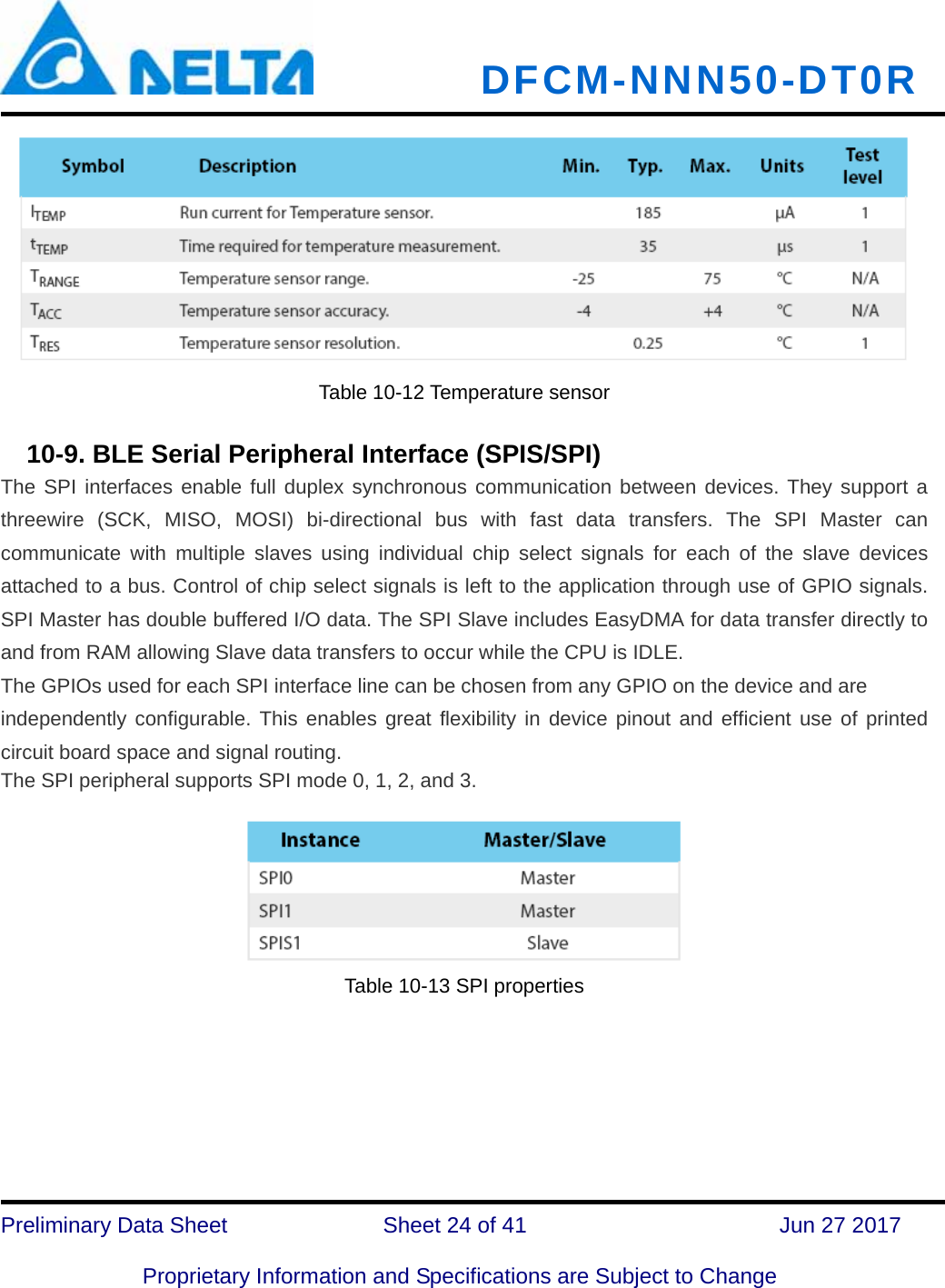
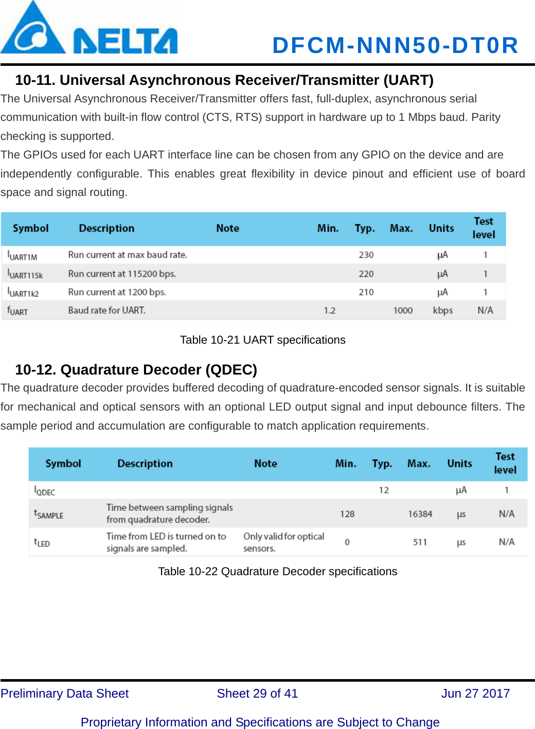
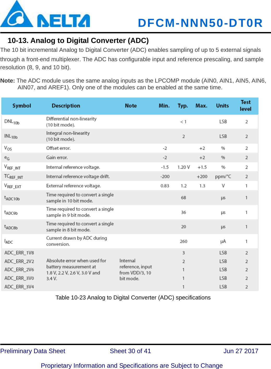
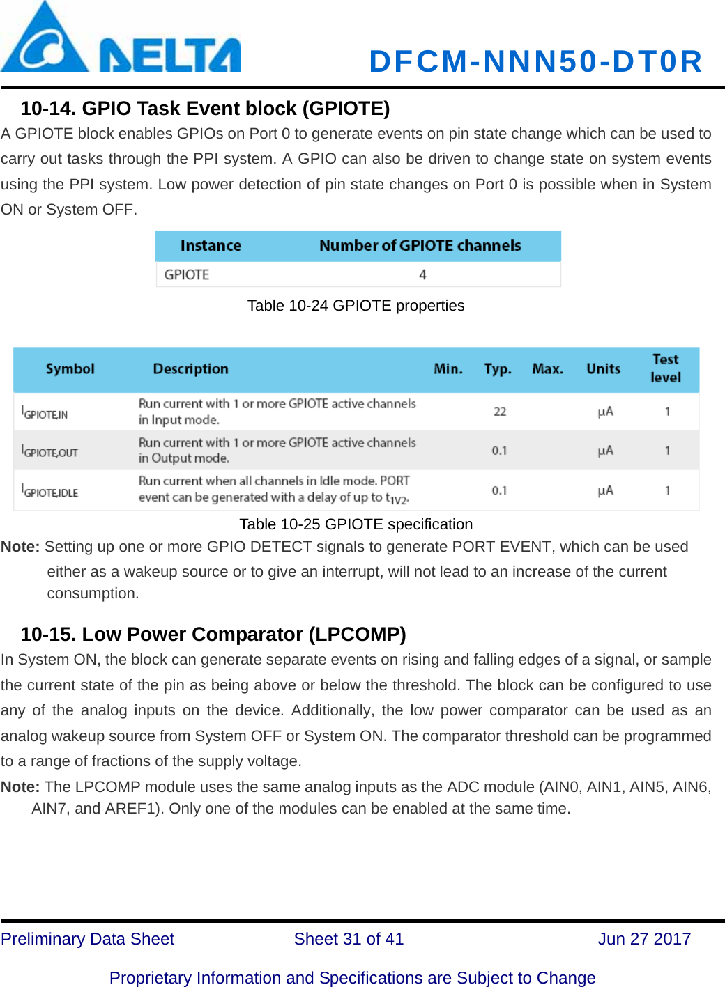
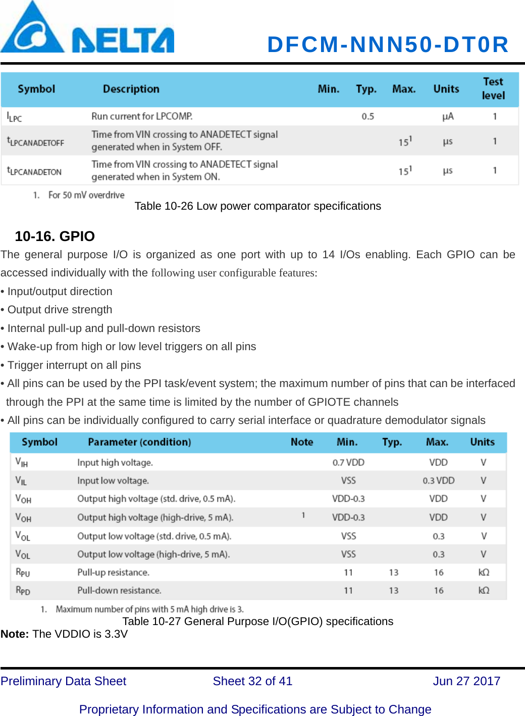
Delta Electronics orporated DFCM-NNN50 IEEE 802.11b/g/n Wireless LAN Plus Bluetooth Low Energy System On Chip Combo Module. User Manual

Delta Electronics Incorporated IEEE 802.11b/g/n Wireless LAN Plus Bluetooth Low Energy System On Chip Combo Module.

Users Manual

  DFCM-NNN50-DT0R   Preliminary Data Sheet               Sheet 1 of 41      Jun 27 2017  Proprietary Information and Specifications are Subject to Change Data sheet DFCM-NNN50-DT0R  A IEEE 802.11b/g/n Wireless LAN Plus Bluetooth Low Energy System On Chip Combo Module.
  DFCM-NNN50-DT0R   Preliminary Data Sheet               Sheet 2 of 41      Jun 27 2017  Proprietary Information and Specifications are Subject to Change Contents  1.Features ........................................................................................................................................... 51-1. General ......................................................................................................................................... 51-2. WLAN ......................................................................................................................................... 51-3. Bluetooth ..................................................................................................................................... 62.Model No. Definition ...................................................................................................................... 73.Block Diagram ................................................................................................................................ 84.General Specification ...................................................................................................................... 95.Electrical Characteristics ............................................................................................................... 105-1. Absolute Maximum Rating ........................................................................................................ 105-2. Recommended Operating Conditions ........................................................................................ 105-2.1. Operating Conditions .............................................................................................................. 105-2.2. Power Consumption................................................................................................................ 106.RF Characteristics ......................................................................................................................... 116-1. WLAN RF Characteristics ......................................................................................................... 116-2. Bluetooth Low Energy RF characteristics ................................................................................. 137.Pin Description .............................................................................................................................. 148.Slow Clock Requirement .............................................................................................................. 168-1. External 32.768KHz crystal oscillator ....................................................................................... 168-2. 32.768KHz RC oscillator .......................................................................................................... 168-3. 32.768KHz synthesized oscillator ............................................................................................. 179.Power-Up Sequence ...................................................................................................................... 1810.Peripheral ...................................................................................................................................... 1910-1. Timer/Counters (TIMER) ........................................................................................................ 2010-2. Real Time Counter (RTC) ........................................................................................................ 2010-3. AES Electronic Codebook Mode Encryption (ECB)............................................................... 2110-4. AES CCM Mode Encryption (CCM) ...................................................................................... 2110-5. Accelerated Address Resolver (AAR) ..................................................................................... 2210-6. Random Number Generator (RNG)......................................................................................... 2210-7. Watchdog Timer (WDT) .......................................................................................................... 2310-8. Temperature sensor (TEMP) .................................................................................................... 23
  DFCM-NNN50-DT0R   Preliminary Data Sheet               Sheet 3 of 41      Jun 27 2017  Proprietary Information and Specifications are Subject to Change 10-9. BLE Serial Peripheral Interface (SPIS/SPI) ............................................................................ 2410-9.1.SPI Slave Specifications and Parameters ...................................................................... 2510-9.2.SPI Master Specifications and Parameters .................................................................... 2610-10. Two-wire interface (TWI) ...................................................................................................... 2710-11. Universal Asynchronous Receiver/Transmitter (UART) ....................................................... 2910-12. Quadrature Decoder (QDEC) ................................................................................................ 2910-13. Analog to Digital Converter (ADC) ...................................................................................... 3010-14. GPIO Task Event block (GPIOTE) ....................................................................................... 3110-15. Low Power Comparator (LPCOMP) ..................................................................................... 3110-16. GPIO ...................................................................................................................................... 3210-17. Debugger support................................................................................................................... 3310-18. WLAN SPI Slave Interface ................................................................................................... 3311.Reference Circuit .......................................................................................................................... 3611-1. Standard Mode ................................................................................................................ 3611-2.  High Speed Mode ........................................................................................................... 3712.Module Dimensions (mm) ............................................................................................................ 3813.Recommend Soldering Conditions ............................................................................................... 3914.Important Notice ........................................................................................................................... 4014.1 Federal Communications Commission (FCC) Notice .............................................................. 4014.2 National Communications Commission (NCC) Notice ............................................................ 41
  DFCM-NNN50-DT0R   Preliminary Data Sheet               Sheet 4 of 41      Jun 27 2017  Proprietary Information and Specifications are Subject to Change Revision History    Version  Date  Reason of change  Maker S0.1  2016/8/15  Initial release  Josh S0.2  2016/11/23 Modify  1.  RF TX output power and RX sensitivity spec   2.  VBAT input voltage range 3.  Delta logo, mechanical information and reflow profile 4. Add reference schematic Josh S0.3  2016/12/07  Modify 5.2 Recommended Operating Conditions  Josh S0.4  2016/12/29  Add current consumption data Modify 11-1、11-2 reference circuit Josh Junru S0.5  2017/02/22  Modify application circuit and condition of voltage Correct model no. definition  Junru S0.6  2017/05/22  Modify 6-1. WLAN RF Characteristics according to 3V3T test results  Josh S0.7  2017/06/22 Modify 1.  Remove SDIO application circuit 2. Add important notice Josh
  DFCM-NNN50-DT0R   Preliminary Data Sheet               Sheet 5 of 41      Jun 27 2017  Proprietary Information and Specifications are Subject to Change DFCM-NNN5-DT0R Wireless LAN/BLE SoC Combo Module  his document describes the DFCM-NNN50-DT0R wireless LAN/BLE SoC combo module hardware specification. The modules provide cost effective, low power, and flexible platform to add Wi-Fi®     connectivity and BLE for embedded devices for a variety of applications, such as wireless sensors and thermostats. It uses the wireless LAN chip and BLE SoC, which integrating the 2.4GHz transceiver, a 32 bit ARM® Cortex M0 CPU, flash memory, and analog and digital peripherals.  1. Features 1-1. General     Integrated wireless LAN chip and BLE chip   Built in RF switch for BLE and WLAN using a single antenna   Integrated a 32 bit ARM® Cortex M0 CPU,256KB flash memory and 32KB RAM   Extra 256KB flash memory for user data storage.   8/9/10 bit ADC - 5 configurable channels   14 General Purpose I/O Pins   Two-wire Master (I2C compatible) support 100K bps and 400K bps   UART baud rate up to 921600 bps     SPI bit rate up to 4M bps   Quadrature Decoder (QDEC)  Temperature sensor   LGA42 pin package   Dimension 12.4mm(L) x 10.9mm(W) x 1.8mm(H)  RoHS compliant    1-2. WLAN   IEEE 802.11 b/g/n (1x1) for up to 65 Mbps     Superior Sensitivity and Range via advanced PHY signal processing     Advanced Equalization and Channel Estimation     Advanced Carrier and Timing Synchronization    Soft-AP support  T
  DFCM-NNN50-DT0R   Preliminary Data Sheet               Sheet 6 of 41      Jun 27 2017  Proprietary Information and Specifications are Subject to Change   Supports IEEE 802.11 WEP, WPA, WPA2 Security    SSL Security   On-Chip network stack offload MCU -  Integrated Network IP stack to minimize high speed mode host CPU requirements (4KB flash - less than 1KB RAM, for Wi-Fi drivers) -  Network features TCP, UDP, DHCP, ARP, HTTP, SSL, and DNS   Support SPI host interface    1-3. Bluetooth   Bluetooth 4.1 specification compliant     AES HW encryption
  DFCM-NNN50-DT0R   Preliminary Data Sheet               Sheet 7 of 41      Jun 27 2017  Proprietary Information and Specifications are Subject to Change 2. Model No. Definition                        D F C M - N N N 5 0 -DT0 RE=Pb free R=RoHS N=NG L=Process with Lead Customer code Version Lead Free 5= 12.4x10.9 mm Dimension WLAN Specification M= Module C= Combo F= FR4 D= DELTA N= IEEE 802.11b/g/n WLAN Chip Product-type Property Substrate Company N=Delta Define 0= WLAN + Bluetooth DT= Delta DefineBluetooth Chip  N=Delta Define 0= Consumer Application Serial no.
  DFCM-NNN50-DT0R   Preliminary Data Sheet               Sheet 8 of 41      Jun 27 2017  Proprietary Information and Specifications are Subject to Change 3. Block Diagram                         Figure 3-1 DFCM-NNN50-DT0R Block Diagram             ADC WLAN/Bluetooth ANT WLAN Chip 26MHz CrystalBalunRF SW UART/SPI/I2C GPIO GPIO VDDIO VBAT BT SOC   32MHz CrystalSPI
  DFCM-NNN50-DT0R   Preliminary Data Sheet               Sheet 9 of 41      Jun 27 2017  Proprietary Information and Specifications are Subject to Change 4. General Specification  Standard  WLAN: IEEE 802.11 b/g/n Bluetooth: V4.1 Frequency  2.412 ~ 2.484 GHz for WLAN 2.402 ~ 2.48 GHz for BT Modulation  64QAM, 16QAM, QPSK, BPSK, CCK, DQPSK, DBPSK for WLANGFSK for Bluetooth Data Rate 802.11b: 1, 2, 5.5, 11 Mbps 802.11g: 6, 9, 12, 18, 24, 36, 48, 54 Mbps 802.11n: 6.5, 13, 19.5, 26, 39, 52, 58.5, 65 Mbps BLE: 0.25, 1, 2 Mbps   Operating Temperature  -25~+85  ℃ Storage Temperature  -40~+85  ℃ Antenna Impedance  50 ohm Package Size  12.4 X 10.9 X 1.8 mm Host Interface  UART, SPI Table 4-1 General Specification
  DFCM-NNN50-DT0R   Preliminary Data Sheet              Sheet 10 of 41      Jun 27 2017  Proprietary Information and Specifications are Subject to Change 5. Electrical Characteristics   5-1. Absolute Maximum Rating Symbol Min.  Max. Units VBAT -0.3  5.0 V VDDIO -0.3  3.9 V VGPIO  -0.3 2.1 V ESD-HBM   1 KV ESD-CDM   500 V Table 5-1 Absolute Maximum Rating    5-2. Recommended Operating Conditions 5-2.1. Operating Conditions  Symbol Parameter  Min.  Typ.  Max. UnitVBAT Supply voltage  3.0  3.3  4.2  V VDDIO Supply voltage  2.7  3.3  3.6  V Table 5-2 Operating Conditions 5-2.2. Power Consumption  Condition: VBAT=3.3V, VDDIO=3.3V, T=25℃ Conditions  VBAT VDDIO. Idle mode  3.7 uA  4.24 mA Standby mode  3.7 uA  67 uA. BLE RF TX mode  3.7 uA  18.6 mA BLE RF RX mode  3.7uA  18 mA WLAN RF TX mode    252 mA  29.1 mA WLAN RF RX mode  75 mA  28.9 mA Table 5-3 Power Consumption
  DFCM-NNN50-DT0R   Preliminary Data Sheet              Sheet 11 of 41      Jun 27 2017  Proprietary Information and Specifications are Subject to Change 6. RF Characteristics    6-1. WLAN RF Characteristics  Condition: VBAT=3.3V, VDDIO=3.3V, T=25℃ Item Condition Min. Typ. Max. Unit802.11b Transmit Transmit power level  11Mbps  8  12*  16  dBmTransmit center frequency tolerance   -25  0  +25  ppmTransmit spectral mask Fc-22MHz<F<Fc-11MHz & Fc+11MHz<F<Fc+22MHz     -30 dBr F<Fc-22MHz&F>Fc+22MHz       -50  dBr Transmit modulation accuracy      11  35  % 802.11b Receiver Receiver minimum input level sensitivity (PER<8%)  11Mbps     -84  -76  dBmReceiver maximum input level (PER<8%)     -10 dBmTable 6-1 WLAN 802.11b RF Characteristics   Condition: VBAT=3.3V, VDDIO=3.3V, T=25℃ Item Condition Min. Typ. Max. Unit802.11g Transmit Transmit power level  54Mbps    7.5  11.5*  15.5  dBmTransmit center frequency tolerance    -25  0  +25  ppmRF carrier suppression  Channel estimation phase    -26  -15  dB Transmit modulation accuracy  54Mbps    -31  -25  dB Transmit spectral mask   Fc-20MHz<F<Fc-11MHz &Fc+11MHz<F<Fc+22MHz    -20 dBrF<Fc-30MHz&F>Fc-20MHz   -28 dBr
  DFCM-NNN50-DT0R   Preliminary Data Sheet              Sheet 12 of 41      Jun 27 2017  Proprietary Information and Specifications are Subject to Change 802.11g Receiver Receiver minimum input level sensitivity (PER<10%)  54Mbps  -70 -65 dBmReceiver maximum input level (PER<10%)     -20 dBmTable 6-2 WLAN 802.11g RF Characteristics  Condition: VBAT=3.3V, VDDIO=3.3 V, T=25℃ Item Condition Min. Typ. Max. Unit802.11n Transmit Transmit power level  65Mbps  5  9*  13  dBmTransmit center frequency tolerance    -25    +25  ppmRF carrier suppression  Channel estimation phase    -22  -15  dB Transmit modulation accuracy  65Mbps    -31  -27  dB Transmit spectral mask   Fc-20MHz<F<Fc-11MHz &Fc+11MHz<F<Fc+22MHz    -20 dBrF<Fc-30MHz&F>Fc-20MHz   -28 dBr802.11n Receiver Receiver minimum input level sensitivity (PER<10%)  65Mbps  -65 -64 dBmReceiver maximum input level (PER<10%)     -20 dBmTable 6-3 WLAN 802.11n RF Characteristics * Transmit power level may be degraded at extreme temperatures.
  DFCM-NNN50-DT0R   Preliminary Data Sheet              Sheet 13 of 41      Jun 27 2017  Proprietary Information and Specifications are Subject to Change     6-2. Bluetooth Low Energy RF characteristics  Condition: VDDIO=3.3V, T=25℃ Item Condition Min. Typ. Max. UnitRF Characteristics Output Power     -20  2.5  8  dBmInitial Frequency Offset     -75  0  75  KHzModulation Characteristics F1 Average  225  250  275  KHzF2 Maximum  185  217   KHzF2 / F1 Ratio  0.8  0.91     Sensitivity (PER<30.8%)  250Kbps   -91  -70  dBmMaximum Input Level (PER<30.8%)  250Kbps   0   dBmTable 6-4 Bluetooth RF Characteristics
  DFCM-NNN50-DT0R   Preliminary Data Sheet              Sheet 14 of 41      Jun 27 2017  Proprietary Information and Specifications are Subject to Change 7. Pin Description Pin Definition  Function  Description 1  BT_P0.23  Digital I/O  Bluetooth General purpose I/O pin 2  BT_P0.03  Digital I/O  Bluetooth General purpose I/O pin 3 GND  Gnd Ground 4 ANT  RF WLAN/Bluetooth RF input/output 5 GND  Gnd Ground 6  BT_P0.25  Digital I/O  Bluetooth general purpose I/O pin 7  BT_P0.13  Digital I/O  Bluetooth general purpose I/O pin 8  BT_P0.20  Digital I/O  Bluetooth general purpose I/O pin 9  BT_P0.17  Digital I/O  Bluetooth general purpose I/O pin 10  BT_P0.16  Digital I/O  Bluetooth general purpose I/O pin 11  BT_SWDCLK  Digital input  Hardware debug and flash programming I/O 12 BT_SWDIO  Digital I/O System reset (active low). Also hardware debug and flash programming I/O 13 GND  Gnd Ground 14  IRQN  Digital I/O  Interrupt pin to host 15 SPI_MOSI  Digital I/O SPI_MOSI  16  WL_GPIO5  Digital I/O  WLAN GPIO5, firmware debug purpose 17 GND  Gnd Ground 18  WL_I2C_SDA  Digital I/O  WLAN I2C slave data, hardware debug purpose 19  WL_I2C_SCL  Digital I/O  WLAN I2C slave clock, hardware debug purpose 20 SD_DAT3  Digital I/O NC 21 SD_CLK  Digital I/O NC 22 BT_P0.06  Digital I/O Analog inputBluetooth general purpose I/O pin ADC input 7 ADC Reference voltage input 1 23 BT_P0.05  Digital I/O Analog inputBluetooth general purpose I/O pin ADC input 6 24  BT_P0.04  Digital I/O  Bluetooth general purpose I/O pin
  DFCM-NNN50-DT0R   Preliminary Data Sheet              Sheet 15 of 41      Jun 27 2017  Proprietary Information and Specifications are Subject to Change 24  BT_P0.04  Analog input ADC input 5 25  BT_P0.31  Digital I/O  Bluetooth general purpose I/O pin 26 GND  Gnd Ground 27  VBAT  Power  VBAT power supply input 28 GND  Gnd Ground 29  BT_P0.30  Digital I/O  Bluetooth general purpose I/O pin 30 BT_P0.00  Digital I/O Analog inputGeneral purpose I/O. ADC Reference voltage. 31 SPI_MISO  Digital I/O SPI_MISO 32 SPI_SCK  Digital I/O SPI_SCK 33 SPI_SSN  Digital I/O SPI_SSN 34 BT_P0.27  Digital I/O Analog inputBluetooth general purpose I/O pin ADC input 1 Crystal connection for 32.768 kHz crystal oscillator or external 32.768 kHz crystal reference 35  BT_P0.29  Digital I/O  Bluetooth general purpose I/O pin 36 BT_P0.26  Digital I/O Analog inputBluetooth general purpose I/O pin ADC input 0 Crystal connection for 32.768 kHz crystal oscillator 37  BT_P0.24  Digital I/O  Bluetooth general purpose I/O pin 38 GND  Gnd Ground 39  VDDIO  Power  Power supply input of VDDIO 40 GND  Gnd Ground 41  BT_P0.21  Digital I/O  Bluetooth general purpose I/O pin 42  BT_P0.22  Digital I/O  Bluetooth general purpose I/O pin Table 7-1 Pin Description
  DFCM-NNN50-DT0R   Preliminary Data Sheet              Sheet 16 of 41      Jun 27 2017  Proprietary Information and Specifications are Subject to Change 8. Slow Clock Requirement   8-1. External 32.768KHz crystal oscillator The 32.768 kHz crystal oscillator is designed for use with a quartz crystal in parallel resonant mode. To achieve correct oscillation frequency, the load capacitance must match the specification in the crystal data sheet. Table 8-1 shows the specification of 32.768 kHz crystal oscillator.   Table 8-1 32.768 kHz crystal oscillator specification     8-2. 32.768KHz RC oscillator The 32.768 kHz RC low frequency oscillator may be used as an alternative to the 32.768 kHz crystal oscillator. It has a frequency accuracy of less than ± 250 ppm in a stable temperature environment or when calibration is periodically performed in changing temperature environments. The 32.768 kHz RC oscillator does not require external components.
  DFCM-NNN50-DT0R   Preliminary Data Sheet              Sheet 17 of 41      Jun 27 2017  Proprietary Information and Specifications are Subject to Change Table 8-2 32.768 kHz RC oscillator specification     8-3. 32.768KHz synthesized oscillator The low frequency clock can be synthesized from the high frequency clock. This saves the cost of a crystal but increases average power consumption as the high frequency clock source will have to be active.    Table 8-3 32.768 kHz synthesized oscillator specification
  DFCM-NNN50-DT0R   Preliminary Data Sheet              Sheet 18 of 41      Jun 27 2017  Proprietary Information and Specifications are Subject to Change 9. Power-Up Sequence Power-Up Sequence The power-up sequence for DFCM-NNN50-DT0R is shown in Figure 9.1 The timing parameters are provided in Table 9.1   Figure 9.1 Power-Up Sequence  Parameter  Min  Max  Units  Description  Notes tB 0    ms  VBAT rise to VDDIO rise  VBAT and VDDIO can rise simultaneously tR   100 ms VDDIO supply rise time (0V to supply voltage) The on-chip power on reset circuitry may not function properly for rise times outside the specified internal  Table 9.1 Power-Up Sequence Timing       VBAT VDDIO tB ttR
  DFCM-NNN50-DT0R   Preliminary Data Sheet              Sheet 19 of 41      Jun 27 2017  Proprietary Information and Specifications are Subject to Change 10. Peripheral Peripheral blocks which have a register interface and/or interrupt vector assigned are instantiated, one or more times, in the device address space. The instances, associated ID (for those with interrupt vectors), and base address of features are found in Table 10-1.                          Table 10-1 Peripheral instance reference
  DFCM-NNN50-DT0R   Preliminary Data Sheet              Sheet 20 of 41      Jun 27 2017  Proprietary Information and Specifications are Subject to Change    10-1. Timer/Counters (TIMER) The timer/counter runs on the high-frequency clock source (HFCLK) and includes a 4 bit (1/2X) prescaler that can divide the HFCLK. The task/event and interrupt features make it possible to use the PPI system for timing and counting tasks between any system peripheral including any GPIO of the device. The PPI system also enables the TIMER task/event features to generate periodic output and PWM signals to any GPIO. The number of input/outputs used at the same time is limited by the number of GPIOTE channels.        Table 10-2 Timer/Counter properties  Table 10-3 Timer specification     10-2. Real Time Counter (RTC) The Real Time Counter (RTC) module provides a generic, low power timer on the low-frequency clock source(LFCLK). The RTC features a 24 bit COUNTER, 12 bit (1/X) prescaler, capture/compare registers, and a tick event generator for low power, tickless RTOS implementation.       Table 10-4 RTC properties
  DFCM-NNN50-DT0R   Preliminary Data Sheet              Sheet 21 of 41      Jun 27 2017  Proprietary Information and Specifications are Subject to Change Table 10-5 RTC specification     10-3. AES Electronic Codebook Mode Encryption (ECB) The ECB encryption block supports 128 bit AES block encryption. It can be used for a range of cryptographic functions like hash generation, digital signatures, and keystream generation for data encryption/decryption. ECB encryption uses EasyDMA to access system RAM for in-place operations on cleartext and ciphertext during encryption. Table 10-6 ECB specification     10-4. AES CCM Mode Encryption (CCM) Cipher Block Chaining - Message Authentication Code (CCM) Mode is an authenticated encryption algorithm designed to provide both authentication and confidentiality during data transfer. CCM combines counter mode encryption and CBC-MAC authentication.  Note: The CCM terminology "Message Authentication Code (MAC)" is called the "Message Integrity Check (MIC)" in Bluetooth terminology.   The CCM block generates an encrypted keystream, applies it to the input data using the XOR operation, and generates the 4 byte MIC field in one operation. The CCM and radio can be configured to work synchronously. The CCM will encrypt in time for transmission and decrypt after receiving bytes into memory from the Radio. All operations can complete within the packet RX or TX time.
  DFCM-NNN50-DT0R   Preliminary Data Sheet              Sheet 22 of 41      Jun 27 2017  Proprietary Information and Specifications are Subject to Change Table 10-7 CCM specification     10-5. Accelerated Address Resolver (AAR) Accelerated Address Resolver is a cryptographic support function to implement the "Resolvable Private Address Resolution Procedure" described in the Bluetooth Core Specification v4.0. "Resolvable Private Address Generation" should be achieved using ECB and is not supported by AAR. The procedure allows two devices that share a secret key to generate and resolve a hash based on their device address. The AAR block enables real-time address resolution on incoming packets. This allows real-time packet filtering (whitelisting) using a list of known shared secrets (Identity Resolving Keys (IRK) in Bluetooth). The following table outlines the properties of the AAR.    Table 10-8 AAR properties  Table 10-9 AAR specification     10-6. Random Number Generator (RNG) The Random Number Generator (RNG) generates true non-deterministic random numbers derived from thermal noise that are suitable for cryptographic purposes. The RNG does not require a seed value.
  DFCM-NNN50-DT0R   Preliminary Data Sheet              Sheet 23 of 41      Jun 27 2017  Proprietary Information and Specifications are Subject to Change Table 10-10 Random Number Generator (RNG) specifications     10-7. Watchdog Timer (WDT) A countdown watchdog timer using the low-frequency clock source (LFCLK) offers configurable and robust protection against application lock-up. The watchdog can be paused during long CPU sleep periods for low power applications and when the debugger has halted the CPU. Table 10-11 Watchdog Timer specifications     10-8. Temperature sensor (TEMP) The temperature sensor measures die temperature over the temperature range of the device with 0.25° C resolution.
  DFCM-NNN50-DT0R   Preliminary Data Sheet              Sheet 24 of 41      Jun 27 2017  Proprietary Information and Specifications are Subject to Change Table 10-12 Temperature sensor     10-9. BLE Serial Peripheral Interface (SPIS/SPI) The SPI interfaces enable full duplex synchronous communication between devices. They support a threewire (SCK, MISO, MOSI) bi-directional bus with fast data transfers. The SPI Master can communicate with multiple slaves using individual chip select signals for each of the slave devices attached to a bus. Control of chip select signals is left to the application through use of GPIO signals. SPI Master has double buffered I/O data. The SPI Slave includes EasyDMA for data transfer directly to and from RAM allowing Slave data transfers to occur while the CPU is IDLE. The GPIOs used for each SPI interface line can be chosen from any GPIO on the device and are independently configurable. This enables great flexibility in device pinout and efficient use of printed circuit board space and signal routing. The SPI peripheral supports SPI mode 0, 1, 2, and 3.        Table 10-13 SPI properties
  DFCM-NNN50-DT0R   Preliminary Data Sheet              Sheet 25 of 41      Jun 27 2017  Proprietary Information and Specifications are Subject to Change 10-9.1.SPI Slave Specifications and Parameters       Table 10-14. SPIS specifications              Figure 10-1 SPIS timing diagram, one byte transmission, SPI Mode 0
  DFCM-NNN50-DT0R   Preliminary Data Sheet              Sheet 26 of 41      Jun 27 2017  Proprietary Information and Specifications are Subject to Change  Table 10-15 SPIS timing parameters  10-9.2.SPI Master Specifications and Parameters Table 10-16 SPI specifications   Figure 10-2 SPI timing diagram, one byte transmission, SPI Mode 0
  DFCM-NNN50-DT0R   Preliminary Data Sheet              Sheet 27 of 41      Jun 27 2017  Proprietary Information and Specifications are Subject to Change   Table 10-17 SPI timing parameters     10-10. Two-wire interface (TWI) The two-wire interface can communicate with a bi-directional wired-AND bus with two lines (SCL, SDA). The protocol makes it possible to interconnect up to 127 individually addressable devices. The interface is capable of clock stretching, supporting data rates of 100 kbps and 400 kbps. The GPIOs used for each two-wire interface line can be chosen from any GPIO on the device and are independently configurable. This enables great flexibility in device pinout and efficient use of board space and signal routing       Table 10-18 Two-wire properties
  DFCM-NNN50-DT0R   Preliminary Data Sheet              Sheet 28 of 41      Jun 27 2017  Proprietary Information and Specifications are Subject to Change Table 10-19 TWI specification          Figure 10-3 SCL/SDA timing   Table 10-20 TWI timing parameters
  DFCM-NNN50-DT0R   Preliminary Data Sheet              Sheet 29 of 41      Jun 27 2017  Proprietary Information and Specifications are Subject to Change    10-11. Universal Asynchronous Receiver/Transmitter (UART) The Universal Asynchronous Receiver/Transmitter offers fast, full-duplex, asynchronous serial communication with built-in flow control (CTS, RTS) support in hardware up to 1 Mbps baud. Parity checking is supported. The GPIOs used for each UART interface line can be chosen from any GPIO on the device and are independently configurable. This enables great flexibility in device pinout and efficient use of board space and signal routing. Table 10-21 UART specifications     10-12. Quadrature Decoder (QDEC) The quadrature decoder provides buffered decoding of quadrature-encoded sensor signals. It is suitable for mechanical and optical sensors with an optional LED output signal and input debounce filters. The sample period and accumulation are configurable to match application requirements.                Table 10-22 Quadrature Decoder specifications
  DFCM-NNN50-DT0R   Preliminary Data Sheet              Sheet 30 of 41      Jun 27 2017  Proprietary Information and Specifications are Subject to Change   10-13. Analog to Digital Converter (ADC) The 10 bit incremental Analog to Digital Converter (ADC) enables sampling of up to 5 external signals through a front-end multiplexer. The ADC has configurable input and reference prescaling, and sample resolution (8, 9, and 10 bit).  Note: The ADC module uses the same analog inputs as the LPCOMP module (AIN0, AIN1, AIN5, AIN6, AIN07, and AREF1). Only one of the modules can be enabled at the same time. Table 10-23 Analog to Digital Converter (ADC) specifications
  DFCM-NNN50-DT0R   Preliminary Data Sheet              Sheet 31 of 41      Jun 27 2017  Proprietary Information and Specifications are Subject to Change    10-14. GPIO Task Event block (GPIOTE) A GPIOTE block enables GPIOs on Port 0 to generate events on pin state change which can be used to carry out tasks through the PPI system. A GPIO can also be driven to change state on system events using the PPI system. Low power detection of pin state changes on Port 0 is possible when in System ON or System OFF.  Table 10-24 GPIOTE properties   Table 10-25 GPIOTE specification Note: Setting up one or more GPIO DETECT signals to generate PORT EVENT, which can be used either as a wakeup source or to give an interrupt, will not lead to an increase of the current consumption.     10-15. Low Power Comparator (LPCOMP) In System ON, the block can generate separate events on rising and falling edges of a signal, or sample the current state of the pin as being above or below the threshold. The block can be configured to use any of the analog inputs on the device. Additionally, the low power comparator can be used as an analog wakeup source from System OFF or System ON. The comparator threshold can be programmed to a range of fractions of the supply voltage. Note: The LPCOMP module uses the same analog inputs as the ADC module (AIN0, AIN1, AIN5, AIN6,   AIN7, and AREF1). Only one of the modules can be enabled at the same time.
  DFCM-NNN50-DT0R   Preliminary Data Sheet              Sheet 32 of 41      Jun 27 2017  Proprietary Information and Specifications are Subject to Change Table 10-26 Low power comparator specifications    10-16. GPIO The general purpose I/O is organized as one port with up to 14 I/Os enabling. Each GPIO can be accessed individually with the following user configurable features: • Input/output direction • Output drive strength • Internal pull-up and pull-down resistors • Wake-up from high or low level triggers on all pins • Trigger interrupt on all pins • All pins can be used by the PPI task/event system; the maximum number of pins that can be interfaced through the PPI at the same time is limited by the number of GPIOTE channels • All pins can be individually configured to carry serial interface or quadrature demodulator signals  Table 10-27 General Purpose I/O(GPIO) specifications Note: The VDDIO is 3.3V
  DFCM-NNN50-DT0R   Preliminary Data Sheet              Sheet 33 of 41      Jun 27 2017  Proprietary Information and Specifications are Subject to Change    10-17. Debugger support The two pin Serial Wire Debug (SWD) interface provided as a part of the Debug Access Port (DAP) in conjunction with the Nordic Trace Buffer (NTB) offers a flexible and powerful mechanism for non-intrusive debugging of program code. Breakpoints, single stepping, and instruction trace capture of code execution flow are part of this support.    10-18. WLAN SPI Slave Interface WLAN provides a Serial Peripheral Interface (SPI) that operates as a SPI slave. The SPI Slave interface can be used for control and for serial I/O of 802.11 data. The SPI Slave pins are mapped as shown in Table 10-28. The RXD pin is same as Master Output, Slave Input (MOSI), and the TXD pin is same as Master Input, Slave Output (MISO). The SPI Slave is a full-duplex slave-synchronous serial interface that is available immediately following reset when module pin 25 is tied to VDDIO.     Pin         SPI Function 25  CFG: Must be tied to VDDIO 33  SSN: Active Low Slave Select 32 SCK: Serial Clock 15  RXD: Serial Data Receive (MOSI) 31  TXD: Serial Data Transmit (MISO) Table 10-28 SPI Slave Interface Pin Mapping  When the SPI is not selected, i.e., when SSN is high, the SPI interface will not interfere with data transfers between the serial-master and other serial-slave devices. When the serial slave is not selected, its transmitted data output is buffered, resulting in a high impedance drive onto the serial master receive line. The SPI Slave interface responds to a protocol that allows an external host to read or write any register in the chip as well as initiate DMA transfers. For the details of the SPI protocol and more specific instructions please refer to ATWILC1000A-UU Programming Guide. The SPI Slave interface supports four standard modes as determined by the Clock Polarity (CPOL) and Clock Phase (CPHA) settings. These modes are illustrated in Table 10-29 and Figure 10-4. The red lines in Figure 10-4 correspond to Clock Phase = 0 and the blue lines correspond to Clock Phase = 1. The SPI Slave timing is provided in Figure 10-5 and Table 10-30
  DFCM-NNN50-DT0R   Preliminary Data Sheet              Sheet 34 of 41      Jun 27 2017  Proprietary Information and Specifications are Subject to Change          Table 10-29 SPI Slave Interface Pin Mapping             Figure 10-4 SPI Slave Clock Polarity and Clock Phase Timing
  DFCM-NNN50-DT0R   Preliminary Data Sheet              Sheet 35 of 41      Jun 27 2017  Proprietary Information and Specifications are Subject to Change   Figure 10-5 SPI Slave Timing Diagram              Table 10-30 SPI Slave Timing Parameters
  DFCM-NNN50-DT0R   Preliminary Data Sheet              Sheet 36 of 41      Jun 27 2017  Proprietary Information and Specifications are Subject to Change 11. Reference Circuit 11-1.  Standard Mode  Figure 11-1 DFCM-NNN50-DT0R Reference Circuit for UART interface
  DFCM-NNN50-DT0R   Preliminary Data Sheet              Sheet 37 of 41      Jun 27 2017  Proprietary Information and Specifications are Subject to Change 11-2.    High Speed Mode   Figure 11-2 DFCM-NNN50-DT0R Reference Circuit for SPI interface
  DFCM-NNN50-DT0R   Preliminary Data Sheet              Sheet 38 of 41      Jun 27 2017  Proprietary Information and Specifications are Subject to Change   12. Module Dimensions (mm)     Figure 12-1 DFCM-NNN50-DT0R Module Dimension
  DFCM-NNN50-DT0R   Preliminary Data Sheet              Sheet 39 of 41      Jun 27 2017  Proprietary Information and Specifications are Subject to Change 13.  Recommend Soldering Conditions   Figure 13-1 Reflow temperature Profile
  DFCM-NNN50-DT0R   Preliminary Data Sheet              Sheet 40 of 41      Jun 27 2017  Proprietary Information and Specifications are Subject to Change 14. Important Notice 14.1 Federal Communications Commission (FCC) Notice You are cautioned that changes or modifications not expressly approved by the part responsible for compliance could void the user’s authority to operate the equipment. This equipment has been tested and found to comply with the limits for a Class B digital device, pursuant to part 15 of the FCC rules. These limits are designed to provide reasonable protection against harmful interference in a residential installation. This equipment generates uses and can radiate radio frequency energy and, if not installed and used in accordance with the instructions, may cause harmful interference to radio communications. However, there is no guarantee that interference will not occur in a particular installation. If this equipment does cause harmful interference to radio or television reception, which can be determined by turning the equipment off and on, the user is encouraged to try to correct the interference by one or more of the following measures:  -Reorient or relocate the receiving antenna. -Increase the separation between the equipment and receiver. -Connect the equipment into an outlet on a circuit different from that to which the receiver is connected. -Consult the dealer or an experienced radio/TV technician for help.  This device complies with part 15 of the FCC Rules. Operation is subject to the following two conditions:   1) this device may not cause interference and 2) this device must accept any interference, including interference that may cause undesired operation of the device.  RF Radiation Exposure Statement: 1.  This Transmitter must not be co-located or operating in conjunction with any other antenna or transmitter. 2.  This equipment complies with FCC RF radiation exposure limits set forth for an uncontrolled environment. This equipment should be installed and operated with a minimum distance of 20 centimeters between the radiator and your body.
  DFCM-NNN50-DT0R   Preliminary Data Sheet              Sheet 41 of 41      Jun 27 2017  Proprietary Information and Specifications are Subject to Change Required end product labeling: Any device incorporating this module must include an external, visible, permanent marking or label which states: “Contains FCC ID: H79DFCM-NNN50.”  Manual Information to the End User The OEM integrator has to be aware not to provide information to the end user regarding how to install or remove this RF module in the user’s manual of the end product which integrates this module. The end user manual shall include all required regulatory information/warming as shown in this manual. 14.2 National Communications Commission (NCC) Notice  根據 NCC 低功率電波輻射性電機管理辦法規定: 第十二條  經型式認證合格之低功率射頻電機,非經許可,公司、商號或使用者均不得擅自變更頻率、加大功率或變更原設計之特性及功能。 第十四條  低功率射頻電機之使用不得影響飛航安全及干擾合法通信;經發現有干擾現象時,應立即停用,並改善至無干擾時方得繼續使用。前項合法通信,指依電信法規定作業之無線電通信。低功率射頻電機須忍受合法通信或工業、科學及醫療用電波輻射性電機設備之干擾。 此模組於取得認證後將依規定於模組本體標示審驗合格標籤,並要求平台廠商於平台上標示 「本產品內含射頻模組:ID  編號」字樣。

Navigation menu