Delta Electronics orporated DFZM-E7220 ZigBee Module User Manual
Delta Electronics Incorporated ZigBee Module
UserManual.wiki
>
Delta Electronics orporated
>
DFZM E7220 User Manual
Users Manual
Navigation menu
Upload a User Manual
Namespaces
Wiki Guide
HTML
PDF
Info
Views
User Manual
Discussion / Help
Navigation

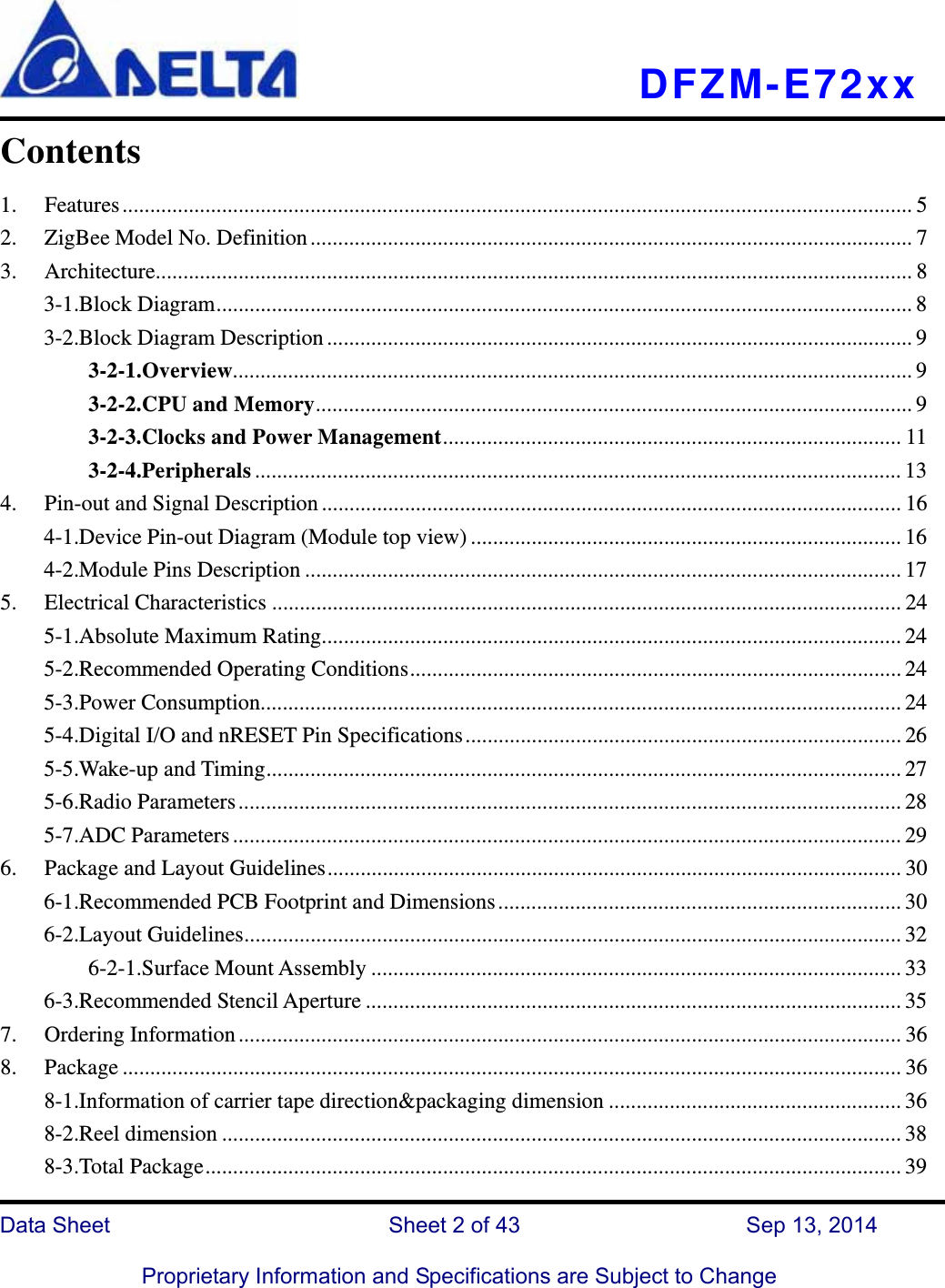
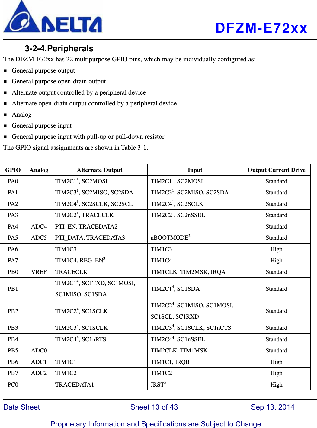
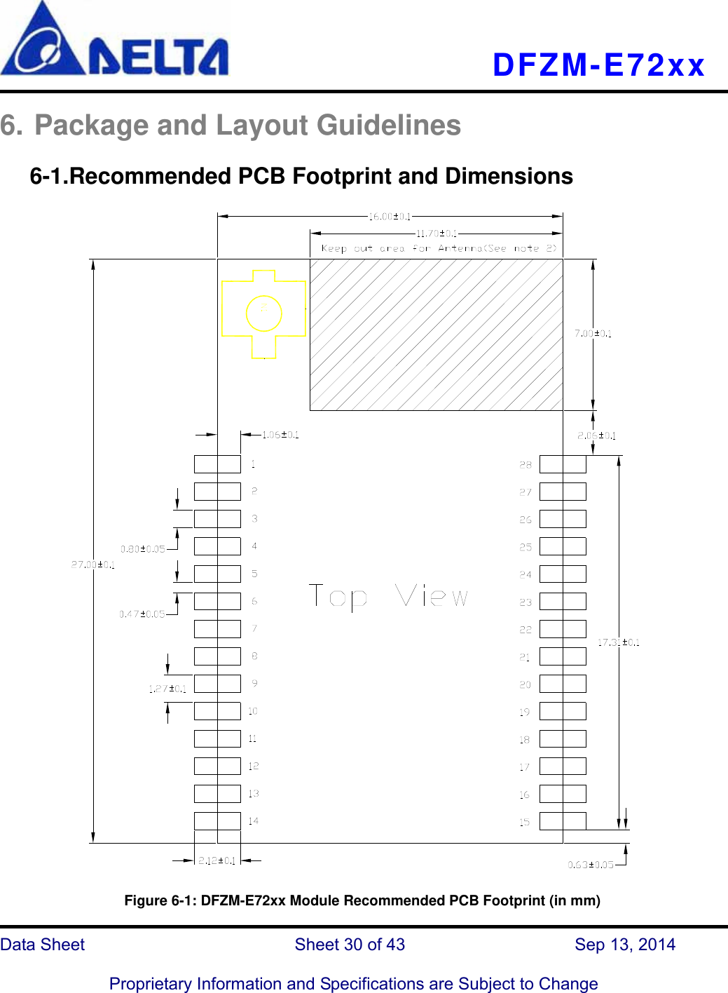
![DFZM-E72xx Data Sheet Sheet 17 of 43 Sep 13, 2014 Proprietary Information and Specifications are Subject to Change 4-2.Module Pins Description Pins Name Pin Type Description 1 GND Ground Ground 2 PC5 I/O Digital I/O(Not available for DFZM-E721X-DT0R) 3 nRESET I Active low chip reset(internal pull-up) 4 PA7 I/O Digital I/O, High current, Disable REG_EN with GPIO_DBGCFG[4] TIM1C4 O Timer 1 Channel 4 output, Enable timer output with TIM1_CCER Select alternate output function with GPIO_PACFGH[15:12] Disable REG_EN with GPIO_DBGCFG[4] TIM1C4 I Timer 1 Channel 4 input, Cannot be remapped REG_EN O External regulator open drain output, Enabled after reset 5 PB3 I/O Digital I/O TIM2C3 O Timer 2 channel 3 output, Enable remap with TIM2_OR[6] Enable timer output in TIM2_CCER Select alternate output function with GPIO_PBCFGL[15:12] TIM2C3 I Timer 2 channel 3 input, Enable remap with TIM2_OR[6] SC1nCTS I UART CTS handshake of Serial Controller 1 Enable with SC1_UARTCFG[5], Select UART with SC1_MODE SC1SCLK O SPI master clock of Serial Controller 1 Either disable timer output in TIM2_CCER, or disable remap with TIM2_OR[6] Enable master with SC1_SPICFG[4], Select SPI with SC1_MODE Select alternate output function with GPIO_PBCFGL[15:12] SC1SCLK I SPI slave clock of Serial Controller 1 Enable slave with SC1_SPICFG[4], Select SPI with SC1_MODE 6 PB4 I/O Digital I/O TIM2C4 O Timer 2 channel 4 output, Enable remap with TIM2_OR[7] Enable timer output in TIM2_CCER Select alternate output function with GPIO_PBCFGH[3:0] TIM2C4 I Timer 2 channel 4 input, Enable remap with TIM2_OR[7] SC1nRTS O UART RTS handshake of Serial Controller 1](https://usermanual.wiki/Delta-Electronics-orporated/DFZM-E7220/User-Guide-2402591-Page-17.png)
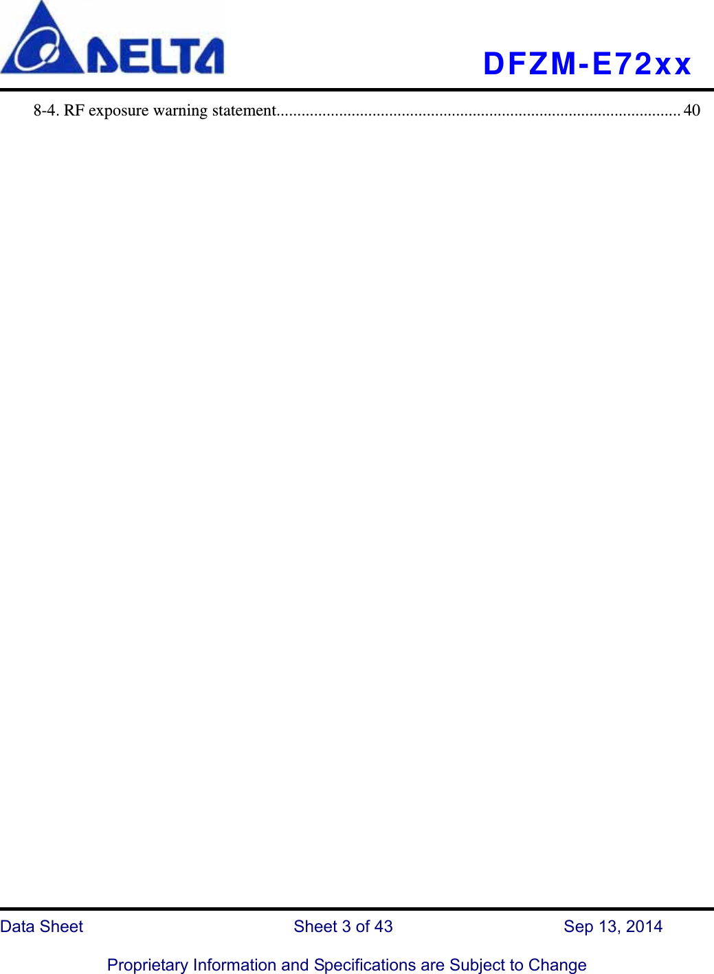
![DFZM-E72xx Data Sheet Sheet 18 of 43 Sep 13, 2014 Proprietary Information and Specifications are Subject to Change Either disable timer output in TIM2_CCER,or disable remap with TIM2_OR[7] Enable with SC1_UARTCFG[5], Select UART with SC1_MODE Select alternate output function with GPIO_PBCFGH[3:0] SC1nSSEL I SPI slave select of Serial Controller 1 Enable slave with SC1_SPICFG[4], Select SPI with SC1_MODE 7 PA0 I/O Digital I/O TIM2C1 O Timer 2 channel 1 output, Disable remap with TIM2_OR[4] Enable timer output in TIM2_CCER Select alternate output function with GPIO_PACFGL[3:0] TIM2C1 I Timer 2 channel 1 input, Disable remap with TIM2_OR[4] SC2MOSI O SPI master data out of Serial Controller 2 Either disable timer output in TIM2_CCER, or enable remap with TIM2_OR[4] Enable master with SC2_SPICFG[4], Select SPI with SC2_MODE Select alternate output function with GPIO_PACFGL[3:0] SC2MOSI I SPI slave data in of Serial Controller 2 Enable slave with SC2_SPICFG[4], Select SPI with SC2_MODE 8 PA1 I/O Digital I/O TIM2C3 O Timer 2 channel 3 output, Disable remap with TIM2_OR[6] Enable timer output in TIM2_CCER Select alternate output function with GPIO_PACFGL[7:4] TIM2C3 I Timer 2 channel 3 input, Disable remap with TIM2_OR[6] SC2SDA I/O TWI data of Serial Controller 2, Either disable timer output in TIM2_CCER, or enable remap with TIM2_OR[6], Select TWI with SC2_MODE Select alternate open-drain output function with GPIO_PACFGL[7:4] SC2MISO O SPI slave data out of Serial Controller 2, Either disable timer output in TIM2_CCER, or enable remap with TIM2_OR[6], Enable slave with SC2_SPICFG[4], Select SPI with SC2_MODE, Select alternate output function with GPIO_PACFGL[7:4]SC2MISO I SPI master data in of Serial Controller 2 Enable slave with SC2_SPICFG[4], Select SPI with SC2_MODE 9 PA2 I/O Digital I/O TIM2C4 O Timer 2 channel 4 output](https://usermanual.wiki/Delta-Electronics-orporated/DFZM-E7220/User-Guide-2402591-Page-18.png)
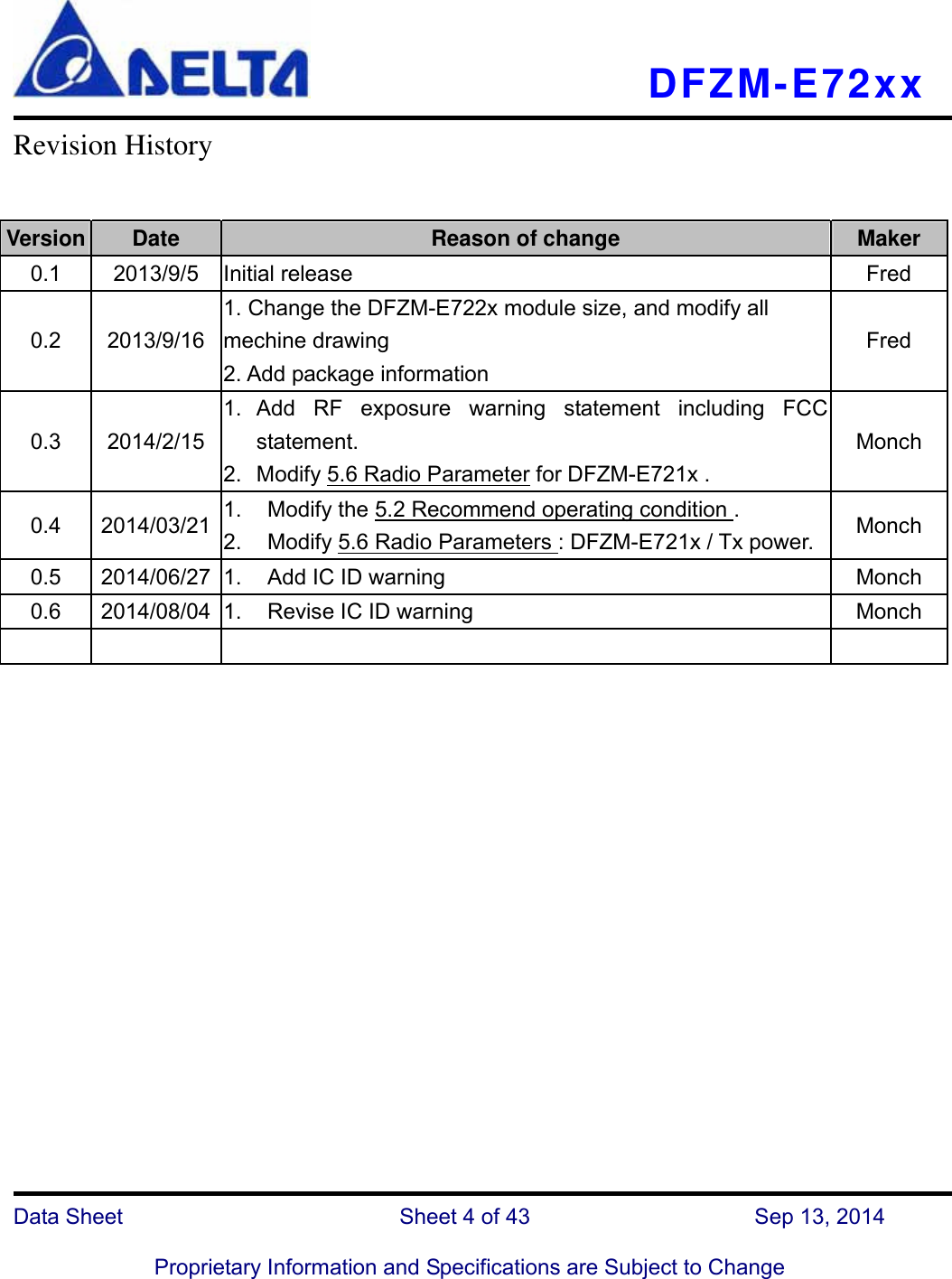
![DFZM-E72xx Data Sheet Sheet 19 of 43 Sep 13, 2014 Proprietary Information and Specifications are Subject to Change Disable remap with TIM2_OR[7], Enable timer output in TIM2_CCER Select alternate output function with GPIO_PACFGL[11:8] TIM2C4 I Timer 2 channel 4 input, Disable remap with TIM2_OR[7] SC2SCL I/O TWI clock of Serial Controller 2, Either disable timer output in TIM2_CCER, or enable remap with TIM2_OR[7], Select TWI with SC2_MODE Select alternate open-drain output function with GPIO_PACFGL[11:8] SC2SCLK O SPI master clock of Serial Controller 2 Either disable timer output in TIM2_CCER, or enable remap with TIM2_OR[7] Enable master with SC2_SPICFG[4], Select SPI with SC2_MODE Select alternate output function with GPIO_PACFGL[11:8] SC2SCLK I SPI slave clock of Serial Controller 2 Enable slave with SC2_SPICFG[4], Select SPI with SC2_MODE 10 PA3 I/O Digital I/O SC2nSSEL I SPI slave select of Serial Controller 2 Enable slave with SC2_SPICFG[4], Select SPI with SC2_MODE TRACECLK O Synchronous CPU trace clock, Either disable timer output in TIM2_CCER, or enable remap with TIM2_OR[5], Enable trace interface in ARM core Select alternate output function with GPIO_PACFGL[15:12] TIM2C2 O Timer 2 channel 2 output Disable remap with TIM2_OR[5], Enable timer output in TIM2_CCER Select alternate output function with GPIO_PACFGL[15:12] TIM2C2 I Timer 2 channel 2 input, Disable remap with TIM2_OR[5] 11 PA4 I/O Digital I/O ADC4 Analog ADC Input 4, Select analog function with GPIO_PACFGH[3:0] PTI_EN O Frame signal of Packet Trace Interface (PTI) Disable trace interface in ARM core, Enable PTI in Ember software Select alternate output function with GPIO_PACFGH[3:0] TRACEDATA2 O Synchronous CPU trace data bit 2 Select 4-wire synchronous trace interface in ARM core Enable trace interface in ARM core Select alternate output function with GPIO_PACFGH[3:0]](https://usermanual.wiki/Delta-Electronics-orporated/DFZM-E7220/User-Guide-2402591-Page-19.png)
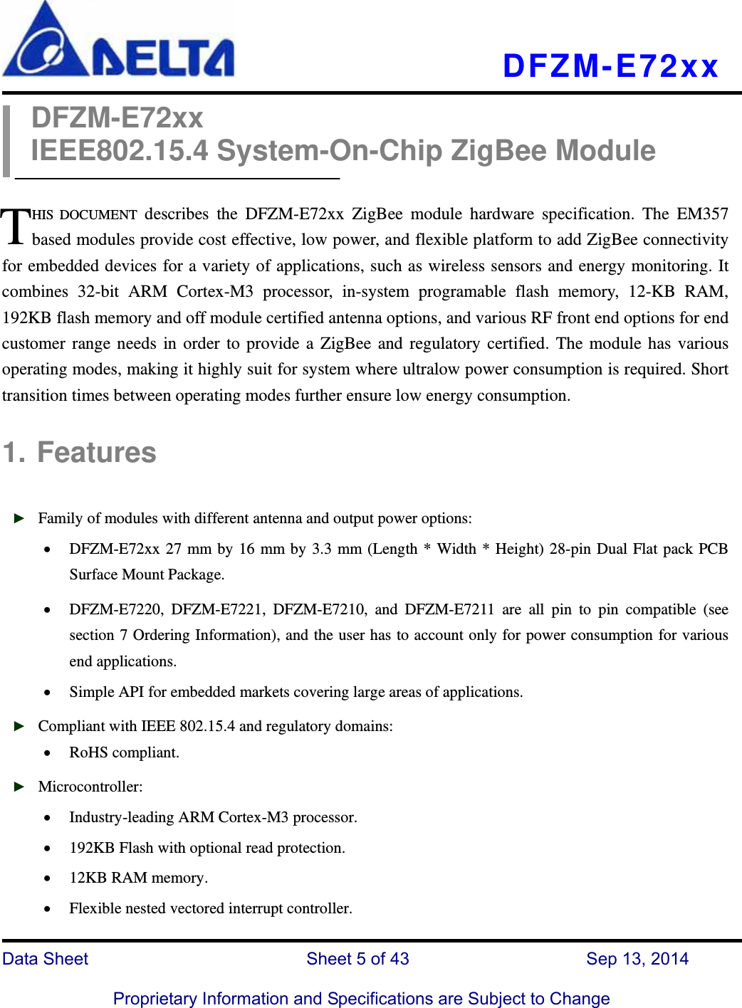
![DFZM-E72xx Data Sheet Sheet 20 of 43 Sep 13, 2014 Proprietary Information and Specifications are Subject to Change 12 PA5 I/O Digital I/O ADC5 Analog ADC Input 5, Select analog function with GPIO_PACFGH[7:4] PTI_DATA O Data signal of Packet Trace Interface (PTI) Disable trace interface in ARM core, Enable PTI in Ember software Select alternate output function with GPIO_PACFGH[7:4] nBOOTMODE I Activate FIB monitor instead of main program or bootloader when coming out of reset. Signal is active during and immediately after a reset on nRESET. TRACEDATA3 O Synchronous CPU trace data bit 3 Select 4-wire synchronous trace interface in ARM core Enable trace interface in ARM core Select alternate output function with GPIO_PACFGH[7:4] 13 PA6 I/O Digital I/O, High current TIM1C3 O Timer 1 channel 3 output, Enable timer output in TIM1_CCER Select alternate output function with GPIO_PACFGH[11:8] TIM1C3 I Timer 1 channel 3 input, Cannot be remapped 14 GND Ground Ground 15 VCC Power Power Supply Input 16 PB1 I/O Digital I/O SC1MISO O SPI slave data out of Serial Controller 1 Either disable timer output in TIM2_CCER, or disable remap with TIM2_OR[4] Select SPI with SC1_MODE, Select slave with SC1_SPICR Select alternate output function with GPIO_PBCFGL[7:4] SC1MOSI O SPI master data out of Serial Controller 1 Either disable timer output in TIM2_CCER, or disable remap with TIM2_OR[4] Select SPI with SC1_MODE, Select master with SC1_SPICR Select alternate output function with GPIO_PBCFGL[7:4] SC1SDA I/O TWI data of Serial Controller 1, Either disable timer output in TIM2_CCER, or disable remap with TIM2_OR[4], Select TWI with SC1_MODE Select alternate open-drain output function with GPIO_PBCFGL[7:4] SC1TXD O UART transmit data of Serial Controller 1 Either disable timer output in TIM2_CCER, or disable remap with TIM2_OR[4]](https://usermanual.wiki/Delta-Electronics-orporated/DFZM-E7220/User-Guide-2402591-Page-20.png)
![DFZM-E72xx Data Sheet Sheet 21 of 43 Sep 13, 2014 Proprietary Information and Specifications are Subject to Change Select UART with SC1_MODE Select alternate output function with GPIO_PBCFGL[7:4] TIM2C1 O Timer 2 channel 1 output Enable remap with TIM2_OR[4], Enable timer output in TIM2_CCER Select alternate output function with GPIO_PACFGL[7:4] TIM2C1 I Timer 2 channel 1 input, Disable remap with TIM2_OR[4] 17 PB2 I/O Digital I/O SC1MISO I SPI master data in of Serial Controller 1 Select SPI with SC1_MODE, Select master with SC1_SPICR SC1MOSI I SPI slave data in of Serial Controller 1 Select SPI with SC1_MODE, Select slave with SC1_SPICR SC1SCL I/O TWI clock of Serial Controller 1, Either disable timer output in TIM2_CCER, or disable remap with TIM2_OR[5], Select TWI with SC1_MODE Select alternate open-drain output function with GPIO_PBCFGL[11:8] SC1RXD I UART receive data of Serial Controller 1, Select UART with SC1_MODE TIM2C2 O Timer 2 channel 2 output Enable remap with TIM2_OR[5], Enable timer output in TIM2_CCER Select alternate output function with GPIO_PBCFGL[11:8] TIM2C2 I Timer 2 channel 2 input, Enable remap with TIM2_OR[5] 18 SWCLK I/O Serial Wire clock input/output with debugger Selected when in Serial Wire mode (see JTMS description, Pin 21) JTCK I JTAG clock input from debugger Selected when in JTAG mode (default mode, see JTMS description, Pin 21) Internal pull-down is enabled 19 PC2 I/O Digital I/O, Enable with GPIO_DBGCFG[5] JTDO O JTAG data out to debugger Selected when in JTAG mode (default mode, see JTMS description, Pin 21) SWO O Serial Wire Output asynchronous trace output to debugger Select asynchronous trace interface in ARM core, Enable trace interface in ARM core Select alternate output function with GPIO_PCCFGL[11:8] Enable Serial Wire mode (see JTMS description, Pin 21), Internal pull-up is enabled](https://usermanual.wiki/Delta-Electronics-orporated/DFZM-E7220/User-Guide-2402591-Page-21.png)
![DFZM-E72xx Data Sheet Sheet 22 of 43 Sep 13, 2014 Proprietary Information and Specifications are Subject to Change 20 PC3 I/O Digital I/O, Either Enable with GPIO_DBGCFG[5] or enable Serial Wire mode (see JTMS description) JTDI I JTAG data in from debugger Selected when in JTAG mode (default mode, see JTMS description, Pin 21) Internal pull-up is enabled 21 PC4 I/O Digital I/O, Enable with GPIO_DBGCFG[5] JTMS I JTAG mode select from debugger, Selected when in JTAG mode (default mode) JTAG mode is enabled after power-up or by forcing nRESET low Select Serial Wire mode using the ARM-defined protocol through a debugger Internal pull-up is enabled SWDIO I/O Serial Wire bidirectional data to/from debugger Enable Serial Wire mode (see JTMS description) Select Serial Wire mode using the ARM-defined protocol through a debugger Internal pull-up is enabled 22 PB0 I/O Digital I/O(Not available for DFZM-E721X-DT0R) VREF Analog O ADC reference output, Enable analog function with GPIO_PBCFGL[3:0] VREF Analog I ADC reference input, Enable analog function with GPIO_PBCFGL[3:0] Enable reference output with an Ember system function IRQA I External interrupt source A TRACECLK O Synchronous CPU trace clock, Enable trace interface in ARM core Select alternate output function with GPIO_PBCFGL[3:0] TIM1CLK I Timer 1 external clock input TIM2MSK I Timer 2 external clock mask input 23 PC1 I/O Digital I/O ADC3 Analog ADC Input 3, Enable analog function with GPIO_PCCFGL[7:4] SWO O Serial Wire Output asynchronous trace output to debugger Select asynchronous trace interface in ARM core, Enable trace interface in ARM core Select alternate output function with GPIO_PCCFGL[7:4] TRACEDATA0 O Synchronous CPU trace data bit 0 Select 1-, 2- or 4-wire synchronous trace interface in ARM core Enable trace interface in ARM core](https://usermanual.wiki/Delta-Electronics-orporated/DFZM-E7220/User-Guide-2402591-Page-22.png)
![DFZM-E72xx Data Sheet Sheet 23 of 43 Sep 13, 2014 Proprietary Information and Specifications are Subject to Change Select alternate output function with GPIO_PCCFGL[7:4] 24 PC0 I/O Digital I/O, High current, Either enable with GPIO_DBGCFG[5] or enable Serial Wire mode (see JTMS description, Pin 21) and disable TRACEDATA1 JRST I JTAG reset input from debugger Selected when in JTAG mode (default mode, see JTMS description) and TRACEDATA1 is disabled, Internal pull-up is enabled IRQD I Default external interrupt source D TRACEDATA1 O Synchronous CPU trace data bit 1 Select 2- or 4-wire synchronous trace interface in ARM core Enable trace interface in ARM core, Select alternate output function with GPIO_PCCFGL[3:0] 25 PB7 I/O Digital I/O, High current ADC2 Analog ADC Input 2, Enable analog function with GPIO_PBCFGH[15:12] IRQC I Default external interrupt source C TIM1C2 O Timer 1 channel 2 output, Enable timer output in TIM1_CCER Select alternate output function with GPIO_PBCFGH[15:12] TIM1C2 I Timer 1 channel 2 input, Cannot be remapped 26 PB6 I/O Digital I/O, High current ADC1 Analog ADC Input 1, Enable analog function with GPIO_PBCFGH[11:8] IRQB I External interrupt source B TIM1C1 O Timer 1 channel 1 output, Enable timer output in TIM1_CCER Select alternate output function with GPIO_PBCFGH[11:8] TIM1C1 I Timer 1 channel 1 input, Cannot be remapped 27 PB5 I/O Digital I/O(Not available for DFZM-E721X-DT0R) ADC0 Analog ADC Input 0, Enable analog function with GPIO_PBCFGH[7:4] TIM2CLK I Timer 2 external clock input TIM1MSK I Timer 1 external clock mask input 28 GND Ground Ground](https://usermanual.wiki/Delta-Electronics-orporated/DFZM-E7220/User-Guide-2402591-Page-23.png)