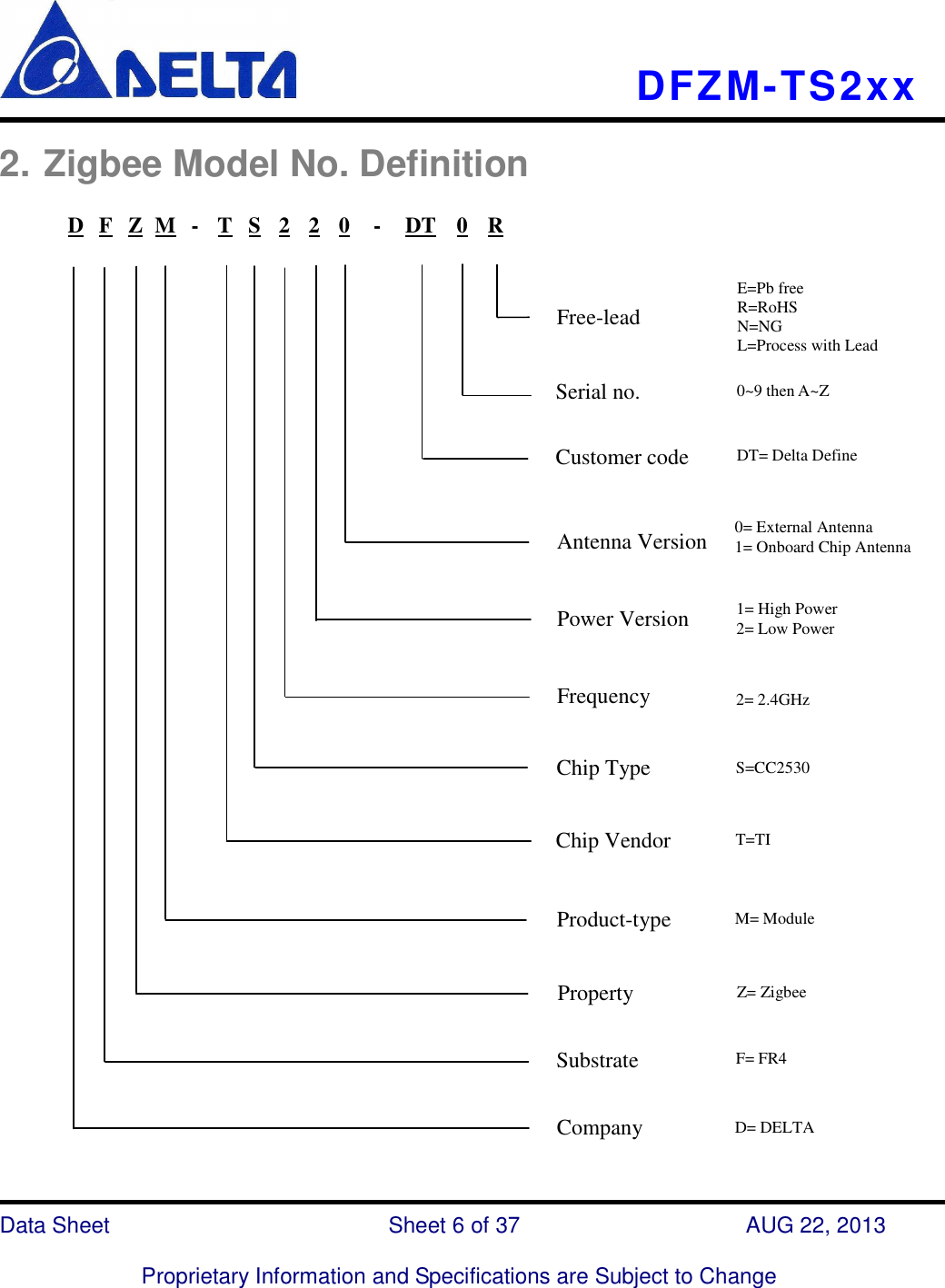
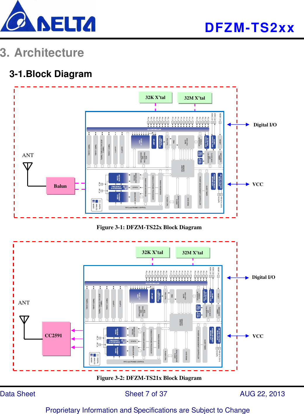
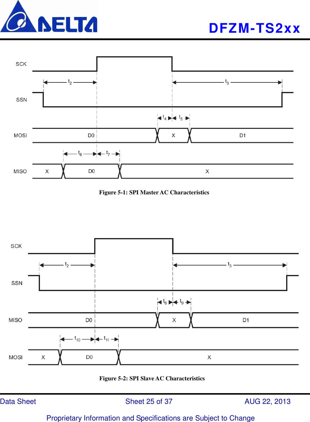
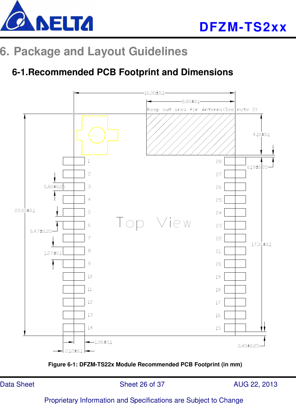
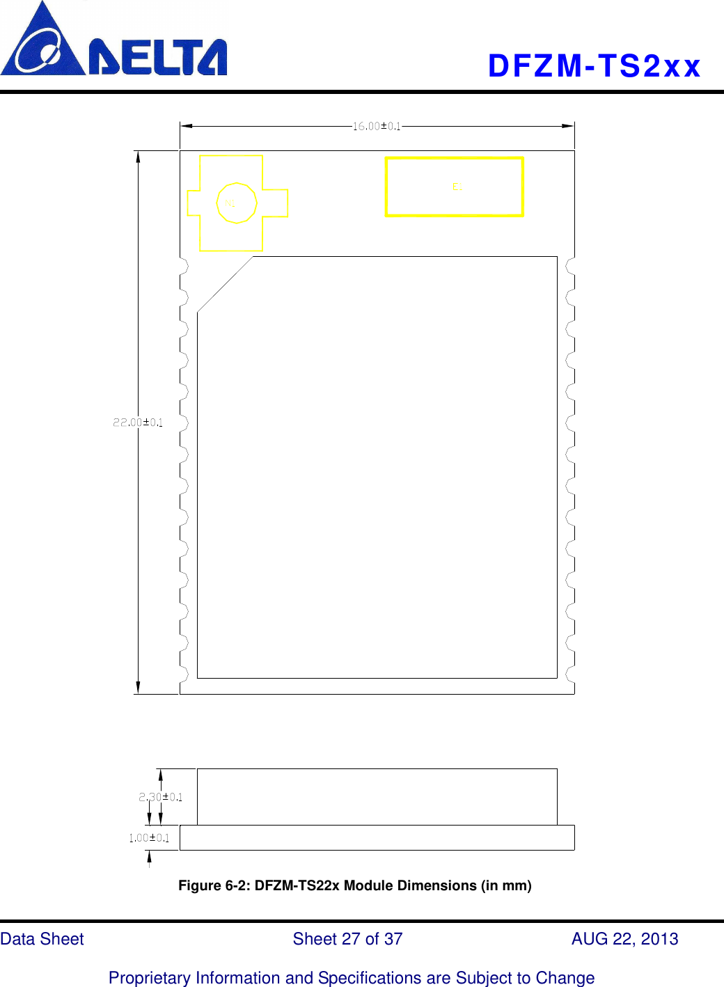
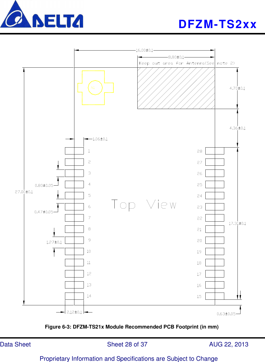
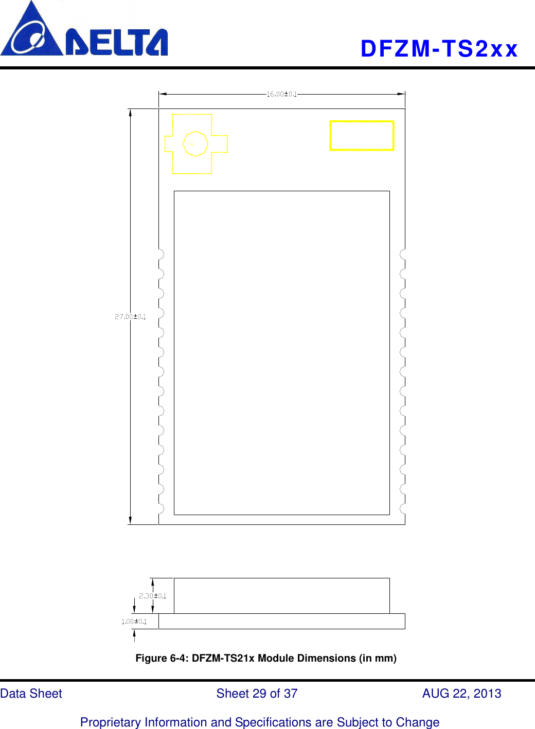
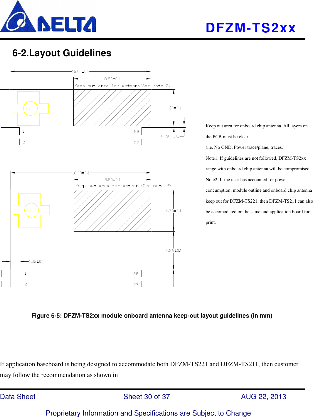
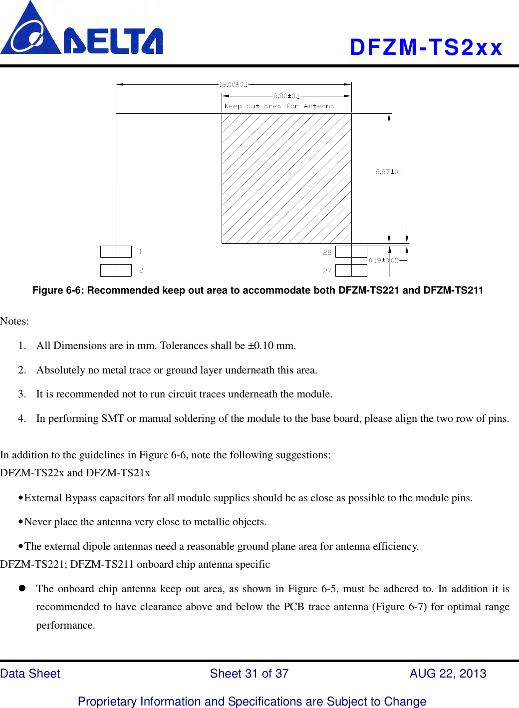
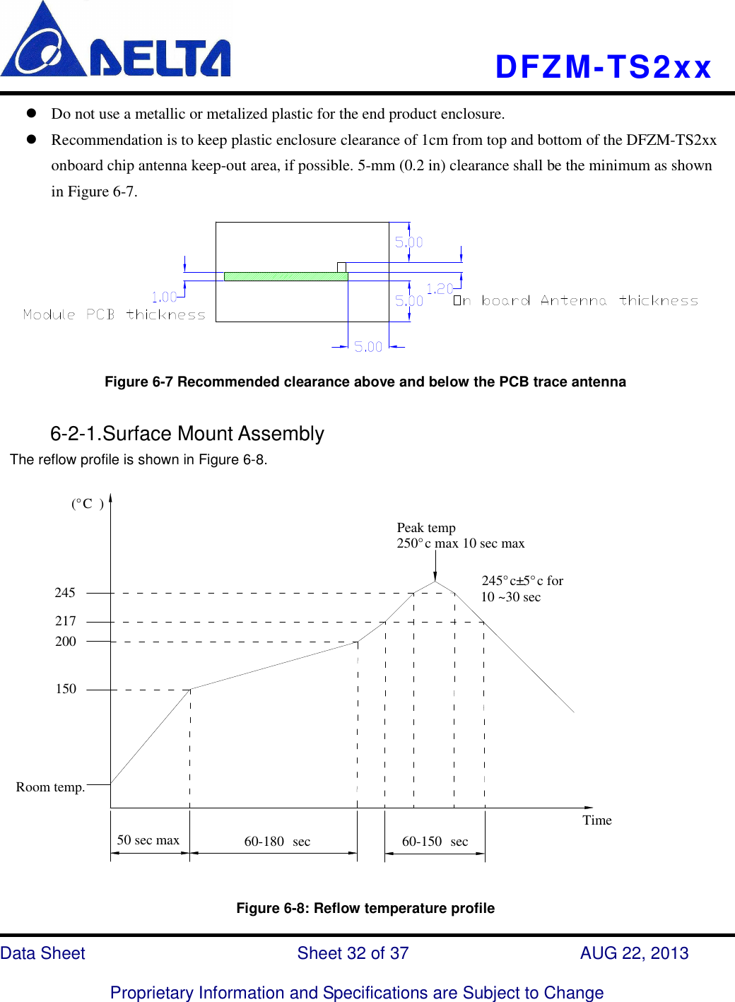
Delta Electronics orporated
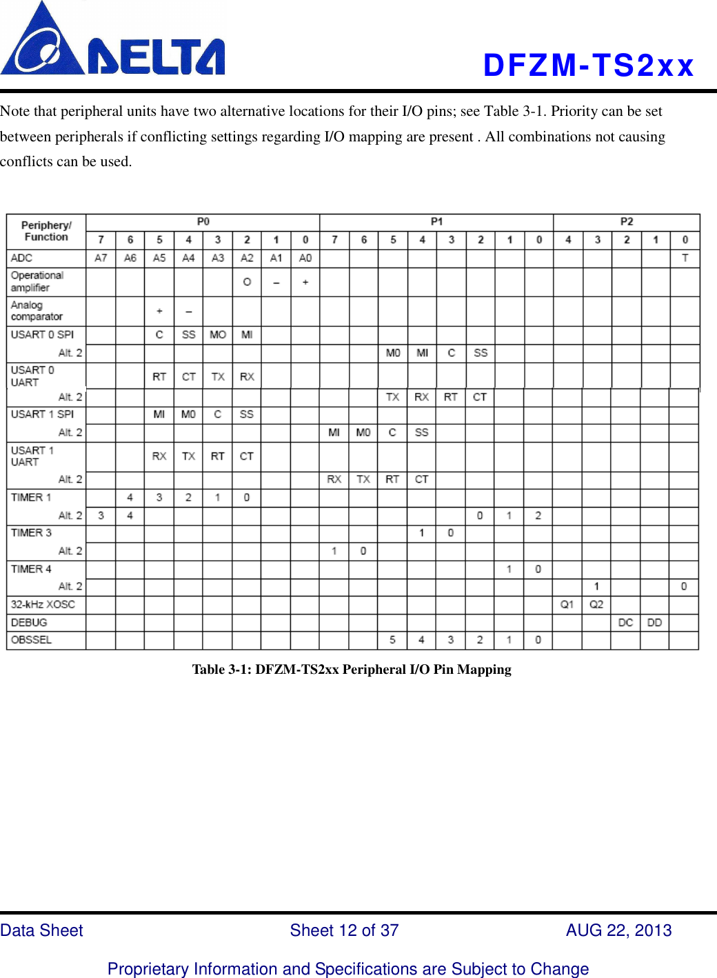
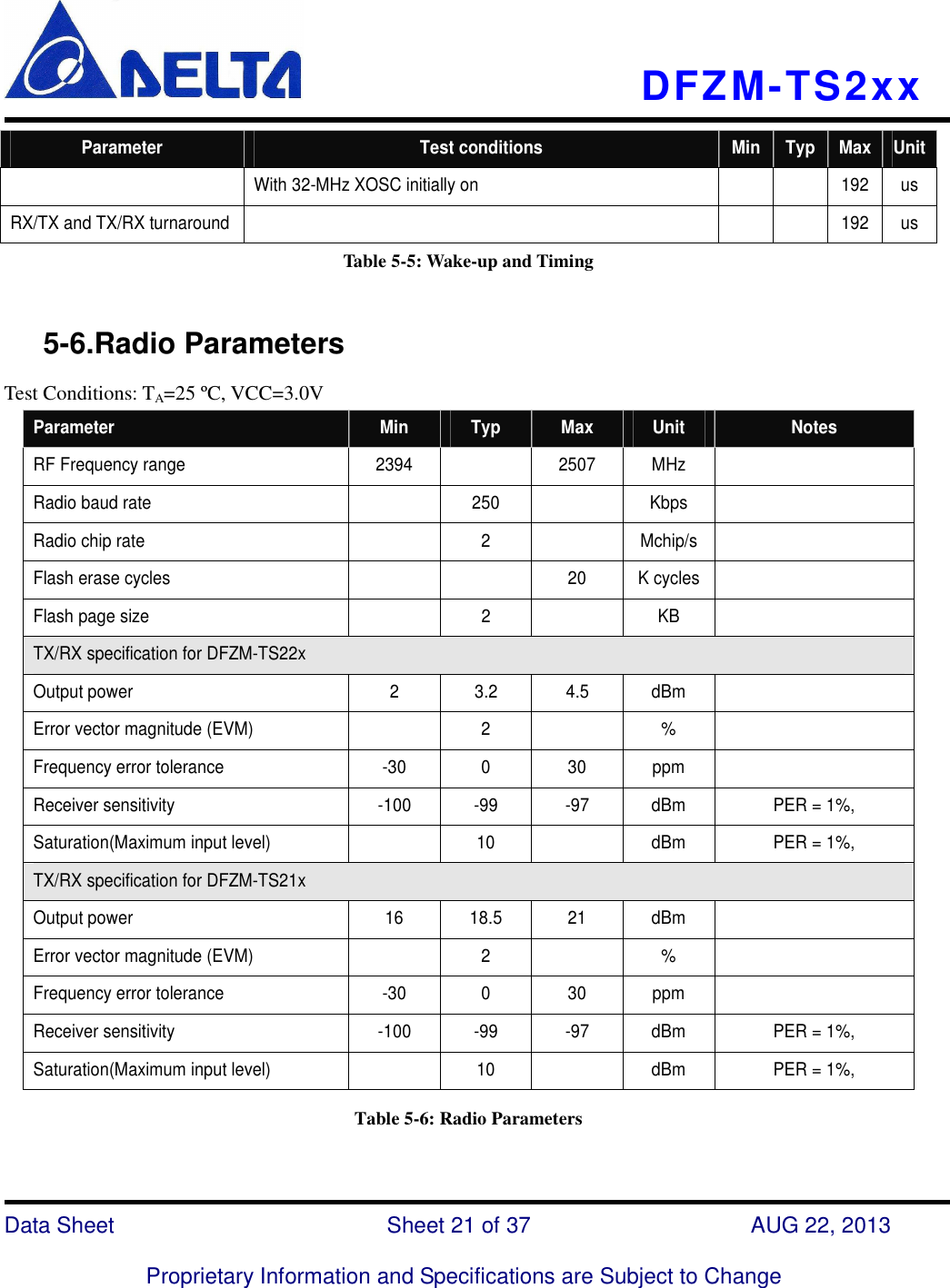
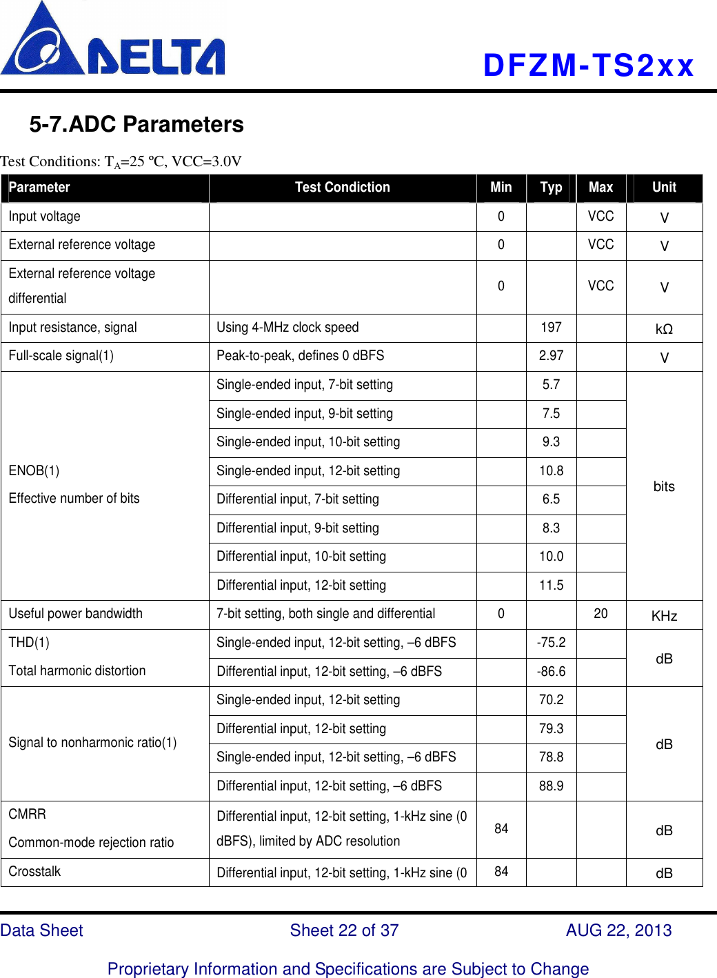
 DFZM-TS210 ZigBee module User Manual DFZM TS2xx Datasheet S4

Delta Electronics Incorporated ZigBee module DFZM TS2xx Datasheet S4

Users Manual

   DFZM-TS2xx   Data Sheet                              Sheet 1 of 37                    AUG 22, 2013  Proprietary Information and Specifications are Subject to Change Data sheet DFZM-TS2xx   An IEEE 802.15.4 System–On-Chip Zigbee module
   DFZM-TS2xx   Data Sheet                              Sheet 2 of 37                    AUG 22, 2013  Proprietary Information and Specifications are Subject to Change Contents   1. Features............................................................................................................................................... 4 2. Zigbee Model No. Definition.............................................................................................................. 6 3. Architecture......................................................................................................................................... 7 3-1.Block Diagram.............................................................................................................................. 7 3-2.Block Diagram Description .......................................................................................................... 8 3-2-1.Overview ........................................................................................................................... 8 3-2-2.CPU and Memory..............................................................................................................8 3-2-3.Clocks and Power Management........................................................................................ 9 3-2-4.Peripherals......................................................................................................................... 9 3-3.Power Management .................................................................................................................... 13 4. Pin-out and Signal Description ......................................................................................................... 15 4-1.Device Pin-out Diagram (Module top view) .............................................................................. 15 4-2.Module Pins Description ............................................................................................................16 5. Electrical Characteristics .................................................................................................................. 18 5-1.Absolute Maximum Rating.........................................................................................................18 5-2.Recommended Operating Conditions......................................................................................... 18 5-3.Power Consumption....................................................................................................................18 5-4.DC Characteristics...................................................................................................................... 20 5-5.Wake-up and Timing...................................................................................................................20 5-6.Radio Parameters........................................................................................................................ 21 5-7.ADC Parameters......................................................................................................................... 22 5-8.SPI AC Characteristics ...............................................................................................................24 6. Package and Layout Guidelines........................................................................................................ 26 6-1.Recommended PCB Footprint and Dimensions......................................................................... 26 6-2.Layout Guidelines.......................................................................................................................30 6-2-1.Surface Mount Assembly ................................................................................................ 32 6-3.Recommended Stencil Aperture ................................................................................................. 34 7. Ordering Information........................................................................................................................ 36
   DFZM-TS2xx   Data Sheet                              Sheet 3 of 37                    AUG 22, 2013  Proprietary Information and Specifications are Subject to Change Revision History    Version Date  Reason of change  Maker 0.1  2013/3/11 Initial release  Fred 0.2  2013/4/26 Add Peripheral I/O Pin Mapping  Fred 0.3  2013/7/1  Add  “Not  available  for  DFZM-TS21X-DT0R”  at  4-2.  Module Pins Description( Pins 10、13、25)  JunRu 0.4  2013/8/22 Update power consumption and radio parameters  JunRu
   DFZM-TS2xx   Data Sheet                              Sheet 4 of 37                    AUG 22, 2013  Proprietary Information and Specifications are Subject to Change DFZM-TS2xx IEEE802.15.4 System-On-Chip Zigbee Module  HIS DOCUMENT describes the DFZM-TS2xx Zigbee module hardware specification. The CC2530 based modules provide cost effective, low power, and flexible platform to add Zigbee connectivity for embedded devices for a variety of applications, such as wireless sensors and energy monitoring. It combines 8051-based processors, in-system programable flash memory, 8-KB RAM, 256KB flash memory and off module certified antenna options, and various RF front end options for end customer range needs in order to provide a Zigbee and regulatory certified. The module has various operating modes, making it highly suit for system where ultralow power consumption is required. Short transition times between operating modes further ensure low energy consumption.  1. Features  ► Family of modules with different antenna and output power options: • DFZM-TS22x 22 mm by 16 mm by 3.3mm (Length * Width * Height) 28-pin Dual Flat pack PCB Surface Mount Package. • DFZM-TS21x 27 mm by 16 mm by 3.3 mm (Length * Width * Height) 28-pin Dual Flat pack PCB Surface Mount Package. • DFZM-TS220,  DFZM-TS221,  DFZM-TS210,  and  DFZM-TS211  are  all  pin  to  pin  compatible  (see section  7  Ordering  Information),  and  the  user  has  to  account  only  for  power  consumption,  module outline,  and  PCB  antenna  keep  out  (if  used)  to  accommodate  “one  size  fits  all”  for  various  end applications. • Simple API for embedded markets covering large areas of applications. ► Compliant with IEEE 802.15.4 and regulatory domains: • RoHS compliant.   T
   DFZM-TS2xx   Data Sheet                              Sheet 5 of 37                    AUG 22, 2013  Proprietary Information and Specifications are Subject to Change • FCC/NCC Certified.   DFZM-TS220  DFZM-TS221  DFZM-TS210  DFZM-TS211 FCC ID  H79DFZM-TS220  H79DFZM-TS220  TBD  TBD NCC ID  CCAJ12LP2570T7  CCAJ12LP2571T9  TBD  TBD ► Microcontroller: • High-Performance and Low Power 8051 Microcontroller core with code prefetch . • 256KB In-Syctem-Programmable Flash.   • 8KB RAM with Retention in all power mode. • Hardware debug support. ► Interfaces: • Chip antenna or external antenna options. • Two powerful USART with support for several serial protocols. • Up to 21 configurable general purpose I/Os. • Single 3.3V supply option: o Wide supply voltage range 2.0 ~ 3.3V.   • One PWM output. • One 7~ 12-bit ADC with 30KHz~40KHz bandwidth resolution. ► Embedded RTC (Real Time Clock) can run directly from battery. ► Low-power mode operations. ► Power mode 1, 2, 3.
   DFZM-TS2xx   Data Sheet                              Sheet 6 of 37                    AUG 22, 2013  Proprietary Information and Specifications are Subject to Change 2. Zigbee Model No. Definition                         D F Z M - T S 2 2 0 - DT 0 R 1= High Power 2= Low Power E=Pb free R=RoHS N=NG L=Process with Lead Customer code Antenna Version Free-lead Power Version Frequency M= Module Z= Zigbee F= FR4 D= DELTA 2= 2.4GHz Chip Vendor Product-type Property Substrate Company T=TI 0= External Antenna 1= Onboard Chip Antenna DT= Delta Define Chip Type S=CC2530 0~9 then A~Z Serial no.
   DFZM-TS2xx   Data Sheet                              Sheet 7 of 37                    AUG 22, 2013  Proprietary Information and Specifications are Subject to Change 3. Architecture 3-1.Block Diagram  Figure 3-1: DFZM-TS22x Block Diagram    Figure 3-2: DFZM-TS21x Block Diagram CC2591 ANT 32K X’tal 32M X’tal Balun 32K X’tal ANT 32M X’tal Digital I/O VCC VCC Digital I/O
   DFZM-TS2xx   Data Sheet                              Sheet 8 of 37                    AUG 22, 2013  Proprietary Information and Specifications are Subject to Change 3-2.Block Diagram Description           3-2-1.Overview DFZM-TS2xx module is a highly integrated Zigbee system-on-chip (SOC) that contains the following: • The module includes TI CC2530 SoC, which contains CPU- and memory-related, peripherals-related, clocks and power management-related in a single package.       • The module features an IEEE802.15.4-compliant radio transceiver with onboard 32 KHz & 32 MHz crystal circuitries, RF, and certified chip antenna or external antenna options. o The  low power  module  option has  a  capability  of  +4.5dBm  output power at the  antenna (see Figure 3-1). o The high power module option has a capability of +18.5dBm output power at the antenna (see Figure 3-2). • Variety  of  interfaces  are  available  such  as  two  USART  and  SPI,  four  TIMER,  one  7~12  bit  ADC, Operational amperifier and GPIO. • DFZM-TS2xx contains single power supply (VCC).              3-2-2.CPU and Memory   The 8051 CPU core used in the CC253x device family is a single-cycle 8051-compatible core. It has three different memory-access buses (SFR, DATA and CODE/XDATA) with single-cycle access to SFR, DATA, and the main SRAM. It also includes a debug interface and an 18-input extended interrupt unit.  The interrupt controller services a total of 18 interrupt sources, divided into six interrupt groups, each of which is associated with one of four interrupt priorities. Any interrupt service request is serviced also when the device is in idle mode by going back to active mode. Some interrupts can also wake up the device from sleep mode (power modes 1–3).  The memory arbiter is at the heart of the system, as it connects the CPU and DMA controller with the physical memories and all peripherals through the SFR bus. The memory arbiter has four memory access points, access of which can map to one of three physical memories: an 8-KB SRAM, flash memory, and XREG/SFR registers. It is responsible for performing arbitration and sequencing between simultaneous memory accesses to the same
   DFZM-TS2xx   Data Sheet                              Sheet 9 of 37                    AUG 22, 2013  Proprietary Information and Specifications are Subject to Change physical memory.  The 8-KB SRAM maps to the DATA memory space and to parts of the XDATA memory spaces. The 8-KB SRAM is an ultralow-power SRAM that retains its contents even when the digital part is powered off (power modes 2 and 3). This is an important feature for low-power applications.  The 256 KB flash block provides in-circuit programmable non-volatile program memory for the device, and maps into the CODE and XDATA memory spaces. In addition to holding program code and constants, the non-volatile memory allows the application to save data that must be preserved such that it is available after restarting the device. Using this feature one can, e.g., use saved network-specific data to avoid the need for a full start-up and network find-and-join process.            3-2-3.Clocks and Power Management The digital core and peripherals are powered by a 1.8-V low-dropout voltage regulator. It provides power management functionality that enables low power operation for long battery life using different power modes. Five different reset sources exist to reset the device.           3-2-4.Peripherals The CC2530 includes many different peripherals that allow the application designer to develop advanced applications.  The debug interface implements a proprietary two-wire serial interface that is used for in-circuit debugging. Through this debug interface, it is possible to perform an erasure of the entire flash memory, control which oscillators are enabled, stop and start execution of the user program, execute supplied instructions on the 8051 core, set code breakpoints, and single-step through instructions in the code. Using these techniques, it ispossible to perform in-circuit debugging and external flash programming elegantly.  The device contains flash memory for storage of program code. The flash memory is programmable from the user software and through the debug interface. The flash controller handles writing and erasing the embedded flash memory. The flash controller allows page-wise erasure and 4-bytewise programming.  The I/O controller is responsible for all general-purpose I/O pins. The CPU can configure whether peripheral modules control certain pins or whether they are under software control, and if so, whether each pin is configured
   DFZM-TS2xx   Data Sheet                              Sheet 10 of 37                    AUG 22, 2013  Proprietary Information and Specifications are Subject to Change as an input or output and if a pullup or pulldown resistor in the pad is connected. CPU interrupts can be enabled on each pin individually. Each peripheral that connects to the I/O pins can choose between two different I/O pin locations to ensure flexibility in various applications.  A versatile five-channel DMA controller is available in the system, accesses memory using the XDATA memory space, and thus has access to all physical memories. Each channel (trigger, priority, transfer mode, addressing mode, source and destination pointers, and transfer count) is configured with DMA descriptors anywhere in memory. Many of the hardware peripherals (AES core, flash controller, USARTs, timers, ADC interface) achieve highly efficient operation by using the DMA controller for data transfers between SFR or XREG addresses and flash/SRAM.  Timer 1 is a 16-bit timer with timer/counter/PWM functionality. It has a programmable prescaler, a 16-bit period value, and five individually programmable counter/capture channels, each with a 16-bit compare value. Each of the counter/capture channels can be used as a PWM output or to capture the timing of edges on input signals. It can also be configured in IR Generation Mode where it counts Timer 3 periods and the output is ANDed with the output of Timer 3 to generate modulated consumer IR signals with minimal CPU interaction.  Timer 2 (the MAC Timer) is specially designed for supporting an IEEE 802.15.4 MAC or other time-slotted protocol in software. The timer has a configurable timer period and a 24-bit overflow counter that can be used to keep track of the number of periods that have transpired. A 40-bit capture register is also used to record the exact time at which a start-of-frame delimiter is received/transmitted or the exact time at which transmission ends, as well as two 16-bit output compare registers and two 24-bit overflow compare registers that can send various command strobes (start RX, start TX, etc.) at specific times to the radio modules.  Timer 3 and Timer 4 are 8-bit timers with timer/counter/PWM functionality. They have a programmable prescaler, an 8-bit period value, and one programmable counter channel with an 8-bit compare value. Each of the counter channels can be used as a PWM output.  The sleep timer is an ultralow-power timer that counts 32-kHz crystal oscillator or 32-kHz RC oscillator periods. The sleep timer runs continuously in all operating modes except power mode 3 (PM3). Typical applications of this timer are as a real-time counter or as a wake-up timer to come out of power mode 1 (PM1) or 2 (PM2).
   DFZM-TS2xx   Data Sheet                              Sheet 11 of 37                    AUG 22, 2013  Proprietary Information and Specifications are Subject to Change The ADC supports 7 to 12 bits of resolution in a 30 kHz to 4 kHz bandwidth, respectively. DC and audio conversions with up to eight input channels (Port 0) are possible. The inputs can be selected as single-ended or differential. The reference voltage can be internal, AVDD, or a single-ended or differential external signal. The ADC also has a temperature-sensor input channel. The ADC can automate the process of periodic sampling or conversion over a sequence of channels.  The operational amplifier is intended to provide front-end buffering and gain for the ADC. Both inputs as well as the output are available on pins, so the feedback network is fully customizable. A chopper-stabilized mode is available for applications that need good accuracy with high gain.  The ultralow-power analog comparator enables applications to wake up from PM2 or PM3 based on an analog signal. Both inputs are brought out to pins; the reference voltage must be provided externally. The comparator output is connected to the I/O controller interrupt detector and can be treated by the MCU as a regular I/O pin interrupt.  The random-number generator uses a 16-bit LFSR to generate pseudorandom numbers, which can be read by the CPU or used directly by the command strobe processor. It can be seeded with random data from noise in the radio ADC.  The AES encryption/decryption core allows the user to encrypt and decrypt data using the AES algorithm with 128-bit keys. The core is able to support the AES operations required by IEEE 802.15.4 MAC security, the ZigBee network layer, and the application layer.  A built-in watchdog timer allows the CC2530 to reset itself in case the firmware hangs. When enabled by software, the watchdog timer must be cleared periodically; otherwise, it resets the device when it times out. It can alternatively be configured for use as a general 32-kHz timer.  USART 0 and USART 1 are each configurable as either a SPI master/slave or a UART. They provide double buffering on both RX and TX and hardware flow control and are thus well suited to high-throughput full-duplex applications. Each has its own high-precision baud-rate generator, thus leaving the ordinary timers free for other uses.
   DFZM-TS2xx   Data Sheet                              Sheet 12 of 37                    AUG 22, 2013  Proprietary Information and Specifications are Subject to Change Note that peripheral units have two alternative locations for their I/O pins; see Table 3-1. Priority can be set between peripherals if conflicting settings regarding I/O mapping are present . All combinations not causing   conflicts can be used.  Table 3-1: DFZM-TS2xx Peripheral I/O Pin Mapping
   DFZM-TS2xx   Data Sheet                              Sheet 13 of 37                    AUG 22, 2013  Proprietary Information and Specifications are Subject to Change      3-3.Power Management Different operating modes, or power modes, are used to allow low-power operation. Ultralow-power operation is obtained by turning off the power supply to modules to avoid static (leakage) power consumption and also by using clock gating and turning off oscillators to reduce dynamic power consumption.   The five various operating modes (power modes) are called active mode, idle mode, PM1, PM2, and PM3 (PM1/PM2/PM3 are also referred to as sleep modes). Active mode is the normal operating mode, whereas PM3 has the lowest power consumption. The impact of the different power modes on system operation is shown in Table 3-2, together with voltage regulator and oscillator options.   Power Mode  High-Frequency Oscillator  Low-Frequency Oscillator  Vlotage Regulator (Digital) Configuration  A: 32MHz XOSC B: 16MHz RCOSC C: 32KHz XOSC D: 32KHz RCOSC  Active/idle mode A or B  C or D  ON PM1  OFF  ON  ON PM2  OFF  ON  OFF PM2  OFF  OFF  OFF Table 3-2: DFZM-TS2xx Power Management  Active mode: The fully functional mode of operation where the CPU, peripherals, and RF transceiver are active. The voltage regulator to the digital core is on, and either the 16MHz RC oscillator or the 32MHz crystal oscillator or both is running. Either the 32KHz RCOSC or the 32KHz XOSC is running.    Idle mode: Identical to active mode, except that the CPU core stops operating (is idle). All other peripherals function normally, and any enabled interrupt wakes up the CPU core (to transition back from idle mode to active mode).  PM1: The voltage regulator to the digital part is on. Neither the 32MHz XOSC nor the 16MHZ RCOSC is running. Either the 32KHz RCOSC or 32KHz XOSC is running. When PM1 is entered, a power-down sequence is run.   PM1 is used when the expected time until a wakeup event is relatively short (less than 3 ms), because PM1 uses a fast power-down/up sequence.
   DFZM-TS2xx   Data Sheet                              Sheet 14 of 37                    AUG 22, 2013  Proprietary Information and Specifications are Subject to Change  PM2: The voltage regulator to the digital core is turned off. Neither the 32MHz XOSC nor the 16MHz RCOSC is running. Either the 32KHz RCOSC or the 32KHz XOSC is running. PM2 has the second-lowest power consumption. In PM2, the power-on reset, external interrupts, selected 32KHz oscillator, and Sleep Timer peripherals are active. I/O pins retain the I/O mode and output value set before entering PM2. All other internal circuits are powered down. The voltage regulator is also turned off. When PM2 is entered, a power-down sequence is run.   PM2 is typically entered when using the Sleep Timer as the wakeup event, and also combined with external interrupts. PM2 should typically be choosen, compared to PM1, when expected sleep time exceeds 3 ms. Using less sleep time does not reduce system power consumption compared to using PM1.  PM3: The voltage regulator to the digital core is turned off. None of the oscillators is running. PM3 is used to achieve the operating mode with the lowest power consumption. In PM3, all internal circuits that are powered from the voltage regulator are turned off (basically all digital modules; the only exceptions are interrupt detection and POR level sensing). Reset (POR or external) and external I/O port interrupts are the only functions that operate in this mode. I/O pins retain the I/O mode and output value set before entering PM3. A reset condition or an enabled external I/O interrupt event wakes the device up and places it into active mode (an external interrupt starts from where it entered PM3, whereas a reset returns to start-of-program execution). The content of RAM and registers is partially preserved in this mode. PM3 uses the same power-down/up sequence as PM2. PM3 is used to achieve ultralow power consumption when waiting for an external event. It should be used when expected sleep time exceeds 3 ms.
   DFZM-TS2xx   Data Sheet                              Sheet 15 of 37                    AUG 22, 2013  Proprietary Information and Specifications are Subject to Change 4. Pin-out and Signal Description      4-1.Device Pin-out Diagram (Module top view)                           Figure 4-1: DFZM-TS2xx Device Pin-out Diagram (Module top view)
   DFZM-TS2xx   Data Sheet                              Sheet 16 of 37                    AUG 22, 2013  Proprietary Information and Specifications are Subject to Change      4-2.Module Pins Description Pins  Name  Pin Type  Description 1  GND  Ground  Ground 2  GND  Ground  Ground 3  GND  Ground  Ground 4  P2_2  Digital I/O  Port 2.2, Debug Clock 5  P2_1  Digital I/O  Port 2.1, Debug Data 6  P2_0  Digital I/O  Port 2.0 7  P1_7  Digital I/O  Port 1.7 8  P1_6  Digital I/O  Port 1.6 9  P1_5  Digital I/O  Port 1.5 10  P1_4  Digital I/O  Port 1.4 (Not available for DFZM-TS21X-DT0R) 11  P1_3  Digital I/O  Port 1.3 12  P1_2  Digital I/O  Port 1.2 13  P1_1  Digital I/O  Port 1.1 (Not available for DFZM-TS21X-DT0R) 14  P1_0  Digital I/O  Port 1.0 15  GND  Ground  Ground 16  GND  Ground  Ground 17  RESET_N  Digital Input  Reset, Active low 18  P0_0  Digital I/O  Port 0.0 19  P0_1  Digital I/O  Port 0.1 20  P0_2  Digital I/O  Port 0.2 21  P0_3  Digital I/O  Port 0.3 22  P0_4  Digital I/O  Port 0.4 23  P0_5  Digital I/O  Port 0.5 24  P0_6  Digital I/O  Port 0.6 25  P0_7  Digital I/O  Port 0.7 (Not available for DFZM-TS21X-DT0R) 26  VCC  Power  Power Supply Input 27  VCC  Power  Power Supply Input
   DFZM-TS2xx   Data Sheet                              Sheet 17 of 37                    AUG 22, 2013  Proprietary Information and Specifications are Subject to Change 28  GND  Ground  Ground
   DFZM-TS2xx   Data Sheet                              Sheet 18 of 37                    AUG 22, 2013  Proprietary Information and Specifications are Subject to Change 5. Electrical Characteristics   5-1.Absolute Maximum Rating Conditions beyond those cited in Table 5-1 may cause permanent damage to the DFZM-TS2xx, and must be avoided.      Parameter  Minimum  Maximum  Unit Supply voltage(VCC)  -0.3  3.9  V Storage temperature range  -40  125  ºC   Voltage on any digitai I/O  -0.3  VCC+0.3, ≤3.9  V Table 5-1: Absolute Maximum Ratings     5-2.Recommended Operating Conditions  Parameter  Minimum  Maximum  Unit Operating supply voltage(VCC)  2  3.6  V Operating ambient temperature range(TA)  -40  85  ºC Table 5-2: Recommended Operating Conditions       5-3.Power Consumption Test Conditions: TA=25 ºC, VCC=3.0V Parameter  Test conditions  Mim Typ Max Unit Digital regulator on. 16MHz RCOSC running. No radio, crystals, or peripherals active. Medium CPU activity: normal flash access(1), no RAM access   3.4   mA Icore      Core current consumption 32MHz  XOSC  running.  No  radio  or  peripherals  active.   6.5  8.9  mA
   DFZM-TS2xx   Data Sheet                              Sheet 19 of 37                    AUG 22, 2013  Proprietary Information and Specifications are Subject to Change Medium CPU activity: normal flash access(1), no RAM access 32MHz XOSC running, radio in RX mode, –50dBm input power, no peripherals active, CPU idle@DFZM-TS22x   20.5   mA 32MHz XOSC running, radio in RX mode, –50dBm input power, no peripherals active, CPU idle@DFZM-TS21x   24    mA 32MHz XOSC running, radio in RX mode at -100dBm input power (waiting for signal), no peripherals active, CPU idle@DFZM-TS22x  23  25  29.6 mA 32MHz XOSC running, radio in RX mode at -100dBm input power (waiting for signal), no peripherals active, CPU idle@DFZM-TS21x  27  31  35  mA 32MHz XOSC running, radio in TX mode, 4.5dBm output power, no peripherals active, CPU idle@DFZM-TS22x  34  36  39.6 mA 32MHz XOSC running, radio in TX mode, 18.5dBm output power, no peripherals active, CPU idle@DFZM-TS21x  150 168 190 mA Power mode 1. Digital regulator on; 16MHz RCOSC and 32MHz crystal oscillator off; 32.768kHz XOSC, POR, BOD and sleep timer active; RAM and register retention   0.2 0.3 uA Power mode 2. Digital regulator off; 16MHz RCOSC and 32MHz crystal oscillator off; 32.768kHz XOSC, POR, and sleep timer active; RAM and register retention   1  2  uA Power mode 3. Digital regulator off; no clocks; POR active; RAM and register retention    0.4 1  uA Timer 1 Timer running, 32MHz XOSC used    90    uA Timer2 Timer running, 32MHz XOSC used    90    uA Timer 3 Timer running, 32MHz XOSC used    60    uA Timer 4 Timer running, 32MHz XOSC used    70    uA Sleep timer  Including 32.753-kHz RCOSC    0.6   uA ADC  When converting    1.2   mA Iper   Peripheral current consumption (Adds to core current Icore for each peripheral unit activated) Flash  Erase    1    mA
   DFZM-TS2xx   Data Sheet                              Sheet 20 of 37                    AUG 22, 2013  Proprietary Information and Specifications are Subject to Change Burst write peak current    6    mA Table 5-3: Poewr Consumption (1) Normal flash access means that the code used exceeds the cache storage, so cache misses happen frequently.       5-4.DC Characteristics Test Conditions: TA=25 ºC, VCC=3.0V Parameter  Test conditions  Min  Typ  Max  Unit Logic-0 input voltage        0.5  V Logic-1 input voltage    2.5      V Logic-0 input current  Input equals 0 V  -50    50  nA Logic-1 input current  Input equals VDD  -50    50  nA I/O-pin pullup and pulldown resistors      20    kΩ Logic-0 output voltage, 4-mA pins  Output load 4 mA      0.5  V Logic-1 output voltage, 4-mA pins  Output load 4 mA  2.4      V Logic-0 output voltage, 20-mA pins  Output load 20 mA      0.5  V Logic-1 output voltage, 20-mA pins  Output load 20 mA  2.4      V Table 5-4: DC Characteristics       5-5.Wake-up and Timing Test Conditions: TA=25 ºC, VCC=3.0V Parameter  Test conditions  Min Typ Max Unit Power mode 1  active  Digital regulator on, 16-MHz RCOSC and 32-MHz crystal oscillator off. Start-up of 16-MHz RCOSC    4    us Power mode 2 or 3  active  Digital regulator off, 16-MHz RCOSC and 32-MHz crystal oscillator off. Start-up of regulator and 16-MHz RCOSC    0.1   ms Active  TX or RX  Initially running on 16-MHz RCOSC, with 32-MHz XOSC OFF   0.5   ms
   DFZM-TS2xx   Data Sheet                              Sheet 21 of 37                    AUG 22, 2013  Proprietary Information and Specifications are Subject to Change Parameter  Test conditions  Min Typ Max Unit With 32-MHz XOSC initially on      192 us RX/TX and TX/RX turnaround       192 us Table 5-5: Wake-up and Timing       5-6.Radio Parameters Test Conditions: TA=25 ºC, VCC=3.0V Parameter  Min  Typ  Max  Unit  Notes RF Frequency range  2394    2507  MHz   Radio baud rate    250    Kbps   Radio chip rate    2    Mchip/s   Flash erase cycles      20  K cycles  Flash page size    2    KB   TX/RX specification for DFZM-TS22x Output power    2  3.2  4.5  dBm   Error vector magnitude (EVM)    2    %   Frequency error tolerance  -30  0  30  ppm   Receiver sensitivity  -100  -99  -97  dBm  PER = 1%, Saturation(Maximum input level)    10    dBm  PER = 1%, TX/RX specification for DFZM-TS21x Output power    16  18.5  21  dBm   Error vector magnitude (EVM)    2    %   Frequency error tolerance  -30  0  30  ppm   Receiver sensitivity  -100  -99  -97  dBm  PER = 1%, Saturation(Maximum input level)    10    dBm  PER = 1%, Table 5-6: Radio Parameters
   DFZM-TS2xx   Data Sheet                              Sheet 22 of 37                    AUG 22, 2013  Proprietary Information and Specifications are Subject to Change      5-7.ADC Parameters Test Conditions: TA=25 ºC, VCC=3.0V Parameter  Test Condiction  Min  Typ  Max Unit Input voltage    0    VCC V External reference voltage    0    VCC V External reference voltage differential    0    VCC V Input resistance, signal  Using 4-MHz clock speed    197   kΩ Full-scale signal(1)  Peak-to-peak, defines 0 dBFS    2.97  V Single-ended input, 7-bit setting    5.7   Single-ended input, 9-bit setting    7.5   Single-ended input, 10-bit setting    9.3   Single-ended input, 12-bit setting    10.8  Differential input, 7-bit setting    6.5   Differential input, 9-bit setting    8.3   Differential input, 10-bit setting    10.0  ENOB(1)   Effective number of bits Differential input, 12-bit setting    11.5  bits Useful power bandwidth  7-bit setting, both single and differential  0    20 KHz Single-ended input, 12-bit setting, –6 dBFS    -75.2  THD(1)   Total harmonic distortion  Differential input, 12-bit setting, –6 dBFS    -86.6  dB Single-ended input, 12-bit setting    70.2  Differential input, 12-bit setting    79.3  Single-ended input, 12-bit setting, –6 dBFS    78.8  Signal to nonharmonic ratio(1) Differential input, 12-bit setting, –6 dBFS    88.9  dB CMRR   Common-mode rejection ratio Differential input, 12-bit setting, 1-kHz sine (0 dBFS), limited by ADC resolution  84     dB Crosstalk  Differential input, 12-bit setting, 1-kHz sine (0  84     dB
   DFZM-TS2xx   Data Sheet                              Sheet 23 of 37                    AUG 22, 2013  Proprietary Information and Specifications are Subject to Change dBFS), limited by ADC resolution Offset  Midscale    -3   mV Gain error      0.68  % 12-bit setting, mean    0.05  DNL(1)   Differential nonlinearity  12-bit setting, maximum    0.9   LSB 12-bit setting, mean    4.6   INL(1)   Integral nonlinearity  12-bit setting, maximum    13.3  LSB Single-ended input, 7-bit setting    35.4  Single-ended input, 9-bit setting    46.8  Single-ended input, 10-bit setting    57.5  Single-ended input, 12-bit setting    66.6  Differential input, 7-bit setting    40.7  Differential input, 9-bit setting    51.6  Differential input, 10-bit setting    61.8  SINAD(1) (–THD+N) Signal-to-noise-and-distortion Differential input, 12-bit setting    70.8  dB 7-bit setting    20   9-bit setting    36   10-bit setting    68   Conversion time 12-bit setting    132   us Internal reference voltage      1.15  mA Internal reference VCC coefficient     4   mV/V Internal reference temperature coefficient      0.4   mV/10°C Table 5-7: ADC Parameters (1) Measured with 300-Hz sine-wave input and VCC as reference.
   DFZM-TS2xx   Data Sheet                              Sheet 24 of 37                    AUG 22, 2013  Proprietary Information and Specifications are Subject to Change      5-8.SPI AC Characteristics Test Conditions: TA= -40~85 ºC, VCC= 2.0~3.6V     Parameter  Test conditions  Mim  Typ  Max  Unit Master, RX and TX  250     t1    SCK period  Slave, RX and TX  250      ns SCK duty cycle  Master    50    % Master  63     t2    SSN low to SCK  Slave  63      ns Master  63     t3    SCK to SSN high  Slave  63      ns t4    MOSI early out  Master, load = 10 pF      7  ns t5    MOSI late out  Master, load = 10 pF      10  ns t6    MISO setup  Master  90      ns t7    MISO hold  Master  10      ns SCK duty cycle  Slave    50    % t10    MOSI setup  Slave  35      ns t11    MOSI hold  Slave  10      ns t9    MISO late out  Slave, load = 10 pF      95  ns Master, TX only      8 Master, RX and TX      4 Slave, RX only      8 Operating frequency Slave, RX and TX      4 MHz   Table 5-85: SPI AC Characteristics
   DFZM-TS2xx   Data Sheet                              Sheet 25 of 37                    AUG 22, 2013  Proprietary Information and Specifications are Subject to Change  Figure 5-1: SPI Master AC Characteristics    Figure 5-2: SPI Slave AC Characteristics
   DFZM-TS2xx   Data Sheet                              Sheet 26 of 37                    AUG 22, 2013  Proprietary Information and Specifications are Subject to Change 6. Package and Layout Guidelines      6-1.Recommended PCB Footprint and Dimensions                      Figure 6-1: DFZM-TS22x Module Recommended PCB Footprint (in mm)
   DFZM-TS2xx   Data Sheet                              Sheet 27 of 37                    AUG 22, 2013  Proprietary Information and Specifications are Subject to Change                         Figure 6-2: DFZM-TS22x Module Dimensions (in mm)
   DFZM-TS2xx   Data Sheet                              Sheet 28 of 37                    AUG 22, 2013  Proprietary Information and Specifications are Subject to Change                         Figure 6-3: DFZM-TS21x Module Recommended PCB Footprint (in mm)
   DFZM-TS2xx   Data Sheet                              Sheet 29 of 37                    AUG 22, 2013  Proprietary Information and Specifications are Subject to Change                         Figure 6-4: DFZM-TS21x Module Dimensions (in mm)
   DFZM-TS2xx   Data Sheet                              Sheet 30 of 37                    AUG 22, 2013  Proprietary Information and Specifications are Subject to Change      6-2.Layout Guidelines                   Figure 6-5: DFZM-TS2xx module onboard antenna keep-out layout guidelines (in mm)      If application baseboard is being designed to accommodate both DFZM-TS221 and DFZM-TS211, then customer may follow the recommendation as shown in Keep out area for onboard chip antenna. All layers on the PCB must be clear. (i.e. No GND, Power trace/plane, traces.) Note1: If guidelines are not followed, DFZM-TS2xx range with onboard chip antenna will be compromised. Note2: If the user has accounted for power concumption, module outline and onboard chip antenna keep out for DFZM-TS221, then DFZM-TS211 can also be accomodated on the same end application board foot print.
   DFZM-TS2xx   Data Sheet                              Sheet 31 of 37                    AUG 22, 2013  Proprietary Information and Specifications are Subject to Change          Figure 6-6: Recommended keep out area to accommodate both DFZM-TS221 and DFZM-TS211  Notes: 1. All Dimensions are in mm. Tolerances shall be ±0.10 mm. 2. Absolutely no metal trace or ground layer underneath this area.   3. It is recommended not to run circuit traces underneath the module. 4. In performing SMT or manual soldering of the module to the base board, please align the two row of pins.  In addition to the guidelines in Figure 6-6, note the following suggestions:   DFZM-TS22x and DFZM-TS21x • External Bypass capacitors for all module supplies should be as close as possible to the module pins. • Never place the antenna very close to metallic objects. • The external dipole antennas need a reasonable ground plane area for antenna efficiency. DFZM-TS221; DFZM-TS211 onboard chip antenna specific  The onboard chip antenna keep out area, as shown in Figure 6-5, must be adhered to. In addition it is recommended to have clearance above and below the PCB trace antenna (Figure 6-7) for optimal range performance.
   DFZM-TS2xx   Data Sheet                              Sheet 32 of 37                    AUG 22, 2013  Proprietary Information and Specifications are Subject to Change  Do not use a metallic or metalized plastic for the end product enclosure.  Recommendation is to keep plastic enclosure clearance of 1cm from top and bottom of the DFZM-TS2xx onboard chip antenna keep-out area, if possible. 5-mm (0.2 in) clearance shall be the minimum as shown in Figure 6-7.     Figure 6-7 Recommended clearance above and below the PCB trace antenna            6-2-1.Surface Mount Assembly The reflow profile is shown in Figure 6-8.   60-180 secRoom temp.50 sec max150200245217(°C  )60-150 secTimePeak temp250°c max 10 sec max245°c±5°c for 10 ~30 sec   Figure 6-8: Reflow temperature profile
   DFZM-TS2xx   Data Sheet                              Sheet 33 of 37                    AUG 22, 2013  Proprietary Information and Specifications are Subject to Change Note: 1. Perform  adequate  test  in  advance  as  the  reflow  temperature  profile  will  vary  accordingly  to  the conditions of the parts and boards, and the specifications of the reflow furnace. 2. Be careful about rapid temperature rise in preheat zone as it may cause excessive slumping of the solder paste. 3. If the preheat is insufficient, rather large solder balls tend to be generated. Conversely, if performed excessively, fine balls and large balls will generate in clusters at a time. 4. If the temperature is too low, non-melting tends to be caused in the area with large heat capacity after reflow. 5. Be careful about sudden rise in temperature as it may worsen the slump of solder paste. 6. Be careful about slow cooling as it may cause the positional shift of parts and decline in joining strength at times.
   DFZM-TS2xx   Data Sheet                              Sheet 34 of 37                    AUG 22, 2013  Proprietary Information and Specifications are Subject to Change      6-3.Recommended Stencil Aperture Note: The thickness of the stencil should be 0.15mm over this area.                       Figure 6-9: DFZM-TS22x recommended stencil aperture
   DFZM-TS2xx   Data Sheet                              Sheet 35 of 37                    AUG 22, 2013  Proprietary Information and Specifications are Subject to Change                         Figure 6-9: DFZM-TS21x recommended stencil aperture
   DFZM-TS2xx   Data Sheet                              Sheet 36 of 37                    AUG 22, 2013  Proprietary Information and Specifications are Subject to Change 7. Ordering Information DEVICE DESCRIPTION  ORDERING NUMBER Extended range module using external antenna  DFZM-TS210-DT0R Extended range module using onboard chip antenna  DFZM-TS211-DT0R Low power module using external antenna  DFZM-TS220-DT0R Low power module using onboard chip antenna  DFZM-TS211-DT0R  8. Federal Communications Commission (FCC) Statement 15.21 You are cautioned that changes or modifications not expressly approved by the part responsible for compliance could void the user’s authority to operate the equipment.  15.105(b) This equipment has been tested and found to comply with the limits for a Class B digital device, pursuant to part 15 of the FCC rules. These limits are designed to provide reasonable protection against harmful interference in a residential installation. This equipment generates, uses and can radiate radio frequency energy and, if not installed and used in accordance with the instructions, may cause harmful interference to radio communications. However, there is no guarantee that interference will not occur in a particular installation. If this equipment does cause harmful interference to radio or television reception, which can be determined by turning the equipment off and on, the user is encouraged to try to correct the interference by one or more of the following measures:
   DFZM-TS2xx   Data Sheet                              Sheet 37 of 37                    AUG 22, 2013  Proprietary Information and Specifications are Subject to Change  -Reorient or relocate the receiving antenna. -Increase the separation between the equipment and receiver. -Connect  the  equipment  into  an  outlet  on  a  circuit  different  from  that  to  which  the  receiver  is connected. -Consult the dealer or an experienced radio/TV technician for help.  This device complies with Part 15 of the FCC Rules. Operation is subject to the following two conditions: 1) this device may not cause harmful interference, and 2) this device must accept any interference received, including interference that may cause undesired operation of the device.  FCC RF Radiation Exposure Statement: This equipment complies with FCC radiation exposure limits set forth for an uncontrolled environment. End users must follow the specific operating instructions for satisfying RF exposure compliance. This transmitter must not be co-located or operating in conjunction with any other antenna or transmitter.    Note: The end product shall has the words “Contains Transmitter Module FCC ID:    ““““H79DFZM-TS210””””    Caution: Exposure to Radio Frequency Radiation. To comply with FCC RF exposure compliance requirements, a separation distance of at least 20 cm must be maintained between the antenna of this device and all persons.

Navigation menu