Delta Electronics orporated DFZM-TT211 zigBee module User Manual DFZM TT2xx Datasheet
Delta Electronics Incorporated zigBee module DFZM TT2xx Datasheet
User manual

DFZM-TT2xx
Data Sheet Sheet 1 of 39 Feb. 3, 2016
Proprietary Information and Specifications are Subject to Change
Data sheet
DFZM-TT2xx
An IEEE 802.15.4 System–On-Chip ZigBee
module

DFZM-TT2xx
Data Sheet Sheet 2 of 39 Feb. 3, 2016
Proprietary Information and Specifications are Subject to Change
Contents
1. Features............................................................................................................................................... 4
2. Zigbee Model No. Definition.............................................................................................................. 6
3. Architecture......................................................................................................................................... 7
3-1.Block Diagram.............................................................................................................................. 7
3-2.Block Diagram Description ..........................................................................................................8
3-2-1.Overview...........................................................................................................................8
3-2-2.CPU and Memory............................................................................................................ 8
3-2-3.AES Engine with 128, 192 256 Bit Key Support...........................................................9
3-2-4.Peripherals .....................................................................................................................10
3-3.Power Management .................................................................................................................... 14
4. Pin-out and Signal Description ......................................................................................................... 17
4-1.Device Pin-out Diagram (Module top view) .............................................................................. 17
4-2.Module Pins Description ............................................................................................................18
5. Electrical Characteristics .................................................................................................................. 20
5-1.Absolute Maximum Rating.........................................................................................................20
5-2.Recommended Operating Conditions......................................................................................... 20
5-3.Power Consumption....................................................................................................................20
5-4.DC Characteristics......................................................................................................................22
5-5.Wake-up and Timing................................................................................................................... 22
5-6.Radio Parameters........................................................................................................................23
5-7.ADC Parameters.........................................................................................................................24
5-8.Control Input AC Characteristics................................................................................................26
5-9.USB Interface DC Characteristics..............................................................................................26
6. Package and Layout Guidelines........................................................................................................ 27
6-1.Recommended PCB Footprint and Dimensions...................................................................27
6-2.Layout Guidelines....................................................................................................................... 29
6-2-1.Surface Mount Assembly ................................................................................................30
6-3.Recommended Stencil Aperture .................................................................................................32
7. Reference Design Schematic ............................................................................................................ 33
8. DUT Setup ........................................................................................................................................ 33

DFZM-TT2xx
Data Sheet Sheet 3 of 39 Feb. 3, 2016
Proprietary Information and Specifications are Subject to Change
9. Federal Communications Commission (FCC) Statement................................................................. 38

DFZM-TT2xx
Data Sheet Sheet 4 of 39 Feb. 3, 2016
Proprietary Information and Specifications are Subject to Change
DFZM-TT2xx
IEEE802.15.4 System-On-Chip ZigBee Module
HIS DOCUMENT
describes the DFZM-TT2xx Zigbee module hardware specification. The CC2538
based modules provide cost effective, low power, and flexible platform to add ZigBee connectivity
for embedded devices for a variety of applications, such as wireless sensors and energy monitoring. It
combines ARM Cotex-M3 based processors, in-system programable flash memory, 32-KB RAM,
512KB flash memory and off module certified antenna options, and various RF front end options for end
customer range needs in order to provide a Zigbee and regulatory certified. The module has various
operating modes, making it highly suit for system where ultralow power consumption is required. Short
transition times between operating modes further ensure low energy consumption.
1. Features
►
Family of modules with different antenna and output power options:
• DFZM-TT2xx 29.3 mm by 19.8 mm by 3.3mm (Length * Width * Height) 42-pin Dual Flat pack PCB
Surface Mount Package.
• DFZM-TT220, DFZM-TT221, DFZM-TT210, and DFZM-TT211 are all pin to pin compatible (see
section 7 Ordering Information), and the user has to account only for power consumption.
• Simple API for embedded markets covering large areas of applications.
►
Compliant with IEEE 802.15.4 and regulatory domains:
• RoHS compliant.
►
Microcontroller:
• Powerful ARM Cortex™ M3 with code prefetch.
• 512KB In-Syctem-Programmable Flash.
• Up to 32KB RAM (16-kB With Retention in All Power Modes).
• Supports On-Chip Over-the-Air Upgrade(OTA).
T

DFZM-TT2xx
Data Sheet Sheet 5 of 39 Feb. 3, 2016
Proprietary Information and Specifications are Subject to Change
• Hardware debug support.
►
Interfaces:
• On board antenna or external antenna options.
• µDMA.
• 4 × General-Purpose Timers (Each 32-Bit or 2 × 16-Bit).
• USB 2.0 Full-Speed Device (12 Mbps).
• 2 × SPI.
• Two universal asynchronous receiver/transmitters (UARTs) with IrDA, 9-bit (one UART with modem
flow control).
• I
2
C.
• Four 32-bit timers (up to eight 16-bit) with pulse width modulation (PWM) capability and
synchronization.
• Up to 28 configurable general purpose I/Os.
• Single 3.3V supply option:
o Wide supply voltage range 2.0 ~ 3.6V.
• One 12-bit ADC with 8 Channels and Configurable Resolution.
►
Embedded RTC (Real Time Clock) can run directly from battery.
►
Low-power mode operations.
►
Power mode 0,1, 2, 3.

DFZM-TT2xx
Data Sheet Sheet 6 of 39 Feb. 3, 2016
Proprietary Information and Specifications are Subject to Change
2. Zigbee Model No. Definition
D
F
Z
M
-
T
T
2
2
0
-
DT
0
R
1= High Power
2= Low Power
E=Pb free
R=RoHS
N=NG
L=Process with Lead
Customer code
Antenna Version
Free-lead
Power Version
Frequency
M= Module
Z= Zigbee
F= FR4
D= DELTA
2= 2.4GHz
Chip Vendor
Product-type
Property
Substrate
Company
T=TI
0= External Antenna
1= Onboard Antenna
DT=
Delta Define
Chip Type
T=CC2538
0~9 then A~Z
Serial no.
DFZM-TT2xx
Data Sheet Sheet 7 of 39 Feb. 3, 2016
Proprietary Information and Specifications are Subject to Change
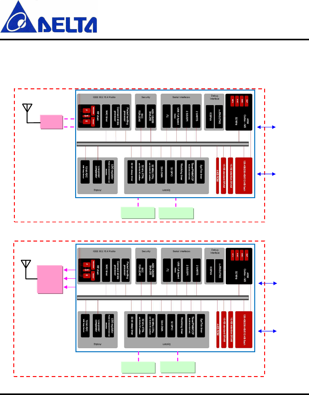
3. Architecture
3-1.Block Diagram
Figure 3-1: DFZM-TT22x Block Diagram
Figure 3-2: DFZM-TT21x Block Diagram
CC2591
32M X’tal
32K X’tal
ANT
Balun
ANT
32M X’tal
32K X’tal
Digital I/O
VCC
VCC
Digital I/O

DFZM-TT2xx
Data Sheet Sheet 8 of 39 Feb. 3, 2016
Proprietary Information and Specifications are Subject to Change
3-2.Block Diagram Description
3-2-1.Overview
DFZM-TT2xx module is a highly integrated ZigBee system-on-chip (SOC) that contains the following:
• The module includes TI CC2538 SoC, which contains CPU- and memory-related, peripherals-related, clocks
and power management-related in a single package.
• The module features an IEEE802.15.4-compliant radio transceiver with onboard 32 KHz & 32 MHz crystal
circuitries, RF, and certified on board antenna or external antenna options.
o The low power module option has a capability of +7dBm output power at the antenna (see Figure 3-1).
o The high power module option has a capability of +18.5dBm output power at the antenna (see Figure
3-2).
• Variety of interfaces are available such as two USART and SPI, four TIMER, one 12 bit ADC, Operational
amperifier and GPIO.
• DFZM-TT2xx contains single power supply (VCC).
3-2-2.CPU and Memory
The CC2538 is designed around an ARM Cortex-M3 processor core. The ARM Cortex-M3 processor provides
the core for a high-performance, low-cost platform that meets the needs of minimal memory implementation,
reduced pin count, and low power consumption, while delivering outstanding computational performance and
exceptional system response to interrupts.
• 32-bit ARM Cortex-M3 architecture optimized for small-footprint embedded applications.
• Outstanding processing performance combined with fast interrupt handling.
• Thumb-2 mixed 16- and 32-bit instruction set delivers the high performance expected of a 32-bit ARM core in
a compact memory size usually associated with 8- and 16-bit devices, typically in the range of a few kilobytes
of memory for microcontroller-class applications.
– Single-cycle multiply instruction and hardware divide.
– Atomic bit manipulation (bit-banding), delivering maximum memory use and streamlined peripheral
control.
– Unaligned data access, enabling data to be efficiently packed into memory.
• Fast code execution permits slower processor clock or increases sleep mode time.

DFZM-TT2xx
Data Sheet Sheet 9 of 39 Feb. 3, 2016
Proprietary Information and Specifications are Subject to Change
• Harvard architecture characterized by separate buses for instruction and data.
• Efficient processor core, system and memories.
• Hardware division and fast multiplier.
• Deterministic, high-performance interrupt handling for time-critical applications.
• Memory protection unit (MPU) provides a privileged mode for protected operating system functionality.
• Enhanced system debug with extensive breakpoint capabilities and debugging through power modes.
• cJTAG reduces the number of pins required for debugging.
• Ultra-low power consumption with integrated sleep modes.
• 32-MHz operation.
The CC2538 provides a 16KB block of single-cycle on-chip SRAM with full retention in all power modes. In
addition, some variants offer an additional 16KB of single-cycle on-chip SRAM without retention in the lowest
power modes. Because read-modify-write (RMW) operations are very time consuming, ARM has introduced
bit-banding technology in the Cortex-M3 processor. With a bit-band-enabled processor, certain regions in the
memory map (SRAM and peripheral space) can use address aliases to access individual bits in a single, atomic
operation. Data can be transferred to and from the SRAM using the micro DMA (µDMA) controller.
The flash block provides in-circuit programmable nonvolatile program memory for the device. The flash memory
is organized as a set of 2KB pages that can be individually erased. Erasing a block causes the entire contents of
the block to be reset to all 1s. These pages can be individually protected. Read-only blocks cannot be erased or
programmed, protecting the contents of those blocks from being modified. In addition to holding program code
and constants, the nonvolatile memory allows the application to save data that must be preserved such that it is
available after restarting the device. Using this feature one can, for example, use saved network-specific data to
avoid the need for a full start-up and network find-and-join process.
The ROM is preprogrammed with a serial boot loader (SPI or UART). For applications that require in-field
programmability, the royalty-free CC2538 boot loader can act as an application loader and support in-field
firmware updates.
3-2-3.AES Engine with 128, 192 256 Bit Key Support
• CCM, GCM, CTR, CBC-MAC, ECB modes of operation
• SHA-256 hash function.

DFZM-TT2xx
Data Sheet Sheet 10 of 39 Feb. 3, 2016
Proprietary Information and Specifications are Subject to Change
• Secure key storage memory.
• High throughput, low latency.
• Public key accelerator.
• Elliptic Curve Cryptography (ECC) and RSA-2048.
• Support for RSA-2048 makes it ideal for ESIs.
• Keeps the key exchange algorithms out of the CPU cycle budget and reduces energy consumption.
3-2-4.Peripherals
The CC2538 device supports both asynchronous and synchronous serial communications with:
• USB 2.0 FS device.
• Two UARTs with 9-bit.
• I2C module.
• Two SSI.
The following sections provide more detail on each of these communications functions.
Universal serial bus (USB) is a serial bus standard designed to allow peripherals to be connected and
disconnected using a standardized interface. The CC2538 device supports the USB 2.0 FS configuration in device
mode and has the following features:
• Complies with USB-IF certification standards.
• USB 2.0 full speed (12 Mbps) operation with integrated PHY.
• 4 transfer types: control, interrupt, bulk, and isochronous.
• Five IN and five OUT configurable endpoints.
• Support for packet sizes between 8 to 256 bytes and remote wake-up.
• 1KB of dedicated endpoint memory flexibly assigned to the different endpoints.
• Efficient transfers using the µDMA controller.
A UART is an integrated circuit used for RS-232C serial communications, containing a transmitter
(parallel-to-serial converter) and a receiver (serial-to-parallel converter), each clocked separately. The CC2538
microcontroller includes two fully programmable 16C550-type UARTs. Although the functionality is similar to a
16C550 UART, this UART design is not register compatible. The UART can generate individually masked
interrupts from the receive (RX), transmit (TX), modem flow control, and error conditions. The module generates
a single combined interrupt when any of the interrupts are asserted and are unmasked.

DFZM-TT2xx
Data Sheet Sheet 11 of 39 Feb. 3, 2016
Proprietary Information and Specifications are Subject to Change
The two UARTs have the following features:
• Programmable baud-rate generator allowing speeds up to 2 Mbps for regular speed (divide by 16) and 4 Mbps
for high speed (divide by 8).
• Separate 16x8 TX and RX FIFOs to reduce CPU interrupt service loading.
• Programmable FIFO length, including 1-byte deep operation providing conventional double-buffered
interface.
• FIFO trigger levels of 1/8, 1/4, 1/2, 3/4, and 7/8.
• Standard asynchronous communication bits for start, stop, and parity.
• Line-break generation and detection.
• Fully programmable serial interface characteristics:
– 5, 6, 7, or 8 data bits.
– Even, odd, stick, or no-parity bit generation and detection.
– 1 or 2 stop-bit generation.
• Full modem handshake support (on UART1).
• Modem flow control (on UART1).
• LIN protocol support.
• EIA-485 9-bit support.
• Standard FIFO-level and end-of-transmission (EoT) interrupts.
• Efficient transfers using the µDMA controller:
– Separate channels for TX and RX.
– Receive single request asserted when data is in the FIFO; burst request asserted at programmed FIFO level.
– Transmit single request asserted when there is space in the FIFO; burst request asserted at programmed
FIFO level.
The I
2
C bus provides bidirectional data transfer through a 2-wire design (a serial data line SDA and a serial clock
line SCL). The I2C bus interfaces to external I
2
C devices such as serial memory (RAMs and ROMs), networking
devices, LCDs, tone generators, and so on. The I
2
C bus may also be used for system testing and diagnostic
purposes in product development and manufacturing. Each device on the I
2
C bus can be designated as a master or
a slave. Each I
2
C module supports both sending and receiving data as either a master or a slave and can operate
simultaneously as both a master and a slave. Both the I
2
C master and slave can generate interrupts.
The CC2538 microcontroller includes an I
2
C module with the following features:
• Devices on the I
2
C bus can be designated as either a master or a slave:

DFZM-TT2xx
Data Sheet Sheet 12 of 39 Feb. 3, 2016
Proprietary Information and Specifications are Subject to Change
– Supports both transmitting and receiving data as either a master or a slave.
– Supports simultaneous master and slave operation.
• Four I
2
C modes:
– Master transmit.
– Master receive.
– Slave transmit.
– Slave receive.
• Two transmission speeds: Standard (100 Kbps) and fast (400 Kbps).
• Clock low time-out interrupt.
• Dual slave address capability.
• Master and slave interrupt generation:
– Master generates interrupts when a TX or RX operation completes (or aborts due to an error).
– Slave generates interrupts when data is transferred or requested by a master or when a START or STOP
condition is detected.
– Master with arbitration and clock synchronization, multimaster support, and 7-bit addressing mode.
An SSI module is a 4-wire bidirectional communications interface that converts data between parallel and serial.
The SSI performs serial-to-parallel conversion on data received from a peripheral device, and parallel-to-serial
conversion on data transmitted to a peripheral device. The SSI can be configured as either a master or slave
device. As a slave device, the SSI can also be configured to disable its output, which allows coupling of a master
device with multiple slave devices. The TX and RX paths are buffered with separate internal FIFOs.
The SSI also includes a programmable bit rate clock divider and prescaler to generate the output serial clock
derived from the input clock of the SSI. Bit rates are generated based on the input clock, and the maximum bit
rate is determined by the connected peripheral.
The CC2538 includes two SSI modules with the following features:
• Programmable interface operation for Freescale SPI, MICROWIRE, or TI synchronous serial interfaces.
• Master or slave operation.
• Programmable clock bit rate and prescaler.
• Separate TX and RX FIFOs, each 16 bits wide and 8 locations deep.
• Programmable data frame size from 4 to 16 bits.
• Internal loopback test mode for diagnostic and debug testing.
• Standard FIFO-based interrupts and EoT interrupt.

DFZM-TT2xx
Data Sheet Sheet 13 of 39 Feb. 3, 2016
Proprietary Information and Specifications are Subject to Change
• Efficient transfers using the µDMA controller:
– Separate channels for TX and RX.
– Receive single request asserted when data is in the FIFO; burst request asserted when FIFO contains four
entries.
– Transmit single request asserted when there is space in the FIFO; burst request asserted when FIFO
contains four entries.
GPIO pins offer flexibility for a variety of connections. The CC2538 GPIO module is comprised of four GPIO
blocks, each corresponding to an individual GPIO port. The GPIO module supports CC2538 programmable I/O
pins. The number of GPIOs available depends on the peripherals being used.
• Up to 28 GPIOs, depending on configuration.
• 4 pins with 20-mA drive strength, 28 pins with 4-mA drive strength.
• Fully flexible digital pin muxing allows use as GPIO or any of several peripheral functions.
• Programmable control for GPIO interrupts:
– Interrupt generation masking per pin.
– Edge-triggered on rising or falling.
• Bit masking in read and write operations through address lines.
• Can be used to initiate a µDMA transfer.
• Pin state can be retained during all sleep modes.
• Pins configured as digital inputs are Schmitt-triggered.
• Programmable control for GPIO pad configuration:
– Weak pull up or pull down resistors.
– Digital input enables.
An ADC is a peripheral that converts a continuous analog voltage to a discrete digital number. The ADC module
features 12-bit conversion resolution and supports eight input channels plus an internal division of the battery
voltage and a temperature sensor.
• Eight shared analog input channels.
• 12-bit precision ADC with up to 11.5 ENOB.
• Single-ended and differential-input configurations.
• On-chip internal temperature sensor.
• Periodic sampling or conversion over a sequence of channels.

DFZM-TT2xx
Data Sheet Sheet 14 of 39 Feb. 3, 2016
Proprietary Information and Specifications are Subject to Change
• Converter uses an internal regulated reference, AVDD or an external reference.
• Efficient transfers using the µDMA controller.
– Dedicated channel for each sample sequencer.
An analog comparator is a peripheral that compares two analog voltages, two external pin inputs, and provides a
logical output that signals the comparison result. The CC2538 microcontroller provides an independent integrated
and low-power analog comparator that can be active in all power modes. The comparator output is mapped into
the digital I/O port, and the MCU can treat the comparator output as a regular digital input.
The random number generator (RNG) uses a 16-bit LFSR to generate pseudorandom numbers, which can be
read by the CPU or used directly by the command strobe processor. The RNG can be seeded with random data
from noise in the radio ADC.
The Joint Test Action Group (JTAG) port is an IEEE standard that defines a test access port (TAP) and
Boundary Scan Architecture for digital integrated circuits and provides a standardized serial interface for
controlling the associated test logic. The TAP, Instruction Register (IR), and Data Registers (DR) can be used to
test the interconnections of assembled printed circuit boards and obtain manufacturing information on the
components. The JTAG port also provides a means of accessing and controlling design-for-test features such as
I/O pin observation and control, scan testing, and debugging. The compact JTAG (cJTAG) interface has the
following features:
• IEEE 1149.1-1990-compatible TAP controller.
• IEEE 1149.7 cJTAG interface.
• ICEPick™ JTAG router.
• Four-bit IR chain for storing JTAG instructions.
• IEEE standard instructions: BYPASS, IDCODE, SAMPLE and PRELOAD, EXTEST and INTEST.
• ARM additional instructions: APACC, DPACC, and ABORT.
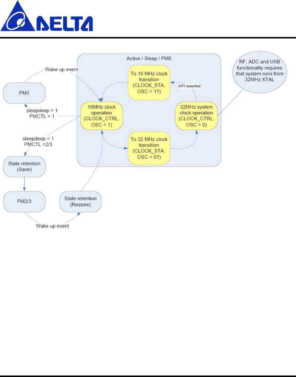
3-3.Power Management
Different operating modes, or power modes, are used to allow low-power operation. Ultralow-power operation is
obtained by turning off the power supply to modules to avoid static (leakage) power consumption and also by
using clock gating and turning off oscillators to reduce dynamic power consumption.

DFZM-TT2xx
Data Sheet Sheet 15 of 39 Feb. 3, 2016
Proprietary Information and Specifications are Subject to Change
The six various operating modes (power modes) are called active mode, Sleep mode, PM0, PM1, PM2, and PM3.
Active mode is the normal operating mode, whereas PM3 has the lowest power consumption. The impact of the
different power modes on system operation is shown in Table 3-1, together with voltage regulator and oscillator
options.
Operational Mode Power Consumption Sequencing time Functional limitations
Active Clock gating with RCGC None None
Sleep Clock gating with SCGC Enter: immediate CPU in sleep
PM0 Clock gating with DCGC Enter: immediate CPU in Deep sleep
PM1 Power down of:
• System clock source
Enter: 0.5 us
Exit: 4 us
CPU in Deep sleep
All peripherals inactive
PM2 Power down of:
• System Clock source
• Digital Power supply
Enter: 136 us
Exit: 136 us
CPU in Deep sleep (inactive)
All peripherals inactive
PM2 Power down of:
• System Clock source
• Digital Power supply
• 32 kHz Clock source
Enter: 136 us
Exit: 136 us
CPU in Deep sleep (inactive)
All peripherals inactive
Sleep Mode Timer inactive
Table 3-1: DFZM-TT2xx Power Management
Note: The RCGCXX register controls clocks in Active mode (Run mode).
The SCGCXX register controls clocks in Sleep mode.
The DCGSXX register controls clocks in PM0 (Deep Sleep mode).
When using power management in CC2538 it is important to understand the sequence of events and timing
involved in the process. A simple flow diagram for power management is shown in Figure 3-3. As can be seen
from the figure PM1, 2 and 3 are always entered from a state where the CPU is running on 16 MHz RCOSC.
DFZM-TT2xx
Data Sheet Sheet 16 of 39 Feb. 3, 2016
Proprietary Information and Specifications are Subject to Change
Figure 3-3: DFZM-TT2xx Simple Flow Diagram for Power Management
DFZM-TT2xx
Data Sheet Sheet 17 of 39 Feb. 3, 2016
Proprietary Information and Specifications are Subject to Change
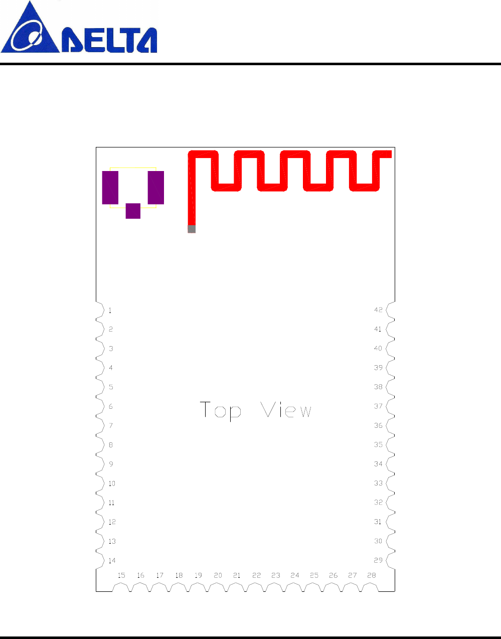
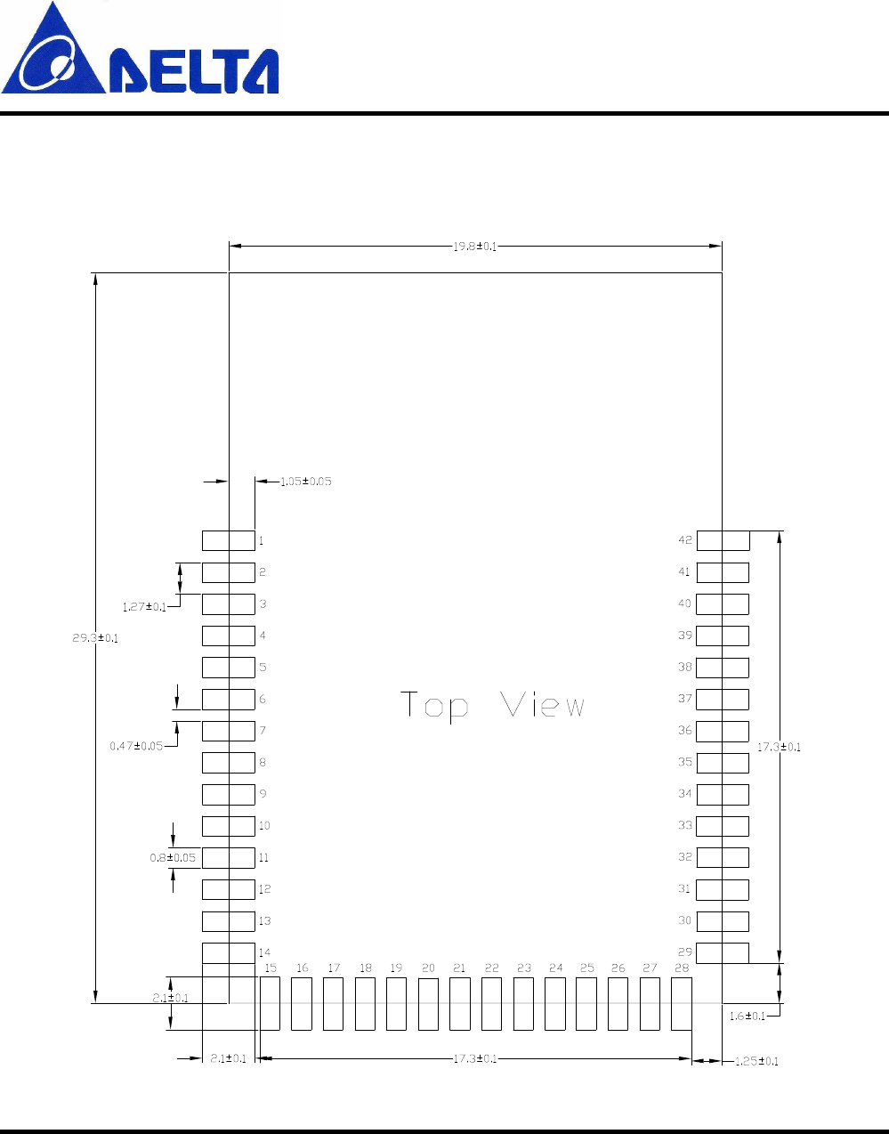
4. Pin-out and Signal Description
4-1.Device Pin-out Diagram (Module top view)
Figure 4-1: DFZM-TT2xx Device Pin-out Diagram (Module top view)

DFZM-TT2xx
Data Sheet Sheet 18 of 39 Feb. 3, 2016
Proprietary Information and Specifications are Subject to Change
4-2.Module Pins Description
Pins Name Pin Type Description
1 GND Ground Ground
2 VCC Power Power Supply Input
3 JTAG_TMS Digital I/O JTAG TMS
4 JTAG_TCK Digital I/O JTAG TCK
5 PB7 Digital I/O GPIO port B pin 7、JTAG TDO
6 PB6 Digital I/O GPIO port B pin 6、JTAG TDI
7 PB5 Digital I/O GPIO port B pin 5
8 PB4 Digital I/O GPIO port B pin 4
9 PB3 Digital I/O GPIO port B pin 3
10 PB2 Digital I/O GPIO port B pin 2
11 PB1 Digital I/O GPIO port B pin 1
12 USB_P USB I/O USB differential data plus (D+)
13 USB_N USB I/O USB differential data plus (D-)
14 GND Ground Ground
15 DVDD_USB Power (USB pads) 3.3V USB power supply connection
16 PB0 Digital I/O GPIO port B pin 0. ROM bootloader UART CTS
17 PC7 Digital I/O GPIO port C pin 7
18 PC6 Digital I/O GPIO port C pin 6
19 PC5 Digital I/O GPIO port C pin 5
20 PC4 Digital I/O GPIO port C pin 4
21 PC3 Digital I/O GPIO port C pin 3, 20 mA output capability, no pull-up or
pull-down. Not available for DFZM-TT21X-DT0R
22 PC2 Digital I/O GPIO port C pin 2, 20 mA output capability, no pull-up or
pull-down. Not available for DFZM-TT21X-DT0R
23 PC1 Digital I/O GPIO port C pin 1, 20 mA output capability, no pull-up or
pull-down
24 PC0 Digital I/O GPIO port C pin 0, 20 mA output capability, no pull-up or

DFZM-TT2xx
Data Sheet Sheet 19 of 39 Feb. 3, 2016
Proprietary Information and Specifications are Subject to Change
pull-down
25 GND Ground Ground
26 PA0 Digital I/O GPIO port A pin 0. ROM bootloader UART RXD
27 PA1 Digital I/O GPIO port A pin 1. ROM bootloader UART TXD
28 PA2 Digital I/O GPIO port A pin 2. ROM bootloader SSI CLK
29 GND Ground Ground
30 PA3 Digital I/O GPIO port A pin 3. ROM bootloader SSI SEL
31 PA4 Digital I/O GPIO port A pin 4. ROM bootloader SSI RXD
32 PA5 Digital I/O GPIO port A pin 5. ROM bootloader SSI TXD
33 PA6 Digital I/O GPIO port A pin 6
34 PA7 Digital I/O GPIO port A pin 7
35 PD0 Digital I/O GPIO port D pin 0
36 PD1 Digital I/O GPIO port D pin 1
37 PD2 Digital I/O GPIO port D pin 2. Not available for DFZM-TT21X-DT0R
38 RESET_N Digital input Reset, active low
39 PD3 Digital I/O GPIO port D pin 3. ROM bootloader UART RTS
40 PD4 Digital I/O GPIO port D pin 4
41 PD5 Digital I/O GPIO port D pin 5
42 GND Ground Ground
DFZM-TT2xx
Data Sheet Sheet 20 of 39 Feb. 3, 2016
Proprietary Information and Specifications are Subject to Change
5. Electrical Characteristics
5-1.Absolute Maximum Rating
Conditions beyond those cited in Table 5-1 may cause permanent damage to the DFZM-TT2xx, and must be
avoided.
Parameter Minimum Maximum Unit
Supply voltage(VCC) -0.3 3.9 V
Storage temperature range -40 125 ºC
Voltage on any digitai I/O -0.3 VCC+0.3, ≤3.9 V
Table 5-1: Absolute Maximum Ratings
5-2.Recommended Operating Conditions
Parameter Minimum Maximum Unit
Operating supply voltage(VCC) 2 3.6 V
Operating ambient temperature range(T
A
) -40 110 ºC
Table 5-2: Recommended Operating Conditions
5-3.Power Consumption
Test Conditions: T
A
=25 ºC, VCC=3.0V
Parameter Test conditions Mim
Typ
Max
Unit
Digital regulator on. 16MHz RCOSC running. No radio,
crystals, or peripherals active. CPU running at 16-MHz with
flash access
74 mA
I
core
Core current consumption
32MHz XOSC running. No radio or peripherals active. CPU
13 mA

DFZM-TT2xx
Data Sheet Sheet 21 of 39 Feb. 3, 2016
Proprietary Information and Specifications are Subject to Change
running at 32-MHz with flash access,.
32MHz XOSC running, radio in RX mode, –50dBm input
power, no peripherals active, CPU idle@DFZM-TT22x
20 mA
32MHz XOSC running, radio in RX mode, –50dBm input
power, no peripherals active, CPU idle@DFZM-TT21x
24 mA
32MHz XOSC running, radio in RX mode at -100dBm input power
(waiting for signal), no peripherals active, CPU idle@DFZM-TT22x 24 27 mA
32MHz XOSC running, radio in RX mode at -100dBm input
power (waiting for signal), no peripherals active, CPU
idle@DFZM-TT21x
27 mA
32MHz XOSC running, radio in TX mode, 7dBm output power, no
peripherals active, CPU idle@DFZM-TT22x 34 mA
32MHz XOSC running, radio in TX mode, 18.5dBm output power, no
peripherals active, CPU idle@DFZM-TT21x 150
mA
Power mode 1. Digital regulator on; 16MHz RCOSC and 32MHz
crystal oscillator off; 32.768kHz XOSC, POR, BOD and sleep timer
active; RAM and register retention
0.6
uA
Power mode 2. Digital regulator off; 16MHz RCOSC and 32MHz
crystal oscillator off; 32.768kHz XOSC, POR, and sleep timer active;
RAM and register retention
1.3
2 uA
Power mode 3. Digital regulator off; no clocks; POR active; RAM and
register retention 0.4
1 uA
General-
purpose
timer
Timer running, 32-MHz XOSC used 120
uA
SPI 300
uA
I
2
C 0.1
mA
UART 0.7
mA
I
peri
Peripheral
current
consumption
(Adds to core
current I
core
for
each peripheral
unit activated) Sleep
timer Including 32.753-kHz RCOSC 0.9
uA
DFZM-TT2xx
Data Sheet Sheet 22 of 39 Feb. 3, 2016
Proprietary Information and Specifications are Subject to Change
USB 48-MHz clock running, USB enabled 3.8
mA
ADC When converting 1.2
mA
Erase 12 mA
Flash Burst write peak current 8 mA
Table 5-3: Poewr Consumption
5-4.DC Characteristics
Test Conditions: T
A
=25 ºC, VCC=3.0V
Parameter Test conditions Min Typ Max Unit
Logic-0 input voltage 0.5 V
Logic-1 input voltage 2.5 V
Logic-0 input current Input equals 0 V -300 300 nA
Logic-1 input current Input equals VDD -300 300 nA
I/O-pin pullup and pulldown resistors 20 kΩ
Logic-0 output voltage, 4-mA pins Output load 4 mA 0.5 V
Logic-1 output voltage, 4-mA pins Output load 4 mA 2.4 V
Logic-0 output voltage, 20-mA pins Output load 20 mA 0.5 V
Logic-1 output voltage, 20-mA pins Output load 20 mA 2.4 V
Table 5-4: DC Characteristics
5-5.Wake-up and Timing
Test Conditions: T
A
=25 ºC, VCC=3.0V
Parameter Test conditions Min
Typ
Max
Unit
Power mode 1
active Digital regulator on, 16-MHz RCOSC and 32-MHz crystal
oscillator off. Start-up of 16-MHz RCOSC 4 us
Power mode 2 or 3
active Digital regulator off, 16-MHz RCOSC and 32-MHz crystal 136
us
DFZM-TT2xx
Data Sheet Sheet 23 of 39 Feb. 3, 2016
Proprietary Information and Specifications are Subject to Change
Parameter Test conditions Min
Typ
Max
Unit
oscillator off. Start-up of regulator and 16-MHz RCOSC
Initially running on 16-MHz RCOSC, with 32-MHz XOSC OFF 0.5 ms
Active
TX or RX With 32-MHz XOSC initially on 192
us
RX/TX and TX/RX turnaround
192
us
USB PLL start-up time With 32-MHz XOSC initially on 32 us
Table 5-5: Wake-up and Timing
5-6.Radio Parameters
Test Conditions: T
A
=25 ºC, VCC=3.0V
Parameter Min Typ Max Unit Notes
RF Frequency range 2394 2507 MHz
Radio baud rate 250 Kbps
Radio chip rate 2 Mchip/s
Flash erase cycles 20 K cycles
Flash page size 2 KB
TX/RX specification for DFZM-TT22x
Output power 7 dBm
Error vector magnitude (EVM) 3 %
Frequency error tolerance -30 0 30 ppm
Receiver sensitivity -97 -92 dBm PER = 1%,
Saturation(Maximum input level) 10 dBm PER = 1%,
TX/RX specification for DFZM-TT21x
Output power 18.5 dBm
Error vector magnitude (EVM) 3 %
Frequency error tolerance -30 0 30 ppm
Receiver sensitivity -99 -92 dBm PER = 1%,
DFZM-TT2xx
Data Sheet Sheet 24 of 39 Feb. 3, 2016
Proprietary Information and Specifications are Subject to Change
Parameter Min Typ Max Unit Notes
Saturation(Maximum input level) 10 dBm PER = 1%,
Table 5-6: Radio Parameters
5-7.ADC Parameters
Test Conditions: T
A
=25 ºC, VCC=3.0V
Parameter Test Condiction Min Typ
Max
Unit
Input voltage 0 VCC
V
External reference voltage 0 VCC
V
External reference voltage differential 0 VCC
V
Input resistance, signal Using 4-MHz clock speed 197
kΩ
Full-scale signal(1) Peak-to-peak, defines 0 dBFS 2.97
V
Single-ended input, 7-bit setting 5.7
Single-ended input, 9-bit setting 7.5
Single-ended input, 10-bit setting 9.3
Single-ended input, 12-bit setting 10.8
Differential input, 7-bit setting 6.5
Differential input, 9-bit setting 8.3
Differential input, 10-bit setting 10.0
ENOB(1)
Effective number of bits
Differential input, 12-bit setting 11.5
bits
Useful power bandwidth 7-bit setting, both single and differential 0 20
KHz
Single-ended input, 12-bit setting, –6 dBFS
-75.2
THD(1)
Total harmonic distortion Differential input, 12-bit setting, –6 dBFS -86.6
dB
Single-ended input, 12-bit setting 70.2
Differential input, 12-bit setting 79.3
Single-ended input, 12-bit setting, –6 dBFS
78.8
Signal to nonharmonic ratio(1)
Differential input, 12-bit setting, –6 dBFS 88.9
dB

DFZM-TT2xx
Data Sheet Sheet 25 of 39 Feb. 3, 2016
Proprietary Information and Specifications are Subject to Change
CMRR
Common-mode rejection ratio
Differential input, 12-bit setting, 1-kHz sine
(0 dBFS), limited by ADC resolution 84
dB
Crosstalk Differential input, 12-bit setting, 1-kHz sine
(0 dBFS), limited by ADC resolution 84
dB
Offset Midscale -3
mV
Gain error 0.68
%
12-bit setting, mean 0.05
DNL(1)
Differential nonlinearity 12-bit setting, maximum 0.9
LSB
12-bit setting, mean 4.6 INL(1)
Integral nonlinearity 12-bit setting, maximum 13.3
LSB
Single-ended input, 7-bit setting 35.4
Single-ended input, 9-bit setting 46.8
Single-ended input, 10-bit setting 57.5
Single-ended input, 12-bit setting 66.6
Differential input, 7-bit setting 40.7
Differential input, 9-bit setting 51.6
Differential input, 10-bit setting 61.8
SINAD(1) (–THD+N)
Signal-to-noise-and-distortion
Differential input, 12-bit setting 70.8
dB
7-bit setting 20
9-bit setting 36
10-bit setting 68
Conversion time
12-bit setting 132
us
Internal reference voltage 1.19
V
Internal reference VCC coefficient 2
mV/V
Internal reference temperature coefficient
0.4
mV/10°C
Table 5-7: ADC Parameters
(1) Measured with 300-Hz sine-wave input and VCC as reference.
DFZM-TT2xx
Data Sheet Sheet 26 of 39 Feb. 3, 2016
Proprietary Information and Specifications are Subject to Change
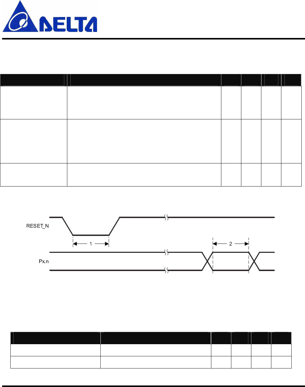
5-8.Control Input AC Characteristics
Test Conditions: T
A
= -40~110 ºC, VCC= 2.0~3.6V
Parameter Test conditions Mim
Typ
Max
Unit
System clock, f
SYSCLK
T
SYSCLK
= 1/f
SYSCLK
The undivided system clock is 32 MHz when crystal oscillator is
used. The undivided system clock is 16 MHz when calibrated
16-MHz RC oscillator is used.
16 32 MHz
RESET_N low duration
See item 1, Figure 5-1. This is the shortest pulse that is
recognized as a complete reset pin request. Note that shorter
pulses may be recognized but might not lead to complete reset
of all modules within the chip.
1 us
Interrupt pulse duration See item 2, Figure 5-1.This is the shortest pulse that is
recognized as an interrupt request. 20 ns
Table 5-8: Control Input AC Characteristics
Figure 5-1: SPI Master AC Characteristics
5-9.USB Interface DC Characteristics
Test Conditions: T
A
= 25 ºC, VCC= 3.0~3.6V
Parameter Test conditions Mim
Typ
Max
Unit
USB pad voltage output, high
VCC 3.6 V, 4-mA load 3.4 V
USB pad voltage output, low VCC 3.6 V, 4-mA load 0.2 V
DFZM-TT2xx
Data Sheet Sheet 27 of 39 Feb. 3, 2016
Proprietary Information and Specifications are Subject to Change
6. Package and Layout Guidelines
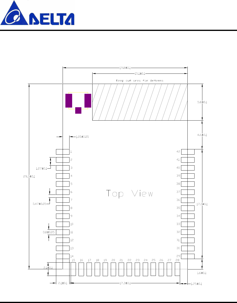
6-1.Recommended PCB Footprint and Dimensions
Figure 6-1: DFZM-TT2xx Module Recommended PCB Footprint (in mm)
DFZM-TT2xx
Data Sheet Sheet 28 of 39 Feb. 3, 2016
Proprietary Information and Specifications are Subject to Change
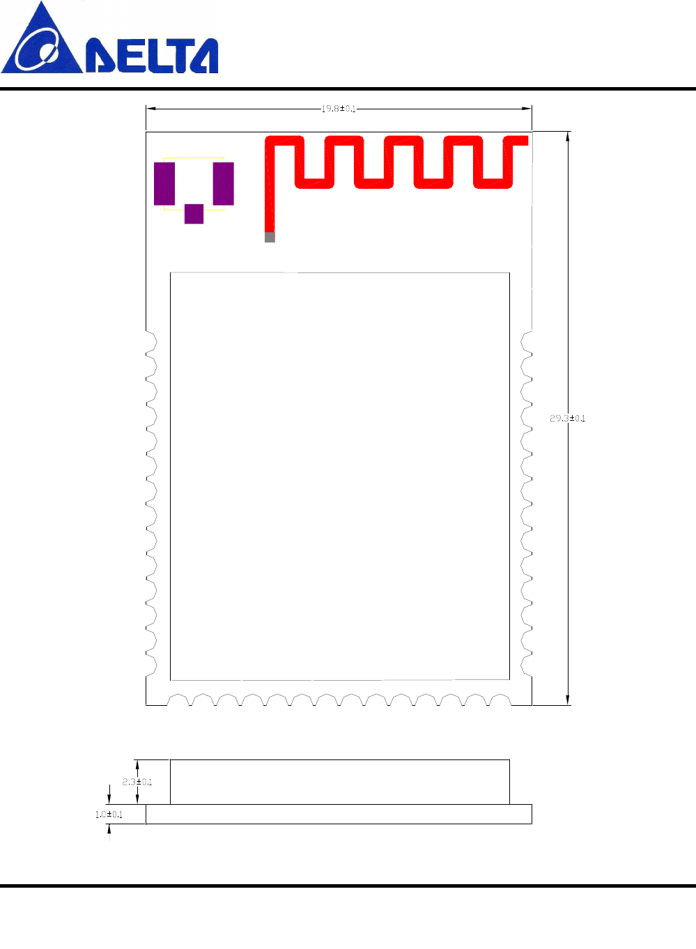
Figure 6-2: DFZM-TT2xx Module Dimensions (in mm)
DFZM-TT2xx
Data Sheet Sheet 29 of 39 Feb. 3, 2016
Proprietary Information and Specifications are Subject to Change
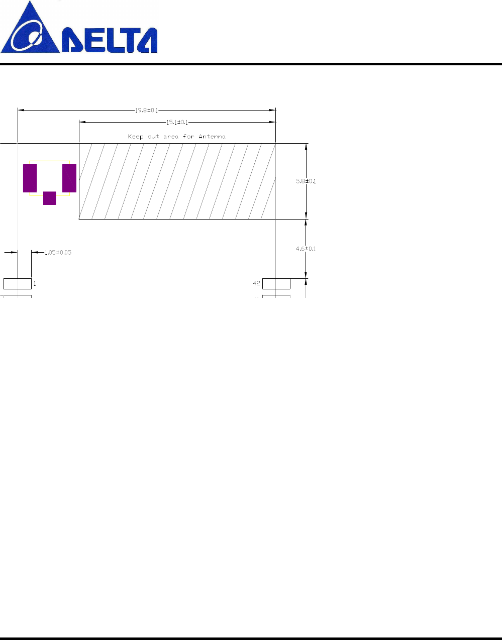
6-2.Layout Guidelines
Figure 6-3: DFZM-TT2xx module onboard antenna keep-out layout guidelines (in mm)
Notes:
1. All Dimensions are in mm. Tolerances shall be ±0.10 mm.
2. Absolutely no metal trace or ground layer underneath this area.
3. It is recommended not to run circuit traces underneath the module.
4. In performing SMT or manual soldering of the module to the base board, please align the two row of pins.
In addition to the guidelines in Figure 6-3, note the following suggestions:
DFZM-TT2xx
• External Bypass capacitors for all module supplies should be as close as possible to the module pins.
• Never place the antenna very close to metallic objects.
• The external dipole antennas need a reasonable ground plane area for antenna efficiency.
DFZM-TT221; DFZM-TT211 onboard antenna specific
• The onboard antenna keep out area, as shown in Figure 6-3, must be adhered to. In addition it is
recommended to have clearance above and below the PCB trace antenna (Figure 6-4) for optimal range
performance.
Keep out area for onboard antenna. All layers on the
PCB must be clear.
(i.e. No GND, Power trace/plane, traces.)
Note: If guidelines are not followed, DFZM-TT2xx
range with onboard chip antenna will be compromised.
DFZM-TT2xx
Data Sheet Sheet 30 of 39 Feb. 3, 2016
Proprietary Information and Specifications are Subject to Change
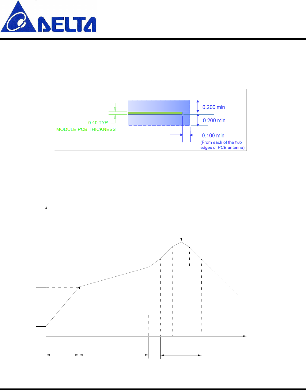
• Do not use a metallic or metalized plastic for the end product enclosure.
• Recommendation is to keep plastic enclosure clearance of 1cm from top and bottom of the DFZM-TT2xx
onboard antenna keep-out area, if possible. 5-mm (0.2 in) clearance shall be the minimum as shown in
Figure 6-4.
Figure 6-4 Recommended clearance above and below the PCB trace antenna
6-2-1.Surface Mount Assembly
The reflow profile is shown in Figure 6-8.
60-180 sec
Room temp.
50 sec max
150
200
245
217
(°C )
60-150 sec
Time
Peak temp
250°c max 10 sec max
245°c±5°c for
10 ~30 sec
Figure 6-5: Reflow temperature profile

DFZM-TT2xx
Data Sheet Sheet 31 of 39 Feb. 3, 2016
Proprietary Information and Specifications are Subject to Change
Note:
1. Perform adequate test in advance as the reflow temperature profile will vary accordingly to the
conditions of the parts and boards, and the specifications of the reflow furnace.
2. Be careful about rapid temperature rise in preheat zone as it may cause excessive slumping of the
solder paste.
3. If the preheat is insufficient, rather large solder balls tend to be generated. Conversely, if performed
excessively, fine balls and large balls will generate in clusters at a time.
4. If the temperature is too low, non-melting tends to be caused in the area with large heat capacity after
reflow.
5. Be careful about sudden rise in temperature as it may worsen the slump of solder paste.
6. Be careful about slow cooling as it may cause the positional shift of parts and decline in joining
strength at times.
DFZM-TT2xx
Data Sheet Sheet 32 of 39 Feb. 3, 2016
Proprietary Information and Specifications are Subject to Change
6-3.Recommended Stencil Aperture
Note: The thickness of the stencil should be 0.15mm over this area.
Figure 6-9: DFZM-TT2xx recommended stencil aperture
DFZM-TT2xx
Data Sheet Sheet 33 of 39 Feb. 3, 2016
Proprietary Information and Specifications are Subject to Change
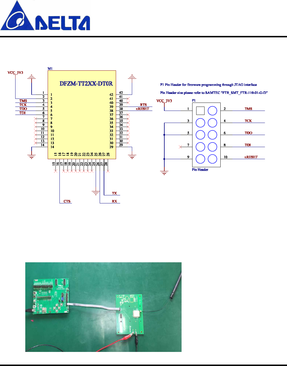
7. Reference Design Schematic
8. DUT Setup
DUT 接線請參考下圖
DUT 與系統板用排 PIN 對接
外接電源 3V3,電流量 500mA
DFZM-TT2xx
Data Sheet Sheet 34 of 39 Feb. 3, 2016
Proprietary Information and Specifications are Subject to Change
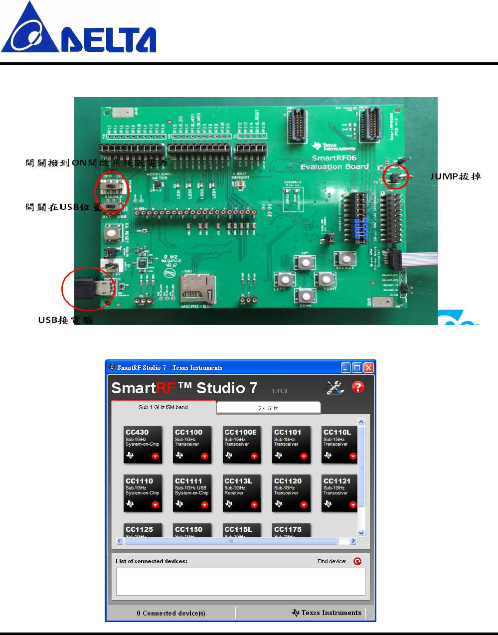
系統板接線如下圖:
開啟 RF Studio 7 如下圖所示:
DFZM-TT2xx
Data Sheet Sheet 35 of 39 Feb. 3, 2016
Proprietary Information and Specifications are Subject to Change
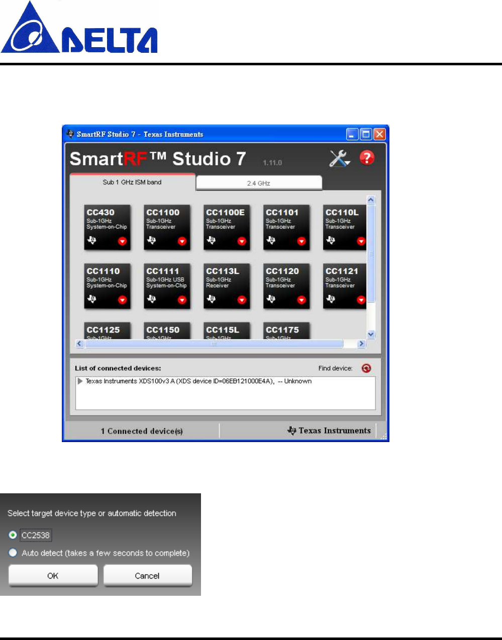
系統板及 DUT 上電後按下右下角 FIND DEVICE 會出現如下圖裝置在 LIST 中
double click list 中的裝置
double click list 中的裝置後出現下圖選 CC2538 按下 OK 進入 control panel
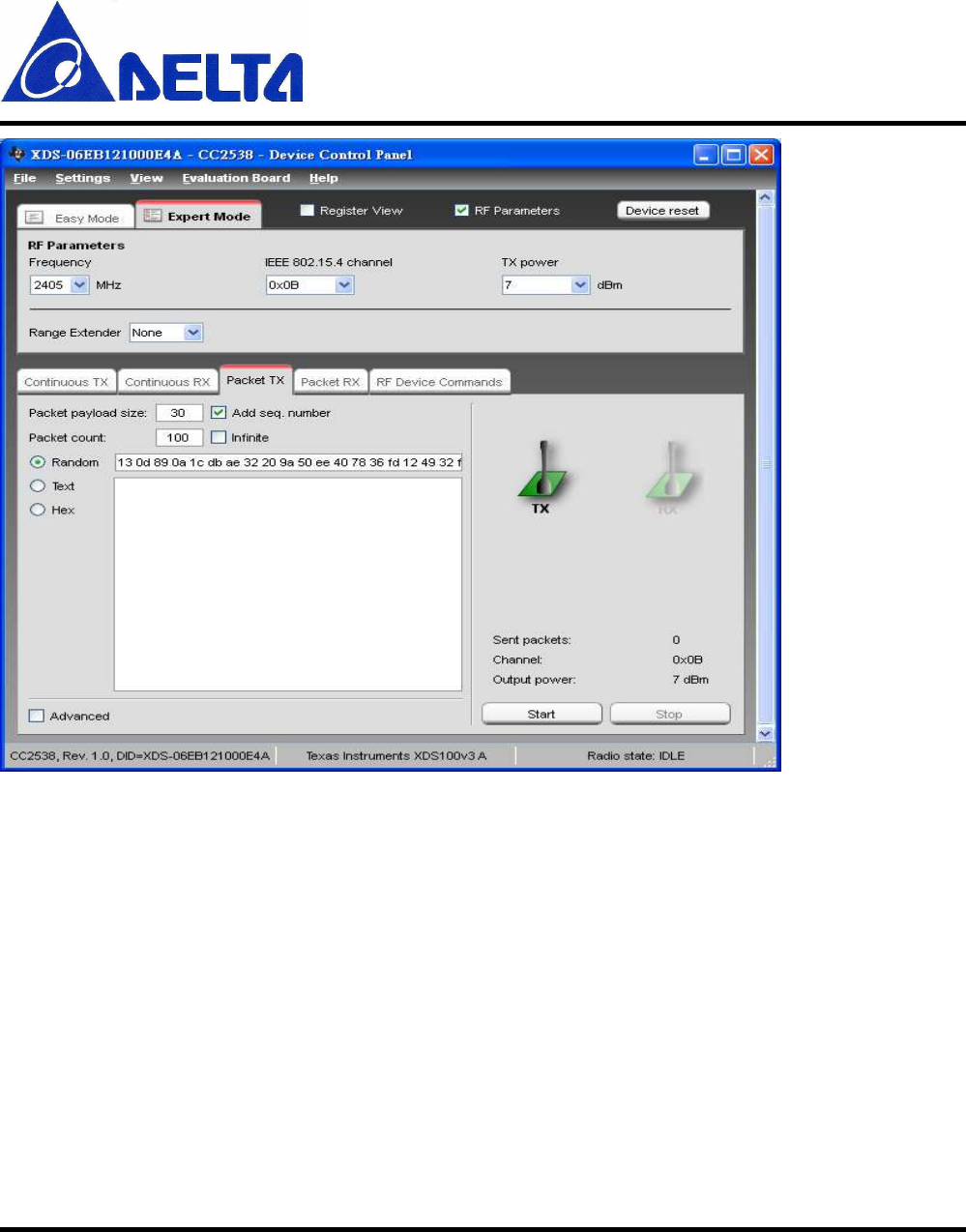
DFZM-TT2xx
Data Sheet Sheet 36 of 39 Feb. 3, 2016
Proprietary Information and Specifications are Subject to Change
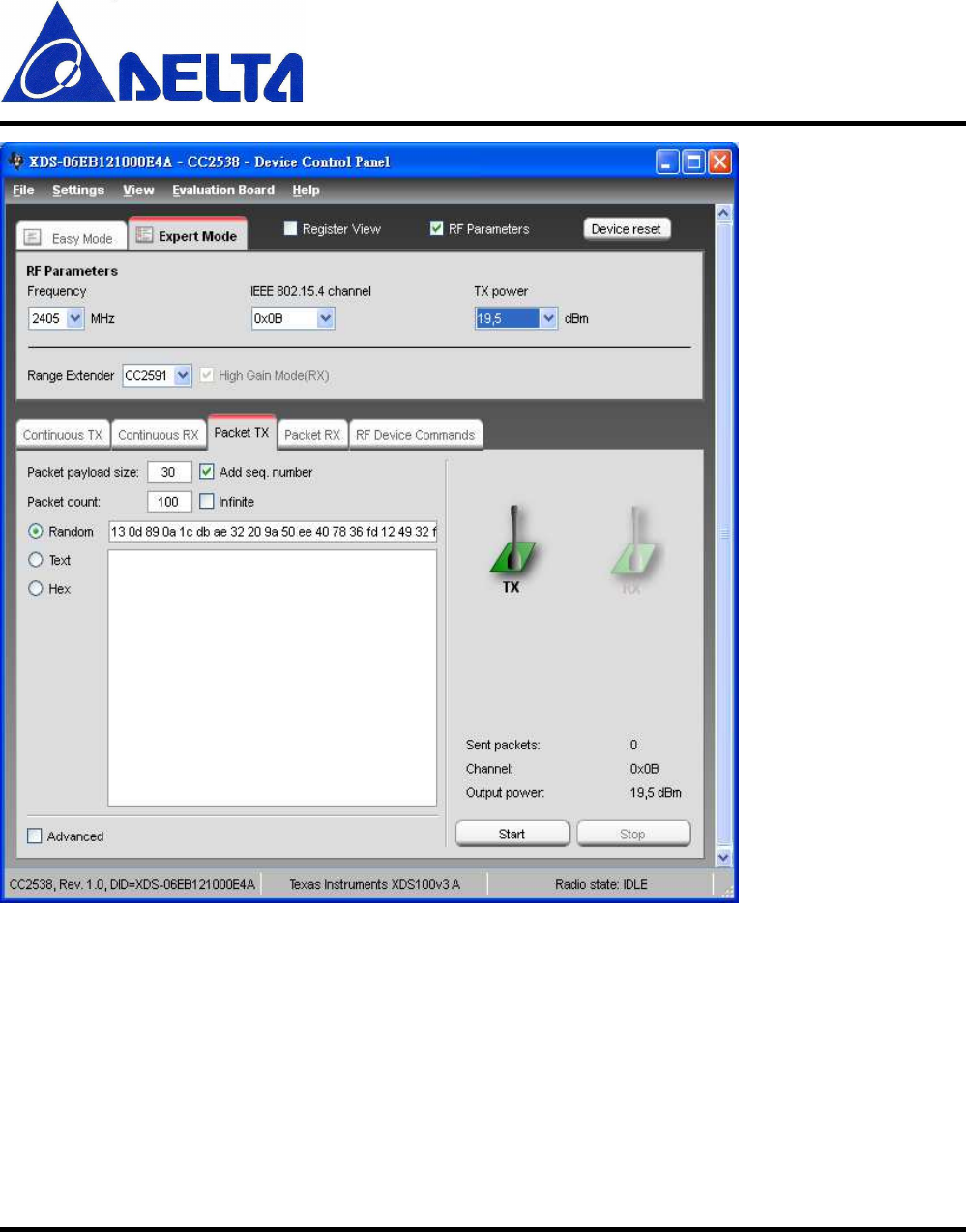
Ranger extender 選CC2591
Frequency selection on left-top, TX power choose 19.5 dBm
DFZM-TT2xx
Data Sheet Sheet 37 of 39 Feb. 3, 2016
Proprietary Information and Specifications are Subject to Change

DFZM-TT2xx
Data Sheet Sheet 38 of 39 Feb. 3, 2016
Proprietary Information and Specifications are Subject to Change
9. Federal Communications Commission (FCC)
Statement
15.21
You are cautioned that changes or modifications not expressly approved by the part
responsible for
compliance could void the user’s authority to operate the equipment.
15.105(b)
This equipment has been tested and found to comply with the limits for a Class B digital device,
pursuant to part 15 of the FCC rules. These limits are designed to provide reasonable
protection against
harmful interference in a residential installation. This equipment generates, uses and can
radiate radio
frequency energy and, if not installed and used in accordance with the instructions, may cause
harmful
interference to radio communications. However, there is no guarantee that interference will not
occur in
a particular installation. If this equipment does cause harmful interference to radio or television
reception, which can be determined by turning the equipment off and on, the user is
encouraged to try to
correct the interference by one or more of the following measures:
-Reorient or relocate the receiving antenna.
-Increase the separation between the equipment and receiver.
-Connect the equipment into an outlet on a circuit different from that to which the receiver is
connected.
-Consult the dealer or an experienced radio/TV technician for help.
This device complies with Part 15 of the FCC Rules. Operation is subject to the following two
conditions:
1) this device may not cause harmful interference, and
2) this device must accept any interference received, including interference that may cause

DFZM-TT2xx
Data Sheet Sheet 39 of 39 Feb. 3, 2016
Proprietary Information and Specifications are Subject to Change
undesired
operation of the device.
FCC RF Radiation Exposure Statement:
This equipment complies with FCC radiation exposure limits set forth for an uncontrolled
environment.
This equipment should be installed and operated with minimum distance 20cm between the
radiator & your body. This transmitter must not be co-located or operating in conjunction with
any other antenna or transmitter.
For modular approval, the following information needs to be in user manual:
Information for the OEMs and Integrators
The following statement must be included with all versions of this document supplied to an
OEM or integrator, but should not be distributed to the end user.
This device is intended for OEM integrators only.
Please See the full Grant of Equipment document for other restrictions.
Information To Be Supplied to the End User by the OEM or Integrator:
The following regulatory and safety notices must be published in documentation supplied to the
end user of the product or system incorporating an adapter in compliance with local regulations.
Host system must be labeled with "Contains FCCID:H79DFZM-TT211“, FCC ID displayed on
label.