Dialog Semiconductor SC14D DECT Module User Manual AN D 212 1v0
Dialog Semiconductor BV DECT Module AN D 212 1v0
Contents
- 1. User Manual
- 2. user manual SC14CVMDECT
- 3. user manual SC14WAMDECT
user manual SC14CVMDECT

Application Note
SC14CVMDECT External Antenna
Design and Leveraging Modular
Approval
AN-D-212
Abstract
This document describes the external antenna design of the SC14CVMDECT_SFxx_DB reference design and how
to leverage the existing Dialog regulatory certification when copying this design.

Application Note Revision 1.0 04-Oct-2017
CFR0014-01 2 of 9 © 2013 Dialog Semiconductor
AN-D-212
SC14CVMDECT External Antenna Design and Leveraging Modular Approval
Contents
1 Introduction . . . . . . . . . . . . . . . . . . . . . . . . . . . . . . . . 3
1.1 TERMS AND ABBREVIATIONS . . . . . . . . . . . . 3
1.2 REFERENCES . . . . . . . . . . . . . . . . . . . . . . . . . 3
1.3 HISTORY . . . . . . . . . . . . . . . . . . . . . . . . . . . . . 3
1.4 DISCLAIMER . . . . . . . . . . . . . . . . . . . . . . . . . . 3
2 Modular Approval . . . . . . . . . . . . . . . . . . . . . . . . . . . 4
2.1 DESCRIPTION . . . . . . . . . . . . . . . . . . . . . . . . . 4
2.2 AVAILABLE CERTIFICATIONS . . . . . . . . . . . . 4
2.3 APPLICABILITY . . . . . . . . . . . . . . . . . . . . . . . . 4
2.4 CONDITIONS . . . . . . . . . . . . . . . . . . . . . . . . . . 4
2.4.1 Antenna . . . . . . . . . . . . . . . . . . . . . . . . . . 4
2.4.2 Host PCB Layout . . . . . . . . . . . . . . . . . . . 4
2.4.3 Labelling Requirements . . . . . . . . . . . . . . 4
2.4.4 User Documentation Text. . . . . . . . . . . . . 5
2.4.5 Safety Requirements . . . . . . . . . . . . . . . . 5
2.5 SAR . . . . . . . . . . . . . . . . . . . . . . . . . . . . . . . . . . 5
2.6 MISCELLANEOUS COMMENTS . . . . . . . . . . . 5
3 External Antenna Design . . . . . . . . . . . . . . . . . . . . . 6
3.1 SC14CVMDECT_SFXX_DB ANTENNA DESIGN
. . . . . . . . . . . . . . . . . . . . . . . . . . . . . . . . . . . . 6
3.1.1 Printed Antenna Design Details . . . . . . . . 6
3.1.2 Printed Antenna Design Operating at 1.8
GHz . . . . . . . . . . . . . . . . . . . . . . . . . . . . 7
3.1.3 Boundary Conditions . . . . . . . . . . . . . . . . 7
3.2 TUNING COMPONENTS . . . . . . . . . . . . . . . . . 7
3.3 OTHER ANTENNAS . . . . . . . . . . . . . . . . . . . . . 8

Application Note Revision 1.0 04-Oct-2017
CFR0014-01 3 of 9 © 2013 Dialog Semiconductor
AN-D-212
SC14CVMDECT External Antenna Design and Leveraging Modular Approval
1 Introduction
The SC14SCMDECT_SFxx_DB Reference Design has
been made available by Dialog Semiconductor that
includes an additional printed antenna to support FAD
(e.g. for FP operation). This design has obtained a
Modular Approval Certificate (US, EU). When meeting
the conditions as referenced in this document, this
implies that those tests already covered by the Modular
Approval Certificate don’t need to be rerun on the end-
product level. This may alleviate the overall regulatory
approval process of the end-product.
1.1 TERMS AND ABBREVIATIONS
DoC Declaration of Conformity
EU Europe
ETSI European Telecommunications Stand-
ards Institute
FAD Fast Antenna Diversity
FCC Federal Communications Commission
FP Fixed Part
IC Industry Canada
JP Japan
KDECT Korean DECT
MIC Ministry of Internal affairs and Com-
munications
SAR Specific Absorption Rate
TCF Technical Construction File
1.2 REFERENCES
1. SC14CVMDECT SF01 Datasheet v1.00 Data
sheet, Dialog Semiconductor B.V.
2. FCC document “DA-00-1407”
3. FCC document "784748 D01 Labelling Part 15
18 Guidelines v07"
4. FCC document “D01 Mobile Portable RF Expo-
sure v04”
5. FCC order “04-165”
1.3 HISTORY
10-Jul-2013, v0.1 Initial version.
19-Jul-2013, v0.2 Added 1.8 GHz.
31-Jul-2013, v0.3 Added FCC/IC number.
04-Oct-2017, v1.0 Section 3.2: Pi attenuator added.
Figure 1 updated.
1.4 DISCLAIMER
This document is for general information purposes
only. Dialog Semiconductor B.V. does not guarantee
the completeness, correctness or accuracy of the infor-
mation in this document and shall not be liable for any
direct or indirect loss or damage arising from the use of
information or documents found in it.
Please consult with your test house when planning for
and/or undertaking any action with respect to regula-
tory certification.
Application Note Revision 1.0 04-Oct-2017
CFR0014-01 4 of 9 © 2013 Dialog Semiconductor
AN-D-212
SC14CVMDECT External Antenna Design and Leveraging Modular Approval
2 Modular Approval
2.1 DESCRIPTION
When a wireless module has passed the Modular
Approval process, and when the host PCB design con-
forms to certain conditions (this will be detailed in the
subsequent sections), then the end-product containing
this module will not need to be tested against the regu-
latory standards covered by the module’s certificates.
The availability of the Modular Approval is intended to
reduce time, cost and effort putting an end-product
containing CVMDECT on the market.
2.2 AVAILABLE CERTIFICATIONS
Dialog Semiconductor B.V. has obtained the following
limited modular approvals for CVMDECT:
• FCC Part 15, subpart D, Isochronous UPCS Device
1920-1930 MHz: FCC ID Y82-SC14D
• IC RSS-213, issue 2, 2 GHz License-exempt Per-
sonal Communications Service Devices:
IC ID 9576A-SC14D
• In addition, testing has shown compliance to the fol-
lowing:
• EU testing (to be used in the DoC process when
applicable:
• Emissions EN 301-406
• Immunity EN 301-489
• CE IECEN 60950-1
• SAR EN 62311
• JP Radio Law pre-test
2.3 APPLICABILITY
Only FCC (US) and IC (Canada) officially support Mod-
ular Certification.
ETSI (Europe) doesn’t supports Modular Certification,
rather Declaration of Conformity (DoC). The manufac-
turer is responsible for the compliance to regulatory
requirements. Previous testing, such as made avail-
able by Dialog Semiconductor B.V., may be taken into
consideration by the module integrator. If module test-
ing is trusted for the DoC of the host, the module’s
Technical Construction File (TCF) becomes part of the
host’s TCF.
This is part of the “self certification” process where the
end-product OEM declares conformity to regulatory
requirements. The available ETSI test reports may be
used to this purpose and the tests in these reports
don’t need to be repeated on end-product/system level.
MIC (Japan) announced that it would allow modular
approvals in Japanese Radio Law (Feb ‘13). Require-
ments are being developed now. Currently, there is no
timeline or estimated implementation date. Modular
Certification is still judged on a case-by-case basis.
Other countries may not support Modular Certification.
The available test reports may help expedite the sys-
tem level certification process though.
Any regulatory standards not covered by the available
Modular Approval certificates will still need to be tested
on end-product/system level.
2.4 CONDITIONS
The FCC document “DA-00-1407” provides a clear
overview of the conditions applicable to the host, asso-
ciated with leveraging existing Modular Approval.
With respect to the SC14CVMDECT_SFxx_DB Refer-
ence Design, the following subsections reference the
relevant conditions that have to be met. Not adhering
to these will invalidate the certification, requiring recer-
tification on end-product/system level.
2.4.1 Antenna
The FCC document “DA-00-1407” specifies:
• The antenna gain of a new antenna should be of the
same type as the originally approved antenna and
the antenna gain should not be higher than the
antenna gain of the originally tested antenna.
• The emission levels or reported RF safety levels
shall not be increased by the new antenna (of the
same antenna type)
• If the new antenna is a different type, recertification
on end-product/system level is required.
With the existing SC14CVMDECT_SFxx_DB certifica-
tion this implies the following:
• If only the embedded/internal antenna of CVMDECT
is used, then the Antenna Condition is fulfilled
• If an external antenna is connected to CVMDECT,
then this antenna would need to meet specific crite-
ria in order to prevent recertification requirements.
Please refer to section 3.0 for further details.
2.4.2 Host PCB Layout
The PCB layout of the host PCB is critical to the validity
of the RF certification of CVMDECT because it is part
of the embedded printed antenna. Please refer to sec-
tions 7.4 and 7.5 of the SC14CVMDECT SFxx data-
sheet for details.
2.4.3 Labelling Requirements
The modular transmitter must be labelled with its own
FCC ID number. If the FCC ID is not visible when the
module is installed inside another device, then the host
device must contain the FCC ID number with the state-
ment such as the following:
"Contains FCC ID:Y82-SC14D",
“Contains IC ID:9576A-SC14D”.
Some further details about labelling requirements and
compliance statements can be found in "784748 D01
Labelling Part 15 18 Guidelines v07".

Application Note Revision 1.0 04-Oct-2017
CFR0014-01 5 of 9 © 2013 Dialog Semiconductor
AN-D-212
SC14CVMDECT External Antenna Design and Leveraging Modular Approval
2.4.4 User Documentation Text
The literature provided to the end user must include the
following wording:
“FCC compliance statement
This device complies with Part 15 of the FCC Rules.
Operation is subject to the following two conditions:
(1) this device may not cause harmful interference, and
(2) this device must accept any interference received,
including interference that may cause undesired opera-
tion of the device.
Module transmetteur ID IC:
Son fonctionnement est soumis aux deux conditions
suivantes:
(1) cet appareil ne doit pas causer d’interférences nuis-
ibles et
(2) appareil doit accepter toute interference recue, y
compris les interferences qui peuvent pertuber le fonc-
tionnement.
Changes or modifications to the equipment not
expressly approved by the Party responsible for com-
pliance could void the user's authority to operate the
equipment.
NOTE: This equipment has been tested and found to
comply with the limits for a Class B digital device, pur-
suant to Part 15 of the FCC Rules. These limits are
designed to provide reasonable protection against
harmful interference in a residential installation. This
equipment generates, uses and can radiate radio fre-
quency energy and, if not installed and used in accor-
dance with the instructions, may cause harmful
interference to radio communications. However, there
is no guarantee that interference will not occur in a par-
ticular installation. If this equipment does cause harm-
ful interference to radio or television reception, which
can be determined by turning the equipment off and
on, the user is encouraged to try to correct the interfer-
ence by one or more of the following measures:
• Reorient or relocate the receiving antenna
• Increase the separation between the equipment and
receiver
• Connect the equipment into an outlet on a circuit dif-
ferent from that to which the receiver is connected.
• Consult the dealer or an experienced radio/TV tech-
nician for help.
Privacy of communications may not be ensured when
using this phone.”
2.4.5 Safety Requirements
This section provides of an overview of the safety
requirements you must adhere to when working with
CVMDECT.
• The specific external power supply for CVMDECT
has to fulfil the requirements according to clause 2.5
(Limited power source) of this standard EN 60950-
1:2006.
• Interconnection circuits shall be selected to provide
continued conformance to the requirements of
clause 2.2 for SELV (Safety Extra Low Voltage) cir-
cuits according to EN 60950-1:2006 after making
connections
• Interface type not subjected to over voltages
• Requirements additional to those specified in this
standard may be necessary for:
• Equipment intended for operation in special envi-
ronments (for example, extremes of temperature,
excessive dust, moisture or vibration, flammable
gases and corrosive or explosive atmospheres)
• Equipment intended to be used in vehicles, on
board ships or aircraft, in tropical countries or at
altitudes greater than 2000 m
• Equipment intended for use where ingress of
water is possible
• Installation by qualified personnel only
• The product is a component intended for installation
and use in complete equipment. The final accep-
tance of the component is dependent upon its instal-
lation and use in complete equipment
2.5 SAR
Because SAR is very device-specific, FCC rules do not
allow for a (Limited) Modular Approval for use with por-
table devices (i.e. devices <20 cm from the human
body).
If time-averaged output power is <60/f(GHz) mW or all
measured 1-g SAR are <0.4 W/kg then modular
approval may still be allowed for portable devices.
Please refer to FCC document “D01 Mobile Portable
RF Exposure v04”.
SAR test reports are available as a reference, showing
compliance to regulatory requirements (with respect to
Portable Equipment).
2.6 MISCELLANEOUS COMMENTS
In FCC terminology, a “Host” is what is referred to in
DECT as a “fixed part”. The FCC term “Mobile” corre-
sponds with the DECT term “portable part”, provided
that the device is >20 cm from the human body. A
DECT termed “portable part” <20 cm from the human
body is referred to as “Portable” in FCC terminology.
The existing Modular Approval may be invalidated if
CVMDECT is co-located with other wireless devices
(e.g. BlueTooth, WLAN/WiFi) that transmit simultane-
ously. Please consult with your test house on the possi-
ble implications.
Application Note Revision 1.0 04-Oct-2017
CFR0014-01 6 of 9 © 2013 Dialog Semiconductor
AN-D-212
SC14CVMDECT External Antenna Design and Leveraging Modular Approval
3 External Antenna Design
FCC-04-165 now allows different antennas may be
certified with one module. Dialog Semiconductor B.V.
has obtained Modular Approval for
theSC14CVMDECT_SFxx_DB Reference Design
using a specific external printed antenna. FCC-04-165
dictates that the certification measurements must to be
performed with the highest gain antenna and any other
antenna must have a similar radiation pattern.
In case of the SC14CVMDECT_SFxx_DB certification,
this implies that an external antenna may be connected
to radio module, without requiring recertification, pro-
vided that:
• the antenna gain is not higher than 0 dBi
• the antenna type is a (printed) monopole
In addition, if the antenna connection is user accessi-
ble, then the antenna connector shall be proprietary.
3.1 SC14CVMDECT_SFXX_DB ANTENNA DESIGN
The SC14CVMDECT_SFxx_DB Reference Design
includes a SC14CVMDECT SFxx module and an addi-
tional printed antenna to support FAD (e.g. to operate
as an FP).
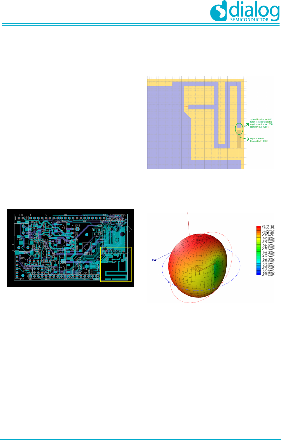
Figure 1: SC14CVMDECT_SFxx_DB Reference
Design Overiew
In Figure 1 an overview is given of the
SC14CVMDECT_SFxx_DB Reference Design. In the
middle right section the SF module can be seen. The
printed antenna occupies the lower right part in Figure
1.
This Reference Design is an example application
design. The key part of this design, in relation to wire-
less performance and leveraging existing Modular
Approval, is the section of the printed antenna in the
lower right corner, together with its location and con-
nection with respect to the SF module, as well as the
ground plane contours. This relevant section is high-
lighted by the light green rectangle in Figure 1.
The gerber files of this design can be obtained through
your Dialog Semiconductor sales contact or represen-
tative.
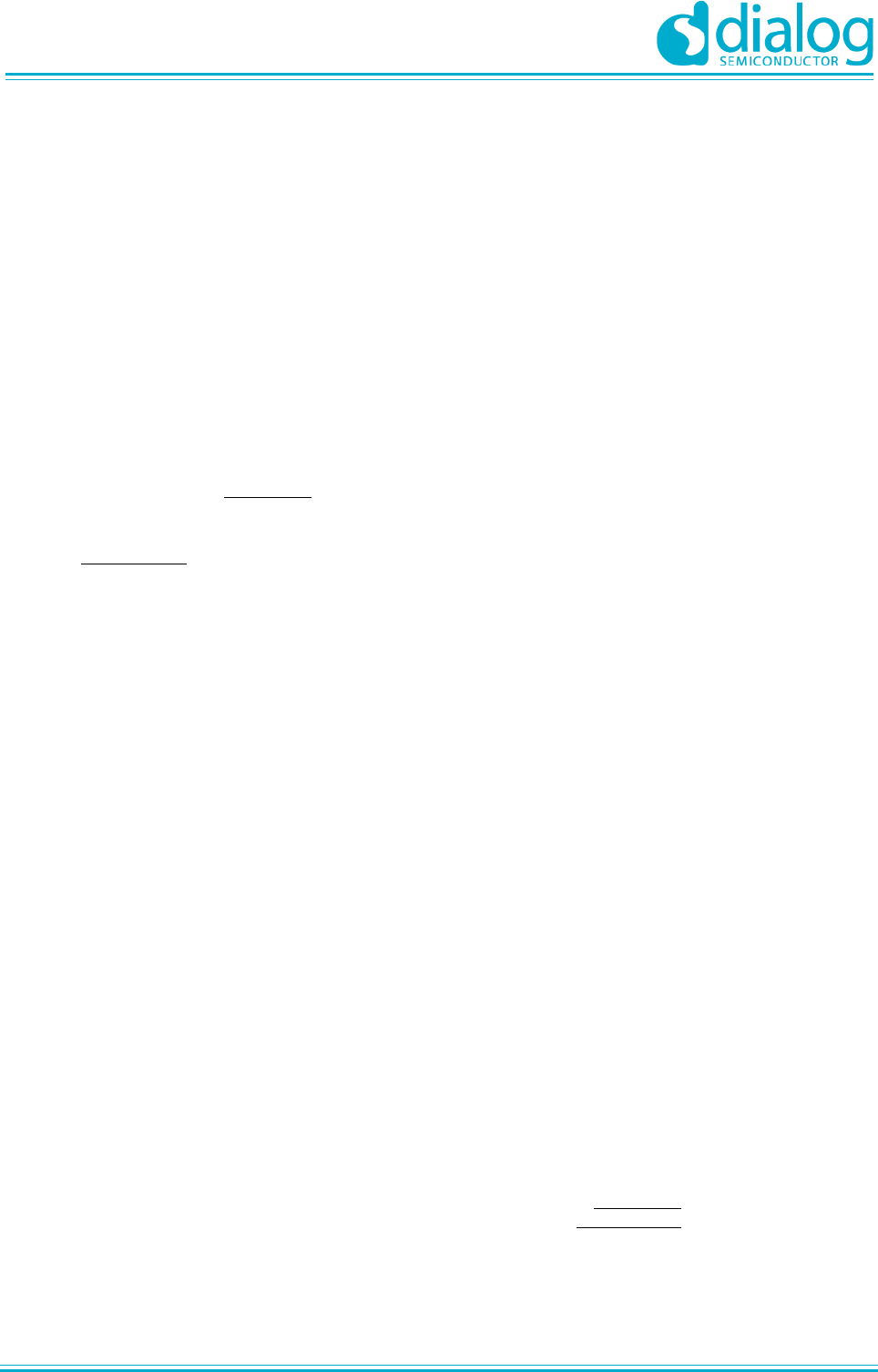
3.1.1 Printed Antenna Design Details
The printed antenna physical design is shown in Figure
2 (noting the 0.5 mm grid in the picture).
Figure 2: Printed Antenna Physical Structure
The simulated radiation pattern is depicted in the fol-
lowing plot (with no 0402 component in Figure 2):
Figure 3: Simulated Radiation Pattern
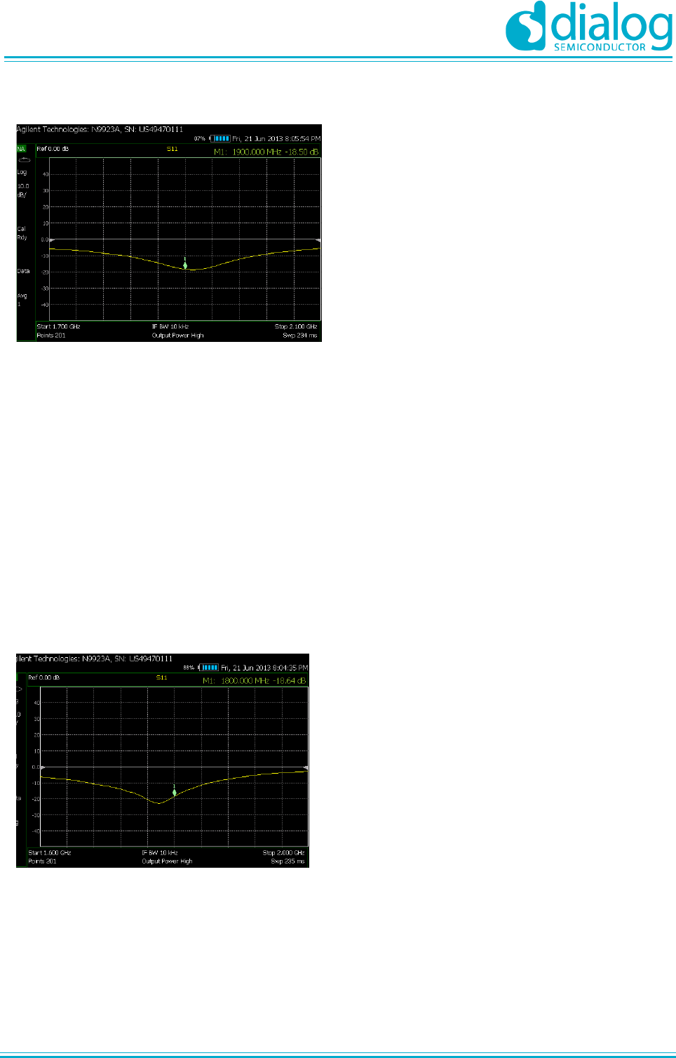
The S11 plot of the SC14CVMDECT_SFxx_DB has
been measured (with no 0402 component in Figure 2)
and is depicted in the following figure:
Application Note Revision 1.0 04-Oct-2017
CFR0014-01 7 of 9 © 2013 Dialog Semiconductor
AN-D-212
SC14CVMDECT External Antenna Design and Leveraging Modular Approval
Figure 4: S11 Measurement Plot of Printed
Antenna
3.1.2 Printed Antenna Design Operating at 1.8 GHz
For KDECT operation, the frequency band is centred
around 1.8 GHz, whereas the default printed antenna
design configuration is designed to be centred around
1.9 GHz. The printed antenna design holds a provision
for this shift in operating frequency.
Please refer to Figure 2. If a 100 pF capacitor (0402
footprint) is placed across the gap indicated by the
green ellipse indicated in Figure 2, then effectively the
antenna length is increased resulting in resonant fre-
quency of 1.8 GHz (without the 100 pF 0402 compo-
nents, the antenna’s resonant frequency remains at
1.9 GHz for other DECT operation). No other tuning
components are required.
Figure 5: Printed Antenna Design S11 Plot in
KDECT Mode
The S11 plot (measured on the actual
SC14CVMDECT_SFxx_DB Reference Design HW)
with the printed antenna design configured in KDECT
mode (i.e. with 100 pF 0402 component placed across
the length extension gap) is depicted in the Figure 5.
One important note with respect to KDECT operation:
though the printed antenna design can be made to
operate at 1.8 GHz, the embedded antenna that is part
of the SC14CVMDECT_SFxx module would remain
centred at 1.9 GHz since there are no external tuning
components to alter the resonant frequency of the
CS14CVMDECT_SFxx embedded antenna. This
implies antenna design should be selected for opera-
tion. This would limit the applicability to PP mode oper-
ation.
3.1.3 Boundary Conditions
In order to be allowed to leverage the CVMDECT Mod-
ular Approval for the SC14CVMDECT_SFxx_DB
design, the PCB should meet the following specifica-
tions:
• PCB material: FR4
• PCB layer stackup:
• L1 copper thickness: 18 m
• L1-L2 prepreg thickness: 360 m (2x “Prepreg
7628”)
• L2 copper thickness: 35 m
• L2-L3 core thickness: 710 m
• L3 copper thickness: 35 m
• L3-L4 prepreg thickness 360 m (2x “Prepreg
7628”)
• L4 copper thickness: 18 m
In addition, it is imperative that the physical design of
the printed antenna is accurately copied. Also the con-
tours of the ground plane surrounding the printed
antenna must be accurately copied. The printed
antenna location should be the same (i.e. in a corner
with the same orientation/spacing with respect to the
SF module).
When deviating in any way from these specifications,
the Modular Approval will be invalidated and recertifi-
cation on end-product/system level will be required.
3.2 TUNING COMPONENTS
The printed antenna design tuning has been validated
and found to require a resistive -attenuator network to
keep spurious emissions within ETSI limit.
It should be also noted that the printed antenna
design’s impedance is a short at DC. So a coupling
capacitor is required to connect the
SC14CVMDECT_SFxx module to the printed antenna
design.

Application Note Revision 1.0 04-Oct-2017
CFR0014-01 8 of 9 © 2013 Dialog Semiconductor
AN-D-212
SC14CVMDECT External Antenna Design and Leveraging Modular Approval
3.3 OTHER ANTENNAS
If an antenna is connected to CVMDECT that has a
dissimilar radiation pattern than that of the
SC14CVMDECT_SFxx_DB design and/or if the
antenna has a higher gain than that of the
SC14CVMDECT_SFxx_DB design, then FCC-04-165
dictates that the Modular Approval is invalidated and
that recertification is required on end-product/system
level.
If the antenna connected to CVMDECT is user acces-
sible, then the antenna connector shall be proprietary
(per FCC DA-00-1407)

Status Definitions
Disclaimer
Information in this document is believed to be accurate and reliable. However, Dialog Semiconductor does not give any
representations or warranties, expressed or implied, as to the accuracy or completeness of such information. Dialog Semi-
conductor furthermore takes no responsibility whatsoever for the content in this document if provided by any information
source outside of Dialog Semiconductor.
Dialog Semiconductor reserves the right to change without notice the information published in this document, including
without limitation the specification and design of the related semiconductor products, software and applications.
Applications, software, and semiconductor products described in this document are for illustrative purposes only. Dialog
Semiconductor makes no representation or warranty that such applications, software and semiconductor products will be
suitable for the specified use without further testing or modification. Unless otherwise agreed in writing, such testing or
modification is the sole responsibility of the customer and Dialog Semiconductor excludes all liability in this respect.
Customer notes that nothing in this document may be construed as a license for customer to use the Dialog Semi-conduc-
tor products, software and applications referred to in this document. Such license must be separately sought by customer
with Dialog Semiconductor.
All use of Dialog Semiconductor products, software and applications referred to in this document are subject to Dialog
Semiconductor's Standard Terms and Conditions of Sale, available on the company website (www.dialog-semiconduc-
tor.com) unless otherwise stated.
Dialog and the Dialog logo are trademarks of Dialog Semiconductor plc or its subsidiaries. All other product or service
names are the property of their respective owners.
© 2013 Dialog Semiconductor. All rights reserved.
Status Definition
DRAFT The content of this document is under review and subject to formal approval, which may result in
modifications or additions.
APPROVED
or unmarked
The content of this document has been approved for publication.
United Kingdom (Headquarters)
Dialog Semiconductor (UK) LTD
Phone: +44 1793 757700
Germany
Dialog Semiconductor GmbH
Phone: +49 7021 805-0
The Netherlands
Dialog Semiconductor B.V.
Phone: +31 73 640 8822
Email:
enquiry@diasemi.com
Contacting Dialog Semiconductor
North America
Dialog Semiconductor Inc.
Phone: +1 408 845 8500
Japan
Dialog Semiconductor K. K.
Phone: +81 3 5769 5100
Taiwan
Dialog Semiconductor Taiwan
Phone: +886 281 786 222
Web site:
www.dialog-semiconductor.com
Hong Kong
Dialog Semiconductor Hong Kong
Phone: +852 2607 4271
Korea
Dialog Semiconductor Korea
Phone: +82 2 3469 8200
Application Note Revision 1.0 04-Oct-2017
CFR0014-01 9 of 9 © 2013 Dialog Semiconductor
AN-D-212
SC14CVMDECT External Antenna Design and Leveraging Modular Approval
China (Shenzhen)
Dialog Semiconductor China
Phone: +86 755 2981 3669
China (Shanghai)
Dialog Semiconductor China
Phone: +86 21 5424 9058