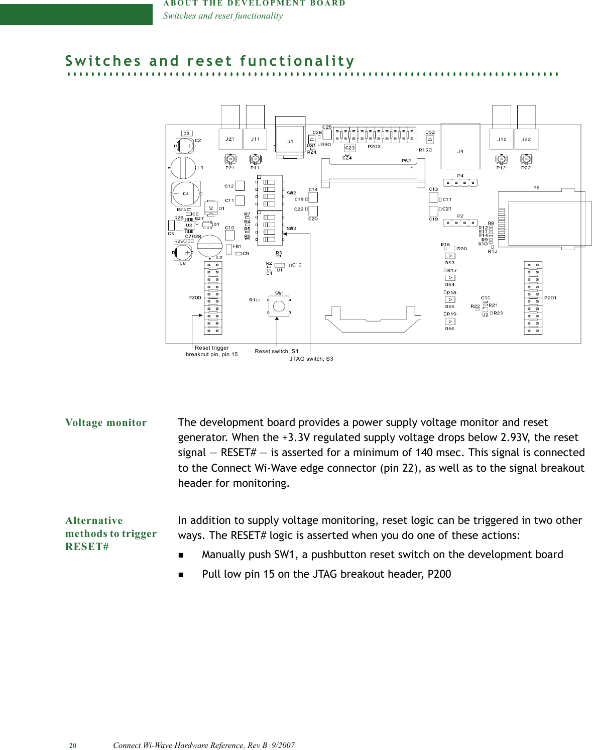
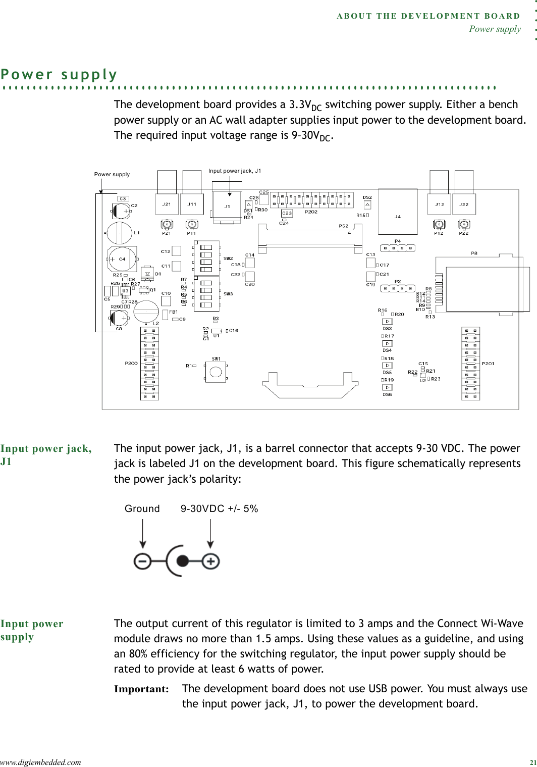
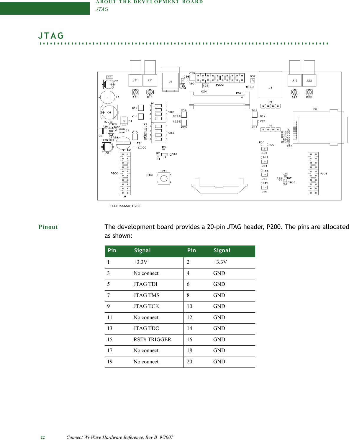
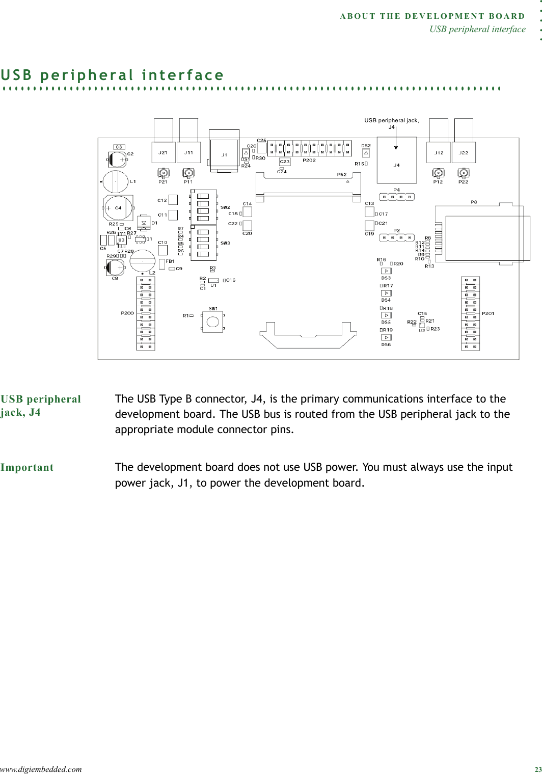
Digi 50M1380 Wi-Wave Module User Manual Wi Wave hrm

Digi International Inc Wi-Wave Module Wi Wave hrm

Users Manul Revision 3

Part number/version: 90000797_BRelease date: September 2007www.digiembedded.comDigi Connect™ Wi-Wave Hardware Reference. . . . . . . . . . . . . . . . . . . . . . . . . . . . . . . . . . . . . . . . . . . . . . . . . . . . . . . . . . . . . . . . . .
Digi International, Inc.11001 Bren Road EastMinnetonka, MN  55343  U.S.A.United States:  +1 877 912-3444Other locations: +1 952 912-3444www.digiembedded.com©2007 Digi International Inc.Printed in the United States of America. All rights reserved.Digi, Digi International, the Digi logo, a Digi International Company, Jump Start Kit, ConnectCore, NET+, NET+OS and NET+Works are trademarks or registered trademarks of Digi International, Inc. in the United States and other countries worldwide. All other trademarks are the property of their respective owners.Information in this document is subject to change without notice and does not represent a committment on the part of Digi International. Digi provides this document “as is,” without warranty of any kind, either expressed or implied, including, but not limited to, the implied warranties of fitness or merchantability for a particular purpose. Digi may make improvements and/or changes in this manual or in the product(s) and/or the program(s) described in this manual at any time.This product could include technical inaccuracies or typographical errors. Changes are made periodically to the information herein; these changes may be incorporated in new editions of the publication.
5Contents. . . . . . . . . . . . . . . . . . . . . . . . . . . . . . . . . . . . . . . . . . . . . . . . . . . . . . . . . . . . . . . . . . . . . Chapter 1:About the Module.......................................................... 9Features 9What’s on the module? 10Connect Wi-Wave module edge connector 10Connect Wi-Wave module edge connector: Pinout 10U.FL connectors 11USB peripheral controller 11802.11b/g modes and channels 12Channel allocations 12Voltage regulators 12Voltage monitor — Reset generator 13LEDS 13Power 13DISABLE signal 13Chapter 2: About the Development Board .............................15What’s on the development board 15Features 15The development board 16???Unpopulated components 16Connect Wi-Wave module connector, P52 17Pinout 17LEDs 19LED DS1 19LED DS2 19Debug (signal) breakout header LEDs 19Switches and reset functionality 20Voltage monitor 20Alternative methods to trigger RESET# 20Power supply 21Input power jack, J1 21Input power supply 21JTAG 22Pinout 22USB peripheral interface 23
6Connect Wi-Wave Hardware Reference, Rev. B,  9/2007USB peripheral jack, J4 23Important 23Debug breakout header, P201 24Debug breakout header signal map 24W_DISABLE# signal 24U.FL and RP-SMA connectors 25U.FL connectors 25???U.FL cables 25RP-SMA connectors 26For more information 26Chapter 3: Using the Antenna ............................................ 27Necessary Conditions for Integration 27Connect Wi-Wave antenna configurations 28U.FL cable and RP-SMA connection 28General information 29Antenna switch 29Antenna specifications: 2 dBi Dipole 29Attributes 29Dimensions 29Antenna strength (radiation pattern) diagram 30Antenna specifications: 5.5 dBi Dipole 31Attributes 31Dimensions 31Radiation pattern: H-Plane (2.0 and 5.0 GHz) 32Radiation pattern: E-plane (2.0 and 5.0 GHz) 33End Product Labeling 34End User Manual: RF Exposure Statements 34Additional End User Information 34Appendix A:Specifications 37Environmental specifications 37Mechanical dimensions 37Power requirements 38RF exposure statement 38Safety statements 38Module and development board dimensions 39Module dimensions 39Development board dimensions 40Appendix B: Certifications 41FCC Part 15 Class B 41
7Using this Guide. . . . . . . . . . . . . . . . . . . . . . . . . . . . . . . . . . . . . . . . . . . . . . . . . . . . . . . . . . . . . . . . . . . . . This guide provides information about the Digi Connect Wi-Wave embedded core module.Conventions used in this guideThis table describes the typographic conventions used in this guide:. . . . . . . . . . . . . . . . . . . . . . . . . . . . . . . . . . . . . . . . . . . . . . . . . . . . . . . . . . . . . . . . . . . . . . . . . . . . . . . . . .Digi informationRelated documentationFor additional documentation, see the Documentation folder in the NET+OS Start menu.Documentation updatesDigi occasionally provides documentation updates on the Web site (www.digiembedded.com/support). Be aware that if you see differences between the documentation you received in your package and the documentation on the Web site, the Web site content is the latest version.This convention Is used foritalic type Emphasis, new terms, variables, and document titles.monospaced type Filenames, pathnames, and code examples.
8Connect Wi-Wave Hardware Reference, Rev B  9/2007Contact informationFor more information about your Digi products, or for customer service and technical support, contact Digi International.To contact Digi International by UseMail Digi International, Inc.11001 Bren Road EastMinnetonka, MN 55343U.S.AWorld Wide Web http://www.digi.com/support/email http://www.digi.com/support/Telephone (U.S.) (952) 912-3444 or (877) 912-3444Telephone (other locations) +1 (952) 912-3444 or +1 (877) 912-3444
9Chapter 1:About the ModuleThe Digi Connect Wi-Wave module is an 802.11b/g WLAN communications module for use in embedded applications. The module is a single circuit card packaged in a PCI Express Mini Card form factor, and supports all the RF, analog, and digital circuitry necessary to implement WLAN functionality. Using Digi’s baseband processor technology, this module is the ideal choice for embedded applications requiring long-term product availability in conjunction with reliability and easy design integration.The primary interface to the module is through a standards-compliant PCI Express Mini Card edge connector, using a USB 2.0 full speed/high speed link for communication with the host system. Note:The Connect Wi-Wave edge connector pinout is compliant with the PCI Express Mini Card Electromechanical Specification, Revision 1.1 (March 28, 2005) with this exception: the Connect Wi-Wave has a 4-wire JTAG programming interface mapped to pins 45, 47, 49, and 51.The Connect Wi-Wave module also provides a dual diversity antenna option through two on-board U.FL connectors, which allow for cabling to remote 2.4 GHz antennas.. . . . . . . . . . . . . . . . . . . . . . . . . . . . . . . . . . . . . . . . . . . . . . . . . . . . . . . . . . . . . . . . . . . . . . . . . . . . . . . . . .FeaturesUltra-compact and standards-based form factorEasy design integration through USB 2.0 full speed/high speed interfaceDual diversity antenna option through two on-module U.FL antenna connectorsDigi 802.11b/g baseband processor technology for long-term product availability-30°C to +70°C operating temperature for harsh environmentsRoHS compliant design
What’s on the module?10 Connect Wi-Wave Hardware Reference, Rev. B,  9/2007. . . . . . . . . . . . . . . . . . . . . . . . . . . . . . . . . . . . . . . . . . . . . . . . . . . . . . . . . . . . . . . . . . . . . . . . . . . . . . . . . .What’s on the module?Connect Wi-Wave module edge connectorThe Connect Wi-Wave module edge connector is a 52-pin connector whose pinout follows the standard PCI Express Mini Card edge connector pinout as stated in the PCI Express Mini Card Electromechanical Specification, Revision 1.1, with this exception: JTAG signals are mapped onto pins 45, 47, 49, and 51. These signals are reserved and not intended for user applications. Connect Wi-Wave module edge connector: PinoutThe module edge connector is configured as shown (signal direction w.r.t Wi-Wave):U.FL connectorsP1P2Edge connector, P3Pin Type  WLAN Mini Card signalPin Type WLAN Mini Card signal1 n/a No connect 2 In Vcc_3.33 n/a No connect 4 In GND5 n/a No connect 6 n/a No connect7 n/a No connect 8 n/a No connect9 In GND 10 n/a No connect
. . . . .USB peripheral controllerwww.digiembedded.com 11U.FL connectors The module uses two U.FL antenna connectors (P1 and P2) to allow for cabling to embedded antennas or external antenna connectors. For more information, see Chapter 3, “Using the Antenna.”. . . . . . . . . . . . . . . . . . . . . . . . . . . . . . . . . . . . . . . . . . . . . . . . . . . . . . . . . . . . . . . . . . . . . . . . . . . . . . . . . .USB peripheral controllerThe module uses a peripheral USB controller to interface to either a full speed or high speed USB 2.0 link. The link first tries to communicate to the host system board at the high speed USB rate (480 Mbps). If not successful, the link reverts to the full speed USB rate (12 Mbps). This link is used for all communication between the module and the host system board.11 n/a No connect 12 n/a No connect13 n/a No connect 14 n/a No connect15 In GND 16 n/a No connectKey Key17 n/a No connect 18 In GND19 n/a No connect 20 In W_DISABLE#21 In GND 22 In PERST#23 n/a No connect 24 n/a No connect25 n/a No connect 26 In GND27 In GND 28 n/a No connect29 In GND 30 n/a No connect31 n/a No connect 32 n/a No connect33 n/a No connect 34 In GND35 In GND 36 I/O USB_D-37 n/a No connect 38 I/O USB_D+39 n/a No connect 40 In GND41 n/a No connect 42 Out LED_WWAN#43 n/a No connect 44 Out LED_WLAN#45 Rsvd (In) JTAG_TCK 46 Out LED_WPAN#47 Rsvd (In) JTAG_TMS 48 n/a No connect49 Rsvd (Out) JTAG_TDO 50 In GND51 Rsvd (In) JTAG_TDI 52 In Vcc_3.3Pin Type  WLAN Mini Card signalPin Type WLAN Mini Card signal
802.11b/g modes and channels12 Connect Wi-Wave Hardware Reference, Rev. B,  9/2007Note:The Connect Wi-Wave module does not support low-speed USB connections.. . . . . . . . . . . . . . . . . . . . . . . . . . . . . . . . . . . . . . . . . . . . . . . . . . . . . . . . . . . . . . . . . . . . . . . . . . . . . . . . . .802.11b/g modes and channelsThe Connect Wi-Wave transmits and receives data at up to 11 Mbps when operating in 802.11b mode and up to 54 Mbps when operating in 802.11g mode. It supports these 802.11b/g channels:Channels 1 through 11 for North America (2.401 GHz–2.473 GHz)Channels 1 through 13 for Europe (2.401 GHz–2.483 GHz)Channels 1 through 14 for Asia (2.401 GHz–2.495 GHz)Channel allocations. . . . . . . . . . . . . . . . . . . . . . . . . . . . . . . . . . . . . . . . . . . . . . . . . . . . . . . . . . . . . . . . . . . . . . . . . . . . . . . . . .Voltage regulatorsThe module takes in 3.3V±9% (3.00V to 3.60V) as its main input power. This power is filtered and used as a 3.3V supply to portions of the digital logic. This power also acts as input to dedicated on-board voltage regulators.Channel Center frequency (MHz)Frequency spread(MHz - MHz)1 2412 2401 - 24232 2417 2406 - 24283 2422 2411 - 24334 2427 2416 - 24385 2432 2421 - 24436 2437 2426 - 24487 2442 2431 - 24538 2447 2436 - 24589 2452 2441 - 246310 2457 2446 - 246811 2462 2451 - 247312 2467 2456 - 247813 2472 2461 - 248314 2484 2473 - 2495
. . . . .Voltage monitor — Reset generatorwww.digiembedded.com 13. . . . . . . . . . . . . . . . . . . . . . . . . . . . . . . . . . . . . . . . . . . . . . . . . . . . . . . . . . . . . . . . . . . . . . . . . . . . . . . . . .Voltage monitor — Reset generatorThe module does not provide a voltage monitor or automatic reset signal generator; rather, the module uses a reset signal generated by the host system board. . . . . . . . . . . . . . . . . . . . . . . . . . . . . . . . . . . . . . . . . . . . . . . . . . . . . . . . . . . . . . . . . . . . . . . . . . . . . . . . . . .LEDSThe module does not have any on-board LEDs, but it drives the LED_WLAN# signal (pin 44) to indicate WLAN association and transmit/receive activity. This table shows the different LED states:. . . . . . . . . . . . . . . . . . . . . . . . . . . . . . . . . . . . . . . . . . . . . . . . . . . . . . . . . . . . . . . . . . . . . . . . . . . . . . . . . .PowerThe module requires only +3.3 VDC, 750 mA max. This power must be a well-regulated +3.3V supply due to limited supply filtering in the module. The digital inputs and outputs are 3.3V CMOS compatible. See “Power requirements” on page 38 for specifications.DISABLE signal The module supports the active low W_DISABLE# signal (pin 20) as specified in the PCI Express Mini Card Electromechanical Specification. This signal not only disables the power supplies to the radio portion of the module, it also powers down additional portions of the module to reduce power consumption to a minimum.LED state IndicationOff Not powered onOn Associated and authenticatedSlow blink Not associated or authenticatedIntermittent blink Transmit/receive activity
15Chapter 2:About the Development BoardThe development board is designed for product evaluation and development purposes. In addition to the Connect Wi-Wave connector, the development board provides several breakout connectors and interfaces.. . . . . . . . . . . . . . . . . . . . . . . . . . . . . . . . . . . . . . . . . . . . . . . . . . . . . . . . . . . . . . . . . . . . . . . . . . . . . . . . . .What’s on the development boardFeatures Connect Wi-Wave connectorPushbutton reset switch and under voltage reset logicExternal USB Type B connector USB peripheral interface Additional signal headers for user accessTwo U.FL RP-SMA antenna connectors-30°C to +75°C ambient operating temperatureRoHS compliant design
ABOUT THE DEVELOPMENT BOARDWhat’s on the development board16 Connect Wi-Wave Hardware Reference, Rev B  9/2007The development board???Unpopulated componentsThere are components on the development that currently are not populated. Do not use these components:P2, SMBus breakout headerP4, USB breakout headerP202, PCIe breakout headerP8, Cellular SIM Card socketP21 and P22, Cellular Antenna 1 and Cellular Antenna 2 U.FL connectorsJ21 and J22, Cellular Antenna 1 and Cellular Antenna 2 SMA connectorsSW2 switchResistors R10 and R11Reset switch, S1JTAG header, P200 Debug header, P201USB peripheral jack, J4LED DS2Power supplyLEDsLED DS1Input power jack, J1Connect Wi-Wave module connector, P52RP_SMA WLAN antenna, J11U.FL connector, WiFi antenna 1, P11 U.FL connector, WiFi antenna 2, P12RP_SMA WLAN antenna, J12JTAG switch, S3
. . . . .ABOUT THE DEVELOPMENT BOARDConnect Wi-Wave module connector, P52www.digiembedded.com 17. . . . . . . . . . . . . . . . . . . . . . . . . . . . . . . . . . . . . . . . . . . . . . . . . . . . . . . . . . . . . . . . . . . . . . . . . . . . . . . . . .Connect Wi-Wave module connector, P52Place the Connect Wi-Wave module into the connector and support bracket, P52, on the development board.The Connect Wi-Wave module connector is a 52-pin connector that conforms to the PCI Express Mini Card Electromechanical Specification, Rev. 1.1, with additional non-standard connections (to the reserved pins on the standard connector). All the non-standard connections are routed through switches:When the switches are off (default), the development board fully complies with the PCI Express Mini Card Electrical Specification.When the switches are closed, the development board provides access to the additional signals. Note that these signals are reserved and not intended for user applications.PinoutNote:Signal direction w.r.t PCIe Mini Card.Connect Wi-Wave module connector, P52Pin Type Signal Pin Type Signal1 n/a No connect 2 In Vcc_3.33 n/a No connect 4 In GND5 n/a No connect 6 n/a No connect7 n/a No connect 8 Out UIM_PWR (C1)9 In GND 10 I/O UIM_DATA (C7)
ABOUT THE DEVELOPMENT BOARDConnect Wi-Wave module connector, P5218 Connect Wi-Wave Hardware Reference, Rev B  9/200711 n/a No connect 12 Out UIM_CLK (C3)13 n/a No connect 14 Out UIM_RESET (C2)15 In GND 16 Out UIM_Vpp (C6)Key Key Key Key Key Key17 I/O UIM C8 18 In GND19 I/O UIM C4 20 In W_DISABLE#21 In GND 22 In PERST#23 n/a No connect 24 n/a No connect25 n/a No connect 26 In GND27 In GND 28 n/a No connect29 In GND 30 n/a No connect31 n/a No connect 32 n/a No connect33 n/a No connect 34 In GND35 In GND 36 I/O USB_D-37 n/a No connect 38 I/O USB_D+39 n/a No connect 40 In GND41 n/a No connect 42 Out LED_WWAN#43 n/a No connect 44 Out LED_WLAN#45 n/a or In No connect or JTAG_TCK 46 Out LED_WPAN#47 n/a or In No connect or JTAG_TMS 48 n/a No connect49 n/a or Out No connect or JTAG_TDO 50 In GND51 n/a or In No connect or JTAG_TDI 52 In Vcc_3.3Pin Type Signal Pin Type Signal
. . . . .ABOUT THE DEVELOPMENT BOARDLEDswww.digiembedded.com 19. . . . . . . . . . . . . . . . . . . . . . . . . . . . . . . . . . . . . . . . . . . . . . . . . . . . . . . . . . . . . . . . . . . . . . . . . . . . . . . . . .LEDsLED DS1 The switching regulator is adjusted to output +3.3VDC ± 5% or better. LED DS1 lights up when the regulator outputs +3.3V power. See “Power supply” on page 21 for more information.LED DS2 LED DS2 lights up when the host system supplies power over the USB bus. This LED indicates that the host platform has recognized the attachment of a USB peripheral device on the USB bus. See “USB peripheral interface” on page 23 for more information.Debug (signal) breakout header LEDs Four LEDs are associated with the debug (signal) breakout header:DISABLE, DS3: Lights up when the W_DISABLE# signal is asserted.WAN, DS4: Reserved for future use. LAN, DS5: Lights up when the module drives the LED_WLAN# signal.PAN, DS6: Reserved for future use.See “Debug breakout header, P201” on page 24 for more information.LED DS2LED DS1LEDs: DS3, DS4, DS5, DS6
ABOUT THE DEVELOPMENT BOARDSwitches and reset functionality20 Connect Wi-Wave Hardware Reference, Rev B  9/2007. . . . . . . . . . . . . . . . . . . . . . . . . . . . . . . . . . . . . . . . . . . . . . . . . . . . . . . . . . . . . . . . . . . . . . . . . . . . . . . . . .Switches and reset functionalityVoltage monitor The development board provides a power supply voltage monitor and reset generator. When the +3.3V regulated supply voltage drops below 2.93V, the reset signal — RESET# — is asserted for a minimum of 140 msec. This signal is connected to the Connect Wi-Wave edge connector (pin 22), as well as to the signal breakout header for monitoring.Alternative methods to trigger RESET#In addition to supply voltage monitoring, reset logic can be triggered in two other ways. The RESET# logic is asserted when you do one of these actions:Manually push SW1, a pushbutton reset switch on the development boardPull low pin 15 on the JTAG breakout header, P200 Reset switch, S1JTAG switch, S3Reset trigger breakout pin, pin 15
. . . . .ABOUT THE DEVELOPMENT BOARDPower supplywww.digiembedded.com 21. . . . . . . . . . . . . . . . . . . . . . . . . . . . . . . . . . . . . . . . . . . . . . . . . . . . . . . . . . . . . . . . . . . . . . . . . . . . . . . . . .Power supplyThe development board provides a 3.3VDC switching power supply. Either a bench power supply or an AC wall adapter supplies input power to the development board. The required input voltage range is 9–30VDC. Input power jack, J1The input power jack, J1, is a barrel connector that accepts 9-30 VDC. The power jack is labeled J1 on the development board. This figure schematically represents the power jack’s polarity:Input power supplyThe output current of this regulator is limited to 3 amps and the Connect Wi-Wave module draws no more than 1.5 amps. Using these values as a guideline, and using an 80% efficiency for the switching regulator, the input power supply should be rated to provide at least 6 watts of power. Important:The development board does not use USB power. You must always use the input power jack, J1, to power the development board.Power supply Input power jack, J1Ground 9-30VDC +/- 5%
ABOUT THE DEVELOPMENT BOARDJTAG22 Connect Wi-Wave Hardware Reference, Rev B  9/2007. . . . . . . . . . . . . . . . . . . . . . . . . . . . . . . . . . . . . . . . . . . . . . . . . . . . . . . . . . . . . . . . . . . . . . . . . . . . . . . . . .JTAGPinout The development board provides a 20-pin JTAG header, P200. The pins are allocated as shown:JTAG header, P200Pin Signal Pin Signal1 +3.3V 2 +3.3V3 No connect 4 GND5 JTAG TDI 6 GND7 JTAG TMS 8 GND9 JTAG TCK 10 GND11 No connect 12 GND13 JTAG TDO 14 GND15 RST# TRIGGER 16 GND17 No connect 18 GND19 No connect 20 GND
. . . . .ABOUT THE DEVELOPMENT BOARDUSB peripheral interfacewww.digiembedded.com 23. . . . . . . . . . . . . . . . . . . . . . . . . . . . . . . . . . . . . . . . . . . . . . . . . . . . . . . . . . . . . . . . . . . . . . . . . . . . . . . . . .USB peripheral interfaceUSB peripheral jack, J4The USB Type B connector, J4, is the primary communications interface to the development board. The USB bus is routed from the USB peripheral jack to the appropriate module connector pins.Important The development board does not use USB power. You must always use the input power jack, J1, to power the development board.USB peripheral jack, J4
ABOUT THE DEVELOPMENT BOARDDebug breakout header, P20124 Connect Wi-Wave Hardware Reference, Rev B  9/2007. . . . . . . . . . . . . . . . . . . . . . . . . . . . . . . . . . . . . . . . . . . . . . . . . . . . . . . . . . . . . . . . . . . . . . . . . . . . . . . . . .Debug breakout header, P201The debug breakout header’s primary purpose is to provide access to the W_DISABLE# signal. The W_DISABLE# signal usually is used as a hardware means to disable RF transmissions from the module without software intervention.Debug breakout header signal mapW_DISABLE# signalThe active low W_DISABLE# signal is on pin 20 of the signal breakout header. GND signals are positioned adjacent to the DISABLE# signal on pins 18 and 19. To assert Debug header, P201W_DISABLE# pin, pin 20Pin Type Signal Pin Type Signal1 n/a No connect 2 Monitor pt Vcc_3.33 n/a No connect 4 Monitor pt LED_WWAN#5 n/a No connect 6 Monitor pt GND7 n/a No connect 8 Monitor pt LED_WLAN#9 Monitor pt GND 10 Monitor pt GND11 n/a No connect 12 Monitor pt LED_WPAN#13 n/a No connect 14 Monitor pt GND15 n/a No connect 16 Monitor pt RESET#17 n/a No connect 18 Monitor pt GND19 Monitor pt GND 20 Input W_DISABLE#
. . . . .ABOUT THE DEVELOPMENT BOARDU.FL and RP-SMA connectorswww.digiembedded.com 25the DISABLE# signal to the module, place a jumper between either pins 18 and 20 or pins 19 and 21. As an alternative, you can drive this pin with a low voltage TTL or CMOS driver. When asserted, DISABLE# lights the DISABLE LED, DS3.. . . . . . . . . . . . . . . . . . . . . . . . . . . . . . . . . . . . . . . . . . . . . . . . . . . . . . . . . . . . . . . . . . . . . . . . . . . . . . . . . .U.FL and RP-SMA connectorsU.FL connectors The development board has two U.FL connectors that pair with two RP-SMA connectors. WiFi antenna 1 (P11) pairs with RP-SMA connector J11; WiFi antenna 2 (P12) pairs with RP-SMA connector J12. ???U.FL cables The development kit includes two U.FL-to-U.FL cables that can be used to connect the module and development board. The number of cables used depends on whether one antenna is used to transmit and receive or two antennas are used (diversity receive). 1Attach one end of the cable(s) to the U.FL connector(s) on the Connect Wi-Wave module.RP_SMA WLAN antenna, J11U.FL connector, WiFi antenna 1, P11 U.FL connector, WiFi antenna 2, P12RP_SMA WLAN antenna, J12
ABOUT THE DEVELOPMENT BOARDU.FL and RP-SMA connectors26 Connect Wi-Wave Hardware Reference, Rev B  9/20072Attach the other end of the cable(s) to the U.FL connector(s) on the development board.3Attach the RP-SMA antenna to the appropriate RP-SMA connector on the development board.RP-SMA connectorsIf you are using only one cable/connection, be sure you attach the RP-SMA antenna to the correct connector:If the cable is connected to U.FL connector P11, or WiFi antenna 1, attach the RP-SMA antenna to J11.If the cable is connected to U.FL connector P12, or WiFi antenna 2, attach the RP-SMA antenna to J12.For more informationFor information about the antenna(s) and using it, see Chapter 3, “Using the Antenna.”
27Using the AntennaThe Digi Connect Wi-Wave development board supports three types of antennas: 29000095 ANT, WHIP 2.4-2.5 GHz Dipole (2.0000)29000146 ANT, WHIP 2.4 GHz Dipole 5 dBi (2.0000)Attach the U.FL-to-U.FL cables, provided in the development kit, to both the module and the development board. There are two cables included; whether you use one cable or both depends on how you set up your antenna(s).Be sure that the antenna you use complies with the regulatory requirements of your region. In North America, for example, you can operate only with antennas approved by Digi International, Inc., or antennas matching the specifications of Digi-approved antennas.Necessary Conditions for IntegrationThe following conditions are necessary for integration:The antenna must be installed such that 20 cm is maintained between the antenna and users for all installations.The transmitter module may not be co-located with any other transmitter or antenna.The Module is approved using the FCC “unlicensed modular transmitter approval” method; therefore, the module must be used with the originally- approved antennas only.  As long as you meet these three conditions, further transmitter testing will not be required.  However, you are still responsible for testing your end-product for any additional compliance requirements associated with this module installation (e.g., digital device emissions, PC peripheral requirements, etc.). Note: In the event that any of these conditions cannot be met  (for example  portable configurations, co-location with another transmitter, or use of a different antenna), then the FCC authorization is no longer considered valid, and you are unable to use the FCC ID on the final product.  In these circumstances, you will be responsible for re-evaluating the end product (including the transmitter) and obtaining a separate FCC authorization.
USING THE ANTENNA28 Connect Wi-Wave Hardware Reference, Rev B  9/2007Connect Wi-Wave antenna configurationsThe Connect Wi-Wave can transmit data or receive data, but not at the same time. Software controls the transmit/receive functionality as well as the antenna switch. You have the option of using two antennas (required for diversity receive) or one antenna to transmit and receive data. Using two antennas: The Connect Wi-Wave transmits on one antenna and receives on the other antenna (at separate times) without changing the antenna switch. Use both cables.Using one antenna: The Connect Wi-Wave transmits on one antenna, software toggles the antenna switch, then the Connect Wi-Wave receives on the same antenna. Use only one cable, which can be connected to either U.FL connector on the module and on the development board.U.FL cable and RP-SMA connectionUse these connection steps with the RP-SMA antennas: 29000095 — 2.4-2.5 GHz Dipole and 29000146 — 2.4 GHz Dipole 5.5 dBi:1Attach one end of the cable(s) to the U.FL connector(s) (P1, P2) on the Connect Wi-Wave module.2Attach the other end of the cable(s) to the U.FL connector(s) (P11, P12) on the development board.3Attach the RP-SMA antenna to the appropriate RP-SMA connector (J11, J12) on the development board. If you are using only one cable/connection, be sure you attach the RP-SMA antenna to the correct connector:–If the cable is connected to U.FL connector P11, or WiFi antenna 1, attach the RP-SMA antenna to J11.–If the cable is connected to U.FL connector P12, or WiFi antenna 2, attach the RP-SMA antenna to J12.
. . . . .USING THE ANTENNAGeneral informationwww.digiembedded.com 29. . . . . . . . . . . . . . . . . . . . . . . . . . . . . . . . . . . . . . . . . . . . . . . . . . . . . . . . . . . . . . . . . . . . . . . . . . . . . . . . . .General informationThe module uses the same antennas to transmit and receive the 802.11b/g RF signal. An antenna switch is required to isolate the transmit signal from the receive signal. The antenna switch works by alternately connecting the antennas to either the transceiver PA transmit output or the transceiver receive input. To support this antenna sharing scheme, the module operates in half-duplex mode; receive and transmit operations do not occur at the same time.Antenna switch The antenna switch is a digitally controlled 2.4 GHz, 50 ohm, multi-function solid state switch, controlled by software.The receive port can be switched between antenna 1 or antenna 2. The transmit port can be switched between antenna 1 or antenna 2. The switch can handle >28dBm of signal on the transmit port. The insertion loss of the antenna switch is <0.5dB and the receive to transmit port isolation is >23dB.. . . . . . . . . . . . . . . . . . . . . . . . . . . . . . . . . . . . . . . . . . . . . . . . . . . . . . . . . . . . . . . . . . . . . . . . . . . . . . . . . .Antenna specifications: 2 dBi DipoleAttributesDimensionsNote:Dimensions are provided for reference purposes only. The actual antenna might vary.Attribute PropertyFrequency 2.4~2.5 GHzPower output 2WDB gain 2 dBiVSWR < or = 2.0Dimension 108.5 mm x 10.0 mmWeight 10.5gTemperature rating -40°–+80° CPart number DG-ANT-20DP-BG
USING THE ANTENNAAntenna specifications: 2 dBi Dipole30 Connect Wi-Wave Hardware Reference, Rev B  9/2007Antenna strength (radiation pattern) diagramThis diagram shows the strength of the signal received by the whip antenna on both a horizontal and vertical plane. The diagram shows the magnetic field when the antenna is in a vertical position. The red solid line represents the horizontal plane and the green dotted line represents the vertical plane. You can see in the illustration that at 90 degrees, the signal strength is 0 (as expected).90.0˚(9.1).360(88.9)3.500(30.5)1.200(25.4)1.010(83.8)3.300(10.1).399R (3.2).125
. . . . .USING THE ANTENNAAntenna specifications: 5.5 dBi Dipolewww.digiembedded.com 31. . . . . . . . . . . . . . . . . . . . . . . . . . . . . . . . . . . . . . . . . . . . . . . . . . . . . . . . . . . . . . . . . . . . . . . . . . . . . . . . . .Antenna specifications: 5.5 dBi DipoleAttributesDimensionsNote:Dimensions are provided for reference purposes only. The actual antenna might vary.Attribute Band 1 Band 2Frequency 2.4~2.5 GHz 5.15~5.35 GHz5.725~5.85 GHzVSWR 2.0 maxReturn loss -10 dB maxDB gain 5 dBi (Typ)Polarization LinearPower output 1WDimension See measurements in the drawing after the tableOperating temperature -20°–+65°CStorage temperature -20°–+65°CPart number DG-ANT-55DP-AG
USING THE ANTENNAAntenna specifications: 5.5 dBi Dipole32 Connect Wi-Wave Hardware Reference, Rev B  9/2007Radiation pattern: H-Plane (2.0 and 5.0 GHz)Color Freq (MHz) Peak (dBi) Angle (o) Avg (dBi)Yellow 2400.0 3.39 257.68 2.98Red 2450.00 3.17 214.74 2.37Blue 2500.00 2.79 288.0 1.96Purple 5150.00 2.25 280.42 0.82Green 5200.00 5.23 252.63 2.71
. . . . .USING THE ANTENNAAntenna specifications: 5.5 dBi Dipolewww.digiembedded.com 33Radiation pattern: E-plane (2.0 and 5.0 GHz)Light brown 5250.00 4.51 272.84 3.16Orange 5750.00 5.03 267.79 3.88Aqua 5850.00 3.83 276.63 2.74Color Freq (MHz) Peak (dBi) Angle (o) Avg (dBi)Color Freq (MHz) Peak (dBi) Angle (o) Avg (dBi)Yellow 2400.0 2.60 283.22 -1.10Red 2450.00 2.57 240.42 -1.36Blue 2500.00 1.92 237.27 -1.78Purple 5150.00 2.37 78.67 -1.91Green 5200.00 4.80 79.30 0.32Light brown 5250.00 4.49 79.93 -0.01Orange 5750.00 6.34 283.85 1.08Aqua 5850.00 4.67 283.22 -0.46
USING THE ANTENNAEnd Product Labeling34 Connect Wi-Wave Hardware Reference, Rev B  9/2007. . . . . . . . . . . . . . . . . . . . . . . . . . . . . . . . . . . . . . . . . . . . . . . . . . . . . . . . . . . . . . . . . . . . . . . . . . . . . . . . . .End Product Labeling This transmitter module is authorized for use only in devices where the antenna may be installed, such that 20 cm may be maintained between the antenna and users (e.g., routers, wireless ASDL modems, and similar equipment).  Label the final end product in a visible area with the following statement:  "Contains Wi-Wave FCC ID: MCQ-50M1380.”Note: For Canadian users, use the following statement: “"Contains Wi-Wave IC: 1846A-50M1380.”. . . . . . . . . . . . . . . . . . . . . . . . . . . . . . . . . . . . . . . . . . . . . . . . . . . . . . . . . . . . . . . . . . . . . . . . . . . . . . . . . .End User Manual: RF Exposure Statements The end user manual must include the following information in a prominent location: "IMPORTANT NOTE:  To comply with FCC RF exposure compliance requirements, the antenna used for this transmitter must be installed to provide a separation distance of at least 20 cm from all persons and must not be co-located or operating in conjunction with any other antenna or transmitter."  Additional End User Information Please do not provide the end user with any instructions on how to remove or to install the Connect Wi-wave module.
. . . . .USING THE ANTENNAEnd User Manual: RF Exposure Statementswww.digiembedded.com 35
37Appendix A: SpecificationsThis appendix provides Digi Connect Wi-Wave module specifications as well as safety statements and antenna specifics.. . . . . . . . . . . . . . . . . . . . . . . . . . . . . . . . . . . . . . . . . . . . . . . . . . . . . . . . . . . . . . . . . . . . . . . . . . . . . . . . . .Environmental specificationsThe module board assembly meets all functional requirements when operating in this environment:Operating temperature: -30°C to +75°C???Storage temperature: -40°C to +125°CRelative humidity: 5% to 95%, non-condensingAltitude: 0 to 12,000 feet. . . . . . . . . . . . . . . . . . . . . . . . . . . . . . . . . . . . . . . . . . . . . . . . . . . . . . . . . . . . . . . . . . . . . . . . . . . . . . . . . .Mechanical dimensionsLength: 2.006 inches (50.95 mm)Width: 1.181 inches (30.00 mm)Height: 0.187 inches (4.75 mm)Top: 0.095 inches (2.40 mm)Bottom: 0.053 inches (1.35 mm)Weight: 8 grams (approximately)
Power requirements38 Connect Wi-Wave Hardware Reference, Rev B  9/2007. . . . . . . . . . . . . . . . . . . . . . . . . . . . . . . . . . . . . . . . . . . . . . . . . . . . . . . . . . . . . . . . . . . . . . . . . . . . . . . . . .Power requirements . . . . . . . . . . . . . . . . . . . . . . . . . . . . . . . . . . . . . . . . . . . . . . . . . . . . . . . . . . . . . . . . . . . . . . . . . . . . . . . . . .RF exposure statementThe Connect Wi-Wave module complies with RF exposure limits for humans as called out in RSS-102. It is exempt from RF evaluation based on its operating frequency of 2.4 GHz, and effective radiated power less than the three watt requirement for a mobile device (>20 cm separation) operating at 2.4 GHz.. . . . . . . . . . . . . . . . . . . . . . . . . . . . . . . . . . . . . . . . . . . . . . . . . . . . . . . . . . . . . . . . . . . . . . . . . . . . . . . . . .Safety statementsTo avoid contact with electrical current:Never install electrical wiring during an electrical storm.Use a screwdriver and other tools with insulated handles.Wear safety glasses or goggles.Installation of inside wiring may bring you close to electrical wire, conduit, terminals and other electrical facilities. Extreme caution must be used to avoid electrical shock from such facilities. Avoid contact with all such facilities.Protectors and grounding wire placed by the service provider must not be connected to, removed, or modified by the customer.Do not touch or move the antenna(s) while the unit is transmitting or receiving.Do not hold any component containing a radio such that the antenna is very close to or touching any exposed parts of the body, especially the face or eyes, while transmitting.Do not operate a portable transmitter near unshielded blasting caps or in an explosive environment unless it is a type especially qualified for such use.Parameter LimitsInput voltage (Vcc) 3.3V±9% (3.00V to 3.60V)Input current 750mA maxInput low voltage 0.0V <VIL <0.3*VccInput high voltage 0.7*Vcc <VIH <VccOutput low voltage 0.0V <VOL <0.4VOutput high voltage Vcc-0.4V <VOH <Vcc
. . . . .Module and development board dimensionswww.digiembedded.com 39Any external communications wiring you may install needs to be constructed to all relevant electrical codes. In the United States, this is the National Electrical Code Article 800. Contact a licensed electrician for details.. . . . . . . . . . . . . . . . . . . . . . . . . . . . . . . . . . . . . . . . . . . . . . . . . . . . . . . . . . . . . . . . . . . . . . . . . . . . . . . . . .Module and development board dimensionsModule dimensionsNote:The measurements in this drawing are in inches.+. 00/ - . 01. 9531. 1811. 012.152CDETAI L  ADEG45.010 MAX. 039.158DETAI L  ACLL2. 00601. 892.126. 032 R MAX+. 00/ - . 01. 059 DI A
Module and development board dimensions40 Connect Wi-Wave Hardware Reference, Rev B  9/2007Development board dimensionsNote:The measurements in this drawing are in inches.AREA REMOVED1. 850 5. 0003. 150. 050" RADMA X003. 0002. 095. 550
41Appendix B:CertificationsThe Connect Wi-Wave products comply with the standards cited in this section.. . . . . . . . . . . . . . . . . . . . . . . . . . . . . . . . . . . . . . . . . . . . . . . . . . . . . . . . . . . . . . . . . . . . . . . . . . . . . . . . . .FCC Part 15 Class BRadio Frequency Interface (RFI) (FCC 15.105)The Connect Wi-Wave embedded module has been tested and found to comply with the limits for Class B digital devices pursuant to Part 15 Subpart B, of the FCC rules. These limits are designed to provide reasonable protection against harmful interference in a residential environment. This equipment generates, uses, and can radiate radio frequency energy, and if not installed and used in accordance with the instruction manual, may cause harmful interference to radio communications. However, there is no guarantee that interference will not occur in a particular installation. If this equipment does cause harmful interference to radio or television reception, which can be determined by turning the equipment off and on, the user is encouraged to try and correct the interference by one or more of the following measures:Reorient or relocate the receiving antenna.Increase the separation between the equipment and receiver.Connect the equipment into an outlet on a circuit different from that to which the receiver is connected.Consult the dealer or an experienced radio/TV technician for help.Labeling Requirements (FCC 15.19)This device complies with Part 15 of FCC rules. Operation is subject to the following two conditions: (1) this device may not cause harmful interference, and (2) this
CERTIFICATIONSFCC Part 15 Class B42 Connect Wi-Wave Hardware Reference, Rev B  9/2007device must accept any interference received, including interference that may cause undesired operation.If the FCC ID is not visible when installed inside another device, then the outside of the device into which the module is installed must also display a label referring to the enclosed module FCC ID. This exterior label can use wording such as the following: Contains Transmitter Module FCC ID: MCQ-50M1380, IC: 1846A-50M1380.Modifications (FCC 15.21)Changes or modifications to this equipment not expressly approved by Digi may void the user’s authority to operate this equipment.Industry CanadaThis digital apparatus does not exceed the Class B limits for radio noise emissions from digital apparatus set out in the Radio Interference Regulations of the Canadian Department of Communications.Le present appareil numerique n’emet pas de bruits radioelectriques depassant les limites applicables aux appareils numeriques de la class B prescrites dans le Reglement sur le brouillage radioelectrique edicte par le ministere des Communications du Canada.
. . . . .CERTIFICATIONSFCC Part 15 Class Bwww.digi.com 43Declaration of Conformity(In accordance with FCC Dockets 96-208 and 95-19)Digi International declares, that the product:to which this declaration relates, meets the requirements specified by the Federal Communications Commission as detailed in the following specifications:Part 15, Subpart B, for Class B equipmentFCC Docket 96-208 as it applies to Class B personalPersonal computers and peripheralsThe product listed above has been tested at an External Test Laboratory certified per FCC rules and has been found to meet the FCC, Part 15, Class B, Emission Limits. Documentation is on file and available from the Digi International Homologation Department.Manufacturer’s Name: Digi InternationalCorporate Headquarters: 11001 Bren Road EastMinnetonka MN 55343Manufacturing Headquarters: 10000 West 76th StreetEden Prairie MN 55344Product Name: Connect Wi-WaveModel Numbers: 50001380-01
CERTIFICATIONSFCC Part 15 Class B44 Connect Wi-Wave Hardware Reference, Rev B  9/2007International EMC StandardsThe Connect Wi-Wave meets the following standards:StandardsEmissions EN 55022:2006 Class BEN 61000-3-2 and EN61000-3-3EN 300 328 V1.6.1 (2004-11)AS/NZS CISPR 22:2006ICES-003, Class BFCC Part 15 Subpart B Class BFCC Part 15 Subpart C Section 15.247(FCC ID: MCQ-50M1380)IC RSS 210 Issue 6 and RSS GEN Issue 1(IC: 1846A-50M1380)Immunity EN 55024EN 301 489-17 V1.2.1: (2002-08)Safety UL 60950-1ICE/EN 60950-1 (European Union)CSA C22.2, No. 60950-1
Index-45Index. . . . . . . . . . . . . . . . . . . . . . . . . . . . . . . . . . . . . . . . . . . . . . . . . . . . . . . . . . . . . . . . . . . . . . . . . . . . . . .Numerics2 dBi Dipole antenna 29-31attributes 29dimensions 29strength (radiation pattern) diagram 305.5 dBi Dipole antenna 31-33attributes 31dimensions 31radiation pattern, E-plane 33radiation pattern, H-Plane 32802.11b/g modes and channels 12Aantenna switch 29antennasabout 27-34configurations 28specifications2 dBi Dipole 295.5 dBi Dipole 31switch 29types 27U.FL cable and RP-SMA connection 28Ccertifications 41Ddebug breakout header, P201 24development boardabout 15-26debug breakout header 24dimensions 40features 15JTAG 22layout 16LEDs 19module connector, P52 17power supply 21reset functionality 20RP-SMA connectors 25switches 20U.FL connectors 25USB peripheral interface 23dimensionsdevelopment board 40module 39DISABLE signal 13DS1 (LED) 19DS2 (LED) 19DS3, DISABLE LED 19DS4, WAN LED 19DS5, LAN LED 19DS6, PAN LED 19EEnd 34environmental specifications 37Ffeaturesdevelopment board 15module 9
Index-46 Connect Wi-Wave Hardware Reference, Rev B  9/2007IndexGGeneral 29Iinput power jack, J1 21input power supply 21JJ1, input power jack 21J4, USB peripheral jack 23JTAG header, P200 22LLED DS1 19LED DS2 19LED DS3, DISABLE 19LED DS4, WAN 19LED DS5, LAN 19LED DS6, PAN 19LEDsdebug (signal) breakout header 19development board 19module 13Mmechanical dimensions, module 37module802.11b/g modes and channels 12about 9-13definition 9dimensions 39environmental specifications 37features 9layout 10LEDs 13mechanical dimensions 37module edge connector 10power 13power requirements 38primary interface 9reset generator 13specifications 37USB peripheral controller 11voltage monitor 13voltage regulators 12module connector, P52 17module edge connector 10pinout 10PP200, JTAG header 22P201, debug breakout header 24powerdevelopment board 21module 13power requirements, module 38Rreset functionality 20reset generator 13RESET# 20RF exposure statement 38RP-SMA connection 28RP-SMA connectors 25Ssafety statements 38specifications, module 37switches 20UU.FL cableand RP-SMA connection 28U.FL cables 25U.FL connectors 25USB peripheral controller 11USB peripheral interface 23USB peripheral jack, J4 23
www.digiembedded.com Index-47Vvoltage monitor 13, 20voltage regulators 12WW_DISABLE# signal 24

Navigation menu