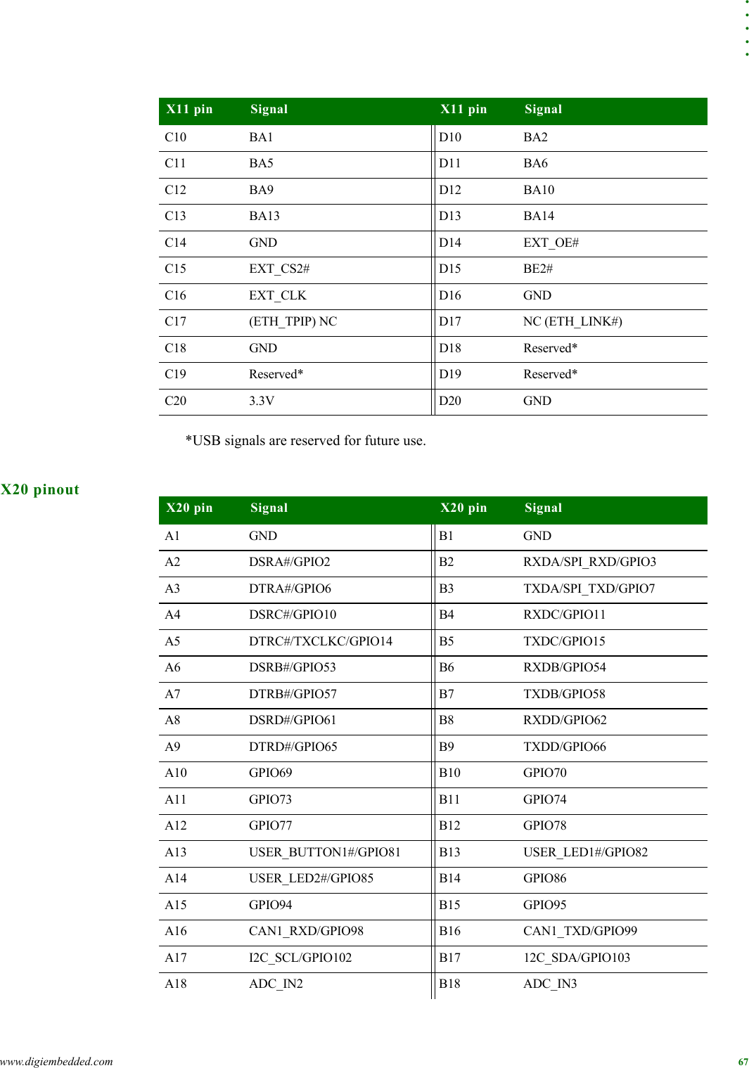
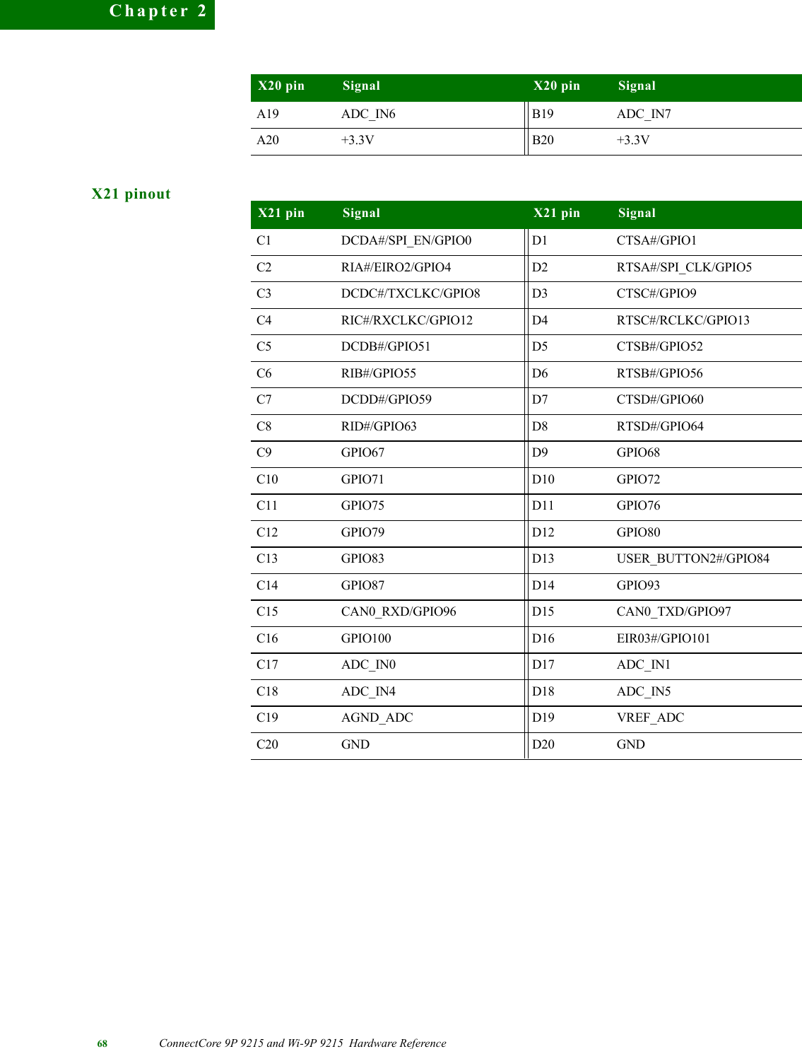
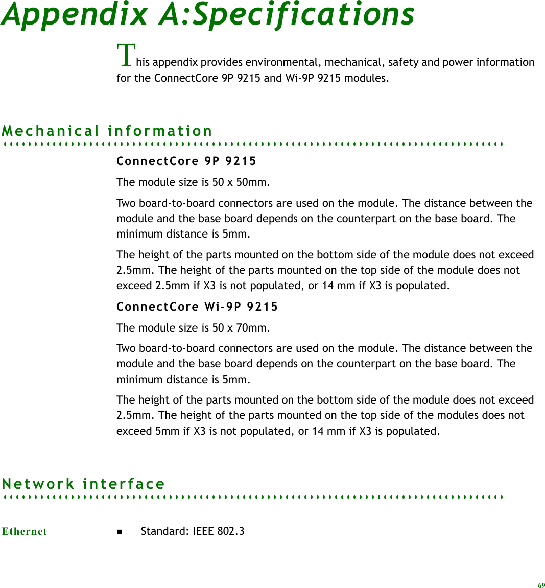
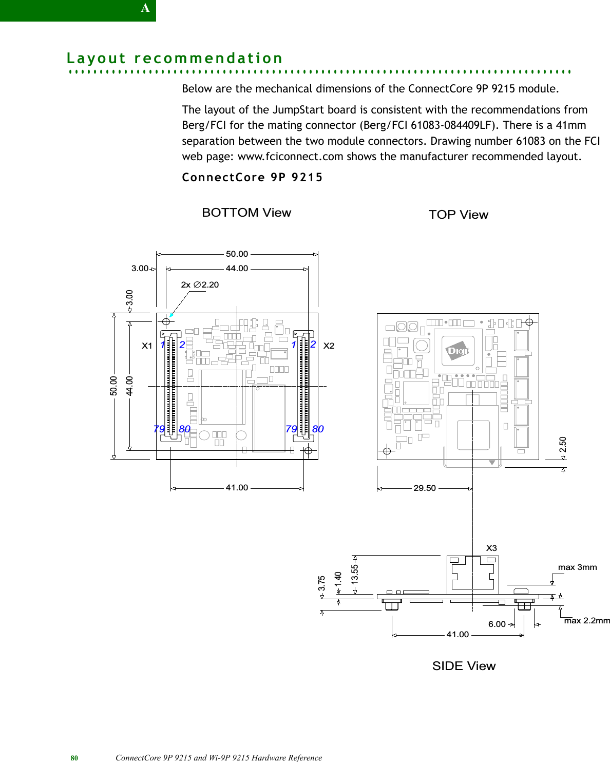
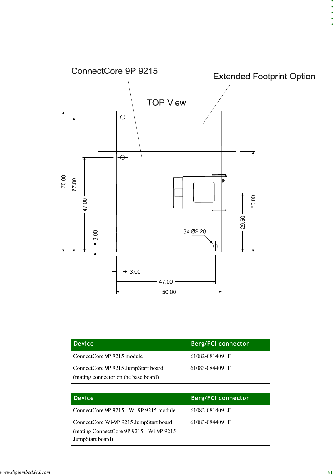
Digi 50M1589 Wireless Embedded ARM Module User Manual ConnectCore 9P 9215 HRM
Digi International Inc Wireless Embedded ARM Module ConnectCore 9P 9215 HRM
UserManual.wiki
>
Digi
>
50M1589 User Manual
Hardware reference manual
Navigation menu
Upload a User Manual
Namespaces
Wiki Guide
HTML
PDF
Info
Views
User Manual
Discussion / Help
Navigation


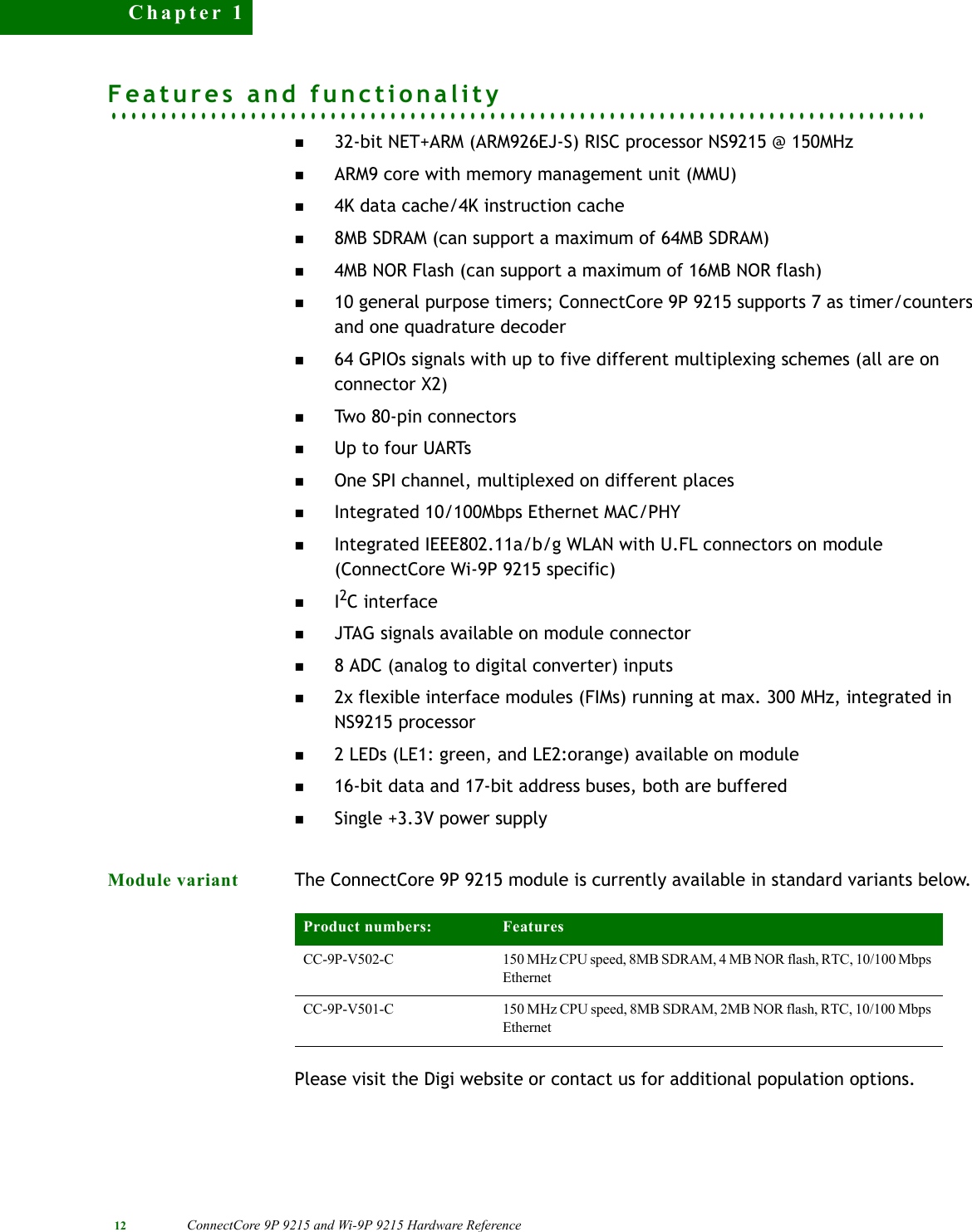
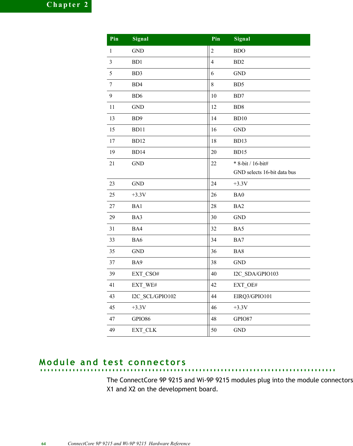
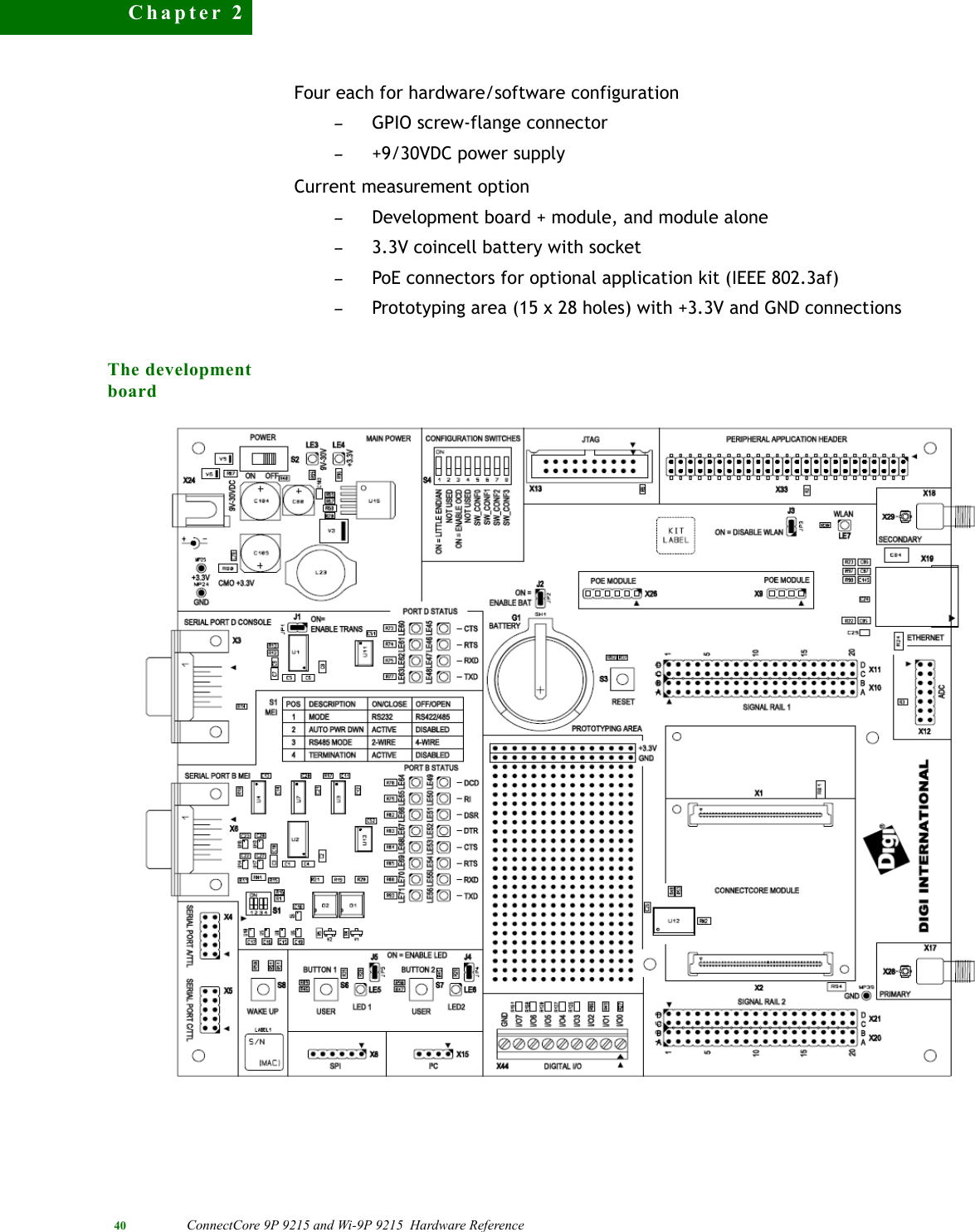
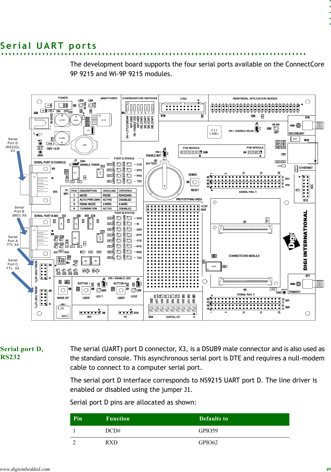
![14 ConnectCore 9P 9215 and Wi-9P 9215 Hardware ReferenceChapter 118 I SOFT_CONF3 SOFT_CONF3 2k2 series resistor on module19 O Reserved (WLAN_LED#)Reserved (WLAN_LED#)Active low signal coming from low-active WLAN signal. This signal comes directly from the Piper chip without series resistor.20 P GND GND21 I/O D0 D0 Buffered Data - only active when either CS0# or CS2# is active NS9215 D[31:16]22 I/O D1 D123 I/O D2 D224 I/O D3 D325 I/O D4 D426 I/O D5 D527 I/O D6 D628 I/O D7 D729 I/O D8 D830 I/O D9 D931 I/O D10 D1032 I/O D11 D1133 I/O D12 D1234 I/O D13 D1335 I/O D14 D1436 I/O D15 D1537 P GND GND38 O AO AO Buffered Address always active 39 O A1 A140 O A2 A241 O A3 A342 O A4 A443 O A5 A544 O A6 A645 O A7 A746 O A8 A8X1 pin numberType Module functionality Usage on Development boardComments](https://usermanual.wiki/Digi/50M1589/User-Guide-1073858-Page-14.png)
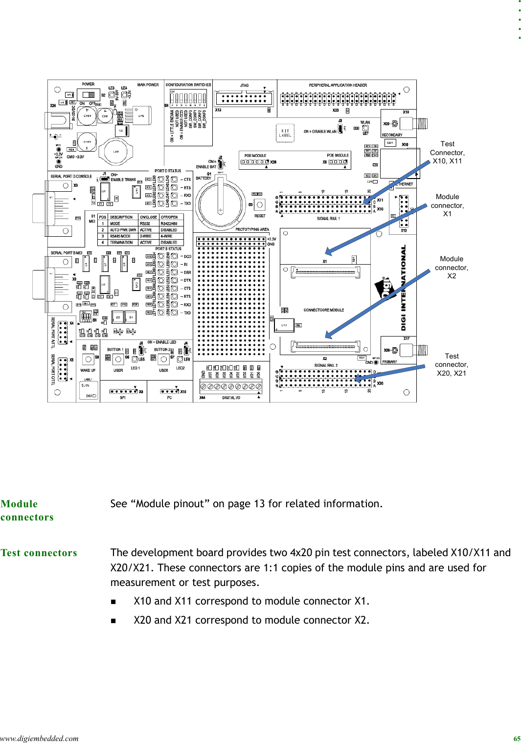
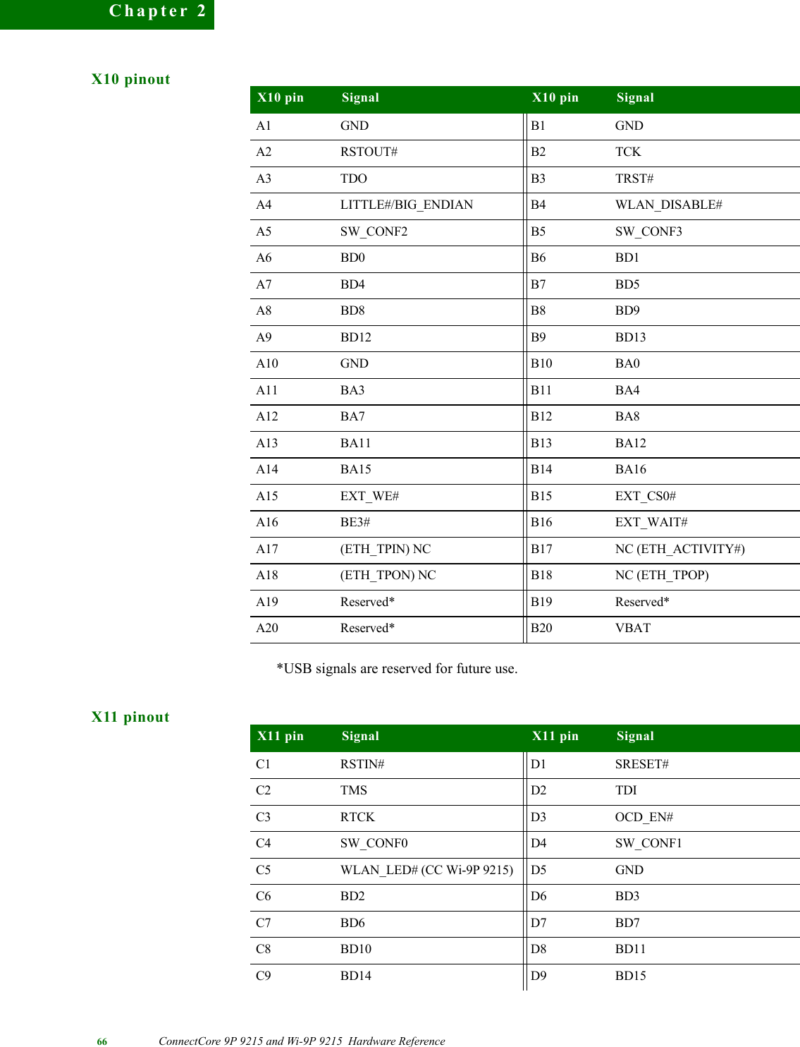
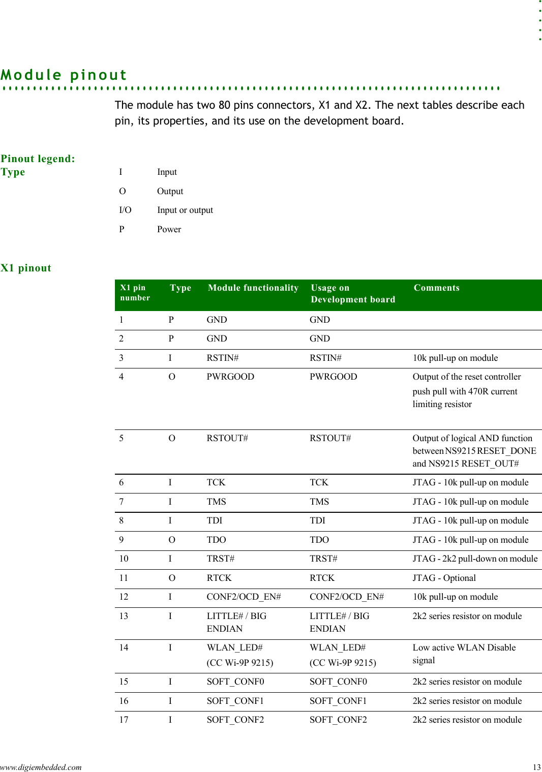
![. . . . .www.digiembedded.com 17X2 pinoutX2 pin number Type Module functionality Usage on Development boardComments1 P GND2 P GND3 I/O DCDA#/DMA0_DONE/PIC_0_GEN_IO[0]GPIO0/SPI_EN (dup)4I/OCTSA#/EIRQ0/PIC_0_GEN_IO[1]GPIO1/-reserved-5I/ODSRA#/EIRQ1/PIC_0_GEN_IO[2]GPIO2/-reserved-6 I/O RXDA/DMA0_PDEN/PIC_0_GEN_IO[3]GPIO3/SPI_RX (dup)7I/ORIA#/EIRQ2/Timer6_in/GPIO4SPI_CLK (dup)/8 I/O RTSA#/ RS485CTLAEIRQ3/Timer6_Out/GPIO5/SPI_CLK (dup)/9 I/O DTRA#/ TXCLKADMA0_REQ/Timer7_In/GPIO6/PIC_DBG_DATA_OUT](https://usermanual.wiki/Digi/50M1589/User-Guide-1073858-Page-17.png)
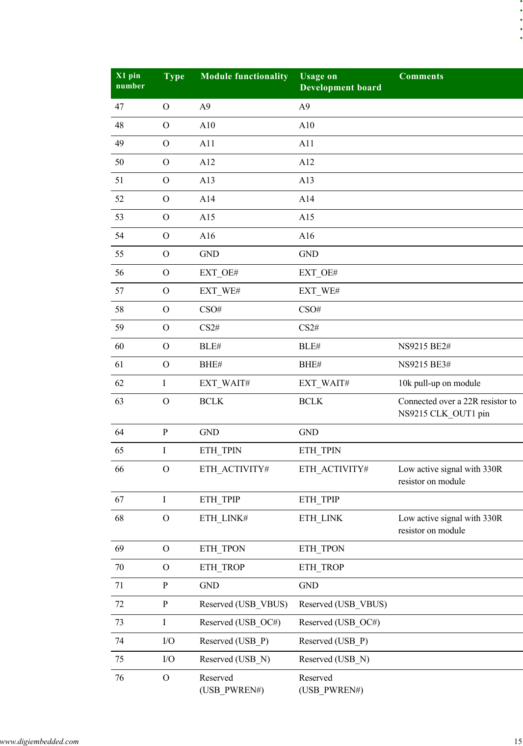
![. . . . .www.digiembedded.com 1918 I/O TXDC/Timer9_In/PIC_0_CAN_TXDGPIO15/SPI_ENboot19 I/O DCDB# (dup)/PIC_0_BUS_1[8]PIC_1_BUS_1[8]GPIO51/20 I/O CTSB# (dup)/PIC_0_BUS_1[9]PIC_1_BUS_1[9]GPIO52/21 I/O DSRB# (dup)/PIC_0_BUS_1[10]PIC_1_BUS_1[10]GPIO53/22 I/O RXDB (dup)/PIC_0_BUS_1[11]PIC_1_BUS_1[11]GPIO54/23 I/O RIB# (dup)/PIC_0_BUS_1[12]PIC_1_BUS_1[12]GPIO55/24 I/O RTSB# (dup) / RS485CTLB (dup) /PIC_0_BUS_1[13]PIC_1_BUS_1[13]GPIO56/25 I/O TXCLKB (dup)/ DTRB# (dup) /PIC_0_BUS_1[14]PIC_1_BUS_1[14]GPIO57/26 I/O TXDB (dup)/PIC_0_BUS_1[15]PIC_1_BUS_1[15]GPIO58/X2 pin number Type Module functionality Usage on Development boardComments](https://usermanual.wiki/Digi/50M1589/User-Guide-1073858-Page-19.png)
![20 ConnectCore 9P 9215 and Wi-9P 9215 Hardware ReferenceChapter 127 I/O DCDD# (dup) /PIC_0_BUS_1[16]PIC_1_BUS_1[16]GPIO59/28 I/O CTSD# (dup)/PIC_0_BUS_1[17]PIC_1_BUS_1[17]GPIO60/29 I/O DSRD# (dup)/PIC_0_BUS_1[18]PIC_1_BUS_1[18]GPIO61/30 I/O RXDD (dup)/PIC_0_BUS_1[19]PIC_1_BUS_1[19]GPIO62/31 I/O RID# (dup)/PIC_0_BUS_1[20]PIC_1_BUS_1[20]GPIO63/32 I/O RTSD# (dup) / RS485CTLD(dup) /PIC_0_BUS_1[21]PIC_1_BUS_1[21]GPIO64/33 I/O TXCLKD (dup) / DTRD# (dup) /PIC_0_BUS_1[22]PIC_1_BUS_1[22]GPIO6534 I/O TXDD (dup) /PIC_0_BUS_1[23]PIC_1_BUS_1[23]GPIO6635 I/O PIC_0_CLK[I]PIC_0_CLK[0]EIRQ3 (dup)/GPIO6736 I/O PIC_0_GEN_IO[0]PIC_1_GEN_IO[0]PIC_1_CAN_RXDGPIO68X2 pin number Type Module functionality Usage on Development boardComments](https://usermanual.wiki/Digi/50M1589/User-Guide-1073858-Page-20.png)
![. . . . .www.digiembedded.com 2137 I/O PIC_0_GEN_IO[1]PIC_1_GEN_IO[1]PIC_1_CAN_TXDGPIO6938 I/O PIC_0_GEN_IO[2]PIC_1_GEN_IO[2]PWM0/GPIO7039 I/O PIC_0_GEN_IO[3]PIC_1_GEN_IO[3]PWM1/GPIO7140 I/O PIC_0_GEN_IO[4]PIC_1_GEN_IO[4]PWM2/GPIO7241 I/O PIC_0_GEN_IO[5]PIC_1_GEN_IO[5]PWM3/GPIO7342 I/O PIC_0_GEN_IO[6]PIC_1_GEN_IO[6]Timer0_In/GPIO7443 I/O PIC_0_GEN_IO[7]PIC_1_GEN_IO[7]Timer1_In/GPIO7544 I/O PIC_0_CTL_IO[0]PIC_1_CTL_IO[0]Timer2_In/GPIO7645 I/O PIC_0_CTL_IO[1]PIC_1_CTL_IO[1]Timer3_In/GPIO7746 I/O PIC_0_CTL_IO[2]PIC_1_CTL_IO[2]Timer4_In/GPIO78X2 pin number Type Module functionality Usage on Development boardComments](https://usermanual.wiki/Digi/50M1589/User-Guide-1073858-Page-21.png)
![22 ConnectCore 9P 9215 and Wi-9P 9215 Hardware ReferenceChapter 147 I/O PIC_0_CTL_IO[3]PIC_1_CTL_IO[3]Timer5_In/GPIO7948 I/O PIC_0_BUS_0[0]PIC_1_BUS_0[0]Timer6_In (dup)/GPIO8049 I/O PIC_0_BUS_0[1]PIC_1_BUS_0[1]Timer7_In (dup)/GPIO8150 I/O PIC_0_BUS_0[2]PIC_1_BUS_0[2]Timer8_In (dup)/GPIO8251 I/O PIC_0_BUS_0[3]PIC_1_BUS_0[3]Timer9_In (dup)/GPIO8352 I/O PIC_0_BUS_0[4]PIC_1_BUS_0[4]Timer0_Out/GPIO8453 I/O PIC_0_BUS_0[5]PIC_1_BUS_0[5]Timer1_Out/GPIO8554 I/O PIC_0_BUS_0[6]PIC_1_BUS_0[6]Timer2_Out/GPIO8655 I/O PIC_0_BUS_0[7]PIC_1_BUS_0[7]Timer3_Out/GPIO8756 I/O PIC_0_BUS_0[13]/PIC_1_BUS_0[13]/Timer9_Out (dup)/GPIO93X2 pin number Type Module functionality Usage on Development boardComments](https://usermanual.wiki/Digi/50M1589/User-Guide-1073858-Page-22.png)
![. . . . .www.digiembedded.com 2357 I/O PIC_0_BUS_0[14]/PIC_1_BUS_0[14]/QDCI (dup)/GPIO9458 I/O PIC_0_BUS_0[15]/PIC_1_BUS_0[15]/QDCQ (dup)/GPIO9559 I/O PIC_0_BUS_1[0]/PIC_1_BUS_1[0]/PIC_0_CAN_RXDGPIO9660 I/O PIC_0_BUS_1[1]/PIC_1_BUS_1[1]/PIC_0_CAN_TXDGPIO9761 I/O PIC_0_BUS_1[2]/PIC_1_BUS_1[2]/PIC_1_CAN_RXDGPIO9862 I/O PIC_0_BUS_1[3]/PIC_1_BUS_1[3]/PIC_1_CAN_TXDGPIO9963 I/O PIC_0_BUS_1[4]/PIC_1_BUS_1[4]/PWM4/GPIO10064 I/O PIC_0_BUS_1[5]/PIC_1_BUS_1[5]/EIRQ3/GPIO10165 I/O PIC_0_BUS_1[6]/PIC_1_BUS_1[6]/I2C_SCL (dup)/GPIO1024k7 pull-up on module66 I/O PIC_0_BUS_1[7]/PIC_1_BUS_1[7]/I2C_SDA (dup)/GPIO1034k7 pull-up on moduleX2 pin number Type Module functionality Usage on Development boardComments](https://usermanual.wiki/Digi/50M1589/User-Guide-1073858-Page-23.png)
![. . . . .www.digiembedded.com 25. . . . . . . . . . . . . . . . . . . . . . . . . . . . . . . . . . . . . . . . . . . . . . . . . . . . . . . . . . . . . . . . . . . . . . . . . . . . . . . . . .Configuration pins — CPUNone of the 64 GPIO pins on connector X2 disturb CPU boot strap functions. The boot strap functions are controlled by address signals; the user can not disturb boot strap functions from outside, if the module configuration signals, described below, are correctly configured.Default module CPU configurationThe user has access to six configuration signals:LITTLE#/BIG_ ENDIAN which allows the user to select the endianess of the module OCD_EN# which allows the user to activate on-chip debuggingSW_CONF [3:0] which are reserved for the user; the user software can read out these signals through the GEN ID register (@ 0xA090_0210).](https://usermanual.wiki/Digi/50M1589/User-Guide-1073858-Page-25.png)
![26 ConnectCore 9P 9215 and Wi-9P 9215 Hardware ReferenceChapter 1. . . . . . . . . . . . . . . . . . . . . . . . . . . . . . . . . . . . . . . . . . . . . . . . . . . . . . . . . . . . . . . . . . . . . . . . . . . . . . . . . .Configuration pins — ModuleThe ConnectCore 9P 9215 and Wi-9P 9215 support the following JTAG signals: TCK, TMS, TDI, TDO, TRST#, and RTCK. Selection can be made between ARM debug mode and boundary scan mode with the signal OCD_EN#.Identification of the moduleIn order to make it easier for software to recognize a module and especially a hardware variant of the module, a specific bit field made of 4-bits has been reserved on the module. This bit field can be read out through GEN ID register and correspond to A[12:9]. These configuration signals use the internal CPU pull-up resistor and can be pulled down through external population option 2k2 resistors.In the same way, 3 bits have been available on the module to identify the SDRAM configuration scheme. This bits correspond to A[19:17]. It is impossible for the user to disturb either the variant specific or SDRAM configuration specific bits from outside.The ConnectCore 9P 9215 and Wi-9P 9215 have also available 4-bit for platform identification. This bit field can be read out through GEN ID register and correspond to A[16:13]. Configuration of these signals is done through the SW_CONF pins. SW_CONF0 is connected to A13 through a 2k2 series resistor, and so on for the further SW_CONF pins. So this bit can be set high by leaving the corresponding SW_CONF pin unconnected and set low by connecting the corresponding SW_CONF pin directly low. The user can benefit from these pins to support application or platform specific software configurations. Module pin configurationSignal name Function PU/PD CommentLITTLE#/BIG_ENDIANSet module endianess. 0 module boots in little endian mode. 1 module boots in big endian mode.PU Signal LITTLE#/BIG_ENDIAN is connected to GPIO_A3/A27 through a 2k2 series resistor.OCD_EN# JTAG / Boundary scan function select0 ARM debug mode, BISTEN# set to high1 Boundary scan mode, BISTEN# set to low PU 10KSW_CONF0 User-defined software configuration pin; can be read in GEN_ID register bit 4, default highConnected to A13 through a 2k2 series resistor.Read bit 4 of GEN ID register (@ 0xA0900210).](https://usermanual.wiki/Digi/50M1589/User-Guide-1073858-Page-26.png)
![. . . . .www.digiembedded.com 27. . . . . . . . . . . . . . . . . . . . . . . . . . . . . . . . . . . . . . . . . . . . . . . . . . . . . . . . . . . . . . . . . . . . . . . . . . . . . . . . . .Clock generationClock frequencies Hardware strapping determines the initial powerup PLL settings. The table below summarizes the default clock frequencies for the ConnectCore 9P 9215 and Wi-9P 9215 modules:SW_CONF1 User-defined software configuration pin; can be read in GEN ID register bit 5, default highConnected to A14 through a 2k2 series resistor.Read bit 5 of GEN ID register (@ 0xA0900210).SW_CONF2 User-defined software configuration pin; can be read in GEN ID register bit 6, default highConnected to A15 through a 2k2 series resistor. Read bit 6 of GEN ID register (@ 0xA0900210).SW_CONF3 User-defined software configuration pin; can be read in GEN ID register bit 7, default highConnected to A16 through a 2k2 series resistor. Read bit 7 of GEN ID register (@ 0xA0900210).Signal name Function PU/PD CommentHardware strapping:"PLL reference clock divider setting: A[4:0] = 0x1D (0b11101)NR = 5"PLL output divider setting:A[6:5] = 0x3 (0b11)OD = 0"PLL bypass setting: A[7] = 0x1 (0b1)Normal operationPLL frequency formula:PLL Vco = (RefClk / NR+1) * (NF+1) ClkOut = PLL Vco / (OD+1)RefClk (Crystal) = 29.4912MHzNF = 0x3C (reset value - can only be changed by software).PLL Vco = (29.4912 / 6) * 61 = 299.8272 MHzClkOut = 299.8272 MHzResulting clock settings:](https://usermanual.wiki/Digi/50M1589/User-Guide-1073858-Page-27.png)
![. . . . .www.digiembedded.com 29. . . . . . . . . . . . . . . . . . . . . . . . . . . . . . . . . . . . . . . . . . . . . . . . . . . . . . . . . . . . . . . . . . . . . . . . . . . . . . . . . .Chip selectsThe module has eight chip selects: four for dynamic memory and four for static memory. Each chip select has a 256MB range.Chip select memory map. . . . . . . . . . . . . . . . . . . . . . . . . . . . . . . . . . . . . . . . . . . . . . . . . . . . . . . . . . . . . . . . . . . . . . . . . . . . . . . . . .SDRAM banksThe module provides connection to 1 SDRAM chip, connected to CS1# (SDM_CS0#). The other SDRAM chip selects are not used.The standard module has one of these SDRAM onboard: 1Mx16x4-banks. A13 is the highest address connected. BA0 and BA1 are connected to A21 and A22, respectively. . . . . . . . . . . . . . . . . . . . . . . . . . . . . . . . . . . . . . . . . . . . . . . . . . . . . . . . . . . . . . . . . . . . . . . . . . . . . . . . . . .Multiplexed GPIO pinsThe 64 GPIOs pins available on the module connector are multiplexed with other functions like:Name CPU Sig. namePin Address range Size [Mb]Usage CommentsSDM_CS0# CS1# D6 0x00000000–0x0FFFFFFF256 SDRAM bank 0 First bank on moduleSDM_CS1# CS3# B5 0x10000000–0x1FFFFFFF256 not usedSDM_CS2# CS5# A4 0x20000000–0x2FFFFFFF256 not usedSDM_CS3# CS7# B4 0x30000000–0x3FFFFFFF256 not used EXT_CS0# CS0# C6 0x40000000–0x4FFFFFFF256 external, CS0#INT_CS1# CS2# B6 0x50000000–0x5FFFFFFFF256 NOR-Flash Program memory on moduleEXT_CS2# CS4# C5 0x60000000–0x6FFFFFFFF256 external, CS2#INT_CS3# CS6# A3 0x70000000–0x7FFFFFFF256 internal, CS3# Reserved for internal usage](https://usermanual.wiki/Digi/50M1589/User-Guide-1073858-Page-29.png)
![30 ConnectCore 9P 9215 and Wi-9P 9215 Hardware ReferenceChapter 1UARTSPIEthernetDMAI2C portTimers and interrupt inputsMemory bus dataPin notes GPIO [15:0] allow five multiplex modes.GPIO [103:16] and GPIO_A [3:0] have four multiplex modes. Using a pin as GPIO means always to give up other functionalities. Some functions are duplicated to enhance the chance to use them without giving up other vital functions.Using original and (dup) functions in parallel is not recommended.Default function of GPIOs after CPU power up is function 03, except GPIO12 (function 02-reset_done) and GPIO [31:16] (function 00 - DATA[15:0]).GPIO multiplex tableIn the GPIO multiplex table below, the default function is written bold,# means low active signal, (dup) means function is available multiple times.Port name, Function 03 Alternate function 00Alternate function 01Alternate function 02Alternate function 04 (only GPIO00...GPIO15)On module, default used asGPIO0 DCDA# DMA0_DONE PIC_0_GEN_IO[0] SPI_EN# (dup) DCDA# / SPI_EN#GPIO1 CTSA# EIRQ0 PIC_0_GEN_IO[1] Reserved CTSA#GPIO2 DSRA# EIRQ1 PIC_0_GEN_IO[2] Reserved DSRA#GPIO3 RXDA# DMA0_PDEN PIC_0_GEN_IO[3] SPI_RXD (dup) RXDA / SPI_RXDGPIO4 RIA# EIRQ2 Timer6_In SPI_CLK (dup) RIA# / SPI_CLKGPIO5 RTSA# / 485CTLA EIRQ3 Timer6_Out SPI_CLK (dup) RTSA#GPIO6 TXCLKA / DTRA# DMA0_REQ Timer7_In PIC_DBG_DATA_OUT DTRA#GPIO7 TXDA Timer8_In Timer7_Out SPI_TXD (dup) TXDA / SPI_TXDGPIO8 DCDC# / TXCLKC DMA1_DONE Timer8_Out SPI_EN# (dup) DCDC#GPIO9 CTSC# I2C_SCL EIRQ0 (dup) PIC_DBG_DATA_IN CTSC#GPIO10 DSRC# QDCI EIRQ1 (dup) PIC_DBG_CLK DSRC#](https://usermanual.wiki/Digi/50M1589/User-Guide-1073858-Page-30.png)
![. . . . .www.digiembedded.com 31GPIO11 RXDC# DMA1_PDEN EIRQ2 (dup) SPI_RXD (boot) RXDCGPIO12 RXCLKC / RIC# I2C_SDA RESET_DONE SPI_CLK (dup) RIC# 1GPIO13 RXCLKC / RTSC# /485CTLCQDCQ Timer9_out SPI_CLK (boot) RXCLKC / RTSC#GPIO14 TXCLKC / DTRC# DMA1_REQ PIC_0_CAN_RXD SPI_TXD (boot) TXCLKCGPIO15 TXDC Timer9_In PIC_0_CAN_TXD SPI_EN# (boot) TXDCGPIO16 D0 DCDB# EIRQ0 (dup) Reserved for upper data linesGPIO17 D1 CTSB# EIRQ1 (dup) Reserved for upper data linesGPIO18 D2 DSRB# EIRQ2 (dup) Reserved for upper data linesGPIO19 D3 RXDB EIRQ3 (dup) Reserved for upper data linesGPIO20 D4 RIB# DMA0_DONE (dup) Reserved for upper data linesGPIO21 D5 RTSB# / 485CTLB DMA0_PDEN (dup) Reserved for upper data linesGPIO22 D6 TXCLKB / DTRB# DMA1_DONE (dup) Reserved for upper data linesGPIO23 D7 TXDB PIC_1_CAN_RXD Reserved for upper data linesGPIO24 D8 DCDD# PIC_1_CAN_TXD Reserved for upper data linesGPIO25 D9 CTSD# RESET_DONE (dup) Reserved for upper data linesGPIO26 D10 DSRD# PIC_1_GEN_IO[0] Reserved for upper data linesGPIO27 D11 RXDD PIC_1_GEN_IO[1] Reserved for upper data linesGPIO28 D12 RID# PIC_1_GEN_IO[2] Reserved for upper data linesGPIO29 D13 RTSD# / 485CTLD PIC_1_GEN_IO[3] Reserved for upper data linesGPIO30 D14 TXCLKD / DTRD# Reserved Reserved for upper data linesPort name, Function 03 Alternate function 00Alternate function 01Alternate function 02Alternate function 04 (only GPIO00...GPIO15)On module, default used as](https://usermanual.wiki/Digi/50M1589/User-Guide-1073858-Page-31.png)
![32 ConnectCore 9P 9215 and Wi-9P 9215 Hardware ReferenceChapter 1GPIO31 D15 TXDD Reserved Reserved for upper data linesGPIO32 MII_MDC PIC_0_GEN_IO[0] Reserved MII InterfaceGPIO33 MII_TXC PIC_0_GEN_IO[1] Reserved MII InterfaceGPIO34 MII_RXC PIC_0_GEN_IO[2] Reserved MII InterfaceGPIO35 MII_MDIO PIC_0_GEN_IO[3] Reserved MII InterfaceGPIO36 MII_RXDV PIC_0_GEN_IO[4] Reserved MII InterfaceGPIO37 MII_RXER PIC_0_GEN_IO[5] Reserved MII InterfaceGPIO38 MII_RXD0 PIC_0_GEN_IO[6] Reserved MII InterfaceGPIO39 MII_RXD1 PIC_0_GEN_IO[7] Reserved MII InterfaceGPIO40 MII_RXD2 PIC_1_GEN_IO[0] Reserved MII InterfaceGPIO41 MII_RXD3 PIC_1_GEN_IO[1] Reserved MII InterfaceGPIO42 MII_TXEN PIC_1_GEN_IO[2] Reserved MII InterfaceGPIO43 MII_TXER PIC_1_GEN_IO[3] Reserved MII InterfaceGPIO44 MII_TXD0 PIC_1_GEN_IO[4] Reserved MII InterfaceGPIO45 MII_TXD1 PIC_1_GEN_IO[5] Reserved MII InterfaceGPIO46 MII_TXD2 PIC_1_GEN_IO[6] Reserved MII InterfaceGPIO47 MII_TXD3 PIC_1_GEN_IO[7] Reserved MII InterfaceGPIO48 MII_COL Reserved Reserved MII InterfaceGPIO49 MII_CRS Reserved Reserved MII InterfaceGPIO50 MII_PHY_Int PIC_1_CLK (I) PIC_1_CLK(0) MII InterfaceGPIO51 DCDB# (dup) PIC_0_BUS_1[8] PIC_1_BUS_1[8] DCDB#GPIO52 CTSB# (dup) PIC_0_BUS_1[9] PIC_1_BUS_1[9] CTSB#GPIO53 DSRB# (dup) PIC_0_BUS_1[10] PIC_1_BUS_1[10] DSRB#GPIO54 RXDB (dup) PIC_0_BUS_1[11] PIC_1_BUS_1[11] RXDBGPIO55 RIB# (dup) PIC_0_BUS_1[12] PIC_1_BUS_1[12] RIB#GPIO56 RTSB# / 485CTLB (dup)PIC_0_BUS_1[13] PIC_1_BUS_1[13] RTSB#GPIO57 TXCLKB (dup) / DTRB# (dup)PIC_0_BUS_1[14] PIC_1_BUS_1[14] DTRB#GPIO58 TXDB (dup) PIC_0_BUS_1[15] PIC_1_BUS_1[15] TXDBGPIO59 DCDD# (dup) PIC_0_BUS_1[16] PIC_1_BUS_1[16] DCDD#GPIO60 CTSD# (dup) PIC_0_BUS_1[17] PIC_1_BUS_1[17] CTSD#Port name, Function 03 Alternate function 00Alternate function 01Alternate function 02Alternate function 04 (only GPIO00...GPIO15)On module, default used as](https://usermanual.wiki/Digi/50M1589/User-Guide-1073858-Page-32.png)
![. . . . .www.digiembedded.com 33GPIO61 DSRD# (dup) PIC_0_BUS_1[18] PIC_1_BUS_1[18] DSRD#GPIO62 RXDD (dup) PIC_0_BUS_1[19] PIC_1_BUS_1[19] RXDDGPIO63 RID# (dup) PIC_0_BUS_1[20] PIC_1_BUS_1[20] RID#GPIO64 RTSD# / 485CTLD (dup)PIC_0_BUS_1[21] PIC_1_BUS_1[21] RTSD#GPIO65 TXCLKD (dup) / DTRD# (dup)PIC_0_BUS_1[22] PIC_1_BUS_1[22] DTRD#GPIO66 TXDD (dup) PIC_0_BUS_1[23] PIC_1_BUS_1[23] TXDDGPIO67 PIC_0_CLK (I) PIC_0_CLK (O) EIRQ3 (dup) PIC_0_CLKGPIO68 PIC_0_GEN_IO[0] PIC_1_GEN_IO[0] PIC_1_CAN_RXD PIC_0_GEN_IO[0]GPIO69 PIC_0_GEN_IO[1] PIC_1_GEN_IO[1] PIC_1_CAN_TXD PIC_0_GEN_IO[1]GPIO70 PIC_0_GEN_IO[2] PIC_1_GEN_IO[2] PWM0 PIC_0_GEN_IO[2]GPIO71 PIC_0_GEN_IO[3] PIC_1_GEN_IO[3] PWM1 PIC_0_GEN_IO[3]GPIO72 PIC_0_GEN_IO[4] PIC_1_GEN_IO[4] PWM2 PIC_0_GEN_IO[4]GPIO73 PIC_0_GEN_IO[5] PIC_1_GEN_IO[5] PWM3 PIC_0_GEN_IO[5]GPIO74 PIC_0_GEN_IO[6] PIC_1_GEN_IO[6] Timer0_In PIC_0_GEN_IO[6]GPIO75 PIC_0_GEN_IO[7] PIC_1_GEN_IO[7] Timer1_In PIC_0_GEN_IO[7]GPIO76 PIC_0_CTL_IO[0] PIC_1_CTL_IO[0] Timer2_In PIC_0_CTL_IO[0]GPIO77 PIC_0_CTL_IO[1] PIC_1_CTL_IO[1] Timer3_In PIC_0_CTL_IO[1]GPIO78 PIC_0_CTL_IO[2] PIC_1_CTL_IO[2] Timer4_In PIC_0_CTL_IO[2]GPIO79 PIC_0_CTL_IO[3] PIC_1_CTL_IO[3] Timer5_In PIC_0_CTL_IO[3]GPIO80 PIC_0_BUS_0[0] PIC_1_BUS_0[0] Timer6_In (dup) Timer6_InGPIO81 PIC_0_BUS_0[1] PIC_1_BUS_0[1] Timer7_In (dup) Timer7_InGPIO82 PIC_0_BUS_0[2] PIC_1_BUS_0[2] Timer8_In (dup) Timer8_InGPIO83 PIC_0_BUS_0[3] PIC_1_BUS_0[3] Timer9_In (dup) Timer9_InGPIO84 PIC_0_BUS_0[4] PIC_1_BUS_0[4] Timer0_Out Timer0_OutGPIO85 PIC_0_BUS_0[5] PIC_1_BUS_0[5] Timer1_Out Timer1_OutGPIO86 PIC_0_BUS_0[6] PIC_1_BUS_0[6] Timer2_Out Timer2_OutGPIO87 PIC_0_BUS_0[7] PIC_1_BUS_0[7] Timer3_Out Timer3_OutGPIO88 PIC_0_BUS_0[8] PIC_1_BUS_0[8] Timer4_Out User LED 0 => LED 1 (on module)GPIO89 PIC_0_BUS_0[9] PIC_1_BUS_0[9] Timer5_Out User LED 1 => LED 2 (on module)Port name, Function 03 Alternate function 00Alternate function 01Alternate function 02Alternate function 04 (only GPIO00...GPIO15)On module, default used as](https://usermanual.wiki/Digi/50M1589/User-Guide-1073858-Page-33.png)
![34 ConnectCore 9P 9215 and Wi-9P 9215 Hardware ReferenceChapter 11 Put a series resistor on the baseboard in this case to avoid input/output conflict between RESET_DONE (output/boot default) and RIC# (input/configuration default). . . . . . . . . . . . . . . . . . . . . . . . . . . . . . . . . . . . . . . . . . . . . . . . . . . . . . . . . . . . . . . . . . . . . . . . . . . . . . . . . . .Module LEDsBy default, the ConnectCore 9P/Wi-9P modules use the LE1 and LE2 LEDs as described:ConnectCore Wi-9P module: To indicate WLAN-related information, such as association status and network activity. ConnectCore 9Pand Wi-9Pmodules: LE1 will flash a repeating blink pattern in a major system failure; for example, a processor exception or Power on Self Te s t f a i lu r e .GPIO90 PIC_0_BUS_0[10] PIC_1_BUS_0[10] Timer6_Out (dup) GPIO reserved on moduleGPIO91 PIC_0_BUS_0[11] PIC_1_BUS_0[11] Timer7_Out (dup) Reserved NAND_R/B#GPIO92 PIC_0_BUS_0[12] PIC_1_BUS_0[12] Timer8_Out (dup) GPIO reserved on moduleGPIO93 PIC_0_BUS_0[13] PIC_1_BUS_0[13] Timer9_Out (dup) Timer9_OutGPIO94 PIC_0_BUS_0[14] PIC_1_BUS_0[14] QDCI (dup) QDCIGPIO95 PIC_0_BUS_0[15] PIC_1_BUS_0[15] QDCQ (dup) QDCQGPIO96 PIC_0_BUS_1[0] PIC_1_BUS_1[0] PIC_0_CAN_RXD PIC_0_CAN_RXDGPIO97 PIC_0_BUS_1[1] PIC_1_BUS_1[1] PIC_0_CAN_TXD PIC_0_CAN_TXDGPIO98 PIC_0_BUS_1[2] PIC_1_BUS_1[2] PIC_1_CAN_RXD PIC_1_CAN_RXDGPIO99 PIC_0_BUS_1[3] PIC_1_BUS_1[3] PIC_1_CAN_TXD PIC_1_CAN_TXDGPIO100 PIC_0_BUS_1[4] PIC_1_BUS_1[4] PWM4 PWM4GPIO101 PIC_0_BUS_1[5] PIC_1_BUS_1[5] EIRQ3 EIRQ3GPIO102 PIC_0_BUS_1[6] PIC_1_BUS_1[6] I2C_SCL (dup) I2C_SCLGPIO103 PIC_0_BUS_1[7] PIC_1_BUS_1[7] I2C_SDA (dup) I2C_SDAGPIO_A0 A24 I2C_SCL dupe EIRQ0 (dup) Reserved EIRQ0 GPIO_A1 A25 I2C_SDA dupe EIRQ1 (dup) Reserved EIRQ1 - USBGPIO_A2 A26 CS0_WE# EIRQ2 (dup) GPIO reserved on moduleGPIO_A3 A27 CS0_OE# UART_REFCLK Little/Big EndianPort name, Function 03 Alternate function 00Alternate function 01Alternate function 02Alternate function 04 (only GPIO00...GPIO15)On module, default used as](https://usermanual.wiki/Digi/50M1589/User-Guide-1073858-Page-34.png)
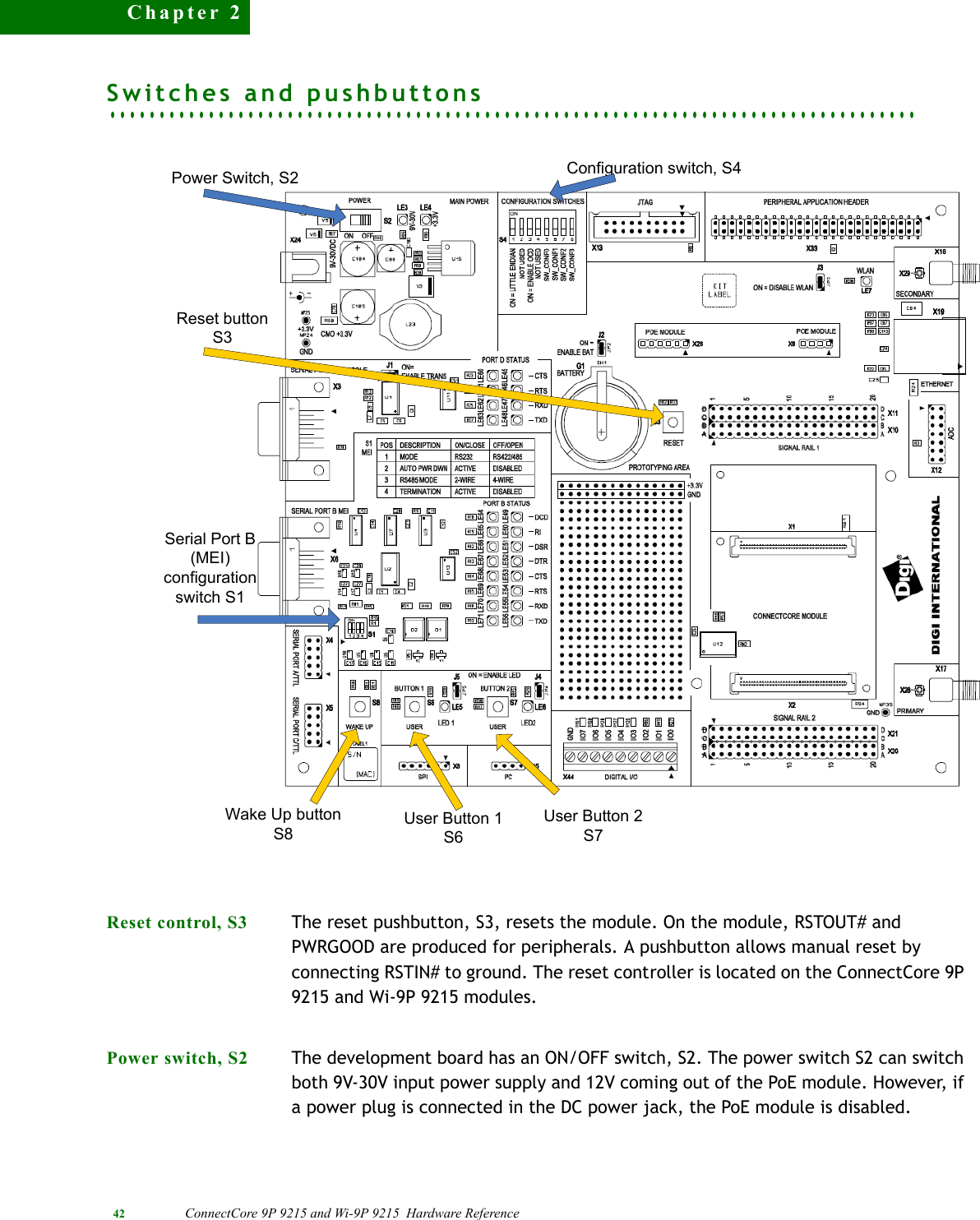
![. . . . .www.digiembedded.com 43User pushbuttons, S6 and S7Use the user pushbuttons to interact with the applications running on the ConnectCore 9P 9215 and Wi-9P 9215 modules. Use these module signals to implement the pushbuttons:Legend for multi-pin switchesSwitches 1 and 4 are multi-pin switches. In the description tables for these switches, the pin is designated as S[switch number].[pin number]. For example, pin 1 in switch 4 is specified as S4.1.Module configuration switches, S4Use S4 to configure the module:Wake-up button, S8The wake-up pushbutton, S8, generates an external interrupt to the module's NS9215 processor using the EIRQ2 signal.Serial Port B MEI configuration switches, S1Use S1 to configure the line interface for serial port B MEI:Signal name Switch (pushbutton)GPIO usedUSER_PUSH_BUTTON_1 S6 GPIO81USER_PUSH_BUTTON_2 S7 GPIO84Switch pin FunctionS4.1 On = Little endianOff = Big endianS4.2 Not usedS4.3 On = ARM DebugOff = Boundary ScanS4.4 Not usedS4.5 – S4.8 Not defined. Software configuration signals, which can be available for user specific configuration.](https://usermanual.wiki/Digi/50M1589/User-Guide-1073858-Page-43.png)
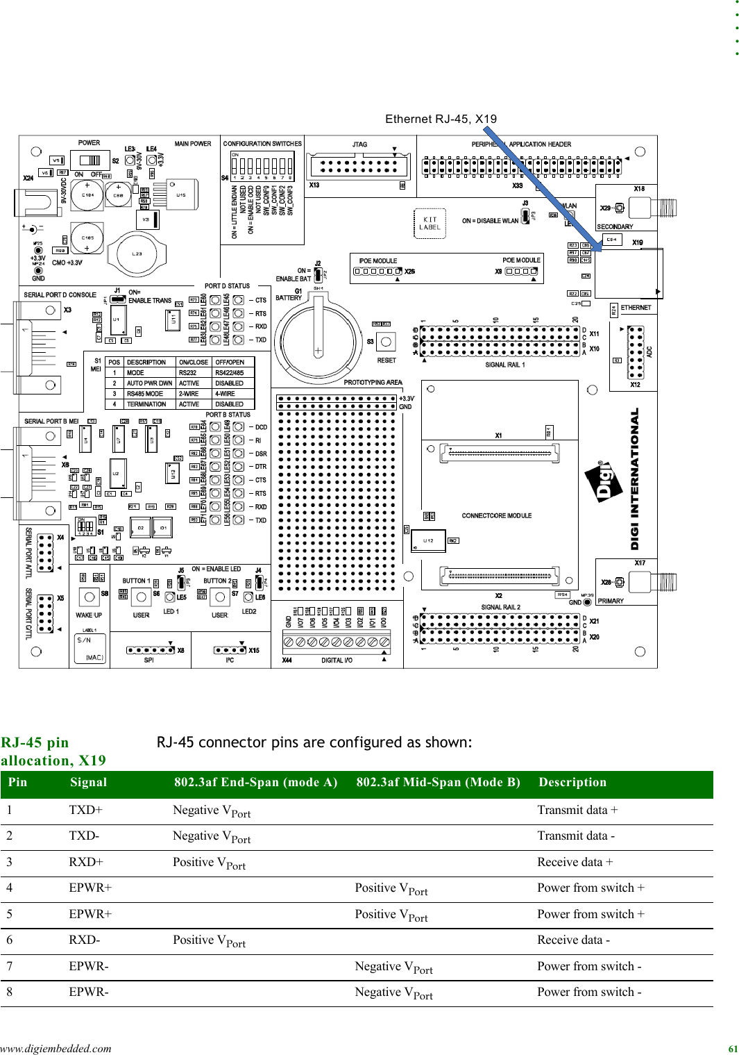
![62 ConnectCore 9P 9215 and Wi-9P 9215 Hardware ReferenceChapter 2LEDs The RJ-45 connector has two LEDs located near the outer lower corners of the connector. These LEDs are not programmable.. . . . . . . . . . . . . . . . . . . . . . . . . . . . . . . . . . . . . . . . . . . . . . . . . . . . . . . . . . . . . . . . . . . . . . . . . . . . . . . . . .WLAN interfaceFor the ConnectCore Wi-9P 9215, attach the antenna to the primary connector [X17] and the secondary connector [X18] on the development board. See figure below.LED DescriptionYellow Network activity (speed): Flashing when network traffic detected; Off when no network traffic detected.Green Network link: On indicates an active network link; Off indicates that no network link is present.Secondaryantennaconnector [X18]Primary antenna connector [X17]](https://usermanual.wiki/Digi/50M1589/User-Guide-1073858-Page-62.png)