Digi 50M880 802.11b Wireless Module User Manual Digi Connect ME Wi ME Hardware Reference
Digi International Inc 802.11b Wireless Module Digi Connect ME Wi ME Hardware Reference
Digi >
Contents
- 1. manual
- 2. user manual
manual
TM
TM
90000631_A
DC_ME-HWR.book Page 1 Thursday, July 1, 2004 11:12 AM

DC_ME-HWR.book Page 2 Thursday, July 1, 2004 11:12 AM
Digi International Inc. 2004. All Rights Reserved.
The Digi logo is a registered trademark of Digi International, Inc.
Connectware and Digi Connect ME and Digi Connect Wi-ME are trademarks of Digi International, Inc.
NetSilicon, NET+Works, NET+OS, and NET+ are trademarks of NetSilicon, Inc.
All other trademarks mentioned in this document are the property of their respective owners.
Information in this document is subject to change without notice and does not represent a commitment on the part of Digi
International.
Digi provides this document “as is,” without warranty of any kind, either expressed or implied, including, but not limited to,
the implied warranties of fitness or merchantability for a particular purpose. Digi may make improvements and/or changes
in this manual or in the product(s) and/or the program(s) described in this manual at any time.
This product could include technical inaccuracies or typographical errors. Changes are periodically made to the information
herein; these changes may be incorporated in new editions of the publication.
DC_ME-HWR.book Page 3 Thursday, July 1, 2004 11:12 AM
DC_ME-HWR.book Page 4 Thursday, July 1, 2004 11:12 AM

5
Contents
About This Document ................................................................................................................7
Kits Contents....................................................................................................................7
Related Documentation....................................................................................................8
Support Information .........................................................................................................8
Chapter 1: About the Digi Connect ME & Digi Connect Wi-ME Embedded Modules.9
Overview ..........................................................................................................................9
Types of Modules........................................................................................................... 10
Connectors: Power and Device Interface.......................................................................12
Connectors: Ethernet Interface....................................................................................... 13
Connectors: Antenna...................................................................................................... 15
Module LEDs ................................................................................................................. 15
Chapter 2: About the Development Board .......................................................................17
Overview ........................................................................................................................17
Basic Description ...........................................................................................................18
Port Descriptions............................................................................................................20
Connectors and Blocks...................................................................................................23
Switches..........................................................................................................................27
Development Board LEDs .............................................................................................30
Power Jack......................................................................................................................32
Test points ......................................................................................................................33
Chapter 3: Programming Considerations.........................................................................35
Overview ........................................................................................................................35
GPIO...............................................................................................................................36
LEDs...............................................................................................................................38
Reset............................................................................................................................... 38
DC_ME-HWR.book Page 5 Thursday, July 1, 2004 11:12 AM

6
Flash............................................................................................................................... 40
Appendix A Module Specifications.................................................................................... 41
Network Interface .......................................................................................................... 41
Serial Interface............................................................................................................... 42
Data Rates (bps)............................................................................................................. 42
Flow Control Options..................................................................................................... 42
GPIO .............................................................................................................................. 42
DC Characteristics ......................................................................................................... 43
Environmental................................................................................................................ 44
Mechanical..................................................................................................................... 45
Dimensions..................................................................................................................... 46
Recommended PCB Layout........................................................................................... 51
Antenna Information...................................................................................................... 53
RF Exposure Statement.................................................................................................. 54
Safety Statements........................................................................................................... 55
Appendix B Certifications.................................................................................................. 57
FCC Part 15 Class B ...................................................................................................... 57
Industry Canada ............................................................................................................. 58
Declaration of Conformity............................................................................................. 59
International EMC Standards......................................................................................... 60
Safety Standards............................................................................................................. 60
Appendix C Sample Application: TTL Signals to EIA-232 ............................................ 61
DC_ME-HWR.book Page 6 Thursday, July 1, 2004 11:12 AM

7
•••••••••••••••••••••••••••••••••••••••••••••••••••••••
•
About This Document
Scope of the Reference Manual
The purpose of this document is to enable developers to integrate the Digi Connect ME or
Digi Connect Wi-ME embedded modules with other devices, enabling these devices to
make use of the module’s rich networking features.
Note
Unless mentioned specifically by name, the products will be referred to as the
embedded modules or modules. Individual naming is used to differentiate
product specific features.
Kits Contents
This manual is intended for customers who use embedded modules Integration Kits or
Development Kits, which are described below.
About the Integration Kit
The integration kit is the ideal platform for product evaluation, rapid prototyping, and
integration of the embedded modules. Targeted specifically at customers who want to take
advantage of the embedded modules with Digi plug-and-play firmware functionality, it
enables integration of the modules without any extensive embedded software development
with all the additional flexibility and benefits of web user interface customization and
application specific java applets.
About the Development Kit
The Digi Connect ME or Digi Connect Wi-ME Development Kit are easy-to-use and
royalty-free development platforms that significantly reduces traditional design risk and
DC_ME-HWR.book Page 7 Thursday, July 1, 2004 11:12 AM

Related Documentation
8
Digi Connect Wi-ME & Digi Connect ME Hardware Reference
accelerates the overall software development process. The kits deliver the integrated
building blocks to quickly and cost effectively create your own custom firmware for an
embedded module based high-performance networking solution that fits the specific
requirements of your application.
Related Documentation
See the NS7520 Hardware Reference for information on the NS7520 chip.
Support Information
To get help with a question or technical problem or make comments and recommendations
about Digi products and documentation, use the following contact information.
General Customer Service and Support
Digi International
11001 Bren Road East
Minnetonka, MN 55343
U.S.A.
United States: 1 877-912-3444
Other Locations: 1 952-912-3444
www.digi.com/support/
www.digi.com
DC_ME-HWR.book Page 8 Thursday, July 1, 2004 11:12 AM

9
About the Digi Connect
ME & Digi Connect Wi-ME
Embedded Modules
CHAPTER 1
Overview
The embedded modules provide fully transparent device connectivity over industry-
standard Ethernet connections and allows both equipment manufacturers and systems
integrators to network-enable products at a fraction of the time and cost required to develop
a custom solution. It is a highly flexible and compact single component solution with a
serial port, GPIO ports, and a robust on-board TCP/IP stack and 10/100 BASE-T Ethernet
support or wireless interface..
From medical systems to building control and industrial automation, in virtually any
application where embedded device connectivity over Ethernet or wireless connectivity is
needed, embedded modules are the ideal choice, delivering high-performance functionality.
Note
Unless mentioned specifically by name, the products will be referred to as the
embedded modules or modules. Individual naming is used to differentiate
product specific features.
This chapter provides information about the modules hardware and contains the following
topics:
"Types of Modules" on page 10
"Connectors: Antenna" on page 15
"Connectors: Ethernet Interface" on page 13
DC_ME-HWR.book Page 9 Thursday, July 1, 2004 11:12 AM
Types of Modules
10 Digi Connect Wi-ME & Digi Connect ME Hardware Reference
"Module LEDs" on page 15
Types of Modules
The type of module that you will use for hardware integration depends on the kit you are
using. If you are using an integration kit, you will be using a module without a JTAG
interface. If you are using a development kit, you will be using a module with a JTAG
interface.
Note
JTAG is a commonly used term that is also referred to as IEEE 1149.1, an
industry standard test protocol. JTAG is an abbreviation for the European Joint
Test Action Group, which invented the first versions of the IEEE 1149.1
interface. The JTAG interface, along with the other development tools, enables
you to download, run and debug programs on the module.
The following figures show the two types of modules.
Digi Connect ME Modules
Model Description Figure
DC-ME-01T-JT
Used for development purposes
only
JTAG interface
DC_ME-HWR.book Page 10 Thursday, July 1, 2004 11:12 AM
11
About the Digi Connect ME & Digi Connect Wi-ME Embedded Modules
DC-ME-01T-S
DC-ME-01T-C
No JTAG interface
Ordered independently of either
kit for use in your
implementation.
Digi Connect ME Modules
Model Description Figure
Digi Connect Wi-ME Modules
Model Description Figure
DC-WIME-01T-JT
Used for development purposes
only
JTAG interface
DC-WIME-01T-S
DC-WIME-01T-C
No JTAG interface
Ordered independently of either
the development or integration
kit for use in your
implementation.
DC_ME-HWR.book Page 11 Thursday, July 1, 2004 11:12 AM
Connectors: Power and Device Interface
12 Digi Connect Wi-ME & Digi Connect ME Hardware Reference
Note
-S: No JTAG for use with Digi Firmware
-C: No JTAG for use with Custom Firmware
-JT: With JTAG for use with custom firmware development
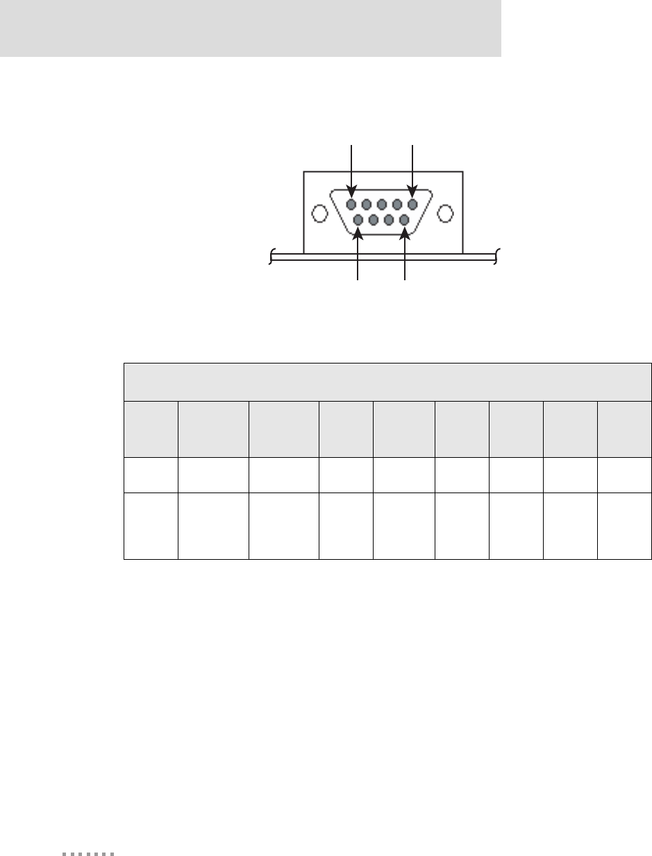
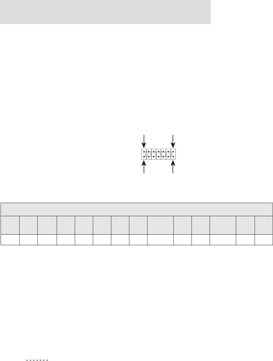
Connectors: Power and Device Interface
The module has a 20-pin male connector that supports a serial interface with data rates up
to 230,400 bps and full-modem control, and GPIO ports. See the following figure for pin
orientation and the table for pin assignments.
Note
Digi recommends 100 pF capacitors to circuit ground on all inputs and outputs
to the module for ESD immunity. This includes the power pass-thru pins if they
are not used.
Power and Device Interface Connector
Power and Device Interface Connector Pin Assignments
Pin Signal Description
1 VETH+ Power Pass-Thru +
2 VETH- Power Pass-Thru -
3-6 — Position Removed
DC_ME-HWR.book Page 12 Thursday, July 1, 2004 11:12 AM
13
About the Digi Connect ME & Digi Connect Wi-ME Embedded Modules
Note
The development board provides a reference design of a POE (Power Over
Ethernet) power supply. A schematic for this reference design is installed by
the setup program on the CD.
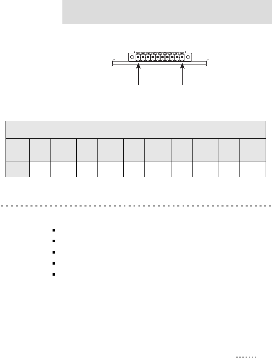
Connectors: Ethernet Interface
The Ethernet connector is an 8-wire RJ-45 jack that meets the ISO 8877 requirements for
10/100BASE-T. See the following figure and table for pin orientation and pin assignments.
Note
Pin orientation and assignments are the same for modules with or without a
JTAG connector.
7 RXD Receive Data (Input)
8 TXD Transmit Data (Output)
9 RTS / GPIO 4 Request to Send (Output) / GPIO
10 DTR / GPIO 5
Data Terminal Ready (Output) / GPIO
11 CTS / GPIO 2 Clear to Send (Input) / GPIO
12 DSR / GPIO 3 Data Set Ready (Input) / GPIO
13 DCD / GPIO 1
Data Carrier Detect (Input) / GPIO
14 RESET Reset
15 +3.3V Power
16 GND Ground
17-19 — Reserved. Do not connect.
20 /INIT Software Reset
Power and Device Interface Connector Pin Assignments
Pin Signal Description
DC_ME-HWR.book Page 13 Thursday, July 1, 2004 11:12 AM
Connectors: Ethernet Interface
14 Digi Connect Wi-ME & Digi Connect ME Hardware Reference
Ethernet Interface Pin Orientation
Ethernet Interface Pin Assignments
Pin
1Pin
2Pin
3Pin
4Pin
5Pin
6Pin
7Pin
8
TXD+ TXD- RXD+ EPWR+ EPWR+ RXD- EPWR- EPWR-
Transmit
Data +
Transmit
Data -
Receive
Data +
Power
from
Switch +
Power
from
Switch +
Receive
Data -
Power from
Switch -
Power from
Switch -
00000021
Pin 1
Pin 8
DC_ME-HWR.book Page 14 Thursday, July 1, 2004 11:12 AM
15
About the Digi Connect ME & Digi Connect Wi-ME Embedded Modules
Connectors: Antenna
The Digi Connect Wi-ME is available with 1 RP-SMA connector. The antenna is
connected to the module with a reverse polarity SMA connector (sub-miniature size A).
The antenna only fits on the module one way to ensure a proper connection. Another option
for both signal reception and design flexibility is to use a "pig tail" cable (Digi part number
DC-ANT-EC) to separate the antenna from the module. This allows the module to fit inside
your product but the antenna to be placed outside the device.
Module LEDs
The module has two LEDs that are located near the upper corners of the Ethernet port (see
the following figure). The following table describes the LEDs.
Note
The LEDs are the same for a module with or without a JTAG connector.
Antenna Specifications
Type Dipole
Part number DC-ANT-24DP
Gain 2 dBi
Caution: This Part 15 radio device operates on a non-interference basis
with other devices operating at this frequency when using the antennae
listed in the Antenna Specification table. Any changes or modification to
user’s authority to operate the device.
the product not expressly approved by Digi International could void the
DC_ME-HWR.book Page 15 Thursday, July 1, 2004 11:12 AM
Module LEDs
16 Digi Connect Wi-ME & Digi Connect ME Hardware Reference
LED Locations
LED Descriptions
LED Color Description
Network Link (left-upper) Yellow
Network Link is operational: On
(continuously) indicates that an Ethernet
connection is made or an access point is
engaged.
Network Activity/
Diagnostic (right-upper) Green
Network Activity: On when network traffic
detected; off when no network traffic detected.
Diagnostic: Flashes three times in even
duration during power up or reset, indicating
successful startup.
DC_ME-HWR.book Page 16 Thursday, July 1, 2004 11:12 AM

17
About the Development
Board
CHAPTER 2
Overview
The development board is a hardware platform from which you can determine how to
integrate the embedded modules into your design. The board consists of the following main
features:
Socket for connecting the embedded modules
JTAG connection (for use with the development kit only)
GPIO switches
Serial and GPIO ports
Power input
This chapter provides information on development board components and contains the
topics listed below. For more detailed information on the development board, see the
schematic and mechanical drawings on the CD that accompanies your integration kit or
development kit. (If you have installed the integration kit or development kit, you can access
the schematic from the Start menu.)
"Basic Description" on page 18
"Placement of Module" on page 20
"Connectors and Blocks" on page 23
"Switches" on page 27
"Development Board LEDs" on page 30
"Power Jack" on page 32
DC_ME-HWR.book Page 17 Thursday, July 1, 2004 11:12 AM
Basic Description
18
Digi Connect Wi-ME & Digi Connect ME Hardware Reference
"Test points" on page 33
Basic Description
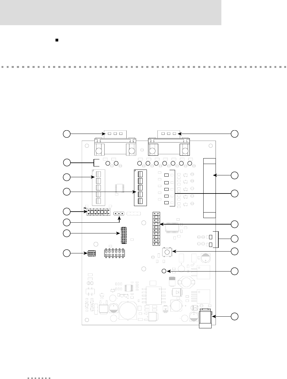
The development board contains connectors, switches, and LEDs for use while integrating
the embedded module into your design. See the following figure for the location of the
connectors, switches, and LEDs. Additionally, the board provides test points (not shown on
the figure). For more information about test points, see "Test points" on page 33.
Board Layout
00000005
P
8
P8
P1
1
P11
P4
C
R2
CR2
P
3
P3
C
R1
6
CR16
C
R
6
CR6
C
R1
5
CR15
P6
P6
S
W
2
SW2
P9
P9
S
W
3
SW3
C
R
4
CR4
CR
9
CR9
C
R
5
CR5
C
R
1
CR1
P7
P7
P
2
P2
S
W
1
SW1
P1
P1
C
R
8
CR8
C
R
7
CR7
C
R11
CR11
C
R1
0
CR10
C
R1
3
CR13
C
R1
2
CR12
C
R14
CR14
C
R
3
CR3
C
R17
CR17
1
2
3
4
5
6
7
8
10
11
12
13
14
15
16
P
12
P12
9
DC_ME-HWR.book Page 18 Thursday, July 1, 2004 11:12 AM
19
About the Development Board
Caution
When handling the development board, wear a grounding wrist strap to
avoid ESD damage to the board.
For more detailed information on connectors, switches and LEDs, see the following:
"Port Descriptions" on page 20
"Connectors and Blocks" on page 23
"Switches" on page 27
"Development Board LEDs" on page 30
"Power Jack" on page 32
The development board accepts either of the following modules:
Module without JTAG connector—for use with an integration kit
Module with JTAG connector—for use with a development kit
See the following figures for placement of either module onto the development board.
Connectors, Switches and LEDs 1-8
Pin
1Pin
2Pin
3Pin
4Pin
5Pin
6Pin
7Pin
8
Secondary
Serial Port, P2
LEDs,
CR1 -CR9
GPIO Switch
Bank, SW1
GPIO Switch
Bank, SW2
JTAG
Header, P4
Jumper
Block, P12
(Reserved)
Embedded
Module
Connector, P7
JTAG
Connector, P8
Connectors, Switches and LEDs
9-16 (continued)
Pin
9Pin
10 Pin
11 Pin
12 Pin
13 Pin
14 Pin
15 Pin
16
Primary
Serial Port, P1 GPIO Port, P3 LEDs, CR10 -
CR14
Digital Signal
Monitor Jack,
P6
LEDs, CR15
and CR16
Reset Switch,
SW3
LED, CR17 Power Jack,
P11
DC_ME-HWR.book Page 19 Thursday, July 1, 2004 11:12 AM
Port Descriptions
20
Digi Connect Wi-ME & Digi Connect ME Hardware Reference
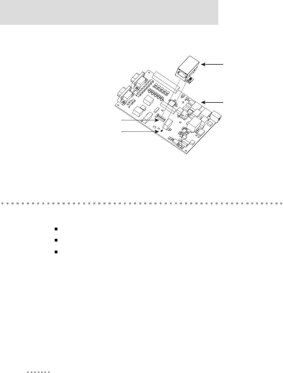
Placement of Module
Caution
If you handle the module, wear a grounding wrist strap to avoid ESD
damage.
Port Descriptions
The development board provides the following ports:
Primary Serial Port, P1
Secondary Serial Port, P2
GPIO Port, P3
See the figure titled "Board Layout" on page 18 for the location of the ports. The following
sections describe the ports.
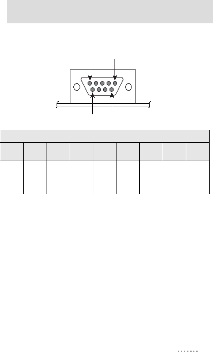
Primary Serial Port, P1
The Primary Serial Port is a DB-9 male connector that is labeled as P1 on the development
board. The port is used with the integration kit and the development kit. See the following
figure for pin orientation; see the following table for pin assignments.
00000015
Module connector
Development
board
Module with
JTAG connector
Module JTAG
connector
DC_ME-HWR.book Page 20 Thursday, July 1, 2004 11:12 AM
21
About the Development Board
Primary Serial Port Pin Orientation
Secondary Serial Port, P2
The Secondary Serial Port is a DB-9 male connector that is labeled as P2 on the
development board. The port is used only with the Digi Connect ME modules with JTAG
interfaces (in the development kit) for debugging purposes. See the following figure for pin
orientation; see the following table for pin assignments.
Primary Serial Port Pin Assignments
Pin
1Pin
2Pin
3Pin
4Pin
5Pin
6Pin
7Pin
8Pin
9
DCD RXD TXD DTR GND DSR RTS CTS —
Data
Carrier
Detect
Receive
Data
Transmit
Data
Data
Terminal
Ready
Signal/
Chassis
Ground
Data Set
Ready
Request
To Send
Clear To
Send
—
0
0000006
Pin 1 Pin 5
Pin 6 Pin 9
DC_ME-HWR.book Page 21 Thursday, July 1, 2004 11:12 AM
Port Descriptions
22
Digi Connect Wi-ME & Digi Connect ME Hardware Reference
Secondary Serial Port Pin Orientation
GPIO Port, P3
The GPIO port is a 10-pin male right-angle connector that is labeled as P3 on the
development board. The port is used with the integration kit and the development kit. See
the following figure for pin orientation; see the following tables for pin assignments. For
input and output threshold specifications, see "DC Characteristics" on page 43.
Note
The development board is shipped with a 10-pin screw-flange plug attached to
the GPIO port.
Secondary Serial Port Pin Assignments
Pin
1Pin
2Pin
3Pin
4Pin
5Pin
6Pin
7Pin
8Pin
9
—RXD TXD—GND————
— Receive
Data
Transmit
Data
— Signal/
Chassis
Ground
————
0
0000006
Pin 1 Pin 5
Pin 6 Pin 9
DC_ME-HWR.book Page 22 Thursday, July 1, 2004 11:12 AM
23
About the Development Board
GPIO Port Pin Orientation
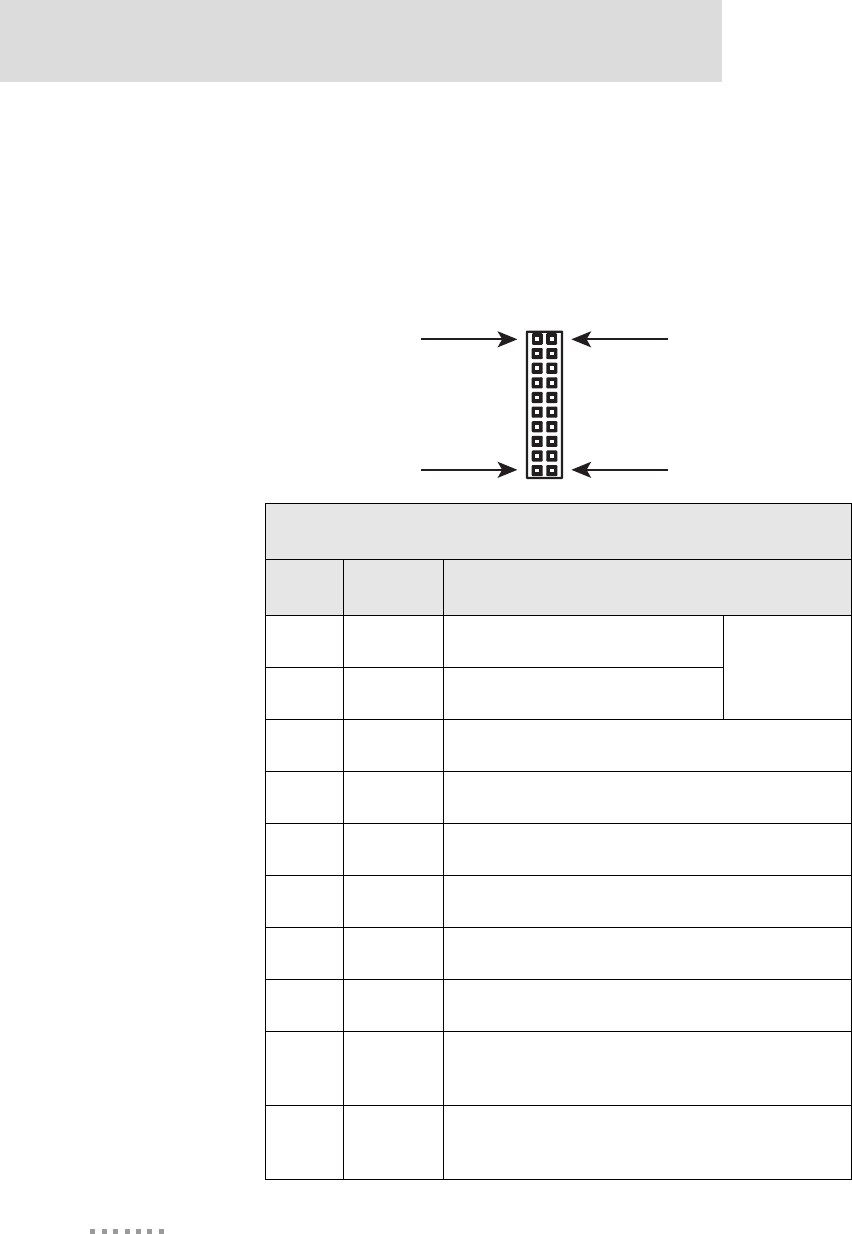
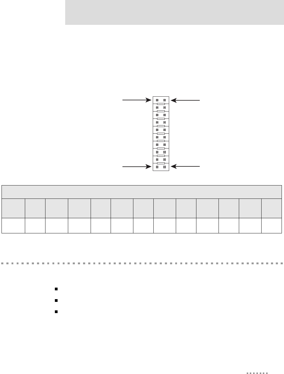
Connectors and Blocks
The development board provides the following connectors and blocks:
Embedded Module Connector, P7
Module JTAG Interface Connector, P8
JTAG Debugger Connector, P4
Jumper Block, P12
Logic Analyzer Header, P6
See the figure titled "Board Layout" on page 18 for the location of the connectors and
blocks. The following sections describe the connectors and blocks.
Embedded Module Connector, P7
The Digi Connect ME embedded module Connector is a 20-pin female vertical header that
is labeled P7 on the development board. The connector is used with the integration kit and
Pin 1 Pin 10
0
0000020
GPIO Port Pin Assignments
Pin
1Pin
2Pin
3Pin
4Pin
5Pin
6Pin
7Pin
8Pin
9Pin
10
Signal GND GPIO-5 GND GPIO-4 GND GPIO-3 GND GPIO-2 GND GPIO-1
DC_ME-HWR.book Page 23 Thursday, July 1, 2004 11:12 AM
Connectors and Blocks
24
Digi Connect Wi-ME & Digi Connect ME Hardware Reference
the development kit. See the following figure for pin orientation; see the following table for
pin assignments.
Note: The figure shows the connector using the same orientation as shown in
the figure titled "Board Layout" on page 18.
Embedded Module Connector Pin Orientation
Module Connector Pin Assignments
Pin Signal Description
1 VETH+ Power Pass-Thru + Unused on
Digi Connect
Wi-ME
2 VETH- Power Pass-Thru -
3 — Position Removed
4 — Position Removed
5 — Position Removed
6 — Position Removed
7 RXD Receive Data (Input)
8 TXD Transmit Data (Output)
9RTS /
GPIO-4 Request to Send (Output) / GPIO
10 DTR /
GPIO-5 Data Terminal Ready (Output) / GPIO
Pin 20
Pin 1
Pin 19
Pin 2
00000008
DC_ME-HWR.book Page 24 Thursday, July 1, 2004 11:12 AM
25
About the Development Board
Module JTAG Interface Connector, P8
The Module JTAG Interface Connector is a 14-pin female vertical header that is labeled P8
on the development board. The connector mates with the JTAG connector on the Digi
Connect ME embedded module. The Module JTAG Connector pins are tied to the JTAG
debugger Connector (see “JTAG Debugger Connector, P4”).
Note
Because there is no direct connection to the Module JTAG Interface Connector,
pin orientation and pin assignments are not described for the connector.
11 CTS /
GPIO-2 Clear to Send (Input) / GPIO
12 DSR /
GPIO-3 Data Set Ready (Input) / GPIO
13 DCD /
GPIO-1 Data Carrier Detect (Input) / GPIO
14 RESET Reset
15 +3.3V Power
16 GND Ground
17 — Reserved. Do not connect.
18 — Reserved. Do not connect.
19 — Reserved. Do not connect.
20 /INIT Soft Reset
Module Connector Pin Assignments
Pin Signal Description
DC_ME-HWR.book Page 25 Thursday, July 1, 2004 11:12 AM
Connectors and Blocks
26
Digi Connect Wi-ME & Digi Connect ME Hardware Reference
JTAG Debugger Connector, P4
The JTAG debugger connector is a 14-pin male vertical header that is labeled P4 on the
development board. The connector mates with a JTAG debugger plug (for example, a
Macraigor Raven). The connector is used with the development kit only. See the following
figure for pin orientation. See the following table for pin assignments.
Note
The figure shows the connector using the same orientation as shown in the
figure titled "Board Layout" on page 18.
JTAG Debugger Connector Pin Orientation
Jumper Block, P12
This jumper block is reserved for future use.
Logic Analyzer Header, P6
The Logic Analyzer Header is a 20-pin male vertical header that is labeled P6 on the
development board. The header is for connecting a digital signal analyzer (for example, a
logic analyzer) to the development board. The header is used with the development kit
00000011
Pin 13 Pin 1
Pin 14 Pin 2
JTAG Debugger Connector Pin Assignments
Pin
1Pin
2Pin
3Pin
4Pin
5Pin
6Pin
7Pin
8Pin
9Pin
10 Pin
11 Pin
12 Pin
13 Pin
14
VCC+ GND /TRST GND TDI GND TMS GND TCKRXD GND TDO ICETRST VCC+ GND
DC_ME-HWR.book Page 26 Thursday, July 1, 2004 11:12 AM
27
About the Development Board
only. See the following figure for pin orientation; see the following table for pin
assignments.
Note
The figure shows the connector using the same orientation as shown in the
figure titled "Board Layout" on page 18.
Logic Analyzer Header Pin Orientation
Switches
The development board provides the following switches:
GPIO Switch Bank 1, SW1
GPIO Switch Bank 2, SW2
Reset, SW3
See the figure titled "Board Layout" on page 18 for the location of the switches. The
following sections describe the switches.
Pin 2
Pin 20
Pin 1
Pin 19
00000013
Logic Analyzer Header Pin Assignments
Pin
1-8 Pin
9Pin
10 Pin
11 Pin
12 Pin
13 Pin
14 Pin
15 Pin
16 Pin
17 Pin
18 Pin
19 Pin
20
Not
Connected /RST Not
Connected GPIO-5 TXD2 GPIO-4 RXD2 GPIO-3 TXD GPIO-2 RXD GPIO-1 GND
DC_ME-HWR.book Page 27 Thursday, July 1, 2004 11:12 AM
Switches
28
Digi Connect Wi-ME & Digi Connect ME Hardware Reference
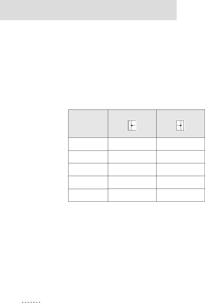
GPIO Switch Bank 1, SW1
GPIO Switch Bank 1, labeled SW1, is a set of five slide switches that allows the Digi
Connect ME embedded module to use either serial signals or GPIO signals to communicate
with a device. The switch is used with the Digi Connect ME embedded module Integration
Kit and the Digi Connect ME embedded module Development Kit. In addition, the switch
is used in conjunction with GPIO Switch Bank 2, SW2. See the following table for switch
definitions of GPIO Switch Bank 1.
GPIO Switch Bank 1 Settings
Switch
Number Left Position Right Position
1DCDGPIO-1
2CTSGPIO-2
3DSRGPIO-3
4RTSGPIO-4
5DTRGPIO-5
DC_ME-HWR.book Page 28 Thursday, July 1, 2004 11:12 AM

29
About the Development Board
GPIO Switch Bank 2, SW2
GPIO Switch Bank 2, labeled SW2, is a set of five slide switches that set GPIO inputs to
logic levels of high (switch to left) or low (switch to right).
If the GPIO port is configured as an output, then the switch should always be to the left. If
there is an external device connected to P3, the switch should always be set to the left.
Each GPIO port can be used independently.
Notes
1These switches do not determine whether the GPIO is an input or output. That is
determined by the module software.
2If GPIO is set to an output by software, switch SW2 must be set to the left (high).
3These switches are used with the integration kit and the development kit and in
conjunction with GPIO Switch Bank 1, SW1.
Reset, SW3
The Reset switch is a push button switch labeled SW3 on the development board. Pressing
the switch holds the Digi Connect ME embedded module in reset. When the push button is
released, the module reboots.
DC_ME-HWR.book Page 29 Thursday, July 1, 2004 11:12 AM
Development Board LEDs
30
Digi Connect Wi-ME & Digi Connect ME Hardware Reference
Development Board LEDs
The development board contains 17 LEDs that are labeled CR1 through CR17. The
following table lists and describes the LEDs.
Development Board LED Descriptions
Board
Label Description
Color or
State
Indication
CR1 TXD, Secondary Serial Port
Flickering Serial activity
Green Inactive
CR2 RXD, Secondary Serial Port
Flickering Serial activity
Green Inactive
CR3 CTS, Primary Serial Port
Yellow Active
Green Inactive
Off Not connected or signal not
being driven
CR4 DTR, Primary Serial Port
Yellow Active
Green Inactive
Off Not connected or signal not
being driven
CR5 TXD, Primary Serial Port
Flickering Serial activity
Green Inactive
CR6 RXD, Primary Serial Port
Flickering Serial activity
Green Inactive
DC_ME-HWR.book Page 30 Thursday, July 1, 2004 11:12 AM
31
About the Development Board
CR7 RTS, Primary Serial Port
Yellow Active
Green Inactive
Off Not connected or signal not
being driven
CR8 DCD, Primary Serial Port
Yellow Active
Green Inactive
Off Not connected or signal not
being driven
CR9 DSR, Primary Serial Port
Yellow Active
Green Inactive
Off Not connected or signal not
being driven
CR10 GPIO-1 Input/Output
On Logic high
Off Logic low
CR11 GPIO-2 Input/Output
On Logic high
Off Logic low
CR12 GPIO-3 Input/Output
On Logic high
Off Logic low
Development Board LED Descriptions
Board
Label Description
Color or
State
Indication
DC_ME-HWR.book Page 31 Thursday, July 1, 2004 11:12 AM
Power Jack
32
Digi Connect Wi-ME & Digi Connect ME Hardware Reference
Power Jack
The Power Jack is a barrel connector that accepts 9 to 30 VDC +/- 5%. The jack is labeled
as P11 on the development board. The following table shows the polarity of the power jack.
CR13 GPIO-4 Input/Output
On Logic high
Off Logic low
CR14 GPIO-5 Input/Output
On Logic high
Off Logic low
CR15 3.3V Indicator
On Power on
Off Power off
CR16 5V Indicator
On Power on
Off Power off
CR17 EPWR, Powered Ethernet
Enabled
On
Ethernet power present from
external powered Ethernet
connector (Ethernet hub or
switch)
Off No powered Ethernet voltage
Development Board LED Descriptions
Board
Label Description
Color or
State
Indication
DC_ME-HWR.book Page 32 Thursday, July 1, 2004 11:12 AM
33
About the Development Board
The following figure schematically represents the polarity of the power jack.
Power Jack Polarity, Schematic
Test points
The development board provides 24 test points that can be identified by board label or test
point number. The board labels are adjacent to each test point on the board. The test point
numbers are in the development board schematic drawings. The following table lists the
test point number, board label, and a brief description of each test point.
Power Jack Polarity
Contact Polarity
Center +9 to +30 VDC
Outer Ground
Ground +9 to +30 VDC
00000014
Test Point Descriptions
Test
Point Board Label Description
TP1 RI RI (test point supported
only)
DC_ME-HWR.book Page 33 Thursday, July 1, 2004 11:12 AM
Test points
34
Digi Connect Wi-ME & Digi Connect ME Hardware Reference
TP2 TX TXD-2, Transmit,
Secondary Serial Port
TP3 RX RXD-2, Receive,
Secondary Serial Port
TP4 CTS CTS, Primary Serial Port
TP5 DTR DTR, Primary Serial Port
TP6 TX TXD, Primary Serial Port
TP7 RX RXD, Primary Serial Port
TP8 RTS RTS, Primary Serial Port
TP9 DCD DCD, Primary Serial Port
TP10 DSR DSR, Primary Serial Port
TP11 GPIO1 GPIO-1
TP12 GPIO2 GPIO-2
TP13 GPIO3 GPIO-3
TP14 GPIO4 GPIO-4
TP15 GPIO5 GPIO-5
TP16 GND Ground
TP17 3.3V 3.3V Supply
TP18 GND Ground
TP19 5V 5.0V Supply
TP20 RESET Reset (active low)
TP21 E+ Ethernet Power +
TP22 E- Ethernet Power -
TP23 V-IN 9-30 VDC Input
TP24 GND Ground
Test Point Descriptions
Test
Point Board Label Description
DC_ME-HWR.book Page 34 Thursday, July 1, 2004 11:12 AM

35
Programming
Considerations
CHAPTER 3
Overview
This chapter provides information programmers may require to make use of some Digi
Connect ME hardware resources. It provides information on the following topics:
"GPIO" on page 36
"LEDs" on page 38
"Reset" on page 38
"Flash" on page 40
"Memory" on page 40
DC_ME-HWR.book Page 35 Thursday, July 1, 2004 11:12 AM

GPIO
36
Digi Connect Wi-ME & Digi Connect ME Hardware Reference
GPIO
General Information
The NS7520 processor supports 16 general purpose I/O (GPIO) lines, some of which are
reserved for specific functions and some of which can be customized. These GPIO lines
fall into three categories:
Those labeled “Reserved” in the following table are reserved for a specific use
and must not be reprogrammed, or the unit might not operate correctly. Often,
these lines are not connected to external interfaces.
Those labeled “Allocated” in the following table are exposed to an external
interface and allocated to a specific use by the software, but can be customized
safely with code modifications.
Those labeled “Available” are exposed to an external interface, not controlled
directly by the software, and can be customized.
Two registers govern the 16 GPIO lines. These registers are named PORTA and PORTC.
Each GPIO pin has four bits which completely describe its behavior, and each register is
responsible for eight GPIO pins. The four bits that describe the GPIO behavior are its mode
(CMODE), its direction (CDIR), its special function (CSF--only applicable to PORTC),
and the data value. The first three bits describe the functionality of the GPIO pin. The
"data" bit provides the current value of the pin when read and allows one to control the
value of an output pin when written.
In order to configure any GPIO pin as a GPIO input, the corresponding bit positions in the
appropriate register must be configured as: CMODE = 0 CDIR = 0 CSF = 0
In order to configure any GPIO pin as a GPIO output, the corresponding bit positions in the
appropriate register must be configured as: CMODE = 0 CDIR = 1 CSF = 0
Since each register controls 8 GPIO lines, it is safest to read the full 32 bit register, modify
the bits corresponding to the GPIO line of interest, and then write the full 32 bits back. In
this way, the behavior of the other GPIO lines will be preserved. For more information
regarding the format and programming of the GPIO registers, see the NS7520 Hardware
Reference.
DC_ME-HWR.book Page 36 Thursday, July 1, 2004 11:12 AM

37
Programming Considerations
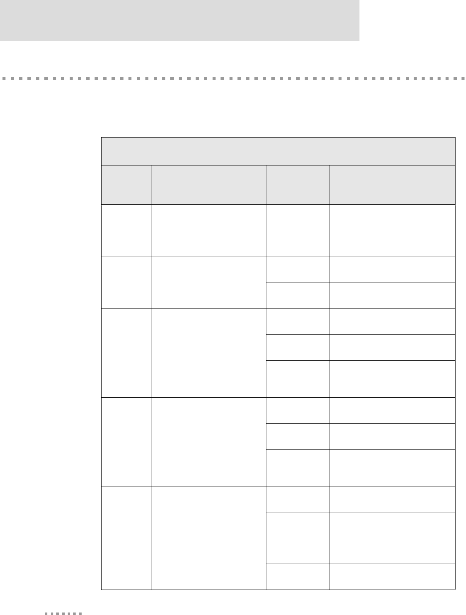
Digi Connect ME GPIO pin use
Name Register
Bit Category External
Interface Description
Serial
transmit PORTA7 Allocated Pin 8 on the 20 pin
header
Used for serial transmit. It could be reassigned as
GPIO input or output and used for a general purposes.
DTR/GPIO5 PORTA6 Allocated Pin 10 on the 20 pin
header
Used for the serial DTR signal. It can be reassigned as
either GPIO input or output and used for a general
purpose. If used in conjunction with the development
board, this pin maps to GPIO5.
RTS/GPIO4 PORTA5 Allocated Pin 9 on the 20 pin
header.
Used for the serial RTS signal. It could be reassigned
as either GPIO input or output and used for a general
purpose. If used in conjunction with the development
board, this pin maps to GPIO4.
NA PORTA4 Reserved NA NA
Serial
receive PORTA3 Allocated Pin 7 on 20 pin
header,
Used for serial receive. It could be reassigned as either
GPIO input or output and used for a general purpose.
DSR/GPIO3 PORTA2 Allocated Pin 12 on 20 pin
header
Used for the serial DSR signal. It could be reassigned
as either GPIO input or output and used for a general
purpose. If used in conjunction with the development
board, this pin maps to GPIO3.
CTS/GPIO2 PORTA1 Allocated Pin 11 on 20 pin
header
Used for the serial CTS signal, but could be
reassigned as either GPIO input or output and used for
a general purpose. If used in conjunction with the
development board, this pin maps to GPIO2.
DCD/
GPIO1 PORTA0 Allocated Pin 13 on 20 pin
header.
Used for the serial DCD signal, but could be
reassigned as either GPIO input or output and used for
a general purpose. If used in conjunction with the
development board, this pin maps to GPIO1.
NA PORTC7 Reserved NA NA
Green LED PORTC6 Allocated Connected to the
green LED
Used as the Ethernet activity LED, but could be
reassigned as a general purpose LED. It must remain
a GPIO output for the LED to operate correctly. The
LED is lit when the signal is a logic low.
/INIT PORTC5 Available Pin 20 on 20 pin
header
Can be configured for either GPIO input or GPIO
output
NA PORTC4 -
PORTC0 Reserved NA NA
DC_ME-HWR.book Page 37 Thursday, July 1, 2004 11:12 AM
LEDs
38
Digi Connect Wi-ME & Digi Connect ME Hardware Reference
LEDs
General Information
The embedded modules have two types of LEDs:
An LED connected directly to GPIO pins on the processor and controlled
directly in software
An LED connected to other hardware components (normally the Ethernet
hardware) and not directly programmable by the operating system
The development kit, by default, correctly configures the GPIO connected to the LED
(PORTC6) as an output and then uses this LED to represent Ethernet activity. For more
information regarding the control of LEDs, see the Net+Works with GNU Tools BSP
Porting Guide.
About Digi Connect ME LEDs
Reset
Hard Reset
The embedded module supports a hardware reset via pin 14 of the 20-pin header. The unit
is forced into a hard reset when this pin is pulled low. When plugged into a development
board, this pin is wired to the push button at SW3. As a result, this switch acts as a hard
reset button.
LED Description
Yellow This is wired directly to Ethernet hardware and provides an indication of link.
Green
This software programmable LED is wired to processor GPIO register bit
PORTC6 and is wired to be lit when low. The default behavior is to blink on
Ethernet activity.
DC_ME-HWR.book Page 38 Thursday, July 1, 2004 11:12 AM

39
Programming Considerations
Soft Reset
Net+OS provides an internal facility to enact a soft reset, but it is the responsibility of a
specific implementation to choose a reasonable trigger to invoke it. One choice is to use a
GPIO pin as a signal to trigger a soft reset. The Digi Connect ME has one GPIO pin named
"/INIT” (PORTC5) that is not normally assigned to any other task. It is an ideal candidate
for a soft reset. The signal is exposed via pin 20 on the 20-pin header, so it can be
controlled by an embedded host. When plugged into the development board, the /INIT
signal is pulled high, unless a jumper is placed across pins 2 and 3 of jumper block P12. In
this way, placing the jumper simulates pressing a soft reset button.
The naresetapp example application demonstrates a simple mechanism for monitoring a
GPIO pin and then initiating a soft reset when the pin achieves a particular value.
Reset Characteristics
Characteristic Specification
Delay 200 milliseconds (typical)
Threshold 2.88 V
Minimum Hold Time 1 microsecond pulse
DC_ME-HWR.book Page 39 Thursday, July 1, 2004 11:12 AM

Flash
40
Digi Connect Wi-ME & Digi Connect ME Hardware Reference
Flash
General Information
The Digi Connect ME has 2 MB of flash memory. The Digi Connect Wi-ME has 4 MB of
flash memory. In both modules the flash memory is controlled by chip select 0, located at
0x02000000.
Memory
The embedded modules have 8 MB of SDRAM memory, controlled by chip select 1,
located at 0x00000000 in the processor address space and aliased at 0x04000000 and
0x08000000. The application program is loaded at address 0x08080000.
DC_ME-HWR.book Page 40 Thursday, July 1, 2004 11:12 AM
41
Module Specifications
APPENDIX A
Network Interface
Digi Connect ME Digi Connect Wi-ME
Standard: IEEE 802.3
Physical Layer: 10/100Base-T
Data Rate: 10/100Mbps
(auto-sensing)
Mode: Half-duplex and full-duplex
support (auto-sensing)
Connector: RJ-45
Standard: IEEE 802.11b
Frequency: 2.4 GHz
Data Rate: Up to 11 Mbps with
automatic fallback
Modulation: CCK (11/5 Mbps),
DQPSK (2 Mbps), DBPSK (1
Mbps)
Transmit Power: 16 dBm typical
Receive sensitivity:
1Mbps: -92 dBm
2Mbps: -89 dBm
5.5Mbps: -87 dBm
11Mbps: -82 dBm
Antenna Connector: 1 x RP-SMA
DC_ME-HWR.book Page 41 Thursday, July 1, 2004 11:12 AM
Serial Interface
42
Digi Connect Wi-ME & Digi Connect ME Hardware Reference
Serial Interface
One TTL serial interface (CMOS 3.3v) with full modem control signals (DTR, DSR, DCD,
RTS, CTS).
Data Rates (bps)
50, 110, 134, 150, 200, 300, 600, 1200, 2400, 3600, 4800, 9600, 19200, 38400, 57600,
115200, 230400
Flow Control Options
RTS/CTS, XON/XOFF, None
GPIO
Five GPIO (General Purpose Input/Output) ports are selectable between modem control
and GPIO as follows:
RTS/GPIO 4
DTR/GPIO 5
CTS/GPIO 2
DCD/GPIO 1
DSR/GPIO 3
DC_ME-HWR.book Page 42 Thursday, July 1, 2004 11:12 AM
43
Module Specifications
DC Characteristics
The following tables provide DC characteristics for operating conditions, inputs, and
outputs.
Warning
The rise time of your 3.3V power supply needs to be faster than 140ms.
That is it needs to be less than 140ms. If the rise time is more than 140ms,
it could lead to the 3-1-3 diagnostic error.
Operating Conditions
Symbol Description Min Typ Max Unit
VCC Supply Voltage 3.14 3.3 3.45 V
ICC Supply Current — —
Digi
Connec
t
EM
27
0
mA
Digi
Connec
t
Wi-EM
40
0
IIL Input Current as “0”
(57K pull-up resistor)
——57µA
IIH Input Current “1”
(57K pull-up resistor) -10 — 10 µA
IOZ HighZ Leakage
Current -10 — 10 µA
IOD Output Drive Strength — — 2 mA
CIO Pin Capacitance
(VO=0) —— 4 pF
Inputs
Symbol Description Min Typ Max Unit
VIH Input High Voltage 2 — VCC+0.3 V
VIL Input Low Voltage VSS-0.3 — 0.2*VCC V
DC_ME-HWR.book Page 43 Thursday, July 1, 2004 11:12 AM
Environmental
44
Digi Connect Wi-ME & Digi Connect ME Hardware Reference
Note
The embedded modules provide an on board supervisor circuit with a 2.88V
reset threshold and an internal 5k pull-up resistor. When VCC falls to the
threshold voltage, a reset pulse is issued, holding the output in active state.
When power rises above 2.88V, the reset remains for approximately 250 ms to
allow the system clock and other circuits to stabilize.
Environmental
Outputs
Symbol Description Min Typ Max Unit
VOH Output High
Voltage 2.4 — 3.45 V
VOL Output Low
Voltage 0—0.4V
Digi Connect ME Digi Connect Wi-ME
Ambient
Temperature
-40oF to 185oF
(-40oC to 85oC)
-4oF to 185oF
(-20oC to 85oC)
Storage
Temperature
-400F to 2570F
(-400C to 1250C)
Humidty 5% to 90%
Altitude 12000 feet
(3657.60 meters)
DC_ME-HWR.book Page 44 Thursday, July 1, 2004 11:12 AM
45
Module Specifications
Mechanical
Dimensions Digi Connect
ME Digi Connect
Wi-ME
Length 1.445 in.
(36.703 mm)
1.945 in
(49.4 mm)
Width 0.75 in.
(19.05 mm)
Height 0.735 in.
(18.669 mm)
Device/serial
interface
connector
20-pin micro header (10-pin double row) with .50-inch (1.27-mm)
pitch (Samtec P/N FTS-110-01-F-DV-TR or similar). Positions 3
through 6 are removed.
DC_ME-HWR.book Page 45 Thursday, July 1, 2004 11:12 AM
Dimensions
46
Digi Connect Wi-ME & Digi Connect ME Hardware Reference
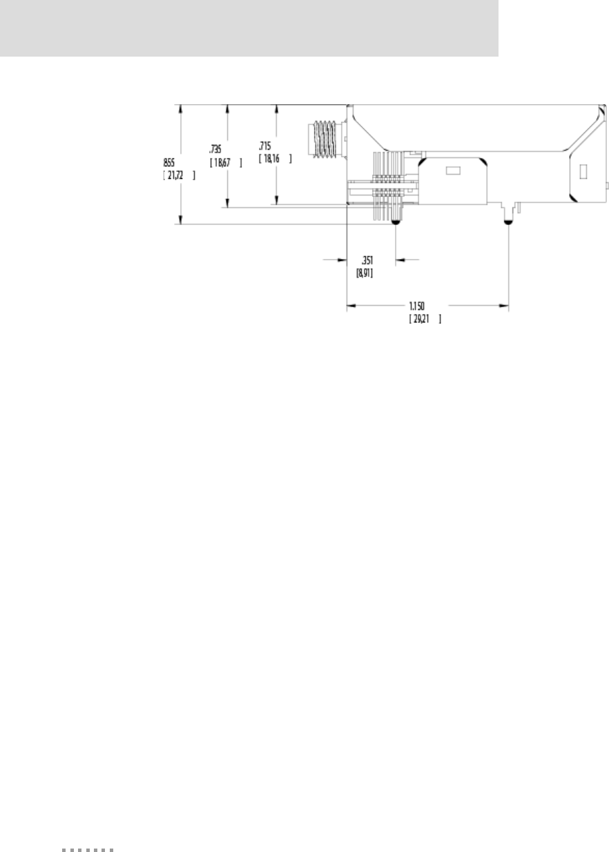
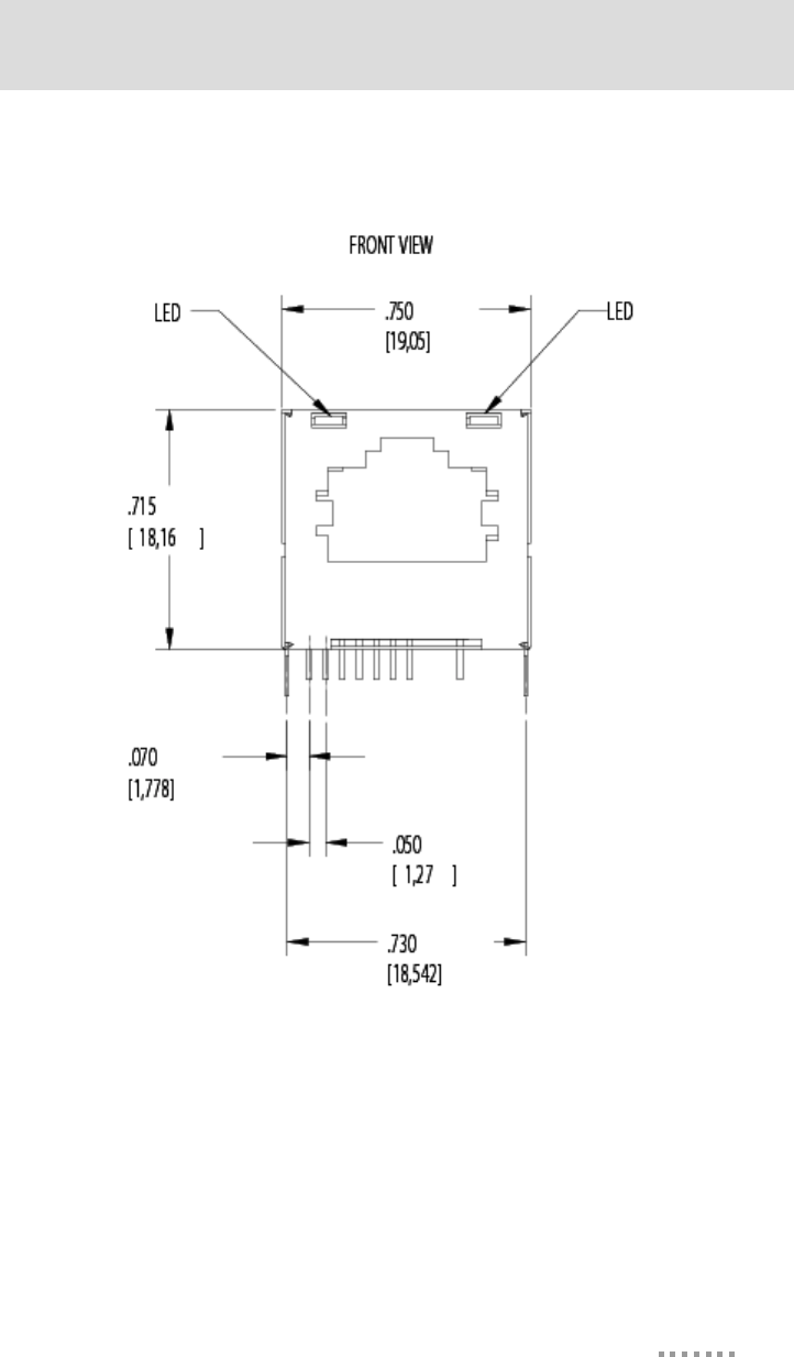
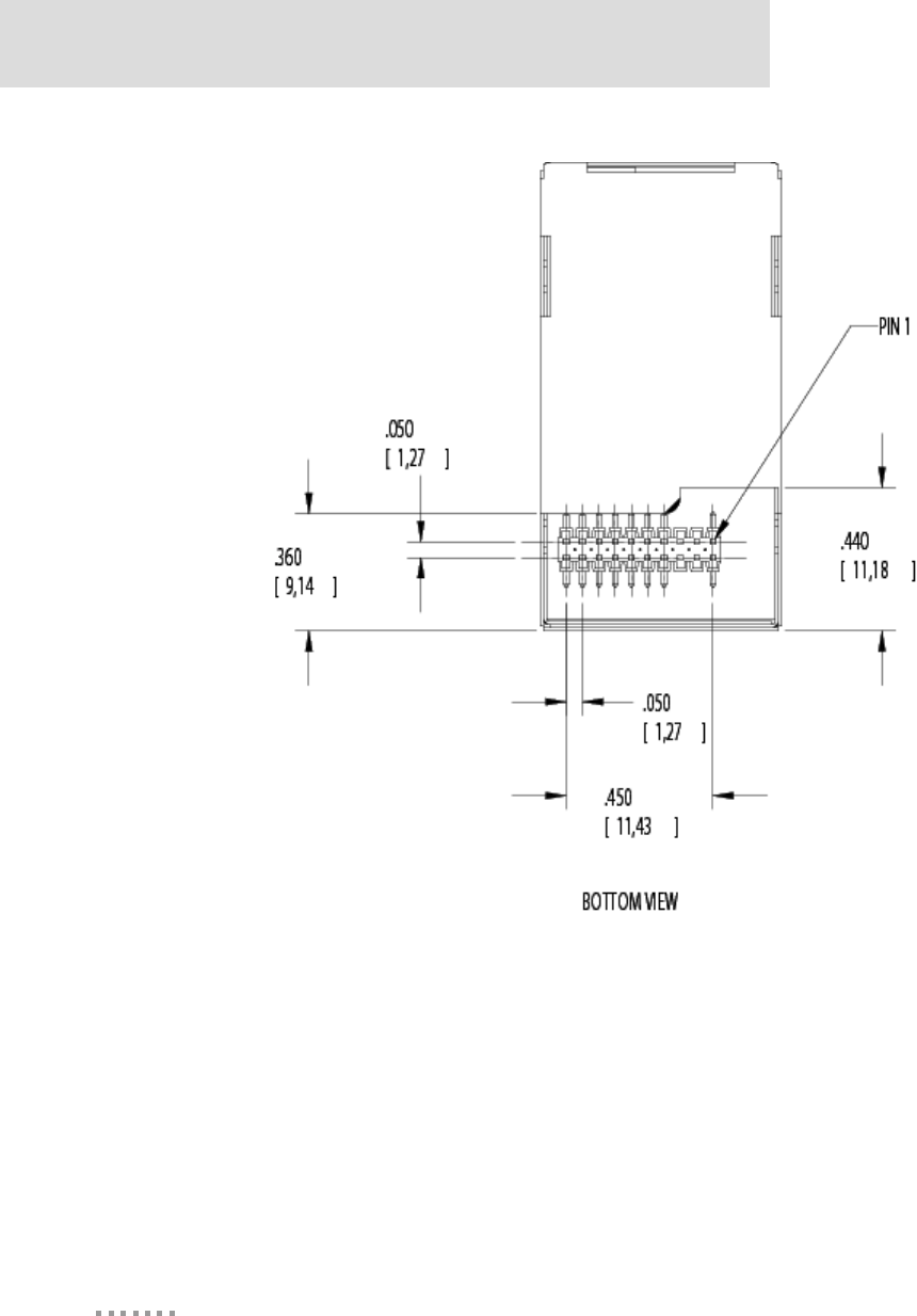
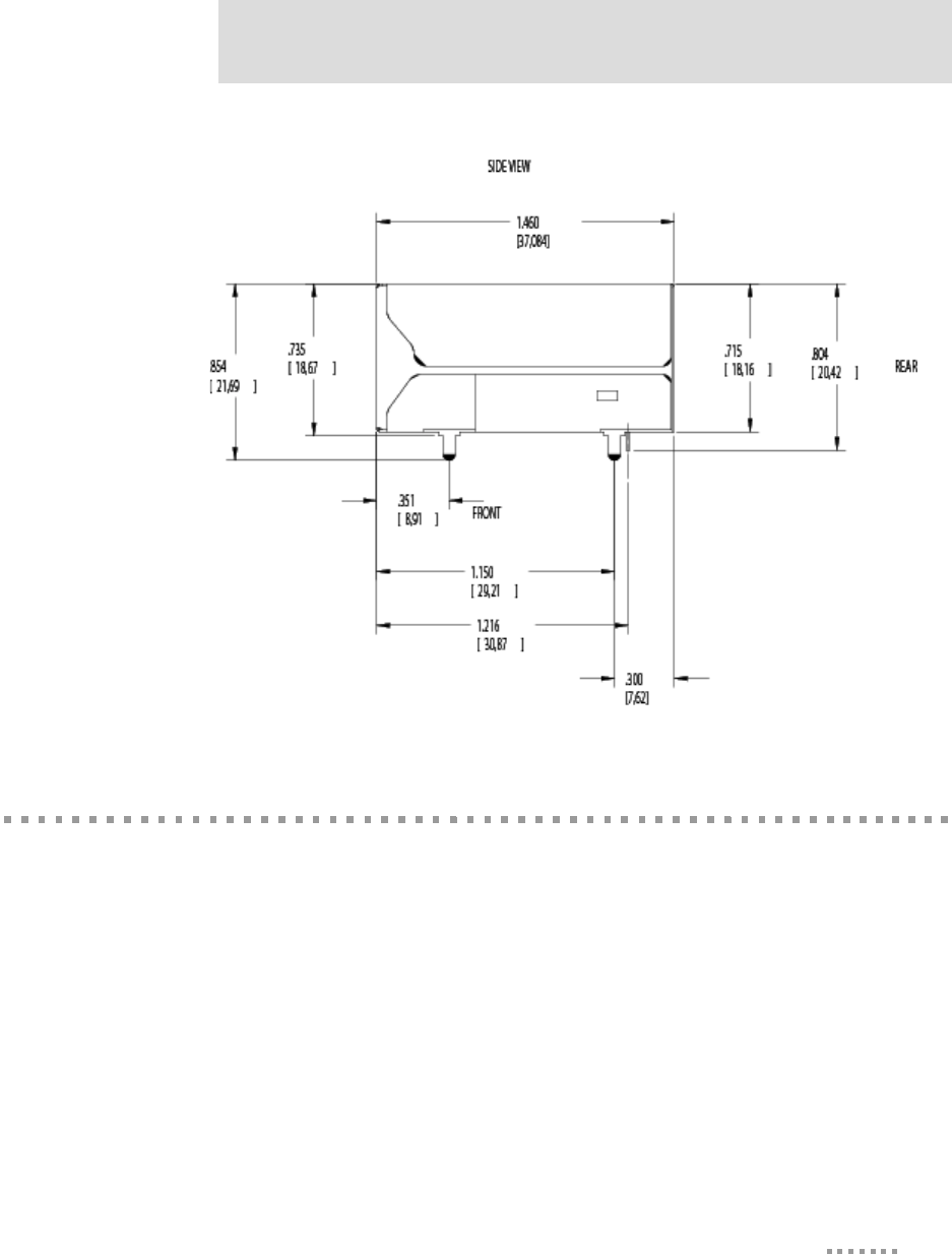
Dimensions
The following figures show the dimensions of Digi Connect Wi-ME and Digi Connect ME
embedded modules.
Digi Connect Wi-ME Module
Front
DC_ME-HWR.book Page 46 Thursday, July 1, 2004 11:12 AM
47
Module Specifications
Bottom
DC_ME-HWR.book Page 47 Thursday, July 1, 2004 11:12 AM
Dimensions
48
Digi Connect Wi-ME & Digi Connect ME Hardware Reference
Side
DC_ME-HWR.book Page 48 Thursday, July 1, 2004 11:12 AM
49
Module Specifications
Digi Connect ME Module
Front View
DC_ME-HWR.book Page 49 Thursday, July 1, 2004 11:12 AM
Dimensions
50
Digi Connect Wi-ME & Digi Connect ME Hardware Reference
Bottom
DC_ME-HWR.book Page 50 Thursday, July 1, 2004 11:12 AM
51
Module Specifications
Side
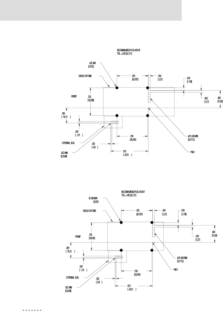
Recommended PCB Layout
The following figure shows the recommended PCB (printed circuit board) layout of the
Digi Connect Wi-ME and Digi Connect ME. It is strongly recommended that you consider
using the Digi Connect Wi-ME footprint for future flexibility.
DC_ME-HWR.book Page 51 Thursday, July 1, 2004 11:12 AM
Recommended PCB Layout
52
Digi Connect Wi-ME & Digi Connect ME Hardware Reference
Digi Connect Wi-ME
Digi Connect ME
DC_ME-HWR.book Page 52 Thursday, July 1, 2004 11:12 AM
53
Module Specifications
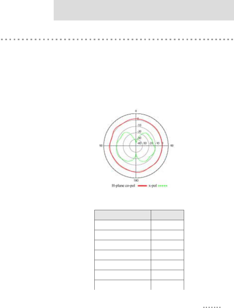
Antenna Information
Antenna Strength
The following diagram demonstrates the strength of the signal received by the whip
antenna on both a horizontal and vertical plane. The diagram shows the magnetic field
when the antenna is in a vertical position. The outside line represents the horizontal plane
and the inside dotted line represents the vertical plane.
Radiation Patterns
Antenna Description Values
Frequency GHz 2.4~2.GHz
Type Dipole
Power Output 2 W
DB Gain 2 dBi
VSWR < or = 2.0
Dimension 10.0x108.5
Weight 10.5g
DC_ME-HWR.book Page 53 Thursday, July 1, 2004 11:12 AM
RF Exposure Statement
54
Digi Connect Wi-ME & Digi Connect ME Hardware Reference
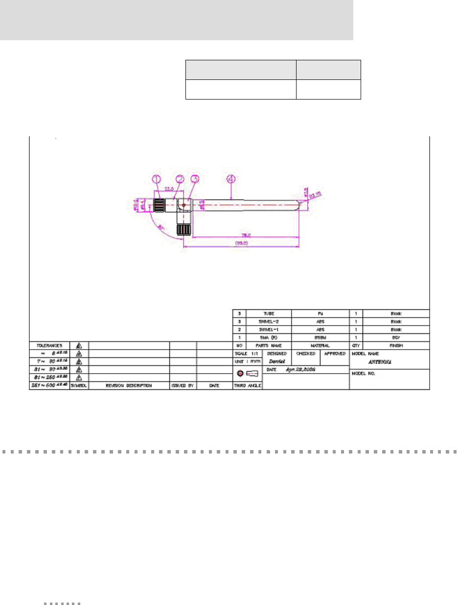
Antenna Details
RF Exposure Statement
The Digi Connect Wi-ME module complies with the RF exposure limits for humans as
called out in RSS-102. It is exempt from RF evaluation based on its operating frequency of
2400 MHz, and effective radiated power of 100 milliwatts. This would be less than the 3
watt requirement for a mobile device (>20 cm separation) operating at 2400 MHz.
In order to comply with FCC RF exposure limits, dipole antennaantenna should be located
at a minimum distance of 7.9 inches (20cm) or more from the body of all persons.
Connector RP-SMA
Antenna Description Values
DC_ME-HWR.book Page 54 Thursday, July 1, 2004 11:12 AM

55
Module Specifications
Safety Statements
To avoid contact with electrical current:
Never install electrical wiring during an electrical storm.
Never install an ethernet connection in wet locations unless that connector is
specifically designed for wet locations.
Use caution when installing or modifying ethernet lines.
Use a screwdriver and other tools with insulated handles.
You and those around you should wear safety glasses or goggles.
Do not place ethernet wiring or connections in any conduit, outlet or junction
box containing electrical wiring.
Installation of inside wire may bring you close to electrical wire, conduit,
terminals and other electrical facilities. Extreme caution must be used to avoid
electrical shock from such facilities. You must avoid contact with all such
facilities.
Ethernet wiring must be at least 6 feet from bare power wiring or lightning rods
and associated wires, and at least 6 inches from other wire (antenna wires,
doorbell wires, wires from transformers to neon signs), steam or hot water
pipes, and heating ducts.
Do not place an ethernet connection where it would allow a person to use an
ethernet device while in a bathtub, shower, swimming pool, or similar
hazardous location.
Protectors and grounding wire placed by the service provider must not be
connected to, removed, or modified by the customer.
Do not touch uninsulated ethernet wiring if lightning is likely!
Do not touch or move the antenna(s) while the unit is transmitting or receiving.
Do not hold any component containing a radio such that the antenna is very
close to or touching any exposed parts of the body, especially the face or eyes,
while transmitting.
Do not operate a portable transmitter near unshielded blasting caps or in an
explosive environment unless it is a type especially qualified for such use
DC_ME-HWR.book Page 55 Thursday, July 1, 2004 11:12 AM

Safety Statements
56
Digi Connect Wi-ME & Digi Connect ME Hardware Reference
Any external communications wiring you may install needs to be constructed to all
relevant electrical codes. In the United States this is the National Electrical Code Article
800. Contact a licensed electrician for details.
DC_ME-HWR.book Page 56 Thursday, July 1, 2004 11:12 AM
File No. NC407961, Page A9 of A10File No. NC407961, Page A9 of A10
Modular Device End User Responsibility
If the FCC ID is not visible when installed inside another device,
then the outside of the device into which the module is installed
must also display a label referring to the enclosed module FCC
ID. This exterior label can use wording such as the following:
“This Device Contains Transmitter Module FCC ID: MCQ-50M880”

57
Certifications
APPENDIX B
This product complies with the following standards.
FCC Part 15 Class B
Radio Frequency Interference (RFI)(FCC 15.105)
The Digi Connect ME embedded module has been tested and found to comply with the
limits for Class B digital devices pursuant to Part 15 Subpart B, of the FCC Rules. These
limits are designed to provide reasonable protection against harmful interference in a
residential environment. This equipment generates, uses, and can radiate radio frequency
energy, and if not installed and used in accordance with the instruction manual, may cause
harmful interference to radio communications. However, there is no guarantee that
interference will not occur in a particular installation. If this equipment does cause harmful
interference to radio or television reception, which can be determined by turning the
equipment off and on, the user is encouraged to try and correct the interference by one or
more of the following measures:
Reorient or relocate the receiving antenna.
Increase the separation between the equipment and the receiver.
Connect the equipment into an outlet on a circuit different from that to which
the receiver is connected.
Consult the dealer or an experienced radio/TV technician for help.
DC_ME-HWR.book Page 57 Thursday, July 1, 2004 11:12 AM

Industry Canada
58
Digi Connect Wi-ME & Digi Connect ME Hardware Reference
Labeling Requirements (FCC 15.19)
This device complies with Part 15 of FCC rules. Operation is subject to the following two
conditions: (1) this device may not cause harmful interference, and (2) this device must
accept any interference received, including interference that may cause undesired
operation.
Modifications (FCC 15.21)
Changes or modifications to this equipment not expressly approved by Digi may void the
user’s authority to operate this equipment.
Industry Canada
This digital apparatus does not exceed the Class B limits for radio noise emissions from
digital apparatus set out in the Radio Interference Regulations of the Canadian Department
of Communications.
Le present appareil numerique n’emet pas de bruits radioelectriques depassant les limites
applicables aux appareils numeriques de la class B prescrites dans le Reglement sur le
brouillage radioelectrique edicte par le ministere des Communications du Canada."
DC_ME-HWR.book Page 58 Thursday, July 1, 2004 11:12 AM

59
Certifications
Declaration of Conformity
(In accordance with FCC Dockets 96-208 and 95-19)
Digi International declares, that the product:
to which this declaration relates, meets the requirements specified by the Federal
Communications Commission as detailed in the following specifications:
Part 15, Subpart B, for Class B Equipment
FCC Docket 96-208 as it applies to Class B personal
Computers and Peripherals
The product listed above has been tested at an External Test Laboratory certified per FCC
rules and has been found to meet the FCC, Part 15, Class B, Emission Limits.
Documentation is on file and available from the Digi International Homologation
Department.
Manufacturer’s Name: Digi International
Corporate Headquarters: 11001 Bren Road East
Minnetonka MN 55343
Manufacturing Headquarters: 10000 West 76th Street
Eden Prairie MN 55344
Product Name: Digi Connect ME embedded module
Model Number: 50000866-xx
Product Name: Digi Connect Wi-ME embedded module
Model Number: 50000880-xx
DC_ME-HWR.book Page 59 Thursday, July 1, 2004 11:12 AM
International EMC Standards
60
Digi Connect Wi-ME & Digi Connect ME Hardware Reference
International EMC Standards
The Digi Connect ME and Digi Connect Wi-ME embedded modules meet the following
electromagnetic emissions standards:
EN55022
EN55024
EN 300 324
EN 301 489
VCCI
AS 3548
RSS 210 (Digi Connect Wi-ME IC: 1846A-50M880)
FCC Part 15 Subpart C (Digi Connect Wi-ME FCC ID: MCQ-50M880)
Safety Standards
The Digi Connect ME and Digi Connect Wi-ME embedded modules meet the following
safety standards:
UL 60950-1
CSA 22.2 No. 60950
EN60950
DC_ME-HWR.book Page 60 Thursday, July 1, 2004 11:12 AM

61
Sample Application:
TTL Signals to EIA-232
APPENDIX C
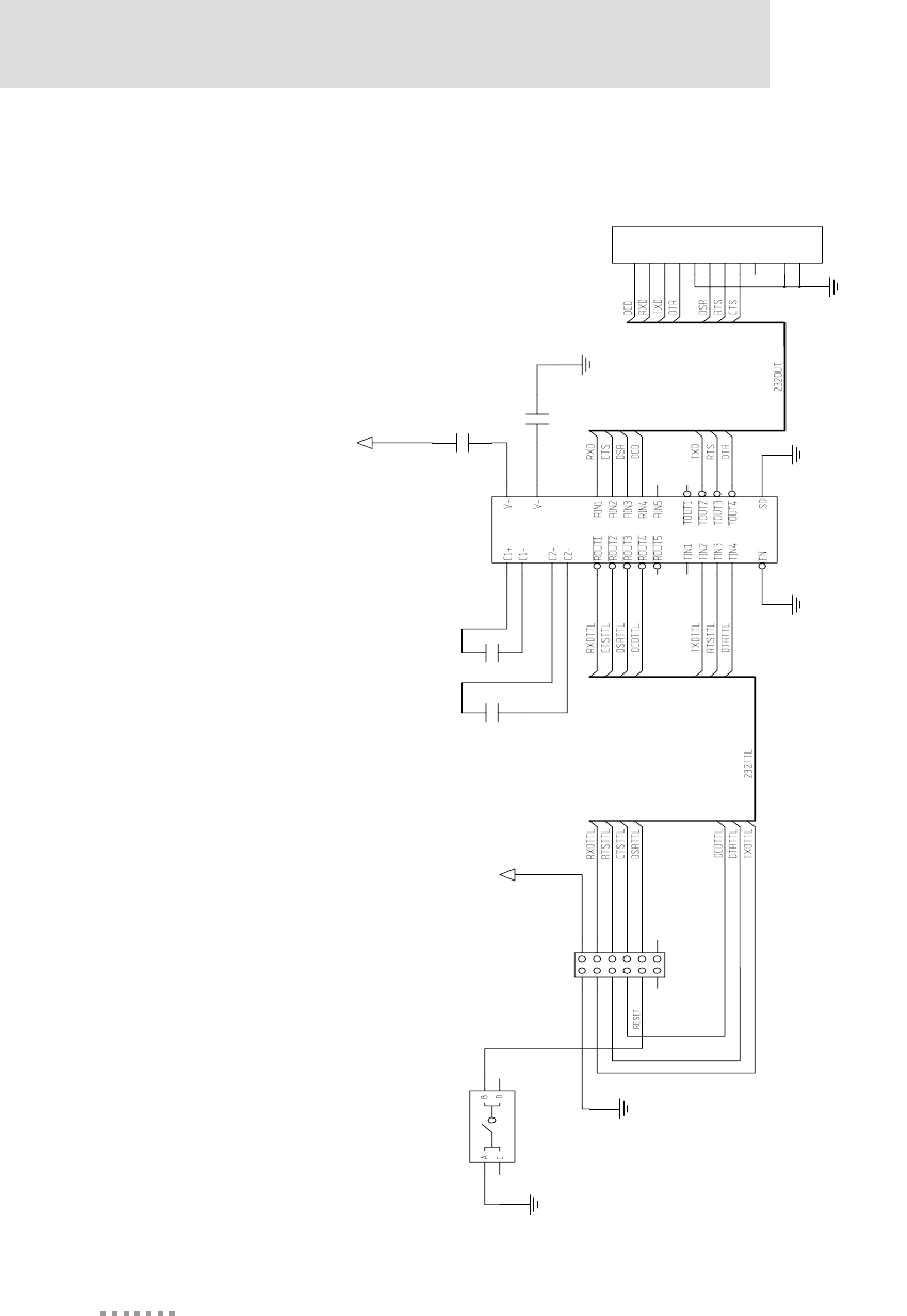
The following schematic is an example of how to convert the modules’s TTL signals to
EIA-232.
DC_ME-HWR.book Page 61 Thursday, July 1, 2004 11:12 AM
62
Digi Connect EM & Wi-EM Hardware Reference
0.1uF
1
2
C6
0.1uF
1
2
C4
0.1uF
1
2
C3
0.1uF
2
1
C5
+5V
GND
11
10
9
8
7
6
5
4
3
2
1
DB9
P1
RS-232 SERIAL 9-PIN CONNECTOR
SHIELD
SHIELD
GND
GND
17
13
25
24
16
15
14
12
28
21
120
36
27
19 18
22 23
26 27
54
89
ADM211E
U1
RS-232 LINE RECVR 5RX 4TX
+5V
GND
1211
109
87
65
43
21
SOCKET 2X6
DIGI ONE EM CONNECTOR
P6
GND GND
RESET SW ITCH
13
24
SW1
DC_ME-HWR.book Page 62 Thursday, July 1, 2004 11:12 AM
DC_ME-HWR.book Page 63 Thursday, July 1, 2004 11:12 AM

DC_ME-HWR.book Page 64 Thursday, July 1, 2004 11:12 AM