Vector_service 017 Service
User Manual: 017 Service
Open the PDF directly: View PDF ![]() .
.
Page Count: 74
- Introduction and Specifications
- Theory of Operation
- VECTOR OUTPUT I/O MODULE OVERVIEW
- INPUT SECTION THEORY OF OPERATION
- OUTPUT SECTION THEORY OF OPERATION
- Main PCA to Top PCA Interface Functional Block
- Internal Oscillator Control Functional Block
- Output Control Functional Block
- RAM Select Functional Block
- SSLOGIC (Start/Stop Logic) Functional Block
- Vector Address Functional Block
- Vector Pattern RAM Functional Block
- Vector Control RAM Functional Block
- Loop Control Functional Block
- Capture Clock Functional Block
- Drive Status Functional Block
- Output Protection Functional Block
- Maintenance
- List of Replaceable Parts
- Schematic Diagrams
- Index

9100 Series
9100A-017
Vector Output I/O Module
Service Manual
P/N 855531
August 1989
© 1989, John Fluke Mfg. Co., Inc. All rights reserved. Litho in U.S.A.
LIMITED WARRANTY
John Fluke Mfg. Co., Inc. (Fluke) warrants your 9100A-017 Vector Output I/O Module to be free from
defects in material and workmanship under normal use and service for one (1) year from the date of
shipment. Software and firmware products are provided “AS IS.” We do not warrant that software or
firmware products will be error free, operated without interruption or that all errors will be corrected. This
warranty extends to you if you are the original purchaser and does not apply to fuses, batteries, or any
product which, in our sole opinion, has been subject to misuse, alteration, or abnormal conditions of
operation or handling.
To obtain warranty service, contact a Fluke Service Center or send the product, with the description of the
difficulty, postage prepaid, to the nearest Fluke Service Center. Fluke assumes no risk for damage in
transit.
Fluke will, at our option, repair or replace the defective product free of charge. However, if we determine
that the failure was caused by misuse, alteration, or abnormal condition of operation or handling, you will
be billed for the repair. The repaired product will be returned to you, transportation prepaid.
THIS WARRANTY IS EXCLUSIVE AND IS IN LIEU OF ALL OTHER WARRANTIES, EXPRESS OR
IMPLIED, INCLUDING BUT NOT LIMITED TO ANY IMPLIED WARRANTY OF MERCHANTABILITY OR
FITNESS FOR A PARTICULAR PURPOSE OR USE. FLUKE WILL NOT BE LIABLE FOR ANY SPECIAL,
INDIRECT, INCIDENTAL, OR CONSEQUENTIAL DAMAGES OR LOSS WHETHER IN CONTRACT, TORT,
OR OTHERWISE.
-i-
Table of Contents
______________________________________________________________________________
SECTION TITLE PAGE
1 Introduction and Specifications ...........................1-1
INTRODUCTION1 ............................................1-1
SPECIFICATIONS ...........................................1-1
Theory of Operation .......................................2-1
VECTOR OUTPUT I/O MODULE OVERVIEW ........................2-1
INPUT SECTION THEORY OF OPERATION ........................2-5
Mainframe to Bus Interface Functional Block .........2-5
MAINFRAME ADDRESSING OF THE MODULE .............2-5
CUSTOM CHIP SELECTION ..........................2-6
Custom Chip Functional Block ........................2-8
Clock and Enable Mux Functional Block ...............2-9
CLOCK AND ENABLE MUX OPERATION .................2-9
General Control Latch Functional Block ..............2-11
CONTROL REGISTER ...............................2-12
DATA COMPARISON INPUTS .........................2-12
FUSE DETECTION .................................2-12
DATA COMPARISON AND GENERAL INTERRUPTS .........2-13
DATA COMPARE EQUAL OUTPUT PIN ..................2-13
OPERATION OF GENERAL CONTROL LATCH BLOCK .......2-13
Connector Code Functional Block .....................2-16
Input Protection Functional Block ...................2-16
OUTPUT SECTION THEORY OF OPERATION .......................2-16
Main PCA to Top PCA Interface Functional Block ......2-17
ADDRESSING .....................................2-18
Internal Oscillator Control Functional Block ........2-20
Output Control Functional Block .....................2-20
RAM Select Functional Block .........................2-21
CHIP COUNTER OPERATION .........................2-22
SSLOGIC (Start/Stop Logic) Functional Block .........2-22
SIGNAL POLARITY/CONTROL REGISTER ...............2-22
DRIVE CLOCK SELECTION ..........................2-23
HANDSHAKE SYNCHRONIZATION ......................2-24
VECTOR DRIVE COMPLETE LOGIC ....................2-25
Vector Address Functional Block .....................2-26
Vector Pattern RAM Functional Block .................2-26
Vector Control RAM Functional Block .................2-26
Loop Control Functional Block .......................2-27
Capture Clock Functional Block ......................2-28
Drive Status Functional Block .......................2-28
Output Protection Functional Block ..................2-29
-ii-
SECTION TITLE PAGE
3 Maintenance ...............................................3-1
INTRODUCTION .............................................3-1
CHANGING THE VECTOR OUTPUT I/O MODULE FUSE ...............3-1
CLEANING .................................................3-2
VECTOR OUTPUT I/O MODULE SELF TEST .......................3-2
DISASSEMBLY ..............................................3-2
TROUBLESHOOTING ..........................................3-3
General Information .................................3-3
4 List of Replaceable Parts .................................4-1
INTRODUCTION .............................................4-3
HOW TO OBTAIN PARTS ......................................4-3
ADDITIONAL INFORMATION ...................................4-4
5 Schematic Diagrams ........................................5-1
-iii-
List of Tables
______________________________________________________________________________
TABLE TITLE PAGE
1-1. Vector Output I/O Module Specifications ...................1-1
2-1. Custom Chip Pin Description ...............................2-11
2-2. Clock and Enable Mux Truth Table ..........................2-12
2-3. VHI and VLO for TTL and CMOS Logic Levels .................2-15
2-4. Dip-Clip and Calibration Module Configuration Codes .......2-17
2-5. Connector Code Examples ...................................2-18
2-6. Vector I/O Module Output Section Address Map ..............2-19
2-7. U25 Drive Register 2 Bit Description (Write @ $D0X21) .....2-20
2-8. U5 Register Bit Description (Write @ $D0X01) ..............2-21
2-9. U6 Register Bit Description (Write @ $D0X11) ..............2-23
2-10. U25 ID/Status Register Bit Description (Read @ $D0X01) ....2-29
4-1. 9100A-017 Vector I/O Final Assembly .......................4-5
4-2. A1 Main PCA ...............................................4-8
4-3. A2 Top PCA ................................................4-10
4-4. Module Revision Information ...............................2-12
-iv-
-v-
List of Figures
______________________________________________________________________________
FIGURE TITLE PAGE
2-1. Input Section Functional Block Diagram ....................2-3
2-2. Output Section Functional Block Diagram ...................2-4
2-3. Input Section Address Decoding Summary ....................2-7
2-4. Address Decoding Example ..................................2-8
2-5. Hot-Bit Decoding Examples .................................2-9
2-6. Bus Interface Timing Diagram ..............................2-10
2-7. I/O Module Control and Interrupt Registers ................2-14
2-8. Custom Chip Voltage Level Detection .......................2-15
4-1. 9100A-017 Final Assembly ..................................4-6
4-2. A1 Main PCA ...............................................4-9
4-3. A2 Top PCA ................................................4-11
-vi-
1-1
Section 1
Introduction and Specifications
INTRODUCTION
This manual presents service information for the 9100A-017 Vector Output
I/O Module. Included are a theory of operation, general maintenance
procedures, performance tests, troubleshooting information, a list of
replacement parts, and schematic diagrams.
SPECIFICATIONS
Table 1-1 contains the specifications for the Vector Output I/O Module.
NOTE
Output specifications for Table 1-1 were obtained using
the Y9100-102 Card Edge Interface Module into 10 LSTTL
loads. Results may vary depending on the impedance,
length, and shielding of the connector used. (Output
timing is measured at 50% of signal amplitude.)
Table 1-1. Vector Output I/O Module Specifications
______________________________________________________________________________
VECTOR OUTPUT I/O MODULE OUTPUT
(into 10 LSTTL loads with card edge connector attached):
Module Vector Size ......................... 8192 vectors, 40 channels wide.
Maximum Vector Pattern (4 Modules) ......... 8192 vectors, 160 channels wide.
Vector Looping ............................. Up to 65536 repetitions of
one vector set.
Output Logic Levels:
High ................................... 3.7V minimum (6.0 mA source).
Low .................................... 0.4V maximum (6.0 mA sink).
INT CLK (internal clock) ................... 1, 5, 10, or 20 MHz (±100
ppm).
DR CLK (external clock) .................... 25 MHz maximum. (This frequency
maximum may be exceeded in some
cases based upon application
and hardware interfacing.)
Clock to Vector Out (tdel):
INT CLK Out to Vector Out Delay ........ 37 ns typical, 45 ns maximum.
DR CLK In to Vector Out Delay .......... 50 ns typical, 58 ns maximum.
______________________________________________________________________________
1/Introduction and Specifications
1-2
Table 1-1. Vector Output I/O Module Specifications (cont.)
______________________________________________________________________________
WAIT (Handshake) Setup Time (twsu) ......... 42.5 ns maximum (35 ns typical)
from WAIT acknowledgement until
next clock cycle drives vector.
If the setup time is not met,
the next clock drives out the
vector. Minimum WAIT pulse
width is 10 ns.
Single Module Channel to Channel Skew* ..... 6 ns maximum (1 ns typical).
Module to Module Channel Skew* ............. 10 ns maximum (1 ns typical).
TRISTATE-:
Activation (txout) ..................... Output source/sink released 25
ns maximum (20 ns typical)
after TRISTATE- goes low.
Minimum TRISTATE- pulse width
is 10 ns.
Recovery (txsu) ........................ TRISTATE- must go high no later
than 5 ns after the rising edge
of the INT CLK or no later than
10 ns after the programmed edge
of DR CLK for the vector to be
output by that clock, otherwise
that vector is only driven
internally and the output is
held tri-stated, effectively
skipping that vector.
Output Series Termination .................. 33 Ohms
Capture Clock:**
INT CLK ................................ Capture Clock clocks 42.5 ns
±5 ns after the falling edge
of INT CLK.
DR CLK ................................. Capture Clock clocks 55 ns
±10 ns after non-clocking edge
of DR CLK (approximate 50% duty
cycle).
START, STOP, and ENABLE:
START, STOP Pulse Width .................... 10 ns minimum.
INT CLK
START Setup Time .................. 30 ns minimum.
STOP Setup Time ................... 30 ns minimum.
ENABLE Setup Time ................. 25 ns minimum.
ENABLE Hold Time .................. 20 ns minimum.
______________________________________________________________________________
* Skew measurement assumes equal loading. Differences in capacitance
may affect results.
** Capture clock may be adjusted in approximate 15 ns steps by using the
setoffset command (see the 9100 Series TL/1 Reference Manual).
______________________________________________________________________________
1/Introduction and Specifications
1-3
Table 1-1. Vector Output I/O Module Specifications (cont.)
______________________________________________________________________________
DR CLK
START Setup Time .................. 20 ns minimum.
STOP Setup Time ................... 20 ns minimum.
ENABLE Setup Time ................. 15 ns minimum.
ENABLE Hold Time .................. 35 ns minimum.
Input Impedance:
DR CLK ................................. 40 kilohm minimum, 35 pF maximum.
TRISTATE- .............................. 40 kilohm minimum, 80 pF maximum.
WAIT ................................... 40 kilohm minimum, 50 pF maximum.
VECTOR OUTPUT I/O MODULE INPUT:
Input Impedance ............................ 50 kilohm minimum, 90 kilohm
typical; 100 pF maximum, 65 pF
typical.*
Operating Voltage Range .................... -0.5V to +5.5V (all lines).
Input/Output Protection .................... +10V/-5V for one minute
maximum, one line only (all
lines).
Input Thresholds:
________________________________________________
| | | |
| TTL | CMOS | |
|_________|__________|___________________________|
| | | |
| 5.0V | 5.0V | \ |
| | | >- Guaranteed HIGH |
| 2.6V | 3.4V | < |
| | | >- HIGH or INVALID |
| 2.1V | 2.9V | < |
| | | >- Guaranteed INVALID |
| 1.0V | 1.2V | < |
| | | >- LOW or INVALID |
| 0.6V | 0.8V | < |
| | | >- Guaranteed LOW |
| 0.0V | 0.0V | / |
|_________|__________|___________________________|
CLOCK, START, STOP, and ENABLE Inputs:
Thresholds:
Logic LOW ......................... 0.8V maximum.
Logic HIGH ........................ 2.0V minimum.
Input Current .......................... 125 uA maximum.
Input/Output Protection ................ +10V/-5V for one minute
maximum, one line only.
______________________________________________________________________________
* Input capacitance includes the Y9100A-102 Card Edge Interface Module.
______________________________________________________________________________
1/Introduction and Specifications
1-4
Table 1-1. Vector Output I/O Module Specifications (cont.)
______________________________________________________________________________
Transition Counter:
Maximum Frequency ...................... 10 MHz minimum.
Maximum Count (Transition Mode) ........ 8388608 (23 bits) counts
(+ overflow).
Frequency Accuracy (Frequency Mode) .... ±250 ppm ±2 Hz.
Stop Counter:
Maximum Frequency ...................... 10 MHz.
Maximum Count .......................... 65535 clocks.
Clock:
Maximum Frequency ...................... 10 MHz.
Minimum Pulse Width .................... 50 ns.
Timing for Synchronous Measurements:
Maximum Frequency of Clock ............. 10 MHz.
Maximum Frequency of Data .............. 5 MHz.
Data Setup Time ........................ 30 ns minimum.
Data Hold Time ......................... 30 ns minimum.
Minimum Pulse Width
(Start/Stop/Enable/Clock) ............ 50 ns.
Start Edge Setup Time
(before clock edge, for clock to
be recognized) ....................... 0 ns minimum.
Stop Edge Setup Time
(before clock edge, for clock
edge to not be recognized) ........... 5 ns minimum.
Enable Setup Time
(before clock edge, for clock
edge to be recognized) ............... 0 ns minimum.
Enable Hold Time
(after clock edge, for clock
edge to be recognized) ............... 10 ns minimum.
Data Timing for Asynchronous Measurements:
Maximum Frequency ...................... 10 MHz.
Minimum Pulse Width (HIGH or LOW) ...... 50 ns.
Minimum Pulse Width (tri-state) ........ 150 ns.
Data Compare Equal:
Minimum Pulse Width of
Data and Enable ...................... 75 ns.
PHYSICAL SPECIFICATIONS
Operating Temperature:
5 to 27oC, 95% RH maximum (non-condensing).
27 to 40oC, RH decreasing linearly from 95% to 50% (non-condensing).
Storage/Shipping Temperature:
20 to 60oC, 8% to 80% RH (non-condensing).
______________________________________________________________________________
2-1
Section 2
Theory of Operation
VECTOR OUTPUT I/O MODULE OVERVIEW
The 9100A-017 Vector Output I/O Module adds 40 lines of input and
high-speed output capability to the 9100A/9105A mainframe. Up to four
Vector Output I/O Modules may be connected to the mainframe for a
maximum of 160 channels of vector output and stimulus measurement. Any
number of the 160 channels may be used simultaneously.
The Vector Output I/O Module has the same input measurement capabilities
as the 9100A-003 Parallel I/O Module. The Vector Output I/O Module is
capable of generating cyclic redundancy checks (CRCs), measuring
frequency or taking event counts, and recording logic level histories.
The input measurements can be synchronized to the 9100A/9105A
microprocessor-specific Pod, to external events (using the module
external START, STOP, ENABLE, and CLOCK lines), to a software strobe, or
to a free-running clock. The input section may also be synchronized to
the output section by using the Capture Clock (a user-programmable clock
generated during vector driving). The module also has a programmable
“breakpoint” capability. The input thresholds may be set to either “TTL”
and “CMOS” levels.
The Vector Output I/O Module can drive vector patterns synchronized to a
user-supplied external clock (at up to 25 MHz), to a user-selectable
internal clock at 1, 5, 10, or 20 MHz, to a software strobe, or to the
Pod. The output can be latched to a level (either high or low) on any of
the module’s lines to test devices using either a “writeword” or
“writepin” command. Each pin can be driven either high or low, or be
tri-stated. An external input is available to provide handshaking
synchronization with the UUT. All 40 outputs can be simultaneously
tri-stated by an external signal.
The Vector Output I/O Module consists of two assemblies: the Main PCA
(9100A-4021) and the Top PCA (9100A-4022).
The Main PCA provides the interface to the mainframe, and is used for
input measurements. The Main PCA includes the inputs for the external
synchronization lines START, STOP, ENABLE, and CLOCK. It also contains
some support circuitry for vector driving, including:
o bus interfacing circuitry for the Top PCA.
o vector drive internal clock control.
o vector loop control circuitry.
2/Theory of Operation
2-2
o vector drive status register.
o six-pin jack for control signals for vector driving.
The Top PCA is used primarily for vector output, although it also
provides the 40-channel input signals, Clip Module Connector Code, and
ready button signals to the input section on the Main PCA. It also
generates the Capture Clock (available as an input sync mode).
The input section of the Vector Output I/O Module consists of the
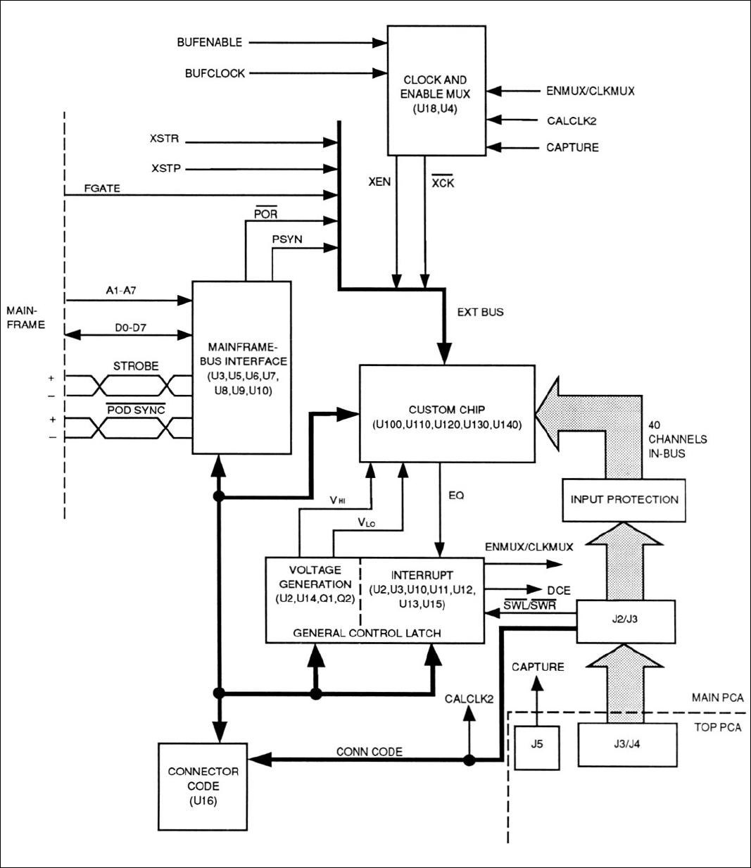
following six functional blocks (See Figure 2-1):
o Mainframe to Bus Interface Functional Block.
o Custom Chip Functional Block.
o Clock and Enable Mux Functional Block.
o General Control Latch Functional Block.
o Connector Code Functional Block.
o Input Protection Functional Block.
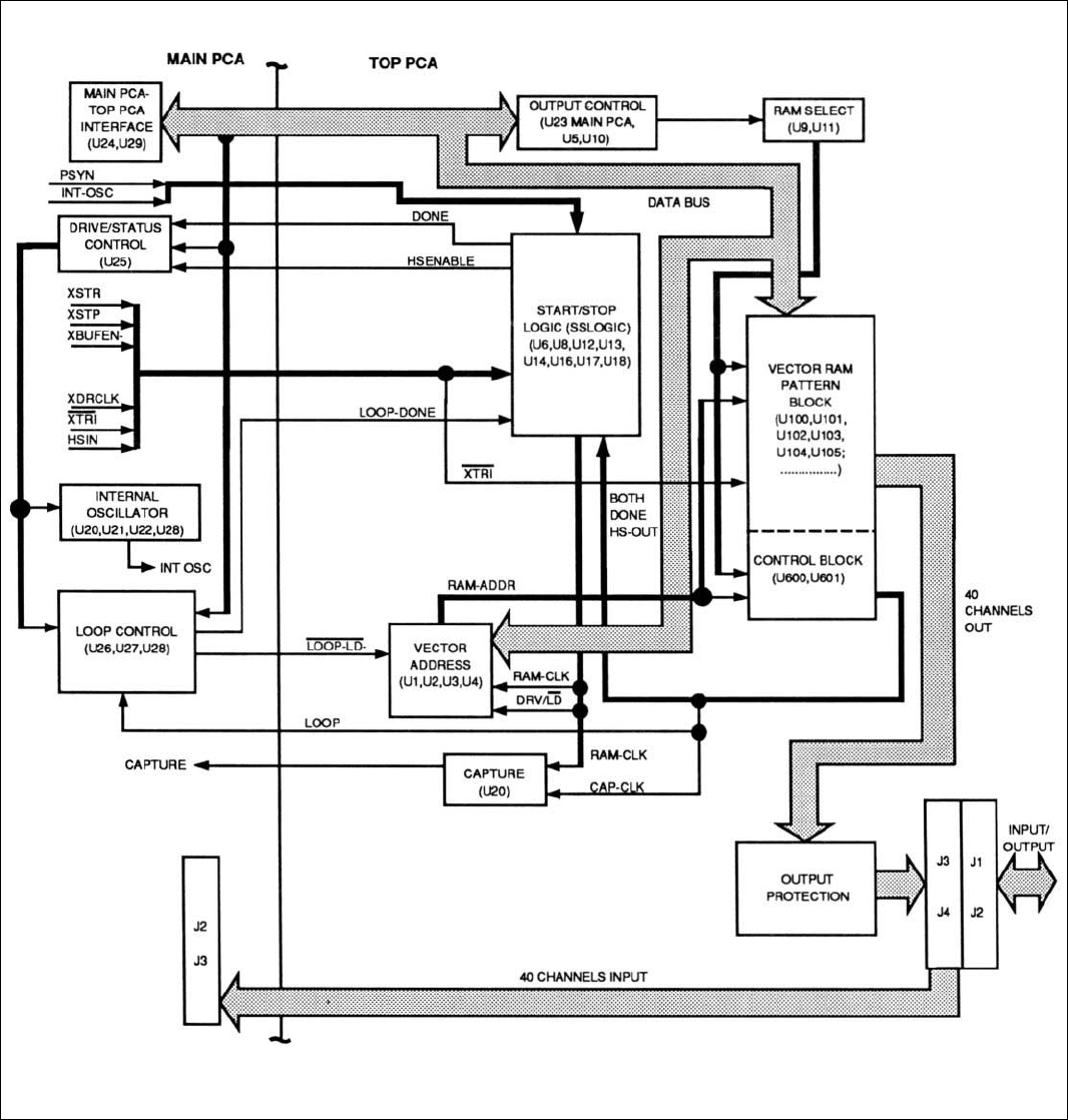
The output section consists of the following twelve functional blocks
(See Figure 2-2):
o Main PCA to Top PCA Interface Functional Block.
o Internal Oscillator Control Functional Block.
o Output Control Functional Block.
o RAM Select Functional Block.
o SSLOGIC (Start/Stop Logic) Functional Block.
o Vector Address Functional Block.
o Vector Pattern RAM Functional Block.
o Vector Control RAM Functional Block.
o Loop Control Functional Block.
o Capture Clock Functional Block.
o Drive Status Functional Block.
o Output Protection Functional Block.
2/Theory of Operation
2-3
Figure 2-1. Input Section Functional Block Diagram
2/Theory of Operation
2-4
Figure 2-2. Output Section Functional Block Diagram
2/Theory of Operation
2-5
INPUT SECTION THEORY OF OPERATION
NOTE
All of the input section circuitry is located on the
Main PCA unless otherwise indicated.
Mainframe to Bus Interface Functional Block
The bus interface block connects the 9100A/9105A mainframe
microprocessor bus to the Vector Output I/O Module. The module is a
memory-mapped device, with all control performed by writing to the
module memory space. The control bus enters the module on connector J1
and consists of the following lines:
o Seven address lines, A1 through A7.
o Eight data lines, D0 through D7.
o Two differential strobe lines, STROBE+ and STROBE-.
o One control line, R/W-.
The two mainframe strobe signals, STROBE+ and STROBE-, are translated by
U9 into the module STROBE- signal. STROBE- is the key signal that
qualifies all of the bus activities and is used by U7 to latch the
addresses and R/W-, and to enable the data bus buffer. The STROBE-
signal, in conjunction with the latched version of the R/W-, generates
the read strobe (RD-) and the write strobe (WR-). The STROBE- signal and
the decoder U6 provide address decoding by generating signals AD8-
through ADE- and ALLCHIP-. Signals AD8- through ADC- and ALLCHIP- are
input to AND Gates U3 and U5 to provide the custom chip selects CS0-
through CS4-. Signals ADD- and ADE- are used as register select lines.
(The mainframe STROBE- signal has already had some amount of address
decoding. STROBE- for any particular module is only active on accesses
to addresses $DXXXX, with address bit 0 = 1, and with the proper “hot
bit” identifying the module. See the heading, “Mainframe Addressing of
the Module”, further on in this section for more information on hot-bit
decoding).
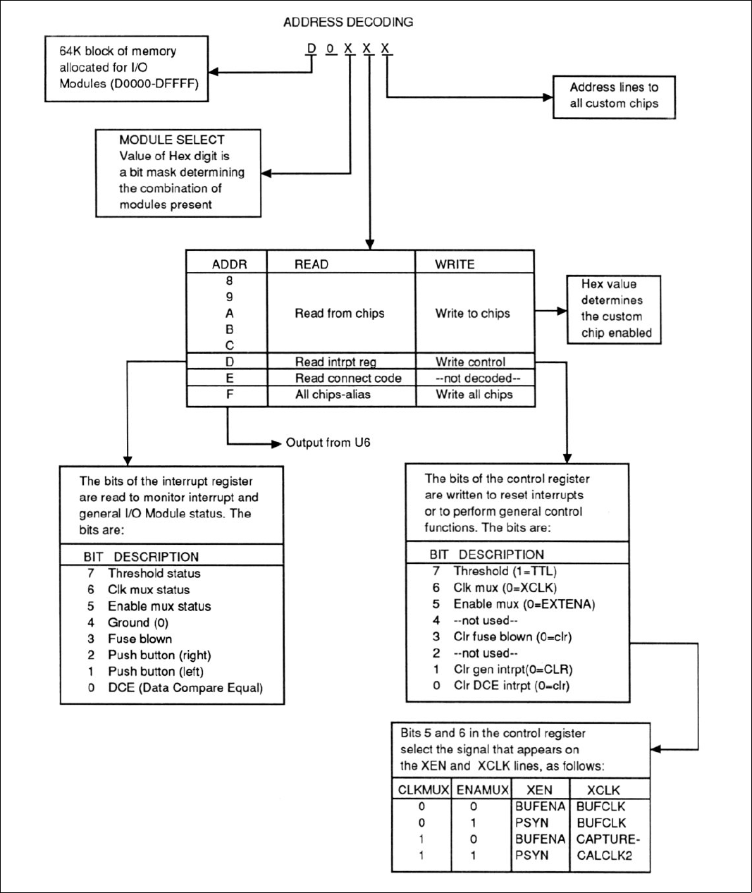
MAINFRAME ADDRESSING OF THE MODULE
Memory reserved for module control occupies the mainframe addresses
$D0000 through $DFFFF. Out of this 64K-byte block, four modules can be
addressed. Lower Data Strobe (LDS-) on the mainframe qualifies all
module addresses; thus address bit 0 is effectively a 1. Addresses
within this space using Upper Data Strobe (UDS-) are unused. Figure 2-3
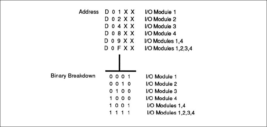
shows a summary of module input section address decoding. Figure 2-4
provides an addressing example.
Each of the four modules is controlled via “hot-bit decoding” of the
mainframe address lines A8 through A11. This method of decoding allows
any combination of modules to be addressed simultaneously. Figure 2-5
2/Theory of Operation
2-6
shows the third least significant digit of the 5-digit hex module
address broken down into binary format. The position of the set bit(s)
determines the module(s) to be addressed.
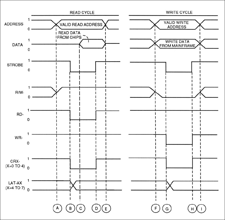
The Vector Output I/O Module bus interface timing diagram (Figure 2-6)
shows the signals contained in the bus interface block during a read and
write cycle. Each transition point (indicated by the letters A through
I) designates the following actions:
A. The address appears on the bus. R/W- goes high, signifying a read
cycle.
B. STROBE- goes low, allowing RD- and CSX- to go active. Data bus
transceiver U8 turns on, driving data from the module to the
mainframe. Addresses and R/W- are latched by U7 and are guaranteed
valid.
C. Valid read data appears on the data bus.
D. STROBE-, RD-, and CSX- return high. Read data is guaranteed valid at
this point.
E. End of the read cycle.
F. The address appears on the bus. R/W- goes low, signifying a write
cycle.
G. STROBE- goes low, allowing WR- and CSX- to go active. Data bus
transceiver U8 turns on, receiving data from the mainframe to the
module. Addresses and R/W- are guaranteed valid.
H. STROBE-, WR-, and CSX- return high. Write data is latched into the
module registers.
I. End of the write cycle.
CUSTOM CHIP SELECTION
The Bus Interface also decodes address lines A1 through A7 from the
mainframe to determine which custom chips are enabled. As the address
signals enter the Main PCA through J1, the address lines are latched by
U7 (the latch signal is STROBE-). Address lines A7 through A4 are used
as address inputs for the decoder (U6). The outputs of U6 are gated to
determine which custom chip is enabled. Any one of the five custom chips
can be addressed, or all five of the chips can be addressed
simultaneously (no other combination of the custom chips can be
addressed within a module).
For example, to select custom chip U100, the input at U7-13 (A7) from
the address bus of the mainframe must be at logic high and U7-18 (A4),
U7-17 (A5), and U7-14 (A6) must be at logic low. When STROBE- occurs, U7
latches the logic levels on these pins. On the output lines of U7,
LAT-A7 is set at logic high, and LAT-A4, LIT-A5, and LAT-A6 are logic
2/Theory of Operation
2-7
Figure 2-3. Input Section Address Decoding Summary
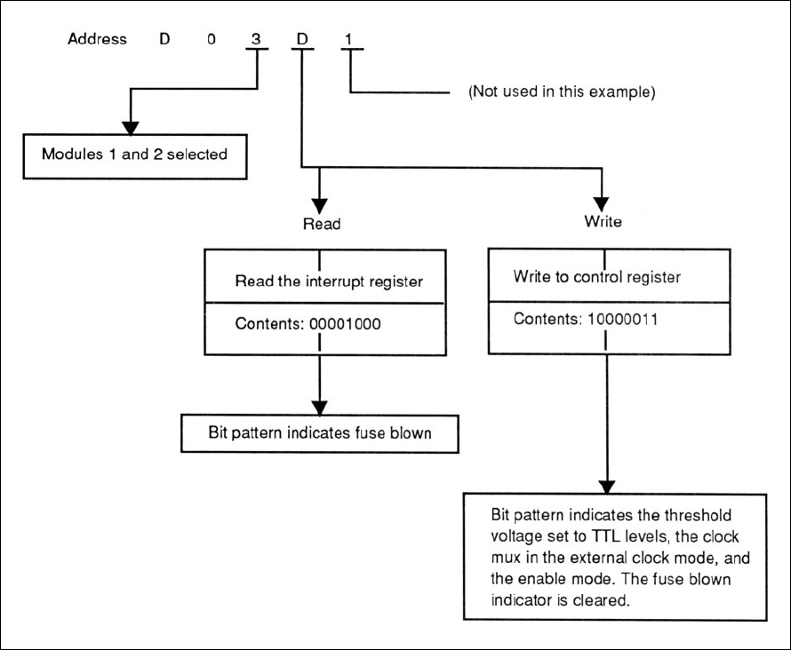
2/Theory of Operation
2-8
Figure 2-4. Address Decoding Example
low. U6 decodes the latched address lines and sets output line AD8- low.
The logic low on AD8- is gated through U5 and sets up a logic low on
CS0-, thereby enabling custom chip U100. To select custom chip U100 on
Module 3, the address $D0481 is used.
A custom chip may be addressed individually, or all custom chips may be
addressed simultaneously. Address bits A4 through A7 determine the
custom chip selection. To address all chips, an address in the form
$DXXFX must be used (X means don’t care). This address causes the
ALLCHIP- signal (U6-7) to go active, which when gated through U5 and U3,
makes all five chip selects CS0- through CS4- active.
Custom Chip Functional Block
The custom chips each contain eight channels of data acquisition. Each
channel performs 16-bit Cyclic Redundancy Checking (CRC), 23-bit (with
overflow) transition counting, 3-bit asynchronous level history
recording, 3-bit synchronous level history recording, and 1-bit data
comparison. The custom chips are used for module control, and are
2/Theory of Operation
2-9
Figure 2-5. Hot-Bit Decoding Examples
connected to the data bus via U8. Eleven internal registers control each
custom chip. These registers are in turn controlled by address lines A1
through A3 and the R/W- line.
The pin-out of the custom chip is shown in Table 2-1.
Clock and Enable Mux Functional Block
The Clock and Enable Mux block is located on the Main PCA and is shown
in the Input Section Functional Block Diagram, Figure 2-1. Two ICs make
up this block: the 74HCT153 Dual 4:1 Multiplexer (U18) and the 74HCT04
Hex Inverter (U4). This block selects one of three sources for the XCK-
signal, and one of two sources for the XEN signal.
CLOCK AND ENABLE MUX OPERATION
Inputs
The Clock and Enable Mux block clock sources include BUFCLOCK, CAPTURE-,
and CALCLK2. BUFCLOCK originates from the CLOCK external synchronization
line. CAPTURE- is a user-programmable clock generated on the Top PCA by
the output section during vector driving. CAPTURE is routed to the Main
PCA through J4-29 where it is inverted by U19 and sent to U18-12.
CALCLK2, which is generated during calibration, enters the Main PCA on
J2-24 and is routed to U18-13.
The POD SYNC signal, which enters the module as a differential ECL
signal, is converted by U9 into the TTL level signal PSYN. This signal
enters the EXT-BUS and is directly applied to the custom chips as a
clocking source, to U18 as an enabling signal, and to the Top PCA
through J4 pin 1 as a vector output clock source.
2/Theory of Operation
2-10
Figure 2-6. Bus Interface Timing Diagram
The Clock and Enable Mux block enable sources include BUFENABLE, a
signal that originates from the external ENABLE synchronization line,
and PSYN (described in the previous paragraph).
The CALCLK2 signal enters the Main PCA through the Connector Code
block. Channels 1 through 39 are tied together and to CALCLK2 when the
Calibration Module is plugged in. CALCLK2 is an input to U18-13. The
ENMUX and CLKMUX signals are generated by the Control Register (U14-15
and U14-16, respectively) and are control inputs to U18. U18 generates
outputs XEN and XCK. Table 2-2 shows which signals appear on the outputs
of the multiplexer for all four states of the control inputs.
2/Theory of Operation
2-11
Table 2-1. Custom Chip Pin Description
______________________________________________________________________________
PIN TYPE FUNCTION
______________________________________________________________________________
A0-A2 Input Address Lines
POR- Input Power-On Reset
SRCK Input 1 MHz Serial-To-Parallel
Conversion Clock
VDD1 Input Positive Voltage Supply
VDD2 Input Positive Voltage Supply
GND1 Input Logic Common
GND2 Input Logic Common
XD0-XD7 Input/Output Microprocessor Data Bus
EQ Output Equal (Data Comparison Equal) Output
TC Output Test Clock Output
WR- Input Write Enable
RD- Input Read Enable
CS- Input Chip Select
VPAT Input Negative Supply for DRV Outputs
TEN Input Test Mode Enable
XSTP Input External Stop
GATE Input Frequency Gate
XSTR Input External Start
XEN Input External Enable
XCK Input External Clock
PSYN Input Pod Sync Clock
VLO Input Logic Low Threshold Reference
Voltage for Inputs CD0-CD7
VHI Input Logic High Threshold Reference
Voltage for Inputs CD0-CD7
CD0-CD7 Input* Channel Inputs
TLI Input Test Channel Comparator Input
TLO Output Test Channel Comparator Output
______________________________________________________________________________
* CDn inputs have an internal resistor network to control the voltage at
which they will float (the “invalid” voltage). This voltage is
approximately 1.6 V, through an effective resistance of >50 kilohms.
______________________________________________________________________________
Outputs
The Clock and Enable MUX block outputs the XEN and XCK- signals to the
EXT-BUS. These two control signals are sent to each custom chip. Three
parallel inverters invert the XCK signal from U18-9, and ensure a fast
rise time into the relatively high capacitance XCK- line.
General Control Latch Functional Block
The General Control Latch Block, located on the Main PCA, varies input
thresholds, clears fault conditions, and controls the Clock and Enable
Multiplexer. Figure 2-1 shows the block’s functional relationship on the
2/Theory of Operation
2-12
Table 2-2. Clock and Enable Mux Truth Table
________________________________________________________
Control In Outputs
________________________________________________________
CLKMUX ENAMUX XEN XCK
________________________________________________________
0 0 BUFENABLE BUFCLOCK
0 1 PSYN BUFCLOCK
1 0 BUFENABLE CAPTURE-
1 1 PSYN CALCLK2
________________________________________________________
block diagram. The ICs in this block include: a 74HC273 8-Bit Latch
(U14), an LM324 Quad Op-Amp (U2), two 2N3906 PNP transistors (Ql, Q2), a
74HC08 Quad 2-Input AND Gate (U3), a 74LS30 8-Input NAND Gate (U15), two
74LS112 Dual JK Negative-Edge-Triggered Flip-Flops (U11, U12), a 74HCT32
Quad 2-Input OR Gate (U10), and a 74HCT244 Octal Buffer (U13).
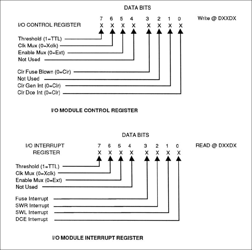
CONTROL REGISTER
Data lines from the A-D-BUS to U14 produce the DCECLR- (Data Compare
Equal Clear), GENCLR- (General Clear), FUSECLR- (Fuse Clear), ENMUX
(Enable Multiplex), CLKMUX (Clock Multiplex), and THRSH (Threshold)
signals. U14 is accessed by a write to $DXXDX, where the ADD- and WR-
signals latch data into U14. The Control Register (U14) is cleared by a
PWRUP (Power Up) signal held low by C44 to ensure a proper reset. See
Figure 2-7 for the Control Register bit position.
The J2 and J3 connectors provide the input to the General Control Latch
block for detection of Clip and Calibration Modules. J2-25 and J3-25 are
the input pins to a detection circuit that provides SWLDET (the
left-hand or A Switch Detect) and SWRDET (the right-hand or B Switch
Detect) signals to generate an interrupt. The mainframe reads the
interrupt register (U13) to determine the reason for an interrupt. See
Figure 2-7 for the interrupt register bit positions.
DATA COMPARISON INPUTS
All 40 lines of the module are compared to programmable data registers
and are qualified by programmable “don’t care” registers. The comparison
is done inside the custom chip(s) between the data on the input lines
and the registers, eight lines per chip. The EQ outputs (pin 55 of the
custom chip) are gated together by U15, and, when they are all high
(i.e., a comparison for all five chips has been detected), an interrupt
is generated and is input to the interrupt register (U13).
FUSE DETECTION
The FUSEDET (Fuse Detect) signal is part of the Multi-Detection area of
the General Control Latch Block. A 1A slow-blow ground fuse located on
2/Theory of Operation
2-13
the module Main PCA protects the ground line. The FUSEDET signal
becomes an input to the interrupt register (U13-8), along with the other
detection signals.
DATA COMPARISON AND GENERAL INTERRUPTS
The General Control Latch block outputs detection and interrupt signals
for any problems or special operations of the module. An external DCE
pin is also available for use as a “hardware interrupt”.
The following two interrupts are produced by the General Control Latch
block:
o DCEINT- (Data Compare Equal Interrupt).
o IOGENINT- (I/O General Interrupt).
The Data Compare Interrupt
DCEINT- is generated by the module when the programmed data compare
registers match the input data. The DCEINT- signal originates from the
EQ pin of each custom chip. The EQ signals are gated to form a DCE-
signal. The DCE- signal triggers a J-K flip-flop to produce the DCEDET
and DCEINT- signals.
The I/O General Interrupt
IOGENINT- is an interrupt generated by the module when either pushbutton
on a clip module is pressed. The interrupt register on the module must
be read to determine the cause. In the case of a button push, two J-K
flip-flops output the SWLDET (A side) and SWRDET (B side) signals. These
signals are gated to produce the IOGENINT- signal.
DATA COMPARE EQUAL OUTPUT PIN
DCE output pin P1-6 can be used to trigger a logic analyzer or
oscilloscope. Buffers and protection circuitry safeguard the DCE signal
output.
OPERATION OF GENERAL CONTROL LATCH BLOCK
The General Control Latch block is divided into three areas. These areas
produce voltages for module operation and contain circuitry that
generates detection for a blown fuse. The functional block contains the
following areas:
o Threshold Voltage Detection.
o Multi-Detection and Interrupt.
o Fuse Blown Detection.
2/Theory of Operation
2-14
Threshold Voltage Generation
Threshold Voltage Generation produces the threshold voltages necessary
for the custom chips to classify input logic levels. Data bit 7 of the
command register (U14) determines the level of the threshold, with a 1
selecting TTL, and a 0 for CMOS.
Figure 2-7. I/O Module Control and Interrupt Registers
The threshold (THRSH) signal output of U14-19 controls the circuitry
that produces a low voltage level (VLO) and a high voltage level (VHI).
These voltage levels are used by the custom chip pins 39 and 45 to
define the logic low, invalid, and logic high voltage ranges. A logic
high out U14-19 designates a TTL logic level and a logic low a CMOS
logic level. The THRSH signal controls resistor dividers that create the
VHI and VLO signals. Two parts of op amp U2 and transistors Q1 and Q2
2/Theory of Operation
2-15
together provide a regulated output with high current sinking
capability. Typical current seen by these regulators can vary from 10 to
40 mA. The approximate VHI and VLO levels generated are listed in Table
2-3.
Table 2-3. VHI and VLO for TTL and CMOS Logic Levels
_____________________________________________________________
DESC THRSH VHI VLO
_____________________________________________________________
TTL 1 -1.05V -2.45V
CMOS 0 -0.25V -2.25V
_____________________________________________________________
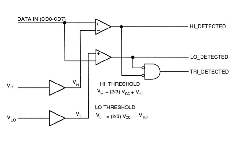
A voltage level-detection system in the custom chip uses data inputs,
VHI, and VLO voltage levels to detect a high voltage input, a low
voltage input, or a tri-state condition. See Figure 2-8 for an
illustration of the detection circuitry contained in the custom chip.
NOTE
The actual input thresholds for the high and low
comparators are computed from the formulas shown
in Figure 2-8.
Figure 2-8. Custom Chip Voltage Level Detection
Multi-Detection and Interrupt
The Vector Output I/O Module accepts different sizes of clip modules. A
detection system within the module informs the mainframe as to the size
of the clip that has been installed on the module. Clip modules are
available in a half-size module and a full-size module. The half-size
module plugs into one connector (either J1 or J2 on the Top PCA), and
2/Theory of Operation
2-16
the full-size module plugs into both connectors (both J1 and J2 on the
Top PCA). Together, the clip(s) plugged into both J1 and J2 of the Top
PCA generate an 8-bit code that can be decoded by the mainframe to
identify the size of the installed clip module(s).
Fuse Blown Detection
Detection of blown fuses is performed by two LM324 Op-Amps (U2) and one
part of U3 configured as a window detector. If the XGND signal exceeds a
+100 millivolt window, U3-6 will go low, forcing the FUSEDET line to go
high. When the interrupt register is read (READ 0 $DXXDX), a 1 in bit 3
indicates the fuse is blown. This blown fuse indication is cleared by
writing to the I/O Command Register (WRITE 0 $DXXDX) with a data value
that has bit 3 = 0.
Connector Code Functional Block
The components associated with the Connector Code block are the 74HCT244
Octal Buffer/Line Driver (U16) and part of the J2 and J3 connectors.
This block is located on the Main PCA as indicated on the functional
block diagram shown in Figure 2-1.
The mainframe determines which Clip Module the user has installed by
reading and decoding connector codes encoded in each Clip Module. To
read the code, the mainframe performs a read at $DXXE1. This operation
generates the ADE- signal, which in turn enables U16, placing the code
on the data bus. Of the eight bits read, the lower four bits refer to
the “A side”, and the upper four bits refer to the “B side”. Thus,
differentiation is possible for 16 different conditions on each side of
the module. Clips that use up an entire module use an 8-bit code. The
most significant nybble of these codes is 1110. A list of these codes is
shown in Table 2-4. For example, to determine the connector codes on
module 3, a Read 0 $D04E1 should be performed. Table 2-5 presents some
examples of codes and their interpretation.
Input Protection Functional Block
The input protection circuit clamps overvoltage, undervoltage, and
static conditions before they reach the custom chip. The signals from
the I/O lines enter the Main PCA through connectors J2 and J3. Each line
passes through a 100 ohm current-limiting resistor. The lines are then
routed to the custom chip inputs. Also attached to the lines are BAV99
diode packs; one diode is tied to +5 volts and the other is tied to
ground to clamp any input above +5 volts or below ground.
OUTPUT SECTION THEORY OF OPERATION
NOTE
All the output section circuitry is located on the Top
PCA unless otherwise indicated.
2/Theory of Operation
2-17
Table 2-4. Dip-Clip and Calibration Module Configuration Codes
______________________________________________________________________________
4-BIT CODE MEANING
______________________________________________________________________________
0000 14-Pin Clip
0001 16-Pin Clip
0010 18-Pin Clip
0011 20-Pin Clip
0100 24-Pin Clip
0101 (reserved)
0110 Used as most significant byte of calibration header
0111 (reserved)
1000 (reserved)
1001 (reserved)
1010 (reserved)
1011 (reserved)
1100 (reserved)
1101 20-Pin Flying Lead Set
1110 Full width connector, use other 4 bits for ID
1111 No Clip Installed
______________________________________________________________________________
8-BIT CODE MEANING
7654 3210
______________________________________________________________________________
1110 0000 28-Pin Clip
1110 0001 40-Pin Clip
1110 0010 Calibration Header
0110 0010 Calibration Header
1110 0011 (reserved)
1110 0100 (reserved)
1110 0101 (reserved)
1110 0110 (reserved)
1110 0111 (reserved)
1110 1000 (reserved)
1110 1001 (reserved)
1110 1010 (reserved)
1110 1011 (reserved)
1110 1100 (reserved)
1110 1101 (reserved)
1110 1111 (reserved)
1111 1111 No Clips Installed
______________________________________________________________________________
Main PCA to Top PCA Interface Functional Block
Communication from the Main PCA to the Top PCA operates similarly to the
mainframe to Bus Interface Functional Block (as described earlier in the
input section). The latched address lines LAT-A4 through LAT-A7 are
routed to the Top PCA through J4 (Main PCA) to J5 (Top PCA). The STROBE-
2/Theory of Operation
2-18
Table 2-5. Connector Code Examples
_________________________________________________________________
CODE READ MEANING
_________________________________________________________________
$F3 No clip on B side, 20-pin clip on A side
$4F 24-pin clip on B side, no clip on A side
$E1 40-pin clip installed
$14 16-pin clip on B side, 24-pin clip on A side
$FF No clips installed
________________________________________________________________
qualified RD- and WR- are also available to the output section. However,
there is a separate data bus for the output section that is selected
when LAT-A7 is low.
Two ICs are required to perform the data bus interfacing: a 74ALS245
Octal 3-State Transceiver (U24) and the 74LS31 delay elements (U29).
Both devices are located on the Main PCA.
The TOPDATA Bus (used by the output section) is isolated from A-D-BUS
(used by the input section) by U24. If a read or write access is made to
any address of the output section (A7 = 0), LAT-A7 remains low, thereby
providing an enable signal to U24 pin 19 (G-). The WR- signal determines
the direction of data travel. If WR- is high, the data passes from the
TOPDATA bus to A-D-BUS for a read. If WR- is low, the data passes in the
other direction for a write.
Some register control signals (such as COMMAND0- and COMMAND1- for U5
and U6 of the Top PCA) use the rising edge of WR- to latch data. Since
the WR- signal also controls the direction of the TOPDATA bus through
}U24, U29 provides a nominal 46.5 ns delay to the direction control
signal (WR-DLY-) on U24. This insures that, during accesses to the
output section, the data bus is held in the correct direction by U24
while the rising edge of RD- or WR- latches the data.
ADDRESSING
All addresses with A7 low are reserved for the output section. Since A3
through A1 only go to the custom chips for use as addresses and STROBE-
is only active for addresses with LDS- active (address bit 0 = 1), the
address space is effectively limited to $DOX01 through $DOX71.
Table 2-6 lists the output section addresses and the signals (or
registers) that are affected by accessing the address for both reads and
writes.
Performing a write to $DOX01 causes the COMMAND0- output of U10 (Top
PCA) to toggle, thereby latching the data on the bus into the U5
register. (See the heading, “Output Control Functional Block”, further
on in this section for more information.) When a read is performed at
this address, the Vector Drive Status Nybble is returned from U25 (Main
PCA). (See the heading, “Drive Status Functional Block”, further on in
this section and Table 2-10 for more information.)
2/Theory of Operation
2-19
Table 2-6. Vector I/O Module Output Section Address Map
______________________________________________________________________________
ADDRESS WRITE READ
______________________________________________________________________________
$DOX01 COMMAND0- Vector Drive Status Nybble
$DOX11 COMMAND1- ----
$DOX21 Drive Register 2 (U25) ----
$DOX31 Loop Counter Load ----
(LCLO- or LCHI-)
$DOX41 RAM-PORT- RAM-PORT-
$D0X51 RAM-STROBE ----
$DOX61 LOAD-RAM-HI- ----
$DOX71 LOAD-RAM-LO- ----
______________________________________________________________________________
Performing a write to $DOX11 toggles the COMMAND1- output of U10 (Top
PCA), thereby latching the data on the bus into the U6 register.
Performing a read at this address has no effect. See the Table 2-9 for
more information.
Performing a write to $DOX21 selects U25 (Main PCA) by address decoding
and latches the data on the bus into Drive Register 2 on U25. Performing
a read at this address has no effect. See the headings, “Internal
Oscillator Control Functional Block”, the “Loop Control Functional
Block”, and Table 2-7 for more information.
Performing a write to $DOX31 toggles either LCLO- or LCHI- of U25 (Main
PCA), depending on the state of bit 3 of Drive Register 2 on U25,
thereby loading the least significant byte (LSB) or most significant
byte (MSB) of the loop count into U26 or U27. Performing a read at this
address has no effect. See the heading, “Loop Control Functional Block”,
and Table 2-7 for more information.
Performing a read or a write to $DOX41 toggles the RAM-PORT- output of
U10 (Top PCA), thereby incrementing the chip counter U9 and updating
which SRAM is selected by U11. The actual data returned by a read is
disregarded.
Performing a write to $DOX51 toggles the RAM-STROBE output of U10 (Top
PCA). This output can be used as a software-controlled clock for driving
vectors. Performing a read at this address has no effect.
Performing a write to $DOX61 toggles the LOAD-RAM-HI- output of U10 (Top
PCA), thereby latching the data on the bus into the upper byte register
U3 of the Loop-Back Address. Performing a read at this address has no
effect.
Performing a write to $DOX71 toggles the LOAD-RAM-LO- output of U10 (Top
PCA), thereby latching the data on the bus into the lower byte register
U4 of the Loop-Back Address. Performing a read at this address has no
effect.
2/Theory of Operation
2-20
Internal Oscillator Control Functional Block
The Vector Output I/O Module contains a 1, 5, 10, and 20MHz internal
clock source that is available for vector driving. The desired clock can
be selected by writing to Drive Register 2 (U25) of the Main PCA
($DOX21) and specifying bits 1 and 0.
The Internal Oscillator Control Functional Block consists of a 20 MHz
Oscillator (U20), a 70HCT390 Dual Decade Ripple Counter (U21), a 74HC74
D-Type Flip-Flop (U28), and a 74AC151 8-Input Multiplexer (U22), all
located on the Main PCA.
Writing to U25 ($DOX21) using bit 1 and bit 0 selects the frequency of
the internal clock. Outputs BMUX1 and BMUX0 from U25 to U22 control the
selection of one of four clocks (see Table 2-7). These clocks are 20 MHz
(obtained directly from the 20 MHz Oscillator U20), 10 MHz (obtained
from U21 by dividing the 20 MHz clock by two), 5 MHz (obtained by
dividing the 10 MHz clock by two using U28), and 1 MHz (obtained by
dividing the 10 MHz clock by ten using U21). The Y output of U22 pin 5
goes directly to the Top PCA and is used by the SSLOGIC Functional Block
as one vector driving clock source. The Y- output from U22 pin 6 is
inverted by U19. This inversion gives OSC-CLK the same phase as the
INT-OSC output and delays it slightly to reduce the clock to vector-out
skew before being routed to the P1 pin 5 INT OSC output.
Table 2-7. U25 Drive Register 2 Bit Description (Write @ $D0X21)
___________________________________________________________________________
BIT SIGNAL 1 0
___________________________________________________________________________
7,6,5,4 ---- ---- ----
3 LCHI-/LCLO- LCHI- LCLO-
2 LTCCLR- NO LTCCLR- LTCCLR-
1 BMUX1*
0 BMUX0*
___________________________________________________________________________
*BMUX1 *BMUX0 FREQUENCY
___________________________________________________________________________
0 0 10 MHz
0 1 20 MHz
1 0 5 MHz
1 1 1 MHz
___________________________________________________________________________
Output Control Functional Block
The U10 PAL provides the majority of the output section control. It
provides the latching signals COMMAND0- and COMMAND1- to U5 and U6. It
provides the RAM-PORT- signal that controls the chip counter U9 and the
RAM Select U11 PAL. It decodes writes to $D0X51 to generate RAM-STROBE,
which provides the soft-clocking ability for vector output. It supplies
2/Theory of Operation
2-21
the LOAD-RAM-HI- and LOAD-RAM-LO- signals that control the Vector RAM
Address Functional Block. For more information on the available
addresses and the signals they affect, see Table 2-6. Table 2-8
illustrates the U5 register bits used by the Output Control Functional
Block.
U10 also provides the START-ENA signal to the SSLOGIC Functional Block.
There are two conditions by which this signal can be made active. If the
CO-START output of U5 is low, setting bit 0 to a 1 when writing to
$D0X11 sets START-ENA high. If the CO-START output of U5 is set high,
START-ENA is not set high until RECV-ARM- is low.
The RECV-ARM- signal comes from the Main PCA and is generated by U23
(74HCT138). RECV-ARM- goes low when ALLCHIP- is low, D0 is low, D1 is
high, and A1 through A3 are low (i.e., the input section is armed). This
permits the input section to be armed at the same time the output
section receives the START-ENA, so that both input and output sections
can be started simultaneously.
To clear START-ENA, the CO-START line must be set low and a WRITE @
$D0X11 must be performed with bit 0 set to 0.
Table 2-8. U5 Register Bit Description (Write @ $D0X01)
___________________________________________________________________________
BIT SIGNAL 1 0
___________________________________________________________________________
7 LOAD-RAM- No Load RAM Load RAM
6 COUNTER-ENA- No Counter Enable Counter Enable
5 HSIN-POL- Falling Edge Rising Edge
4 CO-START Co-Start No Co-Start
3 DRV/LD- Drive Load
2 MUX2*1
1 MUX1*
0 MUX0*
___________________________________________________________________________
*MUX2 *MUX1 *MUXO CLOCK
___________________________________________________________________________
0 1 1 INT-OSC
1 0 0 PSYN
1 0 1 RAM-STROBE
1 1 0 DR CLK
1 1 1 DECREMENT
(other) Ground
___________________________________________________________________________
RAM Select Functional Block
The high-speed 30 ns 8K x 8 SRAM in the module must be accessed when
loading vector files, when driving vector patterns, and when setting the
2/Theory of Operation
2-22
module output to an unchanging state. There are two methods by which the
Vector Pattern RAM and the Vector Control RAM can be selected:
o To drive vectors, the DRV/LD- signal must be set high by performing
a write to the U5 register 0 ($D0X01) with bit 3 set high. This
causes all outputs of U11 (BYTE0- through BYTE9-) and the BYTE10-
output of U10 to be low, thereby selecting all vector RAM.
o To load the Vector Pattern and Control RAM, the DRV/LD- signal must
be set low by performing a write to the U5 register ($D0X01) with
bit 3 set low. Only the RAM addressed by the chip counter U9 is
selected.
CHIP COUNTER OPERATION
The output of the chip counter is decoded by U10 and U11 to determine
which BYTEx- to set low when loading the RAM. The counter is initialized
by setting the LOAD-RAM- output of U5 low (Write @ $D0X01, bit 7 low)
and toggling RAM-PORT- (Read @ $D0X41). This causes the four-bit binary
counter (U9) to parallel-load its preset value of 5. The LOAD-RAM-
signal can then be returned high. When the output of the chip counter is
5, the BYTE0- output of the U11 PAL selects static RAM chip U100. A
write to RAM-PORT- causes the selected RAM to load the data on the bus
and advances the chip counter U9 output to 6, causing U11 output BYTE1-
to select U102. This operation is repeated until the counter reaches 15,
at which point the U10 PAL output BYTE10- selects the Control RAM U600.
Upon performing a write to RAM-PORT-, the Control RAM is loaded with the
data, and the RC0 output of U9 goes low.
The RC0 output is used as the DECREMENT- clock. The clock is routed to
the SSLOGIC block where it decrements the Vector RAM Address Register.
The RC0 output is also routed through U7 to reload the U9 chip counter
to the starting count of 5.
SSLOGIC (Start/Stop Logic) Functional Block
The SSLOGIC Functional Block consists of five groups of circuitry:
o Signal polarity/control register.
o Drive clock selection.
o Start/stop control.
o Handshake synchronization.
o Vector drive complete logic.
SIGNAL POLARITY/CONTROL REGISTER
The output section signal polarity and control is determined by the
values stored in register U6. The values are set by performing a write
to $D0Xll with the desired value. Table 2-9 contains the register bit
assignments. Bits 4 through 7 control the active edge polarity of the
externally supplied START, STOP, ENABLE, and DR CLK signals. Bit 3
2/Theory of Operation
2-23
determines if the vector drive clock should be always enabled or if the
external ENABLE should be used. Bit 2 determines if the vector output
should be “force” started (no external start required) or if the
external START is required. Bit 1 determines if the external STOP signal
should terminate vector driving or not. Bit 0 is unused (the address and
position of this bit are used for clearing START-ENA).
DRIVE CLOCK SELECTION
Five different clock sources are available for use by the output
section: CLKP (from DR CLK), PSYN- (Pod Sync), INT-OSC, RAM-STROBE, and
DECREMENT (used for vector RAM loading). These clocks are input to an
8-Input Multiplexer (U14). The clock selection is controlled by the
MUX2, MUX1, and MUX0 outputs of the U5 register. The clock is selected
by performing a write to $D0X01 and setting bits 2, 1, and 0 to the
desired values. Table 2-8 shows which clocks are selected by the
different bit settings. The clock source selected for vector driving or
loading is routed from U14-5 to U19 (where it is enabled by DONE- if
vector driving is not complete) and to the SSGATE Flip-Flop U16.
Table 2-9. U6 Register Bit Description (Write @ $D0X11)
___________________________________________________________________________
BIT SIGNAL 1 0
___________________________________________________________________________
7 CLK-POL- Falling Edge Rising Edge
6 ENA-POL Enable High Enabie Low
5 STOP-POL- Falling Edge Rising Edge
4 START-POL- Falling Edge Rising Edge
3 ENA-ALWAYS Enable Always No Enable Always
2 FOR-START- No Forcestart Forcestart
1 STOP-ENA- No Stop Enabled Stop Enabled
0 Unused ---- ----
___________________________________________________________________________
The PSYN signal is inverted by U20 to PSYN-. This allows the vectors to
be driven on the falling edge of PSYN (so the vectors are driven and
settled by the time the rising edge of PSYN clocks the input section.
START/STOP CONTROL
The Start/Stop Control Circuit consists of two 74ACT74 D-Type Flip-Flops
(U13 and U16), a 74AC32 OR Gate (U15), a 74AC20 Quad Input NAND Gate
(U12), and a 74AC08 AND Gate (U19).
U16 determines whether the selected clock source (from U14) decrements
the Vector RAM Address Register (and latches the RAM data out if in the
drive mode) or not. If the DONE- signal is not active on U19-1, the
clock is gated through to U16-3. If the SSGATE- line is high, the clock
is disabled. If SSGATE- is low, the rising-edge of the clock causes
CK-OUT (U16-6) to go high and is presented to the vector drive
circuitry. As soon as the clock input is no longer high, the U15
CLK-PRES output goes low (since U15 pin 5 is low as well) and sets U15,
returning the CK-OUT signal low.
2/Theory of Operation
2-24
SSGATE- on U12 pin 6 provides the qualifying signal to the clock. In
order to have the clock qualified, the following conditions must be met:
o U12 pin 1 must be high. This line insures that a start has been
received, either by the FOR-START- line being low or by the STRP
signal having the programmed edge on the external START line.
o U12 pin 2 must be high. This line ensures that no external STOP
signal of the programmed edge has been received or that vector
driving is not yet complete (DONE- on U13 pin 1 clears the pin 5
output, thereby disabling SSGATE-).
o U12 pin 4 must be high. This is the ENA-RCVD line, and is either
high all the time (if ENA-ALWAYS is high) or high only when the
input on the external ENABLE line is at the programmed level.
o U12 pin 5 must be high. This is the HS-ENABLE line and is high if
vector driving is not suspended awaiting a WAIT input. If a WAIT
statement has been reached in the vector file, the HSOUT line of the
Vector Control RAM is active and sets the HS-ENABLE low, suspending
vector driving. (The following text describes handshake
synchronization in more detail.)
HANDSHAKE SYNCHRONIZATION
The handshake synchronization circuitry allows the Vector Output I/O
Module to suspend vector driving until the desired edge has been
detected on the WAIT input (P1 pin 3) of the Main PCA.
The handshake synchronization circuit consists of a 74ACT74 Dual D-Type
Flip-Flop (U8), a 74AC20 Quad Input NAND Gate (U12), and a 74ACT86
Exclusive OR Gate (U17), all on the Top PCA.
Prior to vector driving, the START-ENA line is set low. This signal is
gated by U12 and U17 and is routed to U8-10, which initializes the
HS-ENABLE line from U8-9 high. HS-ENABLE permits SSGATE- to be low upon
receipt of a start and enable with no stop. START-ENA is returned high
to enable vector driving so that U8-10 is not being held to SET-.
HSIN-POL (U5-15) is set to the proper polarity (high) when the vector
file is loaded.
When a vector is driven and is followed by a vector file WAIT statement,
the HSOUT line (U601-16) goes high. This generates a rising edge on U8
pin 11 that sets U8-9 HS-ENABLE low, which returns SSGATE- high (i.e.,
no clocks are permitted to drive vectors). U8-8 is set high as the data
input to U8-2. Upon the receipt of the proper edge on Pl pin 3 (WAIT) on
the Main PCA, HSIN is passed through U17 to become HSIN-PLUS, providing
a rising edge to U8-3, which clocks U8, setting U8-6 low. This low
signal sets the U12-8 output high. This signal is inverted by U17 and is
applied as a low to the U8-10 SET- input. When pin 10 is set, HS-ENABLE
(U8-9) returns high, which sets SSGATE- low (allowing vectors to be
clocked out). U8-8 is also set low, which removes the SET- low signal
from U8-10. The HS-ENABLE signal also goes through J4-36 on the Top PCA
to J3-36 on the Main PCA to U25-12, where the status can be observed by
bit 2 of the Vector Drive Status Nybble.
2/Theory of Operation
2-25
VECTOR DRIVE COMPLETE LOGIC
There are two different mechanisms for controlling the completion of
vector driving, both of which are selected by the vector file in use.
The Vector Drive Complete circuitry consists of a 74AC02 NOR Gate (U20),
a 74ACT86 Exclusive OR Gate (U17), a 74ACT74 D Flip-flop (U16), and a
74AC08 AND Gate (U19).
Performing a General Stop
To stop the vector at a certain location within the vector file, a STOP
statement may be placed in the vector file. The DONEDRV line (U601-15)
goes high at the final vector address. DONEDRV is inverted by U20, which
produces the DONE- signal. DONE- does not allow the CLKMUX-OUT signal to
pass from U19-2 to U19-3. DONE- also clears U13 (which disables SSGATE-
by setting it high) to prevent further clocking of the RAM. DONE- is
also routed through J5-28 to J4-28 on the Main PCA to U25-16, where the
vector drive status is reflected in bit 3 of the Status Nybble.
Performing a Loop and Stop
To loop a specified number of times and then stop vector driving with no
further vectors being driven, a STOP statement may be placed after an
ENDLOOP statement in the vector file.
The LOOP-DONE signal is normally low. This signal remains low until the
final pass through the loop has begun. As long as LOOP-DONE is low, the
output of U16-9 is also low, preventing the BOTH signal from passing
through U19.
The LOOP signal is active one vector before the end of the loop to
permit address loading (since the module uses a pipeline scheme). The
BOTH signal is active at the same time as the final vector of the loop
is driven. Since U17 inverts BOTH, the current status of LOOP-DONE is
not latched until the first vector in the loop is driven (BOTH returns
low, clocking U16).
At the conclusion of the next-to-last pass through the loop, LOOP-DONE
is set high. On the last vector of the loop, BOTH goes high. When the
first vector of the loop is driven, BOTH returns low. The inversion of
BOTH latches LOOP-DONE, setting U16-9 high. As soon as the last vector
in the last pass through the loop is driven, BOTH returns high and
U19-6 goes high, generating the DONE- signal. From this point, the
signal is routed as described in the heading “Performing a General
Stop.”
See the Loop Control Function Block for further information on how
looping operates.
2/Theory of Operation
2-26
Vector Address Functional Block
The Vector RAM Address Registers U1 and U2 are loaded by the following
procedure:
1. The least significant byte (LSB) and the most significant byte (MSB)
of the address are loaded into U4 and U3 by performing writes to
$D0X71 and $D0X61 respectively, and then writing $D0X01 with bit 7
low and then high, toggling the LOAD-RAM- signal and parallel
loading the address.
2. If any looping is to be performed during vector driving, the LSB and
MSB of the LOOP-BACK ADDRESS are loaded into U4 and U3 by performing
writes to $D0X71 and $D0X61 respectively.
3. When vector driving is to occur, a write to $D0X01 with bit 6 set
low is performed, allowing the output of U1 and U2 to be decremented.
The outputs of U1 and U2 form the current address of the vector RAM.
Whenever a RAMCLK clocks U1 and U2, their address is decremented by
one. At the same time that U1 and U2 are being decremented, RAMCLK
latches the data of the current address into the latches of the
Vector RAM Functional Block. This process continues until either the
vector driving is complete or a LOOP command occurs. The LOOP
command generates LOOP-LD- to activate the LOAD-RAM-OUT- signal.
This signal commands U1 and U2 to reload the LOOP-BACK ADDRESS (from
which the vector driving resumes).
Vector Pattern RAM Functional Block
There are ten identical Vector Pattern RAM Functional Blocks that
provide the forty output channels on the Vector Output I/O Module. Each
RAM block consists of an 8K x 8 SRAM, a 74AC273 Octal D-Type Flip-Flop, a
resistor pack, and one 74HC126 Tri-Stateable Buffer.
The resistor pack provides isolation from the D-BUS data bus. When only
the RAM has been selected to be written to, the data on the bus passes
through the resistor pack and is input to the RAM. When vectors are
driven and all devices have been selected, the resistor pack provides
enough isolation from the bus to prevent other devices from interfering
with the output of the RAM.
When vector driving occurs, the data at the current address of the RAM
is latched in the latch by LAT-CLK. This data contains one signal bit
(high or low) and one tri-state bit (on or off) for four lines of
output. The latch also has a TRISTATE- input from P1 pin 2 that, upon a
low input, clears the the latch and resets its contents to all lows,
tri-stating all 40 outputs of the I/O module.
Vector Control RAM Functional Block
The Vector Control RAM provides user-programmed (via vector files)
control signals used for looping, handshaking, Capture clocking, and
vector drive termination.
2/Theory of Operation
2-27
The Vector Control RAM Functional Block consists of an 8K x 8 SRAM
(U600), a 74AC273 Octal D-Type Flip-Flop (U601), a resistor pack (Z600),
and one 74AC08 AND gate (U19).
The Z600 resistor pack provides isolation from the D-BUS data bus. When
only U600 has been selected to be written to, the data on the bus passes
through Z600 and is input to U600. When vectors are driven and all
devices have been selected, the resistor pack provides enough isolation
from the bus to prevent other devices from interfering with the output
of the U600 RAM.
When Vector RAM is being loaded (i.e., DRV/LD- is low), the output of
U601 is cleared to prevent the control signals from causing erratic
behavior in the module.
When vector driving occurs, the current data out of U600 is latched in
U601 by LAT-CLK. The outputs of U601 are used for the following
purposes:
o DONEDRV - terminates vector driving when the final vector in the
file is driven.
o HSOUT - suspends vector driving until the programmed edge is
detected on the WAIT input.
o LOOP - decrements the loop counter and checks the results after
reaching one vector prior to the ENDLOOP statement.
o BOTH - loops until the loop count is exhausted and then
terminates vector driving.
o CAP-CLK - clocks the input section in the center of the current
vector period.
When the TP5 TST test point is pulled low (for testing purposes), the
output of U601 is disabled (forced low). This permits the control RAM to
be loaded with test patterns and driven without affecting the output
(i.e. LOOP bits do not force looping). CRCs of the RAM output verify
that the proper data is at the proper address.
Loop Control Functional Block
NOTE
All the loop control circuitry is located on the Main
PCA unless otherwise noted.
When a vector file that uses looping is loaded into the module, several
actions are performed. A write is performed to $D0X21 to clear LTCCLR-
(bit 2), which causes the U25 PAL to reset the LOOP-DONE output on U28.
Next, a write is performed to $D0X21 with bit 3 set or cleared, choosing
the loading of either the MSB or LSB of the loop count number contained
in the vector file (the value loaded is actually count -- 2). Then a
write is performed to $D0X31 with the MSB or LSB as appropriate. This
2/Theory of Operation
2-28
step is repeated for the other byte (either the MSB or the LSB).
Finally, another write is made to $D0X21 with bit 2 set that releases
the clear on U28.
When a vector file is driven, on the vector prior to the one designated
by the ENDLOOP statement on the vector file the LOOP output (U601-5)
goes high. This signal is passed from the Top PCA (J5-24) to the Main
PCA (J4-24) and is input to a 74AC00 NAND gate (U19). If the looping is
not complete, LOOP-DONE- is high and passes the signal to the inputs of
two 74HC40103 Counters (U26 and U27), decrementing the counters. This
signal is then fed back as LOOP-LD- to J4-25 and J5-25. It passes
through U7 (Top PCA), clocking the U1 and U2 PE- (parallel load) input,
which loads the LOOP-BACK ADDRESS that is stored in U3 and U4. Each time
the vector that contains the LOOP bit is driven, this process is
repeated until U26 has counted down to zero. The TC- output enables U27
to be decremented by the next LOOP, while U26 is rolled-over, turning
off TC-. This process continues until both counters have reached their
terminal count (which occurs one pass prior to exiting the loop). When
the terminal count is reached, U27 has its LPTC signal go low, providing
a low input to U28 pin 2. Entry into the final LOOP clocks U28 to latch
the data and set LOOP-DONE- low, disabling any further LOOPs from
passing through U19. LOOP-DONE is sent to the Top PCA SSLOGIC Functional
Block for terminating vector driving if the BOTH bit of the Vector
Control RAM is set.
Capture Clock Functional Block
When a vector file is driven with the Capture clock programmed to occur,
the CAP-CLK output at U601-2 goes high for the entire vector period.
CAP-CLK is inverted by U20 and is then “ANDed” with the RAMCLK signal
and output from U20-3. The “ANDing” of the two signals provides the
clocking edge that occurs during the middle of the vector period. The
signal is then passed through the 33 ohm series resistor R10 and passes
from J5-29 to J4-29 of the Main PCA. There the signal is inverted once
more through U19 (Main PCA) before it is routed to the input of the
Clock Mux U18-12 (Main PCA).
Drive Status Functional Block
The Drive Status circuitry is located on the Main PCA. The status of the
Vector Output I/O Module is a 4-bit code returned by performing a read
at $D0X01. Table 2-10 illustrates the significance of the bits returned.
Bit 3 contains the vector drive status (0 - complete, 1 - not complete),
bit 2 contains the HS-ENABLE status (0 - drive suspended for handshake,
1 - drive not suspended for handshake), and bit 1 and bit 0 contain the
module type ID code (Vector I/O = 01). Upon the receipt of RD- on U25-7,
the status of the DONE-signal on U25-16, the HS-ENABLE signal on U25-12,
and the ID code on U25-10 and U25-11 are output on U25-17 through
U25-20. The WR-DLY- signal on U24-1 directs the data through U24 from
the TOPDATA Bus to the A-D-Bus. The address $D0X01 ensures that LATA7-
is low to enable the data. The data is then read by the mainframe
through U8.
2/Theory of Operation
2-29
Table 2-10. U25 ID/Status Register Bit Description (Read @ $D0X01)
___________________________________________________________________________
BIT SIGNAL 1 0
___________________________________________________________________________
3 DONE Not Done Done
2 HS-ENABLE Not Suspended Suspended
1,0 ID CODE = 01
___________________________________________________________________________
Output Protection Functional Block
The vector data on the OUT-BUS of the Top PCA is connected to diode
packs (BAV99) that are connected to +5 volts and ground to clamp
overvoltage and undervoltage on the outputs. The output connectors (J1
and J2) have 33 ohm resistors in series with the output that provide
high speed serial termination as well as allowing current limiting in
cases of overvoltage, undervoltage, or stuck outputs.
2/Theory of Operation
2-30
Page 1 of 2
Some semiconductors and custom IC's can be
damaged by electrostatic discharge during
handling. This notice explains how you can
minimize the chances of destroying such devices
by:
1. Knowing that there is a problem.
2. Learning the guidelines for handling them.
3. Using the procedures, and packaging and
bench techniques that are recommended.
The Static Sensitive (S.S.) devices are identified in the Fluke technical manual parts list with the symbol
The following practices should be followed to minimize damage to S.S. devices.
1. MINIMIZE HANDLING
2. KEEP PARTS IN ORIGINAL CONTAINERS
UNTIL READY FOR USE.
3. DISCHARGE PERSONAL STATIC BEFORE
HANDLING DEVICES. USE A HIGH RESIS-
TANCE GROUNDING WRIST STRAP
4. HANDLE S.S. DEVICES BY THE BODY
Page 2 of 2
5. USE STATIC SHIELDING CONTAINERS FOR
HANDLING AND TRANSPORT
6. DO NOT SLIDE S.S. DEVICES OVER
ANY SURFACE
7. AVOID PLASTIC, VINYL AND STYROFOAM®
IN WORK AREA
PORTIONS REPRINTED
WITH PERMISSION FROM TEKTRONIX, INC.
AND GENERAL DYNAMICS, POMONA DIV.
® Dow Chemical
8. WHEN REMOVING PLUG-IN ASSEMBLIES,
HANDLE ONLY BY NON-CONDUCTIVE
EDGES AND NEVER TOUCH OPEN EDGE
CONNECTOR EXCEPT AT STATIC-FREE
WORK STATION. PLACING SHORTING
STRIPS ON EDGE CONNECTOR HELPS TO
PROTECT INSTALLED SS DEVICES.
9. HANDLE S.S. DEVICES ONLY AT A
STATIC-FREE WORK STATION
10. ONLY ANTI-STATIC TYPE SOLDER-
SUCKERS SHOULD BE USED.
11. ONLY GROUNDED TIP SOLDERING
IRONS SHOULD BE USED.
A complete line of static shielding bags and acces-
sories is available from Fluke Parts Department,
Telephone 800-526-4731 or write to:
JOHN FLUKE MFG. CO., INC.
PARTS DEPT. M/S 86
9028 EVERGREEN WAY
EVERETT, WA 98204
J0089D-07U8604/SE EN Litho in U.S.A.
Rev. 1 MAR 86
3-1
Section 3
Maintenance
WARNING
SERVICING DESCRIBED IN THIS SECTION IS TO BE PERFORMED
BY QUALIFIED SERVICE PERSONNEL ONLY. TO AVOID
ELECTRICAL SHOCK, DO NOT PERFORM ANY SERVICING UNLESS
YOU ARE QUALIFIED TO DO SO.
INTRODUCTION
This section describes maintenance procedures for the 9100A-017 Vector
Output I/O Module. Some of these procedures do not require access to the
instrument and can be performed by the operator. Troubleshooting
procedures, which are covered in detail in the 9100A Service Kit, may
require reference to the disassembly and reassembly instruction found in
this section.
CHANGING THE VECTOR OUTPUT I/O MODULE FUSE
An operator display message ("I/O module fuse blown") indicates that the
Vector Output I/O Module fuse has opened. This problem can occur when
the I/O Module COMMON lead is incorrectly connected to the UUT.
Prior to replacing the fuse, determine the incorrect COMMON lead
connection. Then disconnect all I/O Module leads and replace the fuse as
follows:
1. Locate the fuse holder on the back of the I/O Module, near the
cable.
2. Press the fuse holder cap in, then rotate it counterclockwise.
3. Pull the cap and fuse straight out. Separate the cap and fuse.
4. Replace with a 1A, 250V slow blow fuse.
Vector Output I/O Modules configured at the factory for use with 110V
line voltage mainframes use 1/4 x 1-1/4 inch fuses with grey fuse holder
caps. Instruments configured at the factory for 220V use 5 mm x 20 mm
fuses with black fuse holder caps. First, check the color of the fuse
cap (grey caps hold U.S. fuses; black caps hold metric fuses). Then
select the proper fuse part number.
3/Maintenance
3-2
CLEANING
CAUTION
Do not use aromatic hydrocarbons (such as gasoline or
other fuels) or chlorinated solvents for cleaning. They
may damage plastic materials used in the instrument.
Do not use detergent of any kind for cleaning the PCA.
Clean the instrument case with a mild detergent and water.
The main and top PCAs may be washed with isopropyl alcohol or deionized
water and a soft brush. Dry with clean dry air at low pressure.
VECTOR OUTPUT I/O MODULE SELF TEST
The Vector Output I/O Module Self Test verifies that the module is
connected and is communicating with the system. Use the following
procedure to self test the module:
1. Press MAIN MENU on the mainframe and move the cursor to the first
(left-most) field using the left arrow ( <- ) key.
2. Press the SELFTEST softkey (F1).
3. Move the cursor one field to the right and press the I/O MOD softkey
(F3).
4. Move the cursor one more field to the right, and press the number of
the I/O Module to be tested. Check that the display reads:
MAIN: SELFTEST I/O MOD <n>
(where <n> signifies the number of the I/O Module).
5. Press ENTER to initiate the self test.
If the self test fails, a failure message is displayed. Check the Vector
Output I/O Module connection and repeat the test.
If the test fails a second time, the Vector Output I/O Module requires
service.
DISASSEMBLY
To gain access to the 2 PCAs in the Vector Output I/O Module, perform
the following steps:
1. Disconnect the module from the mainframe.
2. Turn the module over on its top (with the large module decal facing
up). Remove the four Phillips screws that hold the case halves
together, and separate the top and bottom case halves.
3/Maintenance
3-3
3. Place the bottom half of the module (with the PCAs still attached)
with the mainframe cable facing you. Remove the two Phillips screws
on the corners of the PCA closest to the mainframe cable that hold
the PCAs to the bottom of the case. Pull the PCAs away from the
lower half of the case.
4. To separate the PCAs, turn the the PCAs component side down. Remove
the three Phillips screws (two on the corners of the PCA furthest
away from the mainframe cable and one in the center of the board)
that hold the PCAs together. Carefully pull the boards apart to
avoid damage to the connectors.
TROUBLESHOOTING
This section contains general troubleshooting information that isolates
the problem to one of the Vector Output I/O Module PCAs. For more
complete information on testing and troubleshooting, along with software
to supplement the tests, a 9100A Service Kit (John Fluke Part Number
818948) can be purchased.
General Information
If the Vector Output I/O Module fails the self test, the PCA that failed
can usually be quickly isolated. To verify that the output section is
driving out any vectors, place the 9100A single-point probe on the
module output connector (J1 and J2 on the Top PCA).
If the module is not driving out vectors, check the following few key
signals on the Top PCA (9100A-4022) on the affected channel(s) while the
self test is being performed:
o Verify the non-assertion of the external TRISTATE- signal on pin 1
of the 74AC273 D-Type Flip-Flops (U101, U103, . . .) of the Pattern
RAM Functional Block.
o Verify the activity of the LAT-CLK signal on pin 11 of the 74AC273
D-Type Flip-Flops (U101, U103, . . .) of the Pattern RAM Functional
Block. If these signals are not active, verify that the SSGATE-
output of the 74AC20 (U12) is low. If it is not low, check the
inputs to U12 to determine which condition is preventing clocking.
If the module is driving out vectors, but failing the self test, the
Main PCA (9100A-4021) can be used for stimulus measurement with the Top
PCA removed. Another module may be used to stimulate the failing
channel(s) by connecting its output to the Main PCA input connectors J2
and J3 while the single-point probe is used to trace the signal paths.
The failure mask of the self test can often provide clues as to whether
the input or output section failed. The failure mask is displayed as a
10-digit hex value. Each channel of the Vector Output I/O Module is
displayed as one bit of the mask (for a total of 40 channels). On the
input section of the module, each custom chip (U100, U110, U120, U130,
and U140 on the Main PCA) has eight channels. On the output section,
each RAM chip (U100, U102, U200, U202, U300, U302, U400, U402, U500, and
3/Maintenance
3-4
U502 on the Top PCA) has four channels of output. By observing the
failure mask and using the single-point probe for verification, the
faulty PCA (Top or Main) can be isolated.
4-1
Section 4
List of Replaceable Parts
____________________________________________________________________________
TABLE OF CONTENTS
TABLE FIGURE
ASSEMBLY NAME DRAWING NO. NO. PAGE NO. PAGE
9100A-017 Final Assembly 9100A-017 4-1 4-5 4-1 4-6
A1 Main PCA 9100A-4021 4-2 4-8 4-2 4-9
A2 Top PCA 9100A-4022 4-3 4-10 4-3 4-11
4/List of Replaceable Parts
4-2
4/List of Replaceable Parts
4-3
INTRODUCTION
This section provides an illustrated parts list for the 9100A-017 Vector
Output I/O Module. Components are listed alphanumerically by assembly.
Both electrical and mechanical components are listed by reference
designation. Each listed part is shown in an accompanying illustration.
The parts lists contain the following information:
o Reference Designator
o Description
o Fluke Stock Number
o Federal Supply Code for Manufacturers (MFRS SPLY CODE)
o Total Quantity of Components per Assembly (TOT QTY)
HOW TO OBTAIN PARTS
Components may be ordered directly from the manufacturer’s part number, or
from the John Fluke Manufacturing Co., Inc., or an authorized
representative by using the Fluke Stock Number. In the event the part
ordered has been replaced by an new or improved part, the replacement
will be accompanied by an explanatory note and installation instructions
if necessary.
To ensure prompt and efficient handling of your order, please include
the following information:
o Quantity
o Fluke Stock Number
o Description
o Reference Designation
o Printed circuit assembly (PCA) number and revision letter
o Instrument Model Number and Serial Number
Parts price information is available from the John Fluke Manufacturing
Co., Inc. or its representative. Prices are also found in the Fluke
Replacement Parts Catalog, which is available on request.
CAUTION
An asterisk in the "S" (static) column indicates a device
or component subject to damage by static discharge.
4/List of Replaceable Parts
4-4
ADDITIONAL INFORMATION
Table 4-4 lists the revision levels of the PCAs documented in this
manual. To identify the configuration of the PCAs used in your
instrument, refer to the revision letter on the component side of each
PCA.
This section also contains a list of Manufacturer’s Federal Supply Codes
and a list of U. S. and international Technical Service Centers.
4/List of Replaceable Parts
4-5
Table 4-1. 9100A-017 Vector I/O Final Assembly
(See Figure 4-1.)
N
REFERENCE FLUKE MFRS MANUFACTURERS 0
DESIGNATOR STOCK PART NUMBER TOT T
-A>-NUMERICS----> S--------------DESCRIPTION-------------- --NO-- -CODE- -OR GENERIC TYPE----- QTY- -E-
A 1 * MAIN PCA 846329 89536 846329 1
A 2 * TOP PCA 846332 89536 846332 1
F 1 FUSE,.25X1.25,1A,250V,SLOW 109272 71400 MDL 1.25 250V 1
F 2 FUSE, 5x20MM, lA,250V,SLOW 808055 61935 034.3117 1
H 1 SCREW,MACH,PH,P,SEMS,STL,6-32X.250 178533 89536 178533 3
H 2 SCREW,MACH,PH,P,SS,6-32,.875 801241 89536 801241 4
H 3 SCREW,MACH,PH,P,STL,6-32,.875 114868 73734 19049 2
H 4 WASHER,FLAT,BRASS,#6,0.028 THK 111310 89536 111310 2
MP 1 FOOT, NON-SKID 774000 89536 774000 4
MP 2 CASE TOP, I/O MODULE 773291 89536 773291 1
MP 3 CASE BOTTOM, I/O MODULE 773283 89536 773283 1
MP 4 DECAL, VECTOR OUTPUT I/O TOP 855387 89536 855387 1
MP 5 DECAL, VECTOR OUTPUT I/O BOTTOM 855390 89536 855390 1
MP 6 DECAL, VECTOR OUTPUT I/O SIDE 855395 89536 855395 1
MP 7 NAMEPLATE, SERIAL -REAR PANEL- 472795 89536 472795 1
TM 1 VECTOR OUTPUT I/O MANUAL, TEXT 855437 89536 855437 1
W 1 CABLE ASSEMBLY, EXTERNAL EVENT 773945 89536 773945 1
W 2 CABLE ASSY, I/O MODULE 783977 89536 783977 1
XF 1 HLDR PART,FUSE,CAP,1/4X1-1/4 460238 61935 031.1666 1
XF 2 HLDR PART,FUSE,CAP,5X20MM 461020 61935 031.1663 1
An * in ’S’ column indicates a static-sensitive part.
NOTES:
The Calibration Module is also provided with the 9100A-017. Order p/n 802074 for replacement modules.
4/List of Replaceable Parts
4-6
Figure 4-1. 9100A-017 Final Assembly
4/List of Replaceable Parts
4-7
Figure 4-1. 9100A-017 Final Assembly (cont.)
4/List of Replaceable Parts
4-8
Table 4-2. A1 Main PCA
(See Figure 4-2.)
N
REFERENCE FLUKE MFRS MANUFACTURERS 0
DESIGNATOR STOCK SPLY PART NUMBER TOT T
-A>-NUMERICS----> S--------------DESCRIPTION-------------- --NO-- -CODE- -OR GENERIC TYPE----- QTY- -E-
C 1, 2, 9, CAP,TA,10UF,+-20%,25V 772491 56289 195D106X0025X2T 15
C 10, 17, 18, 772491
C 27, 37, 42- 772491
C 44, 61, 62, 772491
C 67, 68 772491
C 3- 7, 45 CAP,CER,0.01UF,+-10%,50V,X7R,1206 747261 51406 GRM42-6X7R103K50VPB 6
C 28- 36, 38, CAP,CER,0.1UF,+-10%,25V,X7R,1206 747287 51406 GRM42-6X7R104K25VPB 27
C 39, 56- 60, 747287
C 70- 80 747287
CR 1 DIODE,SI,SCHOTTKY,30V,1.1A,SOT89 782573 61752 10JQ030TRRM 1
CR 2, 3 DIODE,SI,BV=75V,I0=250MA,SOT23 830489 25403 BAS16 2
CR 4- 12,100- DIODE,SI,BV=70.0V,I0=50MA,DUAL,SOT23 742320 25403 BAV99 50
CR 107,200-207, 742320
CR 300-307,400- 742320
CR 407,500-507, 742320
CR 999 742320
E 1- 5 PIN,SINGLE,PWB,O.058 DIA 233411 00779 60599-3 5
J 1 HEADER,2 ROW,.100CTR,RT ANG,38 PIN 782748 00779 1-87230-9 1
J 2, 4 SOCKET,2 ROW,PWB,0.100CTR,30 POS 783795 00779 1-534236-5 2
J 3 SOCKET,2 ROW,PWB,.100CTR,38 POS 844621 00779 1-534236-9 1
P 1 HEADER,1 ROW,.150CTR,RT ANG,6 PIN 783803 89536 783803 1
Q 1, 2 TRANSISTOR,SI,PNP,SMALL SIGNAL,SOT23 742684 04713 MMBT3906T1 2
R 1, 2 RES,CERM,100,+-5%,.125W,200PPM,1206 746297 59124 RM73B2BJ101B 2
R 3, 5, 6, RES,CERM,10K,+-1%,.125W,100PPM,1206 769794 59124 RK73H2BF103B 5
R 10, 32 769794
R 4, 9 RES,CERM,42.2K,+-1%,.125W,100PPM,1206 769851 91637 CRCW-1206-4222 F B02 2
R 7 RES,CERM,7.5K,+-1%,.125W,100PPM,1206 811463 91637 CRCW-1206-7501 F B02 1
R 8 RES,CERM,825,+-1%,.125W,100PPM,1206 811455 91637 CRCW-1206-8253 F B02 1
R 13, 14 RES,CERM,9.1K,+-5%,.125W,200PPM,1206 746602 91637 CRCW-1206-9101 J B02 2
R 15, 17, 41- RES,CERM,43K,+-5%,.125W,200PPM,1206 769299 91637 CRCW-1206-4302 J B02 9
R 47 769299
R 16, 18 RES,CERM,910,+-5%,.125W,200PPM,1206 769257 59124 RM73B-2BJ911B 2
R 19, 20, 23- RES,CERM,4.7K,+-5%,.125W,200PPM,1206 740522 59124 RM73B-2B-J4701KB 11
R 30, 36 740522
R 21, 22, 31, RES,CERM,1K,+-5%,.125M,200PPM,1206 745992 59124 RM73B-2BJ102KB 7
R 33, 34, 39, 745992
R 40 745992
R 35 RES,CERM,33,+-5%,.125W,200PPM,1206 746248 09969 CRCW-1206-330-J-BOZ 1
TP 6- 8 TERM,UNINSUL,WIRE FORM,TEST POINT 781237 27918 TP102-01 3
U 1 * OSCILLATOR,1MHZ,TTL CLOCK 634113 91637 XO-43B 1 1
U 2 * IC,OP AMP,QUAD,LOW POWER,SOIC 742569 18324 LM324D 1
U 3, 5 * IC,CMOS,QUAD 2 INPUT AND GATE,SOIC 853317 18324 74HC08D 2
U 4 * IC,CMOS,HEX INVERTER,SOIC 742585 18324 N74HCT040 1
U 6, 23 * IC,CMOS,3-8 LINE DCDR W/ENABLE,SOIC 837948 18324 74HCT138DT 2
U 7 * IC,LSTTL,OCTL D TRNSPRNT LATCHES,SOIC 742726 01295 SN74LS373DR 1
U 8 * IC,CMOS,OCTAL BUS TRANSCEIVER,SOIC 742577 01295 SN74HCT245DR 1
U 9 * IC,ECL,QUAD ECL-TTL TRANSLATOR,PLCC 852140 04713 MC10H125FN 1
U 10 * IC,CMOS,QUAD,2 INPUT OR GATE,SOIC 853325 18324 74HCT32D 1
U 11, 12 * IC,LSTTL,DUAL JK F/F,-EDG TRIG,SOIC 741256 18324 N74LS112DT 2
U 13, 16 * IC,CMOS,OCTL LINE DRVR,SOIC 742593 01295 SN74HCT244DWR 2
U 14 * IC,CMOS,OCTAL D F/F,+EDG TRG,SOIC 838029 18324 74HC273DT 1
U 15 * IC,LSTTL,SINGLE 8-INP. NAND GATE,SOIC 742510 01295 SN74LS30DR 1
U 17 * IC,CMOS,OCTL LINE DRVR,SOIC 838011 54590 CD74ACT244M 1
U 18 * IC,CMOS,DUAL 4-1 SELECT/MUX,SOIC 780767 18324 74HCT153DT 1
U 19 * IC,CMOS,QUAD 2 INPUT NAND GATE, SOIC 838185 54590 CD74AC00M 1
U 20 * OSCILLATOR,20MHZ,TTL CLOCK 845185 91637 40-43B 20 1
U 21 * IC,CMOS,DUAL DIV BY 2, 5 CNTR,SOIC 852079 18324 74HCT390D 1
U 22 * IC,CMOS,8-1 LINE MUX W/STROBE,SOIC 852061 54590 CD74AC151M 1
U 24 * IC,ALSTTL,OCTAL BUS TRANSCEIVER,SOIC 799593 01295 SN74ALS245ADWR 1
U 25 * PROGRAMMED PAL 22V10 BOTTOM U25 855432 89536 855432 1
U 26, 27 * IC,CMOS,8 STAGE SYNC DOWN CNTR,SOIC 852082 18324 74HC40103D 2
U 28 * IC,CMOS,DUAL D F/F,+EDG TRG,SOIC 782995 01295 SN74HC74DR 1
U 29 * IC,LSTTL,DELAY ELEMENTS,SOIC 773077 01295 SN74LS31DR 1
U 100,110,120, * IC MOS QUEST 9000 CHIP PLASTIC TEST 754499 89536 754499 5
U 130,140 * 754499
XF 1 HLDR PART,FUSE,BODY,PWB MT 602763 61935 FAU031.3573 1
Z 1 RES NET,DIP,16 PIN,8 RES,33,+-2% 852152 91637 SOMC-1603-330G 1
Z 100,200,300, RES NET,DIP,16 PIN,8 RES,100,+-2% 838086 91637 SOMC-1603-101G 5
Z 400,500 838086
An * in ’S’ column indicates a static-sensitive part.
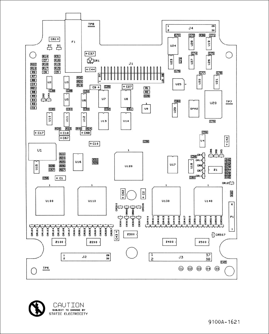
4/List of Replaceable Parts
4-9
Figure 4-2. A1 Main PCA
4/List of Replaceable Parts
4-10
Table 4-3. A2 Top PCA
(See Figure 4-3.)
N
REFERENCE FLUKE MFRS MANUFACTURERS 0
DESIGNATOR STOCK SPLY PART NUMBER TOT T
-A>-NUMERICS----> S--------------DESCRIPTION-------------- --NO-- -CODE- -OR GENERIC TYPE----- QTY- -E-
C 1- 5, 46, CAP,TA,10UF,+-20%,25V 772491 56289 195D106X0025X2T 7
C 47 772491
C 6- 45, 48, CAP,CER,0.1UF,+-10%,25V,X7R,1206 747287 51406 GRM42-6X7R104K25VPB 42
C 900 747287
CR 100-107,200- DIODE,SI,BV=70.0V,IO=50MA,DUAL,SOT23 742320 25403 BAV99 41
CR 207,300-307, 742320
CR 400-407,500- 742320
CR 507,999 742320
H 1 SCREW,MACH,PH,P,SEMS,STL,4-40X.187 732750 89536 732750 4
H 2 WASHER,FLAT,PHENOLIC,#4,0.063 THK 130021 34114 3482-4 4
H 999 SOCKET,IC,14 PIN 276527 00779 2-640357-1 22
J 1, 2 CONN,RECT,PWB,REC,33 POS 800672 50541 KA33/127BPFD21TAHF6 2
J 3, 5 HEADER,2 ROW,.100CTR,30 PIN 854823 00779 1-102977-5 2
J 4 HEADER,2 ROW,.100CTR,38 PIN 838532 00779 1-1-2977-9 1
MP 1 SPACER,SWAGED,RND,BR,6-32,.530 854583 9W423 9538B-B-0632 3
MP 2 SPACER,SWAGED,RND,BR,.150ID,.530 854575 9W423 9511B-B-0256 2
P 1- 4 GUIDE SOCKET 864033 89536 864033 4
R 1- 8, 11 RES,CERM,4.7K,+-5%,.125W,200PPM,1206 740522 59124 RM73B-2B-J4701KB 9
R 9, 10 RES,CERM,33,+-5%,.125W,200PPM,1206 746248 09969 CRCW-1206-330-J-BOZ 2
TP 1- 5 TERM,UNINSUL,WIRE FORM,TEST POINT 781237 27918 TP102-01 5
U 1, 2 * IC,FTTL,8 BIT CNTR,SOIC 852095 18324 74F269D 2
U 3- 6 * IC,CMOS,OCTAL D F/F,+EDG TRG,SOIC 838029 18324 74HC273DT 4
U 7, 19 * IC,CMOS,QUAD 2 INPUT AND GATE,SOIC 838227 54590 CD74AC08M 2
U 8, 13, 16 * IC,CMOS,DUAL D F/F,+EDG TRG,SOIC 837930 54590 CD74ACT74M 3
U 9 * IC,CMOS,SYNC DIV BY 16 BIN CNTR,SOIC 852066 18324 74HC163D 1
U 10 * PROGRAMMED 22V10 TOP U10 855429 89536 855429 1
U 11 * PROGRAMMED 22V10 TOP U11 855424 89536 855424 1
U 12 * IC,CMOS,DUAL 4 INPUT NAND GATE 853320 54590 CD74AC20M 1
U 14 * IC,CMOS,8-1 LINE MUX W/STROBE,SOIC 852061 54590 CD74AC151M 1
U 15 * IC,CMOS,QUAD 2 INPUT OR GATE,SOIC 838276 54590 CD74AC32M 1
U 17, 18 * IC,CMOS,QUAD 2 INPUT XOR GATE,SOIC 838391 54590 CD74ACT86M 2
U 20 * IC,CMOS,QUAD 2 INPUT NOR GATE,SOIC 838193 54590 CD74AC02M 1
U 100,102,200, * IC,CMOS,8K X 8 STATIC RAM,30NS,0.3IN 852058 75569 P4C164-25PC 11
U 202,300,302, * 852058
U 400,402,500, * 852058
U 502,600 * 852058
U 101,103,201, * IC,CMOS,OCTAL D F/F,+EDG TRG,SOIC 852074 12040 74AC273SCT 11
U 203,301,303, * 852074
U 401,403,501, * 852074
U 503,601 * 852074
U 104,105,204, * IC,CMOS,QUAD BUFFER W/3-ST,SOIC 852090 18324 74HC126DT 10
U 205,304,305, * 852090
U 404,405,504, * 852090
U 505 * 852090
Z 100,101,200, RES NET,DIP,16 PIN,8 RES,1K,+-2% 852145 91637 SOMC-1603-102G 11
Z 201,300,301, 852145
Z 400,401,500, 852145
Z 501,600 852145
Z 102,202,302, RES NET,DIP,16 PIN,8 RES,33,+-2% 852152 91637 SOMC-1603-330G 5
Z 402,502 852152
An * in ’S’ column indicates a static-sensitive part.
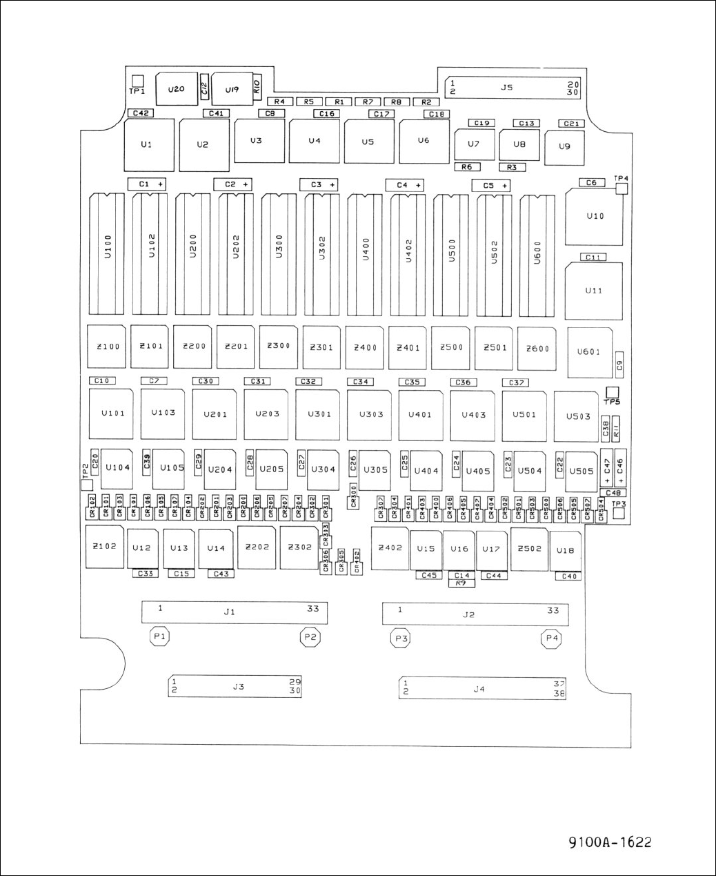
4/List of Replaceable Parts
4-11
Figure 4-3. A2 Top PCA
4/List of Replaceable Parts
4-12
Table 4-4. Module Revision Information
______________________________________________________________________________
Ref. Assembly Fluke Revision
Name Part No. Level
______________________________________________________________________________
A1 Main PCA 873948 C
A2 Top PCA 873950 C
______________________________________________________________________________

4/List of Replaceable Parts
4-13
MANUFACTURER’S FEDERAL SUPPLY CODES
00779
AMP, Inc.
Harrisburg, Pennsylvania
25403
Amperex Electronics Corp.
Semiconductor & Micro-Circuit Div.
Slatersville, Rhode Island
56289
Sprague Electric Co.
North Adams, Massachusetts
75569
Performance Semiconductor Corp.
Sunnyvale, California
01295
Texas Instruments Inc.
Semiconductor Group
Dallas, Texas
27918
Component Parts Corp.
Bellmore, New York
59124
KOA-Speer Electronics Inc.
Bradford, Pennsylvania
9W423
Amatom
El Mont, California
04713
Motorola, Inc.
semiconductor Group
Phoenix, Arizona
34114
Oak Industries
Rancho Bernardo, CA
61752
IR-ONICS Inc.
Warwick, Rhode Island
91637
Dale Electronics, Inc.
Columbus, Nebraska
09969
Dale Electronics, Inc.
Yankton, South Dakota
50541
Hypertronics Corp.
Hudson, Massachusetts
61935
Schurter Inc.
Petalum, California
12040
National Semiconductor Corp.
Danbury, Connecticut
51406
Murata Erie, No. America Inc.
Marietta, Georgia
71400
Bussman Manufacturing
Div. McGraw-Edison Co.
St. Louis, Missouri
18324
Signetics Corp.
Sacramento, California
54590
RCA Corporation
Distribution & Special Products
Cherry Hill, New York
73734
Federal Screw Products Inc.
Chicago, Illinois

4/List of Replaceable Parts
4-14
TECHNICAL SERVICE CENTERS
U.S. Service Locations
California
Fluke Technical Center
16969 Von Karman Avenue
Suite 100
Irvine, CA 92714
Tel: (714) 863-9031
Fluke Technical Center
46610 Landing Parkway
Fremont, CA 94538
Tel: (415) 651-5112
Colorado
Fluke Technical Center
14180 East Evans Avenue
Aurora, CO 80014
Tel: (303) 695-1171
Florida
Fluke Technical Center
940 N. Fern Creek Avenue
Orlando, FL 32803
Tel: (407) 896-4881
Illinois
Fluke Technical Center
1150 W. Euclid Ave.
Palatine, IL 60067
Tel: (312) 705-0500
Maryland
Fluke Technical Center
5640 Fishers Lane
Rockville, MD 20852
Tel: (301) 770-1576
New Jersey
Fluke Technical Center
East 66 Midland Avenue
Paramus, NJ 07652-0930
Tel: (201) 599-9500
Texas
Fluke Technical Center
1801 Royal Lane, Suite 307
Dallas, TX 75229
Tel: (214) 869-2848
Washington
Fluke Technical Center
John Fluke Mfg. Co., Inc.
1420 75th St. S.W.
M/S 6-30
Everett, WA 98203
Tel: (206) 356-5560
International
Argentina
Coasin S.A.
Virrey del Pino 4071 DPTO E-65
1430 CAP FED
Buenos Aires
Tel: 54 1 522-5248
Australia
Philips Customer Support
Scientific and Industrial
23 Lakeside Drive
Tally Ho Technology Park
East Burwood
Victoria 3151
Australia
Philips Customer Support
Scientific & Industrial
25-27 Paul St. North
North Ryde N.S.W. 2113
Tel: 61 02 888 8222
Austria
Oesterreichische Philips Industrie
Unternehmensbereich Prof. Systeme
Triesterstrasse 66
Postfach 217
A-1101 Wein
Tel: 43 222-60101, x1388
Belgium
Philips & MBLE Associated SA.
Scientific & Industrial Equip. Div
Service Department.
80 Rue des deux Gares B-1070
Brussels
Tel: 32 2 525 6111
Brazil
Hi-Tek Electronica Ltda.
Al. Amazonas 422, Alphaville
CEP 06400 Barueri
Sao Paulo
Tel: 55 011 421-5477
Canada
Fluke Electronics Canada Inc.
400 Britannia Rd. East, Unit #1
Mississauga, Ontario
L4Z 1X9
Tel: 416-890-7600
Chile
Intronsa Inc.
Casilla 16158
Santiago 9
Tel: 56 2 232-1886, 232-4308
China
Fluke International Corp.
P.O. Box 9085
Beijing
Tel: 86 01 512-3436
Colombia
Sistemas E Instrumentacion, Ltda.
Carrera 13, No. 37-43, Of. 401
Ap. Aereo 29583
Bogota
Tel: 57 232-4532
Denmark
Philips A/S
Technical Service I & E
Strandlodsveij 1A
PO Box 1919
DK-2300
Copenhagen S
Tel: 45 1 572222
Ecuador
Proteco Coasin Cia., Ltda.
P.O. Box 228-A
Ave. 12 de Octubre
2285 y Orellana
Quito
Tel: 593 2 529684
Egypt
Philips Egypt
10, Abdel Rahman el Rafei st.
el. Mohandessin
P.O. Box 242
Dokki Cairo
Tel: 20-2-490922
England
Philips Scientific
Test & Measuring Division
Colonial Way
Watford
Hertforshire WD2 4TT
Tel: 44 923-240511
Finland
Oy Philips AB
Central Service
Sinikalliontie 1-3
P.O . Box 11
SF-02630 ESPOO
Tel: 358-0-52572
France
S.A. Philips Industrielle
et Comerciale,
Science et Industry
105 Rue de Paris BP 62
93002 Bobigny, Cedex
Tel: 33-1-4942-8040
Germany (F.R.G.)
Philips GmbH
Service fuer FLUKE - Produkte
Department VSF
Oskar-Messter-Strasse 18
D-8045 Ismaning/Munich,
West Germany
Tel: 49 089 9605-239
Greece
Philips S.A. Hellenique
15, 25th March Street
177 78 Tavros
10210 Athens
Tel: 30 1 4894911
Hong Kong
Schmidt & Co (H.K.) Ltd.
18/FL., Great Eagle Centre
23 Harbour Road
Wanchai
Tel: 852 5 8330222
India
Hinditron Services Pvt. Ltd
1st Floor, 17-B
Mahal Industrial Estate
Mahakali Road, Andheri East
Bombay 400 093
Tel: 91 22 6300043
Hinditron Services Pvt. Inc.
33/44A Raj Mahal Villas Extn.
8th Main Road
Bangalore 560 080
Tel: 91 812 363139
Hinditron Services Pvt. Ltd.
Field Service Center
Emerald Complex 1-7-264
5th Floor
114 Sarojini Devi Road
Secunderabad 500 003
Tel: 08 42-821117
Hindtron Services Pvt. Ltd.
15 Community Centre
Panchshila Park
New Delhi 110 017
Tel: 011-6433675
Indonesia
P.T. Lamda Triguna
P.O. Box 6/JATJG
Jakarta 13001
Tel: (021) 8195365
Israel
R.D.T. Electronics Engineering, Ltd.
P.O. Box 43137
Tel Aviv 61430
Tel: 972 3 483211
Italy
Philips S.p.A.
Sezione I&E / T&M
Viale Elvezia 2
20052 Monza
Tel: 39-39-363-5342
Japan
John Fluke Mfg. Co., Inc.
Japan Branch
Sumitomo Higashi Shinbashi Bldg.
1-1-11 Hamamatsucho
Minato-ku
Tokyo 105
Tel: 81 3 434-0181
Korea
Myoung Corporation
Yeo Eui Do P.O. Box 14
Seoul 150
Tel: 82 2 784-9942
Malaysia
Mecomb Malaysia Sdn. Bhd.
P.O . Box 24
46700 Petaling Jaya
Selangor
Tel: 60 3 774-3422
Mexico
Mexel Servicios en Computacion
Instrumentacion y Perifericos
Blvd. Adolfo Lopez Mateos No. 163
Col. Mixcoac
Mexico D.F.
Tel: 52-5-563-5411
Netherlands
Philips Nederland
Test & Meetapparaten Div.
Postbus 115
5000 AC Tilburg
Tel: 31-13-352445
8/89

4/List of Replaceable Parts
4-15
TECHNICAL SERVICE CENTERS
New Zealand
Philips Customer Support
Scientific & Industrial Division
2 Wagener Place
Mt. Albert
Auckland
Tel: 64 9 894-160
Norway
Morgenstierne & Co. A/S
Konghellegate 3
P.O. Box 6688, Rodelokka
Oslo 5
Tel: 47 2 356110
Pakistan
International Operations (PAK) Ltd.
505 Muhammadi House
I.I. Chundrigar Road
P.O. Box 5323
Karachi
Tel: 92 21 221127, 239052
Peru
Importaciones & Representaciones
Electronicas S.A.
Avad Franklin D. Roosevelt 105
Lima 1
Tel: 51 14 288650
Philippines
Spark Radio & ElectronicS Inc.
Greenhills, P.O. Box 610
San Juan, Metro-Manila Zip 3113
Tel: 63-2-775192
Portugal
Decada Espectral
Equipmentos de Elec. e Cientificos
Av. Bomberios Voluntarios
Lote 102B, Miraflores/Alges
1495 Lisboa
Tel: 351 1 410-3420
Singapore
Rank O’Connor’s Singapore Pte Ltd
98 Pasir Panjang Road
Singapore 0511
Tel: 65 4737944
South Africa
South African Philips (Pty) Ltd.
Service Department
195 Main Rd
Martindale, Johannesburg, 2092
Tel: 27 11 470-5255
Spain
Philips Iberica Sae
Depto. Tecnico Instrumentacion
c/Martinez Villergas 2
28027 Madrid
Tel: 34 1 4042200
Sweden
Philips Kistaindustrier Ab
I&E Technical Customer Support
Borgarfjordsgatan 16
S 164 93 Kista
Tel: 46-8-703-1000
Switzerland
Philips A.G.
Technischer Kundendienst
Postfach 670
Allmendstrasse 140
CH-8027 Zurich
Tel: 41 1 482211
Taiwan, R.O.C.
Schmidt Electronics Corp.
5th Floor, Cathay Min Sheng
Commercial Building,
344 Min Sheng East Road
Taipei
Tel: 886 2 501-3468
Thailand
Measuretronix Ltd.
2102/63 Ramkamhaeng Rd.
Bangkok 10240
Tel: 66 2 374-2516, 374-1632
Turkey
Turk Philips Ticaret A.S.
Inonu Caddesi 78/80
Posta Kutusu 504-Beyoglu
Istanbul
Tel: 90 1 1435891
Uruguay
Coasin Uruguaya S.A
Casilla de Correo 1400
Libertad 2525
Montevideo
Tel: 598-2-789015
Venezuela
Coasin C.A.
Calle 9 Con Calle 4, Edif. Edinurbi
Apartado de Correos Nr-70-136
Los Ruices
Caracas 1070-A
Tel: 58 2 241-0309, 241-1248
West Germany
Philips GmbH
Service VSF
Unternehmensbereich Elektribuj
fur Wissenschaft und Industrie
Oskar-Messter-Strasse 18
8045 Ismaning
Tel: 49-089-9605-260
8/89
4/List of Replaceable Parts
4-16
5-1
Section 5
Schematic Diagrams
______________________________________________________________________________
CONTENTS
FIGURE TITLE PAGE
5-1. A1 Main PCA ............................................. 5-3
5-2. A2 Top PCA .............................................. 5-5
5/Schematic Diagrams
5-2
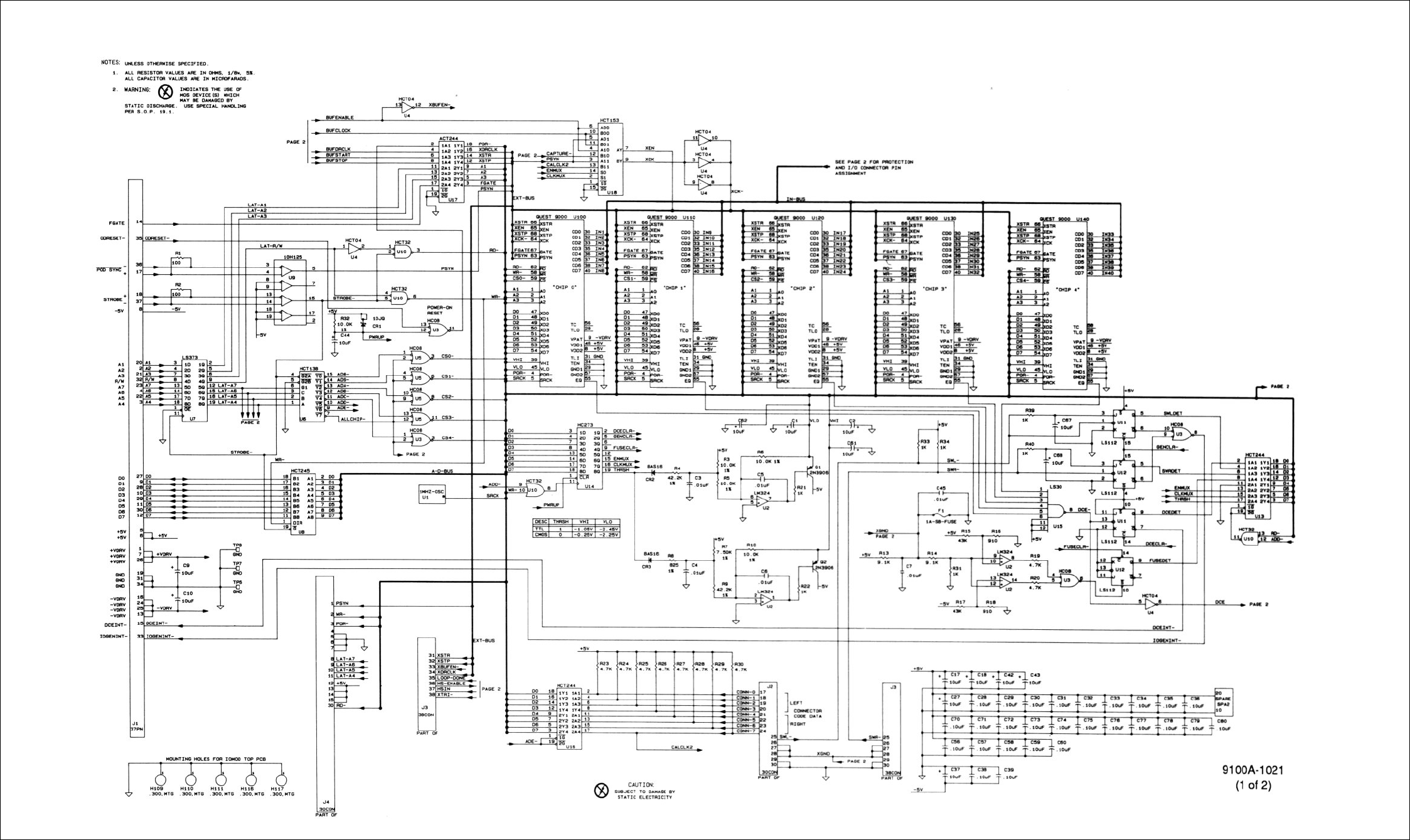
5/Schematic Diagrams
5-3
Figure 5-1. A1 Main PCA
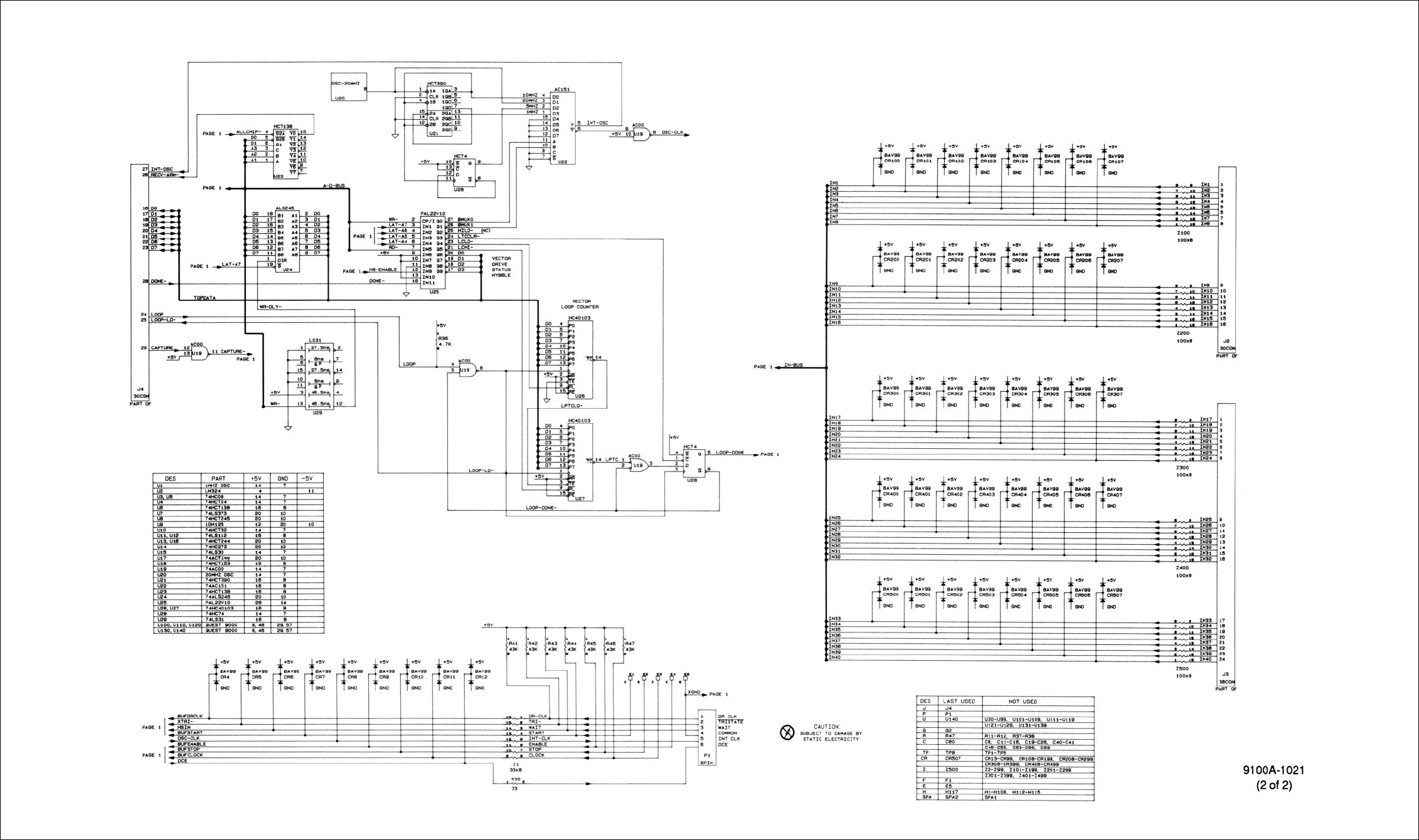
5/Schematic Diagrams
5-4
Figure 5-1. A1 Main PCA (cont.)
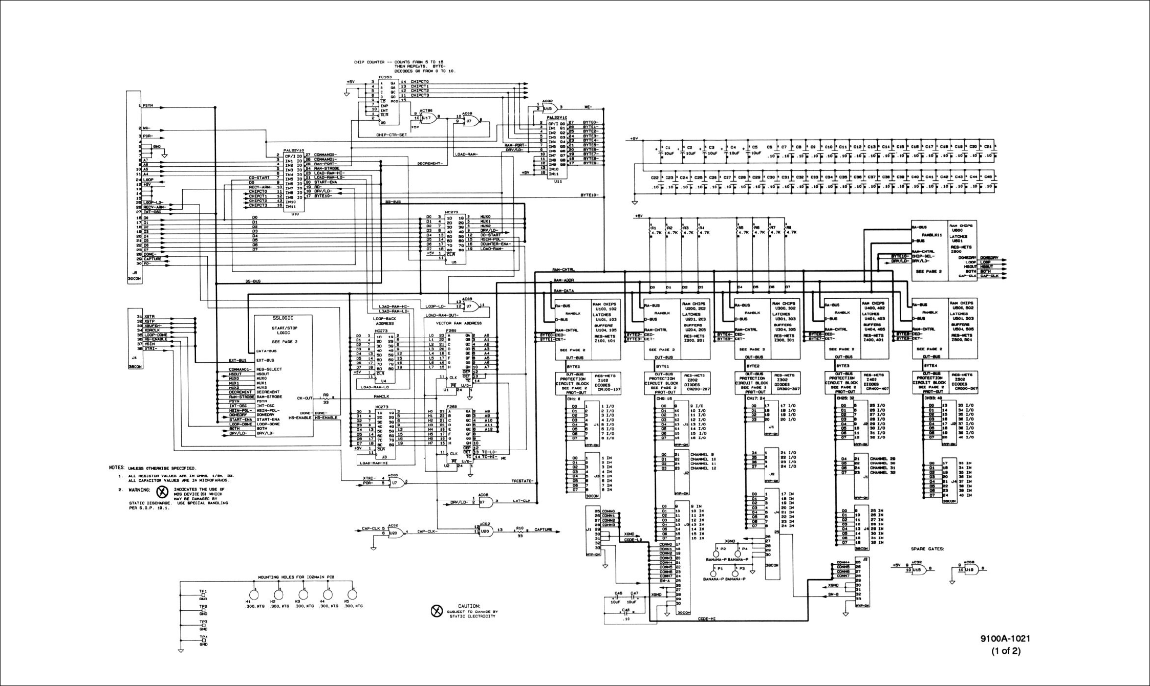
5/Schematic Diagrams
5-5
Figure 5-2. A2 Top PCA
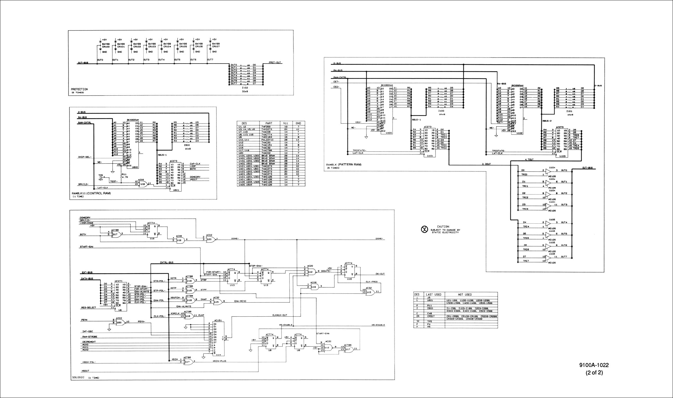
5/Schematic Diagrams
5-6
Figure 5-2. A2 Top PCA (cont.)
Index-1
Index
______________________________________________________________________________
Address Map, Output Section, 2-19
Addressing,
Mainframe Addressing of the Module, 2-5
Output Section, 2-18
Calibration Module, 2-10, 2-17
CAPTURE, 2-9
Capture Clock Functional Block, 2-28
Chip Counter Operation, 2-22
Cleaning the Module, 3-2
Clip Module, 2-16
Clock and Enable Mux Functional Block, 2-9
Connector Code Functional Block, 2-16
Control Register, 2-12
Custom Chip Selection, 2-6
Custom Chip Functional Block, 2-8
Cyclic Redundancy Checking, 2-8, 2-27
Data Compare Equal Output Pin, 2-13
Data Compare Interrupt, 2-13
Data Comparison Interrupts, 2-13
Data Comparison Inputs, 2-12
DCE, 2-13
Dip-Clip Module, 2-17
Disassembling the Module, 3-2
Drive Clock Selection, 2-23
Drive Status Functional Block, 2-28
ENDLOOP Statement, 2-27
Functional Blocks,
Capture Clock, 2-28
Clock and Enable Mux, 2-8
Connector Code, 2-16
Custom Chip, 2-9
Drive Status, 2-28
General Control Latch, 2-11
Input Protection, 2-16
Internal Oscillator Control, 2-20
Loop Control, 2-27
Main PCA to Top PCA Interface, 2-17
Mainframe to Bus Interface, 2-5
Output Control, 2-20
Output Protection, 2-29
RAM Select, 2-21
Index
Index-2
Functional Blocks,
SSLOGIC (Start/Stop Logic), 2-22
Vector Address, 2-26
Vector Control RAM, 2-26
Vector Pattern RAM, 2-26
Fuse Blown Detection, 2-16
Fuse, Changing, 3-1
Fuse Detection, 2-12
General Control Latch Functional Block, 2-11
General Interrupts, 2-13
General Stop, Performing, 2-25
Handshake Synchronization, 2-24
I/O General Interrupt, 2-13
Input Protection Functional Block, 2-16
Input Section Theory of Operation, 2-5
Inputs, 2-9
Internal Oscillator Control Functional Block, 2-20
Internal Clock Source, 2-20
Interrupts,
Data Compare, 2-13
I/O General, 2-13
Loading Vector RAM, 2-27
LOOP, 2-25, 2-27
Loop and Stop, Performing, 2-25
Loop Control Functional Block, 2-27
Main PCA to Top PCA Interface Functional Block, 2-17
Mainframe Addressing of the Module, 2-5
Mainframe to Bus Interface Functional Block, 2-5
Multi-Detection and Interrupt, 2-15
Operation of General Control Latch Block, 2-13
Output Control Functional Block, 2-20
Output Protection Functional Block, 2-29
Output Section Theory of Operation, 2-16
Outputs, 2-11
PAL, 2-20
Performing a General Stop, 2-25
Performing a Loop and Stop, 2-25
POD SYNC Signal, 2-9
RAM Select Functional Block, 2-21
Self Test, 3-2
Signal Polarity/Control Register, 2-22
Specifications, 1-1
SSLOGIC (Start/Stop Logic) Functional Block, 2-22
START, 2-24
Start/Stop Control, 2-23
STOP, 2-24
Index
Index-3
STROBE-, 2-5
Suspending Vector Driving, 2-24
Threshold Voltage Generation, 2-14
TRISTATE-, 2-26
Troubleshooting the Module, 3-3
Vector Address Functional Block, 2-26
Vector Control RAM, 2-22, 2-26
Vector Drive Complete Logic, 2-25
Vector Drive Status Nybble, 2-18, 2-24
Vector Drive Termination, 2-27
Vector Output I/O Module Overview, 2-1
Vector Pattern RAM, 2-22, 2-26
Vector RAM Address Register, 2-23
VHI and VLO, 2-14
WAIT, 2-24, 2-27
Index
Index-4
