04434 Manual
04434_manual
display_manual
User Manual:
Open the PDF directly: View PDF ![]() .
.
Page Count: 5

0.96inch OLED User Manual
1
Rev 2.4.1, May 15th 2015
share awesome hardware
0.96inch OLED
User Manual
1. Key Parameters
Driver Chip
SSD1306
Interface
3-wire SPI、4-wire SPI、I2C
Resolution
128x64
Display Size
0.96 inch
Dimension
29mm*33mm
Colors
Yellow, Blue
Visible Angle
>160°
Operating Temp. (℃)
-20℃~70℃
Storage Temp. (℃)
-30℃~80℃
2. Operation Description
We will illustrate the usage of the module with an example of 4-wire SPI mode (defaultworking mode)
by connecting Waveshare Open103R development board (STM32V MCU onboard).
2.1. Hardwar e configuration
This module provides 3 kinds of driver interfaces; they are 3-wire SPI, 4-wire SPI and I2C interface. In
its factory settings, BS0/BS1 pins are set to 0/0 and 4-wire SPI is selected as default.
Different working mode and pin function of the module can be set by hardware selection on BS0/BS1
pins. (Notice: In this operation, welding is required. Any changes under no guidance from Waveshare
will be considered as a waiver of warranty).
Table 1: Working mode setting
BS1/BS0
CS
D/C
DIN
CLK
3-wire SPI
0/1
CS
0
MOSI
SCLK
4-wire SPI
0/0
CS
D/C
I2C
1/0
0
0/1
SDA
SCL

0.96inch OLED User Manual
2
Rev 2.4.1, May 15th 2015
share awesome hardware
2.2. Softwar e c onfiguration
Open the project file .\IDE\ OLED.uvproj in Keil, navigate to the following text, delete the ‘//’ (Double
slash) before #define INTERFACE_4WIRE_SPI
//#define INTERFACE_3WIRE_SPI
#define INTERFACE_4WIRE_SPI
//#define INTERFACE_IIC
After compiling successfully, download the project to Open103R development board.
Note: You should delete the ‘//’ (Double slash) corresponding to the mode selection
2.3. Hardwar e connections
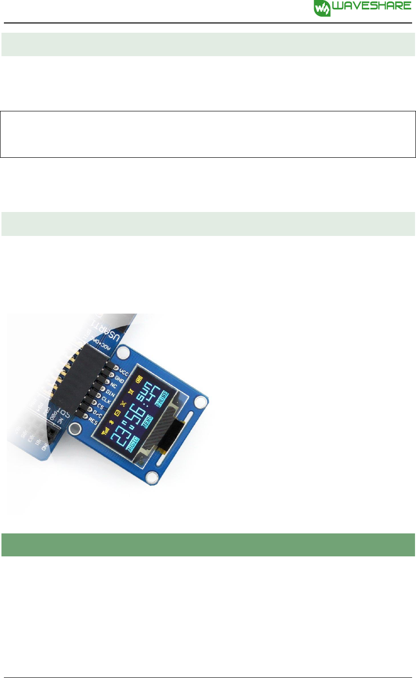
Connect module to the SPI2 interface of Open103R development board, power up.
OLED displays information as Figure 1 shows.
Figure 1: OLED information display
3. 4-wire SPI and I2C interfaces of SSD1306 OLED
This module provides 3 kinds of driver interfaces. We introduce 4-wire SPI and I2C interfaceshere. You
can read Chap. 8.1 from SSD1306-Revision_1.1.pdf for more details.
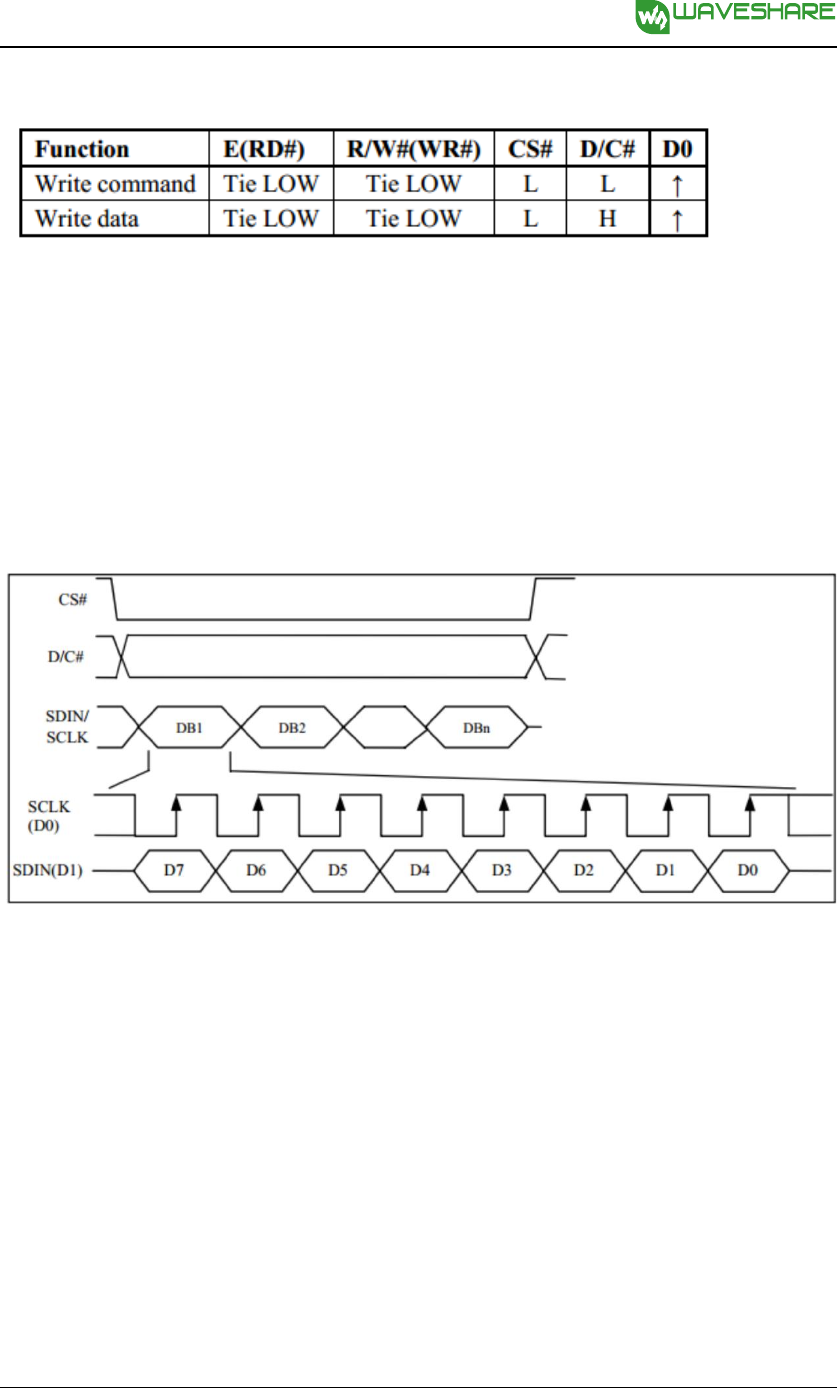
The 4-wire serial interface consists of serial clock: SCLK, serial data: SDIN, D/C#, CS#. In 4-wire SPI
mode,D0 acts as SCLK, D1 acts as SDIN. For the unused data pins, D2 should be left open. The pins
from D3 to D7, E and R/W# (WR#)# can be connected to an external ground.

0.96inch OLED User Manual
3
Rev 2.4.1, May 15th 2015
share awesome hardware
Table 2: 4-wire SPI Control pins of 4-wire Serial interface
Note
(1) H stands for HIGH in signal
(2) L stands for LOW in signal
SDIN is shifted into an 8-bit shift register on every rising edge of SCLK in the order of D7, D6 ... D0.
D/C# is sampled on every eighth clock and the data byte in the shift register is written to the Graphic
Display Data RAM (GDDRAM) or command register in the same clock.
Under serial mode, only write operations are allowed.
Figure 2: Write procedure in 4-wire Serial interface mode
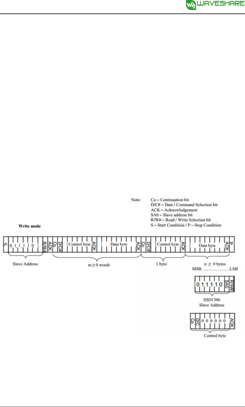
The I2C-bus interface gives access to write data and command into the device. Please refer
to Figure 2 for the write mode of I2C-bus in chronological order.
a) Slave address bit (SA0)
SSD1306 has to recognize the slave address before transmitting or receiving any information by
the I2C-bus. The device will respond to the slave address following by the slave address bit (“SA0”
bit) and the read/write select bit (“R/W#” bit) with the following byte format,
b7
b6
b5
b4
b6
b2
b1
b0
0
1
1
1
1
0
SA0
R/W#
“SA0” bit provides an extension bit for the slave address. Either “0111100” or

0.96inch OLED User Manual
4
Rev 2.4.1, May 15th 2015
share awesome hardware
“0111101”, can be selected as the slave address of SSD1306. D/C# pin acts as SA0 for slave
address selection. “R/W#” bit is used to determine the operation mode of the I2C-bus interface.
R/W#=1, it is in read mode. R/W#=0, it is in write mode.
b) I2C-bus data signal (SDA)
SDA acts as a communication channel between the transmitter and the receiver. The data and
the acknowledgement are sent through the SDA.
It should be noticed that the ITO track resistance and the pulled-up resistance at “SDA” pin
becomes a voltage potential divider. As a result, the acknowledgement would not be possible to
attain a valid logic 0 level in “SDA”
”SDAIN” and “SDAOUT” are tied together and serve as SDA. The “SDAIN” pin must be connected
to act as SDA. The “SDAOUT” pin may be disconnected. When “SDAOUT” pin is disconnected, the
acknowledgement signal will be ignored in the I2C-bus.
c) I2C-bus clock signal (SCL)
The transmission of information in the I2C-bus is following a clock signal, SCL. Each transmission
of data bit is taken place during a single clock period of SCL.
Table 3. I2C I2C-bus data format
1) The slave address is following the start condition for recognition use. For the SSD1306, the slave
address is either “b0111100” or “b0111101” by changing the SA0 to LOW or HIGH (D/C pin acts
as SA0).
2) The write mode is established by setting the R/W# bit to logic “0”

0.96inch OLED User Manual
5
Rev 2.4.1, May 15th 2015
share awesome hardware
3) An acknowledgement signal will be generated after receiving one byte of data, including the
slave address and the R/W# bit.
4) After the transmission of the slave address, either the control byte or the data byte may be sent
across the SDA. A control byte mainly consists of Co and D/C# bits following by six “0” ‘s.
a) If the Co bit is set as logic “0”, the transmission of the following information will contain
data bytes only.
b) The D/C# bit determines the next data byte is acted as a command or a data. If the D/C# bit
is set to logic “0”, it defines the following data byte as a command. If the D/C# bit is set to
logic “1”, it defines the following data byte as a data which will be stored at the GDDRAM.
The GDDRAM column address pointer will be increased by one automatically after each
data write.
5) Acknowledge bit will be generated after receiving each control byte or data byte.