190TW8FB 09071813317667
User Manual: 190TW8FB
Open the PDF directly: View PDF ![]() .
.
Page Count: 90
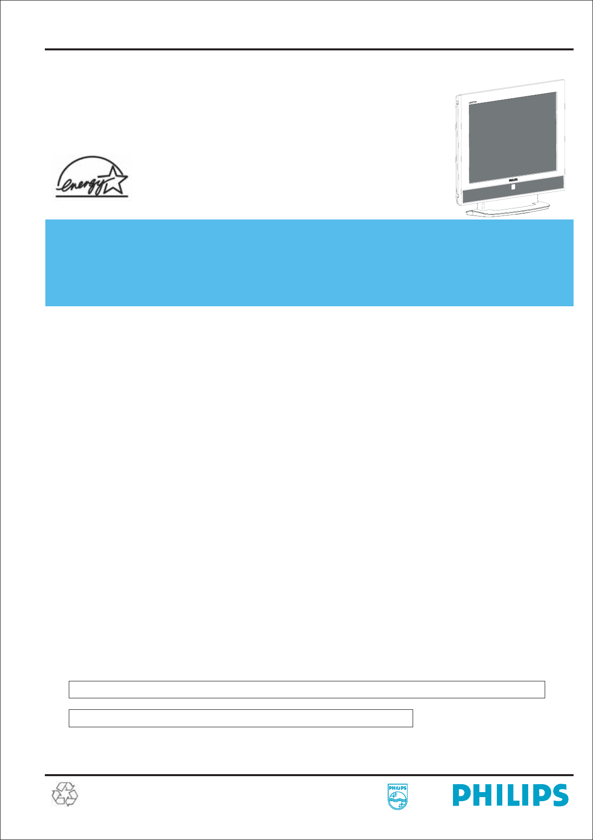
19” TFT LCD COLOR TELEVISION
ServiceService
ServiceService
ServiceService
Service Manual
TABLE OF CONTENTS
Description
Important Safety Notice .............................................
Technical Data ...........................................................
Connection .................................................................
OSD Menu Control Level Structure ...........................
OSD Adjustment ........................................................
Remote Control Keys .................................................
Safety and troubleshooting information ....................
Definition of Pixel Defects ..........................................
...........
Wiring Diagram ..........................................................
Mechanical Instructions .............................................
F/W Upload Instructions ............................................
Electronic Instructions.................................................
DDC DATA .................................................................
Safety Instructions, Warnings and Notes ........
Page
2
3~4
5
6
7
8
9
10~11
12
13~16
17
18~19
20~23
24
Description
Block Diagram ...........................................................
Scaler Board Schematic Diagram ..............................
Power Board Schematic Diagram ..............................
Button Board Schematic Diagram .............................
LED Board Schematic Diagram .................................
Scaler Board Layout Side View .................................
Power Board Layout Side View .................................
Button Board Layout Side View .................................
LED Board Layout Side View ....................................
Exploded View ...........................................................
Recommended Parts List ..........................................
Spare Parts List .........................................................
General Trouble Shooting Guide ...............................
General Product Specification ...................................
Safety Check Process ...............................................
Page
25
26~38
39
40
41
42~43
44~45
46
47
48
49
50~56
57~71
72~89
90
SAFETY NOTICE
ANY PERSON ATTEMPTING TO SERVICE THIS CHASSIS MUST FAMILIARIZE HIMSELF WITH THE CHASSIS
AND BE AWARE OF THE NECESSARY SAFETY PRECAUTIONS TO BE USED WHEN SERVICING ELECTRONIC
EQUIPMENT CONTAINING HIGH VOLTAGES.
CAUTION: USE A SEPARATE ISOLATION TRANSFORMER FOR THIS UNIT WHEN SERVICING.
REFER TO BACK COVER FOR IMPORTANT SAFETY GUIDELINE.
Subject to modification Oct. 16th. 2007 EN :
190TW8FB/00
http://www.wjel.net

2190TW8 TV
Proper service and repair is important to the safe, reliable
operation of all Philips Consumer Electronics Company**
Equipment. The service procedures recommended by Philips
and described in this service manual are effective methods of
performing service operations. Some of these service
operations require the use of tools specially designed for the
purpose. The special tools should be used when and as
recommended.
It is important to note that this manual contains various
CAUTIONS and NOTICES which should be carefully read in
order to minimize the risk of personal injury to service
personnel. The possibility exists that improper service
methods may damage the equipment. It is also important to
understand that these CAUTIONS and NOTICES ARE NOT
EXHAUSTIVE. Philips could not possibly know, evaluate and
advise the service trade of all conceivable ways in which
service might be done or of the possible hazardous
consequences of each way. Consequently, Philips has not
undertaken any such broad evaluation. Accordingly , a
servicer who uses a service procedure or tool which is not
recommended by Philips must first satisfy himself thoroughly
that neither his safety nor the safe operation of the equipment
will be jeopardized by the service method selected.
* * Hereafter throughout this manual, Philips Consumer
Electronics Company will be referred to as Philips.
Critical components having special safety characteristics are
identified with a by the Ref. No.in the parts list and
enclosed within a broken line*
(where several critical components are grouped in one
area) along with the safety symbol on the schematics or
exploded views.
Use of substitute replacement parts which do not have the
same specified safety characteristics may create shock, fire,
or other hazards.
Under no circumstances should the original design be
modified or altered without written permission from Philips.
Philips assumes no liability , express or implied, arising out of
any unauthorized modification of design.
Servicer assumes all liability .
* Broken Line
WARNING
Important Safety Notice
FOR PRODUCTS CONTAINING LASER :
DANGER - In visible laser radiation when open.
AVOID DIRECT EXPOSURE TO BEAM.
CAUTION - Use of controls or adjustments or
performance of procedures other than
those specified herein may result in
hazardous radiation exposure.
CAUTION - The use of optical instruments with this
Product will increase eye hazard.
TO ENSURE THE CONTINUED RELIABILITY OF THIS
PRODUCT, USE ONLY ORIGINAL MANUFACTURER'S
REPLACEMENT PARTS, WHICH ARE LISTED WITH
THEIR PART NUMBERS IN THE PARTS LIST SECTION
OF THIS SERVICE MANUAL.
Take care during handling the LCD module with backlight
unit
- Must mount the module using mounting holes
four corners.
- Do not press on the panel, edge of the frame
electric shock as this will result in damage to the screen.
- Do not scratch or press on the panel with any sharp
such as pencil or pen as this may result in
panel.
- Protect the module from the ESD as it may damage
electronic circuit (C-MOS).
- Make certain that treatment persons body are
through wrist band.
- Do not leave the module in high temperature and in
of high humidity for a long time.
- Avoid contact with water as it may a short circuit
the module.
- If the surface of panel become dirty, please wipe it
a soft material.( Cleaning with a dirty or
damage the panel.)
arranged in
strongly or
objects,
damage to the
the
grounded
areas
within
off with
rough cloth may
http://www.wjel.net
190TW8 TV
Technical Data 3
1. General Specification
Destination Europe
Color System PAL, SECAM
Sound System CCIR B/G, D/K, I and L/L’
Stereo System NICAM and FM Stereo ( A2 )
Sub-Title Teletext 100 pages
RF-AFT (+ / - 1.5MHz)
Maximum Resolution 1440*900
Panel Supplier CMO-M190A1-L07
Lamp Quantity CCFL*4
Display Area 19" Wide Diagonal
Display Color 16.7 M with FRC
Contrast Ratio 1000:1 (Typical)
Brightness 300 cd / m*2 (Typical)
Response Time 5 ms
View Angle 85°(L)/85°(R), 80°(U)/80°(D)
HDMI For Audio & Video
RCA Jack *3 For Audio & Video
Din Jack For S-Video
SCART*1 21 Pin for Video ,S-Video & RGB
PH Jack For TV Input ( PAL system)
Earphone Jack For Audio Output
SPDIF For Audio output (I2S)
3.5mm Stereo Jack For PC Stereo Audio Input , Black color
D-Sub-15 For VGA
Support PAL / NTSC / SECAM video format
Support 480 i , 480 p,720P,1080i format
Build in motion adaptive 3D digital Comb Filter
Build in Teletext Functions
TV System PAL and SECAM system Receivable
Tuner FQ1216-MK5
Horizontal input frequency range : 30~71 KHz
Vertical input frequency range : 50~75 Hz
Maximum resolution : 1440*900
Out of Range
When input signal is out of range or down scaling
support ,the OSD will show "Out of Range "within 5
seconds and LED is green
No Signal
When there is missing signal from selected input ,the
OSD will show "No Signal "within 8 seconds and LED
is green
Standard x=300 , y=310
Warm x=313 , y=329
Cold x=285 , y=293
Maximum Brightness More Than 250 cd / m*2
Key count 43 Keys
Effective Distance More than 6 m +45~-45degree
Supplier Panasonic
Local Control Key 7 Keys Power, Left, Right, Up, Down, Menu, Select
Channel System Full frequency range from channel E2 ( 48.25 MHz )
to channel E69 ( 855.25 MHz)
TV System
LCD Panel
I / O Functions
Video Functions
Input Signal
Color Temperature
VGA
Remote Controller
http://www.wjel.net

4190TW8 TV Technical Data
Display Area: 19W inches diagonal
H-Phase: A-B Less than 1.5mm
V-Center: C-D Less than 1.5mm
Tilt: E-F Less than 1mm
Speaker Internal speaker. 5W*2 stereo, volume adjustable.
Treble, Bass ( + 3db)
Frequency Response 100~15KHz with +/-3 db variation
THD(Total HarmonicDdistortion) Limited to 5 % at 2W (at 0.1~15 KHz)
OSD Capability On screen display adjustment function
ISP Fuctions
ISP (In System Programming) function available
for revising driver easily.
Input Voltage 90 ~ 264 V , 47 ~ 63 Hz
Input Current 0.6~1.5 A
Max. Power 58 Watts
PC saving Power 2Watts Max
Stand-By Power(AV,TV) 1 Watts Max.
Tilt 0~15
VESA Mount 100*100 mm
Mechanical
Display Area & Tilt
Audio
Power Source
A
E
D
CF
B
1.2 Input & Output Signal Specification
Type Analog
Polarity Positive
Level 1Vp-p ( with Sync.)
Impedance 75£[±5%
Interface RCA jack, Yellow color
Type Analog
Polarity Positive
Level Y : 1Vp-p ( with Sync.) , C : 0.286Vp-p
Impedance 75£[±5%
Interface DIN Jack
Type Analog
Polarity Positive
Impedance 75£[±5%
Interface 21 Pin Euro-SCART
Type Stereo R/L Channels
Level 500mVrms
Impedance More than 22k£[
Interface RCA Jack
Right channel Red color.
Left Channel White color
Type Stereo R/L Channels
Level 1Vrms
Impedance More than 22k£[
Interface 3.5mm Stereo Jack , Black color
Type Stereo R/L Channels
Level 40mW rms/per Channel(typ.) for 32 ohm earphon
Impedance 32 ohm
Interface 3.5mm Stereo Jack
Max. Audio output 5W + 5W (at 1.0Vp-p / 1kHZ input,10% THD ma
x
Sound Distortion 1% THD max. ( at 250mW/1kHZ : )
Speaker 5 W / 8 ohms
Speaker Impedance8 ohms at 1kHZ
Residual Hum 500uW Max.( at Min. Volume : )
Max. Hum 1000uW Max ( at Max. Volume )
CVBS Input
S-Video Input
SCART Input
Audio Input
PC Stereo Input
Headphone Output
Built-in Speaker
Type Stereo R/L Channels
Level 400Vrms.
Interface 3.5mm Stereo Jack
Input Impedance 75 ohms
Frequency Range 48.25~855.25 MHz (PAL)
Video S/N Ratio 45 d B (Typical)
AudioS/NRatio 63dB(Typical)
Sync Level : Low = 0 to 0.8V, High = 2.0 to 5 V
Polarity : Positive or Negative
Impedance : 1 k ohm or higher
RGB Signal Level : 0 to 700mV Positive
Impedance : 75£[±5%
1Red Video
2Green Video
3Blue Video
4Ground
5Ground
6Red Ground
7Green Ground
8Blue Ground
9+5V(PC97)
10 VGA-CONN(Sync GND)
11 Ground
12 SDA ( DDC Data )
13 Horizontal Sync
14 Vertical Sync
15 SCL ( DDC Clock )
Type Type A
Level 400mVrms
Impedance 100£[
Type RCA Jack
Level 500mVpp +- 20%
VGA Input
D-Sub Pin Define
HDMI
SPDIF
Audio Line Output
RF Input
http://www.wjel.net
190TW8 TV
Connection 5
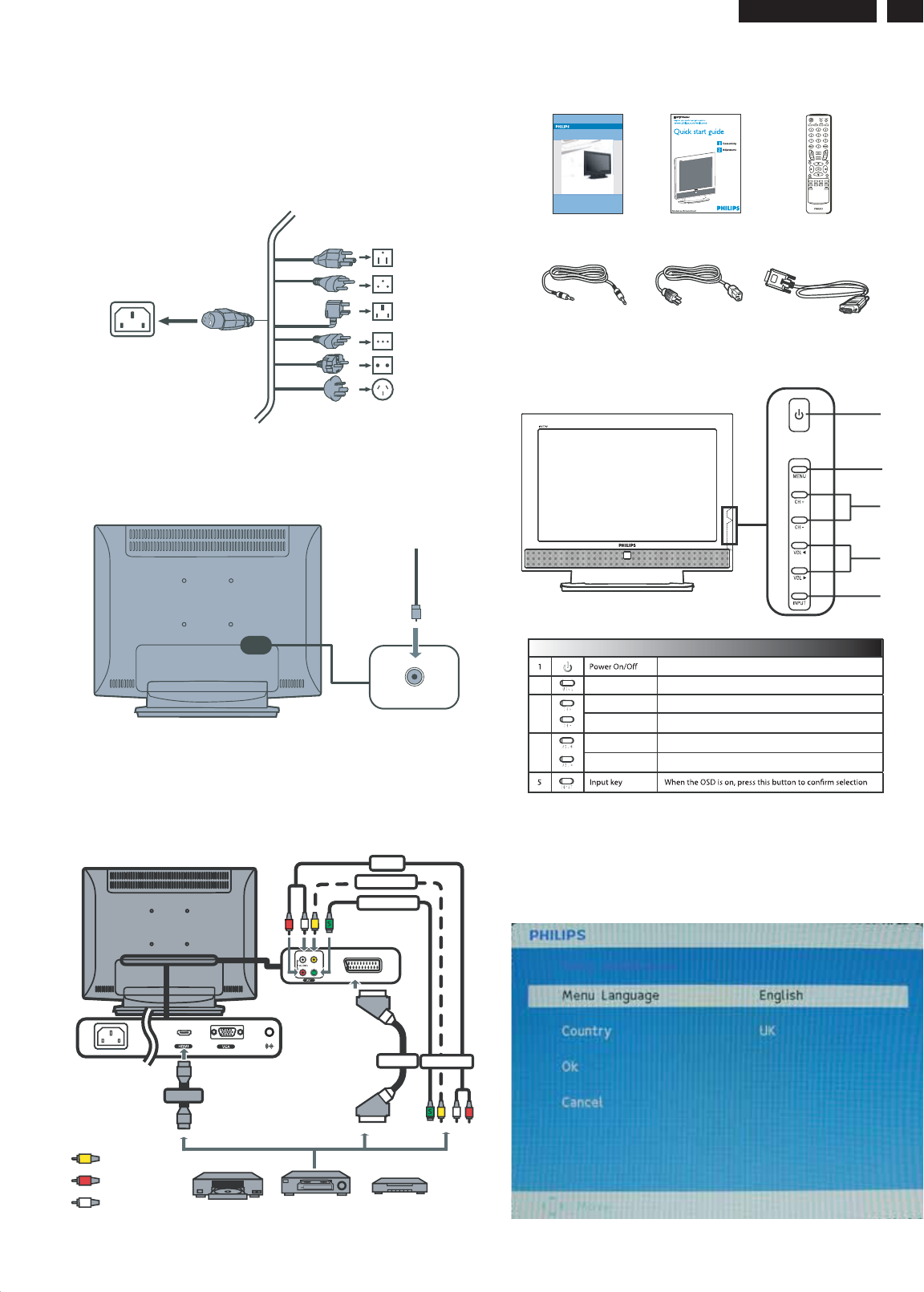
1. Connecting the power cord
2. Setting up the remote control
3. Connect the antenna cable to the appropriate antenna
terminal on the back of the TV Monitor set as shown below.
a. Connect the AC cord into the AC input on the back of the set.
b. Connect the plug to the wall outlet as shown.
a. Open the cover on the back of the remote unit.
b. Insert two AAA batteries(supplied) to match the polarity
indicated inside the battery compartment.
4. Connect your DVD player, VCR, STB or audio/video
equipment using the SCART port located at the rear of your
TV Monitor as shown.
5. Accessory
In the accessory box, you will find:
6. Function key definition
7. Quick Installation
A quick OSD(On Screen Display) that end user can only press
the “Power” button to trigger the dialog appear. It contains -
Menu language, Country, for you to select.
Analog
Y
Yellow
Red
White
R
W
S-VIDEO
SPDIF-OUT
PC AUDIO-IN
W
Y
AUDIO
S-Vid
eo
COMPOSIT E
SCART AV
R
R
Y
W
or
DVD VCR STB
or
HDMI
1
2
3
4
5
Side of set
2 Menu key Turns the OSD menu ON and OFF
To switch TV monitor ON and OFF
3Channel up When the OSD is on, functions the same as the Up arrow
Channel down When the OSD is on, functions the same as the Down arrow
4Volume up When the OSD is on, functions the same as the Right arrow
Volume down When the OSD is on, functions the same as the Left arrow
Philips TV Monitor User's Manual
190TW8
LCD T V Mon itor
Register your product and get support at
www.philips.com/welcome
190TW8
User Manual QSG Remote Control
Audio Cable Power Cord DVI Cable
http://www.wjel.net

6190TW8 TV
4. The OSD tree
Below is an overall view of the structure of the On-Screen
Display. You can use this as a reference when you want to
work your way around the different adjustments later on.
4.1 Only available for EU Model
OSD Menu Control Structure
Note:
sRGB is a standard for ensuring correct exchange of colors
between different devices(e. g. Digital cameras, monitor,
printers, scanners, etc.)
Using a standard unified color space, sRGB will help
represent pictures taken by an sRGB compatible device
correctly on your sRGB enabled Philips monitor. In that way,
the colors are calibrated and you can rely on the correctness
of the colors shown on your screen.
Important with the use of sRGB is that the brightness and
contrast of your monitor is fixed to a predefined setting as
well as the color gamut. Therefore it is important to select the
sRGB setting in the monitor’s OSD.
To do so, open the OSD by pressing the OK button on the
side of your monitor. More the down button to go to color and
press OK again. Use the right button to go to sRGB. Then
move the down button and press OK again to exit the OSD.
After this, please do not change the brightness or contrast
setting of your monitor. If you change either of these, the
monitor will exit the sRGB mode and go to a color
temperature setting of 6500K.
1st Sub Menu
2nd Sub Menu
3rd Sub Menu
4th Sub Menu
ATV
S-Video
AV
Scart
VGA
HDMI
Bri
g
htnes
sSlider [50] 0-100 / 1 VVVVVV
Contrast Slide
r
[
80
]
0-100
/
1
V
V
V
V
V
V
Colou
r
Slide
r
[
70
]
0-100
/
1
V
V
V
V
V
Sharpness Slider [4] 0-7 / 1 VVVV V
Backlight Slider [100] 0-100 / 1 VVVVVV
Cold
V
V
V
V
V
V
[Standard] VVVVVV
Warm
V
V
V
V
V
V
Noise
Reduction Off /
[
Low
]
/
Medium
/
VVVV V
Treble Slide
r
[
50
]
0-100
/
1
V
V
V
V
V
V
Bass Slide
r
[
50
]
0-100
/
1
V
V
V
V
V
V
Balance Slide
r
[
0
]
-50-50
/
1
V
V
V
V
V
V
On
V
V
V
V
V
V
[
Off
]
V
V
V
V
V
V
On
V
V
V
V
V
V
[
Off
]
V
V
V
V
V
V
UK
France
Germany
Italy
Spain
Switzerland
Denmark
Belgium
Netherlands
Luxembourg
Czech
Re
p
ublic
Portugal
United Arab
Emirates
Saudi Arabia
On V
[Off] V
Reorder V
Name V
Frequency V
Auto Scan V
Scan up
Scan down
Scan for
u
p
date
Lock This
Channel
Please ente
r
your PIN [- - -
-
]
Lock/[Unlock] V
Manual
Scan V
Skip
Country V
Audio
Sound
Effect
AVL
Channel Management
PAL Menu Structur
e
Picture
Color
Temp
[English] VVVVVV
Deutsch
V
V
V
V
V
V
French
V
V
V
V
V
V
Italian
V
V
V
V
V
V
S
p
anish
V
V
V
V
V
V
Portu
g
uese
V
V
V
V
V
V
Cestina
V
V
V
V
V
V
Dansk
V
V
V
V
V
V
Dutch
V
V
V
V
V
V
V
V
V
V
V
V
V
V
V
V
V
V
V
V
V
V
V
V
Sleep
[
Off
]
/15/30/
4
5
/
60
/
90
/
12
0
VVVV V
Please ente
r
y
our PIN New PIN:
[- - - -] T
yp
e it a
g
ain to
confirm:
Full VVVVVV
4:3 VVVVVV
[16:9] VVVV V
Panorama VVVV V
Letterbox1 VVVV V
Letterbox2 VVVV V
VVVV V
HDMI
Scan Info.
[
Auto
]
/
Overscan /
Underscan V
SCART
[
Auto
]
/ AV/ S
-
Video
/
RGB V
Factor
y
Default VVVVVV
Wide
Mode
Settings
Menu
Language
Set PIN V
Continue-
http://www.wjel.net
190TW8 TV
OSD Adjustment 7
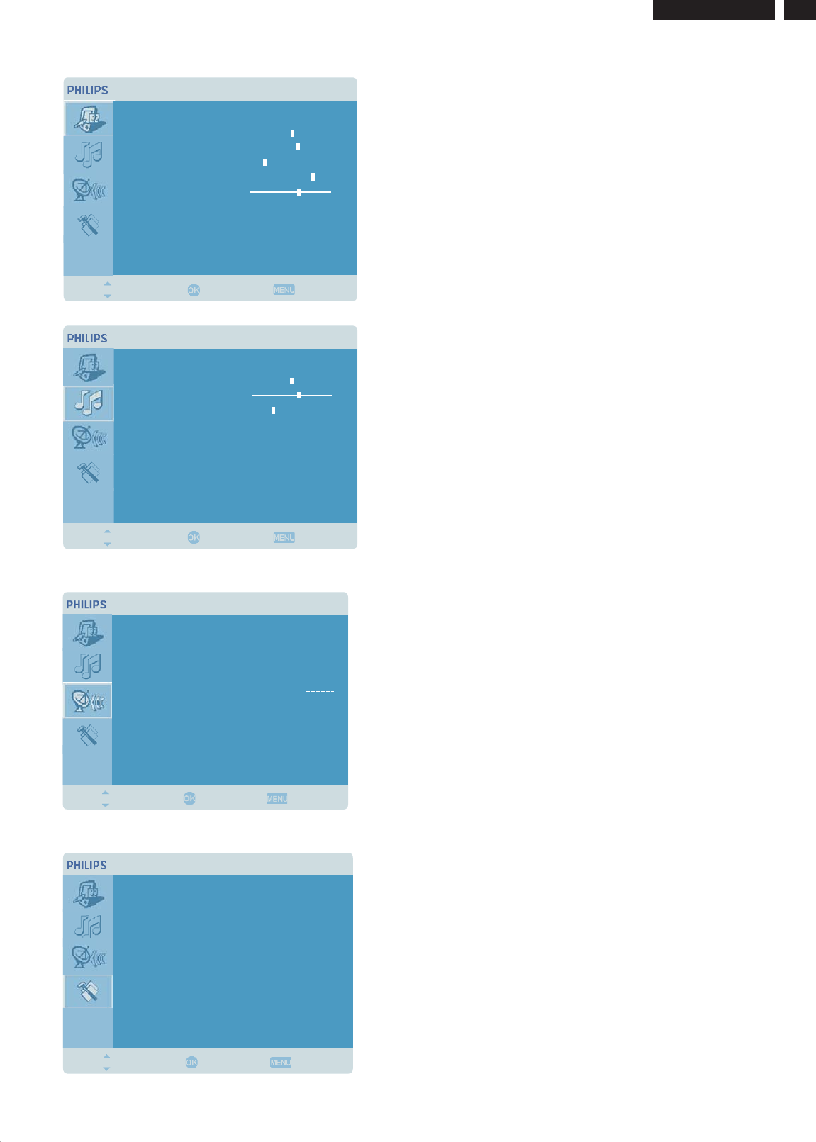
1. Press the key to bring up the OSD.
2. Using the directional keys, select from the on
screen display. Then navigate to the feature you wish to
adjust.
3. Use the left or right keys to adjust the sliding scales. Press
to save.
4. The menu can also be used to adjust the treble,
bass, balance, sound effect and AVL.
MENU
Audio
OK
Audio
1. Press the key to bring up the OSD.
2. Using the directional keys, select from the OSD.
Then navigate to picture element you wish to adjust.
3. Use the left or right keys to adjust the sliding scales.
4. The menu can be used to adjust the brightness,
contrast, colour, sharpness and image-related qualities.
MENU
Picture
Picture
1. Press the key to bring up the OSD.
2. Using the directional keys, select
from the OSD.
3. Use the directional keys to navigate the menus.
4. The menu can be used to set
the channel namings, Auto Scan, Manual Scan Channel and
other related settings.
MENU
Channel
management
Channel management
1. Press the key to bring up the OSD.
2. Using the directional keys, select from the OSD.
Then navigate to the feature you wish to adjust.
3. The menu can be used to adjust the menu
language and other important settings.
MENU
Settings
Settings
Adjusting the picture quality
Adjusting the audio settings
Adjusting the channel management
Adjusting the settings
Audio
Treble
Balance
Bass
Sound Effect
AVL
50
60
30
Off
Off
Move Enter Back
Channel Management
Country
Reorder
Skip
Manual Scan
Name
Auto Scan
Frequency
Germany
Off
639 22Mhz
.
Move Enter Back
Lock This Channel
Settin sg
Menu Language
Set PIN
Sleep
Wide Mode
Factory Default
En lishg
Off
Full
Move Enter Back
Picture
Bri htnessg
Colour
Contrast
Noise Reduction
Sharpness
Colour Temp
Backli htg
50
60
30
80
70
Warm
Low
Move Enter Back
http://www.wjel.net
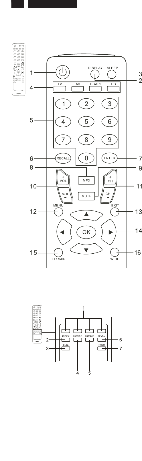
8190TW8 TV Remote Control Keys
1. POWER
Press to turn your TV Monitor on/off.
2. DISPLAY
Press to display input/channel information(dependent on
input/source type).
3. SLEEP
Press to set a time period after which the TV Monitor will switch
itself to standby (15, 30, 45, 60, 90 or 120 minutes).
4. Input buttons
(TV/AV/SCART/PC)*Press to select correct input mode.
5. Number keys.
6. RECALL
Press to return to the previous channel.
7. ENTER
Press to confirm channel number selection.
8. MPX
Press to select the sound input, displayed in the top right- hand
corner (mono, stereo, bilingual).
9. MUTE
Press to toggle audio on and off.
10. VOL (+/-)
Press to increase or decrease the volume.
11. CH (up/down)
Press to sequentially select the TV Monitor channel.
12. MENU
Press to open or close the Menu.
13. EXIT
Exit Menu.
14. Directional keys/OK
VOL (up/down), CH (up/down).
15. TTX/MIX (TELETEXT/MIX)
Press to switch from TV/AV to Teletext mode. Press to overlay
teletext page on the TV Monitor image.
16. WIDE
Press to toggle scaling mode between 4:3,16:10, Full,
Panorama and Letterbox 1, 2 modes.
E.SUBPAGE
Press to access the teletext’s sub pages directly.
F. HOLD
Press to pause the current teletext page in multi-page viewing
mode.0
G. REVEAL
Press to reveal hidden telext information.
D. SUBTITLE
Press to view subtitles on the screen.
A. Colour buttons (R/G/Y/B)
Operates corresponding button on the teletext page.
B. INDEX
Press to go to the index page.
C. SIZE
Press once to zoom teletext page to 2X.Press again to resume.
General Keys
Teletext
http://www.wjel.net
190TW8 TV
Safety and Troubleshooting Information 9
Safety precautions and maintenance
WARNING: Use of controls, adjustments or
procedures other than those specified in this
documentation may result in exposure to shock,
electrical hazards and/or mechanical hazards.
Read and follow these instructions when connecting and using
your computer monitor:
a. To protect your display from possible damage, do not put
excessive pressure on the LCD panel. When moving your
monitor, grasp the frame to lift; do not lift the monitor by
placing your hand or fingers on the LCD panel.
b. Unplug the monitor if you are not going to use it for an
extensive period of time.
c. Unplug the monitor if you need to clean it with a slightly
damp cloth. The screen may be wiped with a dry cloth when
the power is off. However, never use alcohol, solvents or
ammonia-based liquids.
d. Consult a service technician if the monitor does not operate
normally when you have followed the instructions in this
manual.
e. The casing cover should be opened only by qualified service
personnel.
f. Keep the monitor out of direct sunlight and away from stoves
or any other heat source.
g. Remove any object that could fall into the vents or prevent
proper cooling of the monitor’s electronics.
h. Do not block the ventilation holes on the cabinet.
i. Keep the monitor dry. To avoid electric shock, do not expose
it to rain or excessive moisture.
j. When positioning the monitor, make sure the power plug and
outlet are easily accessible.
k. If turning off the monitor by detaching the power cable or DC
power cord, wait for 6 seconds before attaching the power
cable or DC power cord for normal operation.
l. To avoid the risk of shock or permanent damage to the set,
do not expose the monitor to rain or excessive moisture.
m. IMPORTANT: Always activate a screen saver program during
your application. If a still image in high contrast remains on
the screen for an extended period of time, it may leave an
'after-image' or 'ghost image' on front of the screen. This is a
well-known phenomenon that is caused by the shortcomings
inherent in LCD technology. In most cases, the afterimage
will disappear gradually over a period of time after the power
has been switched off. Be aware, that the afterimage
symptom cannot be repaired and is not covered under
warranty.
o. Warning for lifting monitor - Do not use the area underneath
the logo cover to grip or lift the monitor. Placing weight on the
logo cover can cause it to break away from the body and
cause the monitor to fall. When lifting the monitor, place one
hand under the monitor's frame.
* Consult a service technician if the monitor does not operate
normally when the operating instructions given in this manual
have been followed.
Installation Locations
Trouble Shooting
Avoid exposure to heat and extreme cold.
Do not store or use the LCD monitor in locations exposed to
heat, direct sunlight or extreme cold.
Avoid moving the LCD monitor between locations with large
temperature differences. Choose a site that falls within the
following temperature and humidity ranges.
Temperature: 0-35°C 32-95°F
Humidity: 20-80% RH
Do not subject the LCD monitor to severe vibration or high
impact conditions. Do not place the LCD monitor in the trunk of
a car.
Take care not to mishandle this product by either knocking or
dropping it during operation or transportation.
Do not store or use the LCD monitor in locations where there is
a high level of humidity or in dusty environments. Do not allow
water or other liquids to spill on or into the LCD monitor.
This page deals with problems that can be corrected by the
user. If the problem still persists after you have tried these
solutions, contact your nearest Philips dealer.
Having this problem Check these items
No Picture
(Power LED not lit)
a. Make sure the power cord is plugged into the power
outlet and into the back of the monitor.
b. First, ensure that the power button on the front of the
monitor is in the OFF position, then press it to the ON
position.
No Picture
(Power LED is amber or
yellow)
a. Make sure the computer is turned on.
b. Make sure the signal cable is properly connected to
your computer.
c. Check to see if the monitor cable has bent pins.
d. The Energy Saving feature may be activated.
Screen says a. Make sure the monitor cable is properly connected
to your computer.
(Also refer to the Quick Set-Up Guide).
b. Check to see if the monitor cable has bent pins.
c. Make sure the computer is turned on.
Screen says a. Make sure the monitor cable is properly connected to
your computer. (Also refer to the Quick Set-Up Guide).
b. Check to see if the monitor cable has bent pins.
c. Make sure the computer is turned on.
AUTO button not working
properly
a. The Auto Function is designed for use on standard
Macintosh or IBM-compatible PCs running Microsoft
Windows.
b. It may not work properly if using nonstandard PC or
video card.
Display position is
incorrect
a. Press the Auto button.
b. Adjust the image position using the
Phase/Clock of More Settings in OSD Main Controls.
Image vibrates on the
screen
a. Check that the signal cable is properly connected
to the graphics board or PC.
Vertical flicker appears
a. Press the Auto button.
b. Eliminate the vertical bars using the Phase/Clock
of More Settings in OSD Main Controls.
Horizontal flicker appears
a. Press the Auto button.
b. Eliminate the vertical bars using the Phase/Clock
of More Settings in OSD Main Controls.
Common Problems
Imaging Problems
http://www.wjel.net
10 190TW8 TV
Definition of Pixel Defects
Definition of Pixel Defects
This section explains the different types of pixel defects and
defines acceptable defect levels of each type. In order to
quality for repair or replacement under warranty, the number
of pixel defects on a TFT LCD panel must exceed these
acceptable levels.
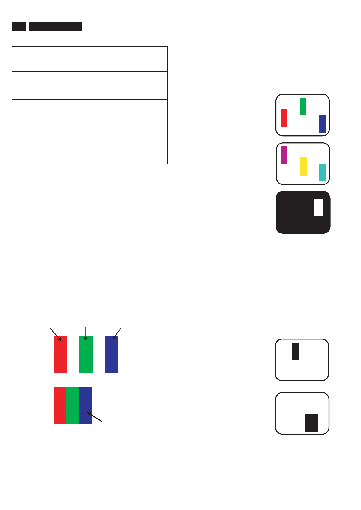
1. Definition of Pixels and Sub-pixels
A pixel, or picture element, is composed of three sub pixels
in the primary colors of red, green and blue. Many pixels
together form an image. When all sub pixels of a pixel are lit,
the three colored sub pixels together appear as a single
white pixel. When all are dark, the three colored sub pixels
together appear as a single black pixel. Other combinations
of lit and dark sub pixels appear as single pixels of other
colors.
2. Types of Pixel Defects
Pixel and sub pixel defects appear on the screen in different
ways. There are two categories of pixel defects and several
types of sub pixel defects within each category.
Bright Dot Defects
Black Dot Defects
Bright dot defects appear as pixels or sub pixels that are
always lit or 'on'. That is, a bright dot is a sub-pixel that
stands out on the screen when the monitor displays a dark
pattern. There are the types of bright dot defects:
One lit red, green or blue sub pixel
Two adjacent lit sub pixels:
-Red+Blue=Purple
- Red + Green = Yellow
- Green + Blue = Cyan (Light Blue)
Three adjacent lit sub pixels
(one white pixel)
Black dot defects appear as pixels or sub pixels that are
always dark or 'off'. That is, a dark dot is a sub-pixel that
stands out on the screen when the monitor displays a light
pattern. These are the types of black dot defects:
One dark sub pixel
Two or three adjacent
dark sub pixels
A red or blue bright dot must be more than 50
percent brighter than neighboring dots while a
green bright dot is 30 percent brighter than
neighboring dots.
subpixel subpixel subpixel
RGB
RGB
Pixel
R
G
B
P
YC
W
The screen is too bright
or
too dark
Adjust the contrast and brightness on On-Screen
Display.(The backlight of the LCD monitor has a fixed life
span. When the screen becomes dark or begins to flicked,
please contact your sales representative).
An after-image appears
If an image remains on the screen for an extended
period of time, it may be imprinted in the screen
and leave an after-image. This usually disappears
after a few hours.
An after-image remains
after
the power has been
turned off
This is characteristic of liquid crystal and is not
caused by a malfunction or deterioration of the
liquid crystal. The after-image will disappear after
aperoidoftime.
Green, red, blue, dark,
and
white dots remains
The remaining dots are normal characteristic of
the liquid crystal used in today’s technology.
For further assistance, refer to the Consumer Information Centers list
and contact your local Philips distributor.
http://www.wjel.net
190TW8 TV
Definition of pixel defects 11
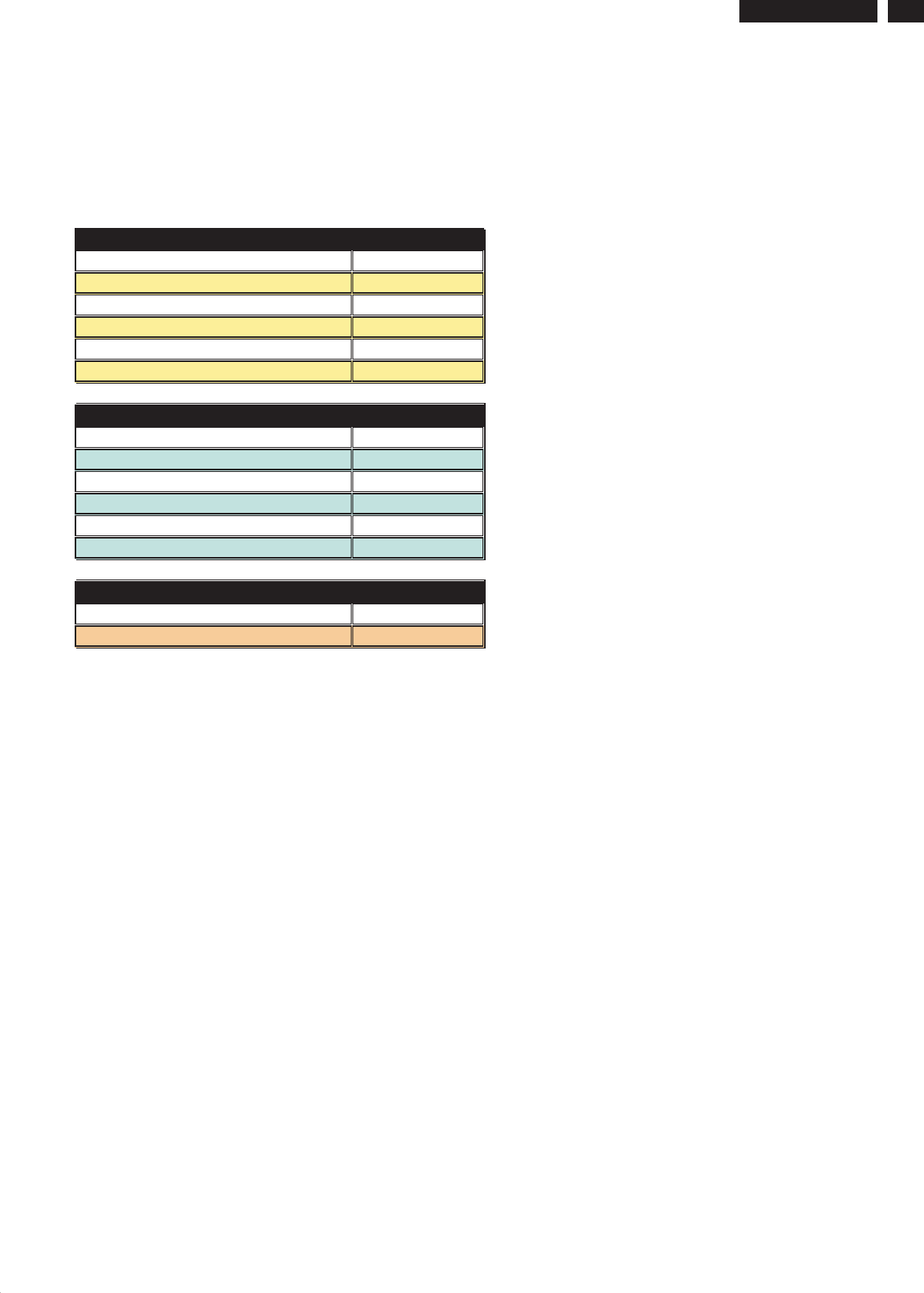
3. Proximity of Pixel Defects
Because pixel and sub pixels defects of the same type that
are near to one another may be more noticeable, Philips also
specifies tolerances for the proximity of pixel defects.
Perfect Panel - ISO 13406-2 Class II compliant do-defect-
free-display.
BRIGHT DOT DEFECTS ACCEPTABLE LEVEL
MODEL 190TW8
1 lit subpixel 3 or fewer
2 adjacent lit subpixels 1 or fewer
3 adjacent lit subpixels (one white pixel) 0
Distance between two bright dot defects* >15mm
Total bright dot defects of all types 3 or fewer
BLACK DOT DEFECTS ACCEPTABLE LEVEL
MODEL 190TW8
1 dark subpixel 5 or fewer
2 adjacent dark subpixels 2 or fewer
3 adjacent dark subpixels 0
Distance between two black dot defects* >15mm
Total black dot defects of all types 5 or fewer
TOTAL DOT DEFECTS ACCEPTABLE LEVEL
MODEL 190TW8
Total bright or black dot defects of all types 5 or fewer
Note:
* 1 or 2 adjacent sub pixel defects = 1 dot defect
http://www.wjel.net

13
190TW8 TV
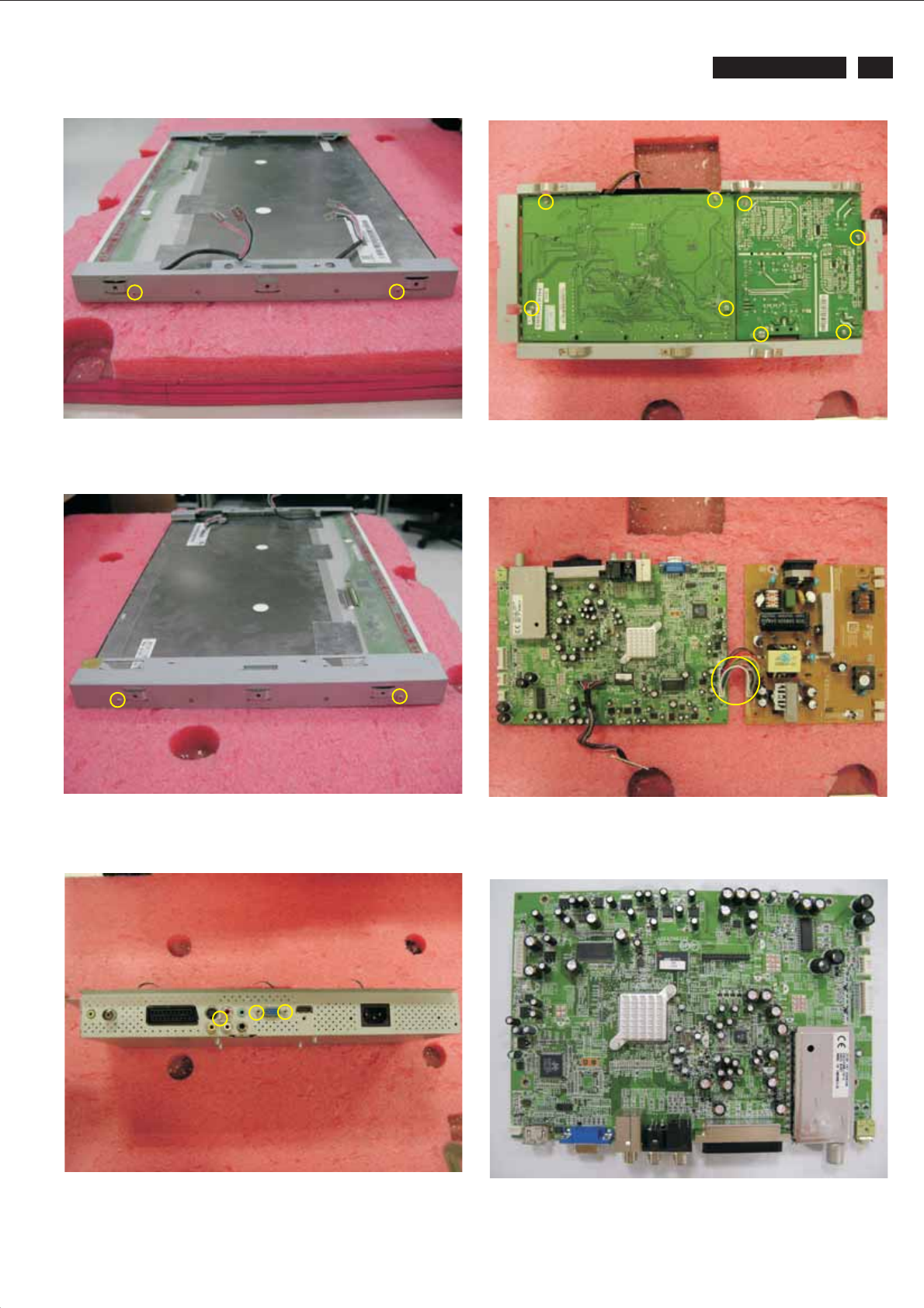
Mechanical Instructions
DISASSEMBLY PROCESS
Fig. 1
Fig. 2
2.Take off rear cover.
Fig. 3
3. Disconnect the cables.
1. Lay down LCD TV, all tools prepared, remove 7pcs screws
from rear cover.
Fig. 4
4. Disconnect the lamp cables.
Fig. 5
5. Disconnect the LVDs cable, and take off PCB shielding.
Fig. 6
6. Remove 4pcs screws from top and down side panel.
http://www.wjel.net
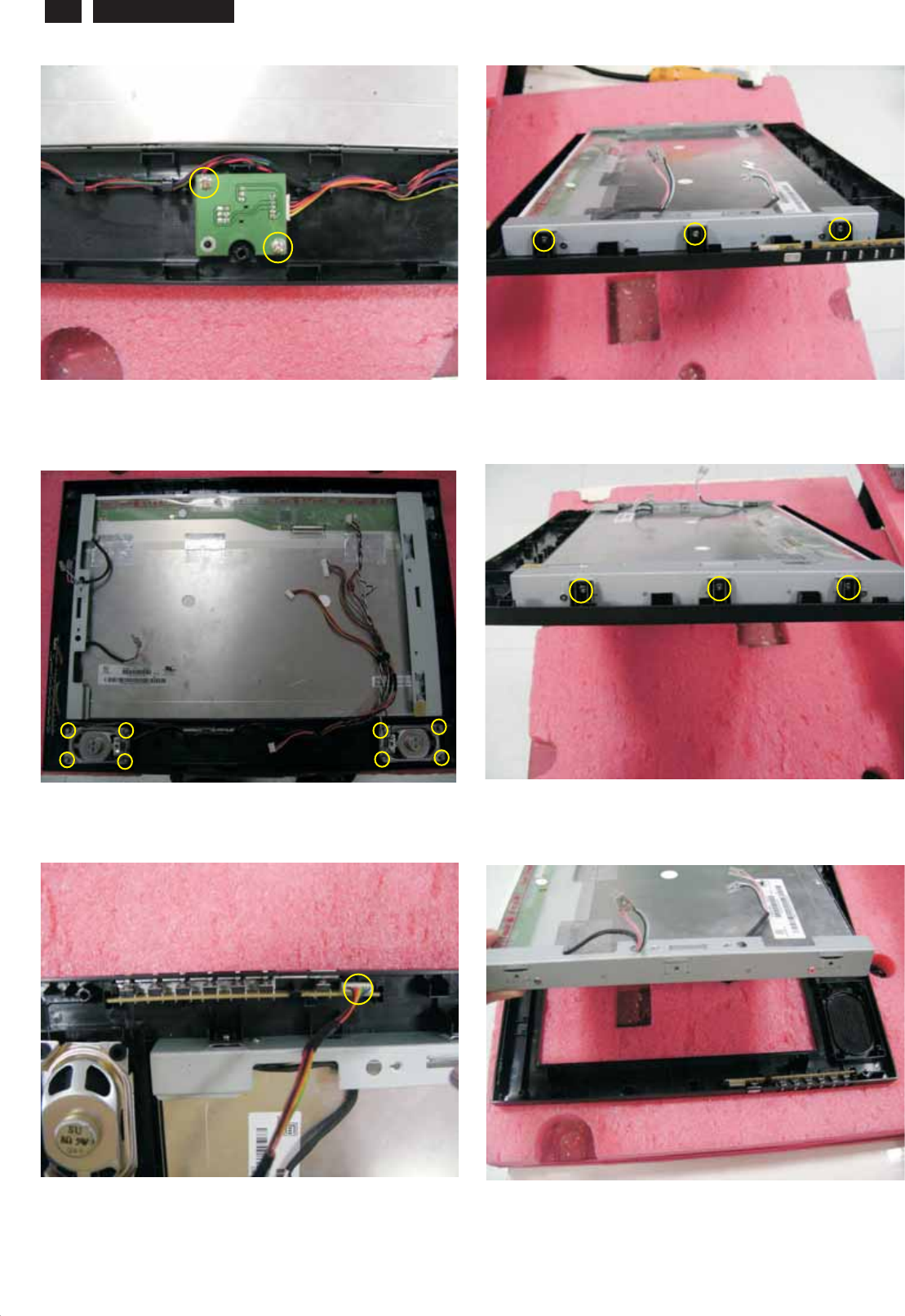
190TW8 TV Mechanical Instructions
Fig.10
10. Remove 3pcs screws from left side of bezel.
Fig. 11
11. Remove 3pcs screws from right side of bezel.
Fig.12
12. Separate bezel from panel.
Fig. 7
Fig. 8
8. Remove 8pcs screws from Speakers, and take off them.
Fig. 9
9.Disconnect the cable from Button/B.
7. Remove 2pcs screws from LED/B, and take off it.
14
http://www.wjel.net
15
190TW8 TV
Fig 16
16. Remove 8pcs screws from Main/B and Power/B.
Fig 17
17. Disconnect Main/B and Power/B.
Fig 18
18. The Main/B.
Mechanical Instructions
Fig.13
13. Remove 2pcs screws from left side of panel bracket.
Fig 14
14. Remove 2pcs screws from right side of bracket.
Fig 15
15. Remove 3pcs screw screws from connector.
http://www.wjel.net

190TW8 TV
Electronic Instruction 17
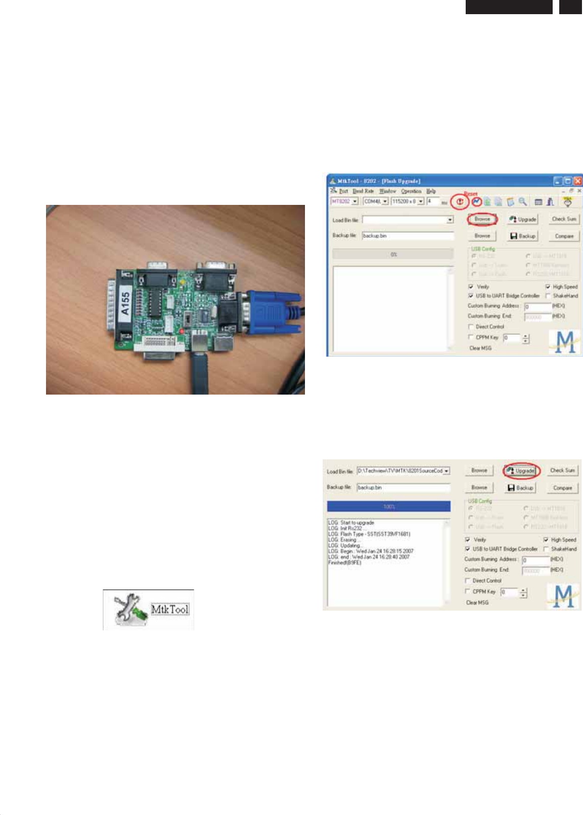
F/W upload instruction
Configuration and procedure(ISP tool)
Purpose and Scope
This document contains introduction the user update firmware
environment and run it on MTK tool.
Prepare to update firmware using ISP board
1. Connection ISP board between PC side and TV side.
* Using USB cable connect between ISP board and PC side, see
figure 1.
* Connect ISP board and TV set by VGA cable, see figure 1
Figure 1
2. How to update firmware:
* Make sure ISP board and TV set are connection.
* Enter factory mode:
A. Use remote control, press “ MENU” key to show use OSD menu
and then key “5588”.
B. Factory mode OSD display when setting OK.
* Executing MTK update tool
MTK tool
* Select com Port and Baud rate
* Press Reset icon
The error message will show on screen when communicate NG.
* Press lightning icon to enter update page.
* Press Browse to choose firmware file.
* Press upgrade to update firmware.
If upgrade fail please to lower Baud rate, then AC power off and
turn on again. Then follow update flow to upgrade firmware again.
Figure 2 Update page
* When update finish, then AC power off and turn on again,
see figure 3.
Figure 3. Finish update firmware illustration
http://www.wjel.net
18 190TW8 TV Electronic Instructions
Electronic instruction
White balance adjusted flow
The purpose of alignments is for the input signal and color
temperature adjustment.
Environment
Equipment Requirements:
Astro VG-848 or VG-859
Minolta CA-210
Fluke 54200
White balance adjusted flow:
Annex 1
1. Factory mode command:
Remote Key: MENU + 5588
2. Make sure user mode at default values
Annex 2:
1. Example
E9P-PT: 1440*900@60
2. Pattern may be changed for different model.
5. Disc Pattern
Annex 3:
1. There are two input source must be done white balance
adjustment
Example: E9P-PT
A. VGA: 1440*900@60
B. AV: PAL(BG)
2. VGA adjusted value for: VGA(and DVI)
3. AV(CVBS) adjusted value for: ATV, CVBS, S-Video, SCART-
RGB and HDMI
Annex 4(White point)
1. Set R/G/B offset value to 128
2. Adjust R/G/B gain value to find the saturation point
3. Follow “White Balance Adjust” rule to adjust white balance
Annex 5(Dark point)
1. Keep offset max. Value at128
2. Follow “White Balance Adjust” rule to adjust white balance
Annex 6
1. Save adjusted value
2. Change color temp to Warm/Standard/Cold
3. Adjust RG, GG, BG, RO, GO, BO
4. Adjust CT values only to meet white spec
Annex 7
1. Change input to VGA/AV(CVBS)
Annex 8
1. Change input source to SCART-RGB to do auto Calibration
2. Timing:
SCART: PAL(BG)
3. Pattern may be changed for different mode
Gray Scale Pattern
ENTER FACOTRY MODE (Annex 1)
Input VGA source timing: (Annex 2) pattern: 5 Disc
Auto Calibration
Input VGA source timing: (Annex 3) pattern: 100% white
Input AV(CVBS) source PAL(BG) or NTSC(M) pattern: 100% white (Annex 3)
White balance adjust (Annex 4)
Check white spec (xy)
Input VGA source timing: (Annex 3) pattern: 25% white
Input AV(CVBS) source PAL(BG) or NTSC(M) pattern: 25% white (Annex 3)
White balance adjust (Annex 5)
Check white spec(xy)
Save adjusted values Change color temperature (Warm/Standard/Cold)
(Annex 6)
Change input source VGA/AV(CVBS) (Annex 7)
Input SCART or YPbPr source timing: PAL(BG)/480p pattern: Gray Scale (Annex 8)
Auto Calibration
Check Brightness spec (Annex 9)
End process
Out spec
In spec
Out spec
In spec
Change input source
Change color temp
Out spec (Annex 10)
In spec
http://www.wjel.net

190TW8 TV
Electronic Instruction 19
Annex 9
1. In Standard mode
2. MENU/Picture/Default Setting
3. Change pattern level to 255(100%)
4. Check brightness whether over spec(250 cd/m² for E9P-PT)
Annex 10
1. Replace panel
2. Repeat white balance flow
Target value Philips (E9P-PT)
White Balance Adjust :
1. x > (=), y > (=) :
A. Fix B value
b. Decrease R value to reduce x value
c. Decrease G value to reduce y value
d. If meet spec than OK
2.x>(=),y<:
a. Fix G value
b. Decrease B value to increase x, y value and let y value to
meet spec
c. Decrease R value to reduce x value
d. If meet spec than OK
3.x<,y>(=):
a. Fix R value
b. Decrease B value to increase x, y value and let x value to
meet spec
c. Decrease G value to reduce y value
d. If meet spec than OK
If you have not CA-110, the following R,G and B values are for
your reference.
4.x<,y<:
a. Decrease B value to increase x, y value and let x = spec, y
>(=) spec or x >(=) spec, y = spec
b. If x = spec, y >(=) spec :
1) Decrease G value to reduce y value
2) If meet spec than OK
c. If x >(=) spec, y = spec :
1) Decrease R value to reduce x value
2) If meet spec than OK
Philips
Color Name Warm Standard Cold
Color Temp 6500K 7500K 9300K
X0.313 0.300 0.285
Y0.329 0.310 0.293
Factory Tolerance dx, dy +-0.007 +-0.007 +-0.007
Shipment Tolerance dx, dy +-0.015 +-0.015 +-0.015
Brightness(Level 255) 270(cd/m²) up 250(cd/m²) up 200(cd/m²) up
19 inch
Color Name
Warm 135 131 137 124 128 117
Standard 120 117 137 125 127 110
Cold 107 110 137 128 126 112
Gain Offset
AV Source
Color Name
Warm 128 125 128 123 128 122
Standard 121 116 128 123 127 128
Cold 108 107 128 124 128 128
Gain Offset
VGA Source
Item1234RX
X > (=) > (=) < <
Y>(=)<>(=)< G Y
Rvv - o
Gv - vo X
B-vvv Y
B
http://www.wjel.net

20 190TW8 TV DDC Data
Mfg. Name
Product Code
Serial Number
Mfg, Week
Mfg, Year
Analog DDC Signal Level
Input Support
Feature Support
Display Type
Image Size :
Red x
Red y
Green x
Green y
Blue x
Blue y
White x
White y
H . Pixels
Refresh rate
V Pixel
H . Pixels
Refresh rate
V Pixel
H . Pixels
Refresh rate
V Pixel
H . Pixels
Refresh rate
V Pixel
H . Pixels
Refresh rate
V Pixel
H . Pixels
Refresh rate
V Pixel
H . Pixels
Refresh rate
V Pixel
Horizontal Image Size
Vertical Image Size
Active Pixels
V Active Lines
H Blank
V Blank
H Sync Offset
V Sync Offset
H Sync Plus Width
V Sync Plus Width
H Border
V Border
Established Timeings
Standard Timings
Block #1
: PHL
: 0864
: 72300001
:23
: 2007
: 0.700 , 0.300
: Separate Sync.
: Stand By, Suspend Active Off /Very
Low Power ,
: RGB Color
Max Hor.(cm) : 41
Max Ver.(cm) : 25
Gamma Value *100 : 220
: 0.647
: 0.334
: 0.284
: 0.607
: 0.151
: 0.071
: 0.313
: 0.329
: 720 x 400 @70Hz [ IBM VGA]
: 640 x 480 @60Hz [ IBM VGA]
: 640 x 480 @67Hz [ Mac2]
: 640 x 480 @72Hz [ VESA]
: 640 x 480 @75Hz [VESA]
: 800 x 600 @56Hz [ VESA]
: 800 x 600 @60Hz [VESA]
: 800 x 600 @72Hz [ VESA]
: 800 x 600 @75Hz [ VESA]
: 832 x 624 @70Hz [Mac2]
: 1024 x 768@60Hz [VESA]
: 1024 x 768@70Hz [VESA]
: 1024 x 768 @75Hz [ VESA]
: 640
:85
: 480
: 800
:85
: 600
: 1024
:85
: 768
: 1280
:60
: 720
: 1280
:75
: 720
: 1440
:60
: 900
: 1440
:75
: 900
: 410mm
: 256 mm
: 1440
: 900
: 464 Pixels
: 34 Lines
: 80 Pixels
: 3 Lines
: 152 Pixels
: 6 Lines
: 0 Pixels
: 0 Lines
Pixels Clock
Refresh Mode
Stero
Refresh Mode
Stero
V Polarity(+) , Digital
Separate
Monitor Range Limits :
Max Pixels Clock
Monitor Name
ASCII String
EDID CODE:
: 106.50 Mhz
: Non-Interlaced
: None
: Non-Interlaced
: None
Min V Rate(Hz) : 50
Max V Rate(Hz) : 76
Min H Rate(KHz) : 30
Max H Rate(KHz) : 83
: 140
: Philips 190TW
: Philips
0123456789ABCDEF
0 00FFFFFFFFFFFF 00 410C64 08 E135 4F 04
10 17 11 01 03 08 29 19 78 EA EE D5 A5 55 48 9B 26
20 12 50 54 BF EE 00 31 59 45 59 61 59 81 C0 81 CF
30 95 00 95 0F 01 01 9A 29 A0 D0 51 84 22 30 50 98
40 36 00 9A 00 11 00 00 1C 00 00 00 FD 00 32 4C 1E
50 53 0E 00 0A 20 20 20 20 20 20 00 00 00 FC 00 50
60 68 69 6C 69 70 73 20 31 39 30 54 57 00 00 00 FE
70 00 50 68 69 6C 69 70 73 0A 20 20 20 20 20 00 77
http://www.wjel.net

190TW8 TV
DDC Data 21
EDID Block 0, Bytes 0-127 [00H-7FH]
Block Type: EDID 1.3
(08H-09H) ID Manufacturer Name = PHL
(0AH-0BH) Product ID Code = 0864
(0CH-0FH) Last 5 Digits of Serial Number = 57313
(10H) Week of Manufacture = 23
(11H) Year of Manufacture = 2007
(12H) EDID Version Number = 1
(13H) EDID Revision Number = 3
(14H) VIDEO INPUT DEFINITION: Digital Signal
(15H) Maximum Horizontal Image Size = 410 mm
(16H) Maximum Vertical Image Size = 250 mm
(17H) Display Gamma = 2.20
(18H) DPMS and Supported Feature(s): Stand-By,
Suspend, Active Off, Preferred Timing Mode
Display Type = R/G/B Color
(19H-22H) CHROMA INFO:
Red x - 0.647 Green x - 0.284
Blue x - 0.151 White x - 0.313
Red y - 0.334 Green y - 0.607
Blue y - 0.071 White y - 0.329
(23H) ESTABLISHED TIMING I:
720 x 400 @ 70Hz (IBM,VGA)
640 x 480 @ 60Hz (IBM,VGA)
640 x 480 @ 67Hz (Apple,Mac II)
640 x 480 @ 72Hz (VESA)
640 x 480 @ 75Hz (VESA)
800 x 600 @ 56Hz (VESA)
800 x 600 @ 60Hz (VESA)
(24H) ESTABLISHED TIMING II:
800 x 600 @ 72Hz (VESA)
800 x 600 @ 75Hz (VESA)
832 x 624 @ 75Hz (Apple,Mac II)
1024 x 768 @ 60Hz (VESA)
1024 x 768 @ 70Hz (VESA)
1024 x 768 @ 75Hz (VESA)
(25H) Manufacturer's Reserved Timing:
None Specified
(26H-35H) Standard Timing Identification:
Standard Timing ID 1: 640 x 480 @85Hz
Standard Timing ID 2: 800 x 600 @85Hz
Standard Timing ID 3: 1024 x 768 @85Hz
Standard Timing ID 4: 1280 x 720 @60Hz
Standard Timing ID 5: 1280 x 720 @75Hz
Standard Timing ID 6: 1440 x 900 @60Hz
Standard Timing ID 7: 1440 x 900 @75Hz
Standard Timing ID 8 - Not Used
(36H-47H) Detailed Timing / Descriptor Block 1:
1440x900 Pixel Clock: 106.50 MHz
Horizontal Image Size: 410 mm
Vertical Image Size: 256 mm
Refreshed Mode:
Non-Interlaced Normal Display - No Stereo
Horizontal:
Active Count: 1440 pixels
Blanking Count: 464 pixels
Sync Offset: 80 pixels
Sync Pulse Width: 152 pixels
Border: 0 pixels
Frequency: 55.93 kHz
Vertical:
Active Count: 900 lines
Blanking Count: 34 lines
Sync Offset: 3 lines
Sync Pulse Width: 6 lines
Border: 0 lines
Frequency: 59.89 Hz
Digital Separate,
Horizontal Polarity (-) Vertical Polarity (+)
(48H-59H) Detailed Timing / Descriptor Block 2:
Monitor Range Limits:
Min Vertical Freq - 50 Hz
Max Vertical Freq - 76 Hz
Min Horiz. Freq - 30 kHz
Max Horiz. Freq - 83 kHz
Pixel Clock - 140 MHz
GTF - Not Used
(5AH-6BH) Detailed Timing / Descriptor Block 3:
Monitor Name:
Philips 190TW
(6CH-7DH) Detailed Timing / Descriptor Block 4:
ASCII Data: Philips
(7EH) Block No: (01) Extension EDID Block(s)
(7FH) CheckSum OK
0123456789ABCDEF
0 00FFFFFFFFFFFF00 410C64 08 E1 35 4F 04
10 17 11 01 03 80 29 19 78 EA EE D5 A5 55 48 9B 26
20 12 50 54 BF EE 00 31 59 45 59 61 59 81 C0 81 CF
30 95 00 95 0F 01 01 9A 29 A0 D0 51 84 22 30 50 98
40 36 00 9A 00 11 00 00 1C 00 00 00 FD 00 32 4C 1E
50 53 0E 00 0A 20 20 20 20 20 20 00 00 00 FC 00 50
60 68 69 6C 69 70 73 20 31 39 30 54 57 00 00 00 FE
70 00 50 68 69 6C 69 70 73 0A 20 20 20 20 20 01 FE
http://www.wjel.net

22 190TW8 TV DDC Data
EDID Block 1, Bytes 128-255 [80H-FFH]
Block Type: CEA EDID Timing Extension Version 3
Extended Block Type: CEA 861B
Detailed Timing Blocks start at Byte:(1EH)
Native Format: (0x1)
(03H) DTV (Underscan)
(03H) DTV (Basic Audio)
(03H) YCbCr (4:4:4)
(03H) YCbCr (4:2:2)
Video Short Block Description:
(05H) 1280 x 720 P 50Hz 16:9 Native Mode
(06H) 1920 x 1080 I 50Hz 16:9
(07H) 720 x 576 P 50Hz 16:9
(08H) 720(1440) x 576 I 50Hz 16:9
(09H) 720(1440) x 576 I 50Hz 4:3
(0AH) 640 x 480 P 59.94/60Hz 4:3
(0BH) 1280 x 720 P 59.94/60Hz 16:9
(0CH) 1920 x 1080 I 59.94/60Hz 16:9
(0DH) 720(1440) x 480 I 59.94/60Hz 16:9
(0EH) 720(1440) x 480 I 59.94/60Hz 4:3
(0FH) 720 x 480 P 59.94/60Hz 16:9
Audio Short Block Description: Numbers of Audio Channels (2)
(11H) Linear PCM(IEC60958)
Audio Supported: 32kHz, 44.1kHz, 48kHz
Audio Bit Rate: 16bit, 20Bit, 24Bit
Speaker Short Block Description: Playload (3 bytes 15H-17H)
Speakers (15H): FL/FR
16H: Reserved
17H:
Vendor Specific Short Block Description:
Bytes: 03H, 0CH, 00H, 10H, 00H
(1EH - 30H) Detailed Timing Descriptions:
1280x720 Pixel Clock: 74.25 MHz
Horizontal Image Size: 408 mm
Vertical Image Size: 230 mm
Refreshed Mode:
Non-Interlaced Normal Display - No Stereo
Horizontal:
Active Count: 1280 pixels
Blanking Count: 700 pixels
Sync Offset: 440 pixels
Sync Pulse Width: 40 pixels
Border: 0 pixels
Frequency: 37.50 kHz
Vertical:
Active Count: 720 lines
Blanking Count: 30 lines
Sync Offset: 5 lines
Sync Pulse Width: 5 lines
Border: 0 lines
Frequency: 50.00 Hz
Digital Separate, Horizontal Polarity (+) Vertical Polarity (+)
Reserved
(30H - 42H) Detailed Timing Descriptions:
720x480 Pixel Clock: 27.00 MHz
Horizontal Image Size: 408 mm
Vertical Image Size: 230 mm
Refreshed Mode:
Non-Interlaced Normal Display - No Stereo
Horizontal:
Active Count: 720 pixels
Blanking Count: 138 pixels
Sync Offset: 16 pixels
Sync Pulse Width: 62 pixels
Border: 0 pixels
Frequency: 31.47 kHz
Vertical:
Active Count: 480 lines
Blanking Count: 45 lines
Sync Offset: 9 lines
Sync Pulse Width: 6 lines
Border: 0 lines
Frequency: 59.94 Hz
Digital Separate, Horizontal Polarity (-) Vertical Polarity (-)
(42H - 54H) Detailed Timing Descriptions:
720x576 Pixel Clock: 27.00 MHz
Horizontal Image Size: 408 mm
Vertical Image Size: 230 mm
Refreshed Mode:
Non-Interlaced Normal Display - No Stereo
Horizontal:
Active Count: 720 pixels
Blanking Count: 144 pixels
Sync Offset: 12 pixels
Sync Pulse Width: 64 pixels
Border: 0 pixels
Frequency: 31.25 kHz
Vertical:
Active Count: 576 lines
Blanking Count: 49 lines
Sync Offset: 5 lines
Sync Pulse Width: 5 lines
Border: 0 lines
Frequency: 50.00 Hz
Digital Separate, Horizontal Polarity (-) Vertical Polarity (-)
(54H - 66H) Detailed Timing Descriptions:
1920x540 Pixel Clock: 74.25 Mhz
Horizontal Image Size: 408 mm
Vertical Image Size: 230 mm
Refreshed Mode: Interlaced Normal Display - No Stereo
Horizontal:
Active Count: 1920 pixels
Blanking Count: 720 pixels
Sync Offset: 528 pixels
Sync Pulse Width: 44 pixels
Border: 0 pixels
Frequency: 28.13 kHz
Vertical:
Active Count: 540 lines
Blanking Count: 22 lines
Sync Offset: 2 lines
Sync Pulse Width: 5 lines
Border: 0 lines
Frequency: 50.04 Hz
Digital Separate, Horizontal Polarity (+) Vertical Polarity (+)
http://www.wjel.net

190TW8 TV
DDC Data 23
(66H - 78H) Detailed Timing Descriptions:
1280x720 Pixel Clock: 74.25 Mhz
Horizontal Image Size: 408 mm
Vertical Image Size: 230 mm
Refreshed Mode: Non-Interlaced Normal Display - No Stereo
Horizontal:
Active Count: 1280 pixels
Blanking Count: 370 pixels
Sync Offset: 110 pixels
Sync Pulse Width: 40 pixels
Border: 0 pixels
Frequency: 45.00 kHz
Vertical:
Active Count: 720 lines
Blanking Count: 30 lines
Sync Offset: 5 lines
Sync Pulse Width: 5 lines
Border: 0 lines
Frequency: 60.00 Hz
Digital Separate, Horizontal Polarity (+) Vertical Polarity (+)
(7FH) CheckSum Valid
0123456789ABCDEF
0 02031EF14B9314121615010405070603
10 23 09 07 07 83 01 00 00 65 03 0C 00 10 00 01 1D
20 00 BC 52 D0 1E 20 B8 28 55 440 98 E6 10 00 00 1E
30 8C 0A D0 8A 20 E0 2D 10 10 3E 96 00 98 E6 10 00
40 00 18 8C 0A D0 90 20 40 31 20 0C 40 55 00 98 E6
50 10 00 00 18 01 1D 80 D0 72 1C 16 20 10 2C 25 80
60 98 E6 10 00 00 9E 01 1D 00 72 51 D0 1E 20 6E 28
70 55 00 98 E6 10 00 00 1E 00 00 00 00 00 00 00 9C
http://www.wjel.net

24 190TW8 TV Safety Instruction, Warnings and Notes
Safety instruction, warnings and notes
index of this chapter:
1 Safety Instructions
2 Warnings
3 Notes
1 Safety Instructions
Safety regulations require that during a repair:
a. Connect the set to the AC Power via an isolation transformer
(> 800 VA).
b. Replace safety components, indicated by the symbol ,
only by components identical to the original ones. Any other
component substitution (other than original type) may
increase risk of fire or electrical shock hazard.
Safety regulations require that after a repair, the set must be
returned in its original condition. Pay in particular attention to
the following points:
a. Route the wire trees correctly and fix them with the mounted
cable clamps.
b. Check the insulation of the AC Power lead for external
damage.
c. Check the strain relief of the AC Power cord for proper
function.
d. Check the electrical DC resistance between the AC Power
plug and the secondary side (only for sets which have a AC
Power isolated power supply):
* Unplug the AC Power cord and connect a wire between the
two pins of the AC Power plug.
* Set the AC Power switch to the "on" position (keep the AC
Power cord unplugged!).
* Measure the resistance value between the pins of the AC
Power plug and the metal shielding of the tuner or the aerial
connection on the set. The reading should be between 4.5
Mohm and 12 Mohm.
* Switch "off" the set, and remove the wire between the two
Pins of the AC Power plug.
e. Check the cabinet for defects, to avoid touching of any inner
parts by the customer.
2 Warnings
a. All ICs and many other semiconductors are susceptible to
electrostatic discharges (ESD ). Careless handling during
repair can reduce life drastically. Make sure that, during
repair,
you are connected with the same potential as the mass of the
set by a wristband with resistance. Keep components and
tools also at this same potential.
b. Be careful during measurements in the high voltage section.
c. Never replace modules or other components while the unit
is switched "on".
d. When you align the set, use plastic rather than metal tools.
This will prevent any short circuits and the danger of a circuit
becoming unstable.
3 Notes
3.1 General
Measure the voltages and waveforms with regard to the
chassis ground or hot ground, depending on the tested area of
circuitry. The voltages and waveforms shown in the diagrams
are indicative.
The semiconductors indicated in the circuit diagram and in the
parts lists, are interchangeable per position with the
semiconductors in the unit, irrespective of the type indication on
3.2 Schematic Notes
All resistor values are in ohms and the value multiplier is often
used to indicate the decimal point location (e.g. 2K2 indicates
2.2 Kohm).
Resistor values with no multiplier may be indicated with either
an "E" or an "R" (e.g. 220E or 220R indicates 220 ohm).
All capacitor values are given in micro-farads ( X10 ),
nano-farads (n= X10 ), or pico-farads (p= X10 ).
Capacitor values may also use the value multiplier as the
decimal point indication (e.g. 2p2 indicates 2.2 pF).
An "asterisk" (*) indicates component usage varies. Refer to the
diversity tables for the correct values.
The correct component values are listed in the Electrical
Replacement Parts List. Therefore, always check this list when
there is any doubt.
3.3 Lead Free Solder
Philips CE is going to produce lead-free sets (PBF) from
1.1.2005 onwards.
Lead-free sets will be indicated by the PHILIPS-lead-free logo
on the Printed Wiring Boards (PWB):
This sign normally has a diameter of 6 mm, but if there is less
space on a board also 3 mm is possible.
In case of doubt wether the board is lead-free or not (or with
mixed technologies), you can use the following method:
* Always use the highest temperature to solder, when using
SAC305 (see also instructions below).
* De-solder thoroughly (clean solder joints to avoid mix of
two alloys).
: For BGA-ICs, you must use the correct temperature
profile, which is coupled to the 12NC. For an overview of these
profiles, visit the website
You will find this and more technical information within the
"Magazine", chapter "Workshop information".
For additional questions please contact your local repair desk.
Due to lead-free technology some rules have to be respected
by the workshop during a repair:
Use only lead-free soldering tin Philips SAC305 with order code
0622 149 00106. If lead-free solder paste is required, please
contact the manufacturer of your soldering equipment.
In general, use of solder paste within workshops should be
avoided because paste is not easy to store and to handle.
Use only adequate solder tools applicable for lead-free
soldering tin. The solder tool must be able
- To reach at least a solder-tip temperature of 400 degree C.
- To stabilise the adjusted temperature at the solder-tip.
- To exchange solder-tips for different applications.
-6
-9 -12
Caution
http://www.atyourservice.ce.philips.com/
http://www.wjel.net
190TW8 TV
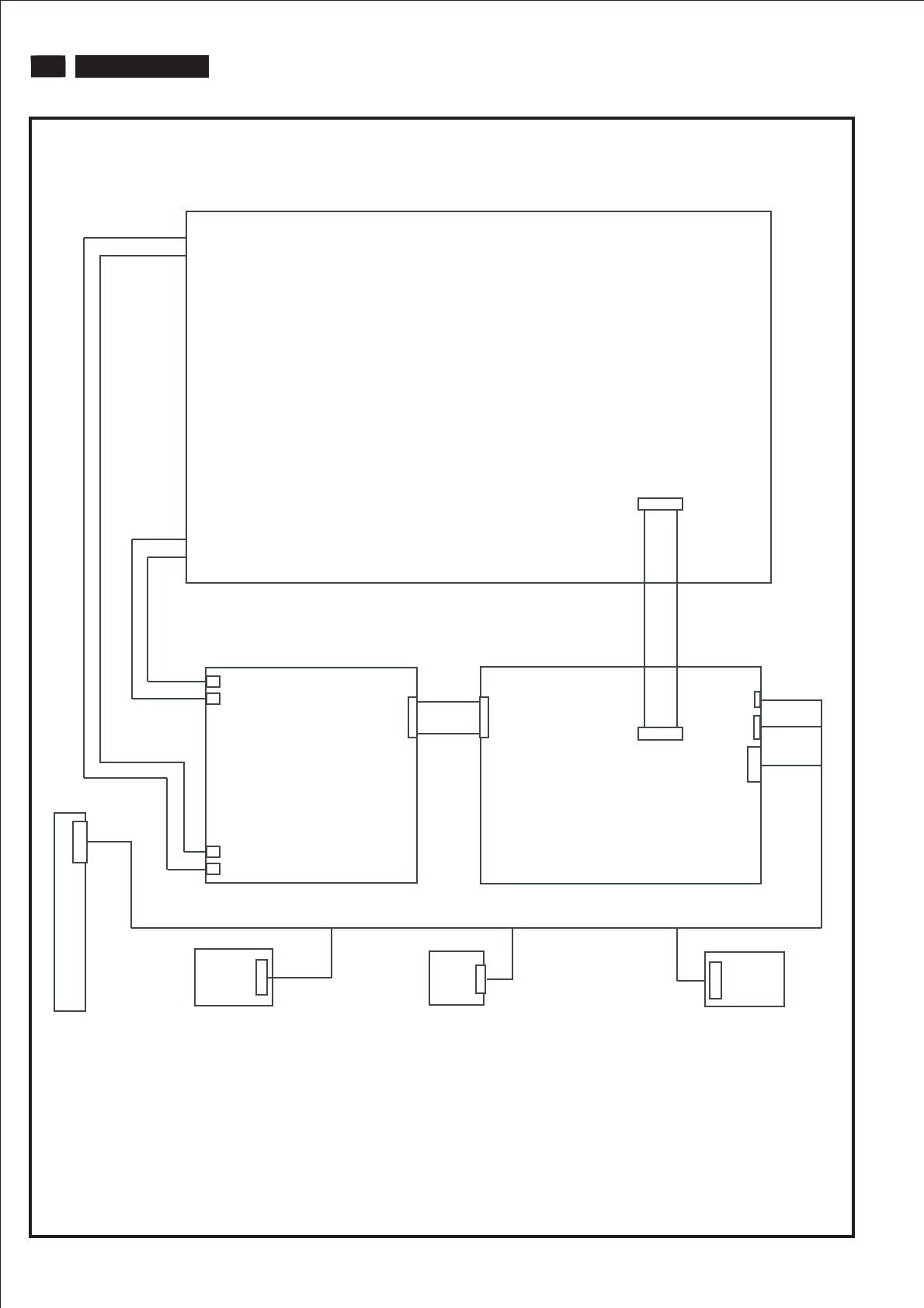
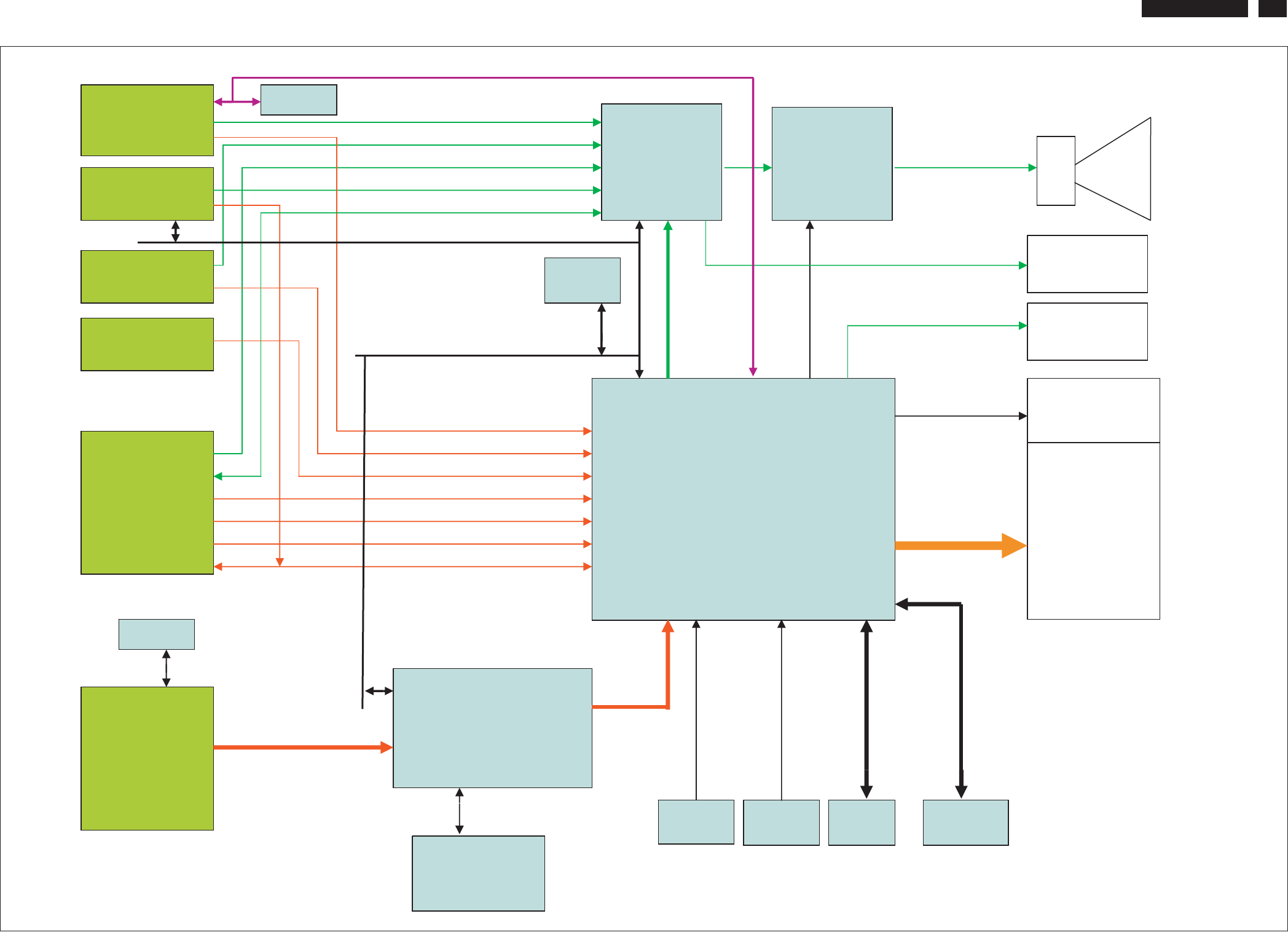
Block Diagram 25
MT8200
Audio
Processor
MT8291
Audio
Amplifier
TFA9810
Backlight
LCD
panel
EEPROM
Flash
ROM
IR
Sensor
2-Wire Bus
SCART
S-video
Video
Tuner
PC PC Audio input
CVBS/S-Video Audio input
SCART Audio input
Tuner Audio input
SCART Audio output
S-Video input
CVBS input
PC Video input
Tuner Video input
LVDS
SCART-RGB input
SCART-S-VIDEO input
SCAR-CVBS input
ADC+
GPIO
Earphone
2-Wire Bus
Speaker
DDC
EEPROM
HDMI
DDC
EEPROM
I2S Bus
HDMI receiver
MT8293
HDCP
Keys
16bit 4:2:2 MTK format
User
Keypad
SPDIF
2-Wire Bus
DDRAM
GPIO
RS232
http://www.wjel.net

Schematic Diagram( Scaler Board - POWER_RESET_)EEPROM) 190TW8 TV 26
S-A01
A
A
B
B
C
C
D
D
E
E
4 4
33
22
1 1
SCL
SDA +12VAUDIO
URST#
SYSROMWP
8201UP3_4
+12V_CN
BL_ON/OFF
Dimming
Dimming
BL_ON/OFF
PWM1
PWM0
+5V_IN
CN_GND
SCL
SDA
SB33B
5VSB
SB33B
SB33B
5VSB VCC
DV33B
DV33B
+12V
+12V
+12V_IN DV33B
+5V_IN 5VSB
SB33B
DV33B
SB33B
+12V_CN +12V_IN +12VAUDIO
SDA 4,6,8,11
SCL 4,6,8,11
+12VAUDIO 11,13
URST# 4
8201UP3_4 4GPIO10 4
8201UP3_4 48201UP3_4 4
PWM04
PWM14
URST#4
Control_Power 7
SYSTEM EEPROM
SYSTEM RESER
H : WP DISABLE
L : WP ENABLE
B
1
3
2
C
RWOPMETSYSRWOPM
ETSYS
AUDIO AMP POWER
MAIN CONNECTOR
EXTERNAL MCU POWER
SYSTEM EEPROM
1
C
B
2
3
PANEL BRIGHTNESS
PANEL BACKLIGHT
2
C
1
3
B
CB2
0.1uF/6
R327 10R/6
C7
0.1uF/6
12
R12
1k/6
Q2
SI9435
2
3
45
7
6
8
1
1
H1
MTH276D126
2
3
4
56
7
8
9
Q6
2N3904
SOT23
2
1 3
Q3
2N3904
SOT23
2
1 3
L3
Bead_121_4A/8
R352 4.7k/6
L2
Bead_121_4A/8
+
CE1
330uF/25V
12
R6
10k/6
C211
22P/6/NC
12
CB1
0.1uF/6
D1
PSM-A
Q8
2N3904
SOT23
2
1 3
+
CE3
47uF/16V
12
C5
0.1uF/6
R3
2.2K/6
Q25
SI9435/NC
2
3
4 5
7
6
8
1
1
H3
MTH276D126
2
3
4
56
7
8
9
+
CE47
330uF/25V
12
Q7
2N3904
SOT23
2
1 3
R353 4.7k/6/NC
R5
1k/6
C2
0.1uF/6
C212
22P/6/NC
12
+
C3
10uF/25V
12
Q26
2N3904/NC
SOT23
2
1 3
CB3
0.1uF/6
CB96
0.1uF/6
U1
24C16
SOIC8
NC
1
NC
2
NC
3
GND
4SDA 5
SCL 6
WP 7
VCC 8
Q5
2N3904
2
1 3
R354 4.7k/6
R4
2.2K/6
L52
Bead_121_4A/8
+
CE4
10uF/25V
12
R1
10k/6
R9
220/6
R308
10k/6/NC
R328 10R/6
R290
10k/6/NC
1
H2
MTH276D126
2
3
4
5 6
7
8
9
CB97
0.1uF/6
R8 0R/6
C195
2200pF/6/NC
R14
4.7k/6
R17
10k/6/NC
C1
2200pF/6
Q1
SI9435
2
3
45
7
6
8
1
C196
0.1uF/6/NC
1
H4
MTH276D126
2
3
4
5 6
7
8
9
CB4
1uF/6
R291
2.2K/6/NC
CB5
0.1uF/6
L1
Bead_121_4A/8
C4
2200pF/6
R310
10k/6/NC
R309
10k/6/NC
R2
10k/6
+
C6
10uF/25V
12
R11
47k/6
+
C197
10uF/25V/NC
12
R10
4.7k/6
R13
10k/6
+
CE2
330uF/25V
12
R7 100R/6
Q4
2N3904
SOT23
2
1 3
R15
20k/6
R16 10k/6
CN1
CON10 2.54
1
2
3
4
5
6
7
8
9
10
C1 B4
C2 C4
C3 C4
C4 A4
C5 A4
C6 B4
C7 A1
C195 D4
C196 D4
C197 D4
C211 C1
C212 C1
CB1 A3
CB2 C3
CB3 D3
CB4 E2
CB5 B1
CB96 B3
CB97 C3
CE1 A3
CE2 C3
CE3 C3
CE4 B1
CE47 B3
CN1 A3
D1 A1
H1 D2
H2 E2
H3 D2
H4 E2
L1 A3
L2 C3
L3 B3
L52 A2
Q1 A4
Q2 B4
Q3 B4
Q4 A4
Q5 A1
Q6 D3
Q7 E4
Q8 C1
Q25 C4
Q26 C4
R1 B4
R2 A4
R3 B4
R4 A4
R5 E3
R6 A1
R7 E3
R8 E3
R9 A1
R10 D3
R11 B1
R12 E4
R13 E4
R14 E4
R15 C2
R16 D1
R17 C1
R290 C4
R291 C4
R308 A4
R309 D3
R310 D1
R327 C1
R328 C1
R352 B4
R353 C4
R354 A4
U1 B1
http://www.wjel.net
Schematic Diagram(Scaler Board - LDO) 190TW8 TV 27
S-A02
A
A
B
B
C
C
D
D
E
E
4 4
3 3
2 2
1 1
PLLVDD
AVDD_VFE0
AVDD_VAD0
AADCVDD
ADACVDD
VPLLVDD2
AVDD_VAD1
AVDD_VFE1
XTALVDD
PLLVDD
XTALVDD
ADACVDD
AADCVDD
AVDD_VFE0 AVDD_VAD0
AVDD_VAD1AVDD_VFE1
VPLLVDD2
LVDS_GND
LVDS_GND
LVDS_GND
ADCV33A
ASB18A
ADCV33A
ADCV33A
ADCV18A
ADCV33A
ADCV33A DV33B DV33A
ADCV33A ADCV18A DV18A
5VSB
SB33B
SB18A ASB18A
SB33A
ADCV18A
ADCV33A
DV18A
DV33B
VCC
5VSB
5VSB
DV33A
PLLVDD 4
AVDD_VFE0 4
AVDD_VAD0 4
AADCVDD 4
ADACVDD 4
VPLLVDD2 4
AVDD_VAD1 4
AVDD_VFE1 4
XTALVDD 4
Power ON alive source
NORMAL VIDEO DAC POWER
STANDBY ANALOG POWER
NORMAL AUDIO ADC / DAC POWER
NORMAL VIDEO ADC POWER
NORMAL ANALOG POWER
CB19
0.1uF/6
12
L8
22uH/8
RC0805
CB17
0.1uF/6
12
L11
Bead_121_4A/8/NC
L9
Bead_121_4A/8/NC
L53
Bead_121_4A/8 CB10
0.1uF/6
12
+
C9
10uF/25V
12
C38
1uF/6
+
C26
10uF/25V
12
R26 330R/6F
C37
0.1uF/6
CB94
0.1uF/6/NC
12
+
C20
10uF/25V
12
C24
0.1uF/6
C35
0.1uF/6
U2
AP1117ELA/TO252
ADJ/GND
1
VOUT 2
VIN
3
C29
1uF/6
+
C41
10uF/25V
12
+
C8
4.7uF/25V
12
+
C18
4.7uF/25V
12
CB11
0.1uF/6
12
FB1 Bead_121_4A/8
C25
0.1uF/6
L55
Bead_121_4A/8
CB95
0.1uF/6/NC
12
U3
AP1117ELA/TO252
ADJ/GND
1
VOUT 2
VIN
3
C13
0.1uF/6
R27 200/6F
CB8
0.1uF/6
12
C43
10uF/10V/8
CC0805
C34
0.1uF/6
CE5
10uF/10V/8
12
FB4 Bead_121_4A/8
R24 100R/6F
U5
AP1117ELA/TO252
ADJ/GND
1
VOUT 2
VIN
3
L65
Bead_121_4A/8
+
C12
10uF/25V
12
+
C39
10uF/25V
12
R19 1.4K/6F R20 2.2K/6F
+
C21
10uF/25V
12
C44
10uF/10V/8
CC0805
L46 Bead_121_4A/8
L64
Bead_121_4A/8
+
CE46
10uF/25V/NC
12
CB14
0.1uF/6
12
L56
Bead_121_4A/8
+
CE6
100uF/16V
12
L7
22uH/8
RC0805
L57
Bead_121_4A/8
CB16
0.1uF/6
12
CB13
0.1uF/6
12
+
C33
10uF/25V
12
C17
0.1uF/6
L6 Bead_121_4A/8
R25 200R/6F
C32
0.1uF/6
CB15
0.1uF/6
12
L4
Bead_121_4A/8
C16
0.1uF/6
C14
0.1uF/6
L5
Bead_121_4A/8
+
CE44
10uF/25V/NC
12
L58
Bead_121_4A/8
+
CE45
10uF/25V/NC
12
U6
AP1117ELA/TO252
ADJ/GND
1
VOUT 2
VIN
3
CB12
0.1uF/6
12
+
C31
10uF/25V
12
R31 200/6F
U8
AP1117ELA/TO252
ADJ/GND
1
VOUT 2
VIN
3
U4
AP1117ELA/TO252
ADJ/GND
1
VOUT 2
VIN
3
R18 2.2K/6F
R23 1.4K/6F
CB6
0.1uF/6
12
CB93
0.1uF/6/NC
12
+
C10
10uF/25V
12
R21 5.6k/6F
CB7
0.1uF/6
12
+
C19
4.7uF/25V
12
C40
0.1uF/6
FB2 Bead_121_4A/8
R30 330R/6F
FB3 Bead_121_4A/8
R29 200R/6FR28 100R/6F
U7
AP1117ELA/TO252
ADJ/GND
1
VOUT 2
VIN
3
+
C45
4.7uF/25V
12
CB9
0.1uF/6
12
+
C36
10uF/25V
12
C11
0.1uF/6
+
CE7
100uF/16V
12
C27
0.1uF/6
R22 2.2K/6F
C42
0.1uF/6
+
C23
10uF/25V
12
C22
0.1uF/6
C28
0.1uF/6
12
CB18
0.1uF/6
12
+
C30
10uF/25V
12
L10
Bead_121_4A/8/NC
+
C15
10uF/25V
12
C8 D4 CB19 D1
C9 A4 CB93 A2
C10 B4 CB94 B2
C11 A4 CB95 C2
C12 A4 CE5 D3
C13 B4 CE6 E3
C14 B4 CE7 E2
C15 C4 CE44 A2
C16 C4 CE45 B2
C17 C4 CE46 C2
C18 D4 FB1 D4
C19 D3 FB2 D2
C20 A3 FB3 D2
C21 B3 FB4 D1
C22 A3 L4 D4
C23 A3 L5 B4
C24 B3 L6 B3
C25 B3 L7 D3
C26 C3 L8 D3
C27 C3 L9 A2
C28 D3 L10 B2
C29 E3 L11 C2
C30 A3 L46 B3
C31 B3 L53 C3
C32 A3 L55 B2
C33 A3 L56 B4
C34 B3 L57 C3
C35 B3 L58 C4
C36 C3 L64 A3
C37 C3 L65 A3
C38 E2 R18 A4
C39 A2 R19 A4
C40 A2 R20 B4
C41 A2 R21 C4
C42 B2 R22 A4
C43 D2 R23 A4
C44 D2 R24 B4
C45 D1 R25 C4
CB6 D4 R26 A3
CB7 D4 R27 A3
CB8 D4 R28 B3
CB9 D4 R29 C3
CB10 E3 R30 A2
CB11 E3 R31 A2
CB12 E3 U2 A4
CB13 E3 U3 C4
CB14 E2 U4 A3
CB15 D2 U5 C3
CB16 E2 U6 A3
CB17 D2 U7 C3
CB18 E2 U8 A2
http://www.wjel.net
190TW8 TV 28
S-A03
A
A
B
B
C
C
D
D
E
E
44
3 3
22
1 1
VGASOG
HDMIBCLK
HDMILRCK
HDMIMCLK
HDMIODCK
SDA0
SCL0
HDMISD0
SCL
SDA
DDC_WP_DE
A_DQ[0..15]
A_CKE
A_BA[0..1]
A_RA[0..11]
A_DQM0
GPIO9_MCLK
AVDD_VAD0
AVDD_VFE0
AVDD_VAD1
GPIO8_BCKL
ADACVDD
AVDD_VFE1
AOSDATA3
GPIO7_LRCK
AADCVDD
IR
SDA
AOMCLK1
AOSDATA1
URST#
FCLK_GPIO
AOBCLK1
GPIO10
IOWR#
ADIN
AOLRCK1
8201UP3_4
SCL
F_A[0..21]
AP[0..7]
F_D[0..7]
AN[0..7]
RXD
TXD
ICE
SB18A
VREF
A_DQS1
A_DQS0
AVICM
ADCV18A TESTN4
RP
CVBS0
A_DQ11
DV25A
A_DQ4
Y1P
SB18A
ERO3_GPIO
AVICM
DV18A
VI13
VI12
VI0
PB1N
RN
BP
GND
DV33A
HDMIMCLK
GND
TTL_CLK
F_D5
A_RA1
A_CLK#
VI6
AOSDATA1
DV33A
VI11
VI1
URST#
PB1N
DV25A
F_A17
8201UP3_1
A_RA3
AR_AOSDATA1
AVDD_VFE0
VI15
F_A10
F_A21
AP5
GPIO23
8291_MUTE
AOBCLK1
XTALI
PR1N
BN
PR1P
SC1
PR1N
BN
AN1
CLK1N
TESTN4
A_DQ10
PW_KEY
VI4
AL_AOSDATA0
CVBS0
GND
GPIO24
F_A5
A_RA6
AN6
AP0
VPLLVDD2
A_DQ15
DV18A
A_CLK
8201UP3_4
AOMCLK1
XTALO
F_A15
AP1
A_DQS1
VGASOG
F_D0
A_RA0
VI14
DV18A
ICE
A_CKE
AP7
XTALO
A_RA4
A_RA5
TXD
VGAHSYNC#
SC0
TTL_VS
DV25A
DE_DVI
SCL0
VGAHSYNC#
AP2
AP3
PWM2VREF
A_DQM0
A_DQ6
A_DQ5
A_DQ2
PB1P
DV25A
A_BA1
DV25A
GND
HSYNC_DVI
VI9
DE_SOG
AOLRCK1
DV18A
SC0
Y1P
CVBS1
ADC_IN1
CLK2N
GND
DV25A
SDA0
ADCV33A
ADCV18A
A_DQ12
GPIO8_BCLK
F_A14
TTL_HS
F_D2
F_D6
8201UP3_0
GPIO28
GPIO6
PB1P
HDMISD0
ADC_IN0
GPIO5
AOSDATA3
RP
F_OE#
GPIO7_LRCK
ADIN
GN
F_D1
AVDD_VFE1
Y1N
ADCV33A
A_DQ9
A_DQ8
F_A13
SB18A
F_A11
DV18A
DV33A
F_A8
F_A4
GP
GPIO17
A_DQS0
A_DQ13
A_RAS#
VI2
A_RA11
PWM0
A_RA9
A_RA7
A_RA8
CVBS2
AN2
AN3
ADCV33A
AN5
GPIO9_MCLK
GP
F_A1
SB33A
A_CS#
A_RA10
VI5
PLLVDD
MPX1
AADCVDD
AVDD_VAD0
GND
HDMIODCK
27MHZ
IOWR#
DV25A
XTALI
IR
RXD
CVBS2
VGAVSYNC#
AN4
A_DQ3
HDMILRCK
ADACVDD
VI7
VI3
SOY1
AN7
GN
A_DQ7
HDMIBCLK
PR1P
A_RA2
F_A12
CVBS1
GND
VI8
PWM1
F_A19
DV18A
SY0
AP4
AN0
CLK1P
F_D7
A_WE#
A_BA0
DV25A
SY0
F_A6
F_A9
VI[0..15]
Y1N
CLK2P
VGAVSYNC#
GPIO10
VREF
A_DQ1
FCLK_GPIO
BP
F_A16
IOCE#
F_D3
F_D4
F_A0
A_CAS#
VSYNC_DVI
PLLVDD
F_A7
F_A20
MPX1
AP6
RN
GPIO20
SCART_FB
SCART_FB
SB33A
DDC_WP_DE
A_DQ0
A_DQ14
SC1
AVDD_VAD1
VI10
PLLVDD
XTALVDD
F_A18
F_A3
SOY1
GND
F_A2
SB33A
ACENT
RXD
TXD
DV18ASB18A
SB33A
DV33A
SB33B
SB33B
SB33A
DV25A
DV25A
ADCV33A
ADCV33A
ADCV18A
ADCV33A
SB33B
VGASOG 7
HDMIMCLK 6
HDMIBCLK 6
HDMILRCK 6
HDMIODCK 6
SDA0 7
SCL0 7
HDMISD0 6
GPIO5 7
GPIO6 7
A_DQM0 5
A_DQ[0..15] 5
A_CKE 5
A_BA[0..1] 5
A_RA[0..11] 5
GPIO9_MCLK 11
ADACVDD 3
AVDD_VFE1 3
AVDD_VAD1 3
AVDD_VAD0 3
IR 7,14
GPIO8_BCLK 11
AOSDATA3 11
AVDD_VFE0 3
GPIO7_LRCK 11
AADCVDD 3
AOLRCK111
SCL2,6,8,11
AOSDATA111
AOBCLK111
URST#2
FCLK_GPIO14
8201UP3_42
ADIN
11
AOMCLK111
SDA2,6,8,11
IOWR#5
GPIO10
2
F_A[0..21]
5
F_D[0..7]
5
AN[0..7]
12
AP[0..7]12
RXD 7
TXD 7
VREF 5
A_DQS1 5
A_DQS0 5
RN 7
GPIO24 6
PWM1 2
PWM0 2
A_BA0 5
BN 7
8291_MUTE 11
VI[0..15] 6
VSYNC_DVI 6
GPIO23 11
A_WE# 5
SCART_FB 10
VGAHSYNC# 7
A_CLK 5
RP 7
GPIO20 13
F_OE#
5
IOCE#5
GPIO17 11
CLK1P12
A_CS# 5
DDC_WP_DE
6,7
DE_DVI 6
DE_SOG 6
ERO3_GPIO11
CLK1N
12
BP 7
HSYNC_DVI 6
A_CAS# 5
GPIO28 12
CLK2P12
A_CLK# 5
A_RAS# 5
GP 7
ERO1_UP3_114
GN 7
CLK2N12
A_BA1 5
ERO0_UP3_07
PW_KEY7,14
27MHZ 6
VGAVSYNC# 7
SC110
SC0
9
CVBS09
MPX18
SOY110
PR1P10
SY0
9
VPLLVDD23
CVBS18
PLLVDD3
CVBS2
10
Y1P
10
XTALVDD
3
ADC_IN114
PB1N10
Y1N
10
PB1P
10
PR1N10
ADC_IN010
GPIO6 FOR S/W SCL
GPIO5 FOR S/W SDA
MT8201 DIGITAL POWER & DECOUPLING
SYSTEM I2C
NEARLY IC PIN
RS-232 DOWNLOAD
TP9
TP6
TP52
C53
3300pF/6
12
R50
0R/6
CB27
0.1uF/6
TP5
C48
10uF/10V/8
CC0805
TP53
C223
0.1uF/6
TP2
TP51
CB28
0.1uF/6
C56
3300pF/6
12
C213
10P/6/NC
12
WR1
Y1
27MHz
1 2
CB22
0.1uF/6
R45
10k/6
C231
3300pF/6
12
C230
3300pF/6
12
ALE1
RD1
C226
0.1uF/6
TP1
C51
3300pF/6
12
TP15
C55
3300pF/6
12
R42
4.7k/6
CB26
0.1uF/6
C46
22pF/6
12
C228
10uF/10V/8
CC0805
R48
10k/6/NC
R47
0R/6
TP50
C222
0.1uF/6
+
C50
4.7uF/25V
12
TP3
+
C49
4.7uF/25V
12
C224
0.1uF/6
TP48
CB29
0.1uF/6
R440R/6
CB20
0.1uF/6
C220
0.1uF/6
C227
0.1uF/6
R49
1k/6
CB110
3300pF/6
12
C221
0.1uF/6
R46
10k/6
CB31
0.1uF/6
TP4
R430R/6
TP47
TP7
TP49
R41
4.7k/6
CB30
0.1uF/6
C47
22pF/6
12
R33 5.6M/6
CON1
HEADER 3pin (2.0mm)
Debug Port
1
2
3
CB21
0.1uF/6
12
CB25
0.1uF/6
MT8201
SMD E-PAD
9.4 mm
9.4 mm
exposed pad
U9
MT8201
LQFP256
DVDD18
27
RXD
28
TXD
29
AOMCLK
30
WR_
20
RA8 88
RA7 89
RA6 90
RA5 91
RA4 92
RA9 87
RD_
21
IOA3
17
INT0
22
PRST_
23
UP3_4
24
IR
25
AOBCK
32
LIN
33
DVDD18
39
GPIO7
40
FCIDAT/GPIO
38
HIGHA1
5
IOA20
6
IOA6
13
IOA5
14
DVDD33
16 IOA4
15
IOA18
10
HIGHA0
11
IOA7
12
IOA19
9
XTALI
199
DQ30/GPIO 102
DVDD2 94
DQ24/GPIO 99
DQ23/GPIO 97
IOALE
19
XTALVDD
197
XTALO
198
DQ28/GPIO 100
PLLVDD2
194
PWM0/GPIO 104
DVDD33I 103
PWM1/GPIO 105
PLLVSS3
195
PLLVDD3
196
A7P/EBO7
208
A5P/EBO1
214
IOA21
7
HIGHA2
4
IOWR_
8
DVDD18 95
RA11 86
CKE 85
IOA2
18
ICE
26
HIGHA3
3
AOLRCK
31
OUT_27MHZ/GPIO 106
DE_SOG/GPIO 107
VI0/GPIO 111
VI1/GPIO 112
VI2/GPIO 114
VI3/GPIO 115
VCLK_DVI 116
VI7/GPIO 120
DVDD18 113
VI8/GPIO 121
VI9/GPIO 122
HSYNC_DVI 109
VI10/GPIO 123
VSYNC_DVI 108
VI11/GPIO 124
VI12/GPIO 125
VI13/GPIO 126
VI14/GPIO 127
VI15/GPIO 128
DVDD33 129
DVDD18 130
AVDD_VAD1 166
PR0N 158
SOY1 159
AVSS_VFE0 171
AVSS_VAD0 177
CVBS1 175
CVBS0 176
AVDD_VFE0 172
SC1 167
SY0 170
AVDD_VAD0 178
AADCVDD 179
SIF 180
AADCVSS 181
TN2 182
TP2 183
ADACVDD 184
ACENT/AOSDATA2 188
AVICM 187
AR/AOSDAT1 186
AL/AOSDAT0 185
ADACVSS 189
TP3 190
TN3 191
PLLVDD1 192
HIGHA4
2
AOSDATA1/GPIO
34
VI6/GPIO 119
VI5/GPIO 118
VI4/GPIO 117
DVDD2 84
RCLK 83
RCLKB 82
RA3 81
RA2 80
RA1 79
RA0 78
RA10 77
DVDD2 76
BA1 75
DVDD18 74
BA0 73
RCS_ 72
RAS_ 71
CAS_ 70
RWE_ 69
DQ15 68
DQ14 67
DQ13 66
DVDD2 65
DVDD18
230
ERO3/GPIO
231
DVDD33A
232
ERO2/UP3_5
233
ERO1/UP3_1
234
ERO0/UP3_0
235
A17
240
IOA0
241
AD7
242
AD6
243
AD5
244
VCLK/GPIO
239
AD4
245
AD3
246
AD2
247
AD0
249
IOOE_
250
IOCS_
251
IOA1
252
DVDD18
253
A16
254
HSYNCO
237
HIGHA6
256
HIGHA5
1
PR1P 164
PB1P 162
Y1P 160
SOY0 152
PR0P 157
Y0P 153
AVSS_VAD1 151
TP1 150
TN1 149
PB0P 155
RP 146
GP 144
SOG 143
BP 141
HDMILRCK/GPIO 133
HDMIBCLK/GPIO 132
HDMIMCLK/GPIO 131
AOSDATA3/GPIO
35
FCICLK/GPIO
36
FCICMD/GPIO
37
DVDD33
45
DQ0
46
DQ1
47
DQ2
48
DVDD2
49
DQ3
50
DQ4
51
DQ5
52
DQ6
53
GPIO8
41
DQ7
54
DQS0
55
DQM0
56
DVDD2
57
DQS1
58
DQ8
59
GPIO9
42
RVREF
60
DQ9
61
GPIO10
43
DQ10
62
DQ11
63
EPAD GND/GPIO
44
DQ12
64
DE/GPIO
238
ADIN1/GPIO
200
ADCVDD
202
PWM2VREF
203
TN4
204
VPLLVDD1
205
A5N/EBO0
215
VPLLVDD2
206
LVDDA
207
LVDDB
216
A3P/EGO5
219
A3N/EGO4
220
CK1P/EGO3
221
CK1N/EGO2
222
A2P/EGO1
223
A2N/EGO0
224
LVDDC
225
A1P/ERO7
226
A1N/ERO6
227
A0P/ERO5
228
AVSS_VFE1 140
VSYNC 139
HSYNC 138
FAST_BLANK 137
SCL0/GPIO 136
SDA0/GPIO 135
HDMISD0/GPIO 134
DE_DVI 110
DVDD2 101
DQ17/GPIO 93
DQ20/GPIO 96
DVDD2 98
BN 142
GN 145
RN 147
PR1N 165
PB1N 163
Y1N 161
PB0N 156
Y0N 154
AVDD_VFE1 148
PLLVSS2
193
A7N/EBO6
209
CK2P/EBO5
210
CK2N/EBO4
211
A6N/EBO2
213 A6P/EBO3
212
HIGHA7
255
A0N/ERO4
229
AD1
248
VSYNCO
236
A4P/EGO7
217
A4N/EGO6
218
ADIN0/GPIO
201
CVBS2 174
CVBS3 173
SC0 169
SY1 168
GND_PAD
257
CB23
0.1uF/6
C52
0.01uF/6
12
C214
10P/6/NC
12
C225
0.1uF/6
R40
100R/6
C229
3300pF/6
12
C54
3300pF/6
12
CB24
0.1uF/6
ALE1 B1 CB30 C1
C46 A1 CB31 C1
C47 A1 CB110 D1
C48 A1 CON1 B1
C49 A3 R33 A2
C50 A3 R40 B1
C51 C1 R41 A1
C52 C1 R42 A1
C53 B1 R43 A1
C54 C1 R44 A1
C55 C1 R45 B1
C56 C1 R46 B1
C213 A1 R47 B1
C214 A1 R48 A2
C220 D1 R49 A2
C221 D1 R50 B1
C222 D1 RD1 B1
C223 D1 TP1 B4
C224 D1 TP2 B4
C225 D1 TP3 B4
C226 D1 TP4 A3
C227 D1 TP5 A2
C228 D1 TP6 A2
C229 D1 TP7 A2
C230 D1 TP9 C1
C231 D1 TP15 B1
CB20 A1 TP47 C4
CB21 A3 TP48 C4
CB22 B1 TP49 C4
CB23 B1 TP50 C4
CB24 C1 TP51 C4
CB25 C1 TP52 C4
CB26 C1 TP53 C4
CB27 C1 U9 B4
CB28 B1 WR1 B1
CB29 C1 Y1 A2
Schematic Diagram(Scaler Board - )MT8201LQFP256
http://www.wjel.net
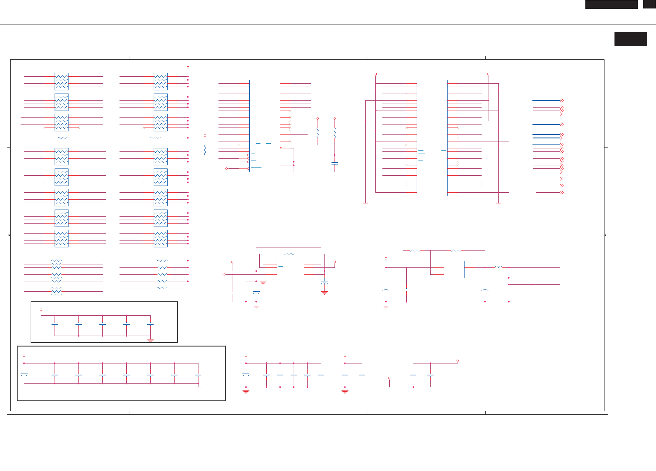
190TW8 TV 29
S-A04
A
A
B
B
C
C
D
D
E
E
44
3 3
2 2
1 1
D_DQM0
D_DQ3
D_CAS#
D_DQ10
D_DQ1
D_DQ2
D_DQ13
D_WE#
D_DQ9
D_DQ4
D_DQS0
D_DQ6
D_DQS1
D_BA0
D_DQ14
D_RA5
D_RA6
D_DQ0
D_BA1
D_RA4
D_DQ12
D_DQ15
D_DQ8
D_DQ5
D_DQ7
D_RA7
D_DQ11
DV25A
VREF
A_DQ1
A_RA3
A_RA7
A_RAS#
D_DQ8
A_DQ10
D_DQM0
D_CLK#
A_DQ4
D_DQ15
D_DQS1
D_WE#
D_CLK#
A_DQ14
A_RA11
D_DQ2
A_DQ0
D_CLK
D_RA11
D_DQ6
D_RA9
A_BA0
D_CLK
A_DQ5
A_CLK#
A_DQS1
A_DQ9
A_RA0
D_CAS#
A_RA4
A_DQ13
D_DQ3
D_DQ13
D_RA4
A_RA9
A_RA8
A_CS#
D_BA0
D_CKE
A_DQM0
D_DQS0
D_DQ7
A_DQ3
A_DQ8
A_RA5
D_DQ1
D_DQ12
A_RA1
D_RAS#
A_BA1
A_CAS#
D_DQ11
A_DQ12
A_DQS0
D_DQ5
D_RA8
A_DQ7
A_RA6
D_DQ0
D_DQ10
A_DQ2
A_RA2
D_CS#
A_CKE
A_WE#
D_DQ9
A_DQ11
A_DQ15
D_DQ4
D_DQ14
A_DQ6
A_CLK
D_RA0
D_RA1
D_RA2
D_RA3
D_RA7
D_RA6
D_RA5
A_RA10 D_RA10
F_A0
A_WE#
D_RA3
D_DQ1
D_CAS#
D_DQ5
F_A12
F_OE#
D_DQ12
F_D2
D_DQ10
D_CS#
D_RA1
D_CKE
D_RA8
F_A19
IOWR#
F_A20
F_A4
IOCE#
F_D5
D_RAS#
A_BA[0..1]
A_CS#
D_DQS1
D_DQ15
A_RAS#
F_D1
D_RA10
F_A21
A_DQM0
D_RA2
F_A16
F_A11
F_A13
D_DQ13
F_A18
A_RA[0..11]
D_DQ4F_A8
A_CKE
D_DQM0
F_A5
F_D3
F_D4
D_RA0
A_DQS1
F_A[0..21]
F_A7
A_DQ[0..15]
D_DQ3
D_DQ8
D_RA4
A_CLK
IOCE#
F_A1
D_RA5
F_A15
F_A6
F_D6
D_CLK
F_A9
F_A3
D_WE#
F_D7
D_RA7
A_CAS#
D_CLK#
IOWR#
D_DQ11
A_DQS0
F_A14
D_DQM0
D_DQ9
F_A2
F_D[0..7]
F_OE#
F_A10
D_DQ0
D_DQ6
VREF
D_RA9
A_CLK#
D_DQ2
FLASHVCC
VREF
F_D0
D_DQ14
D_DQS0
D_DQ7
D_RA6
D_RA11
F_A17
D1V25
D_RA0
D_RA2
D_RA1
D1V25
D_RA3
D_RA11
DV25A
DV25A
DV25B
D_BA0
D_BA1
D_RA10
D_BA1
D_RAS#
D_CS#
D_RA8
D_RA9
D1V25
VREF
D1V25 VREF DV25A
DV25B
SB33B
DV25B
DV25B
SB33B
DV25B
D1V25
SB33B
SB33B
VCC
D1V25
F_D[0..7] 4
IOCE# 4
A_DQ[0..15] 4
IOWR# 4
A_WE# 4
A_CKE 4
A_BA[0..1] 4
F_A[0..21] 4
F_OE# 4
A_DQM0 4
A_CAS# 4
A_RAS# 4
A_CLK 4
A_RA[0..11] 4
A_CLK# 4
A_CS# 4
A_DQS1 4
A_DQS0 4
VREF
4
0603 PUT ON NEARLY SDRAM
TSOP 48 pin
Must use 8bit type flash
Close To RN#
R363 75R/6
RN8 22R/8P4R
1
8
2
7
3
6
4
5
CB99
0.1uF/6
CB106
0.1uF/6
CB102
0.1uF/6
CB117
0.1uF/6
RN4 22R/8P4R
1
8
2
7
3
6
4
5
C244
0.1uF/6
RN1 22R/8P4R
1
8
2
7
3
6
4
5
+
CE51
10uF/25V
12
CB100
0.1uF/6
R52
0R/6
RN15 75R/8P4R
1
8
27
36
45
R364 150R/6
R359 75R/6
R59 22R/6
+
CE50
10uF/25V
12
CB114
0.1uF/6
R358 75R/6
+
CE8
330uF/25V
12
CB101
0.1uF/6
R58 22R/6
RN16 75R/8P4R
18
27
36
45
+
C233
10uF/25V
12
RN19 75R/8P4R
1
8
27
3
6
45
RN3 22R/8P4R
1
8
2
7
3
6
4
5
C232
3300pF/6
12
CB118
0.1uF/6
R362 75R/6
R357 4.7k/6
U29
AP1117ELA/TO252
ADJ/GND
1
VOUT 2
VIN
3
+
CE52
330uF/25V
12
R355 110/6F
+
CE54
330uF/25V
12
U27
IC LP2996 DDR Termination SOP8
SD
2GND
1
VSENSE
3
VREF
4VDDQ 5
AVIN 6
PVIN 7
VTT 8
R360 75R/6
CB38
0.01uF/6
CB108
0.1uF/6
12
R356 110R/6F
RN17 75R/8P4R
18
27
36
45
RN13 75R/8P4R
1
8
27
36
45
CB33
0.1uF/6
CB112
0.1uF/6
R56 22R/6
8M x 16
DDR
U28
M13L128168 8Mx16-5
VDD
1
DQ0
2
VDDQ
3
DQ1
4
DQ2
5
VSSQ
6
DQ3
7
DQ4
8
VDDQ
9
DQ5
10
DQ6
11
VSSQ
12
DQ7
13
NC
14
VDDQ
15
LDQS
16
NC
17
VDD
18
DNU
19
LDM
20
WE
21
CAS
22
RAS
23
CS
24
NC
25
BA0
26
BA1
27
A10/AP
28
A0
29
A1
30
A2
31
A3
32
VDD
33
VSS 66
DQ15 65
VSSQ 64
DQ14 63
DQ13 62
VDDQ 61
DQ12 60
DQ11 59
VSSQ 58
DQ10 57
DQ9 56
VDDQ 55
DQ8 54
NC 53
VSSQ 52
UDQS 51
NC 50
VREF 49
VSS 48
UDM 47
CK 46
CK 45
CKE 44
NC 43
A12 42
A11 41
A9 40
A8 39
A7 38
A6 37
A5 36
A4 35
VSS 34
RN14 75R/8P4R
1
8
27
36
45
CB39
0.01uF/6
RN6 22R/8P4R
1
8
2
7
3
6
4
5
C245
0.1uF/6
CB104
0.1uF/6
RN2 22R/8P4R
1
8
2
7
3
6
4
5
CB103
0.1uF/6
RN18 75R/8P4R
18
2
7
3
6
45
CB35
0.1uF/6
R54 22R/6
RN20 75R/8P4R
1
8
27
3
6
45
CB113
0.1uF/6
CB105
0.1uF/6
R53
10k/6
R367 47R/6
R365 22R/6
CB34
0.1uF/6
CB116
0.1uF/6
R366 47R/6
R57 22R/6
U11
29LV160
A0
25
A1
24
A2
23
A3
22
A4
21
A5
20
A6
19
A7
18
A8
8
A19
9
OE
28
BYTE 47
A18 16
D0 29
D1 31
D2 33
D3 35
A9
7
CE
26
D4 38
D5 40
D6 42
D7 44
D8 30
D9 32
A20
10
D11 36
D12 39
D13 41
D14 43
D15 45
VCC 37
GND1 27
WE
11
RY/BY
15
D10 34
GND2 46
A10
6
A12
4A11
5
A13
3
A14
2
A15
1
A16
48
A17
17 NC 13
RESET
12
WP/ACC 14
CB107
0.1uF/6
RN7 22R/8P4R
1
8
2
7
3
6
4
5
R55 22R/6
CB32
0.1uF/6
12
L59 Bead_121_4A/8
CB115
0.1uF/6
R361 75R/6
RN5 22R/8P4R
1
8
2
7
3
6
4
5
CB37
0.01uF/6
R51
10k/6
CB36
0.1uF/6
C232 C1
C233 C2
C244 E2
C245 D2
CB32 C3
CB33 A1
CB34 A1
CB35 A1
CB36 A1
CB37 B1
CB38 B1
CB39 B1
CB99 D1
CB100 C1
CB101 B2
CB102 D1
CB103 C1
CB104 B2
CB105 E2
CB106 C1
CB107 C1
CB108 E3
CB112 C1
CB113 C1
CB114 A1
CB115 A1
CB116 A1
CB117 A1
CB118 B1
CE8 A1
CE50 D2
CE51 D2
CE52 C2
CE54 B1
L59 E2
R51 C4
R52 C4
R53 B3
R54 A4
R55 A2
R56 A2
R57 A2
R58 A2
R59 A2
R355 D2
R356 D2
R357 C2
R358 B2
R359 B2
R360 B2
R361 B2
R362 B2
R363 B4
R364 A2
R365 A2
R366 A2
R367 A2
RN1 A4
RN2 A4
RN3 A4
RN4 A3
RN5 A3
RN6 A3
RN7 A3
RN8 A3
RN13 B4
RN14 B4
RN15 B4
RN16 B3
RN17 B3
RN18 B3
RN19 B3
RN20 B3
U11 C4
U27 C2
U28 D4
U29 D2
Schematic Diagram(Scaler Board - DDR & FLASH)
http://www.wjel.net
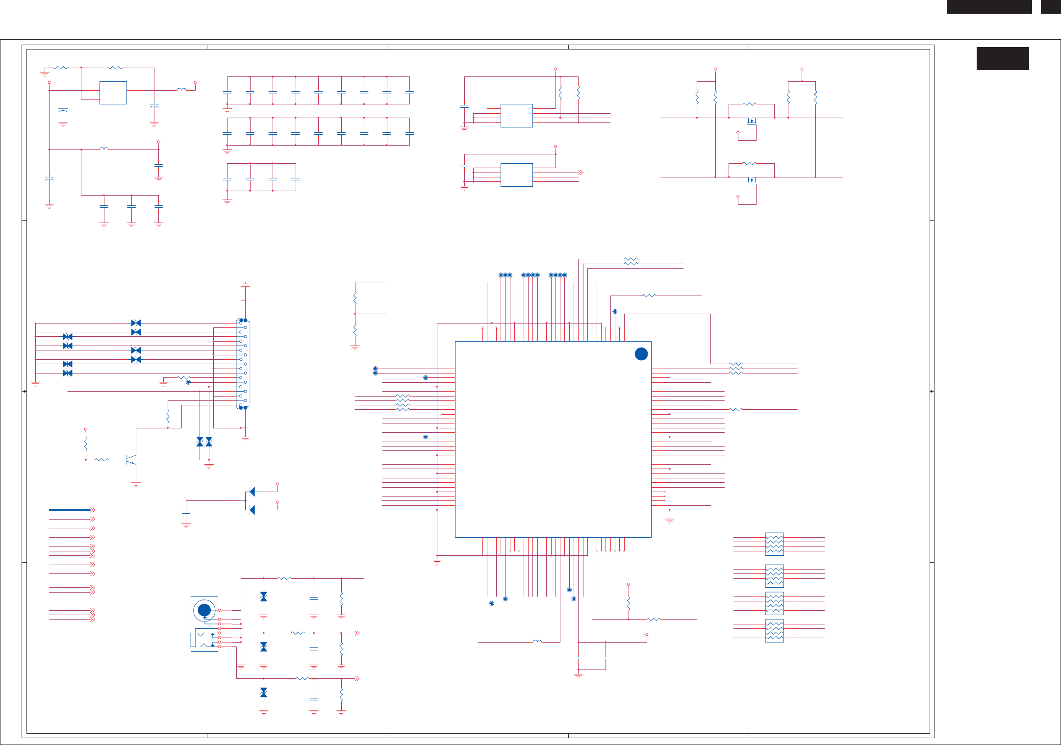
190TW8 TV 30
S-A05
A
A
B
B
C
C
D
D
E
E
4 4
33
2 2
1 1
HDMIODCK
KWP
VCC18
27MHZOSC_IN
HDMIRST#
DATA1+
DATA2+
DATA0+
CLOCK-
DATA2-
AVCC
PVCC
IOVCC
AVCC
AVCC
HDMIBCLK
HDMILRCK
IOVCC
DATA1-
CI2CA
VCC18
VCC18
Q2
Q4
Q10
Q12
IOVCC
Q7
HDMISD0
9993_SCL
Q3
CLOCK+
DATA0-
IOVCC
Q6
IOVCC
HDMIMCLK
PLUGPWR
VCC18
IOVCC
IOVCC
Q11
AVCC
VCC18
Q9
Q1
Q8
REGVCC
VCC18
VCC18
VCC18
VCC18
9993_SDA
Q5
IOVCC
Q0
Q15
SPDIF_OUT
DE_SOG
DATA0-
DATA1+
HDMICAB
CLOCK+
CLOCK-
DATA2+
DATA2-
DATA1-
DATA0+
HDMILRCK
DE_SOG
VI[0..15]
SCL
HDMIBCLK
27MHZ
HDMIODCK
HDMISD0
SDA
HDMIMCLK
IOVCC
CI2CA
GPIO24
VSYNC_DVI
HSYNC_DVI
DE_DVI
PVCC REGVCC
IOVCC
VCC18
IOVCC
DDC_SCL
DDC_WP_DE
PLUGPWR
VGA_R
DE_DVI
HSYNC_DVI
VSYNC_DVI
GPIO24
VI3
VI2
VI1
VI0
VI7
VI6
VI5
VI4
VI11
VI10
VI9
VI15
VI14
VI13
VI12
Q3
Q2
Q1
Q0
Q7
Q6
Q4
Q11
Q10
Q9
Q8
Q15
Q14
Q13
Q12
VI8
Q5
Q14
Q13
SDA
SCL
DDC_SCL
DDC_SCL
9993_SDA
DDC_SDA
AVCC
DDC_SDA
9993_SCLHDCP_SCL
HDCP_SDA
SPDIF
DDC_SDA
HDMI_PLUGPWR
HDCP_SDA
HDCP_SCL
KWP
SPDIF_OUT
VGA_L
DV33B
DV33B
DV33B
DV33B
AVCC
HDMI_PLUGPWR
VCC18
AVCC
HDMI_PLUGPWR
HDMI_PLUGPWR
AVCC
AVCC
VCC
PLUGPWR
SCL 2,4,8,11
VI[0..15] 4
HDMIODCK 4
HDMISD0 4
DE_SOG 4
HDMILRCK 4
HDMIBCLK 4
SDA 2,4,8,11
27MHZ 4
HDMIMCLK 4
GPIO24 4
DE_DVI 4
HSYNC_DVI 4
VSYNC_DVI 4
VGAIN_R 11
VGAIN_L 11
DDC_WP_DE 4,7
CB50
0.1uF/6
TP37
C64
0.1uF/6
1 2
R311
10k/6/NC
R386
39k/6/F
R343
4.7k/6/NC
CB59
0.1uF/6
QF4
2N7002/NC
2
13
R373 100R/6
R76 0R/6
R72
1k/6
R75
4.7k/6
CB66
0.1uF/6
R323 0R/6
Q9
2N3904
SOT23
2
1 3
R67 33R/6
C68
0.01uF/6
12
R318 10R/6
R74 33R/6
L12
Bead_121_4A/8 R340
4.7k/6
CB54
0.1uF/6
C236
10pF/6/NC
12
TP34
CB61
0.1uF/6
TP19
C67
0.1uF/6/NC
C235
0.1uF/6
12
C65
1000pF/6
12
CB68
0.1uF/6
RN10 33R/8P4R
1
8
27
36
45
CB52
0.1uF/6
D20
EZJZ0V800AA/NC
12
U14
24C02
NC
1
NC
2
NC
3
GND
4SDA 5
SCL 6
WP 7
VCC 8
PJ1
PHONE JACK+RCA
5
1
2
3
4
3N
2S
5G
TP20
CB64
0.1uF/6
QF5
2N7002/NC
2
13
CB62
0.1uF/6
CB56
0.1uF/6
CB63
0.1uF/6
R387
39k/6/F
TP33
D18
EZJZ0V800AA/NC
12
CB67
0.1uF/6
TP22
CB57
0.1uF/6
R388
47k/6/NC
R295 200R/6F
CB55
0.1uF/6
R399 22K/6/F
MT8293
U15
MT8293
LQFP128
CVCC18
66 CGND18
65
CGND18 126
RX2+
63
IOGND33 30
CVCC18 112
RX2-
62 AVCC
61
AGND
64
AVCC
57
AGND
60
AGND
56 RX0+
55 RX0-
54
AGND
52 RXC+
51 RXC-
50 AVCC
49
Q11 108
SD1
73
SPDIF
70
IOGND33
78
Q10 109
MCLK
79
CI2CA
38
IOGND33 118
XTALVCC
86
REGVCC
87
IOVCC33
68
Q4 117
MUTE
67
RSVD
48
CVCC18
45
IOGND33
69
IOVCC33 107
IOGND33 97
Q3 121
IOVCC33 120
CGND18 113
IOGND33 106
Q7 114
Q6 115
Q8 111
Q5 116
Q1 123
RX1-
58
RX1+
59
Q9 110
WS
75
SCK
76
VCNTL2 128
VCNTL1 1
VCNTL3 127
CEN 2
SOG_IN 3
OSC_IN 4
NC 5
IOVCC33 7
IOGND33 6
NC 8
KWP 9
KSDA 10
CGND18 13
ODCK 119
CVCC18 12
GPIO13 16
KSCL 11
GPIO14 15
GPIO12 17
GPIO11 20
GPIO10 21
GPIO9 22
IOVCC33 19
IOGND33 18
GPIO8 23
GPIO7 26
GPIO6 27
GPIO5 28
GPIO4 29
GPIO3 32
CVCC18 24
CGND18 25
CGND18
37 CVCC18
36
GPIO2
33
GPIO1
34
NC
35
INT
91
RESET#
89 RSVDL
88
SCDT
90
Q2 122
SD3
71
SD2
72
IOVCC33 98
PGND
46
PVCC
47
NC 14
IOVCC33 31
AVCC
53
CSDA
39
CSCL
40
DSDA
41
DSCL
42
NC
43
PWR5V
44
SD0
74
IOVCC33
77
CGND18
80
CVCC18
81
AUDPVCC18
82
AUDPGND
83
XTALOUT
84
XTALIN
85
Q23
92
Q22
93
Q21
94
Q20
95
Q19
96
Q18 99
Q17 100
Q16 101
Q15 102
Q14 103
Q13 104
Q12 105
Q0 124
CVCC18 125
D17 EZJZ0V800AA/NC
12
TP35
CB51
0.1uF/6
L13
Bead_121_4A/8
R398 22K/6/F
R70 0R/6/NC
P1
CON-HDMI
HDMI TYPE-A
1
2
3
4
5
6
7
8
9
10
11
12
13
14
15
16
17
18
19
2221
20 23
D16 EZJZ0V800AA/NC
12
R69 33R/6
R321 100R/6
CB69
0.1uF/6
RN11 33R/8P4R
1
8
2
7
36
4
5
TP18
CB49
0.1uF/6
+
CE11
47uF/16V
CAR250
TP28
R344
4.7k/6/NC
D21
EZJZ0V800AA/NC
12
R64
4.7k/6
CB47
0.1uF/6
R319 10R/6
R374 100R/6
U12
AP1117ELA/TO252
ADJ/GND
1
VOUT 2
VIN
3
TP31
R341
4.7k/6
R66
4.7k/6/NC
D10 EZJZ0V800AA/NC
12
D13 EZJZ0V800AA/NC
12
TP24
TP36
R68 33R/6
C61
1000pF/6
12
TP23
D14 EZJZ0V800AA/NC
12
C62
1000pF/6
12
CB48
0.1uF/6
R322 100R/6
D19
EZJZ0V800AA/NC
12
RN12 33R/8P4R
18
2
7
3
6
4
5
TP32
TP26
R294 100/6F
R65 0R/6
CB65
0.1uF/6
TP29
D50
EZJZ0V800AA/NC
12
R324 0R/6
R332
10k/6
C63
1000pF/6
12
D15 EZJZ0V800AA/NC
12
R73
1k/6
C66
1000pF/6
12
CB58
0.1uF/6
D12 EZJZ0V800AA/NC
12
R333
10k/6
+
CE9
47uF/16V
12
TP38
D11 EZJZ0V800AA/NC
12
L14
Bead_121_4A/8
C237
0.1uF/6
12
TP21
R71 33R/6
U13
24C04
NC
1
NC
2
NC
3
GND
4SDA 5
SCL 6
WP 7
VCC 8
TP25
TP27
+
CE10
47uF/16V
12
CB53
0.1uF/6
TP30
CB60
0.1uF/6
RN9 33R/8P4R
1
8
27
36
45
D9
BAT54C
C61 B4 R67 D3
C62 C4 R68 D3
C63 B4 R69 D3
C64 C4 R70 A3
C65 B4 R71 D2
C66 B4 R72 A2
C67 A2 R73 A2
C68 D1 R74 B1
C235 B1 R75 D1
C236 B1 R76 D1
C237 B1 R294 A4
CB47 B4 R295 A4
CB48 B4 R311 A2
CB49 B4 R318 C2
CB50 B4 R319 C2
CB51 B4 R321 C2
CB52 B4 R322 C2
CB53 B4 R323 D4
CB54 C4 R324 D4
CB55 B4 R332 C4
CB56 B4 R333 D4
CB57 B4 R340 D4
CB58 B4 R341 D4
CB59 B4 R343 E4
CB60 B4 R344 E4
CB61 B4 R373 D3
CB62 C4 R374 D3
CB63 A4 R386 B1
CB64 B4 R387 B1
CB65 B4 R388 B1
CB66 A4 R398 B1
CB67 A4 R399 B1
CB68 A4 RN9 E2
CB69 D1 RN10 E1
CE9 A4 RN11 E1
CE10 A4 RN12 E1
CE11 A4 TP18 C3
D9 B2 TP19 C3
D10 A3 TP20 C3
D11 A3 TP21 C3
D12 A3 TP22 C3
D13 A3 TP23 C3
D14 A3 TP24 C3
D15 A3 TP25 C3
D16 A3 TP26 C3
D17 A3 TP27 C3
D18 A2 TP28 C3
D19 A2 TP29 D3
D20 B1 TP30 B3
D21 B1 TP31 B3
D50 B1 TP32 C3
L12 A4 TP33 A3
L13 A4 TP34 C2
L14 C1 TP35 C1
P1 B3 TP36 C1
PJ1 A1 TP37 D1
Q9 A2 TP38 C1
QF4 E4 U12 A4
QF5 E4 U13 C4
Schematic Diagram(Scaler Board - )HDMI INPUT-MT8293
http://www.wjel.net

190TW8 TV 31
S-A06
A
A
B
B
C
C
D
D
E
E
44
3 3
2 2
1 1
RP
VGASCL
VGASOG
GP
VGASDA
BP
VGASCL
RN
GN
BN
DDC_WP_DE
VGAVSYNC#
VGASDA
VGASCL
PW_KEY
RST
GPIO5
GPIO6
VGA_PLAG
VGAHSYNC#
VGASDA
HSYNC# BLUE
VGASDA_IN
HSYNC#
VSY NC#
RED_GND
GREEN
GREEN
BLUE
GRN_GND
RED
VSY NC#
BLU_GND
RED
VGA_PLUGPWR
VGASCL_IN
BLU_GND
GRN_GND
RED_GND
TXD
RXD
IR
VSY NC#
HSYNC#
VGASCL_IN
VGASDA_IN
SCL0
SDA0
VGA_PLAG
+3.3V
+3.3V
+3.3V
VCC
VGA_PLUGPWR
+5V_IN
+3.3V
+3.3V
VGA_PLAG
VGA_PLAG
VGA_PLAG
VGA_PLUGPWR
5VSB
SB33B
RN 4
GN 4
BN 4
BP 4
GP 4
RP 4
VGASOG 4
VGAHSYNC# 4
VGAVSYNC# 4
Control_Power 2
GPIO54
GPIO6
4
DDC_WP_DE 4,6
ERO0_UP3_0 4
TXD 4
RXD4
IR4,14
PW_KEY4,14
SCL04
SDA0
4
L:WPDISABLE
VGA IN
H:WPENABLE
S0 S1
0
1
0
1 B3,A3
STATUS
SDA/SCL
TXD/RXD
OUTPUT
B3,A3
11/28 add
D29
EZJZ0V800AA/NC
12
R108 0R/6/NC
C78
5pF/6
12
C80
1uF/6/NC
R1010R/6/NC
Y2
24MHz/NC
1 2
R119 0R/6/NC
D25
EZJZ0V800AA/NC
12
+
C198
10uF/25V/NC
12
C79
0.01uF/6
1 2
C76
0.1uF/6/NC
R105 510R/6
R136 0R/6/NC
D23
EZJZ0V800AA/NC
12
R106 0R/6/NC
R85
10k/6
R316
0R/6
L16 FB/6
CB70
0.1uF/6
C74
5pF/6
12
R314
0R/6/NC
R83 0R/6
R134 0R/6/NC
C202
33pF/6
R292 330R/6F/NC
R122 0R/6/NC
R138 0R/6/NC
R81
75R/6F
R78 68R/6
L17 FB/6
R133 0R/6/NC
C70
5pF/6
12
R990R/6/NC
R139 0R/6/NC
U17
24C02
NC
1
NC
2
NC
3
GND
4SDA 5
SCL 6
WP 7
VCC 8
L47
Bead_121_4A/8/NC
R297 100R/6
P2
D-SUB15
DCN15VGA-15P
1617
1
2
3
4
5
6
7
8
9
10
11
12
13
14
15
C258
0.1uF/6/NC
R88100R/6
R124 0R/6/NC
R131 0R/6/NC
R77
10k/6
C72
4.7nF/6
1 2
R315 0R/6/NC
R1030R/6/NC
R125 0R/6/NC
D26
BAT54C
R107
2k/6
R130 0R/6/NC
R137 0R/6/NC
R980R/6/NC
R120 0R/6/NC
R82 100R/6
R118 0R/6/NC
R1040R/6/NC
R115 0R/6/NC
R132 0R/6/NC
C73
0.01uF/6
1 2
C203
33pF/6
R80100R/6
R113 0R/6/NC
C75
0.01uF/6
1 2
C201
0.1uF/6/NC
R94
0R/6/NC
D22
EZJZ0V800AA/NC
12
R95
4.7k/6/NC
C77
0.01uF/6
1 2
R296 100R/6
D24
EZJZ0V800AA/NC
12
R84 68R/6
R302 10k/6
R377 0R/6
R111 0R/6/NC
C81
10pF/6/NC
R90 68R/6
R91
75R/6F
R87 0R/6/NC
C71
0.01uF/6
12
R93
10k/6/NC
R123 0R/6/NC
R92 100R/6
R79 0R/6/NC
R293 200/6F/NC
U23
AP1117ELA/TO223/NC
ADJ/GND
1
VOUT 2
VIN
3
D27
EZJZ0V800AA/NC
12
R96
82K/6/NC
R126 510R/6
R86
75R/6F
R135
2k/6
D28
EZJZ0V800AA/NC
12
RTD2120L
U16
RTD2120L/NC
P5.0/PWM0
44
P5.1/PWM1
45
P5.2/PWM2
46
P5.3/PWM3
47
P5.4/PWM4
48
P5.5/PWM5
1
DSCL2/P5.6
2
DSDA2/P5.7
3
RST 4
ASDA/P3.1/TXD
8
XO
15
XI
16
VSS
17
VCC 41
P1.0/T2 40
P1.1 39
P1.2 38
P1.3 37
P1.4 36
P1.5 35
P1.6 34
P1.7 33
NC
19
VSYNC 28
NC 32
P6.0/ADC0 20
P6.1/ADC1 21
P6.2/ADC2 22
P6.3/ADC3 23
P6.4 24
P6.5 25
P6.6/CLKO1 26
P6.7 27
ASCL/P3.0/RXD
5
P3.2/INT0
9
P3.3/INT1
10
P3.4/T0
11
P3.5/T1
12
P7.6/CLKO2
13
P7.7
14
NC
18
NC
6
NC
7
NC 42
NC 43
NC 29
NC 30
NC 31
R127 0R/6/NC R128 0R/6/NC
R129 0R/6/NC
R317 0R/6
R97
4.7k/6/NC
C69
0.01uF/6
1 2
R144
10k/6/NC R145
6.8K/6/NC
L15 FB/6
U24
CD4052
SOP16
B0
1
B2
2
BN
3
B3
4
B1
5
INH
6
VEE
7
GND
8S1 9
A2 15
A1 14
AN 13
A3 11
A0 12
VCC 16
S0 10
R1020R/6/NC
R109 0R/6/NC
+
C200
10uF/25V/NC
12
C199
0.1uF/6/NC
R1000R/6/NC
C82
10pF/6/NC
R117 0R/6/NC
R89 100R/6
R121 0R/6/NC
C69 D4 R97 C2
C70 D4 R98 D2
C71 D4 R99 D2
C72 D4 R100 D2
C73 D4 R101 D2
C74 D4 R102 D2
C75 D3 R103 D2
C76 B3 R104 D2
C77 D3 R105 A2
C78 D3 R106 C2
C79 D3 R107 A2
C80 C2 R108 C2
C81 D1 R109 C2
C82 D1 R111 C2
C198 B1 R113 C2
C199 B1 R115 C2
C200 C1 R117 C2
C201 C1 R118 D2
C202 A2 R119 C2
C203 A1 R120 D2
C258 B3 R121 D2
CB70 A1 R122 C2
D22 C4 R123 D2
D23 B4 R124 C2
D24 C4 R125 D2
D25 B3 R126 A2
D26 B3 R127 C2
D27 C3 R128 D2
D28 A2 R129 C2
D29 A2 R130 D2
L15 D4 R131 C2
L16 D4 R132 D2
L17 D3 R133 C2
L47 C1 R134 D2
P2 B4 R135 A1
R77 A4 R136 D1
R78 D4 R137 C1
R79 A4 R138 D1
R80 A4 R139 C1
R81 D4 R144 A1
R82 D4 R145 D1
R83 D4 R292 B1
R84 D4 R293 C1
R85 A4 R296 A2
R86 D4 R297 A2
R87 A4 R302 B3
R88 A4 R314 A3
R89 D3 R315 B3
R90 D3 R316 A3
R91 D3 R317 B3
R92 D3 R377 B3
R93 D3 U16 D2
R94 D2 U17 A1
R95 C2 U23 C1
R96 C2 U24 A3
Y2 D1
Schematic Diagram(Scaler Board - VGA IN & AUDIO IN)
http://www.wjel.net
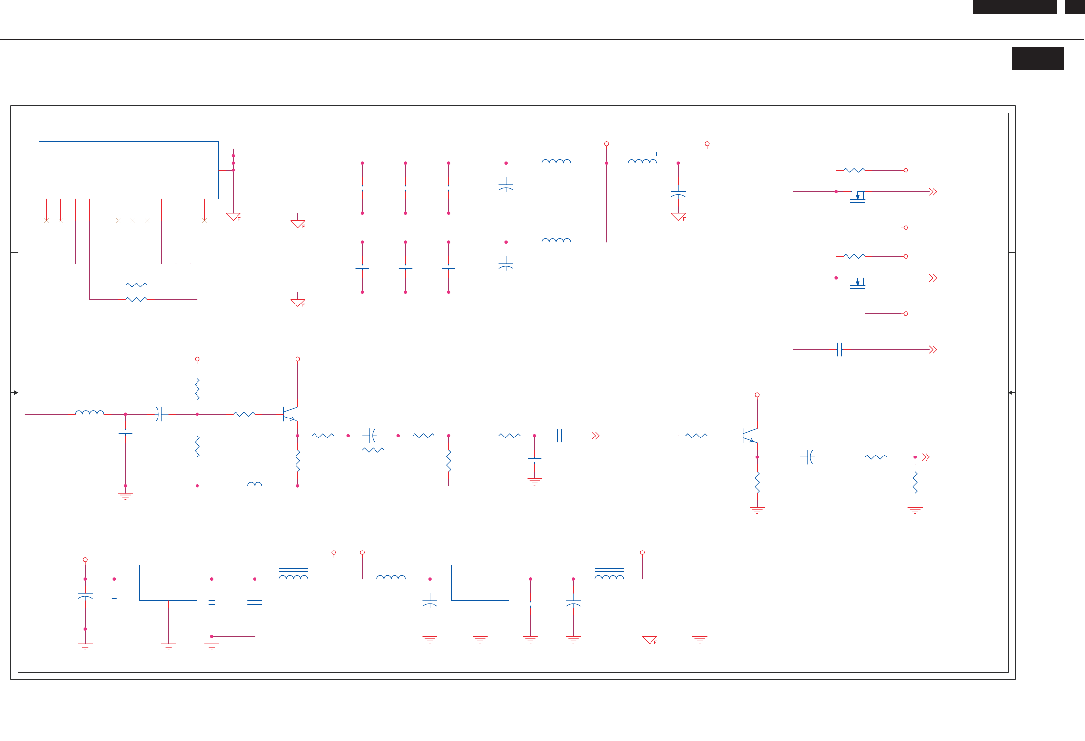
190TW8 TV 32
S-A07
C83 B4
C84 C4
C85 B3
C86 C3
C87 A3
C88 C3
C89 C3
C90 E3
C204 A3
C205 A3
C206 B3
C207 A3
C208 C3
C209 C3
C210 C3
CB71 B4
CB72 B3
CE12 C4
CE13 D4
CE14 C3
CE15 A3
CE16 B3
CE55 D3
L18 C4
L19 C4
L20 A3
L21 B3
L48 B3
L49 D4
L50 C3
L51 B3
Q10 B3
Q34 D3
QF1 E4
QF2 E3
R146 A3
R147 B3
R148 B3
R149 C3
R150 C3
R151 A3
R152 B3
R153 B3
R154 C3
R155 E4
R156 E3
R329 A3
R330 A3
R393 D3
R394 E3
R395 E3
R396 D3
U18 A4
U25 A3
U26 C3
A
A
B
B
C
C
D
D
E
E
4 4
33
22
1 1
TU_AV1 TU_CVBS
VS_TUNER
VS_IF
VIN
TU_SDA_IN
TU_AV1
TUMPX1
VS_IF
VS_TUNER
MPX1
TU_SCL
TUMPX1
TU_SDA SDA
SCL
TU_SCL_IN
TU_SDA
TU_SCL
VIN
VCC
VCC
+5Vt
VCC
DV33A
VCC
DV33A
+12V
+8V
+5Vt
+8V
VCC
VCC
CVBS1 4
SCL 2,4,6,11
SDA 2,4,6,11
MPX1 4
SCART_CVBS_OUT 10
N-MOSFET
N-MOSFET
C89
330pF/6
12
L51
Bead_121_4A/8/NC
CB72
0.1uF/6
C85
3300pF/6
12
R394
18R/6
L19
10uH
RC1206
QF1
2N7002
2
13
R151
10k/6
C210
0.1uF/6/NC
C205
0.1uF/6/NC
C84
1uF/6
12
+
C208
100uF/16V/NC
CB71
0.1uF/6
Q10
2N3904
2
1 3
+
CE55
330uF/25V/NC
R395
56R/6
L20
2.2uH/8
C87
1uF/6/NC
12
+
C206
22uF/25V/NC
+
C209
10uF/16V/NC
R154
56R/6
L50
Bead_121_4A/8/NC
R153
75R/6F
R146
3.3k/6
R396
75R/6F
Q34
2N3904
2
1 3
L49
Bead_121_4A/8
C204
100uF/16V/NC
R150
0R/6
R152
0R/6
U18
FQ1216ME
NC/VTout
2
Vb(+5V)
3
SCL
4
SDA
5
AS
6
2ndIFout
11
CVBSout
12
VIF(+5V)
13
AFout
14
AF-R
9
TH1 17
TH2 18
TH3 15
TH4 16
NC/AGC
1
AF-L
10
U26
7805/NC
GND
2
OUT 3
VIN
1
R329 100R/6
+
CE14
330uF/25V
12
QF2
2N7002
2
13
R156 10k/6
L48
Bead_121_4A/8/NC
L21
Bead_121_4A/8
+
CE13
330uF/25V
12
C90
0.01uF/6
U25
7808/NC
GND
2
OUT 3
VIN
1
+
CE12
330uF/25V
12
C88
47nF/6
1 2
R155 10k/6
C83
3300pF/6
12
C207
0.1uF/6/NC
R393
10R/6
C86
1uF/6
12
+
CE16
330uF/25V/NC
R147
10R/6
+
CE15
330uF/25V
1
2
R149
18R/6
L18
10uH
RC1206
R148
75R/6F
R330 100R/6
Schematic Diagram(Scaler Board - )TUNER
http://www.wjel.net

190TW8 TV 33
S-A08
A
A
B
B
C
C
D
D
E
E
44
33
22
11
CVBS0_IN
AV_SY0
AV0_IN
AV0_GND
SC0_IN
SY0_GND
SY0_IN
SC0_GND
AVSVL
AVSVR
AV_SC0
AVSVR
AV0_GND
AV0_IN
SY0_IN
SY0_GND
SC0_IN
SC0_GND
AVSVL
CVBS0 4
SY0 4
SC0 4
AV0SY0_L 11
AV0SY0_R 11
L22
0R/6
R162
56R/6
FB6
0R/6
C104
330pF/6
12
C92
330pF/6
C99
330pF/6/NC
L23
0R/6
D34
EZJZ0V800AA/NC
12
C100
330pF/6/NC
FB7
0R/6
C98
330pF/6
12
GG
CY
CN2
S-VIDEO +RCA
TEKCON_RCAJACK-SJACK
1
2
3
4
5
7
6
8
9
10
C95 47nF/6
1 2
D31
EZJZ0V800AA/NC
12
R158
75R/6F
L25
0R/6
C94
330pF/6
12
L26
0R/6
FB5
0R/6
R159
0R/6
C96
330pF/6
C93
330pF/6
C91 47nF/6
1 2
R402
47K/6/NC
D32
EZJZ0V800AA/NC
12
R161
18R/6
R160
75R/6F
C97
330pF/6
R157
0R/6
C106
330pF/6/NC
C101 47nF/6
1 2
C102
330pF/6/NC
L24
0R/6
C105
330pF/6/NC
R401
47K/6/NC
C103
330pF/6/NC
D33
EZJZ0V800AA/NC
12
D30
EZJZ0V800AA/NC
12
C91 E4
C92 C4
C93 D4
C94 E4
C95 E3
C96 C3
C97 D3
C98 E3
C99 A3
C100 B3
C101 E2
C102 C2
C103 D2
C104 E2
C105 A2
C106 B2
CN2 A4
D30 B4
D31 A3
D32 A2
D33 B3
D34 B2
FB5 D4
FB6 D3
FB7 D2
L22 C4
L23 C3
L24 B3
L25 C2
L26 A2
R157 D4
R158 D4
R159 D3
R160 D3
R161 D2
R162 D2
R401 A3
R402 A2
Schematic Diagram(Scaler Board - AV/SV/AUDIO)
http://www.wjel.net

190TW8 TV 34
S-A09
A
A
B
B
C
C
D
D
E
E
4 4
3 3
2 2
1 1
SY0
SCART_SC1_IN
SCT1_AUL_OUT
AVR_OUT
AVL_OUT
AVPR1 N
SCART_FB
AVPR1P
Y1N
Y1P
SCT1_AUR_OUT
PR1P
SCT1_AUR_IN
SCT1_AUL_OUT
AVY1N
PR1N
SCT1_B_GND
SCT1_AUL_IN
SCT1_B_IN
SCT1_FS_IN
SCT1_G_GND
SCT1_G_IN
SCT1_R_GND
SCT1_R_IN
SCART_FB
SCT1_AUR_IN
SCT1_AVO_GND
SCT1_AVI_GND
SCT1_AV_OUT
SCT1_AV_IN
PB1NAVPB1N
SCT1_FS_IN
AVPB1P PB1P
SCT1_CVBS
SCT1_AV_OUT
SCT1_AUL_IN
SC1
SOY_SYNC
ADC_IN0
IO_SW1
CVBS_SYNC
AVY1P
CVBS_SYNC SOY_SYNC
AVY1P
SOY1
AVPR1P
SCT1_AV_IN
SCT1_AVI_GND
SCT1_B_GND
SCT1_B_IN
SCT1_AUR_OUT
SCT1_G_GND
SCT1_G_IN
SCT1_R_GND
SCT1_R_IN
VCC
VCC
PB1P 4
PR1N 4
Y1N 4
Y1P 4
PB1N 4
PR1P 4
SOY1 4
CVBS2 4
SC1 4
SCT1_AUR_IN 11
AVR_OUT 11
SCT1_AUL_IN 11
AVL_OUT 11
ADC_IN0 4
SCART_FB 4
IO_SW1
SCART_CVBS_OUT8
AV / Y IN
SCART PIN8 VIDEO STATUS
TV MODE:0V~2V
WIDESCREEN MODE(16:9):4.5V~7.0V
TV MODE(4: 3):9.5V~12V COMPONSITE MODE:0V~0.4V
RGB MODE:1V~3V
SCART PIN16 RGB STATUS
SCART FUNCTION SELECTION
SCART1 AUDIO BYPASS OUT SCART AUDIO INPUT
RGB/C IN BYPASS VIDEO OUTPUT
C107
4.7nF/6
12
C240
0.1uF/6/NC
12
C118
15pF/6
12
R175 100R/6
R389
47k/6/NC
+
CE18
330uF/25v
R171
75R/6F
R179 0R/6
R166
47k/6/NC
R163 0R/6
Q11
2N3904
2
1 3
C262
330pF/6
12
Q30
2N3906
2
13
L30
0R/6
D42
EZJZ0V800AA/NC
12
C112
0.01uF/6
1 2
R169
47k/6/NC
R181 33k/6
R392
75R/6F
P3
SCART
2
4
6
8
10
12
14
16
18
20
1
3
5
7
9
11
13
15
17
19
21
2223
R176 68R/6
C117
0.01uF/6
12
C121
0.01uF/6
1 2
R1680R/6
R1640R/6
D43
EZJZ0V800AA/NC
12
R390
47k/6/NC
R185
1k/6
C109
330pF/6/NC
C125
330pF/6/NC
U30
NC7SB3157
B1
1
GND
2
B0
3
A4
VCC 5
S6
L75
FB/8
1 2
C108
47nF/6
1 2
D41
EZJZ0V800AA/NC
12
R409
0R/6
R165 18R/6
D40
EZJZ0V800AA/NC
12
R178 100R/6
L28
0R/6
R170 68R/6
R184
75R/6F
D35
EZJZ0V800AA/NC
12
C114
330pF/6/NC
+
CE17
10uF/25V
R375
470/6
CB73
0.1uF/6
12
C111
330pF/6
12
FB8
0R/6
D45
EZJZ0V800AA/NC
12
C122
0.01uF/6
1 2
C127
47nF/6
1 2
C113
15pF/6
12
C116
0.01uF/6
1 2
R172 100R/6
R183
10k/6
R173 68R/6
C241
0.1uF/6/NC
12
C261
1uF/6
12
C128
330pF/6
12
D37
EZJZ0V800AA/NC
12
C120
330pF/6/NC
C119
330pF/6/NC
C124
330pF/6/NC
R371
0R/6F/nc
D36
EZJZ0V800AA/NC
12
L27
0R/6
C123
15pF/6
12
C115
330pF/6/NC
R186
75R/6F
+
CE49
330uF/25v
R376
75R/6F
C239
0.1uF/6/NC
12
D38
EZJZ0V800AA/NC
12
L29
0R/6
C259
0.1uF/6
R180
1k/6
D44
EZJZ0V800AA/NC
12
R372
0R/6F/NC
R177
75R/6F
D39
EZJZ0V800AA/NC
12
R167
56R/6
C238
0.1uF/6/NC
12
R408
0R/6/NC
R174
75R/6F
C260
1uF/6
12
C110
330pF/6/NC
C126
0.01uF/6
1 2
C107 D4
C108 D4
C109 B4
C110 B4
C111 C4
C112 D3
C113 C3
C114 B3
C115 B3
C116 D3
C117 D2
C118 C2
C119 B2
C120 B2
C121 D2
C122 D1
C123 C1
C124 B1
C125 B1
C126 D1
C127 D2
C128 D2
C238 E2
C239 E2
C240 E3
C241 E3
C259 A4
C260 A4
C261 A4
C262 A4
CB73 E2
CE17 E2
CE18 E1
CE49 E1
D35 D3
D36 B4
D37 D2
D38 B3
D39 E3
D40 B2
D41 E3
D42 B1
D43 E4
D44 E4
D45 E1
FB8 B4
L27 B4
L28 B3
L29 B2
L30 B1
L75 A4
P3 A3
Q11 E1
Q30 E2
R163 C4
R164 E3
R165 B4
R166 E3
R167 C4
Schematic Diagram(Scaler Board - )SCART FULL FUNCTION
http://www.wjel.net
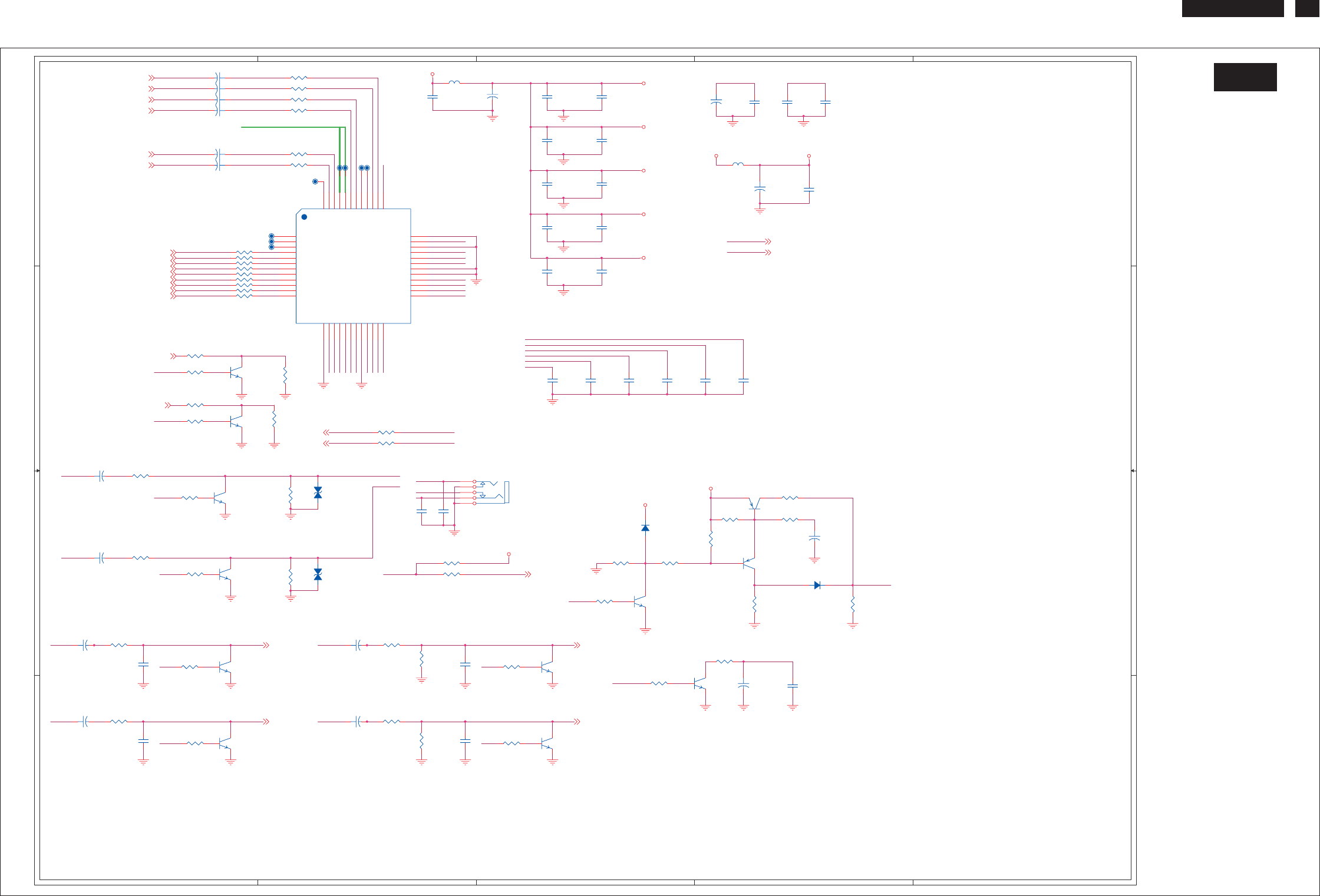
190TW8 TV 35
S-A10
A
A
B
B
C
C
D
D
E
E
44
33
2 2
1 1
HPOUT_R
A_MUTE
HPOUT_L HPOUTL
HPOUTL
+12VAUDIO
GPIO17
AIN1R
AIN1L
HPVDD
VMIDDAC
ADCREFP
VMIDADC
AIN3R
AIN5R
AIN5L
AIN3L
HPOUT_L
SCL14
MUTE
DACV33
DVDD
ADCV33
SDA14
HPOUT_R
HPVDD
HPGND
DACREFP
AOBCLK1
AOSDATA1
AOMCLK1
AOLRCK1
RESET_8291
VMIDADCVMIDDAC
AR
AL
SDA14
SCL14
SDA
SCL
VOUT0R
VOUT0L
AOSDATA3
ADIN
GPIO8_BCLK
GPI O7_LRCK
GPIO9_MCLK
RESET_8291
HPOUTL
HPDET#
A_MUTE
ADCGND
DACREFN
ADCREFN
DACGND
AOBCLK1
AOLRCK1
AOMCLK1
GPIO8_BCLK
GPI O7_LRCK
GPIO9_MCLK
HPOUTRHPOUTRA_MUTE
HPOUTR
A_MUTE
A_MUTE
MUTE
A_MUTE
VMIDDAC
OFF_MUTE
GPIO17
A_MUTE
DACREFP
ADCV33
DVDD
VOUT0L
A_MUTE
A_MUTE
VOUT0R
GPIO23HPDET#
HPOUTR
AR
AL
OFF_MUTE
DACV33
ADCREFP
HPVDD
+12VAUDIO HPVDD
+12VAUDIO
ADCREFP
DACV33
DVDD
ADCV33
DACREFP
DV33B
DV33B
VCC
AVR_OUT 1 0
+12VAUDIO 2,13
SCT1_AUR_IN10
SCT1_AUL_IN
10
VGAIN_R6
VGAIN_L6
AV0SY0_L9
AV0SY0_R9
SCL2,4,6,8
SDA2,4,6,8
AOBCLK14
AOLRCK14
AOMCLK14
AOSDATA14
AOSDATA34
GPIO8_BCLK4
GPIO7_LRCK4
GPIO9_MCLK4
ADIN4
ERO3_GPIO4
8291_MUTE4
AVL_OUT 10
AMP_R 13
AMP_L 13
GPIO17 4
GPIO23 4
HEADPHONE AUDIO OUTPUT
SCART AUDIO OUT AUDIO AMP
CB80
0.1uF/6
CC0603
Q32
2SD2653K
2
1 3
R342
4.7k/6/NC
+
CE22
100uF/16V
12
R202 33R/6
CB76
0.1uF/6
CC0603
+
CE136
10uF/25V
CAR200
1 2
Q27
2SD2653K
2
1 3
R410
3.3k/6
R205 33R/6
R197 33R/6
+
CE29 10uF/25V
12
R335
47k/6
CB88
0.1uF/6
12
Q13
2N3904/NC
SOT23
2
1 3
R350 5.1k/6
R201 33R/6
CB84
10pF/6/NC
12
Q17
2SD2653K
2
1 3
C216
4.7nF/6
1 2
R187 34.5K/6
R345
470R/6
R384
470R/6
Q16
2SD2653K
2
1 3
R404 5.6k/6/NC
C B 111
0.1uF/6
+
C137
10uF/25V
12
C218
4.7nF/6
1 2
R203 33R/6
R221 0R/6
R411
3.3k/6
CB78
0.1uF/6
CC0603
R190 34.5K/6
+
CE20 10uF/25V
1
2
R406 20/6
L31 Bead_121_4A/8
RC0805
R336 10K/6/NC
R196 34.5K/6
CB85
10pF/6/NC
12
R339
200R/6
CB75
0.1uF/6
CC0603
R337 10K/6
+
CE135
10uF/25V
CAR200
1 2
R382
1k/6
CB87
0.1uF/6
12
Q28
2N3904
2
1 3
R407
4.7k/6
CB74
0.1uF/6
CC0603
CB89
0.1uF/6
12
TP42
R230 1k/6
+
CE35
10uF/25V
CAR200
1 2
R199 33R/6
R326
100k/6
R346
470R/6
+
CE23 10uF/25V
12
CB86
10pF/6/NC
12
D49
4148
R403 5.1k/6/NC
+
CE53
33uF/25V
CAR315
C217
4.7nF/6
1 2
CB77
0.1uF/6
CC0603
R195 34.5K/6
Q29
2SD2653K/NC
2
1 3
R383
1k/6
R206 100R/6
R204 33R/6
R207 100R/6
+
CE28 10uF/25V
12
+
CE31
330uF/25V
CAR315
+
CE25 10uF/25V
12
Q12
2N3906
2
1 3
R338
47k/6
R189 34.5K/6
CB83
10pF/6/NC
12
CB98
0.1uF/6
12
+
CE21 10uF/25V
12
R218
10k/6
TP40
D46
EZJZ0V800AA/NC
12
+
CE24
33uF/25v
R222 1k/6
R217 1k/6
D61
4148/NC
Q18
2SD2653K
2
1 3
Q15
2N3906
2
13
+
CE30
330uF/25V
CAR315
1 2
R385
470R/6
CB82
10pF/6/NC
12
R347
470R/6
C134
10uF/10V/8
CC0805
R198 33R/6
C131
10uF/10V/8
CC0805
CB79
0.1uF/6
CC0603
TP39
TP41
TP43
C132
10uF/10V/8
CC0805
CB81
10pF/6/NC
12
+
CE32
330uF/25V
CAR315
1 2
Q33
2SD2653K
2
1 3
L32
Bead_121_4A/8
R210 100R/6
R235 1k/6
R200 33R/6
C219
4.7nF/6
1 2
R216
1k/6/NC
R349 1k/6
R209 100R/6
Q14
2SD2653K
2
1 3
TP54
C133
10uF/10V/8
CC0805
R208
4.7k/6
D47
EZJZ0V800AA/NC
12
R220 47k/6
R405 20/6
C129
10uF/10V/8
CC0805
+
CE37
10uF/25V
CAR200
12
U19
MT8291
AIN6L
1
AIN7R
2
AIN7L
3
BCLK0
4
LRCK0
5
MCLK0
6
DIN0
7
DIN1
8
BCLK1
9
LRCK1
10
MCLK1
11
DOUT
12
DGND
13
DVDD
14
RESET#
15
MUTE#
16
DI
17
CL
18
HPOUTL
19
HPGND
20
HPVDD
21
HPOUTR
22
VOUT0L
23
VOUT0R
24
VOUT1L 25
VOUT1R 26
AVDD 27
VMIDDAC 28
DACGND 29
DACREFN 30
DACREFP 31
DAV33 32
VIMDADC 33
ADCREFN 34
ADCREFP 35
ADCGND 36
ADCV33 37
AIN1R 38
AIN1L 39
AIN2R 40
AIN2L 41
AIN3R 42
AIN3L 43
AIN4R 44
AIN4L 45
AIN5R 46
AIN5L 47
AIN6R 48
R351 2k/6
AJ1
ZD005D100
5
4
3
2
1
C130
10uF/10V/8
CC0805
TP44
R188 34.5K/6
TP55
AJ1 C2 Q32 C2
C129 C4 Q33 C1
C130 D4 R187 B4
C131 C4 R188 B4
C132 C4 R189 B4
C133 C4 R195 B4
C134 C3 R196 B4
C137 D4 R197 A4
C216 A2 R198 A4
C217 A1 R199 A4
C218 B1 R200 A4
C219 B2 R201 A3
CB74 C4 R202 A3
CB75 D4 R203 A3
CB76 D4 R204 A3
CB77 C4 R205 A3
CB78 C4 R206 A3
CB79 C4 R207 A3
CB80 C3 R208 B3
CB81 C3 R209 B3
CB82 C3 R210 B3
CB83 C3 R216 C2
CB84 C3 R217 A2
CB85 D3 R218 D2
CB86 D3 R220 B2
CB87 B2 R221 B2
CB88 B2 R222 A2
CB89 D4 R230 A2
CB98 D1 R235 A1
CB111 B4 R326 D2
CE20 A4 R335 B2
CE21 A4 R336 A3
CE22 C4 R337 A3
CE23 A4 R338 B2
CE24 D4 R339 D2
CE25 A4 R342 B3
CE28 A4 R345 A2
CE29 A4 R346 A1
CE30 A2 R347 D2
CE31 D2 R349 D2
CE32 A2 R350 D2
CE35 A2 R351 D2
CE37 A1 R382 C2
CE53 D1 R383 C1
CE135 B2 R384 B2
CE136 B1 R385 B1
D46 B2 R403 C2
D47 B2 R404 C2
D49 D2 R405 A2
D61 C2 R406 A2
L31 B4 R407 C1
L32 D4 R410 B2
Q12 D2 R411 B1
Q13 C2 TP39 B4
Q14 A2 TP40 B4
Q15 D2 TP41 B4
Q16 A2 TP42 B4
Q17 A2 TP43 B4
Q18 A1 TP44 B4
Schematic Diagram(Scaler Board - MT8291/AUDIO CODEC)
http://www.wjel.net

190TW8 TV 36
S-A11
A
A
B
B
C
C
D
D
E
E
44
33
2 2
1 1
CLK1P
CLK1N
AP[0..7]
AN[0..7]
CLK2P
CLK2N
AN0 AP0
AN1 AP1
AN2 AP2
CLK1N CLK1P
AN3 AP3
AN4 AP4
AN5 AP5
AN6 AP6
CLK2N CLK2P
AN7 AP7
GPIO28
PANEL_PW
VCC
+12V
DV33A DV33A
DV33A LVDSVDD
LVDSVDD
AP[0..7] 4
AN[0..7] 4
CLK1P 4
CLK1N 4
CLK2P 4
CLK2N 4
GPIO284
LVDS POWER
HI = > LVDS POWER ON
LO = > LVDS POWER OFF
LVDS
LOCATION LVDS VCC
L33
L34
VCC
+12V
+
CE42
330uF/25V
12
C145
0.1uF/6
12
+
C143
47uF/16V
12
R244
1M/6/NC
CB91
0.1uF/6
R237
10k/6/NC
+
CE40
330uF/25V
12
+
CE41
330uF/25V
CAR315
R239
0R/6/NC
L33 Bead_121_4A/8
C246
0.1uF/6
R243
200k/6
R312
10k/6/NC
R236 0R/6/NC
QF3
2N7002
SOT23
2
1 3
C144
0.1uF/6
R238
10k/6/NC
R241
100k/6
L34 Bead_121_4A/8/NC
CB90
0.1uF/6
R240
0R/6/NC
Q19
SI9435
2
3
45
7
6
81
CN3
1841-30P
12
34
56
78
9 10
11 12
13 14
15 16
17 18
19 20
21 22
23 24
25 26
27 28
29 30
+
CE39
330uF/25V
12
R242
10k/6
C143 D2
C144 D2
C145 B2
C246 B3
CB90 C3
CB91 C3
CE39 A3
CE40 A3
CE41 B3
CE42 C3
CN3 D4
L33 A4
L34 A4
Q19 B3
QF3 B2
R236 E4
R237 E3
R238 D3
R239 E3
R240 D3
R241 B3
R242 B3
R243 A2
R244 A2
R312 A2
Schematic Diagram(Scaler Board - )LVDS OUT
http://www.wjel.net
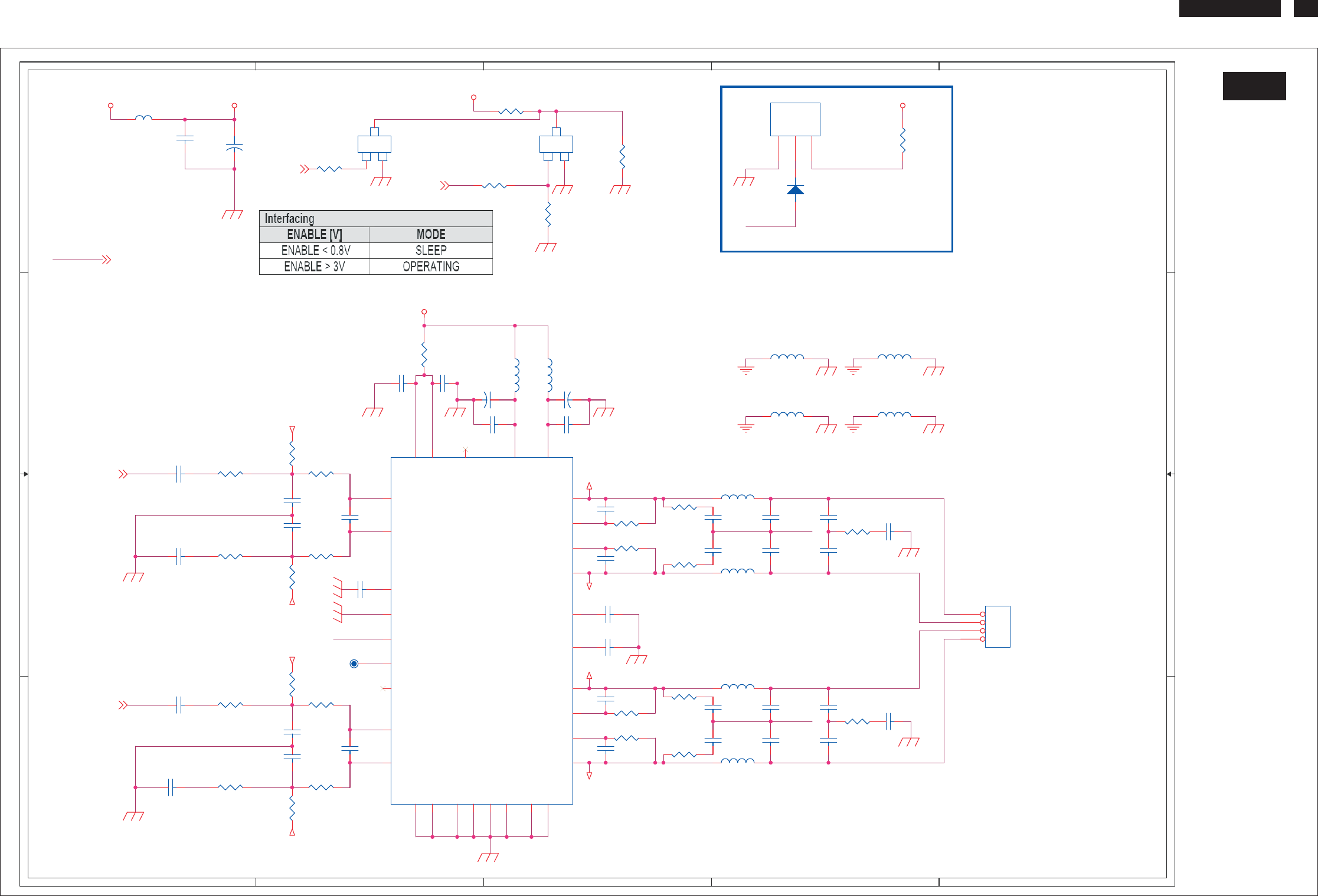
190TW8 TV 37
S-A12
A
A
B
B
C
C
D
D
E
E
44
33
22
1 1
+12V_AMP
AMP_GND
AMP_GND
ENABLE
ENABLE
ENABLE
+12V_AMP
+12VAUDIO
OUT1+
OUT1-
OUT2-
OUT2+
DV33A
+12V_AMP
+12V_AMP
OUT1-
OUT1+
OUT2-
OUT2+
AMP_R11
AMP_L11
OFF_MUTE
GPIO20
4
+12VAUDIO 2,11
Reset circuit
C159
680nF/6
R272
10k/6
R268
10R/12
CON2
4606-04-04P-R
1
2
3
4
L40
Bead_121_4A/8
C173
220nF/6
C161
180pF/6
R245
10k/6
C156
220nF/6
R258
10k/6
C182
100PF
C165
680nF/6
C167
220nF/6
R246 10k/6
C149
330uF/25V
R252
47k/6
D48
LL4148/NC
1 2
C150
330uF/25V
R261
220k/6
C148
0.1uF/6
+
CE43
100uF/16V
12
C146
0.1uF/6
C176
0.1uF/6
C157
100pF/6
C155
180pF/6
R267 1M/6/NC
R263
10R/12
C178
180pF/6
U21
MAX809-S SOT-23 2.93V RST/NC
SOT23
VCC
3
RSTN
2
GND
1
R254
10R/12
TP45
C151
0.1uF/6
R247
10k/6
R262
220k/6
L36
Bead_121_4A/8
L44 22uH
C175
680nF/6
L41 Bead_121_4A/8
C180
680nF/6
C168
330nF/6
R298
4.7k/6/NC
C170
1uF/6
C166
0.1uF/6
R265
10k/6
C181
0.1uF/6
L45 22uH
R255 1M/6/NC
C184
180pF/6
L38
Bead_121_4A/8
L42 22uH
R249
220k/6
R274
220k/6
L43 22uH
R256
10R/12
E
B
C
SOT
23
Q20
2N3904
2
3
1
C164
470pF/6
C177
470nF/6
TFA9810
VDDA1 4
VSSA1
5
IN1P
2
IN1M
3
IN2P
15
IN2M
14
OUT2P 23
OUT1P 26
OUT1M 28
OUT2M 21
VDDP1 25
VDDP2 24
VSSP1
30
VSSP2
19
BOOT1P 27
BOOT2M 20
STABI1 31
ENABLE
7
SO/OL
6
DIAG
10
VSSD
16
VSSD
17
VSSD
1
VSSD
32
VDDA2 13
VSSA2
12
BOOT1M 29
BOOT2P 22
STABI2 18
TEST
11
CDELAY
8
N.C. 9
L35
Bead_121_4A/8
C185
1uF/6
R251
10k/6
R260
10R/12
R257 1M/6/NC
R270 1M/6/NC
R412
1k/6/NC
R27110R/12
C163
1uF/6
R266
47k/6
C183
220nF/6
C172
1uF/6
C158
470pF/6
R248
10R/12
C154
1uF/6
C162
470nF/6
E
B
C
SOT
23
Q35
2N3904/NC
2
3
1
R273
47k/6
C179
470pF/6
L37
Bead_121_4A/8
R299
10k/6
C147
0.1uF/6
L39
Bead_121_4A/8
R259
47k/6
C160
0.1uF/6
C169
1uF/6
C174
470pF/6
C152
0.1uF/6
C146 A4 L37 C3
C147 B3 L38 D3
C148 B3 L39 D3
C149 B3 L40 D3
C150 C3 L41 D3
C151 C3 L42 D2
C152 C3 L43 D2
C154 A3 L44 D2
C155 B2 L45 D1
C156 C2 Q20 C4
C157 B2 Q35 B4
C158 C2 R245 C4
C159 D2 R246 B4
C160 D2 R247 C4
C161 B2 R248 B3
C162 D2 R249 B3
C163 A2 R251 A3
C164 C2 R252 B3
C165 D2 R254 C2
C166 D2 R255 C2
C167 C2 R256 D2
C168 B2 R257 C2
C169 C2 R258 A2
C170 C2 R259 B2
C172 A1 R260 C2
C173 C1 R261 B2
C174 C1 R262 B2
C175 D1 R263 C1
C176 D1 R265 A1
C177 D1 R266 B1
C178 B1 R267 C1
C179 C1 R268 D1
C180 D1 R270 C1
C181 D1 R271 C1
C182 B1 R272 A1
C183 C1 R273 B1
C184 B1 R274 B1
C185 A1 R298 D4
CE43 A4 R299 C4
CON2 E2 R412 B4
D48 D4 TP45 B2
L35 A4 U21 D4
L36 C3 U22 B3
Schematic Diagram(Scaler Board - AUDIO AMP)
http://www.wjel.net
190TW8 TV 38
S-A13
A
A
B
B
C
C
D
D
E
E
44
3 3
22
1 1
SOURCE MENU
LED_R
LED_G
LED_G
LED_R IR
VO-
VO+
CH-
CH+
MENU
SOURCE
LED_R
LED_G
VO-
CH+
MENU
VO+
SOURCE
PW_KEY
LED_R
LED_G
CH-
VO- VO+ CH+ CH- PW_KEY
DV33A
5VSB 5VSB
5VSB
5VSB
SB33B
5VSB 5VSB
SB33B
SB33B
5VSB 5VSB 5VSB 5VSB 5VSB
ADC_IN1
4
PW_KEY 4,7
ERO1_UP3_1
4
FCLK_GPIO
4
IR
4,7
MTK ADC 0V~2.8V
2.2V
2.49V
1.1V
1.59V
0.22V
0.58V
R391
47K/6/NC
C194
20pF/6
L68 FB/6
C248
NC/10pF
L72 FB/6
C188
0.1uF/6/NC
L69 FB/6
Q24
2N3906
2
13
L73 FB/6
Q23
2N3906
2
13
R413 1AFUSE/6
C234
0.1uF/6
L71 FB/6
L63 Bead_121_4A/8
L70 FB/6
R288
330R/6
C251
NC/10pF
C186
20pF/6
D58
BAV99L/NC
2
3
1
C257
NC/10pF
D53
BAV99L
2
3
1
C187
0.1uF/6/NC
J1
HEADER 10pin (2mm)
1
2
3
4
5
6
7
8
9
10
R280
3k/6
R285
0R/6
C193
0.1uF/6/NC
CN4
4501-04-05P-R
1
2
3
4
5
D54
BAV99L/NC
2
3
1
C249
NC/10pF
D59
BAV99L/NC
2
3
1
R281
6k/6
C256
NC/10pF
L60 Bead_121_4A/8
L66 FB/6
D57
BAV99L
2
3
1
D52
BAV99L/NC
2
3
1
R289
100R/6
R278
1k/6
D60
BAV99L/NC
2
3
1
CB92
0.1uF/6
C250
NC/10pF
R279
2k/6
R286
0R/6
C191
0.1uF/6/NC
R283
10k/6
C190
0.1uF/6/NC
D51
BAV99L/NC
2
3
1
L62 Bead_121_4A/8
C192
0.1uF/6/NC
C254
0.1upF/6
C253
NC/10pF
R276
10k/6
L74 FB/6
L61
Bead_121_4A/8
D56
BAV99L/NC
2
3
1
R282
9.1k/6
R277
510R/6
L67 FB/6
D55
BAV99L/NC
2
3
1
C255
NC/10pF
R334
10k/6
C252
NC/10pF
R275
6.8k/6
C186 C4
C187 C3
C188 B3
C190 B3
C191 B3
C192 B3
C193 A3
C194 C2
C234 D2
C248 A1
C249 A1
C250 A1
C251 B1
C252 B1
C253 B1
C254 C1
C255 C1
C256 C1
C257 D1
CB92 A3
CN4 D2
D51 A1
D52 A1
D53 A1
D54 B1
D55 B1
D56 B1
D57 C1
D58 C1
D59 C1
D60 C1
J1 D3
L60 C2
L61 C2
L62 C2
L63 C2
L66 C3
L67 C3
L68 C3
L69 C3
L70 C3
L71 C3
L72 C3
L73 C3
L74 C3
Q23 B2
Q24 B2
R275 A4
R276 C4
R277 A4
R278 A4
R279 B4
R280 B4
R281 B4
R282 B4
R283 A3
R285 A2
R286 A2
R288 B2
Schematic Diagram(Scaler Board - )ADC KEYPAD & IR
http://www.wjel.net
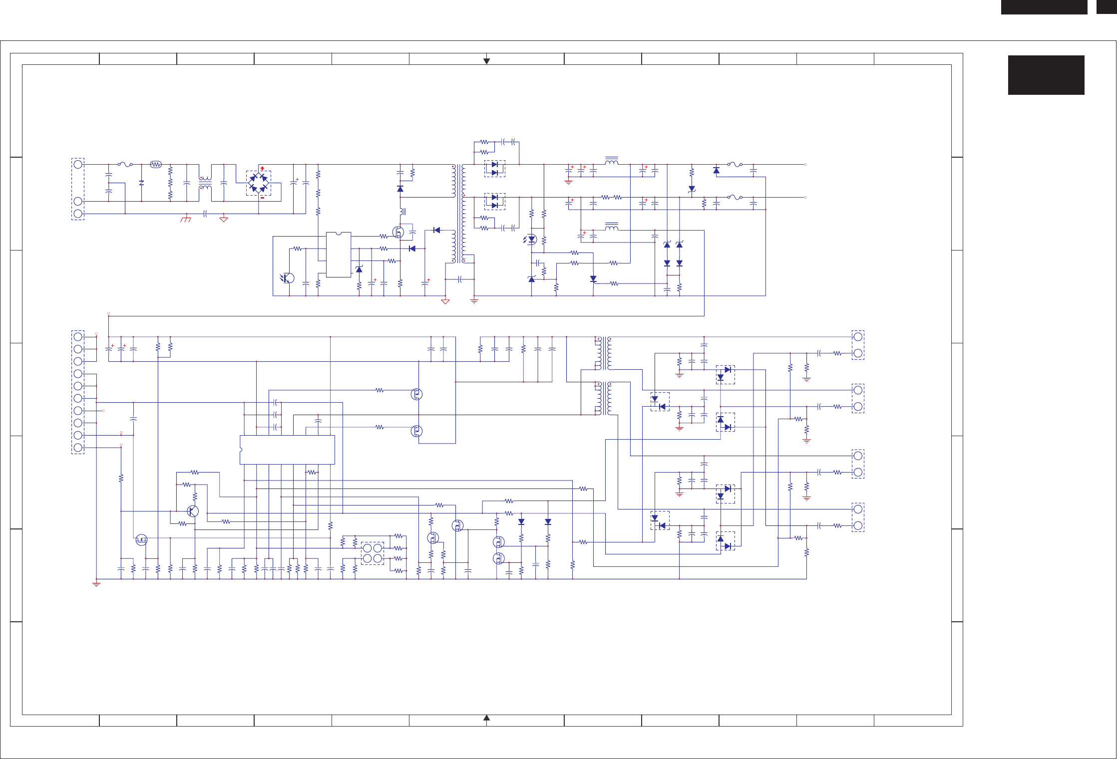
190TW8 TV 39
P-1
1
1
2
2
3
3
4
4
5
5
6
6
7
7
8
8
9
9
10
10
11
11
12
12
A A
BB
C C
DD
E E
F F
G G
C50
332
1
3
4
5
6
9
8
7
T1
C1
X1 0.33uF L1
10mH
R2
470K
R3
470K
C3
681
C4
681
C5
450V100uF
1
43
2
R4
470K
R1
10 OHM 4A
~~
CR1
2KBP06M
CR2
TVR10511K
L
G
N
CN1 F1
250V/T3.15AH
C2
X1 0.33uF
CR51
SRF10100C
L51
4.3uH
C59
10V100uF
R58
N.A
2
1
IC2A
C
A
R
IC51
KIA431
C55
333
C60
104
R60
10K
CR52 SRF10150C C64
25V100uF
C65
104
R67
10R
C58
104
C63
104
C57
10V1000uF
C62
25V680uF
R57
300R
R59
1K
R56
N.A
CR55
5.6V
CR56
N.A
R51 100R
R52 100R
C51
221
C52
221
C69
104
C67
25V680uF
+5V
L53
4.3uH
R61 0
R62
10K
R65
10K
C72
102
C71
104
R64
510R
CR54
7.5V
C66
104
R69
N.A
F51
5A
+12V
R53 100R
R54
100R C53
221
C54
221
C12
N.A
(3.5A)
(1A)
C110
475
C107
N.A
C104
104
C124
474
C123
475
R114
750K
C115
104
R115
N.A
C101
25V330u
R130
0
C105
103
R137
100K
R133
0
CR102
1SS355
C114
104
R102
20K
GND
2
3
1
4
5
6
On/off
+5V
+5V
R113
N.A
R103
10K
G
D
S
Q101
RK7002
R107
N.A
C103
103
CN101
4606-E10N-00B
ADJ
CR103
BAV70
R140
6.8K
C127
5p
C128
222
C130
5p
1HV
2RTN
CN102
FF-A3500-WR2-2
R145
20K
C131
222
1HV
2RTN
CN103
FF-A3500-WR2-2
R152
1K
R149
20K
R111
13K
G
D
S
Q106
RK7002
R104
10K
R101
68K
On/off
ADJ
7
8
+12V
C102
25V330u
C129
104
R146
20K
R148
1K
G
D
S
Q107
RK7002
C113 103
C116
103
C109
392
R131
560K
C111
N.A
R134
200K
Q102
N.A
C126
104
R141
200K
R116
10K
C112
104
R105
10K
R106
68K
R112
130K
R129 180K
R143
43K
C120
475
C119
475
R119
1K
R118
10R
R136 20K
R117
10R
G
D
S
Q105
RK7002
R122
N.A
R121
43K
R132
270K
C132
104
C108
104
4
2
1
3
CR104
BAW56
R147
1K
R150
20K
CR105
BAW56
R142
36K
R151
1K
R144
N.A
R108
N.A
R109
0
R127 10K
R128
N.A
R126 N.A
R125
39K
R123
390K
R124
N.A
C121
475
C122
475
R120
1K
C118
105
C117
105
12345 678
910111213141516
LV LI COMP FT SWSET BRSET DBRT EN
VINBTUGOUTVCCLGPGNDAGND
MP1008
IC101
C106
N.A
R110
15K
9
10
GND
+5V
GND
GND
+5V
CN106
FF-A2544-V-2X2
C56
10V1000uF
F52
2A
+12V
CR106
BAV70
C133
5p
C134
222
C136
5p
1HV
2RTN
CN104
FF-A3500-WR2-2
R153
20K
C137
222
1HV
2RTN
CN105
FF-A3500-WR2-2
R160
1K
R157
20K
C135
104
R154
20K
R156
1K
C138
104
CR107
BAW56
R155
1K
R158
20K
CR108
BAW56
R159
1K
CR101
1SS355
R138
6.8K
G
D
S
Q108
RK7002
C125
104
R139
200K
R135 20K
G
D
S
Q103
AOD484
G
D
S
Q104
AOD484
C13
332
+12V(INV)
C6
222
CR3
UF1007
R11
10R
R14
0.43 OHM
3
4
IC2B
PC123X2Y
C9
471
CR4
PR1003
R12
100R
R13
100R
C8
50V10u
R6
680K
R7
680K
R8
680K
R9
100R
C7
103
CR5
1N4148
C10
50V56u
C11
47pF
L2
R10
100K
R5
27K
G
D
S
Q1
2SK3562(Q)
1
2
3
45
6
7
8
IC1
K
A
G
IC52
XL0840
R63
680R
OB2268CP
R161
N.A
CR6
N.A
R15
N.A
17
10
6
2
3
5
4
T101
17
10
6
2
3
5
4
T102
C139
N.A
C73
104
C74
104
CR57
1SS355
C140
N.A
C141
N.A
C142
N.A
C143
N.A
CR58
N.A
R70
0.56R
R71
0.56R
R162
3.6K
R163
120K
R164
0
C144
104
CR59
P6KE6.8A
ADJ E1 C142 E9 R61 B8
ADJ E2 C143 F9 R61 C8
C1 B3 C144 D2 R62 C8
C2 B3 CN1 B1 R63 C8
C3 B2 CN101 C1 R64 C8
C4 B2 CN102 C11 R65 C9
C5 B4 CN103 D11 R67 B9
C6 B5 CN104 E11 R69 B9
C7 C4 CN105 E11 R70 B8
C8 C5 CN106 F5 R71 B8
C9 C5 CR1 B3 R101 E2
C10 C6 CR2 B2 R102 F2
C11 B6 CR3 B5 R103 C2
C12 B4 CR4 B6 R104 F2
C13 B3 CR5 B6 R105 F2
C50 C6 CR6 C5 R106 E3
C51 A7 CR51 B7 R107 E3
C52 A7 CR52 B7 R108 E3
C53 B7 CR54 B9 R109 E3
C54 B7 CR55 B9 R110 F3
C55 C7 CR56 B9 R111 F3
C56 B8 CR57 C9 R112 F3
C57 B8 CR58 C9 R113 F4
C58 B8 CR59 B9 R115 F4
C59 B8 CR101 E7 R117 D5
C59 B9 CR102 E7 R118 D5
C60 B9 CR103 D9 R119 D6
C62 B8 CR103 D10 R120 D7
C63 B8 CR103 E10 R121 F5
C64 B8 CR104 D10 R122 F5
C64 B9 CR106 F9 R123 F5
C65 B9 CR107 E10 R124 F5
C66 B9 CR108 F10 R125 F5
C67 B8 F1 B2 R126 F5
C69 B8 F31 B10 R127 F5
C71 B9 F52 B10 R128 F5
C72 C9 IC101 E4 R129 E6
C73 B10 IC101 C5 R130 E6
C74 B10 IC2A B7 R131 F6
C101 D2 IC2B C4 R132 F6
C102 D2 IC51 C7 R133 F6
C103 D2 IC52 C8 R134 F6
C104 F2 L1 B3 R135 E7
C105 F2 L2 B5 R136 E7
C106 F3 L2 B6 R137 E7
C107 F3 L51 A8 R138 F7
C108 F3 L53 B8 R139 F7
C109 F4 Q1 B5 R140 F7
C110 F4 Q101 F2 R141 F7
C111 F4 Q102 E3 R142 E8
C112 F5 Q103 D6 R143 F8
C113 D4 Q104 D6 R144 F8
C114 D4 Q105 F6 R145 D9
C114 F4 Q106 E6 R146 D10
C115 D4 Q107 F7 R146 D11
C116 D4 Q108 F7 R147 D11
C117 D6 R1 B2 R148 D11
C118 D6 R2 B2 R149 D9
C119 D7 R3 B2 R150 D10
C120 D7 R4 B2 R150 D11
C121 D7 R5 B6 R151 D11
C122 D7 R6 B4 R152 D11
C123 F6 R7 B4 R153 E9
C124 F6 R8 B4 R154 E10
C125 F7 R9 B4 R154 E11
C126 F7 R10 C4 R155 E11
C128 D9 R11 B5 R156 E11
C129 D11 R12 B5 R157 F9
C130 D9 R13 C5 R158 F10
C131 D9 R14 C5 R158 F11
C132 D11 R15 C5 R159 F11
C133 E9 R51 A6 R160 E11
C134 E9 R52 A6 R161 C2
C135 E11 R53 B6 R162 E3
C136 E9 R54 B6 R163 F4
C137 F9 R56 B7 R164 E4
C138 E11 R57 B7 T101 C8
Schematic Diagram(Power Board)
http://www.wjel.net


Layout Side View(Scaler Board) 190TW8 TV 42
S-A
C1 A1 C5 B2 C49 A3
C3 B1 C6 A1 C50 B2
C4 A1 C7 A3 C51 B3
D8 E2 C8 A1 C52 C2
D9 D4 C9 D2 C53 C2
D10 D4 C10 D1 C54 C2
D11 D3 C11 D1 C55 D3
D12 A4 C12 D1 C56 B2
D13 D4 C13 C2 C57 B3
D14 D4 C14 C2 C58 C2
D15 A4 C15 C2 C59 B3
D16 A4 C16 C2 C60 C2
D17 A4 C17 C2 C61 D2
D18 B4 C18 C2 C62 D2
D19 B4 C19 C2 C63 D2
D20 B4 C20 C4 C64 B2
D21 B4 C21 C4 C65 B2
D22 A4 C22 C4 C66 B3
D23 B4 C23 C2 C67 B3
D24 C4 C24 C2 C68 D2
D25 C4 C25 E2 C69 B2
D26 A4 C26 A4 C70 B3
D27 E2 C27 A4 C71 E1
D28 E3 C28 A4 C72 E2
D29 E2 C29 B4 C73 E2
D30 E1 C30 B4 C74 E2
D31 E1 C31 B4 C75 E2
R108 D2 C32 B4 C76 E2
U1 A2 C33 C4 C77 E3
U2 D2 C34 B4 C78 C2
U3 A4 C35 B4 CN1 A1
U4 C2 C36 B2 CN2 C1
U5 D2 C37 B3 CN3 D4
U6 D2 C38 B2 CN4 B5
U7 B4 C39 B2 CN5 D3
U3-A1 A2 C40 B2 CN6 E2
X1 B3 C41 C2 CN7 E2
CN8 E3 C42 D2 D1 B2
CN9 E5 C43 D2 D2 B2
D32 E2 C44 C2 D3 B4
D33 E2 C45 C2 D4 A3
FB1 D4 C46 C2 D5 C4
FB2 A2 C47 D2 D6 C4
FB3 B2 C48 C2 D7 C4
FB4 A3 R18 A2 R63 A4
FB5 B3 R19 C1 R64 C4
FB6 C2 R20 D2 R65 C4
H1 D4 R21 C1 R66 C2
H2 A1 R22 D2 R67 C2
H3 A3 R23 D1 R68 C2
JP1 B3 R24 D2 R69 C2
L1 A3 R25 E4 R70 B3
L2 E1 R26 E4 R71 B3
L3 E2 R27 C4 R72 B3
L4 E2 R28 C4 R73 B2
L5 E2 R29 C4 R74 C2
L6 E2 R30 C4 R75 C2
L7 E2 R31 C4 R76 D2
L8 E3 R32 C4 R77 D2
L9 E1 R33 C4 R78 B2
L10 E1 R34 C4 R79 D2
Q1 B1 R35 C4 R80 B2
Q2 B1 R36 C4 R81 D2
Q3 A1 R37 C4 R82 D2
Q4 D1 R38 C4 R83 D2
Q5 D2 R39 C4 R84 D2
Q6 B3 R41 D3 R85 D3
Q7 E1 R42 C2 R86 E1
Q8 E1 R43 C2 R87 E1
R1 A1 R44 C4 R88 E1
R2 B1 R45 C4 R89 E2
R3 B1 R46 C2 R90 E2
R4 B1 R47 C2 R91 E2
R5 B1 R48 D3 R92 E2
R6 B1 R49 D3 R93 E2
R7 B2 R50 A4 R94 E3
R8 B1 R51 A4 R95 C2
http://www.wjel.net
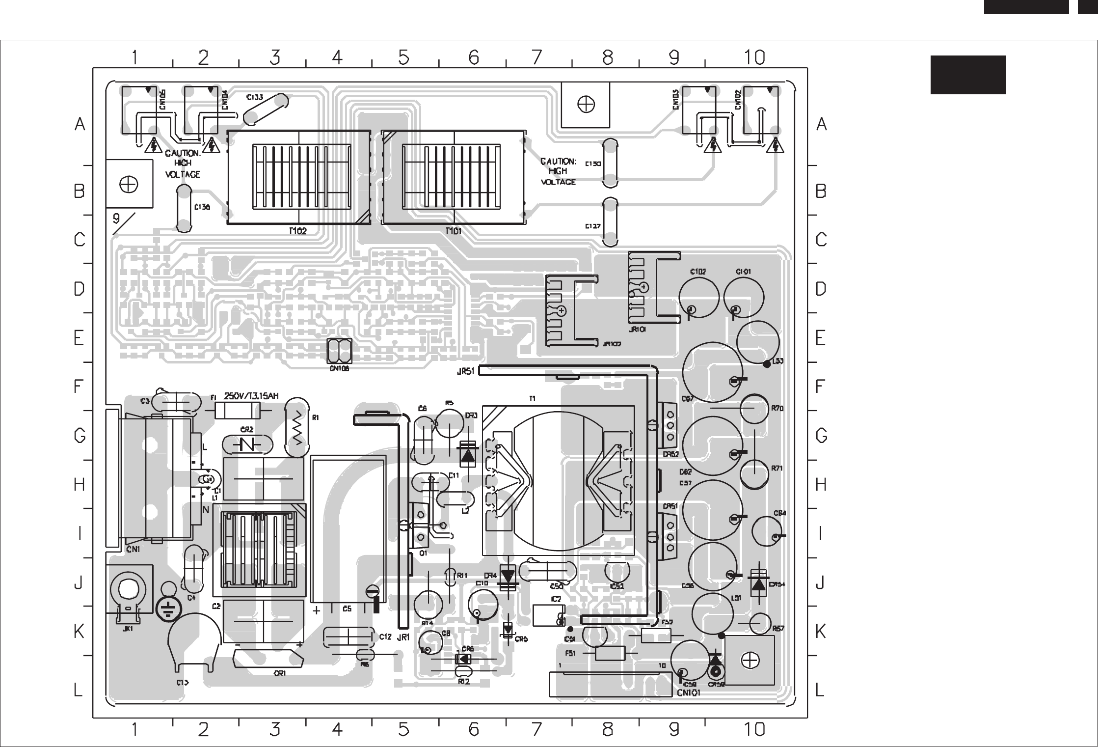
190TW8 TV 44
P-A
C1 H3 CR6 L6
C2 K3 CR51 I9
C3 F2 CR52 G9
C4 J2 CR54 J10
C5 J4 CR59 L10
C6 G5 F1 F2
C8 K5 F51 K8
C10 J6 F52 K9
C11 H5 IC2 K7
C12 K4 IC51 K8
C13 K2 IC52 J8
C50 J7 JR1 I5
C56 J10 JR51 H9
C57 I10 JR101 D9
C59 L9 JR102 D8
C62 G10 L1 I3
C64 I10 L2 H6
C67 F10 L51 K10
C101 D10 L53 E10
C102 D9 Q1 I5
C127 C8 R1 G3
C130 B8 R5 G6
C133 A3 R6 K4
C136 B2 R11 J6
CN1 G1 R12 L6
CN101 L8 R14 J5
CN102 A10 R67 K10
CN103 A9 R70 F10
CN104 A2 R71 H10
CN105 A10 T1 H7
CN106 E4 T101 B6
CR1 L3 T102 B3
CR2 G3 JA1 G1
CR3 G6 JK1 J1
CR4 J7 JP1 E4
CR5 K7
Layout Side View(Power Board)
http://www.wjel.net
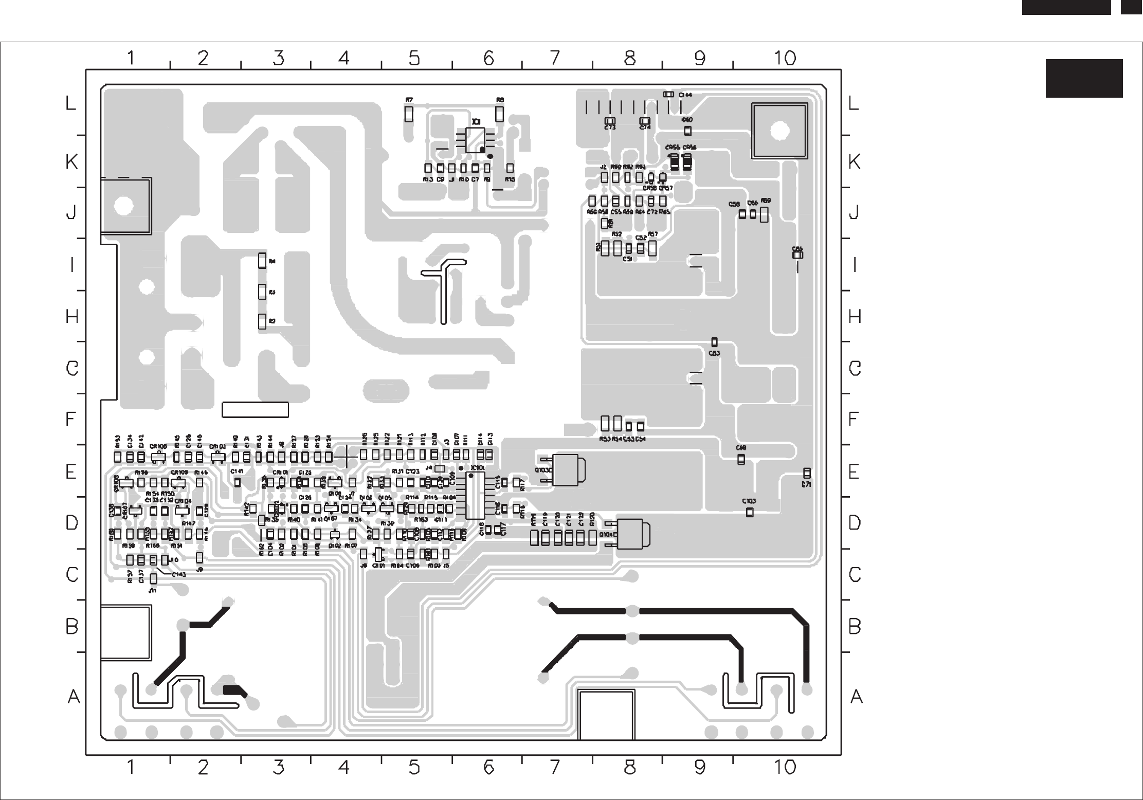
190TW8 TV 45
C51 I8 CR58 K8 R113 E5
C52 I8 CR101 E3 R114 D5
C53 F8 CR102 D3 R115 D5
C54 F8 CR103 E2 R116 D5
C55 J8 CR104 D2 R117 E6
C58 J10 CR105 E2 R118 D6
C60 L9 CR106 E1 R119 D7
C63 H9 CR107 D1 R120 D7
C65 I10 CR108 E1 R121 E5
C66 J10 IC1 K6 R122 E5
C69 E10 IC101 E6 R123 E4
C71 E10 Q101 C4 R124 E4
C72 J8 Q102 D4 R125 E4
C73 L8 Q103 E7 R126 E4
C74 L8 Q104 D8 R127 E3
C103 D10 Q105 D5 R128 E3
C104 D3 Q106 D4 R129 D5
C105 C5 Q107 D4 R130 D5
C106 D5 Q108 E4 R131 E5
C107 E6 R2 H3 R132 E4
C108 E5 R3 H3 R133 E5
C109 E5 R4 I3 R134 D4
C110 E5 R7 L5 R135 D3
C111 D5 R8 L6 R136 E3
C112 D5 R9 K6 R137 D4
C113 E6 R10 K6 R138 E3
C114 E6 R13 K5 R139 E4
C115 E6 R15 K6 R140 D3
C116 D6 R51 I8 R141 D4
C117 D6 R52 I8 R142 D3
C118 D6 R53 F8 R143 E3
C119 D7 R54 F8 R144 E3
C120 D7 R56 J8 R145 E2
C121 D7 R57 I8 R146 E2
C122 D7 R58 J8 R147 D2
C123 E5 R59 J8 R148 D2
C124 D4 R60 K8 R149 E2
C125 E3 R61 J8 R150 E1
C126 D3 R62 K8 R151 D2
C128 E2 R63 K8 R152 D1
C129 D2 R64 J8 R153 E1
C131 E3 R65 J8 R154 E1
C132 D1 R69 J10 R155 D1
C134 E10 R101 D3 R156 D1
C135 D1 R102 D3 R157 C1
C137 C1 R103 C5 R158 E1
C138 D1 R104 C5 R159 D1
C139 E5 R105 D5 R160 D1
C140 E2 R106 D3 R161 C5
C141 E2 R107 D4 R162 D3
C142 E1 R108 D4 R163 D5
C143 C1 R109 D6 R164 D5
C144 L9 R110 D5
CR55 K9
P-B
Layout Side View(Power Board)
http://www.wjel.net

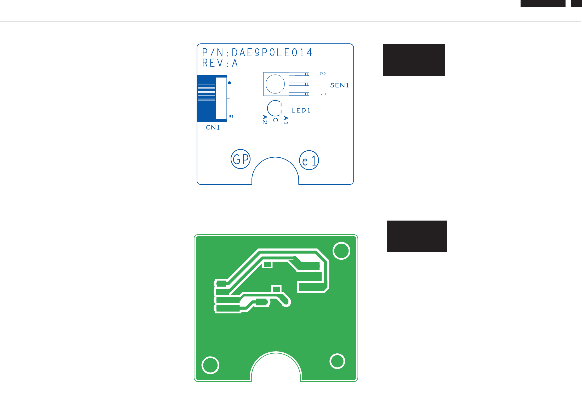
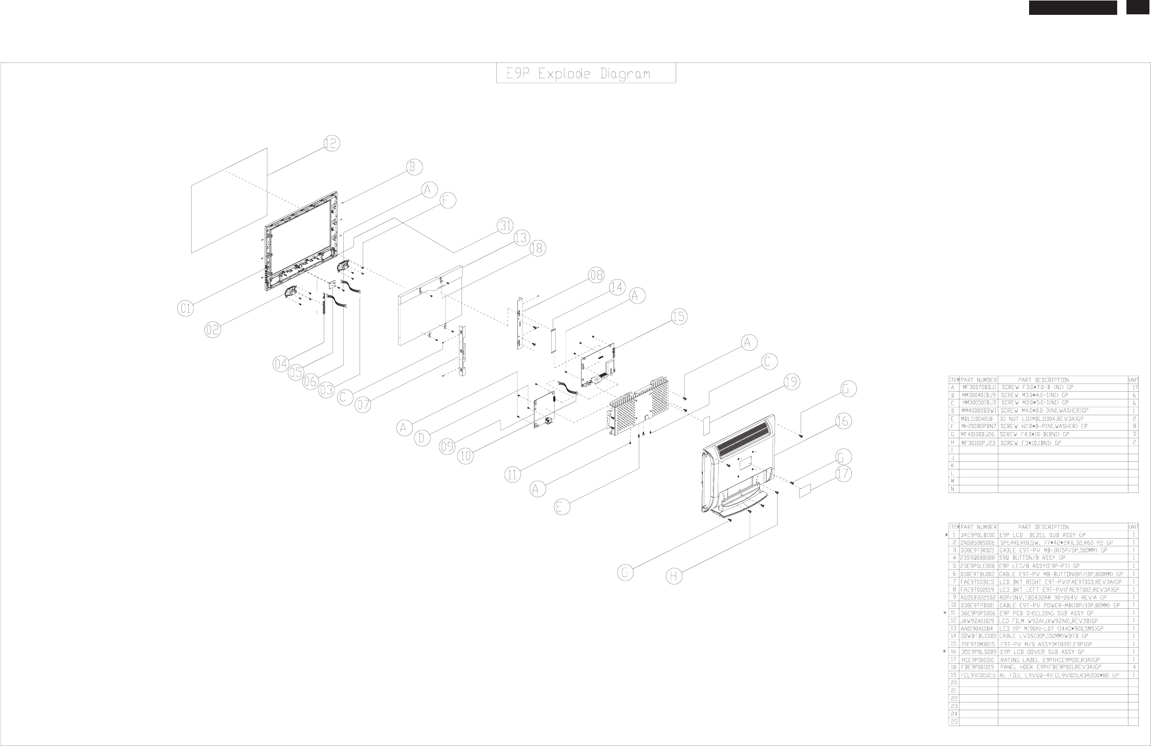

190TW8 TV
Recommended Spare Part List 49
RSPL FOR 190TW8FB/00(E9P-PT)
1 P/N: 1E9PZPPL006(CMO PANEL)
Philips P/N Techview P/N Description Q'ty Location Remark
LCD panel AA0190A1084 LCD 19" M190A1-L07 (1440*900,5MS)GP 1 Item 13 in exploded view CMO PANEL
MB-LCD cable DDWBTBLC005 CABLE LVDS(30P,150MM)WBTB GP 1 Item 14 in exploded view
Button-MB cable DD0E9TBU002 CABLE E9T-PV MB-BUTTON(10P/8P,700MM) GP 1 Item 6 in exploded view
IR-MB cable DD0E9TIR005 CABLE E9T-PV MB-IR(5P/5P,350MM) GP 1 Item 3 in exploded view
Power-MB cable DD0E9TPB001 CABLE E9T-PV POWER-MB(10P/10P,80MM) GP 1 Item 10 in exploded view
Speaker assembly DND8508S006 SPEAKER(8,5W, 77*42*24)L32,R60 P2 GP 1 Item 2 in exploded view
IC AJ098100009 IC(32P)CLASSDAMP TFA9810(2*12W)SOT287 GP 1 U22
2-channel power comparator for
high efficiency class-D audio
amplifier systems
IC AJ8201A0F04 IC(256P)MT8201ALE/B-L(QFP) GP 1 U9
a highly integrated single chip. It
includes ADC, Video Decoder,
Video Processor, Audio
Processor, OSD Processor, Host
Microcontroller, DRAM controller
IC AJ8291E0F09 IC(48P)MT8291E-L(QFP) GP 1 U19
a highly integrated stereo audio
CODEC
IC AJ8293A#F06 IC(128P) MT8293AE-L(QFP) GP 1 U15 a fully HDMI-compliant receiver
IC AKD3NF^K+02 IC(66P)DDR SDR M13S128168A -5TG(TSOP)GP 1 U28 DDR SDRAM
IC AKE1A800Y11 IC EEPROM(8P,5V) 24LC02BT(2K*1,SOP) GP 2 U14,U17 EDID data
IC AKE1F800R02 IC EEPROM(8P)BR24L04F-W(512*8,SO8) GP 1 U13 HDCP KEY data
IC AKE1H800009 IC EEPROM(8P)AF24BC04-SI(512*8,SOIC8) GP 1 U13 HDCP KEY data
IC AKE25FHKZ08 IC(48P) FLASH MX29LV160CBTC-70G(TSOP)GP 1 U11 STORE FLASH ROM
IC AKE268AKK03 IC(48P) FLASH SST39VF1681-70-4C-EKE GP 1 U11 STORE FLASH ROM
IC AKE3A8S0Y10 IC EEPROM(8P)24LC16BT-I(2K*8,100KHZ) GP 1 U1
STORE Timing table, Color
temperature, TV channel data
IC AL001084021 IC(3P) AIC1084PE(TO-252) GP 9
U2,U3,U4,U5,U6,U7,U8,U12,
U29 DC to DC
IC AL002996C00 IC(8P) LP2996MX (SOP8) GP 1 U27 DDR Termination Regulator
IC AL003157107 IC(6P) NC7SB3157P6X_NL SC70 GP 1 U30 Analog Switch
IC ALHC4052018 IC(16P) 74HC4052D(SO16)GP 1 U24
Dual 4-channel analog
multiplexer, demultiplexer
TRANSISTOR BA039040Z19 TR SMD PMBS3904(40V,200MA) GP 19
Q3,Q4,Q5,Q6,Q7,Q8,Q9,Q1
0,Q11,Q14,Q16,Q17,Q18,Q2
0,Q27,Q28,Q32,Q33,Q34
TRANSISTOR BA039060Z10 TR,SMD PMBS3906(40V,200MA) GP 5 Q12,Q15,Q23,Q24,Q30
TRANSISTOR BAM9435YZ17 TR MOSFET SI9435BDY-E3(-30V,5.1A)GP 3 Q1,Q2,Q19
TRANSISTOR BAN70020Z13 TR MOSFET 2N7002E-T1-E3 (60V,250MA) GP 3 QF1,QF2,QF3
Front bezel assembly 34E9P0LB000 E9P LCD BEZEL SUB ASSY GP 1 Item 1 in exploded view
Back cover assembly 35E9P0LS009 E9P LCD COVER SUB ASSY GP 1 Item 16 in exploded view
D-SUB to shielding MBLI1004018 IO NUT LI1(MBLI1004,REV3A)GP 1 Item E in exploded view
Panel to L/R bracket MM30050IBJ3 SCREW M3.0*5.0-I(NI) GP 4 Item C in exploded view
PCBAs to metal shielding MF30060BBJ6 SCREW F3.0*6-B(NI)GP 16
Power board AS56B42TA04 PI 100-240V 55W 4L(140*150)TBD432AR-1 GP 1
Power board AS56B42CA06 PI 100-240V 55W 4L(140*150)AIP-0169 GP 1
Main board 10E9P0MB001 E9T-PV M/B ASSY(MT8201,E9P)GP 1 Item 15 in exploded view 21E9T0MB015
Bios AZE9P0BM007 E9P-PT SW BIOS IMAGE(MT8201 CMO PAL-EU)
LED/B 10E9P0LB006 E9P LED/B ASSY(E9P-PT) GP 1 Item 5 in exploded view 23E9P0LE008
Button/B 10S9T0BB006 S9Q BUTTON/B ASSY GP 1 Item 4 in exploded view 23S9Q0BB008
Audio cable DD0L0TPC007 CABLE AUDIO(ST,1.8M)BLACK L0T GP 1
VGA cable DD0L7WPC001 CABLE MB-VGA(15P,1.8M)L7E BLACK 5.5 GP 1
LCD Film JXW9ZA01019 LCD FILM W9ZA(JXW9ZA01,REV3B)GP 1
Power card DM333181801 PWR CORD B 1.8M SP-023/16A CT-12 EUR GP 1
Remote control DQ731880108 REMOTE CONTROLLER(318801-0958001A) GP 1
Manual HDE9P001011 MANUAL+QSG E9P(HDE9P001,R3A)GP 1
Battery AHDALR03006 BATTERY LR03GW/2SK (ALKALINE 1.5V) GP 1
Battery AHDALR03120 BATTERY LR03(SN) (ALKALINE,1.5V) GP 1
PE bag For LCD HAL0T002019 PE BAG L0T(HAL0T002,REV3A)GP 1
PE bag For Accessories HAS0Q001012 PE BAG S0Q(HAS0Q001,R3A)GP 1
Carton HFE9P001012 CARTON E9P(HFE9P001,R3A)GP 1
Cushion-L HBE9P001019 END CAP-L E9P(HBE9P001,REV3A)GP 1
Cushion-R HBE9P002015 END CAP-R E9P(HBE9P002,REV3A)GP 1
Mechanical
Components:
PCBA:
Packing
Material:
Part Name
Accessories:
Electronic
Components:
http://www.wjel.net

50 190TW8 TV Recommended Spare Part List
C47 CH02206J909 CAP CHIP 22P 50V(+-5%,NPO,0603) GP
C186 CH02206J909 CAP CHIP 22P 50V(+-5%,NPO,0603) GP
C194 CH02206J909 CAP CHIP 22P 50V(+-5%,NPO,0603) GP
C202 CH03306J905 CAP CHIP 33P 50V(+-5%,NPO,0603)GP
C203 CH03306J905 CAP CHIP 33P 50V(+-5%,NPO,0603)GP
C157 CH11006J901 CAP CHIP 100P 50V(+-5%,NPO,0603) GP
C182 CH11006J901 CAP CHIP 100P 50V(+-5%,NPO,0603) GP
C89 CH13306J907 CAP CHIP 330P 50V(+-5%,NPO,0603)GP
C92 CH13306J907 CAP CHIP 330P 50V(+-5%,NPO,0603)GP
C93 CH13306J907 CAP CHIP 330P 50V(+-5%,NPO,0603)GP
C94 CH13306J907 CAP CHIP 330P 50V(+-5%,NPO,0603)GP
C96 CH13306J907 CAP CHIP 330P 50V(+-5%,NPO,0603)GP
C97 CH13306J907 CAP CHIP 330P 50V(+-5%,NPO,0603)GP
C98 CH13306J907 CAP CHIP 330P 50V(+-5%,NPO,0603)GP
C99 CH13306J907 CAP CHIP 330P 50V(+-5%,NPO,0603)GP
C100 CH13306J907 CAP CHIP 330P 50V(+-5%,NPO,0603)GP
C104 CH13306J907 CAP CHIP 330P 50V(+-5%,NPO,0603)GP
C105 CH13306J907 CAP CHIP 330P 50V(+-5%,NPO,0603)GP
C106 CH13306J907 CAP CHIP 330P 50V(+-5%,NPO,0603)GP
C111 CH13306J907 CAP CHIP 330P 50V(+-5%,NPO,0603)GP
C128 CH13306J907 CAP CHIP 330P 50V(+-5%,NPO,0603)GP
C262 CH13306J907 CAP CHIP 330P 50V(+-5%,NPO,0603)GP
C158 CH14706K919 CAP CHIP 470P 50V(+-10%,X7R,0603) GP
C164 CH14706K919 CAP CHIP 470P 50V(+-10%,X7R,0603) GP
C174 CH14706K919 CAP CHIP 470P 50V(+-10%,X7R,0603) GP
C179 CH14706K919 CAP CHIP 470P 50V(+-10%,X7R,0603) GP
C61 CH21006K917 CAP CHIP 1000P 50V(+-10%,X7R,0603) GP
C62 CH21006K917 CAP CHIP 1000P 50V(+-10%,X7R,0603) GP
C63 CH21006K917 CAP CHIP 1000P 50V(+-10%,X7R,0603) GP
C65 CH21006K917 CAP CHIP 1000P 50V(+-10%,X7R,0603) GP
C66 CH21006K917 CAP CHIP 1000P 50V(+-10%,X7R,0603) GP
C1 CH22206K917 CAP CHIP 2200P 50V(+-10%,X7R,0603)GP
C4 CH22206K917 CAP CHIP 2200P 50V(+-10%,X7R,0603)GP
C51 CH2336K9108 CAP CHIP 3300P,50V(+-10%,X7R,0603) GP
C53 CH2336K9108 CAP CHIP 3300P,50V(+-10%,X7R,0603) GP
C54 CH2336K9108 CAP CHIP 3300P,50V(+-10%,X7R,0603) GP
C55 CH2336K9108 CAP CHIP 3300P,50V(+-10%,X7R,0603) GP
C56 CH2336K9108 CAP CHIP 3300P,50V(+-10%,X7R,0603) GP
C83 CH2336K9108 CAP CHIP 3300P,50V(+-10%,X7R,0603) GP
C85 CH2336K9108 CAP CHIP 3300P,50V(+-10%,X7R,0603) GP
C229 CH2336K9108 CAP CHIP 3300P,50V(+-10%,X7R,0603) GP
C230 CH2336K9108 CAP CHIP 3300P,50V(+-10%,X7R,0603) GP
C231 CH2336K9108 CAP CHIP 3300P,50V(+-10%,X7R,0603) GP
C232 CH2336K9108 CAP CHIP 3300P,50V(+-10%,X7R,0603) GP
CB110 CH2336K9108 CAP CHIP 3300P,50V(+-10%,X7R,0603) GP
C72 CH24706K911 CAP CHIP 4700P,50V(+-10%,X7R,0603)GP
C107 CH24706K911 CAP CHIP 4700P,50V(+-10%,X7R,0603)GP
C216 CH24706K911 CAP CHIP 4700P,50V(+-10%,X7R,0603)GP
C217 CH24706K911 CAP CHIP 4700P,50V(+-10%,X7R,0603)GP
C218 CH24706K911 CAP CHIP 4700P,50V(+-10%,X7R,0603)GP
C219 CH24706K911 CAP CHIP 4700P,50V(+-10%,X7R,0603)GP
C52 CH31006K919 CAP CHIP 0.01U 50V(+-10%,X7R,0603) GP
C68 CH31006K919 CAP CHIP 0.01U 50V(+-10%,X7R,0603) GP
C69 CH31006K919 CAP CHIP 0.01U 50V(+-10%,X7R,0603) GP
C71 CH31006K919 CAP CHIP 0.01U 50V(+-10%,X7R,0603) GP
C73 CH31006K919 CAP CHIP 0.01U 50V(+-10%,X7R,0603) GP
C75 CH31006K919 CAP CHIP 0.01U 50V(+-10%,X7R,0603) GP
C77 CH31006K919 CAP CHIP 0.01U 50V(+-10%,X7R,0603) GP
C79 CH31006K919 CAP CHIP 0.01U 50V(+-10%,X7R,0603) GP
C90 CH31006K919 CAP CHIP 0.01U 50V(+-10%,X7R,0603) GP
C112 CH31006K919 CAP CHIP 0.01U 50V(+-10%,X7R,0603) GP
C116 CH31006K919 CAP CHIP 0.01U 50V(+-10%,X7R,0603) GP
C117 CH31006K919 CAP CHIP 0.01U 50V(+-10%,X7R,0603) GP
C121 CH31006K919 CAP CHIP 0.01U 50V(+-10%,X7R,0603) GP
C122 CH31006K919 CAP CHIP 0.01U 50V(+-10%,X7R,0603) GP
10E9P0MB001 E9T-PV M/B ASSY(MT8201,E9P)GP
E9T203-02 21E9T0MB015 E9T M/B Schematic(MT8201)C2A
31E9T0SS011 E9T-PV M/B S/S ASSY(MT8201,E9P)GP
DA0E9TMB032 PCB(M/B)E9T-PV(4L,115*227,R.C)MT8201 GP
E9T205-01 DA0E9TMB032 E9T PCB MB (Board file & Gerber file)
U14 AKE1A800Y11 IC EEPROM(8P,5V) 24LC02BT(2K*1,SOP) GP
U17 AKE1A800Y11 IC EEPROM(8P,5V) 24LC02BT(2K*1,SOP) GP
U13 AKE1F800R02 IC EEPROM(8P)BR24L04F-W(512*8,SO8) GP
U13 AKE1H800009 IC EEPROM(8P)AF24BC04-SI(512*8,SOIC8) GP
U1 AKE3A8S0Y10 IC EEPROM(8P)24LC16BT-I(2K*8,100KHZ) GP
U2 AL001084021 IC(3P) AIC1084PE(TO-252) GP
U3 AL001084021 IC(3P) AIC1084PE(TO-252) GP
U4 AL001084021 IC(3P) AIC1084PE(TO-252) GP
U5 AL001084021 IC(3P) AIC1084PE(TO-252) GP
U6 AL001084021 IC(3P) AIC1084PE(TO-252) GP
U7 AL001084021 IC(3P) AIC1084PE(TO-252) GP
U8 AL001084021 IC(3P) AIC1084PE(TO-252) GP
U12 AL001084021 IC(3P) AIC1084PE(TO-252) GP
U29 AL001084021 IC(3P) AIC1084PE(TO-252) GP
U24 ALHC4052018 IC(16P) 74HC4052D(SO16)GP
Q3 BA039040Z19 TR SMD PMBS3904(40V,200MA) GP
Q4 BA039040Z19 TR SMD PMBS3904(40V,200MA) GP
Q5 BA039040Z19 TR SMD PMBS3904(40V,200MA) GP
Q6 BA039040Z19 TR SMD PMBS3904(40V,200MA) GP
Q7 BA039040Z19 TR SMD PMBS3904(40V,200MA) GP
Q8 BA039040Z19 TR SMD PMBS3904(40V,200MA) GP
Q9 BA039040Z19 TR SMD PMBS3904(40V,200MA) GP
Q10 BA039040Z19 TR SMD PMBS3904(40V,200MA) GP
Q11 BA039040Z19 TR SMD PMBS3904(40V,200MA) GP
Q14 BA039040Z19 TR SMD PMBS3904(40V,200MA) GP
Q16 BA039040Z19 TR SMD PMBS3904(40V,200MA) GP
Q17 BA039040Z19 TR SMD PMBS3904(40V,200MA) GP
Q18 BA039040Z19 TR SMD PMBS3904(40V,200MA) GP
Q20 BA039040Z19 TR SMD PMBS3904(40V,200MA) GP
Q27 BA039040Z19 TR SMD PMBS3904(40V,200MA) GP
Q28 BA039040Z19 TR SMD PMBS3904(40V,200MA) GP
Q32 BA039040Z19 TR SMD PMBS3904(40V,200MA) GP
Q33 BA039040Z19 TR SMD PMBS3904(40V,200MA) GP
Q34 BA039040Z19 TR SMD PMBS3904(40V,200MA) GP
Q12 BA039060Z10 TR,SMD PMBS3906(40V,200MA) GP
Q15 BA039060Z10 TR,SMD PMBS3906(40V,200MA) GP
Q23 BA039060Z10 TR,SMD PMBS3906(40V,200MA) GP
Q24 BA039060Z10 TR,SMD PMBS3906(40V,200MA) GP
Q30 BA039060Z10 TR,SMD PMBS3906(40V,200MA) GP
Q1 BAM09435006 TR MOSFET ME9435A(-30V,-5.3A)SOIC8 GP
Q2 BAM09435006 TR MOSFET ME9435A(-30V,-5.3A)SOIC8 GP
Q19 BAM09435006 TR MOSFET ME9435A(-30V,-5.3A)SOIC8 GP
Q1 BAM9435YZ17 TR MOSFET SI9435BDY-E3(-30V,5.1A)GP
Q2 BAM9435YZ17 TR MOSFET SI9435BDY-E3(-30V,5.1A)GP
Q19 BAM9435YZ17 TR MOSFET SI9435BDY-E3(-30V,5.1A)GP
QF1 BAN70020Z13 TR MOSFET 2N7002E-T1-E3 (60V,250MA) GP
QF2 BAN70020Z13 TR MOSFET 2N7002E-T1-E3 (60V,250MA) GP
QF3 BAN70020Z13 TR MOSFET 2N7002E-T1-E3 (60V,250MA) GP
D9 BCBAT54CZ02 DIODE SMD BAT54C(30V,200MA,SCHOTTKY)GP
D26 BCBAT54CZ02 DIODE SMD BAT54C(30V,200MA,SCHOTTKY)GP
D1 BCLL4148Z19 DIODE,SMD LL4148PT(75V,0.15A) GP
D49 BCLL4148Z19 DIODE,SMD LL4148PT(75V,0.15A) GP
C70 CH00506J904 CAP CHIP 5P,50V(+-5%,NPO,0603)GP
C74 CH00506J904 CAP CHIP 5P,50V(+-5%,NPO,0603)GP
C78 CH00506J904 CAP CHIP 5P,50V(+-5%,NPO,0603)GP
C113 CH0156J9003 CAP CHIP 15P 50V(+-5%,NPO,0603) GP
C118 CH0156J9003 CAP CHIP 15P 50V(+-5%,NPO,0603) GP
C123 CH0156J9003 CAP CHIP 15P 50V(+-5%,NPO,0603) GP
C46 CH02206J909 CAP CHIP 22P 50V(+-5%,NPO,0603) GP
>> MAIN BOARD ASSY
http://www.wjel.net

190TW8 TV
Recommended Spare Part List 51
C126 CH31006K919 CAP CHIP 0.01U 50V(+-10%,X7R,0603) GP
CB37 CH31006K919 CAP CHIP 0.01U 50V(+-10%,X7R,0603) GP
CB38 CH31006K919 CAP CHIP 0.01U 50V(+-10%,X7R,0603) GP
CB39 CH31006K919 CAP CHIP 0.01U 50V(+-10%,X7R,0603) GP
C88 CH34703K916 CAP CHIP 0.047UF 16V(+-10%,X7R,0603) GP
C91 CH34703K916 CAP CHIP 0.047UF 16V(+-10%,X7R,0603) GP
C95 CH34703K916 CAP CHIP 0.047UF 16V(+-10%,X7R,0603) GP
C101 CH34703K916 CAP CHIP 0.047UF 16V(+-10%,X7R,0603) GP
C108 CH34703K916 CAP CHIP 0.047UF 16V(+-10%,X7R,0603) GP
C127 CH34703K916 CAP CHIP 0.047UF 16V(+-10%,X7R,0603) GP
C2 CH41004Z931 CAP CHIP 0.1U,25V(+80-20%,Y5V,0603) GP
C5 CH41004Z931 CAP CHIP 0.1U,25V(+80-20%,Y5V,0603) GP
C7 CH41004Z931 CAP CHIP 0.1U,25V(+80-20%,Y5V,0603) GP
C11 CH41004Z931 CAP CHIP 0.1U,25V(+80-20%,Y5V,0603) GP
C13 CH41004Z931 CAP CHIP 0.1U,25V(+80-20%,Y5V,0603) GP
C14 CH41004Z931 CAP CHIP 0.1U,25V(+80-20%,Y5V,0603) GP
C16 CH41004Z931 CAP CHIP 0.1U,25V(+80-20%,Y5V,0603) GP
C17 CH41004Z931 CAP CHIP 0.1U,25V(+80-20%,Y5V,0603) GP
C22 CH41004Z931 CAP CHIP 0.1U,25V(+80-20%,Y5V,0603) GP
C24 CH41004Z931 CAP CHIP 0.1U,25V(+80-20%,Y5V,0603) GP
C25 CH41004Z931 CAP CHIP 0.1U,25V(+80-20%,Y5V,0603) GP
C27 CH41004Z931 CAP CHIP 0.1U,25V(+80-20%,Y5V,0603) GP
C28 CH41004Z931 CAP CHIP 0.1U,25V(+80-20%,Y5V,0603) GP
C32 CH41004Z931 CAP CHIP 0.1U,25V(+80-20%,Y5V,0603) GP
C34 CH41004Z931 CAP CHIP 0.1U,25V(+80-20%,Y5V,0603) GP
C35 CH41004Z931 CAP CHIP 0.1U,25V(+80-20%,Y5V,0603) GP
C37 CH41004Z931 CAP CHIP 0.1U,25V(+80-20%,Y5V,0603) GP
C40 CH41004Z931 CAP CHIP 0.1U,25V(+80-20%,Y5V,0603) GP
C42 CH41004Z931 CAP CHIP 0.1U,25V(+80-20%,Y5V,0603) GP
C64 CH41004Z931 CAP CHIP 0.1U,25V(+80-20%,Y5V,0603) GP
C144 CH41004Z931 CAP CHIP 0.1U,25V(+80-20%,Y5V,0603) GP
C145 CH41004Z931 CAP CHIP 0.1U,25V(+80-20%,Y5V,0603) GP
C146 CH41004Z931 CAP CHIP 0.1U,25V(+80-20%,Y5V,0603) GP
C147 CH41004Z931 CAP CHIP 0.1U,25V(+80-20%,Y5V,0603) GP
C148 CH41004Z931 CAP CHIP 0.1U,25V(+80-20%,Y5V,0603) GP
C151 CH41004Z931 CAP CHIP 0.1U,25V(+80-20%,Y5V,0603) GP
C152 CH41004Z931 CAP CHIP 0.1U,25V(+80-20%,Y5V,0603) GP
C160 CH41004Z931 CAP CHIP 0.1U,25V(+80-20%,Y5V,0603) GP
C166 CH41004Z931 CAP CHIP 0.1U,25V(+80-20%,Y5V,0603) GP
C176 CH41004Z931 CAP CHIP 0.1U,25V(+80-20%,Y5V,0603) GP
C181 CH41004Z931 CAP CHIP 0.1U,25V(+80-20%,Y5V,0603) GP
C220 CH41004Z931 CAP CHIP 0.1U,25V(+80-20%,Y5V,0603) GP
C221 CH41004Z931 CAP CHIP 0.1U,25V(+80-20%,Y5V,0603) GP
C222 CH41004Z931 CAP CHIP 0.1U,25V(+80-20%,Y5V,0603) GP
C223 CH41004Z931 CAP CHIP 0.1U,25V(+80-20%,Y5V,0603) GP
C224 CH41004Z931 CAP CHIP 0.1U,25V(+80-20%,Y5V,0603) GP
C225 CH41004Z931 CAP CHIP 0.1U,25V(+80-20%,Y5V,0603) GP
C226 CH41004Z931 CAP CHIP 0.1U,25V(+80-20%,Y5V,0603) GP
C227 CH41004Z931 CAP CHIP 0.1U,25V(+80-20%,Y5V,0603) GP
C234 CH41004Z931 CAP CHIP 0.1U,25V(+80-20%,Y5V,0603) GP
C238 CH41004Z931 CAP CHIP 0.1U,25V(+80-20%,Y5V,0603) GP
C239 CH41004Z931 CAP CHIP 0.1U,25V(+80-20%,Y5V,0603) GP
C240 CH41004Z931 CAP CHIP 0.1U,25V(+80-20%,Y5V,0603) GP
C241 CH41004Z931 CAP CHIP 0.1U,25V(+80-20%,Y5V,0603) GP
C244 CH41004Z931 CAP CHIP 0.1U,25V(+80-20%,Y5V,0603) GP
C245 CH41004Z931 CAP CHIP 0.1U,25V(+80-20%,Y5V,0603) GP
C246 CH41004Z931 CAP CHIP 0.1U,25V(+80-20%,Y5V,0603) GP
C254 CH41004Z931 CAP CHIP 0.1U,25V(+80-20%,Y5V,0603) GP
C259 CH41004Z931 CAP CHIP 0.1U,25V(+80-20%,Y5V,0603) GP
CB1 CH41004Z931 CAP CHIP 0.1U,25V(+80-20%,Y5V,0603) GP
CB2 CH41004Z931 CAP CHIP 0.1U,25V(+80-20%,Y5V,0603) GP
CB3 CH41004Z931 CAP CHIP 0.1U,25V(+80-20%,Y5V,0603) GP
CB5 CH41004Z931 CAP CHIP 0.1U,25V(+80-20%,Y5V,0603) GP
CB6 CH41004Z931 CAP CHIP 0.1U,25V(+80-20%,Y5V,0603) GP
CB7 CH41004Z931 CAP CHIP 0.1U,25V(+80-20%,Y5V,0603) GP
CB8 CH41004Z931 CAP CHIP 0.1U,25V(+80-20%,Y5V,0603) GP
CB9 CH41004Z931 CAP CHIP 0.1U,25V(+80-20%,Y5V,0603) GP
CB10 CH41004Z931 CAP CHIP 0.1U,25V(+80-20%,Y5V,0603) GP
CB11 CH41004Z931 CAP CHIP 0.1U,25V(+80-20%,Y5V,0603) GP
CB12 CH41004Z931 CAP CHIP 0.1U,25V(+80-20%,Y5V,0603) GP
CB13 CH41004Z931 CAP CHIP 0.1U,25V(+80-20%,Y5V,0603) GP
CB14 CH41004Z931 CAP CHIP 0.1U,25V(+80-20%,Y5V,0603) GP
CB15 CH41004Z931 CAP CHIP 0.1U,25V(+80-20%,Y5V,0603) GP
CB16 CH41004Z931 CAP CHIP 0.1U,25V(+80-20%,Y5V,0603) GP
CB17 CH41004Z931 CAP CHIP 0.1U,25V(+80-20%,Y5V,0603) GP
CB18 CH41004Z931 CAP CHIP 0.1U,25V(+80-20%,Y5V,0603) GP
CB19 CH41004Z931 CAP CHIP 0.1U,25V(+80-20%,Y5V,0603) GP
CB20 CH41004Z931 CAP CHIP 0.1U,25V(+80-20%,Y5V,0603) GP
CB21 CH41004Z931 CAP CHIP 0.1U,25V(+80-20%,Y5V,0603) GP
CB22 CH41004Z931 CAP CHIP 0.1U,25V(+80-20%,Y5V,0603) GP
CB23 CH41004Z931 CAP CHIP 0.1U,25V(+80-20%,Y5V,0603) GP
CB24 CH41004Z931 CAP CHIP 0.1U,25V(+80-20%,Y5V,0603) GP
CB25 CH41004Z931 CAP CHIP 0.1U,25V(+80-20%,Y5V,0603) GP
CB26 CH41004Z931 CAP CHIP 0.1U,25V(+80-20%,Y5V,0603) GP
CB27 CH41004Z931 CAP CHIP 0.1U,25V(+80-20%,Y5V,0603) GP
CB28 CH41004Z931 CAP CHIP 0.1U,25V(+80-20%,Y5V,0603) GP
CB29 CH41004Z931 CAP CHIP 0.1U,25V(+80-20%,Y5V,0603) GP
CB30 CH41004Z931 CAP CHIP 0.1U,25V(+80-20%,Y5V,0603) GP
CB31 CH41004Z931 CAP CHIP 0.1U,25V(+80-20%,Y5V,0603) GP
CB32 CH41004Z931 CAP CHIP 0.1U,25V(+80-20%,Y5V,0603) GP
CB33 CH41004Z931 CAP CHIP 0.1U,25V(+80-20%,Y5V,0603) GP
CB34 CH41004Z931 CAP CHIP 0.1U,25V(+80-20%,Y5V,0603) GP
CB35 CH41004Z931 CAP CHIP 0.1U,25V(+80-20%,Y5V,0603) GP
CB36 CH41004Z931 CAP CHIP 0.1U,25V(+80-20%,Y5V,0603) GP
CB47 CH41004Z931 CAP CHIP 0.1U,25V(+80-20%,Y5V,0603) GP
CB48 CH41004Z931 CAP CHIP 0.1U,25V(+80-20%,Y5V,0603) GP
CB49 CH41004Z931 CAP CHIP 0.1U,25V(+80-20%,Y5V,0603) GP
CB50 CH41004Z931 CAP CHIP 0.1U,25V(+80-20%,Y5V,0603) GP
CB51 CH41004Z931 CAP CHIP 0.1U,25V(+80-20%,Y5V,0603) GP
CB52 CH41004Z931 CAP CHIP 0.1U,25V(+80-20%,Y5V,0603) GP
CB53 CH41004Z931 CAP CHIP 0.1U,25V(+80-20%,Y5V,0603) GP
CB54 CH41004Z931 CAP CHIP 0.1U,25V(+80-20%,Y5V,0603) GP
CB55 CH41004Z931 CAP CHIP 0.1U,25V(+80-20%,Y5V,0603) GP
CB56 CH41004Z931 CAP CHIP 0.1U,25V(+80-20%,Y5V,0603) GP
CB57 CH41004Z931 CAP CHIP 0.1U,25V(+80-20%,Y5V,0603) GP
CB58 CH41004Z931 CAP CHIP 0.1U,25V(+80-20%,Y5V,0603) GP
CB59 CH41004Z931 CAP CHIP 0.1U,25V(+80-20%,Y5V,0603) GP
CB60 CH41004Z931 CAP CHIP 0.1U,25V(+80-20%,Y5V,0603) GP
CB61 CH41004Z931 CAP CHIP 0.1U,25V(+80-20%,Y5V,0603) GP
CB62 CH41004Z931 CAP CHIP 0.1U,25V(+80-20%,Y5V,0603) GP
CB63 CH41004Z931 CAP CHIP 0.1U,25V(+80-20%,Y5V,0603) GP
CB64 CH41004Z931 CAP CHIP 0.1U,25V(+80-20%,Y5V,0603) GP
CB65 CH41004Z931 CAP CHIP 0.1U,25V(+80-20%,Y5V,0603) GP
CB66 CH41004Z931 CAP CHIP 0.1U,25V(+80-20%,Y5V,0603) GP
CB67 CH41004Z931 CAP CHIP 0.1U,25V(+80-20%,Y5V,0603) GP
CB68 CH41004Z931 CAP CHIP 0.1U,25V(+80-20%,Y5V,0603) GP
CB69 CH41004Z931 CAP CHIP 0.1U,25V(+80-20%,Y5V,0603) GP
CB70 CH41004Z931 CAP CHIP 0.1U,25V(+80-20%,Y5V,0603) GP
CB71 CH41004Z931 CAP CHIP 0.1U,25V(+80-20%,Y5V,0603) GP
CB72 CH41004Z931 CAP CHIP 0.1U,25V(+80-20%,Y5V,0603) GP
CB73 CH41004Z931 CAP CHIP 0.1U,25V(+80-20%,Y5V,0603) GP
CB74 CH41004Z931 CAP CHIP 0.1U,25V(+80-20%,Y5V,0603) GP
CB76 CH41004Z931 CAP CHIP 0.1U,25V(+80-20%,Y5V,0603) GP
CB77 CH41004Z931 CAP CHIP 0.1U,25V(+80-20%,Y5V,0603) GP
CB78 CH41004Z931 CAP CHIP 0.1U,25V(+80-20%,Y5V,0603) GP
CB79 CH41004Z931 CAP CHIP 0.1U,25V(+80-20%,Y5V,0603) GP
CB80 CH41004Z931 CAP CHIP 0.1U,25V(+80-20%,Y5V,0603) GP
CB87 CH41004Z931 CAP CHIP 0.1U,25V(+80-20%,Y5V,0603) GP
CB88 CH41004Z931 CAP CHIP 0.1U,25V(+80-20%,Y5V,0603) GP
CB89 CH41004Z931 CAP CHIP 0.1U,25V(+80-20%,Y5V,0603) GP
http://www.wjel.net

52 190TW8 TV Recommended Spare Part List
CB90 CH41004Z931 CAP CHIP 0.1U,25V(+80-20%,Y5V,0603) GP
CB91 CH41004Z931 CAP CHIP 0.1U,25V(+80-20%,Y5V,0603) GP
CB92 CH41004Z931 CAP CHIP 0.1U,25V(+80-20%,Y5V,0603) GP
CB96 CH41004Z931 CAP CHIP 0.1U,25V(+80-20%,Y5V,0603) GP
CB97 CH41004Z931 CAP CHIP 0.1U,25V(+80-20%,Y5V,0603) GP
CB98 CH41004Z931 CAP CHIP 0.1U,25V(+80-20%,Y5V,0603) GP
CB99 CH41004Z931 CAP CHIP 0.1U,25V(+80-20%,Y5V,0603) GP
CB100 CH41004Z931 CAP CHIP 0.1U,25V(+80-20%,Y5V,0603) GP
CB101 CH41004Z931 CAP CHIP 0.1U,25V(+80-20%,Y5V,0603) GP
CB102 CH41004Z931 CAP CHIP 0.1U,25V(+80-20%,Y5V,0603) GP
CB103 CH41004Z931 CAP CHIP 0.1U,25V(+80-20%,Y5V,0603) GP
CB104 CH41004Z931 CAP CHIP 0.1U,25V(+80-20%,Y5V,0603) GP
CB105 CH41004Z931 CAP CHIP 0.1U,25V(+80-20%,Y5V,0603) GP
CB106 CH41004Z931 CAP CHIP 0.1U,25V(+80-20%,Y5V,0603) GP
CB107 CH41004Z931 CAP CHIP 0.1U,25V(+80-20%,Y5V,0603) GP
CB108 CH41004Z931 CAP CHIP 0.1U,25V(+80-20%,Y5V,0603) GP
CB111 CH41004Z931 CAP CHIP 0.1U,25V(+80-20%,Y5V,0603) GP
CB112 CH41004Z931 CAP CHIP 0.1U,25V(+80-20%,Y5V,0603) GP
CB113 CH41004Z931 CAP CHIP 0.1U,25V(+80-20%,Y5V,0603) GP
CB114 CH41004Z931 CAP CHIP 0.1U,25V(+80-20%,Y5V,0603) GP
CB115 CH41004Z931 CAP CHIP 0.1U,25V(+80-20%,Y5V,0603) GP
CB116 CH41004Z931 CAP CHIP 0.1U,25V(+80-20%,Y5V,0603) GP
CB117 CH41004Z931 CAP CHIP 0.1U,25V(+80-20%,Y5V,0603) GP
CB118 CH41004Z931 CAP CHIP 0.1U,25V(+80-20%,Y5V,0603) GP
C156 CH42206Z932 CAP CHIP 0.22U,50V(+80%-20%,Y5V,0603) GP
C167 CH42206Z932 CAP CHIP 0.22U,50V(+80%-20%,Y5V,0603) GP
C173 CH42206Z932 CAP CHIP 0.22U,50V(+80%-20%,Y5V,0603) GP
C183 CH42206Z932 CAP CHIP 0.22U,50V(+80%-20%,Y5V,0603) GP
C168 CH43303Z932 CAP CHIP 0.33U 16V(+80-20%,Y5V,0603)GP
C162 CH44703Z930 CAP CHIP 0.47U 16V(+80-20%,Y5V,0603) GP
C177 CH44703Z930 CAP CHIP 0.47U 16V(+80-20%,Y5V,0603) GP
C159 CH46802Z933 CAP CHIP 0.68U 10V(+80-20%,Y5V,0603) GP
C165 CH46802Z933 CAP CHIP 0.68U 10V(+80-20%,Y5V,0603) GP
C175 CH46802Z933 CAP CHIP 0.68U 10V(+80-20%,Y5V,0603) GP
C180 CH46802Z933 CAP CHIP 0.68U 10V(+80-20%,Y5V,0603) GP
C29 CH51001K991 CAP CHIP 1U 6.3V(+-10%,X5R,0603)GP
C38 CH51001K991 CAP CHIP 1U 6.3V(+-10%,X5R,0603)GP
C84 CH51001K991 CAP CHIP 1U 6.3V(+-10%,X5R,0603)GP
C86 CH51001K991 CAP CHIP 1U 6.3V(+-10%,X5R,0603)GP
C154 CH51001K991 CAP CHIP 1U 6.3V(+-10%,X5R,0603)GP
C163 CH51001K991 CAP CHIP 1U 6.3V(+-10%,X5R,0603)GP
C169 CH51001K991 CAP CHIP 1U 6.3V(+-10%,X5R,0603)GP
C170 CH51001K991 CAP CHIP 1U 6.3V(+-10%,X5R,0603)GP
C172 CH51001K991 CAP CHIP 1U 6.3V(+-10%,X5R,0603)GP
C185 CH51001K991 CAP CHIP 1U 6.3V(+-10%,X5R,0603)GP
C260 CH51001K991 CAP CHIP 1U 6.3V(+-10%,X5R,0603)GP
C261 CH51001K991 CAP CHIP 1U 6.3V(+-10%,X5R,0603)GP
CB4 CH51001K991 CAP CHIP 1U 6.3V(+-10%,X5R,0603)GP
RN1 CJ022084N28 RES ARRAY CHIP 22,1/16W(+-5%,8P4R) GP
RN2 CJ022084N28 RES ARRAY CHIP 22,1/16W(+-5%,8P4R) GP
RN3 CJ022084N28 RES ARRAY CHIP 22,1/16W(+-5%,8P4R) GP
RN4 CJ022084N28 RES ARRAY CHIP 22,1/16W(+-5%,8P4R) GP
RN5 CJ022084N28 RES ARRAY CHIP 22,1/16W(+-5%,8P4R) GP
RN6 CJ022084N28 RES ARRAY CHIP 22,1/16W(+-5%,8P4R) GP
RN7 CJ022084N28 RES ARRAY CHIP 22,1/16W(+-5%,8P4R) GP
RN8 CJ022084N28 RES ARRAY CHIP 22,1/16W(+-5%,8P4R) GP
RN9 CJ033084N32 RES ARRAY CHIP 33,1/16W(5%,8P4R) GP
RN10 CJ033084N32 RES ARRAY CHIP 33,1/16W(5%,8P4R) GP
RN11 CJ033084N32 RES ARRAY CHIP 33,1/16W(5%,8P4R) GP
RN12 CJ033084N32 RES ARRAY CHIP 33,1/16W(5%,8P4R) GP
FB5 CS00003J918 RES CHIP 0 1/10W+-5%(0603) GP
FB6 CS00003J918 RES CHIP 0 1/10W+-5%(0603) GP
FB7 CS00003J918 RES CHIP 0 1/10W+-5%(0603) GP
FB8 CS00003J918 RES CHIP 0 1/10W+-5%(0603) GP
R8 CS00003J918 RES CHIP 0 1/10W+-5%(0603) GP
R43 CS00003J918 RES CHIP 0 1/10W+-5%(0603) GP
R44 CS00003J918 RES CHIP 0 1/10W+-5%(0603) GP
R47 CS00003J918 RES CHIP 0 1/10W+-5%(0603) GP
R50 CS00003J918 RES CHIP 0 1/10W+-5%(0603) GP
R52 CS00003J918 RES CHIP 0 1/10W+-5%(0603) GP
R65 CS00003J918 RES CHIP 0 1/10W+-5%(0603) GP
R76 CS00003J918 RES CHIP 0 1/10W+-5%(0603) GP
R83 CS00003J918 RES CHIP 0 1/10W+-5%(0603) GP
R150 CS00003J918 RES CHIP 0 1/10W+-5%(0603) GP
R152 CS00003J918 RES CHIP 0 1/10W+-5%(0603) GP
R157 CS00003J918 RES CHIP 0 1/10W+-5%(0603) GP
R159 CS00003J918 RES CHIP 0 1/10W+-5%(0603) GP
R163 CS00003J918 RES CHIP 0 1/10W+-5%(0603) GP
R164 CS00003J918 RES CHIP 0 1/10W+-5%(0603) GP
R168 CS00003J918 RES CHIP 0 1/10W+-5%(0603) GP
R179 CS00003J918 RES CHIP 0 1/10W+-5%(0603) GP
R316 CS00003J918 RES CHIP 0 1/10W+-5%(0603) GP
R317 CS00003J918 RES CHIP 0 1/10W+-5%(0603) GP
R323 CS00003J918 RES CHIP 0 1/10W+-5%(0603) GP
R324 CS00003J918 RES CHIP 0 1/10W+-5%(0603) GP
R377 CS00003J918 RES CHIP 0 1/10W+-5%(0603) GP
R409 CS00003J918 RES CHIP 0 1/10W+-5%(0603) GP
R147 CS01003J911 RES CHIP 10 1/10W +-5%(0603)GP
R209 CS01003J911 RES CHIP 10 1/10W +-5%(0603)GP
R210 CS01003J911 RES CHIP 10 1/10W +-5%(0603)GP
R318 CS01003J911 RES CHIP 10 1/10W +-5%(0603)GP
R319 CS01003J911 RES CHIP 10 1/10W +-5%(0603)GP
R327 CS01003J911 RES CHIP 10 1/10W +-5%(0603)GP
R328 CS01003J911 RES CHIP 10 1/10W +-5%(0603)GP
R393 CS01003J911 RES CHIP 10 1/10W +-5%(0603)GP
R248 CS01006J208 RES CHIP 10 1/4W +-5%(1206) GP
R254 CS01006J208 RES CHIP 10 1/4W +-5%(1206) GP
R256 CS01006J208 RES CHIP 10 1/4W +-5%(1206) GP
R260 CS01006J208 RES CHIP 10 1/4W +-5%(1206) GP
R263 CS01006J208 RES CHIP 10 1/4W +-5%(1206) GP
R268 CS01006J208 RES CHIP 10 1/4W +-5%(1206) GP
R271 CS01006J208 RES CHIP 10 1/4W +-5%(1206) GP
R149 CS01803J901 RES CHIP 18 1/10W +-5%(0603) GP
R161 CS01803J901 RES CHIP 18 1/10W +-5%(0603) GP
R165 CS01803J901 RES CHIP 18 1/10W +-5%(0603) GP
R394 CS01803J901 RES CHIP 18 1/10W +-5%(0603) GP
R54 CS02203J911 RES CHIP 22 1/10W +-5%(0603) GP
R55 CS02203J911 RES CHIP 22 1/10W +-5%(0603) GP
R56 CS02203J911 RES CHIP 22 1/10W +-5%(0603) GP
R57 CS02203J911 RES CHIP 22 1/10W +-5%(0603) GP
R58 CS02203J911 RES CHIP 22 1/10W +-5%(0603) GP
R59 CS02203J911 RES CHIP 22 1/10W +-5%(0603) GP
R365 CS02203J911 RES CHIP 22 1/10W +-5%(0603) GP
R405 CS02203J911 RES CHIP 22 1/10W +-5%(0603) GP
R406 CS02203J911 RES CHIP 22 1/10W +-5%(0603) GP
R67 CS03303J917 RES CHIP 33 1/10W +-5%(0603) GP
R68 CS03303J917 RES CHIP 33 1/10W +-5%(0603) GP
R69 CS03303J917 RES CHIP 33 1/10W +-5%(0603) GP
R71 CS03303J917 RES CHIP 33 1/10W +-5%(0603) GP
R74 CS03303J917 RES CHIP 33 1/10W +-5%(0603) GP
R197 CS03303J917 RES CHIP 33 1/10W +-5%(0603) GP
R198 CS03303J917 RES CHIP 33 1/10W +-5%(0603) GP
R199 CS03303J917 RES CHIP 33 1/10W +-5%(0603) GP
R200 CS03303J917 RES CHIP 33 1/10W +-5%(0603) GP
R201 CS03303J917 RES CHIP 33 1/10W +-5%(0603) GP
R202 CS03303J917 RES CHIP 33 1/10W +-5%(0603) GP
R203 CS03303J917 RES CHIP 33 1/10W +-5%(0603) GP
R204 CS03303J917 RES CHIP 33 1/10W +-5%(0603) GP
R205 CS03303J917 RES CHIP 33 1/10W +-5%(0603) GP
R366 CS04703J914 RES CHIP 47 1/10W +-5%(0603) GP
http://www.wjel.net

190TW8 TV
Recommended Spare Part List 53
R367 CS04703J914 RES CHIP 47 1/10W +-5%(0603) GP
R154 CS05603F911 RES CHIP 56 1/10W +-1%(0603) GP
R162 CS05603F911 RES CHIP 56 1/10W +-1%(0603) GP
R167 CS05603F911 RES CHIP 56 1/10W +-1%(0603) GP
R395 CS05603F911 RES CHIP 56 1/10W +-1%(0603) GP
R78 CS06803J913 RES CHIP 68 1/10W +-5%(1608) GP
R84 CS06803J913 RES CHIP 68 1/10W +-5%(1608) GP
R90 CS06803J913 RES CHIP 68 1/10W +-5%(1608) GP
R170 CS06803J913 RES CHIP 68 1/10W +-5%(1608) GP
R173 CS06803J913 RES CHIP 68 1/10W +-5%(1608) GP
R176 CS06803J913 RES CHIP 68 1/10W +-5%(1608) GP
R81 CS07503F913 RES CHIP 75 1/10W +-1%(0603) GP
R86 CS07503F913 RES CHIP 75 1/10W +-1%(0603) GP
R91 CS07503F913 RES CHIP 75 1/10W +-1%(0603) GP
R148 CS07503F913 RES CHIP 75 1/10W +-1%(0603) GP
R153 CS07503F913 RES CHIP 75 1/10W +-1%(0603) GP
R158 CS07503F913 RES CHIP 75 1/10W +-1%(0603) GP
R160 CS07503F913 RES CHIP 75 1/10W +-1%(0603) GP
R171 CS07503F913 RES CHIP 75 1/10W +-1%(0603) GP
R174 CS07503F913 RES CHIP 75 1/10W +-1%(0603) GP
R177 CS07503F913 RES CHIP 75 1/10W +-1%(0603) GP
R184 CS07503F913 RES CHIP 75 1/10W +-1%(0603) GP
R186 CS07503F913 RES CHIP 75 1/10W +-1%(0603) GP
R358 CS07503F913 RES CHIP 75 1/10W +-1%(0603) GP
R359 CS07503F913 RES CHIP 75 1/10W +-1%(0603) GP
R360 CS07503F913 RES CHIP 75 1/10W +-1%(0603) GP
R361 CS07503F913 RES CHIP 75 1/10W +-1%(0603) GP
R362 CS07503F913 RES CHIP 75 1/10W +-1%(0603) GP
R363 CS07503F913 RES CHIP 75 1/10W +-1%(0603) GP
R376 CS07503F913 RES CHIP 75 1/10W +-1%(0603) GP
R392 CS07503F913 RES CHIP 75 1/10W +-1%(0603) GP
R396 CS07503F913 RES CHIP 75 1/10W +-1%(0603) GP
R24 CS11003F911 RES CHIP 100 1/10W+-1%(0603)GP
R28 CS11003F911 RES CHIP 100 1/10W+-1%(0603)GP
R40 CS11003F911 RES CHIP 100 1/10W+-1%(0603)GP
R80 CS11003F911 RES CHIP 100 1/10W+-1%(0603)GP
R82 CS11003F911 RES CHIP 100 1/10W+-1%(0603)GP
R88 CS11003F911 RES CHIP 100 1/10W+-1%(0603)GP
R89 CS11003F911 RES CHIP 100 1/10W+-1%(0603)GP
R92 CS11003F911 RES CHIP 100 1/10W+-1%(0603)GP
R172 CS11003F911 RES CHIP 100 1/10W+-1%(0603)GP
R175 CS11003F911 RES CHIP 100 1/10W+-1%(0603)GP
R178 CS11003F911 RES CHIP 100 1/10W+-1%(0603)GP
R206 CS11003F911 RES CHIP 100 1/10W+-1%(0603)GP
R207 CS11003F911 RES CHIP 100 1/10W+-1%(0603)GP
R289 CS11003F911 RES CHIP 100 1/10W+-1%(0603)GP
R294 CS11003F911 RES CHIP 100 1/10W+-1%(0603)GP
R296 CS11003F911 RES CHIP 100 1/10W+-1%(0603)GP
R297 CS11003F911 RES CHIP 100 1/10W+-1%(0603)GP
R321 CS11003F911 RES CHIP 100 1/10W+-1%(0603)GP
R322 CS11003F911 RES CHIP 100 1/10W+-1%(0603)GP
R329 CS11003F911 RES CHIP 100 1/10W+-1%(0603)GP
R330 CS11003F911 RES CHIP 100 1/10W+-1%(0603)GP
R373 CS11003F911 RES CHIP 100 1/10W+-1%(0603)GP
R374 CS11003F911 RES CHIP 100 1/10W+-1%(0603)GP
R364 CS11503F919 RES CHIP 150,1/10W,+-1%(0603) GP
R9 CS12203J912 RES CHIP 220 1/10W +-5%(0603) GP
R26 CS13303F917 RES CHIP 330 1/10W +-1%(0603) GP
R30 CS13303F917 RES CHIP 330 1/10W +-1%(0603) GP
R288 CS13303J901 RESISTOR CHIP 330 1/10W +-5% (0603) GP
R345 CS14703J916 RES CHIP 470 1/10W+-5%(0603) GP
R346 CS14703J916 RES CHIP 470 1/10W+-5%(0603) GP
R347 CS14703J916 RES CHIP 470 1/10W+-5%(0603) GP
R375 CS14703J916 RES CHIP 470 1/10W+-5%(0603) GP
R384 CS14703J916 RES CHIP 470 1/10W+-5%(0603) GP
R385 CS14703J916 RES CHIP 470 1/10W+-5%(0603) GP
R105 CS15103J917 RES CHIP 510 1/10W +-5%(0603) GP
R126 CS15103J917 RES CHIP 510 1/10W +-5%(0603) GP
R277 CS15103J917 RES CHIP 510 1/10W +-5%(0603) GP
R278 CS21003F912 RES CHIP 1K,1/10W,+-1%(0603) GP
R355 CS21003F912 RES CHIP 1K,1/10W,+-1%(0603) GP
R356 CS21003F912 RES CHIP 1K,1/10W,+-1%(0603) GP
L72 CS21003J914 RES CHIP 1K 1/10W +-5%(0603) GP
R5 CS21003J914 RES CHIP 1K 1/10W +-5%(0603) GP
R7 CS21003J914 RES CHIP 1K 1/10W +-5%(0603) GP
R12 CS21003J914 RES CHIP 1K 1/10W +-5%(0603) GP
R49 CS21003J914 RES CHIP 1K 1/10W +-5%(0603) GP
R72 CS21003J914 RES CHIP 1K 1/10W +-5%(0603) GP
R73 CS21003J914 RES CHIP 1K 1/10W +-5%(0603) GP
R180 CS21003J914 RES CHIP 1K 1/10W +-5%(0603) GP
R185 CS21003J914 RES CHIP 1K 1/10W +-5%(0603) GP
R217 CS21003J914 RES CHIP 1K 1/10W +-5%(0603) GP
R221 CS21003J914 RES CHIP 1K 1/10W +-5%(0603) GP
R222 CS21003J914 RES CHIP 1K 1/10W +-5%(0603) GP
R230 CS21003J914 RES CHIP 1K 1/10W +-5%(0603) GP
R235 CS21003J914 RES CHIP 1K 1/10W +-5%(0603) GP
R335 CS21003J914 RES CHIP 1K 1/10W +-5%(0603) GP
R338 CS21003J914 RES CHIP 1K 1/10W +-5%(0603) GP
R349 CS21003J914 RES CHIP 1K 1/10W +-5%(0603) GP
R382 CS21003J914 RES CHIP 1K 1/10W +-5%(0603) GP
R383 CS21003J914 RES CHIP 1K 1/10W +-5%(0603) GP
R107 CS22003J917 RES CHIP 2K 1/10W +-5%(0603) GP
R135 CS22003J917 RES CHIP 2K 1/10W +-5%(0603) GP
R279 CS22003J917 RES CHIP 2K 1/10W +-5%(0603) GP
R351 CS22003J917 RES CHIP 2K 1/10W +-5%(0603) GP
R18 CS22203F912 RES CHIP 2.2K 1/10W,+-1%(0603) GP
R20 CS22203F912 RES CHIP 2.2K 1/10W,+-1%(0603) GP
R22 CS22203F912 RES CHIP 2.2K 1/10W,+-1%(0603) GP
R3 CS22203J914 RES CHIP 2.2K 1/10W +-5%(0603) GP
R4 CS22203J914 RES CHIP 2.2K 1/10W +-5%(0603) GP
R280 CS23003F918 RES CHIP 3K 1/10W +-1%(0603) GP
R146 CS23303J911 RES CHIP 3.3K 1/10W +-5%(0603) GP
R410 CS23303J911 RES CHIP 3.3K 1/10W +-5%(0603) GP
R411 CS23303J911 RES CHIP 3.3K 1/10W +-5%(0603) GP
R19 CS21403F909 RES CHIP 1.4K 1/10W +-1%(0603) GP
R23 CS21403F909 RES CHIP 1.4K 1/10W +-1%(0603) GP
R10 CS24703J918 RES CHIP 4.7K 1/10W +-5%(0603) GP
R14 CS24703J918 RES CHIP 4.7K 1/10W +-5%(0603) GP
R41 CS24703J918 RES CHIP 4.7K 1/10W +-5%(0603) GP
R42 CS24703J918 RES CHIP 4.7K 1/10W +-5%(0603) GP
R64 CS24703J918 RES CHIP 4.7K 1/10W +-5%(0603) GP
R75 CS24703J918 RES CHIP 4.7K 1/10W +-5%(0603) GP
R208 CS24703J918 RES CHIP 4.7K 1/10W +-5%(0603) GP
R285 CS24703J918 RES CHIP 4.7K 1/10W +-5%(0603) GP
R286 CS24703J918 RES CHIP 4.7K 1/10W +-5%(0603) GP
R340 CS24703J918 RES CHIP 4.7K 1/10W +-5%(0603) GP
R341 CS24703J918 RES CHIP 4.7K 1/10W +-5%(0603) GP
R352 CS24703J918 RES CHIP 4.7K 1/10W +-5%(0603) GP
R353 CS24703J918 RES CHIP 4.7K 1/10W +-5%(0603) GP
R354 CS24703J918 RES CHIP 4.7K 1/10W +-5%(0603) GP
R357 CS24703J918 RES CHIP 4.7K 1/10W +-5%(0603) GP
R407 CS24703J918 RES CHIP 4.7K 1/10W +-5%(0603) GP
R350 CS25103F909 RES CHIP 5.1K 1/10W+-1%(0603) GP
R21 CS25603F907 RES CHIP 5.6K 1/10W +-1%(0603) GP
R275 CS26803F915 RES CHIP 6.8K 1/10W,+-1%(0603) GP
R281 CS26803F915 RES CHIP 6.8K 1/10W,+-1%(0603) GP
R282 CS29103F900 RES CHIP 9.1K 1/10W +-1%(0603) GP
R1 CS31003J916 RES CHIP 10K 1/10W +-5%(0603) GP
R2 CS31003J916 RES CHIP 10K 1/10W +-5%(0603) GP
R6 CS31003J916 RES CHIP 10K 1/10W +-5%(0603) GP
http://www.wjel.net

54 190TW8 TV Recommended Spare Part List
R13 CS31003J916 RES CHIP 10K 1/10W +-5%(0603) GP
R16 CS31003J916 RES CHIP 10K 1/10W +-5%(0603) GP
R45 CS31003J916 RES CHIP 10K 1/10W +-5%(0603) GP
R46 CS31003J916 RES CHIP 10K 1/10W +-5%(0603) GP
R51 CS31003J916 RES CHIP 10K 1/10W +-5%(0603) GP
R53 CS31003J916 RES CHIP 10K 1/10W +-5%(0603) GP
R77 CS31003J916 RES CHIP 10K 1/10W +-5%(0603) GP
R85 CS31003J916 RES CHIP 10K 1/10W +-5%(0603) GP
R151 CS31003J916 RES CHIP 10K 1/10W +-5%(0603) GP
R155 CS31003J916 RES CHIP 10K 1/10W +-5%(0603) GP
R156 CS31003J916 RES CHIP 10K 1/10W +-5%(0603) GP
R183 CS31003J916 RES CHIP 10K 1/10W +-5%(0603) GP
R218 CS31003J916 RES CHIP 10K 1/10W +-5%(0603) GP
R242 CS31003J916 RES CHIP 10K 1/10W +-5%(0603) GP
R245 CS31003J916 RES CHIP 10K 1/10W +-5%(0603) GP
R246 CS31003J916 RES CHIP 10K 1/10W +-5%(0603) GP
R247 CS31003J916 RES CHIP 10K 1/10W +-5%(0603) GP
R251 CS31003J916 RES CHIP 10K 1/10W +-5%(0603) GP
R258 CS31003J916 RES CHIP 10K 1/10W +-5%(0603) GP
R265 CS31003J916 RES CHIP 10K 1/10W +-5%(0603) GP
R272 CS31003J916 RES CHIP 10K 1/10W +-5%(0603) GP
R276 CS31003J916 RES CHIP 10K 1/10W +-5%(0603) GP
R283 CS31003J916 RES CHIP 10K 1/10W +-5%(0603) GP
R299 CS31003J916 RES CHIP 10K 1/10W +-5%(0603) GP
R302 CS31003J916 RES CHIP 10K 1/10W +-5%(0603) GP
R332 CS31003J916 RES CHIP 10K 1/10W +-5%(0603) GP
R333 CS31003J916 RES CHIP 10K 1/10W +-5%(0603) GP
R334 CS31003J916 RES CHIP 10K 1/10W +-5%(0603) GP
R337 CS31003J916 RES CHIP 10K 1/10W +-5%(0603) GP
R398 CS32203F906 RES CHIP 22K 1/10W +-1%(0603) GP
R399 CS32203F906 RES CHIP 22K 1/10W +-1%(0603) GP
R181 CS33303J912 RES CHIP 33K 1/10W +-5%(0603) GP
R187 CS33303J912 RES CHIP 33K 1/10W +-5%(0603) GP
R188 CS33303J912 RES CHIP 33K 1/10W +-5%(0603) GP
R189 CS33303J912 RES CHIP 33K 1/10W +-5%(0603) GP
R190 CS33303J912 RES CHIP 33K 1/10W +-5%(0603) GP
R195 CS33303J912 RES CHIP 33K 1/10W +-5%(0603) GP
R196 CS33303J912 RES CHIP 33K 1/10W +-5%(0603) GP
R220 CS33303J912 RES CHIP 33K 1/10W +-5%(0603) GP
R386 CS33903F904 RES CHIP 39K 1/10W +-1% (0603) GP
R387 CS33903F904 RES CHIP 39K 1/10W +-1% (0603) GP
R11 CS34703J910 RES CHIP 47K 1/10W +-5%(0603) GP
R252 CS34703J910 RES CHIP 47K 1/10W +-5%(0603) GP
R259 CS34703J910 RES CHIP 47K 1/10W +-5%(0603) GP
R266 CS34703J910 RES CHIP 47K 1/10W +-5%(0603) GP
R273 CS34703J910 RES CHIP 47K 1/10W +-5%(0603) GP
R241 CS41003J918 RES CHIP 100K 1/10W +-5%(0603) GP
R326 CS41003J918 RES CHIP 100K 1/10W +-5%(0603) GP
R243 CS42003J902 RES CHIP 200K 1/10W +-5%(0603) GP
R249 CS42203J900 RES CHIP 220K 1/10W +-5%(0603) GP
R261 CS42203J900 RES CHIP 220K 1/10W +-5%(0603) GP
R262 CS42203J900 RES CHIP 220K 1/10W +-5%(0603) GP
R274 CS42203J900 RES CHIP 220K 1/10W +-5%(0603) GP
R413 DK100WFT002 FUSE SMD 1A 32V FAST(0603SFF100FM/32) GP
L15 CX000300112 EMI FILT CHP FCM1608CF-300T06 30,0.6A GP
L16 CX000300112 EMI FILT CHP FCM1608CF-300T06 30,0.6A GP
L17 CX000300112 EMI FILT CHP FCM1608CF-300T06 30,0.6A GP
L66 CX000300112 EMI FILT CHP FCM1608CF-300T06 30,0.6A GP
L67 CX000300112 EMI FILT CHP FCM1608CF-300T06 30,0.6A GP
L68 CX000300112 EMI FILT CHP FCM1608CF-300T06 30,0.6A GP
L69 CX000300112 EMI FILT CHP FCM1608CF-300T06 30,0.6A GP
L70 CX000300112 EMI FILT CHP FCM1608CF-300T06 30,0.6A GP
L71 CX000300112 EMI FILT CHP FCM1608CF-300T06 30,0.6A GP
L73 CX000300112 EMI FILT CHP FCM1608CF-300T06 30,0.6A GP
L74 CX000300112 EMI FILT CHP FCM1608CF-300T06 30,0.6A GP
L18 CX16100K117 EMI FILTER FCH3216-100K(10UH 150MA) GP
L19 CX16100K117 EMI FILTER FCH3216-100K(10UH 150MA) GP
FB1 CX201209813 EMI FILT CHIP FBMA-11-201209-121A40 GP
FB2 CX201209813 EMI FILT CHIP FBMA-11-201209-121A40 GP
FB3 CX201209813 EMI FILT CHIP FBMA-11-201209-121A40 GP
FB4 CX201209813 EMI FILT CHIP FBMA-11-201209-121A40 GP
L1 CX201209813 EMI FILT CHIP FBMA-11-201209-121A40 GP
L2 CX201209813 EMI FILT CHIP FBMA-11-201209-121A40 GP
L3 CX201209813 EMI FILT CHIP FBMA-11-201209-121A40 GP
L4 CX201209813 EMI FILT CHIP FBMA-11-201209-121A40 GP
L5 CX201209813 EMI FILT CHIP FBMA-11-201209-121A40 GP
L6 CX201209813 EMI FILT CHIP FBMA-11-201209-121A40 GP
L7 CX201209813 EMI FILT CHIP FBMA-11-201209-121A40 GP
L8 CX201209813 EMI FILT CHIP FBMA-11-201209-121A40 GP
L12 CX201209813 EMI FILT CHIP FBMA-11-201209-121A40 GP
L13 CX201209813 EMI FILT CHIP FBMA-11-201209-121A40 GP
L14 CX201209813 EMI FILT CHIP FBMA-11-201209-121A40 GP
L20 CX201209813 EMI FILT CHIP FBMA-11-201209-121A40 GP
L21 CX201209813 EMI FILT CHIP FBMA-11-201209-121A40 GP
L31 CX201209813 EMI FILT CHIP FBMA-11-201209-121A40 GP
L32 CX201209813 EMI FILT CHIP FBMA-11-201209-121A40 GP
L33 CX201209813 EMI FILT CHIP FBMA-11-201209-121A40 GP
L35 CX201209813 EMI FILT CHIP FBMA-11-201209-121A40 GP
L36 CX201209813 EMI FILT CHIP FBMA-11-201209-121A40 GP
L37 CX201209813 EMI FILT CHIP FBMA-11-201209-121A40 GP
L38 CX201209813 EMI FILT CHIP FBMA-11-201209-121A40 GP
L39 CX201209813 EMI FILT CHIP FBMA-11-201209-121A40 GP
L40 CX201209813 EMI FILT CHIP FBMA-11-201209-121A40 GP
L41 CX201209813 EMI FILT CHIP FBMA-11-201209-121A40 GP
L46 CX201209813 EMI FILT CHIP FBMA-11-201209-121A40 GP
L49 CX201209813 EMI FILT CHIP FBMA-11-201209-121A40 GP
L52 CX201209813 EMI FILT CHIP FBMA-11-201209-121A40 GP
L53 CX201209813 EMI FILT CHIP FBMA-11-201209-121A40 GP
L55 CX201209813 EMI FILT CHIP FBMA-11-201209-121A40 GP
L56 CX201209813 EMI FILT CHIP FBMA-11-201209-121A40 GP
L57 CX201209813 EMI FILT CHIP FBMA-11-201209-121A40 GP
L58 CX201209813 EMI FILT CHIP FBMA-11-201209-121A40 GP
L59 CX201209813 EMI FILT CHIP FBMA-11-201209-121A40 GP
L60 CX201209813 EMI FILT CHIP FBMA-11-201209-121A40 GP
L61 CX201209813 EMI FILT CHIP FBMA-11-201209-121A40 GP
L62 CX201209813 EMI FILT CHIP FBMA-11-201209-121A40 GP
L63 CX201209813 EMI FILT CHIP FBMA-11-201209-121A40 GP
L64 CX201209813 EMI FILT CHIP FBMA-11-201209-121A40 GP
L65 CX201209813 EMI FILT CHIP FBMA-11-201209-121A40 GP
L75 CX201209813 EMI FILT CHIP FBMA-11-201209-121A40 GP
C43 CH61002ME32 CAP CHIP 10UF 10V(+-20%,Y5V,0805)GP
C44 CH61002ME32 CAP CHIP 10UF 10V(+-20%,Y5V,0805)GP
C48 CH61002ME32 CAP CHIP 10UF 10V(+-20%,Y5V,0805)GP
C129 CH61002ME32 CAP CHIP 10UF 10V(+-20%,Y5V,0805)GP
C130 CH61002ME32 CAP CHIP 10UF 10V(+-20%,Y5V,0805)GP
C131 CH61002ME32 CAP CHIP 10UF 10V(+-20%,Y5V,0805)GP
C132 CH61002ME32 CAP CHIP 10UF 10V(+-20%,Y5V,0805)GP
C133 CH61002ME32 CAP CHIP 10UF 10V(+-20%,Y5V,0805)GP
C134 CH61002ME32 CAP CHIP 10UF 10V(+-20%,Y5V,0805)GP
C228 CH61002ME32 CAP CHIP 10UF 10V(+-20%,Y5V,0805)GP
CE5 CH61002ME32 CAP CHIP 10UF 10V(+-20%,Y5V,0805)GP
C155 CH1186J9006 CAP CHIP 180P,50V(5%,NPO,0603)GP
C161 CH1186J9006 CAP CHIP 180P,50V(5%,NPO,0603)GP
C178 CH1186J9006 CAP CHIP 180P,50V(5%,NPO,0603)GP
C184 CH1186J9006 CAP CHIP 180P,50V(5%,NPO,0603)GP
L22 CX121T20006 EMI FILT CHP FBMA-11-160808-121T200MA GP
L23 CX121T20006 EMI FILT CHP FBMA-11-160808-121T200MA GP
L24 CX121T20006 EMI FILT CHP FBMA-11-160808-121T200MA GP
L25 CX121T20006 EMI FILT CHP FBMA-11-160808-121T200MA GP
L26 CX121T20006 EMI FILT CHP FBMA-11-160808-121T200MA GP
http://www.wjel.net

190TW8 TV
Recommended Spare Part List 55
L27 CX121T20006 EMI FILT CHP FBMA-11-160808-121T200MA GP
L28 CX121T20006 EMI FILT CHP FBMA-11-160808-121T200MA GP
L29 CX121T20006 EMI FILT CHP FBMA-11-160808-121T200MA GP
L30 CX121T20006 EMI FILT CHP FBMA-11-160808-121T200MA GP
P1 DFHD19MR007 CONN SMD HDMI 19P MR(P0.5,H15.4) GP
RN13 CJ075084309 RES ARRAY CHIP 75 1/16W(5%,8P4R)0603 GP
RN14 CJ075084309 RES ARRAY CHIP 75 1/16W(5%,8P4R)0603 GP
RN15 CJ075084309 RES ARRAY CHIP 75 1/16W(5%,8P4R)0603 GP
RN16 CJ075084309 RES ARRAY CHIP 75 1/16W(5%,8P4R)0603 GP
RN17 CJ075084309 RES ARRAY CHIP 75 1/16W(5%,8P4R)0603 GP
RN18 CJ075084309 RES ARRAY CHIP 75 1/16W(5%,8P4R)0603 GP
RN19 CJ075084309 RES ARRAY CHIP 75 1/16W(5%,8P4R)0603 GP
RN20 CJ075084309 RES ARRAY CHIP 75 1/16W(5%,8P4R)0603 GP
R15 CS32003J919 RES CHIP 20K 1/10W +-5%(0603) GP
R33 CS55603J904 RES CHIP 5.6M 1/10W+-5%(0603)GP
U9 AJ8201A0F04 IC(256P)MT8201ALE/B-L(QFP) GP
U11 AKE25FHKZ08 IC(48P) FLASH MX29LV160CBTC-70G(TSOP)GP
U11 AKE268AKK03 IC(48P) FLASH SST39VF1681-70-4C-EKE GP
U15 AJ8293A#F06 IC(128P) MT8293AE-L(QFP) GP
U19 AJ8291E0F09 IC(48P)MT8291E-L(QFP) GP
U22 AJ098100009 IC(32P)CLASSDAMP TFA9810(2*12W)SOT287 GP
U27 AL002996C00 IC(8P) LP2996MX (SOP8) GP
U28 AKD3NF^K+02 IC(66P)DDR SDR M13S128168A -5TG(TSOP)GP
D53 BCAN217T003 DIODE DAN217(80V,100MA) GP
D57 BCAN217T003 DIODE DAN217(80V,100MA) GP
R25 CS12003F913 RES CHIP 200 1/10W+-1%(0603) GP
R27 CS12003F913 RES CHIP 200 1/10W+-1%(0603) GP
R29 CS12003F913 RES CHIP 200 1/10W+-1%(0603) GP
R31 CS12003F913 RES CHIP 200 1/10W+-1%(0603) GP
R295 CS12003F913 RES CHIP 200 1/10W+-1%(0603) GP
R339 CS12003F913 RES CHIP 200 1/10W+-1%(0603) GP
U30 AL003157107 IC(6P) NC7SB3157P6X_NL SC70 GP
Y1 BG627000009 XTAL DIP 27.0MHZ(+-20PPM,HC-49/S) GP
C8 CC547T3MD04 CAP EC 4.7U 16V(+-20%,105C,5*11,3KHR) GP
C18 CC547T3MD04 CAP EC 4.7U 16V(+-20%,105C,5*11,3KHR) GP
C19 CC547T3MD04 CAP EC 4.7U 16V(+-20%,105C,5*11,3KHR) GP
C45 CC547T3MD04 CAP EC 4.7U 16V(+-20%,105C,5*11,3KHR) GP
C49 CC547T3MD04 CAP EC 4.7U 16V(+-20%,105C,5*11,3KHR) GP
C50 CC547T3MD04 CAP EC 4.7U 16V(+-20%,105C,5*11,3KHR) GP
C3 CC610X6MD01 CAP EC 10U 50V(+-20%.105C.5*11,5K)CXN GP
C6 CC610X6MD01 CAP EC 10U 50V(+-20%.105C.5*11,5K)CXN GP
C9 CC610X6MD01 CAP EC 10U 50V(+-20%.105C.5*11,5K)CXN GP
C10 CC610X6MD01 CAP EC 10U 50V(+-20%.105C.5*11,5K)CXN GP
C12 CC610X6MD01 CAP EC 10U 50V(+-20%.105C.5*11,5K)CXN GP
C15 CC610X6MD01 CAP EC 10U 50V(+-20%.105C.5*11,5K)CXN GP
C20 CC610X6MD01 CAP EC 10U 50V(+-20%.105C.5*11,5K)CXN GP
C21 CC610X6MD01 CAP EC 10U 50V(+-20%.105C.5*11,5K)CXN GP
C23 CC610X6MD01 CAP EC 10U 50V(+-20%.105C.5*11,5K)CXN GP
C26 CC610X6MD01 CAP EC 10U 50V(+-20%.105C.5*11,5K)CXN GP
C30 CC610X6MD01 CAP EC 10U 50V(+-20%.105C.5*11,5K)CXN GP
C31 CC610X6MD01 CAP EC 10U 50V(+-20%.105C.5*11,5K)CXN GP
C33 CC610X6MD01 CAP EC 10U 50V(+-20%.105C.5*11,5K)CXN GP
C36 CC610X6MD01 CAP EC 10U 50V(+-20%.105C.5*11,5K)CXN GP
C39 CC610X6MD01 CAP EC 10U 50V(+-20%.105C.5*11,5K)CXN GP
C41 CC610X6MD01 CAP EC 10U 50V(+-20%.105C.5*11,5K)CXN GP
C137 CC610X6MD01 CAP EC 10U 50V(+-20%.105C.5*11,5K)CXN GP
C233 CC610X6MD01 CAP EC 10U 50V(+-20%.105C.5*11,5K)CXN GP
CE4 CC610X6MD01 CAP EC 10U 50V(+-20%.105C.5*11,5K)CXN GP
CE17 CC610X6MD01 CAP EC 10U 50V(+-20%.105C.5*11,5K)CXN GP
CE20 CC610X6MD01 CAP EC 10U 50V(+-20%.105C.5*11,5K)CXN GP
CE23 CC610X6MD01 CAP EC 10U 50V(+-20%.105C.5*11,5K)CXN GP
CE25 CC610X6MD01 CAP EC 10U 50V(+-20%.105C.5*11,5K)CXN GP
CE28 CC610X6MD01 CAP EC 10U 50V(+-20%.105C.5*11,5K)CXN GP
CE29 CC610X6MD01 CAP EC 10U 50V(+-20%.105C.5*11,5K)CXN GP
CE35 CC610X6MD01 CAP EC 10U 50V(+-20%.105C.5*11,5K)CXN GP
CE37 CC610X6MD01 CAP EC 10U 50V(+-20%.105C.5*11,5K)CXN GP
CE50 CC610X6MD01 CAP EC 10U 50V(+-20%.105C.5*11,5K)CXN GP
CE51 CC610X6MD01 CAP EC 10U 50V(+-20%.105C.5*11,5K)CXN GP
CE135 CC610X6MD01 CAP EC 10U 50V(+-20%.105C.5*11,5K)CXN GP
CE136 CC610X6MD01 CAP EC 10U 50V(+-20%.105C.5*11,5K)CXN GP
L42 CV52214KD05 IND DIP22UH+-10%1.4A(SL0912T-220K-1-N)GP
L43 CV52214KD05 IND DIP22UH+-10%1.4A(SL0912T-220K-1-N)GP
L44 CV52214KD05 IND DIP22UH+-10%1.4A(SL0912T-220K-1-N)GP
L45 CV52214KD05 IND DIP22UH+-10%1.4A(SL0912T-220K-1-N)GP
C143 CC647T4MD01 CAP EC 47U 25V(+-20%,105C,5*11,3KHR) GP
CE3 CC647T4MD01 CAP EC 47U 25V(+-20%,105C,5*11,3KHR) GP
CE9 CC647T4MD01 CAP EC 47U 25V(+-20%,105C,5*11,3KHR) GP
CE10 CC647T4MD01 CAP EC 47U 25V(+-20%,105C,5*11,3KHR) GP
CE11 CC647T4MD01 CAP EC 47U 25V(+-20%,105C,5*11,3KHR) GP
CE11 CC647T4MD01 CAP EC 47U 25V(+-20%,105C,5*11,3KHR) GP
CE6 CC710T3MD12 CAP EC 100U 16V(+-20%,105C,6*11,3KHR) GP
CE7 CC710T3MD12 CAP EC 100U 16V(+-20%,105C,6*11,3KHR) GP
CE22 CC710T3MD12 CAP EC 100U 16V(+-20%,105C,6*11,3KHR) GP
CE43 CC710T3MD12 CAP EC 100U 16V(+-20%,105C,6*11,3KHR) GP
C149 CC733X3MD11 CAP EC 330U16V(+-20%105C.8*11.5,8K)CXNGP
C150 CC733X3MD11 CAP EC 330U16V(+-20%105C.8*11.5,8K)CXNGP
CE1 CC733X3MD11 CAP EC 330U16V(+-20%105C.8*11.5,8K)CXNGP
CE2 CC733X3MD11 CAP EC 330U16V(+-20%105C.8*11.5,8K)CXNGP
CE8 CC733X3MD11 CAP EC 330U16V(+-20%105C.8*11.5,8K)CXNGP
CE12 CC733X3MD11 CAP EC 330U16V(+-20%105C.8*11.5,8K)CXNGP
CE13 CC733X3MD11 CAP EC 330U16V(+-20%105C.8*11.5,8K)CXNGP
CE14 CC733X3MD11 CAP EC 330U16V(+-20%105C.8*11.5,8K)CXNGP
CE15 CC733X3MD11 CAP EC 330U16V(+-20%105C.8*11.5,8K)CXNGP
CE18 CC733X3MD11 CAP EC 330U16V(+-20%105C.8*11.5,8K)CXNGP
CE30 CC733X3MD11 CAP EC 330U16V(+-20%105C.8*11.5,8K)CXNGP
CE31 CC733X3MD11 CAP EC 330U16V(+-20%105C.8*11.5,8K)CXNGP
CE32 CC733X3MD11 CAP EC 330U16V(+-20%105C.8*11.5,8K)CXNGP
CE39 CC733X3MD11 CAP EC 330U16V(+-20%105C.8*11.5,8K)CXNGP
CE40 CC733X3MD11 CAP EC 330U16V(+-20%105C.8*11.5,8K)CXNGP
CE41 CC733X3MD11 CAP EC 330U16V(+-20%105C.8*11.5,8K)CXNGP
CE42 CC733X3MD11 CAP EC 330U16V(+-20%105C.8*11.5,8K)CXNGP
CE47 CC733X3MD11 CAP EC 330U16V(+-20%105C.8*11.5,8K)CXNGP
CE49 CC733X3MD11 CAP EC 330U16V(+-20%105C.8*11.5,8K)CXNGP
CE52 CC733X3MD11 CAP EC 330U16V(+-20%105C.8*11.5,8K)CXNGP
CE54 CC733X3MD11 CAP EC 330U16V(+-20%105C.8*11.5,8K)CXNGP
CE55 CC733X3MD11 CAP EC 330U16V(+-20%105C.8*11.5,8K)CXNGP
P2 DFDS15FR092 CONN D-SUB 15P 3R FR(P1.15,H12.5)MINI GP
CON1 DFHD03MS029 CONN DIP HEADER 3P 1R MS(P2.0,H6) GP
CON2 DFHD04MR132 CONN DIP HEADER 4P 1R MR(P2.0,H4.1) GP
CN4 DFHD05MR641 CONN DIP HEADER 5P 1R MR(P2.0,H5.1) GP
J1 DFHD10MR324 CONN DIP HEADER 10P 1R MR(P2.0,H4.1) GP
CN1 DFHD10MS029 CONN DIP HEADER 10P 1R MS(P2.5,H5.75) GP
CN3 DFHD30MS042 CONN DIP HEADER 30P 2R MS(P2.0,H3.9) GP
CN2 DFRC10FR008 CONN RCA(YWR)+S(2*2)FR 10P(P14,H27)GP
AJ1 DFTJ05FR126 CONN DIP PHONE JACK 5P FR GP
U18 DR01216BD06 TUNER(DIP)FQ1216ME/IH-5(IEC-TYPE) GP
P3 DFSC21FR008 CONN DIP SCART 21P 2R FR(P3.81,H17) GP
C263 CC633T4MD04 CAP EC DIP 33U 25V(+-20%,105C,5*11) GP
CE24 CC633T4MD04 CAP EC DIP 33U 25V(+-20%,105C,5*11) GP
PJ1 DFTJ08FR006 CONN DIP PHONE JACK 8P +RCA FR GP
AZHDCP00004 HDCP KEY
U9 FBL7ZA05018 HEAT SINK L7ZA(FBL7ZA05, REV3A)GP
FBL7ZA05 HEAT SINK
10S9T0BB006 S9Q BUTTON/B ASSY GP
S9Q203-02 S9Q 23S9Q0BB008 BUTTON/B BOM Schematic(A1A)
DAS9Q0TB021 PCB(BUTTON/B) S9Q TB(1L,120*10 REVB) GP
S9Q205-03 DAS9Q0TB021 S9Q BUTTON/B Gerber file & Board Fil
e
CN1 DFHD08MR335 CONN DIP HEADER 8P 1R MR(P1.5,H4.1)GP
SW1 DHP00TSAB11 SWITCH PU-BUTTON(TSAB-2L,50MA,12)GP
SW2 DHP00TSAB11 SWITCH PU-BUTTON(TSAB-2L,50MA,12)GP
SW3 DHP00TSAB11 SWITCH PU-BUTTON(TSAB-2L,50MA,12)GP
SW4 DHP00TSAB11 SWITCH PU-BUTTON(TSAB-2L,50MA,12)GP
SW5 DHP00TSAB11 SWITCH PU-BUTTON(TSAB-2L,50MA,12)GP
SW6 DHP00TSAB11 SWITCH PU-BUTTON(TSAB-2L,50MA,12)GP
SW7 DHP00TSAB11 SWITCH PU-BUTTON(TSAB-2L,50MA,12)GP
>> BUTTON BOARD ASSY
http://www.wjel.net

56 190TW8 TV Recommended Spare Part List
AS56B42CA06 PI 100-240V 55W 4L(140*150)AIP-0169 GP
AS56B42TA04 PI 100-240V 55W 4L(140*150)TBD432AR-1 GP
>> PWR BOARD ASSY
24E9P0LA003 E9P LCD MODULE ASSY
34E9P0LB000 E9P LCD BEZEL SUB ASSY GP
EAE9P002014 LCD BEZEL E9P(EAE9P002,REV3A)GP
EBE9P001019 LENS E9P(EBE9P001,REV3A) GP
EBE9P002015 FUNCTION BUTTON E9P(EBE9P002,REV3A) GP
GBE9T005019 PANEL SPONGE E9T (GBE9T005,R3A)420*7 GP
GBE9T005 PANEL SPONGE
GBS9Q003011 PANEL SPONGE S9Q(GBS9Q03,3A)260*6*0.7 GP
GBS9Q003 PANEL SPONGE
35E9P0LS009 E9P LCD COVER SUB ASSY GP
EAE9P001018 LCD COVER E9P(EAE9P001,REV3A) GP
EAE9P003011 BASE E9P(EAE9P003,REV3A)GP
FAS9Q005012 BASE BKT S9Q(FAS9Q005,REV3A)GP
FAS9Q005 BASE BKT
FAS9Q006019 BASE PLATE S9Q(FAS9Q006,REV3A)GP
FAS9Q006 BASE PLATE
GBE9T004012 COVER SPONGE E9T(GBE9T004,R3A) 80*15 GP
GBE9T004 COVER SPONGE
GAE9P001018 BASE RUBBER CIRCLE E9P(GAE9P001,REV3A)GP
GAE9P001 BASE RUBBER CIRCLE
MM40060IL69 SCREW M4*6-I (BNI)(NYLOK))GP
MF40080IJ23 SCREW F4.0*8-I (BNI) GP
MM30040B247 SCREW M3.0*4.0-B BLACK(NYLOK)GP
GBE9T003016 COVER SPONGE E9T(GBE9T003,R3A) 8*30 GP
GBE9T003 COVER SPONGE
36E9P0PS006 E9P PCB SHIELDING ASSY GP
36E9P000 PCB SHIELDING ASSY
FAE9T001012 PCB SHIELDING E9T-PV(FAE9T001,REV3A)GP
FAE9T001 PCB SHIELDING
GBE9T001013 SHIELDINGSPONGE E9T(GBE9T001,3A)94*7.5GP
GBE9T001 SHIELDING SPONGE
DND8508S006 SPEAKER(8,5W, 77*42*24)L32,R60 P2 GP
DD0E9TBU002 CABLE E9T-PV MB-BUTTON(10P/8P,700MM) GP
DD0E9TPB001 CABLE E9T-PV POWER-MB(10P/10P,80MM) GP
DDWBTBLC005 CABLE LVDS(30P,150MM)WBTB GP
DD0E9TIR005 CABLE E9T-PV MB-IR(5P/5P,350MM) GP
>> LCD MODULE ASSY
27E9P0MA001 E9P MISCELLANEOUS ASSY GP
FBE9P001019 PANEL HOOK E9P(FBE9P001,REV3A)GP
FBE9P001 PANEL HOOK
>> MISCELLANEOUS ASSY
29E9P0SK001 E9P SCREW KIT ASSY GP
MM30050IBJ3 SCREW M3.0*5.0-I(NI) GP
MF25060PBN0 SCREW F2.5*6-P(NI,WASHER) GP
MF30060BBJ6 SCREW F3.0*6-B(NI)GP
MBLI1004018 IO NUT LI1(MBLI1004,REV3A)GP
MBLI1004 IO NUT LI1
MM40080BBW1 SCREW M4.0*8.0-B(NI,WASHER)GP
MF40100BJ26 SCREW F4.0*10-B(BLACK) GP
MF30100PJ23 SCREW F3*10,(BNI) GP
MM30040IBJ9 SCREW M3.0*4.0-I(NI) GP
MM30050BBJ9 SCREW M3*5-B-NI-+ GP
>> SCREW KIT ASSY
2AE9P0PTM00 E9T-PV PANEL KIT ASSY(CMO,5MS)GP
AA0190A1084 LCD 19" M190A1-L07 (1440*900,5MS)GP
AZE9P0BM007 E9P-PT SW BIOS IMAGE(MT8201 CMO PAL-EU)
AZE9P0EM003 E9P-PT D-SUB EDID IMAGE CMO
AZE9P0HM000 E9P-PT HDMI EDID IMAGE(CMO)
FAE9T002019 LCD BKT LEFT E9T-PV(FAE9T002,REV3B)GP
FAE9T002 LCD BKT LEFT
FAE9T003015 LCD BKT RIGHT E9T-PV(FAE9T003,REV3C)GP
FAE9T003 LCD BKT RIGHT
FCL9V005015 AL FOIL L9VDQ-4(FCL9V005,R3A)100*80 GP
FCL9V005 AL FOIL 100*80
FCM7T004014 AL FOIL M7T(FCM7T004,REV3A) GP
FCM7T004 AL FOIL M7T
>> PANEL KIT ASSY
28E9P0PK003 E9P-PV PACKING ASSY GP
HAL0T002019 PE BAG L0T(HAL0T002,REV3A)GP
HAL0T002 PE BAG
HBE9P001019 END CAP-L E9P(HBE9P001,REV3A)GP
HBE9P002015 END CAP-R E9P(HBE9P002,REV3A)GP
HCLM5013016 TRAVEL CARD LM5A(HCLM5013,REV3A) GP
HCLM5013 TRAVEL CARD
HCE9P001010 RATING LABEL E9P(HCE9P001,R3A)GP
HCE9P001 RATING LABEL
HCW0ZR03014 CARTON LABEL W0ZR(HCW0ZR03,REV3A)GP
HCW0ZR03 CARTON LABEL
HDE9P001011 MANUAL+QSG E9P(HDE9P001,R3A)GP
HFE9P001012 CARTON E9P(HFE9P001,R3A)GP
HFE9P002019 SPACE PLATE E9P(HFE9P002,3A)1140*990 GP
JXL7ZI04019 TYPE L7ZI-A1(JXL7ZI04,REV3A)(72MM) GP
JXW9ZA01019 LCD FILM W9ZA(JXW9ZA01,REV3B)GP
JXW9ZA01 LCD FILM
HAS0Q001012 PE BAG S0Q(HAS0Q001,R3A)GP
HAS0Q001 PE BAG
HCL70021011 HI-POT LABEL L70L(HCL70021,REV3A)GP
HCL70021 HI-POT LABEL
AHDALR03006 BATTERY LR03GW/2SK (ALKALINE 1.5V) GP
AHDALR03120 BATTERY LR03(SN) (ALKALINE,1.5V) GP
DD0L0TPC007 CABLE AUDIO(ST,1.8M)BLACK L0T GP
DD0L7WPC001 CABLE MB-VGA(15P,1.8M)L7E BLACK 5.5 GP
DM333181801 PWR CORD B 1.8M SP-023/16A CT-12 EUR GP
DQ731880108 REMOTE CONTROLLER(318801-0958001A) GP
HCW0ZR04011 ENERGY START STICKER W0ZR(HCW0ZR04,3A)GP
HCW0ZR04 ENERGY START STICKER
HFW0ZR22011 PAPER BOARD1135*985W0ZR(HFW0ZR22,R3A)GP
JXW9C001017 HANDLE UPPER W9C-B1(JXW9C001,REV3A)GP
JXW9C001 HANDLE UPPER
JXW9C002013 HANDLE DOWN W9C-B1(JXW9C002,REV3A)GP
JXW9C002 HANDLE DOWN
>> PACKING ASSY
10E9P0LB006 E9P LED/B ASSY(E9P-PT) GP
E9P203-01 23E9P0LE008 E9P-PT LED/B Schematic(A2A)
DAE9P0LE014 PCB(LED/B) E9P LED/B(1L,40*36 REVA) GP
E9P205-01 DAE9P0LE014 E9P PCB LED/B(Gerber file & Board File
)
LED1 BEYG0004DA4 LED(DIP) Y/G(BHP-1L0392Y1G12MC001) GP
LED1 BEYG0014DA0 LED(DIP) YELLOW/GREEN(L-3WYGW-F01) GP
SEN1 BEBK0002DR1 LED DIP(3P) IR RECIVER TSOP34838LL1 GP
CN1 DFHD05MR641 CONN DIP HEADER 5P 1R MR(P2.0,H5.1) GP
>> LED BOARD ASSY
http://www.wjel.net

No display, but LED is ON
or LED is amber (yellow)
1
General Trouble Shooting Guide
Monitor drives
(inf file)
2
Screen size not correct3
Picture too large or small4
Unstable picture /
Picture flickers 5
OutofH/VSync. 6
Picture too bright 7
Picture too dim 8
No power / LED is off 9
Missing color10
OSD main menu locked11
Jitter / Video Noise 12
Power management
function is not active 13
190TW8 TV 57
http://www.wjel.net

190TW8 TV
No display, but LED is ON
or LED is amber (yellow)
1
LED Amber or Green?
Continued
Check point:
1. Click your mouse or type some word with your keyboard to wake up computer
from saving status.
2. Check that your video cable is plugged in and does not have bent pins.
Note:
Do not set screen saver – at “14” minutes.
It will cause “ no display” problem as above mentioned.
Action: Change timer setting of screen saver or disable screen saver.
General Trouble Shooting Guide
58
http://www.wjel.net
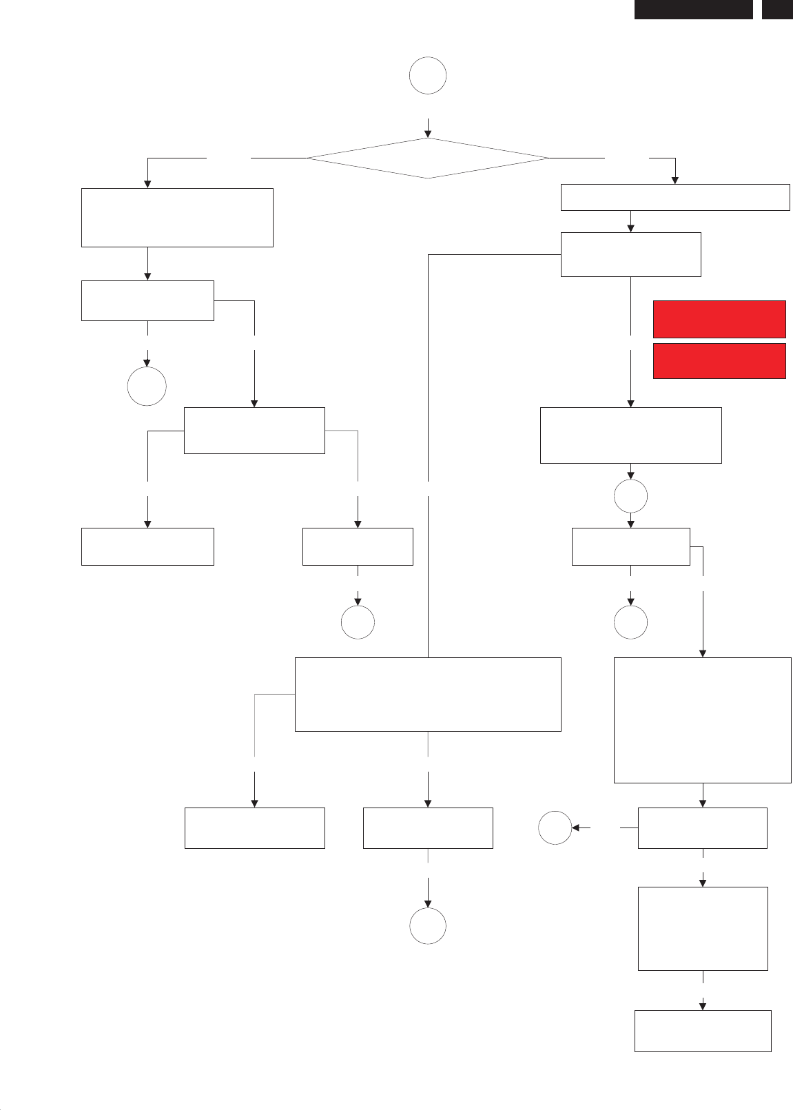
1
LED Amber or Green?
Make sure of the state of the
computer (turn on). Press the
keyboard or operate the mouse.
Is picture display
normally?
END
Power off the monitor
and then restart PC
It is need to check
and repair the monitor
Is picture display
normally?
END
Make sure the correct signal is input.
Is the ATTENTION
picture displayed?
Check contrast level is not
minimized. (Press contrast
button, increase value to 100)
Is picture displayed
normally?
END
1. Check video cable for bent
pins, reseat it.
2. Change resolution (It may
cause by PC.)
3. LCD monitor can not
display Vertical Frequency
settingat76Hz&85Hz
Is picture displayed
normally?
1. Make sure the correct signal is input.
2. Press the keyboard or operate the mouse.
3. Make sure of the range of the input
frequency and then set the computer.
It is need to check and
repair the monitor
Is picture displayed
normally?
END
END
1. Try system with
another monitor.
2. Try monitor with
another system.
It is need to check and
repair the monitor.
Amber
YES
For example:
ATTENTION
CHECK SIGNAL CABLE
ATTENTION
NO SIGNAL INPUT
Green
Continued
No
No Yes Yes
YesNo
Yes
No
Yes Yes No
Yes
No
unsuccessful
OK
General Trouble Shooting Guide 190TW8 TV 59
http://www.wjel.net
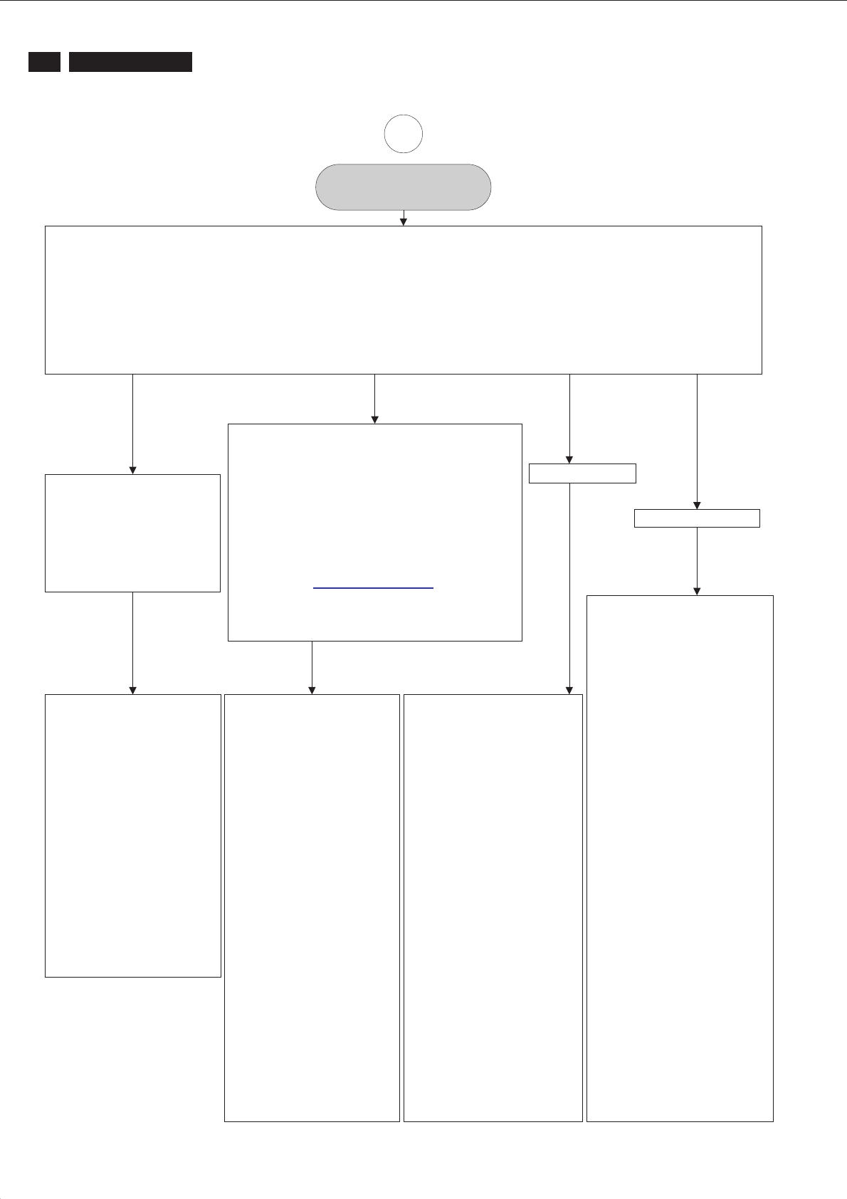
60 190TW8 TV
2
Monitor drivers (inf file)
FOR WINDOWS 95/98/2000/ME OR LATER
Philips’s monitors build in VESA DDC2B feature to support Plug & Play requirement for Windows 95/98/2000/Me. You can install the
information file(.inf) in order to select your Philips monitor from “Monitor” dialog box in Windows 95/98/2000/Me to activate Plug &
Play application. The installation procedure based on Windows 95 OEM Release 2, 98, Me and 2000 is specified as follows, (in case
of connecting the monitor to the PC compliant with VESA standard with the designated signal cable, the PC reads display pixels,
frequency and color feature of this monitor to optimize the picture for the monitor automatically.)
DDC: Abbreviation for Display Data Channel
** Windows NT 4.0 does not require driver (inf file) for monitor.**
1. Start Windows 95
2. Click the ‘Start’ button,
point to ‘setting’, and
then click ‘control panel’.
3. Double click the
‘display’ lcon.
4. Choose the ‘setting’ tab then
click ‘advanced…’
5. Choose ‘monitor’ button,
point to ‘change…’ then click
‘have disk…’.
6. Click ‘browse…’ button then
choose the appropriate drive
F:(CD-ROM Drive) then click
‘ok’ button.
7. Click the ‘ok’ button then
choose your monitor model
and click the ‘ok’.
8. Click ‘close’ button.
For Windows 98
For Windows 98 drivers, our monitors are listed under
2 manufactures name “Philips”, and “Philips
Consumer Electronics Co.” Please select “Philips”
when you would like to set up your monitor in
Windows setting, if you can not find the right model
name just as the label indication on the back of set.
For those set that have been issued since the release
of Window 98, drivers can be found in CD-ROM
under the directory path of “\pc\driver\” or it may be
downloaded at http://www.philips.com. Once you
have installed the new driver, Windows will add a
new manufacture name “Philips Business
Electronics” in your system.
1. Start Windows 98
2. Click the ‘Start’ button, point
to ‘setting’, and then clock
‘control panel’.
3. Double click the
‘display’ lcon.
4. Choose the ‘setting’ tab then
click ‘advanced…’
5. Choose ‘monitor’ button,
point to ‘change…’
then click ‘next’.
6. Choose ‘display a list of all
the drivers in a specify
location, so you can select
the driver you want’, then
click ‘next’ and then click
‘have disk…’
7. Click ‘browse…’ button then
choose the appropriate drive
F: (RD-ROM Drive)
then click ‘ok” button.
8. Click the ‘ok’ button then
choose your monitor model
and click the ‘next’ button.
9. Click ‘finish’ button then click
‘close’ button.
1. Start Window Me
2. Click the ‘start’ button, point
to ‘setting’ , and then click
‘control panel’.
3. Double click the
‘display’ lcon.
4. Choose the ‘setting’ tab then
click ‘advanced…’.
5. Choose ‘monitor’ button, then
click ‘change…’ button.
6. Choose ‘specify the location
of the driver (advanced)’ and
click the ‘next’ button.
7. Choose ‘display a list of all
the drivers in a specific
location, so you can select
the driver you want’, then
click ‘next’ and then click
‘have disk…’.
8. Click ‘browse…’ button then
choose the appropriate drive
F: (CD-ROM Drive)
then click ‘ok’ button.
9. Click the ‘ok’ button then
choose your monitor model
and click the ‘next’ button.
10. Click ‘finish’ button then
click ‘close’ button.
For Window Me
For Windows 2000
1. Start Windows 2000
2. Click the ‘start’ button, point
to ‘setting’, and then click
‘control panel’.
3. Double click the
‘display’ lcon.
4. Choose the ‘setting’ tab then
click ‘advanced…’.
5. Choose ‘monitor;
-If the ‘properties’ button is
inactive, it means your
monitor is properly configured.
Please stop installation.
-If the ‘properties’ button is
active, click ‘properties’ button.
6. Click ‘driver’ and then click on
‘update driver…’ then click on
the ‘next’ button.
7. Choose ‘display a list of the
known drivers for this device
so that I can choose a specific
driver’ then click ‘next’ and
then click ‘have disk…’.
8. Click ‘browse…’ button then
choose the appropriate drive
F: (CD-ROM Drive).
9. Click the ‘open’ button then
click the ‘ok’ button.
10. Choose your monitor model
and click the ‘next’ button.
11. Click ‘finish’ button and then
click the ‘close’ button. If you
can see the ‘digital signature
not found’ window then click
the ‘yes’ button.
For Windows 95
For Windows 95 drivers, your
monitor is listed under
manufacture name “Philips
Business Electronics Co.”.
General Trouble Shooting Guide
http://www.wjel.net
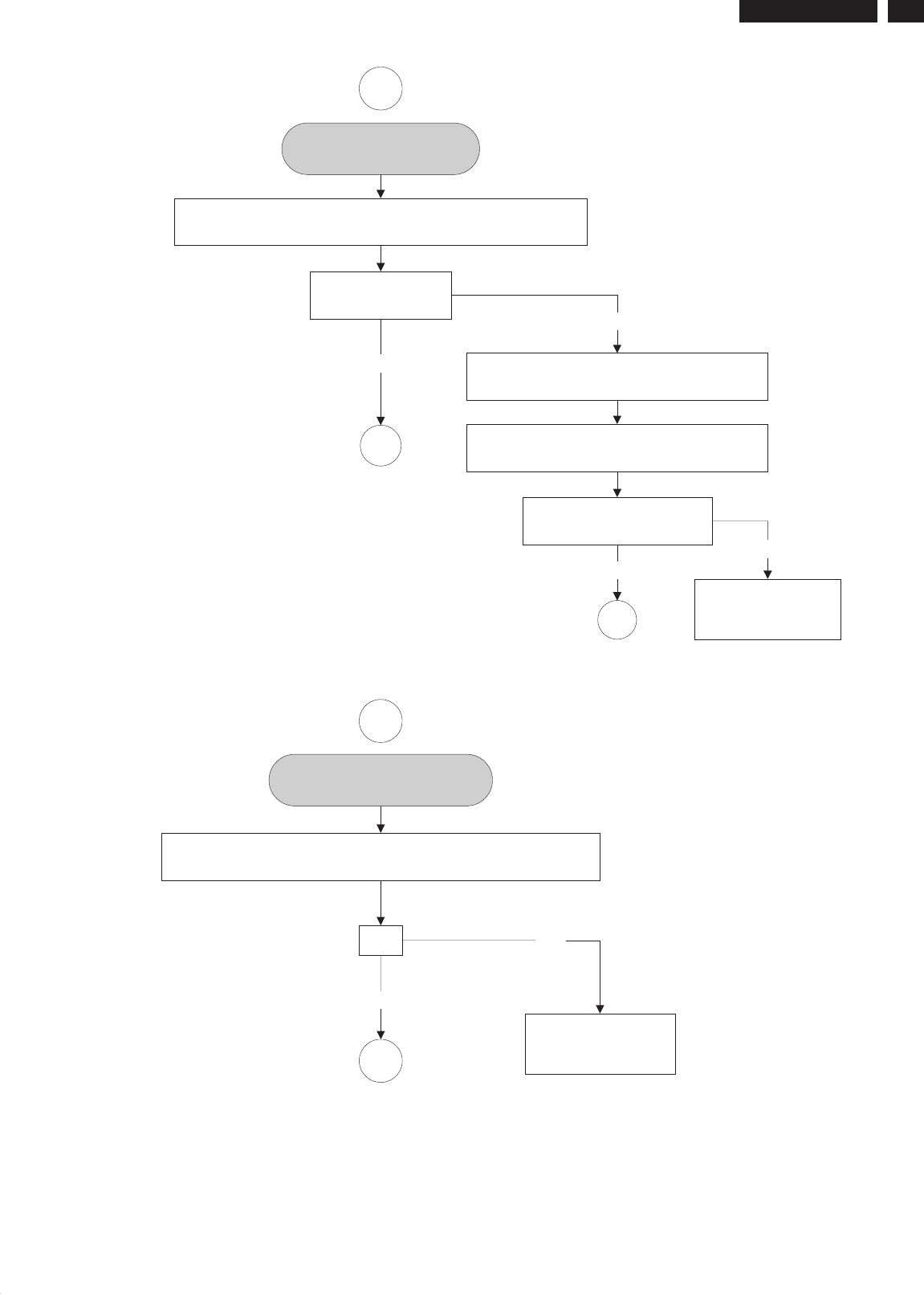
General Trouble Shooting Guide 190TW8 TV 61
3
Screen Size Not Correct
Adjust Horizontal/Vertical/Shape Via the monitor "On Screen
Display" or "Front Control Knob: Auto function key".
Is the Screen Size
displayed correct?
*Reset the monitor via OSD manipulation
(Select Reset to Factory settings).
* Try the monitor with another computer
(Video card could be defective.)
Is picture displayed
normally?
END
Consult a service
center, the monitor
may be defective.
END
YES
No
YES
No
Reset monitor via OSD menu manipulation.
Change monitor timing to work at the recommended resolution.
OK
Please contact your
dealer/reseller for
more information.
4
END
YES
NO
Picture is too large or small
http://www.wjel.net

62 190TW8 TV
6
Unstable picture/picture
flickers
Vertical/Horizontal flicker appears,
Push the AUTO button. Eliminate the Vertical/Horizontal bars
using the Phase Adjustment in the first window.
OK
Please contact your
dealer/reseller for
more information.
YES NO
END
General Trouble Shooting Guide
http://www.wjel.net

7
Out of H/V Sync.
1. Turn off monitor
2. Disconnect signal cable
3. Turn on monitor
In the self test?
(warning signal¡K)
It is need to check and
repair the monitor
Check video cable for bent
pins, reseat to system
video and power system.
Trytogointothe
DOS prompt.
"H/V sync. Out of
presetting timing range"
or "Sync. Problem"?
1. Try system with
another monitor
2. Try monitor with
another system
Monitor related?
Make sure that the video
system doesn't select a
driver that is outside the
monitor H/V scan range out
of presetting timing range
while going into windows.
Run windows by using
basic VGA mode
(example 640*480)
1. Try system with
another monitor
2. Try monitor with
another system
Monitor related?
It is need to check and
repair the monitor
It is need to check and
repair the monitor
Video system problem
YES
NO
YES
NO
YES
"H/V sync. Out of
presetting timing range"
or "Sync. Problem"?
YES
NO
END
YES
END
NO
General Trouble Shooting Guide 190TW8 TV 63
http://www.wjel.net

64 190TW8 TV
8
Picture is too bright
Adjust brightness and/or contrast via
the monitor "On Screen Display"
or "Front Control Knob"
Is picture displayed
normally?
* Reset the monitor via OSD manipulation.
(Select Reset to factory settings¡ )
* (or change the color temperature settings
to be 9300 color coordination from OSD menu.
* Try the monitor with another computer
(video card could be defective.)
Is picture displayed
normally?
It is need to check and
repair the monitor
YES
END
NO
END
YES NO
General Trouble Shooting Guide
http://www.wjel.net
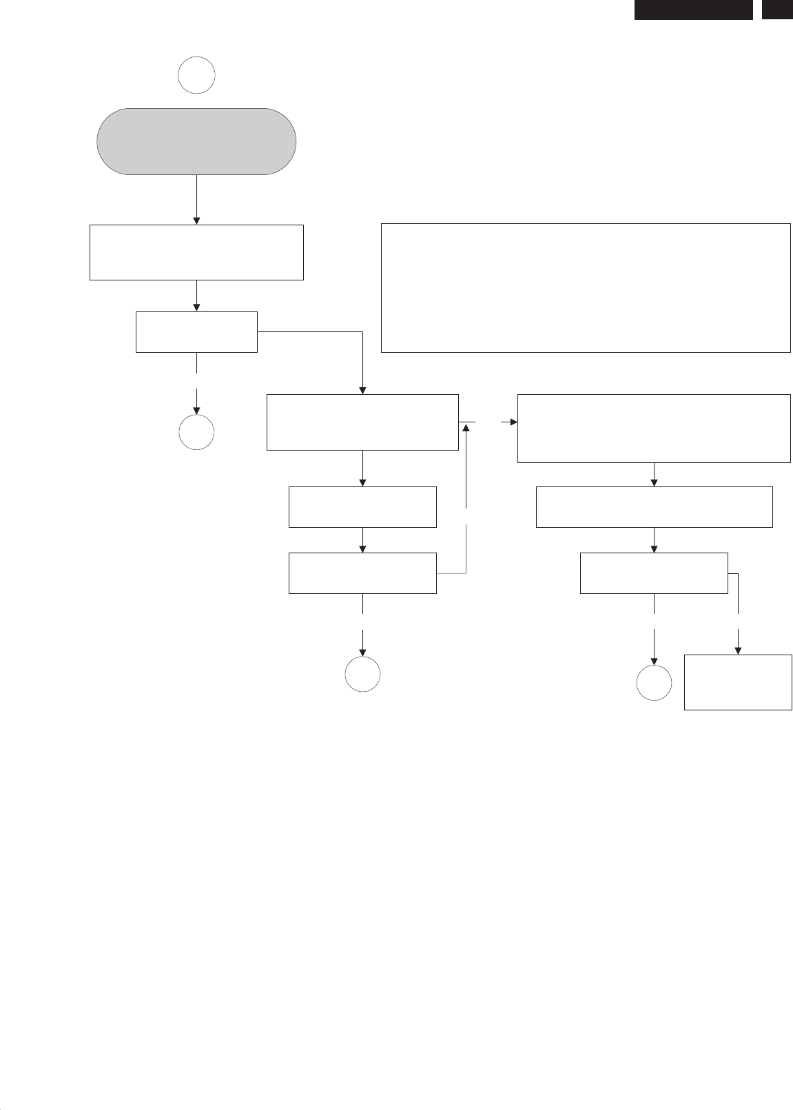
9
Picture is too dim
Adjust brightness and/or contrast
via the monitor "On Screen Display"
or "Front Control Knob".
Is picture displayed
normally?
Is an external Anti-Glare screen
(like protective cover, touch
screen...etc) being used?
Remove any external
Anti-Glare screen
Is picture displayed
normally?
* Reset the monitor via OSD manipulation.
(select Reset to factory settings)
* (or change the color temperature settings to
be 9300 color coordination from OSD menu)
* Try the monitor with another computer
(video card could be defective)
Is picture displayed
normally?
It is need to
check and repair
the monitor
Note:
1. Sun light passing through a window is much brighter than monitor
luminance (luminance is the measurable quantity which most closely
corresponds to brightness), therefore the two worst places for a
monitor is directly facing the window or directly behind the window.
Position the monitor away from these two areas.
END
END
YES
YES
NO
NO
END
YES NO
General Trouble Shooting Guide 65
190TW8 TV
http://www.wjel.net

66 190TW8 TV
10
NOPOWER/LEDisoff
Is cabinet of
monitor damaged
by being dropped?
1. Is the correct AC power
cord connected?
2. Is AC power outlet active?
3. Is the power button in the
ON position?
Power off the monitor
and then on
Power LED on?
The monitor may have
become faulty due to
excessive shock
It is need to check and
repair the monitor
Power LED on?
Insure that unit is plugged into a
known good power source
(move a good radio to plug into
the power source to test it)
It is need to check
and repair the monitor
END
YES
YES
YES
END
NO YES
YES
YES
NO
NO
General Trouble Shooting Guide
http://www.wjel.net

11
Missing Color
1. Turn off monitor
2. Disconnect video cable
3. Turn on monitor
Colors on warning
signal OK?
Check video cable for bent
pins, reseat it
Signal cable pins OK?
1. Try system with
another monitor.
2. Try monitor with
another system.
3. Try changing in
the application.
Is picture displayed
normally?
It is need to check and
repair the monitor.
Cyan Color means that the red sub pixel is missing.
YES
YES
YES
END
NO
There are 2 easy ways to determine the Missing color problem.
1. View an image that is supposed to be "White".
If one of the colors (RGB) is not functioning.
White can not be produced.
2. View an image that supposed to contain Red, Green and Blue.
Color problems will be apparent when one or more of these
colors can not be displayed.
Normal White:
Magenta or Purple Color means that the green sub pixel is missing.
Yellow Color means that the blue sub pixel is missing.
RED ++
GREEN BLUE =WHITE
RED ++
GREEN BLUE =Yellow
RED ++
GREEN BLUE =Magenta
RED ++
GREEN BLUE =Cyan
General Trouble Shooting Guide 190TW8 TV 67
http://www.wjel.net

70 190TW8 TV
13
Jitter / Video Noise
Turn on monitor with a
display or image for 30
minutes (due to drift).
Jitter or Noise still present?
Try moving the monitor to
another location to see if
problem goes away
Jitter or Noise disappear
Environment problem
1. Try system with
another monitor
2. Try monitor with
another system
Jitter or Noise disappear
Video system problem
Monitor related?
Power off any monitor that
is within 2 or 3 feet away
Remove any unshielded
speakers away from the
monitor
Make sure there are no
flourescent light fixtures
close to the monitor
Try to keep monitor away from
large metal structures, power
poles, fans and metal carts
Check for other devices
that may be causing
magnetic interference
Is picture displayed
normally?
It is need to check and
repair the monitor
YES
END
NO
YES
END
YES
END
END
YES
NO
NO
NO
General Trouble Shooting Guide
http://www.wjel.net

14
Power management
function is not active
Verify the PC is compliant with VESA. In case all of the
video signals of PC are not off, power management
function is not active normally. (Repeat to power on and
off power management.) There are accelerator boards
not complied with VESA.
OK
Consult a service
center, the monitor
may be defective
NO
YES
END
General Trouble Shooting Guide 190TW8 TV 71
http://www.wjel.net
General Product Specification
Specification for TVI E9P-PT
Philips Hudson 8 – 190TW8
19’’W TFT LCD TV,
90 ~ 264 V , 47 ~ 63 Hz, Dual input
Table of Contents
1 General Feature
2 Remote Key Definition
3 Local Key Definition
4 Input/Output Signal Specification
5 OSD Tree
6 Power Saving
7 PC Timing Mode
8 Broadcasting Sound
9 Teletext Operation
10 Mechanical Spec
11 Regulation and Reliability
12 Accessory
72 190TW8 TV
http://www.wjel.net

1. General Feature
Destination Europe
Color System PAL, SECAM
Sound System CCIR B/G, D/K, I and L/L’
Stereo System NICAM and FM Stereo ( A2 )
Channel System Full frequency range from channel E2
( 48.25 MHz ) to channel E69 ( 855.25
MHz)
Sub-Title Teletext 100 pages
TV System RF-AFT (+ / - 1.5MHz)
Maximum Resolution 1440*900
Panel Supplier CMO-M190A1-L07
Lamp Quantity CCFL*4
Display Area 19" Wide Diagonal
Display Color 16.7 M with FRC
Contrast Ratio 1000:1 (Typical)
Brightness 300 cd / m*2 (Typical)
Response Time 5 ms
LCD Panel View Angle 85°(L)/85°(R), 80°(U)/80°(D)
HDMI For Audio & Video
RCA Jack *3 For Audio & Video
Din Jack For S-Video
SCART*1 21 Pin for Video ,S-Video & RGB
PH Jack For TV Input ( PAL system)
Earphone Jack For Audio Output
SPDIF For Audio output (I2S)
3.5mm Stereo Jack For PC Stereo Audio Input , Black color
I / O
Functions D-Sub-15 For VGA
Support PAL / NTSC / SECAM video
format
Support 480 i , 480 p,720P,1080i
format
Build in motion adaptive 3D digital
Comb Filter
Video
Functions Build in Teletext Functions
TV System PAL and SECAM system Receivable
Tuner FQ1216-MK5
Horizontal input frequency range :
30~71 KHz
Vertical input frequency range : 50~75
Hz
VGA Maximum resolution : 1440*900
Input Signal
Out of Range
When input signal is out of range or
down scaling support ,the OSD will
show "Out of Range "within 5 seconds
and LED is green
73 190TW8 TV
http://www.wjel.net
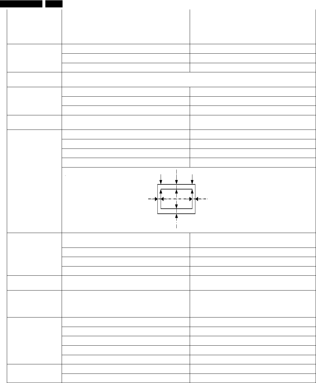
No Signal When there is missing signal from
selected input ,the OSD will show "No
Signal "within 8 seconds and LED is
green
Standard x=300 , y=310
Warm x=313 , y=329
Color
Temperature Cold x=285 , y=293
Maximum
Brightness More Than 250 cd / m*2
Key count 43 Keys
Effective Distance More than 6 m +45~-45degree
Remote
Controller Supplier Panasonic
Local Control
Key 7 Keys
Power, Left, Right, Up, Down, Menu,
Select
Display Area: 19W inches diagonal
H-Phase: A-B Less than 1.5mm
V-Center: C-D Less than 1.5mm
Tilt: E-F Less than 1mm
Display Area
& Tilt
Speaker
Internal speaker. 5W*2 stereo, volume
adjustable.
Treble, Bass ( + 3db)
Frequency Response 100~15KHz with +/-3 db variation
Audio THD(Total HarmonicDdistortion) Limited to 5 % at 2W (at 0.1~15 KHz)
OSD
Capability On screen display adjustment function
ISP Fuctions ISP (In System Programming) function
available for revising driver easily.
Input Voltage 90 ~ 264 V , 47 ~ 63 Hz
Input Current 0.6~1.5 A
Max. Power 58 Watts
PC saving Power 2Watts Max
Power Source Stand-By Power(AV,TV) 1 Watts Max.
Tilt 0~15
Mechanical VESA Mount 100*100 mm
A
E
D
CF
B
74 190TW8 TV
http://www.wjel.net

2. Remote Definition
Item Key Function
1 POWER Power On/Off
2 Mute Mute on/off
3 SLEEP Into sleep mode: Timer Off / 15 / 30 / 45 / 60 / 90 / 120 (minutes)
4 Display Pressing "Display" shows the source information
5 TV ATV
6 SCART SCART
7 AV (AV/S-Video/HDMI)
8 PC VGA
9 1 Number key 1
10 2 Number key 2
11 3 Number key 3
12 4 Number key 4
13 5 Number key 5
14 6 Number key 6
15 7 Number key 7
16 8 Number key 8
17 9 Number key 9
18 0 Number key 0
19 Recall Reture to previous channel
20 Enter Enter to confirm channel selection by number key
21
Up 1.Navigate up in the OSD menu
2.channel up when OSD menu is not showed on screen
22 Down 1.Navigate down in the OSD menu
2.channel down when OSD menu is not showed on screen
23 Left 1.Navigate left in the OSD menu
2.volume down when OSD menu is not showed on screen
24 Right 1.Navigate right in the OSD menu
2.volume up when OSD menu is not showed on screen
25 OK Selection Confirmation
26 Menu Open/Exit Menu
27 Channel Up In ATV mode, press this key to do Channel up,
28 Channel Down In ATV mode, press this key to do Channel down
29 Volume up Volume up
30 Volume down Volume down
31 MPX NICAM
STEREO Broabcast : Stereo/Mono
BILINGUAL Broadcast : Sound 1 / Sound 2
MONAURAL : Mono
FM-FM
STEREO Broadcast : Stereo/Mono
BILINGUAL: Sound1/Sound2/Stereo/Mono
32 INDEX Go to index page
33 SUBTITLE When in teletext mode of any possible source, toggle subtitle on and off
In digital TV mode, press it to change various, subtitle language and off in
a loop. TV screen will display the status icon on the left top corner
34 TELETEXT/MIX when in any possible source which has teletext mode, Turn teletext mode
on / off and Overlay the telext page on the TV picture
35 REVEAL Display Hidden Information
36 SIZE When in teletext pages, this key zoom page toggle 1X/2X and page
selection by Up-arrow and Down-arrow
75 190TW8 TV
http://www.wjel.net
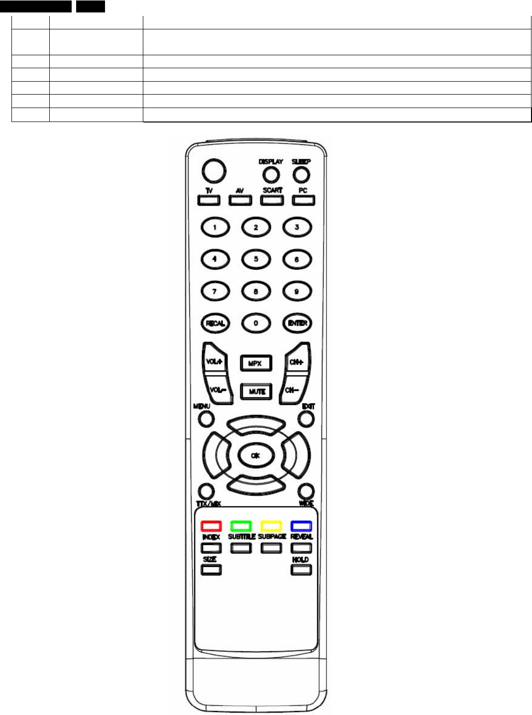
37 SUBPAGE Subpage directly
38 HOLD when in teletext pages, press this button temporarily holds the current
teletext page
39 R Red color button to do teletext operation In teletext mode,
40 G Green color button to teletext operation In teletext mode
41 Y Yellow color button to teletext operation In teletext mode
42 B Blue color button to teletext operation In teletext mode
43 WIDE Scaling Mode ( 4:3 /16:9 /Panorama /Letterbox1/ Letterbox2/ Letterbox3)
76 190TW8 TV
http://www.wjel.net

3. Local Key Definition
BUTTON OSD On OSD Off
1 Power Software On / Off
2 Menu /
Exit
Press this button to open the OSD or
Enter function
3 CH Up Press CH Up key to move selection up
Press these buttons to select the TV
channel in sequence.
4 CH Down
Press CH Down key to move selection
down
Press these buttons to select the TV
channel in sequence.
5 Vol Left
Press Vol Left key to move selection
left or to decrease value
Press these buttons to select the volume
level.
6 Vol Right
Press Vol Right key to move selection
right or to increase value
Press these buttons to select the volume
level.
7 Input / OK Press this button to confirm selection
Press this button to select the input
source: ATV -->AV-->S-Video-->SCART --
>HDMI--->VGA--> Back to ATV
PS: PS: SCART: RGB/S-Video/CVBS
77 190TW8 TV
http://www.wjel.net

4. Input/Output Signal Specication
CVBS Input Type Analog
Polarity Positive
Level 1Vp-p ( with Sync.)
Impedance 75Ω± 5%
Interface RCA jack, Yellow color
S-Video Input Type Analog
Polarity Positive
Level Y : 1Vp-p ( with Sync.) , C : 0.286Vp-p
Impedance 75Ω± 5%
Interface DIN Jack
SCART Input Type Analog
Polarity Positive
Impedance 75Ω± 5%
Interface 21 Pin Euro-SCART
Audio Input Type Stereo R/L Channels
Level 500mVrms
Impedance More than 22kΩ
Interface RCA Jack
Right channel Red color.
Left Channel White color
PC Stereo Input Type Stereo R/L Channels
Level 1Vrms
Impedance More than 22kΩ
Interface 3.5mm Stereo Jack , Black color
Headphone
Output Type Stereo R/L Channels
Level 40mW rms/per Channel(typ.) for 32 ohm earphone
Impedance 32 ohm
Interface 3.5mm Stereo Jack
Built-in Speaker Max. Audio output 5W + 5W (at 1.0Vp-p / 1kHZ input,10% THD max.)
Sound Distortion 1% THD max. ( at 250mW/1kHZ : )
Speaker 5 W / 8 ohms
Speaker Impedance 8 ohms at 1kHZ
Residual Hum 500uW Max.( at Min. Volume : )
Max. Hum 1000uW Max ( at Max. Volume )
Audio Line Output Type Stereo R/L Channels
Level 400Vrms.
Interface 3.5mm Stereo Jack
RF Input Input Impedance 75 ohms
Frequency Range 48.25~855.25 MHz (PAL)
Video S/N Ratio 45 d B (Typical)
Audio S/N Ratio 63 d B (Typical)
VGA Input Sync Level : Low = 0 to 0.8V, High = 2.0 to 5 V
Polarity : Positive or Negative
78 190TW8 TV
http://www.wjel.net

Impedance : 1 k ohm or higher
RGB Signal Level : 0 to 700mV Positive
Impedance : 75Ω± 5%
D-Sub Pin Define 1 Red Video
2 Green Video
3 Blue Video
4 Ground
5 Ground
6 Red Ground
7 Green Ground
8 Blue Ground
9 +5V ( PC97 )
10 VGA-CONN(Sync GND)
11 Ground
12 SDA ( DDC Data )
13 Horizontal Sync
14 Vertical Sync
15 SCL ( DDC Clock )
05/25 TVI update
HDMI Type Type A
Level 400mVrms
Impedance 100Ω
SPDIF Type RCA Jack
Level 500mVpp +- 20%
79 190TW8 TV
http://www.wjel.net
5. OSD Tree
PAL Menu Structure
1st Sub Menu
2nd Sub Menu
3rd Sub Menu
4th Sub Menu
ATV
S-Video
AV
Scart
VGA
HDMI
Brightness Slider [50] 0-100 / 1 V V V V V V
Contrast Slider [80] 0-100 / 1 V V V V V V
Colour Slider [70] 0-100 / 1 V V V V V
Sharpness Slider [4] 0-7 / 1 V V V V V
Backlight Slider [100] 0-100 / 1 V V V V V V
Cold V V V V V V
[Standard] V V V V V V
Color Temp
Warm
V V V V V V
Picture
Noise
Reduction Off / [Low] / Medium / High V V V V V
Treble Slider [50] 0-100 / 1 V V V V V V
Bass Slider [50] 0-100 / 1 V V V V V V
Balance Slider [0] -50-50 /1 V V V V V V
On V V V V V V
Sound Effect [Off] V V V V V V
On V V V V V V
Audio
AVL [Off] V V V V V V
UK
France
Germany
Italy
Spain
Switzerland
Denmark
Belgium
Netherlands
Luxembourg
Czech Republic
Portugal
United Arab Emirates
Channel Management
Country
Saudi Arabia
V
Skip On V
80 190TW8 TV
http://www.wjel.net
[Off] V
Reorder V
Name V
Frequency V
Auto Scan V
Manual Scan
Scan up
Scan down
Scan for update
V
Lock This
Channel
Please enter your PIN [- - -
-] Lock/[Unlock] V
[English] V V V V V V
Deutsch V V V V V V
French V V V V V V
Italian V V V V V V
Spanish V V V V V V
Portuguese V V V V V V
Cestina V V V V V V
Dansk V V V V V V
Dutch V V V V V V
V V V V V V
V V V V V V
Menu
Language
V V V V V V
Sleep [Off]/15/30/45/60/90/120 V V V V V
Please enter your PIN New PIN:
Set PIN [- - - -] Type it again to
confirm:
V
Full V V V V V V
4:3 V V V V V V
[16:9] V V V V V
Panorama V V V V V
Letterbox1 V V V V V
Letterbox2 V V V V V
Wide Mode
V V V V
V
HDMI Scan
Info.
[Auto] / Overscan /
Underscan V
SCART [Auto]/ AV/ S-Video/ RGB V
Settings
Factory
Default V V V V V V
81 190TW8 TV
http://www.wjel.net
6. Power Saving
Mode
Hsync
Vsync Video
Power
Indication Recovery time
Power-On On On Active
<58W Green --
PC saving Off On Off <2W Amber <3s
PC saving On Off Off <2W Amber <3s
PC saving Off Off Off <2W Amber <3s
Standby (AV,TV) <1W Amber R/C or power key on-off
Power off × × × <1W Amber Turn on <5s
Sync on Means normal operation
Sync off Means: Hsync: f<1kHz, duty cycle>25%, Vsync: f<10Hz,duty cycle>25%
* Power comsuption is measured from AC source.
* There are no power saving modes for TV, AV1, S1, SCART inputs.
* While VGA is selected to be input, this LCD TV is equipped with a power
management according to VESA DPMS. There is a delay of 5 seconds before the
transition from On-state to power saving state to avoid unintentionally entering
of a power saving state during display resolution and timing mode changes.
During the period of delay, the LED shall indicate green color and OSD will show
" POWER SAVE “. Transition from any power saving state to another can be
instantaneous. The recovery from Off-state requires no manual power on.
82 190TW8 TV
http://www.wjel.net

7. PC Timing Mode
Pixel
Format Hor.
Freq.(kHz) Hor.
Polarity Vert.
Freq.(Hz) Vertical
Polarity Standard Format
1 640*350 31.5 70 VGA
2 720*400 31.47 - 70 + VGA
3 640*480 31.47 - 60 - VGA
4 640*480 35 66.7 MAC
5 640*480 37.861 - 72 - VESA
6 640*480 37.5 - 75 - VESA
7 800*600 35.156 - 56 + VESA
8 800*600 37.879 + 60 + VESA
9 800*600 48.077 + 72 + VESA
10 800*600 46.875 + 75 + VESA
11 832*624 49.72 74.5 MAC
12 1024*768 48.36 60 VESA
13 1024*768 56.48 70 VESA
14 1024*768 60.02 75 VESA
15 1280*720 44.772 - 59.855 + VESA 16:9
16 1280*720 56.456 - 74.777 + VESA 16:9
17 1360*768 47.72 - 59.799 + VESA 16:9
18 1360*768 60.288 - 74.891 + VESA 16:9
19 1440*900 55.935 - 59.887 + VESA 16:10
20 1440*900 70.635 - 74.984 + VESA 16:10
21 1280x1024
Remark: This LCD TV shall have 10 or more user modes for user
83 190TW8 TV
http://www.wjel.net

8. Broadcasting Sound Standard
Order table for MPX function
Input Sound Mode MPX Key Pressed
MICAM Monaural Mono
Stereo Stereo---Mono
Bilingual Sound1---Sound2
FM
Stereo
(A2) Stereo Stereo---Mono
Bilingual Sound1---Sound2
Reference Table
MPX key Mono Stereo Sound1 Sound2
MICAM Monaural Mono
Stereo Analog mono Stereo
Bilingual Analog mono NICAM-A NICAM-B
FM (A2) Monaural Mono
Stereo Mono Stereo
Bilingual Sound1 Sound2
84 190TW8 TV
http://www.wjel.net

9. Teletext Operation
TELETEXT/MIX TV/Teletext Mode
By pressing Teletext (go to index page),screen will change from TV/AV
mode to Teletext mode and vice versa and Overlay the telext page on
the TV picture
Up/Down and Number
Key Page Selection
Page can be selected in two ways:
a. Press Up or Down to increase or decrease the page number by one
b. By entering the page number, using 0~9 on the remote controller
Red/Green/Yellow/Blue Teletext RGBY soft key
In fast text mode these correspond to differently coloured subjects, In
list mode they correspond to the different coloured page numbers.
HOLD Hold the page
To hold the Teletext page when viewing multi-page information.
Press again to return to automatic page update
SIZE Zoom Teletext Page
This is used to zoom page up to 2X . Press again to return.
SUBTITLE Show Subtitle on the screen
INDEX Go to index page (usually page 10)
REVEAL Display Hidden Information
SUBPAGE Subpage directly
85 190TW8 TV
http://www.wjel.net

10. Mechanical Specification
Weight TBD
Height TBD
Depth TBD
Physical
Dimension Net Weight TBD
Gross Weight TBD
Units per Pallet TBD
Pallet Dimension TBD
40’ Container
Loading TBD
Packing
Specification Carton Label TBD
Display Head ABS UL94HB
Neck / Base ABS UL94HB
Internal Plastic ABS UL94HB
Cabinet Color
Drift
The color drift due to UV-Light shall be less than 3.0 “Delta E”
in the 1976 CIE L*a*b colorspace. Testing shall be performed
according to the requirements of ASTM Test Method D4459-
93.
Cabinet
Material Cabinet Texture
Mold-Tech # 11010 used on all external textured
surfaces.
Bezel The max. gap to the panel glass shall be less than 1.0 mm
Gap
Specification Bezel / Speaker
Cover
The max gap between the bottom of the front bezel and
the top of the speaker cover shall be less than 1.2 mm. The
gap deviation must be less than 0.3mm
Ergonomics Tilt Down 0º up to 1º
Screen Printed
Parts Artwork : TBD
Front Panel
Buttons Tactile
Button Alignment
The gap clearance between the buttons and the bezel
surface shall be uniform
Surface Quality
Surface color, gloss, texture, blemishes, and all other
irregularities in the plastic shall comply with TVIs approval
sheet.
Others Fade and Color
change
All external surfaces shall be sufficiently rugged to withstand
normal operator usage without extreme visible deterioration
in color.
A surface
No defects such as knit lines, parting line, defects in texture,
gate marks, flash, sinks etc. should be visible from a distance
of 18 inches.
B surface
Defects such as knit lines, parting line, defects in texture,
gate marks, flash, sinks etc. should be visible from a distance
of 30 inches.
Cosmetic
Criteria for
Molded Plastic C surface
Unacceptable defects are limited to voids or breaks in the
plastic or gross mold distortions.
Vibration
Frequency : 1 – 200 Hz
Vibration Test
Acceleration : 1.14 G RMS
86 190TW8 TV
http://www.wjel.net

11. Regulation & Reliability
N. America TBD : [ FCC-B, UL (c-UL), CB, NOM.]
S. America TBD: [FCC-B, UL (c-UL), CB, NOM ]
China TBD : [CCC, CB]
Asia/PAL TBD: [C-Tick, CE, CB]
Taiwan TBD: [BSMI, CB, FCC]
Compliance Europe
TBD:[CE, CB, SASO (Saudi Arabia), GOST (Russia), ROHS,
"HD" Logo]
OtherCertification HDMI HDMI Formal Certification on all SKUs with HDMI
Power
Management SRS
SRS Formal Certification on all SKUs where SRS technology is
used
Environmental Requirements
This display shall meet the following environmental requirements under normal operating conditions.
Operating 5°C to 35°C
Temperature Non-
Operation -20°C to 60°C
Operating 20% to 80% (non-condensing)
Humidity Non-
Operation 10% to 85% (<40°C )(non-condensing)
Operating 0 to 12,000 feet
Altitude Non-
Operation 0 to 40,000 feet
*Units tested at an altitude up to 12,000 feet must operate at normal conditions without exhibiting
abnormal behavior such as arcing or shutdown.
Electrostatic Discharge Requirements
This display shall withstand 4kV for contact discharge and 8kV for air discharge of Electrostatic
Discharge to meet the acceptance criteria as specified in EN55024.
Mean time between failure (MTBF)
**For the purposes of demonstrating the MTBF of this product, a failure is defined as the inabilityof
the product to function in accordance with this specification. A failure event interrupts the
expectedoperation of the product and requires service or repair to restore the product to full
functionality.
**The MTBF of this product shall be demonstrated to meet or exceed 50,000 hours @ 25 °C at a
90% lower confidence limit under all operating conditions as specified in previous section. ( Lamp
life is not included )
**All components including power and inverter shall be derate to 80% for active devices, 80% for
under worst case conditions. capacitors and 50% for resistive components, except for polarized
capacitors which may be operated at 90% of voltage - which are all calculated
Mean Time Between Replace (MTTR)
**This display shall be well designed to take less than 5 minutes for replacing control board or
inverter board.
**Note: If there is anything not clarified or specified on this specification, PVT sample shall be a
standard reference.
88 190TW8 TV
http://www.wjel.net

12. Accessory
Length: 1.8meters +15mm/-0mm
Cable Color: Black color
1 Power Cord Quantity: 1
Length: 1.8meters +15mm/-0mm
Cable Color: Black color
2 Audio Cable Quantity: no
Length: 1.8meters +15mm/-0mm
Cable Color: Black color
3 VGA Cable Quantity: no
4 Remote Controller Unit Multi-function
remote controller
include battery
5 TV User Guide Quantity: one
6
Remote Controller User
Guide Quantity: no
7 Warranty Card Quantity: no
8 Battery Quantity: TBD
89 190TW8 TV
http://www.wjel.net
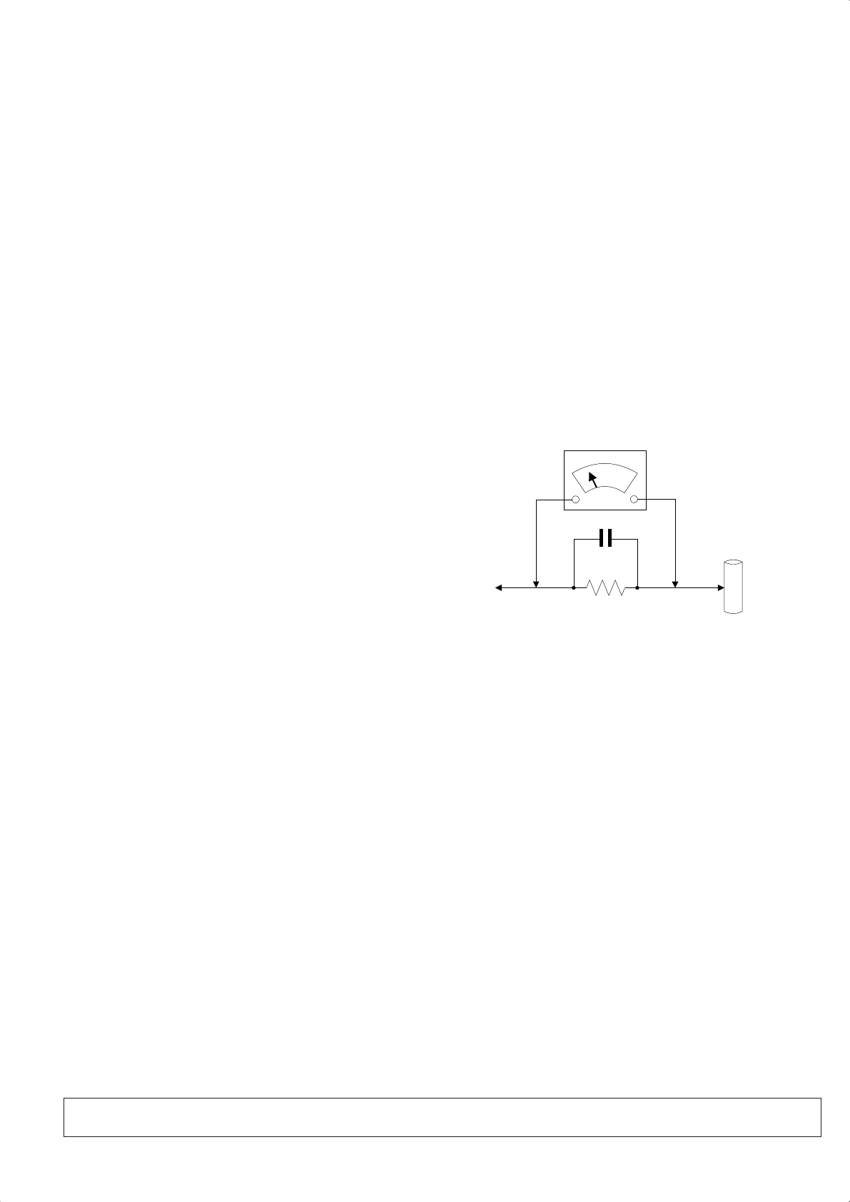
Safety Check Process
Safety Checks
After the original service problem has been corrected, a complete safety check
should be made. Be sure to check over the entire set, not just the areas where
you have worked. Some previous service may have left an unsafe condition,
which could be unknowingly passed on to your customer. Be sure to check all
of the following:
Fire and Shock Hazard
1. Be sure all components are positioned in such a way as to avoid the
possibility of adjacent component shorts. This is especially important on those
chassis which are transported to and form the service shop.
2. Never release a repaired unit unless all protective devices such as
insulators, barries, covers, strain reliefs, and other hardware have been
installed in accordance with the original design.
3. Soldering and wiring must be inspected to locate possible cold solder joints,
solder splashes, sharp solder points, frayed leads, pinched leads, or damaged
insulation(including the accord). Be certain to remove loose solder balls and all
other loose foreign particles.
4. Check across-the-line components and other components for physical
evidence of damage or deteriortion and replace if necessary. Follow original
layout, lead length and dress.
5. No lead or component should touch a receiving tube or a resistor rated at
1watt or more. Lead tension around protruding metal surfaces or edges must
be avoided.
6. Critical components having special safety characteristics are identified with
ans bythe Ref.No in the parts list and enclosed within a broken line *( Where
several critical components are grouped in one area) along with the safety
symbols on the schematic diagrams and/or exploded views.
7.When servicing any unit, always use a separate isolation transformer for the
chassis failure to use a separate isolation transformer may expose you to
possible shock hazard, and may cause damage to servicing instruments.
8. Many electronic products use a polarized ac line cord(one wide pin on the
plug). Defeating this safety feature may create a potential hazard to the
service and the user. Extension cords which do not incorporate the polarizing
feature should never be used.
9. After reassembly of the unit, always perform an leakage test or resistance
test from the line cord to all exposed metal parts of the cabinets. Also check all
metal control shafts(with knobs removed), antenna terminals, handles, screws,
etc. To be sure the unit may be safety operated without danger of electrical
shock.
* Broken line
Implosion
1. All picture tubes used in current model receivers are equipped with an
intergral implosion system care should always be used, and safety glasses
worn, whenever handling any picture tube. Avoid scratching or other wise
damaging the picture tube during installation.
2. Use only replacement tubes specified by the manufacturer.
X-radiation
1. Be sure procedures and instructions to all your service personal cover the
subject of X-radiation. Potential sources of X-rays in TV receivers are the
picture tube and the high voltage circuits. The basic precaution which must be
exercised is to keep the high voltage at the factory recommended level.
2. To avoid possible exposure to X-radiation and electrical shock, only the
manufacturer’s specified anode connectors must be used.
3. It is essential that the service technician has an accurate HV meter available
at all times. The calibration of this meter should be checked periodically against
a reference standard.
4. When the HV circuitry isoperating properly there is no possibility of an X-
radiation problem. High voltage should always be kept at the manufacture,
rated value-no higher- for optimum performance. Every time a color set is
serviced, the brightness should be run up and while monitoring the HV with a
meter to be certain that the HV is requation correctly and does not exceed the
specified value. We suggest that you and your technicians review test
procedures so that HV requation are always checked as a standard servicing
procedure, and the reason for this prudent routine is cleanly understood by
everyone. It is important ot use an accurate and reliable HV meter. It is
recommended that the HV recorded on each customer’s invoice, which will
demonstrate a proper concern for the customer’s safety.
5. When troubleshooting and making test measurements in a receiver with a
problem of excessive high voltage, reduce the line voltage by means of a variac
to bring the HV into acceptable limits while troubleshooting. Do not operate the
chassis loner than necessary to locate the cause of the excessive HV.
6. New picture tubes are specifically designed to withstand higher operating
voltages without creating undesirable X-radiation. It is strongly recommended
that any shop test fixture which is to be used with the new higher voltage
chassis be equipped with one of the new type tubes designed for this service.
Addition of a permanently connected HV meter to the shop test fixture is
advisable. The CRT types used in these new sets should never be replaced
with any other types, as this may result in excessive X-radiation.
7. It is essential to use the specified picture tube to avoid a possible X-radiation
problem.
8. Most TV receivers contain come types of emergency” Hold Down” circuit to
prevent HV from rising to excessive levels in the presence of a failure mode.
These various circuits should be understood by all technicians servicing them,
especially since many hold down circuits are inoperative as long as the
receiver performs normally.
Leakage Current Cold Check
1. Unplug the ac line cord and connect a jumper between the two prongs of the
plug.
2. Turn on the power switch.
3. Measure the resistance value between the jumpered ac plug and all exposed
cabinet parts of the receiver, such as screw heads, antennas, and control
shafts. When the exposed metallic part has a return path to the chassis, the
reading should be between 1 megohm and 5.2 megohms. When the exposed
metal does not have a return path to the chassis, the reading must be infinity.
Remove the jumper from the ac line cord.
Leakage Current Hot Check
1. Do not use an isolation transformer for this test. Plug the completely
reassembled receiver directly into the ac outlet.
2. Connect a 1.5k, 10w resistor paralleled by a 0.15uf capacitor between each
exposed metallic cabinet part and a good earth ground such as a water pipe, as
shown above.
3. Use an ac voltmeter with at least 5000 ohms volt sensitivity to measure the
potential across the resistor.
4. The potential at any point should not exceed 0.75 volts. A leakage current
tester may be used to make this test; leakage current must not exceed a
possibility of shock hazard. The receiver should be repaired and rechecked
before returning it to the customer.
5. Repeat the above procedure with the ac plug reversed.(note: an ac adapter
is necessary when a polarized plug is used. Do not defeat the polarizing
feature of the plug.)
Picture Tube Replacement
The primary source of X-radiation in this television receiver is the picture tube.
The picture tube utilized in this chassis is specially constructed to limit X-
radiation emissions. For continued X-radiation protection, the replacement
tube must be the same types as the original, including suffix letter, or a Philips
approved tube.
Parts Replacement
Many electrical and mechanical parts in Philips television sets have special
safety related characteristics. These characteristics are often not evident from
visual inspection nor can the protection afforded by them necessarily be
obtained by using replacement components r=ated for higher voltage, wattage,
etc. The use of a substitute part which does not have the same safety
characteristics as the Philips recommended replacement part should in this
service manual may create shock, fire, or other hazards.
WARNING: Before removing the back cover, turn the unit OFF and short the HIGH VOLTAGE to the ground.
To
INSTRUMENTS
EXPOSED
METAL PARTS
1500 ohm, 10W
0.15uF
WATER
PIPE
EARTH
GROUND
http://www.wjel.net
