WM EX910 14120609417277
User Manual: WM-EX910
Open the PDF directly: View PDF ![]() .
.
Page Count: 23
SERVICE MANUAL
Ver 1.0 2000. 10
CASSETTE PLAYER
E Model
Chinese Model
SPECIFICATIONS
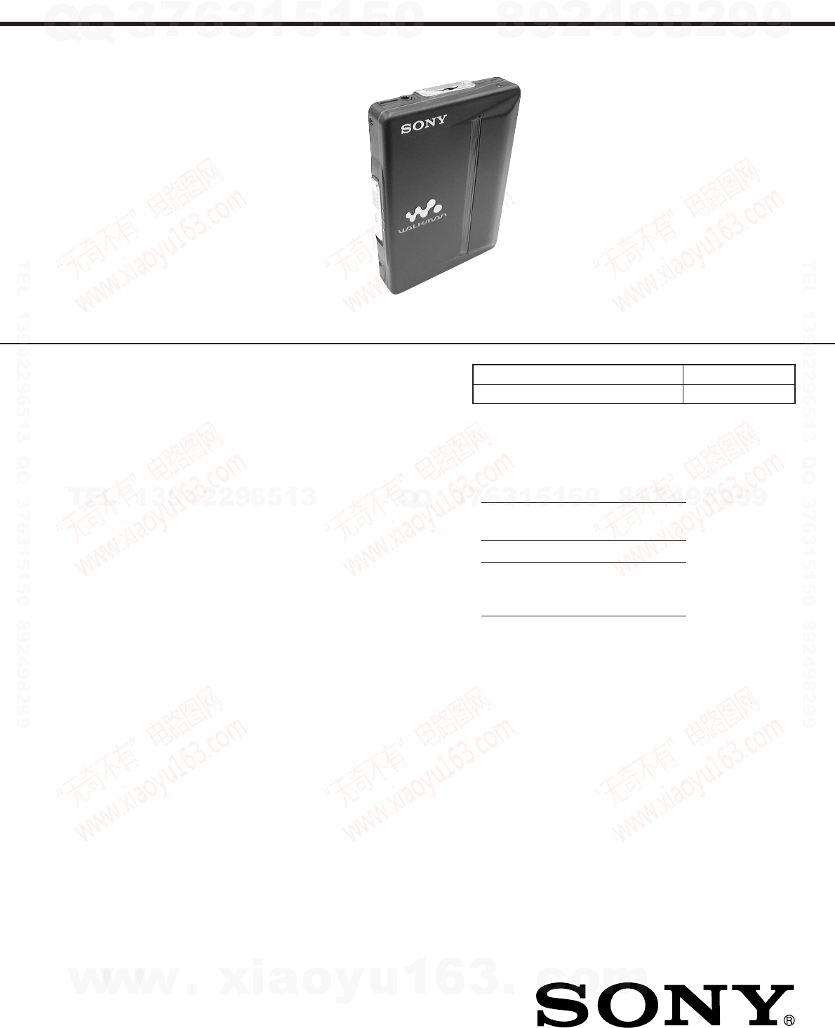
WM-EX910
Photo: Blue model
Manufactured under license from Dolby Laborato-
ries.
“Dolby” and the double-D symbol are trademarks of
Dolby Laboratories.
Model Name Using Similar Mechanism NEW
Tape Transport Mechanism Type MT-WMEX910-162
Battery life (Approx. hours)
(in playback) (EIAJ*)
Rechargeable NC-6WM 20
fully charged
Sony alkaline LR6 (SG)** 66
Rechargeable NC-6WM 84
Sony alkaline LR6 (SG)
used together
* Measured value by the standard
of EIAJ (Electronic Industries
Association of Japan). (Using a
Sony HF series cassette tape)
**When using a Sony LR6 (SG)
“STAMINA” alkaline dry battery
(produced in Japan).
Frequency response (Dolby NR off)
Playback: 30 - 18 000 Hz
Output
Headphones (i jack)
Load impedance 8 - 300 Ω
Power requirements
1.5 V
One rechargeable battery
One R6 (size AA) battery
Dimensions (w/h/d)
Approx. 76.3 × 108.4 × 17.6 mm
(31⁄8 × 43⁄8 x 23⁄32 inches)
Mass
Approx. 140 g (5.0 oz.)
Supplied accessories
Battery case (1)
Stereo headphones or earphones with
remote control (1)
Battery charger (1)
Rechargeable battery (NC-6WM, 1.2V,
600 mAh, Ni-Cd) (1)
Rechargeable battery carrying case (1)
Carrying pouch (1)
Design and specifications subject to
change without notice.
http://www.xiaoyu163.com
http://www.xiaoyu163.com
– 2 –
TABLE OF CONTENTS
1. SERVICING NOTES ............................................... 3
2. GENERAL ................................................................... 5
3. DISASSEMBLY ......................................................... 6
4. MECHANICAL ADJUSTMENTS ....................... 11
5. ELECTRICAL ADJUSTMENTS......................... 11
6. DIAGRAMS
6-1. Block Diagram ................................................................ 13
6-2. Printed Wiring Board ...................................................... 15
6-3. Schematic Diagram ......................................................... 17
6-4. IC Pin Function Description ........................................... 22
7. EXPLODED VIEWS ................................................ 24
8. ELECTRICAL PARTS LIST ............................... 27
Notes on chip component replacement
• Never reuse a disconnected chip component.
• Notice that the minus side of a tantalum capacitor may be dam-
aged by heat.
Flexible Circuit Board Repairing
• Keep the temperature of the soldering iron around 270 ˚C dur-
ing repairing.
• Do not touch the soldering iron on the same conductor of the
circuit board (within 3 times).
• Be careful not to apply force on the conductor when soldering
or unsoldering.
SAFETY-RELATED COMPONENT WARNING!!
COMPONENTS IDENTIFIED BY MARK 0 OR DOTTED
LINE WITH MARK 0 ON THE SCHEMATIC DIAGRAMS
AND IN THE PARTS LIST ARE CRITICAL TO SAFE
OPERATION. REPLACE THESE COMPONENTS WITH
SONY PARTS WHOSE PART NUMBERS APPEAR AS
SHOWN IN THIS MANUAL OR IN SUPPLEMENTS PUB-
LISHED BY SONY.
http://www.xiaoyu163.com
http://www.xiaoyu163.com
– 3 –
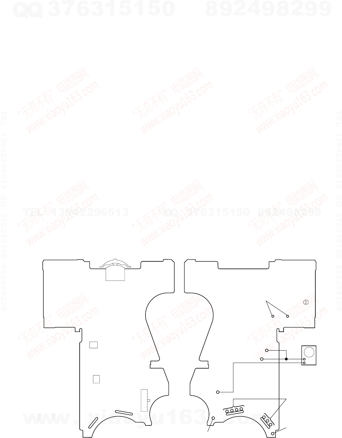
SECTION 1
SERVICING NOTES
This set detects the rotation of the idler gear (A) (side S and side
T) using the photo reflector (PH701, 702). The PH701, 702 are
mounted on the MAIN board, therefore the idler gear (A) (side S
and side T) cannot be detected with the MAIN board removed. As
a result, the motor (M601) cannot be controlled, causing malfunc-
tion.
Further, the DIRECTION switch (S702) is also mounted on the
MAIN board, and with the board removed, the mechanism posi-
tion cannot be detected and the operation is not changed over.
Therefor, when the voltage check is executed with the MAIN board
removed, follow the procedure provided below.
1. Setting
1) Refer to “3. DISASSEMBLY”, and remove the MAIN board.
2) Connect the MAIN board to the motor (M601) and the plunger
(PM701) using jumper wires. These can be connected easily
with the use of the extension tool (Part No. 1-769-143-11) (ten
in one set).
3) Short the lands by solder.
4) Connect the AF oscillator to the TP31 (PH-S), TP32 (PH-T)
and the TP (GND).
5) Supply 1.3 V to the battery terminals using the regulated power
supply.
2. Preset state
To set the PLAY, FF, REW modes, the preset state must be set.
1) Check that the slider (NR) and the DIRECTION switch (S702)
are set to the center position. If not, set the preset state as fol-
low.
2) Move the DIRECTION switch (S702) to the side, which the
slider (NR) is facing.
3) The slider (NR) will move when the regulated power supply
switch is set to OFF once and then set to ON. Move the DI-
RECTION switch (S702) according to this timing and set to
the center position.
3. FF, REW modes
1) Check that the preset state is set.
2) Input the square wave or sine wave to the TP31 (PH-S), TP32
(PH-T) and the TP (GND).
3) Move the jog lever (S703) toward [FF] or [REW].
4. PLAY mode
1) Check that the preset state is set.
2) Input the square wave or sine wave to the TP31 (PH-S), TP32
(PH-T) and the TP (GND).
3) Press the jog lever (S703) will move the slider (NR) once to-
wards the side REV and then to the side FWD. Move the DI-
RECTION switch (S702) according to this timing will set the
PLAY mode (side FWD). Press the jog lever (S703) another time
for a second and move the DIRECTION switch (S702) ac-
cording to the movement of the slider (NR) will set the PLAY
mode (side REV).
Note 1: If the above fails, perform from preset again.
Note 2: When using headphones, the timing for move the DIRECTION
switch (S702) can be determined from the beep sound.
+
–
PUSH –
Y
/
x
r
PH702
S703
jog lever
S702
(DIRECTION)
BP701
FWD
R
STOP
r
REV
PH701
>
REW
.
FF
– MAIN BOARD
(Side A) – – MAIN BOARD (Side B) –
connect to the
plunger (PM701)
TP32 (PH-T)
TP (GND)
TP31 (PH-S)
AF oscillator
square wave
(sine wave)
100 Hz, –3.5 dB
connect to the
motor (M601)
battery
terminal
3
battery terminal
#
http://www.xiaoyu163.com
http://www.xiaoyu163.com
– 4 –
Slider (NR) Rotation system
Rotation system during PLAY.
Rotation system during FF. Rotation system during REW.
slider (NR)
side F side R
center
insert flywheel (N) insert flywheel (R)
reverse pulle
y
clutch assy (F)
gear (Y)
cam gear
gear (REEL) (side T) motor pulley
idler gear (A) (side T)
gear (FR)
(FF: left side)
insert flywheel (N) insert flywheel (R)
reverse pulley
clutch assy (F)
idler gear (B)
gear (Y)
cam gear
gear (REEL) (side T) gear (REEL) (side S)
motor pulley
idler gear (A) (side T) idler gear (A) (side S)
gear (NR)
(FWD : left side/
REV : right side)
insert flywheel (N) insert flywheel (R)
reverse pulley
clutch assy (F)
gear (Y)
cam gear
gear (REEL)
(side S)
motor pulle
y
idler gear (A)
(side S)
gear (FR)
(REW: right side)
http://www.xiaoyu163.com
http://www.xiaoyu163.com
– 5 –
SECTION 2
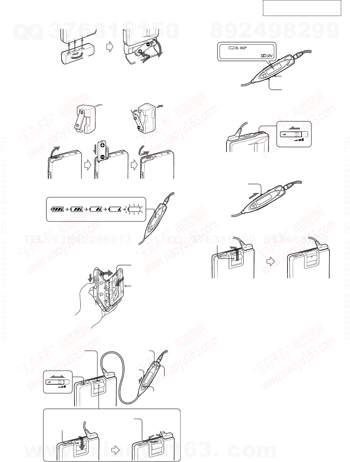
GENERAL This section is extracted from
instruction manual.
A
UK, Australian, and Hong Kong
model
Modèle pour le Royaume-Unie,
l’Australie et Hong-Kong
Modell für GB, Australien und
Hongkong
Other models
Autres modèles
Andere Modelle
1
2
3
4
B
VOL
AVLS
OPEN
C
D
Y •x
FF (+)
REW (–)
Jog lever
Levier Jog
Jog-Hebel
FWD
REV
HOLD
Plug in firmly.
Branchez fermement.
Fest einstecken.
Hold shutter
Cache de
verrouillage
Schutzschieber
Jog lever
Levier Jog
Jog-Hebel
FF REW
E
HOLD
MODE
SOUND
F
G
OPEN
Hold shutter
Cache de
verrouillage
Schutzschieber
VOL
AVLS
http://www.xiaoyu163.com
http://www.xiaoyu163.com
– 6 –
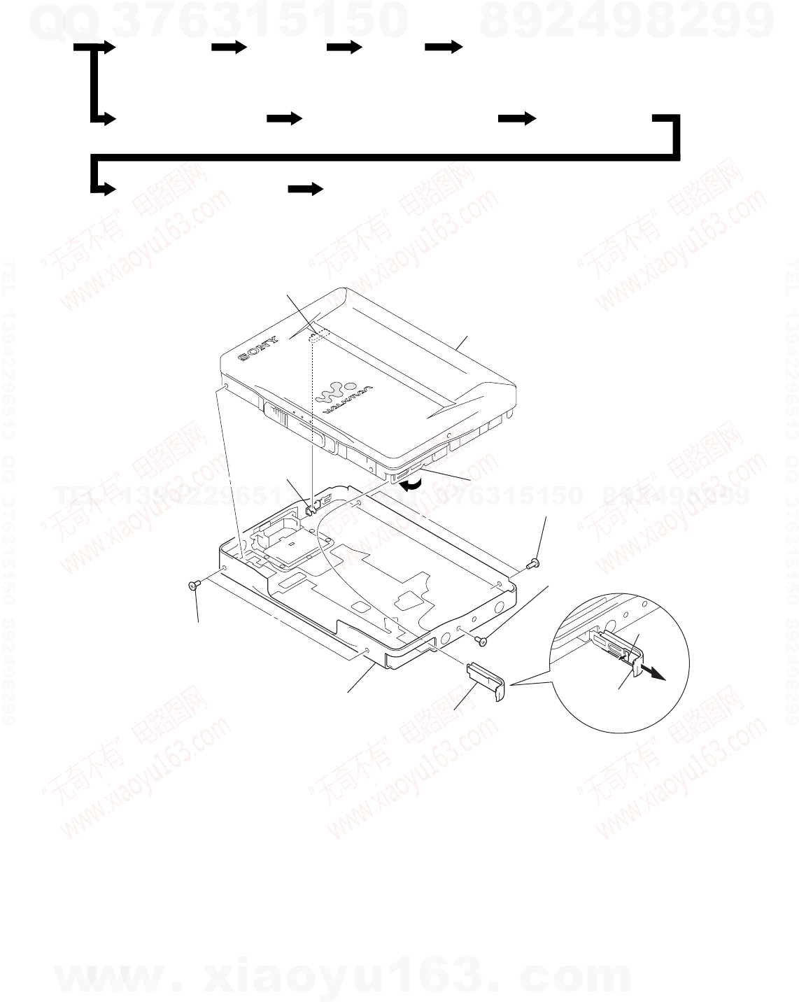
SECTION 3
DISASSEMBLY
• This set can be disassembled in the order shown below.
Note: Follow the disassembly procedure in the numerical order given.
CASE SECTION
SET CASE SECTION MAIN BOARD
HOLDER (FA) ASSY
HEAD, MAGNETIC (PLAYBACK) (HP901)
BELT (F4) MOTOR, DC (CAPSTAN/REEL) (M601)
ORNAMENT (OPEN) BLOCK ASSY
LID SUB ASSY, CASSETTE
LEVER (N2)/(R2) ASSY, PINCH
S701
knob (vol)
Note:On installation
“lid assy, cassette” adjust
the S701 and knob (vol).
lid assy, cassette
4
Close terminal board assy.
5
two screws (MI)
6
screw (MI)
2
claw
1
open “lid, battery
case”.
3
lid, battery case
7
case section
5
two screws (MI)
http://www.xiaoyu163.com
http://www.xiaoyu163.com
– 7 –
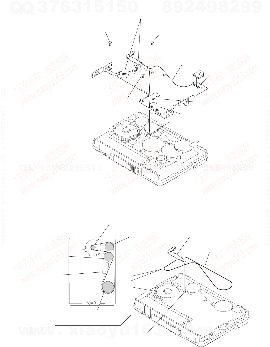
MAIN BOARD
BELT (F4)
2
screw (M1.4) (toothed lock)
3
MAIN board
2
screw
2
screw
1
Remove six solders of
head flexible board.
1
Remove seven solders of “motor, DC (M601)”.
1
Remove two solders of
“solenoid, plunger”.
1
Remove four solders of
“switch, leaf (S704)”
slider
S702
Note:On installation
MAIN board adjust
the S702 and slider.
2
terminal board, battery
1
Remove solder of
“terminal board, battery”.
3
belt (F4)
pulley, motor
pulley, reverse
flywheel (R),
insert
belt (F4)
flywheel (N), insert
http://www.xiaoyu163.com
http://www.xiaoyu163.com
– 9 –
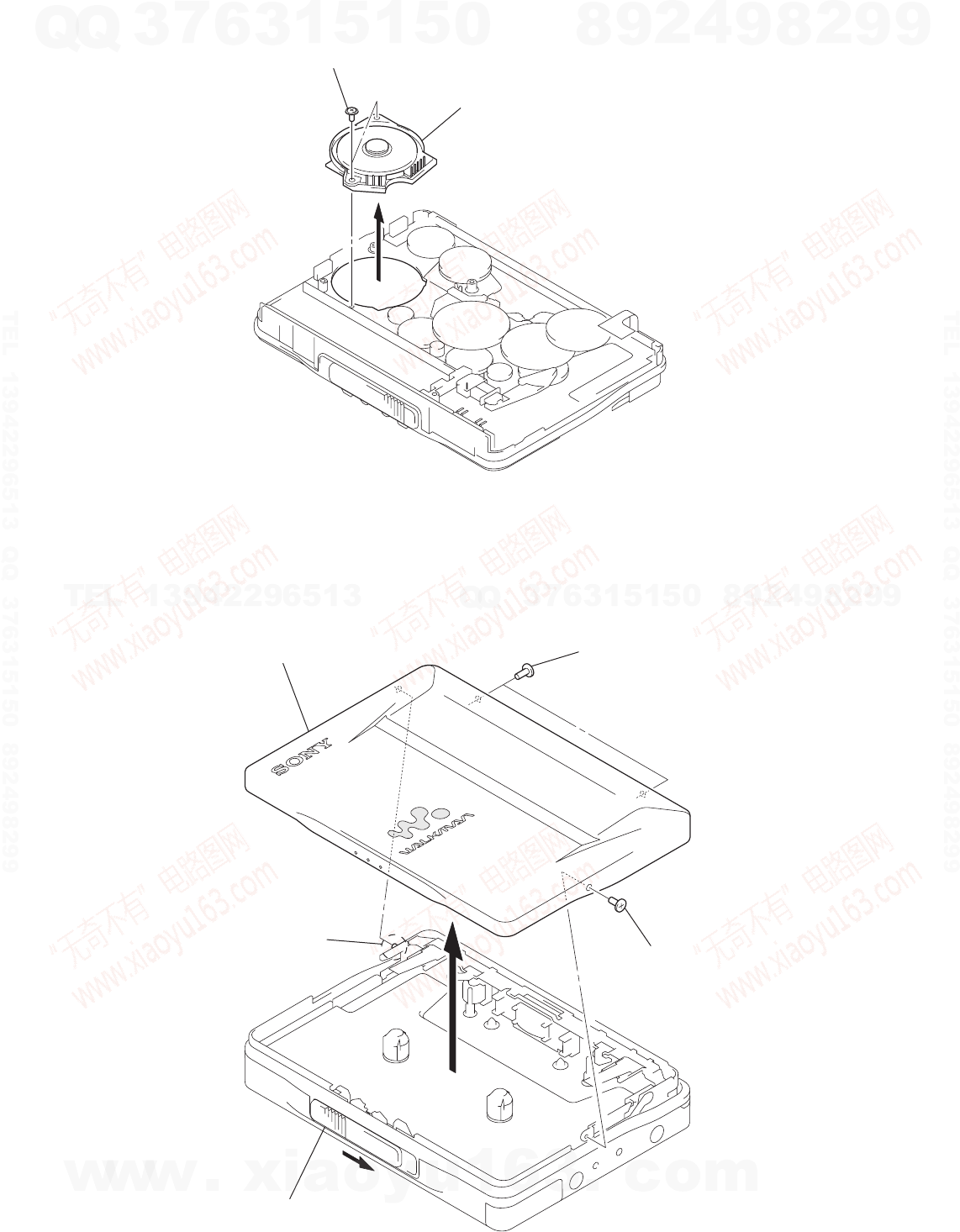
ORNAMENT (OPEN) BLOCK ASSY
HOLDER (FA) ASSY
2
claw
4
two claws
5
ornament (open) block ass
y
3
boss
1
1
7
bracket (cassette/910) assy
2
boss
6
boss
3
lever (B) (/M), loc
k
5
lever (S) (/M), lock
1
two screws (M1.4)
4
screws (M1.4)
8
Remove six solders of
head flexible board.
9
holder (FA) assy
http://www.xiaoyu163.com
http://www.xiaoyu163.com
– 10 –
LEVER (N2)/(R2) ASSY, PINCH
HEAD, MAGNETIC (PLAYBACK) (HP901)
1
claw
3
claw
2
Remove “lever (R2) assy, pinch”
in the direction of the arrow.
4
Remove “lever (N2) assy, pinch
”
in the direction of the arrow.
holder (FA) assy
4
boss
lever, head
3
claw
1
claw
2
5
head, magnetic (playback
)
(HP901)
http://www.xiaoyu163.com
http://www.xiaoyu163.com
– 11 –
PRECAUTION
1. Clean the following parts with a denatured-alcohol-moistened
swab: playback head pinch roller
rubber belts capstan
2. Demagnetize the playback head with a head demagnetizer.
(Do not bring the head demagnetizer close to the erase head.)
3. Do not use a magnetized screwdriver for the adjustments.
4. The adjustments should be performed with the rated power
supply voltage (1.3 V) unless otherwise noted.
Torque Measurement
Mode Torque Meter Meter Reading
(1.47 – 2.94 mN•m)
FWD 15 –25 g•cm
CQ-102C (0.22 –0.36 oz•inch)
(0.029 – 0.196 mN•m)
FWD 0.3 –2.0 g•cm
Back Tension (0.004 –0.01 oz•inch)
(1.47 – 2.94 mN•m)
REV 15 –25 g•cm
CQ-102RC (0.22 –0.36 oz•inch)
(0.029 – 0.196 mN•m)
REV 0.3 –2.0 g•cm
Back Tension (0.004 –0.01 oz•inch)
(more than 3.43 mN•m)
FF, REW CQ-201B more than 35 g•cm
(more than 0.5 oz•inch)
SECTION 4
MECHANICAL ADJUSTMENTS SECTION 5
ELECTRICAL ADJUSTMENTS
PRECAUTION
1. Specified voltage : 1.3 V (DC)
2. Switch position
VOL, AVLS : Center
3. Remote control setting
HOLD switch : OFF
VOL knob : MAX
DOLBY NR : OFF
SOUND mode : Normal
0 dB=0.775 V
Test tape
Type Signal Used for
WS-48A 3 kHz, 0 dB Tape Speed Adjustment
Tape Speed Adjustment
Setting:
Procedure:
1. Playback WS-48A (tape center) in the FWD state.
2. Adjsut RV601 so that the frequency counter reading becomes
3,000 Hz.
Specification Values: 2,985 to 3,015 Hz
3. Playback WS-48A (tape center) in the REV state.
Check that the frequency counter reading is within 2.0%
(approx.60 Hz) of the reading of step 1.
Adjustment Location:
– MAIN BOARD –
frequency counte
r
test tape
WS-48A
(3 kHz, 0 dB)
set
i
jack (J301)
–
+
16
Ω
RV601
http://www.xiaoyu163.com
http://www.xiaoyu163.com
WM-EX910
– 13 – – 14 –
SECTION 6
DIAGRAMS
6-1. BLOCK DIAGRAM
PREAMP
METAL
CONTROL
HP901
(PLAYBACK)
AUDIO MASTER AMP
IC301-1
S704-2
(ATS)
PRE
OUT-L
MTL
DRV-R
FWD
IN-L
REV
IN-L
L-CH
R-CH
FWD
L-CH
R-CH
REV
R-CH
R-CH
R-CH
F/R SW
M/N SW
7
9
46
1
5
S704-1
(TAPE DETECT)
F/R CTL
9
17
CASSETTE SW
5
METAL
SWITCH
Q306
METAL EQ
AMP CONTROL
Q305
PRE OUT
CONTROL
Q315
R-CH
FWD SW
CEN SW
REV SW
S701
(DIRECTION)
FWD STOP REV
2 3 4
MAX MID MIN
4 5
14
IN-L OUL-L
VCC
B+
SWITCH
Q316
DOLBY NR AMP
IC303
DDC B+
VOLUME MIN
SWITCH
Q315
VOLUME MAX
SWITCH
Q311
R-CH R-CH
R-CH
DDC B+
VOL, AVLS
S301
MUTING
Q317
DOLBY CTL
20
AUDIO ATT
REVIVE CTL
MEGA BASS CTL
AMS IN
BOOST CTL
MUTE CTL
BEEP
DATA/RMUM
KEY IN
XT0
XT1
1 7
28
29
30
MEGA BASS/
GROOVE
SWITCHING
Q302
REVIVE/
GROOVE
SWITCHING
Q304
8
R-CH
AMS
V/I
BASS BOOST
AMP
BST
OUT
AMS OUT
40
33
AMS
IN
12
POWER AMP
POWER AMP
EQ-L
PW IN-C
PW
NF-L
PW
IN-L
32
43 41 42
R-CH
R-CH
AGC DET 35
AGC
IN
21
PW
OUT-C
20
17 18 19
PW
OUT-L
BEEP
i
39
39 10 12 36
BST SW
MT SW
PW SW
BEEP
R-CH
BATT B+ VCC
DATA
REMO
GND
JOG LEVER
& SWITCH
S703
REW/FF
PUSH Y/x
+
RIPPLE FILTER
Q309 BATT B+
AUDIO MASTER AMP
IC301-2
RF OUT
BASE
VCC
J301
6 16 28 29
X701
32.768kHz
M/N
CONTROL
Q301
PLUNGER
DRIVE
Q701
PM701
(PLUNGER)
PM CTL
RECHARGEABLE
BATTERY
NC-6WM
DRY BATTERY
SIZE “AA”
(IEC DESIGNATION R6)
1PC. 1.5V
BATTERY
CASE
DC/DC
CONVERTER
IC701
1
2
3
4 8
7
VOLTAGE
DETECT
IC702
STOP
SWITCH
Q702
BATT B+
RESET SIGNAL
GENERATOR
IC704
VOLTAGE DETECT
IC703
351511
DDC B+
OUT1
OUT2
OUT3
OUT4 VCC
CE
DDC
B+
ROTATION
DETECT SENSOR
(T REEL)
PH702
DDC
B+
ROTATION
DETECT SENSOR
(S REEL)
PH701
19
CAPSTAN/REEL
MOTOR SERVO
IC601
DECODER
SOFT
CLIP
13
34
32
31
35
36
1
28
29
30
P-SIG
ENCODER
COMPARATOR
PULSE∆/∆t
BUFFER
COMPARATOR
14
15
17
CAPSTAN/REEL
MOTOR
START SWITCH
Q602
BUFFERVI 16
4
5
6
POWER
CURRENT AMP
21
9
7
TAPE SPEED
RV601
CONTROL
BLOCK 8
10
40
19
BATT B+
2
CAPSTAIN/REEL
MOTOR SWITCH
Q601
CAPSTAIN/REEL
MOTOR CONTROL
Q603-2
CAPSTAIN/REEL
MOTOR CONTROL
Q603-1
M601
CAPSTAIN/REEL
MOTOR
41 18 47 46 45 42 44 43
U
V
W
TU
TV
TW
COM
MC
UOUT
VOUT
WOUT
US
VS
WS
UT
VT
WT
MC
ENTER
PSIG
PW
VC
IV
VI2
VI1
UIN
VIN
WIN
U
V
W
ICI1
DR
CTRL1
CTRL2
CTRL1
CTRL2
U
V
W
CTRL1
CTRL2
RESET
BATT DET
AMP CTL
PHOTO CTL
P-SIG
MOTOR START
SPEED CTL
MOTOR U
MOTOR V
MOTOR W
MOTOR DIR
CTRL1
CTRL2
SYSTEM CONTROLLER
IC705
44
37
PHOTO (S) IN
38
PHOTO (T) IN
05
• SIGNAL PATH
• R-ch is omitted due to same as L-ch.
: PLAY
PHOTO REFLECTOR
SWITCH & BUFFER
Q703
http://www.xiaoyu163.com
http://www.xiaoyu163.com
WM-EX910
– 15 –– 16 –
6-2. PRINTED WIRING BOARD
•Semiconductor
Location
Ref. No. Location
D701 D-2
D702 G-6
IC301 B-6
IC303 C-3
IC601 H-4
IC701 G-6
IC702 D-1
IC703 D-1
IC704 E-3
IC705 D-4
PH701 G-3
PH702 E-3
Q301 E-10
Q302 D-11
Q304 D-11
Q305 B-7
Q306 C-9
Q309 B-5
Q311 B-3
Q312 A-13
Q314 A-13
Q315 C-4
Q316 C-4
Q317 B-13
Q601 I-3
Q602 G-3
Q603 H-5
Q701 C-1
Q702 D-1
Q703 F-3
Note on Printed Wiring Board:
•X: parts extracted from the component side.
•Y: parts extracted from the conductor side.
•z: Through hole.
•b: Pattern from the side which enables seeing.
(The other layers' patterns are not indicated.)
Caution:
Pattern face side: Parts on the pattern face side seen from
(Side B) the pattern face are indicated.
Parts face side: Parts on the parts face side seen from
(Side A) the parts face are indicated.
Q309
BCE
FB701
E
C
B
Q701
F701
R701
Q311
R212
R211
R112
R111
R317
C111
C113
C112
C212
C213
C211
1
7
14
8
IC303
R313
R314
C327
Q315
R724
R723
R721
R720
R718
R719
R716
R717
R722
R109
R209
R301
R308
C109
C209
C306
C324
+
C303
C302
+
IC301
4837
1324
1
12
36
25
C326
+
C322
+
C201
+
C101
+
Q305
C304
+
CB301
C301
+
5
8
4
1
IC703
C702
IC702
12
43
ECB
Q702
X701
D701
KA
C707
C705 C708
C706
C709
R318
C329
R319
R320
E
C
B
Q316
C208
C108
R709
R708
R706
IC705
24 13
37 48
12
1
25
36
IC704
1
2
4
3
R707
C704
C703
R714
R715
PH702
C710
R711
Q703
R712 R713
R614
R613
C611
R611
C610
Q602
B
C
E
PH701
C612
+
R610
C609
RV601
R606
E
C
B
Q601
C601
R608
R605
R607
C608
+
IC601
19
2719
10
18
36
28
Q603
R729
R726
R728
R727
S702
(DIRECTION)
FWD
r
STOP
r
REV
IC701
123
54
L701
D702
AK
i
J301
VCC
DATA
REMOTE
GND
L
R
COM
S703
REW/FF, PUSH Y / x
S301
C328
+
MAIN BOARD
(SIDE A)
1-679-256-
11
(11)
CB301
R205
R204
R201
R202
R105
R102
C203
R203
R104
R103
R101
C103
R303
Q306
BCE
C323
+
Q312
B
C
E
Q314
B
C
E
R316 R216 R116
R213 R113
R214 R114
R217
R117
Q317
R725
JC201
C107
C207
JC101
JC102
JC202
C325
R309
R310
C316
R108
R208
R312
R306
C319
R302
C102
C313
C202 C205
R207
C105
R107
C312
C310
C311
C309
C307
+
C308
Q302
Q304
R710
R702
R705
R703
R704
R730
JC701
Q301
R602
R601
C605
R609
C607
C606
R604
R603
R612
C603
C604
C602
S704-1
(TAPE DETECT)
S704-2
(ATS)
BP701
PM701
RECHARGEABLE
BATTERY
NC-6WM
1.2V 600mAh
REV
FWD
L-ch
R-ch
L-ch
R-ch
HP901
(PLAYBACK)
1
2
3
4
5
6
1
2
3
4
5
6
MAIN BOARD
(SIDE B)
1-679-256-
11
(11)
TV TW COM TU
V
U
W
M601
CAPSTAN/
REEL
(CHASSIS)
05
123 4 5 6 7 8 9 10 11 12 13 14 15
A
B
C
D
E
F
G
H
I
1
7
14
8
C701
+
1S
1G
2D
1D
2G
2S
FF
REW
1S
1G
2D
1D
2G
2S
1S
1G
2D
1D
2G
2S
VOL, AVLS
MIN t MID t MAX
1E
1B
2C
1C
2B
2E
1B
E
2B
1C
2C
1B
E
2B
1C
2C
1B
E
2B
1C
2C
1E
1B
2C
1C
2B
2E
TP32 (PH-T)
TP31 (PH-S)
TP (GND)
DRY BATTERY SIZE “AA”
(IEC DESIGNATION R6)
1PC. 1.5V
http://www.xiaoyu163.com
http://www.xiaoyu163.com
WM-EX910
– 17 –– 18 –– 19 –
6-3. SCHEMATIC DIAGRAM •See page 20 for IC Block Diagrams. •Waveforms
1IC701 5 (LX)
1 V/DIV, 10 µs/DIV
2IC705 wh (CB2)
500 mV/DIV, 20 µs/DIV
Note on Schematic Diagram:
•All capacitors are in µF unless otherwise noted. pF: µµF
50 WV or less are not indicated except for electrolytics
and tantalums.
•All resistors are in Ω and 1/4 W or less unless otherwise
specified.
•% : indicates tolerance.
•C: panel designation.
•A: B+ Line.
•U: B+ Line.
•H: adjustment for repair.
•Power voltage is dc 1.3 V and fed with regulated dc power
supply from battery terminal.
•Voltages and waveforms are dc with respect to ground
under no-signal conditions.
no mark : PLAY
( ) : STOP
[ ] : DOLBY NR ON
•Voltages are taken with a VOM (Input impedance 10 MΩ).
Voltage variations may be noted due to normal produc-
tion tolerances.
•Waveforms are taken with a oscilloscope.
Voltage variations may be noted due to normal produc-
tion tolerances.
•Circled numbers refer to waveforms.
•Signal path.
E: PLAY
3IC705 wl (XT1)
1 V/DIV, 20 µs/DIV
4IC705 ef (OSC1)
1 V/DIV, 1 µs/DIV
5IC705 rg (MOTOR W), rh (MOTOR V),
rj (MOTOR U)
500 mV/DIV, 2 ms/DIV
3 Vp-p
3
µ
s
2.4 Vp-p
1.8
µ
s
1.2 Vp-p
61
µ
s
1.3 Vp-p
6.6 ms
2.2 Vp-p
30
µ
s
http://www.xiaoyu163.com
http://www.xiaoyu163.com
– 20 –– 21 –– 22 –
•IC Block Diagrams
IC301 TA2123AF (EL)
IC303 NJM2185AV-TE2
IC601 LB1994M-TLM
IC703 MM1305BWBE
PRE A PRE B
MIX
PW B
PW A
PW C
BST
MT TC
BASE
RF IN
PW GND
OUT B
OUT C
OUT A
VCC
RF OUT
VREF OUT
BST NF
BST OUT
PW IN C
LPF
EQ A
PW NF A
PW IN A
PW IN B
PW NF B
3
IN A-R
5
PRE NF-A
6
PRE OUT A
7
MTL DRV A
8
MTL DRV B
9
PRE OUT B
10
PRE NF-B
11
AMS IN
12
IN B-R
4
IN B-F
2
IN A-F
1
21
20
19
18
17
GND
16
AMS DET
15
AMS MIX
14
AMS SW
13
22
23
24
38
C-AMP SW 37
PW SW 42
MT SW 41
F/R SW 44
BST SW 43
M/N SW 46
PRE GND 47
VREF IN 48
PRE SW 45
AMS OUT 40
BEEP 39
262728293031323334
DET
36
AGC IN
35
+
–
+
–
+
–
+
–
+
–
+
–
EQ B
25
RIPPLE
FILTER
AGC
DET
BEEP
VREF
SWITCH COMPARATOR
MTL DRV
891014 13 12
21 3
A-CH BLOCK
11
7654
G2 G1 V/I
WEIGHT
BIAS
CIRCUIT
+
–
+
–
GM
SUM
V+
SW
VEXT
OUTA
DCA
DETA
INA
GND
IREF
VREF
OUTB
DCB
DETB
INB
B-CH BLOCK: SAME AS A-CH.
DECODER
CTRL
BLOCK
POWER
D/DT PULSE
BUFFER
COMPARATORBUFFERVI
COMPARATOR
SOFT CLIP
CURRENT
AMP
P-SIG
PW•SW
4 5 61 2 97 8
14
15
16
17
18
19
20212224 23252627
30
29
28
36
35
34
33
32
31
WS MC
U IN
3
VCC
V IN
W IN
CTRL1
CTRL2
DIR
VS
US
U OUT
NC
V OUT
W OUT
WT
VT
UT
PGND
FC
CT2
CT1
IR
ICI2
ICI1
I SOFT
M CENTER
GND
VI2
VI1
IV
VC
13 PW
12 CI
11 Vref
10 P SIG
–
+–
+–
+
1
2
3
45
6
7
8
OUT2
OUT3
OUT4 GND
RIPPLE
CE
VCC
OUT1
–
+
6-4. IC PIN FUNCTION DESCRIPTION
• MAIN BOARD IC705 ML63514-024TBZ060 (SYSTEM CONTROLLER)
Pin No. Pin Name I/O Description
1 AUDIO ATT O Audio attenuate control signal output It attenuates, when cue/review “H”: attenuate
2 FWD SW I Tape direction switch (S702) input terminal “L”: forward position
3 CEN SW I Tape direction switch (S702) input terminal “L”: center position
4 RVS SW I Tape direction switch (S702) input terminal “L”: reverse position
5 CASSETTE SW I Cassette tape detect switch (S704-1) input terminal “L”: cassette detected, “H”: no cassette
6 DATA/RMUM I/O Communication serial data output to the remote commander, and connection detect signal input of
the remote commander
7 REVIVE CTL O Emphasizing sound control signal output to the TA2123AF (IC301)
“L”: normal/mega bass/groove, “H”: revive
8MEGA BASS
CTL OEmphasizing sound control signal output to the TA2123AF (IC301)
“L”: normal/groove, “H”: mega bass/revive
9 F/R CTL O Forward/reverse selection signal output to the TA2123AF (IC301)
“L”: forward direction, “H”: reverse direction
10 BOOST CTL O Bass boost control signal output to the TA2123AF (IC301) “L”: off, “H”: on
11 AMP CTL O Also, this is used as control signal output for power on/off to the TA2123AF (IC301), DC/DC
converter (IC701) and voltage detector (IC703) “L”: power off, “H”: power on
12 MUTE CTL O Power on mute control signal output to the TA2123AF (IC301) “L”: mute on
13 A/B SW I Detection signal input of side A or B “L”: side A, “H”: side B Not used
14 MODEL SELECT I Model destination setting terminal Fixed at “H” in this set
15 BATT DET I Battery voltage detection signal input (A/D input)
16 KEY IN I Key input from the main unit or remote commander (A/D input)
17 PM CTL O Plunger drive signal output terminal “L”: plunger on
18 SPEED CTL O Motor speed control signal output to the capstan/reel motor driver IC (IC601)
“L”: normal speed, “H”: 1/2 speed
19 PHOTO CTL O Control signal output to the idler gear rotation detect circuit
“L”: rotation detect circuit on
20 DOLBY CTL O Power on/off control signal output to the Dolby NR circuit “L”: Dolby NR on
21 VDD1 —Power supply terminal (+2.5V) (for external interface)
22 VSS —Ground terminal
23 VDD —Power supply terminal (+1.5V)
24 VDDH —Power supply terminal (+2.5V) (for back-up boost)
25, 26 CB1, CB2 —Connected to capacitor for the boost power supply
27 VDDL —Power supply terminal (for internal logic)
28 XT0 I Main system clock input terminal (32.768kHz MHz)
29 XT1 O Main system clock output terminal (32.768kHz MHz)
30, 31 TST1B, TEST2B I Test input terminal Normally: fixed at “H”
32 OSCM —Connected to capacitor for the oscillator Not used (open)
33 OSC0 IConnected to resistor for the high speed CR oscillator (550 kHz)
34 OSC1 O Connected to resistor for the high speed CR oscillator (550 kHz)
35 RESET I System reset signal input from the reset signal generator (IC704)
“L”: reset “L” is input for several 100 msec after power on, then it changes to “H”
36 BEEP O Beep sound signal output to the TA2123AF (IC301)
37 PHOTO (S) IN I Rotation detect signal input of the capstan/reel motor (M601)
It detects rotation of the idler gear (A) (side S)
38 PHOTO (T) IN I Rotation detect signal input of the capstan/reel motor (M601)
It detects rotation of the idler gear (A) (side T)
39 AMS IN I Whether a music is present or not from TA2123AF (IC301) is detected at auto music sensor
“L”: music is present, “H”: music is not present
http://www.xiaoyu163.com
http://www.xiaoyu163.com
– 23 –
Pin No. Pin Name I/O Description
40 P-SIG I P-SIG signal input from the capstan/reel motor driver IC (IC601)
41 MOTOR
RESTART OMotor restart control signal output to the capstan/reel motor driver IC (IC601)
“L”: restart the motor
42 MOTOR DIR O Motor direction control signal output to the capstan/reel motor driver IC (IC601)
“L”: clockwise, “H”: counterclockwise
43, 44 CTRL1, CTRL2 O Mode selection signal output to the capstan/reel motor driver IC (IC601)
45 MOTOR W O Motor control signal output to the capstan/reel motor driver IC (IC601) (W phase)
46 MOTOR V O Motor control signal output to the capstan/reel motor driver IC (IC601) (V phase)
47 MOTOR U O Motor control signal output to the capstan/reel motor driver IC (IC601) (U phase)
48 SURROUND CTL O Surround circuit control signal output terminal Not used (open)
http://www.xiaoyu163.com
http://www.xiaoyu163.com
– 24 –
(1) CASE SECTION
SECTION 7
EXPLODED VIEWS
•Items marked “*” are not stocked since they
are seldom required for routine service. Some
delay should be anticipated when ordering
these items.
•The mechanical parts with no reference num-
ber in the exploded views are not supplied.
•Accessories and packing materials are given
in the last of the electrical parts list.
NOTE:
•-XX and -X mean standardized parts, so they
may have some difference from the original
one.
•Color Indication of Appearance Parts
Example:
KNOB, BALANCE (WHITE) . . . (RED)
↑↑
Parts Color Cabinet's Color
Ref. No. Part No. Description Remark Ref. No. Part No. Description Remark
not supplied
not
supplied
4
4
4
4
5
6
3
2
8
1
1 3-221-642-11 LID, BATTERY CASE (BLUE)
1 3-221-642-21 LID, BATTERY CASE (PINK)
1 3-221-642-31 LID, BATTERY CASE (SILVER)
2 A-3052-259-A ORNAMENT (OPEN) BLOCK ASSY
3 3-029-220-11 SPRING, TENSION
4 4-218-229-25 SCREW (1.4), MI (PINK, SILVER)
4 4-218-229-27 SCREW (1.4), MI (BLUE)
5 4-218-229-09 SCREW (1.4), MI (PINK, SILVER)
5 4-218-229-11 SCREW (1.4), MI (BLUE)
6 X-3379-836-1 CASE SUB ASSY (L) (BLUE)
6 X-3379-837-1 CASE SUB ASSY (P) (PINK)
6 X-3379-839-1 CASE SUB ASSY (S) (SILVER)
8 X-3379-840-1 LID SUB ASSY (L), CASSETTE (BLUE)
8 X-3379-841-1 LID SUB ASSY (P), CASSETTE (PINK)
8 X-3379-843-1 LID SUB ASSY (S), CASSETTE (SILVER)
http://www.xiaoyu163.com
http://www.xiaoyu163.com
– 25 –
Ref. No. Part No. Description Remark Ref. No. Part No. Description Remark
(2) MAIN BOARD SECTION
S704
61
62
60
63
64
55
53
57 58
56
53
51 52 55
54
68 67
52
66
65
59
51 3-038-056-01 TERMINAL BOARD (MINUS) (/M)
52 3-375-114-41 SCREW
53 3-224-837-01 SHEET (ATS)
*54 A-3021-344-A MAIN BOARD, COMPLETE
55 3-224-466-01 SHEET (BOARD)
56 4-225-239-01 KNOB (JOG)
57 3-366-892-01 SCREW (M1.4)
58 X-3377-717-1 BRACKET ASSY (/M)
59 4-963-883-51 SCREW (M1.4), PRECISION PAN
60 3-221-643-51 COVER, MD
61 3-365-630-41 SCREW (M1.4)
62 X-3379-431-1 BRACKET (CASSETTE/910) ASSY
63 3-038-054-01 LEVER (B) (/M), LOCK
64 3-704-197-01 SCREW (M1.4), SPECIAL HEAD
65 3-029-213-01 TERMINAL BOARD, BATTERY
66 3-345-648-71 SCREW (M1.4), TOOTHED LOCK
67 X-3377-726-1 TERMINAL BOARD ASSY (/M)
68 3-031-460-01 SHEET (BT)
S704 1-762-553-11 SWITCH, LEAF
http://www.xiaoyu163.com
http://www.xiaoyu163.com
– 26 –
(3) MECHANISM DECK SECTION
(MT-WMEX910-162)
Ref. No. Part No. Description Remark Ref. No. Part No. Description Remark
101 X-3377-589-1 HOLDER (FA) ASSY /M
102 X-3377-995-1 LEVER (R2) ASSY, PINCH
103 3-038-611-01 SPRING (HD2)
104 X-3377-994-1 LEVER (N2) ASSY, PINCH
105 3-029-276-01 WASHER (STOPPER R)
106 3-029-289-01 WASHER
107 3-029-275-01 WASHER (STOPPER N)
108 3-029-278-01 WASHER
109 X-3376-813-1 CLUTCH ASSY (FM)
110 3-932-724-21 WASHER
111 3-040-897-01 SPRING (TGA), TORSION
112 3-386-694-01 WASHER
113 3-029-306-11 FLYWHEEL (N), INSERT
114 3-220-035-01 BELT (F4)
115 3-029-268-11 FLYWHEEL (R), INSERT
116 3-007-428-01 WASHER (R)
117 3-029-765-01 SCREW (M1.4), TOOTHED LOCK
118 3-029-883-01 RETAINER (F1), MOTOR
119 3-007-433-01 SHEET (N), REFLECTION
120 X-3377-584-1 CHASSIS ASSY (FA)
121 3-010-274-02 TABLE, REEL
122 3-010-954-01 SPRING (BT), COMPRESSION
123 3-029-282-01 GEAR (Y)
124 3-029-285-01 GEAR, CAM
125 3-029-284-01 LEVER, TRIGGER
126 3-029-281-01 GEAR, IDLER (B)
127 3-010-273-02 GEAR (REEL)
128 3-029-273-01 GEAR (FR)
129 3-029-283-01 GEAR, IDLER (A)
130 3-029-286-01 GEAR (NR)
131 3-029-288-01 PULLEY, REVERSE
132 3-046-789-01 SPRING (HDA)
133 3-038-610-01 LEVER, HEAD
134 3-033-757-01 SHEET (H)
HP901 1-500-623-11 HEAD, MAGNETIC (PLAYBACK)
M601 1-763-559-11 MOTOR, DC (CAPSTAN/REEL) (WITH PULLEY)
PM701 1-454-674-31 SOLENOID, PLUNGER
113
PM701
HP901
M601
110
109
112
111
116
115
117
118
119
106
120
105
108
107
104
101
132
102
103
134
133
114
119
121
121
122
122
123
124
125
126
127 127
128
129
129
130
131
http://www.xiaoyu163.com
http://www.xiaoyu163.com
– 27 –
SECTION 8
ELECTRICAL PARTS LIST
Ref. No. Part No. Description Remark Ref. No. Part No. Description Remark
*A-3021-344-A MAIN BOARD, COMPLETE
*********************
< CAPACITOR >
C101 1-107-520-11 TANTALUM CHIP 33uF 20% 2.5V
C102 1-107-819-11 CERAMIC CHIP 0.022uF 10% 16V
C103 1-107-819-11 CERAMIC CHIP 0.022uF 10% 16V
C105 1-107-819-11 CERAMIC CHIP 0.022uF 10% 16V
C107 1-115-156-11 CERAMIC CHIP 1uF 10V
C108 1-115-156-11 CERAMIC CHIP 1uF 10V
C109 1-115-156-11 CERAMIC CHIP 1uF 10V
C110 1-115-156-11 CERAMIC CHIP 1uF 10V
C111 1-115-156-11 CERAMIC CHIP 1uF 10V
C112 1-117-863-11 CERAMIC CHIP 0.47uF 10% 6.3V
C113 1-115-467-11 CERAMIC CHIP 0.22uF 10% 10V
C201 1-107-520-11 TANTALUM CHIP 33uF 20% 2.5V
C202 1-107-819-11 CERAMIC CHIP 0.022uF 10% 16V
C203 1-107-819-11 CERAMIC CHIP 0.022uF 10% 16V
C205 1-107-819-11 CERAMIC CHIP 0.022uF 10% 16V
C207 1-115-156-11 CERAMIC CHIP 1uF 10V
C208 1-115-156-11 CERAMIC CHIP 1uF 10V
C209 1-115-156-11 CERAMIC CHIP 1uF 10V
C211 1-115-156-11 CERAMIC CHIP 1uF 10V
C212 1-117-863-11 CERAMIC CHIP 0.47uF 10% 6.3V
C213 1-115-467-11 CERAMIC CHIP 0.22uF 10% 10V
C301 1-113-600-11 TANTALUM CHIP 2.2uF 20% 6.3V
C302 1-125-926-11 TANTALUM CHIP 4.7uF 20% 6.3V
C303 1-115-156-11 CERAMIC CHIP 1uF 10V
C304 1-127-895-11 TANTALUM CHIP 22uF 20% 4V
C306 1-107-820-11 CERAMIC CHIP 0.1uF 16V
C307 1-113-600-11 TANTALUM CHIP 2.2uF 20% 6.3V
C308 1-164-505-11 CERAMIC CHIP 2.2uF 16V
C309 1-125-837-11 CERAMIC CHIP 1uF 10% 6.3V
C310 1-115-467-11 CERAMIC CHIP 0.22uF 10% 10V
C311 1-165-112-11 CERAMIC CHIP 0.33uF 16V
C312 1-165-128-11 CERAMIC CHIP 0.22uF 16V
C313 1-164-937-11 CERAMIC CHIP 0.001uF 10% 16V
C316 1-107-820-11 CERAMIC CHIP 0.1uF 16V
C319 1-164-874-11 CERAMIC CHIP 100PF 5% 16V
C322 1-125-926-11 TANTALUM CHIP 4.7uF 20% 6.3V
C323 1-125-926-11 TANTALUM CHIP 4.7uF 20% 6.3V
C324 1-125-976-11 TANTALUM CHIP 150uF 20% 2.5V
C325 1-107-819-11 CERAMIC CHIP 0.022uF 10% 16V
C326 1-127-895-11 TANTALUM CHIP 22uF 20% 4V
C327 1-164-937-11 CERAMIC CHIP 0.001uF 10% 16V
C328 1-135-201-11 TANTALUM CHIP 10uF 20% 4V
C329 1-115-156-11 CERAMIC CHIP 1uF 10V
C601 1-125-837-11 CERAMIC CHIP 1uF 10% 6.3V
C602 1-115-156-11 CERAMIC CHIP 1uF 10V
C603 1-115-156-11 CERAMIC CHIP 1uF 10V
C604 1-115-156-11 CERAMIC CHIP 1uF 10V
C605 1-117-863-11 CERAMIC CHIP 0.47uF 10% 6.3V
C606 1-119-923-81 CERAMIC CHIP 0.047uF 10% 10V
C607 1-119-923-81 CERAMIC CHIP 0.047uF 10% 10V
C608 1-119-663-11 TANTALUM CHIP 47uF 20% 2.5V
C609 1-107-819-11 CERAMIC CHIP 0.022uF 10% 16V
C610 1-127-671-91 CERAMIC CHIP 10000PF 5% 50V
C611 1-164-937-11 CERAMIC CHIP 0.001uF 10% 16V
C612 1-113-600-11 TANTALUM CHIP 2.2uF 20% 6.3V
C701 1-135-259-11 TANTALUM CHIP 10uF 20% 6.3V
C702 1-115-156-11 CERAMIC CHIP 1uF 10V
C703 1-115-156-11 CERAMIC CHIP 1uF 10V
C704 1-115-156-11 CERAMIC CHIP 1uF 10V
C705 1-164-850-11 CERAMIC CHIP 10PF 0.5PF 16V
C706 1-115-156-11 CERAMIC CHIP 1uF 10V
C707 1-125-777-11 CERAMIC CHIP 0.1uF 10% 10V
C708 1-125-838-11 CERAMIC CHIP 2.2uF 10% 6.3V
C709 1-115-156-11 CERAMIC CHIP 1uF 10V
C710 1-115-156-11 CERAMIC CHIP 1uF 10V
CB301 1-127-575-21 CERAMIC CHIP 470PF 50V
< DIODE >
D701 8-719-073-01 DIODE MA111- (K8). S0
D702 8-719-072-70 DIODE MA2ZD14001S0
< FUSE >
F701 1-576-439-21 FUSE (SMD) (0.25A)
< FERRITE BEAD >
FB701 1-414-760-21 FERRITE BEAD
< IC >
IC301 8-759-579-12 IC TA2123AF (EL)
IC303 8-759-488-80 IC NJM2185AV-TE2
IC601 8-759-553-51 IC LB1994M-TLM
IC701 8-759-553-28 IC XC6383C251ML
IC702 8-759-692-22 IC XC61CS1RXXNR
NOTE:
•Due to standardization, replacements in the
parts list may be different from the parts speci-
fied in the diagrams or the components used
on the set.
•-XX and -X mean standardized parts, so they
may have some difference from the original
one.
•RESISTORS
All resistors are in ohms.
METAL: Metal-film resistor.
METAL OXIDE: Metal oxide-film resistor.
F: nonflammable
•Items marked “*” are not stocked since they
are seldom required for routine service.
Some delay should be anticipated when order-
ing these items.
•SEMICONDUCTORS
In each case, u: µ, for example:
uA. . : µA. . uPA. . : µPA. .
uPB. . : µPB. . uPC. . : µPC. .
uPD. . : µPD. .
•CAPACITORS
uF: µF
•COILS
uH: µH
The components identified by
mark 0 or dotted line with mark
0 are critical for safety.
Replace only with part number
specified.
When indicating parts by reference
number, please include the board.
MAIN
http://www.xiaoyu163.com
http://www.xiaoyu163.com
– 28 –
Ref. No. Part No. Description Remark Ref. No. Part No. Description Remark
MAIN
IC703 8-759-438-27 IC MM1305BWBE
IC704 8-759-572-21 IC S-80808ANNP-E7Y-T2
IC705 8-759-833-30 IC ML63514-024TBZ060
< JACK >
J301 1-779-867-81 JACK (i)
< SHORT >
JC101 1-218-990-11 SHORT 0
JC102 1-218-990-11 SHORT 0
JC201 1-218-990-11 SHORT 0
JC202 1-218-990-11 SHORT 0
JC701 1-218-990-11 SHORT 0
< COIL >
L701 1-412-034-11 INDUCTOR 330uH
< PHOTO REFLECTOR >
PH701 8-749-016-56 REFLECTOR NJL5197K-W-F20 (TE1)
PH702 8-749-016-56 REFLECTOR NJL5197K-W-F20 (TE1)
< TRANSISTOR >
Q301 8-729-425-46 TRANSISTOR XP4315-TXE
Q302 8-729-426-36 TRANSISTOR XP1215-TXE
Q304 8-729-426-36 TRANSISTOR XP1215-TXE
Q305 8-729-038-06 TRANSISTOR HN1K02FU (TE85L)
Q306 8-729-037-63 TRANSISTOR UN9115J- (TX). SO
Q309 8-729-053-70 TRANSISTOR 2SA202800LS0
Q311 8-729-038-06 TRANSISTOR HN1K02FU (TE85L)
Q312 8-729-230-63 TRANSISTOR 2SC4116-YG
Q314 8-729-230-63 TRANSISTOR 2SC4116-YG
Q315 8-729-038-06 TRANSISTOR HN1K02FU (TE85L)
Q316 8-729-046-89 TRANSISTOR 2SB970-S (TX). S0
Q317 8-729-426-36 TRANSISTOR XP1215-TXE
Q601 8-729-043-94 TRANSISTOR CPH3106-PM-TL
Q602 8-729-420-24 TRANSISTOR 2SB1218A-QRS
Q603 8-729-039-36 TRANSISTOR MDC06TR
Q701 8-729-046-89 TRANSISTOR 2SB970-S (TX). S0
Q702 8-729-037-63 TRANSISTOR UN9115J- (TX). SO
Q703 8-729-427-51 TRANSISTOR XP4215-TXE
< RESISTOR >
R101 1-218-967-11 RES-CHIP 15K 5% 1/16W
R102 1-218-943-11 RES-CHIP 150 5% 1/16W
R103 1-218-977-11 RES-CHIP 100K 5% 1/16W
R104 1-218-963-11 RES-CHIP 6.8K 5% 1/16W
R105 1-218-963-11 RES-CHIP 6.8K 5% 1/16W
R107 1-218-953-11 RES-CHIP 1K 5% 1/16W
R108 1-218-969-11 RES-CHIP 22K 5% 1/16W
R109 1-244-161-81 RES-CHIP 2.2 5% 1/16W
R111 1-218-959-11 RES-CHIP 3.3K 5% 1/16W
R112 1-218-971-11 RES-CHIP 33K 5% 1/16W
R113 1-218-955-11 RES-CHIP 1.5K 5% 1/16W
R114 1-218-989-11 RES-CHIP 1M 5% 1/16W
R116 1-218-973-11 RES-CHIP 47K 5% 1/16W
R117 1-218-943-11 RES-CHIP 150 5% 1/16W
R201 1-218-967-11 RES-CHIP 15K 5% 1/16W
R202 1-218-943-11 RES-CHIP 150 5% 1/16W
R203 1-218-977-11 RES-CHIP 100K 5% 1/16W
R204 1-218-963-11 RES-CHIP 6.8K 5% 1/16W
R205 1-218-963-11 RES-CHIP 6.8K 5% 1/16W
R207 1-218-953-11 RES-CHIP 1K 5% 1/16W
R208 1-218-969-11 RES-CHIP 22K 5% 1/16W
R209 1-244-161-81 RES-CHIP 2.2 5% 1/16W
R211 1-218-959-11 RES-CHIP 3.3K 5% 1/16W
R212 1-218-971-11 RES-CHIP 33K 5% 1/16W
R213 1-218-955-11 RES-CHIP 1.5K 5% 1/16W
R214 1-218-989-11 RES-CHIP 1M 5% 1/16W
R216 1-218-973-11 RES-CHIP 47K 5% 1/16W
R217 1-218-943-11 RES-CHIP 150 5% 1/16W
R301 1-218-981-11 RES-CHIP 220K 5% 1/16W
R302 1-218-955-11 RES-CHIP 1.5K 5% 1/16W
R303 1-218-985-11 RES-CHIP 470K 5% 1/16W
R306 1-218-983-11 RES-CHIP 330K 5% 1/16W
R308 1-220-803-81 RES-CHIP 4.7 5% 1/16W
R309 1-218-971-11 RES-CHIP 33K 5% 1/16W
R310 1-218-961-11 RES-CHIP 4.7K 5% 1/16W
R312 1-218-969-11 RES-CHIP 22K 5% 1/16W
R313 1-208-939-11 METAL CHIP 150K 0.5% 1/16W
R314 1-208-927-11 METAL CHIP 47K 0.5% 1/16W
R316 1-218-985-11 RES-CHIP 470K 5% 1/16W
R317 1-218-985-11 RES-CHIP 470K 5% 1/16W
R318 1-218-941-11 RES-CHIP 100 5% 1/16W
R319 1-218-969-11 RES-CHIP 22K 5% 1/16W
R320 1-218-985-11 RES-CHIP 470K 5% 1/16W
R601 1-218-973-11 RES-CHIP 47K 5% 1/16W
R602 1-218-973-11 RES-CHIP 47K 5% 1/16W
R603 1-218-969-11 RES-CHIP 22K 5% 1/16W
R604 1-218-977-11 RES-CHIP 100K 5% 1/16W
R605 1-218-985-11 RES-CHIP 470K 5% 1/16W
R606 1-218-981-11 RES-CHIP 220K 5% 1/16W
R607 1-218-979-11 RES-CHIP 150K 5% 1/16W
R608 1-218-977-11 RES-CHIP 100K 5% 1/16W
R609 1-218-963-11 RES-CHIP 6.8K 5% 1/16W
R610 1-218-977-11 RES-CHIP 100K 5% 1/16W
R611 1-218-983-11 RES-CHIP 330K 5% 1/16W
R612 1-218-989-11 RES-CHIP 1M 5% 1/16W
R613 1-218-989-11 RES-CHIP 1M 5% 1/16W
R614 1-218-977-11 RES-CHIP 100K 5% 1/16W
R701 1-218-935-11 RES-CHIP 33 5% 1/16W
R702 1-218-977-11 RES-CHIP 100K 5% 1/16W
R703 1-218-971-11 RES-CHIP 33K 5% 1/16W
R704 1-218-971-11 RES-CHIP 33K 5% 1/16W
R705 1-218-973-11 RES-CHIP 47K 5% 1/16W
R706 1-208-711-11 METAL CHIP 15K 0.5% 1/16W
R707 1-208-943-11 METAL CHIP 220K 0.5% 1/16W
R708 1-218-985-11 RES-CHIP 470K 5% 1/16W
R709 1-218-977-11 RES-CHIP 100K 5% 1/16W
R710 1-218-985-11 RES-CHIP 470K 5% 1/16W
R711 1-218-973-11 RES-CHIP 47K 5% 1/16W
R712 1-218-955-11 RES-CHIP 1.5K 5% 1/16W
R713 1-218-987-11 RES-CHIP 680K 5% 1/16W
R714 1-218-955-11 RES-CHIP 1.5K 5% 1/16W
R715 1-218-987-11 RES-CHIP 680K 5% 1/16W
R716 1-208-935-11 METAL CHIP 100K 0.5% 1/16W
http://www.xiaoyu163.com
http://www.xiaoyu163.com
– 29 –
Ref. No. Part No. Description Remark Ref. No. Part No. Description Remark
R717 1-208-707-11 METAL CHIP 10K 0.5% 1/16W
R718 1-208-675-11 METAL CHIP 470 0.5% 1/16W
R719 1-208-687-11 METAL CHIP 1.5K 0.5% 1/16W
R720 1-208-683-11 METAL CHIP 1K 0.5% 1/16W
R721 1-208-699-11 RES-CHIP 4.7K 0.5% 1/16W
R722 1-208-683-11 METAL CHIP 1K 0.5% 1/16W
R723 1-208-703-11 METAL CHIP 6.8K 0.5% 1/16W
R724 1-208-687-11 METAL CHIP 1.5K 0.5% 1/16W
R725 1-218-953-11 RES-CHIP 1K 5% 1/16W
R726 1-218-985-11 RES-CHIP 470K 5% 1/16W
R727 1-218-985-11 RES-CHIP 470K 5% 1/16W
R728 1-218-985-11 RES-CHIP 470K 5% 1/16W
R729 1-218-985-11 RES-CHIP 470K 5% 1/16W
R730 1-218-981-11 RES-CHIP 220K 5% 1/16W
< VARIABLE RESISTOR >
RV601 1-223-325-21 RES, ADJ, METAL GLAZE 100K
< SWITCH >
S301 1-692-605-11 SWITCH, SLIDE (VOL, AVLS)
S702 1-771-475-21 SWITCH, SLIDE (DIRECTION)
S703 1-771-816-21 SWITCH, LEVER (SLIDE)
(REW/FF, PUSH Y/x)
< VIBRATOR >
X701 1-579-258-11 VIBRATOR, CRYSTAL (32.768kHz)
************************************************************
MISCELLANEOUS
**************
HP901 1-500-623-11 HEAD, MAGNETIC (PLAYBACK)
M601 1-763-559-11 MOTOR, DC (CAPSTAN/REEL) (WITH PULLEY)
PM701 1-454-674-31 SOLENOID, PLUNGER
S704 1-762-553-11 SWITCH, LEAF
************************************************************
ACCESSORIES & PACKING MATERIALS
*******************************
1-528-543-22 BATTERY, NI-CD (NC-6WM)
01-528-661-15 BATTERY CHARGER (BC-7DR) (Korean)
01-528-822-13 BATTERY CHARGER (BC-7DN) (Chinese)
1-759-700-22 CASE, BATTERY
3-008-521-01 CASE, BATTERY CHARGE
3-221-647-11 MANUAL, INSTRUCTION
(ENGLISH, KOREAN, CHINESE)
3-222-163-01 POUCH, CARRYING
8-953-304-90 RECEIVER MDR-E805SP
A-3052-256-A REMOTE CONTROL ASSY(RM-WME23L)
The components identified by mark 0 or dotted
line with mark 0 are critical for safety.
Replace only with part number specified.
MAIN
http://www.xiaoyu163.com
http://www.xiaoyu163.com

