1COVER 170C8FS
User Manual: 170C8FS
Open the PDF directly: View PDF ![]() .
.
Page Count: 94
Description Page
Important Safety Notice---- ------------------------------ 2
Technical Data-------------------------------------------3~4
Instalation/On Screen Display------------------------5~6
------------------------------------7
--------------------------------8
Troubleshooting -------------------------------------------9
Warning Message ----------------------------------------10
Lock/unlock,Aging,Factory mode ---------------------11
Mechanical Instructions----------------------------12~13
Color adjustment -----------------------------------------14
---------------------------------------------15
DDC Instructions& ---16~22
DDC DATA --------------------------------------------23~26
------------------------27~28
Failure Mode Of Panel
Smart Manage
Serial Number Definition
Philips Pixel Defect Policy
Firmware Upgrade for CPU
Horizontal frequencies
30-82kHz
Service
Service
Service
TABLE OF CONTENTS
Published by BCU Monitors Printed in Suzhou Copyright reserved Subject to modification K Jun,01, 2007
Description Page
------------29~30
Safety Test Requirments-------------------------------31
Wiring Diagram-------------------------------------32~33
Block Diagram---------------------------------------34~35
Scaler Diagram&C.B.A ----------------------------36~45
Power Diagram & C.B.A---------------------------46~51
Control Diagram&C.B.A---------------------------52~54
General product specification--------------------55~73
Exploded View --------------------------------------74~75
Repair tips--------------------------------------------76~77
Repair Flow chart-----------------------------------78~80
Spare&Recommended parts list-----------------81~89
Different parts list-----------------------------------90~92
----------------------------------------------93
FAQs (Frequently Asked Questions)
Revision List
REFER TO BACK COVER FOR IMPORTANT SAFETY GUIDELINES
CAUTION: USE A SEPARATE ISOLATION TRANSFORMER FOR THIS UNIT WHEN SERVICING.
ANY PERSON ATTEMPTING TO SERVICE THIS CHASSIS MUST FAMILIARIZE HIMSELF WITH THE CHASSIS
AND BE AWARE OF THE NECESSARY SAFETY PRECAUTIONS TO BE USED WHEN SERVICING ELECTRONIC
EQUIPMENT CONTAINING HIGH VOLTAGES.
SAFETY NOTICE
Chassis: HUDSON 8
GB 3122 785 17180
LCD Colour Monitor
170C8FS/00 190C8FS/00
170C8FS/93
Important Safety Notice
2HUDSON 8
Proper service and repair is important to the safe,
reliable operation of all Philips Consumer Electronics
Company** Equipment. The service procedures
recommended by Philips and described in this service
manual are effective methods of performing service
operations. Some of these service operations require
the use of tools specially designed for the purpose. The
special tools should be used when and as
recommended.
It is important to note that this manual contains various
CAUTIONS and NOTICES which should be carefully
read in order to minimize the risk of personal injury to
service personnel. The possibility exists that improper
service methods may damage the equipment. It is also
important to understand that these CAUTIONS and
NOTICES ARE NOT EXHAUSTIVE. Philips could not
possibly know, evaluate and advise the service trade of
all conceivable ways in which service might be done or
of the possible hazardous consequences of each way.
Consequently, Philips has not undertaken any such
broad evaluation. Accordingly, a servicer who uses a
service procedure or tool which is not recommended by
Philips must first satisfy himself thoroughly that neither
his safety nor the safe operation of the equipment will
be jeopardized by the service method selected.
* * Hereafter throughout this manual, Philips Consumer
Electronics Company will be referred to as Philips.
WARNING
Critical components having special safety
characteristics are identified with a by the Ref. No.
in the parts list and enclosed within a broken line*
(where several critical components are grouped in one
area) along with the safety symbol on the
schematics or exploded views.
Use of substitute replacement parts which do not have
the same specified safety characteristics may create
shock, fire, or other hazards.
Under no circumstances should the original design be
modified or altered without written permission from
Philips. Philips assumes no liability, express or implied,
arising out of any unauthorized modification of design.
Servicer assumes all liability.
* Broken Line
!
!
Take care during handling the LCD module with backlight
unit
- Must mount the moduleusing mounting holes arranged infour
corners.
- Do not press onthe panel, edge of theframe strongly or electric
shock as this will result in damage to the screen.
- Do not scratch orpress on the panel withany sharp objects, such
as pencil or pen asthis may result in damage to the panel.
- Protect the module fromthe ESD as it maydamage the electronic
circuit (C-MOS).
- Make certain that treatment person s body are grounded through
wrist band.
- Do not leave themodule in high temperature andin areas of high
humidity for a long time.
- Avoid contact with water as it may ashort circuit within the module.
- If the surface ofpanel become dirty, please wipe it off with a soft
material. (Cleaning with a dirty or rough cloth may damage the
panel.)
3
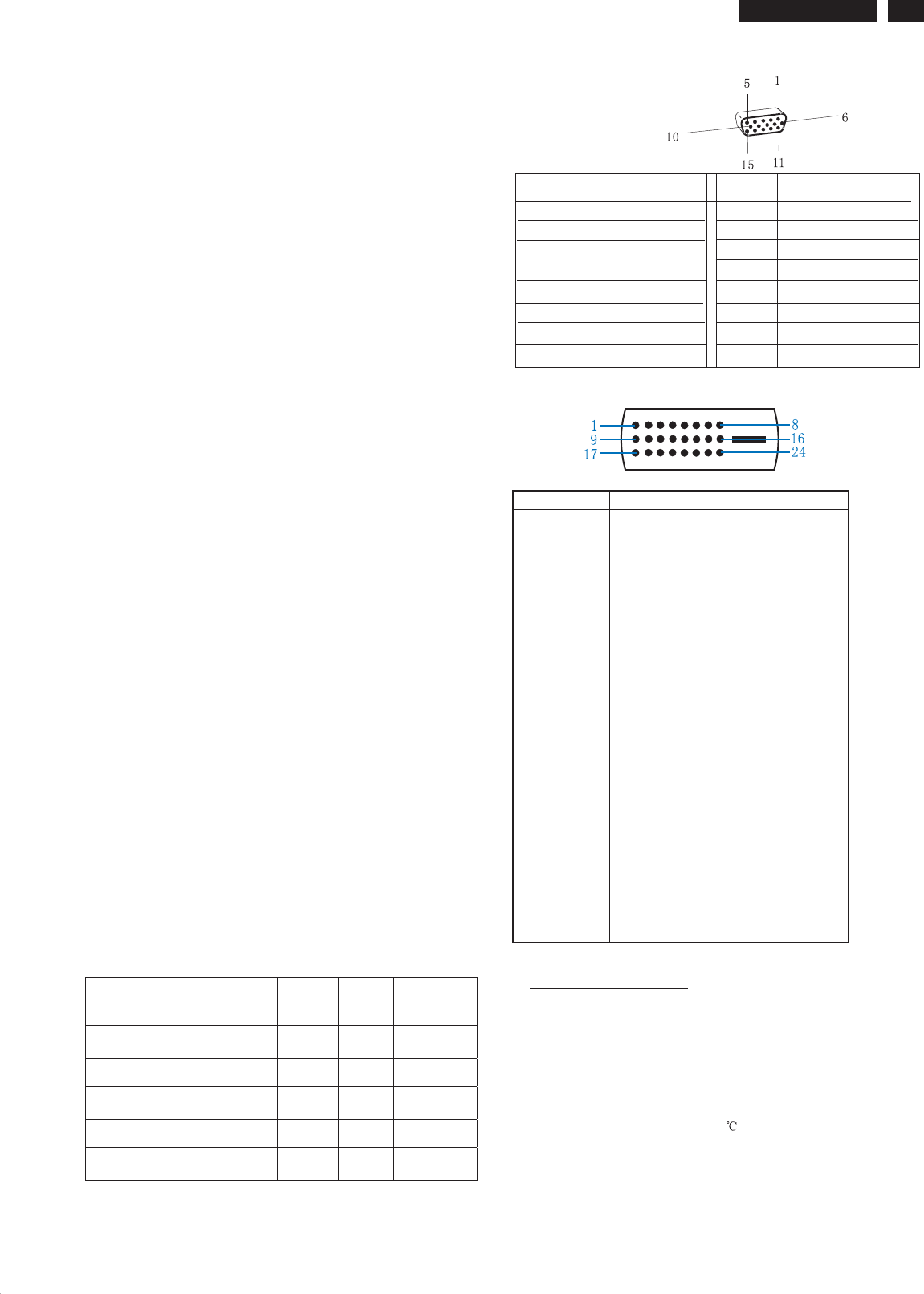
Technical Data - 170C8 HUDSON 8
Pin Assignment
Input DVI-D connector pin
Red video input
Green video input
Blue video input
GND
Cable detect
Red video GND
Green video GND
Blue video GND
DDC +3.3V OR +5V
GND
GND
Serial data line (SDA)
H-sync
V-sync
Data clock line (SCL)
7
8
6
5
4
3
2
19
10
11
12
13
14
15
Pin No. Pin No.
Assignment Assignment
Pin No. Description
1T.M.D.S. data2-
2T.M.D.S. data2+
3T.M.D.S. data2 shield
4No Connect
5No Connect
6DDC clock
7DDC data
8No Connect
9T.M.D.S. data1-
10 T.M.D.S. data1+
11 T.M.D.S. data1 shield
12 No Connect
13 No Connect
14 +5V Power
15 Ground (for +5V) - Cable detect
16 Hot plug detect
17 T.M.D.S. data0-
18 T.M.D.S. data0+
19 T.M.D.S. data0 shield
20 No Connect
21 No Connect
22 T.M.D.S clock shield
23 T.M.D.S. clock+
24 T.M.D.S. clock-
LCD
Type NR. : LM170E03 TLL1
Number of Pixels. : 1280 (H) x1024 (V)
Physical Size. : 358.5(w)*296.5(h)*16(d) mm
Pixel Pitch. : 0.264 mm x 0.264 mm
Color pixel arrangement. : RGB stripes arrangement
Support Color. : 16.7M colors
Display Mode. : Normally White
Backlight. : CCFL edge light system
Active area. (WXH). : 337.92 x 270.336mm (17" diagonal)
Viewing Angle (CR>=10). : Right:80 , Left:80 , UP:75 , down:85
Contrast ratio. : 800 :1(typ.), 500:1(min.)
White luminance. : 300 nit (typ.), 250nit (min.)
Type NR. : LM170E03 TLL4
Number of Pixels. : 1280 (H) x1024 (V)
Physical Size. : 358.5(w)*296.5(h)*16(d) mm
Pixel Pitch. : 0.264 mm x 0.264 mm
Color pixel arrangement. : RGB stripes arrangement
Support Color. : 16.7M colors
Display Mode. : Normally White
Backlight. : CCFL edge light system
Active area. (WXH). : 337.92 x 270.336mm (17" diagonal)
Viewing Angle (CR>=10). : Right:80 , Left:80 , UP:75 , down:85
Contrast ratio. : 800 :1(typ.), 500:1(min.)
White luminance. : 300 nit (typ.), 250nit (min.)
Type NR. : CLAA170EA07 P - 040
Number of Pixels. : 1280 (H) x1024 (V)
Physical Size. : 358.5(w)*296.5(h)*17.5(d) mm
Pixel Pitch. : 0.264 mm x 0.264 mm
Color pixel arrangement . : RGB vertical stripes
Support Color. : 16.2M colors
Display Mode. : Normally White
Backlight. : CCFL edge light system
Active area. (WXH). : 337.9 x 270.3 mm (17" diagonal)
Viewing Angle (CR>=10). : Right:80 , Left:80 , UP:80 , down:80
Contrast ratio. : 700 :1(typ.) ; 550:1 (min.)
White luminance. : 300 nit (typ.), 250nit (min.)
Type NR. : CLAA170EA07 P - 050
Number of Pixels. : 1280 (H) x1024 (V)
Physical Size. : 358.5(w)*296.5(h)*17.5(d) mm
Pixel Pitch. : 0.264 mm x 0.264 mm
Color pixel arrangement . : RGB vertical stripes
Support Color. : 16.2M colors
Display Mode. : Normally White
Backlight. : CCFL edge light system
Active area. (WXH). : 337.9 x 270.3 mm (17" diagonal)
Viewing Angle (CR>=10). : Right:80 , Left:80 , UP:80 , down:80
Contrast ratio. : 700 :1(typ.) ; 550:1 (min.)
White luminance. : 300 nit (typ.), 250nit (min.)
STATUS H-sync V-sync Video Power LED
On On On Active <36W Green
Stand-by Off On Blanked <1W Amber LCD
Suspend On Off Blanked <1W
Amber LCD
Off Off Off Blanked <1W Amber LCD
DC Power off N / A <1W LCD Off
Power Management Definition:
Environmental conditions
Operating
- Temperature : 0 to 35 degree C
- Humidity : 80% max
- Altitude : 0-3658m
- Air pressure : 600-1100 mBAR
Storage
- Temperature : -20 to 60 degree C
- Humidity : 85% max ( < 40 )
- Altitude : 0-12192m
- Air pressure : 300-1100 mBAR
Note: recommend at 5 to 35°C, Humidity less than 60 %
4HUDSON 8 Technical Data - 190C8
Pin Assignment
Input DVI-D connector pin
Red video input
Green video input
Blue video input
GND
Cable detect
Red video GND
Green video GND
Blue video GND
DDC +3.3V OR +5V
GND
GND
Serial data line (SDA)
H-sync
V-sync
Data clock line (SCL)
7
8
6
5
4
3
2
19
10
11
12
13
14
15
Pin No. Pin No.
Assignment Assignment
Pin No. Description
1T.M.D.S. data2-
2T.M.D.S. data2+
3T.M.D.S. data2 shield
4No Connect
5No Connect
6DDC clock
7DDC data
8No Connect
9T.M.D.S. data1-
10 T.M.D.S. data1+
11 T.M.D.S. data1 shield
12 No Connect
13 No Connect
14 +5V Power
15 Ground (for +5V) - Cable detect
16 Hot plug detect
17 T.M.D.S. data0-
18 T.M.D.S. data0+
19 T.M.D.S. data0 shield
20 No Connect
21 No Connect
22 T.M.D.S clock shield
23 T.M.D.S. clock+
24 T.M.D.S. clock-
Power Management Definition
STATUS H-
sync
V-
sync Video Power LED
On On On Active <40W Green
Stand-by Off On Blanked <1W Amber LCD
Suspend On Off Blanked <1W Amber LCD
Off Off Off Blanked <1W Amber LCD
DCPoweroff N/A <1W LCDOff
LCD
Type NR. : LM190E08 TLL1 / LM190E08 TLL4
Number of Pixels. : 1280 (H) x1024 (V)
Physical Size. : 396.0(w)*324.0(h)*15(d) mm
Pixel Pitch. : 0.098*RGB(H) mm x 0.294(V) mm
Color pixel arrangement. : RGB stripes arrangement
Support Color. : 16.7M colors
Display Mode. : Normally White
Backlight. : CCFL edge light system
Active area. (WXH). : 376.32 x 301.056mm (19" diagonal)
Viewing Angle (CR>=10). : Right:80 , Left:80 , UP:75 , down:85
Contrast ratio. : 800 :1(typ), 500:1(min)
White luminance. : 300 nit (typ)
Type NR. : HSD 190MEN3-A00
Number of Pixels. : 1280 (H) x1024 (V)
Physical Size. : 396.0(w)*324.0(h)*16.5(d) (Typ) mm
Pixel Pitch. : 0.294 mm x 0.294 mm
Color pixel arrangement. : RGB vertical stripes
Support Color. : 16.7M colors
Display Mode. : Normally White
Backlight. : CCFL edge light system
Active area. (WXH). : 376.32x301.056mm (19" diagonal)
Viewing Angle (CR>=10). : Right:85 , Left:85 , UP:80 , down:80
Contrast ratio. : 1000 :1(typic)
White luminance. : 300 nit (typ)
Scanning frequencies
H-Frequency. : 30K- 83 KHz
V-Frequency. : 56 - 76 Hz
Video dot rate. : < 140 MHz
Power input. : 90-264 V AC, 50/60 ±2Hz
Power consumption. : < 40W maximum
Functions:
(1)D-Sub analog R/G/B separate inputs, H/V sync separated, Composite
(H+V) TTL level, SOG sync.
(2)DVI-D digital Panel Link TMDS input
Ambient temperature: 0 °C- 35 °C
Environmental conditions
Operating
- Temperature : 0 to 35 degree C
- Humidity : 80% max
- Altitude : 0-3658m
- Air pressure : 600-1100 mBAR
Storage
- Temperature : -20 to 60 degree C
- Humidity : 85% max ( < 40 )
- Altitude : 0-12192m
- Air pressure : 300-1100 Mbar
Note: recommend at 5 to 35°C, Humidity less than 60 %
5
HUDSON 8
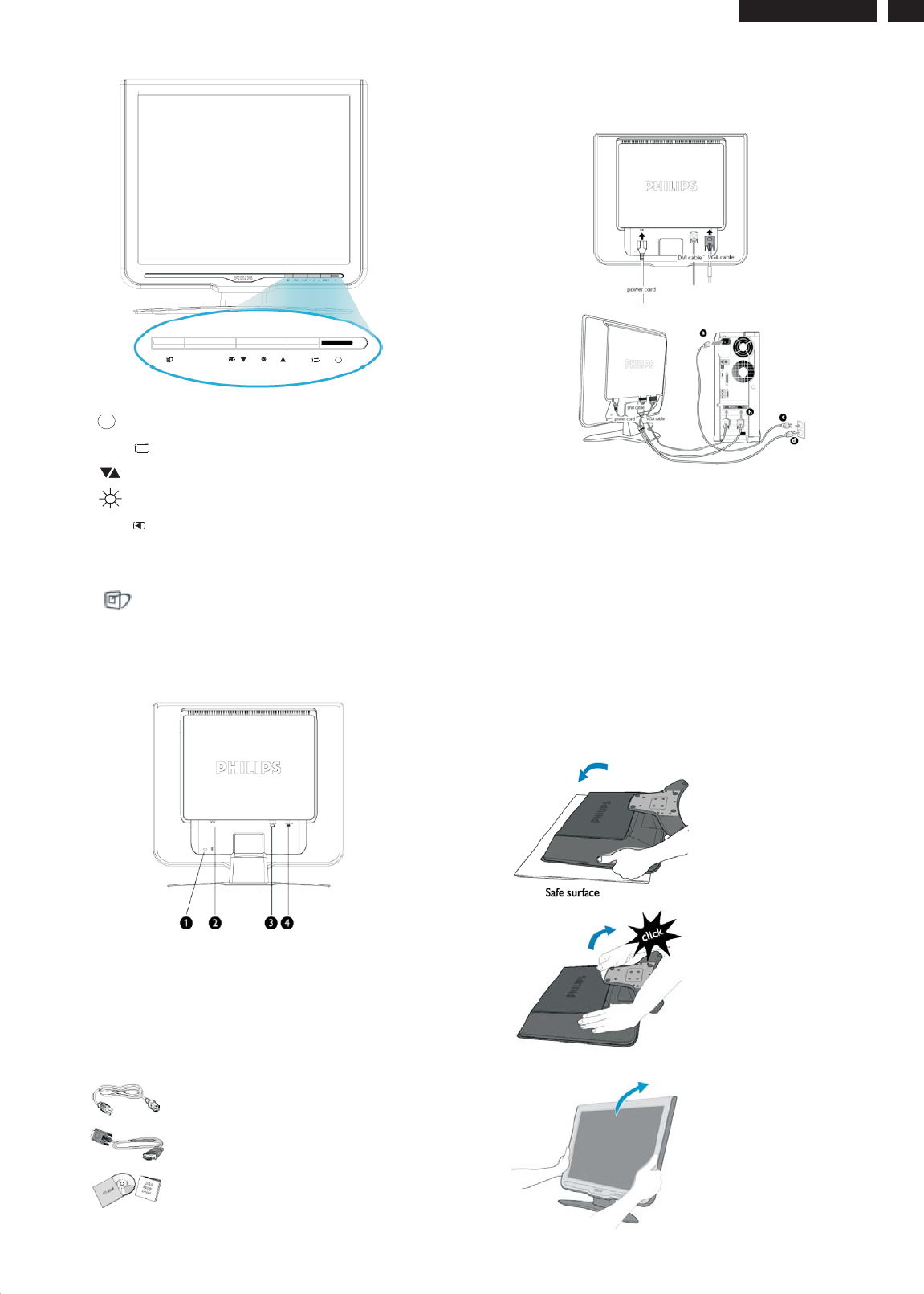
Installation
Front View
Rear View
1 Kensington anti-thief lock
2 AC power input
3 DVI-I input
4 VGA input
Power cord
VGA signal cable
EDFU pack
Accessory Pack
Item Description
Connecting to Your PC
Connect the power cord and DVI cable to the back of the monitor
firmly. (Philips has preconnected VGA cable for the first installation.)
Connect the cables to the back of your computer by
following these steps:
(a) Turn off your computer and unplug its power cable.
(b) Connect the monitor signal cable to the video connector on the
back of your computer.
(c) Plug the power cord of your computer and your monitor into a
nearby outlet.
(d) Turn on your computer and monitor. If the monitor displays an
image, installation is complete.
The Base
Unfold and Fold the Base
Unfold the Base
Fold the Base
1) Push down the head of
monitor.
2) Pull up the base.
1) Put monitor face down
on the safe surface.
INPUT AUTO/ I
I
1. To switch monitor's power On and Off
OK
MENU/
2. To access OSD menu
3. To adjust the OSD
4. To adjust brightness of the display
AUTO/
5. Automatically adjust the horizontal position, vertical position,
phase and clock settings / Return to previous OSD level.
6. INPUT To change the signal input source.
7. There are five modes to be selected: Office Work,
Image Viewing, Entertainment, Economy, and Off.
OK
MENU/
6
Go to cover page
HUDSON 8
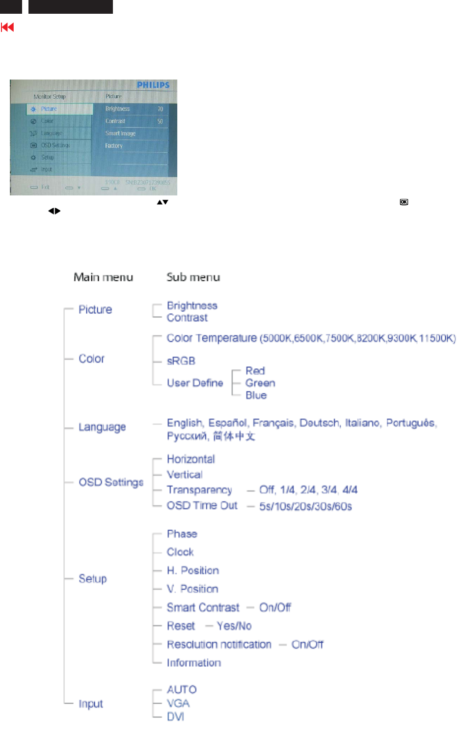
Description of the On Screen Display
On-Screen Display (OSD) is a feature in all Philips LCD monitors. It allows an end user to adjust screen performance or select functions
of the monitors directly through an on-screen instruction window. A user friendly on screen display interface is shown as below :
Basic and simple instruction on the control keys.
In the OSD shown above users can press buttons at the front bezel of the monitor to move the cursor, to confirm the choice or
change, and to adjust/select the change.
The OSD Tree
Below is an overall view of the structure of the On-Screen Display. You can use this as a reference when you want to work your way around the
different adjustments later on.
On Screen Display
7
HUDSON 8
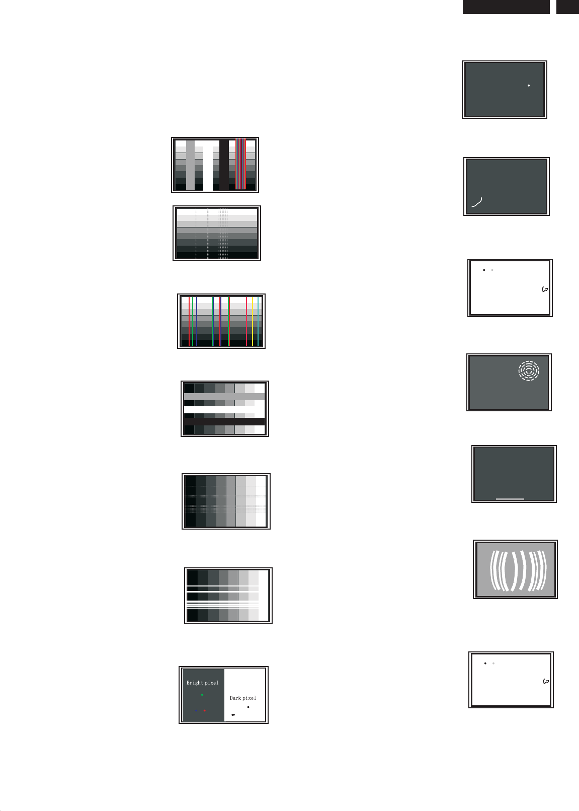
Failure description Phenomenon
Vertical block defect
Vertical dim lines
Vertical lines defect
(Always bright or dark)
Horizontal block defect
Horizontal dim lines
Horizontal lines defect
(Always bright or dark)
Has bright or dark pixel
Polarizer has bubbles
Polarizer has bubbles
Foreign material inside
polarizer. It shows liner or
dot shape.
Concentric circle formed
Bottom back light of LCD is
brighter than normal
Back light un-uniformity
Backlight has foreign material.
Black or white color, liner or
circular type
Quick reference for failure mode of LCD panel
this page presents problems that could be made by LCD panel.
It is not necessary to repair circuit board. Simply follow the mechanical
instruction on this manual to eliminate failure by replace LCD panel.
Failure Mode Of Panel
8HUDSON 8
Philips' Flat Panel Monitors Pixel Defect Policy
Philips strives to deliver the highest quality products. We use some of
the industry's most advanced manufacturing processes and practice
stringent quality control. However, pixel or sub pixel defects on
the TFT LCD panels used in flat panel monitors are sometimes unavoidable.
No manufacturer can guarantee that all panels will be free from pixel defects,
but Philips guarantees that any monitor with an unacceptable number of
defects will be repaired or replaced under warranty. This notice explains
the different types of pixel defects and defines acceptable defect levels for
each type. In order to qualify for repair or replacement under warranty,
the number of pixel defects on a TFT LCD panel must exceed these
acceptable levels. For example, no more than 0.0004% of the sub pixels on a 17"
XGA monitor may be defective. Furthermore, Philips sets even higher quality
standards for certain types or combinations of pixel defects that are more
noticeable than others. This policy is valid worldwide
Philips Pixel Defect Policy
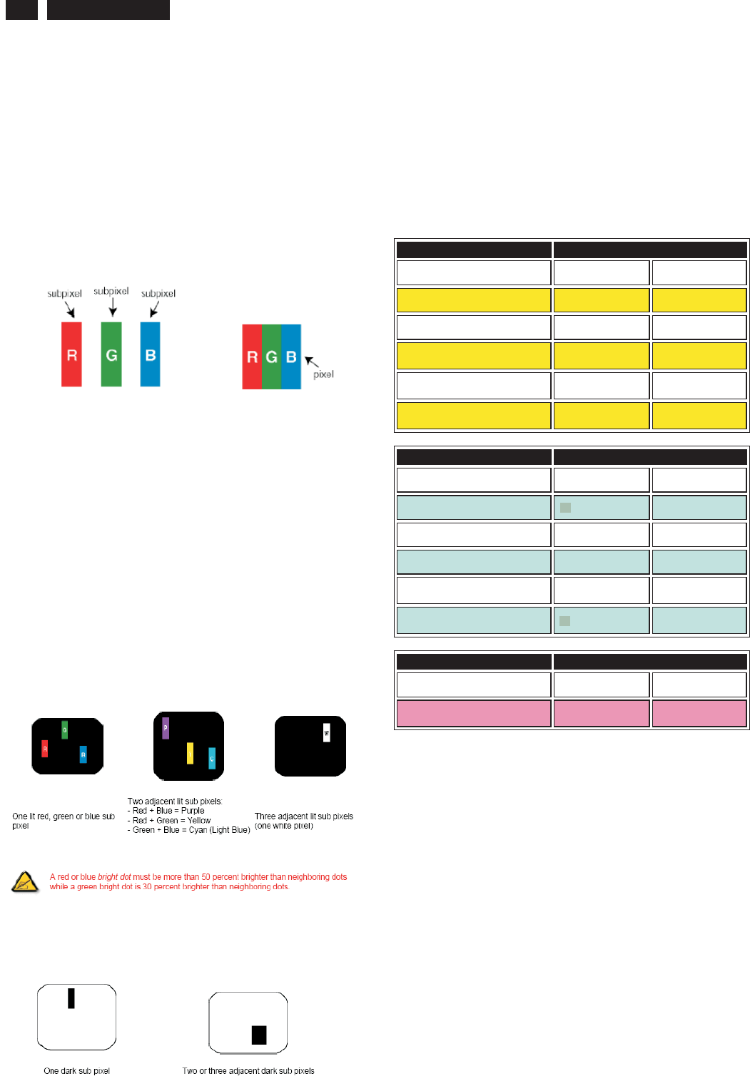
Pixels and Sub pixels
A pixel, or picture element, is composed of three sub pixels
in the primary colors of red, green and blue. Many pixels
together form an image. When all sub pixels of a pixel are lit,
the three colored sub pixels together appear as a single white
pixel. When all are dark, the three colored sub pixels together
appear as a single black pixel. Other combinations of lit and
dark sub pixels appear as single pixels of other colors.
Types of Pixel Defects
Pixel and sub pixel defects appear on the screen in different ways.
There are two categories of pixel defects and several types of sub
pixel defects within each category.Bright Dot Defects Bright dot
defects appear as pixels or sub pixels that are always lit or 'on'.
That is,a bright dot is a sub-pixel that stands out on the screen
when the monitor displays a dark pattern.There are the types
of bright dot defects
Black Dot Defects Black dot defects appear as pixels or sub
pixels that are always dark or 'off'. That is, a dark dot is a
sub-pixel that stands out on the screen when the monitor
displays a light pattern.These are the types of black dot defects:
Proximity of Pixel Defects
Because pixel and sub pixels defects of the same type that
are near to one another may be more noticeable, Philips also
specifies tolerances for the proximity of pixel defects.
Pixel Defect Tolerances
In order to qualify for repair or replacement due to pixel defects
during the warranty period, a TFT LCD panel in a Philips flat
panel monitor must have pixel or sub pixel defects exceeding the
tolerances listed in the following tables.
BRIGHT DOT DEFECTS ACCEPTABLE LEVEL
MODEL 170C7 190C7
1 lit subpixel 3orfewer 3orfewer
2 adjacent lit subpixels 1 or fewer 1 or fewer
3 adjacent lit subpixels (one
white pixel) 0 0
Distance between two bright
dot defects* 15 mm or more 25 mm or more
Total bright dot defects of all
types 3orfewer 3orfewer
BLACK DOT DEFECTS ACCEPTABLE LEVEL
MODEL 170C7 190C7
1 dark subpixel 4orfewer 5orfewer
2 adjacent dark subpixels 2 or fewer 2 or fewer
3 adjacent dark subpixels 0 0
Distance between two black
dot defects* 15 mm or more 15 mm or more
Total black dot defects of all
types 4orfewer 5orfewer
BLACK DOT DEFECTS ACCEPTABLE LEVEL
MODEL 170C7 190C7
Total bright or black dot
defects of all types 5orfewer 5orfewer
Note:
* 1 or 2 adjacent sub pixel defects = 1 dot defect
All Philips monitors are ISO13406-2 Compliant
88
8
8
88
1
5
5
9
HUDSON 8
Troubleshooting
Common Problems
Having this problem Check these items
No Picture
Power LED not lit)
.Make sure the power cord is plugged into the power out let and
into the back of the monitor.
.First, ensure that the power button on the front of the monitor is
in the OFF position, then press it to the ON position.
No Picture
(Power LED is amber or yellow)
Make sure the computer is turned on.
Make sure the signal cable is properly connected
computer.
Check to see if the monitor cable has bent pins.
The Energy Saving feature may be activated
Screen says Make sure the monitor cable is properly connected to
your computer. (Also refer to the Quick Set-Up Guide).
Check to see if the monitor cable has bent pins.
Make sure the computer is turned on.
AUTO button not working properly
The Auto Function is designed for use on standard Macintosh or
IBM-compatible PCs running Microsoft Windows.
It may not work properly if using nonstandard PC or videocard.
Imaging Problems
Display position is incorrect
Press the Auto button.
Adjust the image position using the Phase/Clock of More Settings
in OSD Main Controls.
Image vibrates on the screen
Check that the signal cable is properly connected to the
graphics board or PC
Vertical flicker appears Press the Auto button.
Eliminate the vertical bars using the Phase/Clock of More
Settings in OSD Main Controls.
Horizontal flicker appears Press the Auto button.
Eliminate the vertical bars using the Phase/Clock of More
Settings in OSD Main Controls.
The screen is too bright or too dark
Adjust the contrast and brightness on On-Screen Display.(The
backlight of the LCD monitor has a fixed life span. When the screen
becomes dark or begins to flicker, please contact your sales
representative).
An after-image appears If an image remains on the screen for an extended period of time,
it may be imprinted in the screen and leave an afterimage.This
usually disappears after a few hours
An after-image remains after the power
has been turned off.
This is characteristic of liquid crystal and is not caused by
amalfunction or deterioration of the liquid crystal. The afterimage
will disappear after a peroid of time.
Green, red, blue, dark, and white dots The remaining dots are normal characteristic of the liquid crystal
10 HUDSON 8 Warning Message
Item Attention Signals Display Time Condition
1 CANNOT DISPLAY THIS
VIDEO MODE, CHANGE
COMPUTER DISPLAY
INPUT TO 1280X1024 @
60HZ
30 mins This warning appears when the input signal from your computer is not in
a standard video mode or is out of the monitor s scanning range. After
30 mins, monitor enters sleeping mode.
2 NO VIDEO INPUT 30 mins This message appears when there is no signal input but with cable while
AC or DC power on. After 30 mins, monitor enters sleeping mode.
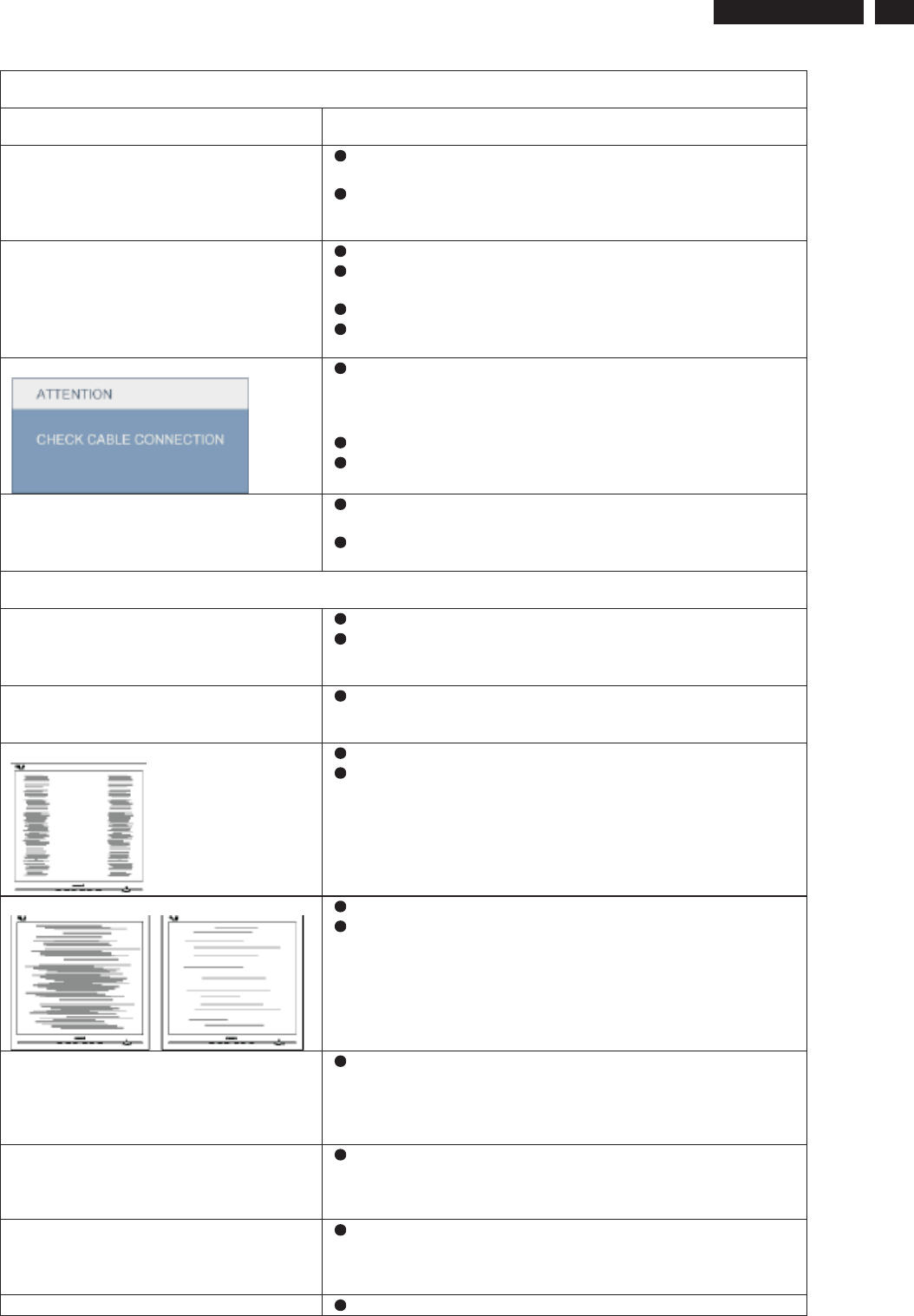
3 CHECK CABLE
CONNECTION
30 mins This message appears when a signal cable is disconnected while
monitor is working. After 30 mins, monitor enters sleeping mode.
4 ENTERING SLEEP MODE 3 secs This message appears when monitor is about to enter power saving
mode.
5 WAITING FOR AUTOMATIC
ADJUSTMENT
till auto adjustment
finished
This message is displayed when the auto adjustment button is pressed.
It disappears when automatic adjustments are completed.
6 USE 1280X 1024 FOR BEST
RESULT
On top of OSD main
menu
The message will show up at the top of the OSD main menu in red color
when the input resolution is not the 1280x1024.
7 OSD MAIN CONTROLS
LOCKED
3 secs / or Till "OSD
MAIN CONTROLS
UNLOCKED"
appear
This message will appear 3 seconds to indicate the OSD MAIN
CONTROLS status when to lock or un-lock it by pressing "MENU(OK) "
button for more than 10 seconds while there is video input from PC. This
function provides the alternative that user can lock all the OSD main
control in case user don t want the FOS performance setting to be
changed, for instance, during commercial exhibition.
8 OSD MAIN CONTROLS
UNLOCKED
3 secs This message will appear 3 seconds to indicate the OSD MAIN
CONTROLS status when to un-lock it by pressing "MENU (OK) " button
for more than 10 seconds while there is video input from PC.
9 the window of "VOLUME" 60 secs This message will appear when the VOLUME button is pressed.
10 THIS IS 85HZ OVERSCAN,
CHANGE COMPUTER
DISPLAY INPUT TO
1280X1024@60HZ
10 mins This message will appear 5 seconds in every 60 seconds for 10 minutes
when the input of PC video timing is at 85Hz mode.
Remark: AUTO is still functional in this mode
11 the window of OSD
"MONITOR SETUP "
60 secs This message will appear when the "OK" button is pressed.
12 the window of
"BRIGHTNESS"
60 secs This message will appear when the BRIGHTNESS button is pressed.
13 "SELECTED INPUT NOT
AVAILABLE"
3 secs This message will appear 3 seconds to indicate the SIGNAL SOURCE
status when change the signal source but it is not found while there is
video input from PC.
Warning message table
11
HUDSON 8
Lock/Unlock,Aging,Factory Mode
Front Control
INPUT AUTO/ I
OK
MENU/
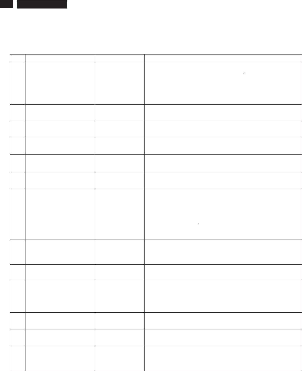
To Lock/Unlock OSD FUNCTION(User Mode)
The OSD function can be locked by pressing"OK"button(1) for more
than 10 seconds, the screen shows following windows for 4 seconds.
Everytime when you press"OK" button, this message
appears on the screen automatically.
Unlock OSD function
Unlocked OSD function can be released by pressing "OK" button for
more than 10 seconds again.
After 15 seconds,
bring up:
After 30 seconds,
bring up: AGING...
Access Aging Mode
Step1:D
Step 2 : [Push "AUTO"&"OK"buttons
at the same time and hold them]+[Press power " " button untill comes
out " AGING screen"] => then release all buttons.
Bring up:
isconnect Interface Cable between Monitor and PC.
Turn off LCD monitor.Then
AGING...
After 15 seconds,
bring up:
----------
----------
repeatly
Connect Signal cable again=> go back to normal display
Enter Factory Menu
Step1:Press button.
Step2:Choose Picture ,then press button.
Step3:Press button and choose factory .
Step4:Press button.
"OK"
" " "OK"
"" " "
"OK"
Access Factory Mode
1). Turn off monitor.
2).
3).Press "OK" button, wait until the OSD menu with Characters
"Smart Image" "Factory" (below OSD menu) come on the
Screen of the monitor.
[Push "AUTO" & "OK" buttons at the same time and hold them]
+[Press "power" button untill comes out "Windows screen" ]
=> then release all buttons
Factory Mode indicator
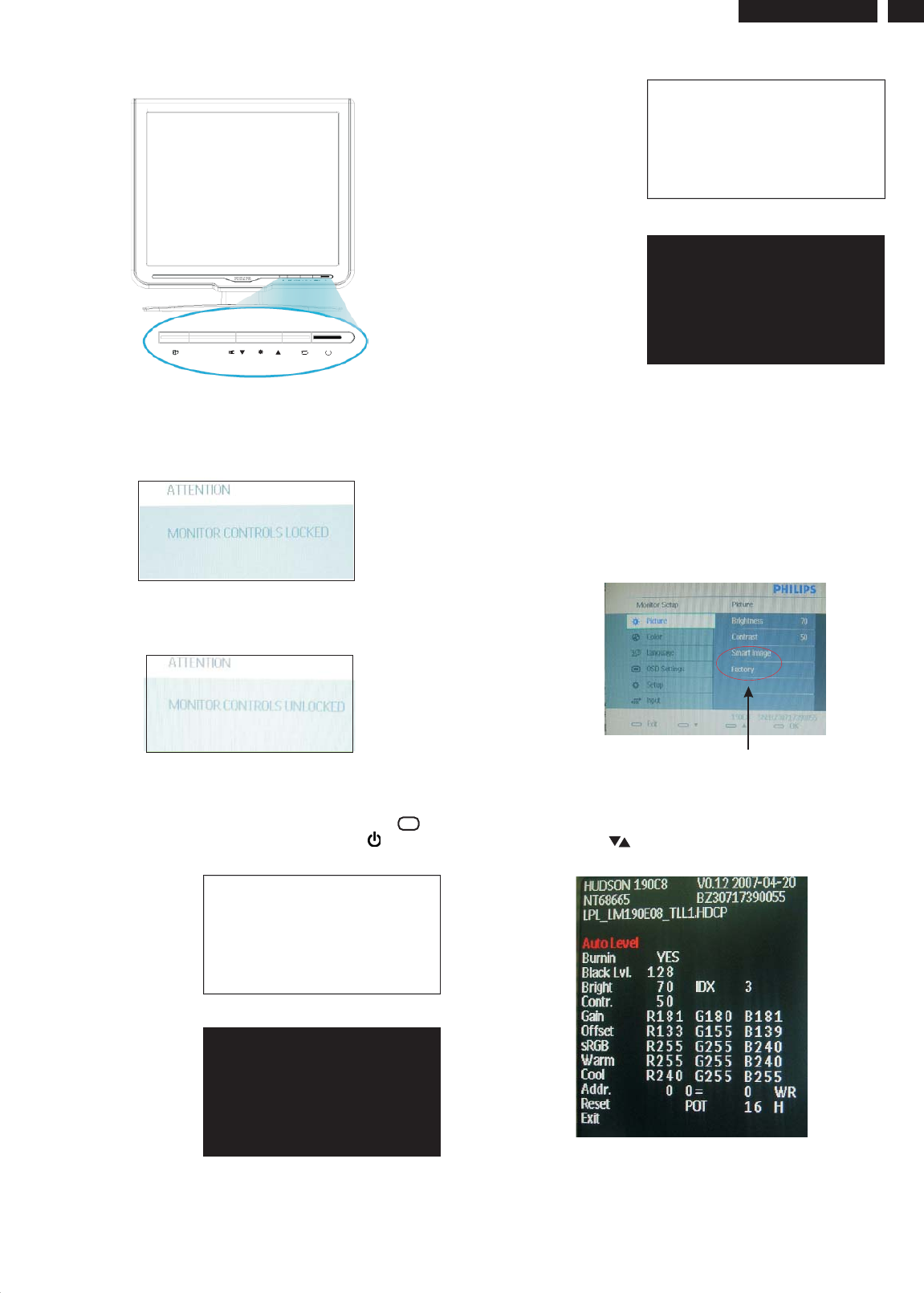
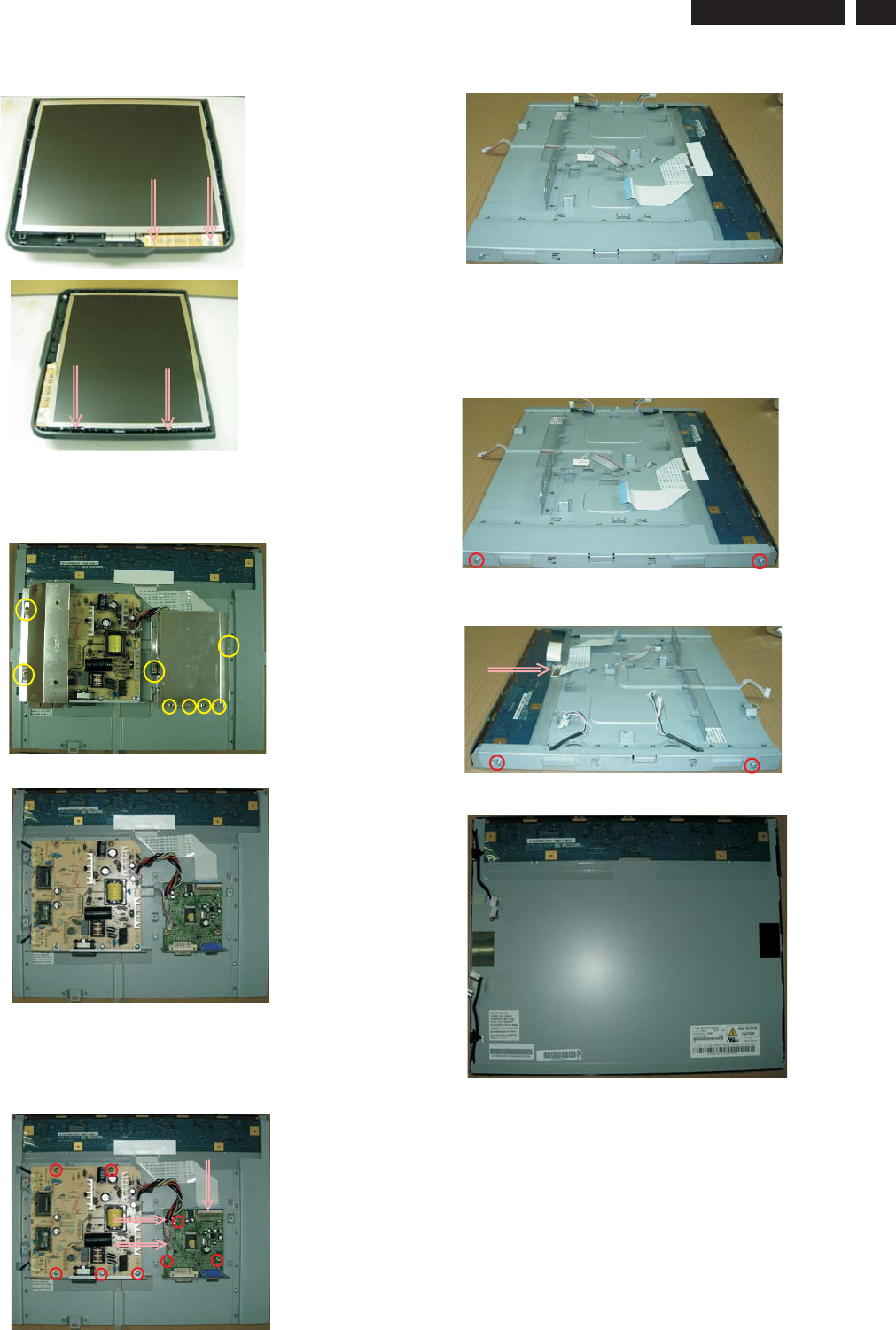
12 HUDSON 8 Mechanical Instruction
Front View
Back View
Step1. Remove the base
-Use two
-Remove the screws as shown in Fig.4, then remove the base
thin " " screw drivers to drive upon the cover simultaneously
as shown in Fig.3
Step2. Remove the Front Bezel as shown in Fig.5~11
-Remove the one screw as shown in Fig.5
-Use the to open the front Bezel clicks at the top
side as shown in Fig.6
-Pull the front away from the back cover from both left and
right sides as shown in Fig.7
-Pull out the front from the back cover at the bottom side
plastic putty knife
Bezel
Bezel as
shown in Fig.8
Fig.1
Fig.2
Fig.4
Fig.5
Fig.9
Fig.3
Fig.11
Fig.10
Step3.Remove the Back cover
- Remove the two screws as shown in Fig.12 ,then remove the Control
board
-Use the thin " " type screw driver to open the clicks as shown in Fig.13
Fig.6
Fig.8
Fig.7
13
HUDSON 8
Mechanical Instruction
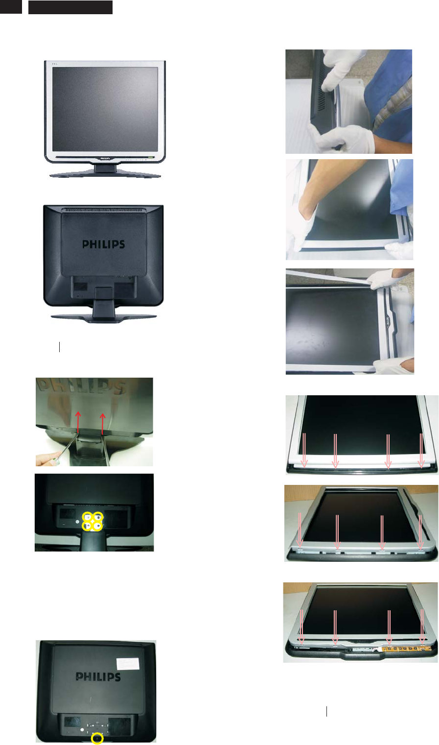
Step 5. Remove the sclar and power board.
- Remove the eight screws as shown in Fig.16
- Disconnect the three cables as shown in Fig.16
- Remove the scaler and power board as shown in Fig.17
***********************************************************************************************************************************
***********************************************************************************************************************************
In warranty, it is not allowed to disassembly the LCD panel, even the
backlight unit defect.
Out of warranty, the replacement of backlight units is a correct way
when the defect is caused by backlight (CCFL, Lamp).
Fig.15
Fig.16
Fig.17
Step6. Remove the Metal Frame.
- Remove the two screws as shown in Fig.18
- Remove the two screws as shown in Fig.19
- Disconnect the one cable as shown in Fig.19
Fig.18
Fig.19
Fig.20
Step4. Remove the Power and Scaler shielding.
- Remove the eight screws as shown in Fig.14
- Remove the as shown in Fig.15Power and Scaler shielding
Fig.12
Fig.13
Fig.14
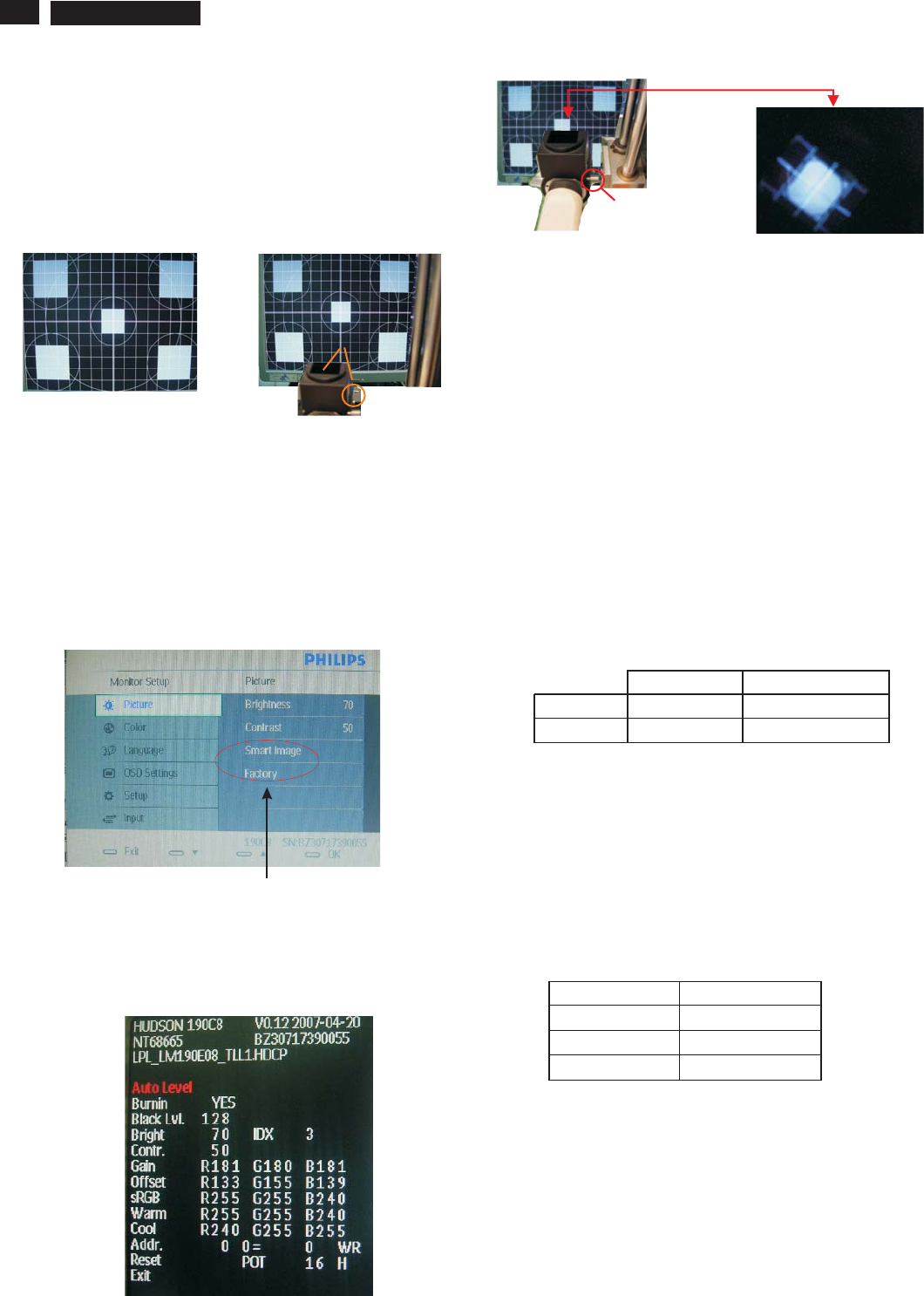
14 HUDSON 8 Color Adjustment
Alignment procedure
1. Turn on the LCD monitor.
2.Turn on the Timing/pattern generator. See Fig.1
3. Preset LCD color Analyzer CA-110
-Remove the lens protective cover of probe CA-A30.
-Set measuring/viewing selector to measuring position for reset
analyzer.(zero calibration) as Fig.2
- Turn on the color analyzer (CA-110)
-Press 0-CAL button to starting reset analyzer.
Fig. 1 Fig. 2
Clear imageClear image
Measurement/viewing selectorMeasurement/viewing selector
Fig. 3
4). Press button, then select factory indicator by"OK" "UP"
or "DOWN" button .Press"OK button to bring up submenu
windows as below:
""
"
Fig.5
Cover (black)Cover (black)
Measurement viewing selectorMeasurement viewing selector
Fig. 4
Fig. 2
5.Display
Press "UP" or "DOWN" button to select . Change the value
by "LEFT" or "RIGHT" key until the X,Y co-ordinates as below
4. Access Factory Mode
1). Turn off monitor.
2).
3).Press "OK button, wait until the OSD menu with Characters"
Smart Image (below OSD menu) come on the Screen of
the monitor. as shown in Fig3.
[Push "AUTO" & "OK" buttons at the same time and hold them]
+[Press "power" button untill comes out "Windows screen" ]
=> then release all buttons
"
" "Factory"
6. Display Adjustment
6.1 Access to factory mode (RS232) in auto-alignment system. The
communication protocol switches to RS232.
6.2 Auto color adjustment (B)
Apply a 640*480/60Hz signal with 16 level grey test pattern, set
brightness control at 100%, and contrast control at 50%. Adjust
the R.G. B. offset, and gain to calibrate the color smoothly and
64-grey level distinguishable.
6.3 Adjustment of WHITE-D (B)
Apply a 1280*1024 / 60Hz signal with white pattern, set
brightness control at 100%, and contrast control at 50%. Adjust
the R, G, B Sub-Gain, for the screen center, the 1931 CIE
chromaticity (X, Y) co-ordinates shall be
Use Minolta CA-210 for color coordinates and luminance check.
Luminance is > 200 Nits in the center of the screen when
brightness at 100% and contrast set to 100%.
6.4 Adjustment of sRGB (B)
Apply a 1280*1024/ 60Hz signal with white pattern, set
brightness control at 100%, and contrast control at 50%.
Adjust the R, G, B Sub-Gain, for the screen center, the 1931
CIE chromaticity (X, Y) co-ordinates shall be;
sRGB
x(center) 0.313 ±0.008
y(center) 0.329 ±0.008
Ynits 180 ±10
9300°K6500°K
x (center) 0.283 ±0.020 0.313 ±0.020
y (center) 0.297 ±0.020 0.329 ±0.020
Factory Mode indicator
15
15
15
15
15
HUDSON 8
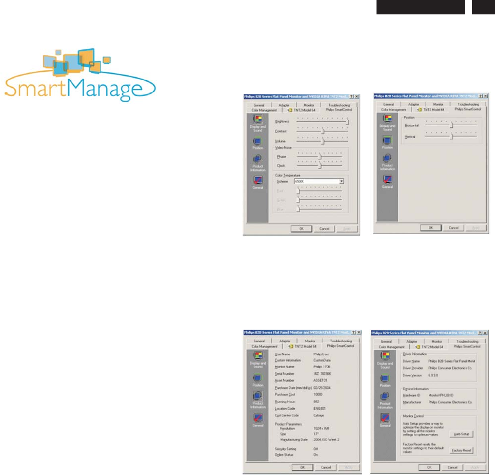
Smart Manage
Introduction
SmartManage Features and Benefits
Philips SmartControl
Philips SmartManage is an advanced solution for users, corporate/
institution IT administrator in particular, to manage their Philips
monitors as part of the asset management environment. The
solution includes three essential components, Philips SmartManage
Administrator, and Philips SmarControl and Agent. Philips
SmartManage is a solution joint developed by Philips and Altiris Inc.
The Philips SmartManage is a working console for IT management
to gather monitors assets information, run asset report, control
assets security, monitor assets security, and issue instant messages
to monitor users. Philips SmartManage includes the following major
features:
1. Provides an additional security measure that helps corporate
users safeguard their
investment.
2. Power saving feature that reduces utility costs and manpower
required to turn monitors on or off.
3. SmartControl provides an efficient means for adjusting monitor
performance and settings.
4. Built-in asset reports reduce audit/maintenance manpower, cycle
time and costs.
A trial version of SmartManage can be downloaded from
http://www.altiris.com/philips
For more information of Philips SmartManage, please contact with
Philips sales representatives in your country.
Notes: SmartManage is a software dedicated to business
environments. Personal users normally do not need to use
SmartManage.
The SmartControl and SmartManage Agent are deployed and
installed in computers using Philips monitors. With SmartControl
and SmartManage Agent, monitors and PCs can interact with the
administrator's inquiries. Because SmartControl operates on
individual PC, end users can also use SmartControl to adjust
monitor's performance settings.
1. Requirement
1. Graphic cards with nVIDIA (TNT2, GeForce, Quadro, or newer)
and ATI (Radeon or newer) graphic chipsets that support the
DDC/CI interface
2.Microsoft Windows 2000 and XP operation systems.
3. Philips monitors supporting DDC/CI interface
2. Installation
How to download "SmartControl Installation " file:
1. Visit http:// www.philips.com
2. Select "Your Country"
3. Click on "Support Center"
4. Click into "Monitors and PC Products"
5. Enter your model number
6. Enter "Software" page
7. Select "SmartControl Installation", and you can download
SmartControl and its driver for installation.
Please follow the guidance in the SmartControl installation program.
3. Accessing SmartControl
1. Right click on the desktop of your PC, and select Properties from
the shortcut menu pops up.
2. Click on Settings tab, and click on Advanced button.
3. Click Philips SmartControl tab.
4. SmartControl Options
1.Display and Sound
By moving the sliding bar toward left or right, users will be able
to adjust brightness, contrast, audio volume (if applicable),
video noise (not applicable when using DVI-D input), and color
temperatures.
2.Position
Users can adjust the horizontal and vertical position of the screen
by moving the sliding bar left and right. This function is disabled
when using DVI-D (digit) input.
3.Product Information
Click Product Information in the left pane to view the product
information stored in the monitor's memory.
4.General
Click on General for general information including driver
information, device information, and monitor control.
Within monitor control, users can click on Auto Setup to achieve
optimum performance or click on factory reset to reset the
parameters of the monitor. Such choices are disabled when using
DVI-D(digit) input.
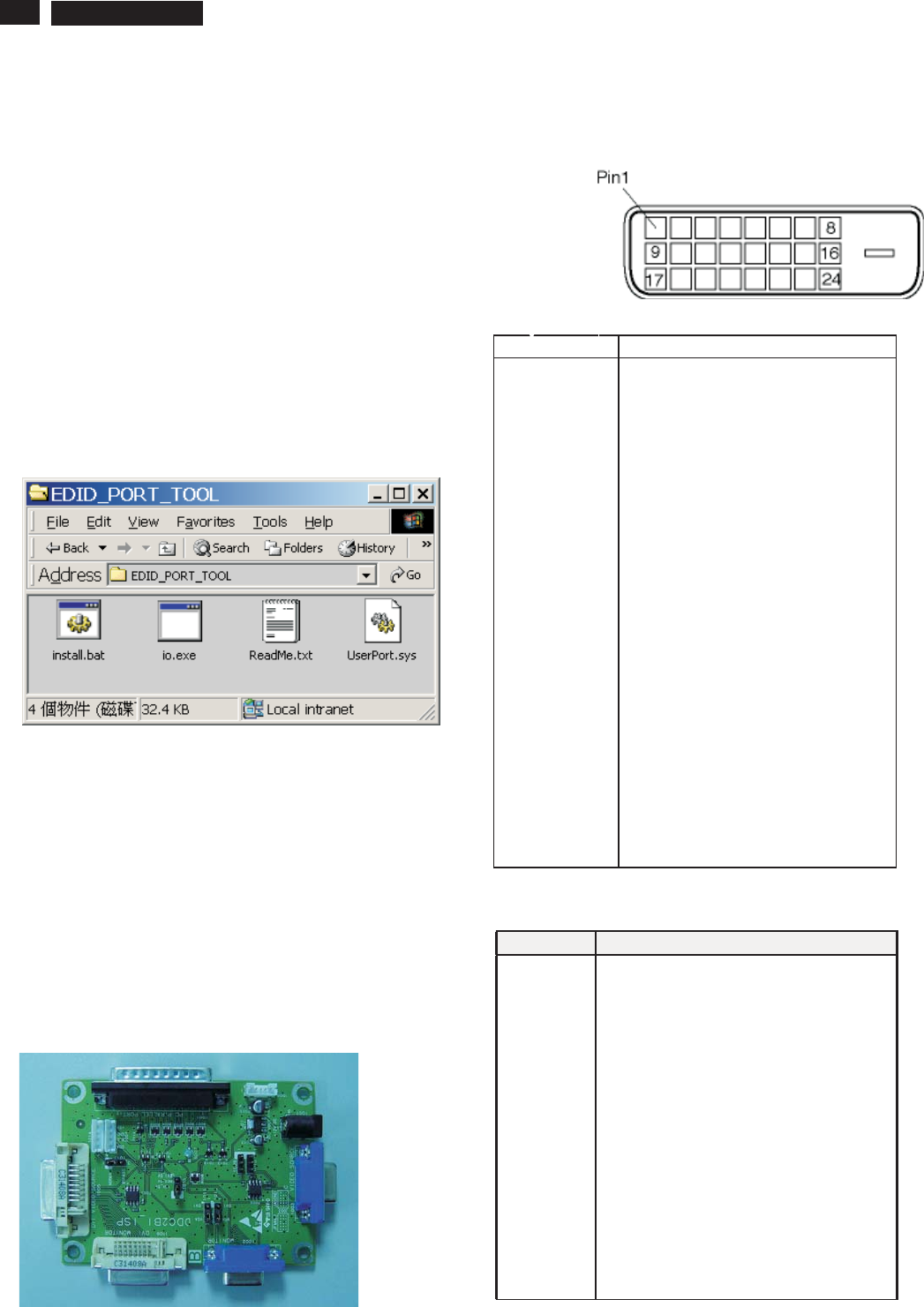
16 HUDSON 8 DDC Instructions
Pin No. Description
1 T.M.D.S. data2-
2 T.M.D.S. data2+
3 T.M.D.S. data2 shield
4 No Connect
5 No Connect
6 DDC clock
7 DDC data
8 No Connect
9 T.M.D.S. data1-
10 T.M.D.S. data1+
11 T.M.D.S. data1 shield
12 No Connect
13 No Connect
14 +5V Power
15 Ground (for +5V) - Cable detect
16 Hot plug detect
17 T.M.D.S. data0-
18 T.M.D.S. data0+
19 T.M.D.S. data0 shield
20 No Connect
21 No Connect
22 T.M.D.S clock shield
23 T.M.D.S. clock+
24 T.M.D.S. clock-
To Monitor
D-sub/DVI cable
DC 8~12V
To Printer port
Power
indicator
To Monitor
D-sub cable
DC 8~12V
To Printer port
Power
indicator
General
DDC Data Re-programming
In case the DDC data memory IC or main EEPROM which storage all
factory settings were replaced due to a defect, the serial numbers have
to be re-programmed"Analog DDC IC, & EEPROM".
It is advised to re-soldered DDC IC and main EEPROM from the old
board onto the new board if circuit board have been replaced, in this case
the DDC data does not need to be re-programmed.
Additional information
Additional information about DDC (Display Data Channel) may be
obtained from Video Electronics Standards Association (VESA).
Extended Display Identification Data(EDID) information may be also
obtained from VESA.
1. An i486 (or above) personal computer or compatible.
2. Microsoft operation system Windows 95/98 .
Y o Install the EDID_PORT_Tool under Win2000/XP . As
Fig. 1 .
A. Copy the "UserPort.sys" to C:\WINNT\system32\drivers(win2000)
C:\WINDOWS\system32\drivers(winXP)
B. Running " io.exe" everytime, Before you start to programming
edid data .
4. DDC 2BI-ISP TOOL:
Inclusion :
A. DDC2BI-ISP TOOL(3138 106 10396) x1 (as Fig. 2)
B. Printer cable x1
c. (D-Sub) to (D-Sub) cable x2
D. D-SUB to DVI cable X1
Note: The EDID46.EXE is a windows-based program, which cannot
be run in MS-DOS.
System and equipment requirements
ou have t
3. EDID45.exe program .
Fig. 2Fig. 2
Fig. 1Fig. 1
Pin Assignment
The digital only connector contains 24 signal contacts organized in
three rows of eight contacts. Signal pin assignments are listed in the
following table:
Fig. 3Fig. 3
Fig. 4Fig. 4
Input analog D-sub connector pin assignment
PIN No. SIGNAL
1 Red video input
2 Green video input /sync on green
3 Blue video input
4GND
5 GND--Cable detect
6 Red video GND
7 Green video GND
8 Blue video GND
9 DDC +3.3V or +5V
10 Logic GND
11 GND
12 Serial data line (SDA)
13 H-sync /H+V
14 V-sync
15 Data clock line (SCL)
17
DDC Instructions HUDSON 8
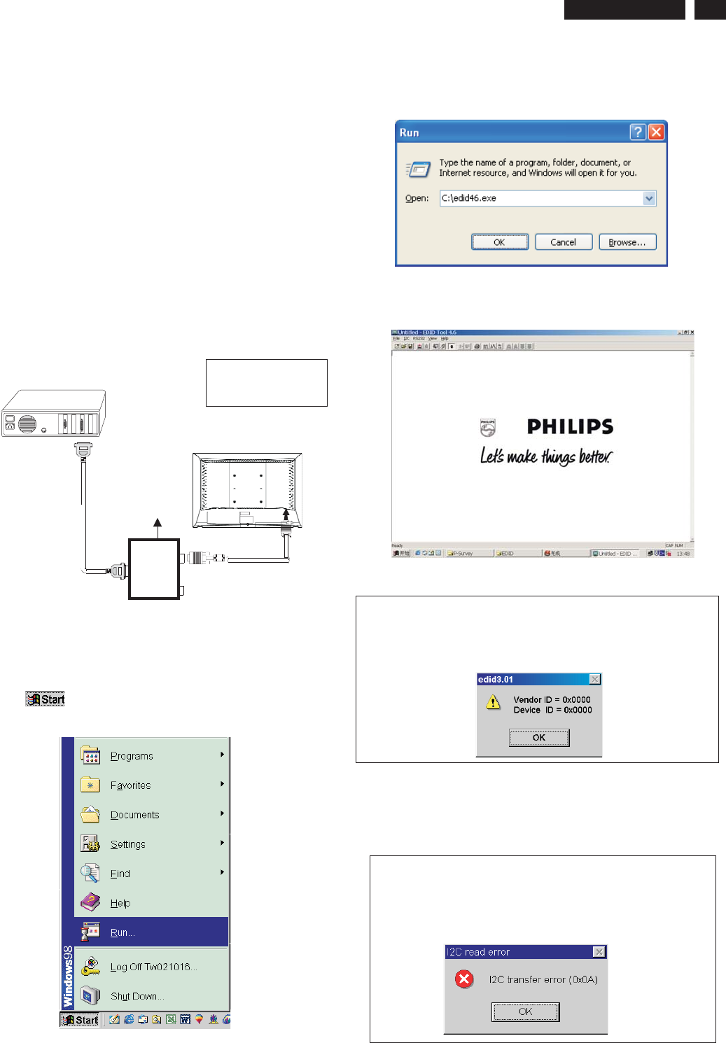
Step 3: Installation of EDID46.EXE
Method 1: Start on DDC program
Start Microsoft Windows.
1. The Program"EDID46.EXE" in service manual cd-rom be copyed to C:\ .
2. Click , choose Run at start menu of Windows as shown
In Fig. 5.
Fig. 5
4. Click OK button. The main menu appears (as shown in Fig. 7).
This is for initialize alignment box.
Fig. 7
Fig. 6
3. At the submenu, type the letter of your computer's hard disk drive
followed by :EDID46 (for example, C:\EDID46, as shown in Fig. 6).
Note 2: During the loading, EDID46 will verify the EDID data which just
loaded from monitor before proceed any further function, once
the data structure of EDID can not be recognized, the following
error message will appear on the screen as below. Please
confirm following steps to avoid this message.
1. The data structure of EDID was incorrect.
2. DDC IC that you are trying to load data is empty.
3. Wrong communication channel has set at configuration setup
windows.
4. Cables loosed or poor contact of connection.
1
Fig. 8
Note 1: If the connection is improper, you will see the following error
message (as shown in Fig. 8) before entering the main menu.
Meanwhile, the (read EDID) function will be disable. At this
time, please make sure all cables are connected correctly and
fixedly, and the procedure has been performed properly.
Fig. 9
Configuration and procedure
There is no Hardware DDC (DDC IC) anymore. Main EEPROM stores
all factory settings and DDC data (EDID code) which is also called
Software DDC. The following section describes the connection and
procedure for Software DDC application. The main EEPROM can be re-
programmed by enabling '' factory memory data write'' function on the
DDC program (EDID46.EXE).
Initialize alignment box
In order to avoid that monitor entering power saving mode due
to sync will cut off by alignment box, it is necessary to initialize
alignment box before running programming software
(EDID46.EXE). Following steps show you the procedures and
connection.
Step 1: Supply 8-12V DC power source to the Alignment box by
plugging a DC power cord .
Step 2: Connecting printer cable and D-Sub cable of monitor as Fig. 4
Fig. 4
PC
1=Power connector
2=D-SUBconnector
To printer port (LTP1)
DC Power
8-12 V
Printer
Port
To
Monitor
To PC
12
----->
----->
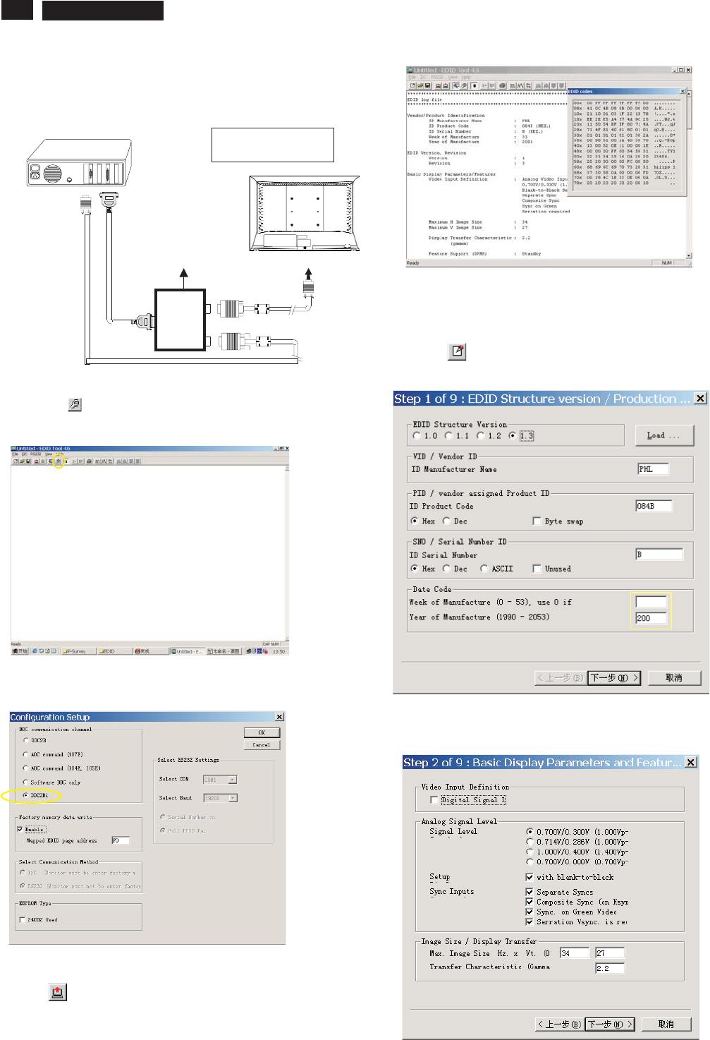
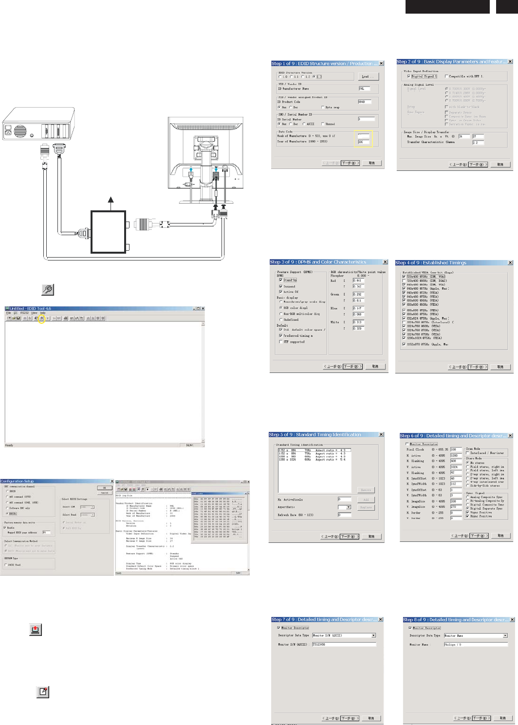
18 DDC Instructions
HUDSON 8
Step 3: Modify DDC data (verify EDID version, week,
year)
Click (new function) icon from the tool bar, bring up
Step 1 of 9 as shown in Fig. 14 .
EDID46 DDC application provides the function selection and
Step 4: Modify DDC data (Monitor Serial No.)
1. Click Next , bring up Fig. 15.
3. Click OK button to confirm your selection.
4. Click icon (Read EDID function) to read DDC EDID data from
monitor. The EDID codes will display on screen as shown in Fig. 13.
Fig. 15
2. Select the DDC2Bi as the communication channel.
As shown in Fig. 12.
Fig. 12
Fig. 13
Fig. 14
Step 2: Read DDC data from monitor
1. Click icon as shown in Fig. 11 from the tool bar to bring up
the Channels "Configuration Setup" windows as shown in Fig. 11.
Fig. 10
1=Power connector
2=D-SUB connector
PC
To printer port (LTP1)
DC Power
8-12V
Printer
Port
To
Monitor
To PC
12
----->
----->
To PC Video port (D-sub)
Click this button
=====>
Fig. 11
Re-programming Analog DDC IC
Step 1: After initialize alignment box, connecting all
cables and box as shown in Fig. 10.
Select and fill out,
If necessary.
17
7
19
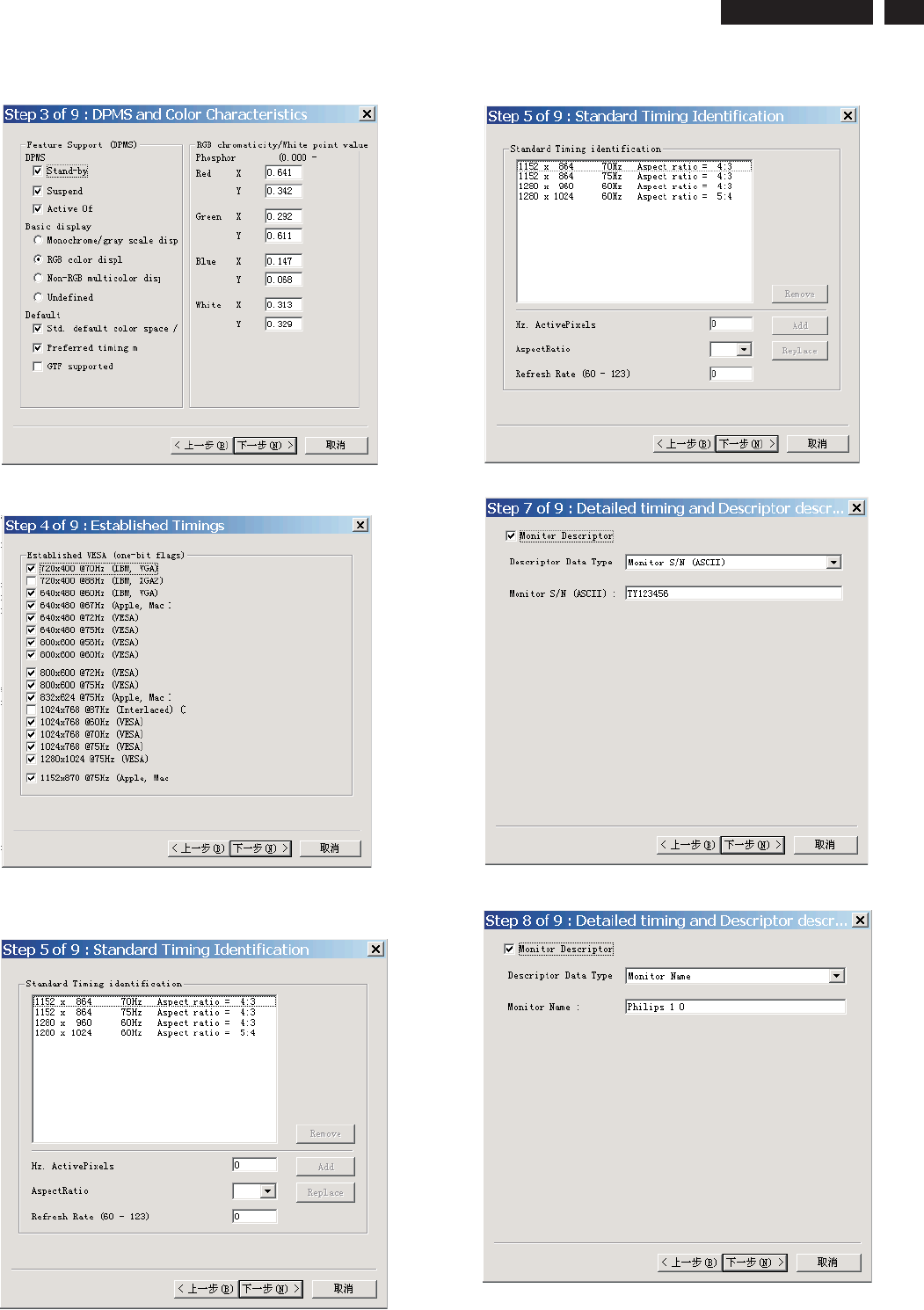
DDC Instructions HUDSON 8
Fig. 21
Fig. 18
Fig. 19
7. Click Next , bring up Fig. 21.
4. Click Next , bring up Fig.18.
5. Click Next , bring up Fig.19.
6. Click Next , bring up Fig. 20.
Fig. 20
2. Click Next , bring up Fig.16.
Fig. 16
Fig. 17
3. Click Next , bring up Fig.17.
C
9
20 DDC Instructions
HUDSON 8
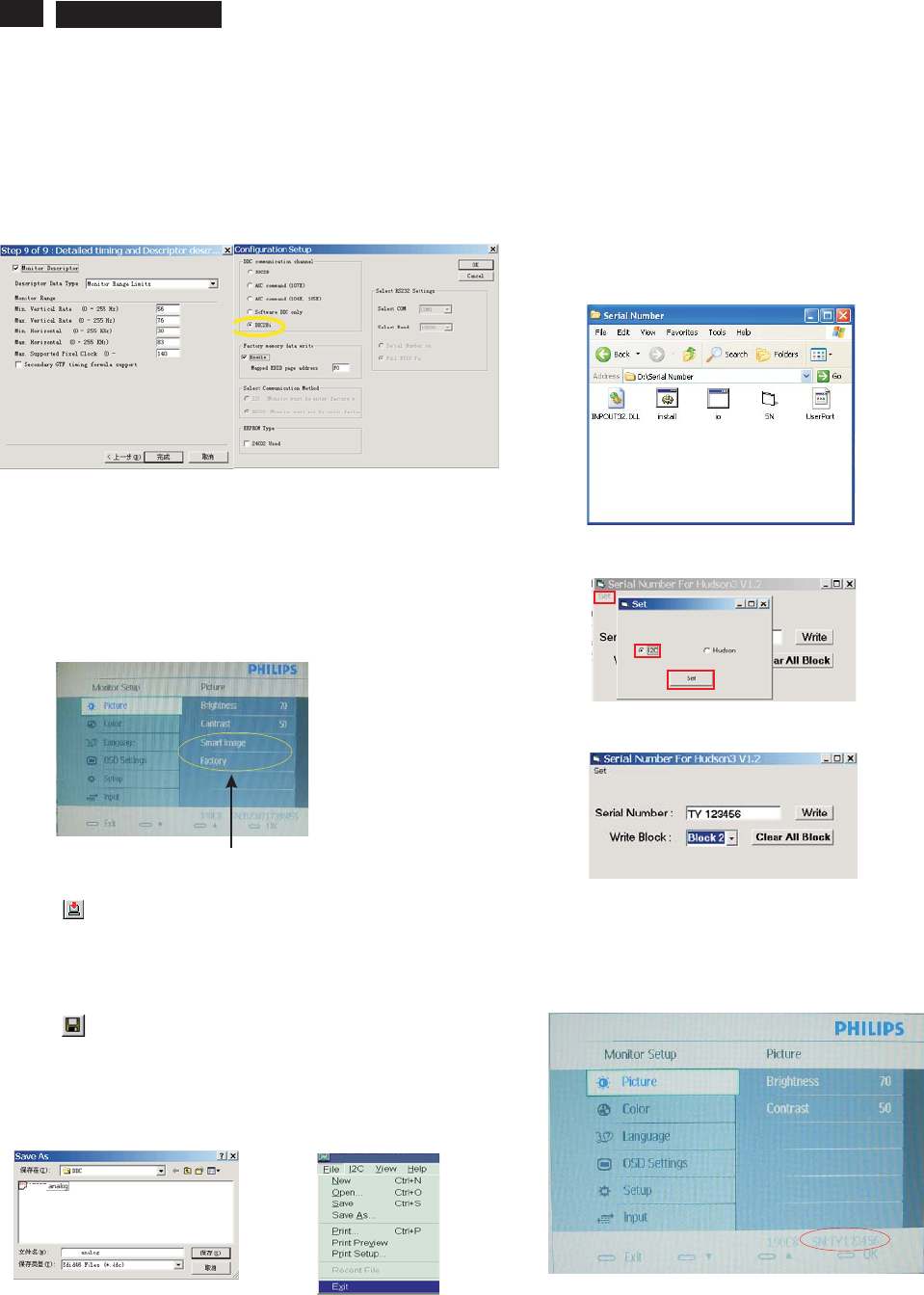
4). Click (Write EDID) icon from the tool bar to write DDC data.
Then wait for 20-30 seconds ,DDC data will be finished Writing.
Fig. 24
3) Push AUTO to exit OSD menu.""
Fig. 22
Step 5: Write DDC data
1. Configuration should be as Fig. 23. And press OK.
Fig. 23
2. Click Save.
Step 7: Exit DDC program
Pull down the File menu and select Exit as shown in Fig. 26.
Step 6: Save DDC data
Sometimes, you may need to save DDC data as a text file for
using in other IC chip. To save DDC data, follow the steps below:
1. Click (Save) icon (or click "file"-> "save as") from the tool bar
and give a file name as shown in Fig. 25.
The file type is EDID46 file (*.ddc) which can be open in WordPad.
By using WordPad, the texts of DDC data & table (128 bytes, hex
code) can be modified. If DDC TEXTS & HEX Table ar completely
correct, it can be saved as .ddc flie to re-load it into DDC IC for DDC
Data application.
Fig. 26
Fig. 25
2. Access Factory Mode
1). Turn off monitor.
2).
3).Press "OK" button, wait until the OSD menu with Characters
"Smart Image " "Factory " (below OSD menu) come on the
Screen of the monitor. as shown in Fig24.
[Push "AUTO" & "OK" buttons at the same time and hold them]
+[Press "power" button untill comes out "Windows screen" ]
=> then release all buttons
Factory Mode indicator
Step9:
1. Disconnect the monitor power cord and connect it again.
2. Press the OK button to bring up the OSD main manu.
3. Re-confirm the serial Number is updated as shown in Fig.30.
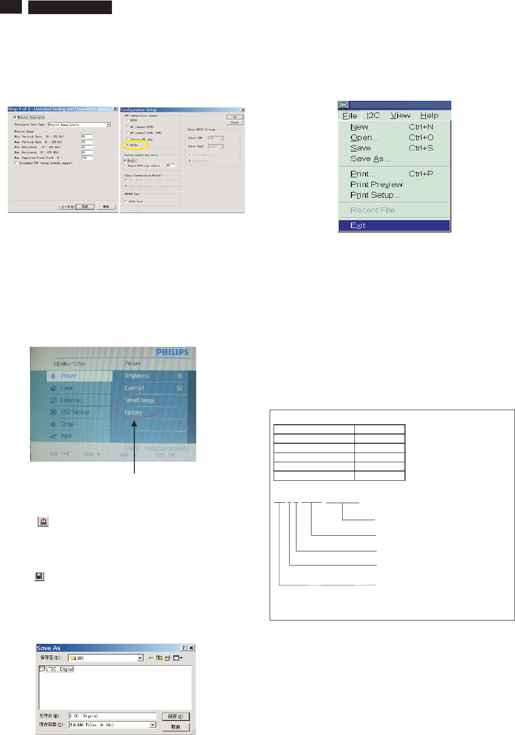
Step 8: Modify serial number in OSD
1. Unzip the serial number.zip to your computer, then open the folder
as shown in Fig.27.
2. If use Win98 OS, you can execute SN.exe directly.
If use Win2000 or XP OS, first, you must execute install.bat, then
execute SN.exe
3. Set I2C bus(press the left-top button of operating window) as shown
in Fig.28, then press " SET" button.
4. Set Block2 as shown in Fig.29
5. key in new serial number, then press " Write" button as shown in
Fig.29 , Click " WRITE" button.
6. It will appear "Serial Number Write OK" , Click "Enter" to finish it.
Fig.27
Fig.28
Fig.29
Fig.30
8. Click Next , bring up Fig. 22.
- In this step, please confirm the Descriptor Data Type is
Monitor Range Limits, and all the items are same as below.
- Click Finish to exit the Step window.
- Serial number can be filled up at this moment (for example, TY
123456).
190C8
190C8
21
DDC Instructions HUDSON 8
Step 3: Modify DDC data (verify EDID version, week,
year)
Click (new function) icon from the tool bar, bring up
Step 1 of 9 as shown in Fig. 35 .
EDID46 DDC application provides the function selection and
text change (select & fill out) from Step 1 to Step 9.
Step 4: Modify DDC data (Monitor Serial No.)
1. Click Next , bring up Fig. 36.
3. Click OK button to confirm your selection.
4. Click icon (Read EDID function) to read DDC EDID data from
monitor. The EDID codes will display on screen as shown in Fig. 34.
Fig. 36
2. Select the DDC2Bi as the communication channel.
As shown in Fig. 33.
Fig. 33
Fig. 34
Fig. 35
Select and fill out,
If necessary.
Re-programming Digital DDC IC
Step 1: After initialize alignment box, connecting all
cables and box as shown in Fig. 31.
Fig. 32
Step 2: Read DDC data from monitor
1. Click icon as shown in Fig. 11 from the tool bar to bring up
the Channels "Configuration Setup" windows as shown in Fig. 32.
Fig. 31
Click this button
=====>
D-sub to DVI-D cable
1=DVI-D connector
2=D-sub connector
3=Power Plug
2
1
3
D-sub cable
DC Power
8 12V~
PC
To video card
To printer port (LTP1)
To
Monitor
Printer
Port
Fig. 42
Fig. 39 Fig. 40
7. Click Next , bring up Fig. 42.
4. Click Next , bring up Fig. 39.
5. Click Next , bring up Fig. 40.
6. Click Next , bring up Fig. 41.
In this step, please confirm the Descriptor Data Type is
Monitor Range Limits, and all the items are same as below.
Fig. 41
2. Click Next , bring up Fig. 37.
Fig. 37 Fig. 38
3. Click Next , bring up Fig. 38.
C
17
7
9
22 DDC Instructions
HUDSON 8
3. Click (Write EDID) icon from the tool bar to write DDC data.
Then wait for 20-30 seconds ,DDC data will be finished Writing.
Fig. 45
Fig. 43
Step 5: Write DDC data
1. Configuration should be as Fig. 40. And press OK.
Fig. 44
2. Click Save.
Step 7: Exit DDC program
Pull down the File menu and select Exit as shown in Fig. 47.
Step 8: Turn off the monitor, exit the factory mode.
Fig. 47
3) Push Menu to exit OSD menu.""
Fig.46
Sometimes, you may need to save DDC data as a text file for using in
other IC chip. To save DDC data, follow the steps below:
1. Click (Save) icon (or click "file"-> "save as") from the tool bar and
give a file name as shown in Fig. 46.
The file type is EDID46 file (*.ddc) which can be open in WordPad. By
using WordPad, the texts of DDC data & table (128 bytes, hex code)
can be modified. If DDC TEXTS & HEX Table ar completely correct, it
can be saved as *.ddc flie to re-load it into DDC IC for DDC Data
Application.
Step 6: Save DDC data
Factory Mode indicator
Serial Number Definition
BOM Code
Panel Supplier CODE
AUO 1
CPT 2
LPL(LG) 3
QDI 4
CMO 5
BZ1A0625000001
SERIAL NO
YEAR/WEEK
SERVICE VERSION CHANGE CODE
BOM CODE(BILL OF MATERIAL)CODE
SITE CODE(PRODUCTION CENTER)
BZ CODE(AR-CZECH REPUBLIC
VN-HUNGARY(SZR),BZ-SUZHOU
DS-DONGGUAN)
2. Access Factory Mode
1). Turn off monitor.
2).
3).Press "OK" button, wait until the OSD menu with Characters
"Smart image" "Factory" (below OSD menu) come on the Screen of
the monitor. as shown in Fig24.
[Push "AUTO" & "OK" buttons at the same time and hold them]
+[Press "power" button untill comes out "Windows screen" ]
=> then release all buttons
8. Click Next , bring up Fig. 43.
- In this step, please confirm the Descriptor Data Type is Monitor
Range Limits, and all the items are same as below.
- Click Finish to exit the Step window.
- Serial number can be filled up at this moment (for example, TY
123456).
98
98

23
HUDSON 8
For LPL panel (analog DDC) 170C8
**********************************************************************
EDID log file
**********************************************************************
Vendor/Product Identification
ID Manufacturer Name : PHL
ID Product Code : C016 (HEX.)
ID Serial Number : 123456 (HEX.)
Week of Manufacture : 19
Year of Manufacture : 2007
EDID Version, Revision
Version : 1
Revision : 3
Basic Display Parameters/Features
Video Input Definition : Analog Video Input
0.700V/0.300V (1.00Vpp)
Blank-to-Black Setup
Separate Sync
Composite Sync
Sync on Green
Serration required
Maximum H Image Size : 34
Maximum V Image Size : 27
Display Transfer Characteristic : 2.2
(gamma)
Feature Support (DPMS) : no Standby
no Suspend
Active Off
Display Type : RGB color display
Preferred Timing Mode : Detailed timing block 1
Color Characteristics
Red X coordinate : 0.635
Red Y coordinate : 0.342
Green X coordinate : 0.298
Green Y coordinate : 0.611
Blue X coordinate : 0.147
Blue Y coordinate : 0.07
White X coordinate : 0.313
White Y coordinate : 0.329
Established Timings
Established Timings I : 720 x 400 @70Hz (IBM,VGA)
640 x 480 @60Hz (IBM,VGA)
640 x 480 @67Hz (Apple,Mac II)
640 x 480 @72Hz (VESA)
640 x 480 @75Hz (VESA)
800 x 600 @56Hz (VESA)
800 x 600 @60Hz (VESA)
Established Timings II : 800 x 600 @72Hz (VESA)
800 x 600 @75Hz (VESA)
832 x 624 @75Hz (Apple,Mac II)
1024 x 768 @60Hz (VESA)
1024 x 768 @70Hz (VESA)
1024 x 768 @75Hz (VESA)
1280 x 1024 @75Hz (VESA)
Manufacturer's timings : 1152 x 870 @75Hz (Apple,Mac II)
Standard Timing Identification #1
Horizontal active pixels : 1280
Aspect Ratio : 5:4
Refresh Rate : 60
Standard Timing Identification #2
Horizontal active pixels : 1152
Aspect Ratio : 4:3
Refresh Rate : 75
Detailed Timing #1
Pixel Clock (MHz) : 108
H Active (pixels) : 1280
H Blanking (pixels) : 408
V Active (lines) : 1024
V Blanking (lines) : 42
H Sync Offset (F Porch) (pixels): 48
H Sync Pulse Width (pixels) : 112
V Sync Offset (F Porch) (lines) : 1
V Sync Pulse Width (lines) : 3
H Image Size (mm) : 338
V Image Size (mm) : 270
H Border (pixels) : 0
V Border (lines) : 0
Flags : Non-interlaced
: Normal Display, No stereo
: Digital Separate sync.
: Positive Vertical Sync.
: Positive Horizontal Sync.
Monitor Descriptor #2
Serial Number : TY10623123456
Monitor Descriptor #3
Monitor Name : Philips 170C
Monitor Descriptor #4
Monitor Range Limits
Min. Vt rate Hz : 56
Max. Vt rate Hz : 76
Min. Horiz. rate kHz : 30
Max. Horiz. rate kHz : 83
Max. Supported Pixel : 140
No secondary GTF timing formula supported.
Extension Flag : 0
Check sum : 8F (HEX.)
**********************************************************************
EDID data (128 bytes)
**********************************************************************
0: 00 1: ff 2: ff 3: ff 4: ff 5: ff 6: ff 7: 00
8: 41 9: 0c 10: 16 11: c0 12: 56 13: 34 14: 12 15: 00
16: 13 17: 11 18: 01 19: 03 20: 1f 21: 22 22: 1b 23: 78
24: 2a 25: a6 26: c5 27: a2 28: 57 29: 4c 30: 9c 31: 25
32: 12 33: 50 34: 54 35: bf 36: ef 37: 80 38: 81 39: 80
40: 71 41: 4f 42: 01 43: 01 44: 01 45: 01 46: 01 47: 01
48: 01 49: 01 50: 01 51: 01 52: 01 53: 01 54: 30 55: 2a
56: 00 57: 98 58: 51 59: 00 60: 2a 61: 40 62: 30 63: 70
64: 13 65: 00 66: 52 67: 0e 68: 11 69: 00 70: 00 71: 1e
72: 00 73: 00 74: 00 75: ff 76: 00 77: 54 78: 59 79: 31
80: 30 81: 36 82: 32 83: 33 84: 31 85: 32 86: 33 87: 34
88: 35 89: 36 90: 00 91: 00 92: 00 93: fc 94: 00 95: 50
96: 68 97: 69 98: 6c 99: 69 100: 70 101: 73 102: 20 103: 31
104: 37 105: 30 106: 43 107: 0a 108: 00 109: 00 110: 00 111: fd
112: 00 113: 38 114: 4c 115: 1e 116: 53 117: 0e 118: 00 119: 0a
120: 20 121: 20 122: 20 123: 20 124: 20 125: 20 126: 00 127: 8f
DDC DATA

24 HUDSON 8 DDC DATA
For CPT panel (analog DDC)
**********************************************************************
EDID log file
**********************************************************************
Vendor/Product Identification
ID Manufacturer Name : PHL
ID Product Code : C016 (HEX.)
ID Serial Number : 123456 (HEX.)
Week of Manufacture : 19
Year of Manufacture : 2007
EDID Version, Revision
Version : 1
Revision : 3
Basic Display Parameters/Features
Video Input Definition : Analog Video Input
0.700V/0.300V (1.00Vpp)
Blank-to-Black Setup
Separate Sync
Composite Sync
Sync on Green
Serration required
Maximum H Image Size : 34
Maximum V Image Size : 27
Display Transfer Characteristic : 2.2
(gamma)
Feature Support (DPMS) : no Standby
no Suspend
Active Off
Display Type : RGB color display
Preferred Timing Mode : Detailed timing block 1
Color Characteristics
Red X coordinate : 0.655
Red Y coordinate : 0.327
Green X coordinate : 0.273
Green Y coordinate : 0.617
Blue X coordinate : 0.144
Blue Y coordinate : 0.079
White X coordinate : 0.313
White Y coordinate : 0.329
Established Timings
Established Timings I : 720 x 400 @70Hz (IBM,VGA)
640 x 480 @60Hz (IBM,VGA)
640 x 480 @67Hz (Apple,Mac II)
640 x 480 @72Hz (VESA)
640 x 480 @75Hz (VESA)
800 x 600 @56Hz (VESA)
800 x 600 @60Hz (VESA)
Established Timings II : 800 x 600 @72Hz (VESA)
800 x 600 @75Hz (VESA)
832 x 624 @75Hz (Apple,Mac II)
1024 x 768 @60Hz (VESA)
1024 x 768 @70Hz (VESA)
1024 x 768 @75Hz (VESA)
1280 x 1024 @75Hz (VESA)
Manufacturer's timings : 1152 x 870 @75Hz (Apple,Mac II)
Standard Timing Identification #1
Horizontal active pixels : 1280
Aspect Ratio : 5:4
Refresh Rate : 60
Standard Timing Identification #2
Horizontal active pixels : 1152
Aspect Ratio : 4:3
Refresh Rate : 75
Detailed Timing #1
Pixel Clock (MHz) : 108
H Active (pixels) : 1280
H Blanking (pixels) : 408
V Active (lines) : 1024
V Blanking (lines) : 42
H Sync Offset (F Porch) (pixels): 48
H Sync Pulse Width (pixels) : 112
V Sync Offset (F Porch) (lines) : 1
V Sync Pulse Width (lines) : 3
H Image Size (mm) : 338
V Image Size (mm) : 270
H Border (pixels) : 0
V Border (lines) : 0
Flags : Non-interlaced
: Normal Display, No stereo
: Digital Separate sync.
: Positive Vertical Sync.
: Positive Horizontal Sync.
Monitor Descriptor #2
Serial Number : TY10623123456
Monitor Descriptor #3
Monitor Name : Philips 170C
Monitor Descriptor #4
Monitor Range Limits
Min. Vt rate Hz : 56
Max. Vt rate Hz : 76
Min. Horiz. rate kHz : 30
Max. Horiz. rate kHz : 83
Max. Supported Pixel : 140
No secondary GTF timing formula supported.
Extension Flag : 0
Check sum : 37 (HEX.)
**********************************************************************
EDID data (128 bytes)
**********************************************************************
0: 00 1: ff 2: ff 3: ff 4: ff 5: ff 6: ff 7: 00
8: 41 9: 0c 10: 16 11: c0 12: 56 13: 34 14: 12 15: 00
16: 13 17: 11 18: 01 19: 03 20: 1f 21: 22 22: 1b 23: 78
24: 2a 25: f0 26: d5 27: a7 28: 53 29: 46 30: 9e 31: 24
32: 14 33: 50 34: 54 35: bf 36: ef 37: 80 38: 81 39: 80
40: 71 41: 4f 42: 01 43: 01 44: 01 45: 01 46: 01 47: 01
48: 01 49: 01 50: 01 51: 01 52: 01 53: 01 54: 30 55: 2a
56: 00 57: 98 58: 51 59: 00 60: 2a 61: 40 62: 30 63: 70
64: 13 65: 00 66: 52 67: 0e 68: 11 69: 00 70: 00 71: 1e
72: 00 73: 00 74: 00 75: ff 76: 00 77: 54 78: 59 79: 31
80: 30 81: 36 82: 32 83: 33 84: 31 85: 32 86: 33 87: 34
88: 35 89: 36 90: 00 91: 00 92: 00 93: fc 94: 00 95: 50
96: 68 97: 69 98: 6c 99: 69 100: 70 101: 73 102: 20 103: 31
104: 37 105: 30 106: 43 107: 0a 108: 00 109: 00 110: 00 111: fd
112: 00 113: 38 114: 4c 115: 1e 116: 53 117: 0e 118: 00 119: 0a
120: 20 121: 20 122: 20 123: 20 124: 20 125: 20 126: 00 127: 37

25
HUDSON 8
DDC DATA
For LPL panel (analog DDC)(190C8)
**********************************************************************
EDID log file
**********************************************************************
Vendor/Product Identification
ID Manufacturer Name : PHL
ID Product Code : C017 (HEX.)
ID Serial Number : 123456 (HEX.)
Week of Manufacture : 19
Year of Manufacture : 2007
EDID Version, Revision
Version : 1
Revision : 3
Basic Display Parameters/Features
Video Input Definition : Analog Video Input
0.700V/0.300V (1.00Vpp)
Blank-to-Black Setup
Separate Sync
Composite Sync
Sync on Green
Serration required
Maximum H Image Size : 38
Maximum V Image Size : 30
Display Transfer Characteristic : 2.2
(gamma)
Feature Support (DPMS) : no Standby
no Suspend
Active Off
Display Type : RGB color display
Preferred Timing Mode : Detailed timing block 1
Color Characteristics
Red X coordinate : 0.639
Red Y coordinate : 0.342
Green X coordinate : 0.297
Green Y coordinate : 0.615
Blue X coordinate : 0.146
Blue Y coordinate : 0.068
White X coordinate : 0.313
White Y coordinate : 0.329
Established Timings
Established Timings I : 720 x 400 @70Hz (IBM,VGA)
640 x 480 @60Hz (IBM,VGA)
640 x 480 @67Hz (Apple,Mac II)
640 x 480 @72Hz (VESA)
640 x 480 @75Hz (VESA)
800 x 600 @56Hz (VESA)
800 x 600 @60Hz (VESA)
Established Timings II : 800 x 600 @72Hz (VESA)
800 x 600 @75Hz (VESA)
832 x 624 @75Hz (Apple,Mac II)
1024 x 768 @60Hz (VESA)
1024 x 768 @70Hz (VESA)
1024 x 768 @75Hz (VESA)
1280 x 1024 @75Hz (VESA)
Manufacturer's timings : 1152 x 870 @75Hz (Apple,Mac II)
Standard Timing Identification #1
Horizontal active pixels : 1280
Aspect Ratio : 5:4
Refresh Rate : 60
Standard Timing Identification #2
Horizontal active pixels : 1152
Aspect Ratio : 4:3
Refresh Rate : 75
Detailed Timing #1
Pixel Clock (MHz) : 108
H Active (pixels) : 1280
H Blanking (pixels) : 408
V Active (lines) : 1024
V Blanking (lines) : 42
H Sync Offset (F Porch) (pixels): 48
H Sync Pulse Width (pixels) : 112
V Sync Offset (F Porch) (lines) : 1
V Sync Pulse Width (lines) : 3
H Image Size (mm) : 338
V Image Size (mm) : 270
H Border (pixels) : 0
V Border (lines) : 0
Flags : Non-interlaced
: Normal Display, No stereo
: Digital Separate sync.
: Positive Vertical Sync.
: Positive Horizontal Sync.
Monitor Descriptor #2
Serial Number : TY10623123456
Monitor Descriptor #3
Monitor Name : Philips 190C
Monitor Descriptor #4
Monitor Range Limits
Min. Vt rate Hz : 56
Max. Vt rate Hz : 76
Min. Horiz. rate kHz : 30
Max. Horiz. rate kHz : 83
Max. Supported Pixel : 140
No secondary GTF timing formula supported.
Extension Flag : 0
Check sum : A8 (HEX.)
**********************************************************************
EDID data (128 bytes)
**********************************************************************
0: 00 1: ff 2: ff 3: ff 4: ff 5: ff 6: ff 7: 00
8: 41 9: 0c 10: 17 11: c0 12: 56 13: 34 14: 12 15: 00
16: 13 17: 11 18: 01 19: 03 20: 1f 21: 26 22: 1e 23: 78
24: 2a 25: a2 26: a5 27: a3 28: 57 29: 4c 30: 9d 31: 25
32: 11 33: 50 34: 54 35: bf 36: ef 37: 80 38: 81 39: 80
40: 71 41: 4f 42: 01 43: 01 44: 01 45: 01 46: 01 47: 01
48: 01 49: 01 50: 01 51: 01 52: 01 53: 01 54: 30 55: 2a
56: 00 57: 98 58: 51 59: 00 60: 2a 61: 40 62: 30 63: 70
64: 13 65: 00 66: 52 67: 0e 68: 11 69: 00 70: 00 71: 1e
72: 00 73: 00 74: 00 75: ff 76: 00 77: 54 78: 59 79: 31
80: 30 81: 36 82: 32 83: 33 84: 31 85: 32 86: 33 87: 34
88: 35 89: 36 90: 00 91: 00 92: 00 93: fc 94: 00 95: 50
96: 68 97: 69 98: 6c 99: 69 100: 70 101: 73 102: 20 103: 31
104: 39 105: 30 106: 43 107: 0a 108: 00 109: 00 110: 00 111: fd
112: 00 113: 38 114: 4c 115: 1e 116: 53 117: 0e 118: 00 119: 0a
120: 20 121: 20 122: 20 123: 20 124: 20 125: 20 126: 00 127: a8

26 HUDSON 8 DDC DATA
For HSD panel (analog DDC)(190C8)
**********************************************************************
EDID log file
**********************************************************************
Vendor/Product Identification
ID Manufacturer Name : PHL
ID Product Code : C017 (HEX.)
ID Serial Number : 123456 (HEX.)
Week of Manufacture : 19
Year of Manufacture : 2007
EDID Version, Revision
Version : 1
Revision : 3
Basic Display Parameters/Features
Video Input Definition : Analog Video Input
0.700V/0.300V (1.00Vpp)
Blank-to-Black Setup
Separate Sync
Composite Sync
Sync on Green
Serration required
Maximum H Image Size : 38
Maximum V Image Size : 30
Display Transfer Characteristic : 2.2
(gamma)
Feature Support (DPMS) : no Standby
no Suspend
Active Off
Display Type : RGB color display
Preferred Timing Mode : Detailed timing block 1
Color Characteristics
Red X coordinate : 0.641
Red Y coordinate : 0.337
Green X coordinate : 0.304
Green Y coordinate : 0.62
Blue X coordinate : 0.141
Blue Y coordinate : 0.073
White X coordinate : 0.313
White Y coordinate : 0.329
Established Timings
Established Timings I : 720 x 400 @70Hz (IBM,VGA)
640 x 480 @60Hz (IBM,VGA)
640 x 480 @67Hz (Apple,Mac
II)
640 x 480 @72Hz (VESA)
640 x 480 @75Hz (VESA)
800 x 600 @56Hz (VESA)
800 x 600 @60Hz (VESA)
Established Timings II : 800 x 600 @72Hz (VESA)
800 x 600 @75Hz (VESA)
832 x 624 @75Hz (Apple,Mac
II)
1024 x 768 @60Hz (VESA)
1024 x 768 @70Hz (VESA)
1024 x 768 @75Hz (VESA)
1280 x 1024 @75Hz (VESA)
Manufacturer's timings : 1152 x 870 @75Hz
(Apple,Mac II)
Standard Timing Identification #1
Horizontal active pixels : 1280
Aspect Ratio : 5:4
Standard Timing Identification #2
Horizontal active pixels : 1152
Aspect Ratio : 4:3
Refresh Rate : 75
Detailed Timing #1
Pixel Clock (MHz) : 108
H Active (pixels) : 1280
H Blanking (pixels) : 408
V Active (lines) : 1024
V Blanking (lines) : 42
H Sync Offset (F Porch) (pixels): 48
H Sync Pulse Width (pixels) : 112
V Sync Offset (F Porch) (lines) : 1
V Sync Pulse Width (lines) : 3
H Image Size (mm) : 338
V Image Size (mm) : 270
H Border (pixels) : 0
V Border (lines) : 0
Flags : Non-interlaced
: Normal Display, No stereo
: Digital Separate sync.
: Positive Vertical Sync.
: Positive Horizontal Sync.
Monitor Descriptor #2
Serial Number : TY10623123456
Monitor Descriptor #3
Monitor Name : Philips 190C
Monitor Descriptor #4
Monitor Range Limits
Min. Vt rate Hz : 56
Max. Vt rate Hz : 76
Min. Horiz. rate kHz : 30
Max. Horiz. rate kHz : 83
Max. Supported Pixel : 140
No secondary GTF timing formula supported.
Extension Flag : 0
Check sum : 99 (HEX.)
**********************************************************************
EDID data (128 bytes)
**********************************************************************
0: 00 1: ff 2: ff 3: ff 4: ff 5: ff 6: ff 7: 00
8: 41 9: 0c 10: 17 11: c0 12: 56 13: 34 14: 12 15: 00
16: 13 17: 11 18: 01 19: 03 20: 1f 21: 26 22: 1e 23: 78
24: 2a 25: 1f 26: 35 27: a4 28: 56 29: 4d 30: 9e 31: 24
32: 12 33: 50 34: 54 35: bf 36: ef 37: 80 38: 81 39: 80
40: 71 41: 4f 42: 01 43: 01 44: 01 45: 01 46: 01 47: 01
48: 01 49: 01 50: 01 51: 01 52: 01 53: 01 54: 30 55: 2a
56: 00 57: 98 58: 51 59: 00 60: 2a 61: 40 62: 30 63: 70
64: 13 65: 00 66: 52 67: 0e 68: 11 69: 00 70: 00 71: 1e
72: 00 73: 00 74: 00 75: ff 76: 00 77: 54 78: 59 79: 31
80: 30 81: 36 82: 32 83: 33 84: 31 85: 32 86: 33 87: 34
88: 35 89: 36 90: 00 91: 00 92: 00 93: fc 94: 00 95: 50
96: 68 97: 69 98: 6c 99: 69 100: 70 101: 73 102: 20 103: 31
104: 39 105: 30 106: 43 107: 0a 108: 00 109: 00 110: 00 111: fd
112: 00 113: 38 114: 4c 115: 1e 116: 53 117: 0e 118: 00 119: 0a
120: 20 121: 20 122: 20 123: 20 124: 20 125: 20 126: 00 127: 99
27
Go to cover page
HUDSON 8
Firmware Upgrade for CPU
Update the firmware
1. Double click the Easywriter.exe icon in desktop then appears
window as shown in Fig.7 .
Step 5 :Copy the hexcode 190C8 to C:\190C8 as shown in Fig. 5 .
6. Install and setup the Easywriter program
Step 1 : Make a folder in your PC as shown in Fig. 3.
For example : C:\190C8
Step 2 : Copy ISP Software Easywriter into your folder
as shown in Fig.3.
Step 3 : Unzip Easywriter.zip into your folder as shown in Fig. 3.
Step 4 : Double click the EasyWriterV2.4p2 icon to install the
Application as Fig. 4.
.zip
Configuration and procedure
"Easywriter " The software is provided by Novatek to upgrade the
firmware of CPU.
DDC2BI_ISP TOOL (3138 149 53161) is for the interface between
"Parallel Port of PC" and "15 pin-D-SUB connector of Monitor".
It is a windows-based program, which cannot be run in MS-DOS.
System and equipment requirements
1. An i486 (or above) personal computer or compatible.
2. Microsoft operation system Windows 95/98/2000/XP.
4. as shown in Fig. 1
3. ISP Software " Easywrite "
DDC2BI_ISP TOOL (3138 106 10396)
5. Connect and Mains cord to Monitor as shown
in Fig. 2.
DDC2BI_ISP TOOL
Fig. 1
Fig. 4
Fig. 5
Fig. 6
Fig. 7
Parallel Port to Print Port in PC
D-SUB to monitor
Fig.2
PC
To printer port (LTP1)
To video card
Video cable
Connect to
Mains cord
Monitor (A)
190C8-Monitor (B)
D-Sub
Connect to Mains
cord at this moment.
------------------------------->
ISP box
Fig. 3
2. Press the Load hex then select the hex as shown in Fig. 8.
190C8
190C8
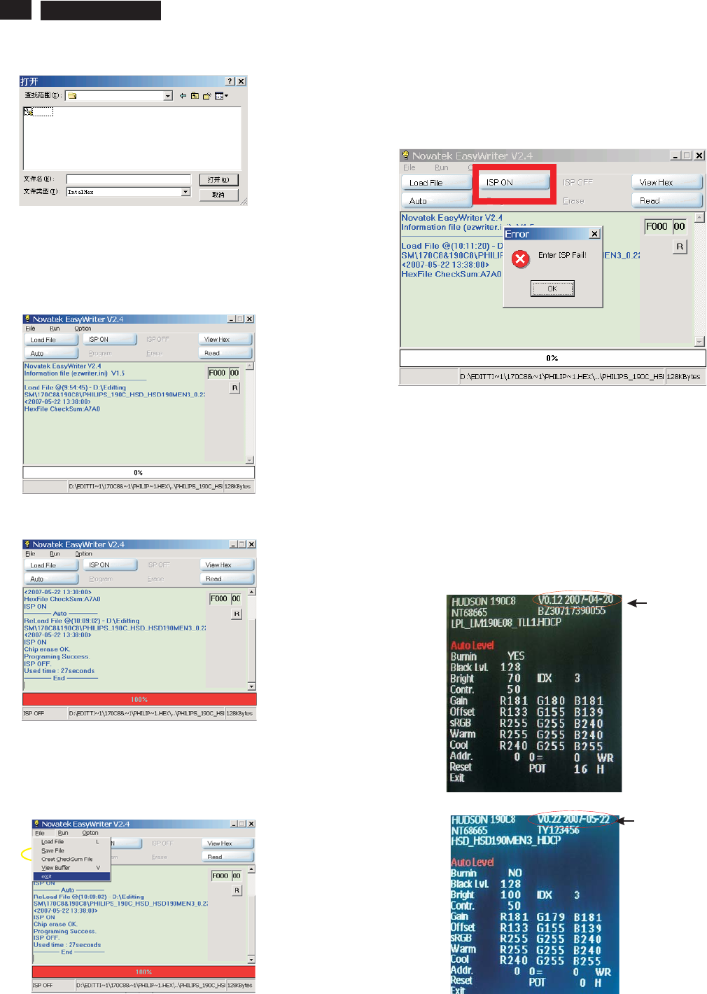
28 HUDSON 8 Firmware Upgrade for CPU
Fig. 8
If there is a warring message coming as shown in Fig 12. , you
have to check the AC power, Video cable, or Novatek MCU.
Fig. 10
Fig. 11
Fig. 13
4 Press the file --> exit to end program , as shown in Fig. 11.
4) Turn off the monitor, exit the factory mode.
Fig. 14
5 Check the firmware version
1). Turn off monitor.
2).
3).Press "OK" button, choose Factory come on the OSD
menu.You will find, after upgrade, the version have already
changed from The former"HUDSON 170C7 V010 2006/06/29" to
the Present "HUDSON 170C7 V011
2006/07/19" as shown in Fig. 13 and Fig. 14.
[Push "AUTO" & "OK" buttons at the same time and hold them]
+[Press "power" button untill comes out "Windows screen" ]
=> then release all buttons.
""
3 Press the AUTO to running program , the firmware be updated
as shown in Fig. 9~10.
Fig. 12
Fig. 9
Factory Mode indicator
190C8
190C8
190C8
Factory Mode indicator

29
HUDSON 8
FAQs (Frequently Asked Questions)
General FAQs
Q: When I install my monitor what should I do if the screen shows 'Cannot display this video
mode'?
A: Recommended video mode for Philips 17": 1280x1024 @60Hz.
1.Unplug all cables, then connect your PC to the monitor that you used previously.
2.In the Windows Start Menu, select Settings/Control Panel. In the Control Panel Window, select the Display icon.
Inside the Display Control Panel, select the 'Settings' tab. Under the setting tab, in box labeled 'desktop area',
move the slidebar to 1280x1024 pixels (17").
3.Open 'Advanced Properties' and set the Refresh Rate to 60Hz, then click OK.
4.Restart your computer and repeat step 2 and 3 to verify that your PC is set at 1280x1024@60Hz (17").
5. Shut down your computer, disconnect your old monitor and reconnect your Philips LCD monitor.
6.Turn on your monitor and then turn on your PC.
Q: What does 'refresh rate' mean in connection with an LCD monitor?
A:The refresh rate is of much less relevance for LCD monitors. LCD monitors display a stable, flicker-free image at 60Hz.
There is no visible difference between 85Hz and 60Hz.
Q: What are the .inf and .icm files on the CD-ROM? How do I install the drivers (.inf and .
icm)?
A:These are the driver files for your monitor. Follow the instructions in your user manual to install the drivers. Your computer may ask you for
monitor drivers (.inf and .icm files) or a driver disk when you first install your monitor. Follow the instructions to Insert the ( companion CD-ROM)
included in this package. Monitor drivers (.inf and .icm files) will be installed automatically.
Q: How do I adjust the resolution?
A:Your video card/graphic driver and monitor together determine the available resolutions. You can select the desired resolution under Windows®
Control Panel with the "Display properties"
Q: What if I get lost when I am making monitor adjustments?
A: Simply press the OK button, then select 'Reset' to recall all of the original factory settings.
Q: What is the Auto function?
A:The AUTO adjustment key restores the optimal screen position, phase and clock settings by pressing of a single button – without the need to
navigate through OSD (On Screen Display) menus and control keys.
Note:Autofunctionisavailableinselectedmodelsonly.
Q: My Monitor has no power (Power LED does not light up). What should I do?
A: Make sure the AC power cord is connected between the monitor and AC outlet,and click a key on keyboard/mouse to wake up the PC.
Q: Will the LCD monitor accept an interlaced signal under PC models?
A: No. If an Interlace signal is used, the screen displays both odd and even horizontal scanning lines at the same time, thus distorting the picture.
Q:What does the Refresh Rate mean for LCD?
A: Unlike CRT display technology, in which the speed of the electron beam is swept from the top to the bottom of the screen determines flicker,
an active matrix display uses an active element (TFT) to control each individual pixel and the refresh rate is therefore not really applicable to
LCD technology.
Q: Will the LCD screen be resistant to scratches?
A: A protective coating is applied to the surface of the LCD, which is durable to a certain extent (approximately up to the hardness of a 2H pencil).
In general, it is recommended that the panel surface is not subject to any excessive shocks or scratches.
Q: How should I clean the LCD surface?
A: For normal cleaning, use a clean, soft cloth. For extensive cleaning, please use isopropyl alcohol. Do not use other solvents such as ethyl
alcohol, ethanol, acetone, hexane, etc
.
Q:Can I change the color setting of my monitor?
A:Yes, you can change your color setting through OSD control as the followingprocedures,
1. Press "OK" to show the OSD (On Screen Display) menu
2. Press "Down Arrow" to select the option "Color" then press "OK" to enter colorsetting, there are four settings as below.
a. Color Temperature; The six settings are 5000K, 6500K, 7500K, 8200K, 9300K and 11500K. With settings in the 5000K range the panel
appears
‘warm,' with a red-white color tone, while a 11500K temperature yields ‘cool,blue-white toning."
b. sRGB; this is a standard setting for ensuring correct exchange of colors between different device (e.g. digital cameras, monitors, printers,
scanners,etc)
c. User Define; the user can choose his/her preference color setting by adjusting red, green blue color.
*A measurement of the color of light radiated by an object while it is being heated.This measurement is expressed in terms of absolute scale,
(degrees Kelvin). Lower Kevin temperatures such as 2004K are red; higher temperatures such as 9300K are blue. Neutral temperature is
white, at 6504K.
Q: Can the Philips LCD Monitor be mounted on the wall?
A: Yes. Philips LCD monitors have this optional feature. For standard VESA mount holes on the rear cover allows the user to mount the Philips
monitor on most of the VESA standard arms or accessories. We recommend to contact your Philips sales representative for more information.
Screen Adjustments
Q: When I install my monitor, how do I get the best performance from the monitor?
A:For best performance, make sure your display settings are set at 1280x1024@60Hz for 17". Note: You can check the current display
settings by pressing the OSD OK button once. The current display mode is shown in OSD first page

30 HUDSON 8 FAQs (Frequently Asked Questions)
Q: How do LCDs compare to CRTs in terms of radiation?
A: Because LCDs do not use an electron gun, they do not generate the same amount of radiation at the screen surface.
Compatibility with other Peripherals
Q: Can I connect my LCD monitor to any PC, workstation or Mac?
A: Yes. All Philips LCD monitors are fully compatible with standard PCs, Macs and workstations. You may need a cable adapter to connect the
monitor to your Mac system. Please contact your Philips sales representative for more information.
Q: Are Philips LCD monitors Plug-and-Play?
A: Yes, the monitors are Plug-and-Play compatible with Windows® 95, 98, 2000, XP and Vista
Q: What is USB (Universal Serial Bus)?
A: Think of USB as a smart plug for PC peripherals. USB automatically determinesresources (like driver software and bus bandwidth) required by
peripherals. USB makes necessary resources available without user intervention. There are three main benefits of USB. USB eliminates "case
anxiety," the fear of removing the computer case to install circuit board cards -- that often requires adjustment of complicated IRQ settings -- for
add-on peripherals. USB does away with "port gridlock." Without USB, PCs are normally limited to one printer, two Com port devices (usually a
mouse and modem), one Enhanced Parallel Port add-on (scanner or video camera, for example),and a joystick. More and more peripherals for
multimedia computers come on the market every day. With USB, up to 127 devices can run simultaneously on one computer. USB permits "hot
plug-in." No need to shut down, plug in, reboot and run set up to install peripherals. No need to go through the reverse process to unplug a
device. Bottom line: USB transforms today's "Plug-and-Pray" into true Plug-and-Play!Please refer to glossary for more information about USB.
Q: What is a USB hub ?
A: A USB hub provides additional connections to the Universal Serial Bus. A hub's upstream port connects a hub to the host, usually a PC.
Multiple downstream ports in a hub allows connection to another hub or device, such as a USB keyboard, camera or printer.
LCD Panel Technology
Q: What is a Liquid Crystal Display?
A: A Liquid Crystal Display (LCD) is an optical device that is commonly used to display ASCII characters and images on digital items such as
watches, calculators,portable game consoles, etc. LCD is the technology used for displays in notebooks and other small computers. Like
light-emitting diode and gas-plasma technologies,LCD allows displays to be much thinner than cathode ray tube (CRT) technology.
LCD consumes much less power than LED and gas-displays because it works on the principle of blocking light rather than emitting it.
Q: What differentiates passive matrix LCDs from active matrix LCDs?
A: An LCD is made with either a passive matrix or an active matrix display grid. An active matrix has a transistor located at each pixel intersection,
requiring less current to control the luminance of a pixel. For this reason, the current in an active matrix display can be switched on and off more
frequently, improving the screen refresh time (your mouse pointer will appear to move more smoothly across the screen, for
example). The passive matrix LCD has a grid of conductors with pixels located at each intersection in the grid.
Q: What are the advantages of TFT LCD compared with CRT?
A: In a CRT monitor, a gun shoots electrons and general light by colliding polarized electrons on fluorescent glass. Therefore, CRT monitors
basically operate with an analog RGB signal. A TFT LCD monitor is a device that displays an input image by operating a liquid crystal panel.
The TFT has a fundamentally different structure than a CRT: Each cell has an active matrix structure and independent active elements. A
TFT LCD has two glass panels and the space between them is filled with liquid crystal. When each cell is connected with electrodes and
impressed with voltage, the molecular structure of the liquid crystal is altered and controls the amount of inlet Lighting to display images. A TFT
LCD has several advantages over a CRT, since it can be very thin and no flickering occurs because it does not use the scanning
method.
Q: Why is vertical frequency of 60Hz optimal for an LCD monitor?
A: Unlike a CDT monitor, the TFT LCD panel has a fixed resolution. For example, an XGA monitor has 1024x3 (R, G, B) x 768 pixels and a higher
resolution may not be available without additional software processing. The panel is designed to optimize the display for a 65MHz dot clock, one of
the standards for XGA displays. Since the vertical/horizontal frequency for this dot clock is 60Hz/48kHz, the optimum frequency
for this monitor is 60Hz
Q: What kind of wide-angle technology is available? How does it work?
A: The TFT LCD panel is an element that controls/displays the inlet of a backlight using the dual-refraction of a liquid crystal. Using the property
that the projection of inlet light refracts toward the major axis of the liquid element, it controls the direction of inlet light and displays it. Since the
refraction ratio of inlet light on liquid crystal varies with the inlet angle of the light, the viewing angle of a TFT is much narrower than that of a CDT.
Usually, the viewing angle refers to the point where the contrast ration is 10. Many ways to widen the viewing angle are currently being developed
and the most common approach is to use a wide viewing angle film, which widens the viewing angle by varying the refraction ratio. IPS (In Plane
Switching) or MVA (Multi Vertical Aligned) is also used to give a wider viewing angle.
Q: Why is there no flicker on an LCD Monitor?
A: Technically speaking, LCDs do flicker, but the cause of the phenomenon is different from that of a CRT monitor -- and it has no impact of the ease
of viewing. Flickering in an LCD monitor relates to usually undetectable luminance caused by the difference between positive and negative voltage.
On the other hand, CRT flickering that can irritate the human eye occurs when the on/off action of the fluorescent object becomes visible. Since the
reaction speed of liquid crystal in an LCD panel is much slower, this troublesome form of flickering is not present in an LCD display
Q: Why is an LCD monitor virtually low of Electro Magnetic Interference?
A: Unlike a CRT, an LCD monitor does not have key parts that generate Electro Magnetic Interference, especially magnetic fields. Also, since an
LCD display utilizes relatively low power, its power supply is extremely quiet.
Ergonomics, Ecology and Safety Standards
Q: What is the CE mark?
A: The CE (Conformité Européenne) mark is required to be displayed on all regulated products offered for sale on the European market. This 'CE'
mark means that a product complies with the relevant European Directive. A European Directive is a European 'Law' that relates to health, safety,
environment and consumer protection, much the same as the U.S. National Electrical Code and UL Standards.
Q: Does the LCD monitor conform to general safety standards?
A: Yes. Philips LCD monitors conform to the guidelines of MPR-II and TCO 99/03 standards for the control of radiation, electromagnetic waves, energy
reduction, electrical safety in the work environment and recyclability. The specification page provides detailed data on safety standards.
More information is provided in the Regulatory Information section..
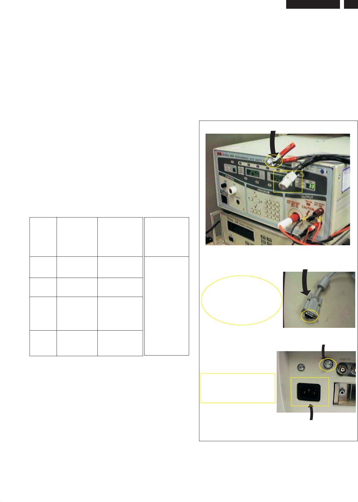
31
HUDSON 8
Safety Test Requirements
All units that are returned for service or repair must pass the
original manufactures safety tests. Safety testing requires both
Hipot and Ground Continuity testing.
HI-POT TEST INSTRUCTION
1.Application requirements
2. Test method
1.1 All mains operated products must pass the Hi-Pot test as
described in this instruction.
1.2 This test must be performed again after the covers have
been refitted following the repair, inspection or modification
of the product.
2.1 Connecting conditions
2.1.1 The test specified must be applied between the parallel-
blade plug of the mainscord and all accessible metal
parts of the product.
2.1.2 Before carrying out the test, reliable conductive
connections must be ensured and thereafter be
maintained throughout the test period.
2.1.3 The mains switch(es) must be in the "ON" position.
2.2 Test Requirements
All products should be HiPot and Ground Continuity tested as
follows:
Test 2820VDC 1700VDC Test current:
voltage (2000VAC) (1200VAC) 25A,AC
Test time:
Test time 3 seconds 1 second 3 seconds(min.)
(min.) Resistance
required:
Trip set at 100 uA 5 mA <=0.09+Rohm,
current for Max. R is the
(Tester) limitation; set resistance of
at 0.1 uA for the mains cord.
Min. Limitation
Ramp set at 2
time seconds
(Tester)
Condition HiPot Test for HiPot Test for Ground Continuity
products where products where Test requirement
the mains input the mains input is
range is Full 110V AC(USA
range(or 220V type)
AC)
2.2.1 The minimum test duration for Quality Control Inspector
must be 1 minute.
2.2.2 The test voltage must be maintained within the specified
voltage + 5%.
2.2.3 There must be no breakdown during the test.
2.2.4 The grounding blade or pin of mains plug must be
conducted with accessible metal parts.
3. Equipments and Connection
3.1. Equipments
For example :
- ChenHwa 9032 PROGRAMMABLE AUTO SAFETY
TESTER
- ChenHwa 510B Digital Grounding Continuity Tester
- ChenHwa 901 (AC Hi-pot test), 902 (AC, DC Hi-pot test)
Withstanding Tester
3.2. Connection
4. Recording
Hipot and Ground Continuity testing records have to be kept
for a period of 10 years.
* Turn on the power switch of monitor before Hipot and
Ground Continuity testing.
Connect the "video cable"
or "grounding screw"
to the CLIP on your tester.
Video cable
(Rear view of monitor)
Connect the power cord
to the monitor.
Grounding screw
Power outlet
(ChenHwa 9032 tester)
Clip
Clip
32 HUDSON 8 Wiring Diagram(170C8)
33
HUDSON 8
Wiring Diagram(190C8)
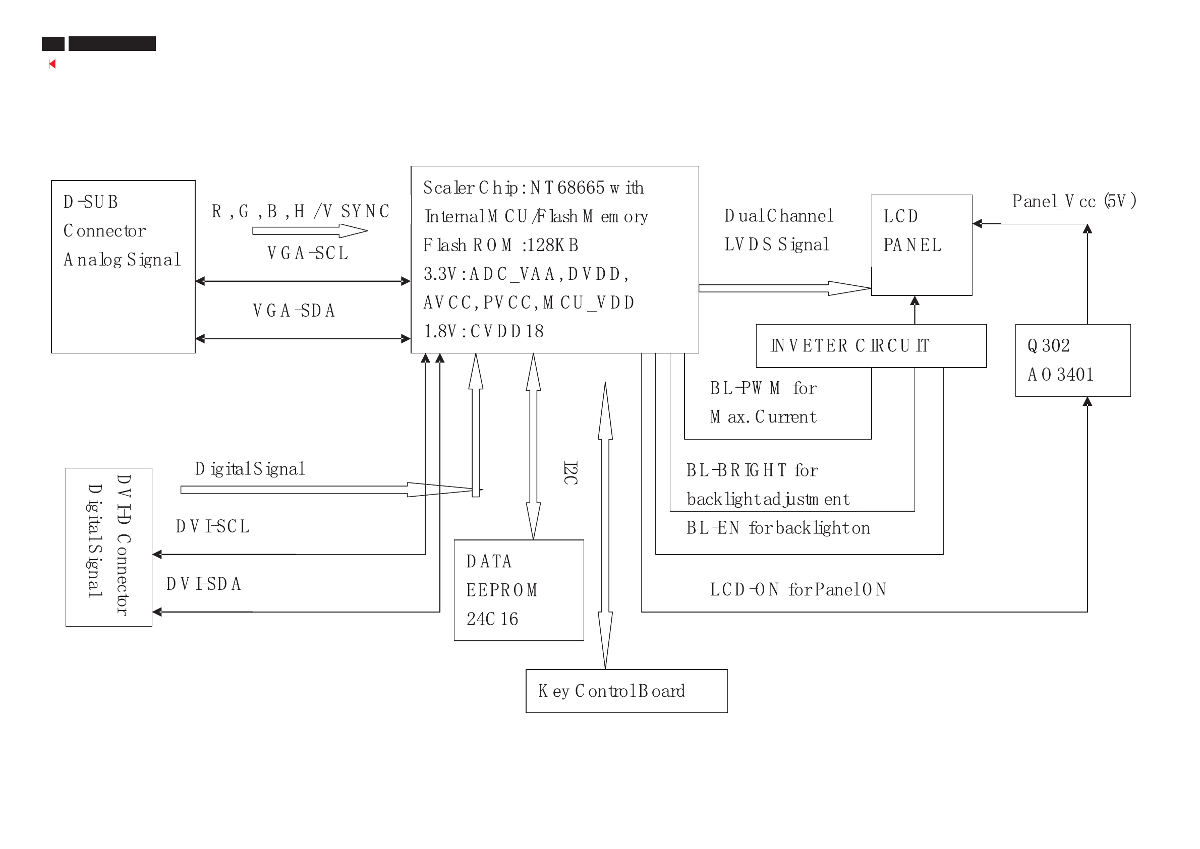
Block Diagram(170C8)
34 HUDSON 8
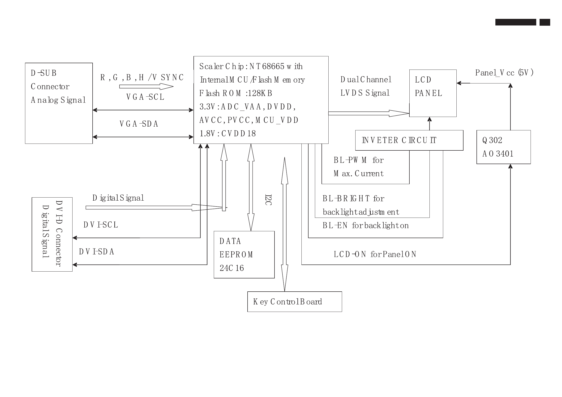
35
HUDSON 8
Block Diagram(190C8)
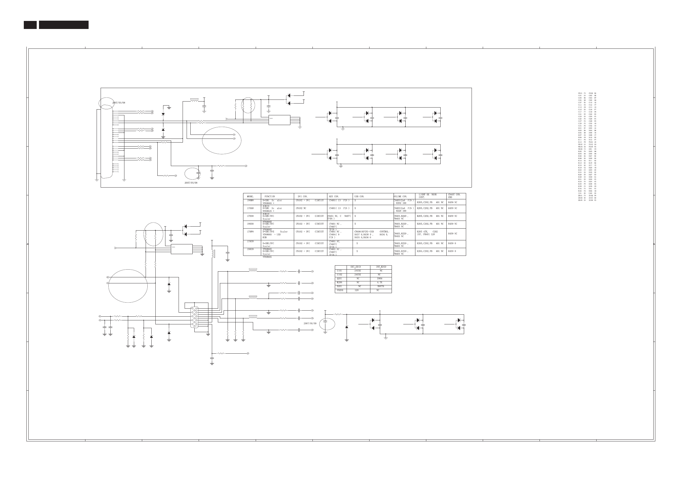
Scaler Diagram(170C8)-1
36 HUDSON 8
1
1
2
2
3
3
4
4
5
5
6
6
7
7
8
8
9
9
10
10
11
11
A A
B B
C C
D D
E E
F F
G G
H H
DVI
CIRCUIT
RX1MRX2P RX1PRX2M
RXCPRX0MRX0P RXCM
GRB
R
G
B
HIN
DDCSCL_D
RX2P
RX2M
RXCM
RXCP
RX0P
RX0M
RX1M
RX1P
DDCSDA
VIN
DDCSDA_D
DDCSCL
RX2- 3
RX2+ 3
DVI_SCL 3
DVI_SDA 3
DVI_CABLE 3
RX1- 3
RX1+ 3
RX0- 3
RX0+ 3
RXC+ 3
RXC- 3
VGA_SDA3
RIN+ 3
RIN- 3
SOG 3
GIN+ 3
GIN- 3
BIN+ 3
BIN- 3
VGA_CABLE 3
DVI-HPD 3
VS3
VGA_SCL3
HS3
DDC_WP3
DDC_WP3
+5V_ESD
+5V_ESD
+5V_ESD
DVI_5V
+5V
DVI_5V
+5V
VGA_5V
VGA_5V
DVI_VDD
VGA_VDD
+5V
R132 100R 1/16W
C113
0.1uF 16V
R127
100R 1/16W
C106
0.1uF 16V
C1180.1uF 16V
R128
100R 1/16W
C131
1000pF
R113 1K 1/16W
D105
BAV99
3
1
2
D111
BAV99
3
1
2
C125
0.047uF
R116 10R 1/16W
C102
0.1uF 16V
R134 100R 1/16W
FB1050R05 1/8W
C127330pF 50V
CN102
JACK
1
2
3
4
5
6
7
8
9
10
11
12
13
14
15
16
17
18
19
20
21
22
23
24
26
25
C1
C2
C3
C4
C5
RX2-
RX2+
GND
RX4-
RX4+
SCL
SDA
VS
RX1-
RX1+
GND
RX3-
RX3+
5V
GND
HP
RX0-
RX0+
GND
RX5-
RX5+
GND
RXC+
RXC-
26
25
RED
GRN
BLU
HS
GND
D107
BAV99
3
1
2
ZD105
RLZ5.6B
R117
10R 1/16W
R125
10K 1/16W
R107
10R 1/16W
D101
BAV99
3
1
2
CN101
DB15
1
6
2
7
3
8
4
9
5
11
12
13
14
15
10
17
16
R122
1K 1/16W
D112
BAV99
3
1
2
C121
0.047uF
R129 150 ? 1/16W
C132
470PF 50V
C111
0.1uF 16V
R124
4K7 1/16W
C115
1uF 16V
C1040.1uF 16V
R118
10R 1/16W
C126
0.047uF
R108 100R 1/16W
C1220.047uF
ZD102
RLZ5.6B
D104
BAV99
3
1
2
R139
75R 1/16W
D109
BAV99
3
1
2
ZD106
RLZ5.6B
R103
4K7 1/16W
C129
0.047uF
C114
0.1uF 16V
FB106
30 OHM
1 2
D113
BAV99
3
1
2
R144
1K 1/16W
ZD107
RLZ5.6B
D108
BAV99
3
1
2
FB102
120 OHM
1
2
FB10430 OHM
1 2
C1231000pF
R102
1K 1/16W
R105
10K 1/16W
R141
2K2 1/16W
D103
BAV99
3
1
2
C1160.1uF 16V
C1120.1uF 16V
FB103
30 OHM
1 2
C117
0.1uF 16V
ZD104
RLZ5.6B
C105
0.1uF 16V
R131 390R 1/16W
R126 100R 1/16W
R140
75R 1/16W
U102
NC/M24C02-WMN6TP
1
2
3
45
6
7
8NC/NC/NC/E0/E0
NC/NC/E1/E1/E1
NC/E2/E2/E2/E2
VSSSDA
SCL
WC
VCC
C107
1uF 16V
R136 100R 1/16W
R110
10R 1/16W
D102
BAV70
C128
33pF
R123
4K7 1/16W
D106
BAV99
3
1
2
R138 150 ? 1/16W
ZD101
RLZ5.6B
R120
1K 1/16W
R142
2K2 1/16W
R109 100R 1/16W
R106
10R 1/16W
R111
10R 1/16W
R133 150 ? 1/16W
FB101
120 OHM
1 2
ZD103
RLZ5.6B
R135 100R 1/16W
C110
0.1uF 16V
R101
75R 1/16W
C124
0.047uF
C1010.1uF 16V
C103
0.1uF 16V
D110
BAV70
C130
0.1uF 16V
R104
4K7 1/16W
R115
10R 1/16W
U101
NC/M24C02-WMN6TP
1
2
3
45
6
7
8NC/NC/NC/E0/E0
NC/NC/E1/E1/E1
NC/E2/E2/E2/E2
VSSSDA
SCL
WC
VCC
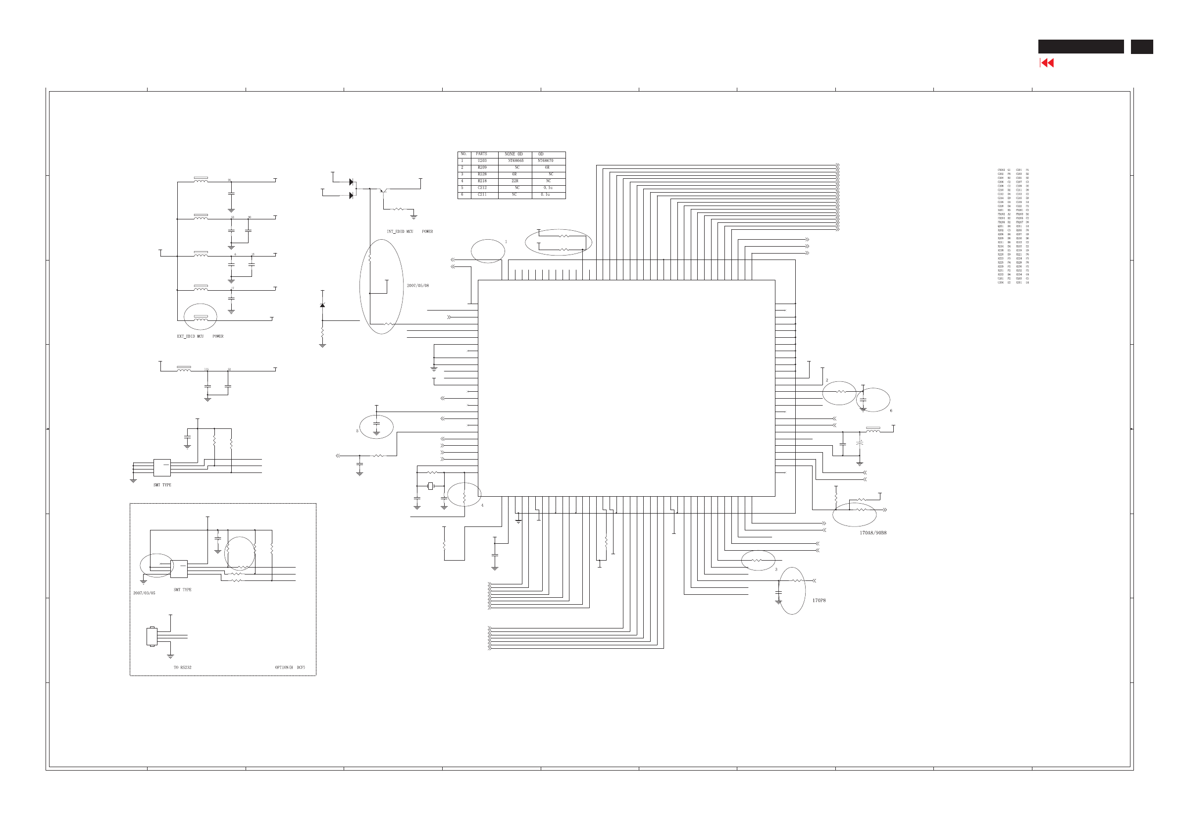
37
HUDSON 8
Scaler Diagram(170C8) - 2
Go to cover page
1
1
2
2
3
3
4
4
5
5
6
6
7
7
8
8
9
9
10
10
11
11
A A
B B
C C
D D
E E
F F
G G
H H
PHILIPS F
170C8 D
35May 24, 2007
715G2561-1-PHI <>
03.MCU+SCALER NT68665
G2561-1-PHI-X-1-070522
OEM MODEL Size
Rev
Date Sheet of
TPV MODEL
PCB NAME
TCLK
IICSCL
24C16_WP
RX
VSO
VSO
HSO
IICSDA
HSO
H_SDA
RX
TX
IRQN
IRQN
TCLK
IICSCL
IICSDA
24C16_WP
TX
H_SCL
H_SDA
H_SCL
5V_DECT
5V_DECT
DDC_WP
PANEL_PWR 4
VGA_CABLE2
RX2+2
RXC+2
HS 2
RX2-2
GIN-2
RX1-2
RIN-2
VS 2
DDC_WP 2
RIN+2
BIN+2
BRIGHTNESS4,5
DVI_SCL 2
RX0-2
KEY_PWR 5
DVI_SDA 2
VGA_SCL 2
RX1+2
SOG2
LED_B/G5
DVI-HPD 2
KEY15
RX0+2
LED_R 5
LF_LED5
VGA_SDA 2
GIN+2
VOLUME 5
KEY25
RXC-2
PANEL_IDX4
BIN-2
DVI_CABLE2
T7P 5
T6M 5
T6P 5
T7M 5
TCLK2P 5
T0M 5
TCLK1M 5
T4P 5
T1M 5
T2M 5
T5P 5
T3P 5
T5M 5
T2P 5
TCLK2M 5
T4M 5
TCLK1P 5
T1P 5
T0P 5
T3M 5
BL_CONTROL4
AUDIO_STDBY5
LIGHT_SEN 5
MCU_VDD
CVDD18
CVDD18
MCU_VDD
DVDD
AVCC
+1.8VCC
MCU_VDD
+1.8VCC
+5V
PVCC
DVDD
MCU_VDD
MCU_VDD
ADC_VAA
DVDD
+3.3VCC
AVCC
CVDD18
ADC_VAA
DVDD
AVC C
PVCC
CVDD18
DVI_VDD
VGA_VDD
MCU_VDD
MCU_VDD
MCU_VDD
+5V
MCU_VDD
CVDD18
R224
NC/4.7K
C206
0.1uF 16V
FB204
120 OHM
1 2
R225
100R 1/16W
C222
NC/1uF 16V
R233
NC/750R OHM 1/16W 5%
C209
0.1uF 16V
R230
NC/100
R202
10K 1/16W
C212
NC/0.1uF 16V
R223
NC/4.7K
C220
22pF
FB203
120 OHM
1 2
U201
NC/M24C04-WMN6TP
1
2
3
4 5
6
7
8
NC
E1
E2
VSS SDA
SCL
WC
VCC
R215
4K7 1/16W
C204
0.1uF 16V
R206
4K7 1/16W
R229
NC/100
R220
100R 1/16W
FB202
120OHM
1 2
R219
NC/4.7K
C207
0.1uF 16V
R228
0R05 1/16W
C201
0.1uF 16V
C216
0.1uF 16V
ZD201
RLZ2.2B
R213
4K7 1/16W
C211
NC/0.1uF 16V
R207
NC/4.7K
C219
22pF
R205
NC/47K 1/16W
R214
4K7 1/16W
C214
100uF/16V
R201
1M 1/16W
U204
M24C16
1
2
3
4 5
6
7
8
NC
NC
NC
VSS SDA
SCL
WC
VCC
FB201
NC/120 OHM
1 2
FB205
120 OHM
1 2
R231
NC/4K7 1/16W
C208
0.1uF 16V
R209
NC/0R05 1/16W
C205
0.1uF 16V
C213
1uF 16V
U203
NT68665MFG-128
39
46
47
50
51
52
53
54
40
48
49
17
18
19
20
21
22
23
24
25
26
27
28
29
30
31
32
33
34
35
36
37
38
6
7
8
9
11
12
69
70
71
72
78
79
111
1
2
3
4
5
10
13
14
16
15
41
42
43
44
45
65
66
67
68
89
90
91
92
101
103
102
104
110
109
108
107
106
105
117
116
115
114
113
112
118
119
120
121
122
124
123
126
125
128
127
55
56
57
58
59
60
61
62
63
64
73
74
75
76
77
80
81
82
84
83
85
86
87
88
94
93
96
95
98
97
100
99
PA6*/PWM8*
PB5*/DDC_SDA0
PB4*/DDC_SCL0
SCL/P34
IRQn
CVDD
DVDD
RSBA1P/V0
PA7*/PWM9*
RSTn/PD5
SDA/P35
PVCC
PGND
BIN1+
BIN1-
SOG1I
GIN1+
GIN1-
RIN1+
RIN1-
ADC_VAA
ADC_GNDA
PC2
PD6
PB3/ADC3/INT1
P31/TXD
P30/RXD
PB2/ADC2/INT0
PB7*/DDC_SDA1
PB6*/DDC_SCL1
PA3/PWM5
PA4*/PWM6*
PA5*/PWM7*
AVCC
RX1+
RX1-
AGND
RX0-
AGND
RSGA2M/T7M
RSGA3P/TCLK2P
RSGA3M/TCLK2M
RSRA1P/T6P/RSBB0P
DGND/CGND
RSBB1P/T3P
AD0/GPO2
RSTB
MCU_VCC
MCU_GND
RX2+
RX2-
RX0+
RXC+
RXC-
REXT
AVCC
HSYNCI1
TOUTP/VSYNCI1
PLL_GND
TCLK
PLL_VDD
PA0/PWM2
PA2/PWM4
PA1/PWM3
RSGA2P/T7P
SP
DVDD
RSGB2P
RSGB2M
DGND/CGND
PC7
PC6
PD0
GPO1
NC/(HSYNCI)
PD4
PD3
PD2
PD1
PWMA/GPO7
GPO6
CVDD
INT_HSO/GPO5
INT_VSO/GPO4
AD1/GPO3
PWMB/GPO8
NC/(VSYNCI)
PC0*
PC1*
PC3/PWM0
PC5
PC4/PWM1
PB0/ADC0
PB1/ADC1
OSCO
OSCI
RSBA1M/V1
RSBA2P/V2
RSBA2M/V3
RSBA3P/V4
RSBA3M/V5
RSCLKAP/V6
RSCLKAM/V7
RSGA1P/VCKI
RSGA1M
CGND/DGND
RSRA1M/T6M/RSBB0M
RSRA2P/T5P/RSGB0P
RSRA2M/T5M/RSGB0M
RSRA3P/T4P/RSRB0P
RSRA3M/T4M/RSRB0M
RSBB1M/T3M
RSBB2P/TCLK1P
RSBB2M/TCLK1M
RSBB3M/T2M
RSBB3P/T2P
RSCLKBP/T1P
RSCLKBM/T1M
RSGB1P/T0P
RSGB1M/T0M
RSGB3M
RSGB3P
RSRB1M
RSRB1P
RSRB2M
RSRB2P
RSRB3M
RSRB3P
R221
470R 1/16W
FB207
1000OHM
1 2
R210
NC/0R05 1/16W
C203
0.1uF 16V
CN202
NC/4PIN 2.0mm CONN
1
2
3
4
R218
22R 1/16W
R234
220R 1/16W
C210
0.1uF 16V
D201
BAV70
Q201
2N3906S-RTK/PS
FB206
120OHM
1 2
C2150.1uF 16V
X201
12MHz
1 2
R232 NC/0R05 1/16W
C202
NC/1uF 16V
R211
0R05 1/16W
Scaler Diagram(170C8) - 3
38 HUDSON 8
1
1
2
2
3
3
4
4
5
5
6
6
7
7
8
8
9
9
10
10
11
11
A A
B B
C C
D D
E E
F F
G G
H H
modify
1/8
BL_CONTROL 3
BRIGHTNESS 3,5
PANEL_PWR3
PANEL_IDX 3
+1.8VCC
+3.3VCC
+3.3VCC
+12V
+5V
PANEL_VCC
+5V
+5V
+3.3VCC
+5V
+5V
FB303
120
C306
100uF/16V
R308 4K7 1/16W
C317
0.1uF 16V
C309
100uF/16V
C308
1uF 16V
R304
10K 1/16W
U303
NC/LD1117S33
3 2
1
VI VO
GND
R311
1K 1/16W
C316
0.1uF/25V
C304
1uF 16V
R316 4K7 1/16W
Q305
2N3904S-RTK/PS
U302
NC/AZ1117D-1.8-E1
1
2
3
ADJ/GND
OUTPUT
INPUT
R307
51K? 1/16W
C312
0.1uF 16V
C302
10uF/16V
CN301
CONN
1
2
3
4
5
6
7
8
9
C307
0.1uF 16V
Q302
AO3401
R312
1K 1/16W
D301
SM340A
R303
330 1/4W
C310
100uF/16V
U304
AP1117E18LA
3 2
1
VI VO
GND
C311
0.1uF 16V
Q301
2N3904S-RTK/PS
C303
0.1uF 16V
C305
100uF/16V
FB302
120
R305
10K 1/16W
R301
1K 1/16W
R309
100R 1/16W
C315
100uF/16V
R302
330? 1/4W
U301
AP1117D33LA
1
2
3
ADJ(GND)
VOUT
VIN
C301
0.1uF 16V
R314
4K7 1/16W
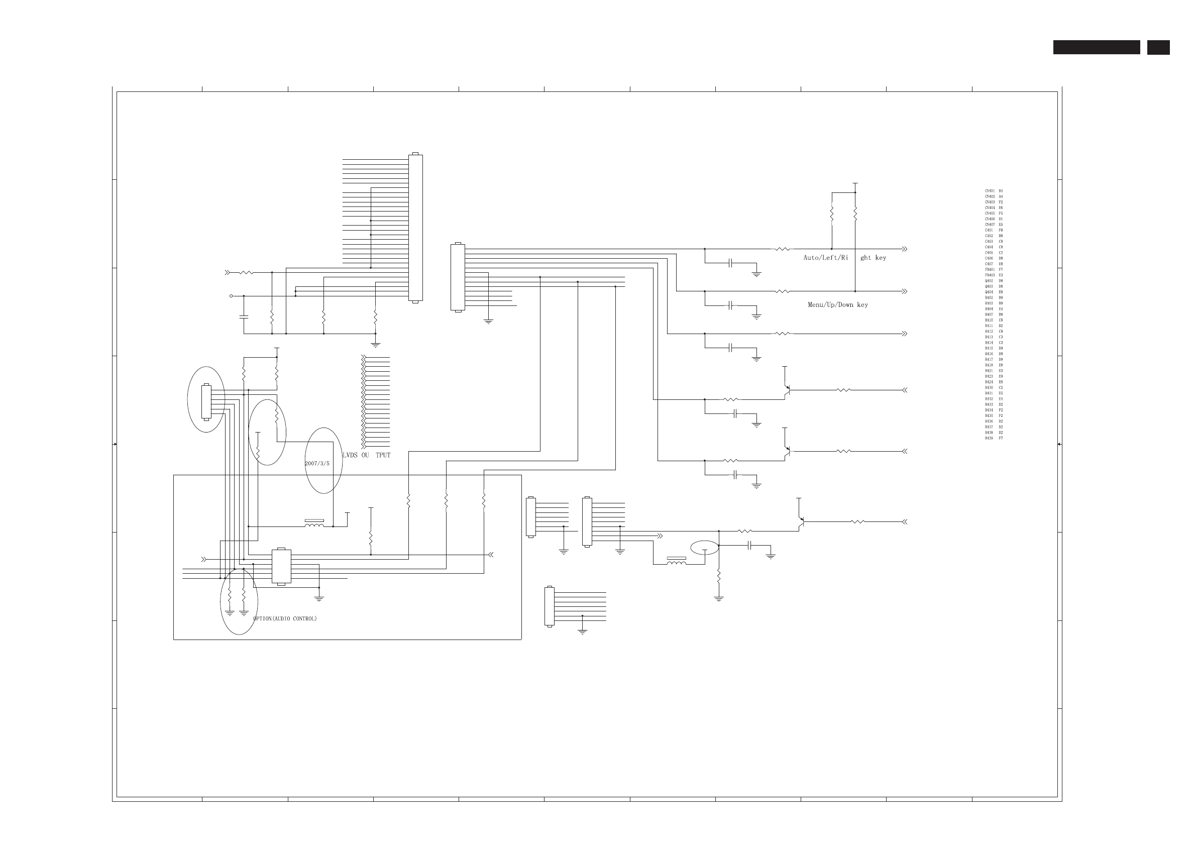
39
HUDSON 8
Scaler Diagram(170C8) - 4
1
1
2
2
3
3
4
4
5
5
6
6
7
7
8
8
9
9
10
10
11
11
A A
B B
C C
D D
E E
F F
G G
H H
T3P
T0P
TCLK1M
T4M
T1M
T4P
T7P
T5M
T6M
TCLK1P
T7M
T1P
T3M
T2M
TCLK2M
T0M
T6P
T2P
T5P
TCLK2P
EAR-L
EAR-R
LED_O
KEY1_PAD
KEY2_PAD
OUT-R+
EAR-R
EAR-SENSE
POWER
LED_G
LIGHT_SEN
OUT-L+
OUT-L-
5V_FB
LF_B
OUT-R-
LED_O
KEY1_PAD
5V_FB
POWER
LED_G
KEY2_PAD
LED_G
KEY1_PAD
LED_O
POWER
LF_B
KEY2_PAD
OUT-L-
OUT-L+
EAR-L
POWER
KEY1_PAD
LED_O
LED_G
KEY2_PAD
LF_B LF_B
LED_R 3
LED_B/G 3
KEY1 3
KEY2 3
KEY_PWR 3
T1P3
T2M3
T6P3
T2P3
T1M3
T5M3
T7P3
T0M3
T7M3
TCLK2P3
T0P3
T6M3
T3M3
TCLK1M3
T4M3
T3P3
T4P3
T5P3
TCLK1P3
TCLK2M3
BRIGHTNESS3,4
LF_LED 3
VOLUME3
AUDIO_STDBY 3
LIGHT_SEN 3
+3.3VCC
+3.3VCC
+3.3VCC
PANEL_VCC
+3.3VCC
+12V
+5V
+3.3VCC
+5V
+3.3VCC
R404
0R05 1/16W
CN401
NC/CONN
1
2
3
4
5
6
7
8
9
10
11
12
13
R407
100R 1/16W
FB401
NC/120 OHM
1 2
R415 10K 1/16W
R424 NC/100R 1/16W
R435
NC/0R05 1/10W 5%
C403
0.1uF 16V
R436
NC/0R05 1/10W 5%
R421
10K 1/16W
R413
NC/0R05 1/16W
R410
100R 1/16W
C407
0.1uF 16V
R439
0R05 1/16W
CN407
CONN
1
2
3
4
5
6
7
Q402
2N3906S-RTK/PS
R403
3.9K? 1/16W
C402
0.1uF 16V
R431
0R05 1/16W
R430
NC/0R05 1/16W
R417 10K 1/16W
C401
NC/0.1uF 16V
CN403
CONN
2
4
6
8
10
12
1
3
5
7
9
11
CN405
NC/CONN
1
2
3
4
5
6
7
R438
NC/0R05 1/10W 5%
R416 100R 1/16W
R411
NC/22
R423 NC/10K 1/16W
R434
NC/0R05 1/10W 5%
R433
NC/0R05 1/10W 5%
FB403
NC/120?
1 2
C404
0.1uF 16V
CN404
NC/CONN
1
2
3
4
5
6
7
8
9
R418 100R 1/16W
CN406
NC/CONN
1
2
3
4
5
6
C405
0.1uF 16V
Q404
NC/2N3906S-RTK/PS
CN402
CONN
1
2
3
4
5
6
7
8
9
10
11
12
13
14
15
16
17
18
19
20
21
22
23
24
25
26
27
28
29
30
R402
3.9K? 1/16W
Q403
2N3906S-RTK/PS
C406
0.1uF 16V
R432
0R05 1/16W
R414
NC/0R05 1/16W
R412 1K 1/16W
R437
NC/0R05 1/10W 5%
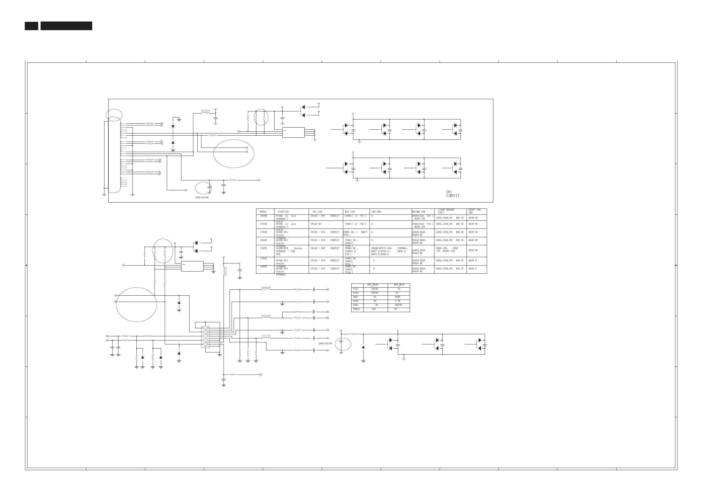
Scaler Diagram(190C8)-1
40 HUDSON 8
1
1
2
2
3
3
4
4
5
5
6
6
7
7
8
8
9
9
10
10
11
11
A A
B B
C C
D D
E E
F F
G G
H H
CN101 F3 CN102 B2
C101 E4 C102 B6
C103 B7 C104 B7
C105 B8 C106 B4
C107 B5 C110 C6
C111 C7 C112 C7
C113 C8 C114 C4
C115 D3 C116 F7
C117 F7 C118 F8
C121 E5 C122 E5
C123 E5 C124 E5
C125 F5 C126 F5
C127 F2 C128 F2
C129 F5 C130 G4
C131 F6 C132 C4
D101 B7 D102 A5
D103 B6 D104 B6
D105 B8 D106 B6
D107 B6 D108 B7
D109 B8 D110 D3
D111 F7 D112 F7
D113 F8 FB101 A3
FB102 E4 FB103 E4
FB104 E4 FB105 F2
FB106 F4 R101 F4
R102 F6 R103 B4
R104 B4 R105 B4
R106 B3 R107 B3
R108 B4 R109 B4
R110 B3 R111 B3
R113 B3 R115 B3
R116 B3 R117 C3
R118 C3 R120 C4
R122 C3 R123 D3
R124 D3 R125 D2
R126 E5 R127 E3
R128 E3 R129 E5
R131 E5 R132 E5
R133 F5 R134 F2
R135 F5 R136 F2
R138 F5 R139 F4
R140 F4 R141 F2
R142 F3 R144 G4
U101 B5 U102 D3
ZD101 F3 ZD102 F6
ZD103 B3 ZD104 B3
ZD105 E3 ZD106 F2
RX1MRX2P RX1PRX2M
RXCPRX0MRX0P RXCM
GRB
R
G
B
HIN
DDCSCL_D
RX2P
RX2M
RXCM
RXCP
RX0P
RX0M
RX1M
RX1P
DDCSDA
VIN
DDCSDA_D
DDCSCL
RX2- 3
RX2+ 3
DVI_SCL 3
DVI_SDA 3
DVI_CABLE 3
RX1- 3
RX1+ 3
RX0- 3
RX0+ 3
RXC+ 3
RXC- 3
VGA_SDA3
RIN+ 3
RIN- 3
SOG 3
GIN+ 3
GIN- 3
BIN+ 3
BIN- 3
VGA_CABLE 3
DVI-HPD 3
VS3
VGA_SCL3
HS3
DDC_WP3
DDC_WP3
+5V_ESD
+5V_ESD
+5V_ESD
DVI_5V
+5V
DVI_5V
+5V
VGA_5V
VGA_5V
DVI_VDD
VGA_VDD
+5V
R132 100R 1/16W
R127
100R 1/16W
C113
0.1uF 16V
R128
100R 1/16W
C118
0.1uF 16V
C106
0.1uF 16V
C131
1000pF
D111
BAV99
3
1
2
D105
BAV99
3
1
2
R113 1K 1/16W
C125
0.047uF
C102
0.1uF 16V
R116 10R 1/16W
R134 100R 1/16W
FB105
0R05 1/8W
C127330pF 50V
D107
BAV99
3
1
2
CN102
JACK
1
2
3
4
5
6
7
8
9
10
11
12
13
14
15
16
17
18
19
20
21
22
23
24
26
25
C1
C2
C3
C4
C5
RX2-
RX2+
GND
RX4-
RX4+
SCL
SDA
VS
RX1-
RX1+
GND
RX3-
RX3+
5V
GND
HP
RX0-
RX0+
GND
RX5-
RX5+
GND
RXC+
RXC-
26
25
RED
GRN
BLU
HS
GND
R125
10K 1/16W
R117
10R 1/16W
ZD105
RLZ5.6B
D101
BAV99
3
1
2
R107
10R 1/16W
CN101
DB15
1
6
2
7
3
8
4
9
5
11
12
13
14
15
10
17
16
D112
BAV99
3
1
2
R122
1K 1/16W
C121
0.047uF
R129 150 ? 1/16W
C132
470PF 50V
C111
0.1uF 16V
R124
4K7 1/16W
R118
10R 1/16W
C104
0.1uF 16V
C115
1uF 16V
R108 100R 1/16W
C126
0.047uF
ZD102
RLZ5.6B
C122
0.047uF
D104
BAV99
3
1
2
D109
BAV99
3
1
2
R139
75R 1/16W
ZD106
RLZ5.6B
R103
4K7 1/16W
C129
0.047uF
FB106
30 OHM
1 2
C114
0.1uF 16V
D113
BAV99
3
1
2
R144
1K 1/16W
ZD107
RLZ5.6B
D108
BAV99
3
1
2
FB102
120 OHM
1
2
C1231000pFFB104
30 OHM
1 2
R102
1K 1/16W
R105
10K 1/16W
R141
2K2 1/16W
D103
BAV99
3
1
2
C116
0.1uF 16V
FB103
30 OHM
1 2
C112
0.1uF 16V
C117
0.1uF 16V
ZD104
RLZ5.6B
R131 390R 1/16W
C105
0.1uF 16V
R126 100R 1/16W
U102
NC/M24C02-WMN6TP
1
2
3
45
6
7
8NC/NC/NC/E0/E0
NC/NC/E1/E1/E1
NC/E2/E2/E2/E2
VSSSDA
SCL
WC
VCC
R140
75R 1/16W
C107
1uF 16V
R110
10R 1/16W
R136 100R 1/16W
D102
BAV70
C128
33pF
D106
BAV99
3
1
2
R123
4K7 1/16W
R138 150 ? 1/16W
ZD101
RLZ5.6B
R120
1K 1/16W
R109 100R 1/16W
R142
2K2 1/16W
R111
10R 1/16W
R106
10R 1/16W
R133 150 ? 1/16W
FB101
120 OHM
1 2
ZD103
RLZ5.6B
R135 100R 1/16W
R101
75R 1/16W
C110
0.1uF 16V
C124
0.047uF
C101
0.1uF 16V
D110
BAV70
C103
0.1uF 16V
R115
10R 1/16W
R104
4K7 1/16W
C130
0.1uF 16V
U101
NC/M24C02-WMN6TP
1
2
3
45
6
7
8NC/NC/NC/E0/E0
NC/NC/E1/E1/E1
NC/E2/E2/E2/E2
VSSSDA
SCL
WC
VCC
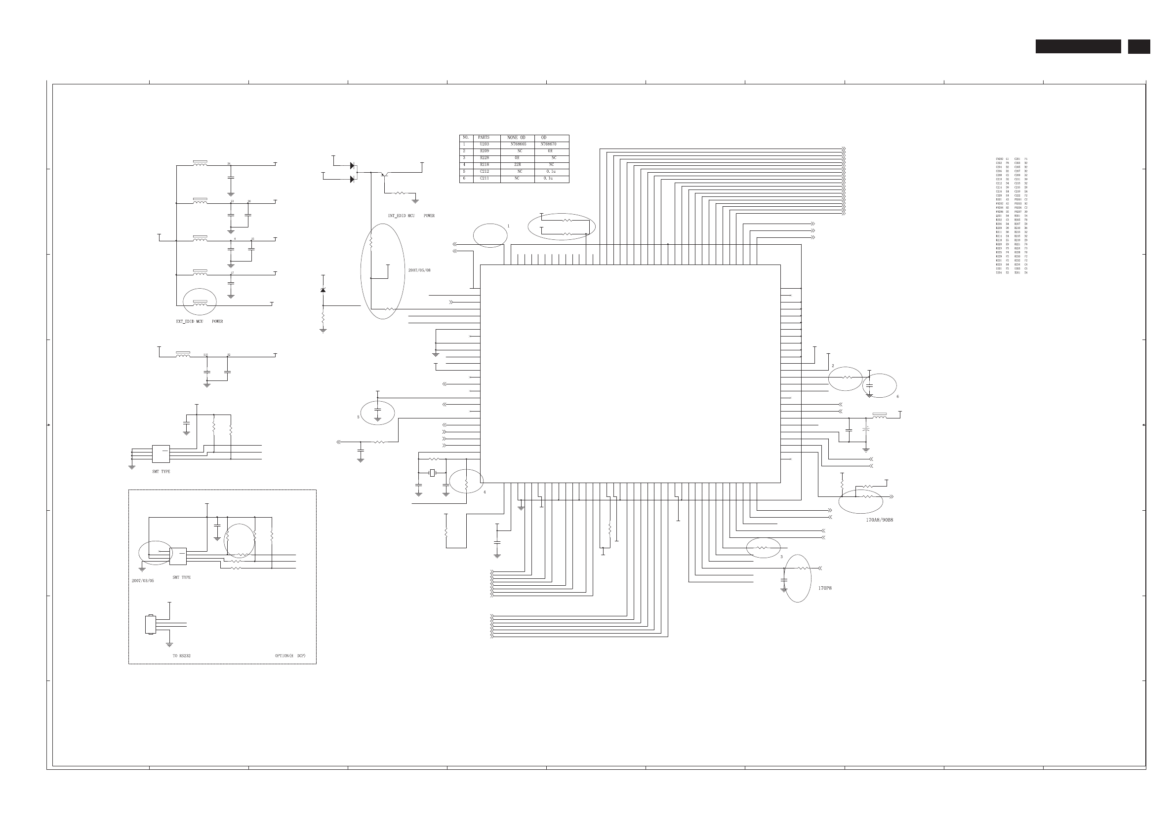
41
HUDSON 8
Scaler Diagram(190C8)-2
1
1
2
2
3
3
4
4
5
5
6
6
7
7
8
8
9
9
10
10
11
11
A A
B B
C C
D D
E E
F F
G G
H H
TCLK
IICSCL
24C16_WP
RX
VSO
VSO
HSO
IICSDA
HSO
H_SDA
RX
TX
IRQN
IRQN
TCLK
IICSCL
IICSDA
24C16_WP
TX
H_SCL
H_SDA
H_SCL
5V_DECT
5V_DECT
DDC_WP
PANEL_PWR 4
VGA_CABLE2
RX2+2
RXC+2
HS 2
RX2-2
GIN-2
RX1-2
RIN-2
VS 2
DDC_WP 2
RIN+2
BIN+2
BRIGHTNESS4,5
DVI_SCL 2
RX0-2
KEY_PWR 5
DVI_SDA 2
VGA_SCL 2
RX1+2
SOG2
LED_B/G5
DVI-HPD 2
KEY15
RX0+2
LED_R 5
LF_LED5
VGA_SDA 2
GIN+2
VOLUME 5
KEY25
RXC-2
PANEL_IDX4
BIN-2
DVI_CABLE2
T7P 5
T6M 5
T6P 5
T7M 5
TCLK2P 5
T0M 5
TCLK1M 5
T4P 5
T1M 5
T2M 5
T5P 5
T3P 5
T5M 5
T2P 5
TCLK2M 5
T4M 5
TCLK1P 5
T1P 5
T0P 5
T3M 5
BL_CONTROL4
AUDIO_STDBY5
LIGHT_SEN 5
MCU_VDD
CVDD18
CVDD18
MCU_VDD
DVDD
AVCC
+1.8VCC
MCU_VDD
+1.8VCC
+5V
PVCC
DVDD
MCU_VDD
MCU_VDD
ADC_VAA
DVDD
+3.3VCC
AVCC
CVDD18
ADC_VAA
DVDD
AVCC
PVCC
CVDD18
DVI_VDD
VGA_VDD
MCU_VDD
MCU_VDD
MCU_VDD
+5V
MCU_VDD
CVDD18
C206
0.1uF 16V
R224
NC/4.7K
FB204
120 OHM
1 2
R225
100R 1/16W
C222
NC/1uF 16V
C209
0.1uF 16V
R233
NC/750R OHM 1/16W 5%
R230
NC/100
C212
NC/0.1uF 16V
R202
10K 1/16W
R223
NC/4.7K
C220
22pF
U201
NC/M24C04-WMN6TP
1
2
3
4 5
6
7
8
NC
E1
E2
VSS SDA
SCL
WC
VCC
FB203
120 OHM
1 2
R215
4K7 1/16W
C204
0.1uF 16V
R206
4K7 1/16W
R220
100R 1/16W
R229NC/100
FB202
120OHM
1 2
R219
NC/4.7K
C207
0.1uF 16V
C216
0.1uF 16V
C201
0.1uF 16V
R228
0R05 1/16W
R213
4K7 1/16W
ZD201
RLZ2.2B
C211
NC/0.1uF 16V
R207
NC/4.7K
C219
22pF
C214
100uF/16V
R2144K7 1/16W
R205
NC/47K 1/16W
R201
1M 1/16W
U204
M24C16
1
2
3
4 5
6
7
8
NC
NC
NC
VSS SDA
SCL
WC
VCC
FB201
NC/120 OHM
1 2
FB205
120 OHM
1 2
R231
NC/4K7 1/16W
C208
0.1uF 16V
R209
NC/0R05 1/16W
C213
1uF 16V
C205
0.1uF 16V
U203
NT68665MFG-128
39
46
47
50
51
52
53
54
40
48
49
17
18
19
20
21
22
23
24
25
26
27
28
29
30
31
32
33
34
35
36
37
38
6
7
8
9
11
12
69
70
71
72
78
79
111
1
2
3
4
5
10
13
14
16
15
41
42
43
44
45
65
66
67
68
89
90
91
92
101
103
102
104
110
109
108
107
106
105
117
116
115
114
113
112
118
119
120
121
122
124
123
126
125
128
127
55
56
57
58
59
60
61
62
63
64
73
74
75
76
77
80
81
82
84
83
85
86
87
88
94
93
96
95
98
97
100
99
PA6*/PWM8*
PB5*/DDC_SDA0
PB4*/DDC_SCL0
SCL/P34
IRQn
CVDD
DVDD
RSBA1P/V0
PA7*/PWM9*
RSTn/PD5
SDA/P35
PVCC
PGND
BIN1+
BIN1-
SOG1I
GIN1+
GIN1-
RIN1+
RIN1-
ADC_VAA
ADC_GNDA
PC2
PD6
PB3/ADC3/INT1
P31/TXD
P30/RXD
PB2/ADC2/INT0
PB7*/DDC_SDA1
PB6*/DDC_SCL1
PA3/PWM5
PA4*/PWM6*
PA5*/PWM7*
AVCC
RX1+
RX1-
AGND
RX0-
AGND
RSGA2M/T7M
RSGA3P/TCLK2P
RSGA3M/TCLK2M
RSRA1P/T6P/RSBB0P
DGND/CGND
RSBB1P/T3P
AD0/GPO2
RSTB
MCU_VCC
MCU_GND
RX2+
RX2-
RX0+
RXC+
RXC-
REXT
AVCC
HSYNCI1
TOUTP/VSYNCI1
PLL_GND
TCLK
PLL_VDD
PA0/PWM2
PA2/PWM4
PA1/PWM3
RSGA2P/T7P
SP
DVDD
RSGB2P
RSGB2M
DGND/CGND
PC7
PC6
PD0
GPO1
NC/(HSYNCI)
PD4
PD3
PD2
PD1
PWMA/GPO7
GPO6
CVDD
INT_HSO/GPO5
INT_VSO/GPO4
AD1/GPO3
PWMB/GPO8
NC/(VSYNCI)
PC0*
PC1*
PC3/PWM0
PC5
PC4/PWM1
PB0/ADC0
PB1/ADC1
OSCO
OSCI
RSBA1M/V1
RSBA2P/V2
RSBA2M/V3
RSBA3P/V4
RSBA3M/V5
RSCLKAP/V6
RSCLKAM/V7
RSGA1P/VCKI
RSGA1M
CGND/DGND
RSRA1M/T6M/RSBB0M
RSRA2P/T5P/RSGB0P
RSRA2M/T5M/RSGB0M
RSRA3P/T4P/RSRB0P
RSRA3M/T4M/RSRB0M
RSBB1M/T3M
RSBB2P/TCLK1P
RSBB2M/TCLK1M
RSBB3M/T2M
RSBB3P/T2P
RSCLKBP/T1P
RSCLKBM/T1M
RSGB1P/T0P
RSGB1M/T0M
RSGB3M
RSGB3P
RSRB1M
RSRB1P
RSRB2M
RSRB2P
RSRB3M
RSRB3P
R221
470R 1/16W
FB207
1000OHM
1 2
R210
NC/0R05 1/16W
C203
0.1uF 16V
CN202
NC/4PIN 2.0mm CONN
1
2
3
4
R218
22R 1/16W
R234220R 1/16W
C210
0.1uF 16V
D201
BAV70
Q2012N3906S-RTK/PS
FB206
120OHM
1 2
C215
0.1uF 16V
X201
12MHz
1 2
C202
NC/1uF 16V
R232 NC/0R05 1/16W
R211
0R05 1/16W
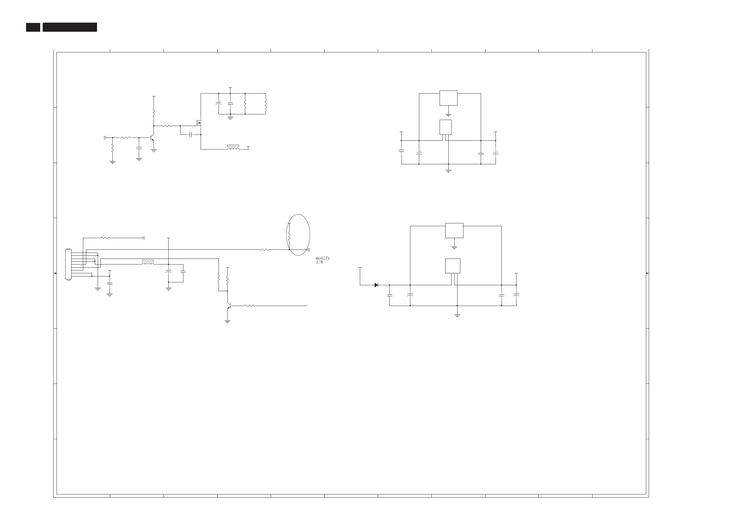
42 HUDSON 8
Scaler Diagram(190C8)-3
1
1
2
2
3
3
4
4
5
5
6
6
7
7
8
8
9
9
10
10
11
11
A A
B B
C C
D D
E E
F F
G G
H H
CN301
D1
C301 B7
C302 A3
C303 A4
C304 B3
C305 B7
C306 B9
C307 B8
C308 B2
C309 E7
C310 E9
C311 E7
C312 E9
C315 D3
C316 E1
C317 D3
D301 E6
FB302 B4
FB303 D2
Q301 B2
Q302 B3
Q305 E4
R301 E4
R302 A4
R303 A4
R304 B1
R305 B2
R307 B2
R308 B2
R309 D1
R311 D4
R312 D5
R314 D3
R316 E4
U301 B8
U302 D8
U303 A8
U304 D8
BL_CONTROL 3
BRIGHTNESS 3,5
PANEL_PWR3
PANEL_IDX 3
+1.8VCC
+3.3VCC
+3.3VCC
+12V
+5V
PANEL_VCC
+5V
+5V
+3.3VCC
+5V
+5V
FB303
120?
C306
100uF/16V
R308 4K7 1/16W
C309
100uF/16V
C317
0.1uF 16V
C308
1uF 16V
R304
10K 1/16W
U303
NC/LD1117S33
3 2
1
VI VO
GND
R311
1K 1/16W
C316
0.1uF/25V
R316 4K7 1/16W
C304
1uF 16V
Q305
2N3904S-RTK/PS
U302
NC/AZ1117D-1.8-E1
1
2
3
ADJ/GND
OUTPUT
INPUT
R307
51K? 1/16W
C312
0.1uF 16V
C302
10uF/16V
CN301
CONN
1
2
3
4
5
6
7
8
9
C307
0.1uF 16V
Q302
AO3401
R312
1K 1/16W
D301
SM340A
C310
100uF/16V
R303
330? 1/4W
Q301
2N3904S-RTK/PS
C311
0.1uF 16V
U304
AP1117E18LA
3 2
1
VI VO
GND
C305
100uF/16V
C303
0.1uF 16V
FB302
120?
R305
10K 1/16W
R301
1K 1/16W
R309
100R 1/16W
C315
100uF/16V
R302
330? 1/4W
U301
AP1117D33LA
1
2
3
ADJ(GND)
VOUT
VIN
C301
0.1uF 16V
R314
4K7 1/16W
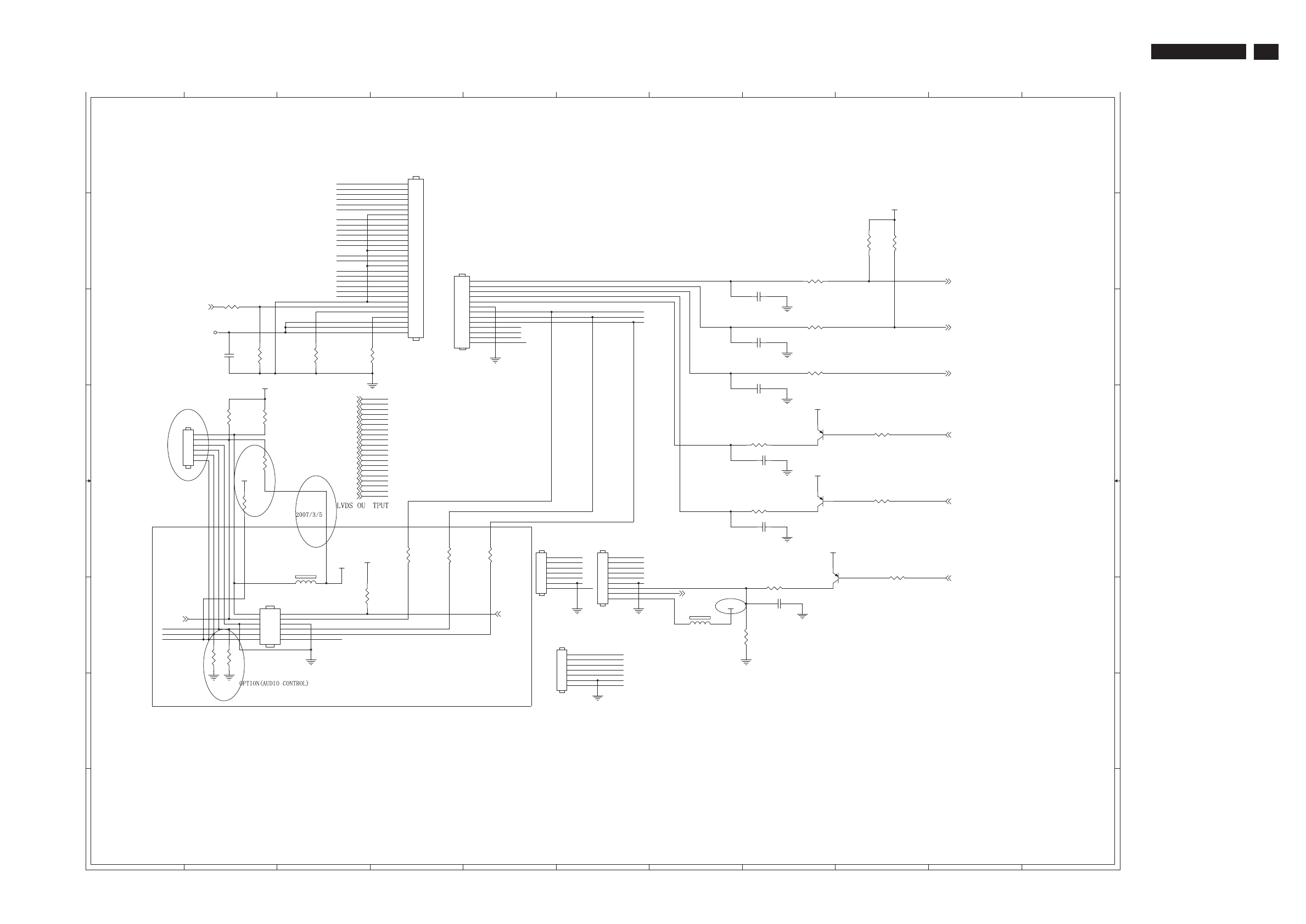
43
HUDSON 8
Scaler Diagram(190C8)-4
1
1
2
2
3
3
4
4
5
5
6
6
7
7
8
8
9
9
10
10
11
11
A A
B B
C C
D D
E E
F F
G G
H H
Menu/Up/Down key
Auto/Left/Right key
CN401 B4 CN402 A4
CN403 F2 CN404 E6
CN405 F5 CN406 D1
CN407 E5 C401 F8
C402 C8 C403 C8
C404 C8 C405 C2
C406 D8 C407 E8
FB401 F7 FB403 E3
Q402 D8 Q403 E8
Q404 E8 R402 B9
R403 B9 R404 E4
R407 B8 R410 C8
R411 C2 R412 C8
R413 C3 R414 C3
R415 D9 R416 D8
R417 E9 R418 E8
R421 F3 R423 E9
R424 F8 R430 C2
R431 E5 R432 E4
R433 D2 R434 F2
R435 F2 R436 E2
R437 D2 R438 D2
T3P
T0P
TCLK1M
T4M
T1M
T4P
T7P
T5M
T6M
TCLK1P
T7M
T1P
T3M
T2M
TCLK2M
T0M
T6P
T2P
T5P
TCLK2P
EAR-L
EAR-R
LED_O
KEY1_PAD
KEY2_PAD
OUT-R+
EAR-R
EAR-SENSE
POWER
LED_G
LIGHT_SEN
OUT-L+
OUT-L-
5V_FB
LF_B
OUT-R-
LED_O
KEY1_PAD
5V_FB
POWER
LED_G
KEY2_PAD
LED_G
KEY1_PAD
LED_O
POWER
LF_B
KEY2_PAD
OUT-L-
OUT-L+
EAR-L
POWER
KEY1_PAD
LED_O
LED_G
KEY2_PAD
LF_B LF_B
LED_R 3
LED_B/G 3
KEY1 3
KEY2 3
KEY_PWR 3
T1P3
T2M3
T6P3
T2P3
T1M3
T5M3
T7P3
T0M3
T7M3
TCLK2P3
T0P3
T6M3
T3M3
TCLK1M3
T4M3
T3P3
T4P3
T5P3
TCLK1P3
TCLK2M3
BRIGHTNESS3,4
LF_LED 3
VOLUME3
AUDIO_STDBY 3
LIGHT_SEN 3
+3.3VCC
+3.3VCC
+3.3VCC
PANEL_VCC
+3.3VCC
+12V
+5V
+3.3VCC
+5V
+3.3VCC
R404
0R05 1/16W
CN401
NC/CONN
1
2
3
4
5
6
7
8
9
10
11
12
13
FB401
NC/120 OHM
1 2
R407
100R 1/16W
R415 10K 1/16W
R435
NC/0R05 1/10W 5%
R424 NC/100R 1/16W
C403
0.1uF 16V
R436
NC/0R05 1/10W 5%
R421
10K 1/16W
R413
NC/0R05 1/16W
R410
100R 1/16W
C407
0.1uF 16V
R439
0R05 1/16W
CN407
CONN
1
2
3
4
5
6
7
Q402
2N3906S-RTK/PS
R431
0R05 1/16W
C402
0.1uF 16V
R403
3.9K? 1/16W
R430
NC/0R05 1/16W
R417 10K 1/16W
CN403
CONN
2
4
6
8
10
12
1
3
5
7
9
11
C401
NC/0.1uF 16V
CN405
NC/CONN
1
2
3
4
5
6
7
R438
NC/0R05 1/10W 5%
R411
NC/22
R416 100R 1/16W
R423 NC/10K 1/16W
R434
NC/0R05 1/10W 5%
R433
NC/0R05 1/10W 5%
FB403
NC/120?
1 2
C404
0.1uF 16V
CN404
NC/CONN
1
2
3
4
5
6
7
8
9
R418 100R 1/16W
CN406
NC/CONN
1
2
3
4
5
6
C405
0.1uF 16V
CN402
CONN
1
2
3
4
5
6
7
8
9
10
11
12
13
14
15
16
17
18
19
20
21
22
23
24
25
26
27
28
29
30
Q404
NC/2N3906S-RTK/PS
R402
3.9K? 1/16W
R432
0R05 1/16W
C406
0.1uF 16V
Q403
2N3906S-RTK/PS
R414
NC/0R05 1/16W
R412 1K 1/16W
R437
NC/0R05 1/10W 5%
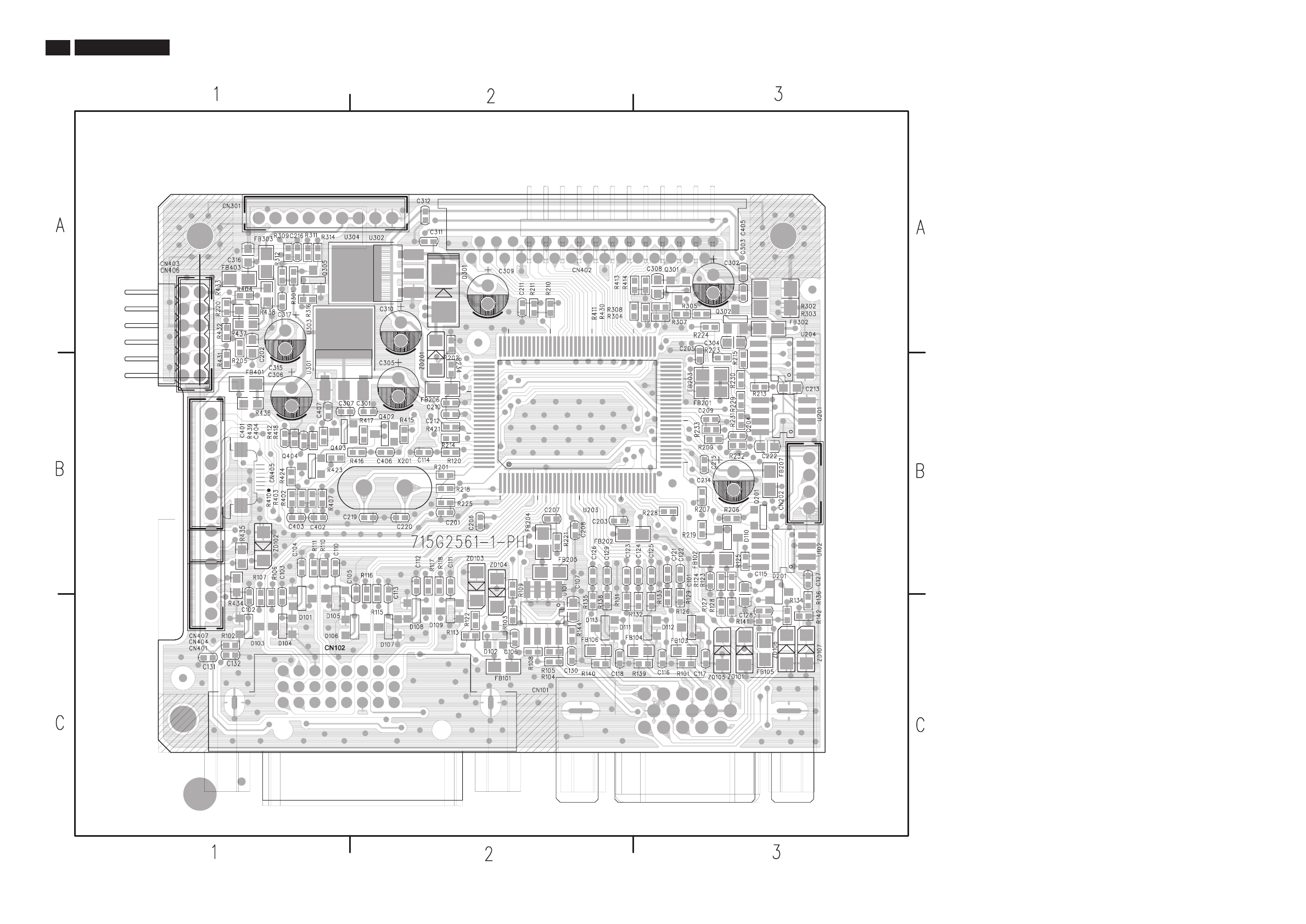
44 HUDSON 8
Scaler Layout-1
C101B3C215B3D105C1Q305A1R202A2R412B1
C102C1C216A1D106C2Q402B2R205A1R413A3
C103C1C219B2D107C2Q403B2R206B3R414A3
C104B1C220B2D108C2Q404B1R207B3R415B2
C105C2C222B3D109C2R101C3R209B3R416B2
C106C2C301B2D110B3R102C1R210A2R417B2
C107 C2 C302 A3 D111 C3 R103 C2 R211 A2 R418 B1
C110 B1 C303 A3 D112 C3 R104 C2 R213 B3 R421 B2
C111 B2 C304 A3 D113 C2 R105 C2 R214 B2 R423 B1
C112 B2 C305 B2 D201 B3 R106 C1 R215 B3 R424 B1
C113 C2 C306 B1 D301 A2 R107 C1 R218 B2 R430 A3
C114 B2 C307 B1 FB101 C2 R108 C2 R219 B3 R431 B1
C115 C3 C308 A3 FB102 B3 R109 B2 R220 A1 R432 A1
C116 C3 C309 A2 FB103 C3 R110 B1 R221 B2 R433 A1
C117 C3 C310 A2 FB104 C3 R111 B1 R223 B3 R434 B1
C118C2C311A2FB105C3R113C2R224A3R435B1
C121 B3 C312 A2 FB106 C2 R115 C2 R225 B2 R436 B1
C122 B3 C315 A1 FB201 B3 R116 C2 R228 B3 R437 A1
C123 B2 C316 A1 FB202 B3 R117 B2 R229 B3 R438 A1
C124 B3 C317 A1 FB203 B3 R118 B2 R230 B3 R439 B1
C125 B3 C401 B1 FB204 B2 R120 B2 R231 B3 U101 B2
C126 B2 C402 B1 FB205 B2 R122 C2 R232 B3 U102 B3
C127 B3 C403 B1 FB206 B2 R123 B3 R233 B3 U201 B3
C128 C3 C404 B1 FB207 B3 R124 B3 R234 B2 U203 B2
C129 B2 C405 A3 FB302 A3 R125 B3 R301 A1 U204 B3
C130 C2 C406 B2 FB303 A1 R126 C3 R302 A3 U301 B1
C131 C1 C407 B1 FB401 B1 R127 C3 R303 A3 U302 A2
C132C1CN101C3FB403A1R128C3R304A3U303B1
C201 B2 CN102 C2 FDT1 B3 R129 C3 R305 A3 U304 A2
C202A1CN202B3FDT10:1R131C2R307A3X201B2
C203B2CN301A2FDT11C8R132C3R308A3ZD101C3
C204B3CN401B1FDT12:8R133C3R309A1ZD102B1
C205B3CN402A2FDT13C1R134C3R311A1ZD103B2
C206 B2 CN403 B1 FDT2 A2 R135 C2 R312 A1 ZD104 B2
C207 B2 CN404 B1 FDT3 A3 R136 C3 R314 A1 ZD105 C3
C208 B2 CN405 B1 FDT4 C1 R138 C2 R316 A1 ZD106 C3
C209 B3 CN406 A1 FDT5 C1 R139 C3 R402 B1 ZD107 C3
C210 B2 CN407 B1 FDT8 :8 R140 C2 R403 B1 ZD201 B2
C211A2D101C1FDT9C1R141C3R404A1
C212B2D102C2Q201B3R142C3R407B1
C213 B3 D103 C1 Q301 A3 R144 C2 R410 B1
C214B3D104C1Q302A3R201B2R411A3
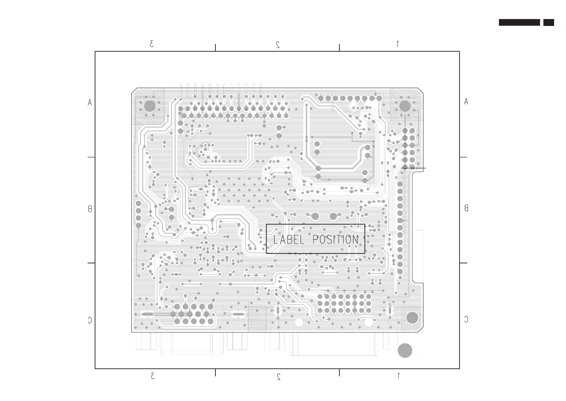
45
HUDSON 8
Scaler Layout-2
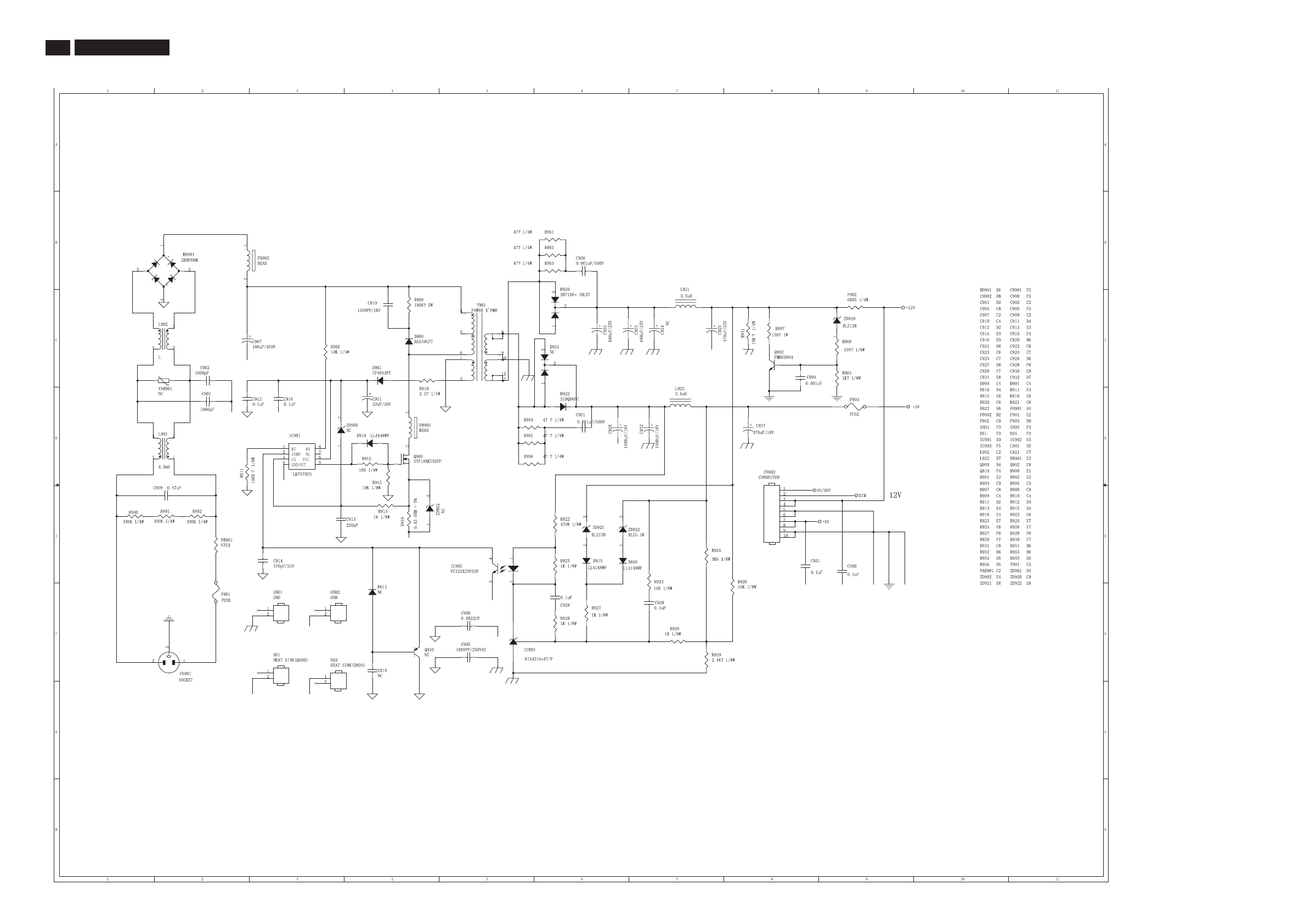
46 HUDSON 8 Power Board Diagram(170C8)-1
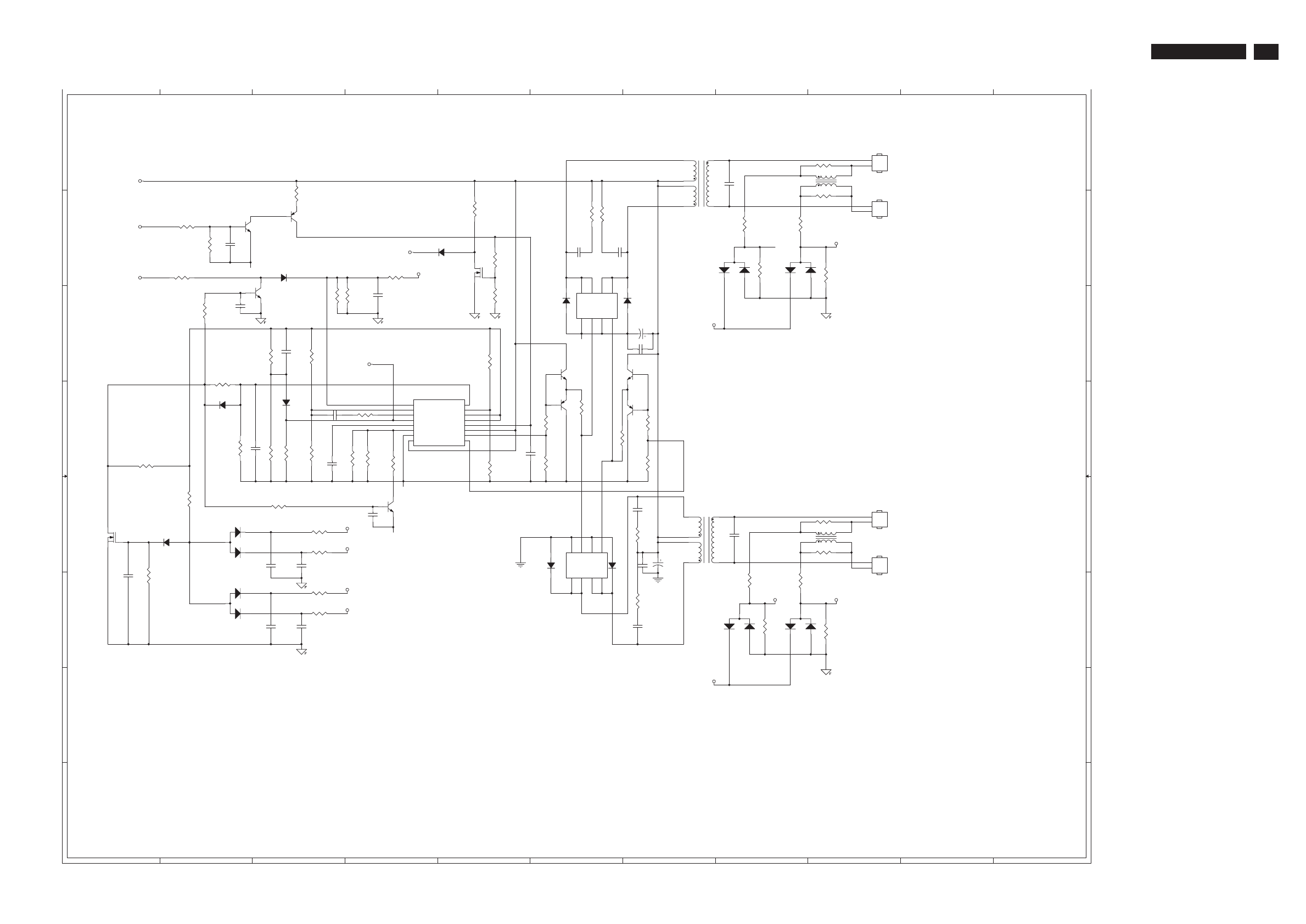
47
HUDSON 8
Power Board Diagram(170C8)-2
1
1
2
2
3
3
4
4
5
5
6
6
7
7
8
8
9
9
10
10
11
11
A A
B B
C C
D D
E E
F F
G G
H H
CN801 A9 CN802 B9
CN803 E9 CN804 E9
C801 A8 C802 B2
C803 B6 C804 C4
C805 C7 C806 C3
C807 D3 C808 D2
C809 D3 C810 D5
C811 E7 C812 E8
C813 E3 C814 E1
C815 E3 C816 E7
C817 F3 C818 F3
C819 C2 C820 E4
C821 B6 C822 F7
C823 C7 C824 E7
D801 B7 D802 B8
D803 B3 D804 C6
D805 C6 D806 E2
D807 E1 D808 F2
D809 F8 D810 F8
D811 D2 D812 D3
D813 B4 D814 E6
D815 E6 IC801 D4
L801 A9 L802 E9
PT801 A7 PT802 E7
Q801 B3 Q802 B2
Q803 C2 Q804 C6
Q805 D6 Q806 D6
Q807 E4 Q808 E1
Q809 E6 Q810 C6
Q811 C6 Q812 B5
R801 A9 R802 A3
R803 C5 R804 B9
R805 B5 R806 B8
R807 B8 R808 B2
R809 B2 R810 B6
R811 B8 R812 B9
R813 B2 R814 B4
R815 C3 R816 C2
R817 C3 R818 C3
R819 C3 R820 C2
R821 D2 R822 D3
R823 D3 R824 D3
R825 D3 R826 D4
R827 D1 R828 E2
R829 E3 R830 E9
R831 E3 R832 E9
R833 E3 R834 E8
R835 E8 R836 E1
R837 E7 R838 F3
R839 F8 R840 F3
R841 F9 R842 D4
R843 D4 R844 D6
R845 D6 R846 D6
R847 D7 R848 D6
R849 D7 R850 B6
R851 F7 R852 D5
R853 C5 ZD801 B5
OLP1 OLP2
FB
FB
OLP1
OLP3
OLP4
OLP2
OLP4
FB
OLP3
+12V
ON/OFF
DIM
DTC
DTC
PT802
POWER X'FMR
6
3
7
4
81
C824
0.1uF/25V
R813
100? 1/10W
C805
470uF/25V
D812
LL4148WP
PT801
POWER X'FMR
6
3
7
4
81
R803
2.4K? 1/10W
R825 51K? 1% 1/8W
R850
15? 1/4W
R838
10K 1/10W
R827
1K 1/10W 1%
C813
0.0022uF
R823 10.3K OHM 1% 1/10W
C817
0.0022uF
D806
BAW56
3
1
2
C
B
E
Q803
PMBS3904
R806
1K 1/10W 1%
R840
10K 1/10W
R829
68K? 1% 1/10W
C801
10pF/3KV
C804
0.1uF/16V
D809
BAV99
3
1
2
Q809
AM9945N-T1-PF
1
2
3
4
8
7
6
5
S
G
S
G
D
D
D
D
R817
NC
R839
1K 1/10W 1%
L802
NC
1
4
2
3
C806
1uF/16V
CN803
CONN
1
2
Q812
RK7002
R802
100R 1/8W
R807
1K 1/10W 1%
D811
LL4148WP
D808
BAW56
3
1
2
C
B
E
C802
1uF/16V
D804
NC
R808
10K 1/10W
R815
47K 1/10W
R844
22R 1/10W 5%
R810
15? 1/4W
C820
NC
Q805
PMBS3906
R822 47K? 1/10W
R824 10K 1/10W
R818
NC
CN801
CONN
1
2
D803
LL4148WP
C809 220pF
R834
1K 1/10W 1%
R814
68K OHM 1% 1/10W
D801
BAV99
3
1
2
D815 NC
C818
0.0022uF
R812
1K 1/10W 1%
R837
15? 1/4W
R847
22R 1/10W 5%
C811
470uF/25V
C819
NC
Q810
PMBS3904
C816
1500PF/50V
R835
1K 1/10W 1%
Q811
PMBS3904
R830 0R05 1/10W 5%
D802
BAV99
3
1
2
D814
NC
Q807
PMBS3904
R846
22R 1/10W 5%
R819
10K 1/10W
Q804
AM9945N-T1-PF
1
2
3
4
8
7
6
5
S
G
S
G
D
D
D
D
C807
0.1uF/16V
L801
NC
1
4
2
3
C822
1500PF/50V
R832 0R05 1/10W 5%
ZD801
10K? 1/4W
R804 0R05 1/10W 5%
R841
1K 1/10W 1%
R821 1M 1/10W 5%
R826 180K? 1% 1/8W
R816
68K? 1% 1/10W
R853
10K 1/10W
R828
47K 1/10W
IC801
TL494IDR
1
2
3
4
5
6
7
8 9
10
11
12
13
14
15
16
1IN+
1IN-
FEEDBACK
DTC
CT
RT
GND
C1 E1
E2
C2
VCC
OUTPUT CTRL
REF
2IN-
2IN+
D813
LL4148WP
CN804
CONN
1
2
R820
560K? 1/10W
Q801
PDTA144WK
C812
10pF/3KV
Q808
RK7002
R842
47K 1/10W
R851
15? 1/4W
R849
1K 1/10W 1%
C808 2.2uF/16V
Q802
PDTC144WK
R809
NC
R852
10K 1/10W
D807
LL4148WP
D810
BAV99
3
1
2
C821
1500PF/50V
C814
0.1uF/16V
D805
NC
R811
1K 1/10W 1%
Q806
PMBS3906
R831
10K 1/10W
C823
0.1uF/25V
R843 NC
R845
22R 1/10W 5%
R801 0R05 1/10W 5%
C803
1500PF/50V
CN802
CONN
1
2
C810
0.1uF/25V
R836
1M 1/10W 5%
C815
0.0022uF
R833
10K 1/10W
R805
4.7K? 1/10W
R848
1K 1/10W 1%
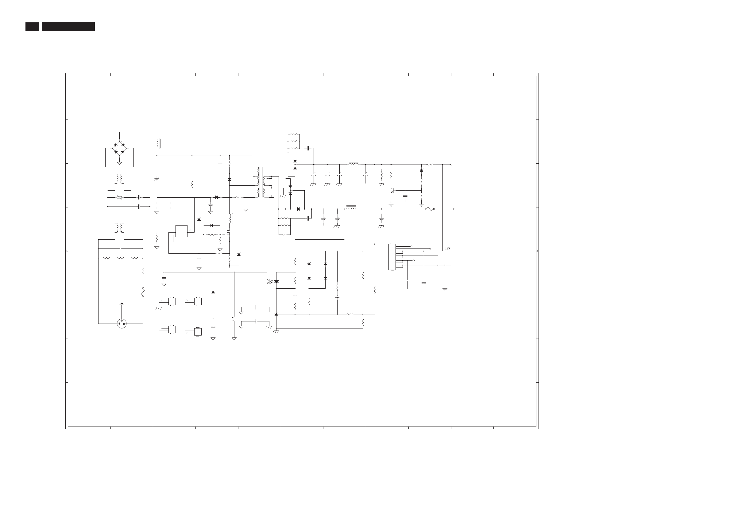
48 HUDSON 8 Power Board Diagram(190C8)-1
1
1
2
2
3
3
4
4
5
5
6
6
7
7
8
8
9
9
10
10
11
11
A A
B B
C C
D D
E E
F F
G G
H H
BD901 B1 CN901 F2
CN902 D8 C900 F5
C901 C2 C902 C2
C904 C8 C905 F5
C907 C3 C909 D2
C910 B4 C911 C4
C912 C3 C913 E3
C914 E3 C915 F4
C916 C3 C920 B6
C921 D6 C922 C6
C923 C6 C924 C7
C925 C7 C926 D6
C927 D8 C928 E6
C929 E7 C930 E9
C931 E8 C932 D7
D900 C4 D901 C4
D910 D4 D911 E4
D915 E6 D916 E6
D920 B6 D921 C6
D922 C6 FB901 D4
FB902 B3 F901 E2
F902 B9 F903 C9
GND1 E3 GND2 E3
HS1 F3 HS5 F3
IC901 D3 IC902 E5
IC903 F5 L901 D2
L902 C2 L921 B7
L922 C7 NR901 E2
Q900 D4 Q902 C8
Q910 F4 R900 E1
R901 E2 R902 E2
R903 C9 R905 C3
R907 C8 R908 C9
R909 B4 R910 C4
R911 D3 R912 D4
R913 D4 R915 D4
R916 E4 R922 E6
R923 E7 R924 E7
R925 E6 R926 E8
R927 F6 R928 F6
R929 F7 R930 F7
R931 C8 R951 B6
R952 B6 R953 B6
R954 D5 R955 D5
R956 D5 T901 C5
VAR901 C2 ZD901 D3
ZD902 D4 ZD920 C9
ZD921 E6 ZD922 E6
+12V
+5V
ON/OFF
DIM
+5V
R900
330K 1/4W
HS1
HEAT SINK(Q900)
1
2
C931
0.1uF
C902
1000pF
R956 47? 1/4W
R915
10K 1/8W
L921
3.5uH
R922
470R 1/8W
R954 47? 1/4W
F902
0R05 1/4W
GND1GND
1
2
T901
POWER X'FMR
1
3
4
5
6
7
8
9
10
11
12 C904
0.001uF
BD901
2KBP08M
2
1
3
4
R909
100K? 2W
IC902
PC123X2YFZOF
1
2
4
3
C905
1000PF/250VAC
R930
1K 1/8W
ZD902
NC
12
ZD921
RLZ13B
12
FB901
BEAD
1
2
Q900
STP10NK70ZFP
ZD922
RLZ5.1B
12
CN901
SOCKET
12
3
D920
SBT150-10LST
1
2
3
D915
LL4148WP
CN902
CONNECTOR
1
2
3
4
5
6
7
8
9
10
F901
FUSE
R95147? 1/4W
ZD901
NC
12
IC901
LD7575PS
1
2
3
4 5
6
7
8
RT
COMP
CS
GND OUT
VCC
NC
HV
D901
UF4003PT
R95347? 1/4W
L901
4.0mH
1
2
4
3
Q902
PMBS3904
C930
0.1uF
C920
0.001uF/500V
L902
L
1
4
2
3
D922
31DQ06FC
C911
22uF/50V
C900
0.0022UF
C922
680uF/25V
D916
LL4148WP
GND2
GND
1
2
D910 LL4148WP
R95247? 1/4W
D911
NC
D900
BA159GPT
C910
1500PF/1KV
C924
NC
R901
330K 1/4W
R903
1K? 1/8W
C929
0.1uF
R924
3K6 1/8W
R926
33K 1/8W
C901
1000pF F903
FUSE
VAR901
NC
C926
1000uF/16V
C907
100uF/450V
C912
0.1uF
R902
330K 1/4W
NR901
NTCR
C916
0.1uF
R929
2.4K? 1/8W
R910
2.2? 1/4W
C932
1000uF/16V
ZD920
RLZ13B
12
C923
680uF/25V
Q910
NC
C913
220pF
C928
0.1uF
C914
470pF/25V
C925
470uF/25V
C915
NC
FB902
BEAD
1
2
R931
10K? 1/4W
R925
1K 1/8W
R911
100K? 1/8W
R916
0.43 OHM +-5%
C927
470uF/16V
R955 47? 1/4W
D921
NC
1
2
3
IC903
KIA431A-AT/P
R912
10R 1/4W
L922
3.5uH
C921
0.001uF/500V
R913
1K 1/8W
C909 0.47uF
HS5
HEAT SINK(D920)
1
2
R923
10K 1/8W
R927
1K 1/8W
R928
1K 1/8W
R908
470? 1/8W
R907
150? 1W
R905
10K? 1/4W
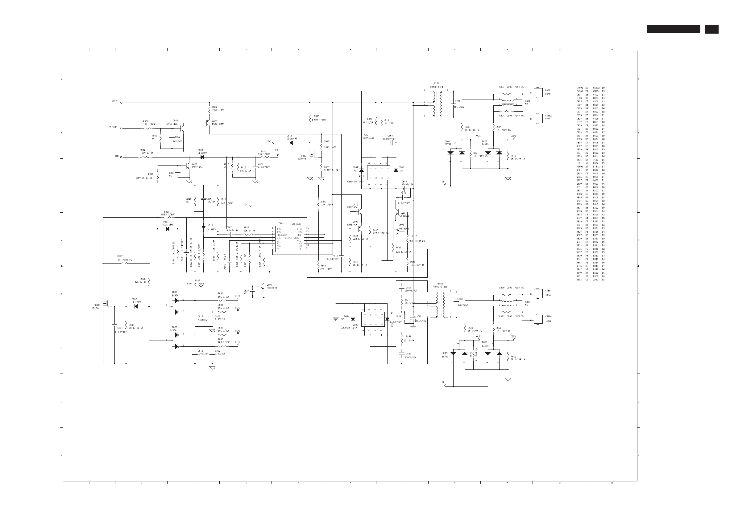
49
HUDSON 8
Power Board Diagram(190C8)-2
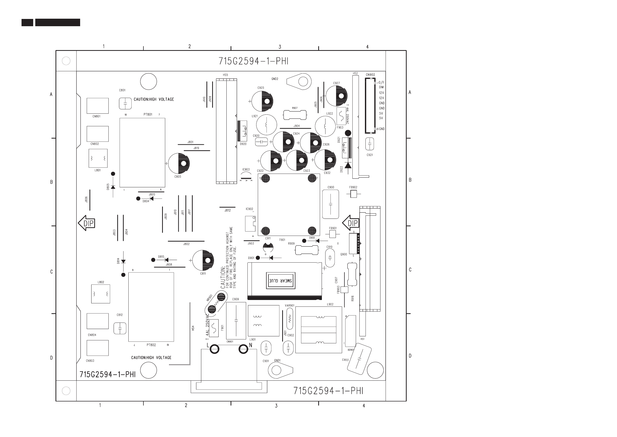
50 HUDSON 8 Power Board Layout-1
BD901 D4 J802 C2
C801A1J803B1
C805B2J804B1
C811C2J805B2
C812D1J806B1
C900B4J808C2
C901D3J809C2
C902D3J810C2
C903D4J811C2
C907C4J812B2
C909D3J817C2
C910C4J819B2
C911C3J901D3
C920B3J903C3
C921 B4 J904 A3
C922 B3 J905 A3
C923 B3 J906 A4
C924 B3 J909 A2
C925A3J910A2
C926B3L801B1
C927A4L802C1
C932B4L901D3
CN801 A1 L902 D4
CN802 A1 L921 A3
CN803 D1 L922 A4
CN804 D1 NR901 C2
CN901 D2 PT801 B1
CN902 A4 PT802 C2
D804B1Q900C4
D805 B1 R907 A3
D814C1R909C3
D815C2R916C4
D900C3SG11C4
D901C3SG12D2
D920A3SG19D2
D921B4SG22D4
D922A4SG25D4
F901 D2 SG27 D3
F903 A4 SG28 C3
FB901 C4 SG31 D3
FB902 B4 SG33 A1
FB903 C4 SG34 A1
HS10 A3 SG35 A1
HS13 A3 SG36 A1
HS14 A2 SG39 A1
HS16 A2 SG40 D1
HS17 B4 SG42 D1
HS20 A8 SG44 D1
HS28 A7 SG45 D1
HS29 B1 SG46 C4
HS31 B4 SG47 C4
IC902 B3 SG49 C4
IC903 B3 T901 C3
J801 B2 VAR901 D3
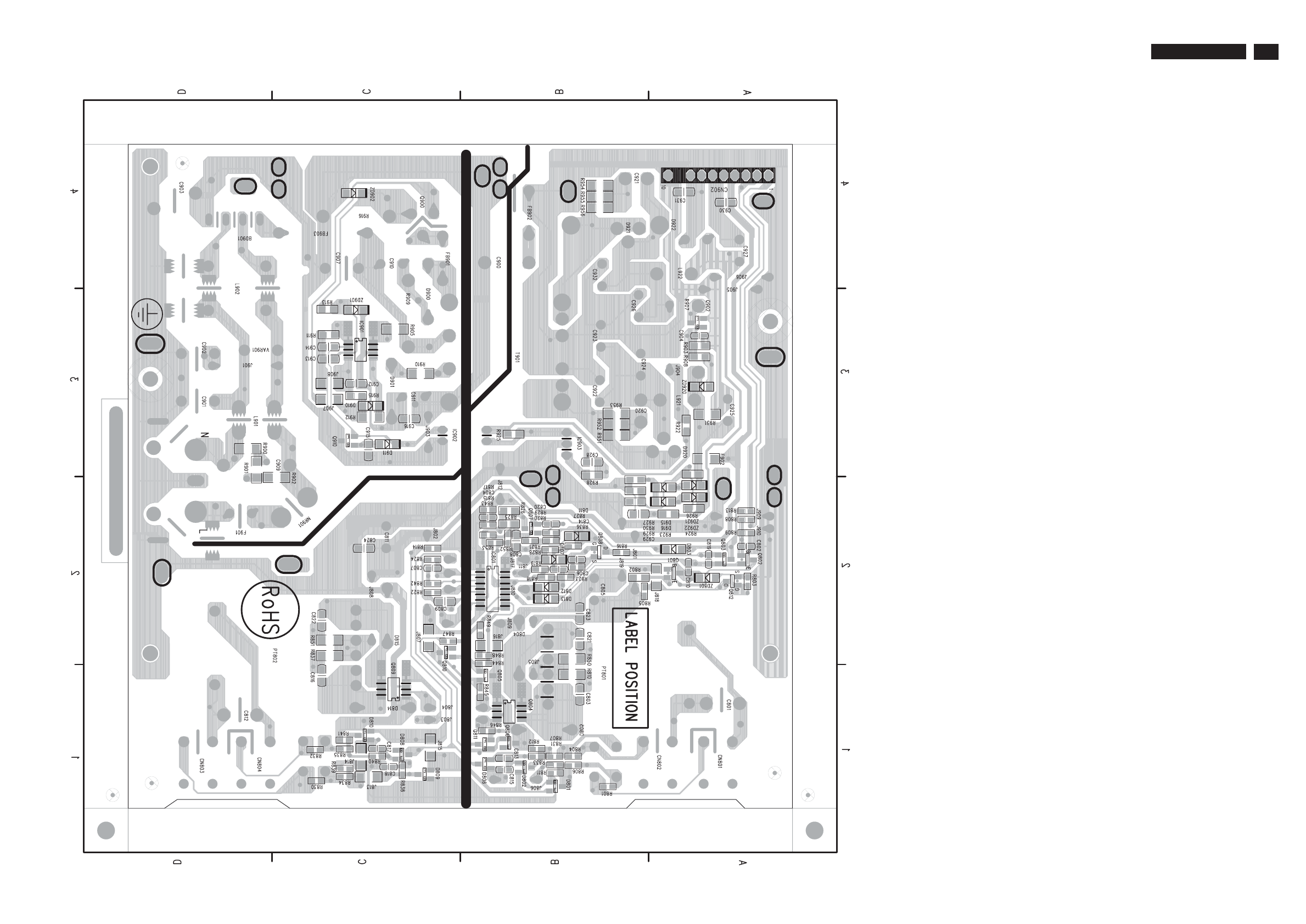
51
HUDSON 8
Power Board Layout-2
C802A2J907C3R843B2
C803B1J908C3R844B2
C804B2Q801A2R845B1
C806B2Q802A2R846B1
C807C2Q803A2R847C2
C808B2Q804B1R848B2
C809C2Q805B1R849B2
C810A2Q806B1R850B2
C813B1Q807B2R851C2
C814B2Q808B2R852B2
C815B1Q809C1R853B2
C816C1Q810C2R900D3
C817C1Q811B1R901D3
C818C1Q812A2R902C2
C819 A2 Q902 A3 R903 A3
C820B2Q910C3R905C3
C821B2R801B1R908A3
C822C2R802B2R910C3
C823B2R803A2R911C3
C824C2R804B1R912C3
C904A3R805B2R913C3
C912C3R806B1R915C3
C913C3R807B1R922A3
C914 C3 R808 A2 R923 A2
C915 C3 R809 A2 R924 A2
C916C3R810B1R925B3
C928B3R811B1R926A3
C929B2R812B1R927B2
C930 A4 R813 A2 R928 B3
C931 A4 R814 C2 R929 B2
D801B1R815B2R930B2
D802B1R816B2R931A3
D803A2R817B2R951B3
D806B1R818B2R952B3
D807B2R819B2R953B3
D808C1R820B2R954B4
D809C1R821B2R955B4
D810C1R822C2R956B4
D811B2R823B2SG10C3
D812B2R824C2SG15D3
D813B2R825B2SG17D3
D910C3R826B2SG18D4
D911C3R827B2SG20D4
D915A2R828B2SG21D3
D916A2R829B2SG23D4
F902 A3 R830 C1 SG24 D3
HS11 D4 R831 B1 SG26 D4
HS15 A1 R832 C1 SG29 C3
HS21 A7 R833 B1 SG30 D3
HS22 A1 R834 C1 SG32 D3
IC801B2R835C1SG37D2
IC901 C3 R836 B2 SG38 D2
J807 C2 R837 C2 ZD801 A2
J813 C1 R838 C1 ZD901 C3
J814 C1 R839 C1 ZD902 C4
J815 C1 R840 C1 ZD920 A3
J816 B2 R841 C1 ZD921 A2
J818 A2 R842 C2 ZD922 A2
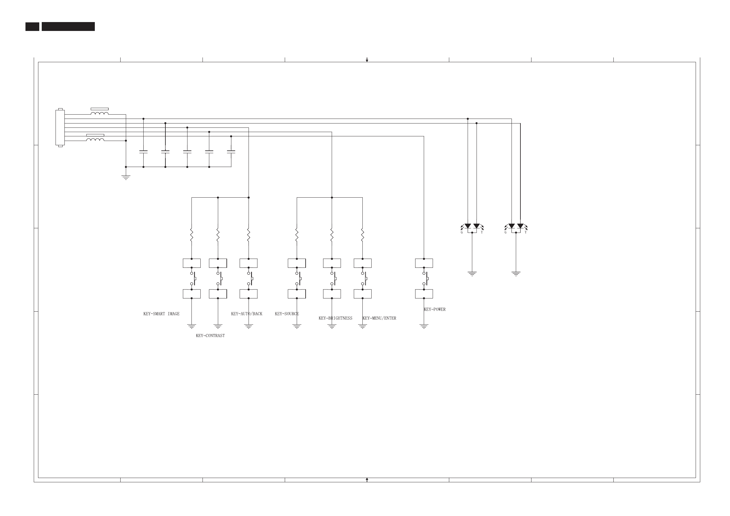
52 HUDSON 8 Key Board Diagram(170C8)
1
1
2
2
3
3
4
4
5
5
6
6
7
7
8
8
A A
B B
C C
D D
E E
CN101 A1
C101 B2
C102 B2
C103 B2
C104 B3
C105 B3
FB101 A1
FB102 A1
LED1 B6
LED2 B6
R101 B3
R102 B3
R103 B2
R104 B4
R105 B4
R106 B4
SW1 C3
SW2 C3
SW3 C2
SW4 C4
SW5 C4
SW6 C4
SW7 C5
LED-G
LED-O
KEY1
KEY2
K-PWR
R105
910? 1% 1/10W
FB102
300 OHM
12
SW4
SKHHAM2520-PL
13
4 2
CN101
CONN
1
2
3
4
5
6
7
SW3
SKHHAM2520-PL
13
4 2
R103
2.4K? 1% 1/10W
FB101
300 OHM
12
C104
470pF
LED1
LED
3
1
2
C105
470pF
SW2
SKHHAM2520-PL
13
4 2
C103
470pF
SW7
SKHHAM2520-PL
13
4 2
LED2
LED
3
1
2
C102
470pF
R101
4.3K? 1% 1/10W
R102
910? 1% 1/10W
SW5
SKHHAM2520-PL
13
4 2
R104
4.3K? 1% 1/10W
C101
470pF
R106
2.4K? 1% 1/10W
SW1
SKHHAM2520-PL
13
4 2
SW6
SKHHAM2520-PL
13
4 2
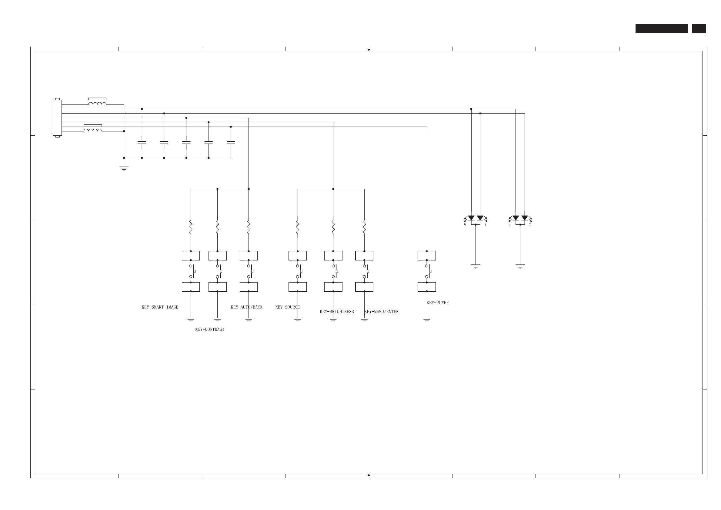
53
HUDSON 8
Key Board Diagram(190C8)
1
1
2
2
3
3
4
4
5
5
6
6
7
7
8
8
A A
B B
C C
D D
E E
CN101 A1
C101 B2
C102 B2
C103 B2
C104 B3
C105 B3
FB101 A1
FB102 A1
LED1 B6
LED2 B6
R101 B3
R102 B3
R103 B2
R104 B4
R105 B4
R106 B4
SW1 C3
SW2 C3
SW3 C2
SW4 C4
SW5 C4
SW6 C4
SW7 C5
LED-G
LED-O
KEY1
KEY2
K-PWR
R105
910? 1% 1/10W
SW4
SKHHAM2520-PL
13
4 2
FB102
300 OHM
12
CN101
CONN
1
2
3
4
5
6
7
SW3
SKHHAM2520-PL
13
4 2
R103
2.4K? 1% 1/10W
FB101
300 OHM
12
C104
470pF
LED1
LED
3
1
2
C105
470pF
C103470pF
SW2
SKHHAM2520-PL
13
4 2
SW7
SKHHAM2520-PL
13
4 2
LED2
LED
3
1
2
C102
470pF
R101
4.3K? 1% 1/10W
R102
910? 1% 1/10W
SW5
SKHHAM2520-PL
13
4 2
R104
4.3K? 1% 1/10W
C101
470pF
R106
2.4K? 1% 1/10W
SW1
SKHHAM2520-PL
13
4 2
SW6
SKHHAM2520-PL
13
4 2
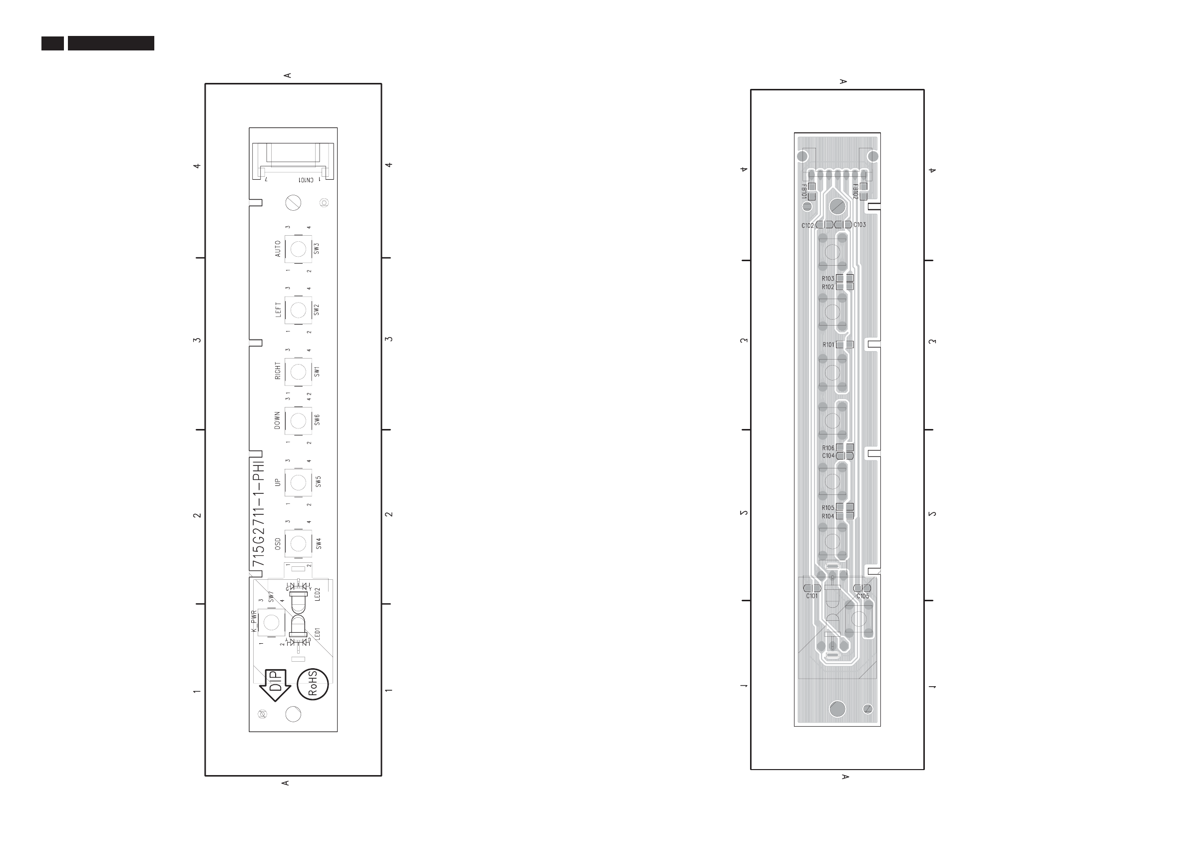
54 HUDSON 8 Key Board Layout
CN101 A4
LED1 A1
LED2 A2
SW5 A2
SW4 A2
SW6 A3
SW1 A3
SW2 A3
SW3 A4
SW7 A1
C101 A2
C102 A4
C103 A4
C104 A2
C105 A2
FB101 A4
FB102 A4
R101 A3
R102 A3
R103 A3
R104 A2
R105 A2
R106 A2

HUDSON 8 55
GENERAL PRODUCT SPECIFICATION
HUDSON-8 170C8
GENERAL PRODUCT
SPECIFICATION
.ANALOGAND DIGITAL DUAL INPUT
.AUTOPICTURE ADJUSTMENT
.12 FACTORYPRESET MODESAND 45 PRESET MODESWHICH
CANBERECOVEREDTOPRESET MODES
.NEWOSDSTYLINGDISPLAYFORMODEIDENTIFICATION
/ADJUSTMENT
.DDC2B&DDC/CI COMMUNICATION CAPABILITY
.MAX. RESOLUTION 1280*1024 NON-INTERLACEDAT 76 HZ
. 17" COLOR TFT LCDFLAT PANEL
.EASY TILT &SWIVEL BASE
.FULL RANGE POWER SUPPLY90–264VAC
.CE ENVIRONMENTAL POLICY
.LEAD-FREE PRODUCT POLICY
.ANTI-GLARE TOREDUCE LIGHTREFLECTION
.POWER MANAGEMENT CAPABILITY
.SOGSUPPORT
.TCO’03
1
BRAND : PHILIPS
17 inch LCD Monitor
TYPE :170C8FS/00
8670 000 25561
2007-06-01
590
2007-06-01
56 HUDSON 8 GENERAL PRODUCT SPECIFICATION(Continued)
CONTENTS
1.0 Foreword
2.0 Product profile
2.1 LCD
2.2 Scanning frequencies
2.3 Video dot rate
2.4 Power input
2.5 Power consumption
2.6 Dimensions
2.7 Weight
2.8 Functions
2.9 Ambient temperature
2.10 Regulatory compliance
3.0 Electrical characteristics
3.1 Interface signals
3.2 Interface
3.2.1 D-Sub cable
3.2.2 DVI cable
3.2.3 Audio cable
3.2.4 USB cable
3.2.5 OSD function control
3.3 Timing requirement
3.3.1 Mode storing capacity
3.3.2 Factory/ preset timings
3.3.3 Horizontal scanning
3.3.4 Vertical scanning
3.4 Power input connection
3.5 Power management
3.6 Display identification
3.6.1 Analog DDC
3.6.2 Digital DDC
4.0 Visual characteristics
4.1 Test conditions
4.2 Resolution
4.3 Brightness
4.4 Image size
4.4.1 Actual display size
4.4.2 Max scan size
4.5 Brightness uniformity
4.6 Check cross talk
4.7 White color adjustment
5.0 Mechanical characteristics
5.1 Controls
5.2 Unit dimension / weight
5.3 Tilt and swivel base
5.4 Transportation packages
5.4.1 Shipping dimension / weight
5.4.2 Block unit / palletization
6.0 Environmental characteristics
6.1 Susceptibility of display to external environment
6.2 Transportation tests
6.3 Display disturbances from external environment
6.4 Display disturbances to external environment
6.4.1 EMI
7.0 Reliability
7.1 Mean time between failures
8.0 Quality assurance requirements
8.1 Acceptance test
9.0 Serviceability
10.0 Philips’Flat panel monitors pixel defect policy
19 2
2007-06-01
BRAND : PHILIPS
17 inch LCD Monitor
TYPE : 170C8FS/00 8670 000 25561
2007-06-01
590
HUDSON 8 57
GENERAL PRODUCT SPECIFICATION(Continued)
1.0 FOREWORD
Thisspecification describesa17"SXGA multi-scancolorTFT-LCDmonitorwithmax
resolution upto 1280*1024 /76 Hz non-interlaced.
2.0 PRODUCT PROFILE
Thisdisplay monitorunit isacolordisplay monitorenclosed in PHILIPSglobal stylingcabinet,which has an
integrated tiltand swivelbase.
2.1 LCD
2.1.1 TypeNR.:LM170E03 TLL1
NumberofPixels. : 1280 (H)x1024 (V)
Physical Size. : 358.5(w)*296.5(h)*16(d) mm
PixelPitch. : 0.264 mm x 0.264 mm
Colorpixel arrangement.:RGBstripes arrangement
SupportColor. : 16.7M colors
Display Mode.:Normally White
Backlight.:CCFL edgelightsystem
Activearea. (WXH). : 337.92 x 270.336mm (17”diagonal)
ViewingAngle(CR>=10).:Right:80 , Left:80 , UP:75 , down:85
Contrastratio. : 800 :1(typ.), 500:1(min.)
White luminance.:300nit (typ.), 250nit (min.)
2.1.2 TypeNR.:LM170E03 TLL4
NumberofPixels. : 1280 (H)x1024 (V)
Physical Size. : 358.5(w)*296.5(h)*16(d) mm
PixelPitch. : 0.264 mm x 0.264 mm
Colorpixel arrangement.:RGBstripes arrangement
SupportColor. : 16.7M colors
Display Mode.:Normally White
Backlight.:CCFL edgelightsystem
Activearea. (WXH). : 337.92 x 270.336mm (17”diagonal)
ViewingAngle(CR>=10).:Right:80 , Left:80 , UP:75 , down:85
Contrastratio. : 800 :1(typ.), 500:1(min.)
White luminance.:300nit (typ.), 250nit (min.)
2.1.3 TypeNR.:CLAA170EA07 P-040
NumberofPixels. : 1280 (H)x1024 (V)
Physical Size. : 358.5(w)*296.5(h)*17.5(d) mm
PixelPitch. : 0.264 mm x 0.264 mm
Colorpixel arrangement .:RGBvertical stripes
SupportColor. : 16.2M colors
Display Mode.:Normally White
Backlight.:CCFL edgelightsystem
Activearea. (WXH). : 337.9 x 270.3 mm (17”diagonal)
ViewingAngle(CR>=10).:Right:80 , Left:80 , UP:80 , down:80
Contrastratio. : 700 :1(typ.); 550:1 (min.)
White luminance.:300nit (typ.), 250nit (min.)
2.1.4 TypeNR.:CLAA170EA07 P-050
NumberofPixels. : 1280 (H)x1024 (V)
Physical Size. : 358.5(w)*296.5(h)*17.5(d) mm
PixelPitch. : 0.264 mm x 0.264 mm
Colorpixel arrangement .:RGBvertical stripes
SupportColor. : 16.2M colors
Display Mode.:Normally White
Backlight.:CCFL edgelightsystem
Activearea. (WXH). : 337.9 x 270.3 mm (17”diagonal)
ViewingAngle(CR>=10).:Right:80 , Left:80 , UP:80 , down:80
Contrastratio. : 700 :1(typ.); 550:1 (min.)
White luminance.:300nit (typ.), 250nit (min.)
BRAND : PHILIPS
17 inch LCDMonitor
TYPE :170C8FS/00
8670 000 25561
2007-06-01
590
2007-06-01
3
58
HUDSON 8
GENERAL PRODUCT SPECIFICATION(Continued)
2.2 Scanning frequencies
H-Frequency. : 30K – 83KHz
V-Frequency. : 56 - 76 Hz
2.3 Video dot rate. : < 140 MHz
2.4 Power input. : 90-264 V AC, 50/60 ±2Hz
2.5 Power consumption. : < 36 W maximum
2.6 Dimensions. :
2.7 Weight. :
2.8 Functions:
(1) D-Sub analog R/G/B separate inputs, H/V sync separated, Composite (H+V) TTL level, SOG sync.
(2) DVI-D digital Panel Link TMDS input
2.9 Ambient temperature: 0 °C-40°C
2.10 Regulatory compliance:
B, CCIB / CCEE(China), CE(Europe), CSA(Canada), DEMKO(Nordic),
EZU(Czech), FIMKO(Nordic), Gost(Russia), IEC 950 CB Report, NOM
NYCE(Mexico), PSB(Singapore), SEMKO(Nordic),SISIR CPA(Singapore),
TUV(Germany), UL(USA),
* UL2601-1(NAFTA), EN60601(EU) and IEC60601-1(WW)
C-tick, CE(Europe), FCC(USA), IC(Canada), VCCI(Japan),BSMI,
*IEC60601-1-2 (EU)
Ergonomics E2000, MPRII(Sweden), Nutek(Sweden), TCO99, TCO03, TUV/GS, TUV/ERG,
EPA, ISO13406-2
Compatibility PC2001, Windows 2000, Windows 98/Me, Windows XP, NSTL
Safety
EMI
19 4
* Medical compliance only applies for dedicated models
3.0 Electrical characteristics
3.1 Interface signals
There are two main display interface input signals (D-sub and DVI-D)
1). D-shell Analog
Input signal: Video, H-sync, V-sync,
Video: 0.7 V p-p, input impedance, 75 ohm
Sync. : Separate sync TTL level, input impedance 2k2 ohm terminate
H-sync Positive/Negative
V-sync Positive/Negative
Composite sync TTL level, input impedance 2k2 ohm terminate
(Positive/Negative)
Sync on green video 0.3V p-p Negative. (Video 0.7 V p-p Positive)
2). DVI-D Digital
Input signal: Single TMDS link (Three channels: RX0-/+, RX1-/+, RX2-/+)
3.2 Interface
3.2.1 D-Sub Cable
Length. : 1.8 M +/- 50 mm
Connector type. : D-Sub male with DDC-2B pin assignments.
Blue connector thumb-operated jackscrews
BRAND : PHILIPS
17 inch LCD Monitor
TYPE : 170C8FS/00 8670 000 25561
2007-06-01
590
2007-06-01
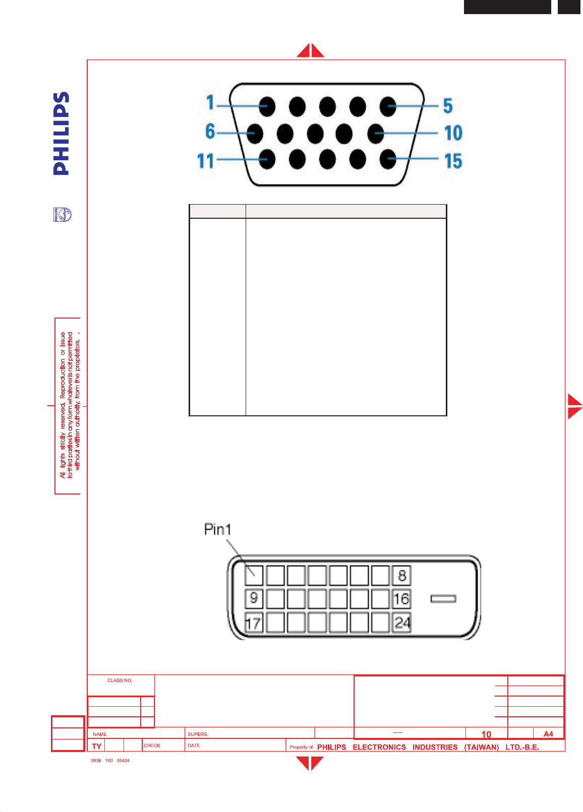
HUDSON 8 59
GENERAL PRODUCT SPECIFICATION(Continued)
3.2.2 DVICable
Theinput signals areappliedtothedisplay through DVI-D cable.
Length. : 1.8 M +/- 50 mm
Connectortype.:DVI-D malewithDDC-2B pin assignments
White connectorthumb-operated jackscrews
Pin Assignment:
PINNo. SIGNAL
1Red video input
2Green video input /syncon green
3Blue video input
4GND
5GND- Cable detect
6Red video GND
7Green video GND
8Blue video GND
9DDC+3.3V or+5V
10 LogicGND
11 GND
12 Serial dataline (SDA)
13 H-sync/H+V
14 V-sync
15 Dataclock line (SCL)
Pin Assignment:
5
19
BRAND : PHILIPS
17 inch LCDMonitor
TYPE :170C8FS/00
8670 000 25561
2007-06-01
590
2007-06-01
60 HUDSON 8 GENERAL PRODUCT SPECIFICATION(Continued)
Pin No. Description
1 T.M.D.S. data2-
2 T.M.D.S. data2+
3 T.M.D.S. data2 shield
4 No Connect
5 No Connect
6 DDC clock
7 DDC data
8 No Connect
9 T.M.D.S. data1-
10 T.M.D.S. data1+
11 T.M.D.S. data1 shield
12 No Connect
13 No Connect
14 +5V Power
15 Ground (for +5V) – Cable detect
16 Hot plug detect
17 T.M.D.S. data0-
18 T.M.D.S. data0+
19 T.M.D.S. data0 shield
20 No Connect
21 No Connect
22 T.M.D.S clock shield
23 T.M.D.S. clock+
24 T.M.D.S. clock-
3.2.5 Software control functions via OSD/control
OSD (On Screen Display) function
(1) Analog interface OSD:
Adjustable functions:
1. Main Menu 2.1 Sub Menu 2.2 Sub Menu 2
MONITOR SETUP
Exit
Brightness & Contrast Brightness, Contrast
Color Original Color, 9300K,6500K, sRGB
User Define Red, Green, Blue
Position Horizontal, Vertical
Input Selection Analog(D-Sub), Digital(DVI-D)
More Settings Language English, Spanish, French,
German, Italian, S. Chinese
Phase/ Clock Phase, Clock
OSD Setting Horizontal, Vertical
Reset Yes, No
Serial No.:
(Serial No.)
(Timing Mode)
Move Selection Then ok
MAIN MENU Sub Menu Sub Menu 2 Description
Brightness Sliding barPicture
Contrast Sliding bar
Original
Color Temperature
5000K
6500K
7500K
8200K
9300K
11500K
sRGB
User Define
Red(0-100) Sliding bar
Green(0-100) Sliding bar
Color
Blue(0-100) Sliding bar
19 6
BRAND : PHILIPS
17 inch LCD Monitor
TYPE : 170C8FS/00 8670 000 25561
2007-06-01
590
2007-06-01
HUDSON 8 61
GENERAL PRODUCT SPECIFICATION(Continued)
AUTO
VGA
Source
DVI
Left/rightarrowto selec
English t
Spanish
French
German
Italian
Portuguese
Russian
Language
Simplified Chinese
Horizontal 0-100 Sliding bar
Vertical 0-100 Sliding bar
Transparency Off, 1, 2, 3, 4
OSD Timeout 5, 10, 20, 60
OSD Settings
OSDLock On,Off
Phase0~100 Sliding bar(Ifthesignal sourceis
comingfromDVI,thisfunction
shouldbedisabled,and begrayed
out)
Clock 0~100 Sliding bar(Ifthesignal sourceis
comingfromDVI,thisfunction
shouldbedisabled,and begrayed
out)
H.Position 0~100 Sliding bar(Ifthesignal sourceis
comingfromDVI,thisfunction
shouldbedisabled,and begrayed
out)
V.Position 0~100 Sliding bar(Ifthesignal sourceis
comingfromDVI,thisfunction
shouldbedisabled,and begrayed
out)
Smart ContrastOn,Off
Reset Yes, No
Resolution Notification On,Off
Information
Setup
Demo
Reset -Yes: Auto adjustment fordisplayingtimingmode and recall factory preset
No:Exit
BRAND : PHILIPS
17 inch LCDMonitor
TYPE :170C8FS/00
8670 000 25561
2007-06-01
590
2007-06-01
7
62 HUDSON 8 GENERAL PRODUCT SPECIFICATION(Continued)
3.3 Timing requirement
3.3.1 Mode storing capacity
(1) Factory preset modes. : 12
(2) Preset modes. : 45
(3)User define modes : 10
3.3.2 Factory/ Preset timings
The factory settings of size and centering are according to the reference timing charts
(See as below
MODENO.1234
RESOLUTION 640 x 350 720 x 400 640 x 480 640 x 480
Dot clock(MHz) 25.175 28.321 25.175 30.24
f h 31.469kHz 31.468kHz 31.5kHz 35 kHz
A ( us ) 31.778(800 dots) 31.78(900dots) 31.778(800 dots) 28.571 (864 dots)
B ( us ) 3.813(96 dots) 3.813(108dots) 3.813( 96 dots) 2.116 ( 64 dots)
C ( us ) 1.907(48 dots) 1.907(54dots) 1.907( 48 dots) 3.175( 96 dots)
D ( us ) 25.422(640 dots) 25.42(720dots) 25.422( 640 dots) 21.164( 640 dots)
E ( us ) 0.636(16 dots) 0.636(18dots) 0.636( 16 dots) 2.116( 64 dots)
f v 70Hz(70.09) 70Hz(70.085) 60Hz 67Hz
O (ms ) 14.27(449 lines) 14.27(449 lines) 16.683 (525 lines) 15 (525 lines)
P ( ms ) 0.064(2 lines) 0.064(2 lines) 0.064 ( 2 lines) 0.086( 3 lines)
Q (ms ) 1.907(60 lines) 1.080(34 lines) 1.049 ( 33 lines) 1.114( 39 lines)
R ( ms ) 11.12(350 lines) 12.71(400 lines) 15.253 (480 lines) 13.714(480 lines)
S ( ms ) 1.175(37 lines) 0.381(13 lines) 0.317 ( 10 line ) 0.086( 3 line )
SYNC. H/V +/- -/+ - / - - / -
POLARITY
SEP . SYNC Y Y Y Y
19 8
MODENO.5678
RESOLUTION 640 x 480 640 x 480 640x480 800 x 600
Dot clock(MHz) 31.500 31.501 36 36
f h 37.861kHz 37.5kHz 36kHz 35.2kHz
A ( us ) 26.413(832 dots) 26.667 (840 dots) 23.111 (832 dots) 28.444(1024 dots)
B ( us ) 1.270(40 dots) 2.032 ( 54 dots) 1.556 (56 dots) 2.000 ( 72 dots)
C ( us ) 3.810(120 dots) 3.81 ( 120 dots) 2.222 ( 80 dots) 3.556 ( 128 dots)
D ( us ) 20.317(640 dots) 20.317 (640 dots) 17.778 (640 dots) 22.222( 800 dots)
E ( us ) 1.016(32 dots) 0.508 ( 26 dots) 1.555 (56 dots) 0.666 ( 24 dots)
f v 72.809Hz 75Hz 85Hz 56Hz
O (ms ) 13.735(520 lines) 13.333 (500 lines ) 11.763 (509 lines ) 17.778 (625 lines)
P ( ms ) 0.079(3 lines) 0.08 ( 3 lines ) 0.069 ( 3 lines ) 0.057 ( 2 lines)
Q (ms ) 0.528(20 lines) 0.427 ( 16 lines ) 0.578 ( 25 lines ) 0.626 ( 22 lines)
R ( ms ) 12.678(480 lines) 12.8 (480 lines ) 11.093 (480 lines ) 17.066 (600 lines)
S ( ms ) 0.45(17 lines) 0.026 ( 1 lines) 0.023 ( 1 lines) 0.029 ( 1 line )
SYNC. H/V -/- - / - -/- + / +
POLARITY
SEP . SYNC Y Y Y Y
BRAND : PHILIPS
17 inch LCD Monitor
TYPE : 170C8FS/00 8670 000 25561
2007-06-01
590
2007-06-01
HUDSON 8 63
GENERAL PRODUCT SPECIFICATION(Continued)
MODENO. 9 10 11 12
RESOLUTION 800 x 600 800 x 600 800 x 600 800 x 600
Dot clock(MHz)40 50 49.498 56.251
f h 37.9kHz 48.077kHz 46.9kHz 53.7kHz
A(us)26.4 (1056 dots)20.80 (1040dots)21.333 (1056 dots)18.631 (1048 dots)
B(us)3.2 (128 dots)2.400 (120 dots)1.616 (80 dots)1.138 (64 dots)
C(us)2.2 (88 dots)1.280 (64 dots)3.232 (160 dots)2.702 (152 dots)
D(us)20 (800 dots)16.00 (800 dots)16.162 (800 dots)14.222 (800 dots)
E(us)1(40 dots)1.120 (56 dots)0.323 (16 dots)0.569 (32 dots)
f v 60Hz 72Hz (72.188)75Hz 85Hz
O(ms )16.579 (628 lines)13.85 (666 lines)13.333 (625 lines)11.756(631 lines)
P(ms )0.106 (4lines)0.125 (6lines)0.064 (3lines)0.056 (3lines)
Q(ms )0.607 (23 lines)0.478 (23 lines)0.448 (21 lines)0.503 (27 lines)
R(ms )15.84 (600lines)12.48 (600 lines)12.8 (600 lines)11.179 (600 lines)
S(ms )0.026 (1line ) 0.770 (37 line ) 0.021 (1line ) 0.018 (1lines)
SYNC.H/V +/+ +/+ +/+ +/+
POLARITY
SEP .SYNCYYYY
MODENO.13141516
RESOLUTION 832 x 624 1024 x 768 1024 x 768 1024 x 768
Dot clock(MHz)57.28 65 75 78.75
f h 49.7kHz 48.363kHz 56.5kHz 60kHz
A(us)20.11(1152 dots)20.677(1344 dots)17.707(1328 dots)16.66 (1312dots)
B(us)1.117(64 dots)2.092(136 dots)1.813(136 dots)1.219 (96 dots)
C(us)3.91(224 dots)2.462(160 dots)1.920(144 dots)2.235 (176 dots)
D(us)14.52(832 dots)15.754(1024 dots)13.653(1024 dots)13.003 (1024 dots)
E(us)0.563(32 dots)0.369(24 dots)0.321 (24 dots)0.203 (16 dots)
f v 75Hz 60.004Hz 70.004Hz 75Hz (75.000)
O(ms )13.41(667 lines)16.666(806 lines)14.272(806 lines)13.328 (800 lines)
P(ms )0.06(3lines)0.124(6lines)0.106(6lines)0.05(3lines)
Q(ms )0.784(39 lines)0.600(29 lines)0.514(29 lines)0.446 (28 lines)
R(ms )12.55(624 lines)15.880(768 lines)13.599(768 lines)12.80 (768 lines)
S(ms )0.016(1lines)0.062(3lines)0.053(3lines)0.017 (1line )
SYNC.H/V +/+ -/- -/- +/+
POLARITY
SEP .SYNCYYYY
MODENO. 17 18 21 22
RESOLUTION 1024 x 768 1024 x 768 1152 x 864 1152 x 864
Dot clock(MHz)83.096 94.5 79.9 94.5
fh 61.1kHz 68.7kHz 54.0kHz 63.9kHz
A(us)16.367 (1360dots)14.561 (1376 dots)18.523(1480 dots)15.661(1480 dots)
B(us)1.348 (112 dots)1.016 (96 dots)1.952(156 dots)1.016(96 dots)
C(us)2.022 (168 dots)2.201 (208 dots)1.352(108 dots)1.116(105 dots)
D(us)12.323 (1024 dots)10.836 (1024 dots)14.418(1152 dots)12.19(1152 dots)
E(us)0.674 (56 dots)0.508 (48 dots)0.801(64 dots)1.339(127 dots)
fv 76Hz 85Hz 60Hz 70Hz
O(ms )13.142 (803 lines)11.765 (808 lines)16.671(900lines)14.283(912lines)
P(ms )0.049 (3lines)0.044 (3lines)0.148(8lines)0.047(3lines)
Q(ms )0.507 (31 lines)0.524 (36 lines)0.445(24 lines)0.689(44 lines)
R(ms )12.57 (768 lines)11.183 (768lines)16.004(864 lines)13.531(864 lines)
S(ms )0.016 (1line ) 0.014 (1line ) 0.074(4lines)0.016(1lines)
SYNC.H/V +/+ +/+ +/+ +/+
POLARITY
SEP .SYNCYYYY
9
19
BRAND : PHILIPS
17 inch LCDMonitor
TYPE :170C8FS/00
8670 000 25561
2007-06-01
590
2007-06-01
64 HUDSON 8 GENERAL PRODUCT SPECIFICATION(Continued)
MODE NO. 23 24 25 26
RESOLUTION 1152 x 864 1152 x 870 1152 x 900 1152 x 900
Dot clock(MHz) 108 100 94.5 108
f h 67.5kHz 68.7kHz 61.8kHz 71.8kHz
A ( us ) 14.815 (1600 dots) 14.56 (1456 dots) 16.169 (1528 dots) 13.926 (1054dots)
B ( us ) 1.185 ( 128 dots) 1.28 ( 128 dots) 1.354 ( 128 dots) 1.185 ( 128 dots)
C ( us ) 2.37 ( 256 dots) 1.44( 144 dots) 2.201 ( 208 dots) 1.778 ( 192 dots)
D ( us ) 10.667 ( 1152 dots) 11.52 ( 1152 dots) 12.19 ( 1152 dots) 10.667 ( 1152 dots)
E ( us ) 0.593 ( 64 dots) 0.32 ( 32 dots) 0.424 ( 40 dots) 0.296 ( 32 dots)
f v 75Hz 75Hz 66Hz 76Hz
O (ms ) 13.333 (900 lines) 13.333 (916 lines) 15.151 (937lines) 13.132 (943 lines)
P ( ms ) 0.044 ( 3 lines) 0.044 ( 3 lines) 0.065 ( 4 lines) 0.111 ( 8 lines)
Q (ms ) 0.474 ( 32 lines) 0.568( 39 lines) 0.501 ( 31 lines) 0.46 ( 33 lines)
R ( ms ) 12.8 (864 lines) 12.678 (870 lines) 14.552 (900lines) 12.533 (900 lines)
S ( ms ) 0.015 ( 1 lines) 0.043 ( 4 line ) 0.033 ( 2 line ) 0.028 ( 2 lines)
SYNC. H/V - / - - / - Serr- + / +
POLARITY
SEP . SYNC Y Y Y Y
MODENO.27282930
RESOLUTION 1280 x 960 1280 x 960 1280 x 1024 1280 x 1024
Dot clock(MHz) 108 129.895 108 117
f h 60kHz 75kHz 64kHz 71.7kHz
A ( us ) 16.667(1800 dots) 13.307 (1728 dots) 15.63 (1688 dots) 13.949 (1632 dots)
B ( us ) 1.037(112 dots) 1.047 ( 136 dots) 1.037 ( 112 dots) 0.957 (112 dots)
C ( us ) 2.889(312 dots) 1.725 ( 224 dots) 2.296 ( 248 dots) 1.915 (224 dots)
D ( us ) 11.852(1280 dots) 9.857 ( 1280 dots) 11.852 ( 1280 dots) 10.94 (1280 dots)
E ( us ) 0.889(96 dots) 0.678 ( 88 dots) 0.445 ( 48 dots) 0.137 (16 dots)
f v 60Hz 75Hz 60Hz 67Hz
O (ms ) 16.667(1000 lines) 13.333 (1002 lines) 16.661 (1066 lines) 14.883 (1067lines)
P ( ms ) 0.05(3 lines) 0.039 ( 3 lines) 0.047 ( 3 lines) 0.112 ( 8 lines)
Q (ms ) 0.600(36 lines) 0.48 ( 36 lines) 0.594 ( 38 lines) 0.46 ( 33 lines)
R ( ms ) 16(960 lines) 12.774 (960 lines) 16.005 (1024 lines) 14.283 (1024 lines)
S ( ms ) 0.017(1 lines) 0.04 ( 3 lines ) 0.015 ( 1 line) 0.028 (2 lines )
SYNC. H/V +/+ + / + + / + + / +
POLARITY
SEP . SYNC Y Y Y Y
MODENO.31323334
RESOLUTION 1280 x 1024 1280 x 1024 1280 x 1024 1280*1024
Dot clock(MHz) 130.223 135 138.008 157.5
F h 76kHz 80kHz 81.1kHz 91.1KHz
A ( us ) 13.158 (1712 dots) 12.504(1688 dots) 12.326 (1664 dots) 10.971(1728 dots)
B ( us ) 1.024 ( 133 dots) 1.067(144 dots) 0.474 (64 dots) 1.016(160 dots)
C ( us ) 1.905 ( 248 dots) 1.837(248 dots) 2.133 (288 dots) 1.422(224 dots)
D ( us ) 9.83 ( 1280 dots) 9.481(1280 dots) 9.481 (1280 dots) 8.127(1280 dots)
E ( us ) 0.399( 51 dots) 0.119(16 dots) 0.238 (32 dots) ???
F v 72Hz 75Hz 76Hz 85Hz
O (ms ) 14 (1064 lines) 13.329(1066 lines) 13.139 (1066 lines) 11.761(1072 lines)
P ( ms ) 0.02 ( 2 lines) 0.038(3 lines) 0.099 ( 8 lines) 0.033(3 lines)
Q (ms ) 0.5 ( 38 lines) 0.475(38 lines) 0.394 ( 32 lines) 0.483(44 lines)
R ( ms ) 13.468 (1024 lines) 12.804(1024 lines) 12.622 (1024 lines) 11.234(1024 lines)
S ( ms ) 0.012 ( 0 line) 0.012 (1 line) 0.024( 2 lines ) ???
SYNC. H/V + / + +/+ - / - +/+
POLARITY
SEP . SYNC Y Y Y Y
19 10
BRAND : PHILIPS
17 inch LCD Monitor
TYPE : 170C8FS/00 8670 000 25561
2007-06-01
590
2007-06-01
HUDSON 8 65
GENERAL PRODUCT SPECIFICATION(Continued)
MODENO. 35 36 37 38
RESOLUTION 1280x720 1280*720 1440*900 1440*900
Dot clock(MHz)74.5 88.75 106.5
Fh44.772KHz 56.456KHz 55.469KHz 55.935KHz
A(us)22.335 17.713 18.028(1600 dots)17.878(1904 dots)
B(us)1.718 1.337 0.361(32 dots)1.427(152 dots)
C(us)2.577 2.172 0.901(80 dots)2.178(232 dots)
D(us)17.181 13.368 16.225(1440 dots)13.521(1440 dots)
E(us)0.859 ??? ??? ???
Fv(Hz)59.855 75 59.901 59.887
O(ms )16.707 13.373 16.694(926 lines)16.698(934 lines)
P(ms )0.112 0.089 0.108(6lines)0.107(6lines)
Q(ms )0.447 0.478 0.306(17 lines)0.447(25 lines)
R(ms )16.082 12.753 16.225(900 lines)16.090(900 lines)
S(ms )0.067 ??? ??? ???
SYNC.H/V -/+ -/+ +/- -/+
POLARITY
SEP .SYNCYYYY
MODENO. 39 40 41 42
RESOLUTION 1440*900 1600*1200 1920*1080 1680*1050
Dot clock(MHz)136.75 162 138.5 146.25
Fh70.635KHz 75KHz 66.587KHz 65.29KHz
A(us)14.157(1936 dots)13.333(2160 dots)15.018(2080 dots)15.316(2240 dots)
B(us)1.112(152 dots)1.185(192 dots)0.231(32 dots)1.203(176 dots)
C(us)1.814(248 dots)1.877(304 dots)0.587(80 dots)1.915(280 dots)
D(us)10.530(1440 dots)9.877(1600 dots)13.863(1920 dots)11.487(1680 dots)
E(us)??? ??? ??? ???
Fv(Hz)74.984 60 59.934 59.954
O(ms )13.336(942 lines)16.667(1250 lines)16.685(1111 lines)16.679(1089 lines)
P(ms )0.085(6lines)0.040(3lines)0.075(5lines)0.092(6lines)
Q(ms )0.467(33 lines)0.613(46 lines)0.360(24 lines)0.459(30 lines)
R(ms )12.741(900 lines)16.000(1200 lines)16.219(1080 lines)16.082(1050 lines)
S(ms )??? ??? ??? ???
SYNC.H/V -/+ +/+ -/- -/-
POLARITY
SEP .SYNCYYYY
MODENO. 43 44 45 19 20
RESOLUTION 1680*1050 1920*1200 1600*1000 1280 x 768 1280 x 768
Dot clock(MHz)119.00 79.5 102.25
Fh64.674KHz 74.52KHz 47.776kHz 60.289kHz
A(us)15.462(1840
dots)
20.931 16.587
B(us)0.269(32 dots)1.61 1.252
C(us)0.672(80 dots)2.415 2.034
D(us)14.118(1680
dots)
16.101 12.518
E(us)??? 0.805 0.782
Fv(Hz)60 60 60 59.87Hz 74.893Hz
O(ms )16.699(1080
lines)
16.703 13.352
P(ms )0.093(6lines)0.147 0.116
Q(ms )0.340(22 lines)0.419 0.448
R(ms )16.235(1050
lines)
16.075 12.739
S(ms )??? 0.063 0.05
SYNC.H/V -/- - / + -/ + - / + -/ +
POLARITY
SEP .SYNCYYY
11
19
BRAND : PHILIPS
17 inch LCDMonitor
TYPE :170C8FS/00
8670 000 25561
2007-06-01
590
2007-06-01
66 HUDSON 8 GENERAL PRODUCT SPECIFICATION(Continued)
3.3.3 Horizontal scanning
Sync polarity. : Positive or Negative
Scanning frequency. : 30 - 83KHz
3.3.4 Vertical scanning
Sync polarity. : Positive or Negative
Scanning frequency. : 56 - 76 Hz
3.4 Power input connection
Power-cord length. : 1.8 M
Power-cord type. : 3 leads power cord with protective earth plug.
3.5 Power management
The power consumption and the status indication of the set with power management function are as
below:
Status H-sync V-sync Video Power LED
On On On Active <36W Green
Stand-by Off On Blanked <1W Amber
Suspend On Off Blanked <1W Amber
Off Off Off Blanked <1W Amber
DC Power off N/A <1W LED Off
According to VESA power saving signal. TCO’99 power saving requirement
EPA energy star requirement
(Power Switch Off)
For digital input power consumption is less 1W
(In non-DMPM recoverable off mode)
3.6 Display identification
3.6.1 In accordance with VESA Display Channel Standard V1.0 and having DDC-2B and DDC/CI
capability.
3.6.2 In accordance with DVI requirement (DDWG digital Visual Interface revision 1.0) use DDC-2B,
DDC/CI, and EDID 3.0 structure 2.0
4.0 Visual characteristics
4.1 Test conditions
Unless otherwise specified, this specification is defined under the following conditions.
(1) Input signal: As defined in 3.3, 1280 x 1024/60Hz non-interlaced mode, signal sources
must have 75 ohm output impedance.
(2) Luminance setting: controls to be set to 200 nits with full screen 100 % duty cycle white
signal
(3) Warm up: more than 30 minutes after power on with signal supplied.
(4) Ambient light: 400 -- 600 lux.
(5) Ambient temperature: 20 ± 5 °C
4.2 Resolution
Factory preset modes (12 modes)
Item Resolution V.Freq. (Hz) H.Freq. (KHz) Mode
1640x350 70.086 31.469 IBM VGA 10H
2720x400 70.087 31.469 IBM VGA 3H
3640x480 59.94 31.469 IBM VGA 12H
4640x480 67 35 MACINTOSH
5640x480 75 37.5 VESA
6800x600 60.317 37.879 VESA
7800x600 75 46.875 VESA
8832x624 75 49.7 MACINTOSH
91024x768 60.004 48.363 VESA
10 1024x768 75.029 60.023 VESA
11 1280x1024 60.02 63.981 VESA
12 1280x1024 75.025 79.976 VESA
19 12
BRAND : PHILIPS
17 inch LCD Monitor
TYPE : 170C8FS/00 8670 000 25561
2007-06-01
590
2007-06-01
HUDSON 8 67
GENERAL PRODUCT SPECIFICATION(Continued)
Note:1. Screen displays perfectpictureat12 factory-preset modes.
2. Screen displays visiblepicturewithOSDwarningwhen input modesareotherthen
45 preset modes
4.3 Brightness: 200 nits(atpanelcolortemperature,Screen centerpoint,Fig. 1)
4.4 Imagesize
4.4.1 Actual display size
338x270mm
4.5 Brightness uniformity
Set contrastat50% and turnthebrightness to get averageabove200 nitsatcenterofthescreen.
Apply theFig1.It shouldcomply withthefollowingformula:
Minimumluminanceofnine points(brightness)
>= 0.75 (Min)
Maximumluminanceofnine points(brightness)
4.6 Check Cross talk (S)
Apply Pattern2. Set contrastat100 % and brightness at100 %. MeasureA.Then
output Pattern3and measureA’. Thecross talk value:
ABS (YA-YB)
¾¾¾¾¾¾¾¾¾ X 100 % < 2.0% (Max)
YA
4.7 White coloradjustment
Therearethree factory preset white color 9300K, 6500K, sRGB.
Apply full white pattern,withbrightness in 100 % position and the
contrastcontrolat50 % position.The1931 CIE Chromaticity(colortriangle)
diagram (x,y)coordinate forthescreen centershouldbe:
9300K CIE coordinates X = 0.283 ± 0.020
Y = 0.297 ± 0.020
6500K CIE coordinates X = 0.313 ± 0.020
Y = 0.329 ± 0.020
sRGBCIE coordinates X = 0.313 ± 0.020
Y = 0.329 ± 0.020
5.0 Mechanical characteristics
5.1 Controls
Front.:
DCpowerswitch
OSD function key
UP/DOWN (Brightness key)
LEFT/RIGHT
Auto key
Rear. :
Video signal connector
DVIsignal connector
Powercordsocket
5.2 Unit dimension /Weight
Set dimension (incl. pedestal). : 403(W)* 392(H)* 171(D)mm
Net weight. : 4.63 Kg
5.3 Tiltand swivel base
Pedestal.: Detachable
Tiltangle:-2°to +23 °
Swivelrotation:
5.4 Green aspects(not labels/certificates)
Type
Cabinet material PC +ABS
Document material (paper)Recycled paper
Buffermaterial EPS
Elimination ofCFC/PBBE/PBDE/absent 100% eliminated
Designfordisassembly yes
13
19
BRAND : PHILIPS
17 inch LCDMonitor
TYPE :170C8FS/00
8670 000 25561
2007-06-01
590
2007-06-01
68 HUDSON 8 GENERAL PRODUCT SPECIFICATION(Continued)
5.5 Transportation packages
5.5.1 Shipping dimension/Weight
Carton dimension. : 482(W) * 488(D) * 189(H) mm
Gross weight. : 6.0 Kg
5.5.2 Block unit / Palletization
Basic Base:
layers / block sets/layer sets/block unit
pallet 11 4 44
slipsheet 12/11 4 48/44
Blocks/container
20 feet 40 feet
pallet 12 24
slipsheet 10/2 22/2
6.0 Environmental characteristics
The following sections define the interference and susceptibility condition limits that might occur
between external environment and the display device.
6.1 Susceptibility of display to external environment
Operating
- Temperature : 0 to 35 degree C
- Humidity : 80% max
- Altitude : 0-3658m
- Air pressure : 600-1100 mBAR
Storage
- Temperature : -20 to 60 degree C
- Humidity : 85% max ( < 40? )
- Altitude : 0-12192m
- Air pressure : 300-1100 mBAR
Note: recommend at 5 to 35°C, Humidity less than 60 %
Note: recommended at 5 to 35°C, Humidity less than 60 %
6.2 Transportation tests
Standard NSTA
Height 76.0 cm
1 corner
Drop Sequence 3 edge
Test (Room temp) 6 face
Electrical function ok
Test Mechanical function ok
Result No serious damage on set appearance
(Room temp 20° C~23° C, humidity 40%~65%)
(1) PACKAGING
Sequence 0.73 Grms. Truck spectrum, 30 min /axis , 3 Axes.
(2) OPERATING
Vibration 10-55-10 Hz, 0.35 Ampl,30 min/axis, 3 Axes
Test Test Electrical function ok
Result Mechanical function ok
No serious damage on set appearance
For design evaluation only
Operating
10 G, 11 msec, 1000 cycles
Bump Temperature : 23° C
Test Humidity : 60 %
Air pressure : 100 kpa
(According to DSD draft standard UAN-D636)
19 14
BRAND : PHILIPS
17 inch LCD Monitor
TYPE : 170C8FS/00 8670 000 25561
2007-06-01
590
2007-06-01
HUDSON 8 69
GENERAL PRODUCT SPECIFICATION(Continued)
6.3 Display disturbancesfromexternal environment
Accordingto IEC 801-2 forESD disturbances
6.4 Display disturbancesto external environment
6.4.1 EMI
EMI:FCC,VCCI,CE,C-Tick, MPRIII,BCIQ, IC, BSMI,*IEC60601-1-2 (EU)
*Medical complianceonly appliesfordedicated models.
6.4. 2 Markingand identification
In accordancewithUAN-D1109 and theapproval markingrequired by thecountriesof
destination.
7.0 Reliability
7.1. MeanTimeBetween Failures
SystemMTBF(ExcludingtheLCDpaneland CCFL):50,000hrs
CCFL MTBF:30,000hrs(50% oforiginal brightness)
8.0 Qualityassurancerequirements
8.1 Acceptancetest
Accordingto MIL-STD-105D ControlII level
AQL:0.4(major)
1.5 (minor)
(Pleasealsoreferto annual qualityagreement)
Customeracceptancecriteria: UAW0377/00
9.0 Serviceability
Theserviceabilityofthismonitorshouldfulfill therequirements, which areprescribed in UAW-0346
and mustbechecked withthechecklistUAT-0361.
10.0 Philips’FlatPanelMonitors PixelDefectPolicy
BRIGHTDOTDEFECTSACCEPTABLE LEVEL
MODEL 170C8
1lit subpixels 3
2adjacent lit subpixels 1
3adjacent lit subpixels 0
Distancebetween twobright dot defects>15mm
Total bright dot defectsofalltypes3
BLACKDOTDEFECTS
MODEL 170C8
1dark subpixels 4
2adjacent dark subpixels 2
3adjacent dark subpixels 0
Distancebetween twodark dot defects>15mm
Total dark dot defectsofalltypes4
Total DOTDEFECTS
MODEL 170C8
Total brightordark dot defectofalltype5
15
19
*1or2adjacent sub-pixeldefects=1dot defect
BRAND : PHILIPS
17 inch LCDMonitor
TYPE :170C8FS/00
8670 000 25561
2007-06-01
590
2007-06-01
Go to cover page
70 HUDSON 8 GENERAL PRODUCT SPECIFICATION(Continued)
Fig 1: Brightness and Uniformity
123
78
W/10
L
W
L/10
L/2
W/2
456
9
Position 5 = Screen center point
Fig 2: Cross talk pattern
Gray level 46 (64 Gray level)
YA
1/2
1/2
1/6
19 16
BRAND : PHILIPS
17 inch LCD Monitor
TYPE : 170C8FS/00 8670 000 25561
2007-06-01
590
2007-06-01
HUDSON 8 71
Go to cover page
GENERAL PRODUCT SPECIFICATION(Continued)
Fig3: Cross talk pattern
Center at Gray level 0 (Black)
YB
1/2
1/2
1/6
1/3 1/3
1/3
1/3
1/3
17
19
BRAND : PHILIPS
17 inch LCD Monitor
TYPE :170C8FS/00
8670 000 25561
2007-06-01
590
2007-06-01
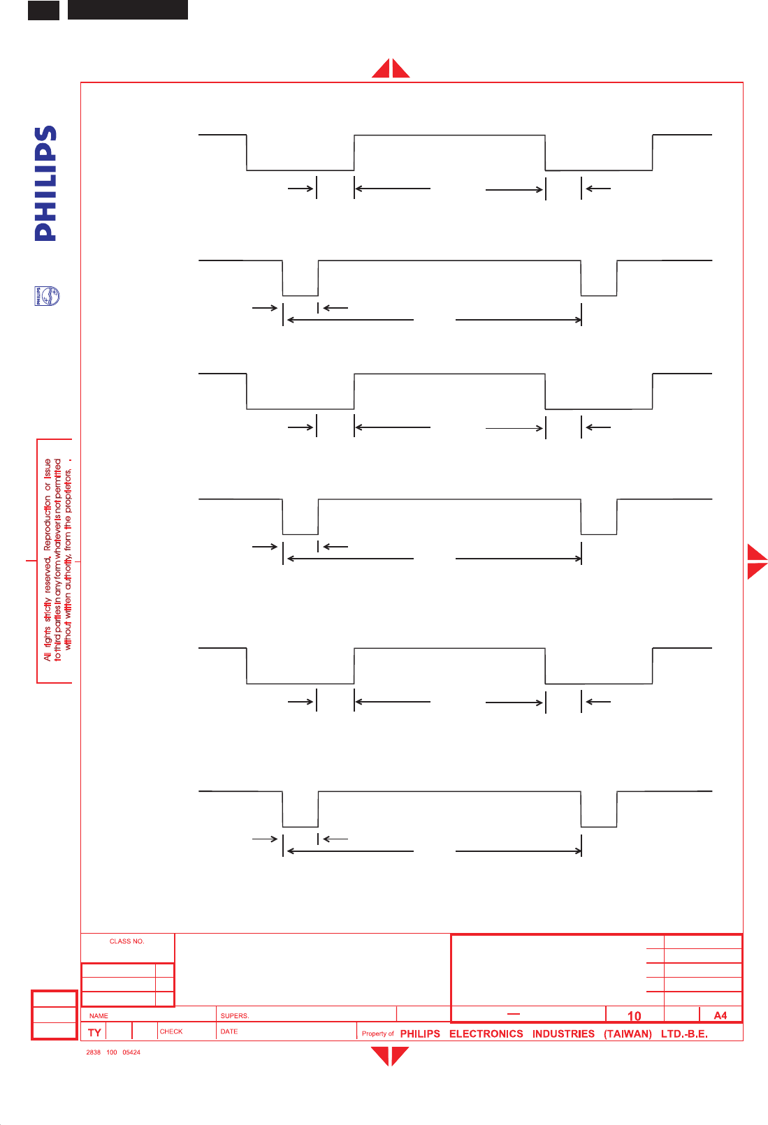
72 HUDSON 8 GENERAL PRODUCT SPECIFICATION(Continued)
D
VIDEO
CE
SEPARATE SYNC.
HORIZONTAL
B
A
R
VIDEO
QS
P
O
D
VIDEO
CE
B
A
VERTICAL
HORIZONTAL
COMPOSITE SYNC.
FIG-4 TIMING CHART -1
19 18
BRAND : PHILIPS
17 inch LCD Monitor
TYPE : 170C8FS/00 8670 000 25561
2007-06-01
590
2007-06-01
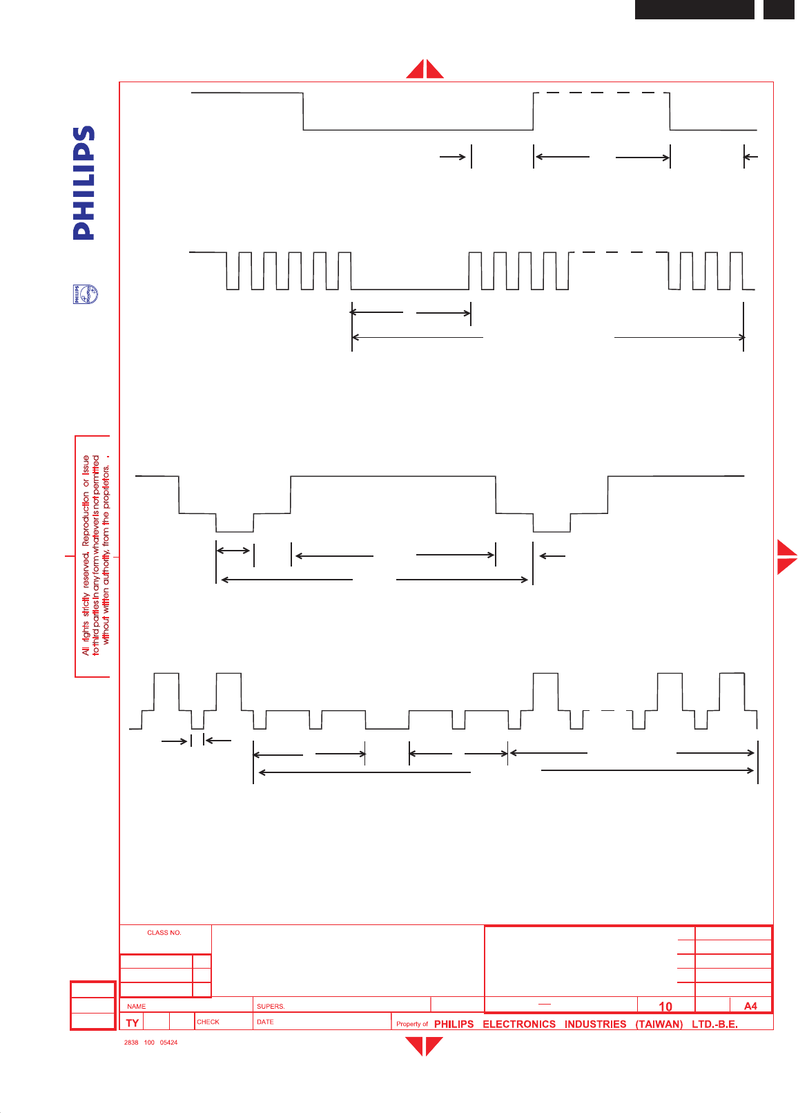
HUDSON 8 73
GENERAL PRODUCT SPECIFICATION(Continued)
D
VIDEO
CE
B
A
VERTICAL
COMPOSITE SYNC.
FIG-5 TIMING CHART -2
O
P
QR S
&VIDEO
B
SPQ
O
R
( SYNC. ON GREEN )
HORIZONTAL
VERTICAL
19
19
BRAND : PHILIPS
17 inch LCDMonitor
TYPE :170C8FS/00
8670 000 25561
2007-06-01
590
2007-06-01
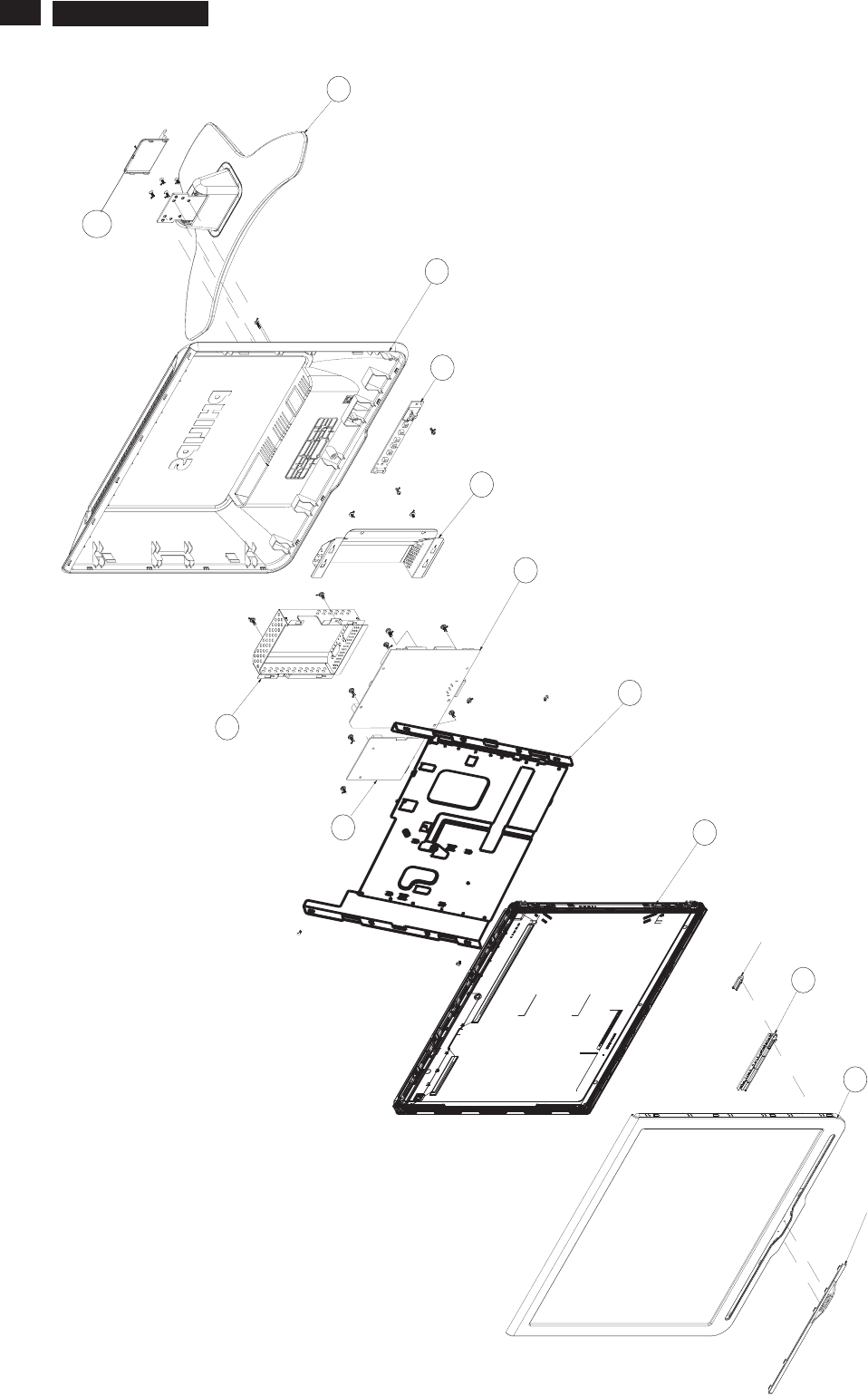
74 HUDSON 8 Exploded View
1
2
3
4
5
6
7
8
910
11
TYPE:170C8FS/00
705GZ734004
BEZEL ASSY
KEPC7AB3
KEY BOARD
750GLG70E3L42M000F
PANEL LM170E03-TLL4 PHILIPS LPL
705GZ715002
MAIN FRAME ASSY
CPBC7GNAPHA1
SCALER ASSY
PWPC742GR4
POWER ASSY
Z85G00041
SCALER SHIELDING
P85G00141
SHIELDING
P33G0055
FUNCTION KEY
12
705G2-000041
BACK COVER ASSY
P37G0002 1 VB
FOLD-BASE
P33G0027
HINGE COVER
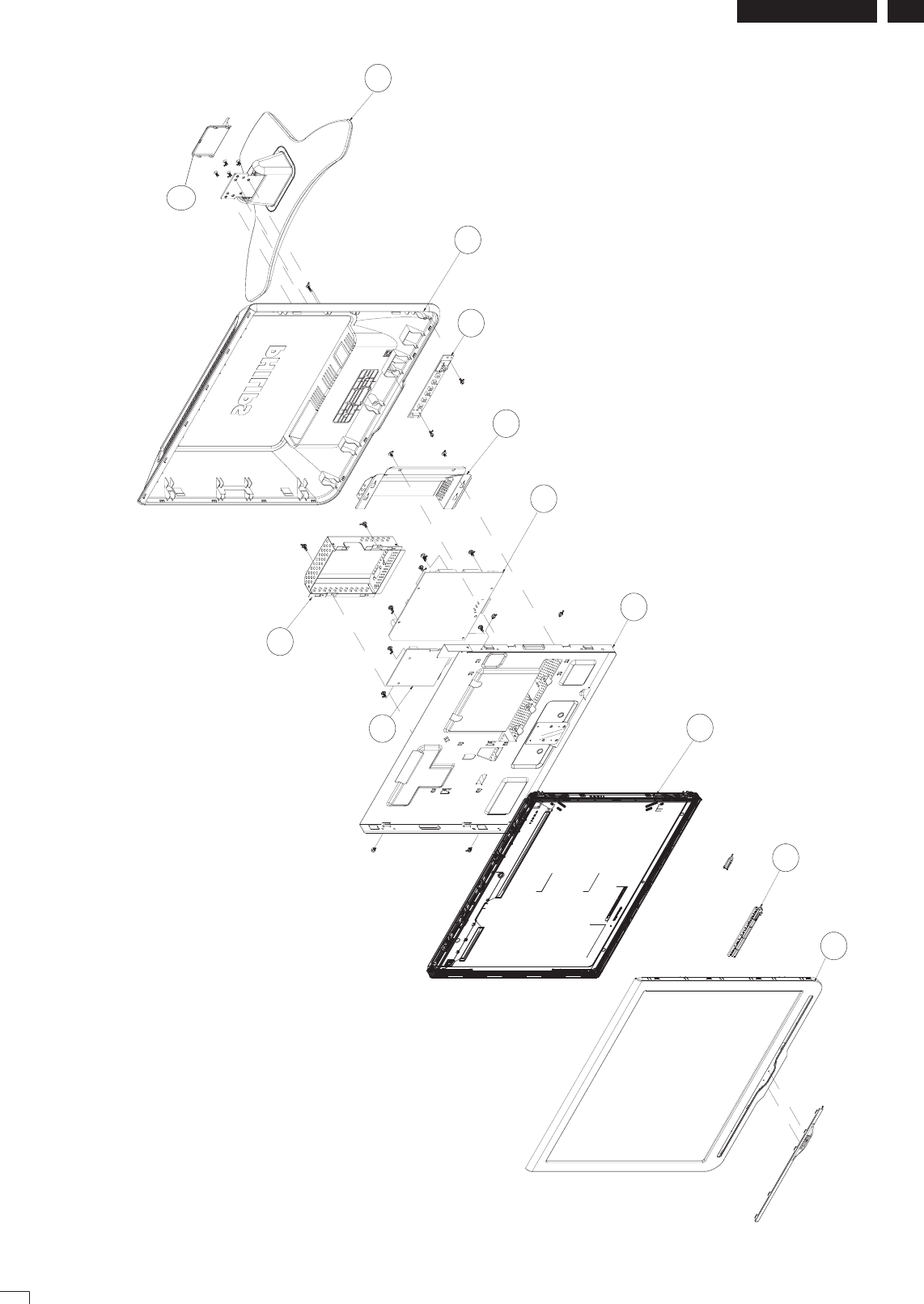
75
HUDSON 8
Exploded View
1
2
3
4
5
6
7
8
910
11
12
TYPE:190C8FS/00
705GZ734006
BEZEL ASSY
P33G0055
FUNCTION KEY
750GLH90N3A11N
PANEL HSD190MEN3-A 19 HANNSTAR
705GZ2715003
MAIN FRAME ASSY
CPBC7HNAPHA1
SCALER ASSY
PWPC942HR2
POWER ASSY
KEPC7AB3
KEY BOARD
P34G0112
BACK COVER ASSY
P37G0015
BASE
P33G0027
HINGE COVER
Z85G00041
SCALER SHILEDING
P85G0035
POWER SHILEDING
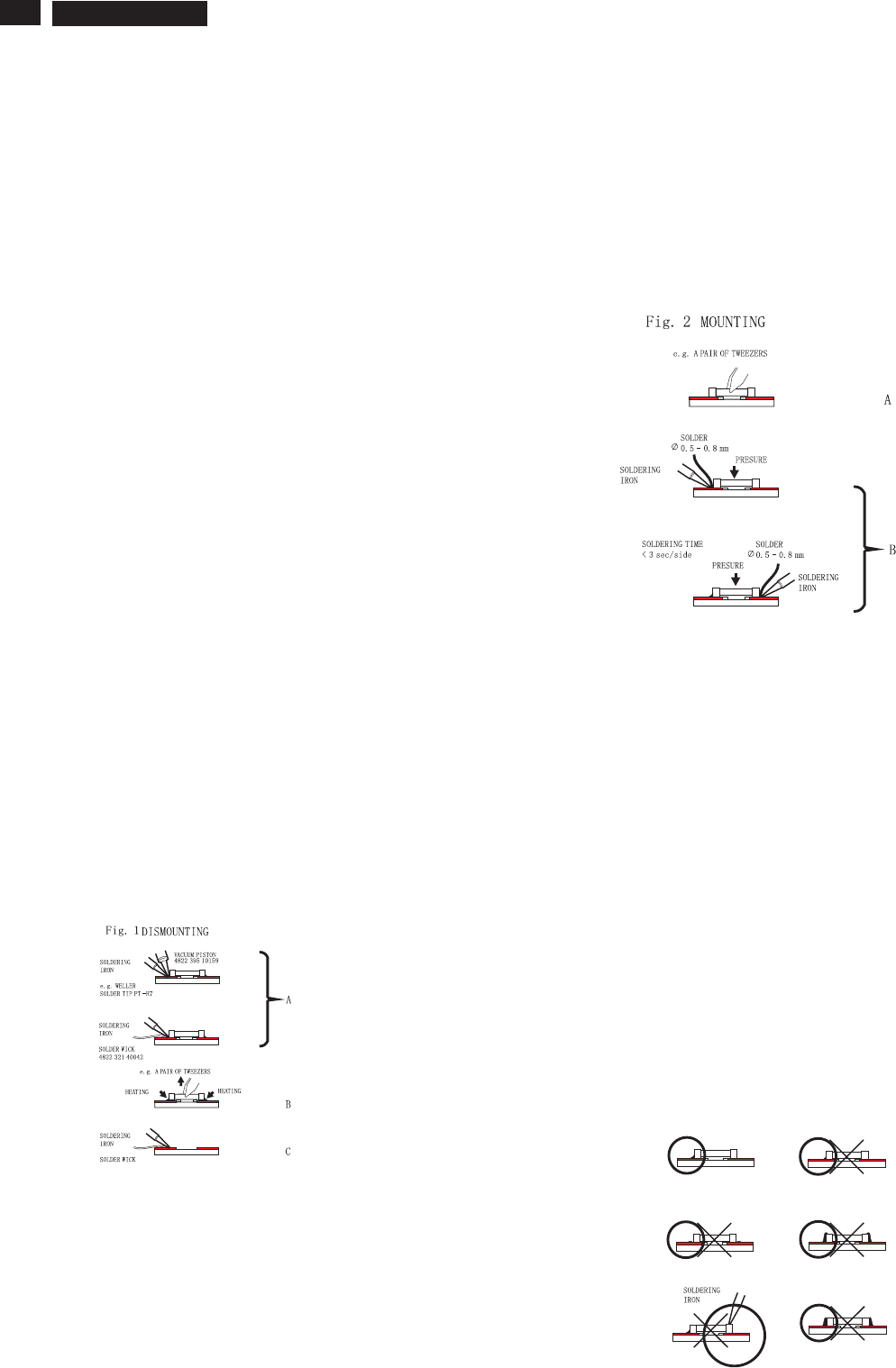
76 HUDSON 8 Repair Tips
0. Warning
All ICs and many other semi-conductors are susceptible to
electrostatic discharges (ESD). Careless handling during
repair can reduce life drastically. When repairing, make sure
that you are connected with the same potential as the mass
of the unit via a wrist wrap with resistance. Keep components
and tools also at the same potential !
1. Servicing of SMDs (Surface Mounted Devices)
1.1 General cautions on handling and storage
- Oxidation on the terminals of SMDs results in poor soldering.
Do not handle SMDs with bare hands.
- Avoid using storage places that are sensitive to oxidation
such as places with sulphur or chlorine gas, direct sunlight,
high temperatures or a high degree of humidity. The
capacitance or resistance value of the SMDs may be
affected by this.
- Rough handling of circuit boards containing SMDs may
cause damage to the components as well as the circuit
boards. Circuit boards containing SMDs should never be
bent or flexed. Different circuit board materials expand and
contract at different rates when heated or cooled and the
components and/or solder connections may be damaged
due to the stress. Never rub or scrape chip components as
this may cause the value of the component to change.
Similarly, do not slide the circuit board across any surface.
1.2 Removal of SMDs
- Heat the solder (for 2-3 seconds) at each terminal of the
chip. By means of litz wire and a slight horizontal force,
small components can be removed with the soldering iron.
They can also be removed with a solder sucker (see Fig.
1A)
While holding the SMD with a pair of tweezers, take it off gently using the
soldering iron's heat applied to each terminal (see Fig. 1 B).
- Remove the excess solder on the solder lands by means of
litz wire or a solder sucker (see Fig. 1C).
1.3 Caution on removal
- When handling the soldering.iron. use suitable pressure and be careful.
- When removing the chip, do not use undue force with the pair of tweezers.
- The soldering iron to be used (approx. 30 W) should
preferably be equipped with a thermal control (soldering
temperature: 225 to 250 C).
- The chip, once removed, must never be reused.
1.4 Attachment of SMDs
- Locate the SMD on the solder lands by means of tweezers
and solder the component on one side. Ensure that the
component is positioned correctly on the solder lands (see Fig.2A).
- Next complete the soldering of the terminals of the
component (see Fiq. 2B).
2. Caution when attaching SMDs
- When soldering the SMD terminals, do not touch them
directly with the soldering iron. The soldering should be
done as quickly as possible, care must be taken to avoid
damage to the terminals of the SMDs themselves.
- Keep the SMD's body in contact with the printed board when
soldering.
- The soldering iron to be used (approx. 30 W ) should
preferably be equipped with a thermal control (soldering
temperature: 225 to 250 C).
- Soldering should not be done outside the solder land.
- Soldering flux (of rosin) may be used, but should not be
acidic.
- After soldering, let the SMD cool down gradually at room
temperature.
- The quantity of solder must be proportional to the size of the
solder land. If the quantity is too great, the SMD might
crack or the solder lands might be torn loose from the
printed board (see Fig. 3).
Fig.3 Examples
Right

77
HUDSON 8
3. Lead-free product identification
You can identify lead-free product by Philips-lead-free logo on PCB.
4. Lead-free product repair instruction
4.1 Use only lead-free Solder Alloy 0622 149 00106(1.2mm SAC305) or 0622 14900108(1.0mm SAC305).
Remark: For lead free soldering material, please visit website for details. This is recommended by Philips.
4.2 Use only adequate solder tools applicable for lead-free soldering-tin. The solder tool must be able to reach at least a
solder-temperature of 400 , to stabilize the adjusted temperature at the solder-tip and to exchange solder-tips for different applications.
Small Passives/Actives to be removed with thermal tweezers
Automated system for IC and BGA repair (Microscope, Camera, Beam split optics, Computer, Programmer, Heat controllers, Vacuum
system, Laser pointer) Solder Hand-Tool (Adjustable in temperature height, Temperature shall be held constant,Flexible tips)
4.3 Adjust your solder tool so that a temperature around 360 -380 is reached and stabilized at the solder joint.
Heating-time of the solder-joint should not exceed~4sec.Avoid temperatures above 400 otherwise wear-out of tips will rise drastically
and flux-fluid will be destroyed.Corrosion of Tool-Spikes can be avoided when using SAC305 and a temperature of less than 400 .
4.4 Mix of lead-free solder-tin/parts with leaded soldering-tin/parts is possible but not recommended. If not to avoid clean carefully the
solder-joint from old tin and re-solder with new tin.
4.5 Use only original spare-parts listed in the Service-Manuals. Standard-material(consumables) can also be purchased at external
companies.
4.6 Special information for lead-free BGA-ICs: this ICs will be delivered in so-called dry-packaging to protect the IC against moisture and
with lead-free logo on it. This packaging may only be opened shortly before it is used (soldered). Otherwise the body of the IC gets wet
inside and during the heating time the structure of the IC will be destroyed due to high (steam-)pressure. If the packaging was opened
before usage the IC has to be heated up for some hours (around 90 ) for drying (Take attention for ESD-protection!)
5. Rework on BGA (Ball Grid Array) ICs
General
Although (LF)BGA assembly yields are very high, there may still be a requirement for component rework. By rework, we
mean the process of removing the component from the PWB and replacing it with a new component. If an (LF)BGA is
removed from a PWB, the solder balls of the component are deformed drastically so the removed (LF)BGA has to be
discarded.
Device Removal
As is the case with any component that, it is essential when removing an (LF)BGA, the board, tracks, solder lands, or
surrounding components are not damaged. To remove an (LF)BGA, the board must be uniformly heated to a temperature
close to the reflow soldering temperature. A uniform temperature reduces the chance of warping the PWB.
To do this, we recommend that the board is heated until it is certain that all the joints are molten. Then carefully pull the
component off the board with a vacuum nozzle. For the appropriate temperature profiles, see the IC data sheet.
Area Preparation
When the component has been removed, the vacant IC area must be cleaned before replacing the (LF)BGA.
Removing an IC often leaves varying amounts of solder on the mounting lands. This excessive solder can be removed with
either a solder sucker or solder wick. The remaining flux can be removed with a brush and cleaning agent. After the board
is properly cleaned and inspected, apply flux on the solder lands and on the connection balls of the(LF)BGA
Note: Do not apply solder paste, as this has shown to result in problems during re-soldering.
Device Replacement
The last step in the repair process is to solder the new component on the board. Ideally, the (LF)BGA should be
aligned under a microscope or magnifying glass. If this is not possible, try to align the (LF)BGA with any board markers.
To reflow the solder, apply a temperature profile according to the IC data sheet. So as not to damage neighbouring
components, it may be necessary to reduce some tempera
www.alphametals.com
More Information
For more information on how to handle BGA devices, visit this URL: http://www.atyourservice.ce.philips.com (needs
subscription). After login, select Magazine , then go to Workshop Information . Here you will find Information on how
.to deal with BGA-ICs.
Repair Tips
78 HUDSON 8
AC IN
Power Board
Control Board Scaler Board
LCD Panel
No power
(power indicator off)
Check 12V/5V NG
Bad power board
Check Control Board Check Control Wires
Check Scaler Board
OK
NG
OK
Bad Scaler Board
Check LCD Panel
OK
Repair Flow Chart
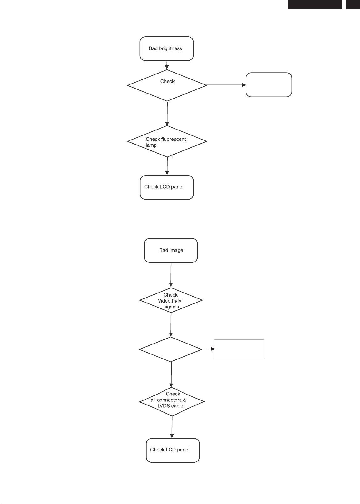
79
HUDSON 8
Power Board Bad Power Board
OK
NG
OK
OK
Check Scaler Board Bad Scaler Board
OK
OK
Repair Flow Chart
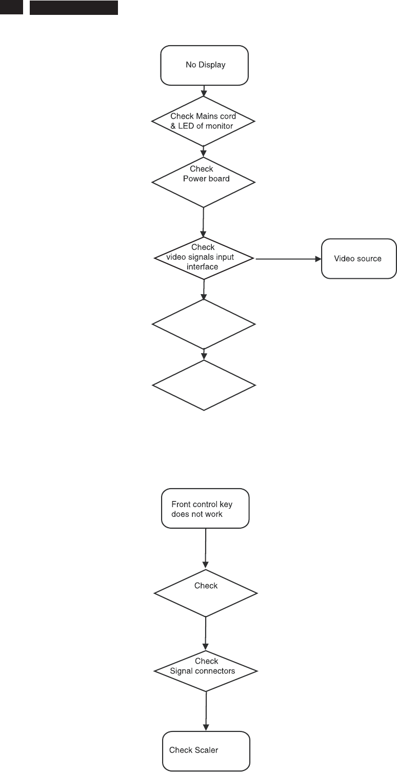
80 HUDSON 8 Repair Flow Chart
Check
Power Board
OK
Check LCD Panel
OK
NO
OK
Control Board
OK
OK
Board
18V/12V/5V DC

81
HUDSON 8
Recommended Parts List
Recommended Parts List
TYPE:170C8FS/00(LPL)
Item Component description
705GZ701001 DFU Assy
Q45G7628B05 PE BAG FOR MANUAL
Z41G7002813 1A QSG
Z40G7N01813 1A RATING LABEL
Z44G7002813 1A CARTON
Z70G7001813 1A E-D.F.U.
40 089G179E30H 15 FFC CABLE 30P 200mm
50 089G1738SAA922 D-SUB CABLE 1800mm BK RFS-92101708
60 089G404A18NLS1 POWER CORD PG8B1C3C300-060
100 705GZ734004 BEZEL ass'y
040G 152509 RECYCLE LABEL
040G 152512 RECYCLE LABEL
P33G0055 FUNCTION KEY
P33G0057 POWER LENS
P33G0059 2 STRIP
P34G0109 BEZEL
110 705GZ-000041 Back COVER ass'y
P15T0048 HINGE PLATE
P34G0110 Back COVER
120 P33G0027 HINGE COVER
130 P37G0002 1 VB FOLD-BASE
140 705GZ715002 MAIN FRAME ASSY
095G8014 7D 16 HARNESS 7P-7P 300mm
Z15G0004 1 MAIN FRAME
150 P15G8316 1 POWER BRACKET
160 P85G0014 1 SHIELDING
170 Z85G0004 1 SCALER SHIELDING
270 P44G700 1 CUSHION-RIGHT
280 P44G700 2 CUSHION-LEFT
U203 056G 562908 IC NT68665MEFG-128 QFP128
U301 056G 563 52 IC AP1117D33LA TO252-3L ATC
U304 056G 56327A IC AP1117E18LA SOT223-3L ANACHIP
U204 056G1133 56 M24C16-WMN6TP
Q301 057G 417 4 PMBS3904/PHILIPS-SMT(04)
Q305 057G 417 4 PMBS3904/PHILIPS-SMT(04)
Q403 057G 417 6 PMBS3906/PHILIPS-SMT(06)
Q402 057G 417 6 PMBS3906/PHILIPS-SMT(06)
Q201 057G 417 6 PMBS3906/PHILIPS-SMT(06)
Recommended Parts List
TYPE:190C8FS/00(CMO)
Item Component description
089G1738SAA922 D-SUB CABLE 1800mm BK RFS-92101708
089G1738WAA922 I/F cable
089G179E30H 16 FFC CABLE 30P 170mm
089G404A18NLS1 POWER CORD PG8B1C3C300-060
705GZ701002 DFU Assy
Q45G7628B05 PE BAG FOR MANUAL
Z41G9010813 1A QSG
705GZ715003 MAIN_FRAME ASSY
095G8014 7D 17 HARNESS 7P-7P 250mm
Z15G0005 1 MAIN FRAME(Panel-CMO)
705GZ734006 BEZEL ASSY
P33G0055 FUNCTION KEY
P33G0056 BEZEL STRIP
P33G0057 POWER LENS
P34G0111 BEZEL
P33G0027 HINGE COVER
P33G0058 1 housing cover
P34G0112 B/C ASSY
P37G0015 BASE
P41T1800813 4A CHINA WARRANTY CARD
P44G9008 1 CUSHION-R(WW)
P44G9008 2 CUSHION - L (ww)
P44T9504090 CORNER PAPER(6 layer)
P44T9504110 CORNER PAPER(5 layer)
P52G 57001 MIDDLE TAPE FOR CARTON
P52G 58002 SMALL TAPE
P85G0035 POWER_SHIELDING
Z40G9N01813 1A RATING LABEL
Z44G9010813 1A CARTON
Z70G9001813 1A E-D.F.U
Z85G0004 1 SCALER SHIELDING
U301 056G 563 52 IC AP1117D33LA TO252-3L ATC
U304 056G 56327A IC AP1117E18LA SOT223-3L ANACHIP
U204 056G1133 56 M24C16-WMN6TP
Q301 057G 417 4 PMBS3904/PHILIPS-SMT(04)
Q305 057G 417 4 PMBS3904/PHILIPS-SMT(04)
Q201 057G 417 6 PMBS3906/PHILIPS-SMT(06)
Q402 057G 417 6 PMBS3906/PHILIPS-SMT(06)
Q403 057G 417 6 PMBS3906/PHILIPS-SMT(06)

82 HUDSON 8 Spare Parts List
Model:170C8FS/00(LPL) 12NC:8670 000 25561
Item 18NC Description
Mechanical Parts
100 705GZ734004 BEZEL ass'y
040G 152509 RECYCLE LABEL
040G 152512 RECYCLE LABEL
P33G0055 FUNCTION KEY
P33G0057 POWER LENS
P33G0059 2 STRIP
P34G0109 BEZEL
110 705GZ-000041 Back COVER ass'y
P15T0048 HINGE PLATE
P34G0110 Back COVER
120 P33G0027 HINGE COVER
130 P37G0002 1 VB FOLD-BASE
Packing parts
Z44G7002813 1A CARTON
270 P44G700 1 CUSHION-RIGHT
280 P44G700 2 CUSHION-LEFT
Q45G7628B05 PE BAG FOR MANUAL
Accessory
60 089G404A18NLS1 POWER CORD PG8B1C3C300-060
Miscellanea
705GZ701001 DFU Assy
Z41G7002813 1A QSG
Z40G7N01813 1A RATING LABEL
Z70G7001813 1A E-D.F.U.
40 089G179E30H 15 FFC CABLE 30P 200mm
50 089G1738SAA922 D-SUB CABLE 1800mm BK RFS-92101708
140 705GZ715002 MAIN FRAME ASSY
095G8014 7D 16 HARNESS 7P-7P 300mm
Z15G0004 1 MAIN FRAME
150 P15G8316 1 POWER BRACKET
160 P85G0014 1 SHIELDING
170 Z85G0004 1 SCALER SHIELDING
LCD Panel
80 750GLG70E3L42M000F PANEL LM170E03-TLL4 PHILIPS LPL
PCB Assy
10 CPBC7GNAPHA1 scaler assy
20 KEPC7AB3 KEY BOARD
30 PWPC742GR4 POWER G2594-G-X-X-2-070515
PCB Assy
10 CPBC7GNAPHA1 scaler assy
Various
CN101 088G 35315F H D-SUB 15PIN
CN102 088G 35424F H DV1 CONNECTOR 24PIN
CN402 033G801930F H FPC CONN. 1.0MM 30P
X201 093G 22 51 CRYSTAL 12MHz HC-49US ARG6-120
705GZ756004 CPU Assembly
100CZ101000301 CPU Software
Z40G700081328A CPU Label
C101 065G0402104 12 CHIP 0.1UF 50V X7R
C101 065G040210412K Y CAP CHIP 0402 100N 16V X7R 10%
C102 065G0402104 12 CHIP 0.1UF 50V X7R
C102 065G040210412K Y CAP CHIP 0402 100N 16V X7R 10%
C103 065G0402104 12 CHIP 0.1UF 50V X7R
C103 065G040210412K Y CAP CHIP 0402 100N 16V X7R 10%
C104 065G0402104 12 CHIP 0.1UF 50V X7R
C104 065G040210412K Y CAP CHIP 0402 100N 16V X7R 10%
C105 065G0402104 12 CHIP 0.1UF 50V X7R
C105 065G040210412K Y CAP CHIP 0402 100N 16V X7R 10%
C106 065G0402104 12 CHIP 0.1UF 50V X7R
C106 065G040210412K Y CAP CHIP 0402 100N 16V X7R 10%
C107 065G060310517T MLCC 0603 CAP 1UF Z 16V Y5V
C107 065G060310517Z Y CAP CHIP 0603 1UF Z 16V Y5V
C110 065G0402104 12 CHIP 0.1UF 50V X7R
C110 065G040210412K Y CAP CHIP 0402 100N 16V X7R 10%
C111 065G0402104 12 CHIP 0.1UF 50V X7R
C111 065G040210412K Y CAP CHIP 0402 100N 16V X7R 10%
C112 065G0402104 12 CHIP 0.1UF 50V X7R
C112 065G040210412K Y CAP CHIP 0402 100N 16V X7R 10%
C113 065G0402104 12 CHIP 0.1UF 50V X7R
C113 065G040210412K Y CAP CHIP 0402 100N 16V X7R 10%
C114 065G0402104 12 CHIP 0.1UF 50V X7R
C114 065G040210412K Y CAP CHIP 0402 100N 16V X7R 10%
C115 065G060310517T MLCC 0603 CAP 1UF Z 16V Y5V
C115 065G060310517Z Y CAP CHIP 0603 1UF Z 16V Y5V
C116 065G0402104 12 CHIP 0.1UF 50V X7R
C116 065G040210412K Y CAP CHIP 0402 100N 16V X7R 10%
C117 065G0402104 12 CHIP 0.1UF 50V X7R
C117 065G040210412K Y CAP CHIP 0402 100N 16V X7R 10%
C118 065G0402104 12 CHIP 0.1UF 50V X7R
C118 065G040210412K Y CAP CHIP 0402 100N 16V X7R 10%
C121 065G0402473 12 CHIP 0.047uF 16V X7R
C122 065G0402473 12 CHIP 0.047uF 16V X7R
C123 065G0402102 32 1000PF +10% 50V X7R
C124 065G0402473 12 CHIP 0.047uF 16V X7R
C125 065G0402473 12 CHIP 0.047uF 16V X7R
C126 065G0402473 12 CHIP 0.047uF 16V X7R
C127 065G0402331 32 CHIP 330PF 50V X7R
C128 065G0402330 31 33PF +50% 50V NPO
C129 065G0402473 12 CHIP 0.047uF 16V X7R
C130 065G0402104 12 CHIP 0.1UF 50V X7R
C130 065G040210412K Y CAP CHIP 0402 100N 16V X7R 10%
C201 065G0402104 12 CHIP 0.1UF 50V X7R
C201 065G040210412K Y CAP CHIP 0402 100N 16V X7R 10%
C203 065G0402104 12 CHIP 0.1UF 50V X7R
C203 065G040210412K Y CAP CHIP 0402 100N 16V X7R 10%
C204 065G0402104 12 CHIP 0.1UF 50V X7R
C204 065G040210412K Y CAP CHIP 0402 100N 16V X7R 10%
C205 065G0402104 12 CHIP 0.1UF 50V X7R
C205 065G040210412K Y CAP CHIP 0402 100N 16V X7R 10%
C206 065G0402104 12 CHIP 0.1UF 50V X7R
C206 065G040210412K Y CAP CHIP 0402 100N 16V X7R 10%
C207 065G0402104 12 CHIP 0.1UF 50V X7R
C207 065G040210412K Y CAP CHIP 0402 100N 16V X7R 10%
C208 065G0402104 12 CHIP 0.1UF 50V X7R
C208 065G040210412K Y CAP CHIP 0402 100N 16V X7R 10%
C209 065G0402104 12 CHIP 0.1UF 50V X7R
C209 065G040210412K Y CAP CHIP 0402 100N 16V X7R 10%
C210 065G0402104 12 CHIP 0.1UF 50V X7R
C210 065G040210412K Y CAP CHIP 0402 100N 16V X7R 10%
C213 065G060310517T MLCC 0603 CAP 1UF Z 16V Y5V
C213 065G060310517Z Y CAP CHIP 0603 1UF Z 16V Y5V
C214 067G 305101 3T 100UF 16V 105C
C214 067G305V101 3 105 100UF M 16V
C214 067G305V101 3L 105 RADIAL E-CAPACTOR 100uF 16V
C215 065G0402104 12 CHIP 0.1UF 50V X7R
C215 065G040210412K Y CAP CHIP 0402 100N 16V X7R 10%
C216 065G0402104 12 CHIP 0.1UF 50V X7R
C216 065G040210412K Y CAP CHIP 0402 100N 16V X7R 10%
C219 065G0402220 31 CHIP 22PF 50V NPO
C220 065G0402220 31 CHIP 22PF 50V NPO
C301 065G0402104 12 CHIP 0.1UF 50V X7R
C301 065G040210412K Y CAP CHIP 0402 100N 16V X7R 10%
C302 067G305V100 3 105 10UF +20% 16V
C302 067G305V100 3L RGA100M1CCC-0511
C303 065G0402104 12 CHIP 0.1UF 50V X7R
C303 065G040210412K Y CAP CHIP 0402 100N 16V X7R 10%
C304 065G060310517T MLCC 0603 CAP 1UF Z 16V Y5V
C304 065G060310517Z Y CAP CHIP 0603 1UF Z 16V Y5V
C305 067G 305101 3T 100UF 16V 105C
C305 067G305V101 3 105 100UF M 16V
C305 067G305V101 3L 105 RADIAL E-CAPACTOR 100uF 16V
C306 067G 305101 3T 100UF 16V 105C
C306 067G305V101 3 105 100UF M 16V
C306 067G305V101 3L 105 RADIAL E-CAPACTOR 100uF 16V
C307 065G0402104 12 CHIP 0.1UF 50V X7R
C307 065G040210412K Y CAP CHIP 0402 100N 16V X7R 10%
C308 065G060310517T MLCC 0603 CAP 1UF Z 16V Y5V
C308 065G060310517Z Y CAP CHIP 0603 1UF Z 16V Y5V
C309 067G 305101 3T 100UF 16V 105C
C309 067G305V101 3 105 100UF M 16V
C309 067G305V101 3L 105 RADIAL E-CAPACTOR 100uF 16V
C310 067G 305101 3T 100UF 16V 105C
C310 067G305V101 3 105 100UF M 16V
C310 067G305V101 3L 105 RADIAL E-CAPACTOR 100uF 16V
C311 065G0402104 12 CHIP 0.1UF 50V X7R

83
HUDSON 8
Spare Parts List
C311 065G040210412K Y CAP CHIP 0402 100N 16V X7R 10%
C312 065G0402104 12 CHIP 0.1UF 50V X7R
C312 065G040210412K Y CAP CHIP 0402 100N 16V X7R 10%
C315 067G 305101 3T 100UF 16V 105C
C315 067G305V101 3 105 100UF M 16V
C315 067G305V101 3L 105 RADIAL E-CAPACTOR 100uF 16V
C316 065G0603104 22 CHIP 0.1UF 25V X7R
C317 065G0402104 12 CHIP 0.1UF 50V X7R
C317 065G040210412K Y CAP CHIP 0402 100N 16V X7R 10%
C402 065G0402104 12 CHIP 0.1UF 50V X7R
C402 065G040210412K Y CAP CHIP 0402 100N 16V X7R 10%
C403 065G0402104 12 CHIP 0.1UF 50V X7R
C403 065G040210412K Y CAP CHIP 0402 100N 16V X7R 10%
C404 065G0402104 12 CHIP 0.1UF 50V X7R
C404 065G040210412K Y CAP CHIP 0402 100N 16V X7R 10%
C405 065G0402104 12 CHIP 0.1UF 50V X7R
C405 065G040210412K Y CAP CHIP 0402 100N 16V X7R 10%
C406 065G0402104 12 CHIP 0.1UF 50V X7R
C406 065G040210412K Y CAP CHIP 0402 100N 16V X7R 10%
C407 065G0402104 12 CHIP 0.1UF 50V X7R
C407 065G040210412K Y CAP CHIP 0402 100N 16V X7R 10%
R101 061G0402750 RST CHIPR 75 OHM +5% 1/16W
R102 061G0402102 RST CHIPR 1 KOHM +5% 1/16W
R103 061G0402472 RST CHIPR 4.7 KOHM +5% 1/16W
R104 061G0402472 RST CHIPR 4.7 KOHM +5% 1/16W
R105 061G0402103 RST CHIPR 10 KOHM +5% 1/16W
R106 061G0402000 RST CHIPR 0 OHM +5% 1/16W
R107 061G0402000 RST CHIPR 0 OHM +5% 1/16W
R108 061G0402101 RST CHIPR 100 OHM +5% 1/16W
R109 061G0402101 RST CHIPR 100 OHM +5% 1/16W
R110 061G0402000 RST CHIPR 0 OHM +5% 1/16W
R111 061G0402000 RST CHIPR 0 OHM +5% 1/16W
R113 061G0402102 RST CHIPR 1 KOHM +5% 1/16W
R115 061G0402000 RST CHIPR 0 OHM +5% 1/16W
R116 061G0402000 RST CHIPR 0 OHM +5% 1/16W
R117 061G0402000 RST CHIPR 0 OHM +5% 1/16W
R118 061G0402000 RST CHIPR 0 OHM +5% 1/16W
R120 061G0402102 RST CHIPR 1 KOHM +5% 1/16W
R122 061G0402102 RST CHIPR 1 KOHM +5% 1/16W
R123 061G0402472 RST CHIPR 4.7 KOHM +5% 1/16W
R124 061G0402472 RST CHIPR 4.7 KOHM +5% 1/16W
R125 061G0402103 RST CHIPR 10 KOHM +5% 1/16W
R126 061G0402101 RST CHIPR 100 OHM +5% 1/16W
R127 061G0402101 RST CHIPR 100 OHM +5% 1/16W
R128 061G0402101 RST CHIPR 100 OHM +5% 1/16W
R129 061G0402151 RST CHIP 150R 1/16W 5%
R131 061G0402391 RST CHIPR 390 OHM +5% 1/16W
R132 061G0402101 RST CHIPR 100 OHM +5% 1/16W
R133 061G0402151 RST CHIP 150R 1/16W 5%
R134 061G0402101 RST CHIPR 100 OHM +5% 1/16W
R135 061G0402101 RST CHIPR 100 OHM +5% 1/16W
R136 061G0402101 RST CHIPR 100 OHM +5% 1/16W
R138 061G0402151 RST CHIP 150R 1/16W 5%
R139 061G0402750 RST CHIPR 75 OHM +5% 1/16W
R140 061G0402750 RST CHIPR 75 OHM +5% 1/16W
R141 061G0402222 RST CHIPR 2.2 KOHM +5% 1/16W
R142 061G0402222 RST CHIPR 2.2 KOHM +5% 1/16W
R144 061G0402102 RST CHIPR 1 KOHM +5% 1/16W
R201 061G0402105 RST CHIPR 1MOHM +5% 1/16W
R202 061G0402103 RST CHIPR 10 KOHM +5% 1/16W
R206 061G0402472 RST CHIPR 4.7 KOHM +5% 1/16W
R211 061G0402000 RST CHIPR 0 OHM +5% 1/16W
R213 061G0402472 RST CHIPR 4.7 KOHM +5% 1/16W
R214 061G0402472 RST CHIPR 4.7 KOHM +5% 1/16W
R215 061G0402472 RST CHIPR 4.7 KOHM +5% 1/16W
R218 061G0402220 RST CHIPR 22 OHM +5% 1/16W
R221 061G0402471 RST CHIPR 470 OHM +5% 1/16W
R225 061G0402101 RST CHIPR 100 OHM +5% 1/16W
R228 061G0402000 RST CHIPR 0 OHM +5% 1/16W
R301 061G0402102 RST CHIPR 1 KOHM +5% 1/16W
R302 061G1206151 RST CHIPR 150 OHM +5% 1/4W
R303 061G1206151 RST CHIPR 150 OHM +5% 1/4W
R304 061G0402103 RST CHIPR 10 KOHM +5% 1/16W
R305 061G0402103 RST CHIPR 10 KOHM +5% 1/16W
R307 061G0402513 RST CHIP 51K 1/16W 5%
R308 061G0402472 RST CHIPR 4.7 KOHM +5% 1/16W
R309 061G0402101 RST CHIPR 100 OHM +5% 1/16W
R311 061G0402102 RST CHIPR 1 KOHM +5% 1/16W
R312 061G0402102 RST CHIPR 1 KOHM +5% 1/16W
R314 061G0402472 RST CHIPR 4.7 KOHM +5% 1/16W
R316 061G0402472 RST CHIPR 4.7 KOHM +5% 1/16W
R402 061G0402392 RST CHIP 3.9K 1/16W 5%
R403 061G0402392 RST CHIP 3.9K 1/16W 5%
R404 061G0402000 RST CHIPR 0 OHM +5% 1/16W
R407 061G0402101 RST CHIPR 100 OHM +5% 1/16W
R410 061G0402101 RST CHIPR 100 OHM +5% 1/16W
R412 061G0402102 RST CHIPR 1 KOHM +5% 1/16W
R415 061G0402103 RST CHIPR 10 KOHM +5% 1/16W
R416 061G0402101 RST CHIPR 100 OHM +5% 1/16W
R417 061G0402103 RST CHIPR 10 KOHM +5% 1/16W
R418 061G0402101 RST CHIPR 100 OHM +5% 1/16W
R431 061G0402000 RST CHIPR 0 OHM +5% 1/16W
R432 061G0402000 RST CHIPR 0 OHM +5% 1/16W
R439 061G0402000 RST CHIPR 0 OHM +5% 1/16W
FB101 071G 56D121 B201209D121TT
FB101 071G 56G121 TA CHIP BEAD 120R/200mA FCM2012KF-121T02
FB102 071G 56D121 B201209D121TT
FB102 071G 56G121 TA CHIP BEAD 120R/200mA FCM2012KF-121T02
FB103 071G 59B300 K CHIP BEAD 30 OHM 0603
FB103 071G 59B300 M CHIP BEAD 30 OHM
FB103 071G 59K300 TA CHIP BEAD 0603 30R/700mA TAI-TECH
FB104 071G 59B300 K CHIP BEAD 30 OHM 0603
FB104 071G 59B300 M CHIP BEAD 30 OHM
FB104 071G 59K300 TA CHIP BEAD 0603 30R/700mA TAI-TECH
FB105 071G 56D121 B201209D121TT
FB105 071G 56G121 TA CHIP BEAD 120R/200mA FCM2012KF-121T02
FB106 071G 59B300 K CHIP BEAD 30 OHM 0603
FB106 071G 59B300 M CHIP BEAD 30 OHM
FB106 071G 59K300 TA CHIP BEAD 0603 30R/700mA TAI-TECH
FB202 071G 56D121 B201209D121TT
FB202 071G 56G121 TA CHIP BEAD 120R/200mA FCM2012KF-121T02
FB203 071G 56D121 B201209D121TT
FB203 071G 56G121 TA CHIP BEAD 120R/200mA FCM2012KF-121T02
FB204 071G 56D121 B201209D121TT
FB204 071G 56G121 TA CHIP BEAD 120R/200mA FCM2012KF-121T02
FB205 071G 56D121 B201209D121TT
FB205 071G 56G121 TA CHIP BEAD 120R/200mA FCM2012KF-121T02
FB206 071G 56D121 B201209D121TT
FB206 071G 56G121 TA CHIP BEAD 120R/200mA FCM2012KF-121T02
FB207 071G 56C102 TA CHIP BEAD 1000R/400mA FCM2012KF-102T0
4
FB207 071G 56D102 B201209D102TT
FB302 071G 56K121 M CHIP BEAD
FB302 071G 56K121 TA CHIP BEAD 120R/6000mA HCB2012KF-121T6
0
FB303 071G 56K121 M CHIP BEAD
FB303 071G 56K121 TA CHIP BEAD 120R/6000mA HCB2012KF-121T6
0
D101 093G 64 33 DIO SIG SM BAV99 (PHSE)R
D101 093G 6433S DIODE BAV99 SEMTECH
D102 093G 64 42 PP BAV70 SOT-23
D103 093G 64 33 DIO SIG SM BAV99 (PHSE)R
D103 093G 6433S DIODE BAV99 SEMTECH
D104 093G 64 33 DIO SIG SM BAV99 (PHSE)R
D104 093G 6433S DIODE BAV99 SEMTECH
D105 093G 64 33 DIO SIG SM BAV99 (PHSE)R
D105 093G 6433S DIODE BAV99 SEMTECH
D106 093G 64 33 DIO SIG SM BAV99 (PHSE)R
D106 093G 6433S DIODE BAV99 SEMTECH
D107 093G 64 33 DIO SIG SM BAV99 (PHSE)R
D107 093G 6433S DIODE BAV99 SEMTECH
D108 093G 64 33 DIO SIG SM BAV99 (PHSE)R
D108 093G 6433S DIODE BAV99 SEMTECH
D109 093G 64 33 DIO SIG SM BAV99 (PHSE)R
D109 093G 6433S DIODE BAV99 SEMTECH
D110 093G 64 42 PP BAV70 SOT-23
D111 093G 64 33 DIO SIG SM BAV99 (PHSE)R
D111 093G 6433S DIODE BAV99 SEMTECH
D112 093G 64 33 DIO SIG SM BAV99 (PHSE)R
D112 093G 6433S DIODE BAV99 SEMTECH
D113 093G 64 33 DIO SIG SM BAV99 (PHSE)R
D113 093G 6433S DIODE BAV99 SEMTECH
D201 093G 64 42 PP BAV70 SOT-23
D301 093G3004 3 SM340A
ZD101 093G 39GA01 T RLZ5.6B
ZD101 093G 39S 24 T RLZ 5.6B LLDS
ZD102 093G 39GA01 T RLZ5.6B
ZD102 093G 39S 24 T RLZ 5.6B LLDS
ZD103 093G 39GA01 T RLZ5.6B
ZD103 093G 39S 24 T RLZ 5.6B LLDS
ZD104 093G 39GA01 T RLZ5.6B
ZD104 093G 39S 24 T RLZ 5.6B LLDS
ZD105 093G 39GA01 T RLZ5.6B
ZD105 093G 39S 24 T RLZ 5.6B LLDS
ZD106 093G 39GA01 T RLZ5.6B
ZD106 093G 39S 24 T RLZ 5.6B LLDS

ZD107 093G 39GA01 T RLZ5.6B
ZD107 093G 39S 24 T RLZ 5.6B LLDS
ZD201 093G 39G586 RLZ2.2B
Q201 057G 417 6 PMBS3906/PHILIPS-SMT(06)
Q201 057G 417 13 T KEC 2N3906S-RTK/PS
Q301 057G 417 4 PMBS3904/PHILIPS-SMT(04)
Q301 057G 417 12 T KEC 2N3904S-RTK/PS
Q302 057G 763 1 AO3401 SOT23 BY AOS(A1)
Q305 057G 417 4 PMBS3904/PHILIPS-SMT(04)
Q305 057G 417 12 T KEC 2N3904S-RTK/PS
Q402 057G 417 6 PMBS3906/PHILIPS-SMT(06)
Q402 057G 417 13 T KEC 2N3906S-RTK/PS
Q403 057G 417 6 PMBS3906/PHILIPS-SMT(06)
Q403 057G 417 13 T KEC 2N3906S-RTK/PS
U203 056G 562908 IC NT68665MEFG-128 QFP128
U204 056G1133 56 M24C16-WMN6TP
U301 056G 563 52 IC AP1117D33LA TO252-3L ATC
U304 056G 56327A IC AP1117E18LA SOT223-3L ANACHIP
PCB Assy
20 KEPC7AB3 KEY BOARD
Various
LED1 081G 12900 KB LED VS L-115WSYKCGKW-8.03LSF5/F
LED2 081G 12900 KB LED VS L-115WSYKCGKW-8.03LSF5/F
SW1 077G 605 1 FD SWI TACT H=5 GY 160G SKHHAM B
SW2 077G 605 1 FD SWI TACT H=5 GY 160G SKHHAM B
SW3 077G 605 1 FD SWI TACT H=5 GY 160G SKHHAM B
SW4 077G 605 1 FD SWI TACT H=5 GY 160G SKHHAM B
SW5 077G 605 1 FD SWI TACT H=5 GY 160G SKHHAM B
SW6 077G 605 1 FD SWI TACT H=5 GY 160G SKHHAM B
SW7 077G 605 1 FD SWI TACT H=5 GY 160G SKHHAM B
C101 065G0603471 32 CHIP 470PF 50V X7R
C102 065G0603471 32 CHIP 470PF 50V X7R
C103 065G0603471 32 CHIP 470PF 50V X7R
C104 065G0603471 32 CHIP 470PF 50V X7R
C105 065G0603471 32 CHIP 470PF 50V X7R
FB101 071G 59G301 CHIP BEAD 300OHM
FB102 071G 59G301 CHIP BEAD 300OHM
R101 061G0603432 RST CHIPR 4.3 KOHM +5% 1/10W
R102 061G0603911 RST CHIPR 910 OHM +5% 1/10W
R103 061G0603242 RST CHIPR 2.4 KOHM +5% 1/10W
R104 061G0603432 RST CHIPR 4.3 KOHM +5% 1/10W
R105 061G0603911 RST CHIPR 910 OHM +5% 1/10W
R106 061G0603242 RST CHIPR 2.4 KOHM +5% 1/10W
PCB Assy
30 PWPC742GR4 POWER G2594-G-X-X-2-070515
Vsrious
BD901 093G 50460 28 BRIDGE DIODE KBP208G LITEON
CN801 033G8021 2E F WAFER
CN801 033G8021 2E U WAFER
CN802 033G8021 2E F WAFER
CN802 033G8021 2E U WAFER
CN803 033G8021 2E F WAFER
CN803 033G8021 2E U WAFER
CN804 033G8021 2E F WAFER
CN804 033G8021 2E U WAFER
CN901 087G 501 32 S AC SOCKET
CN902 095G801410D 53 HARNESS 9P-10P 130mm
F901 084G 56 4W FUSE 4.0A 250V
F902 061G1206000 RST CHIPR 0 OHM +5% 1/4W
IC801 056G 379 22 IC TL494IDR SOIC-16
IC902 056G 139 8 IC PS2561L1-1-V-A LJ Lead Bending 4pin
IC902 056G 139 3A PC123Y22FZOF
IC902 056G 139 3B PC123 Y82FZ0F
IC903 056G 158 12 KIA431A-AT/P TO-92
J807 061G1206000 RST CHIPR 0 OHM +5% 1/4W
J813 061G1206000 RST CHIPR 0 OHM +5% 1/4W
J814 061G1206000 RST CHIPR 0 OHM +5% 1/4W
J815 061G1206000 RST CHIPR 0 OHM +5% 1/4W
J816 061G1206000 RST CHIPR 0 OHM +5% 1/4W
J818 061G1206000 RST CHIPR 0 OHM +5% 1/4W
J907 061G1206000 RST CHIPR 0 OHM +5% 1/4W
J908 061G1206000 RST CHIPR 0 OHM +5% 1/4W
NR901 061G 58 9T RST NTCR 10 ohm +20% 5A THINKING
PT801 080GL17T 40 V X'FMR TK.2001U.101
PT801 080GL17T 40 DN X'FMR TK.2001U.101
PT802 080GL17T 40 V X'FMR TK.2001U.101
84 HUDSON 8 Spare Parts List
PT802 080GL17T 40 DN X'FMR TK.2001U.101
T901 080GL17T 33 N2 XFMR POWER 550uH YUVA
T901 080GL17T 33 T2 X'FMR 550uH SRW28EC-T147H015
T901 080GL17T 33DN2 XFMR 550uH LK.PC001.B60
T901 080GL17T 33YS2 X'FMR 550uH YS04160106
C801 065G 3J1006ET 10PF,J,3KV,SL
C802 065G0603105 12 CHIP 1UF 16VX7R 0603
C803 065G0805152 32 CHIP 1500PF 50V X7R 0805
C804 065G0603104 12 CER2 0603 X7R 16V 100N P M10 R
C805 067G215D4714KV E.C 105 CAP 470UF M 25V ED SERIES
C806 065G0603105 12 CHIP 1UF 16VX7R 0603
C807 065G0603104 12 CER2 0603 X7R 16V 100N P M10 R
C808 065G0805225 12 CHIP 2.2UF 16V X7R 0805
C809 065G0805221 31 220PF 50V NPO
C810 065G0603104 22 CHIP 0.1UF 25V X7R
C811 067G215D4714KV E.C 105 CAP 470UF M 25V ED SERIES
C812 065G 3J1006ET 10PF,J,3KV,SL
C813 065G0603222 22 CHIP 2200PF 25V X7R
C814 065G0603104 12 CER2 0603 X7R 16V 100N P M10 R
C815 065G0603222 22 CHIP 2200PF 25V X7R
C816 065G0805152 32 CHIP 1500PF 50V X7R 0805
C817 065G0603222 22 CHIP 2200PF 25V X7R
C818 065G0603222 22 CHIP 2200PF 25V X7R
C821 065G0805152 32 CHIP 1500PF 50V X7R 0805
C822 065G0805152 32 CHIP 1500PF 50V X7R 0805
C823 065G0805104 22 CHIP 0805 0.1UF +10% 25V X7R
C824 065G0805104 22 CHIP 0805 0.1UF +10% 25V X7R
C900 065G306M2222BP 2200PF +20% 400VAC
C901 065G305M1022E2 1000P 400VAC/250VAC
C901 065G305M1022E3 1000PF. M.250VAC.Y2
C901 065G305M1022EM Y2 1000PF +20% 250VAC
C902 065G305M1022E2 1000P 400VAC/250VAC
C902 065G305M1022E3 1000PF. M.250VAC.Y2
C902 065G305M1022EM Y2 1000PF +20% 250VAC
C903 065G306M1022BP 1000PF Y1.CAP
C904 065G0603102 32 1000PF +10% 50V X7R
C907 067G 40J10115K EC CAP 100uF 450V 18*35mm
C907 067G305T10115H ELCAP 105 100UF M 450V
C909 063G 107474 U MPX-474K27B15L3
C909 063G 107474 HS 0.47UF 275VAC
C910 065G 2K152 1T6921 1.5NF/2KV Y5P +10%
C911 067G 2152207NT KY50VB22M-TP5 5*11
C911 067G215Y2207KT CAP 105 22UF M 50V KINGNICHI
C912 065G0805104 32 CHIP 0.1U 50V X7R
C913 065G0805221 31 220PF 50V NPO
C914 065G0805471 21 CHIP 470PF 25V NPO
C914 065G0805471 31 CHIP 470PF 50V NPO
C916 065G0805104 32 CHIP 0.1U 50V X7R
C920 065G517K102 5T 1000PF 10% Y5P 500V
C921 065G517K102 5T 1000PF 10% Y5P 500V
C922 067G215D6814KV CAP 105 680uF M 25V
C923 067G215D6814KV CAP 105 680uF M 25V
C925 067G215D4714KV E.C 105 CAP 470UF M 25V ED SERIES
C926 067G215S102 3K ED1000UF 16V
C927 067G215S4713KV EC 105 CAP 470UF M 16V
C928 065G0805104 32 CHIP 0.1U 50V X7R
C929 065G0805104 32 CHIP 0.1U 50V X7R
C930 065G0805104 32 CHIP 0.1U 50V X7R
C931 065G0805104 32 CHIP 0.1U 50V X7R
C932 067G215S102 3K ED1000UF 16V
R801 061G0603000 RST CHIPR 0 OHM +5% 1/10W
R802 061G0805101 RST CHIPR 100 OHM +5% 1/8W
R803 061G0603242 RST CHIPR 2.4 KOHM +5% 1/10W
R804 061G0603000 RST CHIPR 0 OHM +5% 1/10W
R805 061G0603472 RST CHIPR 4.7KOHM +5% 1/10W
R806 061G0603100 1F RST CHIPR 1 KOHM +1% 1/10W
R807 061G0603100 1F RST CHIPR 1 KOHM +1% 1/10W
R808 061G0603100 2F RST CHIPR 10 KOHM +1% 1/10W
R810 061G1206150 RST CHIPR 15 OHM +5% 1/4W
R811 061G0603100 1F RST CHIPR 1 KOHM +1% 1/10W
R812 061G0603100 1F RST CHIPR 1 KOHM +1% 1/10W
R813 061G0603101 RST CHIPR 100 OHM +5% 1/10W
R814 061G0603680 2F RST CHIPR 68 KOHM +1% 1/10W
R815 061G0603470 2F RST CHIPR 47 KOHM +1% 1/10W
R816 061G0603680 2F RST CHIPR 68 KOHM +1% 1/10W
R819 061G0603100 2F RST CHIPR 10 KOHM +1% 1/10W
R820 061G0603564 RST CHIPR 560 KOHM +5% 1/10W
R821 061G0603105 RST CHIPR 1 MOHM +5% 1/10W
R822 061G0603473 RST CHIPR 47 KOHM +5% 1/10W
R824 061G0603100 2F RST CHIPR 10 KOHM +1% 1/10W
R825 061G0805510 2F RST CHIPR 51 KOHM +1% 1/8W
R826 061G0805180 3F RST CHIPR 180 KOHM +1% 1/8W
R827 061G0603100 1F RST CHIPR 1 KOHM +1% 1/10W
R828 061G0603470 2F RST CHIPR 47 KOHM +1% 1/10W
R829 061G0603680 2F RST CHIPR 68 KOHM +1% 1/10W
R830 061G0603000 RST CHIPR 0 OHM +5% 1/10W

85
HUDSON 8
Spare Parts List
R831 061G0603100 2F RST CHIPR 10 KOHM +1% 1/10W
R832 061G0603000 RST CHIPR 0 OHM +5% 1/10W
R833 061G0603100 2F RST CHIPR 10 KOHM +1% 1/10W
R834 061G0603100 1F RST CHIPR 1 KOHM +1% 1/10W
R835 061G0603100 1F RST CHIPR 1 KOHM +1% 1/10W
R836 061G0603105 RST CHIPR 1 MOHM +5% 1/10W
R837 061G1206150 RST CHIPR 15 OHM +5% 1/4W
R838 061G0603100 2F RST CHIPR 10 KOHM +1% 1/10W
R839 061G0603100 1F RST CHIPR 1 KOHM +1% 1/10W
R840 061G0603100 2F RST CHIPR 10 KOHM +1% 1/10W
R841 061G0603100 1F RST CHIPR 1 KOHM +1% 1/10W
R842 061G0603470 2F RST CHIPR 47 KOHM +1% 1/10W
R844 061G0603220 RST CHIPR 22 OHM +5% 1/10W
R845 061G0603220 RST CHIPR 22 OHM +5% 1/10W
R846 061G0603220 RST CHIPR 22 OHM +5% 1/10W
R847 061G0603220 RST CHIPR 22 OHM +5% 1/10W
R848 061G0603100 1F RST CHIPR 1 KOHM +1% 1/10W
R849 061G0603100 1F RST CHIPR 1 KOHM +1% 1/10W
R850 061G1206150 RST CHIPR 15 OHM +5% 1/4W
R851 061G1206150 RST CHIPR 15 OHM +5% 1/4W
R852 061G0603100 2F RST CHIPR 10 KOHM +1% 1/10W
R853 061G0603100 2F RST CHIPR 10 KOHM +1% 1/10W
R900 061G1206334 RST CHIPR 330KOHM +5% 1/4W
R901 061G1206334 RST CHIPR 330KOHM +5% 1/4W
R902 061G1206334 RST CHIPR 330KOHM +5% 1/4W
R903 061G0805102 RST CHIPR 1KOHM +5% 1/8W
R905 061G1206103 RST CHIPR 10 KOHM +5% 1/4W
R907 061G 208151 64 RST MOFR 150 OHM +5% 1W
R908 061G0805471 RST CHIPR 470 OHM +5% 1/8W
R909 061G152M104 64 100KOHM 5% 2W
R910 061G1206229 RST CHIPR 2.2 OHM +5% 1/4W
R911 061G0805100 3F RST CHIPR 100KOHM +1% 1/8W
R912 061G1206100 RST CHIP 10R 1/4W 5%
R913 061G0805100 1F RST CHIPR 1KOHM +1% 1/8W
R915 061G0805100 2F RST CHIPR 10KOHM +1% 1/8W
R916 061G152M438 64 RST MOFR 0.43OHM +5% 2WS
R922 061G0805471 RST CHIPR 470 OHM +5% 1/8W
R923 061G0805100 2F RST CHIPR 10KOHM +1% 1/8W
R924 061G0805360 1F RST CHIPR 3.6KOHM +1% 1/8W
R925 061G0805100 1F RST CHIPR 1KOHM +1% 1/8W
R926 061G0805330 2F RST CHIPR 33 KOHM +1% 1/8W
R927 061G0805100 1F RST CHIPR 1KOHM +1% 1/8W
R928 061G0805100 1F RST CHIPR 1KOHM +1% 1/8W
R929 061G0805240 1F RST CHIPR 2.4KOHM +1% 1/8W
R930 061G0805100 1F RST CHIPR 1KOHM +1% 1/8W
R931 061G1206103 RST CHIPR 10 KOHM +5% 1/4W
R951 061G1206470 RST CHIPR 47 OHM +5% 1/4W
R952 061G1206470 RST CHIPR 47 OHM +5% 1/4W
R953 061G1206470 RST CHIPR 47 OHM +5% 1/4W
R954 061G1206470 RST CHIPR 47 OHM +5% 1/4W
R955 061G1206470 RST CHIPR 47 OHM +5% 1/4W
R956 061G1206470 RST CHIPR 47 OHM +5% 1/4W
FB901 071G 55 29 FERRITE BEAD
FB902 071G 55 29 FERRITE BEAD
FB903 071G 55 29 FERRITE BEAD
L901 073G 174 76 H FILTER
L901 073G 174 76 L CHOKE COIL LI TAI LF-002923
L902 073G 174 65 H LINE FILTER
L902 073G 174 65 T LINE FILTER 7mH MIN TDK
L921 073G 253 91 H CHOKE COIL
L921 073G 253 91 LS CHOKE BY LI SHIN
L922 073G 253 91 H CHOKE COIL
L922 073G 253 91 LS CHOKE BY LI SHIN
D801 093G 64 33 DIO SIG SM BAV99 (PHSE)R
D802 093G 64 33 DIO SIG SM BAV99 (PHSE)R
D803 093G 6432V LL4148-GSO8
D803 093G 64S3PH BAS32L
D803 093T 64 44 S LL4148WP
D806 093G 64 38 D DIODE BAW56 DIODES
D806 093G 64S 10 DIODE BAW56PT SOT-23 CHENMKO
D807 093G 6432V LL4148-GSO8
D807 093G 64S3PH BAS32L
D807 093T 64 44 S LL4148WP
D808 093G 64 38 D DIODE BAW56 DIODES
D808 093G 64S 10 DIODE BAW56PT SOT-23 CHENMKO
D809 093G 64 33 DIO SIG SM BAV99 (PHSE)R
D810 093G 64 33 DIO SIG SM BAV99 (PHSE)R
D811 093G 6432V LL4148-GSO8
D811 093G 64S3PH BAS32L
D811 093T 64 44 S LL4148WP
D812 061G1206000 RST CHIPR 0 OHM +5% 1/4W
D813 093G 6432V LL4148-GSO8
D813 093G 64S3PH BAS32L
D813 093T 64 44 S LL4148WP
D900 093T1100 1052T BA159GPT
D901 093G 6038T52T FR103
D901 093T1020 752T UF4003PT
D910 093G 6432V LL4148-GSO8
D910 093G 64S3PH BAS32L
D910 093T 64 44 S LL4148WP
D915 093G 6432V LL4148-GSO8
D915 093G 64S3PH BAS32L
D915 093T 64 44 S LL4148WP
D916 093G 6432V LL4148-GSO8
D916 093G 64S3PH BAS32L
D916 093T 64 44 S LL4148WP
D920 093G 60276 DIODE SBT150-10LST SANYO
D922 093G3006 1 1 31DQ06FC3 NIHON INTER
ZD801 061G1206103 RST CHIPR 10 KOHM +5% 1/4W
ZD920 093G 39GA28 T ZENER DIODE RLZ13B SEMTECH
ZD920 093G 39S 40 T RLZ 13B LLDS
ZD921 093G 39GA28 T ZENER DIODE RLZ13B SEMTECH
ZD921 093G 39S 40 T RLZ 13B LLDS
ZD922 093G 39GA26 T ZENER DIODE RLZ5.1B SEMTECH
ZD922 093G 39S 25 T RLZ5.1B LLDS
Q801 057G 760 4 DTA144WKA BY ROHM SMT
Q801 057G 760 4B PDTA144WK SOT346
Q802 057G 760 5B PDTC144WK SOT346
Q803 057G 417 4 PMBS3904/PHILIPS-SMT(04)
Q803 057G 417 12 T KEC 2N3904S-RTK/PS
Q804 057G 763 6 AO4828L
Q804 057G 763 14 AM9945N
Q805 057G 417 6 PMBS3906/PHILIPS-SMT(06)
Q805 057G 417 13 T KEC 2N3906S-RTK/PS
Q806 057G 417 6 PMBS3906/PHILIPS-SMT(06)
Q806 057G 417 13 T KEC 2N3906S-RTK/PS
Q807 057G 417 4 PMBS3904/PHILIPS-SMT(04)
Q807 057G 417 12 T KEC 2N3904S-RTK/PS
Q808 057G 759 2 RK7002
Q808 057G 763904 TRA FET 2N7002 SOT-23 PHILIPS
Q808 057T 758 1 FET 2N7002E VISHAY
Q809 057G 763 6 AO4828L
Q809 057G 763 14 AM9945N
Q810 057G 417 4 PMBS3904/PHILIPS-SMT(04)
Q810 057G 417 12 T KEC 2N3904S-RTK/PS
Q811 057G 417 4 PMBS3904/PHILIPS-SMT(04)
Q811 057G 417 12 T KEC 2N3904S-RTK/PS
Q812 057G 759 2 RK7002
Q812 057G 763904 TRA FET 2N7002 SOT-23 PHILIPS
Q812 057T 758 1 FET 2N7002E VISHAY
Q900 057G 667 21 STP10NK70ZFP
Q902 057G 417 4 PMBS3904/PHILIPS-SMT(04)
Q902 057G 417 12 T KEC 2N3904S-RTK/PS
U901 056T 379 61 IC LD7575PS SOP-8 LEADTREND

86 HUDSON 8 Spare Parts List
Model:190C8FS/00(CMO) 12NC:
Item 18NC Description
Mechanical Parts
705GZ734006 BEZEL ASSY
P33G0055 FUNCTION KEY
P33G0056 BEZEL STRIP
P33G0057 POWER LENS
P34G0111 BEZEL
P33G0027 HINGE COVER
P33G0058 1 housing cover
P34G0112 B/C ASSY
P37G0015 BASE
Packing Parts
Q45G7628B05 PE BAG FOR MANUAL
P44G9008 1 CUSHION - R (WW)
P44G9008 2 CUSHION - L (ww)
Z44G9010813 1A CARTON
Accessory
089G404A18NLS1 POWER CORD PG8B1C3C300-060
Miscellanea
089G1738SAA922 D-SUB CABLE 1800mm BK RFS-92101708
089G1738WAA922 I/F cable
089G179E30H 16 FFC CABLE 30P 170mm
705GZ701002 DFU Assy
Z41G9010813 1A QSG
705GZ715003 MAIN_FRAME ASSY
095G8014 7D 17 HARNESS 7P-7P 250mm
Z15G0005 1 MAIN FRAME(Panel-CMO)
P41T1800813 4A CHINA WARRANTY CARD
P44T9504090 CORNER PAPER(6 layer)
P44T9504110 CORNER PAPER(5 layer)
P52G 57001 MIDDLE TAPE FOR CARTON
P52G 58002 SMALL TAPE
P85G0035 POWER_SHIELDING
Z40G9N01813 1A RATING LABEL
Z70G9001813 1A E-D.F.U
Z85G0004 1 SCALER SHIELDING
LCD Panel
750GLH90N3A11N PANEL HSD190MEN3-A 19" HANNSTAR
PCB Assy
CPBC7HNAPHA1 SCALER BOARD ASSY-HSD
KEPC7AB3 KEY BOARD
PWPC942HR2 POWER ASSY-HSD
PCB Assy
CPBC7HNAPHA1 SCALER BOARD ASSY-HSD
Various
CN101 088G 35315F H D-SUB 15PIN
CN102 088G 35424F H DV1 CONNECTOR 24PIN
CN402 033G801930F H FPC CONN. 1.0MM 30P
X201 093G 22 51 CRYSTAL 12MHz HC-49US ARG6-120
705GZ756001 CPU Assy
100CZ101000251 CPU Software
Z40G900081359A CPU Label
C101 065G0402104 12 CHIP 0.1UF 50V X7R
C101 065G040210412K Y CAP CHIP 0402 100N 16V X7R 10%
C102 065G0402104 12 CHIP 0.1UF 50V X7R
C102 065G040210412K Y CAP CHIP 0402 100N 16V X7R 10%
C103 065G0402104 12 CHIP 0.1UF 50V X7R
C103 065G040210412K Y CAP CHIP 0402 100N 16V X7R 10%
C104 065G0402104 12 CHIP 0.1UF 50V X7R
C104 065G040210412K Y CAP CHIP 0402 100N 16V X7R 10%
C105 065G0402104 12 CHIP 0.1UF 50V X7R
C105 065G040210412K Y CAP CHIP 0402 100N 16V X7R 10%
C106 065G0402104 12 CHIP 0.1UF 50V X7R
C106 065G040210412K Y CAP CHIP 0402 100N 16V X7R 10%
C107 065G060310517T MLCC 0603 CAP 1UF Z 16V Y5V
C107 065G060310517Z Y CAP CHIP 0603 1UF Z 16V Y5V
C110 065G0402104 12 CHIP 0.1UF 50V X7R
C110 065G040210412K Y CAP CHIP 0402 100N 16V X7R 10%
C111 065G0402104 12 CHIP 0.1UF 50V X7R
C111 065G040210412K Y CAP CHIP 0402 100N 16V X7R 10%
C112 065G0402104 12 CHIP 0.1UF 50V X7R
C112 065G040210412K Y CAP CHIP 0402 100N 16V X7R 10%
C113 065G0402104 12 CHIP 0.1UF 50V X7R
C113 065G040210412K Y CAP CHIP 0402 100N 16V X7R 10%
C114 065G0402104 12 CHIP 0.1UF 50V X7R
C114 065G040210412K Y CAP CHIP 0402 100N 16V X7R 10%
C115 065G060310517T MLCC 0603 CAP 1UF Z 16V Y5V
C115 065G060310517Z Y CAP CHIP 0603 1UF Z 16V Y5V
C116 065G0402104 12 CHIP 0.1UF 50V X7R
C116 065G040210412K Y CAP CHIP 0402 100N 16V X7R 10%
C117 065G0402104 12 CHIP 0.1UF 50V X7R
C117 065G040210412K Y CAP CHIP 0402 100N 16V X7R 10%
C118 065G0402104 12 CHIP 0.1UF 50V X7R
C118 065G040210412K Y CAP CHIP 0402 100N 16V X7R 10%
C121 065G0402473 12 CHIP 0.047uF 16V X7R
C122 065G0402473 12 CHIP 0.047uF 16V X7R
C123 065G0402102 32 1000PF +10% 50V X7R
C124 065G0402473 12 CHIP 0.047uF 16V X7R
C125 065G0402473 12 CHIP 0.047uF 16V X7R
C126 065G0402473 12 CHIP 0.047uF 16V X7R
C127 065G0402331 32 CHIP 330PF 50V X7R
C128 065G0402330 31 33PF +50% 50V NPO
C129 065G0402473 12 CHIP 0.047uF 16V X7R
C130 065G0402104 12 CHIP 0.1UF 50V X7R
C130 065G040210412K Y CAP CHIP 0402 100N 16V X7R 10%
C201 065G0402104 12 CHIP 0.1UF 50V X7R
C201 065G040210412K Y CAP CHIP 0402 100N 16V X7R 10%
C203 065G0402104 12 CHIP 0.1UF 50V X7R
C203 065G040210412K Y CAP CHIP 0402 100N 16V X7R 10%
C204 065G0402104 12 CHIP 0.1UF 50V X7R
C204 065G040210412K Y CAP CHIP 0402 100N 16V X7R 10%
C205 065G0402104 12 CHIP 0.1UF 50V X7R
C205 065G040210412K Y CAP CHIP 0402 100N 16V X7R 10%
C206 065G0402104 12 CHIP 0.1UF 50V X7R
C206 065G040210412K Y CAP CHIP 0402 100N 16V X7R 10%
C207 065G0402104 12 CHIP 0.1UF 50V X7R
C207 065G040210412K Y CAP CHIP 0402 100N 16V X7R 10%
C208 065G0402104 12 CHIP 0.1UF 50V X7R
C208 065G040210412K Y CAP CHIP 0402 100N 16V X7R 10%
C209 065G0402104 12 CHIP 0.1UF 50V X7R
C209 065G040210412K Y CAP CHIP 0402 100N 16V X7R 10%
C210 065G0402104 12 CHIP 0.1UF 50V X7R
C210 065G040210412K Y CAP CHIP 0402 100N 16V X7R 10%
C213 065G060310517T MLCC 0603 CAP 1UF Z 16V Y5V
C213 065G060310517Z Y CAP CHIP 0603 1UF Z 16V Y5V
C214 067G 305101 3T 100UF 16V 105C
C214 067G305V101 3 105 100UF M 16V
C214 067G305V101 3L 105 RADIAL E-CAPACTOR 100uF 16V
C215 065G0402104 12 CHIP 0.1UF 50V X7R
C215 065G040210412K Y CAP CHIP 0402 100N 16V X7R 10%
C216 065G0402104 12 CHIP 0.1UF 50V X7R
C216 065G040210412K Y CAP CHIP 0402 100N 16V X7R 10%
C219 065G0402220 31 CHIP 22PF 50V NPO
C220 065G0402220 31 CHIP 22PF 50V NPO
C301 065G0402104 12 CHIP 0.1UF 50V X7R
C301 065G040210412K Y CAP CHIP 0402 100N 16V X7R 10%
C302 067G305V100 3 105 10UF +20% 16V
C302 067G305V100 3L RGA100M1CCC-0511
C303 065G0402104 12 CHIP 0.1UF 50V X7R
C303 065G040210412K Y CAP CHIP 0402 100N 16V X7R 10%
C304 065G060310517T MLCC 0603 CAP 1UF Z 16V Y5V
C304 065G060310517Z Y CAP CHIP 0603 1UF Z 16V Y5V
C305 067G 305101 3T 100UF 16V 105C
C305 067G305V101 3 105 100UF M 16V
C305 067G305V101 3L 105 RADIAL E-CAPACTOR 100uF 16V
C306 067G 305101 3T 100UF 16V 105C
C306 067G305V101 3 105 100UF M 16V
C306 067G305V101 3L 105 RADIAL E-CAPACTOR 100uF 16V
C307 065G0402104 12 CHIP 0.1UF 50V X7R
C307 065G040210412K Y CAP CHIP 0402 100N 16V X7R 10%
C308 065G060310517T MLCC 0603 CAP 1UF Z 16V Y5V
C308 065G060310517Z Y CAP CHIP 0603 1UF Z 16V Y5V
C309 067G 305101 3T 100UF 16V 105C
C309 067G305V101 3 105 100UF M 16V
C309 067G305V101 3L 105 RADIAL E-CAPACTOR 100uF 16V
C310 067G 305101 3T 100UF 16V 105C
C310 067G305V101 3 105 100UF M 16V
C310 067G305V101 3L 105 RADIAL E-CAPACTOR 100uF 16V
C311 065G0402104 12 CHIP 0.1UF 50V X7R
C311 065G040210412K Y CAP CHIP 0402 100N 16V X7R 10%
C312 065G0402104 12 CHIP 0.1UF 50V X7R
C312 065G040210412K Y CAP CHIP 0402 100N 16V X7R 10%
C315 067G 305101 3T 100UF 16V 105C
C315 067G305V101 3 105 100UF M 16V
C315 067G305V101 3L 105 RADIAL E-CAPACTOR 100uF 16V
C316 065G0603104 22 CHIP 0.1UF 25V X7R
C317 065G0402104 12 CHIP 0.1UF 50V X7R
C317 065G040210412K Y CAP CHIP 0402 100N 16V X7R 10%
C402 065G0402104 12 CHIP 0.1UF 50V X7R
C402 065G040210412K Y CAP CHIP 0402 100N 16V X7R 10%
C403 065G0402104 12 CHIP 0.1UF 50V X7R
C403 065G040210412K Y CAP CHIP 0402 100N 16V X7R 10%
C404 065G0402104 12 CHIP 0.1UF 50V X7R
C404 065G040210412K Y CAP CHIP 0402 100N 16V X7R 10%
C405 065G0402104 12 CHIP 0.1UF 50V X7R
C405 065G040210412K Y CAP CHIP 0402 100N 16V X7R 10%
C406 065G0402104 12 CHIP 0.1UF 50V X7R
C406 065G040210412K Y CAP CHIP 0402 100N 16V X7R 10%

C407 065G0402104 12 CHIP 0.1UF 50V X7R
C407 065G040210412K Y CAP CHIP 0402 100N 16V X7R 10%
R101 061G0402750 RST CHIPR 75 OHM +5% 1/16W
R102 061G0402102 RST CHIPR 1 KOHM +5% 1/16W
R103 061G0402472 RST CHIPR 4.7 KOHM +5% 1/16W
R104 061G0402472 RST CHIPR 4.7 KOHM +5% 1/16W
R105 061G0402103 RST CHIPR 10 KOHM +5% 1/16W
R106 061G0402000 RST CHIPR 0 OHM +5% 1/16W
R107 061G0402000 RST CHIPR 0 OHM +5% 1/16W
R108 061G0402101 RST CHIPR 100 OHM +5% 1/16W
R109 061G0402101 RST CHIPR 100 OHM +5% 1/16W
R110 061G0402000 RST CHIPR 0 OHM +5% 1/16W
R111 061G0402000 RST CHIPR 0 OHM +5% 1/16W
R113 061G0402102 RST CHIPR 1 KOHM +5% 1/16W
R115 061G0402000 RST CHIPR 0 OHM +5% 1/16W
R116 061G0402000 RST CHIPR 0 OHM +5% 1/16W
R117 061G0402000 RST CHIPR 0 OHM +5% 1/16W
R118 061G0402000 RST CHIPR 0 OHM +5% 1/16W
R120 061G0402102 RST CHIPR 1 KOHM +5% 1/16W
R122 061G0402102 RST CHIPR 1 KOHM +5% 1/16W
R123 061G0402472 RST CHIPR 4.7 KOHM +5% 1/16W
R124 061G0402472 RST CHIPR 4.7 KOHM +5% 1/16W
R125 061G0402103 RST CHIPR 10 KOHM +5% 1/16W
R126 061G0402101 RST CHIPR 100 OHM +5% 1/16W
R127 061G0402101 RST CHIPR 100 OHM +5% 1/16W
R128 061G0402101 RST CHIPR 100 OHM +5% 1/16W
R129 061G0402151 RST CHIP 150R 1/16W 5%
R131 061G0402391 RST CHIPR 390 OHM +5% 1/16W
R132 061G0402101 RST CHIPR 100 OHM +5% 1/16W
R133 061G0402151 RST CHIP 150R 1/16W 5%
R134 061G0402101 RST CHIPR 100 OHM +5% 1/16W
R135 061G0402101 RST CHIPR 100 OHM +5% 1/16W
R136 061G0402101 RST CHIPR 100 OHM +5% 1/16W
R138 061G0402151 RST CHIP 150R 1/16W 5%
R139 061G0402750 RST CHIPR 75 OHM +5% 1/16W
R140 061G0402750 RST CHIPR 75 OHM +5% 1/16W
R141 061G0402222 RST CHIPR 2.2 KOHM +5% 1/16W
R142 061G0402222 RST CHIPR 2.2 KOHM +5% 1/16W
R144 061G0402102 RST CHIPR 1 KOHM +5% 1/16W
R201 061G0402105 RST CHIPR 1MOHM +5% 1/16W
R202 061G0402103 RST CHIPR 10 KOHM +5% 1/16W
R206 061G0402472 RST CHIPR 4.7 KOHM +5% 1/16W
R211 061G0402000 RST CHIPR 0 OHM +5% 1/16W
R213 061G0402472 RST CHIPR 4.7 KOHM +5% 1/16W
R214 061G0402472 RST CHIPR 4.7 KOHM +5% 1/16W
R215 061G0402472 RST CHIPR 4.7 KOHM +5% 1/16W
R218 061G0402220 RST CHIPR 22 OHM +5% 1/16W
R221 061G0402471 RST CHIPR 470 OHM +5% 1/16W
R225 061G0402101 RST CHIPR 100 OHM +5% 1/16W
R228 061G0402000 RST CHIPR 0 OHM +5% 1/16W
R301 061G0402102 RST CHIPR 1 KOHM +5% 1/16W
R302 061G1206151 RST CHIPR 150 OHM +5% 1/4W
R303 061G1206151 RST CHIPR 150 OHM +5% 1/4W
R304 061G0402103 RST CHIPR 10 KOHM +5% 1/16W
R305 061G0402103 RST CHIPR 10 KOHM +5% 1/16W
R307 061G0402513 RST CHIP 51K 1/16W 5%
R308 061G0402472 RST CHIPR 4.7 KOHM +5% 1/16W
R309 061G0402101 RST CHIPR 100 OHM +5% 1/16W
R311 061G0402102 RST CHIPR 1 KOHM +5% 1/16W
R312 061G0402102 RST CHIPR 1 KOHM +5% 1/16W
R314 061G0402472 RST CHIPR 4.7 KOHM +5% 1/16W
R316 061G0402472 RST CHIPR 4.7 KOHM +5% 1/16W
R402 061G0402392 RST CHIP 3.9K 1/16W 5%
R403 061G0402392 RST CHIP 3.9K 1/16W 5%
R404 061G0402000 RST CHIPR 0 OHM +5% 1/16W
R407 061G0402101 RST CHIPR 100 OHM +5% 1/16W
R410 061G0402101 RST CHIPR 100 OHM +5% 1/16W
R412 061G0402102 RST CHIPR 1 KOHM +5% 1/16W
R415 061G0402103 RST CHIPR 10 KOHM +5% 1/16W
R416 061G0402101 RST CHIPR 100 OHM +5% 1/16W
R417 061G0402103 RST CHIPR 10 KOHM +5% 1/16W
R418 061G0402101 RST CHIPR 100 OHM +5% 1/16W
R431 061G0402000 RST CHIPR 0 OHM +5% 1/16W
R432 061G0402000 RST CHIPR 0 OHM +5% 1/16W
R439 061G0402000 RST CHIPR 0 OHM +5% 1/16W
FB101 071G 56D121 B201209D121TT
FB101 071G 56G121 TA CHIP BEAD 120R/200mA FCM2012KF-121T02
FB102 071G 56D121 B201209D121TT
FB102 071G 56G121 TA CHIP BEAD 120R/200mA FCM2012KF-121T02
FB103 071G 59B300 K CHIP BEAD 30 OHM 0603
FB103 071G 59B300 M CHIP BEAD 30 OHM
FB103 071G 59K300 TA CHIP BEAD 0603 30R/700mA TAI-TECH
FB104 071G 59B300 K CHIP BEAD 30 OHM 0603
FB104 071G 59B300 M CHIP BEAD 30 OHM
FB104 071G 59K300 TA CHIP BEAD 0603 30R/700mA TAI-TECH
FB105 071G 56D121 B201209D121TT
87
HUDSON 8
Spare Parts List
FB105 071G 56G121 TA CHIP BEAD 120R/200mA FCM2012KF-121T02
FB106 071G 59B300 K CHIP BEAD 30 OHM 0603
FB106 071G 59B300 M CHIP BEAD 30 OHM
FB106 071G 59K300 TA CHIP BEAD 0603 30R/700mA TAI-TECH
FB202 071G 56D121 B201209D121TT
FB202 071G 56G121 TA CHIP BEAD 120R/200mA FCM2012KF-121T02
FB203 071G 56D121 B201209D121TT
FB203 071G 56G121 TA CHIP BEAD 120R/200mA FCM2012KF-121T02
FB204 071G 56D121 B201209D121TT
FB204 071G 56G121 TA CHIP BEAD 120R/200mA FCM2012KF-121T02
FB205 071G 56D121 B201209D121TT
FB205 071G 56G121 TA CHIP BEAD 120R/200mA FCM2012KF-121T02
FB206 071G 56D121 B201209D121TT
FB206 071G 56G121 TA CHIP BEAD 120R/200mA FCM2012KF-121T02
FB207 071G 56C102 TA CHIP BEAD 1000R/400mA FCM2012KF-102T04
FB207 071G 56D102 B201209D102TT
FB302 071G 56K121 M CHIP BEAD
FB302 071G 56K121 TA CHIP BEAD 120R/6000mA HCB2012KF-121T60
FB303 071G 56K121 M CHIP BEAD
FB303 071G 56K121 TA CHIP BEAD 120R/6000mA HCB2012KF-121T60
D101 093G 64 33 DIO SIG SM BAV99 (PHSE)R
D101 093G 6433S DIODE BAV99 SEMTECH
D102 093G 64 42 PP BAV70 SOT-23
D103 093G 64 33 DIO SIG SM BAV99 (PHSE)R
D103 093G 6433S DIODE BAV99 SEMTECH
D104 093G 64 33 DIO SIG SM BAV99 (PHSE)R
D104 093G 6433S DIODE BAV99 SEMTECH
D105 093G 64 33 DIO SIG SM BAV99 (PHSE)R
D105 093G 6433S DIODE BAV99 SEMTECH
D106 093G 64 33 DIO SIG SM BAV99 (PHSE)R
D106 093G 6433S DIODE BAV99 SEMTECH
D107 093G 64 33 DIO SIG SM BAV99 (PHSE)R
D107 093G 6433S DIODE BAV99 SEMTECH
D108 093G 64 33 DIO SIG SM BAV99 (PHSE)R
D108 093G 6433S DIODE BAV99 SEMTECH
D109 093G 64 33 DIO SIG SM BAV99 (PHSE)R
D109 093G 6433S DIODE BAV99 SEMTECH
D110 093G 64 42 PP BAV70 SOT-23
D111 093G 64 33 DIO SIG SM BAV99 (PHSE)R
D111 093G 6433S DIODE BAV99 SEMTECH
D112 093G 64 33 DIO SIG SM BAV99 (PHSE)R
D112 093G 6433S DIODE BAV99 SEMTECH
D113 093G 64 33 DIO SIG SM BAV99 (PHSE)R
D113 093G 6433S DIODE BAV99 SEMTECH
D201 093G 64 42 PP BAV70 SOT-23
D301 093G3004 3 SM340A
ZD101 093G 39GA01 T RLZ5.6B
ZD101 093G 39S 24 T RLZ 5.6B LLDS
ZD102 093G 39GA01 T RLZ5.6B
ZD102 093G 39S 24 T RLZ 5.6B LLDS
ZD103 093G 39GA01 T RLZ5.6B
ZD103 093G 39S 24 T RLZ 5.6B LLDS
ZD104 093G 39GA01 T RLZ5.6B
ZD104 093G 39S 24 T RLZ 5.6B LLDS
ZD105 093G 39GA01 T RLZ5.6B
ZD105 093G 39S 24 T RLZ 5.6B LLDS
ZD106 093G 39GA01 T RLZ5.6B
ZD106 093G 39S 24 T RLZ 5.6B LLDS
ZD107 093G 39GA01 T RLZ5.6B
ZD107 093G 39S 24 T RLZ 5.6B LLDS
ZD201 093G 39G586 RLZ2.2B
Q201 057G 417 6 PMBS3906/PHILIPS-SMT(06)
Q201 057G 417 13 T KEC 2N3906S-RTK/PS
Q301 057G 417 4 PMBS3904/PHILIPS-SMT(04)
Q301 057G 417 12 T KEC 2N3904S-RTK/PS
Q302 057G 763 1 AO3401 SOT23 BY AOS(A1)
Q305 057G 417 4 PMBS3904/PHILIPS-SMT(04)
Q305 057G 417 12 T KEC 2N3904S-RTK/PS
Q402 057G 417 6 PMBS3906/PHILIPS-SMT(06)
Q402 057G 417 13 T KEC 2N3906S-RTK/PS
Q403 057G 417 6 PMBS3906/PHILIPS-SMT(06)
Q403 057G 417 13 T KEC 2N3906S-RTK/PS
U203 056G 562908 IC NT68665MEFG-128 QFP128
U204 056G1133 56 M24C16-WMN6TP
U301 056G 563 52 IC AP1117D33LA TO252-3L ATC
U304 056G 56327A IC AP1117E18LA SOT223-3L ANACHIP
PCB Assy
KEPC7AB3 KEY BOARD
Various
LED1 081G 12900 KB LED VS L-115WSYKCGKW-8.03LSF5/F
LED2 081G 12900 KB LED VS L-115WSYKCGKW-8.03LSF5/F
SW1 077G 605 1 FD SWI TACT H=5 GY 160G SKHHAM B
88 HUDSON 8 Spare Parts List
SW2 077G 605 1 FD SWI TACT H=5 GY 160G SKHHAM B
SW3 077G 605 1 FD SWI TACT H=5 GY 160G SKHHAM B
SW4 077G 605 1 FD SWI TACT H=5 GY 160G SKHHAM B
SW5 077G 605 1 FD SWI TACT H=5 GY 160G SKHHAM B
SW6 077G 605 1 FD SWI TACT H=5 GY 160G SKHHAM B
SW7 077G 605 1 FD SWI TACT H=5 GY 160G SKHHAM B
C101 065G0603471 32 CHIP 470PF 50V X7R
C102 065G0603471 32 CHIP 470PF 50V X7R
C103 065G0603471 32 CHIP 470PF 50V X7R
C104 065G0603471 32 CHIP 470PF 50V X7R
C105 065G0603471 32 CHIP 470PF 50V X7R
R101 061G0603432 RST CHIPR 4.3 KOHM +5% 1/10W
R102 061G0603911 RST CHIPR 910 OHM +5% 1/10W
R103 061G0603242 RST CHIPR 2.4 KOHM +5% 1/10W
R104 061G0603432 RST CHIPR 4.3 KOHM +5% 1/10W
R105 061G0603911 RST CHIPR 910 OHM +5% 1/10W
R106 061G0603242 RST CHIPR 2.4 KOHM +5% 1/10W
FB101 071G 59G301 CHIP BEAD 300OHM
FB102 071G 59G301 CHIP BEAD 300OHM
PCB Assy
PWPC942HR2 POWER ASSY-HSD
Various
BD901 093G 50460 28 BRIDGE DIODE KBP208G LITEON
CN801 033G8021 2E F WAFER
CN801 033G8021 2E U WAFER
CN802 033G8021 2E F WAFER
CN802 033G8021 2E U WAFER
CN803 033G8021 2E F WAFER
CN803 033G8021 2E U WAFER
CN804 033G8021 2E F WAFER
CN804 033G8021 2E U WAFER
CN901 087G 501 32 S AC SOCKET
CN902 095G801410D 53 HARNESS 9P-10P 130mm
F901 084G 56 4W FUSE 4.0A 250V
F902 061G1206000 RST CHIPR 0 OHM +5% 1/4W
IC801 056G 379 22 IC TL494IDR SOIC-16
IC902 056G 139 8 IC PS2561L1-1-V-A LJ Lead Bending 4pin
IC902 056G 139 3A PC123Y22FZOF
IC902 056G 139 3B PC123 Y82FZ0F
IC903 056G 158 12 KIA431A-AT/P TO-92
J807 061G1206000 RST CHIPR 0 OHM +5% 1/4W
J813 061G1206000 RST CHIPR 0 OHM +5% 1/4W
J814 061G1206000 RST CHIPR 0 OHM +5% 1/4W
J815 061G1206000 RST CHIPR 0 OHM +5% 1/4W
J816 061G1206000 RST CHIPR 0 OHM +5% 1/4W
J818 061G1206000 RST CHIPR 0 OHM +5% 1/4W
J907 061G1206000 RST CHIPR 0 OHM +5% 1/4W
J908 061G1206000 RST CHIPR 0 OHM +5% 1/4W
NR901 061G 58 9T RST NTCR 10 ohm +20% 5A THINKING
PT801 080GL17T 40 V X'FMR TK.2001U.101
PT801 080GL17T 40 DN X'FMR TK.2001U.101
PT802 080GL17T 40 V X'FMR TK.2001U.101
PT802 080GL17T 40 DN X'FMR TK.2001U.101
T901 080GL17T 33 N2 XFMR POWER 550uH YUVA
T901 080GL17T 33 T2 X'FMR 550uH SRW28EC-T147H015
T901 080GL17T 33DN2 XFMR 550uH LK.PC001.B60
T901 080GL17T 33YS2 X'FMR 550uH YS04160106
C801 065G 3J1006ET 10PF,J,3KV,SL
C802 065G0603105 12 CHIP 1UF 16VX7R 0603
C803 065G0805152 32 CHIP 1500PF 50V X7R 0805
C804 065G0603104 12 CER2 0603 X7R 16V 100N P M10 R
C805 067G215D4714KV 105 CAP 470UF M 25V ED SERIES
C806 065G0603105 12 CHIP 1UF 16VX7R 0603
C807 065G0603104 12 CER2 0603 X7R 16V 100N P M10 R
C808 065G0805225 12 CHIP 2.2UF 16V X7R 0805
C809 065G0805221 31 220PF 50V NPO
C810 065G0603104 22 CHIP 0.1UF 25V X7R
C811 067G215D4714KV 105 CAP 470UF M 25V ED SERIES
C812 065G 3J1006ET 10PF,J,3KV,SL
C813 065G0603222 22 CHIP 2200PF 25V X7R
C814 065G0603104 12 CER2 0603 X7R 16V 100N P M10 R
C815 065G0603222 22 CHIP 2200PF 25V X7R
C816 065G0805152 32 CHIP 1500PF 50V X7R 0805
C817 065G0603222 22 CHIP 2200PF 25V X7R
C818 065G0603222 22 CHIP 2200PF 25V X7R
C821 065G0805152 32 CHIP 1500PF 50V X7R 0805
C822 065G0805152 32 CHIP 1500PF 50V X7R 0805
C823 065G0805104 22 CHIP 0805 0.1UF +10% 25V X7R
C824 065G0805104 22 CHIP 0805 0.1UF +10% 25V X7R
C900 065G306M2222BP 2200PF +20% 400VAC
C901 065G305M1022E2 1000P 400VAC/250VAC
C901 065G305M1022E3 1000PF. M.250VAC.Y2
C901 065G305M1022EM Y2 1000PF +20% 250VAC
C902 065G305M1022E2 1000P 400VAC/250VAC
C902 065G305M1022E3 1000PF. M.250VAC.Y2
C902 065G305M1022EM Y2 1000PF +20% 250VAC
C903 065G306M1022BP 1000PF Y1.CAP
C904 065G0603102 32 1000PF +10% 50V X7R
C907 067G 40J10115K EC CAP 100uF 450V 18*35mm
C907 067G305T10115H EC 105 CAP 470UF M 16V
C909 063G 107474 U MPX-474K27B15L3
C909 063G 107474 HS 0.47UF 275VAC
C910 065G 2K152 1T6921 CAP 1.5NF/2KV Y5P +10%
C911 067G 2152207NT KY50VB22M-TP5 5*11
C911 067G215Y2207KT CAP 105 22UF M 50V KINGNICHI
C912 065G0805104 32 CHIP 0.1U 50V X7R
C913 065G0805221 31 220PF 50V NPO
C914 065G0805471 21 CHIP 470PF 25V NPO
C914 065G0805471 31 CHIP 470PF 50V NPO
C916 065G0805104 32 CHIP 0.1U 50V X7R
C920 065G517K102 5T 1000PF 10% Y5P 500V
C921 065G517K102 5T 1000PF 10% Y5P 500V
C922 067G215D6814KV CAP 105 680uF M 25V
C923 067G215D6814KV CAP 105 680uF M 25V
C925 067G215D4714KV 105 CAP 470UF M 25V ED SERIES
C926 067G215S102 3K ED1000UF 16V
C927 067G215S4713KV EC 105 CAP 470UF M 16V
C928 065G0805104 32 CHIP 0.1U 50V X7R
C929 065G0805104 32 CHIP 0.1U 50V X7R
C930 065G0805104 32 CHIP 0.1U 50V X7R
C931 065G0805104 32 CHIP 0.1U 50V X7R
C932 067G215S102 3K ED1000UF 16V
R801 061G0603000 RST CHIPR 0 OHM +5% 1/10W
R802 061G0805101 RST CHIPR 100 OHM +5% 1/8W
R803 061G0603242 RST CHIPR 2.4 KOHM +5% 1/10W
R804 061G0603000 RST CHIPR 0 OHM +5% 1/10W
R805 061G0603472 RST CHIPR 4.7KOHM +5% 1/10W
R806 061G0603100 1F RST CHIPR 1 KOHM +1% 1/10W
R807 061G0603100 1F RST CHIPR 1 KOHM +1% 1/10W
R808 061G0603100 2F RST CHIPR 10 KOHM +1% 1/10W
R810 061G1206150 RST CHIPR 15 OHM +5% 1/4W
R811 061G0603100 1F RST CHIPR 1 KOHM +1% 1/10W
R812 061G0603100 1F RST CHIPR 1 KOHM +1% 1/10W
R813 061G0603101 RST CHIPR 100 OHM +5% 1/10W
R814 061G0603750 2F RST CHIPR 75KOHM +1% 1/10W
R815 061G0603470 2F RST CHIPR 47 KOHM +1% 1/10W
R816 061G0603680 2F RST CHIPR 68 KOHM +1% 1/10W
R819 061G0603100 2F RST CHIPR 10 KOHM +1% 1/10W
R820 061G0603564 RST CHIPR 560 KOHM +5% 1/10W
R821 061G0603105 RST CHIPR 1 MOHM +5% 1/10W
R822 061G0603473 RST CHIPR 47 KOHM +5% 1/10W
R824 061G0603100 2F RST CHIPR 10 KOHM +1% 1/10W
R825 061G0805510 2F RST CHIPR 51 KOHM +1% 1/8W
R826 061G0805180 3F RST CHIPR 180 KOHM +1% 1/8W
R827 061G0603100 1F RST CHIPR 1 KOHM +1% 1/10W
R828 061G0603470 2F RST CHIPR 47 KOHM +1% 1/10W
R829 061G0603680 2F RST CHIPR 68 KOHM +1% 1/10W
R830 061G0603000 RST CHIPR 0 OHM +5% 1/10W
R831 061G0603100 2F RST CHIPR 10 KOHM +1% 1/10W
R832 061G0603000 RST CHIPR 0 OHM +5% 1/10W
R833 061G0603100 2F RST CHIPR 10 KOHM +1% 1/10W
R834 061G0603100 1F RST CHIPR 1 KOHM +1% 1/10W
R835 061G0603100 1F RST CHIPR 1 KOHM +1% 1/10W
R836 061G0603105 RST CHIPR 1 MOHM +5% 1/10W
R837 061G1206150 RST CHIPR 15 OHM +5% 1/4W
R838 061G0603100 2F RST CHIPR 10 KOHM +1% 1/10W
R839 061G0603100 1F RST CHIPR 1 KOHM +1% 1/10W
R840 061G0603100 2F RST CHIPR 10 KOHM +1% 1/10W
R841 061G0603100 1F RST CHIPR 1 KOHM +1% 1/10W
R842 061G0603470 2F RST CHIPR 47 KOHM +1% 1/10W
R844 061G0603220 RST CHIPR 22 OHM +5% 1/10W
R845 061G0603220 RST CHIPR 22 OHM +5% 1/10W
R846 061G0603220 RST CHIPR 22 OHM +5% 1/10W
R847 061G0603220 RST CHIPR 22 OHM +5% 1/10W
R848 061G0603100 1F RST CHIPR 1 KOHM +1% 1/10W
R849 061G0603100 1F RST CHIPR 1 KOHM +1% 1/10W
R850 061G1206150 RST CHIPR 15 OHM +5% 1/4W
R851 061G1206150 RST CHIPR 15 OHM +5% 1/4W
R852 061G0603100 2F RST CHIPR 10 KOHM +1% 1/10W
R853 061G0603100 2F RST CHIPR 10 KOHM +1% 1/10W
R900 061G1206334 RST CHIPR 330KOHM +5% 1/4W
R901 061G1206334 RST CHIPR 330KOHM +5% 1/4W
R902 061G1206334 RST CHIPR 330KOHM +5% 1/4W
R903 061G0805102 RST CHIPR 1KOHM +5% 1/8W
R905 061G1206103 RST CHIPR 10 KOHM +5% 1/4W
R907 061G 208151 64 RST MOFR 150 OHM +5% 1W
R908 061G0805471 RST CHIPR 470 OHM +5% 1/8W

89
HUDSON 8
Spare Parts List
R909 061G152M104 64 100KOHM 5% 2W
R910 061G1206229 RST CHIPR 2.2 OHM +5% 1/4W
R911 061G0805100 3F RST CHIPR 100KOHM +1% 1/8W
R912 061G1206100 RST CHIP 10R 1/4W 5%
R913 061G0805100 1F RST CHIPR 1KOHM +1% 1/8W
R915 061G0805100 2F RST CHIPR 10KOHM +1% 1/8W
R916 061G152M438 64 RST MOFR 0.43OHM +5% 2WS
R922 061G0805471 RST CHIPR 470 OHM +5% 1/8W
R923 061G0805100 2F RST CHIPR 10KOHM +1% 1/8W
R924 061G0805360 1F RST CHIPR 3.6KOHM +1% 1/8W
R925 061G0805100 1F RST CHIPR 1KOHM +1% 1/8W
R926 061G0805330 2F RST CHIPR 33 KOHM +1% 1/8W
R927 061G0805100 1F RST CHIPR 1KOHM +1% 1/8W
R928 061G0805100 1F RST CHIPR 1KOHM +1% 1/8W
R929 061G0805240 1F RST CHIPR 2.4KOHM +1% 1/8W
R930 061G0805100 1F RST CHIPR 1KOHM +1% 1/8W
R931 061G1206103 RST CHIPR 10 KOHM +5% 1/4W
R951 061G1206470 RST CHIPR 47 OHM +5% 1/4W
R952 061G1206470 RST CHIPR 47 OHM +5% 1/4W
R953 061G1206470 RST CHIPR 47 OHM +5% 1/4W
R954 061G1206470 RST CHIPR 47 OHM +5% 1/4W
R955 061G1206470 RST CHIPR 47 OHM +5% 1/4W
R956 061G1206470 RST CHIPR 47 OHM +5% 1/4W
FB901 071G 55 29 FERRITE BEAD
FB902 071G 55 29 FERRITE BEAD
FB903 071G 55 29 FERRITE BEAD
L901 073G 174 76 H FILTER
L901 073G 174 76 L CHOKE COIL LI TAI LF-002923
L902 073G 174 65 H LINE FILTER
L902 073G 174 65 T LINE FILTER 7mH MIN TDK
L921 073G 253 91 H CHOKE COIL
L921 073G 253 91 LS CHOKE BY LI SHIN
L922 073G 253 91 H CHOKE COIL
L922 073G 253 91 LS CHOKE BY LI SHIN
D801 093G 64 33 DIO SIG SM BAV99 (PHSE)R
D802 093G 64 33 DIO SIG SM BAV99 (PHSE)R
D803 093G 6432V LL4148-GSO8
D803 093G 64S3PH BAS32L
D803 093T 64 44 S LL4148WP
D806 093G 64 38 D DIODE BAW56 DIODES
D806 093G 64S 10 DIODE BAW56PT SOT-23 CHENMKO
D807 093G 6432V LL4148-GSO8
D807 093G 64S3PH BAS32L
D807 093T 64 44 S LL4148WP
D808 093G 64 38 D DIODE BAW56 DIODES
D808 093G 64S 10 DIODE BAW56PT SOT-23 CHENMKO
D809 093G 64 33 DIO SIG SM BAV99 (PHSE)R
D810 093G 64 33 DIO SIG SM BAV99 (PHSE)R
D811 093G 6432V LL4148-GSO8
D811 093G 64S3PH BAS32L
D811 093T 64 44 S LL4148WP
D812 061G1206000 RST CHIPR 0 OHM +5% 1/4W
D813 093G 6432V LL4148-GSO8
D813 093G 64S3PH BAS32L
D813 093T 64 44 S LL4148WP
D900 093T1100 1052T BA159GPT
D901 093G 6038T52T FR103
D901 093T1020 752T UF4003PT
D910 093G 6432V LL4148-GSO8
D910 093G 64S3PH BAS32L
D910 093T 64 44 S LL4148WP
D915 093G 6432V LL4148-GSO8
D915 093G 64S3PH BAS32L
D915 093T 64 44 S LL4148WP
D916 093G 6432V LL4148-GSO8
D916 093G 64S3PH BAS32L
D916 093T 64 44 S LL4148WP
D920 093G 60276 DIODE SBT150-10LST SANYO
D922 093G3006 1 1 31DQ06FC3 NIHON INTER
ZD801 061G1206103 RST CHIPR 10 KOHM +5% 1/4W
ZD920 093G 39GA28 T ZENER DIODE RLZ13B SEMTECH
ZD920 093G 39S 40 T RLZ 13B LLDS
ZD921 093G 39GA28 T ZENER DIODE RLZ13B SEMTECH
ZD921 093G 39S 40 T RLZ 13B LLDS
ZD922 093G 39GA26 T ZENER DIODE RLZ5.1B SEMTECH
ZD922 093G 39S 25 T RLZ5.1B LLDS
Q801 057G 760 4 DTA144WKA BY ROHM SMT
Q801 057G 760 4B PDTA144WK SOT346
Q802 057G 760 5B PDTC144WK SOT346
Q803 057G 417 4 PMBS3904/PHILIPS-SMT(04)
Q803 057G 417 12 T KEC 2N3904S-RTK/PS
Q804 057G 763 6 AO4828L
Q804 057G 763 14 AM9945N
Q805 057G 417 6 PMBS3906/PHILIPS-SMT(06)
Q805 057G 417 13 T KEC 2N3906S-RTK/PS
Q806 057G 417 6 PMBS3906/PHILIPS-SMT(06)
Q806 057G 417 13 T KEC 2N3906S-RTK/PS
Q807 057G 417 4 PMBS3904/PHILIPS-SMT(04)
Q807 057G 417 12 T KEC 2N3904S-RTK/PS
Q808 057G 759 2 RK7002
Q808 057G 763904 TRA FET 2N7002 SOT-23 PHILIPS
Q808 057T 758 1 FET 2N7002E VISHAY
Q809 057G 763 6 AO4828L
Q809 057G 763 14 AM9945N
Q810 057G 417 4 PMBS3904/PHILIPS-SMT(04)
Q810 057G 417 12 T KEC 2N3904S-RTK/PS
Q811 057G 417 4 PMBS3904/PHILIPS-SMT(04)
Q811 057G 417 12 T KEC 2N3904S-RTK/PS
Q812 057G 759 2 RK7002
Q812 057G 763904 TRA FET 2N7002 SOT-23 PHILIPS
Q812 057T 758 1 FET 2N7002E VISHAY
Q900 057G 667 21 STP10NK70ZFP
Q902 057G 417 4 PMBS3904/PHILIPS-SMT(04)
Q902 057G 417 12 T KEC 2N3904S-RTK/PS
U901 056T 379 61 IC LD7575PS SOP-8 LEADTREND
90 HUDSON 8 Different Parts List
Item 18NC Description Item 18NC Description
80 750GLC70A7P51N PANEL CLAA170EA07P Rev050 CPT 17" 80 750GLG70E3L42M000F PANEL LM170E03-TLL4 PHILIPS LPL
1 P40G700081336A VISTA STICKER
90 705GZ-P00024 PROCESS BOX
180 0M1G1730 6106 SCREW TAPPING M3X0.5X6+SW
190 0D1G3440 8106 SCREW
210 0M1G1430 5128 SCREW (FOR SHIELD)
230 0B1G 930 8128 SCREW
240 0P 1T0001 1 SCREW 3x8 PT BLK
250 0M1G 130 8 47 SCREW FLAT M3-0.5X10
330 P52G 58002 SMALL TAPE
350 P40G700081330A SCREEN STICKER
360 P33G0058 1 housing cover
370 P40G5000813 1A Hi-pot label
380 P45G 46014 1A PE BAG FOR MONITOR
390 P52G 57001 MIDDLE TAPE FOR CARTON
400 P44T9504090 CORNER PAPER(6 layer)
410 P44T9504110 CORNER PAPER(5 layer)
420 P44GSLIP001 8A paperboard
430 P45G 77001 paperboard
440 040G 58162435A LABEL
450 P44GSLIP002 5A Slip Sheet
460 P07G0032 Pallet
470 P40GD000813 9A FAMILY SHEET
480 P40GD00081310A Family Sheet
490 P50T 53002 cable tie
CPBC7CNAPHA1 scaler assy CPBC7GNAPHA1 scaler assy
C131 065G0402102 32 1000PF +-10% 50V X7R
C132 065G040247132K T CAP CHIP 0402 470PF 50V X7R
C132 065G040247132K Y CAP CHIP 0402 470P 50V X7R +/-10%
C132 065T0402471 32 CHIP 470PF 50V X7R
CN301 033G3802 9 WAFER 9P RIGHT ANELE PITCH
CN407 033G3802 7 WAFER EH 7
FB105 061G0805000 0 OHM 1/10W FB105 071G 56D121 B201209D121TT
R234 061G0402221 RST CHIPR 220 OHM +-5% 1/16W
U204 056G1133 24 AT24C16AN-10SU-2.7 U204 056G1133 56 M24C16-WMN6TP
314105870031 THERMAL TRANSFER RIBBON
CN-313816850385 N2
CN-313816850387 Label
P49G 52001 Lonco RF800 flux(LT)
P55G 71001 SOLD BAR SAC305(KG)
P55G72001 SOLDWRCRSAC3051532(KG)
P55G 74001 THINNER ALPHA IPA425(LT)
SMTC7CNAPHA1 CPBC7CNAPHA1 SMT
705GZ756003 CPU Assembly 705GZ756004 CPU Assembly
100CZ101000281 CPU Software 100CZ101000301 CPU Software
Z40G700081324A CPU Label Z40G700081328A CPU Label
715G2561 1PHI Scaler Bare PCB
P55G 73002 SOLD PASTE (reflow-OM-338SAC405)(KG)
PWPC742CR1 POWER G2594-G-X-X-1-070515 PWPC742GR4 POWER G2594-G-X-X-1-070515
C905 065G306M1022BP 1000PF Y1.CAP
CN901 006G 31500 EYELET CN901 087G 501 32 S AC SOCKET
F903 095G 90 23 Fuse
GND1 009G6005 1 Fuse
GND2 009G6005 1 Fuse
HS1 090G6264 1 HEAT SINK
HS4 Q85G0053 1 S shield
HS5 090G6241 1 GP HEAT SINK
J801 095G 90 23 RST CHIPR
J802 095G 90 23 RST CHIPR
J803 095G 90 23 RST CHIPR
J804 095G 90 23 RST CHIPR
J805 095G 90 23 RST CHIPR
J806 095G 90 23 RST CHIPR
J808 095G 90 23 RST CHIPR
J809 095G 90 23 RST CHIPR
J810 095G 90 23 RST CHIPR
J811 095G 90 23 RST CHIPR
J812 095G 90 23 RST CHIPR
J817 095G 90 23 RST CHIPR
J819 095G 90 23 RST CHIPR
J901 095G 90 23 RST CHIPR
J903 095G 90 23 RST CHIPR
J904 095G 90 23 RST CHIPR
J905 095G 90 23 RST CHIPR
J906 095G 90 23 RST CHIPR
J909 095G 90 23 RST CHIPR
J910 095G 90 23 RST CHIPR
NR901 006G 31 4 1.7MM RIVET NR901 061G 58 9T RST NTCR 10 ohm +20% 5A THINKING
R823 061G0603100 2F RST CHIPR 10 KOHM +-1% 1/10W
705GQ761016 NR901 ASS'Y
096G 29 10 H.S. TUBE
P51G 11006 GLUE FOR SMD LOCTITE
314105870031 THERMAL TRANSFER RIBBON
CN-313816850387 Label
P51G 13001 GREASE SILICONE DC4
051G 6 4503 paperboard
705GQ9KP 57001 Q900 ASS"Y
0M1G1730 8128 CR3 SCREW M3X6
705GQ9KP 93001 D920 ASS"Y
0M1G1730 8128 CR3 SCREW M3X6
CN-313816850385 N2
170C8FS/00(CPT) 170C8FS/00(LPL)
Diversity of 170C8FS/00(CPT) compared with 170C8FS/00(LPL)
91
HUDSON 8
Different Parts List
ITEM 18NC DESCRIPTION ITEM 18NC DESCRIPTION
Q45G7628B05 PE BAG FOR MANUAL
Z41G9010813 1A QSG
Z15G0005 1 MAIN FRAME(Panel-CMO)
P33G0055 FUNCTION KEY
P33G0056 BEZEL STRIP
P33G0057 POWER LENS
P34G0111 BEZEL
750GLG90E8L12M000F PANEL LM190E08-TLL1 NJ PHP LPL 750GLH90N3A11N PANEL HSD190MEN3-A 19" HANNSTAR
P 1G0001 1 SCREW_3X10_BLK
P 7G0019 1 pallet
P33G0058 1 housing cover
P40G5000813 1A Hi-pot label
P40G700081330A SCREEN STICKER
P40G700081336A VISTA STICKER
P40GA00081334A PASS CARD LABEL
P40GD000813 9A FAMILY SHEET
P40GD00081310A Family Sheet
P41T1800813 4A CHINA WARRANTY CARD
P44G600281324A paper board
P44G9008 1 CUSHION - R (WW)
P44G9008 2 CUSHION - L (ww)
P44GSLIP00142A SLIP SHEET
P44T9504090 CORNER PAPER(6 layer)
P44T9504110 CORNER PAPER(5 layer)
P45G 77001
P45G?46041 1A pe bag for monitor
P50T 53002 cable tie
P52G 57001 MIDDLE TAPE FOR CARTON
P52G 58002 SMALL TAPE
P52T 58004 REINFORCED TAPE
P85G 86021 GASKET
P85G0035 POWER_SHIELDING
Z40G9N01813 1A RATING LABEL
Z44G9010813 1A CARTON
Z85G0004 1 SCALER SHIELDING
CPBC7GNAPHA3 MAIN BOARD CPBC7HNAPHA1 SCALER BOARD ASSY-HSD
C131 065G0402102 32 1000PF +-10% 50V X7R
C131 065G0402102 32 1000PF +-10% 50V X7R
C132 065G040247132K T CAP CHIP 0402 470PF 50V X7R
C132 065G040247132K Y CAP CHIP 0402 470P 50V X7R +/-10%
C132 065T0402471 32 CHIP 470PF 50V X7R
CN301 033G3802 9 WAFER 9P RIGHT ANELE PITCH
CN402 033G801930F BH U CONNECTOR 30PIN CN402 033G801930F H FPC CONN. 1.0MM 30P
CN407 033G3802 7 WAFER EH 7
FB105 061G0805000 0 OHM 1/10W FB105 071G 56D121 B201209D121TT
R234 061G0402221 RST CHIPR 220 OHM +-5% 1/16W
U203 056G 562908 IC NT68665MEFG-128 QFP128 U203 705GZ756001 CPU Assy-HSD
U204 056G1133 24 AT24C16AN-10SU-2.7 U204 056G1133 56 M24C16-WMN6TP
314105870031 THERMAL TRANSFER RIBBON
CN-313816850385 N2
CN-313816850387 Label
P49G 52001 Lonco RF800 flux(LT)
P55G 71001 SOLD BAR SAC305(KG)
P55G 72001 SOLD WR CR SAC305 1532(KG)
P55G 74001 THINNER ALPHA IPA425(LT)
SMTC7GNAPHA3 CPBC7GNAPHA3 SMT
705GZ756002 CPU Assy
100CZ101000261 CPU Software 100CZ101000261 CPU Software
Z40G900081361A CPU Label Z40G900081361A CPU Label
715G2561 1PHI Scaler Bare PCB
P55G 73002 SOLD PASTE (reflow-OM-338SAC405)(KG)
PWPC942GR3 POWER G2594-G-X-X-1-070515 PWPC942HR2 POWER ASSY-HSD
C905 065G306M1022BP 1000PF Y1.CAP
CN801 033G8021 2E F WAFER
CN801 033G8021 2E U WAFER
CN802 033G8021 2E F WAFER
CN802 033G8021 2E U WAFER
CN803 033G8021 2E F WAFER
CN803 033G8021 2E U WAFER
CN804 033G8021 2E F WAFER
CN804 033G8021 2E U WAFER
CN901 006G 31500 EYELET CN901 087G 501 32 S AC SOCKET
D812 093G 64 44 S 3LL4148WP D812 061G1206000 RST CHIPR 0 OHM +5% 1/4W
F903 095G 90 23 FERRITE BEAD
GND1 009G6005 1
GND2 009G6005 1
HS1 090G6264 1 HEAT SINK
HS4 Q85G0053 1 S shield
HS5 090G6241 1 GP HEAT SINK
J801 095G 90 23 RST
J802 095G 90 23 RST
J803 095G 90 23 RST
J804 095G 90 23 RST
J805 095G 90 23 RST
J806 095G 90 23 RST
J808 095G 90 23 RST
J809 095G 90 23 RST
J810 095G 90 23 RST
J811 095G 90 23 RST
J812 095G 90 23 RST
J817 095G 90 23 RST
J819 095G 90 23 RST
190C8FS/00(CMO) 190C8FS/00(HSD)
Diversity of 170C8FS/00(CMO) compared with 190C8FS/00(HSD)
92 HUDSON 8
J901 095G 90 23 RST
J903 095G 90 23 RST
J904 095G 90 23 RST
J905 095G 90 23 RST
J906 095G 90 23 RST
J909 095G 90 23 RST
J910 095G 90 23 RST
NR901 006G 31 4 1.7MM RIVET NR901 061G 58 9T RST NTCR 10 ohm +20% 5A THINKING
R823 061G0603100 2F RST CHIPR 10 KOHM +-1% 1/10W
P51G 11006 GLUE FOR SMD LOCTITE
314105870031 THERMAL TRANSFER RIBBON
CN-313816850387 Label
P51G 13001 GREASE SILICONE DC4
705GQ761016 NR901 ASS'Y
096G 29 10 H.S. TUBE
705GQ9KP 57001 Q900 ASS"Y
0M1G1730 8128 CR3 SCREW M3X6
705GQ9KP 93001 D920 ASS"Y
0M1G1730 8128 CR3 SCREW M3X6
CN-313816850385 N2
P49G 52001 Lonco RF800 flux(LT)
P51G 11001 GLUE JETMELT 3748-V0-TC
P55G 71001 SOLD BAR SAC305(KG)
P55G 72001 SOLD WR CR SAC305 1532(KG)
P55G 74001 THINNER ALPHA IPA425(LT)
SMTPWPC942GR3 POWER BOARD FOR SMT
AIPWPC942GR3 POWER BOARD FOR AI
715G2594 1PHI PHILIPS 17" 19" 19W LCD POWER BOARD
051G 6 4503 RTV ?3000
Different Parts List
Item 18NC Description Item 18NC Description
SZ022 750GLG70E3L12M000F PANEL LM170E03-TLL1 PHILIPS LPL 750GLG70E3L42M000F PANEL LM170E03-TLL4 PHILIPS LPL
SZ024 CBPC7GNAPHSA4 SCALER ASSY- LPL SZ024 CPBC7GNAPHA1 scaler assy
C131 065G0402102 32 1000PF +10% 50V X7R
C132 065G040247132K T CAP CHIP 0402 470PF 50V X7R
C132 065G040247132K Y CAP CHIP 0402 470P 50V X7R 10%
C132 065T0402471 32 CHIP 470PF 50V X7R
FB105 061G0805000 0 OHM 1/10W FB105 071G 56D121 B201209D121TT
R106 061G0402100 RST CHIPR 10 OHM +5% 1/16W R106 061G0402000 RST CHIPR 0 OHM +5% 1/16W
R107 061G0402100 RST CHIPR 10 OHM +5% 1/16W R107 061G0402000 RST CHIPR 0 OHM +5% 1/16W
R110 061G0402100 RST CHIPR 10 OHM +5% 1/16W R110 061G0402000 RST CHIPR 0 OHM +5% 1/16W
R111 061G0402100 RST CHIPR 10 OHM +5% 1/16W R111 061G0402000 RST CHIPR 0 OHM +5% 1/16W
R115 061G0402100 RST CHIPR 10 OHM +5% 1/16W R115 061G0402000 RST CHIPR 0 OHM +5% 1/16W
R116 061G0402100 RST CHIPR 10 OHM +5% 1/16W R116 061G0402000 RST CHIPR 0 OHM +5% 1/16W
R117 061G0402100 RST CHIPR 10 OHM +5% 1/16W R117 061G0402000 RST CHIPR 0 OHM +5% 1/16W
R118 061G0402100 RST CHIPR 10 OHM +5% 1/16W R118 061G0402000 RST CHIPR 0 OHM +5% 1/16W
R234 061G0402221 RST CHIPR 220 OHM +5% 1/16W
R302 061G1206331 RST CHIPR 330 OHM +5% 1/4W R302 061G1206151 RST CHIPR 150 OHM +5% 1/4W
R303 061G1206331 RST CHIPR 330 OHM +5% 1/4W R303 061G1206151 RST CHIPR 150 OHM +5% 1/4W
SZ025 705GZ756008 CPU Assembly - LPL
170C8FS/93(LPL) 170C8FS/00(LPL)
Diversity of 170C8FS/93(LPL) comparef with 170C8FS/00(LPL)
Item 18NC Description Item 18NC Description
SZ001 705TZ701030 DFU ASSY 705GZ701001 DFU Assy
SZ007 750GLC70A7P41N PANEL CLAA170EA07P Rev040 750GLG70E3L42M000F PANEL LM170E03-TLL4 PHILIPS LPL
SZ008 750GLC70A7P51N PANEL CLAA170EA07P Rev050
SZ017 P33G0058 1 housing cover
SZ018 CBPC7GNAPHSA3 scaler assy - CPT SZ018 CPBC7GNAPHA1 scaler assy
C131 065G0402102 32 1000PF +10% 50V X7R
C132 065G040247132K T CAP CHIP 0402 470PF 50V X7R
C132 065G040247132K Y CAP CHIP 0402 470P 50V X7R 10%
C132 065T0402471 32 CHIP 470PF 50V X7R
FB105 061G0805000 0 OHM 1/10W FB105 071G 56D121 B201209D121TT
R106 061G0402100 RST CHIPR 10 OHM +5% 1/16W R106 061G0402000 RST CHIPR 0 OHM +5% 1/16W
R107 061G0402100 RST CHIPR 10 OHM +5% 1/16W R107 061G0402000 RST CHIPR 0 OHM +5% 1/16W
R110 061G0402100 RST CHIPR 10 OHM +5% 1/16W R110 061G0402000 RST CHIPR 0 OHM +5% 1/16W
R111 061G0402100 RST CHIPR 10 OHM +5% 1/16W R111 061G0402000 RST CHIPR 0 OHM +5% 1/16W
R115 061G0402100 RST CHIPR 10 OHM +5% 1/16W R115 061G0402000 RST CHIPR 0 OHM +5% 1/16W
R116 061G0402100 RST CHIPR 10 OHM +5% 1/16W R116 061G0402000 RST CHIPR 0 OHM +5% 1/16W
R117 061G0402100 RST CHIPR 10 OHM +5% 1/16W R117 061G0402000 RST CHIPR 0 OHM +5% 1/16W
R118 061G0402100 RST CHIPR 10 OHM +5% 1/16W R118 061G0402000 RST CHIPR 0 OHM +5% 1/16W
R234 061G0402221 RST CHIPR 220 OHM +5% 1/16W
R302 061G1206331 RST CHIPR 330 OHM +5% 1/4W R302 061G1206151 RST CHIPR 150 OHM +5% 1/4W
R303 061G1206331 RST CHIPR 330 OHM +5% 1/4W R303 061G1206151 RST CHIPR 150 OHM +5% 1/4W
SZ019 705GZ756007 CPU Assembly- CPT
170C8FS/93(CPT) 170C8FS/00(LPL)
Diversity of 170C8FS/93(CPT) compared with 170C8FS/00(LPL)

93
HUDSON 8
Manual 3122 785 17180
-First release
-ALL chapters
Revision List
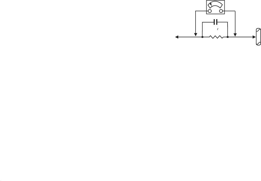
MONITOR SAFFTY GUIDELINES FOR THE PROFESSIONAL SERVICE TECHNICIAN
Safety Checks
Fire and Shock Hazard
leads,
or damaged insulation ( including the ac cord).Be certain to
remove
loose solder balls and all other loose foreign particles.
4. Check across-the-line components and other components for
physical
evidence of damage or deterioration and replace if necessary.
Follow
original layout,lead length, and dress.
5. No lead or component should touch a receiving tube or a resistor
rated
at 1 watt or more. Lead tension around protruding metal surfaces
or
edges must be avoided.
6. Critical components having special safety characteristics are
identified
with ans by the Ref. No. in the parts list and enclosed within a
broken line
* (where several critical components are grouped in one area)
along with
the safety symbols on the schematic diagrams and/or exploded
views.
7. When servicing any unit, always use a separate isolation
transformer
for the chassis Failure to use a separate isolation transformer may
expose you to possible shock hazard, and may cause damage to
servicing instruments.
8. Many electronic products use a polarized ac line cord (one wide
pin on
the plug.) Defeating this safety feature may create a potential
hazard to
the service and the user. Extension cords which do not
incorporate the
polarizing feature should never be used.
9. After reassembly of the unit, always perform an leakage test or
resistance
test from the line cord to all exposed metal parts of the cabinet.
Also check
all metal control shafts(with knobs removed), antenna terminals,
handles,
screws, etc. to be sure the unit may be safety operated without
danger o
After the original service problem has been corrected,a complete
safety check
shouldbemade.Besuretocheckovertheentireset,notjust the
areas
where you have worked. Somepreviousservicermayhaveleftan
unsafe
condition,which could be unknowingly passed on to your customer.
Be sure
tocheckallofthefollowing:
1. Be sure all components are positioned in such a way as to avoid
the
possibility of adjacent component shorts. Thisisespecially
important
onthosechassiswhicharetransportedtoandfromtheservice
shop.
2.Neverreleasearepairedunitunlessallprotectivedevicessuchas
insulators, barries, covers, strain reliefs, and other hardware
have been
installed in accordance with the original design.
3.Solderingandwiringmustbeinspectedtolocatepossiblecold
solder
joints,solder splashes,sharp solder points, frayed leads, pinched
f
electrical shock.
WARNING : Before removing the CRT anode cap, turn the unit OFF and short the HIGH VOLTAGE to the CRT DAG ground.
SERVICE NOTE : The CRT DAG is not at chassis ground.
6. New picture tubes are specifically designed to withstand higher
operathng
voltages without creating undesirable X-radiation. It is strongly
recommended that any shop test fixture which is to be used with
the new
higher voltage chassis be equipped with one of the new type
tubes
designed for this service. Addition of a permanently connected
HV meter
to the shop test fixture is advisable. The CRT types used in these
new
sets should never be replaced with any other types, as this may
result in
excessive X-radiation.
7. It is essential to use the specified picture tube to avoid a possible
X-diation
problem.
8. Most TV receivers contain some type of emergency "Hold Down"
circuit to
prevent HV from rising to excessive levels in the presence of a
failure
mode. These various circuits should be understood by all
technicians
servicing them, especially since many hold down circuits are
inoperative
as long as the receiver performs normally.
Leakage Current Cold Check
1. Unplug the ac line cord and connect a jumper between the two
prongs of
the plug.
2.Turn on the power switch.
3.Measure the resistance value between the jumpered ac plug and
all
exposed cabinet parts of the receiver, such as screw heads,
antennas,
and control shafts. When the exposed metallic part has a return
path to
the chassis, the reading should be between 1 megohm and 5.2
megohms.
When the exposed metal does not have a return path to the
chassis, the
reading must be infinity. Remove the jumper from the ac line cord.
Leakage Current Hot Check
1. Donotuseanisolationtransformerforthistest.Plug the
completely
reassembled receiver directly into the ac outlet.
2.Connect a 1.5k, 10w resistor paralleled by a 0.15uf. capacitor
between
each exposed metallic cabinet part and a good earth ground
such as a
waterpipe,asshownabove.
3.Useanacvoltmeterwithatleast5000 ohms volt sensitivity to
measure
the potential across the resistor.
4. The potential at any point should not exceed 0.75 volts. A
leakage current
1500 ohm, 10W
0.15 uFWATER
PIPE
EARTH
GROUND
TO
INSTRUMENTS
EXPOSED
METAL PARTS
