171820 001 I SBC432 100 Processor Board Hardware Reference Manual Feb81
171820-001_iSBC432-100_Processor_Board_Hardware_Reference_Manual_Feb81 171820-001_iSBC432-100_Processor_Board_Hardware_Reference_Manual_Feb81
User Manual: manual pdf -FilePursuit
Open the PDF directly: View PDF ![]() .
.
Page Count: 70
inter
iSBC
432/100™
Processor
Board
Hardware
Reference
Manual
PN
171820-001
I I
11
I
iSBC
432/100™
PROCESSOR
BOARD
HARDWARE REFERENCE MANUAL
Manual Order Number:
171820-001
Copyright©
1981
Intel Corporation
Intel Corporation,
3065
Bowers Avenue, Santa Clara, California
95051
11
11
I
ii
Additional copies
of
this manual or other Intel literature may
be
obtained from:
Literature Department
Intel Corporation
3065
Bowers Avenue
Santa Clara, CA
95051
The information
in
this document
is
subject to change without notice.
Intel Corporation makes no warranty
of
any kind with regard to this material. including, but not limited
to, the implied warranties
of
merchantability and fitness for a particular purpose. lniel Corporation
assume<,
no responsibility for any errors that may appear
in
this document. Intel Corporation
make~
no
-:ommitment to update nor to keep current the information contained
in
this document.
Intel Corporation assumes no responsibility for the use
of
any circuicry other than circuitry embodied
in
an Intel product. No other circuit patent licenses are implied.
Intel software products are copyrighted
by
and shall remain the property
of
Intel Corporation. Lse,
duplication or disclosure
is
subject to restrictions stated
in
Intel's software license, or as defined
in
ASPR
7-104.9(a)(9).
No
part of this document may
be
copied or reproduced
in
any form or
by
any means without the prior
written consent of Intel Corporation.
The follo,,ing are trademarks of Intel Corporation and its affiliate' and may
be
used only to identify Intel
products:
BXP
lntde1i,ion
\luliihu'
CRI
DIT
Intel
le.:
\lultimoduk
iR~I\
Plu~-A.-Buhhlf
IC!:-
iSHC
PRO\IPT
iCS iSHX
Prol1l\\arc
I
ihrrir'.··
\h1naL~er
R\1\
~o
\1CS
~htcn,
~non
lrPt'i
\1egd~·ha\.."1i\
LJl'I
inr
el
\licrnnwr
~score
and the combination
of
ICE. iCS. iR\1X. iSBC. iSBX, l\1CS. or R\1X and a numerical suffix.
PREFACE
This
manual
contains general information, installation, programming information,
and principles
of
operation
for the Intel iSBC
432/
100 Processor Board. Additional
hardware/
architectural information pertaining to the iSBC
432/
100
board
is
available in the following documents:
•
iAPX
432 General Data Processor Architecture Reference Manual, Order No.
171860-001.
• Intel
8251
Universal Synchronous/ Asynchronous Receiver/Transmitter,
Appiication
Note
AP-i6.
• Intel Multibus Specification, Order No 9800683.
• Intel Multibus Interfacing, Application Note AP-28.
Introductory
iAPX
432 information, if required,
is
contained
in
the following
documents:
• The
iAP
X 432 Object Primer, Order No. 171858-001.
• Introduction to the
iAPX
432 Architecture, Order No. 171821-001.
• GettingStartedontheintellec432/JOO,
OrderNo.171819-001.
• Object Builder User's Guide,
Order
No. 171859-001.
• Object Programming Language User's Manual, Order No. 171823-001.
iii

.
~
n
CHAPTER 1
GENERAL
INFORMATION
PAGE
Introduction . . . . . . . . . . . . . . . . . . . . . . . . . . . . . . . . . .
l-1
Description . . . . . . . . . . . . . . . . . . . . . . . . . . . . . . . . . . .
l-l
Equipment Supplied . . . . . . . . . . . . . . . . . . . . . . . . . . . l-2
Equipment Required . . . . . . . . . . . . . . . .
..
. . . . . . . . . . l-2
Specifications . . . . . . . . . . . . . . . . . . . . . . . . . . . . . . . . . !-2
CHAPTER2
PREPARATION
FOR
USE
Introduction . . . . . . . . . . . . . . . . . . . . . . . . . . . . . . . . . . 2-l
Unpacking and Inspection . . . . . . . . . . . . . . . . . . . . . .
2-1
Installation Considerations . . . . . . . . . . . . . . . . . . . . . 2-l
User Furnished Components . . . . . . . . . . . . . . . . . . . .
2-2
Power Requirements . . . . . . . . . . . . . . . . . . . . . . . . . . .
2-2
Cooling Requirements . . . . . . . . . . . . . . . . . . . . . . . . .
2-2
Physical Dimensions . . . . . . . . . . . . . . . . . . . . . . . . . . .
2-2
Jumper Configuration . . . . . . . . . . . . . . . . . . . . . . . . .
2-2
1/0
Access . . . . . . . . . . . . . . . . . . . . . . . . . . . . . . . . . . .
2-3
Multibus
Bus
Access . . . . . . . . . . . . . . . . . . . . . . . . . . .
2-4
Multibus
Bus
Configuration . . . . . . . . . . . . . . . . . . . .
2-4
Signal Characteristics . . . . . . . . . . . . . . . . . . . . . . . . . .
2-4
Serial Priority Resolution . . . . . . . . . . . . . . . . . . . . . . .
2-4
Parallel Priority Resolution
.....................
2-l l
Serial
1/0
Cabling . . . . . . . . . . . . . . . . . . . . . . . . . . . . .
2-11
Board Installation . . . . . . . . . . . . . . . . . . . . . . . . . . . . .
2-12
CHAPTER3
PROGRAMMING
INFORMATION
Introduction . . . . . . . . . . . . . . . . . . . . . . . . . . . . . . . . . . 3-l
Memory Addressing and Access . . . . . . . . . . . . . . . . .
3-1
1/0
Addressing and Access . . . . . . . . . . . . . . . . . . . . .
3-1
Initialization . . . . . . . . . . . . . . . . . . . . . . . . . . . . . . . . . 3-l
8251A USART Programming . . . . . . . . . . . . . . . . . . .
3-1
Mode Instruction Format . . . . . . . . . . . . . . . . . . . . .
3-1
Sync Characters . . . . . . . . . . . . . . . . . . . . . . . . . . . . .
3-4
Command Instruction Format . . . . . . . . . . . . . . . . .
3-4
Reset . . . . . . . . . . . . . . . . . . . . . . . . . . . . . . . . . . . . . .
3-4
Addressing . . . . . . . . . . . . . . . . . . . . . . . . . . . . . . . . .
3-4
Initialization . . . . . . . . . . . . . . . . . . . . . . . . . . . . . . .
3-4
CONTENTS
PAGE
Operation . . . . . . . . . . . . . . . . . . . . . . . . . . . . . . . . . . . .
3-5
Data Input/Output . . . . . . . . . . . . . . . . . . . . . . . . . .
3-5
Status Read . . . . . . . . . . . . . . . . . . . . . . . . . . . . . . . .
3-5
8253A PIT Programming . . . . . . . . . . . . . . . . . . . . . . .
3-5
Mode Control Word and Count . . . . . . . . . . . . . . .
3-6
Addressing . . . . . . . . . . . . . . . . . . . . . . . . . . . . . . . . .
3-8
Initialization . . . . . . . . . . . . . . . . . . . . . . . . . . . . . . .
3-8
Operation . . . . . . . . . . . . . . . . . . . . . . . . . . . . . . . . . . . .
3-9
Counter Read . . . . . . . . . . . . . . . . . . . . . . . . . . . . . . .
3-9
Clock Frequency/Divide Ratio Selection . . . . . . . .
3-9
Synchronous Mode
........................
3-9
Asynchronous Mode
.......................
3-9
iSBC
432/
100
Control and Status Registers . . . . . . . .
3-10
CHAPTER4
PRINCIPLES
OF
OPERATION
Introduction . . . . . . . . . . . . . . . . . . . . . . . . . . . . . . . . . .
4-1
Functional Description . . . . . . . . . . . . . . . . . . . . . . . . . 4-l
Clock Generation . . . . . . . . . . . . . . . . . . . . . . . . . . .
4-2
iAPX
432
Processor . . . . . . . . . . . . . . . . . . . . . . . . .
4-2
Address Generation . . . . . . . . . . . . . . . . . . . . . . . . .
4-3
Data Transfer State Machine . . . . . . . . . . . . . . . . . .
4-4
Multibus Interface . . . . . . . . . . . . . . . . . . . . . . . . . . .
4-7
Interval Timer . . . . . . . . . . . . . . . . . . . . . . . . . . . . . .
4-7
Serial
1/0
. . . . . . . . . . . . . . . . . . . . . . . . . . . . . . . . . .
4-7
Parallel
1/0
. . . . . . . . . . . . . . . . . . . . . . . . . . . . . . . .
4-7
Circuit Analysis . . . . . . . . . . . . . . . . . . . . . . . . . . . . . . .
4-8
Initialization . . . . . . . . . . . . . . . . . . . . . . . . . . . . . . .
4-8
Clock Generation . . . . . . . . . . . . . . . . . . . . . . . . . . .
4-8
iAPX
432
General Data Processor . . . . . . . . . . . . .
4-8
Address Generation . . . . . . . . . . . . . . . . . . . . . . . . .
4-8
Data Transfer State Machine . . . . . . . . . . . . . . . . . .
4-8
Multibus Interface
...........................
4-11
1/0
Operation
..............................
4-14
CHAPTERS
REFERENCE
INFORMATION
Introduction . . . . . . . . . . . . . . . . . . . . . . . . . . . . . . . . . .
5-1
Replaceable Parts . . . . . . . . . . . . . . . . . . . . . . . . . . . . .
5-1
Schematic and Parts Location Diagrams . . . . . . . . . .
5-1
Service and Repair Assistance . . . . . . . . . . . . . . . . . . .
5-1
v
TABLE
1-1
2-1
2-2
2-3
2-4
2-5
2-6
2-7
FIGURE
1-1
2-1
2-2
2-3
2-4
3-1
3-2
3-3
3-4
3-5
3-6
3-7
3-8
vi
TITLE PAGE
iSBC
432/
100
Specifications . . . . . . . . . . . .
1-2
Connector Details . . . . . . . . . . . . . . . . . . . . .
2-1
Jumper Selectable Options . . . . . . . . . . . . . .
2-2
Multibus Connector P 1 Pin Assignments . .
2-5
Multibus Signal Functions
-.
. . . . . . . . . . . . .
2-6
iSBC
432/
100
DC
Characteristics . . . . . . . .
2-7
iSBC
432/
100
AC
Characteristics
(Master Mode) . . . . . . . . . . . . . . . . . . . . . .
2-8
iSBC
432/
100
l/O
Access
AC
Characteristics . . . . . . . . . . . . . . . . . .
2-8
TITLE PAGE
iSBC
432/
100
Processor Board
Bus
Exchange Timing (Master Mode)
....
.
I/O
Access Timing (Read/Write)
.......
.
Serial Priority Resolution Scheme
.......
.
Parallel Priority Resolution Scheme
.....
.
USART Synchronous Mode Instruction
Word Format
......................
.
USART Synchronous Mode Transmission
Format
...........................
.
USART Asynchronous Mode Instruction
Word Format
......................
.
USART Asynchronous Mode Transmission
Format
...........................
.
USART Command Instruction Word
Format
...........................
.
Typical USART Initialization and Data
I/O
Sequence
......................
.
USART Status Read Format
PIT Mode Control Word Format
.......
.
1-1
2-9
2-10
2-10
2-11
3-3
3-3
3-3
3-3
3-4
3-5
3-6
3-7
TABLE
2-8
2-9
3-1
3-2
5-1
5-2
TABLES
TITLE
PAGE
Serial
l/O
Connector J 1 Pin Assignments
2-12
Connector J 1
vs
RS-232-C Pin
Correspondence . . . . . . . . . . . . . . . . . . . . . 2-12
iSBC
432/
100
l/O
Address Assignments . .
3-2
PIT Count Value vs. Rate Multiplier for
Each Baud Rate . . . . . . . . . . . . . . . . . . . . . 3-10
Replaceable Parts . . . . . . . . . . . . . . . . . . . . .
5-2
List of Manufacturers' Codes . . . . . . . . . . .
5-3
ILLUSTRATIONS
FIGURE
TITLE
PAGE
3-9
3-10
4-1
4-2
4-3
4-4
4-5
4-6
4-7
4-8
4-9
5-1
5-2
PIT Programming Sequence Examples
3-8
PIT Counter Register Latch Control Word
Format . . . . . . . . . . . . . . . . . . . . . . . . . . . .
3-9
iSBC
432/
100
Processor Board Functional
Areas . . . . . . . . . . . . . . . . . . . . . . . . . . . . . .
4-2
iSBC 4321100 Processor Board Block
Diagram . . . . . . . . . . . . . . . . . . . . . . . . . . .
4-3
Two-Phase Overlapped Processor Clock . .
4-3
24-Bit Processor Physical Address to 20-Bit
Multibus Address Conversion . . . . . . . . .
4-4
iSBC
432/
100
Data Transfer Routing
to/from
the Multibus Bus . . . . . . . . . . . .
4-5
Typical Processor Write Cycle Timing . . . .
4-9
Typical Processor Read Cycle Timing . . . .
4-9
Eight--Bit Transfer Specification Opcode
..
4-10
Data Tran sf er State Machine State
Diagram . . . . . . . . . . . . . . . . . . . . . . . . . . .
4-12
iSBC
432/100 Parts Location Diagram . . .
5-5
Schematic Diagram . . . . . . . . . . . . . . . . . . . .
5-
7
1.1
INTRODUCTION
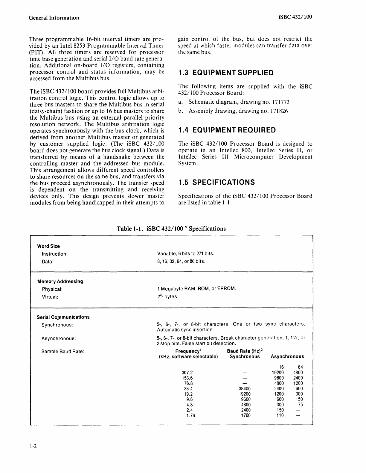
The
iSBC
432/100
Processor
Board
is
a Multibus-
compatible
implementation
of
the
iAPX
432 Micro-
mainframe,
a 32-bit VLSI microprocessor. This
board
is
designed
to
operate
as a Multibus master in
Intellec
microcomputer
systems.
The
iSBC 432/100
board
contains
an
iAPX
432 microprocessor, a serial
communications
interface,
programmable
timers,
Multibus
control
logic,
and
bus expansion drivers for
interfacing with
other
Multibus-compatible
boards.
1.2 DESCRIPTION
The iSBC
432/
100 Processor Board (figure 1-1)
is
controlled by
an
iAPX
432 General
Data
Processor
(GDP).
The
GDP
consists
of
two VLSI components:
the 43201
Instruction
Decode Unit
and
the 43202
Instruction Execution Unit.
The
GDP's
instruction
set supports a wide range
of
data
addressing modes
and
data
manipulation
operations, as well as highly
efficient
and
secure protection mechanisms.
The
iSBC 432/100
board
accesses the Multibus system
bus for all
memory
and
1/0
operations.
CHAPTER 1
GENERAL INFORMATION
An
RS-232-C
compatible
serial 110
port,
controlled
by an Intel 8251A
USART
(Universal
Synchronous/
Asynchronous Receiver
/Transmitter),
operates with
standard
CRT
terminals
at
baud
rates from 110 to
19.2K
bits/second.
The
USART
is
individually pro-
grammable for
operation
in many synchronous
and
asynchronous serial
data
transmission
formats
(including IBM Bi-sync). In operation, most
transmission characteristics (e.g., character length,
parity,
and
baud
rate) are
programmable.
In
both
the
synchronous
and
asynchronous
modes,
the serial 110
port
features half-
or
full-duplex,
double
buffered
transmit
and
receive capability. In
addition,
USART
error
detection circuits can check
for parity,
overrun,
and
framing errors.
The
USART
transmit
and
receive clocks are supplied by a
programmable
baud
rate
generator.
The
RS-232-C
control lines, serial
data
lines,
and
signal
ground
lines
are
brought
out
to a 26-pin edge connector (in the
upper right
corner
of
the
board)
that
mates with flat
or
round
cable
(through
a
standard
board
edge
connector).
Figure 1-1. iSBC
432/
1
OO'M
Processor Board
171820-1
1-1
General Information
Three
programmable
16-bit interval timers are pro-
vided by
an
Intel 8253
Programmable
Interval Timer
(PIT). All three timers are reserved for processor
time base generation
and
serial
I/O
baud
rate genera-
tion. Additional
on-board
l/O
registers, containing
processor control
and
status information, may be
accessed from the Multibus bus.
The
iSBC 432/100
board
provides full Multibus arbi-
tration
control
logic. This control logic allows up to
three bus masters to share the Multibus bus in serial
(daisy-chain) fashion
or
up
to
16
bus masters
to
share
the Multibus bus using
an
external parallel priority
resolution network.
The
Multibus
aribtration
logic
operates synchronously with the bus clock, which
is
derived from
another
Multibus master
or
generated
by customer supplied logic. (The iSBC 432/100
board
does
not
generate the bus clock signal.)
Data
is
transferred by means
of
a handshake between the
controlling master
and
the addressed bus module.
This arrangement allows different speed controllers
to share resources
on
the same bus,
and
transfers via
the bus proceed asynchronously. The transfer speed
is
dependent
on
the transmitting
and
receiving
devices only. This design prevents slower master
modules from being handicapped in their attempts to
iSBC 432/100
gain control
of
the bus,
but
does not restrict the
speed
at
which faster modules can transfer
data
over
the same bus.
1.3 EQUIPMENT SUPPLIED
The following items are supplied with the iSBC
432/
100
Processor Board:
a. Schematic diagram, drawing no. 171773
b. Assembly drawing, drawing no. 171826
1.4 EQUIPMENT REQUIRED
The iSBC
432/
100 Processor Board
is
designed to
operate in
an
Intellec 800, Intellec Series II, or
Intellec Series III Microcomputer Development
System.
1.5
SPECIFICATIONS
Specifications
of
the iSBC
432/
100
Processor Board
are listed in table 1-1.
Table 1-1. iSBC 432/100™ Specifications
Word Size
Instruction:
Variable, 6 bits
to
271
bits.
Data:
8,
16,
32,
64,
or
80
bits.
Memory
Addressing
Physical: 1
Megabyte
RAM, ROM,
or
EPROM.
Virtual: 2
40
bytes
Serial
Cojllmunications
Synchronous:
5-,
6-,
7-,
or
8-bit characters. One
or
two
sync
characters.
Automatic sync
insertion.
Asynchronous:
5-,
6-,
7-,
or
8-bit characters. Break
character
generation.
1,
11/2,
or
2
stop
bits. False start bit
detection.
Sample Baud Rate:
Frequency
1 Baud Rate (Hz)2
(kHz,
software
selectable)
Synchronous
Asynchronous
16
64
307.2
-
19200
4800
153.6
-
9600
2400
76.8
-
4800
1200
38.4
38400
2400
600
19.2
19200
1200
300
9.6
9600
600
150
4.8
4800
300
75
2.4
2400
150
-
1.76
1760
110 -
1-2
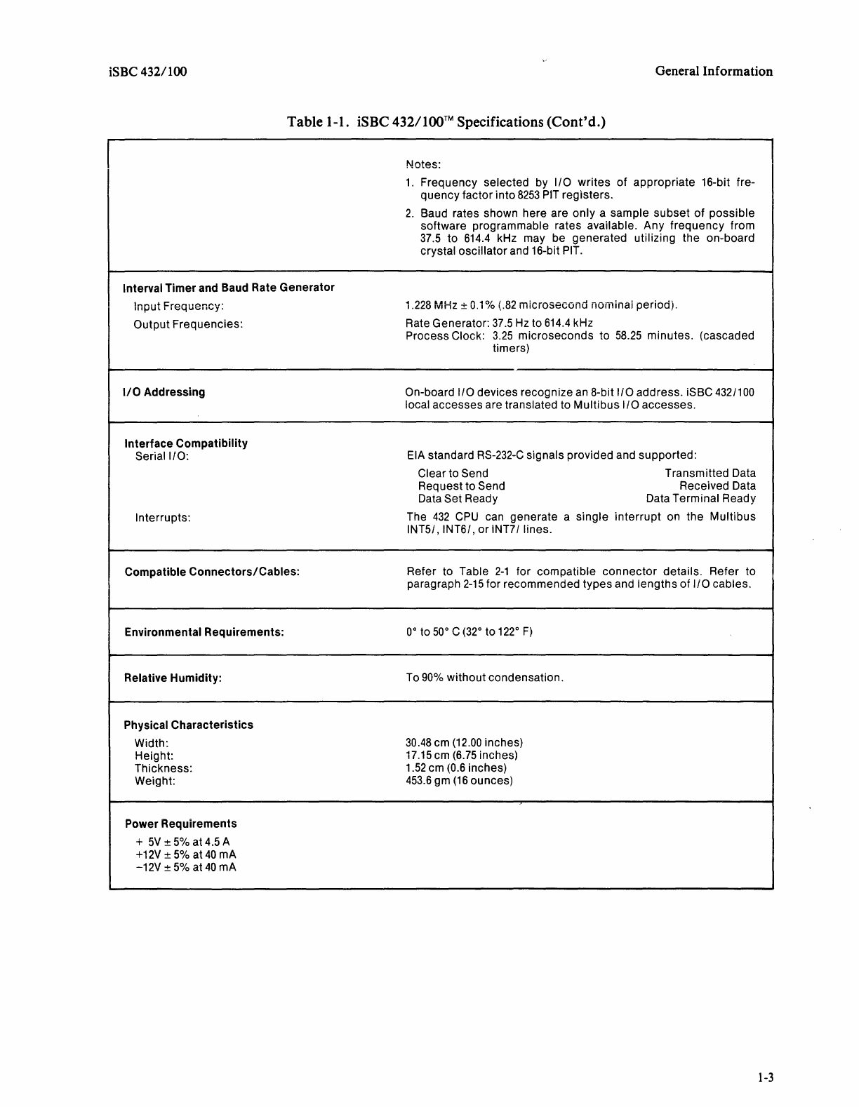
iSBC 432/100 General Information
Table 1-1. iSBC 432/100™ Specifications
(Cont'd.)
Interval Timer and Baud Rate Generator
Output Frequencies:
1/0
Addressing
Interface Compatibility
Serial 1/0:
Interrupts:
Compatible
Connectors/Cables:
Environmental Requirements:
Relative Humidity:
Physical Characteristics
Width:
Height:
Thickness:
Weight:
Power Requirements
+
5V
5%
at
4.5
A
+12V
5%
at
40
mA
-12V
5%
at
40
mA
Notes.
1.
Frequency selected by 1/0 writes of appropriate 16-bit fre-
quency factor into
8253
PIT
registers.
2.
Baud rates shown here are only a sample subset
of
possible
software programmable rates available. Any frequency from
37.5
to
614.4
kHz may be generated utilizing the on-board
crystal oscillator and 16-bit
PIT.
1.228
MHz±
0.1%
(.82
micmsecond nominai period).
Rate Generator:
37.5
Hz
to
614.4
kHz
Process Clock:
3.25
microseconds to
58.25
minutes. (cascaded
timers)
On-board 1/0 devices recognize
an
8-bit 1/0 address. iSBC
432/100
local accesses are translated to Multibus 1/0 accesses.
EIA
standard
RS-232-C
signals provided and supported:
Clear to Send
Request to Send
Data Set Ready
Transmitted Data
Received Data
Data Terminal Ready
The
432
CPU
can generate a single interrupt on the Multibus
INT5/, INT6/, or INT7/ lines.
Refer to Table
2-1
for compatible connector details. Refer to
paragraph
2-15
for recommended types and lengths of 1/0 cables.
0°
to
50°
C
(32°
to
122°
F)
To
90%
without condensation.
30.48
cm
(12.00
inches)
17.15
cm
(6.75
inches)
1.52
cm
(0.6
inches)
453.6
gm
(16
ounces)
1-3

2.1
INTRODUCTION
This
chapter
provides instructions
for
configuring
the iSBC
432/
100
Processor
Board
for
operation
in a
user-defined
environment.
It
is
advisable
that
the
contents
of
Chapters
1
and
3 be fully
understood
before
beginning the
configuration
and
installation
procedures described in this
chapter.
2.2
UNPACKING
AND
INSPECTION
Inspect the shipping
carton
immediately
upon
receipt
for evidence
of
mishandling
during
transit.
If
the
shipping
carton
is
severely
damaged
or
waterstained,
request
that
the
carrier's
agent
be present when the
carton
is
opened.
If
the
carrier's
agent
is
not
present
when the
carton
is
opened
and
the contents
of
the
carton
are
damaged,
keep the
carton
and
packing
material
for
the
agent's
inspection.
CHAPTER 2
PREPARATION
FOR
USE
For
repairs
to
a
product
damaged
in shipment, refer
to the
customer
letter
contained
in
the
shipping car-
ton.
It
is
suggested
that
salvageable shipping
cartons
and
packing
material
be
saved
for
future use in the
event the
product
must
be
reshipped.
2.3 INSTALLATION
CONSIDERATIONS
The
iSBC
432/
100
board
is
designed for use as a bus
master in
an
lntellec 800, Intellec Series II,
or
Intellec
Series III
Microcomputer
Development System.
Important
criteria
for
installing
and
interfacing the
iSBC
432/
100
board
in
this
configuration
are
presented in the following
paragraphs.
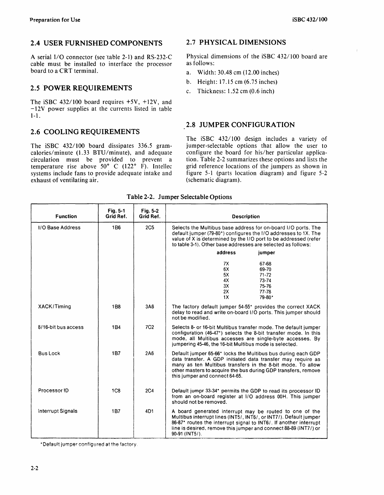
Table 2-1. Connector Details
No.
of
Pairs/
Centers
Connector
Intel®
Function
Pins
(inches)
Type
Vendor
Vendor
Part
No.
Part
No.
Serial 13/26
0.1
Flat
Crimp
3M
3462-0001
iSBC
955
1/0 AMP
88106-1
Cable
Connector
ANSLEY
609-2615
Set
SAE SD6726 SERIES
Serial 13/26
0.1
Soldered
Tl
H312113
N/A
1/0 AMP 1-583485-5
Connector
Serial 13/26
0.1
Wirewrap1
Tl
H311113
N/A
1/0
Connector
Multibus
43/86 0.156 Soldered1
CDC3
VPB01E43DOOA1
N/A
Connector
MICRO PLASTICS M P-0156-43-BW-4
ARCO AE443WP1 LESS EARS
VIKING 2VH43/1AV5
Multibus
43/86 0.156
Wirewrap
1,2
CDC3
VFB01E43DOOA1
or
MDS 985*
Connector
CDC3
VP
801E43AOOA1
VIKING 2VH43/1AV5
NOTES:
1.
Connector heights are not guaranteed to conform to
OEM
packaging requirements.
2.
Wirewrap
pin
lengths
are
not
guaranteed
to
conform
to
OEM
packaging
requirements.
3.
CDC
VPB01
... , VPB02 ... , VP804 ... , etc. are
identical
connectors
with
different
electroplating
thickness
or
metal
surfaces.
*"MOS"
is an
ordering
code
only,
and is
not
used
as a
product
name
or
trademark.
MDS® is a
registered
trademark
of
Mohawk
Data
Sciences
Corp.
2-1
:Preparation for Use
2.4
USER
FURNISHED
COMPONENTS
A serial
1/0
connector (see ·table 2-1)
and
RS-232-C
cable
must
be installed to interface the processor
board
to a
CRT
terminal.
2.5
.POWER
REQUIREMENTS
The
iSBC
432/
100
board
requires +5V, + l 2V, and
- l
2V
power supplies
at
the currents listed
in
table
1-1.
2.6
COOLING
REQUIREMENTS
The iSBC 432/100
board
dissipates 336.5 gram-
calories/minute
(1.33
BTU/minute),
and
adequate
circulation must be provided to prevent a
temperature rise above 50° C (122° F). Intellec
systems include fans to provide adequate intake and
exhaust
of
ventilating air.
iSBC 432/100
2.7
PHYSICAL
DIMENSIONS
Physical dimensions
of
the iSBC
432/
100
board
are
as follows:
a. Width: 30.48 cm (12.00 inches)
b. Height:
17
.15 cm (6.
75
inches)
c. Thickness: 1.52 cm (0.6 inch)
2.8
JUMPER
CONFIGURATION
The iSBC
432/
100 design includes a variety
of
jumper-selectable options
that
allow the user to
configure the
board
for
his/her
particular applica-
tion. Table 2-2 summarizes these options
and
lists the
grid reference locations
of
the
jumpers
as shown
in
figure
5-1
(parts location diagram)
and
figure 5-2
(schematic diagram).
Table 2-2. Jumper Selectable Options
Fig.
5-1
Fig.
5-2
Function
Grid Ref. Grid Ref. Description
1/0
Base Address
1B6
2C5
Selects the Multibus base address for on-board
1/0
ports. The
default jumper
(79-80*)
configures the
110
addresses to
1X.
The
value of X is
determined
by the
1/0
port to be addressed (refer
to table
3-1
).
Other base addresses are selected as follows:
address
jumper
7X
67-68
6X
69-70
5X
71-72
4X
73-74
3X
75-76
2X
77-78
1X
79-80*
XACK/Timing
1B8
3A6
The factory default
jumper
54-55*
provides the
correct
XACK
delay to read and write on-board
1/0
ports. This
jumper
should
not be modified.
8/16-bit bus access
1B4
7C2
Selects
8-
or 16-bit Multibus transfer mode. The default
jumper
configuration
(46-47*)
selects the ·a-bit transfer mode.
In
this
I
mode, all Multibus accesses are single-byte accesses. By
jumpering
45-46,
the 16-bit Multibus mode is selected.
Bus Lock 187
2A6
Default jumper
65-66*
locks the Multibus bus during each
GDP
data transfer. A
GDP
initiated data transfer may require as
many as ten Multibus transfers in
the
8-bit mode. To allow
other masters
to
acquire the bus during GDP transfers, remove
this jumper and connect
64-65.
Processor
ID
1C8
2C4
Default jumpr
33-34*
permits the
GOP
to
read its
processor
ID
from
an
on-board register at
1/0
address
OOH.
This
jumper
should not be removed.
Interrupt Signals 1
B7
4D1
A board generated interrupt may be routed to one of the
Multibus interrupt lines (INT5/, INT6/,
or
INT?/). Default
jumper
J
86-87*
routes the interrupt signal to INT6/. If another
interrupt
line is desired. remove this jumper and connect
88-89
(INT?/)
or
90-91
(INT51).
-~
•Default jumper configured at the factory
2-2
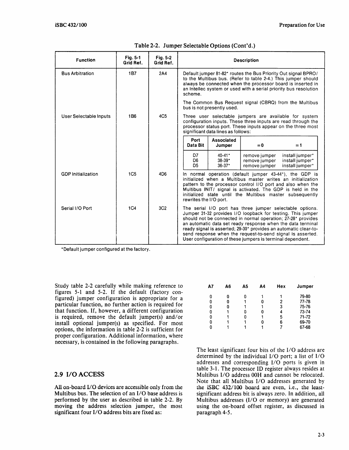
iSBC 432/100 Preparation for Use
Table 2-2.
Jumper
Selectable Options
(Cont'd.)
Function Fig.
5-1
I Fig.
5-2
I
Grid Ref. Grid Ref.
Bus Arbitration 1B7
2A4
User Selectable Inputs 1B6
4C5
GDP
Initialization
1C5
4D6
Serial
1/0
Port
1C4
3C2
*Default
jumper
configured at the factory.
Study table 2-2 carefully while making reference to
figures
5-1
and
5-2.
If
the
default
(factory con-
figured)
jumper
configuration
is
appropriate
for a
particular function, no further action
is
required for
that
function.
If,
however, a different configuration
is
required, remove the default jumper(s)
and/
or
install optional jumper(s) as specified.
For
most
options, the
information
in table 2-2
is
sufficient for
proper
configuration. Additional information, where
necessary,
is
contained in the following paragraphs.
2.9
1/0
ACCESS
All
on-board
1/0
devices
are
accessible only from the
Multibus bus.
The
selection
of
an
1/0
base address
is
performed by the user as described in table 2-2.
By
moving the address selection
jumper,
the most
significant
four
1/0
address bits are fixed as:
Description
Default
jumper
81-82*
routes the Bus Priority Out signal BPRO/
to the Multibus bus. (Refer to table
2-4.)
This
jumper
should
always be connected when the processor board is inserted in
an
lntellec system
or
used with a serial priority bus resolution
scheme.
The Common Bus Request signal (CBRQ) from the Multibus
bus is not presently used.
Three user selectable jumpers are available for system
confiQuration inputs. These three inputs are read throuqh the
processor status port. These inputs ·appear on the
three
most
significant data lines as follows:
Port Associated
Data Bit Jumper
=0
=1
07
40-41
* remove
jumper
install jumper*
06
38-39*
remove
jumper
install jumper*
05
36-37*
remove
jumper
install jumper*
In
normal operation (default
jumper
43-44*), the GDP is
initialized when a Multibus master writes
an
initialization
pattern to the processor control 1/0 port and also when the
Multibus INIT I signal is activated. The GDP is held in the
initialized state until the Multibus master subsequently
rewrites the
110
port.
The serial 1/0 port has three
jumper
selectable options.
Jumper
31-32
provides 1/0 loopback for testing. This
jumper
should not be connected
in
normal operation;
27-28*
provides
an
automatic data set ready response when the data terminal
ready signal is asserted;
29-30*
provides an automatic clear-to-
send response when the request-to-send signal is asserted.
User configuration
of
these jumpers is terminal dependent.
A7 A6
AS
A4
Hex Jumper
0 0 0 1 1
79-80
0 0 1 0 2
77-78
0 0 1 1 3
75-76
0 1 0 0 4
73-74
0 1 0 1 5
71-72
0 1 1 0 6
69-70
0 1 1 1 7
67-68
The least significant four bits
of
the
1/0
address are
determined by the individual
1/0
port; a list
of
1/0
addresses
and
corresponding
I/O
ports
is
given
in
table 3-1.
The
processor ID register always resides
at
Multibus
1/0
address
OOH
and
cannot
be relocated.
Note
that
all Multibus
1/0
addresses generated by
the iSBC 432/
100
board
are even, i.e., the least-
significant address bit
is
always zero. In addition, all
Multibus addresses (110
or
memory) are generated
using the
on-board
off
set register, as discussed
in
paragraph
4-5.
2-3
Preparation for Use
2.10 MULTIBUS BUS ACCESS
The iSBC
432/
100
board
contains no local memory.
All system memory resides
on
separate Multibus
modules. Both system
memory
and
all
1/0
ports
(including
1/0
ports contained
on
the processor
board) must be accessed via the Multibus bus. Each
GDP
access specifies either a local address
or
a
physical address (refer
to
the discussion in
Chapter
3). Local address requests are translated into
Multibus
1/0
commands; physical address requests
are translated into Multibus memory commands.
The iSBC
432/
100
board
is
designed to operate with
either 8-bit
or
16-bit memory modules. A user-
selectable
jumper
(table 2-2)
is
provided to select the
8-bit
or
16-bit Multibus transfer mode. (The
board
is
factory-configured to operate in the 8-bit mode.)
GDP
memory accesses may require the transfer
of
one to ten
data
bytes over the Multibus bus. In the
8-
bit mode, all
GDP
memory requests initiate a series
of
single-byte read
or
write accesses. In the 16-bit
mode, all
GDP
multibyte memory requests that
originate
on
even byte boundaries are satisfied by a
series
of
double-byte (16-bit) read
or
write accesses.
All
other
accesses are
performed
in the same manner
as are accesses in the 8-bit mode.
When operating with iSBC/MDS* 016
16K
RAM memory modules, the 8-bit mode must
be used. The 16-bit
mode
may be used with
iSBC/MDS
032/048/064
RAM memory
modules.
As mentioned earlier, a single
GDP
memory request
may require the transfer
of
ten
data
bytes over the
Multibus bus. In
order
to shorten the overall time
required for these
data
transfers, the bus may be
locked from the beginning
of
the first transfer until
the
GDP
memory transfer has been completed.
Locking the bus eliminates the time required to·
acquire
and
release the bus for each byte
data
transfer. This
"bus
lock"
feature, which results in
higher processor
throughput,
is
user selectable as
described in table 2-2. The processor
board
is
shipped
with the
"bus
lock"
feature enabled.
The bus lock provision
cannot
be enabled in
systems
with
double-density
diskette
controllers and 8-bit memory if the diskette
controller will operate simultaneously with
· the iSBC 432/100
board.
*"lllDS" is
an
ordering code only, and is not used
as
a
product name or trademark.
MOS®
is
a registered
trademark of Mohawk Data Sciences Corp.
2-4
iSBC 432/100
2.11 MULTIBUS BUS CONFIGURATION
For
system applications, the iSBC
432/
100
board
is
designed for installation in a
standard
Multibus
backplane (e.g.,
an
Intellec Microcomputer Develop-
ment System). Multibus signal characteristics and
methods
of
implementing a serial
or
parallel priority
resolution scheme for resolving bus contention in a
multiple bus master system are described in the
following paragraphs.
Always
turn
off
the system power supply
before installing
or
removing any
board
from the backplane. Failure to observe this
precaution can cause damage to the
board.
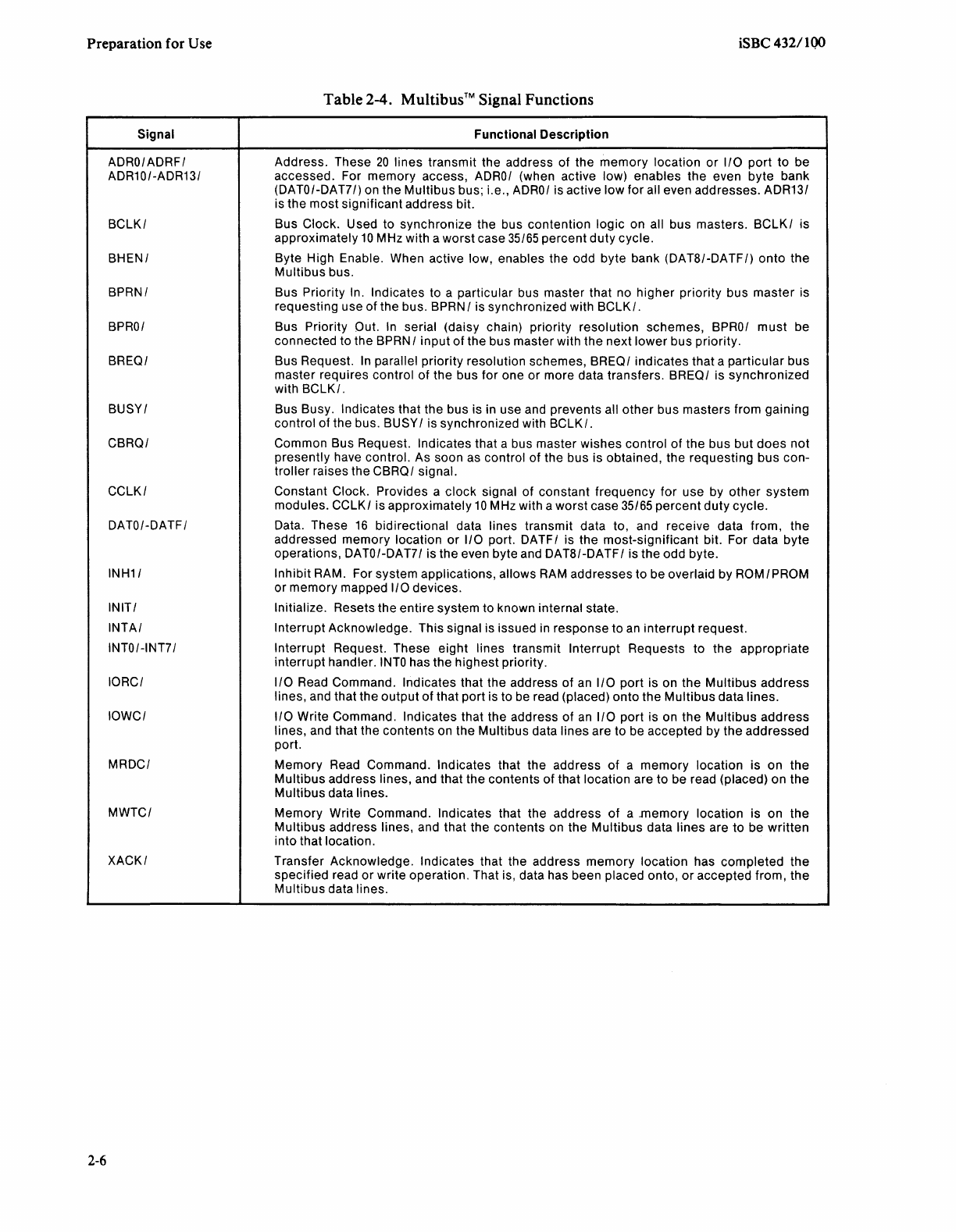
2.12 SIGNAL CHARACTERISTICS
As shown in figure 1-1, connector P 1 interfaces the
iSBC 432/100
board
to the Multibus bus. The pin
assignments for this 86-pin connector are listed in
table
2-3
and
descriptions
of
the signal functions are
provided in table 2-4.
The de characteristics
of
the iSBC
432/
100 bus inter-
face are provided in table 2-5. The ac characteristics
of
the iSBC
432/
100
board
when operating in the
master mode
and
slave mode are provided in tables
2-6
and
2-
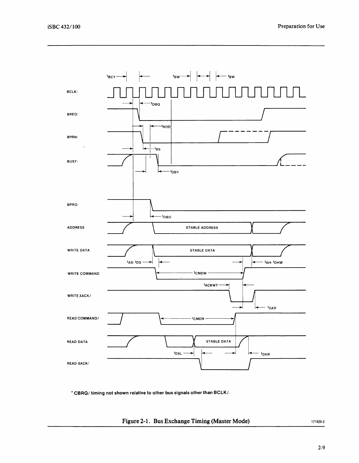
7, respectively. Bus exchange timing
diagrams are provided in figures
2-1
and 2-2.
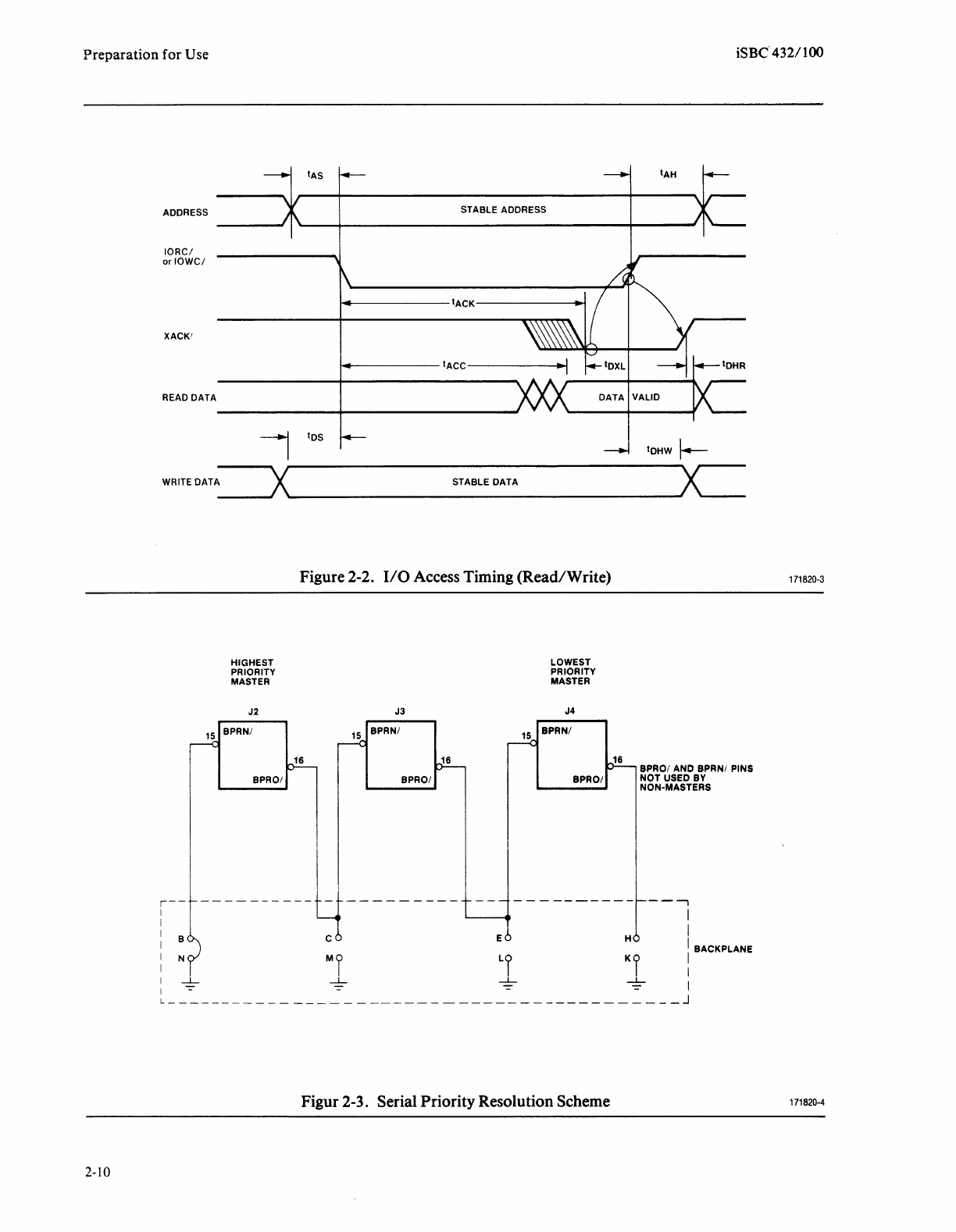
2.13 SERIAL PRIORITY RESOLUTION
In a multiple bus master system, bus contention can
be resolved by implementing a serial priority resolu-
tion scheme as shown in figure 2-3. Due to the prop-
agation delay
of
the
BPRO/
signal path, this scheme
is
limited to a maximum
of
three bus masters capable
of
acquiring
and
controlling the Multibus bus. In the
configuration shown in figure 2-3, the bus master
installed in slot J2 has the highest priority
and
is
able
to acquire control
of
the bus
at
any time because its
BPRN/
input
is
always enabled (tied to ground).
If
the bus master in slot J2 desires control
of
the
Multibus bus, it drives its BPRO/
output
high
and
inhibits the
BPRN/
input
to all lower-priority bus
masters. When finished using the bus, the J2 bus
master pulls its
BPRO/
output
low
and
gives the
J3
bus master the
opportunity
to
take control
of
the
bus.
If
the J3 bus master does
not
desire to control
the bus
at
this time, it pulls its
BPRO/
output
low
and gives the lowest priority bus master in slot J4 the
opportunity to assume control
of
the bus.
iSBC 4321100 Preparation for Use
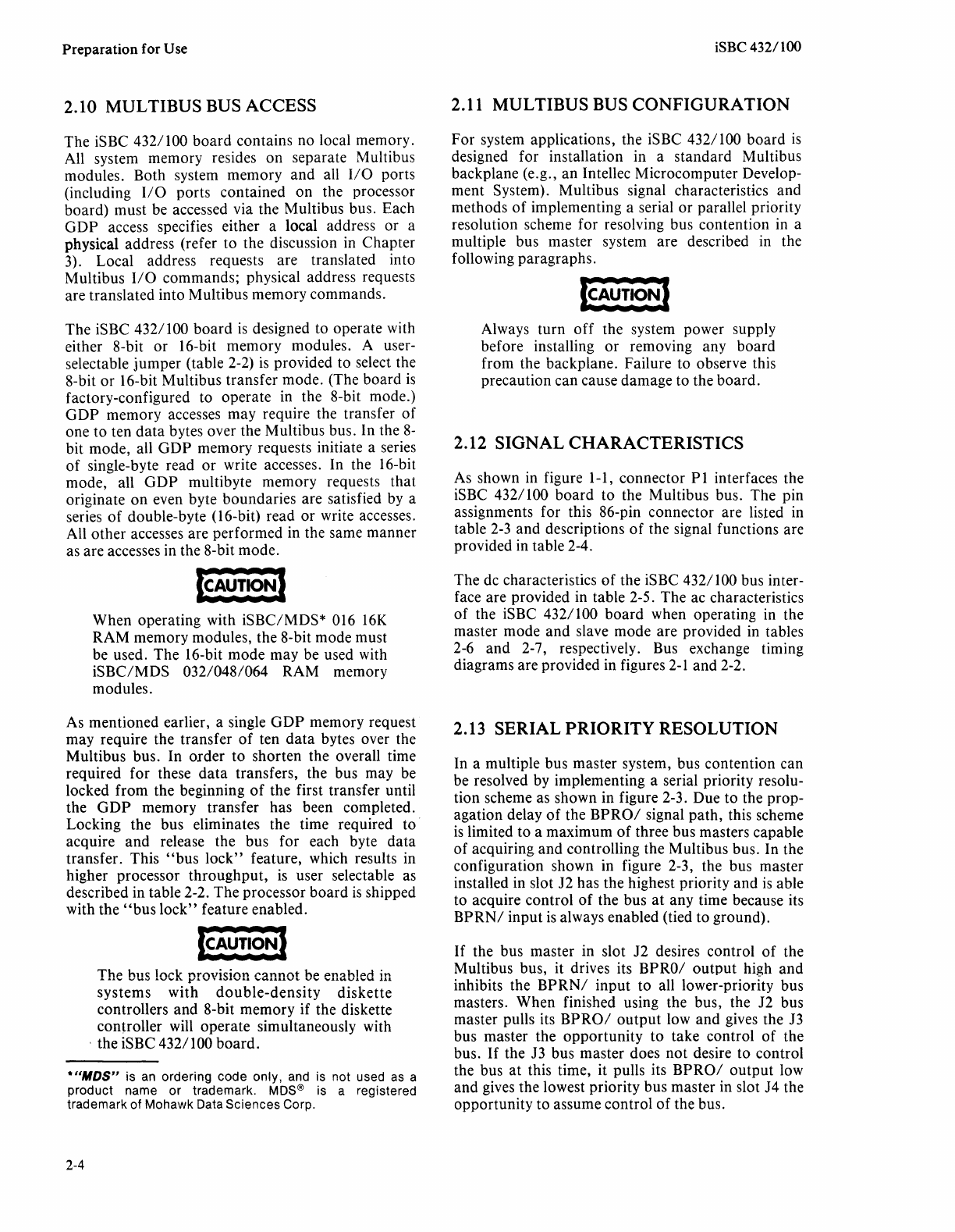
Table 2-3. Multibus™ Connector
Pl
Pin
Assignments
Pin* Signal Function Pin* Signal
Function
1 I GND \
AA
ADRF/ \
I 1
Ground
....
2 GND
45
ADRC/
3 +5V
46
ADRD/
4 +5V
47
ADRA/
5 +5V
48
ADRB/
6 +5V
Power
input
49
ADR8/
7 +12V
50
ADR9/
8 +12V
51
ADR6/
Address
bus
9
-5V
52
ADR7/
10
-5V
53
ADR4/
11
GND
l
Ground
54
ADR5/
1"1
I
GND
I
r::r::
ADR2/
1£.
,
.J.J
13
BCLK/
Bus
Clock
56
ADR3/
14
INIT/
System
Initialize
57
AORO/
15
BPRN/
Bus
Priority
In
58
ADR1i
16
BPRO/
Bus
Priority
Out
59
DATE/
17
BUSY/
Bus
Busy
60
DATF/
18
BREQ/
Bus
Request
61
DATC/
19
MRDC/
Memory
Read
Command
62
DATO/
20
MWTC/
Memory
Write
Command
63
DATA/
21
IORC/
1/0 Read
Command
64
DATB/
22
IOWC/
1/0
Write
Command
65
OATS/
23
XACK/
Transfer
Acknowledge
66
DAT9/ Data
Bus
24
INH1/
Inhibit
RAM
67
DAT6/
25
68
DAT?/
26
69
DAT4/
27
BHEN/
Byte
High
Enable
70
DAT5/
28
ADR10/
Address
bus
bit
10
71
DAT2/
29
CBRQ/
Common
Bus
Request
72
DAT3/
30
AOR11
/
Address
bus
bit
11
73
DATO/
31
CCLK/
Constant
Clock
74
DAT1/
32
ADR12/
Address
bus
bit
12
75
GND }
Ground
33
INTA/
Interrupt
Acknowledge
76
GND
34
ADR13/
Address
bus
bit
13
77
35
INT6/
Interrupt
request
on
levern
78
36
INT?/
Interrupt
request
on
level 7
79
-12V
37
INT4/
Interrupt
request
on
level 4
80
-12V
38
INT5/
Interrupt
request
on
level 5
81
+5V
Power
input
39
INT2/
Interrupt
request
on
level 2
82
+5V
40
INT3/
Interrupt
request
on
level 3
83
+5V
41
INTO/
Interrupt
request
on level 0
84
+5V
42
INT1 I
Interrupt
request
on level 1
85
GND }
Ground
43
ADRE/
86
GND
*All
odd-numbered
pins
(1,3,5 ...
85)
are
on
component
side
of
the
board. Pin 1 is
the
left-most
pin
when
viewed
from
the
component
side
of
the
board
with
the
extractors
at
the
top. All
unassigned
pins
are
reserved.
2-5
Preparation for Use
iSBC
432/lQO
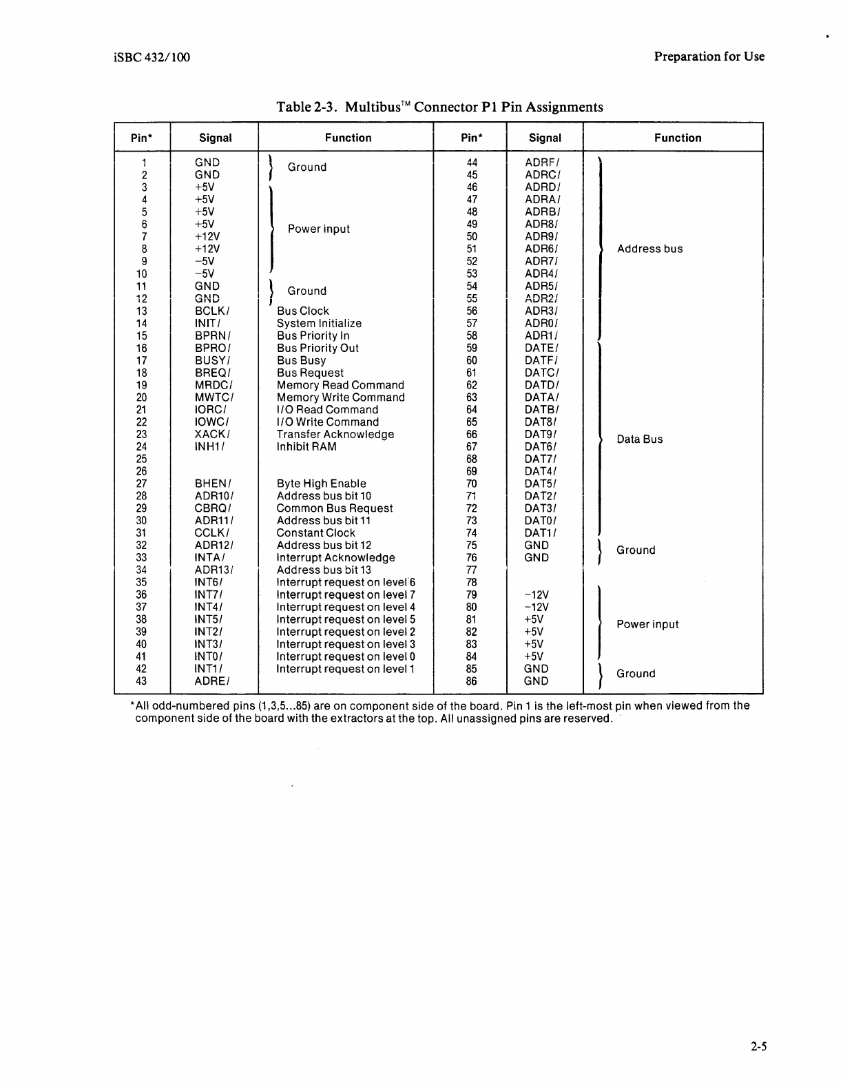
Table 2-4. Multibus™ Signal Functions
Signal Functional Description
ADRO/ADRF/ Address. These
20
lines transmit the address of the memory location
or
1/0 port to be
AOR10/-ADR13/ accessed. For memory access,
ADRO/
(when active low) enables the even byte bank
(DATO/-DAT71) on the Multibus bus; i.e.,
ADRO/
is active low for all even addresses. ADR13/
is the most significant address bit.
BCLK/ Bus Clock. Used to synchronize the bus contention logic on all bus masters. BCLK/ is
approximately
10
MHz with a worst case 35/65 percent duty cycle.
BHENI Byte High Enable. When active low, enables the odd byte bank (DAT8/-DATFI) onto the
Multibus bus.
BPRN/ Bus Priority In. Indicates to a particular bus master that no higher priority bus master is
requesting use of the bus. BPRN I is synchronized with BCLK/.
BPRO/
Bus Priority Out.
In
serial (daisy chain) priority resolution schemes,
BPRO/
must be
connected to the
BPRN
I input of the bus master with the next lower bus priority.
BREQ/ Bus Request.
In
parallel priority resolution schemes, BREQ/ indicates that a particular bus
master requires control of the bus for one or more data transfers. BREQ/ is synchronized
with BCLK/.
BUSY/ Bus Busy. Indicates that the bus is in use and prevents all
other
bus masters from gaining
control of the bus. BUSY I is synchronized with BCLK/.
CBRQ/ Common Bus Request. Indicates that a bus master wishes control of the bus but does not
presently have control. As soon
as
control of the bus is obtained, the requesting bus con-
troller raises the CBRQ/ signal.
CCLK/ Constant Clock. Provides a clock signal of constant frequency for use by other system
modules. CCLK/ is approximately
10
MHz with a worst case 35/65 percent duty cycle.
DATO/-DATF/ Data. These
16
bidirectional data lines transmit data to, and receive data from, the
addressed memory location
or
1/0 port. DATF/ is the most-significant bit. For data byte
operations, DATO/-DAT7/ is the even byte and DAT8/-DATF
I is the odd byte.
INH1/ Inhibit RAM. For system applications, allows
RAM
addresses to be overlaid by
ROM
I PROM
or memory mapped 1/0 devices.
INIT/ Initialize. Resets the entire system to known internal state.
INTA/ Interrupt Acknowledge. This signal is issued in response to
an
interrupt request.
INTO/-INT7 / Interrupt Request. These eight lines transmit Interrupt Requests to the appropriate
interrupt handler.
INTO
has the highest priority.
IORC/ 1/0 Read Command. Indicates that the address of
an
1/0 port is on the Multibus address
lines, and that the output of that port is to
be
read (placed) onto the Multibus data lines.
IOWC/ 1/0 Write Command. Indicates that the address of
an
1/0 port is on the Multibus address
lines, and that the contents on the Multibus data lines are to be accepted by the addressed
port.
MRDC/ Memory Read Command. Indicates that the address of a memory location is on the
Multibus address lines, and that the contents of that location are to be read (placed) on the
Multibus data lines.
MWTC/ Memory Write Command. Indicates that the address of a
memory
location is on the
Multibus address lines, and that the contents on the Multibus data lines are to be written
into that location.
XACK/ Transfer Acknowledge. Indicates that the address memory location has completed the
specified read
or
write operation. That is, data has been placed onto,
or
accepted from, the
Multibus data lines.
2-6
iSBC 432/100 Preparation for Use
Table 2-5. iSBC 432/100™ DC Characteristics
r l
Parameter
l
Test
I l
Signals
Symbol
Description
Conditions
Min. Max.
Units
XACK/
Vol
Output
Low Voltage t0L
=16
mA
0.4
v
VoH
Output
High Voltage t0H
=-2.6
mA
2.4
v
VIL
Input
Low
Voltage
0.8
v
VIH
Input High Voltage
2.0
v
Ill
Input
Current
at Low V
VIN
=0.4V
-0.4
mA
llH
Input
Current
at High V
VIN
=2.7V
20
µA
ADRO/-ADRF/
Vol
Output
Low
Voltage t0L
=32
mA
0.45
v
ADR10/-ADR13/ VoH
Output
High Voltage loH
=-5
mA
2.4
v
BHENi VIL
input
Low Voltage
0.8
v
VIH
Input High Voltage
2.0
v
Ill
Input
Current
at Low V
VIN
=0.45V
-2.2
mA
llH
Input
Current
at High V
VIN
=2.7V
100
µA
ILH
Output
Leakage High v0 =5.25V
50
µA
1
LL
Output
Leakage Low v 0 =0.45V
-50
µA
BCLK/
VIL Input Low Voltage
0.8
v
VIH
Input High Voltage
2.0
v
1
1L
Input
Current
at
Low
V
VIN
=0.45V
-0.5
mA
llH
Input
Current
at High V
VIN
=5.5V
60
µA
CCLK VIL Input Low Voltage
.8
v
VIH
Input High Voltage
2.0
v
1
1L
Input
Current
at Low V
VIN
=0.4V
-0.4
mA
llH
Input
Current
at High V
VIN
=2.7V
20
µA
BPRN/
VIL
Input Low Voltage
0.8
v
VIH
Input High Voltage
2.0
v
Ill
Input
Current
at Low V
VIN
=0.45V
-0.5
mA
llH
Input
Current
at High V
VIN
=5.5V
60
µA
BPRO/ ,BREQ/
Vol
Output
Low
Voltage
loL
=10
mA
0.45
v
VoH
Output
High Voltage loH
=-0.4
mA
2.4
v
BUSY/
,CBRQ/,
Vol
Output
Low Voltage
loL
=20
mA
0.45
v
(OPEN COLLECTOR)
DATO/-DATF/
Vol
Output
Low Voltage loL
=32
mA
0.45
v
VoH
Output
High Voltage loH
=-5
mA
2.4
v
VIL
Input
Low Voltage
0.90
v
VIH
Input High Voltage
2.0
v
Ill
Input
Current
at Low V
VIN
=0.45V -0.80 mA
llH
Output
Leakage High v0 =5.25V
200
µA
INIT/ VIL Input Low Voltage
0.8
v
(SYSTEM RESET)
VIH
Input High Voltage
2.0
v
Ill
Input
Current
at Low V
VIN
=0.4V
-0.9
mA
llH
Input
Current
at High V
VIN
=2.4V
80
µA
INT5/-INT7/
Vol
Output
Low
Voltage
loL
=16
mA
0.4
v
IORC/ ,IOWC/
Vol
Output
Low Voltage loL
=32
mA
0.5
v
VoH
Output
High Voltage t0H
=-5
mA
2.4
v
ILH
Output
Leakage High V0=5.25V
100
µA
I ILL
Output
Leakage Low
Vo
=0.4V -100
µA
I
VIL
Input
Low Voltage
.8
v
VIH
Input
High Voltage
2.0
v
Ill
Input
Current
at
Low
V
VIN
=.4V
-.4
mA
llH
Input
Current
at High V
VIN
=2.7V
20
µA
MRDC/ ,MWTC/
Vol
Output
Low Voltage t0L
=32
mA
0.5
v
VoH
Output
High Voltage loH
=-5
mA
2.4
v
ILH
Output
Leakage High v0 =5.25V
100
µA
ILL
Output
Leakage
Low
v0 =.4V -100
µA
2-7
Preparation for Use iSBC 432/100
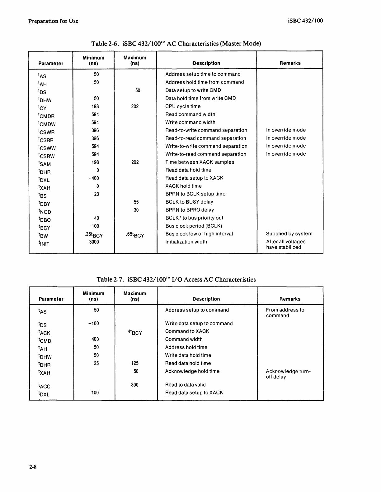
Table 2-6. iSBC 432/100™ AC Characteristics (Master Mode)
Minimum Maximum
Parameter (ns) (ns) Description Remarks
tAS
50
Address setup time to command
tAH
50
Address hold time from command
tos
50
Data setup to write
GMO
toHW
50
Data hold time from write CMD
tcv
198
202
CPU
cycle time
tcMDR
594
Read command width
tcMDW
594
Write command width
tcswR
396
Read-to-write command separation
In
override mode
tcsRR
396
'Read-to-read command separation
In
override mode
tcsww
594
Write-to-write command separation
In
override mode
tcsRw
594
Write-to-read command separation
In
override mode
tsAM
198
202
Time between XACK samples
to
HR
0 Read data hold time
toxL
-400 Read data setup to XACK
txAH
0 XACK hold time
tBs
23
BPRN
to BCLK setup time
to
BY
55
BCLK to BUSY delay
tNOD
30
BPRN
to
BPRO
delay
to
Bo
40
BCLK I to bus priority out
tBcv
100
Bus clock period (BCLK)
tBw
.35tBcv .65tBcv Bus clock low
or
high interval Supplied by system
ti NIT
3000
Initialization width After all voltages
have stabilized
Table 2-7. iSBC
432/
100™
1/0
Access
AC
Characteristics
Minimum Maximum
Parameter (ns) (ns) Description Remarks
tAs
50
Address setup to command From address to
command
tos
-100 Write data setup to command
tACK 4
tBcv
Command to XACK
tcMO
400
Command width
tAH
50
Address hold time
toHW
50
Write data hold time
toHR
25
125
Read data hold time
txAH
50
Acknowledge hold time Acknowledge turn-
off delay
tACC
300
Read to data valid
toxL
100
Read data setup to XACK
2-8
iSBC 432/100
BCLK/
BREQ/
BPRN/
BUSY/
BPRO/
ADDRESS
WRITE
DATA
WRITE
COMMAND
WRITEXACK/
READ
COMMAND/
READ
DATA
READ
XACK/
1
acv---..j
I
'aw---1
H
r-
taw
Preparation for Use
I
tt~.J
--------------
~
tas
=7
_J
~1---------____,r(
___
_
l.--1DBY
~
l.:==1Dao
=7
\
STABLE
ADDRESS
~
(
=7
J
~TABLE
DATA
x T
IAS·
IDS
.____r-
____
--1____,i:==
'AH·
'DHW
\w
•
......_~~~~~tcMDw~~~~~-----4~~/r-----------
\'--__
__;.
____________
--'7
IACKWT\
u
__J
k-
txAH
STABLE
DATA
IDXL~
r-
---1
I
L.DHR
*
CBRQ/
timing
not
shown
relative
to
other
bus signals
other
than
BCLK/.
Figure 2-1. Bus Exchange Timing (Master Mode)
171820-2
2-9
Preparation
for Use
ADDRESS
IORC/
or
IOWC/
XACK1
READ DATA
WRITE DATA
I
x
HIGHEST
PRIORITY
MASTER
J2
15
BPRN/
r--
1
I
I B
I
I N
I
I
BPRO/
IAS
STABLE ADDRESS
IACK
IACC
tDs
STABLE DATA
Figure 2-2.
1/0
Access Timing (Read/Write)
J3
15
BPRN/
16 16
BPRO/
c E
LOWEST
PRIORITY
MASTER
J4
15
BPRN/
BPRO/
16
H
iSBC432/100
IAH
IOHW
~
x=
BPRO/ AND BPRN/ PINS
NOT USED BY
NON-MASTERS
---,
I
I
: BACKPLANE
I
I
171820-3
L_
-------
- - -
---
- - -
------
-
-----
--
------
- - - -
_j
Figur 2-3. Serial Priority Resolution Scheme
171820-4
2-10
iSBC 432/100
NO.
2
PRIORITY
J2
(NOTE
1)
15
BPRN/
18
BREQ/
N0.1
PRIORITY
(HIGHEST)
J3
(NOTE
1)
15
BPRN/
BREQ/
15
18
BUS
PRIORITY
RESOLVER
(NOTE
2)
7 p
R
'-----------<116
I
p 0
R
I 1
0
BREO/INPUTS
FROM MASTERS
IN BACKPLANE
0
5 R
I
4 T
y
E
2 N
c
1 0
D
0 E
R 2
I
T 3
y
NOTE: REFER TO TEXT REGARDING THE
DISABLING OF
BPRO/
OUTPUT.
Preparation
for Use
NO.
8
NO.
7
PRIORITY
PRIORITY
(LOWEST)
J4
JS
(NOTE
1) 15
(NOTE
1)
BPRN/ BPRN/
BREQ/
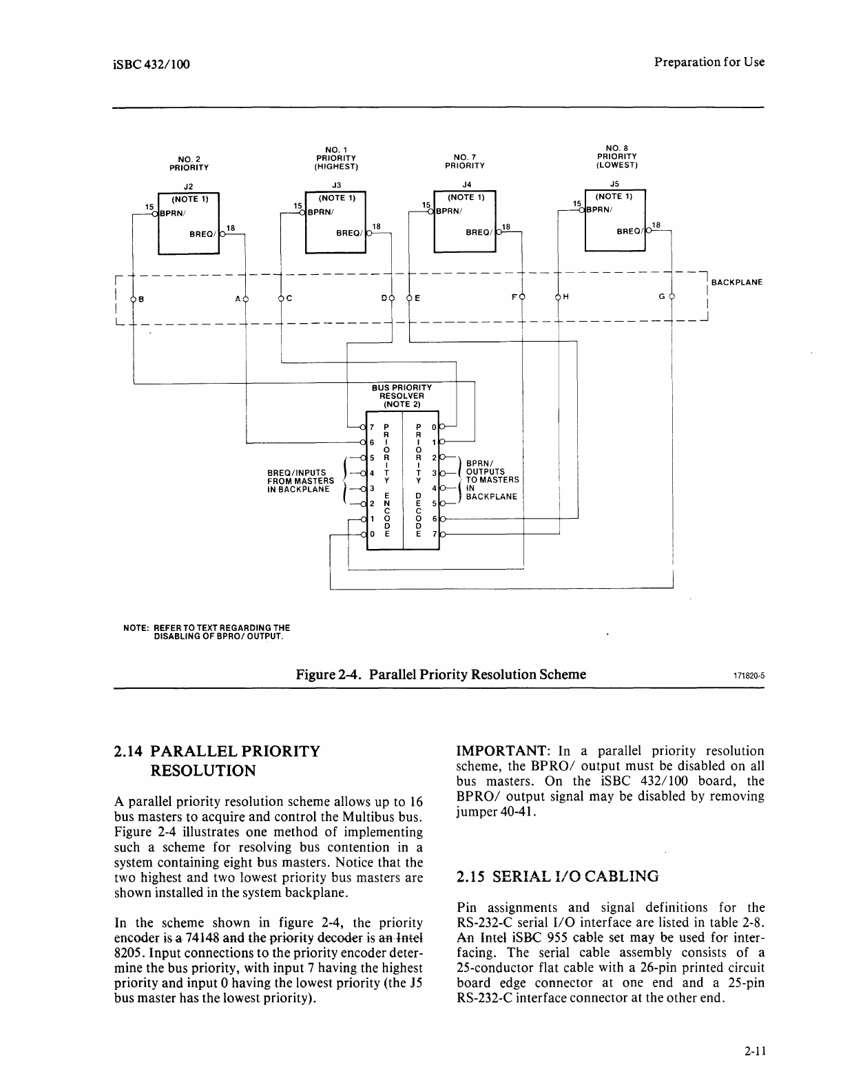
Figure 2-4. Parallel
Priority
Resolution Scheme 171820-5
2.14 PARALLEL PRIORITY
RESOLUTION
A parallel priority resolution scheme allows up to
16
bus masters
to
acquire
and
control the Multibus bus.
Figure 2-4 illustrates one
method
of
implementing
such a scheme for resolving bus contention in a
system containing eight bus masters. Notice
that
the
two highest
and
two lowest priority bus masters are
shown installed in the system backplane.
In the scheme shown in figure 2-4, the priority
encoder is a 7 4148
and
the priority decoder
is
an· Intel
8205.
Input
connections
to
the priority encoder deter-
mine the bus priority, with
input
7 having the highest
priority
and
input
0 having the lowest priority (the
15
bus master has the lowest priority).
IMPORTANT:
In a parallel priority resolution
scheme, the
BPRO/
output
must be disabled
on
all
bus masters.
On
the iSBC
432/
100
board,
the
BPRO/
output
signal may be disabled by removing
jumper
40-41.
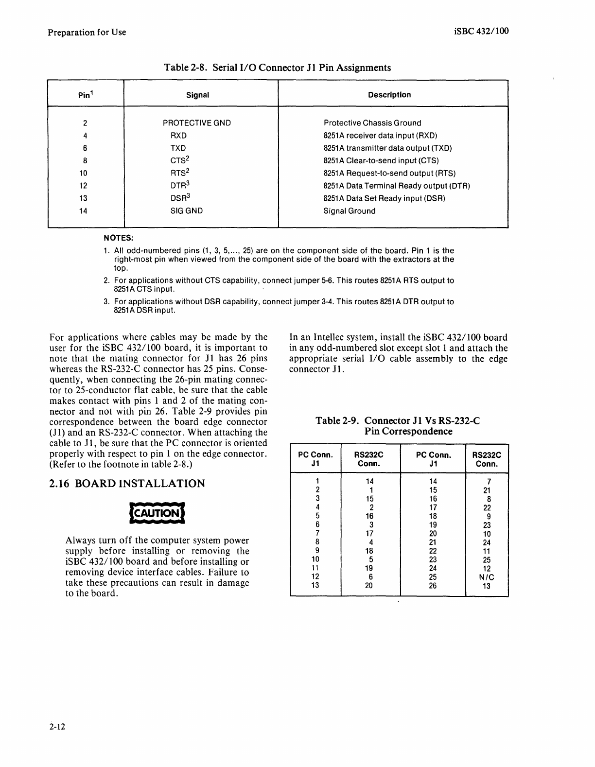
2.15 SERIAL
I/O
CABLING
Pin assignments
and
signal definitions for the
RS-232-C serial
1/0
interface are listed in table 2-8.
An Intel iSBC
955
cable set may
be
used for inter-
facing. The serial cable assembly consists
of
a
25-conductor flat cable with a 26-pin printed circuit
board
edge connector
at
one end and a 25-pin
RS-232-C interface connector
at
the other end.
2-11
Preparation
for Use iSBC 432/100
Pin1
2
4
6
8
10
12
13
14
Table 2-8. Serial
1/0
Connector
JI
Pin
Assignments
Signal Description
PROTECTIVE
GND
Protective Chassis Ground
RXD
8251A
receiver data input
(RXD)
TXD
8251A
transmitter data output
(TXD)
cTs
2
8251
A Clear-to-send input
(CTS)
RTs2
8251A
Request-to-send output
(RTS)
DTR
3
8251
A Data Terminal Ready output
(DTR)
DSR
3
8251A
Data Set Ready input
(DSR)
SIGGND Signal Ground
NOTES:
1.
All odd-numbered pins
(1,
3,
5,
... ,
25)
are
on
the component side of the board. Pin 1 is the
right-most pin when viewed from the component side of the board with the extractors at the
top.
2.
For applications without
CTS
capability, connect jumper
5-6.
This routes
8251A
RTS
output to
8251A
CTS
input.
3.
For applications without
DSR
capability, connect jumper
3-4.
This routes
8251A
DTR
output to
8251
A
DSR
input.
For applications where ,cables may be made by the
user for the iSBC
432/
100
board,
it
is
important to
note
that
the mating connector for J 1 has
26
pins
whereas the RS-232-C connector has
25
pins. Conse-
quently, when connecting the 26-pin mating connec-
tor to 25-conductor flat cable, be sure
that
the cable
makes contact with pins 1 and 2
of
the mating con-
nector
and
not
with pin 26. Table 2-9 provides pin
correspondence between the
board
edge connector
(JI)
and
an
RS-232-C connector. When attaching the
cable to
JI,
be sure
that
the
PC
connector
is
oriented
properly with respect to pin 1 on the edge connector.
(Refer to the footnote in table 2-8.)
In
an
Intellec system, install the iSBC 432/100
board
in any odd-numbered slot except slot I
and
attach the
appropfiate serial
1/0
cable assembly to the edge
connector
JI
.
2.16 BOARD INSTALLATION
2-12
Always
turn
off
the computer system power
supply before installing
or
removing the
iSBC
432/
100
board
and before installing
or
removing device interface cables. Failure to
take these precautions can result in damage
to the
board.
Table 2-9. Connector J 1
Vs
RS-232-C
Pin
Correspondence
PC
Conn.
RS232C
PC
Conn.
RS232C
J1
Conn.
J1
Conn.
1
14 14
7
2 1
15
21
3
15 16
8
4 2
17
22
5
16 18
9
6 3
19
23
7
17
20
10
8 4
21
24
9
18
22
11
10
5
23
25
11
19
24
12
12
6
25
N/C
13
20
26
13
CHAPTER 3
PROGRAMMING INFORMATION
3.1
INTRODUCTION
This chapter lists
1/0
address assignments, describes
the effects
of
hardware initialization, and provides
programming information for the Intel
8251
A
USART (Universal
Synchronous/
Asynchronous
Receiver/Transmitter), the Intel 8253
PIT
(Program-
mabie intervai Timer),
and
the on-board controi and
status registers.
A complete description
of
the Intel iAPX 432
General
Data
Processor
(GDP)-its
instruction set,
programming,
and
protection
mechanisms-may
be
found in the
iAPX
432 General Data Processor
Architecture Reference Manual,
Order
No.
171860-00
I.
3.2
MEMORY
ADDRESSING
AND ACCESS
The iSBC
432/
100 Processor Board contains no local
memory; all
GDP
memory accesses are processed
over the Multibus architecture.
GDP
physical
address references are translated into Multibus
memory
read/write
commands. Physical addresses
generated by the
GDP
are modified by an on-board
off
set register
to
permit an Intellec
or
iSBC system
processor to share Multibus memory with the iSBC
432/
100
processor.
When the
GDP
addresses memory (via the Multibus
bus) each
GDP
access request
is
implemented as one
or
more 8/16-bit Multihus
data
transfers. Memory
access mechanisms are described in detail beginning
in paragraph 4-4. Briefly, to perform Multibus
data
transfers, the iSBC
432/
100
board
must first gain
control
of
the bus.
After
addressing the correct
memory location
and
issuing a Memory Read
or
Memory Write
command,
the processor board waits
until a Transfer Acknowledge
(XACK/)
is
received
from the addressed memory module. When the
data
transfer
is
completed, the iSBC 432/100
board
releases the bus to permit
other
masters
to
use it.
When a
GDP
access request specifies a multibyte
data
transfer
that
must be translated into more
than
one Multibus transfer, a
"bus
lock"
feature permits
the processor
board
to
retain Multibus control for
the complete sequence
of
Multibus transfers. This
feature eliminates the time required to release
and
regain bus control between
data
transfers, thereby
increasing
throughput
and
lowering Multibus band-
width requirements.
3.3
1/0
ADDRESSING AND ACCESS
GDP
local address references are translated into
Multibus
1/0
read/write
commands. All
1/0
port
accesses (including accesses to on-board devices)
occur via the Multibus bus.
1/0
ports physically
located
on
the iSBC
432/
100 Processor Board are
logically situated
on
the bus.
Any
bus master may
access the
board's
1/0
ports (listed in table 3-1).
1/0
address generation
is
performed in the same manner
as memory address generation (described in
paragraph 4-5).
3.4 INITIALIZATION
The Multibus initialization signal line (INIT
/),
when
activated, resets the
GDP
and
causes the 8251A
USART
to
enter
an
"idle"
state waiting for a set
of
Command
Words to program the desired function.
The
8253
PIT
is
not
affected by the INIT I signal.
In addition to the
INIT
I reset sequence, another
Multibus master may reset the
GDP
by writing the
processor reset flag (contained within the processor
control
register-refer
to
table 3-1).
3.5 8251A USART
PROGRAMMING
The USART converts parallel
output
data
into a
serial
output
data
format
(e.g., IBM Bi-Sync) for
half-
or
full-duplex operation. The USART also con-
verts serial input
data
into parallel
data
format.
Prior
to the start
of
data
transmission
or
data
recep-
tion, the
USART
must be loaded with a set
of
control
words. These control words, which define the com-
plete functional operation
of
the USART, must
immediately follow a reset (internal
or
external).
The
control words are either Mode instructions
or
Command
instructions.
3.6 MODE INSTRUCTION FORMAT
The Mode instruction word defines the general
characteristics
of
the
USART
and
must follow a reset
operation. Once the
Mode
instruction word has been
3-1
Programming
Information
iSBC 432/100
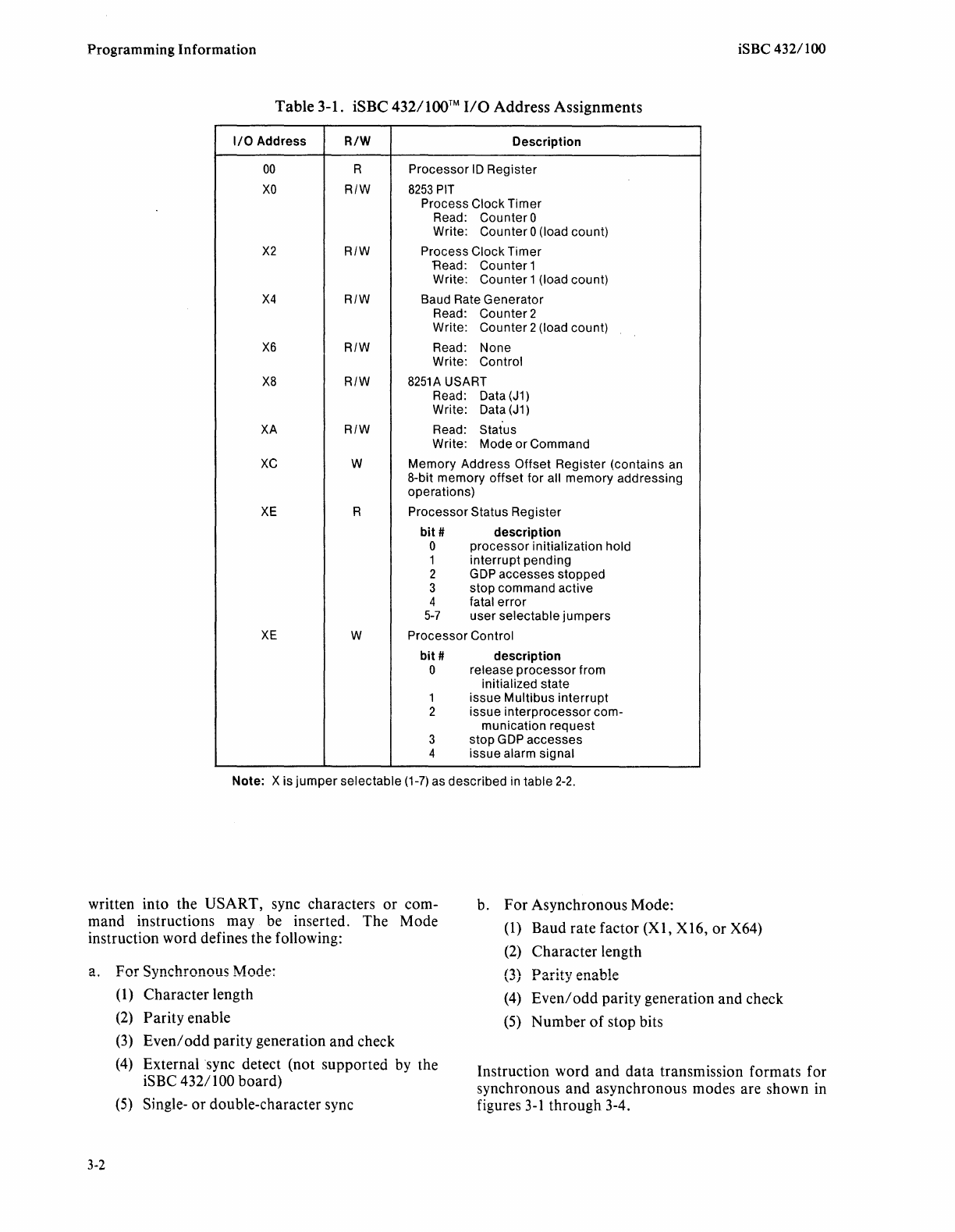
Table 3-1. iSBC
432/
100™
1/0
Address Assignments
1/0
Address
R/W
Description
00
R Processor
ID
Register
XO
R/W
8253
PIT
Process Clock Timer
Read: Counter 0
Write: Counter O (load count)
X2
R/W Process Clock Timer
'Read: Counter 1
Write: Counter 1 (load count)
X4
R/W Baud Rate Generator
Read: Counter 2
Write: Counter 2 (load count)
X6
R/W
Read: None
Write: Control
X8
R/W
8251A
USART
Read: Data (J1)
Write: Data (J1)
XA
R/W Read: Status
Write: Mode
or
Command
xc
w Memory Address Offset Register (contains
an
8-bit memory
offset
for all memory addressing
operations)
XE
R Processor Status Register
bit#
description
0
processor
initialization hold
1 interrupt pending
2
GDP
accesses stopped
3 stop command active
4 fatal error
5-7
user selectable
jumpers
XE
w Processor Control
bit#
description
0 release
processor
from
initialized state
1 issue Multibus
interrupt
2 issue
interprocessor
com-
munication request
3 stop
GDP
accesses
4 issue alarm signal
Note:
Xis
jumper
selectable
(1-7)
as described in table
2-2.
written into the
USART,
sync characters
or
com-
mand
instructions
may
be inserted.
The
Mode
instruction
word
defines the following:
b.
For
Asynchronous
Mode:
(1)
Baud
rate factor
(Xl,
X16,
or
X64)
(2)
Character
length
a.
For
Synchronous Mode:
(
1)
Character
length
3-2
(2)
Parity
enable
(3)
Even/
odd
parity generation
and
check
(4) External sync detect
(not
supported
by the
iSBC
432/100
board)
(5) Single-
or
double-character sync
(3)
Parity
enable
(4)
Even/odd
parity generation
and
check
(5)
Number
of
stop
bits
Instruction
word
and
data
transmission formats for
synchronous
and
asynchronous modes are shown in
figures
3-1
through
3-4.
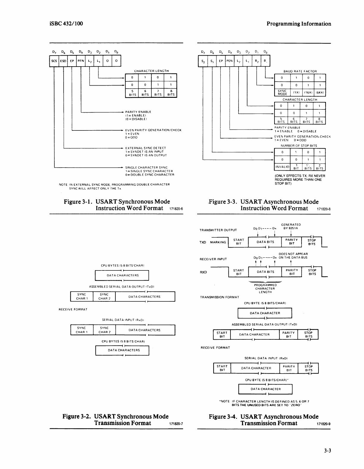
iSBC 432/100
CHARACTER
Lti'llGTH
0 1 0 1
0 0 1 1
5 6 7
a.
BITS BITS BITS
BITS
'----------
PARITY
ENABLE
11=ENABLEI
IO=DISABLEI
'------------
EVEN
PARITY
GENERATION/CHECK
1
=EVEN
0
=OOD
EXTERNAL
SYNC
DETECT
1 =
SYNDET
IS
AN
INPUT
O=SYNDET
IS AN
OUTPUT
SINGLE
CHARACTER
SYNC
l=SINGLE
SYNC
CHARACTER
O=
DOUBLE
SYNC
CHARACTER
NOTE IN
EXTERNAL
SYNC MODE.
PROGRAMMING
DOUBLE
CHARACTER
SYNC
WILL
AFFECT
ONLY
THE
Tx
Figure 3-1.
USART
Synchronous Mode
Instruction Word Format
111820-s
SYNC
CHAR
1
RECEIVE
FORMAT
SYNC
CHAR
1
CPU
BYTES
15
8
BITS'CHARI
DATA
CHARACH
RS
...._
____
..,.)
1--1
____
....
ASSEMBLED
SERIAL
DATA
OUTPUT
ITxDI
SYNC
CHAR
2
DAT
A c H
~JR~,_
A_c_T_E
_Rs
___
....
SERIAL
DATA
INPUT
iRxDI
SYNC
CHAR
2
DATA
CHARACTERS
CPU
BYTES
15
8 BITS
CHARI
DATA
CHl~l;ACTERS
Figure 3-2.
USART
Synchronous Mode
Transmission Format
111820-1
11
Programming Information
c
BAUD
RATE
FACTOR
0 1 0 1
0 0 1 1
SYNC
llXI
116XI 164XI
MODE
CHARACTER
LENGTH
0 1 0 1
0 0 1 1
s 6 7 8
BITS BITS BITS BITS
'----------
~~~l~~:L~ABLOE~
DISABLE
'------------
EVEN
PARITY
GENERATION.CHECK
1=EVEN
O•ODD
NUMBER
OF STOP BITS
0 1 0 1
0 0 1 1
INVALIO
1
,.
2
BIT
BITS
BITS
(ONLY EFFECTS
TX;
RX
NEVER
REQUIRES MORE THAN ONE
STOP BIT)
.Figure 3-3.
USART
Asynchronous Mode
Instruction Word Format
111820-8
GENERATED
TRANSMITTER
OUTPUT
Do
D1----Dx
BY
8251A
I
START
BIT
DATA
BITS
PARITY
BIT
ST~
BITS
L
RECEIVER
INPUT
DoD1----Dx
DOES NOT APPEAR
ON THE
DATA
BUS
RXD
---i
STARTT
~
i t
B~IT_Si"'----P-A-Rl_T_Y--S"""'T6;1
~
BIT
BITS
L
-,-
PROGRAMMED
CHARACTER
LENGTH
TRANSMISSION
FORMAT
START
BIT
CPU
BYTE
15
8
BITS/CHARI
DATA
C~~RACTER
ASSEMBLED
SERIAL
DATA
OUTPUT
ITxDI
DATA
CHARACTER
PARITY
BIT
BITS
STOD
.....
____
...._
___
......
_-!
RECEIVE
FORMAT
SERIAL
DATA
INPUT
IRxDI
.._s_T_~_~_T__..
___
D_A_TA_c_H-4ARA~-CT_E_R
__
..._P_A_:_1~_y__...__s
......
~~~
CPU
BYTE
15
8
BITS/CHARI"
: I
DATA
CHA~ACTER
'NOTE
IF
CHARACTER
LENGTH
IS
DEFINED
AS
5.
6 OR 7
BITS
T+tE
UNUSH>BHS
ARE SET TO
"lEAO"
Figure 3-4.
USART
Asynchronous Mode
Transmission Format
111820-e
3-3
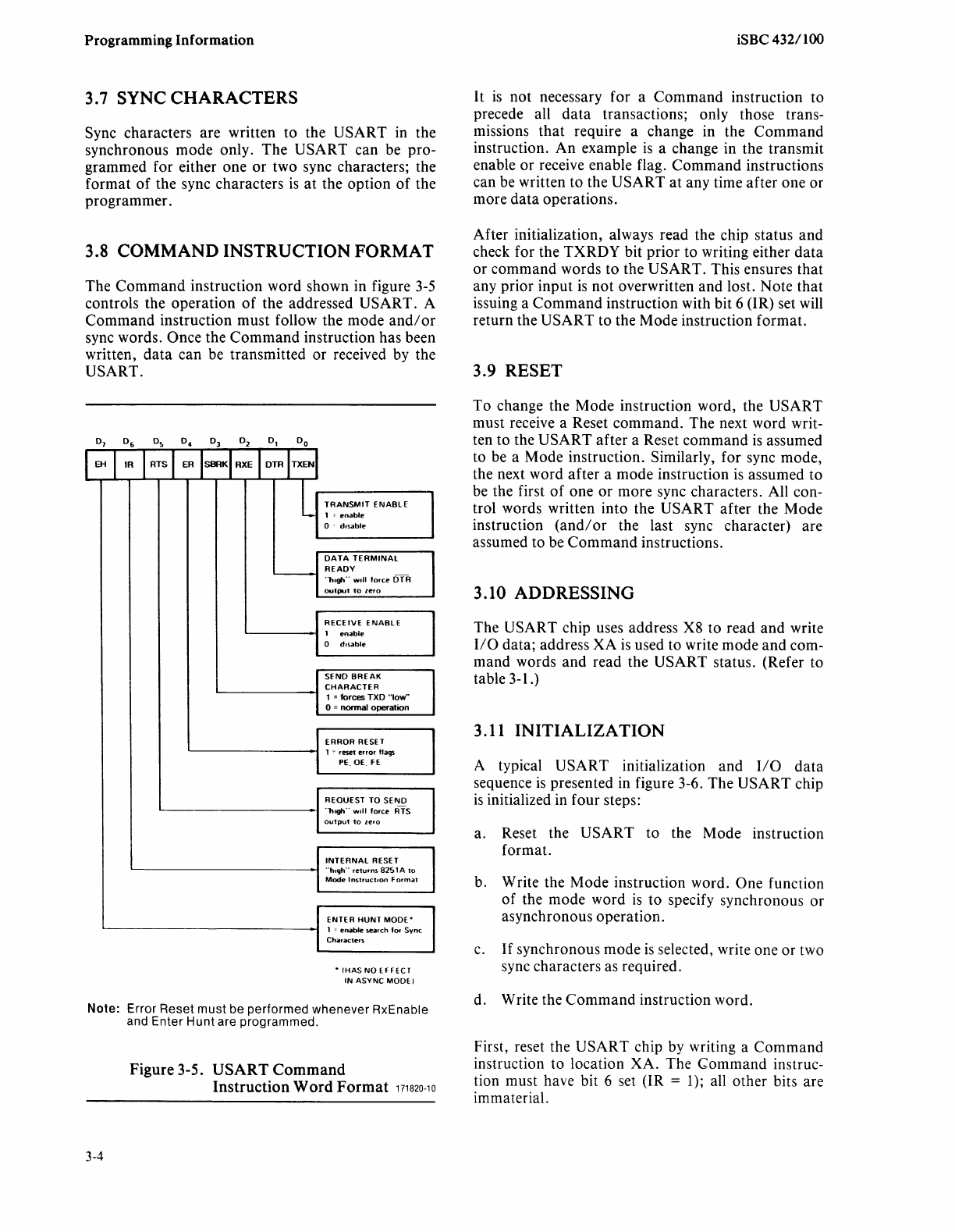
Programming Information
3.7 SYNC CHARACTERS
Sync characters are written to the USART in the
synchronous mode only.
The
USART can be pro-
grammed for either
one
or
two sync characters; the
format
of
the sync characters
is
at
the option
of
the
programmer.
3.8 COMMAND INSTRUCTION FORMAT
The
Command
instruction word shown in figure
3-5
controls the
operation
of
the addressed USART. A
Command
instruction
must
follow the mode
and/
or
sync words. Once the
Command
instruction has been
written,
data
can
be transmitted
or
received by the
USART.
~
EH
J
IR
I RTS l
ER
ISBRKI
RXEl
DTR
lTXEN
[
~
TRANSMIT
ENABLE
1 '
enable
0 ·
disable
DATA
TERMINAL
READY
..
high''
will
lorce
OTR
output
to
zero
RECEIVE
ENABLE
1
enable
0
disable
SEND
BREAK
CHARACTER
1 = forces
TXD
"low"
0 = normal
operation
ERROR
RESET
1 - reset
error
flags
PE. OE. FE
REQUEST
TO
SEND
-
"high"
will
force
ATS
output
to
lero
INTERNAL
RESET
''high"
returns
8251
A
to
Mode
Instruction
Format
ENTER HUNT
MODE•
1 °
enable
..,arch
lor
Sync
Characters
"IHASNOEFFECT
IN
ASYNC MOOE I
Note: Error Reset must be performed whenever RxEnable
and Enter Hunt are programmed.
Figure 3-5. USART Command
Instruction Word Format
111s20-10
3-4
iSBC 432/100
It
is
not
necessary for a
Command
instruction to
precede all
data
transactions; only those trans-
missions
that
require a change in the
Command
instruction.
An
example
is
a change in the transmit
enable
or
receive enable flag.
Command
instructions
can be written
to
the
USART
at
any time
after
one
or
more
data
operations.
After initialization, always read the chip status
and
check for the
TXRDY
bit
prior
to writing either
data
or
command
words to the USART. This ensures
that
any prior
input
is
not
overwritten
and
lost. Note
that
issuing a
Command
instruction with bit 6 (IR) set will
return the USART to the Mode instruction
format.
3.9 RESET
To
change the
Mode
instruction word, the USART
must receive a Reset
command.
The next word writ-
ten to the
USART
after
a Reset
command
is
assumed
to be a Mode instruction. Similarly, for sync mode,
the next word
after
a
mode
instruction
is
assumed
to
be the first
of
one
or
more sync characters. All con-
trol words written
into
the USART after the Mode
instruction
(and/
or
the last sync character) are
assumed to be
Command
instructions.
3.10 ADDRESSING
The USART chip uses address X8 to read
and
write
110
data; address
XA
is
used to write mode
and
com-
mand words
and
read the USART status. (Refer to
table 3-1.)
3
.11
INITIALIZATION
A typical
USART
initialization and
1/0
data
sequence
is
presented in figure 3-6. The USART chip
is
initialized in four steps:
a. Reset the
USART
to the Mode instruction
format.
b. Write the Mode instruction word. One function
of
the mode word
is
to specify synchronous
or
asynchronous operation.
c.
If
synchronous
mode
is
selected, write one
or
two
sync characters as required.
d. Write the
Command
instruction word.
First, reset the USART chip by writing a
Command
instruction to location XA. The
Gommand
instruc-
tion must have bit 6 set (IR =
1);
all other bits are
immaterial.
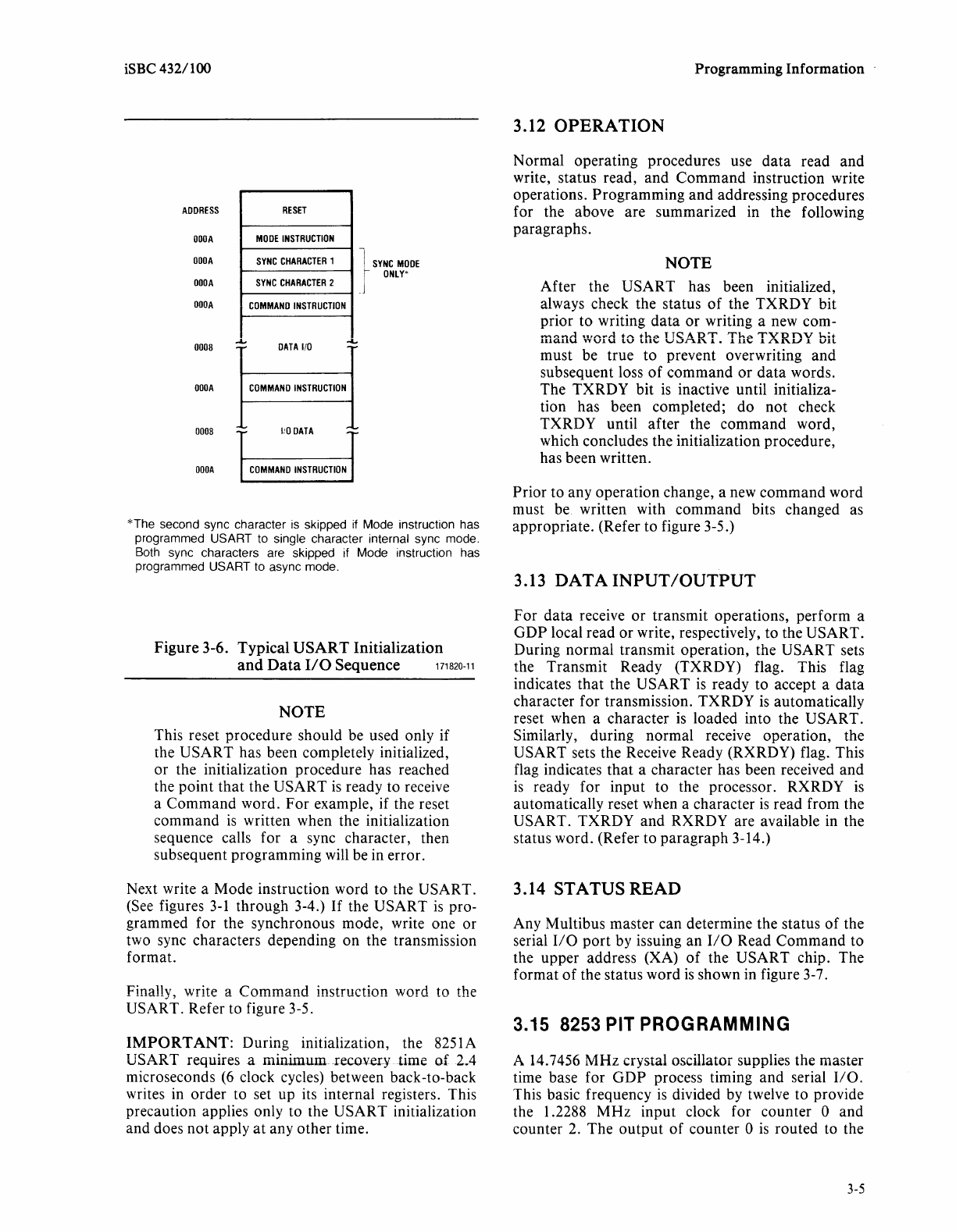
iSBC 432/100
ADDRESS
RESET
OOOA
MODE
INSTRUCTION
l
OOOA
SYNC
CHARACTER
1 I
SYNC
MODE
_f
ONLY*
OOOA
SYNC
CHARACTER
2
OOOA
COMMAND
INSTRUCTION
0008
.,r"
DATA
I/
0
-,...
OOOA
COMMAND
INSTRUCTION
0008
::~
110
DATA
~
OOOA
COMMAND
INSTRUCTION
*The second sync character
is
skipped
if
Mode instruction has
programmed USART to single character internal sync mode.
Both sync characters are skipped if Mode instruction has
programmed USART to async mode.
Figure
3-6.
Typical
USART
Initialization
and
Data
I/O
Sequence
rna20-11
NOTE
This reset
procedure
should be used only if
the
USART
has been completely initialized,
or
the initialization procedure has reached
the
point
that
the
USART
is
ready
to
receive
a
Command
word.
For
example, if the reset
command
is
written when the initialization
sequence calls for a sync character, then
subsequent
programming
will be in error.
Next write a
Mode
instruction word
to
the USART.
(See figures
3-1
through
3-4.)
If
the
USART
is
pro-
grammed for the synchronous mode, write one
or
two sync characters depending
on
the transmission
format.
Finally, write a
Command
instruction
word
to
the
USART. Refer to figure 3-5.
IMPORTANT:
During initialization, the 8251A
USART requires a
minimum
.recover-y time
of
2.4
microseconds
(6
clock cycles) between back-to-back
writes in
order
to set
up
its internal registers. This
precaution applies only
to
the
USART
initialization
and
does
not
apply
at
any
other
time.
Programming Information ·
3.12 OPERATION
Normal
operating
procedures use
data
read
and
write, status read,
and
Command
instruction write
operations.
Programming
and
addressing procedures
for the above
are
summarized in the following
paragraphs.
NOTE
After
the
USART
has been initialized,
always check the status
of
the
TXRDY
bit
prior
to
writing
data
or
writing a new com-
mand
word
to
the
USART.
The
TXRDY
bit
must
be
true
to
prevent overwriting
and
subsequent loss
of
command
or
data
words.
The
TXRDY
bit
is
inactive until initializa-
tion has been completed;
do
not
check
TXRDY
until
after
the
command
word,
which concludes the initialization procedure,
has been written.
Prior
to
any
operation
change, a new
command
word
must
be.
written with
command
bits changed as
appropriate.
(Refer
to
figure 3-5.)
3.13
DATAINPUT/OUTPUT
For
data
receive
or
transmit
operations,
perform
a
GDP
local read
or
write, respectively,
to
the
USART.
During
normal
transmit
operation,
the
USART
sets
the
Transmit
Ready (TXRDY) flag. This flag
indicates
that
the
USART
is
ready
to
accept a
data
character for transmission.
TXRDY
is automatically
reset when a
character
is
loaded into the
USART.
Similarly, during
normal
receive
operation,
the
USART
sets the Receive Ready (RXRDY) flag. This
flag indicates
that
a
character
has been received
and
is
ready
for
input
to
the processor. RXRDY
is
automatically reset when a character
is
read from the
USART.
TXRDY
and
RXRDY are available in the
status word. (Refer
to
paragraph
3-14.)
3.14 STATUS READ
Any Multibus
master
can determine the status
of
the
serial
1/0
port
by issuing
an
1/0
Read
Command
to
the upper address (XA)
of
the
USART
chip. The
format
of
the status
word
is
shown in figure
3-
7.
3.15 8253 PIT
PROGRAMMING
A 14. 7456
MHz
crystal oscillator supplies the master
time base for
GDP
process timing
and
serial
I/0.
This basic frequency
is
divided by twelve
to
provide
the 1.2288
MHz
input
clock for
counter
0
and
counter 2.
The
output
of
counter
0
is
routed to the
3-5
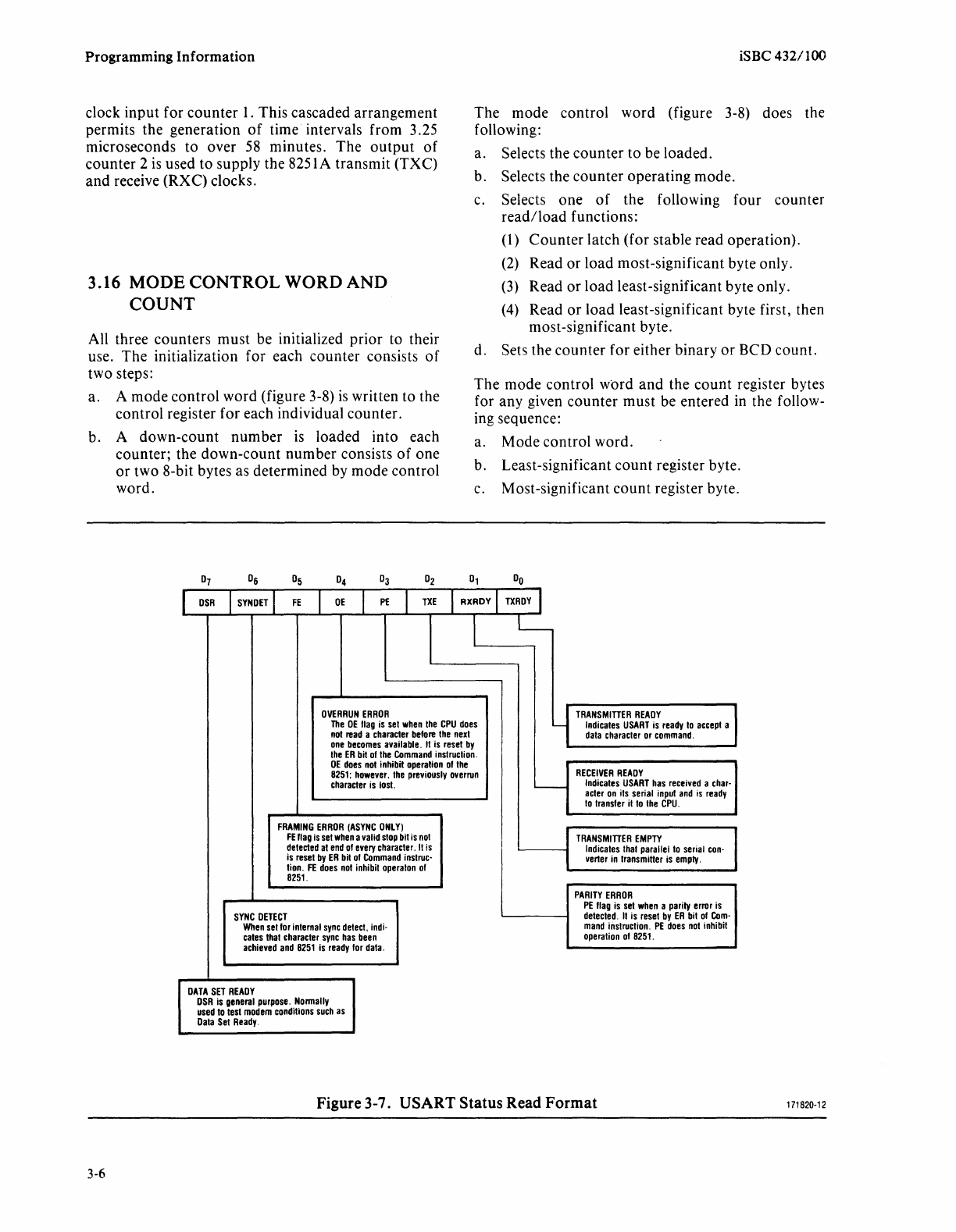
Programming Information
clock
input
for
counter
1.
This
cascaded
arrangement
permits
the
generation
of
time· intervals from 3 .25
microseconds
to
over
58 minutes.
The
output
of
counter
2
is
used
to
supply
the
8251 A
transmit
(TXC)
and
receive
(RXC)
clocks.
3.16 MODE CONTROL WORD AND
COUNT
All three
counters
must
be initialized
prior
to their
use.
The
initialization
for
each
counter
consists
of
two steps:
a. A
mode
control
word
(figure 3-8)
is
written to the
control
register
for
each individual
counter.
b. A
down-count
number
is
loaded
into
each
counter;
the
down-count
number
consists
of
one
or
two
8-bit bytes as
determined
by
mode
control
word.
iSBC
432/100
The
mode
control
word
(figure 3-8) does the
following:
a. Selects the
counter
to
be
loaded.
b. Selects
the
counter
operating
mode.
c. Selects
one
of
the following
four
counter
read/load
functions:
(1)
Counter
latch
(for
stable read
operation).
(2)
Read
or
load
most-significant byte only.
(3)
Read
or
load
least-significant byte only.
(4)
Read
or
load
least-significant byte first, then
most-significant byte.
d. Sets
the
counter
for
either
binary
or
BCD
count.
The
mode
control
word
and
the
count
register bytes
for any given
counter
must
be entered in the follow-
ing sequence:
a.
Mode
control
word.
b. Least-significant
count
register byte.
c. Most-significant
count
register byte.
l
DSR
l
SYNDET
I
FE
I
OE
I
PE
l
TXE
l
RXRDY
l
TXRDY
]
l
L__
OVERRUN
ERROR
4
TRANSMITTER
READY
The
OE
flag
is
set
when
the
CPU
does
Indicates
USART
is
ready
lo
accept
a
not
read
a
character
before
the
next
data
character
or
command.
one
becomes
available.
It
is
reset
by
the
ER
bit
of
the
Command
instruction.
OE
does
not
inhibit
operation
of
the
RECEIVER
READY
8251;
however.
the
previously
overrun
character
is
lost.
L..--
Indicates
USART
has
received
a
char-
acter
on
its
serial
input
and
is
ready
lo
transfer
it
to
the
CPU.
FRAMING
ERROR
(ASYNC
ONLY)
FE
flag
is
set
when
a
valid
stop
bit
is
not
TRANSMITTER
EMPTY
detected
at
end
of
every
character.
II
is
Indicates
that
parallel
to
serial
con-
is
reset
by
ER
bit
of
Command
instruc-
verier
in
transmitter
is
empty.
lion.
FE
does
not
inhibit
operalon
of
8251.
PARITY
ERROR
PE
flag
is
set
when
a
parity
error
is
SYNC
DETECT
detected.
II
is
reset
by
ER
bit
of
Com-
When
set
for
internal
sync
detect,
indi-
mand
instruction.
PE
does
not
inhibit
cates
that
character
sync
has
been
operation
of
8251.
achieved
and
8251
is
ready
for
data.
DATA
SET
READY
DSR
is
general
purpose.
Normally
used
to
test
modem
conditions
such
as
Data
Set
Ready.
Figure 3-7. USART Status Read Format
171820-12
3-6
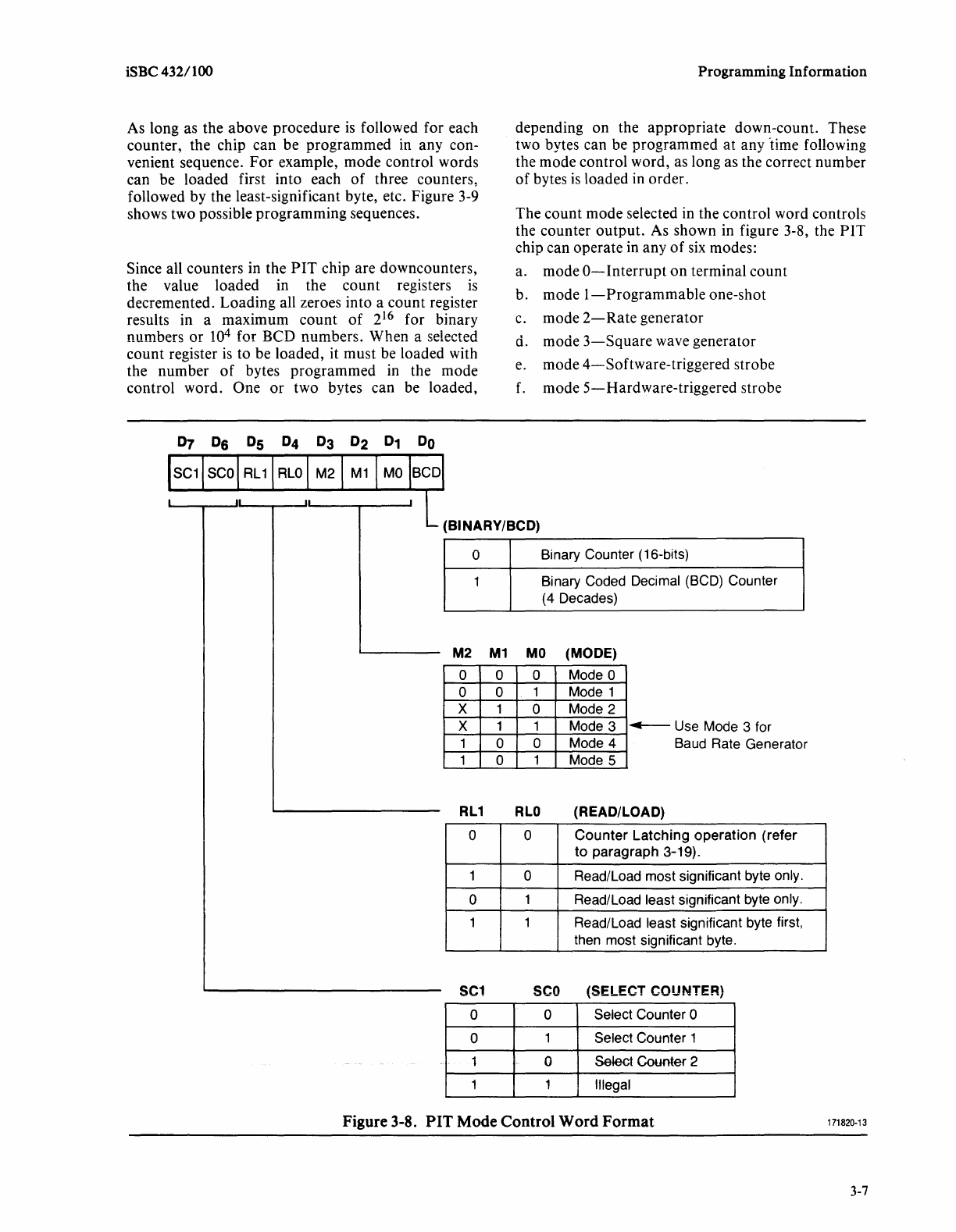
iSBC 432/100
As long
as
the
above
procedure
is
followed
for
each
counter,
the
chip
can
be
programmed
in
any
con-
venient sequence.
For
example,
mode
control
words
can
be
loaded
first
into
each
of
three counters,
followed by the least-significant byte, etc. Figure 3-9
shows two possible
programming
sequences.
Since all
counters
in
the
PIT
chip
are
downcounters,
the value
loaded
in the
count
registers
is
decremented.
Loading
all zeroes into a
count
register
results in a
maximum
count
of
2
16
for binary
numbers
or
10
4
for
BCD
numbers.
When
a selected
count
register
is
to
be
loaded,
it
must
be loaded with
the
number
of
bytes
programmed
in the
mode
control
word.
One
or
two bytes
can
be loaded,
07 05
05
04
03
D2
D1
Do
SC1
SCO
RL1
ALO
M2
M1
MO
BCD
IL
_JL
_J
Programming Information
depending
on
the
appropriate
down-count.
These
two bytes can
be
programmed
at
any
'time following
the
mode
control
word,
as long as the correct
number
of
bytes
is
loaded
in
order.
The
count
mode
selected in the
control
word controls
the
counter
output.
As shown in figure 3-8, the
PIT
chip
can
operate
in
any
of
six modes:
a.
mode
0-Interrupt
on
terminal
count
b.
mode
I-Programmable
one-shot
c.
mode
2-Rate
generator
d.
mode
3-Square
wave
generator
e.
mode
4-Software-triggered
strobe
f.
mode
5-Hardware-triggered
strobe
(BINARY/BCD)
0 Binary Counter (16-bits)
1 Binary Coded Decimal (BCD) Counter
(4 Decades)
M2
M1
MO
(MODE)
0 0 0 Mode O
0 0 1 Mode 1
x 1 0 Mode 2
x 1 1 Mode 3
~
Use Mode 3 for
1 0 0 Mode 4 Baud Rate Generator
1 0 1 Mode 5
RL
1
RLO
(READ/LOAD)
0 0
Counter
Latching
operation
(refer
to
paragraph
3-19).
1 0 Read/Load most significant byte only.
0 1 Read/Load least significant byte only.
1 1 Read/Load least significant byte first,
then most significant byte.
SC1
SCO
(SELECT
COUNTER)
0 0 Select Counter O
0 1 Select Counter 1
1 0 Select Counter 2
1 1 Illegal
Figure 3-8. PIT Mode Control Word Format
171820-13
3-7
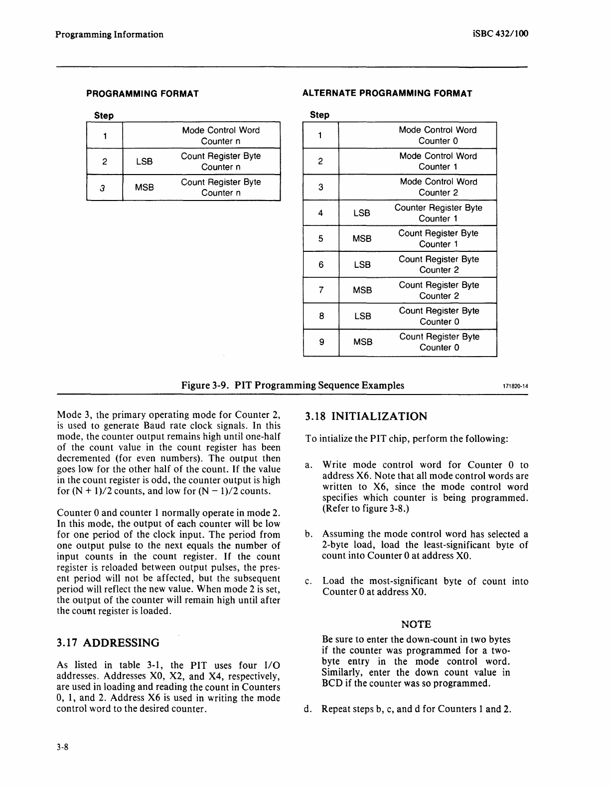
Programming Information iSBC 4321100
PROGRAMMING
FORMAT
ALTERNATE
PROGRAMMING
FORMAT
Step Step
1 Mode Control Word
Counter n 1 Mode Control Word
Counter 0
2 LSB Count Register Byte
Counter n 2 Mode Control Word
Counter 1
3 MSB Count Register Byte
Counter n 3 Mode Control Word
Counter 2
4 LSB Counter Register Byte
Counter 1
5 MSB Count Register Byte
Counter 1
6 LSB Count Register Byte
Counter 2
7 MSB Count Register Byte
Counter 2
8 LSB Count Register Byte
Counter 0
9 MSB Count Register Byte
Counter 0
Figure 3-9.
PIT
Programming Sequence Examples
171820-14
Mode 3, the primary operating mode for
Counter
2,
is
used to generate Baud rate clock signals. In this
mode, the counter
output
remains high until one-half
of
the
count
value in the
count
register has been
decremented (for even numbers). The
output
then
goes low for the
other
half
of
the
count.
If
the value
in the
count
register
is
odd, the counter
output
is
high
for (N +
1)/2
counts,
and
low for (N -
1)/2
counts.
Counter
0
and
counter 1 normally operate in mode 2.
In this mode, the
output
of
each
counter
will be low
for one period
of
the clock input.
The
period from
one
output
pulse to the next equals the
number
of
input counts in the
count
register.
If
the
count
register
is
reloaded between
output
pulses, the pres-
ent period will
not
be affected,
but
the subsequent
period will reflect the new value. When mode 2
is
set,
the
output
of
the counter will remain high until
after
the couTtt register
is
loaded.
3.17 ADDRESSING
As listed in table 3-1, the
PIT
uses four
I/
0
addresses. Addresses
XO,
X2,
and
X4, respectively,
are used in loading
and
reading the
count
in Counters
0,
1,
and
2. Address X6
is
used in writing the mode
control word to the desired counter.
3-8
3.18 INITIALIZATION
To
intialize the
PIT
chip,
perform
the following:
a. Write mode control word for
Counter
0 to
address X6.
Note
that
all mode control words are
written
to
X6, since the
mode
control word
specifies which
counter
is
being programmed.
(Refer to figure 3-8.)
b. Assuming the mode control word has selected a
2-byte load,
load
the least-significant byte
of
count
into
Counter
0
at
address
XO.
c.
Load
the most-significant byte
of
count
into
Counter
0
at
address
XO.
NOTE
Be
sure
to
enter the down-count in two bytes
if the
counter
was
programmed
for a two-
byte entry in the mode control word.
Similarly, enter the
down
count
value in
BCD if the counter was so programmed.
d. Repeat steps b, c,
and
d for Counters 1
and
2.
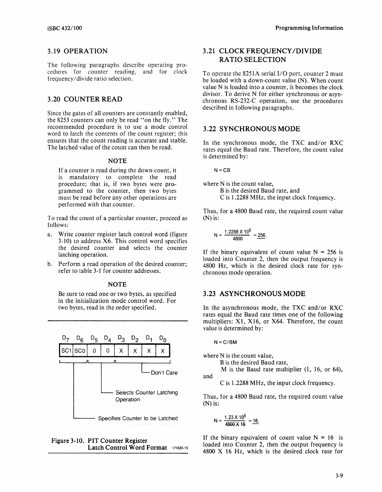
iSBC 432/100
3.19
OPERATION
The following
paragraphs
describe operating pro-
cedures for counter reading, and for clock
frequency I divide ratio selection.
3.20
COUNTER
READ
Since the gates
of
all counters are constantly enabled,
the 8253 counters can only be read
"on
the
fly."
The
recommended
procedure
is
to
use a
mode
control
word
to
latch the contents
of
the
count
register; this
ensures
that
the
count
reading
is
accurate
and
stable.
The
latched value
of
the
count
can then be read.
NOTE
If
a
counter
is
read
during the down-count, it
is
mandatory
to
complete
the
read
procedure;
that
is, if two bytes were pr0--
grammed
to
the
counter,
then two bytes
must be read
before
any
other
operations are
performed
with
that
counter.
To
read the
count
of
a
particular
counter, proceed as
follows:
a. Write
counter
register latch
control
word (figure
3-10) to address X6. This
control
word specifies
the desired
counter
and
selects the
counter
latching
operation.
b.
Perform
a read
operation
of
the desired counter;
refer
to
table
3-1
for
counter
addresses.
NOTE
Be
sure
to
read
one
or
two bytes, as specified
in the initialization
mode
control
word.
For
two bytes, read in the
order
specified.
TL
I I
Loon't
Care
Selects Counter Latching
L Operation
Specifies Counter
to
be
Latched
Figure 3-10.
PIT
Counter Register
Latch Control Word Format
1?1s20-15
Programming Information
3.21 CLOCK
FREQUENCY
/DIVIDE
RA
TIO
SELECTION
To
operate the 8251A serial
I/O
port,
counter
2
must
be loaded with a
down-count
value (N).
When
count
value N
is
loaded into a
counter,
it becomes the clock
divisor.
To
derive N for either synchronous
or
asyn-
chronous RS-232-C
operation,
use the procedures
described in following
paragraphs.
3.22 SYNCHRONOUS MODE
In the synchronous
mode,
the
TXC
and/or
RXC
rates equal the Baud rate.
Therefore,
the
count
value
is
determined by:
N=CB
where N
is
the
count
value,
B
is
the desired
Baud
rate,
and
C
is
1.2288
MHz,
the
input
clock frequency.
Thus, for a 4800 Baud rate, the required
count
value
(N) is:
N =
1.2288
X
10
6 =
256
4800
-·
If
the binary equivalent
of
count
value N = 256
is
loaded into
Counter
2, then the
output
frequency
is
4800 Hz, which
is
the desired clock rate for syn-
chronous
mode
operation.
3.23 ASYNCHRONOUS MODE
In the
asynchronous
mode,
the
TXC
and/or
RXC
rates equal the Baud
rate
times
one
of
the following
multipliers:
XI,
X16,
or
X64. Therefore, the
count
value
is
determined by:
N
=C/BM
where N
is
the
count
value,
B
is
the desired
Baud
rate,
M
is
the Baud
rate
multiplier (1, 16,
or
64),
and C
is
1.2288
MHz,
the
input
clock frequency.
Thus, for a 4800 Baud rate, the required
count
value
(N) is:
N =
1.23
X
10
6 =
16
4800X18
_;
If
the binary equivalent
of
count
value N =
16
is
loaded into
Counter
2, then the
output
frequency
is
4800 X
16
Hz, which
is
the desired clock rate for
3-9
Programming Information
asynchronous mode operation.
Count
values (N) ver-
sus rate multiplier (M) for each Baud rate are listed
in
table 3-2.
NOTE
During initialization, be sure to load the
count
value (N) into counter 2
and
the Baud
rate multiplier (M) into the
825
lA
USART.
Table
3-2.
PIT
Count
Value vs.
Rate
Multiplier
for
Each
Baud
Rate
Baud Rate: Count Value (N)* For
(B) M = 1 M =
16
M=64
75
16384
1024
256
110
11171
698
175
150
8192
512
128
300
4096
256
64
600
2048
128
32
1200
1024
64
16
2400
512
32
8
4800
256
16
4
9600
128
8 2
19200
64
4
38400
32
*Count Values (N) assume clock is
1.2288
MHz. Count
Values (N) and Rate Multipliers (M) are in decimal.
3.24 iSBC 432/100 CONTROL AND
STATUS REGISTERS
In addition
to
the previously described
1/0
devices,
the processor
board
also contains a write-only con-
trol register and a read-only status register as listed in
table 3-1.
The
status register contains iSBC
432/
100
operational information as follows when each bit
is
set:
Bit Number Description
3-10
0 Processor Initialization Hold. The
GDP
is
held in the initialized state. When this bit is
reset, the
GDP
is executing instructions.
Interrupt
Pending.
A GDP
interrupt
request has been issued.
2 Processor Access Stopped. The iSBC
432/100
board has stopped Multibus
accesses.
The GDP may
continue
executing until the next Multibus access
i!:>
attempted.
3 Stop Request.
An
access stop request has
been issued. When the iSBC
432/100
board
acknowledges this request, the Processor
Access Stopped flag (bit 2 above) is set.
Bit Number
4
5-7
iSBC 432/100
Description
Fatal Error. The
GDP
has entered a state
from which it cannot continue executing.
For example, a fatal error can be caused by
the corruption
of
system data structures.
User Selectable Jumpers. Three flags that
may be individually selected by the user.
IMPORTANT: The Fatal Error signal is connected to a red
LED
in the upper left corner of the processor board. When
this
LED
is lit, a fatal
error
has occurred and the
GDP
has
suspended execution. The. iSBC
432/100
processor must
be re-initialized to continue execution.
The processor control register contains five software
controlled
command
flags
that
control processor
initialization
and
interprocessor communication as
follows:
Bit Number Description
O Initialize Processor. When reset, this
command flag holds the
GDP
in the initial-
ized state. When the flag is subsequently
set, the
GDP
begins execution.
Issue Multibus Interrupt. When set, this
flag sets the Interrupt Pending flag
in
the
status register and generates
an
interrupt
request on the appropriate Multibus level
(see table
2-2).
2
Issue
Interprocessor
Communication
Request. Reserved for future implementa-
tion. This flag should always be reset.
3 Stop Multibus Access Request. Setting
this flag causes the iSBC
432/100
board to
stop Multibus accesses. After stopping
Multibus activity, the Processor Access
Stopped flag (bit 2 in the status register) is
set. When this flag is reset, the processor
board continues with the next access. The
GDP may
continue
executing
while
Multibus accesses are stopped.
4 Issue Alarm Signal. Activation of this
signal causes a
GDP
ALARM condition.
This command flag is automatically reset
(by the iSBC
432/100
hardware) after the
ALARM condition is initiated.
NOTE
When interfacing the iSBC 432/100
Pro-
cessor Board
to
another
system processor
(e.g., in
an
Intellec Microcomputer Develop-
ment System), the processor interrupt
capabilities should be fully utilized for
synchronization
and
communication. These
interrupt capabilities greatly enhance system
throughput
by eliminating Multibus polling
accesses
and
processor
"busy
wait"
operations.
I
• 0
n CHAPTER 4
PRINCIPLES
OF
OPERATION
4.1
INTRODUCTION
The iSBC
432/
100 Processor Board
is
designed
to
incorporate the advanced processing features
of
the
iAPX
432 microprocessor into Multibus compatible
systems.
The
43201 Instruction Decode Unit
and
the
43202 Instruction Execution Unit comprise the
iAPX
432 General
Data
Processor (GDP). These LSI
devices form the
heart
of
the iSBC 432/100
board.
The
GDP
operates with a two-phase overlapped
clock
that
is
generated
on-board.
The
GDP
address space
is
divided into two com-
ponents: a local address space
and
a physical address
space.
On-board
logic converts local address space
references into Multibus
1/0
commands; physical
address space references are converted into Multibus
memory
commands.
To
perform
a memory
or
1/0
access, the
GDP
outputs
24
address bits
and
8 bits
of
control
information
(on the processor packet bus) in
two 16-bit cycles. This 24-bit address
is
converted to
a 20-bit Multibus address as described in
paragraph
4-5.
To
perform
this conversion,
an
address offset
register
is
used, permitting the iSBC 432/100
board
to share Intellec system memory with
another
pro-
cessor. All iSBC
432/
100 Multibus memory
references are translated
to
addresses in upper
memory (as specified by the offset value). In this
manner,
software
for
the system processor (e.g., the
Intellec
operating
system)
is
protected from iSBC
432/
100 accesses, allowing
both
processors
to
operate independently.
The iSBC
432/
100
board
is
designed to
operate
within
8-
or
16-bit wide Multibus systems; a single
user selectable
jumper
option
configures the
board
for the
appropriate
operating
mode.
For
each
data
transfer, the
GDP
indicates the
number
of
bytes
to
be
transferred by means
of
a three-bit code embedded in
the eight
control
bits
(output
by the
GDP
at
the
start
of
each transfer). This code specifies a one to ten byte
transfer (1, 2, 4, 6, 8,
or
10
bytes). In the 8-bit
transfer mode,
data
reads
and
writes are
performed
one byte
at
a time over the Multibus bus. In the 16-bit
mode,
data
reads
and
writes are
performed
as
follows:
1.
When
a single byte
transfer
is
requested,
an
8-bit
Multibus read
or
write
is
performed.
2.
When
a multibyte transfer
is
requested
on
an
even byte
boundary,
the
appropriate
number
of
16-bit Multibus transfers
is
performed.
3.
When
a multi byte transfer
is
requested
on
an
odd
byte
boundary,
the
appropriate
number
of
8-bit
Multibus transfers
is
performed.
In the 8-bit
mode
a single 80-bit (10 byte) processor
requested read
or
write
operation
requires ten
Multibus accesses. A
jumper
option
is
provided
that
permits the iSBC
432/
I 00 processor
to
lock the bus
during a complete
data
transaction. Using this
"bus
lock"
provision results in faster overall processor
operation.
The
"bus
lock"
cannot
be used in systems
with double-density diskette controllers
and
8-bit
memory
if the disk controller
is
required
to
operate
simultaneously with the
iSBC
432/
100 Processor Board.
The actual
data
transfers in
both
the
8-
and
the 16-bit
mode are controlled by a small
FPLA
state machine
in
conjunction
with a
memory
transfer counter. The
state machine determines whether the 8-
or
the 16-bit
transfer
mode
is
active
and
requests the correct
number
of
Multibus accesses. All Multibus accesses
are carried
out
by means
of
an
8288 bus controller
and
an
8289 bus arbiter.
The iSBC
432/
100
board
also contains a serial 110
port
and
three timers.
One
timer provides the
baud
rate clock for the serial 110
port.
The
other
two
timers are cascaded
to
generate a process clock
(PCLK) for the 43202.
The
board
also contains a
number
of
miscellaneous
1/0
flags
that
can be read
or
written
(from
the bus)
to
control
processor opera-
tion
and
monitor
processor status. 110
port
address
assignments are detailed in
paragraph
3-3.
4.2
FUNCTIONAL
DESCRIPTION
The iSBC
432/
100 Processor
Board
may be func-
tionally subdivided into 6 units:
1.
CPU
and
110 Clock Generators
2.
iAPX
432
Processor
3. Address
Generator
4.
Data
Transfer
State
Machine
5.
Multibus Interface
6.
Input
and
Output
4-1
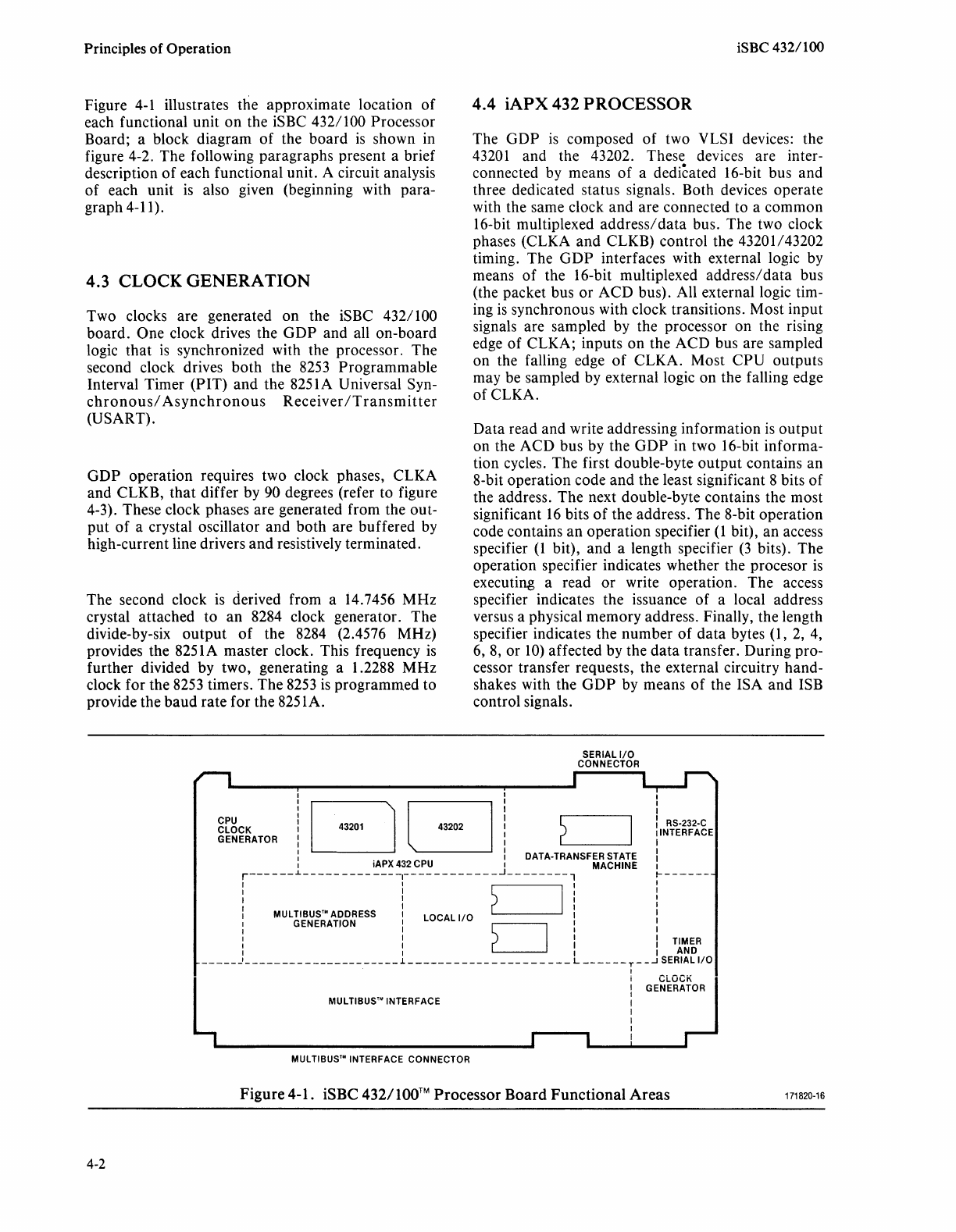
Principles
of
Operation
Figure
4-1
illustrates the approximate location
of
each functional unit
on
the iSBC
432/
100
Processor
Board; a block diagram
of
the
board
is
shown in
figure 4-2. The following paragraphs present a brief
description
of
each functional unit. A circuit analysis
of
each unit
is
also given (beginning with para-
graph 4-11).
4.3 CLOCK GENERATION
Two clocks are generated
on
the iSBC
432/
100
board.
One clock drives the
GDP
and all on-board
logic
that
is
synchronized with the processor. The
second clock drives
both
the 8253 Programmable
Interval Timer (PIT)
and
the
825
lA
Universal Syn-
chronous/
Asynchronous
Receiver
/Transmitter
(USART).
GDP
operation requires two clock phases, CLKA
and CLKB,
that
differ by 90 degrees (ref er to figure
4-3). These clock phases are generated from the out-
put
of
a crystal oscillator
and
both are buffered by
high-current line drivers
and
resistively terminated.
The second clock
is
derived from a
14.
7456
MHz
crystal attached to
an
8284 clock generator. The
divide-by-six
output
of
the 8284 (2.4576 MHz)
provides the 8251A master clock. This frequency
is
further divided by two, generating a 1.2288
MHz
clock for the 8253 timers. The 8253
is
programmed to
provide the
baud
rate for the
825
lA.
iSBC 432/100
4.4 iAPX 432 PROCESSOR
The
GDP
is
composed
of
two VLSI devices: the
43201
and the 43202. These devices are inter-
connected by means
of
a dedicated 16-bit bus and
three dedicated status signals. Both devices operate
with the same clock and are connected to a common
16-bit multiplexed
address/
data
bus. The two clock
phases (CLKA and CLKB) control the 43201/43202
timing. The
GDP
interfaces with external logic by
means
of
the 16-bit multiplexed
address/data
bus
(the packet bus
or
ACD
bus). All external logic tim-
ing
is
synchronous with clock transitions. Most input
signals are sampled by the processor on the rising
edge
of
CLKA; inputs on the ACD bus are sampled
on the falling edge
of
CLKA. Most CPU outputs
may be sampled by external logic on the falling edge
of
CLKA.
Data
read and write addressing information
is
output
on the ACD bus by the
GDP
in two 16-bit informa-
tion cycles. The first double-byte
output
contains an
8-bit operation code
and
the least significant 8 bits
of
the address. The next double-byte contains the most
significant
16
bits
of
the address. The 8-bit operation
code contains
an
operation specifier
(1
bit), an access
specifier
(1
bit), and a length specifier
(3
bits). The
operation specifier indicates whether the procesor
is
executing a read
or
write operation. The access
specifier indicates the issuance
of
a local address
versus a physical memory address. Finally, the length
specifier indicates the number
of
data
bytes (1, 2, 4,
6,
8,
or
10)
affected by the
data
transfer. During pro-
cessor transfer requests, the external circuitry hand-
shakes with the
GDP
by means
of
the ISA
and
ISB
control signals.
SERIAL
1/0
CONNECTOR
CPU
CLOCK
GENERATOR
I I
843201
83202
i ? ! RS-232-C
I
!INTERFACE
I I
I I
I iAPX 432 CPU :
DATA-TRANSF~~~w~~
l
4-2
r---
-
__
.1..
_____
-
---
---
-,--
--
------
-
_...1
__
------1
;------
: l
~
: I
I I c I :
: MULTIBUS™ ADDRESS :
LOCAL
1/0
: 1
GENERATION :
~
: :
I 1 1 TIMER
I : I : AND
------'-
-------
-
------------.!.------
-
----
-
---
- - - -
--
L
----
--T-
_..J
SERIAL
1/0
I
MULTIBUS™ INTERFACE
MULTIBUS™ INTERFACE
CONNECTOR
CLOCK
GENERATOR
Figure 4-1. iSBC
432/
1
OO™
Processor
Board
Functional
Areas
171820-16
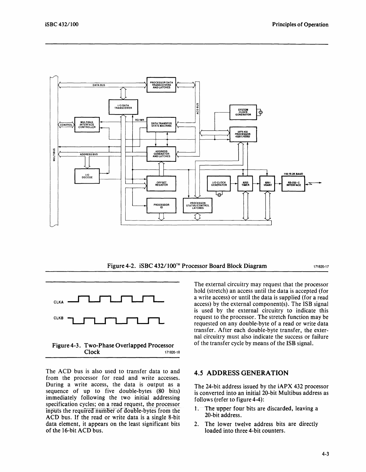
iSBC
432/
100 Principles
of
Operation
1,.._--------------'1.1
PROCESSORDATA
11'---~I
DATA
BUS
MULTIBUS
INTERFACE
CONTROLLER
ADDRESS
BUS
I\.----~
1/0
DECODE
TRANSCEIVERS
AND LATCHES
DATA TRANSFER
STATE MACHINE
ADDRESS
GENERATOR
AND LATCHES
en
:::>
"'
c
CJ
...
SYSTEM
CLOCK
GENERATOR
iAPX432
PROCESSOR
43201143202
11G-19.2K
BAUD
RS-232-C
INTERFACE
Figure 4-2. iSBC 432/100™ Processor Board Block Diagram
171820-17
CLKA
CLKB
Figure 4-3. Two-Phase Overlapped Processor
Clock
111020-10
The ACD bus
is
also used to transfer
data
to and
from the processor for read and write accesses.
During a write access, the
data
is
output
as a
sequence
of
up to five double-bytes (80 bits)
immediately following the two initial addressing
specification cycles;
on
a read request, the processor
iriplifa the requifecrnumoer"of-aouble-bytes
from
the
ACD bus.
If
the read
or
write
data
is
a single 8-bit
data element, it appears
on
the least significant bits
of
the 16-bit ACD bus.
The external circuitry may request
that
the processor
hold (stretch)
an
access until the
data
is
accepted (for
a write access)
or
until the
data
is
supplied (for a read
access) by the external component(s). The ISB signal
is
used by the external circuitry to indicate this
request to the processor. The stretch function may be
requested
on
any double-byte
of
a read or write
data
transfer. After each double-byte transfer, the exter-
nal circuitry must also indicate the success
or
failure
of the tr an sf er cycle by means
of
the ISB signal.
4.5 ADDRESS GENERATION
The 24-bit address issued by the iAPX 432 processor
is
converted into
an
initial 20-bit Multibus address as
follows (refer
to
figure 4-4):
L The
upper
four
bits are discarded, leaving a
20-bit address.
2. The lower twelve address bits are directly
loaded into three 4-bit counters.
4-3
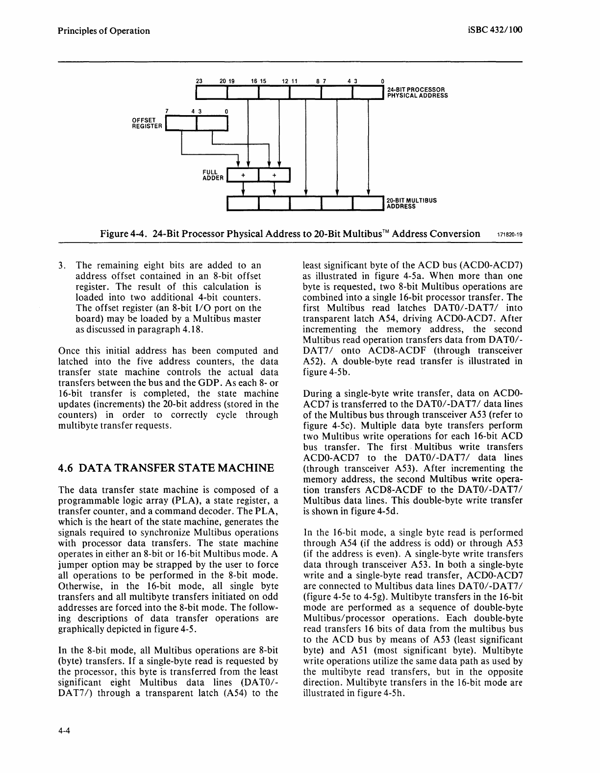
Principles
of
Operation
iSBC 432/100
23
20
19 16 15 12
11
8 7 4 3
24-BIT PROCESSOR
-----------....-------
PHYSICAL ADDRESS
OFFSET
REGISTER
4 3 0
__
__..
__
...
FULL
ADDER
______
_.
20-BIT MULTIBUS
________
...._
_____
ADDRESS
Figure 4-4. 24-Bit Processor Physical Address to 20-Bit Multibus™ Address Conversion
171820-19
3.
The
remammg
eight bits are
added
to
an
address
offset
contained
in
an
8-bit offset
register.
The
result
of
this calculation
is
loaded into two
additional
4-bit counters.
The
offset register (an 8-bit
1/0
port
on
the
board)
may be loaded by a Multibus master
as discussed in
paragraph
4.18.
Once this initial address has been
computed
and
latched into the five address counters, the
data
transfer state machine controls the actual
data
transfers between the
bus
and
the
GDP.
As each
8-
or
16-bit transfer
is
completed, the state machine
updates (increments) the 20-bit address (stored in the
counters) in
order
to
correctly cycle
through
multibyte transfer requests.
4.6
DAT
A
TRANSFER
ST A
TE
MACHINE
The
data
tr
an
sf er state machine
is
composed
of
a
programmable
logic
array
(PLA),
a state register, a
transfer
counter,
_and
a
command
decoder.
The
PLA,
which
is
the
heart
of
the
state
machine, generates the
signals required to synchronize Multibus operations
with processor
data
transfers.
The
state machine
operates in either
an
8-bit
or
16-bit Multibus mode. A
jumper
option
may
be
strapped
by the user
to
force
all
operations
to
be
performed
in the 8-bit mode.
Otherwise, in the 16-bit mode, all single byte
transfers
and
all multibyte transfers initiated
on
odd
addresses are forced into the 8-bit mode. The follow-
ing descriptions
of
data
transfer
operations
are
graphically depicted in figure 4-5.
In the 8-bit mode, all Multibus operations are 8-bit
(byte) transfers.
If
a single-byte read
is
requested by
the processor, this byte
is
transferred from the least
significant eight Multibus
data
lines (DATO/-
DA
T7
/)
through
a
transparent
latch (A54) to the
4-4
least significant byte
of
the
ACD
bus
(ACDO-ACD7)
as illustrated in figure 4-5a.
When
more
than
one
byte
is
requested, two 8-bit Multibus
operations
are
combined into a single 16-bit processor transfer.
The
first Multibus read latches
DATO/-DAT7/
into
transparent
latch A54, driving ACDO-ACD7.
After
incrementing the
memory
address, the second
Multibus read
operation
transfers
data
from DATO/-
DAT7 I
onto
ACD8-ACDF
(through
transceiver
A52). A double-byte
read
transfer
is
illustrated in
figure 4-Sb.
During a single-byte write transfer,
data
on
ACDO-
ACD7 is transferred
to
the
DATO/-DAT7/
data
lines
of the Multibus bus
through
transceiver A53 (refer
to
figure 4-Sc). Multiple
data
byte transfers
perform
two Multibus write
operations
for each 16-bit
ACD
bus transfer.
The
first . Multibus write transfers
ACDO-ACD7
to
the
DATO/-DAT7/
data
lines
(through transceiver A53).
After
incrementing the
memory address, the second Multibus write opera-
tion transfers
ACD8-ACDF
to
the
DATO/-DAT7/
Multibus
data
lines. This double-byte write transfer
is
shown in figure 4-5d.
In the 16-bit mode, a single byte read
is
performed
through A54 (if the address
is
odd)
or
through
A53
(if the address
is
even). A single-byte write transfers
data
through
transceiver A53. In
both
a single-byte
write
and
a single-byte read transfer, ACDO-ACD7
are connected
to
Multibus
data
lines
DATO/-DAT7/
(figure 4-Se to 4-5g). Multibyte transfers in the 16-bit
mode are
performed
as a sequence
of
double-byte
Multibus/processor
operations.
Each
double-byte
read transfers
16
bits
of
data
from the multibus bus
to the
ACD
bus by means
of
A53 (least significant
byte)
and
A5 l (most significant byte). Multibyte
write operations utilize the same
data
path
as used by
the multibyte read transfers,
but
in the opposite
direction. Multibyte transfers in the 16-bit mode are
illustrated in figure 4-Sh.

iSBC
432/
I 00 Principles
of
Operation
DAT8-FI
DATo.7/
(A) SINGLE-BYTE READ TRANSFER, 8-BIT MODE
ACD8-F
---~--4
ACDo-7
ACDo-7
DAT8-FI
FIRST MULTIBUS
TRANSFER-
LOW BYTE IS LATCHED IN A54
DATo.7/
DAT8-FI
SECOND MULTIBUS
TRANSFER-
HIGH BYTE FROM BUS, LOW BYTE
FROM LATCH
t--------
DATo.7/
(B) DOUBLE-BYTE READ TRANSFER, 8-BIT MODE
DAT8-FI
DATo.7/
(C) SINGLE-BYTE WRITE TRANSFER, 8-BIT MODE
Figure4-5. iSBC
432/lOOrM
Data
Transfer Routing
to/from
the Multibus™ Bus
171820-20
4-5
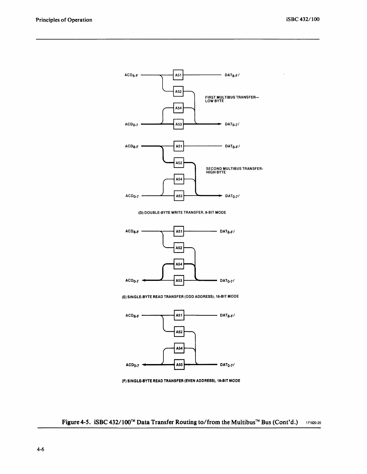
Principles
of
Operation
DAT5.F/
FIRST MULTIBUS
TRANSFER-
LOW BYTE
DATo.7/
DAT
a-Fl
SECOND MULTIBUS TRANSFER-
HIGH BYTE
(D) DOUBLE-BYTE WRITE TRANSFER, 8-BIT MODE
(E) SINGLE-BYTE READ TRANSFER (ODD ADDRESS), 16-BIT MODE
(F)
SINGLE-BYTE
READ
TRANSFER
(EVEN
ADDRESS),
16-BIT
MODE
iSBC 432/100
Figure 4-5. iSBC 432/100™
Data
Transfer Routing
to/from
the Multibus™ Bus
(Cont'd.)
111820-20
4-6
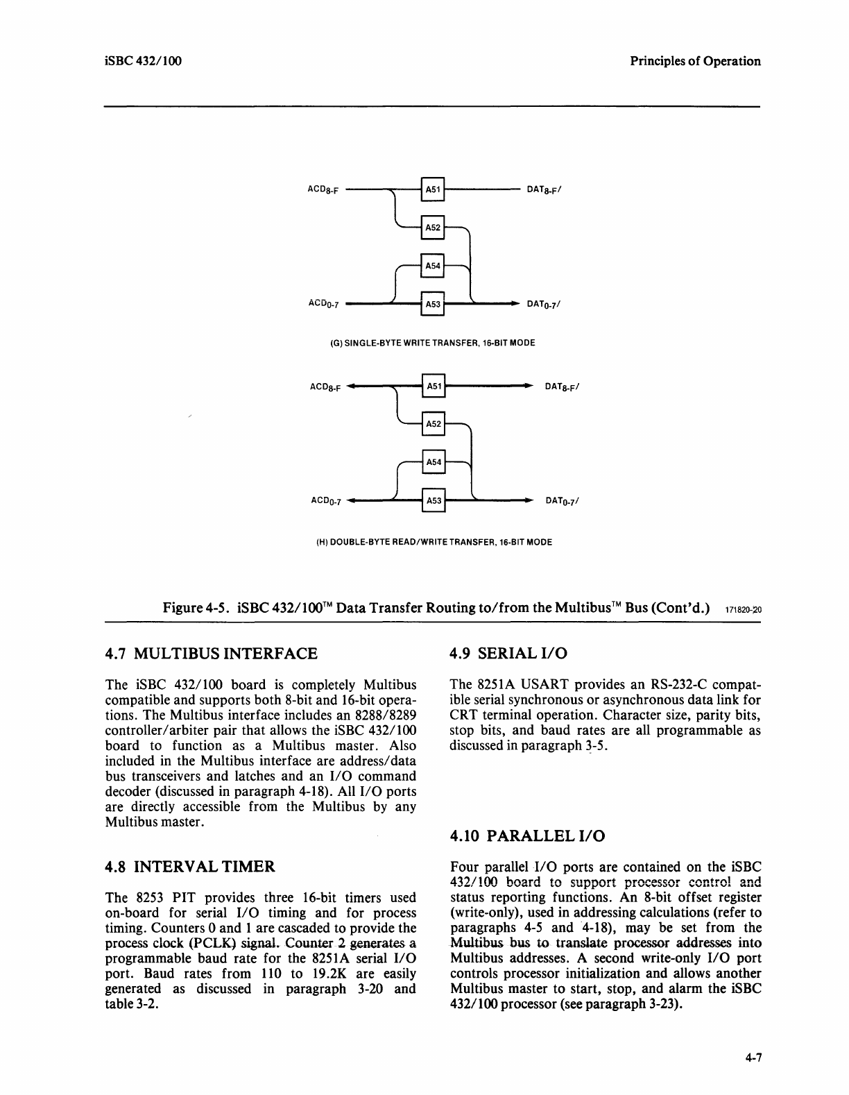
iSBC 432/100 Principles
of
Operation
(G) SINGLE-BYTE WRITE TRANSFER, 16-BIT MODE
DATs-FI
(H) DOUBLE-BYTE READ/WRITE TRANSFER, 16-BIT MODE
Figure 4-5. iSBC 432/100™
Data
Transfer
Routing
to/from
the
Multibus™ Bus
(Cont'd.)
rns20-~o
4.7 MULTIBUS INTERFACE
The iSBC 432/100 board
is
completely Multibus
compatible and supports both 8-bit and 16-bit opera-
tions. The Multibus interface includes an 8288/8289
controller/arbiter pair that allows the iSBC 432/100
board to function as a Multibus master. Also
included in the Multibus interface are address/data
bus transceivers and latches and an
1/0
command
decoder (discussed in paragraph 4-18). All
1/0
ports
are directly accessible from the Multibus by any
Multibus master.
4.8 INTERVAL TIMER
The
8253
PIT
provides three 16-bit timers used
on-board for serial
1/0
timing and for process
timing. Counters 0
and
1 are cascaded to provide the
process clock (PCLK) signal. Counter 2 generates a
programmable
baud
rate for the 8251A serial
1/0
port. Baud rates from
110
to
19
.2K are easily
generated as discussed in paragraph 3-20 and
table 3-2.
4.9 SERIAL
I/O
The 8251A USART provides an RS-232-C compat-
ible serial synchronous
or
asynchronous data link for
CRT terminal operation. Character size, parity bits,
stop bits, and
baud
rates are all programmable as
discussed in paragraph
~-5.
4.10 PARALLEL
I/O
Four parallel
1/0
ports are contained on the iSBC
432/
100
board to support processor control and
status reporting functions. An 8-bit offset register
(write-only), used in addressing calculations (refer to
paragraphs
4-5
and
4-18), may be set from the
Multibus bus
to
translate processor addresses into
Multibus addresses. A second write-only
1/0
port
controls processor initialization and allows another
Multibus master
to
start, stop, and alarm the iSBC
432/100 processor (see paragraph 3-23).
4-7
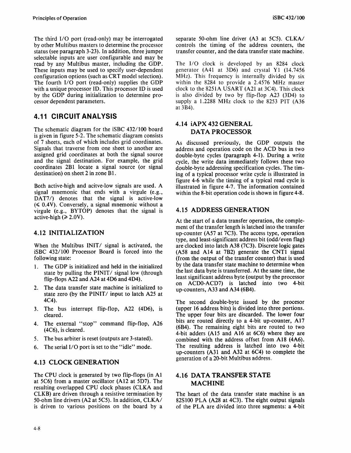
Principles
of
Operation
The third
1/0
port
(read-only) may be interrogated
by other Multibus masters
to
determine the processor
status (see
paragraph
3-23). In addition, three
jumper
selectable inputs are user configurable
and
may be
read by any Multibus master, including the
GDP.
These inputs
may
be used
to
specify user-dependent
configuration
options
(such as
CRT
model selection).
The
fourth
110
port
(read-only) supplies the
GDP
with a unique processor ID. This processor ID
is
used
by the
GDP
during initialization to determine pro-
cessor dependent parameters.
4.11
CIRCUIT ANALYSIS
The schematic
diagram
for the iSBC 432/100
board
is
given in figure 5-2.
The
schematic diagram consists
of
7 sheets, each
of
which includes grid coordinates.
Signals
that
traverse from one sheet to
another
are
assigned grid coordinates
at
both
the signal source
and
the signal destination.
For
example, the grid
coordinates
2Bl
locate a signal source (or signal
destination)
on
sheet 2 in zone
Bl.
Both active-high
and
acitve-low signals are used. A
signal mnemonic
that
ends with a virgule (e.g.,
DA T7
/)
denotes
that
the signal
is
active-low
(~
0.4V). Conversely, a signal mnemonic without a
virgule (e.g., BYTOP) denotes
that
the signal
is
active-high(~
2.0V).
4.12 INITIALIZATION
When the Multibus
INIT
I signal
is
activated, the
iSBC 432/100 Processor
Board
is
forced into the
following state:
1.
The
GDP
is
initialized
and
held in the initialized
state by pulling the
PIN
IT I signal low (through
flip-flops A22
and
A24
at
4D6
and
4D4).
2.
The
data
transfer state machine
is
initialized to
state zero (by the
PINIT
I
input
to
latch A25
at
4C4).
3.
The
bus
interrupt
flip-flop, A22 (4D6),
is
cleared.
4. The external
"stop"
command
flip-flop, A26
(4C6),
is
cleared.
5.
The bus arbiter
is
reset (outputs are 3-stated).
6. The serial
1/0
port
is
set to the
"idle"
mode.
4.13 CLOCKGENERATION
The
CPU
clock
is
generated by two flip-flops (in
Al
at
5C6)
from
a master oscillator
(Al2
at
5D7). The
resulting overlapped
CPU
clock phases (CLKA
and
CLKB) are driven
through
a resistive termination by
50-ohm line drivers (A2
at
5C5).
In
addition,
CLKA/
is
driven to v,arious positions on the
board
by a
4-8
iSBC 432/100
separate 50-ohm line driver (A3
at
5C5).
CLKA/
controls the timing
of
the address counters, the
transfer counter,
and
the
data
transfer state machine.
The 110 clock
is
developed by
an
8284 clock
generator (A41
at
3D6) and crystal
Yl
(14.7456
MHz). This frequency
is
internally divided by six
within the 8284 to provide a 2.4576
MHz
master
clock to the 8251A USART (A21
at
3C4). This clock
is
also divided by two by flip-flop A23 (3D4) to
supply a 1.2288
MHz
clock to the 8253
PIT
(A36
at
3B4).
4.14
iAPX432GENERAL
DAT A PROCESSOR
As discussed previously, the
GDP
outputs
the
address
and
operation
code
on
the
ACD
bus
in two
double-byte cycles
(paragraph
4-1). During a write
cycle, the write
data
immediately follows these two
double-byte addressing specification cycles.
The
tim-
ing
of
a typical processor write cycle
is
illustrated in
figure 4-6 while the timing
of
a typical read cycle
is
illustrated in figure 4-7.
The
information
contained
within the 8-bit
operation
code
is
shown in figure 4-8.
4.1
S ADDRESS GENERATION
At
the
start
of
a
data
tr
an
sf er operation, the comple-
ment
of
the
transfer
length
is
latched into the transfer
up-counter (A57
at
7C3).
The
access type,
operation
type,
and
least-significant address
bit
(odd/even
flag)
are clocked into latch A38 (7C3). Discrete logic gates
(A58
and
Al4
at
7B2) generate the
CNTl
signal
(from the
output
of
the transfer counter)
that
is
used
by the
data
transfer state machine
to
determine when
the last
data
byte
is
transferred.
At
the same time, the
least significant address byte
(output
by the processor
on
ACDO-ACD7)
is
latched
into
two 4-bit
up-counters, A33
and
A34 (6B4).
The second double-byte issued by the procesor
(upper
16
address bits)
is
divided
into
three portions.
The
upper
four
bits are discarded.
The
lower four
bits are routed directly
to
a 4-bit up-counter,
Al
7
(6B4).
The
remaining eight bits are
routed
to
two
4-bit adders
(AlS
and
Al6
at
6C6) where they are
combined with the address offset from
Al8
(4A6).
The resulting address
is
latch~d
into
two 4-bit
up-counters (A3 l
and
A32
at
6C4)
to
complete the
generation
of
a 20-bit Multibus address.
4.16
DATATRANSFERSTATE
MACHINE
The
heart
of
the
data
transfer state machine.
is
an
82Sl00
PLA
(A28
at
4C3).
The
eight
output
signals
of
the
PLA
are divided into three segments: a 4-bit
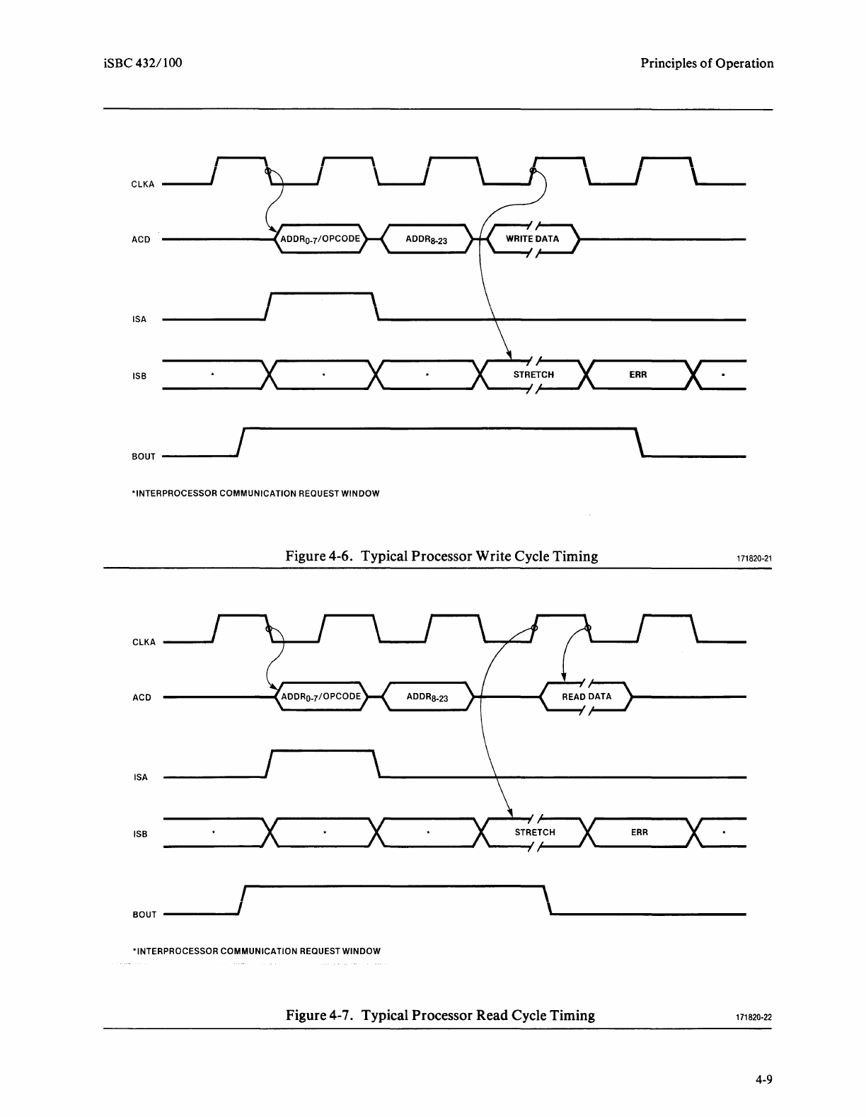
iSBC 432/100 Principles
of
Operation
CLKA
---'
I \
\
__
, I \
__
_
ACD ADDRs-23
ISA
ISB
____
s_T~·~~---E-RR
__
__,X~-----
BOUT
--------
*INTERPROCESSOR COMMUNICATION REQUEST WINDOW
Figure 4-6. Typical Processor Write Cycle Timing
171820-21
CLKA
ACD ADDRs-23
READ~
ISA
ISB
____
s_T~··~~---E-R_R
___
.J><~-----
BOUT
--------
*INTERPROCESSOR COMMUNICATION REQUEST WINDOW
Figure 4-7. Typical Processor Read Cycle Timing
171820-22
4-9
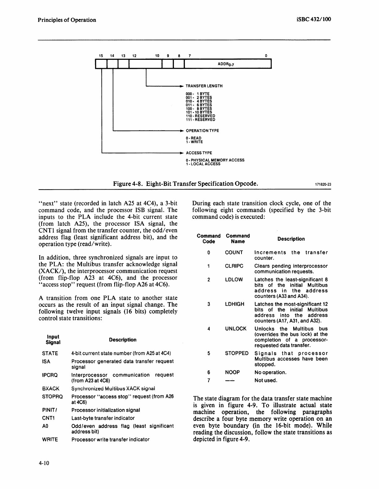
Principles
of
Operation iSBC 432/100
15
14 13
12
10
9 8 7 0
ADDRo.7
.__-----1.-
TRANSFER LENGTH
000·
1 BYTE
001
• 2 BYTES
010·
4 BYTES
011
• 6 BYTES
100·
8 BYTES
101
• 10 BYTES
110
·RESERVED
111
·RESERVED
"------------.
OPERATION TYPE
0-READ
1-WRITE
"-------------
ACCESS TYPE
0
·PHYSICAL
MEMORY ACCESS
1
·LOCAL
ACCESS
Figure 4-8. Eight-Bit
Transfer
Specification Opcode.
171820-23
"next"
state (recorded in latch
A25
at 4C4), a 3-bit
command code, and the processor
ISB
signal. The
inputs to the
PLA
include the 4-bit current state
(from latch A25), the processor ISA signal, the
CNT 1 signal from the transfer counter, the
odd/
even
address flag (least significant address bit), and the
operation type (read/write).
In addition, three synchronized signals are input to
the PLA: the Multibus transfer acknowledge signal
(XACK/), the interprocessor communication request
(from flip-flop
A23
at 4C6), and the processor
"access stop" request (from flip-flop
A26
at 4C6).
A transition from one
PLA
state to another state
occurs as the result
of
an input signal change. The
following twelve input signals
(16
bits) completely
control state transitions:
Input
Signal
STATE
ISA
IPCRQ
Description
4-bit current state number (from
A25
at
4C4)
Processor generated data transfer request
signal
Interprocessor communication request
(from
A23
at
4C6)
BXACK Synchronized Muitibus
XACK
sigr1ai
STOPRQ
Processor "access
stop"
request (from
A26
at4C6)
PINIT I Processor initialization signal
CNT1
Last-byte transfer indicator
AO
Odd/even address flag (least significant
address bit)
WRITE
Processor write transfer indicator
4-10
During each state transition clock cycle, one
of
the
following eight commands (specified
by
the 3-bit
command code)
is
executed:
Command Command Description
Code Name
0
2
3
4
5
6
7
COUNT
CLRIPC
LDLOW
LDHIGH
Increments
the
transfer
counter.
Clears pending interprocessor
communication requests.
Latches the least-significant 8
bits of the initial Multibus
address
in
the
address
counters
(A33
and
A34).
Latches the most-significant
12
bits
of
the initial Multibus
address
into
the address
counters
(A17,
A31,
and
A32).
UNLOCK Unlocks the Multibus bus
(overrides the bus lock) at the
completion of a processor-
requested data transfer.
STOPPED
Signals
that
processor
Multibus accesses have been
stopped.
NOOP
No operation.
Not used.
The state diagram for the data transfer state machine
is
given in figure 4-9.
To
illustrate actual state
machine operation, the following paragraphs
describe a four byte memory write operation on an
even byte boundary (in the 16-bit mode). While
reading the discussion, follow the state transitions as
depicted
in
figure 4-9.
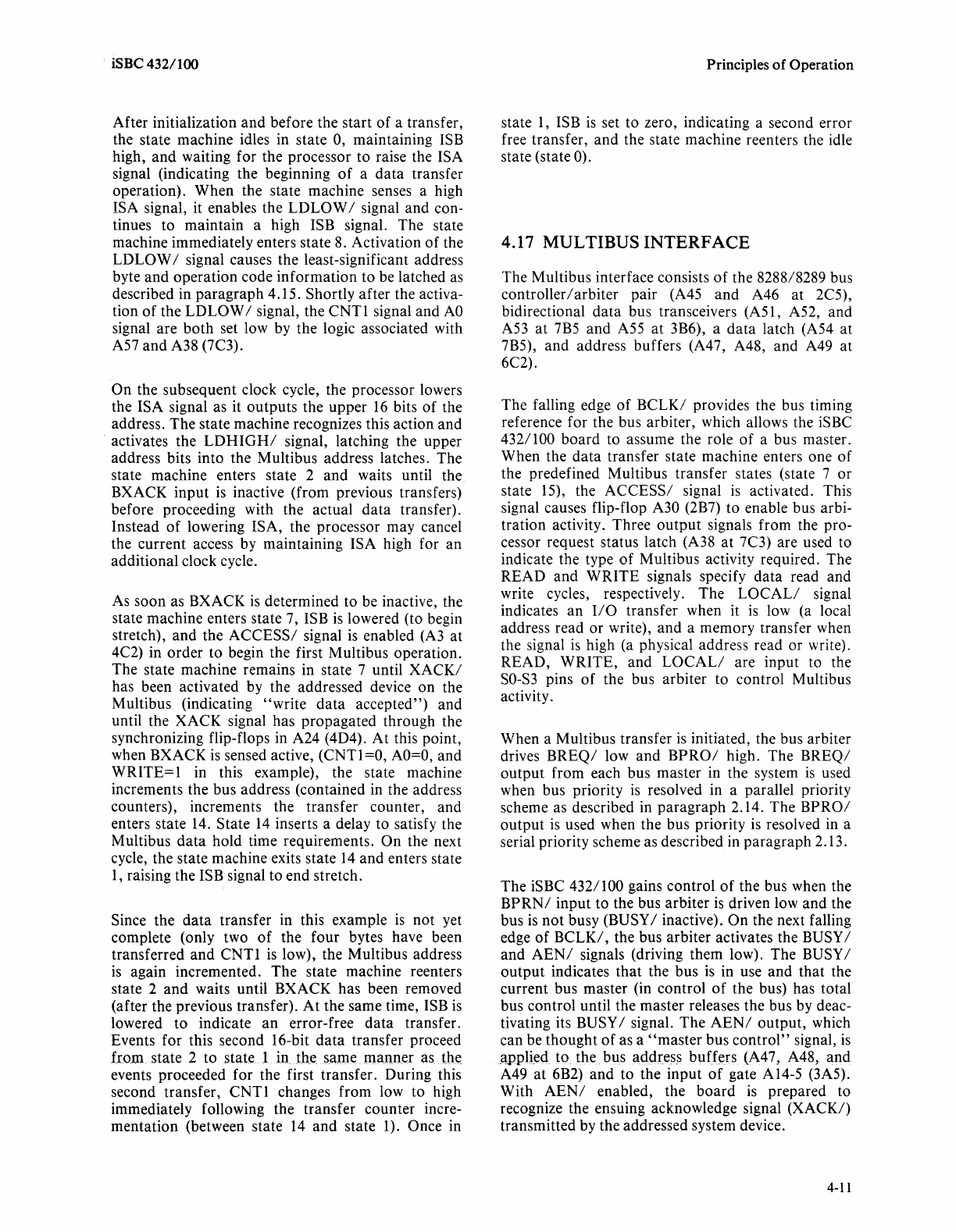
iSBC 432/100
After initialization
and
before the
start
of
a transfer,
the state machine idles in state 0, maintaining ISB
high,
and
waiting for the processor
to
raise the ISA
signal (indicating the beginning
of
a
data
transfer
operation).
When
the state machine senses a high
ISA signal, it enables the
LDLOW
I signal and con-
tinues to maintain a high ISB signal. The state
machine immediately enters state 8. Activation
of
the
LDLOW
I signal causes the least-significant address
byte
and
operation
code
information
to
be latched as
described in
paragraph
4.15. Shortly
after
the activa-
tion
of
the
LDLOW
I signal, the
CNTl
signal
and
AO
signal are
both
set low by the logic associated with
A57
and
A38 (7C3).
On
the subsequent clock cycle, the processor lowers
the ISA signal as it
outputs
the upper
16
bits
of
the
address.
The
state machine recognizes this action
and
activates the
LDHIGH/
signal, latching the upper
address bits into the Multibus address latches. The
state machine enters state 2
and
waits until the
BXACK input
is
inactive (from previous transfers)
before proceeding with the actual
data
transfer).
Instead
of
lowering ISA, the processor may cancel
the
current
access by maintaining ISA high for
an
additional clock cycle.
As soon as BXACK
is
determined to be inactive, the
state machine enters state 7, ISB
is
lowered (to begin
stretch),
and
the
ACCESS/
signal
is
enabled (A3
at
4C2) in
order
to
begin the first Multibus operation.
The state machine remains in state 7 until
XACK/
has been activated by the addressed device on the
Multibus (indicating
"write
data
accepted")
and
until the XACK signal has
propagated
through the
synchronizing flip-flops in A24 (4D4).
At
this point,
when BXACK
is
sensed active,
(CNTl
=O,
AO=O,
and
WRITE=
1 in this example), the state machine
increments the bus address (contained in the address
counters), increments the transfer counter, and
enters state 14. State
14
inserts a delay to satisfy the
Multibus
data
hold time requirements.
On
the next
cycle, the state machine exits state
14
and
enters state
1,
raising the ISB signal to end stretch.
Since the
data
transfer in this example
is
not yet
complete (only two
of
the
four
bytes have been
transferred
and
CNTl
is
low), the Multibus address
is
again incremented. The state machine reenters
state 2
and
waits until BXACK has been removed
(after the previous transfer).
At
the same time, ISB
is
lowered
to
indicate
an
error-free
data
transfer.
Events for this second 16-bit
data
transfer proceed
from state 2 to state l in the same
manner
as . the
events proceeded for the first transfer. During this
second transfer,
CNTI
changes from low to high
immediately following the transfer counter incre-
mentation (between state
14
and
state 1). Once in
Principles
of
Operation
state
1,
ISB
is
set to zero, indicating a second error
free transfer,
and
the state machine reenters the idle
state (state 0).
4.17 MULTIBUS INTERFACE
The Multibus interface consists
of
the 8288/8289 bus
controller/arbiter
pair (A45
and
A46
at
2C5),
bidirectional
data
bus transceivers (A5
l,
A52, and
A53
at
7B5
and
A55
at
3B6), a
data
latch (A54
at
7B5),
and
address buffers (A47, A48,
and
A49
at
6C2).
The falling edge
of
BCLK/
provides the bus timing
reference for the bus arbiter, which allows the iSBC
4321100
board
to assume the role
of
a bus master.
When the
data
transfer state machine enters one
of
the predefined Multibus transfer states (state 7
or
state 15), the
ACCESS/
signal
is
activated. This
signal causes flip-flop A30 (2B7) to enable bus arbi-
tration activity. Three
output
signals from the pro-
cessor request status latch (A38
at
7C3) are used to
indicate the type
of
Multibus activity required. The
READ
and
WRITE
signals specify
data
read
and
write cycles, respectively.
The
LOCAL/
signal
indicates
an
1/0
transfer when it
is
low (a local
address read
or
write),
and
a memory transfer when
the signal
is
high (a physical address read or write).
READ,
WRITE,
and
LOCAL/
are input to the
SO-S3
pins
of
the bus arbiter to control Multibus
activity.
When a Multibus transfer
is
initiated, the bus arbiter
drives
BREQ/
low
and
BPRO/
high. The
BREQ/
output
from each bus master in the system
is
used
when bus priority
is
resolved in a parallel priority
scheme as described in
paragraph
2.14. The
BPRO/
output
is
used when the bus priority
is
resolved in a
serial priority scheme as described in
paragraph
2.13.
The iSBC
432/
l 00 gains control
of
the bus when the
BPRN/
input
to the bus arbiter
is
driven low
and
the
bus
is
not
busy (BUSY I inactive).
On
the next falling
edge
of
BCLK/,
the bus arbiter activates the BUSY I
and
AEN/
signals (driving them low). The BUSY I
output
indicates
that
the bus
is
in use
and
that
the
current bus master (in control
of
the bus) has total
bus control until the master releases the bus by deac-
tivating its BUSY I signal.
The
AEN/
output,
which
can be
thought
of
as a
"master
bus
control"
signal,
is
_applied
to
the bus addres.s buffers (A47, A48,
and
A49
at
6B2)
and
to the
input
of
gate Al4-5 (3A5).
With
AEN/
enabled, the
board
is
prepared to
recognize the ensuing acknowledge signal
(XACK/)
transmitted by the addressed system device.
4-11
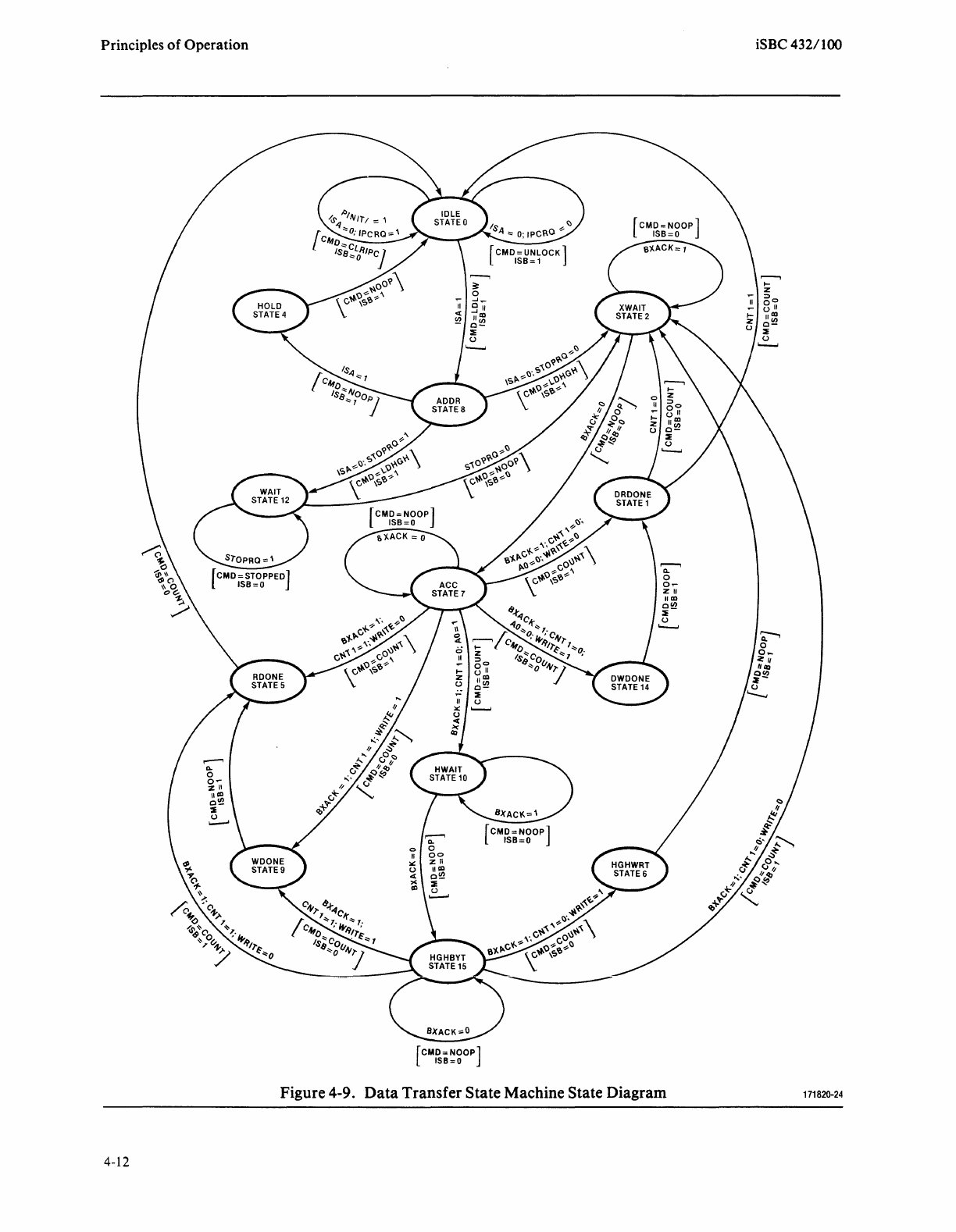
Principles
of
Operation
4-12
[CMD=NOOP]
ISB=O
[CMD=NOOP]
ISB=O
Figure 4-9. Data Transfer State Machine State Diagram
iSBC 432/100
171820-24
iSBC 432/100 Principles
of
Operation
Data
Transfer State Machine Description
State Activating
Next
Output
(Number) lnput(s) State ISB Command Comments
IDLE(O) ISA=O IDLE 1 UNLOCK Wait
for
something
to
happen
IPCRQ=O
IDLE ISA=O IDLE 0 CLRIPC
Issue
pending
IPC
if
no
access
IPCRQ=1
PINIT/=1
IDLE ISA=1 ADDA 1 LDLOW
Access
start,
capture
low
address
ADDR(8) ISA=1 HOLD 1 NOOP
Access
cancelled
ADDA ISA=O WAIT 1 LDHIGH Load
high
address;
stop
accesses
on
STOPRQ=1
stop
request
ADDA ISA=O XWAIT 1 LDHIGH Load high
address
STOPRQ=O
HOLD(4)
--
IDLE 1 NOOP
Prevent
an IPC
after
a
cancel
WAIT(12) STOPRQ=1 WAIT 0 STOPPED Set
stopped
status
and wait
for
the
stop
request
to
end
WAIT STOPRQ=O XWAIT 0 NOOP
Exit
wait
to
continue
access
XWAIT(2) BXACK=1 XWAIT 0 NOOP Wait
for
BXACK
inactive
to
start
access
XWAIT BXACK=O ACC 0 NOOP Start
the
access
ACC(7) BXACK=O ACC 0 NOOP Wait
for
access
complete
ACC BXACK=1 RDONE 1 COUNT _
Byte
read
access
complete
CNT1=1
WRITE=O
ACC BXACK=1 WDONE 0 COUNT
Byte
write,
stretch
write
access
to
CNT1=1
satisfy
hold
time
WRITE=1
ACC BXACK=1
DR
DONE 1 COUNT
Double-byte
read
access
complete
CNT1=0
AO=O
WRITE=O
ACC BXACK=1 DWDONE 0 COUNT
Double-byte
write,
stretch
write
CNT1=0
access
to
satisfy
hold
time
AO=O
WRITE=1
ACC BXACK=1 HWAIT 0 COUNT Odd
access
boundary,
perform
one
CNT1=0
byte
at a
time
A0=1
HWAIT(10) BXACK=1 HWAIT 0 NOOP Wait
until
BXACK
done
HWAIT BXACK=O HGHBYT 0 NOOP Start
high
byte
access
HGHBYT(15) BXACK=O HGHBYT 0 NOOP Wait
for
access
to
complete
HGHBYT
BXACK=1 XWAIT 1 COUNT Start
next
double-byte
CNT1=0
WRITE=O
HGHBYT BXACK=1 HGHWRT 0 COUNT
Stretch
write
data
CNT1=0
WRITE=1
HGHBYT BXACK=1 RDONE 1 COUNT Read
access
complete
CNT1=1
WRITE=O
HGHBYT BXACK=1 WDONE 0 COUNT
Stretch
write
data
CNT1:::::1
WRITE=1
HGHWRT(6)
--
XWAIT 1 NOOP
ComQ_lete
write
OQ_eration
DWDONE(14)
--
DRDONE 1 NOOP
Complete
write
operation
DRDONE(1) CNT1=0 XWAIT 0 COUNT
Get
next
double-byte
DRDONE CNT1=1 IDLE 0 COUNT
Access
complete,
no
errors
WOONE(9) -ROONE 1
NOOP
Complete write operation
RDONE(5)
--
IDLE 0 COUNT
Access
complete,
no
errors
Figure 4-9.
Data
Transfer State Machine State Diagram (Cont'd.)
171820-24
4-13
Principles
of
Operation
When a Multibus transfer
is
initiated, the bus con-
troller (A46
at
2B5)
is
also enabled, The controller
decodes the
SO-S2
control signals
and
drives the
appropriate
Multibus
command
lines low when
AEN/
is
activated by the bus arbiter. The bus con-
troller also drives DEN high to selectively enable
data
bus drivers/receivers A51, A52, A53,
and/or
A54
(7B5) as described in
paragraph
4.6.
The
data
bus
drivers are switched
to
the
appropriate
"transmit"
or
"receive"
mode
depending
on
the state
of
the
READ,
WRITE,
and
processor generated BOUT
signals.
After the
command
is
acknowledged (signified by the
addressed device driving the Multibus
XACK/
line
low), the
data
transfer state machine terminates the
command.
The
bus arbiter
and
bus controller,
respectively, terminate
AEN/
and
DEN; the bus
arbiter also relinquishes control
of
the bus by driving
BREQ/
high
and
BPRO/
low
and
then raising
BUSY/.
When gaining control
of
the bus, the iSBC
432/
100
board
can invoke a
"bus
lock"
condition to prevent
loss
of
bus
control
during Multibyte transfers (see
paragraph
2.10
and
table 2-2). The
"bus
lock"
con-
dition
is
invoked by driving the bus arbiter LOCK pin
low. The
"bus
lock"
capability
is
enabled by a user-
selectable
jumper
option
(A30
at
2A6).
4-14
iSBC 432/100
4.18
1/0
OPERATION
The following paragraphs describe
on-board
1/0
operations. All
on-board
1/0
devices are accessible
only from the Multibus bus. The actual functions
performed by specific read and write commands to
on-board
1/0
devices are described in
Chapter
3.
Multibus address bits ADRO/ through ADR7 I are
applied to the
1/0
address decoder, which
is
com-
posed
of
A50, A37,
Al3,
and
A28 (2D5). The
board
1/0
base address
is
user-selected from the
jumper
matrix associated with the address decoder A50
(2C5). This address decoder decodes a portion
of
the
incoming address bits
(ADR3/
through
ADR7/)
from the bus. Addresses ADRO/ through
ADR2/
further qualify the
I/O
address
and
are decoded by
A37 to provide chip selects for the 8253
PIT,
the
8251A
USART,
and
the four parallel
110
ports:
Address* Chip Select
1/0
Device
00
PRID/
Processor
ID
Register
X2,X4,X6 53CS/
8253
PIT
XA 51CS/
8251A
USART
xc
OFFCS/
Address
Offset
Register
XE
STATCS/
Processor
Status/Control
Register
*X may be 1
through
7 as
selected
from
the
base
address
jumper
matrix.
·n , CHAPTER
51
REFERENCE
INFORMATION
5.1
INTRODUCTION
This
chapter
provides a list
of
replaceable
parts,
a
schematic
diagram,
and
a
parts
location
diagram
for
the iSBC
432/100
Processor
Board.
5.2 REPLACEABLE
PARTS
Table
5-1
provides a list
of
replaceable
parts
for
the
iSBC
432/
100
board.
Table
5-2 identifies
and
locates
the
manufacturers
specified in the
MFR
CODE
col-
umn
in table 5-1. Intel
parts
that
are available
on
the
open
market
are
listed in the
MFR
CODE
column
as
"COML";
every
effort
should
be
made
to
procure
these
parts
from
a local (commercial)
distributor.
5.3 SCHEMATIC AND
PARTS
LOCATION DIAGRAMS
The
iSBC
432/
100
parts
location
diagram
and
schematic
diagram
are
provided
in figures
5-1
and
5-2, respectively.
On
the schematic
diagram,
a signal
mnemonic
that
ends with a virgule (e.g.,
IOWC/)
is
active low. Conversely, a signal mnemonic
without
a
virgule (e.g.,
BYTOP)
is
active high.
5.4 SERVICE AND
REPAIR
ASSISTANCE
United States
Customers
can
obtain
service
and
repair assistance
by
contacting
the Intel
Product
Service
Hotling
in
Phoenix,
Arizona.
Customers
out-
side the
United
States
should
contact
their sales
source (Intel Sales
Office
or
Authorized
Distributor)
for service
information
and
repair assistance.
Before calling
the
Product
Service Hotline, you
should have the following
information
available:
a.
Date
you received
the
product.
b.
Complete
part
number
of
the
product
(including
dash
number).
On
boards,
this
number
is
usually
silk-screened
onto
the
board.
On
other
MCSD
products,
it
is
usually
stamped
on
a label.
c. Serial
number
of
product.
On
boards,
this
number
is
usually
stamped
on
the
board.
On
other
MCSD
products,
the serial
number
is
usually
stamped
on
a label.
d. Shipping & billing addresses.
e.
If
your
Intel
product
warranty
has expired, you
must
provide a
purchase
order
number
for
billing
purposes.
f.
If
you have
an
extended
warranty
agreement,
be sure
to
advise the
Hotline
personnel
of
this
agreement.
Use the following
numbers
for
contacting the Intel
Product
Service Hotline:
All U.S. locations, except Alaska,
Arizona,
&
Hawaii
Telephone:
(800) 528-0595
All
other
locations telephone:
(602) 869-4600
TWX
Number:
910-951-1330
Always
contact
the
Product
Service
Hotline
before
returning a
product
to
Intel for repair. You will be
given a repair
authorization
number,
shipping
instructions,
and
other
important
information
whjch
will help Intel
provide
you with fast, efficient service.
If
you are
returning
the
product
because
of
damage
sustained
during
shipment
or
if the
product
is
out
of
warranty, a
purchase
order
is
required
before
Intel
can initiate the
repair.
In preparing
the
product
for shipment to the Repair
Center, use the original factory packing material, if
possible.
If
this
material
is
not
available, wrap the
product
in a cushioning material such as Air
Cap
TH-240,
manufactured
by the Sealed Air
Corpora-
tion,
Hawthorne,
N .J.
Then
enclose in a heavy
duty
corrugated shipping
carton,
and
label
"FRAGILE"
to ensure careful handling. Ship only to the address
specified by
Product
Service Hotline personnel.
5-1
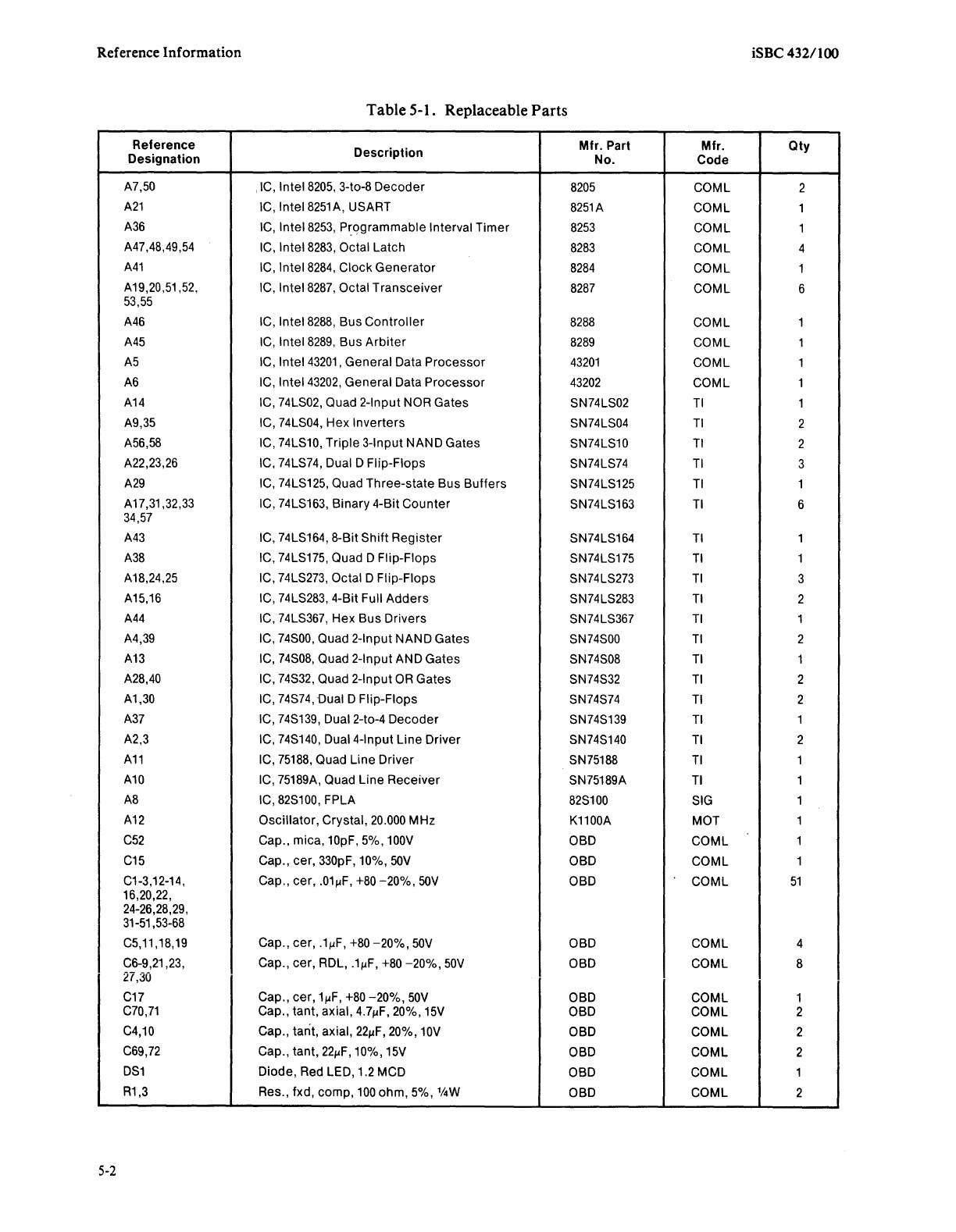
Reference Information iSBC 432/100
Table 5-1. Replaceable Parts
Reference
Description
Mfr.
Part
Mfr.
Qty
Designation
No.
Code
A7,50 , IC,
Intel
8205,
3-to-8
Decoder
8205
COML 2
A21
IC,
Intel
8251
A, USART
8251A
COML
1
A36
IC,
Intel
8253,
P~ogrammable
Interval
Timer
8253
COML
1
A47,48,49,54 IC,
Intel
8283,
Octal Latch
8283
COML 4
A41
IC,
Intel
8284,
Clock
Generator
8284
COML
1
A19,20,51,52, IC, Intel
8287,
Octal
Transceiver
8287
COML
6
53,55
A46
IC,
Intel
8288,
Bus
Controller
8288
COML 1
A45
IC,
Intel
8289,
Bus
Arbiter
8289
COML 1
A5
IC,
Intel
43201,
General
Data
Processor
43201
COML 1
A6
IC,
Intel
43202,
General
Data
Processor
43202
COML 1
A14
IC, 74LS02, Quad
2-lnput
NOR Gates SN74LS02 Tl 1
A9,35 IC, 74LS04,
Hex
Inverters
SN74LS04 Tl 2
A56,58 IC, 74LS10,
Triple
3-lnput
NANO Gates SN74LS10 Tl 2
A22,23,26 IC, 74LS74, Dual D
Flip-Flops
SN74LS74 Tl 3
A29
IC, 74LS125, Quad
Three-state
Bus
Buffers
SN74LS125 Tl 1
A
17
,31,32,33 IC, 74LS163,
Binary
4-Bit
Counter
SN74LS163 Tl 6
34,57
A43
IC, 74LS164, 8-Bit
Shift
Register
SN74LS164 Tl 1
A38
IC, 74LS175, Quad D
Flip-Flops
SN74LS175 Tl 1
A18,24,25 IC, 74LS273, Octal D
Flip-Flops
SN74LS273 Tl 3
A15,16 IC, 74LS283, 4-Bit Full
Adders
SN74LS283 Tl 2
A44
IC, 74LS367,
Hex
Bus
Drivers
SN74LS367 Tl 1
A4,39 IC,
74SOO,
Quad 2-lnput NANO Gates
SN74SOO
Tl 2
A13
IC,
74S08,
Quad 2-lnput AND
Gates
SN74S08 Tl 1
A28,40 IC, 74S32, Quad 2-lnput
OR
Gates
SN74S32 Tl 2
A1,30 IC,
74S74,
Dual
D
Flip-Flops
SN74S74 Tl 2
A37
IC,
74S139,
Dual 2-to-4
Decoder
SN74S139 Tl 1
A2,3 IC, 748140, Dual
4-lnput
Line
Driver
SN74S140 Tl 2
A11
IC,
75188,
Quad
Line
Driver
SN75188 Tl 1
A10
IC, 75189A, Quad
Line
Receiver
SN75189A Tl 1
A8
IC, 82$100, FPLA 828100 SIG 1
A12
Oscillator,
Crystal,
20.000
MHz
K1100A MOT 1
C52
Cap., mica, 10pF, 5%, 100V OBD
COML
1
C15
Cap., cer, 330pF, 10%,
50V
OBD
COML
1
C1-3,12-14, Cap.,
cer,
.01µF, +80
-20%,
50V
OBD
COML
51
16,20,22,
24-26,28,29,
31-51,53-68
C5,11,18,19 Cap.,
cer,
.1µF,
+80-20%,
50V
OBD
COML
4
C6-9,21,23, Cap., cer, RDL, .1µF,
+80-20%,
50V
OBD COML 8
27,30
C17
Cap., cer, 1µF,
+80-20%,
50V
OBD
COML
1
C70,71
Cap., tant, axial, 4.7µF, 20%,
15V
OBD
COML
2
C4,10 Cap., tarit, axial,
22µF,
20%,
10V
OBD
COML
2
C69,72 Cap., tant,
22µF,
10%, 15V OBD
COML
2
DS1
Diode,
Red LED, 1.2 MCD OBD
COML
1
R1,3 Res., fxd,
comp,
100
ohm,
5%,
1/4W
OBD
COML
2
5-2

iSBC 432/100
Reference
Designation
R2
R4,5
RP1-3
XA12
XA36
XA8,21
XA5,6
Y1
Mfr.
Code
AMP
AUG
CAL
CRY
INT
MOT
SIG
Tl
08D
Table 5-1. Replaceable Parts
(Cont'd.)
Description
Res., fxd, comp,
220
ohm, 5%,
1/4WS
Res., fxd, comp, 1
Kohm,
5%,
1/4W
Res., pack, 8 pin, 1K ohm, 2%,
2W
Socket, 14-pin, DIP
Socket, 24-pin,
DIP
Socket, 28-pin,
DIP
Socket
Assembly, 64-pin Lead less
Crystal,
14.7456
MHz, Fundamental
Extractor, Card
Post, Wire Wrap
Plug, Shorting, 2-Position
Mfr. Part
No.
08D
08D
08D
514-AG19D
524-AG11D
528-AG11D
827-0067-00
CY148
105UL
89531-6
530153-2
Table 5-2. List
of
Manufacturers' Codes
Manufacturer
AMP, Inc.
Augat, Inc.
Calmark Corporation
Crystek
Intel Corporation
Motorola
Semiconductor
Signetics
Texas
Instruments
Order
by Description; available from
any commerical (COML) source
Reference Information
Mfr.
Qty
Code
COML 1
COML 2
COML 3
AUG 1
AUG 1
AUG 2
INT 2
CRY 1
CAL 2
AMP"
91
AMP
15
Address
Harrisburg,
PA
Attleboro,
MA
San Gabriel, CA
Fort Meyers, FL
Santa Clara, CA
Phoenix, AZ
Sunnyvale, CA
Dallas,
TX
5-3/5-4

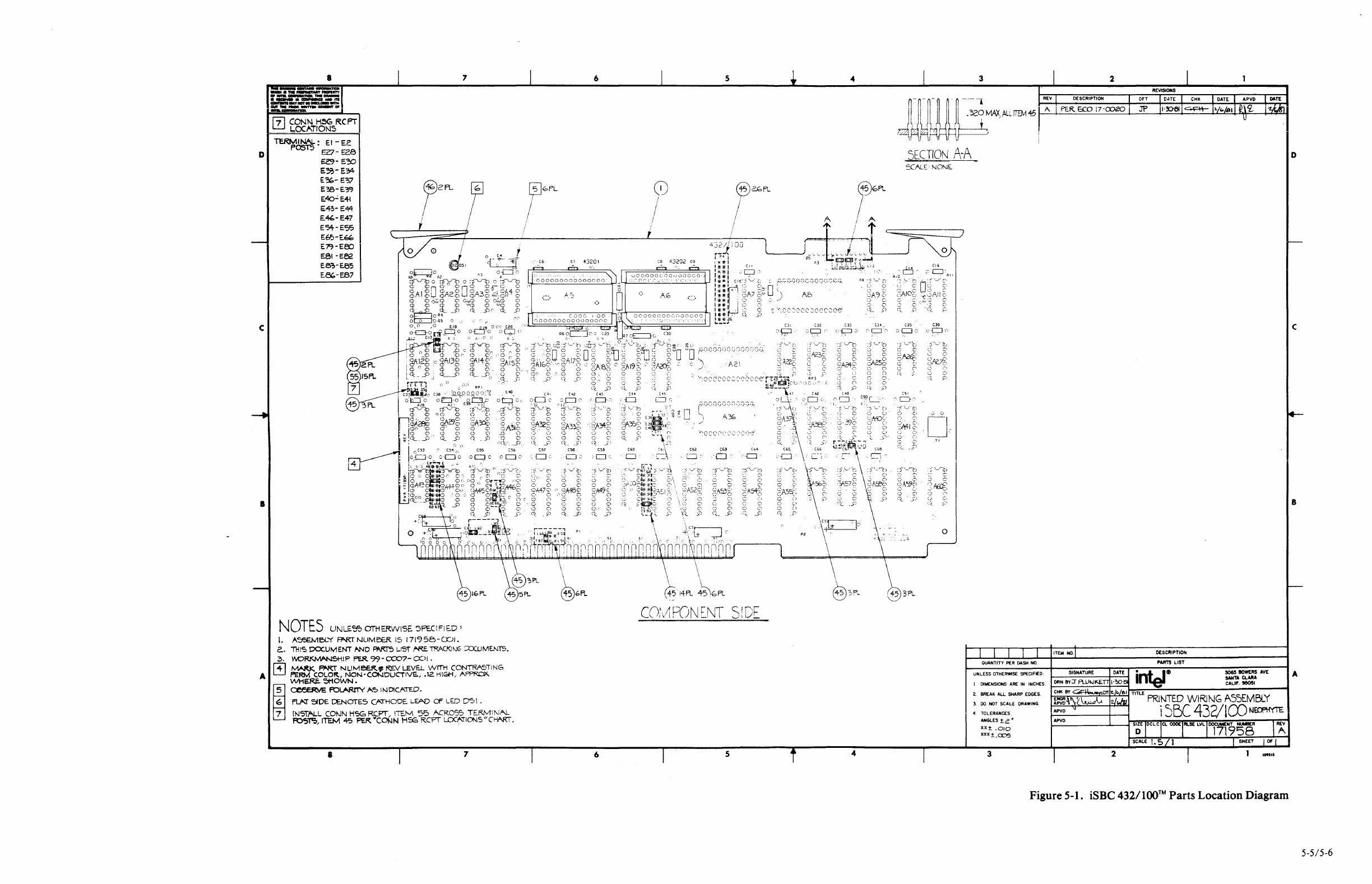
D
c
I
8
r:;i
CONN
H5G
RCPT
~
LOC,._TION5
TERMINAL:
El -
E~
POSTS
EV-
E2e
~-E~
E53-E'34
E?b-E'?>7
1:::8-E.3'3
E~...;E41
E43-
1::44
E.4'.-E47
E'54-E5S
E6':l-E.~
E",'9-EOO
E81
·Ee2
e:.e:.-e.es
E.8'.-E87
NOTES
UNL£$?
OTHERWISE. ':>PE.CIFIED:
I.
A'::F.£W!eL'f
F1"RTNUMBER.
15
171955-CDI.
7
8
I
I
e..
'TI-II':>
DCX.UMENT
.A\ND
~5
Ll$T
fflf..
TRA.CKINE
:;()QJM[NT5.
~RKNV'IN'5HI
P PER
99-
CXXJ7-
(X.1
I •
MARK.
ffRT"
NUMe.E..R.~
R.EV
LEV8.
WITH
(ONTRA5T1NG
PERM
COLOR,
NON·C.ONDUCTIVE..,
.12
HIGH, APPROX.
VVHE.RE.
5HOWN.
~
FOLARnY
A'?
lt-.IDICA.it:D.
fl.AT 51DE
C£NOTE5
CA.THODE.
LEP-0
Cf
LE.D
DS1.
!N~T,.o..LL
COi-JN
HSG
RCPT',
\TEM
55
,A.CROSS TER..M!N.A.L
FO~~'
ITEM
45
PER.
+CONN
HSS
RCPr
LOC1'TI0\15"CHM'.T,
8 7
6
~6PL
I
"
43201
'"'
~po
r.~~~CJ
0
:i)Vlp
Clo
0
c 0
C:A32.0
\....;.'
., Ci
(-:...
()
G 0
'~·
_;"J
.o:
:ii'--"h
L~'
0
'.."::·
0
~A3:i6
()
0
0
C'
q
__
S'
6
0)
I
I
I
'~
43202
':
5
®2.bPL
I
/
~
0
;;.n01).')l)C:;c;c1:.:_cr;;;.
i
'1
. / . f\21
@'
14Fl
~f,PL
•CJ·
:-)---"\.._f-C)
'~:
0
c. c
0
C"
~:A54g
COi"
1
1PONENT
S!D~
5
'-o·
4
C.3:3
c·p~·
4
3 2
n-n-n
n n
----1
REV
DESCRIPTION
DrT
JUUUUULl
WX,ALL
ITDA45
"414J4H~·
SECTION
A-A
~ALE•NO~E.
~r~~~
~AS9~;
-.;,
(_
~\~
,,,
.(q:All
CJ&
u-po
~~-\_,r-~
~~
(~
(
l·
~~--
0
QUANTITY
PER
DASH
NC
UNLESS
OTHERWISE
SPECIFIED
I
DIMENSIONS
ARE
IN
INCHES
2.
BREAK
AU.
SHARP
EDGES
3.
00
NOT
SCALE
ORAWING
4
TOLERANCES
ANGLES
±e •
XX±
.010
XXX±.C05
3
A
PE.R..
ECO
17-00CO
ITEM
NO.
SIGllATURE
OESClllPTION
PARTS
LIST
!065
BOWERS
AVE
SANTA
CLAllA
CAL"·
96051
APVO
1-------~----
SIZE OCLC
Cl
CODE
Al.SE
l'IL
DOCl*ENT
NUMBER
D
17l958
SHEET
2
REV
A
Figure 5-1. iSBC
432/IO<r.1
Parts Location Diagram
D
c
B
A
5-515-6

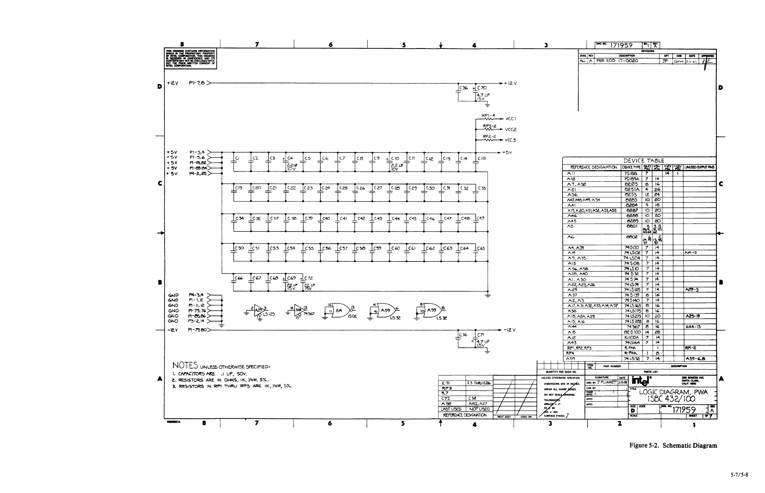
I J 7 l 6 l 5 4 l
D
-tlZ:.V
c
I
A
l
~oV
+5Y
+5V
+
'!>V
+
~y
......
RPl-.q.
~Ve.Cl
~VCC2.
~2.-2
JO.,,·"
..... VCL3
_kso
_ks1
C53
Tc.54
(55
C%
Tc57
C?e
C'5'7
CfO
C{;I
C<Cc
C~3
Tcb4
'"·5
~
f
~
~
f
~
~
~
*
~
~
f f
QJD
G.ND
GND
Gl>ID
GNO
C:."10
~-I~:~~
P1-75,
7'1
P1-e5..eE.
~-2,14
l I
~125
-~v
Pl-7'-eo....-~~~~~~~~~~~~~~~~~~~~~~~~~~~~~~~~~~~~~~~~---r:::---~~~~
.....
~~~--•
-1cv
....J....C
If.
__LC71
NOTES
UNLE!:O
OTHE.RWl5[ '.:i'ECIFIED:
1.
CAPl'ICITO~
~
.1
Uf,
SOV.
Z.
RESISTORS
ARE
IN
OHMS,
IK.,
Y~W.
51..
3.
RESISTORS
IN
RPI
THR.\J
RP~
ARE.
IK,
Y4W, Si'o.
8 T 7 I 6 T 5
T
+ns\iuF
z
R.P3
en.
c
s.e
L
,....,
56
A.42,A2-7
'i..1'-0T
U$ED
NOT
U':£D L
NEXT
ASSY
' 4 I
z
7_
z
L
_/_
USED
OH
3 l
1-~
171959
l
DFT
CHt I
nm
I
N'f\IOlllD
D
DE VICE TABLE
.A..1\
75188
7
~
I
A41
82eA
~
18
A1~
f\2.0,A51,~,P\53,"55
82137
10
eo
~
ec..ee
10
e.D
7
14
7
14
7 14
7
14
A5'.,AS8
74LS10 7
14
Al,A30
74574
7
14
l--'A~22~~~A~2~~-Ai!h~~~~~+-'-7-+~L5~~=-+--'-7-o-+-l4...,..-1---+~-+-~~~~--11
P...2.'} 74L5125 7
14
A
37
74
5
139
e
\6
A2.,A3
7'1-5140
7
14
741.5175 e
'"
Ale,
Ac!+,
A25
74
l.5273
10
20
1"15,A16
74LS20'3 e 1'-
Ale
A43
QUANTITY
PER
DUH
NO.
UNLESS OTHERWISE SPECIFIED•
DIMEllSIOHS
ARE
IN I
BREAK
All.
SHMP
DD
NOT
Wll'IG.
xx
.113
±
.010
SURFACE
FINISH
1
3
A44-13
e2.51CO
14
2e
KllCOP\ 7
1-4-
1"!-lS164 7
14
~:PM.
I
~
l
PMT
NUMBER
l'AllTS LIST
SIGNAlURE
DATE
ft-··
ORN
BY
:f
F'LUNK£iT
2•5'81
•
l'e'
318
IOWElll
AYE.
SMITACUM,
CN.JF.-
CHI<
BY
1
TITLE
...,..1~-
1
-----.T.-+--JJ;..;~
LOGIC
DIAGRAM,
PNA
"'
~N"fD
____
l_....--~
i
5&
4
32/
I
00
~
APYD
i)j
alM
IIJCll0.17\959
. j A
SCM.£
I J
IH&T
t
fllI
T 2 T 1
Figure 5-2. Schematic Diagram
A
5-7
/5-8

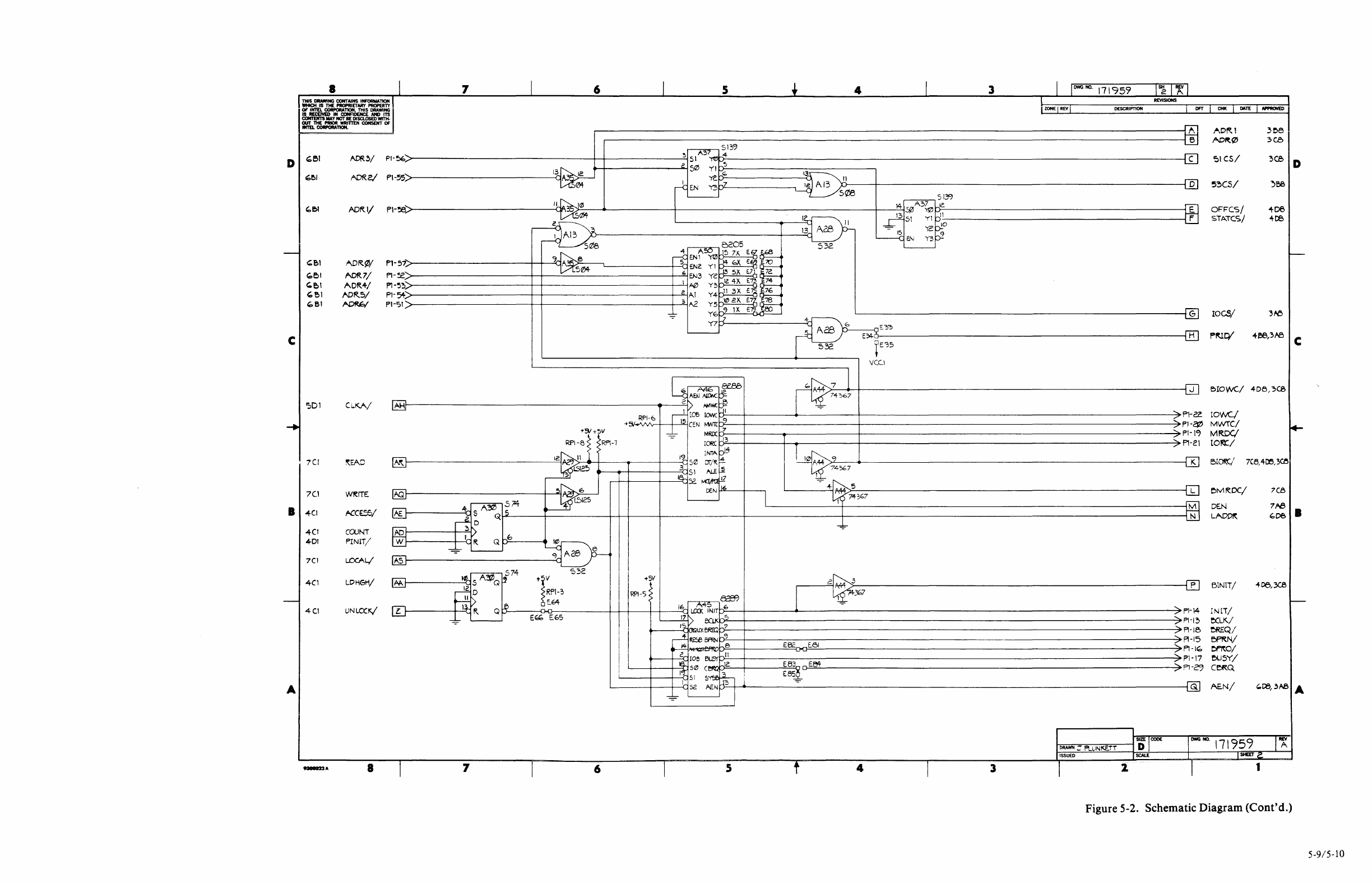
8 7 6 5
D
l'DR..2./
p
~513''7
1-%>
~
...,.,i....4
SI
!'"".
13~1e
~
50
YIP:
1-55.....-
~k~
fill'A I I'"'.
r{:
EN
'Gp;'
'-----
AD1'.I/ P
~Bl
ADR.~/
P
'-e
I
f".DR.
7 /
Pl
C.~I
l"\DR+/
P1
'-
e 1 l'DR.5/ P
'-Bl
N)Rbf
P
'~10
1-~---
_'1/1:$~
~
5205
L__./'sre
~k_S7X
E.€:7~
1-57,.....
9.
,"\'"le
EN1
t-{:
"°~
i>r5e'A-
~
ENZ.
Y1
r,,l4
bX
-
e.g_.
-2>
6
EN3
YC'.~5X
E.~~
I~
n8Z.4Y.,
£~
~
-~'3..--
1-54'."""
e Al
Y4P'.-1
3X
E._3;
~
t-?t>
:.
A2.
y5h.~
zx.
@:
~
Y€.h9
1X
~eo
~
y7t:l:
I'"'
c
501
Ci..KA/
7C! ltEAD
7(.1
w~rrE
I
-4C1
KCE3S/
4(1
CCU
NT
4Dt PIN
IT/
7(1
LOCAL/
4C1 LDHGH/
4C.1 UNLCXK/
~r
AH
c~
fMW:.
_Qroe
IDNcr-;
1
RPl-E>
CEN
~"'9
+:J.l
......
+9/+SV
r
~
MROCP
RPI-Bl'""
I -
TORC~
3
INTA.pl~
~
--
12m11
'~s~
or;R.i±
i.SteS
~51
N..£~
~2~
~6
AD.
C£1\1
lJ2.
1
4.~574
~l.5125
.________,
AE.
d~
~~
f>D
I>
w l
!,...~
Q
h.6
~
-*-
~
'-----!'""
•
A5
I
1~~74
532
AA
tr
I
·~
HD
Rf'l-3 I
RPl-5
Eiff)
[>
oEG'\-
'~~
l.
~~~
Jo(
.::::-!
~
EGG
E65
~
EG.l'P;?
'~w:f:RFQi.-..7
::--
t'-'.
,.-i.
~
EfflNPc:;i
~~p.8
l
S..,
JOB
e.IBl'h_ll
~SeJ
C ht.:'.
~
-~~th
J-$1
$~:,
i
-b
X.
AENt'-' J
'*~
8 7 6 5
4 3
13
Al3
II
1e
508
~513'7
14
A~?
r,,e
~
'T!Zlf'-'.
~
13
,SI
Yf
r,11
*1'
~2~0
re
15
9
~EN
Y3~
532
L___J
4
~
..nE.:;:,
E:4[5.
32.
rE"35
~
VCCI
crrJ
T
10
A+4
,9
74%7
I
-=-
+Ds
g7+3{.7
]
+
1
2~XJ
Ee2._,..,_,...,_E..01
~~
E83
EM
EeS!~
4 3
DWG
NO.
171959
DESCRIPTION
DRAWN
::;
R...UNt<E.TT
ISSUED
2
REVISIOftS
Df'T!CHK!DllTE
'~I
,..,
6
c
D
E.
F
G
H
J
(Pl-
Pl-
? Pl-19
:::,,.
PH:\
K
L
M
N
[f]
~Pl-14
?Pl-I~
~PJ-18
:::,.FH5
~Pl-I
~Pl·l
~Pl-
Q.
DWG
NO.
AD~<Z'
':llCS/
~3CS/
OFF
CS/
STA.TCS/
3i:>e
~c.e
'3C5
)'flS
-+08
4C8
roes/
3f'eJ
D
+eB,3"8 c
BIO
WC/
405,
'3C8
rol/v'C./
MWTC/
MRDC/
LORC/
EitORC./
7C8,4~,3CO
OMRDC/
7(8
DE.N
7N3
L~
'-08
I
51NIT/
+oe,:xe
INl1/
C:CLK./
~Q/
flf'RN/
errtO/
WSY/
Ce«Q
AF-N/
'-r::8,
3"'8
A
171959
MY
A
1
Figure 5-2. Schematic Diagram (Cont'd.)
5-915-10

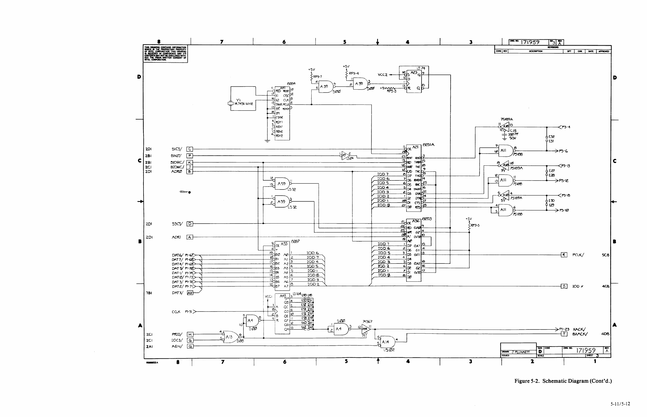
I
D
201 51C5/
c.
2BI OINIT/ p
c 281
2C.I
2.DI
ZDI
"2.DI
I
181
A
1'IORC/
BIONC/
AD!Wl
AOKI
/(..
j
6
D
A
-
·~
-~(
..........
1-"-'_....
DAiq/
Pl
Ol'-.T7/
Pl
DAi4/
P
Di"T
Sol
P
DATl/
Pl
DAT(Zl/P
DAi?J/
P
DATZ/ P
I- .Jo..
·~
-"J"I-:'."
1-73_....
1·1e,....
1-71>
Dl'\TYy'
CCLI<.
P!-~1.)
7
l l
YI
D
14.74:b
MHZ.
J
T
'
"
'
'
"
"
"
"'
4
6
-t5V
RP3-7
a2B'I-
4
II~
5
A39
r.f
ro
rar~<Zl
17
Xl
<J.:l.
12.
161-2
CLK~
1
!2.Tf..NK.PCLK
e
~
f,/(
1':.E.'ID!'
5
~
€Fl
t----1-
(91'1'£
4
~Dfl
:c
AENI
1~c~
"
RDi'Z'
-=-
'----------'
1e.
II
1~
A5'7
LS32
I
~
~
9
~EXB7
~a
T
l't-,
B0
N'.J
1
IODE:.
ie::
"
Bl
f\l
2.
IOD7
17;:'.
Bi: 1\2 3
IOD
4
"-
16.::'.
B~
f'0
4
!ODS
"-
I~
"
61-
M 5
IODI
I~
B5
A.5
6
IOD©
"-
1~
56
No 7
IOD
3
'-
~
e1
/'\? e
lOD
7..
'--
'-'
~
~
L.51~'18
VCC.I
3
E:
E."I")
I Q
l1_
E:
)·~
1
QB
i:. E
~
QC
...,.._
__
E-u
QD
f-"6'----i..H~
5 3
CMG
llO. 171959
'f'5V
l LS7-t
~5AaQ
~
RP3-4
\ICC..2
I
Uo
D
"'
e_
A~~·
rr
I>
~
+5
'~
~
Q
SW
L___...
RP3-3
'"1~
L__
7Sl8~A.
II
f\r!J
13
1(32
P3-
IZ.
C.15
I 3?/l}PF
-=-
"5l:JJ
lE.31
rt~8C51A
~
8
~(£
1¢J
All
-:;;.~-~
I
A"}
2
cl~
~
7'1e6
L51Z'>4
~1QJ
~~'5
8~10
~.....,
wrl'
TXE
t!e
P3·1
ti'
Ir
Jl)
Tl<(~
~
7518':>A ¢
E.27
IOD?
el~
T"'.,i
PEfl
QE.28
/
IODf:.
7~~
..
~~-
v
!ODS
"'05
Ri!C~
I 75iffi
v
IOD4
504
~~
v
1003
e
D3
~
~
v
A.Vil
4
...__P3-
!OD
"2
I
·i:;e
:::£:?+
v
IOD
I
~DI
~1".J7
5 7518'JA
~
E3:)
v
roo~
27
00
¥J'S~
4
¢~
v All b
~P!rl
~
5
4
e
c
75100
~~3
1"5V
c.~~
R:lb
e;f,
"°
"
.,.,.
"
>Rf'3-5
~~~II
~Al
LJ
19
ND
IOD
7 I
07
a.Kl
15
v
roo
E.
e.
C6
C:-1
14
v
IOD
S 3
OS
run
•3
v
!004
~
+
D4
v
IOD
~
~
ce
18
O.K2
v
!OD
2 "
C2
16
v
GZ
IQDI
7
01
,...,1
17
v
IOD~
a 00 '"'1
v
PCLK/
sc.e
I
L_____J
.L s
IOD
I<
«.a
A
>-..--------------------------------~~-c3
X/'.£.t</
406
Kl
~D/
"2CI
(0(5/
2A.I .A.EN/
H
El
[fil
r-------------------------------1T
BXl'<t</
---------------------------------~~
171959
SIZE
CODE
-----:r~f'L.-UN_1<.f._TT'
_
_,
D
R£V
L5~2
A
ISSIEJ
~A
8 7 6 5 3 2 1
Figure 5-2. Schematic Diagram (Cont'd.)
5-11/5-12

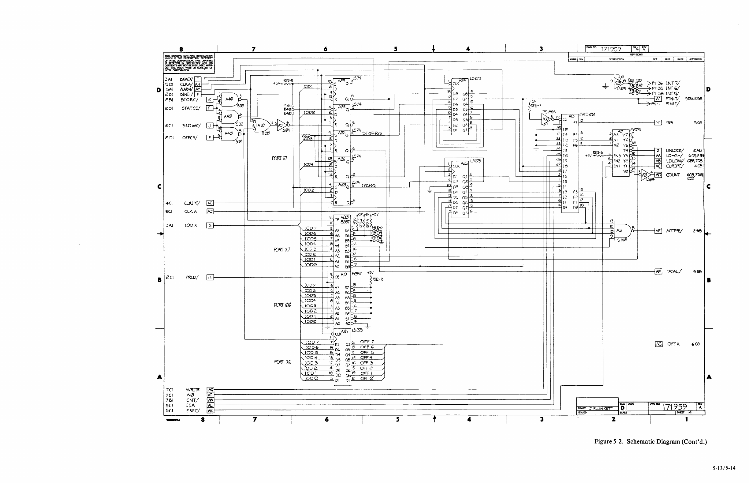
8 7 6 5 4 3 DWGNO. 171959
THIS
DRAWING
CONTAINS
INFORMATION
REVISIONS
I
OF
Wlll1c:!U5
~~E!.
ATHRYIS!'ROPEDRAWIR"JYNG.
I l
"'~~,~·~
I
._1<_0N_<~i~-~~1
____
o_<se_R_1~_1o_N
___
__Jl_~_rr_._
1
__
~_~~l~~-~__._l_~
__
w-1
1
~~™~~~m
1 . . . . . . . .
COHTUITS
MAY
NOT
BE
DISCUlSED
WIT!!-
r J
~TH~~~·~_OF
___
_,i
J.--------RP-3--8-----r-~1---~-~~-~-74---+--+------+----l-
.--~c-4_L5_2_73
___
~
~Elf!~
501
CLKl'y'~
_____
_,
+sv
V'
I¢,
S
ACZQ
~
L__f
CLR
6
..+:o
~Pl-~
INT7/
D SAl
/'UtfM/z:p~F
r
r-r-1
____
_.
/'"I:..:::O..::.D.:..1_,
........
__:~::.io
I
____
.:_:.11J>l)
125JHp1-35
INT~,/
c
e.t
eINIT/
~-----+--l---4'....+-..o~
11
t>
.-------+----
16
""
JB
Qe'-'-
1
'=''---- P1-38
INT
5V
a~
~ro~&
~
~
3
i~R
Qe
l
Jr
.---~
1
_,
7
~w~~--~--+-----~-----------------T--
,~w
~~
~~
c
532
E44~
f---=-
1..574
1
1
----+---+----'
14
'-'-lD~
Qb~
T
+;:2-7
~~-I
P!Nti/
ZDl
5TATC5/
F +
E4
3
~D--+----1-1-+--~<
1
'S
NZQ'"-'S"------+---+--'
~
DS
QSf--'IC.=---+-+-'
--+---~
S
A-40
~
E-e
Vr-l_O_D_0-+-+-+--e"_,
D 1 B D4
Q4t-'.L-
75169A
~62.
5
~
I
~
~
'1
r---2
D3
Q~'-=""-4--1-1----+------
I
A.
191
cs
AB~J
532
~
le
R Q
b~
I I 4
D2
QC~
I I - f7
l-'1-"-""-------------I
y
I
MiP
5:;
""'
0'
I
v'ffsfu
JJ
N!OQ
(74
STOPRG I : I I
111
l
~
~i-=2'--ll-j1f-+-1
+-1--
:
__
-==-2=_
-==-~;:::
....
~:""'<:
1~
:!
l~I
:2=-~
____
.,2~~·
t
~r
tt-b~.
Q
~r-~1--------
· ·
-=:;:-
---=~'-'-'[11
RP.3·E>
Y•q:P
7
I
10
~
L$74
.~110
+5V
·v';;
6 EN3 y;p
12
f--/A
-?ts o,si
~
t...Sm
~
1'7
~ENZ
y~r-1
3
~
V~l=O:.:::D-'-4--+-....._..-'IC""'-
D
.--i1-----+-1<'"'1
CLR
,A25
----+-+--+-~2=--7
IB
lf4
EN1
Yl
pl4
+jt
~
ili>
~17
yaid,5~
~
"'
Q
k)c
8
r-------+-+-----'
c2._ D 1 Q 1 2
'---+----f-+-1---+--~
3
1 b r L
A~
4
"'°
~
L.Sil1-
~-4------1..±IB~
D2
QZ~
1~---+-----+-+--+---'"'4
[ 5 -
'--
L5flJ'l-
..._+-----4-+--4r-<1
5
Ae3
QI
s IPC.Rt;i
.l1.
j
----'-""-'
08
Q5~
,--5- I 4
,I_O_D=2--+-+-"-2 D i
~
~
D4
Q4~'7'----------1----+-+-++~6
I 3
F3
~
v I
~
I ,-----Q.
D5
QS
l2.
7
12
Fi:~
4C1
U~PC/
~1------++--------+--+----+-~-.l:
R
Qp
6
~
~
QG
15
e I 1
Fl
L
'--+----+-----------+-----~
~17,'D7
Q7lb
..'l'----10
F0118
SCI
CLK~
AJ1------++----~-~--+----+---------~~+-------+~
o_;
Q~~
l
9
~
lf'if5V
,rSV
+5V
~
7 1(10E
ea37
fi:'.
;!,<
~';>
13
3M
WDX
51------~-------~~~
7
~T
j&~~
'--~---__,~-------+---~H-----~~-~~~~
8
1
'-'[~0~D~6::__+--1-~~~
~hiW'-~-.._tl§tolr~~~
~-+-----+---------+---++-+-1------_...._~+-~~~QIA3
/"'n-+------1/'E..
1\.1
,__.r=o""'D'--')5"--+--1-7_,
A5
5583
~
/
~
I
'--'[=0::..::D:...4-=----1--<-8""-
M
Mp
12.
'
~*
"--=10::..::D'-'3,.__-+--1-4...:..
A.
3
133
1Ju-=1i;,=---_-__,,___,
I"
,~ill..:.:..::.D-=2=---1--<..-=-3
N..
ee
p!nl_7
___
---l,__---+-1
_____
_11
......
,
-----+-------
J l
r-..'-=IO=D~l
-+-+-e""-
Al
Bl
hl6
'--------------+---r+.._
1
+---------+------
1f'..
,~I=O=D~0=---1--<----'-\
A0
BZJ~[.)--'1~------11--------~l'
______
.......,.
_________
~
BIOWC/
2.CI J
OffCS/
eo1
E.
FORT
X7
!SB
see
UNLCO;/
e.M
LDHGH/ b(b,C.
LD
L.OW/
'~
7C8
CLl'UFC/
4C8
COUNT
~7D~
'--------------------------++++--------+------~{'tF
FATN../
see
~BCB7
-t5V
H
1------+----------1-----+-+--a:t:
a: Al9
._Ji T
<;>Rl'E-8
I 2C1 PIUD/
A
7Cl
7(1
7BI
5(1
50
VVP'1TE
/'\0
CNT/
ISA
El\EC/
8
f'..~[0'--=D'-'7--+--i--=.'='
A7
57
r~>=-15
__
-<11
1\.1
'-"IO=D-=~'--+--i-.;;;.'-
AC:.
Ek.
rpc""-l+
__
-<11
r-..~Wo..:D'-'5=---+--f-'-7
A5
BSrh',i-=-1;
__
_.
l\.'"""""LO'""'D"""4_......_i.....=.8
AA
B+~ri=E
__
_.
l\.~[0~0_3
_
_,__....__,4
/'13
B3
rhl
:>'--l(o
__
_.
f'._
1
'-'I:..:::0:..::D;...:2=--..__+-=-13
~
E2
boc:-17
__
_.
l\.'--"-'LO::.:D'---'--1
-+_,.1-e.=-i
/'\I
51
po=l8
__
"'IODel
I t
N{J
eqirft---,
~
~.
--
-d:--
1 -
!,._
A16
ILS27.3
-
~Cl~
'-----------+------'~I·~)
'
l\.~lQ=-D--'-7---'7'--<D
3
Q3
·'°'
OFF
7
~"-"-'ro"-=-D--'-6
__
14--'"
Db
Q6
15
OFf
b
;r
~~l=O~D~5---'8"-"'
D4
04 9
OFf'
5 ./I
r--.......:...:ro::....::.D-'4'----"13=-lD5
Q5
12
OFF4
./I
~
1
,-...=
!O"""-'D~~--'-17'-ID?
Q?
16
CR""
.3
./I
l'\
1
·-..:.IO=)""--"
DC..=-----4..:..-i
ce
Q1:
5
Off
2
./
r-..'--"--'LO"""D"-'--1
__
16"'""
t:e
~~
19
OFF
1
_/
,,_.l....,O"""'D~0'---~~
Dl
~
2
OFf
0
L....__
Xii
r
11------------_____J
11
l J
7 6 5 4 3
171959
lll£Y
A.
SCALE
2 1
D
c
a
A
Figure 5-2. Schematic Diagram (Cont'd.)
5-13/5-14

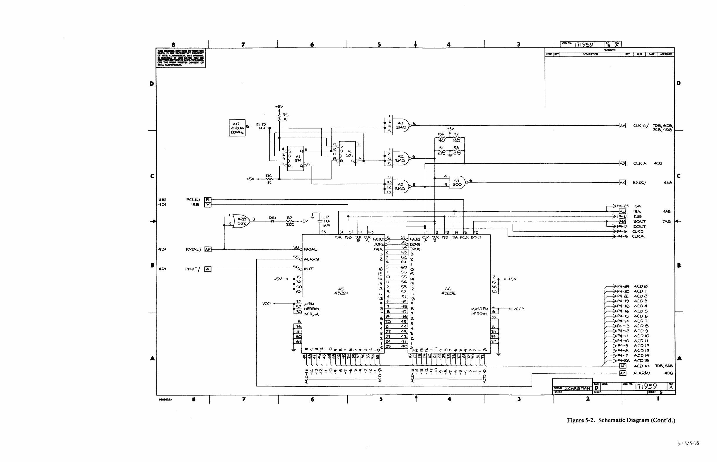
D
c
I
I
TlllS-CDll"--"IK*
MKll
IS
TIE
NONETMY
-.-rt
OlllllD.IXm'llMTlllll.lHIS-
IS llECEMD •
a.lDEllC£
Mm
115
CQ9llElflS
llAY
llOf •
1119ClOSED
SJll.
QUT
TIE
-
WMITEll
CllllSlllT
f11
lllTB.IXm'llMTlllll.
7 6
El
U
R4
+SV
-~,,,...,.........,-------+------'
IK.
5 4
Z..70
e
361
401
PCLK../
R.1-------------------------------------~--+---I-----~
ISB
YI----~~~-------~~~~~~------,
n_c17
>-='-----tc~-"""""""'--+SV
IUF
r;ov
53
4BI
401
-· I 7 6
51
52.
E>I
E:.~
ISA
\SB
A5
4"5t::01
CLK
CLK
FF-.UL\·rr:6'-----=5:;...:;8n
B A
CX>N~n-7
_ ___.;:o...;;c1
"TRUE.'""-'-'--""-'-<
3 z
z 3
I 1-4.:........--=:...<
""'°
</)
5
15
1-
9
.!.....--~:..j
So
SS
14
IO
13
II
rz.
rz.
II
13
1¢
14
9
IE.
e "
7 18
E.
IC!
s zo
4
ZI
3
z:z
'2.
23
Z4
s
54
53
52
SI
4.,
48
41
46
45
44
43
4£.
3 13
14
s 12
156
ISA
PC.LI<.
BDJI
z
I
¢
1S
14
\"3
11..
A'Q
II
43202
10
~
8
MASTER
7
Ht:.R"R.IN
E.
s
4
3
z..
4
4
B
35
3
-1-SV
VC.C3
3
1~·1~
I
DWG
NO.
OFT
CHK
DATE
Al'l'llOVE)
~
CLK
Aj
IDS,
E:.De,
"2.C.B,4D8
CLKA.
4C.B
IS}'..
ISA.
1'38
e.ouT
eour
CJ..Ke
CLKA.
AC.D
'2!
ACD
I
AC.DZ.
ACD
3
AC.D-4-
A.CD 5
ACD6
ACD
7
AC.De
A.CD 9
A.CD 10
A.CD
II
ACDl2
ACDl3
il\CDl4
A.CD15
4A8
7A8
.ACD
xx
1oe.,6Ae
ALA.RM/
408
171959
IEV
A
SHEET
1
Figure 5-2. Schematic Diagram (Cont'd.)
D
c
I
A
5-15/5-16

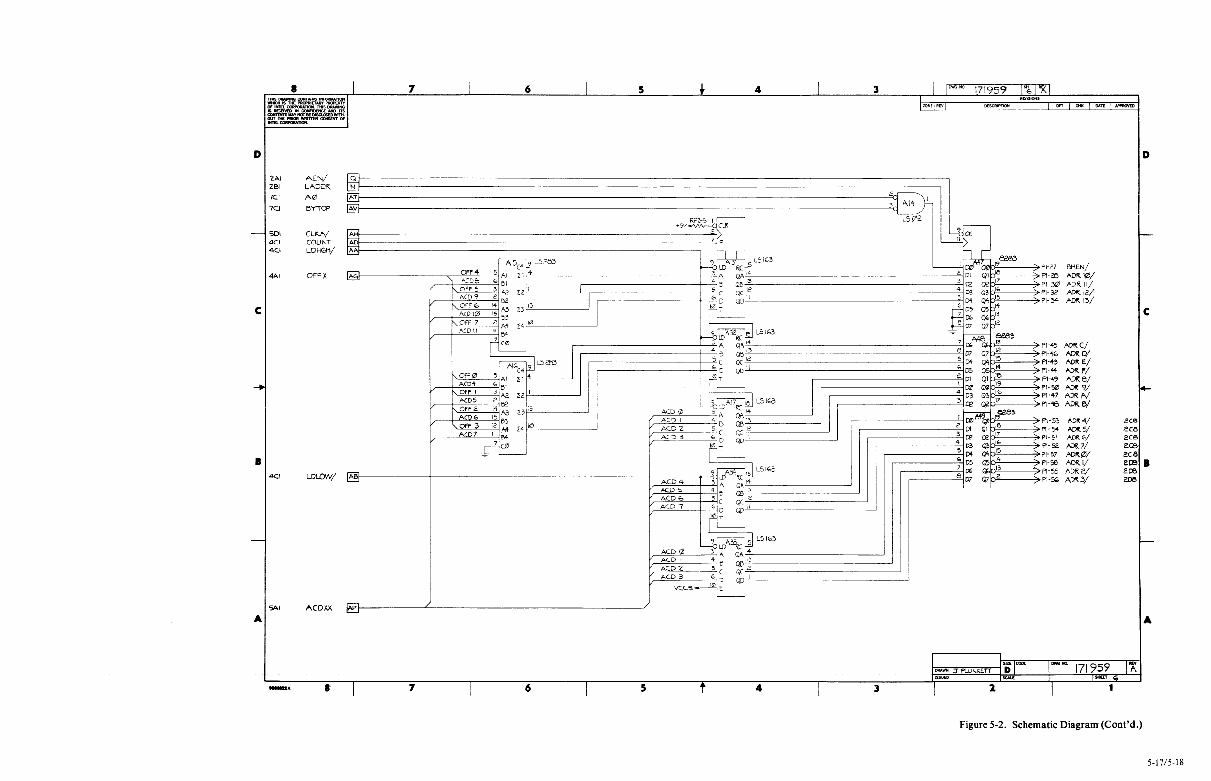
8 7 6 s
I
THIS
-
COllTAINS
lllFORMATION
WHICH
1$
THE
PRa'RIETAJl't
PROPERTY
OF
INlEL aR'OllATION.
THIS
DRAWING
IS
RECEIYED
IN
CONFIDENCE
N«l
ITS
CONTDITS llAY
NOT
BE
DISCl.OSED
WITH-
OUT
THE
PRIOR
WRITTEN
CONSENT
OF
INlEL
CORPORATION.
D
2AI
AEN/
ZBI
LADOR.
7CI
Ar;5
7CI
BYTOP
5DI CLKf'y'
AH
4C.I
COUNT
AD
4C.I LDHGH/
AA
4AI
OFFX.
c
~
9
LS253
OFF4
C4
r
AG.
"
'5
Al
~I
4
f\CDB
IC>
Bl
/ ~Off 5
~
f'2. U:'.' J
ACO
9 e
52
v
~OFF~
14
A3
B
13
ACD~
15
53
v !'-.OFF 7
12.
A4
10
H
ACDll
II
B4
v
[~
~LS~
(4
!'-.0Ff0
~Al
~1
4
ACD4
"-Bl
v
1'
Off
1 3 f'.2
u,
f'.CD5 2
v
f4
Be
~OFF
2.
n
;3
A<:;Q'-
A3
15
B3 /
v
~~
llZ)
v
12
Ht H
ACD7
11
e4
v
v
~
v
a
4C.\
LDLOW/
AB
v
v
v
v
v
v
v
v
SA.I
ACDXX
r.:;;i.
_L
~
A
-·
a·
7 6 5
4 3
RPZ-6 1
,-----
Cs02
+5V......-VV-.
-:9
CL.I':
_z_[>
7 p
")
A31
L'jlf.3
K
LD
R.crl-
5
3 A
QA
14
4 B
QB
i3
5(
QCl.2
6 D
QD
11
[~
H~LS1c;3
lD
l\(
3 A
QA.14
4 e
OB
i:;,
')(
<Xl2
~
D
QD
U
[~
4~L5lb3
ACD.!P._
~
~
14
~
A
Q,'\
13
ACD
I B
QB
ACD
2.
5 (
0:
12-
ACD
3
E~"
9~l.5lb3
ti
LD
R.C
15
A.CD4
3A
QA!4
KD
S 4 B
QB
13
ACD6
5 c Cf.
12
ACD
7
'°'
D
QD
II
I [L_J
ACD!P._ 4
LDA~
id
LS
1b3
3
I\
QA.
14
ACD
I 4 B
QB
13
ACD
"2
5 c
~
'2
ACD
3
,;;,
D
QD
II
VCC3~
E
~
4 3
OWG
NO.
171959
REVISIONS
ZONE
REV
DESCRIPTION
I~
11
I
_,...
196?83
C.
DI
Ql~e
3 Q?
02~7
4
D3
Q3P!"
.2
()4
Q4~5
~
DS
OS~t~
~"'
o<t!'
07
a?~F
-
~
ee83
7
rx;,
~~:P
8
D7
Q?pl2
5
D4
Q4p15
b
D5
QSp
14
c
DI
Ql
p1
5
1
DZi
~P!9
4
D3
Q3~
6
3
~
Q2p!7
1----:-=--i
ees~
l
c:iziM9~
h)<;I
~8
2
DI
QI
h_t1
3
C2
Ge
hib
4
D3
Q3
~
D'f
Q4
h!s
"'
os
as
W.dr
7
IX>
Q:.
hl3
B
D7
Q7
t:'.i2
p...r
L...-__
Sat:
COO[
'"'DRA=WN,,.......,.:r.....,P!=w..,...,,-N"'""K.£=r=r--t
D
ISSUED
2
:::,,
:;;:
:
:::,,
;..
7
7
:;;:
/
:::,,
~
~
~
~
~
-;?"
--'::..
~
~
~
~
1:
~
7
OFT
CHK
DATE
N'PROYED
Ph:?
BHE.N/
Ph35
ADR.10/
Pl-'y;J
ADR.11/
Pl-32
~12/
fl-34
.A.DR..
13/
Pl-45
MRC/
PMG
ADRD/
Pl-+3
l"\D~
f./
PH4
ADR..
f'/
Pl-4~
~5/
Pl-
50
~'7/
Pl-47
ADRfV
PM5
A~B/
Pl-53 AD!t4'/ 2ce
Pl-54
NJRS/
ece
Pl-51 !\DR
ro/
2C8
Pl-~
~7/
e.ca
Pl-57
,A.DR..0/
ece
Pt-56
ADR...I/
e.re
Pl-55
ADR2/
2t:e
fl-~
A.DR3/
c.oe
ll£V
A
1
Figure 5-2. Schematic
Diagram
(Cont'd.)
D
c
I
A
5-17/5-18

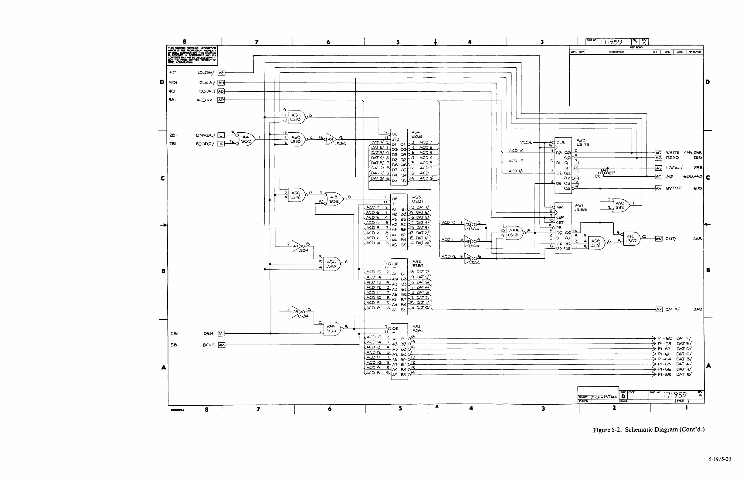
8
THIS
~NG
alNTAINS
INFORMATION
WHICH
II
THE
PllOPRIETARY
PROPERTY
01
unn.
COllPOllATION.
THIS
DRAWING
IS llE:EIWD
IN
a>NFIDDICE
ANO
ITS
COllTENTS
MAY
NOT
IC
DISClOSED
WITll-
OUT
THE
l'lllOll
WRITTEN
CONSENT
OF
llllEL
COllPOllAllON.
..
Ci
LDLOW/
[§Jr-------'
7 6 5 4
D
SDI
4C.I
~LKA/
AHlt---------if---+-+-------------+-----------------------~
COUNT
AD,t--------+--1--1-----------+---+-----------------------~
3
OWG
NO.
111959
ZONE
REV
DESCRIPTION
OFT
CHK
DI.TE
Al'PROYEI>
SAi
A.CJ::;xx
AP
1
t--------+--l-I-------------+--..-------------~---------~!--..
ZBI
ZSI
BMRDC/
L
BIOR.C./ K
i3
12
g
._..
____
l~I
AS6
lre:._
_______
1----1--~
~.:J
LSl<ti I
~
,----,
·~·
.....
+----'-'~"-"
~OE:
A':><+
A4
r-' 1---t-+-+-------11 J
Ase
1
r-12=-
_
_a-'-'1
~~
1 A9
>-'-=i.--+---+-----1'--'1-l
SIB
e-ze.:.
500
~
LS¢4
DAT
71_
Z.
DI
QI
p.18
ACD
7
DAT
G./
I
OO
acz>hl9 AC.D 6
DAT
SJ
4
D3>
Q3b"16 AC.D 5
DAT
4 3
DZ
Q2.
hil
AC.D 4
DA.T
3 7
D6
Q6~1~
AC.D
3
DATZ
8
D?
Qlpi'-
AC.D
2.
vcc~
--~~"'
,~
~~
5
~
l'--A-"C=-D_l~4~----+-+-4-'""'
D¢
Qr/Ji--;:z'-------------+---1--1---ll>Q.
WRITE 4A8,Z.B8
Q.i;ti
p.3 A
R'CAD
zee.
''--_A_C~D_IS~--..-.-5-=-<
DI
QI
~
QI
·~~
0
~----~~.__
_____
..___.____.A5
Lcx:JJ..l/ Z.68
D
c
DAi
I/ S D4
Q4plS
ACD
I
11-~=--
DAT!/}/_ 6
DS
QSpl4
AC.D
~
'--_A_C_D~r:/)----+-+---IZ_.
DZ
Q'2.1--IO=-----E~-o~·E47
Q"Z.
~
= AT
A¢
b08,4AB
(
.--i--1---'-'l~"-l
~
Q3
~
I
Z.Bl
561
A
~
L~~fpi-z.~:
~~~I'./
1
~8--+----CJ.:....,...r
1
~
ASO
.---4----'l-'-l_, T
8£.87
1
'-'-A:=C.-"--D--'7--=-Z....;
Al
B 1
p!8
DA.i 7 /
1
,A'-'C.-=-D"--"'6'---'-I
__.
A¢
f!4;
p'~
DAT€,/
l'-'-'A.C.:::.D::......::5;___c.4....;A~
B"3
hl6
DAi
S)
r-:-:AC=D""--'4--=3'-4
A.C.
BZ
~17
DAI
4/
"-A:....:C..;;:.D=c.....:3'----1'-'
AE:.
eE:.
hl3
DAT
3/
"-A.'-'C=D::;_::Z,____,.8<-<
Al
Bl
~"2
CV>..T
if
1
.._A'""'C-"-D"--1---'S~
A.4
54
1--JS
CAT
\J
~
"'-'A:=C.D=--..!¢'---'E.=-
AS
BS
~4
DA.T
(jJ'
-
---
4
~rr-6-=---1--1-+----g~,r~'------
AS2
--,
ri.
:'---OE BZ.Bl
._+---------4....:..i'
1
LSlw
l I T
A.C.D
IS
Z.
Al
Bl
pl8
DAi
7/
ACD
14
I
A¢
B¢p'~
DAT_!:,/_
ACD
13
4
A7>
83
t:)E.
DP..i
S)
ACD
12
3
A-Z.
B'Z.
hil
DA.I
4/
ACD
I I 7 />6
86
~13
DAT
3j
ACD
l(f; 8
Al
Bl
hl'Z.
DAI
?./
~Lp.~
1
4~-----.i•--)--D---
1
___,1------iAV
BYTO?
e.oe
~MR
ASl
'-
2.
t>
LSIE:.3
.__-------+--+----
7
~cEP
ACD 10 I
A-.,S
-Z.
T::i£
CE.I
.-------<-...---~
LS04
.__
_
__:_I
'-11
~
PE
8 3
D¢
Q¢
14
~
r-.,..
~--4--<DI
Q.I
1'3
3
~
A14
AC.D
11
3
JA?~>AJ,_4_i--e
J
Ji-
DZ
Q°'
~
~5~
bn-::6=--_8.;:;cl L
501.
LS04
jrE.~~
A-CD
1"2.
S"
A'S
::>,,...,o-=E:.=-----41>--------~
AW
CNT/
4N3
LS04
"~'\scti~o
ACD
'1
S M
B4hlS
DAT
I/
ACD
8 0
A5
Bsr~~14.:._=D~A~~~~:z._::,>--
_____________________________________
___,AX
DA.TX/
3A8
'------
10
.----
A~g
r-..;8=---..--1-+----g-'-!..rn
OE
AS
I
DEN
M
1-----------------~q'-l
soo
1 I T eze1
1'-'-'A!.-=C~D~l~S_2=-1AI
Bl
po.:..:18=----~----------------------------------------?:~
Pl-f,O
SOU\
Alv\1--------------------------'
r"'"-'A!.=C.=-D-'-l
4
-'--~I
AC/>
BIJ>
p
1
~
~
Pl-S'1
1
,A-'-C=D"--"13=--_4~A7>
B3
pl6
~
Pl-E,"2.
DAT
F/
DA.TE/
DA..T
D/
c:AI
c/
DAT
B/
DAT
A/
DAT
9/
DAT
e/
;,A~C=-D-'-.!1._
___
3=-<A?.
B?..pll
~
Pi-61
"-A:...:C.:D=--.:.1..:...1
_7-=--lAo
B6Pl3
:'......
Pl-&4
1'-AC..:C..=-D:::.......:.1¢=--=B=-4Al
Bl
PIZ
~
PH:>"3
lACD
'1
5
hiS
A4
B4
"-' 7
Pl-E>e
"A-'-C=-=D~S'---'~=-IAS
BS
p
14
......_
Pl-65
L___
DWG
NO.
171959
REV
A
SHEET
1
8 7 6 5 4 3 1
Figure 5-2. Schematic Diagram (Cont'd.)
I
A
5-19/5-20


iSBC
432i100™
Processor Board Hardware Reference Manual
171820-001
REQUEST
FOR
READER'S
COMMENTS
The Microcomputer Division Technical Publications Department attempts to provide documents that meet
the needs of all Intel product users. This form lets you participate directly in the documentation process.
Piease restrict your comments to the usability, accuracy, readability, organization,
and
compieteness of
this document.
1.
Please specify by page any errors you found
in
this manual.
2.
Does the document cover the information you expected or required? Please make suggestions for
improvement.
3.
Is
this the right type of document for your needs?
Is
it at the right level? What other types of
documents
are'
needed?
4.
Did
you have any difficulty understanding descriptions or wording? Where?
5.
Please rate this document
on
a scale of 1 to 10with10 being the best rating.
NAME
___________________________________________
~
DATE
____________________ _
TITLE
__________________________________________________________________
~
COMPANY
NAME/DEPARTMENT
________________________________________________
~
ADDRESS
________________________________________________________________________ _
C
ITV
------------------------------------------------------------------
STATE--------------
ZIP
CODE
---------------------
Please check here if you require a written reply. D
WE'D
LIKE
YOUR
COMMENTS
•..
This document is one of a series describing Intel products. Your comments on the back of this form will
help us produce better manuals.
Each
reply will be carefully reviewed
by
the responsible person. All
comments and suggestions become the property of Intel Corporation.
BUSINESS REPLY MAIL
FIRST CLASS PERMIT NO.
1040
SANTA CLARA, CA
POSTAGE
WILL
BE
PAID
BY
ADDRESSEE
Intel
Corporation
Attn:
Technical
Publications
M/S
6-2000
3065
Bowers
Avenue
Santa Clara, CA 95051
NO
POSTAGE
NECESSARY
IF
MAILED
IN
U.S.A.

INTEL CORPORATION, 3585
S.W.
198th Avenue, Aloha, Oregon 97007 •
(503)
681-8080
Printed
in
U.S.A./Y36/1 K/0281
/IH
