227 5977 1_1131_Computing_System_FEMM 1 1131 Computing System FEMM
227-5977-1_1131_Computing_System_FEMM 227-5977-1_1131_Computing_System_FEMM
User Manual: 227-5977-1_1131_Computing_System_FEMM
Open the PDF directly: View PDF ![]() .
.
Page Count: 66
I
~ ~
~@
Computing
System
Field Engineering
Maintenance Manual
N
N
'-I
I
Ul
\0
'-I
'-I
I
....
Field Engineering
Maintenance Manual
Issued
to:
____________
_
Branch Office:
___________
_
Department:
___________
_
Address:
____________
_
If
this
manual
is
misplaced, it
should
be
returned
to
the
above
address.
TI
TI
~@
Computing
System
PREFACE
This
manual
contains
all
maintenance
procedures
required
to
service
the
IBM 1130
Data
Processing
System.
This
manual
assumes
that
the
CE
has
limited
experience
and/or
training
on
the
system
and
is
fa-
miliar
with
the
material
contained
in
the
Field
Engi-
neering
Theory
of
Operation
(Instruction
Manual)
manuals
listed
in
the
Bibliography
(Appendix
A).
The
users
of
this
manual
are
cautioned
that
specifications
are
subject
to
change
at
any
time
and
without
prior
notice
by IBM.
Wiring
diagrams
(logics)
at
the
engineering
change
level
of
that
spec-
ific
machine
are
included
in
each
machine
shipment.
This
manual
(Form
227-5977-1)
is a
major
revision
of
Form
227-5977-0.
The
latter
is
made
obsolete
by
this
revision.
Copies
of
this
and
other
IBM
publications
can
be
obtained
through
IBM
Branch
Ofiices.
A
form
has
been
provided
at
the
back
of
this
publication
for
readers'
comments.
If
the
form
has
been
detached,
comments
may
be
directed
to
:
IBM,
Product
Publications
Department,
San
Jose,
Calif.
95114
@)
International
Business
Machines
Corporation,1966.
ii
CHAPTER 1 DIAGNOSTIC AIDS
•••••••••••••••••••
1.
1
Diagnostic
Techniques.
• • • • • • • • • • • • • • • • • • • • • • .
••
1.1
1.
1
TROUBLESHOOTING.....................
1.
1
1.
1.
1
Introduction........................
1. 1
1.
1.2
Error
Detection.
. • . • • • • • . • • • • • • • • • .
.•
1.
1
1.1.3
Error
Isolation.
• • • • • • • . • • • • • • • • • • • •
••
1.1
1.1.4
Dynamic
Detection
•.•.•••••••••••••••
1.2
1.
1.5
Static
Detection
(CE
Control)
.•.••••••.••
1.2
1.
1.
6
Special
Techniques
• . • . • • • . . • • • • • . . •
.•
1. 3
1.2
THE MAINTENANCE DIAGRAM MANUAL (MDM) .
•.
1.
3
1.
2. 1
IBM
1130
Configurator
• • • . • • . • • • • • • • .
.•
1.
3
1.
2.2
System
Data
Flow
Diagram
. • • • • • • • • • . •
••
1.
3
1.
2.3
Unit
Data
and
Control
Diagram
(UDCD) . • • •
.•
1.
3
1.2.4
I/O
Operations
Diagrams
••••.•.••••••••
1. 3
1.
2.
5
Simplified
Logic
Diagrams
(SLD's) • . • • • • •
••
1.
3
1.
2.
6 Logic Flow Charts (CLFC) • • • • • • • • • . • • •
••
1.3
1.2.7
Timing
Charts (T)
..•••••••••.•••••••
1.5
1.3
DIAGNOSTIC PROGRAMMING AND MACHINE
••••
CHECK OUT
••••.•.•.•.•••.•••••••••••
1.5
1.
3.1
Maintenance
Diagnostic
Programs.
• • • • • • •
•.
1.
5
1.
3.
2
Program
Language.
• . • • • • • • • • • • • • • • •
••
1.
5
1.3;
3
Program
Control.
• • • • • • • • • • • • • • • • • •
••
1.5
1.
3.
4 Error Messages
and
Documentation
. • • • • • •
••
1.
5
1.
3.
5
Program
Loading.
• • . • • • . • • • • • • • • • • •
••
1.
5
1.
3.
6 Tests for
Device
Interaction
•••••••••••••
1.5
1.3.7
Operation
Modes.
• • • • • • • • • • • • • • • • . •
••
1.5
1.4
SERVICE CHECK LIST • • • • • • • • • • • • • • • • • •
••
1.7
1.4.1
General
Information
.••••••••••••••
•
••
1.7
1.4.2
General
Check
List
••••••••••••••••••
1.7
1.4.3
Core Storage
Check
List • • • • • • • • • • • • • •
••
1.
7
1.4.4
Addressing
Failure
Check
List
••••••••••••
1.
8
1.4.
5 Core Storage Console
Isolation.
• • • • • • • • •
••
1. 8
1.4.6
Current
Scoping
of
Core.
• • • • • • • • • • • • •
••
1.8
1.4.7
Core Diagnostic Aids (Figure
1-2)
•••••••••
1.
11
1.4.8
Transient
Power
Line
Noise.
• • • • • • • • • • •
••
1.12
1.5
CONSOLE PANEL. • • • • • • • • • • • • • • • • • • • • •
••
1.13
1.6
CE
PANEL.
• • • . • • • • • • • • • • • • • • • • • • • • •
••
1.13
1.7
CONSOLE
PRINTER.
• • • • • • • • • . • . • • . • . . .
••
1.13
1.
7.
1 Console
Printer
Diagnostic
Aids (Figure
1-3)
•
••
1. 13
1.8
MARGINAL CHECKING
•••••••••••••••••.•
1.14
1.9
MISCELLANEOUS
TECHNIQUES.
• • • • • • • • . . •
.•
1.15
1.9.1
Locating
Grounds
••.•••••••••••••••.•
1.15
1.
9.2
Locating
Marginal
SLT Cards
••••••••.•.•
1.15
1.9.3
Signal
Levels.
• • • • • • • • • • • • • • . • • . • •
••
1.15
1.9.4
Transistor
Delay
Times
••.•••••••••••••
1.15
1.9.5
Multi-Input
Flip-Flop's
•..•.•••.•••••••
1.15
CHAPTER 2 MAINTENANCE FEATURES
.••.••••••••••
2.1
Basic
Machine
• . • • • • . . . . • . . . . • . . . . . • . • • . • . •
..
2.
1
2.1
MANUAL CONTROLS AND
INDICATORS.
• • • • •
••
2.1
2.1.1
Objectives.........................
2.1
2.1.
2
Control
Switch
Panel.
• • . • • . • • • • • • • • .
••
2.1
2.1.3
Mode
Switch. • • • • • . • . . . . . • • • • • • • • •
••
2.2
2.1.4
Console Bit Switches
••
• • • • • • . • • . • • • •
••
2.3
iii
CONTENTS
2.1.5
CE
Panel.
• . • • • • . • • • • • • • • • • • • • • •
••
2.3
2.1.
6
Miscellaneous
Switches.
• • • • • • • • • • • • •
••
2.4
2.1.7
Indicators
••••••••••••••••••••••••
2.5
2.2
CE
CARD.
• • • • • • • • • • • • • • • • • • • • • • • • •
••
2.6
2.3
CONSOLE PRINTER AND KEYBOARD. • • • • • • •
••
2.6
2.4
DISK
STORAGE.
• • • • • • • • • • • • • • • • • • • • •
••
2.7
2.4.1
Manual
Controls
and
Indicators.
• • • • • • • •
••
2.7
Features • • • • • • • • • • • • • • • • • • • • • • • • • • • • • • • •
••
2.8
2.5
1442 READER
PUNCH.
• • • • • • • • • • • • • • • • •
••
2.8
2.5.1
CE
Switch.
• • • • • • • • • • • • • • • • • • • • •
••
2.8
2.5.2
Controls
and
Indicators.
• • • • • • • • • • • • •
••
2.8
2.6
1132 PRINTER
••••••••••••••••••••••••
2.9
2.6.1
Manual
Control
and
Indicators • • • • • • • • •
••
2.9
2.7
1627 PLOTTER • . • • • • • • • • • • • • • • • • • • • •
••
2.9
2.7.1
Controls
•••••••••••••••••••••••••
2~9
2.8
1132 PAPER TAPE
READER.
• • . • • • • • • • • • • •
••
2.10
2.9
1055 PAPER TAPE
PUNCH.
• • • • • • • • • • • • • •
••
2.10
2.9.1
Controls
•••••••••••••••••••••••••
2.10
CHAPTER 3 SCHEDULED MAINTENANCE
PROCEDURES..
3.1
Basic
Machine
• • • • • • • • . • . • • • • • • • • • • • • • • • • •
••
3.
1
3.1
APPROACH
TO
SCHEDULED MAINTENANCE. • •
••
3.
1
3.
1. 1
Visual
Inspection.
• • • • • • • • • • • • • • • • •
••
3.
1
3.1.
2
Electronics
Circuits
• • • • • • • • • • • • • • • •
••
3.1
3.1.
3
Mechanical
Units
.••••••••••••••••••
3.1
3.1.4
Scheduled
Maintenance
Procedures • • • • • •
••
3.1
3.
1.5
Console
Printer
Preventive
Maintenance
• • •
••
3.2
3.1.
6 Console
Keyboard
Preventive
Maintenance
•
••
3.2
3.1.7
Disk
Storage
Preventive
Maintenance
••••••
3.2
Features
3.3
3.2
PREVENTIVE MAINTENANCE OF
I/O
DEVICES
•••
3.3
3.2.1
Preventive
Maintenance
••
• • • • • • • • • • •
••
3.3
3.2.2
1442
Preventive
Maintenance
•••••••••••
3.3
3.2.3
1134
Preventive
Maintenance
3.2.4
1055
Preventive
Maintenance
3.2.5
1627
Preventive
Maintenance
CHAPTER 4 CHECKS, ADJUSTMENTS, AND
3.3
3.3
3.3
REMOVAL PROCEDURES
••••••••••••••••••••••
4.1
Basic
Machine
• • • • • • • • • • • • • • • • • • • • • • • • • • • •
••
4.1
4.
1 SOLID LOGIC TECHNOLOGY MAINTENANCE. • •
••
4.1
4.1.1
SLT Cards • • • • • • • • • • • • • • • • • • • • • •
••
4.1
4.1.2
Single
Shots
••••••••••••••••••••••
4.1
4.2
CORE STORAGE
UNIT
• • • • • • • • • • • • • • • • •
••
4.
1
4.2.
1
Removal.........................
4.
1
4.2.2
Adjustment
Procedure
for
Core
Storage
•••••
4.1
4.3
OSCILLATOR.........................
4.2
4.3.
1
Oscillator
Phase
Adjustment.
• • • • • • • • • •
••
4.
2
4.4
CONSOLE KEYBOARD • • • • • • • • • • • • • • • • • •
••
4.
3
4.4.
1
Keyboard
Removal
••••••••••••••••••
4.
3
4.4.
2
Keyboard-Printer
Single Shots
•••••••••••
4.
3
4.4.
3
Keyboard
Assembly
• • • • • • . • • • • • • • • •
••
4.
3
4.
5 CONSOLE PRINTER • • • • • • • • • • • • • • • • • • •
••
4.
8
4.5.
1
General
Information.
• • • • • • • • • • • • • • •
••
4.
8
4.5.2
Service
Checks
••.••••••••••••••••••
4.5.3
Removal
•••••••••••••••••••••••••
4.6
I/O
CABlES
••••••••••••.•••••••••••••
4.
7 DISK STORAGE
UNIT
•••••••••••••••••••
4.
7.
1
Removal
•••••••••••••••••••••••••
4.7.2
File
Read-Write
Single
Shot
••••••••••••
4.
8 MISCELLANEOUS UNITS
••••••••••••••••••
4.
8.1
Table
Top
••••••••••••••••••••••••
4.
8.
2
Gate
Blowers
••••••••••••••••••••••
4.8.3
Filters
••••••••••••••••••••••••••
4.
8.4
Console Lamps
•••••••••••••••••••••
4.
8.5
Status
Indicator
Panel
••••••••••••••••
Features
••••••••••••••••••••••••••••••••••
4.9
1442
ATTACfWENT
••••••••••••••••••••
4.9.1
Read
Single
Shot
.••••••••••••••••••
4.
9.2, Punch
Gate
Single
Shot·
•••••••••••••••
4.10
PAPER TAPE ATTACHMENT
•••••••••••••••
4.
10.
1
Paper
Tape
Reader
Single
Shot
•••••••••••
4.10.2
Paper
Tape
Punch
•••••••••••••••••••
4.10.3
1134
Attachment
Oscillator
•••••••••••••
4.11
1132 PRINTER ATTACHMENT
•••••••••••••
4.12
1627 PLOTTER ATTACHMENT
•••••••••••••
4.13
1132 PRINTER
••••••••••••••••••••••••
4.14
1627 PLOTTER
•••••••••••••••••••••••
4.8
4.8
4.8
4.9
4.9
4.9
4~9
4.9
4.9
4.9
4.9
4.10
4.11
4.11
4.11
4.11
4.11
4.11
4.11
4.11
4.11
4.11
4.11
4.11
iv
4.15
1134
PAPER TAPE
READER'
• • • • • • • • • •
••
4.11
4.16
1055
PAPER TAPE PUNCH
•••••••••••••
4.11
4.17
1442 SERIAL READER
PUNCH.
• • • • • • • •
••
4.11
CHAPTER 5 POWER SUPPLIES. • • • • • • • • • • • • • • • • • • •
5.
1
Basic
Machine
• • • • • • • • • • • • • • • • • • • • • • • • • • • •
••
5.
1
5.1
GENERAL...........................
5.
1
5.1.1
Power
Distribution
and
Sequencing.
• • • • •
••
5.1
5.1.2
Switches.........................
5.2
S. 1. 3 CE Power Switches
••••••••••••••••••
5.2
5.1.4
Indicators • • • • • • • • • • • • • • • • • • • • • • • •
5.2
5.1.5
Voltage
Variation.
• • • • • • • • • • • • • • • •
••
5.2
S. 1. 6
Convenience
Outlet
•••••••••••••••••
5.2
5.1.7
Voltages
Present
Under
Normal
Power Off
Conditions.
• • • • • • • • • • • • • • • • • • • • • • • S. 2
S. 1. 8
Input
Power
Specifications
••
• • • • • • • • • • •
5.2
5.1.9
Individual
Power
Supplies.
• • • • • • • • • • • • •
5.2
5.1.10
Core
Storage
Voltages
• • • • • • • • • • • • • • • •
5.2
5.
2 SERVICE CHECKS AND HINTS
•••••••••••••
5.
3
5.3
ClEANING...........................
5.3
5.4
ADJUSTMENTS AND REMOVAL PROCEDURE • • • •
5.3
S.
4.
1
Removal
••••••••••••••••••••••••
S. 3
S. 4. 2
Adjustment.......................
S. 3
5.5
DIAGNOSTICS........................
5.3
5.5.1
Power Supply
Trouble
Symptom
Analysis
Chart
5.4
APPENDIX A - BIBLIOGRAPHY. . . . . . . . . . . . . .
..
A. 1
WARNINGS
Core
Storage
Be
extremely
cautious
when
working
around
the
core
array.
Avoid
disturbing
individual
planes.
Sense
and
select
wires
are
welded
to
pins
at
the
perimeter
of
the
array.
Bending
these
pins
can
fracture
welds
or
cause
shorts
between
adjacent
pins.
Use
the
han-
dles
provided
and
exercise
care
to
prevent
the
sides
from
striking
the
frame
of SL T
cards
whenever
it
is
necessary
to
remove
the
array.
Do
not
leave
core
storage
unit
unattended
when
covers
are
removed.
Oscilloscope
Core
Storage
Direct
probing
of
the
core
planes
is
not
advised.
Because
core
is
a
current
device,
no
valuable
infor-
mation
can
be
obtained
with
voltage
measurements
in
this
area
and
considerable
damage
could
result.
Due
to
physical
construction
of
the
core
array
the
current
probe
cannot
be
used
directly.
Techniques
for
obtaining
current
and
voltage
wave
shapes
are
detailed
in
section
1.4.
6
of
this
manual.
General
The
SLT
probe
tip
should
be
used
when
scoping
to
prevent
shorting
of
voltage
pins.
Probing
with
alli-
gator
clips
or
uninsulated
tips
should
be
avoided.
Power
Supplies
When
the
system
is
in
a
power-off
status,
24
vac
is
present
in
the
power
supply
area.
SLT
Components
Turn
off
power
whenever
an
SLT
card
is
removed
or
replaced.
Turn
off
power
to
the
sy
stem
when
v
wrapping
or
unwrapping
wire
or
when
testing
for
continuity.
Avoid
operating
the
system
for
prolonged
periods
of
time
with
the
SLT
card
covers
removed.
Servicing
Clear
core
storage
after
servicing
the
processor
to
prevent
returning
the
system
to
the
customer
with
an
invalid
word
in
core
storage.
An
invalid
word
re-
sults
in
a
data
error
when
the
word
is
read
from
core.
Tying
input
and
output
logic
functions
to
the
ground
or
to 0
volt
level
can
be
helpful
in
troubleshooting.
Exercise
care
in
the
disk
storage
unit
to
prevent
des-
troying
disk
storage
data
when tying
lines
to
the
0
volt
level.
Some
logic
blocks
can
be
tied
to
the
+ 3
volt
level.
It
is
necessary
to
evaluate
the
physical
con-
struction
of
the
component
circuits,
both
input
and
output,
on
a
line
before
it
can
be
determined
whether
the
+ 3
volt
level
will
be
effective.
Information
about
the
component
circuits
is
not
now
available
in
the
field.
In
general,
use
a 0
volt
level
and
work
back
to
an
input
or
an
output
which
gives
the
required
+ 3
volt
level.
Power
supply
voltages
are
present
on
some
pins.
Exercise
care
not
to
ground
these
pins.
NOTE:
Insert
a
470Q
resistor
to
act
as
a
load
limit-
ing
resistor
in
the
jumper
used
for
tying
down
lines.
Card
Reader
I/O
Run
all
cards
out
of
the
card
reader
punch
before
powering
down.
Powering
down
the
card
reader
punch
when
the
card
punch
is
loaded
with
cards
results
in
a
card
laced
in
column
one.
Use
the
pro-
vided
diagnostic
tests
as
masters
and
reproduce
the
deck
before
uSIng
the
deck
to
reduce
exposure
to
having
to
re-keypunch
cards.
Make
customer
aware
of
the
lacing
of
cards.
SAFETY
Personal
safety
cannot
be
over-emphasized.
To
ensure
your
own
safety,
make
it
an
every
day
practice
to
follow
safety
precautions
at
all
times.
Become
familiar
with
and
use
the
safety
practices
outlined
in
the
pocket-size
cards,
IBM
Forms
124-0002
and
MO
4-8401,
issued
to
all
Customer
Engineers.
Voltages
Potential
difference
within
the
electronic
gates,
printed
cards,
and
display
back
panel
is
+48v
dc
to
-3v
dc.
Do
not
remove
or
replace
circuit
cards
when
dc
power
is
on.
Do
not
short
out
or
bypass
safety
features.
Power
Supplies
Extreme
care
must
be
exercised
when
servicing
or
inspecting
the
power
supply
even
though
the
voltage
range
on
the
machine
is
low.
Dangerous
voltages
and
currents
are
present
even
when
the
system
is
in
a
power-off
status.
If
it
is
necessary
to
connect
a
test
instrument
within
the
power
supply,
or
to
reach
into
it
for
any
reason,
disconnect
the
main-
line
cord.
Discharge
capacitors
before
working
near
them.
Each
heat
sink
is
at
an
electrical
poten-
tial.
Do
not
short
heat
sinks
to
each
other
or,
to
the
machine
frame.
Grounding
Convenience
outlets
for
Customer
Engineers
are
provided
in
the
1131, 1132,
and
1442.
Machine
grounding
is
required.
Three-wire
grounded
power
cords
are
provided.
The
third
wire
is
for
grounding
and
must
not
carry
current
from
any
source.
IT
IS IMPORTANT
TO
THE
SAFETY
OF
PERSONNEL
THAT
IF
ANY
MACHINE
OF
A GROUP
IS GROUNDED,
ALL
OTHER
EQUIPMENT
OF
THE
GROUP MUST
BE
GROUNDED.
Grounded
machines
must
be
placed
so
that
it
is
not
possible
for
a
person
to
touch
both
a
grounded
machine
and
any
ungrounded
metal
equipment.
Grounded
machines
do
not
present
vi
a
hazard
in
themselves;
the
real
hazard
is
from
un-
grounded
electrical
equipment.
Console
Printer
(Modified IBM
SELECTRIC
® )
Working
in
certain
areas
of
the
typewriter
is
particu-
lar
ly
hazardous
due
to
the
positive
action
of
the
type-
writer.
Follow
safe
working
practices.
Because
it
is
not
possible
to
foresee
each
individual
area
of
exposure,
the
following
general
rules
serve
as
a
guide
when
working
on
this
equipment.
1.
At
the
completion
of
a
service
call,
replace
gear
guards
and
dust
shields.
These
safety
guards
are
installed
to
prevent
the
operator
from
placing
his
hands
too
near
moving
parts.
Because
most
operators
do
not
have
a
complete
knowledge
of
the
mechanical
workings
of
the
machine,
the
only
way
they
can
be
adequately
protected
is
to
place
guards
over
the
exposed
areas.
Be
cautious
when
servicing
this
machine
during
the
time
the
rear
guards
and
dust
shields
are
removed.
2.
When
lubricating,
replacing
parts,
etc.,
make
sure
the
machine
is
turned
off.
It
is
a good
idea
to
remove
the
motor
plug
from
the
socket
after
turning
the
switch
to
the
off
position.
3.
Exercise
caution
when
handling
the
motor.
The
shaded-pole
motor
used
in
this
machine
runs
considerably
hotter
than
the
capacitor
type
motor
used
in
the
Model
B
typewriter.
4.
Be
particularly
careful
to
avoid
injury
to
the
hands
from
sharp
edges
on
stamped
parts,
springs,
links,
etc.
when
picking
up
and
handling
all
types
of
machines.
Although
the
safety
of
the
operator
and
the
CE
is
one
of
the
prime
consider-
ations
in
the
design
of
the
product,
mass
pro-
duction
techniques
do
not
permit
separate
opera-
tions
on
each
part
to
provide
a
smooth
edge.
5.
Wear
safety
glasses
when
performing
any
work
that
could
result
in
parts,
lubricants,
cleaning
solvents,
or
any
other
materials
contacting
the
eyes.
NOTE:
The
word
CAUTION
is
used
in
this
manual
to
indicate
procedures
that
require
extra
precautions
to
ensure
personal
safety.
DIAGNOSTIC TECHNIQUES
1.
1 TROUBLESHOOTING
1. 1.
1
Introduction
The
service
philosophy
of
the
1130
system
is
based
on
the
effective
use
of
diagnostic
programs
and
techniques.
These
programs
and
techniques
depend
heavily
on
the
multiple
modes
of
operation
of
the
processor
and
of
the
console
indicators
to
define
problem
areas.
It
must
be
recognized
that
the
pro-
grams
and
techniques
carmot
always
eliminate
the
need
for
detailed
pulse
and
voltage
checking,
but
they
are
designed
to
reduce
this
detailed
evaluation
to a
minimum.
When a
failure
occurs,
note
all
pertinent
infor-
mation.
Record
the
contents
of
all
registers
and
console
panel
indicators
on a
check
sheet
for
later
reference.
Try
to
localize
the
failure
before
re-
moving
the
machine
from
productive
work.
The
+12
and
+48
volt
supplies
do
not
power
down
the
system
if
either
has
a
power
failure.
The
sys-
tem
does
not
run
if
these
voltages
are
missing
and
the
supplies
should
be
checked
first
to
determine
their
condition.
The
increased
realiability
of
electronic
com-
ponents
suggests
that
the
majority
of
general
service
problems
are
electro-mechanical
in
nature.
These
problems
are
caused
by
mechanical
adjustments,
mechanical
wear,
electrical
timing,
and
loose
connections.
Diagnostic
procedures
have
been
provided
to
assist
in
isolating
troubles
between
the
electronics
of
the
processor
and
the
functions
of
electro-
mechanical
peripheral
devices.
Keep
in
mind
two
other
problem
sources,
pro-
gram
troubles
and
electrical
noise
troubles.
Be-
cause
the
1131
processor
depends
completely
on
programming
for
all
input
and
output
functions
as
well
as
for
processing,
program
timing
errors
and
incorrect
data
can
appear
as
electronic
processor
or
I/o
problems.
The
diagnostic
programs
are
designed
to
exercise
and
examine
the
fWlCtions
of
the
processor
and
I/o
devices.
In
general,
the
tests
provide
the
assurance
needed
to
guide
problem
analysis
to
the
machine
or
the
program.
Electrical
noise
can
be
a
problem
due to
the
low
level
signals
used
in
this
and
other
solid
state
systems.
Critical
evaluation
during
test
assures
that
the
system
is
CHAPTER
1 - DIAGNOSTIC AIDS
free
from
electrical
noise
interference
anticipated
in
most
environments.
Suppression
circuits
have
been
designed
into
the
system
to
reduce
exposure
to
both
internal
and
external
interference.
However,
there
is
always
the
possibility
of
unique
external
conditions
or
of
the
failure
of
grounding
or
suppres-
sion
circuits.
While
there
are
no
unique
tests
or
tools
available
to
pinpoint
electrical
noise,
the
diagnostic
section
of
this
manual
does
provide
some
analYSis
procedures
which
can
assIst
trouble
analysis
when
electrical
interference
is
suspected.
Note:
For
problems
that
do
not
seem
to
lend
themselves
to
analysis,
check
that
all
cards
and
interboard
connectors
are
in
place
and
seated.
1. 1.
2
Error
Detection
All
data
entering
core
storage
has
odd
parity
added
to
each
half
word.
The
parity
is
checked
when
reading
out
of
core
storage.
A
parity
error
in
core
results
in
the
processor
stopping
at
the
end
of
the
core
storage
cycle
in
which
the
parity
error
con-
dition
is
detected.
Parity
bypass
is
under
CE
switch
control,
not
under
program
control.
The
I/o
devices
have
checking
circuits
with
error
checks
which
can
be
recognized
by
programmed
interrogation
of
the
corresponding
Device
Status
Word
(DSW);
Disk
Storage,
1132
Printer,
and
1442-6
or
7
Card
Reader-Punch.
Each
of
these
devices,
except
Disk
Storage,
uses
a
visual
indicator
to
alert
the
operator
to
the
fact
that
an
error
has
occurred.
System
diagnostic
programs
provide
for
error
handling
techniques
for
program
recognizable
input
data
errors,
and
supply
printouts
to
aid
in
diagnosing
troubles.
1.
1. 3
Error
Isolation
The
CE
switches
under
the
right
hand
top
cover
pro-
vide
specific
functions
for
processor
error
isolation.
Bit
switch
data
can
be
written
into
core
and
then
read
back
for
parity
verification.
Bit
switch
data
can
be
cycled
through
the
processor
and
registers
without
reference
to
storage.
Interrupt
request
can
be
in-
hibited.
Indicator
lamps
can
be
mass
tested.
In
addition
to
the
CE
switches,
four
modes
of
operation
(single
step,
single
cycle,
single
instruc-
tion,
and
interrupt
run)
are
available
at
the
console.
These
modes
are
described
in
detail
in
section
1. 1.
5.
1.1
To
further
assist
error
isolation,
the
single
disk
storage
can
be
disconnected
from
the
system
and
operated
in
the
read
mode
under
CE
switch
con-
trol.
The
processor
can
also
be
operated
independ-
ently
of
the
disk
storage
when
it
has
been
discon-
nected
from
the
system.
The
I/o
devices
are
capable
of
limited
mechan-
ical
operation
independently
of
the
processor.
In
general,
independent
mechanical
operation
of
the
devices
cannot
be
performed
without
affecting
pro-
cessor
performance.
It
is
possible
to
remove
the
devices
from
the
system
by
disconnecting
their
signal
connectors.
In
some
cases
it
is
necessary
to
ground
interrupt
level
lines
to
permit
operation
of
the
processor
with
the
device
removed.
The
following
chart
indicates
which
lines
must
be
grounded,
if
the
I/O
device
is
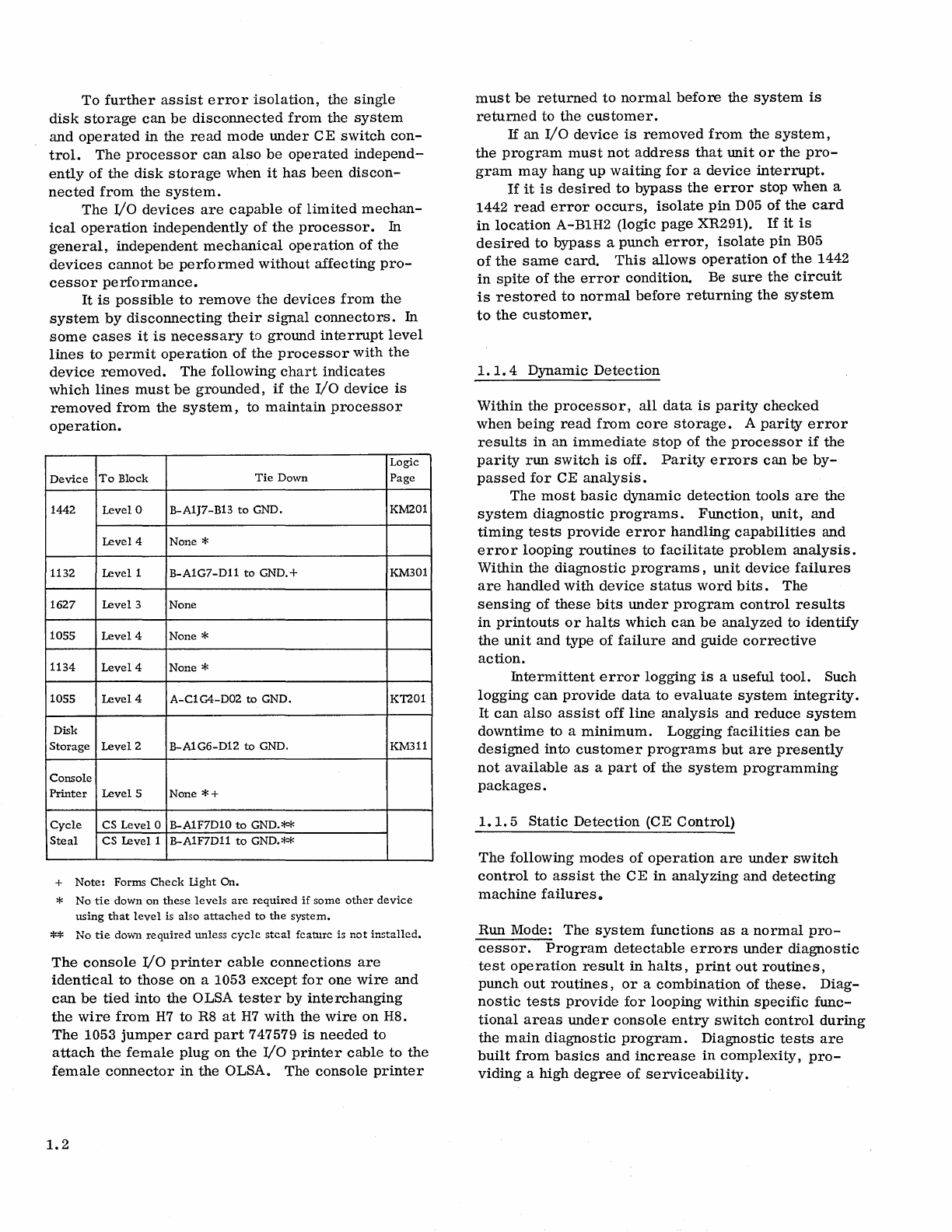
removed
from
the
system,
to
maintain
processor
operation.
Logic
Device
To
Block
Tie
Down
Page
1442
Level
a
B-AIJ7-B13
to
GND. KM201
Level
4
None
*
1132
Levell
B-AIG7-D11
to
GND.+
KM301
1627
Level
3
None
lOSS
Level
4
None
*
1134
Level
4
None
*
lOSS
Level
4
A-CIG4-D02
to
GND. KT201
Disk
Storage
Level
2
B-AIG6-D12
to
GND. KM311
Console
Printer
levelS
None
*+
Cycle
CS
Level
0
B-AIF7DlO
to
GND.**
Steal
CS
Levell
B-AIF7D11
to
GND.**
+
Note:
Forms
Check
Light
On.
* No
tie
down
on
these
levels
are
required
if
some
other
device
using
that
level
is
also
attached
to
the
system.
......
No
tie
dovvi1
required
unless
cycle
steal
feature
is
not
installed.
The
console
I/o
printer
cable
connections
are
identical
to
those
on
a 1053
except
for
one
wire
and
can
be
tied
into
the
OLSA
tester
by
interchanging
the
wire
from
H7
to R8
at
H7
with
the
wire
on
H8.
The
1053
jumper
card
part
747579
is
needed
to
attach
the
female
plug
on
the
I/o
printer
cable
to
the
female
connector
in
the
OLSA. The
console
printer
1.2
must
be
returned
to
normal
before
the
system
is
returned
to
the
customer.
If
an
I/O
device
is
removed
from
the
system,
the
program
must
not
address
that
unit
or
the
pro-
gram
may
hang
up
waiting
for
a
device
interrupt.
If
it
is
desired
to
bypass
the
error
stop
when
a
1442
read
error
occurs,
isolate
pin
D05
of
the
card
in
location
A-B1H2 (logic
page
XR291).
If
it
is
desired
to
bypass
a
punch
error,
isolate
pin
B05
of
the
same
card.
This
allows
operation
of
the
1442
in
spite
of
the
error
condition. Be
sure
the
circuit
is
restored
to
normal
before
returning
the
system
to
the
customer.
1.1.4
Dynamic
Detection
Within
the
processor,
all
data
is
parity
checked
when
being
read
from
core
storage.
A
parity
error
results
in
an
immediate
stop
of
the
processor
if
the
parity
run
switch
is
off.
Parity
errors
can
be
by-
passed
for
CE
analysis.
The
most
basic
dynamic
detection
tools
are
the
system
diagnostic
programs.
Function,
unit,
and
timing
tests
provide
error
handling
capabilities
and
error
looping
routines
to
facilitate
problem
analysis.
Within
the
diagnostic
programs,
unit
device
failures
are
handled
with
device
status
word
bits.
The
sensing
of
these
bits
under
program
control
results
in
printouts
or
halts
which
can
be
analyzed
to
identify
the
unit
and
type
of
failure
and
guide
corrective
action.
Intermittent
error
logging
is
a
useful
tool.
Such
logging
can
provide
data
to
evaluate
system
integrity.
It
can
also
assist
off
line
analysis
and
reduce
system
downtime
to a
minimum.
Logging
facilities
can
be
designed
into
customer
programs
but
are
presently
not
available
as
a
part
of
the
system
programming
packages.
1.1.
5
Static
Detection
(CE
Control)
The
following
modes
of
operation
are
under
switch
control
to
assist
the
CE
in
analyzing
and
detecting
machine
failures
0
Run Mode:
The
system
functions
as
a
normal
pro-
cessor.
Program
detectable
errors
under
diagnostic
test
operation
result
in
halts,
print
out
routines,
punch
out
routines,
or
a
combination
of
these.
Diag-
nostic
tests
provide
for
looping
within
specific
func-
tional
areas
under
console
entry
switch
control
during
the
main
diagnostic
program.
Diagnostic
tests
are
built
from
basics
and
increase
in
complexity,
pro-
viding
a
high
degree
of
serviceability.
Run
Interrupt
Mode: A
level
five
interrupt
occurs
after
each
main
line
instruction.
This
mode
can
be
used
for
tracing
main
line,
branch,
or
sub-routine
operations.
Single
Instruction
Mode:
The
processor
stops
after
each
instruction
is
executed.
The
start
key
controls
the
advance.
Single
Machine
Cycle:
The
processor
executes
a
single
clock
cycle
TO-T7,
E,
I,
IX, IA,
etc.
,
under
control
of
the
start
key.
SMC
can
be
used
to
investi-
gate
CPU
functions
with
every
cycle
taken
by
memory.
Single
Step:
The
processor
executes
a
single
clock
step,
i.
e.
,
Tl
under
control
of
the
start
key.
Pressing
the
single
step
key
results
in
the
generation
of
an
A
pulse,
the
release
of
the
key
results
in
a
B
pulse.
Exercise
care
when
using
single
step
because
core
data
can
be
destroyed
if
the
processor
is
reset
or
if
the
mode
switch
is
changed
between
TO
and
T6
time.
1.
1.
6
Special
Techniques
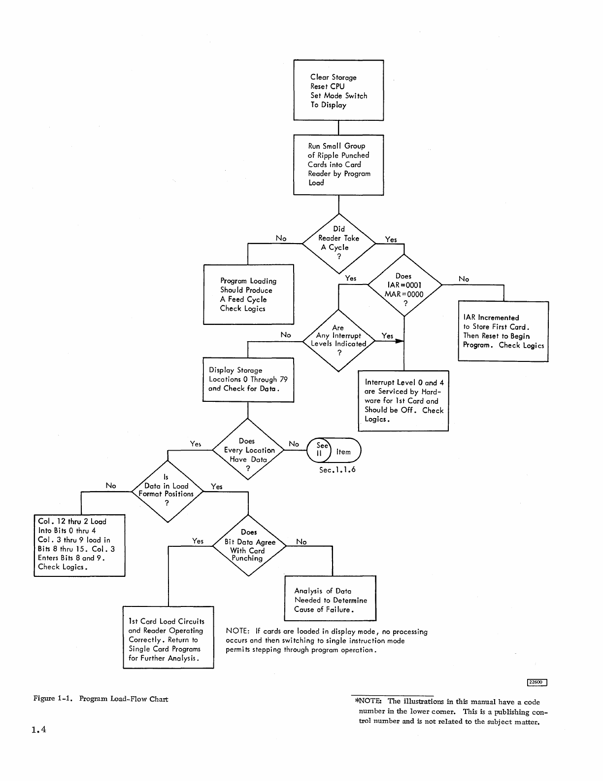
Failure
to
Program
Load
(card
system):
(Figure
1-1)
The
initial
problem
is
to
define
whether
the
card
reader
or
the
processor
is
at
fault.
The
following
procedure
can
assist
diagnosis:
1.
Try
one
card
programs.
If
these
do
not
lead
to
an
immediate
fault
location,
load
core
with
hex
7000 (MDX)
using
the
bit
switches
and
the
storage
load
switch.
Press
reset
and
start
the
program
by
pressing
the
start
key.o
This
causes
the
processor
to
perform
a
no-op
operation.
By
changing
the
displacement
through
core,
the
instruction
operates
as
a
branch.
If
the
MDX
instruction
operates
properly,
enter
hex
COOO
(load
accumulator)
in
location
0000.
Enter
hex
DOOO
(store
accumulator)
in
location
0001.
Reset
the
CPU
and
press
the
start
key.
This
simple
routine
loops
and
sets
hex
DOOO
in
every
core
location.
If
these
routines
run,
check
the
system
using
the
following flow
chart.
2.
An
incorrectly
adjusted
read
emitter
causes
intermittent
loss
of
interrupts.
In
this
case
the
last
words
in
the
read
in
area
are
blank
and
the
data
read
is
in
adjacent
positions.
Failure
to
read
a
column
(assuming
an
interrupt
occurs)
results
in
blank
words
within
the
SO-word
field
causing
a
read
register
check
or
a
feed
check.
Double
incrementing
of
the
I
counter
on
pro-
gram
load
causes
blank
words
in
core
on
program
load.
Card
Feeding
(no
program):
A
technique
for
causing
the
1442 to
feed
cards
without
a
program
in
the
machine
is
sometimes
needed.
This
technique
is
1.
Load
the
read
hopper
with
cards.
2.
Turn
the
mode
switch
to
single
step.
3.
Press
the
program
load
key.
Cards
continue
to
feed
as
long
as
the
program
load
key
is
held.
The
program
load
key
may
be
blocked
down
and
the
feeding
controlled
by
the
1442
start
and
stop
keys.
1.
2
THE
MAINTENANCE DIAGRAM MANUAL (MDM)
The
following
paragraphs
define
the
organization
and
contents
of
this
manual.
1.
2.1
IBM 1130
Configurator
•
Defines
the
maximum
system
configuration.
1.2.2
System
Data
Flow
Diagram
• Shows
over-all
data
flow
of
the
1130.
• Shows
exits
and
entries
to
I/O.
1.
2. 3 Unit
Data
and
Control
Diagram
(UDCD)
•
Expands
each
unit
contained
within
the
system
data
flow
diagram
to
include
major
controls.
1.
2.4
I/o
Operations
Diagrams
• Shows
the
over-all
functions
of
I/o
operations
in
positive
logic
diagrams.
1.
2.5
Simplified
Logic
Diagrams
(SLDs)
•
Contains
logic
diagrams,
arranged
in
an
under-
standable
manner,
of
those
complex
areas
of
the
system
where
an
additional
level
of
logic
is
desired
for
clarity.
1.
2.6
Logic
Flow
Charts
(CLFC)
• Shows
in
condensed
form,
the
concept
of
a
particular
operation.
1.3
Col.
12 thru 2 Load
Into Bits 0 thru 4
Col.
3 thru 9 load in
Bits 8 thru
15.
Col.
3
Enters Bits 8
and
9.
Check
Logics.
Yes
1
st
Card
Load
Circui
ts
and
Reader
Operating
Correctly.
Return to
Single
Card
Programs
for
Further
Analysis.
Figure
1-1.
Program
Load-Flow
Chart
1.4
No
Program Load i ng
Shou
Id
Produce
A
Feed
Cycle
Check
Logics
No
Display
Storage
Locations 0 Through
79
and
Check
for
Data.
No
C
lear
Storage
Reset CPU
Set
Mode Switch
To
Display
Run
Small
Group
of
Ripple
Punched
Cards
into
Card
Reader by Program
Load
Interrupt
Level 0
and
4
are
Serviced
by
Hard-
ware
for 1
st
Card
and
Should
be
Off.
Check
Logics.
Analysis
of
Data
Needed
to
Determine
Cause
of
Fai
lure.
No
IAR
Incremented
to Store First
Card.
Then Reset
to
Begin
Pr09ram.
Check
Logi cs
NOTE:
If
cards
are
loaded
in
display
mode I no
processing
occurs
and
then
switching
to
single
instruction
mode
permits
stepping
through program
operction.
*NOTE:
The
illustrations
in
this
manual
have
a
code
number
in
the
lower
comer.
This
is a
publishing
con-
trol
number
and
is
not
related
to
the
subject
matter.
1.2.7
Timing
Charts
(T)
•
Contains
diagrams
depicting
the
timing
con-
ditions
of
applicable
operations.
1.
3 DIAGNOSTIC PROGRAMMING AND MACHINE
CHECK OUT
Diagnostic
programs
provide
rapid
diagnosis
of
many
system
troubles.
The
console
panel
is
useful
for
controlling
manually
entered
tests
used
when
diag-
nostic
programs
cannot
be
run.
1.
3.1
Maintenance
Diagnostic
Programs
•
The
information
on the
diagnostic
programs
presented
here
is
for
general
use
only.
Detailed
descriptions
of
the
programs
and
their
use
are
provided
with
the
programs.
The
maintenance
programming
system
was
developed
to
test
and
check,
as
completely
as
possible,
the
data
paths,
checking
circuits,
control
functions,
timing
relationships,
registers,
mechanical
adjust-
ments,
and
I/o
interaction.
The
various
programs
that
test
the
individual
machine
functions
provide
detection,
degrees
of
localization,
and
communicate
to
the
CE
those
indi-
cations
of
machine
status
which
assist
him
in
repairing
the
problem
rapidly.
1.
3.2
Program
Language
The
maintenance
program
system
is
programmed
using
the
1800/1130
standard
assembler
program
language.
The
lis
tings
follow the-
standard
assembler
program
format
and
include
comments
and
explanations
to
help
the
CE
understand
and
follow
the
program
operation.
1.
3.
3
Program
Control
Manual
control
of
the
maintenance
program
system
is
provided
as
follows:
1.
Stop
or
continue
on
error.
2.
Loop
program,
loop
routine,
loop
function,
or
loop
on
error.
3.
Bypass
or
allow
error
type
out.
4.
The
program
can
bypass
or
allow
manual
intervention
requests.
1.
3.
4
Error
Messages
and
Documentation
These
items
are
included
in
either
the
error
messages
or
documentation,
or
both.
1.
The
location
in
the
program
of
the
failing
routine
or
function.
2. The
cause
of
the
program
halt
or
error
message.
3.
The
function
or
functions
that
failed.
4. A
comparison
of
the
actual
results
to
the
expected
results.
1.
3.
5
Program
Loading
The
maintenance
programs
are
provided
on
cards
and
paper
tape
•
1.
3.6
Tests
for
Device
Interaction
The
diagnostic
monitor
has
the
facility
for
con-
trolling
up to
six
test
programs
simultaneously,
depending
on
core
size,
to
provide
overlapped
or
interaction
operation
of
devices.
1.
3.7
Operation
Modes
The
maintenance
programs
are
designed
to
run
in
one
of
two
modes,
independent
mode
or
dependent
mode.
1.
3.
7.1
Independent
Processor
Tests
These
programs
assume
complete
control
of
the
system
and
run
independently
of
any
other
program.
All
I/o
functions
and
interrupt
controls
are
handled
within
the
program.
Errors
are
indicated
by
error
halts
which
are
described
in
the
documentation.
Function
Tests:
These
tests
are
engineered
specifi-
cally
to
exercise
and
evaluate
each
of
the
functions
of
the
system.
The
function
tests
are
designed
to
provide
thorough
fault
detection
(data,
sequence
and
inter-
action
related
problems
may
not
necessarily
be
de-
tected
by
a
function
test),
with
short
run
time
and
minimal
program
size.
These
programs
use
the
building
block
approach,
that
is,
the
simplest
instruction
is
tested
first
and
no
instruction
is
used
to
test
another
instruction
until
it
has
been
fully
tested
itself.
The
procedures
for
running
the
tests
are
given
in
the
CPU
test
index
in
the
test
documentation.
1.5
Tests
included
in
the
independent
mode
are:
1.
CPU
function
test
2.
Core
storage
function
test
3.
Core
storage
adjustment
test
4.
Basic
diagnostic
loader
5. One
card
diagnostic
programs
(7)
6.
Program
load
manual
tests
7.
Interrupt
test
The
program
load
manual
tests
are
used
when
none
of
the
other
function
tests
will
load.
To
diag-
nose
this
type
of
trouble,
the
CE
must
use
the
test
facilities
provided
on
the
console.
To
optimize
his
performance
in
the
use
of
these
facilities,
a
pro-
gram
load
diagnostic
guide,
in
the
test
documen-
tation,
has
been
developed.
Instructions
are
entered
one
at
a
time
through
the
bit
switches
and
the
instruc-
tion
operation
can
be
evaluated
by
the
CE.
1. 3. 7. 2
Monitor
Controlled
I/o
Tests
These
programs
run
under
control
of
the
diagnostic
monitor
and
may
be
over
lapped.
Errors
are
indi-
cated
by
error
messages
printed
out
on
the
1131
Console
Printer.
All
I/O
programs
run
under
control
of
this
monitor.
Under
this
control,
programs
can
be
run
one
at
a
time,
run
in
a
predetermined
sequence,
Program
1.
Monitor
2.
CPU
function
test
3.
Core
storage
function
test
4.
Disk
storage
function
test
5.
Disk
initialization
program
6.
1132
function
test
7.
1442
function
test
8.
1442
timing
test
9.
Paper
tape
function
test
10.
1627
function
test
11.
Console/keyboard
printer
function
test
12.
Core
adjustment
test
13.
Meter
test
14.
Basic
diagnostic
loader
15.
One
card
diagnostic
programs
16.
Program
load
manual
test
17.
Interrupt
function
test
18.
Maintenance
routines
1.6
or
run
simultaneously
in
any
combination,
except
as
limited
by
core
size.
Two
versions
are
available;
card
and
paper
tape.
Program
selection
is
via
the
bit
switches.
This
program
controls
the
I/o
function
tests
and
incorporates
the
functions
of
housekeeping,
program
loading
and
execution,
interrupt
handling,
error
handling
and
customer
engineer
communi-
cation,
such
as
printouts.
The
documentation
pro-
vides
an
I/O
monitor
test
index
to
aid
in
running
these
tests.
The
following
programs
are
provided:
1.
Paper
tape
reader/punch
function
test
2. 1131
Console/keyboard
function
test
3. 1132
function
test
4. 1442
function
test
5. 1442
timing
test
6. 1627
function
test
7.
Disk
storage
function
test
8.
Disk
initialization
program
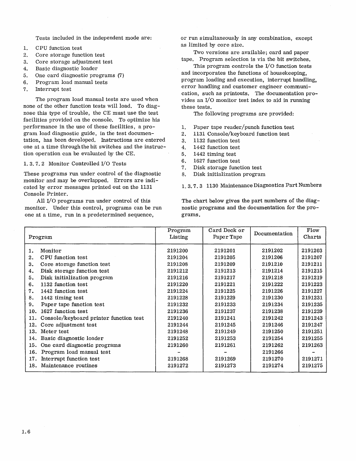
1. 3.
7.
3 1130
Maintenance
Diagnostics
Part
Numbers
The
chart
below
gives
the
part
numbers
of
the
diag-
nostic
programs
and
the
documentation
for
the
pro-
grams.
Program
Card
Deck
or
Documenta
tion
Flow
Listing
Paper
Tape
Charts
2191200
2191201
2191202 2191203
2191204 2191205 2191206 2191207
2191208 2191209 2191210 2191211
2191212 2191213 2191214 2191215
2191216 2191217 2191218 2191219
2191220 2191221 2191222 2191223
2191224 2191225 2191226 2191227
2191228 2191229 2191230 2191231
2191232 2191233
2191234
2191235
2191236 2191237 2191238 2191239
2191240 2191241 2191242 2191243
2191244 2191245 2191246 2191247
2191248 2191249 2191250 2191251
2191252 2191253 2191254 2191255
2191260 2191261 2191262 2191263
- - 2191266 -
2191268 2191269
2191270
2191271
2191272 2191273
2191274
2191275
1.
4 SERVICE CHECK LIST
1.
4.1
General
Information
1.
On
what
operation
does
the
machine
fail?
a.
Diagnostic
test.
b.
Customer
work
(Fortran,
etc.)
c.
Op
code
during
which
failure
occurred.
2-.
What
is
the
frequency
of
error?
a.
Time
of
day.
b.
Environment
(temperature,
etc.)
c.
Does
customer
power
fluctuate
at
certain
time
of
day?
(welder,
heavy
machinery,
etc.
)
1.
4.
2
General
Check
List
1.
Have
connectors
and
cards
been
checked
for
looseness
or
for
bent
contacts?
a.
Edge
connectors
b.
Laminar
bus
(pins
and
terminals)
c.
TB
connectors
(power
supply,
power
sequence,
etc.)
2.
Have
grounds
been
checked?
(1.
9.
1)
a.
DC
isolated
ground
b.
AC
isolated
ground
c.
Ground
straps
(check
contact
from
the
gate
to
the
frame)
3.
Have
power
supplies
been
checked?
a.
Voltage
levels
b.
Ripple
4.
Have
fans
and
blowers
been
checked?
a.
Power
supply
fans
b.
Gate
fans
and
blowers
5.
Does
the
machine
fail
on
margins?
a.
Normal
margins
± 4%.
1.
4.
3
Core
Storage
Check
List
1.
Which
lights
are
on?
2.
Has
indicator
lamp
test
switch
been
checked?
3.
What
is
the
pattern
of
the
failure?
a.
Greater
or
less
than
4K; odd
or
even,
etc.
b.
Picking
or
dropping
bits
-
c.
What
bits
are
affected?
4.
Is
the
trouble
in
B
register
rather
than
core
storage?
5.
Core
storage
air
flow
correct?
6.
Has
component
substitution
been
tried?
7.
Have
the
sense
lines
been
scoped?
WARNING:
Use
an
insulated
probe
tip
when
scoping
core
as
shorts
in
the
core
area
can
damage
the
core
array.
When
adjusting
pots
in
the
core
circuits,
use
the
plastic
alignment
screw
driver,
part
460811,
to
avoid
shorting
to
other
cards.
Adjustments
of
the
core
storage
timings
and
voltages
should
not
be
changed
until
proven
to
be
out
of
tolerance.
1.
4.
3.1
Solid
Core
Failure,
Limited
Area
of
Failure
1.
Record
mode
of
failure.
a.
Bit
pickup
or
drop
out.
b.
Addressing
failure.
2.
Record
pattern
of
failure.
a.
Build
table
of
failures.
b.
If
Y
drive
line
is
open,
replace
cards.
c.
If X
drive
line
is
open,
replace
cards.
d.
Make
continuity
check
for
open
drive
or
sense
lines.
e.
C
heck
diodes
on
array.
f.
Remove
array
and
check
welds,
and
wires
visually.
g. If
core
is
bad,
replace
array.
1.
4.
3.
2 Solid
Core
Failure,
General
Failure
1.
All
addresses
or
all
bits
a.
Tum
on
the
storage
load
CE
switch.
b.
Tum
on
all
bit
switches.
c.
System
cycles
through
all
of
core
and
tries
to
enter
all
bits.
d.
Check
SLT
voltages
to
core
(-Iii, +3,
-3).
e.
Check
+12v
and
output
of
regulator
voltage
at
8.5v.
1.
Adjust
voltages
if
out.
2.
Replace
regulator
cards.
Note: Do
not
replace
regulator
cards
if
the
output
is
ground,
as
the
new
card
will
be
shorted
out.
f.
Check
timing
signals
1.
Read/Write,
long
time,
short
time,
strobe,
emitter
strobe.
g.
Check
V
reference
and
VSA
voltages.
h.
Check
X
and
Y
current
by
scoping
voltage
test
points.
1.7
1. 4. 3. 3
Core
Failure,
Intermittent
1.
Check
SLT
voltages
to
core
(+6,
+3,
-3).
2.
Check
+
12v
and
output
of
regulator
voltage
at
8. 5v.
3.
Check
timing
signals.
4.
Check
V
reference
and
VSA
voltages.
5.
Check
X
and
Y
current
by
scoping
voltage
test
points.
1. 4. 4
Addressing
Failure
Check
List
Addressing
failures
can
be
very
elusive,
due
to
the
branching,
indirect
addressing,
and
effective
addressing
features
of
the
CPU.
This
list
will
help
the
CE
isolate
such
failures.
1.
Record
all
console
indications
of
the
failure
(IAR, M
register,
and
B
register).
2.
If
cycle
steal
addressing
trouble
is
suspected,
it
may
be
necessary
to
statically
check
the
addressing
circuits.
The
CE
indicators
can
be
wired
to
help
evaluate
the
addressing
circuits.
3.
Using
the
core
service
techniques,
try
to
eval-
uate
whether
the
trouble
is
in
core
storage
or
in
the
addressing
circuits.
4.
Trace
routines
us
ing
the
interrupt
run
mode
of
operation
should
be
considered.
A
simple
routine
which
stores
the
IAR
and
returns
to
the
mainline
program
on
any
branch
or
instruction
is
helpful
to
see
how
far
the
program
progressed
before
it
failed.
Be
aware
that
this
kind
of
operation
can
be
misleading
if
the
first
branch
is
to
data
which
is
acted
upon
as
an
ins
truction.
1. 4. 5
Core
Storage
Console
Isolation
1.
Load
system
to
all
bits.·
a.
Turn
on
the
storage
load
CE
switch.
b.
Turn
on
all
bit
switches.
c.
Turn
the
mode
switch
to
load.
d.
Press
the
start
key.
2. Stop
and
reset
the
system.
3.
Turn
off
storage
load
CE
switch.
4.
Turn
on
storage
display
CE
switch.
5.
Turn
function
switch
to
display.
6.
Press
the
start
key.
7.
Machine
stops
with
a
parity
error.
1.8
8.
Storage
address
register
bits
on
indicate
the
failing
X-Hi-or-Low,
Y-Hi-or-Low
driver.
Example,
,
"~'I'
M
register
a 1 2 3 4 5 6 7 8 9
}PI/\l\
12 13 14 15
The
bad
driver
is
Y-Hi-RD/write
gate
011
at
B-CIG3
according
to
the
core
unit
plugging
chart,
SD021.
If
B
register
does
not
contain
all
bits,
the
trouble
is
in
a
sense/inhibit
card.
Picking
bits
may
be
checked
by
changing
step
1-b
to:
No
bit
switches
on.
In
the
event
of
an
intermittent
failure,
a
re-
cording
of
each
failure
must
be
made,
indicating
the
M
register
address
and
B
register
contents
and
parity
bits.
An M
register
bits
on
pattern
should
develop
if
the
failure
is
in
X
or
Y
line
circuits.
If
no M
register
pattern
is
evident,
examine
the
words
in
B
register
for
a
pattern.
Remember
that
parity
bits
indicate
which
half
of
the
word
is
wrong.
A
failure
indicates
a
failing
sense
amplifier
or
an
inhibit
driver
(same
card).
No
pattern
in
either
area
indicates
a
problem
in
address
or
strobe
time
generation.
1. 4. 6
Current
Scoping
of
Core
1.
4.6.
1
Initial
Oscilloscope
Set
Up
1.
If
a
particular
address
is
in
question,
load
MDX
*-1
(hex
70FF)
into
that
address,
using
CE
and
bit
switches,
to
provide
a
one
instruction
loop.
2.
Oscilloscope
a.
Current
probe
in
channel
1
b.
Time
Base:
05 J.!s/div.
c.
Vertical
input
channell:
O.lv/div.
d. Sync
on
rise
of
TO:
+DC,
external
B-A1J2B13.
3.
Core
set
up.
a.
Remove
jumper
block
for
position
desired,
using
removal
tool
part
2108860
and
pulling
straight
out.
b.
Install
ten
4"
jumpers
in
place
of
the
jumper
block
following
the
printed
circuit
pattern
on
the
back
of
the
block.
c.
Hang
current
probe
on
specific
jumper.
1. 4. 6. 2
Core
Array
Waveforms
The
following
examples
of
core
storage
waveforms
were
obtained
using
a 561A
oscilloscope
plus
the
oscilloscope
and
core
set
up
described
in
the
section
above,
and
hex
address
0000.
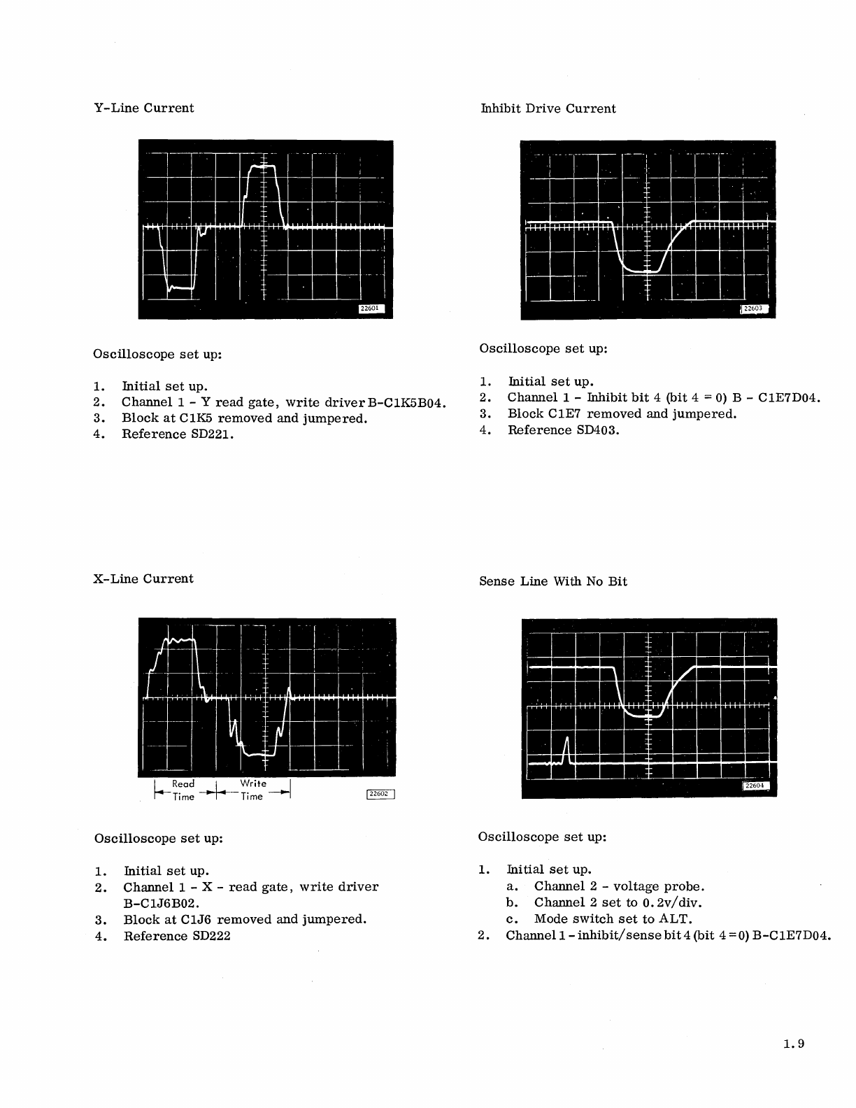
Y-Line
Current
.
--l-
==!!!!
~··
--
-T-
I
-·
:
,.
il
I
I
--
.
~
l'
m
, i
--
II
L'
"
M
I~
II
~
-,J
-.
j
l~
.•
-j
1=
.. -
..
Oscilloscope
set
up:
1.
Initial
set
up.
2.
Channell
- Y
read
gate,
write
driverB-CIK5B04.
3.
Block
at
CIK5
removed
and
jumpered.
4.
Reference
SD221.
X-Line
Current
T
LJ--
I
~-~l-
_ .
--t--
I .
__
:
!:
._'.
. .
Oscilloscope
set
up:
1.
Initial
set
up.
2.
Channell
- X -
read
gate,
write
driver
B-CIJ6B02.
3.
Block
at
CIJ6
removed
and
jumpered.
4.
Reference
SD222
Inhibit
Drive
Current
Oscilloscope
set
up:
1.
Initial
set
up.
2.
Channell
-
Inhibit
bit
4
(bit
4
==
0)
B -
CIE7D04.
3.
Block
C
lE7
removed
and
jumpered.
4.
Reference
SD403.
Sense
Line
With No
Bit
.-
--
:
I
l~
a· .•
r:.I
u·
, ,
~
~~
..
~
i!!J
11
c::::i
!!!I'
-=
.-
...
Oscilloscope
set
up:
1.
Ini
tial
set
up.
a.
Channel
2 -
voltage
probe.
b.
Channel
2
set
to
O.
2v/div.
c.
Mode
switch
set
to
ALT.
2.
Channell-
inhibit/
sense
bit
4
(bit
4 =
0)
B-CIE7D04.
1.9
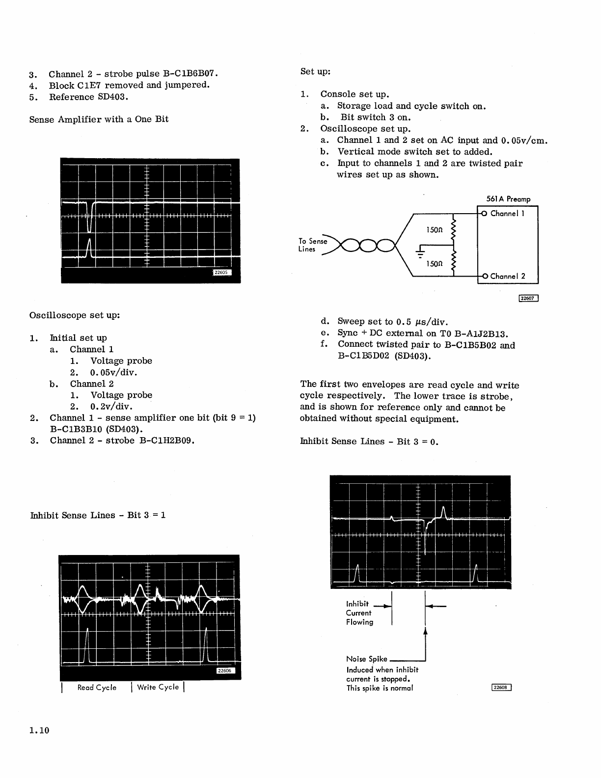
3.
Channel
2 -
strobe
pulse
B-C
1B6B07 .
4.
Block
C 1E7
removed
and
jumpered.
5.
Reference
SD403.
Sense
Amplifier
with
a One
Bit
---,
I
I
Ii::,;
=
I.
u,
'J
~
c:=::::;
!!I'
Oscilloscope
set
up:
1.
Initial
set
up
a.
Channell
1.
Voltage
probe
2.
0.05v/div.
b.
Channel
2
1.
Voltage
probe
2.
0.2v/div.
2.
Channel
1 -
sense
amplifier
one
bit
(bit
9 = 1)
B-C1B3B10
(SD403).
3.
Channel
2 -
strobe
B-C1H2B09.
Inhibit
Sense
Lines
-
Bit
3 = 1
1.10
Set
up:
1.
Console
set
up.
a.
Storage
load
and
cycle
switch
on.
b.
Bit
switch
3
on.
2.
Oscilloscope
set
up.
a.
Channell
and
2
set
on
AC
input
and
o.
05v/cm.
b.
Vertical
mode
switch
set
to
added.
c.
Input to
channels
1
and
2
are
twisted
pair
wires
set
up
as
shown.
561 A Preamp
~-----,--+O
Channell
'-------'--+-0
Channe
I 2
d.
Sweep
set
to
0.5
/ls/
div.
e.
Sync +
DC
external
on
TO
B-A1J2B13.
f.
Connect
twisted
pair
to
B-C
1B5B02
and
B-C1B5D02 (SD403).
The
first
two
envelopes
are
read
cycle
and
write
cycle
respectively.
The
lower
trace
is
strobe,
and
is
shown
for
reference
only
and
cannot
be
obtained
without
special
equipment.
Inhibit
Sense
Lines
-
Bit
3 =
o.
II
II
II
II
----=t:
11
I'
I
II
I m
II
..
li~
I
II
J
--~.-.-
~----
--~
:111
--
~~E~~--l
r-
No;,.
Sp;k.
~
Induced when
inhibit
current
is
stopped.
This spike is normal
-r-
I
~--
I I
r
II I
I I
~
~
Ft
, _
1!I
.m
'
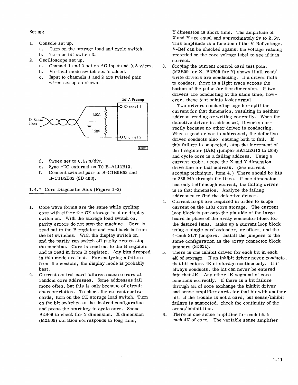
Set
up:
1.
Console
set
up.
a.
Turn
on
the
storage
load
and
cycle
switch.
b.
Turn
on
bit
switch
3.
2.
Oscilloscope
set
up.
a.
Channell
and
2
set
on
AC
input
and
0.5
v/cm.
b.
Vertical
mode
switch
set
to
added.
c.
fuput to
channels
1
and
2
are
twisted
pair
wires
set
up
as
shown.
561
A Preamp
__
----'T--+-O
Channe I 1
'-----"---04-0
Channe I 2
d.
Sweep
set
to
o.
5~s/div.
e.
Sync
+DC
external
on
TO
B-A1J2B13.
f.
Connect
twisted
pair
to
B-C1B5B02
and
B-C
1B5D02 (SD 403).
1.
4.
7
Core
Diagnostic
Aids
(Figure
1-2)
1.
Core
wave
forms
are
the
same
while
cycling
core
with
either
the
CE
storage
load
or
display
switch
on.
With
the
storage
load
switch
on,
parity
errors
do
not
stop
the
machine.
Core
is
read
out
to
the
B
register
and
read
back
in
from
the
bit
switches.
With
the
display
switch
on,
and
the
parity
run
switch
off
parity
errors
stop
the
machine.
Core
is
read
out
to
the
B
register
and
is
read
in
from
B
register.
Any
bits
dropped
in
this
mode
are
lost.
For
analyzing
a
failure
from
the
console,
the
display
mode
is
probably
best.
2.
Current
control
card
failures
cause
errors
at
random
core
addresses.
Some
addresses
fail
more
often,
but
this
is
only
because
of
circuit
characteristics.
To
check
the
current
control
cards,
turn
on
the
CE
storage
load
switch.
Turn
on
the
bit
switches
to
the
desired
configuration
and
press
the
start
key
to
cycle
core.
Scope
B2B09 to
check
for
Y
dimension.
X
dimension
(M2B09)
duration
corresponds
to
long
time,
Y
dimension
is
short
time.
The
amplitude
of
X
and
Yare
equal
and
approximately
2v
to
2.
5v.
This
amplitude
is
a
function
of
the
V-Refvoltage.
V-Ref
can
be
checked
against
the
voltage
reading
recorded
on
the
core
voltage
label
to
see
if
it
is
correct.
3.
Scoping
the
current
control
card
test
point
(M2B09
for
X,
B2B09
for
Y)
shows
if
all
read/
write
drivers
are
conducting.
If
a
driver
fails
to
conduct,
there
is
a
light
trace
across
the
bottom
of
the
pulse
for
that
dimension.
If
two
drivers
are
conducting
at
the
same
time,
how-
ever,
these
test
points
look
normal.
Two
drivers
conducting
together
split
the
current
for
that
dimension,
resulting
in
neither
address
reading
or
writing
correctly.
When
the
defective
driver
is
addressed,
it
works
cor-
rectly
because
no
other
driver
is
conducting.
When a good
driver
is
addressed,
the
defective
driver
conducts
also,
causing
both
to
fail.
If
this
failure
is
suspected,
stop
the
increment
of
the
I
register
(IAR)
(jumper
BA1M2G13
to
DOS)
and
cycle
core
in
a
failing
address.
Using
a
current
probe,
scope
the
X
and
Y
dimension
drive
line
for
that
address.
(See
current
scoping
technique,
Item
4.)
There
should
be
210
to 265 MA
through
the
lines.
If
one
dimension
has
only
half
enough
current,
the
failing
driver
is
in
that
dimension.
Analyze
the
failing
addresses
to
find
the
defective
driver.
4.
Current
loops
are
required
in
order
to
scope
current
on
the
1131
core
storage.
The
current
loop
block
is
put
onto
the
pin
side
of
the
large
board
in
place
of
the
array
connector
block
for
the
desired
lines.
Make
up
a
current
loop
block
using
a
single
card
extender,
or
offset,
and
the
4-inch
SLT
jumpers.
fustall
the
jumpers
to
the
same
configuration
as
the
array
connector
block
jumpers
(SD021).
5.
There
is
one
inhibit
driver
for
each
bit
in
each
4K
of
storage.
If
an
inhibit
driver
never
conducts,
that
bit
enters
4K
of
storage
continuously.
If
it
always
conducts,
the
bit
can
never
be
entered
into
that
4K. Any
other
4K
segment
of
core
fWlCtions
correctly.
If
there
is
a
bit
failure
through
4K
of
core
exchange
the
inhibit
driver
and
sense
amplifier
cards
for
that
bit
with
another
bit.
If
the
trouble
is
not
a
card,
but
sense/inhibit
failure
is
suspected,
check
the
continuity
of
the
sense/inhibit
line.
6.
There
is
one
sense
amplifier
for
each
bit
in
each
4K
of
core.
The
variable
sense
amplifier
1.11
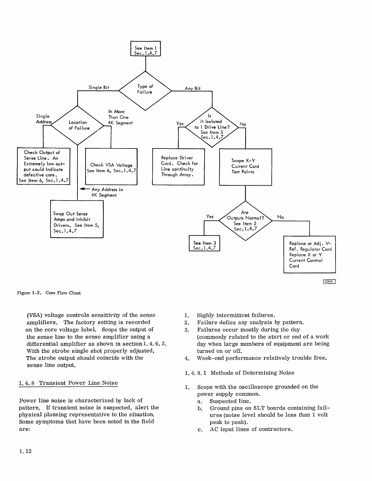
Check
Output
of
Sense
Line.
An
Extremely
low
out-
put
could
Indicate
defective
core.
See
Item
6,
Sec.1
.4.7
Single
Bit
In
More
Than
One
4K
Segment
Check
VSA
Voltage
See
Item
6,
Sec.1.4.7
..-
Any Address in
4K
Segment
Swap
Ou
t Sense
Amps
and
Inhibit
Drivers.
See
Item
5,
Sec.1.4.7
Figure
1-2.
Core
Flow
Chart
(VSA)
voltage
controls
sensitivity
of
the
sense
amplifiers.
The
factory
setting
is
recorded
on
the
core
voltage
label.
Scope
the
output
of
Replace
Driver
Card.
Check
for
Line
continuity
Through
Array.
Scope
X-V
Current
Card
Test Points
1. Highly
intermittent
failures.
No
Replace or
Adj.
V-
Ref. Regulator
Card
Replace
X or Y
Current
Control
Card
2.
Failure
defies
any
analysis
by
pattern.
the
sense
line
to
the
sense
amplifier
using
a
differential
amplifier
as
shown
in
section
1. 4.
6.2.
With
the
strobe
single
shot
properly
adjusted,
3.
Failures
occur
mostly
during
the
day
(commonly
related
to
the
start
or
end
of
a
work
day
when
large
numbers
of
equipment
are
being
turned
on
or
off.
The
strobe
output
should
coincide
with
the
sense
line
output.
1.
4.8
Transient
Power
Line
Noise
Power
line
noise
is
characterized
by
lack
of
pattern.
If
transient
noise
is
suspected,
alert
the
physical
planning
representative
to
the
situation.
Some
symptoms
that
have
been
noted
in
the
field
are:
1.
12
4.
Week-end
performance
relatively
trouble
free.
1.
4.8.1
Methods
of
Determining
Noise
1. Scope
with
the
oscilloscope
grounded
on
the
power
supply
common.
a.
Suspected
line.
b.
Ground
pins
on
SLT
boards
containing
fail-
ures
(noise
level
should
be
less
than
1
volt
peak
to
peak).
c.
AC
input
lines
of
contractors.
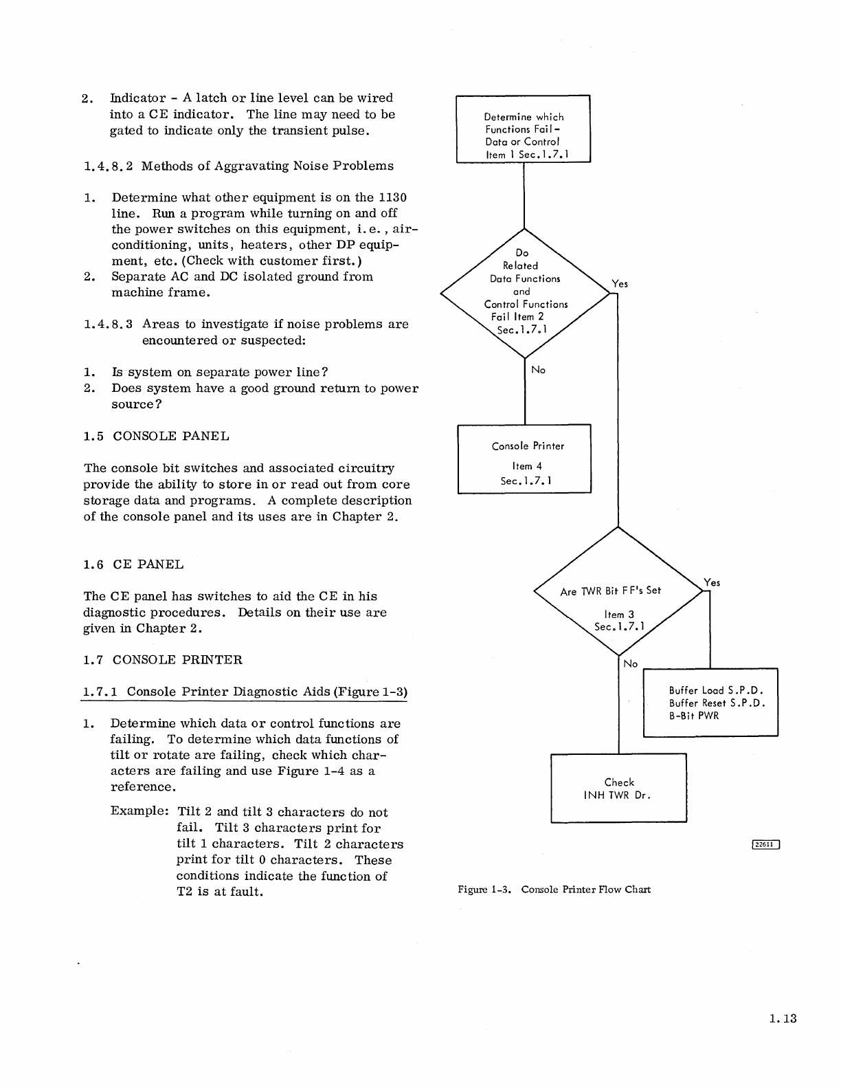
2.
Indicator
- A
latch
or
line
level
can
be
wired
into
a
CE
indicator.
The
line
may
need
to
be
gated
to
indicate
only
the
transient
pulse.
1.
4.
8.
2
Methods
of
Aggravating
Noise
Problems
1.
Determine
what
other
equipment
is
on
the
1130
line.
RWl
a
program
while
turning
on
and
off
the
power
switches
on
this
equipment,
i.
e.
,
air-
conditioning,
Wlits,
heaters,
other
DP
equip-
ment,
etc.
(Check
with
customer
first.)
2.
Separate
AC
and
DC
isolated
ground
from
machine
frame.
1.4.
8. 3
Areas
to
investigate
if
noise
problems
are
encountered
or
suspected:
1.
Is
system
on
separate
power
line?
2.
Does
system
have
a good
ground
return
to
power
source?
1.
5 CONSOLE
PANEL
The
console
bit
switches
and
associated
circuitry
provide
the
ability
to
store
in
or
read
out
from
core
storage
data
and
programs.
A
complete
description
of
the
console
panel
and
its
uses
are
in
Chapter
2.
1.6
CE
PANEL
The
C E
panel
has
switches
to
aid
the
C E
in
his
diagnostic
procedures.
Details
on
their
use
are
given
in
Chapter
2.
1.
7 CONSOLE
PRINTER
1.
7.1
Console
Printer
Diagnostic
Aids
(Figure
1-3)
1.
Determine
which
data
or
control
functions
are
failing.
To
determine
which
data
fWlctions
of
tilt
or
rotate
are
failing,
check
which
char-
acters
are
failing
and
use
Figure
1-4
as
a
reference.
Example:
Tilt
2
and
tilt
3
characters
do
not
fail.
Tilt
3
characters
print
for
tilt
1
characters.
Tilt
2
characters
print
for
tilt
0
characters.
These
conditions
indicate
the
function
of
T2
is
at
fault.
Determine which
Functions
Fai
1-
Data or Control
Item
I
Sec.I.?1
No
Console Printer
Item 4
Sec.I.7.!
No
.--
___
---L.
____
-,
Check
INH
TWR
Dr.
Buffer
Load
S.P.D.
Buffer Reset
S.
P • D •
B-Bit
PWR
Figure
1-3.
Console
Printer
Flow
Chart
1.13
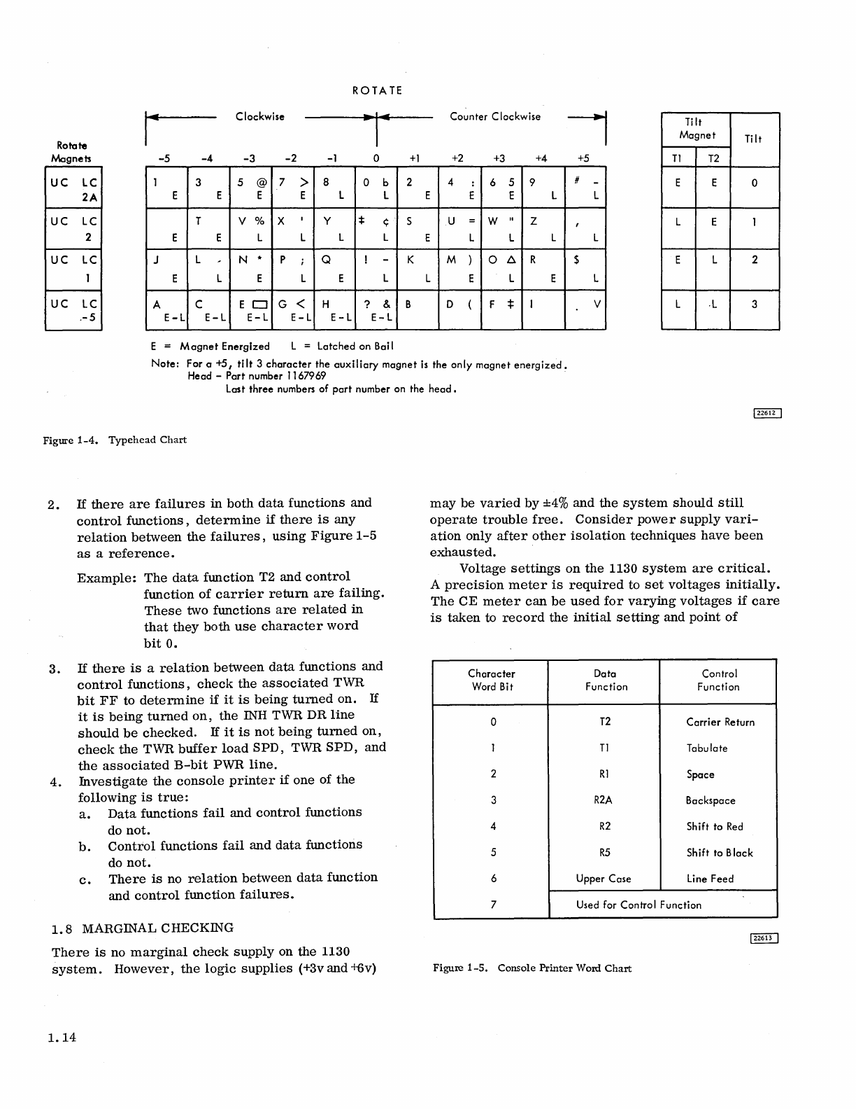
ROT
ATE
I-
Clockwise
~I-
Counter Clockwise I
Rotate
Tilt
Magnet Tilt
Magnets
-5
-4
-3
-2
-1
0
+1
+2
+3
+4
+5
Tl
T2
UC
lC
1 3 5 @ 7 > 8 0 b 2 4 : 6 5 9 # -E E 0
2A
E E E E L L E E E L L
UC
LC
T V % X I Y *
~.
S U = W " Z , L E 1
2 E E L L L L E L L L L
UC
LC
J L , N * P ; Q ! -K M ) 0 6. R $ E L 2
1 E L E L E L L E L E L
UC
lC
A C
ED
G < H ? & B 0 ( F * I V L
·L
3
.-5
E-L
E-L
E-L
E-L
E-L E-L
E =
Magnet
Energized L = Latched on
Boll
Note: For a +5,
tilt
3 character the auxiliary magnet
is
the only magnet
energized.
Head -Port number 1167969
Lost
three numbers of port number on the
head.
Figure
1-4.
Typehead
Chart
2.
If
there
are
failures
in
both
data
functions
and
control
functions,
determine
if
there
is
any
relation
between
the
failures,
using
Figure
1-5
as
a
reference.
Example:
The
data
function
T2
and
control
function
of
carrier
return
are
failing.
These
two fWlCtions
are
related
in
that
they
both
use
character
word
bit
o.
3.
If
there
is
a
relation
between
data
functions
and
control
functions,
check
the
associated
TWR
bit
FF
to
determine
if
it
is
being
turned
on.
If
it
is
being
turned
on,
the
INH
TWR
DR
line
should
be
checked.
If
it
is
not
being
turned
on,
check
the
TWR
buffer
load
SPD,
TWR
SPD,
and
the
associated
B-bit
PWR
line.
4.
Investigate
the
console
printer
if
one of
the
following
is
true:
a.
Data
functions
fail
and
control
functions
do
not.
b.
Control
functions
fail
and
data
functions
do
not.
c.
There
is
no
relation
between
data
function
and
control
function
failures.
1.8
MARGINAL CHECKING
There
is
no
marginal
check
supply
on
the
1130
system.
However,
the
logic
supplies
(+3v and
-Ii)
v)
1.14
may
be
varied
by
±4%
and
the
system
should
still
operate
trouble
free.
Consider
power
supply
vari-
ation
only
after
other
isolation
techniques
have
been
exhausted.
Voltage
settings
on
the
1130
system
are
critical.
A
precision
meter
is
required
to
set
voltages
initially.
The
CE
meter
can
be
used
for
varying
voltages
if
care
is
taken
to
record
the
initial
setting
and
point
of
Character Data Control
Word
Bit
Function Function
0
T2
Carrier Return
1
TI
Tabulate
2
RI
Space
3
R2A
Backspace
4
R2
Shift to
Red
5
R5
Shift to Black
6 Upper Case
Line
Feed
7
Used
for Control Function
Figure
1-5.
Console
Printer
Word
Chart
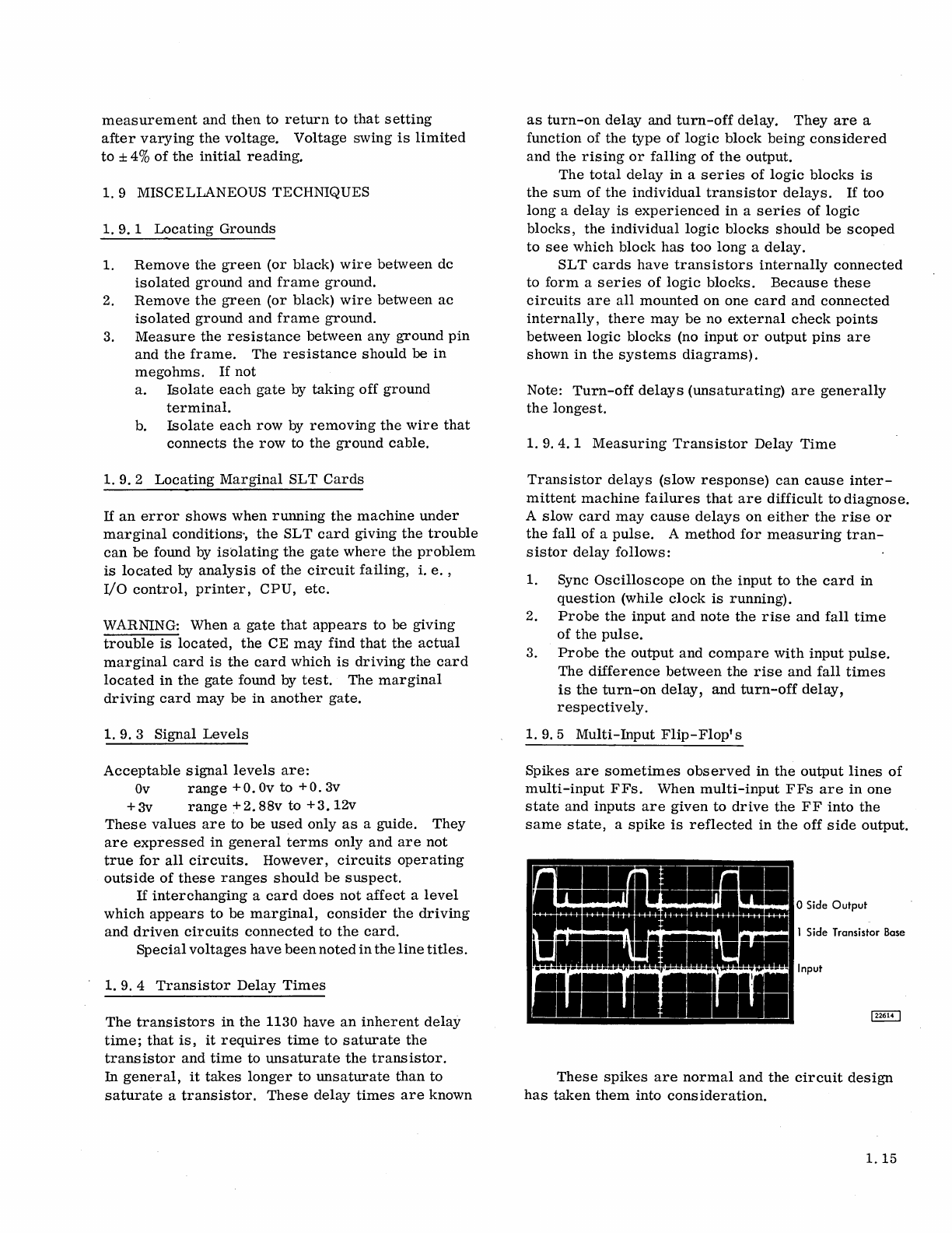
measurement
and
then
to
return
to
that
setting
after
varying
the
voltage.
Voltage
swing
is
limited
to
±
4%
of
the
initial
reading.
1. 9 MISCELLANEOUS TECHNIQUES
1. 9. 1
Locating
Grounds
1.
Remove
the
green
(or
black)
wire
between
dc
isolated
ground
and
frame
ground.
2.
Remove
the
green
(or
black)
wire
between
ac
isolated
ground
and
frame
ground.
3.
Measure
the
resistance
between
any
ground
pin
and
the
frame.
The
resistance
should
be
in
megohms.
If
not
a.
Isolate
each
gate
by
taking
off
ground
terminal.
b.
Isolate
each
row
by
removing
the
wire
that
connects
the
row
to
the
ground
cable.
1. 9. 2
Locating
Marginal
SLT
Cards
If
an
error
shows
when
running
the
machine
under
marginal
conditions·,
the
SLT
card
giving
the
trouble
can
be
found by
isolating
the
gate
where
the
problem
is
located
by
analysis
of
the
circuit
failing,
i.
e.
,
I/O
control,
printer,
CPU,
etc.
WARNING: When a
gate
that
appears
to be
giving
trouble
is
located,
the
CE
may
find
that
the
actual
marginal
card
is
the
card
which
is
driving
the
card
located
in
the
gate
found by
test.
The
marginal
driving
card
may
be
in
another
gate.
1. 9. 3 Signal
Levels
Acceptable
signal
levels
are:
Ov
range
+0.
Ov
to
+0.
3v
+
3v
range
+ 2. 88v
to
+
3.
12v
These
values
are
to
be
used
only
as
a guide.
They
are
expressed
in
general
terms
only
and
are
not
true
for
all
circuits.
However,
circuits
operating
outside
of
these
ranges
should
be
suspect.
If
interchanging
a
card
does
not
affect
a
level
which
appears
to
be
marginal,
consider
the
driving
and
driven
circuits
connected
to
the
card.
Special
voltages
have
been
noted
in
the
line
titles.
1. 9. 4
Transistor
Delay
Times
The
transistors
in
the
1130
have
an
inherent
delay
time;
that
is,
it
requires
time
to
saturate
the
transistor
and
time
to
unsaturate
the
transistor.
In
general,
it
takes
longer
to
unsaturate
than
to
saturate
a
transistor.
These
delay
times
are
known
as
turn-on
delay
and
turn-off
delay.
They
are
a
function
of
the
type
of
logic
block
being
considered
and
the
rising
or
falling
of
the
output.
The
total
delay
in
a
series
of
logic
blocks
is
the
sum
of
the
individual
transistor
delays.
If
too
long
a
delay
is
experienced
in
a
series
of
logic
blocks,
the
individual
logic
blocks
should
be
scoped
to
see
which
block
has
too
long
a
delay.
SLT
cards
have
transistors
internally
connected
to
form
a
series
of
logic
blocks.
Because
these
circuits
are
all
mounted
on
one
card
and
connected
internally,
there
may
be
no
external
check
points
between
logic
blocks
(no
input
or
output
pins
are
shown
in
the
systems
diagrams).
Note:
Turn-off
delays
(unsaturating)
are
generally
the
longest.
1.
9.4.
1
Measuring
Transistor
Delay
Time
Transistor
delays
(slow
response)
can
cause
inter-
mittent
machine
failures
that
are
difficult
to
diagnose.
A
slow
card
may
cause
delays
on
either
the
rise
or
the
fall
of
a
pulse.
A
method
for
measuring
tran-
sistor
delay
follows:
1. Sync
Oscilloscope
on
the
input
to
the
card
in
question
(while
clock
is
running).
2.
Probe
the
input
and
note
the
rise
and
fall
time
of
the
pulse.
3.
Probe
the
output
and
compare
with
input
pulse.
The
difference
between
the
rise
and
fall
times
is
the
turn-on
delay,
and
turn-off
delay,
respectively.
1.
9.
5
Multi-Input
Flip-Flop's
Spikes
are
sometimes
observed
in
the
output
lines
of
multi-input
FFs.
When
multi-input
FFs
are
in
one
state
and
inputs
are
given
to
drive
the
FF
into
the
same
state,
a
spike
is
reflected
in
the
off
side
output.
o Side
Output
1
Side
Transistor Base
Input
These
spikes
are
normal
and
the
circuit
design
has
taken
them
into
consideration.
1.
15

BASIC MACHINE
2.1
MANUAL CONTROLS
AND
INDICATORS
2. 1. 1
Objectives
•
•
Provide
manual
operation
for
program
and
sys-
tern
analysis.
Provide
visual
indication
of
machine
and
program
status
under
the
various
system
modes.
•
Supplement
areas
which
the
program
cannot
check.
2. 1. 2
Control
Switch
Panel
2. 1. 2. 1
System
Reset
Function:
Reset
processor
registers
to
their
initial
state,
with
the
exception
of
the
M
register.
Operation:
1.
Data
or
instructions
in
core
storage
is
not
affected.
2.
Reset
is
active
in
all
modes
of
operation
except
run
mode.
3.
In
single
step
mode,
it
is
necessary
to
be
at
T7
time
to
prevent
loss
of
data
or
instructions
when
using
reset.
2. 1. 2. 2
Program
Stop
Function:
Causes
a
level
five
interrupt
for
the
con-
sole.
With
appropriate
sub-routines,
this
stop
is
used
to
cycle
down
the
processor
and
I/O
devices
to
a
stop.
WARNING:
If
these
routines
are
not
in
the
program,
use
of
the
program
stop
key
may
cause
loss
of
information.
Operation:
1.
The
program
stop
key
is
pressed
and
a
level
5
interrupt
is
developed.
2.
The
bit-zero
of
the
console
keyboard-device-
status
-word
is
a
one,
indicating
to
the
program
that
a
program
stop
is
requested.
CHAPTER
2 MAINTENANCE
FEATURES
3. A
user-supplied
programmed
wait
loop
is
required
to
block
main
line
operations
until
the
operator
intervenes.
4.
The
interrupt
routine
should
allow
the
program
to
continue
when
the
start
key
is
pressed.
2. 1. 2. 3 IMM Stop
Function:
Stops
the
processor
immediately.
Inter-
rupt
and
cycle
stealing
occurs
at
T7
of
the
cycle
in
which
the
IMM Stop
occurs.
Operation:
1.
Data
from
I/O
devices
are
lost
if
the
devices
are
operating
at
the
time
of
the
stop.
2. A
complete
program
restart
is
required.
2. 1. 2. 4
Program
Start
-
Push
Button
Function:
Causes
the
program
to
start
or
continue
from
its
present
state.
The
program
continues
according
to
the
setting
of
the
mode
switch.
Operation:
1.
If
a
program
start
routine
is
in
the
program
and
the
start
key
is
pressed
after
completing
a
pro-
gram
stop
operation,
the
instruction
being
pro-
cessed
continues
as
though no
program
stop
had
occurred.
2.
If
the
start
key
is
pressed
after
reset,
the
instruction
specified
by
the
instruction
counter
(normally
zero)
is
the
first
one
executed.
By
using
the
load
IAR
function
and
entering
a
new
instruction
address,
a
different
starting
address
can
be
manually
inserted
after
reset.
3.
Each
time
the
start
key
is
pressed
the
instruction
address
register
advances
when
the
machine
is
in
load
or
display
mode.
When
in
single
step,
single
memory
cycle,
or
single
instruction
mode,
the
processor
advances
a
single
increment
of
the
speCified
mode
each
time
the
start
key
is
pressed.
2. 1. 2. 5
Load
IAR -
Push
Button
Function:
In
the
load
mode
position,
data
entered
in
the
bit
switches
is
loaded
directly
into
the
in-
struction
address
register
via
the
storage
buffer
register.
2.1
Operation:
1.
The
key
is
functional
only
when
the
processor
is
in
the
load
or
display
mode.
2.
When
in
the
load
mode,
an
address
set
in
the
bit
switches
is
entered
in
the
instruction
address
register
when
the
load
IAR
key
is
pressed.
3.
Display:
When
in
this
mode,
the
contents
of
the
B
register
enter
the
IAR
when
the
load
IAR
key
is
pressed.
2.1.2.6
Program
Load
-
Push
Button
Function:
Provides
a
means
for
entering
a
program
into
the
system.
Operation:
1.
Paper
Tape
System
a.
Pressing
the
load
key
causes
groups
of
four,
four-bit
characters
(16
bit
words)
to
be
.
loaded
into
core
consecutively,
beginning
at
location
zero.
b.
Groups
continue
to
be
read
until
a
punch
in
the
fifth
channel
is
encountered.
c.
When
a
punch
in
the
fifth
channel
is
en-
countered,
loading
stops
and
control
trans-
fers
to
word
zero.
2.
Card
Reader-Punch
System
a.
Pressing
the
key
causes
a
card
to
advance
from
pre
-read
through
the
read
station.
b.
The
contents
of
each
column
is
stored
con-
secutively
in
storage
locations
beginning
at
location
zero.
c.
The
12
bits
are
split
into
five
operation
bits
and
eight
displacement
bits,
two
of
which
are
sign
bits.
d.
At
completion
of
the
card
cycle,
an
auto-
matic
branch
to
0000
is
executed.
Note:
If
the
card
reader
is
installed,
program
load
is
not
active
on
the
paper
tape.
The
system
can
be
ordered
without
program
load
installed.
2.1.2.7
Console/Keyboard-Toggle
Switch
Function:
Sets
bit
position
3
in
the
keyboard/printer
device
status
word
(DSW)
to
indicate
to
the
program
that
the
keyboard
is
the
source
of
input
data
during
program
control.
Operation:
In
the
console
position,
the
bit
switches
are
the
source
of
input
data.
In
the
keyboard
posi-
tion'
the
keyboard
is
the
source
of
input
data.
2.2
2.1.3
Mode
Switch
•
Rotary
switch
to
control
mode
of
machine
operation.
2. 1. 3. 1
Load
Position
Function:
Provides
for
manual
entry
of
data
or
instructions
from
the
bit
switches
to
core
storage
or
I
register.
Operation:
1.
In
load
mode,
operation
of
the
load
IAR
key
trans-
fers
bit
switch
data
(2-15)
to
the
I
register.
2. When
in
load
mode,
pressing
the
start
key
enters
the
bit
switch
data
(0-15) into
core
storage
at
the
address
indicated
in
the
I
register.
The
I
reg-
ister
is
incremented
by
1.
3.
Switching
from
load
to
any
other
mode
of
opera-
tion
does
not
affect
storage
or
result
in
reset
of
any
set
conditions.
4.
During
machine
operation,
IMM
stop
or
program
stop
keys
must
be
pressed
prior
to
switching
to
load
mode
to
preserve
the
integrity
of
the
data
in
core
storage
and
to
preserve
the
program.
5.
It
is
not
necessary
to
reset
prior
to
switching
to
load
mode.
Such
switching
does
not
affect
any
set
conditions
other
than
the
B
register.
2.
1.3.2
Display
1.
Function:
To
display
the
data
at
any
location
in
core
storage.
Operation:
In
display,
pressing
of
the
start
key
displays,
in
the
B
register,
the
data
at
the
address
specified
in
the
I
register
prior
to
pressing
of
the
start
key.
Pressing
the
start
key
successively
displays
sequentially
increasing
addresses.
That
is,
the
I
register
is
incremented
each
time
the
start
key
is
pressed.
2.
Function:
Load
the
I
register
with
the
con-
tents
of
the
B
regis
ter
.
Operation:
Depressing
the
load
IAR
key
transfers
the
B
register
contents
into
the
I
register.
2.1.3.3
Run
Function:
To
condition
the
system
for
the
start
of
programmed
operation.
Requirements
:
1.
Pressing
the
start
key
in
run
mode
results
in
program
operation
beginning
at
the
address
specified
by
the
I
register.
2.
Pressing
the
IMM
stop
key
halts
machine
pro-
cessing
at
the
end
of
the
active
cycle
at
T 7
time.
3.
Switching
from
run
mode
to
any
other
mode
requires
IMM
stop
or
program
stop
prior
to
switching
to
insure
integrity
of
the
core
data.
2. 1.
3.4
Interrupt
Run
-(Int Run)
Function:
Forces
a
level
five
interrupt
after
com-
pletion
of
each
instruction.
Operation:
1. A
level
five
interrupt
occurs
after
the
end
of
each
instruction
execution.
2.
Higher
level
interrupts
are
handled
automat-
ically.
during
this
operation.
3.
An
interrupt-run
program
which
stops
on
the
level
5
interrupt
and
starts
with
the
start
key,
is
required
to
use
this
mode
of
operation
effectively.
2. 1. 3. 5
Single
Step
(SS)
Function:
Pressing
the
start
key
advances
the
processor
one
clock
cycle.
Operation:
1.
Pressing
the
start
key
in
this
mode
causes
a
T (X),
phase
A,
pulse
to
be
generated.
Releas-
ing
the
start
key
causes
a T (X), B
pulse.
2.
Pressing
the
reset
key
in
a
single
step
mode
causes
loss
of
storage
integrity
unless
the
clock
is
in
time
T5,
T6
or
T7
and
of
program
integ-
rity
unless
in
T7
time.
2. 1. 3. 6
Single
Machine
Cycle
(SMC)
Function:
Advances
the
processor
one
complete
ma-
chine
cycle
(T7toT7)
under
control
of
the
start
key.
Operation:
1.
Pressing
the
start
key
causes
one
machine
clock
cycle.
2.1.
3. 7
Single
Instruction
Function:
To
advance
the
processor
one
complete
instruction
at
a
time
under
control
of
the
start
key.
Operation:
1.
Pressing
the
start
key
causes
a
complete
instruction
to
be
executed.
2.
I/O
operations
are
completed
to
the
point
of
interrupt
request.
3. Switching
to
another
mode
of
operation
does
not
affect
instructions
or
data.
2.1.4
Console
Bit
Switches
Function:
Provide
for
manual
entrance
of
a
machine
language
instruction
or
binary
data
into
core
storage,
an
instruction
address
in
the
I
register,
or
manual
control
by
program
interrogation.
Operation:
1.
Data
set
in
the
bit
switches
can
be
loaded
into
core
storage
under
program
control.
2.
When
the
machine
is
in
load
mode,
the
bit
switches
are
gated
directly
into
the
B
register.
3.
The
bit
switches
have
no
effect
on
the
processor
under
any
other
mode
except
as
addressed
by
an
I/O
command.
2. 1. 5
CE
Panel
2. 1. 5. 1
Storage
Load
Function:
Provides
a
starting
point
for
isolating
problems
and
checking
the
storage
circuits.
Operation:
1.
Data,
as
set
up
in
the
bit
switches,
cycles
through
all
of
core
storage.
Setting
this
switch
allows
cycling
of
memory
by
turning
on
the
run
controls
and
incrementing
the
I
register.
2. 1. 5. 2
Storage
Display
Function:
Provides
for
checking
the
core
storage
circuits.
Operation:
The
core
storage
contents
are
displayed
in
the
B
register
console
lights
in
a
sequential
manner.
Setting
this
switch
allows
core
storage
to
cycle
by
turning
on
the
run
controls
and
incrementing
the
I
register.
A
parity
error
results
in
an
immediate
halt
if
the
parity
run
switch
is
off.
2.1.
5.3
Non-Storage
Load
and
Cycle
Function:
Allows
console
data
(bit)
switches
to
be
used
as
a
source
of
data
in
place
of
core
storage.
2.3
Operation:
With
non-storage
load
and
cycle
(NSLC)
switch
on,
the
input
and
output
to
core
storage
is
crippled.
Input
to
the
B
register
comes
from
the
bit
switches
only.
An
operation
may
be
entered
and
executed
from
the
bit
switches,
either
in
single
step,
single
instruc-
tion,
or
run
modes.
If
a
valid
operation
code
is
entered
and
the
mode
switch
is
in
run,
the
1131
cycles
through
the
operation
code,
incrementing
the
IAR
and
cycling
again.
This
permits
scoping
of
I
cycles,
E
cycles
and
controls
without
disturbing
the
contents
of
storage.
If
an
invalid
operation
code
is
entered,
it
is
decoded
as
a
wait
command
and
the
1131
stops.
Example
#1
a)
Machine
fails
on
any
long
instruction.
By
single
stepping
a
double
word
instruction,
it
is
found
that
there
never
is
an
1-2
cycle.
b)
1.
Turn
on
the
NSLC
switch.
2.
Turn
the
mode
switch
to
run.
3.
Set
load
accumulator
long
instruction
in
the
bit
switches
(hex C400).
4.
Press
the
start
key.
The
1131
cycles
and
the
1-2
circuits
may
be
scoped
dynamically
for
the
failure.
Example
#2:
In
order
to
examine
an
XIO
instruction
and
IOCC
in
single
step
or
single
machine
cycle
mode,
the
following
technique
may
be
used:
1.
Turn
on
the
NSLC
switch.
2.
Turn
the
mode
switch
to
single
step
or
single
machine
cycle.
3.
Set
up XIO
instruction
in
the
bit
switches
(hex
0800).
4.
Step
through
the
II
cycle
to E1,
TO
time
by
pressing
the
start
key.
5.
Change
the
bit
switches
to
the
desired
IOCC
word,
i.
e.
device,
function
codes.
6.
Continue
to
step
through
the
IOCC
operation.
7.
If
the
function
of
the
IOCC
was
a
sense
command,
the
DSW
is
brought
into
the
A
register.
If
the
device
had
been
a 1442,
with
a
feed
command,
a
card
would
have
fed
from
the
hopper,
etc.
2.1.
5. 4
Interrupt
Delay
Function:
Blocks
Interrupt.
Operation:
The
interrupt
delay
switch,
when
on,
inhibits
setting
of
the
interrupt
request
circuits.
2.4
2.1.
5. 5
Parity
Run
Function:
Provide
a
means
of
bypassing
the
error
when
an
out
of
parity
character
is
read
out
of
core
storage.
Operation:
When
the
parity
run
switch
is
in
the
on
position,
errors
do
not
stop
the
system.
When
the
parity
run
switch
is
in
the
off
position,
the
system
stops
at
the
end
of
the
cycle
in
which
the
error
is
detected.
WARNING:
This
switch
must
be
returned
to
the
off
position
before
the
system
is
returned
to
the
customer.
2. 1.
5.6
Lamp
Test
Function:
Tests
all
lamps
to
see
if
they
are
in
good
condition.
Operation:
Pressing
the
lamp
test
switch
lights
all
indicator
lamps.
2.1.6
Miscellaneous
Switches
2.1.6.1
Power
ON/OFF
Function:
Provide
for
removing
or
applying
power
to
the
entire
system.
When
off, 24
vac
is
still
up
and
the
convenience
outlet
power
is
off.
2. 1. 6. 2
Disk
Storage
ON/OFF
Function:
Provides
for
removing
or
applying
AC
power
to
the
disk
drive
unit.
Operation:
1.
Controls
the
drive
motor.
2.
Provides,
indirectly,
the
head
load
and
unload
facility
.
2.1.6.3
Emergency
Power
Off
Function:
Removes
power
to
every
unit
of
system
including
convenience
outlet
but
not
to
the
24
vac
supply.
Operation:
1.
Requires
CE
intervention
to
reset.
2.1.
6. 4
Power
Supply
Voltage
Potentiometer
Function:
Provides
ability
to
set
each
dc
voltage
accurately.
It
can
be
used
to
help
isolate
marginal
circuit
conditions.
Located
on
each
supply.
Operation:
1.
Allow
voltage
variation
of
processor
dc
voltages
±4%,
one
at
a
time.
This
is
not
considered
a
normal
trouble
shooting
procedure.
I CAUTION:
The
potentiometer
is
not
mechanically
stopped
to
prevent
over
voltage
los
s of
power.
2.1.7
Indicators
2.1.
7.1
Power
The
ready
light
on
the
keyboard
console
indicates
power
ON/OFF.
2.
1.
7. 2
Console
Instruction
Address
Register
(IAR)
has
14
positions
and
provides
full
time
indication.
Storage
Address
Register
(SAR)
has
14
positions
and
provides
full
time
indication.
Storage
Buffer
Register
(B)
has
16 pOSitions
and
provides
full
time
indication.
Arithmetic
Factor
Register
(D)
has
16
positions
and
provides
full
time
indication.
Accumulator
Register
(A)
has
16
positions
and
pro-
vides
full
time
indication.
Accumulator
Extension
Register
(Q)
has
16
positions
and
provides
full
time
indication.
Operation
Register
(OP)
has
5
positions
and
provides
full
time
indication.
Operation
Tags
has
Flag
bit
5,
Tag
bits
6
and
7,
Mod
bits
8 and 9.
Condition
Register
has
2
positions
and
provides
full
time
indication
of
carry
and
overflow.
Cycle
Control
Counter
has
6
positions
and
full
time
indication.
Interrupt
Levels
has
5
positions
and
indicates
inter-
ruptlevel.
Machine
Cycle
Indicators
has
7
positions,
indicates
type
of
I
or
E
cycle
and
provides
full
time
indication.
Clock
Cycle
Indicators
has
8
positions,
displays
T
Clock
position
when
in
Single
Cycle
operation
and
provides
full
time
indication.
Special
Arithmetic
Indicators
has
6
positions
and
provides
full
time
indication.
Add,
Arith
Control
(AC),
Shift
Control
(SC),
Accumulator
Sign (AS),
Accumulator
Carry
(TC),
Zero
Remainder
(ZR).
CE
Indicators:
There
are
12
indicating
lamps
located
in
the
lower
portion
of
the
lamp
panel.
These
can
be
used
to
indicate
circuit
conditions
as
needed.
Input
to
each
lamp
is
shown
on
logic
page
ZL101.
The
input
level
must
be
plus
to
light
the
indicator.
The
lamps
require
no
external
driver.
There-
fore,
any
normal
signal
level
may
be
used
as
an
input
without
concern
for
loading
the
circuit
excessively.
Example:
While
stepping
through
a
program,
if
indication
is
desired
each
time
the
accumulator
equal
zero
flip-
flop
comes
on (KG221),
wire
CE
indicator
#1
to
the
FF
so
that
it
indicates
the
on
condition.
To
accom-
plish
this,
wire
B-A1E2-B04
to
B-A1A3-B13.
Location
of
Terminals
CE Lamp 1 B-A1.A3B13 CE
Lamp
7 B-B1M2B13
CE Lamp 2 B-A1.A3D13 CE
Lamp
8 B-B1M2D13
CE Lamp 3 B-A1A4B12 CE
Lamp
9 B-B1N2D13
CE Lamp 4 B-A1A4D12 CE
Lamp
10
B-B1N2B13
CE Lamp 5 B-A1A4B13 CE
Lamp
11
B-B1N4B12
CE
Lamp
6 B-A1A4D13 CE
Lamp
12 B-B1N4D12
X7
Clock
Indicator
has
1
position,
displays
X
clock
7·
when
in
single
cycle
operation
and
provides
full
time
indication.
Wait
is
on
when
CPU
is
in
wait
condition.
P1-P2
has
2
positions,
uses
parity
bits
to
indicate
when
the
half
word
read
from
core
storage
is
even.
Index
Register
displays
index
register
address.
2.
1.
7. 3
Keyboard
Console
Forms
Check
is
on
if
console
printer
is
out
of
paper.
Keyboard
Select
is
on
when
request
for
keyboard
interrupt
has
been
serviced
and
keyboard
is
ready
to
operate.
2.5
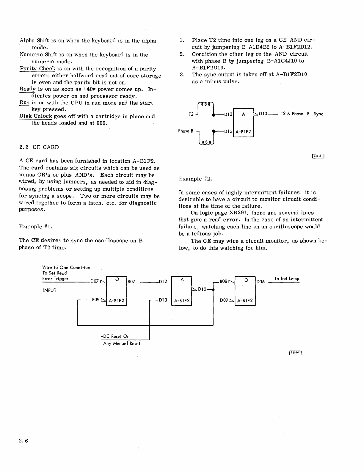
Alpha Shift
is
on when
the
keyboard
is
in
the
alpha
mode.
Numeric
Shift
is
on when
the
keyboard
is
in
the
numeric
mode.
Parity
Check
is
on
with
the
recognition
of a
parity
error;
either
ha
lfword
read
out
of
core
storage
is
even
and
the
parity
bit
is
not
on.
Ready
is
on
as
soon
as
+48v
power
comes
up.
In-
--d-icates
power
on and
processor
ready.
Run
is
on
with
the
CPU
in
run
mode
and
the
start
key
pressed.
Disk
Unlock
goes
off
with
a
cartridge
in
place
and
the
heads
loaded
and
at
000.
2.2
CE CARD
A CE
card
has
been
furnished
in
location
A-BIF2.
The
card
contains
six
circuits
which
can
be
used
as
minus
OR's
or
plus
AND's.
Each
circuit
may
be
wired,
by
using
jumpers,
as
needed
to
aid
in
diag-
nosing
problems
or
setting
up
multiple
conditions
for
syncing
a
scope.
Two
or
more
circuits
may
be
Wired
together
to
form
a
latch,
etc.
for
diagnostic
purposes.
Example
#1.
The
CE
desires
to
sync
the
oscilloscope
on B
phase
of
T2
time.
Wire to
One
Condition
To
Set
Read
1.
Place
T2
time
into
one
leg
on a
CE
AND
cir-
cuit
by
jumpering
B-AID4B2
to
A-BIF2D12.
2.
Condition
the
other
leg
on
the
AND
circuit
with
phase
B
by
jumpering
B-AIC4JIO
to
A-BIF2D13.
3.
The
sync
output
is
taken
off
at
A-BIF2DIO
as
a
minus
pulse.
T2
JLDI2~r:,.DI0-
T2
& Phase B Sync
Phase S
l.uJDI36J
Example
#2.
In
some
cases
of
highly
intermittent
failures,
it
is
desirable
to
have
a
circuit
to
monitor
circuit
condi-
tions
at
the
time
of
the
failure.
On
logic
page
XR291,
there
are
several
lines
that
give
a
read
error.
In
the
case
of
an
intermittent
failure,
watching
each
line
on
an
oscilloscope
would
be
a
tedious
job.
The
CE
may
wire
a
circuit
monitor,
as
shown
be-
low, to do
this
watching
for
him.
Error Trigger
INPUT
D07
r:,.!lS07
-B09~
D12
Cd
r-B08~DD06
I:::::::..D10_
'
~D13
A-BIF2
D09~
A-B1F2
To
Ind
Lamp
-DC Reset
Or
Any Manual Reset
2.6
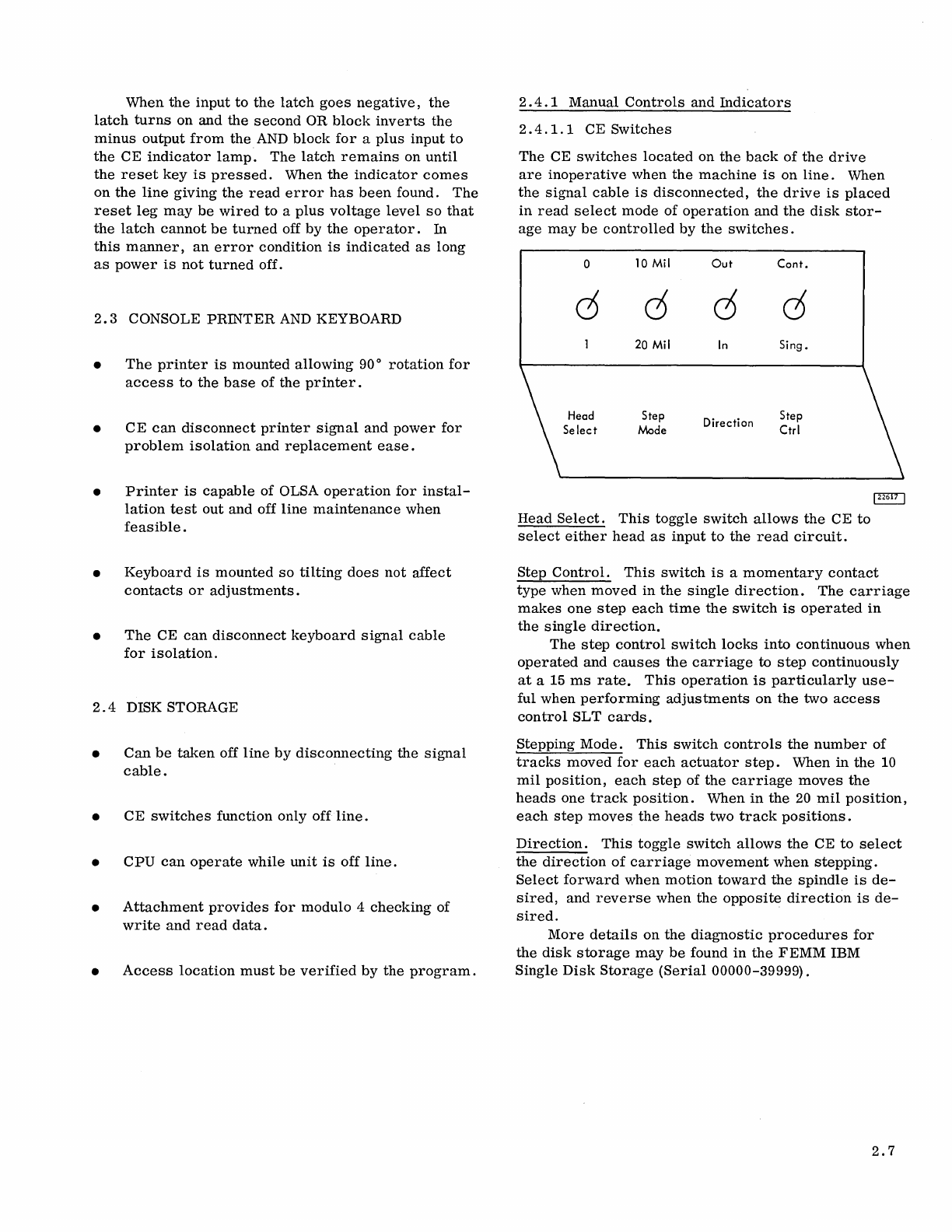
When
the
input
to
the
latch
goes
negative,
the
latch
turns
on
and
the
second
OR
block
inverts
the
minus
output
from
the.
AND
block
for
a
plus
input
to
the
CE
indicator
lamp.
The
latch
remains
on
until
the
reset
key
is
pressed.
When
the
indicator
comes
on
the
line
giving
the
read
error
has
been
found.
The
reset
leg
may
be
wired
to
a
plus
voltage
level
so
that
the
latch
cannot
be
turned
off
by
the
operator.
In
this
manner,
an
error
condition
is
indicated
as
long
as
power
is
not
turned
off.
2.3
CONSOLE
PRINTER
AND
KEYBOARD
•
The
printer
is
mounted
allowing
90 0
rotation
for
access
to
the
base
of
the
printer.
•
•
CE
can
disconnect
printer
signal
and
power
for
problem
isolation
and
replacement
ease.
Printer
is
capable
of
OLSA
operation
for
instal-
lation
test
out
and
off
line
maintenance
when
feasible.
•
Keyboard
is
mounted
so
tilting
does
not
affect
contacts
or
adjustments.
•
The
CE
can
disconnect
keyboard
signal
cable
for
isolation.
2.4
DISK STORAGE
•
Can
be
taken
off
line
by
disconnecting
the
signal
cable.
•
CE
switches
function
only
off
line.
•
CPU
can
operate
while
unit
is
off
line.
•
Attachment
provides
for
modulo
4
checking
of
write
and
read
data.
•
Access
location
must
be
verified
by
the
program.
2.4.
1
Manual
Controls
and
Indicators
2.4.1.1
CE
Switches
The
CE
switches
located
on
the
back
of
the
drive
are
inoperative
when
the
machine
is
on
line.
When
the
signal
cable
is
disconnected,
the
drive
is
placed
in
read
select
mode
of
operation
and
the
disk
stor-
age
may
be
controlled
by
the
switches.
o
d
Head
Se
lect
10 Mil
20
Mil
Step
Mode
Out
In
Direction
Cont.
Sing.
Step
Ctrl
Head
Select.
This
toggle
switch
allows
the
CE
to
select
either
head
as
input
to
the
read
circuit.
Step
Control.
This
switch
is
a
momentary
contact
type
when
moved
in
the
single
direction.
The
carriage
makes
one
step
each
time
the
switch
is
operated
in
the
single
direction.
The
step
control
switch
locks
into
continuous
when
operated
and
causes
the
carriage
to
step
continuously
at
a 15
ms
rate.
This
operation
is
particularly
use-
ful
when
performing
adjustments
on
the
two
access
control
SLT
cards.
Stepping
Mode.
This
switch
controls
the
number
of
tracks
moved
for
each
actuator
step.
When
in
the
10
mil
pOSition,
each
step
of
the
carriage
moves
the
heads
one
track
position.
When
in
the
20
mil
pOSition,
each
step
moves
the
heads
two
track
positions.
Direction.
This
toggle
switch
allows
the
CE
to
select
the
direction
of
carriage
movement
when
stepping.
Select
forward
when
motion
toward
the
spindle
is
de-
sired,
and
reverse
when
the
opposite
direction
is
de-
sired.
More
details
on
the
diagnostic
procedures
for
the
disk
storage
may
be
found
in
the
FEMM
IBM
Single
Disk
Storage
(Serial
00000-39999).
2.7
FEATURES
2.5
1442 READER PUNCH
• On
line
service
only.
•
Punch
and
Read
error
checking
takes
place
in
the
attachment.
•
The
DSW
provides
error
indication
to
the
pro-
gram
and
lights
on
the
1442
provide
indication
to
the
operator.
•
Data
read
or
punch
errors
drop
ready
on
the
1442
but
do
not
stop
the
system
except
by
program
control.
• Any
error
stops
the
1442
operation
and
signa
Is
the
program
by
the
DSW.
2.5.1
CE
Switch
The
CE
switch
controls
the
ac
power
to
the
1442
so
that
mechanical
adjustment
may
be
made
while
the
system
power
is
up.
2.
5.
2
Controls
and
Indicators
This
section
describes
the
switches,
indicators,
and
their
functions
in
the
1442
operations.
2.5.2.1
Start
Key:
To
run
in:
1.
Turn
power
switch
on.
2.
Check
that
the
card
path
is
empty.
3.
Place
cards
in
the
hopper.
4.
Pres
s
the
start
key
to
feed one
card.
5.
The
ready
light
comes
on.
To
restore
the
machine
to
ready
status
after
manual
stop,
press
the
start
key.
2.5.2.2
Stop
Key.
Removes
the
machine
from
ready
status.
2.5.2.3
Non-Process
Runout Key:
This
key
causes
cards
to
be
ejected
from
the
card
path
without
being
processed.
The
key
is
ineffective
unless
the
reader
punch
is
removed
from
ready
status
and
the
hopper
is
empty.
2.8
2.5.2.4
Power
On
Light:
Indicates
that
the
ac
and
dc
power
is
applied
to
the
reader
punch
control
circuits.
2.5.2.5
Ready
Light:
Indicates
that
the
reader
punch
is
prepared
to
accept
instructions
from
the
processing
unit.
The
fo Howing
conditions
are
required.
1.
Power
must
be
on.
2.
Cards
are
registered
at
the
read
station.
3.
Cards
are
in
the
hopper.
4.
Stacker
is
not
full.
5.
Check
light
is
off
(no
card
jam
or
feed
failure
conditions).
6. Chip
box
is
not
full
or
removed.
2.5.2.
6
Check
Light:
Indicates
that
one
of
the
following
error
conditions
displayed
on
the
backlighted
panel
has
occurred.
Anyone
of
these
removes
the
1442
from
the
ready
status.
1.
Hopper
-
Indicates
that
a
card
failed
to
feed
from
the
hopper.
2.
Read
Station
-
Indicates
a
read
station
jam
or
a
defective
photo
transistor
or
lamp.
3.
Punch
Station
-
Indicates
a
jam
at
the
punch
station.
4.
Transport
-
Indicates
a
jam
in
the
stacker
transport
area.
5.
Feed
Clutch
-
Indicates
that
the
clutch
failed
to
latch
up;
thus,
causing
an
extra
feed
cycle
to
be
taken.
6.
Read
Registration
-
Indicates
the
first
two
read-
ings
of
each
card
hole
were
not
equal
during
the
read
cycle.
7.
Punch
-
Indicates
that
the
punch
echo
data
did
not
equal
the
punch
data.
The
check
light
along
with
the
corresponding
error
condition
is
turned
off
by
the
following
action:
1.
Remove
jammed
cards,
if
any,
from
the
card
path
with
the
CE
switch
turned
off.
2.
Mispositioned
card,
or
read,
or
punch
error
-
run
out
cards
with
NPRO
key.
2.5.2.7
Chip
Box
Light:
Indicates
that
the
punch
chip
box
is
full
or
has
been
removed.
2. 6 1132
PRINTER
• On
line
service
only.
•
Error
checking
is
done
in
the
attachment
circuits.
•
Error
indication
is
provided
to
the
program
by
the
DSW,
and
the
operator
by
lights
on
the1132.
2.
6.1
Manual
Control
and
Indicators
•
Provide
manual
operation
of
some
printer
functions
which
are
independent
of
the
program.
•
Provide
visual
indication
of
some
purely
printer
functions.
2. 6.
1.
1
Controls
Power
On Off -
This
switch
controls
power
to
the
main
printer
drive
motor
and
to
the
48
volt
magnet
supply.
Start
Key -
Initiates
the
printer
ready
status.
Stop Key -
Takes
the
printer
out
of
ready
status
at
the
completion
of
the
current
program
step.
Carriage
Space
Key -
Pressing
of
the
key
single
spaces
the
printer
paper
carriage.
Carriage
Restore
Key -
Restores
the
paper
carriage
to
the
hole
in
channel
#1.
Carriage
Stop Key -Stops
the
carriage.
2.6.1.2
Indicators
Power
On -
The
light
on
indicates
that
the
motor
is
on and
the
48
volts
power
is
up.
Ready
-
Light
comes
on
with
power
on,
forms
in
place,
and
start
key
pressed.
Form
Check
-
Indicates
need
for
more
paper
forms
on
the
printer.
Print
Scan
Check
-
Set
when
printer
cycle
steal
cycles
are
taken
before
the
program
has
completely
set
up
the
print
scan
field.
CE Switch.
Controls
ac
power
to
the
main
printer
drive
motor
and
to
the
48
volt
magnet
supply.
2.7
1627
PLOTTER
•
Provides
manual
operation
of
plotter
functions
independently
of
programming.
• Mounted on
front
panel
of
the
1627.
2.7.1
Controls
Power
On/Off:
The
power
on/off
switch
connects
115
volts
AC
from
the
P5
connector
on
the
rear
of
the
recorder
to
the
cooling
fan and
the
power
supply
transformer.
A
neon
indicator,
located
directly
below
the
switch,
is
lighted
whenever
the
switch
is
on.
Carriage
Fast
Run:
The
carriage
fast
run
switch
allows
the
pen
carriage
to
be
stepped
rapidly
to
the
left
or
right
at
the
rate
of
120
steps
per
second.
The
switch
may
be
used
to
move
the
carriage
to
any
desired
area
of
the
graph,
or
for
operational
checkout
of
the
carriage
control
circuits
and
the
carriage
step
motor.
Carriage
Single Step:
The
carriage
single
step
switch
allows
the
pen
carriage
to
be
moved
in
single
step
(1/100
1t
)
increments
either
to
the
left
or
right.
This
control,
in
combination
with
the
drum
single
step
control,
permits
the
operator
to
accurately
align
the
carriage
on a
point
or
fixed
coordinate
on
the
graph.
Chart
Drive
On/Off:
The
chart
drive
on/off
switch
allows
the
operator
to
disable
the
front
and
rear
chart
takeup
motors.
This
permits
the
use
of
single
sheets
of
graph
paper
in
place
of
the
paper
rolls.
Pen
Up/Down:
The
pen
up/down
switch
provides
a
means
of
manually
raising
and
lowering
the
pen
from
the
surface
of
the
drum.
When
the
recorder
is
first
turned
on,
or
if
the
pen
is
removed
and
replaced
when
the
pen
is
in
the
up
position,
the
pen
can
remain
down. When
this
occurs,
turn
the
switch
first
to
the
down
position,
then
to
the
up
position.
Drum
Fast
Run:
The
drum
fast
run
switch
allows
the
drum
to
be
stepped
rapidly
up
or
down
at
the
rate
of
120
steps
per
second.
The
switch
is
used
in
the
same
manner
as
the
carriage
fast
run
control
to
move
the
pen
to
any
desired
area
of
the
graph,
or
for
opera-
tional
checkout
of
the
drum
control
circuits
and
the
drum
step
motor.
2.9
Drum
Single
Step:
The
drum
single
step
switch
allows
the
drum
to
be
moved
in
single
step
(1.100")
increments
either
up
or
down.
This
control,
in
combination
with
the
carriage
single
step
control,
permits
the
operator
to
accurately
align
the
pen
on
a
point
or
fixed
coordinate
on
the
graph.
Carriage
Scale
Factor
Adjustment
(Model 2 Only): A
carriage
travel
scale
factor
adjustment
is
provided
for
the
purpose
of
varying
the
carriage
travel
to
com-
pensate
for
stretch
or
shrinkage
in
the
graph
paper.
2.8
1134
PAPER
TAPE
READER
•
Provides
on
line
service
only.
2.10
2.9
1055
PAPER
TAPE
PUNCH
•
Provides
manual
punching
of
feed
holes.
2.9.1
Controls
Feed
Key:
Pressing
the
feed
key
energizes
the
punch
and
the
feed
hole
magnets.
Delete
Key:
Pressing
the
delete
key
energizes
the
punch
clutch,
the
feed
hole
magnets,
and
all
data
punches
except
the
channel
8
punch.
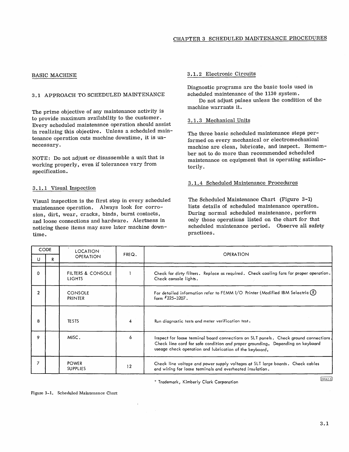
BASIC MACHINE
3.1
APPROACH
TO
SCHEDULED MAINTENANCE
The
prime
objective
of
any
maintenance
activity
is
to
provide
maximum
availability
to
the
customer.
Every
scheduled
maintenance
operation
should
assist
in
realizing
this
objective.
Unless
a
scheduled
main-
tenance
operation
cuts
machine
downtime,
it
is
un-
necessary.
NOTE:
Do
not
adjust
or
disassemble
a
unit
that
is
working
properly,
even
if
tolerances
vary
from
spe
cification.
3.1.1
Visual
Inspection
Visual
inspection
is
the
first
step
in
every
scheduled
maintenance
operation.
Always
look
for
corro-
sion,
dirt,
wear,
cracks,
binds,
burnt
contacts,
and
loose
connections
and
hardware.
Alertness
in
noticing
these
items
may
save
later
machine
down-
time.
CODE
LOCATION
OPERATION
FREQ.
U R
CHAPTER
3 SCHEDULED MAINTENANCE
PROCEDURES
3.1.2
Electronic
Circuits
Diagnostic
programs
are
the
basic
tools
used
in
scheduled
maintenance
of
the
1130
system.
Do
not
adjust
pulses
unless
the
condition
of
the
machine
warrants
it.
3.1.3
Mechanical
Units
The
three
basic
scheduled
maintenance
steps
per-
formed
on
every
mechanical
or
electromechanical
machine
are
clean,
lubricate,
and
inspect.
Remem-
ber
not
to
do
more
than
recommended
scheduled
maintenance
on
equipment
that
is
operating
satisfac-
torily.
3.
1.4
Scheduled
Maintenance
Procedures
The
Scheduled
Maintenance
Chart
(Figure
3-1)
lists
details
of
scheduled
maintenance
operation.
During
normal
scheduled
maintenance,
perform
only
those
operations
listed
on
the
chart
for
that
scheduled
maintenance
period.
Observe
all
safety
practices.
OPERATION
0 FIL
TERS
&
CONSOLE
1
Check
for
dirty
filters.
Replace
as
required.
Check
cooling
fans for
proper
operation.
LIGHTS
Check
console
lights.
2
CONSOLE
For
detailed
information
refer
to FEMM
I/O
Printer
(Modified
IBM
Selectric
®
PRINTER form
#225-3207.
8
TESTS
4
Run
diagnostic
tests
and
meter
verification
test.
9
MISC.
6
Inspect
for loose
terminal
board
connections
on
SL
T
panels.
Check
ground
connections
Check
line
cord
for
safe
condition
and
proper
grounding.
Depending
on
keyboard
useage
check
operation
and
lubrication
of
the
keyboard.
7 POWER
Check
line
voltage
and
power
supply
voltages
at
SLT
large
boards.
Check
cab
les
SUPPLIES
12
and
wiring
for loose
terminals
and
overheated
insulation.
*
Trademark,
Kimberly
Clark
Corporation
Figure
3-1.
Scheduled
Mamtenance
Chart
3.1
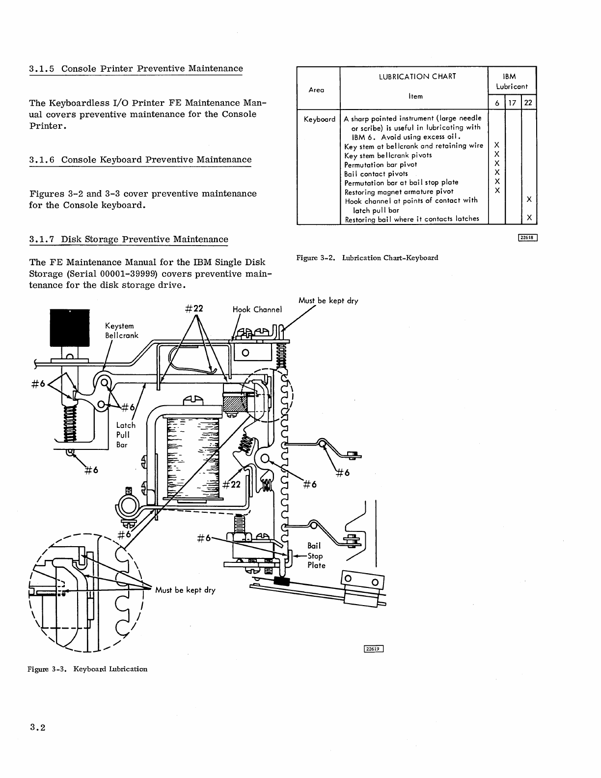
3.
1.
5
Console
Printer
Preventive
Maintenance
The
Keyboardless
I/O
Printer
FE
Maintenance
Man-
ual
covers
preventive
maintenance
for
the
Console
Printer.
3.
1.
6
Console
Keyboard
Preventive
Maintenance
Figures
3-2
and
3-3
cover
preventive
maintenance
for
the
Console
keyboard.
3.1.7
Disk
Storage
Preventive
Maintenance
The
FE
Maintenance
Manual
for
the
ruM
Single
Disk
Storage
(Serial
00001-39999)
covers
preventive
main-
tenance
for
the
disk
storage
drive.
Figure
3-3.
Keyboard
Lubrication
3.2
LUBRICATION CHART
Area
Item
Keyboard
A
sharp
pointed
instrument
(large
needle
or
scribe)
is
useful
in
lubricating
with
IBM
6.
Avoid
using
excess
oil.
Key
stem
at
bellcrank
and
retaining
wire
Key
stem
bellcrank
pivots
Permutation
bar
pivot
Bai I
contact
pivots
Permutation
bar
at
bai
I
stop
plate
Restoring
magnet
armature
pivot
Hook
channel
at
points
of
contact
with
latch
pu
II
bar
Restoring
bai
I
where
it
contacts
latches
Figure
3-2.
Lubrication
Chart-Keyboard
Must
be
kept
dry
IBM
Lubricant
6 17
22
X
X
X
X
X
X X
X
FEATURES
3.2
PREVENTNE
MAINTENANCE
OF
I/O
DEVICES
3.2.1
1132
Preventive
Maintenance
The
FE
Maintenance
Manual
1132
Printer
contains
detailed
information.
3.2.2
1442
Preventive
Maintenance
The
FE
Maintenance
Manual
for
the
1442
covers
pre-
ventive
maintenance
of
the
1442.
3.2.3
1134
Preventive
Maintenance
The
FE
Maintenance
Manual
for
the
1134
covers
pre-
ventive
maintenance
for
the
1134.
3.2.4
1055
Preventive
Maintenance
The
FE
Maintenance
Manual
for
the
1054/1055
covers
preventive
maintenance
of
the
1055.
3.2.5
1627
Preventive
Maintenance
The
FE
Instruction-Maintenance
Manual
for
the
1627
covers
preventive
maintenance
of
the
1627 •
3.3
CHAPTER
4 CHECKS, ADJUSTMENTS,
AND
REMOVAL
PROCEDURES
BASIC MACHINE
4.
1 SOLID LOGIC TECHNOLOGY MAINTENANCE
All
normal
maintenance
procedures
for
solid
logic
technology
components
are
found
in
IBM
Field
Engi-
neering
Manual of
Instruction
SLT
Packaging.
This
manual
includes
information
regarding:
Wrapped
Wire
Connections
Crimped
Connections
Soldered
Connections
Wiring
Change
Procedures
SLT
Service
Tools
SLT
Card
Maintenance
Measurements
Ventilating
Systems
SLT
Components
and
Packaging
SLT
Service
Techniques
4.
1. 1
SLT
Cards
The
lettering
within
a
logical
block
on a
systems
diagram
page
gives
the
location
of
that
block
in
the
card
gates.
It
also
indicates
other
pertinent
data
as
described
in
the
SLT
Packaging
FEMI.
Identifica-
tion
of
pins,
panels,
rows,
and
columns,
is
shown
in
the
SLT
Packaging
FEMI.
Logic
block
locations
within
the
system
diagrams
are
shown on
system
diagram
card
location
charts.
The
system
diagram
index
gives
the
machine
features
indexing
of
ALDIs
and
maintenance
diagrams.
4.
1. 2 Single Shots
The
single
shots
are
adjusted
with
the
CE
alignment
screwdriver,
part
460811,
or
jewelers
screwdriver,
part
2108286.
Adjust
each
of
the
single
shots
so
that
the
time
from
the
input
pulse
to
the
output
pulse
is
equal
to
the
time
specified
in
the
system
diagrams
for
the
individual
single
shot.
4.
2 CORE STORAGE UNIT
WARNING:
Be
extremely
cautious
when
working
around
core
storage.
Do
not
disturb
the
core
planes.
Do
not
leave
the
core
storage
unit
unattended
when
the
covers
are
removed.
4.2.1
Removal
1.
Remove
all
power
to
the
system.
2.
Remove
cards
around
unit.
3.
Unplug
the
connecting
assemblies
(on
the
wiring
side
of
the
large
board),
using
pulling
tool,
part
2108860, by
pulling
straight
out.
4.
Unlock
the
four
retainers
that
secure
the
array
to
the
large
board.
Note:
Pull
out
straight
to
prevent
damage
to
pins
and
land
patterns
on
the
core
unit.
5.
Remove
core
array
from
machine
and
place
array
in
a
safe
and
secure
working
area.
WARNING: Do
not
leave
the
unit
unattended
as
the
connections
and
pins
can
be
damaged.
Do
not
place
unit
with
pins
down
as
the
outside
pins
may
be
bent
as
array
is
picked
up.
4.2.2
Adjustment
procedure
for
Core
storage
The
storage
unit
contains
three
potentiometers
which
must
be
adjusted
to
optimize
storage
performance.
These
potentiometers
set
the
reference
voltage
level
(array
current
magnitude),
position
the
sense
amplifier
strobe,
and
set
the
sense
amplifier
sensi-
tivity.
Load
the
core
storage
with
the
core
adjustment
diagnostic
test,
which
contains
a
worse-case
pat-
tern
program.
After
the
pattern
is
loaded,
the
pro-
gram
stops.
Using
the
maintenance
switches,
the
system
is
set
in
automatic
display
mode
and
parity
check.
In
this
mode,
the
CPU
cycles
through
the
storage
at
the
maximum
speed
(continuous
read/write)
and
regenerates
the
data
read
out.
If
parity
errors
are
detected,
the
processor
stops
and
displays
a
parity
check.
If
the
core
adjustment
test
will
not
load,
set
all
of
core
storage
with
an
alternating
bit
pattern
with
the
bit
switches.
After
loading,
make
the
core
adjustments.
After
the
adjustments
are
made,
load
the
core
adjustment
test
and
remake
the
adjustments.
The
parity
is
restored
at
the
faulty
location
by:
1. Note
the
address
in
IAR
2.
Set
the
bit
switches
to
the
IAR
address
minus
1.
3.
Set
the
mode
switch
to
load.
4.
Press
the
load
IAR
switch.
4.1
5.
Set
the
bit
switches
to
a
correct
parity
word.
6.
Set
the
storage
load
switch
on,
and
the
display
switch
off.
Set
run
and
storage
load
switches
off,
and
the
display
switch
on.
7.
Press
the
start
switch.
8.
Set
the
mode
switch
to
run
and
the
storage
load
switch
off,
display
switch
on.
9.
Press
the
start
switch.
The
processor
should
again
cycle
through
storage
without
errors.
It
should
be
noted
that
VSA-
VE
varies
if
the
-3v
sup-
ply
is
varied;
but
once
adjusted,
it
remains
at
the
optimum
value
of
operation
even
if
-3v
is
varied.
It
is
suggested
that
the
adjustment
procedure
described
below
should
be
used
after
every
card
replacement.
SLT
voltages
-3,
+3, +6,
and
the
special
voltage,
+ 12v,
should
be
set
to
within
1%
of
their
nominal
values,
with
a
Weston
901
meter
or
equivalent
i.
e.
,
-3,
±0.03v,
+3
±O.
03v, +6
±0.06v,
and
+12
±O.
12v,
respectively,
measured
at
the
core
storage
large
board
with
the
system
operating.
4.2.2.1
Strobe
Adjustment
Scope
setup:
1.
Channel
A
and
B
-lv/div.
2.
Time
per
division
0.5
micro-seconds/div.
3.
Alternate
sweep.
Adjustment:
Measure
time
interval
between
positive
shift
of
short
time
(SD111)
on
pin
N2-B13
and
positive
shift
of
sample
pulse
(SD111) on
pin
N2-B05.
These
are
to
be
measured
at
1
volt
above
the
reference
line
on
the
scope.
Adjust
to
400
nanoseconds,
±20
nano-
seconds
using
potentiometer
located
on
card
N2
(reference
diagram
SD021).
4.2.2.
2 V
-Reference
-
VSA
Adjustment
WARNING: Do
not
use
a
scope
for
this
adjustment
as
the
reference
is
to
-3v
not
ground.
1.
Set
the
reference
voltage,
V
-Ref,
(G2B02)
refer-
enced
to
-3V
(G2B06)
to
the
value
given
in
the
fol-
lowing
table
by
adjusting
the
V
-Ref
potentiometer
(upper)
of
the
V
Ref
and
sense
control
card
(Reference
diagram
SD021).
This
is
an
initial
adjustment.
The
final
adjustment
is
defined
in
Item
4.
4.2
Room
Temperature
V-REF
C F
(Reference
to
-3V)
40-52°
104_124°
1.7V
30_40°
86-104°
1.8V
20_30°
68-86°
1.9V
10_20°
50_68°
2.0V
4_10°
39_50°
2.1V
2.
Press
the
stop
Key. With
the
clock
stopped,
adjust
-3v
supply
to
give
-2.
70v
measured
be-
tween
-3v
emitter
strobe
(G2B12)
and
ground.
Set
the
sense
control
voltage
to
2.
14v
±
0.02v
(G2B07)
referenced
to
offset
voltage
G2B09
(SD211) by
adjusting
the
VSA
potentiometer
(lower)
on
the
V
-Ref
and
Sense
Control
card
G2.
Re-
store
-3
volt
supply
to
-3
±
0.03v.
3.
Decrease
the
sense
control
voltage
(G2B07)
(SD211)
referenced
to
(G2B09)
until
failure
occurs
(parity
error)
by
adjusting
the
VSA
potentiometer
(G2
lower)
on
the
V
Ref
and
sense
control
card.
Then
set
the
sense
control
voltage
to
O.
1
volt
above
the
value
recorded
at
the
failure
point.
4.
After
operations
1, 2,
and
3
are
completed,
con-
tinue
to
cycle
the
storage
and
determine
the
ref-
erence
voltage
limits
by
varying
the
V
-Ref
po-
tentiometer
(G2
upper)
on
the
V
-Ref
and
sense
control
card
(Reference
diagram
SD021).
Adjust
reference
voltage,
V
-Ref
(G2B02),
referenced
to
-3V
(G2B06)
to
the
midpoint
between
the
limits
of
operation.
5.
If
the
V
-Ref
and
sense
control
card
is
replaced,
repeat
section
4.2.2.2.
If
the
clock-strobe
card
is
replaced,
repeat
section
4.
2. 2. 1.
4.3
OSCILLATOR
•
The
frequency
of
the
1131
oscillator
is
2. 25
mega-
cycles
± 11.
25
kilocycles
and
is
not
adjustable.
4.3.
1
Oscillator
Phase
Adjustment
Objective:
Set
up
initial
adjustment
when
oscillator
is
replaced.
Adj
ustment:
1.
Set
the
mode
switch
to
run
and
the
C E
switch
to
storage
display
and
press
the
start
key.
2. Sync
on
+
oscillator
trigger,
B-A1C4D13
(KA101).
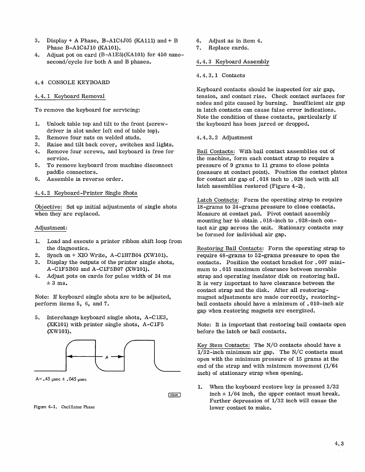
3.
Display
+ A
Phase,
B-AlC4J05
(KAlIl)
and
+ B
Phase
B-AlC4JlO
(KAlOl).
4.
Adjust
pot
on
card
(B-AlE5)(KAlOl)
for
450
nano-
second/cycle
for
both
A and B
phases.
4.4.
CONSOLE KEYBOARD
4.4.
1
Keyboard
Removal
To
remove
the
keyboard
for
servicing:
1. Unlock
table
top
and
tilt
to
the
front
(screw-
driver
in
slot
under
left
end
of
table
top).
2.
Remove
four
nuts
on
welded
studs.
3.
Raise
and
tilt
back
cover,
switches
and
lights.
4.
Remove
four
screws,
and
keyboard
is
free
for
service.
5.
To
remove
keyboard
from
machine
disconnect
paddle
connectors.
6.
Assemble
in
reverse
order.
4.4.2
Keyboard-Printer
Single Shots
Objective:
Set
up
initial
adjustments
of
single
shots
when
they
are
replaced.
Adjustment:
1.
Load
and
execute
a
printer
ribbon
shift
loop
from
the
diagnostics.
2. Synch on + XIO
Write,
A-CIH7B04
(XWI0l).
3.
Display
the
outputs
of
the
printer
single
shots,
A-ClF5B03
and
A-ClF5B07
(XWI0l).
4.
Adjust
pots
on
cards
for
pulse
width
of 24
ms
± 3
ms.
Note:
If
keyboard
single
shots
are
to
be
adjusted,
perform
items
5,
6,
and
7.
5.
Interchange
keyboard
single
shots,
A-CIE3,
(XKlOl)
with
printer
single
shots,
A-ClF5
(XWI01).
A=
.45
fJsec ± .045 fJsec
Figure
4-1.
Oscillator
Phase
6.
Adjust
as
in
item
4.
7.
Replace
cards.
4.4.3
Keyboard
Assembly
4.4.3.1
Contacts
Keyboard
contacts
should
be
inspected
for
air
gap,
tension,
and
contact
rise.
Check
contact
surfaces
for
nodes
and
pits
caused
by
burning.
Insufficient
air
gap
in
latch
contacts
can
cause
false
error
indications.
Note
the
condition
of
these
contacts,
particularly
if
the
keyboard
has
been
jarred
or
dropped.
4.4.3.2
Adjustment
Bail
Contacts:
With
bail
contact
assemblies
out
of
the
machine,
form
each
contact
strap
to
require
a
pressure
of
9
grams
to
11
grams
to
close
points
(measure
at
contact
point).
Position
the
contact
plates
for
contact
air
gap
of
.018
inch
to
.028
inch
with.
all
latch
assemblies
restored
(Figure
4-2).
Latch
Contacts:
Form
the
operating
strap
to
require
l8-grams
to
24-grams
pressure
to
close
contacts.
Measure
at
contact
pad.
Pivot
contact
assembly
mounting
bar
to
obtain.
018-inch
to
.
028-inch
con-
tact
air
gap
across
the
unit.
stationary
contacts
may
be
formed
for
individual
air
gap.
Restoring
Bail
Contacts:
Form
the
operating
strap
to
require
48-grams
to
52-grams
pressure
to
open
the
contacts.
Position
the
contact
bracket
for.
007
mini-
mum
to
.015
maximum
clearance
between
movable
strap
and
operating
insulator
disk
on
restoring
bail.
It
is
very
important
to
have
clearance
between
the
contact
strap
and
the
disk.
Mter
all
restoring-
magnet
adjustments
are
made
correctly,
restoring-
bail
contacts
should
have
a
minimum
of
•
010-inch
air
gap
when
restoring
magnets
are
energized.
Note:
It
is
important
that
restoring
bail
contacts
open
before
the
latch
or
bail
contacts.
Key
stem
Contacts:
The
N/O
contacts
should
have
a
1/32-inch
minimum
air
gap.
The
N/C
contacts
must
open
with
the
minimum
pressure
of
15
grams
at
the
end
of
the
strap
and
with
minimum
movement
(1/64
inch) of
stationary
strap
when
opening.
1. When
the
keyboard
restore
key
is
pressed
3/32
inch
±
1/64
inch,
the
upper
contact
must
break.
Further
depression
of
1/32
inch
will
cause
the
lower
contact
to
make.
4.3
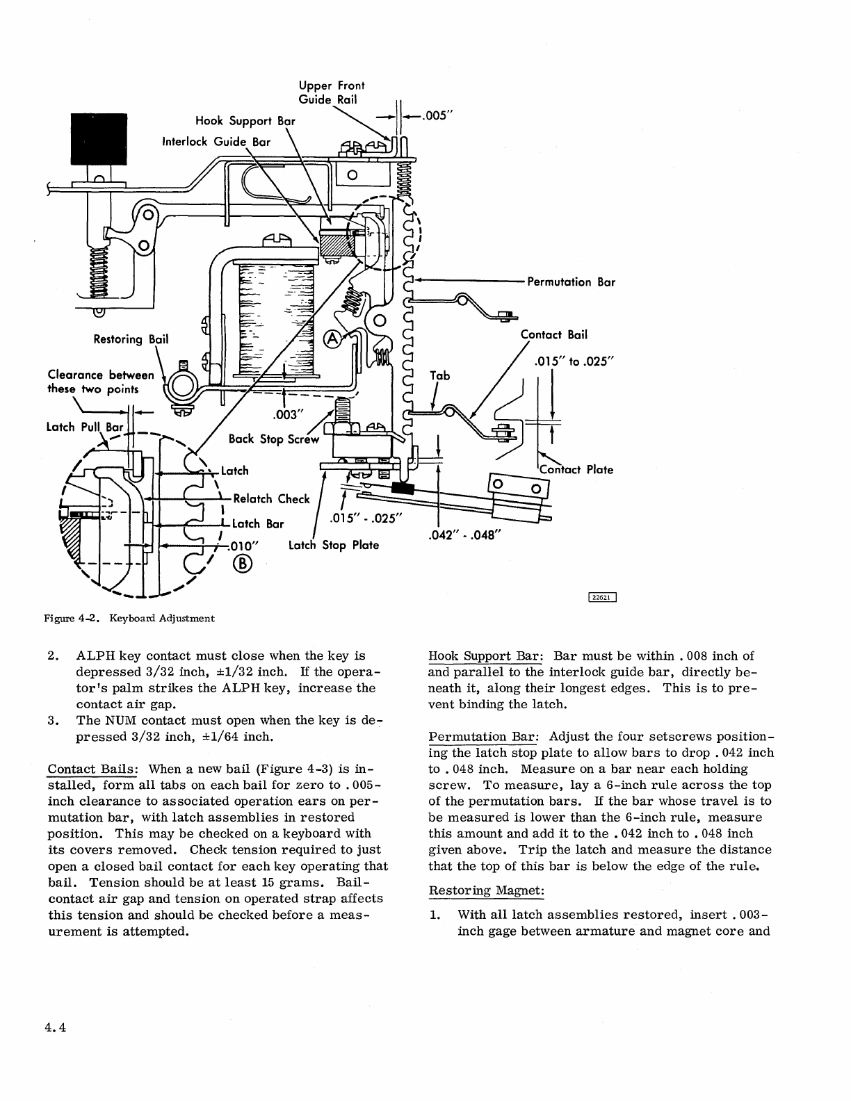
Figure
4-2.
Keyboard
Adjustment
Upper Front
Guide
Rail
2.
ALPH
key
contact
must
close
when
the
key
is
depressed
3/32
inch,
±1/32
inch.
If
the
opera-
tor's
palm
strikes
the
ALPH
key,
increase
the
contact
air
gap.
3.
The
NUM
contact
must
open
when
the
key
is
de-
pressed
3/32
inch,
±1/64
inch.
Contact
Bails:
When a
new
bail
(Figure
4-3)
is
in-
stalled,
form
all
tabs
on
each
bail
for
zero
to
.
005-
inch
clearance
to
associated
operation
ears
on
per-
mutation
bar,
with
latch
assemblies
in
restored
position.
This
may
be
checked
on a
keyboard
with
its
covers
removed.
Check
tension
required
to
just
open
a
closed
bail
contact
for
each
key
operating
that
bail.
Tension
should
be
at
least
15
grams.
Bail-
contact
air
gap
and
tension
on
operated
strap
affects
this
tension
and
should
be
checked
before
a
meas-
urement
is
attempted.
4.4
;..1
...
-------
Permutation Bar
Hook
Support
Bar:
Bar
must
be
within.
008
inch
of
and
parallel
to
the
interlock
guide
bar,
directly
be-
neath
it,
along
their
longest
edges.
This
is
to
pre-
vent
binding
the
latch.
Permutation
Bar:
Adjust
the
four
setscrews
position-
ing
the
latch
stop
plate
to
allow
bars
to
drop.
042
inch
to
. 048
inch.
Measure
on a
bar
near
each
holding
screw.
To
measure,
lay
a
6-inch
rule
across
the
top
of
the
permutation
bars.
If
the
bar
whose
travel
is
to
be
measured
is
lower
than
the
6-inch
rule,
measure
this
amount
and
add
it
to
the.
042
inch
to
.048
inch
given
above.
Trip
the
latch
and
measure
the
distance
that
the
top
of
this
bar
is
below
the
edge
of
the
rule.
Restoring
Magnet:
1.
With
all
latch
assemblies
restored,
insert.
003-
inch
gage
between
armature
and
magnet
core
and
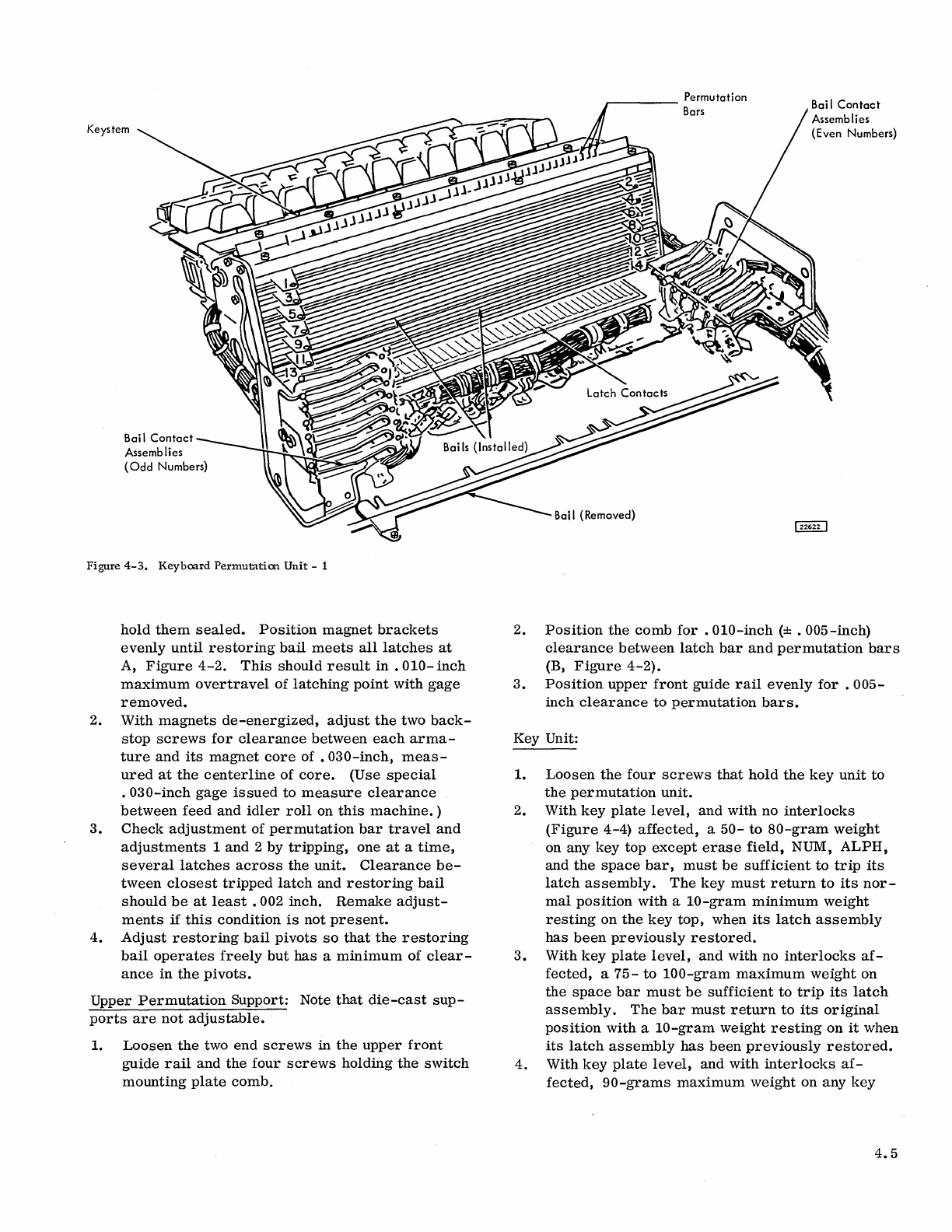
Keystem
Bai I
Contact
Assemblies
(Odd
Numbers)
Figure
4-3.
Keyboard
Permutation
Unit
- 1
hold
them
sealed.
Position
magnet
brackets
evenly
until
restoring
bail
meets
all
latches
at
A,
Figure
4-2.
This
should
result
in
.010-
inch
maximum
overtravel
of
latching
point
with
gage
removed.
2.
With
magnets
de-energized,
adjust
the
two
back-
stop
screws
for
clearance
between
each
arma-
ture
and
its
magnet
core
of
.030-inch,
meas-
ured
at
the
centerline
of
core.
(Use
special
.
030-inch
gage
issued
to
measure
clearance
between
feed
and
idler
roll
on
this
machine.
)
3.
Check
adjustment
of
permutation
bar
travel
and
adjustments
1
and
2
by
tripping,
one
at
a
time,
several
latches
across
the
unit.
Clearance
be-
tween
closest
tripped
latch
and
restoring
bail
should
be
at
least.
002
inch.
Remake
adjust-
ments
if
this
condition
is
not
present.
4.
Adjust
restoring
bail
pivots
so
that
the
restoring
bail
operates
freely
but
has
a
minimum
of
clear-
ance
in
the
pivots.
Upper
Permutation
Support:
Note
that
die-cast
sup-
ports
are
not
adjustable.
1.
Loosen
the
two
end
screws
in
the
upper
front
guide
rail
and
the
four
screws
holding
the
switch
mounting
plate
comb.
,...-
____
Permutation
Bars
2.
Position
the
comb
for.
OIO-inch (±
.005-inch)
clearance
between
latch
bar
and
permutation
bars
(B,
Figure
4-2).
3.
Position
upper
front
guide
rail
evenly
for.
005-
inch
clearance
to
permutation
bars.
Key Unit:
1.
Loosen
the
four
screws
that
hold
the
key
unit
to
the
permutation
unit.
2.
With
key
plate
level,
and
with
no
interlocks
(Figure
4-4)
affected,
a
50-
to
SO-gram
weight
on any
key
top
except
erase
field,
NUM,
ALPH,
and
the
space
bar,
must
be
sufficient
to
trip
its
latch
assembly.
The
key
must
return
to
its
nor-
mal
position
with
a
10-gram
minimum
weight
resting
on
the
key
top,
when
its
latch
assembly
has
been
previously
restored.
3.
With
key
plate
level,
and
with
no
interlocks
af-
fected,
a
75-
to
100-gram
maximum
weight
on
the
space
bar
must
be
sufficient
to
trip
its
latch
assembly.
The
bar
must
return
to
its
original
position
with
a
10-gram
weight
resting
on
it
when
its
latch
assembly
has
been
previously
restored.
4.
With
key
plate
level,
and
with
interlocks
af-
fected,
90-grams
maximum
weight
on
any
key
4.5
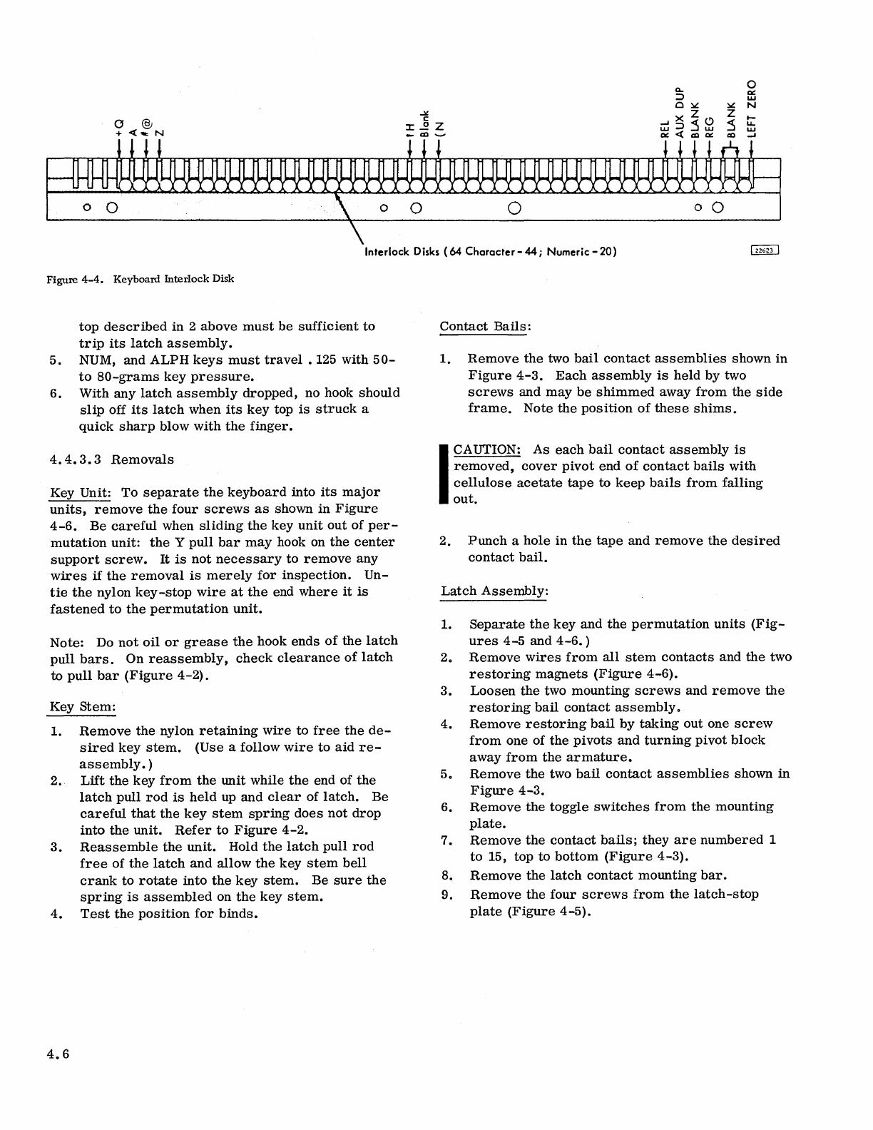
Q..
0
a::
::>
w
Q::.o!
::.o!
N
,.:,t. Z Z
o
@;
c
~~:58
:5
.--
:x:J:!Z
u.
+ <
....
N w
_cc
_
a::<c:ca::
c:c
-'
Interlock Disks
(64
Character
-
44;
Numeric -
20)
Figure
4-4.
Keyboard
Interlock
Disk
top
described
in 2 above
must
be
sufficient
to
trip
its
latch
assembly.
5.
NUM, and ALPH
keys
must
travel.
125 with
50-
to
80-grams
key
pressure.
6. With any
latch
assembly
dropped, no hook should
slip
off
its
latch
when
its
key
top
is
struck
a
quick
sharp
blow
with
the
finger.
4.4.3.3
Removals
Key Unit: To
separate
the
keyboard
into
its
major
units,
remove
the
four
screws
as
shown
in
Figure
4-6.
Be
careful
when
sliding
the
key
unit
out of
per-
mutation
unit:
the
Y
pull
bar
may
hook on
the
center
support
screw.
It
is
not
necessary
to
remove
any
wires
if
the
removal
is
merely
for
inspection.
Un-
tie
the
nylon
key-stop
wire
at
the
end
where
it
is
fastened
to
the
permutation
unit.
Note: Do
not
oil
or
grease
the
hook
ends
of
the
latch
pull
bars.
On
reassembly,
check
clearance
of
latch
to
pull
bar
(Figure
4-2).
Key
stem:
1.
Remove
the
nylon
retaining
wire
to
free
the
de-
sired
key
stem.
(Use a follow
wire
to
aid
re-
assembly.
)
2.
Lift
the
key
from
the
unit
while
the
end of
the
latch
pull
rod
is
held
up and
clear
of
latch.
Be
careful
that
the
key
stem
spring
does
not
drop
into
the
unit.
Refer
to
Figure
4-2.
3.
Reassemble
the
unit.
Hold
the
latch
pull
rod
free
of
the
latch
and allow
the
key
stem
bell
crank
to
rotate
into
the
key
stem.
Be
sure
the
spring
is
assembled
on
the
key
stem.
4.
T.est
the
position
for
binds.
4.6
Contact
Bails:
1.
Remove
the
two
bail
contact
assemblies
shown
in
Figure
4-3.
Each
assembly
is
held
by two
screws
and
may
be
shimmed
away
from
the
side
frame.
Note
the
position
of
these
shims.
I
CAUTION:
As
each
bail
contact
assembly
is
removed,
cover
pivot
end
of
contact
bails
with
cellulose
acetate
tape
to
keep
bails
from
falling
out.
2.
Punch
a
hole
in
the
tape
and
remove
the
desired
contact
bail.
Latch
Assembly:
1.
Separate
the
key
and
the
permutation
units
(Fig-
ures
4-5
and
4-6.
)
2.
Remove
wires
from
all
stem
contacts
and
the
two
restoring
magnets
(Figure
4-6).
3.
Loosen
the
two mounting
screws
and
remove
the
restoring
bail
contact
assembly.
4.
Remove
restoring
bail
by
taking
out one
screw
from
one of
the
pivots
and
turning
pivot
block
away
from
the
armature.
5.
Remove
the
two
bail
contact
assemblies
shown
in
Figure
4-3.
6.
Remove
the
toggle
switches
from
the mounting
plate.
7.
Remove
the
contact
bails;
they
are
numbered
1
to
15, top
to
bottom
(Figure
4-3).
8.
Remove
the
latch
contact
mounting
bar.
9.
Remove
the
four
screws
from
the
latch-stop
plate
(Figure
4-5).
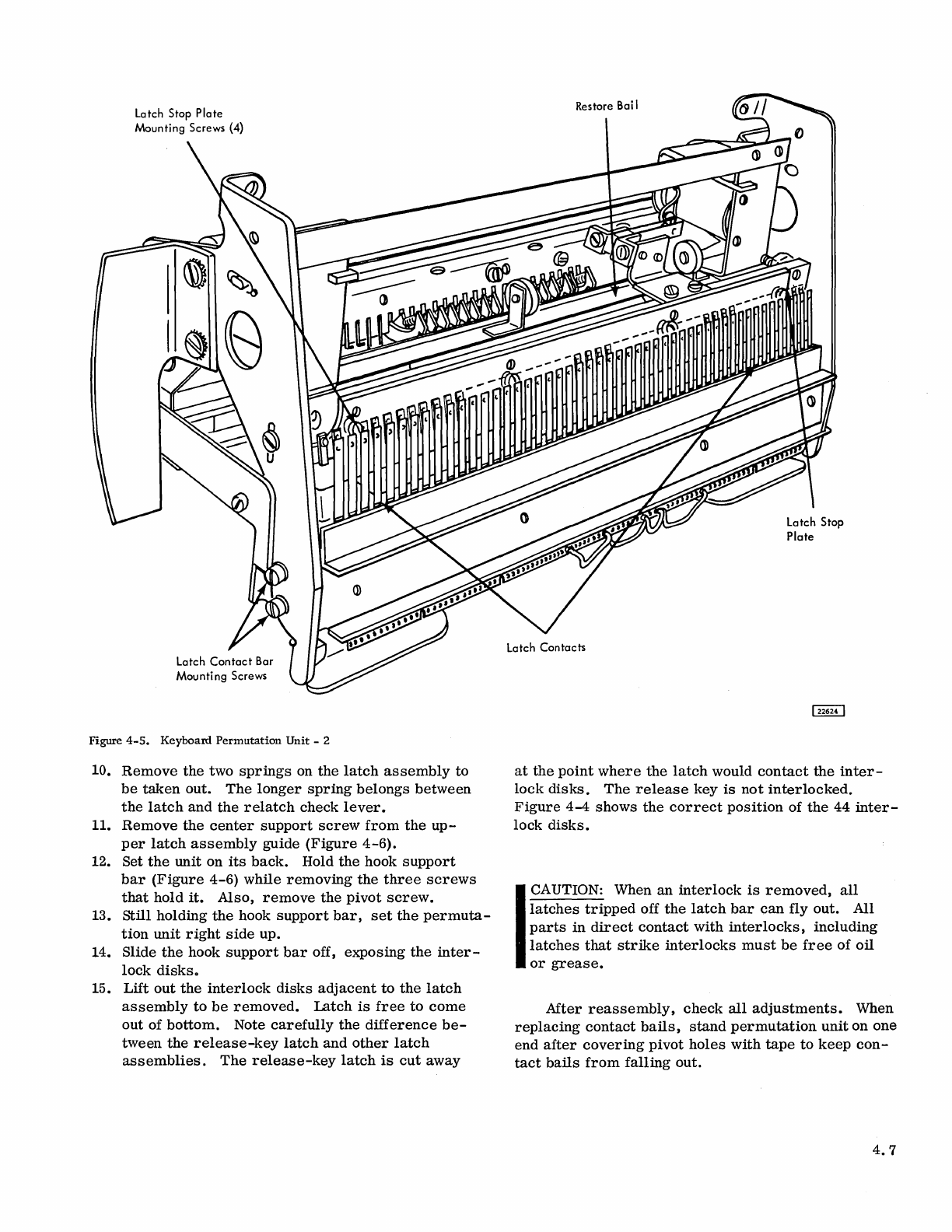
Mounting
Screws
Figure
4-5.
Keyboard
Permutation
Unit
-2
10.
Remove
the
two
springs
on
the
latch
assembly
to
be
taken
out.
The
longer
spring
belongs
between
the
latch
and
the
relatch
check
lever.
11.
Remove
the
center
support
screw
from
the
up-
per
latch
assembly
guide
(Figure
4-6).
12. Set
the
unit
on
its
back.
Hold
the
hook
support
bar
(Figure
4-6)
while
removing
the
three
screws
that
hold
it.
Also,
remove
the
pivot
screw.
13.
Still
holding
the
hook
support
bar,
set
the
permuta-
tion
unit
right
side
up.
14. Slide
the
hook
support
bar
off,
exposing
the
inter-
lock
disks.
15.
Lift
out
the
interlock
disks
adjacent
to
the
latch
assembly
to
be
removed.
Latch
is
free
to
come
out
of
bottom.
Note
carefully
the
difference
be-
tween
the
release-key
latch
and
other
latch
assemblies.
The
release-key
latch
is
cut
away
Restore Bci I
at
the
point
where
the
latch
would
contact
the
inter-
lock
disks.
The
release
key
is
not
interlocked.
Figure
4-4
shows
the
correct
position
of
the
44
inter-
lock
disks.
I
CAUTION: When
an
interlock
is
removed,
all
latches
tripped
off
the
latch
bar
can
fly
out.
All
parts
in
direct
contact
with
interlocks,
including
latches
that
strike
interlocks
must
be
free
of
oil
or
grease.
After
reassembly,
check
all
adjustments.
When
replacing
contact
bails,
stand
permutation
unit
on
one
end
after
covering
pivot
holes
with
tape
to
keep
con-
tact
bails
from
falling
out.
4.7
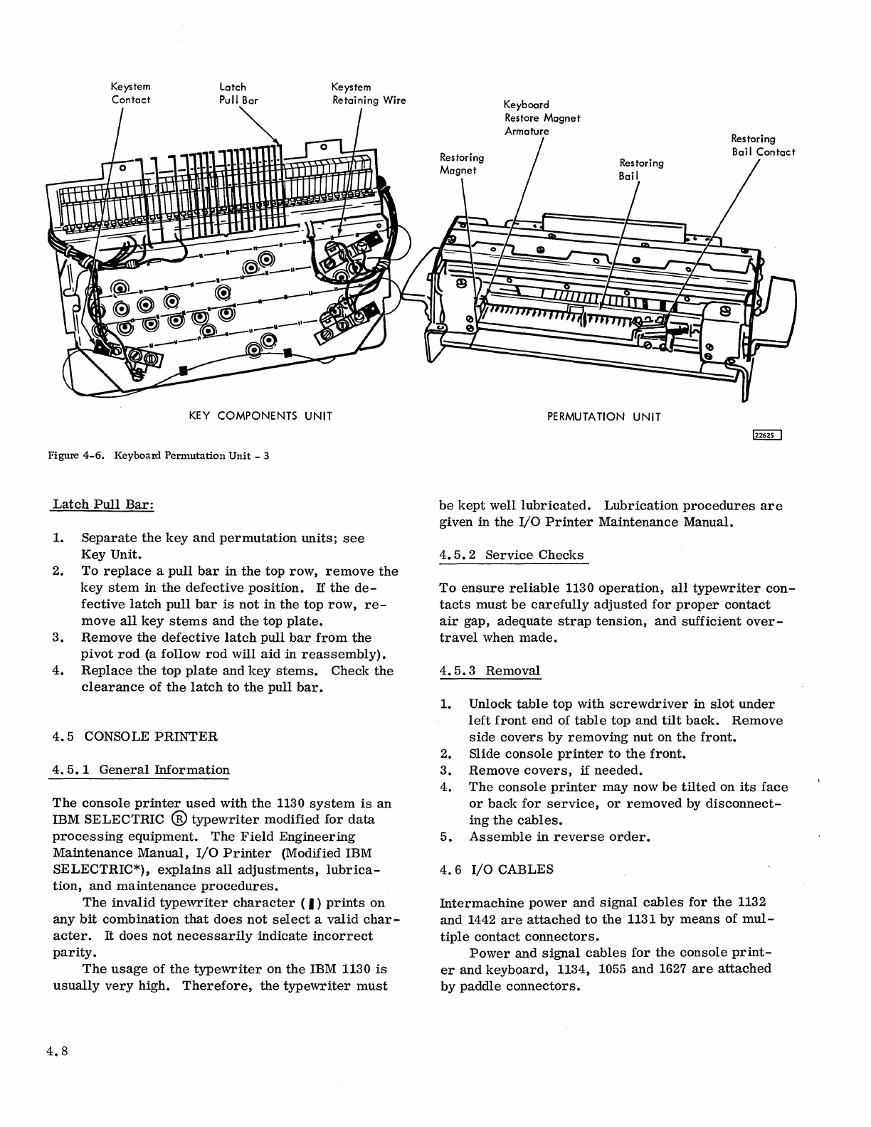
Keystem
Contact Latch
Pull
Bar
Keystem
Retaining Wire
KEY
COMPONENTS UNIT
Figure
4-6.
Keyboard
Permutation
Unit
- 3
Latch
Pull
Bar:
1.
Separate
the
key
and
permutation
units;
see
Key
Unit.
2.
To
replace
a
pull
bar
in
the
top
row,
remove
the
key
stem
in
the
defective
position.
If
the
de-
fective
latch
pull
bar
is
not
in
the
top
row,
re-
move
all
key
stems
and
the
top
plate.
3.
Remove
the
defective
latch
pull
bar
from
the
pivot
rod
(a
follow
rod
will
aid
in
reassembly).
4.
Replace
the
top
plate
and
key
stems.
Check
the
clearance
of
the
latch
to
the
pull
bar.
4.5
CONSOLE
PRINTER
4.5.1
General
Information
The
console
printer
used
with
the
1130
system
is
an
IBM
SELECTRIC
®
typewriter
modified
for
data
processing
equipment.
The
Field
Engineering
Maintenance
Manual,
I/O
Printer
(Modified IBM
SELECTRIC*),
explains
all
adjustments,
lubrica-
tion,
and
maintenance
procedures.
The
invalid
typewriter
character
(
I)
prints
on
any
bit
combination
that
does
not
select
a
valid
char-
acter.
It
does
not
necessarily
indicate
incorrect
parity.
The
usage
of
the
typewriter
on
the
IBM 1130
is
usually
very
high.
Therefore,
the
typewriter
must
4.8
Keyboard
Restore Magnet
Armature
PERMUTATION
UNIT
be
kept
well
lubricated.
Lubrication
procedures
are
given
in
the
I/O
Printer
Maintenance
Manual.
4.
5.
2
Service
Checks
To
ensure
reliable
1130
operation,
all
typewriter
con-
tacts
must
be
carefully
adjusted
for
proper
contact
air
gap,
adequate
strap
tension,
and
sufficient
over-
travel
when
made.
4.5.3
Removal
1. Unlock
table
top
with
screwdriver
in
slot
under
left
front
end of
table
top
and
tilt
back.
Remove
side
covers
by
removing
nut
on
the
front.
2. Slide
console
printer
to
the
front.
3.
Remove
covers,
if
needed.
4.
The
console
printer
may
now
be
tilted
on
its
face
or
back
for
service,
or
removed
by
disconnect-
ing
the
cables.
5.
Assemble
in
reverse
order.
4.
6
I/O
CABLES
Intermachine
power
and
signal
cables
for
the
1132
and
1442
are
attached
to
the
1131
by
means
of
mul-
tiple
contact
connectors.
Power
and
signal
cables
for
the
console
print-
er
and
keyboard,
1134, 1055
and
1627
are
attached
by
paddle
connectors.
4.7
DISK STORAGE UNIT
•
Maintenance
procedures
for
the
disk
storage
are
described
in
the
IBM Single
Disk
Storage
(Serial
00001-39999)
Field
Engineering
Maintenance
Manual.
4.7.1
Removal
1.
Remove
the
table
top.
2.
Remove
the
top,
front,
right
end
and
right
rear
covers.
3.
Remove
the
top
cover
from
the
unit.
4.
Remove
the
cartridge.
5
~
Remove
the
air
duct
from
rear
of
the
unit.
6.
Remove
the
cable
from
the
switch
panel
by
un-
plugging
from
the
TB
on
top
of
unit.
7.
Remove
the
dc
cable
from
the
TB
on
the
rear
of
the
unit
and
the
ac
cable
from
the
sequence
box
under
the
right
front
of
unit.
8.
Remove
four
nuts
from
mounting
studs
on
bot-
tom
of
the
unit.
9.
Open
the
SLT
gate.
10.
Remove
the
connector
holder.
11.
Remove
the
signal
connector
from
X-A1
A2.
12.
Remove
the
signal
connector
holding
clip
as
the
cable
leaves
box.
13.
Remove
block
from
the
cable.
14.
Pull
the
cable
from
the
box.
15. Now
the
unit
is
ready
to
be
removed.
This
takes
two
men,
one
at
the
front
and
one
at
the
rear
of
the
unit.
Reach
down
from
the
top
and
lift
straight
up.
16.
Assemble
in
reverse
order.
4.7.2
File
Read-Write
Single
Shot
Objective:
To
delay
the
start
of
writing
data
so
that
a
disk
written
on
one
system
may
be
read
on
another
system.
Adjustment:
1.
Turn
on
the
disk
storage
onloff
switch.
2.
Synch
scope
on
+
sector
pulse,
pin
A-C1M6G10
(XF181).
3.
Adjust
the
potentiometer
on
card,
A-C1M6,
so
that
the
Single
shot
output~
A-C1M6J13,
is
nega-
tive
for
250 ± 28
microsecond.
4.8
MISCELLANEOUS UNITS
4.8.1
Table
Top
4.8.1.1
Removal
1. Unlock
the
table
with
a
screwdriver
in
the
slot
under
right
end
of
table
top
and
tilt
to
the
front.
2.
Remove
the
two
screws
on
the
stay
brace.
Note: Do
not
remove
holding
screws
on
the
adjust-
able
bracket.
3.
Tilt,
to
the
front,
the
stop
bracket
on
the
right
end of
the
table
top.
4.
Slide
the
table
top
to
the
right
and
remove.
5.
Assemble
in
reverse
order.
4.8.2
Gate
Blowers
4.8.2.
1
Removal
1.
Drop
the
power
with
the
C E
switch.
2. Swing
the
gates
out
full.
3.
Remove
the
mounting
screws
on
the
TB's.
4.
Remove
the
two
screws
on
each
end
of
the
housing.
5.
Swing
the
housing
out
and
place
on
its
side.
6.
Remove
the
wires
to
the
fan
from
the
TB.
7.
Remove
the
holding
screws.
8.
Remove
the
fan.
9.
Place
the
new
fan
in
position.
10.
Assemble
in
reverse
order.
4.8.3
Filters
4.8.3.1
Cleaning
1.
Remove
the
filter
by
sliding
it
forward.
2.
Clean
in
clear
water.
3.
Shake
dry.
4.
Replace
4.8.4
Console
Lamps
•
Test
with
lamp
test
CE
switch.
4.8.4.1
Lamp
Removal
1.
Drop
power.
4.9
2.
Remove
the
back
cover
of
console.
3.
Pull
the
bank
of
lights
to
the
rear.
Note:
Be
careful
not
to
damage
the
wires
and
connectors.
4.
Remove
the
wire
terminals
from
the
individual
lamp
holder.
5.
Remove
the
old
lamp
from
the
holder.
6.
Replace
the
new
lamp
in
place
and
clip
the
leads.
7.
Replace
the
wries
in
the
holder.
8.
Be
sure
that
the
leads
are
not
shorted
or
grounded.
9.
Power
on.
10.
Test
the
lamps
with
the
lamp
test
CE
switch.
11.
Power
down.
12.
Replace
the
bank
of
lamps
in
the
panel.
13.
Replace
the
back
cover.
14.
Power
up.
15.
Test
the
lamps
with
the
lamp
test
CE
switch.
4.
8.4.
2
Lamp
Driver
Removal
1.
Turn
off
power.
2.
Remove
the
back
cover
from
the
console.
3.
Pull
the
bank
of
lamps
to
the
rear.
4.10
Note:
Be
careful
not
to
damage
the
wires
and
connectors.
4.
Remove
the
lamp
terminal
from
the
driver.
5.
Remove
the
signal
connector
from
the
driver.
6.
Unsolder
two
leads
to
bus
board
and
remove
driver.
7.
Form
two
outside
leads
on
new
driver
down
at
90°
.
8.
Place
on
bus
board
and
solder
in
place.
9.
Replace
signal
connector
on
driver.
10.
Replace
lamp
terminal
in
driver.
11.
Turn
on
power.
12.
Test
lamps
with
lamp
test
switch.
13.
Turn
off
power.
14.
Replace
bank
of
lamps
in
console.
15.
Replace
rear
cover.
16.
Turn
on
power.
17.
Test
lamps
with
lamp
test
switch.
4.8.5
Status
Indicator
Panel
4.8.5.1
Lamp
Removal
1.
Pull
up
the
lamp
cover
and
remove.
2.
Install
the
new
lamp.
3.
Replace
cover.
FEATURES
4.9
1442 ATTACHMENT
4.9.1
Read
Single
Shot
Obj
ective:
Allow
each
column
of
the
card
to
be
read
twice
for
read
registration
checking.
Adjustment:
1.
Program
load
the
read
diagnostics
in
order
to
read
cards
while
making
the
adjustment.
2.
Display
the
output
of
the
single
shot,
synch
internal.
A-B1K3B03
(XR301).
3.
Adjust
potentiometer
(upper
potentiometer)
on
the
card,
A-B1K3
for
a 100 ±12
microsecond
pulse
on
models
6
and
7.
4.9.2
Punch
Gate
Single
Shot
Objective:
Provide
a
delay
gate
to
allow
the
1442
to
accept
punch
data.
Adjustment:
1.
Program
load
the
punch
diagnostics
in
order
to
punch
cards
while
making
the
adjustment.
2.
Display
the
output
of
the
single
shot,
synch
in-
ternal,
A-BIK3B07
(XR301).
3.
Adjust
lower
potentiometer
on
the
card,
A-B1K3
for
a 500 ±60
microsecond
pulse
on
model
7
or
1000 ±120
microsecond
pulse
for
model
6.
4.10
PAPER
TAPE
ATTACHMENT
4.10.1
Paper
Tape
Reader
Single Shot
Objective:
Set
timing
for
transfer
of
information
to
the
attachment.
Adjustment:
1.
Load
the
paper
tape
reader
program.
2.
Synch
oscilloscope
minus
internal
on
single
out-
put
on
board
A-B1G6B07
(XT301).
3.
Adjustable
potentiometer
is
the
lower
of
the
2
on
the
card
(toward
card
row
7).
4.
Adjust
single
shot
output
to
500
microseconds
±60
MS.
4.10.2
Paper
Tape
Punch
•
There
are
no
adjustments
on
the
punch
attachment.
4.10.3
1134
Attachment
Oscillator
Symmetry:
Adjust
the
plus
oscillator
FF
signal
(bottom
potentiometer)
on
A-B1H7B09 (XT331)
for
4.5
±O. 5
milliseconds
duration.
Frequency:
Adjust
the
plus
oscillator
FF
signal
(top
potentiometer)
on
A-B1H7B09 (XT331)
for
8.3
±
O.
25
millis
econds
between
puIs
es
.
4.11
1132
PRINTER
ATTACHMENT
•
There
are
no
adjustments
on
the
printer
attachment.
4.12
1627
PLOTTER
ATTACHMENT
•
There
are
no
adjustments
on
the
plotter
attachment.
Note:
Attachment
contains
jumpers
that
are
changed
for
Model
I
and
Model
II (XG101).
4.
13 1132
PRINTER
The
Field
Engineering
Maintenance
Manual
.132
Printer
describes
maintenance
procedures
for
the
IBM 1132
Printer.
4.
14 1627
PLOTTER
The
Field
Engineering
Maintenance
Manual
1627
Plotter
describes
maintenance
procedures
for
the
IBM 1627
Plotter.
4.15
1134
PAPER
TAPE
READER
The
Field
Engineering
Instruction
Maintenance
Manual
1134
Paper
Tape
Reader
describes
main-
tenance
procedures
for
the
IBM
1134
Paper
Tape
Reader.
4.
16 1055
PAPER
TAPE
PUNCH
The
Field
Engineering
Maintenance
Manual
1054/1055
Paper
Tape
Reader/Punch
describes
maintenance
procedures
for
the
IBM 1055
Paper
Tape
Punch.
4.
17 1442
SERIAL
READER
PUNCH
The
Field
Engineering
Maintenance
Manual
1442
Serial
Reader
Punch
models
6
and
7
describes
main-
tenance
procedures
for
the
IBM 1442
Serial
Reader
Punch.
4.11
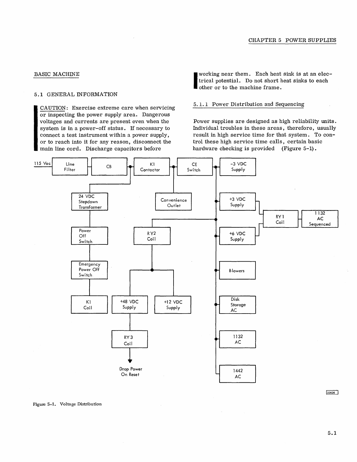
BASIC MACHINE
5.1
GENERAL
INFORMATION
CA UTION :
Exercise
extreme
care
when
servicing
or
inspecting
the
power
supply
area.
Dangerous
voltages
and
currents
are
present
even
when
the
system
is
in
a
power-off
status.
If
necessary
to
connect
a
test
instrument
within
a
power
supply,
or
to
reach
into
it
for
any
reason,
disconnect
the
main
line
cord.
Discharge
capacitors
before
115
Vec
Line
Fi
Iter -
24
VDC
Stepdown
Transformer
Power
Off
Switch
Emergency
Power Off
Switch
K1
Coil
Figure
5-1.
Voltage
Distribution
CB
~.-
+48
VDC
Supply
RY3
Coil
L
K1
Contactor
RY2
Coil
Drop
Power
On
Reset
-4.-
Convenience
Outlet
+12
VDC
Supply
CHAPTER
5
POWER
SUPPLIES
I
working
near
them.
Each
heat
sink
is
at
an
elec-
trical
potential.
Do
not
short
heat
sinks
to
each
other
or
to
the
machine
frame.
5.
1.
1
Power
Distribution
and
Sequencing
Power
supplies
are
designed
as
high
reliability
units.
Individual
troubles
in
these
areas,
therefore,
usually
result
in
high
service
time
for
that
system.
To
con-
trol
these
high
service
time
calls,
certain
basic
hardware
checking
is
provided
(Figure
5-1).
CE
Switch
-41-1
...
I.-
4'-
4.-
.-
-
-3
VDC
Supply
+3
VDC
Supply
+6
VDC
Supply
Blowers
Disk
Storage
AC
1132
AC
1442
AC
1
1132
RY1
-
AC
U Coil Sequenced
122626 I
5.1
5.
1.
2
Switche
s
Emergency
Power
Off:
(not
customer
resettable).
Turns
off
all
primary
transformer
power
in
the
proc-
essor,
except
the
24
vac
power.
Drops
all
power
to
I/O
machines.
Power
On/Off:
Same
as
emergency
power
off
except
resettable.
Disk
On/Off:
Controls
ac
power
to
the
disk
storage
drive.
5.1.3
CE
Power
Switches
Processor:
Removes
all
primary
power
to
system
except
processor
convenience
outlets.
Printer:
Removes
primary
power
in
printer.
Re-
moves
power
to
motors
except
chassis
cooling
fans.
Leaves
convenience
outlets
on.
Reader
Punch:
Same
function
as
for
printer.
5.1.4
Indicators
Ready:
Indicates
when
power
is
up.
5.1.
5
Voltage
Variation
Those
voltages
which
can
provide
an
indication
of
a
deteriorating
component
condition
can
be
varied
within
±4%to
assist
in
isolating
extreme
difficulties.
See
table
section
5.
1.
9.
5.
1.
6
Convenience
Outlet
A 115v
convenience
outlet
is
provided
in
the
CPU.
It
is
fused
at
6.
25
amps.
5.1.
7
Voltages
Present
Under
Normal
Power
Off
Conditions
1.
24
vac
circuits.
2.
115
vac
in
sequence
box.
5.1.8
Input
Power
Specifications
60
cycle:
The
IBM 1130
System
operates
from
a
115v,
60
cycle,
single
phase,
three
wire
service
line.
Input
voltage
may
have
a
total
variation
of
±10%
of
the
rated
voltage.
Line
frequency
must
be
60
±O.5
CPS.
5.2
The
mainline
CB
is
designed
to
trip
when
the
input
current
is
excessive.
It
must
be
reset
man-
ually.
50
cycle:
The
50
cycle
version
of
the
1130
requires
an
input
voltage
of
195v
ac,
220v
ac,
or
235 v
ac,
single
phase,
three
wire
service
line.
Input
voltage
may
have
a
total
variation
of
±10%
of
the
rated
voltage.
Line
frequency
must
be
50
±O.5
cps.
5.
1.
9
Individual
Power
Supplies
Operating
Limits:
For
normal
operation,
the
dc
power
supplies
must
be
maintained
within
the
toler-
ances
specified
below.
All
voltages
must
be
meas-
ured
at
the
SLT
large
card
pins.
Voltage
Allowable
Range
of
Voltage
-3
2.88
to
-
3.12
+3 +
2.88
to
+
3.12
+6 +
5.76
to
+
6.24
+12 +
11.16
to
+
12.84
+48 +
44.16
to
+
51.84
The
dc
voltage
tolerances
include
regulation
and
rip-
ple
and
are
measured
at
the
voltage
bus
on
01B-C1
board
for
+
12v,
+ 6v,
+3v,
and
-3v.
The
+48v
is
measured
at
the
TB2
block
on
the
A
gate.
5.1.10
Core
Storage
Voltages
Current
Requirements:
Storage
in
Use
-
Storage
Stand
By
+6v
4.0a
2.5a
+3v
-3v
+12v
.6a
1.5a
.5a
.4a
.5a
O.Oa
Voltage
Limit:
In
order
to
prevent
damage
to
the
storage
circuits,
the
supply
voltages
should
never
exceed
-8.0v,
+8.0v,
+9.0v
and
+15v
for
-3,+3,
+6,
and
+12
voltages,
respectively.
Transient
voltages
greater
than
10%
above
nominal
must
be
less
than
50
milliseconds
duration.
Under
voltage
does
not
damage
the
storage.
Marginal
Checking:
There
is
no
provision
for
mar-
ginal
checking
of
storage
voltages.
Power
Sequencing:
The
special
voltage,
+
12v,
is
applied
to
the
storage
large
card
after
the
SL
T
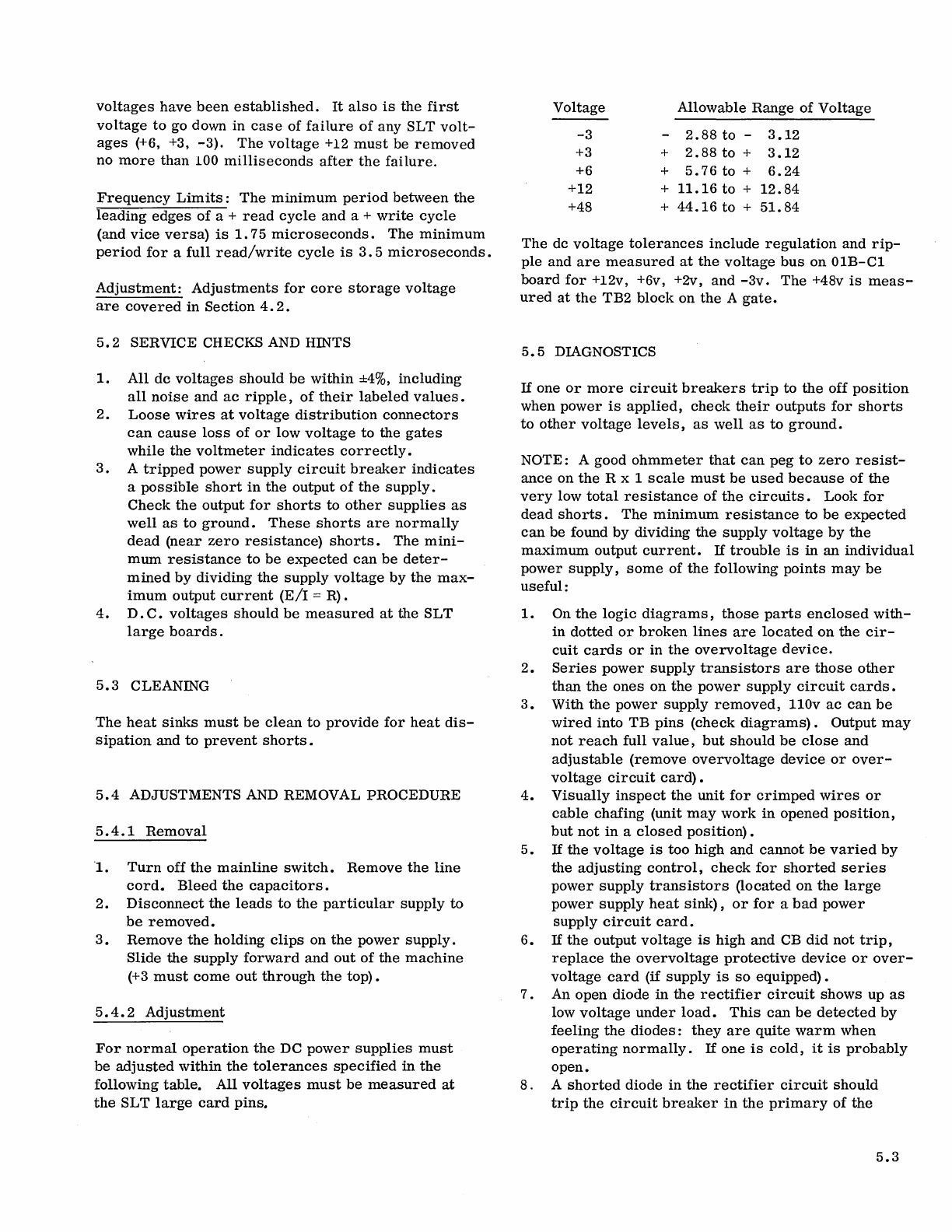
voltages
have
been
established.
It
also
is
the
first
voltage
to
go down in
case
of
failure
of
any
SLT
volt-
ages
(+6, +3,
-3).
The
voltage
+12
must
be
removed
no
more
than
100
milliseconds
after
the
failure.
Frequency
Limits:
The
minimum
period
between
the
leading
edges
of
a +
read
cycle
and
a +
write
cycle
(and
vice
versa)
is
1.
75
microseconds.
The
minimum
period
for
a
full
read/write
cycle
is
3.
5
microseconds.
Adjustment:
Adjustments
for
core
storage
voltage
are
covered
in
Section
4.
2.
5.2
SERVICE CHECKS AND HINTS
1.
All
dc
voltages
should
be
within
±4%,
including
all
noise
and
ac
ripple,
of
their
labeled
values.
2.
Loose
wires
at
voltage
distribution
connectors
can
cause
loss
of
or
low
voltage
to
the
gates
while
the
voltmeter
indicates
correctly.
3.
A
tripped
power
supply
circuit
breaker
indicates
a
possible
short
in
the
output
of
the
supply.
Check
the
output
for
shorts
to
other
supplies
as
well
as
to
ground.
These
shorts
are
normally
dead
(near
zero
resistance)
shorts.
The
mini-
mum
resistance
to
be
expected
can
be
deter-
mined
by
dividing
the
supply
voltage
by
the
max-
imum
output
current
(E/I
=
R)
.
4.
D.
C.
voltages
should
be
measured
at
the
SLT
large
boards.
5.3
CLEANING
The
heat
sinks
must
be
clean
to
provide
for
heat
dis-
sipation
and
to
prevent
shorts.
5.4
ADJUSTMENTS AND REMOVAL PROCEDURE
5.4.1
Removal
'1.
Turn
off
the
mainline
switch.
Remove
the
line
cord.
Bleed
the
capacitors.
2.
Disconnect
the
leads
to
the
particular
supply
to
be
removed.
3.
Remove
the
holding
clips
on
the
power
supply.
Slide
the
supply
forward
and
out
of
the
machine
(+3
must
come
out
through
the
top).
5.4.2
Adjustment
For
normal
operation
the
DC
power
supplies
must
be
adjusted
within
the
tolerances
specified
in
the
following
table.
All
voltages
must
be
measured
at
the
SL
T
large
card
pins.
Voltage
Allowable
Range
of
Voltage
-3
2.88
to
-
3.12
+3 +
2.88
to
+
3.12
+6 +
5.76
to
+
6.24
+12 +
11.16
to
+
12.84
+48 +
44.16
to
+
51.84
The
dc
voltage
tolerances
include
regulation
and
rip-
ple
and
are
measured
at
the
voltage
bus
on
01B-C1
board
for
+12v, +6v, +2v,
and
-3v.
The
+48v
is
meas-
ured
at
the
TB2
block
on
the
A
gate.
5.5
DIAGNOSTICS
If
one
or
more
circuit
breakers
trip
to
the
off
position
when
power
is
applied,
check
their
outputs
for
shorts
to
other
voltage
levels,
as
well
as
to
ground.
NOTE:
A good
ohmmeter
that
can
peg
to
zero
resist-
ance
on
the
R x 1
scale
must
be
used
because
of
the
very
low
total
resistance
of
the
circuits.
Look
for
dead
shorts.
The
minimum
resistance
to
be
expected
can
be
found
by
dividing
the
supply
voltage
by
the
maximum
output
current.
If
trouble
is
in
an
individual
power
supply,
some
of
the
following
points
may
be
useful:
1.
On
the
logic
diagrams,
those
parts
enclosed
with-
in
dotted
or
broken
lines
are
located
on
the
cir-
cuit
cards
or
in
the
overvoltage
device.
2.
Series
power
supply
transistors
are
those
other
than
the
ones
on
the
power
supply
circuit
cards.
3.
With
the
power
supply
removed,
110v
ac
can
be
wired
into
TB
pins
(check
diagrams).
Output
may
not
reach
full
value,
but
should
be
close
and
adjustable
(remove
overvoltage
device
or
over-
voltage
circuit
card)
•
4.
Visually
inspect
the
unit
for
crimped
wires
or
cable
chafing
(unit
may
work
in
opened
pOSition,
but
not
in
a
closed
position)
.
5.
If
the
voltage
is
too
high
and
cannot
be
varied
by
the
adjusting
control,
check
for
shorted
series
power
supply
transistors
(located
on
the
large
power
supply
heat
sink),
or
for
a
bad
power
supply
circuit
card.
6.
If
the
output
voltage
is
high
and
CB
did
not
trip,
replace
the
overvoltage
protective
device
or
over-
voltage
card
(if
supply
is
so
equipped).
7 . An
open
diode
in
the
rectifier
circuit
shows
up
as
low
voltage
under
load.
This
can
be
detected
by
feeling
the
diodes:
they
are
quite
warm
when
operating
normally.
If
one
is
cold,
it
is
probably
open.
8 . A
shorted
diode
in
the
rectifier
circuit
should
trip
the
circuit
breaker
in
the
primary
of
the
5.3
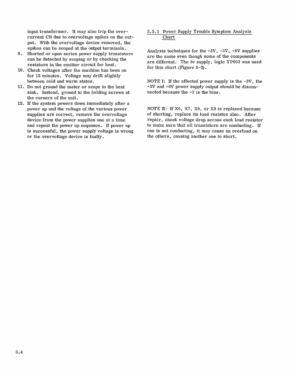
input
transformer.
It
may
also
trip
the
over-
current
CB
due
to
overvoltage
spikes
on
the
out-
put.
With
the
overvoltage
device
removed,
the
spikes
can
be
scoped
at
the
output
terminals.
9.
Shorted
or
open
series
power
supply
transistors
can
be
detected
by
scoping
or
by
checking
the
resistors
in
the
emitter
circuit
for
heat.
10.
Check
voltages
after
the
machine
has
been
on
for
15
minutes.
Voltage
may
drift
slightly
between
cold
and
warm
states.
11.
Do
not
ground
the
meter
or
scope
to
the
heat
sink.
Instead,
ground
to
the
holding
screws
at
the
corners
of
the
unit.
12.
If
the
system
powers
down
immediately
after
a
power
up
and
the
voltage
of
the
various
power
supplies
are
correct,
remove
the
overvoltage
device
from
the
power
supplies
one
at
a
time
and
repeat
the
power
up
sequence.
If
power
up
is
successful,
the
power
supply
voltage
is
wrong
or
the
overvoltage
device
is
faulty.
5.4
5.5.1
Power
Supply
Trouble
Symptom
Analysis
Chart
Analysis
techniques
for
the
+3V,
-3V,
+6V
supplies
are
the
same
even
though
some
of
the
components
are
different.
The
3v
supply,
logic
YP003
was
used
for
this
chart
(Figure
5-2).
NOTE
I:
If
the
affected
power
supply
is
the
-3V,
the
+3V
and
+6V
power
supply
output
should
be
discon-
nected
because
the
-3
is
the
bias.
NOTE
II:
If
X6, X7,
X8,
or
X9
is
replaced
because
of
shorting,
replace
its
load
resistor
also.
After
repair,
check
voltage
drop
across
each
load
resistor
to
make
sure
that
all
transistors
are
conducting.
If
one
is
not
conducting,
it
may
cause
an
overload
on
the
others,
causing
another
one
to
short.
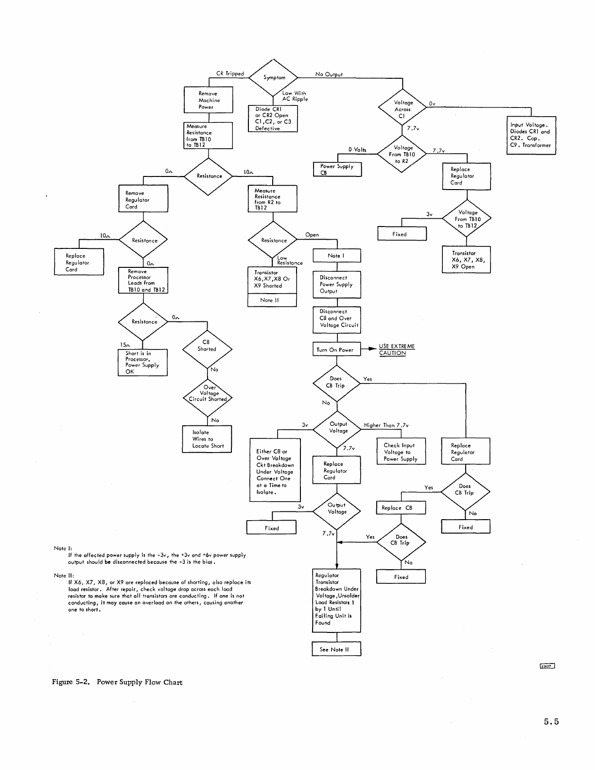
Note
I:
If
the
affected
power supply
is
the
-3v,
the
+3v
and
+6v power supply
output
shou
Id
be
disconnected
because
the
-3
is
the
bios.
Note
II:
If
X6, X7,
X8,
or
X9
are
replaced
because
of
shorting,
also
replace
its
load
resistor.
After
repair,
check
voltage
drop across
each
load
resistor to
make
sure
that
all
transistors
are
conducting.
If
one
is
not
conducting,
it
may couse on
overload
on
the
others,
causing
another
one
to
short.
Figure
5-2.
Power
Supply
Flow
Chart
Either C8
or
Over
Vo
I
tage
Ckt
Breakdown
Under Voltage
Connect
One
at
a Time to
bolate.
Regulator
Transistor
Breakdown Under
Voltage ,Unsolder
Load Resistors 1
by
1 Until
Fai ling Unit
is
Found
Input
Voltage.
Diodes
CRI
and
CR2.
Cop.
C9.
Transformer
5.5
Figure
6-1
1131
Central
Processing
Unit-Left
Front
View.
Figure
6-2
1131
Central
Processing
Unit-Right
Rear
View.
Figure
6-3
1131
Central
Processing
Unit-I/O
Con-
nectors.
Figure
6-4
Keyboard-Top
View.
+3v Supply
8-C1
Figure
6-1.
1131
Central
Processing
Unit
-Left Front
View
CHAPTER
6 LOCATIONS
Figure
6-5
Keyboard-Bottom
View.
Figure
6-6
Keyboard
Keystem
Numbering.
Figure
6-7
Console
Keyboard.
Figure
6-8
CE
Panel.
Figure
6-9
Console
Display
Panel.
Figure
6-10
Console
Printer.
uses
6.1
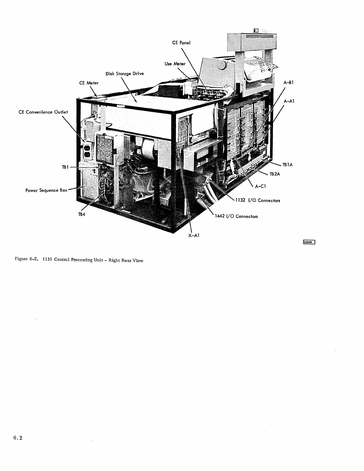
Power Sequence
Box
I/o
Connectors
1442
I/O
Connectors
Figure
6-2.
1131
Central
Processing
Unit
-
Right
Rear
View
6.2
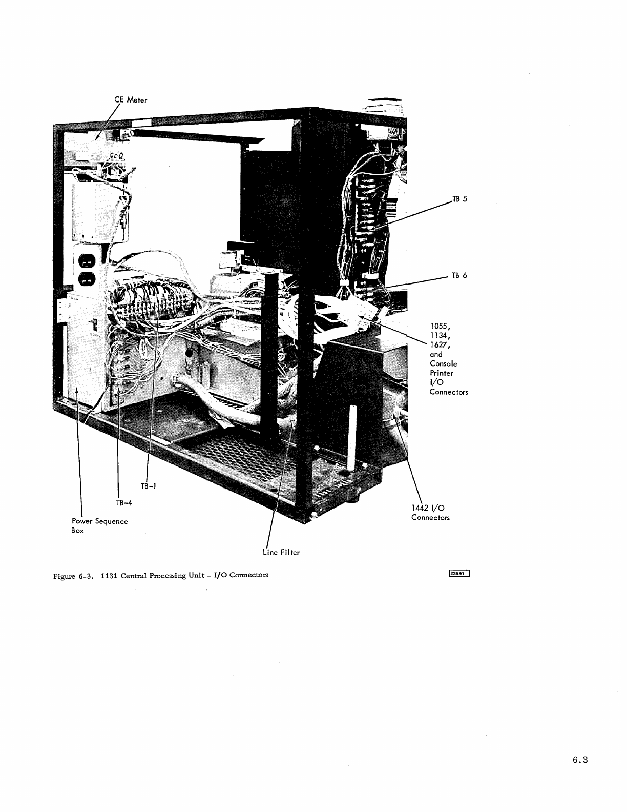
CE
Meter
TB-4
Power
Sequence
Box
Figure
6-3.
1131
Central
Processing
Unit
-
I/O
Connectors
TB
5
Printer
I/o
Connectors
6.3
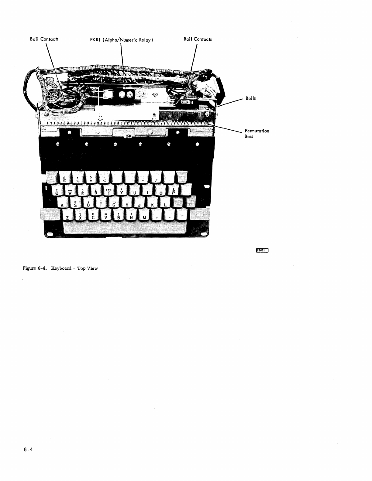
Bail Contacts
PKRl
(Alpha/Numeric Relay)
Figure
6-4.
Keyboard
-
Top
View
6.4
Bai
I Contacts
Bails
Permutation
Bars
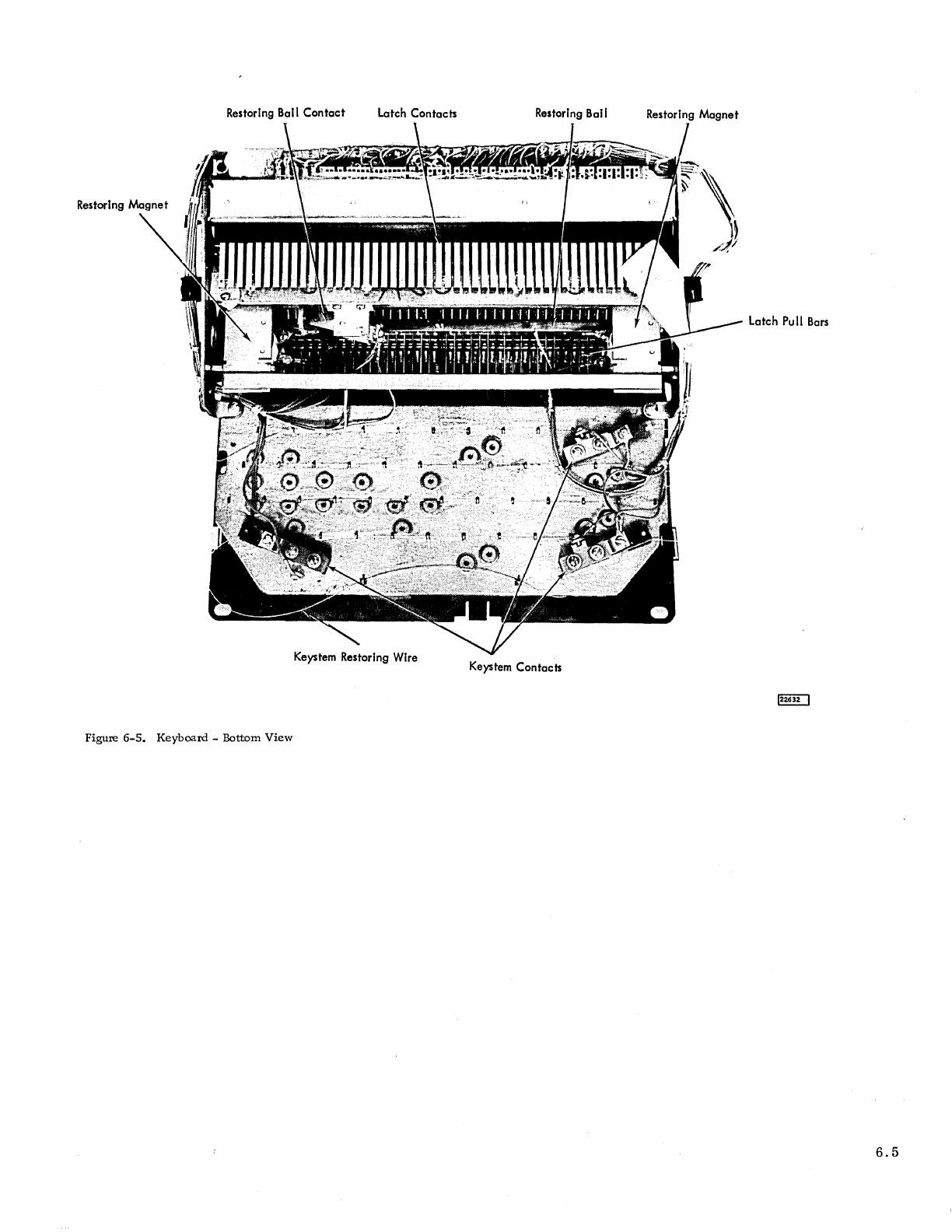
Restoring Ball Contact Latch Contacts Restoring Ball Restoring Magnet
Latch
Pu
11
Bars
Keystem
Contacts
Figure
6-5.
Keyboard
-
Bottom
View
6.5
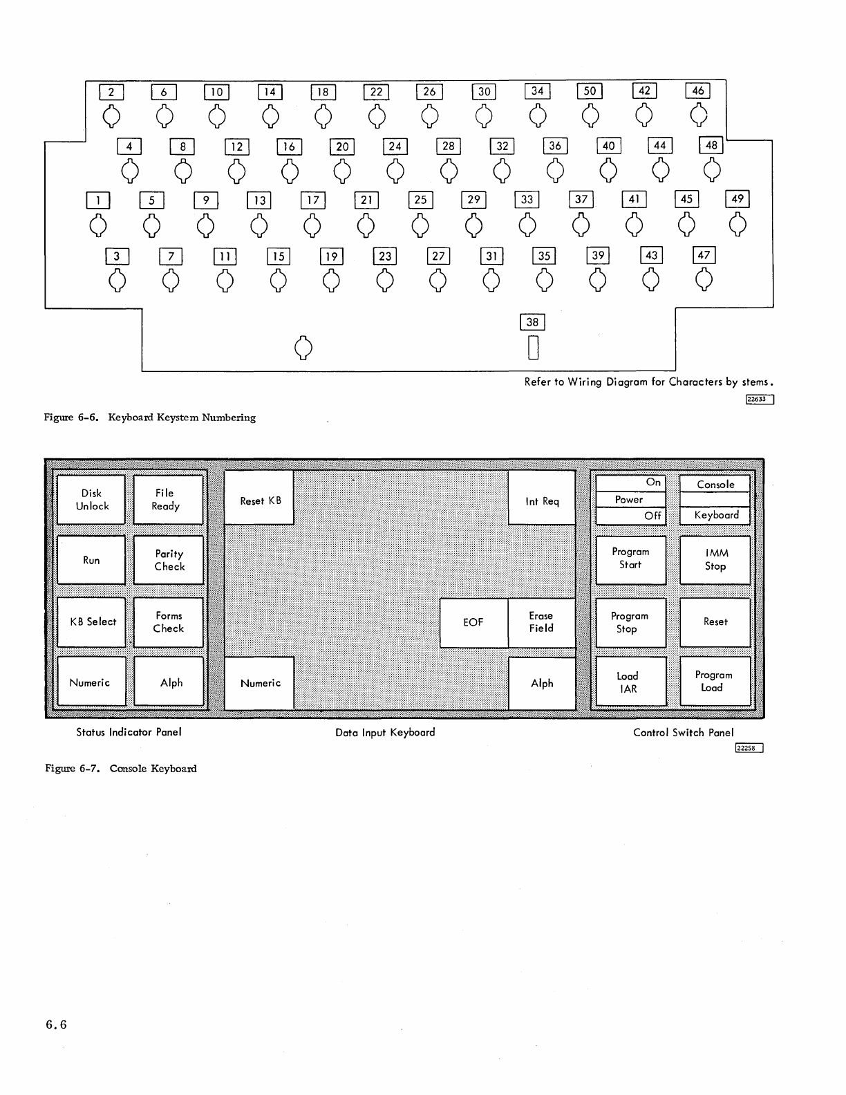
IT]
m lliJ
[ill
[ill
@]
0 0 0 0 0 0
IT]
[]]
OIl
@]
em
[ill
0 0 0 0 0
OJ
IT] 0
[ill
[l2]
0 0 0 0 0
OJ
[TI
OIJ
@]
[ill
0 0 0 0 0
0
Figure
6-6.
Keyboard
Keystem
Numbering
Disk
File
Un
lock Ready
Parity
Check
Forms
Check
0
[ill
0
[ill
0
[ill
0
lliJ
0
@]
0
@J
0
Status Indicator Panel Data Input Keyboard
Figure
6-7.
Console
Keyboard
6.6
[ill
[E]
[ill
[ill
~
0 0 0 0 0
[ill
~
8QJ
@]
[ill
0 0 0 0 0
IT?]
[]I]
@J
@J
[ill
@]
0
[2!J
0
0 0 0 0 0
@]
[ill @] @]
0 0 0 0
[]I]
D
Refer to Wiring Diagram for
Characters
by stems.
122633 I
Control Switch Panel
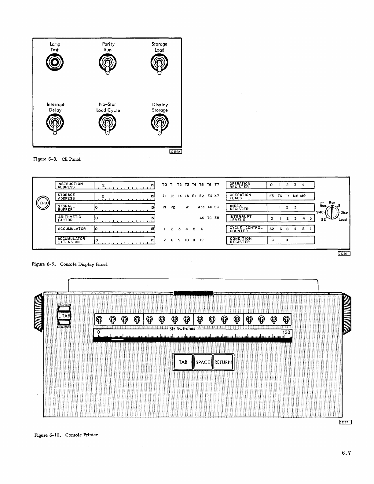
Lamp
Test
~
Interrupt
i
Figure
6-8.
CE
Panel
INSTRUCTION
ADDRESS
e STORAGE
ADDRESS
STORAGE
BUFFER
ARITHMETIC
FACTOR
ACCUMULATOR
ACCUMULATOR
EXTENSION
Parity
Run
No-Stor
,Ie
2
2
I
1
0
10•
1
0•
10•
Figure
6-9.
Console
Display
Panel
Figure
6-10.
Console
Printer
Storage
Load
"
Display
Storage
"
••
15
1 TO
lsi
II
, ,
)51
PI
lsi
:51
•
15
1 7
TI
12
P2
2
8
T2
T3
T4
T5
T6
T7 OPERATION 0 2 3 4
REGISTER
IX
IA
EI
E2
E3 X7 OPERATION F5
T6
T7
M8 M9
FLAGS
Int
Run
W Add
AC
SC
INDEX
2 3 I
R"W'
REGISTER
SMC
Disp
AS
TC
ZR
INTERRUPT
0 2 3 4 S 1
SS
Load
LEVELS
3 4 5 6 CYCLE CONTROL
32
16
8 4 2
COUNTER
9
10
II
12
CONDITION
C 0
REGISTER
~
..
-
~-
..
,
-------------
- - --
6.7
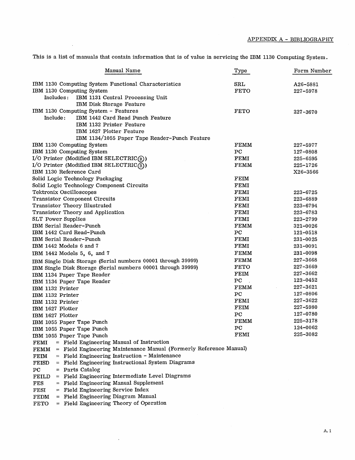
APPENDlX
A -
BffiLIOGRAPHY
This
is
a
list
of
manuals
that
contain
information
that
is
of
value
in
servicing
the
IBM 1130
Computing
System.
Manual
Name
IBM 1130
Computing
System
Functional
Characteristics
IBM 1130
Computing
System
Includes:
IBM
1131
Central
Processing
Unit
ffiM
Disk
Storage
Feature
IBM 1130
Computing
System
-
Features
Include:
IBM
1442
Card
Read
Punch
Feature
IBM
1132
Printer
Feature
IBM
1627
Plotter
Feature
IBM
1134/1055
Paper
Tape
Reader-Punch
Feature
IBM 1130
Computing
System
IBM 1130
Computing
System
I/O
Printer
(Modified
IBM
SELECTRIC®)
I/O
Printer
(Modified
IBM
SELECTRIC®)
IBM
1130
Reference
Card
Solid
Logic
Technology
Packaging
Solid
Logic
Technology
Component
Circuits
Tektronix
Oscilloscopes
Transistor
Component
Circuits
Transistor
Theory
Illustrated
Transistor
Theory
and
Application
SL
T
Power
Supplies
IBM
Serial
Reader-Punch
IBM
1442
Card
Read-Punch
IBM
Serial
Reader-Punch
IBM
1442
Models
6
and
7
IBM
1442
Models
5,
6,
and
7
IBM
Single
Disk
Storage
(Serial
numbers
00001
through
39999)
ffiM
Single
Disk
Storage
(Serial
numbers
00001
through
39999)
IBM
1134
Paper
Tape
Reader
IBM
1134
Paper
Tape
Reader
IBM
1132
Printer
IBM 1132
Printer
mM
1132
Printer
IBM 1627
Plotter
IBM 1627
Plotter
Type
SRL
FE
TO
FETO
FEMM
PC
FEMI
FEMM
FEIM
FEMI
FEMI
FEMI
FEMI
FEMI
FEMI
FEMM
PC
FEMI
FEMI
FEMM
FEMM
FETO
FEIM
PC
FEMM
PC
FEMI
FEIM
PC
mM
1055
Paper
Tape
Punch
FEMM
IBM 1055
Paper
Tape
Punch
PC
ffiM 1055
Paper
Tape
Punch
FEMI
FEMI
Field
Engineering
Manual
of
Instruction
FEMM
Field
Engineering
Maintenance
Manual
(Formerly
Reference
Manual)
FEIM
Field
Engineering
Instruction
-
Maintenance
FEISD
Field
Engineering
Instructional
System
Diagrams
PC
Parts
Catalog
FEILD
Field
Engineering
Intermediate
Level
Diagrams
FES
Field
Engineering
Manual
Supplement
FESI
Field
Engineering
Service
Index
FEDM
Field
Engineering
Diagram
Manual
FETO
Field
Engineering
Theory
of
Operation
Form
Number
A26-5881
227-5978
227-3670
227-5977
127-0808
225-6595
225-1726
X26-3566
223-6725
223-6889
223-6794
223-6783
223-2799
321-0026
121-0518
231-0025
231-0091
231-0098
227-3668
227-3669
227-3662
123-0452
227-3621
127-0806
227-3622
227-5980
127-0780
225-3178
124-0062
225-3082
A.1
A
Register
Lamps
2.
5
Acceptable
Signal
Levels
1.15
Accumulator
Extension
Register
Lamps
2.5
Accumulator
Register
Lamps
2.5
AC
Lamp
2.5
Add
Lamp
2.5
Alpha
Shift
Lamp
2.6
Arithmetic
Factor
Register
Lamps
2.5
Arithmetic
Indicators
2.5
AS
Lamp
2.5
B
Register
Lamps
2.
5
Bail
Contact
Adjustment
4.
3
Bibliography
A. 1
Blocking
1442
Read
Errors
1.2
Card,
CE
2.6
CCC
Lamps
2.
5
CE
Card
2.6
CE
Indicators
2.
5
CE
Panel
1.13,
2.3
CE
Power
Switches
5.2
Check
list,
Core
Storage
1.
7
Check
list,
General
1.
7
CLFC
1.3
Clock
Cycle
Indicators
2.5
Condition
Register
Lamps
2.
5
Configurator
1.3
Console
Bit
Switches
2.
3
Console
Keyboard
2.7
Console
Keyboard
Lamps
2.5
Console
Keyboard
Removal
4.
3
Console
Keyboard
Single
Shot
Adjustment
4.3
Console/Keyboard
Switch
2.2
Console
Lamp
Driver
Removal
4.10
Console
Lamp
Removal
4.9
Console
Panel
1.13,
2.5
Console
Printer
1.13,
2.7
Console
Printer
Adjustments
4.
8
Console
Printer,
Diagnostic
Aids
1.13
Console
Printer
Preventive
Maintenance
3.2
Console
Printer
Removals
4.
8
Console
Printer
Single
Shot
Adjustment
4.3
Console
Printer
Testing
1.
2
Contact
Bail
Adjustment
4.4
Contact
Bail
Removal
4.
6
Controls,
Disk
Storage
2.
7
Control
Switch
Panel
2.1
Convenience
Outlet
5.2
Core
Array
Waveforms
1.8
Core,
Current
Scoping
1.8
Core
Diagnostic
Aids
1.
11
Core
Storage
Adjustments
4.
1
Core
Storage
Check
List
1.
7
Core
Storage
Isolation
1.
8
Core
Storage
Removals
4.
1
Core
Storage
Voltages
5.2
Current
Scoping
of
Core
1.
8
Cycle
Control
Counter
Lamps
2.
5
D
Register
Lamps
2.5
Delay
Times,
Transistor
1.15
Determining
Noise
1.12
Diagnostic
Aids,
Console
Printer
1.
13
Diagnostic
Aids,
Core
Storage
1.
11
Diagnostic
Monitor
1.
5,
1.6
Diagnostic
Program
Language
1.5
Diagnostic
Program
Loading
1.
5
Diagnostic
Programming
1.
5
Diagnostic
Techniques
1.
1
Diagnostic
Tests
Part
Numbers
1.
6
Direction
Switch
2.7
Disk
Storage
2. 7
Disk
Storage,
CE
Switches
2.7
Disk
Storage
Controls
2.7
Disk
Storage
On/Off
Switch
2.4
Disk
Storage
Preventive
Maintenance
3.2
Disk
Storage
Removal
4.
9
Disk
Unlock
Lamp
2.6
Display
Mode
2.
2
Dynamic
Detection
1. 2
Emergency
Power
Off
Switch
2.4,
5.
2
Error
Detection
1.
1
Error
Isolation
1. 1
Error Logging
1.
2
Error Messages 1. 5
Failure
to
Program
Load
1.
3
FF's
1.15
File
Read-Write
Single
Shot
Adjustment
4.
9
Filter
Cleaning
4.
9
Forced
Card
Feeding
1.3
Forms
Check
Lamp
2.
5
Function
Tests
1.5
Gate
Blower
Removal
4.
9
General
Check
List
1.
7
Grounding,
Interrupt
Levels
1.
2
Grounds,
Locating
1.
15
Head
Select
Switch
2.7
Hook
Support
Bar
Adjustment
4.4
IAR
Lamps
2.5
IMM Stop
Switch
2.
1
Index
Register
Lamps
2.
5
Instruction
Address
Register
Lamps
2.
5
Interrupt
Delay
Switch
2.
4
Interrupt
Level
Grounding
1.2
I/O
Cables
4.8
I/O
Operations
Diagram
1. 3
Isolation,
Core
Storage
1.
8
Keyboard
Assembly
Adjustments
4.3
Keyboard,
Console
2.7
Keyboard
Select
Lamp
2.
5
Key
Stem
Contact
Adjustment
4.
3
INDEX
1.1
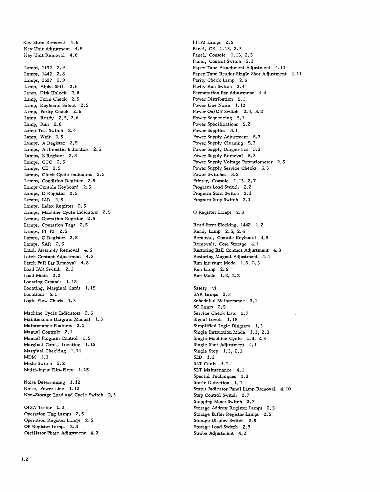
Key
Stem
Removal
4.6
Key
Unit
Adjustment
4.5
Key
Unit
Removal
4.
6
Lamps, 1132
2.9
Lamps, 1442
2.8
Lamps,
1627
2.9
Lamp,
Alpha
Shift
2.
6
Lamp, Disk
Unlock
2.
6
Lamp,
Form
Check
2.5
Lamp,
Keyboard
Select
2.5
Lamp,
Parity
Check
2.6
Lamp,
Ready
2.5,
2.6
Lamp,
Run
2.
6
Lamp
Test
Switch
2.4
Lamp,
Wait
2.5
Lamps, A
Register
2.5
Lamps,
Arithmetic
Indicators
2.5
Lamps, B
Register
2.5
Lamps,
CCC
2.5
Lamps, CE 2. 5
Lamps,
Clock
Cycle
Indicators
2.5
Lamps,
Condition
Register
2.5
Lamps
Console
Keyboard
2.5
Lamps, D
Register
2.5
Lamps, IAR
2.5
Lamps,
Index
Register
2.5
Lamps,
Machine
Cycle
Indicators
2.5
Lamps,
Operation
Register
2.5
Lamps,
Operation
Tags
2.5
Lamps,
PI-P2
2.5
Lamps, Q
Register
2.5
Lamps, SAR
2.
5
Latch
Assembly
Removal
4.
6
Latch
Contact
Adjustment
4.3
Latch
Pull
Bar
Removal
4.
8
Load IAR
Switch
2.1
Load
Mode
2.2
Locating
Grounds
1.
IS
Locating,
Marginal
Cards
1.15
Locations
6.
1
Logic Flow
Charts
1.
3
Machine
Cycle
Indicators
2.5
Maintenance
Diagram
Manual
1.3
Maintenance
Features
2. 1
Manual
Controls
2.1
Manual
Program
Control
1.
5
Marginal
Cards,
Locating
1.15
Marginal
Checking
1.
14
MDM
1.3
Mode
Switch
2.
2
Multi-Input
Flip-Flops
1.15
Noise
Determining
1.12
Noise,
Power Line
1.12
Non-Storage
Load
and
Cycle
Switch
2.3
OLSA
Tester
1.2
Operation
Tag
Lamps 2. 5
Operation
Re
gister
Lamps
2.
5
OP
Register
Lamps
2.5
Oscillator
Phase
Adjustment
4.
2
1.2
PI-P2
Lamps
2.5
Panel,
CE
1.13,
2.3
Panel,
Console
1.13,
2.5
Panel,
Control
Switch
2. 1
Paper
Tape
Attachment
Adjustment
4.
11
Paper
Tape
Reader
Single Shot
Adjustment
4.
11
Parity
Check
Lamp
2. 6
Parity
Run
Switch
2.4
Permutation
Bar
Adjustment
4.4
Power
Distribution
5.
1
Power Line Noise
1.
12
Power
On/Off
Switch
2.4,
5.2
Power
Sequencing
5.
1
Power
Specifications
5.
2
Power Supplies
5.
1
Power Supply
Adjustment
5.
3
Power Supply
Cleaning
5.3
Power Supply
Diagnostics
5.
3
Power Supply
RemovalS.
3
Power
Supply
Voltage
Potentiometer
2.5
Power
Supply
Service
Checks
5.3
Power Switches
5.2
Printer, Console
1.13,
2.7
Program
Load
Switch
2.2
Program
Start
Switch
2. 1
Program
Stop
Switch
2. 1
Q
Register
Lamps
2.5
Read
Error Blocking, 1442 1. 2
Ready
Lamp
2.5,
2.6
Removal,
Console
Keyboard
4.
3
Removals,
Core
Storage
4.
1
Restoring
Bail
Contact
Adjustment
4.3
Restoring
Magnet
Adjustment
4.4
Run
IntelTUpt
Mode
1.
3,
2.
3
Run
Lamp
2.6
RunMode
1.2,2.2
Safety
vi
SAR Lamps
2.
5
Scheduled
Maintenance
3.1
SC
Lamp
2.5
Service
Check
Lists
1.
7
Signal
Levels
1.
15
Simplified
Logic
Diagram
1.
3
Single
Instruction
Mode
1.
3,
2.3
Single
Machine
Cycle
1.3,
2.3
Single
Shot
Adjustment
4.
1
Single
Step
1.3,
2.3
SLD
1.3
SLT Cards
4.1
SL
T
Maintenance
4.
1
Special
Techniques
1.
3
Static
Detection
1. 2
Status
Indicator
Panel
Lamp
Removal
4.
10
Step
Control
Switch
2.
7
Stepping
Mode
Switch
2.7
Storage
Address
Register
Lamps
2.
5
Storage
Buffer
Register
Lamps
2.5
Storage
Display
Switch
2.3
Storage
Load
Switch
2.
3
Strobe
Adjustment
4.2
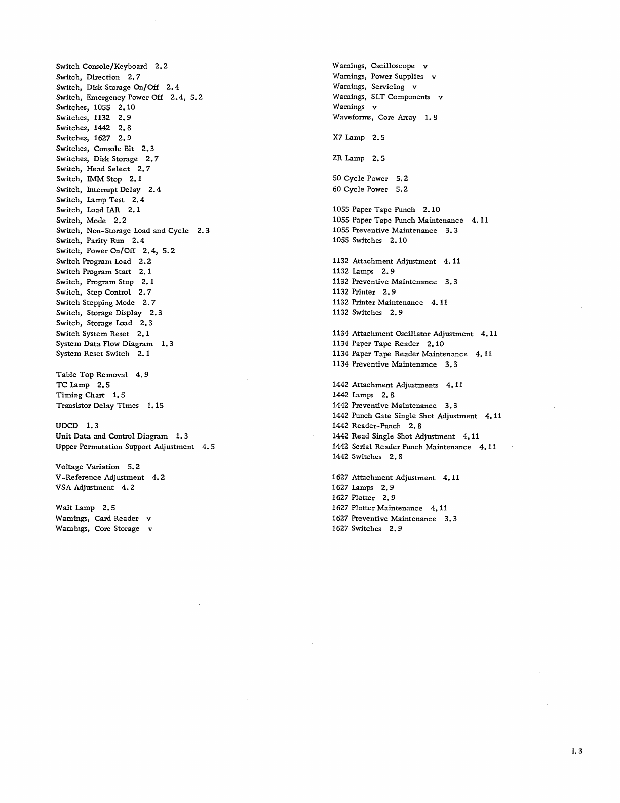
Switch
Console/Keyboard
2.2
Switch,
Direction
2. 7
Switch,
Disk
Storage
On/Off
2.4
Switch,
Emergency
Power
Off
2.4,
5.2
Switches,
1055
2.
10
Switches,
1132
2.9
Switches,
1442
2.8
Switches,
1627
2.9
Switches,
Console
Bit
2.3
Switches,
Disk
Storage
2.7
Switch,
Head
Select
2.
7
Switch,
IMM
Stop
2.
1
Switch,
Interrupt
Delay
2.4
Switch,
Lamp
Test
2.4
Switch,
Load IAR
2.
1
Switch,
Mode
2.2
Switch,
Non-Storage
Load
and
Cycle
2.
3
Switch,
Parity
Run
2.4
Switch,
Power
On/Off
2.4,
5.2
Switch
Program
Load
2.2
Switch
Program
Start
2. 1
Switch,
Program
Stop
2.
1
Switch,
Step
Control
2.7
Switch
Stepping
Mode
2.7
Switch,
Storage
Display
2.3
Switch,
Storage
Load
2.3
Switch
System
Reset
2.
1
System
Data
Flow
Diagram
1.3
System
Reset
Switch
2.
1
Table
Top
Removal
4.
9
TC
Lamp
2.5
Timing
Chart
1.5
Transistor
Delay
Times
1.15
UDCD
1.3
Unit
Data
and
Control
Diagram
1.3
Upper
Permutation
Support
Adjustment
4.
5
Voltage
Variation
5.2
V-Reference
Adjustment
4.2
VSA
Adjustment
4.
2
Wait
Lamp
2.5
Warnings,
Card
Reader
v
Warnings, Core
Storage
v
Warnings,
Oscilloscope
v
Warnings,
Power
Supplies
v
Warnings,
Servicing
v
Warnings, SLT
Components
v
Warnings v
Waveforms,
Core
Array
1.
8
X7
Lamp
2.5
ZR
Lamp
2.5
SO
Cycle
Power
5.
2
60
Cycle
Power
5.2
1055
Paper
Tape
Punch
2.
10
1055
Paper
Tape
Punch
Maintenance
4.
11
1055
Preventive
Maintenance
3.3
1055
Switches
2.
10
1132
Attachment
Adjustment
4.
11
1132 Lamps
2.9
1132
Preventive
Maintenance
3.3
1132
Printer
2.
9
1132
Printer
Maintenance
4.
11
1132 Switches
2.9
1134
Attachment
Oscillator
Adjustment
4.11
1134
Paper
Tape
Reader
2.
10
1134
Paper
Tape
Reader
Maintenance
4.11
1134
Preventive
Maintenance
3.3
1442
Attachment
Adjustments
4.11
1442 Lamps
2.
8
1442
Preventive
Maintenance
3.3
1442
Punch
Gate
Single
Shot
Adjustment
4.
11
1442
Reader-Punch
2.8
1442
Read
Single
Shot
Adjustment
4.11
1442
Serial
Reader
Punch
Maintenance
4.
11
1442 Switches
2.
8
1627
Attachment
Adjustment
4.
11
1627
Lamps
2.9
1627
Plotter
2.9
1627
Plotter
Maintenance
4.
11
1627
Preventive
Maintenance
3.3
1627
Switches
2.9
1.3
III
Z
J
(!)
z
o
.J
~
I-
:l
o
FOLD
FOLD
READER'S
COMMENT
FORM
FROM:
NAME
_________________
DATE
_______________
_
OFFICE!DEPT.
__________________________________
__
CHECK
ONE
OR
MORE
OF
THE
COMMENT
BLOCKS
AND
EXPLAIN
IN
THE
SPACE
PROVIDED.
o
ADDITION:
PAGE(S)
FIGURE(S)
o
DELETION:
PAGE(S)
FIGURE(S)
o
ALTERATION:
PAGE(S)
FIGURE(S)
EXPLANATION:
NO
POSTAGE
NECESSARY
IF
MAILED
IN
U.S.A.
1130
Computing
System
FOLD
ON
TWO
LINES,
STAPLE,
AND
MAIL
227-5977-1
FOLD
FOLD
STAPLE STAPLE
FOLD
----------------------------------------------------------_.'
FOLD
BUSINESS
REPLY
MAIL
NO
POSTAGE
STAMP
NECESSARY
IF
MAILED
IN
U.
S.
A.
POSTAGE
WILL
BE
PAID
BY
IBM
CORPORATION
MONTEREY
&
COTTLE
RDS.
SAN
JOSE,
CALIFORNIA
95114
ATTN:
PRODUCT
PUBLICATIONS
DEPT.
455
FIRST
CLASS
PERMIT
NO.
2078
SAN
JOSE.
CALIF.
,
'w
z
J
l!)
z
o
.J
«
I-
:J
U
e
m
-
En
>-
til
I
I
I
I
I
I
I
I
- - - - -
cut
here - - - - - - - - - - - -
~
227-5977-1
TIIIDrill
®
International
Business
Machines Corporation
Field Engineering Division
112
East
Post Road, White
P~ains,
N.Y.
10601
~
.....
.....
OJ
o
