2N7002 Datasheet. Www.s Manuals.com. Panjit
User Manual: Marking of electronic components, SMD Codes S7, S72, S72**, S780. Datasheets 2N7002, SD103BW, SST177, SiS780DN.
Open the PDF directly: View PDF ![]() .
.
Page Count: 8
PAGE . 1August 29,2013-REV.03
2N7002
FEATURES
• RDS(ON), VGS@10V,IDS@500mA=5
• RDS(ON), VGS@4.5V,IDS@75mA=7.5
• Advanced Trench Process Technology
• High Density Cell Design For Ultra Low On-Resistance
• Specially Designed for Battery Operated Systems, Solid-State Relays
Drivers : Relays, Displays, Lamps, Solenoids, Memories, etc.
• Lead free in comply with EU RoHS 2011/65/EU directives
• Green molding compound as per IEC61249 Std. . (Halogen Free)
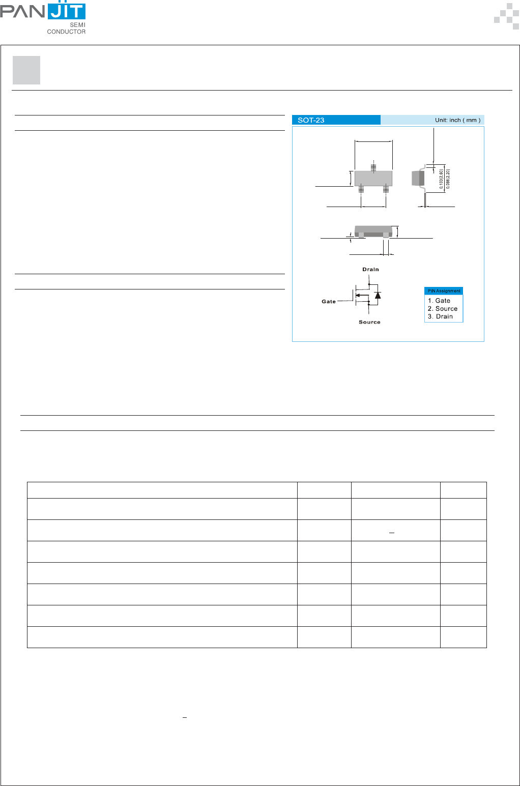
MECHANICAL DATA
• Case : SOT-23 Package
• Terminals : Solderable per MIL-STD-750,Method 2026
• Approx. Weight : 0.0003 ounces, 0.008 grams
• Marking : S72
60V N-Channel Enhancement Mode MOSFET
Maximum Ratings and Thermal Characteristics (TA=25OC unless otherwise noted )
Note:1. Maximum DC current limited by the package
2. Surface mounted on FR4 board, t < 10 sec
RETEMARAPlobmyStimiLstinU
egatloVecruoS-niarD V
SD
06V
egatloVecruoS-etaG V
SG
+ 02V
tnerruCniarDsuounitnoC I
D
052Am
tnerruCniarDdesluP
)1
I
MD
0031Am
noitapissiDrewoPmumixaM T
A
52=
O
C
T
A
57=
O
CP
D
053 012 Wm
egnaRerutarepmeTegarotSdnanoitcnuJgnitarepO T
J
T,
GTS
051+ot55-
O
C
)detnuomBCP(ecnatsiseRlamrehTtneibmAot-noitcnuJ
2
R
θAJ
753
O
W/C
0.120(3.04)
0.110(2.80)
0.056(1.40)
0.047(1.20)
0.079(2.00)
0.070(1.80)
0.020(0.50)
0.013(0.35)
0.044(1.10)
0.035(0.90)
0.006(0.15)MIN.
0.008(0.20)
0.003(0.08)
0.004(0.10)
0.000(0.00)
PAGE . 2August 29,2013-REV.03
2N7002
ELECTRICAL CHARACTERISTICS
V
DD
V
OUT
V
IN
R
G
R
L
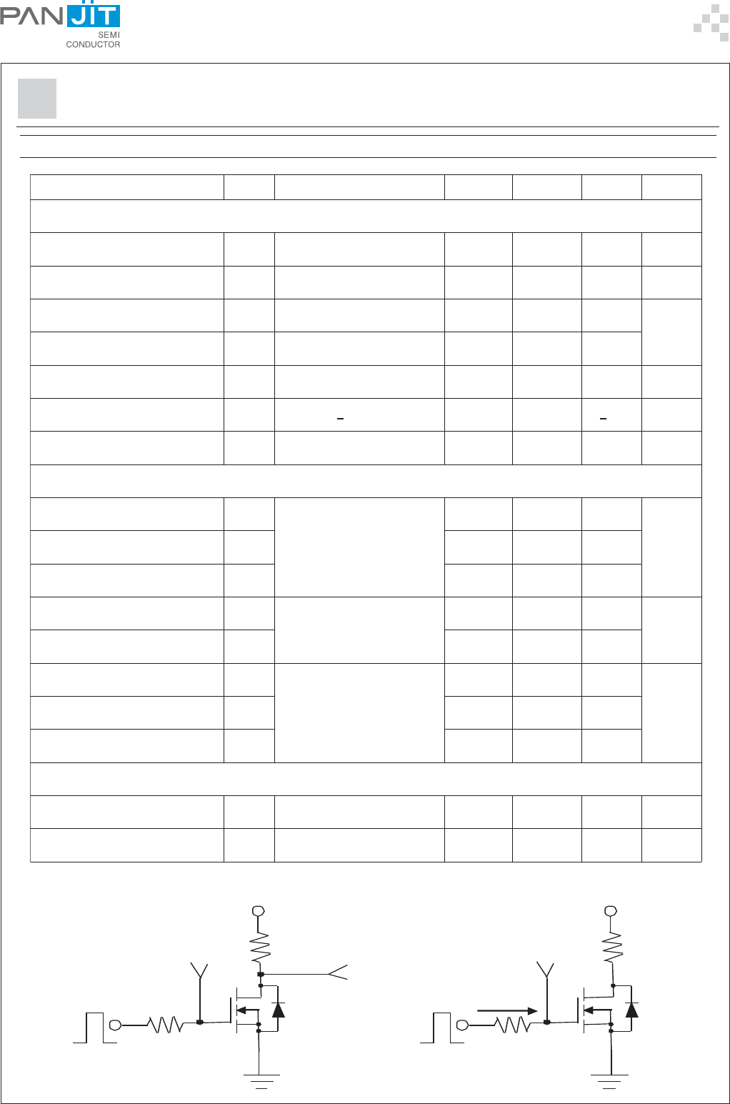
Switching
Test Circuit
Gate Charge
Test Circuit
V
DD
V
GS
R
G
R
L
1mA
retemaraPlobmySnoitidnoCtseT.niM.pyT.xaMstinU
citatS
egatloVnwodkaerBecruoS-niarDVB
SSD
V
SG
I,V0=
D
Au01=06--V
egatloVdlohserhTetaGV
)ht(SG
V
SD
V=
SG
I,
D
Au052=1-5.2V
ecnatsiseRetatS-nOecruoS-niarDR
)no(SD
V
SG
I,V5.4=
D
Am57=--5.7
Ω
ecnatsiseRetatS-nOecruoS-niarDR
)no(SD
V
SG
I,V01=
D
Am005=--5
tnerruCniarDegatloVetaGoreZI
SSD
V
SD
V,V06=
SG
V0=--1Au
egakaeLydoBetaGI
SSG
V
SG
=+ V,V02
SD
V0=--+001An
ecnatcudnocsnarTdrawroFg
Sf
V
SD
I,V51=
D
Am052=002--Sm
cimanyD
egrahCetaGlatoTQ
g
V
SD
I,V51=
D
Am005=
V
DD
V5.4=
-6.07.0
CnegrahCecruoS-etaGQ
sg
-1.0-
egrahCniarD-etaGQ
dg
-80.0-
emiTnO-nruTt
no
V
DD
R,V01=
L
02= Ω
I
D
V,Am005=
NEG
V01=
R
G
01= Ω
-951
sn
emiTffO-nruTt
ffo
-1262
ecnaticapaCtupnIC
ssi
V
SD
V,V52=
SG
V0=
HM0.1=f
Z
--05
FpecnaticapaCtuptuOC
sso
--52
ecnaticapaCrefsnarTesreveRC
ssr
--5
edoiDniarD-ecruoS
tnerruCdrawroFedoiD.xaMI
s
---052Am
egatloVdrawroFedoiDV
DS
I
S
V,Am052=
SG
V0=-39.02.1V
PAGE . 3August 29,2013-REV.03
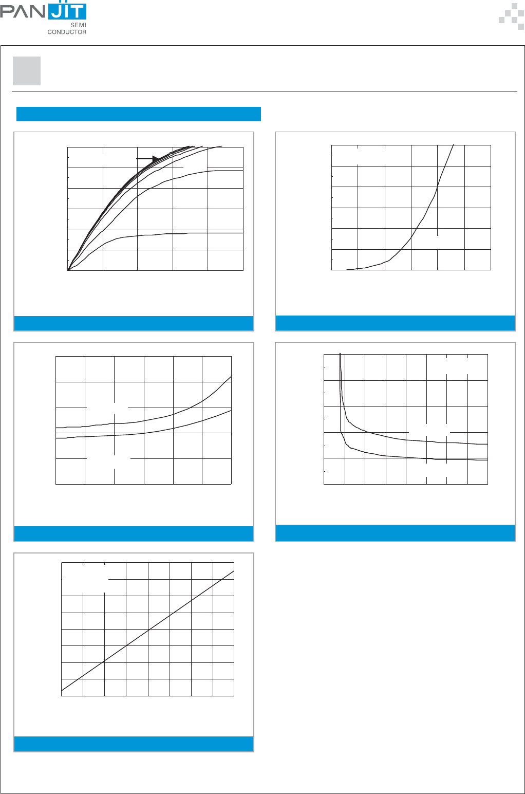
Fig. 1-TYPICAL FORWARD CHARACTERISTIC
FIG.1- Output Characteristic
Typical Characteristics Curves (T =25 C,unless otherwise noted)
A
O
FIG.2- Transfer Characteristic
FIG.3- On Resistance vs Drain Current
FIG.4- On Resistance vs Gate to Source Voltage
FIG.5- On Resistance vs Junction Temperature
0
0.2
0.4
0.6
0.8
1
1.2
012345
VDS -Drain-to-Source Voltage (V)
ID-Drain-to-Source Current (A)
5.0V
4.0V
3.0V
VGS
= 6.0~10V
0
0.2
0.4
0.6
0.8
1
1.2
0123456
VGS -Gate-to-Source Voltage (V)
ID-Drain Source Current (A)
VDS =10V
0
1
2
3
4
5
0 0.2 0.4 0.6 0.8 1 1.2
ID-Drain Current (A)
RDS(ON)-On-Resistance
()W
VGS =4.5V
V
GS
=10V
0
2
4
6
8
10
2345678910
VGS - Gate-to-Source Voltage (V)
RDS(ON) - On-Resistance
I
D
=500mA
oC
T =125
J
oC
T=25
J
()W
0.4
0.6
0.8
1
1.2
1.4
1.6
1.8
2
-50 -25 0 25 50 75 100 125 150
TJ- Junction Temperature ( oC)
R
DS(ON)
- On-Resistance(Normalized)
VGS =10V
ID=500mA
oC
T=25
J
2N7002
PAGE . 4August 29,2013-REV.03
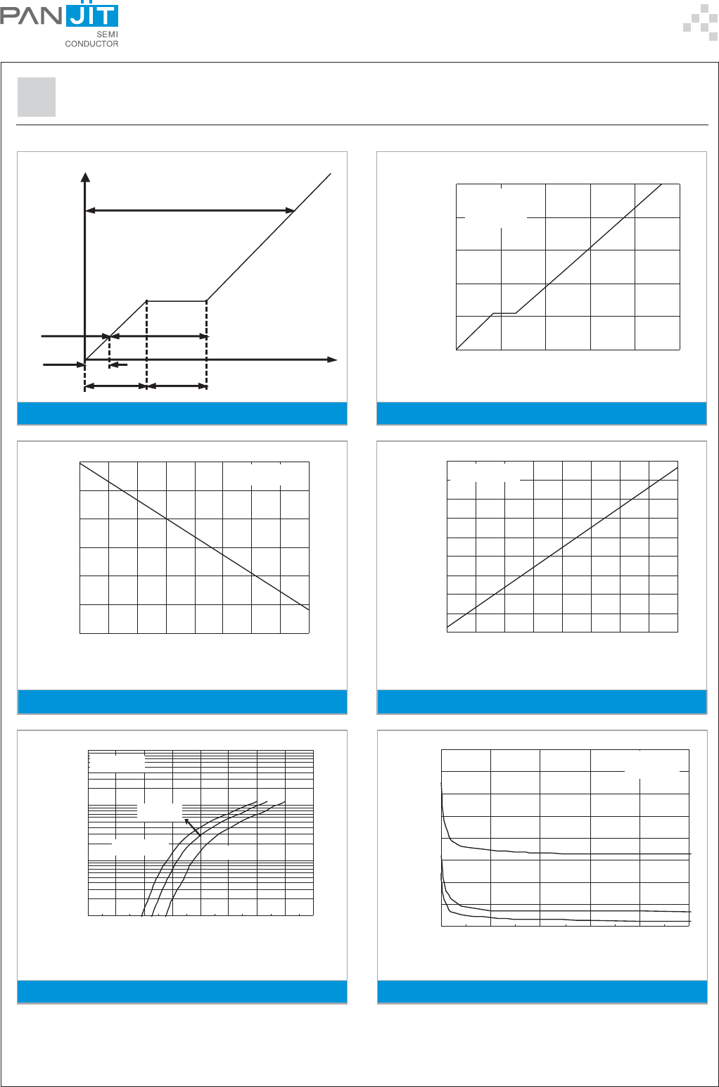
Fig.6 - Gate Charge Waveform
Fig.8 - Threshold Voltage vs Temperature
Fig.7 - Gate Charge
Fig.9 - Breakdown Voltage vs Junction Temperature
Fig.10 - Source-Drain Diode Forward Voltage
QgdQgs Qg
Qsw
Vgs(th)
Vgs
Qg
Qg(th)
0
2
4
6
8
10
0 0.2 0.4 0.6 0.8 1
Qg- Gate Charge (nC)
V
GS
- Gate-to-Source Volt age (V)
VDS=
15V
ID=500mA
0.6
0.7
0.8
0.9
1
1.1
1.2
-50 -25 0 25 50 75 100 125 150
TJ- Junction Temperature ( oC)
V
th
- G-S Threshold Voltage (NORMALIZED)
ID=250 Am
64
65
66
67
68
69
70
71
72
73
-50 -25 0 25 50 75 100 125 150
TJ- Junction Temperature ( oC)
BVDSS - Breakdown Voltage (V)
I=250A
D
m
0.01
0.1
1
10
0.2 0.4 0.6 0.8 1 1.2 1.4 1.6 1.8
V
SD
- Source-to-Drain Voltage (V)
I
S
- Source Current (A)
T
J
=125
o
C
VGS =0V
T =-55
J
o
C
Fig.11 - Capacitance vs Drain to Source Voltage
VDS- Drain-to-Source Voltage (V)
C - Capacitance (pF)
o
C
T=25
J
0
10
20
30
40
50
60
70
80
0 5 10 15 20 25
Ciss
f=1MHz
V
GS
=0V
Crss
Coss
2N7002
PAGE . 5August 29,2013-REV.03
2N7002
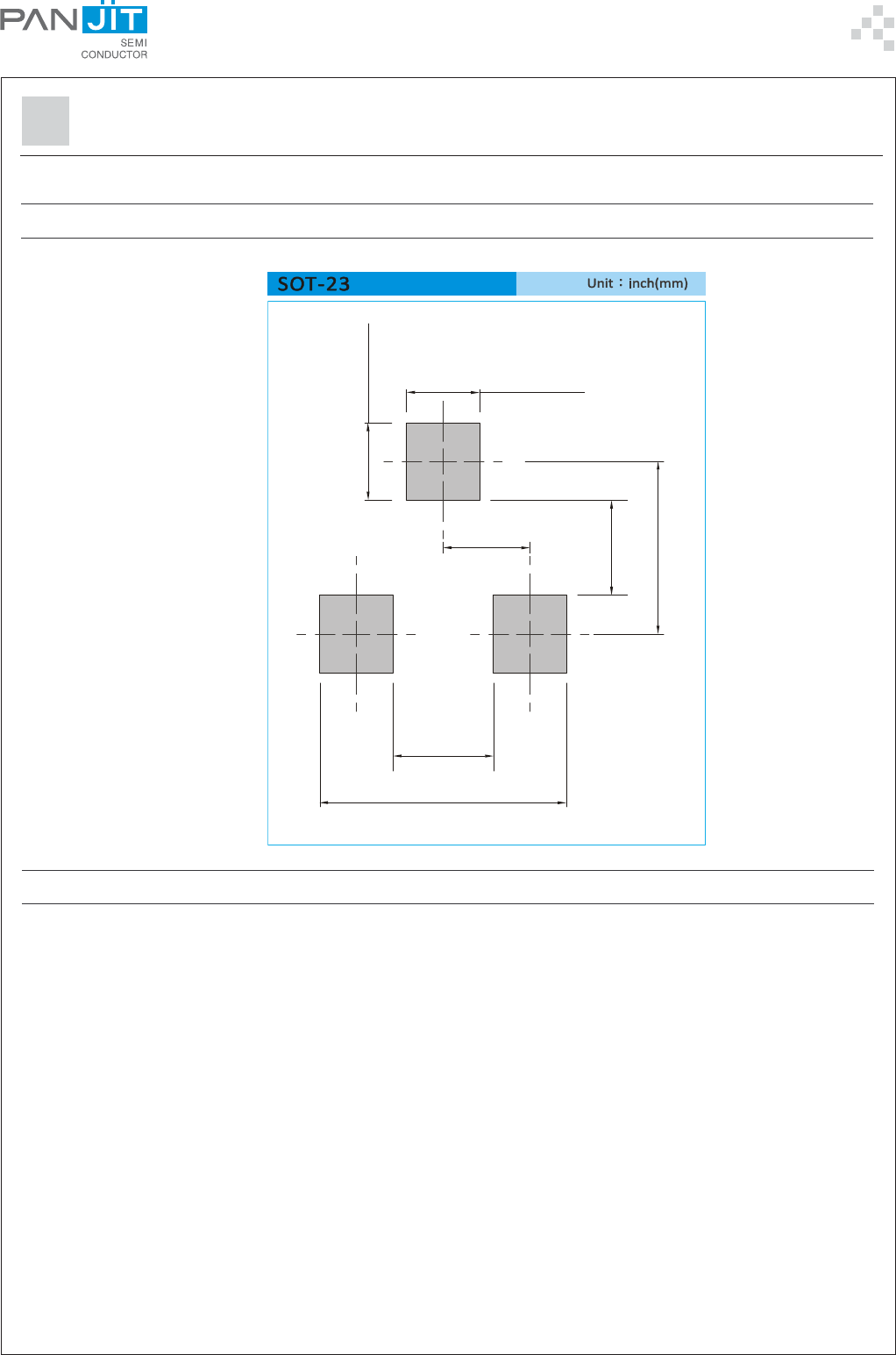
MOUNTING PAD LAYOUT
ORDER INFORMATION
• Packing information
T/R - 12K per 13" plastic Reel
T/R - 3K per 7" plastic Reel
0.031 MIN.
(0.80) MIN.
0.037
(0.95)
0.043
(1.10)
0.078
(2.00)
0.035 MIN.
(0.90) MIN.
0.043
(1.10)
0.106
(2.70)
PAGE . 6August 29,2013-REV.03
2N7002
Part No_packing code_Version
2N7002_R1_00001
2N7002_R2_00001
For example :
RB500V-40_R2_00001
Part No.
Serial number
Version code means HF
Packing size code means 13"
Packing type means T/R
Packing Code XX Version Code XXXXX
Packing type 1
st
Code Packing size code 2
nd
Code HF or RoHS 1
st
Code 2
nd
~5
th
Code
Tape and Ammunition Box
(T/B) AN/A 0HF 0 serial number
Tape and Reel
(T/R) R7" 1RoHS 1 serial number
Bulk Packing
(B/P) B13" 2
Tube Packing
(T/P) T26mm X
Tape and Reel (Right Oriented)
(TRR) S52mm Y
Tape and Reel (Left Oriented)
(TRL) LPANASERT T/B CATHODE UP
(PBCU) U
FORMING FPANASERT T/B CATHODE DOWN
(PBCD) D

PAGE . 7
Disclaimer
•Reproducing and modifying information of the document is prohibited without permission
from Panjit International Inc..
•Panjit International Inc. reserves the rights to make changes of the content herein the
document anytime without notification. Please refer to our website for the latest
document.
Panjit International Inc. disclaims any and all liability arising out of the application or use of
any product including damages incidentally and consequentially occurred.
•Panjit International Inc. does not assume any and all implied warranties, including warranties
of fitness for particular purpose, non-infringement and merchantability.
•Applications shown on the herein document are examples of standard use and operation.
Customers are responsible in comprehending the suitable use in particular applications.
Panjit International Inc. makes no representation or warranty that such applications will be
suitable for the specified use without further testing or modification.
•The products shown herein are not designed and authorized for equipments requiring high
level of reliability or relating to human life and for any applications concerning life-saving
or life-sustaining, such as medical instruments, transportation equipment, aerospace
machinery et cetera. Customers using or selling these products for use in such applications
do so at their own risk and agree to fully indemnify Panjit International Inc. for any damages
resulting from such improper use or sale.
•
•Since Panjit uses lot number as the tracking base, please provide the lot number for tracking
when complaining.
2N7002
August 29,2013-REV.03