2N7002 Datasheet. Www.s Manuals.com. Zetex
User Manual: Marking of electronic components, SMD Codes 7002, 7005, 702, 702⚫, 702*, 703 *, 7030L, 704, 705, 709, 709**, 70N10L, 70T. Datasheets 2N7002, 2N7002-G, 2N7002DW, 2N7002E, 2N7002K, 2N7002L, 2N7002MTF, 2V7002K, 2V7002L, FAN7005M, FCX705, G709RCUf, G709T1Uf, L2N7002LT1G, MTN138ZN3, MTN7002N3, MTN7002ZHN3, MTNK1N3, MTNK2N3, PH7030L, SPB70N10L, SPI70N10L, SPP70N10L, TK71570AS.
Open the PDF directly: View PDF ![]() .
.
Page Count: 5
Issue 5 - October 2007 1 www.zetex.com
© Zetex Semiconductors plc 2007
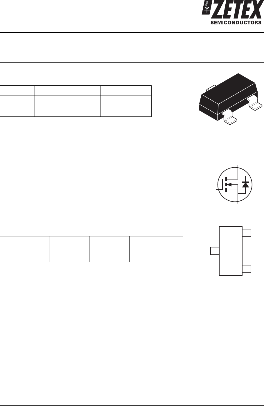
2N7002
60V SOT23 N-channel enhancement mode MOSFET
Summary
Description
A small signal MOSFET for general purpose switching applications.
Features
• Fast switching speed
• Low gate drive capability
• SOT23 package
Applications
• General switching applications
Ordering information
Device marking
702
V(BR)DSS RDS(on) (⍀)I
D (A)
60
7.5 @ VGS= 10V 0.5
7.5 @ VGS= 5V 0.05
Device Reel size
(inches)
Tape width
(mm)
Quantity per reel
2N7002 7 8 3,000
D
S
G
D
Top view
S
G
2N7002
Issue 5 - October 2007 2 www.zetex.com
© Zetex Semiconductors plc 2007
Absolute maximum ratings
Electrical characteristics (at Tamb = 25°C unless otherwise stated)
NOTES:
(a) Measured under pulsed conditions. Pulse width ⱕ300s; duty cycle ⱕ2%.
(b) Sample test.
(c) Switching times measured with 50⍀ source impedance and <5ns rise time on a pulse generator
Spice parameter data is available upon request for this device.
Parameter Symbol Limit Unit
Drain-source voltage VDS 60 V
Continuous drain current at Tamb=25°C ID115 mA
Pulsed drain current IDM 800 mA
Gate-source voltage VGS ±40 V
Power dissipation at Tamb =25°C Ptot 330 mW
Operating and storage temperature range Tj, Tstg -55 to +150 °C
Parameter Symbol Min. Max. Unit Conditions
Drain-source breakdown voltage BVDSS 60 V ID= 10A, VGS=0V
Gate-source threshold voltage VGS(th) 12.5VI
D= 250A, VDS=VGS
Gate-body leakage IGSS 10 nA VGS=±20V, VDS=0V
Zero gate voltage drain current IDSS 1AV
DS= 48V, VGS=0V
500 A
V
DS
= 48V, V
GS
=0V, T=125°C
On-state drain current(a) ID(on) 500 mA VDS= 25V, VGS= 10V
Static drain-source on-state
voltage(a)
VDS(on) 3.75 V VGS= 10V, ID= 500mA
375 mV VGS= 5V, ID= 50mA
Static drain-source on-state
resistance(a)
RDS(on) 7.5 ⍀VGS= 10V, ID= 500mA
7.5 ⍀VGS= 5V, ID= 50mA
Forward transconductance(a)(b) gfs 80 mS VDS= 25V, ID= 500mA
Input capacitance(b) Ciss 50 pF
VDS= 25V, VGS=0V f=1MHz
Common source output
capacitance(b)
Coss 25 pF
Reverse transfer capacitance(b) Crss 5pF
Turn-on time(b)(c) t(on) 20 ns VDD≈30V, ID= 200mA,
Rg=25⍀, RL=150⍀
Turn-off time(b)(c) t(off) 20 ns
2N7002
Issue 5 - October 2007 3 www.zetex.com
© Zetex Semiconductors plc 2007
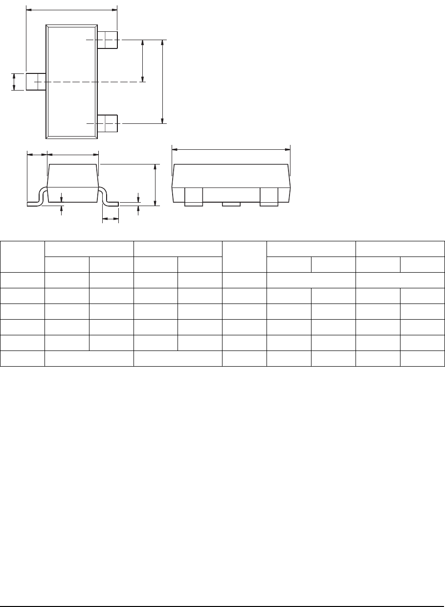
SOT23 Package outline
Note: Controlling dimensions are in millimeters. Approximate dimensions are provided in inches
Dim. Millimeters Inches Dim. Millimeters Inches
Min. Max. Min. Max. Min. Max. Min. Max.
A - 1.12 - 0.044 e1 1.90 NOM 0.075 NOM
A1 0.01 0.10 0.0004 0.004 E 2.10 2.64 0.083 0.104
b 0.30 0.50 0.012 0.020 E1 1.20 1.40 0.047 0.055
c 0.085 0.20 0.003 0.008 L 0.25 0.60 0.0098 0.0236
D 2.80 3.04 0.110 0.120 L1 0.45 0.62 0.018 0.024
e 0.95 NOM 0.037 NOM - - - - -
E
e
L
e1
D
A
c
E1
L1
A1
b
3 leads

2N7002
Issue 5 - October 2007 4 www.zetex.com
© Zetex Semiconductors plc 2007
Definitions
Product change
Zetex Semiconductors reserves the right to alter, without notice, specifications, design, price or conditions of supply of any product or
service. Customers are solely responsible for obtaining the latest relevant information before placing orders.
Applications disclaimer
The circuits in this design/application note are offered as design ideas. It is the responsibility of the user to ensure that the circuit is fit for
the user’s application and meets with the user’s requirements. No representation or warranty is given and no liability whatsoever is
assumed by Zetex with respect to the accuracy or use of such information, or infringement of patents or other intellectual property rights
arising from such use or otherwise. Zetex does not assume any legal responsibility or will not be held legally liable (whether in contract,
tort (including negligence), breach of statutory duty, restriction or otherwise) for any damages, loss of profit, business, contract,
opportunity or consequential loss in the use of these circuit applications, under any circumstances.
Life support
Zetex products are specifically not authorized for use as critical components in life support devices or systems without the express written
approval of the Chief Executive Officer of Zetex Semiconductors plc. As used herein:
A. Life support devices or systems are devices or systems which:
1. are intended to implant into the body
or
2. support or sustain life and whose failure to perform when properly used in accordance with instructions for use provided in the
labeling can be reasonably expected to result in significant injury to the user.
B. A critical component is any component in a life support device or system whose failure to perform can be reasonably expected to
cause the failure of the life support device or to affect its safety or effectiveness.
Reproduction
The product specifications contained in this publication are issued to provide outline information only which (unless agreed by the
company in writing) may not be used, applied or reproduced for any purpose or form part of any order or contract or be regarded as a
representation relating to the products or services concerned.
Terms and Conditions
All products are sold subjects to Zetex’ terms and conditions of sale, and this disclaimer (save in the event of a conflict between the two
when the terms of the contract shall prevail) according to region, supplied at the time of order acknowledgement.
For the latest information on technology, delivery terms and conditions and prices, please contact your nearest Zetex sales office.
Quality of product
Zetex is an ISO 9001 and TS16949 certified semiconductor manufacturer.
To ensure quality of service and products we strongly advise the purchase of parts directly from Zetex Semiconductors or one of our
regionally authorized distributors. For a complete listing of authorized distributors please visit: www.zetex.com/salesnetwork
Zetex Semiconductors does not warrant or accept any liability whatsoever in respect of any parts purchased through unauthorized sales channels.
ESD (Electrostatic discharge)
Semiconductor devices are susceptible to damage by ESD. Suitable precautions should be taken when handling and transporting devices.
The possible damage to devices depends on the circumstances of the handling and transporting, and the nature of the device. The extent
of damage can vary from immediate functional or parametric malfunction to degradation of function or performance in use over time.
Devices suspected of being affected should be replaced.
Green compliance
Zetex Semiconductors is committed to environmental excellence in all aspects of its operations which includes meeting or exceeding reg-
ulatory requirements with respect to the use of hazardous substances. Numerous successful programs have been implemented to reduce
the use of hazardous substances and/or emissions.
All Zetex components are compliant with the RoHS directive, and through this it is supporting its customers in their compliance with
WEEE and ELV directives.
Product status key:
“Preview” Future device intended for production at some point. Samples may be available
“Active” Product status recommended for new designs
“Last time buy (LTB)” Device will be discontinued and last time buy period and delivery is in effect
“Not recommended for new designs”
Device is still in production to support existing designs and production
“Obsolete” Production has been discontinued
Datasheet status key:
“Draft version” This term denotes a very early datasheet version and contains highly provisional information, which
may change in any manner without notice.
“Provisional version” This term denotes a pre-release datasheet. It provides a clear indication of anticipated performance.
However, changes to the test conditions and specifications may occur, at any time and without notice.
“Issue” This term denotes an issued datasheet containing finalized specifications. However, changes to
specifications may occur, at any time and without notice.
Zetex sales offices
Europe
Zetex GmbH
Kustermann-park
Balanstraße 59
D-81541 München
Germany
Telefon: (49) 89 45 49 49 0
Fax: (49) 89 45 49 49 49
europe.sales@zetex.com
Americas
Zetex Inc
700 Veterans Memorial Highway
Hauppauge, NY 11788
USA
Telephone: (1) 631 360 2222
Fax: (1) 631 360 8222
usa.sales@zetex.com
Asia Pacific
Zetex (Asia Ltd)
3701-04 Metroplaza Tower 1
Hing Fong Road, Kwai Fong
Hong Kong
Telephone: (852) 26100 611
Fax: (852) 24250 494
asia.sales@zetex.com
Corporate Headquarters
Zetex Semiconductors plc
Zetex Technology Park, Chadderton
Oldham, OL9 9LL
United Kingdom
Telephone: (44) 161 622 4444
Fax: (44) 161 622 4446
hq@zetex.com
© 2007 Published by Zetex Semiconductors plc