Discovery Kit With STM32F769NI MCU User Manual 32f769i
User Manual:
Open the PDF directly: View PDF ![]() .
.
Page Count: 56
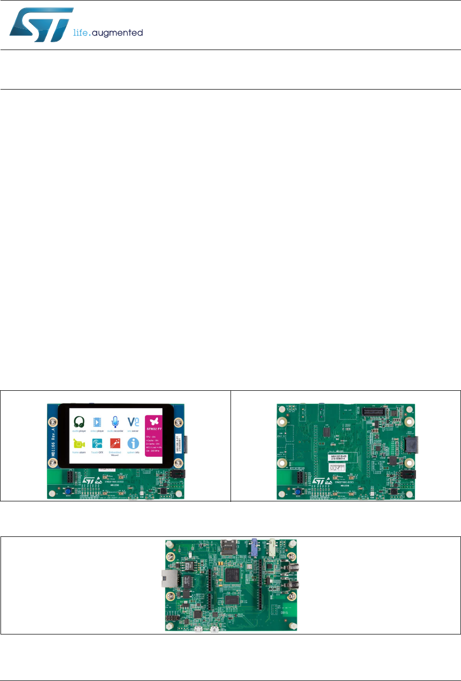
- Figure 1. STM32F769I-DISCO (top view)
- Figure 2. STM32F769I-DISC1 (top view)
- Figure 3. 32F769IDISCOVERY board (bottom view)
- 1 Features
- 2 Demonstration software
- 3 Product marking
- 4 Ordering information
- 5 Technology partners
- 6 Hardware layout and configuration
- Figure 4. Hardware block diagram
- 6.1 The 32F769IDISCOVERY Discovery board layout
- 6.2 The 32F769IDISCOVERY Discovery board mechanical drawing
- 6.3 Embedded ST-LINK/V2-1
- 6.4 Power supply
- 6.5 Programming/debugging when the power supply is not from ST-LINK (5 V link)
- 6.6 Clock sources
- 6.7 Reset sources
- 6.8 Audio
- 6.9 USB OTG HS
- 6.10 microSD™ card
- 6.11 Ethernet
- 6.12 Power over Ethernet
- 6.13 SDRAM memory
- 6.14 Quad-SPI NOR Flash memory
- 6.15 Virtual COM port
- 6.16 Buttons and LEDs
- 6.17 LCD display MIPI DSI (with STM32F769I-DISCO only)
- 6.18 Adapter board from on-board DSI to HDMI (optional accessory display)
- 6.19 Adapter board from on-board DSI to external DSI (optional accessory display)
- 6.20 Wi-Fi® and extension I2C connector
- 7 Connectors
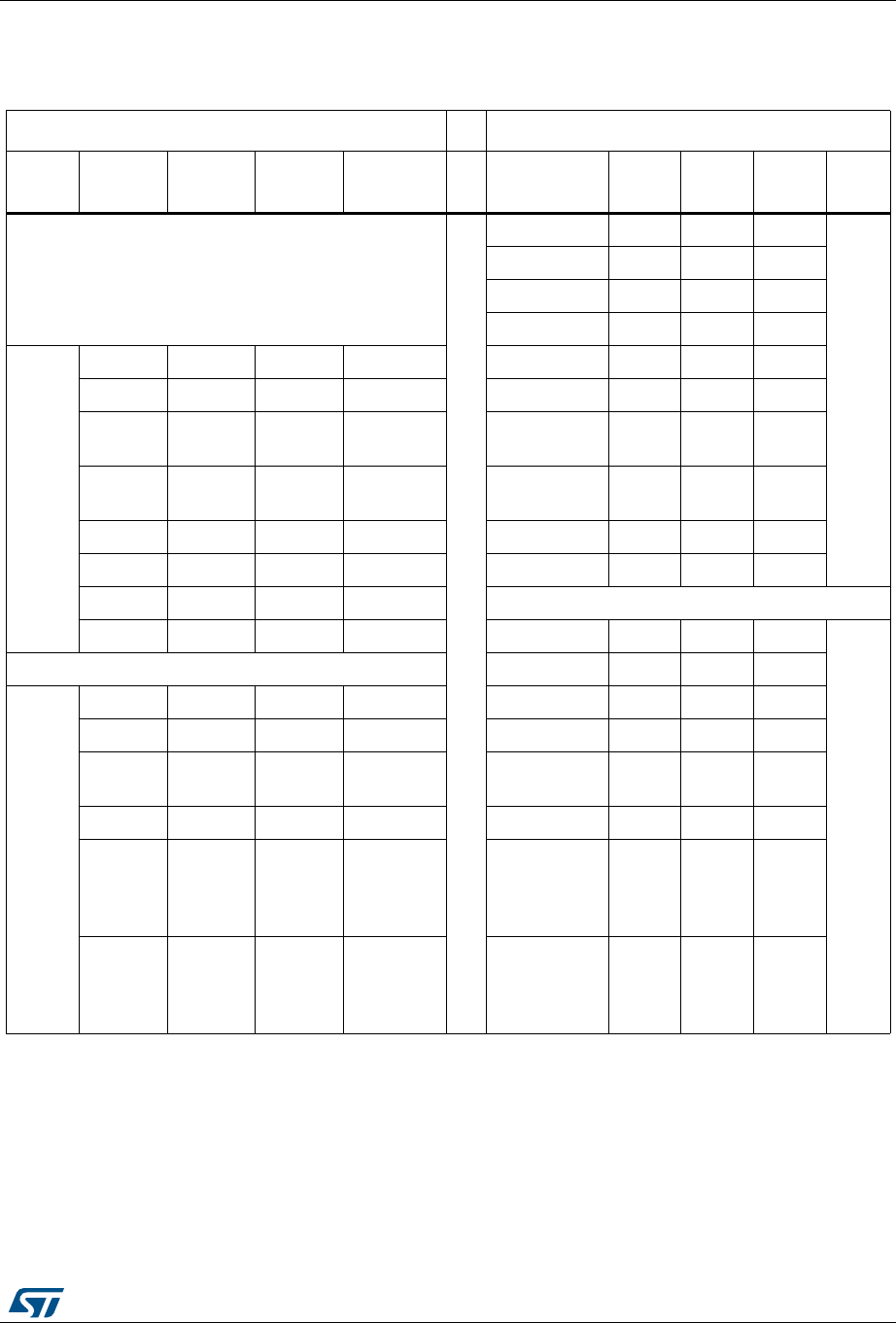
- 7.1 Wi-Fi® and I2C extension connector CN2
- 7.2 Arduino™ Uno V3 connectors
- 7.3 USB OTG HS micro-AB connector CN15
- 7.4 Ethernet RJ45 connector CN10
- 7.5 LCD display MIPI DSI connector CN1
- 7.6 microSD™ connector CN5
- 7.7 ST-LINK/V2-1 USB micro-B connector CN16
- 7.8 Audio stereo speakers JP2 and JP3
- 7.9 Audio line output connector jack CN7
- 7.10 Audio line input connector jack CN6
- 7.11 SPDIF input RCA connector CN12
- 7.12 SPDIF output RCA connector CN8
- Appendix A 32F769IDISCOVERY I/O assignment
- Appendix B Schematics
- Figure 28. 32F769IDISCOVERY Discovery board interconnections
- Figure 29. ST-LINK/V2-1 with support of SWD only
- Figure 30. STM32F769NIH6 connections
- Figure 31. Audio codec WOLFSON and audio connectors
- Figure 32. SDRAM (MICRON)
- Figure 33. Quad-SPI Flash memory (MACRONIX mounted)
- Figure 34. Arduino™ UNO connectors
- Figure 35. USB OTG HS PHY with micro A-B connector
- Figure 36. Ethernet PHY with RJ45 connector
- Figure 37. Power over Ethernet 3 W
- Figure 38. MIPI connector for DSI LCD and HDMI boards
- Figure 39. microSD™, Wi-Fi®, LEDs and push-button
- Figure 40. 4-inch DSI LCD board
- Figure 41. DSI to HDMI adapter
- Figure 42. DSI connector adapter
- Appendix C Federal Communications Commission (FCC) and Industry Canada (IC) Compliance Statements
- Revision history
April 2018 UM2033 Rev 3 1/56
1
UM2033
User manual
Discovery kit with STM32F769NI MCU
Introduction
The 32F769IDISCOVERY Discovery kit is a complete demonstration and development
platform for STMicroelectronics Arm® Cortex®-M7 core-based STM32F769NIH6
microcontroller. It features four I2Cs, six SPIs with three multiplexed simplex I2S,
2xSDMMC, four USARTs, four UARTs, three CAN buses, three 12-bit ADCs, two 12-bit
DACs, two SAIs, 8- to 14-bit digital camera module interface, internal 512+4-Kbyte SRAM
and 2-Mbyte Flash memory, USB HS OTG and USB FS OTG, Ethernet MAC, FMC
interface, Quad-SPI interface and SWD debugging support.
The Discovery kit offers all required to get started quickly and develop applications easily.
The full range of hardware features available on the 32F769IDISCOVERY Discovery kit for
both STM32F769I-DISCO and STM32F769I-DISC1 variants (see Figure 1: STM32F769I-
DISCO (top view) and Figure 2: STM32F769I-DISC1 (top view)), helps users to evaluate the
following peripherals: USB OTG HS, 10/100-Mbit Ethernet, microSD™, USART, SAI Audio
DAC
stereo with two audio jacks for input/output, ST MEMS digital microphones, SDRAM,
Quad-SPI Flash memory, SPDIF input/output and DSI interface LCD with capacitive multi-
touch panel. This latter is only available on the STM32F769I-DISCO, see Figure 1.
Arduino™ Uno V3 connectors allow easy connection of extension shields or daughterboards.
The integrated ST-LINK/V2-1 provides an embedded in-circuit debugger and programmer for
the STM32. The 32F769IDISCOVERY Discovery kit comes with the STM32 comprehensive
software HAL library together with various packaged software examples.
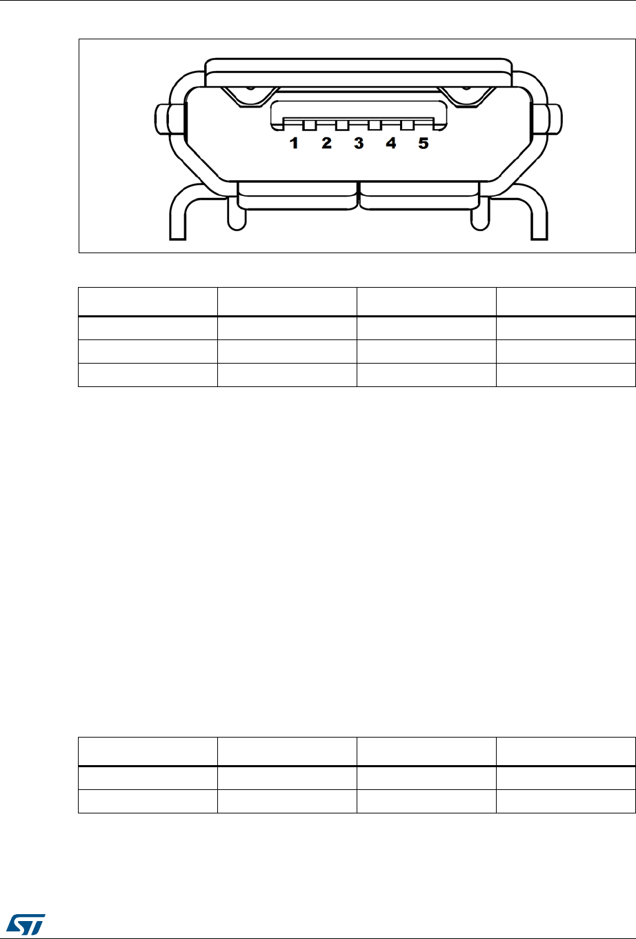
1. Fig 1, Fig2 and Fig3 are not contractual.
Figure 3. 32F769IDISCOVERY board (bottom view)
Figure 1. STM32F769I-DISCO (top view) Figure 2. STM32F769I-DISC1 (top view)
Bottom view of:
STM32F769I-DISCO and
STM32F769I-DISC1
www.st.com

Contents UM2033
2/56 UM2033 Rev 3
Contents
1 Features . . . . . . . . . . . . . . . . . . . . . . . . . . . . . . . . . . . . . . . . . . . . . . . . . . . 6
2 Demonstration software . . . . . . . . . . . . . . . . . . . . . . . . . . . . . . . . . . . . . . 7
3 Product marking . . . . . . . . . . . . . . . . . . . . . . . . . . . . . . . . . . . . . . . . . . . . 7
4 Ordering information . . . . . . . . . . . . . . . . . . . . . . . . . . . . . . . . . . . . . . . . 7
5 Technology partners . . . . . . . . . . . . . . . . . . . . . . . . . . . . . . . . . . . . . . . . . 8
6 Hardware layout and configuration . . . . . . . . . . . . . . . . . . . . . . . . . . . . . 9
6.1 The 32F769IDISCOVERY Discovery board layout . . . . . . . . . . . . . . . . . 10
6.2 The 32F769IDISCOVERY Discovery board mechanical drawing . . . . . . 12
6.3 Embedded ST-LINK/V2-1 . . . . . . . . . . . . . . . . . . . . . . . . . . . . . . . . . . . . . 13
6.3.1 Drivers . . . . . . . . . . . . . . . . . . . . . . . . . . . . . . . . . . . . . . . . . . . . . . . . . . 13
6.3.2 ST-LINK/V2-1 firmware upgrade . . . . . . . . . . . . . . . . . . . . . . . . . . . . . . 14
6.4 Power supply . . . . . . . . . . . . . . . . . . . . . . . . . . . . . . . . . . . . . . . . . . . . . . 15
6.5 Programming/debugging when the power supply is not from
ST-LINK (5 V link) . . . . . . . . . . . . . . . . . . . . . . . . . . . . . . . . . . . . . . . . . . . 18
6.6 Clock sources . . . . . . . . . . . . . . . . . . . . . . . . . . . . . . . . . . . . . . . . . . . . . . 18
6.7 Reset sources . . . . . . . . . . . . . . . . . . . . . . . . . . . . . . . . . . . . . . . . . . . . . 18
6.8 Audio . . . . . . . . . . . . . . . . . . . . . . . . . . . . . . . . . . . . . . . . . . . . . . . . . . . . 18
6.9 USB OTG HS . . . . . . . . . . . . . . . . . . . . . . . . . . . . . . . . . . . . . . . . . . . . . . 19
6.10 microSD™ card . . . . . . . . . . . . . . . . . . . . . . . . . . . . . . . . . . . . . . . . . . . . 19
6.11 Ethernet . . . . . . . . . . . . . . . . . . . . . . . . . . . . . . . . . . . . . . . . . . . . . . . . . . 19
6.12 Power over Ethernet . . . . . . . . . . . . . . . . . . . . . . . . . . . . . . . . . . . . . . . . . 19
6.13 SDRAM memory . . . . . . . . . . . . . . . . . . . . . . . . . . . . . . . . . . . . . . . . . . . 20
6.14 Quad-SPI NOR Flash memory . . . . . . . . . . . . . . . . . . . . . . . . . . . . . . . . . 20
6.15 Virtual COM port . . . . . . . . . . . . . . . . . . . . . . . . . . . . . . . . . . . . . . . . . . . . 20
6.16 Buttons and LEDs . . . . . . . . . . . . . . . . . . . . . . . . . . . . . . . . . . . . . . . . . . 20
6.17 LCD display MIPI DSI (with STM32F769I-DISCO only) . . . . . . . . . . . . . . 21
6.18 Adapter board from on-board DSI to HDMI
(optional accessory display) . . . . . . . . . . . . . . . . . . . . . . . . . . . . . . . . . . . 21

UM2033 Rev 3 3/56
UM2033 Contents
3
6.19 Adapter board from on-board DSI to external DSI
(optional accessory display) . . . . . . . . . . . . . . . . . . . . . . . . . . . . . . . . . . . 22
6.20 Wi-Fi® and extension I2C connector . . . . . . . . . . . . . . . . . . . . . . . . . . . . 23
6.20.1 Serial Wi-Fi® module . . . . . . . . . . . . . . . . . . . . . . . . . . . . . . . . . . . . . . . 23
6.20.2 Extension I2C board . . . . . . . . . . . . . . . . . . . . . . . . . . . . . . . . . . . . . . . . 23
7 Connectors . . . . . . . . . . . . . . . . . . . . . . . . . . . . . . . . . . . . . . . . . . . . . . . 24
7.1 Wi-Fi® and I2C extension connector CN2 . . . . . . . . . . . . . . . . . . . . . . . . 24
7.2 Arduino™ Uno V3 connectors . . . . . . . . . . . . . . . . . . . . . . . . . . . . . . . . . 25
7.3 USB OTG HS micro-AB connector CN15 . . . . . . . . . . . . . . . . . . . . . . . . 26
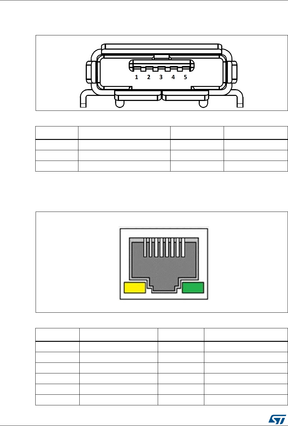
7.4 Ethernet RJ45 connector CN10 . . . . . . . . . . . . . . . . . . . . . . . . . . . . . . . . 26
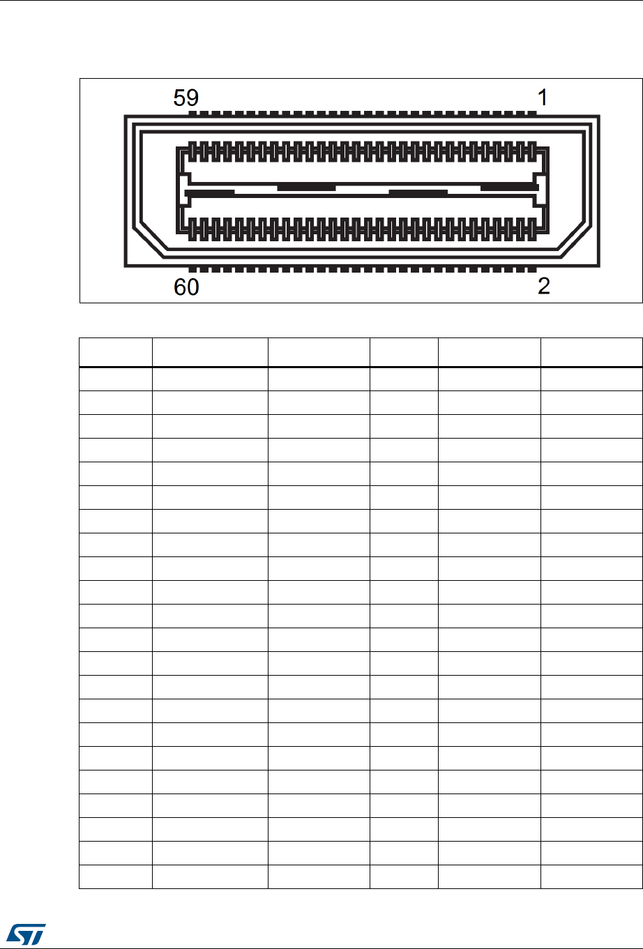
7.5 LCD display MIPI DSI connector CN1 . . . . . . . . . . . . . . . . . . . . . . . . . . . 27
7.6 microSD™ connector CN5 . . . . . . . . . . . . . . . . . . . . . . . . . . . . . . . . . . . . 28
7.7 ST-LINK/V2-1 USB micro-B connector CN16 . . . . . . . . . . . . . . . . . . . . . 28
7.8 Audio stereo speakers JP2 and JP3 . . . . . . . . . . . . . . . . . . . . . . . . . . . . 29
7.9 Audio line output connector jack CN7 . . . . . . . . . . . . . . . . . . . . . . . . . . . 29
7.10 Audio line input connector jack CN6 . . . . . . . . . . . . . . . . . . . . . . . . . . . . 29
7.11 SPDIF input RCA connector CN12 . . . . . . . . . . . . . . . . . . . . . . . . . . . . . 29
7.12 SPDIF output RCA connector CN8 . . . . . . . . . . . . . . . . . . . . . . . . . . . . . 30
Appendix A 32F769IDISCOVERY I/O assignment . . . . . . . . . . . . . . . . . . . . . . . . 31
Appendix B Schematics. . . . . . . . . . . . . . . . . . . . . . . . . . . . . . . . . . . . . . . . . . . . . 38
Appendix C Federal Communications Commission (FCC)
and Industry Canada (IC) Compliance Statements. . . . . . . . . . . . . 54
C.1 FCC Compliance Statement . . . . . . . . . . . . . . . . . . . . . . . . . . . . . . . . . . . 54
C.1.1 Part 15.19 . . . . . . . . . . . . . . . . . . . . . . . . . . . . . . . . . . . . . . . . . . . . . . . . 54
C.1.2 Part 15.105 . . . . . . . . . . . . . . . . . . . . . . . . . . . . . . . . . . . . . . . . . . . . . . . 54
C.1.3 Part 15.21 . . . . . . . . . . . . . . . . . . . . . . . . . . . . . . . . . . . . . . . . . . . . . . . . 54
C.2 IC Compliance Statement . . . . . . . . . . . . . . . . . . . . . . . . . . . . . . . . . . . . . 54
7.12.1 Compliance Statement . . . . . . . . . . . . . . . . . . . . . . . . . . . . . . . . . . . . . . 54
7.12.2 Déclaration de conformité . . . . . . . . . . . . . . . . . . . . . . . . . . . . . . . . . . . 54
Revision history . . . . . . . . . . . . . . . . . . . . . . . . . . . . . . . . . . . . . . . . . . . . . . . . . . . . 55

List of tables UM2033
4/56 UM2033 Rev 3
List of tables
Table 1. List of the order codes . . . . . . . . . . . . . . . . . . . . . . . . . . . . . . . . . . . . . . . . . . . . . . . . . . . . . 7
Table 2. List of the order codes for the display accessories. . . . . . . . . . . . . . . . . . . . . . . . . . . . . . . . 8
Table 3. Control port assignment . . . . . . . . . . . . . . . . . . . . . . . . . . . . . . . . . . . . . . . . . . . . . . . . . . . 20
Table 4. Wi-Fi® and I2C extension connector CN2. . . . . . . . . . . . . . . . . . . . . . . . . . . . . . . . . . . . . . 24
Table 5. Arduino™ connectors (CN11, CN14, CN13 and CN9) . . . . . . . . . . . . . . . . . . . . . . . . . . . . 25
Table 6. USB OTG HS micro-AB CN15 . . . . . . . . . . . . . . . . . . . . . . . . . . . . . . . . . . . . . . . . . . . . . . 26
Table 7. Ethernet RJ45 connector CN10 . . . . . . . . . . . . . . . . . . . . . . . . . . . . . . . . . . . . . . . . . . . . . 26
Table 8. LCD display MIPI DSI connector CN1 . . . . . . . . . . . . . . . . . . . . . . . . . . . . . . . . . . . . . . . . 27
Table 9. microSD™ connector CN5 . . . . . . . . . . . . . . . . . . . . . . . . . . . . . . . . . . . . . . . . . . . . . . . . . 28
Table 10. USB micro-B connector CN16 . . . . . . . . . . . . . . . . . . . . . . . . . . . . . . . . . . . . . . . . . . . . . . 29
Table 11. SPDIF input RCA connector CN12. . . . . . . . . . . . . . . . . . . . . . . . . . . . . . . . . . . . . . . . . . . 29
Table 12. SPDIF output RCA connector CN8. . . . . . . . . . . . . . . . . . . . . . . . . . . . . . . . . . . . . . . . . . . 30
Table 13. 32F769IDISCOVERY I/O assignment . . . . . . . . . . . . . . . . . . . . . . . . . . . . . . . . . . . . . . . . 31
Table 14. Document revision history . . . . . . . . . . . . . . . . . . . . . . . . . . . . . . . . . . . . . . . . . . . . . . . . . 55

UM2033 Rev 3 5/56
UM2033 List of figures
5
List of figures
Figure 1. STM32F769I-DISCO (top view) . . . . . . . . . . . . . . . . . . . . . . . . . . . . . . . . . . . . . . . . . . . . . . 1
Figure 2. STM32F769I-DISC1 (top view). . . . . . . . . . . . . . . . . . . . . . . . . . . . . . . . . . . . . . . . . . . . . . . 1
Figure 3. 32F769IDISCOVERY board (bottom view). . . . . . . . . . . . . . . . . . . . . . . . . . . . . . . . . . . . . . 1
Figure 4. Hardware block diagram. . . . . . . . . . . . . . . . . . . . . . . . . . . . . . . . . . . . . . . . . . . . . . . . . . . . 9
Figure 5. 32F769IDISCOVERY top layout. . . . . . . . . . . . . . . . . . . . . . . . . . . . . . . . . . . . . . . . . . . . . 10
Figure 6. 32F769IDISCOVERY bottom layout. . . . . . . . . . . . . . . . . . . . . . . . . . . . . . . . . . . . . . . . . . 11
Figure 7. 32F769IDISCOVERY mechanical drawing. . . . . . . . . . . . . . . . . . . . . . . . . . . . . . . . . . . . . 12
Figure 8. USB composite device . . . . . . . . . . . . . . . . . . . . . . . . . . . . . . . . . . . . . . . . . . . . . . . . . . . . 13
Figure 9. CN3 (ext5V) from JP1 (Ext 5 V) . . . . . . . . . . . . . . . . . . . . . . . . . . . . . . . . . . . . . . . . . . . . . 15
Figure 10. CN3 (ext5V) from CN11 (Vin) . . . . . . . . . . . . . . . . . . . . . . . . . . . . . . . . . . . . . . . . . . . . . . . 15
Figure 11. CN3 (chgr) . . . . . . . . . . . . . . . . . . . . . . . . . . . . . . . . . . . . . . . . . . . . . . . . . . . . . . . . . . . . . 16
Figure 12. CN3 (poe5V). . . . . . . . . . . . . . . . . . . . . . . . . . . . . . . . . . . . . . . . . . . . . . . . . . . . . . . . . . . . 16
Figure 13. CN3 (stlk) . . . . . . . . . . . . . . . . . . . . . . . . . . . . . . . . . . . . . . . . . . . . . . . . . . . . . . . . . . . . . . 17
Figure 14. CN3 (usbhs) . . . . . . . . . . . . . . . . . . . . . . . . . . . . . . . . . . . . . . . . . . . . . . . . . . . . . . . . . . . . 17
Figure 15. 4-inch WVGA TFT DSI LCD daughterboard. . . . . . . . . . . . . . . . . . . . . . . . . . . . . . . . . . . . 21
Figure 16. DSI to HDMI adapter board . . . . . . . . . . . . . . . . . . . . . . . . . . . . . . . . . . . . . . . . . . . . . . . . 22
Figure 17. DSI to HDMI adapter board . . . . . . . . . . . . . . . . . . . . . . . . . . . . . . . . . . . . . . . . . . . . . . . . 22
Figure 18. On-board DSI to external DSI. . . . . . . . . . . . . . . . . . . . . . . . . . . . . . . . . . . . . . . . . . . . . . . 22
Figure 19. On-board DSI to external DSI. . . . . . . . . . . . . . . . . . . . . . . . . . . . . . . . . . . . . . . . . . . . . . . 22
Figure 20. Wi-Fi® module (ESP8266-01). . . . . . . . . . . . . . . . . . . . . . . . . . . . . . . . . . . . . . . . . . . . . . . 23
Figure 21. Wi-Fi® and I2C extension connector CN2 (front view) . . . . . . . . . . . . . . . . . . . . . . . . . . . . 24
Figure 22. Wi-Fi® and I2C extension connector CN2 (front view) . . . . . . . . . . . . . . . . . . . . . . . . . . . . 24
Figure 23. USB OTG micro-AB connector CN15 (front view) . . . . . . . . . . . . . . . . . . . . . . . . . . . . . . . 26
Figure 24. Ethernet RJ45 connector CN10 (front view) . . . . . . . . . . . . . . . . . . . . . . . . . . . . . . . . . . . . 26
Figure 25. LCD display MIPI DSI connector CN1 (front view) . . . . . . . . . . . . . . . . . . . . . . . . . . . . . . . 27
Figure 26. microSD™ connector CN5 (front view). . . . . . . . . . . . . . . . . . . . . . . . . . . . . . . . . . . . . . . . 28
Figure 27. USB micro-B connector CN16 (front view) . . . . . . . . . . . . . . . . . . . . . . . . . . . . . . . . . . . . . 29
Figure 28. 32F769IDISCOVERY Discovery board interconnections . . . . . . . . . . . . . . . . . . . . . . . . . . 39
Figure 29. ST-LINK/V2-1 with support of SWD only . . . . . . . . . . . . . . . . . . . . . . . . . . . . . . . . . . . . . . 40
Figure 30. STM32F769NIH6 connections . . . . . . . . . . . . . . . . . . . . . . . . . . . . . . . . . . . . . . . . . . . . . . 41
Figure 31. Audio codec WOLFSON and audio connectors . . . . . . . . . . . . . . . . . . . . . . . . . . . . . . . . . 42
Figure 32. SDRAM (MICRON). . . . . . . . . . . . . . . . . . . . . . . . . . . . . . . . . . . . . . . . . . . . . . . . . . . . . . . 43
Figure 33. Quad-SPI Flash memory (MACRONIX mounted). . . . . . . . . . . . . . . . . . . . . . . . . . . . . . . . 44
Figure 34. Arduino™ UNO connectors . . . . . . . . . . . . . . . . . . . . . . . . . . . . . . . . . . . . . . . . . . . . . . . . 45
Figure 35. USB OTG HS PHY with micro A-B connector . . . . . . . . . . . . . . . . . . . . . . . . . . . . . . . . . . 46
Figure 36. Ethernet PHY with RJ45 connector . . . . . . . . . . . . . . . . . . . . . . . . . . . . . . . . . . . . . . . . . . 47
Figure 37. Power over Ethernet 3 W . . . . . . . . . . . . . . . . . . . . . . . . . . . . . . . . . . . . . . . . . . . . . . . . . . 48
Figure 38. MIPI connector for DSI LCD and HDMI boards . . . . . . . . . . . . . . . . . . . . . . . . . . . . . . . . . 49
Figure 39. microSD™, Wi-Fi®, LEDs and push-button . . . . . . . . . . . . . . . . . . . . . . . . . . . . . . . . . . . . 50
Figure 40. 4-inch DSI LCD board. . . . . . . . . . . . . . . . . . . . . . . . . . . . . . . . . . . . . . . . . . . . . . . . . . . . . 51
Figure 41. DSI to HDMI adapter . . . . . . . . . . . . . . . . . . . . . . . . . . . . . . . . . . . . . . . . . . . . . . . . . . . . . 52
Figure 42. DSI connector adapter . . . . . . . . . . . . . . . . . . . . . . . . . . . . . . . . . . . . . . . . . . . . . . . . . . . . 53

Features UM2033
6/56 UM2033 Rev 3
1 Features
•STM32F769NIH6 Arm®(a)-based microcontroller featuring 2-Mbyte Flash memory and
512+16+4 Kbytes of RAM, in BGA216 package
•On-board ST-LINK/V2-1 supporting USB reenumeration capability
•USB ST-LINK functions: virtual COM port, mass storage, debug port
•4-inch capacitive touch LCD display with MIPI® DSI connector (on STM32F769I-DISCO
only)
•Optional display accessories: DSI LCD, HDMI adapter and DSI adapter
•SAI audio codec
•Two audio line jacks, one for input and one for output
•Stereo speaker outputs
•Four ST-MEMS microphones on DFSDM inputs
•Two SPDIF RCA input and output connectors
•Two push-buttons (user and reset)
•512-Mbit Quad-SPI Flash memory
•128-Mbit SDRAM
•Connector for microSD™ card
•Wi-Fi® or Ext-EEP daughterboard connector
•USB OTG HS with micro-AB connector
•Ethernet connector compliant with IEEE-802.3-2002
•Five power supply options:
– ST LINK/V2-1
– USB HS connector
– 5 V from RJ45 (Power Over Ethernet)
– 5 V from Arduino™ or external connector
– USB charger
•Power Over Ethernet based on IEEE 802.3af (Powered Device, 48 V to 5 V, 3 W)
•Power supply output for external applications: 3.3 V or 5 V
•Arduino™ Uno V3 connectors
•Comprehensive free software including a variety of examples,
part of the STM32Cube package
•Supported by a wide choice of integrated development environments
a. Arm is a registered trademark of Arm Limited (or its subsidiaries) in the US and/or elsewhere.
UM2033 Rev 3 7/56
UM2033 Demonstration software
55
2 Demonstration software
The demonstration software is preloaded in the STM32F769NIH6 Flash memory. The latest
versions of the demonstration source code and associated documentation can be
downloaded from www.st.com/stm32f7-discovery.
3 Product marking
Evaluation tools marked as "ES" or "E" are not yet qualified and therefore they are not ready
to be used as reference design or in production. Any consequences deriving from such
usage will not be at ST charge. In no event, ST will be liable for any customer usage of
these engineering sample tools as reference design or in production.
"E" or "ES" marking examples of location:
•On the targeted STM32 that is soldered on the board (for illustration of STM32 marking,
refer to the section "Package information" of the STM32 datasheet at www.st.com).
•Next to the evaluation tool ordering part number, that is stuck or silkscreen printed on
the board
This board features a specific STM32 device version, which allows the operation of any
bundled commercial stack/library available. This STM32 device shows a "U" marking option
at the end of the standard part number and is not available for sales. In order to use the
same commercial stack in his application, a developer may need to purchase a part number
specific to this stack/library. The price of those part numbers includes the stack/library
royalties.
4 Ordering information
To order the Discovery kit with the STM32F769NI MCU, refer to Table 1.
To order the optional display accessories for the 32F769IDISCOVERY Discovery kit, refer to
Table 2.
Table 1. List of the order codes
Order code Product package
STM32F769I-DISCO with 4-inch WVGA TFT LCD display
STM32F769I-DISC1 without 4-inch WVGA TFT LCD display
Technology partners UM2033
8/56 UM2033 Rev 3
5 Technology partners
MICRON:
•128-Mbit SDRAM, part number MT48LC4M32B2
MACRONIX:
•512-Mbit Quad-SPI NOR Flash memory device, part number MX25L51245G
Table 2. List of the order codes for the display accessories
Order code Product description
B-LCD40-DSI1 4-inch WVGA TFT LCD with MIPI-DSI interface and capacitive touch
screen
B-LCDAD-RPI1 15-pin single row Flexible Printed Circuit DSI adapter board
B-LCDAD-HDMI1 DSI to HDMI adapter
UM2033 Rev 3 9/56
UM2033 Hardware layout and configuration
55
6 Hardware layout and configuration
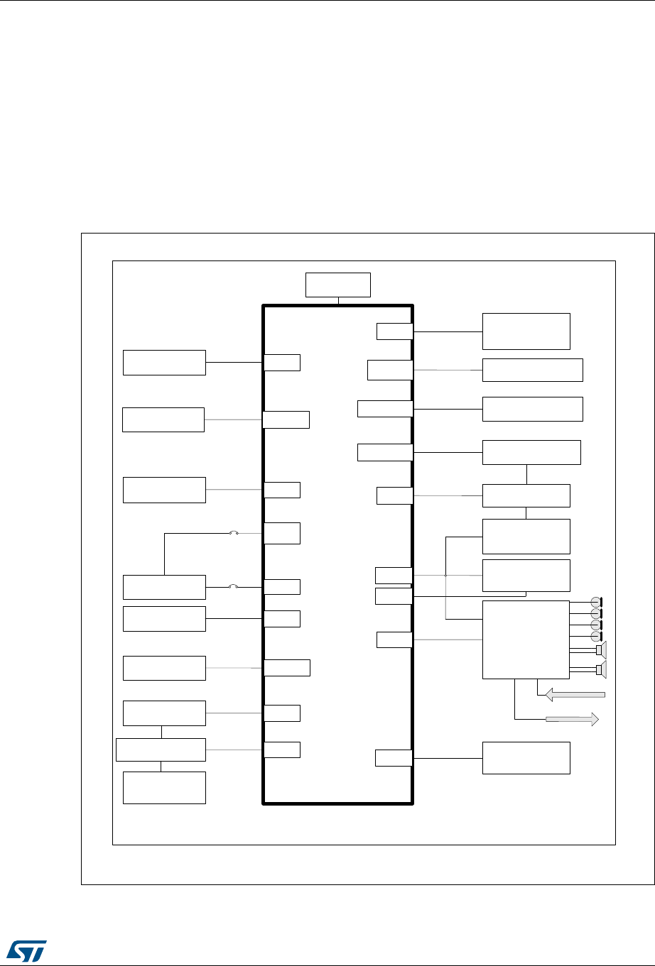
The 32F769IDISCOVERY Discovery board is designed around the STM32F769NIH6
(216-pin TFBGA package). The hardware block diagram (see Figure 4) illustrates the
connections between the STM32F769NIH6 and the peripherals (SDRAM, Quad-SPI Flash
memory, LCD DSI connector, USB OTG connectors, USART, Ethernet, Audio, SPDIF RCA
in, SPDIF RCA out, microSD™ card, Arduino™ Uno shields and embedded ST-LINK).
Figure 5 and Figure 6 help users to locate these features on the Discovery board. The
mechanical dimensions of the Discovery board are showed in Figure 7.
Figure 4. Hardware block diagram
06Y9
670)1,+
$XGLR'$&DQG
$PSOLILHU
57&
(WKHUQHW3+<DQG
5-FRQQHFWRU
6:'
93RZHU
6XSSO\
.+]FU\VWDO
67/,1.9
,&
50,,
6$,
:L)LRU(;7,&
%RDUGVFRQQHFWRU
&DSDFLWLYH
PXOWLSRLQW
WRXFKVFUHHQ
0+]2VFLOODWRU
/('VSXVKEXWWRQ
DQGZDNHXS
*3,2
+6,
+63+<DQG
0LFUR86%FRQQHFWRU
27*
+6
6'5$0 )0&
/&''6,
FRQQHFWRU
'6,
463, 463,)ODVK
63',)B7; 63',)2XWSXW
DQG5&$FRQQHFWRU
9&3
8$57
$5'8,12812
VKLHOGFRQQHFWRUV *3,2V
63',)B5; 63',)'HFRGHU,QSXW
DQG5&$FRQQHFWRU
(63:L)L 5;7;
3RZHU2YHU
(WKHUQHW9
9:
PLFUR6'FDUG
FRQQHFWRU 6'00&
8$57
6WHUHRMDFN
/LQHLQSXW
6WHUHRMDFN
/LQHLQSXW
Hardware layout and configuration UM2033
10/56 UM2033 Rev 3
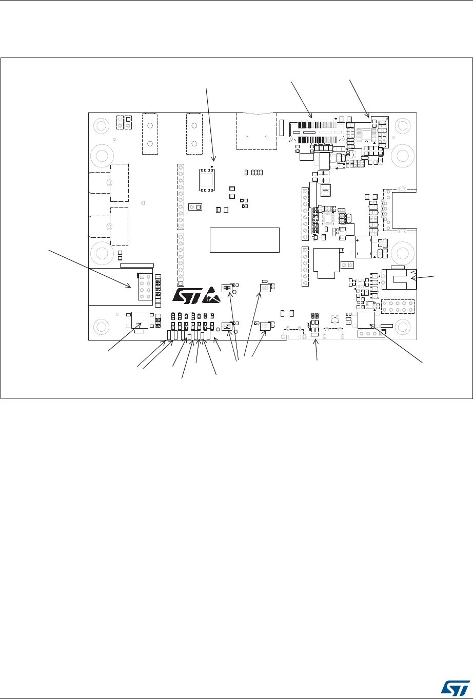
6.1 The 32F769IDISCOVERY Discovery board layout
Figure 5. 32F769IDISCOVERY top layout
H6
H8
H3
H1
B1
CN2
R70
R68
C54
SB9
SB8
R57
R52
SB6
R54
R56
R200
R50
SB5
LD2
LD1
R63
R62
LD4
LD3 R64
R65
LD5
LD6 R58
R66
U250
LD7
TP5
R59
C31
U8
U5
C23
TP104
C55
TP103
C44
C27
R71
C25
R17
R18
R19
U9
U6 R51
R20
R21
C56 C45
C52
C2
C81 SB3
SB4
R60
R61
R5
C12
R4
C9
C7
C6
C38
R2
R47
R36
R40
C33
R43
R44
R30
R32
R34
C75
C70 SB2
SB1
T1
C1
CN1
LD8
T3
C15
C14
C13
C4
U1
R45
R28
R27
C29
C28 L5
R67
SB10
C53
R6
C11
C16
C10
C8
R3
C5
C36
L2
C35
R1
U3
R31
C30
R29
D1
R10
R9
C49
C51
C48
C46
C47
C42
C41
R39
R41
R37
R35
R38
R12
C17
C19
C3
SB7
U4
C43
D4
R46
C37
R42
C32
C34
R26
R33
C89
C26
R13
R14
R15
U2
C50
U7
R11
C18
CN4
B2
D8 D7 D6 D5
C40
R49
C39
R16
H7
JP1
H5
R48
H4
H2
8
1
1
18
1924
2
10
4 3
16
9
2
7
1
82
5
4
8
50
60
59
3040
12
13
6
7
20
Rev.B
B.L
STM32F769I-DISCO
T.L
MB1225
MB1225B
CN5
B.R
uSD
T.R
DSI LCD
CN15
USB HS COM
ST_LINK
CN16
USB
A
GNDDIO CLK 3V3
reset
A
Ext 5V
Ethernet
CN10
CN3
Line In
www.st.com/stm32f7-discovery
Fault
CN6
PWR
OC
VBUS
SPDIF RX
CN12
CN8
SPDIF TX
Wifi or I2C ext
B
S
JP3
spk R
JP2
spk L
user
CN7
Line Out
usr1
usr2
usr3
WI-FI or Ext-EEP
daughterboard
connector
User pushbutton
User pushbutton
FourSTMEMS
microphoneson
DFSDM inputs
5 V external
connector
LCD display with
MIPI DSI connector
PoE converter around
PM8800A
User LEDs
512-Mbit Quad-SPI
Flash memory
(MACRONIX)
Arduino
LED Overcurrent
LED
USB HS
LED
Power
LED
Fault
power
LED
ST-LINK
COM LED
UM2033 Rev 3 11/56
UM2033 Hardware layout and configuration
55
Figure 6. 32F769IDISCOVERY bottom layout
CN12
CN8
R102
C87
JP3
R115
R116 C94
C95
R111
C120
TP20
TP106
TP108
C79
C73
C71
TP105
TP109
R100
R101
TP107
R78 C57
JP2
R114
U16
C91
C90
C92
C93
C119
C118
U11
C67
R117
C117
U15
R112
U14
C100
R87
C64
C65
C59
C82
R95
R94
C78
C74
R88
C63
TP8
TP7
TP6
R77
CN7
CN13 CN9
C58
SB15
JP4
SB13
SB14
R109
C96
SB12
SB11
U12
R86
C62
T5
C130
C127
R98
C85
R92
R93
TP18 CN6
R130
R132
R131 C125
U17
C114
C115
TP26
TP22 C72
U13
TP100
TP17
TP16 R90
R91
R89
TP13
R129
C136
C137
C138 C112
C113
C111
TP14
TP15
R83
TP12 CN5
C148
U21
TP28
C135
C124 C109
C108
C110 R82
TP9
C156
C153
R134
C147
C134
C133
C144
C123
C105
C106
C104
C107
R80
R81
TP11
CN15
C150
C149
L8
R142
R139
R136
R126
C145 X4
C131
TP27
C126
C128
C116
C101
C103
C102
R79
C68
C69
L7
D13
U20
L6 R110
TP101
R107
X2
C99
R108
R106
C97
C86
C83
C88
C80
C76
R76 R73
C154
R137
D12
R125
R133
R128
R123
R124 CN14 CN11 C98 C77C84
X1
TP21
TP102
R104
R99
R97
TP2
R8
C157
R147
R148
R149
R146
R143
C151
SB22
SB21
D11
R141
R138
R135
R127
C143
R122
R23
R103
C22
D3
R24
C24
R25
TP3
R7
L3
TP1
R145
U19
R121
C142
X3
C140
R118
C132
C20
C61
C60
C141
R119
R120
SB16
T4
T100
R85
C200
L4
C155
CN16
R144
JP5
D9
R74
R150
U22
C146
SB19
SB18
SB20
SB17
U10
SB23
R140
C152
C129
C139
U18
C122 R105
T2
C66
R84
D10
D2
R75
CN3
R113
C121
R22
C21
CN10
R96
8 5
2
16 9
58
2
1
8
10
9
5
1
A
16
17
8
9
6
1
8
1
3637
48
4
4
24
25
12
13
34
8
A
15
R
R
A
1
9
1
A
24
25
32
9
A1
H
118
10
8
5
4
91
SPDIF RX
SPDIF TX
Wifi or I2C ext
spk R
CN2
spk L
B
B
Line Out
AVDD
D0
D2
D1
D4
D3
D6
D5
D7
D9
D8
D11
D10
D13
D12
GND
D14
D15
Idd
Line In
uSD
USB HS
A5
A3
A4
A1
A2
A0
GND
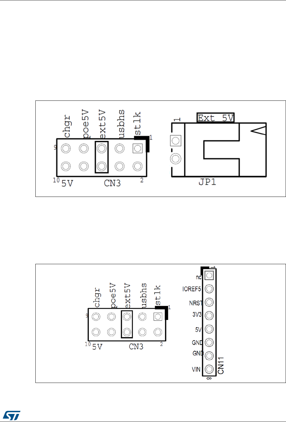
VIN
5V
GND
NRST
3V3
IOREF5
nc
VCP_TX
USB ST_LINK
VCP_RX
usbhs
stlk
Ethernet
poe5V
ext5V
Ext 5V
5V
chgr
JP1
SPDIF
RCAoutput
connector
SPDIFRCA
input
connector
USBOTGHSwith
Micro-ABconnector
STLINK/V2-1with
Micro-Bconnector
PowerSupply
selector
RJ45
Ethernet
connector
microSDcard
connector
Inputaudio
linejack
Outputaudio
linejack
Stereo
speaker
outputs
Arduinoconnectors
STM32F769NIH6MCU
Audio
codec
WM8994
128-MbitSDRAM
(MICRON)
STM32F103CBT6
forST-LINK
Hardware layout and configuration UM2033
12/56 UM2033 Rev 3
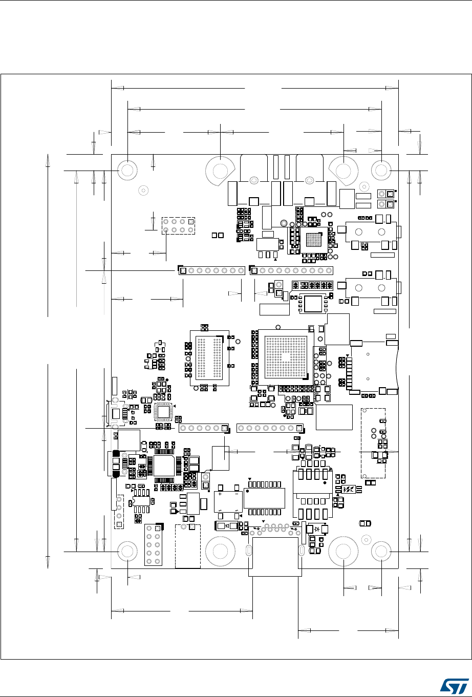
6.2 The 32F769IDISCOVERY Discovery board mechanical
drawing
Figure 7. 32F769IDISCOVERY mechanical drawing
CN12
CN8
R102
C87
JP3
R115
R116 C94
C95
R111
C120
TP20
TP106
TP108
C79
C73
C71
TP105
TP109
R100
R101
TP107
R78 C57
JP2
R114
U16
C91
C90
C92
C93
C119
C118
U11
C67
R117
C117
U15
R112
U14
C100
R87
C64
C65
C59
C82
R95
R94
C78
C74
R88
C63
TP8
TP7
TP6
R77
CN7
CN13 CN9
C58
SB15
JP4
SB13
SB14
R109
C96
SB12
SB11
U12
R86
C62
T5
C130
C127
R98
C85
R92
R93
TP18 CN6
R130
R132
R131 C125
U17
C114
C115
TP26
TP22 C72
U13
TP100
TP17
TP16 R90
R91
R89
TP13
R129
C136
C137
C138 C112
C113
C111
TP14
TP15
R83
TP12
CN5
C148
U21
TP28
C135
C124 C109
C108
C110 R82
TP9
C156
C153
R134
C147
C134
C133
C144
C123
C105
C106
C104
C107
R80
R81
TP11
CN15
C150
C149
L8
R142
R139
R136
R126
C145 X4
C131
TP27
C126
C128
C116
C101
C103
C102
R79
C68
C69
L7
D13
U20
L6 R110
TP101
R107
X2
C99
R108
R106
C97
C86
C83
C88
C80
C76
R76 R73
C154
R137
D12
R125
R133
R128
R123
R124 CN14 CN11 C98 C77C84
X1
TP21
TP102
R104
R99
R97
TP2
R8
C157
R147
R148
R149
R146
R143
C151
SB22
SB21
D11
R141
R138
R135
R127
C143
R122
R23
R103
C22
D3
R24
C24
R25
TP3
R7
L3
TP1
R145
U19
R121
C142
X3
C140
R118
C132
C20
C61
C60
C141
R119
R120
SB16
T4
T100
R85
C200
L4
C155
CN16
R144
JP5
D9
R74
R150
U22
C146
SB19
SB18
SB20
SB17
U10
SB23
R140
C152
C129
C139
U18
C122 R105
T2
C66
R84
D10
D2
R75
CN3
R113
C121
R22
C21
CN10
R96
4
8
8 5
2
16 9
58
2
1
8
10
9
5
1
A
16
17
8
9
6
1
8
1
36
37
48
4
4
24
25
12
13
3
A
15
R
R
A
1
9
1
A
2425
32
9
A1
H
118
10
8
5
4
91
SPDIF RX
SPDIF TX
Wifi or I2C ext
spk R
CN2
spk L
B
B
Line Out
AVDD
D0
D2
D1
D4
D3
D6
D5
D7
D9
D8
D11
D10
D13
D12
GND
D14
D15
Idd
Line In
uSD
USB HS
A5
A3
A4
A1
A2
A0
GND
VIN
5V
GND
NRST
3V3
IOREF5
nc
VCP_TX
USB ST_LINK
VCP_RX
usbhs
stlk
Ethernet
poe5V
ext5V
Ext 5V
5V
chgr
JP1
88mm
28.49mm
77.8mm
5.2mm
5mm
37.7mm
11.61mm
23.24mm
5mm
30.71mm
5mm
16.76mm 22.04mm
4.06mm
116.74mm
127mm
48.26mm
116.74mm
22.86mm
30.4mm
37.77mm
5.26mm
5mm
11.61mm
5.2mm
5.26mm
43.31mm
30.72mm
UM2033 Rev 3 13/56
UM2033 Hardware layout and configuration
55
6.3 Embedded ST-LINK/V2-1
The ST-LINK/V2-1 programming and debugging tool is integrated on the
32F769IDISCOVERY Discovery board. Compared to ST-LINK/V2 the changes are listed
below.
The new features supported on ST-LINK/V2-1 are:
•USB software re-enumeration
•Virtual COM port interface on USB
•Mass storage interface on USB
•USB power management request for more than 100mA power on USB
These features are no more supported on ST-LINK/V2-1:
•SWIM interface
•Application voltage lower than 3 V
For general information concerning the debugging and programming features that are
common to both versions V2 and V2-1, refer to ST-LINK/V2 in-circuit debugger/programmer
for STM8 and STM32 User manual (UM1075).
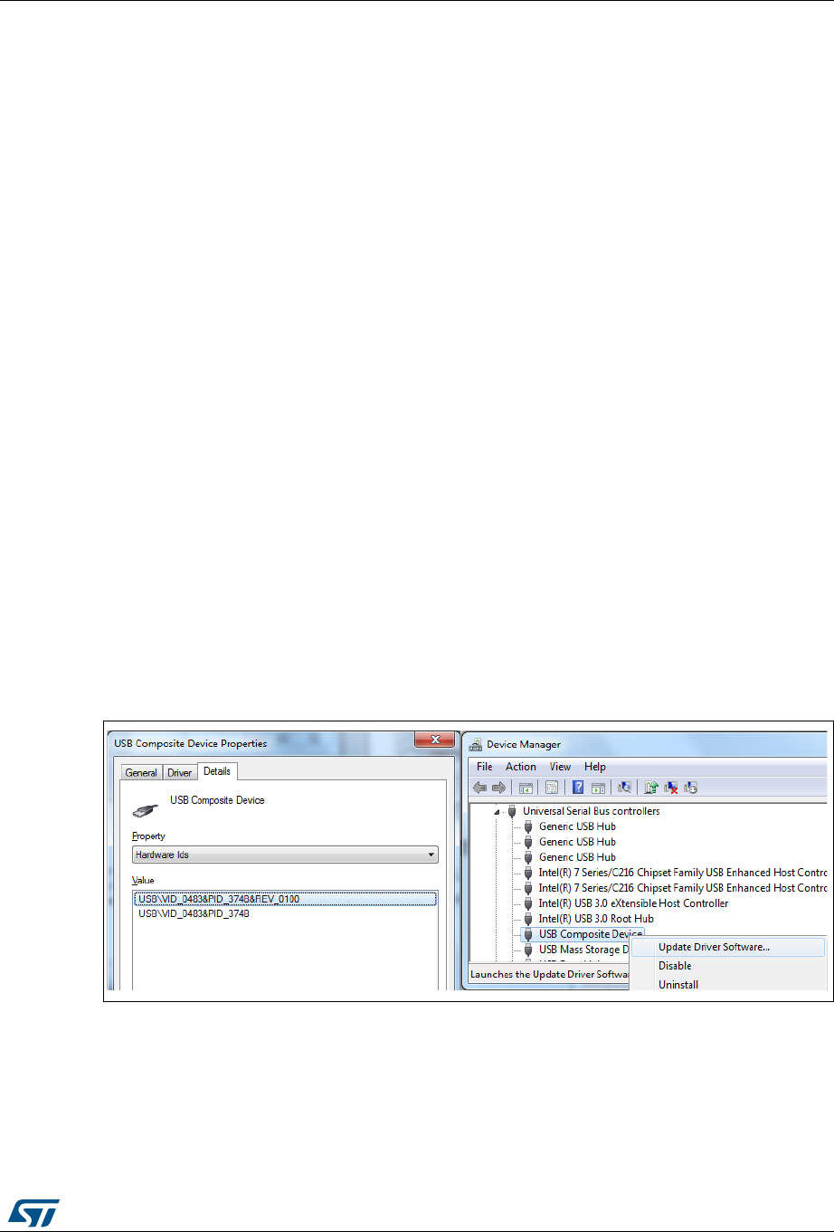
6.3.1 Drivers
The ST-LINK/V2-1 requires a dedicated USB driver, which, for Windows® XP, 7 and 8, is
available at the www.st.com website.
In case the 32F769IDISCOVERY Discovery board is connected to the PC before the driver
is installed, some 32F769IDISCOVERY interfaces may be declared as "unknown" in the PC
device manager. In this case the user must install the driver files and update the driver of the
connected device from the device manager.
Note: Prefer using the "USB Composite Device" handle for a full recovery.
Figure 8. USB composite device

Hardware layout and configuration UM2033
14/56 UM2033 Rev 3
6.3.2 ST-LINK/V2-1 firmware upgrade
The ST-LINK/V2-1 embeds a firmware upgrade mechanism for in-situ upgrade through the
USB port. As the firmware may evolve during the life time of the ST-LINK/V2-1 product (for
example new functionalities, bug fixes, support for new microcontroller families), it is
recommended to visit the www.st.com website before starting to use the
32F769IDISCOVERY Discovery board and periodically, to stay up-to-date with the latest
firmware version.
UM2033 Rev 3 15/56
UM2033 Hardware layout and configuration
55
6.4 Power supply
The 32F769IDISCOVERY Discovery board is designed to be powered by the 5 V DC power
supply. It is possible to configure the Discovery board to use any of the following five
sources for the power supply:
•5 V DC power adapter connected to JP1 (Ext 5 V). In this case, the
32F769IDISCOVERY Discovery board must be powered by a power supply unit or by
an auxiliary equipment complying with the standard EN-60950-1: 2006+A11/2009, and
must be Safety Extra Low Voltage (SELV) with limited power capability (5 V power
source on the silkscreen of JP1 (Ext 5 V). See Figure 9:
Figure 9. CN3 (ext5V) from JP1 (Ext 5 V)
•7-12 V DC power from CN11 pin named Vin on silkscreen, the extension connectors for
Arduino™ UNO shields or daughterboards (5 V power source on silkscreen of JP1 (Ext
5 V)). The input current capability is linked to the input voltage (see Figure 10):
– 800 mA input current when Vin=7 V
– 450 mA input current when 7 V<Vin (< or =) 9 V
– 250 mA input current when 9 V<Vin (< or =) 12 V
Figure 10. CN3 (ext5V) from CN11 (Vin)
Hardware layout and configuration UM2033
16/56 UM2033 Rev 3
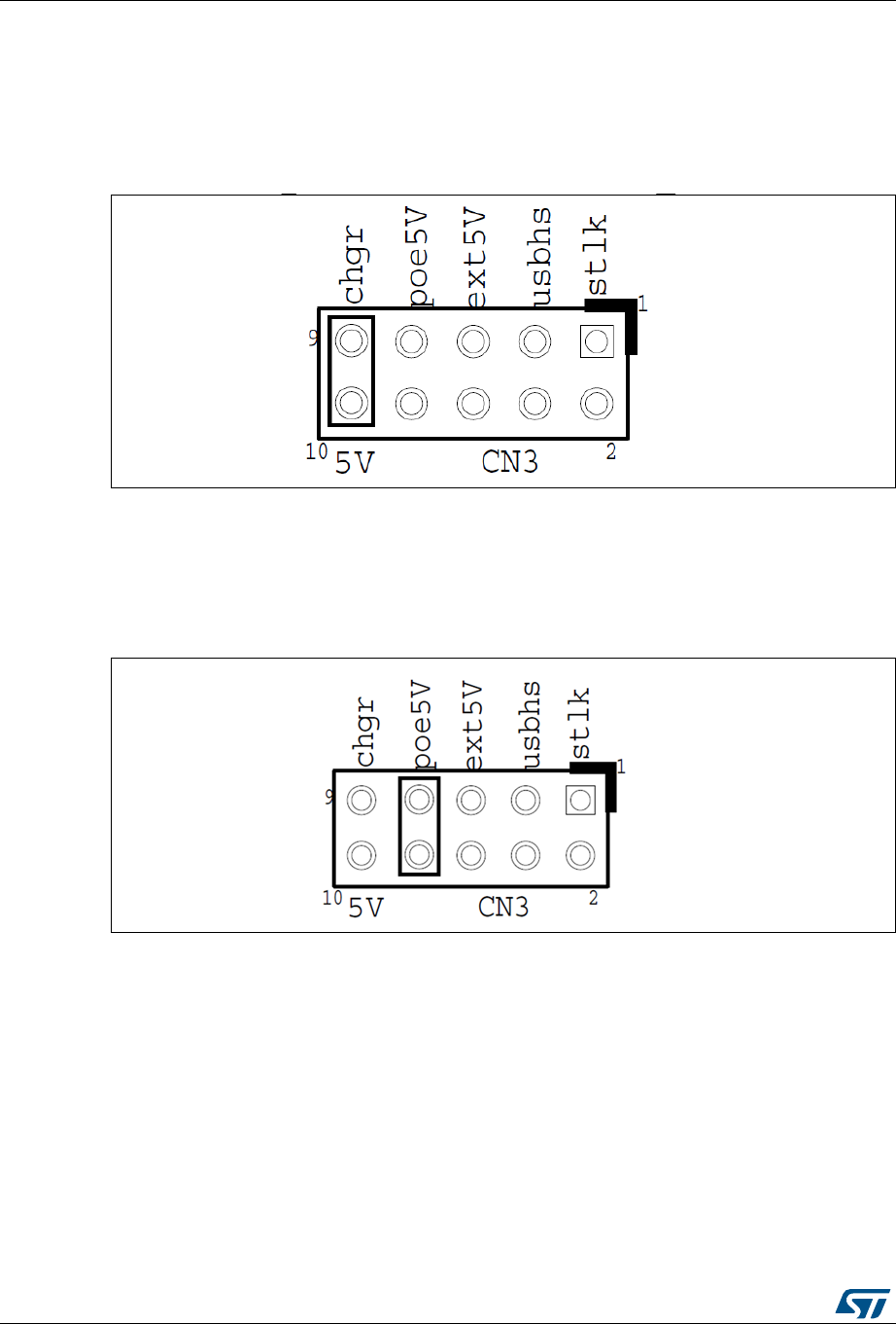
•5 V DC power charger connected to USB ST-LINK (CN16). In this case, if the
32F769IDISCOVERY Discovery board is powered by an external USB charger then
the debug features are not available. If the board is connected to the PC instead, the
limitation is no more effective with high risk to damage the PC (5 V power source on
silkscreen of CN3 (chgr). See Figure 11:
Figure 11. CN3 (chgr)
•48 V DC power from RJ45 connector CN10 (Ethernet). In this case, the on-board
module PoE (Power over Ethernet) generates the 5 V and it is able to provide up to
600 mA. This module is a Powered Device complying with the standard IEEE802.3af,
class 1 / 2. The external power supply must be fully IEEE 802.3af compliant (5 V power
source on silkscreen of CN3 (poe5V). See Figure 12:
Figure 12. CN3 (poe5V)
•5 V DC power with limitation from CN16, the USB type micro-B connector of
ST-LINK/V2-1 (USB 5 V power source on silkscreen of CN3 (stlk)). It is the default
setting. If the USB enumeration succeeds (as explained below), the ST-LINK 5 V link
power is enabled, by asserting the PWR_ENn signal. This pin is connected to a power
switch ST890, which powers the board. This power switch also features a current
limitation to protect the PC in case of a short-circuit on the board (more than 700 mA).
See Figure 13.
The 32F769IDISCOVERY Discovery board can be powered from the ST-LINK USB
connector CN16 (stlk), but only the ST-LINK circuit has the power before the USB
enumeration, because the host PC only provides 100 mA to the board at that time. During
the USB enumeration, the 32F769IDISCOVERY Discovery board asks for the 500 mA
power to the host PC. If the host is able to provide the required power, the enumeration
finishes by a "SetConfiguration" command and then, the power transistor ST890 is switched
UM2033 Rev 3 17/56
UM2033 Hardware layout and configuration
55
ON, the red LED LD6 is turned ON, thus the 32F769IDISCOVERY Discovery board can
consume maximum 500 mA current, but no more. If the host is not able to provide the
requested current, the enumeration fails. Therefore the ST890 remains OFF and the STM32
part including the extension board is not powered. As a consequence the red LED LD6
remains turned OFF. In this case it is mandatory to use an external power supply.
Figure 13. CN3 (stlk)
Note: In case the board is powered by a USB charger, there is no USB enumeration, so the led
LD2 remains set to OFF permanently and the board is not powered. Only in this specific
case, the resistor R138 needs to be soldered, to allow the board to be powered anyway.
The LED LD6 is lit when the 32F769IDISCOVERY Discovery board is powered by the 5 V
correctly.
Caution: Do not connect the PC to the ST-LINK (CN16) when R138 is soldered. The PC may be
damaged or the board not powered correctly.
•5 V DC power with 500 mA limitation from CN15, the USB OTG HS micro-AB
connector (5 V power source on silkscreen of CN3 (usbhs)). See Figure 14:
Figure 14. CN3 (usbhs)

Hardware layout and configuration UM2033
18/56 UM2033 Rev 3
6.5 Programming/debugging when the power supply is not from
ST-LINK (5 V link)
It is mandatory to power the board first using JP1 (Ext 5 V) or CN11 (Vin) or CN10
(Ethernet) or CN15 (usbhs), then connecting the USB cable to the PC. Proceeding this way
ensures that the enumeration succeeds thanks to the external power source.
The following power sequence procedure must be respected:
1. Connect the jumper CN3 on (ext5V) or (usbhs) or (poe5V)
2. Connect the external power source to JP1 or CN11 or CN10 or CN15
3. Check the red LED LD2 is turned ON
4. Connect the PC to USB connector CN16
If this order is not respected, the board may be powered first by VBUS from the ST-LINK,
and the following risks may be encountered:
1. If more than 500 mA current is needed by the board, the PC may be damaged or
current can be limited by the PC. As a consequence the board is not powered correctly.
2. 500 mA is requested at the enumeration: in this case there is a risk that the request is
rejected and the enumeration does not succeed if the PC cannot provide such current.
6.6 Clock sources
Up to three clock sources are available, as described below:
•X1, 24MHz oscillator for USB OTG HS PHY
•X2, 25MHz oscillator for the STM32F769NIH6 microcontroller and Ethernet PHY
•X3, 32KHz crystal for the STM32F769NIH6 embedded RTC
6.7 Reset sources
The reset signal of the 32F769IDISCOVERY Discovery board is active low and the reset
sources are:
•Reset button B2
•Arduino™ Uno shield board from CN11
•Embedded ST-LINK/V2-1
6.8 Audio
An audio codec WM8994ECS/R from CIRRUS with 4 DACs and 2 ADCs is connected to the
SAI interface of the STM32F769NIH6. It communicates with the STM32F769NIH6 via I2C
bus shared with the touch panel of the LCD DSI:
•The analog line input is connected to ADC of WM8994ECS/R through
the audio jack CN6.
•The analog line output is connected to DAC of WM8994ECS/R
via the audio jack CN7.
•Two external speakers can be connected to WM8994ECS/R via
the JP2 for the left speaker and JP3 for the right speaker.

UM2033 Rev 3 19/56
UM2033 Hardware layout and configuration
55
•Four digital microphones (ST MEMS microphone) MP34DT01TR are available on the
32F769IDISCOVERY Discovery board. They are connected to the input digital
microphones of the STM32F769NIH6 and are managed by the DFSDM functionality.
•One coaxial connector CN12 is implemented on the 32F769IDISCOVERY to receive
an external audio data compatible with SPDIF specification.
•One coaxial connector CN8 is implemented on the 32F769IDISCOVERY to output
external audio data compatible with SPDIF specification.
6.9 USB OTG HS
32F769IDISCOVERY Discovery board supports USB OTG high-speed communication via a
USB micro-AB connector and a USB high-speed PHY USB3320C-EZK from MICROCHIP
for high-speed function.
The Discovery board can be powered by the USB connectors at 5 V DC with 500 mA
current limitation.
A USB power switch is also connected on VBUS and provides power to CN15. The green
LED LD5 is lit in one of these cases:
•Power switch is ON and 32F769IDISCOVERY works as a USB host
•VBUS is powered by another USB host when 32F769IDISCOVERY works as a USB
device
The red LED LD4 is lit when an overcurrent occurs.
Note: 32F769IDISCOVERY Discovery board should be powered by an external power supply
when using OTG function.
6.10 microSD™ card
The 2-Gbyte (or more) microSD™ card connected to SDMMC2 port of STM32F769NIH6 is
supported by the board.
6.11 Ethernet
The 32F769IDISCOVERY Discovery board supports 10/100-Mbit Ethernet communication
by a PHY LAN8742A-CZ-TR from MICROCHIP and integrated a RJ45 connector. Ethernet
PHY is connected to the STM32F769NIH6 via an RMII interface.
The oscillator X2 generates a 25 MHz clock for the PHY, the PHY RMII_REF_CLK
generates the 50 MHz clock for the STM32F769NIH6.
6.12 Power over Ethernet
The 32F769IDISCOVERY Discovery board integrates a power module that uses Ethernet.
This module is an IEEE802.3af compliant, class 1 / 2 PoE converter based on the simple
diode rectified Flyback topology around the PM8800A component from ST. This module
''Powered Device'' accepts input voltage of 48 V and is able to provide 5 V with 600 mA.
Hardware layout and configuration UM2033
20/56 UM2033 Rev 3
6.13 SDRAM memory
A 128-Mbit SDRAM (MT48LC4M32B2B5-6A from MICRON) is connected to the FMC
interface of the STM32F769NIH6. This memory is used as 4M x 32bits.
6.14 Quad-SPI NOR Flash memory
A 512-Mbit Quad-SPI NOR Flash memory (MX25L51245GZ2I-08G from MACRONIX) is
connected to the Quad-SPI interface of the STM32F769NIH6.
6.15 Virtual COM port
The serial interface USART1 is directly available as a virtual COM port of the PC, connected
to the ST-LINK/V2-1 USB connector CN1. The virtual COM port settings are configured as:
115200 b/s, 8 bits data, no parity, 1 stop bit, no flow control.
6.16 Buttons and LEDs
The black button B2 located top side is the reset of the microcontroller STM32F769NIH6.
The blue button B1 located top side is available to be used as a digital input or as a wakeup-
alternate function. When the button is depressed the logic state is 1, otherwise the logic
state is 0. Four LEDs located top side are available for the user. From left to right the LEDs
are LD1, LD2, LD3, and LD4 with colors green, orange, red and blue respectively (refer to
the Figure 5: 32F769IDISCOVERY top layout). To light a LED a low-logic state 0 should be
written in the corresponding GPIO register. Table 3 shows the assignment of the control
ports to the LED indicators.
Table 3. Control port assignment
Reference Color Name Comment
B1 BLUE USER Alternate function Wake-up
B2 BLACK RESET -
LD1 RED USER1 PJ13
LD2 GREEN USER2 PJ5
LD3 GREEN Arduino PA12
LD4 RED OTG overcurrent PD4
LD5 GREEN VBUS USB HS -
LD6 RED 5 V Power -
LD7 RED Fault Power Current upper than 625 mA
LD8 RED/GREEN STLINK COM Green when communication
UM2033 Rev 3 21/56
UM2033 Hardware layout and configuration
55
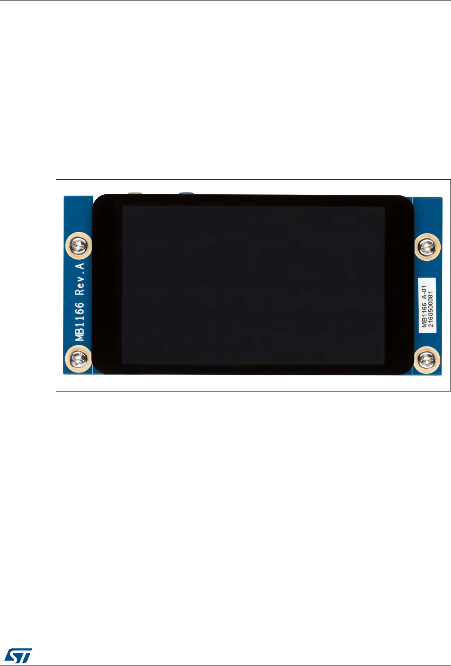
6.17 LCD display MIPI DSI (with STM32F769I-DISCO only)
The color display on the board MB1166, 4-inch 800x472 LCD-TFT with capacitive touch
panel is connected to the MIPI DSI interface of the STM32F769NIH6 (for technical
information on the board refer to the Section Appendix B: Schematics). The DSI (Display
Serial Interface) is a specification of the MIPI Alliance standard and defines the physical
interface and the protocol used by the STM32F769NIH6 microcontroller to communicate
with such LCD module (see Figure 15). This module is an optional accessory for the
STM32F769I-DISC1 board and has to be ordered separately, while for the STM32F769I-
DISCO board it is provided in the board package.
For more information on the LCD display refer to “4" WVGA TFT LCD board with MIPI® DSI
interface and capacitive touch screen” User manual (UM2104).
Figure 15. 4-inch WVGA TFT DSI LCD daughterboard
1. Picture is not contractual.
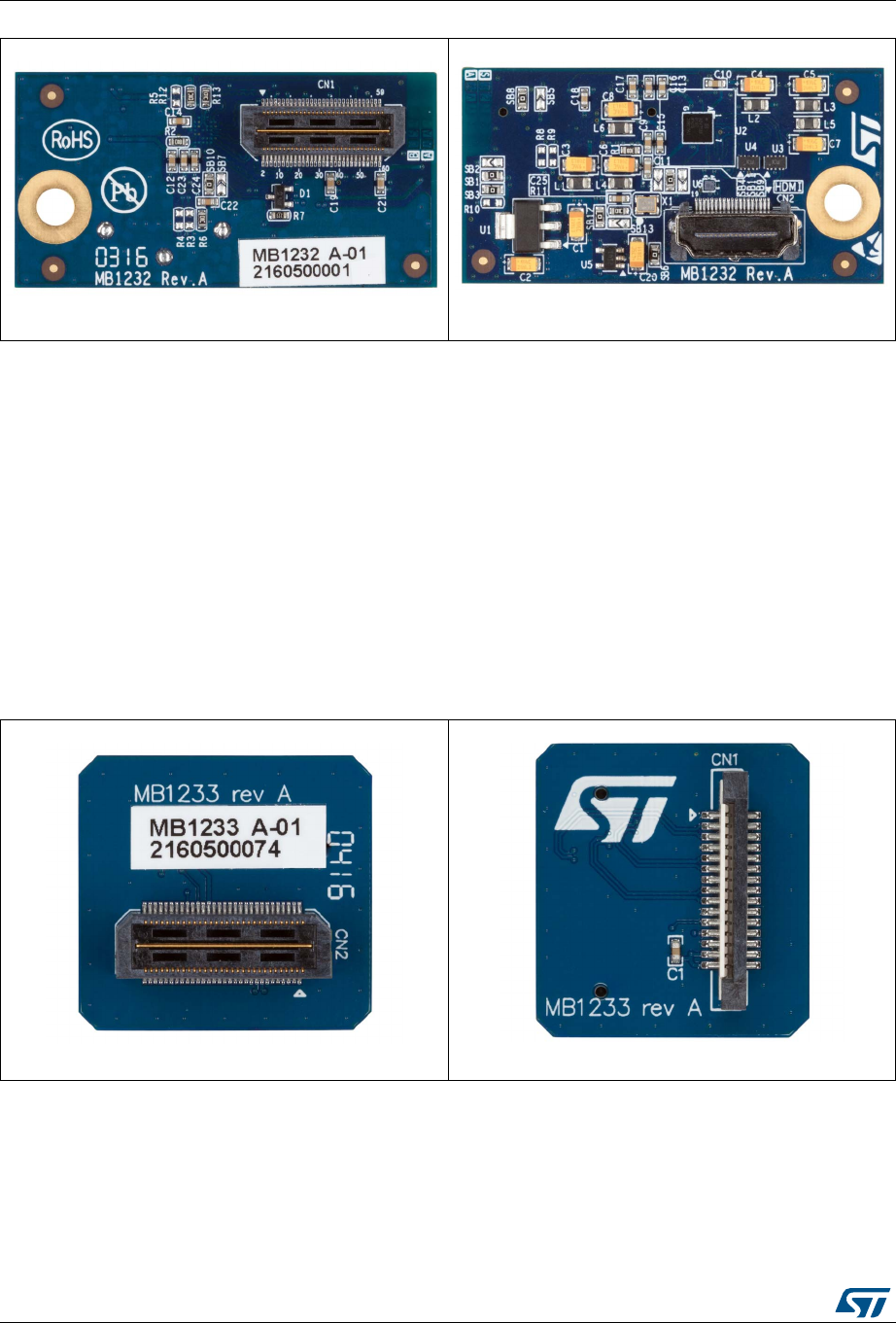
6.18 Adapter board from on-board DSI to HDMI
(optional accessory display)
The DSI to HDMI adapter board provides DSI input port and HDMI output port. It is used on
the 32F769IDISCOVERY Discovery board, to demonstrate video solutions based on STM32
(for technical information on this adapter board refer to the Section Appendix B:
Schematics).
It supports 2-, 3- or 4-lane DSI video as input data, S/PDIF, 2-channel I2S audio as input
data and HDMI v1.3 output port (see Figure 16 and Figure 17). For more information refer to
“DSI to HDMI adapter board for STM32 Development Tools” User manual (UM2048).
Hardware layout and configuration UM2033
22/56 UM2033 Rev 3
1. Pictures are not contractual.
6.19 Adapter board from on-board DSI to external DSI
(optional accessory display)
This adapter board allows the user to connect an external LCD with DSI format. This
adapter board is connected to the high-speed connector (Samtec high-speed connector
QTH-030) from the 32F769IDISCOVERY Discovery board to the standard DSI display
connector (TE 1-1734248). For technical information on the board refer to the
Section Appendix B: Schematics.
This DSI adapter board features up to two lanes of MIPI/DSI data and I2C interface support,
and enables the use of extended displays with the standard DSI interface on STM32
evaluation and Discovery board families (see Figure 18 and Figure 19).
1. Pictures are not contractual.
Figure 16. DSI to HDMI adapter board
Bottom view
Figure 17. DSI to HDMI adapter board
Top view
Figure 18. On-board DSI to external DSI
Bottom view
Figure 19. On-board DSI to external DSI
Top view
UM2033 Rev 3 23/56
UM2033 Hardware layout and configuration
55
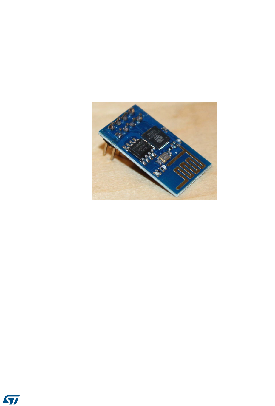
6.20 Wi-Fi® and extension I2C connector
The connector CN2 is able to support the Wi-Fi® module or extension I2C board.
6.20.1 Serial Wi-Fi® module
This module is 802.11 b/g/n compliant and is driven through a serial communication using
only RX and TX of a UART interface (see Figure 20).
This low-cost module is not an STMicroelectronics accessory. Its order code is ESP8266-
01.
Figure 20. Wi-Fi® module (ESP8266-01)
6.20.2 Extension I2C board
User can design a board according to the pin-out provided in Section 7: Connectors and to
the schematic Figure 39: microSD™, Wi-Fi®, LEDs and push-button.
Each signal used for this I2C is GPIOs, the I2C protocol must be managed by software.
Connectors UM2033
24/56 UM2033 Rev 3
7 Connectors
7.1 Wi-Fi® and I2C extension connector CN2
Figure 21. Wi-Fi® and I2C extension connector CN2 (front view)
Figure 22. Wi-Fi® and I2C extension connector CN2 (front view)
1. For more details refer to Figure 39: microSD™, Wi-Fi®, LEDs and push-button.
Table 4. Wi-Fi® and I2C extension connector CN2
Pin number Wi-Fi® description Pin number I2C description
1 WIFI_RX 1 GND
23V32 NC
3 GPIO0 3 3V3
4 WIFI-RST 4 NC
5 GPIO2 5 EXT_SCL
6 CH_PD 6 EXT_RST
7 GND 7 EXT_SDA
8WIFI_TX8 NC
!
LL
!!
!
!
! !
UM2033 Rev 3 25/56
UM2033 Connectors
55
7.2 Arduino™ Uno V3 connectors
Table 5. Arduino™ connectors (CN11, CN14, CN13 and CN9)
Left connectors - Right connectors
CN No. Pin
No.
Pin
name
STM32
Pin Function - Function STM32
Pin
Pin
name Pin
No.
CN
No.
-
-
I2C1_SCL PB8 D15 10
CN9
digital
I2C1_SDA PB9 D14 9
AVDD - AREF 8
Ground - GND 7
CN11
power
1 NC - - SPI2_SCK PA12 D13 6
2 IOREF - 3.3 V Ref SPI2_MISO PB14 D12 5
3 RESET NRST RESET TIM12_CH2,
SPI2_MOSI PB15 D11 4
4+3V3- 3.3 V
input/output
TIM1_CH4,
SPI2_NSS PA11 D10 3
5 +5 V - 5 V output TIM12_CH1 PH6 D9 2
6 GND - Ground - PJ4 D8 1
7 GND - Ground -
8 VIN - Power input - PJ3 D7 8
CN13
digital
- TIM11_CH1 PF7 D6 7
CN14
analog
1 A0 PA6 ADC1_IN6 TIM3_CH3 PC8 D5 6
2 A1 PA4 ADC1_IN4 - PJ0 D4 5
3A2PC2
ADC1_IN1
2TIM10_CH1 PF6 D3 4
4 A3 PF10 ADC3_IN8 - PJ1 D2 3
5A4
PF8 or
PB(1)
ADC3_IN6
(PF8) or
I2C1_SDA
(PB9)
USART6_TX PC6 D1 2
6A5
PF9 or
PB8(1)
ADC3_IN7
(PF9) or
I2C1_SCL
(PB8)
USART6_RX PC7 D0 1
1. For details refer to the Table 13: 32F769IDISCOVERY I/O assignment.
Connectors UM2033
26/56 UM2033 Rev 3
7.3 USB OTG HS micro-AB connector CN15
Figure 23. USB OTG micro-AB connector CN15 (front view)
7.4 Ethernet RJ45 connector CN10
Figure 24. Ethernet RJ45 connector CN10 (front view)
Table 6. USB OTG HS micro-AB CN15
Pin number Description Pin number Description
1 VBUS 4 ID
2D- 5GND
3D+ --
Table 7. Ethernet RJ45 connector CN10
Pin number Description Pin number Description
1TX+ 7 -
2TX- 8 -
3 RX+ 9 K, yellow LED
4 - 10 A, yellow LED
5 - 11 K, green LED
6 RX- 12 A, green LED
UM2033 Rev 3 27/56
UM2033 Connectors
55
7.5 LCD display MIPI DSI connector CN1
Figure 25. LCD display MIPI DSI connector CN1 (front view)
Table 8. LCD display MIPI DSI connector CN1
Pin No. Description Pin connection Pin No. Description Pin connection
1GND - 2 - -
3 DSI_CK_P H12 4 LCD_INT PI13
5 DSI_CK_N H13 6 GND -
7 GND - 8 DSI_D2_P/GND -
9 DSI_D0_P J12 10 DSI_D2_N/GND -
11 DSI_D0_N J13 12 GND -
13 GND - 14 DSI_D3_P/GND -
15 DSI_D1_P F12 16 DSI_D3_N/GND -
17 DSI_D1_N F13 18 GND -
19 GND - 20 - -
21 BLVDD(5 V) - 22 - -
23 BLVDD(5 V) - 24 - -
25 - - 26 - -
27 BLGND - 28 - -
29 BLGND - 30 - -
31 - - 32 - -
33 - - 34 - -
35 SCLK/MCLK nc 36 3.3V -
37 LRCLK nc 38 - -
39 SPDIF_I2S PD11 40 I2C1_SDA PB7
41 - - 42 - -
43 - - 44 I2C1_SCL PD12
Connectors UM2033
28/56 UM2033 Rev 3
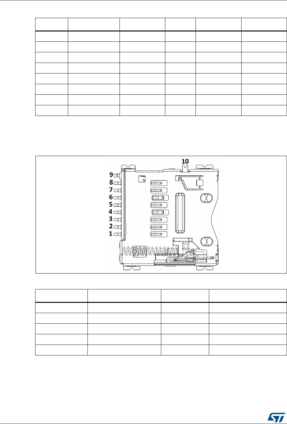
7.6 microSD™ connector CN5
Figure 26. microSD™ connector CN5 (front view)
7.7 ST-LINK/V2-1 USB micro-B connector CN16
The USB connector CN16 is used to connect the embedded ST-LINK/V2-1 to a PC for
programming and debugging purposes.
45 CEC_CLK - 46 - -
47 CEC - 48 - -
49 DSI_TE PJ2 50 - -
51 - - 52 - -
53 BL_CTRL PI14 54 - -
55 - - 56 - -
57 DSI_RESET PJ15 58 - -
59 - - 60 1V8 -
Table 8. LCD display MIPI DSI connector CN1 (continued)
Pin No. Description Pin connection Pin No. Description Pin connection
Table 9. microSD™ connector CN5
Pin number Description Pin number Description
1 SDMMC2_D2 6 Vss/GND
2 SDMMC2_D3 7 SDMMC2_D0
3 SDMMC2_CMD (PD2) 8 SDMMC2_D1
4 +3.3V 9 GND
5 SDMMC2_CK (PC12) 10 microSD™ card_detect
UM2033 Rev 3 29/56
UM2033 Connectors
55
Figure 27. USB micro-B connector CN16 (front view)
7.8 Audio stereo speakers JP2 and JP3
The stereo audio outputs JP2 and JP3 are available to support the stereo speakers (left and
right respectively).
7.9 Audio line output connector jack CN7
A 3.5-mm stereo audio jack output CN10 is available to support the headphone.
7.10 Audio line input connector jack CN6
A 3.5-mm stereo audio jack input CN6 is available to support the audio line input.
7.11 SPDIF input RCA connector CN12
Table 10. USB micro-B connector CN16
Pin number Description Pin number Description
1 VBUS (power) 4 GND
2 DM 5, 6 Shield
3DP- -
Table 11. SPDIF input RCA connector CN12
Pin number Description Pin number Description
1 SPDIF_RX 2 GND
2GND- -
Connectors UM2033
30/56 UM2033 Rev 3
7.12 SPDIF output RCA connector CN8
Table 12. SPDIF output RCA connector CN8
Pin number Description Pin number Description
1SPDIF_TX2 GND
2GND- -
UM2033 Rev 3 31/56
UM2033 32F769IDISCOVERY I/O assignment
55
Appendix A 32F769IDISCOVERY I/O assignment
Table 13. 32F769IDISCOVERY I/O assignment
Pin No. Pin name Signal or label Comment
A1 PE4 SAI1_FS_A -
A2 PE3 SAI1_SD_B -
A3 PE2 QUADSPI_BK1_IO2 -
A4 PG14 ETH_TXD1 -
A5 PE1 FMC_NBL1 -
A6 PE0 FMC_NBL0 -
A7 PB8 I2C1_SCL ARD_D15/SCL
A8 PB5 USB_OTG_HS_ULPI_D7 -
A9 PB4 SDMMC2_D3 -
A10 PB3 SDMMC2_D2 -
A11 PD7 SDMMC2_CMD -
A12 PC12 UART5_TX WIFI_RX
A13 PA15 CEC CEC
A14 PA14 SYS_JTCK-SWCLK SWCLK
A15 PA13 SYS_JTMS-SWDIO SWDIO
B1 PE5 SAI1_SCK_A -
B2 PE6 SAI1_SD_A -
B3 PG13 ETH_TXD0 -
B4 PB9 I2C1_SDA ARD_D14/SDA
B5 PB7 I2C4_SDA -
B6 PB6 QUADSPI_BK1_NCS -
B7 PG15 FMC_SDNCAS -
B8 PG11 ETH_TX_EN -
B9 PJ13 GPIO_Input LD_USER1
B10 PJ12 GPIO_Input Audio_INT
B11 PD6 SDMMC2_CK -
B12 PD0 FMC_D2 -
B13 PC11 DFSDM_DATIN5 -
B14 PC10 QUADSPI_BK1_IO1 -
B15 PA12 SPI2_SCK ARD_D13/SCK
C1 VBAT - -
C2 PI8 GPIO_Input NC4
32F769IDISCOVERY I/O assignment UM2033
32/56 UM2033 Rev 3
C3 PI4 FMC_NBL2 -
C4 PK7 GPIO_Input NC3
C5 PK6 GPIO_Input NC2
C6 PK5 GPIO_Input NC1
C7 PG12 SPDIFRX_IN1 -
C8 PG10 SDMMC2_D1 -
C9 PJ14 GPIO_Input WIFI_RST
C10 PD5 GPIO_Input RMII_RXER
C11 PD3 DFSDM_CKOUT -
C12 PD1 FMC_D3 -
C13 PI3 FMC_D27 -
C14 PI2 FMC_D26 -
C15 PA11 SPI2_NSS ARD_D10/PWM/CS
D1 PC13 RTC_OUT_ALARM NC6
D2 PF0 FMC_A0 -
D3 PI5 FMC_NBL3 -
D4 PI7 FMC_D29 -
D5 PI10 FMC_D31 -
D6 PI6 FMC_D28 -
D7 PK4 GPIO_Input NC8
D8 PK3 GPIO_Input NC7
D9 PG9 SDMMC2_D0 -
D10 PJ15 GPIO_Input DSI_RESET
D11 PD4 GPIO_Input OTG_HS_OverCurrent
D12 PD2 UART5_RX WIFI_TX
D13 PH15 FMC_D23 -
D14 PI1 FMC_D25 -
D15 PA10 USART1_RX VCP_RX
E1 PC14/OSC32_IN RCC_OSC32_IN -
E2 PF1 FMC_A1 -
E3 PI12 GPIO_Input NC5
E4 PI9 FMC_D30 -
E5 PDR_ON - -
E6 BOOT0 - -
E7 VDD - -
Table 13. 32F769IDISCOVERY I/O assignment (continued)
Pin No. Pin name Signal or label Comment
UM2033 Rev 3 33/56
UM2033 32F769IDISCOVERY I/O assignment
55
E8 VDD - -
E9 VDD - -
E10 VDD - -
E11 VCAP_2 - -
E12 PH13 FMC_D21 -
E13 PH14 FMC_D22 -
E14 PI0 FMC_D24 -
E15 PA9 USART1_TX VCP_TX
F1 PC15/OSC32_OUT RCC_OSC32_OUT -
F2 VSS - -
F3 PI11 USB_OTG_HS_ULPI_DIR -
F4 VDD - -
F5 VDD - -
F6 VSS - -
F7 VSS - -
F8 VSS - -
F9 VSS - -
F10 VSS - -
F11 VDD - -
F12 DSIHOST_D1P DSIHOST_D1P -
F13 DSIHOST_D1N DSIHOST_D1N -
F14 PC9 QUADSPI_BK1_IO0 -
F15 PA8 RCC_MCO_1 CEC_CLK
G1 PH0/OSC_IN RCC_OSC_IN -
G2 PF2 FMC_A2 -
G3 PI13 GPIO_Input LCD_INT
G4 PI15 GPIO_Input uSD_Detect
G5 VDD - -
G6 VSS - -
G10 VSS - -
G11 VDDUSB - -
G12 VSSDSI - -
G13 VDD - -
G14 PC8 TIM3_CH3 ARD_D5/PWM
G15 PC7 USART6_RX ARD_D0/RX
Table 13. 32F769IDISCOVERY I/O assignment (continued)
Pin No. Pin name Signal or label Comment

32F769IDISCOVERY I/O assignment UM2033
34/56 UM2033 Rev 3
H1 PH1/OSC_OUT RCC_OSC_OUT -
H2 PF3 FMC_A3 -
H3 PI14 GPIO_Input LCD_BL_CTRL
H4 PH4 USB_OTG_HS_ULPI_NXT -
H5 VDD - -
H6 VSS - -
H10 VSS - -
H11 VDDDSI - -
H12 DSIHOST_CKP DSIHOST_CKP -
H13 DSIHOST_CKN DSIHOST_CKN -
H14 PG8 FMC_SDCLK -
H15 PC6 USART6_TX ARD_D1/TX
J1 NRST - -
J2 PF4 FMC_A4 -
J3 PH5 FMC_SDNWE -
J4 PH3 FMC_SDNE0 -
J5 VDD - -
J6 VSS - -
J10 VSS - -
J11 VDD - -
J12 DSIHOST_D0P DSIHOST_D0P -
J13 DSIHOST_D0N DSIHOST_D0N -
J14 PG7 SAI1_MCLK_A -
J15 PG6 GPIO_Input EXT_SDA
K1 PF7 TIM11_CH1 ARD_D6/PWM
K2 PF6 TIM10_CH1 ARD_D3/PWM
K3 PF5 FMC_A5 -
K4 PH2 FMC_SDCKE0 -
K5 VDD - -
K6 VSS - -
K7 VSS - -
K8 VSS - -
K9 VSS - -
K10 VSS - -
K11 VDD - -
Table 13. 32F769IDISCOVERY I/O assignment (continued)
Pin No. Pin name Signal or label Comment

UM2033 Rev 3 35/56
UM2033 32F769IDISCOVERY I/O assignment
55
K12 VCAPDSI - -
K13 PD15 FMC_D1 -
K14 PB13 USB_OTG_HS_ULPI_D6 -
K15 PD10 FMC_D15 -
L1 PF10 ADC3_IN8 ARD_A3
L2 PF9 ADC3_IN7 ARD_A5
L3 PF8 ADC3_IN6 ARD_A4
L4 PC3 DFSDM_DATIN1 -
L5 BYPASS_REG - -
L6 VSS - -
L7 VDD - -
L8 VDD - -
L9 VDD - -
L10 VDD - -
L11 VCAP_1 - -
L12 PD14 FMC_D0 -
L13 PB12 USB_OTG_HS_ULPI_D5 -
L14 PD9 FMC_D14 -
L15 PD8 FMC_D13 -
M1 VSSA - -
M2 PC0 USB_OTG_HS_ULPI_STP -
M3 PC1 ETH_MDC -
M4 PC2 ADC1_IN12 ARD_A2
M5 PB2 QUADSPI_CLK -
M6 PF12 FMC_A6 -
M7 PG1 FMC_A11 -
M8 PF15 FMC_A9 -
M9 PJ4 GPIO_Input ARD_D8
M10 PD12 I2C4_SCL -
M11 PD13 QUADSPI_BK1_IO3 -
M12 PG3 GPIO_Input EXT_SCL
M13 PG2 FMC_A12 -
M14 PJ5 GPIO_Input LD_USER2
M15 PH12 FMC_D20 -
N1 VREF- - -
Table 13. 32F769IDISCOVERY I/O assignment (continued)
Pin No. Pin name Signal or label Comment

32F769IDISCOVERY I/O assignment UM2033
36/56 UM2033 Rev 3
N2 PA1 ETH_REF_CLK -
N3 PA0/WKUP SYS_WKUP0 B_USER
N4 PA4 ADC1_IN4 ARD_A1
N5 PC4 ETH_RXD0 -
N6 PF13 FMC_A7 -
N7 PG0 FMC_A10 -
N8 PJ3 GPIO_Input ARD_D7
N9 PE8 FMC_D5 -
N10 PD11 SAI2_SD_A -
N11 PG5 FMC_BA1 -
N12 PG4 FMC_BA0 -
N13 PH7 GPIO_Input EXT_RST
N14 PH9 FMC_D17 -
N15 PH11 FMC_D19 -
P1 VREF+ - -
P2 PA2 ETH_MDIO -
P3 PA6 ADC1_IN6 ARD_A0
P4 PA5 USB_OTG_HS_ULPI_CK -
P5 PC5 ETH_RXD1 -
P6 PF14 FMC_A8 -
P7 PJ2 DSIHOST_TE DSIHOST_TE
P8 PF11 FMC_SDNRAS -
P9 PE9 FMC_D6 -
P10 PE11 FMC_D8 -
P11 PE14 FMC_D11 -
P12 PB10 USB_OTG_HS_ULPI_D3 -
P13 PH6 TIM12_CH1 ARD_D9/PWM
P14 PH8 FMC_D16 -
P15 PH10 FMC_D18 -
R1 VDDA - -
R2 PA3 USB_OTG_HS_ULPI_D0 -
R3 PA7 ETH_CRS_DV -
R4 PB1 USB_OTG_HS_ULPI_D2 -
R5 PB0 USB_OTG_HS_ULPI_D1 -
R6 PJ0 GPIO_Input ARD_D4
Table 13. 32F769IDISCOVERY I/O assignment (continued)
Pin No. Pin name Signal or label Comment

UM2033 Rev 3 37/56
UM2033 32F769IDISCOVERY I/O assignment
55
R7 PJ1 GPIO_Input ARD_D2
R8 PE7 FMC_D4 -
R9 PE10 FMC_D7 -
R10 PE12 FMC_D9 -
R11 PE15 FMC_D12 -
R12 PE13 FMC_D10 -
R13 PB11 USB_OTG_HS_ULPI_D4 -
R14 PB14 SPI2_MISO ARD_D12/MISO
R15 PB15 SPI2_MOSI ARD_D11/PWM/MOSI
Table 13. 32F769IDISCOVERY I/O assignment (continued)
Pin No. Pin name Signal or label Comment

Schematics UM2033
38/56 UM2033 Rev 3
Appendix B Schematics
This section provides design schematics for the 32F769IDISCOVERY Discovery board
features and optional accessories:
•MB1225 (32F769IDISCOVERY Discovery board)
– 32F769IDISCOVERY Discovery Interconnexion (Figure 28)
– ST-LINK/V2-1 with support of SWD only (Figure 29)
– STM32F769NIH6 connexions (Figure 30)
– Audio Codec WOLFSON and Audio connectors (Figure 31)
– SDRAM (MICRON) (Figure 32)
– Quad-SPI Flash memory (MACRONIX) (Figure 33)
– Arduino™ UNO connectors (Figure 34)
– USB OTG HS PHY with micro A-B connector (Figure 35)
– Ethernet PHY with RJ45 connector (Figure 36)
– Power Over Ethernet 3W (Figure 37)
– MIPI connector for DSI LCD and HDMI boards (Figure 38)
– microSD™, Wi-Fi®, LEDs and push-button (Figure 39)
•MB1166 (4-inch DSI LCD board)
– 4-inch DSI LCD board (Figure 40)
•MB1232 (DSI to HDMI adapter)
– DSI to HDMI adapter (Figure 41)
•MB1233 (DSI connector adapter)
– DSI connector adapter (Figure 42)
UM2033 Schematics
UM2033 Rev 3 39/56
Figure 28. 32F769IDISCOVERY Discovery board interconnections
112
STM32F769 Discovery Interconnexion
MB1225 B-01
3/11/2016
Title:
Size: Reference:
Date: Sheet: of
A4 Revision:
STM32F769I-DISCO
Project:
SWDIO
SWCLK
NRST
Rev B-01 --> MB1225 B-01, VDD_VREGDSI of U13 is connected to VDD
instead of DSI_VDD12, EXT I2C for CN2 is built by GPIOs.
Add DFSDM_CKOUT/DATAIN1/DATAIN5, Remove L1
Rev A-01 --> MB1225 A-01
VCP_TX
VCP_RX
SWDIO
SWCLK
NRST
VCP_RX
VCP_TX
SWO
U_ST_LINK_V2-1
ST_LINK_V2-1.SCHDOC
AUDIO_SDA
AUDIO_SCL
SAI1_MCLKA
SPDIF_RX
SAI1_SCKA
SAI1_FSA
SAI1_SDA
SAI1_SDB
Audio_INT
SPDIF_TX
DFSDM_CKOUT
DFSDM_DATIN1
DFSDM_DATIN5
U_AUDIO
AUDIO.SchDoc
NRST
EXT_RST
EXT_SCL
EXT_SDA
uSD_CLK
uSD_CMD
uSD_D0
uSD_D1
uSD_D2
uSD_D3
uSD_Detect
B_USER
WIFI_TX
WIFI_RX
WIFI_RST
LD_USER1
LD_USER2
U_Peripherals
Peripherals.SchDoc
NRST
EXT_RST
QSPI_D0
QSPI_D3
QSPI_D1
QSPI_CLK
QSPI_NCS
QSPI_D2
U_QSPI
QSPI.SchDoc
QSPI_D0
QSPI_D1
QSPI_D2
QSPI_D3
QSPI_NCS
QSPI_CLK
NRST
EXT_RST
QSPI_D0
QSPI_D1
QSPI_D2
QSPI_D3
QSPI_NCS
QSPI_CLK
VCP_TX
SWO
NRST
ARD_D[0..15]
ARD_A[0..5]
U_Arduino_ Connectors
Arduino_ Connectors.SchDoc
FMC_A[0..12]
FMC_SDNWE
FMC_SDNRAS
FMC_SDNCAS
FMC_SDCLK
FMC_BA0
FMC_BA1
FMC_NBL0
FMC_NBL1
FMC_SDNE0
FMC_SDCKE0
FMC_D[0..31]
FMC_NBL2
FMC_NBL3
U_SDRAM
SDRAM.SchDoc
ULPI_D[0..7]
ULPI_CK
ULPI_DIR
ULPI_NXT
ULPI_STP
NRST
OTG_HS_OverCurrent
U_USB_OTG_HS
USB_OTG_HS.SchDoc
PA[0..15]
PB[0..15]
PC[0..15]
PD[0..15]
PE[0..15]
PF[0..15]
PG[0..15]
PH[0..15]
PI[0..15]
PJ[0..15]
PK[0..7]
OSC_25M
RMII_TXD0
RMII_TX_EN
RMII_RXD0
RMII_REF_CLK
RMII_CRS_DV
RMII_MDC
RMII_MDIO
RMII_TXD1
RMII_RXD1
ULPI_D[0..7]
ULPI_CK
ULPI_DIR
ULPI_NXT
ULPI_STP
QSPI_D0
QSPI_D3
QSPI_D1
QSPI_CLK
QSPI_NCS
AUDIO_SDA
AUDIO_SCL
SAI1_MCLKA
EXT_SCL
EXT_SDA
EXT_RST
uSD_CLK
uSD_CMD
uSD_D0
uSD_D1
uSD_D2
uSD_D3
uSD_Detect
SWDIO
SWCLK
NRST
SWO
VCP_RX
VCP_TX
FMC_A[0..12]
FMC_D[0..31]
FMC_SDNWE
FMC_SDNRAS
FMC_SDNCAS
FMC_SDCLK
FMC_BA0
FMC_BA1
FMC_SDNE0
FMC_SDCKE0
FMC_NBL0
FMC_NBL1
SPDIF_RX
QSPI_D2
B_USER
ARD_D[0..15]
RMII_RXER
OTG_HS_OverCurrent
SAI1_SCKA
SAI1_FSA
SAI1_SDA
SAI1_SDB
Audio_INT
SPDIF_TX
FMC_NBL2
FMC_NBL3
DSI
LCD_BL_CTRL
SCLK_MCLK
LRCLK
SPDIF_I2S
CEC_CLK
CEC
LCD_INT
LCD_SDA
LCD_SCL
WIFI_RST
WIFI_RX
WIFI_TX
ARD_A[0..5]
LD_USER1
LD_USER2
DFSDM_CKOUT
DFSDM_DATIN1
DFSDM_DATIN5
U_STM32F7
STM32F7.SchDoc
RMII_TXD0
RMII_TX_EN
RMII_RXD0
RMII_REF_CLK
RMII_CRS_DV
RMII_MDC
RMII_MDIO
NRST
RMII_TXD1
RMII_RXD1
OSC_25M
RMII_RXER
U_Ethernet
Ethernet.SchDoc EXT_SDA
EXT_SCL
PA[0..15]
PB[0..15]
PC[0..15]
PD[0..15]
PE[0..15]
PF[0..15]
PG[0..15]
PH[0..15]
PI[0..15]
PJ[0..15]
PK[0..7]
ULPI_D[0..7]
ULPI_CK
SWCLK
SWDIO
SWO
VCP_RX
RMII_MDIO
ARD_D[0..15]
B_USER
ULPI_DIR
ULPI_STP
uSD_D0
uSD_D1
uSD_D2
uSD_D3
uSD_CLK
uSD_Detect
RMII_RXD0
RMII_RXD1
RMII_MDC
FMC_SDCKE0
RMII_CRS_DV
RMII_REF_CLK
uSD_CMD
FMC_NBL0
FMC_NBL1
FMC_D[0..31]
OTG_HS_OverCurrent
FMC_SDNRAS
RMII_TX_EN
RMII_TXD0
RMII_TXD1
FMC_BA0
FMC_BA1
FMC_SDCLK
FMC_SDNCAS
ULPI_NXT
FMC_SDNWE
FMC_SDNE0
FMC_A[0..12]
EXT_SDA
EXT_SCL
B_USER
uSD_D1
uSD_D2
uSD_D3
uSD_D0
uSD_CLK
uSD_Detect
uSD_CMD
OSC_25M
RMII_RXER
RMII_RXER
FMC_SDCKE0
FMC_NBL1
FMC_NBL0
FMC_D[0..31]
FMC_SDNRAS
FMC_BA1
FMC_BA0
FMC_SDCLK
FMC_SDNCAS
FMC_SDNWE
FMC_SDNE0
FMC_A[0..12]
ARD_A[0..5]
ARD_D[0..15]
OSC_25M
NRST
SPDIF_RX
SPDIF_TX
SAI1_SDB
AUDIO_SDA
AUDIO_SCL
Audio_INT
SAI1_MCLKA
SAI1_SCKA
SAI1_FSA
SAI1_SDA
ULPI_D[0..7]
ULPI_CK
ULPI_DIR
ULPI_STP
OTG_HS_OverCurrent
ULPI_NXT
NRST
RMII_MDIO
RMII_RXD0
RMII_RXD1
RMII_MDC
RMII_CRS_DV
RMII_REF_CLK
RMII_TX_EN
RMII_TXD0
RMII_TXD1
NRST
iSDRAM
Matched Net Lengths [Tolerance = 100mil]
iSDRAM
iSDRAM
iSDRAM
iSDRAM
iSDRAM
iSDRAM
iSDRAM
iQSPI
Matched Net Lengths [Tolerance = 100mil]
iQSPI
iQSPI
iQSPI
iQSPI
iQSPI
iUSB HS
iUSB HS
Matched Net Lengths [Tolerance = 100mil]
iUSB HS
iUSB HS
iUSB HS
iRMII
iRMII
Matched Net Lengths [Tolerance = 100mil]
iRMII
iRMII
iRMII
iRMII
iRMII
iRMII
iRMII
iCLOCK
DSI
LCD_INT
LCD_BL_CTRL
SCLK_MCLK
LRCLK
SPDIF_I2S
CEC_CLK
CEC
LCD_SDA
LCD_SCL
U_DSI_LCD
DSI_LCD.SCHDOC
WIFI_TX
WIFI_RX
WIFI_RST
FMC_NBL2
FMC_NBL3
DSI
LRCLK
SPDIF_I2S
LCD_BL_CTRL
LCD_INT
SCLK_MCLK
CEC_CLK
CEC
DSI
LCD_SCL
LCD_SDA
ARD_A[0..5]
SPDIF_RX
SPDIF_TX
SAI1_SDB
AUDIO_SDA
AUDIO_SCL
Audio_INT
SAI1_MCLKA
SAI1_SCKA
SAI1_FSA
SAI1_SDA
FMC_NBL2
FMC_NBL3
LRCLK
SPDIF_I2S
LCD_BL_CTRL
LCD_INT
SCLK_MCLK
CEC_CLK
CEC
LCD_SCL
LCD_SDA
WIFI_TX
WIFI_RX
WIFI_RST
LD_USER1
LD_USER2
LD_USER1
LD_USER2
H7 H6
H2 H1
DFSDM_CKOUT
DFSDM_DATIN1
DFSDM_DATIN5
DFSDM_CKOUT
DFSDM_DATIN1
DFSDM_DATIN5
Schematics UM2033
40/56 UM2033 Rev 3
Figure 29. ST-LINK/V2-1 with support of SWD only
212
ST-LINK/V2-1 with support of SWD only
MB1225 B-01
3/10/2016
Title:
Size: Reference:
Date: Sheet: of
A4 Revision:
STM32F769I-DISCO
Project:
STM_RST
T_JTCK
T_JTCK
T_JTMS
STM_JTMS
STM_JTCK
OSC_IN
OSC_OUT
T_NRST
AIN_1
3V3_ST_LINK
3V3_ST_LINK
USB_STLK_N
USB_STLK_P
USB ST-LINK
COM
ST-LINK Power
3V3_ST_LINK
Board Ident: PC13=0
T_JTCK
T_JTMS SWD
3V3_ST_LINK
1
2
3
4
CN4
STM_JTMSSTM_JTCK
SWCLK SWDIO
3V3_ST_LINK
T_SWDIO_IN
T_SWO
LED_STLINK
LED_STLINK
3V3_ST_LINK
Red
_Green
2 1
3 4
LD8
LD_BICOLOR_CMS
SWDIO
SWCLK
5V
NRST
T_NRST
51
2
GND
3
4
BYPASS
INH
Vin Vout
U4 LD3985M33R
VCP_RX
VCP_TX
STLINK_TX
STLINK_RX
LD6
LED, red
C151
100nF
C146
100nF
C140
100nF
C143
100nF C47
1uF
C41
1uF
C42
100nF
C46
100nF
C43
10nF
C132
100nF
3V3_ST_LINK
USB_RENUMn
PWR_EXT
PWR_ENn
3
1
2
T3
9013-SOT23
3V3_ST_LINK
USB_RENUMn
PA14
PA13
PWR_ENn
EN
1
GND
2
VO 4
NC 5
GND
7
VI
6PG 3
U7 LD39050PU33R
C48
1uF
C49
100nF
C51
1uF
C50
100nF
3V3_ST_LINK
5 Volts Output 3.3 Volts Output5 Volts Power Supply
3V3_ST_LINK
3V3_ST_LINK
VBAT
1
PA7
17
PC13
2
PA12 33
PC14
3
PB0
18
PC15
4JTMS/SWDIO 34
OSCIN
5
PB1
19
OSCOUT
6
VSS_2 35
NRST
7
PB2/BOOT1
20
VSSA
8
VDD_2 36
VDDA
9
PB10
21
PA0
10
JTCK/SWCLK 37
PA1
11
PB11
22
PA2
12
PA15/JTDI 38
PA3
13
VSS_1
23
PA4
14
PB3/JTDO 39
PA5
15
VDD_1
24
PA6
16
PB4/JNTRST 40
PB12 25
PB5 41
PB13 26
PB6 42
PB14 27
PB7 43
PB15 28
BOOT0 44
PA8 29
PB8 45
PA9 30
PB9 46
PA10 31
VSS_3 47
PA11 32
VDD_3 48
U19
STM32F103CBT6
5V
5V_USB_ST_LINK
5V_USB_ST_LINK
D11
BAT60JFILM
Not Fitted
IN
1
IN
2
ON
3GND 4
SET 5
OUT 6
OUT 7
FAULT
8
U22
ST890CDR
R150
100K
R144
10K
C152
100nF
R135
4K7_1%_0402
R122
10K
R121
[NA]
R127
100K_1%_0402
R118
100K_1%_0402
R120
4K7
R119
4K7
R145
100
R147
10K
R148
1K5
R146
36K
R58
1K
R141
2K7_1%_0402
R143
100
SWO
T_SWO PB3
R61
330
R60
330
1.8 Volts Output
SB7
SB19
SB22
SB20
SB23
3V3
E5V
Arduino UNO power pin
VIN Vin
3Vout 2
1
Tab 4
U18 LD1117S50TR
E5V
1 2
X3
NX3225GD-8.00M
MCO
Ilim = 625mA
1.2Ilim = 750mA < Isc
1.5Ilim = 938mA > Isc
R138
0Not Fitted, must be on a border or the PCB.
5V_POE
5V_USB_HS
T_JTDO
T_JTDI
T_JRST
1V83V3 Vin
3Vout 2
1
Tab 4
U14
LD1117S18TR
SB16
E5V
Must be on a border or the PCB.
C129
10uF
C139
10uF
C100
10uF
D6
BAT60JFILM
5V_ST_LINK
5V_ST_LINK
D7
BAT60JFILM
D8
BAT60JFILM
D5
BAT60JFILM
E5V
5V_POE
5V_USB_HS
5V_USB_ST_LINK
5V
C141
10pF
C142
10pF
SB21
SB17
SB18
LD7
LED, red
R59
1K
VBUS 1
DM 2
DP 3
ID 4
GND 5
Shield 6
USB_Micro-B receptacle
Shield 7
Shield 8
Shield 9
EXP 10
EXP 11
CN16
1050170001
R149
100K
Not Fitted
USB_STLK_N
USB_STLK_P
1 2
3 4
5 6
7 8
109
CN3
Header M Straight 5x2H
5V_USB_CHARGER
5V_USB_ST_LINK5V_USB_CHARGER
C155
1uF
JP5
1
2
JP1
R140
2K2
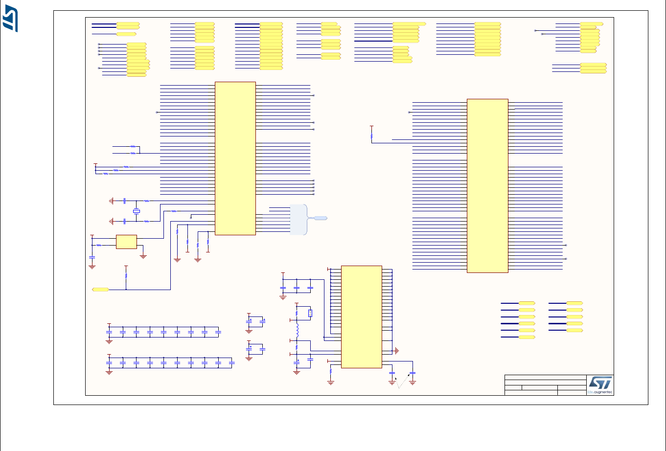
UM2033 Schematics
UM2033 Rev 3 41/56
Figure 30. STM32F769NIH6 connections
312
STM32F769NIH6 Connexion
MB1225 B-01
3/11/2016
Title:
Size: Reference:
Date: Sheet: of
A3 Revision:
STM32F769I-DISCO
Project:
PA4
PA5
PA6
PA7
PA11
PA12
PA9
PA10
PA0
PA1
PA15
PA3
PA13
PA14
PA2
PA8
PB5
PB6
PB7
PB14
PB15
PB10
PB8
PB9
PB1
PB2
PB3
PB0
PB4
PB11
PB12
PB13
PC0
PC1
PC2
PC3
PC4
PC5
PC6
PC7
PC8
PC9
PC10
PC11
PC12
PC13
PC14
PC15
PJ0
PJ14
PJ15
PJ12
PJ13
PJ1
PJ2
PJ3
PJ4
PJ5
PK3
PK4
PK5
PK6
PK7
PH0
PH1
PD0
PD1
PD2
PD3
PD4
PD5
PD6
PD7
PD8
PD9
PD10
PD11
PD12
PD13
PD14
PD15
PI0
PI14
PI15
PI9
PI8
PI11
PI10
PI12
PI13
PI1
PI2
PI3
PI4
PI5
PI6
PI7
PE0
PE14
PE15
PE9
PE8
PE11
PE10
PE12
PE13
PE1
PE2
PE3
PE4
PE5
PE6
PE7
PF0
PF14
PF15
PF9
PF8
PF11
PF10
PF12
PF13
PF1
PF2
PF3
PF4
PF5
PF6
PF7
PG0
PG14
PG15
PG9
PG8
PG11
PG10
PG12
PG13
PG1
PG2
PG3
PG4
PG5
PG7
PH14
PH15
PH9
PH8
PH11
PH10
PH12
PH13
PH2
PH3
PH4
PH5
PH6
PH7
NRST NRST
BOOT0
VDDA
VREF+
3V3
Ceramic capacitor (Low ESR)
VDDA
3V3
PC13-ANTI_TAMP D1
PC0 M2
PC1 M3
PC2 M4
PC3 L4
PA0-WKUP
N3
PA1
N2
PA2
P2
PA3
R2
PA4
N4
PA5
P4
PA6
P3
PA7
R3
PC4 N5
PC5 P5
PB0
R5
PB1
R4
PB2
M5
PB10
P12
PB11
R13
PB12
L13
PB13
K14
PB14
R14
PB15
R15
PC6 H15
PC7 G15
PC8 G14
PC9 F14
PA8
F15
PA9
E15
PA10
D15
PA11
C15
PA12
B15
PA13
A15
PA14
A14
PA15
A13
PC10 B14
PC11 B13
PC12 A12
PB3
A10
PB4
A9
PB5
A8
PB6
B6
PB7
B5
PB8
A7
PB9
B4
PC14-OSC32_IN
E1
PC15-OSC32_OUT
F1
PH0-OSC_IN
G1
PH1-OSC_OUT
H1
NRST
J1
BOOT
E6
PDR_ON
E5
PJ2 P7
PJ3 N8
PJ4 M9
PJ5 M14
DSI_D0_P J12
DSI_CK_P H12
DSI_D0_N J13
DSI_CK_N H13
PJ12 B10
PJ13 B9
PJ14 C9
PJ15 D10
PJ0 R6
PJ1 R7
DSI_D1_N F13
PK3 D8
PK4 D7
PK5 C6
PK6 C5
PK7 C4
DSI_D1_P F12
U13A
STM32F769NIH6
PE2
A3
PE3
A2
PE4
A1
PE5
B1
PE6
B2
PF0
D2
PF1
E2
PF2
G2
PF3
H2
PF4
J2
PF5
K3
PF6
K2
PF7
K1
PF8
L3
PF9
L2
PF10
L1
PH2 K4
PH3 J4
PH4 H4
PH5 J3
PF11
P8
PF12
M6
PF13
N6
PF14
P6
PF15
M8
PG0 N7
PG1 M7
PE7
R8
PE8
N9
PE9
P9
PE10
R9
PE11
P10
PE12
R10
PE13
R12
PE14
P11
PE15
R11
PH6 P13
PH7 N13
PH8 P14
PH9 N14
PH10 P15
PH11 N15
PH12 M15
PG2 M13
PG3 M12
PG4 N12
PG5 N11
PG6 J15
PG7 J14
PG8 H14
PH13 E12
PH14 E13
PH15 D13
PG9 D9
PG10 C8
PG11 B8
PG12 C7
PG13 B3
PG14 A4
PG15 B7
PE0
A6
PE1
A5
PD8
L15
PD9
L14
PD10
K15
PD11
N10
PD12
M10
PD13
M11
PD14
L12
PD15
K13
PD0
B12
PD1
C12
PD2
D12
PD3
C11
PD4
D11
PD5
C10
PD6
B11
PD7
A11
PI8-ANTI_TAMP2 C2
PI9 E4
PI10 D5
PI11 F3
PI0 E14
PI1 D14
PI2 C14
PI3 C13
PI4 C3
PI5 D3
PI6 D6
PI7 D4
PI12 E3
PI13 G3
PI14 H3
PI15 G4
U13B
STM32F769NIH6
VBAT
C1
VSS2 F10
VSS1 K9
VREF- N1
VSSA M1
VREF+
P1
VSS10 F8
VSS11 F7
VCAP2 E11
VSS12 J6
VDD4
K5 VDD3
E7
VSS13-VSS18 F2
VDD_VREGDSI
H11
VCAP1 L11
VSS14 K10
VDD2
F11
VSS15 F9
VDD19
L7
VSS17 G6
VDD18
G5
VDD1
L10
VDD5
H5
VDDA
R1
VDD_MMC33
E9
VDD11
E8
VDD12
J5
VDD13
F4
VDD14
K11
VDD15
E10
VDD17
F5
VSS19 L6
VSS20 H10
VSS3 F6
VSS4 K6
BYPASS-REG
L5
VDD6
L8
VDD7
L9
VDD8
J11
VDD_USB33
G11
VSS5 H6
VSS6 K7
VSS7 K8
VSS8 J10
VSS9 G10
DSI_VCAP
K12 DSI_VSS G12
DSI_VDD12_0
G13
U13C
STM32F769NIH6
R99
0
R97
0
X1
NX3215SA-32.768K
VDD
4OUT 3
EN
1GND 2
X2
NZ2520SB-25.00M
R107
10K_1%_0402
3V3
C98
100nF
OSC_25M
R104
100_1%_0402
OSC_25M
C103
100nF
C88
100nF
C108
100nF
C83
100nF
C105
100nF
C114
100nF
C109
100nF
C112
100nF
C113
100nF
C106
100nF
C102
100nF
C99
100nF
C86
100nF
C110
100nF
C115
100nF
C111
100nF
C104
100nF
C76
100nF
C97
100nF
C80
100nF
C107
100nF
PG6
R18
10K_1%_0402
R19
[NA]
R20
10K_1%_0402
R21
[NA]
3V3
LCD_INT
RMII_TXD0
RMII_TX_EN
RMII_RXD0
RMII_REF_CLK
RMII_CRS_DV
RMII_MDC
RMII_MDIO
RMII_TXD1
RMII_RXD1
ULPI_D[0..7]
ULPI_CK
ULPI_DIR
ULPI_NXT
ULPI_STP
OTG_HS_OverCurrent
QSPI_D0
QSPI_D3
QSPI_D2
QSPI_D1
QSPI_CLK
QSPI_NCS
AUDIO_SDA
AUDIO_SCL
SAI1_MCLKA
SAI1_SCKA
SAI1_FSA
SAI1_SDA
SAI1_SDB
Audio_INT
EXT_SDA
EXT_SCL
EXT_SCL
EXT_SDA
EXT_RST
B_USER
uSD_CLK
uSD_CMD
uSD_D0
uSD_D1
uSD_D2
uSD_D3
uSD_Detect
SWDIO
SWCLK
SWO
VCP_RX
VCP_TX
SWCLK
SWDIO
AUDIO_SDA
AUDIO_SCL
FMC_A[0..12]
FMC_D[0..31]
FMC_SDNWE
FMC_SDNRAS
FMC_SDNCAS
FMC_SDCLK
FMC_BA0
FMC_BA1
FMC_SDNE0
FMC_SDCKE0
FMC_NBL0
FMC_NBL1
SPDIF_RX
ARD_D14
ARD_A[0..5]
ARD_D[0..15]
ARD_D15
R91
2K7
R89
2K7
R90
2K7
R17
2K7
3V3
3V3
RMII_RXER
QSPI_D0
QSPI_D1
QSPI_D2
QSPI_D3
QSPI_NCS
QSPI_CLK
ARD_D[0..15]
OSC_25M EXT_RST
B_USER
FMC_SDCKE0
FMC_NBL0
FMC_NBL1
FMC_SDNRAS
FMC_BA0
FMC_BA1
FMC_SDCLK
FMC_SDNCAS
FMC_SDNWE
FMC_SDNE0
FMC_A[0..12]
EXT_SDA
EXT_SCL
VCP_TX
SWCLK
SWDIO
SWO
VCP_RXuSD_D1
uSD_D2
uSD_D3
uSD_D0
uSD_CLK
uSD_Detect
uSD_CMD
ULPI_D[0..7]
ULPI_CK
ULPI_DIR
ULPI_STP
OTG_HS_OverCurrent
ULPI_NXT
RMII_MDIO
RMII_RXD0
RMII_RXD1
RMII_MDC
RMII_CRS_DV
RMII_REF_CLK
RMII_TX_EN
RMII_TXD0
RMII_TXD1
RMII_RXER
R109
0
VDD
VDD
VDD
VDD
VDD
VDD
NC1
NC2
C68
4.7uF
C69
4.7uF
C116
1uF
C101
1uF
C72
2.2uF
C31
2.2uF
L6
FCM1608KF-601T03
R110
0
R108
10K
R106
10K_1%_0402
3V3
JP4
DSI_VDD12
C23
2.2uF[N/A]
C25
2.2uF
C27
100nF
DSI_CK_P
DSI_CK_N
DSI_D0_P
DSI_D0_N
DSI_D1_P
DSI_D1_N
DSI_TE
DSI_RESET
DSI
DSI_TE
DSI_RESET
DSI
DSI_CK_P
DSI_CK_N
DSI_D0_P
DSI_D0_N
DSI_D1_P
DSI_D1_N
FMC_D[0..31]
FMC_NBL2
FMC_NBL2
FMC_NBL3
FMC_NBL3
WIFI_TX
WIFI_RX
WIFI_RST
SPDIF_RX
SPDIF_TX
SAI1_SDB
AUDIO_SDA
AUDIO_SCL
Audio_INT
SAI1_MCLKA
SAI1_SCKA
SAI1_FSA
SAI1_SDA
SPDIF_TX
ARD_A[0..5]
LRCLK
SPDIF_I2S
LCD_BL_CTRL
LCD_INT
SCLK_MCLK
CEC_CLK
CEC
LCD_BL_CTRL
SCLK_MCLK
LRCLK
SPDIF_I2S
CEC_CLK
CEC
LCD_INT
LCD_SCL
LCD_SDA LCD_SDA
LCD_SCL
WIFI_RST
WIFI_RX
WIFI_TX
ARD_A0
ARD_A1
ARD_A2
ARD_A3
RMII_MDIO
RMII_RXD0
RMII_RXD1
RMII_MDC
RMII_CRS_DV
RMII_REF_CLK
RMII_TX_EN
RMII_TXD0
RMII_TXD1
RMII_RXER
FMC_SDCKE0
FMC_NBL0
FMC_NBL1
FMC_SDNRAS
FMC_BA0
FMC_BA1
FMC_SDCLK
FMC_SDNCAS
FMC_SDNWE
FMC_SDNE0
FMC_NBL2
FMC_NBL3
FMC_A0
FMC_D0
FMC_A1
FMC_A2
FMC_A3
FMC_A4
FMC_A5
FMC_A6
FMC_A7
FMC_A8
FMC_A9
FMC_A10
FMC_A11
FMC_D1
FMC_D2
FMC_D3
FMC_D4
FMC_D5
FMC_D6
FMC_D7
FMC_D8
FMC_D9
FMC_D10
FMC_D11
FMC_D12
FMC_D13
FMC_D14
FMC_D15
FMC_D16
FMC_D17
FMC_D18
FMC_D19
FMC_D20
FMC_D21
FMC_D22
FMC_D23
FMC_D24
FMC_D25
FMC_D26
FMC_D27
FMC_D28
FMC_D29
FMC_D30
FMC_D31
SPDIF_I2S
LCD_BL_CTRL
CEC_CLK
CEC
LCD_SCL
LCD_SDA
FMC_A12
QSPI_D0
QSPI_D1
QSPI_D2
QSPI_D3
QSPI_NCS
QSPI_CLK
SPDIF_RX
SPDIF_TX
SAI1_SDB
Audio_INT
SAI1_MCLKA
SAI1_SCKA
SAI1_FSA
SAI1_SDA
ARD_A4
ARD_A5
VCP_TX
SWO
VCP_RX
uSD_D1
uSD_D2
uSD_D3
uSD_D0
uSD_CLK
uSD_Detect
uSD_CMD
ARD_D0
ARD_D1
ARD_D2
ARD_D3
ARD_D4
ARD_D5
ARD_D6
ARD_D7
ARD_D8
ARD_D9
ARD_D10
ARD_D11
ARD_D12
ARD_D13
B_USER
WIFI_TX
WIFI_RST
ULPI_D0
ULPI_CK
ULPI_DIR
ULPI_STP
OTG_HS_OverCurrent
ULPI_NXT
ULPI_D1
ULPI_D2
ULPI_D3
ULPI_D4
ULPI_D5
ULPI_D6
ULPI_D7
DSI_TE
DSI_RESET
LD_USER1 LD_USER1
LD_USER2
LD_USER2
LD_USER1
LD_USER2
R93
0
R92
[NA]
NC3
NC4
TP12
NC5
TP13
NC6
TP1
TP3
NC7
NC8
TP14
TP9
TP18
TP17
TP16
TP15
TP21
TP8
TP6
TP7
TP11
TP22
TP2
PA[0..15] PA[0..15]
PB[0..15] PB[0..15]
PC[0..15] PC[0..15]
PD[0..15] PD[0..15]
PE[0..15] PE[0..15]
PF[0..15] PF[0..15]
PG[0..15] PG[0..15]
PH[0..15] PH[0..15]
PI[0..15] PI[0..15]
PJ[0..15] PJ[0..15]
PK[0..7] PK[0..7]
EXT_RST
DFSDM_CKOUT
DFSDM_DATIN1
DFSDM_DATIN5
DFSDM_CKOUT
DFSDM_DATIN1
DFSDM_DATIN5
DFSDM_CKOUT
DFSDM_DATIN1
DFSDM_DATIN5 TP100
TP101
TP102
WIFI_RX
C77
4.3pF_NPO_-+0.25pF_0402
C84
4.3pF_NPO_-+0.25pF_0402
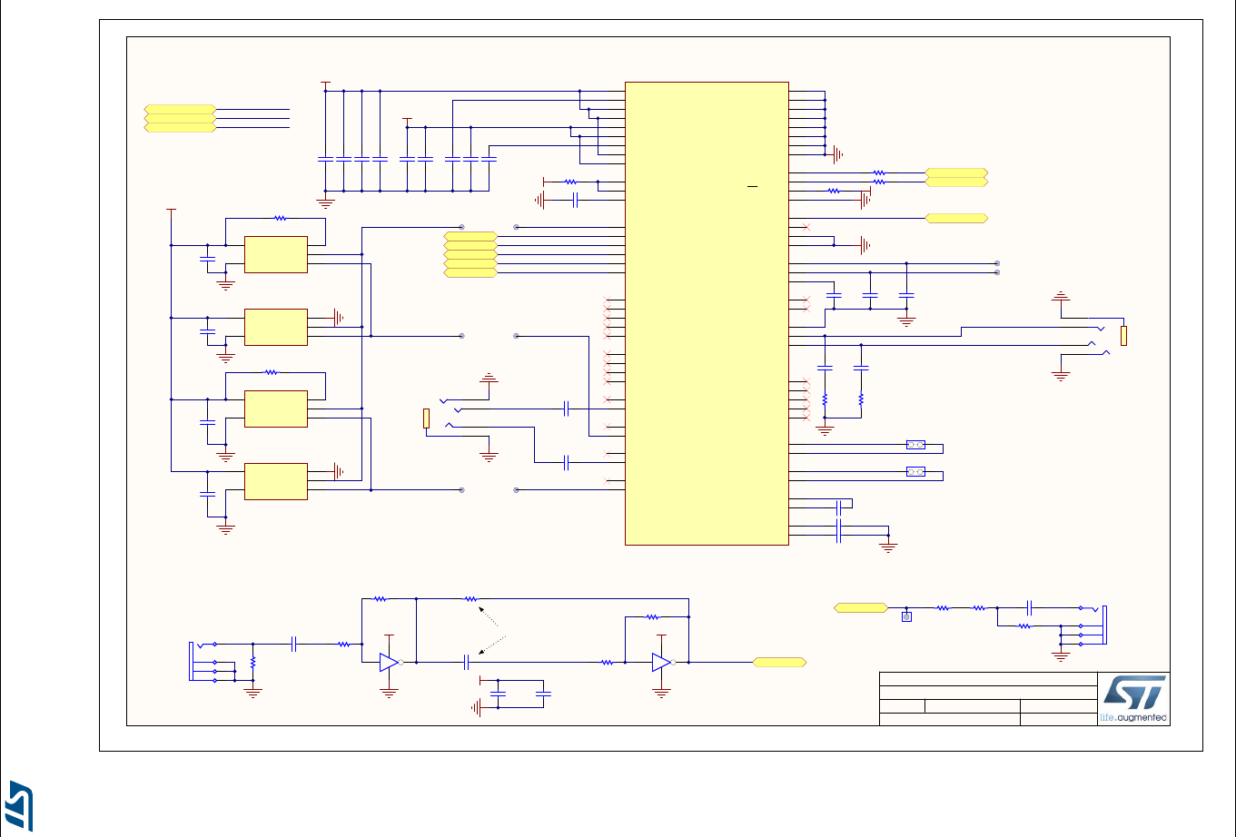
Schematics UM2033
42/56 UM2033 Rev 3
Figure 31. Audio codec WOLFSON and audio connectors
412
Audio Codec WOLFSON and Audio Connectors
MB1225 B-01
3/10/2016
Title:
Size: Reference:
Date: Sheet: of
A4 Revision:
STM32F769I-DISCO
Project:
SAI1_SCKA
WM8994 I2C Address : 0011 0100
ADCDAT1
F2
ADCLRCLK1/GPIO1
G3
AGND D6
CPVDD
G9
CPVOUTN H7
CPVOUTP G7
CS/ADDR G2
DACDAT1
E4
CPGND H9
DCVDD
F1
DBVDD
D2 DGND E2
CPCB H8
AVDD1
D9
BCLK1
G1
CIFMODE A4
CPCA G8
DMICCLK
C6
AGND E7
AGND E8
AVDD2
D8
GPIO2/MCLK2 E1
GPIO3/BCLK2
H2
GPIO4/LRCLK2
F4
GPIO5/DACDAT2
H3
GPIO6/ADCLRCLK2
G4 GPIO7/ADCDAT2
E5
GPIO8/DACDAT3
H4
GPIO9/ADCDAT3
F5
GPIO10/LRCLK3
H5 GPIO11/BCLK3
F6
HP2GND F7
HPOUT1FB G5
HPOUT1L H6
HPOUT1R G6
HPOUT2N F9
HPOUT2P F8
IN1LN
D7 IN1LP
C8
IN1RN
B7 IN1RP
C7
IN2LN/DMICDAT1
B9 IN2LP/VRXN
B8
IN2RN/DMICDAT2
A9 IN2RP/VRXP
A8
LDO1ENA
D4
LDO1VDD
E9
LDO2ENA
D5
LDO2VDD
D1
LINEOUT1N C5
LINEOUT1P B5
LINEOUT2N C4
LINEOUT2P B4
LINEOUTFB A6
LRCLK1
E3
MCLK1 D3
MICBIAS1 A7
MICBIAS2 B6
REFGND A5
SCLK H1
SDA F3
SPKGND1 A1
SPKGND2 C1
SPKMODE A3
SPKOUTLN B1
SPKOUTLP A2
SPKOUTRN C3
SPKOUTRP B3
SPKVDD1
B2
SPKVDD2
C2
VMIDC C9
VREFC
E6
U11
WM8994ECS/R
1V8
3V3
SAI1_FSA
SAI1_SDA
SAI1_SDB
Audio_INT
AUDIO_SDA
AUDIO_SCL
SAI1_MCLKA
3V3
3V3
MIC_DATA1
MIC_CLK
MIC_VDD1
Bottom Left
Bottom Right
GND
5
LR 2
CLK 3
VDD
1
DOUT 4
U9
MP34DT01
GND
5
LR 2
CLK 3
VDD
1
DOUT 4
U8
MP34DT01
SPK Left
SPK Right
Right
Left
Jack Line output Green
Jack Line input blue
Right
Left
RCA White for SPDIF input
SPDIF_RX
2
6
4
3
CN6
PJ3028B-3_BE
2
6
4
3
CN7
PJ3028B-3_GR
C924.7uF
C671uF
C90
1uF
R87
10K
R71 10K
C62
1uF
C95
4.7uF
C73
4.7uF
R95 0
R94 [NA]
C71100nF
C65100nF
C57100nF
C56100nF
C82 2.2uF
C78 2.2uF
C74 2.2uF
R78
20
C934.7uF
C944.7uF
C64100nF
C91100nF
C631uF
C55100nF
C59100nF
C58
1uF
R88 0
R77
20
2
3
4
5
U16
74LVC1G04SE
C118
100nF
2
3
4
5
U15
74LVC1G04SE
R115
1M R112
1M
R111
75
R116
100
R117
100
C117
100nF
C120
22nF
C119
22nF
3V3 3V3
3V3
Very close to Output pin 4
Second Stage
R114
[NA]
First Stage
of first stage
GND
5
LR 2
CLK 3
VDD
1
DOUT 4
U6
MP34DT01
GND
5
LR 2
CLK 3
VDD
1
DOUT 4
U5
MP34DT01
C45100nFC44100nF
R51 10K
Top Right
Top Left
RCA Yellow for SPDIF ouput
SPDIF_TX R100
0
C87
100nF
R102
110
R101
210
C79
4.7uF
MIC_VDD2
TP20
MIC_DATA2
TP5
JP2
JP3
DFSDM_CKOUT
DFSDM_DATIN1
DFSDM_DATIN5
DFSDM_CKOUT
DFSDM_DATIN1
DFSDM_DATIN5
DFSDM_CKOUT
DFSDM_DATIN1
DFSDM_DATIN5
TP103
TP104
TP105
3V3
TP106
TP107
TP108
TP109
4
3
1
2
CN8
RCA_SMD_Y
4
3
1
2
CN12
RCA_SMD_W
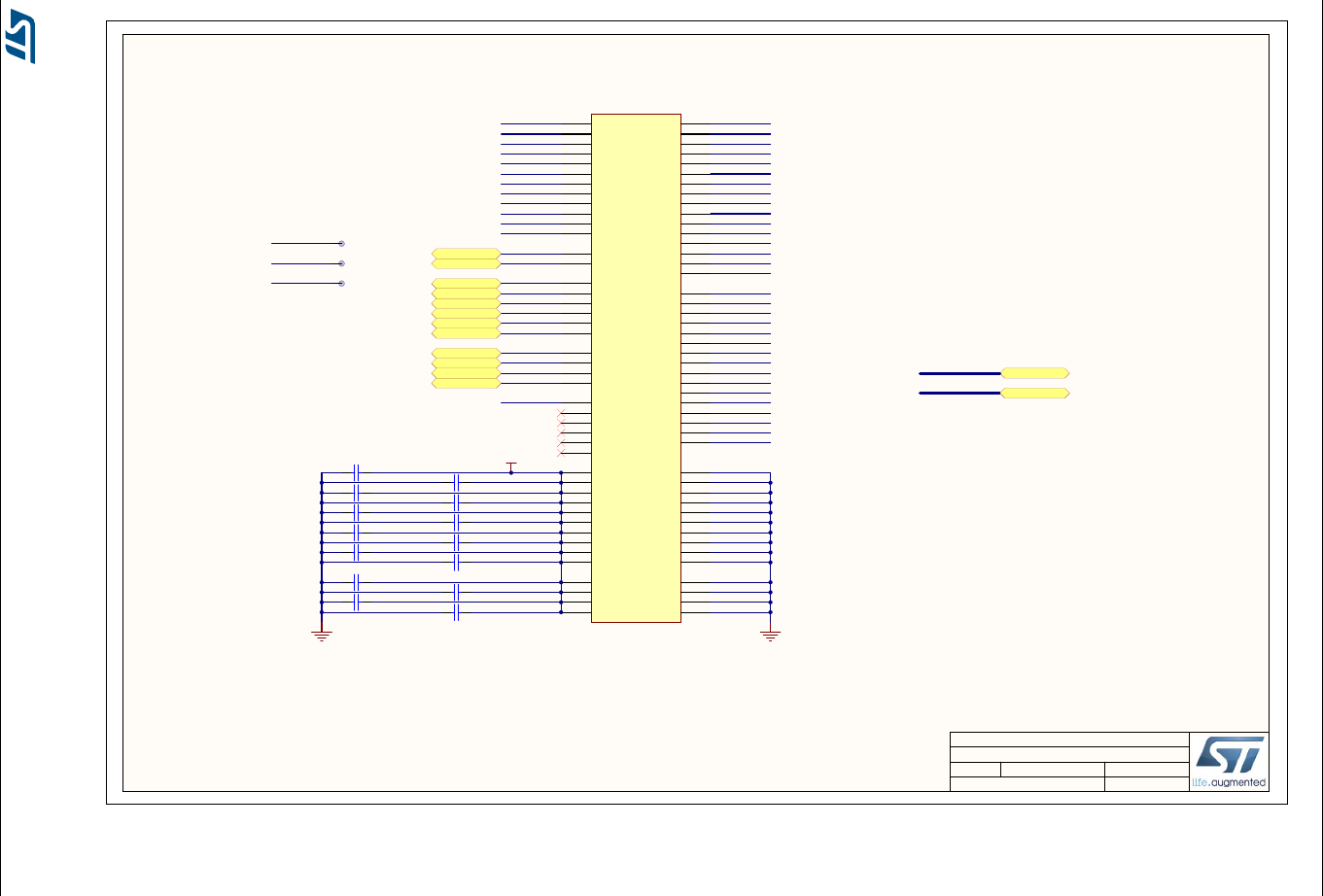
UM2033 Schematics
UM2033 Rev 3 43/56
Figure 32. SDRAM (MICRON)
512
SDRAM (MICRON)
MB1225 B-01
3/10/2016
Title:
Size: Reference:
Date: Sheet: of
A4 Revision:
STM32F769I-DISCO
Project:
FMC_A[0..12]
FMC_D[0..31]
Place close SDRAM
FMC_D[0..31]
FMC_A[0..12]
A11
H9
A10
G7
A9
J3
A8
H2
A7
H1
A6
G3
A5
G2
A4
G1
A3
F3
A2
F7
A1
G9
A0
G8
NC
E3
DQ0 R8
DQ8 L2
DQ1 N7
DQ9 M3
DQ2 R9
DQ10 M2
DQ3 N8
DQ11 P1
VDDQ
B2
DQ4 P9
DQ12 N2
DQ5 M8
DQ13 R1
DQ6 M7
DQ14 N3
DQ7 L8
DQ15 R2
VSS A3
VDD
A7
DQ16 E8
DQ24 A2
DQ17 D7
DQ25 C3
DQ18 D8
DQ26 A1
DQ19 B9
DQ27 C2
DQ20 C8
DQ28 B1
DQ21 A9
DQ29 D2
DQ22 C7
DQ30 D3
DQ23 A8
DQ31 E2
VSSQ B3
VDDQ
B7 VSSQ B8
VSSQ C1
VDDQ
C9
VSSQ D1
VDDQ
D9
VDDQ
E1
NC
E7
VSSQ E9
VSS F1
VDD
F9
NC
H3
NC
H7
BA0
J7 BA1
H8
NU
K2 NC
K3
VDDQ
L1
VSS L3
VDD
L7
VSSQ L9
VSSQ M1
VDDQ
M9
VSSQ N1
VDDQ
N9
VDDQ
P2 VSSQ P3
VDDQ
P7 VSSQ P8
VSS R3
VDD
R7
DQM0
K9 DQM1
K1 DQM2
F8
CLK
J1 CKE
J2 CS#
J8
DQM3
F2
RAS#
J9 CAS#
K7 WE#
K8
U17
MT48LC4M32B2B5-6A (MICRON)
FMC_A0
FMC_SDNWE
FMC_SDNRAS
FMC_BA0
FMC_BA1
FMC_SDCLK
FMC_SDNCAS
FMC_SDNWE
FMC_SDNRAS
FMC_SDNCAS
FMC_SDCLK
FMC_BA0
FMC_BA1
C128
100nF_X7R_10%_0402
C137
100nF_X7R_10%_0402
C136
100nF_X7R_10%_0402
C133
100nF_X7R_10%_0402
C134
100nF_X7R_10%_0402
C126
100nF_X7R_10%_0402
C135
100nF_X7R_10%_0402
C127
100nF_X7R_10%_0402
C123
100nF_X7R_10%_0402
C124
100nF_X7R_10%_0402
C130
100nF_X7R_10%_0402
C125
100nF_X7R_10%_0402
C138
100nF_X7R_10%_0402
3V3
FMC_D0
FMC_NBL0
FMC_NBL1
FMC_NBL0
FMC_NBL1
C131
100nF_X7R_10%_0402
FMC_SDCKE0
FMC_SDNE0
FMC_SDNE0
FMC_SDCKE0
FMC_D1
FMC_D2
FMC_D3
FMC_D4
FMC_D5
FMC_D6
FMC_D7
FMC_D8
FMC_D9
FMC_D10
FMC_D11
FMC_D12
FMC_D13
FMC_D14
FMC_D15
FMC_A1
FMC_A2
FMC_A3
FMC_A4
FMC_A5
FMC_A6
FMC_A7
FMC_A8
FMC_A9
FMC_A10
FMC_A11
FMC_NBL2
FMC_NBL3
FMC_NBL2
FMC_NBL3
FMC_D16
FMC_D17
FMC_D18
FMC_D19
FMC_D20
FMC_D21
FMC_D22
FMC_D23
FMC_D24
FMC_D25
FMC_D26
FMC_D27
FMC_D28
FMC_D29
FMC_D30
FMC_D31
FMC_A12
TP26
FMC_SDCLK
FMC_SDNWE
FMC_D0
TP28
TP27
do not modify the way of the wire
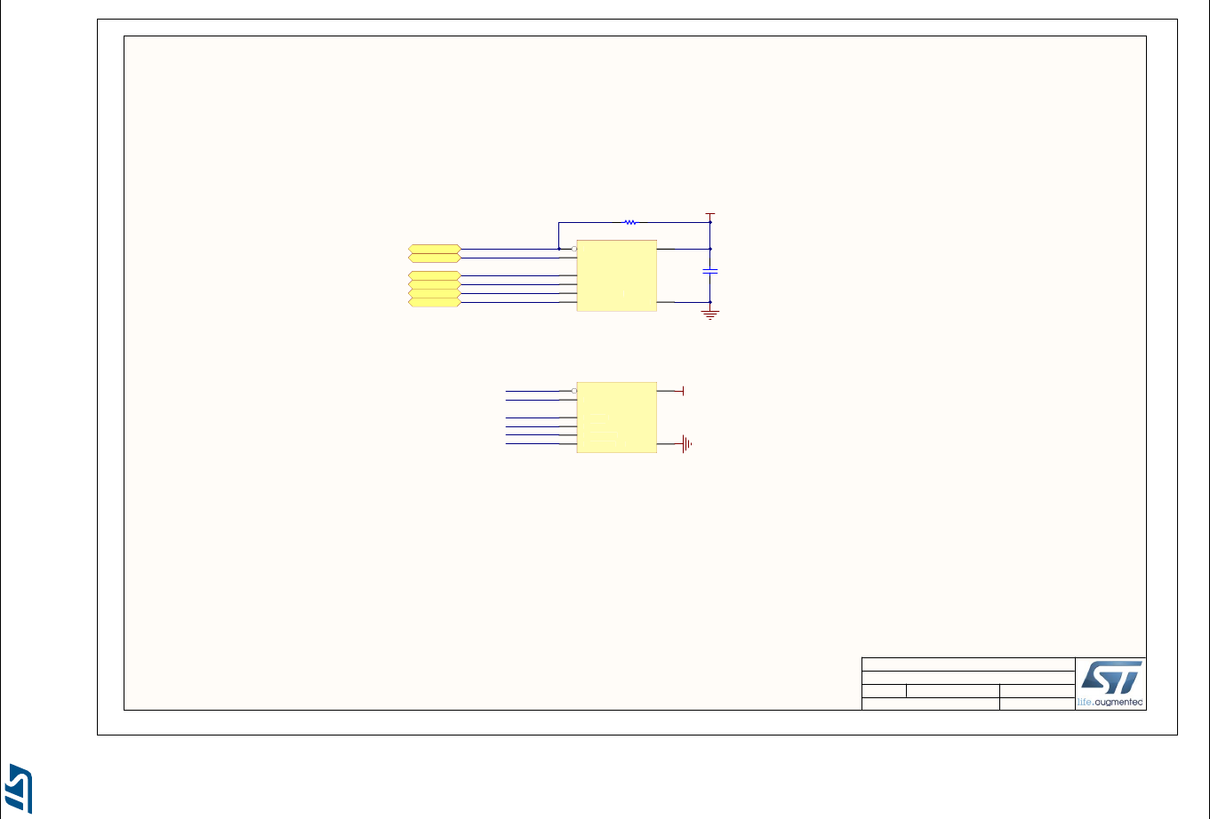
Schematics UM2033
44/56 UM2033 Rev 3
Figure 33. Quad-SPI Flash memory (MACRONIX mounted)
612
Quad SPI Flash Memory (MICRON)
MB1225 B-01
3/10/2016
Title:
Size: Reference:
Date: Sheet: of
A4 Revision:
STM32F769I-DISCO
Project:
3V3
Quad SPI Flash Memory
QSPI_D0
QSPI_D3
QSPI_D2
QSPI_D1
QSPI_CLK
QSPI_NCS
R86
10K_1%_0402
C96
100nF_X7R_10%_0402
QSPI_D0
QSPI_D1
QSPI_D2
QSPI_D3
QSPI_NCS
QSPI_CLK
SIO3/RESET#
7
VCC 8
CS#
1
SIO1/SO
2
SCLK
6
SIO0/SI
5
GND 4
SIO2/WP#
3
SI
O3
/
RE
S
E
T
#
VCC
CS#
SI
O
1/
S
O
SC
L
K
SI
O
0/
S
I
G
ND
SI
O
2/
W
P
#
U250
MX25L51245G (MACRONIX)
QSPI_D0
QSPI_D1
QSPI_D2
QSPI_D3
QSPI_NCS
QSPI_CLK 3V3
DQ3/HOLD#
7
VCC 8
S#
1
DQ1
2
C
6
DQ0
5
VSS 4
DQ2/Vpp/W#
3
DQ
3/HOLD#
VCC
S
#
DQ
1
C
DQ
0
VSS
D
Q2/V
pp
/
W
#
U12
MT25QL512ABB1EW9 (MICRON)
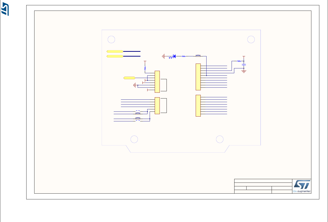
UM2033 Schematics
UM2033 Rev 3 45/56
Figure 34. Arduino™ UNO connectors
712
Arduino UNO connectors
MB1225 B-01
3/10/2016
Title:
Size: Reference:
Date: Sheet: of
A4 Revision:
STM32F769I-DISCO
Project:
Arduino UNO connector
A0
A1
A2
A3
A4
A5
RX/D0
TX/D1
D2
D4
PWM/D3
PWM/D5
PWM/D6
D7
D8
PWM/D9
PWM/CS/D10
SDA/D14
SCL/D15
NRST
VIN
NRST
SCK/D13
MISO/D12
PWM/MOSI/D11
AVDD
GND
VREF+
PA6
PA4
PC2
PF10
PC6
PJ1
PF6
PJ0
PA11
PF7
PJ3
PJ4
PH6
PC8
PB15
PB14
PA12
ADC3_IN8
ADC1_IN12
ADC1_IN4
ADC1_IN6
USART6_RX
USART6_TX
TIM10_CH1
TIM3_CH3
TIM12_CH1
TIM1_CH4, SPI2_NSS
TIM12_CH2, SPI2_MOSI
SPI2_MISO
SPI2_SCK
IOREF
NRST
3V3
5V
GND
GND
VIN
POWERAIN
TIM11_CH1
LD3
LED, green
R64
510_1%_0402
SB15
3V3
5V
PB8
PB9
PB8
PB9
ARD_A[0..5]
ARD_D[0..15]
ARD_A[0..5]
ARD_D[0..15]
ARD_A0
ARD_D0
ARD_D1
ARD_D2
ARD_D3
ARD_D4
ARD_D5
ARD_D6
ARD_D7
ARD_D8
ARD_D9
ARD_D10
ARD_D11
ARD_D12
ARD_D13
ARD_D14
ARD_D15
ARD_D14
ARD_D15
ARD_A1
ARD_A2
ARD_A3
SDA/D14
SCL/D15
PC7
C85
[NA]
R98
0
SB13
SB11
ARD_A4
ARD_A5
ADC3_IN6
ADC3_IN7
PF8
PF9
1
2
3
4
5
6
CN14
BL 1-6 G
1
2
3
4
5
6
7
8
CN11
BL 1-8 G
1
2
3
4
5
6
7
8
9
10
CN9
BL 1-10 G
1
2
3
4
5
6
7
8
CN13
BL 1-8 G
R103
1K
E5V
SB14
SB12
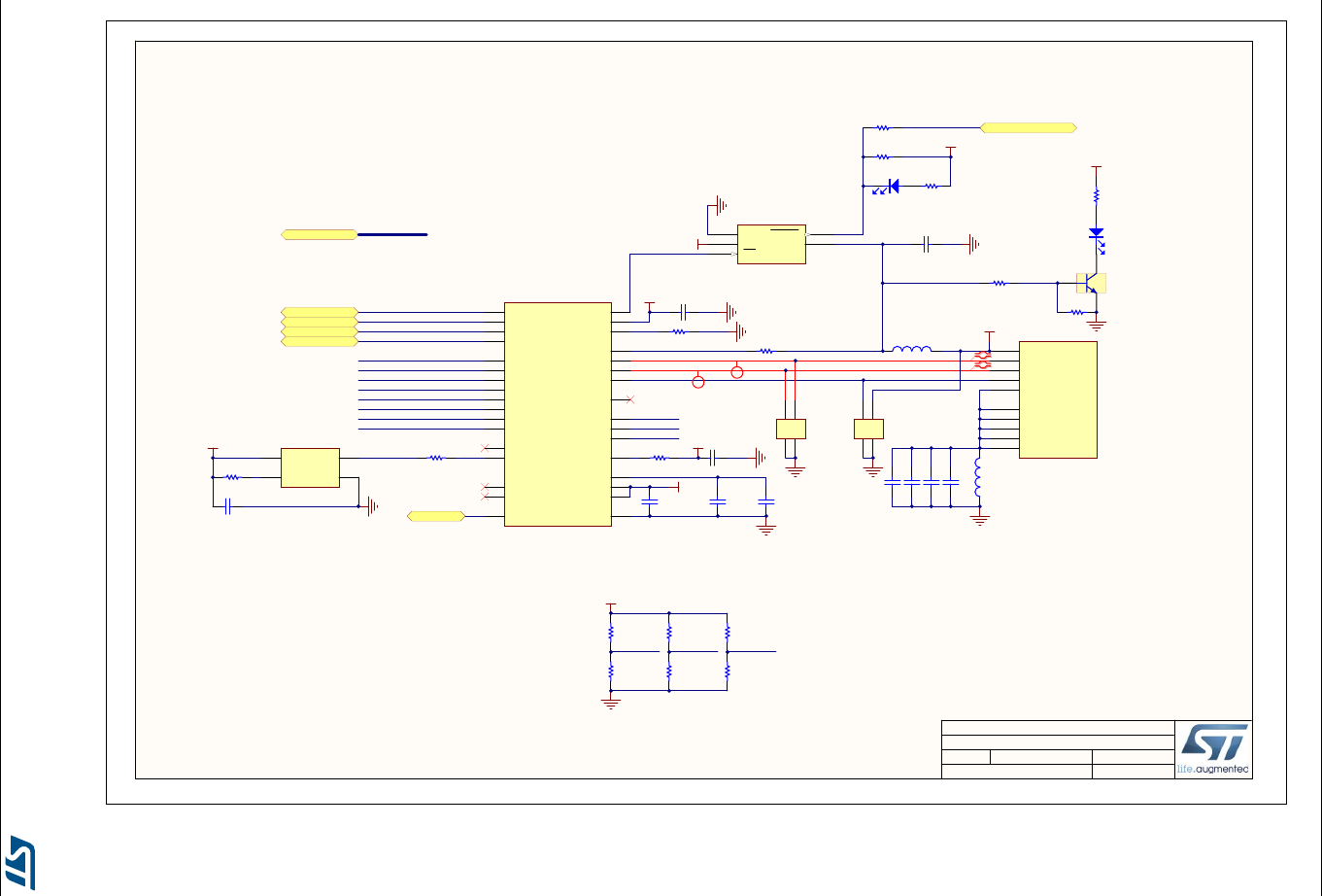
Schematics UM2033
46/56 UM2033 Rev 3
Figure 35. USB OTG HS PHY with micro A-B connector
812
USB OTG HS PHY with micro A-B connector
MB1225 B-01
3/10/2016
Title:
Size: Reference:
Date: Sheet: of
A4 Revision:
STM32F769I-DISCO
Project:
ULPI_D[0..7]
ULPI_CK
ULPI_D0
ULPI_D1
ULPI_D2
ULPI_D3
ULPI_DIR
ULPI_NXT
ULPI_STP
5V
VBUS
1
DM
2
DP
3
ID
4
GND
5
Shield
6
USB_Micro-AB receptacle
Shield
7
Shield
8
Shield
9
EXP
10
CN15
475900001
ULPI_D[0..7]
ULPI_D4
ULPI_D5
ULPI_D6
ULPI_D7
NRST
A1
A2
B1
B2
D13
USBULC6-2F3
A1
A2
B1
B2
D12
ESDA14V2-2BF3
3V3
3V3
OTG_HS_OverCurrent
USB_HS_N
USB_HS_P
3
1
2
T5
9013-SOT23
CPEN 17
VBUS 22
ID 23
REFSEL0 8
DP 18
DM 19
RESETB
27
VBAT 21
NXT
2
DIR
31
STP
29
CLKOUT
1
VDD1.8 30
VDD3.3 20
D7
13
D6
10
D5
9
D4
7
D3
6
D2
5
D1
4
D0
3REFSEL1 11
VDD1.8 28
XO
25
NC 12
REFCLK
26
REFSEL2 14
VDDIO 32
RBIAS 24
GNDPAD 33
SPK_R
16 SPK_L
15
U20
USB3320C-EZK
GND
2
IN
5
EN
4OUT 1
FAULT 3
U21
STMPS2151STR
ULPI_NXT
ULPI_DIR
ULPI_STP
ULPI_CK
LD5
LED, green
LD4
LED, red
R65
620_1%_0603 R66
330_1%_0402
R132
47K_1%_0402
R129
0
R136
100_1%_0402
5V_USB_HS
3V3
1V8
C153
100nF
C156
100nF
C154
100nF
C157
100nF
C145
100nF
C149
100nF
5V
R123
0_5%_0402
R124
[NA]
C52
2.2uF_X7R_10%_0805
R125
0_5%_0402
R128
[NA]
R137
0_5%_0402
R133
[NA]
REFSEL0 REFSEL1 REFSEL2
REFSEL0
REFSEL1
REFSEL2
3V3
R142 820_1%_0805
C148
4.7uF_X5R_10%_0603
C144
100nF
R126
0_5%_0402
C150
100nF
R139
8K06_1%_0402
i
Diff Pair 90ohm
Matched Net Lengths [Tolerance = 150mil]
i
Diff Pair 90ohm
L7
BLM18PG121SN1D
L8
BLM18PG121SN1D
R130
3K3
R131
100K_1%_0402
R134
10K_1%_0402
3V3
OSC_24M
C147
100nF_X7R_10%_0402
VDD
4OUT 3
EN
1GND 2
X4
NZ2520SB-24.00M
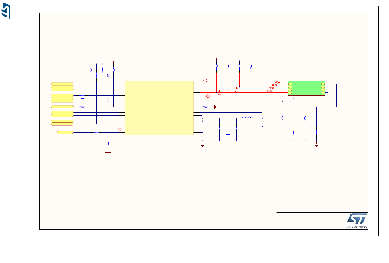
UM2033 Schematics
UM2033 Rev 3 47/56
Figure 36. Ethernet PHY with RJ45 connector
912
Ethernet PHY with RJ45 connector
MB1225 B-01
3/10/2016
Title:
Size: Reference:
Date: Sheet: of
A4 Revision:
STM32F769I-DISCO
Project:
RMII_TXD0
RMII_TX_EN
RMII_RXD0
RMII_REF_CLK
RMII_CRS_DV
RMII_MDC
RMII_MDIO
NRST
RMII_TXD1
RMII_RXD1
3V3
3V3
C33
100nF
C35
100nF C30
100nF
MDIO
12 MDC
13
RXD1/MODE1
7RXD0/MODE0
8
RXER/PHYAD0
10
TXEN
16
TXD0
17
TXD1
18
CRS_DV/MODE2
11
nRST
15
XTAL1/CLKIN
5XTAL2
4
GND_EP 25
RBIAS 24
VDDIO 9
VDD1A 19
VDD2A 1
VDDCR 6
RXP 23
RXN 22
TXN 20
TXP 21
nINT/REFCLK0
14
LED2/nINT/nPME/nINTSEL 2
LED1/nINT/nPME/REGOFF 3
U3
LAN8742A-CZ-TR
OSC_25M OSC_25M R27
100
3V3
RMII_RXER
R47
1K5
i
Diff Pair 100ohm
Matched Net Lengths [Tolerance = 100mil]
i
Diff Pair 100ohm
i
Diff Pair 100ohm
i
Diff Pair 100ohm
TD_N
TD_P
RD_N
RD_P
R31
12K1
C38
10uF
R37
50
R35
50
R36 33
R41
50
R39
50
R32 33
R44 33
R29
10K
R28
10K
L2
BLM18PG121SN1D
R105
330
R113
330
LED2_SPEED_YELLOW
LED1_LINK/ACT_GREEN
C28
1uF
C36
10uF
C29
470pF
R40
10K
R30
10K
R43
10K
R34
10K
R45
10K
LED_G_K
LED_G_A
LED_Y_A
LED_Y_K
LED_G_A
LED_G_K
LED_Y_A
LED_Y_K
RD_P
TD_N
TD_P
RD_N
U_PoE
PoE.SchDoc
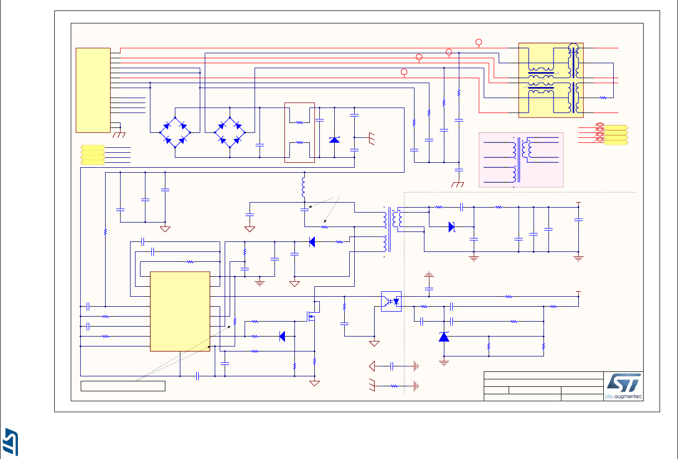
Schematics UM2033
48/56 UM2033 Rev 3
Figure 37. Power over Ethernet 3 W
10 12
Power Over Ethernet 3W
MB1225 B-01
3/10/2016
Title:
Size: Reference:
Date: Sheet: of
A4 Revision:
STM32F769I-DISCO
Project:
Power Over Ethernet
Chassis
Chassis Chassis
INPUT
RX+ 3
nc5 5
nc4 4
nc7 7
RX- 6
nc8 8
LED_Yellow_A 10
LED_Yellow_K 9
LED_Green_K 11
LED_Green_A 12
TX+ 1
TX- 2
Shield_13 13
Shield_14 14
CN10
KRJ-CB4 R48
0
R49
0
C18
47uF_X5R_20%_0805
C13
47uF_X5R_20%_0805
C14
47uF_X5R_20%_0805
C15
47uF_X5R_20%_0805
R9
0.47_1%_1206
R2
0_5%_0603
C40
100nF_100V_X7R_10%_0805
C89
1nF_2KV
R42
75
1 2
D10
SMAJ58A
R75
10_1%_0805
R3
2K_1%_0805 R10
56_1%_0805
C81
100nF_100V_X7R_10%_0805
C5
10nF_100V_X7R_10%_0603
C10
10nF_100V_X7R_10%_0603
C24
1uF_25V_X5R_10%_0603
R6
124K_1%_0603
R1
75K_1%_0603
L5
ME3220-562ML
R22
15
R23
200
C16
100nF_X7R_10%_0603
C21
560pF_X7R_10%_0603
C75
4.7uF_100V_X7S_20%_1206
C22
27pF_100V_NPO_5%_0603
5V_POE
5V_POE
R26
75
R33
75
R46
75
LED_G_K
LED_G_A
LED_Y_A
1
2
3
6
7
89
10
11
14
15
16
T4
H2019NL
Chassis R96
0_5%_0805
C3
1nF_2KV_X7R_10%_1206
1
3 2
4
T1
STN4NF20L
35
4
U2
TS431AILT
RT
1
SS
2
AUXII
3
VIN
4CS 13
COMP 14
VFB 15
AGND 16
RCLASS
5
AUXI_IRL
6
DCCL
7
GND 9
GD 10
VCC 11
nPGD 12
Ex Pad
17
VSS
8
U1
PM8800A C9
470pF_100V_X7R_10%_0603
-
+
4
1
3
2
~~
D4
DF01S
-
+
4
1
3
2
~~
D9
DF01S
4 1
23
U10
HMHA2801A
R85
1K_1%_0603
R5
1K_1%_0603
R25
10K_1%_0603
R12
10K_1%_0603
R11
20K_1%_0603
R4
510_1%_0603
D1
BAT46JFILM
D3
BAT46JFILM
TD_N
TD_P
RD_N
RD_P
R38
0_5%_0805
C70
4.7uF_100V_X7S_20%_1206
C7
100nF_50V_X7R_10%_0603
C6
100nF_50V_X7R_10%_0603
C11
100nF_50V_X7R_10%_0603
C12
100nF_50V_X7R_10%_0603
C17
100pF_50V_X7R_10%_0603
C19
22nF_50V_X7R_10%_0603
C66
1uF_25V_X5R_10%_0603
LED_G_K
LED_G_A
LED_Y_A
LED_Y_K
LED_G_A
LED_G_K
LED_Y_A
LED_Y_K
TD_N
TD_P
RD_N
RD_P RD_P
TD_N
TD_P
RD_N
i
Diff Pair 100ohm
Matched Net Lengths [Tolerance = 100mil]
i
Diff Pair 100ohm
Matched Net Lengths [Tolerance = 100mil]
i
Diff Pair 100ohm
Matched Net Lengths [Tolerance = 100mil]
i
Diff Pair 100ohm
Matched Net Lengths [Tolerance = 100mil]
LED_Y_K
AGND
N
OTE : The AGND is a dedicated plan.
The resistor 0 ohm must be very close to pin 9
N
OTE : Place for additional ferrite beads
R74
0
R16
0_5%_0603
R24
68
R15
13K_1%_0603
R14
13K_1%_0603
R84
0_5%_0805
R13
10K_1%_0603
Not Fitted
D2
STPS2L40UF
C8
1nF_100V_X7R_10%_0603
C121
1nF_100V_X7R_10%_0603
C122
1nF_100V_X7R_10%_0603
C34
1nF_100V
C26
1nF_100V
C32
1nF_100V
C37
1nF_100V
C4
1nF_100V_X7R_10%_0603
C39
1nF_100V_X7R_10%_0603
C200
10nF_X7R_10%_0603
C20
4.7uF_100V_X7S_20%_1206
4
1
2
3 7
5
8
6
Pri
Bias
Sec
T2
POE30P50L
1
4
3
2 6
8
5
7
Pri
Bias
Sec
T100
POE30P50L
POE1
POE2
POE3
POE4 POE5
POE6
POE7
POE8
POE1
POE5
POE6
POE7
POE8
POE2
POE3
POE4
1
4
3
2
6
8
5
7
Pr
i
Bia
s
S
e
c
T100
PO
E30P50L
PO
E
1
P
O
E5
P
O
E
6
P
O
E
7
P
O
E
8
PO
E2
PO
E3
PO
E
4
Not Fitted
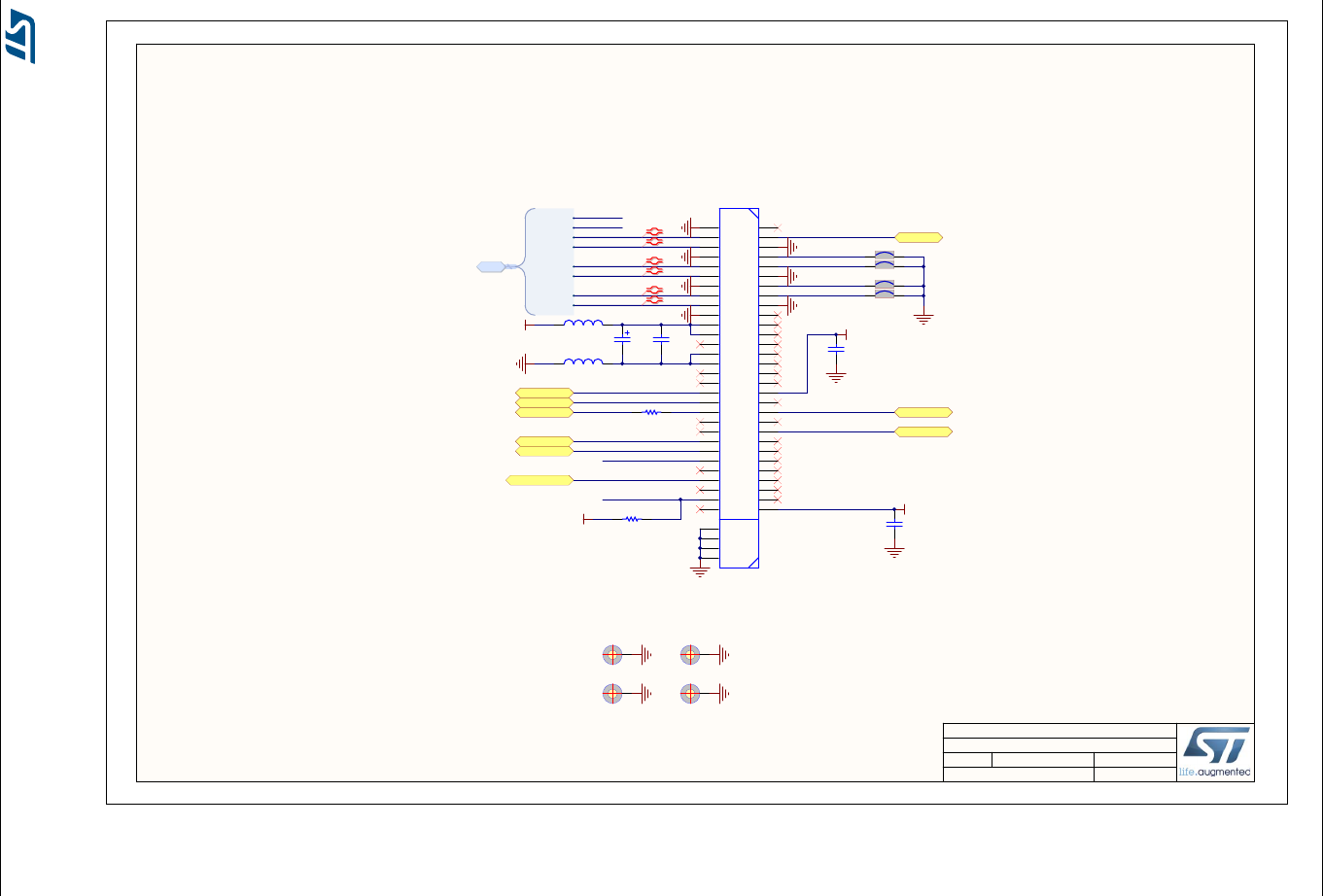
UM2033 Schematics
UM2033 Rev 3 49/56
Figure 38. MIPI connector for DSI LCD and HDMI boards
11 12
MIPI connector for DSI LCD and HDMI boards.
MB1225 B-01
3/11/2016
Title:
Size: Reference:
Date: Sheet: of
A4 Revision:
STM32F769I-DISCO
Project:
LCD_INT
DSI LCD
LCD_INT
LCD_BL_CTRL
5V
LCD_BL_CTRL
PB9
PB8
LCD_SCL
LCD_SDA
3V3
3V3
DSI_CK_P
DSI_CK_N
DSI_D0_P
DSI_D0_N
DSI_D1_P
DSI_D1_N
DSI_TE
DSI_RESET
DSI
DSI_TE
DSI_RESET
DSI
DSI_TE
DSI_RESET
DSI_CK_P
DSI_CK_N
DSI_D0_P
DSI_D0_N
DSI_D1_P
DSI_D1_N
DSI_D2_P
DSI_D2_N
DSI_D3_P
DSI_D3_N
1V8
SCLK_MCLK
LRCLK
SPDIF_I2S
CEC_CLK
CEC
H8
L4
FCM1608KF-601T03
L3
FCM1608KF-601T03
C61
10uF
C60
100nF
R8
10K C2
100nF
C1
100nF
SB1
SB2
SB3
SB4
H3 H4
H5
LCD_SDA
LCD_SCL
R7
0MB1166 I2C Address : 0101 0100
1
122
3
344
5
566
7
788
9
910 10
11
11 12 12
13
13 14 14
15
15 16 16
17
17 18 18
19
19 20 20
21
21 22 22
23
23 24 24
25
25 26 26
27
27 28 28
29
29 30 30
31
31 32 32
33
33 34 34
35
35 36 36
37
37 38 38
39
39 40 40
41
41 42 42
43
43 44 44
45
45 46 46
47
47 48 48
49
49 50 50
51
51 52 52
53
53 54 54
55
55 56 56
57
57 58 58
59
59 60 60
61
61
62
62
63
63
64
64
CN?
QSH-030-01-F-D-A-K-TR
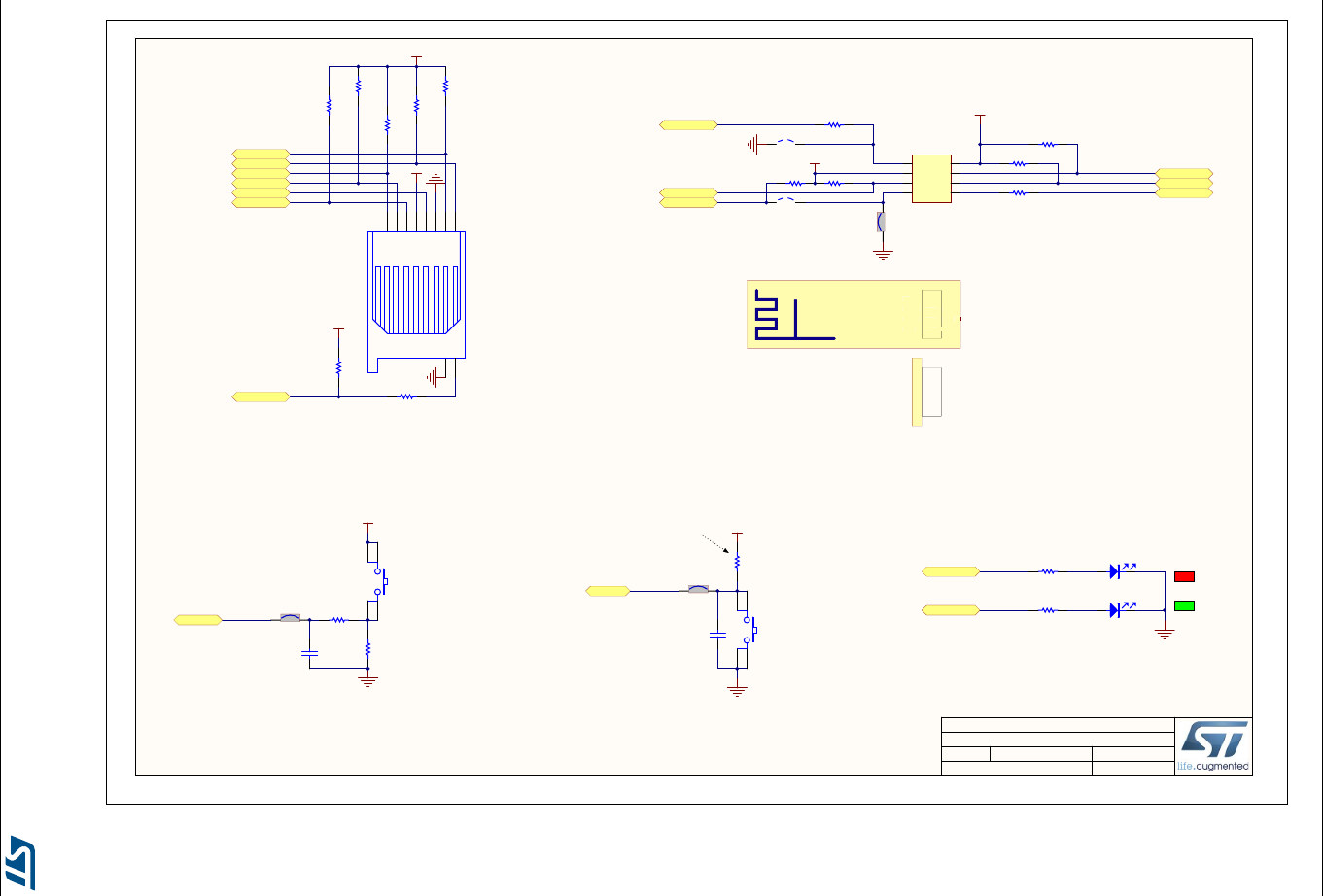
Schematics UM2033
50/56 UM2033 Rev 3
Figure 39. microSD™, Wi-Fi®, LEDs and push-button
12 12
uSD, Wifi, LEDs and Push Button
MB1225 B-01
3/11/2016
Title:
Size: Reference:
Date: Sheet: of
A4 Revision:
STM32F769I-DISCO
Project:
NRST
NRST
RESET Button
3V3
12
3 4
B2
SW-PUSH-CMS_BLACK
C53
100nF
I2C EXT Connector
R67
10K_1%_0402
Not Fitted
MICRO SD
uSD_CLK
uSD_CMD
SMS064FF or SMS128FF
uSD_D0
uSD_D1
uSD_D2
uSD_D3
uSD_Detect
3V3
(TF) Card
Input pin with pull-up
3V3
3V3
R80
47K_1%_0402
R76
[NA]
R73
0_5%_0402
R79
47K_1%_0402
R83
47K_1%_0402
R82
47K_1%_0402
R81
47K_1%_0402
SB9
B_USER
USER & WAKE-UP Button
12
3 4
B1
SW-PUSH-CMS_BLUE
B_USER
C54
100nF
SB10
1
2
3
4
5
6
7
8
SW2
9
SW1
10
CN5
PJS008-2003
R68
10K
R70
10K
1 2
3 4
5 6
7 8
CN2
Header F Straight 4x2H
WIFI with ESP8266
GND
VCC
GPIO2
GPIO0
CH_PD
RST
TX
RX
WIFI_RST
WIFI_TX
WIFI_RX
R56
10K
GND
GPIO2
GPIO0
RX VCC
CH_PD
TX
° °
SB5
° °
° °
° °
EXT_SDA
EXT_SCL
EXT_SCL
EXT_SDA
R52
10K
ESP8266-01
MB1064
R54
10K
3V3
EXT_RST EXT_RST
or
WIFI board
I2C board
SB5, SB6, OFF
WIFI_RST
LEDs
LD_USER1
LD_USER1
LD2
LED, green
LD1
LED, red
LD_USER2 LD_USER2 R63
330_1%_0603
R62
1K_1%_0603
3V3
GND
VCC
SCL
SDA
NC
NC
RST
NC
° °
° °
° °
° °
RST
G
ND
G
PI
O
2
G
PI
O
0
RX
VCC
C
H_
PD
T
X
°
°
°
°
°
°
°
°
R
ST
D
MB1020
SB8
SB6
3V3
WIFI_TX
WIFI_RX
SB8, ON
R57
1K
R50
1K
EXT_RST, EXT_SCL, EXT_SDA = HIZ
WIFI_RST, WIFI_RX, WIFI_TX = HIZ
R200
10K
SB8, OFF
SB5, SB6, ON
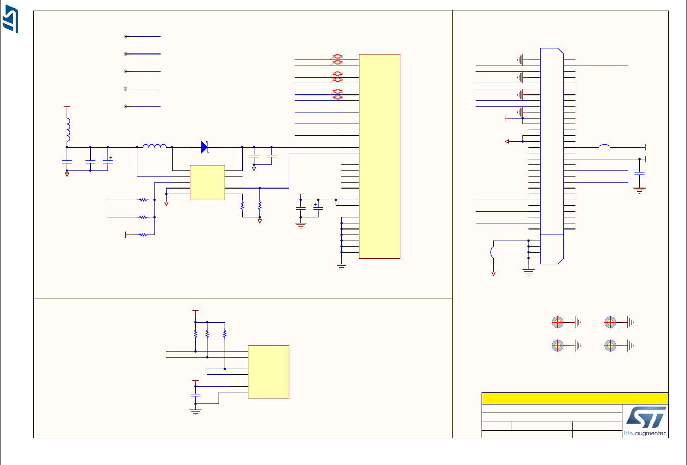
UM2033 Schematics
UM2033 Rev 3 51/56
Figure 40. 4-inch DSI LCD board
11
4 inch DSI LCD board
MB1166 A.1
8/15/2016
Title:
Size: Reference:
Date: Sheet: of
A4 Revision:
LCD daugterboard
Project:
Touch panel connector for LCD panel
VDD
I2C_SDA
I2C_SCL
INT
BL_CTRL
VDD
C6
4.7uF
C7
100nF
A
K
Z1
STPS1L40M
C1
4.7uF/50V
L2
4.7uH(1A)
R3
10
BLGND
BLVDD
R2
100K
C5
4.7uF/10V
R4
[N/A]
R5
4K7
BL_CTRL
BLGND
BLGND
BLGND Vi
1
Rset 2
GND
3FB 4
NC 5
Vo 6
EN
7
SW
8
PGND
9
U1
STLD40DPUR
C4
10nF
C3
100nF
L1
BEAD
C2
10nF
VL VH
BLGND
BLVDD
Connector for motherboard
KJD KM-040TMP-02
TP1
TP2
TP3
TP4
TP5
GND
BLGND
VDD
VH
VL
I2C Address:1010100
N
ote: Text in italic placed on a wire doesn¡¯t correspond to net name. It just helps to
identify rapidly MCU IO related to this wire.
H3
H4
Backlight driver & PFC connector for LCD panel
HSSI_CLK_N
HSSI_CLK_P
HSSI_D0_N
HSSI_D0_P
HSSI_D1_N
HSSI_D1_P
TE
C9
100nF
VDD
RST
RST
CABC
CABC R1
0
INT
R6
[N/A]
R7
[N/A]
VDD
R8
4K7
I2C_SDA
I2C_SCL
HSSI_CLK_N
HSSI_CLK_P
HSSI_D0_N
HSSI_D0_P
HSSI_D1_N
HSSI_D1_P
TE
RST
C8
100nF
HSSI_CLK_N
12
NC
13
HSSI_CLK_P
14
GND
15
HSSI_D1_N
16
NC
17
HSSI_D1_P
18
GND
19
NC/ERR
20
VCC
21
TE
22
LEDK
23 LEDA
24
GND
25
IOVCC
6
ID
1
GND
2
CABC
3
GND
4
HSSI_D0_N
8
NC
9
HSSI_D0_P
10
GND
11
RESX
5
GND
7
CN2
FH26-25S-0.3SHW
GND
6VDD
1
INT
2
SCL
3
SDA
4
RESET
5
CN3
FH19C-6S-05SH
1
122
3
344
5
566
7
788
9
910 10
11
11 12 12
13
13 14 14
15
15 16 16
17
17 18 18
19
19 20 20
21
21 22 22
23
23 24 24
25
25 26 26
27
27 28 28
29
29 30 30
31
31 32 32
33
33 34 34
35
35 36 36
37
37 38 38
39
39 40 40
41
41 42 42
43
43 44 44
45
45 46 46
47
47 48 48
49
49 50 50
51
51 52 52
53
53 54 54
55
55 56 56
57
57 58 58
59
59 60 60
61
61
62
62
63
63
64
64
CN1
QTH-030-02-F-D-A
SB1 Open BLVDD
BLGND
SB2
Open
VDD
FPC03025-14201(ATOM)
FPC05006-09200(ATOM)
H1
H2
Frida FRD397B2509
LCD P/N:
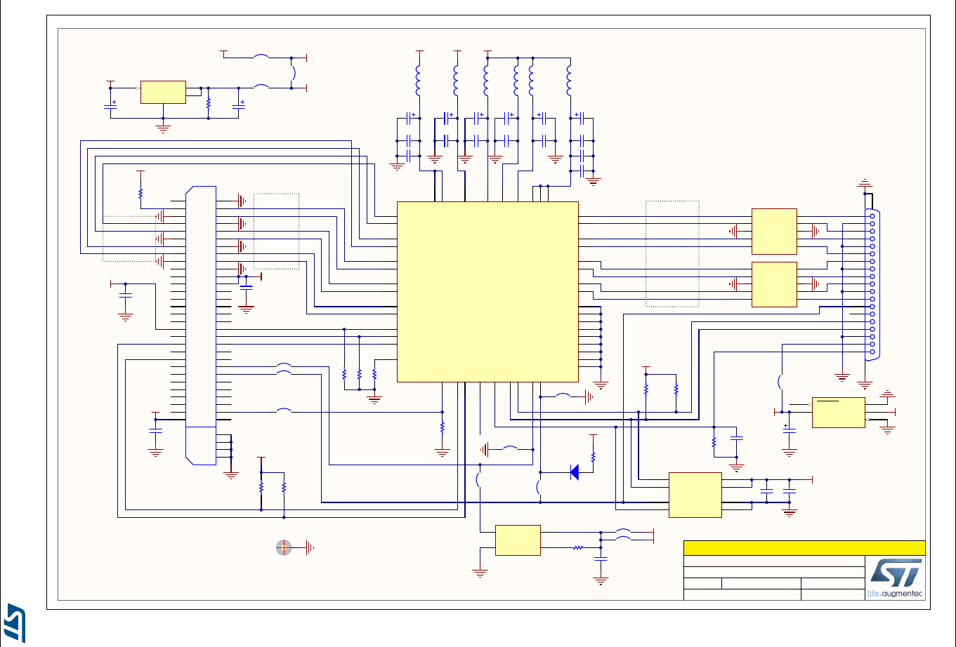
Schematics UM2033
52/56 UM2033 Rev 3
Figure 41. DSI to HDMI adapter
11
DSI to HDMI adapter
MB1232 A.1
5/20/2016
Title:
Size: Reference:
Date: Sheet: of
A4 Revision:
HDMI daugher board
Project:
Source
+5V
C20
4.7uF
GND 2
IN 5
EN 4
OUT
1FAULT
3
U5
STMPS2141STR@54
HDMI_5V_Source
+5V
TMDS_Data2+
TMDS_Data2-
TMDS_Data1+
TMDS_Data1-
TMDS_Data0+
TMDS_Data0-
TMDS_Clock+
TMDS_Clock-
Tx2- A2
GND C7
LRCLK
D3
V1P2 D4
INT
D5
CEC
D6
GND E7
GND F1
CEC_CLK
D7
DRx3+
G6 Tx1+ A3
GND B5
AVDD B4
GND B3
GND B2
V3P3 B1
PD
C3
HPD
C4
R_EXT
C5
PVDD C6
DRx1-
F4
DVDD E4
SDA
E5 SCL
E6
GND B6
Tx0+ A5
GND E1
DVDD E2
V1P2 E3
DVDD G1
DRxC+
G2
DRx0+
G3
DRx1+
G4
DRx2+
G5
DRx2-
F5
TxC- B7
DRx3-
F6
GND F7
Tx1- A4
Tx2+ A1
DDC_SDA
D2
DRx0-
F3
I2S/SPDIF
C1
Tx0- A6
DDC_SCL
D1
DRxC-
F2
SCLK/MCLK
C2
TxC+ A7
A2VDD G7
U2
ADV7533BCBZ-RL
+3V3
I2C_SDA
I2C_SCL
INT
+5V
Connector for motherboard
HSSI_CLK_N
HSSI_CLK_P
HSSI_D0_N
HSSI_D0_P
HSSI_D1_N
HSSI_D1_P
RST
C19
100nF
11
2
2
33
4
4
55
6
6
77
8
8
99
10
10
11 11
12
12
13 13
14
14
15 15
16
16
17 17
18
18
19 19
20
20
21 21
22
22
23 23
24
24
25 25
26
26
27 27
28
28
29 29
30
30
31 31
32
32
33 33
34
34
35 35
36
36
37 37
38
38
39 39
40
40
41 41
42
42
43 43
44
44
45 45
46
46
47 47
48
48
49 49
50
50
51 51
52
52
53 53
54
54
55 55
56
56
57 57
58
58
59 59
60
60
61 61
62 62
63 63
64 64
CN1
QTH-030-02-F-D-A
HSSI_D2_N
HSSI_D2_P
HSSI_D3_N
HSSI_D3_P
SCLK
LRCLK
I2S
CEC_CLK
INT
+1V8_CON
C21
100nF
HPD
DDC_SDA
DDC_SCL
L110uH
L310uH
L210uH
L410uH
L510uH
L610uH
C3
10uF
C9 100nF
C15 100nF
+3V3
C10 100nF
C4
10uF
+1V8
C14 100nF
C5
10uF
C11 100nF
C6
10uF
C7
10uF
C12 100nF
C8
10uF
C13 100nF
C16 100nF
C17 100nF
R6
10K
R8
[N/A]
R9
[N/A]
+1V8
SB11
Closed
R7
27K
+3V3
D1
BAR18
R2
1K[1%]
+3V3
CEC
A2 GND B2
5V A1
SCL
A3
SDA
B3 RPU C1
GND C2
HPD
C3
U6
HDMI05-CL01F3
CEC
+5V
C23
100nF
C24
100nF
Vin
3Vout 2
1
Tab 4
U1
LD1117S18TR
C2
10uF
+3V3
SB3 Closed
SB2 Open +1V8
+1V8_CON
SB8 Closed
SB9
Open
SB7
Open
H1
N
ote: Text in italic placed on a wire doesn¡¯t correspond to net name. It just helps to
identify rapidly MCU IO related to this wire.
SB6
Closed
R1
2K
R5
2K[N/A]
R3
2K[N/A]
R4
2K[N/A]
C22
100nF
SB5 Open
SB10
Closed
CEC_IO
Differential pairs 100ohm
Differential pairs 100ohm
Differential pairs 100ohm
C18
100nF
I2C address:0x7A
C1
10uF
R10
120[N/A]
SB1
Closed
V1P2
V1P2
VDD 4
OUT
3
EN 1
GND
2
X1
NZ2520SB-12.000000M-NSA3412D
+3V3
C25
100nF
R11 10K
SB4 Open
SB13 Open
SB12 Closed +1V8
R13
10K
R12
10K
1
2
3
4
5
6
7
8
9
10
11
12
13
14
15
16
17
18
19
22
20
21
CN2
HD119F-3A09200
GND 3
D1- 2
D1+ 1
D1+
10 D1-
9
D2+ 4
D2- 5
D2-
6
D2+
7
GND
8
U3
ECMF04-4HSWM10
GND 3
D1- 2
D1+ 1
D1+
10 D1-
9
D2+ 4
D2- 5
D2-
6
D2+
7
GND
8
U4
ECMF04-4HSWM10
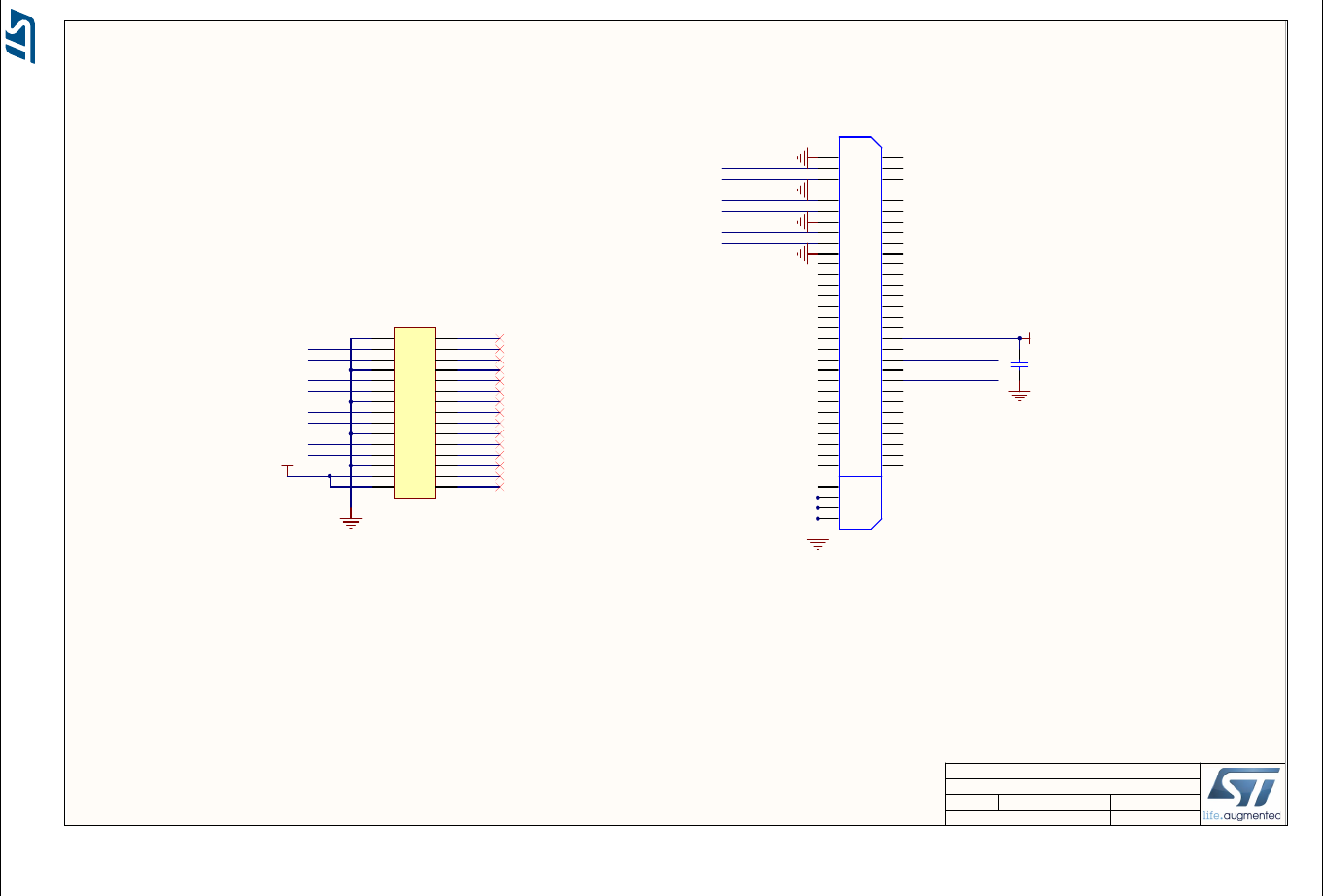
UM2033 Schematics
UM2033 Rev 3 53/56
Figure 42. DSI connector adapter
11
Overview
MB1233 A.1
5/23/2016
Title:
Size: Reference:
Date: Sheet: of
A4 Revision:
RaspberryPI Adapter
Project:
DSI_CK_P
DSI_CK_N
DSI_D0_P
DSI_D0_N
DSI_D1_P
DSI_D1_N
I2C_SCL
I2C_SDA
1
2
3
4
5
6
7
8
9
10
11
12
13
14
15
16
17
18
19
20
21
22
23
24
25
26
27
28
29
30
CN1
1-1734248-5
VDD
I2C_SDA
I2C_SCL
Connector for motherboard
C1
100nF
1
122
3
344
5
566
7
788
9
910 10
11
11 12 12
13
13 14 14
15
15 16 16
17
17 18 18
19
19 20 20
21
21 22 22
23
23 24 24
25
25 26 26
27
27 28 28
29
29 30 30
31
31 32 32
33
33 34 34
35
35 36 36
37
37 38 38
39
39 40 40
41
41 42 42
43
43 44 44
45
45 46 46
47
47 48 48
49
49 50 50
51
51 52 52
53
53 54 54
55
55 56 56
57
57 58 58
59
59 60 60
61
61
62
62
63
63
64
64
CN2
QTH-030-02-F-D-A
DSI_CK_P
DSI_CK_N
DSI_D0_P
DSI_D0_N
DSI_D1_P
DSI_D1_N
VDD
Connector for RaspberryPI LCD

Federal Communications Commission (FCC) and Industry Canada (IC) Compliance Statements
54/56 UM2033 Rev 3
Appendix C Federal Communications Commission (FCC)
and Industry Canada (IC) Compliance
Statements
C.1 FCC Compliance Statement
C.1.1 Part 15.19
This device complies with Part 15 of the FCC Rules. Operation is subject to the following
two conditions: (1) this device may not cause harmful interference, and (2) this device must
accept any interference received, including interference that may cause undesired
operation.
C.1.2 Part 15.105
This equipment has been tested and found to comply with the limits for a Class A digital
device, pursuant to part 15 of the FCC Rules. These limits are designed to provide
reasonable protection against harmful interference when the equipment is operated in a
commercial environment. This equipment generates, uses, and can radiate radio frequency
energy and, if not installed and used in accordance with the instruction manual, may cause
harmful interference to radio communications. Operation of this equipment in a residential
area is likely to cause harmful interference in which case the user will be required to correct
the interference at his own expense.
C.1.3 Part 15.21
Any changes or modifications to this equipment not expressly approved by
STMicroelectronics may cause harmful interference and void the user's authority to operate
this equipment.
C.2 IC Compliance Statement
7.12.1 Compliance Statement
Industry Canada ICES-003 Compliance Label: CAN ICES-3 (A)/NMB-3(A)
7.12.2 Déclaration de conformité
Étiquette de conformité à la NMB-003 d'Industrie Canada: CAN ICES-3 (B)/NMB-3(B)
UM2033 Rev 3 55/56
UM2033 Revision history
55
Revision history
Table 14. Document revision history
Date Revision Changes
20-May-2016 1 Initial release.
03-Oct-2016 2
Updates to introduce optional display accessories:
Section 1: Features and Section 4: Ordering information
Section 6.4: Power supply
New sections added:
Section 6.18: Adapter board from on-board DSI to HDMI (optional
accessory display)
Section 6.19: Adapter board from on-board DSI to external DSI
(optional accessory display)
New figures added:
Figure 3: 32F769IDISCOVERY board (bottom view), Figure 15: 4-
inch WVGA TFT DSI LCD daughterboard, Figure 16: DSI to HDMI
adapter board, Figure 17: DSI to HDMI adapter board, Figure 18:
On-board DSI to external DSI, Figure 19: On-board DSI to external
DSI, Figure 20: Wi-Fi module (ESP8266-01), Figure 39: 4-inch DSI
LCD board, Figure 40: DSI to HDMI adapter, Figure 41: DSI
connector adapter.
13-Apr-2018 3
Updated the former order code STM32F769I-DISCO1 to
STM32F769I-DISC1 across the whole document. Added note
about U device suffix in Chapter 3: Product marking. Corrected PI3
to PJ3 in Table 5: Arduino™ connectors (CN11, CN14, CN13 and
CN9). Corrected USART3 to USART1 in chapter Section 6.15:
Virtual COM port. Added missing SDRAM schematic as Figure 32:
SDRAM (MICRON). Attributed Quad-SPI Flash memory to
MACRONIX.

UM2033
56/56 UM2033 Rev 3
IMPORTANT NOTICE – PLEASE READ CAREFULLY
STMicroelectronics NV and its subsidiaries (“ST”) reserve the right to make changes, corrections, enhancements, modifications, and
improvements to ST products and/or to this document at any time without notice. Purchasers should obtain the latest relevant information on
ST products before placing orders. ST products are sold pursuant to ST’s terms and conditions of sale in place at the time of order
acknowledgement.
Purchasers are solely responsible for the choice, selection, and use of ST products and ST assumes no liability for application assistance or
the design of Purchasers’ products.
No license, express or implied, to any intellectual property right is granted by ST herein.
Resale of ST products with provisions different from the information set forth herein shall void any warranty granted by ST for such product.
ST and the ST logo are trademarks of ST. All other product or service names are the property of their respective owners.
Information in this document supersedes and replaces information previously supplied in any prior versions of this document.
© 2018 STMicroelectronics – All rights reserved
