Sd_5b_e_i1.PMD DCS500 3ADW000066R0901 System Description E I
User Manual: DCS500
Open the PDF directly: View PDF ![]() .
.
Page Count: 61
- Latest Technology, High Performance and a User Friendly Concept
- 1 DCS 500 - a State-of-the-art technology
- List of contents
- 2 DCS 500B components overview
- 2.1 Environmental Conditions
- 2.2 DCS 500B Power Converter Modules
- 2.3 DCS 500B Overload Capability
- 2.4 Field Supply
- 2.5 Options for DCS 500B / DCF 500B converter modules
- 2.6 Options for the drive
- 3 How to engineer your drive
- 3.1 Standard drive configuration using an internal field
- 3.2 Drive configuration using the internal field with reduced external components
- 3.3 Standard drive configuration using an external half-controlled field (1-ph)
- 3.4 Standard configuration using a fully-controlled field (3-ph) without armature converter
- 3.5 Typical configuration for high power drives
- 3.6 Typical configuration for high power drives connected in 12-pulse parallel Master-Follower application
- 4 Overview of software (Version 21.2xx)
- 4.1 GAD Engineering-Program
- 4.2 Introduction to the structure and handling
- Diagrams A4
- Diagrams A3
- Diagram A1
3ADW000066R0901_DCS500_System_description_e_i
DCS 500 Thyristor Power Converter
for DC drive systems
25 to 5200 A
6 to 5000 kW
System Description
DCS 500B / DCF 500B
Hints for printing:
A4-format from page 1...56 (System description + Software structure diagrams A4)
A3-format from page 57...60 (Software structure diagrams)
A1-format page 61 (Software structure overview)
These hints will not be printed!
3ADW000066R0901_DCS500_System_description_e_i
Latest Technology, High Performance and a User Friendly Concept
Wide Variety of Industrial
Applications
The DCS, DCA, DCF and DCR converters can
handle most demanding applications like:
• Metals
• Pulp & Paper
• Material handling
• Test Rigs
• Food & Beverage
• Printing
• Plastic & Rubber
• Oil Rigs
• Vessels
• Ski lifts
• Magnets
• MG Sets
• Electrolysis
• Battery Chargers
• and more
The DCS 500 series is a complete range of DC convert-
ers with high performance and reliability intended for
the supply and control of DC machine armatures.
DCA 500 is a DCS 500 converter module mounted in
a converter enclosure called "Common Cabinet" ( see
separate documentation).
DCF 500 is a DCS 500 module modified in a way to
supply other consumers than armature circuits of DC
machines ( e.g. inductive loads like motor field wind-
ings, magnets etc.).
For revamp projects ABB has created a special "Rebuild
Kit" called DCR 500 to polish up your old DC power
stack with a new modern digital front end (see separate
documentation).
A selection of options is available to provide the user
with a system meeting the most demanding technical
requirements and performance expectations as well as
many safety standards.
Common control electronics throughout the whole
range reduce spare parts, inventory and training.
TOOLS
• Effort, time and cost will be saved with the user-
friendly CMT-Tool (Commissioning and Mainte-
nance Tool) for drive programming, commission-
ing, monitoring and maintenance.
• Data Logger • Trending • Fault Logger
• Parameter/Signals • Local operation
•GAD Tool (Graphical Application Designer) con-
tains an extensive library of standard function blocks
for the creation of customized software solutions
creating conveniently the documentation during
programming.
Both, CMT and GAD, represent a powerful set for each
design, commissioning and service engineer to achieve
best results and performance.
II D 1-2
3ADW000066R0901_DCS500_System_description_e_i
1 DCS 500 - a State-of-the-art technology
❖flexible design
❖user-friendliness
Basic hardware complements
❋Thyristor bridge(s) (from size A5 with leg fuses
installed)
❋Temperature monitor for the thyristor bridge(s)
❋Fan
❋Power supply for the electronics
❋Microprocessor board
Additional components for integration in the mod-
ule
❋Field power converter
– uncontrolled full wave diode bridge, 6A or
– half-controlled diode/thyristor bridge, 16A
❋Communication board
❋Control panel
Moreover, the accessories listed below can be used
to individually customize the drive package in ac-
cordance with the application intended
❋External field supply units
❋Additional I/O boards
❋Interface modules for various communication pro-
tocol
❋EMC filter(s)
❋Application software packages
❋PC programs
The drive system functionality can be integrated with
various fieldbus control systems from simple to factory-
wide control.
DCS 500 is a freely programmable drive to meet almost
every application. Templates like Master-Follower,
Winder etc. can be obtained.
The DCS 500 constitutes a complete program for
ratings between 25 A and 5200 A as a power converter
module (for 12-pulse parallel connection, up to ap-
prox. 10,000 A), suitable for all commonly used three-
phase systems.
All our products are CE marked.
The DC drives factory of ABB Automation Products,
Drives Division in Lampertheim has implemented and
maintains a quality management system according to
DIN EN ISO 9001 and an environmental manage-
ment system according to DIN EN ISO 14001.
DCS 500 Drives are also approved according to UL
(Underwriters Laboratory).
They also comply with the relevant EMC standards for
Australia and New Zealand and are C-Tick marked.
DCS 500 converter units are suitable for both, standard
drive applications as well as demanding applications.
Appropriate PC programs ensure that the drives are
human-engineered for user-friendly operator control.
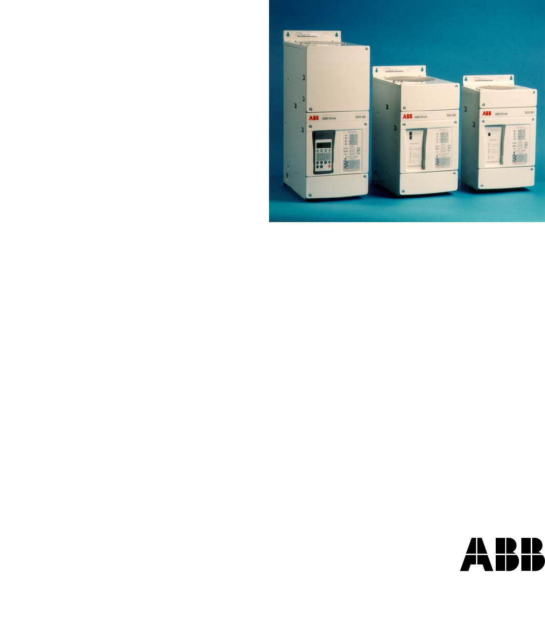
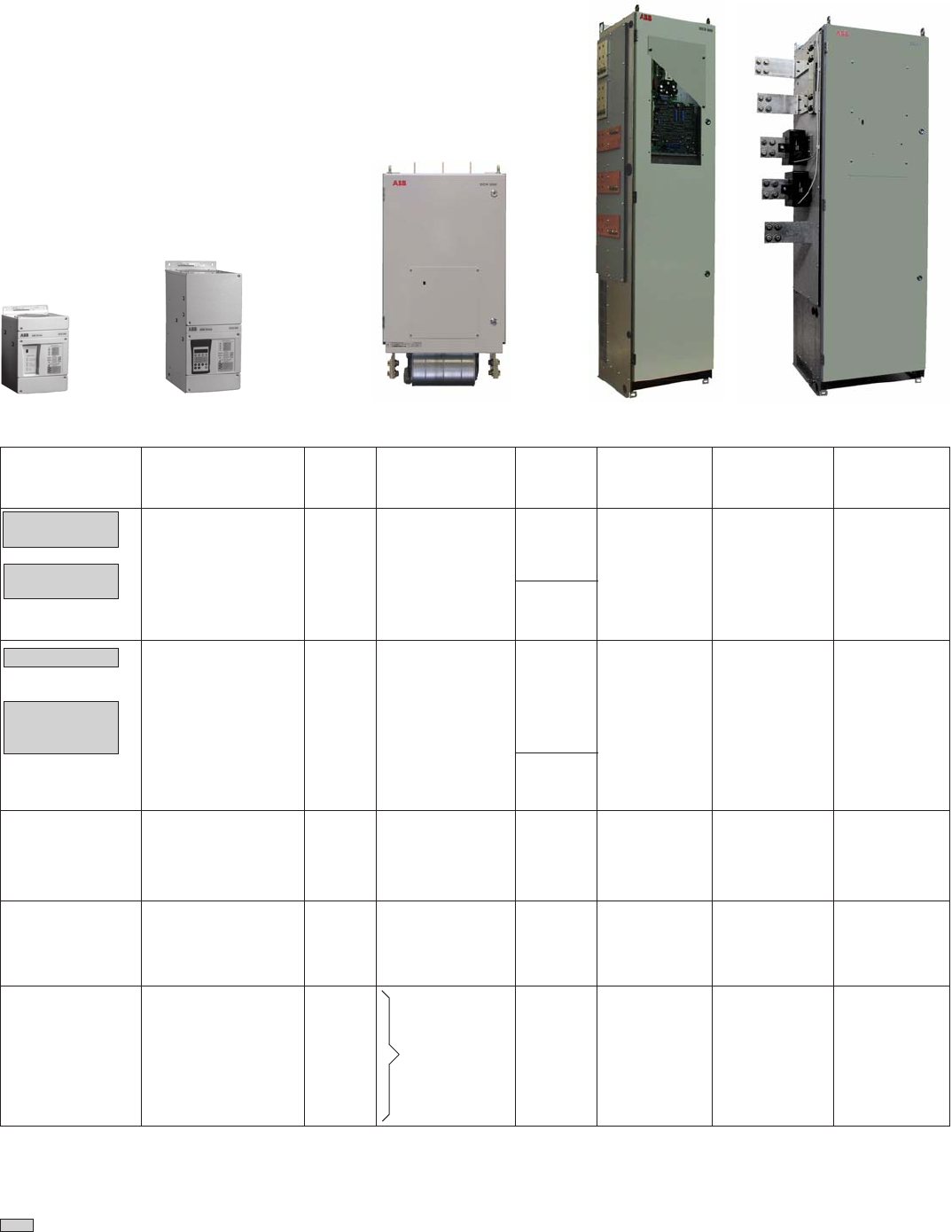
Unit range
The range comprises of 5 sizes, C1, C2, A5, A6 and A7.
We can deliver both modules and standard cubicles.
C1 - Module DCA cubicle
II D 1-3
DIN EN ISO 9001
DIN EN ISO 14001

3ADW000066R0901_DCS500_System_description_e_i
List of contents
II D SYSTEM DESCRIPTION
1 DCS 500 - a State-of-the-art technology .... II D 1-3
2 DCS 500 components overview ................. II D 2-1
2.1 Environmental conditions ............................................. II D 2-4
2.2 DCS 500 Power Converter Modules ............................ II D 2-5
2.3 DCS 500B overload capability ..................................... II D 2-8
2.4 Field Supply ............................................................... II D 2-10
2.5 Options for DCS 500B / DCF 500B converter mod. .. II D 2-12
Inputs/Outputs ........................................................... II D 2-12
Panel (control and display panel) ............................. II D 2-15
Serial interface
for operation by PC ................................................... II D 2-16
for drive control ......................................................... II D 2-16
2.6 Options for the drive ................................................... II D 2-18
Line reactors for armature and field supply .............. II D 2-18
Aspects of fusing for armature-circuit and field
supplies of DC drives ............................................. ...II D 2-20
Semiconductor type F1 fuses and fuse holders for
AC and DC power lines ............................................ II D 2-22
Fuses F3.x and fuse holders for 2-phase field supplyII D 2-22
Transformer T3 for field supply ................................. II D 2-22
Auxiliary transformer T2 for electronic system /
fan supply .................................................................. II D 2-23
Commutating reactor ................................................ II D 2-23
Residual current detection ........................................ II D 2-23
EMC filter .................................................................. II D 2-24
3 How to engineer your drive........................ II D 3-1
3.1 Standard drive configuration using an internal field .... II D 3-3
3.2 Drive configuration using the internal field with
reduced external components ..................................... II D 3-5
3.3 Standard drive configuration using an external
half-controlled field (1-ph) ............................................ II D 3-6
3.4 Standard configuration using a fully-controlled
field (3-ph) without armature converter ....................... II D 3-7
3.5 Typical configuration for high power drives ................. II D 3-8
3.6 Typical configuration for high power drives connected
in 12-pulse parallel Master-Follower application ....... II D 3-10
4 Overview of Software (Vers. 21.2xx) ......... II D 4-1
4.1 GAD Engineering Program .......................................... II D 4-1
4.2 Introduction to the structure and handling .................... II D 4-2
Software structure diagrams including comments
II D 1-4
II D 2-1
3ADW000066R0901_DCS500_System_description_e_i
2 DCS 500B components overview
Description of the converter
Drive configuration
DCA 500 / DCA 600 Enclosed con-
verters System description for standard
cubicles equipped with DC drives.
For those, who want to re-
program or adapt the soft-
ware of their drive a detailed
comprehensive description of the soft-
ware structure of the drive as well as of
all available function blocs can be delivered.
A DCS 500 Service Manual
is available for service engi-
neers.
Engineering and design peo-
ple for drive systems can get a separate
collection of information with regard to installation,
sizing, fusing etc. of DC drives called "Technical
guide".
In case you want to re-configure terminals by means of
software, please read the software description first and
inform yourself about the possibilities you have before
you start. (Never change any terminal while your drive
is still connected to the mains!). After that you need to
make sure that the correct signals are provided to your
terminals.
DCS 500 drives are freely programmable and therefore
also terminals with their in and outs can be modified in
their functionality.
When you receive your converter all terminals from X3:
to X7: are set to a default configuration as shown below.
This enables you to connect your drive according to
connection example (see chapter 3) without any chang-
es.
The documentation in hand describes
the functionality of DCS 500 converter
units as well as the cooperation of all
single components belonging to a com-
plete drive system.
As additional documentation is availa-
ble:
DCS 500 Technical Data giving infor-
mation about all direct technical data
for components used inside and outside
the converter module.
DCS 500 Operating Instructions including informa-
tion and advise to commission the drive.
If three phase DCF 500 field supply units are needed
please use the same documents as for DCS 500 arma-
ture converters.
Supplementary documentation
Application Blocks
DCS 500B
3ADW000048
Volume V D2
SW Description
DCS 500B
3ADW000078
Volume V D1
Technical Guide
DCS
3ADW000163
Volume VII A
Service Manual
DCS 500(B)/600
3ADW000093
Volume VI A
11023456789
X6: Analogue IN
AITAC AI1
90...270 V -
+
30...90 V -
8...30 V -
TACHO +
-
+
-
11023456789
X4: Analogue IN / OUT
IACT
0 V
0 V
+10V
0V
AO1
-10V
AO2
11023456789
X5: Encoder
0 V
CH A +
CH A -
11023456789
X6: Digital IN
+48 V
0 V
DI1
DI2
DI3
DI4
DI6
DI7
DI5
DI8
Converter Fan
RUN
Motor Fan
Main contactor
FREE
Emergency Stop
RESET
ON/OFF
12345678
X7: Digital OUT
DO1
DO2
DO3
DO4
DO6
DO7
DO5
0 V
Fan Contactor
Excitation contactor
Main contactor
Ready Running
Running
FREE
FREE
+
-
Main speed reference AI 1
Torque reference AI 2
FREE AI 3
AI2 AI3
+
-
FREE AI 4
AI4
Actual speed AO 1
Actual armature voltage AO 2
Actual current
CH B +
CH B -
CH Z +
CH Z -
SENSE 0 V
POWER OUT +
SENSE Power out +
(DO8 on SDCS-POW-1)
System Description
DCS 500B
3ADW000066
Volume II D
Operating Instructions
DCS 500B
3ADW000055
Volume IV D
Technical Data
3ADW000165
Volume III
Scope of delivery
The delivery consists of a converter module and some
accessories. The document Quick Guide and a CD
ROM with all the converter related documentation in
different languages and screws to allow the wiring acc.
to EMC are always included. For C1 and C2 converters
a plug to connect the fan and screws to fix the power
cables are added. Depending on the construction type
screws for the power cables (A5), a key to open the door
(all) and a tool to exchange thyristors will be delivered
with the converter.
additional parts A5, A6, A7additional parts C1, C2
System Description
DCA 500 / DCA 600
3ADW000121
Volume II D1
II D 2-2
3ADW000066R0901_DCS500_System_description_e_i
The DCS 500B power converter together with the
options or accessories is designed to control DC motors
as well as other DC loads. In case of DC motors the
This overview has been designed to help you to familiarize yourself
with the system; its main components are shown in the diagram above.
The system’s heart is the DCS 500B power converter module.
Fig. 2/1: DCS 500B Components overview
L1
K1
T2
Q1
F2 F3
X12:
X13:
X37:
X1: X2:
M
T
T
83
857
2
X17: X16: X14:
PC +
CMT/DCS500
DCF 503 / 504
COM x CON 2 POW 1
PIN 1x
PIN 51
DCF 501B / 502B
IOB 2x IOB 3 IOE 1
PS5311
X11:
X33:
PIR 21
PIN 2x/20x
7
3
8
4
T3
F1
K5
K3
≤ 690V
≤ 1000V
CDP 312
SNAT 6xx
FEX 1 FEX 2
Nxxx-0x
µP
M
DCS 50.B....-.1-21.....
PIN 41
PIN 41
L3
*
+24 V
Power
supply
to field
Three-phase field supply
COM x - short designation of components
analogue input / output
alternative
EMC filter
Earth-fault monitor
Field bus
to the PLC
optical fibre optical fibre
digital input / output
Legend
7.1 - detailed description see chapter 7.1
see Technical Data
*
Armature converter components overview
DCS 500B converter itself is used for the armature
supply and a build-in or external field supply to control
the field current.
II D 2-3
3ADW000066R0901_DCS500_System_description_e_i
X1: X2: X17: X16:
COM x CON 2
X11:
X33:
CDP 312
µP
83
857
2
IOB 2x IOB 3 IOE 1
PS5311
7
3
8
4
Nxxx-0x
+24 V
L1
K3
T2
Q1
F2
X37:
PC +
DDC-Tool
POW 1
PIN 1x
DCF 506
PIR 21
PIN 2x/20x
F1
K5
≤ 690V
≤ 500V
SNAT 6xx
M
DCF 50.B....-.1-21.....
X12:
X13:
CZD-0x
to X16: DCS 500B
(Armature converter)
to a digital input
of DCF 500B
COM x - short designation of components
analogue input / output
alternative
EMC filter
Earth-fault monitor
digital input / output
Legend
7.1 - detailed description see chapter 7.1
modified
optical fibre optical fibre
Field bus
to the PLC
The hardware of a DCS 500B converter had been taken
as a basis to get the DCF 500B converter which is used
to control high inductive loads. Both converters use the
same software. Looking on a complete system these two
Fig. 2/2: DCF 500B Components overview
Field converter components overview
converters differ in some boards, the options and the
wiring (the option CZD-0x is not needed in every case;
see manual Technical Data).
II D 2-4
3ADW000066R0901_DCS500_System_description_e_i
2.1 Environmental Conditions
System connection
Voltage, 3-phase: 230 to 1000 V acc. to IEC 60038
Voltage deviation: ±10% continuous; ±15% short-time *
Rated frequency: 50 Hz or 60 Hz
Static frequency deviation: 50 Hz ±2 %; 60 Hz ±2 %
Dynamic: frequency range: 50 Hz: ±5 Hz; 60 Hz: ± 5 Hz
df/dt: 17 % / s
* = 0.5 to 30 cycles.
Please note: Special consideration must be taken for voltage deviation
in regenerative mode.
Degree of protection
Converter Module and options
(line chokes, fuse holder,
field supply unit, etc.): IP 00
Enclosed converters: IP 20/21/31/41
Paint finish
Converter module: NCS 170 4 Y015R
Enclosed converter: light grey RAL 7035
Fig. 2.1/1: Effect of the site elevation above sea level
on the converter’s load capacity.
Current reduction to (%)
Fig. 2.1/2: Effect of the ambient temperature on the
converter module load capacity.
Current reduction to (%)
Regulatory Compliance
The converter module and enclosed converter components are designed for use
in industrial environments. In EEA countries, the components fulfil the require-
ments of the EU directives, see table below.
North American Standards
In North America the system components fulfil
the requirements of the table below.
70
80
90
100
110
30 35 40 45 50 55°C
50
60
70
80
90
100
1000 2000 3000 4000 5000m
Standards Rated
supply
voltage
Converter module Enclosed converter
to 600 V UL 508 C
Power Conversion
Equipment
CSA C 22.2 No. 14-95
Industrial Control
Equipment,
Industrial Products
Available for converter
modules including field
exciter units.
Types with UL mark:
• see UL Listing
www.ul.com /
certificate no.
E196914
• or on request
UL/CSA types: on request
> 600 V
to
1000 V
EN / IEC xxxxx see
table on the left
Available for converter
modules
including field exciter
units.
EN / IEC types: on request
(for details see table on the
left)
Environmental limit values
Permissible cooling air temperature
- at converter module air inlet: 0 to +55°C
with rated DC current: 0 to +40°C
w. different DC curr. acc. Fig. 2.1/2: +30 to +55°C
- Options: 0 to +40°C
Relative humidity (at 5...+40°C): 5 to 95%, no condensation
Relative humidity (at 0...+5°C): 5 to 50%, no condensation
Change of the ambient temp.: < 0.5°C / minute
Storage temperature: -40 to +55°C
Transport temperature: -40 to +70°C
Pollution degree (IEC 60664-1, IEC 60439-1): 2
Site elevation:
<1000 m above M.S.L.: 100%, without current reduction
>1000 m above M.S.L.: with current reduct., see Fig. 2.1/1
Size Sound pressure level LPVibration
(1 m distance)
as module enclosed conv. as module enclosed conv.
C1 59 dBA 57 dBA g, 2...150 Hz
C2 75 dBA 77 dBA g, 2...150 Hz
A5 73 dBA 78 dBA g, 2...150 Hz
A6 75 dBA 73 dBA g, 2...150 Hz
A7 82 dBA 80 dBA g, 2...150 Hz
0.5 g, 5...55 Hz
1 mm, 2...9 Hz
0.3 g, 9...200 Hz
Standards Rated
supply
voltage
Converter module Enclosed converter
to 600 V UL 508 C
Power Conversion
Equipment
CSA C 22.2 No. 14-95
Industrial Control
Equipment,
Industrial Products
Available for converter
modules including field
exciter units.
Types with UL mark:
• see UL Listing
www.ul.com /
certificate no.
E196914
• or on request
UL/CSA types: on request
> 600 V
to
1000 V
EN / IEC xxxxx see
table on the left
Available for converter
modules
including field exciter
units.
EN / IEC types: on request
(for details see table on the
left)
evitceriDnoinUnaeporuEecnarussAs'rerutcafunaM
sdradnatSdezinomraH
eludomretrevnoCretrevnocdesolcnE
evitceriDyrenihcaM
CEE/73/89
CEE/86/39
fonoitaralceD
noitaroprocnI
1-40206NE
]1-40206CEI[
1-40206NE
]1-40206CEI[
evitceriDegatloVwoL
CEE/32/37
CEE/86/39
ytimrofnoCfonoitaralceD
1-1-64106NE
]1-1-64106CEI[
]--CEI[87105NE
lanoitiddaees
46606CEI
1-40206NE
]1-40206CEI[
1-93406NE
]1-93406CEI[
evitceriDCME
CEE/633/98
CEE/86/39
ytimrofnoCfonoitaralceD
llatahtdedivorP(
snoitcurtsninoitallatsni
elbacgninrecnoc
dnag
nilbac,noitceles
detacidedrosretlifCME
).dewolloferaremrofsnart
3-00816NE ➀
]3-00816CEI[
3-00816NE ➀
]3-00816
CEI[
➀htiwecnadroccani
230000WDA3
➀ecnadroccani
/230000WDA3htiw
190000WDA3

II D 2-5
3ADW000066R0901_DCS500_System_description_e_i
2.2 DCS 500B Power Converter Modules
The power converter modules are modular in construc-
tion. They are based on the casing, which houses the
power section with the RC snubber circuit. There are
different sizes (C1a/b, C2a/b, A5, A6, A7), graduated
in terms of current and voltage ranges. All units are fan-
cooled.
The power section is controlled by the unit’s electronic
system, which is identical for the entire range. Parts of
the unit’s electronic system can be installed in the unit,
depending on the particular application involved, e.g.
a field supply for the motor, or an interface board. A
control/display panel is available for the operator. It can
be snapped into place on the power converter module
or installed in the switchgear cubicle door by means of
a mounting kit.
Accessories such as external fuses, line reactors etc. are
also available, to compose a complete drive system.
Reference variables
The voltage characteristics are shown
in Table 2.2/1. The DC voltage char-
acteristics have been calculated using
the following assumptions:
•UVN = rated input terminal volt-
age, 3-phase
• Voltage tolerance ±10 %
• Internal voltage drop approx. 1%
•If a deviation or a voltage drop has
to be taken into consideration in
compliance with IEC and VDE
standards, the output voltage or
the output current must be re-
duced by the actual factor accord-
ing to the table on the right.
Table 2.2/1: DCS 500B max. DC voltages achievable with a specified input
voltage.
System con- DC voltage Ideal DC Recommended
nection voltage (recommended) voltage DCS 500B
U
VN
U
dmax 2-Q
U
dmax 4-Q without load Voltage class
U
di0 y=
230 265 240 310 4
380 440 395 510 4
400 465 415 540 4
415 480 430 560 4
440 510 455 590 5
460 530 480 620 5
480 555 500 640 5
500 580 520 670 5
525 610 545 700 6
575 670 600 770 6
600 700 625 810 6
660 765 685 890 7
690 800 720 930 7
790 915 820 1060 8
1000 1160 1040 1350 9
1190 1380 1235 1590 1
If armature voltages higher than recommended are re-
quested, please check carefully, wether your system is still
working under safe conditions.
Table 2.2/2: Maximum permitted armature voltage
Max. permitted armature voltage depending on
Field exciter type
Application Armature converter
SDCS-FEX-1 SDCS-FEX-2A
DCF 503A/504A
DCF 501B
DCF 504A
DCF 502B
Power always positive (Ua and Ia pos.).
Extruder
2-Q Udmax 2-Q U
dmax 2-Q -
Power often or always negative.
Unwinder, suspended load
2-Q Udmax 4-Q U
dmax 4-Q U
dmax 4-Q
Power sporadically negative.
Printing machine at electrical stop
2-Q - -
Udmax 2-Q +
change
software
parameter
Power positive or negative.
Test rig
4-Q Udmax 4-Q U
dmax 4-Q -
Power positive, sporadically negative.
4-Q Udmax 4-Q U
dmax 2-Q +
change
software
parameter
-
II D 2-6
3ADW000066R0901_DCS500_System_description_e_i
Converter type y →y=4 (400 V) y=5 (500 V) y=6 (600 V) y=7 (690 V)
x=1 → 2-Q IDC [A] IAC [A] P [kW] P [kW] P [kW] P [kW]
x=2 → 4-Q 4Q 2Q 4Q 2Q 4Q 2Q 4Q 2Q 4Q 2Q 4Q 2Q
DCS50xB0025-y1 25 25 20 20 10 12 13 15
DCS50xB0050-y1 50 50 41 41 21 23 26 29
DCS50xB0050-61 50 50 41 41 31 35
DCS50xB0075-y1 75 75 61 61 31 35 39 44
DCS50xB0100-y1 100 100 82 82 42 47 52 58
DCS50xB0110-61 110 100 90 82 69 70
DCS50xB0140-y1 140 125 114 102 58 58 73 73
DCS50xB0200-y1 200 180 163 147 83 84 104 104
DCS50xB0250-y1 250 225 204 184 104 105 130 131
DCS50xB0270-61 270 245 220 200 169 172
DCS50xB0350-y1 350 315 286 257 145 146 182 183
DCS50xB0450-y1 450 405 367 330 187 188 234 235 281 284
DCS50xB0520-y1 520 470 424 384 216 219 270 273
DCS50xB0680-y1 680 610 555 500 282 284 354 354
DCS50xB0820-y1 820 740 670 605 340 344 426 429
DCS50xB1000-y1 1000 900 820 738 415 418 520 522
DCS50xB0903-y1 900 900 734 734 563 630 648 720
DCS50xB1203-y1 1200 1200 979 979 498 558 624 696
DCS50xB1503-y1 1500 1500 1224 1224 623 698 780 870 938 1050 1080 1200
DCS50xB2003-y1 2000 2000 1632 1632 830 930 1040 1160 1400 1600
DCF50xB0025-y1 25 25 20 20 10 12 13 15
DCF50xB0050-y1 50 50 41 41 21 23 26 29
DCF50xB0075-y1 75 75 61 61 31 35 39 44
DCF50xB0100-y1 100 100 82 82 42 47 52 58
DCF50xB0200-y1 200 180 163 147 83 84 104 104
DCF50xB0350-y1 350 315 286 257 145 146 182 183
DCF50xB0450-y1 450 405 367 330 187 188 234 235
DCF50xB0520-y1 520 470 424 384 216 219 270 273
Table 2.2/3: Table of DCS 500B / DCF 500B units - construction types C1, C2, A5
Converter type y →y=4 (400 V) y=5 (500 V) y=6 (600 V) y=7 (690 V) y=8 (790 V) y=9 (1000V) y=1 (1190V)
IDC [A] IAC [A] P [kW] P [kW] P [kW] P [kW] P [kW] P [kW] P [kW] ➀
2-Q converters
DCS501B1903-y1 1900 1550 1740
DCS501B2053-y1 2050 1673 1190 1430 1640
DCS501B2503-y1 2500 2040 1160 1450 1750 2000 2300
DCS501B3003-y1 3000 2448 1395 1740 2090 2400 2750
DCS501B2053-y1 2050 1673 2390
DCS501B2603-y1 2600 2121 3030
on request
DCS501B3303-y1 3300 2693 1540 1925 2310 2660 3040 3850
on request
DCS501B4003-y1 4000 3264 1870 2330 2800 3220 3690 4670
on request
DCS501B4803-y1 4800 3917 3360 3860 4420
DCS501B5203-y1 5200 4243 2430 3030
4-Q converters
DCS502B1903-y1 1900 1550 1560
DCS502B2053-y1 2050 1673 1070 1280 1470
DCS502B2503-y1 2500 2040 1040 1300 1560 1800 2060
DCS502B3003-y1 3000 2448 1250 1560 1880 2150 2470
DCS502B2053-y1 2050 1673 2390
DCS502B2603-y1 2600 2121 3030
on request
DCS502B3303-y1 3300 2693 1375 1720 2060 2370 2720 3440
on request
DCS502B4003-y1 4000 3264 1670 2080 2500 2875 3290 4170
on request
DCS502B4803-y1 4800 3917 3000 3450 3950
DCS502B5203-y1 5200 4243 2170 2710
➀ These converters are equipped with additional components. More information on request
Table 2.2/4: Table of DCS 500B units - construction type A6 / A7
Higher currents up to 15,000 A are achieved by
paralleling converters - information on request.
II D 2-7
3ADW000066R0901_DCS500_System_description_e_i
Construction type C2Construction type C1
Converter type ➁Dimensions Weight Clearances Construct. Power loss Fan Semiconductor
H x W x D top/bottom/side type at 500V connection Fuses
[mm] [kg] [mm] PV [kW]
DCS50xB0025-y1 420x273x195 7.1 150x100x5 C1a < 0.2 230 V/1 ph external
DCS50xB0050-y1 420x273x195 7.2 150x100x5 C1a < 0.2 230 V/1 ph external
DCS50xB0050-61 420x273x195 7.6 150x100x5 C1a - 230 V/1 ph external
DCS50xB0075-y1 420x273x195 7.6 150x100x5 C1a < 0.3 230 V/1 ph external
DCS50xB0100-y1 469x273x228 11.5 250x150x5 C1b < 0.5 230 V/1 ph external
DCS50xB0110-61 469x273x228 11.5 250x150x5 C1b - 230 V/1 ph external
DCS50xB0140-y1 469x273x228 11.5 250x150x5 C1b < 0.6 230 V/1 ph external
DCS50xB0200-y1 505x273x361 22.3 250x150x5 C2a < 0.8 230 V/1 ph external
DCS50xB0250-y1 505x273x361 22.3 250x150x5 C2a < 1.0 230 V/1 ph external
DCS50xB0270-61 505x273x361 22.8 250x150x5 C2a - 230 V/1 ph external
DCS50xB0350-y1 505x273x361 22.8 250x150x5 C2a < 1.3 230 V/1 ph external
DCS50xB0450-y1 505x273x361 28.9 250x150x10 C2a < 1.5 230 V/1 ph external
DCS50xB0520-y1 505x273x361 28.9 250x150x10 C2a < 1.8 230 V/1 ph external
DCS50xB0680-y1 652x273x384 42 250x150x10 C2b < 1.6 230 V/1 ph external
DCS50xB0820-y1 652x273x384 42 250x150x10 C2b < 2.0 230 V/1 ph external
DCS50xB1000-y1 652x273x384 42 250x150x10 C2b < 2.5 230 V/1 ph external
DCS50xB0903-y1 1050x510x410 110 300x100x20 A5 - 230 V/1-ph internal
DCS50xB1203-y1 1050x510x410 110 300x100x20 A5 < 5.2 230 V/1-ph internal
DCS50xB1503-y1 1050x510x410 110 300x100x20 A5 < 5.5 230 V/1-ph internal
DCS50xB2003-y1 1050x510x410 110 300x100x20 A5 < 6.6 230 V/1-ph internal
DCS50xB1903-81 1750x460x410 180 ➂ x0x50 A6 - 400...500 V/3-ph
DCS50xB2053-y1 1750x460x410 180 ➂ x0x50 A6 < 7.9 at y = 4, 5, 8 internal
DCS50xB2503-y1 1750x460x410 180 ➂ x0x50 A6 < 9.3 500...690 V/3-ph
DCS50xB3003-y1 1750x460x410 180 ➂ x0x50 A6 < 11.9 at y = 6, 7
DCS50xB2053-y1L➀1750x770x570 315 A7 - 400/690 V/3-ph
DCS50xB2603-y1L➀1750x770x570 315 A7 - 400/690 V/3-ph internal
DCS50xB3203-y1L➀1750x770x570 315 A7 - 400/690 V/3-ph
DCS50xB3303-y1L➀1750x770x570 315 A7 < 15 400/690 V/3-ph
DCS50xB4003-y1L➀1750x770x570 315 A7 < 16 400/690 V/3-ph
DCS50xB4803-y1L➀1750x770x570 315 A7 - 400/690 V/3-ph
DCS50xB5203-y1L➀1750x770x570 315 A7 < 20 400/690 V/3-ph
➀Busbar connection on the right side is optional
Example for the type designation: connection left DCS50xB5203-y1L; connection right DCS50xB5203-y1R)
➁ x=1 → 2-Q; x=2 → 4-Q; y=4...9/1 → 400...1000 V/1190 V supply voltage
➂Exhaust air must leave enclosure via air channel
also available as field supply converter DCF50xB (for 500 V s. also table 2.2/3). Data are the same as the armature current converter DCS50xB
Table 2.2/5: Table of DCS 500B units
Construction type A5 Construction type A6 Construction type A7
left busbar connection
to be installed
in cubicle

II D 2-8
3ADW000066R0901_DCS500_System_description_e_i
Unit type IDC I IDC II IDC III IDC IV
contin- 100 % 150 % 100 % 150 % 100 % 200 %
uous 15 min 60 s 15 min 120 s 15 min 10 s
400 V / 500 V [A] [A] [A] [A]
DCS 50xB0025-41/51 25 24 36 23 35 24 48
DCS 50xB0050-41/51 50 44 66 42 63 40 80
DCS 50xB0075-41/51 75 60 90 56 84 56 112
DCS 50xB0100-41/51 100 71 107 69 104 68 136
DCS 501B0140-41/51 125 94 141 91 137 90 180
DCS 502B0140-41/51 140 106 159 101 152 101 202
DCS 501B0200-41/51 180 133 200 132 198 110 220
DCS 502B0200-41/51 200 149 224 146 219 124 248
DCS 501B0250-41/51 225 158 237 155 233 130 260
DCS 502B0250-41/51 250 177 266 173 260 147 294
DCS 501B0350-41/51 315 240 360 233 350 210 420
DCS 502B0350-41/51 350 267 401 258 387 233 466
DCS 501B0450-41/51 405 317 476 306 459 283 566
DCS 502B0450-41/51 450 352 528 340 510 315 630
DCS 501B0520-41/51 470 359 539 347 521 321 642
DCS 502B0520-41/51 520 398 597 385 578 356 712
DCS 501B0680-41/51 610 490 735 482 732 454 908
DCS 502B0680-41/51 680 544 816 538 807 492 984
DCS 501B0820-41/51 740 596 894 578 867 538 1076
DCS 502B0820-41/51 820 664 996 648 972 598 1196
DCS 501B1000-41/51 900 700 1050 670 1005 620 1240
DCS 502B1000-41/51 1000 766 1149 736 1104 675 1350
DCS 50xB1203-41/51 1200 888 1332 872 1308 764 1528
DCS 50xB1503-41/51 1500 1200 1800 1156 1734 1104 2208
DCS 50xB2003-41/51 2000 1479 2219 1421 2132 1361 2722
DCS 50xB2053-51 2050 1550 2325 1480 2220 1450 2900
DCS 501B2503-41/51 2500 1980 2970 1880 2820 1920 3840
DCS 502B2503-41/51 2500 2000 3000 1930 2895 1790 3580
DCS 501B3003-41/51 3000 2350 3525 2220 3330 2280 4560
DCS 502B3003-41/51 3000 2330 3495 2250 3375 2080 4160
DCS 50xB3303-41/51 3300 2416 3624 2300 3450 2277 4554
DCS 50xB4003-41/51 4000 2977 4466 2855 4283 2795 5590
DCS 50xB5203-41/51 5200 3800 5700 3669 5504 3733 7466
600 V / 690 V
DCS 50xB0050-61 50 44 66 43 65 40 80
DCS 501B0110-61 100 79 119 76 114 75 150
DCS 502B0110-61 110 87 130 83 125 82 165
DCS 501B0270-61 245 193 290 187 281 169 338
DCS 502B0270-61 270 213 320 207 311 187 374
DCS 501B0450-61 405 316 474 306 459 282 564
DCS 502B0450-61 450 352 528 340 510 313 626
DCS 50xB0903-61/71 900 684 1026 670 1005 594 1188
DCS 50xB1503-61/71 1500 1200 1800 1104 1656 1104 2208
DCS 501B2003-61/71 2000 1479 2219 1421 2132 1361 2722
DCS 50xB2053-61/71 2050 1520 2280 1450 2175 1430 2860
DCS 501B2503-61/71 2500 1940 2910 1840 2760 1880 3760
DCS 502B2503-61/71 2500 1940 2910 1870 2805 1740 3480
DCS 501B3003-61/71 3000 2530 3795 2410 3615 2430 4860
DCS 502B3003-61/71 3000 2270 3405 2190 3285 2030 4060
DCS 50xB3303-61/71 3300 2416 3624 2300 3450 2277 4554
DCS 50xB4003-61/71 4000 3036 4554 2900 4350 2950 5900
DCV 50xB4803-61/71 4800 3734 5601 3608 5412 3700 7400
790 V
DCS 50xB1903-81 1900 1500 2250 1430 2145 1400 2800
DCS 501B2503-81 2500 1920 2880 1820 2730 1860 3720
DCS 502B2503-81 2500 1910 2865 1850 2775 1710 3420
DCS 501B3003-81 3000 2500 3750 2400 3600 2400 4800
DCS 502B3003-81 3000 2250 3375 2160 3240 2000 4000
DCS 50xB3303-81 3300 2655 3983 2540 3810 2485 4970
DCS 50xB4003-81 4000 3036 4554 2889 4334 2933 5866
DCS 50xB4803-81 4800 3734 5601 3608 5412 3673 7346
1000 V
DCS 50xB2053-91 2050 1577 2366 1500 2250 1471 2942
DCS 50xB2603-91 2600 2000 3000 1900 2850 1922 3844
DCS 50xB3303-91 3300 2551 3827 2428 3642 2458 4916
DCS 50xB4003-91 4000 2975 4463 2878 4317 2918 5836
1190 V Data on request
x=1 → 2-Q; x=2 → 4-Q
2.3 DCS 500B Overload Capability
To match a drive system’s components as efficiently as possible to the driven
machine’s load profile, the armature power converters DCS 500B can be dimen-
sioned by means of the load cycle. Load cycles for driven machines have been
defined in the IEC 146 or IEEE specifications, for example.
The currents for the DC I to DC IV types of load (see diagram on the following page) for the power converter
modules are listed in the table below.
Table 2.3/1:
Power converter module
currents with corresponding
load cycles.
The characteristics are
based on an ambient tem-
perature of max. 40°C and
an elevation of max. 1000 m
a.s.l.
II D 2-9
3ADW000066R0901_DCS500_System_description_e_i
Operating Load for Typical applications Load cycle
cycle converter
DC I IDC I continuous (IdN) pumps, fans
DC II IDC II for 15 min and extruders, conveyor belts
1,5 * IDC II for 60 s
DC III * IDC III for 15 min and extruders, conveyor belts
1,5 * IDC III for 120 s
DC IV * IDC IV for 15 min and
2 * IDC IV for 10 s
100%
150% 100%
150% 100%
200% 100%
15 min
15 min
15 min
If the driven machine’s load cycle does
not correspond to one of the examples
listed, you can determine the necessary
power converter using the DriveSize soft-
ware program.
This program can be run under Microsoft® Windows,
and enables you to dimension the motor and the power
converter, taking types of load (load cycle), ambient
temperature, site elevation, etc. into account. The
design result will be presented in tables, charts, and can
be printed out as well.
To facilitate the start-up procedure as much as possible
the converter´s software is structured similar as the
inputs made at the program. Because of that many of
the data can be directly utilized at the converter like
high current, line voltage and others.
Fig. 2.3/1: Entry screen of the PC for the dimensioning program.
Microsoft is a registered trademark. Windows is a designation of the Microsoft Corporation.
Types of load
* Load cycle is not identical to the menu item
Duty cycle
in the DriveSize program !
Table 2.3/2: Definition of the load cycles
II D 2-10
3ADW000066R0901_DCS500_System_description_e_i
2.4 Field Supply
General data
SDCS-FEX-1
• Diode bridge
• 6 A rated current
• Internal minimum field current monitor, requiring
no adjustment.
• Construction and components have been designed
for an insulation voltage of 600 V AC.
• Output voltage UA:
UU TOL
AV
=+
⎛
⎝
⎜⎞
⎠
⎟
**,
100%
100% 09
TOL = tolerance of line voltage in %
UV = Line voltage
• Recommendation:
Field voltage ~ 0,9 * UV
SDCS-FEX-2A
• Half-controlled thyristor/diode bridge (1-Q)
• Microprocessor control, with the electronic system
being supplied by the armature-circuit converter.
• Construction and components have been designed
for an insulation voltage of 600 V AC.
• Fast-response excitation is possible with an appro-
priate voltage reserve; de-excitation takes place by
field time constant.
• Output voltage UA:
UU TOL
AV
=+
⎛
⎝
⎜⎞
⎠
⎟
**,
100%
100% 09
TOL = tolerance of line voltage in %
UV = Line voltage
• Recommendation:
Field voltage 0.6 to 0.8 * UV
All field power converters (except for the SDCS-FEX-
1) are controlled by the armature-circuit converter via
a serial interface at a speed of 62.5 kBaud. This interface
serves to parameterize, control and diagnose the field
power converter and thus provides an option for exact
control. Moreover, it enables you to control an internal
(SDCS-FEX-2A) and an external (DCF 501B/2B/3A/
4A) or two external field supply units (2 x DCF 501B/
2B/3A/4A). The respective software function required
is available in every DC power converter.
Field converter types
• Currents from 6 to 520 A
• Minimum field current monitor
• Integrated external field power converter or com-
pletely separate switchgear cubicle
• 2-phase or 3-phase model
• Fully digital control (except SDCS-FEX-1)
We recommend integrating an autotransformer in the
field power converter's supply circuit to adjust the AC
input voltage to the field voltage and for reducing the
voltage ripple in the field circuit.
SDCS-FEX-1
SDCS-FEX-2A
II D 2-11
3ADW000066R0901_DCS500_System_description_e_i
DCF 503A
• Half-controlled thyristor/diode bridge (1-Q)
• Microprocessor control with the control electronics
being supplied separately (115...230 V/1-ph).
• Construction and components have been designed
for an insulation voltage of 690 V AC.
• Output voltage UA:
UU TOL
AV
=+
⎛
⎝
⎜⎞
⎠
⎟
**,
100%
100% 09
TOL = tolerance of line voltage in %
UV = Line voltage
• Recommendation:
Field voltage 0.6 to 0.8 * UV
DCF 504A
• Fully-controlled antiparallel thyristor bridges (4-Q)
• This unit is permissible -in difference to the SDCS-
FEX-2- for fast-response excitation / de-excitation
as well as field reversal. For fast-response excitation
an appropriate voltage reserve is necessary.
In the steady-state condition, the fully-controlled
bridge runs in half-controlled mode so as to keep the
voltage ripple as low as possible. With a quickly
alternating field current, the bridge runs in fully-
controlled mode.
• Same design as DCF 503A
DCF 500B
This field power converter is used mainly for armature-
circuit converters with rated currents of 2050 to 5200
A. It consists of a modified armature-circuit converter.
• Output voltage UA respectively Udmax 2-Q :
see table 2.2/1
• Recommendation:
Field voltage 0.5 to 1.1 * UV
• The three-phase field supply converters DCF 501B/
502B need a separate active Overvoltage Protection
unit DCF 506 for protecting the power part against
inadmissibly high voltages.
The overvoltage protection unit DCF 506 is suit-
able for 2-Q converters DCF 501B and for
4-Q converters DCF 502B.
Unit type Output Supply Installation Remarks
current IDC ➀voltage site
[A] [V]
SDCS-FEX-1-0006 0.02...6 110V -15%...500V/1-ph +10% internal external fuse, 6 A ⇒ IFrated
SDCS-FEX-2A-0016 0.3...16 110V -15%...500V/1-ph +10% internal ext. fuse, reactor; for C1: 0.3 ... 8 A ➀, not to be used for A6/A7 mod.!
DCF 503A-0050 0.3...50 110V -15%...500V/1-ph +10% external
DCF 504A-0050 0.3...50 110V -15%...500V/1-ph +10% external
DCF 50xBxxxx-51 see table 200V...500V/3-ph external
2.2/3
➀ Current reduction see also
2.1 Environmental conditions Fig.: 2.1/1 and 2.1/2
Table 2.4/1: Table of field converter units
⎫
⎬
⎭
auxiliary supply (115...230V) if necessary via matching transformer;
fuse external; Dimensions HxWxD: 370x125x342 [mm]
are based on the hardware of the DCS 500B and additional
hardware components (DCF 506); auxiliary supply (115/230V)
DCF506-140-51,
without cover
DCF501B/502B
Assignment Field supply converter to Overvol-
tage protection unit
Field supply converter Overvoltage Protection
for motor fields
DCF50xB0025-51
... DCF506-0140-51
DCF50xB0140-51
DCF50xB0200-51
... DCF506-0520-51
DCF50xB0520-51
DCF 503A / 504A
II D 2-12
3ADW000066R0901_DCS500_System_description_e_i
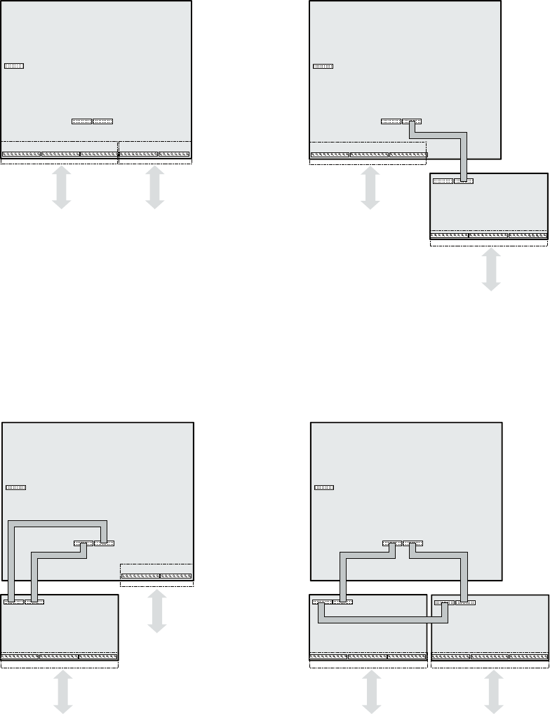
In-/output signals
addition to this an extension of I/O´s by SDCS-IOE 1
is possible.
Fig. 2.5/1: I/O´s via SDCS-CON2
Analogue I/O´s: standard
Digital I/O´s: not isolated
Encoder input: not isolated
Fig. 2.5/2: I/O´s via SDCS-CON2 and SDCS-IOB2
Analogue I/O´s: standard
digital I/O´s: all isolated by means of
optocoupler/relay, the signal
status is indicated by LED
Fig. 2.5/3: I/O´s via SDCS-CON2 and SDCS-IOB3
Analogue I/O´s: more input capacity
digital I/O´s: not isolated
encoder input: isolated
current source for: PT100/PTC element
Fig. 2.5/4: I/O´s via SDCS-IOB2 and SDCS-IOB3
Analogue I/O´s: more input capacity
digital I/O´s: all isolated by means of
optocoupler/relay, the signal
status is indicated by LED
current source for: PT100/PTC element
The converter can be connected in 4 different ways to
a control unit via analogue/digital links. Only one of
the four choices can be used at the same time. In
X3: X4: X5: X6: X7:
X2: X1:
X17:
SDCS-CON-2
1 2
X3: X4: X5:
X2: X1:
X17:
SDCS-CON-2
X3: X1:
SDCS-IOB-2
1
4
X1: X2:
SDCS-IOB-3
X6: X7:
X2:
X17:
X1:
3
2
SDCS-CON-2
X2:
SDCS-IOB-3
X2:
X17:
SDCS-CON-2
X1:
SDCS-IOB-2
X1:
X1: X3:
3 4
2.5 Options for DCS 500B / DCF 500B converter modules

II D 2-13
3ADW000066R0901_DCS500_System_description_e_i
Description of I/O signals SDCS-CON-2
Mechanical system installed in the basic unit
Terminals
Screw-type terminals for finely stranded wires up to max. 2.5 mm2 cross-
sectional area
Functionality
1 tacho input
Resolution: 12 bit + sign; differential input; common-mode range ±20 V
3 ranges from 8...30...90...270 V- with nmax
4 analogue inputs
Range -10...0...+10 V, 4...20 mA, 0...20 mA
All as differential inputs; RE = 200 kΩ; time constant of smoothing
capacitor ≤2 ms
Input 1: Resolution: 12 bit + sign.; common-mode range ±20 V
Inputs 2, 3, 4: Resolution: 11 bit + sign; common-mode range ±40 V
Current source for PTC element evaluation via jumper and input 2
2 outputs
+10 V, -10 V, IA ≤ 5 mA each; sustained-short-circuit-proof
for reference potentiometer voltage supply
1 analogue output
bipolar current feedback - from the power section; decoupled
IdN ⇒ ±3 V; IA≤ 5 mA, short-circuit-proof
2 analogue outputs
Range -10...0...+10 V; IA ≤ 5 mA
Output signal and scaling can be selected by means of the software
Resolution: 11 bit + sign
1 pulse generator input
Voltage supply for 5 V/12 V/24 V pulse generators (sustained-short-
circuit-proof)
Output current with 5 V: IA ≤ 0.25 A
12 V: IA ≤ 0.2 A
24 V: IA ≤ 0.2 A
Input range: 12 V/24 V: asymmetrical and differential
5 V: differential
Pulse generator as 13 mA current source: differential
Line termination (impedance 120Ω), if selected
max. input frequency ≤300 kHz
Description of I/O signals SDCS-IOB-2x & SDCS-IOB-3
Mechanical system always external, outside the basic unit
Terminals
Screw-clamp terminals for finely stranded wires up to max. 2.5 mm2
cross-sectional area
Functionality of SDCS-IOB-3
1 tacho input
Resolution: 12 bit + sign; differential input; common-mode range ±20 V
Range 8 V- with nmax; if higher tacho voltages are in use the tacho
adaptation board PS 5311 is needed.
4 analogue inputs
All as differential inputs; time constant of smoothing capacitor ≤2 ms
Input 1: Range -10 V/-20 mA...0...+10 V/+20 mA; 4... 20 mA unipolar;
RE = 200 kΩ/ 500Ω/ 500Ω; Resolution: 12 bit + sign; common-mode
range ±20 V
Inputs 2+3: Range as with input 1, in addition -1 V...0...+1 V
RE = 200 kΩ/ 500Ω/ 500Ω/ 20kΩ; Resolution: 11 bit + sign; common-
mode range with -1 V...0...+1 V range ±10 V, otherwise ±40 V
Input 4: Range as with input 1
RE = 200 kΩ/ 500Ω/ 500Ω; Resolution: 11 bit + sign; common-mode
range ±40 V
Residual current detection in combination with analogue input 4
(sum of phase currents ≠ 0)
2 outputs
+10 V, -10 V, IA ≤ 5 mA each; sustained-short-circuit-proof
for reference potentiometer voltage supply
1 analogue output
Bipolar current feedback - from the power section; decoupled
IdN ⇒ ±3 V (at gain = 1); IA≤ 5 mA, UAmax = 10 V, gain can be adjusted
by means of a potentiometer between 0.5 and 5, short-circuit-proof
2 analogue outputs
Range -10...0...+10 V; IA ≤ 5 mA; short-circuit-proof
Output signal and scaling can be selected by means of the software
Resolution: 11 bit + sign
Current source for PT 100 or PTC element evaluation
IA = 5 mA / 1.5 mA
1 pulse generator input
Voltage supply, output current, input range: as with IOB1
Inputs electrically isolated from 0 V (casing earth) by means of optocou-
pler and voltage source.
Functionality of SDCS-IOB-2x
3 different designs available:
SDCS-IOB-21 inputs for 24...48 V-; RE = 4.7 kΩ
SDCS-IOB-22 inputs for 115 V AC; RE = 22 kΩ
SDCS-IOB-23 inputs for 230 V AC; RE = 47 kΩ
Terminals
Screw-clamp terminals up to max. 4 mm2 cross-sectional area
8 digital inputs
The functions can be selected by means of the software
The signal status is indicated by an LED
all isolated by means of optocouplers
Input voltage: IOB-21:0...8 V ⇒ "0 signal", 18...60 V ⇒ "1 sig."
IOB-22:0...20 V ⇒ "0 signal", 60...130 V ⇒ "1 sig."
IOB-23:0...40 V ⇒ "0 signal", 90...250 V ⇒ "1 sig."
Filter time constant: 10 ms (channels 1...6), 2 ms (channels 7+8)
Auxiliary voltage for digital inputs: +48 V-, ≤ 50 mA, sustained- short-
circuit-proof; referenced to the unit casing potential
8 digital outputs
The functions can be selected by means of the software
The signal status is indicated by an LED
6 of them potential-isolated by relay (N.O. contact element: AC: ≤250 V/
≤3 A / DC: ≤24 V/ ≤3 A or ≤115/230 V/ ≤0.3 A) , protected by VDR
component.
2 of them potential-isolated by optocoupler, protected by Zener diode
(open collector) 24 V DC external, IA ≤ 50 mA each.
8 digital inputs
The functions can be selected by means of the software
Input voltage: 0...8 V ⇒ "0 signal", 16...60 V ⇒ "1 signal"
Time constant of smoothing capacitor: 10 ms
RE = 15 kΩ
The signal refers to the unit casing potential
Auxiliary voltage for digital inputs: +48 V-, ≤ 50 mA, sustained-short-
circuit-proof
7+1 digital outputs
The function can be selected by means of the software
7 outputs: relay driver with free-wheel diode, total current limitation
≤ 160 mA, short-circuit-proof
1 relay output - on power pack board SDCS-POW-1 (N.O. contact
element: AC: ≤250 V/ ≤3 A / DC: ≤24 V/ ≤3 A or ≤115/230 V/ ≤0.3 A)
protected by VDR component.

II D 2-14
3ADW000066R0901_DCS500_System_description_e_i
Please note:
Unless otherwise stated, all signals are referenced to a
0 V potential. Within the power pack subassembly
(SDCS-POW-1) and on all other PCBs, this potential
is firmly connected to the unit’s casing by means of
plating-through at the fastening points.
X17:
SDCS-IOE-1
X3: X4: X5: X6: X7:
X2: X1:
X17:
SDCS-CON-2
4 x analog
1 x Tacho
7 x digital
8 x digital
2 x analog
Pulsgeber
5
The digital and analogue inputs can be extended by
means of the SDCS-IOE1 board. This is in addition to
the a.m. solutions.
Fig. 2.5/5: Additional Inputs via SDCS-IOE1
Analogue inputs: extended
Digital inputs: all isolated by means of
optocoupler, the signal status
is indicated by LED
current source for: PT100/PTC element
Description of input signals SDCS-IOE-1
Mechanical system always external, outside the basic unit
Terminals
Screw-type terminals for finely stranded wires up to max. 2.5 mm2 cross-sectional area
Functionality
7 digital inputs
The functions can be selected by means of the software
The signal status is indicated by an LED
Input voltage: 0...8 V ⇒ "0 signal", 16...31 V ⇒ "1 signal"
Isolated from the unit’s electronics by optocouplers
Potentialwise arranged in two groups (DI 9...DI 12 and DI 13...DI 15)
Time constant of smoothing capacitor: 2 ms
2 analogue inputs
All as differential inputs; common-mode range ±40 V
Range -10 V/-20 mA...0...+10 V/+20 mA; 4... 20 mA unipolar
RE = 200 kΩ /500 Ω /500 Ω
Resolution: 11 bit + sign
Input 2: range as for input 1,
in addition -1 V/-2 mA...0...+1 V/+2 mA, then common-mode range ±40 V, RE = 20 kΩ
Current source for PT 100 or PTC element evaluation
IA = 5 mA / 1.5 mA
The signals are referenced to the unit casing potential
II D 2-15
3ADW000066R0901_DCS500_System_description_e_i
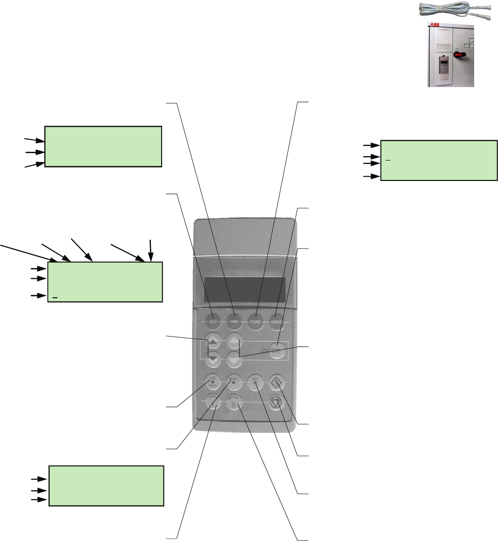
Panel (control and display panel)
The CDP 312 control and display panel communicates
with the power converter via a serial connection in
accordance with the RS 485 standard at a transmission
rate of 9.6 kBaud. It is an option for the converter unit.
After completion of the commissioning procedure, the
panel is not necessarily required for diagnostic routines,
because the basic unit incorporates a 7-segment display
for indicating errors, for example.
Fig. 2.5/6: Function keys and various displays on the removable
control and display panel. The panel can also be used to load the
same program on different power converters.
Actual
Selects the display of feedback values plus the
signal group and the error memory group.
Parameters
For selecting and adjusting
all parameters and signals.
Function
Selects the “functions” operating mode; can be used
to perform special functions such as uploading and
downloading or application programming.
Drive
for subsequent extensions
Twin arrow keys
are used to change the group. In the parameter and
reference presetting modes, you can alter the param-
eter value or the reference setting ten times faster by
means of the twin arrow keys than by means of the
single arrow key.
Arrow keys
are used to select parameters within a group. You al-
ter the parameter value or the reference setting in
the parameter and reference presetting modes. In
the feedback signal display mode, you select the line
you want.
Enter
is used in the following modes:
Parameter setting: enter new parameter value
Feedback value
signal display: enter the current signal selec-
tion mode
Signal selection: accept selection and return to
the feedback value signal dis-
play mode
Local/Remote
is used to select local (control
panel) or remote control.
Reset
Error acknowledgement key.
Reference
is used to activate the reference presetting mode.
Start
starts the drive in local mode.
Stop
shuts the drive down if you are in local mode.
On
in local mode switches the main contactor on.
Off
in local mode switches the main contactor off.
Equipment
• 16 membrane pushbuttons in three function groups
• LCD display comprising four lines with 20 charac-
ters each
• Language: German, English, French, Italian, Span-
ish
• Options for the CDP 312:
– cable, separated from the power converter for
utilization; 3 m long
– kit for mounting the panel in the switchgear
cubicle door
Group
and name
Subgroup
and name
0 L 0,0 rpm 00
17 RAMP GENERATOR
08 ACCEL 1
20.0 s
Value
ID number
of the
drive
selected
Control
location
L = local
= remote
Main contactor
status
0 = open
1 = closed
Speed
reference
rpm
Run status
1 = Run
0 = Stop
Status row
Actual signal
name and value
Cursor shows
the row selected
0 L 0,0 rpm 00
SPEEED ACT 0,0 rpm
CONV CUR 0 A
U ARM ACT 0 V
0 L 0,0 rpm 00
1 LAST FAULT
Emergency stop
3212:59:35:56
1 = last fault
2 = last-but-one fault
99 = last-but-98 fault
Total time after
switch-on
HHHH:MM:SS.ss
Name of Fault
or alarm
Status row
Functions to be
selected
Display contrast
setting
0 L 0,0 rpm 00
U
PLOAD <==
DOWNLOAD ==>
CONTRAST
II D 2-16
3ADW000066R0901_DCS500_System_description_e_i
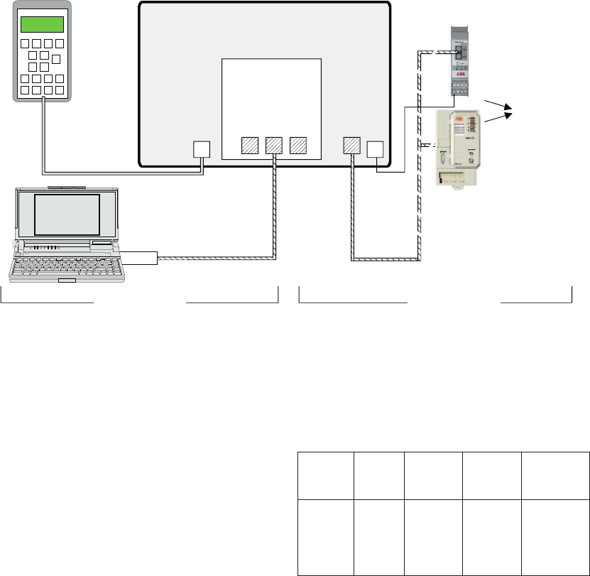
Serial interface
There are various serial interface options available for
operation, commissioning and diagnosis, plus for con-
trolling. According to the description in the previous
section, there is a serial connection to the control and
display panel (X33:/X34: on the SDCS-CON-2 con-
trol board). Installing the optional SDCS-COM-5
Control
components required:
• plastic optical fibre for distances up to 20 m (longer
distances on request)
• field bus module Nxxx-0x
Functionality:
You will find more detailed information on data ex-
change in the specific fieldbus module documentation.
Operation by PC
System requirements/recommendation:
• Laptop PC with Windows NT ™ or Windows 2000 ™ operating
system (desktop PC on request)
• hard disk with 4MB free memory; each graph recorded requires
additional 500 kB of free memory.
• CD rom drive
• PCMCIA slot
Components required:
• SDCS-COM-5 as an option
• DDCTool 4.x package for Windows NT ™ or
DDCTool 4.x package for Windows 2000 ™
(DDCTool 4.0 package for Windows XP ™ on request)
The package contains of:
• CD rom with installation software
• SNAT624 PCcard (PCMCIA)
• NDPC-02 connector (interface from SNAT624 to plastic opti-
cal fibre cable)
• plastic optical fibre cable (10m)
Functionality:
• DDCtool starts program part CMT/DCS 500, when a DCS500B
is connected
• CMT/DCS 500 is the core program (this name will be used further
on as a cross-reference) for commissioning, diagnosis, mainte-
nance and trouble-shooting based on point-to-point connection.
In addition to the functionality provided by the CDP 312 control
panel, there are further functions available described on next page.
Fig. 2.5/7: Options for serial communication
communication board on the SDCS-CON-2 control
board creates additional serial interfaces.
Both interfaces use optical fibres. One channel is used
for drive/PC interfacing. The other for fieldbus module
interfacing. All three serial interfaces are independent
from each other.
Field bus Module Number Parameter Baudrate
of cyclic exchange
words from/ possible
to drive
Profibus NPBA-12 ≤ 6 ➀➁ Yes ≤ 12 MB
CANopen NCAN-02 ≤ 6 ➀Yes ≤ 1 MB
DeviceNet NDNA-02 ≤ 6 ➀Yes ≤ 1 MB
ControlNet NCNA-01 ≤ 6 ➀Yes ≤ 5 MB
ModBus NMBA-01 ≤ 6 ➀Yes ≤ 19.2 KB
AC70 / FCI ----- ≤ 6 ➀No ≤ 4 MB
➀Four of them are predefined via the profile variable speed
drives done by the Profibus user organization; they can be
altered, if necessary.
➁The module supports the PPO types 1 to 5; depending on
the PPO type in use less words will be transferred or they
will be empty.
SDCS-COM-5
CDP 312
X34:
Interface
PC
≤ 3 m
SDCS-CON-2
X16:
V260 FCI
AC70
Nxxx
electrical
connection
optical fibre
≤ 10 m
optical fibre
≤ 20 m
ControlOperation
Power supply
to the PLC
II D 2-17
3ADW000066R0901_DCS500_System_description_e_i
Operation by PC (continued)
The program incorporates nine different function win-
dows which can be used to alter the application pro-
gram on-line, to monitor the drive’s functionality, to
alter the parameter values, to control the drive and to
monitor its status. You will find below a brief descrip-
tion of the individual menu options, some of which are
shown as a screen display to serve as examples.
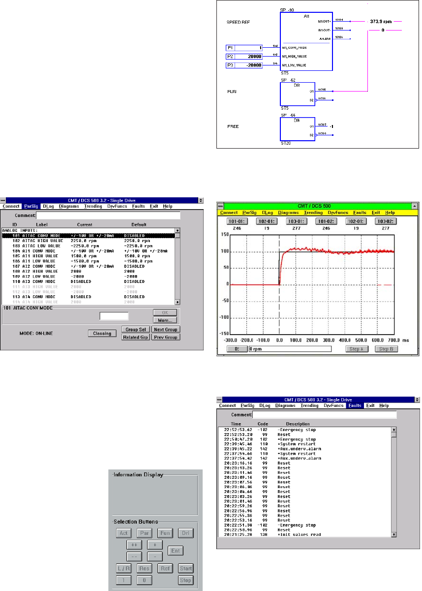
ParSig
The parameter and signal display enables the user to view
parameter or signal values in a table and to alter them. One
of the functions available for the user is to allocate each
parameter or each signal to self-defined groups. He/she can
then select only special groups, and trace or alter the values
of parameters or signals in this group.
Dlog
The DC power converter is able to continuously log up to six
signals and to store them in non-volatile memory from a
trigger condition to be set (level, pre-event and post-event
history). These values can then be read out by the program
in chronological sequence and processed further. They are
available as a table or as a diagram, in forms similar to those
with the “Trending” option, and can also be printed out in
these forms.
Diagrams
This window shows the function block diagram created by
means of the GAD program. If necessary, the user can also
use this window to view the values of selected parameters or
connections.
Trending
This window can be used to trace the signal characteristics
of specified parameters or signals. Up to six parameters or
signals can be monitored. The window shows the values in
a curve diagram.
DrvFuncs
This display provides the
same display and the same
pushbuttons for the user as
the CDP 312 display and
control panel. For that rea-
son, the drive functions are
also identical.
Faults
This display shows the current fault messages last fed into
the fault logger in chronological sequence.
Exit
Quitting the program.
Help
Descriptions of the parameters.
Connect
This option is used to trigger special functions such as es-
tablishing the connection to the power converter or config-
uring the program.
Please note:
For more information of
the CMT/DCS 500 soft-
ware package there is an
own documentation
available describing the
possibilities and the han-
dling of the program.
II D 2-18
3ADW000066R0901_DCS500_System_description_e_i
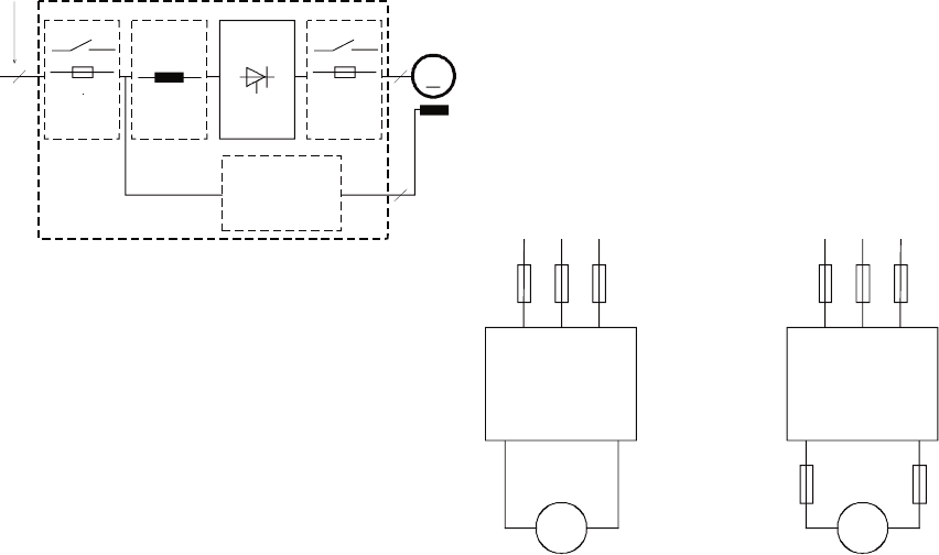
2.6 Options for the drive
Line reactors
for armature (DCS 50xB) and field
(DCF 50xB) supply
When thyristor power converters operate, the line
voltage is short-circuited during commutation from
one thyristor to the next. This operation causes voltage
dips in the mains (point of common coupling). For the
connection of a power converter system to the mains,
one of the following configurations can be applied:
With reference to the power converter:
The line reactors listed in table (2.6/1)
- have been allocated to the units nominal current
- are independent of converter's voltage classifica-
tion; at some converter types the same line choke is
used up to 690 V line voltage
- are based on a duty cycle
- can be used for DCS 500B as well as for DCF 500B
converters
Configuration A
When using the power converter, a min-
imum of impedance is required to en-
sure proper performance of the snubber
circuit. A line reactor can be used to meet
this minimum impedance requirement.
The value must therefore not drop be-
low 1% uk (relative short circuit voltage).
It should not exceed 10% uk, due to
considerable voltage drops which would
then occur.
Configuration B
If special requirements have to be met at
the PCC (standards like EN 61 800-3,
DC and AC drives at the same line, etc),
different criteria must be applied for
selecting a line reactor. These require-
ments are often defined as a voltage dip
in percent of the nominal supply voltage.
The combined impedance of ZLine and
ZLR constitute the total series impedance
of the installation. The ratio between the
line impedance and the line reactor impedance deter-
mines the voltage dip at the connecting point. In such
cases line chokes with an impedance around 4% are
often used.
Configuration C
If an isolation transformer is used, it is
possible to comply with certain connect-
ing conditions per Configuration B with-
out using an additional line reactor. The
condition described in Configuration A
will then likewise be satisfied, since the uk
is >1 %.
Configuration C1
If 2 or more converters should be supplied by one
transformer the final configuration depends on the
number of drives in use and their power capability.
Configuration A or B has to be used which are based on
commutation chokes, if the drive system consists of any
of the converters
(C1, C2, A5, A6,
A7). In case only two
converters type A7
are involved no com-
mutation chokes are
necessary because the
design of these con-
verters is adapted to
that wiring.
You will find further information in publication:
Technical Guide chapter: Line reactors
Line
PCC
uk LR > 1%
Line
PCC
LLine
LLR
Line
PCC
....
Netzdr_f.dsf
LLR LLR LLR
PCC
Line
II D 2-19
3ADW000066R0901_DCS500_System_description_e_i
Fig. 1 Fig. 2 Fig. 3
DCS Type Line choke Design Line choke Design
400V-690V type for Fig. type for Fig.
50/60 Hz configur. A configur. B
DCS50xB0025-41/51 ND01 1 ND401 4
DCS50xB0050-41/51 ND02 1 ND402 4
DCS50xB0050-61 ND03 1 on request -
DCS50xB0075-41/51 ND04 1 ND403 5
DCS50xB0100-41/51 ND06 1 ND404 5
DCS50xB0110-61 ND05 1 on request -
DCS50xB0140-41/51 ND06 1 ND405 5
DCS50xB0200-41/51 ND07 2 ND406 5
DCS50xB0250-41/51 ND07 2 ND407 5
DCS50xB0270-61 ND08 2 on request -
DCS50xB0350-41/51 ND09 2 ND408 5
DCS50xB0450-41/51 ND10 2 ND409 5
DCS50xB0450-61 ND11 2 on request -
DCS50xB0520-41/51 ND10 2 ND410 5
DCS50xB0680-41/51 ND12 2 ND411 5
DCS501B0820-41/51 ND12 2 ND412 5
DCS502B0820-41/51 ND13 3 ND412 5
DCS50xB1000-41/51 ND13 3 ND413 5
DCS50xB0903-61/71 ND13 3 on request -
DCS50xB1203-41/51 ND14 3 on request -
DCS50xB1503-41/51/61/71 ND15 3 on request -
DCS50xB2003-41/51 ND16 3 on request -
DCS501B2003-61/71 ND16 * 3 on request -
* with forced cooling
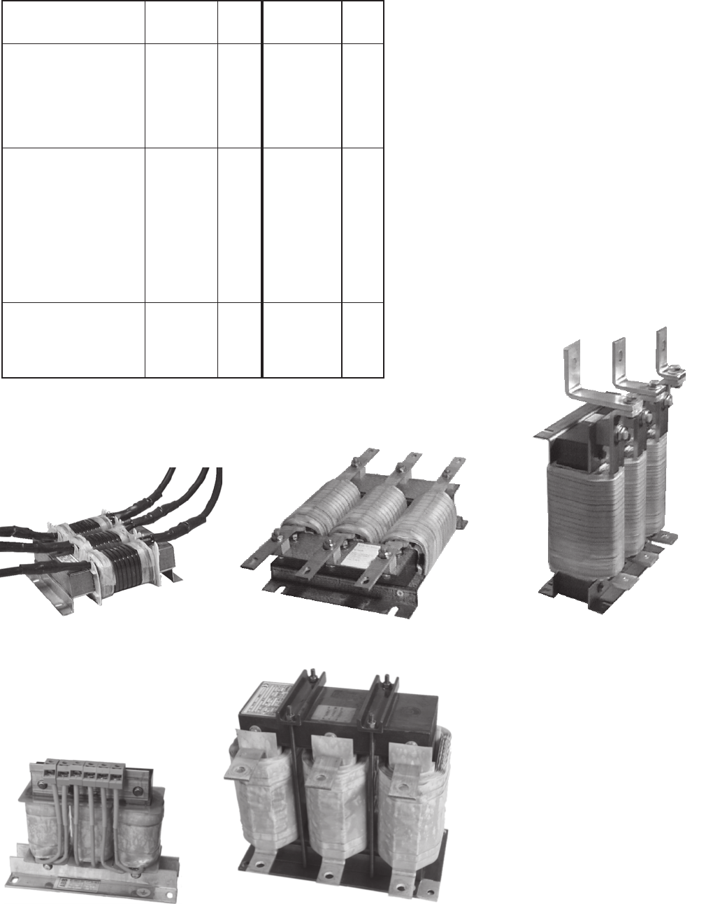
Line reactors L1
Table 2.6/1: Line reactors (for more information see publication
Technical Data)
Fig. 5Fig. 4
II D 2-20
3ADW000066R0901_DCS500_System_description_e_i
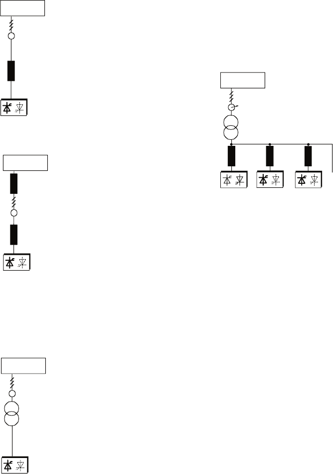
Conclusion for the armature supply
Due to cost saving standard fuses are used instead of the
more expensive semiconductor fuses at some applica-
tions. Under normal and stable operating conditions,
this is understandable and comprehensible, as long as
fault scenarios can be ruled out.
In the event of a fault , however, the saving may cause
very high consequential costs. Exploding power semi-
conductors may not only destroy the power converter,
but also cause fires.
Adequate protection against short-circuit and earth
fault, as laid down in the EN50178 standard, is possi-
ble only with appropriate semiconductor fuses.
General
Unit configuration
Protection elements such as fuses or overcurrent trips
are used whenever overcurrents cannot entirely be ruled
out. In some configurations, this will entail the follow-
ing questions: firstly, at what point should which
protective element be incorporated? And secondly, in
the event of what faults will the element in question
provide protection against damage?
Fig. 2.6/1 Arrangement of the switch-off elements in the
armature-circuit converter
Aspects of fusing for the armature-circuit and field supplies of DC drives
M
.
.
.
.
.
3
2
2
For field supply
see Fig. 2.6/2
AC supply: public mains / plant's mains
Cabinet
You will find further information in publication:
Technical Guide
chapter:
Aspects for fusing
Complies with Basic Principles on:
1 – Explosion hazard yes
2 – Earth fault yes
3 – “Hard“ networks yes
4 – Spark-quenching gap yes
5 – Short-circuit yes
6 – 2Q regenerative yes
M M
DCS converter
2-Q non-regen.
Semiconductor
fuses
Semiconductor
fuses
Semiconductor
fuses
4-Q resp.
2-Q regenerative
DCS converter
ABB's recommendations
II D 2-21
3ADW000066R0901_DCS500_System_description_e_i
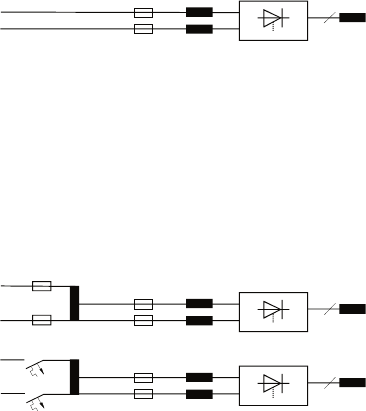
Conclusion for the field supply
Basically, similar conditions apply for both field supply
and armature-circuit supply. Depending on the power
converter used (diode bridge, half-controlled bridge,
fully controlled 4-quadrant bridge), some of the fault
sources may not always be applicable. Due to special
system conditions, such as supply via an autotransform-
er or an isolating transformer, new protection condi-
tions may additionally apply.
The following configurations are relatively frequent:
In contrast to the armature-circuit supply, fuses are
never used on the DC side for the field supply, since a
fuse trip might under certain circumstances lead to
greater damage than would the cause tripping the fuse
in the first place (small, but long-lasting overcurrent;
fuse ageing; contact problems; etc.).
Semiconductor fuse F3.1 (super-fast acting) should be
used, if conditions similar to those for armature-circuit
supply are to apply, like for example protection of the
field supply unit and the field winding.
2
F3.1 ND30 /
built-in
Fig 2.6/2 Configuration for field supplies
The F3.2 and F3.3 fuse types serve as line protectors
and cannot protect the field supply unit. Only pure
HRC fuses or miniature circuit-breakers may be used.
Semiconductor fuses would be destroyed, for example,
by the transformer’s starting current inrush.
F3.3
2
2
F3.2
F3.1
F3.1
FF_ASP_b.dsf
ND30 /
built-in
Fig 2.6/3 Configurations for field supplies
II D 2-22
3ADW000066R0901_DCS500_System_description_e_i
Field converter type for field current Transformer
≤≤
≤≤
≤500 V; 50/60 Hz IFtype 50/60 Hz
Uprim = ≤≤
≤≤
≤500 V
SDCS-FEX-1 ≤6 A T 3.01
SDCS-FEX-2A ≤12 A T 3.02
SDCS-FEX-2A ≤16 A T 3.03
DCF503A/4A-0050 ≤30 A T 3.04
DCF503A/4A-0050 ≤50 A T 3.05
Uprim = ≤≤
≤≤
≤600 V
SDCS-FEX-1 ≤6 A T 3.11
SDCS-FEX-2A ≤12 A T 3.12
SDCS-FEX-2A ≤16 A T 3.13
Uprim = ≤≤
≤≤
≤690 V
DCF503A/4A-0050 ≤30 A T 3.14
DCF503A/4A-0050 ≤50 A T 3.15
Table 2.6/4: Autotransformer data (details see
Technical Data)
Transformer T3 for field supply to match voltage levels
Fig. 2.6/4: T3 autotrans-
former
Type of converter Type Fuse holder
DCS50xB0025-41/51 170M 1564 OFAX 00 S3L
DCS50xB0050-41/51 170M 1566 OFAX 00 S3L
DCS50xB0050-61 170M 1566 OFAX 00 S3L
DCS50xB0075-41/51 170M 1568 OFAX 00 S3L
DCS50xB0100-51 170M 3815 OFAX 1 S3
DCS50xB0110-61 170M 3815 OFAX 1 S3
DCS50xB0140-41/51 170M 3815 OFAX 1 S3
DCS50xB0200-41/51 170M 3816 OFAX 1 S3
DCS50xB0250-41/51 170M 3817 OFAX 1 S3
DCS50xB0270-61 170M 3819 OFAX 1 S3
DCS50xB0350-41/51 170M 5810 OFAX 2 S3
DCS50xB0450-41/51/61 170M 6811 OFAX 3 S3
DCS50xB0520-41/51 170M 6811 OFAX 3 S3
DCS50xB0680-41/51 170M 6163 3x 170H 3006
DCS50xB0820-41/51 170M 6163 3x 170H 3006
DCS50xB1000-41/51 170M 6166 3x 170H 3006
Table 2.6/2: Fuses and fuse holders (details see
Technical Data)
Semiconductor type F1 fuses and fuse holders for AC and DC power lines
(DCS 501B /DCS 502B - DCF 501B/DCF 502B)
The converter units are subdivided into two
groups:
– Unit sizes C1 and C2 with rated currents
up to 1000 A require external fuses.
– In unit sizes A5, A6 and A7 with rated
currents of 900 A to 5200 A, the semicon-
ductor fuses are installed internally (no
additional external semiconductor fuses
are needed).
The table on the right assigns the AC fuse
type to the converter type. In case the con-
verter should be equipped with DC fuses
according to the hints use the same type of
fuse used on the AC side now in the plus and
minus line. Blade type fuses are used for all
the converters construction type C1 and C2
except the biggest one.
The field supply units’ insulation voltage is
higher than the rated operating voltage (see
Chapter Field supplies), thus providing an
option in systems of more than 500 V for
supplying the power section of the converter
directly from the mains for purposes of arma-
ture supply, and using an autotransformer to
match the field supply to its rated voltage.
Moreover, you can use the autotransformer
to adjust the field voltage (SDCS-FEX-1
diode bridge) or to reduce the voltage ripple.
Different types (primary voltages of 400...500
V and of 525...690 V) with different rated
currents each are available.
Depending on the protection strategy
different types of fuses are to be used.
The fuses are sized according to the
nominal current of the field supply de-
vice. If the field supply unit is connected
to two phases of the network, two fuses
should be used; in case the unit is con-
nected to one phase and neutral only one
fuse at the phase can be used. Table 2.6/
3 lists the fuses currents with respect to
table 2.6/2.
The fuses can be sized according to the
maximum field current. In this case take
the fuse, which fits to the field current
levels.
Fuses F3.x and fuse holders for 2-phase field supply
Field conv. Field F3.1 F3.2 F 3.3
current
SDCS-FEX-1 IF ≤ 6 A 170M 1558 OFAA 00 H10 10 A
SDCS-FEX-2A
SDCS-FEX-2A IF ≤ 12 A 170M 1559 OFAA 00 H16 16 A
SDCS-FEX-2A IF ≤ 16 A 170M 1561 OFAA 00 H25 25 A
DCF 503A
DCF 504A
DCF 503A IF ≤ 30 A 170M 1564 OFAA 00 H50 50 A
DCF 504A
DCF 503A IF ≤ 50 A 170M 1565 OFAA 00 H63 63 A
DCF 504A
Type of protection Semiconduct. LV HRC type circuit breaker
elements type fuse for for 690 V; fuse for 500 V or
fuse holder hold. OFAX 00 690 V
type OFAX 00
Table 2.6/3: Fuses and fuse holders for 2-phase field supply
II D 2-23
3ADW000066R0901_DCS500_System_description_e_i
Auxiliary transformer T2 for electronic
system / fan supply
The converter unit requires various auxiliary voltages,
e.g. the unit’s electronics require 115 V/1-ph or 230 V/
1-ph, the unit fans require 230 V/1-ph or 400 V/690 V/
3-ph, according to their size. The T2 auxiliary trans-
former is designed to supply the unit’s electronic sys-
tem and all the single-phase fans including the fan of
the A5 converter.
Input voltage: 380...690 V/1-ph; 50/60 Hz
Output voltage: 115/230 V/1-ph
Power: 1400 VA
Fig. 2.6/5: T2 auxiliary transformer
Residual current detection
This function is provided by the standard software. If
needed, the analogue input AI4 has to be activated, a
current signal of the three phase currents should be
supplied to AI4 by a current transformer. If the addi-
tion of the three current signal is different from zero, a
message is indicated (for more information, see publi-
cation Technical Data).
Commutating reactor
When using the SDCS-FEX-2A field power converter,
you should additionally use a commutating reactor
because of EMC considerations. A commutating reac-
tor is not necessary for the SDCS-FEX-1 (diode bridge).
With DCF 503A/504A field power converters, it is
already installed.
Converter Reactor
≤≤
≤≤
≤500 V; 50/60 Hz
SDCS-FEX-2A ND 30
Table 2.6/4: Commutating reactor (for more information
see publication
Technical Data)
II D 2-24
3ADW000066R0901_DCS500_System_description_e_i
Fig. 2.6/5: Classification
Not applicable
First environment (residential area with light industry) with restricted distribution
Not applied, since general distribution sales channel excluded
satisfied
satisfied
The paragraphs below describe selection of the electri-
cal components in conformity with the EMC Guide-
line.
The aim of the EMC Guideline is, as the name implies,
to achieve electromagnetic compatibility with other
products and systems. The guideline ensures that the
emissions from the product concerned are so low that
they do not impair another product's interference
immunity.
In the context of the EMC Guideline, two aspects must
be borne in mind:
• the product's interference immunity
• the product's actual emissions
The EMC Guideline expects EMC to be taken into
account when a product is being developed; however,
EMC cannot be designed in, it can only be quantita-
tively measured.
Note on EMC conformity
The conformity procedure is the responsibility of both
the power converter's supplier and the manufacturer of
the machine or system concerned, in proportion to
their share in expanding the electrical equipment in-
volved.
EMC filters
You will find further in-
formation in publica-
tion:
Technical Guide
chapter:
EMC Com-
pliant Installation and
Configuration for a
Power Drive System
MM
Mains filter
Converter
Line reactor
Supply transformer for a residential
area (rating normally ≤ 1,2 MVA)
Earthed public 400-V
network with neutral
conductor
Medium-voltage network
Earthed
neutral
To other loads, e.g. drive systems
An isolating transformer
with an earthed screen
and earthed iron core
renders mains filter and
line reactor superfluous.
Operation at public
low-voltage network
together with other
loads of all kinds.
Residential area
To other loads which have to be protected from the system disturbances caused by
power converters (HF interference and commutation notches)
Converter
MM
MM MM
alternative
alternative
Line reactor +
Y-capacitor
Medium-voltage network
Supply transformer for a residential
area (rating normally ≤ 1.2 MVA)
Earthed
neutral
Earthed public 400-V
network with neutral
conductor
To other loads, e.g. drive systems
Mains filter
Line reactor
Converter Converter
Mains filter
Line reactor
Converter Converter
An isolating transformer
with an earthed screen
and earthed iron core
renders mains filter and
line reactor superfluous.
Operation at public
low-voltage network
together with other
loads of all kinds.
To other loads, e.g. drive systems
To other loads which have to be protected from the system disturbances caused by
power converters (HF interference and commutation notches)
Earthed public 400-V
network with neutral
conductor
Operation at public
low-voltage network
together with other
loads of all kinds.
Light industry Residential area
II D 2-25
3ADW000066R0901_DCS500_System_description_e_i
EN 61800-3
EN 61000-6-3
EN 61000-6-4
EN 61000-6-2
EN 61000-6-1
satisfied
satisfied
Second environment (industry) with restricted distribution
on customer's request satisfied
Not applicable
Standards Classification
The following overview
utilises the terminology
and indicates the action
required in accordance
with Product Standard
EN 61800-3
For the DCS 500B series,
the limit values for emit-
For compliance with the protection objectives of the
German EMC Act (EMVG) in systems and machines,
the following EMC standards must be satisfied:
Product Standard EN 61800-3
EMC standard for drive systems (PowerDriveSys-
tem), interference immunity and emissions in resi-
dential areas, enterprise zones with light industry
and in industrial facilities.
This standard must be complied with in the EU for
satisfying the EMC requirements for systems and
machines!
For emitted interference, the following apply:
EN 61000-6-3 Specialised basic standard for emissions in light industry can
be satisfied with special features (mains filters, screened power
cables) in the lower rating range *(EN 50081-1).
EN 61000-6-4 Specialised basic standard for emissions in industry
*(EN 50081-2)
For interference immunity, the following apply:
EN 61000-6-1 Specialised basic standard for interference immunity in residen-
tial areas *(EN 50082-1)
EN 61000-6-2 Specialised basic standard for interference immunity in indus-
try. If this standard is satisfied, then the EN 61000-6-1 standard
is automatically satisfied as well *(EN 50082-2).
* The generic standards are given in brackets
The field supply is not depicted in
this overview diagram. For the
field current cables, the same
rules apply as for the armature-
circuit cables.
ted interference are complied with,
provided the action indicated is car-
ried out. This action is based on the
term Restricted Distribution used in
the standard (meaning a sales chan-
nel in which the products concerned
can be placed in the stream of com-
merce only by suppliers, customers
or users which individually or jointly
possess technical EMC expertise).
For power converters without addi-
tional components, the following
warning applies:
This is a product with restricted
distribution under IEC 61800-3.
This product may cause radio inter-
ference in residential areas; in this
case, it may be necessary for the
operator to take appropriate action
(see adjacent diagrams).
MM
MM
Supply transformer for a
residential area (rating
normally ≤ 1.2 MVA)
Earthed 400-V network
with neutral conductor;
3~ ≤ 400 A
Operation at low-voltage network together with
other loads of all kinds, apart from some kinds
of sensitive communication equipment.
To other loads, e.g. drive systems
Line reactor +
Y-capacitor Line reactor
Converter Converter
Mains filter
Earthed
neutral
Medium-voltage network
Industrial zone
alternative
alternative
MMMM
Converter
transformer
Case-referenced EMC analysis
alternative
Converter
transformer
with earthed
iron core
(and earthed
screen where
appropriate)
alternative
I > 400 A
and/or
U > 500 V
Operation with separate power converter transformer. If there
are other loads at the same secondary winding, these must be
able to cope with the commutation gaps caused by the power
converter. In some cases, commutating reactors will be
required.
To other loads, e.g. drive systems
Converter Converter
Line reactor
Medium-voltage network
Industrial zone
Legend
Unscreened cable with restriction
Screened cable

II D 2-26
3ADW000066R0901_DCS500_System_description_e_i
Converter IDC [A] Const. Filter type for y=4 Filter type for y= 5 Filter type for y=6 or 7
type
DCS50xB0025-y1 25A C1a NF3-440-25 NF3-500-25 ---
DCS50xB0050-y1 50A C1a NF3-440-50 NF3-500-50 ---
DCS50xB0075-y1 75A C1a NF3-440-64 NF3-500-64 ---
DCS50xB0100-y1 100A C1b NF3-440-80 NF3-500-80 ---
DCS50xB0140-y1 140A C1b NF3-440-110 NF3-500-110 ---
DCS50xB0200-y1 200A C2a NF3-500-320 NF3-500-320 ---
DCS50xB0250-y1 250A C2a NF3-500-320 NF3-500-320 ---
DCS50xB0270-61 250A C2a NF3-500-320 NF3-500-320 NF3-690-600 ➀
DCS50xB0350-y1 350A C2a NF3-500-320 NF3-500-320 ---
DCS50xB0450-y1 450A C2a NF3-500-600 NF3-500-600 NF3-690-600 ➀
DCS50xB0520-y1 520A C2a NF3-500-600 NF3-500-600 ---
DCS50xB0680-y1 680A C2b NF3-500-600 NF3-500-600 ---
DCS501B0820-y1 740A C2b NF3-500-600 NF3-500-600 ---
DCS502B0820-y1 820A C2b NF3-690-1000 ➀NF3-690-1000 ➀---
DCS50xB1000-y1 1000A C2b NF3-690-1000 ➀NF3-690-1000 ➀---
DCS50xB0903-y1 900A A5 NF3-690-1000 ➀NF3-690-1000 ➀NF3-690-1000 ➀
DCS50xB1203-y1 1200A A5 NF3-690-1000 ➀NF3-690-1000 ➀NF3-690-1000 ➀
DCS50xB1503-y1 1500A A5 NF3-690-1600 ➀NF3-690-1600 ➀NF3-690-1600 ➀
DCS50xB2003-y1 2000A A5 NF3-690-1600 ➀NF3-690-1600 ➀NF3-690-1600 ➀
≤ 3000A A6 NF3-690-2500 ➀NF3-690-2500 ➀NF3-690-2500 ➀
➀ Filter only available on request
Three - phase filters
EMC filters are necessary to fulfil the standard for
emitted interference if a converter shall be run at a
public low voltage line, in Europe for example with 400
V between the phases. Such lines have a grounded
neutral conductor. ABB offers suitable three - phase
filters for 400 V and 25 A...600 A and 500 V filters for
440 V lines outside Europe.
Converter type of dc current Filter type
field supply unit Umax = 250 V
[A]
SDCS-FEX-1 6 NF1-250-8
SDCS-FEX-2A 8 NF1-250-8
SDCS-FEX-2A 16 NF1-250-20
DCF 503A-0050 50 NF1-250-55
DCF 504A-0050 50 NF1-250-55
further filters for 12 NF1-250-12
30 NF1-250-30
➊The filters can be optimized for the real field currents: IFilter =
IField
➊
Filter in a grounded line (earthed TN or TT
network)
The filters are suitable for grounded lines only, for
example in public European 400 V lines. According to
EN 61800-3 filters are not needed in insulated indus-
trial lines with own supply transformers. Furthermore
they could cause safety risks in such floating lines (IT
networks).
Single - phase filters for field supply
Many field supply units are single - phase converters for
up to 50 A excitation current. They can be supplied by
two of the three input phases of the armature supply
converter. Then a field supply unit does not need its
own filter.
If the phase to neutral voltage shall be taken (230 V in
a 400 V line) then a separate filter is necessary. ABB
offers such filters for 250 V and 6...30 A.
The filters can be optimized for the real motor currents:
IFilter = 0.8 • IMOT max ; the factor 0.8 respects the current
ripple.
Lines with 500 V to 1000 V are not public. They are
local lines inside factories, and they do not supply
sensitive electronics. Therefore converters do not need
EMC filters if they shall run with 500 V and more.
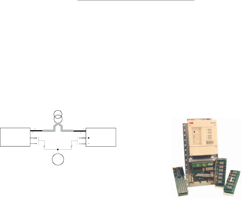
II D 3-1
3ADW000066R0901_DCS500_System_description_e_i
3 How to engineer your drive
This chapter will give engineering hints for different drive configurations. In the first place converters are shown with all possible field supply
options using wiring diagrams. Afterwards wiring diagrams are only shown for the most common configurations.
•Standard configuration using a fully-controlled field
(3-ph) without armature converter (see
chapter
3.4
)
The fourth configuration shows a 3-phase field supply unit DCF
501B/2B as stand alone unit.
This configuration shows a system in field current control mode
and is used, if any type of existing DC-motor-field supply should
be upgraded to a digital controlled one with all modern options like
serial link etc.
There are other than field applications, magnets for example, which
can be controlled with this equipment in current or voltage control
mode without any additional components.
•Typical configuration for high power drives
(see
chapter
3.5
)
The fifth configuration is used for quite big drives and is based on
the diagrams used for configuration 3.3 and 3.4. Now all the
components used for the other two are shown all together with all
interconnections and interlockings needed. It is adapted to the
converter construction types A5, A6 and A7.
•Standard drive configuration using an internal field
(see
chapter 3.1
)
The first configuration shows a speed controlled drive, using a very
flexible external wiring and a build in field supply. With these
components, it will fit to most drives of the smaller power range .
This configuration can only be used together with construction
types C1 - A5, because bigger power stacks (C4, A6, A7) do not
allow to incorporate an internal field supply.
•Drive configuration using the internal field with re-
duced external components (see
chapter
3.2)
The second configuration uses the same basic components as the
one first, but a reduced external wiring schematics.
This configuration can only be used together with construction
types C1 - A5, because bigger power stacks (C4, A6, A7) do not
allow to incorporate an internal field supply.
•Standard drive configuration using an external half-
controlled field (1-ph) (see
chapter
3.3
)
The third configuration uses the external wiring of the first one, but
a more powerful and flexible field supply unit.
This configuration can be used for all construction types.
•Typical configuration for very high power drives using
two parallel converter modules with symmetrical load
share
Another configuration is the paralleling of converters. In this case
converters of the same construction type (A7) are placed close to
each other having connected their AC and DC terminals directly.
They will behave like one bigger converter, which is not available as
a single standard module. Such a system uses additional electronic
boards for safety functions as well as interfacing and monitoring the
converters.
More information on request.
•Revamp of existing DC Equipment
If existing drives need modernization in some cases brand new
drives shown in one of the first configurations will replace them.
Because of space or economical reasons in some cases the existing
power stack will remain and only the control part is upgraded.
For these cases a construction kit based on electronic boards,
normally used in DCS- A7 type converters, called DCR revamp kit,
is available.
All options shown and explained in chapter 2 are suitable for this
kit.
Additional boards enable this kit to be used for power stack
constructions with up to four thyristors in parallel.
For more information please see manual Selection, Installation and
Start-up of Rebuild Kits.
+
-
DCS ... xxxx ..Rxx .......
3
dedicated
power transformer
DCS ... xxxx ..Lxx .......
3
M
Figure 3/1: Hard paralleling for high currents
Figure 3/2: Rebuild Kit
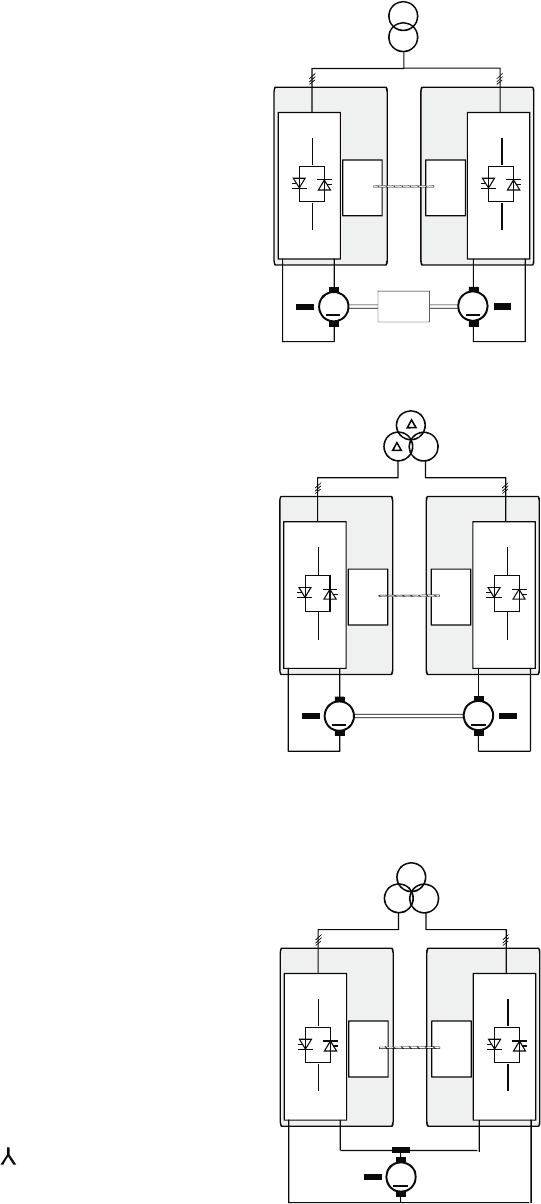
II D 3-2
3ADW000066R0901_DCS500_System_description_e_i
•Master-Follower-Applications
-Drives connected in Master-Follower application
If motors have to run with the same speed / torque they are often
controlled in a way called MASTER - FOLLOWER.
Drives used for such systems are of the same type and may differ in
power, but will be supplied from the same network. Their number
normally is not limited.
From the control point of view different conditions and demands
need to be matched.
Examples are available on request from ABB Automation Products
GmbH.
- Typical configuration for high power drives connected in
12-pulse parallel Master-Follower application
(see
chapter 3.6
)
This configuration shows a 12-pulse parallel drive system. It is an
easy option to increase the power of a drive system. Depending on
the engineering features , redundancy or emergency operation, if
one converter fails, is made available.
Such drives use two identical 6-pulse converters and an especially
designed choke called T-reactor or 12-pulse choke or interface
reactor. The converters are fed by a 12-pulse line transformer with
separated secondary windings whose phase positions differ by
30°el.
An example is the transformer configuration Ì//Ì. This
configuration gives a reduced level and a reduced order number of
harmonics on the AC side. Only the 11th and 13th, the 23rd and 25th,
the 35th a.s.o. are existing. The harmonics on the DC side are
reduced too, which gives a higher efficiency. (The field supply is not
shown on the wiring diagram 3.6. Depending on the field supply
selected, the connections to the network, the interlocking and the
control connections can be taken from any other wiring diagram
showing the selected field supply.)
It is not possible to connect two 12-pulse systems (2 converters, T-
reactor and 1 motor) to one 12-pulse transformer.
For more information, please see manual 12-pulse operation.
Figure 3/3: Application with two mechanically connected motors
-Typical configuration for high power drives connected in
Master-Follower application (two motors with one common
shaft)
This configuration is often used, if two motors have to share the
load half and half. They are mechanically fixed to each other via a
gearbox or any other device. The converters are fed by a 12-pulse
line transformer with separated secondary windings whose phase
positions differ by 30°el.
Each motor is connected to its own converter and field supply. The
converters exchange signals to make sure, that each motor takes half
of the load.
This configuration delivers the same advantages concerning har-
monics to the network as a standard 12- pulse application (see next
item), but no T-reactor is needed.
Depending on the mechanical configuration commissioning per-
sonal needs some experience to adapt control accordingly.
Figure 3/5: 12-Pulse parallel application
CON 2
C1
D1
M
CON 2
C1 D1
∆
Y
∆
MASTER-
FOLLOWER
Master
DCS 500B
Follower
DCS 500B
Figure 3/4: 12-Pulse application with two mechanically connected motors
CON 2
C1
D1
M
CON 2
C1 D1
M
connected
via load
MASTER-
FOLLOWER
Master
DCS 500B
Follower
DCS 500B
CON 2
C1
D1
M
CON 2
C1 D1
M
Y
Tandem motors
Master
DCS 500B
Follower
DCS 500B
MASTER-
FOLLOWER
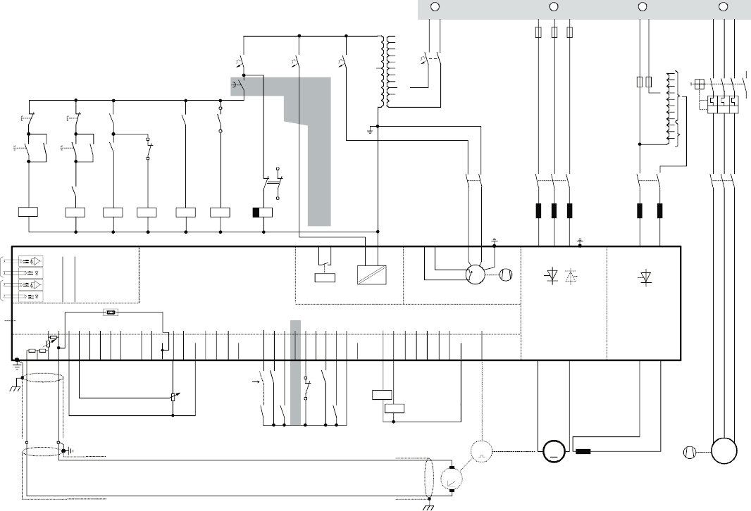
II D 3-3
3ADW000066R0901_DCS500_System_description_e_i
Figure 3.1/1: Standard drive configuration using an internal field
3.1 Standard drive configuration using an internal field
Wiring the drive according to this diagram gives the most flexibility and offers the highest degree of standard monitoring functions done
by the drive. There are no software modifications to adapt the drive to the external wiring.
•Selection of components
For this wiring diagram a DCS 500B converter construction type C1 / C2 / A5 (for A7 types, please use diagram 3.3 or higher) was selected together with
a SDCS-FEX-1 or 2A field supply. This field supply can be used at line voltages up to 500V and will give field current up to 6 / 16A. For higher field currents,
use the next bigger field supply unit DCF 503A/4A (wiring is shown at 3.3/1) or a 3-phase supply DCF 500B (wiring is shown at 3.5/2).
•Power supply
There are several components, which need a power supply:
- Converter´s power part: 200 V to 1000 V, depending on converter type;
see chapter 2
- Converter´s electronics power supply: 115V or 230V, selectable by jumper
- Converter cooling fan: 230V 1-ph;
see Technical Data
- Power part field supply: 115 V to 500 V; together with an isolating / auto transformer up to 600 V;
see chapter 2 and / or
Technical Data
- Motor cooling fan: depending on motor manufacturer / local demands
- Relay logic: depending on local demands
The fuses F1 are used because the converter construction type C1 and C2 don´t have them build in. All components, which can be fed by either 115/230 V
have been combined and will be supplied by one isolating transformer T2. All components are set to 230 V supply or selected for this voltage level. The different
consumers are fused separate. As long as T2 has the right tappings it can be connected to the power supply, used to feed the converter´s power part.
The same can be applied to the field supply circuit. There are two different types of matching transformers available. One can be used for supply voltages
up to 500 V, the other for voltages up to 690 V. Do not use the 690 V primary tapping together with the SDCS-FEX-1/2A field supply!
Depending on the motor fan voltage the power can be taken from the same source which is used for the converter´s power part.
In case the power for A, D and E should be taken from the source, used for C, a decision must be made, whether the fuses F1 can be used for two reasons
(protection of the power part + auxiliary power supply) or not.In addition it has to be checked, if the consumers can be supplied with this voltage wave form
(see chapter
Line Chokes
) before connecting to C. If the converter is supplied directly by a high-voltage converter transformer at point C, additional conditions
are to be considered during engineering of the drive (more details on request).
IN3
OUT3
IN1
OUT1
V5
V6
V1
V2
X96:
DO8
12 X99:12 X2:45 X2:1 2 3 U1 W1V1 PE
K1 F6
K20
K21K20 K3 K1
X96:1
X96:2
L1 L2 L3
F1
F3
K3
13
24
M
~
T3
F2
3
4
1
2
T2
690V
660V
600V
575V
525V
500V
450V
415V
400V
380V
115V
230V
K15
K15
S1
1
2
K6 K8
X2:4
X2:5
K11
K10
K21
500V
460V
415V
400V
365V
350V
265V
250V
90V
60V
30V
X33
C 1 D 1
AITAC AI1 AI2 AI3 AI4
+10V -10V AO1 AO2 IACT DI1 DI2 DI3 DI4 DI5 DI6 DI7 DI8 +48V DO1 DO2 DO3 DO4 DO5 DO6 DO7
__ __ _
++++ +
T
TM
0V
0V0V0V0V
X3:12345678910X4:12345678910 X6:12345678910 X7: 12345678 1...10
X5:
+_
+
_
K1
K20
K21
K6
K8
1
2
S1
K11
K10
S4
56
246
135
K6
F5
1
2
F8
1
2
F7
1
2
2
1
4
3
6
5
F6
I > I > I >
13
14
U
VW
M
3~
K1
135
246
L1
1
2
3
4
K8
13
14
X1: 1 7
L3
X1: 5 3
+_
L1 N L1 N L1 L2 L3
Voltage levels
see description
A C D E
Communication
board (COM-x) Control board (CON-2)
Power supply
(POW-1)
Converter
module
ON
OFF STOP
START
EMER.
STOP
Field exciter unit
(SDCS-FEX-1/2)
depending on the unit type
an other configuration is possible
the polarities are shown for motor operation
if there are intermediate terminals
e.g. Pressure
switch at C4
module
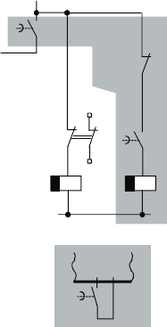
II D 3-4
3ADW000066R0901_DCS500_System_description_e_i
•Control
The relay logic can be split into three parts:
a: Generation of the ON/OFF and START/STOP command:
The commands represented by K20 and K21 (latching interface relay) can be generated by a PLC and transferred to the terminals of the converter either
by relays, giving galvanic isolation or directly by using 24V signals. There is no absolute need to use hardwired signals. These commands can be
transferred via a serial link system too. Even a mixed solution can be realized by selecting the one or the other possibility for the one or the other signal.
b: Generation of control and monitoring signals:
The main power contactor K1 for the armature circuit is controlled by a dry contact located on the electronic power supply board. The status of this contactor
is checked by the converter via binary input 3. The field supply contactor K3 is controlled by the auxiliary contact K11 connected to a binary output of the
converter. The binary outputs consist of relay drivers, capable to give appr. 50 mA each and a current limitation of around 160 mA for all of the outputs.
The contactors K6 and K8 control the fans of the drive system. They are controlled by the auxiliary contact K10 (similar to K11). In series with K6 is an
auxiliary contact of the circuit breaker F6, which monitors the motor fan supply. For the converter fan supply monitoring the contact of the temperature
detector is used in series with K8. Auxiliary contacts K6 and K8 are used and connected to the binary inputs 1 and 2 to monitor the status of the fan supplies
by the converter. The function of K15 is described at the next point.
c: Stop mode beside ON/OFF and START/STOP:
This chapter tries to explain the reaction of the drive when the input named EMERGENCY_STOP (906) or COAST_STOP (905) is operated. Please take
the external wiring used for this explanation as an example only!
For EMERGENCY STOP different preconditions have to be taken into account. This description focus on the functionality and does not take special safety
conditions depending on the type of machine into account.
In this case, if emergency stop is hit, the information is transferred to the converter via binary input 5. The converter will act according to the function
programmed (stop by ramp, current limit or coasting). If the converter will not manage to get the drive to standstill within the time set at K15, the auxiliary
contact will switch off the control power. Because of this the main power contactors K1 and all the others will be switched off. This may result in failure
of components (
see Operating Instructions
). This danger can be minimized by adding another time delay (grey-shaded parts below). By doing so another
stop mode is available.
- Emergency stop signal initializes the ramp down function
inside the converter in that way described before. If the
drive comes to standstill within the time specified by K15,
the converter will switch off the main power contactor K1.
If the converter doesn´t manage to get the drive to
standstill within this time, K15 will start the function
ELECTRICAL DISCONNECT with the time delay speci-
fied by K16. This information will be transferred to the
converter to a free binary input. This input has to be
connected to the COAST_STOP input of the drive logic.
The COAST_STOP input forces the current down to zero
as fast as possible. The delay time of K16 has to be
slightly higher than the time needed by the current con-
troller to get the current to zero. When the time K16 has
elapsed the control voltage will be switched off and all
power contactors will drop off.
- If no care should be taken to the speed of the drive the
function of K16 can be initialized by the command ELEC-
TRICAL DISCONNECT.
d: Main contactor handling by the PLC only because of safety reasons:
This mode is not recommended to be used as a standard switch on or switch off sequence. Nevertheless it is sometimes used to fulfill safety regulations
or other needs. In such cases it´s recommended to follow the next guidelines:
- It´s assumed that the PLC´s contact is in serial with the K1 (underneath the terminals named X96: 1 and 2) or in serial with the auxillary contact of K16
or replaces this one
- Switching off the main power contactor in regenerative mode may result in failure of components (see Operating Instruction)
- The PLC generates the command “main contactor off”. Two types of contacts are needed:
- A pretriggered contact should then be connected to an unused binary input of the converter; this input has to be connected to the signal START_INHIBIT
(908). This will block the controllers, trying to get the current to zero and switch off the main contactor from the converter point of view (independent, if
the converter´s command is used or not).
- A normal contact can then handle the main contactor.
- Caused by the final timing alarms or error may be detected; they should be reset or bypassed (e.g. by the auto reclosing function
•Sequencing
When the ON command is given to the converter and there is no error signal active, the converter closes the fan, field and main contactor, checks the supply
voltage and the status of the contactors and without error messages, releases the regulators and starts waiting for the RUN command. When the RUN
command is given, the speed reference is released and speed control mode is active (for more details,
see Software Description
).
EMER.
STOP
K16
K15 K16
K15
ELEC.
DISCONN.
DIx
K15
X6:9
CON-2
S1
1
2
II D 3-5
3ADW000066R0901_DCS500_System_description_e_i
Figure 3.2/1: Drive configuration using the internal field with reduced external components
3.2 Drive configuration using the internal field with reduced external components
Wiring the drive according to this diagram gives the same control performance, but a lower degree of flexibility and nearly no external
monitoring functions done by the drive. The software has to be adapted to the external wiring.
IN3
OUT3
IN1
OUT1
V5
V6
V1
V2
X96:
DO8
12 X99:12 X2:45 X2:1 2 3 U1 W1V1 PE
K1
K20
K21K20 K1
X96:1
X96:2
L1 L2 L3
400V 50Hz
F1
F3
M
~
K21
X33
C 1 D 1
AITAC AI1 AI2 AI3 AI4 +10V -10V AO1 AO2 IACT DI1 DI2 DI3 DI4 DI5 DI6 DI7 DI8 +48V DO1 DO2 DO3 DO4 DO5 DO6 DO7
__ __ _
++++ +
T
TM
0V
0V0V0V0V
X3:12345678910X4:12345678910 X6:12345678910 X7: 12345678 1...10
X5:
+_
+
_
K1
K20
K21
S4
56
F5
1
2
F8
1
2
F7
1
2
K1
135
246
L1
X1: 1 7
L3
X1: 5 3
+_
L1 MP
230V 50Hz
2
1
4
3
6
5
F6
I > I > I >
13
14
UVW
M
3~
Communication
board (COM-x) Control board (CON-2)
Power supply
(POW-1)
Converter
module
ON
OFF STOP
START
Field exciter unit
(SDCS-FEX-1/2)
depending on the unit type
an other configuration is possible
the polarities are shown for motor operation
if there are intermediate terminals
e.g. Pressure
switch at C4
module
•Selection of components
same as figure 3.1/1
•Power supply
There are several components, which need a power supply. Because of the wiring preconditions have to be taken into account:
- Converter´s power part: 200 V to 500 V, depending on converter type;
see chapter 2
- Converter´s electronics power supply: use only 230 V possibility, selected by jumper
- Converter cooling fan: 230V 1-ph;
see Technical Data
- Power part field supply: 200 V to 500 V;
see chapter 2 and / or Technical Data
- Motor cooling fan: select the motor voltage acc. to the voltage used for the armature supply
- Relay logic: select the components for 230 V!
This configuration is basically identical to the one shown at figure 3.1/1. Please check the sizing of F1 for the additional load like field and motor fan. All
components are either selected for 230V or set to 230V to be able to combine them and to supply them by an auxiliary power supply. The different consumers
are fused separately.
•Control and safety
The relay logic can be split into three parts:
a: Generation of the ON/OFF and START/STOP command: same as figure 3.1/1
b: Generation of control and monitoring signals:
The main power contactor K1 is handled in the same way it was done at figure 3.1/1. The field and motor fan supply is picked up at the output of K1. So
all 3 consumers are controlled in the same way.
The fan monitoring is not taken into consideration. Because of this these parameter settings have to be made:
Connection (default) must be changed to:
910 from 10701 10908
911 from 10703 10908
906 from 10709 12502
c: Stop mode beside ON/OFF and START/STOP: Not taken into consideration!
•Sequencing
When the ON command is given to the converter and there is no error signal active, the converter closes the fan, field and main contactor, checks the supply
voltage and the status of the contactors and without an error messages, releases the regulators and starts waiting for the RUN command. When the RUN
command is given, the speed reference is released and speed control mode is active (for more details,
see Software Description
).
II D 3-6
3ADW000066R0901_DCS500_System_description_e_i
Figure 3.3/1: Standard drive configuration using an external half-controlled field (1-ph)
3.3 Standard drive configuration using an external half-controlled field (1-ph)
Wiring the drive according to this diagram gives the most flexibility and offers the highest degree of standard monitoring functions done by
the drive. There are no software modifications to adapt the drive to the external wiring.
•Selection of components
For this wiring diagram a DCS 500B converter was selected together with a DCF 503A/4A field supply. If a DCF 504A is used for field supply, field reversal
is possible. Then a DCS 501B (2-Q) for the armature supply is sufficient for low demanding drives. This field supply can be used at line voltages up to 500 V
and will give field current up to 50 A. For higher field currents, a 3-phase supply DCF 500B (wiring is shown at 3.5/2).
•Power supply
There are several components, which need a power supply:
- Converter´s power part: 200 V to 1000 V, depending on converter type;
see chapter 2
- Converter´s electronics power supply: 115 V or 230 V, selected by jumper
- Converter cooling fan: 230 V 1-ph; 400 V / 690 V 3-ph. at A6/A7;
see Technical Data
- Power part field supply: 115 V to 500 V; together with an isolating/auto transformer up to 690 V;
s. chap. 2 and/or Tech-
nical Data
- Electronics supply of field unit: 115 V to 230 V
- Motor cooling fan: depending on motor manufacturer / local demands
- Relay logic: depending on local demands
This configuration is basically identical to the one shown at figure 3.1/1. In addition to figure 3.1/1 the field supply unit needs an electronic power supply, which
is separately fused and taken from the 230V level, generated by T2. This field controller is controlled via a serial link, connected to X16: at the armature
converter. The 690V primary tapping can be used together with this type of field supply!
In case the power for A, D and E should be taken from the source, used for C, a decision must be made, whether the fuses F1 can be used for two reasons
(protection of the power part + auxiliary power supply) or not. In addition it has to be checked, if the consumers can be supplied with this voltage wave form
(see chapter
Line Chokes
) before connecting to C.
•Control
The relay logic can be split into three parts as decribed in figure 3.1/1. Basically the logic shown at figure 3.2/1 could be used for this configuration. The size
of the drive and/or it´s value may be a criteria to select the logic according to figure 3.1/1 or to figure 3.2/1 or a combination of both.
*
Recomendation
: Keep the control of K3 as shown, if a DCF 504A field supply is used!
•Sequencing
same as figure 3.1/1
IN3
OUT3
IN1
OUT1
V5
V6
V1
V2
X96:
DO8
12 X99:12 X2:45 X2:1 2 3 U1 W1V1 PE U1 V1
K1 F6
K20
K21K20 K3 K1
X96:1
X96:2
F1
F3
K3
13
24
M
~
T3
F2
3
4
1
2
T2
690V
660V
600V
575V
525V
500V
450V
415V
400V
380V
115V
230V
K15
K15
S1
1
2
K6 K8
X2:4
X2:5
K11
K10
K21
500V
460V
415V
400V
365V
350V
265V
250V
90V
60V
30V
X33
C 1 D 1 C1 D1
AITAC AI1 AI2 AI3 AI4
+10V -10V AO1 AO2 IACT DI1 DI2 DI3 DI4 DI5 DI6 DI7 DI8 +48V DO1 DO2 DO3 DO4 DO5 DO6 DO7
__ __ _
++++ +
T
TM
0V
0V0V0V0V
X3:12345678910X4:12345678910 X6:12345678910 X7: 12345678 1...10
X5:
+_+_
+
_
K1
K20
K21
K6
K8
1
2
S1
K11
K10
S4
56
X16:
321
X2:
321
X3: 21
246
135
K6
F5
1
2
F9
1
2
F8
1
2
F7
1
2
2
1
4
3
6
5
F6
I > I > I >
13
14
U
VW
M
3~
K1
135
246
L1
1
2
3
4
K8
13
14
L1 L2 L3L1 N L1 N L1 L2 L3
A C D E
*
Communication
board (COM-x) Control board (CON-2)
Power supply
(POW-1)
Converter
module
ON
OFF STOP
START
EMER.
STOP
Field exciter unit
(DCF503A/504A) *
depending on the unit type
an other configuration is possible
the polarities are shown for motor operation
if there are intermediate terminals
e.g. Pressure
switch at C4
module
Voltage levels
see description
II D 3-7
3ADW000066R0901_DCS500_System_description_e_i
3.4 Standard configuration using a fully-controlled field (3-ph) without armature converter
The DCS 500B converter is used as a DCF 500B version in a non-motoric application. If the drive should be wired according to this example
or to the one shown at figure 3-2.1 it has to be decided depending on the application and it´s demands. The software structure has to be
adapted and is described within the Operating Manual.
•Selection of components
For this wiring diagram a DCF 500B converter construction type C1 or C2 was selected together with a DCF 506 unit, which serves as an overvoltage
protection.
•Power supply
There are several components, which need a power supply:
- Converter´s power part: 200 V to 500 V, depending on converter type;
see chapter 2
- Converters electronics power supply: 115 V or 230 V, selected by jumper
- Converter cooling fan: 230 V 1-ph at C1 + C2;
see Technical Data
- Relay logic: depending on local demands
Basically according to figure 3.1/1. If the converter is supplied directly by a high-voltage converter transformer at point C , make sure that the high voltage
switch is not opened, as long as field current flows. Additional conditions are to be considered during engineering of the drive (further information on request).
•Control
The relay logic can be split into three parts.
a: Generation of the ON/OFF and START/STOP command: same as figure 3.1/1
b: Generation of control and monitoring signals: Basically identical to figure 3.1/1.
Instead of the monitoring of the motor fan at binary input 2, which is not existing here but may exist as a cooling device for the inductance, the over-
voltage protection DCF 506 is monitored by the same input. If any type of additional cooling device should be monitored extra function blocks can be
used.
c: Stop mode beside ON/OFF and START/STOP: Basically identical to figure 3.1/1
In this case it may be much more important to focus on a reduction of the current than on something else. If so, select coasting at the parameter
EMESTOP_MODE.
•Sequencing
same as figure 3.1/1
Figure 3.4/1: Standard configuration using a fully-controlled field (3-ph) without armature converter
IN3
OUT3
IN1
OUT1
V5
V6
V1
V2
X96:
DO8
12 X99:12 X2:45 X2:1 2 3 U1 W1V1 PE
F1.2
M
~
X33 AITAC AI1 AI2 AI3 AI4
+10V -10V AO1 AO2 IACT DI1 DI2 DI3 DI4 DI5 DI6 DI7 DI8 +48V DO1 DO2 DO3 DO4 DO5 DO6 DO7
__ __ _
++++ +
0V
0V0V0V0V
X3: 1 2 3 4 5 6 7 8 9 10 X4: 1 2 3 4 5 6 7 8 9 10 X6: 1 2 3 4 5 6 7 8 9 10 X7: 12 34 5 6 7 8 1...10
X5:
K8
K1
S4
56
K1
135
246
L1
C 1 D 1
+_+
X4:1
X4:2
_
X11 X12
DCF 506
K10
L1 L2 L3
C
K1
K20
K21K20 K1
X96:1
X96:2
F2
3
4
1
2
T2
690V
660V
600V
575V
525V
500V
450V
415V
400V
380V
115V
230V
K15
K15
S1
1
2
K8
X2:4
X2:5
K10
K21
F5
1
2
F8
1
2
F7
1
2
1
2
3
4
K8
L1 N
A
K20
K21
1
2
S1
Communication
board (COM-x) Control board (CON-2)
Power supply
(POW-1)
Converter
module
depending on the unit type
an other configuration is possible
Overvoltage
protection
Voltage levels
see description
ON
OFF STOP
START
EMER.
STOP
II D 3-8
3ADW000066R0901_DCS500_System_description_e_i
3.5 Typical configuration for high power drives
This wiring diagram has been generated to show the configuration for big drives with preferably more than 2000 A for the armature supply
and a 3-phase field supply. For such drives the converter construction type A6 or A7 is used. The basic idea is identical to figure 3.1/1.
Figure 3.5/1: Typical configuration for high power drives (armature unit DCS 500B)
•Selection of components
For this wiring diagram a DCS 500B converter construction type A6 or A7 was selected together with a 3-phase field supply. This field supply can be used
at line voltages up to 500 V and will give field current up to 540 A.
•Power supply
There are several components, which need a power supply:
- Armature converter´s power part: 200 V to 1000 V, depending on converter type;
see chapter 2
- Field converter´s power part: 200 V to 500 V
- Converters electronics power supply: 115 V or 230 V, selected by jumper
- Converter cooling fan: 230V 1-ph at A5 (armature), C1 + C2 (field); 400 V / 690 V 3-ph. at A6/A7 (armature);
see
Technical Data
- Motor cooling fan: depending on motor manufacturer / local demands
- Relay logic: depending on local demands
This configuration is basically identical to the one shown at figure 3.1/1. The converters in use here are much bigger than before. They are equipped with
fuses in the legs of the power part. That´s the reason F1 is drawn within the square of the power part. If additional fuses are needed between supply transformer
or not, has to be decided case by case. The field supply transformer T3 cannot be used for this configuration! See also power supply fig. 3.4/1 (
fully-controlled
field
).
In case the power for A, B, D and E should be taken from the source, used for C, a decision must be made, whether the fuses F1 can be used for two reasons
(protection of the power part + auxiliary power supply) or not. In addition it has to be checked, if the consumers can be supplied with this voltage wave form
(see chapter
Line Chokes
) before connecting to C.
IN3
OUT3
IN1
OUT1
V5
V6
V1
V2
X96:
DO8
12 X99:12 X2:TKTK X2:U1V1W1 U1 W1V1 PE
K1 F6
K20
K21K20 K1
X96:1
X96:2
M
~
F2
3
4
1
2
T2
690V
660V
600V
575V
525V
500V
450V
415V
400V
380V
115V
230V
K15
K15
S1
1
2
K6 K8
X2:TK
X2:TK
K10
K21
X33
C 1 D 1
AITAC AI1 AI2 AI3 AI4 +10V -10V AO1 AO2 IACT DI1 DI2 DI3 DI4 DI5 DI6 DI7 DI8 +48V DO1 DO2 DO3 DO4 DO5 DO6 DO7
__ __ _
++++ +
T
TM
0V
0V0V0V0V
X3:12345678910X4:12345678910 X6:12345678910 X7: 12345678 1...10
X5:
+_
+
_
K1
K20
K21
K6
K8
1
2
S1
K10
S4
56
X16:
321
246
135
K6
F5
1
2
F7
1
2
2
1
4
3
6
5
F6
I > I > I >
13
14
UVW
M
3~
K1
135
246
L1
13
14
246
135
K8
2
1
4
3
6
5
F8
I > I > I >
13
14
PE
1
2
3
F1
L1 L2 L3L1 N L1 L2 L3
A B C E
L1 L2 L3
X16:
3
2
1
Communication
board (COM-x) Control board (CON-2)
Power supply
(POW-1)
Converter
module
ON
OFF STOP
START
EMER.
STOP
depending on the unit type and supply voltage
an other configuration is possible
the polarities are shown for motor operation
if there are intermediate terminals
e.g. Pressure
switch at C4
module
Voltage levels
see description
II D 3-9
3ADW000066R0901_DCS500_System_description_e_i
Figure 3.5/2: Typical configuration for high power drives (field unit DCF 500B)
•Control
The relay logic can be split into three parts. Basically the logic shown at figure 3.2/1 could be used for this configuration. Because of the size of the drive and
it´s value the logic shown is recommended:
a: Generation of the ON/OFF and START/STOP command: same as figure 3.1/1
b: Generation of control and monitoring signals: same as figure 3.1/1
Each converter is monitoring his main contactor and his fan supply by himself.
c: Stop mode beside ON/OFF and START/STOP: same as figure 3.1/1
It is recommended to use the additional safety provided by the use of the ELECTRICAL DISCONNECT function at such type of drives.
•Sequencing
It is basically the same than the one described for figure 3.1/1. The 3-phase field exciter is equipped with much more detailed service functionallity compared
to the single phase types (SDCS-FEX-2A or DCF 503A/4A). Nevertheless from the control point of view (binary signals given to the armature converter) it
will act in exactly the same way as a single phase one!
When the ON command is given to the armature converter and there is no error signal active, the converter transfers this command via the serial link to the
field converter. Afterwards, each converter closes the fan and main contactor, checks the supply voltage and the status of the contactors and without any
error messages, releases the regulators. Then the same actions take place described at fig. 3.1/1.
In case the field unit records an error a common error signal is send to the armature converter. In parallel an error indication is displayed on the field unit´s
7-segment display and at its binary output, if programmed. The armature converter will indicate the field unit´s error message with F39 on its display. The
drive will be switched off by itself if it was running. The control system should then send a Reset command to the armature converter after having removed
the ON/OFF and RUN commands. The error message should no longer be shown. With a new start command the armature converter will at first send a Reset
command to the field converter. The field unit will then reset its error message, if the reason for it is no longer present. After that the field unit receives the
start command from the armature converter and will switch on its main contactor.
It's not necessary to exchange information like commands, actual values or error message within field converter and control system based on a serial link
like PROFIBUS or others. In case the more comfortable servicing capabilities of a 3-phase field unit should be used it´s no problem to do so either via hardware
(terminal row) or via a serial link.
IN3
OUT3
IN1
OUT1
V5
V6
V1
V2
X96:
DO8
12 X99:12 X2:45 X2:1 2 3 U1 W1V1 PE
K1.2
X96:1
X96:2
F1.2
M
~
X33 AITAC AI1 AI2 AI3 AI4
+10V -10V AO1 AO2 IACT DI1 DI2 DI3 DI4 DI5 DI6 DI7 DI8 +48V DO1 DO2 DO3 DO4 DO5 DO6 DO7
__ __ _
++++ +
0V
0V0V0V0V
X3: 1 2 3 4 5 6 7 8 9 10 X4: 1 2 3 4 5 6 7 8 9 10 X6: 1 2 3 4 5 6 7 8 9 10 X7: 12 34 5 6 7 8 1...10
X5:
K8.2
K1.2
S4
56
F5.2
1
2
F8.2
1
2
K1.2
135
246
L1.2
1
2
3
C 1 D 1
+_+
Overvoltage
protection
X4:1
X4:2
_
X11 X12
K8.2
X2:4
X2:5
X16:
321
1
2
3
4
K8.2
DCF 506
K10.2
K10.2
X16:
3
2
1
L1 L2 L3
Voltage levels
see description
C
Communication
board (COM-x) Control board (CON-2)
Power supply
(POW-1)
Converter
module
depending on the unit type
an other configuration is possible
II D 3-10
3ADW000066R0901_DCS500_System_description_e_i
•Selection of components
See remarks above.
•Power supply
There are several components, which need a power supply:
- Armature converter´s power part: 200 V to 1000 V, depending on converter type;
see chapter 2
- Converters electronics power supply: 115 V or 230 V, selected by jumper
- Converter cooling fan: 230V 1-ph at C1 + C2, A5; 400 V / 690 V 3-ph. at A6/A7;
see Technical Data
- Motor field supply: see fig. 3.5/2
- Motor cooling fan: depending on motor manufacturer / local demands
- Relay logic: depending on local demands
This configuration is basically identical to the one shown at figure 3.5/1. The drive system is supplied by a 12-pulse transformer, which has got two secondary
windings with a phase shift of 30 degrees. In this case a decision has to be made, how the auxiliary voltage levels A, B, C, D=field and E are generated.
Attention has to be paid to the auxiliary voltage A:
- is the power of transformer T2 sufficient to supply all consumers? Consumers are electronics of all the converters, possibly fans of the two 12-
pulse converters and the field supply unit, main contactors, monitoring circuits, etc.
- is redundancy required, and/or flexibility to be able to operate master and follower independent of one another?
If necessary several auxiliary voltage levels (A, A', A'' etc.) should be constructed.
•Power supply (continuation)
Afterwards it has to be decided how the different consumers will be protected against any type of failure. If circuit breakers are used, take their interruption
capacity into account. Take the hints given before as a rough idea. See also power supply fig. 3.4/1 (
fully-controlled field
).
3.6 Typical configuration for high power drives connected in 12-pulse parallel Master-Follower ap-
plication
This wiring diagram can be used for 12-pulse parallel systems. It´s is based on the configuration shown at firgure 3.1/1, too. Such a
configuration can be done with two 25 A converters as well as with two 5200 A types. Most often this configuration is selected because of
the total power. That´s the reason why the wiring is already adapted to A5 (converter fan 1-phase) or A7 type converters. For the field supply,
please take the field wiring at figure 3.5/2. If a smaller type is used, pick up the part of interest shown at one of the figures before.
Figure 3.6/1: Typical configuration for high power drives connected in 12-pulse parallel (MASTER)
IN3
OUT3
IN1
OUT1
V5
V6
V1
V2
X96:
DO8
12 X99:12 X2:TKTK X2:U1V1W1 U1 W1V1 PE
K1 F6
K20
K21K20 K1
X96:1
X96:2
M
~
F2
3
4
1
2
T2
690V
660V
600V
575V
525V
500V
450V
415V
400V
380V
115V
230V
K15
K15
S1
1
2
K6 K8
X2:TK
X2:TK
K10
K21
X33
C 1 D 1
AIT AC AI1 A I2 AI3 AI4
+10V -10V AO1 AO2 IACT DI1 DI2 DI3 DI4 DI5 DI6 DI7 DI8 +48V DO1 DO2 DO3 DO4 DO5 DO6 DO7
__ __ _
++++ +
0V
0V0V0V0V
X3:1 2 3456 78910X4:12 345 6 7 8 910 X6:12 3456 78910 X7: 1 2 3 4 5 6 7 8 1...10
X5:
T
T
+
_
K1
K20
K21
K6
K8
1
2
S1
K10
S4
56
X16:
321
X16:
3
2
1
246
135
K6
F5
1
2
F7
1
2
2
1
4
3
6
5
F6
I > I > I >
13
14
U
VW
M
3~
K1
135
246
13
14
246
135
K8
2
1
4
3
6
5
F8
I > I > I >
13
14
PE
1
2
3
M
X18:
F1
L1 L2 L3L1 N L1 L2 L3
A B C E
L1 L2 L3
+_
Communication
board (COM-x) Control board (CON-2)
Power supply
(POW-1)
Converter
module
ON
OFF STOP
START
EMER.
STOP
depending on the unit type and supply voltage
an other configuration is possible
the polarities are shown for motor operation
if there are
intermediate
terminals
e.g. Pressure
switch at C4
module
to field converter
DCF 500B X16:
Voltage levels
see description
II D 3-11
3ADW000066R0901_DCS500_System_description_e_i
Figure 3.6/2: Typical configuration for high power drives connected in 12-pulse parallel (FOLLOWER)
•Control
The relay logic can be split into three parts. Basically the logic shown at figure 3.2/1 could be used for this configuration. Because of the size of the drive
and it´s value the logic shown is recommended:
a: Generation of the ON/OFF and START/STOP command: same as figure 3.1/1
b: Generation of control and monitoring signals: same as figure 3.1/1
Each converter is monitoring his main contactor and his fan supply by himself.
c: Stop mode beside ON/OFF and START/STOP: same as figure 3.1/1
It is recommended to use the additional safety provided by the use of the ELECTRICAL DISCONNECT function at such type of drives.
•Sequencing
The circuit diagram is based on a permanent 12-pulse mode without any adaptation concerning redundancy and on one converter working as a Master and
taking care for the field control. All remarks given in chapter 3.5 can be applied to this configuration too. The converters exchange binary signals for bridge
reversal and for fast monitoring via the flat cable connection X18:. Analogue signals like current reference and actual current are exchanged via terminal row
X3: / X4:. Parameters at group 36 have to be set within Master and Slave converter to get the data exchange via flat cable connection X18: and connected
inputs / outputs working. Parameters to be set at group 1 and 2 within Master and Slave make sure the data exchange of current values analogue inputs
and outputs will take place. Additional information and a detailed parameter list are available within the manual
Planning and Start-up for 12-pulse Power
Converters
.
•Engineering hint
If the drive system has to be available in case of a failure redundancy is needed and basically possible! Basically errors and failures can happen to all
components any time, depending on the single component affected the result will have a different severity. Because of that errors and faults resulting in a
redundancy mode have to be specified at first. Errors and faults causing severe break down are found at the power supply / 12-pulse transformer, at the two
converters, supplying the armature, at the field supply unit, at the 12-pulse interphase reactor or at the motor. Precautions can be made to increase the
availability of the drive in case the load condition and the motor data allow to use the system with reduced power. This can be made for example by using
two transformers instead of one single 12-pulse transformer, by enabling 6-pulse mode at the converters (only one converter is switched on; the other is still
kept switched off), by a second installed field supply unit in case of hardware failures there or by enabling the field control done by either the one or the other
converter and by a possibility to bypass the 12-pulse interphase choke.
1
2
3
IN3
OUT3
IN1
OUT1
V5
V6
V1
V2
AITAC AI1 AI2 AI3 AI4 +10V -10V AO1 AO2 IACT DI1 DI2 DI3 DI4 DI5 DI6 DI7 DI8 +48V DO1 DO2 DO3 DO4 DO5 DO6 DO7
__ _ _ _
++++ +
0V
0V0V0V0V
X3:12345678910X4:12345678910 X6:12345678910 X7: 12 34 5 6 7 8 1...10
X5:
K1.3
K20
K8.3
S4
56
K10.3
X16:
21
X96:
DO8
12 X99:
X96:1
X96:2
F5.3
1
2
K1.3
K8.3
X2:TK
X2:TK
K10.3
246
135
K8.3
2
1
4
3
6
5
F8.3
I > I > I >
13
14
12 X2:TKTK X2:U1V1W1
M
~
PE
X33
U1 W1V1 PE
K1.3
135
246
F1
L1 L2 L3 L2 L3
BC
L1
C 1
+
D 1
_
X18:
∆
Y
∆
Communication
board (COM-x)
Control board (CON-2)
Power supply
(POW-1)
Converter
module
depending on the unit type and supply voltage
an other configuration is possible
Pressure
switch
Voltage levels
see description
II D 3-12
3ADW000066R0901_DCS500_System_description_e_i
II D 4-1
3ADW000066R0901_DCS500_System_description_e_i
The standard diagram of the DCS500 Software Struc-
ture is added to this chapter as folder.
In addition to all the function blocks presented there
(called "Standard Function Blocks") additional blocks
(called "Application blocks") are available, like ABSo-
lute value, ADDer with 2 and 4 inputs, AND gates with
2 and 4 inputs, COMParators, CONVersion blocks,
COUNTer, DIVider, FILTer, FUNG (x-y function
generator, LIMiter, MULiplier, OR gates with 2 and 4
inputs, PARameter function block, PI controller, SR
memory, SUBtraction, XOR gates and others.
Both types are stored in the converter and delivered
with every converter. The application function blocks
as well as the standard function blocks are available as
a library in file format. This library serves as a basis for
your customized modifications.
As a library is always a copy of the one available within
the converter former libraries are automatically includ-
ed in the latest one.
Commissioning and Maintenance Tools for DCS500
(Panel or DDC/CMT Tool) are able to connect or
disconnect function blocks and therefore can produce
customized software applications. Both these tools
however are not able to produce a documentation of the
Fig. 4.1/1 Standard and Applications function blocks utilized with GAD
Application blockStandard function block
Please note:
For more information of the GAD PC program and the
library there are manuals available describing the pos-
sibilities and the handling of the program.
changes in software other than in a table. Therefore
ABB offers another special tool to develop extended
software structures as drawings and deliver a data file
with these informations to be transferred into the drive
control section via the CMT Tool.
This tool is called GAD ( Graphical Application De-
signer). The GAD is for off-line use only and needs a
CMT tool to transfer the changed software structure
into the drive.
The GAD PC program features the following func-
tions:
• application design and programming
• graphics editor for drawing and altering program
diagrams
• user-controlled document depiction
• compilation of the application file to be download-
ed into the converter by using CMT tool
• compilation of the diagram file to be loaded into the
CMT tool window to see actual values on-line
System requirements / recommendation:
• min. 486 PC, 4 MB RAM, 40MB free hard disk
space
• operating system: Windows 3.x, 95, 98, NT, 2000
or XP
4 Overview of software (Version 21.2xx)
4.1 GAD Engineering-Program
II D 4-1
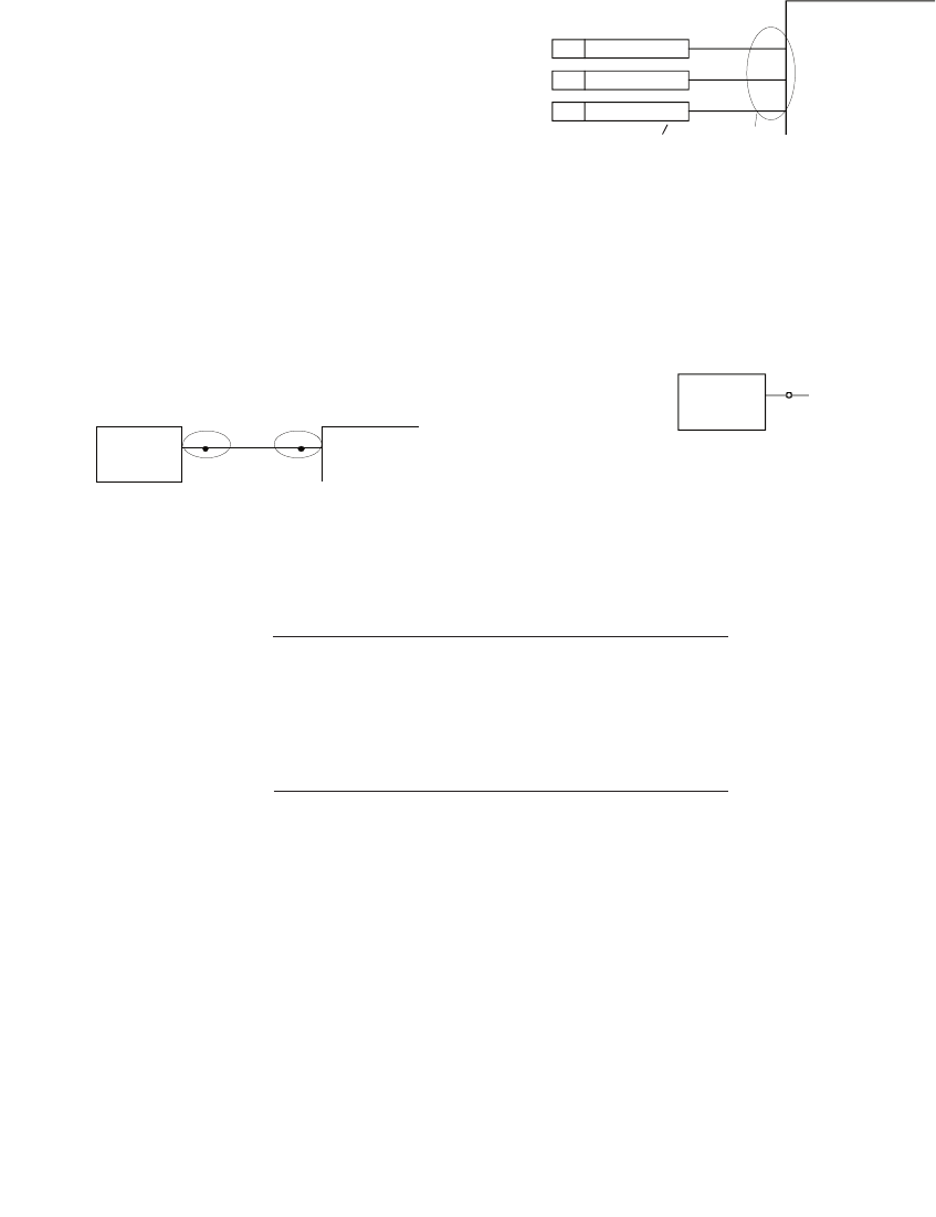
II D 4-2
3ADW000066R0901_DCS500_System_description_e_i
4.2 Introduction to the structure and handling
Please note:
The following pages describe the as-delivered wired functionality. If a desired signal or a certain function seems
to be missing, it can in most cases be implemented very easily:
The following pages correspond to what you get
printed from the GAD tool with additional explana-
tions based on software 21.233 which is identical with
software 21.234.
When you want to alter connections between function
blocks, proceed as follows:
• first select the input
• and then connect to output
All those connections possessing one dot each at their
beginning and end can be altered.
Parameters for setting values
(such as ramp-up time / ramp-down time, controller
gain, reference values and others)
RAMP GENERATOR
P6
P2
P4
1708
1709
1710
Parameter
Val ue
Val ue
Val ue
For input / parameter selection, the following applies:
• Ignore the two right-hand digits; the remaining
digits are the group and to be selected
• The two right-hand digits are the element and to be
selected
DI7 10713
The selection can be done with the control panel
CDP312, using the (double-up-down) for the group
and the (single-up-down) for the element or a PC-based
tool program CMT/DCS500B.
The entire software is made up of connected function
blocks. Each of these individual function blocks consti-
tutes a subfunction of the overall functionality. The
function blocks can be subdivided into two categories:
•Function blocks which are permanently active, are
almost always in use; these are described on the
following pages.
•Function blocks which, although they are available
within the software as standard features, have to be
expressly activated when they are needed for special
requirements. These include, for example:
AND gates with 2 or 4 inputs,
OR gates with 2 or 4 inputs,
adders with 2 or 4 inputs,
multipliers/dividers, etc.
or closed-control-loop functions, such as
integrator,
PI controller,
D-T1 element, etc.
All function blocks are characterized by input and
output lines, equipped with numbers. These inputs/
outputs can likewise be subdivided into two categories:
Inputs for designating connections
901 DRIVE LOGIC
DI7 10713
Output Input
Default setting
Group 107
element 13
• In addition to that please note that the functionality
described on the next pages is available a second time
for Motor Set 2. There are two parameter sets
(groups 1 to 24) available within the drive's memo-
ry.
• The values of the parameters are displayed in GAD-
Tool format.
• Either the desired signal does already exist, but - due
to its complexity - is not easy to describe, which is
why it appears in a signal listing given in the software
description.
• Or it can be generated with available signals and
additionally available function blocks.
II D 4-2
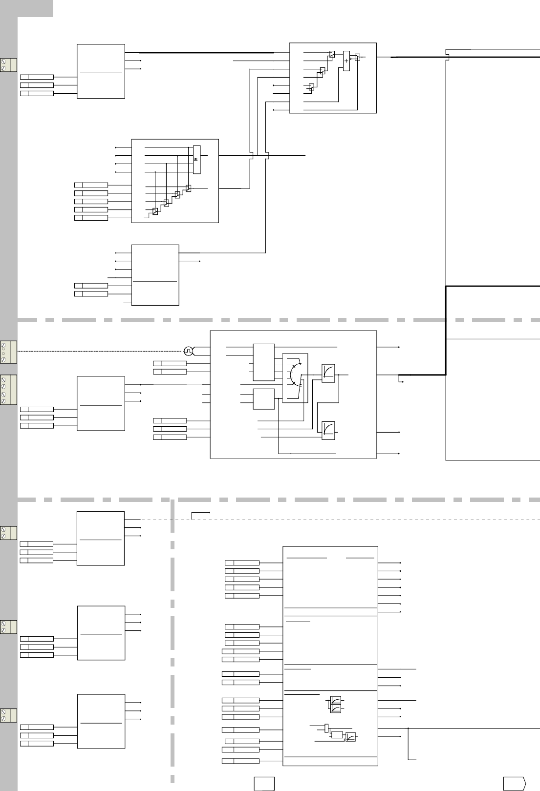
II D 4-3
3ADW000066R0901_DCS500_System_description_e_i
2/81/8
AITAC LOW VALUE
AITAC HIGH VALUE
AITAC CONV MODE
SP
AITAC:OUT+
AITAC:OUT-
AITAC:ERR
AITAC
ST5
10101
10102
10103
P2
P3
P1
-84
101
102
103
0
30000
-30000
+
-8...-30V
-30...-90V
-90...-270V
TACHO PULSES
SPEED ACT FLT FTR
SPEED MEASUREMENT
SPEED ACT EMF
SPEED ACT FILT
SPEED ACT
SPEED ACT FTR
SPEED MEAS MODE
U MOTN V
U ARM ACT
TACHOPULS NR
SPEED SCALING
CH B
CH A
5
0
4
3
2
1
T
T
SPEED
TO
EMF
CALC
(10505)
(501)
AITAC:OUT+
T5
SP
TACHO
PULSE
12104
12102
12103
12101
P1
P2
P3
P4
P5
-11
2103
2101
2102
2104
2105
15000
2048
5
0
500
MAINTENANCE
(1210)
REF SEL
SP
ST5
0
SEL1
IN1
IN2
SEL2
IN3
SEL3
OUT
ADD
REV
1910
1911
1912
1913
1914
1915
1916
1917
11903
-20
CONST REF
ST5
1
REF4
DEF
REF3
REF1
REF2
ACT2
ACT3
ACT4
ACT
SP
OUT
ACT1
1901
1902
1903
1904
11902
11901
P5
P1
P4
P2
P3
-77
1905
1906
1907
1908
1909
1000
1500
0
0
0
SP
1923 ENABLE
FOLLOW
1920
RUNNING
(10903)
T20
OHL
OLL
P1
P2
INCR
DECR
OUT
ACT
SOFTPOT
1918
1919
11904
11905
-15 SOFTPOT1
1921
1922
5000
-5000
DRIVE LOGIC (10903)
AI1 LOW VALUE
AI1 HIGH VALUE
AI1 CONV MODE
SP
AI1:OUT+
AI1:OUT-
AI1:ERR
AI1
ST5
10104
10105
10106
P2
P3
P1
-90
104
105
106
1
20000
-20000
+
--
AI2 LOW VALUE
AI2 HIGH VALUE
AI2 CONV MODE
SP
AI2
AI2:OUT+
AI2:OUT-
AI2:ERR
ST5
10107
10108
10109
P2
P3
P1
-89
107
108
109
0
2000
-2000
+
--
Control Adjust.
10507
10514
10513
10512
10511
10509
10510
BRIDGE TEMP
QUADR TYPE
CONV TYPE
MAX BR TEMP
Conv. valuesConv. settings C4
SET QUADR TYPE
SET CONV TYPE
SET MAX BR TEMP
SET U CONV V
SET I COMV A
U CONV V
I CONV A
I TRIP A
SETTINGS
SP
P5
P4
P3
P1
P2
Motor Data
I MOTN A
U MOTN V
I MOT1 FIELDN A
I MOT2 FIELDN A
FEXC SEL
P11
P10
P9
P8
P7
10508
10515
U NET DC NOM V
U SUPPLY
P13
PHASE SEQ CW
P14
10504
U NET ACT
LINE FREQUENCY
Supply Data
ST20
LANGUAGE
P15
(only for Cur. Controlling)
UNI FILT TC
P19
P6
P18
P12
P16
P17
CURR ACT FILT TC
PLL CONTROL
PLL DEV LIM
CONV CUR ACT
ARM CUR ACT
TORQUE ACT
10501
10502
10503
U ARM ACT
EMF ACT
CALC
Iact
+
-
OFFSET UDC
UDC 10505
10506
EMF FILT TC
-1 SETTGS_3
517
518
519
520
521
513
501
502
503
504
505
523
507
506
522
524
528
526
525
0
0
0
0
0
10
500
10
30
30
0
0
500
2
0
4
1024
0
10
DATA LOGGER (604)
DATA LOGGER (602)
MAINTENANCE (1211)
DATA LOGGER (603)
MAINTENANCE (1212)
AI4 LOW VALUE
AI4 HIGH VALUE
AI4 CONV MODE
SP
AI4:OUT+
AI4:OUT-
AI4:ERR
AI4
ST5
10113
10114
10115
P2
P3
P1
-87
113
114
115
0
2000
-2000
AI3 LOW VALUE
AI3 HIGH VALUE
AI3 CONV MODE
SP
AI3:OUT+
AI3:OUT-
AI3:ERR
AI3
ST5
10110
10111
10112
P2
P3
P1
-88
110
111
112
0
2000
-2000
+
--
+
--
12PULSE LOGIC (3604)
DATA LOGGER
(601)
DI8 (10715)
DRIVE LOGIC (903)
65
X3:
21
X3:
43 10 9
X3:
87
X3:
21
X4:
1
X5:
10
Speed reference
Tacho
Line
Speed feedback calculation
Speed reference
handling
Terminals
SDCS-CON-2
Incremental encoder
Torque reference
Not used
Not used
3ADW000066R0901_DCS500_System_description_e_i
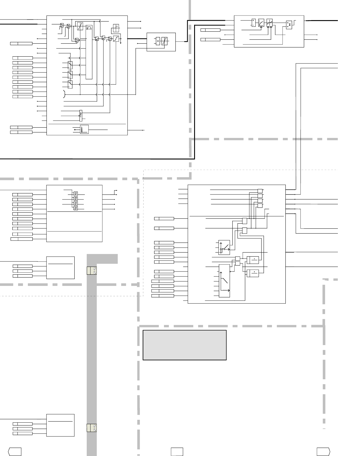
II D 4-4
3ADW000066R0901_DCS500_System_description_e_i
1/8 3/82/8
AO1 NOMINAL VALUE
AO1 OFFSET V
AO1 NOMINAL V
201 IN
SP
AO1
ST5
P2
P3
P1
-81
202
203
204
10000
0
20000
WIN SIZE
WIN MODE
2002
2021
2003
FRS
STEP
ST5
2005
2004
0
0
SPEED ERROR
STEP RESP
OUT OF WIN
OUT
SPEED ACT
12001
12002
12003
2001
P1
P2
IN
SP -13
FREE SIGNALS
(12517)
CURR LIM N
CURR LIM P
TORQ MIN2
TORQ MAX2
TREF TORQMIN1
TREF TORQMAX1
SPC TORQMIN1
SPC TORQMAX1
FLUX REF1
ARM CURR LIM N5
ARM CURR LIM N4
ARM CURR LIM N3
ARM CURR LIM N2
ARM CURR LIM N1
MAX CURR LIM SPD
SPEED ACT
ARM CURR LIM N
ARM CURR LIM P
GEAR.TORQ RAMP
GEAR.TORQ TIME
GEAR.START TORQ
TORQ MIN
TORQ MAX
TREF TORQ MIN
TREF TORQ MAX
SPC TORQ MIN
SPC TORQ MAX TORQUE/CURRENT LIMITATION
4192
yx
x
y
Min
Max
T
t
I
n
Max
Min
Min
Max
Min
Max
SP
(12102)
(11001)
ST5
P1
P2
P7
P6
P5
P4
P3
P8
P9
P11
P10
P12
P13
12308
12307
12301
12302
12303
12304
12305
12306
2301
2302
2303
2304
-10
2305
2306
2315
2316
2317
2307
2308
2309
2310
2311
2312
2313
2314
4000
-4000
16000
100
200
4095
-4095
20000
16383
16383
16383
16383
16383
4192
yx
x
y
CONSTANTS (12510)
CONSTANTS (12511)
CONSTANTS (12510)
CONSTANTS (12511)
ACCELCOMP
ACC COMP.TRMIN
ACC COMP.MODE
EMESTOP RAMP
SPEED SET
SP
RAMP GENERATOR 11801
SPEED
REFERENCE
11703
SIGN
(11803)
(10906)
0
LOCAL
LOC REF
1701 IN
1720
P12
P11
P9
P8
P7
P6
P5
P4
P3
P2
P1
P10
SET ALL RAMP
VALUES TO ZERO
OUT
11702
(OUT)
11701
S
H
E-
T+
T-
0
STARTSEL
RES IN
ST5
BC
HOLD
SMOOTH2
SMOOTH1
DECEL2
DECEL1
ACCEL2
ACCEL1
T1/T2
SPEEDMIN
SPEEDMAX
FOLLOW IN
FOLL ACT
RES OUT
RUNNING
1707
1703
1706
1705
1704
(10903)
(11205)
1702
-18 RAMP_3
1714
1708
1711
1709
1712
1710
1713
1715
1716
1717
1718
1719
200
200
100
200
100
0
0
20000
-20000
0
0
0TORQ REF HANDLING
MIN SPEED
SPEED MONITOR
SPEED GT L2
SPEED GT L1
OVERSPEED
MON.EMF V
MON.MEAS LEV
SPEED L2
SPEED L1
MIN SPEED L
SPEED ACT
P8
P7
P6
P5
P4
P3
P2
P1
P10
P9
ST20
STALL.TIME
SP
OVERSPEEDLIMIT
STALL.SEL
STALL.SPEED
STALL.TORQUE
12201
12202
12203
12204
-12 SPMONI_2
2201
2202
2203
2204
2205
2206
2207
2208
2209
2210
50
5000
10000
23000
0
50
3000
10
200
50
ST5
SP
IN2
11802
OUT
1802
1801 IN1
-17
REFSUM_2
AO2 NOMINAL VALUE
AO2 OFFSET V
AO2 NOMINAL V
205 IN
SP
AO2
ST5
P2
P3
P1
-80
206
207
208
5000
0
4095
DRIVE LOGIC
BRAKE CONTROL
(303)
710
X4:
0 V
AO1
810
X4:
0 V
AO2
Terminals
SDCS-CON-2
Speed controller
and motor data
DCS 500B Software structure
Software version: S21.233
Schematics: S21V2_0
Library: DCS500_1.5
3ADW000066R0901_DCS500_System_description_e_i
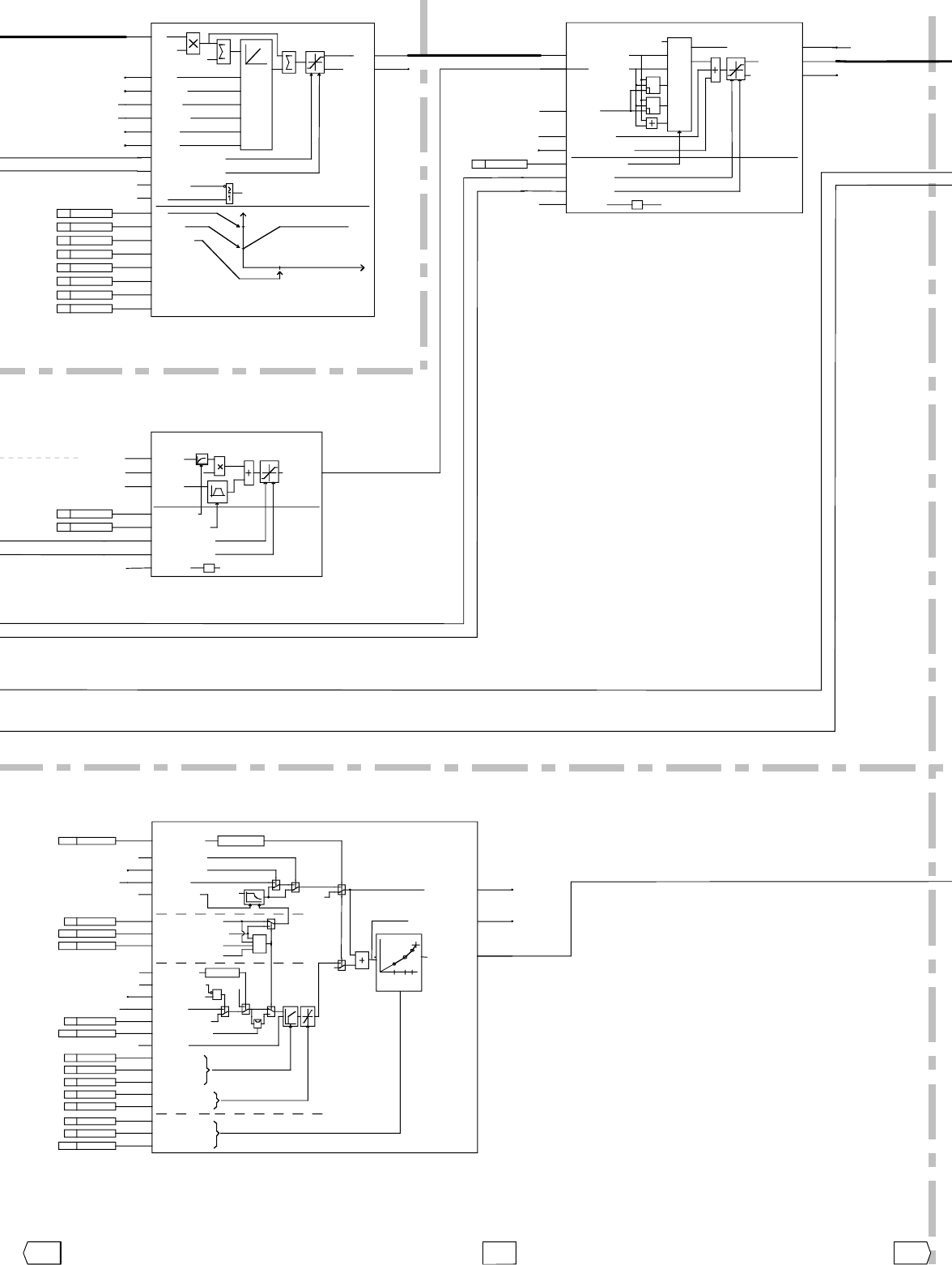
II D 4-5
3ADW000066R0901_DCS500_System_description_e_i
1/82/8 4/83/8
SPEED CONTROL
IN LIM
SPC TORQMIN1
SPC TORQMAX1
12005
12004
2007
2012
2011
2010
2009
2008
2006
SET OUT TO ZERO
BC
ST5
TF
TD
KI
DROOPING
KPSMIN
KPSPOINT
KPSWEAKFILT
KP
Torque ref
SET1
VAL1
SET2
VAL2
HOLD
CLEAR
RUNNING
(11205)
(10903)
IN
SP
OUT
KP
DROOPING
HOLD
BALREF
BAL
BAL2
BAL2REF
RINT
P3
P1
P2
P4
P8
P7
P5
P6
-14
2014
2015
2016
2017
2018
2013
2019
2020
500
0
0
500
5000
0
0
50
TORQ REF
HANDLING (12403)
TORQ REF
HANDLING (12402)
FREE SIGNALS (12521)
FREE SIGNALS (12519)
SEL1:OUT
TORQ REF SELECTION
TREF TORQMIN1
TREF TORQMAX1
TREF B SLOPE
TREF B
TREF A FTC
LOAD SHARE
TREF A
SETS SEL1:OUT TO ZERO
-1
RUNNING
ST5
SP
P2
P1
2401
2403
2404
12401
-8
2402
2405
0
0
(10903)
SEL2:TORQ/SPEED
TORQ MIN2
TORQ MAX2
ACCELCOMP
SEL2.TREF SEL
SEL2.TORQ STEP
SP ERR
SEL2.TREF EXT
TORQ REF HANDLING
SEL2.TREF SPC
SP
(11702)
00
1
RUNNING SET OUTPUTS TO ZERO
ST5
-1(10903)
SEL2:IN_LIM
SEL2:OUT
4
3
Max
Min
5
2
P1
2409
2407
2408
12403
12402
12404
-9 TREFHND2
2406
1
FREE SIGNALS (12520)
(12001)
SPEED CONTROL
(2010)
SPEED ACT
(12102)
907040
100%
EMESTOP ACT
(10907)
cal
EMF CONTROL
0
100%
F CURR REF
FLUX REF SUM
FLUX REF 1
11003
11002
EMF REF
EMF REF SEL
EMESTOP ACT
FIELD WEAK DELAY
GENER.WEAK POINT
FIELD WEAK POINT
FLUX REF
FLUX REF SEL
FIELD MODE
11001
ST10
P9
P10
P8
FIELD CONST 2
FIELD CONST 1
FIELD CONST 3
P6
P7
EMF REG LIM P
EMF REG LIM N
P5
P3
P4
EMF KP
EMF KI
EMF REL LEV
EMF ACT
(10506)
TRef2
1201=10
&
GENER.EMF REF
P12
P1
LOCAL EMF REF
1003
1005
(1201)
(10907)
generatoric
P14
P13
P2
1004
1002
1001=1,3,5
P11
SP -34 EMFCONT2
1006
1012
1007
1008
1011
1009
1010
1013
1014
1015
1001
1016
1017
1018
100
20000
150
4905
50
410
-4095
1187
2190
3255
0
160
23100
0
CONSTANTS (12512)
DRIVE MODE
CONSTANTS (12509)
Motor voltage controller
Torque/current limitation
3ADW000066R0901_DCS500_System_description_e_i
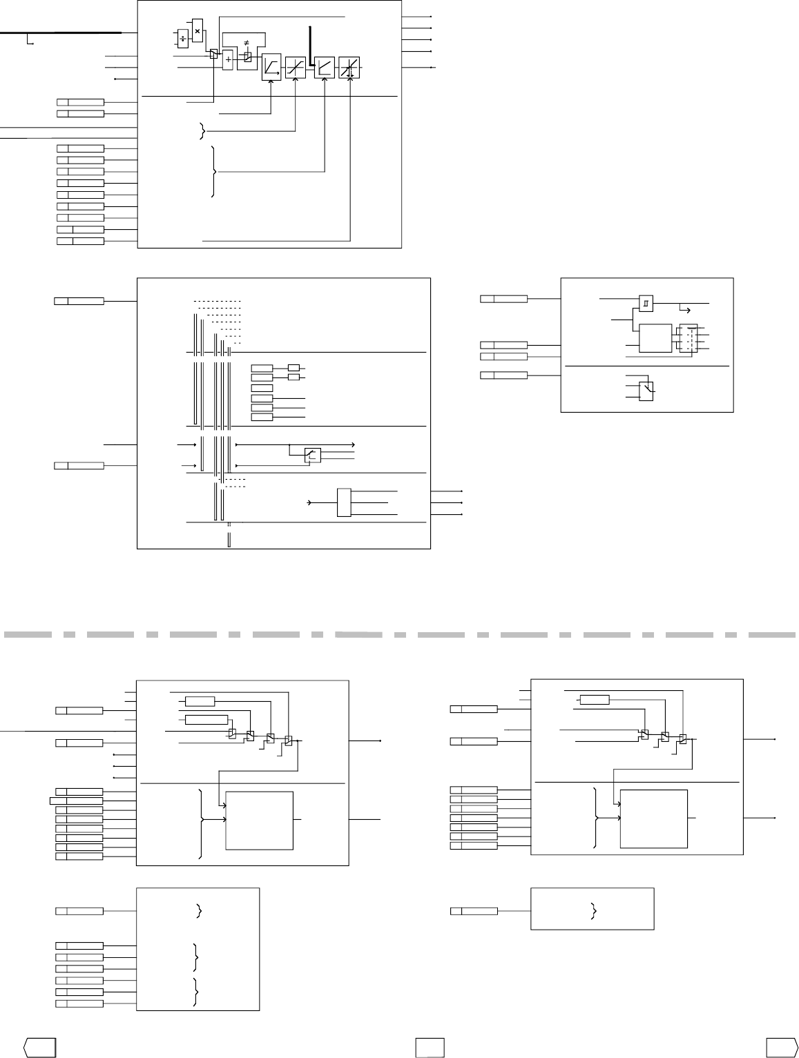
II D 4-6
3ADW000066R0901_DCS500_System_description_e_i
1/83/8 5/84/8
via Options
CURRENT MONITOR
CURRENT ZERO
SIGNAL
DriveLogic
F03
F34
F34
A137
A137
EXTERNAL
INTERNAL
1
0
Monit.
method 2
1
3
2
1
0
Iact
STSYN
P4 ZERO CUR DETECT
CURRENT
RISE MAX
P1
CUR RIPPLE MONITP3
CUR RIPPLE LIMP2
SP -104 C_MONIT
418
421
420
419
32767
7
0
0
ARM ALPHA
CURRENT CONTROL
CURR REF IN LIM
CURR DER IN LIM
ARM DIR
ARM CURR REF
ARM CONT CURR LIM
ARM CURR LIM N
ARM CURR LIM P
ARM CURR REF SLOPE
ARM CURR CLAMP
ARM R
ARM L
ARM ALPHA LIM MIN
ARM ALPHA LIM MAX
ARM CURR PI KI
ARM CURR PI KP
REF TYPE SEL
ARM CUR ACT
CURR STEP
CURR REF
FLUX REF1
TORQ REF
FLUX N
10405
SP
10403
10402
10404
10401
401
402
403
404 t
STSYN
P11
P10
P9
416
415
1,2[1209]
12-PULS
DXN
BLOCK
P1
P2
P6
P5
P4
P3
P8
P7
-75 C_CNTR_3
405
406
407
408
409
412
413
414
410
411
417
0
1366
300
3200
2050
150
15
0
0
0
40
OVP SELECT
REF DCF
RUN DCF
RESET DCF
DI/OVP
F 21
A121
DCF FIELDMODE
as FEX 2 (Receiver)
as FEX 1 (Receiver)
6542
65421
5
4
Fexlink as Transmitter
for FEX1 and FEX2
6
Input for external Overvoltg.Protection
Cur.Controller for high inductive load
1216
P2
BC
0
1
6
5
4
3
2
1
from ext. FEXLINK
x8
ARM_CURR_PI_KP...
x8
ARM_CURR_PI_KI
... 408
407
ARM_CONT_CUR_LIM
3601 REV_DELAY
409
15 3602 REV_GAP
15 3603 FREV_DELAY
15
0
DCF Current Control
Stand Alone
Fexlink Node 1
Fexlink Node 2
MG Set
Disabled
Reserved
:
:
:
:
:
:
:
0
11303
10916
10917
SP
P1 DCF MODE :
-105 DCFMOD
1215
1217
0
0
DI2 (10703)
CONSTANTS (12526)
CONSTANTS (12527)
F2 CURR ACT
F2 CURR REF
F2 U LIM P
F2 U LIM N
F2 KI
F2 KP
F2 CURR TC
F2 OVERCURR L
F2 CURR GT MIN L
FANS ON
TEST REF2
F2 SEL.REF
F2 REF
F2 RED.SEL
DRIVE MODE
MOTOR 2 FIELD
1201=7
11502
11501
1501
ST20
DCF501/502
DCF503/504
SDCS-FEX-2
or
or
0%
100%
(10908)
(1201)
SP
P1
P2
P8
P7
P6
P5
P4
P3
P9
-28 M2FIELD2
1510
1511
1502
1503
1504
1505
1506
1508
1509
0
1228
2047
4710
0
1
20
-4096
4096
FREE WHEELING
MOTOR 2 FIELD OPTIONS
F2 U AC DIFF MAX
P1
ST20
SP -24
1507
10
CONSTANTS (12512)
REV.FLUX TD
REV.REF HYST
REV.REV HYST
OPTI.REF MIN TD
OPTI.REF MIN L
OPTI.REF GAIN
MOTOR 1 FIELD OPTIONS
F1 U AC DIFF MAX
SP
ST20
FREE WHEELING
FIELD REVERSAL
OPTITORQUE
P1
P4
P5
P6
P7
P8
P9
-26
1310
1315
1316
1317
1318
1319
1320
10
100
614
200
80
80
0
SPEED CONTROL (2011)
DATA LOGGER (606)
F1 CURR MIN TD
P10
F1 U LIM P
F1 U LIM N
F1 KI
F1 KP
F1 CURR TC
F1 OVERCURR L
P8
P7
P6
P5
P4
P9
ST20
F1 CURR ACT
F1 CURR REF
F1 CURR GT MIN L
TEST REF2
F1 ACK
F1 FORCE REV
F1 FORCE FWD
F1 SEL.REF
F1 REF
FIELD MODE
F1 RED.SEL
DRIVE MODE
FANS ON MOTOR 1 FIELD
1001=1,3,5
1201=7
DCF501/502
DCF503/504
SDCS-FEX-2
or
or
0%
100%
(10908)
(1201)
SP
P1
P2
P3
1301
1302
1303
1304
11302
11301
-30 M1FIELD2
1313
1314
1305
1306
1307
1308
1309
1311
1312
1321
0
1228
2047
4710
0
1
20
-4096
4096
200
DATA LOGGER
(605)
(1001)
Armature current
controller
Field current controller 1 and 2
3ADW000066R0901_DCS500_System_description_e_i
II D 4-7
3ADW000066R0901_DCS500_System_description_e_i
O1
O2
ST5
DI15 10729
10730
SP-55
O1
O2
ST5
DI14 10727
10728
SP-56
O1
O2
ST5
DI13 10725
10726
SP-57
O1
O2
ST5
DI12 10723
10724
SP-58
O1
O2
ST5
DI11 10721
10722
SP-59
O1
O2
ST5
DI10 10719
10720
SP-60
O1
O2
SP-61
ST5
DI9 10717
10718
AI5 LOW VALUE
AI5 HIGH VALUE
AI5 CONV MODE
SP
AI5
AI5:OUT+
AI5:OUT-
AI5:ERR
ST5
10116
10117
10118
P2
P3
P1
-86
116
117
118
0
2000
-2000
AI6 LOW VALUE
AI6 HIGH VALUE
AI6 CONV MODE
SP
AI6 AI6:OUT+
AI6:OUT-
AI6:ERR
ST5
10119
10120
10121
P2
P3
P1
-85
119
120
121
0
2000
-2000
COMFLT. TIMEOUT
COMM FAULT
DYN BRAKE ON
TRIP DC BREAKER
MOTOR ACT
MAIN CONT ON
FIELD ON
FAN ON
COMFAULT MODE
PWR LOSS MODE
PANEL DISC MODE
EME STOP MODE
STOP MODE
MAIN CONT MODE
FIELD HEAT SEL
ACK MAIN CONT
ACK MOTOR FAN
ACK CONV FAN
DISABLE LOCAL
START INHIBIT
EMESTOP ACT
RDY RUNNING
RDY ON
MIN SPEED
EME STOP
COAST STOP
DRIVE LOGIC
AUTO-RECLOSING
10914
10912
10901
10902
10903
10904
10905
10907
10906
10908
10909
10910
10913
10911
10915
913
912
911
910
909
908
907
905
904
903
902
901
P5
P4
P3
P2
P1
P6
P7
P8
906
LOCAL
SP
ALARM
FAULT
RUNNING
1
RUN3
RUN2
RUN1
ON/OFF
MOTOR2
RESET
LOCAL
(12201)
(11205)
BC (BLOCK.)
T20
-36 DRLOGI_2
914
915
916
917
918
919
920
921
0
1
0
0
0
0
0
2
O1
O2
SP
DI8
ST5
10715
10716
-62
O1
O2
SP
DI7
ST5
10713
10714
-63
O1
O2
SP
ST5
DI6 10711
10712
-64
O1
O2
SP
ST5
DI5 10709
10710
-65
O1
O2
SP
ST5
DI4 10707
10708
-66
O1
O2
SP
ST5
DI3 10705
10706
-67
O1
O2
SP
ST5
DI2 10703
10704
-68
O1
O2
DI1
SP
ST5
10701
10702
-69
REF SEL (1911) CONST REF (11902)
RAMP GENERATOR
TORQ REF SELECTION
TORQ REF HANDLING
DCF FIELDMODE
(1216)
MAIN CONT
MOTOR FAN
CONV FAN
RESET
EM STOP
RUN
ON/OFF
MOTOR 1/2 FIELD
Must be connected, when no fan acknowledges (DI1, DI2)
MAINTENANCE
BRAKE CONTROL (302)
DATASET 3
OUT3
OUT2
OUT1
IN
SP
ST5
10125
10126
10127
-93
DATASET 1
IN
OUT3
OUT2
OUT1
SP
ST5
10122
10123
10124
-91
FIELDBUS PAR.1
(MODULE TYPE)
SP
FIELDBUS
modul type
depends of
Parameters
P15
P14
P13
P12
P11
ST5
P10
P09
P08
P07
P06
P05
P04
P03
P02
P01
-95 FLBSET_2
4001
4002
4003
4004
4005
4006
4007
4008
4009
4010
4011
4012
4013
4014
4015
0
0
0
0
0
0
0
0
0
0
0
0
0
0
0
BC Logic
Revers.Logic
Bridge Logic
IREF0 Logic
Res. f.Commun
BC not Zero
Logic f. INHIBIT
Fault Current
Bridge of Slave
Bridge
IREF2-Pol.Broth
IREF2-Polarity
Curr.Ref.2
IREF1-Pol.Master
IREF1-Polarity
Curr.Ref.1
Arm.CURR.Both
Conv.Curr.Both
Arm.Curr.Slave
Conv.Curr.Slave
Fault Reversion
Indicat.Revers
[1209]
*
2048
ADJ REF1
INHIB Logic
DIFF CURR DELAY
DIFF CURRENT
IACT SLAVE
FREV DELAY
REV GAP
REV DELAY
13622
13605
STSYN
BC
6-PULSE
MASTER
CURRENT REFERENCE
P6
3604
13608
P5
P4
active, if [1209] = 1
CURRENT ANALYSIS 13601
13602
13603
13604
13615
13621
3616
ON/OFF LOGIC
(11205)
13616
3607
P3
P2
P1
active, if [1209]= 1 or 2
BRIDGE REVERSAL LOGIC
SP
12-PULSE LOGIC
3608
3609
3610
13611
13606
13609
13607
13610
13612
13613
13614
-99 12PULS_2
3601
3602
3603
3605
3606
3615
1
10
10
10
150
2048
X18:16
X18:15
X18:14
X18:13 13618
STSYN
SP
INPUT X18
13617
13619
13620
-97
AI2 (10107)
+
--
+
--
3
X6:
2
X6:
1
X6:
6
X6:
5
X6:
8
X6:
7
X6:
4
X6:
7
X1:
6
X1:
4
X1:
3
X1:
2
X1:
1
X1:
21
X2:
54
X2:
8
X1:
4/8 6/85/8
not used
not used
not used
not used
not used
not used
not used
not used
not used
Additional binary
inputs
Binary in and outputs (standard)
Inputs and outputs for fieldbus
Inputs and outputs for 12 pulse
Terminals
SDCS-CON-2
Terminals
SDCS-IOE-1
3ADW000066R0901_DCS500_System_description_e_i
II D 4-8
3ADW000066R0901_DCS500_System_description_e_i
CONVERTER PROTECTION
EARTH.FLT DLY
EARTH.FLT LEV
EARTH.CURR SEL
ARM OVERVOLT LEV
ARM OVERCURR LEV
U NET MIN1
U NET MIN2
PWR DOWN TIME
CONV TEMP DELAY
P9
P8
ST20
SP
P1
P2
P3
P4
P5
P6
P7
-76 CONPROT2
511
512
508
509
510
514
515
516
527
110
230
80
60
5000
0
4
10
0
MOT2 CALC TEMP
MOT2 MEAS TEMP
MOTOR 2 PROTECTION
MODEL2.TRIP L
MODEL2.ALARM L
MOT2.TEMP FAULT L
MOT2.TEMP ALARM L
MOT2.TEMP IN
P7
P6
P5
P4
P3
P1
P2
11601
11602
1601
ST20
SP
MODEL2.SEL
MODEL2.CURR
MODEL2.TC
-21 M2PROT_2
1602
1603
1604
1605
1606
1607
1608
0
0
0
4096
120
130
240
MOTOR 1 PROTECTION
MOT1 CALC TEMP
MOT1 MEAS TEMP
MOT1.TEMP IN
1401
MODEL1.TRIP L
MODEL1.ALARM L
KLIXON IN
MOT1.TEMP FAULT L
MOT1.TEMP ALARM L
P2
P1 11401
P7
P6
P5
P4
P3 11402
ST20
SP
MODEL1.SEL
MODEL1.CURR
MODEL1.TC
1404
-22 M1PROT_2
1402
1403
1405
1406
1407
1408
1409
0
0
0
4096
120
130
240
BTW.POT1/2
MACRO SELECT
ACTUAL VALUE 3
ACTUAL VALUE 2
ACTUAL VALUE 1
FIELDBUS NODE ADDR
t
PERIOD
DRIVEMODE
P1
MAINTENANCE
11220 FEXC1 SW VERSION
11221 FEXC2 SW VERSION
11215
FEXC2 COM ERRORS
FEXC2 COM STATUS 11214
11213
FEXC2 CODE
11212
11211
FEXC1 COM ERRORS
FEXC1 COM STATUS
FEXC1 CODE 11210
FEXC STATUS 11203
11217
11216
CMT COM ERRORS
CDI300 BAD CHAR
11205
BC
11219 CNT BOOT SW VER
11218 CNT SW VERSION
11222 PROGRAM LOAD
11202 BACKUPSTOREMODE
11201 COMMIS STAT 11204
TC STATUS
11206
SQUARE WAVE
CDP312
1212
1211
1210
P11
P9
P8
P7
P6
P5
P4
P3
P2
P10
T5
SELECT OPER.SYST
WRITE ENABLE PIN
WRITE ENABLE KEY
CMT DCS500 ADDR
DRIVE ID
(11207) TEST REF
04
7
8
9
10
0
1
2
3
4EMF CONTROLLER
SPEED LOOP
SECOND FIELD EXCITER
FIRST FIELD EXCITER
ARM. CONTROLLER
RELEASE OF ARM.
CONTROLLING
&
4I1=I2
POT2 VALUE
POT1 VALUE
TEST REF SEL
(11209)
(11208)
(10906)
TEST RELEASE
LOCAL
SP -100 MANTUN_3
1201
1204
1205
1206
1202
1203
1207
1208
1209
1213
1214
0
1000
0
100
250
1
358
358
0
1
0
SPEED MESUREMENT (12103)
SETTINGS (10501)
SETTINGS (10505)
DRIVE LOGIC
RAMP GENERATOR
12 PULSE LOGIC
DO4
INV IN
IN
807
808
T20
SP -46
DO8
INV IN
IN
815
816
T20
SP -42
DO7
INV IN
IN
813
814
T20
SP -43
DO6
INV IN
IN
811
812
T20
SP -44
DO5
INV IN
IN
809
810
T20
SP -45
DO3
805
INV IN
IN
806
T20
SP -47
DO2
INV IN
IN
803
804
T20
SP -48
DO1
INV IN
IN
801
802
T20
SP -49
SDCS-POW-1
Relay output
MAIN CONT
MAIN CONT
EXC CONT
FAN CONT
RUNNING
RDY RUNNING
DATASET 4
214
213
212
OUT
IN3
IN2
IN1
SP
ST5
-94
DATASET 2
211
210
209
OUT
IN3
IN2
IN1
SP
ST5
-92
X18:12
X18:11
X18:10
X18:09
OUTPUT X18
SP
STSYN
3611
3612
3613
3614
-98
5
X7:
1
X7:
2
X7:
3
X7:
6
X7:
7
X7:
4
X7:
2
1
X96:
5/8 7/86/8
Maintenance
Monitoring
Terminals
SDCS-CON-2
3ADW000066R0901_DCS500_System_description_e_i
II D 4-9
3ADW000066R0901_DCS500_System_description_e_i
DLY
TEXT
TYPE
IN USER EVENT 6
SP
ST20
P3
P1
"EXT. IND. 6"
1121
1123
-2
1122
1124
0
0
DLY
TEXT
TYPE
IN USER EVENT 5
SP
ST20
1117
1119
P3
P1
"EXT. IND. 5"
-3
1118
1120
0
0
DLY
TEXT
TYPE
IN USER EVENT 4
SP
ST20
P3
P1
"EXT. IND. 4"
1113
1115
-4
1114
1116
0
0
DLY
TEXT
TYPE
IN USER EVENT 3
SP
ST20
1109
1111
P3
P1
"EXT. IND. 3"
-5
1110
1112
0
0
DLY
TEXT
TYPE
IN USER EVENT 2
SP
ST20
P3
P1
"EXT. IND. 2"
1105
1107
-6
1106
1108
0
0
DLY
TEXT
TYPE
IN USER EVENT 1
SP
ST20
P3
P1
"EXT. IND. 1"
1101
1103
-7
1102
1104
0
0
DLOG STATUS
DLOG.SAMPL INT
DLOG.TRIGG DELAY
DLOG.TRIGG VALUE
DLOG.TRIGG COND
0
0
0
DATA LOGGER
SP
RESTART
STOP
TRIG
613
611
612
DLOG.RESTART
DLOG.STOP
DLOG.TRIG
T1ms
IN5 Ch.5
10601
STOP RESTART
CMT-TOOL
TRIG
P4
P3
P2
P1
IN6 Ch.6
606
605
IN4 Ch.4
604
IN3 Ch.3
603
IN2 Ch.2
602
IN1 Ch.1
601
-102 DATALOG
607
608
609
610
1
20000
200
3
SPEED MEASUREMENT (12102)
SETTINGS (10501)
SETTINGS (10505)
SETTINGS (10504)
MOTOR 1 FIELD (11302)
CURRENT CONTROL (10401)
BRAKE CONTROL
ACT BRAKE
BRAKE RUN
LIFT BRAKE
DECEL CMND
TREF ENABLE
TREF OUT
EMESTOP BRAKE
HOLD TORQ
STOP DELAY
START DELAY
MIN SP IND
BR RELEASE
HOLD REF
TORQUE ACT
10305
10304
10303
10302
10301
304
303
302
301
P1
P2
P3
P4
LOCAL
(10503)
RESET
SP
(10902)
ST20
-32
305
306
307
308
0
0
0
0
DI8 (10715)
SPEED MONITOR (12201)
FAULT WORD 1
OPERATING HOURS
LATEST ALARM
ALARM WORD 3
ALARM WORD 2
ALARM WORD 1
LATEST FAULT
FAULT WORD 3
FAULT WORD 2
T20
11109
11108
11107
11106
11105
11103
11102
SP
FAULT HANDLING
11104
11101
-103 FLTHNDL
0
-1
SPEED: 100%
CUR,FLX,VLT:-100%
CUR,FLX,VLT: 100%
12509
12508
12507
12506
12505
12504
12503
12510
12511
12513
12512
12515
12514
12502
12501
CONSTANTS
SP
ST
SPEED:-100%
TORQ:-100%
TORQ:100%
EMF:100%
31416
1000
100
10
2
1
-73
CONST_0
CONST_M1_TRUE
CONST_1
CONST_2
CONST_10
CONST_100
CONST_1000
CONST_31416
EMF_MAX
TORQ_MAX
TORQ_MAX_N
CONST_4095
CONST_M4095
CONST_20000
CONST_M20000
SIG12(CURR._STEP)
SIG11(CURR. REF)
SIG10(FORCE REV)
SIG9(FORCE_FWD)
SIG8(EMF REF)
SIG7(FLUX REF)
SIG6(LOAD SHARE)
SIG5(TORQUE STEP)
SIG4(TORQ. REF B)
SIG3(TORQ. REF A)
SIG2(SPEED STEP)
SIG1(SPEED REF)
FREE SIGNALS
12527
12526
12525
12524
12523
12522
12521
12520
12519
12518
12517
12516
ST
SP -74
SPEED_STEP
TORQ_REF_B
TORQ_STEP
LOAD_SHARE
CUR_REF
CUR_STEP
6/8 8/87/8
Brake control
User events
Data logger
Additional signals
3ADW000066R0901_DCS500_System_description_e_i

II D 4-10
3ADW000066R0901_DCS500_System_description_e_i
7/8 8/8
Speed reference handling
The speed reference for the ramp function generator is formed by the REF SEL blocks, which
can be used to select the reference value required, the CONST REF block, which generates
a maximum of 4 permanently settable reference values, the SOFTPOT block, which repro-
duces the function of a motorpotentiometer in conjunction with the block RAMP
GENERATOR, or by the AI1 block (analogue input 1).
The RAMP GENERATOR block contains a ramp function generator with 2 ramp-up and
ramp-down ramps, 2 times for the S-curve, limitation for upper and lower limits, hold function
and the functions for ”Follow” the speed reference or ”Follow” the speed feedback. There is a
special signal available for the treatment of acceleration and deceleration.
The REF SUM block enables the output of the ramp function generator and a user-definable
signal to be added.
Speed feedback calculation
This page depicts the conditioning routine for speed feedback and reference values. The
AITAC block is used to read in the speed feedback from an analogue tacho The SPEED
MEASUREMENT block processes the 3 possible feedback signals: analogue tacho, pulse
generator or the converter's output voltage (SPEED_ACT_EMF) - conditioned by the EMF
TO SPEED CALC block (if 2102=5 , no field weakening function possible). Parameters
are used for activating smoothing functions, selecting the feedback value and where applica-
ble for setting the maximum speed. This parameter also serves for scaling the speed control
loop.
The SPEED MONITOR block contains motor stalled - and tacho monitoring function, and
compares a selected speed feedback value against overspeed, minimum speed and 2 setta-
ble thresholds.
The AO1 block represents a scalable analogue output.
Speed controller
The result is compared to the speed feedback from the SPEED MEASUREMENT block,
using the SPEED ERROR block, and then passed to the speed controller. This block permits
evaluation of the system deviation by means of a filter. Moreover, it is possible here to make
a few settings which are needed for the ”Window” operating mode. If the drive’s speed feed-
back is within a window around the reference value, then the speed controller is ”bypassed”
(provided ”Window Mode” has been activated; the drive is controlled by means of a torque
reference value at the TORQ REF HANDLING block). If the speed feedback is outside the
window, the speed controller will be activated, and will lead the drive’s actual speed back into
the window.
The SPEED CONTROL block contains the speed controller with P, I and DT1 contents. For
adaptation it receives a variable P-amplification.
Torque / current limitation
The ”torque reference” generated by the speed controller is passed to the input of the
CURRENT CONTROL block via the TORQ REF HANDLING block, and there it is converted
into a current reference value and used for current regulation. The TORQUE / CURRENT
LIMITATION block is used for generating the various reference values and limitations; this
block contains the following functions: ”speed-dependent current limitation”, ”gear backlash
compensation”, ”generation of the values for static current limitation” and ”torque limitation”.
The values for the various limitations are used again at some other points, for instance at the
following blocks: SPEED CONTROL, TORQ REF HANDLING, TORQ REF SELECTION, and
CURRENT CONTROL.
The AI2 block (analogue input 2) is used for reading in an analogue signal.
The TORQ REF SELECTION block contains a limitation with upstream addition of two sig-
nals, one of which can be routed through a ramp function generator; the other signal’s
evaluation can be dynamically altered using a multiplier.
The TORQ REF HANDLING block determines the drive's operating mode. When in position
1, the speed control mode has been activated, whereas in position 2 it is torque control mode
(no closed-loop control since there is no "genuine" torque feedback available in the unit). In
both cases, the reference value required comes from outside. Positions 3 and 4 are a combi-
nation of the first two options stated above. Note that with position 3 the smaller value out of
external torque reference and speed controller output is passed to the current controller
whereas with position 4 it is the larger one. Position 5 uses both signals, corresponding to the
method of functioning of "Window Mode".
Armature current controller
The CURRENT CONTROL block contains the current controller with a P and I content, plus
an adaptation in the range of discontinuous current flow. This block also contains functions
for current-rise limitation, the conversion of torque reference value into current reference
value by means of the field crossover point, and some parameters describing the supply
mains, and the load circuit.
At applications with high inductive load and high dynamic performance a different hardware is
used to generate the signal current equal to zero. This hardware is selected by the
CURRENT MONITOR block. The functions monitoring the current can now be adapted to the
needs of the application. This gives easier handling and a higher degree of safety at high
performance drives, like test rigs.
The DCF mode can be activated via the block DCF FIELDMODE. The functionality within this
mode can be specified. If one of these functions is selected the current controller gets a
different characteristic, the overvoltage protection DCF 506 is monitored and the field current
reference via the X16: terminals is routed.
Line and motor data
The SETTINGS block serves for scaling all important signals, such as line voltage, motor
voltage, motor current and field current. Parameters are available to adjust the control to
special conditions like weak networks or interactions with harmonic filter systems. The lan-
guage, in which you want to read your information on the panel, can be selected.
The AO2 block represents a scalable analogue output.
Motor voltage controller
The EMF CONTROL block contains the armature-circuit voltage controller (e.m.f. controller).
It is based on a parallel structure comprising a PI controller and a precontrol feature, gener-
ated with a characteristic of 1/x. The ratio between the two paths can be set. The output
variable of this block is the field current reference value, which is produced from the flux
reference value by another characteristic function using linearization. To enable the drive to
utilize a higher motor voltage even with a 4 quadrant system two different field weakening
points can be set by parameter.
Field current controller 1 and 2
Since a DCS power converter can control 2 field units, some of the function blocks are dupli-
cated. This means that, depending on the mechanical configuration of the drives concerned,
you can control 2 motors either in parallel or alternatively. The requisite configuration of the
software structure can be generated by designing the blocks appropriately during the com-
missioning routine.
The MOTOR1 FIELD / MOTOR2 FIELD block reads in the field current reference value and
all values which are specific to the field supply unit, and transfers these to the field power
converter via an internal serial link; the field power converter is scaled to suit its hardware,
and performs field current regulation. The field current direction for motor 1 can be deter-
mined using binary commands, while for motor 2 it can be generated in the course of an
application upstream of the block concerned.
The MOTOR1 FIELD OPTIONS / MOTOR2 FIELD OPTIONS block controls the free-
wheeling function in the event of line undervoltage, and the field current reversal function with
field reversal drives (only for motor 1). In case of field reversal drives, there is an option for
selectively influencing the moment of armature-circuit and field current reduction and build-
up.
Binary in and outputs (standard)
The DRIVE LOGIC block reads in various signals from the system via digital inputs DIx,
processes them, and generates commands, which are outputted to the system via digital
outputs DOx, e.g. for controlling the power converter’s line contactor, the field-circuit contac-
tor or contactors for various fans, or for outputting status messages.
Additional binary inputs
The AI3 and AI4 blocks represent another 2 analogue inputs which have as yet not been
assigned to any particular functions. The blocks A15 and A16 represent another 2 additional
inputs which are only active, if the board SDCS-IOE1 is connected. Another 7 digital inputs DI
9 .. DI15 are available with this additional hardware.
Inputs and outputs for fieldbus
A fieldbus module with serial communicated references should be used, if analogue and
digital signals are not sufficient for the control of the drive (equipment for the installation of
Profibus, CS31, Modbus etc. is available). This type of module is activated by means of the
block FIELDBUS. The data transferred from the control to the converter are stored in the
blocks DATASET1 and DATASET3 as 16-bit-information. Depending on the application the
output pins of these blocks have to be connected to input pins of other blocks in order to
transport the message. The same procedure is valid for blocks DATASET2 and DATASET4,
if they are connected. These blocks are transmitting information from the converter to the
control system.
Inputs and outputs for 12 pulse
The converter is able to be configurated in a 12-pulse parallel application. In this case you
need: two identical armature converters; one field supply unit; one T-reactor; communication
via ribbon cable connected to X 18 of both converters The 12-PULSE LOGIC must be acti-
vated and guarantees a synchronous control of the MASTER and the SLAVE drive.
Maintenance
The MAINTENANCE block provides reference values and test conditions so as to enable all
controllers to be adjusted in the power converter. If the panel is used as a meter in the cubicle
door, an assortment of signals can be defined here.
Monitoring
The CONVERTER PROTECTION block monitors the armature circuit for overvoltage and
overcurrent, and monitors the mains for undervoltage. It provides an option for reading in the
total current of the 3 phases through an additional external sensor and monitoring it for "not
equal to zero". Adaptations are made for rebuild applications, which keep the power part and
the fan, to sense overload conditions or fan failures.
The MOTOR1 PROTECTION block, in its upper part, evaluates either the signal from an
analogue temperature sensor, or from a Klixon. In its lower part, it computes motor heat-up
with the aid of the current feedback value and a motor model, after which a message is
outputted.
The MOTOR2 PROTECTION block works in the same way as the MOTOR1 PROTECTION
block, but without Klixon evaluation.
User event
By using the block USER EVENT1 to USER EVENT6 six different messages are created,
which are displayed as faults or alarms on the panel CDP312 as well as on the 7 segment
display of the converter.
Brake control
The BRAKE CONTROL block generates all signals needed for controlling a mechanical
brake.
Data logger
The block DATA LOGGER is able to record up to six signals. The values of these signals will
be stored in a battery buffered RAM and are still available after a break down of the supply
voltage. The time of recording can be influenced by a trigger signal, as well as the number of
recorded values before and after the trigger signal. The function DATA LOGGER can be set
with both panel and PC tool. For evaluation of the recorded values a PC tool is recom-
mended.
Additional signals
By using the block FAULT HANDLING the faults and alarms of the drive are regrouped as 16-
bit information. The CONSTANTS and FREE SIGNALS blocks can be used for setting limita-
tions or special test conditions.
3ADW000066R0901_DCS500_System_description_e_i

II D 4-11
3ADW000066R0901_DCS500_System_description_e_i
No. Parameter name
101 AITAC_CONV_MODE
102 AITAC_HIGH_VALUE
103 AITAC_LOW_VALUE
104 AI1_CONV_MODE
105 AI1_HIGH_VALUE
106 AI1_LOW_VALUE
107 AI2_CONV_MODE
108 AI2_HIGH_VALUE
109 AI2_LOW_VALUE
110 AI3_CONV_MODE
111 AI3_HIGH_VALUE
112 AI3_LOW_VALUE
113 AI4_CONV_MODE
114 AI4_HIGH_VALUE
115 AI4_LOW_VALUE
116 AI5_CONV_MODE
117 AI5_HIGH_VALUE
118 AI5_LOW_VALUE
119 AI6_CONV_MODE
120 AI6_HIGH_VALUE
121 AI6_LOW_VALUE
201 AO1.[IN]
202 AO1_NOMINAL_V
203 AO1_OFFSET_V
204 AO1_NOMINAL_VAL
205 AO2.[IN]
206 AO2_NOMINAL_V
207 AO2_OFFSET_V
208 AO2_NOMINAL_VAL
209 DATASET2.[IN1]
210 DATASET2.[IN2]
211 DATASET2.[IN3]
212 DATASET4.[IN1]
213 DATASET4.[IN2]
214 DATASET4.[IN3]
301 [HOLD_REF]
302 [BR_RELEASE]
303 [MIN_SP_IND]
304 [ACT_BRAKE]
305 START_DELAY
306 STOP_DELAY
307 HOLD_TORQ
308 EMESTOP_BRAKE
401 [TORQ_REF]
402 [CURR_REF]
403 [CURR_STEP]
404 [BLOCK]
405 REF_TYPE_SEL
406 ARM_CURR_REF_SLOPE
407 ARM_CURR_PI_KP
408 ARM_CURR_PI_KI
409 ARM_CONT_CURR_LIM
410 ARM_L
411 ARM_R
412 ARM_ALPHA_LIM_MAX
413 ARM_ALPHA_LIM_MIN
414 DXN
415 [ARM_CURR_LIM_P]
416 [ARM_CURR_LIM_N]
417 ARM_CURR_CLAMP
418 CURRENT_RISE_MAX
419 ZERO_CUR_DETECT
420 CUR_RIPPLE_MONIT
421 CUR_RIPPLE_LIM
501 U_MOTN_V
502 I_MOTN_A
503 I_MOT1_FIELDN_A
504 I_MOT2_FIELDN_A
505 FEXC_SEL
506 PHASE_SEQ_CW
No. Parameter name
507 U_SUPPLY
508 U_NET_MIN1
509 U_NET_MIN2
510 PWR_DOWN_TIME
511 ARM_OVERVOLT_LEV
512 ARM_OVERCURR_LEV
513 EMF_FILT_TC
514 EARTH.CURR_SEL
515 EARTH.FLT_LEV
516 EARTH.FLT_DLY
517 SET_I_CONV_A
518 SET_U_CONV_V
519 SET_MAX_BR_TEMP
520 SET_CONV_TYPE
521 SET_QUADR_TYPE
522 LANGUAGE
523 CURR_ACT_FILT_TC
524 PLL_CONTROL
525 UNI_FILT_TC
526 OFFSET_UDC
527 CONV_TEMP_DELAY
528 PLL_DEV_LIM
601 DLOG.[IN1]
602 DLOG.[IN2]
603 DLOG.[IN3]
604 DLOG.[IN4]
605 DLOG.[IN5]
606 DLOG.[IN6]
607 DLOG.TRIGG_COND
608 DLOG.TRIGG_VALUE
609 DLOG.TRIGG_DELAY
610 DLOG.SAMPL_INT
611 DLOG.TRIG
612 DLOG.STOP
613 DLOG.RESTART
801 DO1.[IN]
802 DO1.[INV_IN]
803 DO2.[IN]
804 DO2.[INV_IN]
805 DO3.[IN]
806 DO3.[INV_IN]
807 DO4.[IN]
808 DO4.[INV_IN]
809 DO5.[IN]
810 DO5.[INV_IN]
811 DO6.[IN]
812 DO6.[INV_IN]
813 DO7.[IN]
814 DO7.[INV_IN]
815 DO8.[IN]
816 DO8.[INV_IN]
901 [ON/OFF]
902 [RUN1]
903 [RUN2]
904 [RUN3]
905 [COAST_STOP]
906 [EME_STOP]
907 [RESET]
908 [START_INHIBIT]
909 [DISABLE_LOCAL]
910 [ACK_CONV_FAN]
911 [ACK_MOTOR_FAN]
912 [ACK_MAIN_CONT]
913 [MOTOR 2]
914 FIELD_HEAT_SEL
915 MAIN_CONT_MODE
916 STOP_MODE
917 EME_STOP_MODE
918 PANEL_DISC_MODE
919 PWR_LOSS_MODE
No. Parameter name
920 COMFAULT_MODE
921 COMFAULT_TIMEOUT
1001 FIELD_MODE
1002 [FLUX_REF]
1003 [EMF_REF]
1004 [FLUX_REF_SEL]
1005 [EMF_REF_SEL]
1006 LOCAL_EMF_REF
1007 EMF_KP
1008 EMF_KI
1009 EMF_REG_LIM_P
1010 EMF_REG_LIM_N
1011 EMF_REL_LEV
1012 FIELD_WEAK_POINT
1013 FIELD_CONST_1
1014 FIELD_CONST_2
1015 FIELD_CONST_3
1016 GENER.EMF_REF
1017 GENER.WEAK_POINT
1018 FIELD_WEAK_DELAY
1101 USER_EVENT1.[IN]
1102 USER_EVENT1.TYPE
1103 USER_EVENT1.TEXT
1104 USER_EVENT1.DLY
1105 USER_EVENT2.[IN]
1106 USER_EVENT2.TYPE
1107 USER_EVENT2.TEXT
1108 USER_EVENT2.DLY
1109 USER_EVENT3.[IN]
1110 USER_EVENT3.TYPE
1111 USER_EVENT3.TEXT
1112 USER_EVENT3.DLY
1113 USER_EVENT4.[IN]
1114 USER_EVENT4.TYPE
1115 USER_EVENT4.TEXT
1116 USER_EVENT4.DLY
1117 USER_EVENT5.[IN]
1118 USER_EVENT5.TYPE
1119 USER_EVENT5.TEXT
1120 USER_EVENT5.DLY
1121 USER_EVENT6.[IN]
1122 USER_EVENT6.TYPE
1123 USER_EVENT6.TEXT
1124 USER_EVENT6.DLY
1201 DRIVEMODE
1202 CMT_DCS500_ADDR
1203 DRIVE_ID
1204 POT1_VALUE
1205 POT2_VALUE
1206 PERIOD_BTW.POT1/2
1207 WRITE_ENABLE_KEY
1208 WRITE_ENABLE_PIN
1209 SELECT_OPER.SYST.
1210 ACTUAL VALUE 1
1211 ACTUAL VALUE 2
1212 ACTUAL VALUE 3
1213 FIELDBUS NODE ADDR
1214 MACRO_SELECT
1215 DCF MODE
1216 DI/OVP
1217 OVP_SELECT
1301 [F1_REF]
1302 [F1_FORCE_FWD]
1303 [F1_FORCE_REV]
1304 [F1_ACK]
1305 F1_CURR_GT_MIN_L
1306 F1_OVERCURR_L
1307 F1_CURR_TC
1308 F1_KP
1309 F1_KI
List of parameters (with column for customer-specific values)
3ADW000066R0901_DCS500_System_description_e_i

II D 4-12
3ADW000066R0901_DCS500_System_description_e_i
List of parameters (with column for customer-specific values)
No. Parameter name
1310 F1_U_AC_DIFF_MAX
1311 F1_U_LIM_N
1312 F1_U_LIM_P
1313 F1_RED.SEL
1314 F1_RED.REF
1315 OPTI.REF_GAIN
1316 OPTI.REF_MIN_L
1317 OPTI.REF_MIN_TD
1318 REV.REV_HYST
1319 REV.REF_HYST
1320 REV.FLUX_TD
1321 F1_CURR_MIN_TD
1401 MOT1.[TEMP_IN]
1402 MOT1.TEMP_ALARM_L
1403 MOT1.TEMP_FAULT_L
1404 [KLIXON_IN]
1405 MODEL1.SEL
1406 MODEL1.CURR
1407 MODEL1.ALARM_L
1408 MODEL1.TRIP_L
1409 MODEL1.TC
1501 [F2_REF]
1502 F2_CURR_GT_MIN_L
1503 F2_OVERCURR_L
1504 F2_CURR_TC
1505 F2_KP
1506 F2_KI
1507 F2_U_AC_DIFF_MAX
1508 F2_U_LIM_N
1509 F2_U_LIM_P
1510 F2_RED.SEL
1511 F2_RED.REF
1601 MOT2.[TEMP_IN]
1602 MOT2.TEMP_ALARM_L
1603 MOT2.TEMP_FAULT_L
1604 MODEL2.SEL
1605 MODEL2.CURR
1606 MODEL2.ALARM_L
1607 MODEL2.TRIP_L
1608 MODEL2.TC
1701 RAMP.[IN]
1702 RAMP.[RES_IN]
1703 RAMP.[HOLD]
1704 RAMP.[FOLLOW_IN]
1705 RAMP.[FOLL_ACT]
1706 RAMP.[RES_OUT]
1707 RAMP.[T1/T2]
1708 ACCEL1
1709 DECEL1
1710 SMOOTH1
1711 ACCEL2
1712 DECEL2
1713 SMOOTH2
1714 EMESTOP_RAMP
1715 SPEEDMAX
1716 SPEEDMIN
1717 STARTSEL
1718 ACC_COMP.MODE
1719 ACC_COMP.TRMIN
1720 RAMP.[SPEED_SET]
1801 REF_SUM.[IN1]
1802 REF_SUM.[IN2]
1901 CONST_REF.[ACT1]
1902 CONST_REF.[ACT2]
1903 CONST_REF.[ACT3]
1904 CONST_REF.[ACT4]
1905 CONST_REF.DEF
1906 CONST_REF.REF1
1907 CONST_REF.REF2
1908 CONST_REF.REF3
No. Parameter name
1909 CONST_REF.REF4
1910 REFSEL.[IN1]
1911 REFSEL.[SEL1]
1912 REFSEL.[IN2]
1913 REFSEL.[SEL2]
1914 REFSEL.[IN3]
1915 REFSEL.[SEL3]
1916 REFSEL.[ADD]
1917 REFSEL.[REV]
1918 SOFTPOT.[INCR]
1919 SOFTPOT.[DECR]
1920 SOFTPOT.[FOLLOW]
1921 SOFTPOT.OHL
1922 SOFTPOT.OLL
1923 SOFTPOT.[ENABLE]
2001 ERR.[IN]
2002 ERR.[STEP]
2003 ERR.[WIN_MODE]
2004 ERR.WIN_SIZE
2005 ERR.FRS
2006 SPC.[IN]
2007 SPC.[RINT]
2008 SPC.[BAL]
2009 SPC.[BALREF]
2010 SPC.[BAL2]
2011 SPC.[BAL2REF]
2012 SPC.[HOLD]
2013 SPC.DROOPING
2014 SPC.KP
2015 SPC.KPSMIN
2016 SPC.KPSPOINT
2017 SPC.KPSWEAKFILT
2018 SPC.KI
2019 SPC.TD
2020 SPC.TF
2021 ERR. [SPEED_ACT]
2101 TACHOPULS_NR
2102 SPEED_MEAS_MODE
2103 SPEED_SCALING
2104 SPEED_ACT_FTR
2105 SPEED_ACT_FLT_FTR
2201 MIN_SPEED_L
2202 SPEED_L1
2203 SPEED_L2
2204 OVERSPEEDLIMIT
2205 STALL.SEL
2206 STALL.SPEED
2207 STALL.TORQUE
2208 STALL.TIME
2209 MON.MEAS_LEV
2210 MON.EMF_V
2301 [SPC_TORQ_MAX]
2302 [SPC_TORQ_MIN]
2303 [TREF_TORQ_MAX]
2304 [TREF_TORQ_MIN]
2305 TORQ_MAX
2306 TORQ_MIN
2307 ARM_CURR_LIM_P
2308 ARM_CURR_LIM_N
2309 MAX_CURR_LIM_SPD
2310 MAX_CURR_LIM_N1
2311 MAX_CURR_LIM_N2
2312 MAX_CURR_LIM_N3
2313 MAX_CURR_LIM_N4
2314 MAX_CURR_LIM_N5
2315 GEAR.START_TORQ
2316 GEAR.TORQ_TIME
2317 GEAR.TORQ_RAMP
2401 SEL1.[TREF_A]
2402 SEL1.TREF_A_FTC
No. Parameter name
2403 SEL1.[LOAD_SHARE]
2404 SEL1.[TREF_B]
2405 SEL1.TREF_B_SLOPE
2406 SEL2.TREF_SEL
2407 SEL2.[TREF_SPC]
2408 SEL2.[TREF_EXT]
2409 SEL2.[TORQ_STEP]
2501 TASK1_EXEC_ORDER
2502 TASK2_EXEC_ORDER
2503 TASK3_EXEC_ORDER
2504 FB_APPL_ENABLE
2505 FB_TASK_LOCK
2601-Par. f. appl. func. blocks
2701-Par. f. appl. func. blocks
2801-Par. f. appl. func. blocks
2901-Par. f. appl. func. blocks
3001-Par. f. appl. func. blocks
3101-Par. f. appl. func. blocks
3201-Par. f. appl. func. blocks
3301-Par. f. appl. func. blocks
3401-Par. f. appl. func. blocks
3601 REV_DELAY
3602 REV_GAP
3603 FREV_DELAY
3604 IACT_SLAVE
3605 DIFF_CURRENT
3606 DIFF_CURR_DELAY
3607 INHIB_Logic
3608 IREF0_Logic
3609 Bridge_Logic
3610 Reverse.Logic
3611 [X18:09]
3612 [X18:10]
3613 [X18:11]
3614 [X18:12]
3615 ADJ_REF1
3616 BC-Logic
3701-Par. f. appl. func. blocks
3801-Par. f. appl. func. blocks
3901-Par. f. appl. func. blocks
4001 FIELDBUS_PAR.1
4002 FIELDBUS_PAR.2
4003 FIELDBUS_PAR.3
4004 FIELDBUS_PAR.4
4005 FIELDBUS_PAR.5
4006 FIELDBUS_PAR.6
4007 FIELDBUS_PAR.7
4008 FIELDBUS_PAR.8
4009 FIELDBUS_PAR.9
4010 FIELDBUS_PAR.10
4011 FIELDBUS_PAR.11
4012 FIELDBUS_PAR.12
4013 FIELDBUS_PAR.13
4014 FIELDBUS_PAR.14
4015 FIELDBUS_PAR.15
3ADW000066R0901_DCS500_System_description_e_i

II D 4-13
3ADW000066R0901_DCS500_System_description_e_i
List of signals
No. Parameter name
10101 AITAC:OUT+
10102 AITAC:OUT-
10103 AITAC:ERR
10104 AI1:OUT+
10105 AI1:OUT-
10106 AI1:ERR
10107 AI2:OUT+
10108 AI2:OUT-
10109 AI2:ERR
10110 AI3:OUT+
10111 AI3:OUT-
10112 AI3:ERR
10113 AI4:OUT+
10114 AI4:OUT-
10115 AI4:ERR
10116 AI5:OUT+
10117 AI5:OUT-
10118 AI5:ERR
10119 AI6:OUT+
10120 AI6:OUT-
10121 AI6:ERR
10122 DATASET1:OUT1
10123 DATASET1:OUT2
10124 DATASET1:OUT3
10125 DATASET3:OUT1
10126 DATASET3:OUT2
10127 DATASET3:OUT3
10301 TREF_OUT
10302 TREF_ENABLE
10303 DECEL_CMND
10304 LIFT_BRAKE
10305 BRAKE_RUN
10401 ARM_ALPHA
10402 ARM_DIR
10403 CURR_REF_IN_LIM
10404 CURR_DER_IN_LIM
10405 ARM_CURR_REF
10501 CONV_CURR_ACT
10502 ARM_CURR_ACT
10503 TORQUE_ACT
10504 U_NET_ACT
10505 U_ARM_ACT
10506 EMF_ACT
10507 BRIDGE_TEMP
10508 U_NET_DC_NOM_V
10509 I_CONV_A
10510 I_TRIP_A
10511 U_CONV_V
10512 MAX_BR_TEMP
10513 CONV_TYPE
10514 QUADR_TYPE
10515 LINE_FREQUENCY
10601 DLOG_STATUS
10701 DI1:O1
10702 DI1:O2
10703 DI2:O1
10704 DI2:O2
10705 DI3:O1
10706 DI3:O2
10707 DI4:O1
10708 DI4:O2
10709 DI5:O1
10710 DI5:O2
10711 DI6:O1
10712 DI6:O2
10713 DI7:O1
10714 DI7:O2
10715 DI8:O1
10716 DI8:O2
10717 DI9:O1
10718 DI9:O2
10719 DI10:O1
10720 DI10:O2
10721 DI11:O1
10722 DI11:O2
10723 DI12:O1
10724 DI12:O2
10725 DI13:O1
10726 DI13:O2
10727 DI14:O1
10728 DI14:O2
10729 DI15:O1
No. Parameter name
10730 DI15:O2
10901 RDY_ON
10902 RDY_RUNNING
10903 RUNNING
10904 FAULT
10905 ALARM
10906 LOCAL
10907 EMESTOP_ACT
10908 FAN_ON
10909 FIELD_ON
10910 MAIN_CONT_ON
10911 TRIP_DC_BREAKER
10912 DYN_BRAKE_ON
10913 MOTOR_ACT
10914 AUTO-RECLOSING
10915 COMM_FAULT
10916 RUN_DCF
10917 RESET_DCF
11001 FLUX_REF1
11002 FLUX_REF_SUM
11003 F_CURR_REF
11101 FAULT_WORD_1
11102 FAULT_WORD_2
11103 FAULT_WORD_3
11104 ALARM_WORD_1
11105 ALARM_WORD_2
11106 ALARM_WORD_3
11107 LATEST_FAULT
11108 LATEST_ALARM
11109 OPERATING_HOURS
11201 COMMIS_STAT
11202 BACKUPSTOREMODE
11203 FEXC_STATUS
11204 TC_STATUS
11205 BC
11206 SQUARE_WAVE
11207 TEST_REF
11208 TEST_RELEASE
11209 TEST_REF_SEL
11210 FEXC1_CODE
11211 FEXC1_COM_STATUS
11212 FEXC1_COM_ERRORS
11213 FEXC2_CODE
11214 FEXC2_COM_STATUS
11215 FEXC2_COM_ERRORS
11216 CMT_COM_ERRORS
11217 CDI300_BAD_CHAR
11218 CNT_SW_VERSION
11219 CNT_BOOT_SW_VERSION
11220 FEXC1_SW_VERSION
11221 FEXC2_SW_VERSION
11222 PROGRAM_LOAD
11301 F1_CURR_REF
11302 F1_CURR_ACT
11303 REF_DCF
11401 MOT1_MEAS_TEMP
11402 MOT1_CALC_TEMP
11501 F2_CURR_REF
11502 F2_CURR_ACT
11601 MOT2_MEAS_TEMP
11602 MOT2_CALC_TEMP
11701 RAMP:OUT
11702 ACCELCOMP:OUT
11703 RAMP:SIGN
11801 SPEED_REFERENCE
11802 REF_SUM:OUT
11803 LOCAL_SPEED_REF
11901 CONST_REF:OUT
11902 CONST_REF:ACT
11903 REF_SEL:OUT
11904 SOFT_POT:OUT
11905 SOFT_POT:ACT
12001 ERR:OUT
12002 ERR:OUT_OF_WIN
12003 ERR:STEP_RESP
12004 SPC:OUT
12005 SPC:IN_LIM
12101 SPEED_ACT_EMF
12102 SPEED_ACT
12103 SPEED_ACT_FILT
12104 TACHO_PULSES
12201 MIN_SPEED
No. Parameter name
12202 SPEED_GT_L1
12203 SPEED_GT_L2
12204 OVERSPEED
12301 SPC_TORQMAX1
12302 SPC_TORQMIN1
12303 TREF_TORQMAX1
12304 TREF_TORQMIN1
12305 TORQMAX2
12306 TORQMIN2
12307 CURR_LIM_P
12308 CURR_LIM_N
12401 SEL1:OUT
12402 SEL2:OUT
12403 SEL2:TORQ/SPEED
12404 SEL2:IN_LIM
12501 CONSTANT 0
12502 CONSTANT -1
12503 CONSTANT 1
12504 CONSTANT 2
12505 CONSTANT 10
12506 CONSTANT 100
12507 CONSTANT 1000
12508 CONSTANT 31416
12509 EMF: 100%
12510 TORQ: 100%
12511 TORQ -100%
12512 CUR,FLX,VLT 100%
12513 CUR,FLX,VLT -100%
12514 SPEED: 100%
12515 SPEED: -100%
12516 SIG1(SPEED REF)
12517 SIG2(SPEED STEP)
12518 SIG3(TORQ. REF A)
12519 SIG4(TORQ. REF B)
12520 SIG5(TORQUE STEP)
12521 SIG6(LOAD SHARE)
12522 SIG7(FLUX REF)
12523 SIG8(EMF REF)
12524 SIG9(FORCE FWD)
12525 SIG10(FORCE REV)
12526 SIG11(CURR. REF)
12527 SIG12(CURR. STEP)
12601-
12699
Signals for application function blocks
12701-
12799
Signals for application function blocks
12801-
12899
Signals for application function blocks
12901-
12999
Signals for application function blocks
13001-
13013
Signals for application function blocks
13501 STATUS_WORD
13502 LTIME
13503 LDATE
13601 Conv.Curr.Slave
13602 Arm.Curr.Slave
13603 Conv.Curr.Both
13604 Arm.CURR.Both
13605 Curr.-Ref.1
13606 IREF1-Polarity
13607 IREF1-Pol.Master
13608 Curr.-Ref.2
13609 IREF2-Polarity
13610 IREF2-Pol.Broth.
13611 Bridge
13612 Bridge of Slave
13613 Indicat.Revers.
13614 Fault Reversion
13615 Fault Current
13616 Logik f.INHIBIT
13617 Input X18:13
13618 Input X18:14
13619 Input X18:15
13620 Input X18:16
13621 BC not Zero
13622 Reserved f.Commun
13801-
13819
Function for application winder
13901-
13912
Function for application winder
3ADW000066R0901_DCS500_System_description_e_i
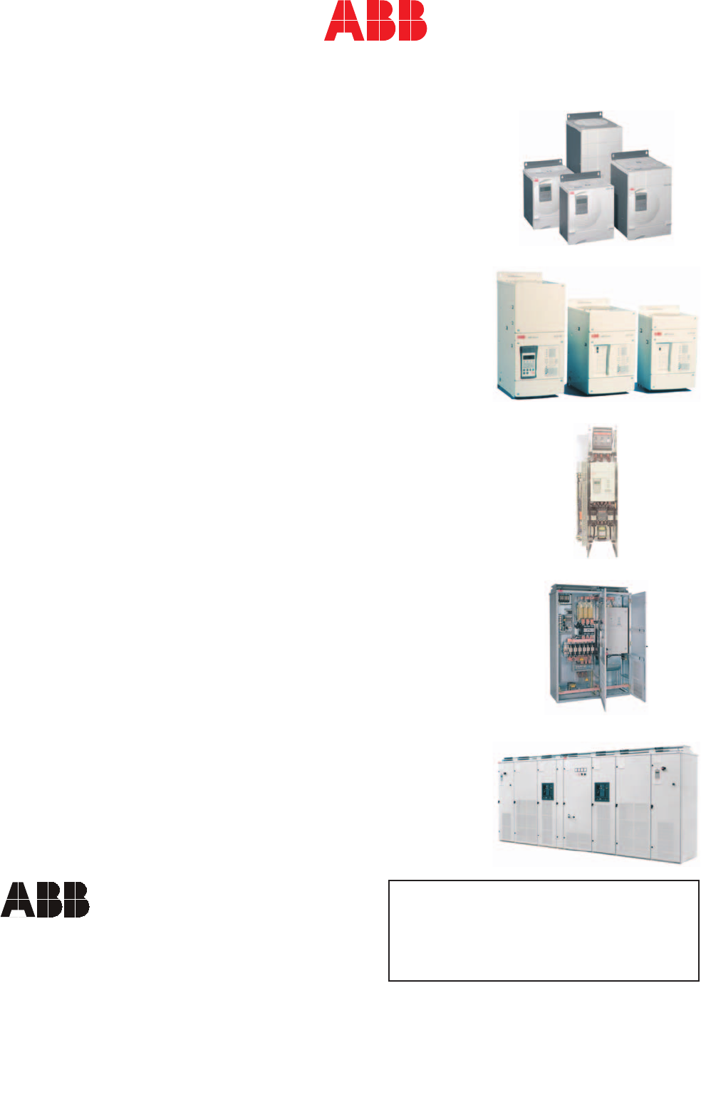
II D 4-14
3ADW000066R0901_DCS500_System_description_e_i
3ADW 000 066 R0901 REV I
09_2005
ABB Automation Products GmbH
Postfach 1180
68619 Lampertheim • GERMANY
Telefon +49(0) 62 06 5 03-0
Telefax +49(0) 62 06 5 03-6 09
www.abb.com/dc
*066R0901A5360000*
*066R0901A5360000*
DCS 400
DCS 500B / DCS 600
DCS 400 / DCS 500
Easy Drive
DCA 500 / DCA 600
DCE 500 / DCE 600
The drive module for standard applications
●Integrated field supply (max. 20 A)
●Accurate speed and torque control
●Extremely small and compact design
●Very easy installation and commissioning
●Express delivery
●Power range: 10...500 kW (13...670 HP)
The drive module for demanding
applications
●Free programming of software
●6- and 12-pulse configuration up to 10 MW/
13,000 HP and more
●Plain text display
●Power range: 10...5000 kW (13...6700 HP)
Highly integrated panel
●Excellent upgrade or revamp solution
●Contains:
●DCS 500B / DCS 600 module
●AC fuses
●Auxiliary transformer
●Motor fan starter with protection
●Main contactor
●Power range: 10...130 kW (26...300 HP)
The complete standard cabinet solution
●Pre-engineered
●Easy installation and commissioning
●Protection class: IP 21
●Plain text display
●Short delivery time
●Power range: 50...1350 kW (65...1800 HP)
For complex, completely engineered Drive
System in common cabinet design
●Flexible and modular hardware structure
●6- and 12-pulse configuration up to 18 MW/
23,000 HP and more
●Pre-programmed applications:
Metals, Cranes, P&P application, Mining
●Power range: 10...18000 kW (13...23000 HP)
DC Drives Product Portfolio
Since we aim to always meet the latest state-of-the-art
standards with our products, we are sure you will
understand when we reserve the right to alter particulars
of design, figures, sizes, weights, etc. for our equipment
as specified in this brochure.
2/81/8 1/8 3/82/8
AITAC LOW VALUE
AITAC HIGH VALUE
AITAC CONV MODE
SP
AITAC:OUT+
AITAC:OUT-
AITAC:ERR
AITAC
ST5
10101
10102
10103
P2
P3
P1
-84
101
102
103
0
30000
-30000
+
-8...-30V
-30...-90V
-90...-270V
TACHO PULSES
SPEED ACT FLT FTR
SPEED MEASUREMENT
SPEED ACT EMF
SPEED ACT FILT
SPEED ACT
SPEED ACT FTR
SPEED MEAS MODE
U MOTN V
U ARM ACT
TACHOPULS NR
SPEED SCALING
CH B
CH A
5
0
4
3
2
1
T
T
SPEED
TO
EMF
CALC
(10505)
(501)
AITAC:OUT+
T5
SP
TACHO
PULSE
12104
12102
12103
12101
P1
P2
P3
P4
P5
-11
2103
2101
2102
2104
2105
15000
2048
5
0
500
MAINTENANCE
(1210)
AO1 NOMINAL VALUE
AO1 OFFSET V
AO1 NOMINAL V
201 IN
SP
AO1
ST5
P2
P3
P1
-81
202
203
204
10000
0
20000
WIN SIZE
WIN MODE
2002
2021
2003
FRS
STEP
ST5
2005
2004
0
0
SPEED ERROR
STEP RESP
OUT OF WIN
OUT
SPEED ACT
12001
12002
12003
2001
P1
P2
IN
SP -13
FREE SIGNALS
(12517)
CURR LIM N
CURR LIM P
TORQ MIN2
TORQ MAX2
TREF TORQMIN1
TREF TORQMAX1
SPC TORQMIN1
SPC TORQMAX1
FLUX REF1
ARM CURR LIM N5
ARM CURR LIM N4
ARM CURR LIM N3
ARM CURR LIM N2
ARM CURR LIM N1
MAX CURR LIM SPD
SPEED ACT
ARM CURR LIM N
ARM CURR LIM P
GEAR.TORQ RAMP
GEAR.TORQ TIME
GEAR.START TORQ
TORQ MIN
TORQ MAX
TREF TORQ MIN
TREF TORQ MAX
SPC TORQ MIN
SPC TORQ MAX TORQUE/CURRENT LIMITATION
4192
yx
x
y
Min
Max
T
t
I
n
Max
Min
Min
Max
Min
Max
SP
(12102)
(11001)
ST5
P1
P2
P7
P6
P5
P4
P3
P8
P9
P11
P10
P12
P13
12308
12307
12301
12302
12303
12304
12305
12306
2301
2302
2303
2304
-10
2305
2306
2315
2316
2317
2307
2308
2309
2310
2311
2312
2313
2314
4000
-4000
16000
100
200
4095
-4095
20000
16383
16383
16383
16383
16383
4192
yx
x
y
CONSTANTS (12510)
CONSTANTS (12511)
CONSTANTS (12510)
CONSTANTS (12511)
REF SEL
SP
ST5
0
SEL1
IN1
IN2
SEL2
IN3
SEL3
OUT
ADD
REV
1910
1911
1912
1913
1914
1915
1916
1917
11903
-20
CONST REF
ST5
1
REF4
DEF
REF3
REF1
REF2
ACT2
ACT3
ACT4
ACT
SP
OUT
ACT1
1901
1902
1903
1904
11902
11901
P5
P1
P4
P2
P3
-77
1905
1906
1907
1908
1909
1000
1500
0
0
0
SP
1923 ENABLE
FOLLOW
1920
RUNNING
(10903)
T20
OHL
OLL
P1
P2
INCR
DECR
OUT
ACT
SOFTPOT
1918
1919
11904
11905
-15 SOFTPOT1
1921
1922
5000
-5000
DRIVE LOGIC (10903)
ACCELCOMP
ACC COMP.TRMIN
ACC COMP.MODE
EMESTOP RAMP
SPEED SET
SP
RAMP GENERATOR 11801
SPEED
REFERENCE
11703
SIGN
(11803)
(10906)
0
LOCAL
LOC REF
1701 IN
1720
P12
P11
P9
P8
P7
P6
P5
P4
P3
P2
P1
P10
SET ALL RAMP
VALUES TO ZERO
OUT
11702
(OUT)
11701
S
H
E-
T+
T-
0
STARTSEL
RES IN
ST5
BC
HOLD
SMOOTH2
SMOOTH1
DECEL2
DECEL1
ACCEL2
ACCEL1
T1/T2
SPEEDMIN
SPEEDMAX
FOLLOW IN
FOLL ACT
RES OUT
RUNNING
1707
1703
1706
1705
1704
(10903)
(11205)
1702
-18 RAMP_3
1714
1708
1711
1709
1712
1710
1713
1715
1716
1717
1718
1719
200
200
100
200
100
0
0
20000
-20000
0
0
0TORQ REF HANDLING
AI1 LOW VALUE
AI1 HIGH VALUE
AI1 CONV MODE
SP
AI1:OUT+
AI1:OUT-
AI1:ERR
AI1
ST5
10104
10105
10106
P2
P3
P1
-90
104
105
106
1
20000
-20000
+
--
MIN SPEED
SPEED MONITOR
SPEED GT L2
SPEED GT L1
OVERSPEED
MON.EMF V
MON.MEAS LEV
SPEED L2
SPEED L1
MIN SPEED L
SPEED ACT
P8
P7
P6
P5
P4
P3
P2
P1
P10
P9
ST20
STALL.TIME
SP
OVERSPEEDLIMIT
STALL.SEL
STALL.SPEED
STALL.TORQUE
12201
12202
12203
12204
-12 SPMONI_2
2201
2202
2203
2204
2205
2206
2207
2208
2209
2210
50
5000
10000
23000
0
50
3000
10
200
50
AI2 LOW VALUE
AI2 HIGH VALUE
AI2 CONV MODE
SP
AI2
AI2:OUT+
AI2:OUT-
AI2:ERR
ST5
10107
10108
10109
P2
P3
P1
-89
107
108
109
0
2000
-2000
+
--
ST5
SP
IN2
11802
OUT
1802
1801 IN1
-17
REFSUM_2
Control Adjust.
10507
10514
10513
10512
10511
10509
10510
BRIDGE TEMP
QUADR TYPE
CONV TYPE
MAX BR TEMP
Conv. valuesConv. settings C4
SET QUADR TYPE
SET CONV TYPE
SET MAX BR TEMP
SET U CONV V
SET I COMV A
U CONV V
I CONV A
I TRIP A
SETTINGS
SP
P5
P4
P3
P1
P2
Motor Data
I MOTN A
U MOTN V
I MOT1 FIELDN A
I MOT2 FIELDN A
FEXC SEL
P11
P10
P9
P8
P7
10508
10515
U NET DC NOM V
U SUPPLY
P13
PHASE SEQ CW
P14
10504
U NET ACT
LINE FREQUENCY
Supply Data
ST20
LANGUAGE
P15
(only for Cur. Controlling)
UNI FILT TC
P19
P6
P18
P12
P16
P17
CURR ACT FILT TC
PLL CONTROL
PLL DEV LIM
CONV CUR ACT
ARM CUR ACT
TORQUE ACT
10501
10502
10503
U ARM ACT
EMF ACT
CALC
Iact
+
-
OFFSET UDC
UDC 10505
10506
EMF FILT TC
-1 SETTGS_3
517
518
519
520
521
513
501
502
503
504
505
523
507
506
522
524
528
526
525
0
0
0
0
0
10
500
10
30
30
0
0
500
2
0
4
1024
0
10 AO2 NOMINAL VALUE
AO2 OFFSET V
AO2 NOMINAL V
205 IN
SP
AO2
ST5
P2
P3
P1
-80
206
207
208
5000
0
4095
DATA LOGGER (604)
DATA LOGGER (602)
MAINTENANCE (1211)
DATA LOGGER (603)
MAINTENANCE (1212)
AI4 LOW VALUE
AI4 HIGH VALUE
AI4 CONV MODE
SP
AI4:OUT+
AI4:OUT-
AI4:ERR
AI4
ST5
10113
10114
10115
P2
P3
P1
-87
113
114
115
0
2000
-2000
AI3 LOW VALUE
AI3 HIGH VALUE
AI3 CONV MODE
SP
AI3:OUT+
AI3:OUT-
AI3:ERR
AI3
ST5
10110
10111
10112
P2
P3
P1
-88
110
111
112
0
2000
-2000
+
--
+
--
12PULSE LOGIC (3604)
DRIVE LOGIC
BRAKE CONTROL
(303)
DATA LOGGER
(601)
DI8 (10715)
DRIVE LOGIC (903)
65
X3:
21
X3:
43 10 9
X3:
87
X3:
21
X4:
710
X4:
0 V
AO1
810
X4:
0 V
AO2
1
X5:
10
Speed reference
Tacho
Terminals
SDCS-CON-2
Speed controller
Line and motor data
Speed feedback calculation
Speed reference
handling
Terminals
SDCS-CON-2
Incremental encoder
Torque reference
Not used
Not used
DCS 500B Software structure
Software version: S21.233
Schematics: S21V2_0
Library: DCS500_1.5
1/82/8 4/83/8 1/83/8 5/84/8
via Options
CURRENT MONITOR
CURRENT ZERO
SIGNAL
DriveLogic
F03
F34
F34
A137
A137
EXTERNAL
INTERNAL
1
0
Monit.
method 2
1
3
2
1
0
Iact
STSYN
P4 ZERO CUR DETECT
CURRENT
RISE MAX
P1
CUR RIPPLE MONITP3
CUR RIPPLE LIMP2
SP -104 C_MONIT
418
421
420
419
32767
7
0
0
ARM ALPHA
CURRENT CONTROL
CURR REF IN LIM
CURR DER IN LIM
ARM DIR
ARM CURR REF
ARM CONT CURR LIM
ARM CURR LIM N
ARM CURR LIM P
ARM CURR REF SLOPE
ARM CURR CLAMP
ARM R
ARM L
ARM ALPHA LIM MIN
ARM ALPHA LIM MAX
ARM CURR PI KI
ARM CURR PI KP
REF TYPE SEL
ARM CUR ACT
CURR STEP
CURR REF
FLUX REF1
TORQ REF
FLUX N
10405
SP
10403
10402
10404
10401
401
402
403
404 t
STSYN
P11
P10
P9
416
415
1,2[1209]
12-PULS
DXN
BLOCK
P1
P2
P6
P5
P4
P3
P8
P7
-75 C_CNTR_3
405
406
407
408
409
412
413
414
410
411
417
0
1366
300
3200
2050
150
15
0
0
0
40
OVP SELECT
REF DCF
RUN DCF
RESET DCF
DI/OVP
F 21
A121
DCF FIELDMODE
as FEX 2 (Receiver)
as FEX 1 (Receiver)
6542
65421
5
4
Fexlink as Transmitter
for FEX1 and FEX2
6
Input for external Overvoltg.Protection
Cur.Controller for high inductive load
1216
P2
BC
0
1
6
5
4
3
2
1
from ext. FEXLINK
x8 ARM_CURR_PI_KP...
x8 ARM_CURR_PI_KI
... 408
407
ARM_CONT_CUR_LIM
3601 REV_DELAY
409
15 3602 REV_GAP
15 3603 FREV_DELAY
15
0
DCF Current Control
Stand Alone
Fexlink Node 1
Fexlink Node 2
MG Set
Disabled
Reserved
:
:
:
:
:
:
:
0
11303
10916
10917
SP
P1 DCF MODE :
-105 DCFMOD
1215
1217
0
0
DI2 (10703)
CONSTANTS (12526)
CONSTANTS (12527)
F2 CURR ACT
F2 CURR REF
F2 U LIM P
F2 U LIM N
F2 KI
F2 KP
F2 CURR TC
F2 OVERCURR L
F2 CURR GT MIN L
FANS ON
TEST REF2
F2 SEL.REF
F2 REF
F2 RED.SEL
DRIVE MODE
MOTOR 2 FIELD
1201=7
11502
11501
1501
ST20
DCF501/502
DCF503/504
SDCS-FEX-2
or
or
0%
100%
(10908)
(1201)
SP
P1
P2
P8
P7
P6
P5
P4
P3
P9
-28 M2FIELD2
1510
1511
1502
1503
1504
1505
1506
1508
1509
0
1228
2047
4710
0
1
20
-4096
4096
FREE WHEELING
MOTOR 2 FIELD OPTIONS
F2 U AC DIFF MAX
P1
ST20
SP -24
1507
10
CONSTANTS (12512)
REV.FLUX TD
REV.REF HYST
REV.REV HYST
OPTI.REF MIN TD
OPTI.REF MIN L
OPTI.REF GAIN
MOTOR 1 FIELD OPTIONS
F1 U AC DIFF MAX
SP
ST20
FREE WHEELING
FIELD REVERSAL
OPTITORQUE
P1
P4
P5
P6
P7
P8
P9
-26
1310
1315
1316
1317
1318
1319
1320
10
100
614
200
80
80
0
SPEED CONTROL (2011)
DATA LOGGER (606)
F1 CURR MIN TD
P10
F1 U LIM P
F1 U LIM N
F1 KI
F1 KP
F1 CURR TC
F1 OVERCURR L
P8
P7
P6
P5
P4
P9
ST20
F1 CURR ACT
F1 CURR REF
F1 CURR GT MIN L
TEST REF2
F1 ACK
F1 FORCE REV
F1 FORCE FWD
F1 SEL.REF
F1 REF
FIELD MODE
F1 RED.SEL
DRIVE MODE
FANS ON MOTOR 1 FIELD
1001=1,3,5
1201=7
DCF501/502
DCF503/504
SDCS-FEX-2
or
or
0%
100%
(10908)
(1201)
SP
P1
P2
P3
1301
1302
1303
1304
11302
11301
-30 M1FIELD2
1313
1314
1305
1306
1307
1308
1309
1311
1312
1321
0
1228
2047
4710
0
1
20
-4096
4096
200
DATA LOGGER
(605)
(1001)
SPEED CONTROL
IN LIM
SPC TORQMIN1
SPC TORQMAX1
12005
12004
2007
2012
2011
2010
2009
2008
2006
SET OUT TO ZERO
BC
ST5
TF
TD
KI
DROOPING
KPSMIN
KPSPOINT
KPSWEAKFILT
KP
Torque ref
SET1
VAL1
SET2
VAL2
HOLD
CLEAR
RUNNING
(11205)
(10903)
IN
SP
OUT
KP
DROOPING
HOLD
BALREF
BAL
BAL2
BAL2REF
RINT
P3
P1
P2
P4
P8
P7
P5
P6
-14
2014
2015
2016
2017
2018
2013
2019
2020
500
0
0
500
5000
0
0
50
TORQ REF
HANDLING (12403)
TORQ REF
HANDLING (12402)
FREE SIGNALS (12521)
FREE SIGNALS (12519)
SEL1:OUT
TORQ REF SELECTION
TREF TORQMIN1
TREF TORQMAX1
TREF B SLOPE
TREF B
TREF A FTC
LOAD SHARE
TREF A
SETS SEL1:OUT TO ZERO
-1
RUNNING
ST5
SP
P2
P1
2401
2403
2404
12401
-8
2402
2405
0
0
(10903)
SEL2:TORQ/SPEED
TORQ MIN2
TORQ MAX2
ACCELCOMP
SEL2.TREF SEL
SEL2.TORQ STEP
SP ERR
SEL2.TREF EXT
TORQ REF HANDLING
SEL2.TREF SPC
SP
(11702)
00
1
RUNNING SET OUTPUTS TO ZERO
ST5
-1(10903)
SEL2:IN_LIM
SEL2:OUT
4
3
Max
Min
5
2
P1
2409
2407
2408
12403
12402
12404
-9 TREFHND2
2406
1
FREE SIGNALS (12520)
(12001)
SPEED CONTROL
(2010)
SPEED ACT
(12102)
907040
100%
EMESTOP ACT
(10907)
cal
EMF CONTROL
0
100%
F CURR REF
FLUX REF SUM
FLUX REF 1
11003
11002
EMF REF
EMF REF SEL
EMESTOP ACT
FIELD WEAK DELAY
GENER.WEAK POINT
FIELD WEAK POINT
FLUX REF
FLUX REF SEL
FIELD MODE
11001
ST10
P9
P10
P8
FIELD CONST 2
FIELD CONST 1
FIELD CONST 3
P6
P7
EMF REG LIM P
EMF REG LIM N
P5
P3
P4
EMF KP
EMF KI
EMF REL LEV
EMF ACT
(10506)
TRef2
1201=10
&
GENER.EMF REF
P12
P1 LOCAL EMF REF
1003
1005
(1201)
(10907)
generatoric
P14
P13
P2
1004
1002
1001=1,3,5
P11
SP -34 EMFCONT2
1006
1012
1007
1008
1011
1009
1010
1013
1014
1015
1001
1016
1017
1018
100
20000
150
4905
50
410
-4095
1187
2190
3255
0
160
23100
0
CONSTANTS (12512)
DRIVE MODE
CONSTANTS (12509)
Armature current
controller
Motor voltage controller
Torque/current limitation
Field current controller 1 and 2
O1
O2
ST5
DI15 10729
10730
SP-55
O1
O2
ST5
DI14 10727
10728
SP-56
O1
O2
ST5
DI13 10725
10726
SP-57
O1
O2
ST5
DI12 10723
10724
SP-58
O1
O2
ST5
DI11 10721
10722
SP-59
O1
O2
ST5
DI10 10719
10720
SP-60
O1
O2
SP-61
ST5
DI9 10717
10718
AI5 LOW VALUE
AI5 HIGH VALUE
AI5 CONV MODE
SP
AI5
AI5:OUT+
AI5:OUT-
AI5:ERR
ST5
10116
10117
10118
P2
P3
P1
-86
116
117
118
0
2000
-2000
AI6 LOW VALUE
AI6 HIGH VALUE
AI6 CONV MODE
SP
AI6 AI6:OUT+
AI6:OUT-
AI6:ERR
ST5
10119
10120
10121
P2
P3
P1
-85
119
120
121
0
2000
-2000
CONVERTER PROTECTION
EARTH.FLT DLY
EARTH.FLT LEV
EARTH.CURR SEL
ARM OVERVOLT LEV
ARM OVERCURR LEV
U NET MIN1
U NET MIN2
PWR DOWN TIME
CONV TEMP DELAY
P9
P8
ST20
SP
P1
P2
P3
P4
P5
P6
P7
-76 CONPROT2
511
512
508
509
510
514
515
516
527
110
230
80
60
5000
0
4
10
0
MOT2 CALC TEMP
MOT2 MEAS TEMP
MOTOR 2 PROTECTION
MODEL2.TRIP L
MODEL2.ALARM L
MOT2.TEMP FAULT L
MOT2.TEMP ALARM L
MOT2.TEMP IN
P7
P6
P5
P4
P3
P1
P2
11601
11602
1601
ST20
SP
MODEL2.SEL
MODEL2.CURR
MODEL2.TC
-21 M2PROT_2
1602
1603
1604
1605
1606
1607
1608
0
0
0
4096
120
130
240
MOTOR 1 PROTECTION
MOT1 CALC TEMP
MOT1 MEAS TEMP
MOT1.TEMP IN
1401
MODEL1.TRIP L
MODEL1.ALARM L
KLIXON IN
MOT1.TEMP FAULT L
MOT1.TEMP ALARM L
P2
P1 11401
P7
P6
P5
P4
P3 11402
ST20
SP
MODEL1.SEL
MODEL1.CURR
MODEL1.TC
1404
-22 M1PROT_2
1402
1403
1405
1406
1407
1408
1409
0
0
0
4096
120
130
240
BTW.POT1/2
MACRO SELECT
ACTUAL VALUE 3
ACTUAL VALUE 2
ACTUAL VALUE 1
FIELDBUS NODE ADDR
t
PERIOD
DRIVEMODE
P1
MAINTENANCE
11220 FEXC1 SW VERSION
11221 FEXC2 SW VERSION
11215
FEXC2 COM ERRORS
FEXC2 COM STATUS 11214
11213
FEXC2 CODE
11212
11211
FEXC1 COM ERRORS
FEXC1 COM STATUS
FEXC1 CODE 11210
FEXC STATUS 11203
11217
11216
CMT COM ERRORS
CDI300 BAD CHAR
11205
BC
11219 CNT BOOT SW VER
11218 CNT SW VERSION
11222 PROGRAM LOAD
11202 BACKUPSTOREMODE
11201 COMMIS STAT 11204
TC STATUS
11206
SQUARE WAVE
CDP312
1212
1211
1210
P11
P9
P8
P7
P6
P5
P4
P3
P2
P10
T5
SELECT OPER.SYST
WRITE ENABLE PIN
WRITE ENABLE KEY
CMT DCS500 ADDR
DRIVE ID
(11207) TEST REF
04
7
8
9
10
0
1
2
3
4EMF CONTROLLER
SPEED LOOP
SECOND FIELD EXCITER
FIRST FIELD EXCITER
ARM. CONTROLLER
RELEASE OF ARM.
CONTROLLING
&
4I1=I2
POT2 VALUE
POT1 VALUE
TEST REF SEL
(11209)
(11208)
(10906)
TEST RELEASE
LOCAL
SP -100 MANTUN_3
1201
1204
1205
1206
1202
1203
1207
1208
1209
1213
1214
0
1000
0
100
250
1
358
358
0
1
0
SPEED MESUREMENT (12103)
SETTINGS (10501)
SETTINGS (10505)
DRIVE LOGIC
RAMP GENERATOR
12 PULSE LOGIC
COMFLT. TIMEOUT
COMM FAULT
DYN BRAKE ON
TRIP DC BREAKER
MOTOR ACT
MAIN CONT ON
FIELD ON
FAN ON
COMFAULT MODE
PWR LOSS MODE
PANEL DISC MODE
EME STOP MODE
STOP MODE
MAIN CONT MODE
FIELD HEAT SEL
ACK MAIN CONT
ACK MOTOR FAN
ACK CONV FAN
DISABLE LOCAL
START INHIBIT
EMESTOP ACT
RDY RUNNING
RDY ON
MIN SPEED
EME STOP
COAST STOP
DRIVE LOGIC
AUTO-RECLOSING 10914
10912
10901
10902
10903
10904
10905
10907
10906
10908
10909
10910
10913
10911
10915
913
912
911
910
909
908
907
905
904
903
902
901
P5
P4
P3
P2
P1
P6
P7
P8
906
LOCAL
SP
ALARM
FAULT
RUNNING
1
RUN3
RUN2
RUN1
ON/OFF
MOTOR2
RESET
LOCAL
(12201)
(11205) BC (BLOCK.)
T20
-36 DRLOGI_2
914
915
916
917
918
919
920
921
0
1
0
0
0
0
0
2
DO4
INV IN
IN
807
808
T20
SP -46
DO8
INV IN
IN
815
816
T20
SP -42
DO7
INV IN
IN
813
814
T20
SP -43
DO6
INV IN
IN
811
812
T20
SP -44
DO5
INV IN
IN
809
810
T20
SP -45
DO3
805
INV IN
IN
806
T20
SP -47
DO2
INV IN
IN
803
804
T20
SP -48
DO1
INV IN
IN
801
802
T20
SP -49
O1
O2
SP
DI8
ST5
10715
10716
-62
O1
O2
SP
DI7
ST5
10713
10714
-63
O1
O2
SP
ST5
DI6 10711
10712
-64
O1
O2
SP
ST5
DI5 10709
10710
-65
O1
O2
SP
ST5
DI4 10707
10708
-66
O1
O2
SP
ST5
DI3 10705
10706
-67
O1
O2
SP
ST5
DI2 10703
10704
-68
O1
O2
DI1
SP
ST5
10701
10702
-69
REF SEL (1911) CONST REF (11902)
RAMP GENERATOR
TORQ REF SELECTION
TORQ REF HANDLING
DCF FIELDMODE
(1216) SDCS-POW-1
Relay output
MAIN CONT
MAIN CONT
EXC CONT
FAN CONT
RUNNING
RDY RUNNING
MAIN CONT
MOTOR FAN
CONV FAN
RESET
EM STOP
RUN
ON/OFF
MOTOR 1/2 FIELD
Must be connected, when no fan acknowledges (DI1, DI2)
MAINTENANCE
BRAKE CONTROL (302)
DATASET 4
214
213
212
OUT
IN3
IN2
IN1
SP
ST5
-94
DATASET 3
OUT3
OUT2
OUT1
IN
SP
ST5
10125
10126
10127
-93
DATASET 2
211
210
209
OUT
IN3
IN2
IN1
SP
ST5
-92
DATASET 1
IN
OUT3
OUT2
OUT1
SP
ST5
10122
10123
10124
-91
FIELDBUS PAR.1
(MODULE TYPE)
SP
FIELDBUS
modul type
depends of
Parameters
P15
P14
P13
P12
P11
ST5
P10
P09
P08
P07
P06
P05
P04
P03
P02
P01
-95 FLBSET_2
4001
4002
4003
4004
4005
4006
4007
4008
4009
4010
4011
4012
4013
4014
4015
0
0
0
0
0
0
0
0
0
0
0
0
0
0
0
BC Logic
Revers.Logic
Bridge Logic
IREF0 Logic
Res. f.Commun
BC not Zero
Logic f. INHIBIT
Fault Current
Bridge of Slave
Bridge
IREF2-Pol.Broth
IREF2-Polarity
Curr.Ref.2
IREF1-Pol.Master
IREF1-Polarity
Curr.Ref.1
Arm.CURR.Both
Conv.Curr.Both
Arm.Curr.Slave
Conv.Curr.Slave
Fault Reversion
Indicat.Revers
[1209]
*
2048
ADJ REF1
INHIB Logic
DIFF CURR DELAY
DIFF CURRENT
IACT SLAVE
FREV DELAY
REV GAP
REV DELAY
13622
13605
STSYN
BC
6-PULSE
MASTER
CURRENT REFERENCE
P6
3604
13608
P5
P4
active, if [1209] = 1
CURRENT ANALYSIS 13601
13602
13603
13604
13615
13621
3616
ON/OFF LOGIC
(11205)
13616
3607
P3
P2
P1
active, if [1209]= 1 or 2
BRIDGE REVERSAL LOGIC
SP
12-PULSE LOGIC
3608
3609
3610
13611
13606
13609
13607
13610
13612
13613
13614
-99 12PULS_2
3601
3602
3603
3605
3606
3615
1
10
10
10
150
2048
X18:12
X18:11
X18:10
X18:09
OUTPUT X18
SP
STSYN
3611
3612
3613
3614
-98
X18:16
X18:15
X18:14
X18:13 13618
STSYN
SP
INPUT X18
13617
13619
13620
-97
AI2 (10107)
+
--
+
--
5
X7:
1
X7:
2
X7:
3
X7:
6
X7:
7
X7:
4
X7:
2
1
X96:
3
X6:
2
X6:
1
X6:
6
X6:
5
X6:
8
X6:
7
X6:
4
X6:
7
X1:
6
X1:
4
X1:
3
X1:
2
X1:
1
X1:
21
X2:
54
X2:
8
X1:
4/8 6/85/8 5/8 7/86/8
not used
not used
not used
not used
not used
not used
not used
not used
not used
Maintenance
Monitoring
Additional binary
inputs
Binary in and outputs (standard)
Inputs and outputs for fieldbus
Inputs and outputs for 12 pulse
Terminals
SDCS-CON-2
Terminals
SDCS-IOE-1
Terminals
SDCS-CON-2
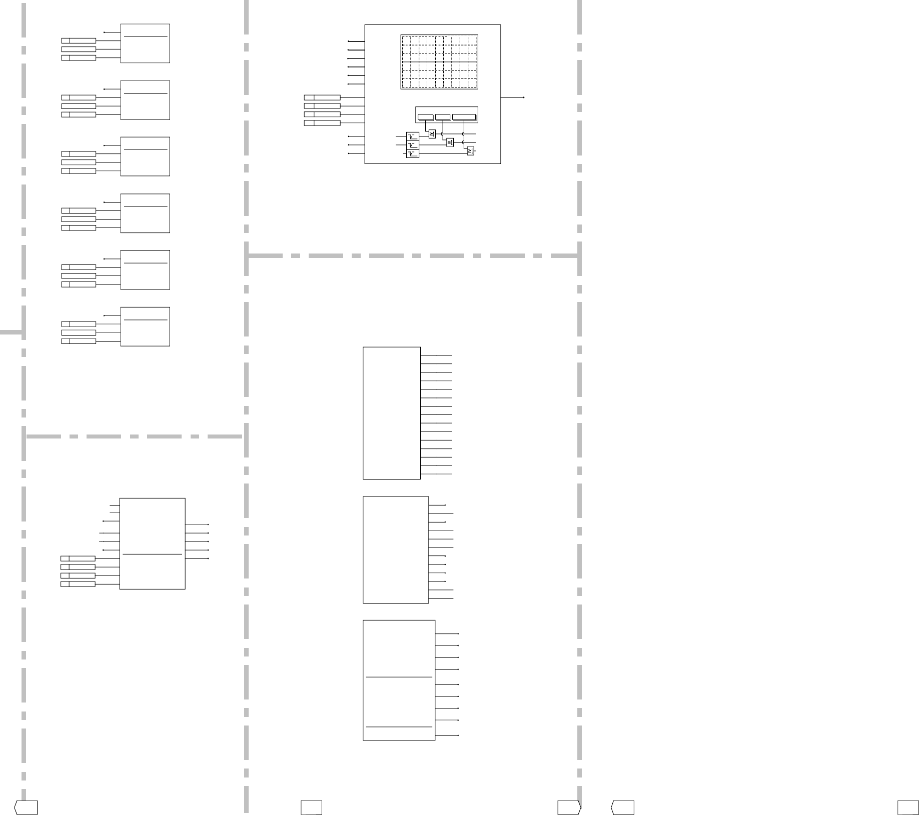
DLY
TEXT
TYPE
IN USER EVENT 6
SP
ST20
P3
P1
"EXT. IND. 6"
1121
1123
-2
1122
1124
0
0
DLY
TEXT
TYPE
IN USER EVENT 5
SP
ST20
1117
1119
P3
P1
"EXT. IND. 5"
-3
1118
1120
0
0
DLY
TEXT
TYPE
IN USER EVENT 4
SP
ST20
P3
P1
"EXT. IND. 4"
1113
1115
-4
1114
1116
0
0
DLY
TEXT
TYPE
IN USER EVENT 3
SP
ST20
1109
1111
P3
P1
"EXT. IND. 3"
-5
1110
1112
0
0
DLY
TEXT
TYPE
IN USER EVENT 2
SP
ST20
P3
P1
"EXT. IND. 2"
1105
1107
-6
1106
1108
0
0
DLY
TEXT
TYPE
IN USER EVENT 1
SP
ST20
P3
P1
"EXT. IND. 1"
1101
1103
-7
1102
1104
0
0
DLOG STATUS
DLOG.SAMPL INT
DLOG.TRIGG DELAY
DLOG.TRIGG VALUE
DLOG.TRIGG COND
0
0
0
DATA LOGGER
SP
RESTART
STOP
TRIG
613
611
612
DLOG.RESTART
DLOG.STOP
DLOG.TRIG
T1ms
IN5 Ch.5
10601
STOP RESTART
CMT-TOOL
TRIG
P4
P3
P2
P1
IN6 Ch.6
606
605
IN4 Ch.4
604
IN3 Ch.3
603
IN2 Ch.2
602
IN1 Ch.1
601
-102 DATALOG
607
608
609
610
1
20000
200
3
SPEED MEASUREMENT (12102)
SETTINGS (10501)
SETTINGS (10505)
SETTINGS (10504)
MOTOR 1 FIELD (11302)
CURRENT CONTROL (10401)
BRAKE CONTROL
ACT BRAKE
BRAKE RUN
LIFT BRAKE
DECEL CMND
TREF ENABLE
TREF OUT
EMESTOP BRAKE
HOLD TORQ
STOP DELAY
START DELAY
MIN SP IND
BR RELEASE
HOLD REF
TORQUE ACT
10305
10304
10303
10302
10301
304
303
302
301
P1
P2
P3
P4
LOCAL
(10503)
RESET
SP
(10902)
ST20
-32
305
306
307
308
0
0
0
0
DI8 (10715)
SPEED MONITOR (12201)
FAULT WORD 1
OPERATING HOURS
LATEST ALARM
ALARM WORD 3
ALARM WORD 2
ALARM WORD 1
LATEST FAULT
FAULT WORD 3
FAULT WORD 2
T20
11109
11108
11107
11106
11105
11103
11102
SP
FAULT HANDLING
11104
11101
-103 FLTHNDL
0
-1
SPEED: 100%
CUR,FLX,VLT:-100%
CUR,FLX,VLT: 100%
12509
12508
12507
12506
12505
12504
12503
12510
12511
12513
12512
12515
12514
12502
12501
CONSTANTS
SP
ST
SPEED:-100%
TORQ:-100%
TORQ:100%
EMF:100%
31416
1000
100
10
2
1
-73
CONST_0
CONST_M1_TRUE
CONST_1
CONST_2
CONST_10
CONST_100
CONST_1000
CONST_31416
EMF_MAX
TORQ_MAX
TORQ_MAX_N
CONST_4095
CONST_M4095
CONST_20000
CONST_M20000
SIG12(CURR._STEP)
SIG11(CURR. REF)
SIG10(FORCE REV)
SIG9(FORCE_FWD)
SIG8(EMF REF)
SIG7(FLUX REF)
SIG6(LOAD SHARE)
SIG5(TORQUE STEP)
SIG4(TORQ. REF B)
SIG3(TORQ. REF A)
SIG2(SPEED STEP)
SIG1(SPEED REF)
FREE SIGNALS
12527
12526
12525
12524
12523
12522
12521
12520
12519
12518
12517
12516
ST
SP -74
SPEED_STEP
TORQ_REF_B
TORQ_STEP
LOAD_SHARE
CUR_REF
CUR_STEP
6/8 8/87/8 7/8 8/8
Brake control
User events
Data logger
Additional signals
Speed reference handling
The speed reference for the ramp function generator is formed by the REF SEL blocks, which
can be used to select the reference value required, the CONST REF block, which generates
a maximum of 4 permanently settable reference values, the SOFTPOT block, which repro-
duces the function of a motorpotentiometer in conjunction with the block RAMP
GENERATOR, or by the AI1 block (analogue input 1).
The RAMP GENERATOR block contains a ramp function generator with 2 ramp-up and
ramp-down ramps, 2 times for the S-curve, limitation for upper and lower limits, hold function
and the functions for ”Follow” the speed reference or ”Follow” the speed feedback. There is a
special signal available for the treatment of acceleration and deceleration.
The REF SUM block enables the output of the ramp function generator and a user-definable
signal to be added.
Speed feedback calculation
This page depicts the conditioning routine for speed feedback and reference values. The
AITAC block is used to read in the speed feedback from an analogue tacho The SPEED
MEASUREMENT block processes the 3 possible feedback signals: analogue tacho, pulse
generator or the converter's output voltage (SPEED_ACT_EMF) - conditioned by the EMF
TO SPEED CALC block (if 2102=5 , no field weakening function possible). Parameters
are used for activating smoothing functions, selecting the feedback value and where applica-
ble for setting the maximum speed. This parameter also serves for scaling the speed control
loop.
The SPEED MONITOR block contains motor stalled - and tacho monitoring function, and
compares a selected speed feedback value against overspeed, minimum speed and 2 setta-
ble thresholds.
The AO1 block represents a scalable analogue output.
Speed controller
The result is compared to the speed feedback from the SPEED MEASUREMENT block,
using the SPEED ERROR block, and then passed to the speed controller. This block permits
evaluation of the system deviation by means of a filter. Moreover, it is possible here to make
a few settings which are needed for the ”Window” operating mode. If the drive’s speed feed-
back is within a window around the reference value, then the speed controller is ”bypassed”
(provided ”Window Mode” has been activated; the drive is controlled by means of a torque
reference value at the TORQ REF HANDLING block). If the speed feedback is outside the
window, the speed controller will be activated, and will lead the drive’s actual speed back into
the window.
The SPEED CONTROL block contains the speed controller with P, I and DT1 contents. For
adaptation it receives a variable P-amplification.
Torque / current limitation
The ”torque reference” generated by the speed controller is passed to the input of the
CURRENT CONTROL block via the TORQ REF HANDLING block, and there it is converted
into a current reference value and used for current regulation. The TORQUE / CURRENT
LIMITATION block is used for generating the various reference values and limitations; this
block contains the following functions: ”speed-dependent current limitation”, ”gear backlash
compensation”, ”generation of the values for static current limitation” and ”torque limitation”.
The values for the various limitations are used again at some other points, for instance at the
following blocks: SPEED CONTROL, TORQ REF HANDLING, TORQ REF SELECTION, and
CURRENT CONTROL.
The AI2 block (analogue input 2) is used for reading in an analogue signal.
The TORQ REF SELECTION block contains a limitation with upstream addition of two sig-
nals, one of which can be routed through a ramp function generator; the other signal’s
evaluation can be dynamically altered using a multiplier.
The TORQ REF HANDLING block determines the drive's operating mode. When in position
1, the speed control mode has been activated, whereas in position 2 it is torque control mode
(no closed-loop control since there is no "genuine" torque feedback available in the unit). In
both cases, the reference value required comes from outside. Positions 3 and 4 are a combi-
nation of the first two options stated above. Note that with position 3 the smaller value out of
external torque reference and speed controller output is passed to the current controller
whereas with position 4 it is the larger one. Position 5 uses both signals, corresponding to the
method of functioning of "Window Mode".
Armature current controller
The CURRENT CONTROL block contains the current controller with a P and I content, plus
an adaptation in the range of discontinuous current flow. This block also contains functions
for current-rise limitation, the conversion of torque reference value into current reference
value by means of the field crossover point, and some parameters describing the supply
mains, and the load circuit.
At applications with high inductive load and high dynamic performance a different hardware is
used to generate the signal current equal to zero. This hardware is selected by the
CURRENT MONITOR block. The functions monitoring the current can now be adapted to the
needs of the application. This gives easier handling and a higher degree of safety at high
performance drives, like test rigs.
The DCF mode can be activated via the block DCF FIELDMODE. The functionality within this
mode can be specified. If one of these functions is selected the current controller gets a
different characteristic, the overvoltage protection DCF 506 is monitored and the field current
reference via the X16: terminals is routed.
Line and motor data
The SETTINGS block serves for scaling all important signals, such as line voltage, motor
voltage, motor current and field current. Parameters are available to adjust the control to
special conditions like weak networks or interactions with harmonic filter systems. The lan-
guage, in which you want to read your information on the panel, can be selected.
The AO2 block represents a scalable analogue output.
Motor voltage controller
The EMF CONTROL block contains the armature-circuit voltage controller (e.m.f. controller).
It is based on a parallel structure comprising a PI controller and a precontrol feature, gener-
ated with a characteristic of 1/x. The ratio between the two paths can be set. The output
variable of this block is the field current reference value, which is produced from the flux
reference value by another characteristic function using linearization. To enable the drive to
utilize a higher motor voltage even with a 4 quadrant system two different field weakening
points can be set by parameter.
Field current controller 1 and 2
Since a DCS power converter can control 2 field units, some of the function blocks are dupli-
cated. This means that, depending on the mechanical configuration of the drives concerned,
you can control 2 motors either in parallel or alternatively. The requisite configuration of the
software structure can be generated by designing the blocks appropriately during the com-
missioning routine.
The MOTOR1 FIELD / MOTOR2 FIELD block reads in the field current reference value and
all values which are specific to the field supply unit, and transfers these to the field power
converter via an internal serial link; the field power converter is scaled to suit its hardware,
and performs field current regulation. The field current direction for motor 1 can be deter-
mined using binary commands, while for motor 2 it can be generated in the course of an
application upstream of the block concerned.
The MOTOR1 FIELD OPTIONS / MOTOR2 FIELD OPTIONS block controls the free-
wheeling function in the event of line undervoltage, and the field current reversal function with
field reversal drives (only for motor 1). In case of field reversal drives, there is an option for
selectively influencing the moment of armature-circuit and field current reduction and build-
up.
Binary in and outputs (standard)
The DRIVE LOGIC block reads in various signals from the system via digital inputs DIx,
processes them, and generates commands, which are outputted to the system via digital
outputs DOx, e.g. for controlling the power converter’s line contactor, the field-circuit contac-
tor or contactors for various fans, or for outputting status messages.
Additional binary inputs
The AI3 and AI4 blocks represent another 2 analogue inputs which have as yet not been
assigned to any particular functions. The blocks A15 and A16 represent another 2 additional
inputs which are only active, if the board SDCS-IOE1 is connected. Another 7 digital inputs DI
9 .. DI15 are available with this additional hardware.
Inputs and outputs for fieldbus
A fieldbus module with serial communicated references should be used, if analogue and
digital signals are not sufficient for the control of the drive (equipment for the installation of
Profibus, CS31, Modbus etc. is available). This type of module is activated by means of the
block FIELDBUS. The data transferred from the control to the converter are stored in the
blocks DATASET1 and DATASET3 as 16-bit-information. Depending on the application the
output pins of these blocks have to be connected to input pins of other blocks in order to
transport the message. The same procedure is valid for blocks DATASET2 and DATASET4,
if they are connected. These blocks are transmitting information from the converter to the
control system.
Inputs and outputs for 12 pulse
The converter is able to be configurated in a 12-pulse parallel application. In this case you
need: two identical armature converters; one field supply unit; one T-reactor; communication
via ribbon cable connected to X 18 of both converters The 12-PULSE LOGIC must be acti-
vated and guarantees a synchronous control of the MASTER and the SLAVE drive.
Maintenance
The MAINTENANCE block provides reference values and test conditions so as to enable all
controllers to be adjusted in the power converter. If the panel is used as a meter in the cubicle
door, an assortment of signals can be defined here.
Monitoring
The CONVERTER PROTECTION block monitors the armature circuit for overvoltage and
overcurrent, and monitors the mains for undervoltage. It provides an option for reading in the
total current of the 3 phases through an additional external sensor and monitoring it for "not
equal to zero". Adaptations are made for rebuild applications, which keep the power part and
the fan, to sense overload conditions or fan failures.
The MOTOR1 PROTECTION block, in its upper part, evaluates either the signal from an
analogue temperature sensor, or from a Klixon. In its lower part, it computes motor heat-up
with the aid of the current feedback value and a motor model, after which a message is
outputted.
The MOTOR2 PROTECTION block works in the same way as the MOTOR1 PROTECTION
block, but without Klixon evaluation.
User event
By using the block USER EVENT1 to USER EVENT6 six different messages are created,
which are displayed as faults or alarms on the panel CDP312 as well as on the 7 segment
display of the converter.
Brake control
The BRAKE CONTROL block generates all signals needed for controlling a mechanical
brake.
Data logger
The block DATA LOGGER is able to record up to six signals. The values of these signals will
be stored in a battery buffered RAM and are still available after a break down of the supply
voltage. The time of recording can be influenced by a trigger signal, as well as the number of
recorded values before and after the trigger signal. The function DATA LOGGER can be set
with both panel and PC tool. For evaluation of the recorded values a PC tool is recom-
mended.
Additional signals
By using the block FAULT HANDLING the faults and alarms of the drive are regrouped as 16-
bit information. The CONSTANTS and FREE SIGNALS blocks can be used for setting limita-
tions or special test conditions.
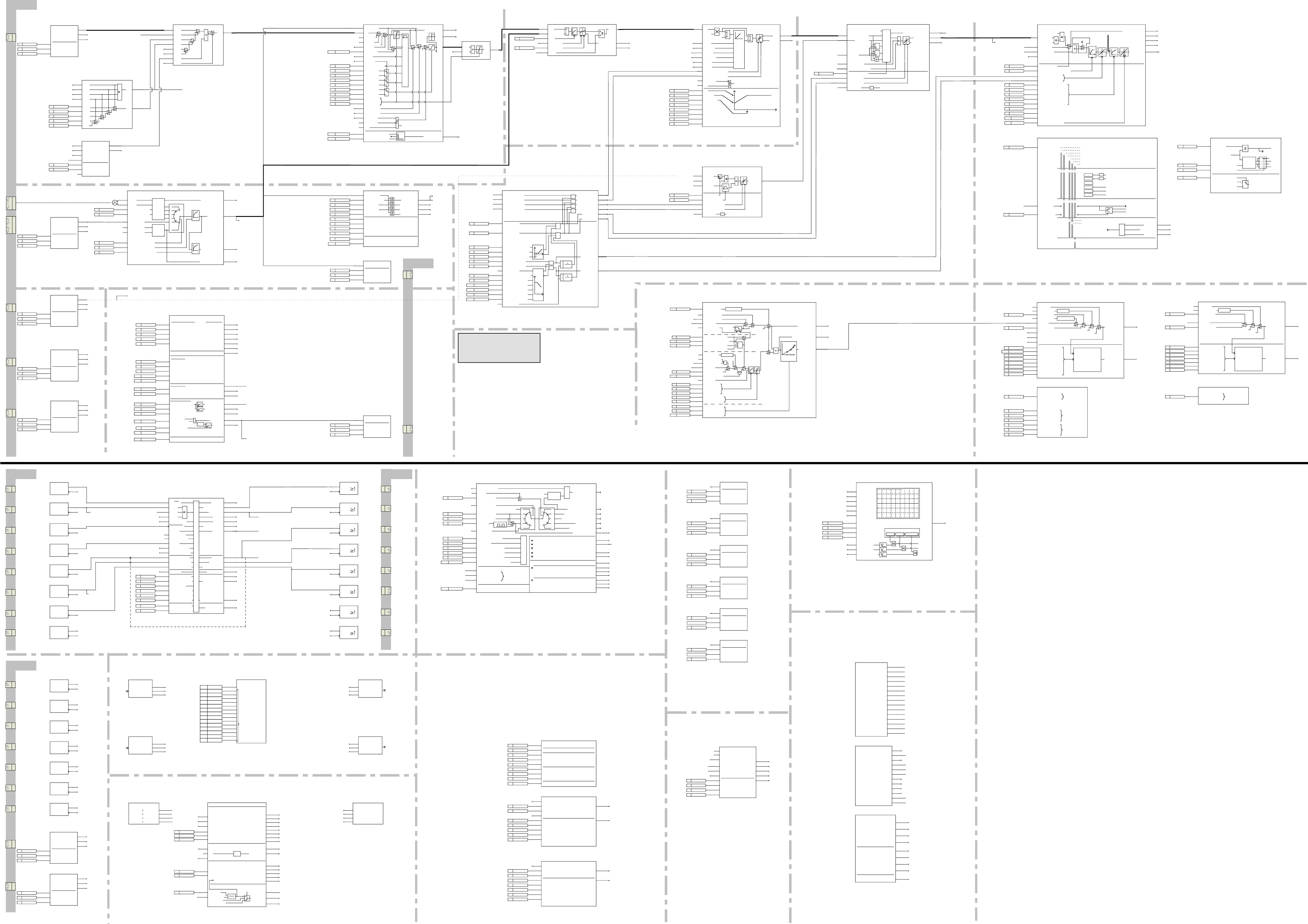
O1
O2
ST5
DI15 10729
10730
SP-55
O1
O2
ST5
DI14 10727
10728
SP-56
O1
O2
ST5
DI13 10725
10726
SP-57
O1
O2
ST5
DI12 10723
10724
SP-58
O1
O2
ST5
DI11 10721
10722
SP-59
O1
O2
ST5
DI10 10719
10720
SP-60
O1
O2
SP-61
ST5
DI9 10717
10718
AI5 LOW VALUE
AI5 HIGH VALUE
AI5 CONV MODE
SP
AI5
AI5:OUT+
AI5:OUT-
AI5:ERR
ST5
10116
10117
10118
P2
P3
P1
-86
116
117
118
0
2000
-2000
AI6 LOW VALUE
AI6 HIGH VALUE
AI6 CONV MODE
SP
AI6 AI6:OUT+
AI6:OUT-
AI6:ERR
ST5
10119
10120
10121
P2
P3
P1
-85
119
120
121
0
2000
-2000
DLY
TEXT
TYPE
IN USER EVENT 6
SP
ST20
P3
P1
"EXT. IND. 6"
1121
1123
-2
1122
1124
0
0
DLY
TEXT
TYPE
IN USER EVENT 5
SP
ST20
1117
1119
P3
P1
"EXT. IND. 5"
-3
1118
1120
0
0
DLY
TEXT
TYPE
IN USER EVENT 4
SP
ST20
P3
P1
"EXT. IND. 4"
1113
1115
-4
1114
1116
0
0
DLY
TEXT
TYPE
IN USER EVENT 3
SP
ST20
1109
1111
P3
P1
"EXT. IND. 3"
-5
1110
1112
0
0
DLY
TEXT
TYPE
IN USER EVENT 2
SP
ST20
P3
P1
"EXT. IND. 2"
1105
1107
-6
1106
1108
0
0
DLY
TEXT
TYPE
IN USER EVENT 1
SP
ST20
P3
P1
"EXT. IND. 1"
1101
1103
-7
1102
1104
0
0
CONVERTER PROTECTION
EARTH.FLT DLY
EARTH.FLT LEV
EARTH.CURR SEL
ARM OVERVOLT LEV
ARM OVERCURR LEV
U NET MIN1
U NET MIN2
PWR DOWN TIME
CONV TEMP DELAY
P9
P8
ST20
SP
P1
P2
P3
P4
P5
P6
P7
-76 CONPROT2
511
512
508
509
510
514
515
516
527
110
230
80
60
5000
0
4
10
0
MOT2 CALC TEMP
MOT2 MEAS TEMP
MOTOR 2 PROTECTION
MODEL2.TRIP L
MODEL2.ALARM L
MOT2.TEMP FAULT L
MOT2.TEMP ALARM L
MOT2.TEMP IN
P7
P6
P5
P4
P3
P1
P2
11601
11602
1601
ST20
SP
MODEL2.SEL
MODEL2.CURR
MODEL2.TC
-21 M2PROT_2
1602
1603
1604
1605
1606
1607
1608
0
0
0
4096
120
130
240
MOTOR 1 PROTECTION
MOT1 CALC TEMP
MOT1 MEAS TEMP
MOT1.TEMP IN
1401
MODEL1.TRIP L
MODEL1.ALARM L
KLIXON IN
MOT1.TEMP FAULT L
MOT1.TEMP ALARM L
P2
P1 11401
P7
P6
P5
P4
P3 11402
ST20
SP
MODEL1.SEL
MODEL1.CURR
MODEL1.TC
1404
-22 M1PROT_2
1402
1403
1405
1406
1407
1408
1409
0
0
0
4096
120
130
240
DLOG STATUS
DLOG.SAMPL INT
DLOG.TRIGG DELAY
DLOG.TRIGG VALUE
DLOG.TRIGG COND
0
0
0
DATA LOGGER
SP
RESTART
STOP
TRIG
613
611
612
DLOG.RESTART
DLOG.STOP
DLOG.TRIG
T1ms
IN5 Ch.5
10601
STOP RESTART
CMT-TOOL
TRIG
P4
P3
P2
P1
IN6 Ch.6
606
605
IN4 Ch.4
604
IN3 Ch.3
603
IN2 Ch.2
602
IN1 Ch.1
601
-102 DATALOG
607
608
609
610
1
20000
200
3
SPEED MEASUREMENT (12102)
SETTINGS (10501)
SETTINGS (10505)
SETTINGS (10504)
MOTOR 1 FIELD (11302)
CURRENT CONTROL (10401)
BRAKE CONTROL
ACT BRAKE
BRAKE RUN
LIFT BRAKE
DECEL CMND
TREF ENABLE
TREF OUT
EMESTOP BRAKE
HOLD TORQ
STOP DELAY
START DELAY
MIN SP IND
BR RELEASE
HOLD REF
TORQUE ACT
10305
10304
10303
10302
10301
304
303
302
301
P1
P2
P3
P4
LOCAL
(10503)
RESET
SP
(10902)
ST20
-32
305
306
307
308
0
0
0
0
DI8 (10715)
SPEED MONITOR (12201)
BTW.POT1/2
MACRO SELECT
ACTUAL VALUE 3
ACTUAL VALUE 2
ACTUAL VALUE 1
FIELDBUS NODE ADDR
t
PERIOD
DRIVEMODE
P1
MAINTENANCE
11220 FEXC1 SW VERSION
11221 FEXC2 SW VERSION
11215
FEXC2 COM ERRORS
FEXC2 COM STATUS 11214
11213
FEXC2 CODE
11212
11211
FEXC1 COM ERRORS
FEXC1 COM STATUS
FEXC1 CODE 11210
FEXC STATUS 11203
11217
11216
CMT COM ERRORS
CDI300 BAD CHAR
11205
BC
11219 CNT BOOT SW VER
11218 CNT SW VERSION
11222 PROGRAM LOAD
11202 BACKUPSTOREMODE
11201 COMMIS STAT 11204
TC STATUS
11206
SQUARE WAVE
CDP312
1212
1211
1210
P11
P9
P8
P7
P6
P5
P4
P3
P2
P10
T5
SELECT OPER.SYST
WRITE ENABLE PIN
WRITE ENABLE KEY
CMT DCS500 ADDR
DRIVE ID
(11207) TEST REF
04
7
8
9
10
0
1
2
3
4EMF CONTROLLER
SPEED LOOP
SECOND FIELD EXCITER
FIRST FIELD EXCITER
ARM. CONTROLLER
RELEASE OF ARM.
CONTROLLING
&
4I1=I2
POT2 VALUE
POT1 VALUE
TEST REF SEL
(11209)
(11208)
(10906)
TEST RELEASE
LOCAL
SP -100 MANTUN_3
1201
1204
1205
1206
1202
1203
1207
1208
1209
1213
1214
0
1000
0
100
250
1
358
358
0
1
0
SPEED MESUREMENT (12103)
SETTINGS (10501)
SETTINGS (10505)
DRIVE LOGIC
RAMP GENERATOR
12 PULSE LOGIC
COMFLT. TIMEOUT
COMM FAULT
DYN BRAKE ON
TRIP DC BREAKER
MOTOR ACT
MAIN CONT ON
FIELD ON
FAN ON
COMFAULT MODE
PWR LOSS MODE
PANEL DISC MODE
EME STOP MODE
STOP MODE
MAIN CONT MODE
FIELD HEAT SEL
ACK MAIN CONT
ACK MOTOR FAN
ACK CONV FAN
DISABLE LOCAL
START INHIBIT
EMESTOP ACT
RDY RUNNING
RDY ON
MIN SPEED
EME STOP
COAST STOP
DRIVE LOGIC
AUTO-RECLOSING 10914
10912
10901
10902
10903
10904
10905
10907
10906
10908
10909
10910
10913
10911
10915
913
912
911
910
909
908
907
905
904
903
902
901
P5
P4
P3
P2
P1
P6
P7
P8
906
LOCAL
SP
ALARM
FAULT
RUNNING
1
RUN3
RUN2
RUN1
ON/OFF
MOTOR2
RESET
LOCAL
(12201)
(11205) BC (BLOCK.)
T20
-36 DRLOGI_2
914
915
916
917
918
919
920
921
0
1
0
0
0
0
0
2
DO4
INV IN
IN
807
808
T20
SP -46
DO8
INV IN
IN
815
816
T20
SP -42
DO7
INV IN
IN
813
814
T20
SP -43
DO6
INV IN
IN
811
812
T20
SP -44
DO5
INV IN
IN
809
810
T20
SP -45
DO3
805
INV IN
IN
806
T20
SP -47
DO2
INV IN
IN
803
804
T20
SP -48
DO1
INV IN
IN
801
802
T20
SP -49
O1
O2
SP
DI8
ST5
10715
10716
-62
O1
O2
SP
DI7
ST5
10713
10714
-63
O1
O2
SP
ST5
DI6 10711
10712
-64
O1
O2
SP
ST5
DI5 10709
10710
-65
O1
O2
SP
ST5
DI4 10707
10708
-66
O1
O2
SP
ST5
DI3 10705
10706
-67
O1
O2
SP
ST5
DI2 10703
10704
-68
O1
O2
DI1
SP
ST5
10701
10702
-69
REF SEL (1911) CONST REF (11902)
RAMP GENERATOR
TORQ REF SELECTION
TORQ REF HANDLING
DCF FIELDMODE
(1216) SDCS-POW-1
Relay output
MAIN CONT
MAIN CONT
EXC CONT
FAN CONT
RUNNING
RDY RUNNING
MAIN CONT
MOTOR FAN
CONV FAN
RESET
EM STOP
RUN
ON/OFF
MOTOR 1/2 FIELD
Must be connected, when no fan acknowledges (DI1, DI2)
MAINTENANCE
BRAKE CONTROL (302)
FAULT WORD 1
OPERATING HOURS
LATEST ALARM
ALARM WORD 3
ALARM WORD 2
ALARM WORD 1
LATEST FAULT
FAULT WORD 3
FAULT WORD 2
T20
11109
11108
11107
11106
11105
11103
11102
SP
FAULT HANDLING
11104
11101
-103 FLTHNDL
0
-1
SPEED: 100%
CUR,FLX,VLT:-100%
CUR,FLX,VLT: 100%
12509
12508
12507
12506
12505
12504
12503
12510
12511
12513
12512
12515
12514
12502
12501
CONSTANTS
SP
ST
SPEED:-100%
TORQ:-100%
TORQ:100%
EMF:100%
31416
1000
100
10
2
1
-73
CONST_0
CONST_M1_TRUE
CONST_1
CONST_2
CONST_10
CONST_100
CONST_1000
CONST_31416
EMF_MAX
TORQ_MAX
TORQ_MAX_N
CONST_4095
CONST_M4095
CONST_20000
CONST_M20000
SIG12(CURR._STEP)
SIG11(CURR. REF)
SIG10(FORCE REV)
SIG9(FORCE_FWD)
SIG8(EMF REF)
SIG7(FLUX REF)
SIG6(LOAD SHARE)
SIG5(TORQUE STEP)
SIG4(TORQ. REF B)
SIG3(TORQ. REF A)
SIG2(SPEED STEP)
SIG1(SPEED REF)
FREE SIGNALS
12527
12526
12525
12524
12523
12522
12521
12520
12519
12518
12517
12516
ST
SP -74
SPEED_STEP
TORQ_REF_B
TORQ_STEP
LOAD_SHARE
CUR_REF
CUR_STEP
DATASET 4
214
213
212
OUT
IN3
IN2
IN1
SP
ST5
-94
DATASET 3
OUT3
OUT2
OUT1
IN
SP
ST5
10125
10126
10127
-93
DATASET 2
211
210
209
OUT
IN3
IN2
IN1
SP
ST5
-92
DATASET 1
IN
OUT3
OUT2
OUT1
SP
ST5
10122
10123
10124
-91
FIELDBUS PAR.1
(MODULE TYPE)
SP
FIELDBUS
modul type
depends of
Parameters
P15
P14
P13
P12
P11
ST5
P10
P09
P08
P07
P06
P05
P04
P03
P02
P01
-95 FLBSET_2
4001
4002
4003
4004
4005
4006
4007
4008
4009
4010
4011
4012
4013
4014
4015
0
0
0
0
0
0
0
0
0
0
0
0
0
0
0
BC Logic
Revers.Logic
Bridge Logic
IREF0 Logic
Res. f.Commun
BC not Zero
Logic f. INHIBIT
Fault Current
Bridge of Slave
Bridge
IREF2-Pol.Broth
IREF2-Polarity
Curr.Ref.2
IREF1-Pol.Master
IREF1-Polarity
Curr.Ref.1
Arm.CURR.Both
Conv.Curr.Both
Arm.Curr.Slave
Conv.Curr.Slave
Fault Reversion
Indicat.Revers
[1209]
*
2048
ADJ REF1
INHIB Logic
DIFF CURR DELAY
DIFF CURRENT
IACT SLAVE
FREV DELAY
REV GAP
REV DELAY
13622
13605
STSYN
BC
6-PULSE
MASTER
CURRENT REFERENCE
P6
3604
13608
P5
P4
active, if [1209] = 1
CURRENT ANALYSIS 13601
13602
13603
13604
13615
13621
3616
ON/OFF LOGIC
(11205)
13616
3607
P3
P2
P1
active, if [1209]= 1 or 2
BRIDGE REVERSAL LOGIC
SP
12-PULSE LOGIC
3608
3609
3610
13611
13606
13609
13607
13610
13612
13613
13614
-99 12PULS_2
3601
3602
3603
3605
3606
3615
1
10
10
10
150
2048
X18:12
X18:11
X18:10
X18:09
OUTPUT X18
SP
STSYN
3611
3612
3613
3614
-98
X18:16
X18:15
X18:14
X18:13 13618
STSYN
SP
INPUT X18
13617
13619
13620
-97
AI2 (10107)
+
--
+
--
5
X7:
1
X7:
2
X7:
3
X7:
6
X7:
7
X7:
4
X7:
2
1
X96:
3
X6:
2
X6:
1
X6:
6
X6:
5
X6:
8
X6:
7
X6:
4
X6:
7
X1:
6
X1:
4
X1:
3
X1:
2
X1:
1
X1:
21
X2:
54
X2:
8
X1:
not used
not used
not used
not used
not used
not used
not used
not used
not used
Brake control
Maintenance
Monitoring
Additional binary
inputs
Binary in and outputs (standard)
Inputs and outputs for fieldbus
Inputs and outputs for 12 pulse
User events
Data logger
Additional signals
Terminals
SDCS-CON-2
Terminals
SDCS-IOE-1
Terminals
SDCS-CON-2 Speed reference handling
The speed reference for the ramp function generator is formed by the REF SEL blocks, which
can be used to select the reference value required, the CONST REF block, which generates
a maximum of 4 permanently settable reference values, the SOFTPOT block, which repro-
duces the function of a motorpotentiometer in conjunction with the block RAMP
GENERATOR, or by the AI1 block (analogue input 1).
The RAMP GENERATOR block contains a ramp function generator with 2 ramp-up and
ramp-down ramps, 2 times for the S-curve, limitation for upper and lower limits, hold function
and the functions for ”Follow” the speed reference or ”Follow” the speed feedback. There is a
special signal available for the treatment of acceleration and deceleration.
The REF SUM block enables the output of the ramp function generator and a user-definable
signal to be added.
Speed feedback calculation
This page depicts the conditioning routine for speed feedback and reference values. The
AITAC block is used to read in the speed feedback from an analogue tacho The SPEED
MEASUREMENT block processes the 3 possible feedback signals: analogue tacho, pulse
generator or the converter's output voltage (SPEED_ACT_EMF) - conditioned by the EMF
TO SPEED CALC block (if 2102=5 , no field weakening function possible). Parameters
are used for activating smoothing functions, selecting the feedback value and where applica-
ble for setting the maximum speed. This parameter also serves for scaling the speed control
loop.
The SPEED MONITOR block contains motor stalled - and tacho monitoring function, and
compares a selected speed feedback value against overspeed, minimum speed and 2 setta-
ble thresholds.
The AO1 block represents a scalable analogue output.
Speed controller
The result is compared to the speed feedback from the SPEED MEASUREMENT block,
using the SPEED ERROR block, and then passed to the speed controller. This block permits
evaluation of the system deviation by means of a filter. Moreover, it is possible here to make
a few settings which are needed for the ”Window” operating mode. If the drive’s speed feed-
back is within a window around the reference value, then the speed controller is ”bypassed”
(provided ”Window Mode” has been activated; the drive is controlled by means of a torque
reference value at the TORQ REF HANDLING block). If the speed feedback is outside the
window, the speed controller will be activated, and will lead the drive’s actual speed back into
the window.
The SPEED CONTROL block contains the speed controller with P, I and DT1 contents. For
adaptation it receives a variable P-amplification.
Torque / current limitation
The ”torque reference” generated by the speed controller is passed to the input of the
CURRENT CONTROL block via the TORQ REF HANDLING block, and there it is converted
into a current reference value and used for current regulation. The TORQUE / CURRENT
LIMITATION block is used for generating the various reference values and limitations; this
block contains the following functions: ”speed-dependent current limitation”, ”gear backlash
compensation”, ”generation of the values for static current limitation” and ”torque limitation”.
The values for the various limitations are used again at some other points, for instance at the
following blocks: SPEED CONTROL, TORQ REF HANDLING, TORQ REF SELECTION, and
CURRENT CONTROL.
The AI2 block (analogue input 2) is used for reading in an analogue signal.
The TORQ REF SELECTION block contains a limitation with upstream addition of two sig-
nals, one of which can be routed through a ramp function generator; the other signal’s
evaluation can be dynamically altered using a multiplier.
The TORQ REF HANDLING block determines the drive's operating mode. When in position
1, the speed control mode has been activated, whereas in position 2 it is torque control mode
(no closed-loop control since there is no "genuine" torque feedback available in the unit). In
both cases, the reference value required comes from outside. Positions 3 and 4 are a combi-
nation of the first two options stated above. Note that with position 3 the smaller value out of
external torque reference and speed controller output is passed to the current controller
whereas with position 4 it is the larger one. Position 5 uses both signals, corresponding to the
method of functioning of "Window Mode".
Armature current controller
The CURRENT CONTROL block contains the current controller with a P and I content, plus
an adaptation in the range of discontinuous current flow. This block also contains functions
for current-rise limitation, the conversion of torque reference value into current reference
value by means of the field crossover point, and some parameters describing the supply
mains, and the load circuit.
At applications with high inductive load and high dynamic performance a different hardware is
used to generate the signal current equal to zero. This hardware is selected by the
CURRENT MONITOR block. The functions monitoring the current can now be adapted to the
needs of the application. This gives easier handling and a higher degree of safety at high
performance drives, like test rigs.
The DCF mode can be activated via the block DCF FIELDMODE. The functionality within this
mode can be specified. If one of these functions is selected the current controller gets a
different characteristic, the overvoltage protection DCF 506 is monitored and the field current
reference via the X16: terminals is routed.
Line and motor data
The SETTINGS block serves for scaling all important signals, such as line voltage, motor
voltage, motor current and field current. Parameters are available to adjust the control to
special conditions like weak networks or interactions with harmonic filter systems. The lan-
guage, in which you want to read your information on the panel, can be selected.
The AO2 block represents a scalable analogue output.
Motor voltage controller
The EMF CONTROL block contains the armature-circuit voltage controller (e.m.f. controller).
It is based on a parallel structure comprising a PI controller and a precontrol feature, gener-
ated with a characteristic of 1/x. The ratio between the two paths can be set. The output
variable of this block is the field current reference value, which is produced from the flux
reference value by another characteristic function using linearization. To enable the drive to
utilize a higher motor voltage even with a 4 quadrant system two different field weakening
points can be set by parameter.
Field current controller 1 and 2
Since a DCS power converter can control 2 field units, some of the function blocks are dupli-
cated. This means that, depending on the mechanical configuration of the drives concerned,
you can control 2 motors either in parallel or alternatively. The requisite configuration of the
software structure can be generated by designing the blocks appropriately during the com-
missioning routine.
The MOTOR1 FIELD / MOTOR2 FIELD block reads in the field current reference value and
all values which are specific to the field supply unit, and transfers these to the field power
converter via an internal serial link; the field power converter is scaled to suit its hardware,
and performs field current regulation. The field current direction for motor 1 can be deter-
mined using binary commands, while for motor 2 it can be generated in the course of an
application upstream of the block concerned.
The MOTOR1 FIELD OPTIONS / MOTOR2 FIELD OPTIONS block controls the free-
wheeling function in the event of line undervoltage, and the field current reversal function with
field reversal drives (only for motor 1). In case of field reversal drives, there is an option for
selectively influencing the moment of armature-circuit and field current reduction and build-
up.
Binary in and outputs (standard)
The DRIVE LOGIC block reads in various signals from the system via digital inputs DIx,
processes them, and generates commands, which are outputted to the system via digital
outputs DOx, e.g. for controlling the power converter’s line contactor, the field-circuit contac-
tor or contactors for various fans, or for outputting status messages.
Additional binary inputs
The AI3 and AI4 blocks represent another 2 analogue inputs which have as yet not been
assigned to any particular functions. The blocks A15 and A16 represent another 2 additional
inputs which are only active, if the board SDCS-IOE1 is connected. Another 7 digital inputs DI
9 .. DI15 are available with this additional hardware.
Inputs and outputs for fieldbus
A fieldbus module with serial communicated references should be used, if analogue and
digital signals are not sufficient for the control of the drive (equipment for the installation of
Profibus, CS31, Modbus etc. is available). This type of module is activated by means of the
block FIELDBUS. The data transferred from the control to the converter are stored in the
blocks DATASET1 and DATASET3 as 16-bit-information. Depending on the application the
output pins of these blocks have to be connected to input pins of other blocks in order to
transport the message. The same procedure is valid for blocks DATASET2 and DATASET4,
if they are connected. These blocks are transmitting information from the converter to the
control system.
Inputs and outputs for 12 pulse
The converter is able to be configurated in a 12-pulse parallel application. In this case you
need: two identical armature converters; one field supply unit; one T-reactor; communication
via ribbon cable connected to X 18 of both converters The 12-PULSE LOGIC must be acti-
vated and guarantees a synchronous control of the MASTER and the SLAVE drive.
Maintenance
The MAINTENANCE block provides reference values and test conditions so as to enable all
controllers to be adjusted in the power converter. If the panel is used as a meter in the cubicle
door, an assortment of signals can be defined here.
Monitoring
The CONVERTER PROTECTION block monitors the armature circuit for overvoltage and
overcurrent, and monitors the mains for undervoltage. It provides an option for reading in the
total current of the 3 phases through an additional external sensor and monitoring it for "not
equal to zero". Adaptations are made for rebuild applications, which keep the power part and
the fan, to sense overload conditions or fan failures.
The MOTOR1 PROTECTION block, in its upper part, evaluates either the signal from an
analogue temperature sensor, or from a Klixon. In its lower part, it computes motor heat-up
with the aid of the current feedback value and a motor model, after which a message is
outputted.
The MOTOR2 PROTECTION block works in the same way as the MOTOR1 PROTECTION
block, but without Klixon evaluation.
User event
By using the block USER EVENT1 to USER EVENT6 six different messages are created,
which are displayed as faults or alarms on the panel CDP312 as well as on the 7 segment
display of the converter.
Brake control
The BRAKE CONTROL block generates all signals needed for controlling a mechanical
brake.
Data logger
The block DATA LOGGER is able to record up to six signals. The values of these signals will
be stored in a battery buffered RAM and are still available after a break down of the supply
voltage. The time of recording can be influenced by a trigger signal, as well as the number of
recorded values before and after the trigger signal. The function DATA LOGGER can be set
with both panel and PC tool. For evaluation of the recorded values a PC tool is recom-
mended.
Additional signals
By using the block FAULT HANDLING the faults and alarms of the drive are regrouped as 16-
bit information. The CONSTANTS and FREE SIGNALS blocks can be used for setting limita-
tions or special test conditions.
AITAC LOW VALUE
AITAC HIGH VALUE
AITAC CONV MODE
SP
AITAC:OUT+
AITAC:OUT-
AITAC:ERR
AITAC
ST5
10101
10102
10103
P2
P3
P1
-84
101
102
103
0
30000
-30000
+
-8...-30V
-30...-90V
-90...-270V
TACHO PULSES
SPEED ACT FLT FTR
SPEED MEASUREMENT
SPEED ACT EMF
SPEED ACT FILT
SPEED ACT
SPEED ACT FTR
SPEED MEAS MODE
U MOTN V
U ARM ACT
TACHOPULS NR
SPEED SCALING
CH B
CH A
5
0
4
3
2
1
T
T
SPEED
TO
EMF
CALC
(10505)
(501)
AITAC:OUT+
T5
SP
TACHO
PULSE
12104
12102
12103
12101
P1
P2
P3
P4
P5
-11
2103
2101
2102
2104
2105
15000
2048
5
0
500
MAINTENANCE
(1210)
AO1 NOMINAL VALUE
AO1 OFFSET V
AO1 NOMINAL V
201 IN
SP
AO1
ST5
P2
P3
P1
-81
202
203
204
10000
0
20000
WIN SIZE
WIN MODE
2002
2021
2003
FRS
STEP
ST5
2005
2004
0
0
SPEED ERROR
STEP RESP
OUT OF WIN
OUT
SPEED ACT
12001
12002
12003
2001
P1
P2
IN
SP -13
FREE SIGNALS
(12517)
CURR LIM N
CURR LIM P
TORQ MIN2
TORQ MAX2
TREF TORQMIN1
TREF TORQMAX1
SPC TORQMIN1
SPC TORQMAX1
FLUX REF1
ARM CURR LIM N5
ARM CURR LIM N4
ARM CURR LIM N3
ARM CURR LIM N2
ARM CURR LIM N1
MAX CURR LIM SPD
SPEED ACT
ARM CURR LIM N
ARM CURR LIM P
GEAR.TORQ RAMP
GEAR.TORQ TIME
GEAR.START TORQ
TORQ MIN
TORQ MAX
TREF TORQ MIN
TREF TORQ MAX
SPC TORQ MIN
SPC TORQ MAX TORQUE/CURRENT LIMITATION
4192
yx
x
y
Min
Max
T
t
I
n
Max
Min
Min
Max
Min
Max
SP
(12102)
(11001)
ST5
P1
P2
P7
P6
P5
P4
P3
P8
P9
P11
P10
P12
P13
12308
12307
12301
12302
12303
12304
12305
12306
2301
2302
2303
2304
-10
2305
2306
2315
2316
2317
2307
2308
2309
2310
2311
2312
2313
2314
4000
-4000
16000
100
200
4095
-4095
20000
16383
16383
16383
16383
16383
4192
yx
x
y
CONSTANTS (12510)
CONSTANTS (12511)
CONSTANTS (12510)
CONSTANTS (12511)
via Options
CURRENT MONITOR
CURRENT ZERO
SIGNAL
DriveLogic
F03
F34
F34
A137
A137
EXTERNAL
INTERNAL
1
0
Monit.
method 2
1
3
2
1
0
Iact
STSYN
P4 ZERO CUR DETECT
CURRENT
RISE MAX
P1
CUR RIPPLE MONITP3
CUR RIPPLE LIMP2
SP -104 C_MONIT
418
421
420
419
32767
7
0
0
ARM ALPHA
CURRENT CONTROL
CURR REF IN LIM
CURR DER IN LIM
ARM DIR
ARM CURR REF
ARM CONT CURR LIM
ARM CURR LIM N
ARM CURR LIM P
ARM CURR REF SLOPE
ARM CURR CLAMP
ARM R
ARM L
ARM ALPHA LIM MIN
ARM ALPHA LIM MAX
ARM CURR PI KI
ARM CURR PI KP
REF TYPE SEL
ARM CUR ACT
CURR STEP
CURR REF
FLUX REF1
TORQ REF
FLUX N
10405
SP
10403
10402
10404
10401
401
402
403
404 t
STSYN
P11
P10
P9
416
415
1,2[1209]
12-PULS
DXN
BLOCK
P1
P2
P6
P5
P4
P3
P8
P7
-75 C_CNTR_3
405
406
407
408
409
412
413
414
410
411
417
0
1366
300
3200
2050
150
15
0
0
0
40
OVP SELECT
REF DCF
RUN DCF
RESET DCF
DI/OVP
F 21
A121
DCF FIELDMODE
as FEX 2 (Receiver)
as FEX 1 (Receiver)
6542
65421
5
4
Fexlink as Transmitter
for FEX1 and FEX2
6
Input for external Overvoltg.Protection
Cur.Controller for high inductive load
1216
P2
BC
0
1
6
5
4
3
2
1
from ext. FEXLINK
x8 ARM_CURR_PI_KP...
x8 ARM_CURR_PI_KI
... 408
407
ARM_CONT_CUR_LIM
3601 REV_DELAY
409
15 3602 REV_GAP
15 3603 FREV_DELAY
15
0
DCF Current Control
Stand Alone
Fexlink Node 1
Fexlink Node 2
MG Set
Disabled
Reserved
:
:
:
:
:
:
:
0
11303
10916
10917
SP
P1 DCF MODE :
-105 DCFMOD
1215
1217
0
0
DI2 (10703)
CONSTANTS (12526)
CONSTANTS (12527)
REF SEL
SP
ST5
0
SEL1
IN1
IN2
SEL2
IN3
SEL3
OUT
ADD
REV
1910
1911
1912
1913
1914
1915
1916
1917
11903
-20
CONST REF
ST5
1
REF4
DEF
REF3
REF1
REF2
ACT2
ACT3
ACT4
ACT
SP
OUT
ACT1
1901
1902
1903
1904
11902
11901
P5
P1
P4
P2
P3
-77
1905
1906
1907
1908
1909
1000
1500
0
0
0
SP
1923 ENABLE
FOLLOW
1920
RUNNING
(10903)
T20
OHL
OLL
P1
P2
INCR
DECR
OUT
ACT
SOFTPOT
1918
1919
11904
11905
-15 SOFTPOT1
1921
1922
5000
-5000
DRIVE LOGIC (10903)
ACCELCOMP
ACC COMP.TRMIN
ACC COMP.MODE
EMESTOP RAMP
SPEED SET
SP
RAMP GENERATOR 11801
SPEED
REFERENCE
11703
SIGN
(11803)
(10906)
0
LOCAL
LOC REF
1701 IN
1720
P12
P11
P9
P8
P7
P6
P5
P4
P3
P2
P1
P10
SET ALL RAMP
VALUES TO ZERO
OUT
11702
(OUT)
11701
S
H
E-
T+
T-
0
STARTSEL
RES IN
ST5
BC
HOLD
SMOOTH2
SMOOTH1
DECEL2
DECEL1
ACCEL2
ACCEL1
T1/T2
SPEEDMIN
SPEEDMAX
FOLLOW IN
FOLL ACT
RES OUT
RUNNING
1707
1703
1706
1705
1704
(10903)
(11205)
1702
-18 RAMP_3
1714
1708
1711
1709
1712
1710
1713
1715
1716
1717
1718
1719
200
200
100
200
100
0
0
20000
-20000
0
0
0TORQ REF HANDLING
AI1 LOW VALUE
AI1 HIGH VALUE
AI1 CONV MODE
SP
AI1:OUT+
AI1:OUT-
AI1:ERR
AI1
ST5
10104
10105
10106
P2
P3
P1
-90
104
105
106
1
20000
-20000
+
--
MIN SPEED
SPEED MONITOR
SPEED GT L2
SPEED GT L1
OVERSPEED
MON.EMF V
MON.MEAS LEV
SPEED L2
SPEED L1
MIN SPEED L
SPEED ACT
P8
P7
P6
P5
P4
P3
P2
P1
P10
P9
ST20
STALL.TIME
SP
OVERSPEEDLIMIT
STALL.SEL
STALL.SPEED
STALL.TORQUE
12201
12202
12203
12204
-12 SPMONI_2
2201
2202
2203
2204
2205
2206
2207
2208
2209
2210
50
5000
10000
23000
0
50
3000
10
200
50
AI2 LOW VALUE
AI2 HIGH VALUE
AI2 CONV MODE
SP
AI2
AI2:OUT+
AI2:OUT-
AI2:ERR
ST5
10107
10108
10109
P2
P3
P1
-89
107
108
109
0
2000
-2000
+
--
ST5
SP
IN2
11802
OUT
1802
1801 IN1
-17
REFSUM_2
F2 CURR ACT
F2 CURR REF
F2 U LIM P
F2 U LIM N
F2 KI
F2 KP
F2 CURR TC
F2 OVERCURR L
F2 CURR GT MIN L
FANS ON
TEST REF2
F2 SEL.REF
F2 REF
F2 RED.SEL
DRIVE MODE
MOTOR 2 FIELD
1201=7
11502
11501
1501
ST20
DCF501/502
DCF503/504
SDCS-FEX-2
or
or
0%
100%
(10908)
(1201)
SP
P1
P2
P8
P7
P6
P5
P4
P3
P9
-28 M2FIELD2
1510
1511
1502
1503
1504
1505
1506
1508
1509
0
1228
2047
4710
0
1
20
-4096
4096
FREE WHEELING
MOTOR 2 FIELD OPTIONS
F2 U AC DIFF MAX
P1
ST20
SP -24
1507
10
CONSTANTS (12512)
REV.FLUX TD
REV.REF HYST
REV.REV HYST
OPTI.REF MIN TD
OPTI.REF MIN L
OPTI.REF GAIN
MOTOR 1 FIELD OPTIONS
F1 U AC DIFF MAX
SP
ST20
FREE WHEELING
FIELD REVERSAL
OPTITORQUE
P1
P4
P5
P6
P7
P8
P9
-26
1310
1315
1316
1317
1318
1319
1320
10
100
614
200
80
80
0
Control Adjust.
10507
10514
10513
10512
10511
10509
10510
BRIDGE TEMP
QUADR TYPE
CONV TYPE
MAX BR TEMP
Conv. valuesConv. settings C4
SET QUADR TYPE
SET CONV TYPE
SET MAX BR TEMP
SET U CONV V
SET I COMV A
U CONV V
I CONV A
I TRIP A
SETTINGS
SP
P5
P4
P3
P1
P2
Motor Data
I MOTN A
U MOTN V
I MOT1 FIELDN A
I MOT2 FIELDN A
FEXC SEL
P11
P10
P9
P8
P7
10508
10515
U NET DC NOM V
U SUPPLY
P13
PHASE SEQ CW
P14
10504
U NET ACT
LINE FREQUENCY
Supply Data
ST20
LANGUAGE
P15
(only for Cur. Controlling)
UNI FILT TC
P19
P6
P18
P12
P16
P17
CURR ACT FILT TC
PLL CONTROL
PLL DEV LIM
CONV CUR ACT
ARM CUR ACT
TORQUE ACT
10501
10502
10503
U ARM ACT
EMF ACT
CALC
Iact
+
-
OFFSET UDC
UDC 10505
10506
EMF FILT TC
-1 SETTGS_3
517
518
519
520
521
513
501
502
503
504
505
523
507
506
522
524
528
526
525
0
0
0
0
0
10
500
10
30
30
0
0
500
2
0
4
1024
0
10 AO2 NOMINAL VALUE
AO2 OFFSET V
AO2 NOMINAL V
205 IN
SP
AO2
ST5
P2
P3
P1
-80
206
207
208
5000
0
4095
DATA LOGGER (604)
DATA LOGGER (602)
MAINTENANCE (1211)
DATA LOGGER (603)
MAINTENANCE (1212)
AI4 LOW VALUE
AI4 HIGH VALUE
AI4 CONV MODE
SP
AI4:OUT+
AI4:OUT-
AI4:ERR
AI4
ST5
10113
10114
10115
P2
P3
P1
-87
113
114
115
0
2000
-2000
AI3 LOW VALUE
AI3 HIGH VALUE
AI3 CONV MODE
SP
AI3:OUT+
AI3:OUT-
AI3:ERR
AI3
ST5
10110
10111
10112
P2
P3
P1
-88
110
111
112
0
2000
-2000
+
--
+
--
12PULSE LOGIC (3604)
DRIVE LOGIC
BRAKE CONTROL
(303)
DATA LOGGER
(601)
DI8 (10715)
DRIVE LOGIC (903)
SPEED CONTROL (2011)
DATA LOGGER (606)
F1 CURR MIN TD
P10
F1 U LIM P
F1 U LIM N
F1 KI
F1 KP
F1 CURR TC
F1 OVERCURR L
P8
P7
P6
P5
P4
P9
ST20
F1 CURR ACT
F1 CURR REF
F1 CURR GT MIN L
TEST REF2
F1 ACK
F1 FORCE REV
F1 FORCE FWD
F1 SEL.REF
F1 REF
FIELD MODE
F1 RED.SEL
DRIVE MODE
FANS ON MOTOR 1 FIELD
1001=1,3,5
1201=7
DCF501/502
DCF503/504
SDCS-FEX-2
or
or
0%
100%
(10908)
(1201)
SP
P1
P2
P3
1301
1302
1303
1304
11302
11301
-30 M1FIELD2
1313
1314
1305
1306
1307
1308
1309
1311
1312
1321
0
1228
2047
4710
0
1
20
-4096
4096
200
DATA LOGGER
(605)
(1001)
SPEED CONTROL
IN LIM
SPC TORQMIN1
SPC TORQMAX1
12005
12004
2007
2012
2011
2010
2009
2008
2006
SET OUT TO ZERO
BC
ST5
TF
TD
KI
DROOPING
KPSMIN
KPSPOINT
KPSWEAKFILT
KP
Torque ref
SET1
VAL1
SET2
VAL2
HOLD
CLEAR
RUNNING
(11205)
(10903)
IN
SP
OUT
KP
DROOPING
HOLD
BALREF
BAL
BAL2
BAL2REF
RINT
P3
P1
P2
P4
P8
P7
P5
P6
-14
2014
2015
2016
2017
2018
2013
2019
2020
500
0
0
500
5000
0
0
50
TORQ REF
HANDLING (12403)
TORQ REF
HANDLING (12402)
FREE SIGNALS (12521)
FREE SIGNALS (12519)
SEL1:OUT
TORQ REF SELECTION
TREF TORQMIN1
TREF TORQMAX1
TREF B SLOPE
TREF B
TREF A FTC
LOAD SHARE
TREF A
SETS SEL1:OUT TO ZERO
-1
RUNNING
ST5
SP
P2
P1
2401
2403
2404
12401
-8
2402
2405
0
0
(10903)
SEL2:TORQ/SPEED
TORQ MIN2
TORQ MAX2
ACCELCOMP
SEL2.TREF SEL
SEL2.TORQ STEP
SP ERR
SEL2.TREF EXT
TORQ REF HANDLING
SEL2.TREF SPC
SP
(11702)
00
1
RUNNING SET OUTPUTS TO ZERO
ST5
-1(10903)
SEL2:IN_LIM
SEL2:OUT
4
3
Max
Min
5
2
P1
2409
2407
2408
12403
12402
12404
-9 TREFHND2
2406
1
FREE SIGNALS (12520)
(12001)
SPEED CONTROL
(2010)
SPEED ACT
(12102)
907040
100%
EMESTOP ACT
(10907)
cal
EMF CONTROL
0
100%
F CURR REF
FLUX REF SUM
FLUX REF 1
11003
11002
EMF REF
EMF REF SEL
EMESTOP ACT
FIELD WEAK DELAY
GENER.WEAK POINT
FIELD WEAK POINT
FLUX REF
FLUX REF SEL
FIELD MODE
11001
ST10
P9
P10
P8
FIELD CONST 2
FIELD CONST 1
FIELD CONST 3
P6
P7
EMF REG LIM P
EMF REG LIM N
P5
P3
P4
EMF KP
EMF KI
EMF REL LEV
EMF ACT
(10506)
TRef2
1201=10
&
GENER.EMF REF
P12
P1 LOCAL EMF REF
1003
1005
(1201)
(10907)
generatoric
P14
P13
P2
1004
1002
1001=1,3,5
P11
SP -34 EMFCONT2
1006
1012
1007
1008
1011
1009
1010
1013
1014
1015
1001
1016
1017
1018
100
20000
150
4905
50
410
-4095
1187
2190
3255
0
160
23100
0
CONSTANTS (12512)
DRIVE MODE
CONSTANTS (12509)
65
X3:
21
X3:
43 10 9
X3:
87
X3:
21
X4:
710
X4:
0 V
AO1
810
X4:
0 V
AO2
1
X5:
10
Speed reference
Tacho
Terminals
SDCS-CON-2
Armature current
controller
Motor voltage controller
Torque/current limitation
Speed controller
Line and motor data
Speed feedback calculation
Speed reference
handling
Field current controller 1 and 2
Terminals
SDCS-CON-2
Incremental encoder
Torque reference
Not used
Not used
DCS 500B Software structure
Software version: S21.233
Schematics: S21V2_0
Library: DCS500_1.5
