46f500a
User Manual: 46f500a
Open the PDF directly: View PDF ![]() .
.
Page Count: 162 [warning: Documents this large are best viewed by clicking the View PDF Link!]

AUGUST 2004 HHEA-MANUFACTURING DIVISION
PA No. 0193
46F510 DP33KA
46F500A DP33KB
R/C: CLU-4328UG
NNTTSSCCDDPP3333KKAA//BB
CChhaassssiiss
SERVICE MANUAL
CONTENTS
IMPORTANT SAFETY INSTRUCTIONS . . . . . . . . . . . . . . . . . . . . . . . . . . . . . . . . . . . . . 2
SERVICING PRECAUTIONS . . . . . . . . . . . . . . . . . . . . . . . . . . . . . . . . . . . . . . . . . . . . . . 6
TECHNICAL CAUTIONS . . . . . . . . . . . . . . . . . . . . . . . . . . . . . . . . . . . . . . . . . . . . . . . . 11
SPECIFICATIONS . . . . . . . . . . . . . . . . . . . . . . . . . . . . . . . . . . . . . . . . . . . . . . . . . . . . . 12
CAUTIONS WHEN CONNECTING/DISCONNECTING THE HV CONNECTOR . . . . . .13
GENERAL INFORMATION . . . . . . . . . . . . . . . . . . . . . . . . . . . . . . . . . . . . . . . . . . . . . . .14
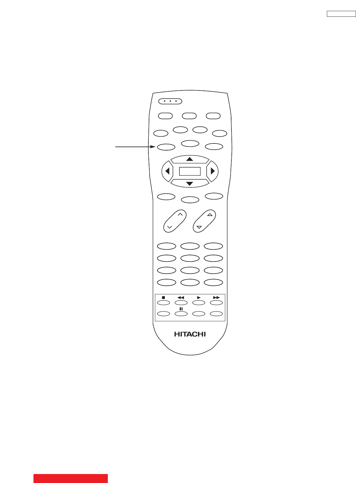
REMOTE CONTROL . . . . . . . . . . . . . . . . . . . . . . . . . . . . . . . . . . . . . . . . . . . . . . . . . . . .17
CUSTOMIZED PICTURE AND SOUND ADJUSTMENTS . . . . . . . . . . . . . . . . . . . . . . .18
REAR PANEL CONNECTION . . . . . . . . . . . . . . . . . . . . . . . . . . . . . . . . . . . . . . . . . . . . .23
DISPLAY PICTURE FORMATS . . . . . . . . . . . . . . . . . . . . . . . . . . . . . . . . . . . . . . . . . . . .24
SERVICE ADJUSTMENTS . . . . . . . . . . . . . . . . . . . . . . . . . . . . . . . . . . . . . . . . . . . . . . .25
TROUBLESHOOTING FLOW CHART . . . . . . . . . . . . . . . . . . . . . . . . . . . . . . . . . . . . . .69
WAVEFORMS . . . . . . . . . . . . . . . . . . . . . . . . . . . . . . . . . . . . . . . . . . . . . . . . . . . . . . . . .73
DC VOLTAGE TABLES . . . . . . . . . . . . . . . . . . . . . . . . . . . . . . . . . . . . . . . . . . . . . . . . . . .84
PROTECTION CIRCUIT BLOCK DIAGRAM . . . . . . . . . . . . . . . . . . . . . . . . . . . . . . . . . .98
CIRCUIT SCHEMATIC DIAGRAM . . . . . . . . . . . . . . . . . . . . . . . . . . . . . . . . . . . . . . . . . .99
PRINTED CIRCUIT BOARDS . . . . . . . . . . . . . . . . . . . . . . . . . . . . . . . . . . . . . . . . . . . .111
BLOCK DIAGRAM . . . . . . . . . . . . . . . . . . . . . . . . . . . . . . . . . . . . . . . . . . . . . . . . . . . . .124
WIRING DIAGRAM . . . . . . . . . . . . . . . . . . . . . . . . . . . . . . . . . . . . . . . . . . . . . . . . . . . .125
FINAL WIRING DRAWING . . . . . . . . . . . . . . . . . . . . . . . . . . . . . . . . . . . . . . . . . . . . . .126
EXPLODED VIEW . . . . . . . . . . . . . . . . . . . . . . . . . . . . . . . . . . . . . . . . . . . . . . . . . . . . .129
EXPLODED VIEW PARTS LIST . . . . . . . . . . . . . . . . . . . . . . . . . . . . . . . . . . . . . . . . . .131
REPLACEMENT PARTS LIST . . . . . . . . . . . . . . . . . . . . . . . . . . . . . . . . . . . . . . . . . . . .132
DISASSEMBLY INSTRUCTIONS . . . . . . . . . . . . . . . . . . . . . . . . . . . . . . . . . . . . . . . . .155
QUICK REFERENCE PARTS LIST (IC & UNIT) . . . . . . . . . . . . . . . . . . . . . . . . . . . . . .160
CAUTION: These servicing instructions are for use by qualified service personnel only. To reduce the risk of
electric shock do not perform any servicing other than that contained in the operating instructions
unless you are qualified to do so. Before servicing this chassis, it is important that the service
technician read the “IMPORTANT SAFETY INSTRUCTIONS” in this service manual.
SAFETY NOTICE
USE ISOLATION TRANSFORMER WHEN SERVICING
Components having special safety characteristics are identified by a on the schematics and on the parts list in this
Service Data and its supplements and bulletins. Before servicing the chassis, it is important that the service technician
read and follow the “Important Safety Instructions” in this Service Manual.
PROJECTION COLOR TELEVISION
SPECIFICATIONS AND PARTS ARE SUBJECT TO CHANGE FOR IMPROVEMENT
!
TO GO TO A CHAPTER, CLICK ON ITS HEADING BELOW
updated 9/22/05
version 0193.2
updated 11/11/05

2
DP33KA/B
Components having special safety characteristics are identified by a on the schematics and on the parts list in this service
manual and its supplements and bulletins. Before servicing this chassis, it is important that the service technician read and
follow the “Important Safety Instructions” in this Service Manual.
For continued X-Radiation protection, replace picture tube with original type or Hitachi approved equivalent type.
This Service Manual is intended for qualified service technicians; it is not meant for the casual do-it-yourselfer. Qualified
technicians have the necessary test equipment and tools, and have been trained to properly and safely repair complex
products such as those covered by this manual.
Improperly performed repairs can adversely affect the safety and reliability of the product and may void warranty. If you
are not qualified to perform the repair of this product properly and safely, you should not risk trying to do so and refer the
repair to a qualified service technician.
WARNING
Lead in solder used in this product is listed by the California Health and Welfare agency as a known reproductive toxicant which
may cause birth defects or other reproductive harm (California Health and Safety Code, Section 25249.5).
When servicing or handling circuit boards and other components which contain lead in solder, avoid unprotected skin contact
with solder.Also, when soldering do not inhale any smoke or fumes produced.
This television receiver provides display of television closed captioning in accordance with section 15.119 of the FCC rules.
FEDERAL COMMUNICATIONS COMMISSION NOTICE
This equipment has been tested and found to comply with the limits for a Class B digital device, pursuant to Part 15 of the
FCC Rules.These limits are designed to provide reasonable protection against harmful interference in a residential
installation. This equipment generates, uses, and can radiate radio frequency energy and, if not installed and used in
accordance with the instructions, may cause harmful interference to radio communications. However, there is no guarantee
that interference will not occur in a particular installation. If this equipment does cause harmful interference to radio or
television reception, which can be determined by turning the equipment off and on, the user is encouraged to try to correct
the interference by one or more of the following measures:
• Reorient or relocate the receiving antenna.
• Increase the separation between the equipment and the receiver.
• Connect the equipment into an outlet on a circuit different from that to which the receiver is connected.
• Consult the dealer or an experienced radio/television technician for help.
IMPORTANT SAFETY INSTRUCTIONS
USE ISOLATION TRANSFORMER WHEN SERVICING
!
TABLE OF CONTENTS
3
DP33KA/B
IMPORTANT SAFETY INSTRUCTION
1. Before returning an instrument to the customer, always
make a safety check of the entire instrument, including
but not limited to the following items.
a. Be sure that no built-in protective devices are
defective and/or have been deleted during servicing.
(1) Protective shields are provided on this chassis to
protect both the technician and the customer.
Correctly replace all missing protective shields,
including any removed for servicing convenience. (2)
When reinstalling the chassis and/or other assembly
in the cabinet, be sure to put back in place all
protective devices, including but not limited to,
nonmetallic control knobs, insulating fishpaper,
adjustment and compartment covers/shields, and
isolation resistor/capacitor networks. Do not operate
this instrument or permit it to be operated without
all protective devices correctly installed and
functioning. Servicers who defeat safety features
or fail to perform safety checks may be liable for
any resulting damage.
b. Be sure that there are no cabinet openings through
which an adult or child might be able to insert their
fingers and contact a hazardous voltage. Such
openings include, but are not limited to (1) spacing
between the picture tube and cabinet mask, (2)
excessively wide cabinet ventilation slots, and (3) an
improperly fitted and/or incorrectly secured cabinet
back cover.
c. Antenna Cold Check– With the instrument AC plug
removed from any AC source, connect an electrical
jumper across the two AC plug prongs. Place the
instrument AC switch in the on position. Connect one
lead of an ohmmeter to the AC plug prongs tied
together and touch the other ohmmeter lead in turn to
each tuner antenna input, exposed terminal screw
and, if applicable, to the coaxial connector. If the
measured resistance is less than 1.0 megohms or
greater than 5.2 megohms, an abnormality exists that
must be corrected before the instrument is returned to
the customer.Repeat this test with the instrument AC
switch in the off position.
d.
Leakage Current Hot Check -
Plug the AC line cord
directly into a 120V AC 60Hz outlet (do not use an
isolated transformer for this check). Turn the A C
power ON. Using a Leakage Current Tester (Simpson’s
Model 228 or equivalent), measure for current from all
exposed metal parts of the cabinet (antennas,
screwheads, overlays, control shafts, etc.)
particularly any exposed metal
part
having a return path to the chassis or to a
known earth ground (water pipe, conduit, etc.). Any
current measured must not exceed 0.5 MIU.
e. High Voltage – This receiver is provided with a
hold down circuit for clearly indicating that voltage has
increased in excess of a predetermined value.
Comply will all notes described in this Service Manual
regarding this hold down circuit when servicing, so
that this hold down circuit may correctly be operated.
f. Service Warning – With maximum contrast, operating
high voltage in this receiver is lower than 30.5 kV. In
case any component having influence on high voltage
is replaced, confirm that the high voltage with
maximum contrast is lower than 30.5 kV.
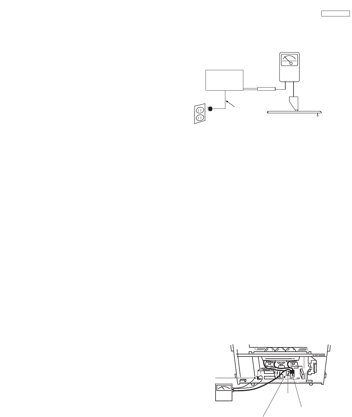
To measure H.V. use a high impedance H.V. meter.
Connect (-) to chassis earth and (+) to the CRT anode
button. (See the following connection diagram.)
Note: Turn power switch off without fail before the
connection to the anode button is made.
Chassis
ground
High Impedance
H.V. meter
Deflection P.W.B.
FBT
(TH01)
High voltage
connector
+-
LEAKAGE
CURRENT
TESTER
DEVICE
UNDER
TEST
TEST ALL
EXPOSED
METAL
SURFACES
2-WIRE CORD
(READING
SHOULD NOT
BE ABOVE
0.5 mA)
EARTH
GROUND
ALSO TEST WITH
PLUG REVERSED (USING
AC ADAPTER PLUS
AS REQUIRED)
AC LEAKAGE TEST
ANY MEASUREMENTS NOT WITHIN THE LIMITS
OUTLINED ABOVE ARE INDICATIVE OF A POTENTIAL
SHOCK HAZARD AND MUST BE CORRECTED BEFORE
RETURNING THE RECEIVER TO THE CUSTOMER.
(READING
SHOULD NOT
BE ABOVE
0.5 MIU)
AC Leakage Test
4
DP33KA/B
g. X-radiation – TUBE: The primary source of X-
radiation in this receiver is the picture tube. The tube
utilized for the above mentioned function in this
chassis is specially constructed to limit X-radiation
emissions.
For continued X-radiation protection, the replacement
tube must be the same type as the original, Hitachi
approved type.
When troubleshooting and making test measure-
ments in a receiver with a problem of excessive high
voltage, avoid being unnecessarily close to the picture
tube and the high voltage component.
Do not operate the chassis longer than is necessary
to locate the cause of excessive voltage.
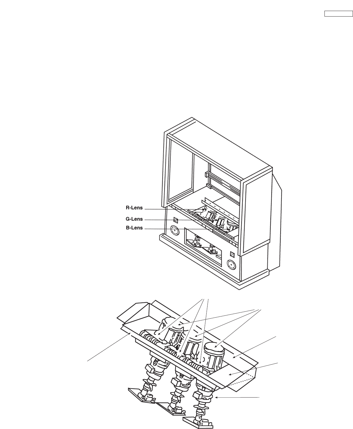
h. X-radiation Shield –
1. This receiver is provided with X-ray shield plates
for protection against X-radiation. Do not remove
X-ray shield plates A, B, or C shown in Fig. 1
unnecessarily, when troubleshooting and/or
making test measurements.
2. To prevent X-radiation, after replacement of
picture tube and lens, confirm these components
to be fixed correctly to bracket and cabinet, and
not to be taken off easily.
Shield Plate A
Glass Lens for Shielding
Shield Plate B
Shield Plate C
Shield Plate D
Detailing X-radiation shield
Shield Plate C
Fig. 1. Installation of shield lens, shield cover and shield plates (oblique view).
IMPORTANT SAFETY INSTRUCTIONS

5
DP33KA/B
2. Read and comply with all caution and safety-related
notes on or inside the receiver cabinet, on the receiver
chassis, or on the picture tube.
3. Design Alteration Warning – Do not alter or add to
the mechanical or electrical design of this TV receiver.
Design alterations and additions including but not
limited to circuit modifications and the addition of
items such as auxiliary audio and/or video output
connectors, might alter the safety characteristics of
this receiver and create a hazard to the user. Any
design alterations or additions may void the
manufacturer’s warranty and may make you, the
servicer, responsible for personal injury or property
damage resulting therefrom.
4. Picture Tube Implosion Protection Warning – The
picture tube in this receiver employs integral implosion
protection. For continued implosion protection,
replace the picture tube only with one of the same
type number. Do not remove, install, or otherwise
handle the picture tube in any manner without first
putting on shatterproof goggles equipped with side
shields. People not so equipped must be kept safely
away while picture tubes are handled. Keep the
picture tube away from your body. Do not handle the
picture tube by its neck.
5. Hot Chassis Warning – a. Some TV receiver chassis
are electrically connected directly to one conductor of
the AC power cord and may be safely serviced without
an isolation transformer only if the AC power plug is
inserted so that the chassis is connected to the
ground side of the AC power source. Confirm that the
AC power plug is inserted correctly with an AC
voltmeter by measuring between the chassis and a
known earth ground. If a voltage reading in excess of
1.0V is obtained, remove and reinsert the AC power
plug in the opposite polarity and again measure the
voltage potential between the chassis and a known
earth ground. b. Some TV receiver chassis normally
have 85V AC (RMS) between chassis and earth
ground regardless of the AC plug polarity. These
chassis can be safely serviced only with an isolation
transformer inserted in the power line between the
receiver and the AC power source, for both personnel
and test equipment protection. c. Some TV receiver
chassis have a secondary ground system in addition
to the main chassis ground. This secondary ground
system is not isolated from the AC power line.The two
ground systems are electrically separated by
insulating material that must not be defeated or
altered.
6. Observe original lead dress. Take extra care to assure
correct lead dress in the following areas: a. near sharp
edges, b. near thermally hot parts – be sure that leads
and components do not touch thermally hot parts, c.
the AC supply, d. high voltage and e. antenna wiring.
Always inspect in all areas for pinched, out-of-plate, or
frayed wiring. Do not change spacing between
components and the printed circuit board. Check AC
power cord for damage.
7. Components, parts, and/or wiring that appear to have
overheated or are otherwise damaged should be
replaced with components, parts, or wiring that meet
original specifications. Additionally, determine the
cause of overheating and/or damage and, if
necessary, take corrective action to remove any
potential safety hazard.
8. PRODUCT SAFETY NOTICE – Many TV electrical
and mechanical parts have special safety-related
characteristics some of which are often not evident
from visual inspection, nor can the protection they
give necessarily be obtained by replacing them with
components rated for higher voltage, wattage, etc.
Parts that have special safety characteristics are
identified in Hitachi service data by shading on
schematics and by a in the parts list. Use of
substitute replacement that does not have the same
safety characteristics as the recommended replace-
ment part in Hitachi service data parts list might
create shock, fire, and/or other hazards. Product
safety is under review continuously and new
instructions are issued whenever appropriate. For the
latest information, always consult the appropriate
current Hitachi service literature. A subscription to, or
additional copies of service literature may be obtained
at a nominal charge from Hitachi.
!
IMPORTANT SAFETY INSTRUCTIONS

6
DP33KA/B
CAUTION: Before servicing instruments covered by this
service data and its supplements and addenda, read and
follow the “Important Safety Instructions” on page 3 of this
publication.
NOTE: If unforeseen circumstances create conflict between
the following servicing precautions and any of the safety
precautions on page 3 of this publication, always follow the
safety precautions. Remember: Safety First.
General Servicing Guidelines
1. Always unplug the instrument AC power cord from the AC
power source before:
a. Removing or reinstalling any component, circuit
board, module, or any other instrument assembly.
b. Disconnecting or reconnecting any instrument
electrical plug or other electrical connection.
c. Connecting a test substitute in parallel with an
electrolytic capacitor in the instrument.
CAUTION: A wrong part substitution or incorrect
polarity installation of electrolytic
capacitors may result in an explosion
hazard.
d. Discharging the picture tube anode.
2. Test high voltage only by measuring it with an appropriate
high voltage meter or other voltage measuring device
(DVM, FETVOM, etc.) equipped with a suitable high
voltage probe. Do not test high voltage by “drawing an
arc.” The H.V. Distribution Box has an internal 400MΩ
resistor (bleeder resistor) connected from the high
voltage to ground. After power is removed from the
instrument the high voltage will discharge through the
high voltage bleeder resistor. If the tubes have high
voltage after power is removed, then the bleeder resistor
is defective or the bleeder ground is disconnected.
3. Discharge the picture tube’s anode at any of the R, G, or
B outputs on the H.V. Distribution Box only by (a) first
connecting one end of an insulated clip lead to the
degaussing or kine aquadag grounding system shield at
the point where the picture tube socket ground lead is
connected, and then (b) touch the other end of the
insulated clip lead to the picture tube high voltage
distribution box R, G, or B output, using an insulated
handle to avoid personal contact with high voltage.
4. Do not spray chemicals on or near this instrument or any
of its assemblies.
5. Unless specified otherwise in these service data, clean
electrical contracts by applying the following mixture to
the contacts with a pipe cleaner, cotton-tipped stick or
comparable nonabrasive applicator: 10% (by volume)
Acetone and 90% (by volume) isopropyl alcohol (90%-
99% strength).
CAUTION: This is a flammable mixture. Unless
specified otherwise in these service data,
lubrication of contacts is not required.
6. Do not defeat any plug/socket B+ voltage interlocks with
which instruments covered by this service data might be
equipped.
7. Do not apply AC power to this instrument and/or any of its
electrical assemblies unless all solid-state device heat-
sinks are correctly installed.
8. Always connect the test instrument ground lead to the
appropriate instrument chassis ground before connecting
the test instrument positive lead. Always remove the test
instrument ground lead last.
9. Use with this instrument only the test fixtures specified in
this service data.
CAUTION: Do not connect the test fixture ground strap
to any heatsink in this instrument.
Electrostatically Sensitive (ES) Devices
Some semiconductor (solid state) devices can be damaged
easily by static electricity. Such components commonly are
called Electrostatically Sensitive (ES) Devices. Examples of
typical ES devices are integrated circuits and some field-
effect transistors and semiconductor “chip” components. The
following techniques should be used to help reduce the
incidence of component damage caused by static electricity.
1. Immediately before handling any semiconductor
component or semiconductor-equipped assembly, drain
off any electrostatic charge on your body by touching a
known earth ground. Alternatively, obtain and wear a
commercially available discharging wrist strap device,
which should be removed for potential shock reasons
prior to applying power to the unit under test.
2. After removing an electrical assembly equipped with ES
devices, place the assembly on a conductive surface
such as aluminum foil, to prevent electrostatic charge
buildup or exposure of the assembly.
3. Use only a grounded-tip soldering iron to solder or
desolder ES devices.
4. Use only can anti-static type solder removal device. Some
solder removal devices not classified as “anti-static” can
generate electrical charges sufficient to damage ES
device.
5. Do not use freon-propelled chemicals. These can
generate electrical charges sufficient to damage ES
devices.
6. Do not remove a replacement ES device from its
protective package until immediately before you are ready
to install it. (Most replacement ES devices are packaged
with leads electrically shorted together by conductive
foam, aluminum foil or comparable conductive material.)
7. Immediately before removing the protective material from
the leads of a replacement ES device, touch the
protective material to the chassis or circuit assembly into
which the device will be installed.
CAUTION: Be sure no power is applied to the chassis or
circuit, and observe all other safety
precautions.
8. Minimize bodily motions when handling unpackaged
replacement ES devices. (Otherwise harmless motion
such as the brushing together of your clothes fabric or the
lifting of your foot from a carpeted floor can generate
static electricity sufficient to damage an ES device.)
SERVICING PRECAUTIONS
TABLE OF CONTENTS
7
DP33KA/B
General Soldering Guidelines
1. Use a grounded-tip, low-wattage soldering iron and
appropriate tip size and shape that will maintain tip
temperature within the range 500°F to 600°F.
2. Use an appropriate lead free solder (see page 10). Lead
solder can be used, but there is a possibility of failure due
to insufficient strength of the solder.
3. Keep the soldering iron tip clean and well-tinned.
4. Thoroughly clean the surfaces to be soldered. Use a
small wire-bristle (0.5 inch or 1.25 cm) brush with a metal
handle. Do not use freon-propelled spray-on cleaners.
5. Use the following desoldering technique.
a. Allow the soldering iron tip to reach normal
temperature (500°F to 600°F).
b. Heat the component lead until the solder melts. Quickly
draw away the melted solder with an anti-static,
suction-type solder removal device or with solder
braid.
CAUTION: Work quickly to avoid overheating the
circuit board printed foil.
6. Use the following soldering technique.
a. Allow the soldering iron tip to reach normal
temperature (500°F to 600°F).
b. First, hold the soldering iron tip and solder strand
against the component lead until the solder melts.
c. Quickly move the soldering iron tip to the junction of
the component lead and the printed circuit foil, and
hold it there only until the solder flows onto and
around both the component lead and the foil.
CAUTION: Work quickly to avoid overheating the
circuit board printed foil or components.
d. Closely inspect the solder area and remove any excess
or splashed solder with a small wire-bristle brush.
Removal
1. Desolder and straighten each IC lead in one operation by
gently prying up on the lead with the soldering iron tip as
the solder melts.
2. Draw away the melted solder with an anti-static suction-
type solder removal device (or with solder braid) before
removing the IC.
Replacement
1. Carefully insert the replacement IC in the circuit board.
2. Carefully bend each IC lead against the circuit foil pad
and solder it.
3. Clean the soldered areas with a small wire-bristle brush.
(It is not necessary to reapply acrylic coating to areas.)
“Small-signal” Discrete Transistor Removal/Replacement
1. Remove the defective transistor by clipping its leads as
close as possible to the component body.
2. Bend into a “U” shape the end of each of three leads
remaining on the circuit board.
3. Bend into a “U” shape the replacement transistor leads.
4. Connect to replacement transistor leads to the
corresponding leads extending from the circuit board and
crimp the “U” with long nose pliers to insure metal to
metal contact, then solder each connection.
Power Output Transistor Devices Removal/Replacements
1. Heat and remove all solder from around the transistor
leads.
2. Remove the heatsink mounting screw (if so equipped).
3. Carefully remove the transistor from the circuit board.
4. Insert new transistor in circuit board.
5. Solder each transistor lead, and clip off excess lead.
6. Replace heatsink.
Diode Removal/Replacement
1. Remove defective diode by clipping its leads as close as
possible to diode body.
2. Bend the two remaining leads perpendicularly to the
circuit board.
3. Observing diode polarity, wrap each lead of the new
diode around the corresponding lead on the circuit board.
4. Securely crimp each connection and solder it.
5. Inspect (on the circuit board copper side) the solder joints
of the two “original leads”. If they are not shiny, reheat
them and, if necessary, apply additional solder.
Use Solding Iron to Pry Leads
IC Removal/Replacement
Some Hitachi unitized chassis circuit boards have slotted
holes (oblong) through which the IC leads are inserted and
then bent flat against the circuit foil. When holes are the
slotted type, the following technique should be used to
remove and replace the IC. When working with boards using
the familiar round hole, use the standard technique as
outlined in paragraphs 5 and 6 above.
SERVICING PRECAUTIONS
8
DP33KA/B
Fuses and Conventional Resistor Removal/Replacement
1. Clip each fuse or resistor lead at top of circuit board
hollow stake.
2. Securely crimp leads of replacement component around
stake 1/8 inch from top.
3. Solder the connections.
CAUTION: Maintain original spacing between the
replaced component and adjacent
components and the circuit board, to
prevent excessive component
temperatures.
Circuit Board Foil Repair
Excessive heat applied to the copper foil of any printed
circuit board will weaken the adhesive that bonds the foil to
the circuit board, causing the foil to separate from, or “lift-off,”
the board. The following guidelines and procedures should
be followed whenever this condition is encountered.
In Critical Copper Pattern Areas
High component/copper pattern density and/or special
voltage/current characteristics make the spacing and
integrity of copper pattern in some circuit board areas more
critical than in others. The circuit foil in these areas is
designated as Critical Copper Pattern. Because Critical
Copper Pattern requires special soldering techniques to
ensure the maintenance of reliability and safety standards,
contact your Hitachi personnel.
At IC Connections
To repair defective copper pattern at IC connections, use the
following procedure to install a jumper wire on the copper
pattern side of the circuit board. (Use this technique only on
IC connections.)
1. Carefully remove the damaged copper pattern with a
sharp knife. (Remove only as much copper as absolutely
necessary.)
2. Carefully scratch away the solder resist and acrylic
coating (if used) from the end of the remaining copper
pattern.
3. Bend a small “U” in one end of a small-gauge jumper wire
and carefully crimp it around the IC pin. Solder the IC
connection.
4. Route the jumper wire along the path of the cut-away
copper pattern and let it overlap the previously scraped
end of the good copper pattern. Solder the overlapped
area, and clip off any excess jumper wire.
1. Remove the defective copper pattern with a sharp knife.
Remove at least 1/4 inch of copper, to ensure hazardous
condition will not exist if the jumper wire opens.
2. Trace along the copper pattern from both wire sides of the
pattern break and locate the nearest component directly
connected to the affected copper pattern.
3. Connect insulated 20-gauge jumper wire from the
nearest component on one side of the pattern break to
the lead of the nearest component on the other side.
Carefully crimp and solder the connections.
CAUTION: Be sure the insulated jumper wire is
dressed so that it does not touch
components or sharp edges.
Frequency Synthesis (FS) Tuning Systems
1. Always unplug the instrument AC power cord before
disconnecting or reconnecting FS tuning system cables
and before removing or inserting FS tuning system
modules.
2. The FS tuner must never be disconnected from the FS
tuning control module while power is applied to the
instrument.
3. When troubleshooting intermittent problems that might be
caused by defective cable connection(s) to the FS tuning
system, remove the instrument AC power as soon as the
defective connector is found and finish confirming the bad
connection with a continuity test. This procedure will
reduce the probability of electrical overstress of the FS
system semi-conductor components.
CRIMP AND
SOLDER
BARE JUMPER
WIRE
Install Jumper Wire and Solder
DEFECTIVE
COPPER
REMOVED
Insulated Jumper Wire
At Other Connections
Use the following technique to repair defective copper
pattern at connections other than IC Pins. This technique
involves the installation of a jumper wire on the component
side of the circuit board.
SERVICING PRECAUTIONS
9
DP33KA/B
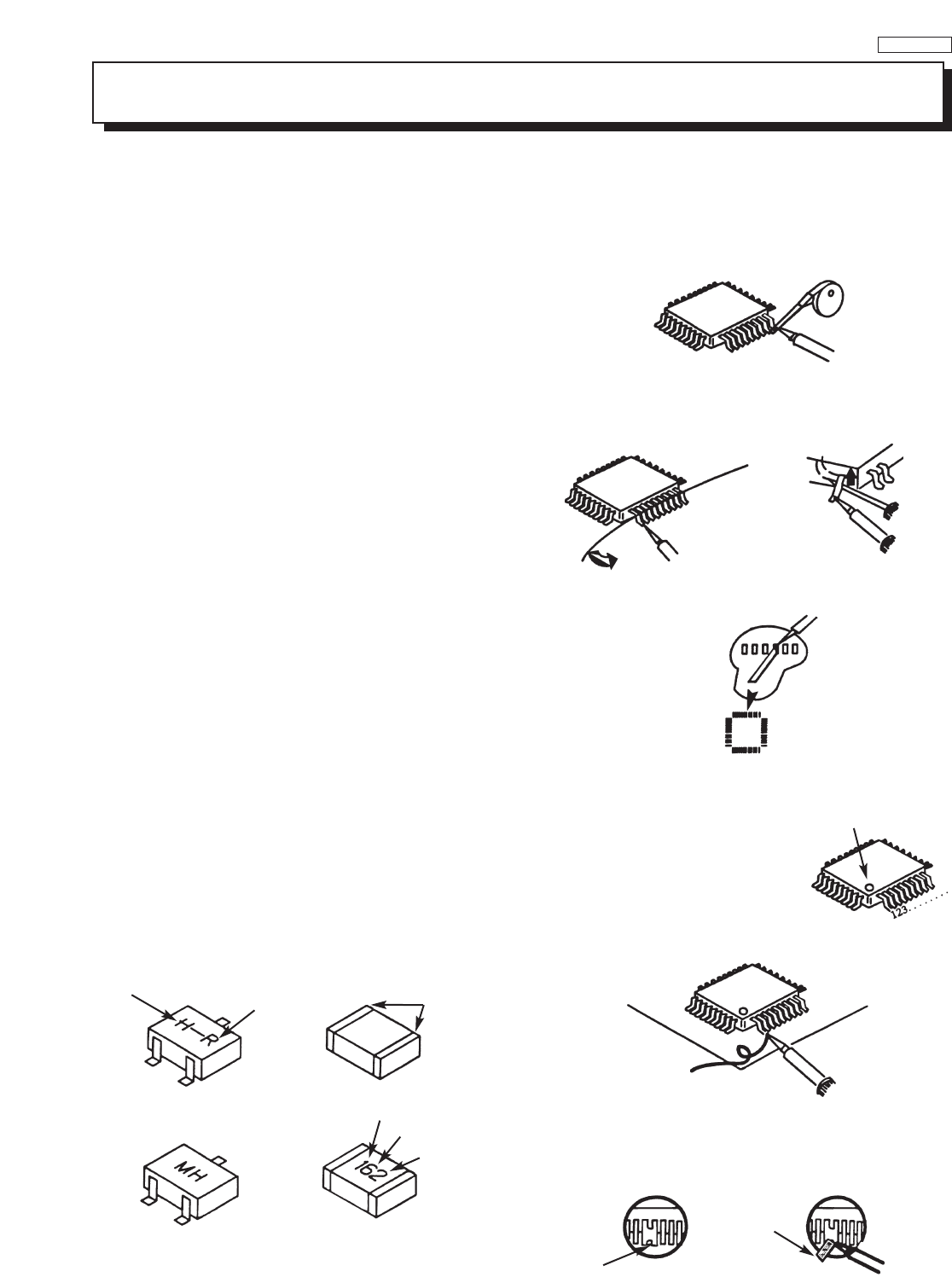
Leadless Chip Components
(surface mount)
Chip components must be replaced with identical
chips due to critical foil track spacing. There are no
holes in the board to mount standard transistors or
diodes. Some chip capacitor or resistor board solder
pads may have holes through the board, however the
hole diameter limits standard resistor replacement to
1/8 watt. Standard capacitors may also be limited for
the same reason. It is recommended that identical
chip components be used. .
Chip resistors have a three digit numerical resistance
code -1st and 2nd significant digits and a multiplier.
Example: 162 = 1600 or 1.6KΩresistor, 0 = 0Ω
(jumper).
Chip capacitors generally do not have the value
indicated on the capacitor.The color of the component
indicates the general range of the capacitance.
Chip transistors are identified by a two letter code.The
first letter indicates the type and the second letter, the
grade of transistor.
Chip diodes have a two letter identification code as per
the code chart and are a dual diode pack with either
common anode or common cathode. Check the parts
list for correct diode number.
Component Removal
1. Use solder wick to remove solder from component
end caps or terminals.
2. Without pulling up, carefully twist the component
with tweezers to break the adhesive.
3. Do not reuse removed leadless or chip
components since they are subject to stress
fracture during removal .
Chip Component Installation
1. Put a small amount of solder on the board
soldering pads.
2. Hold the chip component against the soldering
pads with tweezers or with a miniature alligator
clip and apply heat to the pad area with a 30 watt
iron until solder flows. Do not apply heat for more
than 3 seconds
How to Replace Flat-lC
—Required Tools—
• Soldering iron • iron wire or small awl
•De-solder braids • Magnifier
1. Remove the solder from all of the pins of a Flat-lC
by using a de-solder braid.
2. Put the iron wire under the pins of the Flat-lC and
pull it in the direction indicated while heating the
pins using a soldering iron. A small awl can be
used instead of the iron wire.
3. Remove the solder from all of the pads of the
Fiat-lC by using
a de-solder braid.
4. Position the new Flat-lC in place (apply the pins of
the Flat-lC to the soldering pads where the pins
need to be soldered). Properly
determine the positions of the
soldering pads and pins by
correctly aligning the polarity
symbol.
6. Check with a magnifier for solder bridge between
the pins or for dry joint between pins and soldering
pads.To remove a solder bridge, use a de-solder braid
as shown in the figure below.
NOTE: These components are affixed with glue. Be careful not to break or damage any foil under the
component or at the pins of the ICs when removing. Usually applying heat to the component for a short
time while twisting with tweezers will break the component loose.
Chip Components
TYPE
GRADE
C
B
E
SOLDER
CAPS
TRANSISTOR CAPACITOR
1ST DIGIT
2ND DIGIT
MULTIPLIER
= 1600 = 1.6K
ANODES
MH DIODE RESISTOR
SOLDER CAPS
COMMON CATHODE
Flat-IC De-Solder
Braid
Soldering
Iron
Soldering
Iron
Soldering
Iron
Soldering
Iron
Soldering
Iron
Soldering
Iron
De-Solder
Braid
Flat-IC
Solder
Bridge
Solder
De-Solder
Braid
Iron
Wire
Pull
Awl
Polarity Symbol
5. Solder all pins to the soldering pads using a fine
tipped soldering iron.
SERVICING PRECAUTIONS
10
DP33KA/B
Information for service about lead-free solder introduction
Hitachi introduced lead-free solder to conserve the "Earth Environment".
Please refer to the following before servicing.
(1) Characteristic of lead-free solder
Melting point of lead free solder is 40-50oC higher than solder containing lead.
(2) Solder for service
Following composition is reccomended.
" Sn - 3.0Ag - 0.5Cu " , or " Sn - 0.7 Cu "
Lead solder can be used, but there is a possibility of failure due to insufficient strength of the solder.
Caution when using solder containing lead.
Please remove previous solder as much as possible from the soldering point.
When soldering, please perfectly melt the lead-free solder to mix well with the previous solder.
(3) Soldering iron for lead-free solder.
Melting point of lead-free solder is higher than solder containing lead.
Use of a soldering tool "with temperature control" and "with much thermal capacitance" is reccomended.
(Reccomended temperature control : 320oC - 450oC)
Reccomended temperature
PWB with chip parts 320oC +/- 30oC
PWB without chip parts 380oC +/- 30oC
Chassis, metal, shield etc. 420oC +/- 30oC
(4) Identification of lead-free PWB
2003 models >> not applied
2003 models >> mixed
2004 models >> lead-free solder is intoduced
On lead-free PWB, "F" is added at the end of stamp on PWB. (e.g. DP33WF)
11
DP33KA/B
High Voltage limiter circuit operation check.
1. Turn off TV and connect jig as shown in Figure 2. Adjust
jig fully counter-clockwise for minimum resistance.
2. Set the AC input to 120V AC and turn on TV.
3. Confirm test pattern on CRT is a usable picture, then
slowly adjust jig until the picture disappears and TV shuts
down.
4. When the limiter circuit is operating properly, High
Voltage will be less than 31 kV at 1.72mA when TV shuts
down.
5. Turn off set immediately after checking circuit operation.
6. Unplug set for one minute to reset shutdown circuit.
Remove jig and voltmeter.
TECHNICAL CAUTIONS
(TH01)
AC CORD POLARITY
This check is based on the UL standard. Use the jigs
specified by the production technology section. The GND
side (wider blade) of the AC power cord should be
connected to K9Y1
TABLE OF CONTENTS
D.C.U
RH19
RH17
Fig. 2. Power/Deflection P.W.B
Remove RH19 and connect 50KΩ VR jig as shown.
TH02
FBT
50KΩ VR
50KΩ VR 33KΩ
Resistor
33KΩ
12
DP33KA/B
Models: 46F510/46F500A
Cathode-Ray Tube:
46F510 R=P16LXS00RFA B
46F500A G=P16LXS00HHA B
B=P16LXS00BMB B
Power Input: 120 volts AC, 60 Hz
Power Consumption:
• Stand-By Power
46F510/500A . . . . . . . . . . . . . . . . . . . .0.4W
• Power Consumption (operating)
46F510/500A . . . . . . . . . . . . . . . . . . . .220W
•Power Consumption (maximum)
46F510/500A . . . . . . . . . . . . . . . . . . . .275W
Antenna Impedance: 75 Ohm Unbalanced
VHF / UHF / CATV
Receiving Channel: BAND CH
VHF 2~13
UHF 14~69
EXT. Mid (A-5)~(A-1), 4+
CATV Mid. A~I
CATV Super J~W
CATV Hyper (W+1)~(W+28)
CATV Ultra (W+29)~(W+84)
Intermediate Frequency: Picture l-F Carrier 45.75 MHz
Sound l-F Carrier 41.25 MHz
Color Sub Carrier 42.17 MHz
Video Input: 1.0 ± 0.2 Volt p-p, 75 Ohm
T
ermination
Video Output: 1.0 ± 0.2 Volt p-p, 75 ohm
Termination
Audio Input: 470 mVrms, 47 k Ohm ±10%
Stereo Audio Output: 470 mVrms, 1 k Ohm ± 10%
Audio Output Power:
Front: 24 watts per channel at 10% distortion,
8 ohm Impedance. Max output 30 watts.
Anode Voltage:
DP33KA/B 30.7±0.2kv (1.52±0.2mA)
Brightness: 46”
(white screen) 290cd/m2
Speakers: 46” 2 Woofers - 5 inch (12 cm) round
Dimensions:
46F510 46F500A
• Height (in.) 45 9/16 39 13/16
(mm) 1,157.0 1,010.5
•Width (in.) 44 7/16 44 7/16
(mm) 1,128.0 1,128.0
•Depth (in.) 26 7/16 24 9/16
(mm) 671.5 623.5
• Weight (lbs.) 161 160
(kg) 73 72.5
Circuit Board Assemblies:
C.P.T. (B) P.W.B. IR P.W.B.
C.P
.T.(G) P
.W.B.IR Sub P
.W.B.
C.P.T. (R) P.W.B. Terminal P.W.B.
Power Supply P.W.B. Signal P.W.B.
Control P
.W.B.Def/Convergence P.W.B.
Sensor Distribution P.W.B. DVI P.W.B
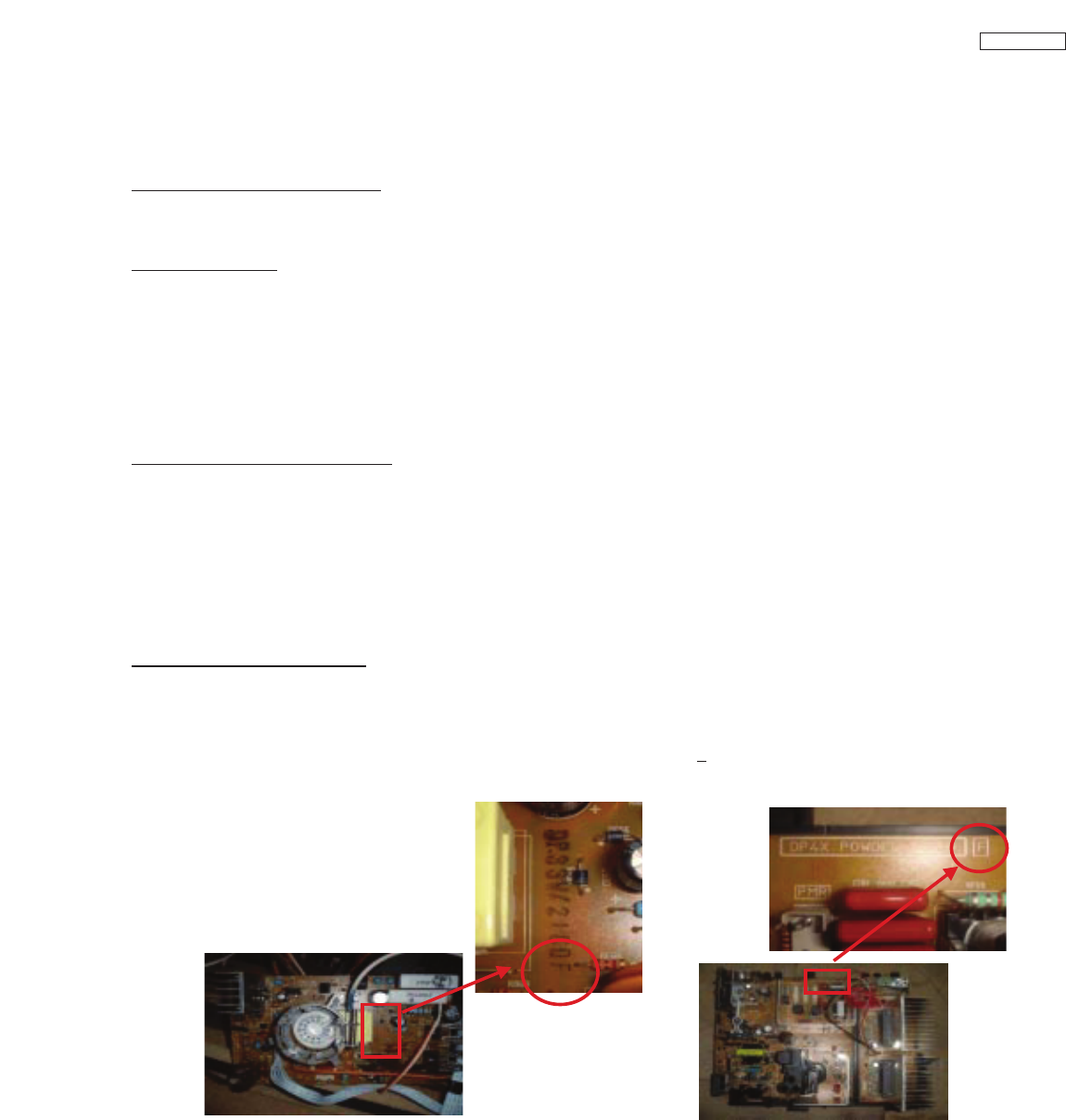
CIRCUIT PROTECTION
CAUTION: Below is an EXAMPLE only. See Replacement Parts List for details. The following symbol near the fuse
indicates fast operation fuse (to be replaced). Fuse ratings appear within the symbol.
125V
10A
F
10 A 125V
Example:
SPECIFICATIONS
“RISK OF FIRE - REPLACE FUSE AS MARKED”
The rating of fuse F901 is 10A - 125V.
Replace with the same type fuse for continued protection
against fire.
TABLE OF CONTENTS
13
DP33KA/B
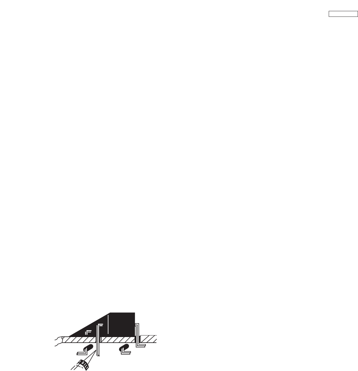
During Insertion
1. Please refer to direction for insertion as shown in Fig. B (L position). Insert connector until “CLICK” sound is heard.
2. Make sure the connector is pressed right in, so that it has a good contact with the spring.
3. Confirm the contact by pulling the connector slightly. (Don’t pull hard because it may damage the connector).
4. Cover the high voltage output by carefully pushing silicon cover onto it. (Don’t turn the connector).
(REMARK)
1. Make sure the silicon cover is
covering the high voltage output.
CAUTIONS WHEN CONNECTING / DISCONNECTING THE HV CONNECTOR
Perform the following when the
HV connector (anode connector)
is removed or inserted for CPT
replacement, etc.
Deflection P.W.B.
Silicon cover
Wing
L Position
L Position
Wing
FBT
Anode
connector
3. Remove the connector slowly
by pulling it away from the
case.
During Removal
1. Roll out silicon cover from FBT’s contact area slowly.
2. While turning the connector about 90 degrees
following the arrow (0 position), push the connector
slightly towards the case. (Fig. A)
Fig. A
Fig. B
Silicon Cover
less than 1mm
PUSH
PUSH
TABLE OF CONTENTS
14
DP33KA/B
GENERAL INFORMATION
46F510
TABLE OF CONTENTS
INPUT 5
S-VIDEO VIDEO
AUDIO
L/MONO REXIT
INPUT
SELECT
MENU
VOL- VOL+ CH- CH+
E
FGH
cf
a
b
d
g
e
CURSOR
MAGIC
FOCUS
e
h
aMENU/SELECT button
This button allows you to enter the MENU, making it possible to set TV features to your preference without using the remote. This
button also serves as the SELECT button when in MENU mode.
bINPUT/EXIT button
Press this button to select the current antenna source, VIDEO: 1, 2, 3, 4, 5 or alternate antenna source. Your selection is shown in
the top right corner of the screen. This button also serves as the EXIT button when in MENU mode.
cCHANNEL selector
Press these buttons until the desired channel appears in the top right corner of the TV screen. These buttons also serve as
the cursor down (H) and up (G) buttons when in MENU mode.
dVOLUME level
Press these buttons for your desired sound level. The volume level will be displayed on the TV screen. These buttons also serve
as the cursor left (F) and right (E) buttons when in MENU mode.
ePOWER button/POWER LED
Press this button to turn the TV on or off. This LED light is ON during normal operation.
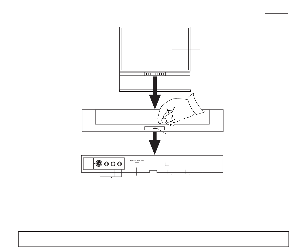
fMAGIC FOCUS
Use this button to automatically adjust your picture quality to optimum performance. The Magic Focus button will not work when
adjustment mode is set to manual.
gFRONT INPUT JACKS (INPUT 5)
Use these audio/video jacks for a quick hook-up from a camcorder or VCR to instantly view your favorite show or new recording.
Press the INPUT button until VIDEO: 5 appears in the top right corner of the TV screen. If you have mono sound, insert the audio
cable into the left audio jack.
hIR RECEIVER Sensor
When using the remote control, point it towards the IR receiver for best response.
NOTES: Your remote control does not have an INPUT button. To change to video inputs, press VID1~VID5 buttons depending
on your choice.
15
DP33KA/B
GENERAL INFORMATION
46F500A
INPUT 5
S-VIDEO VIDEO -AUDIO-
L/MONO R
EXIT
INPUT
SELECT
MENU
VOL- VOL+ CH- CH+
EF G
H
c
fa
b
d
g
POWER
PULL
e
h
aMENU/SELECT button
This button allows you to enter the MENU, making it possible to set TV features to your preference without using the remote. This
button also serves as the SELECT button when in MENU mode.
bINPUT/EXIT button
Press this button to select the current antenna source, VIDEO: 1, 2, 3, 4, 5 or alternate antenna source. Your selection is shown in
the top right corner of the screen. This button also serves as the EXIT button when in MENU mode.
cCHANNEL selector
Press these buttons until the desired channel appears in the top right corner of the TV screen. These buttons also serve as
the cursor down (H) and up (G) buttons when in MENU mode.
dVOLUME level
Press these buttons for your desired sound level. The volume level will be displayed on the TV screen. These buttons also serve
as the cursor left (F) and right (E) buttons when in MENU mode.
ePOWER button
Press this button to turn the TV on or off.
fMAGIC FOCUS
Use this button to automatically adjust your picture quality to optimum performance. The Magic Focus button will not work when
adjustment mode is set to manual.
gFRONT INPUT JACKS (INPUT 5)
Use these audio/video jacks for a quick hook-up from a camcorder or VCR to instantly view your favorite show or new recording.
Press the INPUT button until VIDEO: 5 appears in the top right corner of the TV screen. If you have mono sound, insert the audio
cable into the left audio jack.
hIR RECEIVER
The screen area acts as the IR receiver (remote sensor) of the TV. When using the remote control, point it towards the screen for
best response.
NOTES: Your remote control does not have an INPUT button. To change to video inputs, press VID1~VID5 buttons depending
on your choice.
16
DP33KA/B
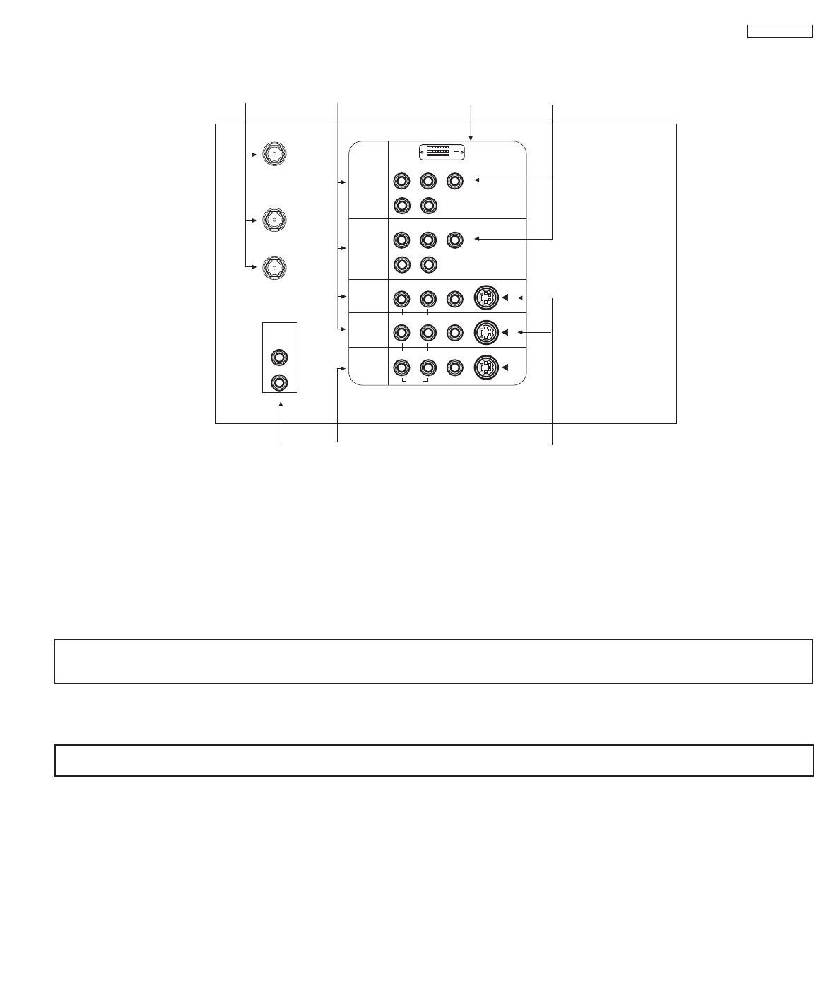
REAR PANEL JACKS
aAntenna Input/Output
The remote control allows you to switch between two separate 75-Ohm RF antenna inputs, ANT A and ANT B. ANT A input can
be displayed as a main picture or sub-picture.ANT B can only be displayed as a main picture. (ANT B cannot be displayed as a
sub-picture.) The antenna output labeled “TO CONVERTER” allows the ANT A connection to pass directly to a different source
such as a cable box, only when ANT B is displayed as a main picture.
bAudio/Video Inputs 1, 2, 3 and 4
The VID1~VID4 buttons will select each video source each time they are pressed. Use the audio and video inputs to connect
external devices, such as VCRs, camcorders, laserdisc players, DVD players etc. (If you have mono sound, insert the audio cable
into the left audio jack.)
cMONITOR OUT
These jacks provide fixed audio and video signals which are used for recording. Use the S-VIDEO Output for high quality video
output.
dAUDIO TO HI-FI Output
These jacks provide variable audio output to a separate stereo amplifier. With this connection, the audio to the stereo can be
controlled by the television’s main volume.
eS-VIDEO Inputs 3 and 4
Inputs 3 and 4 provide S-VIDEO (Super Video) jacks for connecting equipment with S-VIDEO output capability.
NOTE: You may use VIDEO or S-VIDEO inputs to connect to INPUT 3 and 4, but only one of these inputs may be used at a
time.
NOTE: S-VIDEO Output may be used for recording, only when the input is of S-VIDEO type.
PB
PR
PB
PR
DVI-HDTV
ANT A
TO
CONVERTER
ANT B
L
AUDIO
TO HI-FI
R
b
a
de
f
g
c
Y
R(MONO)/L
S-VIDEO
S-VIDEO
S-VIDEO
Y/VIDEO
R(MONO)/L
R(MONO)/L VIDEO
R(MONO)/L VIDEO
RL VIDEO
INPUT 1
INPUT 2
INPUT 3
INPUT 4
MONITOR
OUT
AUDIO
AUDIO
AUDIO
18
DP33KA/B
CUSTOMIZED PICTURE AND SOUND ADJUSTMENTS
TABLE OF CONTENTS
Color
Brightness
Contrast
Picture Mode
Video
Move
SEL
Select
Color Temperature
Sharpness
Tint
Reset Video Settings
Edge Enhancement
Setup
Locks
Aspect
Audio
Video
Move
SEL
Sel
Black Enhancement
Chan. Manager
100%
50%
50%
50%
High
ANT A/B
Middle
High
Day Night
SEL
Select
Picture Mode Day Night
Return
Next/Prev
MENU
SELECT
Select VIDEO to adjust picture settings and improve picture quality. You can independently customize each of the
Video Inputs to your preference to increase viewing performance and pleasure depending upon the video program
being viewed. If RESET is selected, only the selected input will reset to initial conditions.
Video
Use CURSOR For E to highlight and select Picture Mode settings.
Press EXIT to quit menu or select
PICTURE MODE to return to previous menu.
Use this function to choose from automatic picture settings to optimize your TV’s performance.
Picture Mode
Contrast 100% 50%
Brightness 50% 50%
Color 50% 45%
Tint Center Center
Sharpness 50% 50%
Color Temperature High Standard
Black Enhancement Middle Low
Edge Enhancement High Low
Auto Color Off Off
Noise Reduction Off Off
Color Management Off Off
(Set User Colors)
Auto Movie Mode Off Off
(TV/Cinema Detection)
Function Day Night Reset
Reset the video
menu settings on
current input to the
Day or Night
conditions depending
on the selected
VIDEO mode.
19
DP33KA/B
CUSTOMIZED PICTURE AND SOUND ADJUSTMENTS
Use this function to change the contrast between black and white levels in the picture.
Use the CURSOR Gor Hto highlight the function to be adjusted.
Press the SELECT button to select the function settings.
Press the CURSOR For Eto adjust the function.
Press MENU to return to main menu.
Press EXIT to quit menu.
Use this function to adjust the level of color in the picture.
Use this function to adjust overall picture brightness.
Set this to High for cooler color with more blue, set to Medium for more natural color, set to Standard for
accurate color or set to Black/White for more reddish color.
Contrast
Color
Brightness
Color Temperature
NOTES: 1. If CONTRAST is selected, you are adjusting CONTRAST. The additional menu items BRIGHTNESS, COLOR, TINT,
and SHARPNESS can be selected and adjusted in the same manner.
2. Contrast will decrease automatically if stationary images such as digital still photos are left on the screen for more than
3 minutes.
3. It may be necessary to adjust TINT to obtain optimum picture quality when using the COMPONENT VIDEO Y-PBPR
input jacks.
4. Ant A/Ant B have independent Video settings. Also, each of the video inputs have their own independent settings.
Use this function to adjust flesh tones so they appear natural.
Tint
Use this function to adjust the amount of fine detail in the picture. Sharpness function will be disabled
when Noise Reduction is ON.
Sharpness
Use this function to automatically enhance the edges between light and dark areas using the settings Off,
Low, Middle, and High.
Edge Enhancement
Color
Brightness
Contrast
Picture Mode
Video
Move
SEL
Select
Color Temperature
Sharpness
Tint
Reset Video Settings
Edge Enhancement
Setup
Locks
Aspect
Audio
Video
Move
SEL
Sel
Black Enhancement
Chan. Manager
100%
50%
50%
50%
High
ANT A/B
Middle
High
Day Night
MENU
SELECT
Use this function to enhance the shadow detail in dark scenes using the settings off, low, middle and high.
Black Enhancement
20
DP33KA/B
CUSTOMIZED PICTURE AND SOUND ADJUSTMENTS
MAGIC
FOCUS
MAGIC FOCUS
Auto Digital Convergence Adjustment
Please turn ON your television for at least 20 minutes before using this feature.
The Magic Focus button on control panel will not work when adjustment mode is set to Manual.
Your HITACHI Projection TV has three color projection tubes: one for red, one for green, one for blue. When mixed together in the proper
proportion, the output of these three color tubes can produce any color. To produce these colors, however, the beams must be precisely
aligned over each other so that the colors can be mixed. The process of aligning these picture beams is called “convergence”.
Over a period of time, the picture tubes can drift out of alignment due to normal bumps and vibrations or moving the TV. If you move
your TV, or if, after a time, you notice color rings or halos around objects in the picture, you may want to converge (align) the colors.
Properly converged, the lines appear white, which is actually a combination of the outputs of the three color tubes. The output of the
green tube is stationary. The outputs of the red and blue tubes can be adjusted. When properly aligned, the outputs of all three tubes
should be directly over each other to produce the white lines.
To simplify convergence, HITACHI incorporates a function called MAGIC FOCUS located on the front control panel, which allows the TV
to self-adjust. Press this MAGIC FOCUS button and the convergence self adjustment will start and this process will take approximately
20 seconds. If this button is pressed during this process, no change in picture quality will occur. After this 20 second self-adjust period,
picture quality will be optimum (do not move the TV during self-adjust).
You may also select MAGIC FOCUS TUNE UP from the Setup Menu.
Magic Focus
Tune Up
NOTES: Only a momentary press of the MAGIC FOCUS button is necessary to start AUTO DIGITAL CONVERGENCE. At any
time during this convergence correction process, you may press the MAGIC FOCUS button to exit the MAGIC FOCUS
mode. However, the convergence correction process needs to be completed to SAVE the new corrected convergence
data.
Magic Focus Tune Up
Setup
Move
SEL
Return
Aligns the Red, Green, and Blue
colors to correct for Magnetic
Influences.
Auto
Manual
Setup
Locks
Chan. Manager
Aspect
Video
Move
SEL
Sel
Set The Inputs
Set The Clock
Menu Preference
Magic Focus Tune Up
Setup
Move
SEL
Select
Set Black Side Panel
Set Virtual HD
Set The Color System
Adjustment Mode
If you want to adjust now Start
Audio
About Your TV
Set Closed Caption
Set Event Timer
MAGIC FOCUS
MENU SELECT
SELECT
SELECT
21
DP33KA/B
CUSTOMIZED PICTURE AND SOUND ADJUSTMENTS
Manual Convergence Adjustment Mode
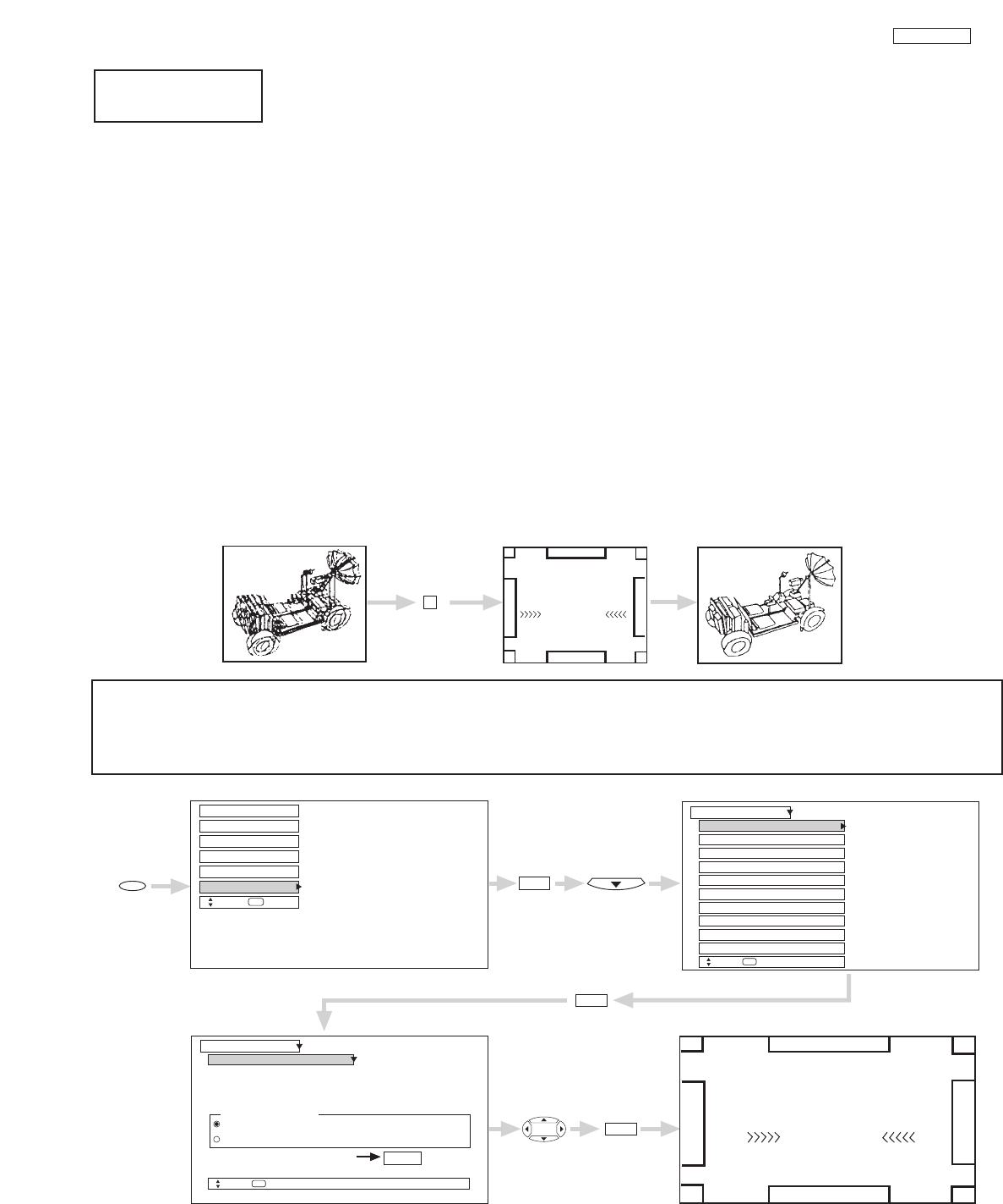
Using the Remote Control, select SETUP-MAGIC FOCUS TUNE UP-MANUAL ADJUSTMENT MODE-START to access convergence
crosshatch pattern. The adjustment point is indicated by the Adjustment Point Cursor.
To Move Adjustment Point
To move the adjustment point cursor using the CURSOR buttons, the Adjustment Cursor must be WHITE. Another way to move the
Adjustment Point Cursor is to press the following buttons: [2] up, [4] left, [5] down, [6] right. If you use the number buttons while the
adjustment point is WHITE, it will change to RED.
To Change the Color of Adjustment Point
Press the SELECT button repeatedly (WHITE-RED-BLUE-WHITE...). Green color is fixed and cannot be adjusted.
To Adjust the Convergence
Move the Adjustment Cursor to the point to be adjusted. Use the CURSOR to match the RED and BLUE colors to GREEN (reference
color). Properly aligned, all three colors should appear white.
If convergence is acceptable after Manual Convergence adjustment, press EXIT button to access menu mode.
Press the [0] button on the remote control to CANCEL adjusted data and return to main picture.
Press the [1] button on the remote control to SAVE adjusted data and return to main picture.
Press the [2] button on the remote control to return to the manual convergence adjustment mode (crosshatch pattern).
Press the [3] button on the remote control to recall the factory pre-set convergence data.
NOTES: 1. Please turn ON your television for at least 20 minutes before using this feature.
2. Auto Adjustment Mode is recommended. If convergence is still not acceptable, use the Manual Adjustment Mode.
3. If Auto Adjust mode is selected or the Magic Focus button is pressed, all manual adjust mode settings will be erased.
Setup
Locks
Chan. Manager
Aspect
Video
Move
SEL
Sel
Audio
Magic Focus Tune Up
Setup
Move
SEL
Return
Aligns the Red, Green, and Blue
colors to correct for Magnetic
Influences.
Auto
Manual
Adjustment Mode
If you want to adjust now Start
Adjustment Point
Cursor
Set The Inputs
Set The Clock
Menu Preference
Magic Focus Tune Up
Setup
Move
SEL
Select
Set Black Side Panel
Set Virtual HD
Set The Color System
About Your TV
Set Closed Caption
Set Event Timer
MENU SELECT
SELECT
SELECT
117 Manual Adjust
Please Enter Number.
0.Cancel and go to Normal Mode.
1.Done and go to Normal Mode.
2.Back to Adjust Mode
3.Factory Reset and back to
Adjust Mode.
0-3.Select
EXIT
22
DP33KA/B
CUSTOMIZED PICTURE AND SOUND ADJUSTMENTS
Select AUDIO to adjust the TV to your preference and to improve the sound quality.
Audio
Sound Enhancement
Balance
Bass
Treble
Audio
Move
SEL
Return
Internal Speakers
Audio Source
Perfect Volume
Auto Noise Cancel
50%
Off
On
Locks
Chan. Manager
Aspect
Audio
Video
Move
SEL
Sel
Setup
On
On
45%
LR
Stereo
Loudness On
MENU
SELECT
This function controls the low frequency audio to all speakers.
Press CURSOR G,H, to select menu item.
Press CURSOR For Eto adjust the function.
Press EXIT to quit the MENU, or select Audio to return to the main menu.
NOTE: If TREBLE is selected you are adjusting treble. The additional menu items Bass and Balance can be selected and
adjusted in the same manner.
This function controls the high frequency audio to all speakers.
This function will control the left to right balance of the Projection TV internal speakers.
Bass
Balance
Treble
Multi-Channel Television Sound will allow you to select STEREO (a stereo broadcast), MONO (monaural
sound) used when receiving a weak stereo broadcast or 2nd Audio Prog (SAP) which may be a secondary
language, weather report, etc.
The sources received will be displayed at the top right edge of the TV. The source you select will be displayed
above the sources received. See example below for each selection when both stereo and second audio are
received (monaural is always received).
This function is useful when setting up the external speakers.
ON - Select this feature if using the internal speakers only.
OFF - Select this feature if you prefer to use only speakers from a separate stereo system.
This function eliminates the noise between stations. If a channel is tuned and is noisy, this function will
automatically eliminate the audio for that channel.
This function will automatically adjust volume so each channel and input has the same average volume
level.
This function turns loudness ON or OFF
.It will improve the quality of both low and high frequency sounds
when listening at low volume levels.
STEREO SELECTED SAP SELECTED MONO SELECTED
3:32 PM
Ant A 10
Stereo
R
3:32 PM
Ant A 10
SAP
R
3:32 PM
Ant A 10
Mono
R
Audio Source
Internal Speakers
Auto Noise Cancel
Perfect Volume
Loudness
Sound Enhancement This unction will reproduce the “live” sound you would hear in concert halls, sport stadiums, movie theaters,
etc. with only two speakers.
23
DP33KA/B
REAR PANEL CONNECTIONS
TABLE OF CONTENTS
NOTE: 1. Connect only 1 component to each input jack.
2. Follow connections that pertain to your personal entertainment system.
3. Composite video signal can be input to Input2~Input5.
4. Cables are not included with the purchase of this television.
PB
PR
PB
PR
Outside antenna or
cable TV coaxial cable
2-Way signal splitter
Stereo System Amplifier
LR
INPUT
Laserdisc player, VCR,
camcorder, etc.
HDTV Set-Top Box
DVD Player
Cable TV Box
OUTPUT INPUT
VCR #1
ANT
IN
OUTPUT
S-VIDEO VLR
ANT A
TO
CONVERTER
ANT B
L
Y
R(MONO)/L
AUDIO
TO HI-FI
R
S-VIDEO
S-VIDEO
S-VIDEO
Y/VIDEO
R(MONO)/L
R(MONO)/L VIDEO
R(MONO)/L VIDEO
RL VIDEO
INPUT 1
INPUT 2
INPUT 3
INPUT 4
MONITOR
OUT
OUTPUT
YP
B/CBPR/CR
L R
VCR #2
V L R
OUTPUT
S-VIDEO
V L R
INPUT
S-VIDEO
OUTPUT
Y PB PR L R
AUDIO
AUDIO
AUDIO
DVI-HDTV
D-VHS
DIGITAL OUTPUT
LR
OUTPUT
TYPICAL FULL-FEATURE SETUP
24
DP33KA/B
TABLE OF CONTENTS
Display Picture Formats
Press this button to quickly change the picture format ASPECT ratio.
Depending on the input signal, the picture format ratio allows you to adjust the images through the following options.
4:3 Standard Use this aspect mode to display conventional (4:3) images. Side panels (gray areas) are placed to the
left and right of the image to preserve the original aspect ratio of the source. Note: Use this mode for
only 15% of your total viewing time to prevent uneven aging of the phosphors. Phosphors in the lighted
area of the picture will age more rapidly than the black areas.
4:3 Expanded use this aspect mode to display conventional (4:3) sources by linearly increasing image expansion from
the center towards the edges of the display area in order to fill it.
4:3 Zoom1/Zoom2 Use these aspect modes to zoom in on conventional (4:3) sources.
16:9 Standard Use this aspect mode to display 16:9 sources like HDTV and DVD’s preserving the original 16:9 aspect
ratio.
16:9 Zoom Use this aspect mode to zoom 16:9 images.
(1) NTSC/480i/480p Input
(2) 480i/480p INPUT
(3) 720p/1080i INPUT
4:3
INPUT 4:3 EXPANDED 4:3 ZOOM1
4:3 ZOOM2
16:9 STANDARD
4:3 STANDARD
INPUT 4:3 EXPANDED 4:3 ZOOM1
4:3 ZOOM2
16:9 STANDARD
4:3 STANDARD
INPUT
16:9
16:9 STANDARD 16:9 ZOOM
16:9 ZOOM
16:9 ZOOM
16:9
NOTE: The Aspect Style setting you
select for an ANT input will
automatically be set for the
other ANT inputs.However,
all five video inputs have
independent Aspect Style
settings.

25
DP33KA/B
SERVICE ADJUSTMENTS
1. ASSEMBLED P.W.B ADJUSTMENT..................................................................................................................26
1-1. Service Menu Access (NTSC, SDTV and HDTV) ..................................................................................26
1-2. Comb Filter Operation Check ................................................................................................................45
1-3. Video Settings Check..............................................................................................................................45
1-3-1. Color Temperature Check ............................................................................................................45
1-3-2. Black Enhancement......................................................................................................................45
1-3-3. Edge Enhancement ......................................................................................................................45
1-3-4. Color Management ......................................................................................................................45
1-3-5. Color Coding ................................................................................................................................45
1-3-6. Auto Color ....................................................................................................................................45
1-3-7. Noise Reduction Check ................................................................................................................45
1-3-8. Auto Movie Mode Check ..............................................................................................................45
1-4. High Voltage Adjustment ........................................................................................................................46
2. FINAL ASSEMBLY ADJUSTMENT (Adjustment should be according to below order) ..............................46
2-1. Cut Off Adjustment..................................................................................................................................46
2-2. DCU Phase Data Setting ......................................................................................................................46
2-3. Horizontal Position Adjustment (Coarse) ................................................................................................47
2-4. Raster Tilt (Deflection Yoke) ....................................................................................................................47
2-5. Beam Alignment......................................................................................................................................47
2-6. Raster Position........................................................................................................................................48
2-7. Vertical Size ..........................................................................................................................................48
2-8. Horizontal Size ......................................................................................................................................48
2-9. Beam Form ............................................................................................................................................49
2-10. Lens Focus..............................................................................................................................................49
2-11. Static Focus ............................................................................................................................................51
2-12. Digital Convergence ..............................................................................................................................51
2-12-1. Magic Focus Character Set Up ..................................................................................................52
2-12-2. Magic Focus Pattern Set Up ......................................................................................................53
2-12-3. Convergence Jig Screen Specification ......................................................................................53
2-12-4. Raster Position Adjsutment ........................................................................................................54
2-12-5. Convergence Point Adjustment ..................................................................................................54
2-12-6. Magic Focus Initialize..................................................................................................................55
2-13. Blue Defocus ..........................................................................................................................................59
2-14. White Balance ........................................................................................................................................59
2-15. Sub Brightness........................................................................................................................................60
2-16. Sub-Picture Signal Amplitude Adjustment ..............................................................................................61
2-17. Horizontal Position ................................................................................................................................62
2-18. Scanning Area Check ............................................................................................................................62
2-19. Raster Distortion Check ........................................................................................................................63
3. ADJUSTMENT POINT ........................................................................................................................................64
3-1. CPT (R)(G)(B), Focus Pack ....................................................................................................................64
3-2. Signal Block Assembly............................................................................................................................65
3-3. Main Chassis Deflection P
.W.B...............................................................................................................66
3-4. Power Supply P.W.B. ..............................................................................................................................74
*IMPORTANT
For many of the above adjustments, it is necessary to have an HDTV (1080i or 720P) signal generator, SDTV (480P) signal
generator, as well as the usual NTSC (480i) signal generator.
Hitachi recognizes that few companies offer HDTV or SDTV signal generators and that the cost of these generators is
sometimes prohibitive. For this reason, we suggest the use of a set-top-box for HDTV and SDTV adjustments. Usually,
there is a switch on the set-top-box which enables it to output HDTV (1080i or 720P) or SDTV (480P) signals even with
no input. In this case, the sync is automatically detected by the TV (at the Y-PBPRInputs on the rear panel).
TO GO TO AN ADJUSTMENT, CLICK ON ITS HEADING BELOW
TABLE OF CONTENTS

26
DP33KA/B
1. ASSEMBLED P.W.B. ADJUSTMENT
1.1 Service Menu Access
Adjustment Procedure
(1) Press and hold INPUT key on Control Panel and then press POWER key on control panel to access I2C
adjustment mode.
(2) Receive signal on main picture. (NTSC, SDTV or HDTV).
Some menu pages have I2C adjustments for SDTV and HDTV. The set will automatically allow you to set
these items only when a SDTV or HDTV signal is input to the COMPONENT jacks on the back of the TV. ......
See table below.
(3) Check the OSD according to table on the following pages, using CURSOR G, Hon Remote Control.
*: Adjustable Data
Others: Fixed Data (be careful not to change)
(4) Press EXIT key to exit I2C ADJUST mode.
NOTES: (1) If the TV I2C data is different from the I2C Parameter (of the following pages) for fixed data, change
the data.
(2) When exchanging microprocessor or EEPROM and TV is turned on for first time, it requires
initialization of Memory Initial of I2C adjustment menu. Press CURSOR Eand hold for 3
seconds to initialize memory.
(3) Use FACTORY RESET to set TV to out of factory shipping conditions: Do not use MEMORY
INITIALIZE.
IMPORTANT: AFTER PERFORMING A FACTORY RESET OR A MEMORY INITIALIZATION, YOU MUST
UNPLUG THE AC CORD AND THEN PLUG IT BACK IN.
BACK TO ADJUSTMENTS
27
DP33KA/B
I2C OSD Flowchart
(a) Adjust Mode OSD
Press [POWER] + [INPUT] of Control Panel.
*: ADJUSTABLE ITEM
EXIT I2C ADJUST MODE
[EXIT] OR POWER on/off.
28
DP33KA/B
(a) Adjust Mode OSD (continued)
29
DP33KA/B
(a) Adjust Mode OSD (continued)
30
DP33KA/B
(a) Adjust Mode OSD (continued)
31
DP33KA/B
(b) I2C Parameter List
Adjustment
Mode OSD
Adjustment Item Adjustment
Range(HEX)
Initial
Data(HEX)
Adjustment
Value(HEX)
SERVICE SERVICE OFF
TA1360 (88H)
SUB BRIGHT Sub Brightness 3C~ FF 7F
WHITE BAL White Balance Mode (TA1360 88H)
High 3F
Medium 49
Standard 4F
G DRIVE(HIGH)
G DRIVE(MED)
G DRIVE(STD)
G DRIVE (B/W)
Green Drive Gain Adjustment
00: .5 dB ~ 7F: +3dB
Data(M) = High + Medium - 3F
Data(S) = High + Standard - 3F
Data (B) = High + B/W - 3F Black/White
00~ 7F
58
High 3F
Medium 4F
Standard 57
R DRIVE(HIGH)
R DRIVE(MED)
R DRIVE(STD)
R DRIVE (B/W)
Red Drive Gain Adjustment
00: .5 dB ~ 7F: +3dB
Data(M) = High + Medium - 3F
Data(S) = High + Standard - 3F Black/White
00~ 7F
65
High 7F
Medium 7F
Standard 7F
R CUTOFF(HIGH)
R CUTOFF(MED)
R CUTOFF(STD)
R CUTOFF (B/W)
Red Cutoff Adjustment
00: 1.9 V~ FF: 2.9 V
Data(M) = High + Medium - 7F
Data(S) = High + Standard - 7F Black/White
00~ FF
7F
High 7F
Medium 7F
Standard 7F
G CUTOFF(HIGH)
G CUTOFF(MED)
G CUTOFF(STD)
G CUTOFF (B/W)
Green Cutoff Adjustment
00: 1.9 V~ FF: 2.9 V
Data(M) = High + Medium - 7F
Data(S) = High + Standard - 7F Black/White
00~ FF
7F
High 7F
Medium 7F
Standard 7F
B CUTOFF(HIGH)
B CUTOFF(MED)
B CUTOFF(STD)
B CUTOFF (B/W)
Blue Cutoff Adjustment
00: 1.9 V~ FF: 2.9 V
Data(M) = High + Medium - 7F
Data(S) = High + Standard - 7F Black/White
00~ FF
7F
H POSITION Normal 40
H POSITION H
Horizontal Position Adjustment
00: .10%~ 7F: +10%
Data(H) = H POSI + H POSI H - 3F
Bypass
00~ 7F
49
FLEX
VD POSITION Vertical Position 00~ 7F 3F
FACTORY
RESET
TA13483-Sub (DAH)
SUB-CONT(TV-S) Sub Contrast Control
00: MIN(-3Db), 1F: MAX(+3Db)
00~ 1F 0F
OSD POSITION
H POSI OSD Horizontal Position 00~ FF 0D
V POSI OSD Vertical Position 00~ FF 22
CLK1 00~ 4F 40
CLK2 00~ 4F 40
CLK3 00~ 4F 49
CLK4
OSD Clock Adjust
00 4F 4F
AFC/CLOCK TEST - -
MEMORY INITIAL - -
I2C OPEN - -
IR BLASTER - -
~
32
DP33KA/B
Adjustment
Mode OSD
Adjustment Item Adjustment
Range(HEX)
Initial
Data(HEX)
Adjustment
Value(HEX)
E2PROM edit
ADRRESS ADRRESS - -
DATA DATA 00~ FF -
P MODE ADJ
Day Mode 00~ 60 60 Contrast Contrasrt Reset Step Adjustment
00 step (0%) ~ 60 step (100%) Night Mode 00~ 60 30
Day Mode 00~ 60 30 Brightness Brightness Reset Step Adjustment
00 step (0%) ~ 60 step (100%) Night Mode 00~ 60 30
Day Mode 00~ 60 30
Color Color Reset Step Adjustment
00 step (0%) ~ 60 step (100%) Night Mode 00~ 60 27
Day Mode 00~ 60 30 Tint Contrast Reset Step Adjustment
00 step ~ 60 step Night Mode 00~ 60 30
Day Mode 00~ 60 30 Sharpness Tint Reset Step Adjustment
00 step (0%) ~ 60 step (100%) Night Mode 00~ 60 30
Day Mode High
Medium
Standard
Black/White
High
Color Temperature Color Temperature Reset Adjustment
High, Medium, Standard, Black/White
Night Mode High
Medium
Standard
Black/White
Standard
Day Mode High, Middle
Low, Off
Middle Black Enhancement Black Enhancement Reset Adjustment
High, Middle, Low, Off
Night Mode High, Middle
Low, Off
Low
Day Mode High, Middle
Low, Off
High
Edge Enhancement Edge Enhancement Reset Adjustment
High, Middle, Low, Off
Night Mode High, Middle
Low, Off
Low
DIGITAL MODULE HDTV Model only - -
HFRQ-N The number of times of Sync Frequency 00~ 0F 03
INPUT1 Input1 YPBPR Horizontal Frequency Detection Select
00: Auto, 01: 480i, 02: 480p, 03: 720p, 04: 1080i
00~ 04 00
INPUT2 Input2 YPBPR Horizontal Frequency Detection Select
00: Auto, 01: 480i, 02: 480p, 03: 720p, 04: 1080i
00~ 04 00
V CHIP/ CCD
SAMPL ING 00~ FF 00
POLLING 00~ FF 0F
START 00~ 07 02
TIMEOUT 00~ 1E 05
STATUS
V Chip Adjust
00~ 07 02
CLK POS Adjust CCD Clock Position
HDTV only 00~ 1F 0A
VIDEO ID VIDEO ID Detection
0: 4:3 signal, 1: 4:3 letter box signal
2: 16:9 screen signal, FF: No VIDEO ID
00~ 02, FF *
IR BLASTER
WAIT IR Blaster Adjustment 00~ FF 06
REPEAT 00~ FF 20
(b) I2C Parameter List (continued)
33
DP33KA/B
Adjustment
Mode OSD
Adjustment Item Adjustment
Range(HEX)
Initial
Data(HEX)
Adjustment
Value(HEX)
ISF Mode: TA1360 (88H)
RGBOUT0 RGB Output Mode Switch
00: Normal, 01: R only, 02: G only, 03: B only
00~ 03 00
SUB-BRT Brightness Adjustment
00: .40 IRE~ FF: +40 IRE
DVI Input Data=SUB-BRT + SUBBRTH-7H
3C~ FF 7F
G-DRV-H High 3F
G-DRV-M Medium 49
G-DRV-S Standard 4F
G-DRV-B
Green Drive Gain Adjustment
00: -5 dB ~ 7F: +3dB
Data(M) = High + Medium - 3F
Data(S) = High + Standard - 3F Black/White
00~ 7F
58
R-DRV-H High 3F
R-DRV-M Medium 4F
R-DRV-S Standard 57
R-DRV-B
Red Drive Gain Adjustment
00: -5 dB ~ 7F: +3dB
Data(M) = High + Medium - 3F
Data(S) = High + Standard - 3F Black/White
00~ 7F
65
R-CUT-H High 7F
R-CUT-M Medium 7F
R-CUT-S Standard 7F
R-CUT-B
Red Cutoff Adjustment
00: 1.9 V~ FF: 2.9 V
Data(M) = High + Medium - 7F
Data(S) = High + Standard - 7F Black/White
00~ FF
7F
G-CUT-H High 7F
G-CUT-M Medium 7F
G-CUT-S Standard 7F
G-CUT-B
Green Cutoff Adjustment
00: 1.9 V~ FF: 2.9 V
Data(M) = High + Medium - 7F
Data(S) = High + Standard - 7F Black/White
00~ FF
7F
B-CUT-H High 7F
B-CUT-M Medium 7F
B-CUT-S Standard 7F
B-CUT-B
Blue Cutoff Adjustment
00: 1.9 V~ FF: 2.9 V
Data(M) = High + Medium - 7F
Data(S) = High + Standard - 7F Black/White
00~ FF
7F
SUBCNT0 Sub Contrast 00: -3.4 dB ~ 1F: +2.6 dB 00~ 1F 12
COLOR-3 TV/NTSC 4D
COLOR-D SDTV 4D
COLOR-E
Color
(Center Adjustment)
00: -20 dB ~ 7F: +4.5 dB HDTV
00~ 7F
52
COLOR-M Medium 1F
COLOR-S Standard 1F
COLOR-B
Color Offset
B/W
00~ 3F
1F
TINT-3 TV/NTSC 41
TINT-D SDTV 41
TINT-E
Tint(Center Adjustment)
00: -32 degree
7F: +32 degree HDTV
00~ 7F
43
TINT-M Medium 1F
TINT-S Standard 1F
TINT-B
Tint Offset
B/W
00~ 3F
1F
SHARP-3 ANT A, B/NTSC 20
SHARP-G 480i/480p 20
SHARP-I 720p/1080i 1F
SHARP-9 Photo MC 1F
SHARP-C
Sharpness
(Center Adjustment)
-10 dB ~ +15 dB
SPLIT
00~ 7F
20
(b) I2C Parameter List (continued)
34
DP33KA/B
Adjustment
Mode OSD
Adjustment Item Adjustment
Range(HEX)
Initial
Data(HEX)
Adjustment
Value(HEX)
ISF Mode: TA1360 (88H)
RY-PH3 ANT A, B/NTSC 00
RY-PHD SDTV 00
RY-PHE
R-Y/B-Y Phase
00: 90 degree
0F: 109 degree HDTV
00~0F
00
R/BGA3H High 0A
R/BGA3M Medium 08
R/BGA3S Standard 06
R/BGA3B
TV/NTSC
Black/White 03
R/BGADH High 0A
R/BGADM Medium 08
R/BGADS Standard 06
R/BGADB
SDTV
Black/White 03
R/BGAEH High 08
R/BGAEM Medium 06
R/BGAES Standard 04
R/BGAEB
R-Y/B-Y Gain
00: 0.56
0F: 0.86
HDTV
Black/White
00~ 0F
03
GY-PH-4 TV/NTSC 02
GY-PH-F SDTV 02
GY-PH-G
G-Y/B-Y Phase
00: 232.5 degree
0F: 255 degree HDTV
00~ 0F
03
G/BGA3H High 02
G/BGA3M Medium 03
G/BGA3S Standard 04
G/BGA3B
TV/NTSC
Black/White 05
G/BGADH High 02
G/BGADM Medium 03
G/BGADS Standard 04
G/BGADB
SDTV
Black/White 05
G/BGAEH High 00
G/BGAEM Medium 00
G/BGAES Standard 00
G/BGAEB
G-Y/B-Y Gain
00: 0.3
0F: 0.45
HDTV
Black/White
00~ 0F
00
DC-PNT0 DC Restoration Point 00: 0% ~ 07: 47% 00~ 07 00
DCRATH High 00
DCRATM Middle 00
DCRATL Low 00
DCRATO
DC Restoration Rate
00: 100% ~ 07: 135%
Black
Enhancement
Off
00~ 07
00
DC-LMT0 DC Restoration Limit Point
00: 60%, 01: 73%, 02: 87%, 03: 100%
00~ 03 00
DABLPN0 Dynamic ABL Detection Point
00: MIN ~ 03: MAX
00~ 03 03
DABLGAH High 00
DABLGAM Middle 00
DABLGAL Low 00
DABLGAO
Dynamic ABL Gain
00: MIN ~ 03: MAX
Black
Enhancement
Off
00~ 03
00
(b) I2C Parameter List (continued)
35
DP33KA/B
Adjustment
Mode OSD
Adjustment Item Adjustment
Range(HEX)
Initial
Data(HEX)
Adjustment
Value(HEX)
TA1360 (88H)
DIMMER Not use 00~ 3F *
CONTRAST Not use 00~ 7F *
SCP-SW0 Sand castle Pulse Switch
00: Internal, 01: External Input
00~ 01 01
H-POSI Normal 40
H-POSIH Bypass 49
H-POSIS
Horizontal Position Adjustment
00: -10%~ 7F: +10%
Data(H) = H POSI + H POSI H - 3F
DVI=SAM 1080i Bypass,
Data(S) = H POSI + H POSI H - 3F
+
H-POSIS - 3F
SAM-1080i Bypass
00~ 7F
37
APRTR-3 ANT A, B/NTSC 01
APRTR-G 480i/480p 01
APRTR-I 720p/1080i/PhotoMC 00
APRTR-C
Aperture Control Peak f0
0: 15 MHz, 1: 8.8 MHz
2: 7.5 MHz, 3: 5 MHz
SPLIT
00~ 03
01
CLT-0 Color Limiter Level Switch
0: 1.65 Vp-p, 1: 2 Vp-p
00~ 01 01
CSRTG-0 Color SRT Gain
0: min~ 3: max 00~ 03 00
CSRTF-0 Color SRT Frequency
0: 4.3 MHz~ 1: 5.8 MHz
00~ 01 01
VSM-PHP ANT A, B, NTSC/480i/480p 06
VSM-PHJ
VM Phase
00: -37.5 ns, 05: Normal
07: +15 ns
720p/1080i/ANT C/PhotoMC
00~ 07
04
CDE-0 Color Detail Enhancer
00: min ~ 03: max
00~ 03 00
DCUBRT0 RGB Brightness 00: -20 IRE ~ 7F: +20 IRE 00~ 7F 3F
DCUCNT0 RGB Contrast 00: -17 dB ~ 7F: 0 dB 00~ 7F 5A
OSDACL0 OSD Auto Contrast Limiter Switch 0: OFF 1: ON 00~ 01 00
OSDBRT0 OSD Brightness Adjustment
00: 5 IRE, 01: 0 IRE, 02:-5 IRE, 03:-10 IRE
00~ 03 02
OSDCNT0 OSD Contrast Adjustment
00: -9.5 dB ~ 03: 0 dB
00~ 03 02
DCRRSW0 DC Restoration Ratio Switch
0: 100% less, 1: 100% over
00~ 01 00
COLORG0 Color Correction Point
00: OFF, 01: 0.23 Vp-p, 02: 0.37 Vp-p, 03: 0.52 Vp-p
00~ 03 00
YCGA-0 Component Dynamic Y/C Correction Select
00: OFF, 01: min, 02: mid, 03: max
00~ 03 00
APL/BS0 APL / Black Stretch Start Point
00: 0 IRE ~ 03: 23 IRE
00~ 03 00
BLC-0 Black Level Auto Correction Switch
00: OFF, 01: ON
00~ 01 00
BDL-0 Black Detection Level Switch
00: 3 IRE, 1: 0 IRE
00~ 01 00
BSARE0 Black Stretch Area Correction Switch
00: ON, 01: OFF
00~ 01 01
SRTGA-0 SRT(Super Real Transient) Gain
00: MIN ~ 1F: MAX
00~ 1F 10
(b) I2C Parameter List (continued)
36
DP33KA/B
Adjustment
Mode OSD
Adjustment Item Adjustment
Range(HEX)
Initial
Data(HEX)
Adjustment
Value(HEX)
TA1360 (88H)
WPLLVL-0 White Character Correction Amplitude
00: min ~ 07: max
00~ 07 07
ABLPN0 ABL Detection Point
00: MIN ~ 07: MAX
00~ 07 07
ABLGA0 ABL Gain
00: MIN ~ 07: MAX
00~ 07 00
DGGAIN0 Dynamic Y Gamma Gain vs Dark Area
00: OFF ~ 07: MAX(+6 dB)
00~ 03 00
DGAREA0 Dynamic Y Gamma Gain vs Bright Area
00: OFF ~ 07: max
00~ 07 00
STATG10 Static Y Gamma Black Gain
00: OFF, 01: MIN(0 DB) ~ 07: MAX(+6 DB)
00~ 07 00
STATG20 Static Y Gamma Bright Gain
00: OFF, 01: MIN(0 DB) ~ 03: MAX(-6 DB)
00~ 03 03
YOUTG-0 Y Gamma Switch
0: OFF, 1: ON
00~ 01 00
YDTL-0 Y Detail Control
00: MIN(Trap) ~ 0F: MAX(+6 dB)
00~ 0F 07
YDELAY0 Y Group Delay Control
00: MIN(Trap) ~ 0F: MAX(+6 dB)
00~ 0F 09
WPPNT0 White Peak Blue Point
00: 55 IRE ~ 07: 105 IRE
00~ 07 00
WPGA-0 White Peak Blue Gain
00: min(+2 dB) ~ 07: max(+9.5 dB)
00~ 07 00
HIBRT0 High Bright Color Switch
00: OFF, 01: ON
00~ 01 00
WPS-0 White Peak Suppressor Level
00: 110 IRE, 01: 130 IRE
00~ 01 01
BLS-0 Blue Stretch Gamma Correction
00: OFF, 01: ON
00~ 01 00
GSTR-0 Green Stretch
00: OFF ~ 03: MAX
00~ 03 00
BSTRG-0 Blue Stretch Gain
00: OFF ~ 03: MAX(+4 dB)
00~ 03 00
BSTRP-0 Blue Stretch Point
00: MIN(30 IRE)~ 03: MAX(45 IRE)
00~ 03 00
BSCHR10 Black Stretch Characteristic Switch 1
(OFF~ MAX)
00~ 01 00
BSCHR20 Black Stretch Characteristic Switch 2
(OFF~ MAX)
00~ 01 00
(b) I2C Parameter List (continued)
37
DP33KA/B
Adjustment
Mode OSD
Adjustment Item Adjustment
Range(HEX)
Initial
Data(HEX)
Adjustment
Value(HEX)
UPD64084 (B9H) Read Mode
SYNCDET Sync Detection
0: Sync, 1: No Sync
00~ 01 *
F-STD Frame Sync Nonstandard Detection
0: Standard, 1: Non standard
00~ 01 *
V-STD Vertical Sync Nonstandard Detection
0: Standard, 1: Non standard
00~ 01 *
H-STD Horizontal Sync Nonstandard Detection
0: Standard, 1: Non standard
00~ 01 *
NOISE Noise Level Detection
00: Noise Small ~ FF: Noise Large
00~ FF *
VID-ID Video ID Detection
0: 4:3 signal, 1: 16:9 signal, 2: 4:3 letter box signal
00~ 03 *
UPD64084 (B8H)
DYGA Y Motion Detection Gain
0: Gain 0 ~ F: Gain MAX
00~ 0F 09
DCGA Chroma Motion Detection Gain
0: Gain 0 ~ F: Gain MAX
00~ 0F 06
VAPGA Vertical Aperture Control Gain
0: Correction OFF ~ 7: Correction MAX (x0.875)
00~ 07 00
VAPIN Vertical Aperture Control Invert
0: Correction OFF ~ 1F: Correction MAX (x0.875)
00~ 1F 0B
YHCOR Y Output High Frequency Coring
0: Coring OFF, 1: Coring Small, 2: Coring Center, 3: Coring
Large
00~ 03 00
TA1383F-Main (D9H) Read Mode
HSYNC-M Horizontal Sync Number
NTSC/480i = 22, 480p = 43, 1080i = 48, 720p = 60
00~ FF *
VSYNC-M Vertical Sync Number
60Hz = 5E
00~ 7F *
CSYNC-M SYNC Mode Detection
0:2 Level Sync, 1:3 Level Sync
00~ 01 *
TA1383-Sub (DBH) Read Mode
HSYNC-S Horizontal Sync Number
NTSC/480i = 22, 480p = 43, 1080i = 48, 720p = 60
00~ FF *
VSYNC-S Vertical Sync Number
60Hz = 5E
00~ 7F *
CSYNC-S SYNC Mode Detection
0:2 Level Sync, 1:3 Level Sync
00~ 01 *
(b) I2C Parameter List (continued)
38
DP33KA/B
Adjustment
Mode OSD Adjustment Item Adjustment
Range(HEX) Initial
Data(HEX) Adjustment
Value(HEX)
TA1383-Main/Sub (D8H)
CONTM1 Main TA1383 ANT A, B 10
CONTS1 Sub TA1383 ANT A 10
CONT-2 NTSC 10
CONT-K ANT C/YPBPR/DVD/BM 10
CONT-A
Sub Contrast Control
00: MIN(-3dB)
1F: MAX(+3dB)
DVI
00~ 1F
10
CLRM1 Main ANT A, B 10
CLRS1 Sub ANT A 10
CLR-2 NTSC 10
CLR-K ANT C/YPBPR/DVD/BM 10
CLR-A
Sub Color Control
00: MIN(-3dB)
1F: MAX(+3dB)
DVI
00~ 1F
10
TINTM1 Main ANT A, B 08
TINTS1 Sub ANT A 08
TINT-2 NTSC 08
TINT-K ANT C/YPBPR/DVD/BM 08
TINT-A
Sub Tint Control
0: MIN(-7deg)
F: MAX(+7deg)
DVI
00~ 0F
08
TA1383-Main/Sub (D8H/DAH)
BANDW-F ANTA, B/NTSC/480i 01
BANDW-5 480p 02
BANDW-6 720p 00
BANDW-7 1080i 00
BANDW-9 PhotoMC 00
BANDW-C
Band Width Filter Switch
0: OFF, 1: 4.2MHz, 2: 11.3MHz, 3: Mute
SPLIT
00~ 03
01
YDL1-F ANTA, B/NTSC/480i 01
YDL1-5 480p 01
YDL1-6 720p 01
YDL1-7 1080i 01
YDL1-9 PhotoMC 01
YDL1-C
Y Delay Time Adjust 1
Base Band Section
0: -10 ns, 1: 0 ns
2: +10 ns, 3: +20 ns
SPLIT
00~ 03
01
Y-DL2-0 Y Delay Time Adjust 2 NTSC Section
1: +40 ns, 2: +80 ns, 3: +120 ns 00~ 03 00
AFCRAN0 Horizontal AFC Switch
0: Normal, 1: Narrow 00~ 01 00
FDET-3 Frequency Detection Input Switch
0: 480i-1 • • • NTSC, 1: 480i-2 • • • NTSC
2: D-SYNC2, 3: HD/VD
00~ 03 00
HSEPL-3 ANT A, B/NTSC 00
HSEPL-4 480i 00
HSEPL-5 480p 00
HSEPL-J
Horizontal Sync Separation
Level Switch
0: 20%, 1: 27%, 2: 34%, 3: 40%
720p/1080i/ANT C
00~ 03
00
VSEPL-3 TV/NTSC 00
VSEPL-4 480i 00
VSEPL-5 480p 00
VSEPL-J
Vertical Sync Separation Level switch
0: 40%, 1: 50%, 2: 60%, 3: 70%
720p/1080i/ANT C
00~ 03
00
DSEPL-G 480i/480p 00
DSEPL-J
D-SYNC2-IN Sync Separation Level Switch
0: 20%, 1: 30%, 2: 40%, 3: 50% 720p/1080i/ANT C
00~ 03
00
AFCMD-1 ANT A, B 02
AFCMD-2 NTSC 02
AFCMD-L
AFC Gain Switch
0: AUTO 1, 1: AUTO 2, 2: AUTO 3,
3: AUTO 4, 4: +6dB, 5: 0 dB, 6:-12dB
7: OFF(Horizontal Free Run) ANT C/YPBPR/DVD
00~ 07
04
VMODE-0 Vertical Sync Mode Switch
0: Normal PLL Mode, 1: Sync Output Mode ANT A, B/NTSC 00~ 01 00
48ISEP3 480i Separator Mode Switch
0: ON, 1: OFF ANT A, B/NTSC 00~ 01 00
HDPOSI3 ANT A, B/NTSC 06
HDPOSI4 480i 05
HDPOSI5 480p 00
HDPOSI6 720p 09
HDPOSI7
HD Output Phase Adjustment
0: 800 ns Advance, F: Sync Center
1080i
00~ 0F
07
(b) I2C Parameter List (continued)
39
DP33KA/B
Adjustment
Mode OSD Adjustment Item Adjustment
Range(HEX) Initial
Data(HEX) Adjustment
Value(HEX)
NJW1160/61 82H
BBE-LO BBE Low Frequency Effect Level
0dB~ 15dB
00~ 0F 07
BBE-HI BBE High Frequency Effect Level
0dB~ 15dB
00~ 0F 05
AGC AGC Level Setting
150m/300m/400m/540mVrms
00~ 03 01
Adjustment
Mode OSD
Adjustment Item Adjustment
Range(HEX)
Initial
Data(HEX)
Adjustment
Value(HEX)
FC-4 Read Mode
FC-VER FC Unit Micro Version Number 00~ FF *
FC-CHKH FC Unit Micro Check Sum Number (High Bit) 00~ FF *
FC-CHKL FC Unit Micro Check Sum Number (Low Bit) 00~ FF *
3-2T/C TV/Cinema: 3-2 Pull Down Signal Detection
0: TV, 1: Cinema
00~ 01 *
VFREQH 00~ FF *
VFREQL
Main/Sub Vertical Frequency Detection (High 6Bit, Low 8Bit)
59.94Hz = 17D2, 60Hz = 17CC 00~ FF *
HFREQH 00~ FF *
HFREQL
Main/Sub Vertical Frequency Detection (High 5Bit, Low 8Bit)
NTSC/480i = 0E85, 480p = 0742
1080i = 06C2, 720p = 0514
00~ FF *
APLDET APL Detection 00~ FF *
PEAKDET PEAK Detection 00~ FF *
YGAIN Dynamic Contrast Y Gain 00: x1, 7F: x2 00~ 7F *
CGAIN Dynamic Contrast Color Gain 00: x1, 3F: x2 00~ 3F *
FC-4 Write Mode
B-BACK Blue Back: FC Free Run Mode
0: Blue Back OFF, 1: Blue Back ON
00~ 01 *
MAININ Main Input Mode
0: NTSC, 1: 480i, 2: 480p, 3: 720p, 4: 1080i, 5: BM
00~ 0F *
SUBIN Sub Input Mode
0: NTSC, 1: 480i, 2: 480p, 3: 720p, 4: 1080i
00~ 0F *
VDPOS-0 VD Position Offset 00~ 7F 3F
LINE-I0 Line Interpolation 0: OFF, 1: ON 00~ 01 00
M-SLOPE Sat Slope 1 (Magenta) -90˚ (00h)~ 0˚ (40h)~ 90˚ (FFh)
Data=M-SLOPE+M-Menu- 30(1Eh)
00~ 7F 40
M-HUEW Hue Width 1 (Magenta)
Data= Width /360˚ x256=90˚ /360˚ x256=64 (3Fh)
00~ 3F 3F
M-HUECH Hue Center 1 (Magenta) High Bit 00~ 03 00
M-HUECL Hue Center 1 (Magenta) Low Bit
Data= Hue /360˚ x1024=45˚ /360˚ x1024=128 (0080h)
00~ FF 80
M-CLIP Sat Clip 1 (Magenta) 00~ FF FF
R-SLOPE Sat Slope 2 (Red) -90˚ (00h)~ 0˚ (40h)~ 90˚ (FFh)
Data=R-SLOPE+R-Menu- 30(1Eh)
00~ 7F 40
R-HUEW Hue Width 2 (Red)
Data= Width /360˚ x256=90˚ /360˚ x256=64 (3Fh)
00~ 3F 3F
R-HUECH Hue Center 2 (Red) High Bit 00~ 03 01
R-HUECL Hue Center 2 (Red) Low Bit
Data= Hue /360˚ x1024 =113.2˚ /360˚ x1024=322 (0142h)
00~ FF 42
R-CLIP Sat Clip 2 (Red) 00~ FF FF
(b) I2C Parameter List (continued)
40
DP33KA/B
Adjustment
Mode OSD
Adjustment Item Adjustment
Range(HEX)
Initial
Data(HEX)
Adjustment
Value(HEX)
FC-4 Write Mode
Y-SLOPE Sat Slope 3 (Yellow) -90˚ (00h)~ 0˚ (40h)~ 90˚ (FFh)
Data=Y-SLOPE+Y-Menu- 30(1Eh)
00~ 7F 40
Y-HUEW Hue Width 3 (Yellow)
Data= Width /360˚ x256=90˚ /360˚ x256=64 (3Fh)
00~ 3F 3F
Y-HUECH Hue Center 3 (Yellow) High Bit 00~ 03 01
Y-HUECL Hue Center 3 (Yellow) Low Bit
Data= Hue /360˚ x1024=173.0˚ /360˚ x1024=492 (01ECh)
00~ FF EC
Y-CLIP Sat Clip 3 (Yellow) 00~ FF FF
G-SLOPE Sat Slope 3 (Green) -90˚ (00h)~ 0˚ (40h)~ 90˚ (FFh)
Data=G-SLOPE+G-Menu- 30(1Eh)
00~ 7F 40
G-HUEW Hue Width 4 (Green)
Data= Width /360˚ x256=90˚ /360˚ x256=64 (3Fh)
00~ 3F 3F
G-HUECH Hue Center 4 (Green) High Bit 00~ 03 02
G-HUECL Hue Center 4(Green) Low Bit
Data= Hue /360˚ x1024=225.0˚ /360˚ x1024=640 (0280h)
00~ FF 80
G-CLIP Sat Clip 4 (Green) 00~ FF FF
C-SLOPE Sat Slope 5 (Cyan) -90˚ (00h)~ 0˚ (40h)~ 90˚ (FFh)
Data=C-SLOPE+C-Menu- 30(1Eh)
00~ 7F 40
C-HUEW Hue Width 5 (Cyan)
Data= Width /360˚ x256=90˚ /360˚ x256=64 (3Fh)
00~ 3F 3F
C-HUECH Hue Center 5 (Cyan) High Bit 00~ 03 03
C-HUECL Hue Center 5 (Cyan) Low Bit
Data= Hue /360˚ x1024=293.2˚ /360˚ x1024=834 (0342h)
00~ FF 42
C-CLIP Sat Clip 5 (Cyan) 00~ FF FF
B-SLOPE Sat Slope 6 (Blue) -90˚ (00h)~ 0˚ (40h)~ 90˚ (FFh)
Data=B-SLOPE+B-Menu- 30(1Eh)
00~ 7F 40
B-HUEW Hue Width 6 (Blue)
Data= Width /360˚ x256=90˚ /360˚ x256=64 (3Fh)
00~ 3F 3F
B-HUECH Hue Center 6 (Blue) High Bit 00~ 03 03
B-HUECL Hue Center 6 (Blue) Low Bit
Data= Hue /360˚ x1024 =353˚ /360˚ x1024 = 1004 (03ECh)
00~ FF EC
B-CLIP Sat Clip 6 (Blue) 00~ FF FF
HUECLP0 Hue Clip (HUE˚ / 360˚ x1024) 00~ 7F 2F
HUECT10 Hue Center 1 (HUE˚ / 360˚ / 4 x 1024) 00~ FF A1
HUECT00 Hue Center 0 (HUE˚ /360˚ / 4 x 1024) 00~ FF CC
HUESLP0 Hue Slope (0~ 127 / 64) 00~ 7F 2F
HUEWDH0 Hue Width (HUE˚ / 360˚ x1024) 00~ FF 55
CCSGA0 Color Correction Start Gain 00~ 0F 00
CCMAX0 Color Correction Maximum Level 00~ 0F 04
DCMGA0 Dynamic Contrast Maximum Gain 00~ 7F 00
DCMLM0 Dynamic Contrast End APL 00~ 7F 10
DCAPL0 Dynamic Contrast Start APL 00~ 7F 60
DCONTS Dynamic Contrast Gain Change Speed 1, 1/2, 1/4, 1/8 00~ 03 00
(b) I2C Parameter List (continued)
41
DP33KA/B
Adjustment
Mode OSD
Adjustment Item Adjustment
Range(HEX)
Initial
Data(HEX)
Adjustment
Value(HEX)
FC-4 Write Mode
READFA1 1080i, 540p/59.94 03
READFA2
ANT A, B
NTSC/480i 540p/60 02
READFB1 1080i, 540p/59.94 03
READFB2
480p
540p/60 03
READFC1 1080i, 540p/59.94 03
READFC2
720p
540p/60 04
READFD1 59.94 03
READFD2 60 02
READFD3
1080i/PhotoMC
RCA540p 02
READFE1
Read Frequency
Divider
Ratio Offset
Bypass -
00~ 07
03
MFYNR-0 Main Frame Cycle Noise Reduction 3 Dimension Filter
0: OFF, 1: ON
00~ 01 01
MFCNR-0 Main Frame Cycle Noise Reduction 3 Dimension Filter
0: OFF, 1: ON
00~ 01 01
SFYNR-0 Sub Frame Cycle Noise Reduction 3 Dimension
Filter 0: OFF, 1: ON
00~ 01 01
SFCNR-0 Sub Frame Cycle Noise Reduction 3 Dimension
Filter 0: OFF, 1: ON
00~ 01 01
MYNRIN3 ANT A, B/NTSC 04
MYNRINO
Main YNR Input Level
Gain ANT C/YPBPR/DVD/BM
00~ 07
04
SYNRIN3 ANT A, B/NTSC 04
SYNRINO
Sub YNR Input Level
Gain ANT C/YPBPR/DVD/BM
00~ 07
04
MYNRRD0 Main YNR Reducing Gain 00~ 07 01
SYNRRD0 Sub YNR Reducing Gain 00~ 07 01
MYNRPS0 Main YNR Passage Level Limit 00~ 07 00
SYNRPS0 Sub YNR Passage Level Limit 00~ 07 00
MYNR0-0 Main YNR 0 Point 00~ 0F 07
SYNR0-0 Sub YNR 0 Point 00~ 0F 07
MCNRIN0 Main CNR Input Level Gain 00~ 07 04
SCNRIN0 Sub CNR Input Level Gain 00~ 07 04
MCNRRD0 Main CNR Reducing Gain 00~ 07 00
SCNRRD0 Sub CNR Reducing Gain 00~ 07 00
MCNRPS0 Main CNR Passage Level Limit 00~ 07 02
SCNRPS0 Sub CNR Passage Level Limit 00~ 07 02
MCNR0-0 Main CNR 0 Point 00~ 0F 06
SCNR0-0 Sub CNR 0 Point 00~ 0F 06
VECRG-0 Vertical Enhance Coring 00~ 03 00
HECRG-0 Horizontal Enhance Coring 00~ 03 00
Y-CRG-0 Y Coring Amplitude 00~ 07 00
C-CRG-0 Color Coring Amplitude 00~ 07 00
HHPF1-3 ANT A, B/NTSC 00
HHPF1-G 480i/480p 00
HHPF1-I
Horizontal High Pass Filter 1
Characteristic Switch
0: Low Freq, 1: High Freq 720p/1080i/BM
00~ 01
00
V-ENH-3 ANT A, B/NTSC 02
V-ENH-G 480i/480p 02
V-ENH-I
Vertical Enhance
720p/1080i/BM
00~ 03
00
(b) I2C Parameter List (continued)
42
DP33KA/B
Adjustment
Mode OSD
Adjustment Item Adjustment
Range(HEX)
Initial
Data(HEX)
Adjustment
Value(HEX)
FC-4 Write Mode
H-ENH-3 ANT A, B/NTSC 00
H-ENH-G 480i/480p 00
H-ENH-I
Horizontal Enhance
720p/1080i/BM
00~ 03
00
YHFRQ-3 ANT A, B/NTSC 00
YHFRQ-G 480i/480p 00
YHFRQ-I
Y Horizontal HPF Peak
Frequency Switch
720p/1080i/BM
00~ 03
00
CHFRQ-3 ANT A, B/NTSC 02
CHFRQ-G 480i/480p 02
CHFRQ-I
Color Horizontal HPF Peak
Frequency Switch
720p/1080i/BM
00~ 03
02
YVECLP0 Y Vertical Enhance Clip Offset 00~ 0F 00
YVEGA-0 Y Vertical Enhance Gain 00~ 0F 00
YHECLP0 Y Horizontal Enhance Clip Offset 00~ 0F 00
YHEGA-0 Y Horizontal Enhance Gain 00~ 0F 00
CHEGA-0 Color Horizontal Enhance Gain 00~ 0F 0F
YVECSW0 Y Vertical Enhance Clip Switch 0: ENH, 1: LTI 00~ 01 01
CVECSW0 Color Vertical Enhance Clip Switch 0: CTI, 1: ENH 00~ 01 01
YHECSW0 Y Horizontal Enhance Clip Switch 0: ENH, 1: LTI 00~ 01 01
CHECSW0 Color Horizontal Enhance Clip Switch 0: CTI, 1: ENH 00~ 01 01
YSLIP-0 Y Slanting Line Interpolation 0: OFF, 1: ON 00~ 01 01
CSLIP-0 Color Slanting Line Interpolation 0: OFF, 1: ON 00~ 01 01
YVEDGA0 Y Vertical Edge Detection Gain 00~ 03 03
YVEDCR0 Y Vertical Edge coring 00~ 0F 04
YMDEG10 Y Motion Detection Edge Gain 1 00~ 07 05
YMDEC10 Y Motion Detection Edge Coring 1 00~ 1F 05
YMDEG00 Y Motion Detection Edge Gain 0 00~ 07 05
YMDEC00 Y Motion Detection Edge Coring 0 00~ 1F 05
YHEDGA0 Y Horizontal Edge Detection Gain 00~ 03 03
YHEDCR0 Y Horizontal Edge coring 00~ 0F 04
YMDEG30 Y Motion Detection Edge Gain 3 00~ 07 02
YMDEC30 Y Motion Detection Edge Coring 3 00~ 1F 08
YMDEG20 Y Motion Detection Edge Gain 2 00~ 07 02
YMDEC20 Y Motion Detection Edge Coring 2 00~ 1F 08
CMDEG10 C Motion Detection Edge Gain 1 00~ 07 03
CMDEC10 C Motion Detection Edge Coring 1 00~ 1F 08
CMDEG00 C Motion Detection Edge Gain 0 00~ 07 04
CMDEC00 C Motion Detection Edge Coring 0 00~ 1F 06
CMDEG30 C Motion Detection Edge Gain 3 00~ 07 01
CMDEC30 C Motion Detection Edge Coring 3 00~ 1F 0C
CMDEG20 C Motion Detection Edge Gain 2 00~ 07 02
CMDEC20 C Motion Detection Edge Coring 2 00~ 1F 0A
YVNLP-3 ANT A, B/NTSC 00
YVNLP-G 480i/480p 00
YVNLP-I
Y Vertical Nonlinear Peaking
720p/1080i/BM
00~ 3F
00
YHNLP-3 ANT A, B/NTSC 0A
YHNLP-G 480i/480p 0A
YHNLP-I
Y Horizontal Nonlinear Peaking
720p/1080i/BM
00~ 3F
00
(b) I2C Parameter List (continued)
43
DP33KA/B
Adjustment
Mode OSD
Adjustment Item Adjustment
Range(HEX)
Initial
Data(HEX)
Adjustment
Value(HEX)
FC-4 Write Mode
YVHENH3 ANT A, B/NTSC 0B
YVHENHG 480i/480p 0B
YVHENHI
Y Vertical and Horizontal Enhance Gain
720p/1080i/BM
00~ 1F
00
CVHENH3 ANT A, B/NTSC 12
CVHENHG 480i/480p 12
CVHENHI
Color Vertical and Horizontal Enhance
Gain
720p/1080i/BM
00~ 1F
12
MVWPH-3 ANT A, B/NTSC 05
MVWPH-4 480i/DVD 05
MVWPH-5 480p/VGA 05
MVWPH-6 720p 05
MVWPH-7
Main Vertical Write Input
Horizontal Phase Adjustment
1080i/BM
00~ 07
04
SVWPH-3 ANT A, B/NTSC 05
SVWPH-4 480i 05
SVWPH-5 480p 05
SVWPH-6 720p 05
SVWPH-7
Sub Vertical Write Input
Horizontal Phase Adjustment
1080i
00~ 07
04
MHSHP-3 ANT A, B/NTSC 7F
MHSHP-4 480i/DVD 7F
MHSHP-5 480p 7F
MHSHP-6 720p 7F
MHSHP-7 1080i/BM 7F
MHSHP-Q VGA 93
MHSHP-R SAM-720p 98
MHSHP-S
Main Horizontal Sync
Horizontal Phase Offset
SAM-1080i
00~ FF
94
SHSHP-3 ANT A, B/NTSC 7F
SHSHP-4 480i 7F
SHSHP-5 480p 7F
SHSHP-6 720p 7F
SHSHP-7
Sub Horizontal Sync Horizontal
Phase Offset
1080i
00~ FF
7F
FRMBRT0 Y Frame Bright 00~ 7F 60
FRMTOP0 Frame Top Position Offset 00~ 0F 00
VBLKT-0 Vertical Blanking Top Position Offset 00~ 0F 07
VBLKB-0 Vertical Blanking Bottom Position Offset 00~ 0F 07
CBBLK-0 CB Blanking Level Offset 00~ 0F 07
CRBLK-0 CR Blanking Level Offset 00~ 0F 07
HBLKR-0 Horizontal Blanking Right Position Offset 00~ FF 7F
HBLKL-0 Horizontal Blanking Left Position Offset 00~ FF 7F
VPOSI-0 Vertical Position 00~ 7F 3F
HDPOS-0 HD Position Offset 00~ 7F 3F
(b) I2C Parameter List (continued)

44
DP33KA/B
Adjustment
Mode OSD
Adjustment Item Adjustment
Range(HEX)
Initial
Data(HEX)
Adjustment
Value(HEX)
FC-4 Write Mode
BSTOPA0 16:9 Standard 00
BSTOPB0
Black Stretch Stop Pulse Top
Position Offset (for 4x3 Model) Not 16:9 Standard
00~ FF
00
BSBTMA0 16:9 Standard FF
BSBTMB0
Black Stretch Stop Pulse Bottom
Position Offset (for 4x3 Model) Not 16:9 Standard
00~ FF
FF
BSRGTA0 4:3 Standard FF
BSRGTB0
Black Stretch Stop Pulse Right
Position Offset (for 16x9 Model) Not 4:3 Standard
00~ FF
A6
BSLFTA0 4:3 Standard 00
BSLFTB0
Black Stretch Stop Pulse Left
Position Offset (for 16x9 Model) Not 4:3 Standard
00~ FF
59
HEGCRG0 H Edge Coring 00~ 1F 04
DIFCRG0 Difference Coring 00~ 7F 07
VE2CRG0 V Edge 2 Coring 00~ 1F 14
VE1CRG0 V Edge 1 Coring 00~ 1F 14
TCLCK-0 2-3 TV/Cine Lock 00~ 07 03
TCUNL-0 2-3 TV/Cine Unlock 00~ 07 00
TCARE-0 2-3 TV Cinema Detection Motion Area Border Volume 00~ FF 05
TCCBR-0 2-3 TV Cinema Detection Color 2 Bit Border Volume Offset 00~ 0F 07
TCYBR-0 2-3 TV Cinema Detection Y 2 Bit Border Volume 00~ 0F 07
(b) I2C Parameter List (continued)
45
DP33KA/B
1.2 Comb filter operation check
Adjustment preparation
(1) Receive the color bar signal at the regular tuning
point.
(2) Set the CONTRAST control to MAX and the other
controls to center.
Adjustment procedure
(1) Check that between the color bars there are line dots
every second color bar as shown in the drawing.
AA A
B
3D Y/C
Dots
A None
B None
Check and line dots.
B
A
1.3 Video Settings (Advanced Settings)
1.3.1 Color Temperature
(1) Receive the Circle pattern signal.
(2) Set Color Temperature using CURSOR G,Hand
change mode using CURSOR F,Eand then press
select button.
(3) Change Color Temperature from
High/Medium/Standard/Black and White.
1.3.2 Black Enhancement
(1) Receive the color bar signal.
(2) Select video mode by using CURSOR G,H.
(3) Press CURSOR G,Hto select Black Enhancement
then press CURSOR E.
(4) Select Black Enhancement using CURSOR F,E
and set it to High/Medium/Low/Off.
(5) When the mode is High, check that the black level
sinks at the black position of picture.
1.3.3 Edge Enhancement
(1) Receive the circle pattern signal.
(2) Adjust Edge Enhancement using CURSOR F,E
from High/Medium/Low/Off.
(3) When set to High, check that definition level is up at
edge of vertical line of the circle pattern.
1.3.4 Color Management Check
(1) Receive color bar signal.
(2) Select Color Management using CURSOR G,Hand
then press SELECT button to display next menu.
(3) Select Set User Colors using CURSOR G,Hand
then press select button to add check-mark.
(4) Select one of the titles of color and then press
SELECT button. Check that selected color is
changed by pressing CURSOR F,E.
F: Gets thinner E: Gets denser
1.3.5 Color Decoding Check
(1) Receive color bar signal.
(2) Select Color Decoding using CURSOR G,Hand
then press SELECT button.
(3) Select one of the radio buttons of decode mode.
The picture changes as follows:
RGB: Normal picture
R: Red color only
G: Green color only
B: Blue color only
(4) Select Red, Green, Blue or Tint using CURSOR
G,H. Use CURSOR F,Eto adjust.
1.3.6 Auto Color
(1) Set the color control to MAX.
(2) Select Auto Color using CURSOR G,Hand then
press SELECT button.
(3) Use CURSOR F,Eto change Auto Color to On/Off.
(4) When it is on, check that the red part of the color
signal grows deeper.
1.3.7 Noise Reduction
(1) Select Noise Reduction using CURSOR G,Hand
then press SELECT button.
(2) When it is on, check that the noise on the picture is
reduced.
1.3.8 Auto Movie Mode
(1) Receive 480i signal.
(2) Select Auto Movie Mode using CURSOR G,Hand
then press SELECT button.
(3) When it is on, check that the scan becomes smooth.
BACK TO ADJUSTMENTS
46
DP33KA/B
Important: High Voltage adjustment should
NOTbe adjusted in field. This is
adjusted at factory using precise
loads and should NOTbe
readjusted.
1.4 High Voltage Adjustment (should NOTbe
readjusted in field).
Adjustment preparation
(1) Connect High Voltage meter to FBT High Voltage
output. Connect GND of High Voltage meter to CPT
GND or FBT GND.
(2) Check that High Voltage adjustment VR (RH17) is
set to mechanical center. (located behind FBT on
DEFLECTION PWB).
(3) Receive circle pattern signal.
(4) VIDEO control should be reset.
Adjustment procedure
(1) Adjust High Voltage to following spec. by turning VR
RH17 slowly. ADJ. SPEC = 30.7KV±02KV
(2) After adjustment, fix VR RH17 with Silicone glue
(KE40RTV).
2. FINAL ASSEMBLY ADJUSTMENT
2.1 Cut Off Adjustment
Adjustment preparation
(1) Adjust screen VR’s on Focus Pack fully
counterclockwise.
(2) Adjust Focus VR’s on Focus Pack fully
clockwise.
(3) Set video conditions to factory preset.
(4) The vertical incident illumination on the screen
should be 20 lux or less (room should be dark).
(5) Preheat run time should be at least 20 minutes.
!
CONV.
HEATSINK.
DEFLECTION PWB.
RH17
High Voltage Adjustment VR.
TH01
(FBT)
Adjustment procedure
(1) Press and hold INPUT key on control panel and
then POWER ON to access I2C adjustment mode.
(2) Choose “SERVICE” item from I2C adjustment
menu by pressing CURSOR E.
(3) Screen VR should be turned clockwise gradually
and set so that retrace line begins to appear.
(4) Return to “NORMAL” mode by CURSOR Fagain.
(5) Adjust Focus VR’s so that focus is even all around
screen.
2.2 DCU Phase Data Setting
Adjustment preparation
(1) Cut off adjustment should be finished.
(2) Set video conditions to factory preset.
Adjustment procedure
(1) Receive any NTSC signal.
(2) Push “SERVICE ONLY” SW on DEF./CONV. PWB
to enter the DCU adjustment mode.
(3) Press [INFO] then [MENU] to display Green cross-
hatch. Press SAT, VID2, and EXIT key on R/C.
(Character pattern is displayed. This is the PHASE
setting mode).
(4) Set PH-H phase data as shown below by using 4
and 6 key on R/C. (R/C in TV mode)
(5) Set PH-V phase data as shown below by using 2
and 5 key on R/C. (R/C in TV mode)
(6) Set CR-H phase data as shown below by using
CURSOR Fand Ekey on R/C.
(7) Set CR-V phase data as shown below by using
CURSOR Gand Hkey on R/C.
(8) Push PIP MODE key 2 times on R/C to write the
phase data to memory.
(9) When Green dots are displayed, press MUTE key
to return to DCU ADJ. mode.
(10)Push “SERVICE ONLY” SW to return to RF or
VIDEO mode.
1080i Through Mode
(11)Receive any 1080i signal (fH=33.75KHz) circle
pattern signal (input to component video
terminal) and set the Aspect to 1080i Real mode.
(12)Repeat steps (2)~(11) above.
Normal Mode 1080i Through Mode
PHASE MODE: N
PH-H :E2
PH-V: 07
CR-H: 35
CR-V:14
Static Focus VR
RGB
RGB
Screen VR
Focus VR
Screen VR
FOCUS PACK
PHASE MODE: S
PH-H :E2
PH-V: 07
CR-H: 35
CR-V:14
BACK TO ADJUSTMENTS
47
DP33KA/B
1, 2≤±2mm
1≤±2 mm
Notes: (1) If internal cross-hatch does not appear after
clearing RAM data, press service switch
again, on DEF./CONV. PWB.
(2) To restore old RAM data, turn TV off and on.
CROSSHATCH (GREEN)
2
(4) Receive cross-hatch signal.
Adjustment procedure
(1) Green (G) tube beam alignment adjustment.
Short-circuit 2P subminiature connector plug
pins of Red (R) and Blue (B) on the CPT boards
and project only Green (G) light or you may
cover the R and B lens.
(2) Put Green (G) tube beam alignment magnet to
the cancel state as shown below.
(3) Turn the Green (G) static focus (Focus Pack)
counterclockwise all the way and make sure of
position of cross-hatch center on screen. (Halo
state.)
(4) Turn the Green (G) static focus (Focus Pack)
clockwise all the way. (Blooming state.)
(5) Turn two magnets forming alignment magnet in
any desired direction and move cross-hatch
center to position found in (3).
(6) If image position does not shift when Green (G)
static focus (Focus Pack) is turned. Green (G)
beam alignment has been completed.
(7) If image position shifts when Green (G) static
focus (Focus Pack) is turned, repeat (2)-(6).
(8) Conduct beam alignment for red (R) and
Blue (B) focus: Focus Pack UFPK.
(9) Upon completion of adjustment, fix beam
alignment magnets with white paint.
2.5 Beam alignment
Adjustment preparation
(1) Adjust at least 30 minutes after turning on power
switch.
(2) Raster tilt should be completed. Raster position,
horizontal and vertical size, and optical focus
adjustment should be coarse adjusted.
(3) Set video conditions to factory preset.
(4) Turn the deflection yoke of R or B and set so that the
inclination of R or B light with respect to the green
light is as shown below on the top and bottom sides.
(5) After raster inclination adjustment, fixing screw of DY
should be screwed with 12±2kg-cm torque.
Circle center
DCU crosshatch center
DCU crosshatch Circle pattern
BACK TO ADJUSTMENTS
2.3 Horiontal Position Adjustment (Coarse)
Adjustment preparation
(1) DCU PHASE DATA SETTING should be
finished.
Adjustment procedure
(1) Receive circle pattern.
(2) Push SERVICE ONLY switch to display DCU
crosshatch. Mark the DCU crosshatch center
position using your finger tip.
(3) Push SERVICE ONLY switch again to exit from
the DCU crosshatch.
(4) Go to I2C ADJ. mode.
(5) Choose H. POSI item by using R/C MENU (or
up/down cursor) key. Adjust horizontal position
to match the circle center to DCU crosshatch
center (marked by your finger tip).
(6) Exit from I2C menu.
1080i 16:9 STANDARD MODE
(7) Receive any 1080i Signal (fH=33.75KHz) circle
pattern signal (Input to component video
terminal).
(8) Repeat steps (2)~(5).
(9) Press SELECT key, then H. POS H will appear.
It means HD mode is activated.
(10)Exit from I2C menu.
2.4 Raster Tilt adjustment (Deflection yoke)
Adjustment preparation
(1) The set can face east or west.
(2) Input the single cross test signal.
(3) Set CONTRAST to MAX, other controls to
CENTER.
(4) The lens focus and horizontal position
adjustment should have been coarse adjusted.
(5) The static focus should have been coarse
adjusted.
(6) The digital convergence RAM should be cleared
(uncorrected state). With the TV set off, press
and hold the “SERVICE ONLY” switch located on
the DEF./CONV. PWB and then press the power
button.
(7) Start adjustment 20 minutes or more after TV is
turned on.
Adjustment procedure
(1) Short-circuit 2P (TS) sub-mini connectors on
Red and Blue CPT P.W.B.s to project only the
Green beam.
(2) Turn the G deflection yoke and adjust the vertical
raster inclination.
(3) Then, remove the shorted wire on the 2P(TS)
sub-mini connectors on the R or B CPT PWB
and project red or blue light and green light
together on screen.
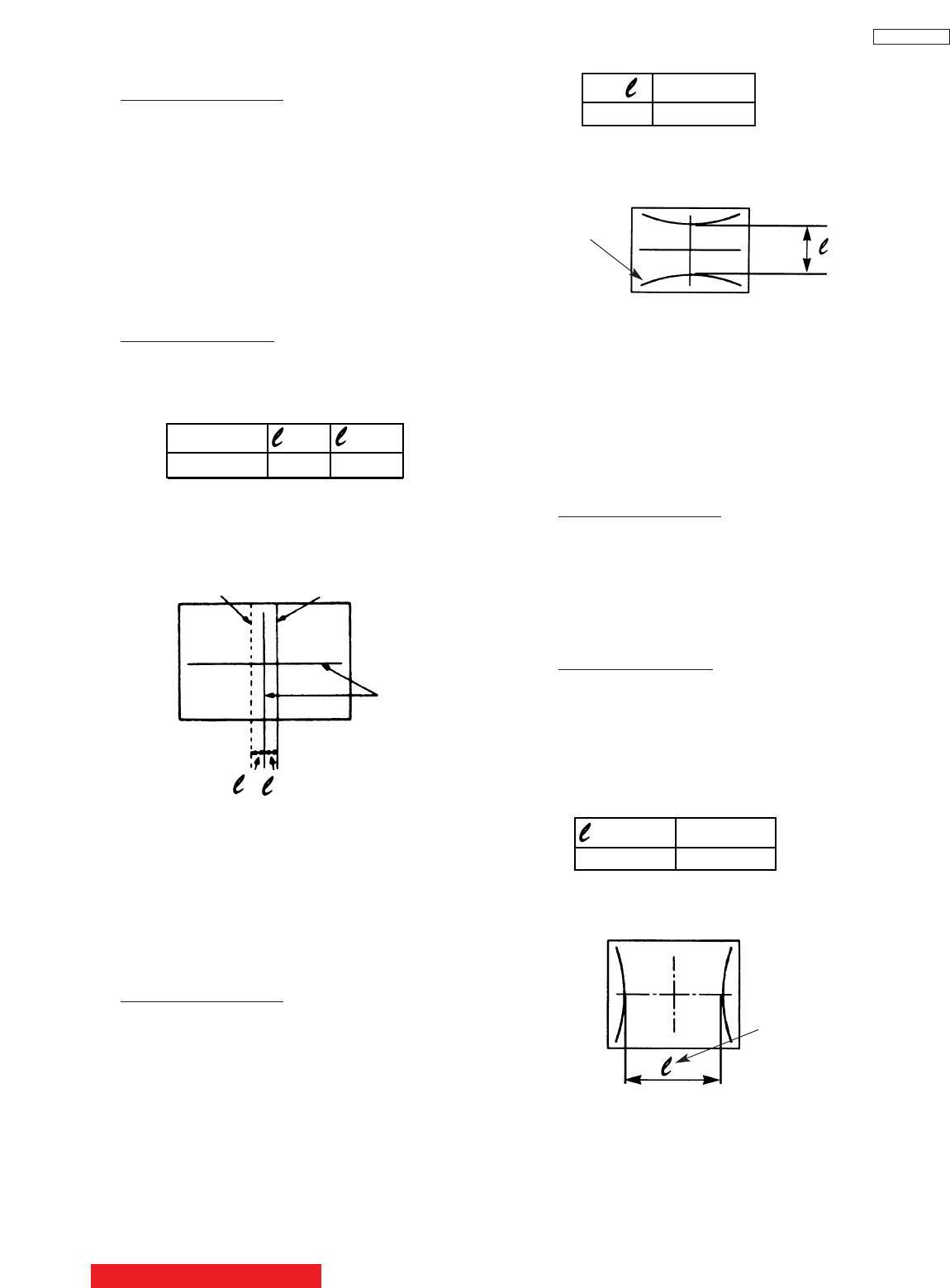
48
DP33KA/B
48
Adjustment procedure
(1) Receive any NTSC signal.
(2) Press the SERVICE ONLY SW on DEF./CONV.
PWB and POWER to display DCU uncorrected
converge data.
(3) Locate the horizontal size VR (R711 on
POWER/DEF PWB). Adjust horizontal size to
the table below.
Notes: (1) Once Normal mode Horizontal size adj. is
done.To restore old RAM data, turn TV off
and on.
(2) After adjustment, press SERVICE ONLY
switch to exit DCU crosshatch.
(3) H. SIZE adjustment is only done in
NORMAL MODE (NTSC).
=NORMAL
MODE
46” 930
Tolerance: ± 5mm
2.8 Horizontal size adjustment
Adjustment preparation
(1) The set can face east or west.
(2) Set video conditions to factory preset.
(3) The Static Focus adjustment should have been
coarse adjusted.
(4) Convergence should not be corrected.
(5) Start adjustment 20 minutes or more after TV is
turned on.
The vertical
lines at the left
and right end.
Units = millimeters
25.4mm = 1in.
2.6 Raster position adjustment
Adjustment preparation
(1) The set can face east or west.
(2) Input the single cross test signal.
(3) Set video conditions to factory preset.
(4) The static focus should have been coarse
adjusted.
(5) The digital convergence RAM should be cleared
(uncorrected state). With the TV set off, press
and hold the service switch located on the
DEF./CONV. PWB and then press the power
button.
(6) Start adjustment 20 minutes or more after TV is
turned on.
Adjustment procedure
(1) Turn the centering magnets for red, green, and
blue to satisfy the condition below. The red and
blue horizontal lines should match with green.
(RED) (BLUE)
46” 25 35
Tolerance: ± 2mm
12
Geometric
center of the
screen
RB
(2) Upon completion of adjustment, fix centering
magnets with white paint.
NOTES: (1) If internal cross-hatch does not appear
after clearing RAM data, press service
switch again.
(2) To restore old RAM data, turn TV off and
on.
12
Notes:(1) If internal cross-hatch does not
appear after clearing RAM data,
press service switch again (on
DEF./CONV. PWB).
(2) To restore old RAM data, turn TV
off and on.
(3) V-Size is only done in NORMAL
mode (NTSC).
=NORMAL
MODE
46” 505
Tolerance: ± 5mm
2.7 Vertical size adjustment
Adjustment preparation
(1) The set can face east or west.
(2) Set video conditions to factory preset.
(3) Convergence should not be corrected.
(4) Start adjustment 20 minutes or more after TV is
turned on.
Adjustment procedure
(1) Receive any NTSC signal.
(2) Press the SERVICE ONLY SW on DEF./CONV.
PWB and POWER to display DCU uncorrected
convergence data.
The horizontal
lines at the top
and bottom
(3) Locate the vertical size VR (R607) on
DEFLECTION PWB. Adjust the vertical size
according to the following table.
Units = millimeters
25.4mm = 1in.
Units = millimeters
25.4mm = 1in.
BACK TO ADJUSTMENTS
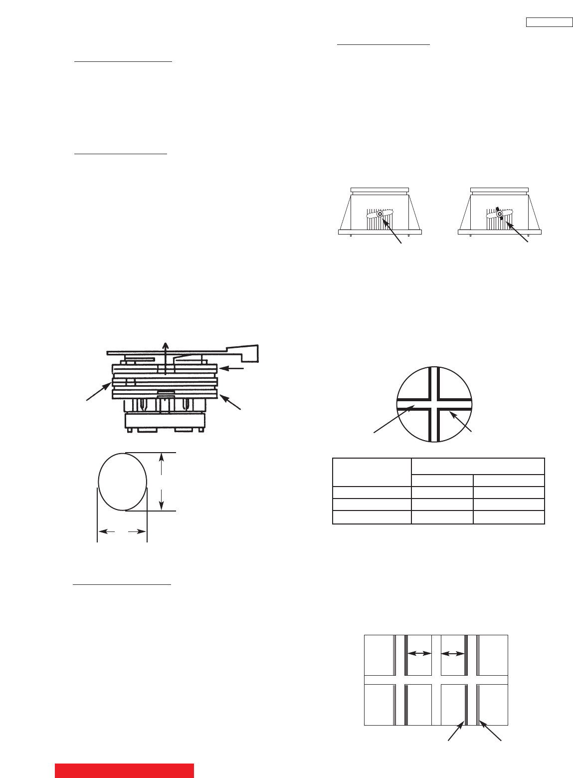
49
DP33KA/B
(Be careful the lens cylinder does not turn after
having tightened the screw or wing nuts. If it is
tightened too much, lens may tilt or screw may
break.)
(2) Apply covers to each color of R, G and B lenses.
And project a single color on the screen and
adjust in sequence. (The adjustment order of G,
R and B is only an example.)
(3) If the lens adjustment knob is turned clockwise
viewed from the front, the color Aberration
change as follows.
(NOTE 1)
Fixing Screw
(NOTE 2)
Fixing Wing Nut
TYPE 1 TYPE 2
Lens Assy Lens Assy
Change of Color Aberration
Short focus Long focus
RED LENS Orange Scarlet
GREEN LENS Blue Red
BLUE LENS Purple Green
Color
Aberration
Cross-Hatch
Change of Color Aberration
Short focus Long focus
RED LENS Orange Scarlet
GREEN LENS Blue Red
BLUE LENS Purple Green
Adjustment procedure
(1) Loosen the fixing screw or wing nut on the lens
cylinder so that the lens cylinder can be turned.
(Be careful not to loosen too much). After
completing steps (4), (5), (6) below, tighten the
fixing screws or wing nuts for each lens with a
torque of 1.18N.m (12Kgf cm) ~ 1.67N.m (17Kgf
cm).
O
I
L1 L2
(4) In case of G lens. Set to the point where the
chromatic aberration switches from blue to red.
If the chromatic aberration appearing all over
the screen is not the same, observe the vertical
bright line and adjust lens focus as specified in
table below. When the red chromatic aberration
appearing at both sides of the bright line is not
equal, observe the side with larger chromatic
aberration when adjusting.
2.10 LENS FOCUS ADJUSTMENT
Adjustment preparation
(1) The orientation of PTV set is arbitrary, west,
east, north and south.
(2) Centering DY inclination should have been
adjusted.
(3) Static focus adjustment should have been
coarse adjusted.
(4) Drive VR location adjustment should have been
completed. (Red : 12 O’clock, Green : 1~2
O’clock).
(5) Receive the cross-hatch pattern signal.
(6) Refer to setup below.
CONTRAST : HALF of full scale.
BRIGHTNESS : minimum
PRT SURFACE SIDE
4-POLE BEAM
SHAPE CORRECTION
MAGNET
2-POLE BEAM
ALIGNMENT
MAGNET
ZERO FIELD
SPACER (NO
ADJUSTMENT)
(3) Make the dot at the screen center a true circle
using the 4-pole magnet as shown below.
(4) Also adjust the Red and Blue PRT beam shapes
according to the steps (1) to (3).
(5) After the adjustment has been completed,
return R, G and B static VRs to the just focus
point.
(6) After the BEAM FORM is completed, fix the
BEAM FORM magnet with white paint.
TRUE CIRCLE SPECIFICATION
TRUE CIRCLE DEGREE: a/b
SPECIFICATION: 1.0-1.1
b
a
2.9 Beam form adjustment
Adjustment preparation
(1) Raster Position should have been completed.
(2) The raster tilt, centering, horizontal/
vertical size, scanning area check, and raster
distortion should have been completed.
(3) Set video conditions to factory preset.
(4) Input the dot signal.
(5) Set Aspect to 4:3 Standard Mode.
Adjustment procedure
(1) Green PRT beam shape adjustment. Short-
circuit 2P (TS) sub-mini connectors on Red and
Blue CPT P.W.B.s to project only the Green
beam.
(2) Turn the green static focus VR, on the Focus
Pack, fully clockwise. (Blooming)
BACK TO ADJUSTMENTS
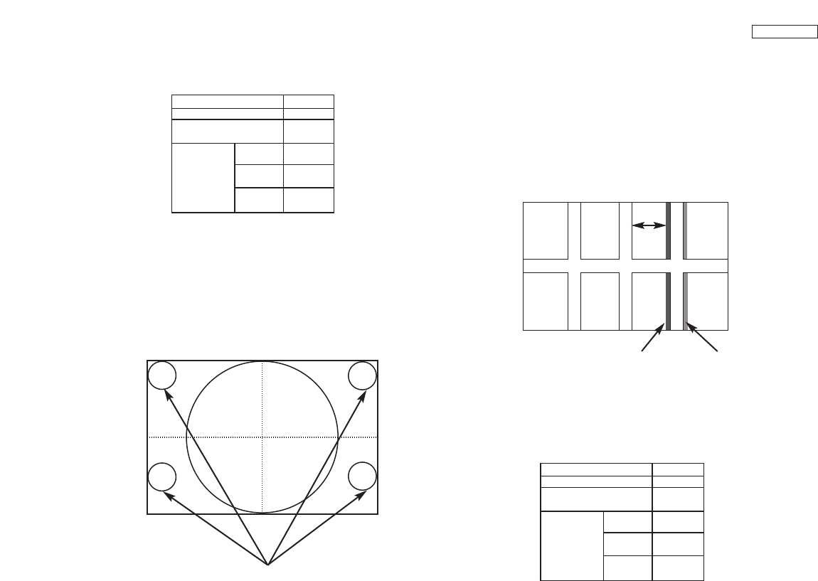
50
DP33KA/B
OPTICAL FOCUSING ADJUSTMENT RED
(6) In case of B lens. Set the position where the
chromatic aberration changes from purple to
green. As shown below, observe the vertical
bright line and adjust lens focus where the
purple or green chromatic aberration slightly
appears inside and purple or green outside
(reference value : 1~3mm) at the point specified
in table below. Change the signal and fine-
adjust in the same way as the G lens.
O
I
L
NOTE: Setting the center between Red and crimson
is optimum.
(5) In case of R lens. Set the position where the
chromatic aberration changes from red to
crimson. As shown below, observe the vertical
bright line and adjust lens focus where the
crimson or red chromatic aberration slightly
appears inside, and crimson or red outside
(reference value : 1~3mm) at the point specified
in table below. Change the signal and fine-
adjust the same way as the G lens.
OPTICAL FOCUSING ADJUSTMENT GREEN
Change the signal to the circle pattern and fine
adjust. Observe the corner part of the screen,
especially observe number in the small circle
when adjusting. If the focus performance at the
screen center exceeds the lower limit, it is
acceptable.
CHASSIS DP33W
SCREEN SIZE 46”
L1 and L2
(PITCHES from CENTER) 3.0
BETWEEN
L1&L2 *
COLOR *
ABERRATION I 2.5mm MAX
*
O 2.5mm MAX
(NOTE) * Slightly reddish or no color
** Slightly bluish or no color
Small circle of circle pattern
NOTES: 1. Since the G light is very important for
picture quality and performance, pay
special attention in its adjustment.
2. Be careful not to touch the lens with your
fingers when adjusting.
CHASSIS DP33W
SCREEN SIZE 46”
L1 and L2
(PITCHES from CENTER) 6.0
BETWEEN
L1&L2 *
COLOR *
ABERRATION I 2.0mm MAX
*
O 2.0mm MAX
(NOTE) * Slightly reddish or no color
** Slightly crimson or no color
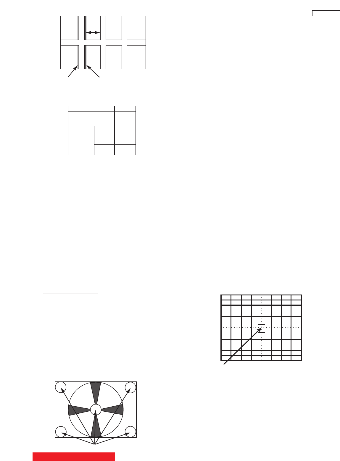
51
DP33KA/B
2.12 Digital convergence adjustment
Note: 1. If replacing a PRT, DY, etc. perform auto-
digital convergence first. (Press front panel
MAGIC FOCUS switch). This can eliminate
the need for a complete digital convergence
alignment.
2. To enter digital convergence adjustment
mode without removing the front speaker
grill, please do the following:
1) Press “Magic Focus” button on the front
panel.
2) While “Magic Focus” is running, press
Magic Focus button again to “Stop”.
3) Press INFO button after “STOP” OSD
appears on the screen to enter digital
convergence mode.
4) Proceed with convergence adjustment
and save the data.
5) Do MAGIC FOCUS sensor initialization.
6) To exit, press POWER button on the front
panel.
Adjustment preparation
(1) Receive an RF or video signal.
(2) Set controls to factory preset.
(3) Install jig screen on the set.
(4) Note the center of the video pattern displayed.
This is necessary to match dotted lines
(adjustment point viewed) and actual point that
is adjusted and displayed by the video signal.
(5) Press the service only switch (on DEF./CONV.
PWB). The pattern displayed is now the digital
convergence mode.
(6) When performing a complete digital
convergence adjustment CLEAR DATA in RAM.
(With the TV set off, press and hold the service
switch located on the DEF./CONV. P.W.B. and
then press the POWER button).
Adjustment procedure
(1) Red and blue static focus adjustment. Adjust
the static focus VR on Focus pack (UFPK) so
that the center of circle pattern is the most clear.
Check that the focus does not get conspicuously
worse at the edges of the circle pattern signal or
cross-hatch signal.
(2) Green static focus adjustment. Adjust the static
focus VR on Focus pack (UFPK) (for green) so
that the center of circle pattern is the most clear.
Check that the focus does not get conspicuously
worse at the checking point, the periphery of
circle pattern cross-hatch signal.
NOTE: Checking point for the periphery of picture.
Checking point
O
I
L
NOTE: Setting to the center between purple and
crimson is optimum.
(7) After all colors have been adjusted, display all
colors with the cross-hatch pattern signal and
check the focus performance.
(8) Then, select the circle pattern signal and check
the focus performance of each color and all
colors together.
(9) If the focus performance is not acceptable re-
adjust step (1) to (6).
2.11 STATIC FOCUS ADJUSTMENT
Adjustment preparation
(1) LENS FOCUS adjustment should be finished.
(2) Contrast : MAX
Brightness : Center.
(3) Receive the circle pattern signal.
(4) Apply covers to the lens of the colors you are not
adjusting and project only one color on the
screen.
OPTICAL FOCUSING ADJUSTMENT BLUE
CHASSIS DP33W
SCREEN SIZE 46”
L1 and L2
(PITCHES from CENTER) 5.0
BETWEEN
L1&L2 *
COLOR *
ABERRATION I 3.0mm MAX
*
O 3.0mm MAX
(NOTE) * Slightly reddish or no color
** Slightly greenish or no color
BACK TO ADJUSTMENTS
Adjustment Point
52
DP33KA/B
Parameter Normal
ADJ. DISP 0F
DEMO WAIT 1F
INT. START 13
V. SQUEEZE 10
INT STEP 1 02
INT STEP 2 06
INT BAR 2D
INT DELAY 01
MGF STEP 1 10
MGF STEP 2 06
MGF BAR 1B
MGF DELAY 01
SEL. STAT. 00
LINE WID 7F
ADD LINE 09
SENSOR CK 00
PORT 0 07
PORT 1 06
PORT 2 05
PORT 3 04
PORT 4 03
PORT 5 02
PORT 6 01
PORT 7 00
AD LEVEL 03
CENT. BAL 00
E. DISPLAY 00
ADJ. TIMS 60
AD LEVEL 05
AD NOISE 0A
OVER. LF-H 01
OVER. LF-V 00
OVER. RI-H 00
OVER. RI-V 00
PHASE MOT 60
H. BLK-RV 00
H. BLK-GV 03
H. BLK-BV 00
H. BLK-H 20
PON DELAY 0F
IR-CODE 00
INITIAL 50 9E
MGF 50 96
CENTER 50 FE
STAT 50 FE
DYNA 50 9F
2.12.1 MAGIC FOCUS Character Set-Up
This instruction should be applied when a new DCU
is being replaced.
Adjustment Preparation
(1) Receive NTSC RF or video signal.
(2) With Power off, PRESS and HOLD the SERVICE
ONLY button on DEF./CONV. PWB, then press the
Power On/Off, when picture appears release
SERVICE ONLY switch. (Internal crosshatch is
displayed without conv. correction data.)
(3) Press the SWAP button 2 times for ROM READ
operation. Picture will appear with convergence
correction data.
Adjustment Procedure
(1) Press FRZ key on R/C. (One additional line appears
near the top and near the bottom.)
(2) Press SURF key, then ADJ. PARAMETER mode is
displayed as following.
(3) Press CURSOR For Eto change the ADJ.DISP.
data.
(4) Press CURSOR Hto access DCU parameter.
Change the data as shown on Table 1, DCU
Parameter.
(5) Press PIP MODE key 2 times to write changed data
into EEPROM. (First press ADJ.PARAMETER/ROM
WRITE? is displayed for alarm. 2nd press, writes
data into EEPROM. Green dots appear after
completion of operation.)
(6) Press MUTE key 3 times to exit from ADJ.
PARAMETER mode.
ADJ. PARAMETER
ADJ. DISP.: 0F
DEMO WAIT: 1F
INT. START: 13
V. SQUEEZE: 10
TABLE 1. - DCU PARAMETER
BACK TO ADJUSTMENTS
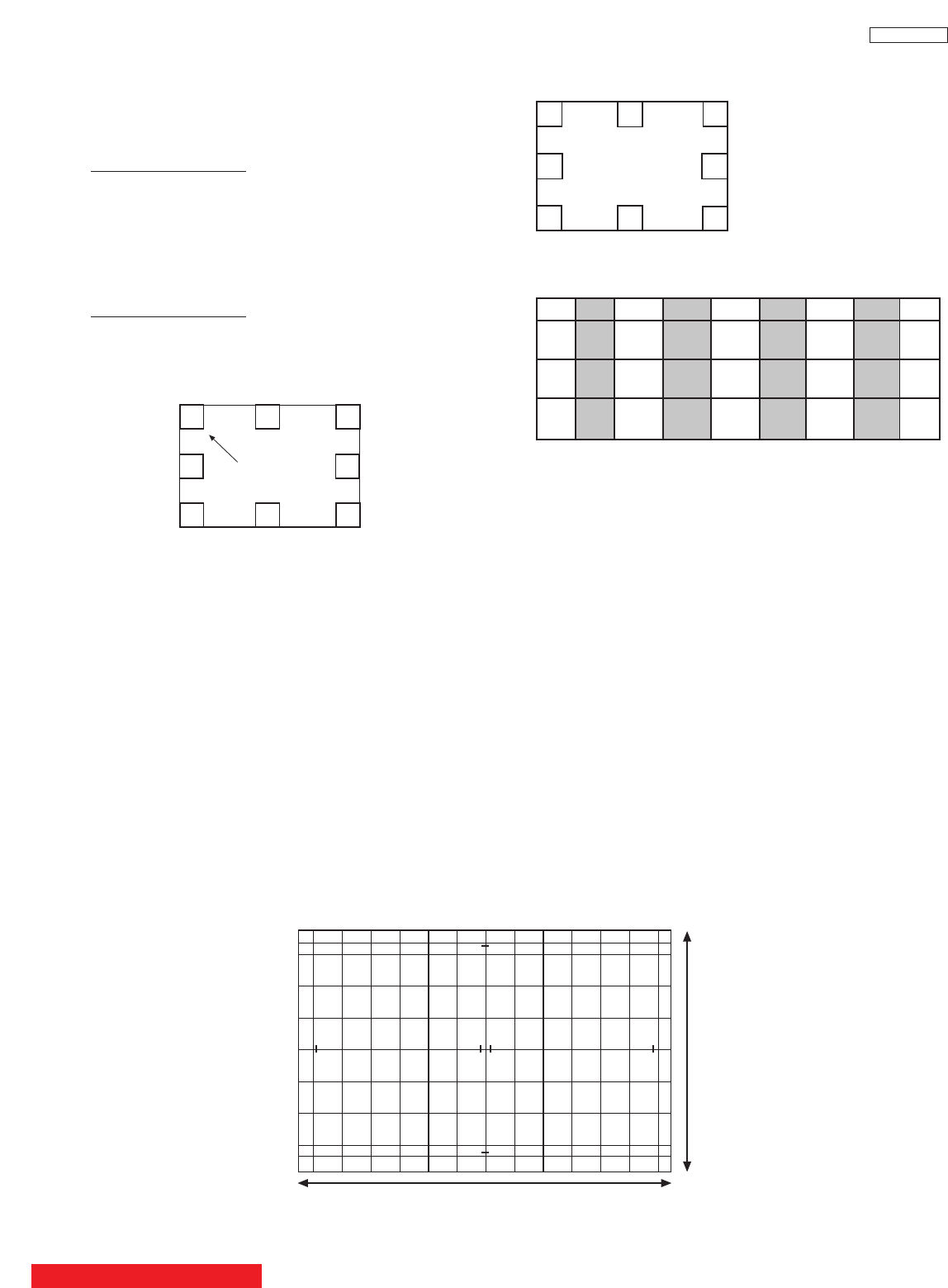
53
DP33KA/B
(7) Press PIP MODE key 2 times to write the changed
data in EEPROM. (First press, ADJ. PATTERN/ROM
WRITE ? 2nd press, writes data into EEPROM.
Green dots appear after completion of operation.)
(8) Press MUTE key to exit from PATTERN mode.
Adjustment Procedure
(1) Receive NTSC RF or video signal.
(2) With Power off, PRESS and HOLD the SERVICE
ONLY button on DEF./CONV. PWB, then press the
Power On/Off, when picture appears release
SERVICE ONLY button. (Internal crosshatch is
displayed without conv. correction data.)
Adjustment Procedure
(1) Press FRZ key on R/C. (One addtional line appears
near the top and near the bottom.)
(2) Press VID2 key, then MAGIC FOCUS PATTERN
mode is displayed as follows:
(3) Use [6] key on remote control to rotate the arrow.
Arrow indicates each sensor position. (Upper left
corner, middle top, upper right corner, right middle, in
this order).
(4) Use the keys to switch color of pattern.
INFO : Green pattern
0 : Red pattern
ANT : Blue pattern
(5) Press CURSOR For Eto change the data value to
the horizontal direction. Press CURSOR Gor Hto
change the data value to the vertical direction.
(6) Set the data as shown below:
RH : 0A
RV : FF
12
3
4
5
6
7
0
1
3
5
7
0123 4567
RH 00 02 fc fe fc 02 00 00
RV 02 00 07 00 f7 01 fd 00
GH 00 00 fc fe fe 00 00 00
GV 06 01 06 00 f9 00 fa 00
BH 04 fe fe 00 00 fe 02 02
BV 08 ff 03 00 fd 01 f8 00
Pattern Position
Normal Mode
02
4
6
Pattern: 46”`
2.12.2 MAGIC FOCUS Pattern Set-Up
NOTE: (1) This instruction should be applied when a new
DCU is being replaced.
(2) This instruction shows how to set up the pattern
position for MAGIC FOCUS.
BACK TO ADJUSTMENTS
18.2 81.8 81.8 81.8 81.8 81.8 81.8 81.8 81.8 81.8 81.8 81.8 81.8 18.2
27.5
37.0
74.0
74.0
1018
573
46” (Part Number H312275)
74.0
74.0
74.0
74.0
37.0
27.5
RB
46”
Wide
2.12.3 Convergence Jig Screen Specifications

54
DP33KA/B
Note: If only minor adjustments to convergence are
needed, the jig screen is not necessary. Use
digital data stored in memory and one color as a
reference (red, green, or blue). DO NOT CLEAR
DATA and WRITE to ROM memory.
2.12.4 Raster position adjustment
Adjustment preparation
(1) Position adjustment - This will move an entire
color. Use this adjustment to match colors at the
center of the screen. (Active video center from
external signal and physical screen center
should now match from phase adjustment).
(2) Use the buttons below to switch color to adjust.
“INFO” - Green
“0” - Red
“ANT” - Blue
Adjustment procedure
(1) Press the FRZ button. Extra horizontal lines
appear to confirm raster position mode.
(2) Use the thumb stick to adjust position.
(3) Press FRZ again to exit raster position mode.
Notes: (1) Other functions cannot be accessed when
in raster position adjustment mode. Press
FRZ and confirm extra horizontal lines
disappear to exit raster position mode.
(2) Press MENU to remove all colors displayed.
2.12.5 Convergence point adjustment
Adjustment preparation
(1) Select color to adjust.
“INFO” - Green
“0” - Red
“ANT” - Blue
(2) Use 4, 6, 2, and 5 to move the cursor position
(dotted lines).
(3) Use thumb stick to move the convergence point.
(4) Three adjustment modes are available:
1. (3x3) Press “INFO” 5 times (only works
when DCU is in uncorrected state)
2. (7x5) Press “0” 5 times
3. (13x9) Press “ANT” 5 times
For touch-up, only the (13x9) mode is necessary.
This will adjust every cross-hatch intersection point
on the screen.
For complete adjustment, start with (3x3) mode.This
will adjust center point and eight edge points only,
but will greatly reduce adjustment time. Then use
(7x5) mode, and finally (13x9) mode to finish
convergence.
If “S” distortion appears between cross-hatch
lines repeat (7x5) mode to change calculation
process while adjusting to remove distortion,
then return to (13x9) mode to finish touch-up
convergence.
Adjustment procedure
(1) Receive any NTSC signal.
(2) Start adjustment at the center of the screen.
(3) Continue adjustment at next closest position.
(4) Adjust center area first, ending with edge sections.
(5) Press VID3 button to perform calculation operation.
This process will take about 1 second and no picture
will be seen at this time.
(6) After interpolation, check convergence again and
repeat (1)-(5) if necessary.
(7) When convergence is acceptable, press PIP MODE
to write data to ROM memory. ROM WRITE? is
displayed to alarm system that ROM will be
overwritten with new data. Press the PIP MODE
button again to write displayed data to ROM.
(8) DATA WRITE TO ROM will take approximately 4
seconds and no picture will be displayed.
(9) Green dots will be displayed when operation is
completed.
(10) Press MUTE to return to convergence pattern, then
confirm again convergence is acceptable.
(11) Press PIP MODE (ROM WRITE) mode, then press
SURF to initialize sensor data positions.
Notes: (1) Display only green for easier adjustment and
match to jig screen. Press “MENU”, THEN
PRESS “INFO”.
(2) Perform interpolation and data write to ROM
after green adjustment. Once green has been
confirmed to match jig screen, the jig screen can
be removed. Do not readjust the green color
after jig screen has been removed. This is now
your reference color.
(3) Display green and red only and match red to
green.
(4) Display all colors and match blue to green and
red. Touch-up red color if necessary.
(5) Existing DATA in ROM can be read by pressing
the SWAP button 2 times.This data can be used
after replacing a component (CRT, DY, etc.)
Where complete convergence adjustment is not
necessary, be careful not to overwrite this data.
DO NOT write cleared RAM data into ROM or a
complete convergence adjustment will be
necessary. Remember to try MAGIC FOCUS
before starting convergence adjustment to
minimize adjustment time.
(6) To confirm and fine tune the convergence at the
edge of the screen, press the SURF button on
the remote control while in the digital
convergence adjustment mode (DCAM) for
additional lines at the edge of the screen. Fine
tune the edge convergence as necessary.To
exit, press SURF again.
BACK TO ADJUSTMENTS
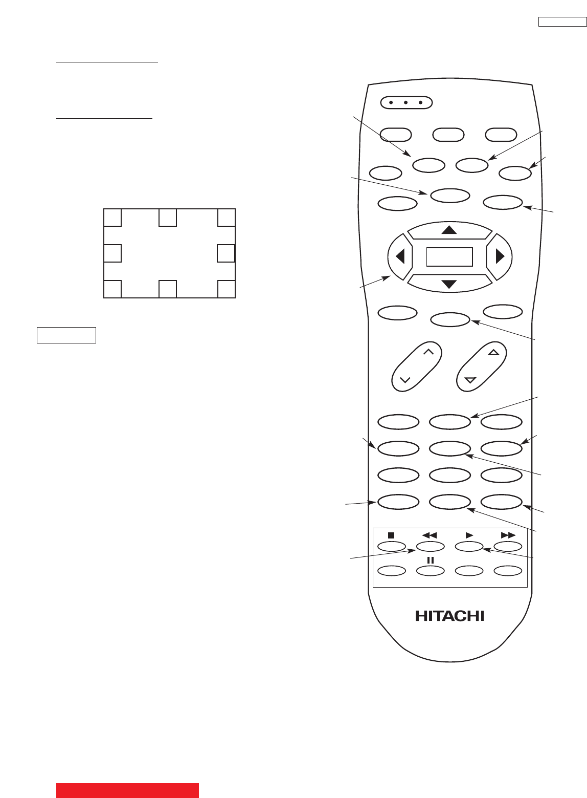
55
DP33KA/B
2.12.6 Magic Focus Initialize
Adjustment Preparation
(1) Receive any NTSC signal.
(2) Digital convergence adjustment should have been
completed.
(3) Set is in DCU adjustment mode.
Adjustment Procedure
(1) Press “PIP MODE” and then “PIP CH” to initialize
Magic Focus. The initialize operation starts and
several windows appear during this operation. It
takes about 30 seconds or less.
(2) When green dots appear, initialize operation is
finished.
(3) Turn power OFF on TV set.
REMARKS
Another way to start the initialize operation:
(1) Press “SERVICE ONLY” Sw. on DEF./CONV. PWB to
set DCU adj. mode.
(2) Press [PIP MODE] key on R/C. Then “ROM
WRITE?” is displayed for alarm. Next, press [PIP
CH] key on R/C to start initialization. When green
dots appear, initalization operation is finished.
NOTE: If there is an error message, red dots or an error
code, refer to page 58, CONVERGENCE
ERRORS.
*INITIAL:N*
Initialization Operation
BACK TO ADJUSTMENTS
123
456
789
0
ANT INFO
VOL CH
POWER
TV CBL/SAT DVD/VCR
PIP SWAP PIP MODE FREEZE
DAY/NIGHT SURF MENU
MUTE EXIT LAST CH
REC ASPECT VIRTUAL HD
SELECT
VID1 VID2 VID3 VID4
VID5
ROM READ
PHASE CALCULATION
R/C must be in
VCR mode.
GREEN
ADJUSTMENT
CURSOR LEFT
CURSOR
DOWN
BLUE
(13x9)
REMOVE
COLOR
ROM WRITE
RASTER
POSITION
CROSSHATCH
VIDEO
CURSOR UP
CURSOR
RIGHT
RED
(7x5)
INITIALIZE
Digital Convergence Remote Control
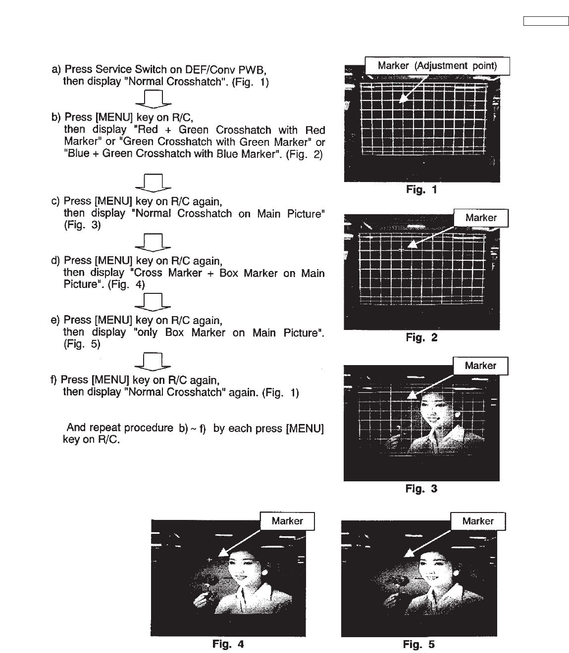
56
DP33KA/B
“Convergence For Outside Signal” function
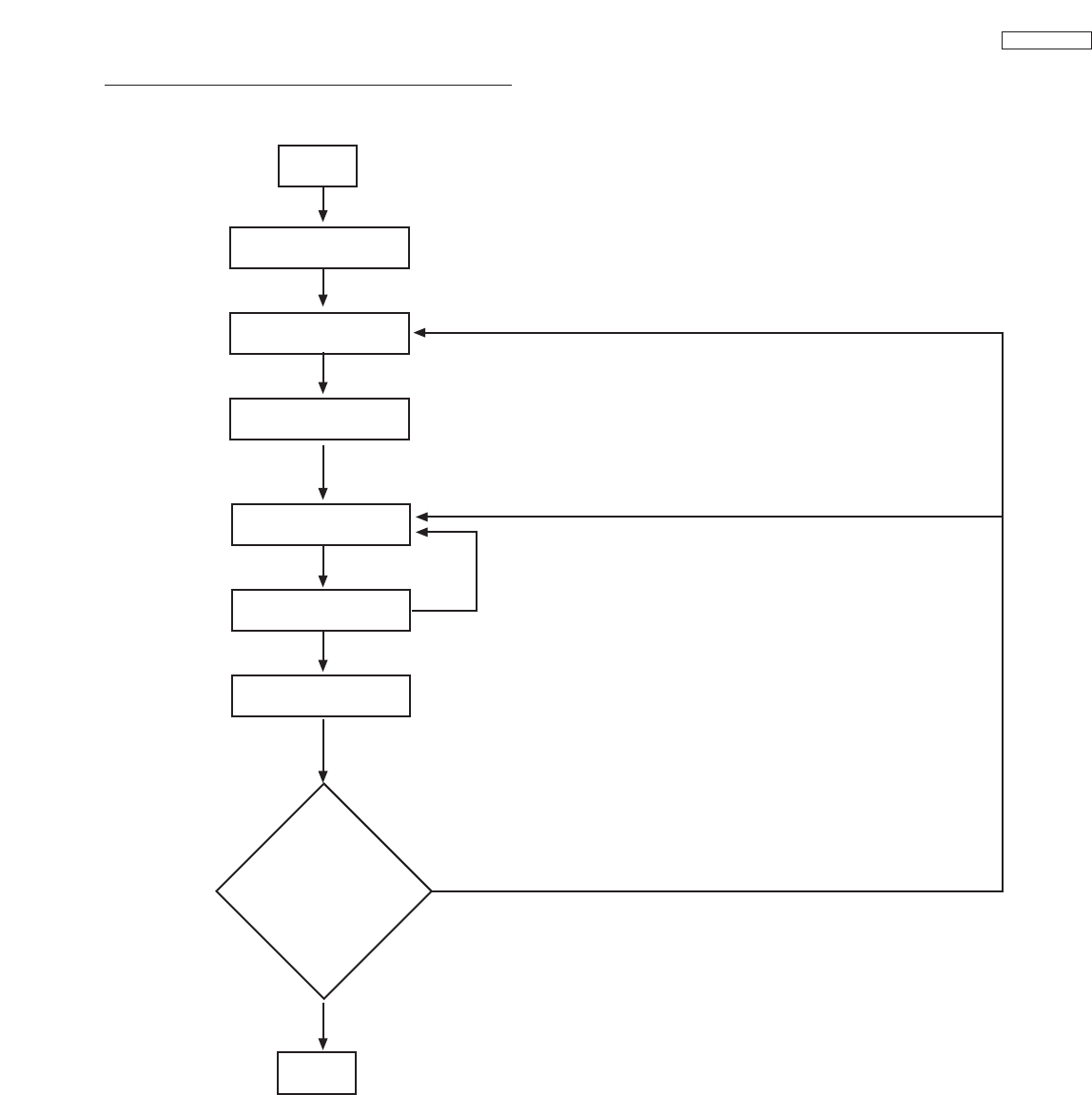
57
DP33KA/B
WHITE BALANCE ADJUSTMENT FLOW CHART
START
Cut Off Adj.
Blue defocus Adj.
Sub bright Adj.
Adj. High Light W/B
Adj. Low Light W/B
Sub bright Adj.
Check
Low Light W/B
High Light W/B
FINISH
Repeat two or three times, until no
adjustment is needed
If NOT OK
If OK
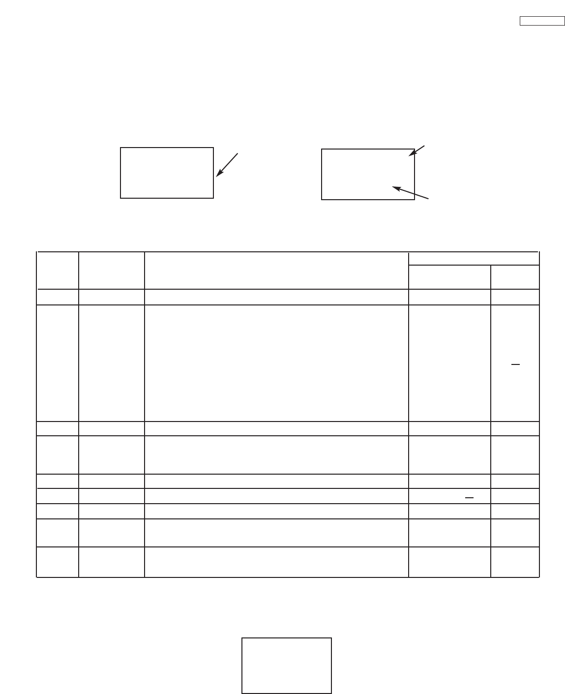
58
DP33KA/B
(5) Convergence Errors.
If an error message or code appears while performing MAGIC FOCUS or initialize (MODE, SURF in DCU service
mode) follow this confirmation and repair method.
1. Turn on power and receive any signal.
2. Press service switch on DEF./CONV. board.
3. Press “SWAP” then “SURF” on remote control.
4. Error code will be displayed in bottom right corner of screen. If there is no error, an “INITIAL OK” message will
appear on screen.
5. Follow repair table for errors.
ERROR!! Error code CONNECT 1!
Error message
Sensor position
XNo. 1 3
DCU REPAIR TABLE
Error
Code
Error
Display
Code Countermeasure
Application
Initialize Magic
Focus
1
2 Connect 1 1. Darken Outside Light
*2 2. Placing of sensor
3. Is pattern hitting sensor
4. Check connection and solder bridge of sensor
5. Replace sensor
6. Replace sensor P.W.B.
7. Sensor Connector check
8. Replace DCU
9. Adjustment check (H/V size, centering)
VF Error Replace DCU
3*2
4Over Flow 1. Check the placement of sensor
2. Adjustment check (H/V size, centering)
3. Conv. amp. gain check *1 (check resistor values only)
A/D Level Same as Error Code 2
Convergence Same as Error Code 4
5
Operation Same as Error Code 4
7
Connect 2 Same as Error Code 2
9
Noise Input strong field signal
Check the wiring of connector between sensor and DCU
10
Sync Input strong field signal
Check the wiring of connetor between sensor and DCU
11
*1 -- RK 41, 42, 45, 46, 49, 50, 53, 54, 57, 58, 61, 62 check these resistors.
*2 Sensor Position
0 1 2
73
654
(View from front side)
XX
X
XX
XX
XX
X
XX
XX
XX
8 Sensors
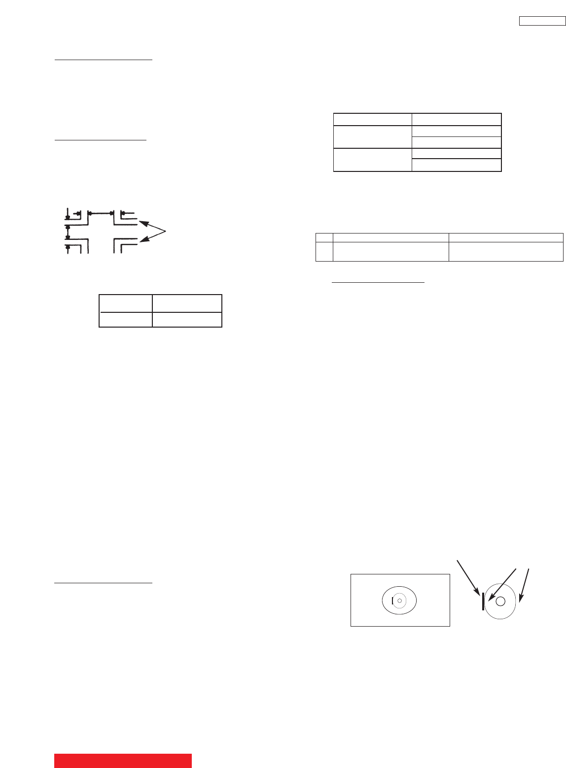
59
DP33KA/B
Condition: User controls are set to the initial set
positions (for shipment)
Measuring point-Screen center.
STICKING OUT OF BLUE
UNEVENNESS SPECIFICATION: ±1cd/m2
Defocus sticking out specification
Screen Size Blue sticking out
46” 1.0mm
2.13 Blue Defocus adjustment
Adjustment Preparation
(1) Optical and electrical focus adjustment should
have been completed.
(2) The convergence adjustment should have been
completed.
(3) Set Video conditions to factory preset.
(4) Input the cross-hatch signal.
Adjustment procedure
(1) Turn the B Focus VR (Focus Pack) fully
clockwise.
(2) Adjust sticking out level of blue to specification
shown in table below, by turning the (B) FOCUS
VR counter clockwise.
(6) BLUE defocus ADJ. should be finished.
(7) The vertical incident illumination on the screen
should be 20 Lux. or less.
(8) Picture Format is 16:9 Standard Mode.
(9) Go into I2C service mode.
Table 1: White Balance Adjustment Signal
Table 1 shows amplitude of White raster (without sync,
termination impedence: 75ohm).
Table 2: White Balance Adjustment Specification
Adjustment Procedure
A. High Light W/B adjustment
(1) Receive signal for High Light white balance ADJ.
(2) Adjust white balance at center of screen, using R
DRV/ G DRV with remote control (see Table 2).
B. Low Light W/B adjustment
(1) Receive signal for Low Light white balance ADJ.
(2) Adjust white balance to center of screen, using R
CUT OFF/G CUT OFF/B CUT OFF with remote
control. Do not touch screen VRs (see Table 2).
(3) Take Green color as a reference color, then adjust
Low Light W/B by increasing other two colors CUT
OFF data. Do not change GREEN CUT OFF data.
CA-100 Probe should be set to a direction as shown
below.
Repeat A & B two or three times, until no adjustment
is needed (white balance tracking-GOOD). If W/B
tracking is not good, set all data (Both DRV and CUT
OFF) to inital data, and change reference color to
different color.
Note: If Low Light adj. spec cannot be followed, apply
previous adj. spec. (adjust by eye.)
Screen Size 46”
High light [IRE] 100
[Vpp] 0.715
Low light [IRE] 25.0
[Vpp] 0.175
Set probe to above direction.
(Screw hole side should
be on the left side)
Top view of
CA-100 Probe
Screen
Screw Hole Flat Face
Size Highlight Lowlight
46” 10800K±0MPCD 10800K±0MPCD
(x=0.277 ± 0.004, y=0.284 ± 0.004) (x=0.277 ± 0.004, y=0.284 ± 0.004)
2.14 White balance adjustment
(1) Screen adjustment
(2) High light white balance.
(3) Low light white balance.
I2C data for High light white balance
Green : G DRIVE (HIGH) 3F (initial data)(Adjustable)
Red : R DRIVE (HIGH) 3F (initial data)(Adjustable)
I2C data for Low light white balance
Green : G CUT OFF (HIGH) 7F (initial) (Fixed data)
Red : R CUT OFF (HIGH) 7F (initial) (Adj. data)
Blue : B CUT OFF (HIGH) 7F (initial) (Adj. data)
Adjustment Preparation
(1) Adjustment should start 20 min. or more after the TV
power is turned ON.
(2) CUT OFF ADJ. should be finished.
(3) VIDEO control : Contrast is MAX., Others are center.
(4) Color temp. : HIGH
(5) Signal:
* Hight Light white Balance Adj.
White raster 0.715Vpp (w/o sync., termination
incidence : 75ohm.) 100IRE
* Low Light white balance ADJ.
White raster 0.180Vpp (w/o sync., termination
incidence : 75ohm.) 25 IRE (The brightness
equal to 20cd/m2at screen center.
BACK TO ADJUSTMENTS
60
DP33KA/B
2.15 Sub brightness adjustment
Adjustment preparation
(1) Start adjustment after the power is turned ON
for 20 minutes or more.
(2) Receive the color bar signal.
(3) The vertical incident illumination on the screen
should be 20 lux or less. (Room should be dark).
(4) Picture Formats is 16:9 Standard Mode.
Should sink
to black
Should rise
slightly from
black
Adjustment procedure
(1) Go to “Sub Brightness” adjustment in I2C
ADJUST mode (press Input and Power button
on Control panel at same time), using CURSOR
G, Hand then CURSOR E.
(2) Then adjust “Sub Brightness” using CURSOR
F, Eto increase or decrease the value,
according to figure. (Visually adjust).
(3) After adjustment, press MENU button to exit I2C
ADJUST mode. (Data is stored in memory).
Note: When selecting SUB-BRIGHTNESS mode the
microprocessor sets the CONTRAST and
COLOR to MIN. automatically, but make sure
that the other conditions are center.
Directly observe the screen by eye without using
a mirror.
Y CY G MG R BL
A7 A6 A5 A4 A3 A2 A1
B
C
D
Q I W 100% BLK
W
75%
BACK TO ADJUSTMENTS
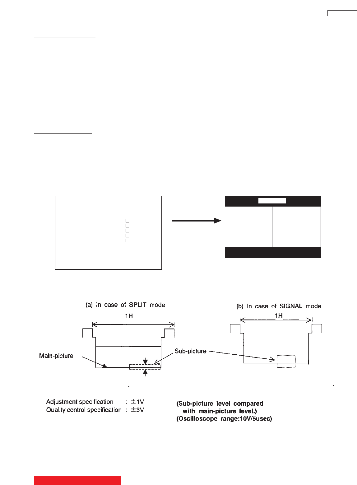
61
DP33KA/B
2.16 Sub Picture Signal Amplitude Adjustment
Adjustment preparation
(1) Sub-brightness adjustment should be finished.
(2) Start adjustment about 20 minutes after the power
switch is turned on.
(3) Condition should be as follows:
Contrast : Max
Brightness : Center
(4) Press PIP button on R/C unit. Select Split mode.
(5) Receive ANT A NTSC white signal (amplitude
1. 0Vp-p), main-picture and sub-picture. (Do not use
Video/S-Video/YPBPR/DVI.)
(6) Connect probe on the P852(CPT P.W.B.-Green) to
check sub-picture amplitude.
Adjustment procedure
(1) Go to “SUB CONT(TV-S)” adj. on the I2C service
mode.
(2) Press “PIP” button and “MODE” button of R/C.
(3) Observe P852 on the CPT P.W.B. and change the
“SUB CONT(TV-S)” I2C data so that the amplitude of
the sub-picture is the same level as that of the main
picture.
DISPLAY
Main Picture
Press “PIP” button
and “PIP Mode”
button
ADJUST MODE
TA1270-M
SUB CONT(TV-S) **
OSD POSITION
AFC/CLOCK TEST
MEMORY INIT
I2COPEN
IR BLASTER
Main Picture
SPLIT
MAIN
ANT A SUB
ANT A
Wave form of P852 (Green Cathode)
BACK TO ADJUSTMENTS
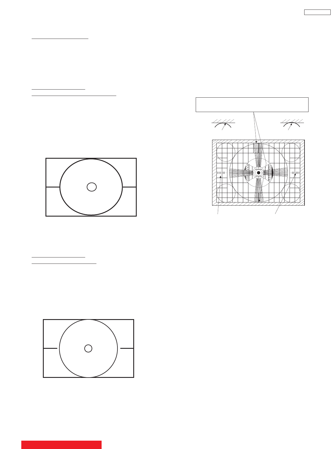
62
DP33KA/B
3 5 5 3
Top and bottom of the circle is between
outer edge and inner edge.
Outer edge of the circle Inner edge of the circle
H size marker
0.7~1.5
H size marker
0.7~1.5
2.18 Scanning area check
Checking condition
(1) Digital convergence adjustment should have
been completed.
(2) Receive the circle pattern signal.
(3) Brightness/Contrast - standard condition
Contrast:max
Other controls:center position
(4) Check that the scanning area matches with the
following drawing.
2.17 Horizontal position adjustment
Adjustment preparation
(1) The screen face of set should be turned to East
or West.
(2) VIDEO control should be set to Factory Preset
Condition.
(3) DIGITAL CONVERGENCE adjustment should
be finished.
Adjustment procedure
NORMAL 16:9 STANDARD MODE
(1) Receive circle pattern.
(2) Picture Format is 16:9 Standard.
(3) Go to I2C Adj. mode by pressing INPUT and
POWER button on control panel at the same
time.
(4) Choose H. POSITION item using R/C CURSOR
G,H.
(5) Adjust HORIZONTAL POSITION as follows,
using R/C CURSOR F,E.
Spec: Balance Left/Right side display position.
H. size marker 1.0~2.0.
Adjustment procedure
1080i 16:9 Standard Mode
(1) Input 1080i (fH=33.75KHz) component circle
pattern signal to component video terminal.
(2) Picture Format is 16:9 Standard.
(3) Go to I2C Adj. mode.
(4) Choose H. POSITION item using R/C CURSOR
G,H.
(5) Adjust HORIZONTAL POSITION as follows,
using R/C CURSOR F,E.
Spec: Balance Left/Right side display position.
BACK TO ADJUSTMENTS
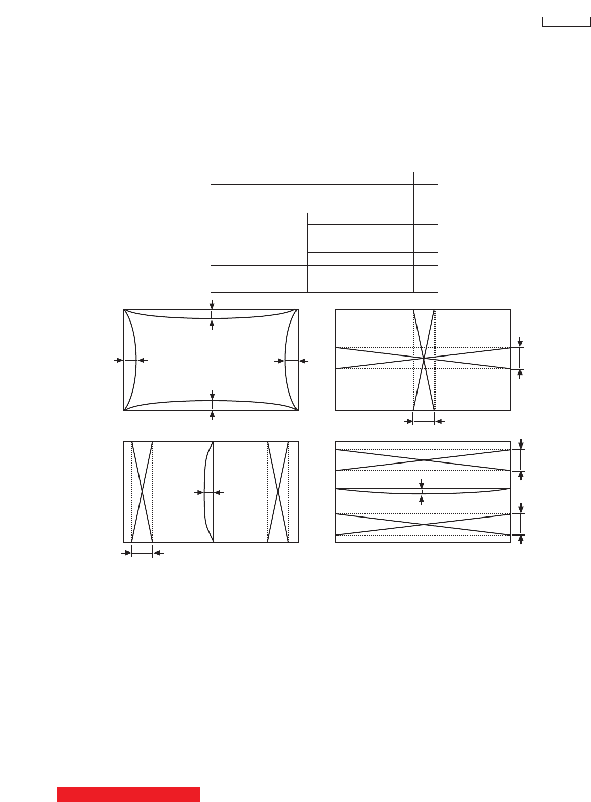
63
DP33KA/B
2.19 Raster distortion check
Checking condition
(1) Digital convergence adjustment should have been completed.
(2) Receive the cross-hatch signal (internal signal of the set is acceptable).
(3) Brightness/Contrast --- standard condition
Contrast : max
Other controls : center position
(4) Check the raster distortion specification: Value shown in the table below or less.
A ~ D
I ~ L ---Measure the winding of the outside line.
Item Symbol 46”
Top/Bottom pincushion distortion A,B ±5
Right/Left pincushion distortion C,D ±4
Center line Vertical line E 5
tilt Horizontal line F 5
Center line Vertical line G ±3
winding Horizontal line H ±3
Trapezoidal distortion Vertical line I,J 4
Skew distortion Horizontal line K,L 5
(unit: mm)
G
IJ
D
C
A
B
F
E
K
H
L
BACK TO ADJUSTMENTS
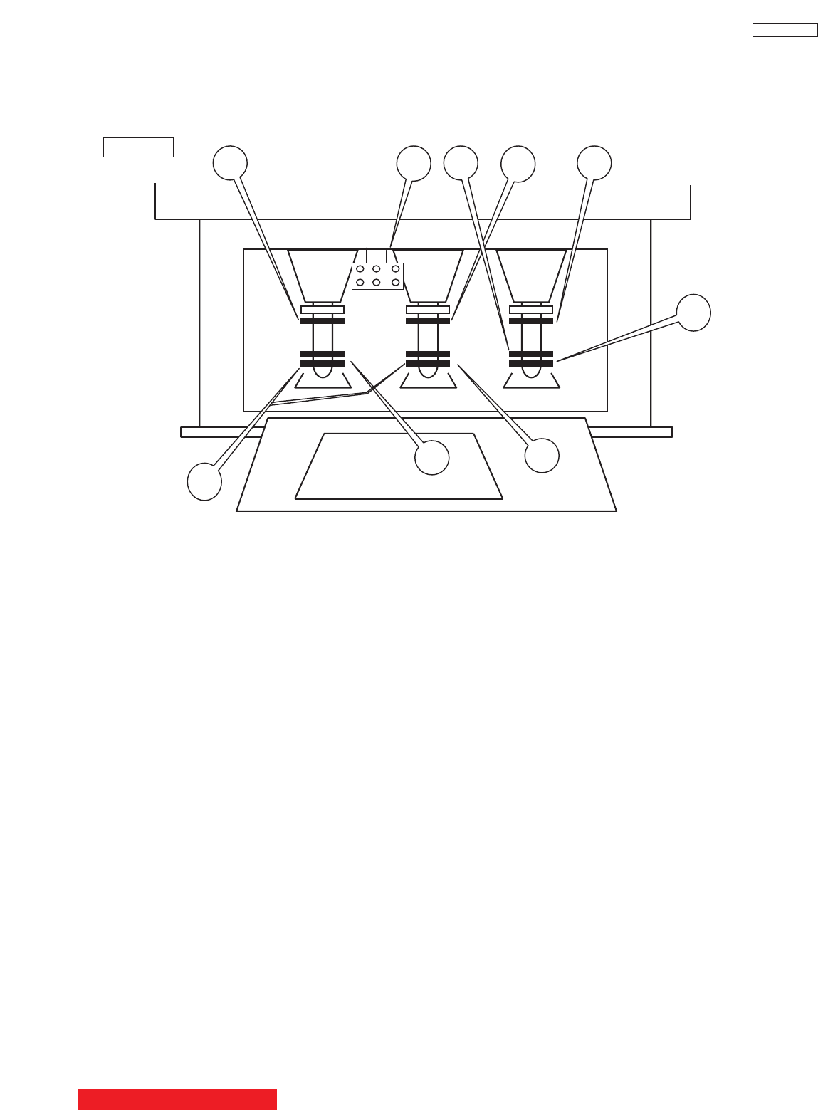
64
DP33KA/B
3. ADJUSTMENT POINT
3.1 CRT, cabinet locations
FRONT
1. CENTERING MAGNET FOR RED PRT
2. CENTERING MAGNET FOR GREEN PRT
3. CENTERING MAGNET FOR BLUE PRT
4. 4-POLE MAGNET FOR BEAM FORM ADJUSTMENT
5. BEAM ALIGNMENT MAGNET
6. FOCUS PACK
164 23
544
5
1. CENTERING MAGNET FOR RED PRT
2. CENTERING MAGNET FOR GREEN PRT
3. CENTERING MAGNET FOR BLUE PRT
4. 4-POLE MAGNET FOR BEAM FORM ADJUSTMENT
5. BEAM ALIGNMENT MAGNET
6. FOCUS PACK
BACK TO ADJUSTMENTS
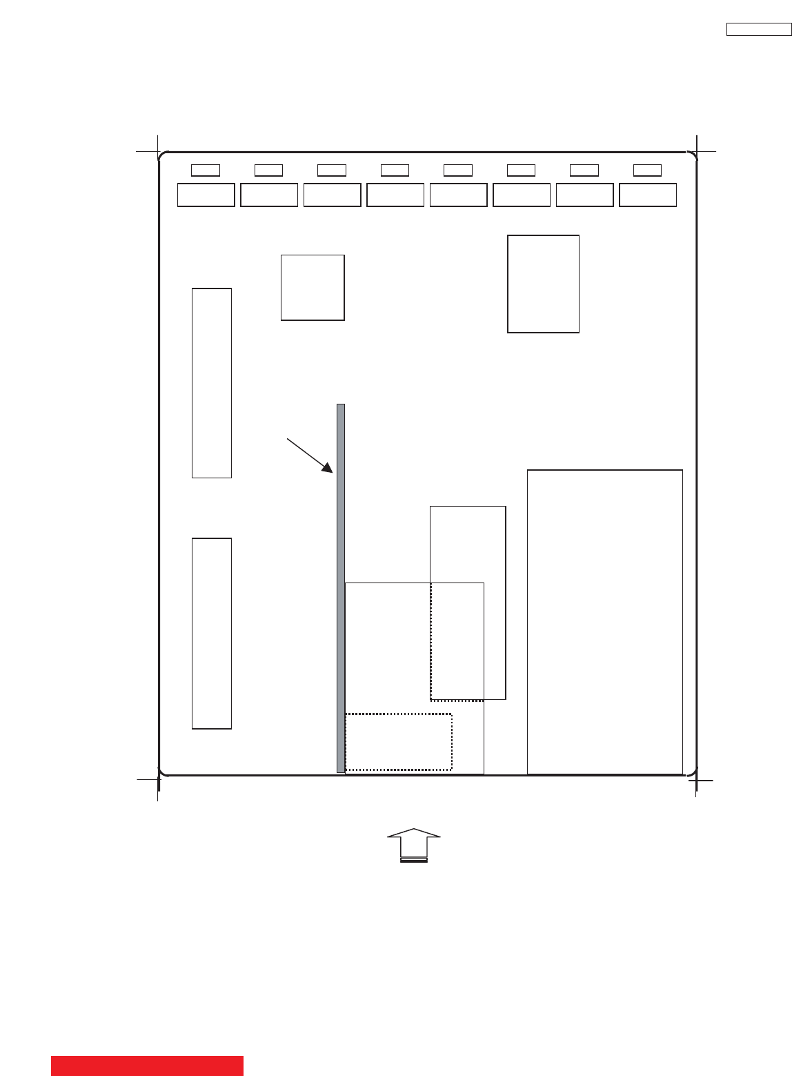
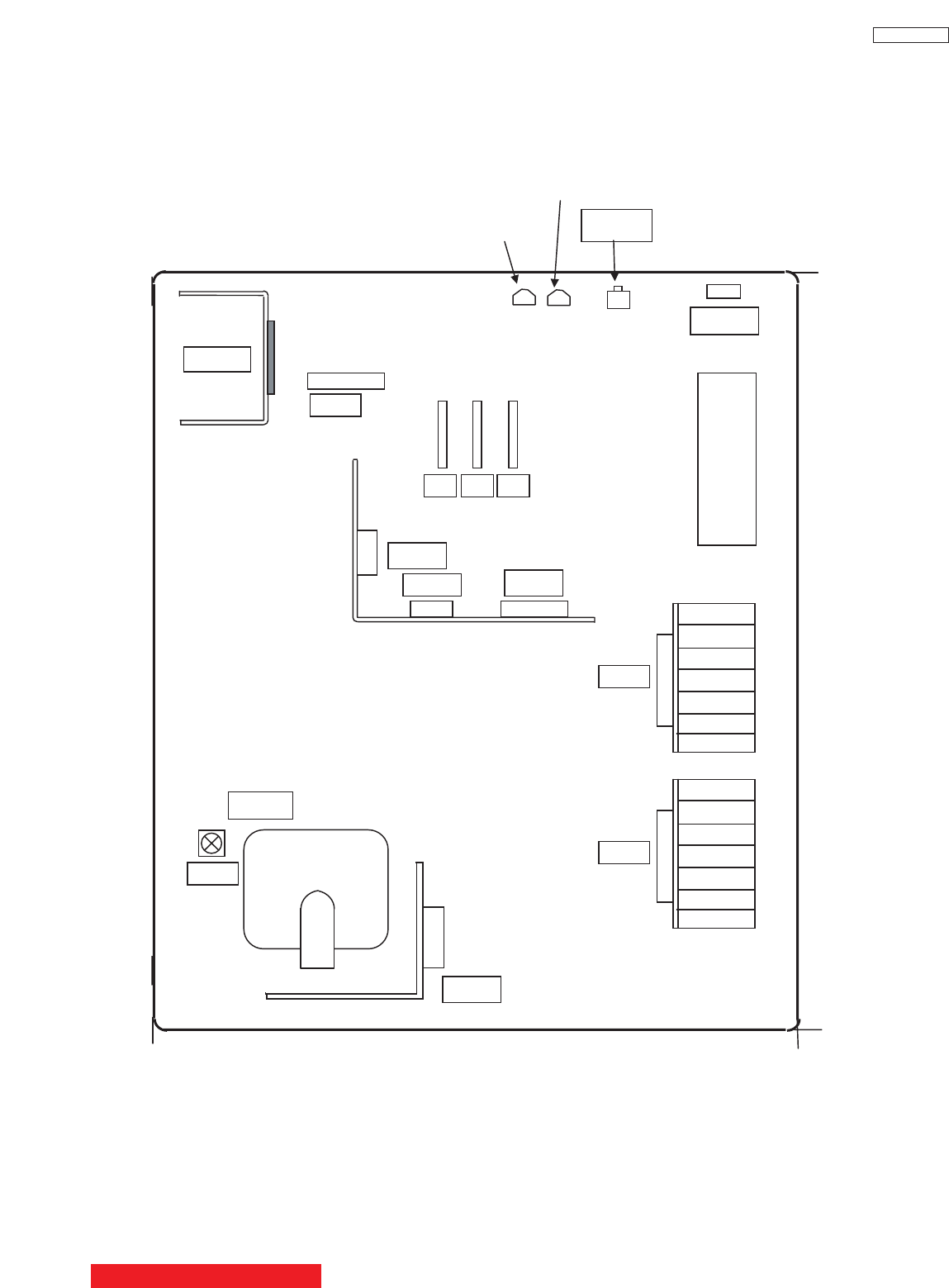
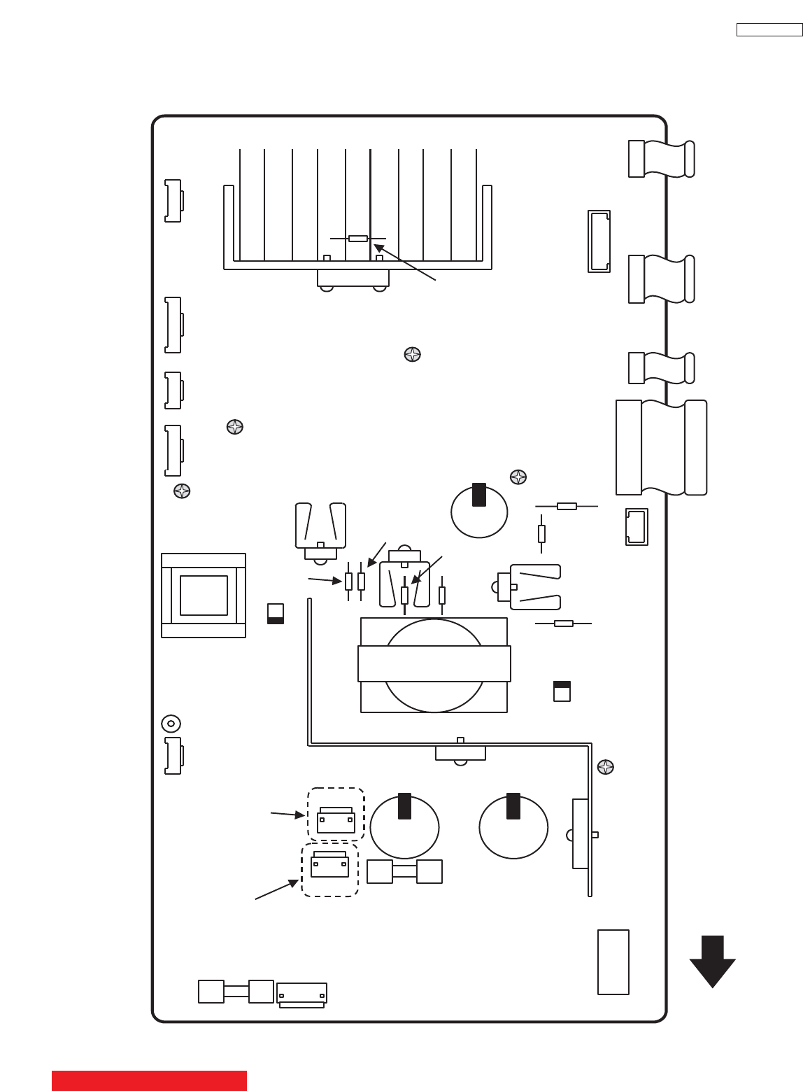
67
DP33KA/B
3-4. POWER SUPPLY P.W.B.
IAA1
PPS1 PPS3 PPS4 PPS5 PPS6
PSP
PPD3
PPD5
PPD4 PPD1
PPC1
D901
S901
D956
Audi
(Green)
o
E903
+2 20
V
D913
SBY+ 5V
D912
Ma in
Pow er
I902
ACK
I903
FB
D932
+B
(Green)
E907
+B
E906
+B Reg
E905
-28V
E901
Audio
E904
+2 8
V
PPC2
PA
1 2
St an d-by
Module
Main Power SW
Back Cove
r
PPQ
PPV
1 3
1 3
DVD Model
only
Digital module Model
only
D955
SW+5.5V
(Green)
D913
SBY+5V
(Green)
E902
+10V
I902
ACK
Module
I903
FB
D912
Main
Power
(Red)
I901
T901
Switching Transformer
F903
FUSE
F901
FUSE
PPD1
EAG1
Audio-GND
U901
BACK TO ADJUSTMENTS
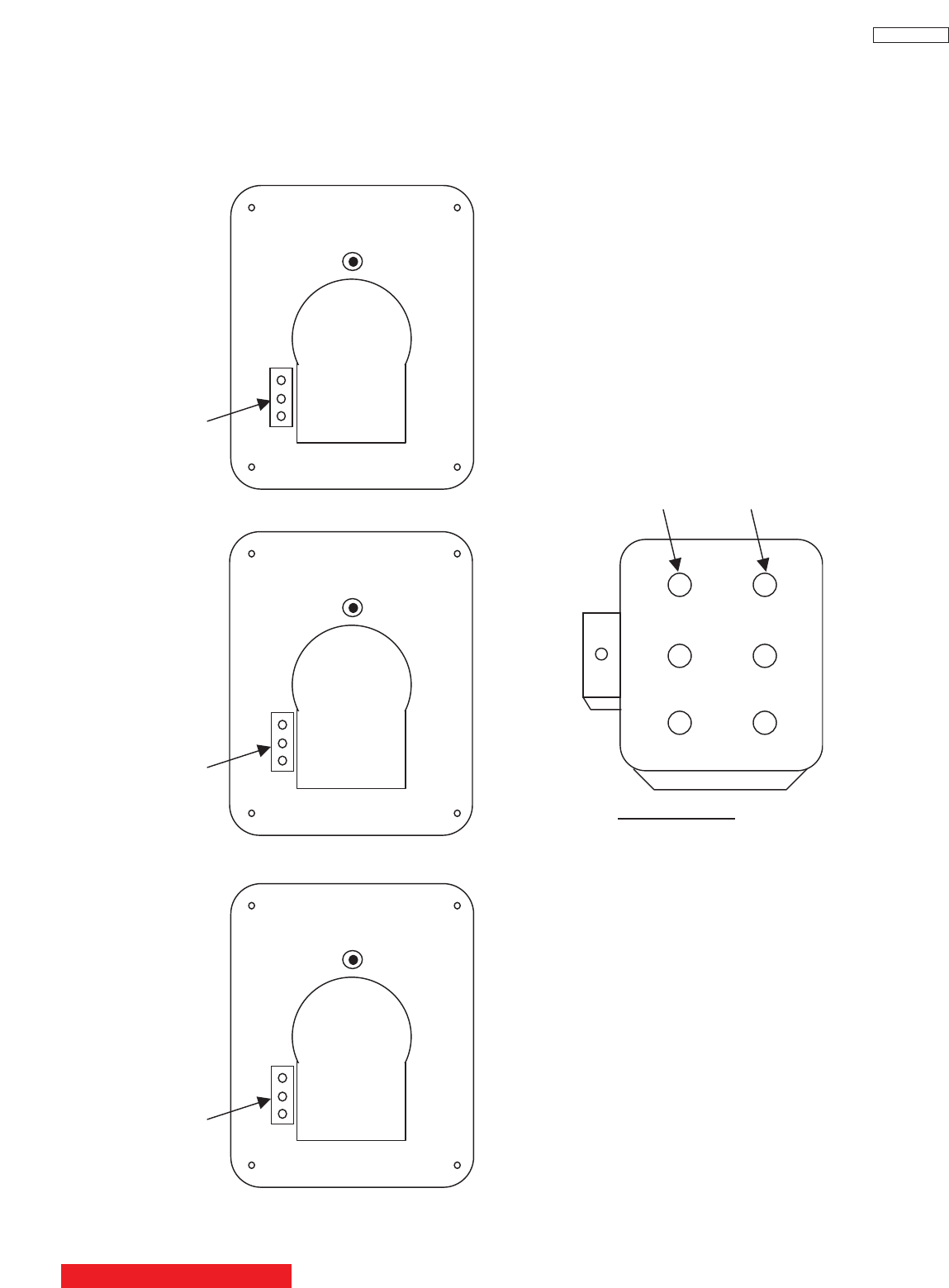
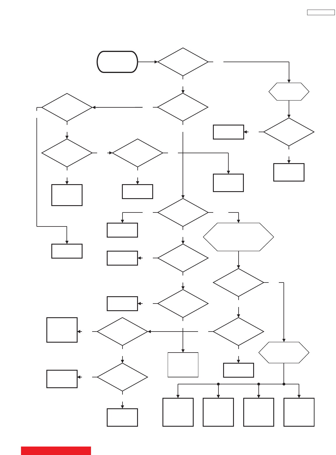
69
DP33KA/B
Check
(Power Supply PWB)
NO
No
Raste
r
Is click sound
of Relay(S901)
heard?
Does Red LED
(D912) "ON","BLINK"
or "OFF"?
1. Turn OFF the power SW.
2. Wait for 3 seconds.
3. Turn ON again after several
seconds,and observe
green LEDs carefully.
Are 4 Green LEDs
turned OFF at the
same time?
PWB connecter
(PPS5) open.
SW+115V line
E907, D932,
D925, Q777,
QH01, Q701,
TH01, T701
etc.
SW+28V line
E904, D922,
etc.
SW+5.5V line
D955, I905,
etc.
Audio line
D956, E901,
D915, IAA1,
etc.
U901, D902,
etc.
SBY+5V line
I009, I001,
etc.
E907,
etc.
Check Check Check
Check
(Power Supply PWB)
Is Voltage at
pin(4) of I901
14V-20V?
(Power Supply PWB)
Has Fuse F903
blown?
Check
D911, R906,
R907, C911
Check
I901, D901,
R902
YES
NO
YES
YES
YES
OFF
YES
NO
NO
BLINK
YES
NO
(Deflection PWB)
Is base Voltage
Of Q709 normal?
Does raster
Appear with (6) and (5)
Of PPD4 shorted?
(Deflection PWB)
Are Voltages
At both ends of T702
(primary side)
normal?
Check
I501 pin(37)
-H out,
I503 pin(31)
-DEF Hvcc
etc.
Check
T702, R748,
R730
etc.
NONO
NO
(Power Supply PWB)
(Power Supply PWB)
Is Power LED
(D913,Green)
"ON"?
NO
YES
(Signal PWB)
Is Voltage
at pin(16) of I001
3.3V?
(Signal PWB)
YES
Check
ON
I001
Check
(Signal PWB)
NO
Check
I901, D911,
D910, R908,
R909, R910
R911
Replace F903
Check
Q903, Q904,
etc.
YES
Check
Find LED(s) that is
Turned dark or OFF
Earlier than the others.
(Power Supply PWB)
(Power Supply PWB)
(Power Supply PWB)
Check
Q001, Q002,
I902, D906
etc.
NO
Is Voltage
at pin(7) of I001
"AC CLOCK in"?
Is Voltage
at pin(59) of I001
"H"?
Q027, Q028,
PPS3, Q902
S901
etc.
Check
YES
YES
Check
NO
I009, I001
YES
Check
Q777, QH01,
T701, TH01
etc.
Is Power LED
(D913,Green)
"ON"?
TROUBLE SHOOTING FLOWCHART
1. NO RASTER AND NO POWER (How to check LED’s Diagnosis)
TABLE OF CONTENTS
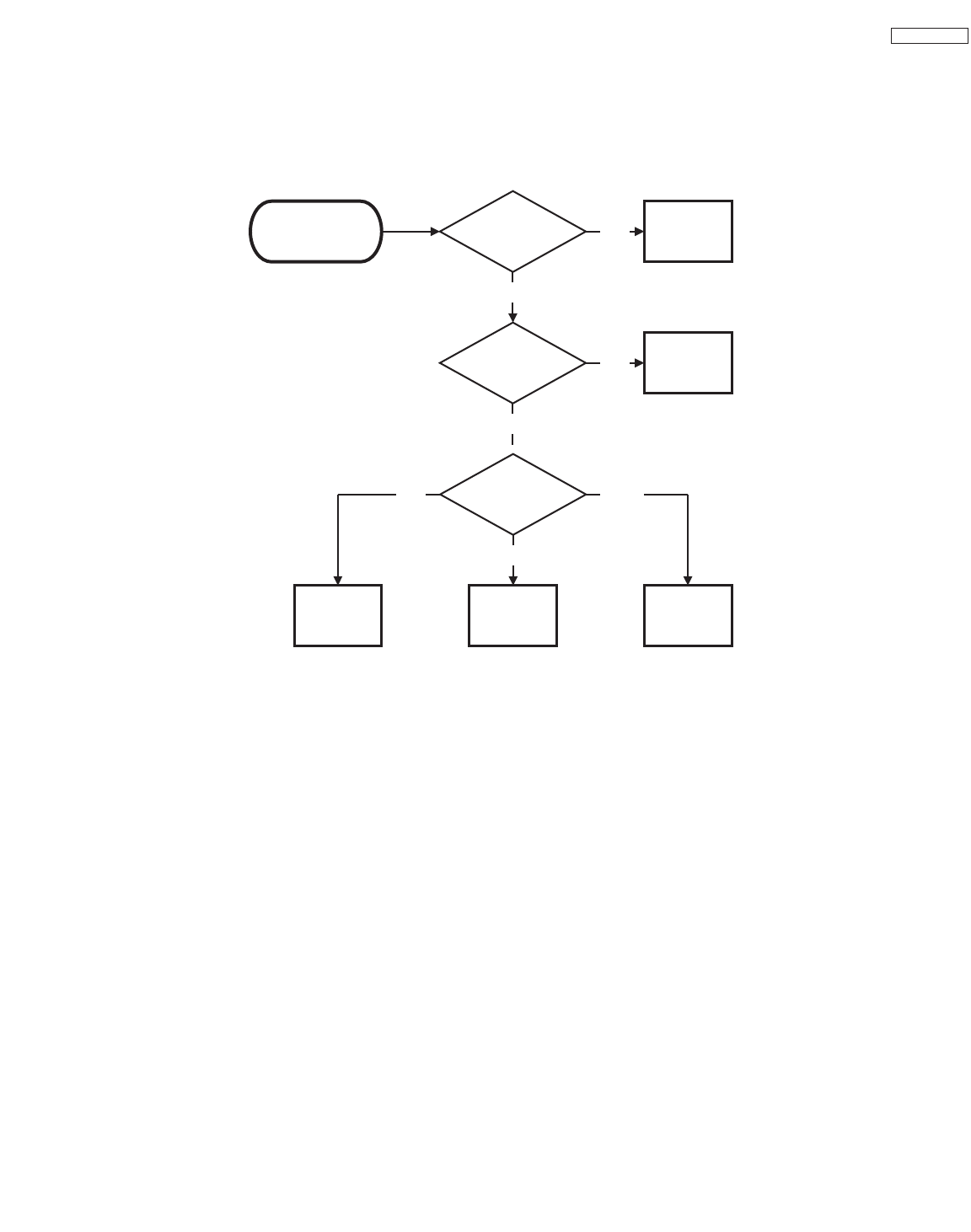
70
DP33KA/B
2. No Picture (Only DTV Mode) DP36 / DP38 / DP38D
Is SBY+5V LED
(DP15,Green)
ìONî?
(Signal / Digi Pow PWB) Check
Q029, Q030,
QP07, SP01
NO
(Power Supply PWB) Check
U901, D902,
PMQ
NO
YES
Is click sound
of Relay(SP01)
heard?
YES
No
Picture
Check
EP01, IP04,
IP05, QP04,
IP03
ON BLINK
Check
DP07, DP08,
DP09, DP10,
IP02, IP03
OFF
Check
IP01, DP02,
DP05, FP01,
DP01, QP01,
QP02, QP03
Does Red LED
(DP06) ìONî,îBLINKî
or ìOFFî?
DP33
W
3. No Picture (Only DVD Mode)
No
Picture
Is Voltage at
(+) and (-) of CUE8
5V?
(Power Supply PWB) Check
U901, D902,
PAS1
NO
(Signal / DVD PWB) Check
Q031, Q032
QU94, SU91
NO
YES
Is click sound
of Relay(SU91)
heard?
YES
Check
EU91, IU94,
IU95, IU96,
IU93
YES
(6V)
Is Voltage at
Pin(1) of IU91
6V?
IU91, DU91,
DU95, FU91,
DU92, QU91,
QU92, QU93
(0V)
Check
Intermittently
(0-6V)
Check
DU97, DU98,
DU99, DUC3,
IU92, IU93
NO
TROUBLE SHOOTING FLOWCHART
2. No Picture (Only DTV Mode)
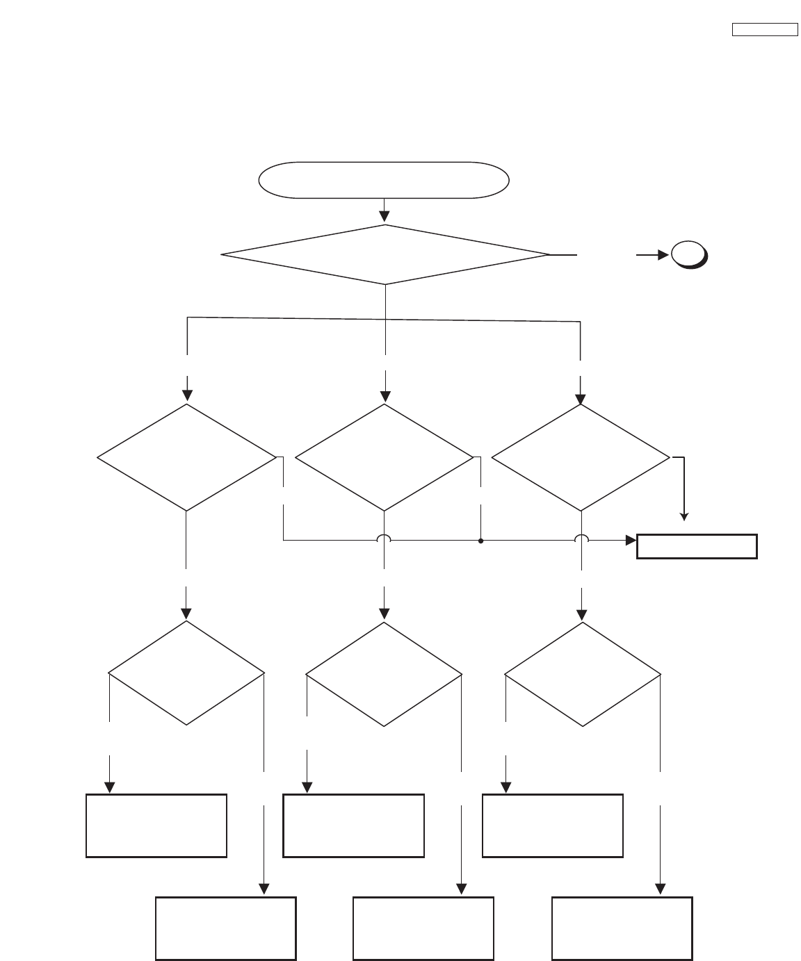
71
DP33KA/B
OK
NG
NG
DCU out CHECK
KK56/LK06 (RH).. (*1)
KK55/LK05 (RV).. (*2)
NG
A
Conver
gence not be corrected
DCU CHANGE
DCU out CHECK
KK52/LK02 (BH).. (*1
KK51/LK01 (BV).. (*2)
OK
What color has shifted?
DCU out CHECK
KK54/LK04 (GH).. (*1)
KK53/LK03 (GV).. (*2)
OK
Which has shifted,
VERTICAL line or
HORIZONTAL line?
Which has shifted,
VERTICAL line or
HORIZONTAL line?
Which has shifted,
VERTICAL line or
HORIZONTAL line?
HORIZONTAL
line
CHECK & CHANGE
RK45/RK46 (RV)
IK04 (CY Amp)
CHECK & CHANGE
RK41/RK42 (RH)
IK04 (CY Amp)
VERTICAL
line CHECK & CHANGE
RK61/RK62 (GV)
IK05 (CY Amp)
CHECK & CHANGE
RK57/RK58 (GH)
IK04 (CY Amp)
VERTICAL
line
HORIZONTAL
line
CHECK & CHANGE
RK53/RK54 (BV)
IK05 (CY Amp)
VERTICAL
line
CHECK & CHANGE
RK49/RK50 (BH)
IK05 (CY Amp)
Blue
GreenRed
All Color
HORIZONTAL
line
TROUBLE SHOOTING FLOWCHART
4. Convergence not corrected (How to check)
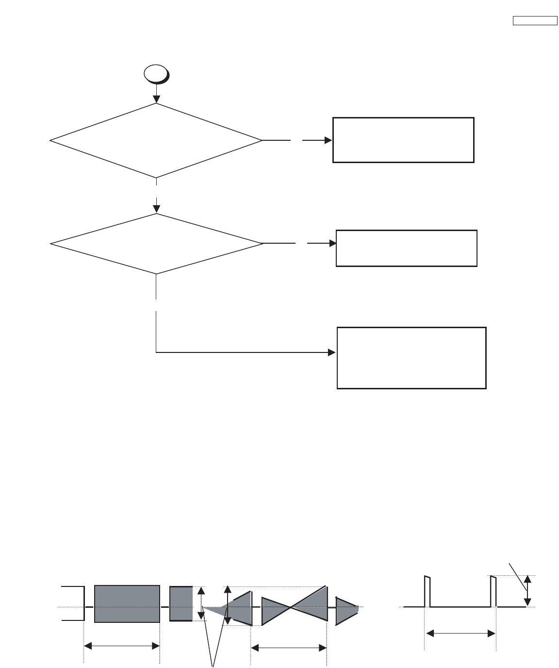
72
DP33KA/B
A
CHECK
IK01
SW +6.3V line
CHECK DCU input (1)
Is Voltage at K273/LK10(K274/LK09)
5V
? (-5V?)
OK
NG
CHECK
DEFLECTION circuit
NG
CHECK
RK41,42,45,46,57,58,
61,62,49,50,53,54
CY Amp (IK04,05),
DCU
CHECK DCU input (2)
LK08 (V.BLK)Ö (*3)
OK
(*1) KK56/LK06 (RH)
KK54/LK04 (GH)
KK52/LK02 (BH)
(*2) KK55/LK05 (RV)
KK53/LK03 (GV)
KK51/LK01 (BV)
(*3) LK08 (V. BLK.)
Vpp =4~ 5 [V]
16~ 17[ms]
GND
GND
16~ 17[ms]
GND
16~ 17[ms]
Vpp =2~ 5 [V]
(QK01
SW-7V Line)
TROUBLE SHOOTING FLOWCHART
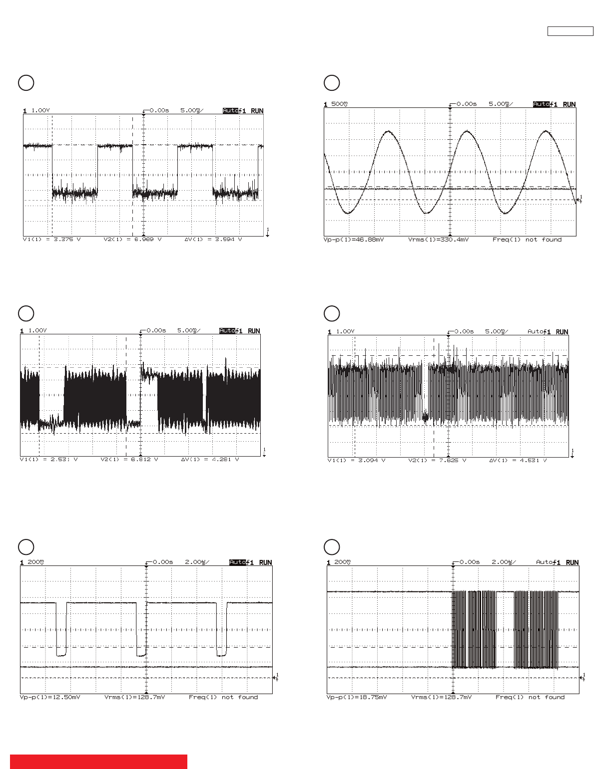
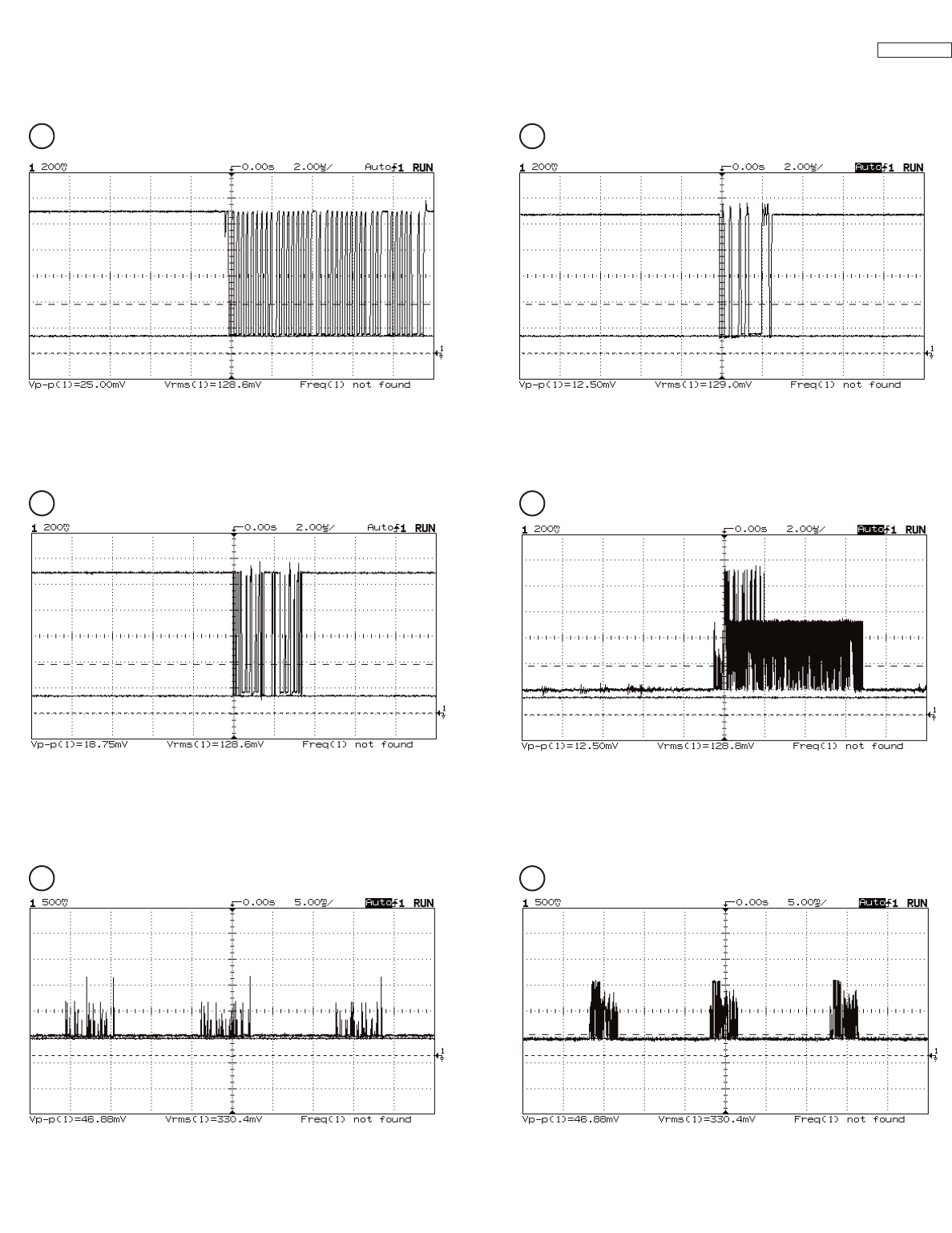
DP33KA/B
WAVEFORMS AT EACH SECTION
Numbers inside circle correspond to locations shown in the circuit diagram.
74
I001 P29 SCL1 I001 P30 SDA1
78
I001 P31 SDA2 I001 P32 OSD R
910
I001 P33 OSD G I001 P34 OSD B
11 12
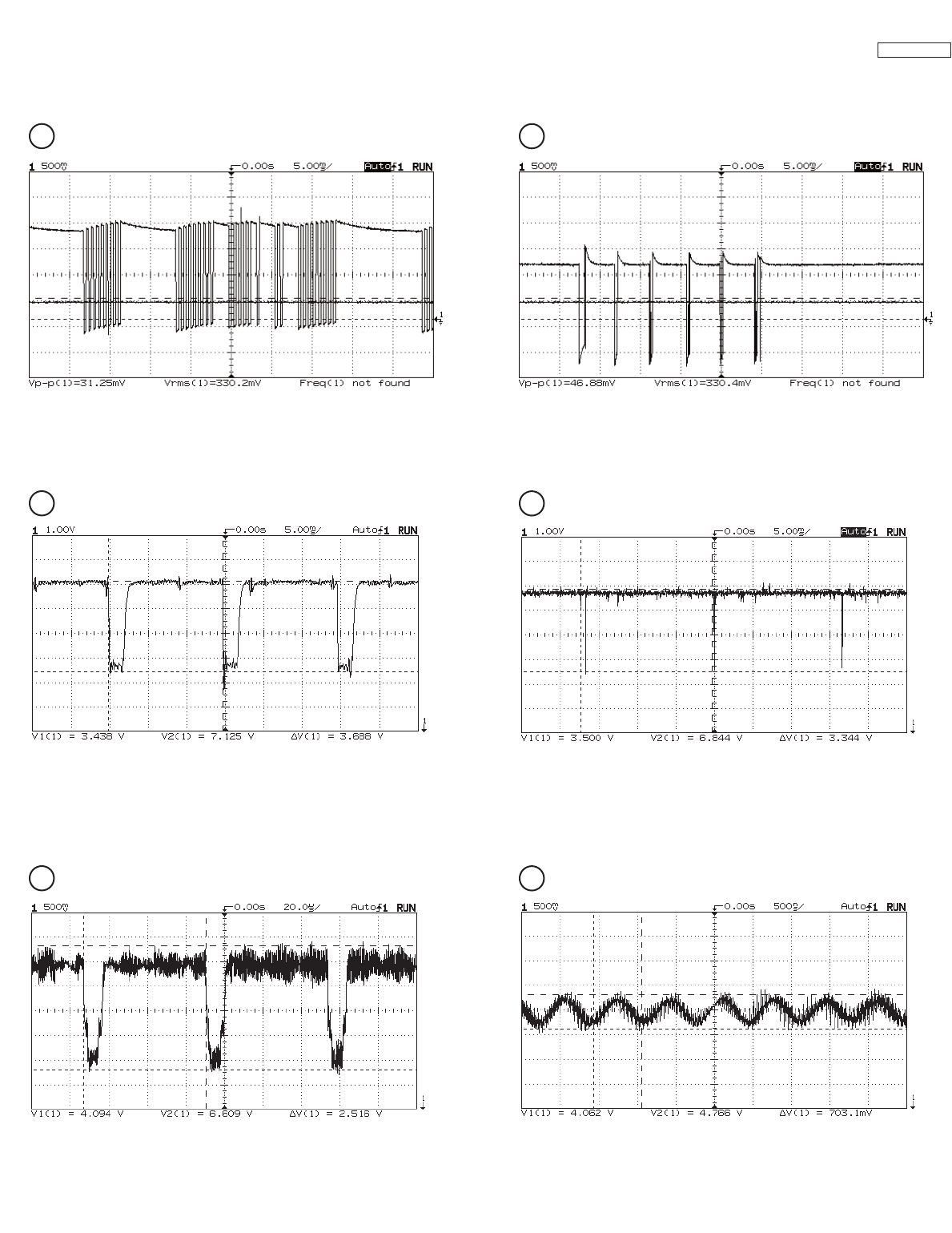
DP33KA/B
WAVEFORMS AT EACH SECTION
Numbers inside circle correspond to locations shown in the circuit diagram.
75
I001 P46 (CE) FLASH I001 P52 DATA/KEY
13 14
I001 P62 OSD HSYNC IN I001 P64 OSD VSYNC IN
15 16
I008 P01 Y1 I008 P02 Y0
17 18
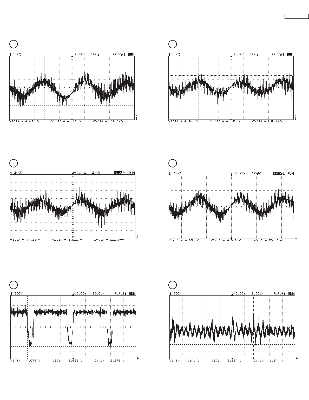
DP33KA/B
WAVEFORMS AT EACH SECTION
Numbers inside circle correspond to locations shown in the circuit diagram.
76
I008 P03 Z1 I008 P04 Z
19 20
I008 P05 Z0 I008 P12 X0
21 22
I008 P13 X1 I010 P01 Vcc
23 24
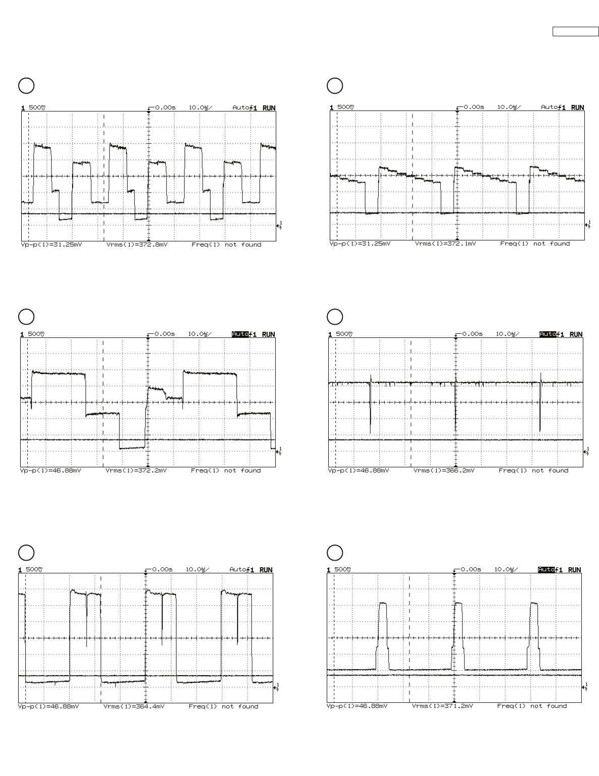
DP33KA/B
WAVEFORMS AT EACH SECTION
Numbers inside circle correspond to locations shown in the circuit diagram.
77
I501 P12 R OUT I501 P13 G OUT
25 26
I501 P14 B OUT I501 P35 VP OUT
27 28
I501 P37 H OUT I501 P39 FBP IN
29 30
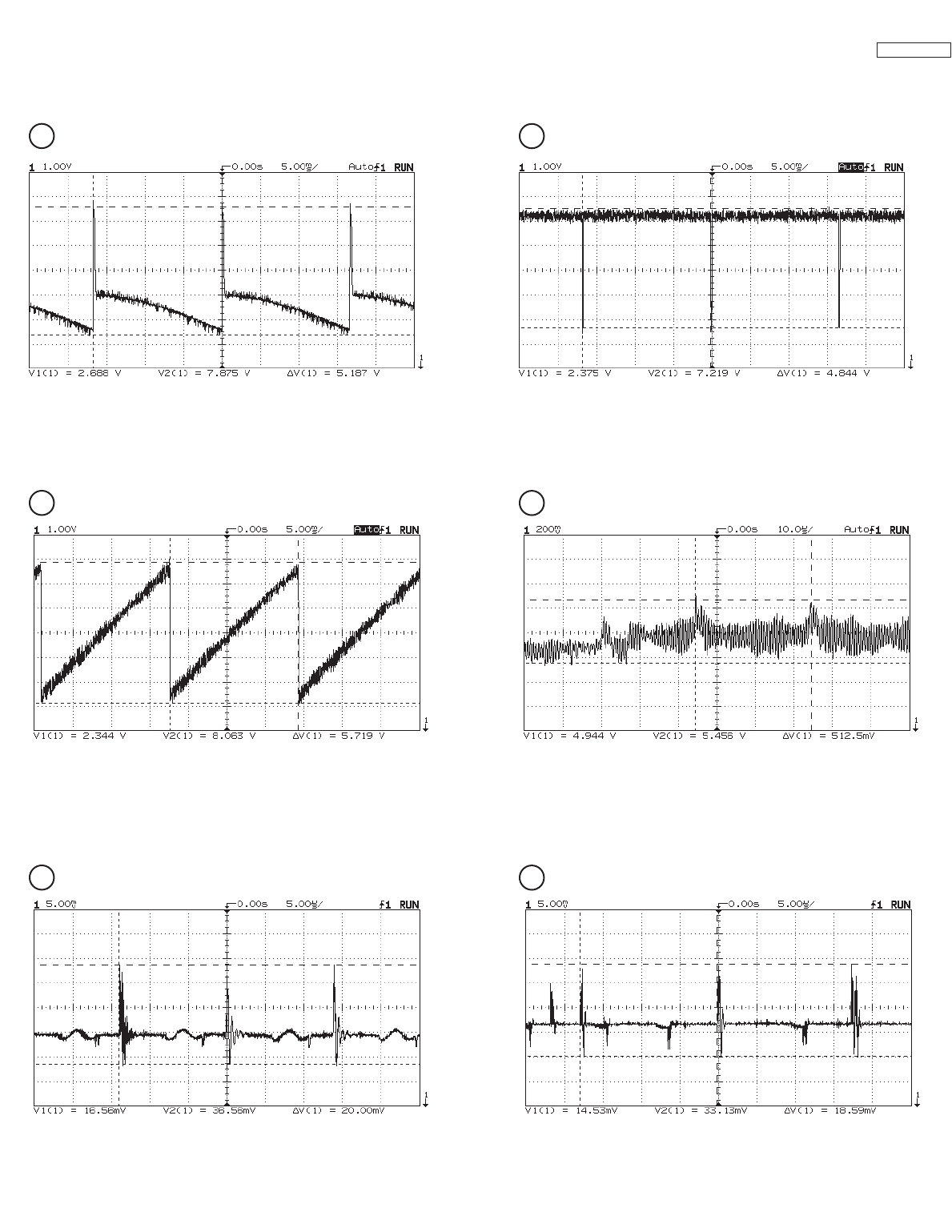
DP33KA/B
WAVEFORMS AT EACH SECTION
Numbers inside circle correspond to locations shown in the circuit diagram.
78
I601 P01 (10X Reduced) V. OUT I601 P03 TRIGGER INPUT
31 32
I601 P07 RAMP GEN. I701 P06
33 34
I901 P01 (100X Reduced) OCP I901 P03 (100X Reduced) D
35 36
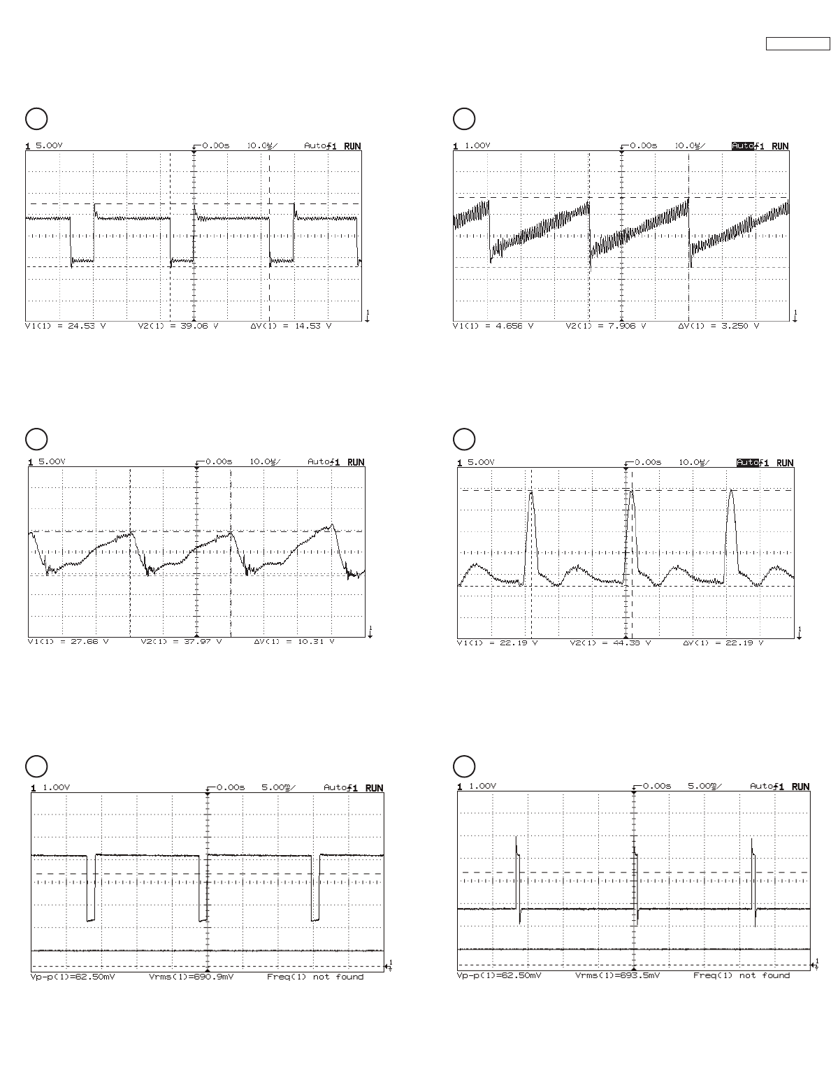
DP33KA/B
WAVEFORMS AT EACH SECTION
Numbers inside circle correspond to locations shown in the circuit diagram.
79
IH01 P01 IH01 P04 GEN.
37 38
IK04 P18 PCG or CYH+ IK05 P09 PCG or CYV+
39 40
IY03 P03 SYNC-OUT IY03 P15 VD-OUT
41 42
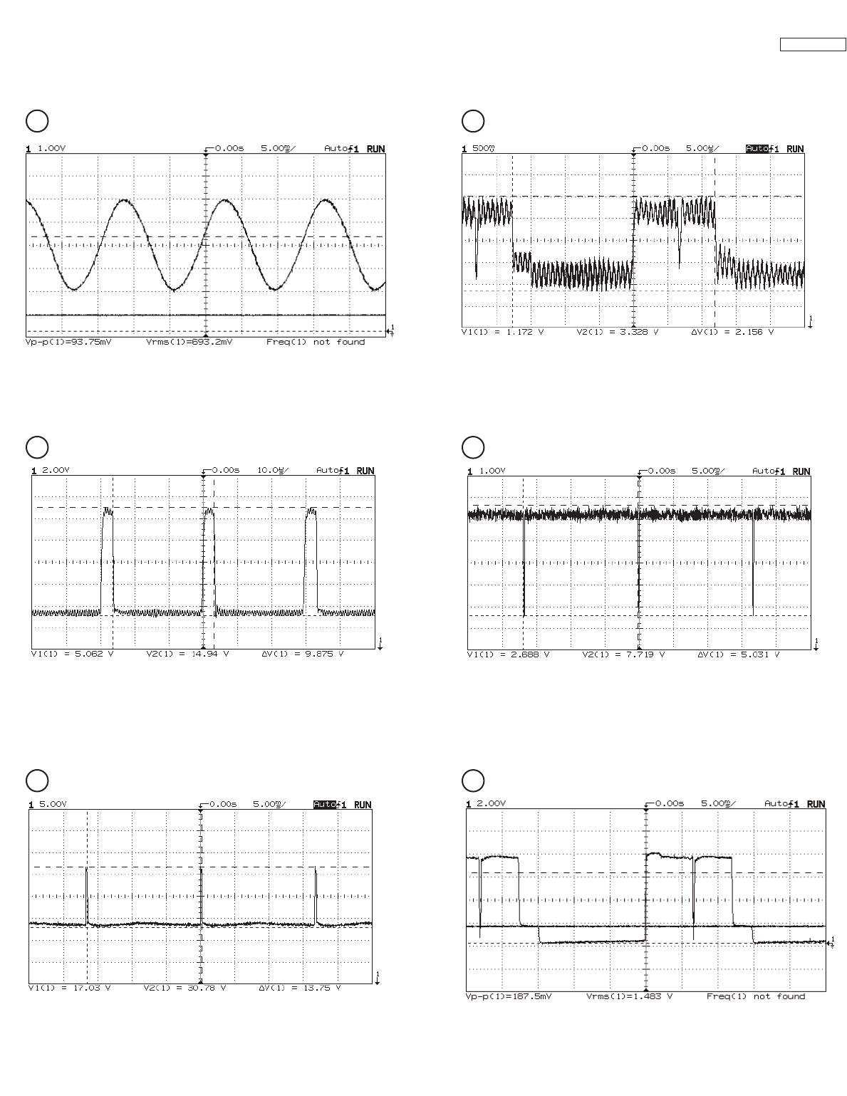
DP33KA/B
WAVEFORMS AT EACH SECTION
Numbers inside circle correspond to locations shown in the circuit diagram.
80
IY03 P26 CW-OUT PPD3 P06 H. DRIVE
43 44
PPD3 P08 H. BLK PPD3 P10 V.DRIVE
45 46
PPD3 P12 V. BLK PPS3 P06 H. DRIVE
47 48
DP33KA/B
WAVEFORMS AT EACH SECTION
Numbers inside circle correspond to locations shown in the circuit diagram.
81
PPS3 P08 H. BLK PPS3 P10 V. DRIVE
49 50
PPS3 P12 V. BLK PST2 P31 SUB. H
51 52
PST2 P32 SUB. V PST2 P34 MAIN V
53 54
DP33KA/B
WAVEFORMS AT EACH SECTION
Numbers inside circle correspond to locations shown in the circuit diagram.
82
PST2 P35 MAIN H Q709 (10X Reduced) BASE
55 56
Q709 COLLECTOR Q709 EMITTER
57 58
Q777 (10X Reduced) BASE Q777 (100X Reduced) COLLECTOR
59 60
DP33KA/B
WAVEFORMS AT EACH SECTION
Numbers inside circle correspond to locations shown in the circuit diagram.
83
Q777 EMITTER Q851 COLLECTOR
61 62
QH01 (100X Reduced) DRAIN QH02 COLLECTOR
63 64
T901 P11 (100X Reduced) CONTROL +115V TH01 P05 (10X Reduced) 50P
65 66
84
DP33KA/B
Symbol Pin No. V(DC) Pin No. V(DC) Pin No. V(DC) Pin No. V(DC)
1 0.2 26 0.0 51 3.7 76 3.1
21.3 27 0.0 52 3.3 77 0.0
3 3.3 28 5.2 53 3.3 78 3.3
4 3.3 29 5.2 54 3.3 79 3.3
5 0.0 30 5.2 55 0.0 80 0.0
6 3.3 31 5.2 56 3.3 81 3.2
71.6 32 0.0 57 0.0 82 3.3
8 0.0 33 0.0 58 3.3 83 3.4
9 0.0 34 0.0 59 3.3 84 3.4
10 3.3 35 0.0 60 0.0 85 3.3
11 3.3 36 0.0 61 0.0 86 3.3
12 3.3 37 0.0 62 3.0 87 3.3
I001 13 1.7 38 0.0 63 0.0 88 0.0
14 0.0 39 3.3 64 3.5 89 0.0
15 1.7 40 3.3 65 0.0 90 0.0
16 3.3 41 0.0 66 0.0 91 3.3
17 0.0 42 0.0 67 0.0 92 1.6
18 3.3 43 0.0 68 0.0 93 2.0
19 3.2 44 3.3 69 0.0 94 2.3
20 0.0 45 3.3 70 0.0 95 0.3
21 0.0 46 3.3 71 0.0 96 1.3
22 0.0 47 0.0 72 0.0 97 2.3
23 2.9 48 0.0 73 3.3 98 0.0
24 3.3 49 0.0 74 3.3 99 5.2
25 0.0 50 3.3 75 3.3 100 2.1
Symbol Pin No. V(DC) Pin No. V(DC) Symbol Pin No. V(DC)
1 0.0 5 5.1 1 5.2
I003 2 0.0 6 5.1 2 0.0
3 0.0 7 0.0 I009 3 1.3
4 0.0 8 5.2 4 3.3
5 5.2
Symbol Pin No. V(DC) Pin No. V(DC)
1 0.0 9 5.2 Symbol Pin No. V(DC) Pin No. V(DC)
2 0.0 10 5.2 1 4.3 9 9.0
3 0.0 11 5.2 2 0.0 10 0.0
I004 4 0.0 12 0.1 3 0.0 11 0.0
5 0.0 13 0.0 I008 4 5.2 12 5.2
6 0.0 14 0.1 5 5.3 13 4.3
7 0.0 15 0.0 6 0.0 14 5.2
8 0.0 16 5.2 7 0.0 15 5.3
8 0.0 16 9.1
Symbol Pin No. V(DC) Pin No. V(DC)
1 5.2 11 5.2 Symbol Pin No. V(DC) Pin No. V(DC)
2 3.2 12 5.2 1 4.8 9 8.8
3 0.0 13 0.0 2 4.9 10 8.8
4 3.3 14 4.8 3 0.0 11 8.8
I010 5 5.0 15 4.9 I301 4 0.1 12 4.8
6 3.1 16 5.2 5 0.1 13 4.7
7 0.0 17 0.0 6 0.0 14 4.7
8 3.3 18 5.1 7 0.0 15 4.8
9 3.3 19 0.0 8 0.0 16 8.8
10 0.0 20 5.2
DC VOLTAGES
Signal 1
TABLE OF CONTENTS
85
DP33KA/B
Symbol Pin No. V(DC) Pin No. V(DC) Symbol Pin No. V(DC) Pin No. V(DC)
1 0.0 6 0.4 1 3.3 8 0.0
2 0.0 7 0.0 2 3.4 9 9.1
PFS 3 0.0 8 0.0 3 3.3 10 0.0
4 0.0 9 3.3 PRST 4 3.3 11 0.0
5 3.3 10 0.0 5 0.0 12 0.0
6 0.0 13 0.0
7 5.2 --
Symbol Pin No. V(DC) Pin No. V(DC) Symbol Pin No. V(DC) Pin No. V(DC)
1 2.3 15 0.0 1 1.8 13 0.0
2 5.5 16 2.9 2 3.8 14 2.4
3 0.0 17 2.3 3 5.0 15 0.0
4 5.2 18 2.1 4 5.2 16 2.4
5 5.2 19 1.8 5 5.2 17 1.8
6 0.0 20 0.0 U302 6 0.0 18 2.3
U301 7 5.0 21 0.1 7 5.0 19 0.0
8 0.0 22 0.1 8 0.0 20 0.0
9 32.5 23 0.1 9 32.5 21 0.0
10 0.0 24 0.0 10 0.0 22 0.0
11 0.0 25 0.0 11 0.0 23 0.0
12 0.0 26 4.2 12 0.0 --
13 8.9 27 4.2
14 0.5 --
DC VOLTAGES
Signal 1
86
DP33KA/B
B 0.5 B 0.7
Q001 C 1.6 Q023 C 0.1
E0.3 E 0.0
B 0.7 B -1.7
Q002 C 1.6 Q025 C 3.0
E 0.3 E 0.0
B 5.2 B 0.0
Q003 C 9.1 Q026 C 3.5
E 4.5 E 0.0
B 5.3 B 0.7
Q004 C 9.1 Q027 C 0.0
E 4.7 E 0.0
B0.0 B 0.0
Q005 C 9.1 Q028 C 2.0
E 0.0 E 0.0
B 0.8 B 0.0
Q006 C 0.0 Q033 C 8.8
E 0.0 E 0.0
B 0.7 B 2.3
Q007 C 0.0 Q035 C 0.0
E 0.0 E 2.9
B 0.1 B 2.9
Q008 C 3.0 Q036 C 5.0
E 0.0 E 2.3
B 5.8 B 0.7
Q009 C 0.5 Q037 C 0.0
E 5.0 E 0.0
B 5.2 B 0.8
Q010 C 0.0 Q038 C 0.0
E 5.8 E 0.0
B 4.9 B 0.1
Q011 C 9.1 Q039 C 3.5
E 5.2 E 0.0
B 3.6 B 0.1
Q012 C 0.0 Q040 C 3.4
E 4.2 E 0.0
B 5.0 B 2.9
Q013 C 9.1 Q041 C 0.0
E 5.3 E 3.5
B 3.5 B 3.5
Q014 C 0.0 Q042 C 4.9
E 4.2 E 2.9
B 4.9 B 0.7
Q015 C 9.1 Q044 C 0.0
E 4.3 E 0.0
B 4.6 B 2.4
Q016 C 0.0 Q050 C 8.9
E 5.2 E 1.7
B 0.0
Q017 C 5.2
E 0.0
DC VOLTAGES
Signal 1
87
DP33KA/B
Symbol Pin No. V(DC) Pin No. V(DC) Symbol Pin No. V(DC) Pin No. V(DC)
1 3.4 5 0.0 1 5.2 5 0.0
I401 2 2.7 6 0.0 I402 2 5.5 6 0.0
3 3.4 7 1.9 3 5.2 7 0.0
4 2.5 8 1.9 4 1.3 8 0.0
Symbol Pin No. V(DC)
Symbol Pin No. V(DC) 1 3.2
1 5.5 2 0.0
I403 2 0.0 I404 3 1.3
3 3.5 4 2.5
5 3.2
Symbol Pin No. V(DC) Pin No. V(DC) Symbol Pin No. V(DC) Pin No. V(DC)
1 5.1 12 5.2 1 5.2 5 0.0
2 0.0 13 4.9 I453 2 5.5 6 0.0
3 4.5 14 0.2 3 5.1 7 0.0
4 3.6 15 3.9 4 1.3 8 0.0
PFC1 5 3.6 16 0.0
(U401) 6 0.0 17 4.5 Symbol Pin No. V(DC) Pin No. V(DC)
7 0.2 18 4.2 1 1.8 12 0.6
8 3.8 19 4.2 2 1.8 13 0.0
9 0.0 20 0.0 3 0.0 14 0.0
10 5.1 21 3.4 4 0.0 15 0.0
11 5.1 22 3.4 PFC2 5 1.0 16 1.6
(U401) 6 3.4 17 0.0
Symbol Pin No. V(DC) Pin No. V(DC) 7 3.3 18 1.8
1 0.0 26 0.0 8 0.2 19 0.0
2 0.0 27 0.0 9 0.0 20 1.8
3 0.0 28 0.0 10 0.0 21 5.0
4 0.0 29 0.0 11 0.2 22 5.0
5 0.0 30 0.0
6 0.0 31 0.0
7 0.0 32 0.0
8 0.0 33 0.0
9 0.0 34 0.0
10 0.0 35 0.0
11 0.0 36 0.0
12 0.0 37 4.6
PST1 13 0.0 38 0.0
14 0.0 39 3.7
15 0.0 40 3.1
16 0.0 41 3.6
17 0.0 42 0.0
18 0.0 43 0.0
19 0.0 44 0.0
20 0.0 45 2.3
21 0.0 46 0.0
22 0.0 47 4.8
23 0.0 48 4.8
24 0.0 49 0.0
25 0.0 50 2.1
DC VOLTAGES
Signal 2
88
DP33KA/B
Symbol Pin No. V(DC) Pin No. V(DC) Pin No. V(DC) Pin No. V(DC)
1 0.6 21 4.1 41 2.9 61 5.1
20.0 22 0.0 42 5.6 62 0.0
3 0.0 23 0.5 43 0.0 63 5.1
4 4.7 24 4.1 44 6.7 64 0.9
5 0.0 25 4.1 45 9.2 65 0.0
6 4.7 26 4.0 46 0.0 66 5.1
74.7 27 0.0 47 0.2 67 5.1
8 9.1 28 4.7 48 0.0 68 5.3
9 0.0 29 0.0 49 1.6 69 0.0
I501 10 0.0 30 4.8 50 3.2 70 5.5
11 0.0 31 2.2 51 0.0 71 0.5
12 2.6 32 0.0 52 3.3 72 0.0
13 2.7 33 0.0 53 2.2 73 0.0
14 2.8 34 0.5 54 0.0 74 5.5
15 0.0 35 5.0 55 0.0 75 9.2
16 9.1 36 0.0 56 0.0 76 0.0
17 0.0 37 1.3 57 7.8 77 4.5
18 4.1 38 0.0 58 7.0 78 5.9
19 4.1 39 1.3 59 0.0 79 0.0
20 0.0 40 2.6 60 5.1 80 0.7
Symbol Pin No. V(DC) Pin No. V(DC) Symbol Pin No. V(DC) Pin No. V(DC)
1 0.3 9 0.5 1 4.6 16 9.1
2 0.3 10 0.5 2 4.6 17 0.0
3 0.3 11 0.5 3 4.6 18 4.8
I502 4 0.3 12 3.2 4 4.6 19 4.0
5 0.3 13 3.9 5 4.6 20 4.0
6 0.0 14 3.2 6 4.6 21 4.5
7 0.0 15 0.0 7 4.6 22 4.6
8 0.0 16 9.2 IA01 8 4.6 23 4.6
9 1.0 24 4.6
10 4.6 25 4.6
Symbol Pin No. V(DC) 11 1.6 26 4.6
1 0.0 12 1.6 27 4.6
2 9.1 13 4.7 28 4.6
I503 3 0.0 14 4.8 29 4.6
4 10.9 15 0.0 30 4.6
5 0.0
Symbol Pin No. V(DC)
1 10.9
I504 2 0.0
3 9.1
Symbol Pin No. V(DC) Pin No. V(DC)
1 4.6 7 3.4
2 3.5 8 0.0
PSC 3 0.0 9 3.5
4 0.0 10 0.0
5 3.3 11 0.0
6 0.0 12 9.3
DC VOLTAGES
Signal 3
89
DP33KA/B
B 0.2 B 0.0 B 2.7
Q501 C 9.1 Q520 C 0.0 Q541 C 9.1
E 0.4 E 0.7 E 2.1
B 9.1 B 0.0 B 2.1
Q502 C 1.0 Q521 C 0.0 Q542 C 0.0
E 9.2 E 0.8 E 2.8
B1.0 B 0.2 B 7.6
Q503 C 9.2 Q522 C 9.2 Q543 C 3.4
E 1.0 E 1.3 E 8.3
B 1.0 B 0.7 B 2.8
Q504 C 0.0 Q523 C 9.2 Q544 C 0.0
E1.6 E 1.3 E 3.5
B 6.8 B 8.7 B 2.8
Q505 C 9.2 Q525 C -0.4 Q545 C 9.1
E 6.1 E 8.7 E 2.2
B 6.7 B 1.6 B 2.2
Q506 C 9.2 Q526 C 9.2 Q546 C 0.0
E 6.0 E 8.7 E 2.9
B 6.7 B 0.0 B 7.7
Q507 C 9.2 Q527 C 9.3 Q547 C 3.5
E 6.0 E 0.0 E 8.4
B 1.8 B 9.1 B 2.9
Q508 C 0.0 Q528 C 0.0 Q548 C 0.0
E 2.4 E 9.1 E 3.5
B 1.8 B 0.1 B 0.2
Q509 C 0.0 Q529 C 9.1 Q554 C 2.6
E 2.5 E 0.0 E 0.0
B 1.6 B 3.8 B 0.1
Q510 C 0.0 Q531 C 9.2 QA01 C 0.0
E 2.3 E 3.5 E 0.0
B 7.4 B 4.1 B 0.0
Q511 C 9.2 Q532 C 8.0 QA02 C 0.0
E 6.8 E 3.5 E 0.0
B 0.1 B 1.9 B 0.0
Q512 C 9.2 Q533 C 3.5 QA51 C 0.0
E 0.1 E 1.2 E 0.0
B 0.1 B 1.6 B 8.4
Q513 C 0.0 Q534 C 8.5 QA52 C 5.2
E 0.7 E 0.9 E 9.1
B 0.0 B 8.5 B 2.2
Q514 C 9.2 Q535 C 3.9 QA53 C 8.4
E 0.7 E 9.2 E 1.5
B 0.1 B 4.0 B 0.0
Q515 C 0.0 Q536 C 0.0 QA54 C 0.0
E 0.7 E 4.6 E 0.0
B 0.1 B 2.7 B 8.4
Q516 C 0.0 Q537 C 9.1 QA55 C 5.4
E 0.7 E 2.0 E 9.1
B 0.1 B 2.0 B 2.2
Q517 C 0.0 Q538 C 0.0 QA56 C 8.4
E 0.8 E 2.7 E 1.6
B 0.0 B 7.6
Q518 C 9.2 Q539 C 3.4
E 0.0 E 8.3
B 0.0 B 2.7
Q519 C 0.0 Q540 C 0.0
E 0.7 E 3.7
DC VOLTAGES
Signal 3
90
DP33KA/B
Symbol Pin No. V(DC) Pin No. V(DC) Symbol Pin No. V(DC) Pin No. V(DC)
1 1.9 33 4.7 1 1.1 33 0.0
2 2.5 34 4.7 2 0.9 34 5.0
3 2.1 35 -0.3 3 1.1 35 0.0
42.6 36 4.2 4 8.8 36 5.0
5 2.8 37 4.2 5 5.2 37 0.0
6 -1.3 38 4.2 6 0.0 38 5.1
7 -1.2 39 3.4 7 4.8 39 8.8
8 2.7 40 4.2 8 0.0 40 4.3
93.3 41 4.1 9 4.8 41 0.0
10 2.9 42 8.7 10 4.9 42 4.2
11 3.4 43 4.3 11 1.2 43 0.0
12 3.5 44 4.0 12 0.9 44 4.3
13 0.8 45 4.3 13 1.2 45 8.8
14 4.0 46 3.5 14 8.8 46 4.2
15 3.1 47 4.3 15 5.2 47 0.0
IV01 16 3.6 48 -0.1 IV03 16 0.0 48 4.2
17 3.3 49 4.7 17 4.8 49 0.0
18 3.7 50 4.3 18 0.0 50 4.3
19 3.7 51 4.3 19 4.8 51 8.8
20 -0.5 52 4.3 20 5.0 52 8.8
21 4.3 53 4.3 21 1.1 53 5.1
22 3.3 54 4.3 22 0.9 54 0.0
23 3.9 55 3.5 23 1.1 55 4.8
24 3.4 56 4.0 24 0.0 56 0.0
25 4.0 57 -0.1 25 0.0 57 4.8
26 4.0 58 4.2 26 4.7 58 8.8
27 0.3 59 4.3 27 4.8 59 5.1
28 4.5 60 4.2 28 5.0 60 0.0
29 4.0 61 4.3 29 0.0 61 4.8
30 3.5 62 4.3 30 4.3 62 0.0
31 4.1 63 4.2 31 2.9 63 4.8
32 -0.3 64 4.3 32 4.9 64 4.7
Symbol Pin No. V(DC) Pin No. V(DC) Symbol Pin No. V(DC) Pin No. V(DC)
1 0.0 9 0.0 1 2.9 9 1.8
2 2.3 10 2.2 2 0.0 10 0.0
3 2.1 11 2.8 3 2.1 11 3.0
IV02 4 3.3 12 2.4 IV04 4 0.0 12 2.7
5 3.8 13 1.3 5 2.1 13 5.0
6 1.6 14 0.0 6 1.0 14 2.9
7 3.6 15 0.0 7 0.0 15 0.0
8 4.9 16 5.0 8 1.9 16 3.0
DC VOLTAGES
Terminal 1
91
DP33KA/B
Symbol Pin No. V(DC) Pin No. V(DC)
1 2.5 9 2.5
22.4 10 2.5
3 4.6 11 0.0
IV11 4 0.4 12 0.0
5 0.4 13 0.0
6 4.7 14 4.7
74.6 15 4.8
8 0.0 16 5.0
B 2.6 B 4.3 B 2.3
QV05 C 0.0 QV21 C 8.9 QV36 C 0.0
E 3.2 E 3.7 E 3.0
B 1.4 B 1.9 B 2.2
QV06 C 1.9 QV22 C 0.0 QV37 C 0.0
E 1.9 E 2.5 E 2.9
B 0.0 B 6.7 B 2.3
QV07 C 3.1 QV23 C 9.0 QV38 C 0.0
E 0.0 E 6.0 E 2.9
B -0.2 B 2.4 B 0.1
QV08 C 0.0 QV24 C 0.0 QXA0 C 5.1
E 0.0 E 3.0 E 0.0
B -0.2 B 4.1 B 0.2
QV09 C 0.0 QV25 C 9.0 QXA1 C 4.9
E 0.0 E 3.4 E 0.3
B 4.2 B 4.3
QV13 C 8.9 QV26 C 8.4
E 3.6 E 3.7
B 4.2 B 3.9
QV14 C 0.0 QV29 C 9.0
E 3.6 E 3.2
B 1.7 B 2.9
QV15 C 0.0 QV30 C 8.4
E 2.3 E 2.3
B 4.4 B 8.4
QV16 C 8.9 QV31 C 2.6
E 3.8 E 9.0
B 1.9 B 2.6
QV17 C 0.0 QV32 C 9.0
E 2.6 E 1.9
B 4.6 B 2.3
QV18 C 8.9 QV33 C 0.0
E 4.0 E 3.0
B 4.6 B 2.2
QV19 C 8.9 QV34 C 0.0
E 4.0 E 2.9
B 1.9 B 2.3
QV20 C 0.0 QV35 C 0.0
E 2.6 E 3.0
DC VOLTAGES
Terminal 1
92
DP33KA/B
Symbol Pin No. V(DC) Pin No. V(DC) Symbol Pin No. V(DC) Pin No. V(DC)
1 8.9 16 2.5 1 8.9 16 2.5
2 2.5 17 4.5 2 2.5 17 4.5
3 0.0 18 0.0 3 0.0 18 0.0
42.5 19 2.5 4 2.4 19 2.5
5 0.0 20 2.1 5 0.0 20 2.1
6 2.0 21 4.0 6 2.0 21 4.0
7 0.0 22 3.5 7 0.1 22 3.5
IY03 8 4.8 23 3.6 IY04 8 4.7 23 3.6
96.2 24 3.8 9 6.2 24 3.8
10 5.0 25 4.9 10 5.0 25 4.9
11 0.0 26 3.0 11 0.0 26 3.0
12 8.9 27 0.0 12 0.0 27 0.0
13 4.7 28 2.3 13 4.7 28 2.3
14 4.8 29 2.3 14 4.8 29 2.3
15 0.2 30 2.0 15 0.2 30 2.0
B 4.7 B 3.8
QY01 C 9.0 QY22 C 0.0
E 4.0 E 4.5
B 1.7 B 3.6
QY02 C 0.0 QY23 C 0.0
E 0.0 E 4.2
B 3.6 B 3.5
QY10 C 8.4 QY24 C 0.0
E 3.0 E 4.2
B 8.4 B 4.5
QY11 C 3.5 QY25 C 5.0
E 9.0 E 3.8
B 3.5 B 0.2
QY12 C 9.0 QY26 C 5.0
E 2.9 E 0.2
B 8.9 B 3.8
QY17 C 0.1 QY28 C 0.0
E 9.0 E 4.5
B 0.1 B 3.6
QY18 C 3.0 QY29 C 0.0
E 0.0 E 4.3
B 0.7 B 3.6
QY19 C 0.0 QY30 C 0.0
E 0.0 E 4.2
B 1.5 B 4.5
QY20 C 0.0 QY31 C 5.0
E 2.2 E 3.8
B 3.0 B 0.2
QY21 C 0.0 QY32 C 5.0
E 3.6 E 0.2
DC VOLTAGES
Terminal 2
93
DP33KA/B
Symbol Pin No. V(DC) Symbol Pin No. V(DC) Symbol Pin No. V(DC)
1 11.6 1 13.3 1 12.1
2 10.0 I902 2 14.5 I903 2 11.1
I901 3 167.0 3 1.4 3 13.6
423.3 4 5.3 4 23.3
5 10.1
Symbol Pin No. V(DC) Symbol Pin No. V(DC) Pin No. V(DC)
1 115.3 1 5.7 5 0.0
I904 2 11.2 I905 2 0.0 6 5.0
30.0 3 29.1 7 2.4
4 ---- 8 0.0
Symbol Pin No. V(DC) Pin No. V(DC)
1 6.6 5 0.0
I906 2 0.0 6 6.6
3 29.1 7 2.3
4 ---- 8 0.0
Symbol Pin No. V(DC) Pin No. V(DC)
1 1.6 7 14.1
2 0.1 8 5.2
IAA1 3 0.1 9 30.4
4 0.1 10 0.1
5 1.6 11 4.6
6 10.3 12 13.8
B 13.6
Q901 C 23.3
E 13.3
B 0.9
Q902 C 0.4
E 0.0
B 1.6
Q903 C 0.0
E 1.6
B 0.0
Q904 C 1.6
E 0.0
B 115.2
Q905 C 0.5
E 115.6
B 6.0
Q906 C 0.0
E 6.2
B 0.1
QAA1 C 10.3
E 0.1
B 0.1
QAA2 C 4.6
E 0.1
DC VOLTAGES
Power Supply
94
DP33KA/B
Symbol Pin No. V(DC) B 0.0 B -0.1
1 15.1 Q603 C 0.9 QN01 C 0.5
2 28.6 E 0.0 E 0.0
34.9 B 28.9 B 9.9
4 6.7 Q604 C 0.0 QN02 C 1.1
5 4.5 E 29.1 E 10.2
I601 6 0.0 B 96.2 B 0.2
7 3.3 Q701 C 115.2 QN03 C 9.9
84.1 E 95.2 E 0.0
9 4.5 B 2.7 B 0.9
10 28.9 Q703 C 96.2 QN04 C 9.9
11 0.9 E 2.1 E 0.5
B 0.8 B 0.0
Q706 C 10.9 QN05 C 10.3
Symbol Pin No. V(DC) E 1.4 E 0.0
1 10.6 B 0.4 B 0.1
2 1.0 Q709 C 11.1 QN06 C 1.1
3 1.4 E 0.0 E 0.0
I701 4 0.0 B 0.0
5 5.5 Q710 C 0.4
6 5.5 E 0.0
7 4.0 B 0.0
8 10.9 Q777 C 94.0
E 0.0
B 9.6
Symbol Pin No. V(DC) QF01 C 483.0
1 6.2 E 10.2
2 10.8 S 0.4
3 0.8 QH01 D 255.6
4 2.5 G 1.7
5 1.7 B 0.6
6 0.1 QH02 C 1.7
7 0.0 E 0.0
IH01 8 0.0 B 0.1
9 4.7 QH04 C 70.6
10 4.7 E 0.0
11 4.7 B 0.5
12 4.7 QH05 C 71.4
13 3.0 E 0.0
14 2.1
15 5.0
16 0.0
DC VOLTAGES
Deflection
95
DP33KA/B
Symbol Pin No. V(DC) B-26.8 Symbol Pin No. V(DC)
1 0.0 QK01 C 0.1 1 2.6
IK01 2 0.1 E -26.8 2 2.6
3 6.3 B 0.1 3 0.6
QK02 C 0.0 4 1.6
E 0.1 5 0.2
Symbol Pin No. V(DC) B 0.0 PDS1 6 0.3
1 0.0 QK03 C -26.8 7 2.0
2 5.2 E 0.1 8 0.8
3-27.3 B 0.0 9 0.4
4 -28.5 QK05 C 0.1 10 0.0
5 28.6 E 0.0 11 0.0
6 0.8 B 0.0 12 5.1
7 0.8 QK06 C 0.1
8 -28.5 E 0.0 B 4.7
IK04 9 0.9 B 0.0 QL10 C 0.3
10 28.6 QK07 C 0.1 E 5.0
11 0.0 E 0.1 B 4.7
12 -28.5 B 0.0 QL11 C 0.1
13 0.0 QK08 C 0.1 E 5.1
14 0.0 E 0.0 B 4.7
15 0.2 QL12 C 0.4
16 0.2 E 5.1
17 -28.5 B 4.7
18 0.2 QL13 C 1.4
E 5.1
B 4.7
Symbol Pin No. V(DC) QL14 C 0.4
1 0.0 E 5.0
2 5.2 B 4.7
3 -27.4 QL15 C 0.2
4 -28.5 E 5.1
5 28.6 B 4.7
6 -0.1 QL16 C 0.6
7 -0.1 E 5.1
8 -28.5 B 4.7
IK05 9 -0.1 QL17 C 0.2
10 28.6 E 5.0
11 -0.5
12 -28.5
13 -0.4
14 -0.4
15 0.0
16 0.0
17 -28.5
18 -0.1
DC VOLTAGES
Convergence Convergence Sensor
96
DP33KA/B
B 3.0 B 193.6 B 4.7
Q801 C 8.6 Q8A5 C 219.3 QEA1 C 9.2
E 2.5 E 193.9 E 4.0
B 5.8 B 3.0 B 4.0
Q802 C 6.4 Q8A6 C 0.0 QEA2 C 9.3
E 5.7 E 2.4 E 3.4
B 9.2 B 2.0 B 2.6
Q803 C 192.3 Q8A7 C 2.4 QEA3 C 0.0
E 8.7 E 2.2 E 3.1
B192.3 B 3.0 B 193.1
Q804 C 1.1 Q8A8 C 9.3 QEA6 C 99.5
E 186.7 E 2.3 E 193.6
B 193.6 B 1.8 B 3.6
Q805 C 219.3 Q8C2 C 1.1 QEA7 C 99.5
E 192.1 E 1.1 E 3.2
B 1.4 B 4.6 B 196.7
Q806 C 0.0 QE01 C 9.2 QEA8 C 3.5
E 2.1 E 3.3 E 197.0
B 1.8 B 4.0
Q812 C 1.1 QE02 C 9.2
E 1.1 E 3.3
B 2.9 B 2.6
Q851 C 8.6 QE03 C 0.0
E 2.5 E 3.2
B 8.7 B 193.4
Q852 C 9.3 QE06 C 100.7
E 8.6 E 193.7
B 9.2 B 3.6
Q853 C 194.0 QE07 C 100.7
E 8.7 E 3.2
B 2.3 B 219.2
Q854 C -0.6 QE08 C 0.0
E 2.3 E 219.5
B 195.3 G 4.6
Q855 C 219.3 QE51 C 9.2
E 193.6 E 4.0
B 0.0 B 4.0
Q856 C 9.9 QE52 C 9.2
E 0.0 E 3.3
B 1.7 B 2.6
Q862 C 1.1 QE53 C 0.0
E 1.0 E 3.2
B 2.9 B 193.3
Q8A1 C 8.6 QE56 C 100.6
E 2.4 E 193.6
B 8.7 B 3.6
Q8A2 C 9.3 QE57 C 100.2
E 8.6 E 3.2
B 9.2
Q8A3 C 193.2
E 8.7
B 193.3
Q8A4 C 1.1
E 190.3
DC VOLTAGES
CPT VM
97
DP33KA/B
Symbol Pin No. V(DC) B 0.7
11.7 QM01 C 0.1
HM01 2 5.2 E 0.0
3 0.0 B 3.1
QM03 C 9.0
E 2.4
Symbol Pin No. V(DC) B 3.1
1 0.0 QM04 C 9.0
PFI 2 5.2 E 2.4
3 0.0 B 0.1
41.3 QM05 C 5.2
E 0.0
Symbol Pin No. V(DC)
1 3.3
2 3.3
3 3.3
4 3.3
5 0.0
6 1.7
PFS 7 5.2
8 0.0
9 9.1
10 0.0
11 1.8
12 1.6
13 0.0
Symbol Pin No. V(DC)
1 9.0
2 0.0
3 0.0
4 2.4
5 2.5
PFT 6 0.0
7 0.0
8 0.0
9 0.0
10 0.0
11 4.9
DC VOLTAGES
Control
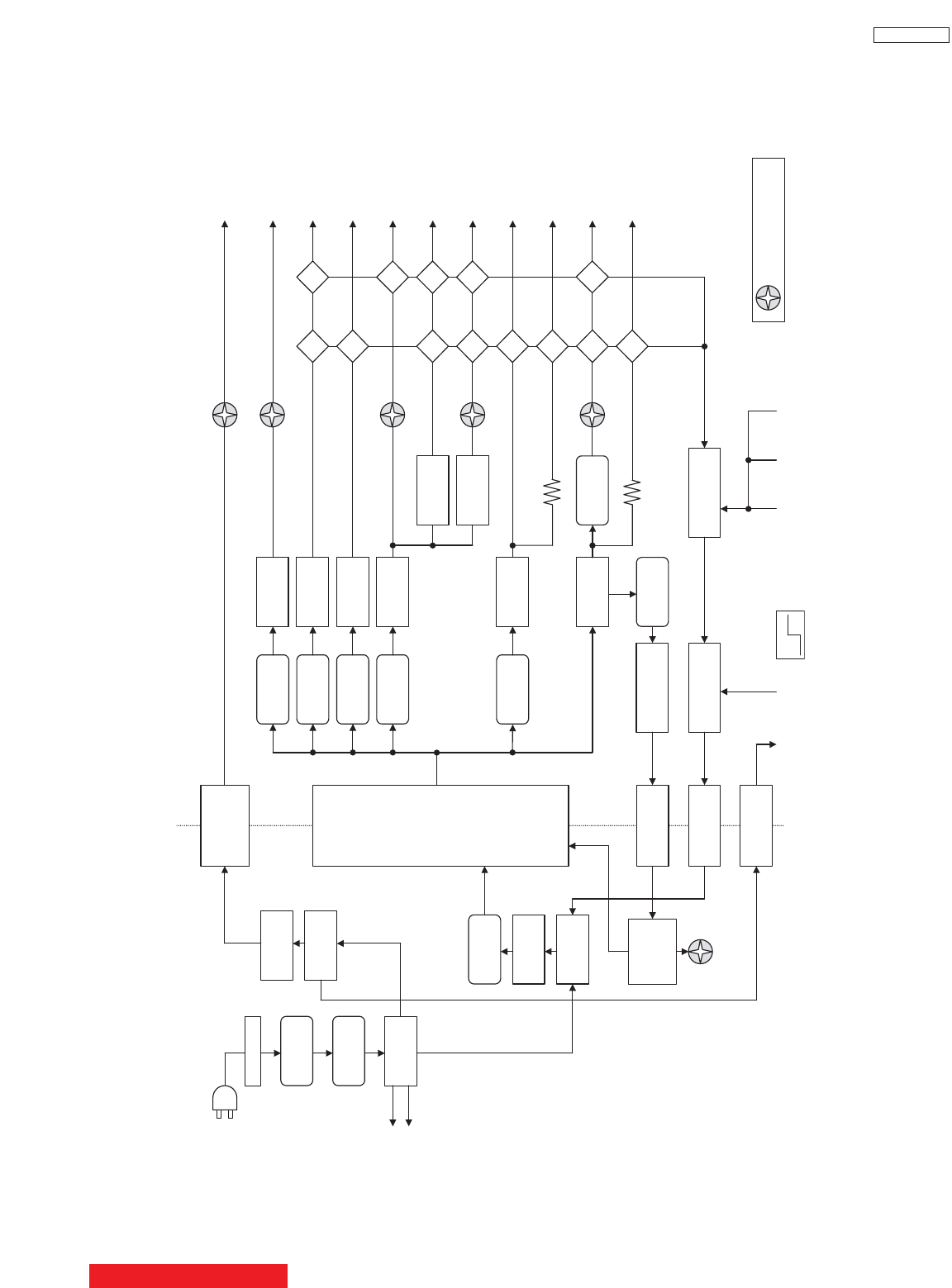
98
DP33KA/B
DM Power Supply
DVD Power Supply
D932:+115V
Switching
Transformer
T901
LIVE COLD
AC Clock
I902
Feed Back
I903
RELAY
S901
Power
Module
U901
Protector
E901:7000
Rectifier
+38.5V:D919
Protector
E902:7000
Rectifier
+10V:D920
Protector
E903:4000
Rectifier
+220V:D921
Protector
E904:10K
Rectifier
+28V:D922
Regulator
+5.5V:I905
Rectifier
+115V:D925
Protector
E907:3000
Protector
E905:10K
Rectifier
-28V:D923
D955:+5.5V
D956:Audio
D913:SBY+5V
Regulator
+6.3V:I906
D954:+28V
D947:>8V D940:<5V
D ZD
D949:>-4V
ZD
D931:>133V
Q905:>1.8A
Q
ZD
D957:>12V
D939:<5V
D ZD
D941
D942:<4V
D
D952:>32V
ZD
D949:>10V D943:<5V
D ZD
D952:>-24V
ZD
D938:<4V
D
Voltage Control
+115V:I904
Short CCT.
Detector
Over Voltage
Detector
Protect On/Off
Switch:Q903/Q904
Power On/Off
Switch:Q902
Power
On/Off
AC Clock
60Hz
Protector
E906:500
Off On
= RED or GREEN LED
AC Plug
Switching
Control
I901
Fuse
F901:10A
Varistor
X901
AC Input
Rectifier
D901
Line Filter
L901
Rectifier
D902
Fuse
F903:5A
Line Filter
L926
IC Power Monitor
LED(RED):D912
Line Filter
L903
Signal:
SW+10V
Signal:
SW+5.5V
Deflection:
SW+115V
Conver:
SW-28V
uCOM:
SBY+5V
VT:
SW+35V
DCU:
SW-7V
Conver / Vert:
SW+28V
Video:
SW+220V
Heater / DCU:
SW+6.3V
Audio:
+38.5V(40W)
+29.0V(24W)
DEF CCT
Protect
SIG CCT
Protect
CPT CCT
Protect
R940
R938
PROTECTION CIRCUIT BLOCK DIAGRAM
Power Supply
TABLE OF CONTENTS
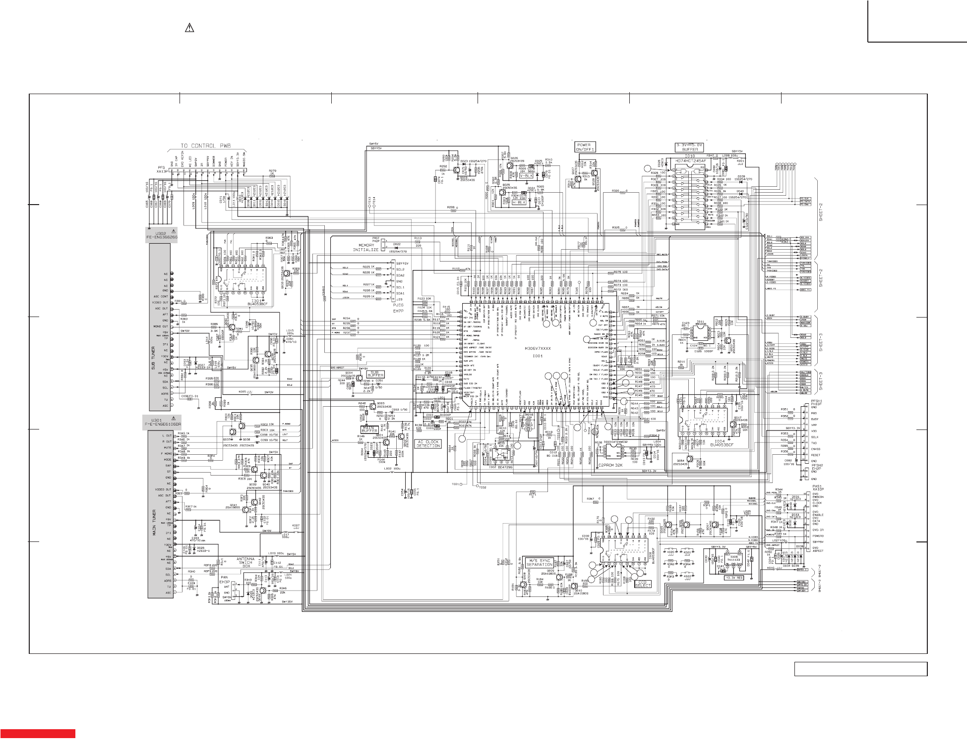
1
2
345
67
8
12
11
10
9
13
1415
16
17
18
19
21
20
22
23
24
1 234 56
A
B
C
D
E
All DC voltage to be measured with a tester (100k/V). Voltage taken on a complex color bar signal including a standard color bar signal.
Since this is a basic circuit diagram, the value of the parts is subject to be altered for improvement.
Signal 1 of 3
PRODUCT SAFETY NOTE: Components marked with a and shaded have special characteristics important to
safety. Before replacing any of these components, read carefully the PRODUCT SAFETY NOTICE of this Service
Manual. Don’t degrade the safety of the receiver through improper servicing.
BASIC CIRCUIT DIAGRAM DP33KA/B
Signal 1 of 3
99
TABLE OF CONTENTS
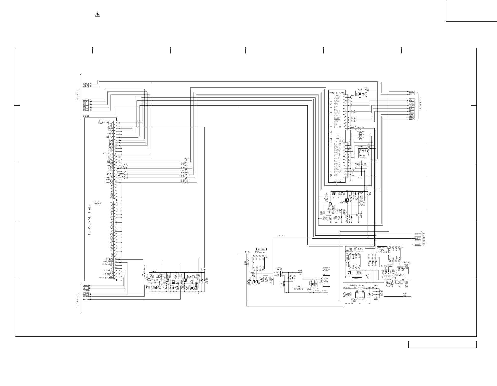
52
53
54
55
1 234 56
A
B
C
D
E
All DC voltage to be measured with a tester (100k/V). Voltage taken on a complex color bar signal including a standard color bar signal.
Since this is a basic circuit diagram, the value of the parts is subject to be altered for improvement.
Signal 2 of 3
PRODUCT SAFETY NOTE: Components marked with a and shaded have special characteristics important to
safety. Before replacing any of these components, read carefully the PRODUCT SAFETY NOTICE of this Service
Manual. Don’t degrade the safety of the receiver through improper servicing.
BASIC CIRCUIT DIAGRAM DP33KA/B
Signal 2 of 3
100
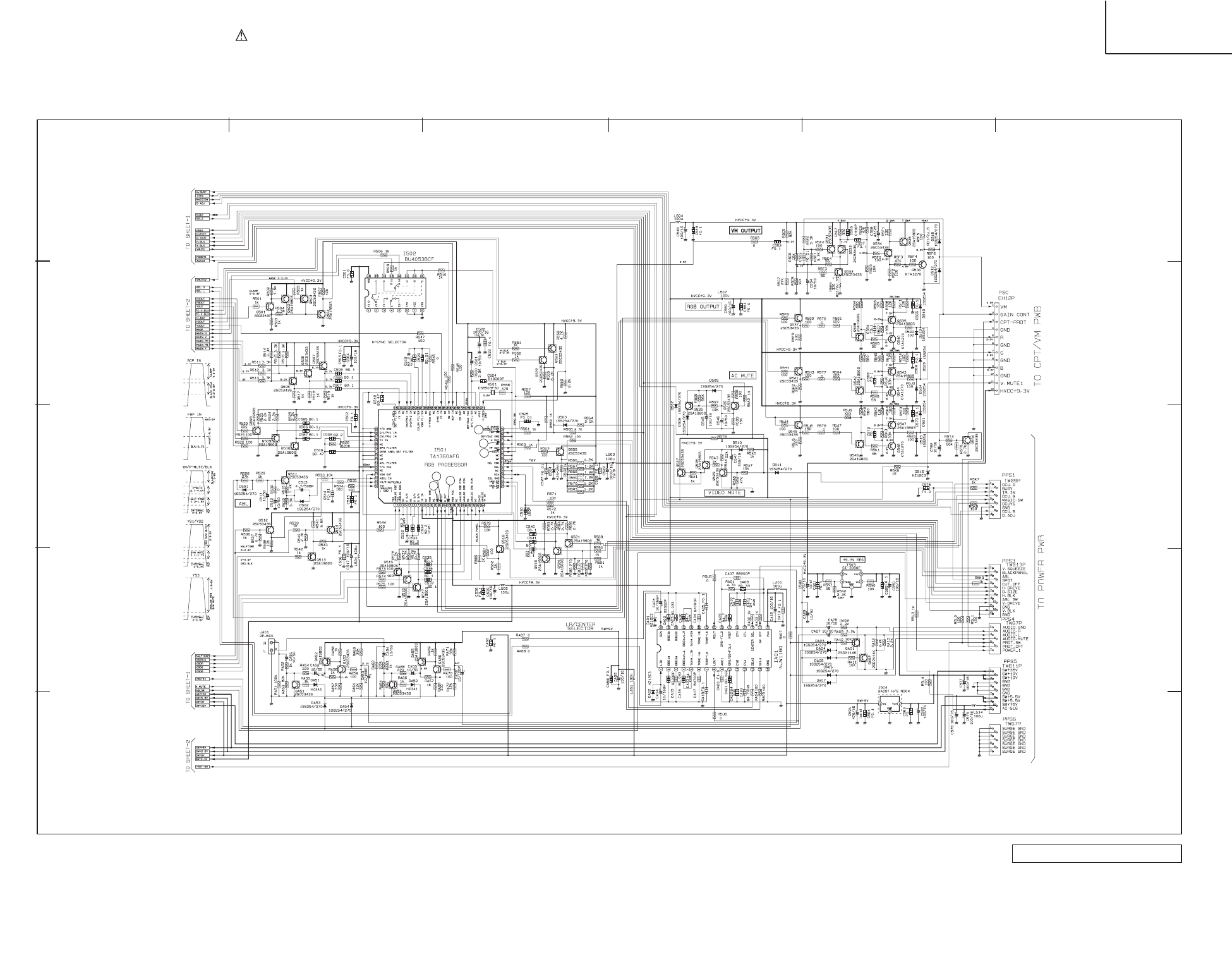
30
29
28
25
26 27
1 234 56
A
B
C
D
E
All DC voltage to be measured with a tester (100k/V). Voltage taken on a complex color bar signal including a standard color bar signal.
Since this is a basic circuit diagram, the value of the parts is subject to be altered for improvement.
Signal 3 of 3
PRODUCT SAFETY NOTE: Components marked with a and shaded have special characteristics important to
safety. Before replacing any of these components, read carefully the PRODUCT SAFETY NOTICE of this Service
Manual. Don’t degrade the safety of the receiver through improper servicing.
BASIC CIRCUIT DIAGRAM DP33KA/B
Signal 3 of 3
101
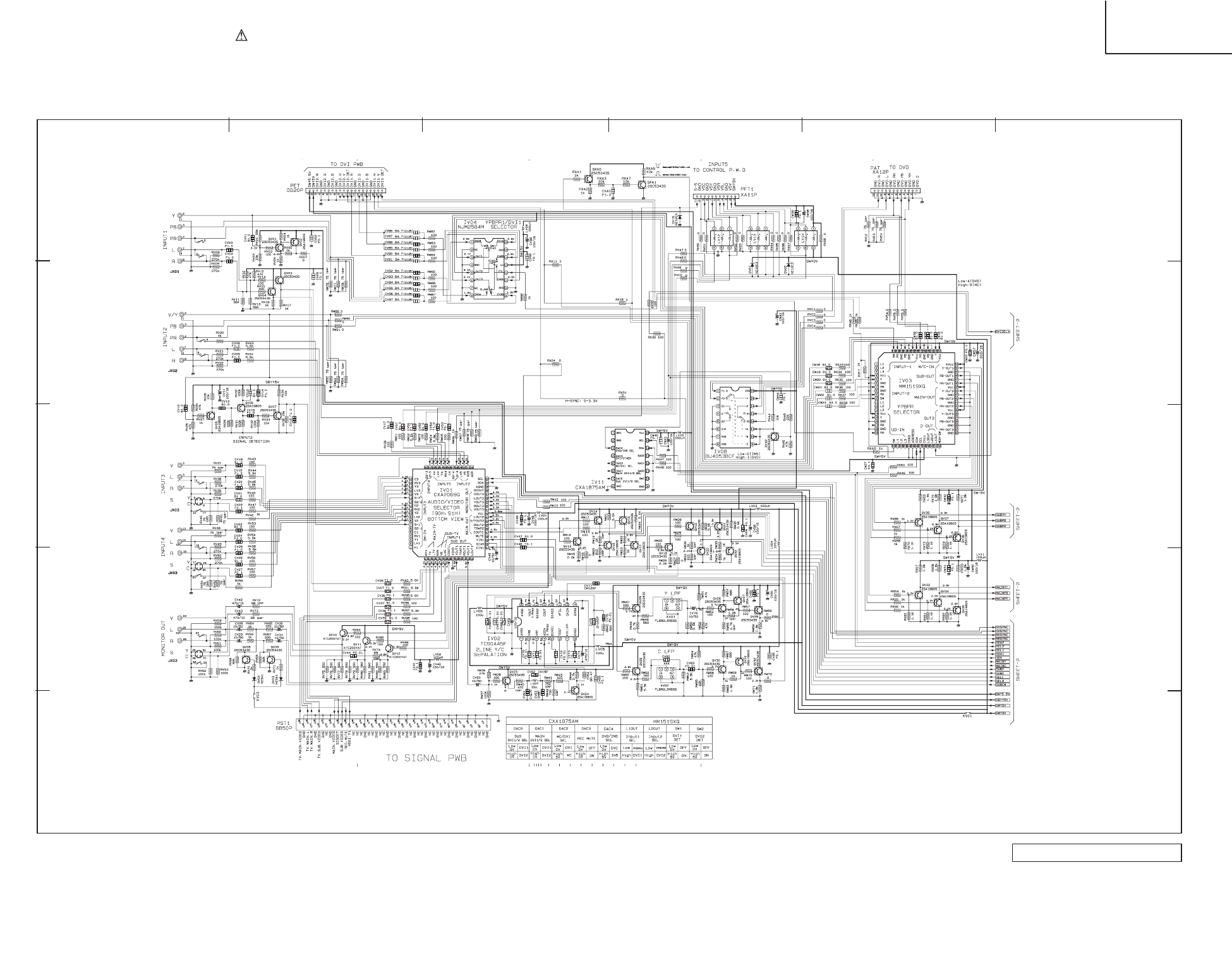
1 234 56
A
B
C
D
E
All DC voltage to be measured with a tester (100k/V). Voltage taken on a complex color bar signal including a standard color bar signal.
Since this is a basic circuit diagram, the value of the parts is subject to be altered for improvement.
Terminal 1 of 2
PRODUCT SAFETY NOTE: Components marked with a and shaded have special characteristics important to
safety. Before replacing any of these components, read carefully the PRODUCT SAFETY NOTICE of this Service
Manual. Don’t degrade the safety of the receiver through improper servicing.
BASIC CIRCUIT DIAGRAM DP33KA/B
Terminal 1 of 2
102
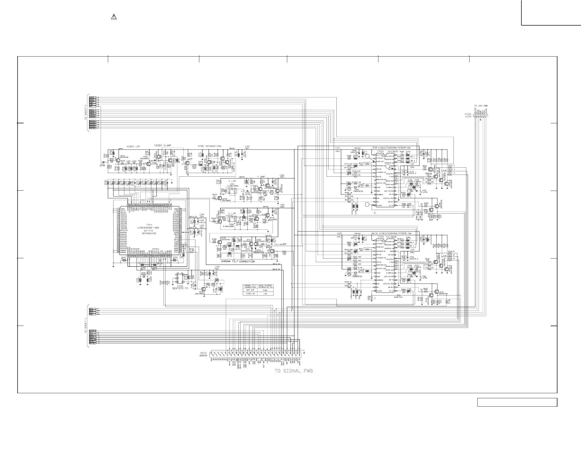
41
43
42
1 234 56
A
B
C
D
E
All DC voltage to be measured with a tester (100k/V). Voltage taken on a complex color bar signal including a standard color bar signal.
Since this is a basic circuit diagram, the value of the parts is subject to be altered for improvement.
Terminal 2 of 2
PRODUCT SAFETY NOTE: Components marked with a and shaded have special characteristics important to
safety. Before replacing any of these components, read carefully the PRODUCT SAFETY NOTICE of this Service
Manual. Don’t degrade the safety of the receiver through improper servicing.
BASIC CIRCUIT DIAGRAM DP33KA/B
Terminal 2 of 2
103
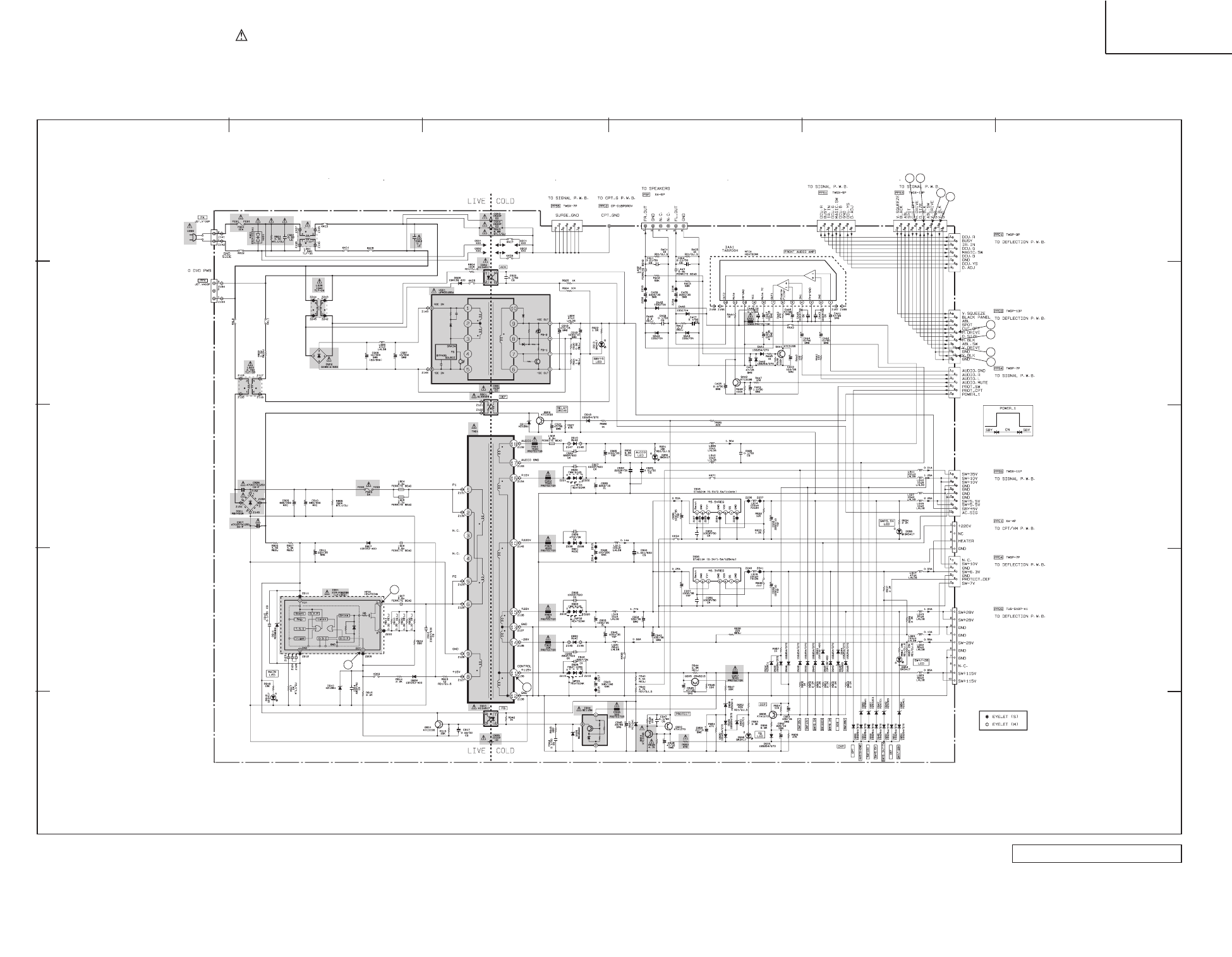
48 49
50 51
44
45
46
47
36
35
65
1 234 56
A
B
C
D
E
All DC voltage to be measured with a tester (100k/V). Voltage taken on a complex color bar signal including a standard color bar signal.
Since this is a basic circuit diagram, the value of the parts is subject to be altered for improvement.
Power Supply
PRODUCT SAFETY NOTE: Components marked with a and shaded have special characteristics important to
safety. Before replacing any of these components, read carefully the PRODUCT SAFETY NOTICE of this Service
Manual. Don’t degrade the safety of the receiver through improper servicing.
BASIC CIRCUIT DIAGRAM DP33KA/B
Power Supply
104
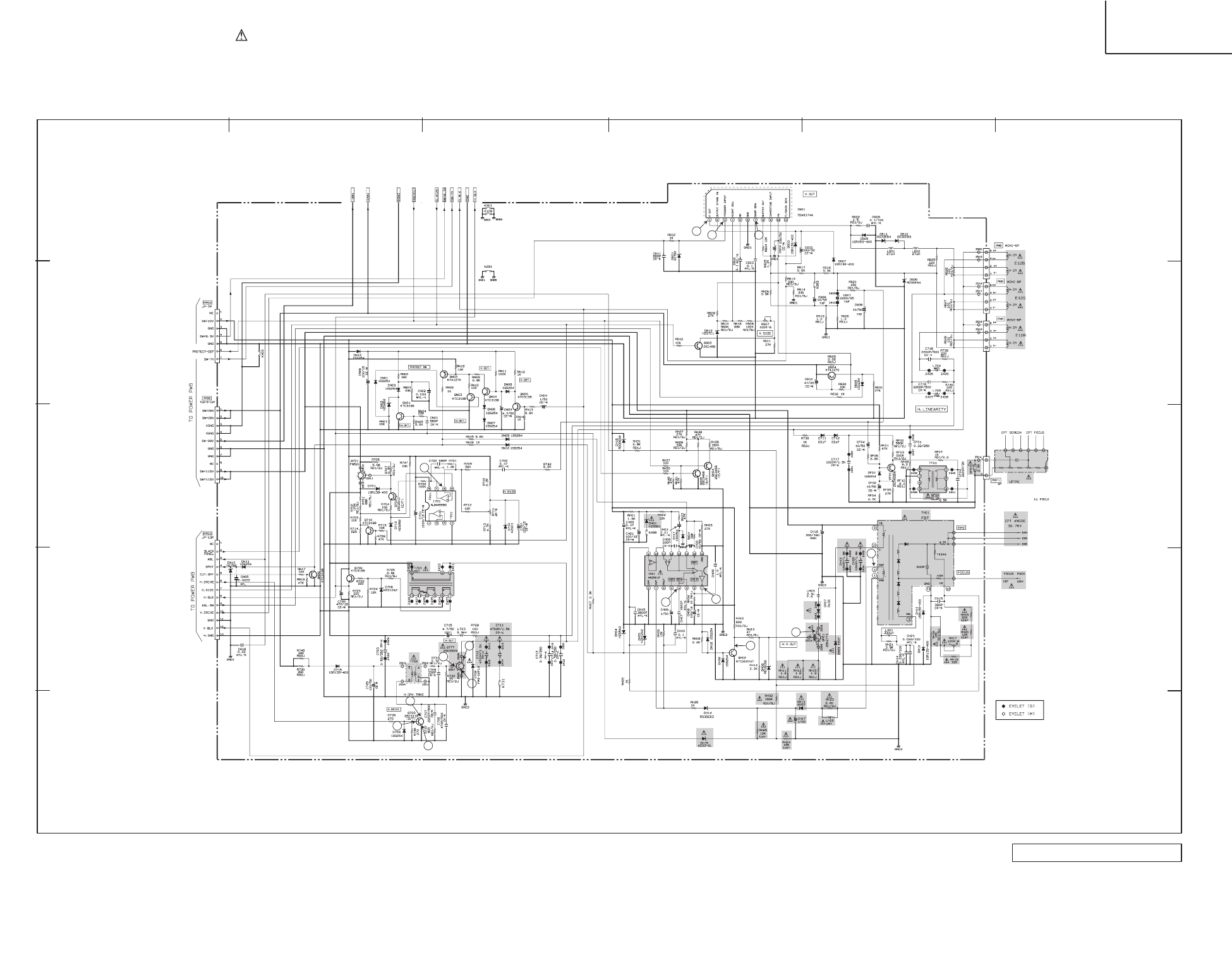
59
61
60
56
57
58
34
37
38
31 32 33
66
63
64
1 234 56
A
B
C
D
E
All DC voltage to be measured with a tester (100k/V). Voltage taken on a complex color bar signal including a standard color bar signal.
Since this is a basic circuit diagram, the value of the parts is subject to be altered for improvement.
Deflection
PRODUCT SAFETY NOTE: Components marked with a and shaded have special characteristics important to
safety. Before replacing any of these components, read carefully the PRODUCT SAFETY NOTICE of this Service
Manual. Don’t degrade the safety of the receiver through improper servicing.
BASIC CIRCUIT DIAGRAM DP33KA/B
Deflection
105
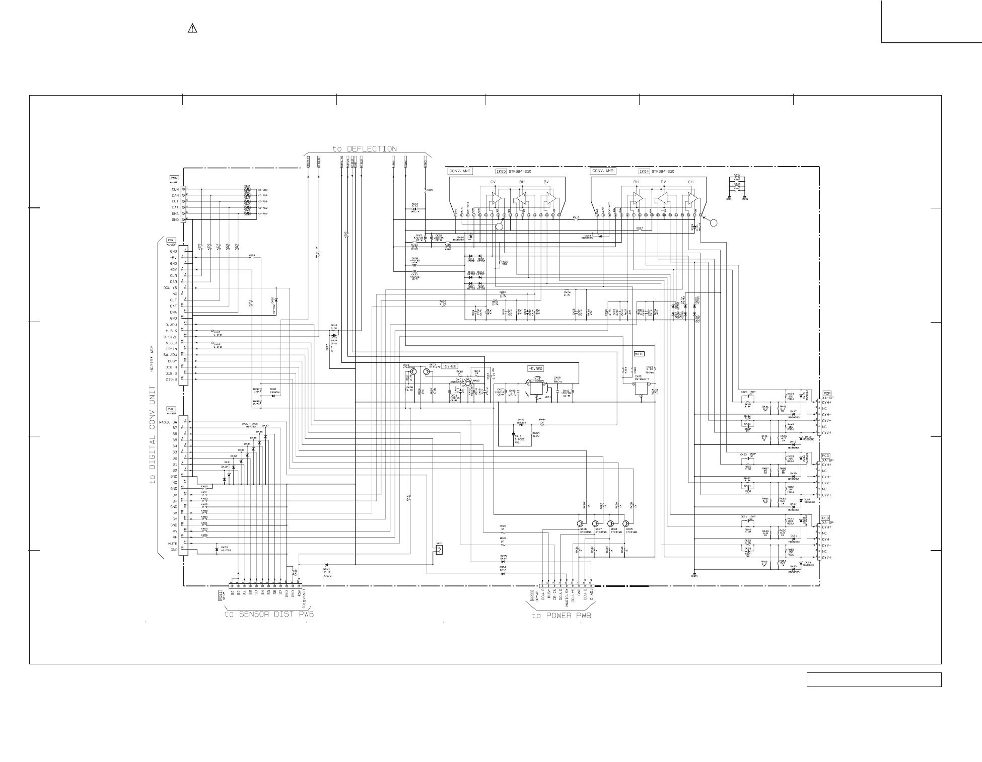
39
40
1 234 56
A
B
C
D
E
All DC voltage to be measured with a tester (100k/V). Voltage taken on a complex color bar signal including a standard color bar signal.
Since this is a basic circuit diagram, the value of the parts is subject to be altered for improvement.
Convergence
PRODUCT SAFETY NOTE: Components marked with a and shaded have special characteristics important to
safety. Before replacing any of these components, read carefully the PRODUCT SAFETY NOTICE of this Service
Manual. Don’t degrade the safety of the receiver through improper servicing.
BASIC CIRCUIT DIAGRAM DP33KA/B
Convergence
106
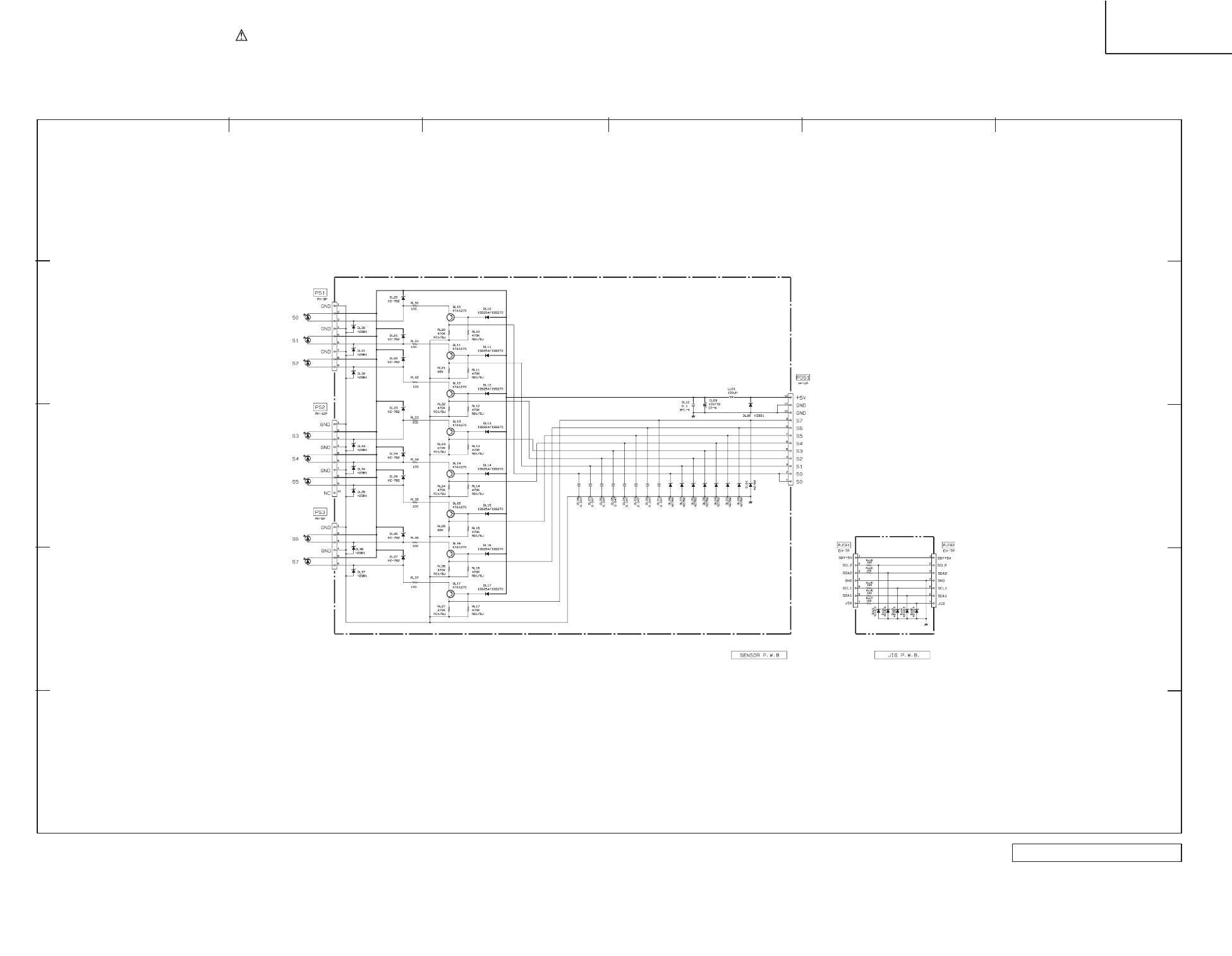
1 234 56
A
B
C
D
E
All DC voltage to be measured with a tester (100k/V). Voltage taken on a complex color bar signal including a standard color bar signal.
Since this is a basic circuit diagram, the value of the parts is subject to be altered for improvement.
Sensor
PRODUCT SAFETY NOTE: Components marked with a and shaded have special characteristics important to
safety. Before replacing any of these components, read carefully the PRODUCT SAFETY NOTICE of this Service
Manual. Don’t degrade the safety of the receiver through improper servicing.
BASIC CIRCUIT DIAGRAM DP33KA/B
Sensor
107
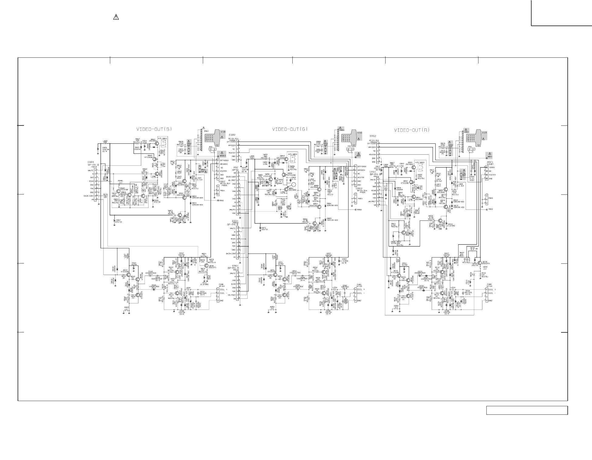
62
1 234 56
A
B
C
D
E
All DC voltage to be measured with a tester (100k/V). Voltage taken on a complex color bar signal including a standard color bar signal.
Since this is a basic circuit diagram, the value of the parts is subject to be altered for improvement.
CPT/VM
PRODUCT SAFETY NOTE: Components marked with a and shaded have special characteristics important to
safety. Before replacing any of these components, read carefully the PRODUCT SAFETY NOTICE of this Service
Manual. Don’t degrade the safety of the receiver through improper servicing.
BASIC CIRCUIT DIAGRAM DP33KA/B
CPT/VM
108
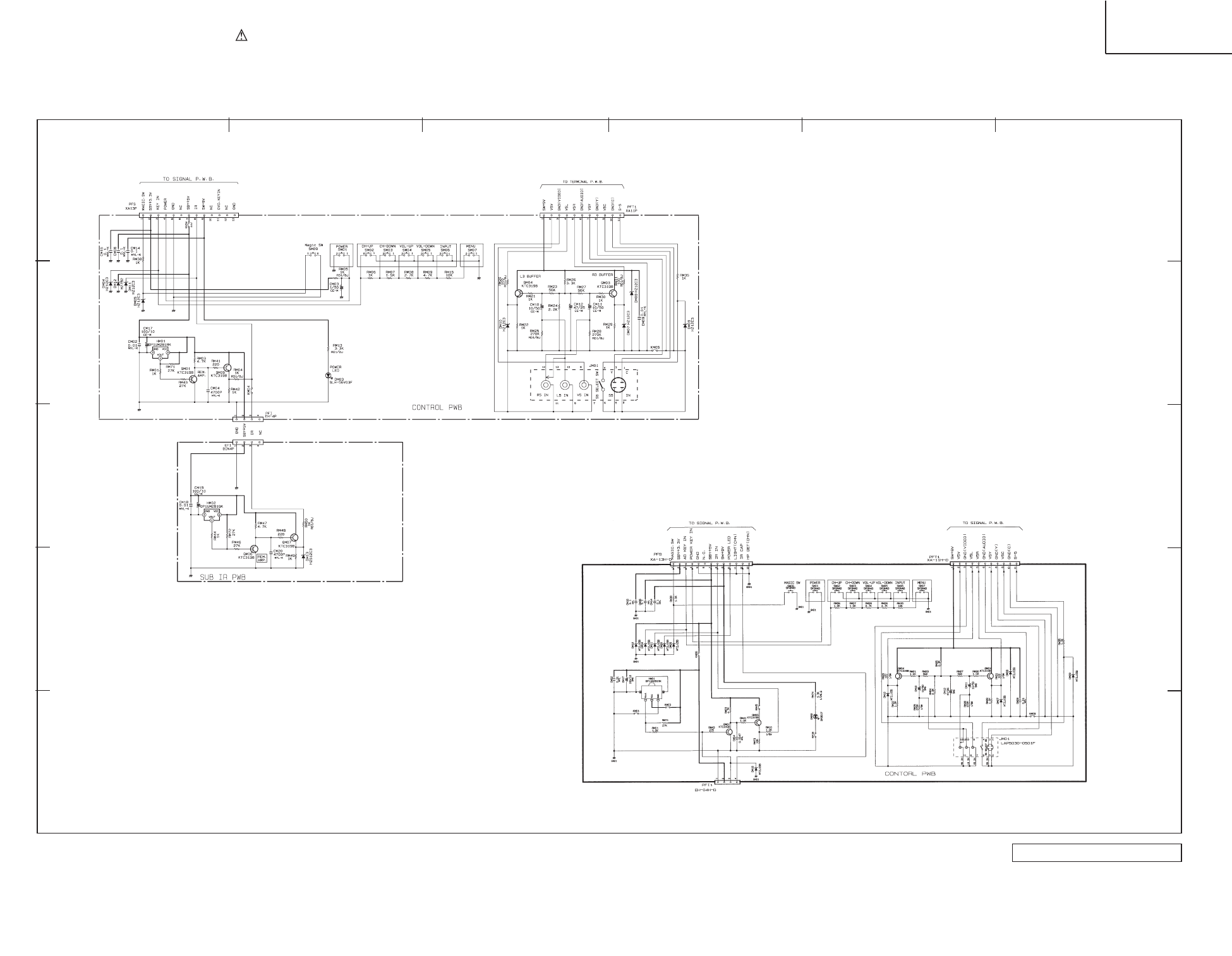
1 234 56
A
B
C
D
E
All DC voltage to be measured with a tester (100k/V). Voltage taken on a complex color bar signal including a standard color bar signal.
Since this is a basic circuit diagram, the value of the parts is subject to be altered for improvement.
Control
PRODUCT SAFETY NOTE: Components marked with a and shaded have special characteristics important to
safety. Before replacing any of these components, read carefully the PRODUCT SAFETY NOTICE of this Service
Manual. Don’t degrade the safety of the receiver through improper servicing.
BASIC CIRCUIT DIAGRAM
DP33KA/B
Control
109
46F500
46F510
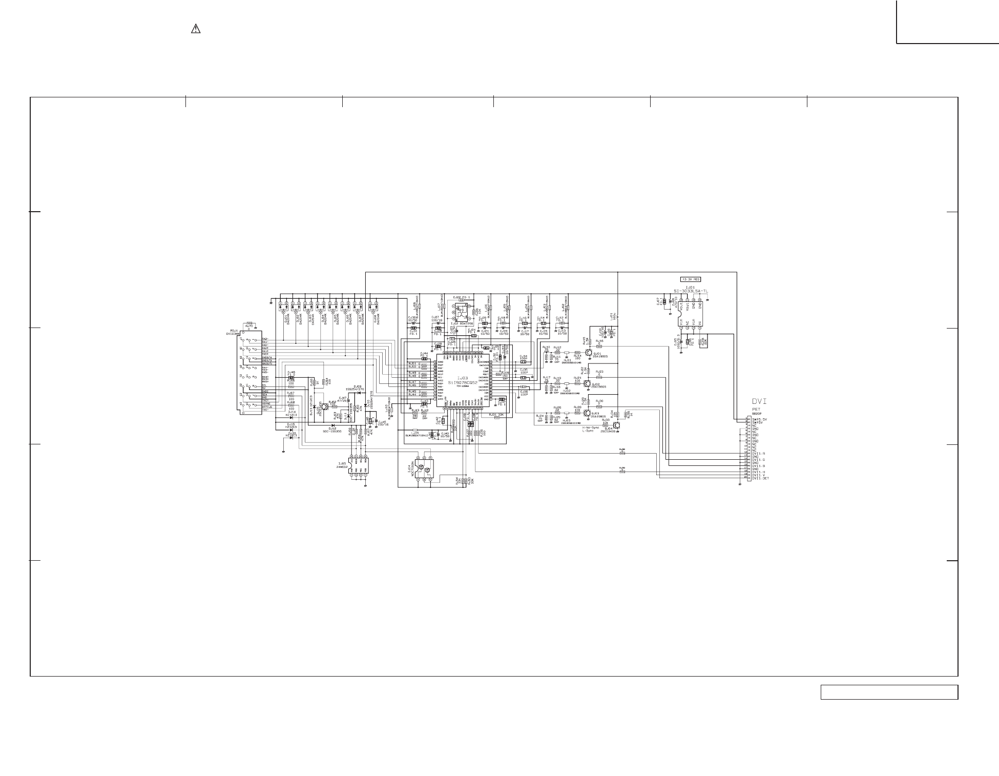
1 234 56
A
B
C
D
E
All DC voltage to be measured with a tester (100k/V). Voltage taken on a complex color bar signal including a standard color bar signal.
Since this is a basic circuit diagram, the value of the parts is subject to be altered for improvement.
DVI
PRODUCT SAFETY NOTE: Components marked with a and shaded have special characteristics important to
safety. Before replacing any of these components, read carefully the PRODUCT SAFETY NOTICE of this Service
Manual. Don’t degrade the safety of the receiver through improper servicing.
BASIC CIRCUIT DIAGRAM DP33KA/B
DVI
110
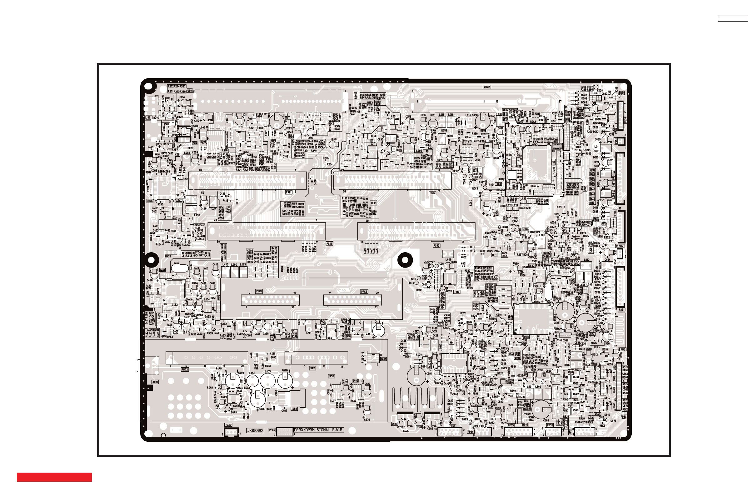
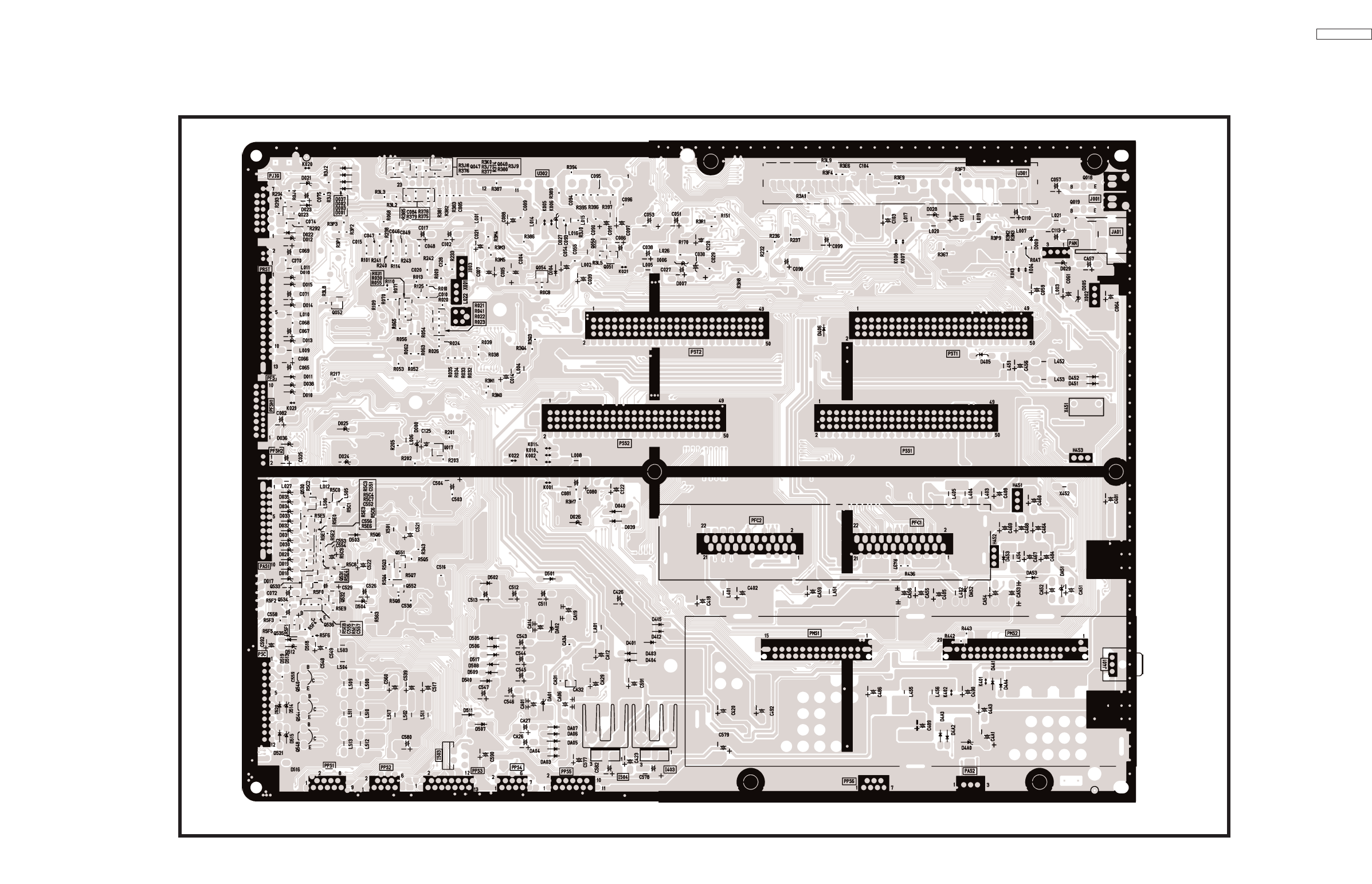
DP33KA/B
PRINTED CIRCUIT BOARD
SIGNAL P.W.B. - PATTERN SIDE
112
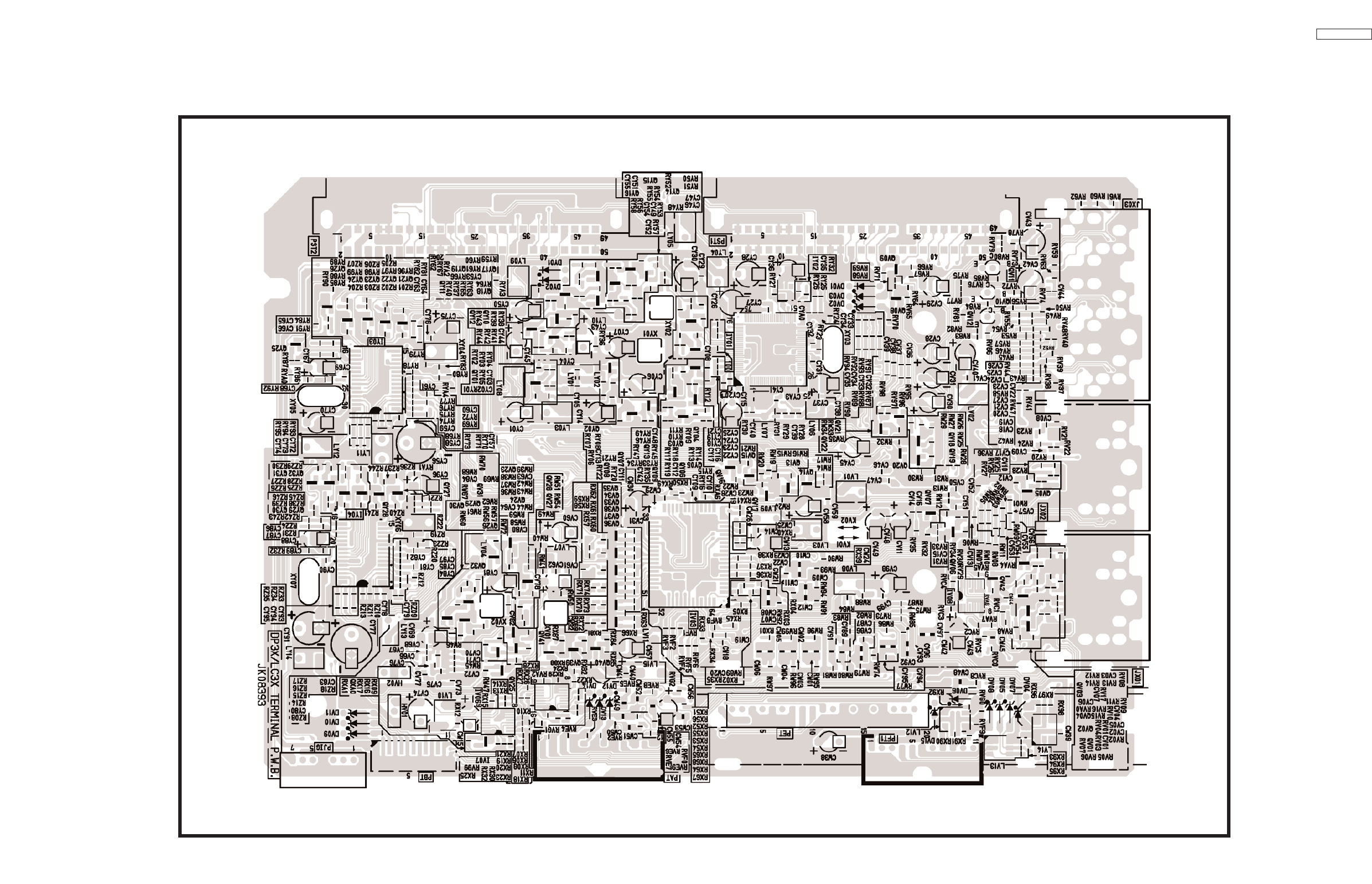
PRINTED CIRCUIT BOARD
TERMINAL P.W.B. - PART SIDE
113
DP33KA/B
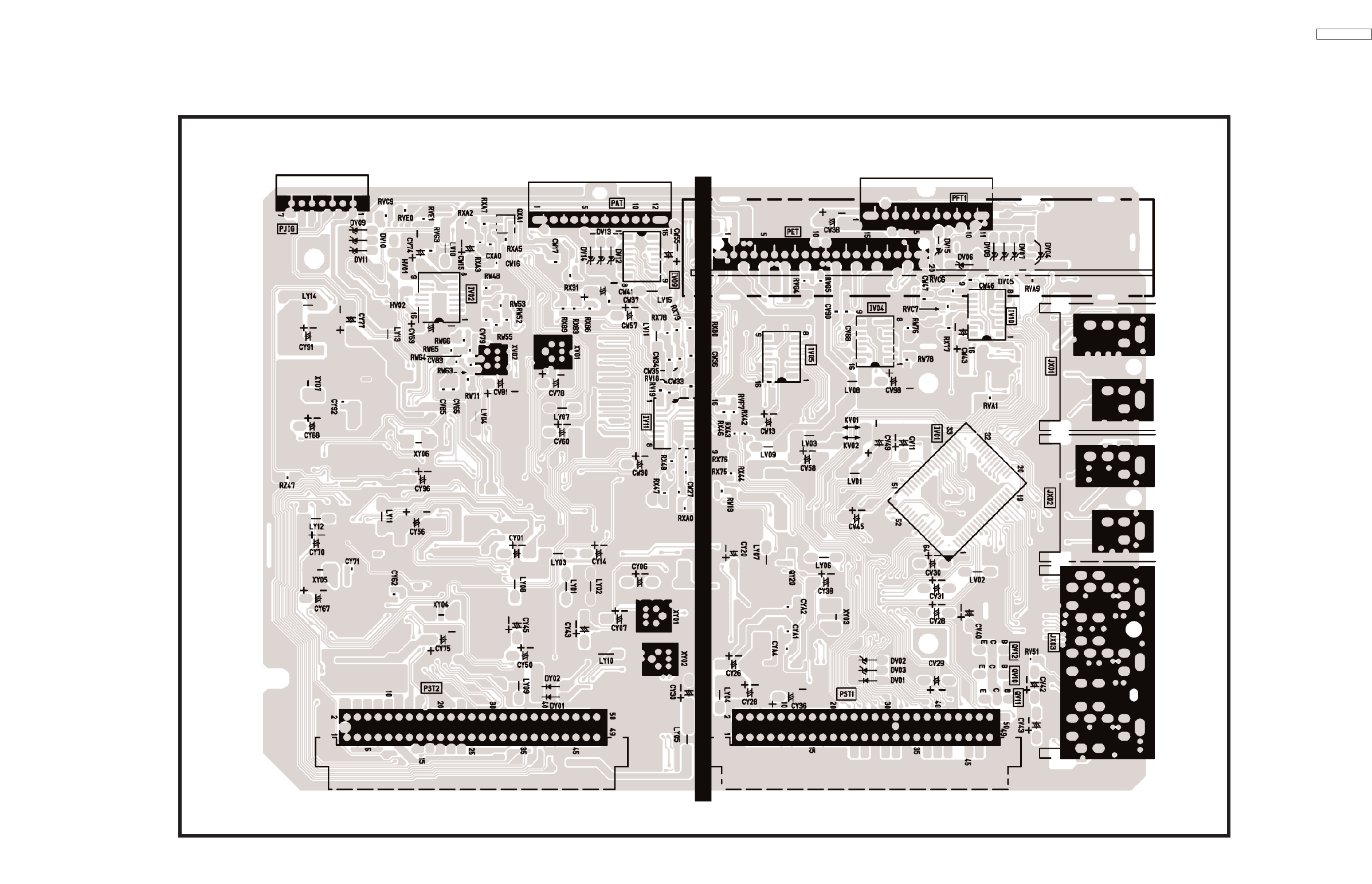
PRINTED CIRCUIT BOARD
TERMINAL P.W.B. - PATTERN SIDE
114
DP33KA/B
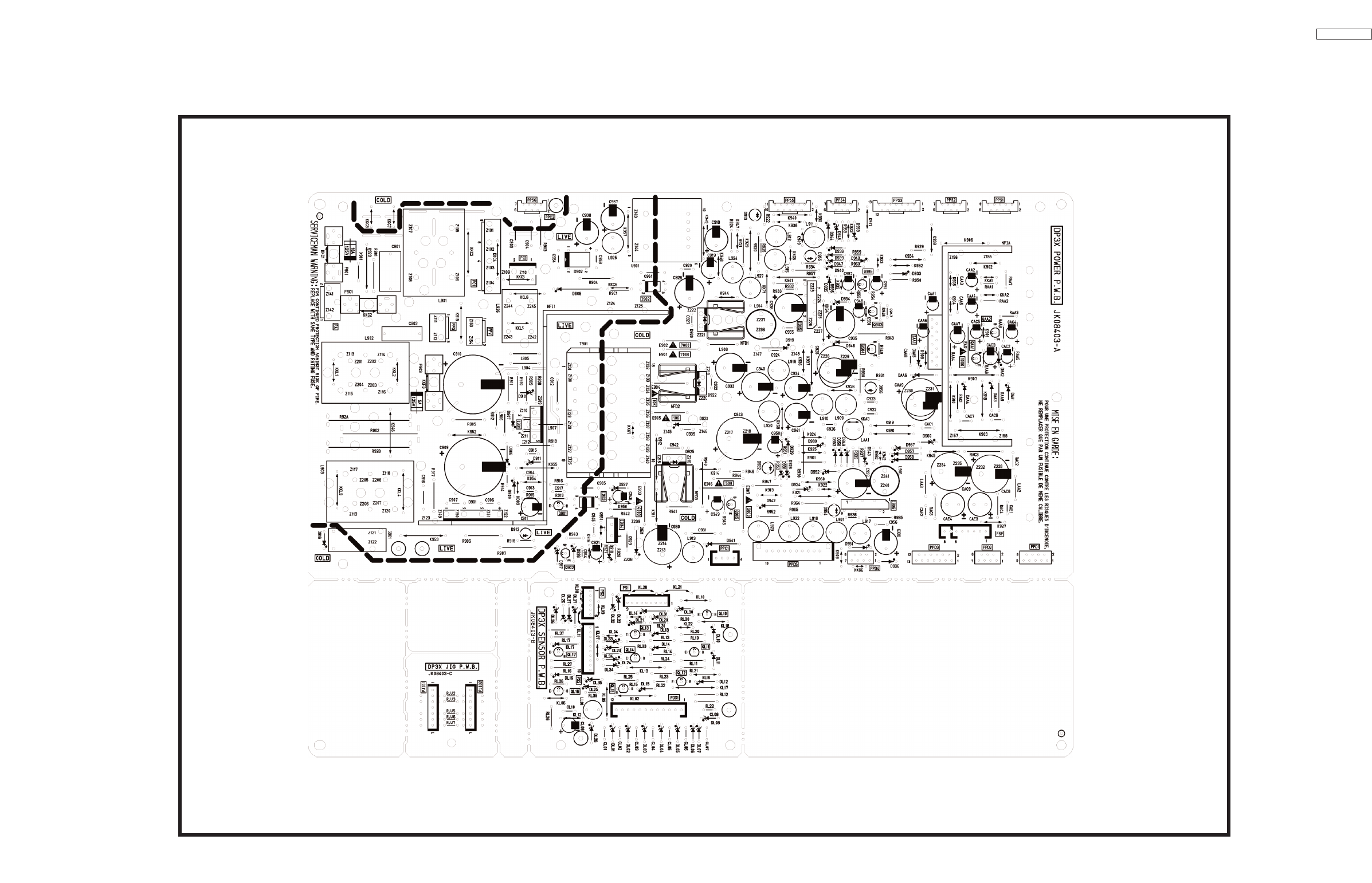
DP33KA/B
PRINTED CIRCUIT BOARD
POWER P.W.B. - PART SIDE
115
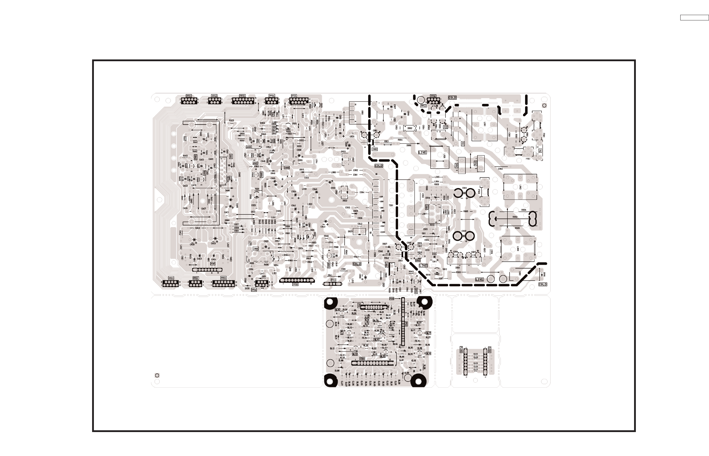
PRINTED CIRCUIT BOARD
POWER P.W.B. - PATTERN SIDE
116
DP33KA/B
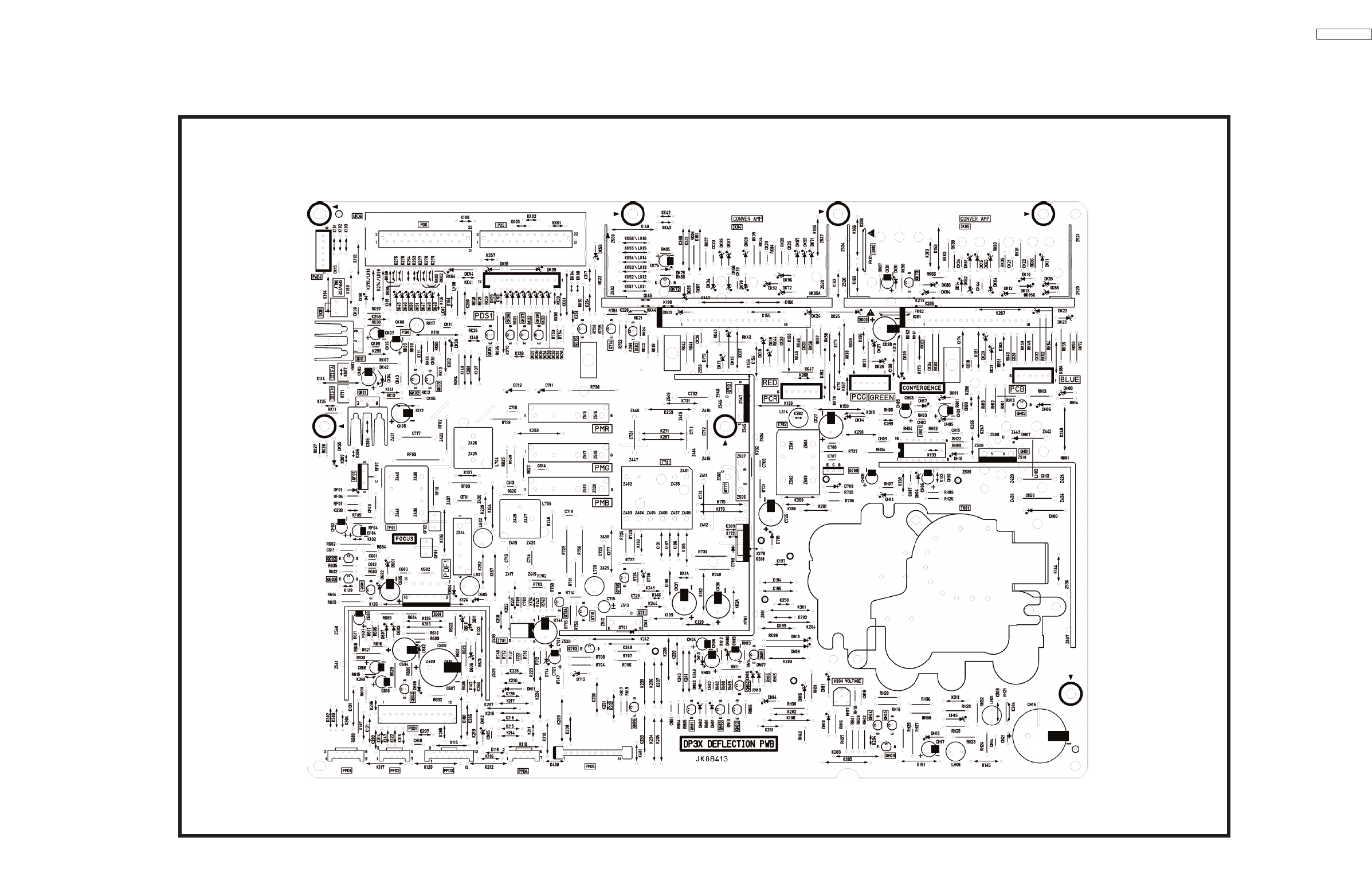
DP33KA/B
PRINTED CIRCUIT BOARD
DEFLECTION P.W.B. - PART SIDE
117
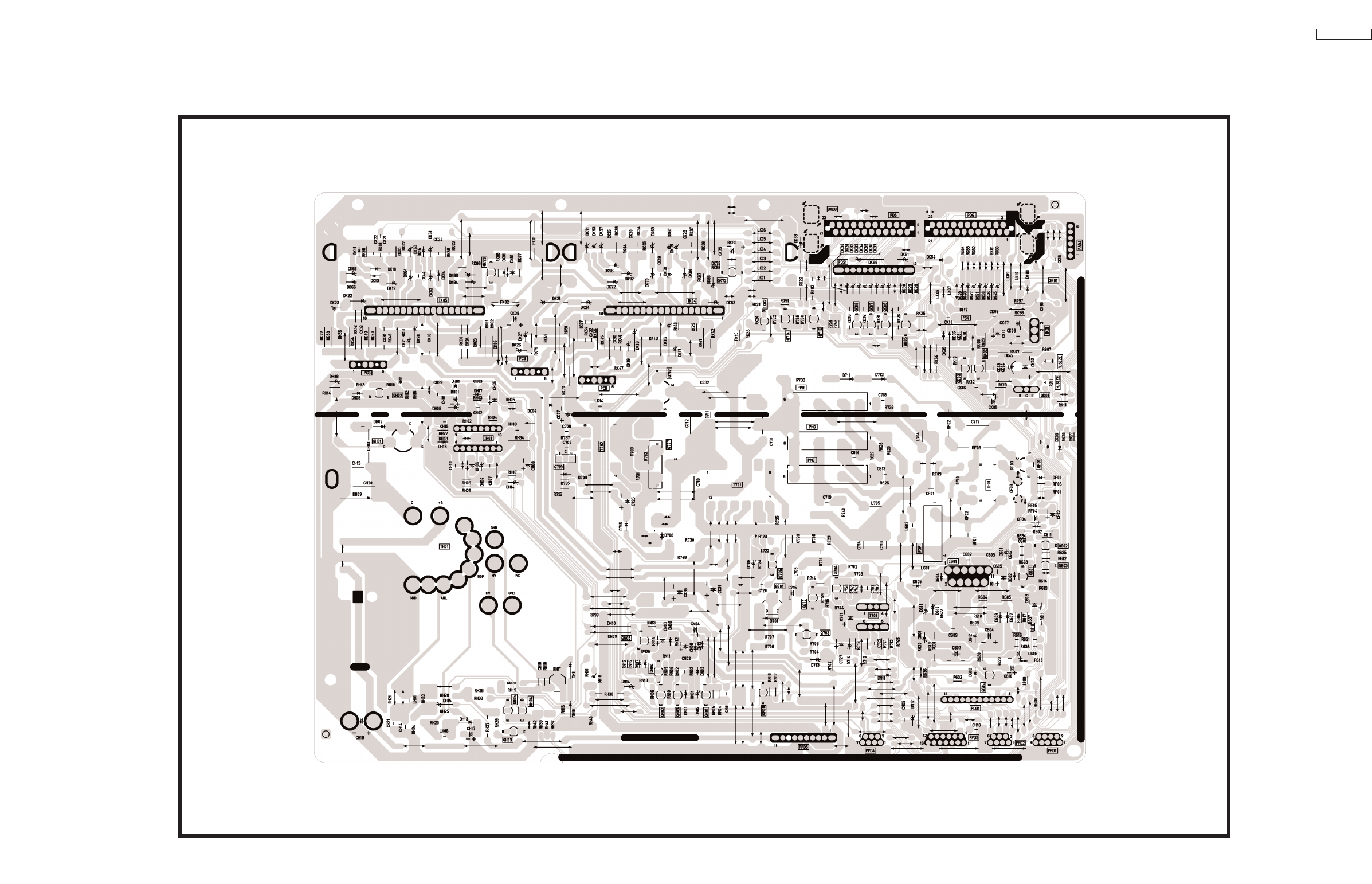
PRINTED CIRCUIT BOARD
DEFLECTION P.W.B. - PATTERN SIDE
118
DP33KA/B
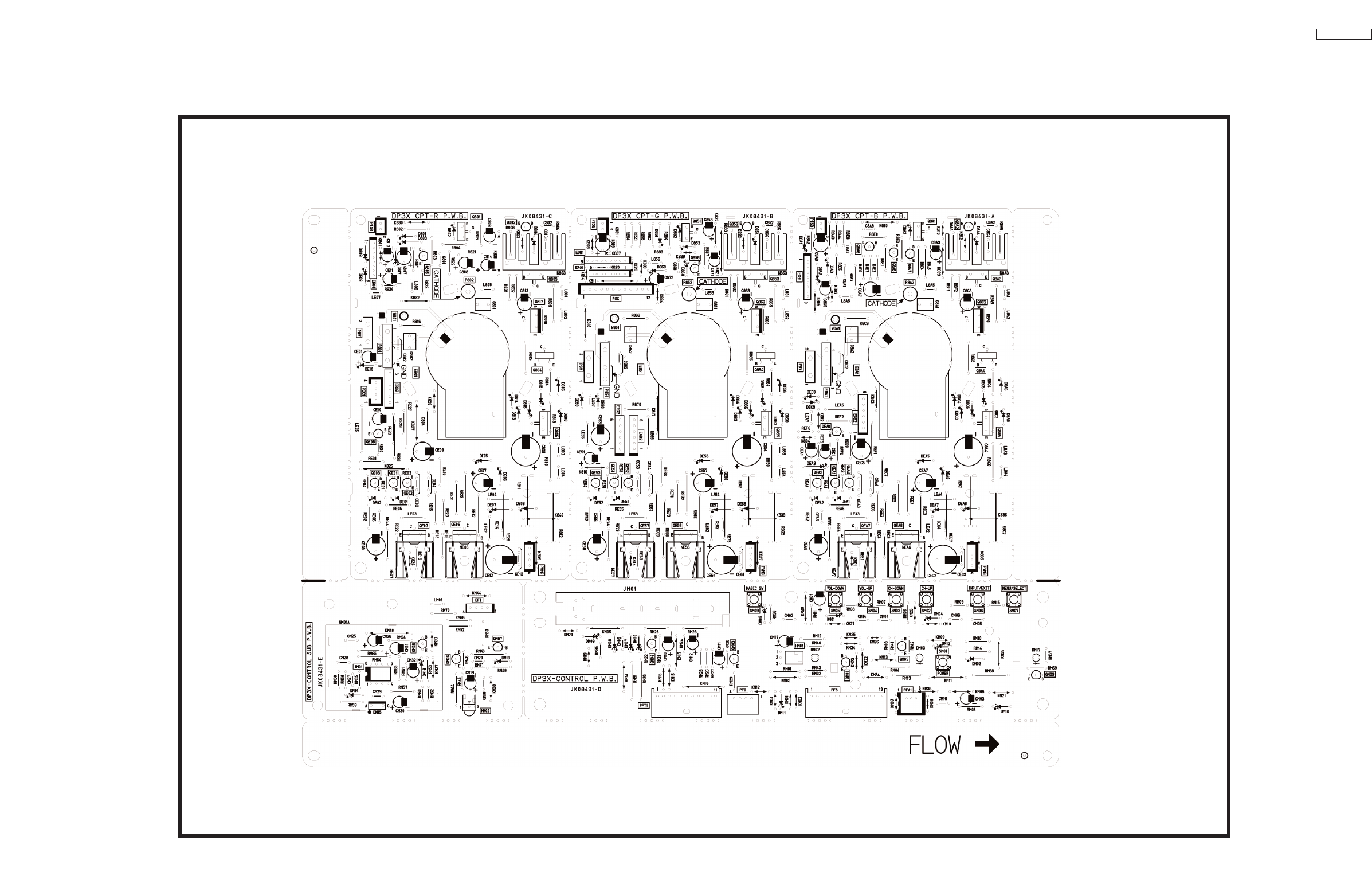
DP33KA/B
PRINTED CIRCUIT BOARD
CPT P.W.B. - PART SIDE (46F500A)
119
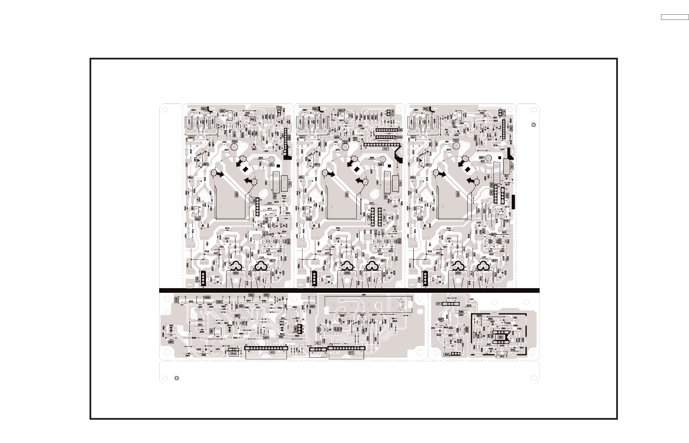
PRINTED CIRCUIT BOARD
CPT P.W.B. - PATTERN SIDE
120
DP33KA/B
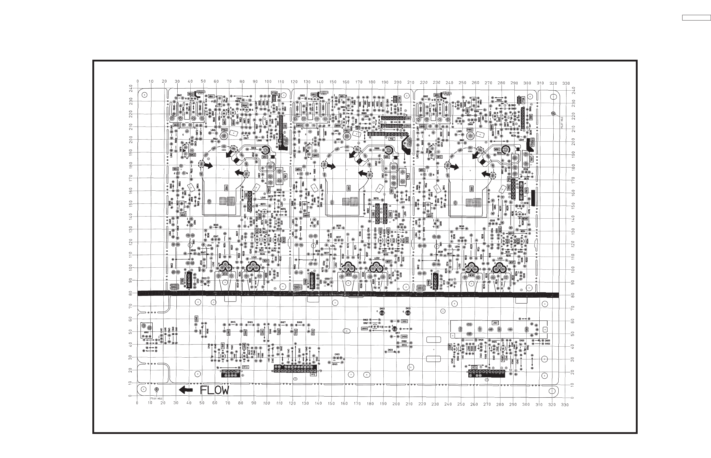
PRINTED CIRCUIT BOARD
46F510 CONTROL P.W.B.
121
DP33KA/B
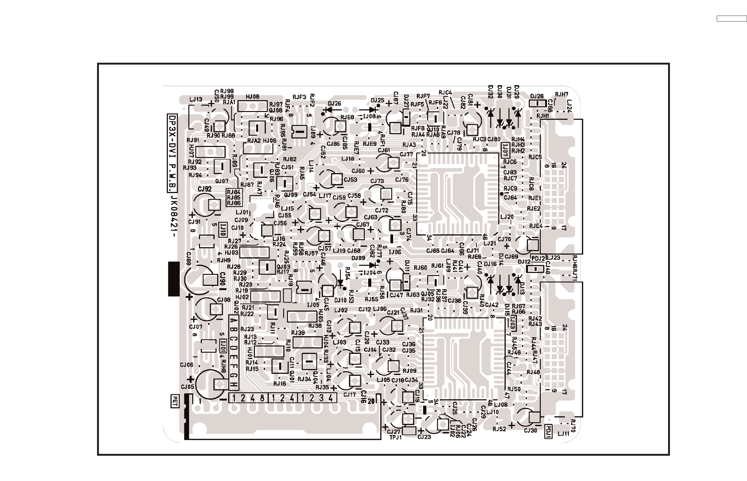
DP33KA/B
PRINTED CIRCUIT BOARD
DVI P.W.B. - PART SIDE
122
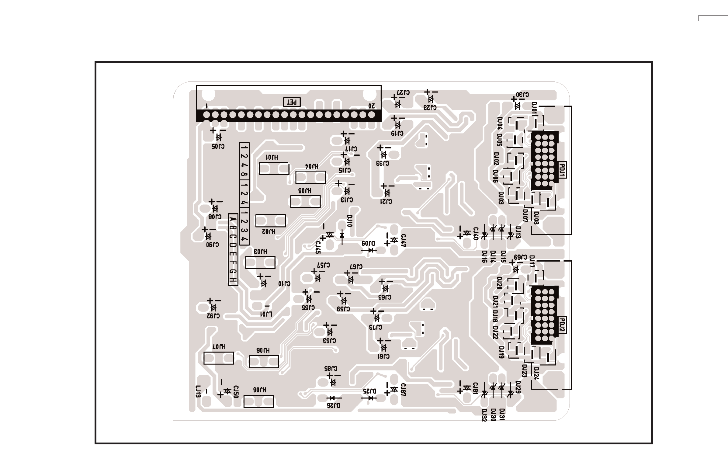
PRINTED CIRCUIT BOARD
DVI P.W.B. - PATTERN SIDE
123
DP33KA/B
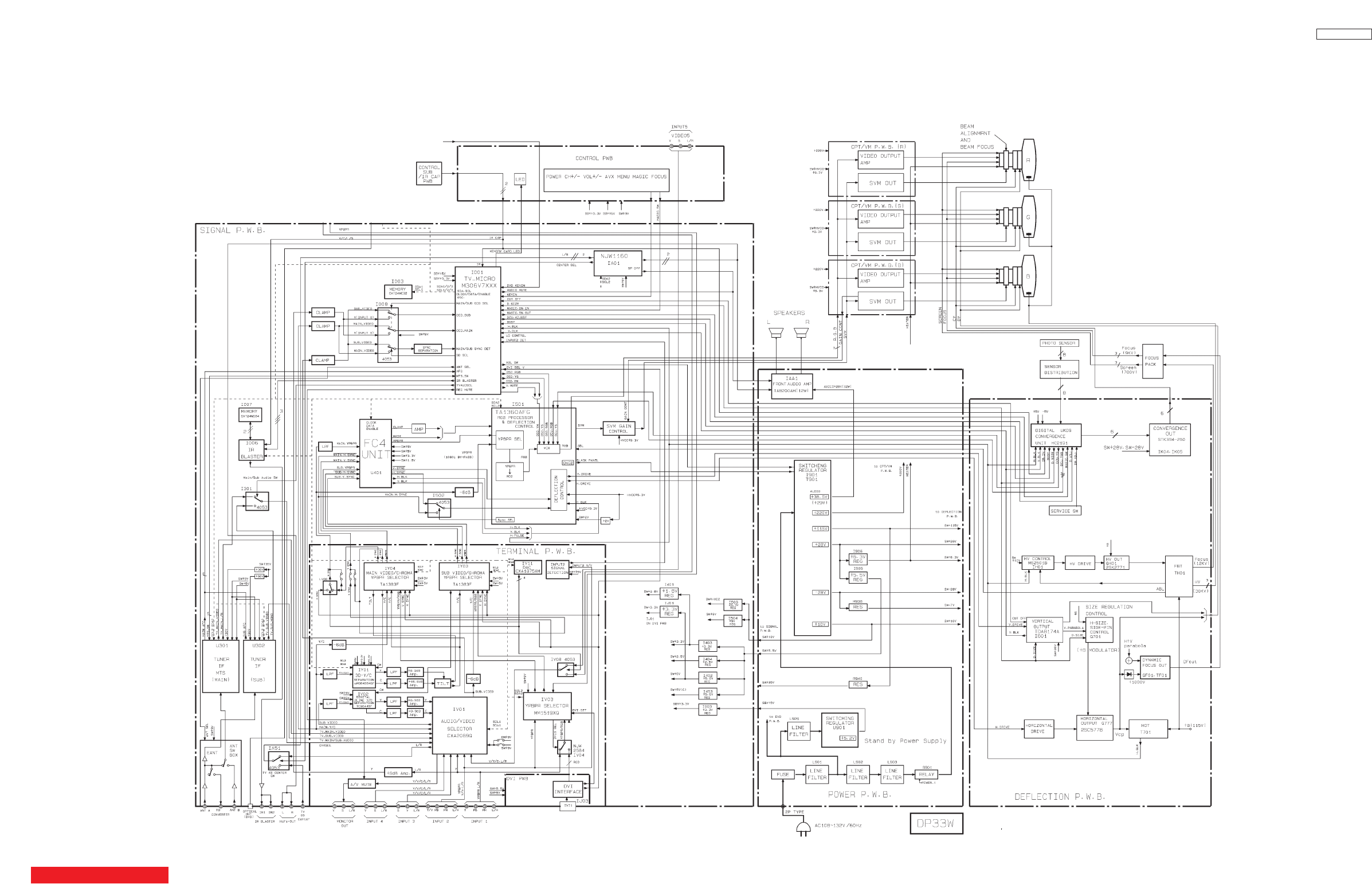
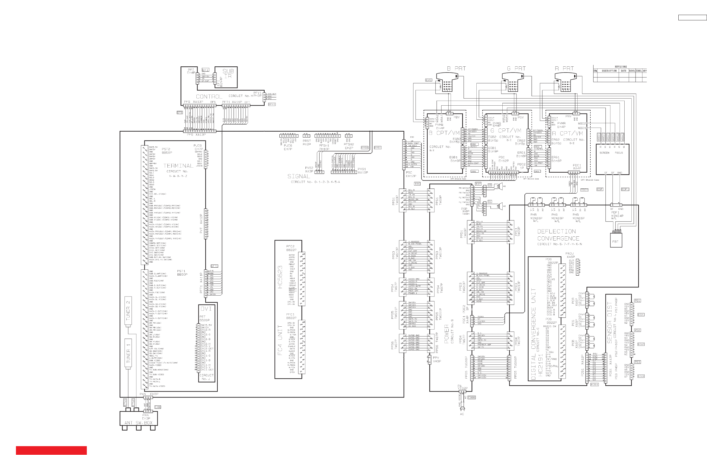
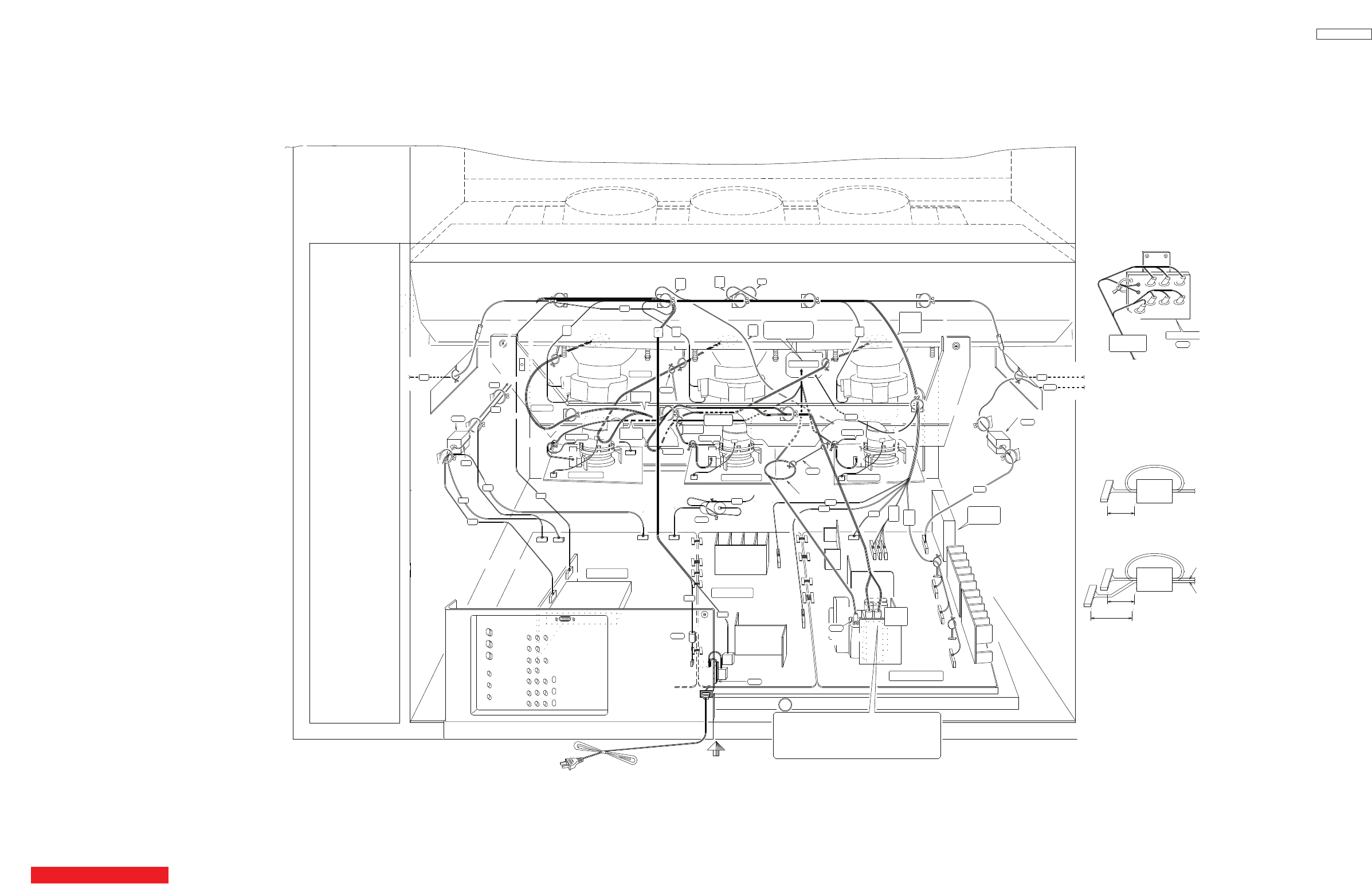
126
DP33KA/B
ÅC
NOTE:(1)
Refer to the figure be
low
about the assembly if
FOCUS PACK leads.
SCREEN
(B) (G) (R)
FOCUS
(B) (G) (R)
FOCUS PACK
EFPK
FOCUS(R,G,B)
SCREEN)R,G,B)
PFT PFS
PFS
PFT
Connector "VMR","VMG"
and "VMB"
should be connected before CPT
P.W.B is inserted to PRT.
NOTE:(2)
CONNECTOR.
CONNECTOR.
200mm
200mm
250mm
(FS)
(FS)
(DS1)
PREPARATION JOB.
LFT1
(FT1)
(FT1) only
(FT1)
(FS),(FT1),(LFT1)
(DS1),(LDS1)
LDS1
THIS DRAWING APPLIES TO
Adjust the slack of a speaker line
by the speaker side.
NOTE:(3)
NOTE:(4)
Even if 300g power is applied
to a wire and wiring dress style
is changed,all wires should not
be contact to a hih temperature,
sharp edge and high voltage parts.
46W500(DP33W CHASS.)
from SENSOR P.W.B.
DS1
L
LDS1
MAG-FERRITE CORE (GX00405)
from Tweeter L
Woofer L
(G)
(BÅj
FOCUS
FOCUS FOCUS
(R)
SCREEN(G)
DIGITAL
CONVERGENCE
UNIT
FOCUS PACK
FOCUS
ANODE(R)
CPT P.W.B.(B)
SCREEN(R)
POWER CORD
PCR
PCG
PCB
BACK SIDE
NOTE: Anode lead should be separated from others
wires. (min. 10mm)
Anode lead must not be twisted during theoperation of wiring dress.
NOTE: Refer to the figure (03/page) when the HV
connector (anode lead) is removed or inserted.
FBT
N005
Ç8
PURSE LOCK
ANODE(R)
ANODE(G)
ANODE(B)
FS
FOCUS
PPD3
PPD6
PPD2
PPD1
PDC1
PDS1
CPT P.W.B.(GÅj
PVMB PVMG
(G)
(G)
FOCUS
SCREEN
(G)
(G)
FOCUS
SCREEN
SCREEN
FOCUS
SCREEN
FOCUS
(B)
(B)
(G)
(G)
PMB PMR
PMG
PS
PSC
SCREEN(B)
to
CPT-R P.W.B.
POWER P.W.B.
DEFLECTION P.W.B.
MR,CR
MG,CG
MB,CB
DC1,DF1
DF1
MR
MG
MB CR
CG
CB
DF1
R
PSC
FS
through
only
NOTE:(2)
NOTE:(2) NOTE:(2)
R
DS1
to CONTROL P.W.B.
make
1 loop
NOTE:(1)
DF
FS FOCUS(R,G,B)
SCREEN(R,G,B)
ÅC
ÅC
Reference
PVMR
CPT P.W.B.(R)
PDF1
(B)
FOCUS
SCREEN
(B)
ANODE(B)ANODE(B)
SIGNAL P.W.B.
MB
CB MG
CG
MR
CR
ANODE(G)
ANODE(B)
ANODE(G)
ANODE(B)
ANODE(G)
ANODE(B)
ANODE(G)
DC1
DF1
N003
DC1
DF1
PPS4
PPS5
PPS1
PPS3
PSP
DC1
SP
make double
loops
MR
CR
SC
LESC
MAG-FEREREITE CORE(GX00662)
PFT1
LFT1
FT1
to CPT P.W.B.(G)
N003
PA L999
MAG-FEREREITE CORE(GX00662)
PPS6
PVS2
PPV
PVT
PVS1
PJIG PFS
VT
VT
FT1
VS1
(R)
ANODE
VS2
PV
PV
VS2
LEVS2
FT1
JIG2
to JIGU P.W.B.
MAG-FERRITE
CORE (GX00661)
TABLE OF CONTENTS
FINAL WIRING DRAWING
This drawing applies to 46W500 (DP33W) chass.
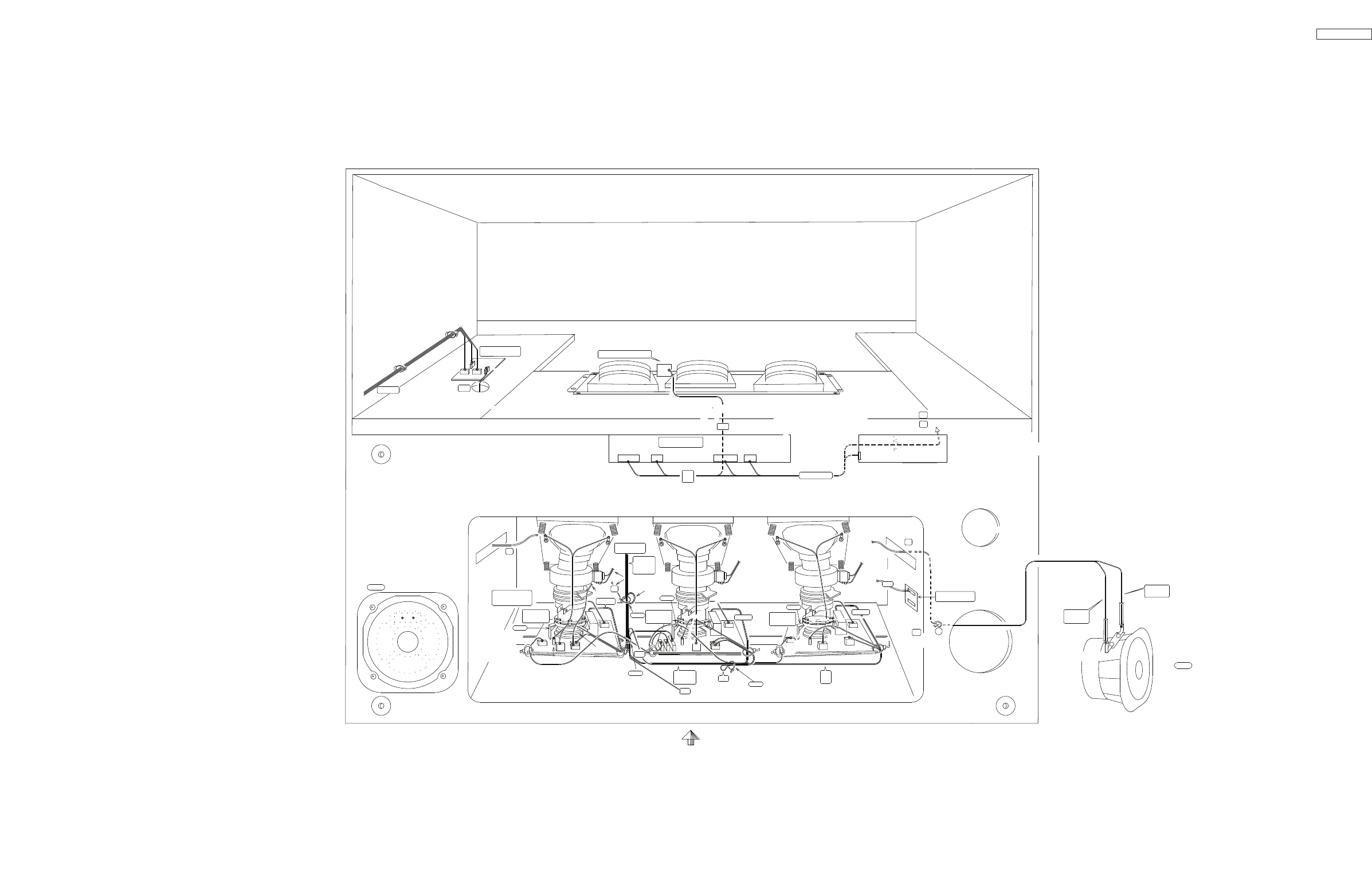
127
DP33KA/B
CPT
P.W.B.
(BÅj
#231
POWER SUPPLY
DEF. P.W.B.
CPT
P.W.B.
(GÅj
SCREENÅ@
(B)
CPT SOCKET
HOLDER
FRONT SIDE
from SIGNAL P.W.B.
EGB1
(01/ )reference
(03/ )
reference
NOTE:(3)
FOCUS
(G)
CPT
P.W.B. (R)
FOCUS(R)
#231
ERG1
#231
PGVPRV
ERG2 EGB2
ERG2
PVMR
PSC
PBV
W8A1
PVMG PVMB
FOCUS
(B)
FOCUS(R,G,B)
SCREEN(R,G,B)
(01/ )reference
from FOCUS PACK
PMG PMB
from
DEFLECTION P.W.B. from
DEFLECTION P.W.B.
W801
SCREENÅ@
(G)
PDC1
W8A2
W802 W852
Terminal base : white
Terminal base : Red
+
-
Put silicon
to cabinet
hole.
Woofer(R)
red(PRÅj
red(PL)
blue(PR)
brown(PL)
U404
Woofer(L)
White Red
+
U402
-
make one loop.
EGB2
SCREEN (R)
PCR
PMR
PCG PCB
L
R
801,802
8A1,8A2
851,852
8A1,8A2
RG2
851,852 GB2 8A1
8A2
GB2
(01/ )reference
from SIGNAL P.W.B.
from
DEFLECTION P.W.B.
DF1
from
POWER P.W.B.
N007
DF1
N006
N006
RG2
PFT
CONTROL P.W.B.
FI
A
specification(1)
reference.
R
(DP37/37C/37D)
PFS
(DP37/37C/37D)
CONTROL SUB P.W.B.
PFI
FI
FT1
W851
ERG1
EGB1
PSC
SC
from SIGNAL P.W.B.
S1,S2,S3
from SCREEN FRAME(Page.4)
THIS DRAWING APPLIES TO
46W500(DP33W CHASS.)
PS3 PS2
PDS1
DSI
from DEFLECTION
CONVERGENCE P.W.B.
PS1
SENSOR P.W.B.
PFV1 PFV1
FT1,FS,FV1
from TERMINAL P.W.B.
from S,BSIGNAL P.W.B.
FT1
FS
JIG CONNECTOR
PJIG2
PJIG1
from SIGNAL P.W.B.
JIG2
FINAL WIRING DRAWING
This drawing applies to 46W500 (DP33W) chass.
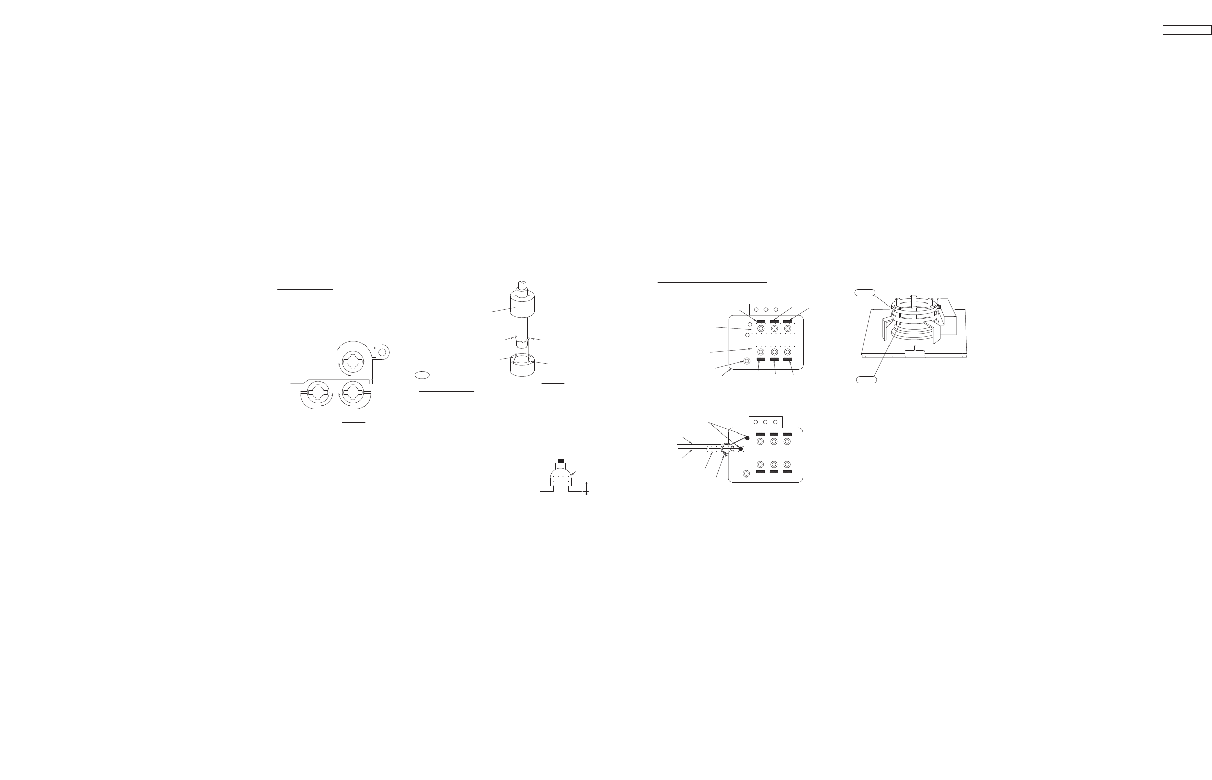
128
DP33KA/B
During Removal
CAUTIONS WHEN CONNECTING/DIS CONNECTING THE HV CONNECTOR
Silicon Cover
less than 1mm
During Insertion
3. Confirm the contact by pulling the connector slightly.
(Don't pull hard because it may damage the connector.)
4. Cover the high voltage output by carefully pushing
silicon cover on to it. (Don't turn the connector.)
(REMARK)
1. Make sure the silicon cover is
covered the high voltage output.
Fig.B
L position
L position
wing wing
Silicon cover
PS process
F.B.T
Çn
Çn
ÇkÇk
Fig. A
PUSH
PUSH
(UFPK) FOCUS PACK ASY.
PAING EACH COLOR
BLUE
GREEN
"@
RED
PAINT EACH COLOR
FOCUS PACK
BACK SIDE
BLUE
GREEN"@
RED
CONNECT EACH COLOR
SCREEN LEAD FROM CPT P.W.B.
LEAD COLOR:ORANDE
CONNECT[FS]CONNECTOR
FROM FBT.
WRAPPING & SOLDER
(DF)CONNECTOR BLACK
(DF)CONNECTOR RED
(NFP1)UL TUBE No.3 L=50mm
CPT SOCKET HOLDER
#231
#234
1. Roll out"@silicon cover from FBT's
contact area slowly.
2. While turning the connector about
"@90 degrees following the arrow
(0 position). Push the conn
ector
slightly towards the case. (Fig.A)
3. Remove the connector slowly by
pulling it away from the case.
1. Please refer to direction for insertion as shown in Fig.B
(L position) Insert connector till $CLICK$ sound is heard.
2. Make sure the connector is pressed right in, so that it
has a good contact with the spring.
CONNECT EACH COLOR
FOCUS LEAD FROM CPT P.W.B.
LEAD COLOR:IVORY
(NFP2)SK BINDER
CPT SOCKET
HOLD BAND
NOTE:(2) CPT SOCKET HOLDER ASSEMBLY.(R.G.B)
CPT SOCKET HOLDER ASSEMBLY SHOULD
BE FOLLOWED BELOW FIG.
WIRING DRAWING
130
DP33KA/B
EXPLODED VIEW
46F500A/510
NOTE: Some parts may appear different than those shown in the exploded view. When ordering, refer to the replacement parts
list for the correct part number. The circled numbers correspond to the parts list shown on page 142.
131
DP33KA/B
Model 46F500/510
No Part No Description Qty.
1QD35413 SCREEN FRAME 46 F500 1
2KR03051 46W SCREEN ASSY 1
3NA60061 SCRN SIDE MTL 46F300 2
4NA60051 SCREN T/B MTL 46F300 2
5NA60781 MIRROR LOW METAL 46G 2
6NA60771 MIRROR TOP METAL 46G 1
755050071 MIRROR BOARD SUB-ASSY 1
8KS05782 1ST MIRROR 46F D250 1
9NJ07072 MIROR COVER HOLDER L 1
10 NJ07071 MIROR COVER HOLDER R 1
11 QD35421 MIRROR COVER 46 F300 1
12 1
13 GK01181 SPEAKER SP-12CM C120RB506-10 2
14 52020112 FRONT ASSY 1
15 PH32812 DECO RAIL L 46F500A 1
16 PH32202 SP GRILL SASY 46F500A 1
17 PH33641 DECO RAIL RIGHT ASSY 46F500A 1
18 PH32735 CONTROL PANEL2003S500(1S P OXIN) PS 1
18A PH32746 CONTROL DOOR 2003 W500 ABS 1
19 1
20 1
21 NA62121 CABI TOP COVER 1
22 NA62551 CABI COV FIX MTL 46W500 1
23 1
24 33010468 BARRIER BOARD 46F500 1
25 H512332 LOWER REAR BOARD 46W500 1
26 NA60742 BARR BRD FIX MTL L46 1
27 NA60741 BARR BRD FIX MTL R46 1
28 Red PRT ASS'Y1
29 Green PRT ASS'Y1
30 Blue PRT ASS'Y1
31 MF01101 BARRIER BOARD 46G500 1
32 NA57181 IR PWB FIX MTL DP2X 1
33 NA57577 LC METAL 2002-51 SIDE 2
34 NA60031 DP3X FOCUS FIX METAL 1
35 NA57221 LC METAL 2002-43 FRONT 1
36 NA56993 LC METAL 2002-25 REAR 1
37 NM00941 CHASSIS SUPPORT 2002 1
38 NA60015 SIDE METAL 46W R D250 1
39 NJ06581 DRIPPING HOLDER DP2X 1
40 NA60016 SIDE METAL 46W L D250 1
41 Not Avail. DP33K CHASSIS ASY 1
42 KQ02333 DELTA LENS ASSY 1
43 KQ02333 DELTA LENS ASSY 1
44 KQ02333 DELTA LENS ASSY 1
45 BY01792 DY-V80-7SS (0.59)CYL 3
46 JT24053 DP33K CPT PWB ASSY 1
EXPLODED VIEW PARTS LIST
TABLE OF CONTENTS
CH 2
See page 161
132
DP33KA/B
132
REPLACEMENT PARTS LIST
PRODUCT SERVICE NOTE: Components marked with a have special characteristics important to safety. Before replacing
any of these components, read carefully, the PRODUCT SAFETY NOTICE of this Service Manual. Don’t degrade the safety of the
receiver through improper servicing.
!
Capacitors: Resistors: Semiconductors:
AL: Aluminum Electrolytic CF: Carbon Film TR: Transistor
CD: Ceramic Disc CC: Carbon Composition DI: Diode
EL: Electrolitic MF: Metal Oxide ZD: Zener Diode
PF: Polyester Film VR: Variable Resistor VA: Varistor
PP: Polypropylene WW: Wire Wound TH: Termistor
PL: Plastic FR: Fuse Resistor IC: Integrated Circuit
TA: Tantalum MG: Metal Grazed
PR: Paper
TM: Trimmer
MC: Mylar
ABBREVIATIONS
SYMBOL PART PART SYMBOL PART PART
NO. NO. DESCRIPTION NO. NO. DESCRIPTION
C037 0893232R CAP 1608CHIP 100000PFZF25V TAPE
CAPACITORS C038 0800326R CAP.-ELECTRO. 100UF-M 16V
C001 0893208R CAP 1608CHIP 1000PFKB 50V TAPE C039 0800326R CAP.-ELECTRO. 100UF-M 16V
C002 0800282R CAP.-ELECTORO. 2.2UF-M(SMG) 50V C040 0893232R CAP 1608CHIP 100000PFZF25V TAPE
C003 0893131R CAP 1608CHIP 220PFJCH 50V TAPE C041 AA01101R CERAMIC CAPACITOR(1UF 10V-F)
C004 0800294R CAP.-ELECTRO. 10UF-M(SMG) 50V C042 AA01101R CERAMIC CAPACITOR(1UF 10V-F)
C005 0893179R CAP.CHIP-CERAMIC 100000PF 16V TAPE C050 0893205R CAP 1608CHIP 560PFKB 50V TAPE
C006 0893193R CAP 1608CHIP 10000PFKB 25V TAPE C051 0800279R CAP.-ELECTORO. 1.0UF-M(SMG) 50V
C007 0800294R CAP.-ELECTRO. 10UF-M(SMG) 50V C052 0893205R CAP 1608CHIP 560PFKB 50V TAPE
C010 0893179R CAP.CHIP-CERAMIC 100000PF 16V TAPE C053 0800279R CAP.-ELECTORO. 1.0UF-M(SMG) 50V
C011 0893104R CAP 1608CHIP 2PFCCK 50V TAPE C054 0800326R CAP.-ELECTRO. 100UF-M 16V
C012 0893182R CERAMIC CAPACITOR(15000PF 16V) C055 0893232R CAP 1608CHIP 100000PFZF25V TAPE
C013 0893232R CAP 1608CHIP 100000PFZF25V TAPE C065 0800326R CAP.-ELECTRO. 100UF-M 16V
C014 0800326R CAP.-ELECTRO. 100UF-M 16V C066 0893232R CAP 1608CHIP 100000PFZF25V TAPE
C015 0893239R CAP 1608CHIP 10000PFZF 50V TAPE C067 0800326R CAP.-ELECTRO. 100UF-M 16V
C016 0893208R CAP 1608CHIP 1000PFKB 50V TAPE C068 0893232R CAP 1608CHIP 100000PFZF25V TAPE
C017 0800282R CAP.-ELECTORO. 2.2UF-M(SMG) 50V C069 0800326R CAP.-ELECTRO. 100UF-M 16V
C018 0893131R CAP 1608CHIP 220PFJCH 50V TAPE C070 0893232R CAP 1608CHIP 100000PFZF25V TAPE
C019 0893204R CAP 1608CHIP 470PFKB 50V TAPE C071 0800279R CAP.-ELECTORO. 1.0UF-M(SMG) 50V
C020 0893232R CAP 1608CHIP 100000PFZF25V TAPE C074 0893232R CAP 1608CHIP 100000PFZF25V TAPE
C021 0800326R CAP.-ELECTRO. 100UF-M 16V C075 0800294R CAP.-ELECTRO. 10UF-M(SMG) 50V
C022 0893204R CAP 1608CHIP 470PFKB 50V TAPE C076 0893128R CAP 1608CHIP 150PFJCH 50V TAPE
C023 0893213R CAP1608CHIP 2200PFKB 50V TAPE C077 0893126R CAP 1608CHIP 100PFJCH 50V TAPE
C024 0893232R CAP 1608CHIP 100000PFZF25V TAPE C078 0893205R CAP 1608CHIP 560PFKB 50V TAPE
C025 0800326R CAP.-ELECTRO. 100UF-M 16V C079 0893239R CAP 1608CHIP 10000PFZF 50V TAPE
C027 0800303R CAP.-ELECTRO. 22UF-M 50V C080 0800326R CAP.-ELECTRO. 100UF-M 16V
C028 0893208R CAP 1608CHIP 1000PFKB 50V TAPE C081 0893232R CAP 1608CHIP 100000PFZF25V TAPE
C029 0893232R CAP 1608CHIP 100000PFZF25V TAPE C082 0800326R CAP.-ELECTRO. 100UF-M 16V
C030 0800326R CAP.-ELECTRO. 100UF-M 16V C083 0893232R CAP 1608CHIP 100000PFZF25V TAPE
C031 AA01111R CERAMIC CAPACITOR(1.0UF 6.3V) C086 0800294R CAP.-ELECTRO. 10UF-M(SMG) 50V
C032 AA01101R CERAMIC CAPACITOR(1UF 10V-F) C087 0893183R CERAMIC CAPACITOR(18000PF 16V)
C033 AA01111R CERAMIC CAPACITOR(1.0UF 6.3V) C090 0893239R CAP 1608CHIP 10000PFZF 50V TAPE
C034 AA01101R CERAMIC CAPACITOR(1UF 10V-F) C091 0800352R CAP.-ELECTRO.470UF 10V
C035 AA01111R CERAMIC CAPACITOR(1.0UF 6.3V) C092 0893239R CAP 1608CHIP 10000PFZF 50V TAPE
C036 AA01101R CERAMIC CAPACITOR(1UF 10V-F) C093 0893239R CAP 1608CHIP 10000PFZF 50V TAPE
BACK TO TABLE OF CONTENTS

133
PRODUCT SERVICE NOTE: Components marked with a have special characteristics important to safety. Before replacing
any of these components, read carefully, the PRODUCT SAFETY NOTICE of this Service Manual. Don’t degrade the safety of the
receiver through improper servicing.
!
DP33KA/B
SYMBOL PART PART SYMBOL PART PART
NO. NO. DESCRIPTION NO. NO. DESCRIPTION
C096 0893239R CAP 1608CHIP 10000PFZF 50V TAPE C533 AA00964R CERAMIC CAPACITOR(2.2UF 6.3V)
C098 0800294R CAP.-ELECTRO. 10UF-M(SMG) 50V C534 AA00964R CERAMIC CAPACITOR(2.2UF 6.3V)
C099 0800294R CAP.-ELECTRO. 10UF-M(SMG) 50V C535 0893179R CAP.CHIP-CERAMIC 100000PF 16V TAPE
C102 0893239R CAP 1608CHIP 10000PFZF 50V TAPE C536 0893179R CAP.CHIP-CERAMIC 100000PF 16V TAPE
C103 0800352R CAP.-ELECTRO.470UF 10V C537 0893179R CAP.CHIP-CERAMIC 100000PF 16V TAPE
C104 0893239R CAP 1608CHIP 10000PFZF 50V TAPE C538 0893232R CAP 1608CHIP 100000PFZF25V TAPE
C106 0893239R CAP 1608CHIP 10000PFZF 50V TAPE C539 0800326R CAP.-ELECTRO. 100UF-M 16V
C109 0893239R CAP 1608CHIP 10000PFZF 50V TAPE C540 0893179R CAP.CHIP-CERAMIC 100000PF 16V TAPE
C111 0800352R CAP.-ELECTRO.470UF 10V C541 0893179R CAP.CHIP-CERAMIC 100000PF 16V TAPE
C112 0893239R CAP 1608CHIP 10000PFZF 50V TAPE C542 0893179R CAP.CHIP-CERAMIC 100000PF 16V TAPE
C113 0800326R CAP.-ELECTRO. 100UF-M 16V C545 0800326R CAP.-ELECTRO. 100UF-M 16V
C114 0893232R CAP 1608CHIP 100000PFZF25V TAPE C546 0800294R CAP.-ELECTRO. 10UF-M(SMG) 50V
C119 0893232R CAP 1608CHIP 100000PFZF25V TAPE C547 0800344R CAP.-ELECTRO. 330UF-M(SMG) 16V
C120 0800326R CAP.-ELECTRO. 100UF-M 16V C548 0800326R CAP.-ELECTRO. 100UF-M 16V
C121 0893232R CAP 1608CHIP 100000PFZF25V TAPE C549 0893232R CAP 1608CHIP 100000PFZF25V TAPE
C122 0800294R CAP.-ELECTRO. 10UF-M(SMG) 50V C552 0893232R CAP 1608CHIP 100000PFZF25V TAPE
C123 0893179R CAP.CHIP-CERAMIC 100000PF 16V TAPE C553 0893239R CAP 1608CHIP 10000PFZF 50V TAPE
C124 0893179R CAP.CHIP-CERAMIC 100000PF 16V TAPE C554 0800294R CAP.-ELECTRO. 10UF-M(SMG) 50V
C125 0800326R CAP.-ELECTRO. 100UF-M 16V C555 0893113R CAP 1608CHIP 10PFCCH 50V TAPE
C126 0893208R CAP 1608CHIP 1000PFKB 50V TAPE C557 0893232R CAP 1608CHIP 100000PFZF25V TAPE
C401 0893232R CAP 1608CHIP 100000PFZF25V TAPE C558 0800318R CAP.-ELECTRO. 47UF-M 25V
C402 0800352R CAP.-ELECTRO.470UF 10V C560 0800326R CAP.-ELECTRO. 100UF-M 16V
C404 0893232R CAP 1608CHIP 100000PFZF25V TAPE C561 0893232R CAP 1608CHIP 100000PFZF25V TAPE
C405 0800352R CAP.-ELECTRO.470UF 10V C564 0893232R CAP 1608CHIP 100000PFZF25V TAPE
C407 0893232R CAP 1608CHIP 100000PFZF25V TAPE C565 0893232R CAP 1608CHIP 100000PFZF25V TAPE
C408 0800326R CAP.-ELECTRO. 100UF-M 16V C568 0893232R CAP 1608CHIP 100000PFZF25V TAPE
C409 0893115R CAP 1608CHIP 15PFJCH 50V TAPE C569 0893232R CAP 1608CHIP 100000PFZF25V TAPE
C410 0893118R CAP 1608CHIP 27PFJCH 50V TAPE C572 0893232R CAP 1608CHIP 100000PFZF25V TAPE
C418 0800358R CAP.-ELECTRO. 1000UF-M 6.3V C573 0893232R CAP 1608CHIP 100000PFZF25V TAPE
C419 0893232R CAP 1608CHIP 100000PFZF25V TAPE C576 AA01101R CERAMIC CAPACITOR(1UF 10V-F)
C420 0800326R CAP.-ELECTRO. 100UF-M 16V C577 0800326R CAP.-ELECTRO. 100UF-M 16V
C421 0893232R CAP 1608CHIP 100000PFZF25V TAPE C578 0800326R CAP.-ELECTRO. 100UF-M 16V
C422 0893232R CAP 1608CHIP 100000PFZF25V TAPE C579 0800326R CAP.-ELECTRO. 100UF-M 16V
C423 0800326R CAP.-ELECTRO. 100UF-M 16V C580 0800353R CAP.-ELECTRO.470UF-M 16V
C424 0893232R CAP 1608CHIP 100000PFZF25V TAPE C581 0893232R CAP 1608CHIP 100000PFZF25V TAPE
C425 0893232R CAP 1608CHIP 100000PFZF25V TAPE C582 0800326R CAP.-ELECTRO. 100UF-M 16V
C426 0800326R CAP.-ELECTRO. 100UF-M 16V C583 0893232R CAP 1608CHIP 100000PFZF25V TAPE
C427 0893232R CAP 1608CHIP 100000PFZF25V TAPE C584 0893232R CAP 1608CHIP 100000PFZF25V TAPE
C428 AA01101R CERAMIC CAPACITOR(1UF 10V-F) C585 0893179R CAP.CHIP-CERAMIC 100000PF 16V TAPE
C429 AA01101R CERAMIC CAPACITOR(1UF 10V-F) C586 0893179R CAP.CHIP-CERAMIC 100000PF 16V TAPE
C491 0893232R CAP 1608CHIP 100000PFZF25V TAPE C587 0893179R CAP.CHIP-CERAMIC 100000PF 16V TAPE
C492 0800326R CAP.-ELECTRO. 100UF-M 16V C589 0893232R CAP 1608CHIP 100000PFZF25V TAPE
C493 0893232R CAP 1608CHIP 100000PFZF25V TAPE C590 0800326R CAP.-ELECTRO. 100UF-M 16V
C4A3 0800326R CAP.-ELECTRO. 100UF-M 16V C591 0800353R CAP.-ELECTRO.470UF-M 16V
C4A6 0880194R CAP.-POLYESTER 0.1UF-J 50V C592 0800294R CAP.-ELECTRO. 10UF-M(SMG) 50V
C501 AA01101R CERAMIC CAPACITOR(1UF 10V-F) C602 0880194R CAP.-POLYESTER 0.1UF-J 50V
C502 0893232R CAP 1608CHIP 100000PFZF25V TAPE C603 0279693R CAP.-POLYESTER FLM 0.1UF
C503 0893232R CAP 1608CHIP 100000PFZF25V TAPE C604 0800347N CAP.-ELECTRO. 330UF-M(SMG) 50V
C504 0800326R CAP.-ELECTRO. 100UF-M 16V C605 0800329R CAP.-ELECTRO. 100UF-M(SMG) 50V
C505 0893179R CAP.CHIP-CERAMIC 100000PF 16V TAPE C606 AL01162R CAP.ELECTRO 10UF-M(YXF)50V
C506 0893179R CAP.CHIP-CERAMIC 100000PF 16V TAPE C607 AL01143S CAP.ELECTROLYTIC 2200UF-M(YXF)25V
C507 0893179R CAP.CHIP-CERAMIC 100000PF 16V TAPE C608 AL01162R CAP.ELECTRO 10UF-M(YXF)50V
C508 AA01113R CCC225K06-B-16CT C609 0279693R CAP.-POLYESTER FLM 0.1UF
C509 AA01121R CERAMIC CAPACITOR(0.47UF 10V) C610 0800318R CAP.-ELECTRO. 47UF-M 25V
C510 AA00966R CERAMIC CAPACITOR(4.7UF 6.3V) C611 0890033M CAP.-CERAMIC 680PF-K B 50V CYLINDRICAL
C511 0800294R CAP.-ELECTRO. 10UF-M(SMG) 50V C701 0800361N CAP.-ELECTRO 1000UF 16V
C512 0800294R CAP.-ELECTRO. 10UF-M(SMG) 50V C702 0880203R CAP.-POLYESTER 0.47UF-J 50V
C513 0284634R CAP.-ELECTRO 4.7UF-SME(BP) 50V C707 0244505R CAP-CERAMIC 0.0022UF-K 500V
C514 0893239R CAP 1608CHIP 10000PFZF 50V TAPE C708 0243509R CAP.-CERAMIC 470PF-K 500V
C515 0893232R CAP 1608CHIP 100000PFZF25V TAPE C709 0890081R CAP.-CERAMIC 330PF 50V
C516 0893232R CAP 1608CHIP 100000PFZF25V TAPE C710 AN01648F 4700PF 1500V METALLIZ PP FILM CAPA
C517 0800326R CAP.-ELECTRO. 100UF-M 16V C711 AN01648F 4700PF 1500V METALLIZ PP FILM CAPA
C518 AA01121R CERAMIC CAPACITOR(0.47UF 10V) C713 AN01896F CQ-394J251PHF FHSM165
C519 AA00964R CERAMIC CAPACITOR(2.2UF 6.3V) C714 AN01896F CQ-394J251PHF FHSM165
C520 0893222R CAP 1608CHIP10000PFKB 50V TAPE C715 0284634R CAP.-ELECTRO 4.7UF-SME(BP) 50V
C521 0800294R CAP.-ELECTRO. 10UF-M(SMG) 50V C717 AN01631F 1000PF1500VMETALLIZ PP FILM CAPA
C522 0800361N CAP.-ELECTRO 1000UF 16V C718 0244505R CAP-CERAMIC 0.0022UF-K 500V
C523 0893232R CAP 1608CHIP 100000PFZF25V TAPE C719 0244505R CAP-CERAMIC 0.0022UF-K 500V
C524 0893222R CAP 1608CHIP10000PFKB 50V TAPE C720 0800353R CAP.-ELECTRO.470UF-M 16V
C525 0893239R CAP 1608CHIP 10000PFZF 50V TAPE C722 0890085R CAP.-CERAMIC 680PF-K 50V
C527 0893239R CAP 1608CHIP 10000PFZF 50V TAPE C723 AN01901F CQ-564J251PHF FHSM165
C528 0893232R CAP 1608CHIP 100000PFZF25V TAPE C725 0800329R CAP.-ELECTRO. 100UF-M(SMG) 50V
C529 0800361N CAP.-ELECTRO 1000UF 16V C727 0800326R CAP.-ELECTRO. 100UF-M 16V
C530 0893126R CAP 1608CHIP 100PFJCH 50V TAPE C801 0890077R CAP.-CERAMIC 180PF-K 50V
C532 AA00964R CERAMIC CAPACITOR(2.2UF 6.3V) C802 0880044R CAP.-POLYESTER 0.01UF-KEB 50V
!
!
134
PRODUCT SERVICE NOTE: Components marked with a have special characteristics important to safety. Before replacing
any of these components, read carefully, the PRODUCT SAFETY NOTICE of this Service Manual. Don’t degrade the safety of the
receiver through improper servicing.
!
DP33KA/B
SYMBOL PART PART SYMBOL PART PART
NO. NO. DESCRIPTION NO. NO. DESCRIPTION
C803 0800279R CAP.-ELECTORO. 1.0UF-M(SMG) 50V C950 0284647R CAP.-ELECTRO.22UF-SME(BP) 16V
C804 0299622F CAPACITOR-PP FILM 0.01UF-J 630V C951 0800326R CAP.-ELECTRO. 100UF-M 16V
C805 AL00031R CAP.-ELECTORO. 33UF-M 250V C952 0800334R CAP.-ELECTRO. 220UF 10V
C807 0800352R CAP.-ELECTRO.470UF 10V C955 0244101R CAPACITOR-CERAMIC 1000PF-K 50V TAPE
C808 0800294R CAP.-ELECTRO. 10UF-M(SMG) 50V C956 0244101R CAPACITOR-CERAMIC 1000PF-K 50V TAPE
C812 AJ00559F CC-222K202YBDF10 C957 AL00016R ALUMINIUM ELECTROLYTIC CAP.(10UF200V)
C813 AL00025R CAP.ALMI 2.2UF250V C961 AJ00173F CAP.CERAMIC CD85-B2GA221KYNS
C814 0800326R CAP.-ELECTRO. 100UF-M 16V CA01 0284638R CAP.-ELECTRO. 10UF-SME(BP) 16V
C817 0800326R CAP.-ELECTRO. 100UF-M 16V CA02 0893215R CAP 1608CHIP 3300PFKB 50V TAPE
C851 0890078R CAP.-CERAMIC 220PF-K 50V CA03 0893186R CERAMIC CAPACITOR(33000PF 16V)
C852 0880044R CAP.-POLYESTER 0.01UF-KEB 50V CA04 0893217R CAP 1608CHIP 4700PFKB 50V TAPE
C853 0800279R CAP.-ELECTORO. 1.0UF-M(SMG) 50V CA05 0893232R CAP 1608CHIP 100000PFZF25V TAPE
C854 AL00031R CAP.-ELECTORO. 33UF-M 250V CA06 0284638R CAP.-ELECTRO. 10UF-SME(BP) 16V
C857 0800352R CAP.-ELECTRO.470UF 10V CA07 0893221R CAP 1608CHIP 8200PFKB 50V TAPE
C858 0880194R CAP.-POLYESTER 0.1UF-J 50V CA08 AA01128R CERAMIC CAPACITOR(0.33UF 10V)
C862 AJ00559F CC-222K202YBDF10 CA09 AA00936R CERAMIC CAP. 2125-X5R 4.7UF 10V
C863 AL00025R CAP.ALMI 2.2UF250V CA10 AA00936R CERAMIC CAP. 2125-X5R 4.7UF 10V
C871 0800326R CAP.-ELECTRO. 100UF-M 16V CA11 AA00936R CERAMIC CAP. 2125-X5R 4.7UF 10V
C872 0800326R CAP.-ELECTRO. 100UF-M 16V CA12 0800326R CAP.-ELECTRO. 100UF-M 16V
C8A1 0890079R CAP.-CERAMIC 270PF-K 50V CA13 0893232R CAP 1608CHIP 100000PFZF25V TAPE
C8A2 0880044R CAP.-POLYESTER 0.01UF-KEB 50V CA14 0284638R CAP.-ELECTRO. 10UF-SME(BP) 16V
C8A3 0800279R CAP.-ELECTORO. 1.0UF-M(SMG) 50V CA15 0893215R CAP 1608CHIP 3300PFKB 50V TAPE
C8A4 AL00031R CAP.-ELECTORO. 33UF-M 250V CA16 0893186R CERAMIC CAPACITOR(33000PF 16V)
C8A7 0800352R CAP.-ELECTRO.470UF 10V CA17 0893217R CAP 1608CHIP 4700PFKB 50V TAPE
C8A8 0880194R CAP.-POLYESTER 0.1UF-J 50V CA18 0893232R CAP 1608CHIP 100000PFZF25V TAPE
C8A9 0800352R CAP.-ELECTRO.470UF 10V CA19 0284638R CAP.-ELECTRO. 10UF-SME(BP) 16V
C8C2 AJ00559F CC-222K202YBDF10 CA20 AA01101R CERAMIC CAPACITOR(1UF 10V-F)
C8C3 AL00025R CAP.ALMI 2.2UF250V CA21 0893184R CERAMIC CAPACITOR(22000PF 16V)
C8C5 0800326R CAP.-ELECTRO. 100UF-M 16V CA22 AA00936R CERAMIC CAP. 2125-X5R 4.7UF 10V
C901 AN02085S PLASTIC FILM CAP.CQ-224K251PVS-LE CA23 AA00936R CERAMIC CAP. 2125-X5R 4.7UF 10V
C902 AN02083S PLASTIC FILM CAP.CQ-104K251PVS-LE CA26 0800294R CAP.-ELECTRO. 10UF-M(SMG) 50V
C903 AJ00183F CAP. CERAMIC CD10-E2GA152MYNS CA27 0800294R CAP.-ELECTRO. 10UF-M(SMG) 50V
C904 AJ00183F CAP. CERAMIC CD10-E2GA152MYNS CA29 0800294R CAP.-ELECTRO. 10UF-M(SMG) 50V
C905 AJ00182F CAP. CERAMIC CD85-E2GA102MYNS CA30 AA00936R CERAMIC CAP. 2125-X5R 4.7UF 10V
C906 AJ00195F CAP. CERAMIC CK45-F2EA472ZYNN CA33 AA00936R CERAMIC CAP. 2125-X5R 4.7UF 10V
C907 AJ00195F CAP. CERAMIC CK45-F2EA472ZYNN CA51 0800294R CAP.-ELECTRO. 10UF-M(SMG) 50V
C908 AL00017R ALUMINIUM ELECTROLYTIC CAP 22UF/200V CA52 0800294R CAP.-ELECTRO. 10UF-M(SMG) 50V
C909 AL02762 CAP.ELEC. 680UF 200V MXC SERIES CA53 0284638R CAP.-ELECTRO. 10UF-SME(BP) 16V
C910 AL02762 CAP.ELEC. 680UF 200V MXC SERIES CA54 0800294R CAP.-ELECTRO. 10UF-M(SMG) 50V
C911 0800337R CAP.-ELECTRO 220UF 35V (SMG TY PE) CA55 0800294R CAP.-ELECTRO. 10UF-M(SMG) 50V
C912 0299616F CAPACITOR-PP FILM 0.0033UF-J 630V CA56 0284638R CAP.-ELECTRO. 10UF-SME(BP) 16V
C914 0890085R CAP.-CERAMIC 680PF-K 50V CA58 0893232R CAP 1608CHIP 100000PFZF25V TAPE
C915 0880194R CAP.-POLYESTER 0.1UF-J 50V CA59 0800326R CAP.-ELECTRO. 100UF-M 16V
C917 0880198R CAP.-PLOY. 0.22UF-J 50V CA60 0893232R CAP 1608CHIP 100000PFZF25V TAPE
C918 0800359R CAP.-ELECTRO. 1000UF-M 10V CAA1 0800318R CAP.-ELECTRO. 47UF-M 25V
C919 0800353R CAP.-ELECTRO.470UF-M 16V CAA2 0800294R CAP.-ELECTRO. 10UF-M(SMG) 50V
C920 0880194R CAP.-POLYESTER 0.1UF-J 50V CAA3 0890087R CAP.-CERAMIC 1000PF-K 50V
C921 0800319R CAP.-ELECTRO. 47UF-M 35V CAA4 0800294R CAP.-ELECTRO. 10UF-M(SMG) 50V
C922 0244105R CAP.-CERAMIC 2200PF-K 50V TAPE CAA5 0890087R CAP.-CERAMIC 1000PF-K 50V
C923 0880044R CAP.-POLYESTER 0.01UF-KEB 50V CAA6 0800318R CAP.-ELECTRO. 47UF-M 25V
C924 0243511R CAP.-CERAMIC 680PF-K 500V TAPE CAA7 0800328R CAP. ELECTRO. 100UF-M 35V
C925 AL01153S CAP.ELECTR. 1000UF-M 35V CAA8 0880194R CAP.-POLYESTER 0.1UF-J 50V
C926 0880194R CAP.-POLYESTER 0.1UF-J 50V CAA9 0800355N CAP.ELECTRO. 470UF-M 35V
C927 0244501R CAP.-CERAMIC 1000PF-K 500V CAC2 0800318R CAP.-ELECTRO. 47UF-M 25V
C928 AL01851R 2200UF 16V ALUMINIUM ELECTROLYTIC CAP. CAC3 0800328R CAP. ELECTRO. 100UF-M 35V
C929 0244202R CAP. CERAMIC DE0907R471K2K CAC4 0800279R CAP.-ELECTORO. 1.0UF-M(SMG) 50V
C930 AL02323 CE-101M251EW(KMX)D16 CAC5 0800282R CAP.-ELECTORO. 2.2UF-M(SMG) 50V
C931 0299610F CAP.-POLYPRO.FILM 0.001UF 630V CAC6 0880194R CAP.-POLYESTER 0.1UF-J 50V
C932 0244501R CAP.-CERAMIC 1000PF-K 500V CAC7 0880194R CAP.-POLYESTER 0.1UF-J 50V
C933 AL01866R 1000UF 35V ALUMINIUM ELECTROLYTIC CAP. CAC8 0284824F CAP.-ELECTRO. 2200UF 35V
C934 0800346R CAP.-ELECTRO 330UF 35V CAC9 0284824F CAP.-ELECTRO. 2200UF 35V
C935 AL01153S CAP.ELECTR. 1000UF-M 35V CAE1 0880181R CAP.METAL-POLY.FLM 0.01UF 50V
C936 AL01118S CAP.ELECTROLYTIC 2200UF-M(YXF)10V CAE2 0880181R CAP.METAL-POLY.FLM 0.01UF 50V
C937 AL01153S CAP.ELECTR. 1000UF-M 35V CE01 0800294R CAP.-ELECTRO. 10UF-M(SMG) 50V
C938 AL01117S CAP.ELECTR.1000UF-M(YXF)10V CE03 0244541F CAPACITOR-CERAMIC 0.01MF-K B 500V
C939 0243511R CAP.-CERAMIC 680PF-K 500V TAPE CE04 0244541F CAPACITOR-CERAMIC 0.01MF-K B 500V
C940 AL01153S CAP.ELECTR. 1000UF-M 35V CE06 0244509R CAP.-CERAMIC 4700PF-KB B 500V
C941 0800346R CAP.-ELECTRO 330UF 35V CE07 0800329R CAP.-ELECTRO. 100UF-M(SMG) 50V
C942 0244209R CAP. CERAMIC DE1010R681K2K CE08 0800329R CAP.-ELECTRO. 100UF-M(SMG) 50V
C943 AL02301 CE-331M 160V KMX160VB330ML31 CE09 AL00027R CAP.-ELECTORO. 4.7UF-M 250V
C944 0880194R CAP.-POLYESTER 0.1UF-J 50V CE10 0800326R CAP.-ELECTRO. 100UF-M 16V
C946 0800303R CAP.-ELECTRO. 22UF-M 50V CE11 0800279R CAP.-ELECTORO. 1.0UF-M(SMG) 50V
C947 0880194R CAP.-POLYESTER 0.1UF-J 50V CE12 AL00032R CAP.-ELECTORO. 47UF-M 250V
C948 0800319R CAP.-ELECTRO. 47UF-M 35V CE13 0244541F CAPACITOR-CERAMIC 0.01MF-K B 500V
C949 0800319R CAP.-ELECTRO. 47UF-M 35V CE14 0246836R CAP.CERAMIC 18PF 500V TAPE
!
!
!
!
!
!
!
!
135
PRODUCT SERVICE NOTE: Components marked with a have special characteristics important to safety. Before replacing
any of these components, read carefully, the PRODUCT SAFETY NOTICE of this Service Manual. Don’t degrade the safety of the
receiver through improper servicing.
!
DP33KA/B
SYMBOL PART PART SYMBOL PART PART
NO. NO. DESCRIPTION NO. NO. DESCRIPTION
CE51 0800294R CAP.-ELECTRO. 10UF-M(SMG) 50V CJ37 0893232R CAP 1608CHIP 100000PFZF25V TAPE
CE53 0244541F CAPACITOR-CERAMIC 0.01MF-K B 500V CJ38 0893232R CAP 1608CHIP 100000PFZF25V TAPE
CE54 0244541F CAPACITOR-CERAMIC 0.01MF-K B 500V CJ39 0893232R CAP 1608CHIP 100000PFZF25V TAPE
CE56 0244509R CAP.-CERAMIC 4700PF-KB B 500V CJ40 0800294R CAP.-ELECTRO. 10UF-M(SMG) 50V
CE57 0800329R CAP.-ELECTRO. 100UF-M(SMG) 50V CJ41 0893232R CAP 1608CHIP 100000PFZF25V TAPE
CE58 0800329R CAP.-ELECTRO. 100UF-M(SMG) 50V CJ42 0893232R CAP 1608CHIP 100000PFZF25V TAPE
CE60 AL00032R CAP.-ELECTORO. 47UF-M 250V CJ43 0893232R CAP 1608CHIP 100000PFZF25V TAPE
CE61 0244541F CAPACITOR-CERAMIC 0.01MF-K B 500V CJ44 0893232R CAP 1608CHIP 100000PFZF25V TAPE
CE62 0246836R CAP.CERAMIC 18PF 500V TAPE CJ45 0800326R CAP.-ELECTRO. 100UF-M 16V
CE63 AL00027R CAP.-ELECTORO. 4.7UF-M 250V CJ46 0893232R CAP 1608CHIP 100000PFZF25V TAPE
CEA1 0800294R CAP.-ELECTRO. 10UF-M(SMG) 50V CJ47 0800318R CAP.-ELECTRO. 47UF-M 25V
CEA3 0244541F CAPACITOR-CERAMIC 0.01MF-K B 500V CJ48 AA01101R CERAMIC CAPACITOR(1UF 10V-F)
CEA4 0244541F CAPACITOR-CERAMIC 0.01MF-K B 500V CK03 0800326R CAP.-ELECTRO. 100UF-M 16V
CEA6 0244509R CAP.-CERAMIC 4700PF-KB B 500V CK04 0880194R CAP.-POLYESTER 0.1UF-J 50V
CEA7 0800329R CAP.-ELECTRO. 100UF-M(SMG) 50V CK05 0800328R CAP. ELECTRO. 100UF-M 35V
CEA8 0800329R CAP.-ELECTRO. 100UF-M(SMG) 50V CK06 0880194R CAP.-POLYESTER 0.1UF-J 50V
CEC1 AL00025R CAP.ALMI 2.2UF250V CK07 0800326R CAP.-ELECTRO. 100UF-M 16V
CEC2 AL00032R CAP.-ELECTORO. 47UF-M 250V CK08 0880194R CAP.-POLYESTER 0.1UF-J 50V
CEC3 0244541F CAPACITOR-CERAMIC 0.01MF-K B 500V CK09 0880194R CAP.-POLYESTER 0.1UF-J 50V
CEC4 0246836R CAP.CERAMIC 18PF 500V TAPE CK10 0800326R CAP.-ELECTRO. 100UF-M 16V
CEC5 AL00027R CAP.-ELECTORO. 4.7UF-M 250V CK11 0880035R CAP.-POLY 2200PF-50V
CF01 AN01889F CQ-224J251PHF FHSM CK18 0880044R CAP.-POLYESTER 0.01UF-KEB 50V
CF02 0800294R CAP.-ELECTRO. 10UF-M(SMG) 50V CK19 0880044R CAP.-POLYESTER 0.01UF-KEB 50V
CF03 AJ00138R CAP. CERAMIC CK45-R3DD222K-VR CK20 0890079R CAP.-CERAMIC 270PF-K 50V
CF04 0800294R CAP.-ELECTRO. 10UF-M(SMG) 50V CK21 0890079R CAP.-CERAMIC 270PF-K 50V
CH01 0800326R CAP.-ELECTRO. 100UF-M 16V CK22 0890079R CAP.-CERAMIC 270PF-K 50V
CH02 0890078R CAP.-CERAMIC 220PF-K 50V CK23 0890079R CAP.-CERAMIC 270PF-K 50V
CH03 0880044R CAP.-POLYESTER 0.01UF-KEB 50V CK24 0890079R CAP.-CERAMIC 270PF-K 50V
CH05 0800294R CAP.-ELECTRO. 10UF-M(SMG) 50V CK25 0890079R CAP.-CERAMIC 270PF-K 50V
CH06 0800279R CAP.-ELECTORO. 1.0UF-M(SMG) 50V CK27 0800355N CAP.ELECTRO. 470UF-M 35V
CH07 0880033R CAP.-POLYESTER 0.0015UF-KEB50V CK28 0800355N CAP.ELECTRO. 470UF-M 35V
CH08 0800326R CAP.-ELECTRO. 100UF-M 16V CK29 0890024M CAP.-CERAMIC 150PF-K B 50V CYLINDORICAL
CH09 0880207R CAP.-POLYESTER 1.0UF-J 50V CK30 0890024M CAP.-CERAMIC 150PF-K B 50V CYLINDORICAL
CH10 0880194R CAP.-POLYESTER 0.1UF-J 50V CK31 0890024M CAP.-CERAMIC 150PF-K B 50V CYLINDORICAL
CH13 AN01113F 1200PF 1800V METALLIZ PP FILM CAPA CK32 0890024M CAP.-CERAMIC 150PF-K B 50V CYLINDORICAL
CH14 0279692R CAP.-POLYESTER 0.068UF 100V CK33 0890024M CAP.-CERAMIC 150PF-K B 50V CYLINDORICAL
CH15 0880038R CAP.-POLYESTER 0.0039UF-KEB50V CK34 0890024M CAP.-CERAMIC 150PF-K B 50V CYLINDORICAL
CH16 AL02752 CAP.ELEC. 390UF 160V MXC SERIES CK36 0800355N CAP.ELECTRO. 470UF-M 35V
CH17 0800279R CAP.-ELECTORO. 1.0UF-M(SMG) 50V CK37 0800355N CAP.ELECTRO. 470UF-M 35V
CH18 0880198R CAP.-PLOY. 0.22UF-J 50V CK43 0880044R CAP.-POLYESTER 0.01UF-KEB 50V
CH19 0890029M CAP.-CERAMIC 390PF-K B 50V CK51 0890024M CAP.-CERAMIC 150PF-K B 50V CYLINDORICAL
CH20 AN01113F 1200PF 1800V METALLIZ PP FILM CAPA CL01 0880053R CAP.-POLYESTER 0.047UF-KEB 50V
CH21 0279690R CAP.-POLYESTOR 0.033UF 100V CL02 0880053R CAP.-POLYESTER 0.047UF-KEB 50V
CH99 0880203R CAP.-POLYESTER 0.47UF-J 50V CL03 0880053R CAP.-POLYESTER 0.047UF-KEB 50V
CJ05 0800358R CAP.-ELECTRO. 1000UF-M 6.3V CL04 0880053R CAP.-POLYESTER 0.047UF-KEB 50V
CJ06 0893232R CAP 1608CHIP 100000PFZF25V TAPE CL05 0880053R CAP.-POLYESTER 0.047UF-KEB 50V
CJ07 0893232R CAP 1608CHIP 100000PFZF25V TAPE CL06 0880053R CAP.-POLYESTER 0.047UF-KEB 50V
CJ08 0800352R CAP.-ELECTRO.470UF 10V CL07 0880053R CAP.-POLYESTER 0.047UF-KEB 50V
CJ09 0893232R CAP 1608CHIP 100000PFZF25V TAPE CL08 0880053R CAP.-POLYESTER 0.047UF-KEB 50V
CJ10 0800326R CAP.-ELECTRO. 100UF-M 16V CL09 0800326R CAP.-ELECTRO. 100UF-M 16V
CJ12 0893232R CAP 1608CHIP 100000PFZF25V TAPE CL10 0880194R CAP.-POLYESTER 0.1UF-J 50V
CJ13 0800294R CAP.-ELECTRO. 10UF-M(SMG) 50V CM02 0880044R CAP.-POLYESTER 0.01UF-KEB 50V
CJ14 0893232R CAP 1608CHIP 100000PFZF25V TAPE CM03 0800279R CAP.-ELECTORO. 1.0UF-M(SMG) 50V
CJ15 0800294R CAP.-ELECTRO. 10UF-M(SMG) 50V CM04 0880039R CAP.-POLYESTER 0.0047UF-KEB50V
CJ16 0893232R CAP 1608CHIP 100000PFZF25V TAPE CM06 0880194R CAP.-POLYESTER 0.1UF-J 50V
CJ17 0800294R CAP.-ELECTRO. 10UF-M(SMG) 50V CM09 0880044R CAP.-POLYESTER 0.01UF-KEB 50V
CJ18 0893232R CAP 1608CHIP 100000PFZF25V TAPE CM10 0800294R CAP.-ELECTRO. 10UF-M(SMG) 50V
CJ19 0800294R CAP.-ELECTRO. 10UF-M(SMG) 50V CM11 0800294R CAP.-ELECTRO. 10UF-M(SMG) 50V
CJ20 0893232R CAP 1608CHIP 100000PFZF25V TAPE CM12 0800318R CAP.-ELECTRO. 47UF-M 25V
CJ21 0800294R CAP.-ELECTRO. 10UF-M(SMG) 50V CM14 0880194R CAP.-POLYESTER 0.1UF-J 50V
CJ22 0893232R CAP 1608CHIP 100000PFZF25V TAPE CM16 0880194R CAP.-POLYESTER 0.1UF-J 50V
CJ23 0800294R CAP.-ELECTRO. 10UF-M(SMG) 50V CM17 0800325R CAP.-ELECTRO. 100UF-M 10V
CJ24 0893232R CAP 1608CHIP 100000PFZF25V TAPE CM18 0880044R CAP.-POLYESTER 0.01UF-KEB 50V
CJ25 0893232R CAP 1608CHIP 100000PFZF25V TAPE CM19 0800325R CAP.-ELECTRO. 100UF-M 10V
CJ26 0893232R CAP 1608CHIP 100000PFZF25V TAPE CM20 0880039R CAP.-POLYESTER 0.0047UF-KEB50V
CJ27 0800326R CAP.-ELECTRO. 100UF-M 16V CN01 0890084R CAP.-CERAMIC 560PF-K 50V
CJ28 0893232R CAP 1608CHIP 100000PFZF25V TAPE CN02 0880051R CAP.-POLYESTER 0.033UF-KEB 50V
CJ29 0893232R CAP 1608CHIP 100000PFZF25V TAPE CN03 0800288R CAP.-ELECTRO. 4.7UF-M(SMG) 50V
CJ30 0800294R CAP.-ELECTRO. 10UF-M(SMG) 50V CN04 0800279R CAP.-ELECTORO. 1.0UF-M(SMG) 50V
CJ31 0893232R CAP 1608CHIP 100000PFZF25V TAPE CN05 0880035R CAP.-POLY 2200PF-50V
CJ32 0893239R CAP 1608CHIP 10000PFZF 50V TAPE CN06 0800326R CAP.-ELECTRO. 100UF-M 16V
CJ33 0800294R CAP.-ELECTRO. 10UF-M(SMG) 50V CU01 0800279R CAP.-ELECTORO. 1.0UF-M(SMG) 50V
CJ34 0893126R CAP 1608CHIP 100PFJCH 50V TAPE CU02 0800279R CAP.-ELECTORO. 1.0UF-M(SMG) 50V
CJ35 0893126R CAP 1608CHIP 100PFJCH 50V TAPE CU03 0800279R CAP.-ELECTORO. 1.0UF-M(SMG) 50V
CJ36 0893126R CAP 1608CHIP 100PFJCH 50V TAPE CU04 0893179R CAP.CHIP-CERAMIC 100000PF 16V TAPE
!
!
!
(46F500A)
(46F500A)
(46F500A)

136
PRODUCT SERVICE NOTE: Components marked with a have special characteristics important to safety. Before replacing
any of these components, read carefully, the PRODUCT SAFETY NOTICE of this Service Manual. Don’t degrade the safety of the
receiver through improper servicing.
!
DP33KA/B
SYMBOL PART PART SYMBOL PART PART
NO. NO. DESCRIPTION NO. NO. DESCRIPTION
CU05 0800303R CAP.-ELECTRO. 22UF-M 50V CV13 AA01111R CERAMIC CAPACITOR(1.0UF 6.3V)
CU06 0893232R CAP 1608CHIP 100000PFZF25V TAPE CV14 AA01101R CERAMIC CAPACITOR(1UF 10V-F)
CU07 0800326R CAP.-ELECTRO. 100UF-M 16V CV15 AA01101R CERAMIC CAPACITOR(1UF 10V-F)
CU08 0800352R CAP.-ELECTRO.470UF 10V CV16 AA01101R CERAMIC CAPACITOR(1UF 10V-F)
CU09 0800352R CAP.-ELECTRO.470UF 10V CV17 AA01111R CERAMIC CAPACITOR(1.0UF 6.3V)
CU10 0800352R CAP.-ELECTRO.470UF 10V CV18 AA01111R CERAMIC CAPACITOR(1.0UF 6.3V)
CU11 0800326R CAP.-ELECTRO. 100UF-M 16V CV19 AA01101R CERAMIC CAPACITOR(1UF 10V-F)
CU12 0893232R CAP 1608CHIP 100000PFZF25V TAPE CV20 AA01101R CERAMIC CAPACITOR(1UF 10V-F)
CU15 0893232R CAP 1608CHIP 100000PFZF25V TAPE CV21 AA01111R CERAMIC CAPACITOR(1.0UF 6.3V)
CU16 0800352R CAP.-ELECTRO.470UF 10V CV22 0893232R CAP 1608CHIP 100000PFZF25V TAPE
CU18 0893131R CAP 1608CHIP 220PFJCH 50V TAPE CV23 AA01111R CERAMIC CAPACITOR(1.0UF 6.3V)
CU21 0893232R CAP 1608CHIP 100000PFZF25V TAPE CV24 AA01101R CERAMIC CAPACITOR(1UF 10V-F)
CU22 0800353R CAP.-ELECTRO.470UF-M 16V CV25 AA01101R CERAMIC CAPACITOR(1UF 10V-F)
CU23 0893232R CAP 1608CHIP 100000PFZF25V TAPE CV26 AA01111R CERAMIC CAPACITOR(1.0UF 6.3V)
CU24 0800326R CAP.-ELECTRO. 100UF-M 16V CV27 0893232R CAP 1608CHIP 100000PFZF25V TAPE
CU25 0893122R CAP 1608CHIP 47PFJCH 50V TAPE CV28 0800294R CAP.-ELECTRO. 10UF-M(SMG) 50V
CU26 0800294R CAP.-ELECTRO. 10UF-M(SMG) 50V CV29 0800294R CAP.-ELECTRO. 10UF-M(SMG) 50V
CU27 0893175R CAP 1608CHIP 1000PFJSL 50V TAPE CV30 0800294R CAP.-ELECTRO. 10UF-M(SMG) 50V
CU28 0800294R CAP.-ELECTRO. 10UF-M(SMG) 50V CV31 0800294R CAP.-ELECTRO. 10UF-M(SMG) 50V
CU29 0800294R CAP.-ELECTRO. 10UF-M(SMG) 50V CV36 0893232R CAP 1608CHIP 100000PFZF25V TAPE
CU31 0893131R CAP 1608CHIP 220PFJCH 50V TAPE CV37 AA01111R CERAMIC CAPACITOR(1.0UF 6.3V)
CU32 0893122R CAP 1608CHIP 47PFJCH 50V TAPE CV38 0893232R CAP 1608CHIP 100000PFZF25V TAPE
CU33 0800294R CAP.-ELECTRO. 10UF-M(SMG) 50V CV39 AA01111R CERAMIC CAPACITOR(1.0UF 6.3V)
CU34 0893175R CAP 1608CHIP 1000PFJSL 50V TAPE CV40 0800326R CAP.-ELECTRO. 100UF-M 16V
CU35 0800326R CAP.-ELECTRO. 100UF-M 16V CV41 0893232R CAP 1608CHIP 100000PFZF25V TAPE
CU36 0893232R CAP 1608CHIP 100000PFZF25V TAPE CV42 0800352R CAP.-ELECTRO.470UF 10V
CU37 0893179R CAP.CHIP-CERAMIC 100000PF 16V TAPE CV43 0800352R CAP.-ELECTRO.470UF 10V
CU39 0800294R CAP.-ELECTRO. 10UF-M(SMG) 50V CV44 0893239R CAP 1608CHIP 10000PFZF 50V TAPE
CU40 0800294R CAP.-ELECTRO. 10UF-M(SMG) 50V CV45 0800294R CAP.-ELECTRO. 10UF-M(SMG) 50V
CU41 0893232R CAP 1608CHIP 100000PFZF25V TAPE CV46 0893232R CAP 1608CHIP 100000PFZF25V TAPE
CU42 0800326R CAP.-ELECTRO. 100UF-M 16V CV47 AA01111R CERAMIC CAPACITOR(1.0UF 6.3V)
CU43 0893117R CAP 1608CHIP 22PFJCH 50V TAPE CV48 0893232R CAP 1608CHIP 100000PFZF25V TAPE
CU91 AN02083S PLASTIC FILM CAP.CQ-104K251PVS-LE CV49 0800326R CAP.-ELECTRO. 100UF-M 16V
CU92 AJ00176F CAP. CERAMIC CD95-B2GA471KYNS CV53 0893232R CAP 1608CHIP 100000PFZF25V TAPE
CU95 AL02312 CE-151M201EW KMX CV54 AA01101R CERAMIC CAPACITOR(1UF 10V-F)
CU96 0880194R CAP.-POLYESTER 0.1UF-J 50V CV55 AA01111R CERAMIC CAPACITOR(1.0UF 6.3V)
CU97 0800319R CAP.-ELECTRO. 47UF-M 35V CV56 AA01101R CERAMIC CAPACITOR(1UF 10V-F)
CU99 0299981F CAP.-POLYESTER 0.01UF-J 630V CV57 AA01111R CERAMIC CAPACITOR(1.0UF 6.3V)
CUA2 0243509R CAP.-CERAMIC 470PF-K 500V CV58 0800326R CAP.-ELECTRO. 100UF-M 16V
CUA3 0880207R CAP.-POLYESTER 1.0UF-J 50V CV59 0893232R CAP 1608CHIP 100000PFZF25V TAPE
CUA4 0893179R CAP.CHIP-CERAMIC 100000PF 16V TAPE CV60 0800294R CAP.-ELECTRO. 10UF-M(SMG) 50V
CUA5 0893179R CAP.CHIP-CERAMIC 100000PF 16V TAPE CV61 0893118R CAP 1608CHIP 27PFJCH 50V TAPE
CUA6 0800319R CAP.-ELECTRO. 47UF-M 35V CV62 0893115R CAP 1608CHIP 15PFJCH 50V TAPE
CUA7 0800326R CAP.-ELECTRO. 100UF-M 16V CV63 0893111R CAP 1608CHIP 8PFCCH 50V TAPE
CUA8 0800334R CAP.-ELECTRO. 220UF 10V CV64 AA01121R CERAMIC CAPACITOR(0.47UF 10V)
CUA9 0243511R CAP.-CERAMIC 680PF-K 500V TAPE CV65 0893232R CAP 1608CHIP 100000PFZF25V TAPE
CUC1 AL01833R 1000UF 6.3V ALUMINIUM ELECTROLYTIC CAPACITOR CV66 0893239R CAP 1608CHIP 10000PFZF 50V TAPE
CUC2 AL01833R 1000UF 6.3V ALUMINIUM ELECTROLYTIC CAPACITOR CV67 0893239R CAP 1608CHIP 10000PFZF 50V TAPE
CUC3 0800318R CAP.-ELECTRO. 47UF-M 25V CV68 0893239R CAP 1608CHIP 10000PFZF 50V TAPE
CUC5 AL01833R 1000UF 6.3V ALUMINIUM ELECTROLYTIC CAPACITOR CV69 0800326R CAP.-ELECTRO. 100UF-M 16V
CUC6 0800352R CAP.-ELECTRO.470UF 10V CV70 0893239R CAP 1608CHIP 10000PFZF 50V TAPE
CUC7 0243511R CAP.-CERAMIC 680PF-K 500V TAPE CV71 0893239R CAP 1608CHIP 10000PFZF 50V TAPE
CUC8 AL01842F 1000UF 10V ALUMINIUM ELECTROLYTIC CAPACITOR CV72 0893239R CAP 1608CHIP 10000PFZF 50V TAPE
CUC9 0800352R CAP.-ELECTRO.470UF 10V CV73 0893232R CAP 1608CHIP 100000PFZF25V TAPE
CUE1 0800352R CAP.-ELECTRO.470UF 10V CV74 0800352R CAP.-ELECTRO.470UF 10V
CUE4 0243511R CAP.-CERAMIC 680PF-K 500V TAPE CV75 0893129R CAP 1608CHIP 180PFJCH 50V TAPE
CUE5 AL01848R 470UF 16V ALUMINIUM ELECTROLYTIC CAPACITOR CV76 0893239R CAP 1608CHIP 10000PFZF 50V TAPE
CUE6 0800353R CAP.-ELECTRO.470UF-M 16V CV77 0893127R CAP 1608CHIP 120PFJCH 50V TAPE
CUE7 0800352R CAP.-ELECTRO.470UF 10V CV78 0800294R CAP.-ELECTRO. 10UF-M(SMG) 50V
CUE8 0800326R CAP.-ELECTRO. 100UF-M 16V CV80 0893232R CAP 1608CHIP 100000PFZF25V TAPE
CUF1 0893179R CAP.CHIP-CERAMIC 100000PF 16V TAPE CV81 0800326R CAP.-ELECTRO. 100UF-M 16V
CUF3 0243511R CAP.-CERAMIC 680PF-K 500V TAPE CV83 0893239R CAP 1608CHIP 10000PFZF 50V TAPE
CUF4 AL01833R 1000UF 6.3V ALUMINIUM ELECTROLYTIC CAPACITOR CV85 0893232R CAP 1608CHIP 100000PFZF25V TAPE
CV01 AA01111R CERAMIC CAPACITOR(1.0UF 6.3V) CV86 AA00966R CERAMIC CAPACITOR(4.7UF 6.3V)
CV02 0893232R CAP 1608CHIP 100000PFZF25V TAPE CV87 AA00966R CERAMIC CAPACITOR(4.7UF 6.3V)
CV03 AA01101R CERAMIC CAPACITOR(1UF 10V-F) CV88 AA00966R CERAMIC CAPACITOR(4.7UF 6.3V)
CV04 AA01101R CERAMIC CAPACITOR(1UF 10V-F) CV89 AA00966R CERAMIC CAPACITOR(4.7UF 6.3V)
CV05 0893232R CAP 1608CHIP 100000PFZF25V TAPE CV90 AA00966R CERAMIC CAPACITOR(4.7UF 6.3V)
CV06 AA01101R CERAMIC CAPACITOR(1UF 10V-F) CV91 AA00966R CERAMIC CAPACITOR(4.7UF 6.3V)
CV07 AA01101R CERAMIC CAPACITOR(1UF 10V-F) CV92 AA00966R CERAMIC CAPACITOR(4.7UF 6.3V)
CV08 AA01101R CERAMIC CAPACITOR(1UF 10V-F) CV93 AA00966R CERAMIC CAPACITOR(4.7UF 6.3V)
CV09 AA01101R CERAMIC CAPACITOR(1UF 10V-F) CV94 AA00966R CERAMIC CAPACITOR(4.7UF 6.3V)
CV10 AA01111R CERAMIC CAPACITOR(1.0UF 6.3V) CV95 AA00966R CERAMIC CAPACITOR(4.7UF 6.3V)
CV11 0800326R CAP.-ELECTRO. 100UF-M 16V CV96 AA00966R CERAMIC CAPACITOR(4.7UF 6.3V)
CV12 AA01111R CERAMIC CAPACITOR(1.0UF 6.3V) CV97 AA00966R CERAMIC CAPACITOR(4.7UF 6.3V)
!
!

137
PRODUCT SERVICE NOTE: Components marked with a have special characteristics important to safety. Before replacing
any of these components, read carefully, the PRODUCT SAFETY NOTICE of this Service Manual. Don’t degrade the safety of the
receiver through improper servicing.
!
SYMBOL PART PART SYMBOL PART PART
NO. NO. DESCRIPTION NO. NO. DESCRIPTION
CV98 0800326R CAP.-ELECTRO. 100UF-M 16V CY55 0893232R CAP 1608CHIP 100000PFZF25V TAPE
CV99 0893232R CAP 1608CHIP 100000PFZF25V TAPE CY56 AL01842R 1000UF 10V ALUMINIUM ELECTROLYTIC CAP.
CW15 0800326R CAP.-ELECTRO. 100UF-M 16V CY57 0893232R CAP 1608CHIP 100000PFZF25V TAPE
CW18 AA01111R CERAMIC CAPACITOR(1.0UF 6.3V) CY58 0893179R CAP.CHIP-CERAMIC 100000PF 16V TAPE
CW19 AA01111R CERAMIC CAPACITOR(1.0UF 6.3V) CY59 0893179R CAP.CHIP-CERAMIC 100000PF 16V TAPE
CW20 AA01111R CERAMIC CAPACITOR(1.0UF 6.3V) CY60 0893179R CAP.CHIP-CERAMIC 100000PF 16V TAPE
CW21 AA01111R CERAMIC CAPACITOR(1.0UF 6.3V) CY61 AA01111R CERAMIC CAPACITOR(1.0UF 6.3V)
CW22 AA01111R CERAMIC CAPACITOR(1.0UF 6.3V) CY62 0893222R CAP 1608CHIP10000PFKB 50V TAPE
CW23 AA01111R CERAMIC CAPACITOR(1.0UF 6.3V) CY63 0893126R CAP 1608CHIP 100PFJCH 50V TAPE
CW27 0893232R CAP 1608CHIP 100000PFZF25V TAPE CY64 0893126R CAP 1608CHIP 100PFJCH 50V TAPE
CW30 0800326R CAP.-ELECTRO. 100UF-M 16V CY65 0893179R CAP.CHIP-CERAMIC 100000PF 16V TAPE
CW31 0893232R CAP 1608CHIP 100000PFZF25V TAPE CY66 0893179R CAP.CHIP-CERAMIC 100000PF 16V TAPE
CW32 0893232R CAP 1608CHIP 100000PFZF25V TAPE CY67 0800282R CAP.-ELECTORO. 2.2UF-M(SMG) 50V
CW33 0893232R CAP 1608CHIP 100000PFZF25V TAPE CY68 0893213R CAP1608CHIP 2200PFKB 50V TAPE
CW34 AA01111R CERAMIC CAPACITOR(1.0UF 6.3V) CY69 0893114R CAP 1608CHIP 12PFJCH 50V TAPE
CW35 AA01111R CERAMIC CAPACITOR(1.0UF 6.3V) CY70 0800351R CAP.-ELECTRO. 470UF-M 6.3V
CW36 AA01111R CERAMIC CAPACITOR(1.0UF 6.3V) CY71 AA01101R CERAMIC CAPACITOR(1UF 10V-F)
CW37 0893232R CAP 1608CHIP 100000PFZF25V TAPE CY72 0893179R CAP.CHIP-CERAMIC 100000PF 16V TAPE
CW38 0800326R CAP.-ELECTRO. 100UF-M 16V CY73 0893179R CAP.CHIP-CERAMIC 100000PF 16V TAPE
CW39 0893232R CAP 1608CHIP 100000PFZF25V TAPE CY74 0893179R CAP.CHIP-CERAMIC 100000PF 16V TAPE
CW40 0893232R CAP 1608CHIP 100000PFZF25V TAPE CY75 0800326R CAP.-ELECTRO. 100UF-M 16V
CW41 0800326R CAP.-ELECTRO. 100UF-M 16V CY76 0893232R CAP 1608CHIP 100000PFZF25V TAPE
CW43 0800326R CAP.-ELECTRO. 100UF-M 16V CY77 AL01842R 1000UF 10V ALUMINIUM ELECTROLYTIC CAP.
CW44 0893232R CAP 1608CHIP 100000PFZF25V TAPE CY78 0893232R CAP 1608CHIP 100000PFZF25V TAPE
CW57 0800326R CAP.-ELECTRO. 100UF-M 16V CY79 0893179R CAP.CHIP-CERAMIC 100000PF 16V TAPE
CXA0 AA01101R CERAMIC CAPACITOR(1UF 10V-F) CY80 0893179R CAP.CHIP-CERAMIC 100000PF 16V TAPE
CY01 0800294R CAP.-ELECTRO. 10UF-M(SMG) 50V CY81 0893179R CAP.CHIP-CERAMIC 100000PF 16V TAPE
CY02 AA01101R CERAMIC CAPACITOR(1UF 10V-F) CY82 AA01111R CERAMIC CAPACITOR(1.0UF 6.3V)
CY03 0893114R CAP 1608CHIP 12PFJCH 50V TAPE CY83 0893222R CAP 1608CHIP10000PFKB 50V TAPE
CY04 0893121R CAP 1608CHIP 39PFJCH 50V TAPE CY84 0893126R CAP 1608CHIP 100PFJCH 50V TAPE
CY05 0893114R CAP 1608CHIP 12PFJCH 50V TAPE CY85 0893126R CAP 1608CHIP 100PFJCH 50V TAPE
CY06 0800282R CAP.-ELECTORO. 2.2UF-M(SMG) 50V CY86 0893179R CAP.CHIP-CERAMIC 100000PF 16V TAPE
CY07 0800282R CAP.-ELECTORO. 2.2UF-M(SMG) 50V CY87 0893179R CAP.CHIP-CERAMIC 100000PF 16V TAPE
CY08 AA01111R CERAMIC CAPACITOR(1.0UF 6.3V) CY88 0800282R CAP.-ELECTORO. 2.2UF-M(SMG) 50V
CY09 AA01111R CERAMIC CAPACITOR(1.0UF 6.3V) CY89 0893213R CAP1608CHIP 2200PFKB 50V TAPE
CY10 0893135R CAP 1608CHIP 470PFJCH 50V TAPE CY90 0893114R CAP 1608CHIP 12PFJCH 50V TAPE
CY11 0893239R CAP 1608CHIP 10000PFZF 50V TAPE CY91 0800358R CAP.-ELECTRO. 1000UF-M 6.3V
CY12 AA01101R CERAMIC CAPACITOR(1UF 10V-F) CY92 AA01101R CERAMIC CAPACITOR(1UF 10V-F)
CY13 0893239R CAP 1608CHIP 10000PFZF 50V TAPE CY93 0893179R CAP.CHIP-CERAMIC 100000PF 16V TAPE
CY14 0800326R CAP.-ELECTRO. 100UF-M 16V CY94 0893179R CAP.CHIP-CERAMIC 100000PF 16V TAPE
CY15 AA01101R CERAMIC CAPACITOR(1UF 10V-F) CY95 0893179R CAP.CHIP-CERAMIC 100000PF 16V TAPE
CY16 0893179R CAP.CHIP-CERAMIC 100000PF 16V TAPE CY96 0800326R CAP.-ELECTRO. 100UF-M 16V
CY17 0893179R CAP.CHIP-CERAMIC 100000PF 16V TAPE CY97 0893232R CAP 1608CHIP 100000PFZF25V TAPE
CY18 0893179R CAP.CHIP-CERAMIC 100000PF 16V TAPE CYA0 0893179R CAP.CHIP-CERAMIC 100000PF 16V TAPE
CY19 0893179R CAP.CHIP-CERAMIC 100000PF 16V TAPE CYA1 0893179R CAP.CHIP-CERAMIC 100000PF 16V TAPE
CY20 0800294R CAP.-ELECTRO. 10UF-M(SMG) 50V CYA2 0893179R CAP.CHIP-CERAMIC 100000PF 16V TAPE
CY21 0893179R CAP.CHIP-CERAMIC 100000PF 16V TAPE CYA3 0893179R CAP.CHIP-CERAMIC 100000PF 16V TAPE
CY22 0893179R CAP.CHIP-CERAMIC 100000PF 16V TAPE CYA4 0893179R CAP.CHIP-CERAMIC 100000PF 16V TAPE
CY23 0893179R CAP.CHIP-CERAMIC 100000PF 16V TAPE
CY24 0893179R CAP.CHIP-CERAMIC 100000PF 16V TAPE DIODES
CY25 0893232R CAP 1608CHIP 100000PFZF25V TAPE D004 2344041M DIODE 1SS254TA/1SS270TA
CY26 0800326R CAP.-ELECTRO. 100UF-M 16V D010 2331849M ZENER HZ12C3 (TA) SI 500MW
CY27 0893232R CAP 1608CHIP 100000PFZF25V TAPE D011 2331849M ZENER HZ12C3 (TA) SI 500MW
CY28 0800352R CAP.-ELECTRO.470UF 10V D012 2331849M ZENER HZ12C3 (TA) SI 500MW
CY29 0893232R CAP 1608CHIP 100000PFZF25V TAPE D013 2331849M ZENER HZ12C3 (TA) SI 500MW
CY30 0800352R CAP.-ELECTRO.470UF 10V D014 2331849M ZENER HZ12C3 (TA) SI 500MW
CY31 0893117R CAP 1608CHIP 22PFJCH 50V TAPE D015 2331849M ZENER HZ12C3 (TA) SI 500MW
CY32 0893117R CAP 1608CHIP 22PFJCH 50V TAPE D016 2331849M ZENER HZ12C3 (TA) SI 500MW
CY35 AA01101R CERAMIC CAPACITOR(1UF 10V-F) D022 2344041M DIODE 1SS254TA/1SS270TA
CY36 0800282R CAP.-ELECTORO. 2.2UF-M(SMG) 50V D023 2344041M DIODE 1SS254TA/1SS270TA
CY37 0893232R CAP 1608CHIP 100000PFZF25V TAPE D024 2331827M ZENER DIODE HZ-9 TAPE (C1) SI 500MW 9.3V
CY38 0800294R CAP.-ELECTRO. 10UF-M(SMG) 50V D025 2331827M ZENER DIODE HZ-9 TAPE (C1) SI 500MW 9.3V
CY39 0893179R CAP.CHIP-CERAMIC 100000PF 16V TAPE D026 2331809M ZENER DIODE HZ-6 TAPE (C3) SI 500MW
CY40 0893134R CAP 1608CHIP 390PFJCH 50V TAPE D027 2339971M ZENER HZS33-1 TA
CY41 0893179R CAP.CHIP-CERAMIC 100000PF 16V TAPE D028 2339971M ZENER HZS33-1 TA
CY42 0893239R CAP 1608CHIP 10000PFZF 50V TAPE D029 2331849M ZENER HZ12C3 (TA) SI 500MW
CY43 0800294R CAP.-ELECTRO. 10UF-M(SMG) 50V D030 2331849M ZENER HZ12C3 (TA) SI 500MW
CY45 0800326R CAP.-ELECTRO. 100UF-M 16V D031 2331849M ZENER HZ12C3 (TA) SI 500MW
CY47 0893179R CAP.CHIP-CERAMIC 100000PF 16V TAPE D032 2331849M ZENER HZ12C3 (TA) SI 500MW
CY48 0893239R CAP 1608CHIP 10000PFZF 50V TAPE D033 2331849M ZENER HZ12C3 (TA) SI 500MW
CY50 0800326R CAP.-ELECTRO. 100UF-M 16V D034 2331849M ZENER HZ12C3 (TA) SI 500MW
CY51 0893232R CAP 1608CHIP 100000PFZF25V TAPE D035 2331849M ZENER HZ12C3 (TA) SI 500MW
CY52 0893121R CAP 1608CHIP 39PFJCH 50V TAPE D036 2331849M ZENER HZ12C3 (TA) SI 500MW
CY53 0893239R CAP 1608CHIP 10000PFZF 50V TAPE D038 2331849M ZENER HZ12C3 (TA) SI 500MW
CY54 0893239R CAP 1608CHIP 10000PFZF 50V TAPE D039 2344041M DIODE 1SS254TA/1SS270TA
DP33KA/B
138
PRODUCT SERVICE NOTE: Components marked with a have special characteristics important to safety. Before replacing
any of these components, read carefully, the PRODUCT SAFETY NOTICE of this Service Manual. Don’t degrade the safety of the
receiver through improper servicing.
!
SYMBOL PART PART SYMBOL PARTPART
NO. NO. DESCRIPTION NO. NO. DESCRIPTION
D040 2344041M DIODE 1SS254TA/1SS270TA
D8A5 2344041M DIODE 1SS254TA/1SS270TA
D401 CH02001M DIODE 1SR139-400
D8A6 2344041M DIODE 1SS254TA/1SS270TA
D402 CH02001M DIODE 1SR139-400
D8A7 2344041M DIODE 1SS254TA/1SS270TA
D403 CH02001M DIODE 1SR139-400
D8C3 CH02001M DIODE 1SR139-400
D404 CH02001M DIODE 1SR139-400
D8C4 CH02001M DIODE 1SR139-400
D406 2344041M DIODE 1SS254TA/1SS270TA
D8C5 CH02001M DIODE 1SR139-400
D455 2344041M DIODE 1SS254TA/1SS270TA
D8C6 CH02001M DIODE 1SR139-400
D4A1 2337341M DIODE 1SS270A (TP)
D901 2338313 DIODE RBV-406M (60V) SI 0.1USEC
D4A2 CH02001M DIODE 1SR139-400
D902CH00051 DIODE SD-S1WB(A)60B (600V)
D4A3 CH02001M DIODE 1SR139-400
D906 CH02001M DIODE 1SR139-400
D4A4 2337341M DIODE 1SS270A (TP)
D907 CH02011MDIODE 1SR153-400
D4A5 2331849M ZENER HZ12C3 (TA) SI 500MW
D908 CH02011MDIODE 1SR153-400
D501 2344041M DIODE 1SS254TA/1SS270TA
D910 2331844MZENER HZ12-B1
D502 2344041M DIODE 1SS254TA/1SS270TA
D911 2334324MZENER DIODE RD36E TAPE (B3) SI 500MW 36V
D503 2344041M DIODE 1SS254TA/1SS270TA
D912 CH02671R LED SR3517F6T (RED)
D504 2339801M ZENER HZS-2 TAPE (B1)SI 400MW 2.0V
D913 CH02673RLED SM3517F6T (GREEN )
D507 2344041M DIODE 1SS254TA/1SS270TA
D917 2331844MZENER HZ12-B1
D508 2344041M DIODE 1SS254TA/1SS270TA
D918 2344041M DIODE 1SS254TA/1SS270TA
D509 2344041M DIODE 1SS254TA/1SS270TA
D919 2337951SDIODE RU4Z(LF015-302)
D510 2344041M DIODE 1SS254TA/1SS270TA
D920 CH02751 FMN-G12S
D511 2344041M DIODE 1SS254TA/1SS270TA
D921 2359314G DIODE RU-3C P12.5
D512 2344041M DIODE 1SS254TA/1SS270TA
D922 CH02751 FMN-G12S
D513 2344041M DIODE 1SS254TA/1SS270TA
D923 2337951SDIODE RU4Z(LF015-302)
D514 2344041M DIODE 1SS254TA/1SS270TA
D925 CH02731 DIO-FMUP-1056E
D515 2344041M DIODE 1SS254TA/1SS270TA
D926 2334304MZENER RD30E (B3 T2/TP/TA) SI 5MA 30.51V
D516 2331849M ZENER HZ12C3 (TA) SI 500MW
D927 2331841MZENER DIODE HZ-12 TAPE (A1)SI 500MW
D518 2344041M DIODE 1SS254TA/1SS270TA
D928 2339961M ZENER HZS30-1 TA
D519 2344041M DIODE 1SS254TA/1SS270TA
D929 2344041M DIODE 1SS254TA/1SS270TA
D520 2344041M DIODE 1SS254TA/1SS270TA
D930 2344041M DIODE 1SS254TA/1SS270TA
D521 2344041M DIODE 1SS254TA/1SS270TA
D931 2339857MZENER HZS7C1 SI
D601 2331815M ZENER HZ7-B2
D932 CH02673RLED SM3517F6T (GREEN )
D603 CH02001M DIODE 1SR139-400
D933 2344041M DIODE 1SS254TA/1SS270TA
D605 CH02011M DIODE 1SR153-400
D934 2339847MZENER HZS6C1 TA
D606 2334305M ZENER RD30E (B4 T2/TP/TA) SI 5MA 30.51V
D935 2344041M DIODE 1SS254TA/1SS270TA
D607 CH02001M DIODE 1SR139-400
D936 2344041M DIODE 1SS254TA/1SS270TA
D608 2344041M DIODE 1SS254TA/1SS270TA
D938 2344041M DIODE 1SS254TA/1SS270TA
D610 2334324MZENER DIODE RD36E TAPE (B3) SI 500MW 36V
D939 2344041M DIODE 1SS254TA/1SS270TA
D611 2334315M ZENER DIODE RD33E TAPE (B4)
D940 2344041M DIODE 1SS254TA/1SS270TA
D701 CH02001M DIODE 1SR139-400
D941 CH02001M DIODE 1SR139-400
D706 2339882M ZENER DIODE HZS-12(A2) TAPE
D942 CH02001M DIODE 1SR139-400
D708 CH02161 DIODE FMQ-G2FLS (1500V)
D943 2344041M DIODE 1SS254TA/1SS270TA
D709 2344041M DIODE 1SS254TA/1SS270TA
D944 2344041M DIODE 1SS254TA/1SS270TA
D711 CH00041M DIODE ES1FV1 (1500V)
D945 2339836MZENER HZS-5 B3
D712 CH00041M DIODE ES1FV1 (1500V)
D946 2344041M DIODE 1SS254TA/1SS270TA
D713 2339802M ZENER DIODE HZS2B2 TAPE
D947 2339857MZENER HZS7C1 SI
D714 2339847M ZENER HZS6C1 TA
D948 2344041M DIODE 1SS254TA/1SS270TA
D715 CH02001M DIODE 1SR139-400
D949 2339816MZENER HZS3B3 TAPE
D801 2344041M DIODE 1SS254TA/1SS270TA
D950 2344041M DIODE 1SS254TA/1SS270TA
D802 2344041M DIODE 1SS254TA/1SS270TA
D951 2344041M DIODE 1SS254TA/1SS270TA
D803 2344041M DIODE 1SS254TA/1SS270TA
D952 2339827MZENER HZS4C1 TA
D804 2344041M DIODE 1SS254TA/1SS270TA
D953 2344041M DIODE 1SS254TA/1SS270TA
D806 2344041M DIODE 1SS254TA/1SS270TA
D954 CH02673RLED SM3517F6T (GREEN )
D808 2344041M DIODE 1SS254TA/1SS270TA
D955 CH02673RLED SM3517F6T (GREEN )
D809 2344041M DIODE 1SS254TA/1SS270TA
D956 CH02673RLED SM3517F6T (GREEN )
D813 CH02001M DIODE 1SR139-400
D957 2339887M ZENER HZS12C1 TA
D814 CH02001M DIODE 1SR139-400
D958 2344041M DIODE 1SS254TA/1SS270TA
D815 CH02001M DIODE 1SR139-400
D959 2344041M DIODE 1SS254TA/1SS270TA
D816 CH02001M DIODE 1SR139-400
D960 2339841MZENER HZS6A1 TAPE
D817 2348212M ZENER DIODE MTZ-J15B
D860 2348212M ZENER DIODE MTZ-J15B (46F510)
ZENER (TA)
(46F510)
D817 2331849M HZ12C3 (46F500A)
D961 2344041M DIODE 1SS254TA/1SS270TA
D851 2344041M DIODE 1SS254TA/1SS270TA DA01 2331849MZENER HZ12C3 (TA)SI 500MW
D852 2344041M DIODE 1SS254TA/1SS270TA DA02 2331849MZENER HZ12C3 (TA)SI 500MW
D853 2344041M DIODE 1SS254TA/1SS270TA DA03 2344041M DIODE 1SS254TA/1SS270TA
D854 2344041M DIODE 1SS254TA/1SS270TA DA04 2344041M DIODE 1SS254TA/1SS270TA
D856 2344041M DIODE 1SS254TA/1SS270TA DA05 2344041M DIODE 1SS254TA/1SS270TA
D858 2344041M DIODE 1SS254TA/1SS270TA DA06 2344041M DIODE 1SS254TA/1SS270TA
D859 2344041M DIODE 1SS254TA/1SS270TA DA07 2344041M DIODE 1SS254TA/1SS270TA
D860 2331849M ZENER HZ12C3 (TA) (46F500A)DA51 2331771M ZENER HZ-3A1 TAPE
D863 CH02001M DIODE 1SR139-400
DA52 2331771M ZENER HZ-3A1 TAPE
D864 CH02001M DIODE 1SR139-400
DA53 2344041M DIODE 1SS254TA/1SS270TA
D865 CH02001M DIODE 1SR139-400
DA54 2344041M DIODE 1SS254TA/1SS270TA
D866 CH02001M DIODE 1SR139-400
DAA1 2344041M DIODE 1SS254TA/1SS270TA
D8A1 2344041M DIODE 1SS254TA/1SS270TA
DAA2 2344041M DIODE 1SS254TA/1SS270TA
D8A2 2344041M DIODE 1SS254TA/1SS270TA
DAA3 2337341MDIODE 1SS270A (TP)
D8A3 2344041M DIODE 1SS254TA/1SS270TA
DAA4 2337341MDIODE 1SS270A (TP)
D8A4 2344041M DIODE 1SS254TA/1SS270TA
DAA5 2337341MDIODE 1SS270A (TP)
!
!
!
DP33KA/B
139
PRODUCT SERVICE NOTE: Components marked with a have special characteristics important to safety. Before replacing
any of these components, read carefully, the PRODUCT SAFETY NOTICE of this Service Manual. Don’t degrade the safety of the
receiver through improper servicing.
!
SYMBOL PART PART SYMBOL PARTPART
NO. NO. DESCRIPTION NO. NO. DESCRIPTION
DAA62337341M DIODE 1SS270A (TP)
DK31 2331815MZENER HZ7-B2
DE01 2344041M DIODE 1SS254TA/1SS270TA
DK32 2331815MZENER HZ7-B2
DE02 2344041M DIODE 1SS254TA/1SS270TA
DK33 2331815MZENER HZ7-B2
DE05 CH02001M DIODE 1SR139-400
DK34 2331815MZENER HZ7-B2
DE06 CH02001M DIODE 1SR139-400
DK35 2331815MZENER HZ7-B2
DE07 CH02001M DIODE 1SR139-400
DK36 2331815MZENER HZ7-B2
DE08 CH02001M DIODE 1SR139-400
DK37 2331815MZENER HZ7-B2
DE09 2344041M DIODE 1SS254TA/1SS270TA
DK39 2344041M DIODE 1SS254TA/1SS270TA
DE10 2344041M DIODE 1SS254TA/1SS270TA
DK45 2331815MZENER HZ7-B2
DE51 2344041M DIODE 1SS254TA/1SS270TA
DK46 2331815MZENER HZ7-B2
DE52 2344041M DIODE 1SS254TA/1SS270TA
DK47 2331815MZENER HZ7-B2
DE55 CH02001M DIODE 1SR139-400
DK48 2331815MZENER HZ7-B2
DE56 CH02001M DIODE 1SR139-400
DK49 2331815MZENER HZ7-B2
DE57 CH02001M DIODE 1SR139-400
DK50 2331815MZENER HZ7-B2
DE58 CH02001M DIODE 1SR139-400
DK53 2331815MZENER HZ7-B2
DE59 2344041M DIODE 1SS254TA/1SS270TA
DK54 2339551M DIODE ED14(V1)SI 5MA 45V
DE60 2344041M DIODE 1SS254TA/1SS270TA
DK55 2339551M DIODE ED14(V1)SI 5MA 45V
DEA1 2344041M DIODE 1SS254TA/1SS270TA
DK61 2331815MZENER HZ7-B2
DEA2 2344041M DIODE 1SS254TA/1SS270TA
DK62 2331815MZENER HZ7-B2
DEA5 CH02001M DIODE 1SR139-400
DK63 2331815MZENER HZ7-B2
DEA6 CH02001M DIODE 1SR139-400
DK64 2331815MZENER HZ7-B2
DEA7 CH02001M DIODE 1SR139-400
DK65 2331815MZENER HZ7-B2
DEA8 CH02001M DIODE 1SR139-400
DK66 2331815MZENER HZ7-B2
DEC0 2344041M DIODE 1SS254TA/1SS270TA
DK67 2331815MZENER HZ7-B2
DEC9 2344041M DIODE 1SS254TA/1SS270TA
DK68 2331815MZENER HZ7-B2
DF01 2344041M DIODE 1SS254TA/1SS270TA
DK69 2331815MZENER HZ7-B2
DH01 2339834M ZENER HZS5(B1) TAPE
DK70 2331815MZENER HZ7-B2
DH04 2339832M ZENER HZS5A2 TA
DK71 2331815MZENER HZ7-B2
DH05 2339882M ZENER DIODE HZS-12(A2) TAPE
DK72 2331815MZENER HZ7-B2
DH06 2344041M DIODE 1SS254TA/1SS270TA
DK83 2334324MZENER DIODE RD36E TAPE (B3) SI 500MW 36V
DH07 2359312S DIODE RU3C LF-C4 (1000V 1.5A )
DK84 2334324MZENER DIODE RD36E TAPE (B3) SI 500MW 36V
DH08 2334243M ZENER RD16E (B2 T2/TP/TA) SI 10MA 16.51V
DK90 2344041M DIODE 1SS254TA/1SS270TA
DH09 CH00041M DIODE ES1FV1 (1500V)
DK91 2331154M ZENER HZ-12 (A1-3 B1-3.TA) SI 200MA 14.3V
DH10 CH02001M DIODE 1SR139-400
DL01 2331815MZENER HZ7-B2
DH11 CH02001M DIODE 1SR139-400
DL02 2331815MZENER HZ7-B2
DH13 CH00031M DIODE AU02V1(280V)
DL03 2331815MZENER HZ7-B2
DH14 2334324MZENER DIODE RD36E TAPE (B3) SI 500MW 36V
DL04 2331815MZENER HZ7-B2
DH15 2335042M ZENER HZ-22 (2L TP) SI 200MA 400MW
DL05 2331815MZENER HZ7-B2
DH16 2334305M ZENER RD30E (B4 T2/TP/TA) SI 5MA 30.51V
DL06 2331815MZENER HZ7-B2
DH17 2344041M DIODE 1SS254TA/1SS270TA
DL07 2331815MZENER HZ7-B2
DH18 2344041M DIODE 1SS254TA/1SS270TA
DL08 2331815MZENER HZ7-B2
DJ01 CC10721R DIODE CHIP DA204K-TPTX
DL10 2344041M DIODE 1SS254TA/1SS270TA
DJ02 CC10721R DIODE CHIP DA204K-TPTX
DL11 2344041M DIODE 1SS254TA/1SS270TA
DJ03 CC10721R DIODE CHIP DA204K-TPTX
DL12 2344041M DIODE 1SS254TA/1SS270TA
DJ04 CC10721R DIODE CHIP DA204K-TPTX
DL13 2344041M DIODE 1SS254TA/1SS270TA
DJ05 CC10721R DIODE CHIP DA204K-TPTX
DL14 2344041M DIODE 1SS254TA/1SS270TA
DJ06 CC10721R DIODE CHIP DA204K-TPTX
DL15 2344041M DIODE 1SS254TA/1SS270TA
DJ07 CC10721R DIODE CHIP DA204K-TPTX
DL16 2344041M DIODE 1SS254TA/1SS270TA
DJ08 CC10721R DIODE CHIP DA204K-TPTX
DL17 2344041M DIODE 1SS254TA/1SS270TA
DJ09 2344041M DIODE 1SS254TA/1SS270TA
DL20 2331815MZENER HZ7-B2
DJ10 2344041M DIODE 1SS254TA/1SS270TA
DL21 2331815MZENER HZ7-B2
DJ11 CC00003R DIODE.CHIP 1SS355
DL22 2331815MZENER HZ7-B2
DJ12 CC00003R DIODE.CHIP 1SS355
DL23 2331815MZENER HZ7-B2
DJ13 2331849M ZENER HZ12C3 (TA) SI 500MW
DL24 2331815MZENER HZ7-B2
DJ14 2331849M ZENER HZ12C3 (TA) SI 500MW
DL25 2331815MZENER HZ7-B2
DJ15 2331849M ZENER HZ12C3 (TA) SI 500MW
DL26 2331815MZENER HZ7-B2
DJ16 2331849M ZENER HZ12C3 (TA) SI 500MW
DL27 2331815MZENER HZ7-B2
DJJ1 2331849M ZENER HZ12C3 (TA) SI 500MW
DL28 2331824MZENER HZ9B1 TA
DJJ2 2331849M ZENER HZ12C3 (TA) SI 500MW
DL30 2331824MZENER HZ9B1 TA
DJJ3 2331849M ZENER HZ12C3 (TA) SI 500MW
DL31 2331824MZENER HZ9B1 TA
DJJ4 2331849M ZENER HZ12C3 (TA) SI 500MW
DL32 2331824MZENER HZ9B1 TA
DJJ5 2331849M ZENER HZ12C3 (TA) SI 500MW
DL33 2331824MZENER HZ9B1 TA
DK16 2334324MZENER DIODE RD36E TAPE (B3) SI 500MW 36V
DL34 2331824MZENER HZ9B1 TA
DK17 2334324MZENER DIODE RD36E TAPE (B3) SI 500MW 36V
DL35 2331824MZENER HZ9B1 TA
DK18 2334324MZENER DIODE RD36E TAPE (B3) SI 500MW 36V
DL36 2331824MZENER HZ9B1 TA
DK19 2334324MZENER DIODE RD36E TAPE (B3) SI 500MW 36V
DL37 2331824MZENER HZ9B1 TA
DK20 2334324MZENER DIODE RD36E TAPE (B3) SI 500MW 36V
DM03 CH02671 LED SR3517F6 (RED)
DK21 2334324MZENER DIODE RD36E TAPE (B3) SI 500MW 36V
DM04 2331849MZENER HZ12C3 (TA) (46F500A)
DK22 2334324MZENER DIODE RD36E TAPE (B3) SI 500MW 36V
DM04 2348212M ZENER DIODE MTZ-J15B (46F510)
DK23 2334324MZENER DIODE RD36E TAPE (B3) SI 500MW 36V
DM05 2331849MZENER HZ12C3 (TA) (46F500A)
DK24 2334324MZENER DIODE RD36E TAPE (B3) SI 500MW 36V
DM05 2348212M ZENER DIODE MTZ-J15B (46F510)
DK25 2334324MZENER DIODE RD36E TAPE (B3) SI 500MW 36V
DM07 2331849MZENER HZ12C3 (TA) (46F500A)
DK26 2334324MZENER DIODE RD36E TAPE (B3) SI 500MW 36V
DM07 2348212M ZENER DIODE MTZ-J15B (46F510)
DK27 2334324MZENER DIODE RD36E TAPE (B3) SI 500MW 36V
DM08 2331849MZENER HZ12C3 (TA) (46F500A)
DK30 2331815M ZENER HZ7-B2
DM08 2348212M ZENER DIODE MTZ-J15B (46F510)
DM09 2331849MZENER HZ12C3 (TA) (46F500A)
DM09 2348212M ZENER DIODE MTZ-J15B (46F510)
DM10 2331849MZENER HZ12C3 (TA) (46F500A)
DM10 2348212M ZENER DIODE MTZ-J15B (46F510)
DM11 2331849MZENER HZ12C3 (TA) (46F500A)
DM11 2348212M ZENER DIODE MTZ-J15B (46F510)
DM12 2331849MZENER HZ7-B2 (46F500A)
DM12 2348212M ZENER DIODE MTZ-J15B (46F510)
!
!
!
!
!
DP33KA/B
140
PRODUCT SERVICE NOTE: Components marked with a have special characteristics important to safety. Before replacing
any of these components, read carefully, the PRODUCT SAFETY NOTICE of this Service Manual. Don’t degrade the safety of the
receiver through improper servicing.
!
SYMBOL PART PART SYMBOL PARTPART
NO. NO. DESCRIPTION NO. NO. DESCRIPTION
DM13 2331849M ZENER HZ12C3 (TA) (46F500A)
DN01 2344041M DIODE 1SS254TA/1SS270TA
SPARK GAPS
DN02 2339802M ZENER DIODE HZS2B2 TAPE
G801 CJ00071RSPARK GAP1.5KV
DN03 2344041M DIODE 1SS254TA/1SS270TA
DM17 2483392 LIGHT EMITTING DIODE (SLR-37) (46F510)
DM18 2348212M ZENER DIODE MTZ-J15B(46F510)
DM20 2348212M ZENER DIODE MTZ-J15B(46F510)
G802 CJ00071RSPARK GAP1.5KV
DN06 2344041M DIODE 1SS254TA/1SS270TA
G851 CJ00071RSPARK GAP1.5KV
DN07 2344041M DIODE 1SS254TA/1SS270TA
G852 CJ00071RSPARK GAP1.5KV
DN08 2344041M DIODE 1SS254TA/1SS270TA
G8A1 CJ00071RSPARK GAP1.5KV
DN09 2344041M DIODE 1SS254TA/1SS270TA
G8A2 CJ00071RSPARK GAP1.5KV
DN10 2344041M DIODE 1SS254TA/1SS270TA
GF01 CJ00072RSPARK GAP2.5KV
DN11 2344041M DIODE 1SS254TA/1SS270TA
GF02 CJ00072RSPARK GAP2.5KV
DN12 2331815M ZENER HZ7-B2
DN13 2344041M DIODE 1SS254TA/1SS270TA
COMPOUND COMPONENTS
DU01 2331849M ZENER HZ12C3 (TA) SI 500MW
EANTHP00772 ANTENNA SWITCH BOX
DU02 2331849M ZENER HZ12C3 (TA) SI 500MW
HM01CZ01171 R/C RECEIVER 1
DU03 2331849M ZENER HZ12C3 (TA) SI 500MW
HM02CZ01161 R/C RECEIVER 2
DU04 2331849M ZENER HZ12C3 (TA) SI 500MW
U301 HC00514 MAIN TUNER
DU05 2331849M ZENER HZ12C3 (TA) SI 500MW
U302 HC00464 PIP TUNER
DU06 2331849M ZENER HZ12C3 (TA) SI 500MW
U401 CS00623 FLEXCONVERTER/PIPASSY
DU07 2331849M ZENER HZ12C3 (TA) SI 500MW
U901 CW00352 UPM0518SA
DU08 2331849M ZENER HZ12C3 (TA) SI 500MW
UFPK AZ00722FOCUS PACKASSY
DU09 2331849M ZENER HZ12C3 (TA) SI 500MW
UKDGCS00731 DCUASSY
DU10 2331849M ZENER HZ12C3 (TA) SI 500MW
DU11 2344041M DIODE 1SS254TA/1SS270TA
INTEGRATED CIRCUITS
DU12 2344041M DIODE 1SS254TA/1SS270TA
I001 CK38651UMAIN MICROPROCESSOR IC
DU13 2331849M ZENER HZ12C3 (TA) SI 500MW
I002CK37051RANALOGMONOLITHIC IC(BD4729G)
DU14 2331809M ZENER DIODE HZ-6 TAPE (C3) SI 500MW
I003 CK35894RIC CAT24WC32J1
DU17 2337341M DIODE 1SS270A (TP)
I004 CK01872RIC BU4053BCFV-E2
DU18 2337341M DIODE 1SS270A (TP)
I008 CK01872RIC BU4053BCFV-E2
DU19 2331849M ZENER HZ12C3 (TA) SI 500MW
I009CK37216RMONO IC TK11133CSCL
DU20 2331849M ZENER HZ12C3 (TA) SI 500MW
I010 CK38491RIC MM74HCT245MTCX
DU21 2331849M ZENER HZ12C3 (TA) SI 500MW
I011 CK39301R IC MM1096AF
DU22 2331849M ZENER HZ12C3 (TA) SI 500MW
I301 CK01872RIC BU4053BCFV-E2
DU23 2331849M ZENER HZ12C3 (TA) SI 500MW
I401 CK37191R MONO IC SI-3018LSA-TL
DU24 2331849M ZENER HZ12C3 (TA) SI 500MW
I402 CK37406RMONO IC SI-3012KS
DU25 2331849M ZENER HZ12C3 (TA) SI 500MW
I403 CP04232 ANALOGMONOLITHIC IC BA033T
DU26 2331849M ZENER HZ12C3 (TA) SI 500MW
I404 CK37212R MONO IC TK11125CSCL
DU27 2331849M ZENER HZ12C3 (TA) SI 500MW
I453 CK37406RMONO IC SI-3012KS
DU28 2331849M ZENER HZ12C3 (TA) SI 500MW
I501 CK38711UIC TA1360AFG(HIT)
DU29 2331849M ZENER HZ12C3 (TA) SI 500MW
I502 CK01872RIC BU4053BCFV-E2
DU30 2331849M ZENER HZ12C3 (TA) SI 500MW
I503 CP05163F IC SI-3090F
DU31 2331849M ZENER HZ12C3 (TA) SI 500MW
I504 CP04234 IC BA09T
DU91 CH00051 DIODE SD-S1WB(A)60B(600V)
I601 CP06891 IC TDA8174A
DU92 2339952M ZENER DIODE HZS27.2 TA
I701 2362606 IC NJM4558D
DU94 2338532M DIODE EG01A (V1)
I901CZ00865 IC STR-F6629B(LF1359)
DU95 CH02011M DIODE 1SR153-400
I902CP08261UIC H11A817B-300W
DU97 CH02751 FMN-G12S
I903CP08261UIC H11A817B-300W
DU98 CH02011M DIODE 1SR153-400
I904 2381343 IC (SE115N)
DU99 2337951S DIODE RU4Z(LF015-302)
I905 CP08301 IC STA821M
DUA2 2344041M DIODE 1SS254TA/1SS270TA
I906 CP08291 IC STA811M
DUA4 2331844M ZENER HZ12-B1
IA01 CK38621RIC NJM1160M-TE1
DUA8 2344041M DIODE 1SS254TA/1SS270TA
IAA12004751 IC TA8200AH
DUC2 2344041M DIODE 1SS254TA/1SS270TA
IH01CP07091 IC M62501P
DUC3 CH02751 FMN-G12S
IJ01 CK37193RMONO IC SI-3033LSA-TL
DUC5 2344041M DIODE 1SS254TA/1SS270TA
IJ02 CK37051RANALOGMONOLITHIC IC(BD4729G)
DV02 2331771MZENER HZ-3A1 TAPE
IJ03 CK35163RIC SII907BCQ52
DV03 2331771MZENER HZ-3A1 TAPE
IJ04 CA01301RTRS.CHIPNDC7002N
DV05 2331849M ZENER HZ12C3 (TA) SI 500MW
IJ05 CK35895RIC CAT24WC02J1
DV07 2331849M ZENER HZ12C3 (TA) SI 500MW
IK01 CP06081 ANALOG MONOLITHIC IC (SI-3050N)
DV15 2331849M ZENER HZ12C3 (TA) SI 500MW
IK02 CP05011R IC PST994D-T
DY01 2344041M DIODE 1SS254TA/1SS270TA
IK04 CZ01142 IC STK394-250
DY02 2344041M DIODE 1SS254TA/1SS270TA
IK05 CZ01142 IC STK394-250
IU01 CK38731RIC MM1623XFBE
FUSES,PROTECTORS
IU02 CK38471RIC SN74LV244ANSR
E901AZ00109M PROTECTOR CRXT491007
IU03 2362606 IC NJM4558D
E902AZ00109M PROTECTOR CRXT491007
IU91 CP08331F IC MIP2E3DMY0LZ
E903AZ00107M PROTECTOR CRXT491004
IU92 CP08261UIC H11A817B-300W
E904AZ00421M PROTECTOR 491010T52
IU93 CP08351RIC NJM2380L(T1)
E905AZ00421M PROTECTOR 491010T52
IU94 CP08341F IC SI-3010KF
E906AZ00101M PROTECTOR(CRXT491.500)
IU95 CP05162F IC SI-3050F
E907AZ00106M PROTECTOR CRXT491003
IU96 CP05163F IC SI-3090F
EAG1AZ00102M PROTECTOR(CRXT491001)
IV01 CK30941UIC CXA2069Q
EU91 AZ00104M PROTECTOR(CRXT491002)
IV02 CK07631RDIGITALMONOLITHIC IC (TC90A45F)
F901 FN00378 FUSE 51MS 100 L125V10A
IV03 CK34811UIC MM1519XQ
F903 FN00373 FUSE 51MS 050 L125V5A
IV04 CK38101R NJM2584M(SW50MHz)
FU91 FN00366 FUSE 51MS 016 L125V1.6A
IV08 CK01872RIC BU4053BCFV-E2
!
!
!
!
!
!
!
!
!
!
!
!
!
!
!
!
!
!
!
!
!
!
!
!
!
!
!
!
!
!
!
!
DP33KA/B
141
PRODUCT SERVICE NOTE: Components marked with a have special characteristics important to safety. Before replacing
any of these components, read carefully, the PRODUCT SAFETY NOTICE of this Service Manual. Don’t degrade the safety of the
receiver through improper servicing.
!
SYMBOL PART PART SYMBOL PART PART
NO. NO. DESCRIPTION NO. NO. DESCRIPTION
IV11 CK31071R IC CXA1875AM L923 2125808N FILT.COIL(LHL08 68UH)
IY01 CK38701U IC UPD64084GC-8EA-A L924 2125806N FILT.COIL(LHL08 47UH)
IY02 CK37053R RESET IC BD4727G L925 2125806N FILT.COIL(LHL08 47UH)
IY03 CK38721R ANALOG MONOLITHIC IC(TA1383FG) L926 BZ05633 LINE FILTER 10MH
IY04 CK38721R ANALOG MONOLITHIC IC(TA1383FG) L927 2125797N FILT.COIL(LHL08 10UH)
LA01 BH00697R FILTER COIL 100UH
COILS LA51 BH00697R FILTER COIL 100UH
L001 BH00697R FILTER COIL 100UH LAA2 BH01341M COIL FERRITE BEADS 0.8UH
L002 BH00697R FILTER COIL 100UH LAA3 BH01341M COIL FERRITE BEADS 0.8UH
L004 BH00697R FILTER COIL 100UH LE04 BH01341M COIL FERRITE BEADS 0.8UH
L005 BH00697R FILTER COIL 100UH LE07 BH00697R FILTER COIL 100UH
L006 BH00697R FILTER COIL 100UH LE54 BH01341M COIL FERRITE BEADS 0.8UH
L008 BH00697R FILTER COIL 100UH LE57 BH00697R FILTER COIL 100UH
L009 BH00697R FILTER COIL 100UH LEA4 BH01341M COIL FERRITE BEADS 0.8UH
L010 BH00697R FILTER COIL 100UH LEA7 BH00697R FILTER COIL 100UH
L011 BH00697R FILTER COIL 100UH LH01 2125817N FILT.COIL(LHL08 330UH)
L015 2123781R FILTER COIL 100UH(EL0607) LH03 BH01342M COIL FERRITE BEADS 2.3UH
L017 BH00697R FILTER COIL 100UH LH06 2125824N FILT.COIL(LHL08 1000UH)
L019 2123781R FILTER COIL 100UH(EL0607) LJ01 BH00697R FILTER COIL 100UH
L021 2123781R FILTER COIL 100UH(EL0607) LJ02 BM00289R FILTER BLM18BD471SN1D
L026 BH00697R FILTER COIL 100UH LJ03 BM00289R FILTER BLM18BD471SN1D
L027 BH00697R FILTER COIL 100UH LJ04 BM00289R FILTER BLM18BD471SN1D
L401 BH00697R FILTER COIL 100UH LJ05 BM00289R FILTER BLM18BD471SN1D
L402 2123781R FILTER COIL 100UH(EL0607) LJ06 BM00289R FILTER BLM18BD471SN1D
L403 BH00697R FILTER COIL 100UH LJ07 BM00289R FILTER BLM18BD471SN1D
L404 BH00675R COIL 2.2UH LJ08 BM00289R FILTER BLM18BD471SN1D
L405 BH00677R COIL 3.3UH LJ09 BM00289R FILTER BLM18BD471SN1D
L4A0 BM00138R FILTER BLM11B141SPT LJ10 BM00289R FILTER BLM18BD471SN1D
L501 BH00697R FILTER COIL 100UH LK07 BH01341M COIL FERRITE BEADS 0.8UH
L502 BH00697R FILTER COIL 100UH LK08 BH01341M COIL FERRITE BEADS 0.8UH
L503 BH00697R FILTER COIL 100UH LL01 2125811N FILT.COIL(LHL08 100UH)
L504 BH00697R FILTER COIL 100UH LU01 BH00697R FILTER COIL 100UH
L507 BH00697R FILTER COIL 100UH LU02 BH00697R FILTER COIL 100UH
L601 2125803N FILT.COIL(LHL08 27UH) LU04 BH00697R FILTER COIL 100UH
L602 2125803N FILT.COIL(LHL08 27UH) LU05 BH00697R FILTER COIL 100UH
L703 BH00228R COIL 332K-1T7608A LU06 BM00481R LXCTZJYS51R5-4PT-01
L704 BZ05572 HORIZONTAL LINEARITY COIL 14UH LU07 BH00697R FILTER COIL 100UH
L705 BZ05571 HORIZONTAL LINEARITY COIL 9UH LU91 BZ05633 LINE FILTER 10MH
L801 BH00679R COIL 4.7UH LU92 2125806N FILT.COIL(LHL08 47UH)
L803 BH00685R COIL 12UH LU93 2125811N FILT.COIL(LHL08 100UH)
L804 BH00683R COIL 8.2UH(FLR50) LU94 2125806N FILT.COIL(LHL08 47UH)
L805 BH00677R COIL 3.3UH LU95 2125811N FILT.COIL(LHL08 100UH)
L806 BH00697R FILTER COIL 100UH LU96 2125811N FILT.COIL(LHL08 100UH)
L851 BH00678R COIL 3.9UH LU97 2125811N FILT.COIL(LHL08 100UH)
L853 BH00685R COIL 12UH LV01 BH00697R FILTER COIL 100UH
L854 BH00679R COIL 4.7UH LV02 BH00697R FILTER COIL 100UH
L855 BH00677R COIL 3.3UH LV03 BH00697R FILTER COIL 100UH
L856 BH00697R FILTER COIL 100UH LV04 BH00697R FILTER COIL 100UH
L8A1 BH00678R COIL 3.9UH LV05 BH00697R FILTER COIL 100UH
L8A3 BH00685R COIL 12UH LV06 BH00697R FILTER COIL 100UH
L8A4 BH00685R COIL 12UH LV07 BH00686R COIL 15UH
L8A5 BH00677R COIL 3.3UH LV08 BH00697R FILTER COIL 100UH
L8A6 BH00697R FILTER COIL 100UH LV10 BH00697R FILTER COIL 100UH
L8A7 BH00671R COIL 1.0UH LV11 BH00697R FILTER COIL 100UH
L901 BZ05691 LINE FILTER 7.5MH LV15 BH00697R FILTER COIL 100UH
L903 BZ04581 LINE FILTER 4.7MH 3.5A LY01 BH00691R COIL 33UH
L904 BH01342M COIL FERRITE BEADS 2.3UH LY02 BH00691R COIL 33UH
L905 BH01342M COIL FERRITE BEADS 2.3UH LY03 BH00697R FILTER COIL 100UH
L906 BH01341M COIL FERRITE BEADS 0.8UH LY04 BH00697R FILTER COIL 100UH
L907 BH01341M COIL FERRITE BEADS 0.8UH LY05 BH00697R FILTER COIL 100UH
L908 BH01342M COIL FERRITE BEADS 2.3UH LY06 BH00697R FILTER COIL 100UH
L909 2125797N FILT.COIL(LHL08 10UH) LY07 BH00679R COIL 4.7UH
L910 2125797N FILT.COIL(LHL08 10UH) LY08 BH00697R FILTER COIL 100UH
L911 2125811N FILT.COIL(LHL08 100UH) LY09 BH00697R FILTER COIL 100UH
L912 2125797N FILT.COIL(LHL08 10UH) LY10 2123107M LAL02 AXIAL COIL 22UH-K
L913 2125811N FILT.COIL(LHL08 100UH) LY11 BH00697R FILTER COIL 100UH
L914 BH01851 7312H TYPE COIL 100UH LY12 BH00697R FILTER COIL 100UH
L915 2125797N FILT.COIL(LHL08 10UH) LY13 BH00697R FILTER COIL 100UH
L916 BH01734 7312N TYPE COIL 100UH 1.34A LY14 BH00697R FILTER COIL 100UH
L917 2125806N FILT.COIL(LHL08 47UH)
L918 2125797N FILT.COIL(LHL08 10UH) TRANSISTORS
L919 2125803N FILT.COIL(LHL08 27UH) Q001 CA01271R TRS.CHIP 2SC5343S
L920 2125808N FILT.COIL(LHL08 68UH) Q002 CA01271R TRS.CHIP 2SC5343S
L921 2125811N FILT.COIL(LHL08 100UH) Q003 CA01271R TRS.CHIP 2SC5343S
L922 2125808N FILT.COIL(LHL08 68UH) Q004 CA01271R TRS.CHIP 2SC5343S
DP33KA/B
!
!
!
!
!
142
PRODUCT SERVICE NOTE: Components marked with a have special characteristics important to safety. Before replacing
any of these components, read carefully, the PRODUCT SAFETY NOTICE of this Service Manual. Don’t degrade the safety of the
receiver through improper servicing.
!
SYMBOL PART PART SYMBOL PART PART
NO. NO. DESCRIPTION NO. NO. DESCRIPTION
Q005 CA01271R TRS.CHIP 2SC5343S Q543 CA01261R TRS.CHIP 2SA1980S
Q006 CA01271R TRS.CHIP 2SC5343S Q544 CF02771R TRS. KTA1270
Q007 CA01271R TRS.CHIP 2SC5343S Q545 CA01271R TRS.CHIP 2SC5343S
Q008 CA01271R TRS.CHIP 2SC5343S Q546 CA01261R TRS.CHIP 2SA1980S
Q009 CA01261R TRS.CHIP 2SA1980S Q547 CA01261R TRS.CHIP 2SA1980S
Q010 CA01261R TRS.CHIP 2SA1980S Q548 CF02771R TRS. KTA1270
Q011 CA01271R TRS.CHIP 2SC5343S Q554 CA01271R TRS.CHIP 2SC5343S
Q012 CA01261R TRS.CHIP 2SA1980S Q603 2320591M TRS. 2SC458 (B TZ/C TZ) SI 230MHZ200MW
Q013 CA01271R TRS.CHIP 2SC5343S Q604 CF02771R TRS. KTA1270
Q014 CA01261R TRS.CHIP 2SA1980S Q701 2328102 TRS.FN-521
Q015 CA01271R TRS.CHIP 2SC5343S Q703 2324321M TRANSISTOR 2SC2610-05
Q016 CA01261R TRS.CHIP 2SA1980S Q706 CF01421R TRS. KTC3198 (GR) TAPE
Q017 CA01271R TRS.CHIP 2SC5343S Q709 2326216 TRS. 2SC3116 (S/T)
Q023 CA01271R TRS.CHIP 2SC5343S Q710 CF01421R TRS. KTC3198 (GR) TAPE
Q025 CA01271R TRS.CHIP 2SC5343S Q777 CF02811F TRS. 2SC5909000LT
Q026 CA01271R TRS.CHIP 2SC5343S Q801 2327471F TRS.2SC3950 (HIT D/E)
Q027 CA01271R TRS.CHIP 2SC5343S Q802 CF01421R TRS. KTC3198 (GR) TAPE
Q028 CA01271R TRS.CHIP 2SC5343S Q803 2312372F TRS-2SC3942
Q033 CA01271R TRS.CHIP 2SC5343S Q804 2312773F TRS-2SA1546(2)M/L
Q035 CA01261R TRS.CHIP 2SA1980S Q805 2312372F TRS-2SC3942
Q036 CA01271R TRS.CHIP 2SC5343S Q806 2320637M TRS. 2SA673 (C 26TZ/D 26TZ) SI 80MHZ 400MW
Q037 CA01271R TRS.CHIP 2SC5343S Q812 2312372F TRS-2SC3942
Q038 CA01271R TRS.CHIP 2SC5343S Q851 2327471F TRS.2SC3950 (HIT D/E)
Q039 CA01271R TRS.CHIP 2SC5343S Q852 CF01421R TRS. KTC3198 (GR) TAPE
Q040 CA01271R TRS.CHIP 2SC5343S Q853 2312372F TRS-2SC3942
Q041 CA01261R TRS.CHIP 2SA1980S Q854 2312773F TRS-2SA1546(2)M/L
Q042 CA01271R TRS.CHIP 2SC5343S Q855 2312372F TRS-2SC3942
Q044 CA01271R TRS.CHIP 2SC5343S Q856 CF01421R TRS. KTC3198 (GR) TAPE
Q050 CA01271R TRS.CHIP 2SC5343S Q862 2312372F TRS-2SC3942
Q053 CA01271R TRS.CHIP 2SC5343S Q8A1 2327471F TRS.2SC3950 (HIT D/E)
Q054 CA01271R TRS.CHIP 2SC5343S Q8A2 CF01421R TRS. KTC3198 (GR) TAPE
Q401 CA01271R TRS.CHIP 2SC5343S Q8A3 2312372F TRS-2SC3942
Q402 CA01271R TRS.CHIP 2SC5343S Q8A4 2312773F TRS-2SA1546(2)M/L
Q403 CA01271R TRS.CHIP 2SC5343S Q8A5 2312372F TRS-2SC3942
Q404 CA01261R TRS.CHIP 2SA1980S Q8A6 CF02771R TRS. KTA1270
Q501 CA01271R TRS.CHIP 2SC5343S Q8A7 CF01421R TRS. KTC3198 (GR) TAPE
Q502 CA01261R TRS.CHIP 2SA1980S Q8A8 CF01421R TRS. KTC3198 (GR) TAPE
Q503 CA01271R TRS.CHIP 2SC5343S Q8C2 2312372F TRS-2SC3942
Q504 CA01261R TRS.CHIP 2SA1980S Q901 CF01421R TRS. KTC3198 (GR) TAPE
Q505 CA01271R TRS.CHIP 2SC5343S Q902 CF01421R TRS. KTC3198 (GR) TAPE
Q506 CA01271R TRS.CHIP 2SC5343S Q903 CF02771R TRS. KTA1270
Q507 CA01271R TRS.CHIP 2SC5343S Q904 CF01421R TRS. KTC3198 (GR) TAPE
Q508 CA01261R TRS.CHIP 2SA1980S Q905 CF02281R TRS. 2SA821S
Q509 CA01261R TRS.CHIP 2SA1980S Q906 CF02771R TRS. KTA1270
Q510 CA01261R TRS.CHIP 2SA1980S QA01 CA00461R TRS.CHIP 2SD2114K 20V TAPE
Q511 CA01271R TRS.CHIP 2SC5343S QA02 CA00461R TRS.CHIP 2SD2114K 20V TAPE
Q512 CA01271R TRS.CHIP 2SC5343S QA51 CA01271R TRS.CHIP 2SC5343S
Q513 CA01261R TRS.CHIP 2SA1980S QA52 CA01261R TRS.CHIP 2SA1980S
Q514 CA01271R TRS.CHIP 2SC5343S QA53 CA01271R TRS.CHIP 2SC5343S
Q515 CA01261R TRS.CHIP 2SA1980S QA54 CA01271R TRS.CHIP 2SC5343S
Q516 CA01261R TRS.CHIP 2SA1980S QA55 CA01261R TRS.CHIP 2SA1980S
Q517 CA01261R TRS.CHIP 2SA1980S QA56 CA01271R TRS.CHIP 2SC5343S
Q518 CA01271R TRS.CHIP 2SC5343S QAA1 CF01421R TRS. KTC3198 (GR) TAPE
Q519 CA01261R TRS.CHIP 2SA1980S QAA2 CF01421R TRS. KTC3198 (GR) TAPE
Q520 CA01261R TRS.CHIP 2SA1980S QE01 CF01421R TRS. KTC3198 (GR) TAPE
Q521 CA01261R TRS.CHIP 2SA1980S QE02 CF01421R TRS. KTC3198 (GR) TAPE
Q522 CA01271R TRS.CHIP 2SC5343S QE03 CF02771R TRS. KTA1270
Q523 CA01271R TRS.CHIP 2SC5343S QE06 2315381 TRS. 2SA1837
Q525 CA01261R TRS.CHIP 2SA1980S QE07 2315391 TRS. 2SC4793
Q526 CA01271R TRS.CHIP 2SC5343S QE08 2326821R TRANSISTOR 2SA1371 (E/F)
Q527 CA01271R TRS.CHIP 2SC5343S QE51 CF01421R TRS. KTC3198 (GR) TAPE
Q528 CA01261R TRS.CHIP 2SA1980S QE52 CF01421R TRS. KTC3198 (GR) TAPE
Q529 CA01271R TRS.CHIP 2SC5343S QE53 CF02771R TRS. KTA1270
Q531 CA01271R TRS.CHIP 2SC5343S QE56 2315381 TRS. 2SA1837
Q532 CA01271R TRS.CHIP 2SC5343S QE57 2315391 TRS. 2SC4793
Q533 CA01271R TRS.CHIP 2SC5343S QEA1 CF01421R TRS. KTC3198 (GR) TAPE
Q534 CA01271R TRS.CHIP 2SC5343S QEA2 CF01421R TRS. KTC3198 (GR) TAPE
Q535 CA01261R TRS.CHIP 2SA1980S QEA3 CF02771R TRS. KTA1270
Q536 CF02771R TRS. KTA1270 QEA6 2315381 TRS. 2SA1837
Q537 CA01271R TRS.CHIP 2SC5343S QEA7 2315391 TRS. 2SC4793
Q538 CA01261R TRS.CHIP 2SA1980S QEA8 2326821R TRANSISTOR 2SA1371 (E/F)
Q539 CA01261R TRS.CHIP 2SA1980S QF01 CF00821F TRS. 2SC4686A 1200V
Q540 CF02771R TRS. KTA1270 QH01 CF01583F TRS. 2SK2771-01R-F168R
Q541 CA01271R TRS.CHIP 2SC5343S QH02 CF02781R TRS. KTC200YAT
Q542 CA01261R TRS.CHIP 2SA1980S QH04 2326811R TRANSISTOR 2SC3468 (E/F)
DP33KA/B
!
!
!
143
PRODUCT SERVICE NOTE: Components marked with a have special characteristics important to safety. Before replacing
any of these components, read carefully, the PRODUCT SAFETY NOTICE of this Service Manual. Don’t degrade the safety of the
receiver through improper servicing.
!
SYMBOL PART PART SYMBOL PART PART
NO. NO. DESCRIPTION NO. NO. DESCRIPTION
QH05 2326811R TRANSISTOR 2SC3468 (E/F) QV32 CA01271R TRS.CHIP 2SC5343S
QJ01 CA01261R TRS.CHIP 2SA1980S QV33 CA01261R TRS.CHIP 2SA1980S
QJ02 CA01261R TRS.CHIP 2SA1980S QV34 CA01261R TRS.CHIP 2SA1980S
QJ03 CA01261R TRS.CHIP 2SA1980S QV35 CA01261R TRS.CHIP 2SA1980S
QJ04 CA01271R TRS.CHIP 2SC5343S QV36 CA01261R TRS.CHIP 2SA1980S
QJ05 CA01271R TRS.CHIP 2SC5343S QV37 CA01261R TRS.CHIP 2SA1980S
QK01 2312171 TRS. 2SC3852 QV38 CA01261R TRS.CHIP 2SA1980S
QK02 CF02771R TRS. KTA1270 QV42 CA01271R TRS.CHIP 2SC5343S
QK03 CF02771R TRS. KTA1270 QXA0 CA01271R TRS.CHIP 2SC5343S
QK05 CF01421R TRS. KTC3198 (GR) TAPE QXA1 CA01271R TRS.CHIP 2SC5343S
QK06 CF01421R TRS. KTC3198 (GR) TAPE QY01 CA01271R TRS.CHIP 2SC5343S
QK07 CF01421R TRS. KTC3198 (GR) TAPE QY02 CA01261R TRS.CHIP 2SA1980S
QK08 CF01421R TRS. KTC3198 (GR) TAPE QY03 CA01271R TRS.CHIP 2SC5343S
QL10 CF02771R TRS. KTA1270 QY04 CA01261R TRS.CHIP 2SA1980S
QL11 CF02771R TRS. KTA1270 QY05 CA01261R TRS.CHIP 2SA1980S
QL12 CF02771R TRS. KTA1270 QY06 CA01271R TRS.CHIP 2SC5343S
QL13 CF02771R TRS. KTA1270 QY07 CA01261R TRS.CHIP 2SA1980S
QL14 CF02771R TRS. KTA1270 QY08 CA01271R TRS.CHIP 2SC5343S
QL15 CF02771R TRS. KTA1270 QY09 CA01261R TRS.CHIP 2SA1980S
QL16 CF02771R TRS. KTA1270 QY10 CA01271R TRS.CHIP 2SC5343S
QL17 CF02771R TRS. KTA1270 QY11 CA01261R TRS.CHIP 2SA1980S
QM01 CF01421R TRS. KTC3198 (GR) TAPE QY12 CA01271R TRS.CHIP 2SC5343S
QM03 CF01421R TRS. KTC3198 (GR) TAPE QY13 CA01261R TRS.CHIP 2SA1980S
QM04 CF01421R TRS. KTC3198 (GR) TAPE QY14 CA01271R TRS.CHIP 2SC5343S
QM05 CF01421R TRS. KTC3198 (GR) TAPE QY15 CA01261R TRS.CHIP 2SA1980S
QM06 CF01421R TRS. KTC3198 (GR) TAPE QY16 CA01271R TRS.CHIP 2SC5343S
QM07 CF01421R TRS. KTC3198 (GR) TAPE QY17 CA01271R TRS.CHIP 2SC5343S
QN01 CF01421R TRS. KTC3198 (GR) TAPE QY18 CA01271R TRS.CHIP 2SC5343S
QN02 CF02771R TRS. KTA1270 QY19 CA01271R TRS.CHIP 2SC5343S
QN03 CF01421R TRS. KTC3198 (GR) TAPE QY20 CA01261R TRS.CHIP 2SA1980S
QN04 CF01421R TRS. KTC3198 (GR) TAPE QY21 CA01261R TRS.CHIP 2SA1980S
QN05 CF01421R TRS. KTC3198 (GR) TAPE QY22 CA01261R TRS.CHIP 2SA1980S
QN06 CF01421R TRS. KTC3198 (GR) TAPE QY23 CA01261R TRS.CHIP 2SA1980S
QU01 CF02771R TRS. KTA1270 QY24 CA01261R TRS.CHIP 2SA1980S
QU02 CF01421R TRS. KTC3198 (GR) TAPE QY25 CA01271R TRS.CHIP 2SC5343S
QU03 CF02771R TRS. KTA1270 QY26 CA01271R TRS.CHIP 2SC5343S
QU04 CF01421R TRS. KTC3198 (GR) TAPE QY28 CA01261R TRS.CHIP 2SA1980S
QU05 CF01421R TRS. KTC3198 (GR) TAPE QY29 CA01261R TRS.CHIP 2SA1980S
QU06 CF01421R TRS. KTC3198 (GR) TAPE QY30 CA01261R TRS.CHIP 2SA1980S
QU07 CF01421R TRS. KTC3198 (GR) TAPE QY31 CA01271R TRS.CHIP 2SC5343S
QU91 CF02771R TRS. KTA1270 QY32 CA01271R TRS.CHIP 2SC5343S
QU92 CF01421R TRS. KTC3198 (GR) TAPE
QU93 CF02771R TRS. KTA1270 RESISTORS
QU94 CF01421R TRS. KTC3198 (GR) TAPE R001 0790037R RES.CHIP 1/16W 1.0K OHM
QV01 CA01271R TRS.CHIP 2SC5343S R002 0790059R RES.CHIP 1/16W 47K OHM
QV02 CA01261R TRS.CHIP 2SA1980S R003 0790059R RES.CHIP 1/16W 47K OHM
QV03 CA01271R TRS.CHIP 2SC5343S R004 0790037R RES.CHIP 1/16W 1.0K OHM
QV04 CA01271R TRS.CHIP 2SC5343S R006 0790024R RES.CHIP 1/16W 100 OHM
QV05 CA01261R TRS.CHIP 2SA1980S R007 0790024R RES.CHIP 1/16W 100 OHM
QV06 CA01261R TRS.CHIP 2SA1980S R008 0790037R RES.CHIP 1/16W 1.0K OHM
QV07 CA01271R TRS.CHIP 2SC5343S R009 0790001R CHIP RESISTOR RECJUMPER-1-16C16T1608
QV08 CA01271R TRS.CHIP 2SC5343S R010 0790051R RES.CHIP 1/16W 10K OHM
QV09 CA01271R TRS.CHIP 2SC5343S R011 0790024R RES.CHIP 1/16W 100 OHM
QV10 CF02781R TRS. KTC200YAT R012 0790051R RES.CHIP 1/16W 10K OHM
QV11 CF02781R TRS. KTC200YAT R013 0790024R RES.CHIP 1/16W 100 OHM
QV12 CF02781R TRS. KTC200YAT R016 0790055R RES.CHIP 1/16W 22K OHM
QV13 CA01271R TRS.CHIP 2SC5343S R017 0790001R CHIP RESISTOR RECJUMPER-1-16C16T1608
QV14 CA01271R TRS.CHIP 2SC5343S R019 0790037R RES.CHIP 1/16W 1.0K OHM
QV15 CA01261R TRS.CHIP 2SA1980S R020 0790042R RES.CHIP 1/16W 2.2K OHM
QV16 CA01271R TRS.CHIP 2SC5343S R021 0790024R RES.CHIP 1/16W 100 OHM
QV17 CA01261R TRS.CHIP 2SA1980S R022 0790024R RES.CHIP 1/16W 100 OHM
QV18 CA01271R TRS.CHIP 2SC5343S R023 0790024R RES.CHIP 1/16W 100 OHM
QV19 CA01271R TRS.CHIP 2SC5343S R024 0790024R RES.CHIP 1/16W 100 OHM
QV20 CA01261R TRS.CHIP 2SA1980S R026 0790037R RES.CHIP 1/16W 1.0K OHM
QV21 CA01271R TRS.CHIP 2SC5343S R028 0790024R RES.CHIP 1/16W 100 OHM
QV22 CA01261R TRS.CHIP 2SA1980S R030 0790051R RES.CHIP 1/16W 10K OHM
QV23 CA01271R TRS.CHIP 2SC5343S R032 0790051R RES.CHIP 1/16W 10K OHM
QV24 CA01261R TRS.CHIP 2SA1980S R033 0790051R RES.CHIP 1/16W 10K OHM
QV25 CA01271R TRS.CHIP 2SC5343S R034 0790051R RES.CHIP 1/16W 10K OHM
QV26 CA01271R TRS.CHIP 2SC5343S R035 0790051R RES.CHIP 1/16W 10K OHM
QV27 CA01261R TRS.CHIP 2SA1980S R036 0790001R CHIP RESISTOR RECJUMPER-1-16C16T1608
QV28 CA01271R TRS.CHIP 2SC5343S R038 0790024R RES.CHIP 1/16W 100 OHM
QV29 CA01271R TRS.CHIP 2SC5343S R039 0790024R RES.CHIP 1/16W 100 OHM
QV30 CA01271R TRS.CHIP 2SC5343S R041 0790024R RES.CHIP 1/16W 100 OHM
QV31 CA01261R TRS.CHIP 2SA1980S R042 0790024R RES.CHIP 1/16W 100 OHM
DP33KA/B
!
(46F500A)
(46F500A)

144
PRODUCT SERVICE NOTE: Components marked with a have special characteristics important to safety. Before replacing
any of these components, read carefully, the PRODUCT SAFETY NOTICE of this Service Manual. Don’t degrade the safety of the
receiver through improper servicing.
!
SYMBOL PART PART SYMBOL PART PART
NO. NO. DESCRIPTION NO. NO. DESCRIPTION
R043 0790024R RES.CHIP 1/16W 100 OHM R125 0790047R RES.CHIP 1/16W 5.6K OHM
R044 0790024R RES.CHIP 1/16W 100 OHM R128 0790037R RES.CHIP 1/16W 1.0K OHM
R045 0790024R RES.CHIP 1/16W 100 OHM R129 0790037R RES.CHIP 1/16W 1.0K OHM
R046 0790033R RES.CHIP 1/16W 470 OHM R131 0790038R RES.CHIP 1/16W 1.2K OHM
R047 0790033R RES.CHIP 1/16W 470 OHM R132 0790037R RES.CHIP 1/16W 1.0K OHM
R048 0790033R RES.CHIP 1/16W 470 OHM R133 0790033R RES.CHIP 1/16W 470 OHM
R049 0790024R RES.CHIP 1/16W 100 OHM R134 0790077R RES.CHIP 1/16W 1.0M OHM
R050 0790024R RES.CHIP 1/16W 100 OHM R135 0790001R CHIP RESISTOR RECJUMPER-1-16C16T1608
R051 0790037R RES.CHIP 1/16W 1.0K OHM R136 0790033R RES.CHIP 1/16W 470 OHM
R053 0790051R RES.CHIP 1/16W 10K OHM R137 0790077R RES.CHIP 1/16W 1.0M OHM
R055 0790042R RES.CHIP 1/16W 2.2K OHM R138 0790024R RES.CHIP 1/16W 100 OHM
R056 0790042R RES.CHIP 1/16W 2.2K OHM R139 0790046R RES.CHIP 1/16W 4.7K OHM
R057 0790051R RES.CHIP 1/16W 10K OHM R140 0790046R RES.CHIP 1/16W 4.7K OHM
R058 0790024R RES.CHIP 1/16W 100 OHM R141 0790051R RES.CHIP 1/16W 10K OHM
R059 0790024R RES.CHIP 1/16W 100 OHM R142 0790064R RES.CHIP 1/16W 100K OHM
R060 0790037R RES.CHIP 1/16W 1.0K OHM R143 0790028R RES.CHIP 1/16W 220 OHM
R061 0790037R RES.CHIP 1/16W 1.0K OHM R144 0790064R RES.CHIP 1/16W 100K OHM
R062 0790059R RES.CHIP 1/16W 47K OHM R146 0790037R RES.CHIP 1/16W 1.0K OHM
R063 0790059R RES.CHIP 1/16W 47K OHM R151 0790001R CHIP RESISTOR RECJUMPER-1-16C16T1608
R064 0790037R RES.CHIP 1/16W 1.0K OHM R152 0790001R CHIP RESISTOR RECJUMPER-1-16C16T1608
R065 0790037R RES.CHIP 1/16W 1.0K OHM R154 0790059R RES.CHIP 1/16W 47K OHM
R066 0790037R RES.CHIP 1/16W 1.0K OHM R155 0790051R RES.CHIP 1/16W 10K OHM
R067 0790037R RES.CHIP 1/16W 1.0K OHM R156 0790059R RES.CHIP 1/16W 47K OHM
R069 0790037R RES.CHIP 1/16W 1.0K OHM R157 0790051R RES.CHIP 1/16W 10K OHM
R070 0790059R RES.CHIP 1/16W 47K OHM R158 0790059R RES.CHIP 1/16W 47K OHM
R071 0790051R RES.CHIP 1/16W 10K OHM R159 0790051R RES.CHIP 1/16W 10K OHM
R072 0790034R RES.CHIP 1/16W 560 OHM R160 0790024R RES.CHIP 1/16W 100 OHM
R073 0790024R RES.CHIP 1/16W 100 OHM R165 0790024R RES.CHIP 1/16W 100 OHM
R074 0790024R RES.CHIP 1/16W 100 OHM R166 0790024R RES.CHIP 1/16W 100 OHM
R075 0790024R RES.CHIP 1/16W 100 OHM R168 0790024R RES.CHIP 1/16W 100 OHM
R076 0790024R RES.CHIP 1/16W 100 OHM R170 0790001R CHIP RESISTOR RECJUMPER-1-16C16T1608
R077 0790024R RES.CHIP 1/16W 100 OHM R171 0790001R CHIP RESISTOR RECJUMPER-1-16C16T1608
R079 0790037R RES.CHIP 1/16W 1.0K OHM R174 0790024R RES.CHIP 1/16W 100 OHM
R080 0790047R RES.CHIP 1/16W 5.6K OHM R175 0790024R RES.CHIP 1/16W 100 OHM
R081 0790037R RES.CHIP 1/16W 1.0K OHM R176 0790059R RES.CHIP 1/16W 47K OHM
R083 0790028R RES.CHIP 1/16W 220 OHM R177 0790059R RES.CHIP 1/16W 47K OHM
R085 0790028R RES.CHIP 1/16W 220 OHM R178 0790058R RES.CHIP 1/16W 39K OHM
R086 0790024R RES.CHIP 1/16W 100 OHM R179 0790046R RES.CHIP 1/16W 4.7K OHM
R087 0790024R RES.CHIP 1/16W 100 OHM R180 0790024R RES.CHIP 1/16W 100 OHM
R088 0790024R RES.CHIP 1/16W 100 OHM R181 0790044R RES.CHIP 1/16W 3.3K OHM
R090 0790037R RES.CHIP 1/16W 1.0K OHM R182 0790047R RES.CHIP 1/16W 5.6K OHM
R091 0790037R RES.CHIP 1/16W 1.0K OHM R183 0790059R RES.CHIP 1/16W 47K OHM
R092 0790037R RES.CHIP 1/16W 1.0K OHM R184 0790051R RES.CHIP 1/16W 10K OHM
R093 0790037R RES.CHIP 1/16W 1.0K OHM R185 0790001R CHIP RESISTOR RECJUMPER-1-16C16T1608
R094 0790051R RES.CHIP 1/16W 10K OHM R186 0790051R RES.CHIP 1/16W 10K OHM
R095 0790051R RES.CHIP 1/16W 10K OHM R187 0790057R RES.CHIP 1/16W 33K OHM
R096 0790037R RES.CHIP 1/16W 1.0K OHM R188 0790037R RES.CHIP 1/16W 1.0K OHM
R097 0790037R RES.CHIP 1/16W 1.0K OHM R189 0790044R RES.CHIP 1/16W 3.3K OHM
R098 0790024R RES.CHIP 1/16W 100 OHM R190 0790024R RES.CHIP 1/16W 100 OHM
R099 0790037R RES.CHIP 1/16W 1.0K OHM R191 0790059R RES.CHIP 1/16W 47K OHM
R0C1 0790037R RES.CHIP 1/16W 1.0K OHM R192 0790059R RES.CHIP 1/16W 47K OHM
R0C2 0790051R RES.CHIP 1/16W 10K OHM R193 0790058R RES.CHIP 1/16W 39K OHM
R0C3 0790051R RES.CHIP 1/16W 10K OHM R194 0790046R RES.CHIP 1/16W 4.7K OHM
R0C4 0790051R RES.CHIP 1/16W 10K OHM R195 0790024R RES.CHIP 1/16W 100 OHM
R0C5 0790051R RES.CHIP 1/16W 10K OHM R196 0790059R RES.CHIP 1/16W 47K OHM
R0C6 0790037R RES.CHIP 1/16W 1.0K OHM R197 0790059R RES.CHIP 1/16W 47K OHM
R0C7 0790051R RES.CHIP 1/16W 10K OHM R198 0790046R RES.CHIP 1/16W 4.7K OHM
R0C8 0790051R RES.CHIP 1/16W 10K OHM R199 0790024R RES.CHIP 1/16W 100 OHM
R0C9 0790037R RES.CHIP 1/16W 1.0K OHM R200 0790024R RES.CHIP 1/16W 100 OHM
R100 0790037R RES.CHIP 1/16W 1.0K OHM R201 0790024R RES.CHIP 1/16W 100 OHM
R101 0790051R RES.CHIP 1/16W 10K OHM R202 0790051R RES.CHIP 1/16W 10K OHM
R108 0790001R CHIP RESISTOR RECJUMPER-1-16C16T1608 R203 0790059R RES.CHIP 1/16W 47K OHM
R111 0790037R RES.CHIP 1/16W 1.0K OHM R204 0790051R RES.CHIP 1/16W 10K OHM
R112 0790059R RES.CHIP 1/16W 47K OHM R205 0790001R CHIP RESISTOR RECJUMPER-1-16C16T1608
R113 0790028R RES.CHIP 1/16W 220 OHM R206 0790024R RES.CHIP 1/16W 100 OHM
R115 0790024R RES.CHIP 1/16W 100 OHM R207 0790024R RES.CHIP 1/16W 100 OHM
R116 0790024R RES.CHIP 1/16W 100 OHM R208 0790042R RES.CHIP 1/16W 2.2K OHM
R117 0790037R RES.CHIP 1/16W 1.0K OHM R209 0790042R RES.CHIP 1/16W 2.2K OHM
R118 0790037R RES.CHIP 1/16W 1.0K OHM R210 0790042R RES.CHIP 1/16W 2.2K OHM
R119 0790037R RES.CHIP 1/16W 1.0K OHM R211 0790037R RES.CHIP 1/16W 1.0K OHM
R120 0790037R RES.CHIP 1/16W 1.0K OHM R224 0790037R RES.CHIP 1/16W 1.0K OHM
R121 0790037R RES.CHIP 1/16W 1.0K OHM R225 0790037R RES.CHIP 1/16W 1.0K OHM
R122 0790037R RES.CHIP 1/16W 1.0K OHM R226 0790037R RES.CHIP 1/16W 1.0K OHM
R123 0790051R RES.CHIP 1/16W 10K OHM R227 0790037R RES.CHIP 1/16W 1.0K OHM
R124 0790051R RES.CHIP 1/16W 10K OHM R228 0790037R RES.CHIP 1/16W 1.0K OHM
DP33KA/B
145
PRODUCT SERVICE NOTE: Components marked with a have special characteristics important to safety. Before replacing
any of these components, read carefully, the PRODUCT SAFETY NOTICE of this Service Manual. Don’t degrade the safety of the
receiver through improper servicing.
!
SYMBOL PART PART SYMBOL PART PART
NO. NO. DESCRIPTION NO. NO. DESCRIPTION
R229 0790037R RES.CHIP 1/16W 1.0K OHM R370 0790051R RES.CHIP 1/16W 10K OHM
R234 0790001R CHIP RESISTOR RECJUMPER-1-16C16T1608 R371 0790024R RES.CHIP 1/16W 100 OHM
R235 0790001R CHIP RESISTOR RECJUMPER-1-16C16T1608 R372 0790024R RES.CHIP 1/16W 100 OHM
R236 0790001R CHIP RESISTOR RECJUMPER-1-16C16T1608 R373 0790059R RES.CHIP 1/16W 47K OHM
R237 0790001R CHIP RESISTOR RECJUMPER-1-16C16T1608 R380 0790001R CHIP RESISTOR RECJUMPER-1-16C16T1608
R239 0790001R CHIP RESISTOR RECJUMPER-1-16C16T1608 R381 0790001R CHIP RESISTOR RECJUMPER-1-16C16T1608
R244 0790024R RES.CHIP 1/16W 100 OHM R383 0790037R RES.CHIP 1/16W 1.0K OHM
R246 0790001R CHIP RESISTOR RECJUMPER-1-16C16T1608 R384 0790061R RES.CHIP 1/16W 56K OHM
R247 0790042R RES.CHIP 1/16W 2.2K OHM R386 0790045R RES.CHIP 1/16W 3.9K OHM
R248 0790024R RES.CHIP 1/16W 100 OHM R390 0790051R RES.CHIP 1/16W 10K OHM
R250 0790001R CHIP RESISTOR RECJUMPER-1-16C16T1608 R391 0790037R RES.CHIP 1/16W 1.0K OHM
R251 0790042R RES.CHIP 1/16W 2.2K OHM R392 0790042R RES.CHIP 1/16W 2.2K OHM
R279 0790037R RES.CHIP 1/16W 1.0K OHM R394 0790001R CHIP RESISTOR RECJUMPER-1-16C16T1608
R292 0790037R RES.CHIP 1/16W 1.0K OHM R395 0790028R RES.CHIP 1/16W 220 OHM
R293 0790064R RES.CHIP 1/16W 100K OHM R396 0790028R RES.CHIP 1/16W 220 OHM
R294 0790047R RES.CHIP 1/16W 5.6K OHM R398 0790037R RES.CHIP 1/16W 1.0K OHM
R295 0790069R RES.CHIP 1/16W 270K OHM R399 0790037R RES.CHIP 1/16W 1.0K OHM
R299 0790001R CHIP RESISTOR RECJUMPER-1-16C16T1608 R3A5 0790037R RES.CHIP 1/16W 1.0K OHM
R300 0790001R CHIP RESISTOR RECJUMPER-1-16C16T1608 R3A6 0790037R RES.CHIP 1/16W 1.0K OHM
R301 0790052R RES.CHIP 1/16W 12K OHM R3A7 0790037R RES.CHIP 1/16W 1.0K OHM
R302 0790047R RES.CHIP 1/16W 5.6K OHM R3A8 0790037R RES.CHIP 1/16W 1.0K OHM
R303 0790064R RES.CHIP 1/16W 100K OHM R3A9 0790037R RES.CHIP 1/16W 1.0K OHM
R304 0790052R RES.CHIP 1/16W 12K OHM R3C0 0790051R RES.CHIP 1/16W 10K OHM
R305 0790047R RES.CHIP 1/16W 5.6K OHM R3C1 0790051R RES.CHIP 1/16W 10K OHM
R306 0790052R RES.CHIP 1/16W 12K OHM R3C2 0790051R RES.CHIP 1/16W 10K OHM
R307 0790047R RES.CHIP 1/16W 5.6K OHM R3C3 0790051R RES.CHIP 1/16W 10K OHM
R308 0790059R RES.CHIP 1/16W 47K OHM R3C4 0790059R RES.CHIP 1/16W 47K OHM
R309 0790051R RES.CHIP 1/16W 10K OHM R3C5 0790059R RES.CHIP 1/16W 47K OHM
R310 0790039R RES.CHIP 1/16W 1.5K OHM R3C6 0790051R RES.CHIP 1/16W 10K OHM
R311 0790059R RES.CHIP 1/16W 47K OHM R3C7 0790051R RES.CHIP 1/16W 10K OHM
R312 0790051R RES.CHIP 1/16W 10K OHM R3C8 0790051R RES.CHIP 1/16W 10K OHM
R313 0790037R RES.CHIP 1/16W 1.0K OHM R3C9 0790051R RES.CHIP 1/16W 10K OHM
R314 0790051R RES.CHIP 1/16W 10K OHM R3E0 0790055R RES.CHIP 1/16W 22K OHM
R320 0790001R CHIP RESISTOR RECJUMPER-1-16C16T1608 R3E1 0790055R RES.CHIP 1/16W 22K OHM
R325 0790001R CHIP RESISTOR RECJUMPER-1-16C16T1608 R3E4 0790001R CHIP RESISTOR RECJUMPER-1-16C16T1608
R326 0790024R RES.CHIP 1/16W 100 OHM R3E5 0790001R CHIP RESISTOR RECJUMPER-1-16C16T1608
R327 0790024R RES.CHIP 1/16W 100 OHM R3E7 0790037R RES.CHIP 1/16W 1.0K OHM
R328 0790024R RES.CHIP 1/16W 100 OHM R3F0 0790051R RES.CHIP 1/16W 10K OHM
R329 0790024R RES.CHIP 1/16W 100 OHM R3F1 0790037R RES.CHIP 1/16W 1.0K OHM
R330 0790024R RES.CHIP 1/16W 100 OHM R3F2 0790042R RES.CHIP 1/16W 2.2K OHM
R331 0790024R RES.CHIP 1/16W 100 OHM R3F8 0790028R RES.CHIP 1/16W 220 OHM
R332 0790024R RES.CHIP 1/16W 100 OHM R3F9 0790028R RES.CHIP 1/16W 220 OHM
R333 0790024R RES.CHIP 1/16W 100 OHM R3H0 0790001R CHIP RESISTOR RECJUMPER-1-16C16T1608
R334 0790024R RES.CHIP 1/16W 100 OHM R3H1 0790037R RES.CHIP 1/16W 1.0K OHM
R335 0790037R RES.CHIP 1/16W 1.0K OHM R3H2 0790037R RES.CHIP 1/16W 1.0K OHM
R336 0790037R RES.CHIP 1/16W 1.0K OHM R3H3 0790024R RES.CHIP 1/16W 100 OHM
R337 0790024R RES.CHIP 1/16W 100 OHM R3H4 0790051R RES.CHIP 1/16W 10K OHM
R338 0790024R RES.CHIP 1/16W 100 OHM R3H5 0790059R RES.CHIP 1/16W 47K OHM
R339 0790037R RES.CHIP 1/16W 1.0K OHM R3H6 0790055R RES.CHIP 1/16W 22K OHM
R340 0790037R RES.CHIP 1/16W 1.0K OHM R3H7 0790001R CHIP RESISTOR RECJUMPER-1-16C16T1608
R341 0790037R RES.CHIP 1/16W 1.0K OHM R3H8 0790058R RES.CHIP 1/16W 39K OHM
R344 0790037R RES.CHIP 1/16W 1.0K OHM R3H9 0790001R CHIP RESISTOR RECJUMPER-1-16C16T1608
R345 0790037R RES.CHIP 1/16W 1.0K OHM R3J0 0790001R CHIP RESISTOR RECJUMPER-1-16C16T1608
R346 0790037R RES.CHIP 1/16W 1.0K OHM R3J1 0195250R RES 2125 CHIP JAMPER WIRE
R347 0790037R RES.CHIP 1/16W 1.0K OHM R3K1 0790001R CHIP RESISTOR RECJUMPER-1-16C16T1608
R348 0790037R RES.CHIP 1/16W 1.0K OHM R3K2 0790001R CHIP RESISTOR RECJUMPER-1-16C16T1608
R349 0790037R RES.CHIP 1/16W 1.0K OHM R3L5 0790001R CHIP RESISTOR RECJUMPER-1-16C16T1608
R350 0790037R RES.CHIP 1/16W 1.0K OHM R3L6 0790037R RES.CHIP 1/16W 1.0K OHM
R351 0790001R CHIP RESISTOR RECJUMPER-1-16C16T1608 R3M1 0790001R CHIP RESISTOR RECJUMPER-1-16C16T1608
R352 0790001R CHIP RESISTOR RECJUMPER-1-16C16T1608 R3N0 0790001R CHIP RESISTOR RECJUMPER-1-16C16T1608
R353 0790001R CHIP RESISTOR RECJUMPER-1-16C16T1608 R3N1 0790001R CHIP RESISTOR RECJUMPER-1-16C16T1608
R354 0790001R CHIP RESISTOR RECJUMPER-1-16C16T1608 R3N7 0790001R CHIP RESISTOR RECJUMPER-1-16C16T1608
R355 0790001R CHIP RESISTOR RECJUMPER-1-16C16T1608 R3P1 0790001R CHIP RESISTOR RECJUMPER-1-16C16T1608
R356 0790001R CHIP RESISTOR RECJUMPER-1-16C16T1608 R3P2 0790001R CHIP RESISTOR RECJUMPER-1-16C16T1608
R359 0790024R RES.CHIP 1/16W 100 OHM R3P4 0790001R CHIP RESISTOR RECJUMPER-1-16C16T1608
R360 0790024R RES.CHIP 1/16W 100 OHM R3Q4 0790001R CHIP RESISTOR RECJUMPER-1-16C16T1608
R361 0790024R RES.CHIP 1/16W 100 OHM R3Q5 0790001R CHIP RESISTOR RECJUMPER-1-16C16T1608
R362 0790024R RES.CHIP 1/16W 100 OHM R3R2 0790001R CHIP RESISTOR RECJUMPER-1-16C16T1608
R363 0790001R CHIP RESISTOR RECJUMPER-1-16C16T1608 R3R3 0790001R CHIP RESISTOR RECJUMPER-1-16C16T1608
R364 0790059R RES.CHIP 1/16W 47K OHM R3R4 0790001R CHIP RESISTOR RECJUMPER-1-16C16T1608
R365 0790059R RES.CHIP 1/16W 47K OHM R401 0790024R RES.CHIP 1/16W 100 OHM
R366 0790059R RES.CHIP 1/16W 47K OHM R402 0790035R RES.CHIP 1/16W 680 OHM
R367 0790061R RES.CHIP 1/16W 56K OHM R403 0790028R RES.CHIP 1/16W 220 OHM
R368 0790061R RES.CHIP 1/16W 56K OHM R404 0790024R RES.CHIP 1/16W 100 OHM
R369 0790051R RES.CHIP 1/16W 10K OHM R405 0790024R RES.CHIP 1/16W 100 OHM
DP33KA/B
146
PRODUCT SERVICE NOTE: Components marked with a have special characteristics important to safety. Before replacing
any of these components, read carefully, the PRODUCT SAFETY NOTICE of this Service Manual. Don’t degrade the safety of the
receiver through improper servicing.
!
SYMBOL PART PART SYMBOL PART PART
NO. NO. DESCRIPTION NO. NO. DESCRIPTION
R406 0790024R RES.CHIP 1/16W 100 OHM R539 0790037R RES.CHIP 1/16W 1.0K OHM
R407 0790031R RES.CHIP 1/16W 330 OHM R540 0790043R RES.CHIP 1/16W 2.7K OHM
R408 0790031R RES.CHIP 1/16W 330 OHM R541 0790047R RES.CHIP 1/16W 5.6K OHM
R409 0790033R RES.CHIP 1/16W 470 OHM R542 0790037R RES.CHIP 1/16W 1.0K OHM
R410 0790021R RES.CHIP 1/16W 56 OHM R543 0790037R RES.CHIP 1/16W 1.0K OHM
R411 0790021R RES.CHIP 1/16W 56 OHM R544 0790024R RES.CHIP 1/16W 100 OHM
R412 0790021R RES.CHIP 1/16W 56 OHM R546 0790001R CHIP RESISTOR RECJUMPER-1-16C16T1608
R414 0790021R RES.CHIP 1/16W 56 OHM R547 0790024R RES.CHIP 1/16W 100 OHM
R415 0790021R RES.CHIP 1/16W 56 OHM R548 0790024R RES.CHIP 1/16W 100 OHM
R416 0790021R RES.CHIP 1/16W 56 OHM R549 0790024R RES.CHIP 1/16W 100 OHM
R417 0790001R CHIP RESISTOR RECJUMPER-1-16C16T1608 R550 0790045R RES.CHIP 1/16W 3.9K OHM
R419 0790055R RES.CHIP 1/16W 22K OHM R551 0790037R RES.CHIP 1/16W 1.0K OHM
R420 0790037R RES.CHIP 1/16W 1.0K OHM R552 0790037R RES.CHIP 1/16W 1.0K OHM
R421 0790024R RES.CHIP 1/16W 100 OHM R555 0790049R RES.CHIP 1/16W 8.2K OHM
R422 0790024R RES.CHIP 1/16W 100 OHM R556 0790033R RES.CHIP 1/16W 470 OHM
R423 0790024R RES.CHIP 1/16W 100 OHM R557 0790051R RES.CHIP 1/16W 10K OHM
R424 0790024R RES.CHIP 1/16W 100 OHM R558 0790046R RES.CHIP 1/16W 4.7K OHM
R425 0790001R CHIP RESISTOR RECJUMPER-1-16C16T1608 R559 0790042R RES.CHIP 1/16W 2.2K OHM
R426 0790001R CHIP RESISTOR RECJUMPER-1-16C16T1608 R560 0790037R RES.CHIP 1/16W 1.0K OHM
R427 0790001R CHIP RESISTOR RECJUMPER-1-16C16T1608 R561 0790037R RES.CHIP 1/16W 1.0K OHM
R428 0790001R CHIP RESISTOR RECJUMPER-1-16C16T1608 R562 0790024R RES.CHIP 1/16W 100 OHM
R429 0790001R CHIP RESISTOR RECJUMPER-1-16C16T1608 R563 0790037R RES.CHIP 1/16W 1.0K OHM
R430 0790001R CHIP RESISTOR RECJUMPER-1-16C16T1608 R564 0790042R RES.CHIP 1/16W 2.2K OHM
R431 0790001R CHIP RESISTOR RECJUMPER-1-16C16T1608 R565 0790043R RES.CHIP 1/16W 2.7K OHM
R432 0790001R CHIP RESISTOR RECJUMPER-1-16C16T1608 R566 0790038R RES.CHIP 1/16W 1.2K OHM
R433 0790001R CHIP RESISTOR RECJUMPER-1-16C16T1608 R567 0790038R RES.CHIP 1/16W 1.2K OHM
R434 0790001R CHIP RESISTOR RECJUMPER-1-16C16T1608 R568 0790038R RES.CHIP 1/16W 1.2K OHM
R436 0790051R RES.CHIP 1/16W 10K OHM R569 0790038R RES.CHIP 1/16W 1.2K OHM
R437 0790051R RES.CHIP 1/16W 10K OHM R570 0790038R RES.CHIP 1/16W 1.2K OHM
R489 0790035R RES.CHIP 1/16W 680 OHM R571 0790024R RES.CHIP 1/16W 100 OHM
R490 AQ00229R RES.CHIP 1/16W 22K OHM TAPE R572 0790037R RES.CHIP 1/16W 1.0K OHM
R493 0790024R RES.CHIP 1/16W 100 OHM R573 0790024R RES.CHIP 1/16W 100 OHM
R494 AQ00229R RES.CHIP 1/16W 22K OHM TAPE R574 0790024R RES.CHIP 1/16W 100 OHM
R495 AQ00234R RES.CHIP 1/16W 33K OHM TAPE R575 0790024R RES.CHIP 1/16W 100 OHM
R496 AQ00234R RES.CHIP 1/16W 33K OHM TAPE R576 0790043R RES.CHIP 1/16W 2.7K OHM
R497 0790051R RES.CHIP 1/16W 10K OHM R577 0790043R RES.CHIP 1/16W 2.7K OHM
R498 AQ00234R RES.CHIP 1/16W 33K OHM TAPE R578 0790043R RES.CHIP 1/16W 2.7K OHM
R499 AQ00234R RES.CHIP 1/16W 33K OHM TAPE R579 0790051R RES.CHIP 1/16W 10K OHM
R4A0 0790051R RES.CHIP 1/16W 10K OHM R580 0790037R RES.CHIP 1/16W 1.0K OHM
R501 0790037R RES.CHIP 1/16W 1.0K OHM R581 0790024R RES.CHIP 1/16W 100 OHM
R502 0790039R RES.CHIP 1/16W 1.5K OHM R582 0790037R RES.CHIP 1/16W 1.0K OHM
R503 0790037R RES.CHIP 1/16W 1.0K OHM R583 0790043R RES.CHIP 1/16W 2.7K OHM
R504 0790039R RES.CHIP 1/16W 1.5K OHM R584 0790043R RES.CHIP 1/16W 2.7K OHM
R505 0790037R RES.CHIP 1/16W 1.0K OHM R585 0790043R RES.CHIP 1/16W 2.7K OHM
R507 0790051R RES.CHIP 1/16W 10K OHM R586 0790029R RES.CHIP 1/16W 270 OHM
R508 0790037R RES.CHIP 1/16W 1.0K OHM R587 0790029R RES.CHIP 1/16W 270 OHM
R509 0790037R RES.CHIP 1/16W 1.0K OHM R588 0790029R RES.CHIP 1/16W 270 OHM
R510 0790037R RES.CHIP 1/16W 1.0K OHM R589 0790037R RES.CHIP 1/16W 1.0K OHM
R511 0790044R RES.CHIP 1/16W 3.3K OHM R590 0790037R RES.CHIP 1/16W 1.0K OHM
R512 0790044R RES.CHIP 1/16W 3.3K OHM R591 0790037R RES.CHIP 1/16W 1.0K OHM
R513 0790044R RES.CHIP 1/16W 3.3K OHM R596 0790061R RES.CHIP 1/16W 56K OHM
R514 0790044R RES.CHIP 1/16W 3.3K OHM R597 0790051R RES.CHIP 1/16W 10K OHM
R515 0790044R RES.CHIP 1/16W 3.3K OHM R598 0790024R RES.CHIP 1/16W 100 OHM
R516 0790044R RES.CHIP 1/16W 3.3K OHM R599 0790053R RES.CHIP 1/16W 15K OHM
R517 0790037R RES.CHIP 1/16W 1.0K OHM R5A0 0790037R RES.CHIP 1/16W 1.0K OHM
R518 0790037R RES.CHIP 1/16W 1.0K OHM R5A1 0790037R RES.CHIP 1/16W 1.0K OHM
R519 0790037R RES.CHIP 1/16W 1.0K OHM R5A3 0790037R RES.CHIP 1/16W 1.0K OHM
R520 0790024R RES.CHIP 1/16W 100 OHM R5A4 0790055R RES.CHIP 1/16W 22K OHM
R521 0790024R RES.CHIP 1/16W 100 OHM R5A5 0790037R RES.CHIP 1/16W 1.0K OHM
R522 0790024R RES.CHIP 1/16W 100 OHM R5A6 0790059R RES.CHIP 1/16W 47K OHM
R523 0790042R RES.CHIP 1/16W 2.2K OHM R5A7 0790051R RES.CHIP 1/16W 10K OHM
R524 0790042R RES.CHIP 1/16W 2.2K OHM R5C5 0790001R CHIP RESISTOR RECJUMPER-1-16C16T1608
R525 0790042R RES.CHIP 1/16W 2.2K OHM R5C6 0790063R RES.CHIP 1/16W 82K OHM
R526 0790076R RES.CHIP 1/16W 820K OHM R5C7 0790056R RES.CHIP 1/16W 27K OHM
R528 0790056R RES.CHIP 1/16W 27K OHM R5C8 0790051R RES.CHIP 1/16W 10K OHM
R529 0790037R RES.CHIP 1/16W 1.0K OHM R5C9 0790051R RES.CHIP 1/16W 10K OHM
R530 0790001R CHIP RESISTOR RECJUMPER-1-16C16T1608 R5E0 0790044R RES.CHIP 1/16W 3.3K OHM
R531 0790038R RES.CHIP 1/16W 1.2K OHM R5E1 0790044R RES.CHIP 1/16W 3.3K OHM
R532 0790045R RES.CHIP 1/16W 3.9K OHM R5E2 0790024R RES.CHIP 1/16W 100 OHM
R533 0790051R RES.CHIP 1/16W 10K OHM R5E3 0790021R RES.CHIP 1/16W 56 OHM
R534 0790024R RES.CHIP 1/16W 100 OHM R5E4 0790021R RES.CHIP 1/16W 56 OHM
R535 0790024R RES.CHIP 1/16W 100 OHM R5E5 AT03864M 330OHM 1/2W RDS50 CARBON FILM RESISTOR
R536 0790037R RES.CHIP 1/16W 1.0K OHM R5E7 0790031R RES.CHIP 1/16W 330 OHM
R537 0790043R RES.CHIP 1/16W 2.7K OHM R5E8 0790059R RES.CHIP 1/16W 47K OHM
R538 0790051R RES.CHIP 1/16W 10K OHM R5E9 0790051R RES.CHIP 1/16W 10K OHM
DP33KA/B
147
PRODUCT SERVICE NOTE: Components marked with a have special characteristics important to safety. Before replacing
any of these components, read carefully, the PRODUCT SAFETY NOTICE of this Service Manual. Don’t degrade the safety of the
receiver through improper servicing.
!
SYMBOL PART PART SYMBOL PART PART
NO. NO. DESCRIPTION NO. NO. DESCRIPTION
R5F0 0790024R RES.CHIP 1/16W 100 OHM R629 AT03184S METAL OX. 0.68OHM 1W
R5F1 0790031R RES.CHIP 1/16W 330 OHM R630 0700054M RES.-CARBON FLM 1/16W 10K-JB
R5F2 0790024R RES.CHIP 1/16W 100 OHM R631 0700059M RES.-CARBON FLM 1/16W 27K-JB
R5F3 0790033R RES.CHIP 1/16W 470 OHM R632 0700041M RES.-CARBON FLM 1/16W 1.0K-JB
R5F4 0790024R RES.CHIP 1/16W 100 OHM R701 0100109M RES.-CARBON FLM 1/8W 68K-JB
R5F5 AT03857M 100OHM 1/2W RDS50 CARBON FILM RESISTOR R702 0100115M RES.-CARBON FLM 1/8W 120K-JB
R5F6 0790024R RES.CHIP 1/16W 100 OHM R703 0700054M RES.-CARBON FLM 1/16W 10K-JB
R5F8 0790024R RES.CHIP 1/16W 100 OHM R704 AT03857M 100OHM 1/2W RDS50 CARBON FILM RESISTOR
R5F9 0790031R RES.CHIP 1/16W 330 OHM R706 AT03881M 5.6KOHM 1/2W RDS50 CARBON FILM RESISTOR
R5G0 0790001R CHIP RESISTOR RECJUMPER-1-16C16T1608 R707 AT03882M 6.8KOHM 1/2W RDS50 CARBON FILM RESISTOR
R5G1 0790024R RES.CHIP 1/16W 100 OHM R708 0700067M RES.-CARBON FLM 1/16W 100K-JB
R5G4 0790035R RES.CHIP 1/16W 680 OHM R709 0700064M RES.-CARBON FLM 1/16W 56K-JB
R5G5 0790021R RES.CHIP 1/16W 56 OHM R710 0700045M RES.-CARBON FLM 1/16W 2.2K-JB
R5G6 0790052R RES.CHIP 1/16W 12K OHM R711 AW00333 6R 2KOHM 0.3W VZ067TH7 TRIMMER RESISTOR
R5G7 0790057R RES.CHIP 1/16W 33K OHM R712 0700055M RES.-CARBON FLM 1/16W 12K-JB
R5G8 0790025R RES.CHIP 1/16W 120 OHM R713 0700049M RES.-CARBON FLM 1/16W 4.7K-JB
R5G9 0790024R RES.CHIP 1/16W 100 OHM R714 0700039M RES.-CARBON FLM 1/16W 820-JB
R5H1 0790024R RES.CHIP 1/16W 100 OHM R715 0700054M RES.-CARBON FLM 1/16W 10K-JB
R5H2 0790031R RES.CHIP 1/16W 330 OHM R721 0700042M RES.-CARBON FLM 1/16W 1.2K-JB
R5H3 0790001R CHIP RESISTOR RECJUMPER-1-16C16T1608 R722 0700032M RES.-CARBON FLM 1/16W 220-JB
R5H4 0790024R RES.CHIP 1/16W 100 OHM R723 AT03862M 220OHM 1/2W RDS50 CARBON FILM RESISTOR
R5H7 0790035R RES.CHIP 1/16W 680 OHM R725 0100085M RES.-CARBON FLM 1/8W 6.8K-JB
R5H8 0790021R RES.CHIP 1/16W 56 OHM R729 AT03562S METAL OX. 100OHM 3W
R5H9 0790052R RES.CHIP 1/16W 12K OHM R730 AT03417S METAL OX. 390OHM 2W
R5J0 0790057R RES.CHIP 1/16W 33K OHM R731 AT01532S METAL FILM RESISTOR(0.12OHM 1/2W )
R5J1 0790025R RES.CHIP 1/16W 120 OHM R732 AT03844M 10.0OHM 1/2W RDS50 CARBON FILM RESISTOR
R5J2 0790024R RES.CHIP 1/16W 100 OHM R735 0700033M RES.-CARBON FLM 1/16W 270-JB
R5J4 0790024R RES.CHIP 1/16W 100 OHM R736 0700033M RES.-CARBON FLM 1/16W 270-JB
R5J5 0790031R RES.CHIP 1/16W 330 OHM R737 AT03869M 820OHM 1/2W RDS50 CARBON FILM RESISTOR
R5J6 0790001R CHIP RESISTOR RECJUMPER-1-16C16T1608 R738 AT03588S METAL OX. 1.0KOHM 3W
R5J7 0790024R RES.CHIP 1/16W 100 OHM R739 AT03251S METAL OX. 220OHM 1W
R5K0 0790035R RES.CHIP 1/16W 680 OHM R740 AT03417S METAL OX. 390OHM 2W
R5K1 0790021R RES.CHIP 1/16W 56 OHM R742 0700052M RES.-CARBON FLM 1/16W 6.8K-JB
R5K2 0790048R RES.CHIP 1/16W 6.8K OHM R747 0700054M RES.-CARBON FLM 1/16W 10K-JB
R5K3 0790053R RES.CHIP 1/16W 15K OHM R748 AT03419S METAL OX. 470 OHM 2W
R5K4 0790024R RES.CHIP 1/16W 100 OHM R759 0700063M RES.-CARBON FLM 1/16W 47K-JB
R5K5 0790023R RES.CHIP 1/16W 82 OHM R802 0100035M RES.-CARBON FLM 1/8W 56-JB
R5K6 0790037R RES.CHIP 1/16W 1.0K OHM R803 0100031M RES.-CARBON FLM 1/8W 39-JB
R5K7 0790037R RES.CHIP 1/16W 1.0K OHM R804 0100017M RES.-CARBON FLM 1/8W 10-JB
R5K8 0790024R RES.CHIP 1/16W 100 OHM R805 0100073M RES.-CARBON FLM 1/8W 2.2K-JB
R5K9 0790037R RES.CHIP 1/16W 1.0K OHM R806 AT00116M RES.CARBON FLM 1/2W 9.1 OHM
R5L0 0790024R RES.CHIP 1/16W 100 OHM R807 AT03867M 560OHM 1/2W RDS50 CARBON FILM RESISTOR
R5L1 0790024R RES.CHIP 1/16W 100 OHM R808 0100113M RES.-CARBON FLM 1/8W 100K-JB
R5L3 0790037R RES.CHIP 1/16W 1.0K OHM R809 AT03866M 470OHM 1/2W RDS50 CARBON FILM RESISTOR
R5L4 0790024R RES.CHIP 1/16W 100 OHM R811 AT04381 METAL OXIDE RESISTOR (1.2KOHM 7W )
R5N0 0790051R RES.CHIP 1/16W 10K OHM R812 AT04381 METAL OXIDE RESISTOR (1.2KOHM 7W )
R5N1 AQ00161R RES.CHIP 1/16W 56 OHM TAPE R813 0100035M RES.-CARBON FLM 1/8W 56-JB
R5N2 AQ00203R RES.CHIP 1/16W 2.2K OHM TAPE R814 0100035M RES.-CARBON FLM 1/8W 56-JB
R5R3 0790038R RES.CHIP 1/16W 1.2K OHM R815 0113725M RESISTOR CARBON FILM SRD1/2P-B 100-J
R5T1 0790024R RES.CHIP 1/16W 100 OHM R816 AT03906M 470KOHM 1/2W RDS50 CARBON FILM RESISTOR
R5T2 0790024R RES.CHIP 1/16W 100 OHM R821 0100073M RES.-CARBON FLM 1/8W 2.2K-JB
R5T3 0790024R RES.CHIP 1/16W 100 OHM R822 0100054M RES.-CARBON FLM 1/8W 360-JB
R5T4 0790062R RES.CHIP 1/16W 68K OHM R823 0100065M RES.-CARBON FLM 1/8W 1K-JB
R5T5 0790043R RES.CHIP 1/16W 2.7K OHM R830 0100049M RES.-CARBON FLM 1/8W 220-JB
R602 0700041M RES.-CARBON FLM 1/16W 1.0K-JB R831 0100075M RES.-CARBON FLM 1/8W 2.7K-JB
R604 0700055M RES.-CARBON FLM 1/16W 12K-JB R832 0100077M RES.-CARBON FLM 1/8W 3.3K-JB
R605 0700042M RES.-CARBON FLM 1/16W 1.2K-JB R852 0100035M RES.-CARBON FLM 1/8W 56-JB
R606 0700048M RES.-CARBON FLM 1/16W 3.9K-JB R853 0100031M RES.-CARBON FLM 1/8W 39-JB
R607 AW00341 6R 100KOHM 0.3W VZ067TH7 TRIMMER RESISTOR R854 0100017M RES.-CARBON FLM 1/8W 10-JB
R608 0100115M RES.-CARBON FLM 1/8W 120K-JB R855 0100073M RES.-CARBON FLM 1/8W 2.2K-JB
R611 0700059M RES.-CARBON FLM 1/16W 27K-JB R856 AT00116M RES.CARBON FLM 1/2W 9.1 OHM
R612 0700054M RES.-CARBON FLM 1/16W 10K-JB R857 AT03867M 560OHM 1/2W RDS50 CARBON FILM RESISTOR
R613 0100053M RES.-CARBON FLM 1/8W 330-JB R858 0100113M RES.-CARBON FLM 1/8W 100K-JB
R614 0100053M RES.-CARBON FLM 1/8W 330-JB R859 AT03866M 470OHM 1/2W RDS50 CARBON FILM RESISTOR
R616 0700047M RES.-CARBON FLM 1/16W 3.3K-JB R861 AT04381 METAL OXIDE RESISTOR (1.2KOHM 7W )
R617 0700051M RES.-CARBON FLM 1/16W 5.6K-JB R862 AT04381 METAL OXIDE RESISTOR (1.2KOHM 7W )
R618 0700065M RES.-CARBON FLM 1/16W 68K-JB R863 0100035M RES.-CARBON FLM 1/8W 56-JB
R619 AT03191S METAL OX. 1.2OHM 1W R864 0100035M RES.-CARBON FLM 1/8W 56-JB
R620 AT03191S METAL OX. 1.2OHM 1W R865 0113725M RESISTOR CARBON FILM SRD1/2P-B 100-J
R621 0100045M RES.-CARBON FLM 1/8W 150-JB R866 AT03906M 470KOHM 1/2W RDS50 CARBON FILM RESISTOR
R622 0188093M ES.-CARBON FLM 1/2W 1.5-J R869 AT03902M 220KOHM 1/2W RDS50 CARBON FILM RESISTOR
R625 AT03251S METAL OX. 220OHM 1W R870 AT03902M 220KOHM 1/2W RDS50 CARBON FILM RESISTOR
R626 AT03857M 100OHM 1/2W RDS50 CARBON FILM RESISTOR R880 0100049M RES.-CARBON FLM 1/8W 220-JB
R627 AT03857M 100OHM 1/2W RDS50 CARBON FILM RESISTOR R881 0100075M RES.-CARBON FLM 1/8W 2.7K-JB
R628 AT03857M 100OHM 1/2W RDS50 CARBON FILM RESISTOR R882 0100077M RES.-CARBON FLM 1/8W 3.3K-JB
DP33KA/B

148
PRODUCT SERVICE NOTE: Components marked with a have special characteristics important to safety. Before replacing
any of these components, read carefully, the PRODUCT SAFETY NOTICE of this Service Manual. Don’t degrade the safety of the
receiver through improper servicing.
!
SYMBOL PART PART SYMBOL PART PART
NO. NO. DESCRIPTION NO. NO. DESCRIPTION
R883 0100089M RES.-CARBON FLM 1/8W 10K-JB R954 0700054M RES.-CARBON FLM 1/16W 10K-JB
R884 0100105M RES.-CARBON FLM 1/8W 47K-JB R955 0700052M RES.-CARBON FLM 1/16W 6.8K-JB
R8A2 0100035M RES.-CARBON FLM 1/8W 56-JB R956 0700063M RES.-CARBON FLM 1/16W 47K-JB
R8A3 0100039M RES.-CARBON FLM 1/8W 82-JB R957 0700041M RES.-CARBON FLM 1/16W 1.0K-JB
R8A4 0100017M RES.-CARBON FLM 1/8W 10-JB R958 0700041M RES.-CARBON FLM 1/16W 1.0K-JB
R8A5 0100057M RES.-CARBON FLM 1/8W 470-JB R959 0700045M RES.-CARBON FLM 1/16W 2.2K-JB
R8A6 AT00116M RES.CARBON FLM 1/2W 9.1 OHM R960 0700045M RES.-CARBON FLM 1/16W 2.2K-JB
R8A7 AT03867M 560OHM 1/2W RDS50 CARBON FILM RESISTOR R961 0700045M RES.-CARBON FLM 1/16W 2.2K-JB
R8A8 0100113M RES.-CARBON FLM 1/8W 100K-JB R962 0700045M RES.-CARBON FLM 1/16W 2.2K-JB
R8A9 AT03867M 560OHM 1/2W RDS50 CARBON FILM RESISTOR R963 0700045M RES.-CARBON FLM 1/16W 2.2K-JB
R8C1 AT04381 METAL OXIDE RESISTOR (1.2KOHM 7W ) R964 AT03886M 15KOHM 1/2W RDS50 CARBON FILM RESISTOR
R8C2 AT04381 METAL OXIDE RESISTOR (1.2KOHM 7W ) R965 AT03886M 15KOHM 1/2W RDS50 CARBON FILM RESISTOR
R8C3 0100035M RES.-CARBON FLM 1/8W 56-JB RA01 0790046R RES.CHIP 1/16W 4.7K OHM
R8C4 0100035M RES.-CARBON FLM 1/8W 56-JB RA02 0790037R RES.CHIP 1/16W 1.0K OHM
R8C5 0113725M RESISTOR CARBON FILM SRD1/2P-B 100-J RA03 0790037R RES.CHIP 1/16W 1.0K OHM
R8C6 AT03906M 470KOHM 1/2W RDS50 CARBON FILM RESISTOR RA04 0790037R RES.CHIP 1/16W 1.0K OHM
R8E0 0100041M RES.-CARBON FLM 1/8W 100-JB RA05 0790037R RES.CHIP 1/16W 1.0K OHM
R8E2 0100057M RES.-CARBON FLM 1/8W 470-JB RA07 0790001R CHIP RESISTOR RECJUMPER-1-16C16T1608
R8E3 0100065M RES.-CARBON FLM 1/8W 1K-JB RA08 0790042R RES.CHIP 1/16W 2.2K OHM
R8E4 0100079M RES.-CARBON FLM 1/8W 3.9K-JB RA09 0790042R RES.CHIP 1/16W 2.2K OHM
R8E5 0100045M RES.-CARBON FLM 1/8W 150-JB RA10 0790051R RES.CHIP 1/16W 10K OHM
R8E6 0100077M RES.-CARBON FLM 1/8W 3.3K-JB RA11 0790051R RES.CHIP 1/16W 10K OHM
R8E7 0100069M RES.-CARBON FLM 1/8W 1.5K-JB RA12 0790042R RES.CHIP 1/16W 2.2K OHM
R8E8 0100042M RES.-CARBON FLM 1/8W 110-JB RA13 0790042R RES.CHIP 1/16W 2.2K OHM
R8F0 0100049M RES.-CARBON FLM 1/8W 220-JB RA51 0790064R RES.CHIP 1/16W 100K OHM
R8F1 0100075M RES.-CARBON FLM 1/8W 2.7K-JB RA52 0790037R RES.CHIP 1/16W 1.0K OHM
R8F2 0100077M RES.-CARBON FLM 1/8W 3.3K-JB RA53 0790063R RES.CHIP 1/16W 82K OHM
R901 AT03672M RES.MTL GRAZD FLM 1/2W 3.3M RA54 0790028R RES.CHIP 1/16W 220 OHM
R902 AT04371 W/WRE-R62K15W AKANE RA55 0790037R RES.CHIP 1/16W 1.0K OHM
R903 AT03676M RES.MTL GRAZD FLM 1/2W 6.8M RA56 0790037R RES.CHIP 1/16W 1.0K OHM
R904 AT03897M 100KOHM 1/2W RDS50 CARBON FILM RESISTOR RA57 0790031R RES.CHIP 1/16W 330 OHM
R905 AT04428M ASR 12 TB 390KOHM J RA58 0790037R RES.CHIP 1/16W 1.0K OHM
R906 AT03444S METAL OX. 3.9KOHM 2W RA59 0790024R RES.CHIP 1/16W 100 OHM
R907 AT03444S METAL OX. 3.9KOHM 2W RA60 0790058R RES.CHIP 1/16W 39K OHM
R908 AT03171S METAL OX. 0.22OHM 1W RA61 0790052R RES.CHIP 1/16W 12K OHM
R909 AT03171S METAL OX. 0.22OHM 1W RA62 0790064R RES.CHIP 1/16W 100K OHM
R910 AT03171S METAL OX. 0.22OHM 1W RA63 0790037R RES.CHIP 1/16W 1.0K OHM
R911 AT03171S METAL OX. 0.22OHM 1W RA64 0790063R RES.CHIP 1/16W 82K OHM
R912 0700038M RES.-CARBON FLM 1/16W 680-JB RA65 0790028R RES.CHIP 1/16W 220 OHM
R913 AT03844M 10.0OHM 1/2W RDS50 CARBON FILM RESISTOR RA66 0790037R RES.CHIP 1/16W 1.0K OHM
R914 0700045M RES.-CARBON FLM 1/16W 2.2K-JB RA67 0790037R RES.CHIP 1/16W 1.0K OHM
R916 0700047M RES.-CARBON FLM 1/16W 3.3K-JB RA68 0790031R RES.CHIP 1/16W 330 OHM
R917 AT03665M RES.MTL GRAZD FLM 1/2W 1M RA69 0790037R RES.CHIP 1/16W 1.0K OHM
R918 0700055M RES.-CARBON FLM 1/16W 12K-JB RA70 0790024R RES.CHIP 1/16W 100 OHM
R919 0700056M RES.-CARBON FLM 1/16W 15K-JB RA71 0790058R RES.CHIP 1/16W 39K OHM
R920 AT03186S METAL OX. 0.82OHM 1W RA72 0790052R RES.CHIP 1/16W 12K OHM
R921 AT03191S METAL OX. 1.2OHM 1W RA87 0790001R CHIP RESISTOR RECJUMPER-1-16C16T1608
R922 0700043M RES.-CARBON FLM 1/16W 1.5K-JB RA88 0790001R CHIP RESISTOR RECJUMPER-1-16C16T1608
R924 0700054M RES.-CARBON FLM 1/16W 10K-JB RAA1 0700027M RES.-CARBON FLM 1/16W 100-JB
R925 0700041M RES.-CARBON FLM 1/16W 1.0K-JB RAA2 0700027M RES.-CARBON FLM 1/16W 100-JB
R927 0700063M RES.-CARBON FLM 1/16W 47K-JB RAA3 0700036M RES.-CARBON FLM 1/16W 470-JB
R928 0700041M RES.-CARBON FLM 1/16W 1.0K-JB RAA4 0700041M RES.-CARBON FLM 1/16W 1.0K-JB
R929 0700032M RES.-CARBON FLM 1/16W 220-JB RAA5 0700041M RES.-CARBON FLM 1/16W 1.0K-JB
R930 AT03288S METAL OX. 5.6KOHM 1W RAA6 0700067M RES.-CARBON FLM 1/16W 100K-JB
R931 AT03886M 15KOHM 1/2W RDS50 CARBON FILM RESISTOR RAA7 0700054M RES.-CARBON FLM 1/16W 10K-JB
R932 0700028M RES.-CARBON FLM 1/16W 120-JB RAA8 0700067M RES.-CARBON FLM 1/16W 100K-JB
R933 0700042M RES.-CARBON FLM 1/16W 1.2K-JB RAA9 AT03197S METAL OX. 2.2OHM 1W
R934 0700045M RES.-CARBON FLM 1/16W 2.2K-JB RAC1 AT03197S METAL OX. 2.2OHM 1W
R935 2974432M JUMPER WIRE (0.5 L=52MM) RAC2 0700065M RES.-CARBON FLM 1/16W 68K-JB
R937 0700047M RES.-CARBON FLM 1/16W 3.3K-JB RAC3 0700065M RES.-CARBON FLM 1/16W 68K-JB
R938 AT03571S METAL OX. 220OHM 3W RAC4 AT03871M 1KOHM 1/2W RDS50 CARBON FILM RESISTOR
R939 0700047M RES.-CARBON FLM 1/16W 3.3K-JB RAC5 AT03871M 1KOHM 1/2W RDS50 CARBON FILM RESISTOR
R940 AT03608S METAL OX. 5.6KOHM 3W RE01 0700017M RES.-CARBON FLM 1/16W 18-J
R941 AT03879M 4.7KOHM 1/2W RDS50 CARBON FILM RESISTOR RE02 AT03862M 220OHM 1/2W RDS50 CARBON FILM RESISTOR
R942 0700041M RES.-CARBON FLM 1/16W 1.0K-JB RE03 0700014M RES.-CARBON FLM 1/16W 10-J
R943 0700032M RES.-CARBON FLM 1/16W 220-JB RE04 0700014M RES.-CARBON FLM 1/16W 10-J
R944 AT03177S METAL OX. 0.39OHM 1W RE05 AT03844M 10.0OHM 1/2W RDS50 CARBON FILM RESISTOR
R946 0700054M RES.-CARBON FLM 1/16W 10K-JB RE12 0100017M RES.-CARBON FLM 1/8W 10-JB
R947 0700058M RES.-CARBON FLM 1/16W 22K-JB RE13 0100017M RES.-CARBON FLM 1/8W 10-JB
R948 0700054M RES.-CARBON FLM 1/16W 10K-JB RE15 AT03895M 68KOHM 1/2W RDS50 CARBON FILM RESISTOR
R949 0700049M RES.-CARBON FLM 1/16W 4.7K-JB RE16 AT03895M 68KOHM 1/2W RDS50 CARBON FILM RESISTOR
R950 0700036M RES.-CARBON FLM 1/16W 470-JB RE18 AT03876M 2.7KOHM 1/2W RDS50 CARBON FILM RESISTOR
R951 0700063M RES.-CARBON FLM 1/16W 47K-JB RE19 0100075M RES.-CARBON FLM 1/8W 2.7K-JB
R952 AT03896M 82KOHM 1/2W RDS50 CARBON FILM RESISTOR RE20 AT03885M 12KOHM 1/2W RDS50 CARBON FILM RESISTOR
R953 0700047M RES.-CARBON FLM 1/16W 3.3K-JB RE21 AT03862M 220OHM 1/2W RDS50 CARBON FILM RESISTOR
DP33KA/B
!
!
!
!
149
PRODUCT SERVICE NOTE: Components marked with a have special characteristics important to safety. Before replacing
any of these components, read carefully, the PRODUCT SAFETY NOTICE of this Service Manual. Don’t degrade the safety of the
receiver through improper servicing.
!
SYMBOL PART PART SYMBOL PARTPART
NO. NO. DESCRIPTION NO. NO. DESCRIPTION
RE22 AT03862M 220OHM 1/2W RDS50 CARBON FILM RESISTOR
RH190119653MRES.-MTL FLM 1/8W 82K-FB
RE23 0113686M RES.-CARBON FLM 1/2W 2.7-J
RH200119633MRES.-MTL FLM 1/8W 12K-FB
RE24 0113686M RES.-CARBON FLM 1/2W 2.7-J
RH21AT03878M
3.
9KOHM 1/2W RDS50 CARBON FILM RESISTOR
RE25 AT03571S METAL OX. 220OHM 3W
RH220700041M RES.-CARBON FLM 1/16W 1.0K-JB
RE27 AT03579S METAL OX. 470OHM 3W
RH23AT03882M
6.
8KOHM 1/2W RDS50 CARBON FILM RESISTOR
RE29 0100081M RES.-CARBON FLM 1/8W 4.7K-JB
RH240119646M RES.-MTL FLM 1/8W 43K-FB (46F500A)
RE31 0100089M RES.-CARBON FLM 1/8W 10K-JB
RH250119633MRES.-MTL FLM 1/8W 12K-FB
RE34 0700041M RES.-CARBON FLM 1/16W 1.0K-JB
RH260700041M RES.-CARBON FLM 1/16W 1.0K-JB
RE35 AT00287S RES.MTL OXIDE FLM 3W 2.2 OHM
RH27AT03889M
27KOHM 1/2W RDS50 CARBON FILM RESISTOR (46F500A)
RE51 0700017M RES.-CARBON FLM 1/16W 18-J RH28AT03892M 39KOHM 1/2W RDS50 CARBON FILM RESISTOR
RE52 AT03862M 220OHM 1/2W RDS50 CARBON FILM RESISTOR RH31AT03291S METAL OX. 6.8KOHM 1W
RE53 0700014M RES.-CARBON FLM 1/16W 10-J RH320100119M RES.-CARBON FLM 1/8W 180K-JB (46F500A)
RE54 0700014M RES.-CARBON FLM 1/16W 10-J
RH34AT03215S METAL OX. 10.0OHM 1W
RE55 AT03844M 10.0OHM 1/2W RDS50 CARBON FILM RESISTOR
RH360100119M RES.-CARBON FLM 1/8W 180K-JB
RE62 0100017M RES.-CARBON FLM 1/8W 10-JB
RH370700054M RES.-CARBON FLM 1/16W 10K-JB
RE63 0100017M RES.-CARBON FLM 1/8W 10-JB
RH38AT03893M 47KOHM 1/2W RDS50 CARBON FILM RESISTOR
RE66 AT03876M 2.7KOHM 1/2W RDS50 CARBON FILM RESISTOR
RH390700054M RES.-CARBON FLM 1/16W 10K-JB
RE67 AT03895M 68KOHM 1/2W RDS50 CARBON FILM RESISTOR
RH410700063M RES.-CARBON FLM 1/16W 47K-JB
RE68 AT03895M 68KOHM 1/2W RDS50 CARBON FILM RESISTOR
RH420700063M RES.-CARBON FLM 1/16W 47K-JB
RE69 0100075M RES.-CARBON FLM 1/8W 2.7K-JB
RJ06 0790051R RES.CHIP 1/16W 10K OHM
RE70 AT03885M 12KOHM 1/2W RDS50 CARBON FILM RESISTOR
RJ09AQ00172R RES.CHIP 1/16W 150 OHM TAPE
RE71 AT03862M 220OHM 1/2W RDS50 CARBON FILM RESISTOR
RJ10AQ00164R RES.CHIP 1/16W 75 OHM TAPE
RE72 0113686M RES.-CARBON FLM 1/2W 2.7-J
RJ11AQ00164R RES.CHIP 1/16W 75 OHM TAPE
RE73 AT03862M 220OHM 1/2W RDS50 CARBON FILM RESISTOR
RJ12 0790015R RES.CHIP 1/16W 22 OHM
RE74 0113686M RES.-CARBON FLM 1/2W 2.7-J
RJ14 0790024R RES.CHIP 1/16W 100 OHM
RE75 AT03571S METAL OX. 220OHM 3W
RJ15 0790039R RES.CHIP 1/16W 1.5K OHM
REA1 0700017M RES.-CARBON FLM 1/16W 18-J
RJ16 0790001R CHIP RESISTOR RECJUMPER-1-16C16T1608
REA2 AT03862M 220OHM 1/2W RDS50 CARBON FILM RESISTOR
RJ17AQ00164R RES.CHIP 1/16W 75 OHM TAPE
REA3 0700014M RES.-CARBON FLM 1/16W 10-J
RJ18AQ00165R RES.CHIP 1/16W 82 OHM TAPE
REA4 0700014M RES.-CARBON FLM 1/16W 10-J
RJ19 0790015R RES.CHIP 1/16W 22 OHM
REA5 AT03844M 10.0OHM 1/2W RDS50 CARBON FILM RESISTOR
RJ21 0790024R RES.CHIP 1/16W 100 OHM
REC3 0100017M RES.-CARBON FLM 1/8W 10-JB
RJ22 0790039R RES.CHIP 1/16W 1.5K OHM
REC4 0100017M RES.-CARBON FLM 1/8W 10-JB
RJ23 0790001R CHIP RESISTOR RECJUMPER-1-16C16T1608
REC7 AT03876M 2.7KOHM 1/2W RDS50 CARBON FILM RESISTOR
RJ24AQ00164R RES.CHIP 1/16W 75 OHM TAPE
REC8 AT03895M 68KOHM 1/2W RDS50 CARBON FILM RESISTOR
RJ25AQ00165R RES.CHIP 1/16W 82 OHM TAPE
REC9 AT03895M 68KOHM 1/2W RDS50 CARBON FILM RESISTOR
RJ26 0790015R RES.CHIP 1/16W 22 OHM
REE1 0100075M RES.-CARBON FLM 1/8W 2.7K-JB
RJ28 0790024R RES.CHIP 1/16W 100 OHM
REE2AT03885M 12KOHM 1/2W RDS50 CARBON FILM RESISTOR
RJ29 0790039R RES.CHIP 1/16W 1.5K OHM
REE3AT03862M 220OHM 1/2W RDS50 CARBON FILM RESISTOR
RJ30 0790001R CHIP RESISTOR RECJUMPER-1-16C16T1608
REE40113686M RES.-CARBON FLM 1/2W 2.7-J
RJ31 0790057R RES.CHIP 1/16W 33K OHM
REE5AT03862M 220OHM 1/2W RDS50 CARBON FILM RESISTOR
RJ33 0790051R RES.CHIP 1/16W 10K OHM
REE60113686M RES.-CARBON FLM 1/2W 2.7-J
RJ34 0790051R RES.CHIP 1/16W 10K OHM
REE7AT03571S METAL OX. 220OHM 3W
RJ35 0790037R RES.CHIP 1/16W 1.0K OHM
REE9 0700027M RES.-CARBON FLM 1/16W 100-JB
RJ36 0790024R RES.CHIP 1/16W 100 OHM
REF1 0100021M RES.-CARBON FLM 1/8W 15-JB
RJ37 0790024R RES.CHIP 1/16W 100 OHM
REF2 AT03857M 100OHM 1/2W RDS50 CARBON FILM RESISTOR
RJ38 0790001R CHIP RESISTOR RECJUMPER-1-16C16T1608
REF4 0700027M RES.-CARBON FLM 1/16W 100-JB
RJ39 0790001R CHIP RESISTOR RECJUMPER-1-16C16T1608
REF5 0700067M RES.-CARBON FLM 1/16W 100K-JB
RJ40 0790057R RES.CHIP 1/16W 33K OHM
REF6 0700027M RES.-CARBON FLM 1/16W 100-JB
RJ42AQ00149R RES.CHIP 1/16W 22 OHM TAPE
RF01 0700063M RES.-CARBON FLM 1/16W 47K-JB
RJ43AQ00183R RES.CHIP 1/16W 390 OHM TAPE
RF02 AT04431M ASR 12 TB 560KOHM J
RJ44 0790001R CHIP RESISTOR RECJUMPER-1-16C16T1608
RF03 AT04431M ASR 12 TB 560KOHM J
RJ45 0790001R CHIP RESISTOR RECJUMPER-1-16C16T1608
RF04 0700049M RES.-CARBON FLM 1/16W 4.7K-JB
RJ46 0790001R CHIP RESISTOR RECJUMPER-1-16C16T1608
RF05 0700059M RES.-CARBON FLM 1/16W 27K-JB
RJ47 0790001R CHIP RESISTOR RECJUMPER-1-16C16T1608
RF06 0700045M RES.-CARBON FLM 1/16W 2.2K-JB
RJ48 0790001R CHIP RESISTOR RECJUMPER-1-16C16T1608
RF07 AT03871M 1KOHM 1/2W RDS50 CARBON FILM RESISTOR
RJ49 0790001R CHIP RESISTOR RECJUMPER-1-16C16T1608
RF09 AT03213S METAL OX. 8.2OHM 1W
RJ50 0790001R CHIP RESISTOR RECJUMPER-1-16C16T1608
RF10 AT03213S METAL OX. 8.2OHM 1W
RJ51 0790001R CHIP RESISTOR RECJUMPER-1-16C16T1608
RH01 0700043M RES.-CARBON FLM 1/16W 1.5K-JB
RJ53 0790057R RES.CHIP 1/16W 33K OHM
RH02 0700055M RES.-CARBON FLM 1/16W 12K-JB
RJ54 0790057R RES.CHIP 1/16W 33K OHM
RH03 0700063M RES.-CARBON FLM 1/16W 47K-JB
RJ57 0790059R RES.CHIP 1/16W 47K OHM
RH04 0700062M RES.-CARBON FLM 1/16W 39K-JB
RJ58 0790059R RES.CHIP 1/16W 47K OHM
RH05 0700059M RES.-CARBON FLM 1/16W 27K-JB
RJ59 0790042R RES.CHIP 1/16W 2.2K OHM
RH07 0700047M RES.-CARBON FLM 1/16W 3.3K-JB
RJ60 0790059R RES.CHIP 1/16W 47K OHM
RH08 0700045M RES.-CARBON FLM 1/16W 2.2K-JB
RJ62 0790024R RES.CHIP 1/16W 100 OHM
RH09 0700055M RES.-CARBON FLM 1/16W 12K-JB
RJ63 0790059R RES.CHIP 1/16W 47K OHM
RH10 AT03869M 820OHM 1/2W RDS50 CARBON FILM RESISTOR
RJ64 0790024R RES.CHIP 1/16W 100 OHM
RH11 AT03195S METAL OX. 1.8OHM 1W
RJ65 0790037R RES.CHIP 1/16W 1.0K OHM
RH12 AT03195S METAL OX. 1.8OHM 1W
RJ66 0790024R RES.CHIP 1/16W 100 OHM
RH13 0100033M RES.-CARBON FLM 1/8W 47-JB
RJ67 0790024R RES.CHIP 1/16W 100 OHM
RH14 0700047M RES.-CARBON FLM 1/16W 3.3K-JB
RJ68 0790024R RES.CHIP 1/16W 100 OHM
RH15 AT03195S METAL OX. 1.8OHM 1W
RJ70 0790001R CHIP RESISTOR RECJUMPER-1-16C16T1608
RH16 0100047M RES.-CARBON FLM 1/8W 180-JB
RJH8 0790055R RES.CHIP 1/16W 22K OHM
RH17 AW00208 TRIMMER RESISTOR 100KOHM 1/2W
RJJ2 0700027M RES.-CARBON FLM 1/16W 100-JB
RH18 0700061M RES.-CARBON FLM 1/16W 33K-JB
RJJ3 0700027M RES.-CARBON FLM 1/16W 100-JB
!
!
!
!
!
!
!
!
!
!
RES.-MTL FLM 1/8W 39K-FB (46F510)
RH24 0119645M
!
!
!
RH320100121M RES.-CARBON FLM 1/8 220K-JB (46F510)
!
RH270100100MRES.-CARBON FLM 1/8 30K-JB (46F510)
!
DP33KA/B
150
PRODUCT SERVICE NOTE: Components marked with a have special characteristics important to safety. Before replacing
any of these components, read carefully, the PRODUCT SAFETY NOTICE of this Service Manual. Don’t degrade the safety of the
receiver through improper servicing.
!
SYMBOL PART PART SYMBOL PARTPART
NO. NO. DESCRIPTION NO. NO. DESCRIPTION
RJJ5 0700027M RES.-CARBON FLM 1/16W 100-JB
RL220100129M RES.-CARBON FLM 1/8W 470K-JB
RJJ6 0700027M RES.-CARBON FLM 1/16W 100-JB
RL230100123M RES.-CARBON FLM 1/8W 270K-JB
RJJ7 0700027M RES.-CARBON FLM 1/16W 100-JB
RL240100129M RES.-CARBON FLM 1/8W 470K-JB
RK01 0700046M RES.-CARBON FLM 1/16W 2.7K-JB
RL250700066MRES.-CARBON FLM 1/16W 82K-JB
RK02 0700046M RES.-CARBON FLM 1/16W 2.7K-JB
RL260100129M RES.-CARBON FLM 1/8W 470K-JB
RK03 0700046M RES.-CARBON FLM 1/16W 2.7K-JB
RL270100123M RES.-CARBON FLM 1/8W 270K-JB
RK04 0700046M RES.-CARBON FLM 1/16W 2.7K-JB
RL300700027M RES.-CARBON FLM 1/16W 100-JB
RK05 0700046M RES.-CARBON FLM 1/16W 2.7K-JB
RL310700027M RES.-CARBON FLM 1/16W 100-JB
RK06 0700046M RES.-CARBON FLM 1/16W 2.7K-JB
RL320700027M RES.-CARBON FLM 1/16W 100-JB
RK07 0700046M RES.-CARBON FLM 1/16W 2.7K-JB
RL330700027M RES.-CARBON FLM 1/16W 100-JB
RK08 0700046M RES.-CARBON FLM 1/16W 2.7K-JB
RL340700027M RES.-CARBON FLM 1/16W 100-JB
RK09 0700036M RES.-CARBON FLM 1/16W 470-JB
RL350700027M RES.-CARBON FLM 1/16W 100-JB
RK10 0700042M RES.-CARBON FLM 1/16W 1.2K-JB
RL360700027M RES.-CARBON FLM 1/16W 100-JB
RK11 0700041M RES.-CARBON FLM 1/16W 1.0K-JB
RL370700027M RES.-CARBON FLM 1/16W 100-JB
RK12 0700041M RES.-CARBON FLM 1/16W 1.0K-JB
RM010700041M RES.-CARBON FLM 1/16W 1.0K-JB
RK13 0700041M RES.-CARBON FLM 1/16W 1.0K-JB
RM030700049M RES.-CARBON FLM 1/16W 4.7K-JB
RK17 0700046M RES.-CARBON FLM 1/16W 2.7K-JB
RM040100065M RES.-CARBON FLM 1/8W 1K-JB (46F500A)
RK18 0700047M RES.-CARBON FLM 1/16W 3.3K-JB
RM050100065M RES.-CARBON FLM 1/8W 1K-JB
RK20 0700041M RES.-CARBON FLM 1/16W 1.0K-JB
RM060700041M RES.-CARBON FLM 1/16W 1.0K-JB
RK23 0100085M RES.-CARBON FLM 1/8W 6.8K-JB
RM070700043M RES.-CARBON FLM 1/16W 1.5K-JB
RK24 0700043M RES.-CARBON FLM 1/16W 1.5K-JB
RM080700046M RES.-CARBON FLM 1/16W 2.7K-JB
RK25 0700041M RES.-CARBON FLM 1/16W 1.0K-JB
RM090700049M RES.-CARBON FLM 1/16W 4.7K-JB
RM100700065M RES.-CARBON FLM 1/8W 1K-JB (46F510)
RK26 0700041M RES.-CARBON FLM 1/16W 1.0K-JB
RM13AT03871M
1KOHM 1/2W RDS50 CARBON FILM RESISTOR (46F500A)
RK27 0700041M RES.-CARBON FLM 1/16W 1.0K-JB
RM150700054M RES.-CARBON FLM 1/16W 10K-JB
RK28 0700041M RES.-CARBON FLM 1/16W 1.0K-JB
RM200100041M RES.-CARBON FLM 1/8W 100-JB
RK29 0700041M RES.-CARBON FLM 1/16W 1.0K-JB
RM210700041M RES.-CARBON FLM 1/16W 1.0K-JB
RK30 0700041M RES.-CARBON FLM 1/16W 1.0K-JB
RM220700041M RES.-CARBON FLM 1/16W 1.0K-JB
RK31 0700041M RES.-CARBON FLM 1/16W 1.0K-JB
RM230700064M RES.-CARBON FLM 1/16W 56K-JB
RK32 0700041M RES.-CARBON FLM 1/16W 1.0K-JB
RM240700045M RES.-CARBON FLM 1/16W 2.2K-JB
RK33 0700041M RES.-CARBON FLM 1/16W 1.0K-JB
RM250100123M RES.-CARBON FLM 1/8W 270K-JB
RK34 0700063M RES.-CARBON FLM 1/16W 47K-JB
RM260700047M RES.-CARBON FLM 1/16W 3.3K-JB
RK35 0700063M RES.-CARBON FLM 1/16W 47K-JB
RM270700064M RES.-CARBON FLM 1/16W 56K-JB
RK36 0700063M RES.-CARBON FLM 1/16W 47K-JB
RM280100123M RES.-CARBON FLM 1/8W 270K-JB
RK37 0700063M RES.-CARBON FLM 1/16W 47K-JB
RM290700041M RES.-CARBON FLM 1/16W 1.0K-JB
RK38 0700063M RES.-CARBON FLM 1/16W 47K-JB
RM300700041M RES.-CARBON FLM 1/16W 1.0K-JB
RK39 0700063M RES.-CARBON FLM 1/16W 47K-JB
RM310100041M RES.-CARBON FLM 1/8W 100-JB
RK40 0700047M RES.-CARBON FLM 1/16W 3.3K-JB
RM350700041M RES.-CARBON FLM 1/16W 1.0K-JB
RK41 AT03213S METAL OX. 8.2OHM 1W
RM380700041M RES.-CARBON FLM 1/16W 1.0K-JB
RK42 AT03213S METAL OX. 8.2OHM 1W
RM410700032M RES.-CARBON
RM410700041M RES.-CARBON FLM 1/16W 1.0K-JB (46F510)
FLM 1/16W 220-JB (46F500A)
RK43 AT03411S METAL OX. 220OHM 2W RM420700041M RES.-CARBON FLM 1/16W 1.0K-JB (46F500A)
RK44 0700047M RES.-CARBON FLM 1/16W 3.3K-JB RM430700059M RES.-CARBON FLM 1/16W 27K-JB (46F500A)
RK45 AT03206S METAL OX. 4.7OHM 1W RM440700041M RES.-CARBON FLM 1/16W 1.0K-JB (46F500A)
RK46 AT03206S METAL OX. 4.7OHM 1W RM460700059M RES.-CARBON FLM 1/16W 27K-JB (46F500A)
RK47 AT03406S METAL OX. 150OHM 2W RM470700049M RES.-CARBON FLM 1/16W 4.7K-JB (46F500A)
RK48 0700047M RES.-CARBON FLM 1/16W 3.3K-JB RM480700032M RES.-CARBON FLM 1/16W 220-JB (46F500A)
RK49 AT03211S METAL OX. 6.8OHM 1W RM490700041M RES.-CARBON FLM 1/16W 1.0K-JB (46F500A)
RK50 AT03211S METAL OX. 6.8OHM 1W RM500100065M RES.-CARBON FLM 1/8W 1K-JB (46F500A)
RM68AT03867M RES.-560OHM 1/2W RDS50 CARBON FLM (46F510)
RK51 AT03411S METAL OX. 220OHM 2W
RM710700059M RES.-CARBON FLM 1/16W 27K-JB
RK52 0700047M RES.-CARBON FLM 1/16W 3.3K-JB
RM720700059M RES.-CARBON
RM730700054M RES.-CARBON FLM 1/16W 10K-JB (46F510)
FLM 1/16W 27K-JB (46F500A)
RK53 AT03206S METAL OX. 4.7OHM 1W
RN010700054M RES.-CARBON FLM 1/16W 10K-JB
RK54 AT03206S METAL OX. 4.7OHM 1W
RN020700057M RES.-CARBON FLM 1/16W 18K-JB
RK55 AT03406S METAL OX. 150OHM 2W
RN030700061M RES.-CARBON FLM 1/16W 33K-JB
RK56 0700047M RES.-CARBON FLM 1/16W 3.3K-JB
RN040700058M RES.-CARBON FLM 1/16W 22K-JB
RK57 AT03215S METAL OX. 10.0OHM 1W
RN050700051M RES.-CARBON FLM 1/16W 5.6K-JB
RK58 AT03215S METAL OX. 10.0OHM 1W
RN060700041M RES.-CARBON FLM 1/16W 1.0K-JB
RK59 AT03411S METAL OX. 220OHM 2W
RN090700052M RES.-CARBON FLM 1/16W 6.8K-JB
RK60 0700047M RES.-CARBON FLM 1/16W 3.3K-JB
RN100700054M RES.-CARBON FLM 1/16W 10K-JB
RK61 AT03208S METAL OX. 5.6OHM 1W
RN110700067M RES.-CARBON FLM 1/16W 100K-JB
RK62 AT03208S METAL OX. 5.6OHM 1W
RN120700041M RES.-CARBON FLM 1/16W 1.0K-JB
RK63 AT03406S METAL OX. 150OHM 2W
RN130700052M RES.-CARBON FLM 1/16W 6.8K-JB
RK64 0700054M RES.-CARBON FLM 1/16W 10K-JB
RN140700041M RES.-CARBON FLM 1/16W 1.0K-JB
RK65 0700053M RES.-CARBON FLM 1/16W 8.2K-JB
RN150700052M RES.-CARBON FLM 1/16W 6.8K-JB
RK66 0700062M RES.-CARBON FLM 1/16W 39K-JB
RN160700041M RES.-CARBON FLM 1/16W 1.0K-JB
RK97 0700044M RES.-CARBON FLM 1/16W 1.8K-JB
RN170700054M RES.-CARBON FLM 1/16W 10K-JB
RK98 0700046M RES.-CARBON FLM 1/16W 2.7K-JB
RN180700055MRES.-CARBON FLM 1/16W 12K-JB
RL10 0100129M RES.-CARBON FLM 1/8W 470K-JB
RN190700063M RES.-CARBON FLM 1/16W 47K-JB
RL11 0100129M RES.-CARBON FLM 1/8W 470K-JB
RU01 0790037R RES.CHIP 1/16W 1.0K OHM
RL12 0100129M RES.-CARBON FLM 1/8W 470K-JB
RU02 0790039R RES.CHIP 1/16W 1.5K OHM
RL13 0100129M RES.-CARBON FLM 1/8W 470K-JB
RU03 0790043R RES.CHIP 1/16W 2.7K OHM
RL14 0100129M RES.-CARBON FLM 1/8W 470K-JB
RU04 0790046R RES.CHIP 1/16W 4.7K OHM
RL15 0100129M RES.-CARBON FLM 1/8W 470K-JB
RU05 0790051R RES.CHIP 1/16W 10K OHM
RL16 0100129M RES.-CARBON FLM 1/8W 470K-JB
RU06AQ00155RRES.CHIP 1/16W 36 OHM TAPE
RL17 0100129M RES.-CARBON FLM 1/8W 470K-JB
RU08AQ00155RRES.CHIP 1/16W 36 OHM TAPE
RL20 0100129M RES.-CARBON FLM 1/8W 470K-JB
RU10AQ00164R RES.CHIP 1/16W 75 OHM TAPE
RL21 0700066M RES.-CARBON FLM 1/16W 82K-JB
RU11AQ00164R RES.CHIP 1/16W 75 OHM TAPE
DP33KA/B
151
PRODUCT SERVICE NOTE: Components marked with a have special characteristics important to safety. Before replacing
any of these components, read carefully, the PRODUCT SAFETY NOTICE of this Service Manual. Don’t degrade the safety of the
receiver through improper servicing.
!
SYMBOL PART PART SYMBOL PART PART
NO. NO. DESCRIPTION NO. NO. DESCRIPTION
RU12 0790001R CHIP RESISTOR RECJUMPER-1-16C16T1608 RUA5 0790046R RES.CHIP 1/16W 4.7K OHM
RU13 0790024R RES.CHIP 1/16W 100 OHM RUA6 0790033R RES.CHIP 1/16W 470 OHM
RU14 0790024R RES.CHIP 1/16W 100 OHM RUA7 0790051R RES.CHIP 1/16W 10K OHM
RU15 0790051R RES.CHIP 1/16W 10K OHM RUA8 0790048R RES.CHIP 1/16W 6.8K OHM
RU16 0790051R RES.CHIP 1/16W 10K OHM RUA9 0790059R RES.CHIP 1/16W 47K OHM
RU17 0790024R RES.CHIP 1/16W 100 OHM RUC1 0790047R RES.CHIP 1/16W 5.6K OHM
RU18 0790024R RES.CHIP 1/16W 100 OHM RUC2 0790051R RES.CHIP 1/16W 10K OHM
RU19 0790024R RES.CHIP 1/16W 100 OHM RUC3 0790028R RES.CHIP 1/16W 220 OHM
RU21 0790024R RES.CHIP 1/16W 100 OHM RUC5 0790028R RES.CHIP 1/16W 220 OHM
RU22 0790024R RES.CHIP 1/16W 100 OHM RUC7 0790059R RES.CHIP 1/16W 47K OHM
RU23 0700027M RES.-CARBON FLM 1/16W 100-JB RUC8 0790037R RES.CHIP 1/16W 1.0K OHM
RU24 0790001R CHIP RESISTOR RECJUMPER-1-16C16T1608 RUC9 0790028R RES.CHIP 1/16W 220 OHM
RU25 0700027M RES.-CARBON FLM 1/16W 100-JB RUE2 0790042R RES.CHIP 1/16W 2.2K OHM
RU26 0790001R CHIP RESISTOR RECJUMPER-1-16C16T1608 RUE3 0790042R RES.CHIP 1/16W 2.2K OHM
RU28 0700027M RES.-CARBON FLM 1/16W 100-JB RUK3 0790001R CHIP RESISTOR RECJUMPER-1-16C16T1608
RU29 0700027M RES.-CARBON FLM 1/16W 100-JB RUK4 0790001R CHIP RESISTOR RECJUMPER-1-16C16T1608
RU30 0790001R CHIP RESISTOR RECJUMPER-1-16C16T1608 RV01 0790061R RES.CHIP 1/16W 56K OHM
RU31 0700045M RES.-CARBON FLM 1/16W 2.2K-JB RV02 0790057R RES.CHIP 1/16W 33K OHM
RU32 0700045M RES.-CARBON FLM 1/16W 2.2K-JB RV03 0790024R RES.CHIP 1/16W 100 OHM
RU33 0790064R RES.CHIP 1/16W 100K OHM RV04 0790037R RES.CHIP 1/16W 1.0K OHM
RU34 0790037R RES.CHIP 1/16W 1.0K OHM RV05 0790037R RES.CHIP 1/16W 1.0K OHM
RU35 0700045M RES.-CARBON FLM 1/16W 2.2K-JB RV06 0790037R RES.CHIP 1/16W 1.0K OHM
RU36 0700045M RES.-CARBON FLM 1/16W 2.2K-JB RV07 0790001R CHIP RESISTOR RECJUMPER-1-16C16T1608
RU37 0790064R RES.CHIP 1/16W 100K OHM RV08 0790069R RES.CHIP 1/16W 270K OHM
RU38 0700041M RES.-CARBON FLM 1/16W 1.0K-JB RV09 0790069R RES.CHIP 1/16W 270K OHM
RU40 0700061M RES.-CARBON FLM 1/16W 33K-JB RV10 0790059R RES.CHIP 1/16W 47K OHM
RU41 0790058R RES.CHIP 1/16W 39K OHM RV11 0790061R RES.CHIP 1/16W 56K OHM
RU42 0790068R RES.CHIP 1/16W 220K OHM RV12 0790059R RES.CHIP 1/16W 47K OHM
RU43 0790068R RES.CHIP 1/16W 220K OHM RV13 0790061R RES.CHIP 1/16W 56K OHM
RU45 AQ00228R RES.CHIP 1/16W 20K OHM TAPE RV14 0790024R RES.CHIP 1/16W 100 OHM
RU46 AQ00233R RES.CHIP 1/16W 30K OHM TAPE RV15 0790024R RES.CHIP 1/16W 100 OHM
RU47 0790049R RES.CHIP 1/16W 8.2K OHM RV16 0790037R RES.CHIP 1/16W 1.0K OHM
RU49 0790001R CHIP RESISTOR RECJUMPER-1-16C16T1608 RV17 0790037R RES.CHIP 1/16W 1.0K OHM
RU50 0790001R CHIP RESISTOR RECJUMPER-1-16C16T1608 RV20 0790037R RES.CHIP 1/16W 1.0K OHM
RU51 0790064R RES.CHIP 1/16W 100K OHM RV21 0790069R RES.CHIP 1/16W 270K OHM
RU52 0790033R RES.CHIP 1/16W 470 OHM RV22 0790069R RES.CHIP 1/16W 270K OHM
RU53 0790001R CHIP RESISTOR RECJUMPER-1-16C16T1608 RV23 0790047R RES.CHIP 1/16W 5.6K OHM
RU54 0790001R CHIP RESISTOR RECJUMPER-1-16C16T1608 RV24 0790047R RES.CHIP 1/16W 5.6K OHM
RU55 0790001R CHIP RESISTOR RECJUMPER-1-16C16T1608 RV25 0790059R RES.CHIP 1/16W 47K OHM
RU56 AQ00228R RES.CHIP 1/16W 20K OHM TAPE RV26 0790059R RES.CHIP 1/16W 47K OHM
RU57 AQ00233R RES.CHIP 1/16W 30K OHM TAPE RV27 0790037R RES.CHIP 1/16W 1.0K OHM
RU58 0790049R RES.CHIP 1/16W 8.2K OHM RV28 0790051R RES.CHIP 1/16W 10K OHM
RU59 0790064R RES.CHIP 1/16W 100K OHM RV29 0790064R RES.CHIP 1/16W 100K OHM
RU60 0790033R RES.CHIP 1/16W 470 OHM RV30 0790064R RES.CHIP 1/16W 100K OHM
RU67 AQ00164R RES.CHIP 1/16W 75 OHM TAPE RV31 0790064R RES.CHIP 1/16W 100K OHM
RU68 AQ00164R RES.CHIP 1/16W 75 OHM TAPE RV32 0790064R RES.CHIP 1/16W 100K OHM
RU69 AQ00164R RES.CHIP 1/16W 75 OHM TAPE RV33 0790051R RES.CHIP 1/16W 10K OHM
RU70 0700027M RES.-CARBON FLM 1/16W 100-JB RV34 0790051R RES.CHIP 1/16W 10K OHM
RU71 0790024R RES.CHIP 1/16W 100 OHM RV35 0790053R RES.CHIP 1/16W 15K OHM
RU72 0700054M RES.-CARBON FLM 1/16W 10K-JB RV36 0790024R RES.CHIP 1/16W 100 OHM
RU74 0790051R RES.CHIP 1/16W 10K OHM RV37 AQ00164R RES.CHIP 1/16W 75 OHM TAPE
RU75 0790001R CHIP RESISTOR RECJUMPER-1-16C16T1608 RV38 0790069R RES.CHIP 1/16W 270K OHM
RU76 0790029R RES.CHIP 1/16W 270 OHM RV39 0790069R RES.CHIP 1/16W 270K OHM
RU77 0790024R RES.CHIP 1/16W 100 OHM RV40 AQ00164R RES.CHIP 1/16W 75 OHM TAPE
RU78 0700027M RES.-CARBON FLM 1/16W 100-JB RV41 AQ00164R RES.CHIP 1/16W 75 OHM TAPE
RU79 0700054M RES.-CARBON FLM 1/16W 10K-JB RV42 0790037R RES.CHIP 1/16W 1.0K OHM
RU80 0790059R RES.CHIP 1/16W 47K OHM RV43 0790024R RES.CHIP 1/16W 100 OHM
RU81 0700027M RES.-CARBON FLM 1/16W 100-JB RV44 0790047R RES.CHIP 1/16W 5.6K OHM
RU82 0790061R RES.CHIP 1/16W 56K OHM RV45 0790047R RES.CHIP 1/16W 5.6K OHM
RU83 0790045R RES.CHIP 1/16W 3.9K OHM RV46 0790024R RES.CHIP 1/16W 100 OHM
RU84 0790059R RES.CHIP 1/16W 47K OHM RV47 0790024R RES.CHIP 1/16W 100 OHM
RU85 0700027M RES.-CARBON FLM 1/16W 100-JB RV48 AQ00164R RES.CHIP 1/16W 75 OHM TAPE
RU86 0790061R RES.CHIP 1/16W 56K OHM RV49 0790069R RES.CHIP 1/16W 270K OHM
RU87 0790045R RES.CHIP 1/16W 3.9K OHM RV50 0790069R RES.CHIP 1/16W 270K OHM
RU92 AT03315S METAL OX. 56K OHM 1W RV51 AQ00164R RES.CHIP 1/16W 75 OHM TAPE
RU93 AT03315S METAL OX. 56K OHM 1W RV52 AQ00164R RES.CHIP 1/16W 75 OHM TAPE
RU94 0790008R RES.CHIP 1/16W 6.8 OHM RV53 0790024R RES.CHIP 1/16W 100 OHM
RU95 0790008R RES.CHIP 1/16W 6.8 OHM RV54 0790047R RES.CHIP 1/16W 5.6K OHM
RU97 0790022R RES.CHIP 1/16W 68 OHM RV55 0790047R RES.CHIP 1/16W 5.6K OHM
RU98 0790042R RES.CHIP 1/16W 2.2K OHM RV56 0790024R RES.CHIP 1/16W 100 OHM
RU99 0790001R CHIP RESISTOR RECJUMPER-1-16C16T1608 RV57 0790024R RES.CHIP 1/16W 100 OHM
RUA1 0119591M RES.-MTL FLM 1/8W 220-FB RV58 0790037R RES.CHIP 1/16W 1.0K OHM
RUA2 AQ00189R RES.CHIP 1/16W 680 OHM TAPE RV59 0790064R RES.CHIP 1/16W 100K OHM
RUA3 AQ00203R RES.CHIP 1/16W 2.2K OHM TAPE RV60 0790064R RES.CHIP 1/16W 100K OHM
RUA4 0790051R RES.CHIP 1/16W 10K OHM RV61 0790064R RES.CHIP 1/16W 100K OHM
DP33KA/B
!
!
152
PRODUCT SERVICE NOTE: Components marked with a have special characteristics important to safety. Before replacing
any of these components, read carefully, the PRODUCT SAFETY NOTICE of this Service Manual. Don’t degrade the safety of the
receiver through improper servicing.
!
SYMBOL PART PART SYMBOL PART PART
NO. NO. DESCRIPTION NO. NO. DESCRIPTION
RV62 0790064R RES.CHIP 1/16W 100K OHM RW32 0790047R RES.CHIP 1/16W 5.6K OHM
RV63 0790064R RES.CHIP 1/16W 100K OHM RW33 0790037R RES.CHIP 1/16W 1.0K OHM
RV64 0790037R RES.CHIP 1/16W 1.0K OHM RW34 0790037R RES.CHIP 1/16W 1.0K OHM
RV65 0790028R RES.CHIP 1/16W 220 OHM RW35 0790047R RES.CHIP 1/16W 5.6K OHM
RV66 0790037R RES.CHIP 1/16W 1.0K OHM RW36 0790056R RES.CHIP 1/16W 27K OHM
RV67 0790028R RES.CHIP 1/16W 220 OHM RW37 0790064R RES.CHIP 1/16W 100K OHM
RV68 0790063R RES.CHIP 1/16W 82K OHM RW38 0790024R RES.CHIP 1/16W 100 OHM
RV69 0790063R RES.CHIP 1/16W 82K OHM RW40 AQ00185R RES.CHIP 1/16W 470 OHM TAPE
RV70 0790037R RES.CHIP 1/16W 1.0K OHM RW41 AQ00191R RES.CHIP 1/16W 750 OHM TAPE
RV71 0790037R RES.CHIP 1/16W 1.0K OHM RW42 AQ00191R RES.CHIP 1/16W 750 OHM TAPE
RV72 AQ00163R RES.CHIP 1/16W 68 OHM TAPE RW43 0790024R RES.CHIP 1/16W 100 OHM
RV73 AQ00163R RES.CHIP 1/16W 68 OHM TAPE RW44 0790043R RES.CHIP 1/16W 2.7K OHM
RV74 AQ00163R RES.CHIP 1/16W 68 OHM TAPE RW46 0790036R RES.CHIP 1/16W 820 OHM
RV75 0790034R RES.CHIP 1/16W 560 OHM RW47 0790024R RES.CHIP 1/16W 100 OHM
RV76 0790034R RES.CHIP 1/16W 560 OHM RW48 0790043R RES.CHIP 1/16W 2.7K OHM
RV77 0790034R RES.CHIP 1/16W 560 OHM RW49 0790034R RES.CHIP 1/16W 560 OHM
RV78 0790034R RES.CHIP 1/16W 560 OHM RW50 0790047R RES.CHIP 1/16W 5.6K OHM
RV79 0790034R RES.CHIP 1/16W 560 OHM RW51 0790059R RES.CHIP 1/16W 47K OHM
RV80 0790034R RES.CHIP 1/16W 560 OHM RW52 0790059R RES.CHIP 1/16W 47K OHM
RV81 0790034R RES.CHIP 1/16W 560 OHM RW53 0790024R RES.CHIP 1/16W 100 OHM
RV82 0790034R RES.CHIP 1/16W 560 OHM RW54 0790035R RES.CHIP 1/16W 680 OHM
RV83 0790034R RES.CHIP 1/16W 560 OHM RW55 AQ00205R RES.CHIP 1/16W 2.7K OHM TAPE
RV84 0790024R RES.CHIP 1/16W 100 OHM RW56 AQ00196R RES.CHIP 1/16W 1.2K OHM TAPE
RV85 0790024R RES.CHIP 1/16W 100 OHM RW57 0790024R RES.CHIP 1/16W 100 OHM
RV86 0790024R RES.CHIP 1/16W 100 OHM RW58 0790041R RES.CHIP 1/16W 1.8K OHM
RV95 0790047R RES.CHIP 1/16W 5.6K OHM RW59 0790001R CHIP RESISTOR RECJUMPER-1-16C16T1608
RV96 0790024R RES.CHIP 1/16W 100 OHM RW60 0790024R RES.CHIP 1/16W 100 OHM
RV97 0790047R RES.CHIP 1/16W 5.6K OHM RW61 0790044R RES.CHIP 1/16W 3.3K OHM
RV98 0790024R RES.CHIP 1/16W 100 OHM RW62 0790034R RES.CHIP 1/16W 560 OHM
RVA0 0790047R RES.CHIP 1/16W 5.6K OHM RW63 0790047R RES.CHIP 1/16W 5.6K OHM
RVA1 0790047R RES.CHIP 1/16W 5.6K OHM RW64 0790059R RES.CHIP 1/16W 47K OHM
RVA4 0790051R RES.CHIP 1/16W 10K OHM RW65 0790055R RES.CHIP 1/16W 22K OHM
RVA5 0790051R RES.CHIP 1/16W 10K OHM RW66 0790024R RES.CHIP 1/16W 100 OHM
RVA6 0790059R RES.CHIP 1/16W 47K OHM RW67 0790035R RES.CHIP 1/16W 680 OHM
RVA9 0790001R CHIP RESISTOR RECJUMPER-1-16C16T1608 RW68 0790041R RES.CHIP 1/16W 1.8K OHM
RVC0 0790001R CHIP RESISTOR RECJUMPER-1-16C16T1608 RW69 0790037R RES.CHIP 1/16W 1.0K OHM
RVC1 0790001R CHIP RESISTOR RECJUMPER-1-16C16T1608 RW70 0790024R RES.CHIP 1/16W 100 OHM
RVC2 0790001R CHIP RESISTOR RECJUMPER-1-16C16T1608 RW71 0790041R RES.CHIP 1/16W 1.8K OHM
RVC3 0790001R CHIP RESISTOR RECJUMPER-1-16C16T1608 RW72 0790001R CHIP RESISTOR RECJUMPER-1-16C16T1608
RVC4 0790001R CHIP RESISTOR RECJUMPER-1-16C16T1608 RW76 AQ00164R RES.CHIP 1/16W 75 OHM TAPE
RVE2 AQ00164R RES.CHIP 1/16W 75 OHM TAPE RW77 AQ00164R RES.CHIP 1/16W 75 OHM TAPE
RVE3 AQ00164R RES.CHIP 1/16W 75 OHM TAPE RW78 AQ00164R RES.CHIP 1/16W 75 OHM TAPE
RVE4 AQ00164R RES.CHIP 1/16W 75 OHM TAPE RW82 0790024R RES.CHIP 1/16W 100 OHM
RVF4 0790001R CHIP RESISTOR RECJUMPER-1-16C16T1608 RW83 0790024R RES.CHIP 1/16W 100 OHM
RVF5 0790001R CHIP RESISTOR RECJUMPER-1-16C16T1608 RW84 0790024R RES.CHIP 1/16W 100 OHM
RVF6 0790001R CHIP RESISTOR RECJUMPER-1-16C16T1608 RW85 0790024R RES.CHIP 1/16W 100 OHM
RW01 0790024R RES.CHIP 1/16W 100 OHM RW86 0790024R RES.CHIP 1/16W 100 OHM
RW02 0790047R RES.CHIP 1/16W 5.6K OHM RW87 0790024R RES.CHIP 1/16W 100 OHM
RW03 0790024R RES.CHIP 1/16W 100 OHM RW88 0790037R RES.CHIP 1/16W 1.0K OHM
RW04 0790047R RES.CHIP 1/16W 5.6K OHM RW89 0790001R CHIP RESISTOR RECJUMPER-1-16C16T1608
RW05 0790024R RES.CHIP 1/16W 100 OHM RW90 0790001R CHIP RESISTOR RECJUMPER-1-16C16T1608
RW06 0790037R RES.CHIP 1/16W 1.0K OHM RW91 0790001R CHIP RESISTOR RECJUMPER-1-16C16T1608
RW07 AQ00164R RES.CHIP 1/16W 75 OHM TAPE RW92 AQ00164R RES.CHIP 1/16W 75 OHM TAPE
RW08 AQ00164R RES.CHIP 1/16W 75 OHM TAPE RW93 AQ00164R RES.CHIP 1/16W 75 OHM TAPE
RW09 AQ00164R RES.CHIP 1/16W 75 OHM TAPE RW94 AQ00164R RES.CHIP 1/16W 75 OHM TAPE
RW12 0790024R RES.CHIP 1/16W 100 OHM RX11 0790001R CHIP RESISTOR RECJUMPER-1-16C16T1608
RW13 0790024R RES.CHIP 1/16W 100 OHM RX18 0790001R CHIP RESISTOR RECJUMPER-1-16C16T1608
RW14 0790024R RES.CHIP 1/16W 100 OHM RX24 0790001R CHIP RESISTOR RECJUMPER-1-16C16T1608
RW15 0790042R RES.CHIP 1/16W 2.2K OHM RX30 0790001R CHIP RESISTOR RECJUMPER-1-16C16T1608
RW16 0790001R CHIP RESISTOR RECJUMPER-1-16C16T1608 RX31 0790001R CHIP RESISTOR RECJUMPER-1-16C16T1608
RW17 0790024R RES.CHIP 1/16W 100 OHM RX32 0790024R RES.CHIP 1/16W 100 OHM
RW18 0790024R RES.CHIP 1/16W 100 OHM RX33 0790024R RES.CHIP 1/16W 100 OHM
RW19 AQ00194R RES.CHIP 1/16W 1.0K OHM TAPE RX34 0790024R RES.CHIP 1/16W 100 OHM
RW20 AQ00193R RES.CHIP 1/16W 910 OHM TAPE RX35 0790024R RES.CHIP 1/16W 100 OHM
RW21 0790047R RES.CHIP 1/16W 5.6K OHM RX36 0790024R RES.CHIP 1/16W 100 OHM
RW22 0790037R RES.CHIP 1/16W 1.0K OHM RX37 0790024R RES.CHIP 1/16W 100 OHM
RW23 0790037R RES.CHIP 1/16W 1.0K OHM RX38 0790024R RES.CHIP 1/16W 100 OHM
RW24 0790047R RES.CHIP 1/16W 5.6K OHM RX45 0790037R RES.CHIP 1/16W 1.0K OHM
RW25 0790024R RES.CHIP 1/16W 100 OHM RX47 0790024R RES.CHIP 1/16W 100 OHM
RW26 0790042R RES.CHIP 1/16W 2.2K OHM RX48 0790024R RES.CHIP 1/16W 100 OHM
RW27 0790001R CHIP RESISTOR RECJUMPER-1-16C16T1608 RX49 0790024R RES.CHIP 1/16W 100 OHM
RW28 0790024R RES.CHIP 1/16W 100 OHM RX50 0790024R RES.CHIP 1/16W 100 OHM
RW29 0790024R RES.CHIP 1/16W 100 OHM RX54 0790037R RES.CHIP 1/16W 1.0K OHM
RW30 AQ00194R RES.CHIP 1/16W 1.0K OHM TAPE RX55 0790037R RES.CHIP 1/16W 1.0K OHM
RW31 AQ00193R RES.CHIP 1/16W 910 OHM TAPE RX56 0790037R RES.CHIP 1/16W 1.0K OHM
DP33KA/B

153
PRODUCT SERVICE NOTE: Components marked with a have special characteristics important to safety. Before replacing
any of these components, read carefully, the PRODUCT SAFETY NOTICE of this Service Manual. Don’t degrade the safety of the
receiver through improper servicing.
!
SYMBOL PART PART SYMBOL PART PART
NO. NO. DESCRIPTION NO. NO. DESCRIPTION
RX57 0790041R RES.CHIP 1/16W 1.8K OHM RY48 0790047R RES.CHIP 1/16W 5.6K OHM
RX58 0790041R RES.CHIP 1/16W 1.8K OHM RY49 0790058R RES.CHIP 1/16W 39K OHM
RX59 0790041R RES.CHIP 1/16W 1.8K OHM RY50 0790051R RES.CHIP 1/16W 10K OHM
RX60 AQ00195R RES.CHIP 1/16W 1.1K OHM TAPE RY51 0790024R RES.CHIP 1/16W 100 OHM
RX61 AQ00195R RES.CHIP 1/16W 1.1K OHM TAPE RY52 0790037R RES.CHIP 1/16W 1.0K OHM
RX62 AQ00195R RES.CHIP 1/16W 1.1K OHM TAPE RY53 0790034R RES.CHIP 1/16W 560 OHM
RX66 0790037R RES.CHIP 1/16W 1.0K OHM RY54 0790039R RES.CHIP 1/16W 1.5K OHM
RX67 0790037R RES.CHIP 1/16W 1.0K OHM RY55 0790024R RES.CHIP 1/16W 100 OHM
RX68 0790037R RES.CHIP 1/16W 1.0K OHM RY56 0790032R RES.CHIP 1/16W 390 OHM
RX69 0790041R RES.CHIP 1/16W 1.8K OHM RY57 0790032R RES.CHIP 1/16W 390 OHM
RX70 0790041R RES.CHIP 1/16W 1.8K OHM RY58 0790034R RES.CHIP 1/16W 560 OHM
RX71 0790041R RES.CHIP 1/16W 1.8K OHM RY59 0790053R RES.CHIP 1/16W 15K OHM
RX72 AQ00195R RES.CHIP 1/16W 1.1K OHM TAPE RY60 0790052R RES.CHIP 1/16W 12K OHM
RX73 AQ00195R RES.CHIP 1/16W 1.1K OHM TAPE RY61 0790024R RES.CHIP 1/16W 100 OHM
RX74 AQ00195R RES.CHIP 1/16W 1.1K OHM TAPE RY62 0790037R RES.CHIP 1/16W 1.0K OHM
RX90 0790001R CHIP RESISTOR RECJUMPER-1-16C16T1608 RY63 0790024R RES.CHIP 1/16W 100 OHM
RX91 0790001R CHIP RESISTOR RECJUMPER-1-16C16T1608 RY64 0790049R RES.CHIP 1/16W 8.2K OHM
RX92 0790001R CHIP RESISTOR RECJUMPER-1-16C16T1608 RY65 0790054R RES.CHIP 1/16W 18K OHM
RX93 0790001R CHIP RESISTOR RECJUMPER-1-16C16T1608 RY66 0790051R RES.CHIP 1/16W 10K OHM
RX94 0790001R CHIP RESISTOR RECJUMPER-1-16C16T1608 RY67 0790051R RES.CHIP 1/16W 10K OHM
RX95 0790001R CHIP RESISTOR RECJUMPER-1-16C16T1608 RY69 0790024R RES.CHIP 1/16W 100 OHM
RX96 0790001R CHIP RESISTOR RECJUMPER-1-16C16T1608 RY71 0790051R RES.CHIP 1/16W 10K OHM
RX97 0790001R CHIP RESISTOR RECJUMPER-1-16C16T1608 RY72 0790024R RES.CHIP 1/16W 100 OHM
RX98 0790001R CHIP RESISTOR RECJUMPER-1-16C16T1608 RY74 0790024R RES.CHIP 1/16W 100 OHM
RXA1 0790037R RES.CHIP 1/16W 1.0K OHM RY75 0790024R RES.CHIP 1/16W 100 OHM
RXA2 0790037R RES.CHIP 1/16W 1.0K OHM RY76 0790024R RES.CHIP 1/16W 100 OHM
RXA3 0790051R RES.CHIP 1/16W 10K OHM RY77 0790024R RES.CHIP 1/16W 100 OHM
RXA5 0790051R RES.CHIP 1/16W 10K OHM RY78 AQ00215R RES.CHIP 1/16W 6.2K OHM TAPE
RXA6 0790037R RES.CHIP 1/16W 1.0K OHM RY79 0790033R RES.CHIP 1/16W 470 OHM
RXA7 0790051R RES.CHIP 1/16W 10K OHM RY80 0790037R RES.CHIP 1/16W 1.0K OHM
RY01 0790055R RES.CHIP 1/16W 22K OHM RY81 0790037R RES.CHIP 1/16W 1.0K OHM
RY02 0790056R RES.CHIP 1/16W 27K OHM RY82 0790037R RES.CHIP 1/16W 1.0K OHM
RY03 0790024R RES.CHIP 1/16W 100 OHM RY84 0790024R RES.CHIP 1/16W 100 OHM
RY04 0790042R RES.CHIP 1/16W 2.2K OHM RY85 0790042R RES.CHIP 1/16W 2.2K OHM
RY05 0790037R RES.CHIP 1/16W 1.0K OHM RY86 0790042R RES.CHIP 1/16W 2.2K OHM
RY06 AQ00174R RES.CHIP 1/16W 180 OHM TAPE RY87 0790024R RES.CHIP 1/16W 100 OHM
RY07 AQ00192R RES.CHIP 1/16W 820 OHM TAPE RY88 0790024R RES.CHIP 1/16W 100 OHM
RY08 0790044R RES.CHIP 1/16W 3.3K OHM RY89 0790033R RES.CHIP 1/16W 470 OHM
RY09 0790061R RES.CHIP 1/16W 56K OHM RY90 0790033R RES.CHIP 1/16W 470 OHM
RY10 0790055R RES.CHIP 1/16W 22K OHM RY91 0790024R RES.CHIP 1/16W 100 OHM
RY11 0790052R RES.CHIP 1/16W 12K OHM RY92 AQ00233R RES.CHIP 1/16W 30K OHM TAPE
RY12 0790041R RES.CHIP 1/16W 1.8K OHM RY93 0790001R CHIP RESISTOR RECJUMPER-1-16C16T1608
RY13 0790024R RES.CHIP 1/16W 100 OHM RY94 0790001R CHIP RESISTOR RECJUMPER-1-16C16T1608
RY14 0790039R RES.CHIP 1/16W 1.5K OHM RY95 0790001R CHIP RESISTOR RECJUMPER-1-16C16T1608
RY15 0790028R RES.CHIP 1/16W 220 OHM RY96 0790042R RES.CHIP 1/16W 2.2K OHM
RY16 0790068R RES.CHIP 1/16W 220K OHM RY97 0790033R RES.CHIP 1/16W 470 OHM
RY17 0790059R RES.CHIP 1/16W 47K OHM RY98 0790033R RES.CHIP 1/16W 470 OHM
RY18 0790056R RES.CHIP 1/16W 27K OHM RY99 0790033R RES.CHIP 1/16W 470 OHM
RY19 0790051R RES.CHIP 1/16W 10K OHM RZ01 0790024R RES.CHIP 1/16W 100 OHM
RY20 0790033R RES.CHIP 1/16W 470 OHM RZ02 0790024R RES.CHIP 1/16W 100 OHM
RY21 0790046R RES.CHIP 1/16W 4.7K OHM RZ03 0790024R RES.CHIP 1/16W 100 OHM
RY22 0790043R RES.CHIP 1/16W 2.7K OHM RZ04 0790024R RES.CHIP 1/16W 100 OHM
RY23 0790028R RES.CHIP 1/16W 220 OHM RZ05 0790001R CHIP RESISTOR RECJUMPER-1-16C16T1608
RY24 0790001R CHIP RESISTOR RECJUMPER-1-16C16T1608 RZ06 0790001R CHIP RESISTOR RECJUMPER-1-16C16T1608
RY25 0790024R RES.CHIP 1/16W 100 OHM RZ07 0790001R CHIP RESISTOR RECJUMPER-1-16C16T1608
RY26 0790024R RES.CHIP 1/16W 100 OHM RZ09 0790024R RES.CHIP 1/16W 100 OHM
RY27 0790064R RES.CHIP 1/16W 100K OHM RZ11 0790051R RES.CHIP 1/16W 10K OHM
RY28 0790032R RES.CHIP 1/16W 390 OHM RZ12 0790024R RES.CHIP 1/16W 100 OHM
RY29 0790037R RES.CHIP 1/16W 1.0K OHM RZ14 0790024R RES.CHIP 1/16W 100 OHM
RY32 0790047R RES.CHIP 1/16W 5.6K OHM RZ15 0790024R RES.CHIP 1/16W 100 OHM
RY33 0790011R RES.CHIP 1/16W 10 OHM RZ16 0790024R RES.CHIP 1/16W 100 OHM
RY34 0790042R RES.CHIP 1/16W 2.2K OHM RZ17 0790024R RES.CHIP 1/16W 100 OHM
RY35 AQ00187R RES.CHIP 1/16W 560 OHM TAPE RZ18 AQ00215R RES.CHIP 1/16W 6.2K OHM TAPE
RY36 AQ00214R RES.CHIP 1/16W 5.6K OHM RZ19 0790033R RES.CHIP 1/16W 470 OHM
RY37 0790058R RES.CHIP 1/16W 39K OHM RZ21 0790037R RES.CHIP 1/16W 1.0K OHM
RY38 0790056R RES.CHIP 1/16W 27K OHM RZ22 0790037R RES.CHIP 1/16W 1.0K OHM
RY39 0790024R RES.CHIP 1/16W 100 OHM RZ23 0790037R RES.CHIP 1/16W 1.0K OHM
RY40 0790037R RES.CHIP 1/16W 1.0K OHM RZ24 0790024R RES.CHIP 1/16W 100 OHM
RY41 AQ00205R RES.CHIP 1/16W 2.7K OHM TAPE RZ25 0790042R RES.CHIP 1/16W 2.2K OHM
RY42 AQ00196R RES.CHIP 1/16W 1.2K OHM TAPE RZ26 0790042R RES.CHIP 1/16W 2.2K OHM
RY43 0790024R RES.CHIP 1/16W 100 OHM RZ27 0790024R RES.CHIP 1/16W 100 OHM
RY44 0790042R RES.CHIP 1/16W 2.2K OHM RZ28 0790024R RES.CHIP 1/16W 100 OHM
RY45 0790011R RES.CHIP 1/16W 10 OHM RZ29 0790033R RES.CHIP 1/16W 470 OHM
RY46 0790042R RES.CHIP 1/16W 2.2K OHM RZ30 0790033R RES.CHIP 1/16W 470 OHM
RY47 0790034R RES.CHIP 1/16W 560 OHM RZ31 0790024R RES.CHIP 1/16W 100 OHM
DP33KA/B
154
PRODUCT SERVICE NOTE: Components marked with a have special characteristics important to safety. Before replacing
any of these components, read carefully, the PRODUCT SAFETY NOTICE of this Service Manual. Don’t degrade the safety of the
receiver through improper servicing.
!
SYMBOL PART PART SYMBOL PARTPART
NO. NO. DESCRIPTION NO. NO. DESCRIPTION
RZ32 AQ00233R RES.CHIP 1/16W 30K OHM TAPE #044 NJ07072 MIROR COVER HOLDER L
RZ33 0790001RCHIP RESISTOR RECJUMPER-1-16C16T1608 #051 UE22181 DP33W DVD B.ASY
RZ34 0790001RCHIP RESISTOR RECJUMPER-1-16C16T1608 #101 QD35421 REAR COVER 46W500
RZ35 0790001RCHIP RESISTOR RECJUMPER-1-16C16T1608 #111 33010468 BARRIER BOARD 46F500
RZ37 0790033RRES.CHIP 1/16W 470 OHM #111A NA60741 BARR BRD FIX MTL R46
RZ38 0790033RRES.CHIP 1/16W 470 OHM #111B NA60742 BARR BRD FIX MTL L46
RZ39 0790033RRES.CHIP 1/16W 470 OHM #112 55020112 FRONT BOARD ASSY 46W500
RZ41 0790024RRES.CHIP 1/16W 100 OHM #113 KS05782 MIRROR 46W500
RZ42 0790024RRES.CHIP 1/16W 100 OHM #115 MN05002 CORE COVER CUSHION B
RZ43 0790024RRES.CHIP 1/16W 100 OHM #200 PH32832 DVD FRONT COVER 46W500 PS (94HB)
RZ44 0790019R RES.CHIP 1/16W 47 OHM #201 PH32821 DVD DOOR 46W500
RZ45 0790019R RES.CHIP 1/16W 47 OHM #201 PH32821 DVD DOOR 46W500
RZ46 0790019R RES.CHIP 1/16W 47 OHM #211APC05691 DVD CONTROL BUTTON 46W500
#212 PH32812 DECO RAIL L 46W500
RELAYS, SWITCHES #415 H512332 LOWER REAR BOARD 46W500
S901FJ00142 RELAY ALKS329 #428 3727972 POWER CORD HANGER
SK01 FE10332R SWITCH (TYPE SWP01N01TKSH0636BT) #510 PH32202 SP GRILL SASY 46W500
SM01 FE10402R PUSH SWITCH SKQNAB (46F500A) #80 PH33641 DECO RAIL RIGHT ASSY 46W500
SM02 FE10402R PUSH SWITCH SKQNAB E801 EY01353 CRT SOCKET
SM03 FE10402R PUSH SWITCH SKQNAB E851 EY01353 CRT SOCKET
SM04 FE10402R PUSH SWITCH SKQNAB E8A1 EY01353 CRT SOCKET
SM05 FE10402R PUSH SWITCH SKQNAB E999EV00559 AC CORD
SM06 FE10402R PUSH SWITCH SKQNAB J401 EY01782 JACK OC-0805T*002OPT BLK
SM07 FE10402R PUSH SWITCH SKQNAB
SM08 FE10402R PUSH SWITCH SKQNAB
JA01 EU01041 TERMINAL(TERMINAL BOARD) 2P PIN JACK
SM09 FE10402R PUSH SWITCH SKQNAB
JX03 ES00351 JACK LAP5120-0101F US9P Y/C3P
SU01 FE10402R PUSH SWITCH SKQNAB
PADJED00385PLUG 6P LOCK 2.5MM JST
SU02 FE10402R PUSH SWITCH SKQNAB
PAS1 ED00389 PLUG10P WITH LOCK
SU03 FE10402R PUSH SWITCH SKQNAB
PCB ED00385 PLUG 6P LOCK 2.5MM JST
SU04 FE10402R PUSH SWITCH SKQNAB
PCGED00385 PLUG 6P LOCK 2.5MM JST
SU05 FE10402R PUSH SWITCH SKQNAB
PCR ED00385 PLUG 6P LOCK 2.5MM JST
SU06 FE10402R PUSH SWITCH SKQNAB
PDC1ED00383PLUG4P JST2.5ROCK
SU91FJ00142 RELAY ALKS329
PDGED01782 22P PLUGPIN
PDS ED01782 22P PLUGPIN
TRANSFORMERS PET ED03196 20P 2.5MM PITCH PLUGTAC-L20P-A3
T701 BT01232 HORIZONTAL OUTPUT TRANSFORMERPFC1ED0178222P PLUGPIN
T702 BZ03061 DRIVE TRANS.-DJ81 PFC2ED0178222P PLUGPIN
T901 BT02162 SW TRANS EE49F17US-DP3X(B) PMB ED01597UPLUG CP-06BP5R0VU-TBL#3,5N
TF01 BT02141 EE22 DYNAMIC FOCUS TRANSFORMER (46F500A) PMGED01597UPLUG CP-06BP5R0VU-TBL#3,5N
TH01 BW03004 FLYBACK TRANSFORMER PMR ED01597UPLUG CP-06BP5R0VU-TBL#3,5N
TU91 BT02171 EE28 SWITCHINGTRANSFORMER PPC1 ED00383 PLUG4P JST2.5ROCK
PPD3 ED01493UCONNECTOR 13BS1R2VUTWGX-A1
FILTERS, CRYSTALS PPD4 ED01471U PLUG07BP1R2HUTWGP-A1
X001 BP01311RCSTLS16M0X PPS3 ED01493UCONNECTOR 13BS1R2VUTWGX-A1
X501 2168771 VFL-CSB503F30 PPS4 ED01471U PLUG07BP1R2HUTWGP-A1
XV01 BJ00642 COIL (LC FILTER 6M LPF) PPS5 ED01492UCONNECTOR 11BS1R2VUTWGX-A1
XV02 BJ00642 COIL (LC FILTER 6M LPF) PPS6 ED01471U PLUG07BP1R2HUTWGP-A1
XY01 BJ00642 COIL (LC FILTER 6M LPF) PS3 2959055 CONNECTOR-6P(PH)
XY02 BJ00642 COIL (LC FILTER 6M LPF) PSP ED00385 PLUG 6P LOCK 2.5MM JST
XY03 BP01191 OSCILLATOR 20HHZ HC-49US PVMB2902263 PLUGPIN SUB MINI 4P
XY04 2168771 VFL-CSB503F30 PVMG2902263 PLUGPIN SUB MINI 4P
XY05 BP01241 OSCILLATOR 3.58 49U PVMR2902263 PLUGPIN SUB MINI 4P
XY06 2168771 VFL-CSB503F30
XY07 BP01241 OSCILLATOR 3.58 49U OWNER ASSY&ACCESSORIES
X901AJ00832 ERZV10D241 E203 FQ00021 DRY BATTERY(R6P-AA)
E301 HL01838 REMOTE CONTROL UNIT
SPEAKERS N201QR61541 INST.BOOK - 46F510
U402 GK01181 12CM SPEAKERQR62281 INST.BOOK - 46F500A
U404 GK01181 12CM SPEAKERN202H462168 PTV WARRANTY CARD W/ C/R/C 04
N203H462168 WARRANTY CARD (F) 02
MISCELLANEOUSN211QT45491 EASY GRAPHIC GUIDE 46F510
#KR02547 46W500 SCREEN ASY QT45441EASY GRAPHIC GUIDE 46F500A
#QG0158146F500 R. COVER ASY N214QT45501 QUICK R/C GUIDE 46F510
#UE21744RED PRT ASSY QT45451 QUICK R/C GUIDE 46F500A
#UE21745GREEN PRT ASSY
#UE21746BLUE PRT ASSY
#UE22323 DP33W CONTROL B.ASY
#H31227546"SCREEN JIG
#010C PH32735 CONTROL PANEL2003S500(1S P OXIN)PS
#011 UE22291 46W500 CORE B.ASY
#022 PH32746 CONTROL DOOR 2003 W500 ABS
#031 NT03022 46W500 FRAME ASY
#041 QG0158146F500 R. COVER ASY
#042 NJ07071 MIROR COVER HOLDER R
#043 NJ07071 MIROR COVER HOLDER R
#043 NJ07072 MIROR COVER HOLDER L
!
!
!
!
!
!
!
!
!
!
!
!
DP33KA/B
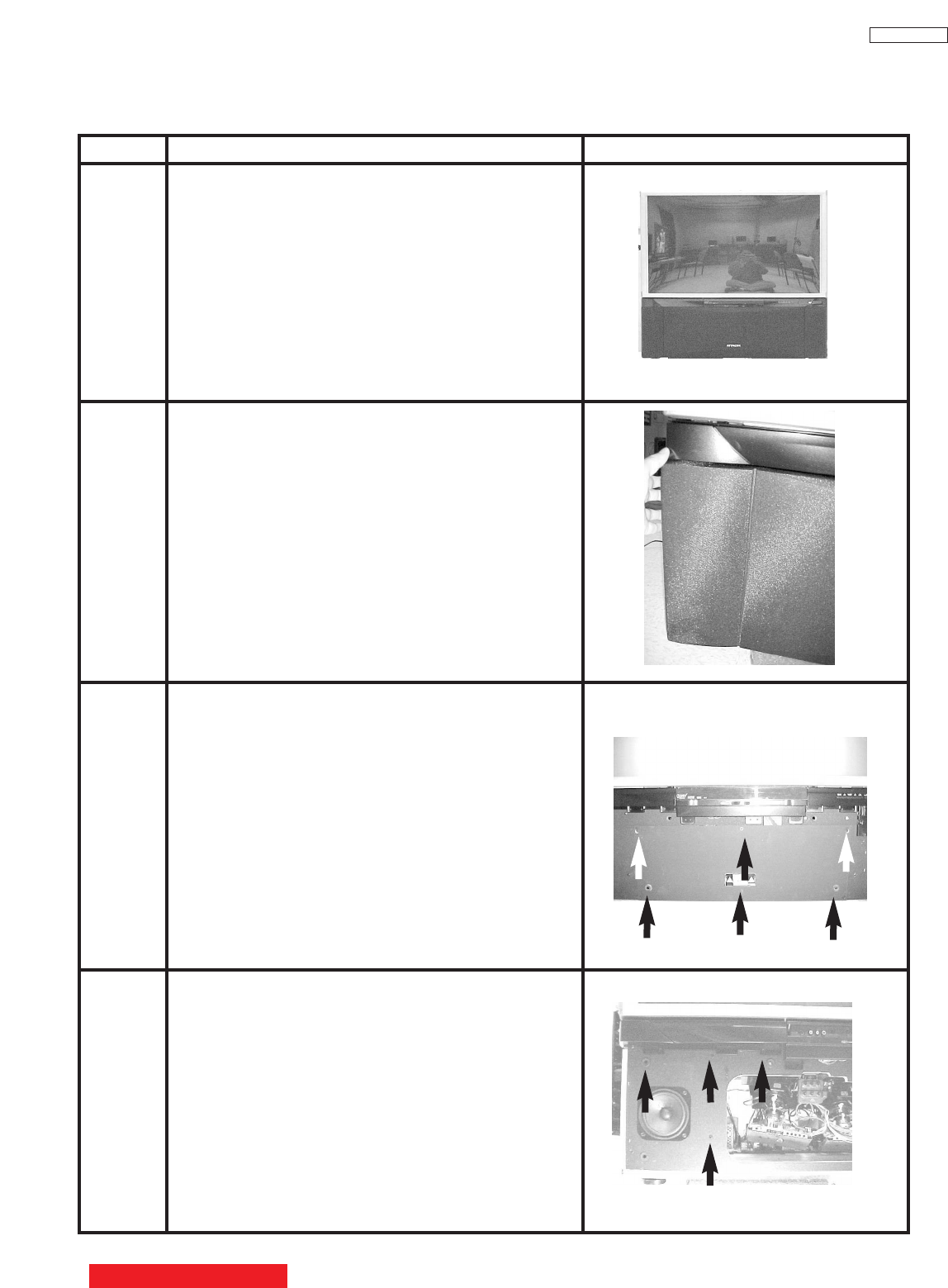
155
DP33KA/B
Remove the left Deco Panel, which are held by 2 screws
under the Deco Panel.
Remove 2 screws which hold the left side of Light Box
Assembly.
STEP INSTRUCTIONS IMAGE
The image shows the front view of the TV.
The front speaker grille needs to be removed.
1
2
Pull the speaker grille off by placing your hands behind
the outside corners and pulling straight out.
The image at the right shows the left side of the TV only.
3
The Front Door needs to be removed. Loosen the top
left and top right screws about half way.
Remove the other 4 screws.Lift the Front Door up and
remove.
4
The following instructions are for models with a Light Box design. This new cabinet design will enable servicers to
remove the Light Box assembly, with out the need to take a complete PTV out for service.
Disassembly Instructions for Screen Frame Assemblies and Light Box (46F500A)
TABLE OF CONTENTS
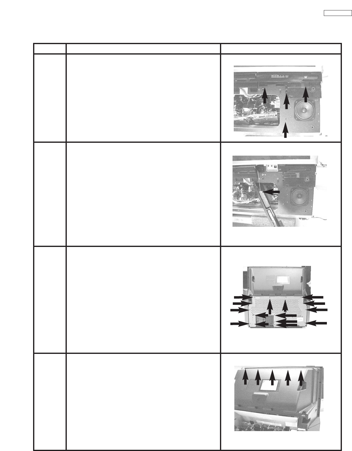
156
DP33KA/B
STEP INSTRUCTIONS IMAGE
5Do the same thing on the right side of the TV.
6
7
Remove 16 screws that hold the back cover assembly
and screen assembly to the cabinet as shown.
The picture only shows one side of the TV.
8
Disconnect the wiring to the right Deco Panel as shown.
Now move to the chassis area on the back of the TV.
Remove 15 screws that hold the lower rear board.
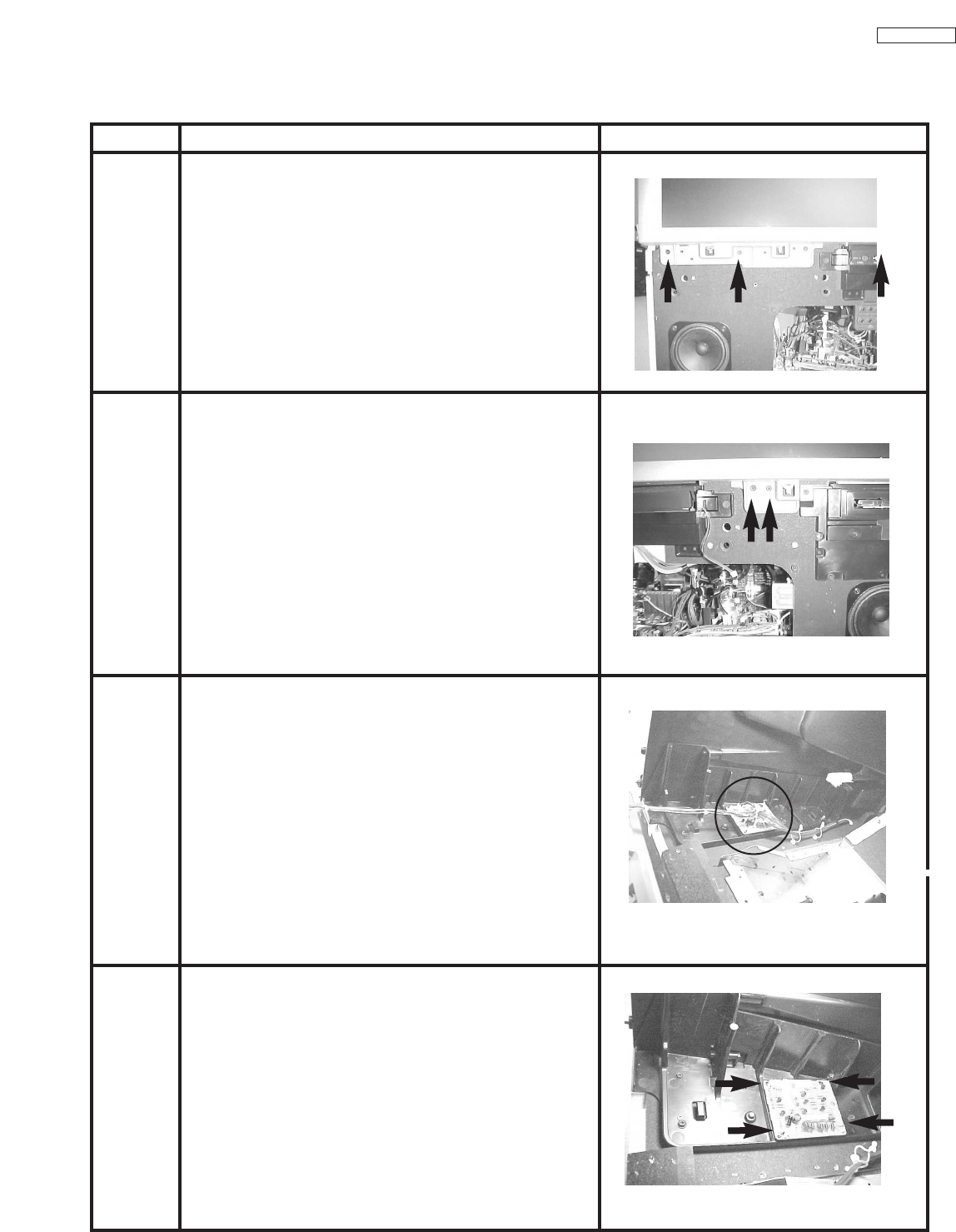
157
DP33KA/B
STEP INSTRUCTIONS IMAGE
9
Remove 2 screws which hold the lower right corner of
the screen assembly.
10
Before removing the screen assembly completely out,
remove all of the wires (with 4 connectors) connecting to
the Magic Focus sensor board first. Get additional help
if necessary.
11
Remove the Magic Focus sensor board which is held in
place by 4 plastic clips at the corners.
12
Remove 3 screws which hold the lower left corner of the
screen assembly.
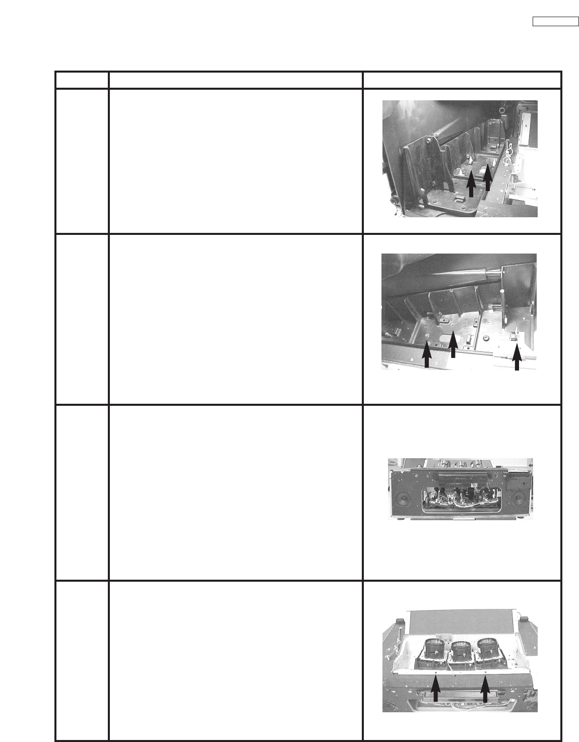
158
DP33KA/B
STEP INSTRUCTIONS IMAGE
Continue at the front, remove 4 screws that hold the left
side of the back cover assembly.
13
Remove 3 screws and a piece of metal (slide outward)
that holds the right side of the back cover assembly.
14
Lift the back cover assembly straight up from the
cabinet.
The picture shows the cabinet and the Light Box
assembly (with the screen assembly and back cover
assembly removed).
15
Remove 2 screws that hold the Light Box to the cabinet.
16
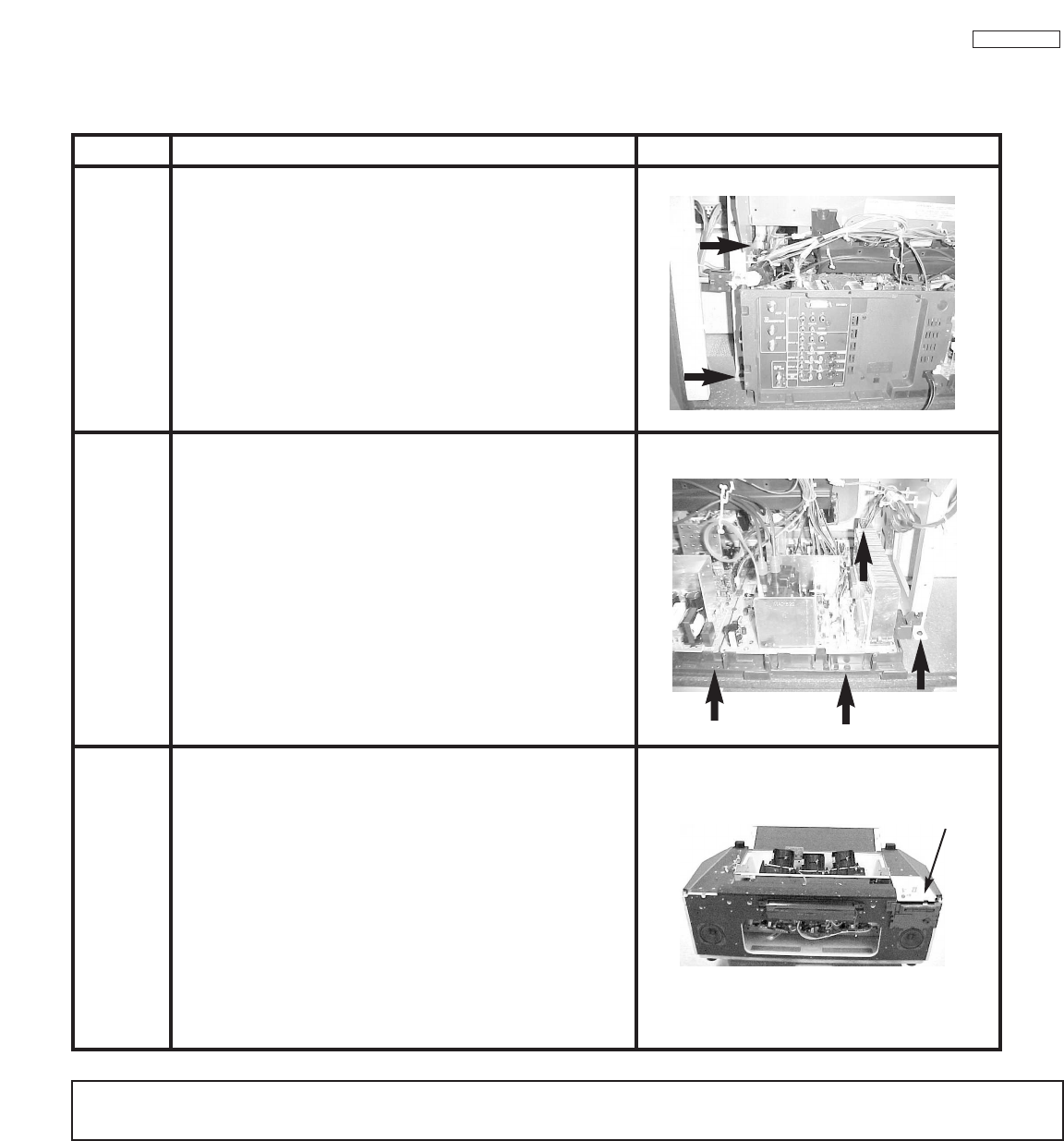
159
DP33KA/B
STEP INSTRUCTIONS IMAGE
Remove 2 screws that hold the Light Box to the cabinet.
For easier removal, one of the screws has to be
removed from the front.
17
Remove 2 screws that hold the chassis to the cabinet,
and 2 screws that hold the Light Box to the cabinet.
For easier removal, one of the screws has to be
removed from the front.
18
Slightly slide the Light Box and chassis backwards until
it is out. Use additional help if necessary.
The Light Box is now ready for easy transport to a
designated service and repair facility.
19
(Does not
apply)
NOTE: The only difference between the Disassembly Instructions for the 46F510 and 46F500A are the speaker grill and control
panel.

160
DP33KA/B
No. Symbol Part # DESCRIPTION FUNCTION PWB
1 I001 CK38651U M306V7MH-XXXFP TV U-COM (Mask) ROM1 Signal
2 I002 CK37051R BD4729G-TR Reset IC for I001 Signal
3 I003 CK35894R CAT24WC32J1 E2PROM for I001 Signal
4 I004 CK01872R BU4053BCFV-E2 Flash mode Selector Signal
5 I008 CK01872R BU4053BCFV-E2 CCD Selector Signal
6 I009 CK37216R TK11133CSCL +3.3V Regulator Signal
7 I010 CK38491R MM74HCT245MTCX Buffer for Bus line Signal
8 I301 CK01872R BU4053BCFV-E2 TV Audio Selector Signal
9 I401 CK37191R SI03018LSA-TL +1.8V Regulator Signal
10 I402 CK37406R SI-3012KS-TL +5.0V Regulator Signal
11 I403 CP04232 AB033T +3.3V Regulator Signal
12 I404 CK37212R TK11125CSCL +2.5V Regulator Signal
13 I453 CK37406R SI-3012KS-TL +5.0V Regulator Signal
14 I501 CK38711U TA1350AFG(Hit) RGB Processor Signal
15 I502 CK01872R BU4053BCFV-E2 Hsync. Selector for FC Unit Signal
16 I503 CP05163F SI-3090F +9.3V Regulator Signal
17 I504 CP04234 BA09T +9.0V Regulator Signal
18 IA01 CK38621R NJW1160M-TE1 Audio Processor w/ BBE and SRS Signal
19 U301 HC00514 F-E-ENGE6106DR Main Tuner Signal
20 U302 HC00464 F-E-ENG36626G Sub Tuner Signal
21 U401 CS00623 HC5623-ASS’Y Flex Control Unit Signal
22 IV01 CK30941U CXA2069Q A/V Selector Terminal
23 IV02 CK07631R TC90A45F Dig. 2 Line Y/C Separator Terminal
24 IV03 CK34811U MM1519XQ YPbPr Selector Terminal
25 IV04 CK38101R NJM2584M(TE1) Comp1/DVI1 Selector Terminal
26 IV08 CK01872R BU4053BCFV-E2 Audio Selector Terminal
27 IV11 CK31071R CXA1875AM DAC for DVI Terminal
28 IY01 CK38701U UPD64084GC-8EA-A Dig. 3D Y/C separator Terminal
29 IY02 CK37053R BD4727G-TR Reset for IY01 Terminal
30 IY03 CK38721R TA1383GF(DRY EL) Sub Y/C YPbPr Selector Terminal
31 IY04 CK38721R TA1383GF(DRY EL) Main Y/C YPbPr Selector Terminal
32 IJ01 CK37193R SI-3033LSA-TL +3.3V Regulator DVI
33 IJ02 CK37051R BD4729G-TR Reset IC for IJ03 DVI
34 IJ03 CK35163R SII907BCQ52 DVI IC DVI
35 IJ04 CA01301R NDC7002N Voltage Converter DVI
QUICK REFERENCE PARTS LIST (IC & UNIT)
TABLE OF CONTENTS

161
DP33KA/B
No. Symbol Part # DESCRIPTION FUNCTION PWB
36 IJ05 CK35895R CAT24WC02J1 EDID E2PROM for Input 1 DVI
37 I901 CZ00865 STR-F6629B(LF1359) Switching Regulator Power
38 I902 CP08261U IC H11A817B-300W OPT. Isolator Power
39 I903 CP08261U IC H11a817B-300W OPT. Isolator Power
40 I904 2381343 SE115N +B(115V) Regulator Power
41 I905 CP08301 STA821M +5.5V Regulator Power
42 I906 CP08291 STA811M +6.3V Regulator Power
43 IAA1 2004751 TA8258H Audio Amp (20+20W) Power
44 T901 BT02162 PT-EE49F17US-DP3X(B) Switching Transformer Power
45 U901 CW00352 UPM0518SA Stand by Power Module Power
46 I601 CP06891 TDA8147A Ver. Output Deflection
47 I701 2362606 NJM4558D Gain Amp (side Pin corr.) Deflection
48 IH01 CP07091 M62501P HV Contoller Deflection
49 IK01 CP06081 SI-3050N +5V Regulator Deflection
50 IK02 CP05011R PST994D-T Mute Deflection
51 IK04 CZ01142 STK394-250 Conv. Amp. Deflection
52 IK05 CZ01142 STK394-250 Conv. Amp. Deflection
53 T701 BT01232 Horiz. Output Transformer HOT Deflection
54 T702 BZ03061 LX-DRIVE TRANS.-DJ81 Hor Drive Transformer Deflection
55 TF01 BT02141 PT-EE22F06U-DP25H-2F Dynamic Focus Transformer Deflection
56 TH01 BW03002 HVT-MSU1AUR103(DP3X) FBT Deflection
57 UKDG CS00731 HC2191-ASS’Y Digital Conv. Unit Deflection
58 HM01 CZ01171 GP1UM281RK IR Receiver on Control Control
59 HM02 CZ01161 GP1UM281QK IR Receiver Control
60 EANT HP00772 UNX ANT SW BOX ANT SW BOX Main Chas.
46F510 CRT Assembly part numbers
UE23434 RED
UE23435 GREEN
UE23436 BLUE
46F500 CRT Assembly part numbers
UE23431 RED
UE23432 GREEN
UE23433 BLUE
CH 2