PANO 0211 50v720
User Manual: 50v720
Open the PDF directly: View PDF ![]() .
.
Page Count: 184 [warning: Documents this large are best viewed by clicking the View PDF Link!]


No. 0211
NTSC
LC57
R/C: CLU-4352UG2
TO GO TO A CHAPTER, CLICK ON ITS HEADING BELOW
PA
!
TO GO TO A CHAPTER, CLICK ON ITS HEADING BELOW
SERVICE MANUAL
CONTENTS
IMPORTANT SAFETY INSTRUCTIONS.............................................................................. 2
SERVICING PRECAUTIONS ............................................................................................. 4
AGENCY REGULATORY INFORMATION........................................................................... 9
FEATURES & SPECIFICATIONS ...................................................................................... 10
GENERAL INFORMATION..................................................................................................13
REMOTE CONTROL GUIDE ...............................................................................................15
SERVICE ADJUSTMENTS .................................................................................................31
TROUBLESHOOTING FLOW CHART................................................................................88
BLOCK DIAGRAM .............................................................................................................96
CONNECTION DIAGRAM .................................................................................................98
ASSEMBLY DRAWINGS .........................................................................................................99
FINAL WIRING DIAGRAM ..................................................................................................................106
QUICK DISASSEMBLY GUIDE ..........................................................................................110
WAVEFORMS ..................................................................................................................................120
DC VOLTAGE TABLES ....................................................................................................123
CIRCUIT SCHEMATIC DRAWING ......................................................................................126
PRINTED CIRCUIT BOARDS ...........................................................................................149
REPLACEMENT PARTS LIST .........................................................................................165
QUICK REFERENCE PARTS LIST (IC & UNIT) ..............................................................181
CAUTION: These servicing instructions are for use by qualified service personnel only. To reduce the risk of
electric shock do not perform any servicing other than that contained in the operating instructions
unless you are qualified to do so. Before servicing this chassis, it is important that the service
technician read the “IMPORTANT SAFETY INSTRUCTIONS” in this service manual.
SAFETY NOTICE
USE ISOLATION TRANSFORMER WHEN SERVICING
Components having special safety characteristics are identified by a on the schematics and on the parts list in this
Service Data and its supplements and bulletins. Before servicing the chassis, it is important that the service technician
read and follow the “Important Safety Instructions” in this Service Manual.
AUGUST 2005 HHEA-MANUFACTURING DIVISION
LCD REAR PROJECTION TELEVISION
SPECIFICATIONS AND PARTS ARE SUBJECT TO CHANGE FOR IMPROVEMENT
50V720 / LC57
2
+-
LEAKAGE
CURRENT
TESTER
DEVICE
UNDER
TEST
TEST ALL
EXPOSED
METAL
SURFACES
2-WIRE CORD
(READING
SHOULD NOT
BE ABOVE
0.5 mA)
EARTH
GROUND
ALSO TEST WITH
PLUG REVERSED (USING
AC ADAPTER PLUS
AS REQUIRED)
NOTICE: Comply with all cautions and safety-related notes
located on or inside the cabinet and on the chassis or optic unit.
WARNING: Since the chassis of this receiver is connected to
one side of the AC power supply during operation, whenever the
receiver is plugged in service should not be attempted by any-
one unfamiliar with the precautions necessary when working on
this type of receiver.
The following precautions should be observed:
1. Do not install, remove, or handle the optic unit in any manner
unless shatterproof goggles are worn. People not so equipped
should be kept away from the optic unit while handling.
2. When service is required, an isolation transformer should be
inserted between power line and the receiver before any serv-
ice is performed on a “HOT” chassis receiver.
3. When replacing a chassis in the receiver, all the protective
devices must be put back in place, such as barriers, nonmetal-
lic knobs, adjustment and compartment cover-shields, isolation
resistors, capacitors, etc.
4. When service is required, observe the original lead dress.
5. Always use the manufacturer’s replacement components.
Critical components as indicated on the circuit diagram should
not be replaced by another manufacturer’s. Furthermore, where
a short circuit has occurred, replace those components that
indicate evidence of overheating.
6. Before returning a serviced receiver to the customer, the serv-
ice technician must thoroughly test the unit to be certain that it
is completely safe to operate without danger of electrical shock,
and be sure that no protective device built into the receiver by
the manufacturer has become defective, or inadvertently
defeated during servicing.
Therefore, the following checks should be performed for the con-
tinued protection of the customer and service technician.
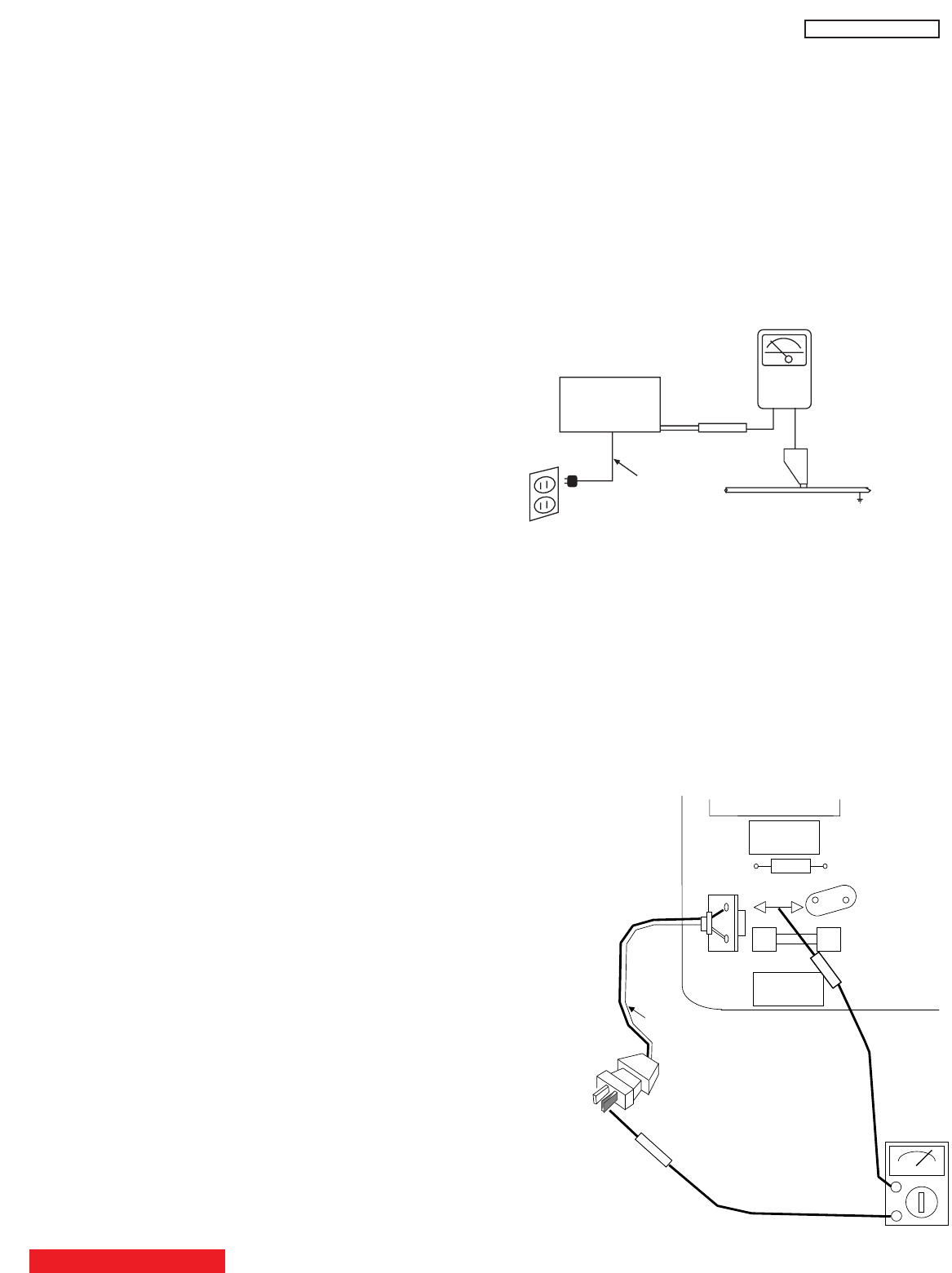
Leakage Current Cold Check
With the AC plug removed from the 120V AC 60Hz source, place
a jumper across the two plug prongs. Using an insulation tester
(DC500V), connect one lead to the jumpered AC plug and touch
the other lead to each exposed metal part (antennas, screwheads,
metal overlays, control shafts, etc.), particularly any exposed
metal part having a return path to the chassis should have a min-
imum resistor reading of 2.4Mand a maximum resistor reading
of 5.2M. Any resistance value below or above this range indi-
cates an abnormality which requires corrective action. An exposed
metal part having a return path to the chassis will indicate an open
circuit.
AC LEAKAGE TEST
ANY MEASUREMENTS NOT WITHIN THE LIMITS OUTLINED
ABOVE ARE INDICATIVE OF A POTENTIAL SHOCK HAZARD
AND MUST BE CORRECTED BEFORE RETURNING THE
RECEIVER TO THE CUSTOMER.
IMPORTANT SAFETY INSTRUCTIONS
Leakage Current Hot Check
Plug the AC line cord directly into a 120V AC 60Hz outlet (do not use
an isolated transformer for this check). Turn the AC power ON. Using
a Leakage Current Tester (Simpson’s Model 228 or equivalent),
measure for current from all exposed metal parts of the cabinet
(antennas, screwheads, overlays, control shafts, etc.) particularly
any exposed metal
part having a return path to the chassis or to a
known earth ground (water pipe, conduit, etc.). Any current meas-
ured must not exceed 0.5 MIU.
TABLE OF CONTENTS
(READING
SHOULD NOT
BE ABOVE
0.5 MIU)
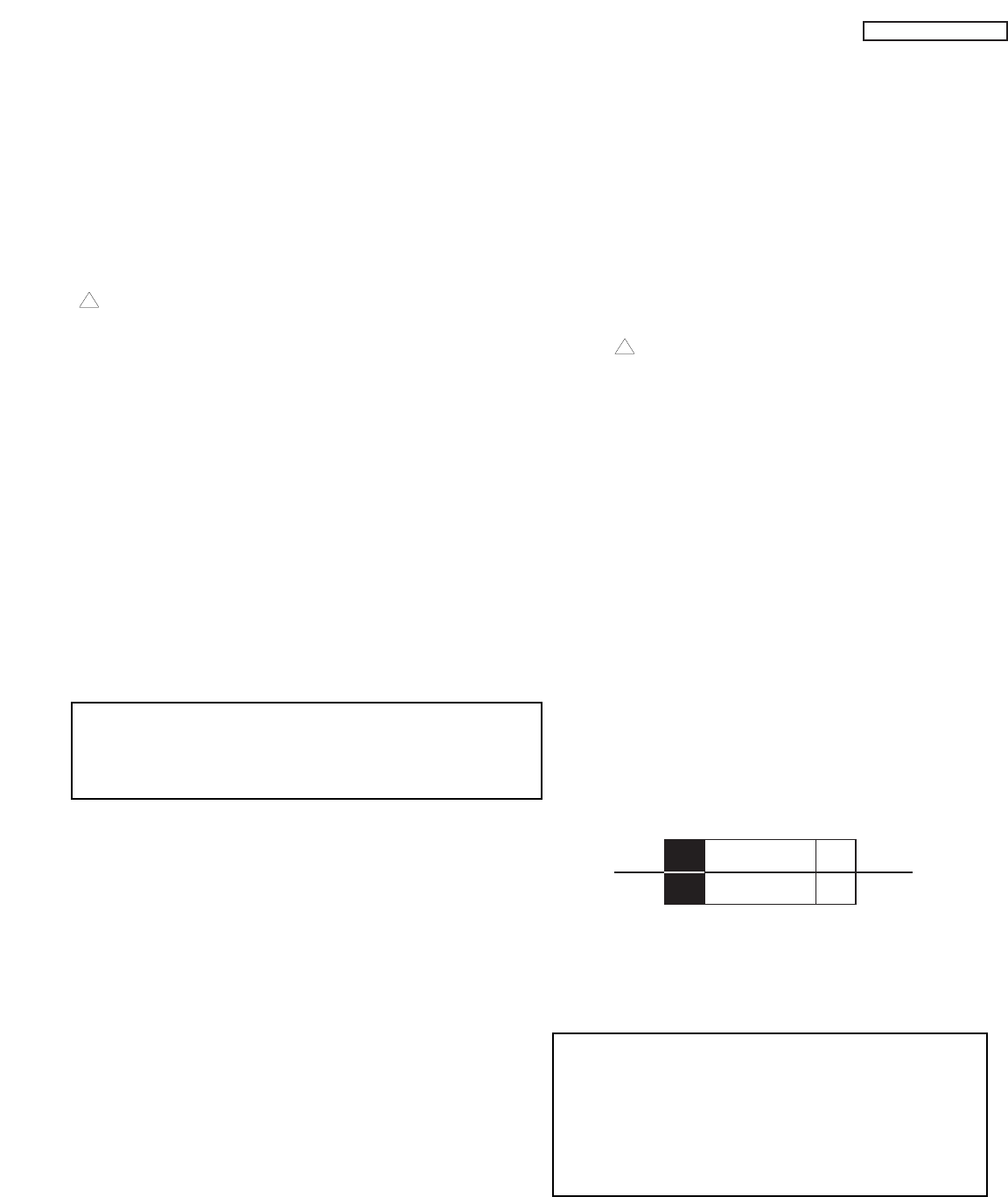
AC CORD POLARITY
This check is based on the UL standard. Use the jigs specified by
the production technology section. The GND side (wider blade)
of the AC power cord should be connected to KKX1.
X901
R901
C901
L901
WHITE side
GND side
PPT1
F901
2
PA
KKX1
Tester
LC57
Many electrical and mechanical parts in HITACHI television
receivers have special safety-related characteristics. These are
often not evident from visual inspection nor can the protection
afforded by them necessarily be obtained by using replacement
components rated for higher voltage, wattage, etc. Replacement
parts which have these special safety characteristics are identified
in this Service Manual.
Electrical components having such features are identified with an
!mark in the schematics and parts list in this Service Manual.
The use of a substitute replacement component which does not
have the same safety characteristics as the HITACHI-recom-
mended replacement component, shown in the parts list in this
Service Manual, may create shock, fire, or other hazards.
Production safety is continuously under review and new instruc-
tions are issued from time to time. For the latest information,
always consult the current HITACHI Service Manual. A subscrip-
tion to, or additional copies of HITACHI Service Manuals may be
obtained at a nominal charge from HITACHI Sales Corporation.
Ultraviolet Radiation
OPTIC UNIT: The primary source of Ultraviolet Radiation in this
receiver is the optic unit. The optic unit utilized in this chassis is
specially constructed to limit Ultraviolet Radiation emissions. For
continued Ultraviolet Radiation protection, the replacement optic
unit must be the same type as the original HITACHI-approved
type.
Service Personnel - WARNING
Eye damage may result from directly viewing the light produced by
the lamp used in this product. Always turn off lamp before open-
ing optic unit. Ultraviolet radiation eye protection required during
servicing.
When troubleshooting and making test measurements in a receiv-
er with an excessive high voltage problem, avoid being unneces-
sarily close to the optic unit and the high voltage component.
Do not operate the chassis longer than is necessary to locate the
cause of excessive voltage.
This Service Manual is intended for qualified service techni-
cians; it is not meant for the casual do-it-yourselfer. Qualified
technicians have the necessary test equipment and tools, and
have been trained to properly and safely repair complex prod-
ucts such as those covered by this manual. Improperly per-
formed repairs can adversely affect the safety and reliability of
the product and may void warranty. Consumers should not risk
trying to do the necessary repairs and should refer to a quali-
fied service technician.
WARNING
Lead in solder used in this product is listed by the California Health
and Welfare agency as a known reproductive toxicant which may
cause birth defects or other reproductive harm (California Health
and Safety Code, Section 25249.5).
When servicing or handling circuit boards and other compo-
nents which contain lead in solder, avoid unprotected skin
contact with solder. Also, when soldering do not inhale any
smoke or fumes produced.
SAFETY NOTICE
USE ISOLATION TRANSFORMER
WHEN SERVICING
Components having special safety characteristics identi-
fied by !on the parts list in this service manual and its
supplements and bulletins. Before servicing this product, it
is important that the service technician read and follow the
“Safety Precautions” and the “Product Safety Notices” in
this Service Manual.
For continued ultraviolet protection, replace optic unit with
original type or HITACHI equivalent type.
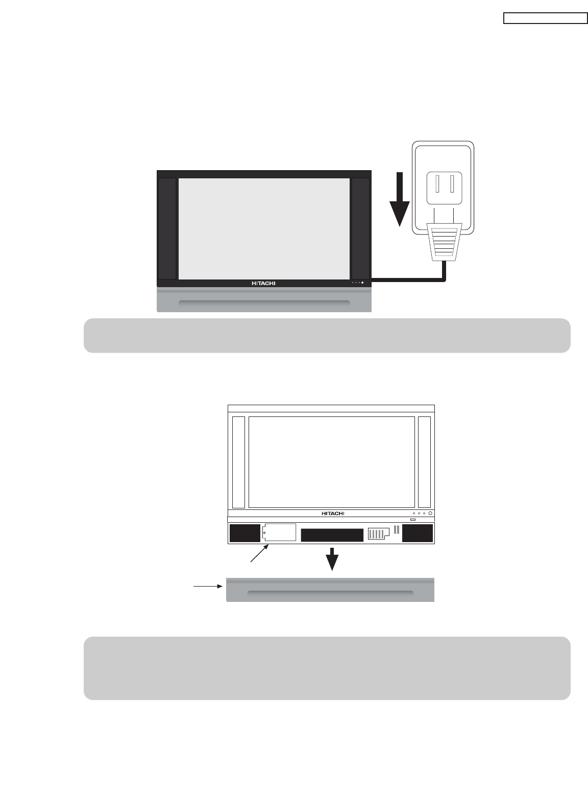
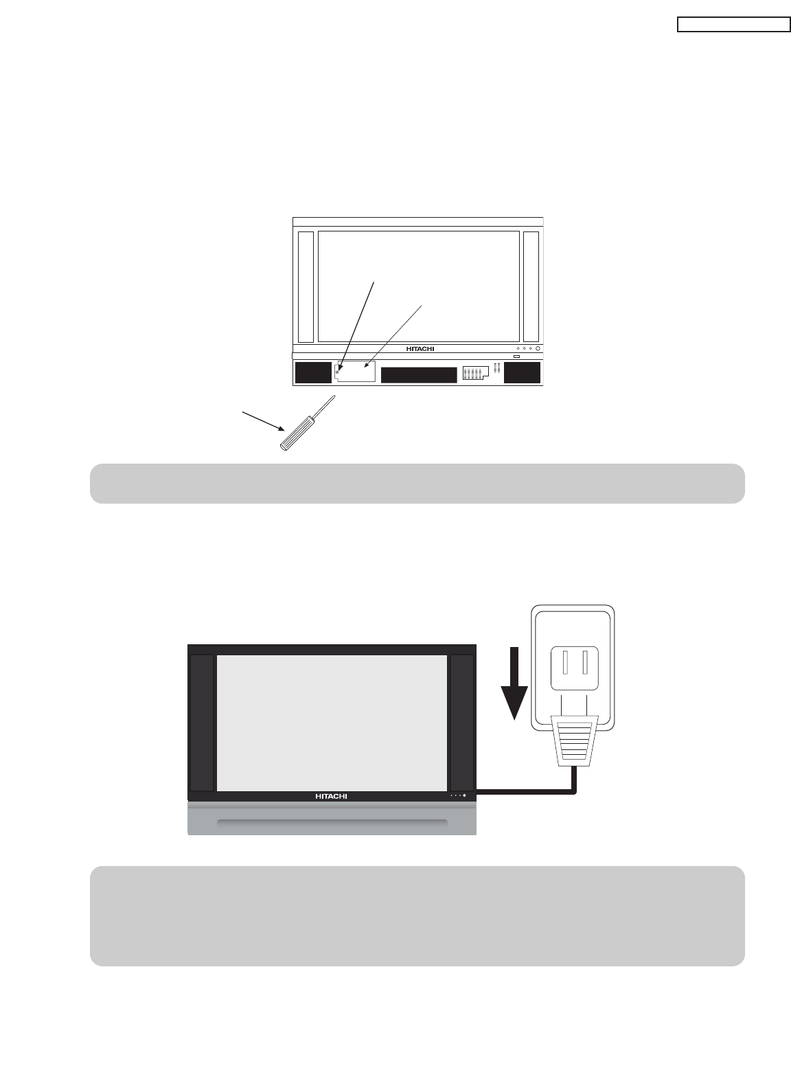
POWER SOURCE
This television receiver is designed to operate on 120
Volts/60Hz, AC house current. Insert the power cord into
a 120 Volts/60Hz outlet.
NEVER CONNECT THE TV TO OTHER THAN THE
SPECIFIED VOLTAGE OR TO DIRECT CURRENT.
CAUTION!
The following symbol near the fuse indicates fast operat-
ing fuse (to be replaced). Fuse ratings appear within the
symbol.
Example:
The rating of fuse F101 is 6.0A-125V.
Replace with the same type of fuse for continued protec-
tion against fire.
The lamp in this product contains Mercury.
Dispose of properly in accordance with applicable
environmental laws. For Recycling and Disposal
information, contact your respective governmen-
tal agencies or the Electronic Industries Alliance
at www.eiae.org (in the U.S.) or Electronic
Product Stewardship Canada at www.epsc.ca (in
Canada).
PRODUCT SAFETY NOTICE
125V
6A
F901
NOTE:
F101
3
LC57

CAUTION: Before servicing instruments covered by this service
data and its supplements and addenda, read and follow the SAFE-
TY PRECAUTIONS on page 2 of this publication.
NOTE: If unforseen circumstances create conflict between the fol-
lowing SERVICING PRECAUTIONS and any of the SAFETY INS-
TRUCTIONS on page 2 of this publication, always follow the SAFE
TY INSTRUCTIONS.
Remember: Safety First.
General Servicing Guidelines
1. Always unplug the instrument AC power cord from the AC power
source before:
a. Removing or reinstalling any component, circuit board,
module, or any other instrument assembly.
b. Disconnecting or reconnecting any instrument electrical
plug or other electrical connection.
c. Connecting a test substitute in parallel with an electrolyt-
ic capacitor in the instrument.
CAUTION: Awrong part substitution or incorrect
polarity installation of electrolytic
capacitors may result in an
explosion hazard.
2. Do not spray chemicals on or near this instrument or any of its
assemblies.
3. Unless specified otherwise in these service data, clean electri-
cal contacts by applying the following mixture to the contacts
with a pipe cleaner, cotton-tipped stick or comparable nonabra-
sive applicator: 10% (by volume) Acetone and 90% (by volume)
ispropyle alchohol (90%-99% strength).
CAUTION: This is a flammable mixture. Unless specified
otherwise in these service data, lubrication of
contacts is not required.
4. Do not defeat any plug/socket B+ voltage interlocks with which
instruments covered by this service data might be equipped.
5. Do not apply AC power to this instrument and/or any of its elec-
trical assemblies unless all solid-state device heat-sinks are cor-
rectly installed.
6. Always connect the test instrument ground lead to the appropri-
ate instrument chassis ground before connecting the test instru-
ment positive lead. Always remove the test instrument ground
lead last.
7. Use with this instrument only the test fixtures specified in this
service data.
CAUTION: Do not connect the test fixture ground strap to
any heatsink in this instrument.
Electrostatically Sensitive (ES) Devices
Some semiconductor (solid state) devices can be damaged easily
by static electricity. Such components commonly are called
Electrostatically Sensitive (ES) Devices. Examples of typical ES
devices are integrated circuits and some field-effect transistors and
semiconductor “chip” components. The following techniques should
be used to help reduce the incidence of component damage caused
by static electricity.
1. Immediately before handling any semiconductor component or
semiconductor-equipped assembly, drain off any electrostatic
charge on your body by touching a known earth ground.
Alternatively, obtain and wear a commercially available dis-
charging wrist strap device, which should be removed for poten-
tial shock reasons prior to applying power to the unit under test.
2. After removing an electrical assembly equipped with ES
devices, place the assembly on a conductive surface such as
aluminum foil, to prevent electrostatic charge build-up or expo-
sure of the assembly.
3. Use only a grounded-tip soldering iron to solder or desolder ES
devices.
4. Use only an anti-static type solder removal device. Some sol-
der removal devices not classified as “anti-static” can generate
electrical charges sufficient to damage ES device.
5. Do not use freon-propelled chemicals. These can generate
electrical charges sufficient to damage ES devices.
6. Do not remove a replacement ES device from its protective
package until immediately before you are ready to install it.
(Most replacement ES devices are packaged with leads electri-
cally shorted together by conductive foam, aluminum foil or
comparable conductive material.)
7. Immediately before removing the protective material from the
leads of a replacement ES device, touch the protective material
to the chassis or circuit assembly into which the device will be
installed.
CAUTION: Be sure no power is applied to the chassis or
circuit, and observe all other safety precautions.
8. Minimize bodily motions when handling unpackaged replace-
ment ES devices. (Otherwise harmless motion such as the
brushing together of your clothes fabric or the lifting of your foot
from a carpeted floor can generate static electricity sufficient to
damage an ES device.)
TABLE OF CONTENTS
SERVICING PRECAUTIONS
4
LC57
General Soldering Guidelines
1. Use a grounded-tip, low-wattage soldering iron and appropriate
tip size and shape that will maintain tip temperature within the
range 500°F to 600°F.
2. Use an appropriate gauge of resin-core solder composed of 60
parts tin/40 parts lead.
3. Keep the soldering iron tip clean and well-tinned.
4. Thoroughly clean the surfaces to be soldered. Use a small wire-
bristle (0.5 inch or 1.25 cm) brush with a metal handle. Do not
use freon-propelled spray-on cleaners.
5. Use the following desoldering technique.
a. Allow the soldering iron tip to reach normal temperature
(500°F to 600°F).
b. Heat the component lead until the solder melts. Quickly
draw away the melted solder with an anti-static, suction-
type solder removal device or with solder braid.
CAUTION: Work quickly to avoid overheating the circuit
board printed foil.
6. Use the following soldering technique.
a. Allow the sodering iron tip to reach normal temperature
(500°F to 600°F).
b. First, hold the soldering iron tip and solder strand against
the component lead until the solder melts.
c. Quickly move the soldering iron tip to the junction of the
component lead and the printed circuit foil, and hold it
there only until the solder flows onto and around both the
component lead and the foil.
CAUTION: Work quickly to avoid overheating the circuit
board printed foil or components.
d. Closely inspect the solder area and remove any excess
or splashed solder with a small wire-bristle brush.
IC Removal/Replacement
Some Hitachi unitized chassis circuit boards have slotted holes
(oblong) through which the IC leads are inserted and then bent flat
against the circuit foil. When holes are the slotted type, the follow-
ing technique should be used to remove and replace the IC. When
working with boards using the familiar round hole, use the standard
technique as outlined in paragraphs 5 and 6 above.
Removal
1. Desolder and straighten each IC lead in one operation by gent-
ly prying up on the lead with the soldering iron tip as the solder
melts.
2. Draw away the melted solder with an anti-static suction-type sol
der removal device (or with solder braid) before removing the
IC.
Replacement
1. Carefully insert the replacement IC in the circuit board.
2. Carefully bend each IC lead against the circuit foil pad and
solder it.
3. Clean the soldered areas with a small wire-bristle brush. (It is
not necessary to reapply acrylic coating to areas.)
“Small-signal” Discrete Transistor Removal/Replacement
1. Remove the defective transistor by clipping its leads as close as
possible to the component body.
2. Bend into a “U” shape the end of each of three leads remain-
ing on the circuit board.
3. Bend into a “U” shape the replacement transistor leads.
4. Connect to replacement transistor leads to the corresponding
leads extending from the circuit board and crimp the “U” with
long nose pliers to insure metal to metal contact, then solder
each connection.
Power Output Transistor Devices Removal/Replacement
1. Heat and remove all solder from around the transistor leads.
2. Remove the heatsink mounting screw (if so equipped).
3. Carefully remove the transistor from the circuit board.
4. Insert new transistor in circuit board.
5. Solder each transistor lead, and clip off excess lead.
6. Replace heatsink.
Diode Removal/Replacement
1. Remove defective diode by clipping its leads as close as pos-
silbe to diode body.
2. Bend the two remaining leads perpendicularly to the circuit
board.
3. Observing diode polarity, wrap each lead of the new diode
around the corresponding lead on the circuit board.
4. Securely crimp each connection and solder it.
5. Inspect (on the circuit board copper side) the solder joints of
the two “original leads”. If they are not shiny, reheat them
and, if necessary, apply additional solder.
Use Soldering Iron to Pry Leads
SERVICING PRECAUTIONS
5
LC57
SERVICING PRECAUTIONS
Fuses and conventional Resistor Removal/Replacement
1. Clip each fuse or resistor lead at top of circuit board hollow
stake.
2. Securely crimp leads of replacement component around stake
1/8 inch from top.
3. Solder the connections.
CAUTION: Maintain original spacing between the replaced
component and adjacent components and the
circuit board, to prevent excessive component
temperatures.
Circuit Board Foil Repair
Excessive heat applied to the copper foil of any printed circuit board
will weaken the adhesive that bonds the foil to the circuit board,
causing the foil to separate from, or “lift-off” the board. The follow-
ing guidelines and procedures should be followed whenever this
condition is encountered.
In Critical Copper Pattern Areas
High component/copper pattern density and/or special voltage/cur-
rent characteristics make the spacing and integrity of copper pattern
in some circuit board areas more critical than in others. The circuit
foil in these area is designated as Critical Copper Pattern. Because
Critical Copper Pattern requires special soldering techniques to
ensure the maintenance of reliability and safety standards, contact
your Hitachi personnel.
At IC Connections
To repair defective copper pattern at IC connections, use the follow-
ing procedure to install a jumper wire on the copper pattern side of
the circuit board. (Use this technique only on IC connections.)
1. Carefully remove the damaged copper pattern with a sharp
knife. (Remove only as much copper as absolutely necessary.)
2. Carefully scratch away the solder resist and acrylic coating (if
used) from the end of the remaining copper pattern.
3. Bend a small “U” in one end of a small-gauge jumper wire and
carefully crimp it around the IC pin. Solder the IC connection.
4. Route the jumper wire along the path of the cut-away copper
pattern and let it overlap the previously scraped end of the good
copper pattern. Solder the overlapped area, and clip off any
excess jumper wire.
At Other Connections
Use the following technique to repair defective copper pattern at
connections other than IC Pins. This technique involves the instal-
lation of a jumper wire on the component side of the circuit board.
1. Remove the defective copper pattern with a sharp knife.
Remove at least 1/4 inch of copper, to ensure hazardous condi-
tion will not exist if the jumper wire opens.
2. Trace along the copper pattern from both wire sides of the pat-
tern break and locate the nearest component directly connected
to the affected copper pattern.
3. Connect insulated 20-gauge jumper wire from the nearest com-
ponent on one side of the pattern break to the lead of the near-
est component on the other side. Carefully crimp and solder the
connections.
CAUTION: Be sure the insulated jumper wire is dressed so
that it does not touch components or sharp
edges.
Frequency Synthesis (FS) Tuning Systems
1. Always unplug the instrument AC power cord before discon-
necting or reconnecting FS tuning system cables and before
removing or inserting FS tuning system modules.
2. The FS tuner must never be disconnected from the FS tuning
control module while the power is applied to the instrument.
3. When troubleshooting intermittent problems that might be
caused by defective cable connection(s) to the FS tuning sys-
tem, remove the instrument AC power as soon as the defective
connector is found and finish confirming the bad connection with
a continuity test. This procedure will reduce the probability of
electrical overstress of the FS system semi-conductor compo-
nents.
CRIMP AND
SOLDER
BARE JUMPER
WIRE
Install Jumper Wire and Solder
DEFECTIVE
COPPER
REMOVED
Insulated Jumper Wire
6
LC57
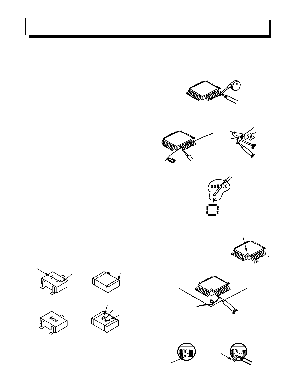
Leadless Chip Components
(surface mount)
Chip components must be replaced with identical chips due
to critical foil track spacing. There are no holes in the board
to mount standard transistors or diodes. Some chip capaci-
tor or resistor board solder pads may have holes through the
board, however the hole diameter limits standard resistor
replacement to 1/8 watt. Standard capacitors may also be
limited for the same reason. It is recommended that identi-
cal chip components be used. .
Chip resistors have a three digit numerical resistance code
-1st and 2nd significant digits and a multiplier. Example: 162
= 1600 or 1.6KΩresistor, 0 = 0Ω(jumper).
Chip capacitors generally do not have the value indicated on
the capacitor. The color of the component indicates the gen-
eral range of the capacitance.
Chip transistors are identified by a two letter code. The first
letter indicates the type and the second letter, the grade of
transistor.
Chip diodes have a two letter identification code as per the
code chart and are a dual diode pack with either
common anode or common cathode. Check the parts list for
correct diode number.
Component Removal
1. Use solder wick to remove solder from component end
caps or terminals.
2. Without pulling up, carefully twist the component with
tweezers to break the adhesive.
3. Do not reuse removed leadless or chip components
since they are subject to stress fracture during removal.
Chip Component Installation
1. Put a small amount of solder on the board soldering
pads.
2. Hold the chip component against the soldering pads
with tweezers or with a miniature alligator clip and apply
heat to the pad area with a 30 watt iron until solder
flows. Do not apply heat for more than 3 seconds
How to Replace Flat-lC
—Required Tools—
•Soldering iron • iron wire or small awl
•De-solder braids • Magnifier
1. Remove the solder from all of the pins of a Flat-lC by
using a de-solder braid.
2. Put the iron wire under the pins of the Flat-lC and pull it
in the direction indicated while heating the pins using a
soldering iron. A small awl can be used instead of the
iron wire.
3. Remove the solder from all of the pads of the Flat-
lC by using
a de-solder braid.
4. Position the new Flat-lC in place (apply the pins of the
Flat-lC to the soldering pads where the pins need to be
soldered). Properly determine the
positions of the soldering pads
and pins by correctly aligning the
polarity symbol.
6. Check with a magnifier for solder bridge between the
pins or for dry joint between pins and soldering pads. To
remove a solder bridge, use a de-solder braid as shown
in the figure below.
NOTE: These components are affixed with glue. Be careful not to break or damage any foil under the
component or at the pins of the ICs when removing. Usually applying heat to the component for a short
time while twisting with tweezers will break the component loose.
Chip Components
TYPE
GRADE
C
B
E
SOLDER
CAPS
TRANSISTOR CAPACITOR
1ST DIGIT
2ND DIGIT
MULTIPLIER
= 1600 = 1.6K
ANODES
MH DIODE RESISTOR
SOLDER CAPS
COMMON CATHODE
Flat-IC De-Solder
Braid
Soldering
Iron
Soldering
Iron
Soldering
Iron
Soldering
Iron
Soldering
Iron
Soldering
Iron
De-Solder
Braid
Flat-IC
Solder
Bridge
Solder
De-Solder
Braid
Iron
Wire
Pull
Awl
Polarity Symbol
5. Solder all pins to the soldering pads using a fine tipped
soldering iron.
SERVICING PRECAUTIONS
7
LC57
Information for service
about lead-free
solder Introduction
Hitachi
introduced lead-free solder to conserve
the "Earth Environment". Please refer to the
following before servicing.
(1)
Characteristic of lead-free solder
Melting point of lead free solder is 40-50
o
C higher than solder containing lead.
(2) Solder for service
Following composition is recommended.
" Sn
- 3.0Ag
- 0.5Cu " , or "
Sn - 0.7 Cu "
Lead solder can be used, but there is a possibility of failure due
to insufficient strength of the solder.
Caution when using solder containing lead.
Please remove
previous solder
as much as possible from the soldering point.
When soldering, please perfectly melt the lead-free solder to mix well
with the previous solder.
(3) Soldering iron for lead-free solder.
Melting point of lead-free solder is higher than solder containing lead.
Use of a soldering tool "with temperature control" and "with much thermal capacitance" is recommended.
(Recommended temperature control : 320
o
C - 450
o
C)
Recommended temperature
PWB with chip parts
320
o
C +/-
30
o
C
PWB without chip parts
380
o
C +/- 30
o
C
Chassis, metal, shield etc.
420
o
C +/- 30
o
C
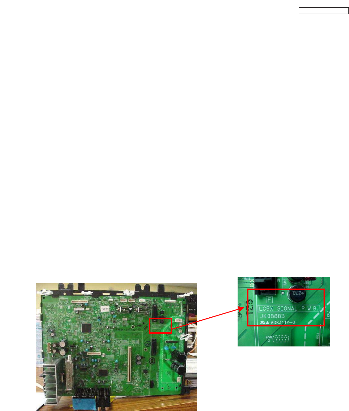
(4) Identification of lead-free PWB
2004 models
>> lead-free solder
is
introduced
2005 models
>> lead-free solder
apply
On lead-free
PWB,
"F" is
added at the
beginning of stamp on
PWB. (e.g.
F
LC57)
8
LC57

Useful Information
Useful Info
PLUG AND PLAY
This Class B digital apparatus meets all requirements of the Canadian Interference-Causing Equipment
Regulations.
This Class B digital apparatus complies with Canadian ICES-003.
Cet appareil numérique de la classe B est conforme à la norme NMB-003 du Canada.
Cable Compatible Television Apparatus- Tèlèvision câblocompatible, Canada.
This LCD Television receiver will display television closed captioning,( or ), in accordance with
paragraph 15.119 of the FCC rules.
AGENCY REGULATORY INFORMATION
Federal Communications Commission Notice
This equipment has been tested and found to comply with the limits for a Class B digital device, pursuant to Part
15 of the FCC Rules. These limits are designed to provide reasonable protection against harmful interference in
a residential installation. This equipment generates, uses and can radiate radio frequency energy and if not
installed and used in accordance with the instructions, may cause harmful interference to radio
communications. However, there is no guarantee that interference will not occur in a particular installation. If this
equipment does cause harmful interference to radio or television reception, which can be determined by turning
the equipment off and on, the user is encouraged to try to correct the interference by one or more of the
following measures:
• Reorient or relocate the receiving antenna.
• Increase the separation between the equipment and the receiver.
• Connect the equipment into an outlet on a circuit different from that to which the receiver is connected.
• Consult the dealer or an experienced radio/television technician for help.
Modifications
The FCC requires the user to be notified that any changes or modifications made to this device that are not
expressly approved by Hitachi Home Electronics (America), Inc. may void the user’s warranty.
Cables
Connections to this device must be made with shielded cables with metallic RFI/EMI connector hoods to
maintain compliance with FCC Rules and Regulations.
Any cables that are supplied with the system must be replaced with identical cables in order to assure
compliance with FCC rules. Order Hitachi spares as replacement cables.
TABLE OF CONTENTS
9
LC57
TABLE OF CONTENTS
10
LC57
FEATURES:
• Superfine Picture Quality; 1280 Line Horizontal
Resolution
• Remote (Controls many PVR/VCR brands, cable
boxes, satellite boxes, and other audio equipment).
• New Easy-to-Use (3-Language) On-Screen Menu
• Full Set of Input Jacks, including S-Video
• COMPONENT VIDEO: Y-PB/PR
• Six Aspect Modes
• Closed Caption Decoder
• 2-Tuner Picture in Picture
• 2 Antenna Inputs (Either for Analog/Digital)
• Video Input Sensor
• HDMI (High Definition Multimedia Interface) (High
Bandwidth Digital Content Protection V1.1
compatible).
• Digital Audio Output (Dolby®Digital and PCM)
• 3 Dimensional Y/C Comb Filter
• Compatible with 1080i, 720p, 480p and 480i input
signals.
• CableCARDTM compatible - Contact your local
cable operator for more information.
• Technology.
Licensed by BBE Sound, Inc. under USP5510752
and 5736897. BBE and BBE symbol are registered
trademarks of BBE Sound, Inc. Manufactured under
license from BBE Sound, Inc.
• Technology.
SRS and symbol are trademarks of SRS Labs,
Inc. SRS technology is incorporated under license
from SRS Labs, Inc.
• Technology.
Manufactured under license from Dolby
Laboratories. Dolby and the double-D symbol are
trademarks of Dolby Laboratories.
• Technology
HDMI, the HDMI logo and High-Definition
Multimedia Interface are trademarks or registered
trademarks of HDMI Licensing LLC.
INPUTS:
• Power Input........................................AC 120V, 60Hz
• Stand-by Power..............................Less than 1 Watt
• Power Consumption - Refer to rear panel at the
back of the T.V.
• Antenna input impedance.............................75 Ohm
• Channel coverage
VHF-Band .....................................................2 – 13
UHF-Band...................................................14 – 69
CATV Band ........................................1 – 135, A – I
• Video ..............................................1.0Vp-p, 75 Ohm
• S-Video
Luminance (Y) .............................1.0Vp-p, 75 Ohm
Chrominance (C) .....................0.286Vp-p, 75 Ohm
• Component Video
Luminance (Y) .............................1.0Vp-p, 75 Ohm
Chrominance (PB/PR) ..................0.7Vp-p, 75 Ohm
• Audio input Impedance...............................47k Ohm
• Average input level ...................................470mVrms
• HDMI.....................................................HDMI 19 PIN
OUTPUTS:
• Video ..............................................1.0Vp-p. 75 Ohm
• Audio (Fixed) ..............................470mVrms, 1k Ohm
• S-Video
Luminance (Y) .............................1.0Vp-p, 75 Ohm
Chrominance (C) .....................0.286Vp-p, 75 Ohm
• Optical Out (Digital Audio) ..........1 optical connector
DIMENSIONS:
50V720
Height (in.) 35 1/2
(mm) 901.0
Width (in.) 54 5/8
(mm) 1,387.0
Depth (in.) 16 3/8
(mm) 415.0
Weight (lbs.) 90
(kg.) 40.8
NOTE: Due to improvements, specifications in this
operating guide are subject to change
without notice.
Features and Specifications
SPECIFICATIONS
11
LC57
2.1 A/V TERMINALS
REAR
No. MODEL
NAME A/V
In S-video
In COMP
In HDMI
In Monitor
Out Monitor
S Out A Out
*1 Cent In
L(mono) ANT
In Optical
Out MM
Card
1 50V720 2 2 2 1 1 1 1 1 2 1 1
2
3
4
5
6
7
8
9
10
REAR FRONT (or SIDE)
No. MODEL
NAME POD
Card
IEEE
1394
A/V
In S-video
In Photo
(USB)
1 50V720 1 1 1 1
2
3
4
5
6
7
8
9
10
Remark: *1 “Monitor out” and “Audio to HiFi” share one terminal and switched by user menu.
See I/B Terminals and other function about the electrical specifications.
SPECIFICATIONS
12
LC57
2.2 STRUCTURAL DIMENSIONS
No. Model name Width Height Depth Weight
(mm) (mm) (mm) (kg)
1 50V720 1387 901 415 40
2
3
4
5
6
7
8
9
10
2.3 MAIN PARTS
(1) LCD panel
LC5x occupies 3 LCD panels (for Red, Green and Blue color).
No. Item Description
1 Product name Blue: L3D07H-51G01B / L3D07H-52G01B
Red: L3D07H-51G01R / L3D07H-52G01R
Green: L3D07H-51G01G / L3D07H-52G01G
2 System type TFT Active matrix
3 Pixels 1284 (H) x 724 (V)
4 Panel size 0.7”
5 Dot pitch 12 µm
6 Life time More than 20,000h (@Ta ≤ 25°C, worst UV filter combination)
LCD panel is UV light sensitive device. UV ray which illuminates LCD panel should be cut
with three UV filters with 50% cut wavelength of 430nm+430nm+430nm (nominal) and
427nm+427nm+426nm (worst combination).
(2) Lamp
No. Item Description
1 Input electricity 120W
2 Manufacture Panasonic
3 Model name
4 Type UHP lamp
5 Arc length 1.3mm
6 Life time
(50% survival rate) More than 6,000h
7 Applied model
50V720
Mercury legislation: Apply Hg mark on body
How to set up your new HITACHI Projection Television
ANTENNA
Unless your LCD Rear PTV is connected to a cable TV system or to a centralized antenna system, a good outdoor
TV antenna is recommended for best performance. However, if you are located in an exceptionally good signal
area that is free from interference and multiple image ghosts, an indoor antenna may be sufficient.
LOCATION
Select an area where sunlight or bright indoor illumination will not fall directly on the picture screen. Also, be sure
that the location selected allows a free flow of air to and from the perforated back cover of the set. To avoid
cabinet warping, cabinet color changes, and increased chance of set failure, do not place the TV where
temperatures can become excessively hot, for example, in direct sunlight or near a heating appliance, etc. When
using your LCD Rear PTV against a wall, keep it at least 10cm (4 inches) from the wall.
NOTE: Your new HDTV has a built-in high definition television signal processor. This television includes a fan
to cool the processor. The sound of moving air from the fan is normal and may be noticeable in very
quiet environments.
VIEWING
The major benefit of the HITACHI LCD Rear PTV is its
large viewing screen. To see this large screen at its best,
test various locations in the room to find the optimum
spot for viewing.
The best picture is seen by sitting directly in front of the
TV and about 10 to 18 feet from the screen. Picture
brightness decreases as the viewer moves to the left
and right of the receiver.
During daylight hours, reflections from outside light may
appear on the screen. If so, drapes or screens can be
used to reduce the reflection or the TV can be located in
a different section of the room.
If the TV’s audio output will be connected to a Hi-Fi
system’s external speakers, the best audio performance
will be obtained by placing the speakers equidistant
from each side of the receiver cabinet and as close as
possible to the height of the picture screen center. For
best stereo separation, place the external speakers at
least four feet from the side of the TV, place the
surround speakers to the side or behind the viewing
area. Differences in room sizes and acoustical
environments will require some experimentation with
speaker placement for best performance.
IMPORTANT NOTES:
1. Since LCD Rear PTV incorporates a high pressure lamp to display an image, it may take about one
minute for the picture to become stable, after the power has been turned on. After extended use, the
picture may darken, the color may look unusual, or the lamp “goes out,” (burns out). You may hear a
“pop” sound when the lamp “goes out.” These are common characteristics of the lamp, and should
not be considered defective.
2. LCD Rear PTV incorporates an advanced cooling fan system to prevent from overheating. If you hear
the cooling fan, it should not be considered defective.
3. If you hear a “cracking” sound from the TV cabinet, it is due to the TV’s cabinet expanding and
contracting due to room temperature changes. It has no effect on the TV’s functions.
4. The LCD Rear PTV cabinet is constructed with all plastic. Make sure to place it on a flat surface. An
uneven surface might warp the cabinet and reduce the picture quality.
BEST
VERTICAL VIEWING
ANGLE
20
3'
0' 5' 10' 15' 20'
50
50
4" Minimum
4" Minimum
BEST
HORIZONTAL
VIEWING ANGLE
5' 10' 15' 20'
20'
S
S
R
L
GENERAL INFORMATION
TABLE OF CONTENTS
13
LC57
14
Most video/audio connections between components can be made with shielded video and audio cables that have
phono connectors. For best performance, video cables should use 75-Ohm coaxial shielded wire. Cables can be
purchased from most stores that sell audio/video products. Below are illustrations and names of common
connectors. Before purchasing any cables, be sure of the output and input connector types required by the
various components and the length of each cable.
300-Ohm Twin Lead Connector
This outdoor antenna cable must be connected to an
antenna adapter (300-Ohm to 75-Ohm).
Phono Connector
Used on all standard video and audio cables which
connect to inputs and outputs located on the
television’s rear jack panel and side control panel.
“F” Type 75-Ohm Coaxial Antenna Connector
For connecting RF signals (antenna or cable TV) to the
antenna jack on the television.
S-Video (Super Video) Connector
This connector is used on camcorders, VCRs and laser-
disc players with an S-Video feature in place of the
standard video cable to produce a high quality picture.
Optical Cable
This cable is used to connect to an audio amplifier with
an Optical Audio In jack. Use this cable for the best
sound quality.
HDMI Cable
This cable is used to connect your external devices
such as Set-Top-Boxes or DVD players equipped with
an HDMI output connection to the TV’s HDMI input.
ANTENNA CONNECTIONS TO REAR JACK PANEL
VHF (75-Ohm) antenna/CATV (Cable TV)
When using a 75-Ohm coaxial cable system, connect
CATV coaxial cable to the CABLE (75-Ohm) terminal. If
you have an antenna, connect the coaxial cable to the
AIR terminal.
VHF (300-Ohm) antenna/UHF antenna
When using a 300-Ohm twin lead from an outdoor
antenna, connect the VHF or UHF antenna leads to
screws of the VHF or UHF adapter. Plug the adapter
into the antenna terminal on the TV.
When both VHF and UHF antennas are
connected
Attach an optional antenna cable mixer to the TV
antenna terminal, and connect the cables to the
antenna mixer. Consult your dealer or service store for
the antenna mixer.
Hook-up Cables and Connectors
LC57
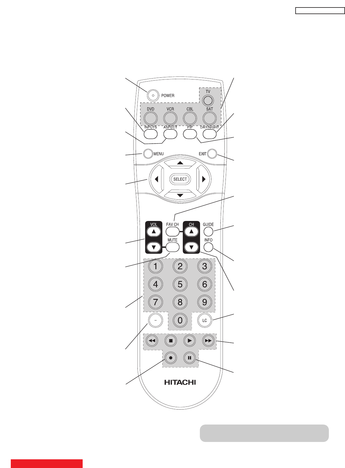
Quick Reference Remote Control Buttons and Functions
POWER BUTTON
(TV, CBL, VCR, DVD, SAT)
Turns the selected device on
and off.
INPUTS BUTTON (TV)
Accesses the INPUTS menu
system.
ASPECT BUTTON (TV)
Changes the aspect ratio while
watching TV.
MENU BUTTON
(CBL, DVD, SAT, TV)
Accesses the OSD menu
system.
CURSOR/SELECT BUTTONS
(TV, DVD, CBL, SAT)
The CURSOR buttons are used
to navigate the cursor through
the OSD and INPUTS menu
systems, and the SELECT
button is used to
Select/Activate the highlighted
menu item.
VOLUME BUTTONS (TV)
Adjusts the audio level of your
TV.
MUTE BUTTON (TV)
Reduces the audio level to 50%
if pressed once, and to
complete mute if pressed twice.
Press it a third time to restore
audio level.
NUMERIC BUTTONS
(TV, DVD, CBL, SAT, VCR)
Used to manually enter the TV
channel, and used for numeric
entry when navigating through
the OSD menu system.
(-) BUTTON (TV, SAT)
The (-) button is used when the
remote is in Set-Top-Box (STB)
mode or when the TV uses a
digital input.
RECORD BUTTON (VCR)
Press twice (2 times) to record
programs.
SOURCE ACCESS BUTTONS
(TV, DVD, VCR, CBL, SAT)
Changes the mode of the
Universal Remote Control to
control the device selected.
DAY/NIGHT BUTTON (TV)
Select picture mode settings
between DAY and NIGHT mode.
PIP BUTTON (TV)
Press to show and change the
Picture-in-Picture mode.
EXIT BUTTON
(TV, CBL, SAT)
Exits out of the OSD or INPUTS
menu systems if their menu is
displayed.
FAVORITE CHANNEL
(FAV CH) button (TV)
Press to enter/access Favorite
Channel (FAV) mode.
GUIDE BUTTON
(SAT/STB, CBL)
Accesses the program guide of
other devices.
INFO BUTTON
(TV, CBL, SAT)
Displays various information on
the screen.
CHANNEL BUTTONS
(TV, CBL, SAT, VCR)
Changes the channel.
LAST CHANNEL (LC) BUTTON
(TV, CBL, SAT)
Switches between the current
and last channel viewed.
DVD/VCR CONTROL
BUTTONS (DVD, VCR)
Controls the precode functions
of your VCR and DVD.
PAUSE BUTTON
(TV, VCR, DVD)
Press to show and change the
Freeze mode of the TV or pause
other devices.
In addition to controlling all of the functions on your HITACHI LCD Rear Projection TV, the new remote control is
designed to operate different types of devices, such as, DVD Players, CBL (Cable Boxes), set-top-boxes, satellite
receivers, and VCRs. The remote control must be programmed to control the chosen device. Please see I/B ma-
nual for a complete description of all features and programming of the Remote Control.
LEGEND
TV — Television VCR — Video Cassette Recorder/Player
CBL — Cable Box DVD — Digital Video Disc Player
STB — Set-Top-Box S AT — Satellite Receiver
NOTE: STB precode is included in the
SAT mode.
15
LC57
TABLE OF CONTENTS
INPUT/EXITCHANNEL
CURSOR
VOLUME
MENU/SELECT POWER
S-VIDEO
VIDEO
AUDIO
L/MONO
R
INPUT 5
MENU/SELECT button
This button allows you to enter the MENU, making it possible to set TV features to your preference without
using the remote. This button also serves as the SELECT button when in MENU mode.
INPUT/EXIT button
Press this button to display the input menu selections of CABLE, AIR, INPUT:1, 2, 3, 4 and 5. This button
also serves as the EXIT button when in MENU mode.
CHANNEL selector
Press these buttons until the desired channel appears in the top right corner of the TV screen. These buttons
also serve as the cursor down () and up () buttons when in MENU mode.
VOLUME level
Press these buttons for your desired sound level. The volume level will be displayed on the TV screen. These
buttons also serve as the cursor left () and right () buttons when in MENU mode. When the TV power is
turned OFF at a volume level 31 or greater, the volume level will default to 30 when the TV is turned ON.
However, if it is set to a level 30 or less, the volume level will be at the level it was set when the TV is turned
ON.
POWER button
Press this button to turn the TV ON or OFF.
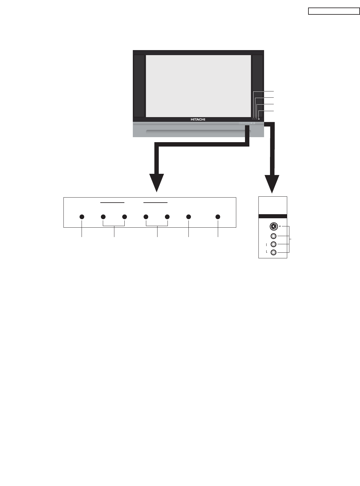
SIDE INPUT JACKS (INPUT 5)
Use these audio/video jacks for a quick hook-up from a camcorder or VCR to instantly view your favorite
show or new recording. Press the INPUT button and select INPUT 5. If you have mono sound, insert the
audio cable into the left audio jack.
IR RECEIVER Sensor
Point the remote control at this area when selecting channels, adjusting volume, etc.
Front Panel Controls
GENERAL INFORMATION
LC57
16
GENERAL INFORMATION
17
LC57
POWER Light
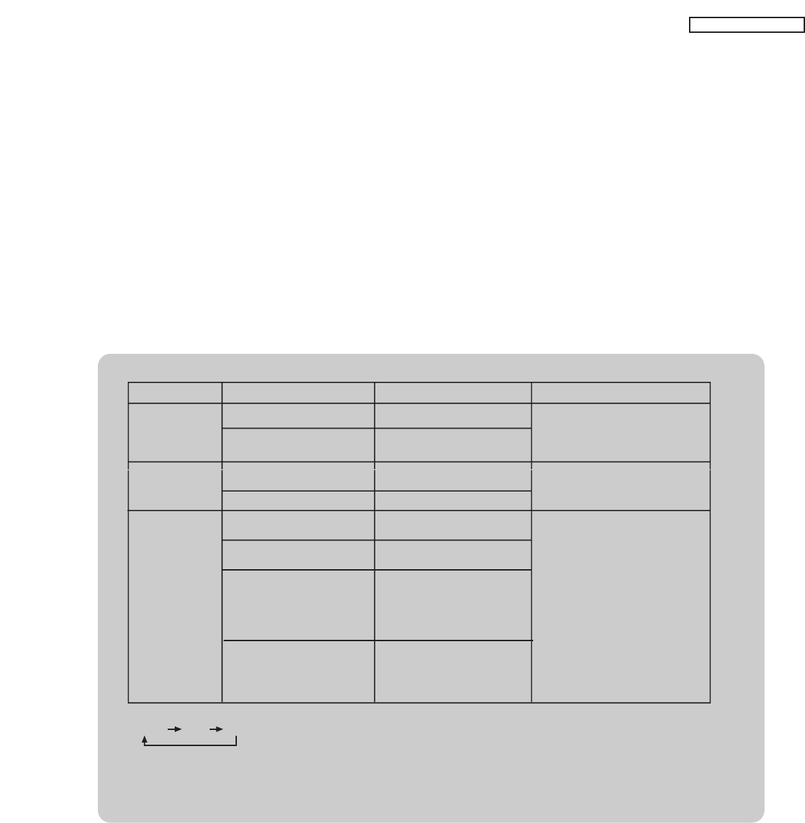
When the TV is turned ON, the Power Light will first blink to indicate that the television lamp is warming
up. This light will be ON during normal operation. When the TV is turned OFF, the Power Light will blink
to indicate that the television lamp will be cooling down and the light will eventually turn off.
TEMP Indicator
This light is off during normal operation. If this indicator is lit, the optic unit is too hot. If this indicator is
blinking, the cooling fan has stopped. Please call service. The optic unit has an air filter that may become
clogged over time. The internal termperature will increse which will trigger the temperature sensor to display
an On-Screen warning. After 6 minutes, the lamp will turn off, then the TV will turn off with the TEMP LED On.
LAMP Indicator
This light is off during normal operation. If light is lit, the lamp has failed. See page 24-27 for lamp
replacement procedure. Consult your Hitachi dealer for proper part. If light is blinking, lamp cover is not
assembled securely after replacement.
NO LAMP LIGHT
or BROKEN LAMP
WRONG LAMP UNIT
ASSEMBLY / LAMP
DOOR OPEN
Too hot inside the
OPTIC unit
COOLING FAN STOPPED
BEGINNING OF WARM UP
AFTER THE POWER ON.
NORMAL OPERATION
BEGINNING OF COOL DOWN
(FOR 20 SEC.)
(TV CANNOT ACCEPT ANY CODE
IN THIS PERIOD EXCEPT WITHIN
THE BEGINNING 5 SEC.)
COOL DOWN
(FOR 6 MINUTES)
(TV CAN ACCEPT REMOTE
CONTROL AND SIDE BUTTONS)
LIGHT ON
BLINKING
LIGHT ON
BLINKING
INTERMEDIATE BLINKING
(0.5 SEC CYCLE)
LIGHT ON
SHORT BLINKING
(0.3 SEC CYCLE)
LONG BLINKING
(1 SEC CYCLE)
INDICATOR INDICATION MEANINGACTION
LAMP LED
TEMP
LED
POWER
LED
Need to replace if
LAMP still does not light by
ìPower On ” again.
Check assembly condition of
LAMP UNIT
Call for Service
NOTES:
1.
2. If the LAMP, TEMP, and POWER LED are blinking in the order below, the television is warming up.
3. Your Hitachi LCD Rear Projection Television may appear to be OFF when it is set to input 1 ~ input 5 and the video
signal is not received from the input jacks. Please make sure the Blue Power light indicator is not lit (OFF) when
you are not watching for long lasting performance.
4. Your Hitachi LCD Rear Projection Television has an internal lamp that lights up the TV screen. Make sure to turn off
the Power when you do not watch the LCD Rear Projection Television for longer lamp life.
POWER TEMP LAMP
Front Panel Controls
First time use
Side Panel Jacks and Connections
GENERAL INFORMATION
18
LC57
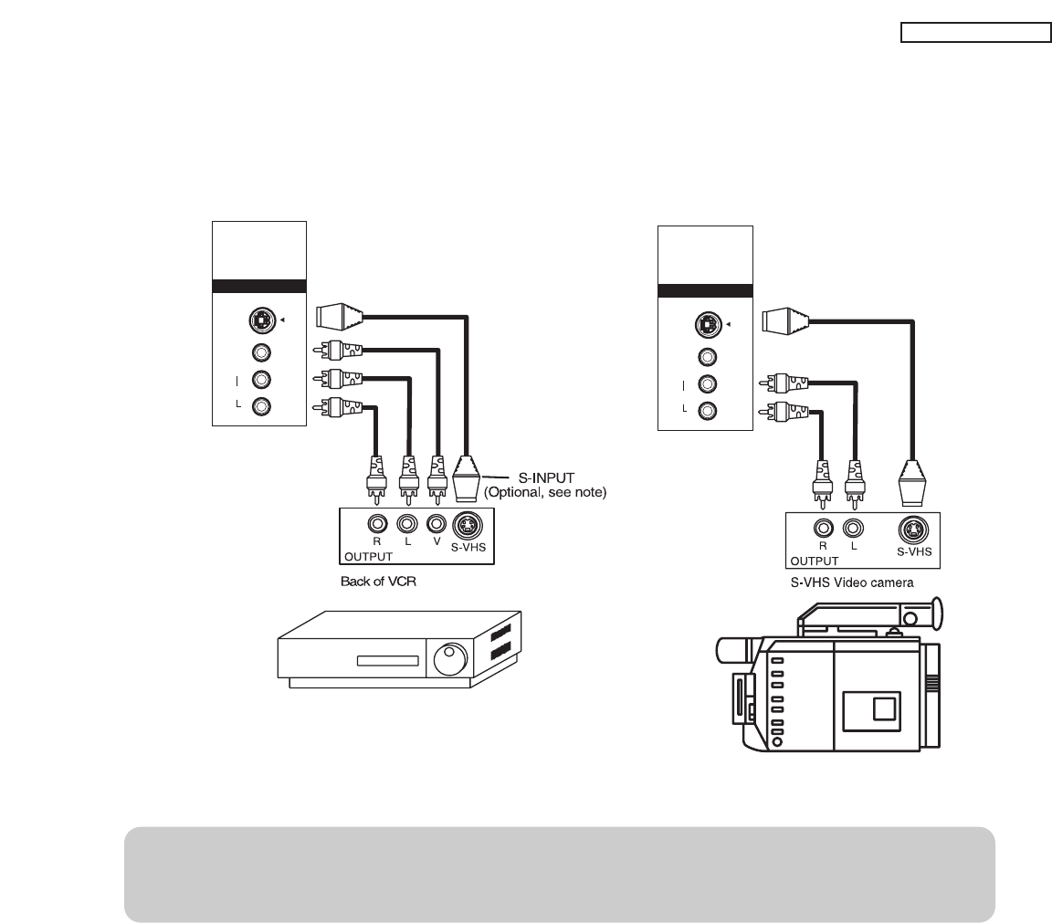
The side panel jacks are provided as a convenience to allow you to easily connect a camcorder or VCR as shown
in the following examples:
NOTE: 1. Completely insert connection cord plugs when connecting to side panel jacks. If you do not, the
played back picture may be abnormal.
2. If you have a S-VHS VCR, use the S-INPUT cable in place of the standard video cable.
3. If you have a mono VCR, insert the audio cable into the left audio jack of your TV.
S-VIDEO
VIDEO
AUDIO
L/MONO
R
INPUT 5
S-VIDEO
VIDEO
AUDIO
L/MONO
R
INPUT 5
GENERAL INFORMATION
19
LC57
First time use
Rear Panel Connections
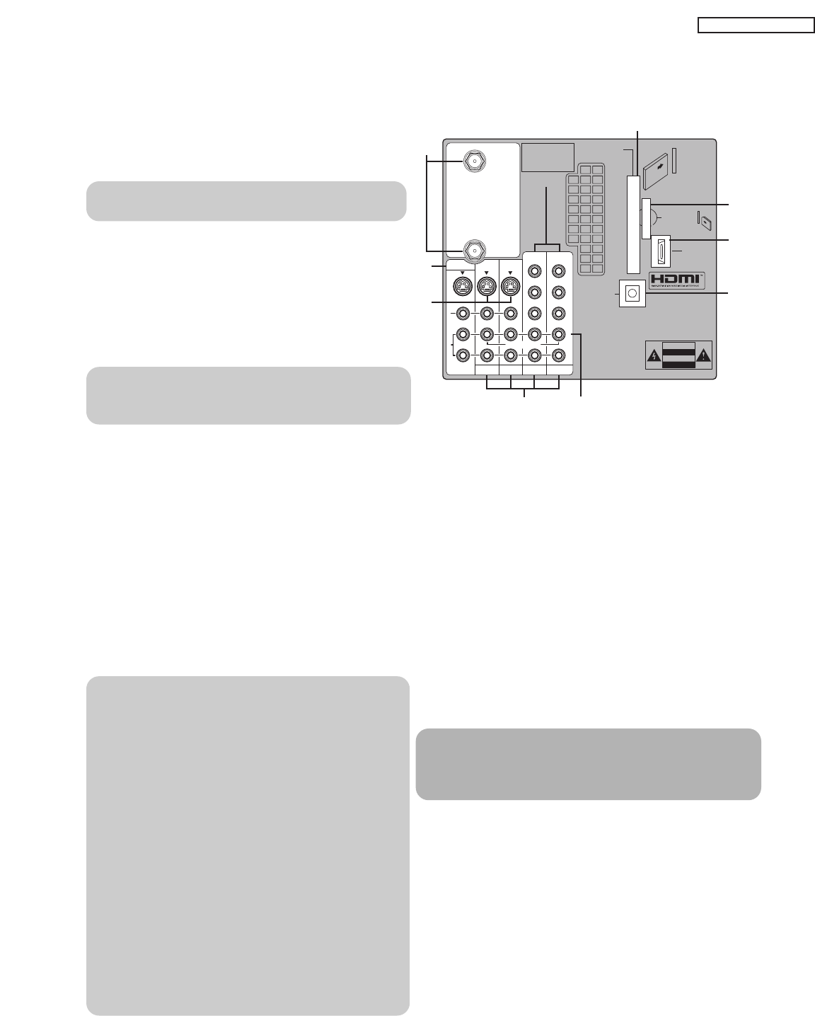
Antenna Input
CABLE – CATV (Cable TV) input.
AIR – RF antenna input.
NOTE: You may ask your local cable company
whether DTV services are available.
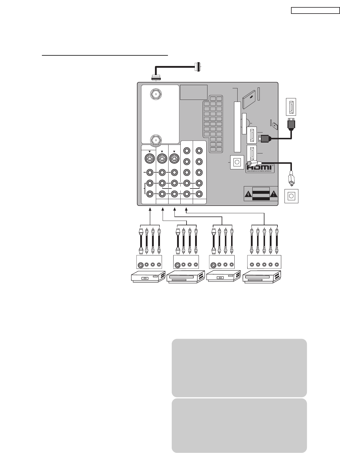
Audio/Video Inputs 1, 2, 3 and 4
By using the INPUTS button, CURSOR buttons
and SELECT button of the remote control you can
select each video source. Use the audio and video
inputs to connect external devices, such as VCRs,
camcorders, laserdisc players, DVD players etc. (If
you have mono sound, insert the audio cable into
the left audio jack.)
NOTE: You may use VIDEO or S-VIDEO inputs to
connect to INPUT 1 and 2, but only one of
these inputs may be used at a time.
Monitor Out
These jacks provide fixed or variable audio and video
signals which are used for recording. Use the S-Video
Output for high quality video output .
S-Video Inputs 1 and 2
INPUTS 1 and 2provide S-Video (Super Video)
jacks for connecting equipment with S-Video
output capability.
Component: Y-PBPRInputs
INPUTS 3 and 4provide Y-PBPRjacks for
connecting equipment with this capability, such as
a DVD player or Set Top Box. You may use
composite video signal for both inputs.
NOTE: 1. Do not connect composite VIDEO and
S-VIDEO to INPUT 1, 2 or 5at the same
time. S-VIDEO has priority over VIDEO input.
2. Your component outputs may be labeled
Y, B-Y, and R-Y. In this case, connect the
components B-Y output to the TV’s PB
input and the components R-Y output to
the TV’s PRinput.
3. Your component outputs may be labeled
Y-CBCR. In this case, connect the component
CBoutput to the TV’s PBinput and the
component CRoutput to the TV’s PRinput.
4. It may be necessary to adjust TINT to
obtain optimum picture quality when using
the Y-PBPR inputs .
5. To ensure no copyright infringement, the
MONITOR OUT output will be abnormal,
when using the Y-PBPRjacks.
6. INPUT 3 and INPUT 4 (Y/VIDEO) can be
used for composite video and component
video input.
HDMI (High Definition Multimedia Interface)
ABOUT HDMI – HDMI is the
next-generation all digital interface for consumer
electronics. HDMI enables the secure distribution
of uncompressed high-definition video and multi-
channel audio in a single cable. Because digital
television (DTV) signals remain in digital format,
HDMI assures that pristine high-definition images
retain the highest video quality from the source all
the way to your television screen.
Use the HDMI input for your external devices such
as Set-Top-Boxes or DVD players equipped with an
HDMI output connection.
HDMI, the HDMI logo and High-Definition
Multimedia Interface are trademarks or registered
trademarks of HDMI Licensing LLC.
NOTE: 1. The HDMI input is not intended for use
with personal computers.
2. Only DTV formats such as 1080i, 720p, 480i
and 480p are available for HDMI.
Optical Out (Digital Audio)
This jack provides Digital Audio Output for your
audio device that is Dolby®Digital and PCM
compatible, such as an audio amplifier.
Manufactured under license from Dolby
Laboratories. DOLBY and the DOUBLE-D
symbol are trademarks of Dolby Laboratories.
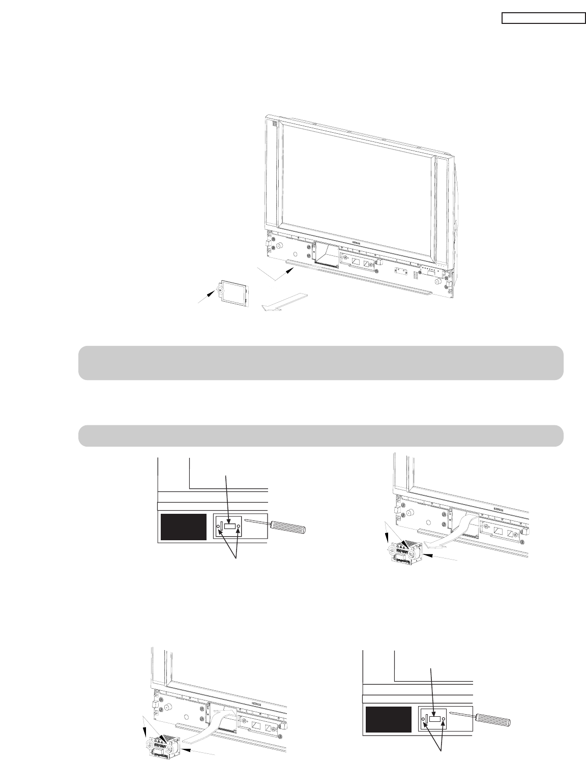
Upgrade Card
This card slot is for future software upgrades.
Hitachi will notify you if a software upgrade is
required for your TV. In order to receive written
notification, please complete and return your
warranty card.
R
L
A
U
D
I
O
V
I
D
E
O
S
I
V
I
D
E
O
(MONO)(MONO)(MONO)(MONO)
P
R
P
B
Y/
VIDEO
Y/
VIDEO
P
R
P
B
P
R
P
B
P
R
P
B
MONITOR OUT
AUDIO
TO HI-FI INPUT 1
CABLE
AIR
INPUT 2
TV AS CENTER
INPUT 3 INPUT 4
CableCARD™
CAUTION
(Top of card faces right)
Top faces
OPTICAL OUT
Digital Audio
Upgrade Card
HDMI INPUT 1
Apparatus Claims of U.S.
Patent Nos. 4,631,603;
4,577,216; 4,819,098;
4,907,093; and 6,381,747
licensed for limited
viewing uses only.
쐋
TV AS CENTER (INPUTS 1-4)
These jacks are for stereo amplifiers with center
signal output capability. This feature allows the TV
speakers to be used as a center speaker. The TV
must be set as a center channel by selecting TV
AS CENTER on the Internal Speakers Settings of
the Audio Menu.
CableCARD Slot
This slot is for the CableCARD that will be provided
by your local cable operator to gain access to
chosen cable channels. The CableCARD will allow
you to tune digital and high definition cable
channels. Please call your local cable operator if
this service is available before requesting a
CableCARD (also known as Point of Deployment
(POD) module).
1. Connect a coaxial cable to cable terminal of
the Rear Panel Jacks.
2. Insert the CableCARD into the slot (Top of card
should be facing right as shown below).
NOTE: 1. A digital cable subscription is required.
2. Do not insert a PCMCIA card into the
CableCARD slot.
If the CableCARD is properly installed or not installed,
the TV will display the following respective screens.
After the CableCARD is installed, wait until the second
screen below appears. The third screen below will
appear if a channel is not authorized for viewing. Press
the EXIT button to exit the second screen.
Please take note of all information on the screen (you
will provide this information to your cable operator).
Call your cable operator and give them the information
from the card to start your cable service.
Not an Authorized Channel
In order to start cable service
for this device, please contact
your cable provider
CableCARD(tm): 123-456-789-1
Host: 123-456-789-1
Data: 123-456-789-1
Unit Address: 123-456-789-1
Press EXIT to return
Acquiring Data.
Please wait.
OR
OR
CableCARD is not installed
CableCARD is installed
Rear Panel Connections
R
L
A
U
D
I
O
V
I
D
E
O
S
I
V
I
D
E
O
(MONO)(MONO)(MONO)(MONO)
P
R
P
B
Y/
VIDEO
Y/
VIDEO
P
R
P
B
P
R
P
B
P
R
P
B
MONITOR OUT
AUDIO
TO HI-FI INPUT 1
CABLE
AIR
INPUT 2
TV AS CENTER
INPUT 3 INPUT 4
CableCARD™
CAUTION
(Top of card faces right)
Top faces
OPTICAL OUT
Digital Audio
Upgrade Card
HDMI INPUT 1
Apparatus Claims of U.S.
Patent Nos. 4,631,603;
4,577,216; 4,819,098;
4,907,093; and 6,381,747
licensed for limited
viewing uses only.
Digital Cable
CableCARD™
Top faces this way
HDMI INPUT 2
GENERAL INFORMATION
20
LC57
Rear Panel Connections
1. Press the MENU button on the Remote Control to
access the Main Menu screen.
2. Use the CURSOR button to highlight SETUP in
the Main Menu and press the SELECT button.
3. Use the CURSOR button to highlight
CableCARD Information and press the SELECT
button.
4. To view the CableCARD ID and Host ID, use the
CURSOR button to highlight CableCARD Info
and press the SELECT button.
NOTE: The Diagnostics Info. window is for
Service use only.
Additional CableCARD Information
After the CableCARD has been successfully installed, a CableCARD Information menu appears in the SETUP menu
of the On-Screen Display.
Follow the instructions below to access the CableCARD Information menu.
Set The Inputs
Lamp Power Control
Set Closed Captions
Menu Preference
Set Monitor Out
CableCARD Information
Setup
Upgrades
Quick Start-Up
Move SEL Select
Setup
Timers
Locks
Channel Manager
Audio
Video
Move SEL Select
CableCARD Information
Setup
Move SEL Return
Select the button below to acess
CableCARD ID and Host ID.
Select the button below to access
CableCARD and Host Diagnostics.
CableCARD Info.
Diagnostics Info.
GENERAL INFORMATION
LC57
21
TIPS ON REAR PANEL CONNECTIONS
•S-VIDEO, Y- P BPRand HDMI
connections are provided for
high performance laserdisc
players, VCRs etc. that have
this feature. Use these
connections in place of the
standard video connection if
your device has this feature.
• If your device has only one
audio output (mono sound),
connect it to the left audio jack
on the television.
• Refer to the operating guide of
your other electronic equipment
for additional information on
connecting your hook-up
cables.
• A single VCR can be used for
VCR #1 and VCR #2, but note
that a VCR cannot record
its own video or line output
(INPUT 1 in the example on
this page). Refer to your VCR
operating guide for more
information on line input-output
connections.
• You may use VIDEO or
S-VIDEO inputs to connect to
INPUT 1, INPUT 2 or INPUT 5,
but only one of these may be
used at a time.
• Connect only one component
(VCR, DVD player, camcorder,
etc.) to each input jack.
• COMPONENT: Y-P BPR(INPUT 3 and INPUT 4)
connections are provided for high performance
components, such as DVD players and set-top-
boxes. Use these connections in place of the
standard video connection if your device has this
feature. INPUT 3 accepts both composite and
component video signals.
• Your component outputs may be labeled Y, B-Y,
and R-Y. In this case, connect the components
B-Y output to the TV’s PBinput and the
components R-Y output to the TV’s PRinput.
• Your component outputs may be labeled Y-CBCR.
In this case, connect the components CBoutput to
the TV’s PBinput and the components CRoutput to
the TV’s PRinput.
• You may use composite and component video
signals for INPUT 3 and INPUT 4.
• It may be necessary to adjust TINT to obtain
optimum picture quality when using the Y-P BPR
inputs .
• To ensure no copyright infringement, the
MONITOR OUT output may be abnormal, when
using the Y-PBPRjacks.
• When using an HDMI input from a Set-Top-Box, it
is recommended that a 1080i or 720p input signal
is used.
NOTE: 1. Connect only one component to each
input jack.
2. Follow connections that pertain to your
personal entertainment system.
3. INPUT 3 and INPUT 4 can accomodate
Composite and Component video signals.
4. Cables are not included with the purchase
of this TV, except when noted as
“provided”.
MACROVISION NOTES:
1. Video signals fed through a VCR may be
affected by copyright protection systems
and the picture will be distorted on the
television.
2. Connecting the television directly to the
Audio /Video output of a Set-Top-Box will
assure a more normal picture.
Rear Panel Connections
R
L
A
U
D
I
O
V
I
D
E
O
S
I
V
I
D
E
O
(MONO)(MONO)(MONO)(MONO)
P
R
P
B
Y/
VIDEO
Y/
VIDEO
P
R
P
B
P
R
P
B
P
R
P
B
MONITOR OUT
AUDIO
TO HI-FI INPUT 1
CABLE
AIR
INPUT 2
TV AS CENTER
INPUT 3 INPUT 4
CableCARD™
CAUTION
(Top of card faces right)
Top faces
OPTICAL OUT
Digital Audio
Upgrade Card
HDMI INPUT 1
Apparatus Claims of U.S.
Patent Nos. 4,631,603;
4,577,216; 4,819,098;
4,907,093; and 6,381,747
licensed for limited
viewing uses only.
Outside Antenna
or Digital Cable
Laserdisc player, VCR,
Camcorder, etc.
VCR #2 VCR #1 DVD Player
To an
amplifier/
receiver with
optical input
capability.
External
Digital
Component
with HDMI
output
capability
INPUT
S-VIDEO VL R
OUTPUT
S-VIDEO VL R
OUTPUT
RLPB/CBPR/CRY
OUTPUT
S-VIDEO VL R
HDMI OUT
OPTICAL IN
HDMI INPUT 2
GENERAL INFORMATION
22
LC57
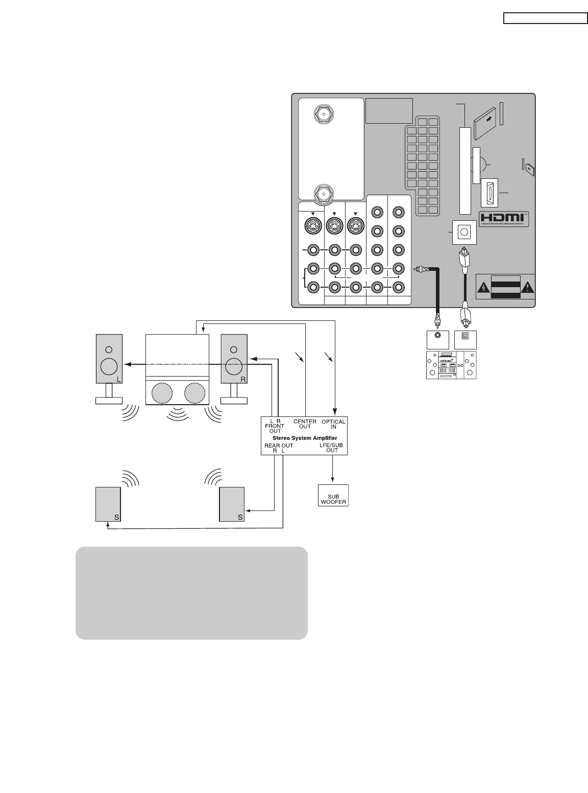
Connecting External Video Sources
Match the numbers below to the diagram for
speaker placement.
The television’s internal speakers will act as
center speaker (select AUDIO - INTERNAL
SPEAKERS - TV AS CENTER).
These FRONT left and right speakers are
connected to the FRONT output of a
separate audio amplifier.
These REAR left and right speakers are
connected to the Rear output of a separate
audio amplifier.
This subwoofer is connected to the LFE/SUB
Out output of a separate audio amplifier.
NOTE: 1. The Optical Out (Digital Audio) provides a
fixed digital audio output to your external
component such as an A/V receiver with
optical input capability. The audio level
can only be controlled through the volume
control of the external audio amplifier.
R
L
A
U
D
I
O
V
I
D
E
O
S
I
V
I
D
E
O
(MONO)(MONO)(MONO)(MONO)
P
R
P
B
Y/
VIDEO
Y/
VIDEO
P
R
P
B
P
R
P
B
P
R
P
B
MONITOR OUT
AUDIO
TO HI-FI INPUT 1
CABLE
AIR
INPUT 2
TV AS CENTER
INPUT 3 INPUT 4
CableCARD™
CAUTION
(Top of card faces right)
Top faces
OPTICAL OUT
Digital Audio
Upgrade Card
Apparatus Claims of U.S.
Patent Nos. 4,631,603;
4,577,216; 4,819,098;
4,907,093; and 6,381,747
licensed for limited
viewing uses only.
CENTER
OUT
OPTICAL
IN
Stereo System Amplifier
or DVD Player
HDMI INPUT 1
쐋쐋
Optical
Cable
RCA
Cable
GENERAL INFORMATION
LC57
23

GENERAL INFORMATION
24
LC57
Lamp Life
The lamp life may vary based on usage of the LCD Rear PTV. Turning on and off frequently may shorten the life of
the lamp.
Lamp Replacement
After extended use, if the TV picture turns dark, the color looks unusual or LAMP INDICATOR light turns on, then it
is time to replace the lamp with a new lamp.
WARNING:
The lamp gets very hot! The lamp may explode if improperly handled. To avoid injury, please observe the
following precautions.
• Do not open lamp compartment or attempt to remove lamp assembly unless the lamp assembly is being
replaced.
• Unplug the product’s power cord from the AC outlet before attempting to replace the lamp assembly.
• If the lamp is in use when failure occurs or if the lamp has exploded, wait at least 30-45 minutes for the lamp
to cool before opening the lamp compartment or touching the lamp assembly or any broken pieces.
• Broken lamp pieces can cause injury. Handle with gloves to avoid cuts.
• Do not place any foreign objects inside the lamp compartment.
• When installing a new lamp, follow handling instruction included with the new lamp. Do not touch glass
surface of new lamp.
• This product contains lead and a lamp that contains mercury. Dispose of this product and its lamp in
accordance with applicable environmental laws. For lamp recycling and disposal information, go to
www.lamprecycle.org. For product recycling and disposal information, contact your local government
agency or eRecycle.org (in California), the Electronic Industries Alliance at www.eiae.org (in the US) or the
Electronic Product Stewardship Canada at www.epsc.ca (in Canada).
For more information, call “1-800-HITACHI.”
CAUTION!
A ”LAMP” indicator will light when lamp becomes hot. Unplug product’s power cord from the AC outlet
and allow lamp to cool for at least 30-45 minutes. If “LAMP” indicator is still lit, please contact your
authorized service center .
NOTES:
• Contact your Hitachi dealer for a new lamp unit. Using other lamps may cause damage to the TV Set.
MODEL# LAMP TYPE PART#
50V720 LM520
• When replacing the lamp, let it cool down completely, for approximately 30 to 45 minutes after the power
has been switched off and A.C. cord has been unplugged.
• Do not touch the glass of the new lamp or make it dirty which can shorten the life of the lamp and reduce
the picture quality.
• Keep the lamp out of the reach of children and away from flammable materials.
• Do not pour water onto the removed lamp or put any object inside the lamp.
• Once the lamp is removed, do not put flammable materials and metal objects inside the lamp receptacle
on the TV set. Do not touch the receptacle.
• Install the new lamp securely, otherwise the picture may become dark or it may cause severe
overheating.
• Install the lamp cover correctly, otherwise power will not come on.
Lamp Replacement
UX21517
CH 1
Lamp Replacement
1. Turn off the main power switch and unplug the power cord. Wait at least 30 minutes to allow the lamp to cool
down before replacing it.
CAUTION: The lamp is very hot and may cause fire or severe burns. Wait at least 30~45 minutes to allow the
lamp to cool before proceeding with lamp removal.
2. Remove the front cover from the TV set. This is held by snap on. Pull the cover outwards until the quick snap
on disengages.
NOTE: This product contains lead and a lamp that contains mercury. Dispose of this product and its lamp in
accordance with applicable environmental laws. For lamp recycling and disposal information, go to
www.lamprecycle.org. For product recycling and disposal information, contact your local government
agency or the Electronic Industries Alliance at www.eiae.org (in the US) or the Electronic Product
Stewardship Canada at www.epsc.ca (in Canada). For more information, call “1-800-HITACHI.”
120V
FRONT COVER
PULL
LAMP COMPARTMENT
Lamp Replacement
GENERAL INFORMATION
LC57
25
3. Remove the screw securing the lamp cover with a Phillips head screw driver as shown. Remove the lamp
cover.
CAUTION: The lamp is very hot and may cause fire or severe burns. Wait at least 30~45 minutes to allow the
lamp to cool before proceeding with lamp removal.
4. Remove the two screws that hold the lamp in place. Remove the lamp unit by holding the lamp handle, then
pulling outwards. Exercise caution when removing the lamp unit to avoid injury to your fingers.
NOTE: Do not put your hand in the Lamp Storage area after the Lamp Unit is removed, your may get burned.
5. Replace with the new lamp.
Place the removed lamp into the empty box of the replacement lamp. Do not touch the front glass of the new
lamp or its receptacle. This may shorten the life of the lamp and reduce the picture quality.
• Push the lamp unit back to its original position.
• Tighten the screws firmly on the lamp unit. If they are loose, the TV may not operate correctly.
Lamp Replacement
UNSCREW
UNSCREW
HANDLE
TIGHTEN THE SCREWS
LAMP UNIT
TIGHTEN THE SCREWS
HANDLE
LAMP COVER
PULL
LAMP COMPARTMENT
LAMP UNIT
GENERAL INFORMATION
26
LC57
6. Without installing the lamp cover, the power will be off and the Lamp Indicator will flash (see page 17). Be sure
to install the lamp cover by re-engaging the two clips and tighten the screws before turning the power on,
otherwise it may cause unusual colors.
NOTE: If power is connected before the Lamp Cover is installed, the power will be off and the Lamp Indicator
will flash (see page 17).
7. Install the front cover as shown below. Put the front cover back in and align the snap on quick connect
then push inwards holding the left and right side of the front cover until you hear a snap. Push the other
snap on gently to make a good fit.
8. Plug power cord into AC outlet and turn on the main power switch.
NOTE: This product contains lead and a lamp that contains mercury. Dispose of this product and its lamp in
accordance with applicable environmental laws. For lamp recycling and disposal information, go to
www.lamprecycle.org. For product recycling and disposal information, contact your local government
agency or eRecycle.org (in California), the Electronic Industries Alliance at www.eiae.org (in the US) or
Electronic Product Stewardship Canada atwww.epsc.ca (in Canada).
For more information, call “1-800-Hitachi”.
Lamp Replacement
120V
SCREW
LAMP COVER
PHILLIP HEAD
SCREW DRIVER
27
GENERAL INFORMATION
LC57
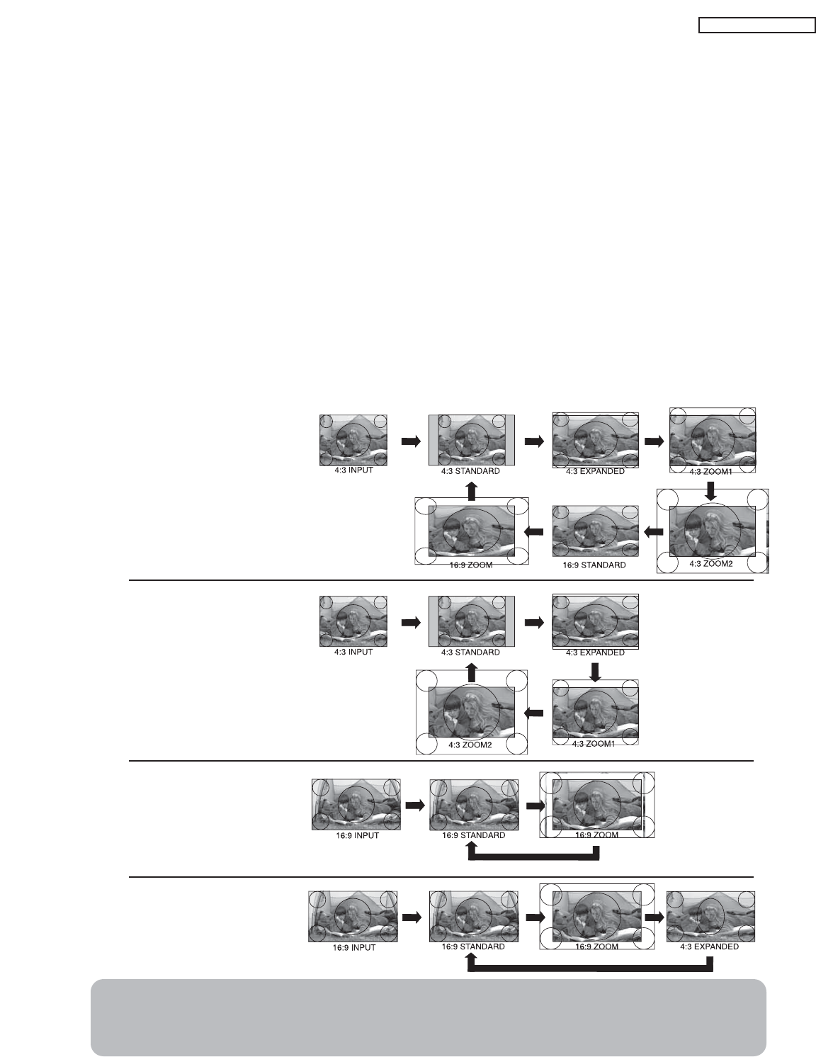
ASPECT button
Press this button to quickly change the picture format ASPECT ratio. Depending on the input signal format
received, the picture format ratio allows you to adjust the images through the following options.
• Antenna-Analog
• S-Video/Video Input
(Auto Aspect: Off)
• HDMI-480i/480p Input
(Auto Aspect: Off)
• Component-480i/480p
Input (Auto Aspect: Off)
• Antenna-Digital (4:3)
• S-Video/Video 4:3 Letter
Input (Auto Aspect: On)
• HDMI-480i/480p 4:3/
Letter Input (Auto Aspect: On)
• Component-480i/480p 4:3
Letter Input
(Auto Aspect: On)
• S-Video/Video 16:9 Input
(Auto Aspect: On)
• HDMI-480i/480p 16:9 Input
(Auto Aspect: On)
• Component-480i/480p
16:9 Input
(Auto Aspect: On)
• Antenna-Digital (16:9)
• HDMI-720p/1080i Input
• Component-720p/1080i
Input
NOTE: 1. The Aspect Style setting you select for an ANT input will automatically be set for the other ANT
input. However, all five video inputs have independent Aspect Style settings.
2. Vertical position adjustments are directly available when you choose 4:3
EXPANDED/ZOOM1/ZOOM2 or 16:9 ZOOM aspect style .
4:3 STANDARD
Use this aspect mode to display conventional (4:3)
images. Side panels (gray areas) are placed to the
left and right of the image to preserve the original
aspect ratio of the source. Note: Use this mode for
only 15% of your total viewing time to prevent
uneven aging of the phosphors. Phosphors in the
lighted area of the picture will age more rapidly
than the gray areas.
4:3 EXPANDED
Use this aspect mode to display conventional (4:3)
sources by linearly increasing image expansion
from the center towards the edges of the display
area in order to fill it.
4:3 ZOOM1/ZOOM2
Use these aspect modes to zoom in on
conventional (4:3) sources.
16:9 STANDARD
Use this aspect mode to display 16:9 sources like
HDTV and DVD’s preserving the original 16:9
aspect ratio.
16:9 ZOOM
Use this aspect to Zoom-in once while in 16:9
aspect.
DISPLAY PICTURE FORMAT
28
LC57
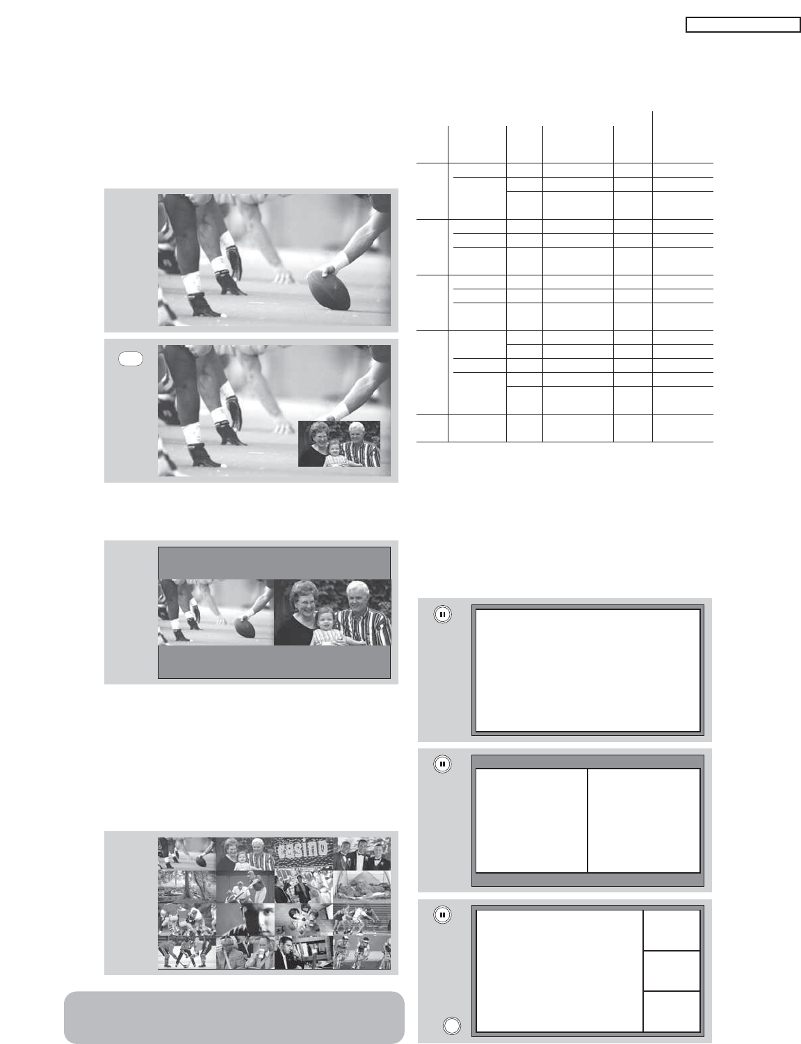
PIP Mode Picture-in-Picture
This feature is only available with a Digital 16:9,
720p and 1080i signal. To prevent a pattern burn,
occasionally move the sub-picture using the
CURSOR buttons.
SPLIT Mode Picture-in-Picture
Split Mode PIP displays the main picture and sub-
picture evenly on the screen.
SURF Mode Picture-in-Picture
Surf Mode PIP automatically scans all active
channels (those set in memory) and displays them
as PIP sub-pictures or Thumbnail channels. Press
the SELECT button to stop on a chosen channel.
Use the remote CURSOR buttons (, , , ) to
navigate the Thumbnail. Press the EXIT button to
enable your chosen channel and return to normal
viewing.
NOTE: Press the SELECT button to stop the Surf mode
or channel scan. Press the SELECT button
again to resume Surf mode or channel scan.
Picture-in-Picture (PIP) Modes
480p/480i
1080i/ Analog Tuner
PIP Main/ Digital Tuner 720p
Video/S-Video
Mode Sub Aspect 16:9 4:3 16:9 16:9 4:3
POP ANT Digital 16:9 — — Yes Yes Yes
480p/480i 16:9 Yes1Yes1———
ANT Analog 4:3 Yes Yes — — —
S-Video/Video
PIP ANT Digital 16:9 —— —Yes
1Yes
4:3 1080i/720p 16:9 —Yes — ——
480p/480i 16:9 —Yes
2———
S-Video/Video
PIP ANT Digital 16:9 ——YesYes
2—
16:9 1080i/720p 16:9 Yes — — — —
480p/480i 16:9 Yes2————
S-Video/Video
SPLIT ANT Digital 16:9 — — Yes Yes Yes
4:3 — — Yes Yes Yes
1080i/720p 16:9 Yes Yes — — —
480p/480i 16:9 Yes Yes — — —
ANT Analog 4:3 Yes Yes — — —
S-Video/Video
SURF — — Yes Yes — — Yes
12 PIX
Yes1= Auto Aspect Off; Yes2= Auto Aspect On
PAUSE button
If you wish to freeze the sub-picture, press the
PAUSE button. This is convenient when trying to
write down the address for a mail order company,
recording statistics for a sporting event, etc. To return
the picture to motion, press the EXIT button. Press
the PAUSE button repeatedly to toggle between
FREEZE modes (Main Freeze, SPLIT and STROBE).
EXIT
Freeze
Freeze
Freeze
Freeze
Freeze
1 2 3 4
5 6 7 8
91010 1111 1212
1313 1414 1515 1616
MAIN PICTUREMAIN PICTURE SUB PICTURESUB PICTURE
PIP
MAIN PICTUREMAIN PICTURE
SUB PICTURESUB PICTURE
Picture-in-Picture (PIP)
29
LC57
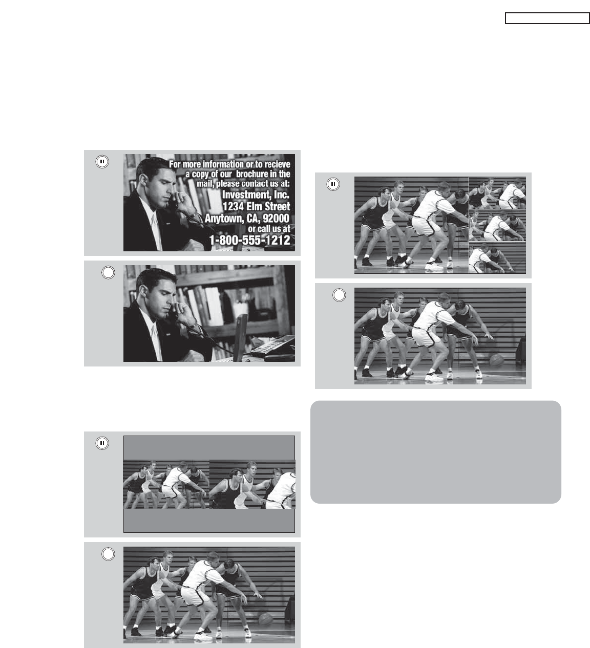
MAIN FREEZE
Press the PAUSE button to freeze one frame of the
picture you are currently viewing and the frozen
frame will show in the Main Picture. Press the EXIT
button to return to normal viewing. This feature is
useful for freezing a picture frame with addresses.
SPLIT FREEZE
Press the PAUSE button to freeze the picture you
are currently viewing (only the right sub-picture will
freeze). Press the EXIT button to return to normal
viewing.
STROBE FREEZE
Press the PAUSE button to freeze three frames of
the picture you are currently viewing (only the 3
sub-pictures will freeze). Press the EXIT button to
return to normal viewing. This feature is useful for
viewing a moving picture that has many details, for
example, a close play in a sporting event or a golf
swing.
NOTE: 1. The default FREEZE mode is the MAIN
freeze followed by the SPLIT freeze and
then the STROBE freeze. The last Freeze
mode you selected before you pressed the
EXIT button will be the one that comes up
after pressing the PAUSE button again.
2. Each freeze frame is delayed about 0.1
(1/10) second.
EXIT
MAIN PICTUREMAIN PICTURE SUB PICTURESUB PICTURE
EXIT
EXIT
Picture-in-Picture (PIP)
30
LC57

TO GO TO AN ADJUSTMENT, CLICK ON ITS HEADING BELOW
SERVICE ADJUSTMENTS
1. CHASSIS ADJUSTMENT................................................................................................................................... 32
1-1. Service Menu Access .................................................................................................................................................32
1-2. Memory Initialize ....................................................................................................................................32
1-3. Factory Reset ...........................................................................................................................................33
1-4. Factory and Service Adjustments ...........................................................................................................33
2. FINAL ASSEMBLY ADJUSTMENT (Adjustment order) ..................................................................................33
2-1. Preheat run conditions ............................................................................................................................33
2-2. Subcontrast Adjustment .........................................................................................................................33
2-3. Raster Position Adjustment ....................................................................................................................34
2-4. Flicker Adjustment ..................................................................................................................................34
2-5. Ghost Adjustment ...................................................................................................................................34
2-6. NRSH Adjustment ..................................................................................................................................34
2-7. Display Area Specifications ....................................................................................................................35
2-8. Gamma Correction (White Balance) ....................................................................................................36
2-9. Color Uniformity (White Uniformity) ....................................................................................................37
2-10. Drive Adjustment Check .......................................................................................................................38
2-10-1. Dot Stripe Checking ...................................................................................................................38
2-10-2. Sub Ghost Checking ..................................................................................................................38
2-10-3. Horizontal Crosstalk Checking ...................................................................................................38
2-11. Lamp Door Protection Operation Check ...............................................................................................39
2-12. Lamp Holder Protection Operation Check ...........................................................................................39
2-13. High Temperature Protection Operation Check ....................................................................................39
2-14. Temperature Sensor Data Setting .......................................................................................................40
2-15. Checking of Temperature Sensor .........................................................................................................41
2-16. Adjustment I2C Parameter List ..............................................................................................................42
2-17. Adjustment OSD Flow Chart ..................................................................................................................79
2-18. Troubleshooting Flow Charts .............................................................................................................................88
*IMPORTANT
For many of the above adjustments, it is necessary to have an HDTV (1080i or 720P) signal generator, SDTV (480P)
signal generator, as well as the usual NTSC (480i) signal generator.
Hitachi recognizes that few companies offer HDTV or SDTV signal generators and that the cost of these generators is
sometimes prohibitive. For this reason, we suggest the use of a set-top-box for HDTV and SDTV adjustments. Usually,
there is a switch on the set-top-box which enables it to output HDTV (1080i or 720P) or SDTV (480P) signals even with
no input. In this case, the sync is automatically detected by the TV (at the Y-PBPRInputs on the rear panel).
TABLE OF CONTENTS
31
LC57

BACK TO ADJUSTMENTS
32
LCD
EXIT
EXIT
SELECT
MENU
Remote Control Buttons
Change
Selection (Up)
Increase
Data Value
Change
Selection (Down)
Decrease
Data Value
ADJUSTMENT PROCEDURE START-UP
The 50V720 LCD rear proyection television sets pass
through adjustment procedures during the assembly
process. These adjustments must be done to assure the
best performance of the LCD set for the consumer.
Also, after servicing, these same adjustments must be
done. Most of the adjustments are made by the I2C bus
by changing data in the Adjustment mode menu.
On pages 42-78 shows the complete parameter list
with a brief description, signal format, the adjustment
range and the initial data.
1-1 HOW TO GET TO ADJUSTMENT MODE
Chassis adjustment mode can be access by pressing
the R/C keys MENU + MENU + 8 + SELECT to enter
adjustment mode. For some parameters the only way
to see them is by selecting the parameter number than
pressed SELECT in order to see it; then DATA can be
change if other parameter needs to change then press
key then repeat the same procedure.
Other way to access this mode is by use JIG R/C code: (9C Hex).
To escape from Adjustment Mode press “INPUT” key on Side
panel or EXIT key of R/C to exit service adjustment mode.
1-1.1 CHANGING DATA AND SELECTING ADJUSTMENT
CODE , ,
, and MENU keys of the remote control or front panel
may be used as the adjustment keys.
A. Use any Hitachi remote control when making an
adjustment.
, keys are used for selecting adjustment item.
,keys are used for changing data values.
MENU key is used to advance through the adjustment
mode menus and pages.
EXIT
EXIT
SELECT
MENU
B. To make a selection, use the NUMBER pad on the
R/C; example : select SEINE press 69 then SELECT
the DATA shown is "EB" ; if this DATA needs to be change
press the keys to modify, when finish press SELECT
key to store the new DATA value.
normal condition.
C. After finishing the necessary adjustment press the R/C
EXIT key or EXIT key on the side panel.
Adjustment mode is released and LCD set returns to
normal condition.
왗,왘,
1-2 MEMORY INITIALIZE
1-2.1 MEMORY INITIALIZE OPERATION
NOTE: The execution of this function returns the
adjustment codes to the preset values, therefore,
adjustment data will be lost.
Procedure
(1) Enter Adjustment mode by the method described in
sub-items 1.1 and 1.2 from item 1 (“Adjustment
procedure start up”).
(2) Get to the second page of Adjust Mode by pressing
remote control “Menu” key once, or with either the
R/C or front panel , cursor keys several times.
(3) Select MEMORY INIT adjust code.
(4) Activate MEMORY INIT by pressing cursor key for
more than 3 seconds.
(5) Check the following process for initialization opera-
tion.
(8) When LCD turns ON , it will tune CH03 this is the
complete operation of Memory Initialize process.
·Process of Memory Initialize operation.
A screen is be colored blue when MEMORY INIT
start.
A screen is be colored green when MEMORY INIT
finish normally.
A screen is be colored black when MEMORY INIT
finish abnormally.
(6) Do not unplug from AC outlet until this operation
is complete and do not perform any key operation
either, after this operation each factory setting and
all adjust mode data should reset to delivery settings
automatically.
(7) After Memory Initialize, it should be unplug AC cord.
Unplug and plug AC cord and then all settings and data
①
②
③
are updated.
ADJUST MODE
▶RGB
H POSITION **
V POSITION **
ENBW **
GHOST
VCOM
NRSH
STRIPE
S.GHOST
STREAK
When the LCD set is in adjustment mode, the cursor
LC57
CH 2
BACK TO ADJUSTMENTS
33
LC57
NOTE: (1) If there is a different value than shown in I2C Parameter List, for
fixed data, adjust it using , buttons (only in this case)
* JIG. R/C FACTORY PRESET CODE:92
MEMORY INITIALIZE and FACTORY PRESET
ITEM MEMORY
INITIALIZE
FACTORY RESET REMARKS
H POSITION ADJUST DATA INITIALIZE NOT INITIALIZE
V POSITION ADJUST DATA INITIALIZE NOT INITIALIZE
RGB(480p) ADJUST DATA INITIALIZE NOT INITIALIZE
SETTING DATA FOR EACH DEVICE INITIALIZE NOT INITIALIZE
BBE EFFECT SETTING DATA INITIALIZE NOT INITIALIZE
AUDIO AGC SETTING DATA INITIALIZE NOT INITIALIZE
V CHIP RATING SETTING DATA INITIALIZE NOT INITIALIZE
CCD SETTING DATA INITIALIZE NOT INITIALIZE
FACTORY RESET ITEM INITIALIZE INITIALIZE
LAMP TIME INITIALIZE INITIALIZE
Accumulate TIME INITIALIZE NOT INITIALIZE
GHOST ADJUST DATA INITIALIZE NOT INITIALIZE
FLICKER ADJUST DATA(V.COM) INITIALIZE NOT INITIALIZE
NRSH ADJUST DATA INITIALIZE NOT INITIALIZE
COLOR UNIFORMITY NOT INITIALIZE NOT INITIALIZE
GAMMA CORRECTION NOT INITIALIZE NOT INITIALIZE
V.REF (EPSON PANEL ONLY ) NOT INITIALIZE NOT INITIALIZE
Automatic Power saving- Yes/No Set to “No”
for heat-run Set to Yes
(8) When LCD turns ON , it will tune CH03 this is the
complete operation of FACTORY RESET process.
·Process of FACTORY RESET operation.
A screen is be colored MAGENTA when FACTORY
RESET start.
A screen is be colored green when FACTORY
RESET finish normally.
A screen is be colored black when FACTORY
RESET finish abnormally.
(6) Do not unplug from AC outlet until this operation
is complete and do not perform any key operation
either, after this operation each factory setting and
all adjust mode data should reset to delivery settings
automatically.
(7) After FACTORY RESET, it should be unplug AC cord.
Unplug and plug AC cord and then all settings and data
①
②
③
are updated.
1-3 FACTORY RESET OPERATION
NOTE: The execution of this function returns the
adjustment made by the customer , this will return all the
adjustments to the original shipping conditions.
Procedure
(1) Enter Adjustment mode by the method described in
sub-items 1.1 and 1.2 from item 1 (“Adjustment
procedure start up”).
(2) Get to the second page of Adjust Mode by pressing
remote control “Menu” key once, or with either the
R/C or front panel G, H cursor keys several times.
(3) Select FACTORY RESET adjust code.
(4) Activate FACTORY RESET by pressing E cursor key
for more than 3 seconds.
(5) Check the following process for FACTORY RESET
operation.
1-4 FACTORY AND SERVICE ADJUSTMENTS
The adjustment item that is affected by the memory
initialize operation is shown below:
2 Final ASSEMBLY ADJUSTMENT
2-1 PRE HEAT RUN CONDITION
Heat run should be performed with moving picture or no signal.
And disable side panel or top/bottom panel.
Do NOT use stock market quotation, computer graphics,
and other fixed (non-moving) image.
Table 2.1 Final adjustment order
Order Adjustment Item Signal
1 SUB CONTRAST ADJUSTMENT (RGB) White Raster 480i,720P
2 RASTER POSITION ADJUSTMENT Circle pattern signal.
3 GHOST ADJUSTMENT
4 FLICKER ADJUSTMENT
5 NRSH ADJUSTMENT
6 White Balance (GAMMA) ADJUSTMENT
7 WHITE UNIFORMITY ADJUSTMENT
8 DOT STRIPE CHECKING and ADJUSTMENT
9 SUB GHOST CHECKING and ADJUSTMENT
10 HORIZONTAL CROSS TALK CHECKING
and ADJUSTMENT
11 LAMP DOOR PROTECTION OPERATION
CHECK
12 LAMP HOLDER PROTECTION OPERATION CHECK
13 HIGH TEMPERATURE PROTECTION
OPERATION CHECK
14 TEMPERATURE SENSOR OPERATION CHECK
15 HDMI ADJUSTMENT / EDID DATA
INSTALLATION
16
17
18
19
20
2-2 SUB-CONTRAST ADJUSTMENT
Preparation
Receive Sub-contrast adjustment signal (Fig. 1).
Adjustment
(1) Select ‘SUB CONTRAST’ of Service Adj. Menu.
Press E for over 2 seconds and have it perform
automatic adjustment. When it’s completed, ‘Auto
Adjusting’ on the screen will be disappeared.
V1
V3V2
Fig. 1
Full White
(RF Input ANT A))
V1=1.0 Vp-p (when
V2=100IRE with
V3=7.51IRE)
(Y PBPR Input 720p,1080i)
V1=1.0 Vp-p (when
V2=100IRE with
V3=7.51IRE)
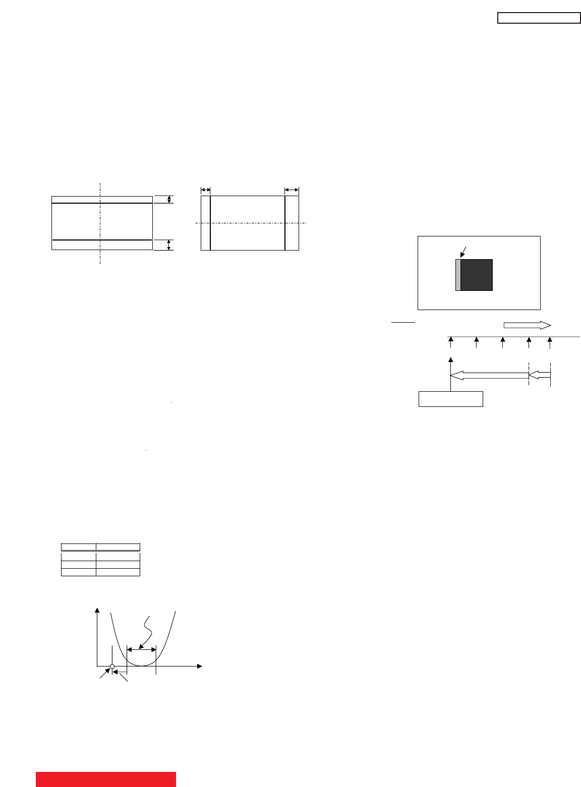
2-3 RASTER POSITION ADJUSTMENT
(1) Receive Circle pattern signal.
(2) Recall Adjustment menu.
(3) Select ‘V POSITION’ by using the cursor stick (▲/▼ direction)
on handset. Adjust the horizontal picture position where |E-F| <= 3mm
by using the cursor stick ( direction).
(4) Select ‘H POSITION’ by using the cursor stick (▲/▼ direction)
on handset. Adjust the horizontal picture position where |G-H| <= 3mm
by using the cursor stick ( direction).
E
F
G H
Final ASSEMBLY ADJUSTMENT
◄/►
◄/►
NOTE : Refer to page 48 for display area spec.
2-4 FLICKER ADJUSTMENT
ADJUSTMENT PROCEDURE
(1) SIGNAL: Internal signal from IC (50% raster signal with one dot
(2) Red FLICKER ADJUSTMENT:
black lines)
LCD ADJUST MODE → V.COM .
LCD ADJUST MODE
VCOM R xx
VCOM G xx
VCOM B xx
Press SELECT key, test pattern will be displayed.
Reduce the flicker by pressing cursor stick ◄► of handset.
The adjustment point is the weakest FLICKER position and required
additional offset. (*1)
(3) GREEN FLICKER ADJUSTMENT:
same procedure as red flicker.
Press SELECT key to return
to the “LCD ADJUST MODE”. Select VCOM G and adjust by
(4) BLUE FLICKER ADJUSTMENT:
to the “LCD ADJUST MODE”. Select VCOM B and adjust by
Press SELECT key to return
same procedure as red flicker
(*1)Additional offset is required for VCOM adjustment. The offset value
Offset steps are shown below.
is depends on each color.
Additional OFFSET table:
Color OFFSET
RED -5
GREEN -7
BLUE -8
Graphic representation of adjustment:
A
DJ.value
FLICKER LEVEL
A
djustment point OFFSET value
Adjustment range
2-5 GHOST ADJUSTMENT
ADJUSTMENT PROCEDURE
(1) ADJ.SIGNAL Internal signal from IC (Black window pattern
with RGB raster signal)
ADJUSTMENT
(2) RED GHOST LCD ADJUST MODE → GHOST
LCD ADJUST MODE
GHOST R xx
GHOST G xx
GHOST B xx
Press SELECT key, test pattern will be displayed.
(3) Increase the I2C data by pressing cursor stick ► of handset
until ghost appears at left side of the window pattern.
(4) Then, decrease the I2C data by pressing cursor stick ◄ of
handset until ghost disappears.
(5) Finally, decrease the I2C data by 3 steps.
Example
(6) GREEN GHOST Press SELECT key to return to the “LCD ADJUST MODE”.
ADJUSTMENT Select GHOST G and adjust same procedure as red GHOST.
(7) BLUE GHOST Press SELECT key to return to the “LCD ADJUST MODE”.
ADJUSTMENT Select GHOST B and adjust same procedure as red GHOST
GHOST
ADJUSTMENT POINT
(1)
Ghost
disappears
(3) (2)
GHOST data
Ghost
appears
10 11 12 13 14
-3 step -2 step -1 step
2-6 NRSH ADJUSTMENT
ADJUSTMENT PROCEDURE
(1) Complete FLICKER ADJUSTMENT before the adjustment.
(2) SIGNAL Internal signal from IC (Gray scale)
(3) Red NRSH ADJUSTMENT LCD ADJUST MODE→ NRSH
LCD ADJUST MODE
NRSH HR xx
NRSH HG xx
Press SELECT key, test pattern will be displayed.
Reduce the vertical lines (12 dot width) by pressing the cursor
stick◄► of handset.
Press SELECT key to return to the “LCD ADJUST MODE”.
re-adjust flicker.
(4) GREEN NRSH ADJUSTMENT Press “▼” of handset. The test pattern
will be changed from red to green.
Adjust the Green NRSH with same procedure as Red NRSH.
The Blue NRSH adjustment is not required.
(5) CHECK FLICKER Check that picture is not flickering. If there is,
BACK TO ADJUSTMENTS
34
LC57
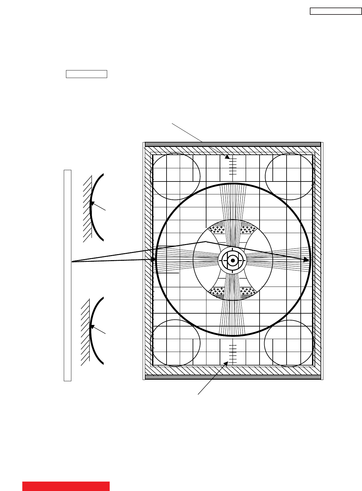
2-7 DISPLAY AREA SPECIFICATIONS
Final ASSEMBLY ADJUSTMENT
H size marker
42”: 0.5~-1.0 (-14mm)
50”: 0.5~-1.0 (-16mm)
60”: 0.5~-1.0 (-20mm)
H size marker
42”: 0.5~-1.0 (-14mm)
50”: 0.5~-1.0 (-16mm)
60”: 0.5~-1.0 (-20mm)
42”: 7mm
50”: 8mm
60”: 10mm
70”: 12mm
Normal mode
Outer edge of the circle Inner edge of the circle
5 3 3 5
Top and bottom of the circle is between oute
r
edge and inne
r
edge.
BACK TO ADJUSTMENTS
35
LC57
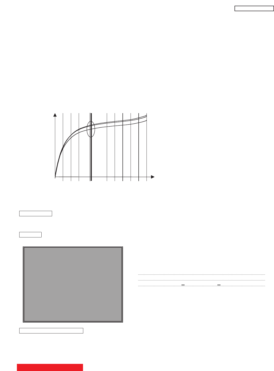
2-8 GAMMA Correction (White Balance)
GAMMA data (white balance) should not be adjusted. This data are adjusted by the factory
and MEMORY INITialize cannot erase these data. If and only if the customer request to
change the GAMMA correction, follow the instruction below.
(1) Heat run for 10 minutes or more after power on.
(2) The white signal is generated from the internal IC.
(3) Change only the step that are requested to change.
For customer request, it is possible to adjust RGB signal amplitude (means adjust the
gamma correction curve) each signal level (No.1_No.32).
If customer require to change the white balance of LCD PTV, we should re-adjust gamma
correction curve.
No.0_ 1 2 3 12 27 28 29 30 31 32
1. ADJUSTMENT PROCEDURE for SERVICE
Input signal level(luminance level) is divided into 32(No.0_No.32).
FOR EXAMPLE,
If customer require to change the white balance of 12th level of white to reddish, increase
the red value and adjust the white balance of 12th signal level (see below).
I 2C MENU
LCDADJ>GAMMA>No.12
(Adjustment)
S TORE THE DATA TO TV SET
LCD ADJ>G/C WRITE_press for several second
After this procedure, this new data will be write back to E2PROM. It takes about 20
seconds (picture will be black out).
INPUT SIGNAL LEVEL (A/32step)
For GAMMA CORRECTION
RED GAMMA CORRECTION CURVE
GREEN GAMMA CORRECTION CURVE
BLUE GAMMA CORRECTION CURVE
LCD ADJUST
GAM No.12
R 126->increase this data
G 138
B 105
Final ASSEMBLY ADJUSTMENT
Remark: The gamma data for higher intensity should
always be bigger than that of lower intensity. If
not, noise may appear on the screen.
example:
GAM No11 GAM No12 GAM No13
R 120 > 119 < 127 NG
R 120 < 128 > 127 NG
R 120 < 125 < 127 OK
GAM No12 Red Adjustable Range 120~127
BACK TO ADJUSTMENTS
36
LC57
III. ASSEMBLED P.W.B. ADJUSTMENT
2-9 Color Uniformity (White Uniformity)
COLOR UNIFORMITY data should not be adjusted. This data are adjusted by the factory
and MEMORY INITialize cannot erase these data. If and only if the customer request to
change the color uniformity, follow the instruction below.
(1) Heat run for 10 minutes or more after power on.
The four white signals generated from the internal IC
(3) Change only the step that are requested to change.
The screen is divided in 25 spaces. It can adjust for 4 different luminance levels. These
data is linearly interpolated on screen.
1. COLOR UNIFORMITY ADJUSTMENT PROCEDURE
Adjustable luminance level is divided in 4 (MIN (8%), MIDL (20%), MIDH (55%), and HMAX
(82%)).
FOR EXAMPLE
If a customer complains about the color uniformity at position 5 on the screen (luminance
level; MIDH), increase the BLUE (or GREEN or RED) value and adjust the color uniformity
of position 5.
I 2C MENU
LCD ADJ > C.UNIF (MIDH) > POINT No.5
S TORE THE DATA TO TV SET
LCD ADJ > G/C WRITE - press for 2- 3 second
After this procedure, this new data will be written back to E2PROM. It takes about 20
seconds.
12345
678910
11 12 13 14 15
17 18 19 20
21 22 23 24 25
16
LCD ADJUST
POINT No.5
R 00 ->increase this data
G 00 ->increase this data
B F7 ->increase this data
05 04 03 02 01 00 FF FE FD FC FB FA F9 F8
increase decrease
center
Final ASSEMBLY ADJUSTMENT
BACK TO ADJUSTMENTS
37
LC57
2.10 DRIVE ADJUSTMENT CHECK
2.10.1 DOT STRIPE(vertical lines 12 dot width) CHECKING and ADJUSTMENT
ADJUSTMENT ITEMS ADJUSTMENT PROCEDURE
0 PREPARATION Complete White uniformity adjustment before the adjustment.
1 SIGNAL Internal signal from IC(Dot pattern with gray scale)
2 RED Stripe
adjustment
LCD ADJUST MODE →STRIPE
LCD ADJUST MODE
STRIPE R0 xx
STRIPE R1 xx
STRIPE R2 xx
STRIPE R3 xx
STRIPE R4 xx
Press SELECT key, test pattern will be displayed.
Check that no vertical line with pitch of 12 dots on screen.
If there is, adjust the data by pressing left or right cursor stick ◄►of
handset.
5 signal levels are required to check and adjust the vertical stripes.
Signal levels are changed pressing ▼cursor of handset.
Press SELECT key of handset return to the LCD ADJUST MODE.
3 GREEN Stripe
adjustment
Press “▼” key to select Green.
Check and adjust Green stripe with same procedure as Red Stripe.
4 BLUE Stripe
adjustment
Press “▼” key to select Blue.
Check and adjust Blue stripe with same procedure as Red Stripe.
2.10.2 SUB GHOST CHECKING and ADJUSTMENT
ADJUSTMENT
ITEMS
ADJUSTMENT PROCEDURE
0 PREPARATION Complete White uniformity adjustment before the adjustment.
1 SIGNAL Internal signal from IC(50% white window pattern )
2 Sub Ghost R
adjustment
LCD ADJUST MODE →S GHOST
LCD ADJUST MODE
S GHOST R xxx
S GHOST G xxx
S GHOST B xxx
Press SELECT key, test pattern will be displayed
Check that no ghost on right hand side of the window.
If there is, decrease Ghost by pressing cursor stick ◄► of handset
Press SELECT key of handset return to the LCD ADJUST MODE.
3 Sub Ghost G
adjustment
Press “▼” key to select green. Check and adjust sub ghost green with
same procedure as Red SUB GHOST.
4 Sub Ghost B
adjustment
Press “▼” key to select blue. Check and adjust sub ghost blue with
same procedure as Red SUB GHOST.
SUB GHOST
12dots
2.10.3 HORIZONTAL CROSS TALK CHECKING and ADJUSTMENT
ADJUSTMENT ITEMS ADJUSTMENT PROCEDURE
0 PREPARATION
Complete White uniformity adjustment before the adjustment.
1 SIGNAL
Internal signal from IC (50% white window pattern)
2 STREAK LEVEL R
STREAK SLOPE R
LCD ADJUST MODE → STREAK
LCD ADJUST MODE
R LEVEL xx
R SLOPE xx
G LEVEL xx
G SLOPE xx
B LEVEL xx
B SLOPE xx
Press SELECT key, test pattern will be displayed
Check that no horizontal cross talk on right side of the window.
If there is, adjust the ”R-LEVEL” by pressing cursor stick ◄► of
handset.
If cross talk does not disappear with “R-LEVEL”, press ▼ key and
adjust “R-SLOPE” until cross talk is disappeared.
Press SELECT key of handset return to the LCD ADJUST MODE.
3 STREAK LEVEL G
STREAK SLOPE G
Press “▼” key to select Green. Check and adjust Green Streak
with same procedure as Red cross talk.
4 STREAK LEVEL B
STREAK SLOPE B
Press “▼” key to select Blue. Check and adjust Blue Streak with
same procedure as Red cross talk.
Horizontal Crosstalk
BACK TO ADJUSTMENTS
38
LC57

Final ASSEMBLY ADJUSTMENT
2-11 LAMP DOOR PROTECTION OPERATION CHECK
Adjustment procedure
(1) Remove Lamp cover and turn the set on.
(2) Check that the lamp dose not light and “Lamp indicator” flash red.
(3) Turn the set off and attach Lamp cover again
2-12 LAMP HOLDER PROTECTION OPERATION CHECK
Adjustment procedure
(1) Remove Lamp holder and turn the set on. (attach Lamp cover)
(2) Check that the lamp dose not light and “Lamp indicator” flash red.
(3) Turn the set off and attach Lamp holder again
2-13 HIGH TEMPERATURE PROTECTION OPERATION CHECK
Adjustment procedure
(1) Remove EPF2 connector while the set is on.
(2) Check that the lamp is turned off and “Temp indicator” flash red.
(3) Turn the set off and attach EPF2 again.
(4) Remove EPF3 connector while the set is on.
(5) Check that the lamp is turned off and “Temp indicator” flash red.
(6) Turn the set off and attach EPF3 again.
(7) Turn the set on and remove the connector of temperature sensor terminals on optical
engine.
(8) Check that the lamp is turned off and “Temp indicator” lights in red.
BACK TO ADJUSTMENTS
39
LC57
2-14 TEMP SENSOR DATA SETTING
2-14.1 Background and Outline
TEMP Sensor is placed in the OPT unit, and is monitoring inner temperature
.
Sensor: IL01(EMC1001 ) on LC5X SENSOR P.W.B connected to
SIGNAL PWB by PTM* connector through SENSOR CONN P.W.B.
Main micro in Digital Core checks that temperature, and indicates LED alarm if the
temperature exceeds the limit.
i ) High Temperature: Alarm message is displayed for 5 minutes and
Power will be shut down with cool-down sequence.
(Only the power button is acceptable. Any menu
and
message OSD cannot be displayed.)
ii ) IL01 failed or not connected: TEMP LED and LAMP LED are blinking
alternately. (Cycle; 1sec)
2-14.2 Purpose
It's important to set the limiting data correctly. And it's better to use the automatic adjustment
then human mistake is prevented.
Because, each model needs the unique data that is different from another models.
2-14.3 Adjustment Spec.
Adjustment procedure
1) Open ADJ menu and select Seine.
2) Input the data 72. Press SELECT and initial data will be displayed.
3) Change the data to required adjustment data as shown in following table,
(This is for
starting of Alarm.)
4) Press SELECT to write.
BACK TO ADJUSTMENTS
40
LC57
Input Data
DATA
(
hex
)
MODEL
No.72
(
Default data
)
(
4B
)
50V720
Not fixed
2-15 Checking of temperature sensor
Adjustment procedure
1) Open ADJ menu and select Seine.
2) Input the data 71. Press SELECT.
Checking
Check that the data is normal. (Hexadecimal number °C)
(If the data 72 were changed to be equal to data 71, alarm
message OSD will be displayed in a minute.)
Simplified method
Check that front LEDs are not blinking alternately after power ON.
(Device
error blinking)
2-15.1 Timing of the sensor operation (as Appendix)
3 minutes (Device Error cannot be checked)
1 minute (Average the data)
Start displaying OSD
Powe
r
Device Error is
checked once
Starting of monitoring
Starting of displaying data 71
Starting of checking the device error
BACK TO ADJUSTMENTS
41
LC57
2-16. Adjustment I2C Parameter List
1st Page (1/2)
*: Stored in EEPROM for Drive Micro
Initial Data(HEX)
Adjustment
Mode OSD Adjustment Item Adjustment
Range(HEX) LC58E LC58 LC57
Drive Up
AMP ADJUST To Auto Adjustment Menu – – – – –
Drive Up (E7070)
H_POSITION [ISF Mode]
Horizontal Position Adjustment
000~3FF 1A1* ← ← ←
V_POSITION [ISF Mode]
Vertical Position Adjustment
000~1FF 00F* ← ← ←
ENBW ENBW (E7070 C0Ch)
00~3F 00B* ← ← ←
GHOST_R GHOST R (E7070 C09H)
00~7F 0F* ← ← ←
GHOST_G GHOST G (E7070 C0AH)
00~7F 0F* ← ← ←
GHOST_B LCD Adjust-GHOST B (E7070 C0BH)
00~7F 0F* ← ← ←
Drive Up (E6110)
VCOM_R LCD Adjust-V-COM_R (E6110-R/8h)
00~FF 8F* ← ← ←
VCOM _G LCD Adjust-V-COM_G (E6110-G/ 8h)
00~FF 8F* ← ← ←
VCOM _B LCD Adjust-V-COM_B (E6110-B/ 8h)
00~FF 8F* ← ← ←
Drive Up (E7070)
NRSH_HR LCD DRIVE-NRSH HR
000~3FF 1D0* ← ← ←
NRSH_HG LCD DRIVE-NRSH HG/HB
000~3FF 1D0* ← ← ←
STRIPE_R0 LCD Adjust-STRIPE0( R) (E7070 C46h)
00~FF 008* ← ← ←
STRIPE_R1 LCD Adjust-STRIPE1( R) (E7070 C47h)
00~FF 002* ← ← ←
STRIPE_R2 LCD Adjust-STRIPE2( R) (E7070 C48h)
00~FF 000* ← ← ←
STRIPE_R3 LCD Adjust-STRIPE3( R) (E7070 C49h)
00~FF 0FB* ← ← ←
STRIPE_R4 LCD Adjust-STRIPE4( R) (E7070 C4Ah)
00~FF 0FA* ← ← ←
1st Page (2/2)
*: Stored in EEPROM for Drive Micro
Initial Data(HEX)
Adjustment
Mode OSD Adjustment Item Adjustment
Range(HEX) LC58E LC58 LC57
Drive Up (E7070)
STRIPE_G0 LCD Adjust-STRIPE0( G) (E7070 C4Bh)
00~FF 008* ← ← ←
STRIPE_G1 LCD Adjust-STRIPE1( G) (E7070 C4Ch)
00~FF 002* ← ← ←
STRIPE_G2 LCD Adjust-STRIPE2( G) (E7070 C4Dh)
00~FF 000* ← ← ←
STRIPE_G3 LCD Adjust-STRIPE3( G) (E7070 C4Eh)
00~FF 0FB* ← ← ←
STRIPE_G4 LCD Adjust-STRIPE4( G) (E7070 C4Fh)
00~FF 0FA* ← ← ←
STRIPE_B0 LCD Adjust-STRIPE0( B) (E7070 C50h)
00~FF 008* ← ← ←
STRIPE_B1 LCD Adjust-STRIPE1( B) (E7070 C51h)
00~FF 002* ← ← ←
STRIPE_B2 LCD Adjust-STRIPE2( B) (E7070 C52h)
00~FF 000* ← ← ←
STRIPE_B3 LCD Adjust-STRIPE3( B) (E7070 C53h)
00~FF 0FB* ← ← ←
STRIPE_B4 LCD Adjust-STRIPE4( B) (E7070 C54h)
00~FF 0FA* ← ← ←
S_GHOST_R LCD Adjust-SUB GHOST R (E7070 C58h)
00~7FF 000* ← ← ←
S_ GHOST_G LCD Adjust-SUB GHOST G (E7070 C59h)
00~7FF 000* ← ← ←
S_ GHOST_B LCD Adjust-SUB GHOST B (E7070 C5Ah)
00~7FF 000* ← ← ←
STREAK_R_LEVEL LCD Adjust-STREAK-LEVEL R (E7070 C6Dh)
00~7FF 000* ← ← ←
STREAK_R_SLOPE LCD Adjust-STREAK-SLOPE R (E7070 C67h)
300h~3FF 3FD* ← ← ←
STREAK_G_LEVEL LCD Adjust-STREAK-LEVEL G (E7070 C70h)
00~7FF 000* ← ← ←
STREAK_G_SLOPE LCD Adjust-STREAK-SLOPE G (E7070 C68h)
300h~3FF 3FD* ← ← ←
STREAK_B_LEVEL LCD Adjust-STREAK-LEVEL B (E7070 C73h)
00~7FF 000* ← ← ←
STREAK_B_SLOPE LCD Adjust-STREAK-SLOPE B (E7070 C69h)
300h~3FF 3FD* ← ← ←
LC57
BACK TO ADJUSTMENTS
42
2nd Page (1/2)
*: Stored in EEPROM for Drive Micro
Initial Data(HEX)
Adjustment
Mode OSD Adjustment Item Adjustment
Range(HEX) LC58E LC58 LC57
Drive Up (E7070)
No. 0~32 LCD Adjust-GAMMA NO.
00~20 000* ← ← ←
R LCD Adjust-GAM R
000~3FF (*1) ← ← ←
G LCD Adjust-GAM G
000~3FF (*1) ← ← ←
B LCD Adjust-GAM B
000~3FF (*1) ← ← ←
No. 1~25 LCD Adjust-C. UNIF NO.
01~19 01 ← ← ←
R LCD Adjust-R. UNIF (MIN).
00~FF (*1) ← ← ←
G LCD Adjust-G. UNIF (MIN).
00~FF (*1) ← ← ←
B LCD Adjust-B. UNIF (MIN).
00~FF (*1) ← ← ←
No. 1~25 LCD Adjust-C. UNIF NO.
01~19 01 ← ← ←
R LCD Adjust-R. UNIF (MIN).
00~FF (*1) ← ← ←
G LCD Adjust-G. UNIF (MIN).
00~FF (*1) ← ← ←
B LCD Adjust-B. UNIF (MIN).
00~FF (*1) ← ← ←
No. 1~25 LCD Adjust-C. UNIF NO.
01~19 01 ← ← ←
R LCD Adjust-R. UNIF (MIN).
00~FF (*1) ← ← ←
G LCD Adjust-G. UNIF (MIN).
00~FF (*1) ← ← ←
B LCD Adjust-B. UNIF (MIN).
00~FF (*1) ← ← ←
No. 1~25 LCD Adjust-C. UNIF NO.
01~19 01 ← ← ←
R LCD Adjust-R. UNIF (MIN).
00~FF (*1) ← ← ←
G LCD Adjust-G. UNIF (MIN).
00~FF (*1) ← ← ←
B LCD Adjust-B. UNIF (MIN).
00~FF (*1) ← ← ←
G/C_WRITE
–
2nd Page (2/2)
Initial Data(HEX)
Adjustment
Mode OSD Adjustment Item Adjustment
Range(HEX) LC58E LC58 LC57
Drive Up (E7070)
LCD DRIVE Device: To LCD Drive Adjustment Item –
Drive Up (E7070)
TEST_PATTERN LCD DRIVE-TEST PATTERN
00~7F
Seine/Sub Micro
ACCUMULATION_
TIME
ACCUMULATION_TiME *
LAMP_TIME LAMP_TIME
*
FACTORY_RESET FACTORY_RESET
–
BACK TO ADJUSTMENTS
43
LC57

3rd page (1/2)
Initial Data(HEX) Adjustment
Mode OSD
Adjustment Item Adjustment
Range(HEX) LC58E LC58 LC57
SEINE
TV_GUIDE Don’t care
TV_GUIDE Don’t care
TV_GUIDE Don’t care
UEI
IR_BLASTER
IR_BLASTER
TC90103
H_TIMING VBIDLY: Slicer H Timing Delay
(ID1/WSS/CCD/G-Gide)
00~0F 08 ← ← ←
V_PHASE VBIVAD: Slicer V Phase
(ID1/WSS/CCD/G-Gide)
00~07 04 ← ← ←
CCD_READ_OUT CCDON: CCD Slice Read Output
00~01 01 ← ← ←
CCD_SLiCE_CONT CSLICES: CCD Slice Control
00~01 00 ← ← ←
CCD_SLiCE_LEVEL CSLICEL: CCD Slice Level
00~03 00 ← ← ←
CCD_SB_DET CSTMOD: CCD SB Detect
00~01 00 ← ← ←
CCD_FIELD_SEL CCDMOD: CCD Field Select
00~03 02 ← ← ←
ID1_READ_OUT ID1ON: ID1 Slice Read Output
00~01 01 ← ← ←
ID1_SLiCE_CONT ISLICES: ID1 Slice Control
00~01 00 ← ← ←
ID1_SLiCE_LEVEL ISLICEL: ID1 Slice Level
00~03 00 ← ← ←
ID1_AMP IRWIDON: ID1 Amplitude Detect
00~01 01 ← ← ←
ID1_PHASE_SEL IEDGES: ID1 Phase Select
00~01 00 ← ← ←
ID1_PHASE_WiDTH IRTIMS: ID1 Detection Phase Width
00~01 00 ← ← ←
3rd page (2/2)
Initial Data(HEX) Adjustment
Mode OSD
Adjustment Item Adjustment
Range(HEX) LC58E LC58 LC57
TC90103
G_READ_OUT GGSON: Guide Slice Read Output
00~01 01 ← ← ←
G_DETECT GGSJDG: Guide Detection Sensitivity
00~01 01 ← ← ←
G_SLiCE_LEVEL GGSLV: Guide Slice Level
00~03 00 ← ← ←
CLOCK_RUN_iN GGPKDET: Guide Clock Run In Detect
00~01 00 ← ← ←
READ_DATA_ORDER SLDSLT: Guide Read Out order
00~01 00 ← ← ←
ADD_DATA GGSIGON: Guide Add Data Function
00~01 00 ← ← ←
LiNE_10_25 Line 10~25
00~FFFF 0000 ← ← ←
Sub Micro
VBi_SLICER_S Sub VBI (CCD/V Chip) Adjustment
SAMPLING
POLLING
START
TIMEOUT
STATUS
Seine/Sub Micro
CLOCK_TEST
AFC_TEST
MAINTENANCE
MEMORY_INITIALIZE
BACK TO ADJUSTMENTS
44
LC57
Drive Micro (1/2)
*: Stored in EEPROM for Drive Micro
Initial Data(HEX)
Adjustment
Mode OSD Adjustment Item Adjustment
Range(HEX) LC58E LC58 LC57
Drive Micro (E7070)
001 [ISF Mode]
LCD DRIVE R-SUB GAIN (High)
Color Temperature: High
000~3FF 200* ← ← ←
002 [ISF Mode]
LCD DRIVE G-SUB GAIN (High)
Color Temperature: High
000~3FF 200* ← ← ←
003 [ISF Mode]
LCD DRIVE B-SUB GAIN (High)
Color Temperature: High
000~3FF 200* ← ← ←
004 [ISF Mode]
LCD DRIVE R-SUB GAIN (Medium)
Color Temperature: Medium
000~3FF 200* ← ← ←
005 [ISF Mode]
LCD DRIVE G-SUB GAIN (Medium)
Color Temperature: Medium
000~3FF 1B9* ← ← ←
006 [ISF Mode]
LCD DRIVE B-SUB GAIN (Medium)
Color Temperature: Medium
000~3FF 18C* ← ← ←
007 [ISF Mode]
LCD DRIVE R-SUB GAIN (STD)
Color Temperature: STD
000~3FF 200* ← ← ←
008 [ISF Mode]
LCD DRIVE G-SUB GAIN (STD)
Color Temperature: STD
000~3FF 1B5* ← ← ←
009 [ISF Mode]
LCD DRIVE B-SUB GAIN (STD)
Color Temperature: STD
000~3FF 16E* ← ← ←
010 [ISF Mode]
LCD DRIVE R-SUB GAIN (B/W)
Color Temperature: B/W
000~3FF 200* ← ← ←
011 [ISF Mode]
LCD DRIVE G-SUB GAIN (B/W)
Color Temperature: B/W
000~3FF 199* ← ← ←
012 [ISF Mode]
LCD DRIVE B-SUB GAIN (B/W)
Color Temperature: B/W
000~3FF 148* ← ← ←
013 LCD DRIVE-VREF
00~FF * ← ← ←
014 LCD DRIVE-SHPR
00~0F 07* ← ← ←
015 LCD DRIVE-SHRG
00~0F 07* ← ← ←
016 LCD DRIVE-SHRB
00~0F 07* ← ← ←
Drive Micro (2/2)
Initial Data(HEX) Adjustment
Mode OSD Adjustment Item Adjustment
Range(HEX) LC58E LC58 LC57
Drive Micro (E7070)
017 LCD DRIVE-NRSH LR
000~3FF 1F0* ← ← ←
018 LCD DRIVE-NRSH LG
000~3FF 1F0* ← ← ←
019 LCD DRIVE-NRSH LB
000~3FF 1F0* ← ← ←
020 LCD DRIVE-BLOCK_R
000~7FF 000* ← ← ←
021 LCD DRIVE-BLOCK_G 000~7FF
000* ← ← ←
022 LCD DRIVE-BLOCK_B 000~7FF
000* ← ← ←
023 LCD DRIVE-RE_GHOST_R 000~7FF
001* ← ← ←
024 LCD DRIVE-RE_GHOST_G 000~7FF
001* ← ← ←
025 LCD DRIVE-RE_GHOST_B 000~7FF
001* ← ← ←
026 LCD DRIVE-GMAS_R 000~3FF
000* ← ← ←
027 LCD DRIVE- GMAS_G 000~3FF
000* ← ← ←
028 LCD DRIVE- GMAS_B 000~3FF
000* ← ← ←
029 LCD DRIVE-NRSH_LP 000~1FF
000* ← ← ←
030 LCD DRIVE- NRSH_LW 000~1FF
075* ← ← ←
031 LCD DRIVE-NRGP 00~7F
057* ← ← ←
032 LCD DRIVE- NRGW 00~FF
046* ← ← ←
033 LCD DRIVE-HPOSI Offset-R 00~0F
07* ← ← ←
034 LCD DRIVE-HPOSI Offset-B 00~0F
07* ← ← ←
035 LCD DRIVE-VPOSI Offset-R 00~0F
07* ← ← ←
036 LCD DRIVE-VPOSI Offset-B 00~0F
07* ← ← ←
Drive Micro (Ballast)
037 Lamp flicker / Lamp Hysteresis 000~FFF
864* ← ← ←
BACK TO ADJUSTMENTS
45
LC57
Seine (1/3)
Initial Data(HEX)
Adjustment
Mode OSD
Adjustment Item Adjustment
Range(HEX) LC58E LC58 LC57
SEINE
026 Picture Digital Output Select
00h: Normal, 01h: Color Bar
00~01
00 ← ← ←
027 Setup
00h: off, 01h: on
00~01
00 ← ← ←
028 Noise Reduction Switch for Y
00h: Not Round, 01h: Round
NTSC/480i Input only
00~01 01 ← ← ←
029 Y Moving Detection Band for Noise Reduction
00h: Narrowband, 01h: Wideband
NTSC/480i Input only
00~01 00 ← ← ←
030 Y Moving Horizontal Extension for Noise Reduction
00h:OFF, 01h:ON
NTSC/480i Input only
00~01 01 ← ← ←
031 Y Signal Round Coefficient for Noise Reduction
NTSC/480i Input only
00~0D 0A ← ← ←
032 Y Frame Difference Limit for Noise Reduction
NTSC/480i Input only
00~1F 03 ← ← ←
033 Color Signal Noise Reduction Switch
00h: Not Round, 01h: Round
NTSC/480i Input only
00~01 01 ← ← ←
034 Color Moving Detection Band for Noise Reduction
00h: Narrowband, 01h: Wideband
NTSC/480i Input only
00~01 00 ← ← ←
035 Color Moving Horizontal Extension foe Noise
Reduction
00h:OFF, 01h:ON
NTSC/480i Input only
00~01 01 ← ← ←
Seine (2/3)
Initial Data(HEX)
Adjustment
Mode OSD
Adjustment Item Adjustment
Range(HEX) LC58E LC58 LC57
SEINE
036 Color Signal Round Coefficient for Noise Reduction
NTSC/480i Input only
00~0D 0A ← ← ←
037 Color Signal Frame Difference Limit for Noise
Reduction
NTSC/480i Input only
00~1F 03 ← ← ←
038 Enhance Movement Mode
00h: Enhancer & 2nd V filter OFF
01h: Enhancer ON
02h: 2nd V filter ON
03h: Reserved
00~03 00 ← ← ←
039 Enhancer Movement Mode Select
00h: 1H, 01h: 2H
00~01 00 ← ← ←
040 Noise Distinction Value 00~10
00 ← ← ←
041 Noise Reduction Gain 00~07
00 ← ← ←
042 Vertical Enhancer Gain
1/16step
0x00: OFF, 0x20: 2 times
00~20 00 ← ← ←
043 Vertical Enhancer Coring Value 00~0F
00 ← ← ←
044 Vertical Enhancer Turning Position 00~FF
00 ← ← ←
045 Horizontal Enhancer Gain
1/16step
0x00: OFF, 0x20: 2 倍
00~20 00 ← ← ←
046 Horizontal Enhancer Coring Value 00~0F
00 ← ← ←
047 Horizontal Enhancer Turning Position 00~FF
00 ← ← ←
048 Horizontal Enhancer Coefficient Z6 00~FF
00 ← ← ←
049 Horizontal Enhancer Coefficient Z5 00~FF
00 ← ← ←
050 Horizontal Enhancer Coefficient Z4 00~FF
00 ← ← ←
051 Horizontal Enhancer Coefficient Z3 00~FF
00 ← ← ←
052 Horizontal Enhancer Coefficient Z2 00~FF
00 ← ← ←
053 Horizontal Enhancer Coefficient Z1 00~FF
00 ← ← ←
054 Horizontal Enhancer Coefficient Z0 00~FF
00 ← ← ←
BACK TO ADJUSTMENTS
46
LC57
Seine (3/3)
Initial Data(HEX)
Adjustment
Mode OSD
Adjustment Item Adjustment
Range(HEX) LC58E LC58 LC57
SEINE
055 ANT/NTSC 000~6B4
0F8 ← ← ←
056 480i_YPbPr 000~35A
0F4 ← ← ←
057 480i_HDMI 000~6B4
000 ← ← ←
058 480p_YPbPr 000~35A
078 ← ← ←
059 480p_HDMI 000~35A
000 ← ← ←
060 1080i_YPbPr 000~898
0E0 ← ← ←
061 1080i_HDMI 000~898
000 ← ← ←
062 720p_YPbPr 000~672
120 ← ← ←
063 720p_HDMI 000~672
000 ← ← ←
064
Odd/Even Field Horizontal Active
Picture Data Start Point
VGA_HDMI 000~35A
000 ← ← ←
065 Mode 1-2 00~FF
19 ← ← ←
066 Mode 2-3 00~FF
32 ← ← ←
067 Mode 3-4 00~FF
4B ← ← ←
068
S/N Detection Setting
(Receiving Mode Border Line Setting)
Mode 4-5 00~FF
64 ← ← ←
069 ANT/NTSC
480i
00~FF Eb ← ← ←
070
Contrast Auto Adjustment Setting Value
480p
1080i/720p
00~FF Eb ← ← ←
071 Temperature Sensor 0 Read Data 00~FF * ← ← ←
072 Alarm 0 Start Temperature Setting 00~FF 4B ← ← ←
073 Alarm 0 Stop Temperature Setting 00~FF 41 ← ← ←
074 Reserve
Temperature Sensor 1 Read Data
00~FF * ← ← ←
075 Reserve
Alarm 1 Start Temperature Setting
00~FF 4B ← ← ←
076 Reserve
Alarm 1 Stop Temperature Setting
00~FF 41 ← ← ←
FC6 (1/20)
Initial Data(HEX) Adjustment
Mode OSD
Adjustment Item Adjustment
Range(HEX) LC58E LC58 LC57
FC6
001 [ISF Mode]
Black Stretch
00h: OFF, 01h: DBS, 02h: HBS
00~02 01 ← ← ←
002 [ISF Mode]
Black Correction
00h: OFF, 01h: DBS, 02h: HBS
00~02 01 ← ← ←
003 [ISF Mode]
Histogram Gamma
00h: OFF, 01h: Active
00~01 01 ← ← ←
004 [ISF Mode]
Histogram Enhancer
00h: OFF, 01h: Active
00~01 01 ← ← ←
005 [ISF Mode]
Histogram Amp
00h: OFF, 01h: Active
00~01 01 ← ← ←
006 [ISF Mode]
Histogram Color Management
00h: OFF, 01h: Active
00~01 01 ← ← ←
007 [ISF Mode]
Dynamic Backlight/Lamp Correction
00h: OFF, 01h: Active
00~01 00 ← ← ←
008 [ISF Mode]
Dynamic Shading
00h: OFF, 01h: Active
00~01 00 ← ← ←
009 [ISF Mode]
Bgm Gain OFF
00h: Normal
01h: Compulsion OFF
00~01 00 ← ← ←
010 Detect Area Display ON
00~01 00 ← ← ←
011
Horizontal Detect Area 00~64 4B ← ← ←
012
Vertical Detect Area 00~64 4C ← ← ←
013 ANT/NTSC 000~7FF
400 ← ← ←
014 480i/480p 000~7FF
400 ← ← ←
015
Brightness Center
1080i/720p 000~7FF
400 ← ← ←
BACK TO ADJUSTMENTS
47
LC57
FC6 (2/20)
Initial Data(HEX) Adjustment
Mode OSD
Adjustment Item Adjustment
Range(HEX) LC58E LC58 LC57
FC6
016 [ISF Mode]
Contrast Center
000~FF 80 ← ← ←
017 [ISF Mode]
Red Gain Adjustment
Color Temperature: High
000h: ×0, 200h: ×1, 3FFh: ×1023/512
000~3FF 200 ← ← ←
018 [ISF Mode]
Green Gain Adjustment
Color Temperature: High
000h: ×0, 200h: ×1, 3FFh: ×1023/512
000~3FF 200 ← ← ←
019 [ISF Mode]
Blue Gain Adjustment
Color Temperature: High
000h: ×0, 200h: ×1, 3FFh: ×1023/512
000~3FF 200 ← ← ←
020 [ISF Mode]
Red Line 1 Setting
000~3FF 040 ← ← ←
021 [ISF Mode]
Red Line 2 Setting
000~3FF 080 ← ← ←
022 [ISF Mode]
Red Line 3 Setting
000~3FF 0C0 ← ← ←
023 [ISF Mode]
Red Line 4 Setting
000~3FF 100 ← ← ←
024 [ISF Mode]
Red Line 5 Setting
000~3FF 140 ← ← ←
025 [ISF Mode]
Red Line 6 Setting
000~3FF 180 ← ← ←
026 [ISF Mode]
Red Line 8 Setting
000~3FF 200 ← ← ←
027 [ISF Mode]
Red Line 10 Setting
000~3FF 280 ← ← ←
028 [ISF Mode]
Red Line 12 Setting
000~7FF 300 ← ← ←
029 [ISF Mode]
Red Line 14 Setting
000~7FF 380 ← ← ←
030 [ISF Mode]
Blue Line 1 Setting
000~3FF 040 ← ← ←
031 [ISF Mode]
Blue Line 2 Setting
000~3FF 080 ← ← ←
032 [ISF Mode]
Blue Line 3 Setting
000~3FF 0C0 ← ← ←
033 [ISF Mode]
Blue Line 4 Setting
000~3FF 100 ← ← ←
034 [ISF Mode]
Blue Line 5 Setting
000~3FF 140 ← ← ←
035 [ISF Mode]
Blue Line 6 Setting
000~3FF 180 ← ← ←
FC6 (3/20)
Initial Data(HEX) Adjustment
Mode OSD
Adjustment Item Adjustment
Range(HEX) LC58E LC58 LC57
FC6
036 [ISF Mode]
Blue Line 8 Setting
000~3FF 200 ← ← ←
037 [ISF Mode]
Blue Line 10 Setting
000~3FF 280 ← ← ←
038 [ISF Mode]
Blue Line 12 Setting
000~7FF 300 ← ← ←
039 [ISF Mode]
Blue Line 14 Setting
000~7FF 380 ← ← ←
040 [ISF Mode]
RGB Output Mode
00h: Normal,
01h: Red only, 02h: Green only, 03h: Blue only
00~03 00 ← ← ←
041 High 000~FFF
59B ← ← ←
042 Medium 000~FFF
59B ← ← ←
043 Standard 000~FFF
59B ← ← ←
044
[ISF Mode]
R-Y_Cr Decode Adjustment
000h(=x0)~400h(=x1)~FFFh(=x4)
Black/White 000~FFF
59B ← ← ←
045 High 000~FFF
000 ← ← ←
046 Medium 000~FFF
000 ← ← ←
047 Standard 000~FFF
000 ← ← ←
048
[ISF Mode]
R-Y_Cb Decode Adjustment
000h(=x0)~400h(=x1)~FFFh(=x4)
Black/White 000~FFF
000 ← ← ←
049 High 000~FFF
2CE ← ← ←
050 Medium 000~FFF
2CE ← ← ←
051 Standard 000~FFF
2CE ← ← ←
052
[ISF Mode]
G-Y_Cr Decode Adjustment
000h(=x0)~400h(=x1)~FFFh(=x4)
Black/White 000~FFF
2CE ← ← ←
053 High 000~FFF
160 ← ← ←
054 Medium 000~FFF
160 ← ← ←
055 Standard 000~FFF
160 ← ← ←
056
[ISF Mode]
G-Y_Cb Decode Adjustment
000h(=x0)~400h(=x1)~FFFh(=x4)
Black/White 000~FFF
160 ← ← ←
BACK TO ADJUSTMENTS
48
LC57
FC6 (4/20)
Initial Data(HEX) Adjustment
Mode OSD
Adjustment Item Adjustment
Range(HEX) LC58E LC58 LC57
FC6
057 High 000~FFF
716 ← ← ←
058 Medium 000~FFF
716 ← ← ←
059 Standard 000~FFF
716 ← ← ←
060
[ISF Mode]
B-Y_Cb Decode Adjustment
000h(=x0)~400h(=x1)~FFFh(=x4)
Black/White 000~FFF
716 ← ← ←
061 ANT/NTSC/480i 00~0F
07 ← ← ←
062
[ISF Mode]
Edge Filter Selection
480p/1080i/720p 00~0F
07 ← ← ←
063 ANT_Mode1 00~1F
0F ← ← ←
064 ANT-Mode2 00~1F
0F ← ← ←
065 ANT-Mode3 00~1F
0F ← ← ←
066 ANT-Mode4 00~1F
0F ← ← ←
067 ANT-Mode5 00~1F
0F ← ← ←
068 NTSC 00~1F
0F ← ← ←
069 480i 00~1F
0F ← ← ←
070 480p 00~1F
0F ← ← ←
071 1080i 00~1F
0F ← ← ←
072 720p 00~1F
0F ← ← ←
073 HDMI/DVI
480i
00~1F
0F ← ← ←
074 HDMI/DVI
480p/VGA
00~1F
0F ← ← ←
075 HDMI/DVI
720p
00~1F
0F ← ← ←
076 HDMI/DVI
1080i
00~1F
0F ← ← ←
077 Reserve 00~1F
0F ← ← ←
078
[ISF Mode]
Y Vertical & Horizontal Enhancer Gain
Adjustment
Reserve 00~1F
0F ← ← ←
079 [ISF Mode]
Y Vertical Enhancer OFF
00~01 00 ← ← ←
FC6 (5/20)
Initial Data(HEX) Adjustment
Mode OSD
Adjustment Item Adjustment
Range(HEX) LC58E LC58 LC57
FC6
080 ANT/NTSC
(DAY)
00~1F 0A ← ← ←
081 480i(DAY) 00~1F
0A ← ← ←
082 480p(DAY) 00~1F
0A ← ← ←
083 1080i/720p
(DAY)
00~1F 0A ← ← ←
084
[ISF Mode]
Y Vertical Enhancer Gain
Adjustment
ALL(NIGHT) 00~1F
0A ← ← ←
085 ANT 00~03
00 ← ← ←
086 NTSC 00~03
00 ← ← ←
087 480i 00~03
00 ← ← ←
088 480p 00~03
00 ← ← ←
089
[ISF Mode]
Y Vertical Dynamic Shoot Balance
Gain Adjustment
1080i/720p 00~03
00 ← ← ←
090 ANT/NTSC 00~1F
1F ← ← ←
091 480i 00~1F
1F ← ← ←
092
[ISF Mode]
Y Vertical Dynamic Shoot Balance
Coring Adjustment
480p/1080i/720p 00~1F
1F ← ← ←
093 ANT/NTSC/480i 00~01
00 ← ← ←
094 480p 00~01
00 ← ← ←
095
[ISF Mode]
Y Vertical Enhancer Clip OFF
1080i/720p 00~01
00 ← ← ←
096 ANT 00~3F
3F ← ← ←
097 NTSC 00~3F
3F ← ← ←
098 480i 00~3F
3F ← ← ←
099 480p 00~3F
3F ← ← ←
100 1080i/720p 00~3F
3F ← ← ←
101 ANT/NTSC/480i
(NIGHT)
00~3F 3F ← ← ←
102 480p
(NIGHT)
00~3F
3F ← ← ←
103
[ISF Mode]
Y Vertical Clip Offset Level
1080i/720p
(NIGHT)
00~3F 3F ← ← ←
BACK TO ADJUSTMENTS
49
LC57
FC6 (6/20)
Initial Data(HEX) Adjustment
Mode OSD
Adjustment Item Adjustment
Range(HEX) LC58E LC58 LC57
FC6
104 ANT/NTSC/480i 00~FF
00 ← ← ←
105
[ISF Mode]
Y Vertical Non Linear Peaking
480p/1080i/720p 00~FF
00 ← ← ←
106 [ISF Mode]
Y Horizontal Enhancer OFF
00~01
00 ← ← ←
107 ANT 00~1F
05 ← ← ←
108 NTSC 00~1F
05 ← ← ←
109 480i 00~1F
05 ← ← ←
110 480p 00~1F
05 ← ← ←
111
[ISF Mode]
Y Horizontal Enhancer Gain
Adjustment
1080i/720p 00~1F
05 ← ← ←
112 ANT 00~03
00 ← ← ←
113 NTSC 00~03
00 ← ← ←
114 480i 00~03
00 ← ← ←
115 480p 00~03
00 ← ← ←
116
[ISF Mode]
Y Horizontal Dynamic Shoot
Balance Gain Adjustment
1080i/720p 00~03
00 ← ← ←
117 ANT/NTSC 00~1F
1F ← ← ←
118 480i 00~1F
1F ← ← ←
119
[ISF Mode]
Y Horizontal Dynamic Shoot
Balance Coring Adjustment
480p/1080i/720p 00~1F
1F ← ← ←
120 ANT/NTSC/480i 00~01
00 ← ← ←
121 480p 00~01
00 ← ← ←
122
[ISF Mode]
Y Horizontal Enhancer Clip OFF
1080i/720p 00~01
00 ← ← ←
123 ANT 00~1F
3F ← ← ←
124 NTSC 00~1F
3F ← ← ←
125 480i 00~1F
3F ← ← ←
126 480p 00~1F
3F ← ← ←
127
[ISF Mode]
Y Horizontal Clip Offset Level
1080i/720p 00~1F
3F ← ← ←
FC6 (7/20)
Initial Data(HEX) Adjustment
Mode OSD
Adjustment Item Adjustment
Range(HEX) LC58E LC58 LC57
FC6
128 ANT/NTSC/480i 00~FF
00 ← ← ←
129
[ISF Mode]
Y Horizontal Non Linear Peaking
480p/1080i/720p 00~FF
00 ← ← ←
130 ANT_Mode1 00~1F
00 ← ← ←
131 ANT-Mode2 00~1F
00 ← ← ←
132 ANT-Mode3 00~1F
00 ← ← ←
133 ANT-Mode4 00~1F
00 ← ← ←
134 ANT-Mode5 00~1F
00 ← ← ←
135 NTSC
(Composite)
00~1F
00 ← ← ←
136 NTSC(Y/C) 00~1F
00 ← ← ←
137 480i 00~1F
00 ← ← ←
138 480p 00~1F
00 ← ← ←
139 1080i 00~1F
00 ← ← ←
140 720p 00~1F
00 ← ← ←
141 HDMI/DVI_480i 00~1F
00 ← ← ←
142 HDMI/DVI
480p/VGA
00~1F
00 ← ← ←
143 HDMI/DVI
720p
00~1F 00 ← ← ←
144 HDMI/DVI
1080i
00~1F 00 ← ← ←
145
[ISF Mode]
Y Coring Amplitude Adjustment
Reserve 00~1F
00 ← ← ←
146 ANT/NTSC 00~10
02 ← ← ←
147 480i 00~10
02 ← ← ←
148 480p 00~10
02 ← ← ←
149
Y Horizontal HPF Center Select
1080i/720p 00~10
09 ← ← ←
BACK TO ADJUSTMENTS
50
LC57
FC6 (8/20)
Initial Data(HEX) Adjustment
Mode OSD
Adjustment Item Adjustment
Range(HEX) LC58E LC58 LC57
FC6
150 Dither Select
00h: OFF, 01h: 10bit, 02h: 8bit, 03h: 6bit
00~03
00 ← ← ←
151 Histogram Gamma Color Correction γ0 00~FF
20 ← ← ←
152 Histogram Gamma Color Correction γ1 00~FF
E0 ← ← ←
153 Histogram Gamma Color Correction γ2 00~80
10 ← ← ←
154 Histogram/APL Data Average Count
00~0F
0A ← ← ←
155 Histogram Gamma Value
00h: Dynamic Gamma OFF
00~80
01 ← ← ←
156 Histogram Gamma APL Point 0
00~FF
00 ← ← ←
157 Histogram Gamma APL Point 1
00~FF
37 ← ← ←
158 Histogram Gamma APL Point 2
00~FF
50 ← ← ←
159 Histogram Gamma APL Point 3
00~FF
78 ← ← ←
160 Histogram Gamma APL Point 4
00~FF
96 ← ← ←
161 Histogram Gamma APL Point 5
00~FF C8 ← ← ←
162 Histogram Gamma APL Point 0 Gamma Select
00~02 00 ← ← ←
163 Histogram Gamma APL Point 1 Gamma Select
00~02 00 ← ← ←
164 Histogram Gamma APL Point 2 Gamma Select
00~02 01 ← ← ←
165 Histogram Gamma APL Point 3 Gamma Select
00~02 02 ← ← ←
166 Histogram Gamma APL Point 4 Gamma Select
00~02 02 ← ← ←
167 Histogram Gamma APL Point 5 Gamma Select
00~02 02 ← ← ←
168 Histogram Gamma Histogram High Start
00~FF 05 ← ← ←
169 Histogram Gamma Histogram High End
00~FF 14 ← ← ←
170 Histogram Gamma APL Point 0 Gamma Select High
00~02 01 ← ← ←
FC6 (9/20)
Initial Data(HEX) Adjustment
Mode OSD
Adjustment Item Adjustment
Range(HEX) LC58E LC58 LC57
FC6
171 Histogram Gamma APL Point 1 Gamma Select High
00~02 00 ← ← ←
172 Histogram Gamma APL Point 2 Gamma Select High
00~02 01 ← ← ←
173 Histogram Gamma APL Point 3 Gamma Select High
00~02 02 ← ← ←
174 Histogram Gamma APL Point 4 Gamma Select High
00~02 02 ← ← ←
175 Histogram Gamma APL Point 5 Gamma Select High
00~02 02 ← ← ←
176 Histogram Gamma Histogram Super High Start
00~FF 64 ← ← ←
177 Histogram Gamma Histogram Super High End
00~FF 80 ← ← ←
178 Histogram Gamma APL Point 0 Gamma Select
S_High
00~03 01 ← ← ←
179 Histogram Gamma APL Point 1 Gamma Select
S_High
00~03 00 ← ← ←
180 Histogram Gamma APL Point 2 Gamma Select
S_High
00~03 01 ← ← ←
181 Histogram Gamma APL Point 3 Gamma Select
S_High
00~03 02 ← ← ←
182 Histogram Gamma APL Point 4 Gamma Select
S_High
00~03 03 ← ← ←
183 Histogram Gamma APL Point 5 Gamma Select
S_High
00~03 03 ← ← ←
184 for Dark Picture 000~3FF
FF ← ← ←
185 for Standard 000~3FF
FF ← ← ←
186 for Bright Picture 000~3FF
FF ← ← ←
187
Gamma Line 16 Setting
for Very Bright Picture 000~3FF
FF ← ← ←
188 for Dark Picture 000~3FF
F3 ← ← ←
189 for Standard 000~3FF
F5 ← ← ←
190 for Bright Picture 000~3FF
F5 ← ← ←
191
Gamma Line 15 Setting
for Very Bright Picture 000~3FF
F0 ← ← ←
BACK TO ADJUSTMENTS
51
LC57
FC6 (10/20)
Initial Data(HEX) Adjustment
Mode OSD
Adjustment Item Adjustment
Range(HEX) LC58E LC58 LC57
FC6
192 for Dark Picture 000~3FF
E6 ← ← ←
193 for Standard 000~3FF
EB ← ← ←
194 for Bright Picture 000~3FF
EB ← ← ←
195
Gamma Line 14 Setting
for Very Bright Picture 000~3FF
D4 ← ← ←
196 for Dark Picture
000~3FF D9 ← ← ←
197 for Standard
000~3FF DB ← ← ←
198 for Bright Picture
000~3FF DB ← ← ←
199
Gamma Line 13 Setting
for Very Bright Picture
000~3FF BB ← ← ←
200 for Dark Picture
000~3FF CB ← ← ←
201 for Standard
000~3FF C8 ← ← ←
202 for Bright Picture
000~3FF CA ← ← ←
203
Gamma Line 12 Setting
for Very Bright Picture
000~3FF AA ← ← ←
204 for Dark Picture
000~3FF BD ← ← ←
205 for Standard
000~3FF B9 ← ← ←
206 for Bright Picture
000~3FF B4 ← ← ←
207
Gamma Line 11 Setting
for Very Bright Picture
000~3FF 9B ← ← ←
208 for Dark Picture
000~3FF AF ← ← ←
209 for Standard
000~3FF A8 ← ← ←
210 for Bright Picture
000~3FF 9E ← ← ←
211
Gamma Line 10 Setting
for Very Bright Picture
000~3FF 8C ← ← ←
212 for Dark Picture
000~3FF 9F ← ← ←
213 for Standard
000~3FF 98 ← ← ←
214 for Bright Picture
000~3FF 8A ← ← ←
215
Gamma Line 9 Setting
for Very Bright Picture
000~3FF 7C ← ← ←
FC6 (11/20)
Initial Data(HEX) Adjustment
Mode OSD
Adjustment Item Adjustment
Range(HEX) LC58E LC58 LC57
FC6
216 for Dark Picture
000~3FF 8E ← ← ←
217 for Standard
000~3FF 86 ← ← ←
218 for Bright Picture
000~3FF 76 ← ← ←
219
Gamma Line 8 Setting
for Very Bright Picture
000~3FF 6C ← ← ←
220 for Dark Picture
000~3FF 7E ← ← ←
221 for Standard
000~3FF 76 ← ← ←
222 for Bright Picture
000~3FF 62 ← ← ←
223
Gamma Line 7 Setting
for Very Bright Picture
000~3FF 5E ← ← ←
224 for Dark Picture
000~3FF 6E ← ← ←
225 for Standard
000~3FF 65 ← ← ←
226 for Bright Picture
000~3FF 4E ← ← ←
227
Gamma Line 6 Setting
for Very Bright Picture
000~3FF 4E ← ← ←
228 for Dark Picture
000~3FF 5D ← ← ←
229 for Standard
000~3FF 54 ← ← ←
230 for Bright Picture
000~3FF 3F ← ← ←
231
Gamma Line 5 Setting
for Very Bright Picture
000~3FF 3F ← ← ←
232 for Dark Picture
000~3FF 4B ← ← ←
233 for Standard
000~3FF 43 ← ← ←
234 for Bright Picture
000~3FF 30 ← ← ←
235
Gamma Line 4 Setting
for Very Bright Picture
000~3FF 30 ← ← ←
236 for Dark Picture
000~3FF 39 ← ← ←
237 for Standard
000~3FF 33 ← ← ←
238 for Bright Picture
000~3FF 24 ← ← ←
239
Gamma Line 3 Setting
for Very Bright Picture
000~3FF 24 ← ← ←
BACK TO ADJUSTMENTS
52
LC57
FC6 (12/20)
Initial Data(HEX) Adjustment
Mode OSD
Adjustment Item Adjustment
Range(HEX) LC58E LC58 LC57
FC6
240 for Dark Picture
000~3FF 26 ← ← ←
241 for Standard
000~3FF 22 ← ← ←
242 for Bright Picture
000~3FF 17 ← ← ←
243
Gamma Line 2 Setting
for Very Bright Picture
000~3FF 17 ← ← ←
244 for Dark Picture
000~3FF 10 ← ← ←
245 for Standard
000~3FF 10 ← ← ←
246 for Bright Picture
000~3FF 0C ← ← ←
247
Gamma Line 1 Setting
for Very Bright Picture
000~3FF 0C ← ← ←
248 for Dark Picture
000~3FF 00 ← ← ←
249 for Standard
000~3FF 00 ← ← ←
250 for Bright Picture
000~3FF 00 ← ← ←
251
Gamma Line 0 Setting
for Very Bright Picture
000~3FF 00 ← ← ←
252 Gradation Amp Weight Ratio
00~7F 50 ← ← ←
253 Gradation Amp Weight Ratio 1
00~7F 0F ← ← ←
254 Gradation Amp Weight Ratio 2
00~7F 05 ← ← ←
255 Gradation Amp Max Histogram Ratio
00~FF 1E ← ← ←
256 Gradation Amp Min Histogram Ratio
00~FF 0A ← ← ←
257 Gradation Amp Up Gain
00~1F 14 ← ← ←
258 Gradation Amp Down Gain
00~1F 02 ← ← ←
259 Gradation Amp Max APL
00~FF 3C ← ← ←
260 Gradation Amp Min APL
00~FF 28 ← ← ←
261 RGB Gamma Line 14 Setting Offset 00~FF
00h ← ← ←
262 RGB Gamma Line 16 Setting Offset 00~FF
00h ← ← ←
FC6 (13/20)
Initial Data(HEX) Adjustment
Mode OSD
Adjustment Item Adjustment
Range(HEX) LC58E LC58 LC57
FC6
263 Black Stretch & Black Correction Speed
00h: Fast, 10h: Slow
00~10 00 ← ← ←
264 Black Stretch & Black Correction Reset ∆APL
00~FF 0A ← ← ←
265 Black Stretch & Black Correction Reset APL
00~FF 32 ← ← ←
266 Black Stretch & Black Correction Speed Up ∆APL
00~FF 0E ← ← ←
267 Black Stretch & Black Correction Speed Up Step
00h: Direct, 01h: Slow~FFh: Fast
00~FF 00 ← ← ←
268 Black Stretch Gain Up Step 0
00h: Direct, 01h: Slow~FFh: Fastx8
00~FF 03 ← ← ←
269 Black Stretch Gain Up Step 1
00h: Direct, 01h: Slow~FFh: Fastx8
00~FF 04 ← ← ←
270 Black Stretch Gain Down Step 0
00h: Direct, 01h: Slow~FFh: Fastx64
00~FF 03 ← ← ←
271 Black Stretch Gain Down Step 1
00h: Direct, 01h: Slow~FFh: Fastx64
00~FF 80 ← ← ←
272 Black Stretch Gain Step SW0
00~FF 32 ← ← ←
273 Black Stretch Gain Step SW1
00~FF 3C ← ← ←
274 Black Stretch Start Level
00~FF 72 ← ← ←
275 Histogram Value
00~05 03 ← ← ←
276 Black Stretch Change Point 0 Black Area
00~FF CA ← ← ←
277 Black Stretch Change Point 1 Black Area
00~FF 6E ← ← ←
278 Black Stretch Change Point 2 Black Area
00~FF 78 ← ← ←
279 Black Stretch Change Point 3 Black Area
00~FF 78 ← ← ←
280 Black Stretch Change Point 4 Black Area
00~FF 78 ← ← ←
281 Black Stretch Change Point 0 Gain
00~FF 41 ← ← ←
282 Black Stretch Change Point 1 Gain
00~FF 26 ← ← ←
283 Black Stretch Change Point 2 Gain
00~FF 00 ← ← ←
284 Black Stretch Change Point 3 Gain
00~FF 00 ← ← ←
285 Black Stretch Change Point 4 Gain
00~FF 00 ← ← ←
BACK TO ADJUSTMENTS
53
LC57
FC6 (14/20)
Initial Data(HEX) Adjustment
Mode OSD
Adjustment Item Adjustment
Range(HEX) LC58E LC58 LC57
FC6
286 Black Stretch Gain
00~FF * ← ← ←
287 Black Correction Gain Up Step
00h: Direct, 01h: Slow~FFh: Fast
00~FF 04 ← ← ←
288 Black Correction Gain Down Step
00h: Direct, 01h: Slow~FFh: Fast
00~FF 80 ← ← ←
289 Histogram Value
00~05 05 ← ← ←
290 Black Correction Area 0 Correction Stop Area
00~FF 28 ← ← ←
291 Black Correction Area 1 Correction Stop Area
00~FF 28 ← ← ←
292 Black Correction Area 2 Correction Stop Area
00~FF 28 ← ← ←
293 Black Correction Area 3 Correction Stop Area
00~FF 28 ← ← ←
294 Black Correction Area 4 Correction Stop Area
00~FF 28 ← ← ←
295 Black Correction Area 0 Max Correction
00~FF 3D ← ← ←
296 Black Correction Area 1 Max Correction
00~FF 1B ← ← ←
297 Black Correction Area 2 Max Correction
00~FF 07 ← ← ←
298 Black Correction Area 3 Max Correction
00~FF 07 ← ← ←
299 Black Correction Area 4 Max Correction
00~FF 00 ← ← ←
300 Black Correction APL Correction Start APL
00~FF 7F ← ← ←
301 Black Correction APL Correction End APL
00~FF 7F ← ← ←
302 Black Correction APL Correction Max Gain
00~FF 00 ← ← ←
303 Black Correction Setting Value
00~FF * ← ← ←
304 Black Correction Contrast Correction Offset
00~FF 00 ← ← ←
305 Black Correction Contrast Correction Value
00~FF * ← ← ←
FC6 (15/20)
Initial Data(HEX) Adjustment
Mode OSD
Adjustment Item Adjustment
Range(HEX) LC58E LC58 LC57
FC6
306 Back Light Correction Speed
00h: Fast, 3Fh: Slow
00~10 05 ← ← ←
307 Back Light Correction Up Step
00h: Direct, 01h~FFh: Adjustment×4/256step
00~FF 40 ← ← ←
308 Back Light Correction Down Step
00h: Direct, 01h~FFh: Adjustment×4/256step
00~FF 10 ← ← ←
309 Back Light Correction 0←1APL
00~FF 0A ← ← ←
310 Back Light Correction 0→1APL
00~FF 14 ← ← ←
311 Back Light Correction 1←2APL
00~FF 40 ← ← ←
312 Back Light Correction 1→2APL
00~FF 00 ← ← ←
313 Back Light Correction Level 0
00h:-255 7Fh:-128 FFh:0
00~FF 80 ← ← ←
314 Back Light Correction Level 1
00h:-255 7Fh:-128 FFh:0
00~FF 7F ← ← ←
315 Back Light Correction Level 2
00h:-255 7Fh:-128 FFh:0
00~FF FF ← ← ←
316 Back Light Correction Level Value
00~FF * ← ← ←
317 Lamp Adjustment Start White Area
00~FF 07 ← ← ←
318 Lamp Adjustment End White Area
00~FF 3C ← ← ←
319 Lamp Adjustment Start White Area Gain
00~FF 00 ← ← ←
320 Lamp Adjustment End White Area Gain
00~FF 80 ← ← ←
321 Lamp Adjustment Start Black Area
00~FF 00 ← ← ←
322 Lamp Adjustment End Black Area
00~FF 00 ← ← ←
323 Lamp Adjustment Start Black Area Gain
00~FF 00 ← ← ←
324 Lamp Adjustment End Black Area Gain
00~FF 00 ← ← ←
325 White Area Detection Count
00~0F 04 ← ← ←
BACK TO ADJUSTMENTS
54
LC57
FC6 (16/20)
Initial Data(HEX) Adjustment
Mode OSD
Adjustment Item Adjustment
Range(HEX) LC58E LC58 LC57
FC6
326 Black Area Detection Count
00~0F 00 ← ← ←
327 White Area Detection
00~FF * ← ← ←
328 Black Area Detection
00~FF * ← ← ←
329 Saturation Correction APL Count
00~10 05 ← ← ←
330 Saturation Correction Up Step Count
00~80 01 ← ← ←
331 Saturation Correction Down Step Count
00~80 01 ← ← ←
332 Saturation Up APL Point 0
00~FF B4 ← ← ←
333 Saturation Up APL Point 1
00~FF E6 ← ← ←
334 Saturation Up Gain
00~80 00 ← ← ←
335 Saturation Down APL Point 0
00~FF 19 ← ← ←
336 Saturation Down APL Point 1
00~FF 4B ← ← ←
337 Saturation Down Gain
00~FF 00 ← ← ←
338 Saturation Up Histogram Point 0
00~FF 50 ← ← ←
339 Saturation Up Histogram Point 1
00~FF 80 ← ← ←
340 Saturation Up Count
00~FF 00 ← ← ←
341 Saturation Down Histogram Point 0
00~FF 50 ← ← ←
342 Saturation Down Histogram Point 1
00~FF 80 ← ← ←
343 Saturation Down Count
00~FF 00 ← ← ←
344 Saturation Correction Value
00~FF * ← ← ←
FC6 (17/20)
Initial Data(HEX) Adjustment
Mode OSD
Adjustment Item Adjustment
Range(HEX) LC58E LC58 LC57
FC6
345 Shading OFF→10%
00~FF 33 ← ← ←
346 Shading 10%→OFF
00~FF 1F ← ← ←
347 Shading 10%→20%
00~FF 3A ← ← ←
348 Shading 20%→10%
00~FF 26 ← ← ←
349 Shading 20%→30%
00~FF 41 ← ← ←
350 Shading 30%→20%
00~FF 2D ← ← ←
351 Histogram Detection Average Value
00~10 05 ← ← ←
352 Histogram Area Start Position
00~07 04 ← ← ←
353 Histogram Area End Position
00~07 07 ← ← ←
354 Histogram Enhancer Border 0 NTSC
00~FF 00 ← ← ←
355 Histogram Enhancer Border 1 NTSC
00~FF 32 ← ← ←
356 Histogram Enhancer Border 2 NTSC
00~FF 78 ← ← ←
357 Histogram Enhancer Border 3 NTSC
00~FF 96 ← ← ←
358 Histogram Enhancer Gain 0 NTSC
00~3E 26 ← ← ←
359 Histogram Enhancer Gain 4 NTSC
00~3E 1D ← ← ←
360 Histogram Enhancer Coring Max Gain NTSC
00~1F 19 ← ← ←
361 Histogram Enhancer Border 0 HD
00~FF 00 ← ← ←
362 Histogram Enhancer Border 1 HD
00~FF 32 ← ← ←
363 Histogram Enhancer Border 2 HD
00~FF 78 ← ← ←
364 Histogram Enhancer Border 3 HD
00~FF 96 ← ← ←
365 Histogram Enhancer Gain 0 HD
00~3E 28 ← ← ←
366 Histogram Enhancer Gain 4 HD
00~3E 14 ← ← ←
367 Histogram Enhancer Coring Max Gain HD
00~1F 05 ← ← ←
BACK TO ADJUSTMENTS
55
LC57
FC6 (18/20)
Initial Data(HEX) Adjustment
Mode OSD
Adjustment Item Adjustment
Range(HEX) LC58E LC58 LC57
FC6
368 Histogram Enhancer Detection Value
00~FF * ← ← ←
369 Histogram Enhancer Setting Value
00~FF * ← ← ←
370 Histogram Coring Setting Value
00~FF * ← ← ←
385 RGB Stretch Start APL
00~FF C8 ← ← ←
386 RGB Stretch End APL
00~FF E6 ← ← ←
387 Dynamic Gamma Flicker Value
00~40 04 ← ← ←
388 Black Correction TV ON/OFF
00h: Black Correction OFF
01h: Black Correction ON
00~01 00 ← ← ←
389 RGB Gamma Select
00h: Linear, 01h: ^1. 9, 02h: ^1. 97
00~02 00 ← ← ←
FC6 (19/20)
Initial Data(HEX) Adjustment
Mode OSD
Adjustment Item Adjustment
Range(HEX) LC58E LC58 LC57
FC6
390 00~3F
3F ← ← ←
391
Audio Delay Value
00~3F
3F ← ← ←
392 Minimum Brightness Level Detection
00~FF * ← ← ←
393 Maximum Brightness Level Detection
00~FF * ← ← ←
394 Average Brightness Level Detection
00~FF * ← ← ←
395 Brightness Histogram Detection 0
0000~FFFF * ← ← ←
396 Brightness Histogram Detection 1
0000~FFFF * ← ← ←
397 Brightness Histogram Detection 2
0000~FFFF * ← ← ←
398 Brightness Histogram Detection 3
0000~FFFF * ← ← ←
399 Brightness Histogram Detection 4
0000~FFFF * ← ← ←
400 Brightness Histogram Detection 5
0000~FFFF * ← ← ←
401 Brightness Histogram Detection 6
0000~FFFF * ← ← ←
402 Brightness Histogram Detection 7
0000~FFFF * ← ← ←
403 Brightness Histogram Detection 8
0000~FFFF * ← ← ←
404 Brightness Histogram Detection 9
0000~FFFF * ← ← ←
405 Brightness Histogram Detection 10
0000~FFFF * ← ← ←
406 Brightness Histogram Detection 11
0000~FFFF * ← ← ←
407 Brightness Histogram Detection 12
0000~FFFF * ← ← ←
408 Brightness Histogram Detection 13
0000~FFFF * ← ← ←
409 Brightness Histogram Detection 14
0000~FFFF * ← ← ←
410 Brightness Histogram Detection 15
0000~FFFF * ← ← ←
BACK TO ADJUSTMENTS
56
LC57
FC6 (20/20)
Initial Data(HEX) Adjustment
Mode OSD
Adjustment Item Adjustment
Range(HEX) LC58E LC58 LC57
FC6
411 Edge Histogram Detection 0
00~FF * ← ← ←
412 Edge Histogram Detection 1
00~FF * ← ← ←
413 Edge Histogram Detection 2
00~FF * ← ← ←
414 Edge Histogram Detection 3
00~FF * ← ← ←
415 Edge Histogram Detection 4
00~FF * ← ← ←
416 Edge Histogram Detection 5
00~FF * ← ← ←
417 Edge Histogram Detection 6
00~FF * ← ← ←
418 Edge Histogram Detection 7
00~FF * ← ← ←
419 Color Histogram Detection 0
00~FF * ← ← ←
420 Color Histogram Detection 1
00~FF * ← ← ←
421 Color Histogram Detection 2
00~FF * ← ← ←
422 Color Histogram Detection 3
00~FF * ← ← ←
FC4 (1/19)
Initial Data(HEX) Adjustment
Mode OSD
Adjustment Item Adjustment
Range(HEX) LC58E LC58 LC57
FC4
001 [ISF Mode]
Dynamic Enhancer
00h:APL/Motion Adjustment Enhancer OFF
01h:APL Synchronize Enhancer OFF
02h:Motion Adjustment Enhancer
03h:Active
00~03 03 ← ← ←
002 [ISF Mode]
Dynamic Contrast Correction
00h: OFF, 01h: Active
00~01 01 ← ← ←
003 Normal 00~FF
80 ← ← ←
004 HDMI/DVI
Setup Cancel OFF
00~FF
80 ← ← ←
005
[ISF Mode]
Contrast Center
DVI
Setup Cancel ON
00~FF 80 ← ← ←
006 [ISF Mode]
Brightness Center
00~1FF
100 ← ← ←
007 ANT/NTSC 00~7F
40 ← ← ←
008 CbCr 00~7F
40 ← ← ←
009 PbPr 00~7F
40 ← ← ←
010 HDMI CbCr
DVI CbCr
00~7F
40 ← ← ←
011
[ISF Mode]
Color Center
HDMI PbPr
DVI PbPr
00~7F
40 ← ← ←
012 ANT/NTSC 00~FF
88 ← ← ←
013 CbCr 00~FF
88 ← ← ←
014 PbPr 00~FF
88 ← ← ←
015 HDMI CbCr
DVI CbCr
00~FF
88 ← ← ←
016
[ISF Mode]
Tint Center
HDMI PbPr
DVI PbPr
00~FF
88 ← ← ←
BACK TO ADJUSTMENTS
57
LC57
FC4 (2/19)
Initial Data(HEX) Adjustment
Mode OSD
Adjustment Item Adjustment
Range(HEX) LC58E LC58 LC57
FC4
017 ANT_Mode1 00~03
01 ← ← ←
018 ANT_Mode2~5 00~03
01 ← ← ←
019 NTSC 00~03
01 ← ← ←
020 480i 00~03
01 ← ← ←
021 480p 00~03
01 ← ← ←
022 1080i/720p 00~03
01 ← ← ←
023 ALL(NIGHT) 00~03
00 ← ← ←
024 Reserve 00~03
03 ← ← ←
025
[ISF Mode]
Horizontal Enhance
Reserve 00~03
03 ← ← ←
026 ANT_Mode1 00~0F
00 ← ← ←
027 ANT_Mode2~5 00~0F
00 ← ← ←
028 NTSC 00~0F
00 ← ← ←
029 480i 00~0F
00 ← ← ←
030 480p 00~0F
01 ← ← ←
031 1080i 00~0F
00 ← ← ←
032 720p 00~0F
00 ← ← ←
033
[ISF Mode]
Horizontal Enhance Coring
Reserve 00~0F
00 ← ← ←
FC4 (3/19)
Initial Data(HEX) Adjustment
Mode OSD
Adjustment Item Adjustment
Range(HEX) LC58E LC58 LC57
FC4
034 ANT_Mode1 00~03
02 ← ← ←
035 ANT_Mode2~5 00~03
02 ← ← ←
036 NTSC 00~03
02 ← ← ←
037 480i 00~03
02 ← ← ←
038 480p 00~03
02 ← ← ←
039 1080i/720p 00~03
01 ← ← ←
040 ALL(NIGHT) 00~03
00 ← ← ←
041 Reserve 00~03
01 ← ← ←
042
[ISF Mode]
Vertical Enhance
Reserve 00~03
01 ← ← ←
043 ANT_Mode1 00~0F
01 ← ← ←
044 ANT_Mode2~5 00~0F
01 ← ← ←
045 NTSC 00~0F
01 ← ← ←
046 480i 00~0F
01 ← ← ←
047 480p 00~0F
01 ← ← ←
048 1080i 00~0F
00 ← ← ←
049 720p 00~0F
00 ← ← ←
050
[ISF Mode]
Vertical Enhance Coring
Reserve 00~0F
02 ← ← ←
BACK TO ADJUSTMENTS
58
LC57
FC4 (4/19)
Initial Data(HEX) Adjustment
Mode OSD
Adjustment Item Adjustment
Range(HEX) LC58E LC58 LC57
FC4
051 ANT_Mode1
00~1F 0F ← ← ←
052 ANT-Mode2
00~1F 0F ← ← ←
053 ANT-Mode3
00~1F 0F ← ← ←
054 ANT-Mode4
00~1F 0F ← ← ←
055 ANT-Mode5
00~1F 0F ← ← ←
056 NTSC
00~1F 0F ← ← ←
057 480i
00~1F 0F ← ← ←
058 480p
00~1F 0F ← ← ←
059 1080i
00~1F 0F ← ← ←
060 720p
00~1F 0F ← ← ←
061 HDMI/DVI
480i
00~1F 0F ← ← ←
062 HDMI/DVI
480p/VGA
00~1F 0F ← ← ←
063 HDMI/DVI
1080i
00~1F 0F ← ← ←
064 HDMI/DVI
720p
00~1F 0F ← ← ←
065 Reserve
00~1F 0F ← ← ←
066
[ISF Mode]
Y Vertical and Horizontal Enhance G
ain
Reserve
00~1F 0F ← ← ←
067 ANT/NTSC
00~03 02 ← ← ←
068 480i
00~03 02 ← ← ←
069 480p
00~03 02 ← ← ←
070
[ISF Mode]
Horizontal High Pass Filter
Switch
00h: Low Freq,
01h: High Freq
1080i/720p
00~03 01 ← ← ←
071 ANT/NTSC/480i
00~01 00 ← ← ←
072 480p
00~01 00 ← ← ←
073
[ISF Mode]
Y Horizontal Enhancer Clip Off
00h: CLIP ON,
01h: CLIP OFF
1080i/720p
00~01 00 ← ← ←
FC4 (5/19)
Initial Data(HEX) Adjustment
Mode OSD
Adjustment Item Adjustment
Range(HEX) LC58E LC58 LC57
FC4
074 ANT
00~0F 0B ← ← ←
075 NTSC
00~0F 0B ← ← ←
076 480i
00~0F 0B ← ← ←
077 480p
00~0F 0A ← ← ←
078 1080i/720p
00~0F 0A ← ← ←
079
[ISF Mode]
Y Horizontal Enhancer Gain
ALL(NIGHT)
00~0F 0A ← ← ←
080 ANT
00~0F 07 ← ← ←
081 NTSC
00~0F 07 ← ← ←
082 480i
00~0F 0F ← ← ←
083 480p
00~0F 0F ← ← ←
084
[ISF Mode]
Y Horizontal Enhance Clip
Offset
1080i/720p
00~0F 0F ← ← ←
085 ANT
00~03 01 ← ← ←
086 NTSC
00~03 01 ← ← ←
087 480i
00~03 01 ← ← ←
088 480p
00~03 01 ← ← ←
089
[ISF Mode]
Y Horizontal Dynamic Shoot
Balance Gain
1080i/720p
00~03 00 ← ← ←
090 ANT/NTSC
00~07 07 ← ← ←
091 480i
00~07 07 ← ← ←
092
[ISF Mode]
Y Horizontal Dynamic Shoot
Balance Coring
480p/1080i/720p
00~07 07 ← ← ←
093 ANT/NTSC/480i
00~3F 00 ← ← ←
094
[ISF Mode]
Y Horizontal Nonlinear Peaking
480p/1080i/720p
00~3F 00 ← ← ←
095 ANT/NTSC/480i
00~01 00 ← ← ←
096 480p
00~01 00 ← ← ←
097
[ISF Mode]
Y Vertical Enhancer Clip OFF
00h:LTI
1080i/720p
00~01 00 ← ← ←
BACK TO ADJUSTMENTS
59
LC57
FC4 (6/19)
Initial Data(HEX) Adjustment
Mode OSD
Adjustment Item Adjustment
Range(HEX) LC58E LC58 LC57
FC4
098 ANT/NTSC
00~0F 00 ← ← ←
099 480i
00~0F 00 ← ← ←
100 480p
00~0F 00 ← ← ←
101 1080i/720p
00~0F 00 ← ← ←
102
[ISF Mode]
Y Vertical Enhance Gain
ALL(NIGHT)
00~0F 00 ← ← ←
103 ANT
00~0F 0F ← ← ←
104 NTSC
00~0F 0F ← ← ←
105 480i
00~0F 0F ← ← ←
106 480p
00~0F 0F ← ← ←
107
[ISF Mode]
Y Vertical Enhance Clip Offset
1080i/720p
00~0F 05 ← ← ←
108 ANT
00~03 00 ← ← ←
109 NTSC
00~03 00 ← ← ←
110 480i
00~03 00 ← ← ←
111 480p
00~03 00 ← ← ←
112
[ISF Mode]
Y Vertical Dynamic Shoot Balance G
ain
1080i/720p
00~03 00 ← ← ←
113 ANT/NTSC
00~07 07 ← ← ←
114 480i
00~07 07 ← ← ←
115
[ISF Mode]
Y Vertical Dynamic Shoot
Balance Coring
480p/1080i/720p
00~07 07 ← ← ←
116 ANT/NTSC/480i
00~3F 00 ← ← ←
117
[ISF Mode]
Y Vertical Nonlinear Peaking
480p/1080i/720p
00~3F 00 ← ← ←
FC4 (7/19)
Initial Data(HEX) Adjustment
Mode OSD
Adjustment Item Adjustment
Range(HEX) LC58E LC58 LC57
FC4
118 ANT_Mode1
00~07 03 ← ← ←
119 ANT-Mode2
00~07 03 ← ← ←
120 ANT-Mode3
00~07 03 ← ← ←
121 ANT-Mode4
00~07 03 ← ← ←
122 ANT-Mode5
00~07 03 ← ← ←
123 NTSC
(Composite)
00~07 04 ← ← ←
124 NTSC(Y/C)
00~07 04 ← ← ←
125 480i
00~07 04 ← ← ←
126 480p
00~07 04 ← ← ←
127 1080i
00~07 01 ← ← ←
128 720p
00~07 01 ← ← ←
129 HDMI/DVI
480i
00~07 04 ← ← ←
130 HDMI/DVI
480p/VGA
00~07 04 ← ← ←
131 HDMI/DVI
1080i
00~07 01 ← ← ←
132 HDMI/DVI
720p
00~07 01 ← ← ←
133
[ISF Mode]
Y Coring Amplitude
Reserve
00~07 07 ← ← ←
134 ANT/NTSC
00~7F 10 ← ← ←
135 480i
00~7F 10 ← ← ←
136 480p
00~7F 10 ← ← ←
137 1080i/720p
Digital HD
00~7F 10 ← ← ←
138 HDMI/DVI
Setup Cancel OFF
00~7F 00 ← ← ←
139 DVI
Setup Cancel ON
00~7F 10 ← ← ←
140
Pedestal Sift
Digital SD
00~7F 10 ← ← ←
BACK TO ADJUSTMENTS
60
LC57
FC4 (8/19)
Initial Data(HEX) Adjustment
Mode OSD
Adjustment Item Adjustment
Range(HEX) LC58E LC58 LC57
FC4
141 DVI SET UP ON/OFF
00h: Setup Cancel OFF(Normal)
01h: Setup Cancel ON
00~01 00 ← ← ←
142 Line Interpolation
ANT/NTSC/480i only
00~01 00 ← ← ←
143 Gain Down Speed
STEP = (SP+1)*8
00~FF 17 ← ← ←
144 Gain Up Speed
STEP = (SP+1)*8
00~FF 03 ← ← ←
145 Dynamic Contrast
ON/OFF/Width
00~7F 2E ← ← ←
146 Lowest APL Dynamic Contrast Adjustment
Width
00~7F 20 ← ← ←
147 Dynamic Contrast Maximum Upper Limit
00~FF F4 ← ← ←
148 Dynamic Contrast Maximum Lower Limit
00~FF 80 ← ← ←
149 High APL Judgment Border
00~FF 7C ← ← ←
150 Low APL Judgment Border
00~FF 36 ← ← ←
151 Lowest APL Judgment Border
00~FF 24 ← ← ←
152 Dynamic Gain Control Offset Value
0000~7FFF * ← ← ←
153 Dynamic Contrast Color Correction Start
Gain
00~7F 20 ← ← ←
154 Dynamic Contrast Color Correction Maximum Value
00~3F 19 ← ← ←
155 Dynamic Contrast Color Correction Value
00~3F * ← ← ←
156 APL Enhancer Correction APL Average
Count
00~10 05 ← ← ←
157 480i
00~FF 78 ← ← ←
158
APL Enhancer Correction Center APL
1080i
00~FF 8C ← ← ←
159 480i
00~FF 50 ← ← ←
160
APL Enhancer Correction APL Width
1080i
00~FF 46 ← ← ←
161 480i
00~1F 0D ← ← ←
162
APL Enhancer Correction Value
1080i
00~1F 0C ← ← ←
163 Horizontal & Vertical Enhancer Setting
Value
00~1F * ← ← ←
164 Moving Enhancer Speed
00~10 0A ← ← ←
FC4 (9/19)
Initial Data(HEX) Adjustment
Mode OSD
Adjustment Item Adjustment
Range(HEX) LC58E LC58 LC57
FC4
165 ANT/NTSC/480i
00~FF 12 ← ← ←
166
Moving Enhancer Start
Frame Differential
480p/1080i/720p
00~FF 0A ← ← ←
167 ANT/NTSC/480i
00~FF 5A ← ← ←
168
Moving Enhancer End Frame
Differential
480p/1080i/720p
00~FF 28 ← ← ←
169 ANT/NTSC/480i
00~07 04 ← ← ←
170
Moving Enhancer Coring
Offset Maximum
480p/1080i/720p
00~07 03 ← ← ←
171 ANT/NTSC/480i
00~0F 0F ← ← ←
172
Moving Enhancer Horizontal Clip
Offset Maximum
480p/1080i/720p
00~0F 02 ← ← ←
173 ANT/NTSC/480i
00~0F 0F ← ← ←
174
Moving Enhancer Vertical Clip Offset
Maximum
480p/1080i/720p
00~0F 05 ← ← ←
175 Moving Enhancer Coring Offset Setting Value
00~07 * ← ← ←
176 Moving Enhancer Horizontal Clip Offset Setting
Value
00~0F * ← ← ←
177 Moving Enhancer Clip Offset Setting Value
00~0F * ← ← ←
178 ANT
00~1F 10 ← ← ←
179 NTSC
00~1F 10 ← ← ←
180 480i
00~1F 10 ← ← ←
181 480p
00~1F 0D ← ← ←
182
Color Vertical and Horizontal Enhance
Gain
1080i/720p
00~1F 0D ← ← ←
183 ANT/NTSC/480i
00~03 02 ← ← ←
184 480p
00~03 02 ← ← ←
185
Color Horizontal High Pass
Filter Peak Frequency Select
1080i/720p
00~03 02 ← ← ←
BACK TO ADJUSTMENTS
61
LC57
FC4 (10/19)
Initial Data(HEX) Adjustment
Mode OSD
Adjustment Item Adjustment
Range(HEX) LC58E LC58 LC57
FC4
186 ANT/NTSC/480i
00~0F 0F ← ← ←
187 480p
00~0F 0F ← ← ←
188
Color Horizontal Enhance
Gain
1080i/720p
00~0F 09 ← ← ←
189 ANT/NTSC/480i
00~0F 0F ← ← ←
190 480p
00~0F 0F ← ← ←
191
Color Vertical Enhancer Gain
1080i/720p
00~0F 09 ← ← ←
192 ANT/NTSC/480i
00~07 01 ← ← ←
193
Color Coring Amplitude
480p/1080i/720p
00~07 01 ← ← ←
194 Main Y Frame Cycle Noise Reduction
3 Dimension Filter
00h: Y OFF, 01h: Y ON
00~01 00 ← ← ←
195 Sub Y Frame Cycle Noise Reduction
3 Dimension Filter
00h: Y OFF, 01h: Y ON
00~01 00 ← ← ←
196 ANT_Mode 1
00~07 00 ← ← ←
197 ANT_Mode2
00~07 00 ← ← ←
198 ANT_Mode3
00~07 00 ← ← ←
199 ANT_Mode4
00~07 00 ← ← ←
200 ANT_Mode5
00~07 00 ← ← ←
201 NTSC
00~07 00 ← ← ←
202 480i
00~07 00 ← ← ←
203 480p
00~07 00 ← ← ←
204
Main/Sub YNR Passage Level
Limit
1080i/720p
00~07 00 ← ← ←
FC4 (11/19)
Initial Data(HEX) Adjustment
Mode OSD
Adjustment Item Adjustment
Range(HEX) LC58E LC58 LC57
FC4
205 ANT
00~07 04 ← ← ←
206 NTSC
00~07 04 ← ← ←
207 480i
00~07 04 ← ← ←
208 480p
00~07 04 ← ← ←
209
Main/Sub YNR Input Level Gain
1080i/720p
00~07 04 ← ← ←
210 Main YNR Reducing Gain
00~07 02 ← ← ←
211 Sub YNR Reducing Gain
00~07 02 ← ← ←
212 Main YNR 0 Point
00~0F 07 ← ← ←
213 Sub YNR 0 Point
00~0F 07 ← ← ←
214 Main Color Frame Cycle Noise Reduction
3 Dimension Filter
00h: C OFF, 01h: C ON
00~01 00 ← ← ←
215 Sub Color Frame Cycle Noise Reduction
3 Dimension Filter
00h: C OFF, 01h: C ON
00~01 00 ← ← ←
216 ANT_Mode1
00~07 02 ← ← ←
217 ANT_Mode2
00~07 02 ← ← ←
218 ANT_Mode3
00~07 02 ← ← ←
219 ANT_Mode4
00~07 02 ← ← ←
220 ANT_Mode5
00~07 02 ← ← ←
221 NTSC
00~07 02 ← ← ←
222 480i
00~07 02 ← ← ←
223 480p
00~07 02 ← ← ←
224
Main/Sub CNR Passage Level
Limit
1080i/720p
00~07 00 ← ← ←
BACK TO ADJUSTMENTS
62
LC57
FC4 (12/19)
Initial Data(HEX) Adjustment
Mode OSD
Adjustment Item Adjustment
Range(HEX) LC58E LC58 LC57
FC4
225 ANT
00~07 04 ← ← ←
226 NTSC
00~07 04 ← ← ←
227 480i
00~07 04 ← ← ←
228 1080i/720p
00~07 04 ← ← ←
229
Main/Sub CNR Input Level Gain
480p
00~07 04 ← ← ←
230 Main CNR Reducing Gain
00~07 00 04 ← ←
231 Sub CNR Reducing Gain
00~07 00 04 ← ←
232 Main CNR 0 Point
00~0F 06 ← ← ←
233 Sub CNR 0 Point
00~0F 06 ← ← ←
234 C/M OFF Phase0 Hue Center
(CbCr Magenta)
Magenta
Data=Tint/360°×1024
=45°/360°×1024=128 (080h)
000~3FF 080 ← ← ←
235 C/M OFF Phase0 Hue Width (CCD Magenta)
90° = 256 (100h)
000~3FF 100 ← ← ←
236 C/M OFF Phase0 Hue Clip (CCD Magenta)
000~3FF 3FF ← ← ←
237 C/M OFF Phase0 Hue Slope (CCD Magenta)
00h:-128, 80h:0, FFh:+127
00~FF 80 ← ← ←
238 C/M OFF Phase1 Hue Center (CCD Red)
Red
Data=Tint/360°×1024
=113. 2°/360°×1024=322 (142h)
000~3FF 142 ← ← ←
239 C/M OFF Phase1 Hue Width (CCD Red)
000~3FF 100 ← ← ←
240 C/M OFF Phase1 Hue Clip (CCD Red)
000~3FF 3FF ← ← ←
241 C/M OFF Phase1 Hue Slope (CCD Red)
00h:-128, 80h:0, FFh:+127
00~FF 80 ← ← ←
242 C/M OFF Phase2 Hue Center (CCD Yellow)
Yellow
Data=Tint/360°×1024
=173°/360°×1024=492 (1ECh)
00~3FF 1EC ← ← ←
243 C/M OFF Phase2 Hue Width (CCD Yellow)
000~3FF 100 ← ← ←
244 C/M OFF Phase2 Hue Clip (CCD Yellow)
000~3FF 3FF ← ← ←
245 C/M OFF Phase2 Hue Slope (CCD Yellow)
00h:-128, 80h:0, FFh:+127
00~FF 80 ← ← ←
FC4 (13/19)
Initial Data(HEX) Adjustment
Mode OSD
Adjustment Item Adjustment
Range(HEX) LC58E LC58 LC57
FC4
246 C/M OFF Phase3 Hue Center (CCD Green)
Green
Data=Tint/360°×1024
=225°/360°×1024=640 (280h)
000~3FF 280 ← ← ←
247 C/M OFF Phase3 Hue Width (CCD Green)
000~3FF 100 ← ← ←
248 C/M OFF Phase3 Hue Clip (CCD Green)
000~3FF 3FF ← ← ←
249 C/M OFF Phase3 Hue Slope (CCD Green)
00h:-128, 80h:0, FFh:+127
00~FF 80 ← ← ←
250 C/M OFF Phase4 Hue Center (CCD Cyan)
Cyan
Data=Tint/360°×1024
=293. 2°/360°×1024=834 (342h)
00~3FF 342 ← ← ←
251 C/M OFF Phase4 Hue Width (CCD Cyan)
000~3FF 100 ← ← ←
252 C/M OFF Phase4 Hue Clip (CCD Cyan)
000~3FF 3FF ← ← ←
253 C/M OFF Phase4 Hue Slope (CCD Cyan)
0:-128 128:0 255:+127
00~FF 80 ← ← ←
254 C/M OFF Phase5 Hue Center (CCD Blue)
Blue
Data=Tint/360°×1024
=353°/360°×1024=1004 (3ECh)
000~3FF 3EC ← ← ←
255 C/M OFF Phase5 Hue Width (CCD Blue)
000~3FF 100 ← ← ←
256 C/M OFF Phase5 Hue Clip (CCD Blue)
000~3FF 3FF ← ← ←
257 C/M OFF Phase5 Hue Slope (CCD Blue)
00h:-128, 80h:0, FFh:+127
00~FF 80 ← ← ←
258 C/M OFF Phase6 Hue Center (CCD Other_1)
Auto Color
Data=Tint/360°×1024
=107°/360°×1024=304 (130h)
000~3FF 141 ← ← ←
259 C/M OFF Phase6 Hue Width (CCD Other_1)
000~3FF 055 ← ← ←
260 C/M OFF Phase6 Hue Clip (CCD Other_1)
000~3FF 02F ← ← ←
261 C/M OFF Phase6 Hue Slope (CCD Other_1)
00h:-128, 80h:0, FFh:+127
00~FF 51 ← ← ←
BACK TO ADJUSTMENTS
63
LC57
FC4 (14/19)
Initial Data(HEX) Adjustment
Mode OSD
Adjustment Item Adjustment
Range(HEX) LC58E LC58 LC57
FC4
262 C/M OFF Phase7 Hue Center (CCD Other_2)
Auto Color
Data=Tint/360°×1024
=137°/360°×1024=390 (186h)
000~3FF 197 ← ← ←
263 C/M OFF Phase7 Hue Width (CCD Other_2)
000~3FF 55 ← ← ←
264 C/M OFF Phase7 Hue Clip (CCD Other_2)
000~3FF 02F ← ← ←
265 C/M OFF Phase7 Hue Slope (CCD Other_2)
00h:-128, 80h:0, FFh:+127
00~FF AF ← ← ←
266 C/M OFF Gain0 Hue Center (CCD Magenta)
Magenta
Data=Tint/360°×1024
=45°/360°×1024=128 (080h)
000~3FF 080 ← ← ←
267 C/M OFF Gain0 Hue Width (CCD Magenta)
000~3FF 100 ← ← ←
268 C/M OFF Gain0 Hue Clip (CCD Magenta)
000~3FF 3FF ← ← ←
269 C/M OFF Gain0 Hue Slope (CCD Magenta)
00h:-128, 80h:0, FFh:+127
00~FF 80 ← ← ←
270 C/M OFF Gain1 Hue Center (CCD Red)
Red
Data=Tint/360°×1024
=113. 2°/360°×1024=322 (142h)
000~3FF 142 ← ← ←
271 C/M OFF Gain1 Hue Width (CCD Red)
000~3FF 100 ← ← ←
272 C/M OFF Gain1 Hue Clip (CCD Red)
000~3FF 3FF ← ← ←
273 C/M OFF Gain1 Hue Slope (CCD Red)
00h:-128, 80h:0, FFh:+127
00~FF 80 ← ← ←
274 C/M OFF Gain2 Hue Center (CCD Yellow)
Yellow
Data=Tint/360°×1024
=173°/360°×1024=492 (1ECh)
000~3FF 1EC ← ← ←
275 C/M OFF Gain2 Hue Width (CCD Yellow)
000~3FF 100 ← ← ←
276 C/M OFF Gain2 Hue Clip (CCD Yellow)
000~3FF 3FF ← ← ←
277 C/M OFF Gain2 Hue Slope (CCD Yellow)
00h:-128, 80h:0, FFh:+127
00~FF 80 ← ← ←
FC4 (15/19)
Initial Data(HEX) Adjustment
Mode OSD
Adjustment Item Adjustment
Range(HEX) LC58E LC58 LC57
FC4
278 C/M OFF Gain3 Hue Center (CCD Green)
Green
Data=Tint/360°×1024
=225°/360°×1024=640 (280h)
000~3FF 280 ← ← ←
279 C/M OFF Gain3 Hue Width (CCD Green)
000~3FF 100 ← ← ←
280 C/M OFF Gain3 Hue Clip (CCD Green)
000~3FF 3FF ← ← ←
281 C/M OFF Gain3 Hue Slope (CCD Green)
00h:-128, 80h:0, FFh:+127
00~FF 80 ← ← ←
282 C/M OFF Gain4 Hue Center (CCD Cyan)
Cyan
Data=Tint/360°×1024
=293. 2°/360°×1024=834 (342h)
000~3FF 342 ← ← ←
283 C/M OFF Gain4 Hue Width (CCD Cyan)
000~3FF 100 ← ← ←
284 C/M OFF Gain4 Hue Clip (CCD Cyan)
000~3FF 3FF ← ← ←
285 C/M OFF Gain4 Hue Slope (CCD Cyan)
00h:-128, 80h:0, FFh:+127
00~FF 80 ← ← ←
286 C/M OFF Gain5 Hue Center (CCD Blue)
Blue
Data=Tint/360°×1024
=353°/360°×1024=1004 (3ECh)
000~3FF 3EC ← ← ←
287 C/M OFF Gain5 Hue Width (CCD Blue)
000~3FF 100 ← ← ←
288 C/M OFF Gain5 Hue Clip (CCD Blue)
000~3FF 3FF ← ← ←
289 C/M OFF Gain5 Hue Slope (CCD Blue)
00h:-128, 80h:0, FFh:+127
00~FF 80 ← ← ←
290 C/M OFF Gain6 Hue Center (CCD Other_1)
Data=Tint/360°×1024
000~3FF 000 ← ← ←
291 C/M OFF Gain6 Hue Width (CCD Other_1)
000~3FF 100 ← ← ←
292 C/M OFF Gain6 Hue Clip (CCD Other_1)
000~3FF 3FF ← ← ←
293 C/M OFF Gain6 Hue Slope (CCD Other_1)
00h:-128, 80h:0, FFh:+127
00~FF 80 ← ← ←
294 C/M OFF Gain7 Hue Center (CCD Other_2)
Data=Tint/360°×1024
000~3FF 000 ← ← ←
295 C/M OFF Gain7 Hue Width (CCD Other_2)
000~3FF 100 ← ← ←
296 C/M OFF Gain7 Hue Clip (CCD Other_2)
000~3FF 3FF ← ← ←
297 C/M OFF Gain7 Hue Slope (CCD Other_2)
00h:-128, 80h:0, FFh:+127
00~FF 80 ← ← ←
BACK TO ADJUSTMENTS
64
LC57

FC4 (16/19)
Initial Data(HEX) Adjustment
Mode OSD
Adjustment Item Adjustment
Range(HEX) LC58E LC58 LC57
FC4
298 C/M OFF Phase0 Hue Center
(Paper Magenta)
Magenta
Data=Tint/360°×1024
=45°/360°×1024=128 (080h)
000~3FF 080 ← ← ←
299 C/M OFF Phase0 Hue Width
(Paper Magenta)
000~3FF 100 ← ← ←
300 C/M OFF Phase0 Hue Clip (Paper Magenta)
000~3FF 3FF ← ← ←
301 C/M OFF Phase0 Hue Slope (Paper Magenta)
00h:-128, 80h:0, FFh:+127
00~FF 80 ← ← ←
302 C/M OFF Phase1 Hue Center (Paper Red)
Red
Data=Tint/360°×1024
=113. 2°/360°×1024=322 (142h)
000~3FF 142 ← ← ←
303 C/M OFF Phase1 Hue Width (Paper Red)
000~3FF 100 ← ← ←
304 C/M OFF Phase1 Hue Clip (Paper Red)
000~3FF 3FF ← ← ←
305 C/M OFF Phase1 Hue Slope (Paper Red)
00h:-128, 80h:0, FFh:+127
00~FF 80 ← ← ←
306 C/M OFF Phase2 Hue Center (Paper Yellow)
Yellow
Data=Tint/360°×1024
=173°/360°×1024=492 (1ECh)
000~3FF 1EC ← ← ←
307 C/M OFF Phase2 Hue Width (Paper Yellow)
000~3FF 100 ← ← ←
308 C/M OFF Phase2 Hue Clip (Paper Yellow)
000~3FF 3FF ← ← ←
309 C/M OFF Phase2 Hue Slope (Paper Yellow)
00h:-128, 80h:0, FFh:+127
00~FF 80 ← ← ←
310 C/M OFF Phase3 Hue Center (Paper Green)
Green
Data=Tint/360°×1024
=225°/360°×1024=640 (280h)
000~3FF 280 ← ← ←
311 C/M OFF Phase3 Hue Width (Paper Green)
000~3FF 100 ← ← ←
312 C/M OFF Phase3 Hue Clip (Paper Green)
000~3FF 3FF ← ← ←
313 C/M OFF Phase3 Hue Slope (Paper Green)
00h:-128, 80h:0, FFh:+127
00~FF 80 ← ← ←
FC4 (17/19)
Initial Data(HEX) Adjustment
Mode OSD
Adjustment Item Adjustment
Range(HEX) LC58E LC58 LC57
FC4
314 C/M OFF Phase4 Hue Center (Paper Cyan)
Cyan
Data=Tint/360°×1024
=293. 2°/360°×1024=834 (342h)
000~3FF 342 ← ← ←
315 C/M OFF Phase4 Hue Width (Paper Cyan)
000~3FF 100 ← ← ←
316 C/M OFF Phase4 Hue Clip (Paper Cyan)
000~3FF 3FF ← ← ←
317 C/M OFF Phase4 Hue Slope (Paper Cyan)
00h:-128, 80h:0, FFh:+127
00~FF 80 ← ← ←
318 C/M OFF Phase5 Hue Center (Paper Blue)
Blue
Data=Tint/360°×1024
=353°/360°×1024=1004 (3ECh)
000~3FF 3EC ← ← ←
319 C/M OFF Phase5 Hue Width (Paper Blue)
000~3FF 100 ← ← ←
320 C/M OFF Phase5 Hue Clip (Paper Blue)
000~3FF 3FF ← ← ←
321 C/M OFF Phase5 Hue Slope (Paper Blue)
00h:-128, 80h:0, FFh:+127
00~FF 80 ← ← ←
322 C/M OFF Gain0 Hue Center (Paper Magenta)
Magenta
Data=Tint/360°×1024
=45°/360°×1024=128 (080h)
000~3FF 080 ← ← ←
323 C/M OFF Gain0 Hue Width (Paper Magenta)
000~3FF 100 ← ← ←
324 C/M OFF Gain0 Hue Clip (Paper Magenta)
000~3FF 3FF ← ← ←
325 C/M OFF Gain0 Hue Slope (Paper Magenta)
00h:-128, 80h:0, FFh:+127
00~FF 80 ← ← ←
326 C/M OFF Gain1 Hue Center (Paper Red)
Red
Data=Tint/360°×1024
=113. 2°/360°×1024=322 (142h)
000~3FF 142 ← ← ←
327 C/M OFF Gain1 Hue Width (Paper Red)
000~3FF 100 ← ← ←
328 C/M OFF Gain1 Hue Clip (Paper Red)
000~3FF 3FF ← ← ←
329 C/M OFF Gain1 Hue Slope (Paper Red)
00h:-128, 80h:0, FFh:+127
00~FF 80 ← ← ←
BACK TO ADJUSTMENTS
65
LC57
FC4 (18/19)
Initial Data(HEX) Adjustment
Mode OSD
Adjustment Item Adjustment
Range(HEX) LC58E LC58 LC57
FC4
330 C/M OFF Gain2 Hue Center (Paper Yellow)
Yellow
Data=Tint/360°×1024
=173°/360°×1024=492 (1ECh)
000~3FF 1EC ← ← ←
331 C/M OFF Gain2 Hue Width (Paper Yellow)
000~3FF 100 ← ← ←
332 C/M OFF Gain2 Hue Clip (Paper Yellow)
000~3FF 3FF ← ← ←
333 C/M OFF Gain2 Hue Slope (Paper Yellow)
00h:-128, 80h:0, FFh:+127
00~FF 80 ← ← ←
334 C/M OFF Gain3 Hue Center (Paper Green)
Green
Data=Tint/360°×1024
=225°/360°×1024=640 (280h)
000~3FF 280 ← ← ←
335 C/M OFF Gain3 Hue Width (Paper Green)
000~3FF 100 ← ← ←
336 C/M OFF Gain3 Hue Clip (Paper Green)
000~3FF 3FF ← ← ←
337 C/M OFF Gain3 Hue Slope (Paper Green)
00h:-128, 80h:0, FFh:+127
00~FF 80 ← ← ←
338 C/M OFF Gain4 Hue Center (Paper Cyan)
Cyan
Data=Tint/360°×1024
=293. 2°/360°×1024=834 (342h)
000~3FF 342 ← ← ←
339 C/M OFF Gain4 Hue Width (Paper Cyan)
000~3FF 100 ← ← ←
340 C/M OFF Gain4 Hue Clip (Paper Cyan)
000~3FF 3FF ← ← ←
341 C/M OFF Gain4 Hue Slope (Paper Cyan)
00h:-128, 80h:0, FFh:+127
00~FF 80 ← ← ←
342 C/M OFF Gain5 Hue Center (Paper Blue)
Blue
Data=Tint/360°×1024
=353°/360°×1024=1004 (3ECh)
000~3FF 3EC ← ← ←
343 C/M OFF Gain5 Hue Width (Paper Blue)
000~3FF 100 ← ← ←
344 C/M OFF Gain5 Hue Clip (Paper Blue)
00~3FF 3FF ← ← ←
345 C/M OFF Gain5 Hue Slope (Paper Blue)
00h:-128, 80h:0, FFh:+127
00~FF 80 ← ← ←
FC4 (19/19)
Initial Data(HEX) Adjustment
Mode OSD
Adjustment Item Adjustment
Range(HEX) LC58E LC58 LC57
FC4
346 C/M OFF Gain6 Hue Center (Paper Other_1)
Data=Tint/360°×1024
000~3FF 000 ← ← ←
347 C/M OFF Gain6 Hue Width (Paper Other_1)
000~3FF 100 ← ← ←
348 C/M OFF Gain6 Hue Clip (Paper Other_1)
00~3FF 3FF ← ← ←
349 C/M OFF Gain6 Hue Slope (Paper Other_1)
00h:-128, 80h:0, FFh:+127
00~FF 80 ← ← ←
350 C/M OFF Gain7 Hue Center (Paper Other_2)
Data=Tint/360°×1024
000~3FF 000 ← ← ←
351 C/M OFF Gain7 Hue Width (Paper Other_2)
000~3FF 100 ← ← ←
352 C/M OFF Gain7 Hue Clip (Paper Other_2)
000~3FF 3FF ← ← ←
353 C/M OFF Gain7 Hue Slope (Paper Other_2)
00h:-128, 80h:0, FFh:+127
00~FF 80 ← ← ←
354 ANT/NTSC/480i
00~07 05 ← ← ←
355 480p
00~07 05 ← ← ←
356 720p
00~07 05 ← ← ←
357
Sub Vertical Write Input Horizontal Ph
ase Adjustment
1080i
00~07 04 ← ← ←
358 Sub Horizontal Sync Horizontal Phase Offset
00~FF 7F ← ← ←
359 Y Frame Bright
00~FF 5A ← ← ←
360 ACT Picture Slice Level
00~FF 66 ← ← ←
361 ACT Max/Min Detection LPF Select
00~03 03 ← ← ←
362 Horizontal Picture Start Position
000~FFF * ← ← ←
363 Horizontal Picture End Position
000~FFF * ← ← ←
364 Vertical Picture Start Position
000~3FF * ← ← ←
365 Vertical Picture End Position
000~3FF * ← ← ←
366 V/H Phase Differential Detection Value
0000~1FFF * ← ← ←
367 3-2/2-2 Pull Down Detection
00h:Monitor, 01h:Control, 02h:2-3, 03h:2-2
00~03 * ← ← ←
368 Spectrum ON/OFF
00~01 01 ← ← ←
BACK TO ADJUSTMENTS
66
LC57
TC90103 (1/12)
Initial Data(HEX)
Adjustment
Mode OSD
Adjustment Item Adjustment
Range(HEX) LC58E LC58 LC57
TC90103 ANT/NTSC/480i
001 3D Motion Detection Select
00h:Compulsion Standard,
01h:Compulsion Still Picture,
02h:MOVE, 03h:MANU
00~03 03 ← ← ←
002 YES Mode
00h:Mode1, 01h:3Line+3DNR,
02h:BPF+3DNR, 03h:Mode2
00~03 03 ← ← ←
003 3D Y Noise Reduction Limiter Level
00h:Level Small~07h:Level Big
00~07 06 ← ← ←
004 3D Color Noise Reduction Round Coefficient
00h:×1, 01h:×1/2, 02h:×3/4, 03h:OFF
00~03 02 ← ← ←
005 3D Y Noise Reduction Gain
00h:OFF~07h:×0. 875
00~07 00 ← ← ←
006 3D Color Noise Reduction Limiter Level
00h:Level Small~07h:Level Large
00~07 05 ← ← ←
007 3D Color Round Coefficient
00h:×1, 01h:×1/2, 02h:×3/4h, 03h:OFF
00~03 01 ← ← ←
008 3D Color Noise Reduction Gain
00h:OFF~07h:×0. 875
00~07 00 ← ← ←
009 Vertical Enhancer Gain
00h:OFF, 01h:×1/8, 02h:×1/4, 03h:×1/2
00~03 00 ← ← ←
010 Vertical Enhancer Turning Point
00h:6 IRE, 01h:9 IRE, 02h:13 IRE, 03h:16 IRE
00~03 01 ← ← ←
011 Vertical Enhancer Coring
00h:OFF, 01h:0. 8 IRE, 02h:1. 6IRE, 03h:2. 3 IRE
00~03 01 ← ← ←
012 Sharpness f0
00h:4. 2MHz, 01h:3. 3MHz
00~01 00 ← ← ←
013 Pre-Enhancer
00h:OFF, 01h:ON
00~01 00 ← ← ←
014 ANT/NTSC
00~0F 00 ← ← ←
015
Sharpness Gain
00h: OFF,
01h: 1. 02dB, 02h: 1. 94dB,
03h: 2. 77dB, 04h: 3. 52dB,
05h: 4. 22dB, 06h: 4. 86dB,
07h: 5. 46dB, 08h: -6. 02dB,
09h: -5. 00dB, 0Ah: -4. 08dB,
0Bh: -3. 25dB, 0Ch: 2. 50dB,
0Dh: -1. 80dB, 0Eh: -1. 16dB,
0Fh: -0. 56 dB
Y/C/480i 00~0F 00 ← ← ←
TC90103 (2/12)
Initial Data(HEX)
Adjustment
Mode OSD
Adjustment Item Adjustment
Range(HEX) LC58E LC58 LC57
TC90103 ANT/NTSC/480i
016 ANT/NTSC
00~03 01 ← ← ←
017
Sharpness/Noise Cancel Coring
00h:0. 8 IRE, 01h:1. 6 IRE,
02h:3. 2 IER, 03h:6. 4 IRE Y/C/480i
00~03 01 ← ← ←
018 Noise Cancel Gain
00h:OFF, 01h:×1/4, 0h2:×1/2, 03h:×1
00~03 00 ← ← ←
019 LTI Gain
(LTI = Luminance Transient Improvement)
00h:OFF, 01h:×1/8, 02h:×1/4, 03h:×1/2
00~03 00 ← ← ←
020 LTI Coring Level
(LTI = Luminance Transient Improvement)
00h:0. 8 IRE, 01h:1. 6 IRE,
02h:3. 2 IER, 03h:6. 4 IRE
00~03 00 ← ← ←
021 ANT
00~0F 09 ← ← ←
022 NTSC/480i
00~0F 08 ← ← ←
023
Chrominance Delay
00h:-296ns~0Fh:259ns
Y/C
00~0F 06 ← ← ←
024 CTI Gain
(CTI = Chrominance Transient Improvement)
00h:OFF, 01h:×1/8, 02h:×1/4, 03h:×1/2
00~03 02 ← ← ←
025 CTI Coring Level
(CTI = Chrominance Transient Improvement)
00:0. 2 IRE, 01:0. 8 IRE, 02:1. 6 IRE, 03:3. 2 IRE
00~03 00 ← ← ←
026 LTI f0
(LTI = Luminance Transient Improvement)
00h:3. 2MHz, 01h:2. 2MHz
00~01 01 ← ← ←
027 CTI f0
(CTI = Chrominance Transient Improvement)
00h:1. 7MHz, 01h:3. 4MHz
00~01 00 ← ← ←
028 Contrast Control
00h:×1/2~40h:×1~FFh:×2. 4
00~FF 4A ← ← ←
029 Brightness (Y Output Offset)
80h:-128Lsbh~00h:OFF~7Fh:+127(10Bit)
00~FF 61 ← ← ←
030 Cr Output Gain
08h:×0. 5 ~ 00:×1 ~ 07:×1. 4
00~0F 0A ← ← ←
031 Cb Output Gain
08h:×0. 5 ~ 00h:×1 ~ 07h:×1. 4
00~0F 0A ← ← ←
032 Cr Output Offset
08h:-8LSB ~ 00h:0 ~ 07h:+7LSB(10Bit)
00~0F 08 ← ← ←
033 Cb Output Offset
08h:-8LSB ~ 00h:0 ~ 07h:+7LSB(10Bit)
00~0F 08 ← ← ←
034 Phase Control
80h:-45° ~ 00h:0° ~ 7Fh: +43. 6°
00~7F 40 ← ← ←
035 Cb Delay
00h:Cb Preceding, 01h:Cr Delay
00~01 00 ← ← ←
BACK TO ADJUSTMENTS
67
LC57
TC90103 (3/12)
Initial Data(HEX)
Adjustment
Mode OSD
Adjustment Item Adjustment
Range(HEX) LC58E LC58 LC57
TC90103 ANT/NTSC/480i
036 Demodulation Angle
00h: 0° ~ 3Fh:+45°
00~3F 00 ← ← ←
037 Color Killer Level
00h:-40dB ~ 07h:-30dB
00~07 00 ← ← ←
038 ACC Level (ACC = Auto Color Level)
00h: Min ~ 0Fh: Max [08h: Center]
00~0F 05 ← ← ←
039 ACK Hysteresis (ACK = Auto Color Killer)
00h: Small, 01h: Large
00~01 01 ← ← ←
040 2'nd BPF/TRAP on/off
00h:ON, 01h:OFF
00~01 01 ← ← ←
041 2'nd BPF/TRAP bpf/trap
00h:Trap, 01h:BPF
00~01 00 ← ← ←
042 TRAP1
00h:ON, 01h:OFF
00~01 00 ← ← ←
043 TRAP2
00h:ON, 01h:OFF
00~01 00 ← ← ←
044 ANT (RF Input)
00~07 07 ← ← ←
045
Take Off Filter
00h:OFF, 01h:BPF ON,
02h:Min ~ 07h:Max NTSC/480i
00~07 01 ← ← ←
046 Y Digital Clamp
00h:OFF, 01h:ON
00~01 00 ← ← ←
047 BSRC Filter
00h:ON, 01h:OFF
00~01 01 ← ← ←
048 Chrominance Digital Clamp
00h:OFF, 01h:ON
00~01 01 ← ← ←
049 Y Noise Cancel Limiter
00h:4lsb, 01h:8lsb, 02h:16lsb, 03h:32lsb
00~03 00 ← ← ←
050 Y Noise Cancel Gain
00h:OFF, 01h:×1, 02h:×1. 5, 03h:×2
00~03 01 ← ← ←
051 Chrominance Noise Cancel Limiter
00h:1lsb, 01h:2lsb, 02h:4lsb, 03h:8lsb
00~03 00 ← ← ←
052 C Noise Cancel Gain
00h:OFF, 01h:×1, 02h:×1. 5, 03h:×2
00~03 00 ← ← ←
053 Horizontal Dot Obstruction Reduction
00h:OFF, 01h:×0. 16, 02h:×0. 17, 03h:×0. 18
00~03 03 ← ← ←
054 COMB+
00h:OFF, 01h:ON
00~01 00 ← ← ←
055 1 Line Dot Improvement
00h:OFF, 01h:ON
00~01 01 ← ← ←
056 Vertical Y Noise Cancel Limiter
00h:8lsb, 01h:16lsb
00~01 00 ← ← ←
057 Vertical Y Noise Cancel Gain
00h:×1, 01h:×2
00~01 00 ← ← ←
TC90103 (4/12)
Initial Data(HEX)
Adjustment
Mode OSD
Adjustment Item Adjustment
Range(HEX) LC58E LC58 LC57
TC90103 ANT/NTSC/480i
058 Vertical Y ON
00h:OFF, 01h:ON
00~01 01 ← ← ←
059 C NY Limiter
00h:16lsb, 01h:24lsb
00~01 00 ← ← ←
060 C NC Gain
00~01 00 ← ← ←
061 C-NC ON
00h:OFF, 01h:ON
00~01 00 ← ← ←
062 IIR Filter
00h:OFF, 01h:ON
00~03 00 ← ← ←
063 Output Peak Limiter
00h:OFF, 01h:ON
00~01 00 ← ← ←
064 AFC Integrate Gain Switch
00~0F 03 ← ← ←
065 AFC Proportional Gain Switch
00~0F 07 ← ← ←
066 Linear Gain Switch at Phase Large Error
00~0F 08 ← ← ←
067 No Linear Area 2nd Gain Switch
00~0F 0C ← ← ←
068 Linear Gain Switch at Phase Small Error
00~0F 05 ← ← ←
069 Integrate Value Reset ON at Limit
00h:OFF, 01h:ON
00~01 01 ← ← ←
070 Linear Area Width Setting
00~07 04 ← ← ←
071 Sync Separation Input Select
00h:Internal, 01h:CsyncH,
02h:CsyncL, 03h:VsyncH,
04h:Internal(OFF_SET), 07h:Free run
00~07 00 ← ← ←
072 AFC Integrate Relay
00h:OFF, 01h:ON
00~01 01 ← ← ←
073 Phase Error Gain Up
00h:ON, 01h:00×2, 02h:00×4, 03h:00×8
00~03 03 ← ← ←
074 Phase Error Maximum Linear Area Width Setting
00h:OFF, 01h:LRW0+16'h5000,
02h:LRW0+16'h6000, 03h:LRW0+16'h7000
00~03 01 ← ← ←
075 Horizontal Standard Phase Adjustment
20h:-4. 7µs ~ 00h:±0 ~ 1Fh:+4. 59µs
(1/6. 75MHz_Step)
00~3F 20 ← ← ←
076 Horizontal Separation Level
00h:30%, 01h:40%
00~01 00 ← ← ←
077 Half Horizontal Killer
00h:OFF, 01h:ON
00~01 01 ← ← ←
BACK TO ADJUSTMENTS
68
LC57
TC90103 (5/12)
Initial Data(HEX)
Adjustment
Mode OSD
Adjustment Item Adjustment
Range(HEX) LC58E LC58 LC57
TC90103 ANT/NTSC/480i
078 Vertical Standard Setting
04h:+4H ~ 00h:Center ~ 03h:–3H
00~07 04 ← ← ←
079 External VD Phase Setting
00h:Center, 01h:+1. 99us, 02h:+3. 97us,
03h:+5. 96us, 04h:-7. 94us, 05h:-5. 96us,
06h:-3. 97us, 07h:-1. 99us
00~07 04 ← ← ←
080 VD Output Control
00h:Always Input Sync
01h:DET50
02h/03h: TVM[1]
00~03 02 ← ← ←
081 Field Distinction Horizontal Phase Setting
00h:-5. 7us, 01h:-8. 2us, 02h:-10. 7us, 03h:-13. 2us,
04h:-15. 7us, 05h:-18. 4us, 06h:-20. 9us, 07h:-23. 2us
00~07 04 ← ← ←
082 Vertical Counter Tolerance
00h:-H/8~+H/4, 01h:±H/8
00~01 00 ← ← ←
083 Vertical Counter Limiter
00h:OFF, 01h:ON
00~01 00 ← ← ←
084 Vertical Jitter Remove
00h:OFF, 01h:ON
00~01 00 ← ← ←
085 Field Distinction at Non Standard
00h:Reverse at Every 1V, 01h:Low
00~01 00 ← ← ←
086 Integrate Center Level Setting for Vertical Separation
00h:5/16, 01h:1/2
00~01 01 ← ← ←
087 Y Horizontal Edge Detection Level
00h:OFF, 01h:6 IRE, 02h:3 IRE, 03h:1. 5 IRE
00~03 02 ← ← ←
088 1 Field Y Detection Slope, Color Motion Picture Edge
00h:1/2 ~ 03h:∞[02]
00~03 02 ← ← ←
089 1 Field Y Detection Offset, Color Motion Picture Edge
00h:Still Picture ~0Fh:Motion Picture [0C: Center]
00~0F 0C ← ← ←
090 Y Vertical Edge Detection Level
00h:OFF, 01h:12 IRE, 02h:5 IRE, 03h:2 IRE
00~03 03 ← ← ←
091 1 Field Y Detection Slope, Color Motion Picture Smooth
00h:1/2 ~ 03h:∞[02]
00~03 02 ← ← ←
092 1 Field Y Detection Offset, Color Motion Picture Edge
00h:Still Picture ~ 0Fh:Motion Picture [0C: Center]
00~0F 0C ← ← ←
093 Color Motion Picture Distinction Standard
00h:8%, 01h:16%, 02h:24%, 03h:32%
00~03 01 ← ← ←
094 1 Field Y Detection Slope, Color Still Picture Edge
00h:1/2 ~ 03h:∞[02]
00~03 01 ← ← ←
095 1 Field Y Detection Offset, Color Still Picture Edge
00h:Still Picture ~ 0Fh:Motion Picture [0C: Center]
00~0F 00 ← ← ←
TC90103 (6/12)
Initial Data(HEX)
Adjustment
Mode OSD
Adjustment Item Adjustment
Range(HEX) LC58E LC58 LC57
TC90103 ANT/NTSC/480i
096 Y Motion Picture Distinction Standard
00h:8%, 01h:16%, 02h:24%, 03h:32%
00~03 00 ← ← ←
097 1 Field Y Detection Slope, Color Still Picture
Smooth
00h:1/2 ~ 03h:∞[02]
00~03 02 ← ← ←
098 1 Field Y Detection Offset, Color Still Picture Smooth
00h:Still Picture ~ 0Fh:Motion Picture [0C: Center]
00~0F 08 ← ← ←
099 2 Field Y Motion Detection Enhancement
00h:ON, 01h:OFF
00~01 00 ← ← ←
100 2 Field Color Motion Detection Enhancement
00h:ON, 01h:OFF
00~01 00 ← ← ←
101 1 Field Y Detection Slope, Y Motion Picture Edge
00h:ON, 01h:OFF
00~03 02 ← ← ←
102 1 Field Y Detection Offset, Y Motion Picture Edge
00h:1/2 ~ 03h:∞[02]
00~0F 08 ← ← ←
103 2 Field Motion Detection Enhancement
00h:Still Picture ~ 0Fh:Motion Picture
[0Ch: Center]
00~01 00 ← ← ←
104 2 Field Motion Detection Enhancement Standard
00h:ON, 01h:OFF
00~01 00 ← ← ←
105 1 Field Y Detection Slope, Y Motion Picture Smooth
00h:ON 01h:OFF
00~03 03 ← ← ←
106 1 Field Y Detection Offset, Y Motion Picture Smooth
00h:1/2 ~ 03h:∞[02: Default]
00~0F 08 ← ← ←
107 2 Field Color Detection 2nd Slope Threshold,
Color Still Picture Edge
00h:0, 01h:1, 0h2:2, 03h:3
00~03 00 ← ← ←
108 1 Field Y Detection Slope, Y Still Picture Edge
00h:1/2 ~ 03h:∞[02]
00~03 02 ← ← ←
109 1 Field Y Detection Offset, Y Still Picture Edge
00h:Still Picture ~ 0Fh:Motion Picture
[0Ch: Center]
00~0F 07 ← ← ←
110 2 Field C Detection 2nd Slope,
Color Still Picture Edge
00h:1/8, 0h1:1/4, 02h:1/2, 03h:1
00~03 00 ← ← ←
BACK TO ADJUSTMENTS
69
LC57
TC90103 (7/12)
Initial Data(HEX)
Adjustment
Mode OSD
Adjustment Item Adjustment
Range(HEX) LC58E LC58 LC57
TC90103 ANT/NTSC/480i
111 1 Filed Detection Slope, Y Still Picture Smooth
00h:1/2 ~ 03h:∞[02]
00~03 03 ← ← ←
112 1 Field Y Detection Offset, Y Still Picture Smooth
00h:Still Picture ~ 0Fh:Motion Picture
[0Ch: Center]
00~0F 0A ← ← ←
113 2 Field Detection 2nd Slope Threshold,
Color Still Picture Smooth
00h:0, 01h:1, 02h:2, 03h:3
00~03 00 ← ← ←
114 2 Field Color Detection Slope,
Color Motion Picture Smooth
00h:1/2 ~ 03h:∞[02]
00~03 02 ← ← ←
115 2 Field Color Detection Offset,
Color Motion Picture Edge
00h:Still Picture ~ 0Fh:Motion Picture
[0Ch: Center]
00~0F 0A ← ← ←
116 2 Field Color Detection 2nd Slope,
Color Still Picture Smooth
00h:1/8, 01h:1/4, 02h:1/2, 03h:1
00~03 00 ← ← ←
117 2 Field Color Detection Slope,
Color Motion Picture Edge
00h:1/2 ~ 03h:∞[02]
00~03 02 ← ← ←
118 2 Field Color Detection Offset, Color Still Picture
Smooth
00h:Still Picture ~ 0Fh:Motion Picture
[0Ch: Center]
00~0F 0C ← ← ←
119 2 Field 2nd Slope Threshold, Y Still Picture Edge
00h:0, 01h:1, 02h:2, 03h:3
00~03 01 ← ← ←
120 2 Field Color Detection Slope, Color Still Picture
Edge
00h:1/2 ~ 03h:∞ [02h: Default]
00~03 01 ← ← ←
121 2 Field Color Detection Offset, Color Still Picture
Smooth
00h:Still Picture ~ 0Fh:Motion Picture
[0Ch: Center]
00~0F 04 ← ← ←
122 2 Field Detection 2nd Slope Offset, Y Still Picture
Edge
00h:1/8, 01h:1/4, 02h:1/2, 03h:1
00~03 02 ← ← ←
123 2 Field Color Slope Threshold, Color Still Picture
Smooth
00h:1/2 ~ 03h:∞ [02h: Default]
00~03 02 ← ← ←
124 2 Field Color Detection Offset, Color Still Picture
Smooth
00h:Still Picture ~ 0Fh:Motion Picture
[0Ch: Center]
00~0F 08 ← ← ←
125 2 Field Detection 2nd Slope Threshold, Y Still
Picture Smooth
00h:0, 01h:1, 02h:2, 03h:3
00~03 00 ← ← ←
TC90103 (8/12)
Initial Data(HEX)
Adjustment
Mode OSD
Adjustment Item Adjustment
Range(HEX) LC58E LC58 LC57
TC90103 ANT/NTSC/480i
126 2 Field Detection Slope, Y Motion Picture Edge
00h:1/2 ~ 03h:∞ [02h: Default]
00~03 03 ← ← ←
127 2 Field Detection Offset, Y Motion Picture Edge
00h:Still Picture ~ 0Fh:Motion Picture
[0Ch: Center]
00~0F 0E ← ← ←
128 2 Field Detection 2nd Slope, Y Still Picture Smooth
00h:1/8, 01h:1/4, 02h:1/2, 03h:1
00~03 01 ← ← ←
129 2 Field Detection Slope. Y Motion Picture Smooth
00h:1/2 ~ 03h:∞ [02h: Default]
00~03 03 ← ← ←
130 2 Field Detection Offset, Y Motion Picture Smooth
00h:Still Picture ~ 0Fh:Motion Picture
[0Ch: Center]
00~0F 0C ← ← ←
131 2 Field Detection Slope, Y Still Picture Edge
00h:1/2 ~ 03h:∞ [02h: Default]
00~03 02 ← ← ←
132 2 Field Detection Offset, Y Still Picture Edge
00h:Still Picture ~ 0Fh:Motion Picture
[0Ch: Center]
00~0F 07 ← ← ←
133 2 Field Detection Slope, Y Still Picture Smooth
00h:1/2 ~ 03h:∞ [02h: Default]
00~03 02 ← ← ←
134 2 Field Detection Offset, Y Still Picture Smooth
00h:Still Picture ~ 0Fh:Motion Picture
[0Ch: Center]
00~0F 0E ← ← ←
135 [NR] Color Level
(for Y Differential Color Level Detection)
00h:Small ~ 0Fh:Large [03h: Center]
00~0F 03 ← ← ←
136 [NR/NR] Y Differential Integrate Motion Picture
Distinction Level
00h:Motion Picture ~ 0Fh:Still Picture [01h: Default]
00~0F 03 ← ← ←
137 2 Field Assistance Simple Color Motion Detection
Threshold
00h:Small ~ 0Fh:Large [0Fh: Default]
00~0F 0F ← ← ←
138 2 Field Assistance Simple Color Motion Detection
ON/OFF
00h:ON, 01h:OFF
00~01 00 ← ← ←
139 Color Signal Edge Detection Level
00h:Small ~ 07h: Large [04h: Default]
00~07 04 ← ← ←
140 2 Field Assistance Function
00h:OFF, 01h:ON
00~01 01 ← ← ←
BACK TO ADJUSTMENTS
70
LC57
TC90103 (9/12)
Initial Data(HEX)
Adjustment
Mode OSD
Adjustment Item Adjustment
Range(HEX) LC58E LC58 LC57
TC90103 ANT/NTSC/480i
141 2 Field Assistance Select
00h:Y, 01h:C
00~01 00 ← ← ←
142 2 Field Assistance Color Still Picture Distinction
Level
00h: Small ~ 07h:Large [04h: Default]
00~07 04 ← ← ←
143 2 Field Assistance Y Still Picture Distinction Level
00h: Small ~ 07h: Large [04h: Default]
00~07 04 ← ← ←
144 1 Field Detection Still Offset Adjustment for Still
Picture Cross Color Improvement
00h:OFF
~0Fh:Compulsion Still Picture 2 Step [0Ah: Default]
00~0F 04 ← ← ←
145 2 Field Detection Still Picture Offset Adjustment for
Still Picture Cross Color Improvement
00h:OFF~0Fh:Still Picture Distinction
00~0F 02 ← ← ←
146 Motion Detection Error, Compulsion Motion Picture
at Vicinity of 3. 4MHz
Still Color Signal Level Threshold (Still Picture Color Detect
ion)
00h:OFF~0Fh:15/1023 (1Lsb Step)[00h: Default]
00~0F 00 ← ← ←
147 Motion Detection Error, Compulsion Motion Picture
at
Vicinity of 3. 4MHz
Still Picture Color Signal Level Threshold
(Still Picture No Color Detection)
00h:OFF~0Fh:15/1023 (1Lsb Step)[00h: Default]
00~0F 00 ← ← ←
148 [NR] Band Select
00h:Wideband, 01h: Narrowband
00~01 00 ← ← ←
149 Y Differential Color Level Detection
00h:Motion Detection OFF, 01h:Nonlinear
Processing
00~01 00 ← ← ←
150 Y Non Correlation Detection Level Switch
00h:[4:0], 01h:「5:1」
00~01 00 ← ← ←
151 Color Non Correlation Detection Level Switch
00h:[5:1], 01h:「6:2」
00~01 00 ← ← ←
152 [NR] Y Differential Color Level Y Motion Picture
Distinction Level
00h:Motion Picture ~ 0Fh:Still Picture [08h: Default]
00~0F 08 ← ← ←
153 AGC Manual Setting (AGC = Auto Gain Control)
00h:OFF, 01h:ON
00~01 00 ← ← ←
154 AGC Manual Gain Setting
(AGC = Auto Gain Control)
00~7F 28 ← ← ←
155 AGC Sync Level Detection ON/OFF
(AGC = Auto Gain Control)
00h:OFF, 01h:ON
00~01 01 ← ← ←
TC90103 (10/12)
Initial Data(HEX)
Adjustment
Mode OSD
Adjustment Item Adjustment
Range(HEX) LC58E LC58 LC57
TC90103 ANT/NTSC/480i
156 AGC Peak Level Detection ON/OFF
(AGC = Auto Gain Control)
00h:OFF, 01h:ON
00~01 01 ← ← ←
157 AGC OFF/ON Level Setting
(AGC = Auto Gain Control)
00h:OFF, 01h:70%, 02h:75%, 03h:80%
00~03 00 ← ← ←
158 GCA Setting (GCA = ?)
00h:Auto, 01h:Digital
00~01 00 ← ← ←
159 AGC Response Time Setting
(AGC = Auto Gain Control)
00h:Fast ~ 07h:Slow
00~07 00 ← ← ←
160 Peak AGC Level (AGC = Auto Gain Control)
00h:105%, 01h:110%, 02h:115%, 03h:120%
00~03 01 ← ← ←
161 GCA Gain Switch (GCA = ?)
00h:-3~+7dB, 01h:+6dB,
02h:–5~+5dB, 03h:–6~+4dB
00~03 01 ← ← ←
162 Pedestal Difference Detection ON/OFF
00h:OFF, 01h:ON
00~01 00 ← ← ←
163 Peak AGC Discharge Speed
00h:Fast ~ 07h:Slow
00~07 00 ← ← ←
164 AGC Pedestal Timing for Digital Clamp
(AGC = Auto Gain Control)
08h:-1. 19us ~ 00h:(Center) ~ 07h:+1. 04us
00~0F 08 ← ← ←
165 AGC Sync Timing for Digital Clamp
08h:-1. 19us ~ 00h:(Center) ~ 07h:+1. 04us
00~0F 08 ← ← ←
166 Horizontal Phase Adjustment for Digital Format
08h:-1. 185us ~ 00h: 0us ~ 0Fh:+1. 04us
00~0F 08 ← ← ←
167 Vertical Phase Adjustment for Digital Format
00h:0H ~ 0Fh:+15H
00~0F 00 ← ← ←
168 Vertical Horizontal Start Phase at Vertical Through
00h:0W, 01h:64W, 02h:128W, 03h:192W,
04h:256W, 05h:320W, 06h:348W, 07h:Prohibition
00~07 00 ← ← ←
169 VD at Non Standard Output
00h:Horizontal Count Standard,
01h:Vertical Separation Standard
00~01 01 ← ← ←
170 656 Non Conforming Horizontal Out Phase
00h:32W, 01h:36W, 02h:40W, 03h:44W
00~03 00 ← ← ←
BACK TO ADJUSTMENTS
71
LC57
TC90103 (11/12)
Initial Data(HEX)
Adjustment
Mode OSD
Adjustment Item Adjustment
Range(HEX) LC58E LC58 LC57
TC90103 ANT/NTSC/480i
171 CK Out Clock Select
00h:13. 5MHz, 01h:27MHz(601:13. 5MHz),
02h:54MHz(656:27MHz), 03h:AUTO
00~03 03 ← ← ←
172 Horizontal Blanking Period
00h:OFF, 01h:ON
00~01 00 ← ← ←
173 Vertical Blanking Period
00h:OFF, 0h1:ON
00~01 00 ← ← ←
174 601 Output Mode YCbCr Overlay Select
00h:OFF, 01h:ON
00~01 00 ← ← ←
175 Horizontal Blanking Period Overlay Line Select
NTSC:21/284 Lines+(Register Value)、
PAL:24/337 Lines+(Register Value)
D2 60Hz 41 Lines+(Register Value)、
D2 50Hz:47 Lines+(Register Value)[00h: Default]
00~1F 00 ← ← ←
176 Field Blanking Period Overlay Line Select
NTSC:1 Line+(Register Value)、
PAL:1 Line+(Register Value)
00~0F 00 ← ← ←
177 for DID Code Setting
00~0F 04 ← ← ←
178 for SDID Code Setting
00~FF 04 ← ← ←
179 Picture Processing Period Horizontal Start Phase
Adjustment
08h:-1. 185us ~ 00h:0us ~ 07h:+1. 04us
00~0F 08 ← ← ←
180 Picture Processing Period Horizontal Width
Adjustment
08h:-1. 185us ~ 00h:0us ~ 07h:+1. 04us
00~0F 08 ← ← ←
181 Picture Processing Period Vertical Start Phase
Adjustment
00h:10 Line ~ 0Fh:25 Lines
00~0F 00 ← ← ←
182 EN_PIXV_E
00h:Manual, 01h:Auto
00~01 00 ← ← ←
183 COMB_KILL
00h:OFF, 01h:1~21H, 02h:1~22H, 03h:1~23H,
04h:1~24H, 05h:1~25H, 06h:1~26H, 07h1:Auto
(60Hz:22H、50Hz:23H)
00~07 07 ← ← ←
184 Horizontal Blanking Pulse Start Phase Adjustment
08h:-2. 37us ~ 00h:0us ~ 07h:+2. 07us
00~0F 08 ← ← ←
185 Horizontal Blanking Pulse Width Adjustment
08h:-2. 37us ~ 00h:0us ~ 07h:+2. 07us
00~0F 08 ← ← ←
186 Memory Write Horizontal Phase Adjustment
08h:-2. 37us ~ 00h:0us ~ 07h:+2. 07us
00~0F 08 ← ← ←
187 Memory Write Vertical Start Phase Adjustment
08h:-8H ~ 00h:0us ~ 07h:+7H
00~0F 08 ← ← ←
188 Burst Gate Pulse Start Phase Adjustment
00h:0us ~ 0Fh:+4. 44us
[02h: Default](3. 58MHz unit)
00~0F 02 ← ← ←
TC90103 (12/12)
Initial Data(HEX)
Adjustment
Mode OSD
Adjustment Item Adjustment
Range(HEX) LC58E LC58 LC57
TC90103 ANT/NTSC/480i
189 Clamp Pulse Horizontal Adjustment for Ghost
Canceller Tuner
08h:-1. 185us ~ 00h:0us ~ 07h:+1. 04us
[0Dh: Default](6. 75MHz unit)
00~0F 08 ← ← ←
190 Pedestal Detection Pulse Start Phase Adjustment
for Horizontal Separation
08h:-2. 37us~00h:±0~07h:+2. 07us 3. 375MHz unit
00~0F 0A ← ← ←
191 Pedestal Detection Pulse Start Width Adjustment
for Horizontal Separation
08h:-2. 37us~00h:±0~07h:+2. 07us 3. 375MHz unit
00~0F 08 ← ← ←
192 Charge Discharge Pulse Start Phase Adjustment for
Input Clamp
08h:-2. 37us~00h:±0~07h:+2. 07us 3. 375MHz unit
00~0F 08 ← ← ←
193 Charge Discharge Pulse Start Width Adjustment for
Input Clamp
08h:-2. 37us~00h:±0~07h:+2. 07us 3. 375MHz unit
00~0F 08 ← ← ←
194 Color Stripe Detection
00h:OFF, 01h:ON
00~01 00 ← ← ←
195 Noise Detection Period Vertical Start Adjustment
NTSC:7H/270H Lines+(Register Value)、
PAL:4H/316H Lines+(Register Value)
00~07 00 ← ← ←
196 Read Data Read Order Switch
00~07 00 ← ← ←
197 EDTV Ⅱ Detection
00h:OFF(ED2 Impossible),
01h:ON(ID1 Impossible)
00~01 00 ← ← ←
198
Linear Area Width Setting for NTSC/480i 00~07 00 ← ← ←
199
Chrominance Delay for 480i 00~0F 0A ← ← ←
200
Cr Output Offset for 480i 00~0F 0F ← ← ←
201
Cb Output Offset for 480i 00~0F 0F ← ← ←
202
ACC Level (ACC = Auto Color Level) 00~0F 06 ← ← ←
203 480i
Black Enhancement
OFF
00~FF 7D ← ← ←
204 ANT/NTSC
Black Enhancement
Low/Mid/High
00~FF 7D ← ← ←
205
Brightness (Y Output Offset)
480i
Black Enhancement
Low/Mid/High
00~FF 7D ← ← ←
206
8bit Output LSB Correction 00~01 01 ← ← ←
BACK TO ADJUSTMENTS
72
LC57
AD9880 (1/2)
Initial Data(HEX)
Adjustment
Mode OSD
Adjustment Item Adjustment
Range(HEX) LC58E LC58LC58 LC57
AD9880 A/D Converter, 480p/1080i/720p
001 Pr channel gain Adjust
00~7F 58 ← ← ←
002 Y Channel Gain Adjust
00~7FF 58 ← ← ←
003 Pb Channel Gain Adjust
00~7F 58 ← ← ←
004 Pr offset MSB
00~FF 40 ← ← ←
005 Pr Offset
00~FF 00 ← ← ←
006 Y Offset MSB
00~FF 08 ← ← ←
007 Y Offset
00~FF 00 ← ← ←
008 Pb Offset MSB
00~FF 40 ← ← ←
009 Pb Offset
00~FF 00 ← ← ←
010 480p
00~FF 06 ← ← ←
011 1080i
00~FF 45 ← ← ←
012
Clamp Placement
720p
00~FF 45 ← ← ←
013 480p
00~FF 22 ← ← ←
014 1080i
00~FF 2A ← ← ←
015
Clamp Duration
720p
00~FF 74 ← ← ←
CXA2211 (1/2)
Initial Data(HEX)
Adjustment
Mode OSD
Adjustment Item Adjustment
Range(HEX) LC58E LC58 LC57
CXA2211 Sync Processor
001 Horizontal Number High Bit
000~3FF * ← ← ←
002 Vertical Number High Bit
000~7FF * ← ← ←
003 480i
00~03 02 ← ← ←
004 480p
00~03 02 ← ← ←
005 1080i
00~03 02 ← ← ←
006
AFC loop gain control
00h = H free-running mode
01h = gain low
02h = gain middle
03h = gain high
720p
00~03 02 ← ← ←
007 480i
00~07 07 ← ← ←
008 480p
00~07 07 ← ← ←
009 1080i
00~07 07 ← ← ←
010
Phase control (Control for rough-tune)
for HOUT
00h = H sync center,
01h = center -3. 125%,
02h = center -6. 25%,
03h = center -9. 375%
04h~06h = Leading edge same phase
as HSSOUT
07h = Outputs the same phase
as HSSOUT
720p
00~07 07 ← ← ←
011 480i
00~FF 10 ← ← ←
012 480p
00~FF 10 ← ← ←
013 1080i
00~FF 10 ← ← ←
014
Phase control (Control for fine-tune)
for HOUT
This is valid when HSHIFT = 0~3.
1 step: 0. 024%, Total control range: 6%
720p
00~FF 10 ← ← ←
015 480i
00~01 01 ← ← ←
016 480p
00~01 01 ← ← ←
017 1080i
00~01 01 ← ← ←
018
Sets the sync separation method.
This is valid when AUTO = 1
00h = Forcibly sliced at the sync tip
+ 78mV level.
01h = Level detection mode
720p
00~01 01 ← ← ←
BACK TO ADJUSTMENTS
73
LC57
CXA2211 (2/2)
Initial Data(HEX)
Adjustment
Mode OSD
Adjustment Item Adjustment
Range(HEX) LC58E LC58 LC57
CXA2211 Sync Processor
019 480i
00~01 00 ← ← ←
020 480p
00~01 00 ← ← ←
021 1080i
00~01 00 ← ← ←
022
This is switch a switch that selects the
route of LPF in the sync sep circuit.
This is valid when AUTO = 1
00h = Through, 01h = LPF
720p
00~01 00 ← ← ←
023 480i
00~03 01 ← ← ←
024 480p
00~03 01 ← ← ←
025 1080i
00~03 01 ← ← ←
026
Sync separation circuit slice level setting
This is valid when HSEPSEL = 1
00h = Automatic setting
01h = H fixed to 65% from the sync tip.
02h = H fixed to 25% from the sync tip.
03h = ***
720p
00~03 01 ← ← ←
HDMI (1/2)
Initial Data(HEX)
Adjustment
Mode OSD
Adjustment Item Adjustment
Range(HEX) LC58E LC58 LC57
HDMI HDMI_1/2
001 VSYNC/Clock detect/Sync detect 1
00~07 * ← ← ←
002 HDCP Status
00~FF * ← ← ←
003 Pixel clock
00~FF * ← ← ←
004 N hardware value 1
Low 7 bit
00~FF * ← ← ←
005 N hardware value 1
Middle 7 bit
00~FF * ← ← ←
006 N hardware value 1
High 4 bit
00~FF * ← ← ←
007 CTS hardware value 1
Low 7 bit
00~FF * ← ← ←
008 CTS hardware value 1
Middle 7 bit
00~FF * ← ← ←
009 CTS hardware value 1
High 4 bit
00~FF * ← ← ←
010 ACR PLL hardware value 1
00~FF * ← ← ←
011 ACR PLL hardware value 1
00~3F * ← ← ←
012 Extracted Sampling Frequency 1
channel status bits 24-27(same value at 0x30)
00~7F * ← ← ←
013 Clock Accuracy/Sampling Frequency 1
00~FF * ← ← ←
014 Audio length/Audio length max 1
00~FF * ← ← ←
015 AV mute/HDMI mode 1
00~FF * ← ← ←
016 AVI info frame type code 1
00~FF * ← ← ←
017 AVI info frame version code 1
00~FF * ← ← ←
018 00~FF
* ← ← ←
019 00~FF
* ← ← ←
020 00~FF
* ← ← ←
021 00~FF
* ← ← ←
022
AVI info frame data 1
00~FF
* ← ← ←
BACK TO ADJUSTMENTS
74
LC57
HDMI (2/2)
Initial Data(HEX)
Adjustment
Mode OSD
Adjustment Item Adjustment
Range(HEX) LC58E LC58 LC57
HDMI HDMI_1/2
023 SPD info frame type code 00~FF
* ← ← ←
024 SPD info frame version code 00~FF
* ← ← ←
025 SPD info frame data 00~FF
* ← ← ←
026 AUDIO Info Frame Type Code 1 00~FF
* ← ← ←
027 AUDIO Info Frame Version Code 1 00~FF
* ← ← ←
028 00~FF
* ← ← ←
029 00~FF
* ← ← ←
030 00~FF
* ← ← ←
031 00~FF
* ← ← ←
032
AUDIO Info Frame Data Bytes 1
00~FF
* ← ← ←
033 GCP data 00~FF
* ← ← ←
034 ACP packet type code 00~FF
* ← ← ←
035 ACP type 00~FF
* ← ← ←
036 DVD-audio type dependent generation 00~FF
* ← ← ←
037 Audio copy information 00~FF
* ← ← ←
038 RGB to YCbCr range scaling 00~01
01 ← ← ←
039 Back Porch Mode, Field 2 Position Adjustment 00~01
01 ← ← ←
040 Matching Test to allow increment of stability counter. 00~01
00 ← ← ←
041 RGB to YCbCr range scaling 00~01
01 ← ← ←
042 Back Porch Mode, Field 2 Position Adjustment 00~01
01 ← ← ←
043 Matching Test to allow increment of stability counter. 00~01
00 ← ← ←
ISF Adjutment Mode List
ISF Adjustment Mode
Device OSD Item
H_POSITION Horizontal Position Adjustment 1st Page
V_POSITION Vertical Position Adjustment
001 LCD DRIVE R-SUB GAIN (High)
002 LCD DRIVE G-SUB GAIN (High)
003 LCD DRIVE B-SUB GAIN (High)
004 LCD DRIVE R-SUB GAIN (Medium)
005 LCD DRIVE G-SUB GAIN (Medium)
006 LCD DRIVE B-SUB GAIN (Medium)
007 LCD DRIVE R-SUB GAIN (STD)
008 LCD DRIVE G-SUB GAIN (STD)
009 LCD DRIVE B-SUB GAIN (STD)
010 LCD DRIVE R-SUB GAIN (B/W)
011 LCD DRIVE G-SUB GAIN (B/W)
Drive Micro
012 LCD DRIVE B-SUB GAIN (B/W)
001 Black Stretch
002 Black Correction
003 Histogram Gamma
004 Histogram Enhancer
005 Histogram Amp
006 Histogram Color Management
007 Dynamic Backlight/Lamp Correction
008 Dynamic Shading
009 Bgm Gain OFF
016 Contrast Center
017 Red Gain Adjustment
Color Temperature: High
018 Green Gain Adjustment
Color Temperature: High
019 Blue Gain Adjustment
Color Temperature: High
020 Red Line 1 Setting
021 Red Line 2 Setting
022 Red Line 3 Setting
023 Red Line 4 Setting
024 Red Line 5 Setting
025 Red Line 6 Setting
026 Red Line 8 Setting
027 Red Line 10 Setting
028 Red Line 12 Setting
029 Red Line 14 Setting
030 Blue Line 1 Setting
031 Blue Line 2 Setting
032 Blue Line 3 Setting
033 Blue Line 4 Setting
034 Blue Line 5 Setting
035 Blue Line 6 Setting
036 Blue Line 8 Setting
037 Blue Line 10 Setting
038 Blue Line 12 Setting
039 Blue Line 14 Setting
FC6
040 RGB Output Mode
BACK TO ADJUSTMENTS
75
LC57
ISF Adjustment Mode
Device OSD Item
041 High
042 Medium
043 Standard
044
R-Y_Cr Decode Adjustment
Black/White
045 High
046 Medium
047 Standard
048
R-Y_Cb Decode Adjustment
Black/White
049 High
050 Medium
051 Standard
052
G-Y_Cr Decode Adjustment
Black/White
053 High
054 Medium
055 Standard
056
G-Y_Cb Decode Adjustment
Black/White
057 High
058 Medium
059 Standard
060
B-Y_Cb Decode Adjustment
Black/White
061 ANT/NTSC/480i
062
Edge Filter Selection
480p/1080i/720p
063 ANT_Mode1
064 ANT-Mode2
065 ANT-Mode3
066 ANT-Mode4
067 ANT-Mode5
068 NTSC
069 480i
070 480p
071 1080i
072 720p
073 HDMI/DVI: 480i
074 HDMI/DVI: 480p/VGA
075 HDMI/DVI: 720p
076 HDMI/DVI: 1080i
077 Reserve
078
Y Vertical & Horizontal Enhancer Gain
Adjustment
Reserve
079 Y Vertical Enhancer OFF
080 ANT/NTSC (DAY)
081 480i (DAY)
082 480p (DAY)
083 1080i/720p (DAY)
084
Y Vertical Enhancer Gain
Adjustment
ALL (NIGHT)
085 ANT
086 NTSC
087 480i
088 480p
089
Y Vertical Dynamic Shoot Balance
Gain Adjustment
1080i/720p
090 ANT/NTSC
091 480i
092
Y Vertical Dynamic Shoot Balance
Coring Adjustment
480p/1080i/720p
093 ANT/NTSC/480i
094 480p
FC6
095
Y Vertical Enhancer Clip OFF
1080i/720p
ISF Adjustment Mode
Device OSD Item
096 ANT
097 NTSC
098 480i
099 480p
100 1080i/720p
101 ANT/NTSC/480i (NIGHT)
102 480p (NIGHT)
103
Y Vertical Clip Offset Level
1080i/720p (NIGHT)
104 ANT/NTSC/480i
105
Y Vertical Non Linear Peaking
480p/1080i/720p
106 Y Horizontal Enhancer OFF
107 ANT
108 NTSC
109 480i
110 480p
111
Y Horizontal Enhancer Gain
Adjustment
1080i/720p
112 ANT
113 NTSC
114 480i
115 480p
116
Y Horizontal Dynamic Shoot
Balance Gain Adjustment
1080i/720p
117 ANT/NTSC
118 480i
119
Y Horizontal Dynamic Shoot
Balance Coring Adjustment
480p/1080i/720p
120 ANT/NTSC/480i
121 480p
122
Y Horizontal Enhancer Clip OFF
1080i/720p
123 ANT
124 NTSC
125 480i
126 480p
127
Y Horizontal Clip Offset Level
1080i/720p
128 ANT/NTSC/480i
129
Y Horizontal Non Linear Peaking
480p/1080i/720p
130 ANT_Mode1
131 ANT-Mode2
132 ANT-Mode3
133 ANT-Mode4
134 ANT-Mode5
135 NTSC (Composite)
136 NTSC (Y/C)
137 480i
138 480p
139 1080i
140 720p
141 HDMI/DVI: 480i
142 HDMI/DVI: 480p/VGA
143 HDMI/DVI: 720p
144 HDMI/DVI: 1080i
FC6
145
Y Coring Amplitude Adjustment
Reserve
BACK TO ADJUSTMENTS
76
LC57
ISF Adjustment Mode
Device OSD Item
001 Dynamic Enhancer
002 Dynamic Contrast Correction
003 Normal
004 HDMI/DVI: Setup Cancel OFF
005
Contrast Center
DVI: Setup Cancel ON
006 Brightness Center
007 ANT/NTSC
008 CbCr
009 PbPr
010 HDMI CbCr: DVI CbCr
011
Color Center
HDMI PbPr: DVI PbPr
012 ANT/NTSC
013 CbCr
014 PbPr
015 HDMI CbCr: DVI CbCr
016
Tint Center
HDMI PbPr: DVI PbPr
017 ANT_Mode1
018 ANT_Mode2~5
019 NTSC
020 480i
021 480p
022 1080i/720p
023 ALL(NIGHT)
024 Reserve
025
Horizontal Enhance
Reserve
026 ANT_Mode1
027 ANT_Mode2~5
028 NTSC
029 480i
030 480p
031 1080i
032 720p
033
Horizontal Enhance Coring
Reserve
034 ANT_Mode1
035 ANT_Mode2~5
036 NTSC
037 480i
038 480p
039 1080i/720p
040 ALL(NIGHT)
041 Reserve
042
Vertical Enhance
Reserve
043 ANT_Mode1
044 ANT_Mode2~5
045 NTSC
046 480i
047 480p
048 1080i
049 720p
FC4
050
Vertical Enhance Coring
Reserve
ISF Adjustment Mode
Device OSD Item
051 ANT_Mode1
052 ANT-Mode2
053 ANT-Mode3
054 ANT-Mode4
055 ANT-Mode5
056 NTSC
057 480i
058 480p
059 1080i
060 720p
061 HDMI/DVI: 480i
062 HDMI/DVI: 480p/VGA
063 HDMI/DVI: 1080i
064 HDMI/DVI: 720p
065 Reserve
066
Y Vertical and Horizontal Enhance Gain
Reserve
067 ANT/NTSC
068 480i
069 480p
070
Horizontal High Pass Filter Switch
1080i/720p
071 ANT/NTSC/480i
072 480p
073
Y Horizontal Enhancer Clip Off
1080i/720p
074 ANT
075 NTSC
076 480i
077 480p
078 1080i/720p
079
Y Horizontal Enhancer Gain
ALL(NIGHT)
080 ANT
081 NTSC
082 480i
083 480p
084
Y Horizontal Enhance Clip Offset
1080i/720p
085 ANT
086 NTSC
087 480i
088 480p
089
Y Horizontal Dynamic Shoot
Balance Gain
1080i/720p
090 ANT/NTSC
091 480i
092
Y Horizontal Dynamic Shoot
Balance Coring
480p/1080i/720p
093 ANT/NTSC/480i
094
Y Horizontal Nonlinear Peaking
480p/1080i/720p
095 ANT/NTSC/480i
096 480p
097
Y Vertical Enhancer Clip OFF
1080i/720p
098 ANT/NTSC
099 480i
100 480p
101 1080i/720p
102
Y Vertical Enhance Gain
ALL(NIGHT)
103 ANT
104 NTSC
105 480i
106 480p
107
Y Vertical Enhance Clip Offset
1080i/720p
108 ANT
109 NTSC
110 480i
111 480p
FC4
112
Y Vertical Dynamic Shoot Balance Gain
1080i/720p
BACK TO ADJUSTMENTS
77
LC57
ISF Adjustment Mode
Device OSD Item
113 ANT/NTSC
114 480i
115
Y Vertical Dynamic Shoot
Balance Coring
480p/1080i/720p
116 ANT/NTSC/480i
117
Y Vertical Nonlinear Peaking
480p/1080i/720p
118 ANT_Mode1
119 ANT-Mode2
120 ANT-Mode3
121 ANT-Mode4
122 ANT-Mode5
123 NTSC (Composite)
124 NTSC (Y/C)
125 480i
126 480p
127 1080i
128 720p
129 HDMI/DVI: 480i
130 HDMI/DVI: 480p/VGA
131 HDMI/DVI: 1080i
132 HDMI/DVI: 720p
FC4
133
Y Coring Amplitude
Reserve:
BACK TO ADJUSTMENTS
78
LC57
2.17 Adjustment OSD Flowchart
(1) Adjust Mode OSD
JIG R/C code:9C or Press [MENU] + [MENU] + [8] + [SELECT] of Control panel.
CH U/D, INPUT
CH U/D, INPUT
JIG Code
LCD
A
DJUST MODE
▶RGB
H POSITION **
V POSITION **
ENBW **
GHOST
VCOM
NRSH
STRIPE
S.GHOST
STREAK
(OSD OFF)
Select or ▶
LCD
A
DJUST MODE
RGB
▶H POSITIN **
V POSITION **
ENBW **
GHOST
VCOM
NRSH
STRIPE
S.GHOST
STREAK
RGB Amplitude ADJUST MODE
▲▼
▲▼ *: ADJUSTABLE ITEM
EXIT ADJUST MODE
JIG R/C code:9C[EXIT]or POWER on/off.
MENU
+
MENU
+
8
+
SELECT
Continues pushing for 2 seconds
Exit after
A
uto Adjusting Operation
◀▶
DATA Change
CH U/D, INPUT
LCD
A
DJUST MODE
RGB
H POSITION **
▶V POSITION **
ENBW **
GHOST
VCOM
NRSH
STRIPE
S.GHOST
STREAK
▲▼ CH U/D, INPUT
LCD
A
DJUST MODE
RGB
H POSITION **
V POSITION **
▶ENBW **
GHOST
VCOM
NRSH
STRIPE
S.GHOST
STREAK
▲▼ CH U/D, INPUT
LCD
A
DJUST MODE
RGB
H POSITION **
V POSITION **
ENBW **
▶GHOST
VCOM
NRSH
STRIPE
S.GHOST
STREAK
▲▼ CH U/D, INPUT
◀▶
DATA Change
◀▶
DATA Change
(Same as left)
EXIT
Select or ▶
(OSD OFF)
(ENBW Test Pattern)
Select
Select
◀▶
DATA Change
EXIT
Select or ▶
◀▶
DATA Change
LCD ADJUST MODE
▶GHOST R **
GHOST G **
GOHST B **
(OSD OFF)
(GHOST R Test Pattern)
Select
Select
◀▶
DATA Change
LCD ADJUST MODE
GHOST R **
▶GHOST G **
GOHST B **
(OSD OFF)
(GHOST G Test Pattern)
Select
Select
▲▼ ▲▼
LCD ADJUST MODE
GHOST R **
GHOST G **
▶GOHST B **
(OSD OFF)
(GHOST B Test Pattern)
Select
Select
▲▼ ▲▼
BACK TO ADJUSTMENTS
79
LC57
CH U/D, INPUT
LCD
A
DJUST MODE
RGB
H POSITION **
V POSITION **
ENBW **
GHOST
▶VCOM
NRSH
STRIPE
S.GHOST
STREAK
▲▼
▲▼
EXIT
Select or ▶
◀▶
DATA Change
LCD ADJUST MODE
▶VCOM R **
VCOM G **
VCOM B **
(OSD OFF)
(VCOM R Test Pattern)
Select
Select
◀▶
DATA Change
LCD ADJUST MODE
VCOM R **
▶VCOM G **
VCOM B **
(OSD OFF)
(VCOM G Test Pattern)
Select
Select
▲▼ ▲▼
LCD ADJUST MODE
VCOM R **
VCOM G **
▶VCOM B **
(OSD OFF)
(VCOM B Test Pattern)
Select
Select
▲▼ ▲▼
LCD
A
DJUST MODE
RGB
H POSITION **
V POSITION **
ENBW **
GHOST
VCOM
▶NRSH
STRIPE
S.GHOST
STREAK
EXIT
Select or ▶
◀▶
DATA Change
LCD ADJUST MODE
▶NRSH HR **
NRSH HG **
(OSD OFF)
(NRSH HR Test Pattern)
Select
Select
◀▶
DATA Change
LCD ADJUST MODE
NRSH HR **
▶NRSH HG **
(OSD OFF)
(NRSH HG Test Pattern)
Select
Select
▲▼ ▲▼
CH U/D, INPUT
CH U/D, INPUT
LCD
A
DJUST MODE
RGB
H POSITION **
V POSITION **
ENBW **
GHOST
VCOM
NRSH
▶STRIPE
S.GHOST
STREAK
▲▼
EXIT
Select or ▶
◀▶
DATA Change
LCD ADJUST MODE
▶STRIPE R0 **
STRIPE R1 **
STRIPE R2 **
STRIPE R3 **
STRIPE R4 **
(OSD OFF)
(STRIPE R0 Test Pattern)
Select
Select
◀▶
DATA Change
LCD ADJUST MODE
STRIPE R0 **
STRIPE R1 **
STRIPE R2 **
STRIPE R3 **
▶STRIPE R4 **
(OSD OFF)
(STRIPE R4 Test Pattern)
Select
Select
▲▼
(
x4
)
▲▼
(
x4
)
LCD ADJUST MODE
▶STRIPE G0 **
STRIPE G1 **
STRIPE G2 **
STRIPE G3 **
STRIPE G4 **
(OSD OFF)
(STRIPE G0 Test Pattern)
Select
Select
▲▼ ▲▼
LCD ADJUST MODE
STRIPE G0 **
STRIPE G1 **
STRIPE G2 **
STRIPE G3 **
▶STRIPE G4 **
(OSD OFF)
(STRIPE G4 Test Pattern)
Select
Select
LCD ADJUST MODE
▶STRIPE B0 **
STRIPE B1 **
STRIPE B2 **
STRIPE B3 **
STRIPE B4 **
(OSD OFF)
(STRIPE B0 Test Pattern)
Select
Select
▲▼ ▲▼
▲▼
(
x4
)
▲▼
(
x4
)
LCD ADJUST MODE
STRIPE B0 **
STRIPE B1 **
STRIPE B2 **
STRIPE B3 **
▶STRIPE B4 **
(OSD OFF)
(STRIPE B4 Test Pattern)
Select
Select
▲▼
(
x4
)
▲▼
(
x4
)
BACK TO ADJUSTMENTS
80
LC57
CH U/D, INPUT
LCD
A
DJUST MODE
RGB
H POSITION **
V POSITION **
ENBW **
GHOST
VCOM
NRSH
STRIPE
▶S.GHOST
STREAK
▲▼
EXIT
Select or ▶
◀▶
DATA Change
LCD ADJUST MODE
▶S GHOST R **
S GHOST G **
S GHOST B **
(OSD OFF)
(S GHOST R Test Pattern)
Select
Select
◀▶
DATA Change
LCD ADJUST MODE
S GHOST R **
▶S GHOST G **
S GHOST B **
(OSD OFF)
(S GHOST G Test Pattern)
Select
Select
▲▼ ▲▼
LCD ADJUST MODE
S GHOST R **
S GHOST G **
▶S GHOST B **
(OSD OFF)
(S GHOST B Test Pattern)
Select
Select
▲▼ ▲▼
CH U/D, INPUT
LCD
A
DJUST MODE
RGB
H POSITION **
V POSITION **
ENBW **
GHOST
VCOM
NRSH
STRIPE
S.GHOST
▶STREAK
▲▼
EXIT
Select or ▶
◀▶
DATA Change
LCD ADJUST MODE
▶R LEVEL **
R SLOPE **
G LEVLE **
G SLOPE **
B LEVEL **
B SLOPE **
(OSD OFF)
(STRAK R Test Pattern)
Select
Select
◀▶
DATA Change
LCD ADJUST MODE
R LEVEL **
▶R SLOPE **
G LEVLE **
G SLOPE **
B LEVEL **
B SLOPE **
(OSD OFF)
(STRAEK R Test Pattern)
Select
Select
▲▼ ▲▼
LCD ADJUST MODE
R LEVEL **
R SLOPE **
G LEVLE **
G SLOPE **
B LEVEL **
▶B SLOPE **
(OSD OFF)
(STRAEK B Test Pattern)
Select
Select
▲▼
(
x4
)
▲▼
(
x4
)
CH U/D, INPUT
LCD
A
DJUST MODE
▶GAMMA
C UNIF MIN
C UNIF MIDL
C UNIF MIDH
C UNIF MAX
G/C WRITE
LCD DRIVE
TEST PATTERN
LPT
FACT RESET
▲▼
EXIT
Select or ▶
◀▶
DATA Change
LCD ADJUST MODE
▶GAM No.0
R **
G **
B **
LCD ADJUST MODE
▶GAM No.32
R **
G **
B **
◀▶ (x32)
◀▶
DATA Change
LCD ADJUST MODE
GAM No.0
▶R **
G **
B **
(OSD OFF)
(GAM No.0 Test Pattern)
Select
Select
▲▼
LCD ADJUST MODE
GAM No.0
R **
▶G **
B ***
(OSD OFF)
(GAM No.0 Test Pattern)
Select
Select
▲▼
LCD ADJUST MODE
GAM No.0
R **
G **
▶B ***
(OSD OFF)
(GAM No.0 Test Pattern)
Select
Select
▲▼
BACK TO ADJUSTMENTS
81
LC57
CH U/D, INPUT
LCD
A
DJUST MODE
GAMMA
▶C UNIF MIN
C UNIF MIDL
C UNIF MIDH
C UNIF MAX
G/C WRITE
LCD DRIVE
TEST PATTERN
LPT
FACT RESET
▲▼
(
x3
)
EXIT
Select or ▶
◀▶
DATA Change
LCD ADJUST MODE
▶POINT No.1
R **
G **
B **
LCD ADJUST MODE
▶GAM No.25
R **
G **
B **
◀▶ (x24)
◀▶
DATA Change
LCD ADJUST MODE
POINT No.1
▶R **
G **
B **
(OSD OFF)
(C UNIF MIN Test Pattern)
Select
Select
▲▼
LCD ADJUST MODE
POINT No.0
R **
▶G **
B ***
(OSD OFF)
(C UNIF MIN Test Pattern)
Select
Select
▲▼
LCD ADJUST MODE
POUNT No.0
R **
G **
▶B ***
(OSD OFF)
(C UNIF MIN Test Pattern)
Select
Select
▲▼
CH U/D, INPUT
LCD
A
DJUST MODE
GAMMA
C UNIF MIN
C UNIF MIDL
C UNIF MIDH
▶C UNIF MAX
G/C WRITE
LCD DRIVE
TEST PATTERN
LPT
FACT RESET
▲▼
EXIT
Select or ▶
◀▶
DATA Change
LCD ADJUST MODE
▶POINT No.1
R **
G **
B **
LCD ADJUST MODE
▶GAM No.25
R **
G **
B **
◀▶ (x24)
◀▶
DATA Change
LCD ADJUST MODE
POINT No.1
▶R **
G **
B **
(OSD OFF)
(C UNIF MAX Test Pattern)
Select
Select
▲▼
LCD ADJUST MODE
POINT No.0
R **
▶G **
B ***
(OSD OFF)
(C UNIF MAX Test Pattern)
Select
Select
▲▼
LCD ADJUST MODE
POUNT No.0
R **
G **
▶B ***
(OSD OFF)
(C UNIF MAX Test Pattern)
Select
Select
▲▼
BACK TO ADJUSTMENTS
82
LC57
CH U/D, INPUT
LCD
A
DJUST MODE
GAMMA
C UNIF MIN
C UNIF MIDL
C UNIF MIDH
C UNIF MAX
▶G/C WRITE
LCD DRIVE
TEST PATTERN
LPT
FACT RESET
▲▼
Select or ▶ LCD ADJUST MODE
WRITING
Exit after writing Operation
CH U/D, INPUT
LCD
A
DJUST MODE
GAMMA
C UNIF MIN
C UNIF MIDL
C UNIF MIDH
C UNIF MAX
G/C WRITE
▶LCD DRIVE
TEST PATTERN
LPT
FACT RESET
▲▼
EXIT
Select or ▶ LCD ADJUST MODE
DRIVE VER XXXX
No DATA
▶--- ***
--- ***
Input Adjust Number and
◀▶ DATA Change
Display Drive Micro Software Version
CH U/D, INPUT
LCD
A
DJUST MODE
GAMMA
C UNIF MIN
C UNIF MIDL
C UNIF MIDH
C UNIF MAX
G/C WRITE
LCD DRIVE
▶TEST PATTERN
LPT
FACT RESET
▲▼
EXIT
Select or ▶
(OSD OFF)
EXIT
Select or ▶
(OSD OFF)
(Test Pattern)
CH U/D, INPUT
LCD
A
DJUST MODE
GAMMA
C UNIF MIN
C UNIF MIDL
C UNIF MIDH
C UNIF MAX
G/C WRITE
LCD DRIVE
TEST PATTERN
LPT
▶FACT RESET
▲▼
▶
LCD
A
DJUST MODE
GAMMA
C UNIF MIN
C UNIF MIDL
C UNIF MIDH
C UNIF MAX
G/C WRITE
LCD DRIVE
TEST PATTERN
▶LPT
FACT RESET
▲▼
EXIT
Select or ▶LCD ADJUST MODE
999999
000900
EXIT
▶ 5 seconds
or more
LCD ADJUST MODE
999999
000000
CH U/D, INPUT
(Magenta)
(Green)
LAMP Time Reset
Finish
BACK TO ADJUSTMENTS
83
LC57
CH U/D, INPUT
LCD
A
DJUST MODE
▶TV GUIDE
IR BLAST
VBI SLICER M
VBI SLICER S
V CHIP
CLOCK TEST
MAINTENANCE
MEMORY INIT
OSD SELECT A
▲▼
EXIT
Select or ▶
CH U/D, INPUT
LCD
A
DJUST MODE
TV GUIDE
▶IR BLAST
VBI SLICER M
VBI SLICER S
V CHIP
CLOCK TEST
MAINTENANCE
MEMORY INIT
OSD SELECT A
▲▼
EXIT
Select or ▶
(TV GUIDE
ADJUST MODE)
(IR BLASTER
ADJUST MODE)
CH U/D, INPUT
CH U/D, INPUT
CH U/D, INPUT
CH U/D, INPUT
LCD
A
DJUST MODE
TV GUIDE
IR BLAST
▶VBI SLICER M
VBI SLICER S
V CHIP
CLOCK TEST
MAINTENANCE
MEMORY INIT
OSD SELECT A
▲▼
▲▼ CH U/D, INPUT
LCD
A
DJUST MODE
H TIMING **
V PHASE **
CCD READ OUT **
CCD SLICE CONT **
CCD SLICE LEVEL **
CCD SB DET **
CCD FIELD SEL **
◀▶
DATA
Chan
g
e
LCD
A
DJUST MODE
ID1READ OUT **
ID1SLICE CONT **
ID1SLICE LEVEL **
ID1AMP **
ID1PHASE SEL **
ID1PHASE WIDTH **
LCD
A
DJUST MODE
G READ OUT **
G DETECT **
G SLICE LEVEL **
CLOCK LINE **
READ DATA **
DATA ADD **
LINE 10 **
LINE 11 **
LINE 12 **
LINE 13 **
LINE 14 **
LCD
A
DJUST MODE
LINE 15 **
LINE 16 **
LINE 17 **
LINE 18 **
LINE 19 **
LINE 20 **
LINE 21 **
LINE 22 **
LINE 23 **
LINE 24 **
LINE 25 **
▲▼MENU
▲▼MENU
▲▼MENU
◀▶
DATA
Chan
g
e
◀▶
DATA
Chan
g
e
◀▶
DATA
Chan
g
e
EXIT
Select or ▶
BACK TO ADJUSTMENTS
84
LC57
CH U/D, INPUT
LCD
A
DJUST MODE
TV GUIDE
IR BLAST
VBI SLICER M
▶VBI SLICER S
V CHIP
CLOCK TEST
MAINTENANCE
MEMORY INIT
OSD SELECT A
▲▼
◀▶
DATA Change
CH U/D, INPUT
LCD
A
DJUST MODE
TV GUIDE
IR BLAST
VBI SLICER M
VBI SLICER S
▶V CHIP
CLOCK TEST
MAINTENANCE
MEMORY INIT
OSD SELECT A
▲▼
CH U/D, INPUT
LCD
A
DJUST MODE
SUB VER **.**
◀▶
DATA
Chan
g
e
CH U/D, INPUT
LCD
A
DJUST MODE
START **
TIME OUT **
STATUS **
◀▶
DATA
Chan
g
e
CH U/D, INPUT
LCD
A
DJUST MODE
TV GUIDE
IR BLAST
VBI SLICER M
VBI SLICER S
V CHIP
▶CLOCK TEST 11:43:50
MAINTENANCE
MEMORY INIT
OSD SELECT A
▲▼ CH U/D, INPUT
LCD
A
DJUST MODE
TV GUIDE
IR BLAST
VBI SLICER M
VBI SLICER S
V CHIP
CLOCK TEST
▶MAINTENANCE
MEMORY INIT
OSD SELECT A
▲▼
A
EXIT
Select or ▶
EXIT
Select or ▶
EXIT
Select or ▶
CH U/D, INPUT
LCD
A
DJUST MODE
TV GUIDE
IR BLAST
VBI SLICER M
VBI SLICER S
V CHIP
CLOCK TEST
MAINTENANCE
▶MEMORY INIT
OSD SELECT A
▲▼
CH U/D, INPUT
LCD
A
DJUST MODE
TV GUIDE
IR BLAST
VBI SLICER M
VBI SLICER S
V CHIP
CLOCK TEST
MAINTENANCE
MEMORY INIT
▶OSD SELECT A
▲▼
(Cyan)
▲▼
Press ▶
for 2 sec
(Green)
Finish
BACK TO ADJUSTMENTS
85
LC57
CH U/D, INPUT
LCD
A
DJUST MODE
SEINE
N0. DATA
_ _ _ **
_ _ _ **
_ _ _ **
_ _ _ **
_ _ _ **
_ _ _ **
_ _ _ **
_ _ _ **
Select SEINE
and Press→SELECT
Press EXIT key
CH U/D, INPUT
LCD
A
DJUST MODE
▶SEINE
FC6
FC4
TC90103
AD9880
CXA2211
SiI9021(HDMI)
CH U/D, INPUT
LCD
A
DJUST MODE
FC6
N0. DATA
_ _ _ **
_ _ _ **
_ _ _ **
_ _ _ **
_ _ _ **
_ _ _ **
_ _ _ **
_ _ _ **
Select TA1360
and Press→SELECT
Press EXIT key
CH U/D, INPUT
LCD
A
DJUST MODE
SEINE
▶FC6
FC4
TC90103
AD9880
CXA2211
SiI9021(HDMI)
▲▼
CH U/D, INPUT
LCD
A
DJUST MODE
FC4
N0. DATA
_ _ _ **
_ _ _ **
_ _ _ **
_ _ _ **
_ _ _ **
_ _ _ **
_ _ _ **
_ _ _ **
Select TC90103
and Press→SELECT
Press EXIT key
CH U/D, INPUT
LCD
A
DJUST MODE
SEINE
FC6
▶FC4
TC90103
AD9880
CXA2211
SiI9021(HDMI)
▲▼
▲▼
◀▶
DATA
Chan
g
e
◀▶
DATA
Chan
g
e
◀▶
DATA
Chan
g
e
CH U/D, INPUT
LCD
A
DJUST MODE
TC90103
N0. DATA
_ _ _ **
_ _ _ **
_ _ _ **
_ _ _ **
_ _ _ **
_ _ _ **
_ _ _ **
_ _ _ **
Select AD9880
and Press→SELECT
Press EXIT key
CH U/D, INPUT
LCD
A
DJUST MODE
SEINE
FC6
FC4
▶TC90103
AD9880
CXA2211
SiI9021(HDMI)
▲▼
CH U/D, INPUT
LCD
A
DJUST MODE
AD9880
N0. DATA
_ _ _ **
_ _ _ **
_ _ _ **
_ _ _ **
_ _ _ **
_ _ _ **
_ _ _ **
_ _ _ **
Select CXA2211
and Press→SELECT
Press EXIT key
CH U/D, INPUT
LCD
A
DJUST MODE
SEINE
FC6
FC4
TC90103
▶AD9880
CXA2211
SiI9021(HDMI)
▲▼
CH U/D, INPUT
PRT
A
DJUST MODE
CXA2211
N0. DATA
_ _ _ **
_ _ _ **
_ _ _ **
_ _ _ **
_ _ _ **
_ _ _ **
_ _ _ **
_ _ _ **
Select SiI9021(HDMI)
and Press→SELECT
Press EXIT key
CH U/D, INPUT
LCD
A
DJUST MODE
SEINE
FC6
FC4
TC90103
AD9880
▶CXA2211
SiI9021(HDMI)
▲▼
◀▶
DATA
Chan
g
e
◀▶
DATA
Chan
g
e
◀▶
DATA
Chan
g
e
CH U/D, INPUT
PRT
A
DJUST MODE
SiI9021
N0. DATA
_ _ _ **
_ _ _ **
_ _ _ **
_ _ _ **
_ _ _ **
_ _ _ **
_ _ _ **
_ _ _ **
Select SiI9021(HDMI)
and Press→SELECT
Press EXIT key
CH U/D, INPUT
LCD
A
DJUST MODE
SEINE
FC6
FC4
TC90103
AD9880
CXA2211
▶SiI9021(HDMI)
▲▼
◀▶
DATA
Chan
ge
BACK TO ADJUSTMENTS
86
LC57
Maintenance
▶Front End Display
Video Format Display
Audio Format Display
System Check Display
Out of Band Display
CableCARD Display
MMC/Sniffer MMC/Sniffer
◀▶
DATA
Chan
g
e
A
Front End Phy:136 MJ:136 MN:1
Frame/MPEG Lock LOCK UNLOCK
Modulation Type 8VSB 64QAM 256QAM
IF Error ****Hz
AGC Level/SNR ****%/****dB
Tuned CH Type DTV STD HRC IRC
Packet Error ****/****
Packet Error Rate *.*E-** / *.*E-**
Total Packet Error ****
Total PER *.*E-** / *.*E-**
PID V:1FFF A:1FFF P:1FFF
Back to Main
Maintenance
Front End Display
▶Video Format Display
Audio Format Display
System Check Display
Out of Band Display
CableCARD Display
MMC/Sniffer MMC/Sniffer
Video Format Phy:136 MJ:136 MN:1
Video Format 1080i 720p 480p 480i
Frame Rate 23.97 24 29.97 30 59.94
Aspect Ratio 16:9 4:3
Pan Scan H:Yes No V:Yes No
3:2 Pull-down ON/OFF
Resolution H:**** V: ****
Bit Rt/VBV Bf *.***Mbps ****KB
CCI Free Never No more
One generation
Back to Main
Maintenance
Front End Display
Video Format Display
▶Audio Format Display
System Check Display
Out of Band Display
CableCARD Display
MMC/Sniffer MMC/Sniffer
Audio Format Phy:136 MJ:136 MN:1
Sampling Fre... 48kHz 44.1kHz 32kHz
Channel Mode MON STEREO DUAL
MULTI-ST 2/1 3/0 2/2
3/2 3/2+LFE
Timing Adjust... -2 -1 0 +1 +2
Back to Main
EXIT
Select or ▶
▲▼
EXIT
Select or ▶
▲▼
EXIT
Select or ▶
▲▼
Maintenance
Front End Display
Video Format Display
Audio Format Display
▶System Check Display
Out of Band Display
CableCARD Display
MMC/Sniffer MMC/Sniffer
◀▶
DATA
Change
System Check
Software Version
Main 01350001
1394 000003
1394NUID Contents
Vender ID 000087
Chip ID 00001348CC
Model ID 00000200
Vender Name HITACHI
Model Name DVT
Back to Main
Maintenance
Front End Display
Video Format Display
Audio Format Display
System Check Display
▶Out of Band Display
CableCARD Display
MMC/Sniffer MMC/Sniffer
Out of Band
Frame Lock LOCK UNLOCK
Frequency 109.00MHz
IF Error -2802Hz
SNR 20.4dB
Symbol Rate More than +20dBmV
Back to Main
Maintenance
Front End Display
Video Format Display
Audio Format Display
System Check Display
Out of Band Display
▶CableCARD Display
MMC/Sniffer MMC/Sniffer
CableCARD
POD Status Available N/A
Authorization... 0x01
Virtual Chan. Table Available
VCM/MMS/CDS OK/OK/OK
Host I.D. 01800026A0
Dfast Mode Production
Cert Path Valid? Yes
POD Information
Back to Main
Maintenance
Front End Display
Video Format Display
Audio Format Display
System Check Display
Out of Band Display
CableCARD Display
▶MMC/Sniffer MMC/Sniffer
▲▼
EXIT
Select or ▶
▲▼
EXIT
Select or ▶
▲▼
EXIT
Select or ▶
▲▼
BACK TO ADJUSTMENTS
87
LC57
2-18.1 TROUBLE SHOOTING FOR DIGITAL MODULE
Digital Main P.W.B has five LED (KNIGHT RIDER) on board.
After Power ON by POWER_1(6pin of PPT3), these LED will be turned on
in sequence as follows. It may take a few seconds for the sequence.
LED sequence
Sequence D302
(Red)
<PiO04>
D303
(Green)
<PiO03>
D304
(Yellow)
<PiO02>
D305
(Orange)
<PiO01>
D306
(Red)
<PiO00>
1 (Start) ○ ○ ○ ○ ●
2 ○ ○ ○ ● ●
3 ○ ○ ● ● ●
4 ○ ● ● ● ●
5 (End) ○ ○ ○ ○ ○
(○: LED OFF ●: LIT)
After Program is loaded without error, all LED will be turned off.
Any LED should not light.
If some errors occur, LED will show the error pattern.
(1) Check that LED is not lit.
(2) If LED is lit, refer to the following table and check the involved devices.
Location of LEDs
front
S ignal B oard
L E D1( D306)
L E D2 (D305)
L E D3 (D304)
LED4
(
D303
)
L E D5 (D302)
Digital Module
S ignal P ower B oard
Di
g
ital Main B oard
2-18 TROUBLESHOOTING FLOW CHARTS
BACK TO ADJUSTMENTS
88
LC57
LED patterns for involved devices
LED
No.
D306
(Red)
D305
(Orange)
D304
(Green)
D303
(Yellow)
D302
(Red)
Device Circuit No
1
2 ○ ○ ○ ● ○ Digital Tuner
Video/Audio of
Cable/Air
3 ○ ○ ○ ● ● Analog Tuner
Video/Audio of
Cable/Air
4 ○ ○ ● ○ ○ MPEG
Video/Audio of
Cable/Air
5 ○ ○ ● ○ ● Graphics
All OSD
6 ○ ○ ● ● ○ Flash Memory
Loading
Program
7 ○ ○ ● ● ● IEEE1394
(Vivid Logic) LC5X only IEEE1394
8
9
10
11
12 ○ ● ● ○ ○ Video Decoder
(TC9010) CCD etc.
13
14 ○ ● ● ● ○ Audio DSP
(AD9980) Audio cont.
SRS/BBE
15
16 ● ○ ○ ○ ○ HDMI
HDMI
17 ● ○ ○ ○ ● A/D Converter
(AD9980) Video
18 ● ○ ○ ● ○ Sync Separator
(CXA2211) Sync
19 ● ○ ○ ● ● FC4
LC5X only Picture Cont.
20 ● ○ ● ○ ○ FC6
LC5X only Picture Cont.
BACK TO ADJUSTMENTS
89
2-18 TROUBLESHOOTING FLOW CHARTS
LC57
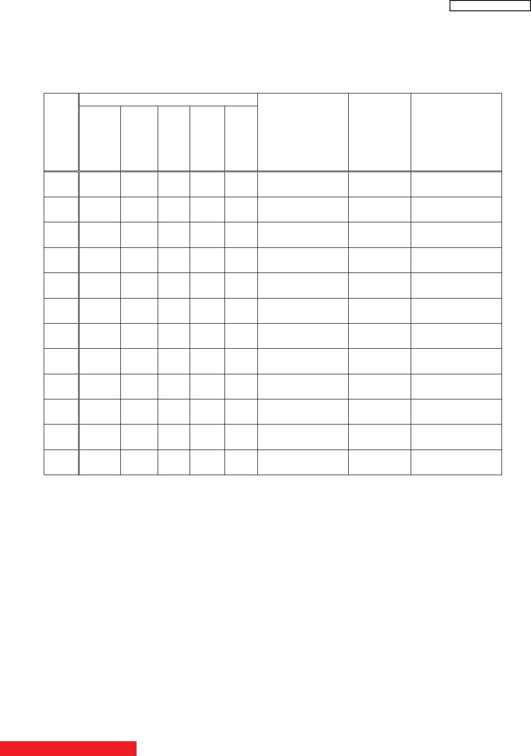
LED
No.
D306
(Red)
D305
(Orange)
D304
(Green)
D303
(Yellow)
D302
(Red)
Device Circuit No Role
21 ● ○ ● ○ ● RGB Processor
(TA1360) DP5X only Picture Cont/
VM
22
23 ● ○ ● ● ● Drive u-COM
LC5X only LCD panel
24 ● ● ○ ○ ○ Video SW
Video
25 ● ● ○ ○ ● Audio SW
Audio
26 ● ● ○ ● ○ Temp. Sensor
LC5X only Temperature
sensor
27
28
29
30
31
32
BACK TO ADJUSTMENTS
90
2-18 TROUBLESHOOTING FLOW CHARTS
LC57
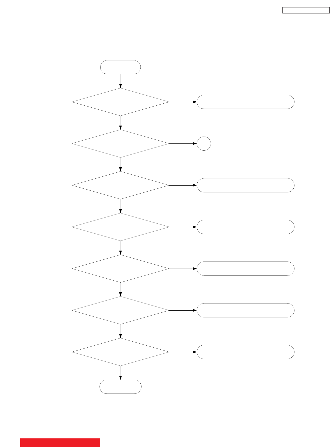
BACK TO ADJUSTMENTS
2.18-2 Troubleshooting for HDMI
(1) No HDMI picture
NG
Ensure Y signal at
emitter of QJ10. OK
NG
Ensure Y signal at
input of HJ01.
Ensure Y signal at
pin 9 of PHS2. OK
NG
Signal PWB defect
RJ93 defect
HJ01 defect
Ensure Y signal at
base of QJ10. QJ10 defect
OK
OK
NG
Ensure Y signal at
pin 12 of IJ03.
NG
OK
IJ03 defect
RJ89 defect
Ensure power at pin
20 and 19 of PHS2.
OK
NG Signal power PWB or Signal PWB defect
Start
HDMI 1?
YES
NO 1
91
2-18 TROUBLESHOOTING FLOW CHARTS
LC57

NG
Ensure Y signal at
emitter of QJ22. OK
NG
Ensure Y signal at
input of HJ04.
Ensure Y signal at
pin 4 of PHS2. OK
NG
Signal PWB defect
RJP5 defect
HJ04 defect
Ensure Y signal at
base of QJ22. QJ22 defect
OK
OK
NG
Ensure Y signal at
pin 12 of IJ09
NG
OK
IJ09 defect
RJP1 defect
1
BACK TO ADJUSTMENTS
92
2-18 TROUBLESHOOTING FLOW CHARTS
LC57
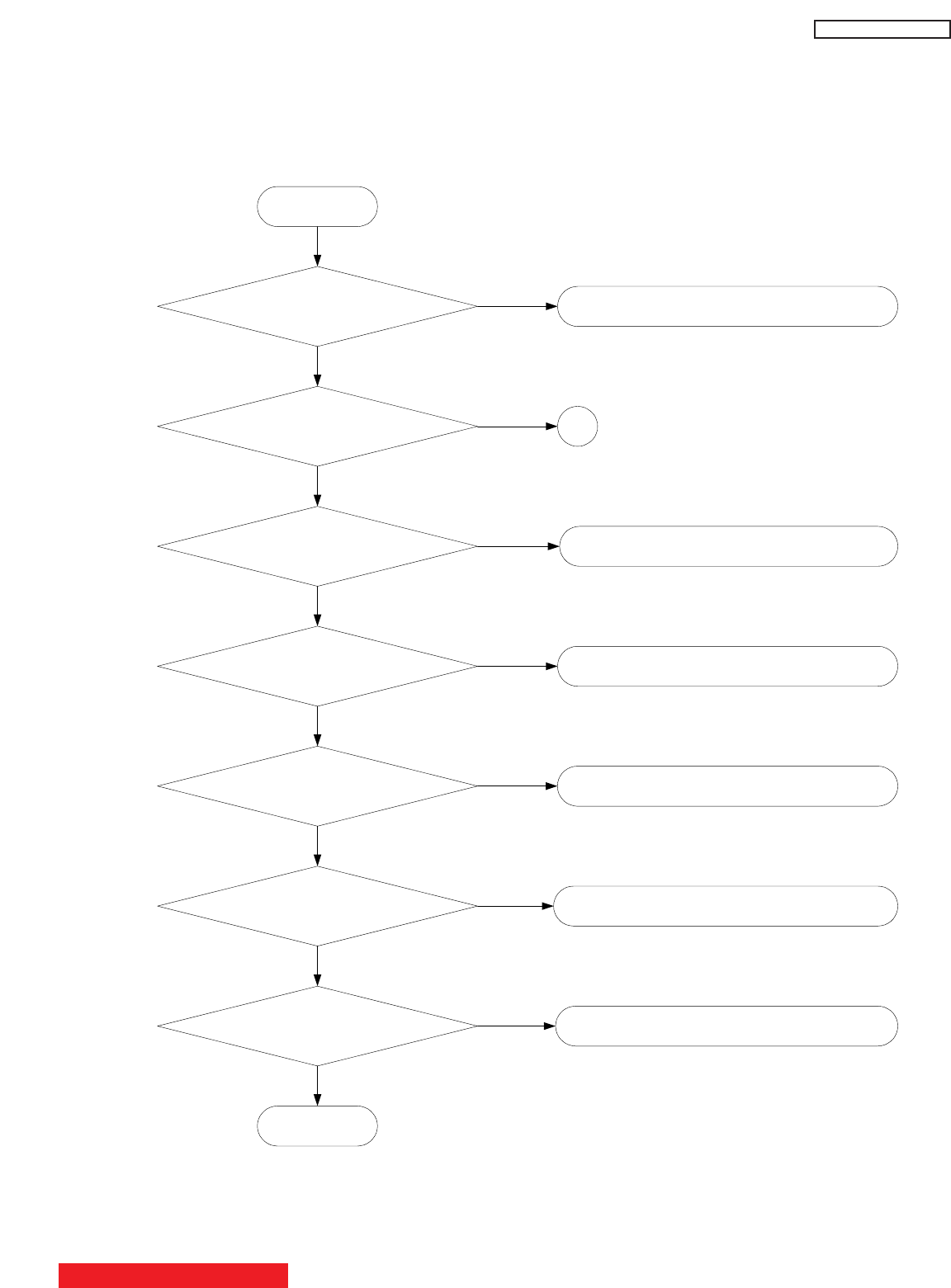
93
(2) No HDMI analog audio
NG
Ensure audio signal at
pin 1 and 7 of IJ06. OK
NG
Ensure audio signal at
pin 7 and 8 of IJ05.
Ensure audio signal at
pin 6 and 8 of PHS1. OK
NG
SIgnal PWB or Signal Power PWB defect
Some of the following components defect
CJ55, RJ82, CJ60, RJ88.
IJ05 defect
Ensure audio signal
at CJ50 and CJ57.
Some of the following components defect
RJ76, RJ78, RJ84, RJ85, IJ06.
OK
OK
NG
Ensure that digital signal at
pin 1, 2, 3 and 16 of IJ05. OK
NG
Either RJ75 or RJ83 defect.
IJ03 defect
Ensure power at pin 19 and 20
of PHS2, and pin 1 of PHS1.
OK
NG
SIgnal PWB defect
Start
HDMI 1?
YES
NO 2
BACK TO ADJUSTMENTS
2-18 TROUBLESHOOTING FLOW CHARTS
LC57

Ensure audio signal at
pin 1 and 7 of IJ11. OK
NG
Ensure audio signal at
pin 7 and 8 of IJ10.
Ensure audio signal at
pin 2 and 4 of PHS1. OK
NG
Some of the following components defect
CJE4, RJN3, CJE9, RJN9
IJ10 defect
Ensure audio signal
at CJC8 and CJE6.
Some of the following components defect
RJM6, RJM8, RJN5, RJN6, IJ11.
OK
OK
NG
Ensure that digital signal at
pin 1, 2, 3 and 16 of IJ10. OK
NG
Either RJM5 or RJN4 defect.
IJ09 defect
SIgnal PWB defect
2
BACK TO ADJUSTMENTS
94
2-18 TROUBLESHOOTING FLOW CHARTS
LC57
(3) No HDMI digital audio
NG
Ensure that SPDIF
at pin 15 of PHS1. OK
NG
Ensure that SPDIF
at pin 4 and 15 of IJ04 .
Ensure power at pin
19 and 20 of PHS2.
OK
NG
Signal PWB defect
RJ51 defect
Ensure that SPDIF
at pin 5 of IJ04. RJ56 defect
OK
OK
NG
Ensure that SPDIF
at pin 29 of IJ03. OK
NG
IJ04 defect
SIgnal PWB or Signal Power PWB defect
Start
IJ03 defect
HDMI 1?
YES
NO
Ensure that SPDIF
at pin 1 and 2 .
RJK3 defect
OK
NG
Ensure that SPDIF
at pin 29 of IJ09. OK
NG
IJ04 defect
IJ09 defect
BACK TO ADJUSTMENTS
95
2-18 TROUBLESHOOTING FLOW CHARTS
LC57


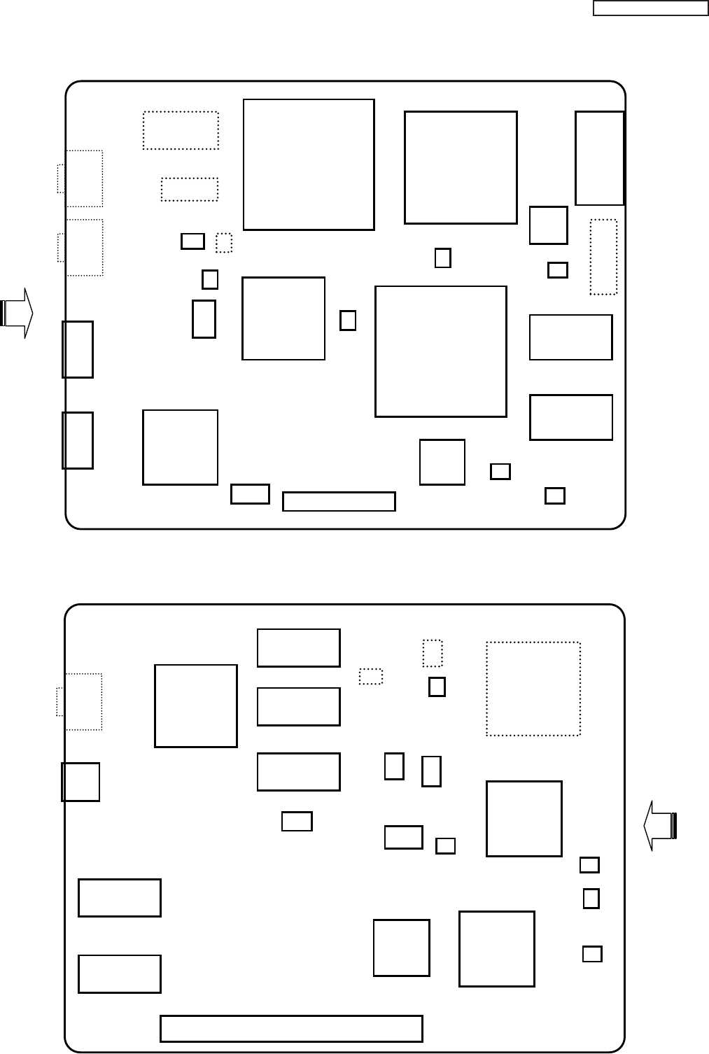
4.9.2 DIGITAL MAIN ASSEMBLY
Rear
view
Digital Main PWB Side A
IA04
IJ01
IF03 IH01
I106
I104
I103
IK02
PK01
IE02
I102
IF04
I101
IA10
JJ02
JJ03
IF01
PK02
PMV
I202
I205
E104
E105
IE02
I501
IH03
I204
IH02
Rear
view
Digital Main PWB Side H
I803
IG06
IJ02
I801
JUSB
I105
I604
IC06
JJ01
PMS
I206
IC04
I703
IG10
IK01
IC03
IC02
I203
I701
IK04
I606
IG05
IA05
I305
100
LC57
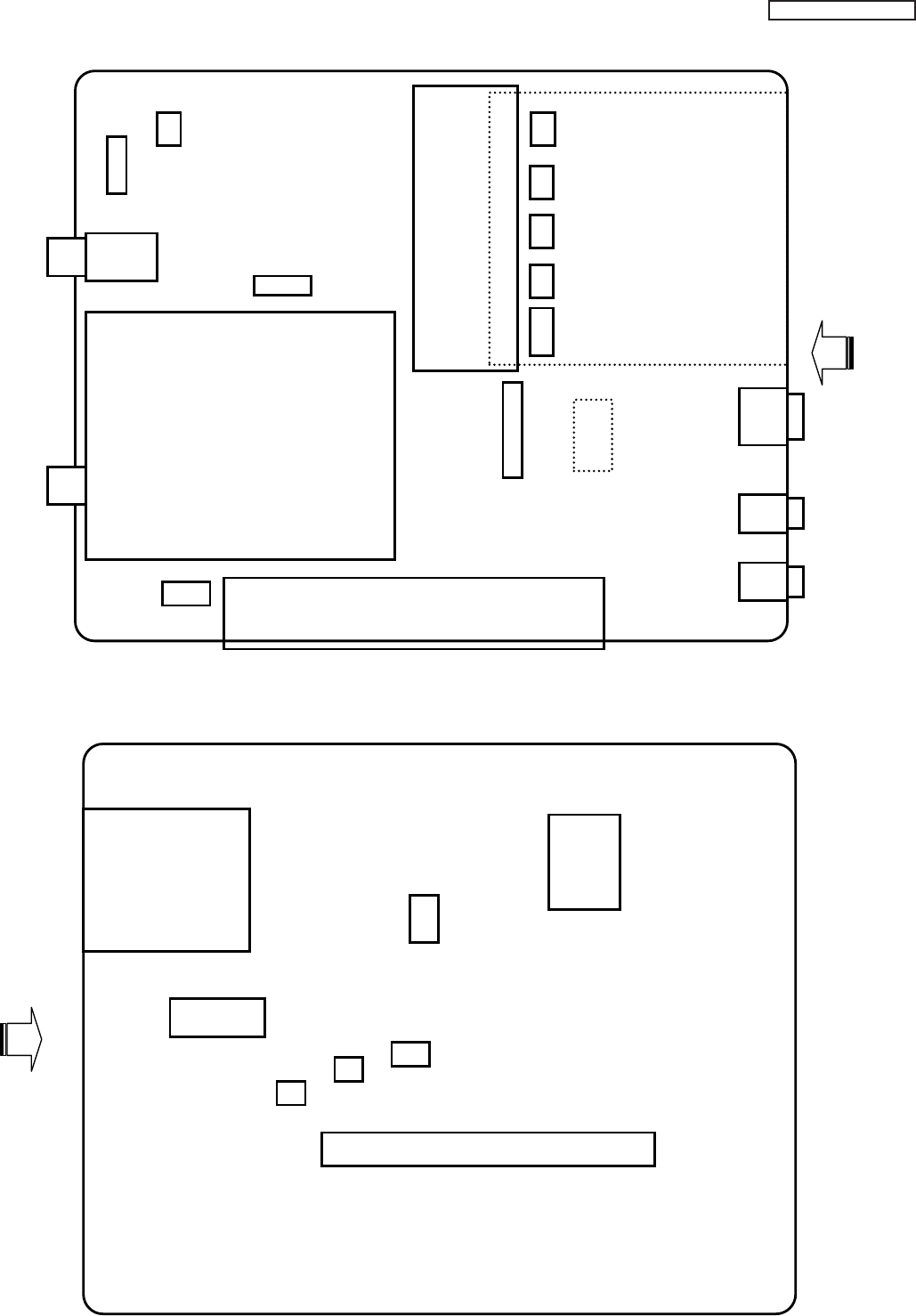
4.9.3 DIGITAL SUB ASSEMBLY
Rear
view
Digital Sub PWB Component Side
XT01
PTS
PSPI
IV04
IT07
UT01
JT01
XT03
JIROUT
HM01
JGLINK
PS
A
IW02
IW03 IW11 IW12 IW05
Rear
view
Digital Sub PWB Pattern Side
IW02
JS01
IT08
IW06
IW08
PMS
IW09
IW10
101
LC57
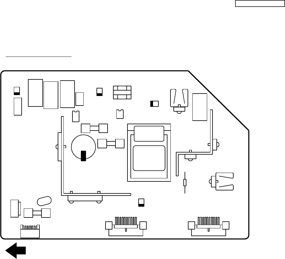
4.9.4 POWER P.W.B.
Back Cover Side
C913
F901
Fuse
F903
Fuse
F902
Fuse
D954
I902
D902
D952
T902
SW
Transformer
E942
SiG+5.6V
PPT2 PPT3
D955
T901
SW-Transformer
D953
PPT1
I901
S903
Relay
S902
Relay
S901
Relay
S904
Relay
PPDE
PA
I905
OVP-PRO
T
I904
FB
I906
FB
D901
X901
Varistor
LC5X POWER P.W.B.
I903
ACK
F904
Temperature-Limited
Resistor
102
LC57
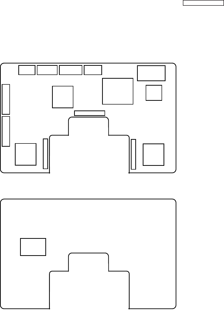
4.9.5 DRIVE P.W.B.
I7K0
Drive PWB Side A
I7A0
I7F0
I750
I700
PDD
P7A2PDJ PSL PDE
PDT PDP
P7A0
P7K
0
P7K0
Drive PWB Side B
I601
103
LC57
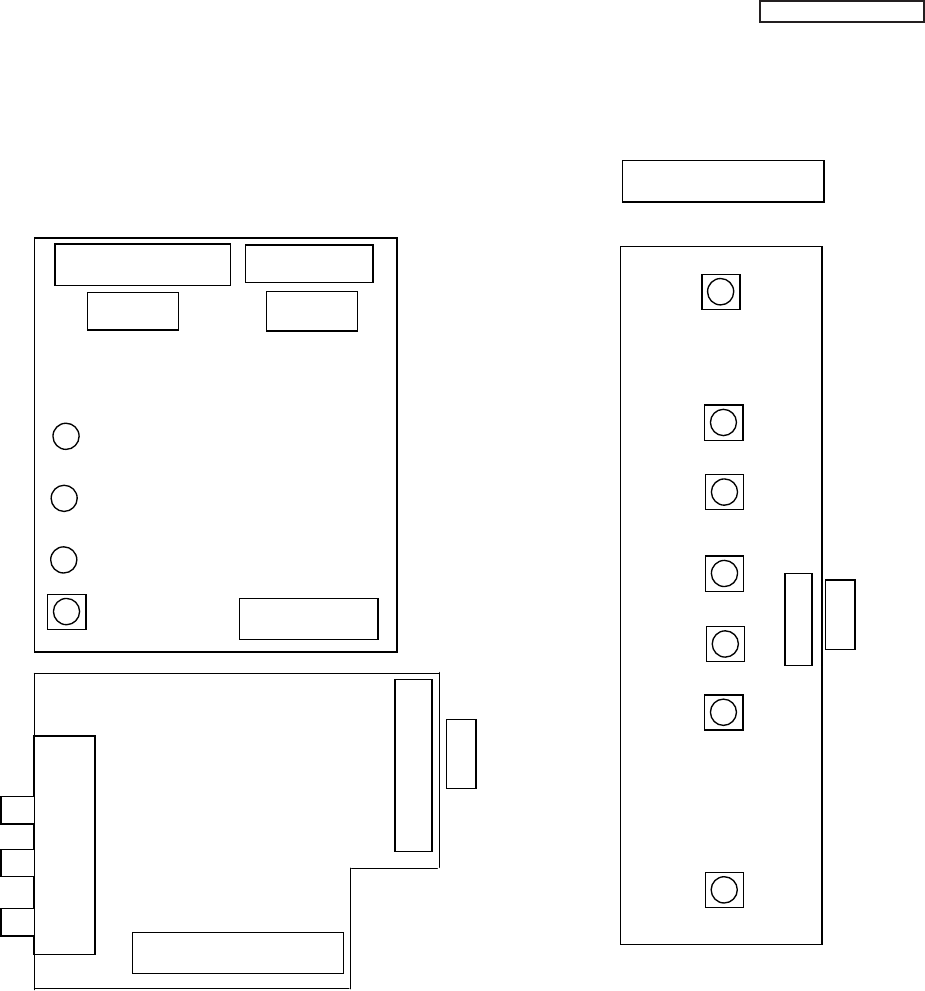
4.9.6 CONTROL P.W.B.
<LC57>
104
LC57
PFF2B
POWER
INPUT
/EXIT
VOL+
CH+
CH-
VOL-
MENU/
SELECT
IR RECEIVER
POWER LED
LAMP LED
TEMP LED
PFF2A
PFT1
S
V
L
R
PFT2
LED PWB
CONTROL PWB
AV JACK PWB
105
CONTROL PANEL and JACKS
LC57 chassis
Model: 50V720
(1) FRONT PANEL
(2) REAR PANEL
LC57


TABLE OF CONTENTS
FINAL WIRING DIAGRAM
TABLE OF CONTENTS
TABLE OF CONTENTS
109
LC57

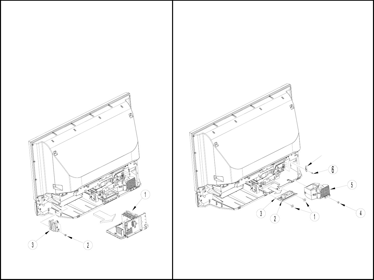
MAIN CHASSIS, SIDE AV JACK BALLAST, OPTICAL BLOCK 1
① Main Chassis P#UE24553 ① Screws T2V 4*16 P#MJ08901(2 Pcs.)
② Screws T2B 4*16 P#MJ03635(2 Pcs.) ② Lamp Power Unit(Ballast) P#HA01631
Pow Unit Holder P#NT03193
③ Side AV Jack Assy P#UE35341
③ Ballast FCC Sheet P#ME04511
④ Screw T2B 4*16 P#MJ03635
⑤ Fan Duct Assy P#UX24691
⑥ Screw M3M 3*10 P#MJ03601
111
LAMP CONN. COVER
(Put Aluminum Face Down)
QUICK DISASSEMBLE GUIDEQUICK DISASSEMBLE GUIDE

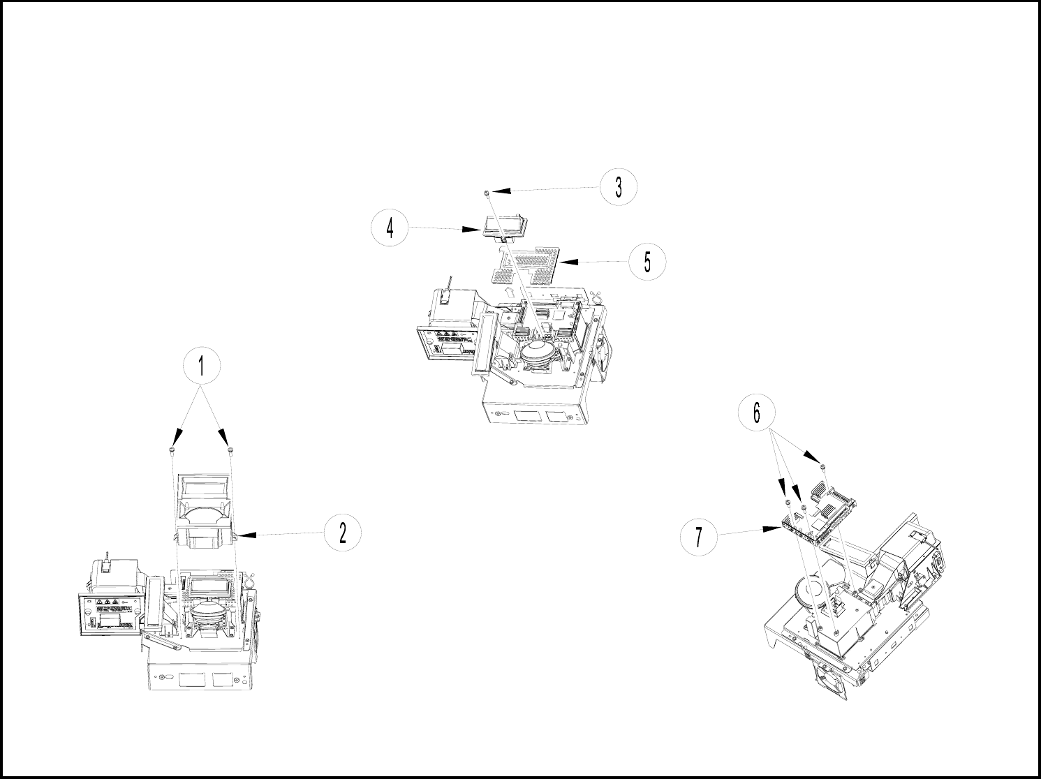
DRIVE PWB
① Screw T3E 3*12 P#MJ03651(2 Pcs.)
② Lens Barrier P#ME04421
③ Screw T3E 3*12 P#MJ03651
④ Panel Out Ducts P#NJ22371
P#NJ22361
⑤ Drive Shield P#MD09382
⑥ Screw T3E 3*12 P#MJ03651(3 Pcs.)
⑦ DRIVE PWB P#JP08483
113
QUICK DISASSEMBLE GUIDEQUICK DISASSEMBLE GUIDE
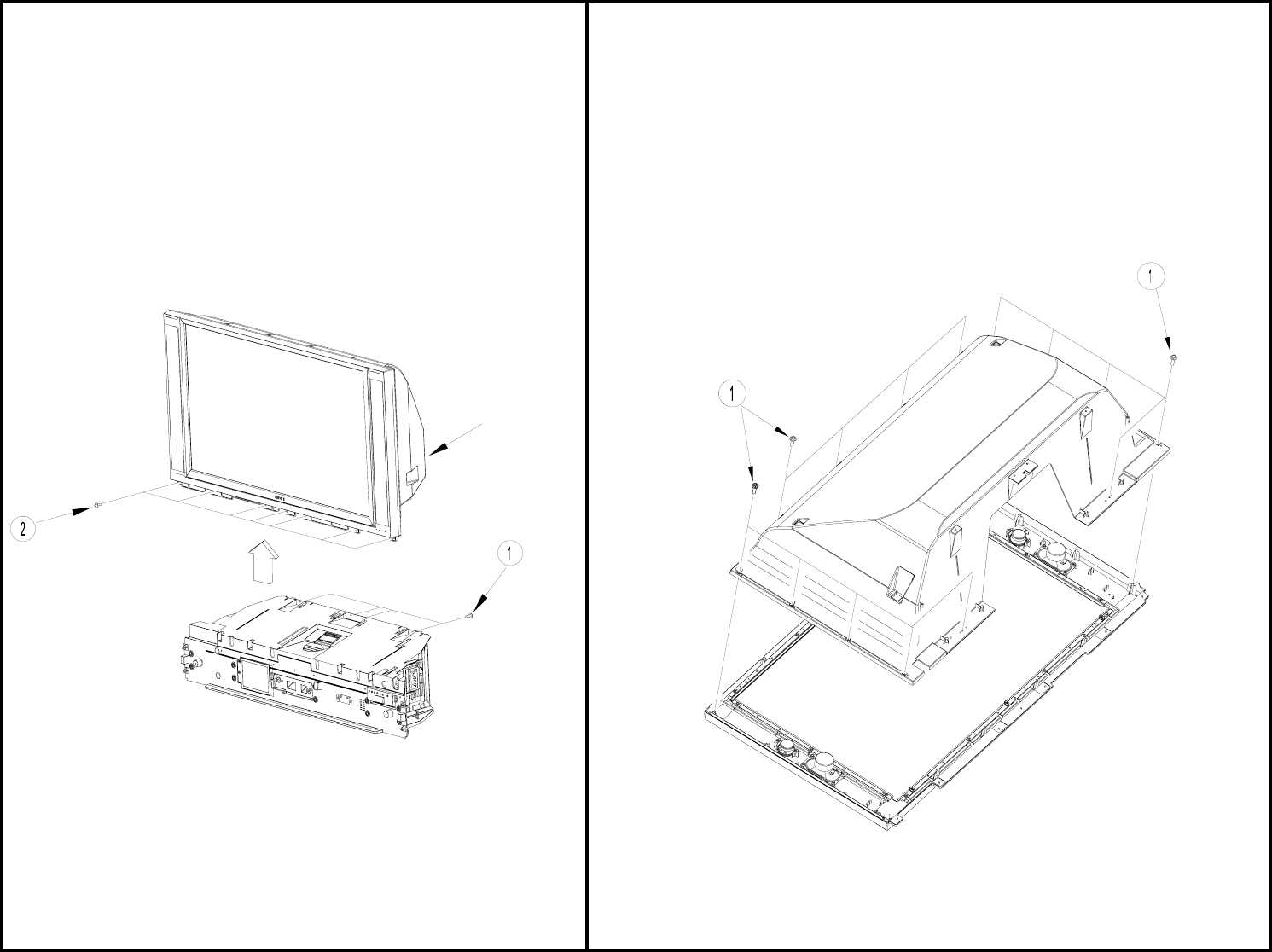
LOW CABINET ASSY, FRAME/MIRROR COVER ASSY SCREEN FRAME ASSY, MIRROR COVER ASSY
① Screws T2B 4*20 P#MJ03638(4 Pcs.) ① Screws T1T 4*18 P#MJ03557(14 Pcs.)
② Screws T2B 4*16 P#MJ03638(7 Pcs.)
114
MIRROR COVER ASSY
QUICK DISASSEMBLE GUIDEQUICK DISASSEMBLE GUIDE
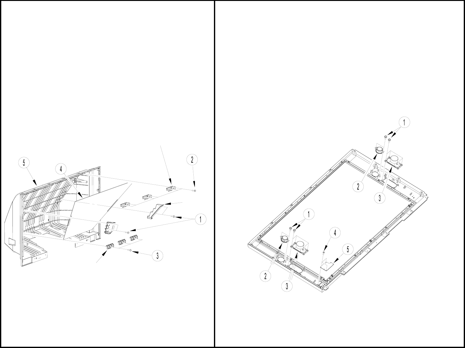
MIRROR COVER ASSY SCREEN FRAME ASSY 1
① Screws T1T 4*25 P#MJ03589(4 Pcs.) ① Screws T2V 3*12 P#MJ03616(8 Pcs.)
T2B 3*12 P#MJ03458(4 Pcs.)
② Screws T1T 4*18 P#MJ03587(6 Pcs.)
② Tweeters P#GK01401
③ Screws T1T 4*18 P#MJ03587(3 Pcs.)
③ Speakers P#GK01391
④ Mirror P#KS09384
④ Screws T2B 3*12 P#MJ03551(3 Pcs.)
⑤ Mirror Cover P#QD36144
⑤ LED PWB Assy P#JT25003
115
MIRROR RETAINER
MIRROR RETAINER
MIRROR
RETAINER
QUICK DISASSEMBLE GUIDEQUICK DISASSEMBLE GUIDE
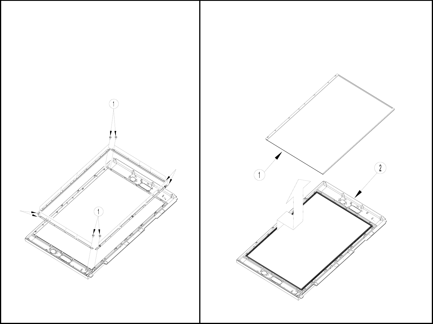
SCREEN FRAME ASSY 2 SCREEN FRAME ASSY 3
① Screws T1T 4*14 P#MJ03588(16 Pcs.) ① Screen Assy P#KR03238
② Screen Frame P#QD50981
116
SCREEN FIX
METALS
SCREEN FIX
METALS
QUICK DISASSEMBLE GUIDEQUICK DISASSEMBLE GUIDE
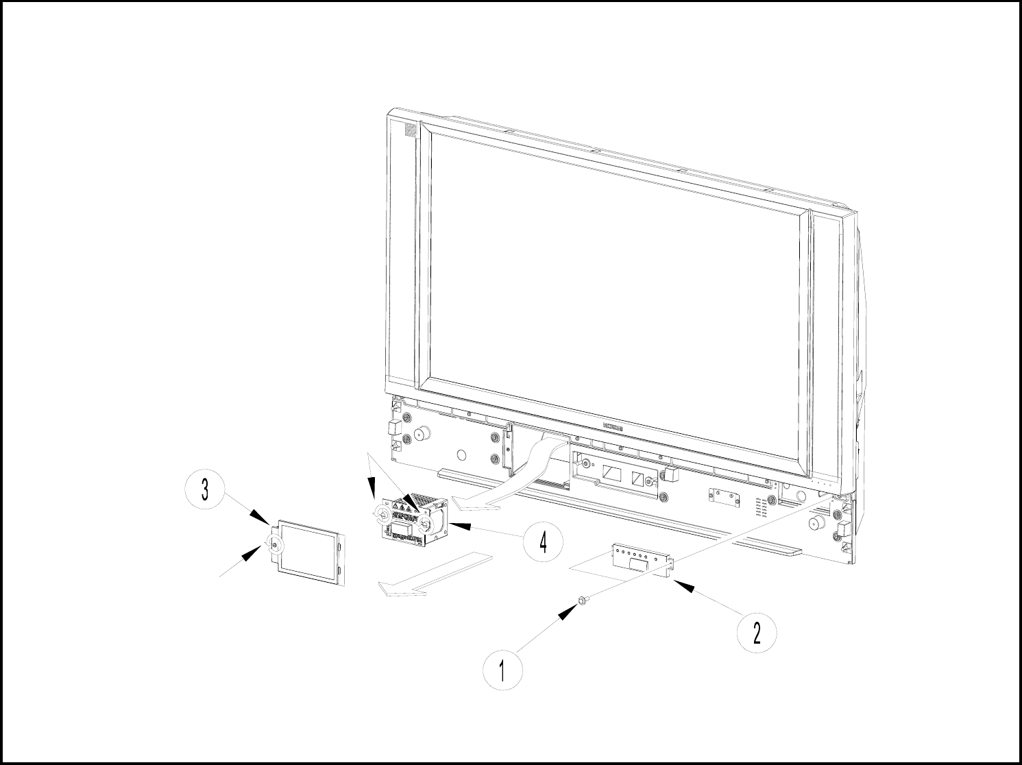
LAMP ASSY, CONTROL BLOCK
① Screws T2B 4*16 P#MJ03635(2 Pcs.)
② Control Block Assy P#UE25331
③ Lamp Cover P#PH33036
④ Lamp Assy P#DP00527
117
LOOSE THIS SCREW
LOOSE THESE
SCREWS
QUICK DISASSEMBLE GUIDEQUICK DISASSEMBLE GUIDE
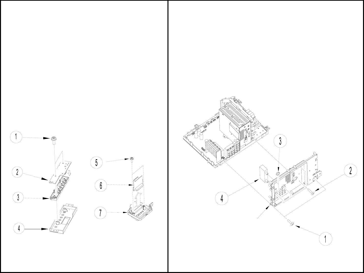
CONTROL BLOCK, SIDE AV JACK MAIN CHASSIS 1
① Screws T2B 3*12 P#MJ03551(2 Pcs.) ① Screws T2B 3*16 P#MJ03459(2 Pcs.)
② Control PWB Assy P#JT2503 ② Screws T2B 3*12 P#MJ03551(4 Pcs.)
③ Control Button P#PC06621 ③ Nut Washer P#MK01431(2 Pcs.)
④ Control Panel Frame P#PH36821 ④ Antenna Switch Box P#HP00774
⑤ Screws T2V 4*16 P#MJ03442(2 Pcs.)
⑥ Side AV Jack PWB Assy P#JT25003
⑦ AV Jack Frame P#PH36452
Plate P#PH36801
118
TERMINAL
HOLDER
QUICK DISASSEMBLE GUIDEQUICK DISASSEMBLE GUIDE
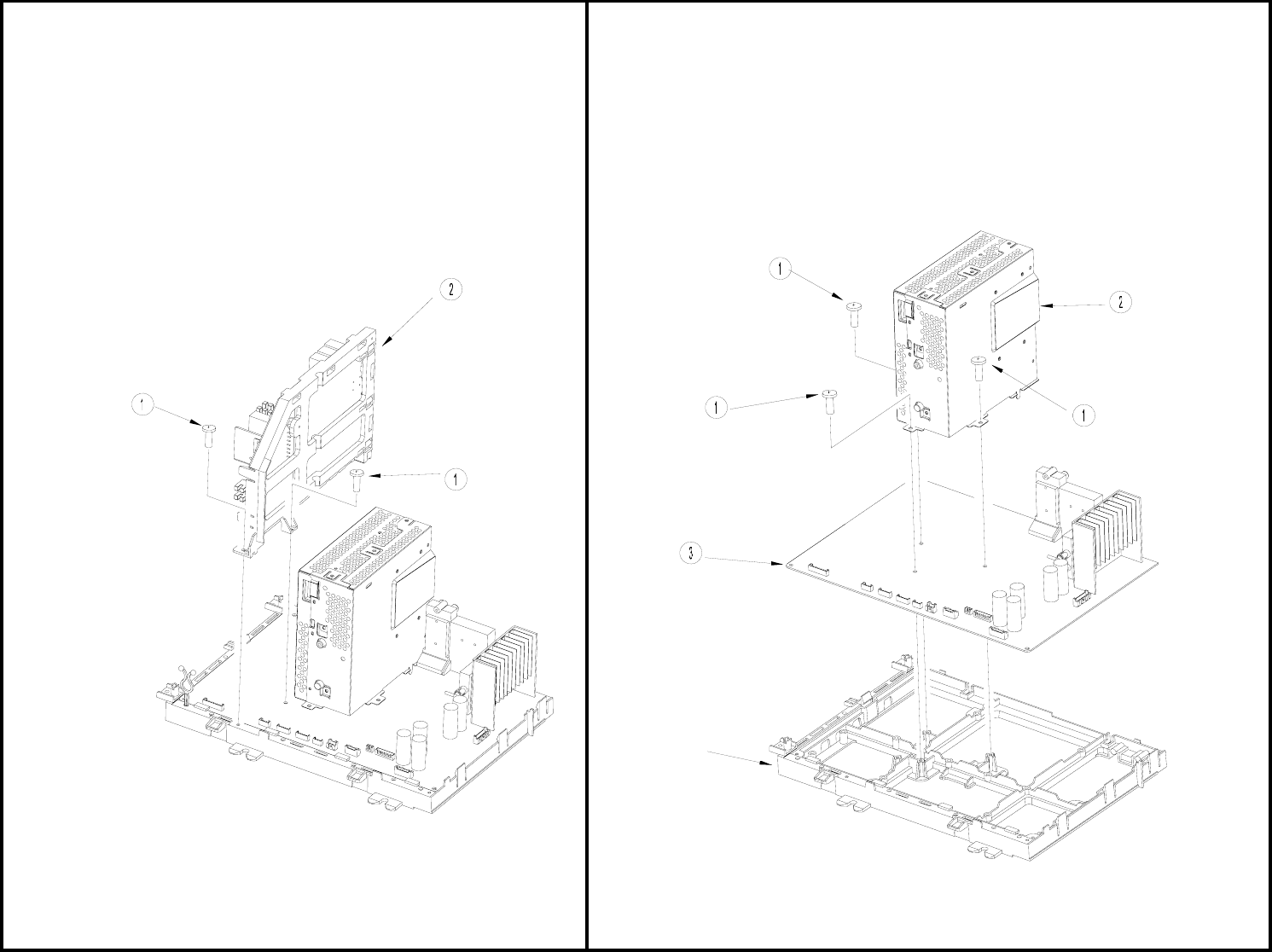
POWER PWB ASSY SIGNAL PWB ASSY, DIGITAL CORE
① Screws T2B 3*16 P#MJ03459(2 Pcs.) ① Screws T2B 3*16 P#MJ03459(3 Pcs.)
② Powe PWB Assy P#JT24993 ② Digital Core P#UE24613
③ Signal PWB Assy P#JT24983
SIGNAL PWB FRAME
119
QUICK DISASSEMBLE GUIDEQUICK DISASSEMBLE GUIDE
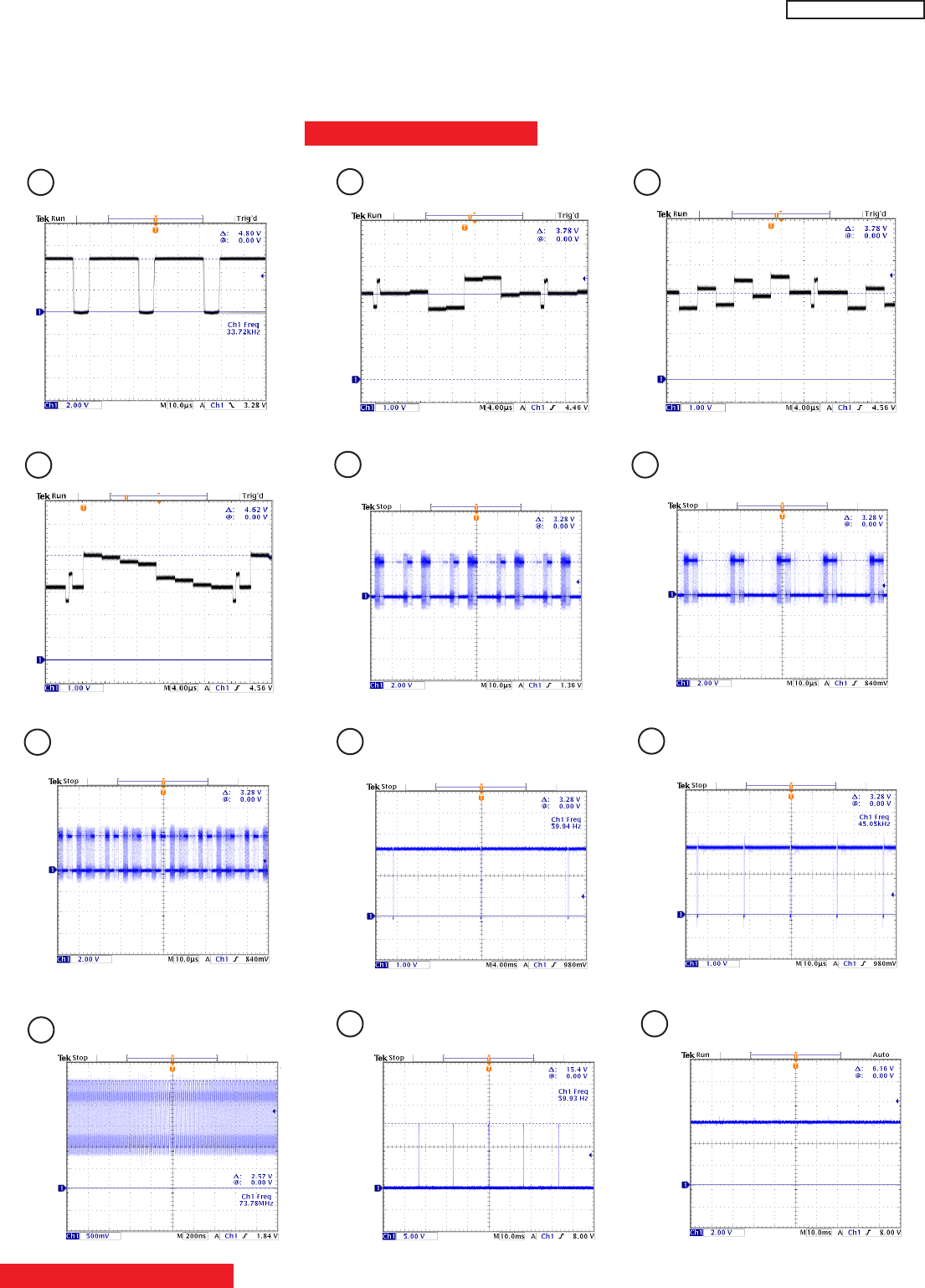
WAVEFORMS AT EACH SECTION
TABLE OF CONTENTS
I001 Pin 4 Main Sync I401 Pin 54 Main PR OUT I401 Pin 55 Main PB OUT
I401 Pin 56 Main Y OUT I700 Pin 12 Rin1 I700 Pin 10 Gin1
I700 Pin 7 Bin1
123
456
78 9
I700 Pin 24 VD OUT I700 Pin 25 HD OUT
11 P7A0/F0/K0 Pin 2 DY
10 I700 Pin 31 CLK OUT 12 P7A0/F0/K0 Pin 5 LCCOM
Click on number to go to schematic
120
LC57
Numbers inside circle correspond to locations shown in the circuit diagram. Waveforms taken
using a Color Bar signal with H sync 31 khz and V. sync 60 hz and a X10 probe.
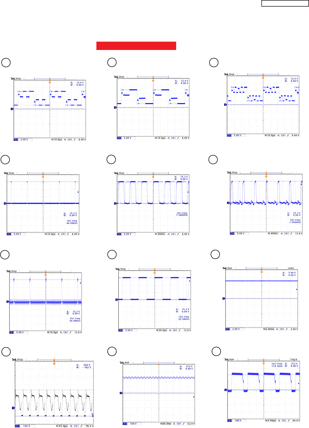
WAVEFORMS AT EACH SECTION
P7A0 Pin 7-18 RVID1-12 P7F0 Pin 7-18 GVID1-12 P7K0 Pin 7-18 BVID1-12
P7A0/F0/K0 Pin 20 DX P7A0/F0/K0 Pin 22 CLX P7A0/F0/K0 Pin 25-28 ENBX1-4
P7A0/F0/K0 Pin 29 NRG
13 14 15
16 17 18
19 20 21
P7A0/F0/K0 Pin 34 CLY I001 Pin 46-48 ALARM 0-2
23 I902 Pin 3,4 DL + OUT
22 I901 Pin 7,8 STBY SWITCHED OUT 24 I902 Pin 1 DL- OUT
Click on number to go to schematic
121
IMPORTANT NOTE: FOR HOT AREA USE AC CORD WITH FLOATING GROUND
LC57
Numbers inside circle correspond to locations shown in the circuit diagram. Waveforms taken
using a Color Bar signal with H sync 31 khz and V. sync 60 hz and a X10 probe.

TABLE OF CONTENTS
LC57
123
Symbol Pin No. Voltage Symbol Pin No. Voltage Symbol Pin No. Voltage Pin No. Voltage Symbol Pin No. Voltage Pin No. Voltage Pin No. Voltage Pin No. Voltage
PAN2 1 0 PDE 1 0 PDP 1 0 6 3.3 PST 1 0 31 11.1 61 0 91 5.6
2 0 2 2.8 2 3.3 7 3.3 2 0 32 -0.1 62 0 92 5.6
3932.8 33.3 8 0 30 33 0 63 4 93 5.6
49 4 3.3 9 3.3 4 0 34 0 64 3.8 94 0
Symbol Pin No. Voltage 5 0 10 0 5 0 35 0 65 0 95 0
Symbol Pin No. Voltage PDJ 1 3.3 6 0 36 0 66 5.3 96 0
PDT 1 16.6 2 3.3 Symbol Pin No. Voltage Pin No. Voltage 7 0.1 37 0 67 5.3 97 0
2 16.6 3 0 PFT1 1080 80380685.3980
30 40 2095 90390690990
4 0 5 3.3 3 5 10 0 10 0 40 0 70 0.1 100 4.8
5 5.7 6 3 4 5 11 0 11 3.3 41 0 71 0.1 101 4.8
6 5.7 7 3.3 5 0 12 0 12 0 42 2.1 72 0.4 102 0
70 6 0 13 0 13 3 43 0 73 0 103 0
8 0 Symbol Pin No. Voltage 7 5 14 0 44 0 74 0 104 9.8
9 0 PTEM 1 3.9 15 0 45 4.3 75 0.4 105 9.8
10 3.3 2 4.2 Symbol Pin No. Voltage Pin No. Voltage 16 0 46 4.3 76 0.1 106 0
11 0 3 3.3 PFT2 1970 170.44707701070
40 2080 183.3480.2782.81080
Symbol Pin No. Voltage 3090 190.1490.37901090
PFA1 1 0 Symbol Pin No. Voltage 4 2.5 10 0 20 0 50 0 80 3.3 110 0
2 11.9 PSP1 1 0 5 2.5 11 9 21 0 51 0 81 3.3 111 0
3 0 2 0 6 0 22 0 52 0 82 3.3 112 0
30 23 3.4 53 0 83 4.7 113 0
Symbol Pin No. Voltage 4 0 Symbol Pin No. Voltage Pin No. Voltage 24 3.4 54 0 84 0 114 0
PFA3 1 0 5 0 PPT2 1 5.7 11 0 25 0 55 0 85 0 115 0
2 10.1 6 0 2 0.0 12 0 26 0.1 56 4.5 86 0 116 0
3 0 7 0 3 0.0 13 0 27 0 57 4.5 87 0 117 0
4 NC 8 0 4 0.0 14 0 28 0 58 4.5 88 5.6 118 0
5NC 5 0 15 0 29 0 59 0 89 5.6 119 0
Symbol Pin No. Voltage 6 5.7 16 0 30 11.1 60 0 90 5.6 120 0
Symbol Pin No. Voltage PTW 1 0 7 5.7 17 5
PFA4 1 0 2 0 8 0 18 0 Symbol Pin No. Voltage Symbol Pin No. Voltage Pin No. Voltage
2 10.1 3 NC 9 0 19 10 PPT3 1 0.5 PDD 1 0 16 1.3
3 0 4 0 10 0 20 10 2 5.0 2 1.3 17 0
4NC 5 0 3 7.6 3 3.3 18 1.3
5 NC Symbol Pin No. Voltage Pin No. Voltage 4 2.9 4 1.3 19 0
Symbol Pin No. Voltage P7A0 1 0 19 0 5 0 5 0 20 1.2
Symbol Pin No. Voltage PINT 1 3.3 P7F0 2 0.3 20 0.7 6 4.8 6 1.3 21 3.3
PFH1 1 0 2 0 P7K0 3 0 21 15.7 7 0 7 0 22 1.3
25 4 0.3 22 7.9 8 0 8 1.3 23 3.3
3 5 Symbol Pin No. Voltage 5 6.2 23 7.7 9 0 9 0 24 1.2
4 0 PPL 1 228 6 2.6 24 -0.3 10 0 10 1.3 25 0
5 5 2 NC 7 7.6 25 2.4 11 31 11 0.4 26 0
6 0 3 -75.3 8 7.6 26 2.2 12 31 12 1.3 27 0
75 9 7.6 27 2.2 13 31 13 3.3 28 0
8 0 Symbol Pin No. Voltage 10 7.6 28 2.1 14 0 14 1.3 29 0
9 5 PPDE 1 74.8 11 7.6 29 0.4 15 0 15 0 30 5
10 0 2 NC 12 7.6 30 5 16 0
3 77.4 13 7.6 31 6.2 17 0 Symbol Pin No. Voltage
Symbol Pin No. Voltage 4 NC 14 7.6 32 15.7 18 0 P7A2 1 10
PFH2 1 0 15 7.6 33 7.9 19 16.6 2 7.6
2 0 Symbol Pin No. Voltage 16 7.6 34 7.9 20 16.6 3 0
PPT1 1 0 17 7.6 35 0.3 40
Symbol Pin No. Voltage 2 0 18 7.6 36 NC 50
PSL 1 0.12 30
20 40
3 4.3 5 0
4 0.6 6 0
5 3.7
60
DC VOLTAGE TABLES
124
Symbol Pin No. Voltage Symbol Pin No. Voltage Symbol Pin No. Voltage Symbol Pin No. Voltage Symbol Pin No. Voltage
Q002 B 4.4 Q017 B 0.1 Q407 B 3.8 QA04 B 8.4 QF01 B 0
C 0 C 4.2 C 0 C 5.6 C 0
E5 E0 E4.4 E9 E0
Symbol Pin No. Voltage Symbol Pin No. Voltage Symbol Pin No. Voltage Symbol Pin No. Voltage Symbol Pin No. Voltage
Q003 B 0 Q018 B 0 Q408 B 3.8 QA05 B 0 QJ03 B 0.3
C5 C5 C0 C0 C1
E0 E0 E4.4 E0 E0
Symbol Pin No. Voltage Symbol Pin No. Voltage Symbol Pin No. Voltage Symbol Pin No. Voltage Symbol Pin No. Voltage
Q005 B 5 Q021 B 4.5 Q409 B 3.8 QA06 B 0 QJ04 B 0.3
C9 C0 C0 C0 C2
E 6.4 E 0 E 4.4 E 0 E 0
Symbol Pin No. Voltage Symbol Pin No. Voltage Symbol Pin No. Voltage Symbol Pin No. Voltage Symbol Pin No. Voltage
Q006 B 0 Q025 B 4.3 Q410 B 3.8 QA07 B 0 Q901 B 0
C 5 C 5 C 0 C 4.3 C 19.4
E0 E5 E4.4 E0 E0
Symbol Pin No. Voltage Symbol Pin No. Voltage Symbol Pin No. Voltage Symbol Pin No. Voltage Symbol Pin No. Voltage
Q008 B 6.4 Q026 B 0 Q500 B 1.5 QA08 B 0 Q942 B 0
C 0 C 5 C 0 C 10.5 C 0.15
E 6.8 E 0 E 2.1 E 0 E 0
Symbol Pin No. Voltage Symbol Pin No. Voltage Symbol Pin No. Voltage Symbol Pin No. Voltage Symbol Pin No. Voltage
Q009 B 0 Q027 B 0 Q501 B 1.5 QA13 B 31 Q943 B 0.8
C5 C5 C0 C0 C0
E0 E0 E2.1 E31 E0
Symbol Pin No. Voltage Symbol Pin No. Voltage Symbol Pin No. Voltage Symbol Pin No. Voltage Symbol Pin No. Voltage
Q011 B 6.8 Q029 B 5 Q502 B 0 QA14 B 0 Q944 B 0.8
C 0.4 C 0 C 0 C 31 C 0.5
E7 E0 E0 E0 E0
Symbol Pin No. Voltage Symbol Pin No. Voltage Symbol Pin No. Voltage Symbol Pin No. Voltage Symbol Pin No. Voltage
Q012 B 5 Q030 B 0 Q503 B 0 QA15 B 0.7 Q982 A 5.8
C0 C5 C0 C0 C0
E5 E0 E0 E0 G0
Symbol Pin No. Voltage Symbol Pin No. Voltage Symbol Pin No. Voltage Symbol Pin No. Voltage Symbol Pin No. Voltage
Q013 B 0.4 Q301 B 0.7 QA01 B 2.1 QA18 B 3.4 Q7F0 B 8.2
C 2.1 C 0 C 8.4 C 0 C 0
E 0.3 E 0 E 1.5 E 3.4 E 7.6
Symbol Pin No. Voltage Symbol Pin No. Voltage Symbol Pin No. Voltage Symbol Pin No. Voltage Symbol Pin No. Voltage
Q014 B 0.7 Q402 B 2.5 QA02 B 8.4 QA19 B 0 Q7F1 B 8.2
C 2.4 C 0 C 5.5 C 8.8 C 15.6
E
0.3 E0 E9 E0 E
7.6
Symbol Pin No. Voltage Symbol Pin No. Voltage Symbol Pin No. Voltage Symbol Pin No. Voltage
Q015 B 1.8 Q403 B 3.8 QA03 B 2.2 QA20 B 8.8
C5 C0 C8.4 C0
E 2.6 E 4.4 E 1.5 E 8.8
LC57
DC VOLTAGE TABLES
125
Symbol Pin No. Voltag
e
Pin No. Voltag
e
Pin No. Voltag
e
Pin No. Voltag
e
Symbol Pin No. Voltag
e
Symbol Pin No. Voltag
e
Pin No. Voltag
e
Pin No. Voltag
e
Pin No. Voltag
e
I001 1 5 30 0 59 0-5 88 0 I002 1 2.5 I401 1 5.5 21 5.5 41 NC 61 NC
2 5 31 5 60 0-5 89 0 2 2.7 2 9 22 0 42 0 62 0
3 NC 32 0 61 NC 90 0 3 0.3 3 NC 23 5.5 43 NC 63 NC
4 4.3 33 0 62 0 91 0 4 5 4 0 24 0 44 0 64 0
5 0 34 5 63 0 92 NC 5 NC 5 NC 25 5.5 45 4 65 5.5
6 2.5 35 2.5 64 0 93 NC 6 0 6 0 26 0 46 4 66 0
7 0 36 0 65 0 94 0 7 5 7 NC 27 5.5 47 9 67 5.5
8 0 37 0-5 66 0 95 0 8 5 8 9 28 0 48 NC 68 0
9NC385670965 9 NC 29 5.5 49 NC 69 5.5
10 NC 39 5 68 0 97 5 10 0 30 0 50 3.8 70 9
11 5 40 0 69 5 98 5 Symbol Pin No. Voltag
e
11 5.5 31 5.5 51 3.8 71 5.5
12 1.9 41 5 70 0 99 5 I005 1 0 12 0 32 0 52 3.8 72 0
13 0 42 5 71 0 100 NC 2 0.5 13 5.5 33 NC 53 9 73 5.5
14 2.1 43 5 72 0 101 6 3 0.5 14 9 34 0 54 3.8 74 0
15 5 44 0 73 0 102 0 4 0 15 5.5 35 NC 55 3.8 75 5.5
16 5 45 0.5 74 0 103 0 5 0 16 3.7 36 0 56 3.8 76 9
17 NC 46 5 75 NC 104 2.6 6 0 17 5.5 37 NC 57 9 77 5.5
18 5 47 5 76 0 105 5 7 0 18 0 38 0 58 3.8 78 0
19 NC 48 5 77 0 106 5 8 3.4 19 5.5 39 NC 59 3.8 79 5.5
20 5 49 NC 78 0 107 0 9 5 20 0 40 0 60 3.8 80 0
21 NC 50 NC 79 0 108 5 10 0
22 0 51 NC 80 NC 109 2 11 3.4 Symbol Pin No. Voltag
e
Pin No. Voltag
e
Pin No. Voltag
e
Pin No. Voltag
e
23 NC 52 NC 81 NC 110 5 12 5 I501 1 4.5 10 4.5 19 4.5 28 NC
24 0 53 5 82 5 111 0 13 0 2 4.5 11 NC 20 0 29 4.5
25 NC 54 2.5 83 NC 112 5 14 3.3 3 4.5 12 NC 21 0 30 4.5
26 5 55 4.3 V 84 NC 113 2.6 4 4.5 13 NC 22 4 31 9
27 0 56 0 85 NC 114 0 5 4.5 14 NC 23 4 32 9
28 5 57 5 86 NC 115 2.3 Symbol Pin No. Voltag
e
6 4.5 15 4.5 24 0 33 NC
29 5 58 0-5 87 NC 116 5 I301 1 0 7 4.5 16 4.5 25 4.5 34 NC
2 10 8 4.5 17 4.5 26 4.5 35 4.5
Symbol Pin No. Voltag
e
Symbol Pin No. Voltag
e
Pin No. Voltag
e
3 9.2 9 4.5 18 4.5 27 NC 36 4.5
I004 1 5 I602 1 0 5 3.3 4 9
2 0 2 0 6 3.3 5 10 Symbol Pin No. Voltag
e
Symbol Pin No. Voltag
e
Pin No. Voltag
e
3 1.3 3 0 7 0 I90
3
1 27.3 I7A2 1 5.3 5 10.4
4 3.3 4 0 8 3.3 Symbol Pin No. Voltag
e
2 29.4 2 5.3 6 10.4
55 I302 1 2.9 3 0.65 3 5.3 7 0
Symbol Pin No. Voltag
e
Pin No. Voltag
e
2 0 4 5.3 4 0 8 15.6
Symbol Pin No. Voltag
e
U301 1 0 11 2.7 3 1.3
I591 1 0 2 5 12 3.8 4 5 Symbol Pin No. Voltag
e
Symbol Pin No. Voltag
e
Pin No. Voltag
e
2 3 3 0 13 2.2 5 0 I904 1 7.7 IA02 1 1.6 7 15
3 9 4 32.4 14 0 6 5.7 2 6.7 2 0 8 5
4 9 5 11.9 15 2.2 30 30931
5 10 6 0 16 2.2 Symbol Pin No. Voltag
e
4 2.1 4 0 10 0
7 5 17 0 IF0
3
10 5 1.6 11 4.3
Symbol Pin No. Voltag
e
8 3.8 18 5 2 3.3 Symbol Pin No. Voltag
e
6 10.5 12 14.4
I941 1 2.4 9 3.9 19 0 3 10.2 I90
5
1 19.2
2 0 10 4.2 20 5 4 9 2 19.4 Symbol Pin No. Voltag
e
Pin No. Voltag
e
3 7.6 5 16 3 0 I7K1 1 6.2 5 6.7
Symbol Pin No. Voltag
e
Pin No. Voltag
e
4 5 2 6.7 6 6.7
Symbol Pin No. Voltag
e
I901 1 0 5 141 3 0 7 6.2
I942 1 7.7 2 17.4 6 NC Symbol Pin No. Voltag
e
Pin No. Voltag
e
4 0 8 15.7
2 0 3 0 7 148 I7K3 1 6.2 5 9.5
3 5 4 2.2 8 148 2 6.7 6 9.5
30710
Symbol Pin No. Voltag
e
Symbol Pin No. Voltag
e
4 0 8 15.6
I60
3
1 0 I802 1 3.3
2 0 2 3.8 Symbol Pin No. Voltag
e
Symbol Pin No. Voltag
e
Pin No. Voltag
e
Pin No. Voltag
e
Pin No. Voltag
e
3 0 3 0 I906 1 8.6 I700 1 0 17 0.3 33 0.7 49 1.3
4 3.3 4 1.8 2 7.6 2 0 18 0.3 34 0.7 50 1.3
5 0 5 1.8 3 0 3 3.3 19 0.4 35 0.9 51 1.3
4 2.1 4 3.3 20 0.8 36 0.9 52 1.3
Symbol Pin No. Voltag
e
Symbol Pin No. Voltag
e
5 3.3 21 0.8 37 0.9 53 3.3
I800 1 3.3 I80
3
1 3.3 Symbol Pin No. Voltag
e
6 0 22 2.5 38 0.9 54 1.3
2 16.5 2 5.7 IF02 1 0 7 0.8 23 3.3 39 0.9 55 1.3
3 0 3 0 2 3.3 8 0.8 24 3.3 40 0.9 56 1.3
4 15.7 4 3.3 3 12 9 0.9 25 3.3 41 0.9 57 1.3
5 1 5 3.3 4 9 10 1 26 0.5 42 1 58 0
5 16 11 1 27 0.6 43 1 59 1.3
Symbol Pin No. Voltag
e
Symbol Pin No. Voltag
e
12 1 28 0.7 44 0 60 1.3
I801 1 3.3 I804 1 5.7 Symbol Pin No. Voltag
e
13 1 29 0.5 45 1 61 1.3
2 5.6 2 5 I808 1 3.3 14 0 30 0 46 1 62 1.3
3 0 3 5.7 2 5.7 15 0.3 31 1.7 47 1 63 0
4 3.9 4 3.3 3 0 16 0 32 0.7 48 3.3 64 3.3
51 50 43.3
6 0 5 3.3
7 3.3
8 3.3
LC57
DC VOLTAGE TABLES
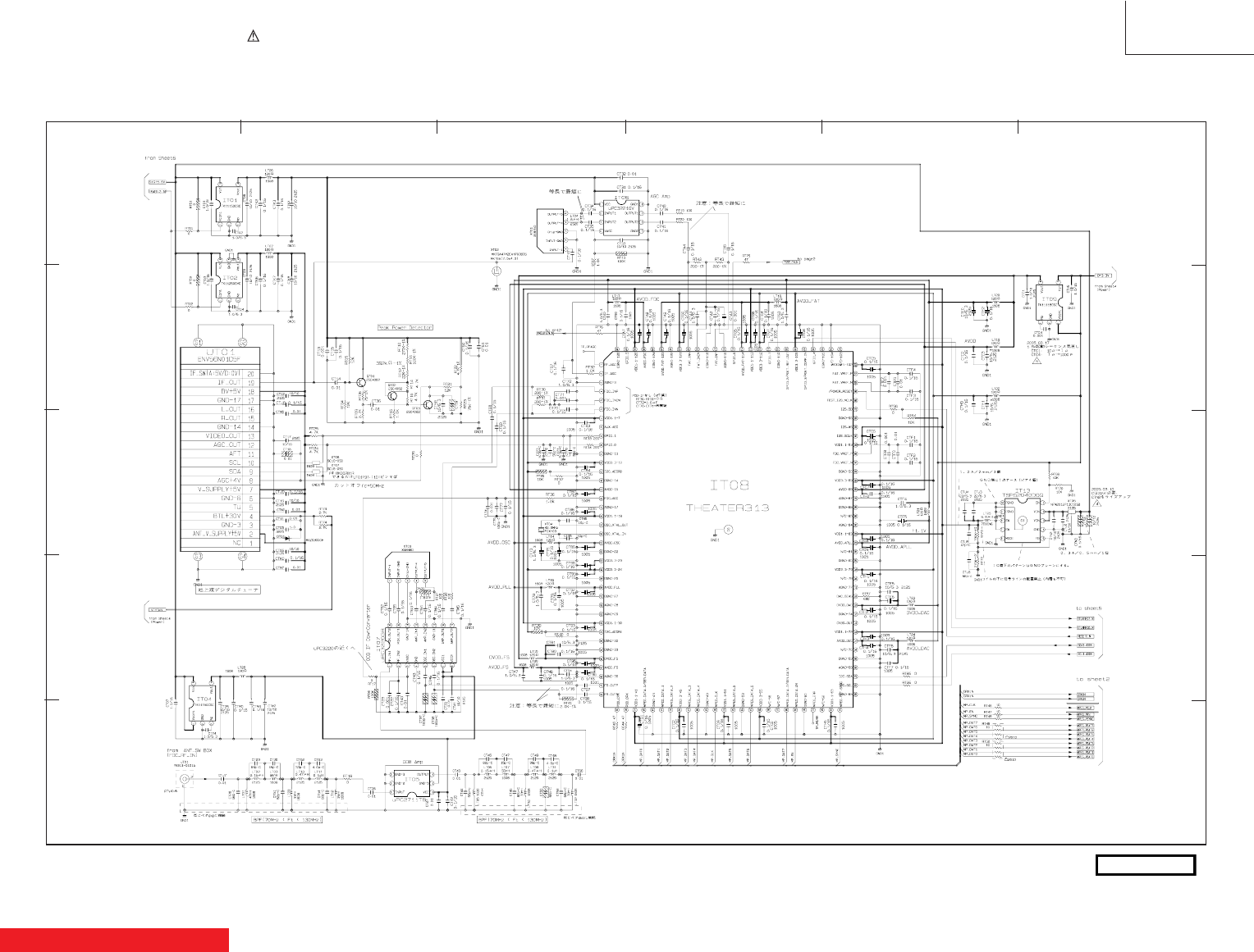
123456
A
B
C
D
E
All DC voltage to be measured with a tester (100k액/V). Voltage taken on a complex color bar signal including a standard color bar signal.
Since this is a basic circuit diagram, the value of the parts is subject to be altered for improvement.
PRODUCT SAFETY NOTE: Components marked with a and shaded have special characteristics important to
safety. Before replacing any of these components, read carefully the PRODUCT SAFETY NOTICE of this Service
Manual. Don’t degrade the safety of the receiver through improper servicing.
BASIC CIRCUIT DIAGRAM
TABLE OF CONTENTS
126
LC57
SUBDIGITAL 1 OF 7
TUNER
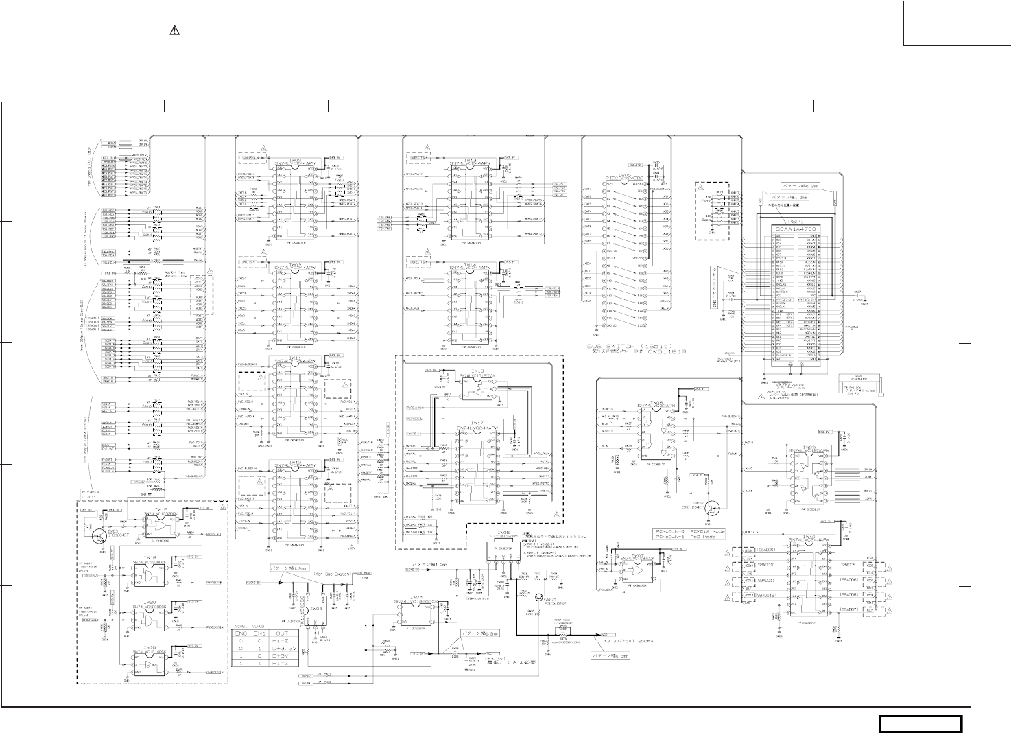
123456
A
B
C
D
E
PRODUCT SAFETY NOTE: Components marked with a and shaded have special characteristics important to
safety. Before replacing any of these components, read carefully the PRODUCT SAFETY NOTICE of this Service
Manual. Don’t degrade the safety of the receiver through improper servicing.
BASIC CIRCUIT DIAGRAM
All DC voltage to be measured with a tester (100k액/V). Voltage taken on a complex color bar signal including a standard color bar signal.
Since this is a basic circuit diagram, the value of the parts is subject to be altered for improvement.
127
POD-IF
LC57
SUBDIGITAL 2 OF 7
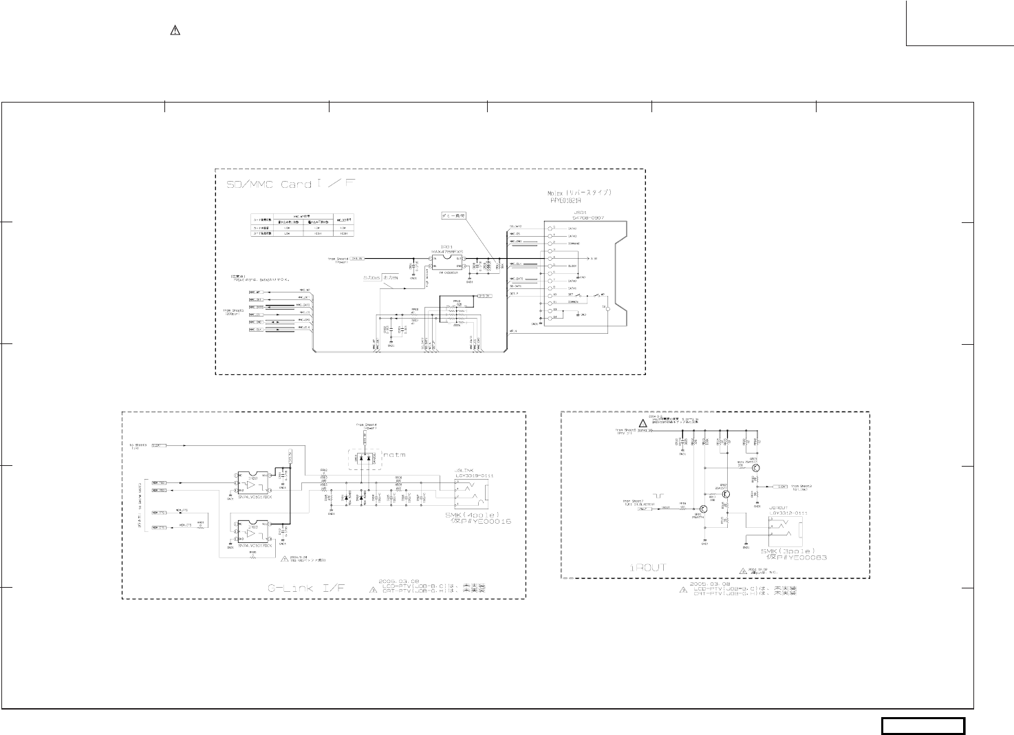
123456
A
B
C
D
E
All DC voltage to be measured with a tester (100k액/V). Voltage taken on a complex color bar signal including a standard color bar signal.
Since this is a basic circuit diagram, the value of the parts is subject to be altered for improvement.
PRODUCT SAFETY NOTE: Components marked with a and shaded have special characteristics important to
safety. Before replacing any of these components, read carefully the PRODUCT SAFETY NOTICE of this Service
Manual. Don’t degrade the safety of the receiver through improper servicing.
BASIC CIRCUIT DIAGRAM
TABLE OF CONTENTS
128
SD G-LINK
SELECTOR
LC57
SUBDIGITAL 3 OF 7
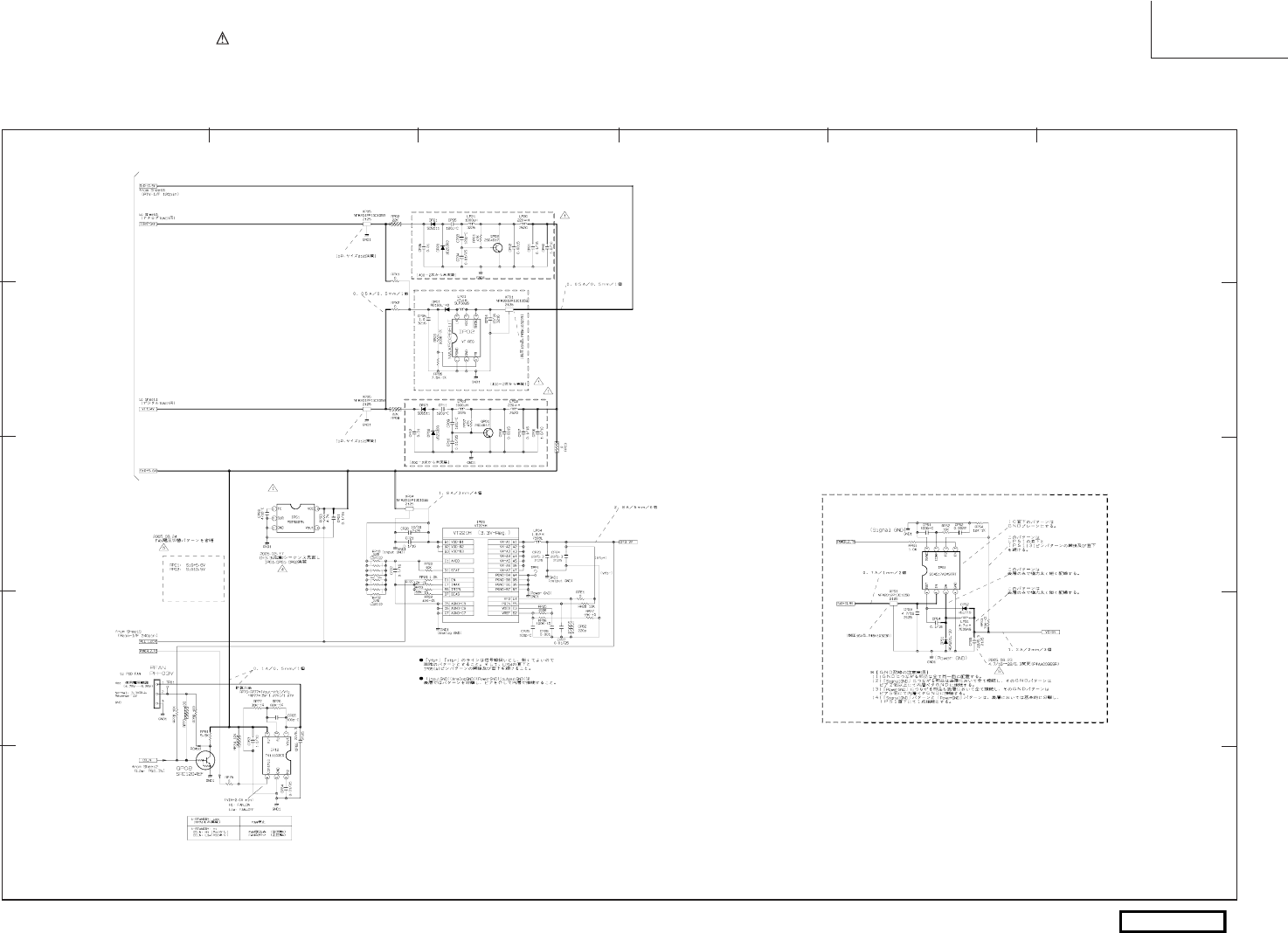
123456
A
B
C
D
E
All DC voltage to be measured with a tester (100k액/V). Voltage taken on a complex color bar signal including a standard color bar signal.
Since this is a basic circuit diagram, the value of the parts is subject to be altered for improvement.
PRODUCTSAFETYNOTE: Components marked with a and shaded have special characteristics important to
safety. Before replacing any of these components, read carefully the PRODUCT SAFETY NOTICE of this Service
Manual. Don’t degrade the safety of the receiver through improper servicing.
BASIC CIRCUIT DIAGRAM
129
POWER I/F
LC57
SUBDIGITAL 4 OF 7
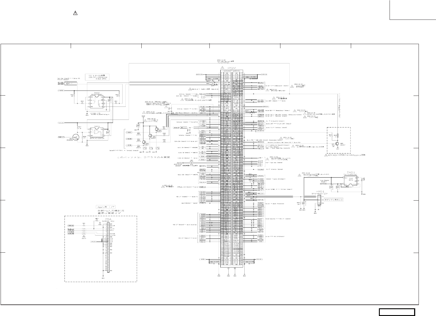
123456
A
B
C
D
E
All DC voltage to be measured with a tester (100k액/V). Voltage taken on a complex color bar signal including a standard color bar signal.
Since this is a basic circuit diagram, the value of the parts is subject to be altered for improvement.
PRODUCT SAFETY NOTE: Components marked with a and shaded have special characteristics important to
safety. Before replacing any of these components, read carefully the PRODUCT SAFETY NOTICE of this Service
Manual. Don’t degrade the safety of the receiver through improper servicing.
BASIC CIRCUIT DIAGRAM
130
240 PIN I/F
LC57
SUBDIGITAL 5 OF 7
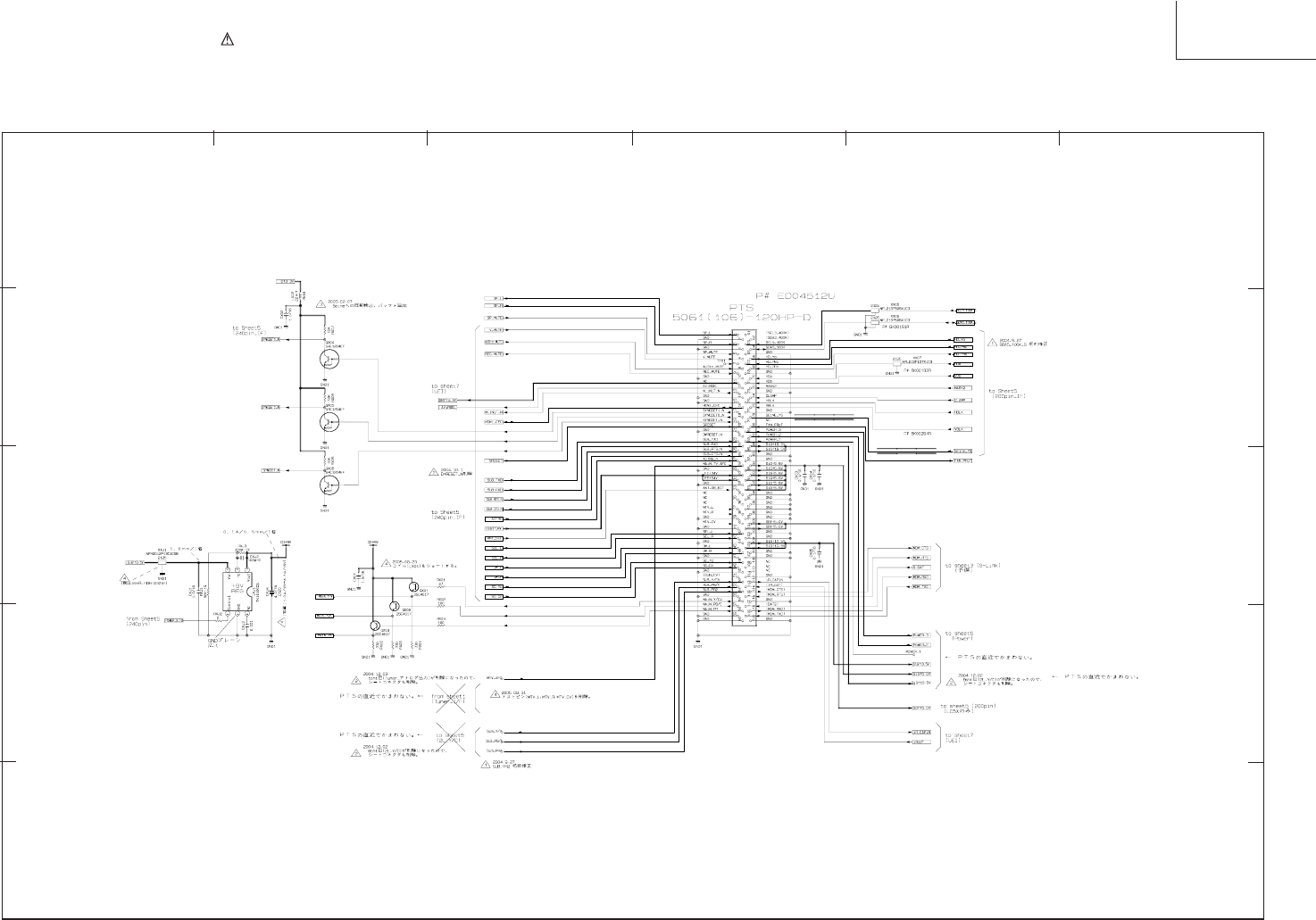
123456
A
B
C
D
E
PRODUCT SAFETY NOTE: Components marked with a and shaded have special characteristics important to
safety. Before replacing any of these components, read carefully the PRODUCT SAFETY NOTICE of this Service
Manual. Don’t degrade the safety of the receiver through improper servicing.
BASIC CIRCUIT DIAGRAM
All DC voltage to be measured with a tester (100k액/V). Voltage taken on a complex color bar signal including a standard color bar signal.
Since this is a basic circuit diagram, the value of the parts is subject to be altered for improvement.
131
SIGNAL I/F
LC57
SUBDIGITAL 6 OF 7
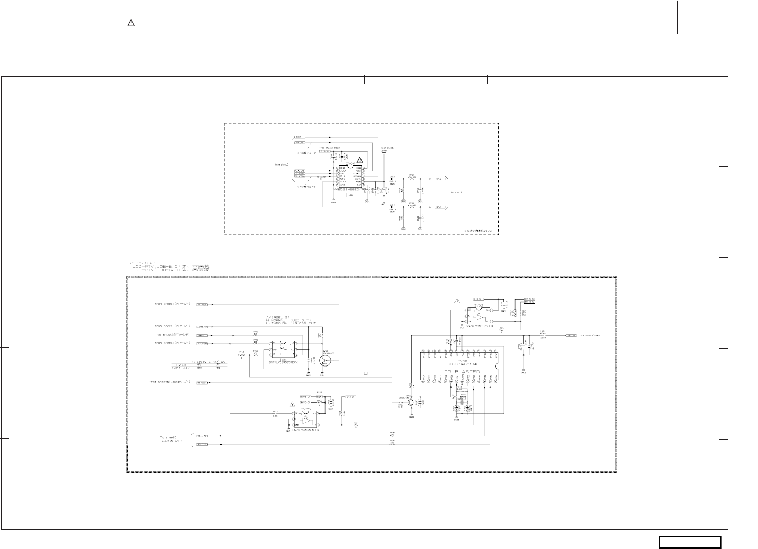
123456
A
B
C
D
E
All DC voltage to be measured with a tester (100k액/V). Voltage taken on a complex color bar signal including a standard color bar signal.
Since this is a basic circuit diagram, the value of the parts is subject to be altered for improvement.
PRODUCT SAFETY NOTE: Components marked with a and shaded have special characteristics important to
safety. Before replacing any of these components, read carefully the PRODUCT SAFETY NOTICE of this Service
Manual. Don’t degrade the safety of the receiver through improper servicing.
BASIC CIRCUIT DIAGRAM
132
UEI
LC57
SUBDIGITAL 7 OF 7
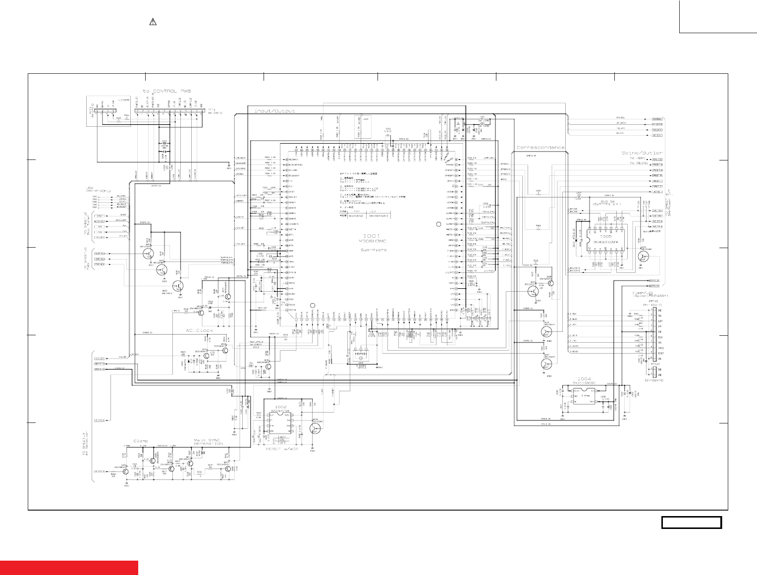
123456
A
B
C
D
E
All DC voltage to be measured with a tester (100k액/V). Voltage taken on a complex color bar signal including a standard color bar signal.
Since this is a basic circuit diagram, the value of the parts is subject to be altered for improvement.
PRODUCT SAFETY NOTE: Components marked with a and shaded have special characteristics important to
safety. Before replacing any of these components, read carefully the PRODUCT SAFETY NOTICE of this Service
Manual. Don’t degrade the safety of the receiver through improper servicing.
BASIC CIRCUIT DIAGRAM
TABLE OF CONTENTS
1
133
21
LC57
SIGNAL 1 OF 7
SUB MICRO
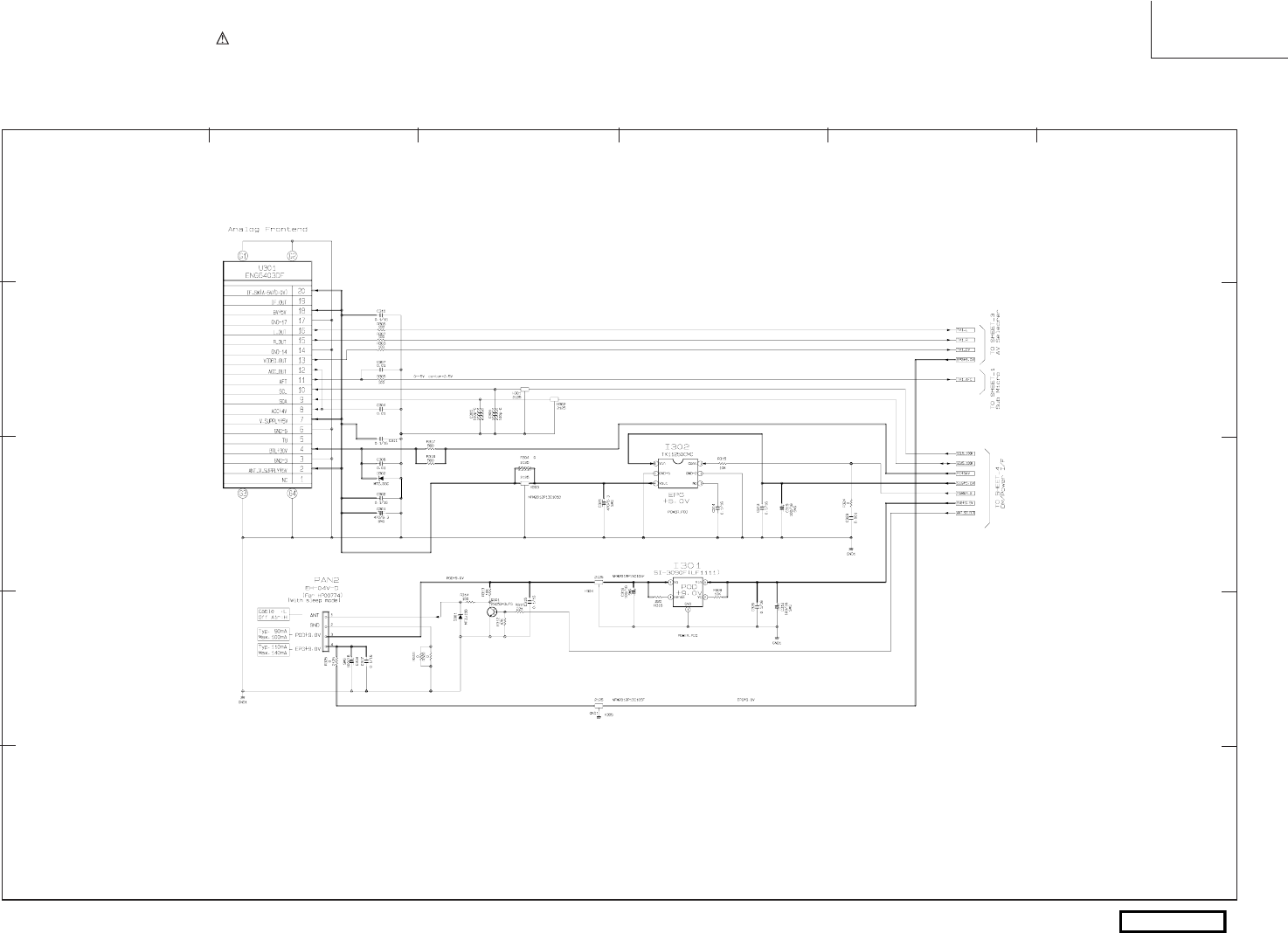
123456
A
B
C
D
E
PRODUCT SAFETY NOTE: Components marked with a and shaded have special characteristics important to
safety. Before replacing any of these components, read carefully the PRODUCT SAFETY NOTICE of this Service
Manual. Don’t degrade the safety of the receiver through improper servicing.
BASIC CIRCUIT DIAGRAM
All DC voltage to be measured with a tester (100k액/V). Voltage taken on a complex color bar signal including a standard color bar signal.
Since this is a basic circuit diagram, the value of the parts is subject to be altered for improvement.
134
TUNER
LC57
SIGNAL 2 OF 7
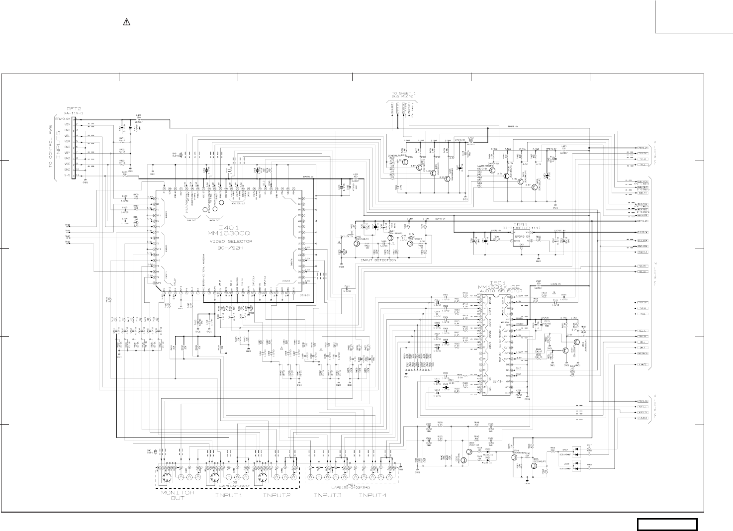
123456
A
B
C
D
E
All DC voltage to be measured with a tester (100k액/V). Voltage taken on a complex color bar signal including a standard color bar signal.
Since this is a basic circuit diagram, the value of the parts is subject to be altered for improvement.
PRODUCT SAFETY NOTE: Components marked with a and shaded have special characteristics important to
safety. Before replacing any of these components, read carefully the PRODUCT SAFETY NOTICE of this Service
Manual. Don’t degrade the safety of the receiver through improper servicing.
BASIC CIRCUIT DIAGRAM
TABLE OF CONTENTS
135
2
3
4
AV SELECTOR
LC57
SIGNAL 3 OF 7
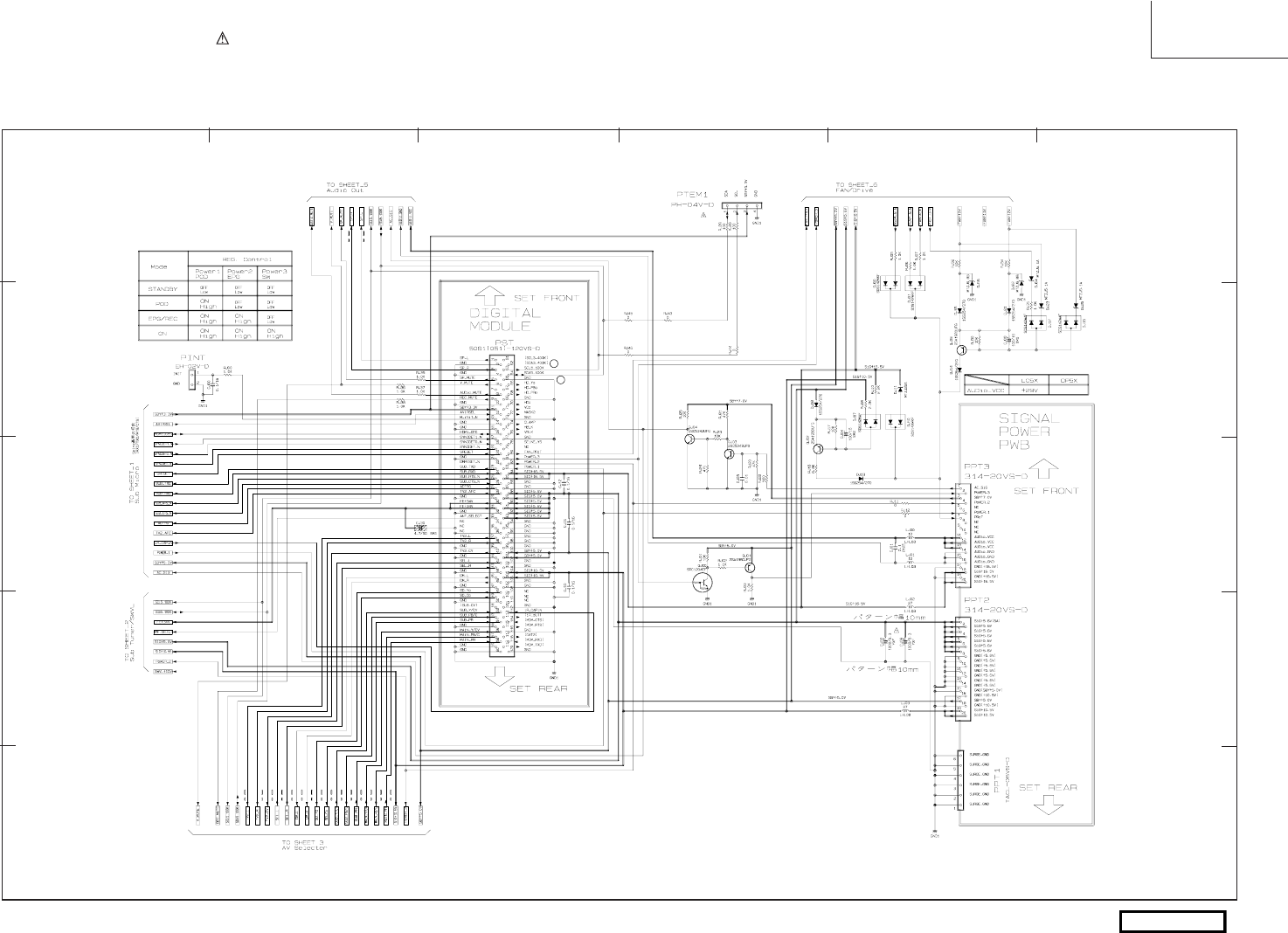
123456
A
B
C
D
E
All DC voltage to be measured with a tester (100k액/V). Voltage taken on a complex color bar signal including a standard color bar signal.
Since this is a basic circuit diagram, the value of the parts is subject to be altered for improvement.
PRODUCTSAFETYNOTE: Components marked with a and shaded have special characteristics important to
safety. Before replacing any of these components, read carefully the PRODUCT SAFETY NOTICE of this Service
Manual. Don’t degrade the safety of the receiver through improper servicing.
BASIC CIRCUIT DIAGRAM
136
26
25
DM/POWER I/F
LC57
SIGNAL 4 OF 7
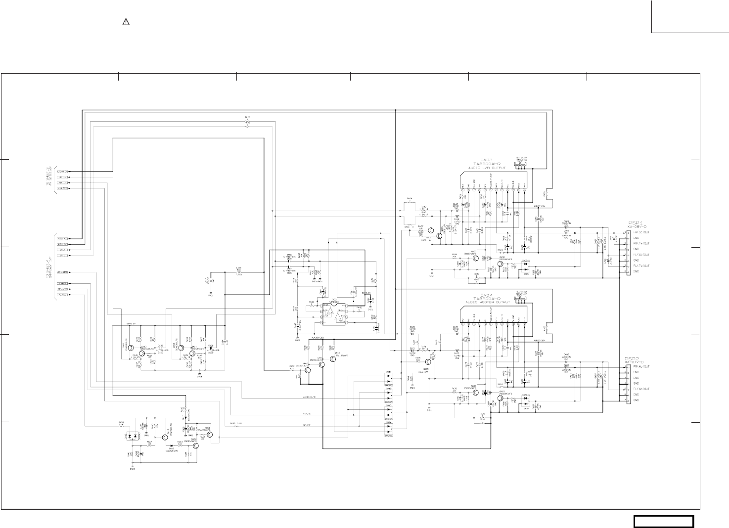
123456
A
B
C
D
E
All DC voltage to be measured with a tester (100k액/V). Voltage taken on a complex color bar signal including a standard color bar signal.
Since this is a basic circuit diagram, the value of the parts is subject to be altered for improvement.
PRODUCT SAFETY NOTE: Components marked with a and shaded have special characteristics important to
safety. Before replacing any of these components, read carefully the PRODUCT SAFETY NOTICE of this Service
Manual. Don’t degrade the safety of the receiver through improper servicing.
BASIC CIRCUIT DIAGRAM
137
AUDIO
LC57
SIGNAL 5 OF 7
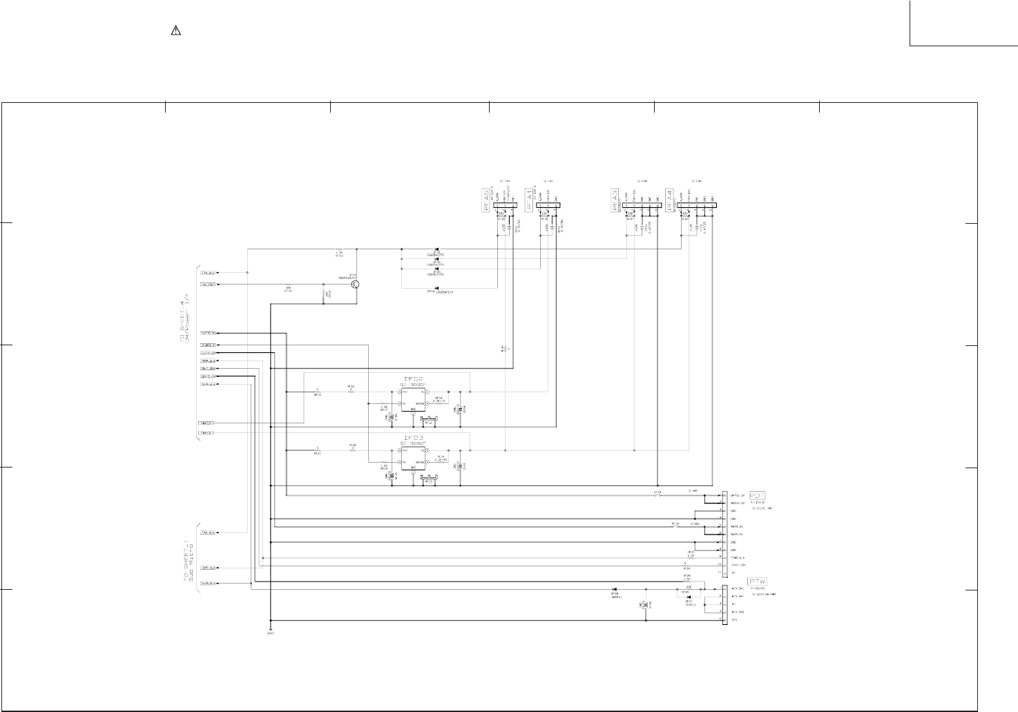
123456
A
B
C
D
E
PRODUCT SAFETY NOTE: Components marked with a and shaded have special characteristics important to
safety. Before replacing any of these components, read carefully the PRODUCT SAFETY NOTICE of this Service
Manual. Don’t degrade the safety of the receiver through improper servicing.
BASIC CIRCUIT DIAGRAM
All DC voltage to be measured with a tester (100k액/V). Voltage taken on a complex color bar signal including a standard color bar signal.
Since this is a basic circuit diagram, the value of the parts is subject to be altered for improvement.
138
FAN
LC57
SIGNAL 6 OF 7
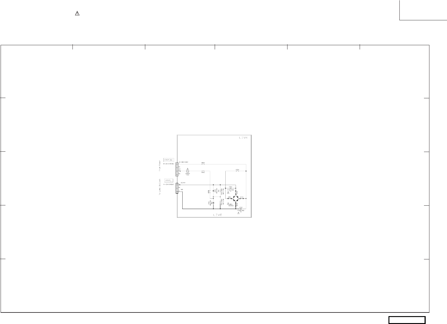
139
123456
A
B
C
D
E
All DC voltage to be measured with a tester (100k액/V). Voltage taken on a complex color bar signal including a standard color bar signal.
Since this is a basic circuit diagram, the value of the parts is subject to be altered for improvement.
PRODUCT SAFETY NOTE: Components marked with a and shaded have special characteristics important to
safety. Before replacing any of these components, read carefully the PRODUCT SAFETY NOTICE of this Service
Manual. Don’t degrade the safety of the receiver through improper servicing.
BASIC CIRCUIT DIAGRAM
LAMP POWER
LC57
SIGNAL 7 OF 7
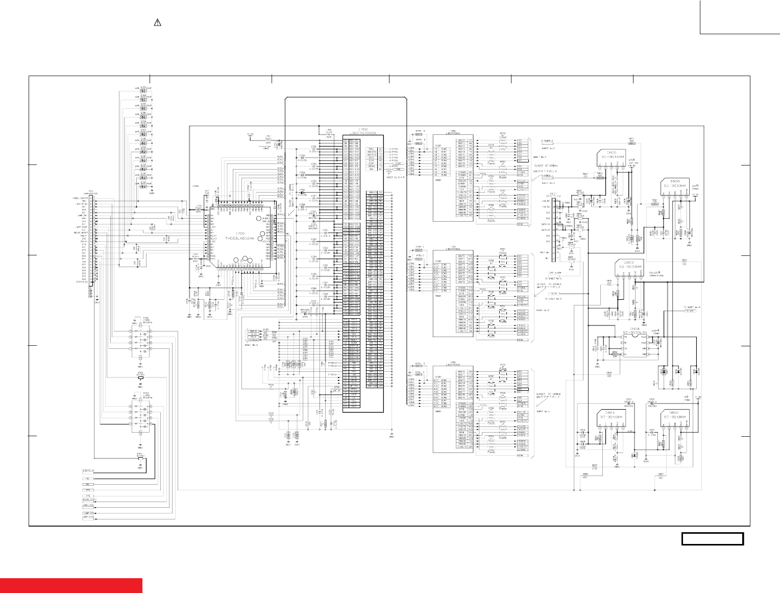
1234 5 6
A
B
C
D
E
All DC voltage to be measured with a tester (100k액/V). Voltage taken on a complex color bar signal including a standard color bar signal.
Since this is a basic circuit diagram, the value of the parts is subject to be altered for improvement.
PRODUCT SAFETY NOTE: Components marked with a and shaded have special characteristics important to
safety. Before replacing any of these components, read carefully the PRODUCT SAFETY NOTICE of this Service
Manual. Don’t degrade the safety of the receiver through improper servicing.
BASIC CIRCUIT DIAGRAM
TABLE OF CONTENTS
140
5
6
7
8
9
10
LC57
DRIVE 1 OF 5
DRIVE
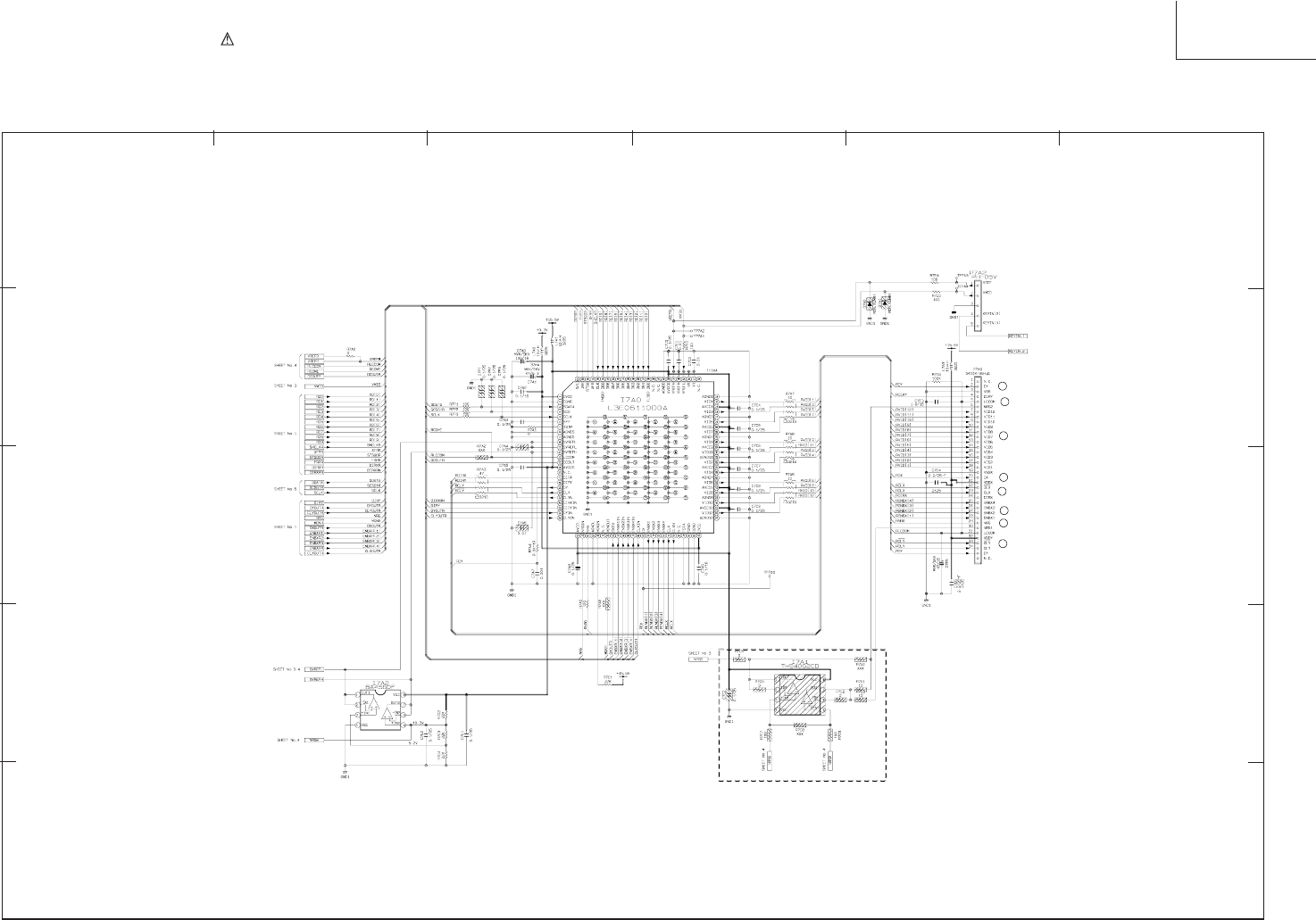
123456
A
B
C
D
E
PRODUCT SAFETY NOTE: Components marked with a and shaded have special characteristics important to
safety. Before replacing any of these components, read carefully the PRODUCT SAFETY NOTICE of this Service
Manual. Don’t degrade the safety of the receiver through improper servicing.
BASIC CIRCUIT DIAGRAM
All DC voltage to be measured with a tester (100k액/V). Voltage taken on a complex color bar signal including a standard color bar signal.
Since this is a basic circuit diagram, the value of the parts is subject to be altered for improvement.
141
11
12
13
16
17
18
19
20
LC57
DRIVE 2 OF 5
DRIVE R OUTPUT
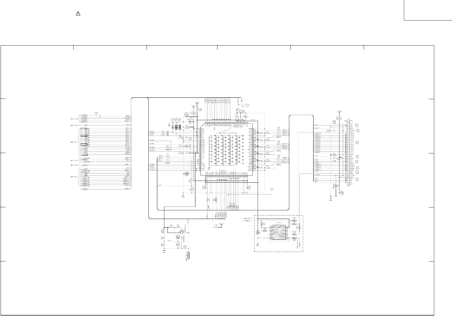
123456
A
B
C
D
E
PRODUCT SAFETY NOTE: Components marked with a and shaded have special characteristics important to
safety. Before replacing any of these components, read carefully the PRODUCT SAFETY NOTICE of this Service
Manual. Don’t degrade the safety of the receiver through improper servicing.
BASIC CIRCUIT DIAGRAM
All DC voltage to be measured with a tester (100k액/V). Voltage taken on a complex color bar signal including a standard color bar signal.
Since this is a basic circuit diagram, the value of the parts is subject to be altered for improvement.
142
11
12
14
16
17
18
19
20
LC57
DRIVE 3 OF 5
DRIVE G OUTPUT
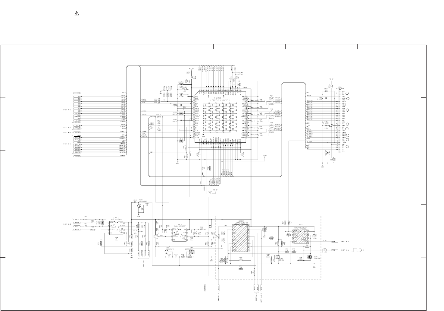
123456
A
B
C
D
E
All DC voltage to be measured with a tester (100k액/V). Voltage taken on a complex color bar signal including a standard color bar signal.
Since this is a basic circuit diagram, the value of the parts is subject to be altered for improvement.
PRODUCT SAFETY NOTE: Components marked with a and shaded have special characteristics important to
safety. Before replacing any of these components, read carefully the PRODUCT SAFETY NOTICE of this Service
Manual. Don’t degrade the safety of the receiver through improper servicing.
BASIC CIRCUIT DIAGRAM
143
11
12
15
16
17
18
19
20
LC57
DRIVE 4 OF 5
DRIVE B OUTPUT
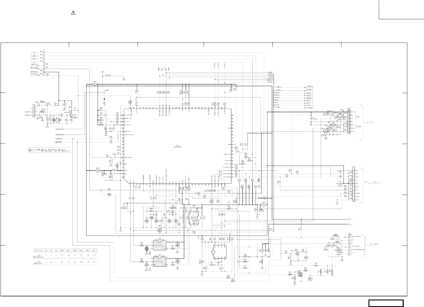
123456
A
B
C
D
E
PRODUCT SAFETY NOTE: Components marked with a and shaded have special characteristics important to
safety. Before replacing any of these components, read carefully the PRODUCT SAFETY NOTICE of this Service
Manual. Don’t degrade the safety of the receiver through improper servicing.
BASIC CIRCUIT DIAGRAM
All DC voltage to be measured with a tester (100k액/V). Voltage taken on a complex color bar signal including a standard color bar signal.
Since this is a basic circuit diagram, the value of the parts is subject to be altered for improvement.
144
LC57
DRIVE 5 OF 5
DRIVE
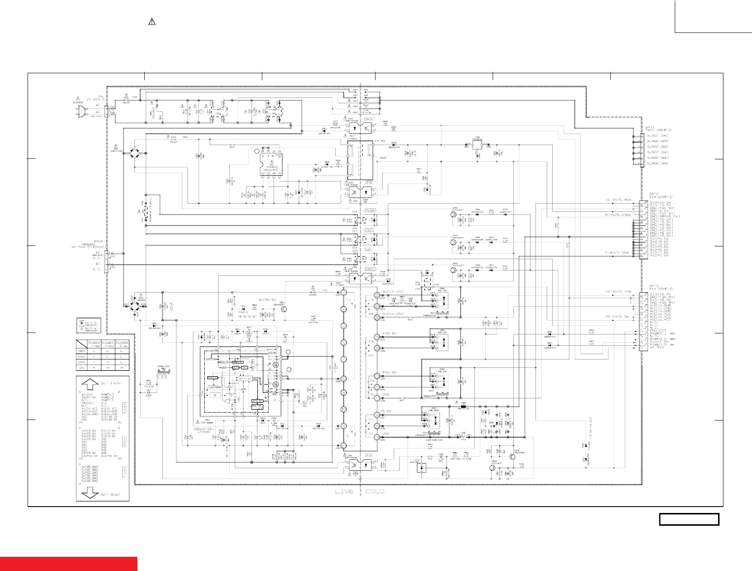
123456
A
B
C
D
E
All DC voltage to be measured with a tester (100k액/V). Voltage taken on a complex color bar signal including a standard color bar signal.
Since this is a basic circuit diagram, the value of the parts is subject to be altered for improvement.
PRODUCT SAFETY NOTE: Components marked with a and shaded have special characteristics important to
safety. Before replacing any of these components, read carefully the PRODUCT SAFETY NOTICE of this Service
Manual. Don’t degrade the safety of the receiver through improper servicing.
BASIC CIRCUIT DIAGRAM
TABLE OF CONTENTS
TABLE OF CONTENTS
145
24
23
22
LC57
POWER 1 OF 1
POWER
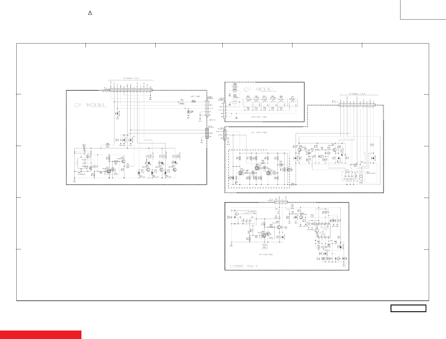
123456
A
B
C
D
E
All DC voltage to be measured with a tester (100k액/V). Voltage taken on a complex color bar signal including a standard color bar signal.
Since this is a basic circuit diagram, the value of the parts is subject to be altered for improvement.
PRODUCT SAFETY NOTE: Components marked with a and shaded have special characteristics important to
safety. Before replacing any of these components, read carefully the PRODUCT SAFETY NOTICE of this Service
Manual. Don’t degrade the safety of the receiver through improper servicing.
BASIC CIRCUIT DIAGRAM
TABLE OF CONTENTS
146
LC57
CONTROL 1 OF 2
CONTROL
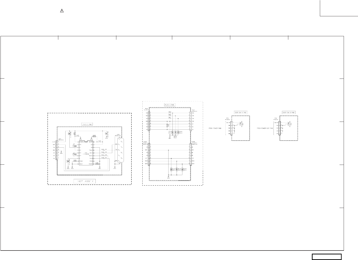
123456
A
B
C
D
E
All DC voltage to be measured with a tester (100k액/V). Voltage taken on a complex color bar signal including a standard color bar signal.
Since this is a basic circuit diagram, the value of the parts is subject to be altered for improvement.
PRODUCT SAFETY NOTE: Components marked with a and shaded have special characteristics important to
safety. Before replacing any of these components, read carefully the PRODUCT SAFETY NOTICE of this Service
Manual. Don’t degrade the safety of the receiver through improper servicing.
BASIC CIRCUIT DIAGRAM
147
LC57
CONTROL 2 OF 2
CONTROL
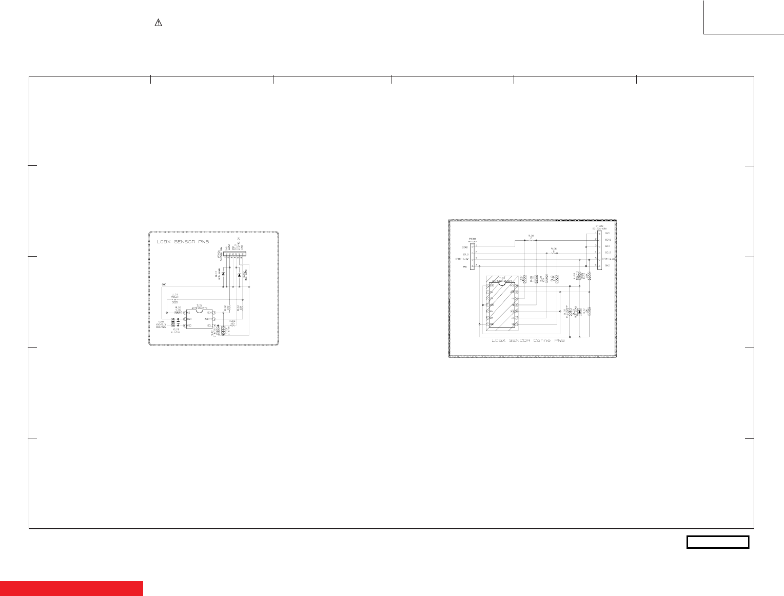
123456
A
B
C
D
E
All DC voltage to be measured with a tester (100k액/V). Voltage taken on a complex color bar signal including a standard color bar signal.
Since this is a basic circuit diagram, the value of the parts is subject to be altered for improvement.
PRODUCT SAFETY NOTE: Components marked with a and shaded have special characteristics important to
safety. Before replacing any of these components, read carefully the PRODUCT SAFETY NOTICE of this Service
Manual. Don’t degrade the safety of the receiver through improper servicing.
BASIC CIRCUIT DIAGRAM
TABLE OF CONTENTS
148
LC57
SENSOR 1 OF 1
SENSOR
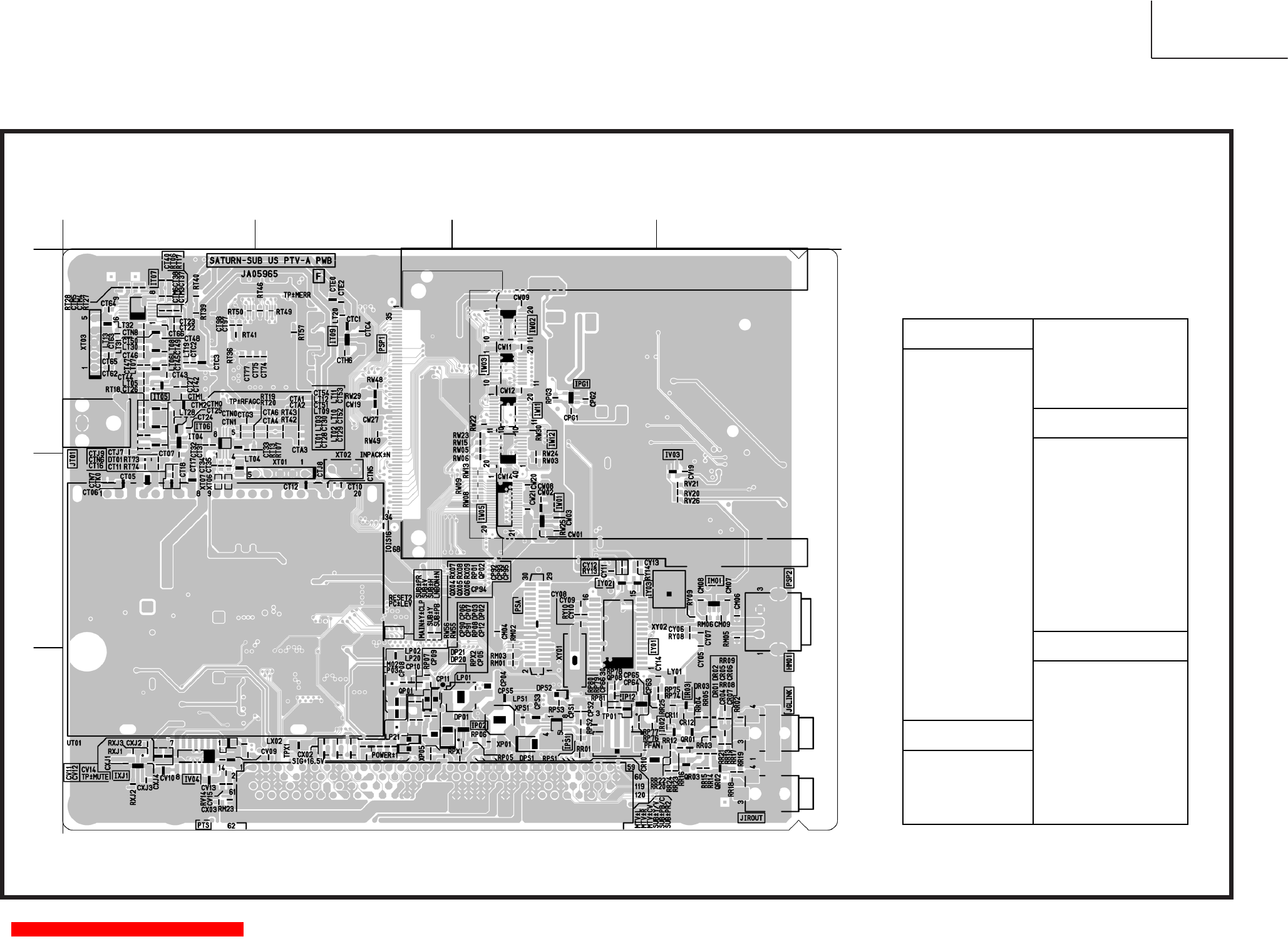
PRINTED CIRCUIT BOARDS
LC57 SUBDIGITAL PWB (Component side)
BACK TO TABLE OF CONTENTS
LC57
SUBDIGITAL PWB SEMICONDUCTOR LOCATION
(Component
side)
QR02 C-4
QR03 C-4
IM01 B-4 QX04 C-2
IP02 C-3 QX05 C-2
IP12 C-3 QX06 C-2
IPG1 A-3
IPS1 C-3
IR02 C-4
IR03 C-4
IT04 A-1 DP01 C-2
IT05 A-1 DP02 C-2
IT06 A-1 DP03 C-2
IT07 A-1 DP20 C-2
IT09 A-2 DP21 C-2
IV03 B-4 DPS1 C-3
IV04 C-1 DPS2 C-3
IW01 B-3 DR01 C-4
IW02 A-3 DR02 C-4
IW03 A-3 DR03 C-4
IW05 B-3 DT01 B-1
IW11 A-3
IW12 A-3
IXJ1 C-1
IY01 B-3 XP01 C-3
IY02 B-3 XP05 C-2
IY03 B-3 XPS1 C-3
XT01 B-2
XT02 B-2
XT03 A-1
QP01 C-2 XT06 B-1
QP02 C-2 XT07 B-1
QP08 C-3 XY01 C-3
QR01 C-4 XY02 B-4
CRYSTAL & FILTER
IC
TRANSISTOR
DIODE
1 2 3 4
A
B
C
149
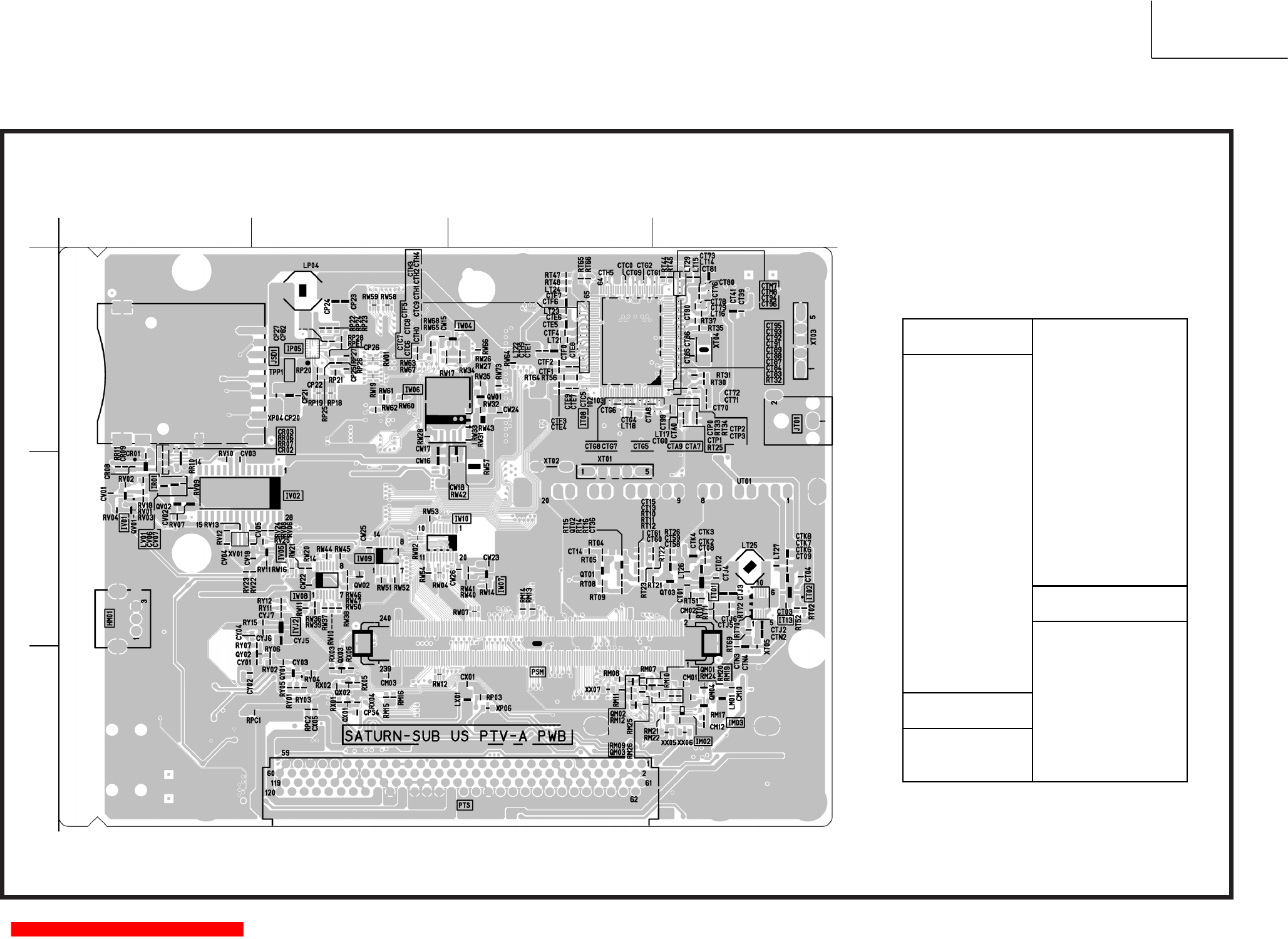
SUBDIGITAL PWB SEMICONDUCTOR LOCATION
(Solder
side)
QM03 C-3
QM04 C-4
IM02 C-4 QT01 B-3
IM03 C-4 QT02 B-3
IP05 A-2 QT03 B-4
IR01 B-1 QV01 B-1
IT01 B-4 QV02 B-1
IT02 B-4 QW01 A-3
IT08 A-3 QW02 B-2
IT13 B-4 QX01 C-2
IV01 B-1 QX02 C-2
IV02 B-1 QX03 C-2
IV05 B-2 QY01 C-2
IW04 A-3 QY02 C-2
IW06 A-3
IW07 B-3
IW08 B-2
IW09 B-2 XP04 A-2
IW10 B-2 XP06 C-3
IYJ2 B-2 XT04 A-4
XT05 B-4
XV01 B-1
XX05 C-4
QM01 C-4 XX06 C-4
QM02 C-3 XX07 C-3
CRYSTAL & FILTER
IC
TRANSISTOR
PRINTED CIRCUIT BOARDS
LC57SUBDIGITAL PWB (Solder side)
BACK TO TABLE OF CONTENTS
LC57
1 2 3 4
A
B
C
150
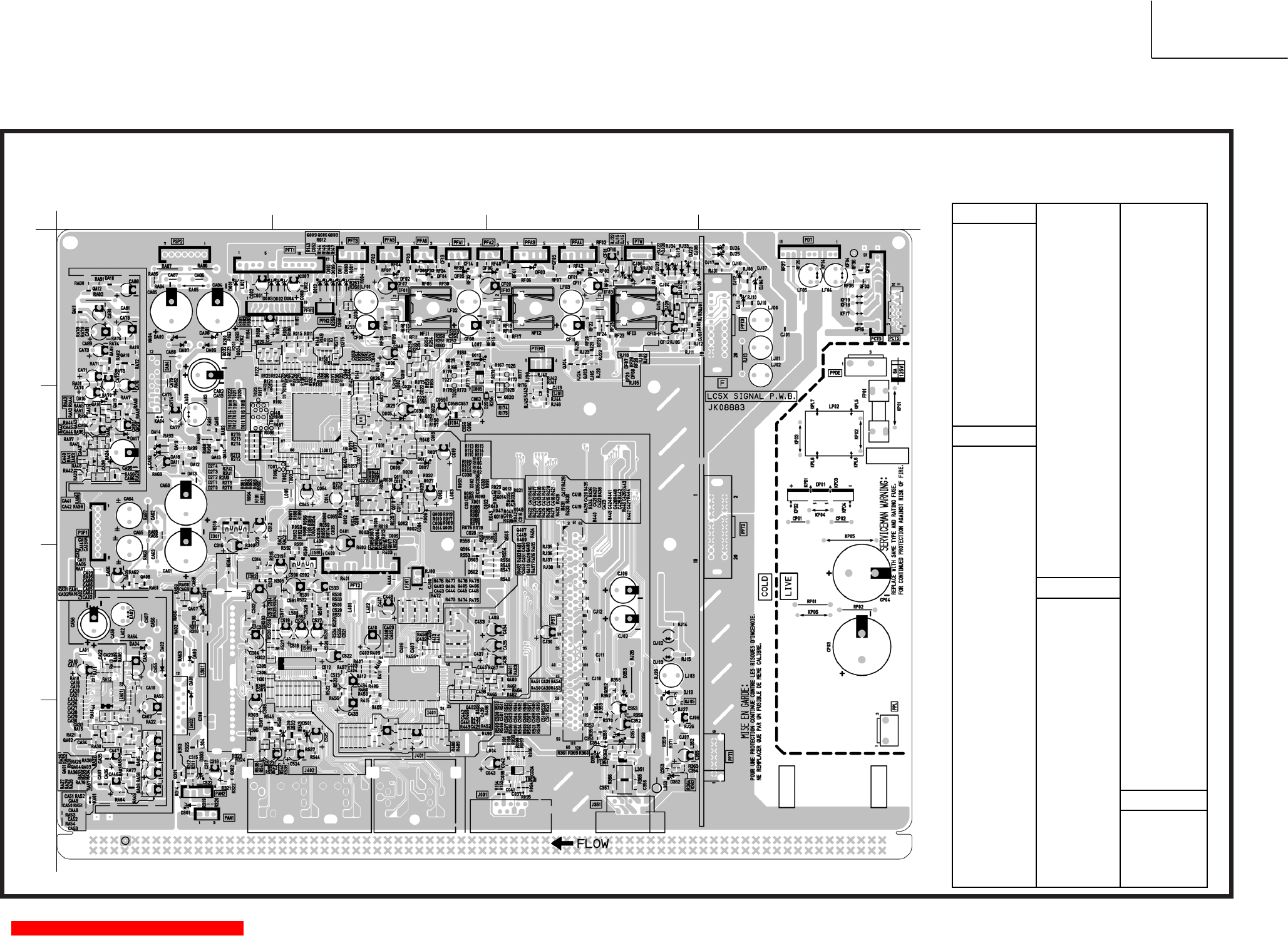
PRINTED CIRCUIT BOARDS
LC57SIGNAL PWB (Component side)
BACK TO TABLE OF CONTENTS
LC57
1 2 3 4
A
B
C
D
Q409 C-2 D355 D-3
Q410 C-2 D500 D-2
I001 B-2 Q500 C-2 D501 D-2
I002 B-2 Q501 C-2 D502 C-2
I003 D-3 Q502 D-2 D503 C-2
I004 B-2 Q503 D-1 DA01 D-1
I005
A
-2 Q504 C-2 DA02 C-1
I301 B-1 Q505 C-3 DA03 C-1
I302 C-1 QA01 D-1 DA04 C-1
I351 D-3 QA02 D-1 DA05 C-1
I401 C-2 QA03 D-1 DA06
A
-1
I501 C-2 QA04 D-1 DA07
A
-1
I591 C-2 QA05 D-1 DA08
A
-1
IA01 C-1 QA06 D-1 DA09
A
-1
IA02 D-1 QA07 C-1 DA10
A
-1
IA03 B-1 QA08 C-1 DA11 B-1
IA04
A
-1 QA09
A
-1 DA12 B-1
IF01
A
-2 QA10
A
-1 DA13 B-1
IF02
A
-3 QA11
A
-1 DA14 B-1
IF03
A
-3 QA12
A
-1 DA15 B-1
IJ01 B-3 QA13 B-1 DA16 B-1
QA14 B-1 DA17 B-1
QA15 B-1 DA18 B-1
QA18 B-1 DA19 B-1
Q001 B-2 QA19 B-1 DF01
A
-3
Q002 B-2 QA20 B-1 DF02
A
-2
Q003
A
-2 QF01
A
-3 DF03
A
-3
Q004 B-2 QF02
A
-4 DF04
A
-2
Q005 B-2 QF03
A
-4 DF05
A
-2
Q006
A
-2 QJ00
A
-3 DF06
A
-2
Q007 B-2 QJ01
A
-3 DF07
A
-3
Q008 B-2 QJ02
A
-3 DF08
A
-3
Q009
A
-2 QJ03
A
-3 DJ00
A
-3
Q010 B-2 QJ04
A
-3 DJ01
A
-3
Q011 B-2 QJ05 C-3 DJ02 C-3
Q012 B-2 QJ06
A
-3 DJ03 C-3
Q013 B-2 DJ04
A
-4
Q014 B-2 DJ07
A
-4
Q015 B-2 DJ08
A
-3
Q016 B-2 D001
A
-1 DJ09
A
-3
Q017 B-2 D002
A
-2 DJ10
A
-4
Q018
A
-2 D003
A
-2 DJ11
A
-4
Q021 B-2 D004
A
-2 DJ12
A
-4
Q022
A
-1 D005 B-2 DJ13 C-3
Q023
A
-1 D006 B-2 DJ14
A
-3
Q024
A
-2 D007 B-2 DJ15
A
-3
Q025 B-2 D008
A
-2 DJ16
A
-3
Q026
A
-2 D009
A
-2 DJ17
A
-4
Q027 B-2 D010
A
-2 DJ18
A
-4
Q028 B-3 D011
A
-2 DJ19
A
-3
Q029
A
-2 D012
A
-2 DJ20
A
-3
Q030
A
-2 D013
A
-2 DJ21
A
-3
Q250
A
-2 D250
A
-2 DJ22
A
-3
Q301 D-1 D251 B-3 DJ23
A
-3
Q302 D-1 D2T0 B-1 DJ24
A
-4
Q351 D-3 D2T1 B-1 DJ25
A
-4
Q352 C-3 D2T2 B-1 DP01 B-4
Q353 D-3 D2T3 B-1
Q400 C-3 D2T4 B-1
Q401 C-3 D2T5
A
-2
Q402 C-2 D301 D-1 H301 C-1
Q403 C-2 D302 C-1 H302 C-1
Q404 C-2 D303 D-1 H303 C-1
Q405 C-2 D351 D-3 H304 C-1
Q406 C-2 D352 D-3 H305 C-2
Q407 C-2 D353 C-3 X001 B-2
Q408 C-2 D354 D-3 X002 B-2
CRYSTAL & FILTER
IC
TRANSISTOR
DIODE
SIGNAL PWB SEMICONDUCTOR LOCATION
(Component side)
151

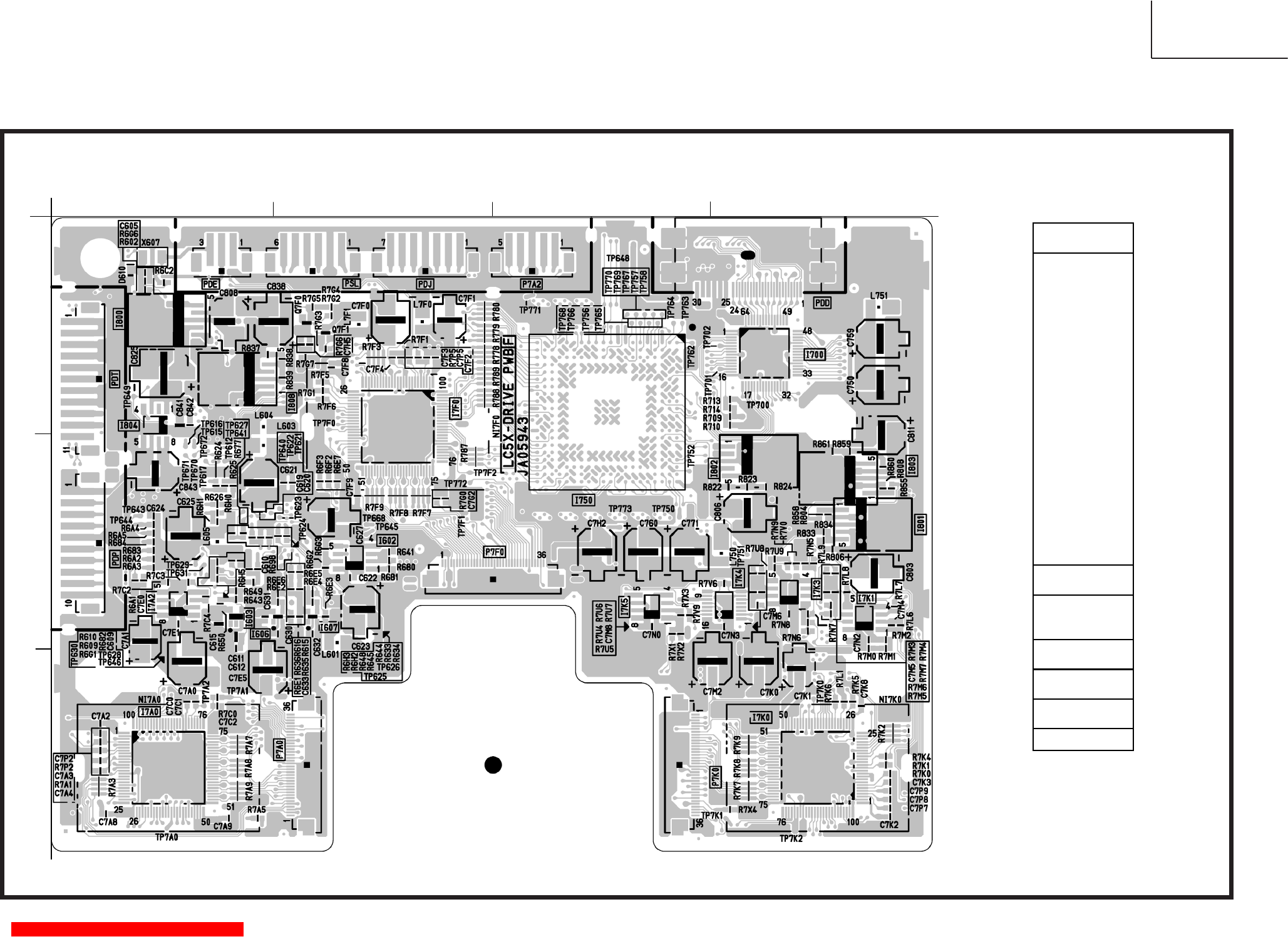
PRINTED CIRCUIT BOARDS
LC57DRIVE PWB (Component side)
BACK TO TABLE OF CONTENTS
LC57
1 2 3 4
A
B
C
I602 B-2
I603 B-1
I606 B-2
I607 B-2
I700 A-4
I750 A-3
I7A0 C-1
I7A2 B-1
I7F0 A-2
I7K0 C-4
I7K1 B-4
I7K3 B-4
I7K4 B-4
I7K5 B-3
I800 A-1
I801 B-4
I802 B-4
I803 B-4
I804 A-1
I808 A-1
Q7F0 A-2
Q7F1 A-2
D610 A-1
X607 A-1
FILTER
DIODE
IC
TRANSISTOR
DRIVE PWB SEMICONDUCTOR LOCATION
(Component Side)
153
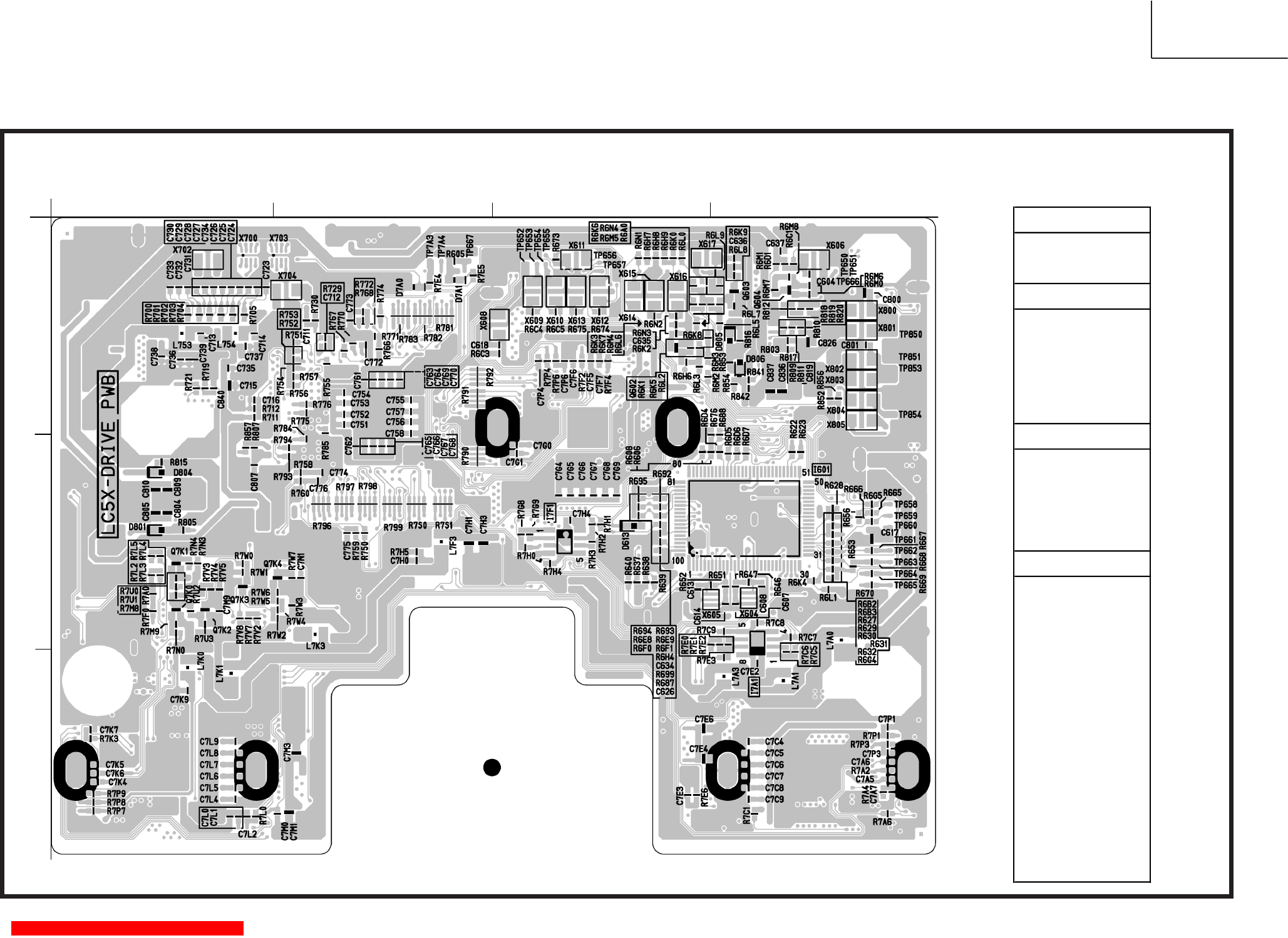
PRINTED CIRCUIT BOARDS
LC57 DRIVE PWB (Solder side)
BACK TO TABLE OF CONTENTS
LC57
1 2 3 4
A
B
C
I601 B-4
I7A1 B-4
I7F1 B-3
Q602 A-3
Q603 A-4
Q604 A-4
Q7K0 B-1
Q7K1 B-1
Q7K2 B-1
Q7K3 B-1
Q7K4 B-2
D613 B-3
D7A0 A-2
D7A1 A-2
D801 B-1
D804 B-1
D805 A-4
D806 A-4
X604 B-4
X605 B-3
X606 A-4
X608 A-3
X609 A-3
X610 A-3
X611 A-3
X612 A-3
X613 A-3
X614 A-3
X615 A-3
X616 A-3
X617 A-3
X700 A-1
X702 A-1
X703 A-2
X704 A-2
X800 A-4
X801 A-4
X802 A-4
X803 A-4
X804 A-4
X80
5
A-4
IC
CRYSTAL & FILTER
TRANSISTOR
DIODE
DRIVE PWB SEMICONDUCTOR LOCATION
(Solder Side)
154
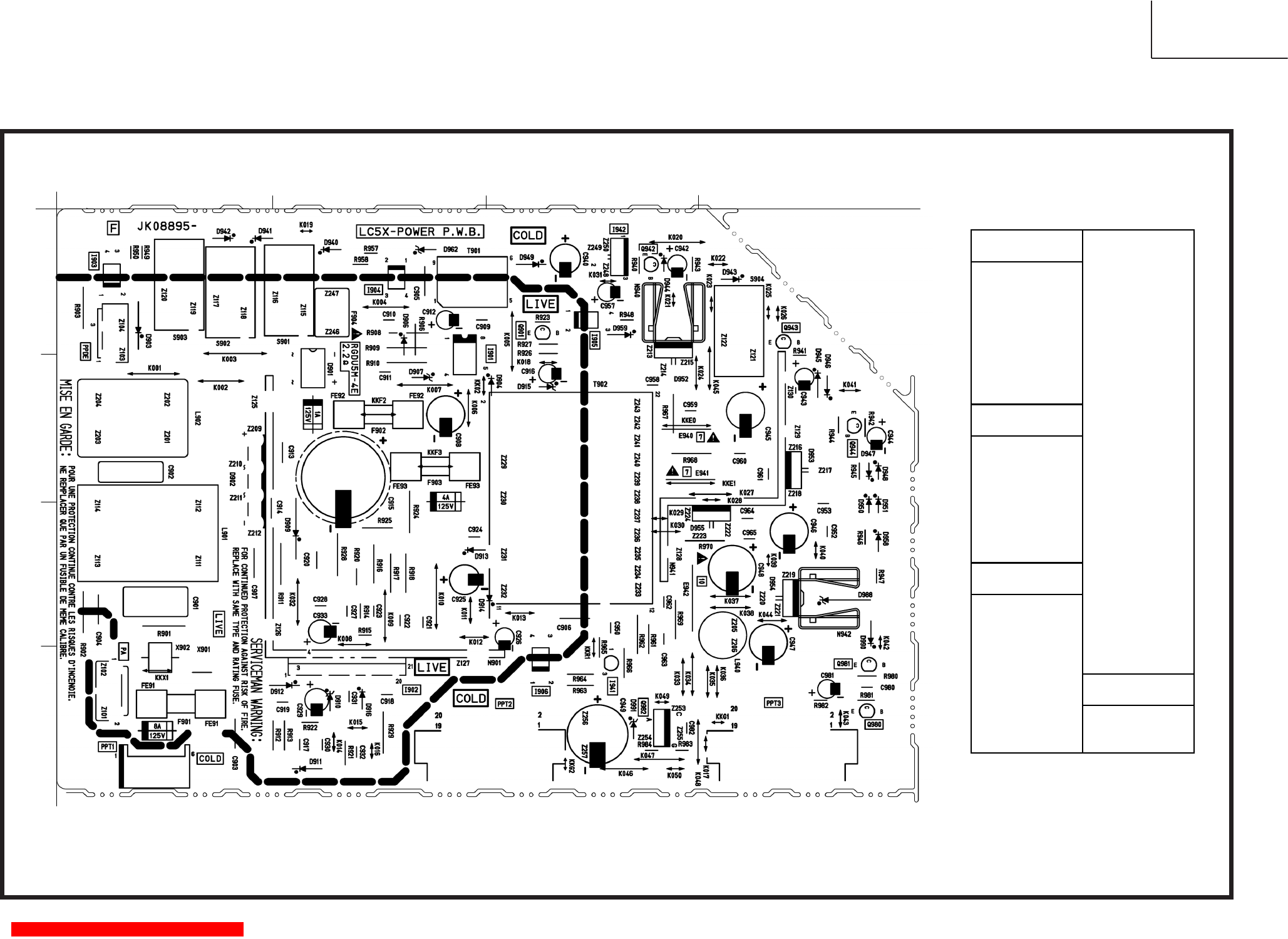
PRINTED CIRCUIT BOARDS
LC57POWER PWB (Component side)
BACK TO TABLE OF CONTENTS
LC57
1
2
3
4
A
B
C
D
D912 D-1
D913 C-3
I901 B-2 D914 C-3
I902 D-2 D915 B-3
I903 A-1 D916 D-2
I904 A-2 D940 A-2
I905 A-3 D941 A-1
I906 D-3 D942 A-1
I941 D-3 D943 A-4
I942 A-3 D944 A-3
D945 B-4
D946 B-4
D947 B-4
Q901 A-3 D948 B-4
Q942 A-3 D949 A-3
Q943 A-4 D950 C-4
Q944 B-4 D951 C-4
Q980 D-4 D952 A-3
Q981 D-4 D953 B-4
Q982 D-3 D954 C-4
D955 C-4
D958 C-4
D959 A-3
D901 B-2 D962 A-2
D902 B-1 D988 C-4
D903 A-1 D990 C-4
D904 B-3 D991 D-3
D906 B-2
D907 B-2
D909 B-2
D910 D-2 X901 D-1
D911 D-2 X902 D-1
D912 D-1
IC
TRANSISTOR
DIODE
CRYSTAL & FILTER
POWER PWB SEMICONDUCTOR LOCATION
(Component side)
155


REPLACEMENT PARTS LIST
PRODUCT SERVICE NOTE:Components marked with a have special characteristics important to safety.Before replacing any
of these components, read carefully, the PRODUCT SAFETY NOTICE of this Service Manual. Don’t degrade the safety of the
receiver through improper servicing.
Capacitors: Resistors: Semiconductors:
AL: Aluminum Electrolytic CF: Carbon Film TR: Transistor
CD: Ceramic Disc CC: Carbon Composition DI: Diode
EL: Electrolitic MF: Metal Oxide ZD: Zener Diode
PF: Polyester Film VR: Variable Resistor VA: Varistor
PP: Polypropylene WW: Wire Wound TH: Termistor
PL: Plastic FR: Fuse Resistor IC: Integrated Circuit
TA: Tantalum MG: Metal Grazed
PR: Paper
TM: Trimmer
MC: Mylar
ABBREVIATIONS
TABLE OF CONTENTS
165
LC57
SYMBOL PART No. DESCRIPTION
LC57
SYMBOL PART No. DESCRIPTION
LC57
CT02 AA01111R CERAMIC CAPACITOR(1.0UF 6.3V) 0
SUBDIGITAL PWB CT03 AA01144R CERAMIC CAP. 1608-B 1.0UF 16V 0
CT04 AA01111R CERAMIC CAPACITOR(1.0UF 6.3V) 0
CAPACITORS CT05 AA01173R CCC1R0K50-B-32CT 1UF/50V-B-3225 0
CM01 0893179R CAP.CHIP-CERAMIC 100000PF 16V TAPE 0 CT06 AA00937R CAP.CHIP-CERAMIC 10UF 10V 2012BK 0
CM02 0893179R CAP.CHIP-CERAMIC 100000PF 16V TAPE 0 CT07 AA01144R CERAMIC CAP. 1608-B 1.0UF 16V 0
CM03 0893179R CAP.CHIP-CERAMIC 100000PF 16V TAPE 0 CT08 AA00937R CAP.CHIP-CERAMIC 10UF 10V 2012BK 0
CM04 0893179R CAP.CHIP-CERAMIC 100000PF 16V TAPE 0 CT09 AA00937R CAP.CHIP-CERAMIC 10UF 10V 2012BK 0
CM06 0893179R CAP.CHIP-CERAMIC 100000PF 16V TAPE 0 CT10 0893179R CAP.CHIP-CERAMIC 100000PF 16V TAPE 0
CM07 AA01111R CERAMIC CAPACITOR(1.0UF 6.3V) 0 CT11 AA01802R CCC103K50-B-16CT MCH18 0
CM08 AA01123R CCC105K10-B-16CT 0 CT12 AA00937R CAP.CHIP-CERAMIC 10UF 10V 2012BK 0
CM09 AA01802R CCC103K50-B-16CT MCH18 0 CT13 0893208R CAP 1608CHIP 1000PFKB 50V TAPE 0
CM11 0893179R CAP.CHIP-CERAMIC 100000PF 16V TAPE 0 CT14 0893222R CAP 1608CHIP10000PFKB 50V TAPE 0
CM12 0893179R CAP.CHIP-CERAMIC 100000PF 16V TAPE 0 CT15 0893179R CAP.CHIP-CERAMIC 100000PF 16V TAPE 0
CP04 AA00699R CAP.CHIP-CERAMIC 10UFK 16V B 3 0 CT16 AA00937R CAP.CHIP-CERAMIC 10UF 10V 2012BK 0
CP05 AA00724R CAP.CHIP-CERAMIC 3216B 1UF 50V 0 CT17 AA00937R CAP.CHIP-CERAMIC 10UF 10V 2012BK 0
CP20 AA00937R CAP.CHIP-CERAMIC 10UF 10V 2012BK 0 CT22 0893179R CAP.CHIP-CERAMIC 100000PF 16V TAPE 0
CP21 0893179R CAP.CHIP-CERAMIC 100000PF 16V TAPE 0 CT23 0893208R CAP 1608CHIP 1000PFKB 50V TAPE 0
CP22 0893179R CAP.CHIP-CERAMIC 100000PF 16V TAPE 0 CT24 AA01111R CERAMIC CAPACITOR(1.0UF 6.3V) 0
CP23 AA00969R CAP.CHIP2125-B-22UF6.3V 0 CT25 AA00937R CAP.CHIP-CERAMIC 10UF 10V 2012BK 0
CP24 AA00969R CAP.CHIP2125-B-22UF6.3V 0 CT26 0893222R CAP 1608CHIP10000PFKB 50V TAPE 0
CP25 0893126R CAP 1608CHIP 100PFJCH 50V TAPE 0 CT27 0893222R CAP 1608CHIP10000PFKB 50V TAPE 0
CP26 0893208R CAP 1608CHIP 1000PFKB 50V TAPE 0 CT28 0893123R CAP 1608CHIP 56PFJCH 50V TAPE 0
CP27 0893193R CAP 1608CHIP 10000PFKB 25V TAPE 0 CT29 0893124R CAP 1608CHIP 68PFJCH 50V TAPE 0
CP63 AA01123R CCC105K10-B-16CT 0 CT30 0893115R CAP 1608CHIP 15PFJCH 50V TAPE 0
CP64 0893193R CAP 1608CHIP 10000PFKB 25V TAPE 0 CT31 0893179R CAP.CHIP-CERAMIC 100000PF 16V TAPE 0
CP65 0893126R CAP 1608CHIP 100PFJCH 50V TAPE 0 CT32 0893222R CAP 1608CHIP10000PFKB 50V TAPE 0
CP66 AA00969R CAP.CHIP2125-B-22UF6.3V 0 CT33 AA00937R CAP.CHIP-CERAMIC 10UF 10V 2012BK 0
CPG1 0893179R CAP.CHIP-CERAMIC 100000PF 16V TAPE 0 CT34 0893179R CAP.CHIP-CERAMIC 100000PF 16V TAPE 0
CPG2 0893135R CAP 1608CHIP 470PFJCH 50V TAPE 0 CT35 0893179R CAP.CHIP-CERAMIC 100000PF 16V TAPE 0
CPS1 0893126R CAP 1608CHIP 100PFJCH 50V TAPE 0 CT36 0893222R CAP 1608CHIP10000PFKB 50V TAPE 0
CPS2 0893213R CAP1608CHIP 2200PFKB 50V TAPE 0 CT39 0893222R CAP 1608CHIP10000PFKB 50V TAPE 0
CPS3 AA00955R CAP.CHIP-CERAMIC 2125 B 4.7UF 0 CT40 0893222R CAP 1608CHIP10000PFKB 50V TAPE 0
CPS4 0893179R CAP.CHIP-CERAMIC 100000PF 16V TAPE 0 CT41 AA00937R CAP.CHIP-CERAMIC 10UF 10V 2012BK 0
CPS5 AA00955R CAP.CHIP-CERAMIC 2125 B 4.7UF 0 CT42 0893179R CAP.CHIP-CERAMIC 100000PF 16V TAPE 0
CR01 0893179R CAP.CHIP-CERAMIC 100000PF 16V TAPE 0 CT43 0893222R CAP 1608CHIP10000PFKB 50V TAPE 0
CR02 0893208R CAP 1608CHIP 1000PFKB 50V TAPE 0 CT44 0893123R CAP 1608CHIP 56PFJCH 50V TAPE 0
CR03 0893208R CAP 1608CHIP 1000PFKB 50V TAPE 0 CT45 0893125R CAP 1608CHIP 82PFJCH 50V TAPE 0
CR08 0893179R CAP.CHIP-CERAMIC 100000PF 16V TAPE 0 CT46 0893125R CAP 1608CHIP 82PFJCH 50V TAPE 0
CT01 AA01144R CERAMIC CAP. 1608-B 1.0UF 16V 0 CT47 0893115R CAP 1608CHIP 15PFJCH 50V TAPE 0
!
PRODUCT SERVICE NOTE: Components marked with a have special characteristics important to safety. Before replacing any
of these components, read carefully, the PRODUCT SAFETY NOTICE of this Service Manual. Don’t degrade the safety of the
receiver through improper servicing.
166
LC57
SYMBOL PART No. DESCRIPTION
LC57
SYMBOL PART No. DESCRIPTION
LC57
CT48 0893106R CAP 1608CHIP 4PFCCK 50V TAPE 0 CTF1 0893179R CAP.CHIP-CERAMIC 100000PF 16V TAPE 0
CT49 0893121R CAP 1608CHIP 39PFJCH 50V TAPE 0 CTF2 0893179R CAP.CHIP-CERAMIC 100000PF 16V TAPE 0
CT51 0893125R CAP 1608CHIP 82PFJCH 50V TAPE 0 CTF3 0893179R CAP.CHIP-CERAMIC 100000PF 16V TAPE 0
CT52 0893119R CAP 1608CHIP 33PFJCH 50V TAPE 0 CTF4 AA01111R CERAMIC CAPACITOR(1.0UF 6.3V) 0
CT53 0893106R CAP 1608CHIP 4PFCCK 50V TAPE 0 CTF5 AA01231R 0.1UF 16V 1005-B CERAMIC CAPAC 0
CT54 0893124R CAP 1608CHIP 68PFJCH 50V TAPE 0 CTF6 AA00968R CCC106M06-B-20CT (10UF 6.3V 2012M) 0
CT58 AA00968R CCC106M06-B-20CT (10UF 6.3V 2012M) 0 CTF7 AA01231R 0.1UF 16V 1005-B CERAMIC CAPAC 0
CT60 0893179R CAP.CHIP-CERAMIC 100000PF 16V TAPE 0 CTG0 AA01231R 0.1UF 16V 1005-B CERAMIC CAPAC 0
CT61 0893222R CAP 1608CHIP10000PFKB 50V TAPE 0 CTG1 AA01231R 0.1UF 16V 1005-B CERAMIC CAPAC 0
CT62 0893179R CAP.CHIP-CERAMIC 100000PF 16V TAPE 0 CTG2 AA01231R 0.1UF 16V 1005-B CERAMIC CAPAC 0
CT63 0893179R CAP.CHIP-CERAMIC 100000PF 16V TAPE 0 CTG3 AA01111R CERAMIC CAPACITOR(1.0UF 6.3V) 0
CT64 0893179R CAP.CHIP-CERAMIC 100000PF 16V TAPE 0 CTG4 AA01231R 0.1UF 16V 1005-B CERAMIC CAPAC 0
CT65 0893179R CAP.CHIP-CERAMIC 100000PF 16V TAPE 0 CTG5 AA01231R 0.1UF 16V 1005-B CERAMIC CAPAC 0
CT66 0893222R CAP 1608CHIP10000PFKB 50V TAPE 0 CTG6 AA01231R 0.1UF 16V 1005-B CERAMIC CAPAC 0
CT67 0893179R CAP.CHIP-CERAMIC 100000PF 16V TAPE 0 CTG7 AA01231R 0.1UF 16V 1005-B CERAMIC CAPAC 0
CT68 0893179R CAP.CHIP-CERAMIC 100000PF 16V TAPE 0 CTG8 AA01231R 0.1UF 16V 1005-B CERAMIC CAPAC 0
CT69 0893179R CAP.CHIP-CERAMIC 100000PF 16V TAPE 0 CTG9 AA01231R 0.1UF 16V 1005-B CERAMIC CAPAC 0
CT70 0893179R CAP.CHIP-CERAMIC 100000PF 16V TAPE 0 CTH0 AA01231R 0.1UF 16V 1005-B CERAMIC CAPAC 0
CT71 0893208R CAP 1608CHIP 1000PFKB 50V TAPE 0 CTH1 AA01231R 0.1UF 16V 1005-B CERAMIC CAPAC 0
CT72 AA01111R CERAMIC CAPACITOR(1.0UF 6.3V) 0 CTH2 AA01231R 0.1UF 16V 1005-B CERAMIC CAPAC 0
CT73 AA01111R CERAMIC CAPACITOR(1.0UF 6.3V) 0 CTH3 AA01231R 0.1UF 16V 1005-B CERAMIC CAPAC 0
CT74 0893208R CAP 1608CHIP 1000PFKB 50V TAPE 0 CTH4 AA01231R 0.1UF 16V 1005-B CERAMIC CAPAC 0
CT75 0893126R CAP 1608CHIP 100PFJCH 50V TAPE 0 CTH5 AA01231R 0.1UF 16V 1005-B CERAMIC CAPAC 0
CT76 AA01231R 0.1UF 16V 1005-B CERAMIC CAPAC 0 CTH6 AA01144R CERAMIC CAP. 1608-B 1.0UF 16V 0
CT77 0893179R CAP.CHIP-CERAMIC 100000PF 16V TAPE 0 CTH9 0893179R CAP.CHIP-CERAMIC 100000PF 16V TAPE 0
CT78 AA01111R CERAMIC CAPACITOR(1.0UF 6.3V) 0 CTJ2 AA00937R CAP.CHIP-CERAMIC 10UF 10V 2012BK 0
CT79 AA01231R 0.1UF 16V 1005-B CERAMIC CAPAC 0 CTJ3 AA00969R CAP.CHIP2125-B-22UF6.3V 0
CT80 AA01231R 0.1UF 16V 1005-B CERAMIC CAPAC 0 CTJ4 AA00969R CAP.CHIP2125-B-22UF6.3V 0
CT81 AA00968R CCC106M06-B-20CT (10UF 6.3V 2012M) 0 CTJ5 0893122R CAP 1608CHIP 47PFJCH 50V TAPE 0
CT83 AA01231R 0.1UF 16V 1005-B CERAMIC CAPAC 0 CTJ6 0893123R CAP 1608CHIP 56PFJCH 50V TAPE 0
CT84 AA01231R 0.1UF 16V 1005-B CERAMIC CAPAC 0 CTJ7 0893222R CAP 1608CHIP10000PFKB 50V TAPE 0
CT85 0893113R CAP 1608CHIP 10PFCCH 50V TAPE 0 CTJ8 0893179R CAP.CHIP-CERAMIC 100000PF 16V TAPE 0
CT86 0893113R CAP 1608CHIP 10PFCCH 50V TAPE 0 CTJ9 0893179R CAP.CHIP-CERAMIC 100000PF 16V TAPE 0
CT87 AA01231R 0.1UF 16V 1005-B CERAMIC CAPAC 0 CTK0 0893179R CAP.CHIP-CERAMIC 100000PF 16V TAPE 0
CT88 AA01231R 0.1UF 16V 1005-B CERAMIC CAPAC 0 CTK2 0893179R CAP.CHIP-CERAMIC 100000PF 16V TAPE 0
CT89 AA01231R 0.1UF 16V 1005-B CERAMIC CAPAC 0 CTK3 0893179R CAP.CHIP-CERAMIC 100000PF 16V TAPE 0
CT90 AA01231R 0.1UF 16V 1005-B CERAMIC CAPAC 0 CTK4 AA00937R CAP.CHIP-CERAMIC 10UF 10V 2012BK 0
CT91 AA01231R 0.1UF 16V 1005-B CERAMIC CAPAC 0 CTK6 0893179R CAP.CHIP-CERAMIC 100000PF 16V TAPE 0
CT92 AA01231R 0.1UF 16V 1005-B CERAMIC CAPAC 0 CTK7 0893179R CAP.CHIP-CERAMIC 100000PF 16V TAPE 0
CT93 AA01231R 0.1UF 16V 1005-B CERAMIC CAPAC 0 CTK8 AA00937R CAP.CHIP-CERAMIC 10UF 10V 2012BK 0
CT94 AA01216R CAP.CHIP-CERAMIC 1005B 1UF 6.3 0 CTM0 0893179R CAP.CHIP-CERAMIC 100000PF 16V TAPE 0
CT95 AA01231R 0.1UF 16V 1005-B CERAMIC CAPAC 0 CTM1 0893179R CAP.CHIP-CERAMIC 100000PF 16V TAPE 0
CT96 AA01231R 0.1UF 16V 1005-B CERAMIC CAPAC 0 CTM2 AA00937R CAP.CHIP-CERAMIC 10UF 10V 2012BK 0
CT97 0893179R CAP.CHIP-CERAMIC 100000PF 16V TAPE 0 CTM3 0893179R CAP.CHIP-CERAMIC 100000PF 16V TAPE 0
CT98 0893179R CAP.CHIP-CERAMIC 100000PF 16V TAPE 0 CTM4 0893179R CAP.CHIP-CERAMIC 100000PF 16V TAPE 0
CT99 AA01231R 0.1UF 16V 1005-B CERAMIC CAPAC 0 CTM5 0893179R CAP.CHIP-CERAMIC 100000PF 16V TAPE 0
CTA0 AA01111R CERAMIC CAPACITOR(1.0UF 6.3V) 0 CTM6 0893179R CAP.CHIP-CERAMIC 100000PF 16V TAPE 0
CTA1 AA01111R CERAMIC CAPACITOR(1.0UF 6.3V) 0 CTM7 AA01111R CERAMIC CAPACITOR(1.0UF 6.3V) 0
CTA2 0893179R CAP.CHIP-CERAMIC 100000PF 16V TAPE 0 CTM8 AA01231R 0.1UF 16V 1005-B CERAMIC CAPAC 0
CTA3 0893208R CAP 1608CHIP 1000PFKB 50V TAPE 0 CTN0 0893179R CAP.CHIP-CERAMIC 100000PF 16V TAPE 0
CTA4 0893179R CAP.CHIP-CERAMIC 100000PF 16V TAPE 0 CTN1 0893179R CAP.CHIP-CERAMIC 100000PF 16V TAPE 0
CTA6 0893179R CAP.CHIP-CERAMIC 100000PF 16V TAPE 0 CTN2 AA00937R CAP.CHIP-CERAMIC 10UF 10V 2012BK 0
CTA7 AA01231R 0.1UF 16V 1005-B CERAMIC CAPAC 0 CTN5 0893222R CAP 1608CHIP10000PFKB 50V TAPE 0
CTA8 AA01231R 0.1UF 16V 1005-B CERAMIC CAPAC 0 CTN6 0893222R CAP 1608CHIP10000PFKB 50V TAPE 0
CTA9 AA01231R 0.1UF 16V 1005-B CERAMIC CAPAC 0 CTN7 0893222R CAP 1608CHIP10000PFKB 50V TAPE 0
CTC0 AA01231R 0.1UF 16V 1005-B CERAMIC CAPAC 0 CTN8 0893124R CAP 1608CHIP 68PFJCH 50V TAPE 0
CTC1 AA00931R CAP. CERAMIC 2012 (1UF 10V) 0 CTP0 0893123R CAP 1608CHIP 56PFJCH 50V TAPE 0
CTC2 0893179R CAP.CHIP-CERAMIC 100000PF 16V TAPE 0 CTP1 0893107R CAP 1608CHIP 5PFCCH 50V TAPE 0
CTC3 AA00968R CCC106M06-B-20CT (10UF 6.3V 2012M) 0 CTP2 0893123R CAP 1608CHIP 56PFJCH 50V TAPE 0
CTC4 0893208R CAP 1608CHIP 1000PFKB 50V TAPE 0 CTP3 0893107R CAP 1608CHIP 5PFCCH 50V TAPE 0
CTC5 AA01231R 0.1UF 16V 1005-B CERAMIC CAPAC 0 CV08 AA01141R CERAMIC CAPACITOR(0.1UF 16V) 0
CTC6 AA01231R 0.1UF 16V 1005-B CERAMIC CAPAC 0 CV09 AA00968R CCC106M06-B-20CT (10UF 6.3V 2012M) 0
CTC7 AA01231R 0.1UF 16V 1005-B CERAMIC CAPAC 0 CV10 AA00968R CCC106M06-B-20CT (10UF 6.3V 2012M) 0
CTC8 AA01231R 0.1UF 16V 1005-B CERAMIC CAPAC 0 CV11 0893008R CAP.CHIP-CERAMIC 100000PF 16V 0
CTC9 AA01231R 0.1UF 16V 1005-B CERAMIC CAPAC 0 CV12 AA00955R CAP.CHIP-CERAMIC 2125 B 4.7UF 0
CTE0 AA00968R CCC106M06-B-20CT (10UF 6.3V 2012M) 0 CV13 AA00968R CCC106M06-B-20CT (10UF 6.3V 2012M) 0
CTE1 AA00968R CCC106M06-B-20CT (10UF 6.3V 2012M) 0 CV14 AA00968R CCC106M06-B-20CT (10UF 6.3V 2012M) 0
CTE2 0893179R CAP.CHIP-CERAMIC 100000PF 16V TAPE 0 CV15 0893217R CAP 1608CHIP 4700PFKB 50V TAPE 0
CTE4 0893179R CAP.CHIP-CERAMIC 100000PF 16V TAPE 0 CV16 0893217R CAP 1608CHIP 4700PFKB 50V TAPE 0
CTE5 AA00968R CCC106M06-B-20CT (10UF 6.3V 2012M) 0 CW01 AA01123R CCC105K10-B-16CT 0
CTE6 AA01231R 0.1UF 16V 1005-B CERAMIC CAPAC 0 CW02 AA00968R CCC106M06-B-20CT (10UF 6.3V 2012M) 0
CTE7 0893208R CAP 1608CHIP 1000PFKB 50V TAPE 0 CW03 0893179R CAP.CHIP-CERAMIC 100000PF 16V TAPE 0
CTE8 0893208R CAP 1608CHIP 1000PFKB 50V TAPE 0 CW08 0893179R CAP.CHIP-CERAMIC 100000PF 16V TAPE 0
CTE9 0893222R CAP 1608CHIP10000PFKB 50V TAPE 0 CW09 0893179R CAP.CHIP-CERAMIC 100000PF 16V TAPE 0
CTF0 0893222R CAP 1608CHIP10000PFKB 50V TAPE 0 CW11 0893179R CAP.CHIP-CERAMIC 100000PF 16V TAPE 0
!

PRODUCT SERVICE NOTE:Components marked with a have special characteristics important to safety.Before replacing any
of these components, read carefully, the PRODUCT SAFETY NOTICE of this Service Manual. Don’t degrade the safety of the
receiver through improper servicing.
167
LC57
SYMBOL PART No. DESCRIPTION
LC57
SYMBOL PART No. DESCRIPTION
LC57
CW12 0893179R CAP.CHIP-CERAMIC 100000PF 16V TAPE 0 LT03 BA00162R CHIP COIL 56NK16CT-HK1608 0
CW14 0893179R CAP.CHIP-CERAMIC 100000PF 16V TAPE 0 LT04 BA00862R 2520 CHIP COIL 2.2UH 0
CW15 0893179R CAP.CHIP-CERAMIC 100000PF 16V TAPE 0 LT05 BA00192R CHIP COIL 47NJ16CT-HK1608 0
CW16 AA00937R CAP.CHIP-CERAMIC 10UF 10V 2012BK 0 LT06 BA01227R HK2125 TYPE CHIP INDUCTOR 150N 0
CW17 AA00937R CAP.CHIP-CERAMIC 10UF 10V 2012BK 0 LT07 BA00162R CHIP COIL 56NK16CT-HK1608 0
CW18 AA00969R CAP.CHIP2125-B-22UF6.3V 0 LT08 BA01234R HK2125 TYPE CHIP INDUCTOR 470N 0
CW19 AA00968R CCC106M06-B-20CT (10UF 6.3V 2012M) 0 LT09 BA00189R CHIP COIL 33NJ16CT-HK1608 0
CW20 0893179R CAP.CHIP-CERAMIC 100000PF 16V TAPE 0 LT10 BA01234R HK2125 TYPE CHIP INDUCTOR 470N 0
CW21 0893179R CAP.CHIP-CERAMIC 100000PF 16V TAPE 0 LT11 BA01225R HK2125 TYPE CHIP INDUCTOR 100N 0
CW22 0893179R CAP.CHIP-CERAMIC 100000PF 16V TAPE 0 LT12 BA00191R COIL HCC39NJ16CT-HK1608 0
CW23 0893179R CAP.CHIP-CERAMIC 100000PF 16V TAPE 0 LT14 BM10348R CHIP FERRITE BEAD BLM18PG121SN 0
CW24 0893179R CAP.CHIP-CERAMIC 100000PF 16V TAPE 0 LT15 BM10348R CHIP FERRITE BEAD BLM18PG121SN 0
CW25 0893179R CAP.CHIP-CERAMIC 100000PF 16V TAPE 0 LT16 BM10348R CHIP FERRITE BEAD BLM18PG121SN 0
CW26 0893179R CAP.CHIP-CERAMIC 100000PF 16V TAPE 0 LT17 BM10348R CHIP FERRITE BEAD BLM18PG121SN 0
CW27 0893179R CAP.CHIP-CERAMIC 100000PF 16V TAPE 0 LT18 BM10348R CHIP FERRITE BEAD BLM18PG121SN 0
CX01 AA01144R CERAMIC CAP. 1608-B 1.0UF 16V 0 LT19 BM10348R CHIP FERRITE BEAD BLM18PG121SN 0
CX02 AA01144R CERAMIC CAP. 1608-B 1.0UF 16V 0 LT20 BM10348R CHIP FERRITE BEAD BLM18PG121SN 0
CX03 0893179R CAP.CHIP-CERAMIC 100000PF 16V TAPE 0 LT21 BM10348R CHIP FERRITE BEAD BLM18PG121SN 0
CX04 0893179R CAP.CHIP-CERAMIC 100000PF 16V TAPE 0 LT22 BM10348R CHIP FERRITE BEAD BLM18PG121SN 0
CX05 0893179R CAP.CHIP-CERAMIC 100000PF 16V TAPE 0 LT23 BM10348R CHIP FERRITE BEAD BLM18PG121SN 0
CXJ1 AA01144R CERAMIC CAP. 1608-B 1.0UF 16V 0 LT24 BM10348R CHIP FERRITE BEAD BLM18PG121SN 0
CXJ2 0893126R CAP 1608CHIP 100PFJCH 50V TAPE 0 LT25 BA02252R 7E06NG TYPE POWER INDUCTOR 6.8 0
CXJ3 0893208R CAP 1608CHIP 1000PFKB 50V TAPE 0 LT26 BM10348R CHIP FERRITE BEAD BLM18PG121SN 0
CXJ4 AA01144R CERAMIC CAP. 1608-B 1.0UF 16V 0 LT27 BM10348R CHIP FERRITE BEAD BLM18PG121SN 0
LT28 BM10348R CHIP FERRITE BEAD BLM18PG121SN 0
DIODES LT29 BM10348R CHIP FERRITE BEAD BLM18PG121SN 0
DP01 CC00781R DIODE.CHIP RB160L-40(TE25) 0 LT30 BA00189R CHIP COIL 33NJ16CT-HK1608 0
DPS1 CC02211R RSX201L-30 0 LT31 BA01225R HK2125 TYPE CHIP INDUCTOR 100N 0
DPS2 CC01641R DIODE HSU119 0 LT32 BA00191R COIL HCC39NJ16CT-HK1608 0
DT01 CC01131R ZENER.CHIP MAZS3000H 0 LX01 BA00889R LBC2518 CHIP COIL 22UH 0
LX02 BA00889R LBC2518 CHIP COIL 22UH 0
MODULES
HM01 CZ01241 GP1FM514TZ0F 0 TRANSISTORS
QM04 CA02091R SRC1204EF_PF 0
INTEGRATED CIRCUITS (IC's) QP08 CA02091R SRC1204EF_PF 0
IM01 CK37218R MONO IC TK11150CSCL 0 QT01 CA02171R TRS.CHIP 2SC4082T106P 0
IM02 CK50961R SN74CB3T3306DCUR 0 QT02 CA02171R TRS.CHIP 2SC4082T106P 0
IM03 CK38326R IC SN74LVC1G32DCKR 0 QT03 CA02171R TRS.CHIP 2SC4082T106P 0
IP02 CK38851R MAX5026EUT-T 0 QW01 CA02171R TRS.CHIP 2SC4082T106P 0
IP05 CK52131R ANALOG MONOLITHIC IC(VT221H) 0 QW02 CA02091R SRC1204EF_PF 0
IP12 CK51331R TK11100CS 0 QX01 1323293R TRS.CHIP 2SC4617 TL (R/S) 0
IPG1 CK33543R ANALOG MONOLITHIC IC(PST9227N 0 QX02 1323293R TRS.CHIP 2SC4617 TL (R/S) 0
IPS1 CK52141R ANALOG MONOLITHIC IC(SC4517AI 0 QX03 1323293R TRS.CHIP 2SC4617 TL (R/S) 0
IR01 CK50051R MAX4788EXS-T 0 QX04 CA02091R SRC1204EF_PF 0
IT01 CK37218R MONO IC TK11150CSCL 0 QX05 CA02091R SRC1204EF_PF 0
IT02 CK37605R IC TK11250CM 0 QX06 CA02091R SRC1204EF_PF 0
IT04 CK37218R MONO IC TK11150CSCL 0
IT05 CK51131R UPC2711TB 0 RESISTORS
IT06 CK51151R UPC3221GV 0 RM01 0790001R CHIP RESISTOR RECJUMPER-1-16C16T1608 0
IT07 CK51141R UPC3220GR 0 RM02 AQ00519R CHIP RESISTOR 47OHM 0
IT08 CK51121U THEATER313 0 RM03 0790051R RES.CHIP 1/16W 10K OHM 0
IT09 CK37211R MONO IC TK11118CSCL 0 RM05 0790051R RES.CHIP 1/16W 10K OHM 0
IT13 CK50071R TPS62040DGQR 0 RM06 0790001R CHIP RESISTOR RECJUMPER-1-16C16T1608 0
IV04 CK51591R WM8521H9GED/RV 0 RM13 0196025R RES.-1608CHIP 1/16W 20-J 0
IW01 CK37218R MONO IC TK11150CSCL 0 RM14 0790001R CHIP RESISTOR RECJUMPER-1-16C16T1608 0
IW02 CK08271R DIGITAL MONOLITHIC IC (SN74LVC244PW) 0 RM15 0790051R RES.CHIP 1/16W 10K OHM 0
IW03 CK08271R DIGITAL MONOLITHIC IC (SN74LVC244PW) 0 RM16 0790051R RES.CHIP 1/16W 10K OHM 0
IW04 CK38327R DIGITAL MONOLITHIC IC (SN74LVC1G86DCKR) 0 RM17 0790046R RES.CHIP 1/16W 4.7K OHM 0
IW05 CK51161R PI5C32X245BEX 0 RM18 0790059R RES.CHIP 1/16W 47K OHM 0
IW06 CK38378R DIGITAL MONO IC SI-3012KM 0 RM19 0790015R RES.CHIP 1/16W 22 OHM 0
IW07 CK38326R IC SN74LVC1G32DCKR 0 RM20 0790015R RES.CHIP 1/16W 22 OHM 0
IW08 CK38917R DIGITAL MONOLITHIC IC (SN74LVC32APWR) 0 RM21 0790015R RES.CHIP 1/16W 22 OHM 0
IW09 CK36321R SN74LVC125APW 0 RM22 0790015R RES.CHIP 1/16W 22 OHM 0
IW10 CK08271R DIGITAL MONOLITHIC IC (SN74LVC244PW) 0 RP05 AQ00255R RES.CHIP 1/16W 200K OHM TAPE 0
IW11 CK08271R DIGITAL MONOLITHIC IC (SN74LVC244PW) 0 RP06 AQ00217R RES.CHIP 1/16W 7.5K OHM TAPE 0
IW12 CK08271R DIGITAL MONOLITHIC IC (SN74LVC244PW) 0 RP18 AQ00528R CHIP RESISTOR 220OHM 0
IXJ1 CK51331R TK11100CS 0 RP19 AQ00528R CHIP RESISTOR 220OHM 0
RP20 0790051R RES.CHIP 1/16W 10K OHM 0
COILS RP21 0790037R RES.CHIP 1/16W 1.0K OHM 0
LM02 BA00892R LBC2518 CHIP COIL 47UH 0 RP22 AQ00223R RES.CHIP 1/16W 12K OHM TAPE 0
LP01 BA00577R SMD CHIP COIL SLF6028T-470MR59 0 RP23 AQ00243R RES.CHIP 1/16W 68K OHM TAPE 0
LP04 BA02261R 7E08L TYPE POWER INDUCTOR 1.8U 0 RP24 AQ00237R RES.CHIP 1/16W 43K OHM TAPE 0
LPS1 BA02251R 7E06NG TYPE POWER INDUCTOR 4.7 0 RP25 0790064R RES.CHIP 1/16W 100K OHM 0
LT01 BA00161R COIL HCC47NK16CT-HK1608 0 RP26 AQ00247R RES.CHIP 1/16W 100K OHM TAPE 0
LT02 BA01227R HK2125 TYPE CHIP INDUCTOR 150N 0 RP27 AQ00227R RES.CHIP 1/16W 18K OHM TAPE 0
!

168
LC57
PRODUCT SERVICE NOTE:Components marked with a have special characteristics important to safety.Before replacing any
of these components, read carefully, the PRODUCT SAFETY NOTICE of this Service Manual. Don’t degrade the safety of the
receiver through improper servicing.
SYMBOL PART No. DESCRIPTION
LC57
SYMBOL PART No. DESCRIPTION
LC57
RP28 0790051R RES.CHIP 1/16W 10K OHM 0RW05 0790019R RES.CHIP 1/16W 47 OHM 0
RP75 0790001R CHIP RESISTOR RECJUMPER-1-16C16T1608 0 RW06 0790019R RES.CHIP 1/16W 47 OHM 0
RP76 AQ00245R RES.CHIP 1/16W 82K OHM TAPE 0 RW07 AQ00519R CHIP RESISTOR 47OHM 0
RP77 AQ00233R RES.CHIP 1/16W 30K OHM TAPE 0 RW08 AQ00519R CHIP RESISTOR 47OHM 0
RP78 0790051R RES.CHIP 1/16W 10K OHM 0 RW09 AQ00519R CHIP RESISTOR 47OHM 0
RP80 0790024R RES.CHIP 1/16W 100 OHM 0 RW10 0790019R RES.CHIP 1/16W 47 OHM 0
RP81 0790047R RES.CHIP 1/16W 5.6K OHM 0 RW11 0790019R RES.CHIP 1/16W 47 OHM 0
RPC1 0790001R CHIP RESISTOR RECJUMPER-1-16C16T1608 0 RW12 AQ00519R CHIP RESISTOR 47OHM 0
RPE1 0790001R CHIP RESISTOR RECJUMPER-1-16C16T1608 0 RW13 AQ00519R CHIP RESISTOR 47OHM 0
RPG3 0790046R RES.CHIP 1/16W 4.7K OHM 0 RW14 0790019R RES.CHIP 1/16W 47 OHM 0
RPS1 0790037R RES.CHIP 1/16W 1.0K OHM 0 RW15 0790019R RES.CHIP 1/16W 47 OHM 0
RPS2 0790051R RES.CHIP 1/16W 10K OHM 0 RW16 AQ00519R CHIP RESISTOR 47OHM 0
RPS3 AQ00236R RES.CHIP 1/16W 39K OHM TAPE 0 RW17 0790019R RES.CHIP 1/16W 47 OHM 0
RPS4 AQ00223R RES.CHIP 1/16W 12K OHM TAPE 0 RW18 0790019R RES.CHIP 1/16W 47 OHM 0
RPX1 0790001R CHIP RESISTOR RECJUMPER-1-16C16T1608 0 RW19 AQ00519R CHIP RESISTOR 47OHM 0
RPX2 0790001R CHIP RESISTOR RECJUMPER-1-16C16T1608 0 RW20 0790051R RES.CHIP 1/16W 10K OHM 0
RR06 0790019R RES.CHIP 1/16W 47 OHM 0 RW22 0790051R RES.CHIP 1/16W 10K OHM 0
RR07 0790019R RES.CHIP 1/16W 47 OHM 0 RW23 0790051R RES.CHIP 1/16W 10K OHM 0
RR10 AQ11519R RES CHIP 1/32 823J 3210 0 RW24 0790064R RES.CHIP 1/16W 100K OHM 0
RR11 0790061R RES.CHIP 1/16W 56K OHM 0 RW25 0790001R CHIP RESISTOR RECJUMPER-1-16C16T1608 0
RT09 0790043R RES.CHIP 1/16W 2.7K OHM 0 RW26 0790051R RES.CHIP 1/16W 10K OHM 0
RT10 AQ00258R RES.CHIP 1/16W 270K OHM TAPE 0 RW27 0790051R RES.CHIP 1/16W 10K OHM 0
RT11 AQ00247R RES.CHIP 1/16W 100K OHM TAPE 0 RW29 0195250R RES 2125 CHIP JUMPER WIRE 0
RT12 AQ00229R RES.CHIP 1/16W 22K OHM TAPE 0 RW31 AQ00243R RES.CHIP 1/16W 68K OHM TAPE 0
RT14 0790046R RES.CHIP 1/16W 4.7K OHM 0 RW32 AQ00247R RES.CHIP 1/16W 100K OHM TAPE 0
RT15 0790037R RES.CHIP 1/16W 1.0K OHM 0 RW33 0790001R CHIP RESISTOR RECJUMPER-1-16C16T1608 0
RT16 0790046R RES.CHIP 1/16W 4.7K OHM 0 RW34 AQ00231R RES.CHIP 1/16W 24K OHM TAPE 0
RT17 0790001R CHIP RESISTOR RECJUMPER-1-16C16T1608 0 RW35 AQ00258R RES.CHIP 1/16W 270K OHM TAPE 0
RT18 0790001R CHIP RESISTOR RECJUMPER-1-16C16T1608 0 RW36 0790001R CHIP RESISTOR RECJUMPER-1-16C16T1608 0
RT19 0790024R RES.CHIP 1/16W 100 OHM 0 RW37 0790019R RES.CHIP 1/16W 47 OHM 0
RT20 0790024R RES.CHIP 1/16W 100 OHM 0 RW38 0790019R RES.CHIP 1/16W 47 OHM 0
RT21 0790052R RES.CHIP 1/16W 12K OHM 0 RW40 0790051R RES.CHIP 1/16W 10K OHM 0
RT22 AQ00212R RES.CHIP 1/16W 4.7K OHM TAPE 0 RW41 0790051R RES.CHIP 1/16W 10K OHM 0
RT23 AQ00244R RES.CHIP 1/16W 75K OHM TAPE 0 RW42 0790051R RES.CHIP 1/16W 10K OHM 0
RT24 0790046R RES.CHIP 1/16W 4.7K OHM 0 RW43 AZ01031R THERMISTOR NANOSMDC050F13.2 0
RT25 0790046R RES.CHIP 1/16W 4.7K OHM 0 RW44 0790019R RES.CHIP 1/16W 47 OHM 0
RT26 0790001R CHIP RESISTOR RECJUMPER-1-16C16T1608 0 RW45 0790019R RES.CHIP 1/16W 47 OHM 0
RT27 0790024R RES.CHIP 1/16W 100 OHM 0 RW47 0790001R CHIP RESISTOR RECJUMPER-1-16C16T1608 0
RT28 0790024R RES.CHIP 1/16W 100 OHM 0 RW48 0790051R RES.CHIP 1/16W 10K OHM 0
RT30 AQ00175R RES.CHIP 1/16W 200 OHM TAPE 0 RW49 0790051R RES.CHIP 1/16W 10K OHM 0
RT31 AQ00175R RES.CHIP 1/16W 200 OHM TAPE 0 RW50 0790051R RES.CHIP 1/16W 10K OHM 0
RT32 0790037R RES.CHIP 1/16W 1.0K OHM 0 RW51 0790051R RES.CHIP 1/16W 10K OHM 0
RT33 0790028R RES.CHIP 1/16W 220 OHM 0 RW52 0790051R RES.CHIP 1/16W 10K OHM 0
RT34 0790028R RES.CHIP 1/16W 220 OHM 0 RW54 0790064R RES.CHIP 1/16W 100K OHM 0
RT36 0790037R RES.CHIP 1/16W 1.0K OHM 0 RW55 0790051R RES.CHIP 1/16W 10K OHM 0
RT37 0790001R CHIP RESISTOR RECJUMPER-1-16C16T1608 0 RW58 AQ00519R CHIP RESISTOR 47OHM 0
RT40 0790001R CHIP RESISTOR RECJUMPER-1-16C16T1608 0 RW59 AQ00519R CHIP RESISTOR 47OHM 0
RT42 AQ00175R RES.CHIP 1/16W 200 OHM TAPE 0 RW60 0790019R RES.CHIP 1/16W 47 OHM 0
RT43 AQ00175R RES.CHIP 1/16W 200 OHM TAPE 0 RW61 0790019R RES.CHIP 1/16W 47 OHM 0
RT44 0790019R RES.CHIP 1/16W 47 OHM 0 RW62 0790019R RES.CHIP 1/16W 47 OHM 0
RT45 0790019R RES.CHIP 1/16W 47 OHM 0 RW63 0790051R RES.CHIP 1/16W 10K OHM 0
RT46 0790011R RES.CHIP 1/16W 10 OHM 0 RW64 0790051R RES.CHIP 1/16W 10K OHM 0
RT47 0790011R RES.CHIP 1/16W 10 OHM 0 RW65 0790051R RES.CHIP 1/16W 10K OHM 0
RT48 0790011R RES.CHIP 1/16W 10 OHM 0 RW66 0790051R RES.CHIP 1/16W 10K OHM 0
RT49 AQ00511R CHIP RESISTOR 10OHM 0 RW67 0790051R RES.CHIP 1/16W 10K OHM 0
RT50 AQ00511R CHIP RESISTOR 10OHM 0 RW68 0790051R RES.CHIP 1/16W 10K OHM 0
RT56 0790001R CHIP RESISTOR RECJUMPER-1-16C16T1608 0 RW73 0790064R RES.CHIP 1/16W 100K OHM 0
RT57 0790035R RES.CHIP 1/16W 680 OHM 0 RW95 0790234R RES.CHIP 1/16W 100K OHM TAPE 0
RT64 0790051R RES.CHIP 1/16W 10K OHM 0 RX01 0790016R RES.CHIP 1/16W 27 OHM 0
RT65 0790001R CHIP RESISTOR RECJUMPER-1-16C16T1608 0 RX02 0790024R RES.CHIP 1/16W 100 OHM 0
RT66 0790001R CHIP RESISTOR RECJUMPER-1-16C16T1608 0 RX03 0790024R RES.CHIP 1/16W 100 OHM 0
RT69 0790051R RES.CHIP 1/16W 10K OHM 0 RX04 0790031R RES.CHIP 1/16W 330 OHM 0
RT70 0790051R RES.CHIP 1/16W 10K OHM 0 RX05 0790031R RES.CHIP 1/16W 330 OHM 0
RT71 AQ00261R RES.CHIP 1/16W 330K OHM TAPE 0 RX06 0790031R RES.CHIP 1/16W 330 OHM 0
RT72 AQ00258R RES.CHIP 1/16W 270K OHM TAPE 0 RX07 0790051R RES.CHIP 1/16W 10K OHM 0
RT73 0790043R RES.CHIP 1/16W 2.7K OHM 0 RX08 0790051R RES.CHIP 1/16W 10K OHM 0
RT74 0790043R RES.CHIP 1/16W 2.7K OHM 0 RX09 0790051R RES.CHIP 1/16W 10K OHM 0
RV14 0790051R RES.CHIP 1/16W 10K OHM 0 RXJ1 AQ00241R RES.CHIP 1/16W 56K OHM TAPE 0
RV15 0790051R RES.CHIP 1/16W 10K OHM 0 RXJ2 0790001R CHIP RESISTOR RECJUMPER-1-16C16T1608 0
RV16 AQ00185R RES.CHIP 1/16W 470 OHM TAPE 0 RXJ3 AQ00261R RES.CHIP 1/16W 330K OHM TAPE 0
RV17 AQ00185R RES.CHIP 1/16W 470 OHM TAPE 0
RW01 AQ00519R CHIP RESISTOR 47OHM 0 TEST POINTS
RW02 AQ00519R CHIP RESISTOR 47OHM 0 TPP1 EA00001R CHECKER CHIP 3216 TAPING 0
RW03 0790001R CHIP RESISTOR RECJUMPER-1-16C16T1608 0
RW04 AQ00519R CHIP RESISTOR 47OHM 0
!
169
PRODUCT SERVICE NOTE:Components marked with a have special characteristics important to safety.Before replacing any
of these components, read carefully, the PRODUCT SAFETY NOTICE of this Service Manual. Don’t degrade the safety of the
receiver through improper servicing.
LC57
SYMBOL PART No. DESCRIPTION
LC57
SYMBOL PART No. DESCRIPTION
LC57
CRYSTALS & FILTERS C060 AA01141R CERAMIC CAPACITOR(0.1UF 16V) 0
XP01 BK10323R CERAMIC FILTER NFM2012P13C105F 0 C061 0800326R CAP.-ELECTRO. 100UF-M 16V 0
XP04 BK10324R CERAMIC FILTER NFM2012P13C105BT1 0 C062 0800326R CAP.-ELECTRO. 100UF-M 16V 0
XP05 0195250R RES 2125 CHIP JUMPER WIRE 0 C064 AA01141R CERAMIC CAPACITOR(0.1UF 16V) 0
XP06 0195250R RES 2125 CHIP JUMPER WIRE 0 C065 AA01141R CERAMIC CAPACITOR(0.1UF 16V) 0
XPS1 BK10323R CERAMIC FILTER NFM2012P13C105F 0 C066 0893213R CAP1608CHIP 2200PFKB 50V TAPE 0
XT01 BG01624U SAW FILTER(X6875D) 0 C301 0800351R CAP.-ELECTRO. 470UF-M 6.3V 0
XT02 BN00261 BGS TRAP MKTGA47M2CAHP00B05 0 C302 AA01141R CERAMIC CAPACITOR(0.1UF 16V) 0
XT03 BG01625U SAW FILTER(X6888D) 0 C304 0893222R CAP 1608CHIP10000PFKB 50V TAPE 0
XT04 BL01491R OSC25R14X10T 0 C307 0893222R CAP 1608CHIP10000PFKB 50V TAPE 0
XT05 BK10324R CERAMIC FILTER NFM2012P13C105BT1 0 C308 0893222R CAP 1608CHIP10000PFKB 50V TAPE 0
XT06 BK00281R CHIP CERAMIC FILTER SC16-050 0 C310 AA01141R CERAMIC CAPACITOR(0.1UF 16V) 0
XT07 BK00281R CHIP CERAMIC FILTER SC16-050 0 C311 AA01141R CERAMIC CAPACITOR(0.1UF 16V) 0
XX05 BK00191R CHIP CERAMIC FILTER NFL21SP506X1C3D 0 C312 0800326R CAP.-ELECTRO. 100UF-M 16V 0
XX06 BK00191R CHIP CERAMIC FILTER NFL21SP506X1C3D 0 C313 AA01141R CERAMIC CAPACITOR(0.1UF 16V) 0
XX07 BK00193R CHIP CERAMIC FILTER NFL21SP107X1C3D 0 C314 AA01141R CERAMIC CAPACITOR(0.1UF 16V) 0
C315 AA01141R CERAMIC CAPACITOR(0.1UF 16V) 0
CONNECTORS, JACKS C316 0800326R CAP.-ELECTRO. 100UF-M 16V 0
JSD1 EY01821R SD MEMORY CARD SOCKET 54768-0977 0 C317 AA01141R CERAMIC CAPACITOR(0.1UF 16V) 0
JT01 EQ00791 JACK 0 C318 0800326R CAP.-ELECTRO. 100UF-M 16V 0
PFAN EA02132R 3P SMT PH CONNE. POST -LF- 0 C319 0800326R CAP.-ELECTRO. 100UF-M 16V 0
PSA EA00507R 30P FPC CONNECTOR 52559-3092 0 C320 AA01141R CERAMIC CAPACITOR(0.1UF 16V) 0
PSM EA02221U 0.5 PITCH 240P B TO B CONN. SH 0 C321 0800351R CAP.-ELECTRO. 470UF-M 6.3V 0
PSP1 EY02002 JACK SCAA1A4700 PC CARD 0 C323 0893208R CAP 1608CHIP 1000PFKB 50V TAPE 0
PSP2 EY01991 JACK SCAB1A8100 0 C400 AA01141R CERAMIC CAPACITOR(0.1UF 16V) 0
PTS ED04512U 2.54MM PITCH 120P B TO B PLUG 0 C401 0800352R CAP.-ELECTRO.470UF 10V 0
C402 AA01123R CCC105K10-B-16CT 0
MISCELLANEOUS C403 AA01123R CCC105K10-B-16CT 0
A JP08503 LC57 SUB DIGITAL PWB ASY 0 C404 AA01141R CERAMIC CAPACITOR(0.1UF 16V) 0
UT01 HJ00541 ENV56N01D5F (TUNER) 0 C406 AA01141R CERAMIC CAPACITOR(0.1UF 16V) 0
B JA05966 SATURN SUB DIGITAL PWB #6 0 C407 AA01141R CERAMIC CAPACITOR(0.1UF 16V) 0
NW01~4 MJ03878 SCRW M3M_2*10PN+SM Unknown 0 C408 AA01141R CERAMIC CAPACITOR(0.1UF 16V) 0
C409 AA01141R CERAMIC CAPACITOR(0.1UF 16V) 0
SIGNAL PWB C410 0800352R CAP.-ELECTRO.470UF 10V 0
C411 AA01123R CCC105K10-B-16CT 0
CAPACITORS C412 AA01123R CCC105K10-B-16CT 0
C004 AA01123R CCC105K10-B-16CT 0 C413 AA01141R CERAMIC CAPACITOR(0.1UF 16V) 0
C006 AA01123R CCC105K10-B-16CT 0 C414 AA01123R CCC105K10-B-16CT 0
C007 0800326R CAP.-ELECTRO. 100UF-M 16V 0 C415 AA01123R CCC105K10-B-16CT 0
C008 AA01141R CERAMIC CAPACITOR(0.1UF 16V) 0 C416 AA01141R CERAMIC CAPACITOR(0.1UF 16V) 0
C010 0893208R CAP 1608CHIP 1000PFKB 50V TAPE 0 C418 AA01141R CERAMIC CAPACITOR(0.1UF 16V) 0
C012 0800303R CAP.-ELECTRO. 22UF-M 50V 0 C419 0800352R CAP.-ELECTRO.470UF 10V 0
C013 0893213R CAP1608CHIP 2200PFKB 50V TAPE 0 C420 AA01123R CCC105K10-B-16CT 0
C014 0284623R CAP.-ELECTRO. 1UF-SME(BP) 50V 0 C421 AA01141R CERAMIC CAPACITOR(0.1UF 16V) 0
C017 AA01141R CERAMIC CAPACITOR(0.1UF 16V) 0 C422 AA01123R CCC105K10-B-16CT 0
C018 0893222R CAP 1608CHIP10000PFKB 50V TAPE 0 C423 0800303R CAP.-ELECTRO. 22UF-M 50V 0
C019 0800326R CAP.-ELECTRO. 100UF-M 16V 0 C424 AA01123R CCC105K10-B-16CT 0
C020 0893222R CAP 1608CHIP10000PFKB 50V TAPE 0 C425 AA01123R CCC105K10-B-16CT 0
C021 0893222R CAP 1608CHIP10000PFKB 50V TAPE 0 C426 AA01123R CCC105K10-B-16CT 0
C022 AA01145R CAP.CHIP-CERAMIC 1608B0.15UF/1 0 C427 AA01123R CCC105K10-B-16CT 0
C023 AA01141R CERAMIC CAPACITOR(0.1UF 16V) 0 C428 AA01123R CCC105K10-B-16CT 0
C025 0893222R CAP 1608CHIP10000PFKB 50V TAPE 0 C429 AA01123R CCC105K10-B-16CT 0
C026 AA01141R CERAMIC CAPACITOR(0.1UF 16V) 0 C430 AA01123R CCC105K10-B-16CT 0
C027 0893205R CAP 1608CHIP 560PFKB 50V TAPE 0 C431 AA01123R CCC105K10-B-16CT 0
C028 0893222R CAP 1608CHIP10000PFKB 50V TAPE 0 C432 0893222R CAP 1608CHIP10000PFKB 50V TAPE 0
C029 AA01141R CERAMIC CAPACITOR(0.1UF 16V) 0 C433 0800352R CAP.-ELECTRO.470UF 10V 0
C033 0893222R CAP 1608CHIP10000PFKB 50V TAPE 0 C434 0800352R CAP.-ELECTRO.470UF 10V 0
C038 AA01141R CERAMIC CAPACITOR(0.1UF 16V) 0 C435 0800294R CAP.-ELECTRO. 10UF-M(SMG) 50V 0
C040 AA01141R CERAMIC CAPACITOR(0.1UF 16V) 0 C436 0800326R CAP.-ELECTRO. 100UF-M 16V 0
C044 AA01141R CERAMIC CAPACITOR(0.1UF 16V) 0 C437 AA01141R CERAMIC CAPACITOR(0.1UF 16V) 0
C045 0800326R CAP.-ELECTRO. 100UF-M 16V 0 C438 AA01123R CCC105K10-B-16CT 0
C046 AA01123R CCC105K10-B-16CT 0 C439 AA01123R CCC105K10-B-16CT 0
C047 0893222R CAP 1608CHIP10000PFKB 50V TAPE 0 C440 AA01123R CCC105K10-B-16CT 0
C048 0800326R CAP.-ELECTRO. 100UF-M 16V 0 C441 AA01123R CCC105K10-B-16CT 0
C049 0893122R CAP 1608CHIP 47PFJCH 50V TAPE 0 C443 0893205R CAP 1608CHIP 560PFKB 50V TAPE 0
C050 AA01141R CERAMIC CAPACITOR(0.1UF 16V) 0 C447 AA01141R CERAMIC CAPACITOR(0.1UF 16V) 0
C051 0893122R CAP 1608CHIP 47PFJCH 50V TAPE 0 C448 0800326R CAP.-ELECTRO. 100UF-M 16V 0
C052 AA01141R CERAMIC CAPACITOR(0.1UF 16V) 0 C453 AA01141R CERAMIC CAPACITOR(0.1UF 16V) 0
C053 AA01141R CERAMIC CAPACITOR(0.1UF 16V) 0 C454 0800326R CAP.-ELECTRO. 100UF-M 16V 0
C054 0893122R CAP 1608CHIP 47PFJCH 50V TAPE 0 C500 AA01123R CCC105K10-B-16CT 0
C055 AA01141R CERAMIC CAPACITOR(0.1UF 16V) 0 C501 AA01123R CCC105K10-B-16CT 0
C056 AA01141R CERAMIC CAPACITOR(0.1UF 16V) 0 C502 AA01123R CCC105K10-B-16CT 0
C057 AA01123R CCC105K10-B-16CT 0 C503 AA01123R CCC105K10-B-16CT 0
C058 AA01141R CERAMIC CAPACITOR(0.1UF 16V) 0 C504 AA01123R CCC105K10-B-16CT 0
C059 0800326R CAP.-ELECTRO. 100UF-M 16V 0 C505 AA01123R CCC105K10-B-16CT 0
!
PRODUCT SERVICE NOTE: Components marked with a have special characteristics important to safety. Before replacing any
of these components, read carefully, the PRODUCT SAFETY NOTICE of this Service Manual. Don’t degrade the safety of the
receiver through improper servicing.
170
LC57
SYMBOL PART No. DESCRIPTION
LC57
SYMBOL PART No. DESCRIPTION
LC57
C506 AA01123R CCC105K10-B-16CT 0 D302 2348293M DIODE MTZ-J33CTA 0
C507 AA01123R CCC105K10-B-16CT 0 D500 2348031M DIO-MTZ-J2.7ATA 0
C508 AA01123R CCC105K10-B-16CT 0 D501 2348031M DIO-MTZ-J2.7ATA 0
C509 AA01123R CCC105K10-B-16CT 0 D502 CC01921R SDS142WKF_PF 0
C510 AA01123R CCC105K10-B-16CT 0 D503 CC01921R SDS142WKF_PF 0
C511 AA01123R CCC105K10-B-16CT 0 DA05 CC10521R DIODE 0
C512 AA01123R CCC105K10-B-16CT 0 DA11 CC01921R SDS142WKF_PF 0
C513 AA01123R CCC105K10-B-16CT 0 DA12 CC01921R SDS142WKF_PF 0
C514 AA01123R CCC105K10-B-16CT 0 DA13 CC01921R SDS142WKF_PF 0
C515 AA01123R CCC105K10-B-16CT 0 DA14 CC01921R SDS142WKF_PF 0
C518 AA01141R CERAMIC CAPACITOR(0.1UF 16V) 0 DA15 CC10521R DIODE 0
C519 0800326R CAP.-ELECTRO. 100UF-M 16V 0 DA16 2344041M DIODE 1SS254TA/1SS270TA 0
C522 0800303R CAP.-ELECTRO. 22UF-M 50V 0 DA17 2344041M DIODE 1SS254TA/1SS270TA 0
C523 0800294R CAP.-ELECTRO. 10UF-M(SMG) 50V 0 DF01 2344041M DIODE 1SS254TA/1SS270TA 0
C524 0800294R CAP.-ELECTRO. 10UF-M(SMG) 50V 0 DF03 2344041M DIODE 1SS254TA/1SS270TA 0
C526 0800294R CAP.-ELECTRO. 10UF-M(SMG) 50V 0 DF05 2344041M DIODE 1SS254TA/1SS270TA 0
C527 0800294R CAP.-ELECTRO. 10UF-M(SMG) 50V 0 DF07 CC01891R SDS511_PF 0
C590 0800352R CAP.-ELECTRO.470UF 10V 0 DF08 CC01891R SDS511_PF 0
C591 AA01141R CERAMIC CAPACITOR(0.1UF 16V) 0 DJ00 CC01921R SDS142WKF_PF 0
C592 AA01141R CERAMIC CAPACITOR(0.1UF 16V) 0 DJ01 CC01921R SDS142WKF_PF 0
C593 0800326R CAP.-ELECTRO. 100UF-M 16V 0 DJ04 2348101M ZENER MTZJ-5.1A TA 0
CA17 0800326R CAP.-ELECTRO. 100UF-M 16V 0 DJ07 CC01911R SDS142WAF_PF 0
CA34 0893222R CAP 1608CHIP10000PFKB 50V TAPE 0 DJ08 2344041M DIODE 1SS254TA/1SS270TA 0
CA35 AA00936R CERAMIC CAP. 2125-X5R 4.7UF 10V 0 DJ09 2344041M DIODE 1SS254TA/1SS270TA 0
CA36 AA00936R CERAMIC CAP. 2125-X5R 4.7UF 10V 0 DJ10 CC01921R SDS142WKF_PF 0
CA48 0800294R CAP.-ELECTRO. 10UF-M(SMG) 50V 0 DJ11 2348251M ZENER MTZJ-22A TA 0
CA49 0800294R CAP.-ELECTRO. 10UF-M(SMG) 50V 0 DJ14 2344041M DIODE 1SS254TA/1SS270TA 0
CA50 0893208R CAP 1608CHIP 1000PFKB 50V TAPE 0 DJ15 2344041M DIODE 1SS254TA/1SS270TA 0
CA51 0893208R CAP 1608CHIP 1000PFKB 50V TAPE 0 DJ16 2348132M ZENER MTZ-J6.8BTA 0
CA52 0800318R CAP.-ELECTRO. 47UF-M 25V 0 DJ17 CC01911R SDS142WAF_PF 0
CA53 0800318R CAP.-ELECTRO. 47UF-M 25V 0 DJ18 CC01911R SDS142WAF_PF 0
CA54 0800328R CAP. ELECTRO. 100UF-M 35V 0 DJ21 2344041M DIODE 1SS254TA/1SS270TA 0
CA55 0880194R CAP.-POLYESTER 0.1UF-J 50V 0 DJ22 2348132M ZENER MTZ-J6.8BTA 0
CA56 0880194R CAP.-POLYESTER 0.1UF-J 50V 0 DJ23 2348101M ZENER MTZJ-5.1A TA 0
CA57 0880194R CAP.-POLYESTER 0.1UF-J 50V 0 DJ25 2348101M ZENER MTZJ-5.1A TA 0
CA59 AL01152S CAP.ELECTROLYTIC 470UF-M(YXF)3 0 DP01 2342062 DIODE D3SBA60-4103 0
CA60 0284824F CAP.-ELECTRO. 2200UF 35V 0
CA61 0284824F CAP.-ELECTRO. 2200UF 35V 0 PROTECTORS
CA64 258616 CAP.-ELECTRO 2.2UF-M 50V 0 FE01 2721351 FUSE HOLDER 0
CA65 258616 CAP.-ELECTRO 2.2UF-M 50V 0 FP01 FN00474 FUSE 51MS 060 L-U 0
CA66 0800319R CAP.-ELECTRO. 47UF-M 35V 0
CA67 0800328R CAP. ELECTRO. 100UF-M 35V 0 INTEGRATED CIRCUITS (IC's)
CA68 0800279R CAP.-ELECTORO. 1.0UF-M(SMG) 50V 0 I001 CK50991U M306H3MC-067FP 0
CA69 AA01141R CERAMIC CAPACITOR(0.1UF 16V) 0 I002 CK51111R BD37A41FVM 0
CA93 0800294R CAP.-ELECTRO. 10UF-M(SMG) 50V 0 I004 CK37216R MONO IC TK11133CSCL 0
CA94 0800326R CAP.-ELECTRO. 100UF-M 16V 0 I005 CK50951R SN74CB3T3125PWR 0
CA95 0800359R CAP.-ELECTRO. 1000UF-M 10V 0 I301 CP05163S IC SI-3090F(LF1111) 0
CF04 AA00983R CERAMIC CAPACITOR(0.47UF 25V-B 0 I302 CK37605R IC TK11250CM 0
CF05 AA00983R CERAMIC CAPACITOR(0.47UF 25V-B 0 I401 CK39882U MM1630CQ 0
CF08 0800345R CAP.-ELECTRO. 330UF-M(SMG) 25V 0 I501 CK39891R MM1631XJBE 0
CF09 0800335R CAP.-ELECTRO. 220UF-M(SMG) 16V 0 I591 CP05163S IC SI-3090F(LF1111) 0
CF10 0800345R CAP.-ELECTRO. 330UF-M(SMG) 25V 0 IA02 2004752 TA8200AHQ 0
CF11 0800335R CAP.-ELECTRO. 220UF-M(SMG) 16V 0 IF02 CP05163F IC SI-3090F 0
CF13 AA00983R CERAMIC CAPACITOR(0.47UF 25V-B 0 IF03 CP05162F IC SI-3050F 0
CF15 0800303R CAP.-ELECTRO. 22UF-M 50V 0
CJ00 AA01141R CERAMIC CAPACITOR(0.1UF 16V) 0 JUMPER WIRES
CJ01 AA00991R CERAMIC CAPACITOR(0.1UF 50V-B) 0 KA01 2784381M 0.60MM TAPED JUMP.WIRE 0
CJ02 AL01105R CAP.ELECTROLYTIC 1000UF-M(YXF) 0 KA02 2784381M 0.60MM TAPED JUMP.WIRE 0
CJ04 0800326R CAP.-ELECTRO. 100UF-M 16V 0 KF04 2784381M 0.60MM TAPED JUMP.WIRE 0
CJ05 0893222R CAP 1608CHIP10000PFKB 50V TAPE 0 KF14 2784381M 0.60MM TAPED JUMP.WIRE 0
CJ08 0800326R CAP.-ELECTRO. 100UF-M 16V 0 KP02 2784381M 0.60MM TAPED JUMP.WIRE 0
CJ09 AL01105R CAP.ELECTROLYTIC 1000UF-M(YXF) 0 KP03 2784381M 0.60MM TAPED JUMP.WIRE 0
CJ10 0893179R CAP.CHIP-CERAMIC 100000PF 16V TAPE 0 KP04 2784381M 0.60MM TAPED JUMP.WIRE 0
CJ11 0893179R CAP.CHIP-CERAMIC 100000PF 16V TAPE 0 KP05 2784381M 0.60MM TAPED JUMP.WIRE 0
CJ12 0893179R CAP.CHIP-CERAMIC 100000PF 16V TAPE 0 KPD1 2784381M 0.60MM TAPED JUMP.WIRE 0
CJ30 0800288R CAP.-ELECTRO. 4.7UF-M(SMG) 50V 0 KPD2 2784381M 0.60MM TAPED JUMP.WIRE 0
CP01 AJ00167F CAP.CERAMIC CS12-F2GA472MYNS 0 KPD3 2784381M 0.60MM TAPED JUMP.WIRE 0
CP02 AJ00167F CAP.CERAMIC CS12-F2GA472MYNS 0 KPD4 2784381M 0.60MM TAPED JUMP.WIRE 0
CP03 AL02762 CAP.ELEC. 680UF 200V MXC SERIES 0
CP04 AL02762 CAP.ELEC. 680UF 200V MXC SERIES 0 COILS
L002 BH00697R FILTER COIL 100UH 0
DIODES L003 BH00697R FILTER COIL 100UH 0
D005 2344041M DIODE 1SS254TA/1SS270TA 0 L005 BH00697R FILTER COIL 100UH 0
D013 2348123M ZENER MTZJ-6.2C TA 0 L006 BH00697R FILTER COIL 100UH 0
D301 2348212M ZENER DIODE MTZ-J15B 0 L007 BH00697R FILTER COIL 100UH 0
!!
!
!
!
!!
!
!!
!
!

PRODUCT SERVICE NOTE: Components marked with a have special characteristics important to safety. Before replacing any
of these components, read carefully, the PRODUCT SAFETY NOTICE of this Service Manual. Don’t degrade the safety of the
receiver through improper servicing.
171
LC57
SYMBOL PART No. DESCRIPTION
LC57
SYMBOL PART No. DESCRIPTION
LC57
L400 BH00697R FILTER COIL 100UH 0 R015 0790051R RES.CHIP 1/16W 10K OHM 0
L401 2123781R FILTER COIL 100UH(EL0607) 0 R017 0790024R RES.CHIP 1/16W 100 OHM 0
L402 BH00697R FILTER COIL 100UH 0 R019 0790044R RES.CHIP 1/16W 3.3K OHM 0
L403 BH00697R FILTER COIL 100UH 0 R020 0790051R RES.CHIP 1/16W 10K OHM 0
L500 BH00697R FILTER COIL 100UH 0 R021 0790055R RES.CHIP 1/16W 22K OHM 0
LA01 BH00697R FILTER COIL 100UH 0 R023 0790037R RES.CHIP 1/16W 1.0K OHM 0
LJ00 2125797N FILT.COIL(LHL08 10UH) 0 R024 0790024R RES.CHIP 1/16W 100 OHM 0
LJ01 2125797N FILT.COIL(LHL08 10UH) 0 R027 0790057R RES.CHIP 1/16W 33K OHM 0
LJ02 2125803N FILT.COIL(LHL08 27UH) 0 R028 0790051R RES.CHIP 1/16W 10K OHM 0
LJ03 2125803N FILT.COIL(LHL08 27UH) 0 R029 0790059R RES.CHIP 1/16W 47K OHM 0
R030 0790042R RES.CHIP 1/16W 2.2K OHM 0
TRANSISTORS R032 0790001R CHIP RESISTOR RECJUMPER-1-16C16T1608 0
Q002 CA02132R TRS.CHIP 2SA1980UFG_PF 0 R033 0790046R RES.CHIP 1/16W 4.7K OHM 0
Q003 CA02091R SRC1204EF_PF 0 R034 0790028R RES.CHIP 1/16W 220 OHM 0
Q005 CA02142R TRS.CHIP 2SC5343UFG_PF 0 R035 0790051R RES.CHIP 1/16W 10K OHM 0
Q006 CA02091R SRC1204EF_PF 0 R037 0790051R RES.CHIP 1/16W 10K OHM 0
Q008 CA02132R TRS.CHIP 2SA1980UFG_PF 0 R038 0790055R RES.CHIP 1/16W 22K OHM 0
Q009 CA02091R SRC1204EF_PF 0 R039 0790052R RES.CHIP 1/16W 12K OHM 0
Q011 CA02132R TRS.CHIP 2SA1980UFG_PF 0 R040 0790064R RES.CHIP 1/16W 100K OHM 0
Q012 CA02132R TRS.CHIP 2SA1980UFG_PF 0 R042 0790059R RES.CHIP 1/16W 47K OHM 0
Q013 CA02142R TRS.CHIP 2SC5343UFG_PF 0 R043 0790046R RES.CHIP 1/16W 4.7K OHM 0
Q014 CA02142R TRS.CHIP 2SC5343UFG_PF 0 R044 0790064R RES.CHIP 1/16W 100K OHM 0
Q015 CA02142R TRS.CHIP 2SC5343UFG_PF 0 R046 0790046R RES.CHIP 1/16W 4.7K OHM 0
Q017 CA02142R TRS.CHIP 2SC5343UFG_PF 0 R047 0790047R RES.CHIP 1/16W 5.6K OHM 0
Q018 CA02091R SRC1204EF_PF 0 R048 0790047R RES.CHIP 1/16W 5.6K OHM 0
Q021 CA02092R SRC1202EF 0 R049 0790056R RES.CHIP 1/16W 27K OHM 0
Q025 CA02132R TRS.CHIP 2SA1980UFG_PF 0 R053 0790059R RES.CHIP 1/16W 47K OHM 0
Q026 CA02091R SRC1204EF_PF 0 R055 0790024R RES.CHIP 1/16W 100 OHM 0
Q027 CA02091R SRC1204EF_PF 0 R056 0790038R RES.CHIP 1/16W 1.2K OHM 0
Q029 CA02091R SRC1204EF_PF 0 R057 0790052R RES.CHIP 1/16W 12K OHM 0
Q030 CA02142R TRS.CHIP 2SC5343UFG_PF 0 R058 0790037R RES.CHIP 1/16W 1.0K OHM 0
Q301 CA02142R TRS.CHIP 2SC5343UFG_PF 0 R060 0790051R RES.CHIP 1/16W 10K OHM 0
Q400 CA02142R TRS.CHIP 2SC5343UFG_PF 0 R067 0790037R RES.CHIP 1/16W 1.0K OHM 0
Q401 CA02132R TRS.CHIP 2SA1980UFG_PF 0 R068 0790046R RES.CHIP 1/16W 4.7K OHM 0
Q402 CA02132R TRS.CHIP 2SA1980UFG_PF 0 R069 0790037R RES.CHIP 1/16W 1.0K OHM 0
Q403 CA02132R TRS.CHIP 2SA1980UFG_PF 0 R070 0790033R RES.CHIP 1/16W 470 OHM 0
Q407 CA02132R TRS.CHIP 2SA1980UFG_PF 0 R071 0790051R RES.CHIP 1/16W 10K OHM 0
Q408 CA02132R TRS.CHIP 2SA1980UFG_PF 0 R074 0790001R CHIP RESISTOR RECJUMPER-1-16C16T1608 0
Q409 CA02132R TRS.CHIP 2SA1980UFG_PF 0 R075 0790051R RES.CHIP 1/16W 10K OHM 0
Q410 CA02132R TRS.CHIP 2SA1980UFG_PF 0 R076 0790051R RES.CHIP 1/16W 10K OHM 0
Q500 CA02132R TRS.CHIP 2SA1980UFG_PF 0 R077 0790037R RES.CHIP 1/16W 1.0K OHM 0
Q501 CA02132R TRS.CHIP 2SA1980UFG_PF 0 R078 0790024R RES.CHIP 1/16W 100 OHM 0
Q502 CA00461R TRS.CHIP 2SD2114K 20V TAPE 0 R079 0790024R RES.CHIP 1/16W 100 OHM 0
Q503 CA00461R TRS.CHIP 2SD2114K 20V TAPE 0 R080 0790024R RES.CHIP 1/16W 100 OHM 0
Q504 CA02142R TRS.CHIP 2SC5343UFG_PF 0 R081 0790024R RES.CHIP 1/16W 100 OHM 0
Q505 CA02142R TRS.CHIP 2SC5343UFG_PF 0 R082 0790001R CHIP RESISTOR RECJUMPER-1-16C16T1608 0
QA01 CA02142R TRS.CHIP 2SC5343UFG_PF 0 R083 0790051R RES.CHIP 1/16W 10K OHM 0
QA02 CA02132R TRS.CHIP 2SA1980UFG_PF 0 R085 0790059R RES.CHIP 1/16W 47K OHM 0
QA03 CA02142R TRS.CHIP 2SC5343UFG_PF 0 R086 0790037R RES.CHIP 1/16W 1.0K OHM 0
QA04 CA02132R TRS.CHIP 2SA1980UFG_PF 0 R088 0790037R RES.CHIP 1/16W 1.0K OHM 0
QA05 CA00461R TRS.CHIP 2SD2114K 20V TAPE 0 R091 0790024R RES.CHIP 1/16W 100 OHM 0
QA06 CA00461R TRS.CHIP 2SD2114K 20V TAPE 0 R092 0790001R CHIP RESISTOR RECJUMPER-1-16C16T1608 0
QA07 CA02142R TRS.CHIP 2SC5343UFG_PF 0 R102 0790037R RES.CHIP 1/16W 1.0K OHM 0
QA08 CA02142R TRS.CHIP 2SC5343UFG_PF 0 R103 0790037R RES.CHIP 1/16W 1.0K OHM 0
QA13 CA02132R TRS.CHIP 2SA1980UFG_PF 0 R104 0790037R RES.CHIP 1/16W 1.0K OHM 0
QA14 CA02142R TRS.CHIP 2SC5343UFG_PF 0 R108 0790001R CHIP RESISTOR RECJUMPER-1-16C16T1608 0
QA15 CA02142R TRS.CHIP 2SC5343UFG_PF 0 R110 0790037R RES.CHIP 1/16W 1.0K OHM 0
QA18 CA02132R TRS.CHIP 2SA1980UFG_PF 0 R111 0790051R RES.CHIP 1/16W 10K OHM 0
QA19 CA02142R TRS.CHIP 2SC5343UFG_PF 0 R112 0790037R RES.CHIP 1/16W 1.0K OHM 0
QA20 CA02132R TRS.CHIP 2SA1980UFG_PF 0 R113 0790037R RES.CHIP 1/16W 1.0K OHM 0
QF01 CA02142R TRS.CHIP 2SC5343UFG_PF 0 R114 0790051R RES.CHIP 1/16W 10K OHM 0
QJ00 CA02091R SRC1204EF_PF 0 R115 0790051R RES.CHIP 1/16W 10K OHM 0
QJ01 CA02132R TRS.CHIP 2SA1980UFG_PF 0 R116 0790051R RES.CHIP 1/16W 10K OHM 0
QJ02 CA02132R TRS.CHIP 2SA1980UFG_PF 0 R119 0790024R RES.CHIP 1/16W 100 OHM 0
QJ03 CA02142R TRS.CHIP 2SC5343UFG_PF 0 R120 0790024R RES.CHIP 1/16W 100 OHM 0
QJ04 CA02142R TRS.CHIP 2SC5343UFG_PF 0 R121 0790024R RES.CHIP 1/16W 100 OHM 0
QJ06 CA02132R TRS.CHIP 2SA1980UFG_PF 0 R122 0790037R RES.CHIP 1/16W 1.0K OHM 0
R123 0790037R RES.CHIP 1/16W 1.0K OHM 0
RESISTORS R124 0790037R RES.CHIP 1/16W 1.0K OHM 0
R002 0790024R RES.CHIP 1/16W 100 OHM 0 R125 0790037R RES.CHIP 1/16W 1.0K OHM 0
R006 0790046R RES.CHIP 1/16W 4.7K OHM 0 R126 0790037R RES.CHIP 1/16W 1.0K OHM 0
R009 0790058R RES.CHIP 1/16W 39K OHM 0 R127 0790037R RES.CHIP 1/16W 1.0K OHM 0
R010 0790059R RES.CHIP 1/16W 47K OHM 0 R128 0790037R RES.CHIP 1/16W 1.0K OHM 0
R011 0790051R RES.CHIP 1/16W 10K OHM 0 R129 0790037R RES.CHIP 1/16W 1.0K OHM 0
R014 0790059R RES.CHIP 1/16W 47K OHM 0 R130 0790024R RES.CHIP 1/16W 100 OHM 0
!

172
LC57
PRODUCT SERVICE NOTE: Components marked with a have special characteristics important to safety. Before replacing any
of these components, read carefully, the PRODUCT SAFETY NOTICE of this Service Manual. Don’t degrade the safety of the
receiver through improper servicing.
SYMBOL PART No. DESCRIPTION
LC57
SYMBOL PART No. DESCRIPTION
LC57
R131 0790024R RES.CHIP 1/16W 100 OHM 0 R412 0790037R RES.CHIP 1/16W 1.0K OHM 0
R132 0790024R RES.CHIP 1/16W 100 OHM 0 R413 0790024R RES.CHIP 1/16W 100 OHM 0
R133 0790024R RES.CHIP 1/16W 100 OHM 0 R414 0790024R RES.CHIP 1/16W 100 OHM 0
R134 0790024R RES.CHIP 1/16W 100 OHM 0 R415 0790037R RES.CHIP 1/16W 1.0K OHM 0
R135 0790024R RES.CHIP 1/16W 100 OHM 0 R416 0790024R RES.CHIP 1/16W 100 OHM 0
R136 0790024R RES.CHIP 1/16W 100 OHM 0 R417 0790024R RES.CHIP 1/16W 100 OHM 0
R137 0790024R RES.CHIP 1/16W 100 OHM 0 R418 0790024R RES.CHIP 1/16W 100 OHM 0
R138 0790037R RES.CHIP 1/16W 1.0K OHM 0 R419 0790024R RES.CHIP 1/16W 100 OHM 0
R139 0790051R RES.CHIP 1/16W 10K OHM 0 R420 0790024R RES.CHIP 1/16W 100 OHM 0
R140 0196060R RES 1608 CHIP 1/16W 510J TAPE 0 R421 0790024R RES.CHIP 1/16W 100 OHM 0
R141 0196075R RES 1608 CHIP 1/16W 2.0KJ TAPE 0 R422 AQ00164R CHIP RESISTOR 1/16W 75OHM TAPE 0
R142 0196075R RES 1608 CHIP 1/16W 2.0KJ TAPE 0 R423 AQ00164R CHIP RESISTOR 1/16W 75OHM TAPE 0
R143 0790051R RES.CHIP 1/16W 10K OHM 0 R424 AQ00164R CHIP RESISTOR 1/16W 75OHM TAPE 0
R144 0790051R RES.CHIP 1/16W 10K OHM 0 R425 AQ00164R CHIP RESISTOR 1/16W 75OHM TAPE 0
R146 0790051R RES.CHIP 1/16W 10K OHM 0 R426 AQ00164R CHIP RESISTOR 1/16W 75OHM TAPE 0
R148 0790059R RES.CHIP 1/16W 47K OHM 0 R427 AQ00164R CHIP RESISTOR 1/16W 75OHM TAPE 0
R149 0790059R RES.CHIP 1/16W 47K OHM 0 R428 0790037R RES.CHIP 1/16W 1.0K OHM 0
R150 0790059R RES.CHIP 1/16W 47K OHM 0 R430 0790037R RES.CHIP 1/16W 1.0K OHM 0
R151 0790059R RES.CHIP 1/16W 47K OHM 0 R431 0790051R RES.CHIP 1/16W 10K OHM 0
R157 0790051R RES.CHIP 1/16W 10K OHM 0 R432 0790051R RES.CHIP 1/16W 10K OHM 0
R158 0790051R RES.CHIP 1/16W 10K OHM 0 R433 0790051R RES.CHIP 1/16W 10K OHM 0
R160 0790051R RES.CHIP 1/16W 10K OHM 0 R434 0790051R RES.CHIP 1/16W 10K OHM 0
R161 0790051R RES.CHIP 1/16W 10K OHM 0 R435 0790024R RES.CHIP 1/16W 100 OHM 0
R165 0790024R RES.CHIP 1/16W 100 OHM 0 R436 0790037R RES.CHIP 1/16W 1.0K OHM 0
R166 0790024R RES.CHIP 1/16W 100 OHM 0 R437 0790024R RES.CHIP 1/16W 100 OHM 0
R167 0790024R RES.CHIP 1/16W 100 OHM 0 R438 0790024R RES.CHIP 1/16W 100 OHM 0
R168 0790037R RES.CHIP 1/16W 1.0K OHM 0 R439 0790051R RES.CHIP 1/16W 10K OHM 0
R170 0790037R RES.CHIP 1/16W 1.0K OHM 0 R440 0790051R RES.CHIP 1/16W 10K OHM 0
R171 0790024R RES.CHIP 1/16W 100 OHM 0 R441 0790024R RES.CHIP 1/16W 100 OHM 0
R172 0790024R RES.CHIP 1/16W 100 OHM 0 R442 0790024R RES.CHIP 1/16W 100 OHM 0
R173 0790037R RES.CHIP 1/16W 1.0K OHM 0 R443 0790024R RES.CHIP 1/16W 100 OHM 0
R174 0790037R RES.CHIP 1/16W 1.0K OHM 0 R444 0790024R RES.CHIP 1/16W 100 OHM 0
R180 0790051R RES.CHIP 1/16W 10K OHM 0 R445 AQ00164R CHIP RESISTOR 1/16W 75OHM TAPE 0
R181 0790037R RES.CHIP 1/16W 1.0K OHM 0 R446 AQ00164R CHIP RESISTOR 1/16W 75OHM TAPE 0
R182 0790035R RES.CHIP 1/16W 680 OHM 0 R447 AQ00164R CHIP RESISTOR 1/16W 75OHM TAPE 0
R183 0790037R RES.CHIP 1/16W 1.0K OHM 0 R448 0790024R RES.CHIP 1/16W 100 OHM 0
R184 0790037R RES.CHIP 1/16W 1.0K OHM 0 R449 0790024R RES.CHIP 1/16W 100 OHM 0
R185 0790037R RES.CHIP 1/16W 1.0K OHM 0 R450 0790024R RES.CHIP 1/16W 100 OHM 0
R186 0790037R RES.CHIP 1/16W 1.0K OHM 0 R451 0790024R RES.CHIP 1/16W 100 OHM 0
R187 0790037R RES.CHIP 1/16W 1.0K OHM 0 R452 AQ00164R CHIP RESISTOR 1/16W 75OHM TAPE 0
R188 0790051R RES.CHIP 1/16W 10K OHM 0 R453 AQ00164R CHIP RESISTOR 1/16W 75OHM TAPE 0
R189 0790051R RES.CHIP 1/16W 10K OHM 0 R454 AQ00164R CHIP RESISTOR 1/16W 75OHM TAPE 0
R190 0790051R RES.CHIP 1/16W 10K OHM 0 R455 AQ00163R RES.CHIP 1/16W 68 OHM TAPE 0
R191 0790064R RES.CHIP 1/16W 100K OHM 0 R456 AQ00163R RES.CHIP 1/16W 68 OHM TAPE 0
R192 0790051R RES.CHIP 1/16W 10K OHM 0 R457 AQ00163R RES.CHIP 1/16W 68 OHM TAPE 0
R200 0790001R CHIP RESISTOR RECJUMPER-1-16C16T1608 0 R458 0790064R RES.CHIP 1/16W 100K OHM 0
R201 0790001R CHIP RESISTOR RECJUMPER-1-16C16T1608 0 R459 0790064R RES.CHIP 1/16W 100K OHM 0
R202 0790001R CHIP RESISTOR RECJUMPER-1-16C16T1608 0 R460 0790064R RES.CHIP 1/16W 100K OHM 0
R257 0790051R RES.CHIP 1/16W 10K OHM 0 R462 0790051R RES.CHIP 1/16W 10K OHM 0
R258 0790059R RES.CHIP 1/16W 47K OHM 0 R463 0790051R RES.CHIP 1/16W 10K OHM 0
R259 0790046R RES.CHIP 1/16W 4.7K OHM 0 R464 0790064R RES.CHIP 1/16W 100K OHM 0
R303 0790024R RES.CHIP 1/16W 100 OHM 0 R465 0790064R RES.CHIP 1/16W 100K OHM 0
R305 0790024R RES.CHIP 1/16W 100 OHM 0 R466 0790064R RES.CHIP 1/16W 100K OHM 0
R306 0790024R RES.CHIP 1/16W 100 OHM 0 R467 0790064R RES.CHIP 1/16W 100K OHM 0
R307 0790024R RES.CHIP 1/16W 100 OHM 0 R468 0790051R RES.CHIP 1/16W 10K OHM 0
R309 0790051R RES.CHIP 1/16W 10K OHM 0 R469 0790037R RES.CHIP 1/16W 1.0K OHM 0
R311 0790055R RES.CHIP 1/16W 22K OHM 0 R470 0790059R RES.CHIP 1/16W 47K OHM 0
R312 0790059R RES.CHIP 1/16W 47K OHM 0 R471 0790059R RES.CHIP 1/16W 47K OHM 0
R313 0790051R RES.CHIP 1/16W 10K OHM 0 R472 0790033R RES.CHIP 1/16W 470 OHM 0
R314 0790024R RES.CHIP 1/16W 100 OHM 0 R476 0790041R RES.CHIP 1/16W 1.8K OHM 0
R315 0790051R RES.CHIP 1/16W 10K OHM 0 R480 0790035R RES.CHIP 1/16W 680 OHM 0
R316 0790028R RES.CHIP 1/16W 220 OHM 0 R481 0790035R RES.CHIP 1/16W 680 OHM 0
R317 0790034R RES.CHIP 1/16W 560 OHM 0 R482 0790035R RES.CHIP 1/16W 680 OHM 0
R318 0790034R RES.CHIP 1/16W 560 OHM 0 R483 0790035R RES.CHIP 1/16W 680 OHM 0
R319 0790001R CHIP RESISTOR RECJUMPER-1-16C16T1608 0 R484 0790041R RES.CHIP 1/16W 1.8K OHM 0
R320 0790001R CHIP RESISTOR RECJUMPER-1-16C16T1608 0 R485 0790034R RES.CHIP 1/16W 560 OHM 0
R324 0790001R CHIP RESISTOR RECJUMPER-1-16C16T1608 0 R486 0790034R RES.CHIP 1/16W 560 OHM 0
R325 0195250R RES 2125 CHIP JAMPER WIRE 0 R487 0790034R RES.CHIP 1/16W 560 OHM 0
R401 AQ00164R CHIP RESISTOR 1/16W 75OHM TAPE 0 R500 0790064R RES.CHIP 1/16W 100K OHM 0
R402 AQ00164R CHIP RESISTOR 1/16W 75OHM TAPE 0 R501 0790064R RES.CHIP 1/16W 100K OHM 0
R403 AQ00164R CHIP RESISTOR 1/16W 75OHM TAPE 0 R502 0790064R RES.CHIP 1/16W 100K OHM 0
R404 0790051R RES.CHIP 1/16W 10K OHM 0 R503 0790064R RES.CHIP 1/16W 100K OHM 0
R409 0790024R RES.CHIP 1/16W 100 OHM 0 R504 0790064R RES.CHIP 1/16W 100K OHM 0
R410 0790024R RES.CHIP 1/16W 100 OHM 0 R505 0790064R RES.CHIP 1/16W 100K OHM 0
R411 0790024R RES.CHIP 1/16W 100 OHM 0 R506 0790064R RES.CHIP 1/16W 100K OHM 0
!

PRODUCT SERVICE NOTE: Components marked with a have special characteristics important to safety. Before replacing any
of these components, read carefully, the PRODUCT SAFETY NOTICE of this Service Manual. Don’t degrade the safety of the
receiver through improper servicing.
173
LC57
SYMBOL PART No. DESCRIPTION
LC57
SYMBOL PART No. DESCRIPTION
LC57
R507 0790064R RES.CHIP 1/16W 100K OHM 0 RA54 0790001R CHIP RESISTOR RECJUMPER-1-16C16T1608 0
R508 0790064R RES.CHIP 1/16W 100K OHM 0 RA55 0790033R RES.CHIP 1/16W 470 OHM 0
R509 0790064R RES.CHIP 1/16W 100K OHM 0 RA56 0790037R RES.CHIP 1/16W 1.0K OHM 0
R510 0790042R RES.CHIP 1/16W 2.2K OHM 0 RA57 0790051R RES.CHIP 1/16W 10K OHM 0
R511 0790042R RES.CHIP 1/16W 2.2K OHM 0 RA58 0790051R RES.CHIP 1/16W 10K OHM 0
R512 0790042R RES.CHIP 1/16W 2.2K OHM 0 RA59 0790059R RES.CHIP 1/16W 47K OHM 0
R513 0790042R RES.CHIP 1/16W 2.2K OHM 0 RA60 0790064R RES.CHIP 1/16W 100K OHM 0
R514 0790042R RES.CHIP 1/16W 2.2K OHM 0 RA61 0790064R RES.CHIP 1/16W 100K OHM 0
R515 0790042R RES.CHIP 1/16W 2.2K OHM 0 RA62 0790037R RES.CHIP 1/16W 1.0K OHM 0
R516 0790042R RES.CHIP 1/16W 2.2K OHM 0 RA63 AT03197S METAL OX. 2.2OHM 1W 0
R517 0790042R RES.CHIP 1/16W 2.2K OHM 0 RA64 AT03197S METAL OX. 2.2OHM 1W 0
R518 0790042R RES.CHIP 1/16W 2.2K OHM 0 RA65 0790062R RES.CHIP 1/16W 68K OHM 0
R519 0790042R RES.CHIP 1/16W 2.2K OHM 0 RA66 0790062R RES.CHIP 1/16W 68K OHM 0
R520 0790042R RES.CHIP 1/16W 2.2K OHM 0 RA67 AT03871M 1KOHM 1/2W RDS50 CARBON FILM RESISTOR 0
R521 0790042R RES.CHIP 1/16W 2.2K OHM 0 RA68 AT03871M 1KOHM 1/2W RDS50 CARBON FILM RESISTOR 0
R522 0790042R RES.CHIP 1/16W 2.2K OHM 0 RA69 0790064R RES.CHIP 1/16W 100K OHM 0
R523 0790042R RES.CHIP 1/16W 2.2K OHM 0 RA76 0790051R RES.CHIP 1/16W 10K OHM 0
R524 0790042R RES.CHIP 1/16W 2.2K OHM 0 RA88 0790055R RES.CHIP 1/16W 22K OHM 0
R525 0790042R RES.CHIP 1/16W 2.2K OHM 0 RA89 0790059R RES.CHIP 1/16W 47K OHM 0
R528 AQ00234R RES.CHIP 1/16W 33K OHM TAPE 0 RA90 0790059R RES.CHIP 1/16W 47K OHM 0
R529 AQ00234R RES.CHIP 1/16W 33K OHM TAPE 0 RA91 0790064R RES.CHIP 1/16W 100K OHM 0
R530 0790044R RES.CHIP 1/16W 3.3K OHM 0 RA92 0790059R RES.CHIP 1/16W 47K OHM 0
R531 0790044R RES.CHIP 1/16W 3.3K OHM 0 RA93 0790037R RES.CHIP 1/16W 1.0K OHM 0
R532 0790001R CHIP RESISTOR RECJUMPER-1-16C16T1608 0 RA94 0790037R RES.CHIP 1/16W 1.0K OHM 0
R533 0790001R CHIP RESISTOR RECJUMPER-1-16C16T1608 0 RAA1 0790058R RES.CHIP 1/16W 39K OHM 0
R534 0790024R RES.CHIP 1/16W 100 OHM 0 RAA2 0790051R RES.CHIP 1/16W 10K OHM 0
R535 0790024R RES.CHIP 1/16W 100 OHM 0 RAA3 0790056R RES.CHIP 1/16W 27K OHM 0
R536 0790064R RES.CHIP 1/16W 100K OHM 0 RAA4 0790051R RES.CHIP 1/16W 10K OHM 0
R537 0790064R RES.CHIP 1/16W 100K OHM 0 RAA5 0790059R RES.CHIP 1/16W 47K OHM 0
R538 0790037R RES.CHIP 1/16W 1.0K OHM 0 RAA6 0790037R RES.CHIP 1/16W 1.0K OHM 0
R539 0790037R RES.CHIP 1/16W 1.0K OHM 0 RAA7 0790055R RES.CHIP 1/16W 22K OHM 0
R540 0790063R RES.CHIP 1/16W 82K OHM 0 RAA8 0790051R RES.CHIP 1/16W 10K OHM 0
R541 0790063R RES.CHIP 1/16W 82K OHM 0 RF01 0790051R RES.CHIP 1/16W 10K OHM 0
R542 0790051R RES.CHIP 1/16W 10K OHM 0 RF02 0790055R RES.CHIP 1/16W 22K OHM 0
R543 0790051R RES.CHIP 1/16W 10K OHM 0 RF03 0790037R RES.CHIP 1/16W 1.0K OHM 0
R545 0790028R RES.CHIP 1/16W 220 OHM 0 RF15 0790001R CHIP RESISTOR RECJUMPER-1-16C16T1608 0
R546 0790028R RES.CHIP 1/16W 220 OHM 0 RF16 0790001R CHIP RESISTOR RECJUMPER-1-16C16T1608 0
R547 0790001R CHIP RESISTOR RECJUMPER-1-16C16T1608 0 RF17 0790037R RES.CHIP 1/16W 1.0K OHM 0
R548 0790001R CHIP RESISTOR RECJUMPER-1-16C16T1608 0 RF18 AQ00196R RES.CHIP 1/16W 1.2K OHM TAPE 0
R550 0790001R CHIP RESISTOR RECJUMPER-1-16C16T1608 0 RF21 0790001R CHIP RESISTOR RECJUMPER-1-16C16T1608 0
R551 AQ00225R RES.CHIP 1/16W 15K OHM TAPE 0 RF22 0790001R CHIP RESISTOR RECJUMPER-1-16C16T1608 0
R552 AQ00225R RES.CHIP 1/16W 15K OHM TAPE 0 RF23 0790037R RES.CHIP 1/16W 1.0K OHM 0
R553 0790034R RES.CHIP 1/16W 560 OHM 0 RF24 AQ00207R RES.CHIP 1/16W 3.3K OHM TAPE 0
R554 0790059R RES.CHIP 1/16W 47K OHM 0 RF26 0790037R RES.CHIP 1/16W 1.0K OHM 0
R555 0790059R RES.CHIP 1/16W 47K OHM 0 RF27 0790001R CHIP RESISTOR RECJUMPER-1-16C16T1608 0
R556 0790051R RES.CHIP 1/16W 10K OHM 0 RF28 0790037R RES.CHIP 1/16W 1.0K OHM 0
R557 0790059R RES.CHIP 1/16W 47K OHM 0 RF29 0790055R RES.CHIP 1/16W 22K OHM 0
R558 0790051R RES.CHIP 1/16W 10K OHM 0 RF39 0790053R RES.CHIP 1/16W 15K OHM 0
R590 AQ00169R RES.CHIP 1/16W 120 OHM TAPE 0 RF41 0790053R RES.CHIP 1/16W 15K OHM 0
R592 0790037R RES.CHIP 1/16W 1.0K OHM 0 RF42 0790053R RES.CHIP 1/16W 15K OHM 0
RA03 0790001R CHIP RESISTOR RECJUMPER-1-16C16T1608 0 RJ00 0790037R RES.CHIP 1/16W 1.0K OHM 0
RA04 0790001R CHIP RESISTOR RECJUMPER-1-16C16T1608 0 RJ01 0790051R RES.CHIP 1/16W 10K OHM 0
RA15 0790001R CHIP RESISTOR RECJUMPER-1-16C16T1608 0 RJ02 0790037R RES.CHIP 1/16W 1.0K OHM 0
RA16 0790001R CHIP RESISTOR RECJUMPER-1-16C16T1608 0 RJ03 0790037R RES.CHIP 1/16W 1.0K OHM 0
RA19 0790001R CHIP RESISTOR RECJUMPER-1-16C16T1608 0 RJ05 0790037R RES.CHIP 1/16W 1.0K OHM 0
RA20 0790001R CHIP RESISTOR RECJUMPER-1-16C16T1608 0 RJ06 0790037R RES.CHIP 1/16W 1.0K OHM 0
RA21 0790001R CHIP RESISTOR RECJUMPER-1-16C16T1608 0 RJ07 0790037R RES.CHIP 1/16W 1.0K OHM 0
RA22 0790001R CHIP RESISTOR RECJUMPER-1-16C16T1608 0 RJ08 0790042R RES.CHIP 1/16W 2.2K OHM 0
RA27 0790058R RES.CHIP 1/16W 39K OHM 0 RJ10 0790042R RES.CHIP 1/16W 2.2K OHM 0
RA28 0790052R RES.CHIP 1/16W 12K OHM 0 RJ11 0790001R CHIP RESISTOR RECJUMPER-1-16C16T1608 0
RA29 0790024R RES.CHIP 1/16W 100 OHM 0 RJ12 0790001R CHIP RESISTOR RECJUMPER-1-16C16T1608 0
RA30 0790037R RES.CHIP 1/16W 1.0K OHM 0 RJ17 0790051R RES.CHIP 1/16W 10K OHM 0
RA31 AQ00181R RES.CHIP 1/16W 330 OHM TAPE 0 RJ18 0790048R RES.CHIP 1/16W 6.8K OHM 0
RA32 AQ00194R RES.CHIP 1/16W 1.0K OHM TAPE 0 RJ20 0790059R RES.CHIP 1/16W 47K OHM 0
RA33 0790058R RES.CHIP 1/16W 39K OHM 0 RJ21 0790059R RES.CHIP 1/16W 47K OHM 0
RA34 0790052R RES.CHIP 1/16W 12K OHM 0 RJ22 0790034R RES.CHIP 1/16W 560 OHM 0
RA35 0790024R RES.CHIP 1/16W 100 OHM 0 RJ23 0790051R RES.CHIP 1/16W 10K OHM 0
RA36 0790037R RES.CHIP 1/16W 1.0K OHM 0 RJ24 0790059R RES.CHIP 1/16W 47K OHM 0
RA37 AQ00181R RES.CHIP 1/16W 330 OHM TAPE 0 RJ25 0790051R RES.CHIP 1/16W 10K OHM 0
RA38 AQ00194R RES.CHIP 1/16W 1.0K OHM TAPE 0 RJ30 0790051R RES.CHIP 1/16W 10K OHM 0
RA49 AQ00201R RES.CHIP 1/16W 1.8K OHM TAPE 0 RJ31 0790037R RES.CHIP 1/16W 1.0K OHM 0
RA50 AQ00201R RES.CHIP 1/16W 1.8K OHM TAPE 0 RJ32 0790051R RES.CHIP 1/16W 10K OHM 0
RA51 AQ00203R RES.CHIP 1/16W 2.2K OHM TAPE 0 RJ34 0790051R RES.CHIP 1/16W 10K OHM 0
RA52 AQ00203R RES.CHIP 1/16W 2.2K OHM TAPE 0 RJ35 0790037R RES.CHIP 1/16W 1.0K OHM 0
RA53 0790001R CHIP RESISTOR RECJUMPER-1-16C16T1608 0 RJ36 0790037R RES.CHIP 1/16W 1.0K OHM 0
!
PRODUCT SERVICE NOTE: Components marked with a have special characteristics important to safety. Before replacing any
of these components, read carefully, the PRODUCT SAFETY NOTICE of this Service Manual. Don’t degrade the safety of the
receiver through improper servicing.
174
LC57
SYMBOL PART No. DESCRIPTION
LC57
SYMBOL PART No. DESCRIPTION
LC57
RJ37 0790037R RES.CHIP 1/16W 1.0K OHM 0 C921 AJ00129R CAP. CERAMIC CK45-R3DD471K-VR 0
RJ38 0790037R RES.CHIP 1/16W 1.0K OHM 0 C922 AJ01005R CAP.CERAMIC 22PF 2KV CC45SL3 0
RJ39 0790024R RES.CHIP 1/16W 100 OHM 0 C923 AJ01005R CAP.CERAMIC 22PF 2KV CC45SL3 0
RJ40 0790024R RES.CHIP 1/16W 100 OHM 0 C925 0800337R CAP.-ELECTRO 220UF 35V (SMG TY PE) 0
RJ43 0790001R CHIP RESISTOR RECJUMPER-1-16C16T1608 0 C926 0800312R CAP..-ELECTRO. 33UF-M 50V 0
RJ44 0790001R CHIP RESISTOR RECJUMPER-1-16C16T1608 0 C927 0880198R CAP.-PLOY. 0.22UF-J 50V 0
RJ45 0790001R CHIP RESISTOR RECJUMPER-1-16C16T1608 0 C928 0244105R CAP.-CERAMIC 2200PF-K 50V TAPE 0
RJ46 0790001R CHIP RESISTOR RECJUMPER-1-16C16T1608 0 C929 0800283R CAP.-ELECTRO. 2.2UF-M(SMG) 100V 0
RP01 AT03662M RES.MTL GRAZD FLM 1/2W 560K 0 C930 0880031R CAP.-POLY.1000PF-K 50V 0
RP02 AT03662M RES.MTL GRAZD FLM 1/2W 560K 0 C931 0880205R CAP.-POLYESTER 0.68UF-J 50V 0
C932 0880192R CQM-683J500HFT 0
CRYSTALS & FILTERS C933 AL00024R ALUMINIUM ELECTRO. CAPACITOR(10UF250V ) 0
H301 BK00213R CERAMIC FILTER LFA20-2A1E473MT 0 C940 0800352R CAP.-ELECTRO.470UF 10V 0
H302 BK00213R CERAMIC FILTER LFA20-2A1E473MT 0 C942 0800334R CAP.-ELECTRO. 220UF 10V 0
H303 BK10324R CERAMIC FILTER NFM2012P13C105BT1 0 C943 0800319R CAP.-ELECTRO. 47UF-M 35V 0
H304 BK10323R CERAMIC FILTER NFM2012P13C105F 0 C944 0800319R CAP.-ELECTRO. 47UF-M 35V 0
H305 BK10323R CERAMIC FILTER NFM2012P13C105F 0 C945 AL01865R 470UF 35V ALUMINIUM ELECTRO. CAPACITOR 0
X002 BL00972R 10MHzRESONATOR 0 C946 AL01152R CAP.ELECTROLYTIC 470UF-M(YXF)35V 0
C947 AL01129S CAP.ELECTROLYTIC 1000UF-M(YXF)16V 0
CONNECTORS, JACKS C948 AL01835R 3300UF 6.3V ALUMINIUM ELECTROL 0
J401 ES00581 JACK LAF5120-0403F 0 C949 AL01109S CAP.ELECTROLYTIC 6800UF-M(YXF) 0
J402 ES00351 JACK LAP5120-0101F US9P Y/C3P 0 C950 0880198R CAP.-PLOY. 0.22UF-J 50V 0
PAN2 2902263 PLUG PIN SUB MINI 4P 0 C952 0244105R CAP.-CERAMIC 2200PF-K 50V TAPE 0
PDT 2959061 PINPOST 11P PH 0 C953 0880181R CAP.METAL-POLY.FLM 0.01UF 50V 0
PFA1 2902262 PLUG PIN SUB MINI 3P 0 C957 0800326R CAP.-ELECTRO. 100UF-M 16V 0
PFA3 ED00384 PLUG 5P LOCK 2.5MM JST 0 C958 0243503R CAP.-CERAMIC 150PF-K B 500V 0
PFA4 ED00384 PLUG 5P LOCK 2.5MM JST 0 C959 0243503R CAP.-CERAMIC 150PF-K B 500V 0
PFH1 2959059 PLUG PH PIN POST 10P 0 C980 0880194R CAP.-POLYESTER 0.1UF-J 50V 0
PFH2 2902261 PLUG PIN SUB MINI 2P 0 C981 0800319R CAP.-ELECTRO. 47UF-M 35V 0
PFT1 ED00393 PLUG 13P LOCK 2.5MM JST 0 C982 0880194R CAP.-POLYESTER 0.1UF-J 50V 0
PFT2 ED00391 PLUG 11P WITH LOCK 0
PINT 2902261 PLUG PIN SUB MINI 2P 0 DIODES
PPDE ED02813 4P VH CONNECTOR PLUG #2 4 NC 0 D901 CH00051 DIODE SD-S1WB(A)60B (600V) 0
PPL 2674281 3P B-PLUG PIN 0 D902 2342061 DIODE D3SB(A)60. 0
PPT1 ED03203 6P 2.5MM PITCH CONNECTOR TAC-L06X-A3 0 D903 CH02001M DIODE 1SR139-400 0
PPT2 ED04332U 2.54MM PITCH 20P B TO B CONNEC 0 D906 CH02011M DIODE 1SR153-400 0
PPT3 ED04332U 2.54MM PITCH 20P B TO B CONNEC 0 D907 2348113M DIO-MTZ-J5.6CTA 0
PSP1 ED00387 PLUG 8P LOCK 2.5MM JST 0 D909 CH02001M DIODE 1SR139-400 0
PST ED04522U 2.54MM PITCH 120P B TO B CONNE 0 D910 2334324M ZENER DIODE RD36E TAPE (B3) SI 500MW 36V 0
PTEM1 2959053 5P POST PIN 4P TYPE PH 0 D911 2338531M DIODE EG-01C (V) SI 0.5A 0
PTW 2959054 PINPOST 5P PH 0 D912 CH03111M EN01Z 0
D913 CH02011M DIODE 1SR153-400 0
MISCELLANEOUS D914 CH02011M DIODE 1SR153-400 0
A JT24983 LC57 SIGNAL PWB ASY 0 D915 2348163M ZENER MTZJ-9.1C TA 0
B JK08884 LC5X SIGNAL PWB #4 0 D916 CH02251M DIODE AG01V1 0
U301 HC00642 ENGE6403DF (TUNER) 0 D940 CH02001M DIODE 1SR139-400 0
NA02 MA01413 AUDIO HEAT SINK DP3K 0 D941 CH02001M DIODE 1SR139-400 0
NA02N MJ03595 SCRW M3M_3*12PN+SM Unknown 0 D942 CH02001M DIODE 1SR139-400 0
NFI2 MA01272 HEAT SINK SPTE H=25 0 D943 CH02001M DIODE 1SR139-400 0
NFI2N MJ03595 SCRW M3M_3*12PN+SM Unknown 0 D944 2344041M DIODE 1SS254TA/1SS270TA 0
NFI3 MA01272 HEAT SINK SPTE H=25 0 D945 2344041M DIODE 1SS254TA/1SS270TA 0
NFI3N MJ03595 SCRW M3M_3*12PN+SM Unknown 0 D946 2344041M DIODE 1SS254TA/1SS270TA 0
Z1 9414017W SILICONE COMPOUND(G-746) 0 D947 2344041M DIODE 1SS254TA/1SS270TA 0
D948 2344041M DIODE 1SS254TA/1SS270TA 0
POWER PWB D949 CH02011M DIODE 1SR153-400 0
D950 2344041M DIODE 1SS254TA/1SS270TA 0
CAPACITORS D951 2344041M DIODE 1SS254TA/1SS270TA 0
C901 AN02085S PLASTIC FILM CAP.CQ-224K251PVS-LE 0 D952 CH03051 DIODE FML-14S 0
C902 AN10501S METALLIZ POLYES(0.1UF 250V ) A 0 D953 CH02604 DIODE FMX-12S 0
C903 AJ00183F CAP. CERAMIC CD10-E2GA152MYNS 0 D954 CH11222 LIGHT EMITTING DIODE 0
C904 AJ00183F CAP. CERAMIC CD10-E2GA152MYNS 0 D955 CH00795 DIODE FMB-2206 0
C905 AJ00173F CAP.CERAMIC CD85-B2GA221KYNS 0 D958 2344041M DIODE 1SS254TA/1SS270TA 0
C906 AJ00182F CAP. CERAMIC CD85-E2GA102MYNS 0 D959 2344041M DIODE 1SS254TA/1SS270TA 0
C907 AJ00182F CAP. CERAMIC CD85-E2GA102MYNS 0 D962 2348132M ZENER MTZ-J6.8BTA 0
C908 AL00029R CAP.-ELECTORO. 22UF-M 250V 0 D988 2348212M ZENER DIODE MTZ-J15B 0
C909 AJ01014R CAP.CERAMIC 100PF 2KV CC45SL 0 D990 2344041M DIODE 1SS254TA/1SS270TA 0
C910 0890087R CAP.-CERAMIC 1000PF-K 50V 0 D991 2343076M HZ6B3LTA 0
C911 0890085R CAP.-CERAMIC 680PF-K 50V 0 D992 2334324M ZENER DIODE RD36E TAPE (B3) SI 500MW 36V 0
C912 0800303R CAP.-ELECTRO. 22UF-M 50V 0
C915 AL02761 CAP.ELEC. 470UF 200V MXC SERIES 0 PROTECTORS
C916 0800303R CAP.-ELECTRO. 22UF-M 50V 0 E942 AZ00921M PROTECTOR 0491010.NRT1-[JA] 0
C917 0880194R CAP.-POLYESTER 0.1UF-J 50V 0 F901 FN00476 FUSE 51MS 080 L-U 0
C918 0880207R CAP.-POLYESTER 1.0UF-J 50V 0 F902 FN00464 FUSE 51MS 010 L-U 0
C919 0880207R CAP.-POLYESTER 1.0UF-J 50V 0 F903 FN00472 FUSE 51MS 040 L-U 0
C920 AN02423 METALLIZ POLYPROPYLENE FILM CA 0 F904 AT05789 RES.WIRE WOUND 5W 2.2OHM CEMEN 0
!
!
!
!
!
!!
!
!
!
!
!
!
!!
!
!!
!
!
PRODUCT SERVICE NOTE: Components marked with a have special characteristics important to safety. Before replacing any
of these components, read carefully, the PRODUCT SAFETY NOTICE of this Service Manual. Don’t degrade the safety of the
receiver through improper servicing.
175
LC57
SYMBOL PART No. DESCRIPTION
LC57
SYMBOL PART No. DESCRIPTION
LC57
FE91 2721351 FUSE HOLDER 0 L903 BH01342M COIL FERRITE BEADS 2.3UH 0
FE92 2721351 FUSE HOLDER 0 L903A 2771893 FERITE BEADS CORE (005) 0
FE93 2721351 FUSE HOLDER 0 L940 BH01941 7313 TYPE CHOKE COIL 4.7UH 0
INTEGRATED CIRCUITS (IC's) TRANSISTORS
I901 CP08515F ANALOG MONOLITHIC IC STR-A6159 0 Q901 CF02981R 2SC5343YT_PF 0
I902 CP08541U STR-T2268 0 Q942 CF02981R 2SC5343YT_PF 0
I903 CP07851 MONO IC TLP421 0 Q943 CF02981R 2SC5343YT_PF 0
I904 CP07851 MONO IC TLP421 0 Q944 CF02981R 2SC5343YT_PF 0
I905 CP07851 MONO IC TLP421 0 Q980 CF02981R 2SC5343YT_PF 0
I906 CP07851 MONO IC TLP421 0 Q981 CF02991R 2SA1979YT_PF 0
I941 CP08351R IC NJM2380L(T1) 0 Q982 CF02962F TRS.TF561S-A-LF610 0
I942 CP08551U S7805PI 0
RESISTORS
JUMPER WIRES R901 AT03672M RES.MTL GRAZD FLM 1/2W 3.3M 0
K001 2784381M 0.60MM TAPED JUMP.WIRE 0 R902 AT03676M RES.MTL GRAZD FLM 1/2W 6.8M 0
K002 2784381M 0.60MM TAPED JUMP.WIRE 0 R903 AT04421M ASR 12 TB 100KOHM J 0
K003 2784381M 0.60MM TAPED JUMP.WIRE 0 R906 AT03848M 22.0OHM 1/2W RDS50 CARBON FILM RESISTOR 0
K005 2784381M 0.60MM TAPED JUMP.WIRE 0 R908 AT03222S METAL OX. 18.0OHM 1W 0
K006 2784381M 0.60MM TAPED JUMP.WIRE 0 R909 AT03224S METAL OX. 22.0OHM 1W 0
K007 2784381M 0.60MM TAPED JUMP.WIRE 0 R910 AT03224S METAL OX. 22.0OHM 1W 0
K008 2784381M 0.60MM TAPED JUMP.WIRE 0 R911 AT03665M RES.MTL GRAZD FLM 1/2W 1M 0
K009 2784381M 0.60MM TAPED JUMP.WIRE 0 R912 AT03215S METAL OX. 10.0OHM 1W 0
K010 2784381M 0.60MM TAPED JUMP.WIRE 0 R914 0700027M RES.-CARBON FLM 1/16W 100-JB 0
K011 2784381M 0.60MM TAPED JUMP.WIRE 0 R915 0700042M RES.-CARBON FLM 1/16W 1.2K-JB 0
K012 2784381M 0.60MM TAPED JUMP.WIRE 0 R916 AT03179S METAL OX. 0.47OHM 1W 0
K013 2784381M 0.60MM TAPED JUMP.WIRE 0 R917 AT03179S METAL OX. 0.47OHM 1W 0
K014 2784381M 0.60MM TAPED JUMP.WIRE 0 R918 AT03179S METAL OX. 0.47OHM 1W 0
K015 2784381M 0.60MM TAPED JUMP.WIRE 0 R920 0700027M RES.-CARBON FLM 1/16W 100-JB 0
K016 2784381M 0.60MM TAPED JUMP.WIRE 0 R921 0700034M RES.-CARBON FLM 1/16W 330-JB 0
K017 2784381M 0.60MM TAPED JUMP.WIRE 0 R922 0700067M RES.-CARBON FLM 1/16W 100K-JB 0
K018 2784381M 0.60MM TAPED JUMP.WIRE 0 R923 0700041M RES.-CARBON FLM 1/16W 1.0K-JB 0
K019 2784381M 0.60MM TAPED JUMP.WIRE 0 R924 AT04428M ASR 12 TB 390KOHM J 0
K020 2784381M 0.60MM TAPED JUMP.WIRE 0 R925 0700057M RES.-CARBON FLM 1/16W 18K-JB 0
K021 2784381M 0.60MM TAPED JUMP.WIRE 0 R926 0700054M RES.-CARBON FLM 1/16W 10K-JB 0
K022 2784381M 0.60MM TAPED JUMP.WIRE 0 R927 0700054M RES.-CARBON FLM 1/16W 10K-JB 0
K023 2784381M 0.60MM TAPED JUMP.WIRE 0 R928 AT03665M RES.MTL GRAZD FLM 1/2W 1M 0
K024 2784381M 0.60MM TAPED JUMP.WIRE 0 R929 AT03665M RES.MTL GRAZD FLM 1/2W 1M 0
K025 2784381M 0.60MM TAPED JUMP.WIRE 0 R940 0700063M RES.-CARBON FLM 1/16W 47K-JB 0
K026 2784381M 0.60MM TAPED JUMP.WIRE 0 R941 0700063M RES.-CARBON FLM 1/16W 47K-JB 0
K027 2784381M 0.60MM TAPED JUMP.WIRE 0 R942 0700063M RES.-CARBON FLM 1/16W 47K-JB 0
K028 2784381M 0.60MM TAPED JUMP.WIRE 0 R943 0700041M RES.-CARBON FLM 1/16W 1.0K-JB 0
K029 2784381M 0.60MM TAPED JUMP.WIRE 0 R944 0700041M RES.-CARBON FLM 1/16W 1.0K-JB 0
K030 2784381M 0.60MM TAPED JUMP.WIRE 0 R945 0700041M RES.-CARBON FLM 1/16W 1.0K-JB 0
K031 2784381M 0.60MM TAPED JUMP.WIRE 0 R946 0700041M RES.-CARBON FLM 1/16W 1.0K-JB 0
K032 2784381M 0.60MM TAPED JUMP.WIRE 0 R947 0700041M RES.-CARBON FLM 1/16W 1.0K-JB 0
K033 2784381M 0.60MM TAPED JUMP.WIRE 0 R948 0700041M RES.-CARBON FLM 1/16W 1.0K-JB 0
K034 2784381M 0.60MM TAPED JUMP.WIRE 0 R949 0700054M RES.-CARBON FLM 1/16W 10K-JB 0
K035 2784381M 0.60MM TAPED JUMP.WIRE 0 R950 0700037M RES.-CARBON FLM 1/16W 560-JB 0
K036 2784381M 0.60MM TAPED JUMP.WIRE 0 R957 0700023M RES.-CARBON FLM 1/16W 47-J 0
K037 2784381M 0.60MM TAPED JUMP.WIRE 0 R958 0700031M RES.-CARBON FLM 1/16W 180-JB 0
K038 2784381M 0.60MM TAPED JUMP.WIRE 0 R961 0119617M RES.-MTL FLM 1/8W 2.7K-FB 0
K039 2784381M 0.60MM TAPED JUMP.WIRE 0 R962 0119593M RES.-MTL FLM 1/8W 270-FB 0
K040 2784381M 0.60MM TAPED JUMP.WIRE 0 R963 0700042M RES.-CARBON FLM 1/16W 1.2K-JB 0
K041 2784381M 0.60MM TAPED JUMP.WIRE 0 R964 0700045M RES.-CARBON FLM 1/16W 2.2K-JB 0
K042 2784381M 0.60MM TAPED JUMP.WIRE 0 R966 0119615M RES.-MTL FLM 1/8W 2.2K-FB 0
K043 2784381M 0.60MM TAPED JUMP.WIRE 0 R967 AT03242S METAL OX. 100OHM 1W 0
K044 2784381M 0.60MM TAPED JUMP.WIRE 0 R980 0700054M RES.-CARBON FLM 1/16W 10K-JB 0
K045 2784381M 0.60MM TAPED JUMP.WIRE 0 R981 0700049M RES.-CARBON FLM 1/16W 4.7K-JB 0
K046 2784381M 0.60MM TAPED JUMP.WIRE 0 R982 0700036M RES.-CARBON FLM 1/16W 470-JB 0
K047 2784381M 0.60MM TAPED JUMP.WIRE 0 R983 0700041M RES.-CARBON FLM 1/16W 1.0K-JB 0
K048 2784381M 0.60MM TAPED JUMP.WIRE 0 R984 0700027M RES.-CARBON FLM 1/16W 100-JB 0
K049 2784381M 0.60MM TAPED JUMP.WIRE 0
K050 2784381M 0.60MM TAPED JUMP.WIRE 0 SWITCHES, RELAYS
KK02 2784381M 0.60MM TAPED JUMP.WIRE 0 S901 FJ00311 RELAY DLS5D1-0(M)0.25W 0
KKE0 2784381M 0.60MM TAPED JUMP.WIRE 0 S902 FJ00311 RELAY DLS5D1-0(M)0.25W 0
KKE1 2784381M 0.60MM TAPED JUMP.WIRE 0 S903 FJ00311 RELAY DLS5D1-0(M)0.25W 0
KKG1 2784381M 0.60MM TAPED JUMP.WIRE 0 S904 FJ00311 RELAY DLS5D1-0(M)0.25W 0
KKG2 2784381M 0.60MM TAPED JUMP.WIRE 0
KKR1 2784381M 0.60MM TAPED JUMP.WIRE 0 TRANSFORMERS
KKX1 2784381M 0.60MM TAPED JUMP.WIRE 0 T901 BT02272 SWITCHING TRANSFORMER EI16F05J 0
0 T902 BT02283 SWITCHING TRANSFORMER 0
COILS 0 0
L901 BZ05691 LINE FILTER 7.5MH 0 CRYSTALS & FILTERS
L902 BZ06201 LINE FILTER 1.8MH 0 X901 AJ00835 ERZV10D471 0
!
!
!
!
!
!
!
!
!
!
!
!
!
!
!
!
!
!
!
PRODUCT SERVICE NOTE: Components marked with a have special characteristics important to safety. Before replacing any
of these components, read carefully, the PRODUCT SAFETY NOTICE of this Service Manual. Don’t degrade the safety of the
receiver through improper servicing.
!
!
!
!
!
176
LC57
SYMBOL PART No. DESCRIPTION
LC57
SYMBOL PART No. DESCRIPTION
LC57
CONNECTORS, JACKS C770 AA01113R CCC225K06-B-16CT 0
PA ED02801 2P PLUG PIN 0 C771 AD00623R CEC101M06-EWMT 105 0
PPDE ED02813 4P VH CONNECTOR PLUG #2 4 NC 0 C772 AA01141R CERAMIC CAPACITOR(0.1UF 16V) 0
PPT1 ED03183 6P 2.5MM PITCH PLUG TAC-L06P-A 0 C773 0893193R CAP 1608CHIP 10000PFKB 25V TAPE 0
PPT2 ED04342U 2.54MM PITCH 20P B TO B CONNEC 0 C7A0 AD00658R CAP.CHIP-ELECTRO 100UF 16V 0
PPT3 ED04342U 2.54MM PITCH 20P B TO B CONNEC 0 C7A1 AD00622R CEC470M06-EWMT 105 0
C7A2 AA01141R CERAMIC CAPACITOR(0.1UF 16V) 0
MISCELLANEOUS C7A3 AA01347R CERAMIC CAPACITOR(0.1UF 25V-B) 0
C7A5 AA01347R CERAMIC CAPACITOR(0.1UF 25V-B) 0
A JT24993 LC57 POWER PWB ASY 0 C7A7 0893208R CAP 1608CHIP 1000PFKB 50V TAPE 0
B JK08896 LC5X POWER PWB #6 0 C7A8 AA01347R CERAMIC CAPACITOR(0.1UF 25V-B) 0
N901 MA01861 POWER HEAT SINK (A) DP5X 0 C7A9 AA01141R CERAMIC CAPACITOR(0.1UF 16V) 0
N940/42 MA01272 HEAT SINK SPTE H=25 0 C7C0 AA01347R CERAMIC CAPACITOR(0.1UF 25V-B) 0
N941 MA01871 POWER HEAT SINK (B) DP5X 0 C7C1 0893222R CAP 1608CHIP10000PFKB 50V TAPE 0
NC93/NX91 ME03402 VARISTOR COVER DIA. 10 PVC 0 C7C2 0893222R CAP 1608CHIP10000PFKB 50V TAPE 0
ND91~5 MJ03595 SCRW M3M_3*12PN+SM Unknown 0 C7C4 AA01347R CERAMIC CAPACITOR(0.1UF 25V-B) 0
NI91 MJ03595 SCRW M3M_3*12PN+SM Unknown 0 C7C5 AA01347R CERAMIC CAPACITOR(0.1UF 25V-B) 0
NX91 ME03402 VARISTOR COVER DIA. 10 PVC 0 C7C6 AA01347R CERAMIC CAPACITOR(0.1UF 25V-B) 0
Z101~ EU01122 EYELET CG-10002 DIA 2.0 0 C7C7 AA01347R CERAMIC CAPACITOR(0.1UF 25V-B) 0
Z201~ EU01121 EYELET CG-10001 DIA 1.6 0 C7C8 AA01347R CERAMIC CAPACITOR(0.1UF 25V-B) 0
Z901~2 ZX03171 SILICON RUBBER SES-40W 0 C7C9 AA01347R CERAMIC CAPACITOR(0.1UF 25V-B) 0
ZNS9 9414017W SILICONE COMPOUND(G-746) 0 C7E0 AA01347R CERAMIC CAPACITOR(0.1UF 25V-B) 0
C7E1 AA01347R CERAMIC CAPACITOR(0.1UF 25V-B) 0
DRIVE PWB C7E3 AA01144R CERAMIC CAP. 1608-B 1.0UF 16V 0
C7E4 AA01002R CERAMIC CAPACITOR(2012 2.2UF 2 0
CAPACITORS C7E5 AD00632R CEC470M16-EWMT 105 0
C604 0893232R CAP 1608CHIP 100000PFZF25V TAPE 0 C7E6 AA01002R CERAMIC CAPACITOR(2012 2.2UF 2 0
C605 0893232R CAP 1608CHIP 100000PFZF25V TAPE 0 C7F0 AD00658R CAP.CHIP-ELECTRO 100UF 16V 0
C609 AA01141R CERAMIC CAPACITOR(0.1UF 16V) 0 C7F1 AD00622R CEC470M06-EWMT 105 0
C610 0893193R CAP 1608CHIP 10000PFKB 25V TAPE 0 C7F2 AA01141R CERAMIC CAPACITOR(0.1UF 16V) 0
C611 AA00968R CCC106M06-B-20CT (10UF 6.3V 2012M) 0 C7F3 AA01347R CERAMIC CAPACITOR(0.1UF 25V-B) 0
C612 AA01141R CERAMIC CAPACITOR(0.1UF 16V) 0 C7F5 AA01347R CERAMIC CAPACITOR(0.1UF 25V-B) 0
C615 AA00968R CCC106M06-B-20CT (10UF 6.3V 2012M) 0 C7F7 0893208R CAP 1608CHIP 1000PFKB 50V TAPE 0
C617 AA00968R CCC106M06-B-20CT (10UF 6.3V 2012M) 0 C7F8 AA01347R CERAMIC CAPACITOR(0.1UF 25V-B) 0
C618 0893232R CAP 1608CHIP 100000PFZF25V TAPE 0 C7F9 AA01141R CERAMIC CAPACITOR(0.1UF 16V) 0
C619 AA01141R CERAMIC CAPACITOR(0.1UF 16V) 0 C7G0 AA01347R CERAMIC CAPACITOR(0.1UF 25V-B) 0
C620 0893232R CAP 1608CHIP 100000PFZF25V TAPE 0 C7G1 0893222R CAP 1608CHIP10000PFKB 50V TAPE 0
C621 AD00623R CEC101M06-EWMT 105 0 C7G2 0893222R CAP 1608CHIP10000PFKB 50V TAPE 0
C622 0893232R CAP 1608CHIP 100000PFZF25V TAPE 0 C7G4 AA01347R CERAMIC CAPACITOR(0.1UF 25V-B) 0
C623 AD00623R CEC101M06-EWMT 105 0 C7G5 AA01347R CERAMIC CAPACITOR(0.1UF 25V-B) 0
C624 0893232R CAP 1608CHIP 100000PFZF25V TAPE 0 C7G6 AA01347R CERAMIC CAPACITOR(0.1UF 25V-B) 0
C625 AD00623R CEC101M06-EWMT 105 0 C7G7 AA01347R CERAMIC CAPACITOR(0.1UF 25V-B) 0
C626 0893232R CAP 1608CHIP 100000PFZF25V TAPE 0 C7G8 AA01347R CERAMIC CAPACITOR(0.1UF 25V-B) 0
C627 AD00623R CEC101M06-EWMT 105 0 C7G9 AA01347R CERAMIC CAPACITOR(0.1UF 25V-B) 0
C634 AA01141R CERAMIC CAPACITOR(0.1UF 16V) 0 C7H0 AA01144R CERAMIC CAP. 1608-B 1.0UF 16V 0
C635 0893222R CAP 1608CHIP10000PFKB 50V TAPE 0 C7H1 AA01002R CERAMIC CAPACITOR(2012 2.2UF 2 0
C637 AA01141R CERAMIC CAPACITOR(0.1UF 16V) 0 C7H2 AD00632R CEC470M16-EWMT 105 0
C713 AA01111R CERAMIC CAPACITOR(1.0UF 6.3V) 0 C7H3 AA01002R CERAMIC CAPACITOR(2012 2.2UF 2 0
C714 AA01111R CERAMIC CAPACITOR(1.0UF 6.3V) 0 C7H5 AA01141R CERAMIC CAPACITOR(0.1UF 16V) 0
C715 AA00968R CCC106M06-B-20CT (10UF 6.3V 2012M) 0 C7K0 AD00658R CAP.CHIP-ELECTRO 100UF 16V 0
C716 AA01141R CERAMIC CAPACITOR(0.1UF 16V) 0 C7K1 AD00622R CEC470M06-EWMT 105 0
C735 0893193R CAP 1608CHIP 10000PFKB 25V TAPE 0 C7K2 AA01141R CERAMIC CAPACITOR(0.1UF 16V) 0
C736 0893193R CAP 1608CHIP 10000PFKB 25V TAPE 0 C7K3 AA01347R CERAMIC CAPACITOR(0.1UF 25V-B) 0
C737 0893193R CAP 1608CHIP 10000PFKB 25V TAPE 0 C7K5 AA01347R CERAMIC CAPACITOR(0.1UF 25V-B) 0
C738 0893193R CAP 1608CHIP 10000PFKB 25V TAPE 0 C7K7 0893208R CAP 1608CHIP 1000PFKB 50V TAPE 0
C750 AD00623R CEC101M06-EWMT 105 0 C7K8 AA01347R CERAMIC CAPACITOR(0.1UF 25V-B) 0
C751 AA01113R CCC225K06-B-16CT 0 C7K9 AA01141R CERAMIC CAPACITOR(0.1UF 16V) 0
C752 0893193R CAP 1608CHIP 10000PFKB 25V TAPE 0 C7L0 AA01347R CERAMIC CAPACITOR(0.1UF 25V-B) 0
C753 0893193R CAP 1608CHIP 10000PFKB 25V TAPE 0 C7L1 0893222R CAP 1608CHIP10000PFKB 50V TAPE 0
C754 0893193R CAP 1608CHIP 10000PFKB 25V TAPE 0 C7L2 0893222R CAP 1608CHIP10000PFKB 50V TAPE 0
C755 0893193R CAP 1608CHIP 10000PFKB 25V TAPE 0 C7L4 AA01347R CERAMIC CAPACITOR(0.1UF 25V-B) 0
C756 0893193R CAP 1608CHIP 10000PFKB 25V TAPE 0 C7L5 AA01347R CERAMIC CAPACITOR(0.1UF 25V-B) 0
C757 0893193R CAP 1608CHIP 10000PFKB 25V TAPE 0 C7L6 AA01347R CERAMIC CAPACITOR(0.1UF 25V-B) 0
C758 AA01113R CCC225K06-B-16CT 0 C7L7 AA01347R CERAMIC CAPACITOR(0.1UF 25V-B) 0
C759 AD00623R CEC101M06-EWMT 105 0 C7L8 AA01347R CERAMIC CAPACITOR(0.1UF 25V-B) 0
C760 AD00623R CEC101M06-EWMT 105 0 C7L9 AA01347R CERAMIC CAPACITOR(0.1UF 25V-B) 0
C761 AA01113R CCC225K06-B-16CT 0 C7M0 AA01144R CERAMIC CAP. 1608-B 1.0UF 16V 0
C762 0893193R CAP 1608CHIP 10000PFKB 25V TAPE 0 C7M1 AA01002R CERAMIC CAPACITOR(2012 2.2UF 2 0
C763 0893193R CAP 1608CHIP 10000PFKB 25V TAPE 0 C7M2 AD00632R CEC470M16-EWMT 105 0
C764 0893193R CAP 1608CHIP 10000PFKB 25V TAPE 0 C7M3 AA01002R CERAMIC CAPACITOR(2012 2.2UF 2 0
C765 0893193R CAP 1608CHIP 10000PFKB 25V TAPE 0 C7M6 AA01347R CERAMIC CAPACITOR(0.1UF 25V-B) 0
C766 0893193R CAP 1608CHIP 10000PFKB 25V TAPE 0 C7M8 AA01141R CERAMIC CAPACITOR(0.1UF 16V) 0
C767 0893193R CAP 1608CHIP 10000PFKB 25V TAPE 0 C7N2 AA01347R CERAMIC CAPACITOR(0.1UF 25V-B) 0
C768 0893193R CAP 1608CHIP 10000PFKB 25V TAPE 0 C800 AA00991R CERAMIC CAPACITOR(0.1UF 50V-B) 0
C769 0893193R CAP 1608CHIP 10000PFKB 25V TAPE 0 C801 AA01141R CERAMIC CAPACITOR(0.1UF 16V) 0
!

PRODUCT SERVICE NOTE: Components marked with a have special characteristics important to safety. Before replacing any
of these components, read carefully, the PRODUCT SAFETY NOTICE of this Service Manual. Don’t degrade the safety of the
receiver through improper servicing.
LC57
SYMBOL PART No. DESCRIPTION
LC57
SYMBOL PART No. DESCRIPTION
LC57
C803 AD00623R CEC101M06-EWMT 105 0 R610 0790051R RES.CHIP 1/16W 10K OHM 0
C804 AA00937R CAP.CHIP-CERAMIC 10UF 10V 2012BK 0 R615 0790001R CHIP RESISTOR RECJUMPER-1-16C16T1608 0
C805 AA00937R CAP.CHIP-CERAMIC 10UF 10V 2012BK 0 R616 0790001R CHIP RESISTOR RECJUMPER-1-16C16T1608 0
C806 AD00623R CEC101M06-EWMT 105 0 R623 0790024R RES.CHIP 1/16W 100 OHM 0
C807 AA01141R CERAMIC CAPACITOR(0.1UF 16V) 0 R624 0790024R RES.CHIP 1/16W 100 OHM 0
C808 AD00658R CAP.CHIP-ELECTRO 100UF 16V 0 R625 0790051R RES.CHIP 1/16W 10K OHM 0
C809 AA00937R CAP.CHIP-CERAMIC 10UF 10V 2012BK 0 R626 0790051R RES.CHIP 1/16W 10K OHM 0
C810 AA00937R CAP.CHIP-CERAMIC 10UF 10V 2012BK 0 R627 0790024R RES.CHIP 1/16W 100 OHM 0
C811 AD00623R CEC101M06-EWMT 105 0 R628 0790024R
RES.CHIP 1/16W 100 OHM 0
C825 AD00635R CEC470M25-EWMT 105 0 R629 0790037R RES.CHIP 1/16W 1.0K OHM 0
C826 AA00991R CERAMIC CAPACITOR(0.1UF 50V-B) 0 R630 0790037R RES.CHIP 1/16W 1.0K OHM 0
C836 AA00937R CAP.CHIP-CERAMIC 10UF 10V 2012BK 0 R631 0790024R RES.CHIP 1/16W 100 OHM 0
C837 AA00937R CAP.CHIP-CERAMIC 10UF 10V 2012BK 0 R632 0790024R RES.CHIP 1/16W 100 OHM 0
C838 AD00623R CEC101M06-EWMT 105 0 R633 0790024R RES.CHIP 1/16W 100 OHM 0
C841 AA00937R CAP.CHIP-CERAMIC 10UF 10V 2012BK 0 R634 0790024R RES.CHIP 1/16W 100 OHM 0
C842 AA01141R CERAMIC CAPACITOR(0.1UF 16V) 0 R635 0790051R RES.CHIP 1/16W 10K OHM 0
C843 AD00632R CEC470M16-EWMT 105 0 R636 0790051R RES.CHIP 1/16W 10K OHM 0
R637 0790046R RES.CHIP 1/16W 4.7K OHM 0
DIODES R638 0790046R RES.CHIP 1/16W 4.7K OHM 0
D613 CC01891R SDS511_PF 0 R639 0790024R RES.CHIP 1/16W 100 OHM 0
D801 CC01891R SDS511_PF 0 R640 0790024R RES.CHIP 1/16W 100 OHM 0
D805 CC01891R SDS511_PF 0 R641 0790001R CHIP RESISTOR RECJUMPER-1-16C16T1608 0
D806 CC01891R SDS511_PF 0 R643 0790024R RES.CHIP 1/16W 100 OHM 0
R644 0790001R CHIP RESISTOR RECJUMPER-1-16C16T1608 0
INTEGRATED CIRCUITS (IC's) R645 0790051R RES.CHIP 1/16W 10K OHM 0
I601 CK52831U LC5X_DRIVE_MICRO(M30620MCP-291 0 R646 0790031R RES.CHIP 1/16W 330 OHM 0
I602 CK39651R DIGITAL MONOLITHIC IC (BR24L64 0 R648 0790024R RES.CHIP 1/16W 100 OHM 0
I603 CK37051R ANALOG MONOLITHIC IC(BD4729G) 0 R649 0790037R RES.CHIP 1/16W 1.0K OHM 0
I700 CK51761U DIGITAL MONOLITHIC IC (THC63LV 0 R650 0790051R RES.CHIP 1/16W 10K OHM 0
I750 CK38931U IC L3E07070K0A 0 R653 0790024R RES.CHIP 1/16W 100 OHM 0
I7A0 CK39631U IC L3E06110D0A 0 R656 0790024R RES.CHIP 1/16W 100 OHM 0
I7A2 CK06371R ANALOG MONOLITHIC IC(BA4560F) 0 R665 0790001R CHIP RESISTOR RECJUMPER-1-16C16T1608 0
I7F0 CK39631U IC L3E06110D0A 0 R666 0790001R CHIP RESISTOR RECJUMPER-1-16C16T1608 0
I7K0 CK39631U IC L3E06110D0A 0 R667 0790001R CHIP RESISTOR RECJUMPER-1-16C16T1608 0
I7K1 CK18641R IC BA10358F-E2/-T1 0 R668 0790001R CHIP RESISTOR RECJUMPER-1-16C16T1608 0
I7K3 CK18641R IC BA10358F-E2/-T1 0 R669 0790001R CHIP RESISTOR RECJUMPER-1-16C16T1608 0
I800 CK38379R ANALOG MONO SI-3010KM-TL 0 R670 0790001R CHIP RESISTOR RECJUMPER-1-16C16T1608 0
I801 CK38379R ANALOG MONO SI-3010KM-TL 0 R673 0790024R RES.CHIP 1/16W 100 OHM 0
I802 CK38372R DIGITAL MONO IC SI-3018KM 0 R674 0790024R RES.CHIP 1/16W 100 OHM 0
I803 CK38375R DIGITAL MONO IC SI-3033KM 0 R675 0790024R RES.CHIP 1/16W 100 OHM 0
I804 CK37193R MONO IC SI-3033LSA-TL 0 R676 0790059R RES.CHIP 1/16W 47K OHM 0
I808 CK38375R DIGITAL MONO IC SI-3033KM 0 R680 0790001R CHIP RESISTOR RECJUMPER-1-16C16T1608 0
R682 0790051R RES.CHIP 1/16W 10K OHM 0
COILS R683 0790051R RES.CHIP 1/16W 10K OHM 0
L601 BA00714R 3225 CHIP COIL 100UH 0 R687 0790001R CHIP RESISTOR RECJUMPER-1-16C16T1608 0
L603 BA00714R 3225 CHIP COIL 100UH 0 R688 0790001R CHIP RESISTOR RECJUMPER-1-16C16T1608 0
L604 BA00714R 3225 CHIP COIL 100UH 0 R692 0790024R RES.CHIP 1/16W 100 OHM 0
L605 BA00714R 3225 CHIP COIL 100UH 0 R693 0790024R RES.CHIP 1/16W 100 OHM 0
L750 BA00707R 3225 CHIP COIL 10UH 0 R694 0790051R RES.CHIP 1/16W 10K OHM 0
L751 BA00707R 3225 CHIP COIL 10UH 0 R695 0790051R RES.CHIP 1/16W 10K OHM 0
L753 BA00712R 3225 CHIP COIL 47UH 0 R698 0790001R CHIP RESISTOR RECJUMPER-1-16C16T1608 0
L754 BA00712R 3225 CHIP COIL 47UH 0 R6A4 0790051R RES.CHIP 1/16W 10K OHM 0
L7A0 BA00707R 3225 CHIP COIL 10UH 0 R6A5 0790051R RES.CHIP 1/16W 10K OHM 0
L7A1 BA00707R 3225 CHIP COIL 10UH 0 R6C4 0790001R CHIP RESISTOR RECJUMPER-1-16C16T1608 0
L7A3 BA00707R 3225 CHIP COIL 10UH 0 R6C5 0790001R CHIP RESISTOR RECJUMPER-1-16C16T1608 0
L7F0 BA00707R 3225 CHIP COIL 10UH 0 R6D1 0790051R RES.CHIP 1/16W 10K OHM 0
L7F1 BA00707R 3225 CHIP COIL 10UH 0 R6D4 0790024R RES.CHIP 1/16W 100 OHM 0
L7F3 BA00707R 3225 CHIP COIL 10UH 0 R6D5 0790024R RES.CHIP 1/16W 100 OHM 0
L7K0 BA00707R 3225 CHIP COIL 10UH 0 R6D6 0790024R RES.CHIP 1/16W 100 OHM 0
L7K1 BA00707R 3225 CHIP COIL 10UH 0 R6D7 0790024R RES.CHIP 1/16W 100 OHM 0
L7K3 BA00707R 3225 CHIP COIL 10UH 0 R6E5 0790001R CHIP RESISTOR RECJUMPER-1-16C16T1608 0
R6E6 0790001R CHIP RESISTOR RECJUMPER-1-16C16T1608 0
TRANSISTORS R6E9 0790024R RES.CHIP 1/16W 100 OHM 0
Q602 CA02142R TRS.CHIP 2SC5343UFG_PF 0 R6F1 0790024R RES.CHIP 1/16W 100 OHM 0
Q604 CA02142R TRS.CHIP 2SC5343UFG_PF 0 R6F2 0790001R CHIP RESISTOR RECJUMPER-1-16C16T1608 0
Q7F0 CA02132R TRS.CHIP 2SA1980UFG_PF 0 R6F3 0790001R CHIP RESISTOR RECJUMPER-1-16C16T1608 0
Q7F1 CA02142R TRS.CHIP 2SC5343UFG_PF 0 R6G1 0790001R CHIP RESISTOR RECJUMPER-1-16C16T1608 0
Q7K0 CA02142R TRS.CHIP 2SC5343UFG_PF 0 R6G3 0790001R CHIP RESISTOR RECJUMPER-1-16C16T1608 0
Q7K1 CA02142R TRS.CHIP 2SC5343UFG_PF 0 R6G4 0790024R RES.CHIP 1/16W 100 OHM 0
R6G5 0790024R RES.CHIP 1/16W 100 OHM 0
RESISTORS R6H0 0790024R RES.CHIP 1/16W 100 OHM 0
R602 0790051R RES.CHIP 1/16W 10K OHM 0 R6H1 0790051R RES.CHIP 1/16W 10K OHM 0
R605 0790028R RES.CHIP 1/16W 220 OHM 0 R6H2 0790024R RES.CHIP 1/16W 100 OHM 0
R608 0790037R RES.CHIP 1/16W 1.0K OHM 0 R6H3 0790051R RES.CHIP 1/16W 10K OHM 0
R609 0790024R RES.CHIP 1/16W 100 OHM 0 R6H4 0790024R RES.CHIP 1/16W 100 OHM 0
177
!

PRODUCT SERVICE NOTE: Components marked with a have special characteristics important to safety. Before replacing any
of these components, read carefully, the PRODUCT SAFETY NOTICE of this Service Manual. Don’t degrade the safety of the
receiver through improper servicing.
178
LC57
SYMBOL PART No. DESCRIPTION
LC57
SYMBOL PART No. DESCRIPTION
LC57
R6H6 0790051R RES.CHIP 1/16W 10K OHM 0 R7F1 0790001R CHIP RESISTOR RECJUMPER-1-16C16T1608 0
R6H9 0790033R RES.CHIP 1/16W 470 OHM 0 R7F3 AQ00339R RES.CHIP 1/16W 47 OHM TAPE 0
R6K0 0790033R RES.CHIP 1/16W 470 OHM 0 R7F4 AQ00202R RES.CHIP 1/16W 2.0K OHM TAPE 0
R6K1 0790059R RES.CHIP 1/16W 47K OHM 0 R7F5 0790024R RES.CHIP 1/16W 100 OHM 0
R6K2 0790024R RES.CHIP 1/16W 100 OHM 0 R7F7 AQ00331R RES.CHIP 1/16W 10 OHM TAPE 0
R6K5 0790037R RES.CHIP 1/16W 1.0K OHM 0 R7F8 AQ00331R RES.CHIP 1/16W 10 OHM TAPE 0
R6K8 0790037R RES.CHIP 1/16W 1.0K OHM 0 R7F9 AQ00331R RES.CHIP 1/16W 10 OHM TAPE 0
R6L0 0790046R RES.CHIP 1/16W 4.7K OHM 0 R7G0 0790024R RES.CHIP 1/16W 100 OHM 0
R6M0 0790059R RES.CHIP 1/16W 47K OHM 0 R7G1 0790059R RES.CHIP 1/16W 47K OHM 0
R6M1 0790051R RES.CHIP 1/16W 10K OHM 0 R7G2 0790044R RES.CHIP 1/16W 3.3K OHM 0
R6M6 0790001R CHIP RESISTOR RECJUMPER-1-16C16T1608 0 R7G3 0790024R RES.CHIP 1/16W 100 OHM 0
R6M7 0790001R CHIP RESISTOR RECJUMPER-1-16C16T1608 0 R7G4 AQ00189R RES.CHIP 1/16W 680 OHM TAPE 0
R6N4 0790001R CHIP RESISTOR RECJUMPER-1-16C16T1608 0 R7G5 0790051R RES.CHIP 1/16W 10K OHM 0
R700 0790024R RES.CHIP 1/16W 100 OHM 0 R7G6 0790051R RES.CHIP 1/16W 10K OHM 0
R701 0790024R RES.CHIP 1/16W 100 OHM 0 R7G7 0790044R RES.CHIP 1/16W 3.3K OHM 0
R702 0790024R RES.CHIP 1/16W 100 OHM 0 R7H5 0790064R RES.CHIP 1/16W 100K OHM 0
R703 0790024R RES.CHIP 1/16W 100 OHM 0 R7K0 0790001R CHIP RESISTOR RECJUMPER-1-16C16T1608 0
R704 0790024R RES.CHIP 1/16W 100 OHM 0 R7K2 AQ00339R RES.CHIP 1/16W 47 OHM TAPE 0
R705 0790024R RES.CHIP 1/16W 100 OHM 0 R7K3 AQ00202R RES.CHIP 1/16W 2.0K OHM TAPE 0
R709 0790047R RES.CHIP 1/16W 5.6K OHM 0 R7K4 0790001R CHIP RESISTOR RECJUMPER-1-16C16T1608 0
R711 0790064R RES.CHIP 1/16W 100K OHM 0 R7K5 0790024R RES.CHIP 1/16W 100 OHM 0
R714 0790047R RES.CHIP 1/16W 5.6K OHM 0 R7K7 AQ00331R RES.CHIP 1/16W 10 OHM TAPE 0
R719 0790016R RES.CHIP 1/16W 27 OHM 0 R7K8 AQ00331R RES.CHIP 1/16W 10 OHM TAPE 0
R729 0790001R CHIP RESISTOR RECJUMPER-1-16C16T1608 0 R7K9 AQ00331R RES.CHIP 1/16W 10 OHM TAPE 0
R730 0790001R CHIP RESISTOR RECJUMPER-1-16C16T1608 0 R7L0 0790024R RES.CHIP 1/16W 100 OHM 0
R750 0790024R RES.CHIP 1/16W 100 OHM 0 R7L1 0790059R RES.CHIP 1/16W 47K OHM 0
R751 0790064R RES.CHIP 1/16W 100K OHM 0 R7L3 0790024R RES.CHIP 1/16W 100 OHM 0
R752 0790064R RES.CHIP 1/16W 100K OHM 0 R7L4 0790054R RES.CHIP 1/16W 18K OHM 0
R753 0790064R RES.CHIP 1/16W 100K OHM 0 R7L6 0790047R RES.CHIP 1/16W 5.6K OHM 0
R754 0790064R RES.CHIP 1/16W 100K OHM 0 R7L8 0790001R CHIP RESISTOR RECJUMPER-1-16C16T1608 0
R755 0790064R RES.CHIP 1/16W 100K OHM 0 R7L9 0790001R CHIP RESISTOR RECJUMPER-1-16C16T1608 0
R756 0790064R RES.CHIP 1/16W 100K OHM 0 R7M3 0790054R RES.CHIP 1/16W 18K OHM 0
R757 0790064R RES.CHIP 1/16W 100K OHM 0 R7M5 0790024R RES.CHIP 1/16W 100 OHM 0
R758 0790024R RES.CHIP 1/16W 100 OHM 0 R7M7 0790047R RES.CHIP 1/16W 5.6K OHM 0
R759 0790024R RES.CHIP 1/16W 100 OHM 0 R7M8 0790051R RES.CHIP 1/16W 10K OHM 0
R760 0790024R RES.CHIP 1/16W 100 OHM 0 R7M9 0790051R RES.CHIP 1/16W 10K OHM 0
R766 0790001R CHIP RESISTOR RECJUMPER-1-16C16T1608 0 R7N0 0790051R RES.CHIP 1/16W 10K OHM 0
R767 0790001R CHIP RESISTOR RECJUMPER-1-16C16T1608 0 R7N3 0790052R RES.CHIP 1/16W 12K OHM 0
R768 AQ00228R RES.CHIP 1/16W 20K OHM TAPE 0 R7N4 0790039R RES.CHIP 1/16W 1.5K OHM 0
R770 0790051R RES.CHIP 1/16W 10K OHM 0 R7N5 0790051R RES.CHIP 1/16W 10K OHM 0
R772 AQ00164R CHIP RESITOR 1/16W 75OHM TAPE 0 R7N6 0790054R RES.CHIP 1/16W 18K OHM 0
R774 0790019R RES.CHIP 1/16W 47 OHM 0 R7N7 0790047R RES.CHIP 1/16W 5.6K OHM 0
R778 AQ00339R RES.CHIP 1/16W 47 OHM TAPE 0 R7N8 0790024R RES.CHIP 1/16W 100 OHM 0
R779 AQ00339R RES.CHIP 1/16W 47 OHM TAPE 0 R7N9 0790037R RES.CHIP 1/16W 1.0K OHM 0
R780 AQ00339R RES.CHIP 1/16W 47 OHM TAPE 0 R7P1 0790024R RES.CHIP 1/16W 100 OHM 0
R781 AQ00339R RES.CHIP 1/16W 47 OHM TAPE 0 R7P2 0790024R RES.CHIP 1/16W 100 OHM 0
R782 AQ00339R RES.CHIP 1/16W 47 OHM TAPE 0 R7P3 0790024R RES.CHIP 1/16W 100 OHM 0
R783 AQ00339R RES.CHIP 1/16W 47 OHM TAPE 0 R7P4 0790024R RES.CHIP 1/16W 100 OHM 0
R787 AQ00339R RES.CHIP 1/16W 47 OHM TAPE 0 R7P5 0790024R RES.CHIP 1/16W 100 OHM 0
R788 AQ00339R RES.CHIP 1/16W 47 OHM TAPE 0 R7P6 0790024R RES.CHIP 1/16W 100 OHM 0
R789 AQ00339R RES.CHIP 1/16W 47 OHM TAPE 0 R7P7 0790024R RES.CHIP 1/16W 100 OHM 0
R790 AQ00339R RES.CHIP 1/16W 47 OHM TAPE 0 R7P8 0790024R RES.CHIP 1/16W 100 OHM 0
R791 AQ00339R RES.CHIP 1/16W 47 OHM TAPE 0 R7P9 0790024R RES.CHIP 1/16W 100 OHM 0
R792 AQ00339R RES.CHIP 1/16W 47 OHM TAPE 0 R7S0 AQ00339R RES.CHIP 1/16W 47 OHM TAPE 0
R796 AQ00339R RES.CHIP 1/16W 47 OHM TAPE 0 R7S1 AQ00339R RES.CHIP 1/16W 47 OHM TAPE 0
R797 AQ00339R RES.CHIP 1/16W 47 OHM TAPE 0 R7U0 0790051R RES.CHIP 1/16W 10K OHM 0
R798 AQ00339R RES.CHIP 1/16W 47 OHM TAPE 0 R7U1 0790051R RES.CHIP 1/16W 10K OHM 0
R799 AQ00339R RES.CHIP 1/16W 47 OHM TAPE 0 R7U4 0790041R RES.CHIP 1/16W 1.8K OHM 0
R7A0 0790001R CHIP RESISTOR RECJUMPER-1-16C16T1608 0 R7U5 0790024R RES.CHIP 1/16W 100 OHM 0
R7A1 0790001R CHIP RESISTOR RECJUMPER-1-16C16T1608 0 R7U6 0790047R RES.CHIP 1/16W 5.6K OHM 0
R7A3 AQ00339R RES.CHIP 1/16W 47 OHM TAPE 0 R7U8 0790047R RES.CHIP 1/16W 5.6K OHM 0
R7A4 AQ00202R RES.CHIP 1/16W 2.0K OHM TAPE 0 R7U9 0790035R RES.CHIP 1/16W 680 OHM 0
R7A5 0790024R RES.CHIP 1/16W 100 OHM 0 R7V0 0790051R RES.CHIP 1/16W 10K OHM 0
R7A7 AQ00331R RES.CHIP 1/16W 10 OHM TAPE 0 R7X4 0790064R RES.CHIP 1/16W 100K OHM 0
R7A8 AQ00331R RES.CHIP 1/16W 10 OHM TAPE 0 R805 0790037R RES.CHIP 1/16W 1.0K OHM 0
R7A9 AQ00331R RES.CHIP 1/16W 10 OHM TAPE 0 R806 AQ00232R RES.CHIP 1/16W 27K OHM TAPE 0
R7C0 0790024R RES.CHIP 1/16W 100 OHM 0 R812 0790001R CHIP RESISTOR RECJUMPER-1-16C16T1608 0
R7C1 0790059R RES.CHIP 1/16W 47K OHM 0 R815 0790001R CHIP RESISTOR RECJUMPER-1-16C16T1608 0
R7C2 0790055R RES.CHIP 1/16W 22K OHM 0 R817 0790024R RES.CHIP 1/16W 100 OHM 0
R7C3 0790055R RES.CHIP 1/16W 22K OHM 0 R818 AQ00238R RES.CHIP 1/16W 47K OHM TAPE 0
R7C4 0790055R RES.CHIP 1/16W 22K OHM 0 R819 AQ00247R RES.CHIP 1/16W 100K OHM TAPE 0
R7E4 0790024R RES.CHIP 1/16W 100 OHM 0 R820 AQ00221R RES.CHIP 1/16W 10K OHM TAPE 0
R7E5 0790024R RES.CHIP 1/16W 100 OHM 0 R822 0790001R CHIP RESISTOR RECJUMPER-1-16C16T1608 0
R7E6 0790064R RES.CHIP 1/16W 100K OHM 0 R823 0790001R CHIP RESISTOR RECJUMPER-1-16C16T1608 0
R7F0 0790001R CHIP RESISTOR RECJUMPER-1-16C16T1608 0 R833 AQ00194R RES.CHIP 1/16W 1.0K OHM TAPE 0
!

PRODUCT SERVICE NOTE: Components marked with a have special characteristics important to safety. Before replacing any
of these components, read carefully, the PRODUCT SAFETY NOTICE of this Service Manual. Don’t degrade the safety of the
receiver through improper servicing.
179
LC57
SYMBOL PART No. DESCRIPTION
LC57
SYMBOL PART No. DESCRIPTION
LC57
R834 AQ00221R RES.CHIP 1/16W 10K OHM TAPE 0
R837 0790001R CHIP RESISTOR RECJUMPER-1-16C16T1608 0 MODULES
R838 0790001R CHIP RESISTOR RECJUMPER-1-16C16T1608 0 HM01 CZ01171 GP1UM281RK0F 0
R854 0790024R RES.CHIP 1/16W 100 OHM 0
R855 0790024R RES.CHIP 1/16W 100 OHM 0 JUMPER WIRES
R856 0790024R RES.CHIP 1/16W 100 OHM 0 KM01 2784381M 0.60MM TAPED JUMP.WIRE 0
R857 0790024R RES.CHIP 1/16W 100 OHM 0 KM05 2784381M 0.60MM TAPED JUMP.WIRE 0
R858 0790024R RES.CHIP 1/16W 100 OHM 0 KM07 2784381M 0.60MM TAPED JUMP.WIRE 0
R859 0790001R CHIP RESISTOR RECJUMPER-1-16C16T1608 0 KM51 2784381M 0.60MM TAPED JUMP.WIRE 0
R860 0790001R CHIP RESISTOR RECJUMPER-1-16C16T1608 0 KM52 2784381M 0.60MM TAPED JUMP.WIRE 0
KM53 2784381M 0.60MM TAPED JUMP.WIRE 0
CRYSTAL & FILTERS KM54 2784381M 0.60MM TAPED JUMP.WIRE 0
X604 BL01181R CSCTE16M0V51-R0 0 KM55 2784381M 0.60MM TAPED JUMP.WIRE 0
X606 BE00412R 3218 CHIP LC FILTER 0 KM56 2784381M 0.60MM TAPED JUMP.WIRE 0
X607 BE00412R 3218 CHIP LC FILTER 0 KM57 2784381M 0.60MM TAPED JUMP.WIRE 0
X608 BE00412R 3218 CHIP LC FILTER 0 KM58 2784381M 0.60MM TAPED JUMP.WIRE 0
X614 BE00412R 3218 CHIP LC FILTER 0 KMA1 2784381M 0.60MM TAPED JUMP.WIRE 0
X615 BE00412R 3218 CHIP LC FILTER 0 KMA2 2784381M 0.60MM TAPED JUMP.WIRE 0
X616 BE00412R 3218 CHIP LC FILTER 0 KMJ1 2784381M 0.60MM TAPED JUMP.WIRE 0
X700 BE00391R SMD LC FILTER MEA3216L50R0 0 KMJ2 2784381M 0.60MM TAPED JUMP.WIRE 0
X702 BE00412R 3218 CHIP LC FILTER 0 KMJ3 2784381M 0.60MM TAPED JUMP.WIRE 0
X703 BE00391R SMD LC FILTER MEA3216L50R0 0 KMK1 2784381M 0.60MM TAPED JUMP.WIRE 0
X704 BE00412R 3218 CHIP LC FILTER 0 KMK2 2784381M 0.60MM TAPED JUMP.WIRE 0
X800 BE00412R 3218 CHIP LC FILTER 0 KMK3 2784381M 0.60MM TAPED JUMP.WIRE 0
X801 BE00412R 3218 CHIP LC FILTER 0 KMK4 2784381M 0.60MM TAPED JUMP.WIRE 0
X802 BE00412R 3218 CHIP LC FILTER 0 KMK5 2784381M 0.60MM TAPED JUMP.WIRE 0
X803 BE00412R 3218 CHIP LC FILTER 0 KMK6 2784381M 0.60MM TAPED JUMP.WIRE 0
X804 BE00412R 3218 CHIP LC FILTER 0 KMK7 2784381M 0.60MM TAPED JUMP.WIRE 0
X805 BE00412R 3218 CHIP LC FILTER 0 KMK8 2784381M 0.60MM TAPED JUMP.WIRE 0
KMK9 2784381M 0.60MM TAPED JUMP.WIRE 0
CONNECTORS, JACKS
P7A0 EA02263R PLUG 54104-3631 0 TRANSISTORS
P7A2 EA02134R 5P SMT PH CONNE. POST -LF- 0 QM01 CF02981R 2SC5343YT_PF 0
P7F0 EA02263R PLUG 54104-3631 0 QM03 CF02981R 2SC5343YT_PF 0
P7K0 EA02263R PLUG 54104-3631 0 QM04 CF02981R 2SC5343YT_PF 0
PDD EA02421U 30P LVDS-IF CONNECTER 0 QM05 CF02981R 2SC5343YT_PF 0
PDE EA02132R 3P SMT PH CONNE. POST -LF- 0 QM10 CF02981R 2SC5343YT_PF 0
PDJ EA02136R 7P SMT PH CONNE. POST -LF- 0 QM11 CF02981R 2SC5343YT_PF 0
PDP EA02139R 10P SMT PH CONNE. POST -LF- 0 QM12 CF02981R 2SC5343YT_PF 0
PDT EA02141R 11P SMT PH CONNE. POST -LF- 0
PSL EA02135R 6P SMT PH CONNE. POST -LF- 0 RESISTORS
RM03 0700049M RES.-CARBON FLM 1/16W 4.7K-JB 0
MISCELLANEOUS RM04 0100065M RES.-CARBON FLM 1/8W 1K-JB 0
#001 MD09371 LC5X DRIVE SHIELD LOW 0 RM06 0700041M RES.-CARBON FLM 1/16W 1.0K-JB 0
#002 MD09391 LC5X DRIVE CON COV A 0 RM07 0700043M RES.-CARBON FLM 1/16W 1.5K-JB 0
#003 MD09401 LC5X DRIVE CON COV B 0 RM08 0700046M RES.-CARBON FLM 1/16W 2.7K-JB 0
#004 MD09411 LC5X DRIVE CON COV C 0 RM09 0700049M RES.-CARBON FLM 1/16W 4.7K-JB 0
#010 MC00704 HEAT SINK GEL SHEET 1 SILICON COH4000 0 RM13 AT03871M 1KOHM 1/2W RDS50 CARBON FILM RESISTOR 0
#012 MC00811 LC47 DRIVE HEAT SINK 0 RM15 0700054M RES.-CARBON FLM 1/16W 10K-JB 0
A JP08483 LC57 DRIVE PWB ASY 0 RM20 0100041M RES.-CARBON FLM 1/8W 100-JB 0
B JA05944 LC5X DRIVE PWB #4 0 RM21 0700041M RES.-CARBON FLM 1/16W 1.0K-JB 0
RM22 0700041M RES.-CARBON FLM 1/16W 1.0K-JB 0
CONTROL PWB RM23 0700064M RES.-CARBON FLM 1/16W 56K-JB 0
RM24 0700045M RES.-CARBON FLM 1/16W 2.2K-JB 0
CAPACITORS RM25 0100123M RES.-CARBON FLM 1/8W 270K-JB 0
CM02 0880044R CAP.-POLYESTER 0.01UF-KEB 50V 0 RM26 0700047M RES.-CARBON FLM 1/16W 3.3K-JB 0
CM04 0880039R CAP.-POLYESTER 0.0047UF-KEB50V 0 RM27 0700064M RES.-CARBON FLM 1/16W 56K-JB 0
CM06 0880194R CAP.-POLYESTER 0.1UF-J 50V 0 RM28 0100123M RES.-CARBON FLM 1/8W 270K-JB 0
CM09 0880044R CAP.-POLYESTER 0.01UF-KEB 50V 0 RM29 0700041M RES.-CARBON FLM 1/16W 1.0K-JB 0
CM10 0800294R CAP.-ELECTRO. 10UF-M(SMG) 50V 0 RM30 0700041M RES.-CARBON FLM 1/16W 1.0K-JB 0
CM11 0800294R CAP.-ELECTRO. 10UF-M(SMG) 50V 0 RM31 0100041M RES.-CARBON FLM 1/8W 100-JB 0
CM12 0800318R CAP.-ELECTRO. 47UF-M 25V 0 RM35 0700041M RES.-CARBON FLM 1/16W 1.0K-JB 0
CM17 0800325R CAP.-ELECTRO. 100UF-M 10V 0 RM41 0700032M RES.-CARBON FLM 1/16W 220-JB 0
RM42 0700041M RES.-CARBON FLM 1/16W 1.0K-JB 0
DIODES RM43 0700059M RES.-CARBON FLM 1/16W 27K-JB 0
DM03 CH02673 LED SM35176 (GREEN ) 0 RM71 0700049M RES.-CARBON FLM 1/16W 4.7K-JB 0
DM04 2348212M ZENER DIODE MTZ-J15B 0 RM72 AT03871M 1KOHM 1/2W RDS50 CARBON FILM RESISTOR 0
DM07 2348212M ZENER DIODE MTZ-J15B 0 RM73 0700049M RES.-CARBON FLM 1/16W 4.7K-JB 0
DM08 2348212M ZENER DIODE MTZ-J15B 0 RM74 AT03871M 1KOHM 1/2W RDS50 CARBON FILM RESISTOR 0
DM09 2348212M ZENER DIODE MTZ-J15B 0 RM75 0700049M RES.-CARBON FLM 1/16W 4.7K-JB 0
DM10 2348212M ZENER DIODE MTZ-J15B 0 RM77 0700059M RES.-CARBON FLM 1/16W 27K-JB 0
DM11 2348212M ZENER DIODE MTZ-J15B 0
DM12 2348123M ZENER MTZJ-6.2C TA 0 SWITCHES
DM18 CH02671 LED SR3517F6 (RED) 0 SM02 FE10402R PUSH SWITCH SKQNAB 0
DM19 CH02671 LED SR3517F6 (RED) 0 SM03 FE10402R PUSH SWITCH SKQNAB 0
!

PRODUCT SERVICE NOTE: Components marked with a have special characteristics important to safety. Before replacing any
of these components, read carefully, the PRODUCT SAFETY NOTICE of this Service Manual. Don’t degrade the safety of the
receiver through improper servicing.
180
LC57
SYMBOL PART No. DESCRIPTION
LC57
SYMBOL PART No. DESCRIPTION
LC57
SM04 FE10402R PUSH SWITCH SKQNAB 0
SM05 FE10402R PUSH SWITCH SKQNAB 0 CONNECTORS, JACKS
SM06 FE10402R PUSH SWITCH SKQNAB 0 E003 3785502 V LOCK 11.5 0
SM07 FE10402R PUSH SWITCH SKQNAB 0 EAN 2973729S CO-04C-C2R5-221 0
SM08 FE10402R PUSH SWITCH SKQNAB 0 ETU1 2979173 PLUG WITH COAXIAL CABLE 0
SS01 FH00171 SWITCH SSCTA11900 0 ETU2 2979178 CO-1C-C****321 0
SS02 FH00171 SWITCH SSCTA11900 0 ETU3 2979178 CO-1C-C****321 0
E999 EV00558 COD VM0284-192-C-NON Pb 0
CONNECTORS, JACKS EDE EF24344 3J PH CONNE. L=270MM #1N 0
JM02 EU01351 TERMINAL S*3P T-355971-01 0 EDJ 2908795 7J PH CONNECTOR 820MM 0
PDJ 2675286 PH CONNE. 7P 0 EDM EW08471 LVDS CABLE L=600MM 0
PFF2A ED02823 2.5MM PITCH 5P XA PLUG (H) 0 EDT 2908914 11J PH CONNECTOR 750MM 0
PFF2B ED02823 2.5MM PITCH 5P XA PLUG (H) 0 EFA1 EF23364 3J SMP-EH CONNE. L= 650MM 0
PFT1 ED02832 2.5MM PITCH 13P XA PLUG (H) 0 EFF3 EF23672 5P XA-XARR CONNECTOR 150MM 0
PFT2 ED00391 PLUG 11P WITH LOCK 0 EFA3 EF24782 5J XAP-SMP CONNECTOR 950MM 0
PJJ 2959056 PIN POST(7P) 0 EFA4 EF24781 5J XAP-SMP CONNECTOR 390MM 0
PTW1 2675284 PIN POST (PH 5P) 0 EFA6 EF24771 5J SMP-XAP CONNECTOR 950MM 0
PTW2 2675284 PIN POST (PH 5P) 0 EFT1 EF23662 13P XA-XARR CONNECTOR 560MM 0
EFT2 EF22134 11P XA CONNECTOR 750MM 0
MISCELLANEOUS EPDE EF24121 4J VH CONNECTOR 470MM #2.4N 0
A JT25003 LC57 CONTROL PWB ASY 0 EPL EF08429 3J VH CONNE. L=390MM #2NC 0
B JK09054 LC5X CONTROL-V PWB#4 0 ESL EF23323 6P PH-SH CONNECTOR 750MM 0
ESP1 EF22807 8P XAP-SMR CONNE. L=500MM 0
SENSOR PWB ESP2 EF24761 7P XAP-5P SMR CONNECTOR 600MM 0
ETEM1 2908704 4J PH CONNECTOR 750MM 0
CAPACITORS ETW EF23315 5P PH-PH CONNECTOR 1300/800MM 0
CL01 AA01141R CERAMIC CAPACITOR(0.1UF 16V) 0 EUSB EW08451 4J USB CABLE L=1 0
ESPL EF24872 5J SMP-FASTON CONNECTOR 2100/1 0
DIODES ESPR EF24881 4J SM-FASTON CONNECTOR 750/600 0
DL01 CC00144R CHIP DIODE RD5.6UM(B-T) 0 EFF2 EF03231S 5P CONNECTOR L=180 0
DL02 CC00144R CHIP DIODE RD5.6UM(B-T) 0 EFT EF20973 13P XA CONNECTOR 220MM 0
INTEGRATED CIRCUITS (IC's)
IL01 CK52151R EMC1001 0 MISCELLANEOUS
EANT HP00774 ANTENNA SWITCH BOX YAA41-0188N 0
COILS ELAMP EZ01368 CORD LAMP CCT9402 LC5X 0
LL01 BA00714R 3225 CHIP COIL 100UH 0 NA001 LAMP120W 0
NFAN GS01092 D06R-05SS6 0
RESISTORS S001 FH00275 THERMAL SWITCH (SMALL PROTECTO 0
RL01 0790057R RES.CHIP 1/16W 33K OHM 0
RL02 0790024R RES.CHIP 1/16W 100 OHM 0 PWB ASS'Y
RL03 0790024R RES.CHIP 1/16W 100 OHM 0 # UE24553 LC57 CHASSIS ASY 0
RL04 0790051R RES.CHIP 1/16W 10K OHM 0 # UE24613 LC57 DIGITAL CORE B.ASY 0
RL05 0790001R CHIP RESISTOR RECJUMPER-1-16C16T1608 0 A JT24983 LC57 SIGNAL PWB ASY 0
RL06 0790001R CHIP RESISTOR RECJUMPER-1-16C16T1608 0 A JP08483 LC57 DRIVE PWB ASY 0
A JP08493 LC57 MAIN DIGITAL PWB ASY 0
CONNECTORS, JACKS A JP08503 LC57 SUBDIGITAL PWB ASY 0
PTEM1 EA02133R 4P SMT PH CONNE. POST -LF- 0 A JT24993 LC57 POWER PWB ASY 0
PTM2A EA02345R 6P 1.0MM PITCH CONNE. -501568- 0 A JT25003 LC57 CONTROL PWB ASY 0
PTM2B EA02325R 6P 1.0MM PITCH CONNE. 501331-0 0 A JT25453 LC57 SENSOR PWB ASY 0
MISCELLANEOUS OTHER ASS'Y
A JT25453 LC57 SENSOR PWB ASY 0 # KR03238 50V SCREEN ASY(TP) L 0
B JK09064 LC5X SENSOR PWB #4 0 # NT05041 50V720 FRAME ASY 0
#UE25307 50V720 OPTICAL B.ASY 0
FINAL ASS'Y # UE25331 LC57 CONTROL B.ASY 0
# KS20271 50V720 MIRROR COVER ASY 0
SPEAKERS
U401 GK01401 SP-06CM C057FT514-10 0
U402 GK01391 SP-06X12D C123RB503-10 0
U403 GK01401 SP-06CM C057FT514-10 0
U404 GK01391 SP-06X12D C123RB503-10 0
ACCESSORIES
E203 FQ00021 DRY BATTERY(R6P-AA) 0
E301 HL02073 REMOTE CONTROL UNIT-CLU-4352UG2 0
N201 QR64621 50V720 INST.BOOK #1 0
N202 QT47721 NATIONAL WARRANTY CARD 0
N203 QT44782 LCD/PTV CANADA WARRANTY CARD #2 0
N206 QT47051 50V720 EASY GRAP 0
!
CH 3
CH 1
!
UX21517
QUICK REFERENCE PARTS LIST
IC’S & UNITS
TABLE OF CONTENTS
181
LC57
No. Symbol Part No. Description Function PWB ASSY
LC57
Remarks
1 A013 JP08493 LC57 MAIN DIGITAL PWB ASY MAIN DIGITAL ASS'Y MAIN DIGITAL 0
2 A023 JP08503 LC57 SUBDIGITAL PWB ASY SUB DIGITAL ASS'Y SUB DIGITAL 0
3 HM01 CZ01241 GP1FM514TZ0F IR TRANSMITTING/ RECEIVER FOR DIGITAL AUDIO INTERFACE SUBDIGITAL 0
4 IM01 CK37218R MONO IC TK11150CSCL 5 V VOLTAGE REGULATOR W ON/OFF SW (OPT AUDIO) SUBDIGITAL 0
5 IM02 CK50961R SN74CB3T3306DCUR DUAL FET BUS SWITCH (LEVEL CONVERTER 3.3V <=> 5V) SUBDIGITAL 0
6 IM03 CK38326R IC SN74LVC1G32DCKR SINGLE 2-INPUT POSITIVE-OR GATE SUBDIGITAL 0
7 IP02 CK38851R MAX5026EUT-T PWM STEP UP DC-DC CONVERTER (+34 V FOR VT) SUBDIGITAL 0
8 IP05 CK52131R ANALOG MONOLITHIC IC(VT221H) INTEGRATED STEP DOWN SWITCHING REGULATOR (D+3.3V) SUBDIGITAL 0
9 IP12 CK51331R TK11100CSCB-G ADJ POSITIVE LOW DROPOUT REGULATOR IC (ANALOG +5V) SUBDIGITAL 0
10 IPG1 CK33543R ANALOG MONOLITHIC IC(PST9227N SYSTEM RESET IC SUBDIGITAL 0
11 IPS1 CK52141R ANALOG MONOLITHIC IC(SC4517AI STEP DOWN SWITCHING REGULATOR (ANALOG +5V) SUBDIGITAL 0
12 IR01 CK50051R MAX4788EXS-T 50mA/100mA CURRENT-LIMIT SWITCHES (FOR SD/MMC) SUBDIGITAL 0
13 IR03 CK38325R DIGITAL MONOLITHIC IC (SN74LVC1G17DCKR) SINGLE SCHMITT TRIGGER BUFFER SUBDIGITAL 0
14 IT01 CK37218R MONO IC TK11150CSCL 5 V VOLTAGE REGULATOR W ON/OFF SW (FOR IF LOGIC) SUBDIGITAL 0
15 IT02 CK37605R IC TK11250CM 5 V VOLTAGE REGULATOR W ON/OFF SW (FOR DIG TUNER) SUBDIGITAL 0
16 IT04 CK37218R MONO IC TK11150CSCL 5 V VOLTAGE REGULATOR W ON/OFF SW (FOR OOB LOGIC) SUBDIGITAL 0
17 IT05 CK51131R UPC2711TB 5V MMIC WIDEBAND AMPLIFIER (FOR OOB) SUBDIGITAL 0
18 IT06 CK51151R UPC3221GV 5 V AGC AMPLIFIER SUBDIGITAL 0
19 IT07 CK51141R UPC3220GR CATV OUT-OF-BAND TUNER SUBDIGITAL 0
20 IT08 CK51121U THEATER313 DIGITAL RECEIVER SUBDIGITAL 0
21 IT09 CK37211R MONO IC TK11118CSCL 1.8 V VOLTAGE REGULATOR W ON/OFF SW (FOR IT08) SUBDIGITAL 0
22 IT13 CK50071R TPS62040DGQR HIGH EFFICIENCY STEP DOWN CONVERTER (1.1 V FOR IT08) SUBDIGITAL 0
23 IV04 CK51591R WM8521H9GED/RV STEREO DAC WITH INTEGRATED OUTPUT STAGE SUBDIGITAL 0
24 IV05 CK38328R IC SN74LVC1G125DCKR SINGLE BUS BUFFER GATE WITH 3-STATE OUTPUTS SUBDIGITAL 0
25 IW01 CK37218R MONO IC TK11150CSCL 5 V VOLTAGE REGULATOR W ON/OFF SW (FOR POD IF) SUBDIGITAL 0
26 IW02 CK08271R DIGITAL MONOLITHIC IC (SN74LVC244PW) OCTAL BUFFER/DRIVER WITH 3-STATE OUTPUTS (FOR POD IF) SUBDIGITAL 0
27 IW03 CK08271R DIGITAL MONOLITHIC IC (SN74LVC244PW) OCTAL BUFFER/DRIVER WITH 3-STATE OUTPUTS (FOR POD IF) SUBDIGITAL 0
28 IW04 CK38327R DIGITAL MONOLITHIC IC (SN74LVC1G86DCKR) SINGLE 2-INPUT EXCLUSIVE-OR GATE SUBDIGITAL 0
29 IW05 CK51161R PI5C32X245BEX 16-BIT, 2-PORT BUS SWITCH SUBDIGITAL 0
30 IW06 CK38378R DIGITAL MONO IC SI-3012KM 1 A, LOW DROPOUT, 5V/3.3 V REGULATOR (FOR POD IF) SUBDIGITAL 0
31 IW07 CK38326R IC SN74LVC1G32DCKR SINGLE 2-INPUT POSITIVE-OR GATE SUBDIGITAL 0
32 IW08 CK38917R DIGITAL MONOLITHIC IC (SN74LVC32APWR) QUADRUPLE 2-INPUT POSITIVE-OR GATES SUBDIGITAL 0
33 IW09 CK36321R SN74LVC125APW QUADRUPLE BUS BUFFER GATE WITH 3-STATE OUT (POD IF) SUBDIGITAL 0
34 IW10 CK08271R DIGITAL MONOLITHIC IC (SN74LVC244PW) OCTAL BUFFER/DRIVER WITH 3-STATE OUTPUTS (FOR POD IF) SUBDIGITAL 0
35 IW11 CK08271R DIGITAL MONOLITHIC IC (SN74LVC244PW) OCTAL BUFFER/DRIVER WITH 3-STATE OUTPUTS (FOR POD IF) SUBDIGITAL 0
36 IW12 CK08271R DIGITAL MONOLITHIC IC (SN74LVC244PW) OCTAL BUFFER/DRIVER WITH 3-STATE OUTPUTS (FOR POD IF) SUBDIGITAL 0
37 IXJ1 CK51331R TK11100CSCB-G ADJ POSITIVE LOW DROPOUT REGULATOR IC (ANALOG +9V) SUBDIGITAL 0
38 UT01 HJ00541 ENV56N01D5F DIGITAL TUNER SUBDIGITAL 0
39 I001 CK50991U M306H3MC-067FP TV SUB µCON SIGNAL 0
40 I002 CK51111R BD37A41FVM VOLTAGE DETECTOR IC W/ WATCHDOG TIMER SIGNAL 0
41 I004 CK37216R MONO IC TK11133CSCL 3.3 V VOLTAGE REGULATOR WITH ON/OFF SWITCH SIGNAL 0
42 I005 CK50951R SN74CB3T3125PWR QUADRUPLE FET BUS SWITCH SIGNAL 0
43 I301 CP05163S IC SI-3090F(LF1111) LOW DROPOUT VOLTAGE 9.3 V IC REGULATOR SIGNAL 0
44 I302 CK37605R IC TK11250CM 5 V VOLTAGE REGULATOR W ON/OFF SW SIGNAL 0
45 I401 CK39882U MM1630CQ VIDEO SELECTOR IC SIGNAL 0
46 I501 CK39891R MM1631XJBE AUDIO SELECTOR IC SIGNAL 0
47 I591 CP05163S IC SI-3090F(LF1111) LOW DROPOUT VOLTAGE 9.3 V IC REGULATOR SIGNAL 0
48 IA02 2004752 TA8200AHQ DUAL AUDIO POWER AMPLIFIER SIGNAL 0
49 IF02 CP05163F IC SI-3090F LOW DROPOUT VOLTAGE 9.3 V IC REGULATOR SIGNAL 0
50 IF03 CK39652R IC SI-3090F LOW DROPOUT VOLTAGE 9.3 V IC REGULATOR SIGNAL 0
51 U301 HC00642 ENGE6403DF ANALOG TUNER SIGNAL 0
52 I901 CP08515F ANALOG MONOLITHIC IC STR-A6159 POWER IC POWER 0
53 I902 CP08541U STR-T2268 POWER IC POWER 0
54 I903 CP07851 MONO IC TLP421 OPTOCOUPLER POWER 0
55 I904 CP07851 MONO IC TLP421 OPTOCOUPLER POWER 0
56 I905 CP07851 MONO IC TLP421 OPTOCOUPLER POWER 0
57 I906 CP07851 MONO IC TLP421 OPTOCOUPLER POWER 0
58 I941 CP08351R IC NJM2380L(T1) SHUNT REGULATOR POWER 0
59 I942 CP08551U S7805PI 5 V FIXED VOLTAGE REGULATOR POWER 0
60 Q982 CF02962F TRS.TF561S-A-LF610 THYRISTOR POWER 0
61 T901 BT02272 SWITCHING TRANSFORMER EI16F05J SWITCHING TRANSFORMER POWER 0
62 T902 BT02283 SWITCHING TRANSFORMER SWITCHING TRANSFORMER POWER 0
63 I601 CK52831U LC5X_DRIVE_MICRO(M30620MCP-291 DRIVE mCON DRIVE 0
64 I602 CK39651R DIGITAL MONOLITHIC IC (BR24L64) 4 x 16 BIT EEPROM DRIVE 0
65 I603 CK37051R ANALOG MONOLITHIC IC(BD4729G) RESET IC DRIVE 0
66 I700 CK51761U DIGITAL MONOLITHIC IC (THC63LVD104A) 90 MHz 30 BITS COLOR LVDS RECEIVER DRIVE 0
67 I750 CK38931U IC L3E07070K0A LCD TIMING GENERATOR DRIVE 0
68 I7A0 CK39631U IC L3E06110D0A LCD DRIVER (SAMPLE & HOLD) DRIVE 0
69 I7A2 CK06371R ANALOG MONOLITHIC IC(BA4560F) DUAL HIGH SLEW RATE OPERATIONAL AMPLIFIER DRIVE 0
70 I7F0 CK39631U IC L3E06110D0A LCD DRIVER (SAMPLE & HOLD) DRIVE 0

QUICK REFERENCE PARTS LIST
IC’S & UNITS
TABLE OF CONTENTS
182
LC57
No. Symbol Part No. Description Function PWB ASSY
LC57
Remarks
71 I7K0 CK39631U IC L3E06110D0A LCD DRIVER (SAMPLE & HOLD) DRIVE 0
72 I7K1 CK18641R IC BA10358F-E2/-T1 DUAL GROUND SENSE OP-AMP DRIVE 0
73 I7K3 CK18641R IC BA10358F-E2/-T1 DUAL GROUND SENSE OP-AMP DRIVE 0
74 I800 CK38379R ANALOG MONO SI-3010KM-TL 1 A, LOW-DROPOUT, VOLTAGE REGULATOR DRIVE 0
75 I801 CK38379R ANALOG MONO SI-3010KM-TL 1 A, LOW-DROPOUT, VOLTAGE REGULATOR DRIVE 0
76 I802 CK38372R DIGITAL MONO IC SI-3018KM LOW-DROPOUT, 1.8 V VOLTAGE REGULATOR DRIVE 0
77 I803 CK38375R DIGITAL MONO IC SI-3033KM LOW-DROPOUT, 3.3 V VOLTAGE REGULATOR DRIVE 0
78 I804 CK37193R MONO IC SI-3033LSA-TL LOW-VOLTAGE, HIGH-CURRENT 3.3 V LINEAR REGULATOR DRIVE 0
79 I808 CK38375R DIGITAL MONO IC SI-3033KM 1 A, LOW-DROPOUT, 3.3 V VOLTAGE REGULATOR DRIVE 0
80 DM15 CH02721 PHOTODIODE PNZ313B IR RECEIVER CONTROL 0
81 HM01 CZ01171 GP1UM281RK0F IR RECEIVER CONTROL 0
82 IL01 CK52151R EMC1001 THERMAL SENSOR SENSOR 0
83 EANT HP00774 ANTENNA SWITCH BOX YAA41-0188N ANTENNA SWITCH BOX FINAL ASSY 0
84 NFAN GS01092 D06R-05SS6 COOLING FAN FINAL ASSY 0