55HDT52 55hdx62
User Manual: 55hdx62
Open the PDF directly: View PDF ![]() .
.
Page Count: 141 [warning: Documents this large are best viewed by clicking the View PDF Link!]

PA No. 0212
55HDX62/DW1-U
55HDT52/DW1-U
55HDS52/DW1-U
Service Manual
Revision History
Change
Number Date of
Change Page numbers
changed Description of change
1 2006.01.13 138 Corrected part number for power supply
2 2006.04.05 88 Added part number for speaker grill assembly
3 2006.04.14 137 Added part numbers for panel boards
6 2007.05.03 29 Changed text Increase > Decrease
4
2006.04.20
78, 97
Replaced connection diagram, replaced voltage table
5
2006.10.20
39
Removed text regarding Magic Focus

SEPTEMBER 2005 HHEA-MANUFACTURING DIVISION
PA No. 0212
55HDX62/DW1-U
55HDT52/DW1-U
55HDS52/DW1-U
R/C: CLU-3851WL
N T S C PDD
DW
1
-U
A C
C
hassis
SERVICE MANUAL
CONTENTS
SAFETY PRECAUTIONS . . . . . . . . . . . . . . . . . . . . . . . . . . . . . . . . . . . . . . . . . . . . . . . . . 2
PRODUCT SAFETY NOTICE . . . . . . . . . . . . . . . . . . . . . . . . . . . . . . . . . . . . . . . . . . . . . .3
SERVICING PRECAUTIONS . . . . . . . . . . . . . . . . . . . . . . . . . . . . . . . . . . . . . . . . . . . . . .4
AGENCY REGULATORY INFORMATION . . . . . . . . . . . . . . . . . . . . . . . . . . . . . . . . . . . . .9
ACKNOWLEDGMENTS AND TRADEMARKS . . . . . . . . . . . . . . . . . . . . . . . . . . . . . . . .10
INTRODUCTION . . . . . . . . . . . . . . . . . . . . . . . . . . . . . . . . . . . . . . . . . . . . . . . . . . . . . . .11
SPECIFICATIONS . . . . . . . . . . . . . . . . . . . . . . . . . . . . . . . . . . . . . . . . . . . . . . . . . . . . . .12
BASIC SETUP & OPERATION . . . . . . . . . . . . . . . . . . . . . . . . . . . . . . . . . . . . . . . . . . . .16
ADJUSTMENTS . . . . . . . . . . . . . . . . . . . . . . . . . . . . . . . . . . . . . . . . . . . . . . . . . . . . . . .28
TROUBLESHOOTING FLOWCHARTS . . . . . . . . . . . . . . . . . . . . . . . . . . . . . . . . . . . . . .70
BLOCK DIAGRAMS . . . . . . . . . . . . . . . . . . . . . . . . . . . . . . . . . . . . . . . . . . . . . . . . . . . . .75
CONNECTION DIAGRAMS . . . . . . . . . . . . . . . . . . . . . . . . . . . . . . . . . . . . . . . . . . . . . . .78
FINAL WIRING DIAGRAM . . . . . . . . . . . . . . . . . . . . . . . . . . . . . . . . . . . . . . . . . . . . . . . .79
QUICK DISASSEMBLY GUIDE . . . . . . . . . . . . . . . . . . . . . . . . . . . . . . . . . . . . . . . . . . . . . . .80
FINAL ASSEMBLY GUIDE . . . . . . . . . . . . . . . . . . . . . . . . . . . . . . . . . . . . . . . . . . . . . . . .87
WAVEFORMS . . . . . . . . . . . . . . . . . . . . . . . . . . . . . . . . . . . . . . . . . . . . . . . . . . . . . . . . . 94
DC VOLTAGES. . . . . . . . . . . . . . . . . . . . . . . . . . . . . . . . . . . . . . . . . . . . . . . . . . . . . . 97
CIRCUIT SCHEMATIC DIAGRAMS . . . . . . . . . . . . . . . . . . . . . . . . . . . . . . . . . . . . . . . 98
PRINTED CIRCUIT BOARDS . . . . . . . . . . . . . . . . . . . . . . . . . . . . . . . . . . . . . . . . . . . . . .117
PARTS LIST . . . . . . . . . . . . . . . . . . . . . . . . . . . . . . . . . . . . . . . . . . . . . . . . . . . . . . . . .127
PLASMA DISPLAY PANEL
SPECIFICATIONS AND PARTS ARE SUBJECT TO CHANGE FOR IMPROVEMENT
TO GO TO A CHAPTER, CLICK ON ITS HEADING BELOW
CAUTION: These servicing instructions are for use by qualified service personnel only. To reduce the risk of
electric shock do not perform any servicing other than that contained in the operating instructions
unless you are qualified to do so. Before servicing this chassis, it is important that the service
technician read the “IMPORTANT SAFETY INSTRUCTIONS” in this service manual.
SAFETY NOTICE
USE ISOLATION TRANSFORMER WHEN SERVICING
Components having special safety characteristics are identified by a on the schematics and on the parts list in this
Service Data and its supplements and bulletins. Before servicing the chassis, it is important that the service technician
read and follow the “Important Safety Instructions” in this Service Manual.
!
QUICK REFERENCE PARTS LIST. . . . . . . . . . . . . . . . . . . . . . . . . . . . . . . . . . . . . . . .138
GI
Updated 01/13/06
Version 0212.06
Updated 04/05/06
Updated 04.14.06
Updated 04.20.06
Updated 04.20.06
Updated 05.03.07
2
DW1U
NOTICE: Comply with all cautions and safety-related notes
located on or inside the cover case and on the chassis or plasma
module.
WARNING: Since the chassis of this receiver is connected to
one side of the AC power supply during operation, whenever the
receiver is plugged in service should not be attempted by any-
one unfamiliar with the precautions necessary when working on
this type of receiver.
1. When service is required, an isolation transformer should be
inserted between power line and the receiver before any
service is performed on a “HOT” chassis receiver.
2. When replacing a chassis in the receiver, all the protective
devices must be put back in place, such as barriers, non-
metallic knobs, insulating cover-shields, and isolation
resistors, capacitors, etc.
3. When service is required, observe the original lead dress.
4. Always use manufacturer’s replacement components. Critical
components as indicated on the circuit diagram should not be
replaced by another manufacturer’s. Furthermore, where a
short circuit has occurred, replace those components that
indicate evidence of over heating.
5. Before returning a serviced receiver to the customer, the
service technician must thoroughly test the unit to be certain
that it is completely safe to operate without danger of electrical
shock, and be sure that no protective device built into the
receiver by the manufacturer has become defective, or
inadvertently defeated during servicing.
Therefore, the following checks should be performed for the
continued protection of the customer and service technician.
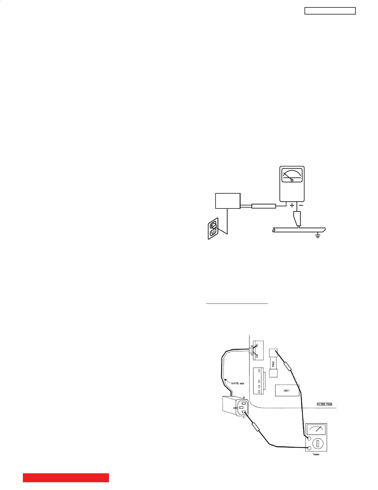
Leakage Current Cold Check
With the AC plug removed from the 120V AC 60Hz source,
place a jumper across Line 1 and Line 2 of the three plug
prongs, do not connect with the third prong, which is physical
ground.
Using an insulation tester (DC500V), connect one of its leads
to the AC plug jumper and touch with the other lead each
exposed metal part (antennas, screwheads, metal overlays,
control shafts, etc.), particularly any exposed metal part
having a return path to the chassis should have a resistor
reading over 4MΩ. Any resistance value below this range
indicates an abnormality which requires corrective action. An
exposed metal part not having a return path to the chassis will
indicate an open circuit.
SAFETY PRECAUTIONS
Leakage Current Hot Check
AC LEAKAGE TEST
ANY MEASUREMENTS NOT WITHIN THE LIMITS OUTLINED
ABOVE ARE INDICATIVE OF A POTENTIAL SHOCK HAZARD
AND MUST BE CORRECTED BEFORE RETURNING THE
RECEIVER TO THE CUSTOMER.
LEAKAGE
CURRENT
TESTER
(READING
SHOULD NOT
BE ABOVE 0.5MIU)
EARTH
GROUND
TEST ALL
EXPOSED
METAL SURFACES
DEVICE
UNDER
TEST
3-WIRE CORD
ALSO TEST WITH PLUG
REVERSED
(USING AC ADAPTER
PLUS AS REQUIRED)
TABLE OF CONTENTS
Plug the AC line cord directly into a 120V AC outlet. (Do not use an
isolation transformer during this test.) Use a leakage current
tester or a metering system that complies with the American
National Standards Institute (ANSI) C101.0 Leakage Current
for Appliances. In the case of the PDP monitor set the AC
switch first in the ON position and then in the OFF position,
measure from across Line 1 and Line 2 of the three plug
prongs, do not connect with the third prong, which is physical
ground, to all exposed metal parts of the instrument
(antennas, handle bracket, metal cabinet, screw heads,
metallic overlays, control shafts, etc.), especially any exposed
metal parts that offer an electrical return path to the chassis.
Any current measured must not exceed 0.5 MIU. Reverse the
instrument power cord plug in the outlet and repeat test.
AC Inlet Polarity
This check is based on the UL Standard
Use the jigs specified by the production technology section.
The GND side (Wider blade) of the AC power cord should
be connected to F902.
GI

3
DW1U
PRODUCT SAFETY NOTICE
Many electrical and mechanical parts in HITACHI television
receivers have special safety-related characteristics. These are
often not evident from visual inspection nor can the protection
afforded by them necessarily be obtained by using replacement
components rated for higher voltage, wattage, etc. Replacement
parts which have these special safety characteristics are
identified in this Service Manual.
Electrical components having such features are identified with a
mark in the schematics and parts list in this Service Manual.
The use of a substitute replacement component which does not
have the same safety characteristics as the HITACHI-
recommended replacement component, shown in the parts list in
this Service Manual, may create shock, fire, X-radiation, or other
hazards.
Product safety is continuously under review and new instructions
are issued from time to time. For the latest information, always
consult the current HITACHI Service Manual. A subscription to,
or additional copies of HITACHI Service Manuals may be
obtained at a nominal charge from HITACHI Sales Corporation.
1. Follow the general caution recommendations from “Safety
precautions” section.
42HDS52/HDT52/HDX62 - Plasma Monitor Unit
55HDS52/HDT52/HDX62 - Plasma Monitor Unit
1. Follow the general caution recommendations from “Safety
precautions” section.
2. Since the Panel module and front filter are made of glass,
sufficient care shall be taken when handling the broken
module and filter in order to avoid injury.
3. If necessary to replace Panel module, this work must be
started after the panel module and the AC/DC Power supply
becomes sufficiently cool.
4. Special care must be taken with the display area to avoid
damaging its surface.
5. The Panel Module shall not be touched with bare hands to
protect its surface from stains.
6. It is recommended to use clean soft gloves during the
replacing work of the Panel module in order to protect, not
only the display area of the panel module but also the
serviceman.
7. The Chip Tube of the panel module (located upper left of the
back of the panel module) and flexible cables connecting
Panel glasses to the drive circuitry Printed Wiring Boards
(P.W.B.) are very weak, so sufficient care must be taken to
prevent breaking or cutting any of these. If the Chip Tube
breaks the panel module will never work, replacement for a
new plasma panel module will be needed.
8. AV Digital Block, power supply and PDP driving circuit
P.W.B.’s are assembled on the rear side of the PDP module,
take special care with this fragile circuitry; particularly, Flexible
Printed Circuits bonded to surrounding edges of the glass
panel. They are not strong enough to withstand harsh outer
mechanical forces. Avoid touching the flexible printed circuits
by not only your hands, but also tools, chassis, or any other
object. Extreme bending of the connectors must be avoided
too. In case the flexible printed circuits are damaged, the
corresponding addressed portions of the screen will not be lit
and exchange of a glass panel will be required.
PDP Module Handling
When there is need to replace a broken PDP module which is the
displaying device from the Plasma monitor unit, consider the
following:
1. When carrying the PDP module, two persons should stand at
both shorter-edge sides of the glass-panel and transport it with
their palms. Avoid touching the Flexible Printed Circuits or the
chip tube on the corner of the glass-panel. Handle only by the
surface of the glass panel. In case of some PDP modules,
electrode repair is done by connecting between regular
terminal with Cu tape and Cu wire. Please do not hook and/or
damage this repair line. If it is damaged, the module will not
function unless the glass-panel is exchanged with a new
glass-panel.
2. When carrying PDP module, watch surrounding objects, such
as tables, and also do not carry it alone since it may be
dangerous and it will be damaged due to excessive stress to
the module (glass-panel).
3. Please do not stand the module with the edge of the glass-
panel on the table since this might result in damage to the
glass-panel and/or flexible printed circuits due to excessive
stress to the module (glass-panel).
WARNING
Lead in solder used in this product is listed by the California
Health and Welfare agency as a known reproductive toxicant
which may cause birth defects or other reproductive harm
(California Health and Safety Code, Section 25249.5).
When servicing or handling circuit boards and other components
which contain lead in solder, avoid unprotected skin contact with
solder. Also, when soldering make sure you are in a well
ventilated area in order to avoid inhalation of any smoke or
fumes released.
SAFETY NOTICE
USE ISOLATION TRANSFORMER
WHEN SERVICING
POWER SOURCE
This plasma television is designed to operate on 120 Volts
60Hz, AC house current. Insert the power cord into a 120 Volts
60Hz outlet.
NEVER CONNECT THE PLASMA TELEVISION TO OTHER
THAN THE SPECIFIED VOLTAGE OR TO DIRECT CURRENT
AND TO 50HZ. TO PREVENT ELECTRIC SHOCK, DO NOT
USE THE PLASMA TELEVISION’S (POLARIZED) PLUG WITH
AN EXTENSION CORD, RECEPTACLE, OR THE OUTLETS
UNLESS THE BLADES AND GROUND TERMINAL CAN BE
FULLY UNSERTED TO PREVENT BLADE EXPOSURE.
TABLE OF CONTENTS
!
GI

4
DW1U
CAUTION: Before servicing instruments covered by this
service data and its supplements and addenda, read and
follow the “Important Safety Instructions” on page 3 of this
publication.
NOTE: If unforeseen circumstances create conflict between
the following servicing precautions and any of the safety
precautions on page 3 of this publication, always follow the
safety precautions. Remember: Safety First.
General Servicing Guidelines
1. Always unplug the instrument AC power cord from the AC
power source before:
a. Removing or reinstalling any component, circuit
board, module, or any other instrument assembly.
b. Disconnecting or reconnecting any instrument
electrical plug or other electrical connection.
c. Connecting a test substitute in parallel with an
electrolytic capacitor in the instrument.
CAUTION: A wrong part substitution or incorrect
polarity installation of electrolytic
capacitors may result in an explosion
hazard.
2. Do not spray chemicals on or near this instrument or any
of its assemblies.
3. Unless specified otherwise in these service data, clean
electrical contacts by applying the following mixture to the
contacts with a pipe cleaner, cotton-tipped stick or
comparable nonabrasive applicator: 10% (by volume)
Acetone and 90% (by volume) isopropyl alcohol (90%-
99% strength).
CAUTION: This is a flammable mixture. Unless
specified otherwise in these service data,
lubrication of contacts is not required.
4. Do not defeat any plug/socket of voltage interlocks with
which instruments covered by this service data might be
equipped.
5. Do not apply AC power to this instrument and/or any of its
electrical assemblies unless all solid-state device heat-
sinks are correctly installed.
6. Always connect the test instrument ground lead to the
appropriate instrument chassis ground before connecting
the test instrument positive lead. Always remove the test
instrument ground lead last.
7. Use with this instrument only the test fixtures specified in
this service data.
CAUTION: Do not connect the test fixture ground strap
to any heatsink in this instrument.
Electrostatically Sensitive (ES) Devices
Some semiconductor (solid state) devices can be damaged
easily by static electricity. Such components commonly are
called Electrostatically Sensitive (ES) Devices. Examples of
typical ES devices are integrated circuits and some field-
effect transistors and semiconductor “chip” components. The
following techniques should be used to help reduce the
incidence of component damage caused by static electricity.
1. Immediately before handling any semiconductor
component or semiconductor-equipped assembly, drain
off any electrostatic charge on your body by touching a
known earth ground. Alternatively, obtain and wear a
commercially available discharging wrist strap device,
which should be removed for potential shock reasons
prior to applying power to the unit under test.
2. After removing an electrical assembly equipped with ES
devices, place the assembly on a conductive surface
such as aluminum foil, to prevent electrostatic charge
buildup or exposure of the assembly.
3. Use only a grounded-tip soldering iron to solder or
desolder ES devices.
4. Use only an anti-static type solder removal device. Some
solder removal devices not classified as “anti-static” can
generate electrical charges sufficient to damage ES
device.
5. Do not use freon-propelled chemicals. These can
generate electrical charges sufficient to damage ES
devices.
6. Do not remove a replacement ES device from its
protective package until immediately before you are
ready to install it. (Most replacement ES devices are
packaged with leads electrically shorted together by
conductive foam, aluminum foil or comparable conductive
material.)
7. Immediately before removing the protective material from
the leads of a replacement ES device, touch the
protective material to the chassis or circuit assembly into
which the device will be installed.
CAUTION: Be sure no power is applied to the chassis or
circuit, and observe all other safety
precautions.
8. Minimize bodily motions when handling unpackaged
replacement ES devices. (Otherwise harmless motion
such as the brushing together of your clothes fabric or the
lifting of your foot from a carpeted floor can generate
static electricity sufficient to damage an ES device.)
SERVICING PRECAUTIONS
TABLE OF CONTENTS
GI
5
DW1U
General Soldering Guidelines
1. Use a grounded-tip, low-wattage soldering iron and
appropriate tip size and shape that will maintain tip
temperature within the range 500°F to 600°F.
2. Use an appropriate lead free solder (see page 8). Lead
solder can be used, but there is a possibility of failure due
to insufficient strength of the solder.
3. Keep the soldering iron tip clean and well-tinned.
4. Thoroughly clean the surfaces to be soldered. Use a
small wire-bristle (0.5 inch or 1.25 cm) brush with a metal
handle. Do not use freon-propelled spray-on cleaners.
5. Use the following desoldering technique.
a. Allow the soldering iron tip to reach normal
temperature (500°F to 600°F).
b. Heat the component lead until the solder melts.
Quickly draw away the melted solder with an anti-
static, suction-type solder removal device or with
solder braid.
CAUTION: Work quickly to avoid overheating the
circuit board printed foil.
6. Use the following soldering technique.
a. Allow the soldering iron tip to reach normal
temperature (500°F to 600°F).
b. First, hold the soldering iron tip and solder strand
against the component lead until the solder melts.
c. Quickly move the soldering iron tip to the junction of
the component lead and the printed circuit foil, and
hold it there only until the solder flows onto and
around both the component lead and the foil.
CAUTION: Work quickly to avoid overheating the
circuit board printed foil or components.
d. Closely inspect the solder area and remove any
excess or splashed solder with a small wire-bristle
brush.
Removal
1. Desolder and straighten each IC lead in one operation by
gently prying up on the lead with the soldering iron tip as
the solder melts.
2. Draw away the melted solder with an anti-static suction-
type solder removal device (or with solder braid) before
removing the IC.
Replacement
1. Carefully insert the replacement IC in the circuit board.
2. Carefully bend each IC lead against the circuit foil pad
and solder it.
3. Clean the soldered areas with a small wire-bristle brush.
(It is not necessary to reapply acrylic coating to areas.)
“Small-signal” Discrete Transistor Removal/Replacement
1. Remove the defective transistor by clipping its leads as
close as possible to the component body.
2. Bend into a “U” shape the end of each of the three leads
remaining on the circuit board.
3. Bend into a “U” shape the replacement transistor leads.
4. Connect the replacement transistor leads to the
corresponding leads extending from the circuit board and
crimp the “U” with long nose pliers to insure metal to
metal contact, then solder each connection.
Power Output Transistor Devices Removal/Replacements
1. Heat and remove all solder from around the transistor
leads.
2. Remove the heatsink mounting screw (if so equipped).
3. Carefully remove the transistor from the circuit board.
4. Insert new transistor in circuit board.
5. Solder each transistor lead, and clip off excess lead.
6. Replace heatsink.
Diode Removal/Replacement
1. Remove defective diode by clipping its leads as close as
possible to diode body.
2. Bend the two remaining leads perpendicularly to the
circuit board.
3. Observing diode polarity, wrap each lead of the new
diode around the corresponding lead on the circuit board.
4. Securely crimp each connection and solder it.
5. Inspect (on the circuit board copper side) the solder joints
of the two “original leads”. If they are not shiny, reheat
them and, if necessary, apply additional solder.
Use Soldering Iron to Pry Leads
IC Removal/Replacement
Some Hitachi unitized chassis circuit boards have slotted
holes (oblong) through which the IC leads are inserted and
then bent flat against the circuit foil. When holes are the
slotted type, the following technique should be used to
remove and replace the IC. When working with boards using
the familiar round hole, use the standard technique as
outlined in paragraphs 5 and 6 above.
GI
6
DW1U
Fuses and Conventional Resistor Removal/Replacement
1. Clip each fuse or resistor lead at top of circuit board
hollow stake.
2. Securely crimp leads of replacement component around
stake 1/8 inch from top.
3. Solder the connections.
CAUTION: Maintain original spacing between the
replaced component and adjacent
components and the circuit board, to
prevent excessive component
temperatures.
Circuit Board Foil Repair
Excessive heat applied to the copper foil of any printed
circuit board will weaken the adhesive that bonds the foil to
the circuit board, causing the foil to separate from, or “lift-
off,” the board. The following guidelines and procedures
should be followed whenever this condition is encountered.
In Critical Copper Pattern Areas
High component/copper pattern density and/or special
voltage/current characteristics make the spacing and
integrity of copper pattern in some circuit board areas more
critical than in others. The circuit foil in these areas is
designated as Critical Copper Pattern. Because Critical
Copper Pattern requires special soldering techniques to
ensure the maintenance of reliability and safety standards,
contact your Hitachi personnel.
At IC Connections
To repair defective copper pattern at IC connections, use the
following procedure to install a jumper wire on the copper
pattern side of the circuit board. (Use this technique only on
IC connections.)
1. Carefully remove the damaged copper pattern with a
sharp knife. (Remove only as much copper as absolutely
necessary.)
2. Carefully scratch away the solder resist and acrylic
coating (if used) from the end of the remaining copper
pattern.
3. Bend a small “U” in one end of a small-gauge jumper wire
and carefully crimp it around the IC pin. Solder the IC
connection.
4. Route the jumper wire along the path of the cut-away
copper pattern and let it overlap the previously scraped
end of the good copper pattern. Solder the overlapped
area, and clip off any excess jumper wire.
1. Remove the defective copper pattern with a sharp knife.
Remove at least 1/4 inch of copper, to ensure hazardous
condition will not exist if the jumper wire opens.
2. Trace along the copper pattern from both wire sides of
the pattern break and locate the nearest component
directly connected to the affected copper pattern.
3. Connect insulated 20-gauge jumper wire from the
nearest component on one side of the pattern break to
the lead of the nearest component on the other side.
Carefully crimp and solder the connections.
CAUTION: Be sure the insulated jumper wire is
dressed so that it does not touch
components or sharp edges.
CRIMP AND
SOLDER
BARE JUMPER
WIRE
Install Jumper Wire and Solder
DEFECTIVE
COPPER
REMOVED
Insulated Jumper Wire
At Other Connections
Use the following technique to repair defective copper
pattern at connections other than IC Pins. This technique
involves the installation of a jumper wire on the component
side of the circuit board.
GI
7
DW1U
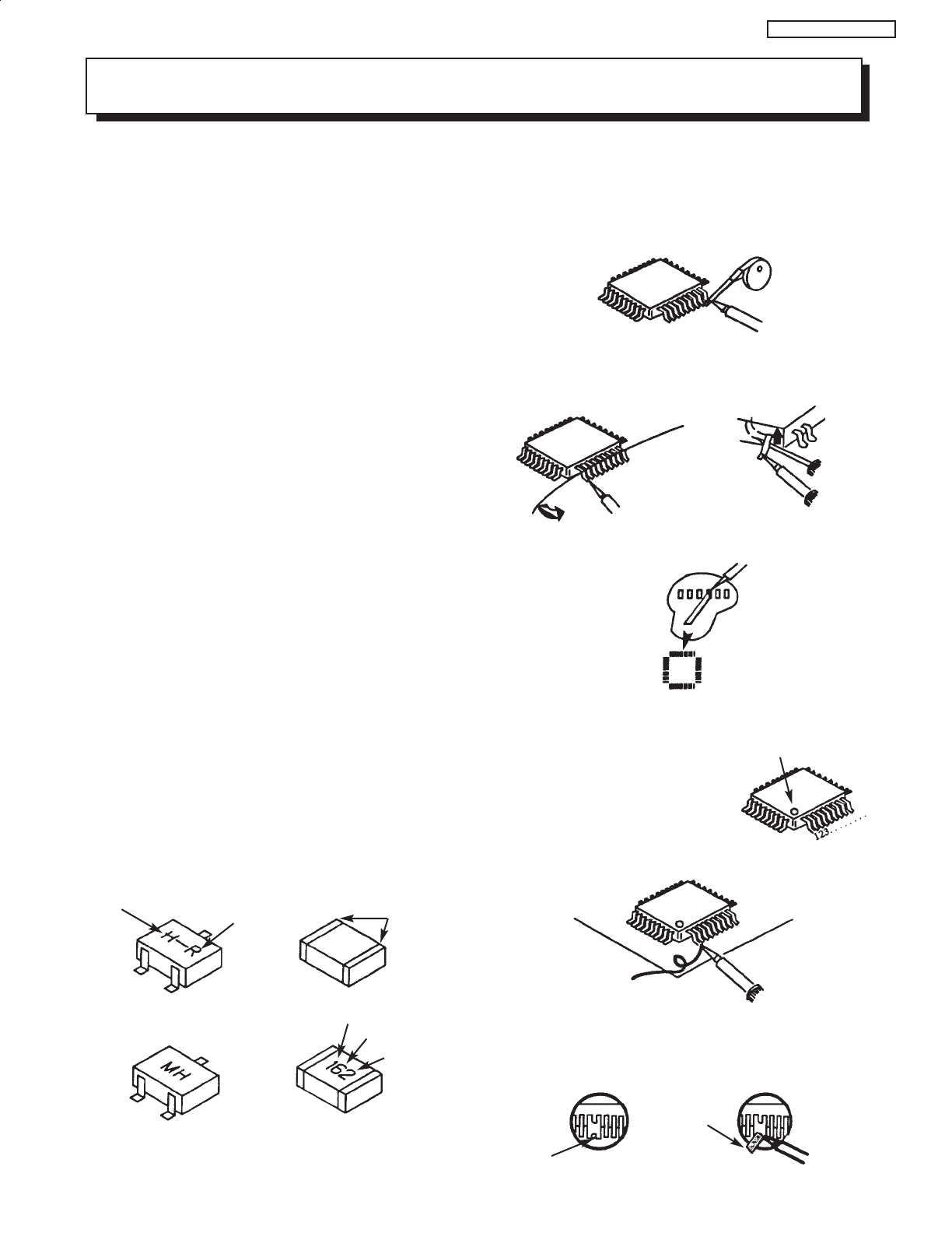
MH DIODE RESISTOR
Leadless Chip Components
(surface mount)
Chip components must be replaced with identical
chips due to critical foil track spacing. There are no
holes in the board to mount standard transistors or
diodes. Some chip capacitor or resistor board solder
pads may have holes through the board, however the
hole diameter limits standard resistor replacement to
1/8 watt. Standard capacitors may also be limited for
the same reason. It is recommended that identical
chip components be used. .
Chip resistors have a three digit numerical resistance
code -1st and 2nd significant digits and a multiplier.
Example: 162 = 1600 or 1.6KΩresistor, 0 = 0Ω
(jumper).
Chip capacitors generally do not have the value
indicated on the capacitor. The color of the component
indicates the general range of the capacitance.
Chip transistors are identified by a two letter code. The
first letter indicates the type and the second letter, the
grade of transistor.
Chip diodes have a two letter identification code as
per the code chart and are a dual diode pack with
either
common anode or common cathode. Check the parts
list for correct diode number.
Component Removal
1. Use solder wick to remove solder from component
end caps or terminals.
2. Without pulling up, carefully twist the component
with tweezers to break the adhesive.
3. Do not reuse removed leadless or chip
components since they are subject to stress
fracture during removal .
Chip Component Installation
1. Put a small amount of solder on the board
soldering pads.
2. Hold the chip component against the soldering
pads with tweezers or with a miniature alligator
clip and apply heat to the pad area with a 30 watt
iron until solder flows. Do not apply heat for more
than 3 seconds
How to Replace Flat-lC
—Required Tools—
• Soldering iron • iron wire or small awl
• De-solder braids • Magnifier
1. Remove the solder from all of the pins of a Flat-lC
by using a de-solder braid.
2. Put the iron wire under the pins of the Flat-lC and
pull it in the direction indicated while heating the
pins using a soldering iron. A small awl can be
used instead of the iron wire.
3. Remove the solder from all of the pads of the
Fiat-lC by using
a de-solder braid.
4. Position the new Flat-lC in place (apply the pins of
the Flat-lC to the soldering pads where the pins
need to be soldered). Properly
determine the positions of the
soldering pads and pins by
correctly aligning the polarity
symbol.
6. Check with a magnifier for solder bridge between
the pins or for dry joint between pins and soldering
pads. To remove a solder bridge, use a de-solder
braid as shown in the figure below.
NOTE: These components are affixed with glue. Be careful not to break or damage any foil under the
component or at the pins of the ICs when removing. Usually applying heat to the component for a short
time while twisting with tweezers will break the component loose.
Chip Components
TYPE
GRADE
C
B
E
SOLDER
CAPS
TRANSISTOR CAPACITOR
1ST DIGIT
2ND DIGIT
MULTIPLIER
= 1600 = 1.6K
ANODES SOLDER CAPS
COMMON CATHODE
De-Solder
Braid
Soldering
Iron
Soldering
Iron
Soldering
Iron
Soldering
Iron
Soldering
Iron
Soldering
Iron
De-Solder
Braid
Flat-IC
Solder
Bridge
Solder
De-Solder
Braid
Iron
Wire
Pull
Awl
Polarity Symbol
5. Solder all pins to the soldering pads using a fine
tipped soldering iron.
GI
8
DW1U
Information for service about lead-free solder introduction
Hitachi introduced lead-free solder to conserve the "Earth Environment".
Please refer to the following before servicing.
(1) Characteristic of lead-free solder
Melting point of lead free solder is 40-50
o
C higher than solder containing lead.
(2) Solder for service
Following composition is recommended.
" Sn - 3.0Ag - 0.5Cu " , or " Sn - 0.7 Cu "
Lead solder can be used, but there is a possibility of failure due to insufficient strength of the solder.
Caution when using solder containing lead.
Please remove previous solder as much as possible from the soldering point.
When soldering, please perfectly melt the lead-free solder to mix well with the previous solder.
(3) Soldering iron for lead-free solder.
Melting point of lead-free solder is higher than solder containing lead.
Use of a soldering tool "with temperature control" and "with much thermal capacitance" is recommended.
(Recommended temperature control : 320
o
C - 450
o
C)
Recommended temperature
PWB with chip parts
320
o
C +/- 30
o
C
PWB without chip parts
380
o
C +/- 30
o
C
Chassis, metal, shield etc.
420
o
C +/- 30
o
C
(4) Identification of lead-free PWB
2003 models
>> not applied
2003 models
>> mixed
2004 models
>> lead-free solder is introduced
2005 models
>> lead-free solder apply
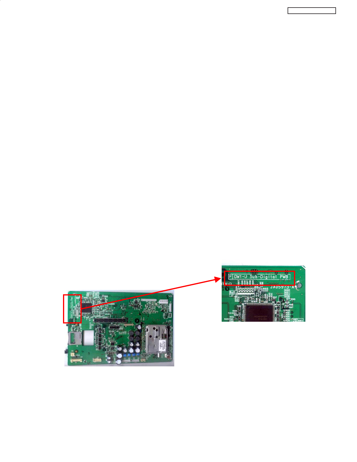
On lead-free PWB, "F" is added at the beginning of stamp on PWB. (e.g. F DW1)
GI

9
DW1U
AGENCY REGULATORY
INFORMATION
Federal Communications Commission Notice
This equipment has been tested and found to comply with the limits for a Class B digital device, pursuant to Part 15 of
the FCC Rules. These limits are designed to provide reasonable protection against harmful interference in a residential
installation. This equipment generates, uses and can radiate radio frequency energy and if not installed and used in
accordance with the instructions, may cause harmful interference to radio communications. However, there is no
guarantee that interference will not occur in a particular installation. If this equipment does cause harmful interference
to radio or television reception, which can be determined by turning the equipment off and on, the user is encouraged
to try to correct the interference by one or more of the following measures:
• Reorient or relocate the receiving antenna.
• Increase the separation between the equipment and the receiver.
• Connect the equipment into an outlet on a circuit different from that to which the receiver is connected.
• Consult the dealer or an experienced radio/television technician for help.
Modifications
The FCC requires the user to be notified that any changes or modifications made to this device that are not expressly
approved by Hitachi Home Electronics (America), Inc. may void the user’s warranty.
Cables
Connections to this device must be made with shielded cables with metallic RFI/EMI connector hoods to maintain
compliance with FCC Rules and Regulations.
Any cables that are supplied with the system must be replaced with identical cables in order to assure compliance with
FCC rules. Order Hitachi spares as replacement cables.
Declaration of Conformity
This device complies with Part 15 of the FCC Rules. Operation is subject to the following two conditions: (1) this device
may not cause harmful interference and (2) this device must accept any interference received, including interference
that may cause undesired operation.
For questions regarding this declaration, contact:
Hitachi America, LTD.
Home Electronics Division
900 Hitachi Way
Chula Vista, CA 91914
Tel. 1-800-448-2244 (1-800-HITACHI)
ATTN: CUSTOMER RELATIONS
TABLE OF CONTENTS
In the United States, TV GUIDE and other related marks are registered marks of Gemstar-TV Guide International,
Inc. and/or one of its affiliates. In Canada, TV GUIDE is a registered mark of Transcontinental Inc., and is used
under license by Gemstar-TV Guide International, Inc.
The TV Guide On Screen system is manufactured under license from Gemstar-TV Guide International, Inc.
and/or one of its affiliates.
The TV Guide On Screen system is protected by one or more of the following issued United States patents
6,498,895; 6,418,556; 6,331,877; 6,239,794; 6,154,203; 5,940,073; 4,908,713; 4,751,578; 4,706,121.
Gemstar-TV Guide International Inc. and/or its related affiliates are not in any way liable for the accuracy or
availability of the program schedule information or other data in the TV Guide On Screen system and cannot
guarantee service availability in your area. In no event shall Gemstar-TV Guide International, Inc. and/or its
related affiliates be liable for any damages in connection with the accuracy or availability of the program
schedule information or other data in the TV Guide On Screen system.
GI
10
DW1U
ACKNOWLEDGMENTS
AND TRADEMARKS
This Plasma Television complies with VESA DDC2B specifications, Plug & Play
is a system with computer, peripherals (including monitors) and operating
system. It works when the monitor is connected to a DDC ready computer that
is running an operating system software that is capable for the plug & play.
When a Plug and Play PC is powered on, it sends a command to the Monitor
requesting identification. The Monitor sends back a string of data including its
characteristics.
TRADEMARK ACKNOWLEDGMENT
DDC is a trademark of Video Electronics Standard Association.
IBM PC/AT and VGA are registered trademarkds of International Business Machines Corporation of the U.S.A.
Apple and Macintosh are registered trademarks of Apple Computer, Inc.
VESA is a trademark of a nonprofit organization, Video Electronics Standard Association.
This Class B digital apparatus meets all requirements of the Canadian Interference-Causing Equipment Regulations.
This Class B digital apparatus complies with Canadian ICES-003.
Cet appareil numérique de la classe B est conforme à la norme NMB-003 du Canada.
Cable Compatible Television Apparatus- Tèlèvision câblocompatible, Canada.
Notes on Closed Caption:
This Plasma Television receiver will display television closed captioning, ( or ), in accordance with
paragraph 15.119 of the FCC rules.
TM
TruBass and the SRS ®symbol are trademarks of SRS Labs, Inc. TruBass technology is incorporated under license
from SRS Labs, Inc.
TABLE OF CONTENTS
In the U.S. , TV GUIDE and other related marks are registered marks of Gemstar-TV Guide International, Inc. and/or
one of its affiliates. In Canada , TV GUIDE is a registered of transcontinental Inc. , and is used under license by Gemstar-TV
Guide International, Inc.
GI
11
DW1U
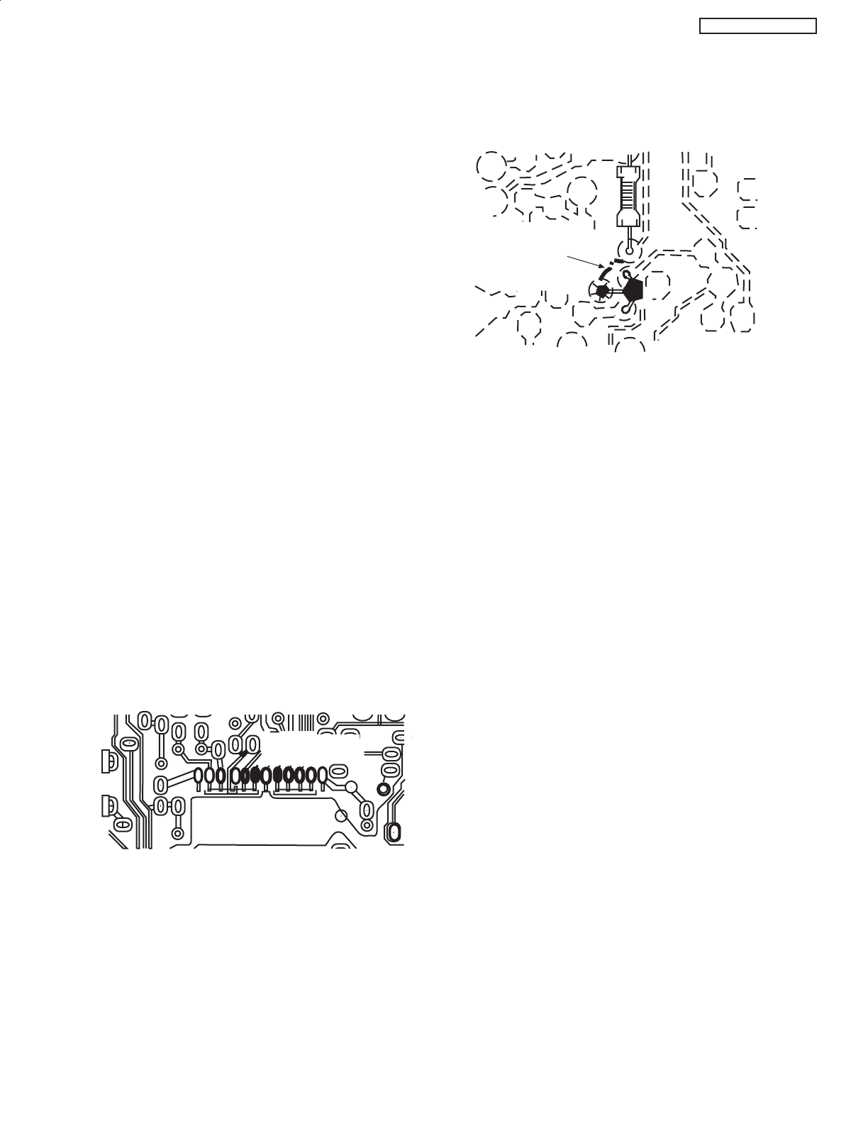
CIRCUIT PROTECTION
CAUTION: Below is an EXAMPLE only. See Replacement Parts List for details. The following symbol near the fuse
indicates fast operation fuse (to be replaced). Fuse ratings appear within the symbol.
6.3 A
250V
F
6.3 A 250V
Example:
“RISK OF FIRE - REPLACE FUSE AS MARKED”
The rating of fuse F902 is 6.3 A - 250V.
Replace with the same type fuse for continued protection
against fire.
The Digital AV Block is inside of the Panel assembly controls most of the user functions of the complete TV set and conditions the signal
to the plasma panel.
The 42” and 55” monitors contain the displaying device, which is the plasma display panel module, and the driving circuitry, which
receives the signal from the Digital AV Block and after processing, delivers the image to the display module.
This HITACHI Service Manual is intended for the qualified service personnel and it contains the necessary information for
troubleshooting the Plasma television set in case of malfunction.
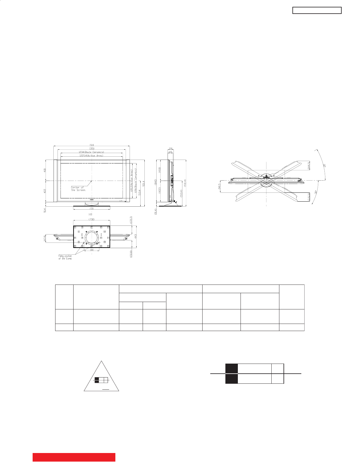
DIMENSIONS:
55HDS52/HDT52/HDX62
POWER RATINGS:
1 55HDS52/HDT52 500W 4.5A 326W 0.5W 15W DW-1U
55HDX62
No. Model Name
Indicated Value
Max Rating Average
Rating (W)
Without POD.
less than 1W Chassis
PST(W)
(W) (A)
With POD.
less than 14W
TABLE OF CONTENTS
INTRODUCTION
GI
Specification Features
A- Plasma
Model 55HDS52/55HDT52/55HDX62
DimensionSize
1
1510mm x 931.4mm x 443mm
Weight
2
71k g
Input AC Voltage
3
AC108V~132V (with 3 Plug AC Power Cord inlet
type ,1.8m length)
Input AC Frequency
4
60Hz
A/C Input
Voltage
Power Consumption
5
370W, SBY/POD -SBY less than 1W/15W
Front End(Sub/ATSC)
6
ENGE6401DF/ENV56N01D5F
NT
SC/
NT
SC/
AT
SC(8
V
S
B
),6
4
Q
AM
,
2
56Q
AM
)
7
2~13
VHP
814 ~ 69 UHF
FrontEnd
Available Channel
9
A-5~A-1,A~W,W+1~W+94
CATV
Video Signal
10
NTSC
Component Signal
11
480 i /p. 1080 i , 720p
PC Signal
12
VGA - UXGA fH:24KHz-1 09KHz,fV:50Hz-
85Hz)
Input Signal
HDMI Signal
13
480i,480p,720p,1080i(EIA-861B)
Y/C Separation
14
3D Y/C (ON fix)
Line Correction
15 No
I-P Conversion
16
Motion Adaptive & Multi Angle Interpolation
FC6
Picture Mode
17
Day.Night
18
42:1024i,55:768p Video Signal
19
42:1024i,55:768p ComponentSignal
20
42:1024i,55:768p PinP Mode
Picture
Display Mode
21
-
Sound Enhancement
22
TruBass or Dynamic Bass (High, Low, Off)
BBE(Off,Soft,Hard) SRS (Off,Normal,Wide)
Settings for Video Signal
23
Picture,Contrast,Brightness,Color,Tint , Sharpness,
W/B Temp.Black Enhancement .Contrast Mode.Color
Management/Decoding ,Auto Color.Noise
Reductfon.Auto Movie Mode, .Black Side Panel
24
Vol, Balance, Bass.Treble, Source, Internal Speakers
25
Adjustment
Settings for Sound
26
,Auto Noise Cancel.Perfect Volume.Mute.Soft Mute
PinP Split
27
With(AII video signal combinations, except PC signal)
Except Photo Input
Mode Strobe
28
With(4Pix:only ANT A/B,Video,480i)
Except Photo Input
Surf
29
With(SURF12:only AMT A/B)
Except Photo Input
POP 30
WithfMain: ANT A/B,Video.480i Sub: ANT A/B,Video.480i,1080i)
Except Photo Input
PIP 31
With(Main:1080i Sub: ANT A/B,Video,480i.10aoi)
Except Photo Input
Freeze
32
Except Photo Input
Wide Mode
33
6Mode
Aspect Video Selection
34
4:3 Standard/1 6:9 Standard/ 4:3 Expanded/Zoom
1/Zoom 2/16:9 Zoom
PC 35
Full/Normal/Real (Real
42:VGA
,
55:VGA/SVGA/XGA/WXGA
)
Film Theater
36
With(Auto Movie Mode:On/Off)
Color Temperature
37
4Mode (High/Medium/Standard/Black & White)
General
Function
Input Signal Selection
38
VIDEO1/2/3/4/5, Cable/ Air,IEEE1394,Photo
Input
12
DW1U
TABLE OF CONTENTS
With(4Pix:only ANT A/B,Video,480i)
GI
13
DW1U
Model
55HDS52/55HDT52/55HDX62
General Gamma Correction
39
Only for Service Menu
FunctionPicture Enhancer
40
-
Input Signal Identification
41 yes
Audio Special Mode
42 No
Power Save Mode
43
With (On/Off) (Video In) LED Normal: Green
44
Power Save: Orange
Stand by: Red
Burning Protection
45
With (Raster Shift:3 option.AII White Pattern)
OSD Language (VIDEO)
46
ENGLISH.FRANCAIS.ESPANOL
Power Swivel
47
With
R/C Handset
48
CLU-3841WL/CLU-122S
PANASONIC/UEI
In/Out
49
Terminal Composite Video Input
(VIDEO1~5)
50
5 Input: RCA pin* 5 (1 Input Front Panel)
S-ln(S2 Terminal) (Video/S are
common selector, priority is S-ln) .
51
3 InputMini Din-4P x 3 (1 S-ln on Front Panel)
Component Signal Input
(VIDEO3.VIDEO4)
52
2 lnput:RCA pin x 6(Y of VIDEO1/2 is common
input for Composite-In)
Digital Input(HDMH-HDCP)
53
2 lnput:HDMI(18P)X1 (Selected by component
Video1/2.Digital input priority)
Audio In (L/R) (Lch:mono)
54
6 lnput;RCApinxi2
(RGB:1 lnput,Video:5 Input)
CATV In
55
1 Input (VIDEO2 LINK) Auto Link Function
Video Control Terminal (BS)
56 No
U/V Ant Input
57
CABLE IN / AIR-B IN
BS-I/F Input
58 No
Video Monitor Out Terminal
59
1 Output: RCA pinx 1
Audio Output Terminal
60
1 Output UR:RCA pinx 2( Common input for No.59 )
Audio Monitor Out Terminal
61
1 Output L/R:RCA pinx 2
IR-OUTPUT 62
2 Terminal
Headphone Terminal
63
1 Terminal (only for AVC)
64
IEEE 1394 Input
65
2 (4pin connector)
RS-232C Terminal 66
1 (Female type)
Photo Input
67
1 (On Side panel)
Audio Optical Output
68
1 (Square type)
FrontMain Power Switch
69 Yes , below panel
Key
Power On/off Switch
70
Yes, on side panel
IR Receiving Unit
71
Yes, on front panel
Power Indicator LED
72
Yes, on front panel
Menu Control Key
73
Yes, on side panel (Channel U/D, Vol U/D, A/V Input
Select , Menu Select)
Option
74
With
POP TV Stand
75
With
Wall Mount Unit
76
-
55HDT52/55HDX62 Only
Specification Features
A- Plasma
GI
14
DW1U
Environment Specification
NO
ItemSpecification
1
Operating Temp.
+5
°
C~+35°C
2
Stock Temp.
-15
°
C
~+60
°
C
3
Operating Humidity
20%~80%RH
4
Stock Humidity
20%~90%RH
5
Operating Atmosphere
Pressure
800~1114h Pa
(1888m~-757m)
6
Stock Atmosphere Pressure
300~1114h P a
(
4727m~-757m
)
7
Warranty Gravity Vertical
0.85 G
8
Warranty Drop High
30cm
9
Tilt Angle 12° Over
㩷
㪙㪸㫊㫀㪺㪅 㩷 㪤㪜㪛㪠㪘 㩷㩷
㪤㫆㪻㪼㫃㩷㪥㪸㫄㪼 㪚㪿㪸㫊㫊㫀㫊 㪚㫃㪸㫊㫊 㪛㫀㪾㫀㫋㪸㫃 㪧㪦㪛 㪜㪧㪞 㪝㪚 㪊㪆㪉 㪤㪼㫄㫆㫉㫐 㪪㪿㫀㫃㪼㪻 㪩㪼㫊㫆㫃㫌㫋㫀㫆㫅 㪦㪪㪛 㪚㫆㫃㫆㫉 㪧㪠㪧 㪘㪭㩷㪥㪜㪫㩷 㪩㪼㫄㫆㫋㪼 㪪㫀㫄㫇㫃㪼
㪥㪦 㩷㩷 㪚㪸㪹㫃㪼 㪞㪼㫄㫊㫋㪸㫉 㪤㪆㪚 㪧㫌㫃㫃㩷㪛㫎㫅 㪹㫐㩷㪠㫅㫇㫌㫋㫊 㪫㪼㫄㫇㪼㫉㪸㫋㫌㫉㪼 㩷㩿㪬㪜㪠㪀
㪈㪌㪌㪟㪛㪯㪍㪉 㪛㪮㪈㪄㪬 㪛㫀㫉㪼㪺㫋㫆㫉㩾㫊 㪯 㪯 㪯 㪬㪪㪙 㪝㪚㪍 㪘㫌㫋㫆㪆㪦㪽㪽 㪯 㪛㪸㫉㫂㩷㪽㫀㫃㫋㪼㫉 㪈㪇㪉㪋㪁㪈㪇㪉㪋 㪇㪌䇭㪛㫀㫉㪼㪺㫋㫆㫉㩷㪦㪪㪛 㪌㪋㪇㪇㪆㪍㪌㪇㪇㪆㪐㪊㪇㪇㪆㪈㪉㪇㪇㪇 㪛㫀㪾㫀㫋㪸㫃㪆㪘㫅㪸㫃㫆㪾䇭㪪㪧㪣㪠㪫 㸊 㪧㪘㪥㪘㩷㪙㫃㪸㪺㫂 㪯
㪉㪌㪌㪟㪛㪫㪌㪉 㪛㪮㪈㪄㪬 㪬㫃㫋㫉㪸㪭㫀㫊㫀㫆㫅 㪯 㪯 㪯 㪬㪪㪙 㪝㪚㪍 㪘㫌㫋㫆㪆㪦㪽㪽 㪯 㪈㪇㪉㪋㪁㪈㪇㪉㪋 㪇㪌㩷㪦㪪㪛㩷㪘 㪌㪋㪇㪇㪆㪍㪌㪇㪇㪆㪐㪊㪇㪇㪆㪈㪉㪇㪇㪇 㪛㫀㪾㫀㫋㪸㫃㪆㪘㫅㪸㫃㫆㪾䇭㪪㪧㪣㪠㪫 㸊 㪧㪘㪥㪘㩷㪙㫃㪸㪺㫂 㪄
㪊㪌㪌㪟㪛㪪㪌㪉 㪛㪮㪈㪄㪬 㪬㫃㫋㫉㪸㪭㫀㫊㫀㫆㫅 㪯 㪯 㪄 㪬㪪㪙 㪝㪚㪍 㪘㫌㫋㫆㪆㪦㪽㪽 㪯 㪈㪇㪉㪋㪁㪈㪇㪉㪋 㪇㪌㩷㪦㪪㪛㩷㪙 㪌㪋㪇㪇㪆㪍㪌㪇㪇㪆㪐㪊㪇㪇㪆㪈㪉㪇㪇㪇 㪛㫀㪾㫀㫋㪸㫃㪆㪘㫅㪸㫃㫆㪾䇭㪪㪧㪣㪠㪫 㸊 㪧㪘㪥㪘㩷㪙㫃㪸㪺㫂 㪄
㪤㫆㪻㪼㫃㩷㪥㪸㫄㪼
㪥㪦 㩷
㪈㪌㪌㪟㪛㪯㪍㪉
㪉㪌㪌㪟㪛㪫㪌㪉
㪊㪌㪌㪟㪛㪪㪌㪉
㪚㫆㫃㫆㫉 㪚㫆㫃㫆㫉 㪘㫌㫋㫆 㪠㪪㪝
㪛㪼㪺㫆㫉㪻㫀㫅㪾 㪤㪸㫅㪸㪾㪼㫄㪼㫅㫋 㪚㫆㫃㫆㫉 㪤㪦㪛㪜
㬍 㬍㩿㪞㪸㫀㫅㪆㪧㪿㪸㫊㪼㪀 㬍 㬍
㪄㪄 㪄㪄
㪄㪄 㪄㪄
㪤㫆㪻㪼㫃㩷㪥㪸㫄㪼
㪥㪦 㩷
㪈㪌㪌㪟㪛㪯㪍㪉
㪉㪌㪌㪟㪛㪫㪌㪉
㪊㪌㪌㪟㪛㪪㪌㪉
㪛㪼㫊㪺㫉㪼㫋㪼 㪦㫌㫋㫇㫌㫋 㪪㫇㪼㪸㫂㪼㫉 㪠㪩㪄㪦㫌㫋 㪩㪪㪉㪊㪉㪚 㪰㪧㪹㪧㫉 㪪㩷㪠㪥 㪘㪭㩷㪠㪥 㪪㩷㪦㪬㪫 㪘㪭㩷 㪍㪚㪟㩷㪘㫌㪻㫀㫆㩷 㪭㪸㫉㫀㪸㪹㫃㪼 㪉㩷㪩㪝 㪪㩷㪠㪥 㪘㪭㩷㪠㪥 㪛㪭 㪘㫌㫋㫆㩷㪣㫀㫅㫂 㪧㫆㫎㪼㫉 㪩㪼㫄㫆㫋㪼
㪚㫆㪻㪼 㪛㫆㫃㪹㫐 㪪㪩㪪㪆㪙㪙㪜 㩿㪮㪸㫋㫋㪀 㪠㪜㪜㪜㪈㪊㪐㪋㪃㪌㪚 㪟㪛㪤㪠 㪦㫌㫋 㪠㫅㪆㪦㫌㫋 㪘㫌㪻㫀㫆㩷㫆㫌㫋 㩷㪣㪜㪛 㪪㫎㫀㫍㪼㫃
㪯 㪛㪹㫐㩷㪘㪚㪊㩷㪛㫎㫅㫄㫀㫏 㪮㪦㪮㪃㪙㪙㪜 㪋㪇 㪉㪝㪩㪃㪉㪮 㪈 㪉 㪉㪯㪉㩿㪈㪟㪃㪉㪟㪃㪉㪅㪈㪋㪟㪀 㪉㪋 㪈 㪈㪦㫇㫋㪄㪦㫌㫋㩿㫆㫇㫋㪀 㪯 㪯 㪈 㪈 㪈 㪯㩿㪞㪀 㪩㪜㪛 㪯
㪯 㪛㪹㫐㩷㪘㪚㪊㩷㪛㫎㫅㫄㫀㫏 㪮㪦㪮㪃㪙㪙㪜 㪋㪇 㪉㪝㪩㪃㪉㪮 㪈 㪉 㪉㪯㪉㩿㪈㪟㪃㪉㪟㪃㪉㪅㪈㪋㪟㪀 㪉㪋 㪈 㪈㪦㫇㫋㪄㪦㫌㫋㩿㫆㫇㫋㪀 㪯 㪯 㪈 㪈 㪈 㪯㩿㪞㪀 㪩㪜㪛 㪯
㪯 㪛㪹㫐㩷㪘㪚㪊㩷㪛㫎㫅㫄㫀㫏 㪮㪦㪮㪃㪙㪙㪜 㪋㪇 㪉㪝㪩㪃㪉㪮 䋭 㪉 㪉㪯㪉㩿㪈㪟㪃㪉㪟㪃㪉㪅㪈㪋㪟㪀 㪉㪋 㪈 㪈㪦㫇㫋㪄㪦㫌㫋㩿㫆㫇㫋㪀 㪯 㪯 㪈 㪈 䋭 㪯㩿㪞㪀 㪩㪜㪛 㪯
㪝㫉㫆㫅㫋㩷㪡㪸㪺㫂㫊
㪪㫌㫉㫉㫆㫌㫅㪻㩷㫊㫆㫌㫅㪻 㪛㫀㪾㫀㫋㪸㫃㩷㪠㪆㪝
㪩㪼㪸㫉㩷㪡㪸㪺㫂㫊
Basic Differences and Specifications
GI
15
DW1U
3. General Specification
3.1 Model Spec
Model Name Item55HDS52/55HDT52/55HDX62
DestinationU.S.A. / CANAD
A
Cabinet Dimensions
(Main Body) (Speaker &
stand inclusive)
1510X840X118 mm
1510x931x443 mm
Frame Color Screen
Dark Charcoal Metallic
Stand
Inclusive (With Power Swivel)
Weight (Main Body)
(Speaker & stand
inclusive)
(
Main Bod
y
: Packed
)
71.0 kg typ. 74.0 kg
Exterior
Screen Siz
e
922x522mm(42lnch 16:9)
Resolution
1024x1024 pixels
Dot Pitch
(
H
)
0.90mm
Dot Pitch
(
V
)
0.51mm
Viewin
g
An
g
le
(
H
)
±85°
Display Panel
Viewin
g
An
g
le
(
V
)
±85°
Front FilterSurface Finishin
g
AR Coatin
g
,
Mesh
Peak Brightness (1%
window)
280 cd/m2 or more
(When VIDEO, Sports, Color te m-
perature 'HIGH' Input Signal A m-
plitude 100 % is set)
280 cd/m2 or more
(When RGB is set)
Brightness
All White Pattern
5Ocd/m or more
Contrast Contrast ratio 1000 : 1
(
t
yp)
Color
Reproduction
Color Reproduction16.7 million colors
or more
Audio Out
p
ut Audio Out
p
ut
12W+ 12W(6ohm>,10%Distortion)
Main Power Switc
h
PUSH (LOCK) 1 switch
Panel Operation
Power Switch
PUSH (NON-LOCK) 1 switch
Input Terminal Video/Audio Input RCA , HDMI DV connector
Audio Line Out
p
ut
Sub Woofer Output 1 system
Output Terminal
S
p
eaker Out
p
ut
-
Connector3 Polarit
y
Rece
p
taclePower Supply
Source Input Voltage
Single Phase AC108 -132V, 6 OHz
Temp. (Operating)
5~35°C (41F~95F)
Tem
p
erature
(
Stored
)
-15~60°C (5F~140F)
Humidity (Operating)
20~80%RH
(Non-condensing)
Humidity (Stored) 20~90%RH (Non-condensing)
Atmospheric Pressure
(Operating)
800 to 1114hPa
(altitude: 1888m to -757m,
6194feet to -2483feet
)
Guaranteed
Environment
Condition
Atmospheric Pressure
(Storage)
300 to 1114hPa (Altitude:
9727m to -757m, 31912feet to -
2483feet)
GI
How To Set Up Your New Hitachi Plasma Television
Securing to a table-top
1.Using wood screws (two) fasten the set to the
clamping screw holes on the rear of the Plasma
Display stand as shown below.
2.Using commercially available wood screws, secure
the set firmly in position.
Securing to a Wall
1.Keep the Plasma television 4 inches away from the
wall except when mounted using the wall mount
bracket.
2.Secure the television to the wall as shown in fig. (a)
or (b).
NOTES: 1. Do not block the ventilation holes of
the Plasma Television. Blocking
the ventilation holes might cause fire
or defect.
2. In case of an abnormal symptom,
unplug the AC cord.
3. If you purchased the wall mount
bracket option, please ask for
professional installer. Do not install
by yourself.
4. If the Power Swivel feature will not be
used, the Plasma television should be
secured to the wall as shown in
fig. (a).
5. If the Power Swivel feature will be
used, the Plasma television should be
secured to the wall as shown in
fig. (b). The wires need to be long
enough to allow the television to turn
30˚ to the left and right.
Caution when moving the main unit
As this product is heavy, whenever it is moved, two
people are required to transport it safely. Whenever the
unit is moved it should be lifted forward using the top
and bottom sides of the Television for stability.
When moving the Television, lift the handles
that support the top frame (55” models) and the
bottom frame as shown below. Do not grab the
speakers or the back cover when lifting.
ANTENNA
Unless your Plasma Television is connected to a cable
TV system or to a centralized antenna system, a good
outdoor color TV antenna is recommended for best
performance. However, if you are located in an
exceptionally good signal area that is free from
interference and multiple image ghosts,
an indoor antenna may be sufficient.
LOCATION
Select an area where sunlight or bright indoor
illumination will not fall directly on the picture screen.
Also, be sure that the location selected allows a free
flow of air to and from the perforated back cover of the
set. In order to prevent an internal temperature
increase, maintain a space of 10 cm (4 inches) from the
sides/back of the Television, and 30 cm (12 inches)
from the top of the television to the wall. To avoid
cabinet warping, cabinet color changes, and increased
chance of set failure, do not place the TV where
temperatures can become excessively hot, for
example, in direct sunlight or near a heating appliance,
etc.
CONNECT POWER SWIVEL CABLE
Connect one end of cable (Arrow mark facing left) to
the swivel slot of the Plasma Rear Panel. Connect the
other end (Arrow mark facing front)to the swivel slot of
the Table Top Stand.
TURNING RADIUS
The maximum turning radius is 30˚ (left and right). Do
not place any objects on the path of the monitor when
using the power swivel feature.
NOTE: The Table Top Stand and Power Swivel cable
for model 55HDT52 are not included
(Optional).
To take measures to prevent the Plasma Television from tipping over and prevent possible injury
it is important to mount the unit in a stable and flat surface.
30 cm (12 inches)
10 cm (4 inches)
10 cm (4 inches)
C
D
B
A
(a) Power Swivel
NOT USED
(b) Power Swivel
USED
Wood screw
two places
Wire
55”
TABLE OF CONTENTS
16
GI
HOW TO SET UP YOUR NEW HITACHI PLASMA TELEVISION
50
50
4" Minimum
4" Minimum
BEST
HORIZONTAL
VIEWING ANGLE
5’ 10’ 15’ 20’
S
S
R
L
VIEWING
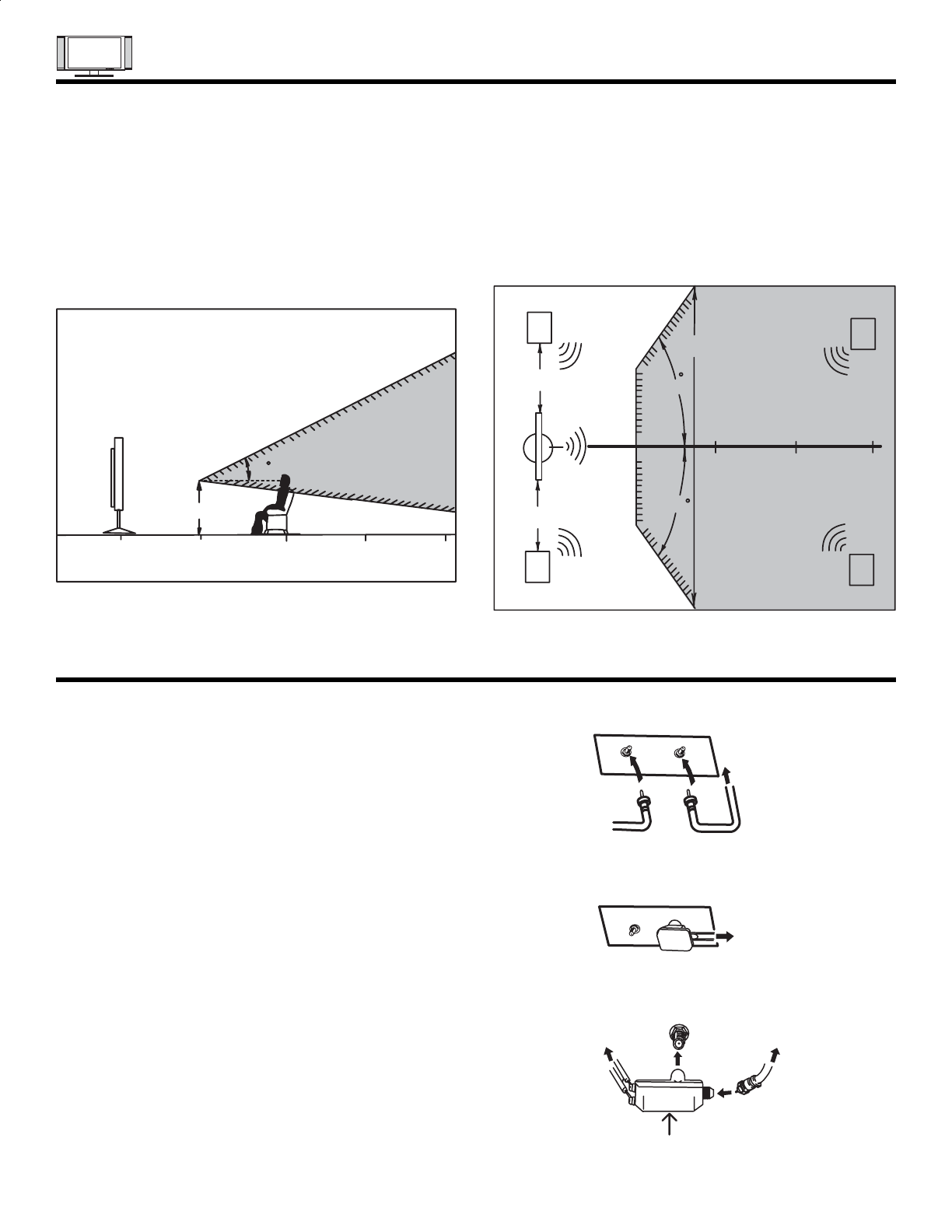
The major benefit of the HITACHI Plasma Television is its large viewing screen. To see this large screen at its best, test various locations
in the room to find the optimum spot for viewing.
The best picture is seen by sitting directly in front of the TV and about 8 to 18 feet from the screen.
During daylight hours, reflections from outside light may appear on the screen. If so, drapes or screens can be used to reduce the
reflection or the TV can be located in a different section of the room.
If the TV’s audio output will be connected to a Hi-Fi system’s external speakers, the best audio performance will be obtained by placing
the speakers equidistant from each side of the receiver cabinet and as close as possible to the height of the picture screen center. For
best stereo separation, place the external speakers at least four feet from the side of the TV, place the surround speakers to the side
or behind the viewing area. Differences in room sizes and acoustical environments will require some experimentation with speaker
placement for best performance.
BEST
VERTICAL VIEWING
ANGLE
20
3’
0’ 5’ 10’ 15’ 20’
ANTENNA CONNECTIONS TO REAR PANEL JACKS
VHF (75-Ohm) antenna/CATV (Cable TV)
When using a 75-Ohm coaxial cable system, connect the outdoor
antenna or CATV coaxial cable to the ANT A (75-Ohm) terminal. If you
have a second antenna, connect the coaxial cable to the ANT B
terminal.
VHF (300-Ohm) antenna/UHF antenna
When using a 300-Ohm twin lead from an outdoor antenna, connect
the VHF or UHF antenna leads to screws of the VHF or UHF adapter.
Plug the adapter into the antenna terminal on the TV.
When both VHF and UHF antennas are connected
Attach an optional antenna cable mixer to the TV antenna terminal,
and connect the cables to the antenna mixer. Consult your dealer or
service store for the antenna mixer.
To outdoor antenna
or CATV cable
To second antenna
To outdoor VHF
or UHF antenna
To outdoor antenna
or CATV system
To UHF
antenna
Antenna Mixer
AIR CABLE
CABLEAIR
AIR
17
GI
300-Ohm Twin Lead Connector
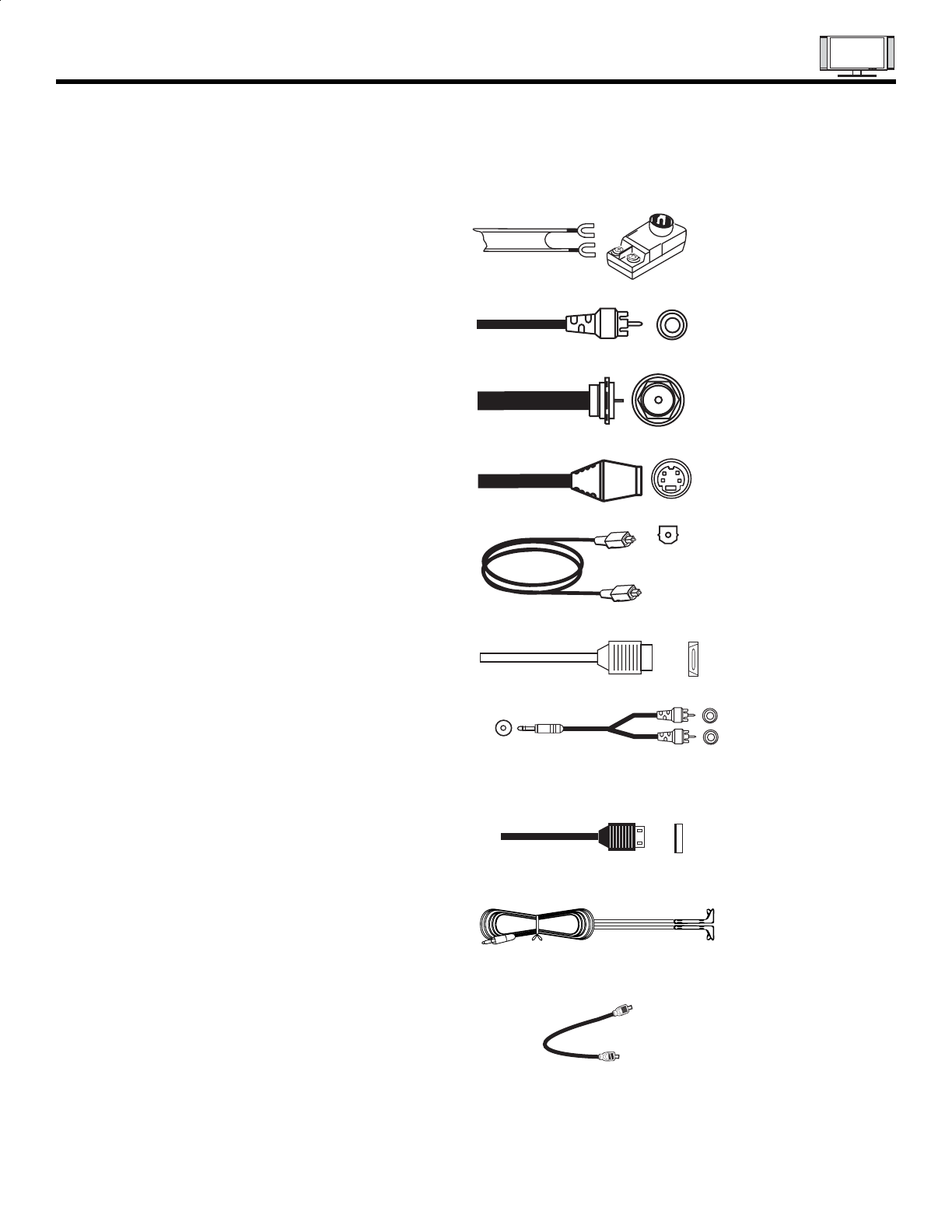
This outdoor antenna cable must be connected to an
antenna adapter (300-Ohm to 75-Ohm).
Phono Connector
Used on all standard video and audio cables which
connect to inputs and outputs located on the
television’s rear jack panel and front control panel.
“F” Type 75-Ohm Coaxial Antenna Connector
For connecting RF signals (antenna or cable TV) to the
antenna jack on the television.
S-Video (Super Video) Connector
This connector is used on camcorders, VCRs and laser-
disc players with an S-Video feature in place of the
standard video cable to produce a high quality picture.
Optical Cable
This cable is used to connect to an audio amplifier with
an Optical Audio In jack. Use this cable for the best
sound quality.
HDMI Cable
This cable is used to connect your external devices
such as Set-Top-Boxes or DVD players equipped with
an HDMI output connection to the TV’s HDMI input.
Stereo Cable (3.8mm plug to 3.5mm plug)
Used on all standard video and audio cable which
connect to inputs and outputs located on the rear jack
panel and front control panel.
USB Cable
This cable is used to connect your digital camera to the
Photo Input in the side of the Plasma television.
IR Mouse Cable (Provided)
Connect the IR Mouse to the IR output of your Plasma
Television when A/V Network is used. You must place
the IR mouse in front of the corresponding IR window
of your cable box and VCR. This connection allows
your TV to control your cable box and VCR.
Power Swivel Cable (Provided)
This cable is used to connect the swivel stand to the
rear panel of the Plasma Television.
Hook-up Cables and Connectors
Most video/audio connections between components can be made with shielded video and audio cables that have
phono connectors. For best performance, video cables should use 75-Ohm coaxial shielded wire. Cables can be
purchased from most stores that sell audio/video products. Below are illustrations and names of common
connectors. Before purchasing any cables, be sure of the output and input connector types required by the
various components and the length of each cable.
AUDIO OUT
3.8mm
STEREO
MINI-PLUG
2
RCA TYPE
PLUGS
18
GI
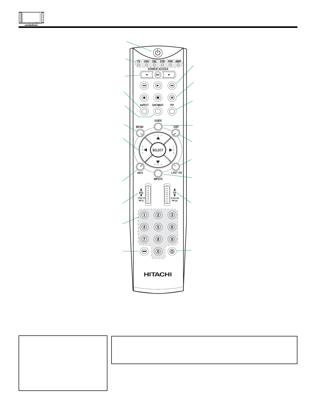
QUICK REFERENCE REMOTE CONTROL
POWER BUTTON
(TV, DVD, CBL, STB, PVR/VCR, AMP/CD)
Turns the selected device on and off.
SOURCE ACCESS BUTTONS
(TV, DVD, CBL, STB, PVR/VCR, AMP/CD)
Changes the mode of the Universal Remote
Control to control the device selected.
DVD/VCR CONTROL BUTTONS
(DVD, PVR/VCR, AMP/CD)
Controls the functions of your VCR, DVD
and audio devices.
DAY/NIGHT
(TV)
Toggles picture mode settings between
DAY and NIGHT mode.
ASPECT BUTTON
(TV)
Changes the aspect ratio of the TV. PIP CONTROL BUTTONS
(TV)
Press to show and change the Picture-in-Picture mode.
MENU BUTTON
(TV, DVD, CBL, STB, PVR/VCR)
Accesses the OSD menu system.
(-) BUTTON
(TV,STB)
The (-) button is used when the remote is in
Set-Top-Box (STB) mode or when the TV uses
a digital input.
NUMERIC BUTTONS
(TV, DVD, CBL, STB, PVR/VCR, AMP/CD)
Used to manually enter the TV channel, and used
for numeric entry when navigating through the OSD,
INPUTS, and AV NET menu systems.
GUIDE BUTTON
(TV, STB, CBL, PVR)
Accesses the Channel Guide of the TV or
the program guide of other devices.
EXIT BUTTON
(TV, CBL, STB, PVR/VCR)
Exits out of the OSD, INPUTS or AV NET menu
systems if their menu is displayed.
LAST CHANNEL BUTTON
(TV, CBL, STB, PVR)
Displays various information on the screen, such as
channel information.
LIGHT BUTTON
(TV, CBL, STB, PVR)
Press to use the back light feature. Can
also be used to change backlight mode.
INFO BUTTON
(TV, STB, CBL, PVR)
Displays various information on the screen,
such as channel information.
CHANNEL WHEEL
(TV, CBL, STB, PVR/VCR, AMP/CD)
Scroll up or down to change channel. Push down on
the wheel to access (FAV) Favorite Channel mode.
(Favorite channel is only available for TV mode.)
CURSOR PAD/SELECT BUTTON
(TV, DVD, CBL, STB, PVR/VCR)
The Cursor Pad is used as a cursor to navigate
through the OSD and INPUT menu systems.
The Select button is used to Select/Activate
highlighted menu items.
VOLUME WHEEL
(TV, AMP/CD)
Scroll up and down to adjust the audio level of your
TV. Push down on the wheel to mute.
PAUSE BUTTON
(TV,PVR/VCR, DVD, AMP/CD)
Press to show and change the Freeze mode of the TV.
Also used to pause other devices when the remote is in
DVD, PVR/VCR, or AMP/CD mode.
INPUTS BUTTON
(TV, AMP)
Accesses the INPUTS menu system.
MODE INDICATOR
Turns on or blinks to show remote control
mode when the SOURCE ACCESS buttons
are pressed.
In addition to controlling all of the functions on your HITACHI Plasma TV, the remote control is designed to operate different types of
devices, such as, DVD Players, Cable Boxes (CBL), set-top-boxes, satellite receivers, PVRs/VCRs and audio devices. The remote
control must be programmed to control the chosen device. Refer to Instruction Book for detailed programming instructions.
LEGEND
TV - Television
DVD - Digital Video Disc Player
CBL - Cable Box
STB - Set-Top-Box/Satellite Receiver
PVR - Personal Video Recorder
VCR - Video Cassette Recorder/Player
AMP/CD - Amplifier/Compact Disc
Player, Audio Devices
NOTES: 1. VCR precode is included in the PVR mode.
2. CD precode is included in the AMP mode.
3. Pressing any buttons will illuminate the backlight for 4 seconds while in
Automatic mode (Default).
19
GI
Firmly bind the cables.
Thread the square
hole with the band.
Hook the band
to the claw.
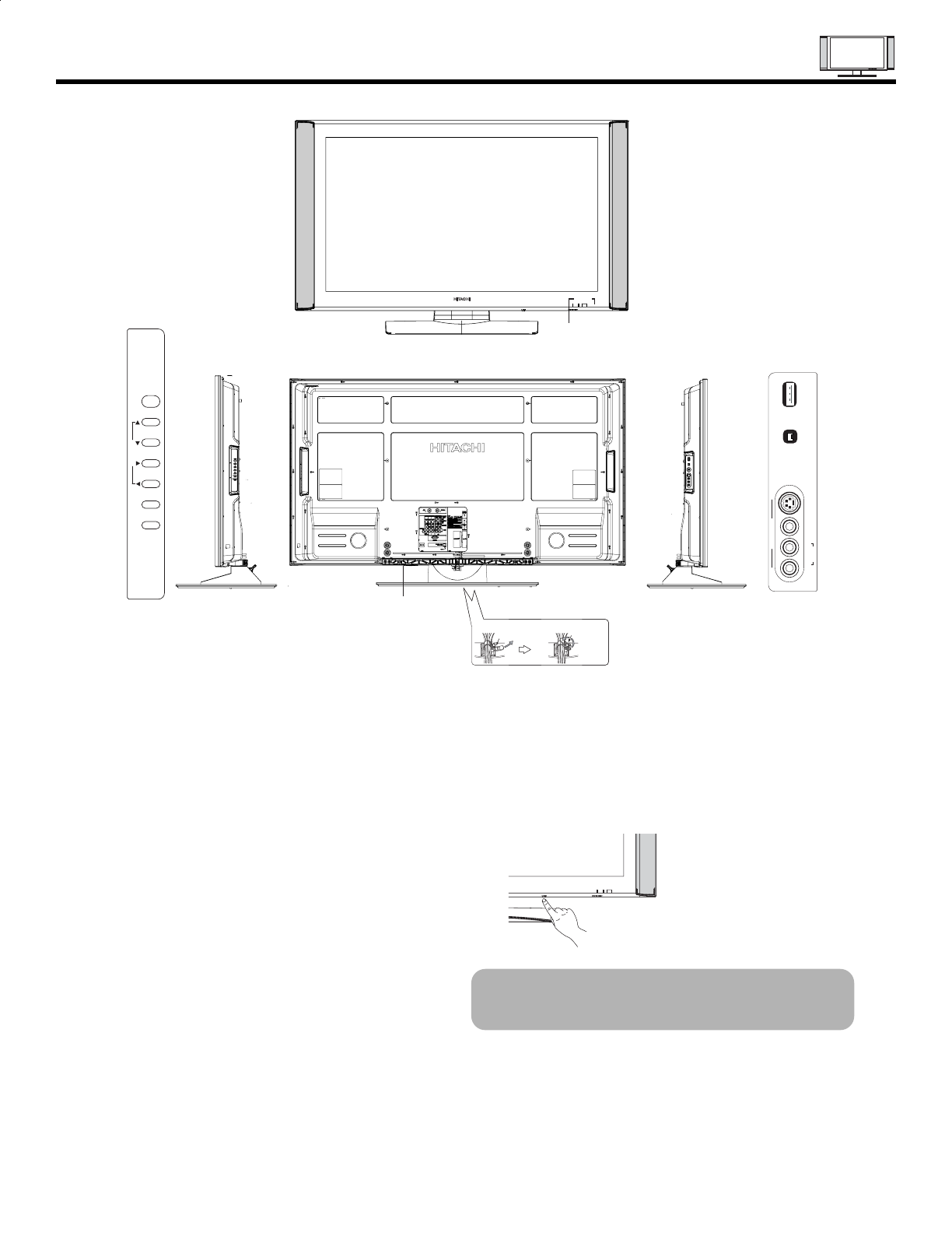
REAR/SIDE VIEW
햲SIDE POWER button
Press this button to turn the Plasma Television
ON/OFF. It can also be turned ON/OFF by remote
control. The “MAIN POWER” button must be at
stand-by mode.
햳MENU/SELECT button
This button allows you to enter the MENU, making
it possible to set TV features to your preference
without using the remote. This button also serves
as the SELECT button when in MENU mode.
햴PHOTO INPUT
Insert USB cable from your Digital Camera, USB
memory or memory card USB drive to view your
digital still pictures .
햵INPUT/EXIT button
Press this button to access the INPUT menu.
Press again to exit the MENU mode.
햶CHANNEL selector
Press these buttons until the desired channel
appears in the top right corner of the TV screen.
These buttons also serve as the cursor down ()
and up () buttons when in MENU mode.
햷VOLUME level
Press these buttons to adjust the sound level. The
volume level will be displayed on the TV screen.
These buttons also serve as the cursor left () and
right () buttons when in MENU mode.
햸POWER button
Display Monitor “MAIN POWER” button
This power button is for the complete system, and
must be turned ON/OFF manually. It is
recommended to leave the “MAIN POWER” to ON
condition (lights red) for stand-by mode.
NOTE: When the “MAIN POWER” button is set to
OFF or the TV is unplugged, the clock will
stop and may eventually reset itself.
FRONT VIEW
The Main Power
button is located on
the broadside
bottom, under the
label “MAIN
POWER”.
20
Front/Rear/Side Panel Controls
햸
POWER
CH
CH
CURSOR
CURSOR
VOL
VOL
INPUT/EXIT
MENU/SELECT
+
+
-
-
햲
햵
햳
햶
햷
R
AUDIO
L/MONO
VIDEO S-VIDEO
INPUT
PHOTO
PHOTO
INPUT 5
INPUT 5
햴
햻
햺햹
햸
햽
IEEE1394
DV INPUT
* Only 55HDT52
and 55HDX62
*
GI
햹POWER light indicator
To turn the monitor ON, press the main power
switch located on the lower right side of the
monitor. A red stand-by indicator lamp located on
the lower right corner of the front bezel will
illuminate. The Plasma TV is now ready for remote
ON/OFF operation.
햺REMOTE CONTROL sensor
Point your remote at this area when selecting
channels, adjusting volume, etc.
햺LEARNING AV NET sensor
Point your equipment’s remote control at this area
while using the AV NET Learning Wizard.
햻SIDE INPUT JACKS (for VIDEO: 5)
Use these audio/video jacks for a quick hook-up
from a camcorder or VCR to instantly view your
favorite show or new recording. Press the INPUTS
button then use the CURSOR PAD and the SELECT
button on the remote control to select INPUT 5. If
you have mono sound, insert the audio cable into
the left audio jack.
Front/Rear/Side Panel Controls
Indicating Lamp Power Status Operating
Off Off When the main power switch is set to
OFF.
Lights Red Off When the main power switch on the display
(Stand-by) monitor is ON.
Lights Green On Display monitor MAIN POWER is ON.
Lights Orange Off Display monitor MAIN POWER is ON
(Power Saving) with no signal input except antenna
(no sync. signal).
NOTES: 1. Your HITACHI Plasma TV will appear to be turned OFF (lights orange) if there is no video input
when VIDEO: 1, 2, 3, 4 and 5. Check the Power Light to make sure the Display Monitor is
turned off or in Stand-by mode (lights red) when not in use.
2. Remote Control can not turn ON/OFF the “MAIN POWER” of the display monitor.
21
햽IEEE1394 (DV Input) Only for 55HDT52 & 55HDX62
This input provides a digital interface for your
external digital devices such as your digital video
(DV) camcorder.
GI
REAR PANEL CONNECTIONS
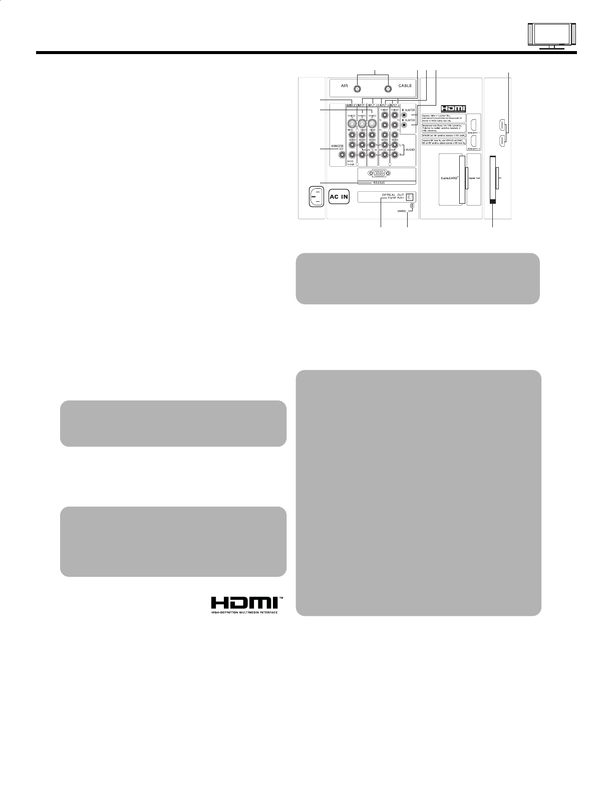
햲Antenna Input
The remote control allows you to switch between
two separate 75-Ohm RF antenna inputs, CABLE
and AIR. CABLE input can be displayed as a main
picture or sub-picture. AIR can only be displayed
as a main picture (AIR cannot be displayed as a
sub-picture).
햳Audio/Video Inputs 1, 2, 3 and 4
By using the INPUTS button, the CURSOR PAD (
and ), and the SELECT button or CURSOR PAD
of the remote control, you can select each video
source. Use the audio and video inputs to connect
external devices, such as VCRs, camcorders,
laserdisc players, DVD players etc. (if you have
mono sound, insert the audio cable into the left
audio jack).
햴MONITOR OUT & HI-FI AUDIO OUT
These jacks provide fixed and variable audio and
video signals (CABLE/AIR, INPUT 1, 2 and 5)
which are used for recording. Use the S-VIDEO
Output for high quality video output. Component
signal to Input 1 and 2, and HDMI inputs will not
have monitor output.
햵Optical Out (Digital Audio)
This jack provides Digital Audio Output for your
audio device that is Dolby®Digital and PCM
compatible, such as an audio amplifier.
NOTE: *Manufactured under license from Dolby
Laboratories. “Dolby” and the double-D
symbol are trademarks of Dolby
Laboratories.
햶S-VIDEO Inputs 1 and 2
Inputs 1 and 2 provide S-VIDEO (Super Video)
jacks for connecting equipment with S-VIDEO
output capability.
NOTE: 1. You may use VIDEO or S-VIDEO inputs to
connect to INPUT 1 and 2, but only one of
these inputs may be used at a time.
2. S-VIDEO output may be used for
recording, only when the input is of S-
VIDEO type.
햷HDMI1 (High Definition Multimedia
Interface) (INPUT 1)
ABOUT HDMI –HDMI is the
next-generation all digital interface for consumer
electronics. HDMI enables the secure distribution
of uncompressed high-definition video and multi-
channel audio in a single cable. Because digital
television (DTV) signals remain in digital format,
HDMI assures that pristine high-definition images
retain the highest video quality from the source all
the way to your television screen.
Use the HDMI input for your external devices such
as Set-Top-Boxes or DVD players equipped with an
HDMI output connection.
HDMI, the HDMI logo and High-Definition
Multimedia Interface are trademarks or registered
trademarks of HDMI Licensing LLC.
NOTE: 1. The HDMI input is not intended for use
with personal computers.
2. Only DTV formats such as 1080I,720P,480I
and 480P are available for HDMI input.
햸Component: Y-PBPRInputs
INPUTS 3 and 4provide Y-PBPRjacks for
connecting equipment with this capability, such as
a DVD player or Set Top Box. You may use
composite video signal for both inputs.
NOTE: 1. Do not connect composite VIDEO and
S-VIDEO to INPUT 1, 2 or 5at the same
time. S-VIDEO has priority over VIDEO input.
2. Your component outputs may be labeled
Y, B-Y, and R-Y. In this case, connect the
components B-Y output to the TV’s PB
input and the components R-Y output to
the TV’s PRinput.
3. Your component outputs may be labeled
Y-CBCR. In this case, connect the component
CBoutput to the TV’s PBinput and the
component CRoutput to the TV’s PRinput.
4. It may be necessary to adjust TINT to
obtain optimum picture quality when using
the Y-PBPRinputs (see page 41).
5. To ensure no copyright infringement, the
MONITOR OUT output will be abnormal,
when using the Y-PBPRjacks and HDMI
Input.
6. INPUT 3 and INPUT 4 (Y/VIDEO) can be
used for composite video and component
video input.
햹IR Blaster
This jack provides IR output to your external
components (VCR, Cable box, DVD player, etc.).
With this connection, your external components
can automatically be controlled by the A/V network
feature. This connection will allow you to control
the external components with your Plasma
Television’s remote control in TV mode.
햺For Service Use Only
Do not connect anything to this terminal.
Specifically for Service use only.
햲햳햸햹
햴
햷
햻
햺
햵햾
햶
햿
햽
22
GI
FRONT/REAR/SIDE PANEL CONNECTIONS
햻Subwoofer Out
Connect this SUB WOOFER OUT output to the
external audio component input using the sub
woofer cable provided.
햽Upgrade Card
This card slot is for future software upgrades.
Hitachi will notify you if a software upgrade is
required for your TV. In order to receive written
notification, please complete and return your
warranty card.
햾To Power Swivel Connector
Connects to the Power Swivel Table Top Stand.
햿CableCARD Slot
This slot is for the CableCARD that will be provided
by your local cable operator to gain access to
chosen cable channels. The CableCARD will allow
you to tune digital and high definition cable
channels. Please call your local cable operator if
this service is available before requesting a
CableCARD (also known as Point of Deployment
(POD) module).
1. Connect a coaxial cable to cable terminal of
the Rear Panel Jacks.
2. Insert the CableCARD into the slot (Top of card
should be facing towards you as shown
below).
NOTE: 1. A digital cable subscription is required.
2. AIR will not be available when CableCARD
is inserted.
3. Do not insert a PCMCIA card into the
CableCARD slot.
If the CableCARD is properly installed or not installed,
the TV will display the following respective screens.
After the CableCARD is installed, wait until the second
screen below appears. The third screen below will
appear if a channel is not authorized for viewing. Press
the EXIT button to exit the second screen.
Please take note of all information on the screen (you
will provide this information to your cable operator).
Call your cable operator and give them the information
from the card to start your cable service.
Digital Cable
INSER
TINSER
INSER
T
CableCARD is installed
CableCARD
is not installed
OR
In order to start cable service
for this device, please contact
your cable provider
CableCARD(tm): 123-456-789-1
Host: 123-456-789-1
Data: 123-456-789-1
UnitAddress: 123-456-789-1
Acquiring Data.
Please wait.
Press EXIT to return
Not an Authorized Channel
OR
23
GI
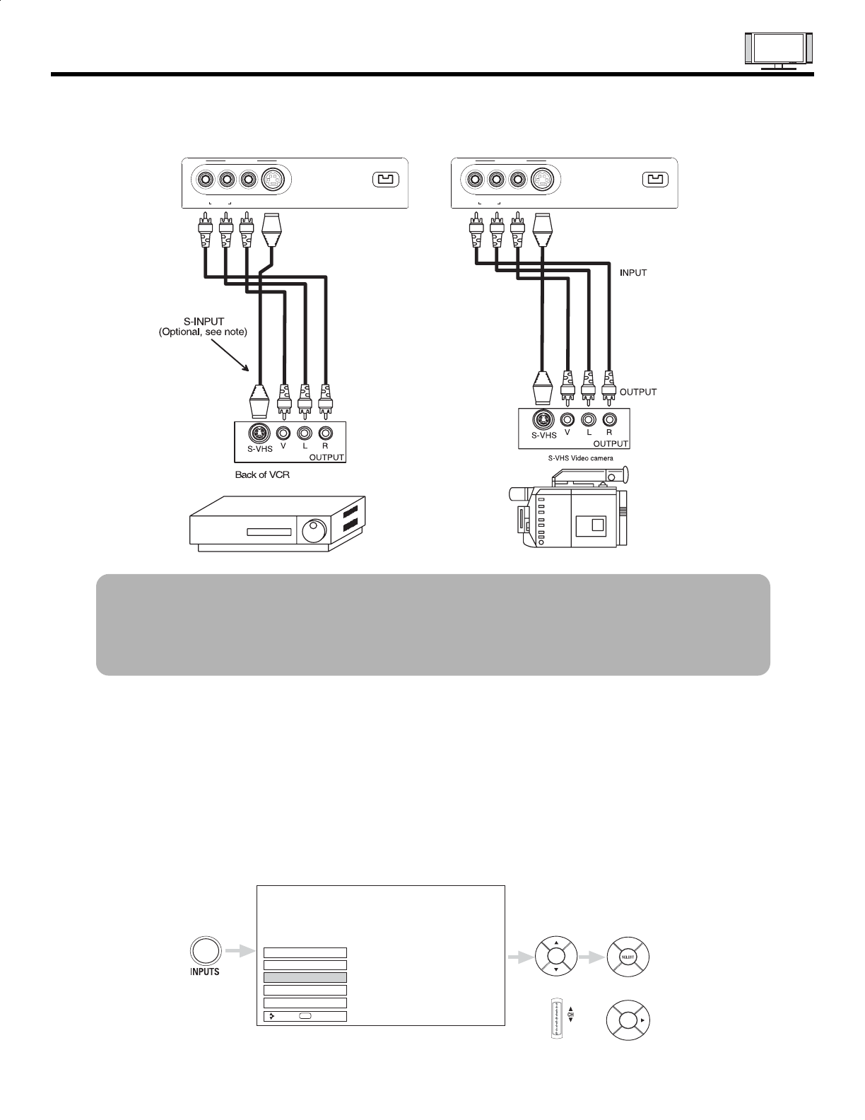
The front panel jacks are provided as a convenience to allow you to easily connect a camcorder or VCR as shown
in the following examples:
NOTE: 1. Completely insert connection cord plugs when connecting to left side panel jacks. If you do not, the
played back picture may be abnormal.
2. If you have a S-VHS VCR, use the S-INPUT cable in place of the standard video cable.
3. If you have a mono VCR, insert the audio cable into the left audio jack of your TV.
4. S-VIDEO input takes priority over VIDEO input.
5. If you have a VHS or 8mmcamcorder, use the S-VIDEO cable in place of the VIDEO cable.
The exact arrangement you use to connect the VCR, camcorder, laserdisc player, DVD player, or HDTV Set
Top Box to your Plasma TV is dependent on the model and features of each component. Check the
owner’s manual of each component for the location of video and audio inputs and outputs.
The following connection diagrams are offered as suggestions. However, you may need to modify them to
accommodate your particular assortment of components and features. For best performance, video and
audio cables should be made from coaxial shielded wire.
Before Operating External Video Source
Connect an external source to one of the INPUT terminals, then press the INPUTS button to show the
INPUTS menu. Use the CURSOR PAD (and ) to select the Antenna or Input of your choice. Then press
the SELECT button or the CURSOR PAD to confirm your choice .
Connecting External Video Sources
Input 1
Air
Cable
Photo Input
Input 5
Move
SEL
Sel.
oror
Left Side Panel Left Side Panel
R
AUDIO
L/MONO
VIDEO S-VIDEO
INPUT
PHOTO
INPUT 5
INPUT 5
R
AUDIO
L/MONO
VIDEO S-VIDEO
INPUT
PHOTO
PHOTO
INPUT 5
INPUT 5
24
GI
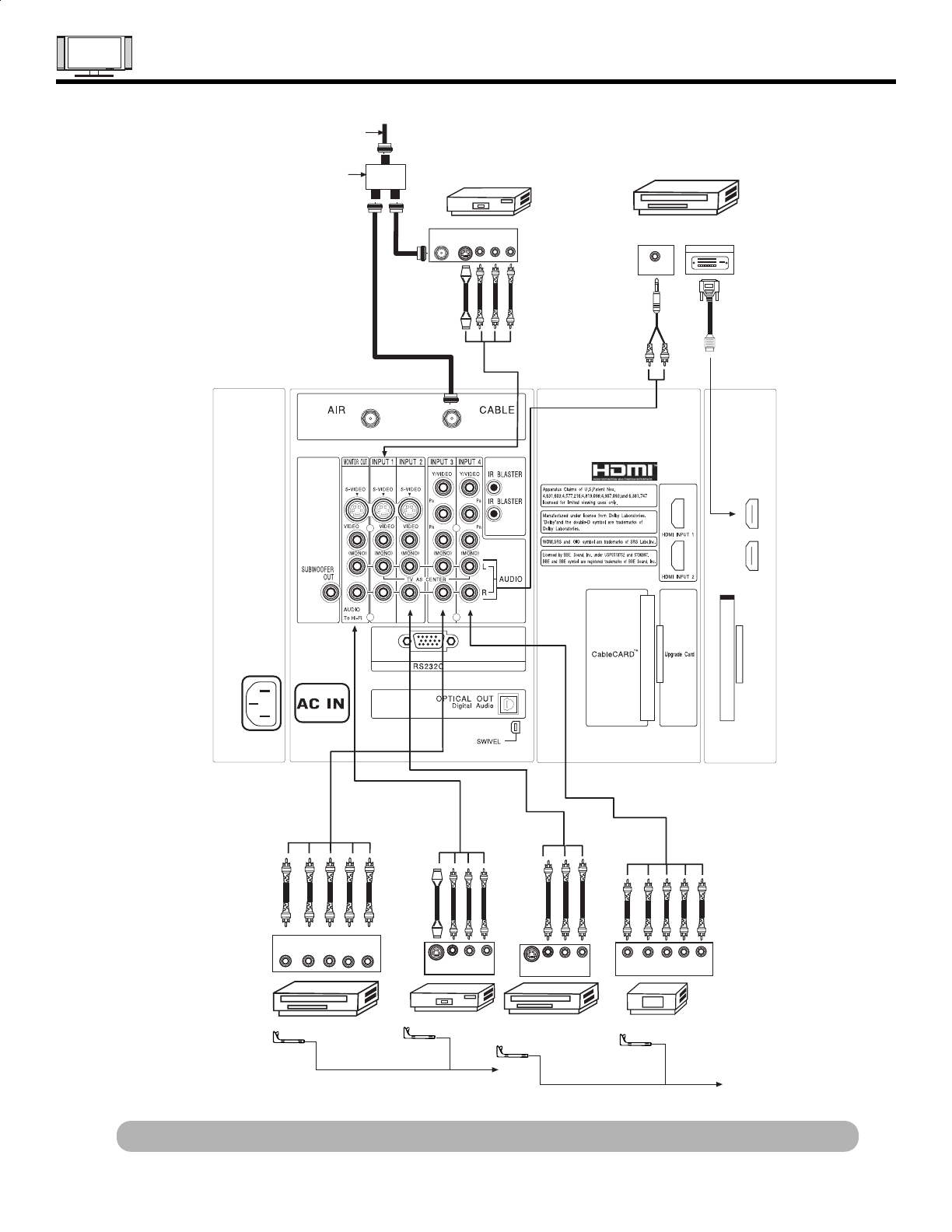
CONNECTING EXTERNAL VIDEO SOURCES
VCR #1
Outside antenna or
cable TV coaxial cable
2-Way signal splitter
ANT
IN
OUTPUT
S-VIDEO VL R
DIGITAL
OUTPUT CAPABILITY
DIGITAL OUTPUT
Laserdisc player, VCR,
camcorder, etc.
OUTPUT
Y PB PR L R
HDTV Set-Top Box
DVD Player
(PROVIDED)
(PROVIDED)
DVI
to
HDMI
AUDIO OUT
OUTPUT
YP
B/CBPR/CR
L R
VCR #2
V L R
OUTPUT
S-VIDEO
V L R
INPUT
S-VIDEO
CONNECT TO
IR BLASTER CONNECT TO
IR BLASTER
NOTE: Cables are optional, except when specified.
25
GI

TIPS ON REAR PANEL CONNECTIONS
• S-VIDEO, YPbPR, or HDMI connections are provided for high performance laserdisc players, VCRs etc. that
have this feature. Use these connections in place of the standard video connection if your device has this
feature.
• If your device has only one audio output (mono sound), connect it to the left audio jack on (L/(MONO)) the
Rear Panel.
• Refer to the operating guide of your other electronic equipment for additional information on connecting
your hook-up cables.
• A single VCR can be used for VCR #1 and VCR #2, but note that a VCR cannot record its own video or line
output (INPUT: 1 in the example on page 25). Refer to your VCR operating guide for more information on
line input-output connections.
• Connect only 1 component (VCR, DVD player, camcorder, etc.) to each input jack.
• COMPONENT: Y-PBPR(Input 3 & 4) connections are provided for high performance components, such as
DVD players and set-top-boxes. Use these connections in place of the standard video connection if your
device has this feature.
• Your component outputs may be labeled Y, B-Y, and R-Y. In this case, connect the components B-Y
output to the TV’s PBinput and the components R-Y output to the TV’s PRinput.
• Your component outputs may be labeled Y-CBCR. In this case, connect the components CBoutput to the
TV’s PBinput and the components CRoutput to the TV’s PRinput.
• It may be necessary to adjust TINT to obtain optimum picture quality when using the Y-PBPRinputs.
• To ensure no copyright infringement, the MONITOR OUT output will be abnormal, when using the Y-PBPR, and
HDMI input jacks.
• Input 1 or 2 can accept HDMI signal.
• S-VIDEO monitor output may be used for recording only when the input is of S-VIDEO type.
• When using a DVI or HDMI input from a Set-Top-Box, it is recommended to use a 1080i or 720p input
signal.
MACROVISION NOTES:
1. Video signals fed through a VCR may be affected by copyright protection systems and the picture will be
distorted on the television.
2. Connecting the television directly to the Audio /Video output of a Set-Top-Box will assure a more normal
picture.
26
GI
27
DW1U
A buzzing sound might be heard when the plasma display monitor is turned on in a very quiet
room. This is due to the plasma panel drive circuit when it is functioning. This arching sound
is normal and it is not a malfunction.
Some infrared rays are emitted from the plasma display monitor’s panel that might affect other
infrared controlling equipment.
High-precision technology is used to manufacture the plasma display panel; But in some
cases, there are minor defects in some parts of the screen. Points that do not light, points
with brightness different from that of the periphery, points with color different from that of the
periphery, etc. Some pixels will always be on or always off. Please note that this is not a
malfunction.
When receving still picture signals, (e.g. channel number indication or clock indication) for a
while, you can see image-like when the picture varied. This is not a defect.
The plasma display panel is lighting the phosphors by the discharge of internal radiation. In
some cases, this may cause the temperature of the panel surface to increase. Please note
that this is not a malfunction. The Plasma TV surface temperature is higher than a
Cathode-ray-tube.
The plasma panel is made from glass. Heavy shock on the front panel might damage it.
When the PDP monitor is transported horizontally, the glass panel has the possibility of being
broken or increasing the picture defects. At the time of transportation, horizontal style is
prohibited. More-over, please treat the plasma panel with great care because of a precision
apparatus. Please instruct transporters so that it should be put into the packing box at the time
of shipment.(There is a possibility that breakage of the panel or defects will increase.)
Rough transportation might cause damage to the panel and pixel failure.
The plasma monitor illuminates phosphor to display images. The phosphor has a finite
illumination life. After extended periods of illumination, the brightness of the phosphor will be
degraded to such extent that stationary images would burn-in that part of the screen as
grayed-out images.
Tips to prevent such image retention are:
- Do not display images having sharp brightness differences or hi-contrast images, such as
monochrome characters and graphic patterns, for long.
- Do not leave stationary images appearing for long, but try to refresh them at appropriate
intervals of time, or try to move them using screen saver function.
- Turn down the contrast and brightness controls.
PDP television has luminosity and low contrast compared with CRT television.
When a screen is seen at point-blank range, a random fine grain may be visible to a dark part.
If an apparatus (VCR, etc.) antenna line is arranged near the monitor, the image may shake,
or disturbance may be received.
There is some time lag betweeen the picture and the sound. You can see lip motion that is
delayed compared to the sound.
Electric discharge/luminescence characteristic of the PDP panel also changes with peripheral
temperature. Moreover, since there is also high power consumption value, a specified
temperature environment is required.
Storing the plasma television for a period of more than 2 to 3 months without use might cause
an unstable picture when the set is turned on.
Operating altitude: 800 to 1114hPa (6194ft to -2484ft). Operating temperature: 41˚F to 95˚F.
Storage Altitude: 300 to 1114hPa (31,912 to -2484ft). Storage temperature: 5˚F to 140˚F.
Frequent use of the Power ON or OFF might trigger the power protection circuit. If the TV
does not turn ON, please wait a little before turning ON again.
1 Arching sound from
plasma display monitor’s
panel.
2 Interference for infrared
equipment.
3 Bright and dark spots
4 Picture Image (Spectrum)
5 Display panel surface
temperature is too high
6 Plasma Surface
7 Transportation
8 Image retention
9 Luminosity and contrast
10 Granular spots
11 Disturbance to video
apparatus
12 Lip Sync
13 About the use
environment of PDP
television (temperature)
14 Caution on prolonged
storage
15 Operating
16 Storage
17 Power ON or OFF
No. Items Notes
IMPORTANT NOTES
BASIC OPERATION
GI

28
DW1U
ADJUSTMENTS TABLE OF CONTENTS
1 Adjustment procedure start up....................................................................................................29
1.1 How to get into adjustment mode ................................................................................29
1.2 Changing data and selecting adjustment code............................................................29
2 Memory initialize ........................................................................................................................29
2.1 Memory initialize operation ..........................................................................................29
2.2 Factory and service adjustments ................................................................................30
3 Video Adjustment .......................................................................................................................30
3.1 Sub-Contrast Adjustment .............................................................................................30
3.2 Brightness Check .........................................................................................................30
4 POWER SUPPLY Vs, Va Voltage Adjustment....................................................................................31
5 White balance adjustment ..........................................................................................................32
5.1 Video Color Temperature Adjustment (High) ..........................................................................32
5.2 Video Color Temperature Adjustment (Medium)..........................................................32
5.3 Video Color Temperature Adjustment (Standard) ........................................................33
5.4 Video Color Temperature Adjustment (Black and White) ............................................33
5.5 White Balance Adjustment OSD Flowchart Diagram ..................................................... 34
10 I2C Adjustment Data .................................................................................................................40
6 DIGITAL MAIN CHECK ............................................................................................................33
7 Screen Check ............................................................................................................................36
8 HDMI Adjustment ..................................................................................................................... 36
9 Settings for Delivery .................................................................................................................37
TO GO TO A SECTION, CLICK ON ITS HEADING BELOW
TABLE OF CONTENTS
GI
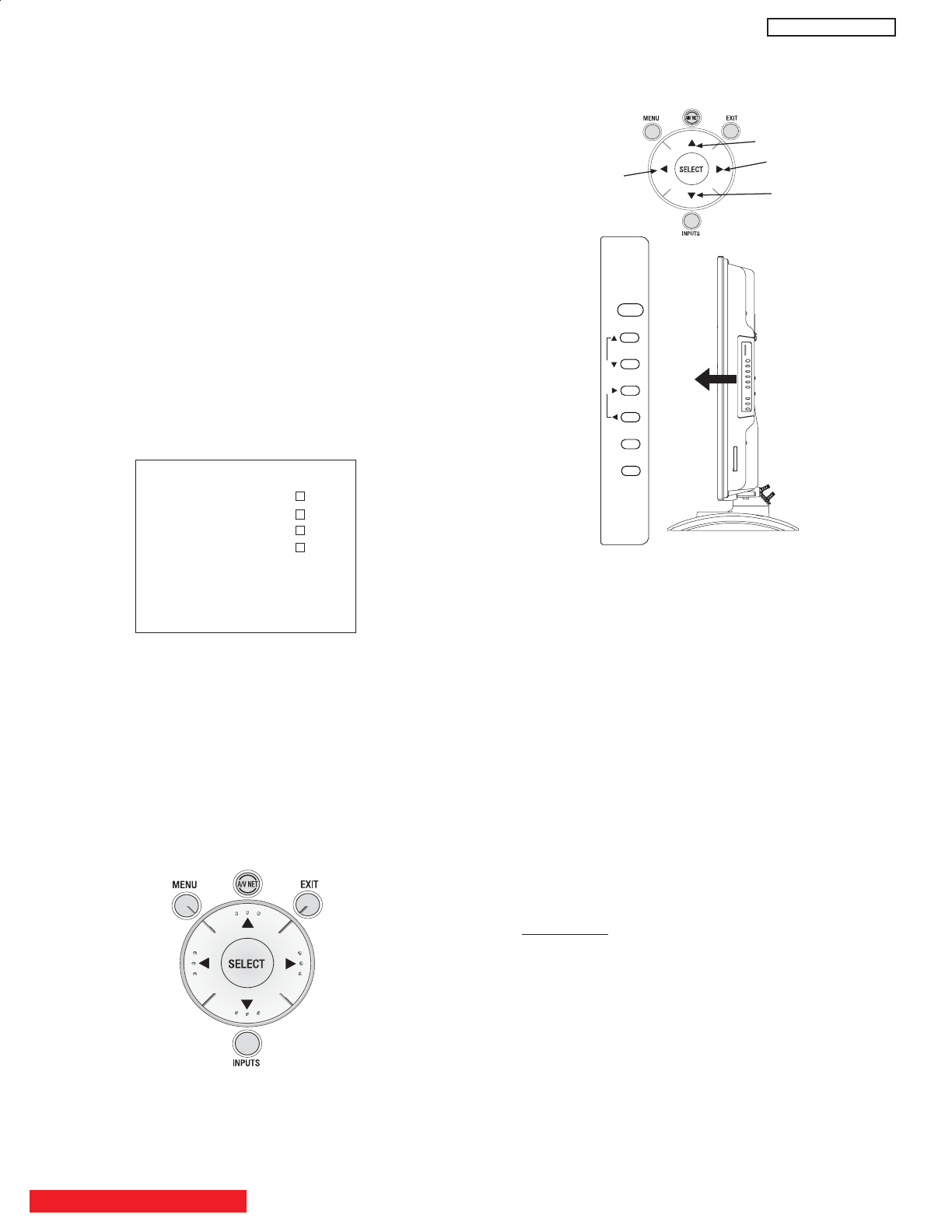
29
DW1U
1 ADJUSTMENT PROCEDURE START-UP
The 55HDT5255HDS52 and 55HDX62 PDP TV sets
pass through adjustment procedures during the assembly
process. These adjustments must be done to assure the
best performance of the PDP set for the consumer.
Also, after servicing, these same adjustments must be
done. The adjustments are all made through the I2C bus
by changing data in the Adjustment mode menu.
Table 2 on pages 38-46 shows the complete parameter
list with a brief description, signal format, the adjustment
range and the initial data.
1.1 HOW TO GET TO ADJUSTMENT MODE
Chassis adjustment mode can be access by pressing
the R/C keys MENU + MENU + 8 + SELECT to enter
adjustment mode. For some parameters the only way
to see them is by selecting the parameter number than
pressed SELECT in order to see it; then DATA can be
change if other parameter needs to change then press
key then repeat the same procedure.
Other way to access this mode is by use JIG R/C code: (9C Hex).
To escape from Adjustment Mode press “INPUT” key on Side
panel or EXIT key of R/C to exit service adjustment mode.
1.2 CHANGING DATA AND SELECTING ADJUSTMENT
CODE
When the PDP set is in adjustment mode, the cursor ,,
, and MENU keys of the remote control or front panel
may be used as the adjustment keys.
A. Use any Hitachi remote control when making an
adjustment.
, keys are used for selecting adjustment item.
,keys are used for changing data values.
MENU key is used to advance through the adjustment
mode menus and pages.
Remote Control Buttons
Change
Selection (Up)
Increase
Data Value
Change
Selection (Down)
Decrease
Data Value
POWER
CH
+
CH
-
VOL
+
VOL
-
INPUT/EXIT
MENU/SELECT
SUB BRIGHT
WHITE BAL HIGH
WHITE BAL MED
WHITE BAL STD
WHITE BAL B/W
H POSITION **
V POSITION **
FACT RESET
B. To make a selection, use the NUMBER pad on the PDP
R/C; example : select SEINE press 69 then SELECT
the DATA shown is "EB" ; if this DATA needs to be change
press the keys to modify, when finish press SELECT
key to store the new DATA value.
normal condition.
C. After finishing the necessary adjustment press the R/C
EXIT key or EXIT key on the side panel.
Adjustment mode is released and PDP set returns to
normal condition.
,,
2 MEMORY INITIALIZE
2.1 MEMORY INITIALIZE OPERATION
NOTE: The execution of this function returns the
adjustment codes to the preset values, therefore,
adjustment data will be lost.
Procedure
(1) Enter Adjustment mode by the method described in
sub-items 1.1 and 1.2 from item 1 (“Adjustment
procedure start up”).
(2) Get to the second page of Adjust Mode by pressing
remote control “Menu” key once, or with either the
R/C or front panel ,cursor keys several times.
(3) Select MEMORY INIT adjust code.
(4) Activate MEMORY INIT by pressing cursor key for
more than 3 seconds.
(5) Check the following process for initialization opera-
tion.
BACK TO ADJUSTMENTS
GI
CH 6
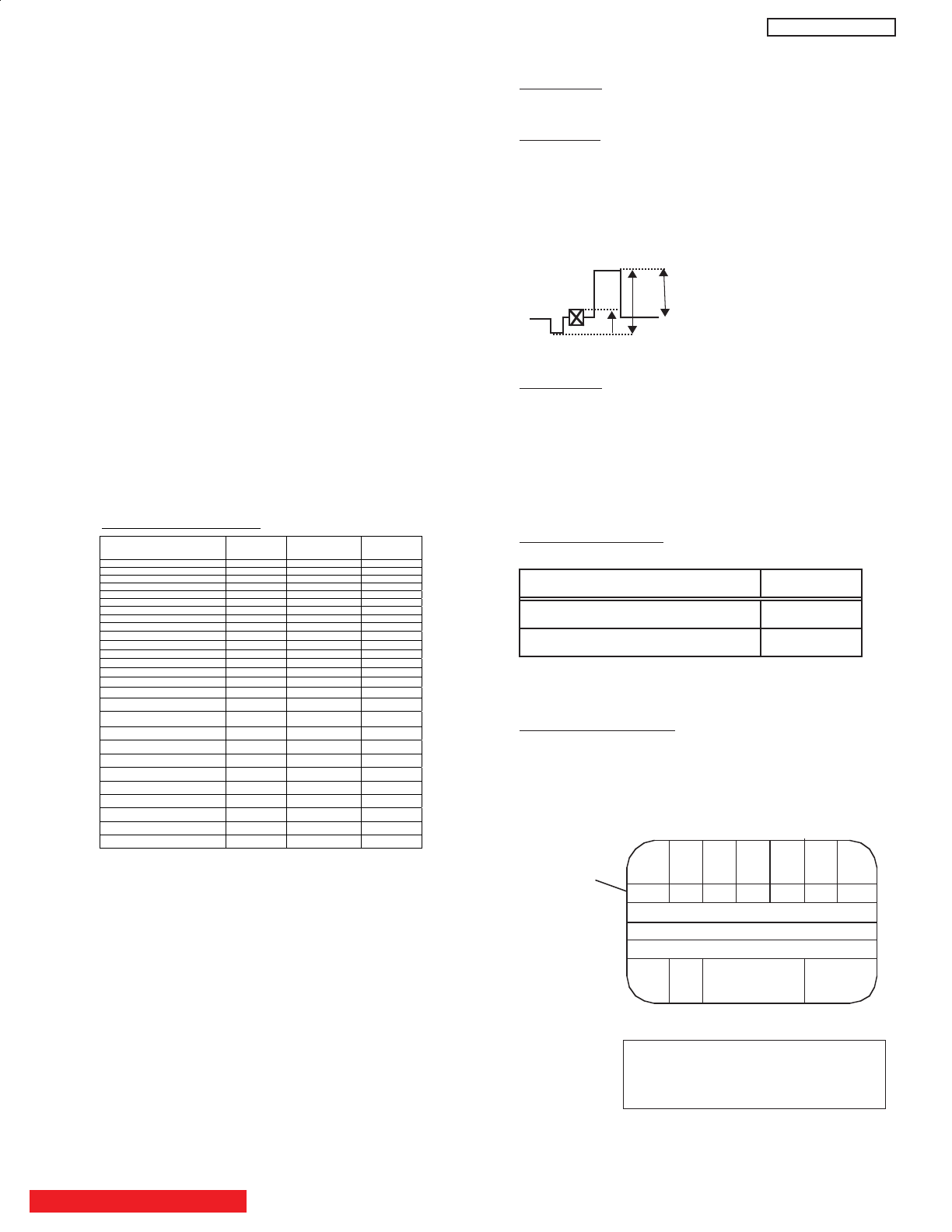
30
DW1U
3.2 SUB-CONTRAST ADJUSTMENT
Preparation
Receive Sub-contrast adjustment signal (Fig. 1).
Adjustment
(1) Select ‘SUB CONTRAST’ of Service Adj. Menu.
Press for over 2 seconds and have it perform
automatic adjustment. When it’s completed, ‘Auto
Adjusting’ on the screen will be disappeared.
V
1
V
3V
2
Fig. 1
Full White
(RF Input ANT A))
V1=1.0 Vp-p (when
V2=100IRE with
V3=7.51IRE)
3.3 BRIGHTNESS CHECK
Preparation
(1) Start checking 20 minutes or more after the power is
turned ON.
(2) Receive the color bar signal.
(3) The vertical incident illumination on the screen
should be 20 lux or less.
(4) Picture Format is 16:9 standard mode.
(5) Select Day mode and reset.
Checking Procedure
(1) Check the brightness as below.
Note: If set black level is NG, readjust item Sub
Contrast adj.
Measuring Conditions
(1) At the signal electric field strength 75± dBµ, the
specification mentioned above should be satisfied.
(2) At the input electric field 46-106dBµ, there should be
no abnormality.
* From color bar pattern below.
DW-1
Can be seen at black A3*
Can be seen slightly from black A5*
A
7
A
6
A
5
A
4
A
3
A
2
A
1
White 100%
7 step gray scale
A
4 has tolerance.
A
4 can be between black and
Slightly from black.
Color Bar Signal
10
0
(8)When PDP turns ON , it will tune CH03 this is the
complete operation of Memory Initialize process.
·Process of Memory Initialize operation.
A screen is be colored blue when MEMORY INIT
start.
A screen is be colored green when MEMORY INIT
finish normally.
A screen is be colored blackwhen MEMORY INIT
finish abnormally.
(6) Do not unplug from AC outlet until this operation
is complete and do not perform any key operation
either, after this operation each factory setting and
all adjust mode data should reset to delivery settings
automatically.
(7) After Memory Initialize, it should be unplug AC cord.
Unplug and plug AC cord and then all settings and data
①
②
③
are updated.
The adjustment item that is affected by the memory
initialize operation is shown below:
Note: Perform pre heat-run for more than 20 min. before
adjusting.
2.2 FACTORY AND SERVICE ADJUSTMENTS
BACK TO ADJUSTMENTS
* JIG. R/C FACTORY PRESET CODE:92
MEMORY INITIALIZE and FACTORY PRESET
ITEM MEMORY
INITIALIZE
FACTORY RESET REMARKS
H POSITION ADJUST DATA INITIALIZE NOT INITIALIZE
V POSITION ADJUST DATA INITIALIZE NOT INITIALIZE
SUB CONTRAST ADJUST DATA INITIALIZE NOT INITIALIZE
SETTING DATA FOR EACH DEVICE INITIALIZE NOT INITIALIZE
BBE EFFECT SETTING DATA INITIALIZE NOT INITIALIZE
AUDIO AGC SETTING DATA INITIALIZE NOT INITIALIZE
V CHIP RATING SETTING DATA INITIALIZE NOT INITIALIZE
CCD SETTING DATA INITIALIZE NOT INITIALIZE
FACTORY RESET ITEM INITIALIZE INITIALIZE
WHITE BALANCE INITIALIZE NOT INITIALIZE
GI
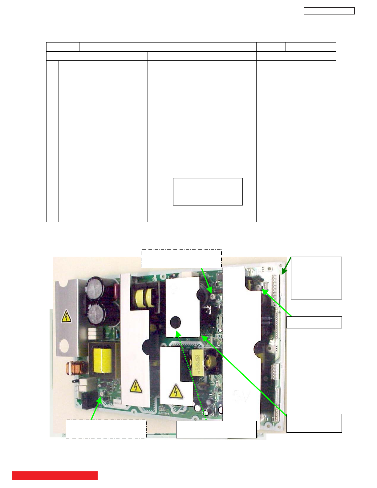
31
DW1U
BACK TO ADJUSTMENTS
R1540 Vs potenciometer
/*KTWMCYC
4. Vs, Va voltage adjustment
Item Power Unit Vs, Va Adjustment Adj. point Refer to following
Adjustment Preparations Adjustment Procedures Remarks
(1) Turn on the set and perform
pre-heat run more than 1 min
on burn-in screen.
(1) Turn Vs ADJ to adjust Vs voltage
to be within r0.1V of the value
specified in the label on the panel.
Permissive level of voltage in
sufficient time of heat-run
performed is:
Vs: withinr0.45V
Va: withinr0.55V
(2) Receive full black pattern signal
(or video silence signal; but the
power will be automatically turned
off after a few seconds by power
save function.)
(2) Turn Va ADJ to adjust Va voltage
to be within r0.2V of the value
specified in the label on the panel.
Reconfirm that Vs voltage remains
within r0.1V of the specified value.
Readjust if it’s outside of the margin.
(3) Connect voltmeter (which has an
error within 0.02V or less) leads
to Vs (or Va) and GND test points
of the power unit.
(3)
Label example Label position (Reference)
: Upper left
If it’s hard to read the voltage
value because of the wiring
positions, write it down by a
marker at visible place in
advance.
<LOT>N6
Vs= 80.0V Va=60.0V
V䌷=140.0V Vx=60.0V
CN64㧦Vs/Va
Test pins
Ԙpin: Va
ԡpin: Vs
Ԝpin: GND
̪Never touch this VR ! (PFC)
(This is already adjusted.)
R1573㧦Va ADJ. VR
Adjustment driver insert into this
hole to adjust Vs VR R1540.
R1540㧦Vs ADJ. VR
(UNDER the FIN)
̪Never touch this VR ! (OLP)
(This is already adjusted.)
GI

32
DW1U
5 WHITE BALANCE ADJUSTMENTS
General Notes for White Balance
(1) If the incident illumination is more than 20 lux,
change the environment (location, lighting, etc.) and
ensure it to be less than 20 lux.
(2) At least one of the color drive codes must stay at its
maximum value, FFH.
5.1 VIDEO COLOR TEMPERATURE ADJUSTMENT
(HIGH)
Preparation 1
(1) Set the output of signal generator to white raster.
(Ratio:100%)
(2) Component signal 42” 55”
Video level: 0.700Vp-p 0.280Vp-p
SYNC: 0.300Vp-p 0.286Vp-p
Set-up level: 0V 0V
(3) Input white raster signal into COMPONENT input
terminal of the PDP set.
(4) Set user control to Day mode. (Picture Mode)
(5) Confirm that the mode is set as “Factory Setting
Mode”.
(6) Aspect: Video: Expanded
Adjustment
(1) Perform the following adjustment with the remote
control.
(2) Set the CRT color analyzer (CA-100) at the center of
the panel.
(3) Set color temperature to “HIGH”.
(4) Ensure that Adjustment R/G/B DRIVE (HIGH) are all
set as FF.
(5) After receiving White raster signal, step down the two
(or one) among Adjustment R/G/B DRIVE (HIGH)
and adjust the value shown in the following:
At least one of the data should be FF.
Specification
Video Color temperature (HIGH)
x = 0.258
42" ± 0.005
y = 0.273 ± 0.005
(Color temp:12000K)
x = 0.264
55" ± 0.005
y = 0.263 ± 0.005
(Color temp:15000K)
Remarks
(1) Color temperature should be adjusted under the
condition in which the screen is the brightest, thus
the initial value for adjustment is set to its maximum.
(2) Adjustment is made by reducing brightness only.
Reduce a bright color for adjustment.
(3) Video color temperature & Adjustment No. are the
same, but addresses in the memory are different,
thus there’s no problem.
5.2 VIDEO COLOR TEMPERATURE ADJUSTMENT
(MEDIUM)
Preparation
(1) Same as “Video Color Temperature adjustment:
(HIGH)”. For 55” the video level changes to
0.700Vp-p.
Adjustment
(1) Perform the following adjustment with the remote
control.
(2) Set the CRT color analyzer (CA-100) at the center of
the panel.
(3) Set color temperature to “MEDIUM”, using SEL key.
(4) Ensure that Adjustment R/G/B DRIVE (MEDIUM) are
all set as FF.
(5) After receiving White raster signal, step down the two
(or one) among Adjustment R/B/G DRIVE (MEDIUM)
and adjust the value shown below.
At least one of the data should be FF.
Specification
Video Color temperature (MED)
x = 0.285
42" ± 0.005
y = 0.293 ± 0.005
(Color temp:9300K )
x = 0.285
55" ± 0.005
y = 0.293 ± 0.005
(Color temp:9300K )
BACK TO ADJUSTMENTS
GI
33
DW1U
5.3 VIDEO COLOR TEMPERATURE ADJUSTMENT
(STD)
Preparation
(1) Same as “Video Color Temperature adjustment:
(HIGH)”. For 55” video level changes to 0.700Vp-p.
Adjustment
(1) Perform the following adjustment with the remote
control.
(2) Set the CRT color analyzer (CA-100) at the center of
the panel.
(3) Set color temperature to “STD”.
(4) Ensure that Adjustment R/G/B DRIVE (STD) are all
set as FF.
(5) After receiving White raster signal, step down the two
(or one) among Adjustment R/B/G DRIVE (STD) and
adjust the value shown below.
At least one of the data should be FF.
5.4 VIDEO COLOR TEMPERATURE ADJUSTMENT
(B/W)
Preparation
(1) Same as “Video Color Temperature adjustment:
(HIGH)”. For 55” video level changes to 0.700Vp-p.
Adjustment
(1) Perform the following adjustment with the remote
control.
(2) Set the CRT color analyzer (CA-100) at the center of
the panel.
(3) Ensure that Adjustment R/G/B DRIVE (B/W) are all
set as FF.
(4) After receiving White Raster signal, step down the
two (or one) among Adjustment R/B/G DRIVE (B/W)
and adjust the value shown below.
At least one of the data should be FF.
Remarks
(1) Same as “Video Color Temperature adjustment
(HIGH)”
Specification
Video Color temperature (STD)
x = 0.314
42" ± 0.005
y = 0.327 ± 0.005
(Color temp:6500K )
x = 0.314
55" ± 0.005
y = 0.327 ± 0.005
(Color temp:6500K )
Specification
Video Color temperature (B/W)
x = 0.335
42" ± 0.005
y = 0.343 ± 0.005
(Color temp:5400K )
x = 0.335
55" ± 0.005
y = 0.343 ± 0.005
(Color temp:5400K )
6. DIGITAL MAIN CHECK
6.1 SYSTEM SOFTWARE VERSION CHECK
Setup
Upg
r
ades
Soft
w
a
r
e
V
e
r
s
i
o
n
#
:M
a
in V
0
1
00
.
0000
MM
CSoft
w
a
r
e Upg
r
ade
Pl
ease
In
se
r
t
MM
Cca
r
dbefo
r
eupg
r
ad
in
g
.
M
o
v
e
R
etu
rn
V
U
pg
arde Now
Software Ver
(5) The upgrading process begin by filling a
bar, when finish the message will say,
“Upgrade complete …” when this appear
unplug the TV from the AC line outlet to
complete the process.
(6) Now plug again the TV and verify the
new software version.
(7) The Main software version will display the
latest version issue by design.
NOTE:
(1) A Service Bulletin will be sent when a
new version is issued officially to the
Service Department every time the soft-
ware version needs to be modified.
(2) In case that the upgrade fails or when a
CARD is inserted with new version and
can’t upgrade ; please perform the
FACTORY RESET processtotheTV,
then try upgrading again.
(1) Press Menu button on the R/C or control
panel.
(2) Enter the SETUP options, and then look
for UPGRADES option.
(3) The Main software version will be display
V0100.0000 as shown on Fig. 1.
(4) If this version needs to be change for a
design improvement or failure, please
select the Upgrade Now button.
Fig. 1
BACK TO ADJUSTMENTS
GI
34
DW1U
5.5 WHITE BALANCE ADJUSTMENT OSD FLOW DIAGRAM
BACK TO ADJUSTMENTS
5.5.1 Adjustment OSD Flowchart
(1) Adjust Mode OSD
JIG R/C code:9C or Press㨇MENU㨉+㨇MENU㨉+㨇8㨉+㨇SELECT㨉of Control panel.
MENU
+
MENU
+
8
+
SELECT
JIG Code
SUB CONTRAST
WHITE BAL HIGH
WHITE BAL MED
WHITE BAL STD
WHITE BAL B/W
H POSITION **
V POSITION **
FACT RESET
CH U/D, INPUT
CH U/D, INPUT
ًٕ CH U/D, INPUT
ًٕ
ًٕ
EXIT
Select or ▶
G DRV **
R DRV **
B DRV **
ًٕ
G DRV HIGH **
R DRV HIGH **
B DRV HIGH **
Select DRV
and Press → key
Press EXIT key
SUB CONTRAST
WHITE BAL HIGH
WHITE BAL MED
WHITE BAL STD
WHITE BAL B/W
H POSITION **
V POSITION **
FACT RESET
SUB CONTRAST
WHITE BAL HIGH
WHITE BAL MED
WHITE BAL STD
WHITE BAL B/W
H POSITION **
V POSITION **
FACT RESET
EXIT
Press ▶ for 2 seg.
GI
WHITE BALANCE
ADJUST MODE
VIDEO SETTINGS
(1) CONTRAST ; MAX
(2) COLOR,TINT,SHARP,BRIGHT ; CENTER
(3) COLOR TEMP ; HIGH
ADJUST
(1) Press ↑↓ to Select the G DRV,R DRV,
B DRV.
(Initial position G/B DRV)
G/B DRV,B/R DRV select by the DR R
and DR BG.
(2) Press ←→
to adjust
ًٕ CH U/D, INPUT
35
DW1U
BACK TO ADJUSTMENTS
5.7.1 Adjustment OSD Flowchart (Cont.)
CH U/D, INPUT
ًٕ
SUB CONTRAST
WHITE BAL HIGH
WHITE BAL MED
WHITE BAL STD
WHITE BAL B/W
H POSITION **
V POSITION **
FACT RESET
SUB CONTRAST
WHITE BAL HIGH
WHITE BAL MED
WHITE BAL STD
WHITE BAL B/W
H POSITION **
V POSITION **
FACT RESET
GI
36
DW1U
7. SCREEN CHECK
Preparation
(1) Set AC120±1V.
(2) Turn on the power and leave it more than 5 min.
(3) Receive circle pattern at 4:3 Expanded mode.
(4) Input 480p and 1080i circle pattern into Component
video 3. (ASPECT 16:9 Standard)
Checking
(1) Receive RF, 480p and 1080i signal, then check
the following items 1~4:
1. Check the symmetry of the pattern (right/left).
2. Check the horizontal position and the balance
(right/left).
3. Check the symmetry of the pattern (top/bottom).
4. Check the vertical position and the balance
(top/bottom).
Remarks
3
SCREEN
0 1 2 2 1 0
A B
8. HDMI adjustment
a. DVI compatibility check
Preparation
1. Prepare HDTV signal generator. (Zenith HD-SAT520)
2. Select DVI mode then 1080i format
3. Connect HDMI-DVI cable to the HDMI input on the
PDP set.
b. DVI/HDCP/Timing (Display Position) Check
1. Set 1080i crosshatch with black background,
with a small color bar and small multi-burst.
(Confirm that the picture appears as shown
below or similar)
2. Press “INFO” button on remote control to
confirm that “1080i Format” indication appears.
3. Confirm that Horizontal and Vertical position
meet the following spec.
BACK TO ADJUSTMENTS
9. FACTORY RESET
After all of the adjustments of main chassis are finished,
perform FACTORY RESET.
(1) Enter Adjustment Mode by the method described in
sub-items 1-1 and 1-2 from page 30. (“Adjustment
Procedure Start-up”).
(2) From the first menu in Adjustment Mode, select
FACT RESET adjustment code.
(3) Activate FACT RESET by pressing “Right” cursor
key once.
(4) Other procedure to acces the FACTORY RESET is by
sending the 92 hex code with a programable R/C.
(5) The procedure of the FACTORY RESET process is
the following and the DATA table is shown next.
SIGNAL ASPECT SPEC(A,B)
Circle pattern 16:9 Standard 0 +/- 0.5
ab
c
d
ATSC
DVI - HDMI
conversion cable
Set Top Box
Chassis DW1-U unit
Screen Size 42” inch
a
b
c
d
mm
GI
37
DW1U
9. DATA TABLE OF SETTING FOR DELIVERY
USER Control Initialization
Settings for delivery (FACTORY RESET)
Function Initial Data Condition DW1-U
Input Mode Cable X
Channel 03-1ch X
Favorite Channels Not Registered X
PIP On/Off Off X
PIP Mode SPLIT X
POP Position Middle Right X
PIP Position Bottom Right X
Freeze Mode Main Freeze
(1pix)
X
Master Volume 20 Step X
Video
Picture Mode Day X
Contrast 100% X
Brightness 50% X
Color 50% X
Tint CENTER X
Sharpness 50% X
Color Temperature High X
Black Enhancement Middle X
Edge Enhancement High X
Noise Reduction Off X
Aspect 4:3 Expanded X
Auto Aspect Off X
Vertical Position 0 X
Black Side Panel Off X
Audio
Treble 50% X
Bass 50% X
Balance CENT X
SRS Off X
BBE Hard X
Audio Source Stereo Analog Broadcast X
Internal Speakers On X
Auto Noise Cancel Off Analog Broadcast X
Perfect Volume Off X
Loudness Off X
DTV Language 1 (English) DTV X
Digital Output Dolby Digital DTV X
DRC On DTV X
(7)When PDP turns ON , it will tune CH03 this is the
complete operation of FACTORY RESET process.
·Process of FACTORY RESET operation.
A screen is colored magenta when FACTORY RESET
start.
A screen is colored green when FACTORY RESET
finish normally.
A screen is colored black when FACTORY RESET
finish abnormally.
(6)AfterFACTORY RESET, it should be unplug AC
cord.Unplug and plug AC cord and then all settings
and data are updated.
①
②
③
BACK TO ADJUSTMENTS
GI
38
DW1U
9. SETTING for Delivery (continued)
Function Initial Data Condition DW1-U
TV Guide On Screen
TV Guide On Screen - Analog Broadcast
/DTV
-
Channel Manager
Signal Meter - DTV X
Auto Channel Scan X
Cable - X
Cable Source CATV1 X
Air - X
Channel List X
FAV Not set X
CH# Registered CH X
Scan On X
Lock Off X
ID - X
Locks
Change Access Code “0000”,”7777” X
Engage Lock
Set Channel Lock Not set X
Set Front Panel Lock Not set X
Movie Rating Not set X
TV Rating Not set X
Canadian Rating (Eng.) Not set X
Canadian Rating (Frn.) Not set X
Timers
Set the Clock
Time Zone PST X
Daylight Savings Off X
Time Not Registered X
Date 2005 01 01 X
Set Sleep Timer Not set X
Set Day/Night Timer
Activate Not set X
Day Start Not set X
Day End Not set X
Set Event Timer Not set X
GI
39
DW1U
9. SETTING for Delivery (continued)
Function Initial Data Condition DW1-U
Setup
Magic Focus Tune Up
Auto/9Point Manual
/117Point Manual
Auto X
Schedule
(At turn off, after 90 days.)
Not set X
Menu Preference
Menu Language English X
Menu Background Shaded X
Set The Inputs
Input1 Rename None X
Input2 Rename None X
Input3 Rename None X
Input4 Rename None X
Input4 Auto Link
(Auto/Remote/Off)
Off X
Input5 Rename None X
Set the AV Net (Wizard will be
starting.)
-
Set Closed Caption
Caption Display Auto X
Mode
(Captions/Text)
Captions X
Channel (1/2/3/4) Channel 1 X
Digital Captions
Service (1/2/3/4/5/6) 1 X
Language (English) X
Font
(Default,1/2/3/4/5/6/7/8)
Default X
Size
(Small/Standard/Large)
Standard X
Style
(Standard/High Visibility)
Standard X
Set Monitor Out
Video Out
(TV Tuner Out / Monitor)
Monitor X
Audio Out
(Fixed/Variable)
Fixed X
Cable CARD Info Not set X
Upgrades - X
Quick Start Up Not set X
Digital Input - HDMI Not detected 1
GI
CH 5
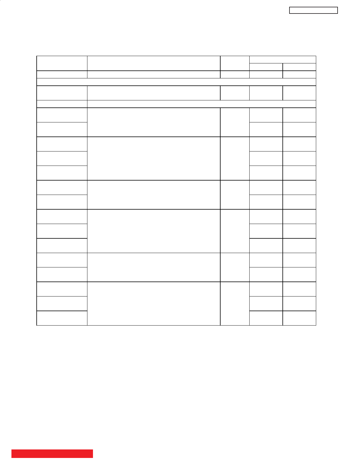
40
DW1U
1st page (1/2)
Initial Data(HEX) Adjustment
Mode OSD
Adjustment Item Adjustment
Range(HEX) DW1-U
SERVICE SERVICE OFF
TA1360 (88H)
SUB BRIGHT [ISF Mode]
Sub Brightness
00㨪FF 3F
WHITE BAL White Balance Mode (TA1360 88H)
G DRIVE(HIGH) 3F
R DRIVE(HIGH)
[ISF Mode]
Color Temperature: High
Green/Red Drive Gain Adjustment
00㨪7F
3F
R CUTOFF(HIGH) 7F
G CUTOFF(HIGH) 7F
B CUTOFF(HIGH)
[ISF Mode]
Color Temperature: High
Red/Green/Blue Cutoff Adjustment
00㨪FF
7F
G DRIVE(MED) 4A
R DRIVE(MED)
[ISF Mode]
Color Temperature: Medium
Green/Red Drive Gain Adjustment
00㨪7F
4E
R CUTOFF(MED) 7F
G CUTOFF(MED) 7F
B CUTOFF(MED)
[ISF Mode]
Color Temperature: Medium
Red/Green/Blue Cutoff Adjustment
00㨪FF
7F
G DRIVE(STD) 52
R DRIVE(STD)
[ISF Mode]
Color Temperature: Standard
Green/Red Drive Gain Adjustment
00㨪7F
56
R CUTOFF(STD) 7F
G CUTOFF(STD) 7F
B CUTOFF(STD)
[ISF Mode]
Color Temperature: Standard
Red/Green/Blue Cutoff Adjustment
00㨪FF
7F
10. I2C Adjustment Parameter List
BACK TO ADJUSTMENTS
GI
1st page (2/2)
Initial Data(HEX) Adjustment
Mode OSD
Adjustment Item Adjustment
Range(HEX) DW1-U
WHITE BAL White Balance Mode (TA1360 88H)
G DRIVE (B/W) 58
R DRIVE (B/W)
[ISF Mode]
Color Temperature: Black/White
Green/Red Drive Gain Adjustment
00㨪7F
64
R CUTOFF (B/W) 7F
G CUTOFF (B/W) 7F
B CUTOFF (B/W)
[ISF Mode]
Color Temperature: Black/White
Red/Green/Blue Cutoff Adjustment
00㨪FF
7F
H POSITION [ISF Mode]
Horizontal Position Adjustment
00: .10%~ 7F: +10%
00㨪7F 42
SEINE
V POSITION [ISF Mode]
Vertical Position Adjustment
00㨪8FCh 465h
FACTORY RESET FACTORY RESET 㧙㧙
10. I2C Adjustment Parameter List (continued)
41
DW1U
GI
42
DW1U
2nd page (1/2)
Initial Data(HEX) Adjustment
Mode OSD
Adjustment Item Adjustment
Range(HEX) DW1-U
SEINE
TV_GUiDE Don’t care
TV_GUiDE Don’t care
TV_GUiDE Don’t care
UEI
iR_BLASTER
iR_BLASTER
TC90103
H_TiMiNG VBIDLY: Slicer H Timing Delay
㧔ID1/WSS/CCD/G-Gide㧕
00∼0F 08
V_PHASE VBIVAD: Slicer V Phase
㧔ID1/WSS/CCD/G-Gide㧕
00∼07 04
CCD_READ_oUT CCDON: CCD Slice Read Output 00㨪01 01
CCD_SLiCE_CoNT CSLICES: CCD Slice Control 00㨪01 00
CCD_SLiCE_LEVEL CSLICEL: CCD Slice Level 00㨪03 00
CCD_SB_DET CSTMOD: CCD SB Detect 00㨪01 00
CCD_FiELD_SEL CCDMOD: CCD Field Select 00㨪03 02
iD1_READ_oUT ID1ON: ID1 Slice Read Output 00㨪01 01
iD1_SLiCE_CoNT ISLICES: ID1 Slice Control 00㨪01 00
iD1_SLiCE_LEVEL ISLICEL: ID1 Slice Level 00㨪03 00
iD1_AMP IRWIDON: ID1 Amplitude Detect 00㨪01 00
iD1_PHASE_SEL IEDGES: ID1 Phase Select 00㨪01 00
iD1_PHASE_WiDTH IRTIMS: ID1 Detection Phase Width 00㨪01 00
10. I2C Adjustment Parameter List (continued)
GI
43
DW1U
2nd page (2/2)
Initial Data(HEX)
Adjustment
Mode OSD
Adjustment Item Adjustment
Range(HEX) DW1-U
TC90103
G_READ_oUT GGSON: Guide Slice Read Output 00㨪01 01
G_DETECT GGSJDG: Guide Detection Sensitivity 00㨪01 01
G_SLiCE_LEVEL GGSLV: Guide Slice Level 00㨪03 00
CLoCK_RUN_iN GGPKDET: Guide Clock Run In Detect 00㨪01 00
READ_DATA_oRDER SLDSLT: Guide Read Out order 00㨪01 00
ADD_DATA GGSIGON: Guide Add Data Function 00㨪01 00
LiNE_10_25 Line 10㨪25 0000㨪FFFF 0000
Sub Micro
VBi_SLiCER_S Sub VBI (CCD/V Chip) Adjustment
SAMPLiNG
POLLiNG
START
TiMEoUT
STATUS
Seine/Sub Micro
CLoCK_TEST
AFC_TEST
MAiNTENANCE
MEMoRY_iNiTiALiZE
10. I2C Adjustment Parameter List (continued)
GI
44
DW1U
Seine (1/4)
Initial Data(HEX)
Adjustment
Mode OSD
Adjustment Item Adjustment
Range(HEX) DW1-U
SEINE
001 Capture Picture Sync Delay
00h: Delay Adjustment, 1: Through
00㨪01 00
002 Active area top field V sync phase
00h: odd field, 01h: even field
00㨪01 00
003 Vertical Delay 000㨪7FF 00
004 Horizontal Delay 000㨪FFF 00
005 Picture Horizontal Sync Up Position 0000㨪1130 898
006 Picture Horizontal Sync Down Position 0000㨪1130 898
007 Picture Horizontal Blanking Up Position 0000㨪1130 898
008 Picture Horizontal Blanking Down Position 0000㨪1130 898
009 Picture Vertical Blanking Up Position 000㨪8FC 465
010 Picture Vertical Blanking Down Position 000㨪8FC 465
011 Picture Clamp Horizontal Up Position 0000㨪1130 898
012 Picture Clamp Horizontal Down Position 0000㨪1130 898
013 Picture Clamp Vertical Position Mask Start Position 000㨪8FC 465
014 Picture Clamp Vertical Position Mack End Position 000㨪8FC 465
015 Picture Black Level Distinction Horizontal Up Position 0000㨪1130 898
016 Picture Black Level Distinction Horizontal Down
Position
0000㨪1130 898
017 Picture Black Level Vertical Mask Start Position 000㨪8FC 465
018 Picture Black Level Vertical Mask End Position 000㨪8FC 465
019 U,V Output Gain Mode
00h: SMPTE, 01h: Beta Cam
00㨪01 00
020 Horizontal Sync Input Delay 00㨪03 00
10. I2C Adjustment Parameter List (continued)
GI
45
DW1U
Seine (2/4)
Initial Data(HEX)
Adjustment
Mode OSD
Adjustment Item Adjustment
Range(HEX) DW1-U
SEINE
021 Vertical Sync Input Delay 00㨪03 00
022 Horizontal Filter Switch for Y
00h: through, 01h: 0.25fs
00㨪01 00
023 Horizontal Filter Switch for U
00h: through, 01h: 0.25fs,
02h: 0.055fs, 03h: 0.037fs
00㨪03 00
024 Horizontal Filter Switch For V
00h: through, 01h: 0.25fs,
02h: 0.055fs, 03h: 0.037fs
00㨪03 00
025 Plain Bland Out Color
00h: YUV_BT709, 01h: YUV_BT601
00㨪01 00
026 Picture Digital Output Select
00h: Normal, 01h: Color Bar
00㨪01 00
027 Setup
00h: off, 01h: on
00㨪01 00
028 Noise Reduction Switch for Y
00h: Not Round, 01h: Round
NTSC/480i Input only
00㨪01 01
029 Y Moving Detection Band for Noise Reduction
00h: Narrowband, 01h: Wideband
NTSC/480i Input only
00㨪01 00
030 Y Moving Horizontal Extension for Noise Reduction
00h:OFF, 01h:ON
NTSC/480i Input only
00㨪01 01
031 Y Signal Round Coefficient for Noise Reduction
NTSC/480i Input only
00㨪0D 0A
032 Y Frame Difference Limit for Noise Reduction
NTSC/480i Input only
00㨪1F 03
033 Color Signal Noise Reduction Switch
00h: Not Round, 01h: Round
NTSC/480i Input only
00㨪01 01
034 Color Moving Detection Band for Noise Reduction
00h: Narrowband, 01h: Wideband
NTSC/480i Input only
00㨪01 00
035 Color Moving Horizontal Extension foe Noise
Reduction
00h:OFF, 01h:ON
NTSC/480i Input only
00㨪01 01
10. I2C Adjustment Parameter List (continued)
GI
46
DW1U
Seine (3/4)
Initial Data(HEX)
Adjustment
Mode OSD
Adjustment Item Adjustment
Range(HEX) DW1-U
SEINE
036 Color Signal Round Coefficient for Noise Reduction
NTSC/480i Input only
00㨪0D 0A
037 Color Signal Frame Difference Limit for Noise
Reduction
NTSC/480i Input only
00㨪1F 03
038 Enhance Movement Mode
00h: Enhancer & 2nd V filter OFF
01h: Enhancer ON
02h: 2nd V filter ON
03h: Reserved
00㨪03 00
039 Enhancer Movement Mode Select
00h: 1H, 01h: 2H
00㨪01 00
040 Noise Distinction Value 00㨪10 00
041 Noise Reduction Gain 00㨪07 00
042 Vertical Enhancer Gain
1/16step
0x00: OFF, 0x20: 2 times
00㨪20 00
043 Vertical Enhancer Coring Value 00㨪0F 00
044 Vertical Enhancer Turning Position 00㨪FF 00
045 Horizontal Enhancer Gain
1/16step
0x00: OFF, 0x20: 2 倍
00㨪20 00
046 Horizontal Enhancer Coring Value 00㨪0F 00
047 Horizontal Enhancer Turning Position 00㨪FF 00
048 Horizontal Enhancer Coefficient Z6 00㨪FF 00
049 Horizontal Enhancer Coefficient Z5 00㨪FF 00
050 Horizontal Enhancer Coefficient Z4 00㨪FF 00
051 Horizontal Enhancer Coefficient Z3 00㨪FF 00
052 Horizontal Enhancer Coefficient Z2 00㨪FF 00
053 Horizontal Enhancer Coefficient Z1 00㨪FF 00
054 Horizontal Enhancer Coefficient Z0 00㨪FF 00
10. I2C Adjustment Parameter List (continued)
GI
47
DW1U
Seine (4/4)
Initial Data(HEX)
Adjustment
Mode OSD
Adjustment Item Adjustment
Range(HEX) DW1-U
SEINE
055 ANT/NTSC 000㨪6B4 0F8
056 480i_YPbPr 000㨪35A 0F4
057 480i_HDMI 000㨪6B4 000
058 480p_YPbPr 000㨪35A 078
059 480p_HDMI 000㨪35A 000
060 1080i_YPbPr 000㨪898 0E0
061 1080i_HDMI 000㨪898 000
062 720p_YPbPr 000㨪672 120
063 720p_HDMI 000㨪672 000
064
Odd/Even Field Horizontal Active
Picture Data Start Point
VGA_HDMI 000㨪35A 000
065 Mode 1-2 00㨪FF 19
066 Mode 2-3 00㨪FF 32
067 Mode 3-4 00㨪FF 4B
068
S/N Detection Setting
(Receiving Mode Border Line Setting)
Mode 4-5 00㨪FF 64
10. I2C Adjustment Parameter List (continued)
GI
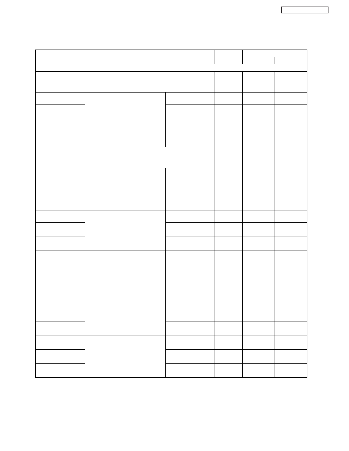
48
DW1U
TA1360 (1/5)
Initial Data(HEX) Adjustment
Mode OSD
Adjustment Item Adjustment
Range(HEX) DW1-U
TA1360
001 [ISF Mode]
RGB Output Mode Switch
00: Normal, 01: R only, 02: G only, 03: B only
00㨪03 00
002 Black Enhancement
Middle
00㨪7F 3F
003 Black Enhancement
Low
00㨪7F 3F
004
[ISF Mode]
Brightness Offset 1
Black Enhancement
Off
00㨪7F 3F
005 [ISF Mode]
Brightness Offset 2
480i/480p/1080i/720p 00㨪7F 3F
006 [ISF Mode]
Sub Contrast
00h: -3.4 dB 㨪 1Fh: +2.6 dB
00㨪1F 12
007 ANT/NTSC 00㨪7F 46
008 480i/480p 00㨪7F 4B
009
[ISF Mode]
Color (Center Adjustment)
00h: -20 dB ∼ 7Fh: +4.5 dB
1080i/720p 00㨪7F 4C
010 Color Temperature
Medium
00㨪3F 1F
011 Color Temperature
Standard
00㨪3F 1F
012
[ISF Mode]
Color Offset
Color Temperature
B/W
00㨪3F 1F
013 ANT/NTSC 00㨪7F 41
014 480i/480p 00㨪7F 3F
015
[ISF Mode]
Tint (Center Adjustment)
00h: -32degree
∼ 7Fh: +32degree
1080i/720p 00㨪7F 3F
016 Color Temperature
Medium
00㨪3F 1F
017 Color Temperature
Standard
00㨪3F 1F
018
[ISF Mode]
Tint Offset
Color Temperature
B/W
00㨪3F 1F
019 ANT/NTSC 00㨪7F 20
020 480i/480p 00㨪7F 20
021
[ISF Mode]
Sharpness(Center Adjustment)
10 dB ∼ +15 dB
1080i/720p 00㨪7F 1F
10. I2C Adjustment Parameter List (continued)
GI
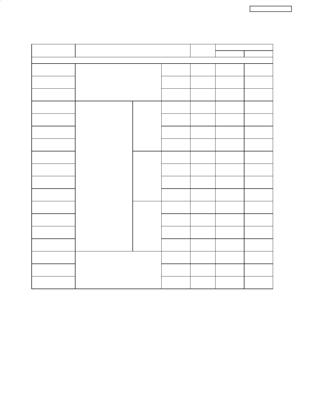
49
DW1U
TA1360 (2/5)
Initial Data(HEX)
Adjustment
Mode OSD
Adjustment Item Adjustment
Range(HEX) DW1-U
TA1360
022 ANT/NTSC 00㨪0F 00
023 480i/480p 00㨪0F 00
024
[ISF Mode]
R-Y/B-Y Phase
00h: 90 degree,
0Fh: 109 degree
1080i/720p 00㨪0F 00
025 Color Temp.
High
00㨪0F 09
026 Color Temp.
Medium
00㨪0F 07
027 Color Temp.
Standard
00㨪0F 05
028
ANT/NTSC
Color Temp.
B/W
00㨪0F 02
029 Color Temp.
High
00㨪0F 0A
030 Color Temp.
Medium
00㨪0F 08
031 Color Temp.
Standard
00㨪0F 06
032
480i/480p
Color Temp.
B/W
00㨪0F 03
033 Color Temp.
High
00㨪0F 07
034 Color Temp.
Medium
00㨪0F 05
035 Color Temp.
Standard
00㨪0F 03
036
[ISF Mode]
R-Y/B-Y Gain
00h: 0.56 ∼ 0Fh: 0.86
1080i/720p
Color Temp.
B/W
00㨪0F 02
037 ANT/NTSC 00㨪0F 02
038 480i/480p 00㨪0F 02
039
[ISF Mode]
G-Y/B-Y Phase
00h: 232.5 degree,
0Fh: 255 degree
1080i/720p 00㨪0F 03
10. I2C Adjustment Parameter List (continued)
GI
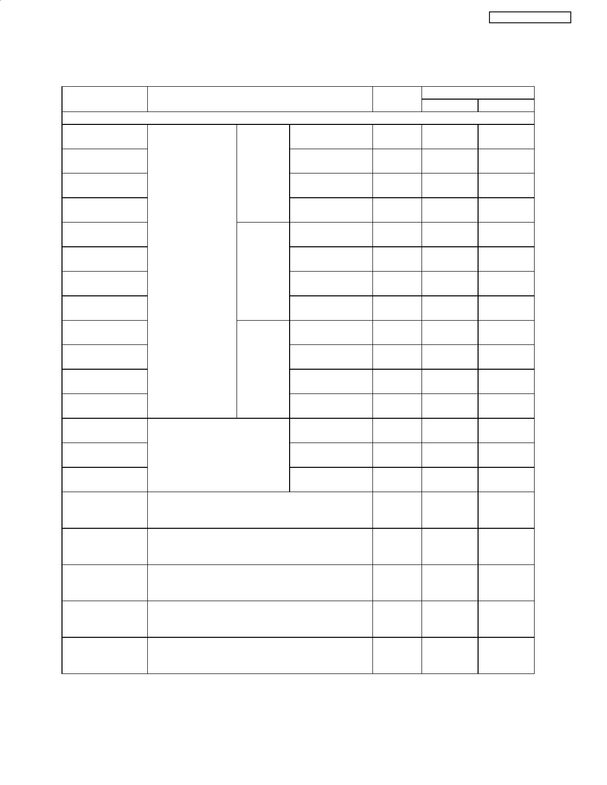
50
DW1U
TA1360 (3/5)
Initial Data(HEX)
Adjustment
Mode OSD
Adjustment Item Adjustment
Range(HEX) DW1-U
TA1360
040 High 00㨪0F 01
041 Medium 00㨪0F 02
042 Standard 00㨪0F 03
043
ANT/NTSC
B/W 00㨪0F 04
044 High 00㨪0F 02
045 Medium 00㨪0F 03
046 Standard 00㨪0F 04
047
480i/480p
B/W 00㨪0F 05
048 High 00㨪0F 00
049 Medium 00㨪0F 01
050 Standard 00㨪0F 02
051
[ISF Mode]
G-Y/B-Y Gain
00h: 0.3 ∼ 0Fh: 0.45
1080i/720p
B/W 00㨪0F 03
052 Black Enhancement
High
00㨪07 05
053 Black Enhancement
Middle
00㨪07 03
054
[ISF Mode]
BLACK STRETCH POINT
Black Enhancement
Low
00㨪07 01
055 [ISF Mode]
DC Restoration Point
00h: 0% 㨪 07h: 47%
00㨪07 00
056 [ISF Mode]
DC Restoration Rate
00h: 100% ∼ 07h: 135%
00㨪07 00
057 [ISF Mode]
DC Restoration Limit Point
00h: 60%, 01h: 73%, 02h: 87%, 03h: 100%
00㨪03 00
058 [ISF Mode]
Dynamic ABL Detection Point
00h: MIN ∼ 03h: MAX
00㨪03 03
059 [ISF Mode]
Dynamic ABL Gain
00h: MIN ∼ 03h: MAX
00㨪03 00
10. I2C Adjustment Parameter List (continued)
GI
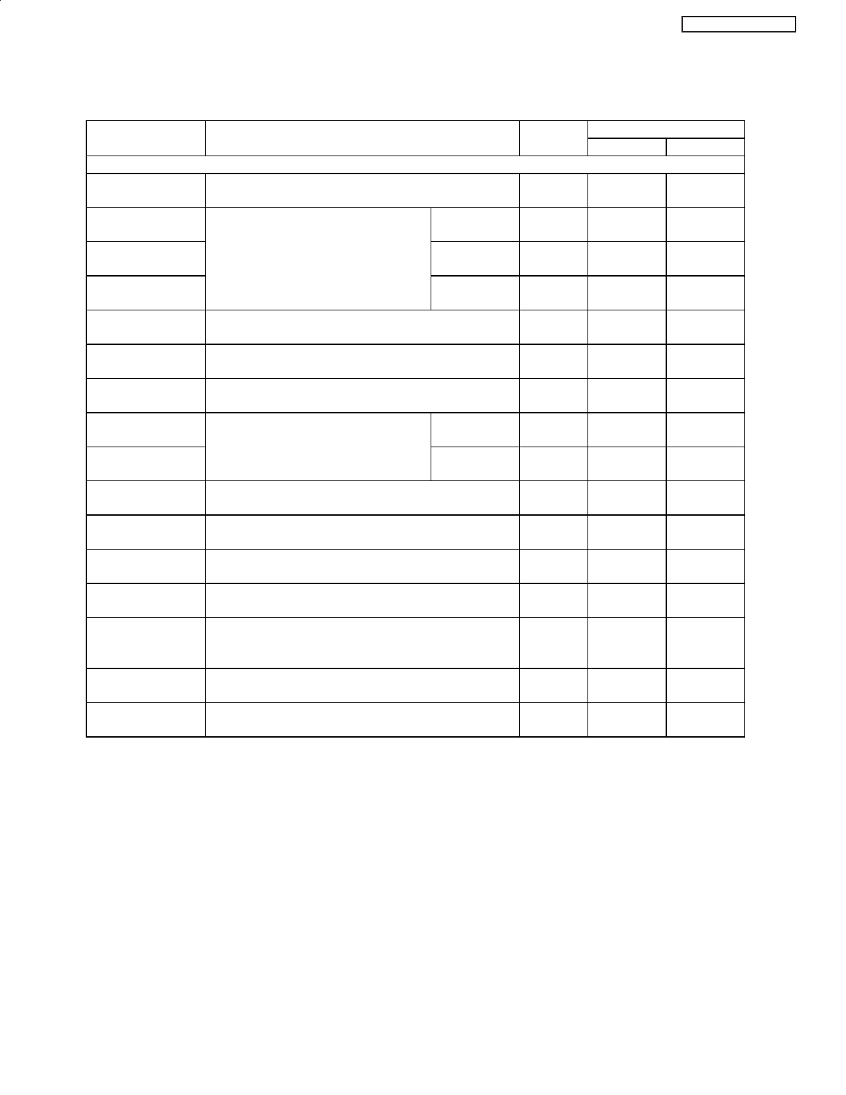
51
DW1U
TA1360 (4/5)
Initial Data(HEX)
Adjustment
Mode OSD
Adjustment Item Adjustment
Range(HEX) DW1-U
TA1360
060 Sand castle Pulse Switch
00h: Internal, 01h: External Input
00㨪01 01
061 ANT/NTSC 00㨪03 01
062 480i/480p 00㨪03 01
063
Aperture Control Peak f0
00h: 15 MHz, 01h: 8.8 MHz ,
02h: 7.5 MHz, 03h: 5 MHz
1080i/720p 00㨪03 00
064 Color Limiter Level Switch
00h: 1.65 Vp-p, 01h: 2 Vp-p
00㨪01 01
065 Color SRT Gain
00h: min ∼ 03h: max
00㨪03 00
066 Color SRT Frequency
00h: 4.3 MHz ∼ 01h: 5.8 MHz
00㨪01 01
067 ANT/NTSC
480i/480p
00㨪07 06
068
VM Phase
00h: -37.5 ns, 05h: Normal,
07h: +15 ns 1080i/720p 00㨪07 04
069 Color Detail Enhancer
00h: min ∼ 03h: max
00㨪03 00
070 DCU RGB Brightness
00h: -20 IRE ∼ 7Fh: +20 IRE
00㨪7F 3F
071 DCU RGB Contrast
00h: -17 dB ∼ 7Fh: 0 dB
00㨪7F 6D
072 DC Restoration Ratio Switch
00h: 100% less, 01h: 100% over
00㨪01 00
073 Color Ȗ Correction Point
00h: OFF, 01h: 0.23 Vp-p,
02h: 0.37 Vp-p, 03h: 0.52 Vp-p
00㨪03 00
074 Component Dynamic Y/C Correction Select
00h: OFF, 01h: min, 02h: mid, 03h: max
00㨪03 00
075 APL / Black Stretch Start Point
00h: 0 IRE ∼ 03h: 23 IRE
00㨪03 00
10. I2C Adjustment Parameter List (continued)
GI
52
DW1U
TA1360 (5/5)
Initial Data(HEX)
Adjustment
Mode OSD
Adjustment Item Adjustment
Range(HEX) DW1-U
TA1360
076 Black Level Auto Correction Switch
D2 00h: OFF, 01h: ON
00㨪01 01
077 Black Detection Level Switch
D1 00h: 3 IRE, 01h: 0 IRE
00㨪01 01
078 Black Stretch Area Correction Switch
D0 00h: ON, 01h: OFF
00㨪01 01
079 SRT (Super Real Transient) Gain
00h: MIN ∼ 1Fh: MAX
00㨪1F 10
080 White Character Correction Amplitude
00h: min ∼ 07h: max
00㨪07 07
081 ABL Detection Point
00h: MIN ∼ 07h: MAX
00㨪07 07
082 ABL Gain
00h: MIN ∼ 07h: MAX
00㨪07 00
083 Dynamic Y Gamma Gain vs. Dark Area
00h: OFF ∼ 07h: MAX(+6 dB)
00㨪03 00
084 Dynamic Y Gamma Gain vs. Bright Area
00h: OFF ∼ 07h: max
00㨪07 00
085 Static Y Gamma Black Gain
00h: OFF, 01h: MIN(0 DB) ∼ 07h: MAX(+6 DB)
00㨪07 00
086 Static Y Gamma Bright Gain
00h: OFF, 01h: MIN(0 DB) ∼ 03h: MAX(-6 DB)
00㨪03 03
087 Y Gamma Switch
00h: OFF, 01h: ON
00㨪01 00
088 Y Detail Control
00h: MIN(Trap) ∼ 0Fh: MAX(+6 dB)
00㨪0F 07
089 Y Group Delay Control
00h: MIN(Trap) ∼ 0Fh: MAX(+6 dB)
00㨪0F 09
090 White Peak Blue Point
00h: 55 IRE ∼ 07h: 105 IRE
00㨪07 00
091 White Peak Blue Gain
00h: min(+2 dB) ∼ 07h: max(+9.5 dB)
00㨪07 00
092 High Bright Color Switch
00h: OFF, 01h: ON
00㨪01 00
093 White Peak Suppressor Level
00h: 110 IRE, 01h: 130 IRE
00㨪01 01
094 Blue Stretch Gamma Correction
00h: OFF, 01h: ON
00㨪01 00
095 Green Stretch
00h: OFF ∼ 03h: MAX
00㨪03 00
096 Blue Stretch Gain
00h: OFF ∼ 03h: MAX(+4 dB)
00㨪03 00
097 Blue Stretch Point
00h: MIN(30 IRE)∼ 03h: MAX(45 IRE)
00㨪03 00
098 Black Stretch Characteristic Switch 1
(OFF∼MAX)
00㨪01 00
099 Black Stretch Characteristic Switch 2
(OFF∼MAX)
00㨪01 00
10. I2C Adjustment Parameter List (continued)
GI
TC90103 (1/12)
Initial Data(HEX)
Adjustment
Mode OSD
Adjustment Item Adjustment
Range(HEX) DW1-U
TC90103 ANT/NTSC/480i
001 3D Motion Detection Select
00h䋺Compulsion Standard,
01h䋺Compulsion Still Picture,
02h䋺MOVE, 03h䋺MANU
00㨪03 03
002 YES Mode
00h䋺Mode1, 01h䋺3Line+3DNR,
02h䋺BPF+3DNR, 03h䋺Mode2
00㨪03 03
003 3D Y Noise Reduction Limiter Level
00h䋺Level Small䌾07h䋺Level Big
00㨪07 06
004 3D Color Noise Reduction Round Coefficient
00h䋺×1, 01h䋺㬍1/2, 02h䋺×3/4, 03h䋺OFF
00㨪03 02
005 3D Y Noise Reduction Gain
00h䋺OFF䌾07h䋺×0.875
00㨪07 00
006 3D Color Noise Reduction Limiter Level
00h䋺Level Small䌾07h䋺Level Large
00㨪07 05
007 3D Color Round Coefficient
00h䋺×1, 01h䋺×1/2, 02h䋺×3/4h, 03h䋺OFF
00㨪03 01
008 3D Color Noise Reduction Gain
00h䋺OFF䌾07h䋺×0.875
00㨪07 00
009 Vertical Enhancer Gain
00h䋺OFF, 01h䋺×1/8, 02h䋺×1/4, 03h䋺×1/2
00㨪03 03
010 Vertical Enhancer Turning Point
00h䋺6 IRE, 01h䋺9 IRE, 02h䋺13 IRE, 03h䋺16 IRE
00㨪03 01
011 Vertical Enhancer Coring
00h䋺OFF, 01h䋺0.8 IRE, 02h䋺1.6IRE, 03h䋺2.3 IRE
00㨪03 01
012 Sharpness f0
00h䋺4.2MHz, 01h䋺3.3MHz
00㨪01 00
013 Pre-Enhancer
00h䋺OFF, 01h䋺ON
00㨪01 00
014 ANT/NTSC 00㨪0F 01
015
Sharpness Gain
00h: OFF,
01h: 1.02dB, 02h: 1.94dB,
03h: 2.77dB, 04h: 3.52dB,
05h: 4.22dB, 06h: 4.86dB,
07h: 5.46dB, 08h: -6.02dB,
09h: -5.00dB, 0Ah: -4.08dB,
0Bh: -3.25dB, 0Ch: 2.50dB,
0Dh: -1.80dB, 0Eh: -1.16dB,
0Fh: -0.56 dB
Y/C/480i 00㨪0F 01
53
DW1U
10. I2C Adjustment Parameter List (continued)
GI
TC90103 (2/12)
Initial Data(HEX)
Adjustment
Mode OSD
Adjustment Item Adjustment
Range(HEX) DW1-U
TC90103 ANT/NTSC/480i
016 ANT/NTSC 00㨪03 01
017
Sharpness/Noise Cancel Coring
00h䋺0.8 IRE, 01h䋺1.6 IRE,
02h䋺3.2 IER, 03h䋺6.4 IRE Y/C/480i 00㨪03 01
018 Noise Cancel Gain
00h䋺OFF, 01h䋺㬍1/4, 0h2䋺×1/2, 03h䋺×1
00㨪03 00
019 LTI Gain
(LTI = Luminance Transient Improvement)
00h䋺OFF, 01h䋺×1/8, 02h䋺×1/4, 03h䋺×1/2
00㨪03 03
020 LTI Coring Level
(LTI = Luminance Transient Improvement)
00h䋺0.8 IRE, 01h䋺1.6 IRE,
02h䋺3.2 IER, 03h䋺6.4 IRE
00㨪03 00
021 ANT 00㨪0F 08
022 NTSC/480i 00㨪0F 08
023
Chrominance Delay
00h䋺-296ns䌾0Fh䋺259ns
Y/C 00㨪0F 08
024 CTI Gain
(CTI = Chrominance Transient Improvement)
00h䋺OFF, 01h䋺×1/8, 02h䋺×1/4, 03h䋺×1/2
00㨪03 01
025 CTI Coring Level
(CTI = Chrominance Transient Improvement)
00䋺0.2 IRE, 01䋺0.8 IRE, 02䋺1.6 IRE, 03䋺3.2 IRE
00㨪03 00
026 LTI f0
(LTI = Luminance Transient Improvement)
00h䋺3.2MHz, 01h䋺2.2MHz
00㨪01 01
027 CTI f0
(CTI = Chrominance Transient Improvement)
00h䋺1.7MHz, 01h䋺3.4MHz
00㨪01 01
028 Contrast Control
00h䋺×1/2䌾40h䋺×1䌾FFh䋺×2.4
00㨪FF 45
029 Brightness (Y Output Offset)
80h䋺-128Lsbh䌾00h䋺OFF䌾7Fh䋺+127䋨10Bit䋩
00㨪FF 7D
030 Cr Output Gain
08h䋺×0.5 䌾 00䋺×1 䌾 07䋺×1.4
00㨪0F 08
031 Cb Output Gain
08h䋺×0.5 䌾 00h䋺×1 䌾 07h䋺×1.4
00㨪0F 08
032 Cr Output Offset
08h䋺-8LSB 䌾 00h䋺0䌾 07h䋺+7LSB䋨10Bit䋩
00㨪0F 08
033 Cb Output Offset
08h䋺-8LSB 䌾 00h䋺0䌾 07h䋺+7LSB䋨10Bit䋩
00㨪0F 08
034 Phase Control
80h䋺-45° 䌾 00h䋺0° 䌾 7Fh: +43.6°
00㨪7F 40
035 Cb Delay
00h䋺Cb Preceding, 01h䋺Cr Delay
00㨪01 00
54
DW1U
10. I2C Adjustment Parameter List (continued)
GI
55
DW1U
TC90103 (3/12)
Initial Data(HEX)
Adjustment
Mode OSD
Adjustment Item Adjustment
Range(HEX) DW1-U
TC90103 ANT/NTSC/480i
036 Demodulation Angle
00h䋺 0° 䌾 3Fh䋺+45°
00㨪3F 00
037 Color Killer Level
00h䋺-40dB 䌾 07h䋺-30dB
00㨪07 00
038 ACC Level (ACC = Auto Color Level)
00h䋺 Min 䌾 0Fh䋺 Max [08h: Center]
00㨪0F 08
039 ACK Hysteresis (ACK = Auto Color Killer)
00h䋺 Small, 01h䋺 Large
00㨪01 01
040 2'nd BPF/TRAP on/off
00h䋺ON, 01h䋺OFF
00㨪01 00
041 2'nd BPF/TRAP bpf/trap
00h䋺Trap, 01h䋺BPF
00㨪01 00
042 TRAP1
00h䋺ON, 01h䋺OFF
00㨪01 01
043 TRAP2
00h䋺ON, 01h䋺OFF
00㨪01 01
044 ANT (RF Input) 00㨪07 07
045
Take Off Filter
00h䋺OFF, 01h䋺BPF ON,
02h䋺Min 䌾 07h䋺Max NTSC/480i 00㨪07 01
046 Y Digital Clamp
00h䋺OFF, 01h䋺ON
00㨪01 00
047 BSRC Filter
00h䋺ON, 01h䋺OFF
00㨪01 01
048 Chrominance Digital Clamp
00h䋺OFF, 01h䋺ON
00㨪01 01
049 Y Noise Cancel Limiter
00h䋺4lsb, 01h䋺8lsb, 02h䋺16lsb, 03h䋺32lsb
00㨪03 00
050 Y Noise Cancel Gain
00h䋺OFF, 01h䋺㬍1, 02h䋺㬍1.5, 03h䋺㬍2
00㨪03 01
051 Chrominance Noise Cancel Limiter
00h䋺1lsb, 01h䋺2lsb, 02h䋺4lsb, 03h䋺8lsb
00㨪03 00
052 C Noise Cancel Gain
00h䋺OFF, 01h䋺㬍1, 02h䋺㬍1.5, 03h䋺㬍2
00㨪03 00
053 Horizontal Dot Obstruction Reduction
00h䋺OFF, 01h䋺×0.16, 02h䋺×0.17, 03h䋺×0.18
00㨪03 03
054 COMB+
00h䋺OFF, 01h䋺ON
00㨪01 00
055 1 Line Dot Improvement
00h䋺OFF, 01h䋺ON
00㨪01 01
056 Vertical Y Noise Cancel Limiter
00h䋺8lsb, 01h䋺16lsb
00㨪01 00
057 Vertical Y Noise Cancel Gain
00h䋺㬍1, 01h䋺㬍2
00㨪01 00
10. I2C Adjustment Parameter List (continued)
GI
56
DW1U
TC90103 (4/12)
Initial Data(HEX)
Adjustment
Mode OSD
Adjustment Item Adjustment
Range(HEX) DW1-U
TC90103 ANT/NTSC/480i
058 Vertical Y ON
00h䋺OFF, 01h䋺ON
00㨪01 00
059 C NY Limiter
00h䋺16lsb, 01h䋺24lsb
00㨪01 00
060 C NC Gain 00㨪01 00
061 C-NC ON
00h䋺OFF, 01h䋺ON
00㨪01 00
062 IIR Filter
00h䋺OFF, 01h䋺ON
00㨪03 03
063 Output Peak Limiter
00h䋺OFF, 01h䋺ON
00㨪01 00
064 AFC Integrate Gain Switch 00㨪0F 03
065 AFC Proportional Gain Switch 00㨪0F 0B
066 Linear Gain Switch at Phase Large Error 00㨪0F 08
067 No Linear Area 2nd Gain Switch 00㨪0F 07
068 Linear Gain Switch at Phase Small Error 00㨪0F 02
069 Integrate Value Reset ON at Limit
00h䋺OFF, 01h䋺ON
00㨪01 00
070 Linear Area Width Setting for NTSC/480i 00㨪07 05
071 Sync Separation Input Select
00h䋺Internal, 01h䋺CsyncH,
02h䋺CsyncL, 03h䋺VsyncH,
04h䋺Internal䋨OFF_SET䋩, 07h䋺Free run
00㨪07 00
072 AFC Integrate Relay
00h䋺OFF, 01h䋺ON
00㨪01 01
073 Phase Error Gain Up
00h䋺ON, 01h䋺00×2, 02h䋺00×4, 03h䋺00×8
00㨪03 03
074 Phase Error Maximum Linear Area Width Setting
00h䋺OFF, 01h䋺LRW0䋫16'h5000,
02h䋺LRW0䋫16'h6000, 03h䋺LRW0䋫16'h7000
00㨪03 03
075 Horizontal Standard Phase Adjustment
20h䋺-4.7µs 䌾 00h䋺±0 䌾 1Fh䋺+4.59µs
䋨1/6.75MHz_Step䋩
00㨪3F 20
076 Horizontal Separation Level
00h䋺30䋦, 01h䋺40䋦
00㨪01 00
077 Half Horizontal Killer
00h䋺OFF, 01h䋺ON
00㨪01 01
10. I2C Adjustment Parameter List (continued)
GI
57
DW1U
TC90103 (5/12)
Initial Data(HEX)
Adjustment
Mode OSD
Adjustment Item Adjustment
Range(HEX) DW1-U
TC90103 ANT/NTSC/480i
078 Vertical Standard Setting
04h䋺+4H 䌾 00h䋺Center 䌾 03h䋺䋭3H
00㨪07 04
079 External VD Phase Setting
00h䋺Center, 01h䋺+1.99us, 02h䋺+3.97us,
03h䋺䋫5.96us, 04h䋺-7.94us, 05h䋺-5.96us,
06h䋺-3.97us, 07h䋺-1.99us
00㨪07 04
080 VD Output Control
00h䋺Always Input Sync
01h䋺DET50
02h/03h: TVM[1]
00㨪03 00
081 Field Distinction Horizontal Phase Setting
00h䋺-5.7us, 01h䋺-8.2us, 02h䋺-10.7us, 03h䋺-13.2us,
04h䋺-15.7us, 05h䋺-18.4us, 06h䋺-20.9us, 07h䋺-23.2us
00㨪07 04
082 Vertical Counter Tolerance
00h䋺-H/8䌾+H/4, 01h䋺±H/8
00㨪01 00
083 Vertical Counter Limiter
00h䋺OFF, 01h䋺ON
00㨪01 00
084 Vertical Jitter Remove
00h䋺OFF, 01h䋺ON
00㨪01 00
085 Field Distinction at Non Standard
00h䋺Reverse at Every 1V, 01h:
Low
00㨪01 00
086 Integrate Center Level Setting for Vertical Separation
00h䋺5/16, 01h䋺1/2
00㨪01 01
087 Y Horizontal Edge Detection Level
00h䋺OFF, 01h䋺6 IRE, 02h䋺3 IRE, 03h䋺1.5 IRE
00㨪03 01
088 1 Field Y Detection Slope, Color Motion Picture
Edge
00h䋺1/2 䌾 03h䋺㺙[02]
00㨪03 02
089 1 Field Y Detection Offset, Color Motion Picture
Edge
00h䋺Still Picture 䌾0Fh䋺Motion Picture [0C: Center]
00㨪0F 0A
090 Y Vertical Edge Detection Level
00h䋺OFF, 01h䋺12 IRE, 02h䋺5 IRE, 03h䋺2 IRE
00㨪03 01
091 1 Field Y Detection Slope, Color Motion Picture
Smooth
00h䋺1/2 䌾 03h䋺㺙[02]
00㨪03 02
092 1 Field Y Detection Offset, Color Motion Picture
Edge
00h䋺Still Picture 䌾 0Fh䋺Motion Picture [0C: Center]
00㨪0F 0C
093 Color Motion Picture Distinction Standard
00h䋺8%, 01h䋺16%, 02h䋺24%, 03h䋺32%
00㨪03 01
094 1 Field Y Detection Slope, Color Still Picture Edge
00h䋺1/2 䌾 03h䋺㺙[02]
00㨪03 01
095 1 Field Y Detection Offset, Color Still Picture Edge
00h䋺Still Picture 䌾 0Fh䋺Motion Picture [0C: Center]
00㨪0F 00
10. I2C Adjustment Parameter List (continued)
GI
58
DW1U
TC90103 (6/12)
Initial Data(HEX)
Adjustment
Mode OSD
Adjustment Item Adjustment
Range(HEX) DW1-U
TC90103 ANT/NTSC/480i
096 Y Motion Picture Distinction Standard
00h䋺8%, 01h䋺16%, 02h䋺24%, 03h䋺32%
00㨪03 01
097 1 Field Y Detection Slope, Color Still Picture
Smooth
00h䋺1/2 䌾 03h䋺㺙[02]
00㨪03 02
098 1 Field Y Detection Offset, Color Still Picture
Smooth
00h䋺Still Picture 䌾 0Fh䋺Motion Picture [0C: Center]
00㨪0F 08
099 2 Field Y Motion Detection Enhancement
00h䋺ON, 01h䋺OFF
00㨪01 00
100 2 Field Color Motion Detection Enhancement
00h䋺ON, 01h䋺OFF
00㨪01 00
101 1 Field Y Detection Slope, Y Motion Picture Edge
00h䋺ON, 01h䋺OFF
00㨪03 02
102 1 Field Y Detection Offset, Y Motion Picture Edge
00h䋺1/2 䌾 03h䋺㺙[02]
00㨪0F 0D
103 2 Field Motion Detection Enhancement
00h䋺Still Picture 䌾 0Fh䋺Motion Picture
[0Ch: Center]
00㨪01 00
104 2 Field Motion Detection Enhancement Standard
00h䋺ON, 01h䋺OFF
00㨪01 00
105 1 Field Y Detection Slope, Y Motion Picture Smooth
00h䋺ON 01h䋺OFF
00㨪03 02
106 1 Field Y Detection Offset, Y Motion Picture Smooth
00h䋺1/2 䌾 03h䋺㺙[02: Default]
00㨪0F 0E
107 2 Field Color Detection 2nd Slope Threshold,
Color Still Picture Edge
00h䋺0, 01h䋺1, 0h2䋺2, 03h䋺3
00㨪03 00
108 1 Field Y Detection Slope, Y Still Picture Edge
00h䋺1/2 䌾 03h䋺㺙[02]
00㨪03 02
109 1 Field Y Detection Offset, Y Still Picture Edge
00h䋺Still Picture 䌾 0Fh䋺Motion Picture
[0Ch: Center]
00㨪0F 06
110 2 Field C Detection 2nd Slope,
Color Still Picture Edge
00h䋺1/8, 0h1䋺1/4, 02h䋺1/2, 03h䋺1
00㨪03 00
10. I2C Adjustment Parameter List (continued)
GI
59
DW1U
TC90103 (7/12)
Initial Data(HEX)
Adjustment
Mode OSD
Adjustment Item Adjustment
Range(HEX) DW1-U
TC90103 ANT/NTSC/480i
111 1 Filed Detection Slope, Y Still Picture Smooth
00h䋺1/2 䌾 03h䋺㺙[02]
00㨪03 02
112 1 Field Y Detection Offset, Y Still Picture Smooth
00h䋺Still Picture 䌾 0Fh䋺Motion Picture
[0Ch: Center]
00㨪0F 0A
113 2 Field Detection 2nd Slope Threshold,
Color Still Picture Smooth
00h䋺0, 01h䋺1, 02h䋺2, 03h䋺3
00㨪03 00
114 2 Field Color Detection Slope,
Color Motion Picture Smooth
00h䋺1/2 䌾 03h䋺㺙[02]
00㨪03 02
115 2 Field Color Detection Offset,
Color Motion Picture Edge
00h䋺Still Picture 䌾 0Fh䋺Motion Picture
[0Ch: Center]
00㨪0F 06
116 2 Field Color Detection 2nd Slope,
Color Still Picture Smooth
00h䋺1/8, 01h䋺1/4, 02h䋺1/2, 03h䋺1
00㨪03 00
117 2 Field Color Detection Slope,
Color Motion Picture Edge
00h䋺1/2 䌾 03h䋺㺙[02]
00㨪03 02
118 2 Field Color Detection Offset, Color Still Picture
Smooth
00h䋺Still Picture 䌾 0Fh䋺Motion Picture
[0Ch: Center]
00㨪0F 0C
119 2 Field 2nd Slope Threshold, Y Still Picture Edge
00h䋺0, 01h䋺1, 02h䋺2, 03h䋺3
00㨪03 01
120 2 Field Color Detection Slope, Color Still Picture
Edge
00h䋺1/2 䌾 03h䋺㺙 [02h: Default]
00㨪03 01
121 2 Field Color Detection Offset, Color Still Picture
Smooth
00h䋺Still Picture 䌾 0Fh䋺Motion Picture
[0Ch: Center]
00㨪0F 04
122 2 Field Detection 2nd Slope Offset, Y Still Picture
Edge
00h䋺1/8, 01h䋺1/4, 02h䋺1/2, 03h䋺1
00㨪03 01
123 2 Field Color Slope Threshold, Color Still Picture
Smooth
00h䋺1/2 䌾 03h䋺㺙 [02h: Default]
00㨪03 02
124 2 Field Color Detection Offset, Color Still Picture
Smooth
00h䋺Still Picture 䌾 0Fh䋺Motion Picture
[0Ch: Center]
00㨪0F 0B
125 2 Field Detection 2nd Slope Threshold, Y Still
Picture Smooth
00h䋺0, 01h䋺1, 02h䋺2, 03h䋺3
00㨪03 01
10. I2C Adjustment Parameter List (continued)
GI

60
DW1U
TC90103 (8/12)
Initial Data(HEX)
Adjustment
Mode OSD
Adjustment Item Adjustment
Range(HEX) DW1-U
TC90103 ANT/NTSC/480i
126 2 Field Detection Slope, Y Motion Picture Edge
00h䋺1/2 䌾 03h䋺㺙 [02h: Default]
00㨪03 01
127 2 Field Detection Offset, Y Motion Picture Edge
00h䋺Still Picture 䌾 0Fh䋺Motion Picture
[0Ch: Center]
00㨪0F 0D
128 2 Field Detection 2nd Slope, Y Still Picture Smooth
00h䋺1/8, 01h䋺1/4, 02h䋺1/2, 03h䋺1
00㨪03 01
129 2 Field Detection Slope. Y Motion Picture Smooth
00h䋺1/2 䌾 03h䋺㺙 [02h: Default]
00㨪03 02
130 2 Field Detection Offset, Y Motion Picture Smooth
00h䋺Still Picture 䌾 0Fh䋺Motion Picture
[0Ch: Center]
00㨪0F 0A
131 2 Field Detection Slope, Y Still Picture Edge
00h䋺1/2 䌾 03h䋺㺙 [02h: Default]
00㨪03 02
132 2 Field Detection Offset, Y Still Picture Edge
00h䋺Still Picture 䌾 0Fh䋺Motion Picture
[0Ch: Center]
00㨪0F 07
133 2 Field Detection Slope, Y Still Picture Smooth
00h䋺1/2 䌾 03h䋺㺙 [02h: Default]
00㨪03 02
134 2 Field Detection Offset, Y Still Picture Smooth
00h䋺Still Picture 䌾 0Fh䋺Motion Picture
[0Ch: Center]
00㨪0F 0A
135 [NR] Color Level
(for Y Differential Color Level Detection)
00h䋺Small 䌾 0Fh䋺Large 䌛03h: Center䌝
00㨪0F 03
136 [NR/NR] Y Differential Integrate Motion Picture
Distinction Level
00h䋺Motion Picture 䌾 0Fh䋺Still Picture [01h: Default]
00㨪0F 01
137 2 Field Assistance Simple Color Motion Detection
Threshold
00h䋺Small 䌾 0Fh䋺Large [0Fh: Default]
00㨪0F 0F
138 2 Field Assistance Simple Color Motion Detection
ON/OFF
00h䋺ON, 01h䋺OFF
00㨪01 00
139 Color Signal Edge Detection Level
00h䋺Small 䌾 07h䋺 Large [04h: Default]
00㨪07 05
140 2 Field Assistance Function
00h䋺OFF, 01h䋺ON
00㨪01 01
10. I2C Adjustment Parameter List (continued)
GI
61
DW1U
TC90103 (9/12)
Initial Data(HEX)
Adjustment
Mode OSD
Adjustment Item Adjustment
Range(HEX) DW1-U
TC90103 ANT/NTSC/480i
141 2 Field Assistance Select
00h䋺Y, 01h䋺C
00㨪01 00
142 2 Field Assistance Color Still Picture Distinction
Level
00h: Small 䌾 07h䋺Large [04h: Default]
00㨪07 04
143 2 Field Assistance Y Still Picture Distinction Level
00h: Small 䌾 07h䋺 Large [04h: Default]
00㨪07 04
144 1 Field Detection Still Offset Adjustment for Still
Picture Cross Color Improvement
00h䋺OFF
䌾0Fh䋺Compulsion Still Picture 2 Step [0Ah: Default]
00㨪0F 0A
145 2 Field Detection Still Picture Offset Adjustment for
Still Picture Cross Color Improvement
00h䋺OFF䌾0Fh䋺Still Picture Distinction
00㨪0F 03
146 Motion Detection Error, Compulsion Motion Picture
at Vicinity of 3.4MHz
Still Color Signal Level Threshold
(Still Picture Color Detection)
00h䋺OFF䌾0Fh䋺15/1023 䋨1Lsb Step䋩[00h: Default]
00㨪0F 00
147 Motion Detection Error, Compulsion Motion Picture
at
Vicinity of 3.4MHz
Still Picture Color Signal Level Threshold
(Still Picture No Color Detection)
00h䋺OFF䌾0Fh䋺15/1023 䋨1Lsb Step䋩[00h: Default]
00㨪0F 00
148 [NR] Band Select
00h䋺Wideband, 01h䋺 Narrowband
00㨪01 00
149 Y Differential Color Level Detection
00h䋺Motion Detection OFF, 01h䋺Nonlinear
Processing
00㨪01 00
150 Y Non Correlation Detection Level Switch
00h䋺[4䋺0], 01h䋺䍀5䋺1」
00㨪01 00
151 Color Non Correlation Detection Level Switch
00h䋺[5䋺1], 01h䋺䍀6䋺2」
00㨪01 00
152 [NR] Y Differential Color Level Y Motion Picture
Distinction Level
00h䋺Motion Picture 䌾 0Fh䋺Still Picture [08h: Default]
00㨪0F 08
153 AGC Manual Setting (AGC = Auto Gain Control)
00h䋺OFF, 01h䋺ON
00㨪01 00
154 AGC Manual Gain Setting
(AGC = Auto Gain Control)
00㨪7F 28
155 AGC Sync Level Detection ON/OFF
(AGC = Auto Gain Control)
00h䋺OFF, 01h䋺ON
00㨪01 01
10. I2C Adjustment Parameter List (continued)
GI
62
DW1U
TC90103 (10/12)
Initial Data(HEX)
Adjustment
Mode OSD
Adjustment Item Adjustment
Range(HEX) DW1-U
TC90103 ANT/NTSC/480i
156 AGC Peak Level Detection ON/OFF
(AGC = Auto Gain Control)
00h䋺OFF, 01h䋺ON
00㨪01 01
157 AGC OFF/ON Level Setting
(AGC = Auto Gain Control)
00h䋺OFF, 01h䋺70%, 02h䋺75%, 03h䋺80%
00㨪03 00
158 GCA Setting (GCA = ?)
00h䋺Auto, 01h䋺Digital
00㨪01 00
159 AGC Response Time Setting
(AGC = Auto Gain Control)
00h䋺Fast 䌾 07h䋺Slow
00㨪07 00
160 Peak AGC Level (AGC = Auto Gain Control)
00h䋺105%, 01h䋺110%, 02h䋺115%, 03h䋺120%
00㨪03 01
161 GCA Gain Switch (GCA = ?)
00h䋺-3䌾+7dB, 01h䋺+6dB,
02h䋺㵥5䌾+5dB, 03h䋺㵥6䌾+4dB
00㨪03 01
162 Pedestal Difference Detection ON/OFF
00h䋺OFF, 01h䋺ON
00㨪01 00
163 Peak AGC Discharge Speed
00h䋺Fast 䌾 07h䋺Slow
00㨪07 00
164 AGC Pedestal Timing for Digital Clamp
(AGC = Auto Gain Control)
08h䋺-1.19us 䌾 00h䋺䋨Center䋩䌾 07h䋺+1.04us
00㨪0F 08
165 AGC Sync Timing for Digital Clamp
08h䋺-1.19us 䌾 00h䋺䋨Center䋩䌾 07h䋺+1.04us
00㨪0F 08
166 Horizontal Phase Adjustment for Digital Format
08h䋺-1.185us 䌾 00h䋺 0us 䌾 0Fh䋺+1.04us
00㨪0F 08
167 Vertical Phase Adjustment for Digital Format
00h䋺0H 䌾 0Fh䋺+15H
00㨪0F 00
168 Vertical Horizontal Start Phase at Vertical Through
00h䋺0W, 01h䋺64W, 02h䋺128W, 03h䋺192W,
04h䋺256W, 05h䋺320W, 06h䋺348W, 07h䋺Prohibition
00㨪07 00
169 VD at Non Standard Output
00h䋺Horizontal Count Standard,
01h䋺Vertical Separation Standard
00㨪01 01
170 656 Non Conforming Horizontal Out Phase
00h䋺32W, 01h䋺36W, 02h䋺40W, 03h䋺44W
00㨪03 00
10. I2C Adjustment Parameter List (continued)
GI
63
DW1U
TC90103 (11/12)
Initial Data(HEX)
Adjustment
Mode OSD
Adjustment Item Adjustment
Range(HEX) DW1-U
TC90103 ANT/NTSC/480i
171 CK Out Clock Select
00h䋺13.5MHz, 01h䋺27MHz䋨601䋺13.5MHz䋩,
02h䋺54MHz䋨656䋺27MHz)
, 03h䋺AUTO
00㨪03 03
172 Horizontal Blanking Period
00h䋺OFF, 01h䋺ON
00㨪01 00
173 Vertical Blanking Period
00h䋺OFF, 0h1䋺ON
00㨪01 00
174 601 Output Mode YCbCr Overlay Select
00h䋺OFF, 01h䋺ON
00㨪01 00
175 Horizontal Blanking Period Overlay Line Select
NTSC䋺21/284 Lines䋫䋨Register Value䋩䇮
PAL䋺24/337 Lines䋫䋨Register Value䋩
D2 60Hz 41 Lines䋫䋨Register Value䋩䇮
D2 50Hz䋺47 Lines䋫䋨Register Value䋩[00h: Default]
00㨪1F 00
176 Field Blanking Period Overlay Line Select
NTSC䋺1 Line䋫䋨Register Value䋩䇮
PAL䋺1 Line䋫䋨Register Value䋩
00㨪0F 00
177 for DID Code Setting 00㨪0F 04
178 for SDID Code Setting 00㨪FF 04
179 Picture Processing Period Horizontal Start Phase
Adjustment
08h䋺-1.185us 䌾 00h䋺0us 䌾 07h䋺+1.04us
00㨪0F 08
180 Picture Processing Period Horizontal Width
Adjustment
08h䋺-1.185us 䌾 00h䋺0us 䌾 07h䋺+1.04us
00㨪0F 08
181 Picture Processing Period Vertical Start Phase
Adjustment
00h䋺10 Line 䌾 0Fh䋺25 Lines
00㨪0F 00
182 EN_PIXV_E
00h䋺Manual, 01h䋺Auto
00㨪01 00
183 COMB_KILL
00h䋺OFF, 01h䋺1䌾21H, 02h䋺1䌾22H, 03h䋺1䌾23H,
04h䋺1䌾24H, 05h䋺1䌾25H, 06h䋺1䌾26H, 07h1䋺Auto
䋨60Hz䋺22H䇮50Hz䋺23H䋩
00㨪07 07
184 Horizontal Blanking Pulse Start Phase Adjustment
08h䋺-2.37us 䌾 00h䋺0us 䌾 07h䋺+2.07us
00㨪0F 08
185 Horizontal Blanking Pulse Width Adjustment
08h䋺-2.37us 䌾 00h䋺0us 䌾 07h䋺+2.07us
00㨪0F 08
10. I2C Adjustment Parameter List (continued)
GI
TC90103 (12/12)
Initial Data(HEX)
Adjustment
Mode OSD
Adjustment Item Adjustment
Range(HEX) DW1-U
TC90103 ANT/NTSC/480i
186 Memory Write Horizontal Phase Adjustment
08h䋺-2.37us 䌾 00h䋺0us 䌾 07h䋺+2.07us
00㨪0F 08
187 Memory Write Vertical Start Phase Adjustment
08h䋺-8H 䌾 00h䋺0us 䌾 07h䋺+7H
00㨪0F 08
188 Burst Gate Pulse Start Phase Adjustment
00h䋺0us 䌾 0Fh䋺+4.44us
[02h: Default]䋨3.58MHz unit䋩
00㨪0F 02
189 Clamp Pulse Horizontal Adjustment for Ghost
Canceller Tuner
08h䋺-1.185us 䌾 00h䋺0us 䌾 07h䋺+1.04us
[0Dh: Default]䋨6.75MHz unit䋩
00㨪0F 08
190 Pedestal Detection Pulse Start Phase Adjustment for Horiz
ontal Separation
08h:-2.37us䌾00h:±0䌾07h:+2.07us 3.375MHz unit
00㨪0F 08
191 Pedestal Detection Pulse Start Width Adjustment for Horizo
ntal Separation
08h:-2.37us䌾00h:±0䌾07h:+2.07us 3.375MHz unit
00㨪0F 08
192 Charge Discharge Pulse Start Phase Adjustment for
Input Clamp
08h:-2.37us䌾00h:±0䌾07h:+2.07us 3.375MHz unit
00㨪0F 08
193 Charge Discharge Pulse Start Width Adjustment for
Input Clamp
08h:-2.37us䌾00h:±0䌾07h:+2.07us 3.375MHz unit
00㨪0F 08
194 Color Stripe Detection
00h䋺OFF, 01h䋺ON
00㨪01 00
195 Noise Detection Period Vertical Start Adjustment
NTSC䋺7H/270H Lines䋫䋨Register Value䋩䇮
PAL䋺䋴H/316H Lines䋫䋨Register Value䋩
00㨪07 00
196 Read Data Read Order Switch 00㨪07 00
197 EDTV Τ Detection
00h䋺OFF䋨ED2 Impossible䋩,
01h䋺ON䋨ID1 Impossible䋩
00㨪01 00
198 Linear Area Width Setting for ANT(Analog) 00㨪07 05
64
DW1U
10. I2C Adjustment Parameter List (continued)
GI
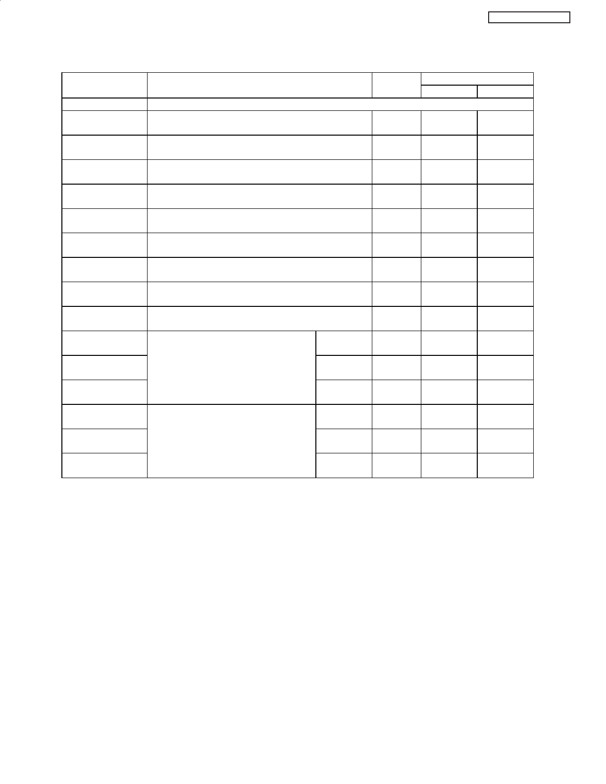
65
DW1U
AD9880 (1/1)
Initial Data(HEX)
Adjustment
Mode OSD
Adjustment Item Adjustment
Range(HEX) DW1-U
AD9880 A/D Converter, 480p/1080i/720p
001 Pr channel gain Adjust 00㨪7F 40
002 Y Channel Gain Adjust 00㨪7FF 40
003 Pb Channel Gain Adjust 00㨪7F 40
004 Pr offset MSB 00㨪FF 40
005 Pr Offset 00㨪FF 00
006 Y Offset MSB 00㨪FF 04
007 Y Offset 00㨪FF 00
008 Pb Offset MSB 00㨪FF 40
009 Pb Offset 00㨪FF 00
010 480p 00㨪FF 06
011 1080i 00㨪FF 45
012
Clamp Placement
720p 00㨪FF 45
013 480p 00㨪FF 1D
014 1080i 00㨪FF 2A
015
Clamp Duration
720p 00㨪FF 74
10. I2C Adjustment Parameter List (continued)
GI
66
DW1U
CXA2211 (1/2)
Initial Data(HEX)
Adjustment
Mode OSD
Adjustment Item Adjustment
Range(HEX) DW1-U
CXA2211 Sync Processor
001 Horizontal Number High Bit 00㨪3FF *
002 Vertical Number High Bit 00㨪7FF *
003 480i 00㨪03 02
004 480p 00㨪03 02
005 1080i 00㨪03 02
006
AFC loop gain control
00h = H free-running mode
01h = gain low
02h = gain middle
03h = gain high
720p 00㨪03 02
007 480i 00㨪07 07
008 480p 00㨪07 07
009 1080i 00㨪07 07
010
Phase control (Control for rough-tune)
for HOUT
00h = H sync center,
01h = center -3.125%,
02h = center -6.25%,
03h = center -9.375%
04h∼06h = Leading edge same phase
as HSSOUT
07h = Outputs the same phase
as HSSOUT
720p 00㨪07 07
011 480i 00㨪FF 10
012 480p 00㨪FF 10
013 1080i 00㨪FF 10
014
Phase control (Control for fine-tune) for HOUT
This is valid when HSHIFT = 0㨪3.
1 step: 0.024%, Total control range: 6%
720p 00㨪FF 10
015 480i 00㨪01 01
016 480p 00㨪01 01
017 1080i 00㨪01 01
018
Sets the sync separation method.
This is valid when AUTO = 1
00h = Forcibly sliced at the sync tip
+ 78mV level.
01h = Level detection mode
720p 00㨪01 01
10. I2C Adjustment Parameter List (continued)
GI
67
DW1U
CXA2211 (2/2)
Initial Data(HEX)
Adjustment
Mode OSD
Adjustment Item Adjustment
Range(HEX) DW1-U
CXA2211 Sync Processor
019 480i 00㨪01 00
020 480p 00㨪01 00
021 1080i 00㨪01 00
022
This is switch a switch that selects the
route of LPF in the sync sep circuit.
This is valid when AUTO = 1
00h = Through, 01h = LPF
720p 00㨪01 00
023 480i 00㨪03 01
024 480p 00㨪03 01
025 1080i 00㨪03 01
026
Sync separation circuit slice level setting
This is valid when HSEPSEL = 1
00h = Automatic setting
01h = H fixed to 65% from the sync tip.
02h = H fixed to 25% from the sync tip.
03h = ***
720p 00㨪03 01
10. I2C Adjustment Parameter List (continued)
GI
68
DW1U
HDMI (1/2)
Initial Data(HEX)
Adjustment
Mode OSD
Adjustment Item Adjustment
Range(HEX) DW1-U
HDMI HDMI_1/2
001 VSYNC/Clock detect/Sync detect 1 00㨪07 *
002 HDCP Status 00㨪FF *
003 Pixel clock 00㨪FF *
004 N hardware value 1
Low 7 bit
00㨪FF *
005 N hardware value 1
Middle 7 bit
00㨪FF *
006 N hardware value 1
High 4 bit
00㨪FF *
007 CTS hardware value 1
Low 7 bit
00㨪FF *
008 CTS hardware value 1
Middle 7 bit
00㨪FF *
009 CTS hardware value 1
High 4 bit
00㨪FF *
010 ACR PLL hardware value 1 00㨪FF *
011 ACR PLL hardware value 1 00㨪3F *
012 Extracted Sampling Frequency 1
channel status bits 24-27(same value at 0x30)
00㨪7F *
013 Clock Accuracy/Sampling Frequency 1 00㨪FF *
014 Audio length/Audio length max 1 00㨪FF *
015 AV mute/HDMI mode 1 00㨪FF *
016 AVI info frame type code 1 00㨪FF *
017 AVI info frame version code 1 00㨪FF *
018 00㨪FF *
019 00㨪FF *
020 00㨪FF *
021 00㨪FF *
022
AVI info frame data 1
00㨪FF *
10. I2C Adjustment Parameter List (continued)
GI
69
DW1U
HDMI (2/2)
Initial Data(HEX)
Adjustment
Mode OSD
Adjustment Item Adjustment
Range(HEX) DW1-U
HDMI HDMI_1/2
023 SPD info frame type code 00㨪FF *
024 SPD info frame version code 00㨪FF *
025 SPD info frame data 00㨪FF *
026 AUDIO Info Frame Type Code 1 00㨪FF *
027 AUDIO Info Frame Version Code 1 00㨪FF *
028 00㨪FF *
029 00㨪FF *
030 00㨪FF *
031 00㨪FF *
032
AUDIO Info Frame Data Bytes 1
00㨪FF *
033 GCP data 00㨪FF *
034 ACP packet type code 00㨪FF *
035 ACP type 00㨪FF *
036 DVD-audio type dependent generation 00㨪FF *
037 Audio copy information 00㨪FF *
038 RGB to YCbCr range scaling 00㨪01 01
039 Back Porch Mode, Field 2 Position Adjustment 00㨪01 01
040 Matching Test to allow increment of stability counter. 00㨪01 00
041 RGB to YCbCr range scaling 00㨪01 01
042 Back Porch Mode, Field 2 Position Adjustment 00㨪01 01
043 Matching Test to allow increment of stability counter. 00㨪01 00
10. I2C Adjustment Parameter List (continued)
GI
㪬㪧
㪛㫀㪾㫀㫋㪸㫃㩷㪤㫆㪻㫌㫃㪼
㪛㫀㪾㫀㫋㪸㫃㩷㪪㫌㪹㩷㪧㪮㪙
Digital Main P.W.B has five LED (KNIGHT RIDER) on board.
After Power ON by POWER_1(6pin of PPT3), these LED will be turned on
in sequence as follows. It may take a few seconds for the sequence.
LED sequence
Sequence D302
(Red)
<PiO04>
D303
(Green)
<PiO03>
D304
(Yellow)
<PiO02>
D305
(Orange)
<PiO01>
D306
(Red)
<PiO00>
1 (Start) ○○ ○○●
2○○ ○●●
3○○ ●●●
4○● ●●●
5 (End) ○○ ○○○
○ is turn off the LED, ● is Lighting the LED
After Program is loaded without error, all LED will be turned off.
Any LED should not light.
If some errors occur, LED will show the error pattern.
(1) Check that LED is not lit.
(2) If LED is lit, refer to the following table and check the involved devices.
Location of LEDs
11. TROUBLESHOOTING FLOWCHARTS
11.1.1 TROUBLE SHOOTING for DIGITAL MODULE (Device error check)
L
ED1 (D306)
LED2 (D305)
LED3 (D304)
LED4 (D303)
L
ED5 (D302)
70
DW1U
TABLE OF CONTENTS
GI
LED patterns for involved devices
LED
No.
D306
(Red)
D305
(Orange)
D304
(Green)
D303
(Yellow)
D302
(Red)
Device Circuit No
1○○○○●
- -
2○○○●○
Digital Tuner Video/Audio of
Cable/Air
3○○○●●
Analog Tuner Video/Audio of
Cable/Air
4○○●○○
MPEG Video/Audio of
Cable/Air
5○○●○●
Graphics All OSD
6○○●●○
Flash Memory Loading
Program
7○○●●●
IEEE1394
(Vivid Logic) IEEE1394
8○●○○○
-
9○●○○●
-
10 ○●○●○
-
11 ○●○●●
-
12 ○●●○○
Video Decoder
(TC9010) CCD etc.
13 ○●●○●
-
14 ○●●●○
Audio DSP
(AD9980)
Audio cont.
SRS/BBE
15 ○●●●●
-
16 ●○○○○
HDMI HDMI
17 ●○○○●
A/D Converter
(AD9980) Video
18 ●○○●○
Sync Separator
(CXA2211) Sync
19 ●○○●●
FC4 Picture Cont.
20 ●○●○○
FC6 Picture Cont.
71
DW1U
11. TROUBLESHOOTING FLOWCHARTS
GI
LED
No.
D306
(Red)
D305
(Orange)
D304
(Green)
D303
(Yellow)
D302
(Red)
Device Circuit No Role
21 ●○●●○
-
22 ●○●●●
Drive u-COM LCD panel
23 ●●○○○
Video SW Video
24 ●●○○●
Audio SW Audio
25 ●●○●○
Temp. Sensor Temperature
sensor
26 ●●○●●
- -
27 ●●●○○
- -
28 ●●●○●
- -
29 ●●●●○
- -
30 ●●●●●
- -
31 ●○○○●
- -
72
DW1U
11. TROUBLESHOOTING FLOWCHARTS
GI
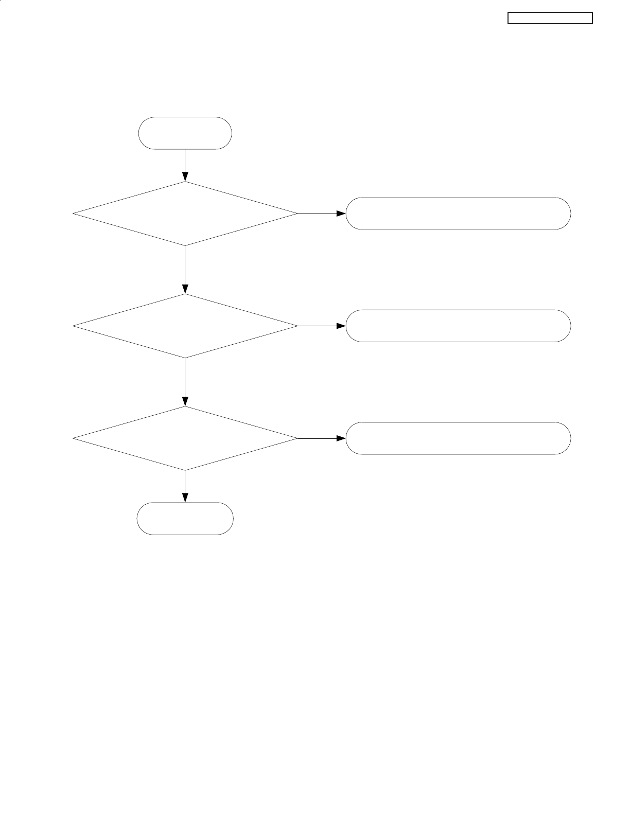
73
DW1U
11.2.1 Trouble shooting for HDMI
(1) No HDMI picture
Ensure Y, H, V and Clock
signal at pin 1 of RK55.
OK
NG
Ensure power at pin 4
of IK03, IK06, IK07 and IK08.
OK
NG
Digital Module (HDMI) defect
I101 or I102 defect
IK02 defect
Ensure power at pin 1 of IK03.
OK
NG
Digital Module, SIgnal PWB or
Signal Power PWB defect
Start
GI
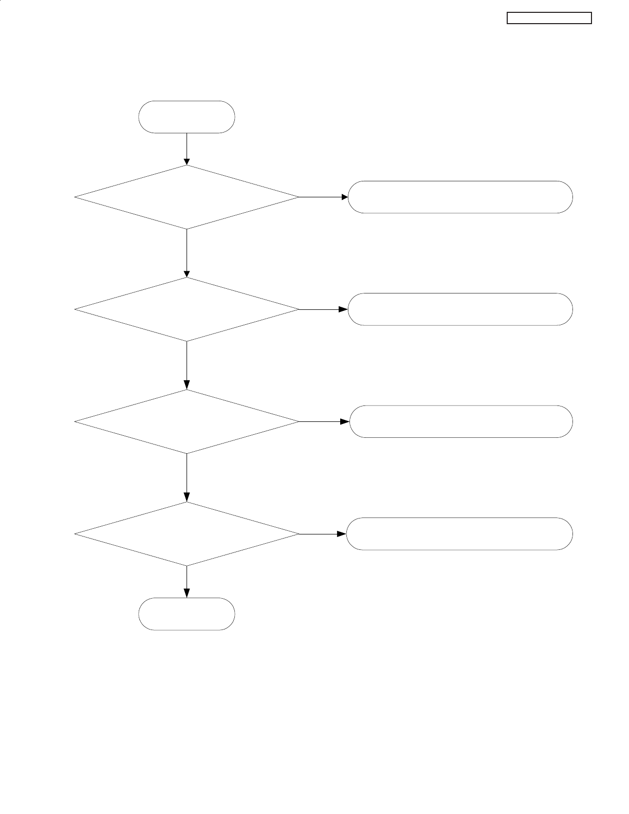
74
DW1U
11. TROUBLESHOOTING FLOWCHARTS
(2) No HDMI analog and/or digital audio
Ensure audio signal at
pin 93 and 95 of PSM. OK
NG
Digital Module (HDMI) defect
I102, IF04 or IV04 defect
Ensure digital signal at
pin 84, 85, 86 and 88 of IK02.
OK
NG
IK02 defect
Ensure power at pin 4
of IK03, IK06, IK07 and IK08.
OK
NG
SIgnal PWB defect
Start
Ensure power at pin 1 of IK03. Digital Module, SIgnal PWB or
Signal Power PWB defect
OK
NG
GI
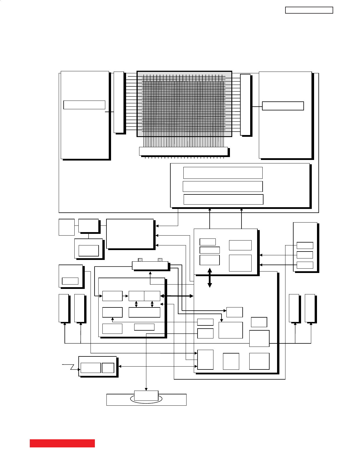
CIRCUIT BLOCK DIAGRAM
TABLE OF CONTENTS
Sub-Digital PWB
Speaker L
Audio
PWM
Vcego
Vsago
Y PWB
X PWB
X Sustain Circuit Y Sustain Circuit
PDP Panel Module
Address Driver
Scan Drive
r
Driver Controller
LVDS Receiver Signal Controller
Data Controller
Logic Control
unit
Scan Drive
r
Digital
Audio
Amplifier
Motor
Driver
Swivel Stand
Main-Digital PWB
Speaker R
Woofer L
Woofer R
Remote
Control LED PWB
IR
Receiver
LED
SW PWB
Main
Power SW
AC
Inlet Power Supply
Unit
Filter
PWB
POD
Card
I/F
Side
Terminal
PWB
A/V
Photo
DV
Control
PWB
Key SW
RGB
(LVDS)
CPUgo
PDPgo
R
F
Power2
Power1
Sub
Micro
UEI
Terminal PWB
IR-Blaster
Driver
Video
SW
Analog
Tuner
A/V
Pin Jack
OPT-Audio
Output
Audio
SW
CTRL
STBY
A
/
V
Digital Tuner
Demodulator
SD/MMC
Card
I/F
Cable
ANT SW Box
Air
OOB
RS-232C
R
F
Digital
Signal
Processor
LVDS
Transmitter
HDMI
Main
MICRO
Sync.Sep.
DW1U
75
GI
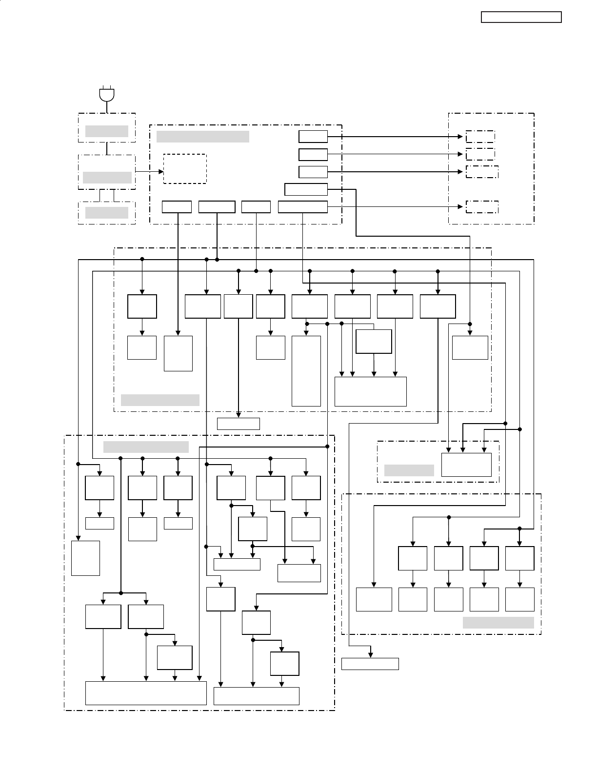
DW1U
POWER SYSTEM BLOCK DIAGRAM
Filter PWB
A
C120V
LED PWB
Digital
Audio
Amp.
Sub
MICRO
Sub-Digital PWB
AC SW +5.6V STBY+3.3V
STBY+5V
+24V
Vcc
Va
Vs
+10.5V
(PFC)
Power Supply Unit
AC INLET
PDP Panel Module
(+5.1V)
(+60V)
(+80V)
(+3.3V)
+9V
DC-DC
Terminal PWB
+3.3V
DC-DC
Main-Digital PWB
+9V
Reg.
+5V
DC-DC
+1.1V
DC-DC
+1.8V
Reg.
+5V
Reg.
ANT SW BOX
Digital Tuner
Demodulator
OOB
Buffer
Amp.
POD-
Vcc
Audio
PWM
IR-
Blaster
Vari.
Reg.
POD-
Vpp
IR
LED
+9V
Reg.
LPF
+3.3V
Reg.
+5V
Reg.
Sync.
sep.
+5V
Reg.
USB +1.8V
Reg.
HDMI
+3.3V
Reg.
PLL
EPLD
Seine Butler FC SDRAM FLASH
Audio-DSP LVDS IEEE1394 etc.
+2.5V
DC-DC
+1.6V
DC-DC
+1.2V
Reg.
Video Decoder
Video ADC
+2.5V
Reg.
+1.5V
Reg.
+3.3V
Reg.
+3.3V
Reg.
+9V
Reg.
+5V
Reg.
+5V
Reg.
Swivel
Motor
Driver
+9V
Reg.
Analog
Tuner
IR-Blaster
Driver
Audio
SW
OPT
Output
Video
SW
POD FAN
Vari.
Reg.
76
GI
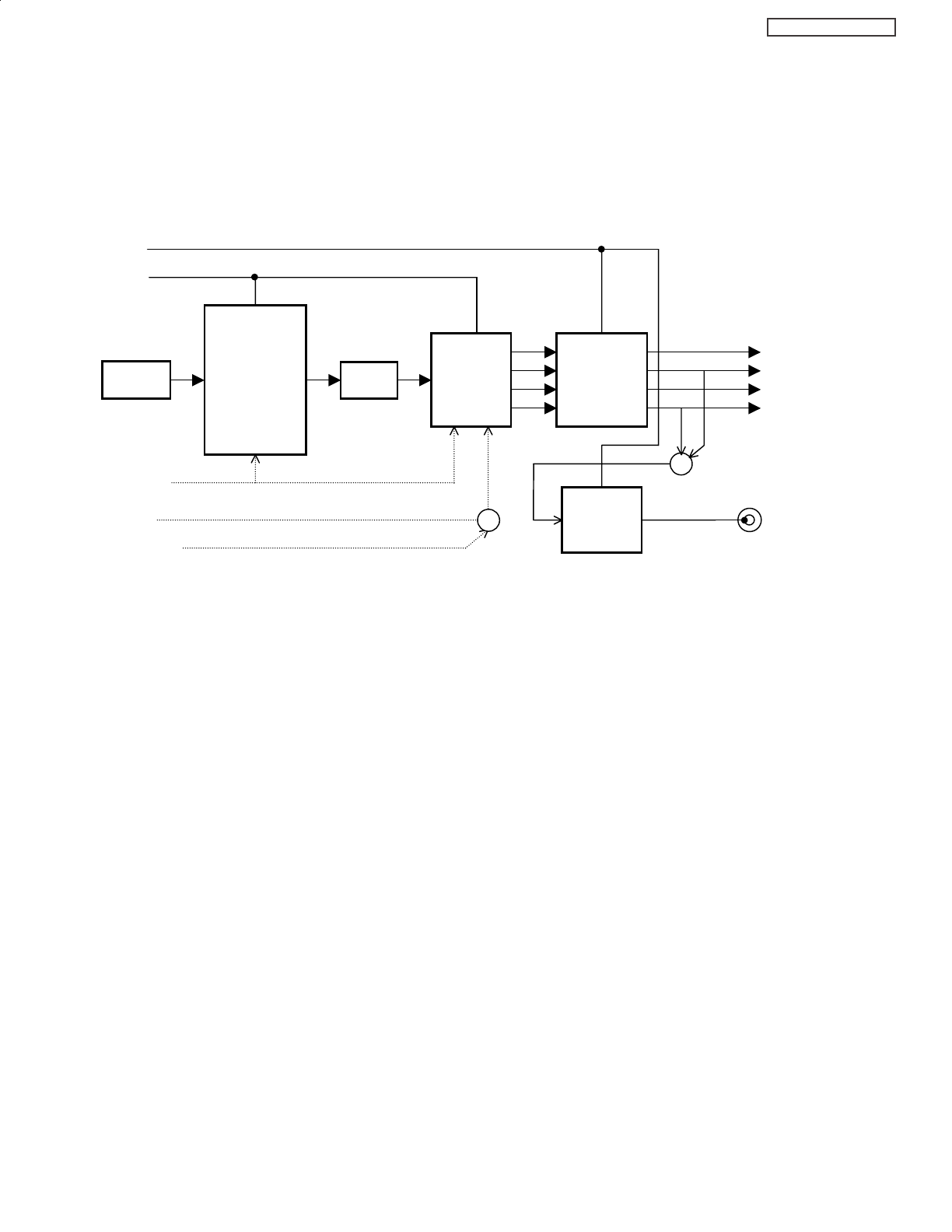
AUDIO CIRCUIT BLOCK DIAGRAM
DW1U
Speaker L
Woofer L
SubWoofer
OUT
PoWERoFF
MUTE
SCL/SDA
I2S
IA01
TAS3103
Volume Mute
Balance
Bass/Treble
SRS BBE
Loudness
AGC TruBass
+24V
I403
BA4558
Am
p
.
MUTE
I401
TAS5508
PWM
Mute
I402
TAS5122
Digital
Power Amp.
Speaker R
Woofer R
+3.3V
(FC6)
(Butler) I2S
PWM
I2S
77
GI
CONNECTION DIAGRAM
DW1U
TABLE OF CONTENTS 78
(55" Models Only)
CH 4

DW1U
79
FINAL WIRING DIAGRAM
TABLE OF CONTENTS
GI
TABLE OF CONTENTS
QUICK DISASSEMBLE GUIDE(Back Cover 1)
Ԙ Remove Screw M3M 6*12 P#MJ03889 (4 Pcs.)
ԙ Remove Screw M3M 6*12 P#MJ04042 (2 Pcs.)
80
DW1U
GI
QUICK DISASSEMBLE GUIDE(Back Cover 2)
Ԙ Remove Screw M3D 4*10 P#MJ03895 (34 Pcs.)
55" BACK COVER
P#QA03303
TABLE OF CONTENTS 81
DW1U
GI
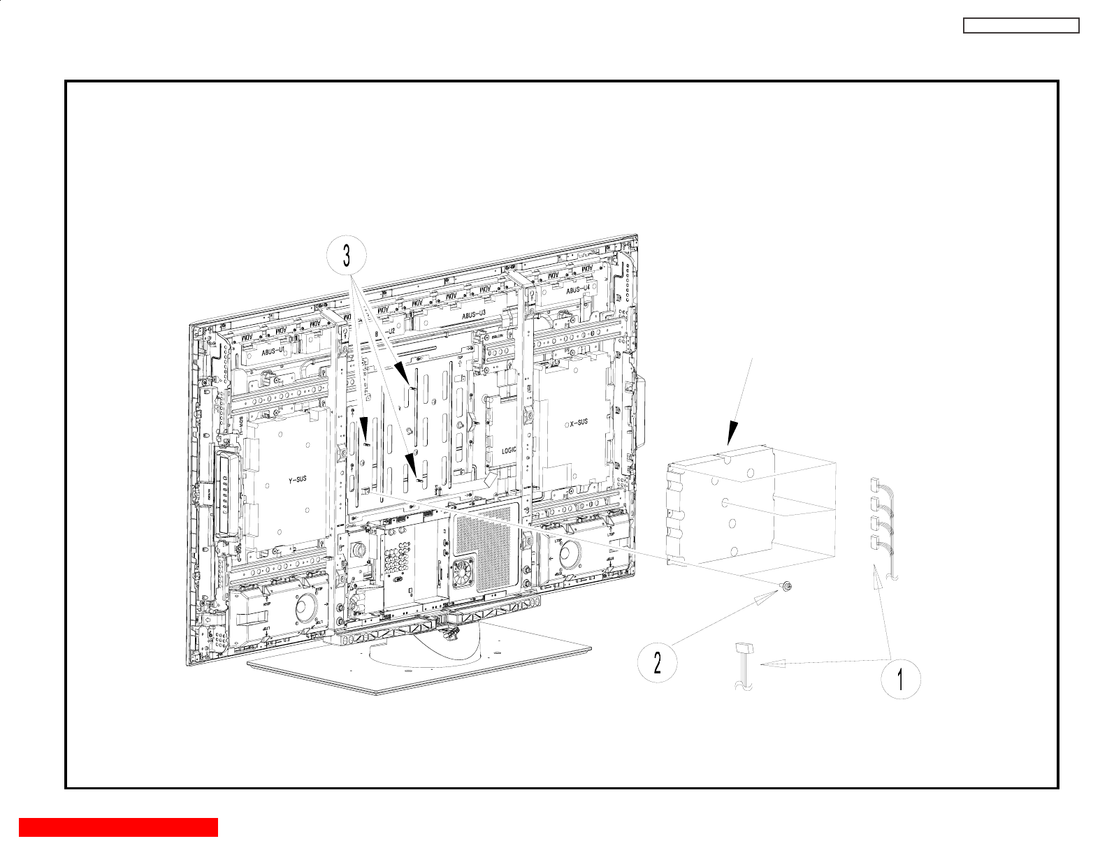
QUICK DISASSEMBLE GUIDE(Power Unit)
ԘUnplug Connectors
ԙ Remove Screws M3E 3*8 P#MJ03963 (6 Pcs.)
82
POWER UNIT
P#HA01572
ԚPush Plastic Holder Wings and Remove Power Unit
TABLE OF CONTENTS
DW1U
GI
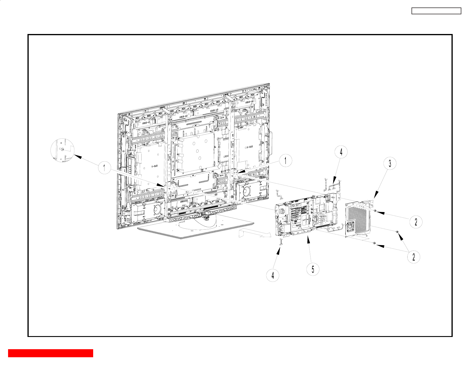
QUICK DISASSEMBLE GUIDE(AV Digital Block)
83
ԘLoose these Screws
ԙ Remove Screws M3E3*8 P#MJ03963 (5 Pcs.)
ԚLift and Remove Fan Mtl Assy(Fan P#GS01092, Tuner Case P#NA78241)
ԛUnplug Connectors
ԜLift and Remove AV Digital Block
TABLE OF CONTENTS
DW1U
GI
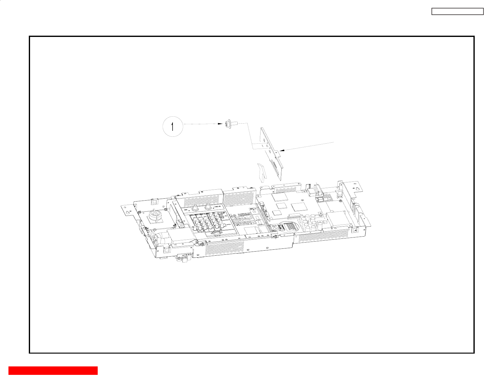
QUICK DISASSEMBLE GUIDE(AV Digital Boards 1)
ԘRemove Screws M3E 3*8 P#MJ03963 (2 Pcs.)
84
TERMINAL PLATE
TABLE OF CONTENTS
DW1U
GI
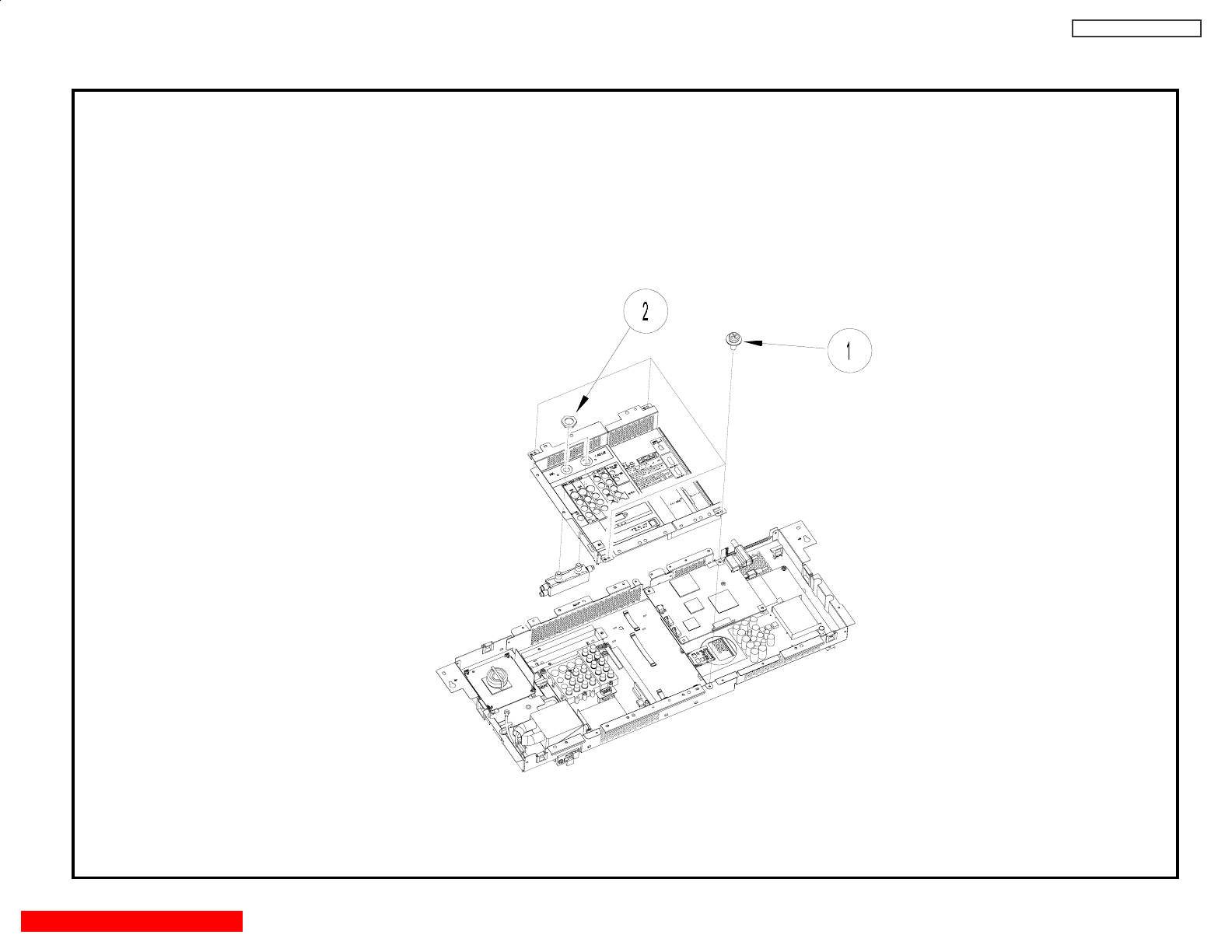
QUICK DISASSEMBLE GUIDE(AV Digital Boards 2)
Ԙ Remove Screws M3E 3*8 P#MJ03963 (4 Pcs.)
ԙ Remove Hex Nut P#MK01511 (2 Pcs.)
Washer P#MK01431 (2 Pcs.)
85
P#HP01241
ANTENNA SWITCH
TERMINAL METAL
TABLE OF CONTENTS
DW1U
GI
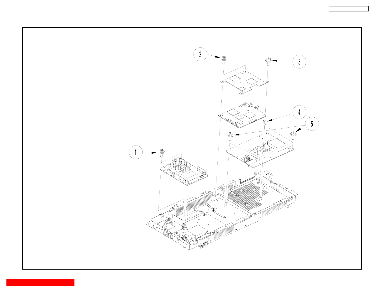
QUICK DISASSEMBLE GUIDE(AV Digital Boards 3)
Ԙ Remove Screws M3E 3*8 P#MJ08781 (4 Pcs.)
ԙ Remove Screws M3S 3*12 P#MJ04025 (2 Pcs.)
Ԛ Remove Screw M3E 3*8 P#MJ03963 (1 Pc.)
ԛ Remove Screw Hex M3 P#MJ08731 (1 Pc.)
Ԝ Remove Screws M3E 3*8 P#MJ03963 (4 Pcs.)
86
P#JP08522
DIGITAL MAIN
P#JP08533(55HDX62/55HDT52)
P#JP08534(55HDS52)
TERMINAL PWB
DIGITAL SUB PWB
P#JP08511
MAIN HEAT SINK
TABLE OF CONTENTSTABLE OF CONTENTS
DW1U
GI
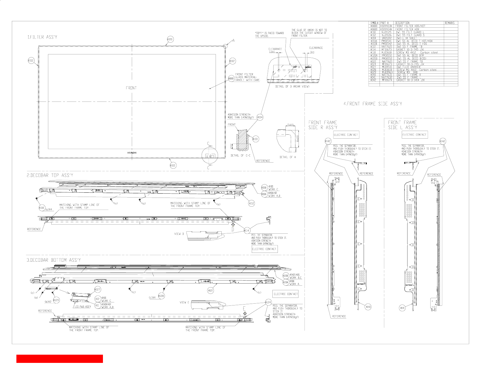
FINAL ASSEMBLY GUIDE
87
TABLE OF CONTENTS
GI
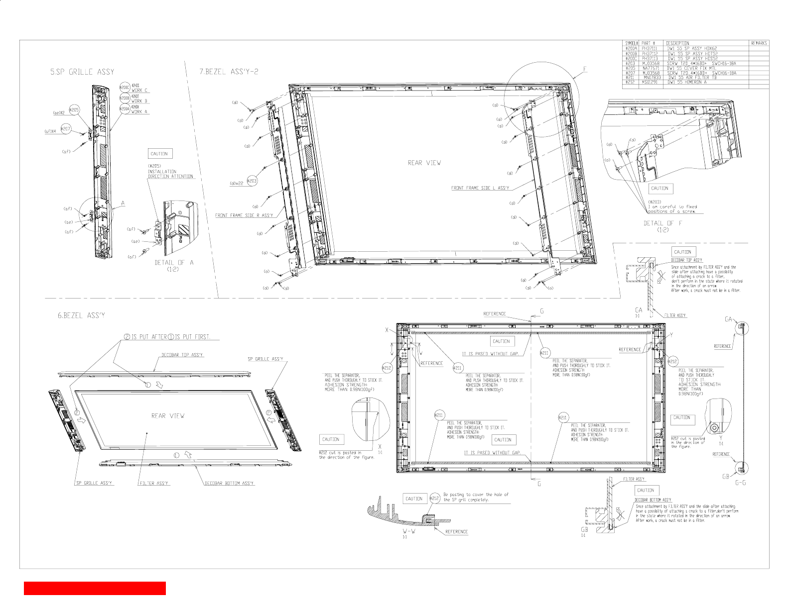
FINAL ASSEMBLY GUIDE
88
TABLE OF CONTENTS
GI
CH 2
Same p# for left and right grills
55HDS
WORK C
55HDT
WORK B
55HDX
WORK A
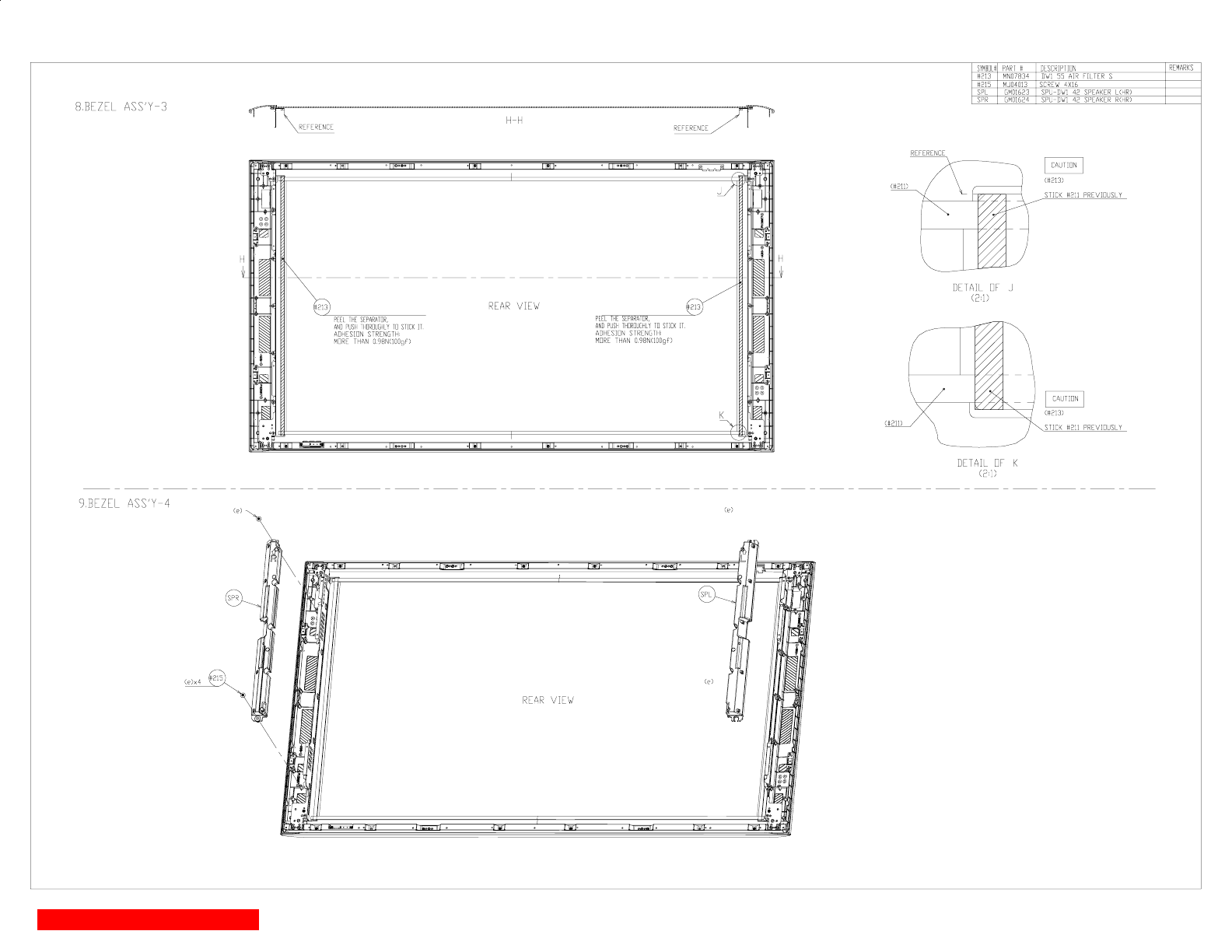
FINAL ASSEMBLY GUIDE
89
TABLE OF CONTENTS
GI
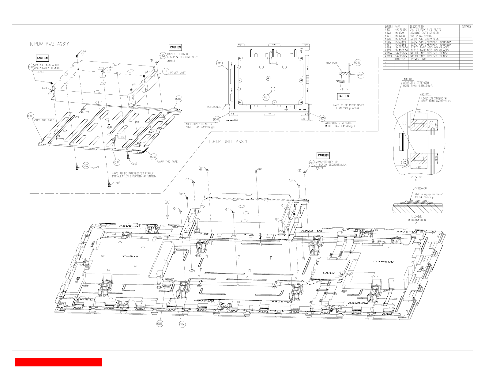
FINAL ASSEMBLY GUIDE
90
TABLE OF CONTENTS
GI
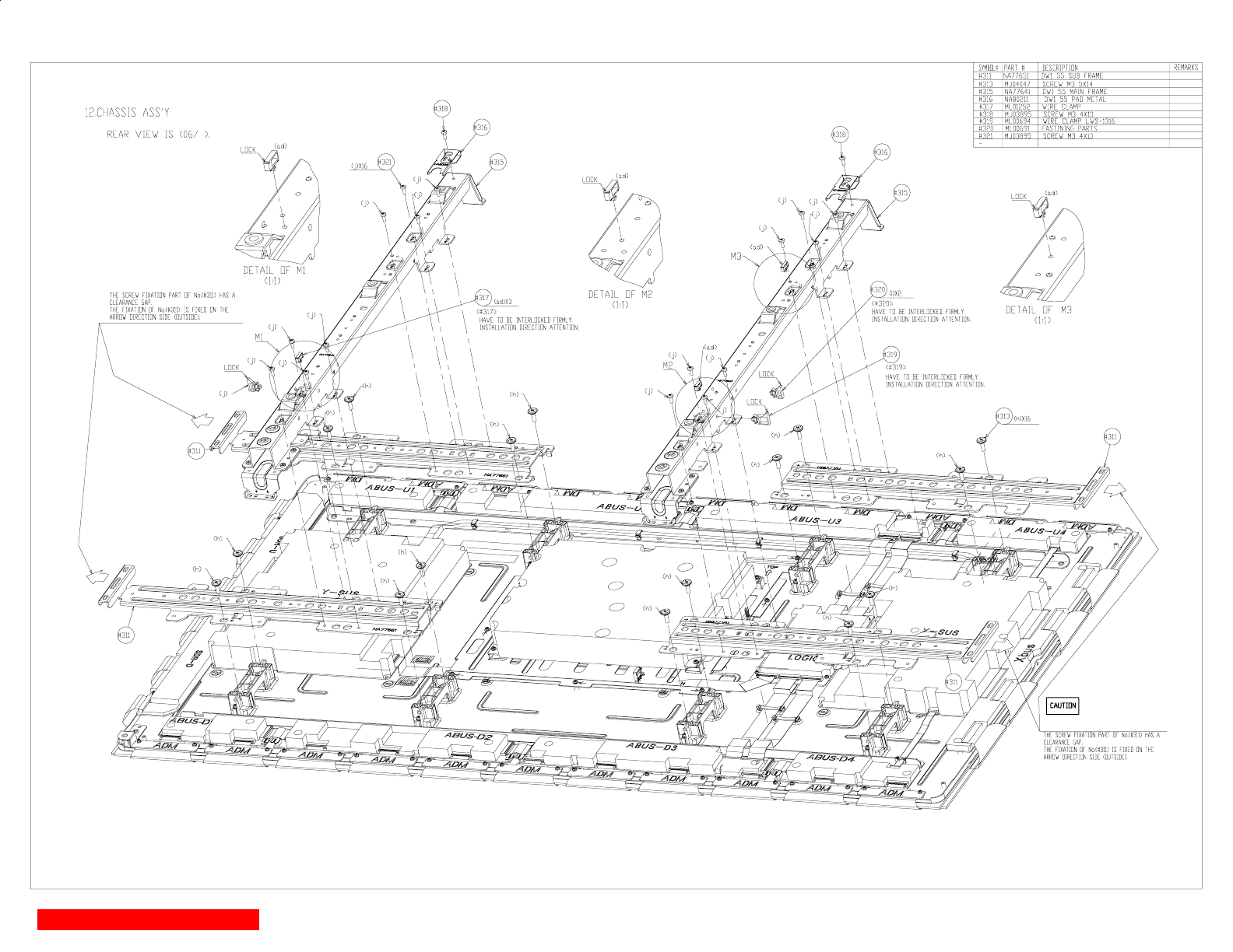
FINAL ASSEMBLY GUIDE
91
TABLE OF CONTENTS
GI
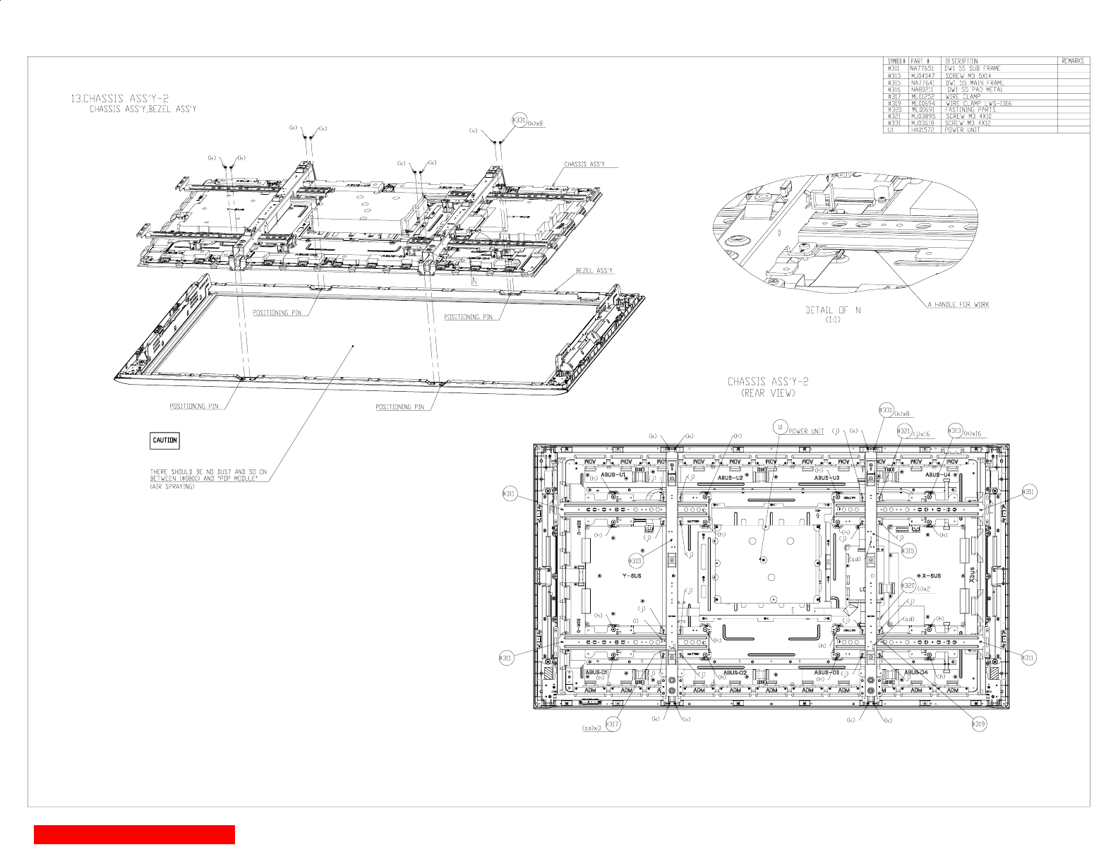
FINAL ASSEMBLY GUIDE
92
TABLE OF CONTENTS
GI
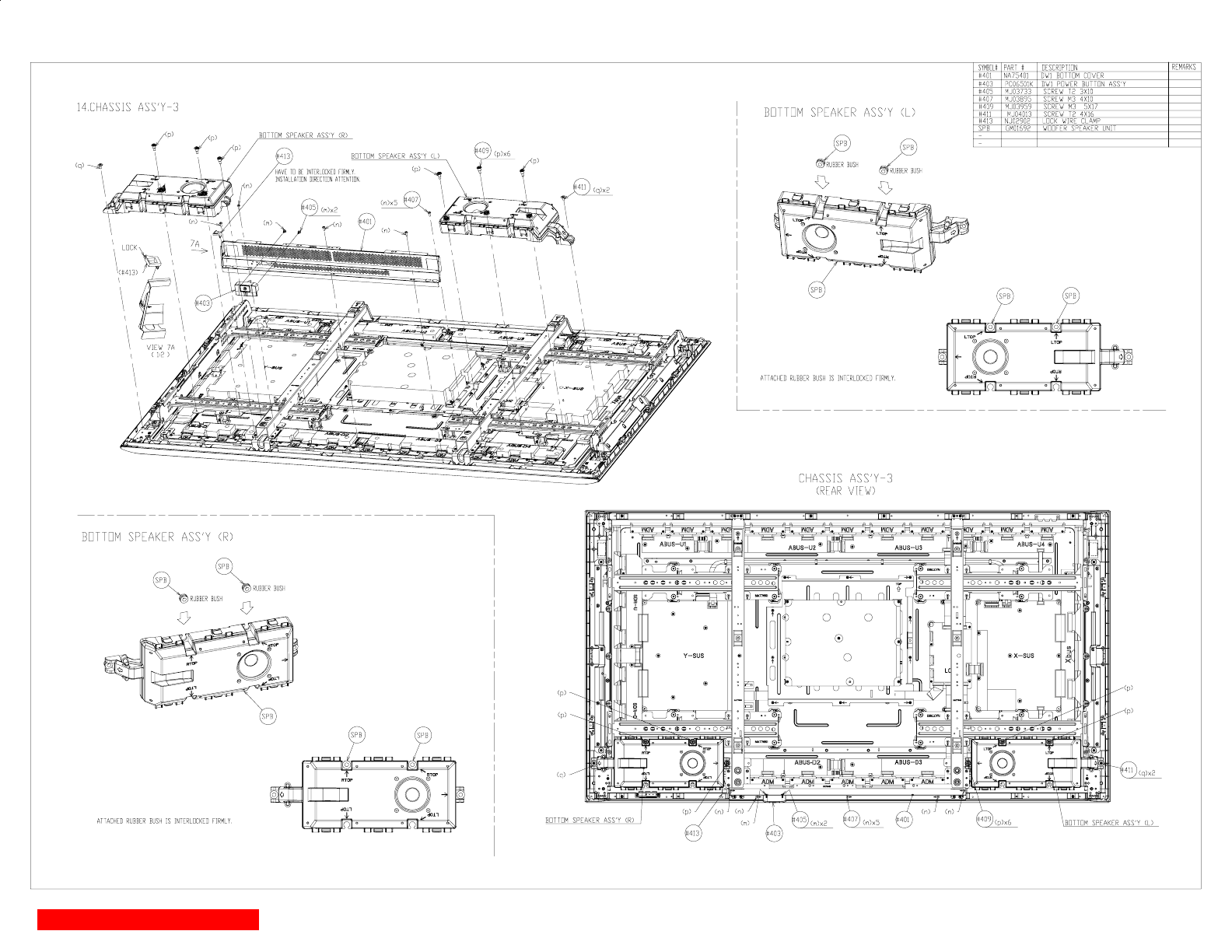
FINAL ASSEMBLY GUIDE
93
TABLE OF CONTENTS
GI
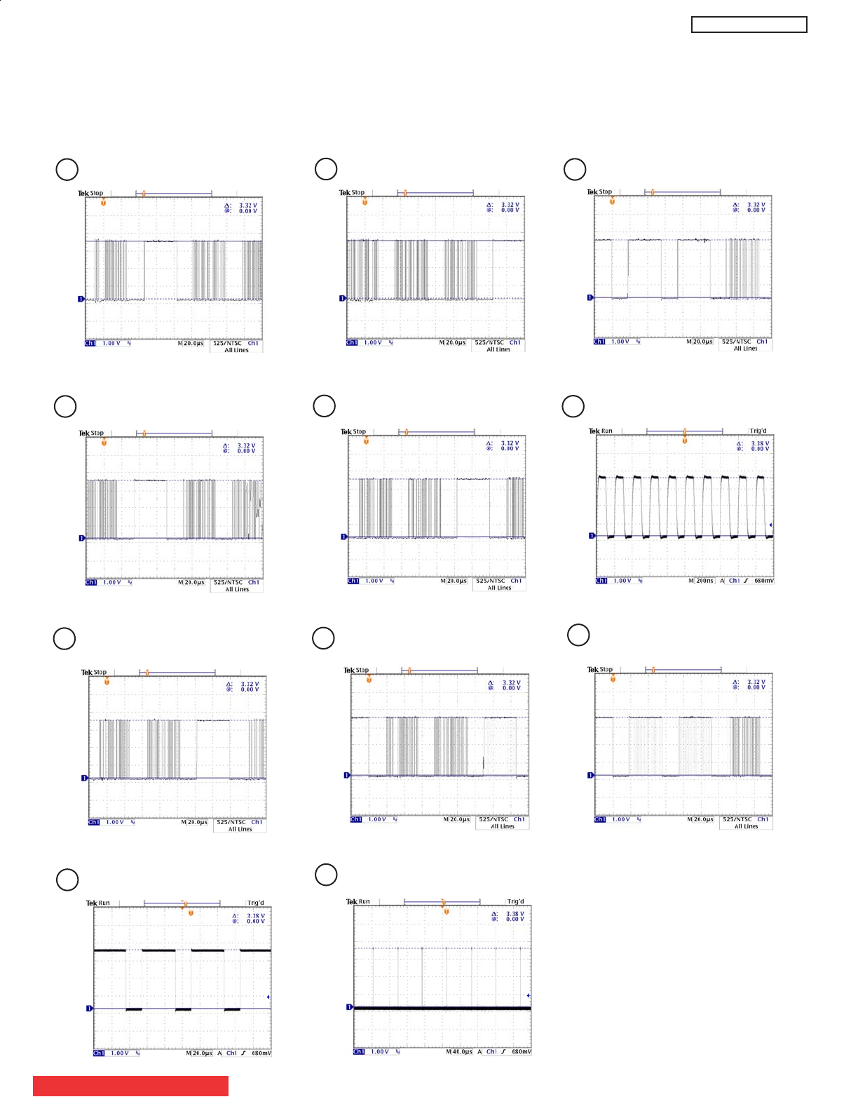
DW1U
IT08 Pin 42 IT08 Pin 44 IT08 Pin 45
IT08 Pin 47 IT08 Pin 48 IT08 Pin 50
IT08 Pin 52
123
456
789
IT08 Pin 54 IT08 Pin 58
11 IT08 Pin 64
10 IT08 Pin 59
TABLE OF CONTENTS
SATURN
SUBDIGITAL PWB
TUNER
Signal amplitude and DC level shown at and @ respectively.
Numbers inside circle correspond to locations shown in the circuit diagram.
WAVEFORMS AT EACH SECTION
∆
click here to go to circuit diagram
94
GI
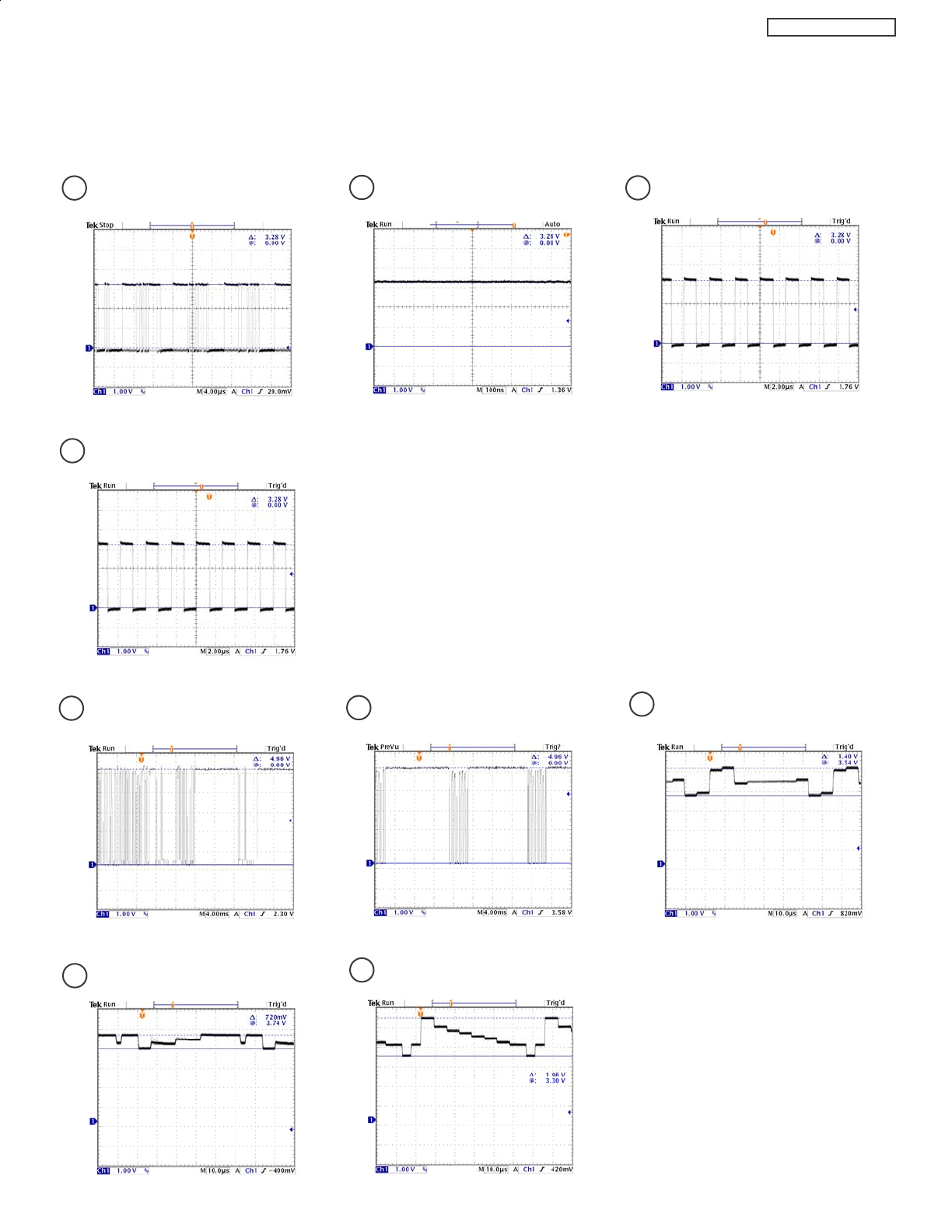
DW1U
12 13 14
15
16 17
20
19
I401 Pin 31 I401 Pin 39 I401 Pin 41
I401 Pin 45
18
I101 Pin 46 I101 Pin 54
I101 Pin 55 I101 Pin 56
I101 Pin 45
SATURN
SUBDIGITAL PWB
DIGITAL AUDIO
using a Color Bar signal with H sync 31 khz and V. sync 60 hz and a X10 probe.
Numbers inside circle correspond to locations shown in the circuit diagram. Waveforms taken
WAVEFORMS AT EACH SECTION
TERMINAL PWB
VIDEO SELECTOR
Signal amplitude and DC level shown at and @ respectively.
∆
click here to go to circuit diagram
click here to go to circuit diagram
95
GI
DW1U
21 I101 Pin 60
WAVEFORMS AT EACH SECTION
Numbers inside circle correspond to locations shown in the circuit diagram. Waveforms taken
using a Color Bar signal with H sync 31 khz and V. sync 60 hz and a X10 probe.
TERMINAL PWB
VIDEO SELECTOR
click here to go to circuit diagram
Signal amplitude and DC level shown at and @ respectively.
∆
96
GI
DW1U
Symbol Pin No. Voltage Symbol Pin No. Voltage Symbol Pin No. Voltage
UTJ1 1 0 UT01 1 0 CN63 1 5.4 V
25 V25 V20
3 0 3 0 3 3.3 V
4 14 V 4 14.6 V 4 0
5 2.4 V 5 8.3 V 5 3.3 V
6 0 6 0 6 3.3 V
7 5 V 7 5 V 7 3.3 V
8 2.5 V 8 3.3 V
9 0.35 V 9 5 V Symbol Pin No. Voltage
10 5 V 10 5 V CN64 1 63.4 V
11 2.6 V 11 0 2 63.4 V
12 2.5 V 12 0 3 5 V
13 2.2 V 13 0 4 5 V
14 0 14 0 5 0
15 2.3 V 15 0 6 0
16 2.3 V 16 0 7 0
17 0 17 0 8 84.7 V
18 5 V 18 5 V 9 84.7 V
19 0 19 0 10 84.7 V
20 5 V 20 0
Symbol Pin No. Voltage
Symbol Pin No. Voltage Symbol Pin No. Voltage CN68 1 NC
CN61 1 1.6 V CNPPS 1 16.5 V 2 3.3 V
2 NC 2 16.5 V 3 3.3 V
3 125 V 3 0 4 1.7 V
4 NC 4 0 5 1.4 V
5 NC 5 25 V 6 0
6 0.65 V 6 25 V 7 0
70 80
Symbol Pin No. Voltage 8 0 9 3.3 V
CNPPD 1 5.7 V 9 10.5 V 10 5 V
2 5.7 V 10 0 11 5 V
3 5.7 V 11 0
4 0 12 10.5 V
50
TABLE OF CONTENTS
97
(55" Models Only)
DW1U DC VOLTAGE TABLES
CH 4
PRODUCT SAFETY NOTE: Components marked with a ! and shaded have special characteristics
important to safety. Before replacing any of these components, read carefully the PRODUCT SAFET
Y
NOTE of this Service Manual. Don't degrade the safety of the receiver through improper servicing.
x
All DC voltage to be measured with a tester (100 kȍ/V). Voltage taken on a complex color bar including a standard color bar signal.
x
Since this is a basic circuit diagram, the value of the parts is subject to be altered for improvement.
1 234 56
A
B
C
D
E
1
2345
6
78
9
10
11
BASIC CIRCUIT DIAGRAM DW1U
Subdigital 1 of 10
TUNER
TABLE OF CONTENTS
98
GI
PRODUCT SAFETY NOTE: Components marked with a ! and shaded have special characteristics
important to safety. Before replacing any of these components, read carefully the PRODUCT SAFET
Y
NOTE of this Service Manual. Don't degrade the safety of the receiver through improper servicing.
x
All DC voltage to be measured with a tester (100 kȍ/V). Voltage taken on a complex color bar including a standard color ba signal.
x
Since this is a basic circuit diagram, the value of the parts is subject to be altered for improvement.
99
BASIC CIRCUIT DIAGRAM
1 234 56
A
B
C
D
E
DW1U
Subdigital 2 of 10
POD-I/F
GI
PRODUCT SAFETY NOTE: Components marked with a ! and shaded have special characteristics
important to safety. Before replacing any of these components, read carefully the PRODUCT SAFET
Y
NOTE of this Service Manual. Don't degrade the safety of the receiver through improper servicing.
x
All DC voltage to be measured with a tester (100 kȍ/V). Voltage taken on a complex color bar including a standard color bar signal.
x
Since this is a basic circuit diagram, the value of the parts is subject to be altered for improvement.
100
BASIC CIRCUIT DIAGRAM
1 234 56
A
B
C
D
E
POWER I/F & SWIVEL
DW1U
Subdigital 3 of 10
GI
PRODUCT SAFETY NOTE: Components marked with a ! and shaded have special characteristics
important to safety. Before replacing any of these components, read carefully the PRODUCT SAFET
Y
NOTE of this Service Manual. Don't degrade the safety of the receiver through improper servicing.
x
All DC voltage to be measured with a tester (100 kȍ/V). Voltage taken on a complex color bar including a standard color bar signal.
x
Since this is a basic circuit diagram, the value of the parts is subject to be altered for improvement.
101
BASIC CIRCUIT DIAGRAM
1 234 56
A
B
C
D
E
240 pin I/F
DW1U
Subdigital 4 of 10
GI
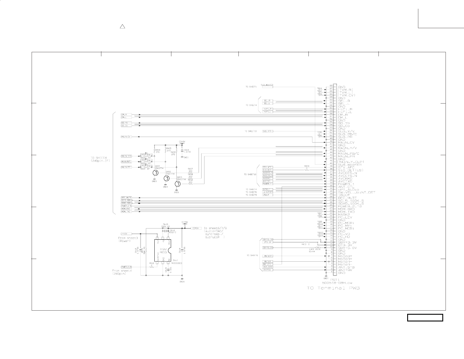
PRODUCT SAFETY NOTE: Components marked with a ! and shaded have special characteristics
important to safety. Before replacing any of these components, read carefully the PRODUCT SAFET
Y
x
All DC voltage to be measured with a tester (100 kȍ/V). Voltage taken on a complex color bar including a standard color bar signal.
x
Since this is a basic circuit diagram, the value of the parts is subject to be altered for improvement.
102
BASIC CIRCUIT DIAGRAM
NOTE of this Service Manual. Don't degrade the safety of the receiver through improper servicing.
1 234 56
A
B
C
D
E
TERMINAL I/F
DW1U
Subdigital 5 of 10
TERMINAL I/F
DW1U
Subdigital 5 of 10
TERMINAL I/F
DW1U
Subdigital 5 of 10
GI
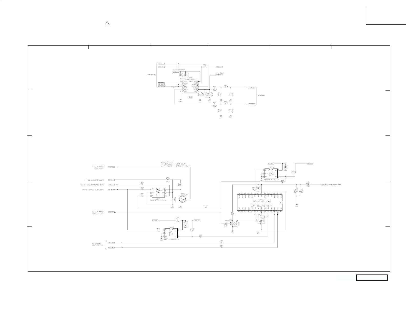
PRODUCT SAFETY NOTE: Components marked with a ! and shaded have special characteristics
important to safety. Before replacing any of these components, read carefully the PRODUCT SAFET
Y
NOTE of this Service Manual. Don't degrade the safety of the receiver through improper servicing.
x
All DC voltage to be measured with a tester (100 kȍ/V). Voltage taken on a complex color bar including a standard color bar signal.
x
Since this is a basic circuit diagram, the value of the parts is subject to be altered for improvement.
103
BASIC CIRCUIT DIAGRAM
1 234 56
A
B
C
D
E
DW1U
Subdigital 6 of 10
UEI
GI
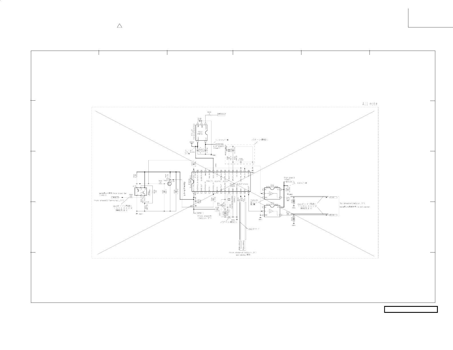
PRODUCT SAFETY NOTE: Components marked with a ! and shaded have special characteristics
important to safety. Before replacing any of these components, read carefully the PRODUCT SAFET
Y
NOTE of this Service Manual. Don't degrade the safety of the receiver through improper servicing.
x
All DC voltage to be measured with a tester (100 kȍ/V). Voltage taken on a complex color bar including a standard color bar signal.
x
Since this is a basic circuit diagram, the value of the parts is subject to be altered for improvement.
104
BASIC CIRCUIT DIAGRAM
1 234 56
A
B
C
D
E
MAIN SYNC SEPARATION
DW1U
Subdigital 7 of 10
GI
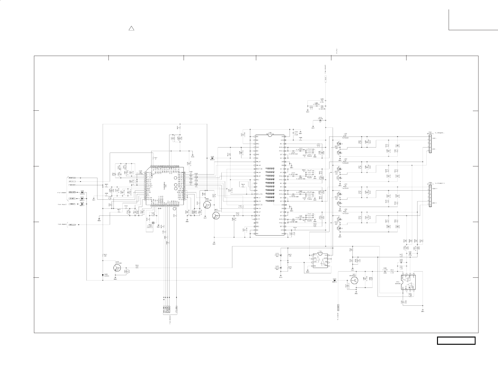
PRODUCT SAFETY NOTE: Components marked with a ! and shaded have special characteristics
important to safety. Before replacing any of these components, read carefully the PRODUCT SAFET
Y
NOTE of this Service Manual. Don't degrade the safety of the receiver through improper servicing.
x
All DC voltage to be measured with a tester (100 kȍ/V). Voltage taken on a complex color bar including a standard color bar signal.
x
Since this is a basic circuit diagram, the value of the parts is subject to be altered for improvement.
105
BASIC CIRCUIT DIAGRAM
1 234 56
A
B
C
D
E
DIGITAL AUDIO
DW1U
Subdigital 8 of 10
12
13
14
15
GI
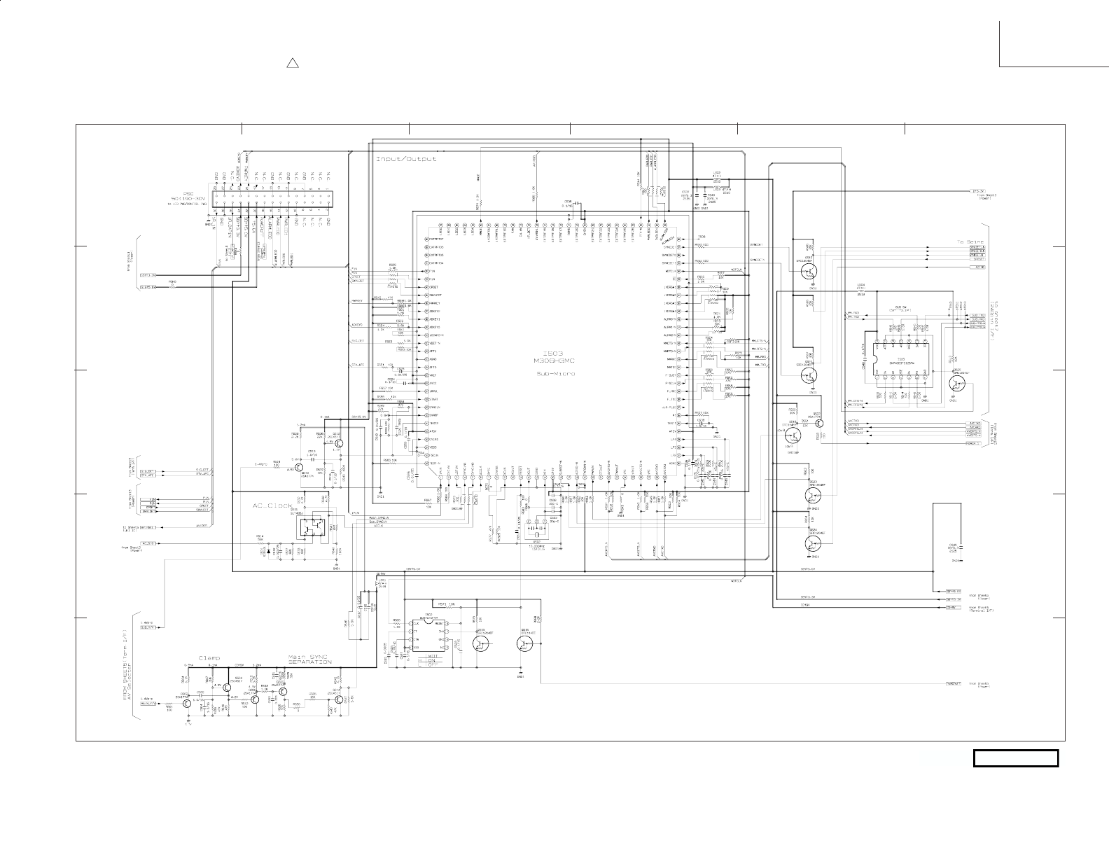
PRODUCT SAFETY NOTE: Components marked with a ! and shaded have special characteristics
important to safety. Before replacing any of these components, read carefully the PRODUCT SAFET
Y
x
All DC voltage to be measured with a tester (100 kȍ/V). Voltage taken on a complex color bar including a standard color bar signal.
x
Since this is a basic circuit diagram, the value of the parts is subject to be altered for improvement.
106
BASIC CIRCUIT DIAGRAM
NOTE of this Service Manual. Don't degrade the safety of the receiver through improper servicing.
1 234 56
A
B
C
D
E
DW1U
Subdigital 9 of 10
SUB-
µ
con
GI
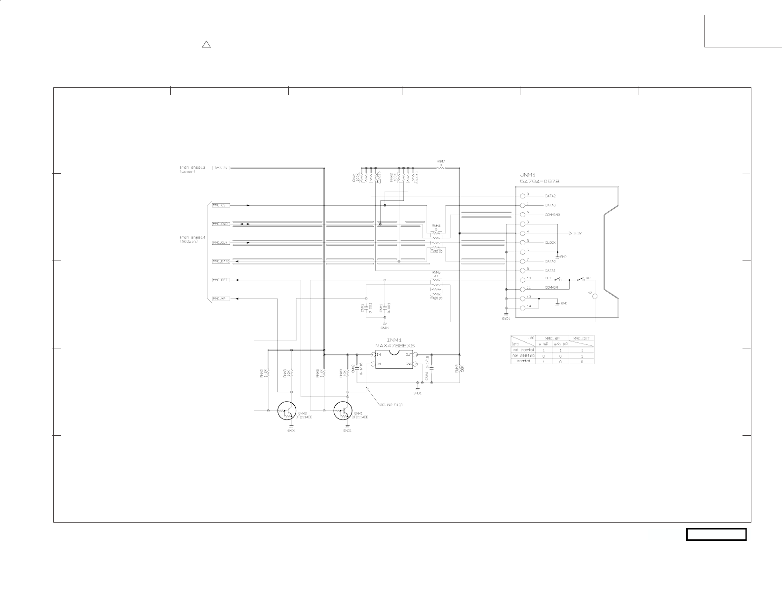
PRODUCT SAFETY NOTE: Components marked with a ! and shaded have special characteristics
important to safety. Before replacing any of these components, read carefully the PRODUCT SAFET
Y
NOTE of this Service Manual. Don't degrade the safety of the receiver through improper servicing.
x
All DC voltage to be measured with a tester (100 kȍ/V). Voltage taken on a complex color bar including a standard color bar signal.
x
Since this is a basic circuit diagram, the value of the parts is subject to be altered for improvement.
107
BASIC CIRCUIT DIAGRAM
1 234 56
A
B
C
D
E
DW1U
Subdigital 10 of 10
SD CARD
GI
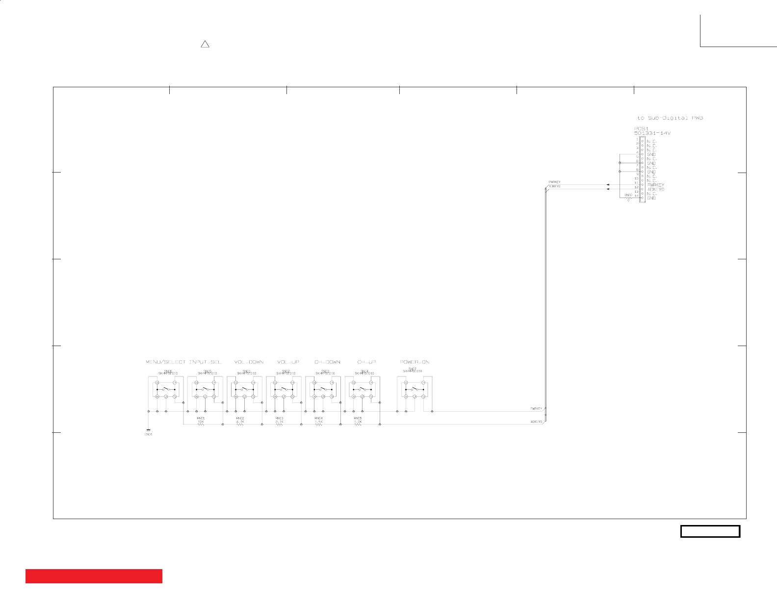
PRODUCT SAFETY NOTE: Components marked with a ! and shaded have special characteristics
important to safety. Before replacing any of these components, read carefully the PRODUCT SAFET
Y
NOTE of this Service Manual. Don't degrade the safety of the receiver through improper servicing.
x
All DC voltage to be measured with a tester (100 kȍ/V). Voltage taken on a complex color bar including a standard color bar signal.
x
Since this is a basic circuit diagram, the value of the parts is subject to be altered for improvement.
TABLE OF CONTENTS
108
BASIC CIRCUIT DIAGRAM DW1U
Terminal 1 of 9
1 234 56
A
B
C
D
E
CONTROL
GI
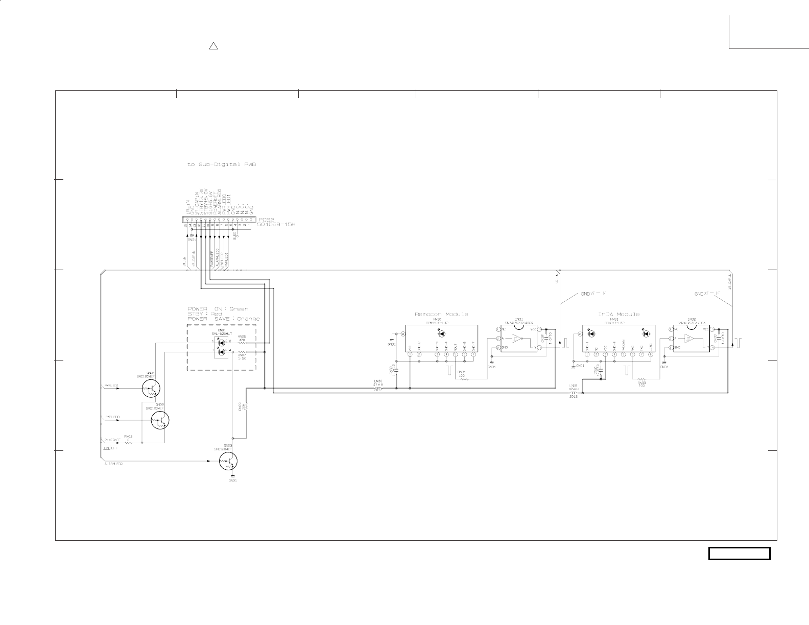
PRODUCT SAFETY NOTE: Components marked with a ! and shaded have special characteristics
important to safety. Before replacing any of these components, read carefully the PRODUCT SAFET
Y
NOTE of this Service Manual. Don't degrade the safety of the receiver through improper servicing.
x
All DC voltage to be measured with a tester (100 kȍ/V). Voltage taken on a complex color bar including a standard color bar signal.
x
Since this is a basic circuit diagram, the value of the parts is subject to be altered for improvement.
109
BASIC CIRCUIT DIAGRAM
1 234 56
A
B
C
D
E
DW1U
Terminal 2 of 9
LED
GI
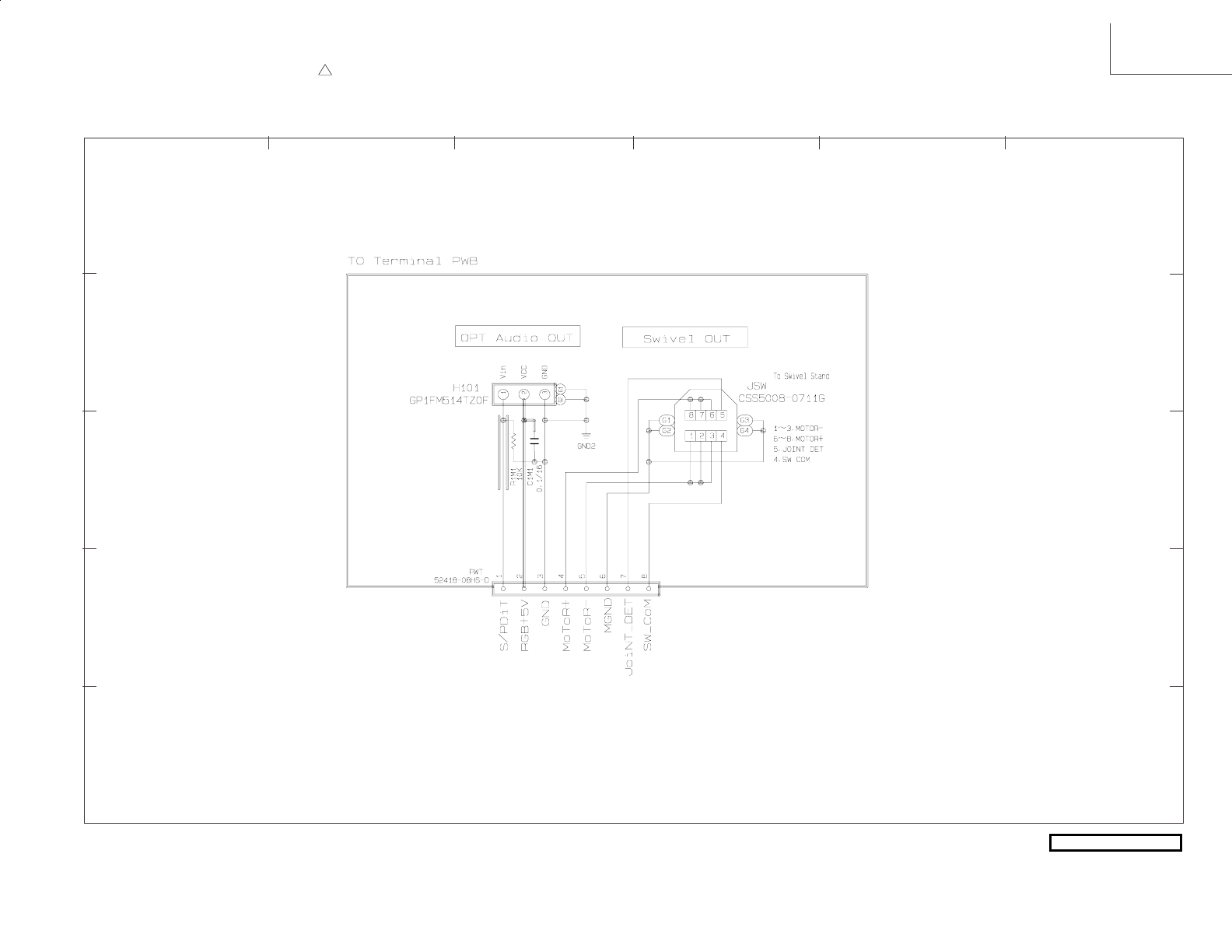
PRODUCT SAFETY NOTE: Components marked with a ! and shaded have special characteristics
important to safety. Before replacing any of these components, read carefully the PRODUCT SAFET
Y
x
All DC voltage to be measured with a tester (100 kȍ/V). Voltage taken on a complex color bar including a standard color bar signal.
x
Since this is a basic circuit diagram, the value of the parts is subject to be altered for improvement.
110
BASIC CIRCUIT DIAGRAM
NOTE of this Service Manual. Don't degrade the safety of the receiver through improper servicing.
OPT / SWIVEL
1 234 56
A
B
C
D
E
DW1U
Terminal 3 of 9
GI
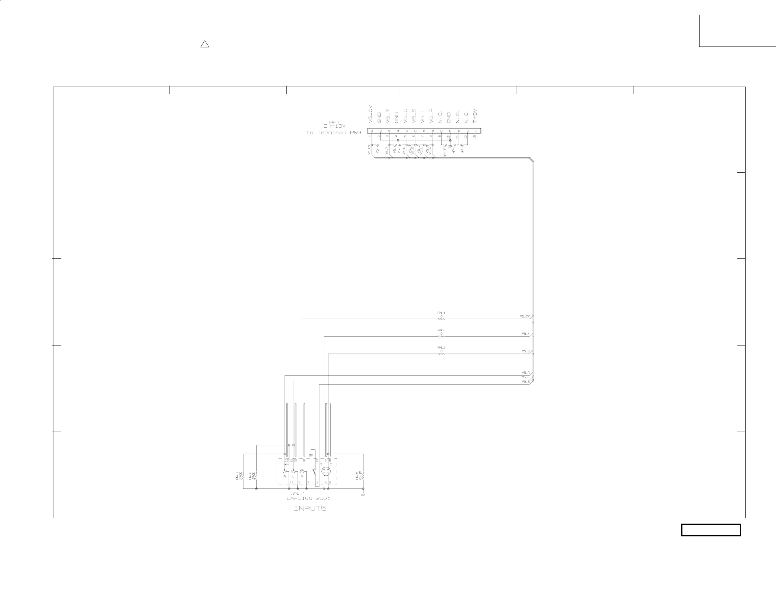
PRODUCT SAFETY NOTE: Components marked with a ! and shaded have special characteristics
important to safety. Before replacing any of these components, read carefully the PRODUCT SAFET
Y
NOTE of this Service Manual. Don't degrade the safety of the receiver through improper servicing.
x
All DC voltage to be measured with a tester (100 kȍ/V). Voltage taken on a complex color bar including a standard color bar signal.
x
Since this is a basic circuit diagram, the value of the parts is subject to be altered for improvement.
111
BASIC CIRCUIT DIAGRAM
1 234 56
A
B
C
D
E
SIDE TERMINAL
DW1U
Terminal 4 of 9
GI
PRODUCT SAFETY NOTE: Components marked with a ! and shaded have special characteristics
important to safety. Before replacing any of these components, read carefully the PRODUCT SAFET
Y
NOTE of this Service Manual. Don't degrade the safety of the receiver through improper servicing.
x
All DC voltage to be measured with a tester (100 kȍ/V). Voltage taken on a complex color bar including a standard color bar signal.
x
Since this is a basic circuit diagram, the value of the parts is subject to be altered for improvement.
112
BASIC CIRCUIT DIAGRAM
1 234 56
A
B
C
D
E
SW / FILTER
DW1U
Terminal 5 of 9
GI
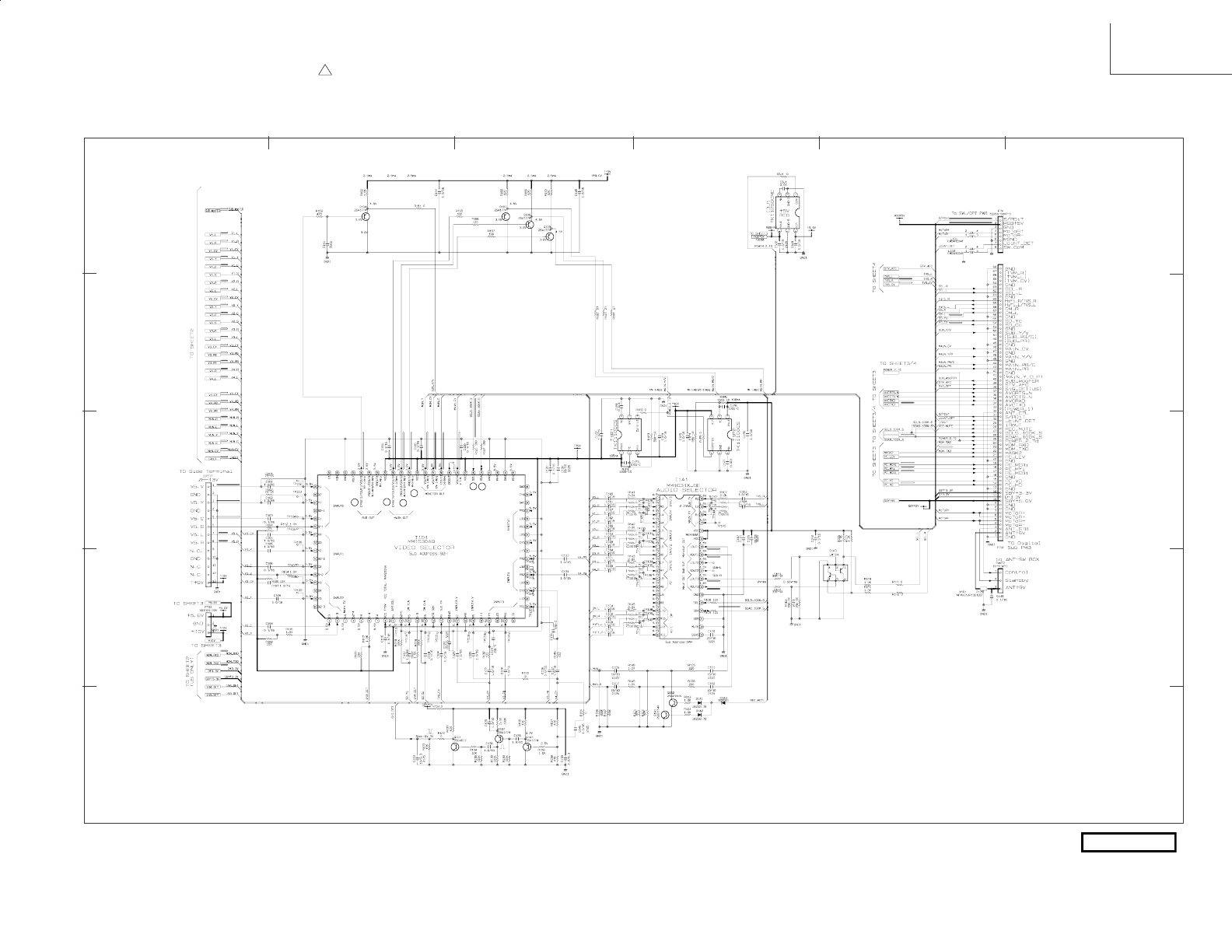
PRODUCT SAFETY NOTE: Components marked with a ! and shaded have special characteristics
important to safety. Before replacing any of these components, read carefully the PRODUCT SAFET
Y
NOTE of this Service Manual. Don't degrade the safety of the receiver through improper servicing.
x
All DC voltage to be measured with a tester (100 kȍ/V). Voltage taken on a complex color bar including a standard color bar signal.
x
Since this is a basic circuit diagram, the value of the parts is subject to be altered for improvement.
113
BASIC CIRCUIT DIAGRAM DW1U
Terminal 6 of 9
IF / SW / AMP
1 234 56
A
B
C
D
E
16
17
18
19
20
21
GI
PRODUCT SAFETY NOTE: Components marked with a ! and shaded have special characteristics
important to safety. Before replacing any of these components, read carefully the PRODUCT SAFET
Y
x
All DC voltage to be measured with a tester (100 kȍ/V). Voltage taken on a complex color bar including a standard color bar signal.
x
Since this is a basic circuit diagram, the value of the parts is subject to be altered for improvement.
114
BASIC CIRCUIT DIAGRAM
NOTE of this Service Manual. Don't degrade the safety of the receiver through improper servicing.
1 234 56
A
B
C
D
E
TERMINAL
DW1U
Terminal 7 of 9
GI
PRODUCT SAFETY NOTE: Components marked with a ! and shaded have special characteristics
important to safety. Before replacing any of these components, read carefully the PRODUCT SAFET
Y
NOTE of this Service Manual. Don't degrade the safety of the receiver through improper servicing.
x
All DC voltage to be measured with a tester (100 kȍ/V). Voltage taken on a complex color bar including a standard color bar signal.
x
Since this is a basic circuit diagram, the value of the parts is subject to be altered for improvement.
115
BASIC CIRCUIT DIAGRAM
1 234 56
A
B
C
D
E
RS232C IN
DW1U
Terminal 8 of 9
GI
PRODUCT SAFETY NOTE: Components marked with a ! and shaded have special characteristics
important to safety. Before replacing any of these components, read carefully the PRODUCT SAFET
Y
NOTE of this Service Manual. Don't degrade the safety of the receiver through improper servicing.
x
All DC voltage to be measured with a tester (100 kȍ/V). Voltage taken on a complex color bar including a standard color bar signal.
x
Since this is a basic circuit diagram, the value of the parts is subject to be altered for improvement.
116
BASIC CIRCUIT DIAGRAM DW1U
Terminal 9 of 9
TUNER
1 234 56
A
B
C
D
E
GI
PRINTED CIRCUIT BOARDS
DW1-U 55 SUBDIGITAL PWB (Component side)
DW1-U
1 2 3 4
A
B
C
D
TABLE OF CONTENTS
QS05 B-3
QS06 B-3
I401 C-2 QS08 B-3
I402 A-1 QS09 B-3
I403 C-2 QS10 A-3
I404 C-1 QS11 B-3
INM1 A-2 QS12 A-3
IP11 C-4 QS13 B-3
IP12 C-1 QS14 B-3
IP13 C-4 QS18 B-4
IP14 D-4 QS19 A-4
IPG1 D-3 QS20 A-4
IPK1 D-4 QS21 A-4
IS03 A-4 QS22 B-4
IS04 B-4 QS23 B-4
IS05 B-4 QS24 B-4
IT01 D-3 QS25 B-4
IT02 D-3 QS26 B-4
IT04 D-1 QT01 D-2
IT05 D-1 QT02 D-3
IT06 D-2 QT03 D-3
IT07 C-1 QW02 B-3
IV05 C-4
IW01 B-3
IW02 B-1
IW03 B-2 D401 C-2
IW04 B-2 D402 C-2
IW05 B-2 D403 C-2
IW06 B-2 D404 C-2
IW07 B-1 D405 C-2
IW08 B-3 D406 A-1
IW09 B-3 DP02 D-3
IW10 B-3 DP03 D-3
IW11 B-2 DP08 C-4
IW12 B-2 DP09 C-4
IW17 A-3 DP10 D-4
IW19 A-3 DP11 D-4
DP12 D-4
DPK2 D-4
DS01 B-3
Q401 C-2 DS02 B-3
Q402 A-1 DS03 B-3
Q403 A-1 DS04 A-3
Q404 A-1 DS05 A-3
Q405 C-2 DS06 A-3
Q406 C-2 DS07 A-3
QM05 B-3 DS08 A-3
QNM1 A-3 DS09 A-3
QNM2 A-3 DS10 B-4
QP01 D-3 DS13 B-4
QP05 C-4 DS15 B-4
QP06 C-4 DT01 D-3
QP07 C-4
QPK2 D-4
QP08 C-1
QP09 D-4 X401 C-2
QP10 D-3 XS01 B-4
QPK1 D-4 XS02 B-4
QPK2 D-4 XT01 D-1
QS01 B-3 XT02 D-1
QS02 B-3 XT03 C-1
QS03 B-3 XT06 D-2
QS04 B-3 XT07 D-2
CRYSTAL
DIODE
IC
TRANSISTOR
DW1-U SUBDIGITAL PWB SEMICONDUCTOR LOCATION
(Component side)
TABLE OF CONTENTS 117
GI
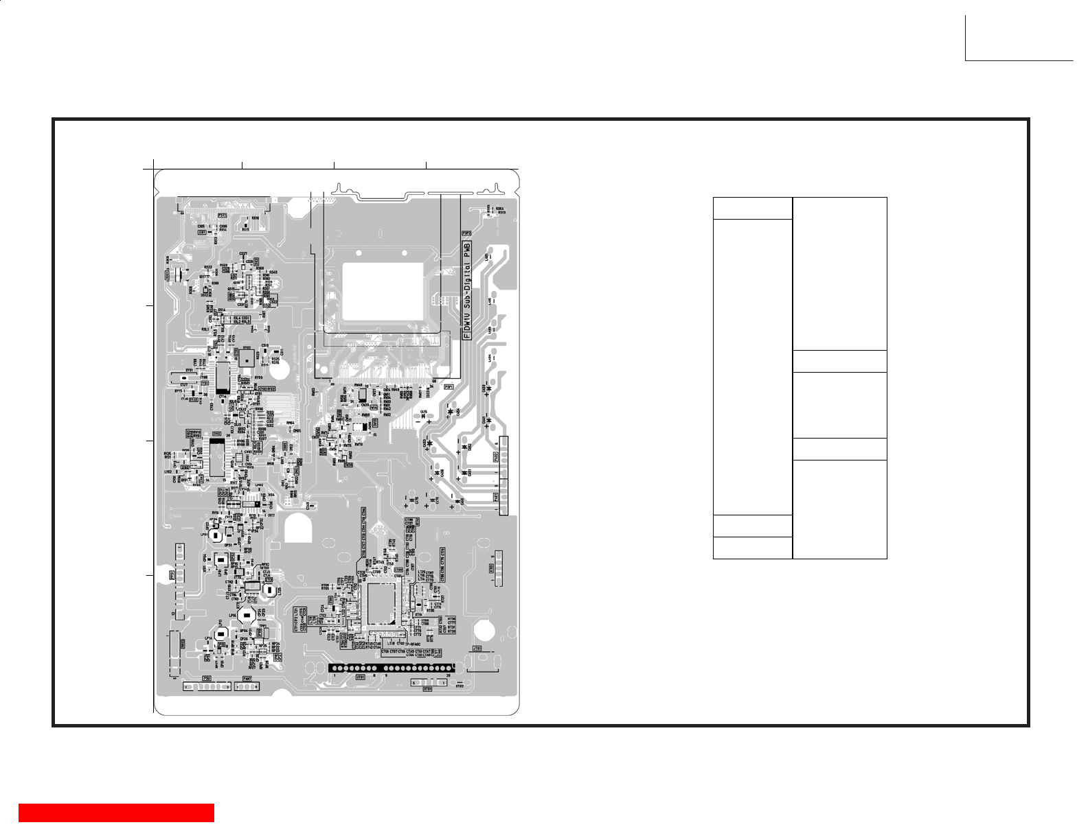
QS15 A-1
IM02 C-2 QS16 A-1
IM03 C-2 QS17 A-1
IP02 C-1 QS27 B-1
IP05 D-2 QV01 C-1
IP15 D-1 QV02 C-1
IPS1 C-1 QW01 B-3
IS02 A-1 QX01 B-2
IT08 D-3 QX02 B-2
IT09 D-2 QX03 B-2
IT13 D-2 QY01 B-2
IV01 C-1 QY02 B-1
IV02 C-1
IV03 C-1
IV04 C-2
IW13 B-3 DP01 C-1
IW14 B-3 DPS1 C-1
IW15 B-2 DPS2 C-1
IW16 B-3 DS12 A-1
IW18 B-3 DS14 B-1
IW20 C-3
IX01 A-1
IXJ1 B-1
IY01 B-1 XP01 C-1
IY02 B-1 XP04 D-1
IY03 B-1 XPS1 C-1
IYJ2 B-1 XT04 D-3
XT05 D-1
XV01 C-1
XY01 B-1
QM04 C-2 XY02 B-2
CRYSTAL
DIODE
IC
TRANSISTOR
PRINTED CIRCUIT BOARDS
DW1-U 55 SUBDIGITAL PWB (Solder side)
DW1-U
DW1-U SUBDIGITAL PWB SEMICONDUCTOR LOCATION
(Solder side)
1 2 3 4
A
B
C
D
TABLE OF CONTENTS 118
GI
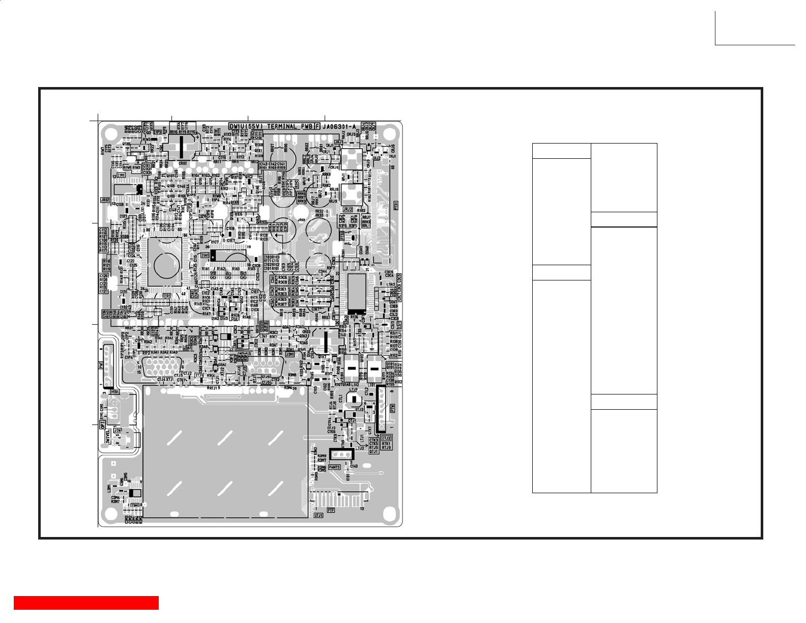
1 2 3 4
A
B
C
D
PRINTED CIRCUIT BOARDS
DW1-U 55 TERMINAL PWB (Component side)
DW1-U
Q3A3 C-3
I101 B-1 Q3A4 B-3
I1A1 B-2 Q3A5 B-3
I1M1 A-1 Q3A6 B-3
I1P1 C-1 QRJ1 A-4
I1P2 A-2 QRJ2 A-3
I1P3 A-1 QRJ3 A-3
I3A1 C-2 QTJ1 D-4
I3A2 B-4
I3J1 C-4
I3M1 D-1 D101 C-4
IRJ1 A-4 D1A1 B-2
IRJ2 A-4 D1A2 B-2
ITJ1 C-2 D1A3 B-2
ITJ2 C-4 D1A4 C-3
D1A5 C-3
D1A6 C-4
Q101 C-4 D3A1 C-2
Q102 C-4 D3A2 C-2
Q103 C-4 D3A3 C-2
Q104 A-2 D3A4 C-2
Q105 A-2 D3A5 C-2
Q106 A-2 D3A6 C-2
Q107 A-1 D3A7 B-4
Q108 A-1 D3A8 B-4
Q109 A-1 D3A9 B-4
Q1A1 B-2 DRJ1 A-4
Q1A2 B-2 DRJ2 A-4
Q1A3 A-3 DRJ3 A-4
Q1A6 A-3 DTJ1 C-4
Q1A7 C-4 DTJ2 C-4
Q1A8 C-4 DTJ3 C-4
Q1C2 A-2
Q1X1 A-2
Q1X2 A-2 X101 D-4
Q1X3 A-2 X3A1 C-1
Q1X4 A-2 X3A2 C-1
Q1X5 A-1 X3A3 C-1
Q1X6 A-1 X3A4 C-2
Q1X7 A-2 X3A5 C-2
Q1X8 A-2 X3A6 C-2
Q1X9 A-2 X3A7 C-2
Q3A1 C-3 XTJ1 C-1
Q3A2 C-3 XTJ2 C-2
XTJ3 C-2
TRANSISTOR
DIODE
IC
CRYSTAL & FILTER
DW1-U TERMINAL PWB SEMICONDUCTOR LOCATION
(Component side)
TABLE OF CONTENTS 119
GI
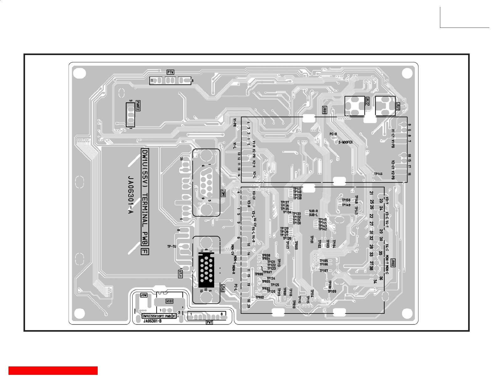
PRINTED CIRCUIT BOARDS
DW1-U 55 TERMINAL PWB (Solder side)
DW1-U
PRINTED CIRCUIT BOARDS DW1-U
TABLE OF CONTENTS 120
GI
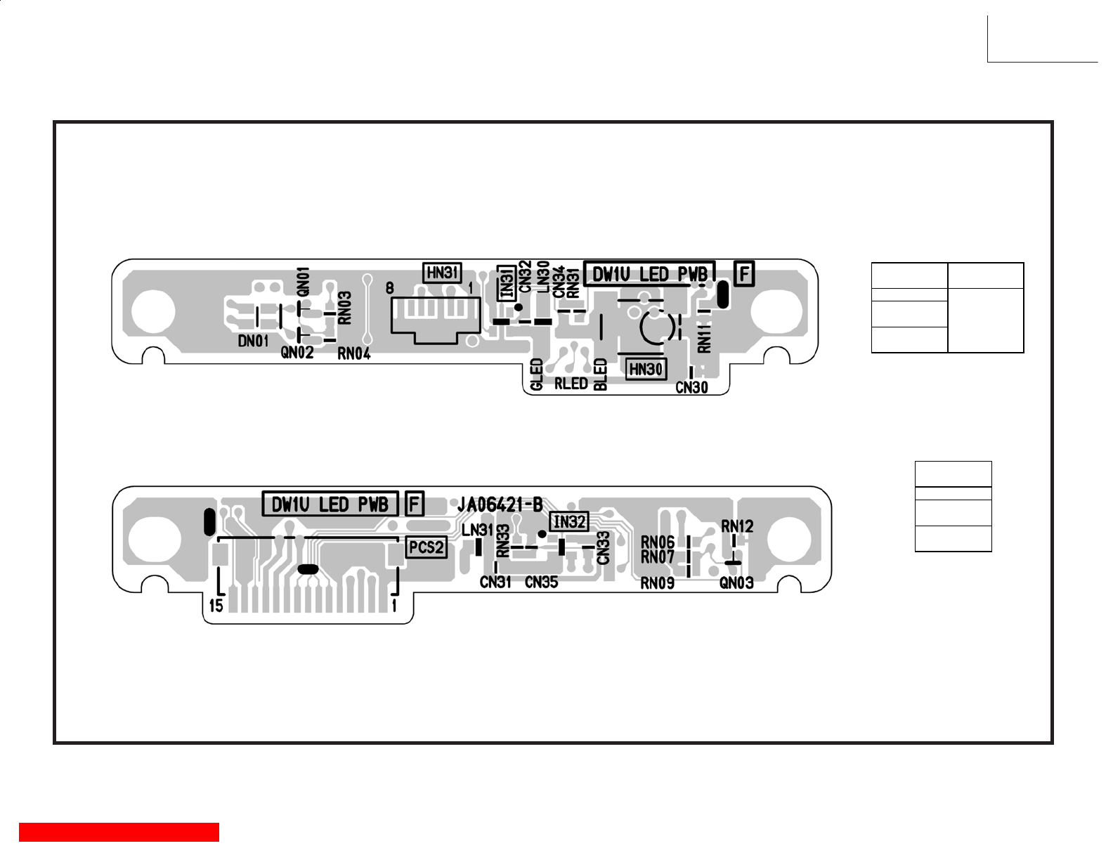
PRINTED CIRCUIT BOARDS
DW1-U 55 LED PWB
DW1-U
Component side
Solder side
(Component side)
(Solder side)
HN31
DN01
HN30
IC DIODE
TRANSISTOR
IN31
QN01
QN02
QN03
TRANSISTOR
IC
IN32
TABLE OF CONTENTS 121
GI
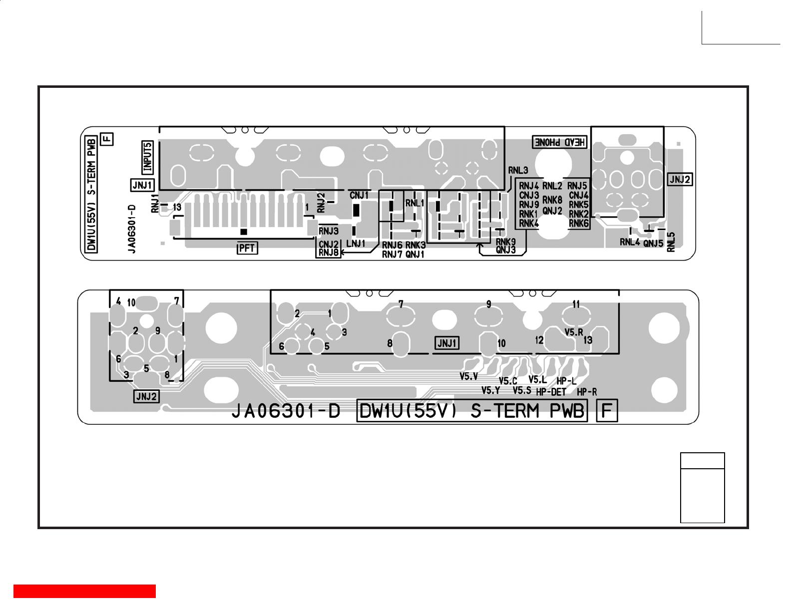
PRINTED CIRCUIT BOARDS
DW1-U 55 SIDE TERMINALPWB
DW1-U
QNJ1
QNJ2
QNJ3
QNJ5
TRANSISTOR
Component side
(Component side)
(Solder side)
TABLE OF CONTENTS 122
GI
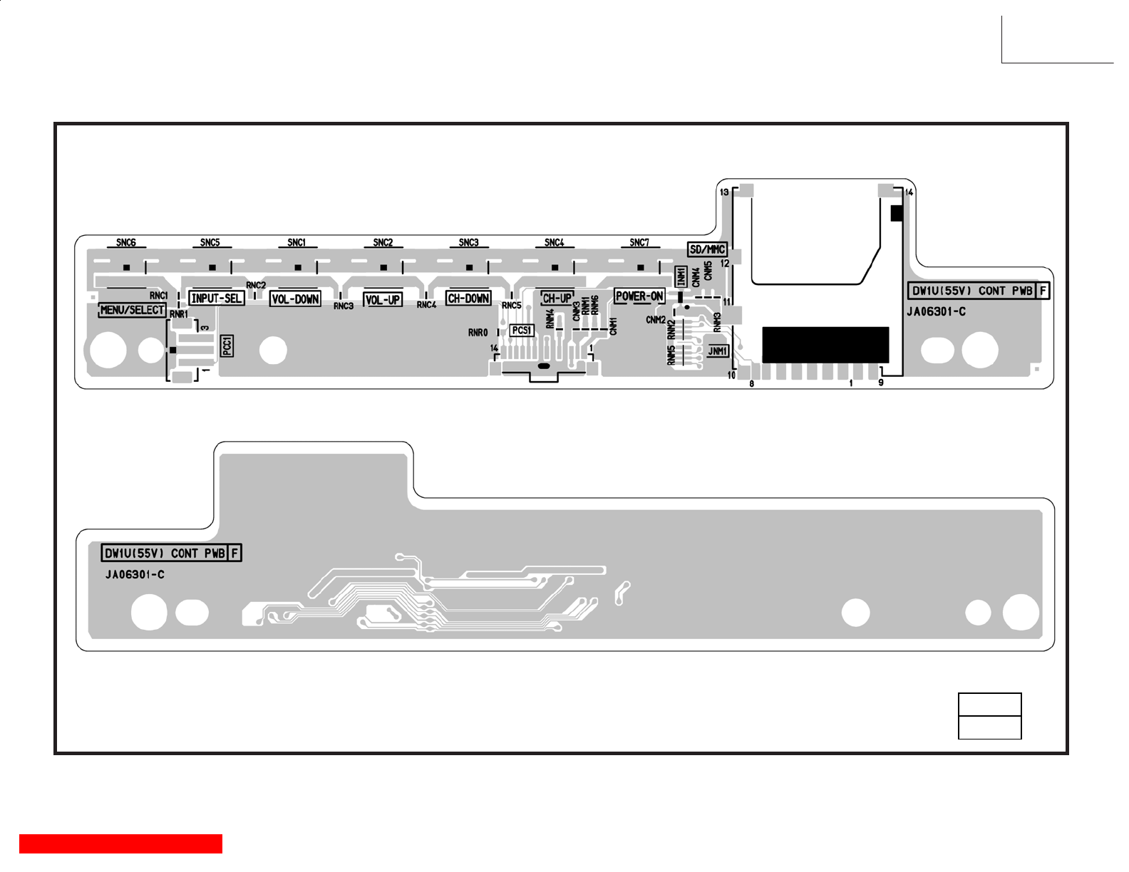
PRINTED CIRCUIT BOARDS
DW1-U CONTROLPWB
DW1-U
(Component side)
INM1
IC
Component side
(Solder side)
TABLE OF CONTENTS 123
GI
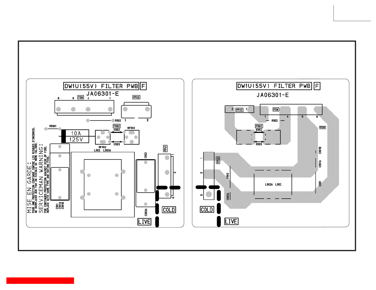
PRINTED CIRCUIT BOARDS
DW1-U FILTER PWB
DW1-U
(Component side) (Solder side)
TABLE OF CONTENTS 124
GI
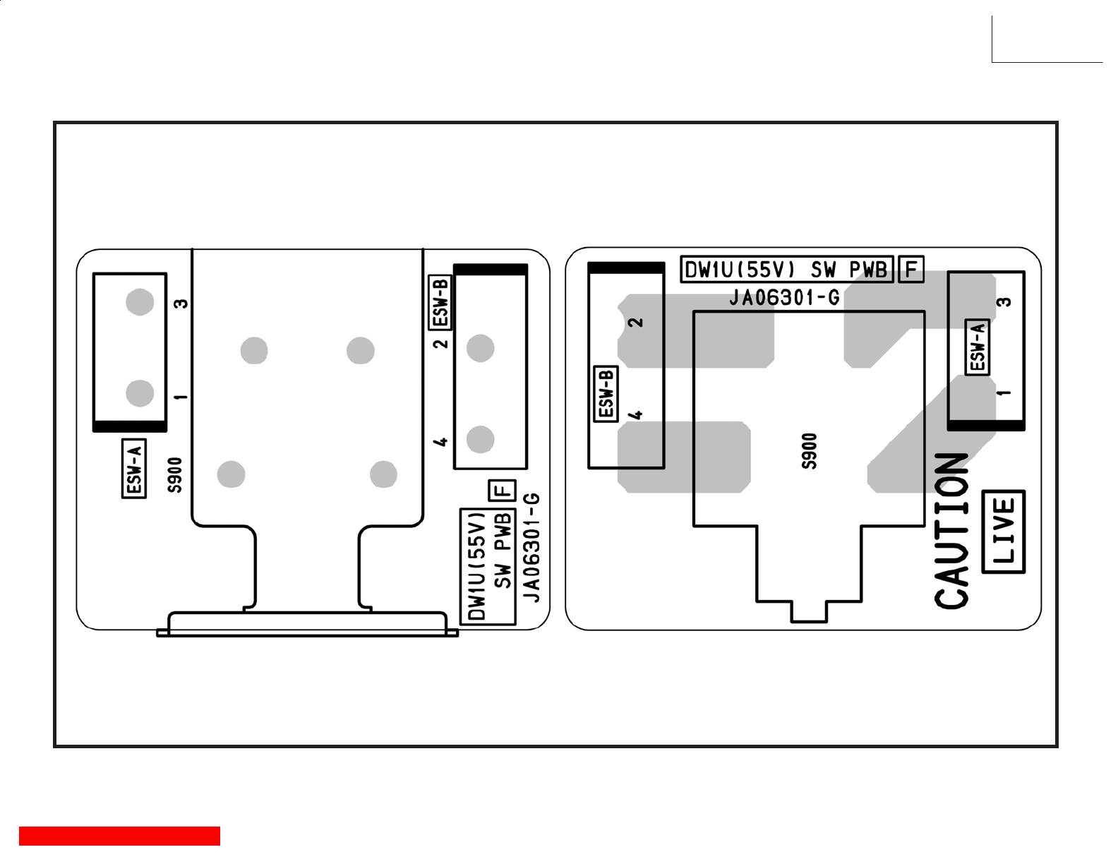
PRINTED CIRCUIT BOARDS
DW1-U SWITCH PWB
DW1-U
(Component side) (Solder side)
TABLE OF CONTENTS 125
GI
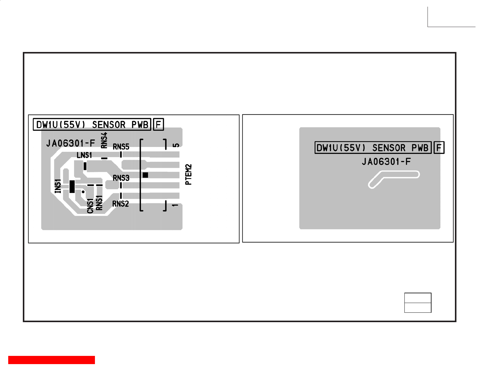
PRINTED CIRCUIT BOARDS
DW1-U SWITCH PWB
DW1-U
(Component side) (Solder side)
INS1
IC
Component side
TABLE OF CONTENTS 126
GI
REPLACEMENT PARTS LIST
PRODUCT SERVICE NOTE: Components marked with a have special characteristics important to safety. Before replacing any
of these components, read carefully, the PRODUCT SAFETY NOTICE of this Service Manual. Don’t degrade the safety of the
receiver through improper servicing.
Capacitors: Resistors: Semiconductors:
AL: Aluminum Electrolytic CF: Carbon Film TR: Transistor
CD: Ceramic Disc CC: Carbon Composition DI: Diode
EL: Electrolitic MF: Metal Oxide ZD: Zener Diode
PF: Polyester Film VR: Variable Resistor VA: Varistor
PP: Polypropylene WW: Wire Wound TH: Termistor
PL: Plastic FR: Fuse Resistor IC: Integrated Circuit
TA: Tantalum MG: Metal Grazed
PR: Paper
TM: Trimmer
MC: Mylar
ABBREVIATIONS
DW1U
127
TABLE OF CONTENTS
SYMBOL PART No. DESCRIPTION SYMBOL PART No. DESCRIPTION
C438 AA00716R CHIP-CERAMIC 1.0UF-25V-B-3216
SUBDIGITAL PWB C439 AA00716R CHIP-CERAMIC 1.0UF-25V-B-3216
C440 AA00716R CHIP-CERAMIC 1.0UF-25V-B-3216
CAPACITORS C441 0893222R CAP 1608CHIP10000PFKB 50V TAPE
C401 0893222R CAP 1608CHIP10000PFKB 50V TAPE C442 0893222R CAP 1608CHIP10000PFKB 50V TAPE
C402 0893222R CAP 1608CHIP10000PFKB 50V TAPE C443 0893222R CAP 1608CHIP10000PFKB 50V TAPE
C403 0893179R CAP.CHIP-CERAMIC 100000PF 16V TAPE C444 0893222R CAP 1608CHIP10000PFKB 50V TAPE
C404 0893179R CAP.CHIP-CERAMIC 100000PF 16V TAPE C445 0893222R CAP 1608CHIP10000PFKB 50V TAPE
C405 0893179R CAP.CHIP-CERAMIC 100000PF 16V TAPE C446 0893222R CAP 1608CHIP10000PFKB 50V TAPE
C406 0893179R CAP.CHIP-CERAMIC 100000PF 16V TAPE C447 0893222R CAP 1608CHIP10000PFKB 50V TAPE
C407 0893179R CAP.CHIP-CERAMIC 100000PF 16V TAPE C448 0893222R CAP 1608CHIP10000PFKB 50V TAPE
C408 0893179R CAP.CHIP-CERAMIC 100000PF 16V TAPE C449 AL01858R 1000UF 25V ALUMINIUM ELECTROLYTIC CAPACITOR
C409 AA00968R CCC106M06-B-20CT (10UF 6.3V 2012M) C450 AL01858R 1000UF 25V ALUMINIUM ELECTROLYTIC CAPACITOR
C410 AA01111R CERAMIC CAPACITOR(1.0UF 6.3V) C451 AL01857R 470UF 25V ALUMINIUM ELECTROLYTIC CAPACITOR
C411 AA00968R CCC106M06-B-20CT (10UF 6.3V 2012M) C452 AL01857R 470UF 25V ALUMINIUM ELECTROLYTIC CAPACITOR
C412 0893179R CAP.CHIP-CERAMIC 100000PF 16V TAPE C453 AL01858R 1000UF 25V ALUMINIUM ELECTROLYTIC CAPACITOR
C413 0893179R CAP.CHIP-CERAMIC 100000PF 16V TAPE C454 AL01858R 1000UF 25V ALUMINIUM ELECTROLYTIC CAPACITOR
C414 AA00754R CAP.CHIP3216-B-47UF6.3V C455 AL01857R 470UF 25V ALUMINIUM ELECTROLYTIC CAPACITOR
C415 AL01865R 470UF 35V ALUMINIUM ELECTROLYTIC CAPACITOR C456 AL01857R 470UF 25V ALUMINIUM ELECTROLYTIC CAPACITOR
C417 0893179R CAP.CHIP-CERAMIC 100000PF 16V TAPE C457 0893197R CAP 1608CHIP 22000PFKB 25V TAPE
C418 0893179R CAP.CHIP-CERAMIC 100000PF 16V TAPE C458 0893208R CAP 1608CHIP 1000PFKB 50V TAPE
C419 AA00968R CCC106M06-B-20CT (10UF 6.3V 2012M) C459 AA00421R CERAMIC CAPACITOR(10UF 16V)
C420 0893179R CAP.CHIP-CERAMIC 100000PF 16V TAPE C460 AA00421R CERAMIC CAPACITOR(10UF 16V)
C421 AA01132R CERAMIC CAPACITOR(0.22UF 6.3V) C461 0893199R CAP 1608CHIP 220PFKB 50V TAPE
C422 AA00968R CCC106M06-B-20CT (10UF 6.3V 2012M) C462 0893199R CAP 1608CHIP 220PFKB 50V TAPE
C423 AA01144R CERAMIC CAP. 1608-B 1.0UF 16V C463 AA00422R CERAMIC CAPACITOR(10UF 16V)
C424 0893179R CAP.CHIP-CERAMIC 100000PF 16V TAPE C464 AA00991R CERAMIC CAPACITOR(0.1UF 50V-B)
C425 0893179R CAP.CHIP-CERAMIC 100000PF 16V TAPE C465 AA00421R CERAMIC CAPACITOR(10UF 16V)
C426 AA01144R CERAMIC CAP. 1608-B 1.0UF 16V C466 0893179R CAP.CHIP-CERAMIC 100000PF 16V TAPE
C427 AA00991R CERAMIC CAPACITOR(0.1UF 50V-B) C468 0893222R CAP 1608CHIP10000PFKB 50V TAPE
C428 AA01348R CERAMIC CAP. 1608-X5R 0.22UF 2 C470 AA01348R CERAMIC CAP. 1608-X5R 0.22UF 2
C429 AA01348R CERAMIC CAP. 1608-X5R 0.22UF 2 C471 AA01348R CERAMIC CAP. 1608-X5R 0.22UF 2
C430 AA01348R CERAMIC CAP. 1608-X5R 0.22UF 2 C472 AA01348R CERAMIC CAP. 1608-X5R 0.22UF 2
C431 AA01348R CERAMIC CAP. 1608-X5R 0.22UF 2 C473 AA01348R CERAMIC CAP. 1608-X5R 0.22UF 2
C432 AA00991R CERAMIC CAPACITOR(0.1UF 50V-B) C474 AA01113R CCC225K06-B-16CT
C433 0893051R CAP2125CHIP 33000PFKB 50V TAPE C475 0800336R CAP.-ELECTRO. 220UF-M(SMG) 25V
C434 0893051R CAP2125CHIP 33000PFKB 50V TAPE C476 0800336R CAP.-ELECTRO. 220UF-M(SMG) 25V
C435 AA00716R CHIP-CERAMIC 1.0UF-25V-B-3216 C480 0893197R CAP 1608CHIP 22000PFKB 25V TAPE
C436 0893051R CAP2125CHIP 33000PFKB 50V TAPE C481 0893222R CAP 1608CHIP10000PFKB 50V TAPE
C437 0893051R CAP2125CHIP 33000PFKB 50V TAPE C482* 0893179R CAP.CHIP-CERAMIC 100000PF 16V TAPE
* with #B*
GI
PRODUCT SERVICE NOTE: Components marked with a have special characteristics important to safety. Before replacing any
of these components, read carefully, the PRODUCT SAFETY NOTICE of this Service Manual. Don’t degrade the safety of the
receiver through improper servicing.
DW1U
128
SYMBOL PART # DESCRIPTION SYMBOL PART # DESCRIPTION
CM01 0893179R CAP.CHIP-CERAMIC 100000PF 16V TAPE CS35 0893179R CAP.CHIP-CERAMIC 100000PF 16V TAPE
CM02 0893179R CAP.CHIP-CERAMIC 100000PF 16V TAPE CS36 0893179R CAP.CHIP-CERAMIC 100000PF 16V TAPE
CM03 0893179R CAP.CHIP-CERAMIC 100000PF 16V TAPE CS37 AA00969R CAP.CHIP2125-B-22UF6.3V
CM04 0893179R CAP.CHIP-CERAMIC 100000PF 16V TAPE CS38 AA01144R CERAMIC CAP. 1608-B 1.0UF 16V
CM05 0893179R CAP.CHIP-CERAMIC 100000PF 16V TAPE CS39 0893193R CAP 1608CHIP 10000PFKB 25V TAPE
CM11 0893179R CAP.CHIP-CERAMIC 100000PF 16V TAPE CS40 AA00969R CAP.CHIP2125-B-22UF6.3V
CM12 0893179R CAP.CHIP-CERAMIC 100000PF 16V TAPE CS41 0893122R CAP 1608CHIP 47PFJCH 50V TAPE
CN30 AA01123R CCC105K10-B-16CT CS42 0893179R CAP.CHIP-CERAMIC 100000PF 16V TAPE
CN31 AA01123R CCC105K10-B-16CT CS44 0893122R CAP 1608CHIP 47PFJCH 50V TAPE
CN32 AA01123R CCC105K10-B-16CT CS45 0893179R CAP.CHIP-CERAMIC 100000PF 16V TAPE
CN33 AA01123R CCC105K10-B-16CT CS46 0893122R CAP 1608CHIP 47PFJCH 50V TAPE
CNM1 0893208R CAP 1608CHIP 1000PFKB 50V TAPE CS48 0893179R CAP.CHIP-CERAMIC 100000PF 16V TAPE
CNM2 0893179R CAP.CHIP-CERAMIC 100000PF 16V TAPE CS49 AA00969R CAP.CHIP2125-B-22UF6.3V
CNM3 0893208R CAP 1608CHIP 1000PFKB 50V TAPE CS50 0893179R CAP.CHIP-CERAMIC 100000PF 16V TAPE
CNM4 0893179R CAP.CHIP-CERAMIC 100000PF 16V TAPE CT01 AA01144R CERAMIC CAP. 1608-B 1.0UF 16V
CP06 AA01123R CCC105K10-B-16CT CT02 AA01111R CERAMIC CAPACITOR(1.0UF 6.3V)
CP07 0893179R CAP.CHIP-CERAMIC 100000PF 16V TAPE CT03 AA01144R CERAMIC CAP. 1608-B 1.0UF 16V
CP08 0893211R CAP 1608CHIP 1500PFKB 50V TAPE CT04 AA01111R CERAMIC CAPACITOR(1.0UF 6.3V)
CP09 0893127R CAP 1608CHIP 120PFJCH 50V TAPE CT05 AA01173R CCC1R0K50-B-32CT 1UF/50V-B-3225
CP10 0893193R CAP 1608CHIP 10000PFKB 25V TAPE CT06 AA00937R CAP.CHIP-CERAMIC 10UF 10V 2012BK
CP11 0893127R CAP 1608CHIP 120PFJCH 50V TAPE CT07 AA01144R CERAMIC CAP. 1608-B 1.0UF 16V
CP12 0893222R CAP 1608CHIP10000PFKB 50V TAPE CT08 AA00937R CAP.CHIP-CERAMIC 10UF 10V 2012BK
CP20 AA00937R CAP.CHIP-CERAMIC 10UF 10V 2012BK CT09 AA00937R CAP.CHIP-CERAMIC 10UF 10V 2012BK
CP21 0893179R CAP.CHIP-CERAMIC 100000PF 16V TAPE CT10 0893179R CAP.CHIP-CERAMIC 100000PF 16V TAPE
CP22 0893179R CAP.CHIP-CERAMIC 100000PF 16V TAPE CT11 AA01802R CCC103K50-B-16CT MCH18
CP23 AA00969R CAP.CHIP2125-B-22UF6.3V CT12 AA00937R CAP.CHIP-CERAMIC 10UF 10V 2012BK
CP24 AA00969R CAP.CHIP2125-B-22UF6.3V CT13 0893208R CAP 1608CHIP 1000PFKB 50V TAPE
CP25 0893126R CAP 1608CHIP 100PFJCH 50V TAPE CT14 0893222R CAP 1608CHIP10000PFKB 50V TAPE
CP26 0893208R CAP 1608CHIP 1000PFKB 50V TAPE CT15 0893179R CAP.CHIP-CERAMIC 100000PF 16V TAPE
CP27 0893193R CAP 1608CHIP 10000PFKB 25V TAPE CT16 AA00937R CAP.CHIP-CERAMIC 10UF 10V 2012BK
CP53 AA01185R CAP.CHIP-CERAMIC 22UF/16V B 32 CT17 AA00937R CAP.CHIP-CERAMIC 10UF 10V 2012BK
CP54 AA01185R CAP.CHIP-CERAMIC 22UF/16V B 32 CT22 0893179R CAP.CHIP-CERAMIC 100000PF 16V TAPE
CP55 0893179R CAP.CHIP-CERAMIC 100000PF 16V TAPE CT23 0893208R CAP 1608CHIP 1000PFKB 50V TAPE
CP56 0893222R CAP 1608CHIP10000PFKB 50V TAPE CT24 AA01111R CERAMIC CAPACITOR(1.0UF 6.3V)
CP57 0893222R CAP 1608CHIP10000PFKB 50V TAPE CT25 AA00937R CAP.CHIP-CERAMIC 10UF 10V 2012BK
CP58 AA00699R CAP.CHIP-CERAMIC 10UFK 16V B 3 CT26 0893222R CAP 1608CHIP10000PFKB 50V TAPE
CP59 AA00968R CCC106M06-B-20CT (10UF 6.3V 2012M) CT27 0893222R CAP 1608CHIP10000PFKB 50V TAPE
CP63 AA01123R CCC105K10-B-16CT CT28 0893123R CAP 1608CHIP 56PFJCH 50V TAPE
CP64 0893193R CAP 1608CHIP 10000PFKB 25V TAPE CT29 0893124R CAP 1608CHIP 68PFJCH 50V TAPE
CP65 0893126R CAP 1608CHIP 100PFJCH 50V TAPE CT30 0893115R CAP 1608CHIP 15PFJCH 50V TAPE
CP66 AA00969R CAP.CHIP2125-B-22UF6.3V CT31 0893179R CAP.CHIP-CERAMIC 100000PF 16V TAPE
CP73 AA00955R CAP.CHIP-CERAMIC 2125 B 4.7UF CT32 0893222R CAP 1608CHIP10000PFKB 50V TAPE
CP74 AA00955R CAP.CHIP-CERAMIC 2125 B 4.7UF CT33 AA00937R CAP.CHIP-CERAMIC 10UF 10V 2012BK
CP75 AA00699R CAP.CHIP-CERAMIC 10UFK 16V B 3 CT34 0893179R CAP.CHIP-CERAMIC 100000PF 16V TAPE
CP79 AA00955R CAP.CHIP-CERAMIC 2125 B 4.7UF CT35 0893179R CAP.CHIP-CERAMIC 100000PF 16V TAPE
CP81 AA01121R CERAMIC CAPACITOR(0.47UF 10V) CT36 0893222R CAP 1608CHIP10000PFKB 50V TAPE
CPG1 0893179R CAP.CHIP-CERAMIC 100000PF 16V TAPE CT39 0893222R CAP 1608CHIP10000PFKB 50V TAPE
CPG2 0893215R CAP 1608CHIP 3300PFKB 50V TAPE CT40 0893222R CAP 1608CHIP10000PFKB 50V TAPE
CPS1 0893126R CAP 1608CHIP 100PFJCH 50V TAPE CT41 AA00937R CAP.CHIP-CERAMIC 10UF 10V 2012BK
CPS2 0893213R CAP1608CHIP 2200PFKB 50V TAPE CT42 0893179R CAP.CHIP-CERAMIC 100000PF 16V TAPE
CPS3 AA00955R CAP.CHIP-CERAMIC 2125 B 4.7UF CT43 0893222R CAP 1608CHIP10000PFKB 50V TAPE
CPS4 0893179R CAP.CHIP-CERAMIC 100000PF 16V TAPE CT44 0893123R CAP 1608CHIP 56PFJCH 50V TAPE
CPS5 AA00955R CAP.CHIP-CERAMIC 2125 B 4.7UF CT45 0893125R CAP 1608CHIP 82PFJCH 50V TAPE
CS02 AA01144R CERAMIC CAP. 1608-B 1.0UF 16V CT46 0893125R CAP 1608CHIP 82PFJCH 50V TAPE
CS04 AA01144R CERAMIC CAP. 1608-B 1.0UF 16V CT47 0893115R CAP 1608CHIP 15PFJCH 50V TAPE
CS06 AA01126R CERAMIC CAPACITOR(0.22UF 10V) CT48 0893106R CAP 1608CHIP 4PFCCK 50V TAPE
CS09 0893208R CAP 1608CHIP 1000PFKB 50V TAPE CT49 0893121R CAP 1608CHIP 39PFJCH 50V TAPE
CS11 AA01185R CAP.CHIP-CERAMIC 22UF/16V B 32 CT51 0893125R CAP 1608CHIP 82PFJCH 50V TAPE
CS12 0893197R CAP 1608CHIP 22000PFKB 25V TAPE CT52 0893119R CAP 1608CHIP 33PFJCH 50V TAPE
CS13 AA01123R CCC105K10-B-16CT CT53 0893106R CAP 1608CHIP 4PFCCK 50V TAPE
CS16 0893179R CAP.CHIP-CERAMIC 100000PF 16V TAPE CT54 0893124R CAP 1608CHIP 68PFJCH 50V TAPE
CS17 0893193R CAP 1608CHIP 10000PFKB 25V TAPE CT58 AA00968R CCC106M06-B-20CT (10UF 6.3V 2012M)
CS18 AA01185R CAP.CHIP-CERAMIC 22UF/16V B 32 CT60 0893179R CAP.CHIP-CERAMIC 100000PF 16V TAPE
CS19 0893193R CAP 1608CHIP 10000PFKB 25V TAPE CT61 0893222R CAP 1608CHIP10000PFKB 50V TAPE
CS20 0893219R CAP 1608CHIP 6800PFKB 50V TAPE CT62 0893179R CAP.CHIP-CERAMIC 100000PF 16V TAPE
CS21 0893179R CAP.CHIP-CERAMIC 100000PF 16V TAPE CT63 0893179R CAP.CHIP-CERAMIC 100000PF 16V TAPE
CS23 0893193R CAP 1608CHIP 10000PFKB 25V TAPE CT64 0893179R CAP.CHIP-CERAMIC 100000PF 16V TAPE
CS24 0893179R CAP.CHIP-CERAMIC 100000PF 16V TAPE CT65 0893179R CAP.CHIP-CERAMIC 100000PF 16V TAPE
CS25 0893205R CAP 1608CHIP 560PFKB 50V TAPE CT66 0893222R CAP 1608CHIP10000PFKB 50V TAPE
CS26 0893193R CAP 1608CHIP 10000PFKB 25V TAPE CT67 0893179R CAP.CHIP-CERAMIC 100000PF 16V TAPE
CS28 0893179R CAP.CHIP-CERAMIC 100000PF 16V TAPE CT68 0893179R CAP.CHIP-CERAMIC 100000PF 16V TAPE
CS31 0893193R CAP 1608CHIP 10000PFKB 25V TAPE CT69 0893179R CAP.CHIP-CERAMIC 100000PF 16V TAPE
CS32 0225037R CAP 1608CHIP 20PFJCH 50V TAPE CT70 0893179R CAP.CHIP-CERAMIC 100000PF 16V TAPE
CS33 0225037R CAP 1608CHIP 20PFJCH 50V TAPE CT71 0893208R CAP 1608CHIP 1000PFKB 50V TAPE
CS34 0893179R CAP.CHIP-CERAMIC 100000PF 16V TAPE CT72 AA01111R CERAMIC CAPACITOR(1.0UF 6.3V)
GI

DW1U
129
SYMBOL PART # DESCRIPTION SYMBOL PART # DESCRIPTION
CT73 AA01111R CERAMIC CAPACITOR(1.0UF 6.3V) CTH3 AA01231R 0.1UF 16V 1005-B CERAMIC CAPAC
CT74 0893208R CAP 1608CHIP 1000PFKB 50V TAPE CTH4 AA01231R 0.1UF 16V 1005-B CERAMIC CAPAC
CT75 0893126R CAP 1608CHIP 100PFJCH 50V TAPE CTH5 AA01231R 0.1UF 16V 1005-B CERAMIC CAPAC
CT76 AA01231R 0.1UF 16V 1005-B CERAMIC CAPAC CTH6 AA01144R CERAMIC CAP. 1608-B 1.0UF 16V
CT77 0893179R CAP.CHIP-CERAMIC 100000PF 16V TAPE CTH9 0893179R CAP.CHIP-CERAMIC 100000PF 16V TAPE
CT78 AA01111R CERAMIC CAPACITOR(1.0UF 6.3V) CTJ2 AA00937R CAP.CHIP-CERAMIC 10UF 10V 2012BK
CT79 AA01231R 0.1UF 16V 1005-B CERAMIC CAPAC CTJ3 AA00969R CAP.CHIP2125-B-22UF6.3V
CT80 AA01231R 0.1UF 16V 1005-B CERAMIC CAPAC CTJ4 AA00969R CAP.CHIP2125-B-22UF6.3V
CT81 AA00968R CCC106M06-B-20CT (10UF 6.3V 2012M) CTJ5 0893122R CAP 1608CHIP 47PFJCH 50V TAPE
CT83 AA01231R 0.1UF 16V 1005-B CERAMIC CAPAC CTJ6 0893123R CAP 1608CHIP 56PFJCH 50V TAPE
CT84 AA01231R 0.1UF 16V 1005-B CERAMIC CAPAC CTJ7 0893222R CAP 1608CHIP10000PFKB 50V TAPE
CT85 0893113R CAP 1608CHIP 10PFCCH 50V TAPE CTJ8 0893179R CAP.CHIP-CERAMIC 100000PF 16V TAPE
CT86 0893113R CAP 1608CHIP 10PFCCH 50V TAPE CTJ9 0893179R CAP.CHIP-CERAMIC 100000PF 16V TAPE
CT87 AA01231R 0.1UF 16V 1005-B CERAMIC CAPAC CTK0 0893179R CAP.CHIP-CERAMIC 100000PF 16V TAPE
CT88 AA01231R 0.1UF 16V 1005-B CERAMIC CAPAC CTK2 0893179R CAP.CHIP-CERAMIC 100000PF 16V TAPE
CT89 AA01231R 0.1UF 16V 1005-B CERAMIC CAPAC CTK3 0893179R CAP.CHIP-CERAMIC 100000PF 16V TAPE
CT90 AA01231R 0.1UF 16V 1005-B CERAMIC CAPAC CTK4 AA00937R CAP.CHIP-CERAMIC 10UF 10V 2012BK
CT91 AA01231R 0.1UF 16V 1005-B CERAMIC CAPAC CTK6 0893179R CAP.CHIP-CERAMIC 100000PF 16V TAPE
CT92 AA01231R 0.1UF 16V 1005-B CERAMIC CAPAC CTK7 0893179R CAP.CHIP-CERAMIC 100000PF 16V TAPE
CT93 AA01231R 0.1UF 16V 1005-B CERAMIC CAPAC CTK8 AA00937R CAP.CHIP-CERAMIC 10UF 10V 2012BK
CT94 AA01216R CAP.CHIP-CERAMIC 1005B 1UF 6.3 CTM0 0893179R CAP.CHIP-CERAMIC 100000PF 16V TAPE
CT95 AA01231R 0.1UF 16V 1005-B CERAMIC CAPAC CTM1 0893179R CAP.CHIP-CERAMIC 100000PF 16V TAPE
CT96 AA01231R 0.1UF 16V 1005-B CERAMIC CAPAC CTM2 AA00937R CAP.CHIP-CERAMIC 10UF 10V 2012BK
CT97 0893179R CAP.CHIP-CERAMIC 100000PF 16V TAPE CTM3 0893179R CAP.CHIP-CERAMIC 100000PF 16V TAPE
CT98 0893179R CAP.CHIP-CERAMIC 100000PF 16V TAPE CTM4 0893179R CAP.CHIP-CERAMIC 100000PF 16V TAPE
CT99 AA01231R 0.1UF 16V 1005-B CERAMIC CAPAC CTM5 0893179R CAP.CHIP-CERAMIC 100000PF 16V TAPE
CTA0 AA01111R CERAMIC CAPACITOR(1.0UF 6.3V) CTM6 0893179R CAP.CHIP-CERAMIC 100000PF 16V TAPE
CTA1 AA01111R CERAMIC CAPACITOR(1.0UF 6.3V) CTM7 AA01111R CERAMIC CAPACITOR(1.0UF 6.3V)
CTA2 0893179R CAP.CHIP-CERAMIC 100000PF 16V TAPE CTM8 AA01231R 0.1UF 16V 1005-B CERAMIC CAPAC
CTA3 0893208R CAP 1608CHIP 1000PFKB 50V TAPE CTN0 0893179R CAP.CHIP-CERAMIC 100000PF 16V TAPE
CTA4 0893179R CAP.CHIP-CERAMIC 100000PF 16V TAPE CTN1 0893179R CAP.CHIP-CERAMIC 100000PF 16V TAPE
CTA6 0893179R CAP.CHIP-CERAMIC 100000PF 16V TAPE CTN2 AA00937R CAP.CHIP-CERAMIC 10UF 10V 2012BK
CTA7 AA01231R 0.1UF 16V 1005-B CERAMIC CAPAC CTN5 0893222R CAP 1608CHIP10000PFKB 50V TAPE
CTA8 AA01231R 0.1UF 16V 1005-B CERAMIC CAPAC CTN6 0893222R CAP 1608CHIP10000PFKB 50V TAPE
CTA9 AA01231R 0.1UF 16V 1005-B CERAMIC CAPAC CTN7 0893222R CAP 1608CHIP10000PFKB 50V TAPE
CTC0 AA01231R 0.1UF 16V 1005-B CERAMIC CAPAC CTN8 0893124R CAP 1608CHIP 68PFJCH 50V TAPE
CTC1 AA01144R CERAMIC CAP. 1608-B 1.0UF 16V CTP0 0893123R CAP 1608CHIP 56PFJCH 50V TAPE
CTC2 0893179R CAP.CHIP-CERAMIC 100000PF 16V TAPE CTP1 0893107R CAP 1608CHIP 5PFCCH 50V TAPE
CTC3 AA00968R CCC106M06-B-20CT (10UF 6.3V 2012M) CTP2 0893123R CAP 1608CHIP 56PFJCH 50V TAPE
CTC4 0893208R CAP 1608CHIP 1000PFKB 50V TAPE CTP3 0893107R CAP 1608CHIP 5PFCCH 50V TAPE
CTC5 AA01231R 0.1UF 16V 1005-B CERAMIC CAPAC CV01 0893179R CAP.CHIP-CERAMIC 100000PF 16V TAPE
CTC6 AA01231R 0.1UF 16V 1005-B CERAMIC CAPAC CV02 AA00968R CCC106M06-B-20CT (10UF 6.3V 2012M)
CTC7 AA01231R 0.1UF 16V 1005-B CERAMIC CAPAC CV03 0893179R CAP.CHIP-CERAMIC 100000PF 16V TAPE
CTC8 AA01231R 0.1UF 16V 1005-B CERAMIC CAPAC CV06 AA00969R CAP.CHIP2125-B-22UF6.3V
CTC9 AA01231R 0.1UF 16V 1005-B CERAMIC CAPAC CV07 0893179R CAP.CHIP-CERAMIC 100000PF 16V TAPE
CTE0 AA00968R CCC106M06-B-20CT (10UF 6.3V 2012M) CV08 0893179R CAP.CHIP-CERAMIC 100000PF 16V TAPE
CTE1 AA00968R CCC106M06-B-20CT (10UF 6.3V 2012M) CV09 AA00968R CCC106M06-B-20CT (10UF 6.3V 2012M)
CTE2 0893179R CAP.CHIP-CERAMIC 100000PF 16V TAPE CV10 AA00968R CCC106M06-B-20CT (10UF 6.3V 2012M)
CTE4 0893179R CAP.CHIP-CERAMIC 100000PF 16V TAPE CV11 0893008R CAP.CHIP-CERAMIC 100000PF 16V
CTE5 AA00968R CCC106M06-B-20CT (10UF 6.3V 2012M) CV12 AA00955R CAP.CHIP-CERAMIC 2125 B 4.7UF
CTE6 AA01231R 0.1UF 16V 1005-B CERAMIC CAPAC CV13 AA00968R CCC106M06-B-20CT (10UF 6.3V 2012M)
CTE7 0893208R CAP 1608CHIP 1000PFKB 50V TAPE CV14 AA00968R CCC106M06-B-20CT (10UF 6.3V 2012M)
CTE8 0893208R CAP 1608CHIP 1000PFKB 50V TAPE CV15 0893217R CAP 1608CHIP 4700PFKB 50V TAPE
CTE9 0893222R CAP 1608CHIP10000PFKB 50V TAPE CV16 0893217R CAP 1608CHIP 4700PFKB 50V TAPE
CTF0 0893222R CAP 1608CHIP10000PFKB 50V TAPE CV18 0893179R CAP.CHIP-CERAMIC 100000PF 16V TAPE
CTF1 0893179R CAP.CHIP-CERAMIC 100000PF 16V TAPE CV19 0893179R CAP.CHIP-CERAMIC 100000PF 16V TAPE
CTF2 0893179R CAP.CHIP-CERAMIC 100000PF 16V TAPE CW01 AA01123R CCC105K10-B-16CT
CTF3 0893179R CAP.CHIP-CERAMIC 100000PF 16V TAPE CW02 AA00968R CCC106M06-B-20CT (10UF 6.3V 2012M)
CTF4 AA01111R CERAMIC CAPACITOR(1.0UF 6.3V) CW03 0893179R CAP.CHIP-CERAMIC 100000PF 16V TAPE
CTF5 AA01231R 0.1UF 16V 1005-B CERAMIC CAPAC CW08 0893179R CAP.CHIP-CERAMIC 100000PF 16V TAPE
CTF6 AA00968R CCC106M06-B-20CT (10UF 6.3V 2012M) CW09 0893179R CAP.CHIP-CERAMIC 100000PF 16V TAPE
CTF7 AA01231R 0.1UF 16V 1005-B CERAMIC CAPAC CW11 0893179R CAP.CHIP-CERAMIC 100000PF 16V TAPE
CTG0 AA01231R 0.1UF 16V 1005-B CERAMIC CAPAC CW12 0893179R CAP.CHIP-CERAMIC 100000PF 16V TAPE
CTG1 AA01231R 0.1UF 16V 1005-B CERAMIC CAPAC CW14 0893179R CAP.CHIP-CERAMIC 100000PF 16V TAPE
CTG2 AA01231R 0.1UF 16V 1005-B CERAMIC CAPAC CW15 0893179R CAP.CHIP-CERAMIC 100000PF 16V TAPE
CTG3 AA01111R CERAMIC CAPACITOR(1.0UF 6.3V) CW16 AA00937R CAP.CHIP-CERAMIC 10UF 10V 2012BK
CTG4 AA01231R 0.1UF 16V 1005-B CERAMIC CAPAC CW17 AA00937R CAP.CHIP-CERAMIC 10UF 10V 2012BK
CTG5 AA01231R 0.1UF 16V 1005-B CERAMIC CAPAC CW18 AA00969R CAP.CHIP2125-B-22UF6.3V
CTG6 AA01231R 0.1UF 16V 1005-B CERAMIC CAPAC CW19 AA00968R CCC106M06-B-20CT (10UF 6.3V 2012M)
CTG7 AA01231R 0.1UF 16V 1005-B CERAMIC CAPAC CW20 0893179R CAP.CHIP-CERAMIC 100000PF 16V TAPE
CTG8 AA01231R 0.1UF 16V 1005-B CERAMIC CAPAC CW21 0893179R CAP.CHIP-CERAMIC 100000PF 16V TAPE
CTG9 AA01231R 0.1UF 16V 1005-B CERAMIC CAPAC CW22 0893179R CAP.CHIP-CERAMIC 100000PF 16V TAPE
CTH0 AA01231R 0.1UF 16V 1005-B CERAMIC CAPAC CW23 0893179R CAP.CHIP-CERAMIC 100000PF 16V TAPE
CTH1 AA01231R 0.1UF 16V 1005-B CERAMIC CAPAC CW24 0893179R CAP.CHIP-CERAMIC 100000PF 16V TAPE
CTH2 AA01231R 0.1UF 16V 1005-B CERAMIC CAPAC CW25 0893179R CAP.CHIP-CERAMIC 100000PF 16V TAPE
PRODUCT SERVICE NOTE: Components marked with a have special characteristics important to safety. Before replacing any
of these components, read carefully, the PRODUCT SAFETY NOTICE of this Service Manual. Don’t degrade the safety of the
receiver through improper servicing.
GI

PRODUCT SERVICE NOTE: Components marked with a have special characteristics important to safety. Before replacing any
of these components, read carefully, the PRODUCT SAFETY NOTICE of this Service Manual. Don’t degrade the safety of the
receiver through improper servicing.
DW1U
130
SYMBOL PART # DESCRIPTION SYMBOL PART # DESCRIPTION
CW26 0893179R CAP.CHIP-CERAMIC 100000PF 16V TAPE IW01 CK37218R MONO IC TK11150CSCL
CW27 0893179R CAP.CHIP-CERAMIC 100000PF 16V TAPE IW02 CK08271R DIGITAL MONOLITHIC IC (SN74LVC244PW)
CW28 0893179R CAP.CHIP-CERAMIC 100000PF 16V TAPE IW03 CK08271R DIGITAL MONOLITHIC IC (SN74LVC244PW)
CW29 0893179R CAP.CHIP-CERAMIC 100000PF 16V TAPE IW04 CK38327R DIGITAL MONOLITHIC IC (SN74LVC1G86DCKR)
CW30 0893179R CAP.CHIP-CERAMIC 100000PF 16V TAPE IW05 CK51161R PI5C32X245BEX
CW31 0893179R CAP.CHIP-CERAMIC 100000PF 16V TAPE IW06 CK38378R DIGITAL MONO IC SI-3012KM
CW32 0893179R CAP.CHIP-CERAMIC 100000PF 16V TAPE IW07 CK38326R IC SN74LVC1G32DCKR
CW33 0893179R CAP.CHIP-CERAMIC 100000PF 16V TAPE IW08 CK38917R DIGITAL MONOLITHIC IC (SN74LVC32APWR)
CW34 0893179R CAP.CHIP-CERAMIC 100000PF 16V TAPE IW09 CK36321R SN74LVC125APW
CW35 0893179R CAP.CHIP-CERAMIC 100000PF 16V TAPE IW10 CK08271R DIGITAL MONOLITHIC IC (SN74LVC244PW)
CX01 0893119R CAP 1608CHIP 33PFJCH 50V TAPE IW11 CK08271R DIGITAL MONOLITHIC IC (SN74LVC244PW)
CX02 0893119R CAP 1608CHIP 33PFJCH 50V TAPE IW12 CK08271R DIGITAL MONOLITHIC IC (SN74LVC244PW)
CX03 0893119R CAP 1608CHIP 33PFJCH 50V TAPE IW13 CK08271R DIGITAL MONOLITHIC IC (SN74LVC244PW)
CX04 AA01144R CERAMIC CAP. 1608-B 1.0UF 16V IW14 CK08271R DIGITAL MONOLITHIC IC (SN74LVC244PW)
CXJ1 AA01144R CERAMIC CAP. 1608-B 1.0UF 16V IW15 CK38326R IC SN74LVC1G32DCKR
CXJ2 0893126R CAP 1608CHIP 100PFJCH 50V TAPE IW16 CK38324R DIGITAL MONOLITHIC IC (SN74LVC
CXJ3 0893208R CAP 1608CHIP 1000PFKB 50V TAPE IW17 CK08271R DIGITAL MONOLITHIC IC (SN74LVC244PW)
CXJ4 AA01144R CERAMIC CAP. 1608-B 1.0UF 16V IW18 CK38323R DIGITAL MONOLITHIC IC (SN74LVC1G08DCKR)
IW19 CK38328R IC SN74LVC1G125DCKR
DIODES IW20 CK38323R DIGITAL MONOLITHIC IC (SN74LVC1G08DCKR)
D401 CC01891R SDS511_PF IXJ1 CK51331R TK11100CS
D402 CC01891R SDS511_PF
D403 CC01891R SDS511_PF COILS
D404 CC01891R SDS511_PF L401 BH01812R COIL 10UH 2.1A
D405 CC01891R SDS511_PF L402 BH01812R COIL 10UH 2.1A
D406 CC01891R SDS511_PF L403 BH01812R COIL 10UH 2.1A
DN01 CC02061R LIGHT EMITTING DIODE SML-020ML L404 BH01812R COIL 10UH 2.1A
DP02 CC02022R ZENER.CHIP UDZSTE-1730B LM02 BA00892R LBC2518 CHIP COIL 47UH
DP03 CC01891R SDS511_PF LN30 BA10986R LB2012 CHIP COIL 47UH 50MA
DP09 CC02002R ZENER.CHIP UDZSTE-175.1B LN31 BA10986R LB2012 CHIP COIL 47UH 50MA
DP11 CC00781R DIODE.CHIP RB160L-40(TE25) LP02 BA02185R HCC221J2520CT
DP12 CC01891R SDS511_PF LP03 BA02244R HCC102J32CT
DPS1 CC02211R RSX201L-30 LP04 BA02261R 7E08L TYPE POWER INDUCTOR 1.8U
DPS2 CC01641R DIODE HSU119 LP13 BA02253R 7E06NG TYPE POWER INDUCTOR 6.8
DS01 CC01891R SDS511_PF LP14 BA00885R LBC2518 CHIP COIL 4.7UH
DT01 CC01131R ZENER.CHIP MAZS3000H LP15 BA00885R LBC2518 CHIP COIL 4.7UH
LPS1 BA02251R 7E06NG TYPE POWER INDUCTOR 4.7
MODULES LS01 BA00892R LBC2518 CHIP COIL 47UH
HN30 CZ01271R REMOCON MODULE(RPM5538-H12) LS02 BA00892R LBC2518 CHIP COIL 47UH
HN30* CE00121R SBX3050-02 LS03 BA00892R LBC2518 CHIP COIL 47UH
HN31 CZ01261R IRDA MODULE IC (RPM871-H12) LS04 BA00892R LBC2518 CHIP COIL 47UH
LT01 BA00161R COIL HCC47NK16CT-HK1608
INTEGRATED CIRCUITS (IC's) LT02 BA01227R HK2125 TYPE CHIP INDUCTOR 150N
I401 CK51361R TAS5508PAG LT03 BA00162R CHIP COIL 56NK16CT-HK1608
I402 CK50471R DIGITAL MONOLITHIC IC (TAS5122 LT04 BA00862R 2520 CHIP COIL 2.2UH
I403 CK07141R ANALOG MONO. IC (BA4558F-E2) LT05 BA00192R CHIP COIL 47NJ16CT-HK1608
I404 CK07141R ANALOG MONO. IC (BA4558F-E2) LT06 BA01227R HK2125 TYPE CHIP INDUCTOR 150N
IM02 CK50961R SN74CB3T3306DCUR LT07 BA00162R CHIP COIL 56NK16CT-HK1608
IM03 CK38326R IC SN74LVC1G32DCKR LT08 BA01234R HK2125 TYPE CHIP INDUCTOR 470N
IN31 CK38324R DIGITAL MONOLITHIC IC (SN74LVC LT09 BA00189R CHIP COIL 33NJ16CT-HK1608
IN32 CK38325R DIGITAL MONOLITHIC IC (SN74LVC LT10 BA01234R HK2125 TYPE CHIP INDUCTOR 470N
INM1 CK50051R MAX4788EXS-T LT11 BA01225R HK2125 TYPE CHIP INDUCTOR 100N
IP05 CK52131R ANALOG MONOLITHIC IC(VT221H) LT12 BA00191R COIL HCC39NJ16CT-HK1608
IP11 CK50461R ANALOG MONOLITHIC IC(BA6287F- LT14 BM10348R CHIP FERRITE BEAD BLM18PG121SN
IP12 CK51331R TK11100CS LT15 BM10348R CHIP FERRITE BEAD BLM18PG121SN
IP15 CK51571R ANALOG MONOLITHIC IC(TK11891F LT16 BM10348R CHIP FERRITE BEAD BLM18PG121SN
IPG1 CK33543R ANALOG MONOLITHIC IC(PST9227N LT17 BM10348R CHIP FERRITE BEAD BLM18PG121SN
IPS1 CK52141R ANALOG MONOLITHIC IC(SC4517AI LT18 BM10348R CHIP FERRITE BEAD BLM18PG121SN
IS02 CK51111R BD37A41FVM LT19 BM10348R CHIP FERRITE BEAD BLM18PG121SN
IS03 CK50991U M306H3MC-067FP LT20 BM10348R CHIP FERRITE BEAD BLM18PG121SN
IS05 CK50951R SN74CB3T3125PWR LT21 BM10348R CHIP FERRITE BEAD BLM18PG121SN
IT01 CK37218R MONO IC TK11150CSCL LT22 BM10348R CHIP FERRITE BEAD BLM18PG121SN
IT02 CK37605R IC TK11250CM LT23 BM10348R CHIP FERRITE BEAD BLM18PG121SN
IT04 CK37605R IC TK11250CM LT24 BM10348R CHIP FERRITE BEAD BLM18PG121SN
IT05 CK51131R UPC2711TB LT25 BA02252R 7E06NG TYPE POWER INDUCTOR 6.8
IT06 CK51151R UPC3221GV LT26 BM10348R CHIP FERRITE BEAD BLM18PG121SN
IT07 CK51141R UPC3220GR LT27 BM10348R CHIP FERRITE BEAD BLM18PG121SN
IT08 CK51121U THEATER313 LT28 BM10348R CHIP FERRITE BEAD BLM18PG121SN
IT09 CK37211R MONO IC TK11118CSCL LT29 BM10348R CHIP FERRITE BEAD BLM18PG121SN
IT13 CK50071R TPS62040DGQR LT30 BA00189R CHIP COIL 33NJ16CT-HK1608
IV01 CK51091R SN74LVC1G3157DCKR LT31 BA01225R HK2125 TYPE CHIP INDUCTOR 100N
IV02 CK51632R 9DR32DW8-1046 LT32 BA00191R COIL HCC39NJ16CT-HK1608
IV03 CK38328R IC SN74LVC1G125DCKR LV02 BA00892R LBC2518 CHIP COIL 47UH
IV04 CK51591R WM8521H9GED/RV LV03 BA00892R LBC2518 CHIP COIL 47UH
IV05 CK38328R IC SN74LVC1G125DCKR
* with #B*
GI

131
SYMBOL PART # DESCRIPTION SYMBOL PART # DESCRIPTION
TRANSISTORS R429 0790043R RES.CHIP 1/16W 2.7K OHM
Q401 CA00771R TRS.CHIP DTC323TK R430 0790004R RES.CHIP 1/16W 3.3 OHM
Q402 CA00981R TRS.CHIP DTC114EE TL R431 0790004R RES.CHIP 1/16W 3.3 OHM
Q403 CA00981R TRS.CHIP DTC114EE TL R432 0790004R RES.CHIP 1/16W 3.3 OHM
Q406 CA00981R TRS.CHIP DTC114EE TL R433 0790004R RES.CHIP 1/16W 3.3 OHM
QM04 CA02091R SRC1204EF_PF R434 0790004R RES.CHIP 1/16W 3.3 OHM
QM05 1323293R TRS.CHIP 2SC4617 TL (R/S) R435 0790004R RES.CHIP 1/16W 3.3 OHM
QN01 CA02091R SRC1204EF_PF R436 0790004R RES.CHIP 1/16W 3.3 OHM
QN02 CA02091R SRC1204EF_PF R437 0790004R RES.CHIP 1/16W 3.3 OHM
QN03 CA02091R SRC1204EF_PF R446 0790004R RES.CHIP 1/16W 3.3 OHM
QNM1 CA00981R TRS.CHIP DTC114EE TL R447 0790051R RES.CHIP 1/16W 10K OHM
QNM2 CA00981R TRS.CHIP DTC114EE TL R448 0790051R RES.CHIP 1/16W 10K OHM
QP01 1323293R TRS.CHIP 2SC4617 TL (R/S) R449 0790051R RES.CHIP 1/16W 10K OHM
QP05 1323293R TRS.CHIP 2SC4617 TL (R/S) R450 0790051R RES.CHIP 1/16W 10K OHM
QP06 1323294R TRS.CHIP 2SA1774 TL (R/S) R451 0790038R RES.CHIP 1/16W 1.2K OHM
QP07 CA02091R SRC1204EF_PF R452 0790051R RES.CHIP 1/16W 10K OHM
QP08 CA02091R SRC1204EF_PF R453 0790051R RES.CHIP 1/16W 10K OHM
QP09 1323293R TRS.CHIP 2SC4617 TL (R/S) R454 0790038R RES.CHIP 1/16W 1.2K OHM
QP10 1323293R TRS.CHIP 2SC4617 TL (R/S) R455 0790037R RES.CHIP 1/16W 1.0K OHM
QPK1 1323294R TRS.CHIP 2SA1774 TL (R/S) R456 0790042R RES.CHIP 1/16W 2.2K OHM
QS02 1323294R TRS.CHIP 2SA1774 TL (R/S) R457 0790038R RES.CHIP 1/16W 1.2K OHM
QS04 1323293R TRS.CHIP 2SC4617 TL (R/S) R458 0790042R RES.CHIP 1/16W 2.2K OHM
QS06 1323294R TRS.CHIP 2SA1774 TL (R/S) R460 0790042R RES.CHIP 1/16W 2.2K OHM
QS09 1323294R TRS.CHIP 2SA1774 TL (R/S) R461 0790046R RES.CHIP 1/16W 4.7K OHM
QS10 1323294R TRS.CHIP 2SA1774 TL (R/S) R463 0790046R RES.CHIP 1/16W 4.7K OHM
QS11 CA02161R TRS.CHIP SUT485J R464 0790051R RES.CHIP 1/16W 10K OHM
QS12 1323293R TRS.CHIP 2SC4617 TL (R/S) R465 0790051R RES.CHIP 1/16W 10K OHM
QS14 1323293R TRS.CHIP 2SC4617 TL (R/S) R466 0790077R RES.CHIP 1/16W 1.0M OHM
QS15 CA02091R SRC1204EF_PF R471 0790024R RES.CHIP 1/16W 100 OHM
QS16 CA00981R TRS.CHIP DTC114EE TL R472 0790024R RES.CHIP 1/16W 100 OHM
QS18 CA00981R TRS.CHIP DTC114EE TL R473 0790024R RES.CHIP 1/16W 100 OHM
QS19 CA02091R SRC1204EF_PF R474 0790024R RES.CHIP 1/16W 100 OHM
QS21 CA02091R SRC1204EF_PF R475 0790051R RES.CHIP 1/16W 10K OHM
QS22 1323294R TRS.CHIP 2SA1774 TL (R/S) R476 0790051R RES.CHIP 1/16W 10K OHM
QS23 CA02091R SRC1204EF_PF R477 0790042R RES.CHIP 1/16W 2.2K OHM
QS24 CA02091R SRC1204EF_PF R479 0790024R RES.CHIP 1/16W 100 OHM
QS26 CA02091R SRC1204EF_PF R480 0790024R RES.CHIP 1/16W 100 OHM
QT01 CA02171R TRS.CHIP 2SC4082T106P R481 0790001R CHIP RESISTOR RECJUMPER-1-16C16T1608
QT02 CA02171R TRS.CHIP 2SC4082T106P R482 0790001R CHIP RESISTOR RECJUMPER-1-16C16T1608
QT03 CA02171R TRS.CHIP 2SC4082T106P R483 0790001R CHIP RESISTOR RECJUMPER-1-16C16T1608
QV01 CA02091R SRC1204EF_PF R485 0790019R RES.CHIP 1/16W 47 OHM
QV02 CA02142R TRS.CHIP 2SC5343UFG_PF R486 0790019R RES.CHIP 1/16W 47 OHM
QW01 CA02171R TRS.CHIP 2SC4082T106P R487 0790019R RES.CHIP 1/16W 47 OHM
QW02 CA02091R SRC1204EF_PF R488 0790019R RES.CHIP 1/16W 47 OHM
QX01 1323294R TRS.CHIP 2SA1774 TL (R/S) R489 0790019R RES.CHIP 1/16W 47 OHM
QX02 1323294R TRS.CHIP 2SA1774 TL (R/S) R490 0790019R RES.CHIP 1/16W 47 OHM
QX03 1323294R TRS.CHIP 2SA1774 TL (R/S) R491 0790019R RES.CHIP 1/16W 47 OHM
R492 0790019R RES.CHIP 1/16W 47 OHM
RESISTORS R493 0790044R RES.CHIP 1/16W 3.3K OHM
R401 AQ00175R RES.CHIP 1/16W 200 OHM TAPE R494 0790044R RES.CHIP 1/16W 3.3K OHM
R402 AQ00175R RES.CHIP 1/16W 200 OHM TAPE RM04 0790037R RES.CHIP 1/16W 1.0K OHM
R403 0790001R CHIP RESISTOR RECJUMPER-1-16C16T1608 RM09 0790051R RES.CHIP 1/16W 10K OHM
R404 0790001R CHIP RESISTOR RECJUMPER-1-16C16T1608 RM13 0790022R RES.CHIP 1/16W 68 OHM
R405 0790001R CHIP RESISTOR RECJUMPER-1-16C16T1608 RM14 0790001R CHIP RESISTOR RECJUMPER-1-16C16T1608
R406 0790001R CHIP RESISTOR RECJUMPER-1-16C16T1608 RM15 0790046R RES.CHIP 1/16W 4.7K OHM
R407 0790001R CHIP RESISTOR RECJUMPER-1-16C16T1608 RM16 0790046R RES.CHIP 1/16W 4.7K OHM
R409 0790001R CHIP RESISTOR RECJUMPER-1-16C16T1608 RM17 0790046R RES.CHIP 1/16W 4.7K OHM
R410 0790055R RES.CHIP 1/16W 22K OHM RM18 0790059R RES.CHIP 1/16W 47K OHM
R411 0790064R RES.CHIP 1/16W 100K OHM RM19 0790015R RES.CHIP 1/16W 22 OHM
R412 0790001R CHIP RESISTOR RECJUMPER-1-16C16T1608 RM20 0790015R RES.CHIP 1/16W 22 OHM
R413 0790024R RES.CHIP 1/16W 100 OHM RM21 0790015R RES.CHIP 1/16W 22 OHM
R414 0790001R CHIP RESISTOR RECJUMPER-1-16C16T1608 RM22 0790015R RES.CHIP 1/16W 22 OHM
R416 0790002R RES.CHIP 1/16W 2.2 OHM RM30 0790001R CHIP RESISTOR RECJUMPER-1-16C16T1608
R417 AQ00511R CHIP RESISTOR 10OHM RM31 0790051R RES.CHIP 1/16W 10K OHM
R418 AQ00511R CHIP RESISTOR 10OHM RM32 0790001R CHIP RESISTOR RECJUMPER-1-16C16T1608
R419 AQ00511R CHIP RESISTOR 10OHM RN03 0790001R CHIP RESISTOR RECJUMPER-1-16C16T1608
R420 0790002R RES.CHIP 1/16W 2.2 OHM RN06 0790033R RES.CHIP 1/16W 470 OHM
R421 0790002R RES.CHIP 1/16W 2.2 OHM RN07 0790039R RES.CHIP 1/16W 1.5K OHM
R422 AQ00511R CHIP RESISTOR 10OHM RN09 0790055R RES.CHIP 1/16W 22K OHM
R423 0790002R RES.CHIP 1/16W 2.2 OHM RN11* 0790001R CHIP RESISTOR RECJUMPER-1-16C16T1608
R424 0790001R CHIP RESISTOR RECJUMPER-1-16C16T1608 RN12* 0790001R CHIP RESISTOR RECJUMPER-1-16C16T1608
R425 0790001R CHIP RESISTOR RECJUMPER-1-16C16T1608 RN31 0790024R RES.CHIP 1/16W 100 OHM
R426 0790043R RES.CHIP 1/16W 2.7K OHM RN33 0790024R RES.CHIP 1/16W 100 OHM
R427 0790043R RES.CHIP 1/16W 2.7K OHM RNM1 AQ00564R CHIP RESISTOR 100KOHM
R428 0790043R RES.CHIP 1/16W 2.7K OHM RNM2 AQ00564R CHIP RESISTOR 100KOHM
* with #B*
PRODUCT SERVICE NOTE: Components marked with a have special characteristics important to safety. Before replacing any
of these components, read carefully, the PRODUCT SAFETY NOTICE of this Service Manual. Don’t degrade the safety of the
receiver through improper servicing.
DW1U
GI
PRODUCT SERVICE NOTE: Components marked with a have special characteristics important to safety. Before replacing any
of these components, read carefully, the PRODUCT SAFETY NOTICE of this Service Manual. Don’t degrade the safety of the
receiver through improper servicing.
DW1U
132
SYMBOL PART # DESCRIPTION SYMBOL PART # DESCRIPTION
RNM3 0790061R RES.CHIP 1/16W 56K OHM RS20 0790037R RES.CHIP 1/16W 1.0K OHM
RNM4 AQ00501R CHIP RESISTOR 0OHM RS21 0790037R RES.CHIP 1/16W 1.0K OHM
RNM5 AQ00519R CHIP RESISTOR 47OHM RS22 0790051R RES.CHIP 1/16W 10K OHM
RNM7 0790001R CHIP RESISTOR RECJUMPER-1-16C16T1608 RS25 0790057R RES.CHIP 1/16W 33K OHM
RNM8 0790038R RES.CHIP 1/16W 1.2K OHM RS26 0790051R RES.CHIP 1/16W 10K OHM
RNM9 0790051R RES.CHIP 1/16W 10K OHM RS27 0790063R RES.CHIP 1/16W 82K OHM
RNN2 0790038R RES.CHIP 1/16W 1.2K OHM RS28 0790042R RES.CHIP 1/16W 2.2K OHM
RNN3 0790051R RES.CHIP 1/16W 10K OHM RS30 0790001R CHIP RESISTOR RECJUMPER-1-16C16T1608
RP01 0790019R RES.CHIP 1/16W 47 OHM RS32 0790046R RES.CHIP 1/16W 4.7K OHM
RP02 0790019R RES.CHIP 1/16W 47 OHM RS33 0790027R RES.CHIP 1/16W 180 OHM
RP03 0790024R RES.CHIP 1/16W 100 OHM RS35 0790051R RES.CHIP 1/16W 10K OHM
RP07 0790059R RES.CHIP 1/16W 47K OHM RS36 0790055R RES.CHIP 1/16W 22K OHM
RP08 0790055R RES.CHIP 1/16W 22K OHM RS37 0790052R RES.CHIP 1/16W 12K OHM
RP18 AQ00528R CHIP RESISTOR 220OHM RS38 0790046R RES.CHIP 1/16W 4.7K OHM
RP19 AQ00528R CHIP RESISTOR 220OHM RS40 0790059R RES.CHIP 1/16W 47K OHM
RP20 0790051R RES.CHIP 1/16W 10K OHM RS41 0790055R RES.CHIP 1/16W 22K OHM
RP21 0790037R RES.CHIP 1/16W 1.0K OHM RS42 0790064R RES.CHIP 1/16W 100K OHM
RP22 AQ00223R RES.CHIP 1/16W 12K OHM TAPE RS43 0790064R RES.CHIP 1/16W 100K OHM
RP23 AQ00243R RES.CHIP 1/16W 68K OHM TAPE RS45 0790046R RES.CHIP 1/16W 4.7K OHM
RP24 AQ00237R RES.CHIP 1/16W 43K OHM TAPE RS46 0790047R RES.CHIP 1/16W 5.6K OHM
RP25 0790064R RES.CHIP 1/16W 100K OHM RS47 0790047R RES.CHIP 1/16W 5.6K OHM
RP26 AQ00247R RES.CHIP 1/16W 100K OHM TAPE RS48 0790056R RES.CHIP 1/16W 27K OHM
RP27 AQ00227R RES.CHIP 1/16W 18K OHM TAPE RS49 0790059R RES.CHIP 1/16W 47K OHM
RP28 0790051R RES.CHIP 1/16W 10K OHM RS51 0790024R RES.CHIP 1/16W 100 OHM
RP61 0790024R RES.CHIP 1/16W 100 OHM RS54 0790038R RES.CHIP 1/16W 1.2K OHM
RP64 0790024R RES.CHIP 1/16W 100 OHM RS55 AQ00537R 4-NETWORKED CHIP RESISTOR 1.0K
RP65 0790024R RES.CHIP 1/16W 100 OHM RS56 0790052R RES.CHIP 1/16W 12K OHM
RP66 AQ01954R RES.CHIP RK73B3ATTE 5R6J RS57 0790051R RES.CHIP 1/16W 10K OHM
RP67 0790051R RES.CHIP 1/16W 10K OHM RS58 0790051R RES.CHIP 1/16W 10K OHM
RP68 AQ01938R RES.CHIP RK73B3ATTE 1R5J RS59 0790037R RES.CHIP 1/16W 1.0K OHM
RP69 0790037R RES.CHIP 1/16W 1.0K OHM RS60 0790047R RES.CHIP 1/16W 5.6K OHM
RP70 0790077R RES.CHIP 1/16W 1.0M OHM RS61 0790047R RES.CHIP 1/16W 5.6K OHM
RP71 0790051R RES.CHIP 1/16W 10K OHM RS62 0790047R RES.CHIP 1/16W 5.6K OHM
RP72 0790051R RES.CHIP 1/16W 10K OHM RS63 0790037R RES.CHIP 1/16W 1.0K OHM
RP75 0790001R CHIP RESISTOR RECJUMPER-1-16C16T1608 RS64 0790033R RES.CHIP 1/16W 470 OHM
RP76 AQ00245R RES.CHIP 1/16W 82K OHM TAPE RS65 0790051R RES.CHIP 1/16W 10K OHM
RP77 AQ00233R RES.CHIP 1/16W 30K OHM TAPE RS67 0790051R RES.CHIP 1/16W 10K OHM
RP78 0790051R RES.CHIP 1/16W 10K OHM RS68 0790037R RES.CHIP 1/16W 1.0K OHM
RP80 0790024R RES.CHIP 1/16W 100 OHM RS69 0790024R RES.CHIP 1/16W 100 OHM
RP81 0790047R RES.CHIP 1/16W 5.6K OHM RS71 0790051R RES.CHIP 1/16W 10K OHM
RPA3 0790055R RES.CHIP 1/16W 22K OHM RS73 AQ00524R CHIP RESISTOR 100OHM
RPA4 0790055R RES.CHIP 1/16W 22K OHM RS74 0790037R RES.CHIP 1/16W 1.0K OHM
RPA5 0790059R RES.CHIP 1/16W 47K OHM RS75 0790051R RES.CHIP 1/16W 10K OHM
RPA6 0790024R RES.CHIP 1/16W 100 OHM RS76 0790001R CHIP RESISTOR RECJUMPER-1-16C16T1608
RPA7 0790059R RES.CHIP 1/16W 47K OHM RS77 0790059R RES.CHIP 1/16W 47K OHM
RPA8 0790011R RES.CHIP 1/16W 10 OHM RS83 0790024R RES.CHIP 1/16W 100 OHM
RPA9 0790045R RES.CHIP 1/16W 3.9K OHM RS85 0790001R CHIP RESISTOR RECJUMPER-1-16C16T1608
RPC1 0790001R CHIP RESISTOR RECJUMPER-1-16C16T1608 RS86 0790037R RES.CHIP 1/16W 1.0K OHM
RPC5 AQ00245R RES.CHIP 1/16W 82K OHM TAPE RS88 0790042R RES.CHIP 1/16W 2.2K OHM
RPC6 AQ00198R RES.CHIP 1/16W 1.5K OHM TAPE RS90 0790037R RES.CHIP 1/16W 1.0K OHM
RPC7 AQ00212R RES.CHIP 1/16W 4.7K OHM TAPE RS91 0790037R RES.CHIP 1/16W 1.0K OHM
RPE1 0790001R CHIP RESISTOR RECJUMPER-1-16C16T1608 RS92 0790051R RES.CHIP 1/16W 10K OHM
RPG1 0790001R CHIP RESISTOR RECJUMPER-1-16C16T1608 RS94 0790037R RES.CHIP 1/16W 1.0K OHM
RPG2 0790001R CHIP RESISTOR RECJUMPER-1-16C16T1608 RS97 0790037R RES.CHIP 1/16W 1.0K OHM
RPG3 0790046R RES.CHIP 1/16W 4.7K OHM RS98 0790051R RES.CHIP 1/16W 10K OHM
RPK1 0790043R RES.CHIP 1/16W 2.7K OHM RSA4 0790051R RES.CHIP 1/16W 10K OHM
RPK2 0790051R RES.CHIP 1/16W 10K OHM RSA5 0790037R RES.CHIP 1/16W 1.0K OHM
RPK3 0790055R RES.CHIP 1/16W 22K OHM RSA6 0790051R RES.CHIP 1/16W 10K OHM
RPK4 0790051R RES.CHIP 1/16W 10K OHM RSA7 AQ00524R CHIP RESISTOR 100OHM
RPK9 0790001R CHIP RESISTOR RECJUMPER-1-16C16T1608 RSA8 0790051R RES.CHIP 1/16W 10K OHM
RPS1 0790037R RES.CHIP 1/16W 1.0K OHM RSA9 0790037R RES.CHIP 1/16W 1.0K OHM
RPS2 0790051R RES.CHIP 1/16W 10K OHM RSC1 0790037R RES.CHIP 1/16W 1.0K OHM
RPS3 AQ00236R RES.CHIP 1/16W 39K OHM TAPE RSC3 0790051R RES.CHIP 1/16W 10K OHM
RPS4 AQ00223R RES.CHIP 1/16W 12K OHM TAPE RSC4 0790051R RES.CHIP 1/16W 10K OHM
RPX8 0790001R CHIP RESISTOR RECJUMPER-1-16C16T1608 RSC6 0790037R RES.CHIP 1/16W 1.0K OHM
RS01 0790024R RES.CHIP 1/16W 100 OHM RSC7 0790051R RES.CHIP 1/16W 10K OHM
RS04 0790046R RES.CHIP 1/16W 4.7K OHM RSC9 AQ00186R RES.CHIP 1/16W 510 OHM TAPE
RS07 0790058R RES.CHIP 1/16W 39K OHM RSE0 0790024R RES.CHIP 1/16W 100 OHM
RS08 0790059R RES.CHIP 1/16W 47K OHM RSE2 0790024R RES.CHIP 1/16W 100 OHM
RS10 0790059R RES.CHIP 1/16W 47K OHM RSE4 AQ00524R CHIP RESISTOR 100OHM
RS12 0790024R RES.CHIP 1/16W 100 OHM RSE5 AQ00524R CHIP RESISTOR 100OHM
RS14 0790061R RES.CHIP 1/16W 56K OHM RSE6 0196075R RES 1608 CHIP 1/16W 2.0KJ TAPE
RS16 0790044R RES.CHIP 1/16W 3.3K OHM RSE7 0790051R RES.CHIP 1/16W 10K OHM
RS18 0790037R RES.CHIP 1/16W 1.0K OHM RSE9 AQ00551R CHIP RESISTOR 10KOHM
RS19 0790024R RES.CHIP 1/16W 100 OHM RSF0 AQ00471R RES.-CHIP 1/16W 10K-J (2 UNIT)
GI

133
SYMBOL PART # DESCRIPTION SYMBOL PART # DESCRIPTION
RSF1 0196075R RES 1608 CHIP 1/16W 2.0KJ TAPE RT66 0790001R CHIP RESISTOR RECJUMPER-1-16C16T1608
RSF2 0790059R RES.CHIP 1/16W 47K OHM RT69 0790051R RES.CHIP 1/16W 10K OHM
RSF3 0790051R RES.CHIP 1/16W 10K OHM RT70 0790051R RES.CHIP 1/16W 10K OHM
RSF5 0790051R RES.CHIP 1/16W 10K OHM RT71 AQ00261R RES.CHIP 1/16W 330K OHM TAPE
RSF7 0790059R RES.CHIP 1/16W 47K OHM RT72 AQ00258R RES.CHIP 1/16W 270K OHM TAPE
RSF8 0790059R RES.CHIP 1/16W 47K OHM RT73 0790043R RES.CHIP 1/16W 2.7K OHM
RSF9 0790059R RES.CHIP 1/16W 47K OHM RT74 0790043R RES.CHIP 1/16W 2.7K OHM
RSG0 0790051R RES.CHIP 1/16W 10K OHM RT75 0790019R RES.CHIP 1/16W 47 OHM
RSG1 0790051R RES.CHIP 1/16W 10K OHM RT76 0790019R RES.CHIP 1/16W 47 OHM
RSG3 0790051R RES.CHIP 1/16W 10K OHM RV01 0790024R RES.CHIP 1/16W 100 OHM
RSG4 0790051R RES.CHIP 1/16W 10K OHM RV02 0790024R RES.CHIP 1/16W 100 OHM
RSG5 0790051R RES.CHIP 1/16W 10K OHM RV03 0790024R RES.CHIP 1/16W 100 OHM
RSG6 0790051R RES.CHIP 1/16W 10K OHM RV04 0790051R RES.CHIP 1/16W 10K OHM
RSG7 0790051R RES.CHIP 1/16W 10K OHM RV06 0790024R RES.CHIP 1/16W 100 OHM
RSG8 0790024R RES.CHIP 1/16W 100 OHM RV07 0790047R RES.CHIP 1/16W 5.6K OHM
RSG9 0790024R RES.CHIP 1/16W 100 OHM RV08 0790024R RES.CHIP 1/16W 100 OHM
RSH0 0790024R RES.CHIP 1/16W 100 OHM RV09 0790051R RES.CHIP 1/16W 10K OHM
RSH1 0790037R RES.CHIP 1/16W 1.0K OHM RV10 0790037R RES.CHIP 1/16W 1.0K OHM
RSH3 0790037R RES.CHIP 1/16W 1.0K OHM RV11 0790037R RES.CHIP 1/16W 1.0K OHM
RSH4 0790024R RES.CHIP 1/16W 100 OHM RV12 0790001R CHIP RESISTOR RECJUMPER-1-16C16T1608
RSH5 0790024R RES.CHIP 1/16W 100 OHM RV13 0790077R RES.CHIP 1/16W 1.0M OHM
RSH6 0790037R RES.CHIP 1/16W 1.0K OHM RV14 0790051R RES.CHIP 1/16W 10K OHM
RSH7 0790037R RES.CHIP 1/16W 1.0K OHM RV15 0790051R RES.CHIP 1/16W 10K OHM
RSJ3 0790051R RES.CHIP 1/16W 10K OHM RV16 AQ00185R RES.CHIP 1/16W 470 OHM TAPE
RSK1 0790051R RES.CHIP 1/16W 10K OHM RV17 AQ00185R RES.CHIP 1/16W 470 OHM TAPE
RSK3 0790051R RES.CHIP 1/16W 10K OHM RV21 0790001R CHIP RESISTOR RECJUMPER-1-16C16T1608
RSK4 0790001R CHIP RESISTOR RECJUMPER-1-16C16T1608 RV24 0790001R CHIP RESISTOR RECJUMPER-1-16C16T1608
RSK5 0790001R CHIP RESISTOR RECJUMPER-1-16C16T1608 RV25 0790047R RES.CHIP 1/16W 5.6K OHM
RSK8 0790001R CHIP RESISTOR RECJUMPER-1-16C16T1608 RV26 0790047R RES.CHIP 1/16W 5.6K OHM
RT01 0790001R CHIP RESISTOR RECJUMPER-1-16C16T1608 RV27 0790025R RES.CHIP 1/16W 120 OHM
RT02 0790001R CHIP RESISTOR RECJUMPER-1-16C16T1608 RV28 0790019R RES.CHIP 1/16W 47 OHM
RT04 0790052R RES.CHIP 1/16W 12K OHM RW01 AQ00519R CHIP RESISTOR 47OHM
RT05 0790052R RES.CHIP 1/16W 12K OHM RW02 AQ00519R CHIP RESISTOR 47OHM
RT07 0790037R RES.CHIP 1/16W 1.0K OHM RW03 0790001R CHIP RESISTOR RECJUMPER-1-16C16T1608
RT08 AQ00164R CHIP RESISTOR 1/16W 75OHM TAPE RW04 AQ00519R CHIP RESISTOR 47OHM
RT09 0790043R RES.CHIP 1/16W 2.7K OHM RW05 0790019R RES.CHIP 1/16W 47 OHM
RT10 AQ00258R RES.CHIP 1/16W 270K OHM TAPE RW06 0790019R RES.CHIP 1/16W 47 OHM
RT11 AQ00247R RES.CHIP 1/16W 100K OHM TAPE RW07 AQ00519R CHIP RESISTOR 47OHM
RT12 AQ00229R RES.CHIP 1/16W 22K OHM TAPE RW08 AQ00519R CHIP RESISTOR 47OHM
RT14 0790046R RES.CHIP 1/16W 4.7K OHM RW09 AQ00519R CHIP RESISTOR 47OHM
RT15 0790037R RES.CHIP 1/16W 1.0K OHM RW10 0790019R RES.CHIP 1/16W 47 OHM
RT16 0790046R RES.CHIP 1/16W 4.7K OHM RW11 0790019R RES.CHIP 1/16W 47 OHM
RT17 0790001R CHIP RESISTOR RECJUMPER-1-16C16T1608 RW12 AQ00519R CHIP RESISTOR 47OHM
RT18 0790001R CHIP RESISTOR RECJUMPER-1-16C16T1608 RW13 AQ00519R CHIP RESISTOR 47OHM
RT19 0790024R RES.CHIP 1/16W 100 OHM RW14 0790019R RES.CHIP 1/16W 47 OHM
RT20 0790024R RES.CHIP 1/16W 100 OHM RW15 0790019R RES.CHIP 1/16W 47 OHM
RT21 0790052R RES.CHIP 1/16W 12K OHM RW16 AQ00519R CHIP RESISTOR 47OHM
RT22 AQ00212R RES.CHIP 1/16W 4.7K OHM TAPE RW17 0790019R RES.CHIP 1/16W 47 OHM
RT23 AQ00244R RES.CHIP 1/16W 75K OHM TAPE RW18 0790019R RES.CHIP 1/16W 47 OHM
RT24 0790046R RES.CHIP 1/16W 4.7K OHM RW19 AQ00519R CHIP RESISTOR 47OHM
RT25 0790046R RES.CHIP 1/16W 4.7K OHM RW20 0790051R RES.CHIP 1/16W 10K OHM
RT26 0790001R CHIP RESISTOR RECJUMPER-1-16C16T1608 RW22 0790051R RES.CHIP 1/16W 10K OHM
RT27 0790024R RES.CHIP 1/16W 100 OHM RW23 0790051R RES.CHIP 1/16W 10K OHM
RT28 0790024R RES.CHIP 1/16W 100 OHM RW24 0790064R RES.CHIP 1/16W 100K OHM
RT30 AQ00175R RES.CHIP 1/16W 200 OHM TAPE RW25 0790001R CHIP RESISTOR RECJUMPER-1-16C16T1608
RT31 AQ00175R RES.CHIP 1/16W 200 OHM TAPE RW26 0790051R RES.CHIP 1/16W 10K OHM
RT32 0790037R RES.CHIP 1/16W 1.0K OHM RW27 0790051R RES.CHIP 1/16W 10K OHM
RT33 0790028R RES.CHIP 1/16W 220 OHM RW29 0195250R RES 2125 CHIP JAMPER WIRE
RT34 0790028R RES.CHIP 1/16W 220 OHM RW31 AQ00243R RES.CHIP 1/16W 68K OHM TAPE
RT36 0790037R RES.CHIP 1/16W 1.0K OHM RW32 AQ00247R RES.CHIP 1/16W 100K OHM TAPE
RT37 0790001R CHIP RESISTOR RECJUMPER-1-16C16T1608 RW33 0790001R CHIP RESISTOR RECJUMPER-1-16C16T1608
RT40 0790001R CHIP RESISTOR RECJUMPER-1-16C16T1608 RW34 AQ00231R RES.CHIP 1/16W 24K OHM TAPE
RT42 AQ00175R RES.CHIP 1/16W 200 OHM TAPE RW35 AQ00258R RES.CHIP 1/16W 270K OHM TAPE
RT43 AQ00175R RES.CHIP 1/16W 200 OHM TAPE RW36 0790001R CHIP RESISTOR RECJUMPER-1-16C16T1608
RT44 0790019R RES.CHIP 1/16W 47 OHM RW37 0790019R RES.CHIP 1/16W 47 OHM
RT45 0790019R RES.CHIP 1/16W 47 OHM RW38 0790019R RES.CHIP 1/16W 47 OHM
RT46 0790011R RES.CHIP 1/16W 10 OHM RW40 0790051R RES.CHIP 1/16W 10K OHM
RT47 0790011R RES.CHIP 1/16W 10 OHM RW41 0790051R RES.CHIP 1/16W 10K OHM
RT48 0790011R RES.CHIP 1/16W 10 OHM RW42 0790051R RES.CHIP 1/16W 10K OHM
RT49 AQ00511R CHIP RESISTOR 10OHM RW43 AZ01031R THERMISTOR NANOSMDC050F13.2
RT50 AQ00511R CHIP RESISTOR 10OHM RW44 0790019R RES.CHIP 1/16W 47 OHM
RT56 0790001R CHIP RESISTOR RECJUMPER-1-16C16T1608 RW45 0790019R RES.CHIP 1/16W 47 OHM
RT57 0790035R RES.CHIP 1/16W 680 OHM RW47 0790001R CHIP RESISTOR RECJUMPER-1-16C16T1608
RT64 0790051R RES.CHIP 1/16W 10K OHM RW48 0790051R RES.CHIP 1/16W 10K OHM
RT65 0790001R CHIP RESISTOR RECJUMPER-1-16C16T1608 RW49 0790051R RES.CHIP 1/16W 10K OHM
PRODUCT SERVICE NOTE: Components marked with a have special characteristics important to safety. Before replacing any
of these components, read carefully, the PRODUCT SAFETY NOTICE of this Service Manual. Don’t degrade the safety of the
receiver through improper servicing.
DW1U
GI
PRODUCT SERVICE NOTE: Components marked with a have special characteristics important to safety. Before replacing any
of these components, read carefully, the PRODUCT SAFETY NOTICE of this Service Manual. Don’t degrade the safety of the
receiver through improper servicing.
DW1U
134
SYMBOL PART # DESCRIPTION SYMBOL PART # DESCRIPTION
RW50 0790051R RES.CHIP 1/16W 10K OHM PSC EA02337R 30P 1.0MM PITCH CONNE. 501331-
RW51 0790051R RES.CHIP 1/16W 10K OHM PSM EA02221U 0.5 PITCH 240P B TO B CONN. SH
RW52 0790051R RES.CHIP 1/16W 10K OHM PSP1 EA01632 CPC68PH1R27HSCAA1A1
RW54 0790064R RES.CHIP 1/16W 100K OHM PSP2 EA01641 SCAB1A5100
RW55 0790051R RES.CHIP 1/16W 10K OHM PST1 EA02241R CPC68FP0R5H
RW58 AQ00519R CHIP RESISTOR 47OHM PST2 EA02322R 3P 1.0MM PITCH CONNE. 501331-0
RW59 AQ00519R CHIP RESISTOR 47OHM PSU 2902266 PLUG PIN SUB MINI 7P
RW61 0790019R RES.CHIP 1/16W 47 OHM JNM1 EY01771R SD MEMORY CARD 54794-0978
RW62 0790019R RES.CHIP 1/16W 47 OHM JT01 2670771 PHONO JACK
RW63 0790051R RES.CHIP 1/16W 10K OHM
RW64 0790051R RES.CHIP 1/16W 10K OHM MISCELLANEOUS
RW65 0790051R RES.CHIP 1/16W 10K OHM UT01 HJ00541 ENV56N01D5F (TUNER)
RW66 0790051R RES.CHIP 1/16W 10K OHM #B JA05978 PSB DW1-U SUB DIGITAL
RW67 0790051R RES.CHIP 1/16W 10K OHM #B* JA06421 PSB DW1-U SUB DIGITAL
RW68 0790051R RES.CHIP 1/16W 10K OHM NW01~4 MJ02881 M2X8 SCREW WITH WASHER
RW69 AQ00519R CHIP RESISTOR 47OHM
RW70 AQ00519R CHIP RESISTOR 47OHM TERMINAL PWB
RW71 AQ00519R CHIP RESISTOR 47OHM
RW73 0790064R RES.CHIP 1/16W 100K OHM CAPACITORS
RW74 0790019R RES.CHIP 1/16W 47 OHM C101 AA01144R CERAMIC CAP. 1608-B 1.0UF 16V
RW75 0790019R RES.CHIP 1/16W 47 OHM C102 AA01144R CERAMIC CAP. 1608-B 1.0UF 16V
RW76 0790051R RES.CHIP 1/16W 10K OHM C103 0893179R CAP.CHIP-CERAMIC 100000PF 16V TAPE
RW77 0790051R RES.CHIP 1/16W 10K OHM C104 AA01144R CERAMIC CAP. 1608-B 1.0UF 16V
RW78 0790051R RES.CHIP 1/16W 10K OHM C105 AA01144R CERAMIC CAP. 1608-B 1.0UF 16V
RW79 AQ00551R CHIP RESISTOR 10KOHM C106 0893179R CAP.CHIP-CERAMIC 100000PF 16V TAPE
RW80 AQ00551R CHIP RESISTOR 10KOHM C107 AA01144R CERAMIC CAP. 1608-B 1.0UF 16V
RW81 0790019R RES.CHIP 1/16W 47 OHM C108 0893179R CAP.CHIP-CERAMIC 100000PF 16V TAPE
RW82 0790019R RES.CHIP 1/16W 47 OHM C109 AA01144R CERAMIC CAP. 1608-B 1.0UF 16V
RW83 0790051R RES.CHIP 1/16W 10K OHM C114 0893179R CAP.CHIP-CERAMIC 100000PF 16V TAPE
RW85 0790051R RES.CHIP 1/16W 10K OHM C115 0893179R CAP.CHIP-CERAMIC 100000PF 16V TAPE
RW87 0790019R RES.CHIP 1/16W 47 OHM C116 0893179R CAP.CHIP-CERAMIC 100000PF 16V TAPE
RW88 0790062R RES.CHIP 1/16W 68K OHM C117 AA01144R CERAMIC CAP. 1608-B 1.0UF 16V
RW89 0790057R RES.CHIP 1/16W 33K OHM C118 0893179R CAP.CHIP-CERAMIC 100000PF 16V TAPE
RX01 0790019R RES.CHIP 1/16W 47 OHM C119 AA00968R CCC106M06-B-20CT (10UF 6.3V 2012M)
RX02 0790019R RES.CHIP 1/16W 47 OHM C120 0893179R CAP.CHIP-CERAMIC 100000PF 16V TAPE
RX03 0790019R RES.CHIP 1/16W 47 OHM C122 AA01185R CAP.CHIP-CERAMIC 22UF/16V B 32
RX04 0790029R RES.CHIP 1/16W 270 OHM C123 0893119R CAP 1608CHIP 33PFJCH 50V TAPE
RX05 0790029R RES.CHIP 1/16W 270 OHM C124 AA01144R CERAMIC CAP. 1608-B 1.0UF 16V
RX06 0790029R RES.CHIP 1/16W 270 OHM C125 AA01144R CERAMIC CAP. 1608-B 1.0UF 16V
RX07 0790024R RES.CHIP 1/16W 100 OHM C126 AA01144R CERAMIC CAP. 1608-B 1.0UF 16V
RX08 0790024R RES.CHIP 1/16W 100 OHM C127 AA01144R CERAMIC CAP. 1608-B 1.0UF 16V
RX09 0790001R CHIP RESISTOR RECJUMPER-1-16C16T1608 C128 AA01144R CERAMIC CAP. 1608-B 1.0UF 16V
RX10* 0790019R RES.CHIP 1/16W 47 OHM C129 AA01123R CCC105K10-B-16CT
RX12 0790024R RES.CHIP 1/16W 100 OHM C130 AA01123R CCC105K10-B-16CT
RX16 0790026R RES.CHIP 1/16W 150 OHM C131 0893179R CAP.CHIP-CERAMIC 100000PF 16V TAPE
RXJ1 AQ00241R RES.CHIP 1/16W 56K OHM TAPE C132 AA01185R CAP.CHIP-CERAMIC 22UF/16V B 32
RXJ2 0790001R CHIP RESISTOR RECJUMPER-1-16C16T1608 C133 AA01144R CERAMIC CAP. 1608-B 1.0UF 16V
RXJ3 AQ00261R RES.CHIP 1/16W 330K OHM TAPE C134 AA01144R CERAMIC CAP. 1608-B 1.0UF 16V
C135 0893119R CAP 1608CHIP 33PFJCH 50V TAPE
TEST POINTS C136 AA01144R CERAMIC CAP. 1608-B 1.0UF 16V
TPM1 EA00002R CHECKER CHIP 2125 TAPING C137 AA01144R CERAMIC CAP. 1608-B 1.0UF 16V
TPM2 EA00002R CHECKER CHIP 2125 TAPING C138 AA01123R CCC105K10-B-16CT
TPP1 EA00001R CHECKER CHIP 3216 TAPING C139 AA01113R CCC225K06-B-16CT
C140 AA00951R CERAMIC CAPACITOR(1.0UF 16V)
CRYSTALS, FILTERS C141 0893205R CAP 1608CHIP 560PFKB 50V TAPE
X401 BL01183R CSTCE13M5V53-R0 C144 AA01144R CERAMIC CAP. 1608-B 1.0UF 16V
XP04 BK10324R CERAMIC FILTER NFM2012P13C105BT1 C148 AA01144R CERAMIC CAP. 1608-B 1.0UF 16V
XPS1 BK10323R CERAMIC FILTER NFM2012P13C105F C149 0893179R CAP.CHIP-CERAMIC 100000PF 16V TAPE
XS02 BL00972R 10MHzRESONATOR C1A1 AA01144R CERAMIC CAP. 1608-B 1.0UF 16V
XT01 BG01624U SAW FILTER(X6875D) C1A2 AA01144R CERAMIC CAP. 1608-B 1.0UF 16V
XT02 BN00261 BGS TRAP MKTGA47M2CAHP00B05 C1A3 AA01144R CERAMIC CAP. 1608-B 1.0UF 16V
XT03 BG01625U SAW FILTER(X6888D) C1A4 AA01144R CERAMIC CAP. 1608-B 1.0UF 16V
XT04 BL01491R OSC25R14X10T C1A5 AA01144R CERAMIC CAP. 1608-B 1.0UF 16V
XT05 BK10324R CERAMIC FILTER NFM2012P13C105BT1 C1A6 AA01144R CERAMIC CAP. 1608-B 1.0UF 16V
XT06 BK00211R CERAMIC FILTER LFA20-2A1E103MT C1A7 AA01144R CERAMIC CAP. 1608-B 1.0UF 16V
XT07 BK00211R CERAMIC FILTER LFA20-2A1E103MT C1A8 AA01144R CERAMIC CAP. 1608-B 1.0UF 16V
XV01 BL01182R CSTCE16M0V53-R0 C1A9 AA01144R CERAMIC CAP. 1608-B 1.0UF 16V
C1C1 AA01144R CERAMIC CAP. 1608-B 1.0UF 16V
CONNECTORS C1C2 AA01144R CERAMIC CAP. 1608-B 1.0UF 16V
P401 2902264 PLUG PIN SUB MINI 5P C1C3 AA01144R CERAMIC CAP. 1608-B 1.0UF 16V
P402 2902265 PLUG PIN SUB MINI 6P C1C4 AA01144R CERAMIC CAP. 1608-B 1.0UF 16V
PCS2 EA02355R 15P 1.0MM PITCH CONNE. -501** C1C5 AA01144R CERAMIC CAP. 1608-B 1.0UF 16V
PFAN EA02132R 3P SMT PH CONNE. POST -LF- C1C6 AA00937R CAP.CHIP-CERAMIC 10UF 10V 2012BK
PPS1 2902272 PLUG PIN SUB MINI 12P C1C7 AA00937R CAP.CHIP-CERAMIC 10UF 10V 2012BK
PPS2 ED01194 PLUG C1C8 AA01185R CAP.CHIP-CERAMIC 22UF/16V B 32
* with #B*
GI
135
PRODUCT SERVICE NOTE: Components marked with a have special characteristics important to safety. Before replacing any
of these components, read carefully, the PRODUCT SAFETY NOTICE of this Service Manual. Don’t degrade the safety of the
receiver through improper servicing.
DW1U
SYMBOL PART # DESCRIPTION SYMBOL PART # DESCRIPTION
C1E1 AA00937R CAP.CHIP-CERAMIC 10UF 10V 2012BK COILS
C1E2 AA00937R CAP.CHIP-CERAMIC 10UF 10V 2012BK L101 BM00241R CHOKE COIL-CHIP (TYPE RC04)
C1E3 AA01144R CERAMIC CAP. 1608-B 1.0UF 16V L102 BM00241R CHOKE COIL-CHIP (TYPE RC04)
C1E5 AA01144R CERAMIC CAP. 1608-B 1.0UF 16V L3M1 BA00894R LBC2518 CHIP COIL 100UH
C1E7 0893222R CAP 1608CHIP10000PFKB 50V TAPE LTJ1 BA02244R HCC102J32CT
C1E8 AA01185R CAP.CHIP-CERAMIC 22UF/16V B 32 LTJ1 BA02244R HCC102J32CT
C1F2 0893179R CAP.CHIP-CERAMIC 100000PF 16V TAPE LTJ2 BA02185R HCC221J2520CT
C1M1 0893179R CAP.CHIP-CERAMIC 100000PF 16V TAPE
C1P1 0893208R CAP 1608CHIP 1000PFKB 50V TAPE TRANSISTORS
C1P2 AA01144R CERAMIC CAP. 1608-B 1.0UF 16V Q101 1323293R TRS.CHIP 2SC4617 TL (R/S)
C1P3 0893126R CAP 1608CHIP 100PFJCH 50V TAPE Q102 1323294R TRS.CHIP 2SA1774 TL (R/S)
C1P4 AA01144R CERAMIC CAP. 1608-B 1.0UF 16V Q103 1323294R TRS.CHIP 2SA1774 TL (R/S)
C1P5 AA01144R CERAMIC CAP. 1608-B 1.0UF 16V Q104 1323294R TRS.CHIP 2SA1774 TL (R/S)
C1P6 0893126R CAP 1608CHIP 100PFJCH 50V TAPE Q107 1323294R TRS.CHIP 2SA1774 TL (R/S)
C1P7 0893208R CAP 1608CHIP 1000PFKB 50V TAPE Q108 1323294R TRS.CHIP 2SA1774 TL (R/S)
C1P8 AA01144R CERAMIC CAP. 1608-B 1.0UF 16V Q109 1323294R TRS.CHIP 2SA1774 TL (R/S)
C3J1 0893222R CAP 1608CHIP10000PFKB 50V TAPE Q1A1 CA00461R TRS.CHIP 2SD2114K 20V TAPE
C3J2 AA00951R CERAMIC CAPACITOR(1.0UF 16V) Q1A2 CA00461R TRS.CHIP 2SD2114K 20V TAPE
C3J3 AA01144R CERAMIC CAP. 1608-B 1.0UF 16V Q1A3 1323391 PHOTO TRANSISTOR
C3M1 AA01144R CERAMIC CAP. 1608-B 1.0UF 16V QRJ1 CA11641R PHOTO TRANSISTOR
C3M2 AA01144R CERAMIC CAP. 1608-B 1.0UF 16V QRJ2 CA11641R PHOTO TRANSISTOR
C3M3 AA01123R CCC105K10-B-16CT QRJ3 1323294R TRS.CHIP 2SA1774 TL (R/S)
C3M4 AA01123R CCC105K10-B-16CT QTJ1 1323293R TRS.CHIP 2SC4617 TL (R/S)
C3M5 0893179R CAP.CHIP-CERAMIC 100000PF 16V TAPE
C3M6 AA00966R CERAMIC CAPACITOR(4.7UF 6.3V) RESISTORS
C901A AN02089S PLASTIC FILM CAP.CQ-105K251PVS R101 AQ00164R CHIP RESISTOR 1/16W 75OHM TAPE
C902 AN02087S PLASTIC FILM CAP.CQ-474K251PVS R102 AQ00164R CHIP RESISTOR 1/16W 75OHM TAPE
CR01 0893222R CAP 1608CHIP10000PFKB 50V TAPE R104 0790051R RES.CHIP 1/16W 10K OHM
CR02 AD00633R CEC471M16-EWMT 105 R106 0790051R RES.CHIP 1/16W 10K OHM
CR03 AD00633R CEC471M16-EWMT 105 R108 0790051R RES.CHIP 1/16W 10K OHM
CRJ1 0893126R CAP 1608CHIP 100PFJCH 50V TAPE R112 0790037R RES.CHIP 1/16W 1.0K OHM
CRJ2 0893126R CAP 1608CHIP 100PFJCH 50V TAPE R114 0790037R RES.CHIP 1/16W 1.0K OHM
CRJ3 0893126R CAP 1608CHIP 100PFJCH 50V TAPE R115 0790037R RES.CHIP 1/16W 1.0K OHM
CRJ4 0893126R CAP 1608CHIP 100PFJCH 50V TAPE R117 0790037R RES.CHIP 1/16W 1.0K OHM
CRJ5 AA01185R CAP.CHIP-CERAMIC 22UF/16V B 32 R118 0790064R RES.CHIP 1/16W 100K OHM
CRJ6 0893179R CAP.CHIP-CERAMIC 100000PF 16V TAPE R119 0790064R RES.CHIP 1/16W 100K OHM
CRJ7 0893179R CAP.CHIP-CERAMIC 100000PF 16V TAPE R120 0790051R RES.CHIP 1/16W 10K OHM
CTJ1 0893179R CAP.CHIP-CERAMIC 100000PF 16V TAPE R122 0790037R RES.CHIP 1/16W 1.0K OHM
CTJ2 AA00966R CERAMIC CAPACITOR(4.7UF 6.3V) R123 0790064R RES.CHIP 1/16W 100K OHM
CTJ3 AA01123R CCC105K10-B-16CT R124 0790001R CHIP RESISTOR RECJUMPER-1-16C16T1608
CTJ4 0893222R CAP 1608CHIP10000PFKB 50V TAPE R126 0790024R RES.CHIP 1/16W 100 OHM
CTJ5 0893222R CAP 1608CHIP10000PFKB 50V TAPE R127 0790024R RES.CHIP 1/16W 100 OHM
CTJ9 0893222R CAP 1608CHIP10000PFKB 50V TAPE R132 0790024R RES.CHIP 1/16W 100 OHM
CTK1 0893222R CAP 1608CHIP10000PFKB 50V TAPE R133 0790051R RES.CHIP 1/16W 10K OHM
CTK2 0893222R CAP 1608CHIP10000PFKB 50V TAPE R134 0790051R RES.CHIP 1/16W 10K OHM
CTK3 0893127R CAP 1608CHIP 120PFJCH 50V TAPE R135 0790064R RES.CHIP 1/16W 100K OHM
CTK4 0893222R CAP 1608CHIP10000PFKB 50V TAPE R137 0790064R RES.CHIP 1/16W 100K OHM
CTK5 0893127R CAP 1608CHIP 120PFJCH 50V TAPE R138 0790064R RES.CHIP 1/16W 100K OHM
CTK6 0893222R CAP 1608CHIP10000PFKB 50V TAPE R139 0790064R RES.CHIP 1/16W 100K OHM
CTK7 0893211R CAP 1608CHIP 1500PFKB 50V TAPE R140 0790024R RES.CHIP 1/16W 100 OHM
CTK8 0893179R CAP.CHIP-CERAMIC 100000PF 16V TAPE R141 0790024R RES.CHIP 1/16W 100 OHM
CTK9 AA01123R CCC105K10-B-16CT R146 0790024R RES.CHIP 1/16W 100 OHM
R150 0790001R CHIP RESISTOR RECJUMPER-1-16C16T1608
DIODES R152 0790001R CHIP RESISTOR RECJUMPER-1-16C16T1608
D1A1 CC01994R ZENER.CHIP UDZSTE-172.7B R154 0790001R CHIP RESISTOR RECJUMPER-1-16C16T1608
D1A2 CC01994R ZENER.CHIP UDZSTE-172.7B R155 0790051R RES.CHIP 1/16W 10K OHM
D1A3 CC01891R SDS511_PF R156 0790037R RES.CHIP 1/16W 1.0K OHM
DRJ1 CC01999R ZENER.CHIP UDZSTE-174.3B R157 0790059R RES.CHIP 1/16W 47K OHM
DRJ2 CC01999R ZENER.CHIP UDZSTE-174.3B R158 0790059R RES.CHIP 1/16W 47K OHM
DTJ1 CC01891R SDS511_PF R159 0790033R RES.CHIP 1/16W 470 OHM
DTJ2 CC02022R ZENER.CHIP UDZSTE-1730B R162 0790041R RES.CHIP 1/16W 1.8K OHM
R163 0790041R RES.CHIP 1/16W 1.8K OHM
PROTECTORS, FUSES R164 0790041R RES.CHIP 1/16W 1.8K OHM
F902 FN00478 FUSE 51MS 100 L-U R165 0790024R RES.CHIP 1/16W 100 OHM
R166 0790024R RES.CHIP 1/16W 100 OHM
INTEGRATED CIRCUITS (IC's) R167 0790024R RES.CHIP 1/16W 100 OHM
I101 CK39882U MM1630CQ R168 0790036R RES.CHIP 1/16W 820 OHM
I1A1 CK39891R MM1631XJBE R169 0790036R RES.CHIP 1/16W 820 OHM
I1P1 CK51331R TK11100CS R170 0790036R RES.CHIP 1/16W 820 OHM
I1P2 CK51331R TK11100CS R181 0790001R CHIP RESISTOR RECJUMPER-1-16C16T1608
I3J1 CK37218R MONO IC TK11150CSCL R181 0790014R RES.CHIP 1/16W 18 OHM
I3M1 CK50027R DIGITAL MONOLITHIC IC (MAX202I) R1A1 AQ00362R RES.CHIP 1/16W 2.2K OHM TAPE
IRJ1 CK38325R DIGITAL MONOLITHIC IC (SN74LVC) R1A2 AQ00362R RES.CHIP 1/16W 2.2K OHM TAPE
IRJ2 CK38325R DIGITAL MONOLITHIC IC (SN74LVC) R1A3 AQ00362R RES.CHIP 1/16W 2.2K OHM TAPE
ITJ1 CK37605R IC TK11250CM R1A5 AQ00362R RES.CHIP 1/16W 2.2K OHM TAPE
!
!
!
GI

136
PRODUCT SERVICE NOTE: Components marked with a have special characteristics important to safety. Before replacing any
of these components, read carefully, the PRODUCT SAFETY NOTICE of this Service Manual. Don’t degrade the safety of the
receiver through improper servicing.
DW1U
SYMBOL PART # DESCRIPTION SYMBOL PART # DESCRIPTION
R1A6 0790064R RES.CHIP 1/16W 100K OHM RR17 AQ00164R CHIP RESISTOR 1/16W 75OHM TAPE
R1A7 0790064R RES.CHIP 1/16W 100K OHM RR18 AQ00164R CHIP RESISTOR 1/16W 75OHM TAPE
R1A8 0790037R RES.CHIP 1/16W 1.0K OHM RR19 0790069R RES.CHIP 1/16W 270K OHM
R1A9 0790037R RES.CHIP 1/16W 1.0K OHM RR20 0790069R RES.CHIP 1/16W 270K OHM
R1C1 0790063R RES.CHIP 1/16W 82K OHM RR21 0790064R RES.CHIP 1/16W 100K OHM
R1C2 0790063R RES.CHIP 1/16W 82K OHM RR22 AQ00163R RES.CHIP 1/16W 68 OHM TAPE
R1C3 0790037R RES.CHIP 1/16W 1.0K OHM RR23 0790064R RES.CHIP 1/16W 100K OHM
R1C4 0790037R RES.CHIP 1/16W 1.0K OHM RR24 AQ00163R RES.CHIP 1/16W 68 OHM TAPE
R1C5 0790028R RES.CHIP 1/16W 220 OHM RR25 0790064R RES.CHIP 1/16W 100K OHM
R1C6 0790028R RES.CHIP 1/16W 220 OHM RR26 AQ00163R RES.CHIP 1/16W 68 OHM TAPE
R1C7 AQ00362R RES.CHIP 1/16W 2.2K OHM TAPE RR27 0790064R RES.CHIP 1/16W 100K OHM
R1C8 0790024R RES.CHIP 1/16W 100 OHM RR28 0790064R RES.CHIP 1/16W 100K OHM
R1C9 0790024R RES.CHIP 1/16W 100 OHM RR31 0790064R RES.CHIP 1/16W 100K OHM
R1E1 AQ00234R RES.CHIP 1/16W 33K OHM TAPE RR32 0790001R CHIP RESISTOR RECJUMPER-1-16C16T1608
R1E2 AQ00234R RES.CHIP 1/16W 33K OHM TAPE RRJ1 0790001R CHIP RESISTOR RECJUMPER-1-16C16T1608
R1E3 AQ00225R RES.CHIP 1/16W 15K OHM TAPE RRJ2 0790028R RES.CHIP 1/16W 220 OHM
R1E4 AQ00225R RES.CHIP 1/16W 15K OHM TAPE RRJ3 0790028R RES.CHIP 1/16W 220 OHM
R1E5 0790044R RES.CHIP 1/16W 3.3K OHM RRJ4 0790056R RES.CHIP 1/16W 27K OHM
R1E6 0790044R RES.CHIP 1/16W 3.3K OHM RRJ5 0790028R RES.CHIP 1/16W 220 OHM
R1E9 0790037R RES.CHIP 1/16W 1.0K OHM RRJ6 0790028R RES.CHIP 1/16W 220 OHM
R1F1 0790037R RES.CHIP 1/16W 1.0K OHM RRJ7 0790012R RES.CHIP 1/16W 12 OHM
R1H1 0790001R CHIP RESISTOR RECJUMPER-1-16C16T1608 RRJ8 0790015R RES.CHIP 1/16W 22 OHM
R1H2 0790001R CHIP RESISTOR RECJUMPER-1-16C16T1608 RRJ9 0790021R RES.CHIP 1/16W 56 OHM
R1P1 AQ00261R RES.CHIP 1/16W 330K OHM TAPE RRK1 0790012R RES.CHIP 1/16W 12 OHM
R1P2 0790001R CHIP RESISTOR RECJUMPER-1-16C16T1608 RRK2 0790031R RES.CHIP 1/16W 330 OHM
R1P3 AQ00241R RES.CHIP 1/16W 56K OHM TAPE RRK3 0790064R RES.CHIP 1/16W 100K OHM
R1P4 AQ00241R RES.CHIP 1/16W 56K OHM TAPE RRK4 0790059R RES.CHIP 1/16W 47K OHM
R1P5 0790001R CHIP RESISTOR RECJUMPER-1-16C16T1608 RRK5 0790024R RES.CHIP 1/16W 100 OHM
R1P6 AQ00261R RES.CHIP 1/16W 330K OHM TAPE RRK6 0790012R RES.CHIP 1/16W 12 OHM
R1X2 0790016R RES.CHIP 1/16W 27 OHM RRK7 0790012R RES.CHIP 1/16W 12 OHM
R1X3 0790016R RES.CHIP 1/16W 27 OHM RRK8 0790031R RES.CHIP 1/16W 330 OHM
R1X4 0790016R RES.CHIP 1/16W 27 OHM RRK9 0790015R RES.CHIP 1/16W 22 OHM
R3J1 0790001R CHIP RESISTOR RECJUMPER-1-16C16T1608 RRL1 0790021R RES.CHIP 1/16W 56 OHM
R3M2 0790037R RES.CHIP 1/16W 1.0K OHM RRL2 0790001R CHIP RESISTOR RECJUMPER-1-16C16T1608
R3M3 0790037R RES.CHIP 1/16W 1.0K OHM RTJ1 0790001R CHIP RESISTOR RECJUMPER-1-16C16T1608
R3M4 0790037R RES.CHIP 1/16W 1.0K OHM RTJ4 0790037R RES.CHIP 1/16W 1.0K OHM
R3M5 0790037R RES.CHIP 1/16W 1.0K OHM RTJ5 0790059R RES.CHIP 1/16W 47K OHM
R3M6 0790037R RES.CHIP 1/16W 1.0K OHM RTJ7 0790024R RES.CHIP 1/16W 100 OHM
R3M7 0790037R RES.CHIP 1/16W 1.0K OHM
R3M8 0790001R CHIP RESISTOR RECJUMPER-1-16C16T1608 SWITCHES
R3M9 0790037R RES.CHIP 1/16W 1.0K OHM S900 FG00251 POWER SW SPW02N02SY17-2-1(U1D1
R3N1 0790001R CHIP RESISTOR RECJUMPER-1-16C16T1608 SNC1 FB00023R CHIP PUSH SWITCH
R3N2 0790037R RES.CHIP 1/16W 1.0K OHM SNC2 FB00023R CHIP PUSH SWITCH
R3N3 0790001R CHIP RESISTOR RECJUMPER-1-16C16T1608 SNC3 FB00023R CHIP PUSH SWITCH
R3N4 0790001R CHIP RESISTOR RECJUMPER-1-16C16T1608 SNC4 FB00023R CHIP PUSH SWITCH
R3N6 0790001R CHIP RESISTOR RECJUMPER-1-16C16T1608 SNC5 FB00023R CHIP PUSH SWITCH
R3N7 0790037R RES.CHIP 1/16W 1.0K OHM SNC6 FB00023R CHIP PUSH SWITCH
RNC1 0790051R RES.CHIP 1/16W 10K OHM SNC7 FB00023R CHIP PUSH SWITCH
RNC2 0790046R RES.CHIP 1/16W 4.7K OHM
RNC3 0790043R RES.CHIP 1/16W 2.7K OHM CRYSTAL, FILTERS
RNC4 0790039R RES.CHIP 1/16W 1.5K OHM X101 BK10323R CERAMIC FILTER NFM2012P13C105F
RNC5 0790037R RES.CHIP 1/16W 1.0K OHM XTJ1 BK10324R CERAMIC FILTER NFM2012P13C105BT1
RNJ1 0790069R RES.CHIP 1/16W 270K OHM XTJ2 BK00213R CERAMIC FILTER LFA20-2A1E473MT
RNJ2 0790069R RES.CHIP 1/16W 270K OHM XTJ3 BK00213R CERAMIC FILTER LFA20-2A1E473MT
RNJ5 AQ00164R CHIP RESISTOR 1/16W 75OHM TAPE
RNL1 0790001R CHIP RESISTOR RECJUMPER-1-16C16T1608 CONNECTORS, JACKS
RNL2 0790001R CHIP RESISTOR RECJUMPER-1-16C16T1608 J3M1 EQ00771 JACK
RNL3 0790001R CHIP RESISTOR RECJUMPER-1-16C16T1608 JNJ1 EU01352 TERMINAL S*3P T-355971-01
RNR0 0790001R CHIP RESISTOR RECJUMPER-1-16C16T1608 JR01 EQ00721 JACK
RR01 AQ00164R CHIP RESISTOR 1/16W 75OHM TAPE JR02 EQ00732 JACK
RR02 AQ00164R CHIP RESISTOR 1/16W 75OHM TAPE JRJ1 EQ00741 JACK
RR03 AQ00164R CHIP RESISTOR 1/16W 75OHM TAPE JRJ2 EQ00741 JACK
RR04 0790069R RES.CHIP 1/16W 270K OHM JSW EA02231R 8P 0.45 PITCH SOCKET 3234
RR05 0790069R RES.CHIP 1/16W 270K OHM PANT 2902262 PLUG PIN SUB MINI 3P
RR06 AQ00164R CHIP RESISTOR 1/16W 75OHM TAPE PCS1 EA02334R 14P 1.0MM PITCH CONNE. 501331-
RR07 AQ00164R CHIP RESISTOR 1/16W 75OHM TAPE PFT EA02183R 13P SMT ZH CONN. POST
RR08 AQ00164R CHIP RESISTOR 1/16W 75OHM TAPE PPU1 ED02812 6P VH CONNECTOR PLUG #2
RR09 0790069R RES.CHIP 1/16W 270K OHM PPU2 ED02801 2P PLUG PIN
RR10 0790069R RES.CHIP 1/16W 270K OHM PSW ED02811 8P VH PLUG PIN
RR11 AQ00164R CHIP RESISTOR 1/16W 75OHM TAPE PTF EA02183R 13P SMT ZH CONN. POST
RR12 AQ00164R CHIP RESISTOR 1/16W 75OHM TAPE PTS1 EA02241R CPC68FP0R5H
RR13 AQ00164R CHIP RESISTOR 1/16W 75OHM TAPE PTS2 EA02322R 3P 1.0MM PITCH CONNE. 501331-0
RR14 0790069R RES.CHIP 1/16W 270K OHM PTW ED01076 PLUG
RR15 0790069R RES.CHIP 1/16W 270K OHM PWT ED01056 CONNECTOR
RR16 AQ00164R CHIP RESISTOR 1/16W 75OHM TAPE
!
GI
137
PRODUCT SERVICE NOTE: Components marked with a have special characteristics important to safety. Before replacing any
of these components, read carefully, the PRODUCT SAFETY NOTICE of this Service Manual. Don’t degrade the safety of the
receiver through improper servicing.
DW1U
SYMBOL PART # DESCRIPTION SYMBOL PART # DESCRIPTION
MISCELLANEOUS
N101 NA75381 DW1 TERMINAL SUP MTL
NF902 FP00031R FUH5R3X50T TP00351
UTJ1 HC00641 ENGE6401DF
WTJ1 2784381M 0.60MM TAPED JUMP.WIRE
#B JA06302 PSB DW1-U 55" TERMINAL
FINAL ASS'
Y
SPEAKERS
SPB GM01692 SPEAKER UNIT
SPL GM01623 SPEAKER UNIT
SPR GM01624 SPEAKER UNIT
MISCELLANEOUS
# JP08522 DW1-U TERMINAL PWB ASS'Y
# JP08511 DW1-U SUB-DIG PWB ASS'Y
#908 NA75392 DW1 MAIN HEATSINK
A01 DD00752K FPF55C17196UB-85
A02 TS06311 55P2 LOGIC PWB
A03 TS06023 FPF28R-SCWM3
A11 UE24723 DW1-U 55" CHASSIS ASSY
A21 JP08533 PSA DW1-UC MAIN-DIG.
A22 JP08534 PSA DW1-UD MAIN-DIG.
EANT HP01241 ANT SW MODULE
U1 HA01572 POWER UNIT
CONNECTORS
E900 EP00341 PJD-ACINNLET 10DKDG3
E902 EF23854 2J VT CONNECTOR 180MM
E903 EF23842 CO-01T-F0R0-900-SRT
EAN 2973704S CONNE.3P L=330
ECN23 EF21628 10P VH CONNECTOR L=341MM #2,7N
ECN6 2908898 11J PH CONNECTOR 200MM
EDS EW08491 30P LVDS CABLE L=440MM
EDV EW08447 4J DV CABLE L=920MM EARTH
EFT EF23888 13J ZH CONNECTOR 1310MM
EGND EF24041 CO-01T-T0R0-101
EPS1 2973977S CO-12C-C2R5-431
EPS2 EF24682 5J VH CONNECTOR 360MM
EPU1 EF25041 6J VH-VH CONNE. L=180MM #2,4,5
ESC EF24742 30J 1MM PITCH CONNE. 501189 12
ESPL EF24695 5J EH-SMPX2 CONNECTOR 1110/510
ESPR EF24705 6J EH-SMPX2 CONNECTOR 1070-690
ESU 2973823S CO-07C-C2R5-301
ETS1 EK01768 PRW68FC0R5-151-2896
ETS2 EF24731 3J 1.0MM PITCH CONNE. 501330 4
ETU1 EF23893 CONNECTOR PINPLUG 2.5C VV 370MM
ETU2 EF23895 CONNECTOR PINPLUG 2.5C-VV 560MM
ETU3 EF23895 CONNECTOR PINPLUG 2.5C-VV 560MM
EUSB EW08561 4J USB CABLE L=910MM EARTH
ACCESSORIES
E01 EV01841 POWER CORD 125V10A UL/CSA
E02 FQ00021 DRY BATTERY(R6P-AA)
E201 EY01641 PJX-IR BLASTER DP2X
E202 EY01641 PJX-IR BLASTER DP2X
N01 QR64864 55HDS52 INSTRUCTION BOOK
N01 QR64865 55HDT52-A INSTRUCTION BOOK
N01 QR64866 55HDX62-A INSTRUCTION BOOK
N02 QR64875 55HDT52-A EASY GRAPHIC GUIDE
N02 QR64876 42HDX62-A EASY GRAPHIC GUIDE
N04~5 2169513 COIL LX-ZCAT2032
N08 MS00931 CLEANING CLOTH
N09 3611877 POLYETHLENE COVER
N202 QT47721 NATIONAL WARRANTY CARD
N202 QT47722 DIRECTOR'S WARRANTY CARD (ONLY 55HDX62)
N203 QT44791 PLASMA WARRANTY CARD CANADA
U01 HL02065 REMOTE CONTROL UNIT CLU-3851WL
U02 HL01863 RCT- CLU122S (ONLY 55HDX62)
U02A FR00061 DRY BATTERY R03(AB) E T (ONLY 55HDX62)
P. W. B.
A02 TS06311 55P2 LOGIC PWB
A11 UE24723 DW1-UC CHASSIS ASSY (HDT/HDX)
A11 UE24724 DW1-UD CHASSIS ASSY (HDS)
A21 JP08522 DW1-U TERMINAL PWB
A11 JP08511 DW1-U DIGITAL SUB PWB
A21 JP08533 PSA DW1-UC MAIN-DIGITAL (HDT/HDX)
A21 JP08534 PSA DW1-UD MAIN-DIGITAL (HDS)
U1 HA01572 POW-LSEP1198A1HB (POWER UNIT)
GI
LED / IR PWB X480310
FPF31R-SDR0033 SDR -U BOARD
FPF31R-SDR0034 SDR -D BOARD
FPF31R-LGC0053 LOGIC BOARD
FPF31R-XBU0029 X-BUS BOARD
FPF31R-XSS0031 X-SUS BOARD
FPF31R-YSS0032 Y-SUS BOARD
FPF31RABD002811 ABUS -D1 BOARD
FPF31RABD002812 ABUS -D2 BOARD
FPF31RABD002813 ABUS -D3 BOARD
FPF31RABD002814 ABUS -D4 BOARD
FPF31RABU002801 ABUS -U1 BOARD
FPF31RABU002802 ABUS -U2 BOARD
FPF31RABU002803 ABUS -U3 BOARD
FPF31RABU002804 ABUS -U4 BOARD
CH 3
QUICK REFERENCE PARTS LIST
IC’S & UNITS
TABLE OF CONTENTS
DW1U
No. Symbol P# Description Function PWB ASSY Remarks
1 A21 JP08531 PSA DW1-U MAIN-DIG. (42HDS52/42HDT52) MAIN DIGITAL ASS'Y MAIN DIGITAL
2 A22 JP08532 PSA DW1-U MAIN-DIG. (42HDX62) MAIN DIGITAL ASS'Y MAIN DIGITAL
3 DN01 CC02061R LIGHT EMITTING DIODE SML-020ML LED LED
4 E901 EP00341 PJD-ACINLET 10DKDG3S AC NOISE FILTER SW
5 EANT HP01241 ANT SW MODUL ANT SWITCH BOX FINAL ASS'Y
6 HN30 CZ01271R REMOCON MODULE(RPM5538-H12) IR RECEIVER LED
7 HN31 CZ01261R IRDA MODULE IC (RPM871-H12) IR RECEIVER LED
8 I101 CK39882U MM1630CQ VIDEO SELECTOR IC TERMINAL
9 I1A1 CK39891R MM1631XJBE AUDIO SELECTOR IC TERMINAL
10 I1P1 CK51331R TK11100CS ADJUSTABLE POSITIVE LOW DROPOUT REGULATOR IC TERMINAL
11 I1P2 CK51331R TK11100CS ADJUSTABLE POSITIVE LOW DROPOUT REGULATOR IC TERMINAL
12 I3J1 CK37218R MONO IC TK11150CSCL 5 V VOLTAGE REGULATOR W ON/OFF SW TERMINAL
13 I3M1 CK50027R DIGITAL MONOLITHIC IC (MAX202IPW) DUAL RS-232 LINE DRIVER/REC W/+-15KV ESD PROTEC TERMINAL
14 I401 CK51361R TAS5508PAG 8 CHANNEL DIGITAL AUDIO PWM PROCESSOR SUBDIGITAL
15 I402 CK50471R DIGITAL MONOLITHIC IC (TAS5122) 30W STEREO DIGITAL AMPLIFIER POWER STAGE SUBDIGITAL
16 I403 CK07141R ANALOG MONO. IC (BA4558F-E2) DUAL OPERATIONAL AMPLIFIER SUBDIGITAL
17 I404 CK07141R ANALOG MONO. IC (BA4558F-E2) DUAL OPERATIONAL AMPLIFIER SUBDIGITAL
18 IM02 CK50961R SN74CB3T3306DCUR DUAL FET BUS SWITCH SUBDIGITAL
19 IM03 CK38326R IC SN74LVC1G32DCKR SINGLE 2-INPUT POSITIVE-OR GATE SUBDIGITAL
20 IN31 CK38324R DIGITAL MONOLITHIC IC (SN74LVC1G14DCK) SINGLE SCHMITT-TRIGGER INVERTER LED
21 IN32 CK38325R DIGITAL MONOLITHIC IC (SN74LVC1G17DCK) SINGLE SCHMITT TRIGGER BUFFER LED
22 INM1 CK50051R MAX4788EXS-T 50mA/100mA CURRENT-LIMIT SWITCHES SUBDIGITAL
23 IP05 CK52131R ANALOG MONOLITHIC IC(VT221H) INTEGRATED STEP DOWN SWITCHING REGULATOR SUBDIGITAL
24 IP11 CK50461R ANALOG MONOLITHIC IC(BA6287F) REVERSIBLE MOTOR DRIVER SUBDIGITAL
25 IP12 CK51331R TK11100CS ADJUSTABLE POSITIVE LOW DROPOUT REGULATOR IC SUBDIGITAL
26 IP15 CK51571R ANALOG MONOLITHIC IC(TK11891F) 5V TO 9V STEP UP CONVERTER SUBDIGITAL
27 IPG1 CK33543R ANALOG MONOLITHIC IC(PST9227N) SYSTEM RESET IC SUBDIGITAL
28 IPS1 CK52141R ANALOG MONOLITHIC IC(SC4517AIMSTRT) STEP DOWN SWITCHING REGULATOR SUBDIGITAL
29 IRJ1 CK38325R DIGITAL MONOLITHIC IC (SN74LVC1G17DCK) SINGLE SCHMITT TRIGGER BUFFER TERMINAL
30 IRJ2 CK38325R DIGITAL MONOLITHIC IC (SN74LVC1G17DCK) SINGLE SCHMITT TRIGGER BUFFER TERMINAL
31 IS02 CK51111R BD37A41FVM VOLTAGE DETECTOR IC W/ WATCHDOG TIMER SUBDIGITAL
32 IS03 CK50991U M306H3MC-067FP TV SUB PCON SUBDIGITAL
33 IS05 CK50951R SN74CB3T3125PWR QUADRUPLE FET BUS SWITCH SUBDIGITAL
34 IT01 CK37218R MONO IC TK11150CSCL 5 V VOLTAGE REGULATOR W ON/OFF SW SUBDIGITAL
35 IT02 CK37605R IC TK11250CM 5 V VOLTAGE REGULATOR W ON/OFF SW SUBDIGITAL
36 IT04 CK37605R IC TK11250CM 5 V VOLTAGE REGULATOR W ON/OFF SW SUBDIGITAL
37 IT05 CK51131R UPC2711TB 5V MMIC WIDEBAND AMPLIFIER SUBDIGITAL
38 IT06 CK51151R UPC3221GV 5 V AGC AMPLIFIER SUBDIGITAL
39 IT07 CK51141R UPC3220GR CATV OUT-OF-BAND TUNER SUBDIGITAL
40 IT08 CK51121U THEATER313 DIGITAL RECEIVER SUBDIGITAL
41 IT09 CK37211R MONO IC TK11118CSCL 1.8 V VOLTAGE REGULATOR W ON/OFF SW SUBDIGITAL
42 IT13 CK50071R TPS62040DGQR HIGH EFFICIENCY STEP DOWN CONVERTER SUBDIGITAL
43 ITJ1 CK37605R IC TK11250CM 5 V VOLTAGE REGULATOR W ON/OFF SW TERMINAL
44 IV01 CK51091R SN74LVC1G3157DCKR SINGLE-POLE, DOUBLE-THROW ANALOG SW SUBDIGITAL
45 IV02 CK51632R 9DR32DW8-1046 IR BLASTER SUBDIGITAL
46 IV03 CK38328R IC SN74LVC1G125DCKR SINGLE BUS BUFFER GATE WITH 3-STATE OUTPUTS SUBDIGITAL
47 IV04 CK51591R WM8521H9GED/RV STEREO DAC WITH INTEGRATED OUTPUT STAGE SUBDIGITAL
48 IV05 CK38328R IC SN74LVC1G125DCKR SINGLE BUS BUFFER GATE WITH 3-STATE OUTPUTS SUBDIGITAL
49 IW01 CK37218R MONO IC TK11150CSCL 5 V VOLTAGE REGULATOR W ON/OFF SW SUBDIGITAL
50 IW02 CK08271R DIGITAL MONOLITHIC IC (SN74LVC244PW) OCTAL BUFFER/DRIVER WITH 3-STATE OUTPUTS SUBDIGITAL
51 IW03 CK08271R DIGITAL MONOLITHIC IC (SN74LVC244PW) OCTAL BUFFER/DRIVER WITH 3-STATE OUTPUTS SUBDIGITAL
52 IW04 CK38327R DIGITAL MONOLITHIC IC (SN74LVC1G86DCKR) SINGLE 2-INPUT EXCLUSIVE-OR GATE SUBDIGITAL
53 IW05 CK51161R PI5C32X245BEX 16-BIT, 2-PORT BUS SWITCH SUBDIGITAL
54 IW06 CK38378R DIGITAL MONO IC SI-3012KM 1 A, LOW DROPOUT, 1.28~15 V REGULATOR SUBDIGITAL
55 IW07 CK38326R IC SN74LVC1G32DCKR SINGLE 2-INPUT POSITIVE-OR GATE SUBDIGITAL
56 IW08 CK38917R DIGITAL MONOLITHIC IC (SN74LVC32APWR) QUADRUPLE 2-INPUT POSITIVE-OR GATES SUBDIGITAL
57 IW09 CK36321R SN74LVC125APW QUADRUPLE BUS BUFFER GATE WITH 3-STATE OUTPUTS SUBDIGITAL
58 IW10 CK08271R DIGITAL MONOLITHIC IC (SN74LVC244PW) OCTAL BUFFER/DRIVER WITH 3-STATE OUTPUTS SUBDIGITAL
59 IW11 CK08271R DIGITAL MONOLITHIC IC (SN74LVC244PW) OCTAL BUFFER/DRIVER WITH 3-STATE OUTPUTS SUBDIGITAL
60 IW12 CK08271R DIGITAL MONOLITHIC IC (SN74LVC244PW) OCTAL BUFFER/DRIVER WITH 3-STATE OUTPUTS SUBDIGITAL
61 IW13 CK08271R DIGITAL MONOLITHIC IC (SN74LVC244PW) OCTAL BUFFER/DRIVER WITH 3-STATE OUTPUTS SUBDIGITAL
62 IW14 CK08271R DIGITAL MONOLITHIC IC (SN74LVC244PW) OCTAL BUFFER/DRIVER WITH 3-STATE OUTPUTS SUBDIGITAL
63 IXJ1 CK51331R TK11100CS ADJUSTABLE POSITIVE LOW DROPOUT REGULATOR IC SUBDIGITAL
64 JNM1 EY01771R SD MEMORY CARD 54794-0978 MEMORY CARD JACK SUBDIGITAL
65U1 POW-LSEP1198A1HBPOWER UNITPOWER
66 UT01 HJ00541 ENV56N01D5F DIGITAL TUNER SUBDIGITAL
67 UTJ1 HC00641 ENGE6401DF ANALOG TUNER TERMINAL
138
GI
HA01572
CH 1

GI

PRINTING THE SERVICE MANUAL
The PDF of this service manual is not designed to be printed from cover to cover. The pages vary in size, and must therefore be printed in sections
based on page dimensions.
NON-SCHEMATIC PAGES
Data that does NOT INCLUDE schematic diagrams are formatted to 8.5 x 11 inches and can be printed on standard letter-size and/or A4-sized paper.
SCHEMATIC DIAGRAMS
The schematic diagram pages are provided in two ways, full size and tiled. The full-sized schematic diagrams are formatted on paper sizes between
8.5” x 11” and 18” x 30” depending upon each individual diagram size. Those diagrams that are LARGER than 11” x 17” in full-size mode have been
tiled for your convience and can be printed on standard 11” x 17” (tabloid-size) paper, and reassembled.
TO PRINT FULL SIZE SCHEMATIC DIAGRAMS
If you have access to a large paper plotter or printer capable of outputting the full-sized diagrams, output as follows:
1) Note the page size(s) of the schematics you want to output as indicated in the middle window at the bottom of the viewing screen.
2) Go to the File menu and select Print Set-up. Choose the printer name and driver for your large format printer. Con fi rm that the printer settings
are set to output the indicated page size or larger.
3) Close the Print Set Up screen and return to the File menu. Select “Print...” Input the page number of the schematic(s) you want to print in the
print range window. Choose OK.
TO PRINT TILED VERSION OF SCHEMATICS
Schematic pages that are larger than 11” x 17” full-size are provided in a 11” x 17” printable tiled format near the end of the document. These can be
printed to tabloid-sized paper and assembled to full-size for easy viewing.
If you have access to a printer capable of outputting the tabloid size (11” x 17”) paper, then output the tiled version of the diagram as follows:
1) Note the page number(s) of the schematics you want to output as indicated in the middle window at the bottom of the viewing screen.
2) Go to the File menu and select Print Set-up. Choose the printer name and driver for your printer. Con fi rm that the plotter settings are set to output
11” x 17”, or tabloid size paper in landscape ( ) mode.
3) Close the Print Set Up screen and return to the File menu. Select “Print...” Input the page number of the schematic(s) you want to print in the
print range window. Choose OK.
TO PRINT SPECIFIC SECTIONS OF A SCHEMATIC
To print just a particular section of a PDF, rather than a full page, access the Graphics Select tool in the Acrobat Reader tool bar.
1) To view the Graphics Select Tool, press and HOLD the mouse button over the Text Select Tool which looks like:
This tool will expand to reveal to additional tools.
Choose the Graphics Select tool by placing the cursor over the button on of the far right that looks like:
2) After selecting the Graphics Select Tool, place your cursor in the document window and the cursor will change to a plus (+) symbol. Click and
drag the cursor over the area you want to print. When you release the mouse button, a marquee (or dotted lined box) will be displayed outlining
the area you selected.
3) With the marquee in place, go to the fi le menu and select the “Print...” option. When the print window appears, choose the option under the section
called “Print Range” which says “Selected Graphic”.
Select OK and the output will print only the area that you outlined with the marquee.
(continued >)
T
