58D04_Sec4_Cover 58D04_Section4_VHF 58D04 Section4 VHF
58D04_Section4_VHF 58D04_Section4_VHF
User Manual: 58D04_Section4_VHF
Open the PDF directly: View PDF ![]() .
.
Page Count: 108 [warning: Documents this large are best viewed by clicking the View PDF Link!]

Professional Radio
GP Series
VHF (136-174MHz)
Service Information
Issue: November 2004

ii
Computer Software Copyrights
The Motorola products described in this manual may include copyrighted Motorola computer programs stored
in semiconductor memories or other media. Laws in the United States and other countries preserve for
Motorola certain exclusive rights for copyrighted computer programs, including the exclusive right to copy or
reproduce in any form, the copyrighted computer program. Accordingly, any copyrighted Motorola computer
programs contained in the Motorola products described in this manual may not be copied or reproduced in
any manner without the express written permission of Motorola. Furthermore, the purchase of Motorola
products shall not be deemed to grant, either directly or by implication, estoppel or otherwise, any license
under the copyrights, patents or patent applications of Motorola, except for the normal non-exclusive royalty-
free license to use that arises by operation of law in the sale of a product.

iii
Table of Contents
Chapter 1 MODEL CHART AND TECHNICAL SPECIFICATIONS
1.0 GP320/GP340/GP360/GP380 Model Chart.........................................................1-1
2.0 GP140 Model Chart .............................................................................................1-2
3.0 GP640/GP680 Model Chart .................................................................................1-2
4.0 GP1280 Model Chart ...........................................................................................1-3
5.0 GP240/GP280/GP540/GP580 Model Chart.........................................................1-4
6.0 Technical Specifications ......................................................................................1-5
Chapter 2 THEORY OF OPERATION
1.0 Introduction ..........................................................................................................2-1
2.0 VHF Transmitter...................................................................................................2-1
2.1 Power Amplifier ..............................................................................................2-1
2.2 Antenna Switch...............................................................................................2-2
2.3 Harmonic Filter ...............................................................................................2-2
2.4 Antenna Matching Network ............................................................................2-2
2.5 Power Control Integrated Circuit (PCIC) ........................................................2-2
3.0 VHF Receiver (for all models except those with PCB8486473Z04) ....................2-3
3.1 Receiver Front-End ........................................................................................2-3
3.2 Receiver Back-End.........................................................................................2-4
3.3 Automatic Gain Control (AGC) .......................................................................2-5
4.0 VHF Receiver (for models with PCB 8486473Z04) .............................................2-6
4.1 Receiver Front-End ........................................................................................2-6
4.2 Receiver Back-End.........................................................................................2-7
4.3 Automatic Gain Control (AGC) .......................................................................2-8
5.0 Frequency Generation Circuit ..............................................................................2-8
5.1 Synthesizer.....................................................................................................2-9
5.2 Voltage Controlled Oscillator (VCO).............................................................2-10
6.0 Voice Storage (GP1280)....................................................................................2-12
Chapter 3 TROUBLESHOOTING CHARTS
1.0 Troubleshooting Flow Chart for Receiver for all models except those with PCB
8486473Z04.........................................................................................................3-1
2.0 Troubleshooting Flow Chart for Receiver for models with PCB 8486473Z04......3-3
3.0 Troubleshooting Flow Chart for Transmitter ........................................................3-5
4.0 Troubleshooting Flow Chart for Synthesizer........................................................3-6
5.0 Troubleshooting Flow Chart for VCO...................................................................3-7
6.0 Troubleshooting Flow Chart for Receive Message/Personal Memo Recording...3-8
7.0 Troubleshooting Flow Chart for Message Playback.............................................3-9

iv
Chapter 4 VHF PCB/SCHEMATICS/PARTS LISTS
1.0 Allocation of Schematics and Circuit Boards .......................................................4-1
1.1 Controller Circuits...........................................................................................4-1
1.2 Voice Storage Facility..................................................................................... 4-1
2.0 VHF PCB 8486062B12 / Schematics ..................................................................4-5
3.0 VHF PCB 8486062B12 Parts List...................................................................... 4-13
4.0 VHF PCB 8486101B09 / Schematics (GP1280)................................................ 4-17
5.0 VHF PCB 8086101B09 Parts List (GP1280) ..................................................... 4-21
6.0 VHF PCB 8486062B14...................................................................................... 4-25
7.0 VHF PCB 8486062B14 Parts List...................................................................... 4-27
8.0 VHF PCB 8486101B10...................................................................................... 4-31
9.0 VHF PCB 8486101B10 Parts List (GP1280) ..................................................... 4-33
10.0 VHF PCB 8486062B16......................................................................................4-37
11.0 VHF PCB 8486062B16 Parts List......................................................................4-45
12.0 VHF PCB 8486062B17......................................................................................4-49
13.0 VHF PCB 8486062B17 Parts List......................................................................4-51
14.0 VHF PCB 8486101B11 .....................................................................................4-55
15.0 VHF PCB 8486101B11 Parts List......................................................................4-57
16.0 VHF PCB 8486473Z04 ..................................................................................... 4-61
17.0 VHF PCB 8486473Z04 Parts List ......................................................................4-69
Chapter 1
MODEL CHART AND TECHNICAL SPECIFICATIONS
1.0 GP320/GP340/GP360/GP380 Model Chart
x = Indicates one of each is required.
* = Service replacement boards
Professional GP300 Series (VHF)
Model Description
MDH25KDC9AN0_E GP320 VHF 136-174MHz 5W 1-Ch
MDH25KDC9AN3_E GP340 VHF 136-174MHz 5W 16-Ch
MDH25KDF9AN5_E GP360 VHF 136-174MHz 5W 255-Ch
MDH25KDH9AN6_E GP380 VHF 136-174MHz 5W 255-Ch
Item Description
X PMLD4121_ *GP320 VHF Back Cover Kit
XPMLD4117_ *GP340 VHF Back Cover Kit
X PMLD4119_ *GP360 VHF Back Cover Kit
XPMLD4118_ *GP380 VHF Back Cover Kit
X 6864110B12 GP320 Basic User Guide
X6864110B13 GP340 Basic User Guide
X 6864110B16 GP360 Basic User Guide
X6864110B18 GP380 Basic User Guide
XXXX PMAD4023_ VHF 14cm (150-161 MHz) Antenna
XXXX HNN9008_ Battery, NiMH Standard

1-2 MODEL CHART AND TECHNICAL SPECIFICATIONS
2.0 GP140 Model Chart
3.0 GP640/GP680 Model Chart
Professional GP140 (VHF)
Model Description
MDH25KDC9AA3_E GP140 VHF 136-174 MHz 5W 16 Ch
Item Description
XPMLE4109_ *GP140 UHF Back Cover Kit
X 6864110B25 GP140 Basic User Guide
XPMAD4023_ VHF 14cm (150-161 MHz) Antenna
X HNN9008_ Battery, NiMH Standard
x = Indicates one of each is required.
* = Service replacement boards
Professional GP600 Series (VHF)
Model Description
MDH25KDC9ACK3_E GP640 VHF 136-174 MHz 5W
MDH25KDH9CK6_E GP680 VHF 136-174 MHz 5W
Item Description
XPMLD4113_ *GP640 VHF Back Cover Kit
X PMLD4114_ *GP680 VHF Back Cover Kit
X6864110B14 GP640 Basic User Guide
X 6864110B19 GP680 Basic User Guide
X X PMAD4023_ VHF 14cm (150-161 MHz) Antenna
X X HNN9008_ Battery, NiMH Standard
x = Indicates one of each is required.
* = Service replacement boards
GP1280 Model Chart 1-3
4.0 GP1280 Model Chart
Professional GP1280 (VHF)
Model Description
MDH25KDN9CK8_E GP1280 VHF 136-174 MHz 5W
Item Description
XPMLD4120_ *GP1280 VHF Back Cover Kit
X 6864110B20 GP1280 Basic User Guide
XPMAD4023_ VHF 14cm (150-161 MHz) Antenna
X HNN9008_ Battery, NiMH Standard
x = Indicates one of each is required.
* = Service replacement boards.

1-4 MODEL CHART AND TECHNICAL SPECIFICATIONS
5.0 GP240/GP540/GP280/GP580 Model Chart
One user guide is selectable via option.
x = Indicates one of each is required.
* = Service replacement boards.
Professional GP200/GP500 Series (VHF)
Model Description
MDH25KDC9GC3 GP540 VHF 136-174MHz 5W
MDH25KDH9GC6 GP580 VHF 136-174MHz 5W
MDH25KDC9GB3 GP240 VHF 136-174MHz 5W
MDH25KDH9GB6 GP280 VHF 136-174MHz 5W
Item Description
X X *PMLD4170_ GP240/GP540 VHF Back Cover Kit
X X *PMLD4171_ GP280/GP580 VHF Back Cover Kit
X X *PMLD4216_ GP240/GP540 VHF Front Housing Kit
X X *PMLD4373_ GP280/GP580 VHF Front Housing Kit
X X 6864120B15 GP240/GP280 User Guide (English)
X X 6864120B16 GP240/GP280 User Guide (ENG, RUS, FR, TUR)
X X 6864120B17 GP240/GP280 User Guide (GER, SPA, POR, IT)
X X 6864120B18 GP240/GP280 User Guide (SWE,NL, DAN, FIN)
X X 6864120B19 GP240/GP280 User Guide (CZ, PL, HU, RO)
X X 6864120B20 GP540/GP580 User Guide (English)
X X 6864120B21 GP540/GP580 User Guide (ENG, RUS, FR, TUR)
X X 6864120B22 GP540/GP580 User Guide (GER, SPA, POR, IT)
X X 6864120B23 GP540/GP580 User Guide (SWE,NL, DAN, FIN)
X X 6864120B24 GP540/GP580 User Guide (CZ, PL, HU, RO)
XXXX NAD6502_ Antenna (146-174 MHz) HELIFLEX
XXXX HNN9008_ Battery, NiMH Standard

Technical Specifications 1-5
6.0 Technical Specifications
Data is specified for +25°C unless otherwise stated.
General Specifications
Channel Capacity
GP140
GP240, GP280
GP320
GP340
GP360, GP380
GP540, GP580
GP640, GP680, GP1280
16
128 in conventional Mode
1
16
255
128 in conventional Mode
16 (Conventional)
Power Supply Rechargeable battery 7.5v
Dimensions: H x W x D (mm) Height excluding knobs
With standard high capacity NiMH battery
With ultra high capacity NiMH battery
With NiCD battery
With Lilon battery
GP140/GP240/320/340/360/380/
GP580/640/680
137 x 57.5 x 37.5
137 x 57.5 x 40.0
137 x 57.5 x 40.0
137 x 57.5 x 33.0
With standard high capacity NiMH battery
With ultra high capacity NiMH battery
With NiCD battery
With Lilon battery
GP1280
152 x 57.5 x 37.5
152 x 57.5 x 37.5
152 x 57.5 x 37.5
152 x 57.5 x 37.5
Weight: (gm)
With Standard high capacity NiMH battery
With Ultra high capacity NiMH battery
With NiCD battery
With Lilon battery
GP140/GP240/ GP360/GP280
GP320/GP340/ GP380/GP580
GP540/GP640 GP680
420 428
500 508
450 458
350 358
With Standard high capacity NiMH battery
With Ultra high capacity NiMH battery
With NiCD battery
With Lilon battery
GP1280
460
535
485
390
Average Battery Life @5/5/90 Cycle:
With Standard high capacity NiMH battery
With Ultra high capacity NiMH battery
With NiCD battery
With Lilon battery
Low Power High Power
11 hours 8 hours
14 hours 11 hours
12 hours 9 hours
11 hours 8 hours
Sealing: Withstands rain testing per
MIL STD 810 C/D /E and IP54
Shock and Vibration: Protection provided via impact
resistant housing exceeding MIL STD
810-C/D /E and TIA/EIA 603
Dust and Humidity: Protection provided via environment
resistant housing exceeding MIL STD
810 C/D /E and TIA/EIA 603

1-6 MODEL CHART AND TECHNICAL SPECIFICATIONS
*Availability subject to the laws and regulations of individual countries.
Transmitter VHF
*Frequencies - Full Bandsplit VHF 136-174 MHz
Channel Spacing 12.5/20/25 kHz
Frequency Stability
(-25°C to +55°C, +25° Ref.) ±2.5 ppm
Power 136 - 174 MHz:1-5W
Modulation Limiting
±2.5 @ 12.5 kHz
±4.0 @ 20 kHz
±5.0 @ 25 kHz
FM Hum & Noise -40 dB typical
Conducted/Radiated Emission -36 dBm <1 GHz
-30 dBm >1 GHz
Adjacent Channel Power -60 dB @ 12.5 kHz
-70 dB @ 25 kHz
Audio Response (300 - 3000 Hz) +1 to -3 dB
Audio Distortion <5% typical
Receiver VHF
*Frequencies - Full Bandsplit VHF 136-174 MHz
Channel Spacing 12.5/20/25 kHz
Sensitivity (12 dB SINAD) EIA
Sensitivity (20 dB SINAD) ETS
0.35 µV typical
0.50 µV typical
Intermodulation EIA -65 dB
Adjacent Channel Selectivity -60 dB @ 12.5 kHz
-70 dB @ 25 kHz
Spurious Rejection -70 dB
Rated Audio 0.5W
Audio Distortion @ Rated Audio <3% typical
Hum & Noise -45 dB @ 12.5 kHz
-50 dB @ 20/25 kHz
Audio Response (300 - 3000 Hz) +1 to -3 dB
Conducted Spurious Emission
-57 dBm <1 GHz
-47 dBm >1 GHz
ETS 300 086
Chapter 2
THEORY OF OPERATION
1.0 Introduction
This Chapter provides a detailed theory of operation for the VHF circuits in the radio. For details of
the theory of operation and trouble shooting for the the associated Controller circuits refer to the
Controller Section of this manual.
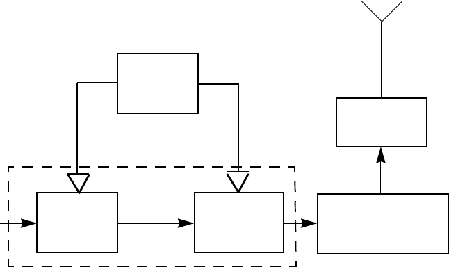
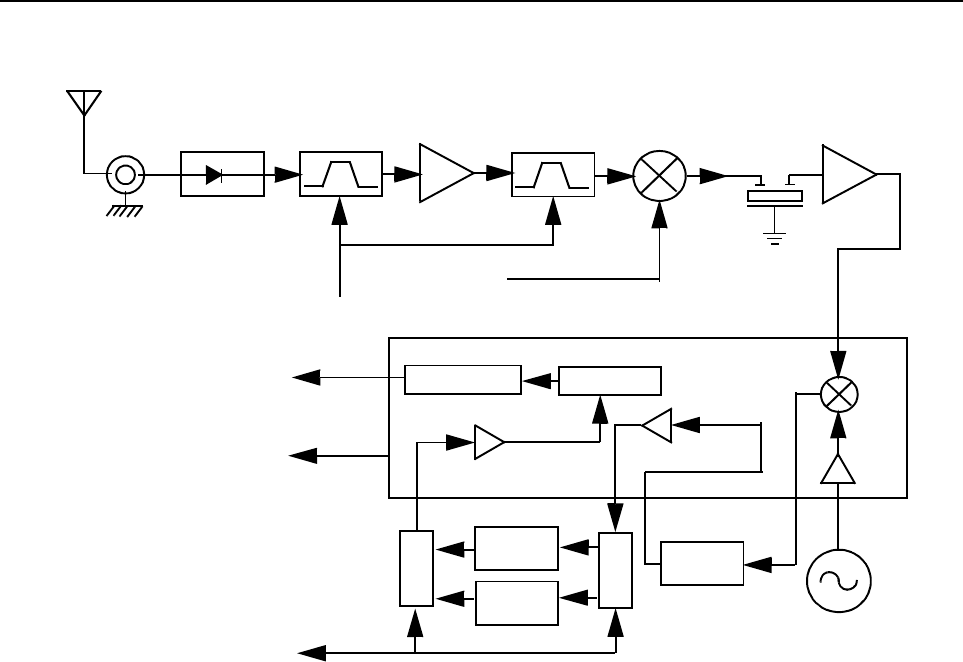
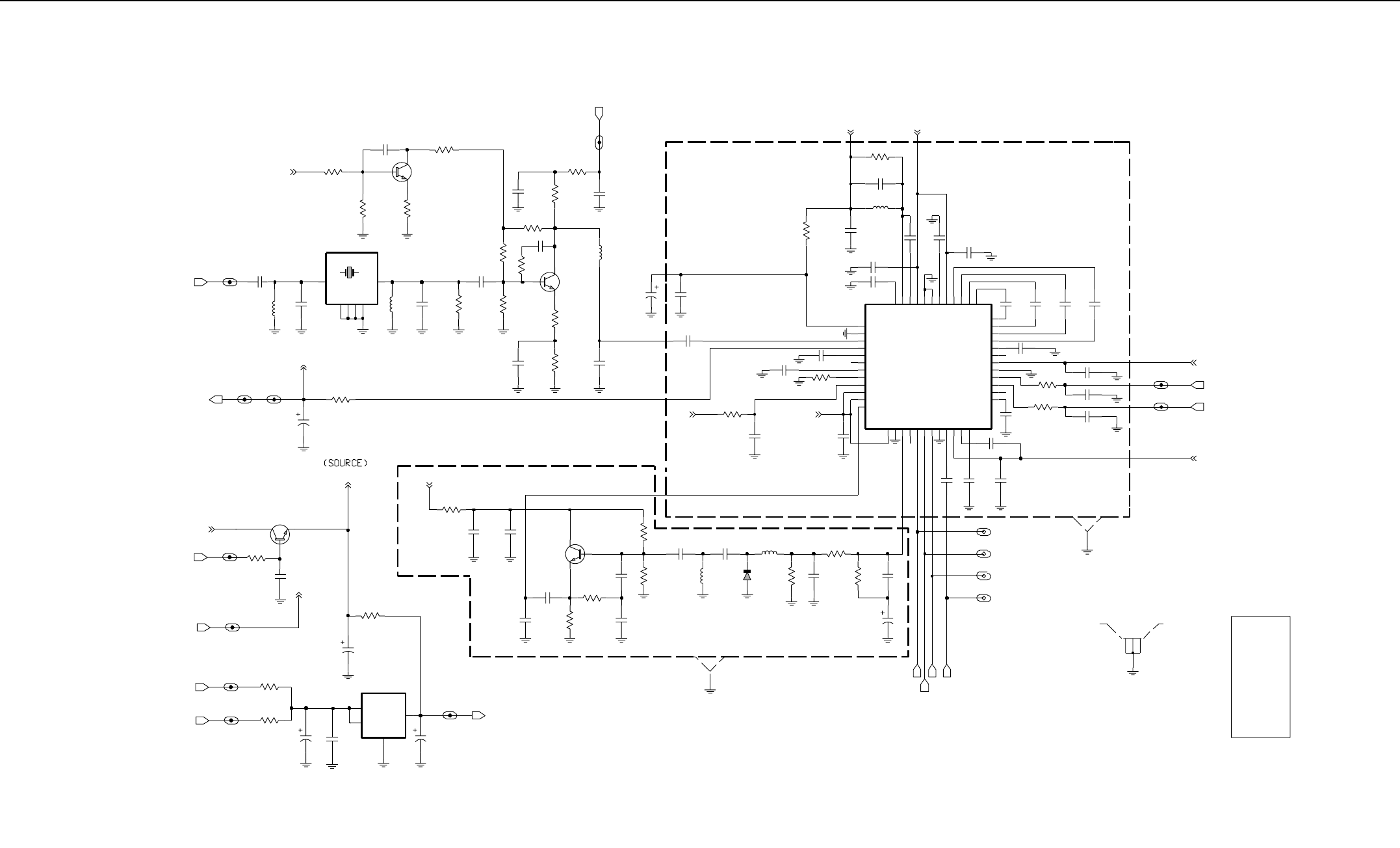
2.0 VHF Transmitter
(
Refer to Figure 2-1 and the VHF Transmitter schematic diagram
)
The VHF transmitter consists of the following basic circuits:
1. Power amplifier (PA).
2. Antenna switch/harmonic filter.
3. Antenna matching network.
4. Power Control Integrated Circuit (PCIC).
Figure 2-1 VHF Transmitter Block Diagram.
2.1 Power Amplifier
The power amplifier consists of two devices:
1. LDMOS driver IC (U3501)
2. LDMOS PA (Q3501)
The LDMOS driver IC contains two stages of amplification with a supply voltage of 7.3V.
Antenna Switch/
Harmonic Filter
Vcontrol Vcontrol
From
Antenna
Matching
Network
Power
Amplifier
VCO
PA
Driver
PCIC
PA Final
Stage

2-2 THEORY OF OPERATION
This RF power amplifier is capable of supplying an output power of 0.3W (pin 6 and 7) with an input
signal of 2mW (3dBm) (pin16). The current drain is typically around 130mA while operating in the
frequency range of 136-174MHz.
The LDMOS PA is capable of supplying an output power of 7W with an input signal of 0.3W. The
current drain is typically around 1800mA while operating in the frequency range of 136-174MHz.
The power output is varied by changing the bias voltage.
2.2 Antenna Switch
The antenna switch circuit consists of two pin diodes, D3521 and D3551, a pi network (C3531,
L3551 and C3550), and three current limiting resistors (R3571, R3572, R3573). In the transmit
mode, B+ at PCIC (U3502) pin 23 goes low to turn on Q3561 where a B+ bias is applied to the
antenna switch circuit to bias the diodes "on". The shunt diode (D3551) shorts out the receiver port,
and the pi network, which operates as a quarter wave transmission line, transforms the low
impedance of the shunt diode to a high impedance at the input of the harmonic filter. In the receive
mode, the diodes are both off, creating a low attenuation path between the antenna and receiver
ports.
2.3 Harmonic Filter
The harmonic filter consists of C3532 to C3536, L3531 and L3532. This network forms a low-pass
filter to attenuate harmonic energy of the transmitter to specifications level. The harmonic filter
insertion loss is typically less than 1.2dB.
2.4 Antenna Matching Network
A matching network made up of L3538 and C3537/C3539 is used to match the antenna impedance
to the harmonic filter. This optimizes the performance of the transmitter and receiver into the
antenna.
2.5 Power Control Integrated Circuit (PCIC)
The transmitter uses the PCIC, U3502 to control the power output of the radio by maintaining the
radio current drain. The current to the final stage of the power module is supplied through R3519,
which provides a voltage proportional to the current drain. This voltage is then fedback to the
Automatic Level Control (ALC) within the PCIC to provide loop stability.
The PCIC also contains internal digital to analog converters (DACs) that provide the reference
voltage of the control loop. The voltage level is controlled by the microprocessor through the data
line of the PCIC.
The resistors and integrators within the PCIC, and external capacitors (C3562, C3563 and C3565)
control the transmitter rise and fall times. These are necessary to reduce the power splatter into
adjacent channels.
U3503 and its associated components act as a temperature cut back circuit. This provides the
necessary voltage to the PCIC to cut the transmitter power if the radio temperature gets too high.
VHF Receiver (for all models except those with PCB8486473Z04) 2-3
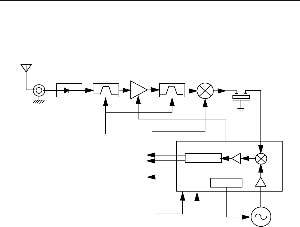
3.0 VHF Receiver (for all models except those with PCB8486473Z04)
The VHF receiver consists of a front end, back end, and automatic gain control circuits. A block
diagram of the VHF receiver is shown in Figure 2-2. Detailed descriptions of these features are
contained in the paragraphs that follow.
Figure 2-2 VHF Receiver Block Diagram.
3.1 Receiver Front-End
(
Refer to Figure 2-2 and the VHF Receiver Front End schematic diagram
)
The RF signal is received by the antenna and applied to a low-pass filter consisting of L3531,
L3532, C3532 to C3563. The filtered RF signal is passed through the antenna switch. The antenna
switch circuit consists of two pin diodes (D3521 and D3551) and a pi network (C3531, L3551, and
C3550).The RF signal is then applied to a varactor tuned bandpass filter which consists of L3301,
L3303, C3301 to C3304, and D3301. The filter is tuned by applying a control voltage to the varactor
diode (D3301) in the filter.
The bandpass filter is electronically tuned by the DACRx from IC 404 which is controlled by the
microprocessor. Depending on the carrier frequency, the DACRx supplies the tuned voltage to the
varactor diodes in the filter. Wideband operation of the filter is achieved by shifting the bandpass
filter across the band.
The output of the bandpass filter is coupled to the RF amplifier transistor Q3302 via C3306. After
being amplified by the RF amplifier, the RF signal is further filtered by a second varactor tuned
bandpass filter, consisting of L3305, L3306, C3311 to C3314 and D3302.
Demodulator
Synthesizer
Crystal
Filter
Mixer
Varactor
Tuned Filter
RF Amp
Varactor
Tuned Filter
Pin Diode
Antenna
Switch
RF Jack
Antenna
AGC
Control Voltage
from ASFIC
First LO
from FGU
Recovered Audio
Squelch
RSSI
IF IC
SPI Bus
16.8 MHz
Reference Clock
Second
LO VCO

2-4 THEORY OF OPERATION
Both the pre and post-RF amplifier varactor tuned filters have similar responses. The 3 dB
bandwidth of the filter is about 12 MHz. This enables the filters to be electronically controlled by
using a single control voltage which is DACRx.
The output of the post-RF amplifier filter is connected to the passive double balanced mixer which
consists of T3301, T3302, and CR3301. Matching of the filter to the mixer is provided by C3317,
C3318 and L3308. After mixing with the first LO signal from the voltage controlled oscillator (VCO)
using high side injection, the RF signal is down-converted to the 45.1 MHz IF signal.
The IF signal coming out of the mixer is transferred to the crystal filter (Y3200) through a resistor
pad (R3321 - R3323) and a diplexer (C3320 and L3309). Matching to the input of the crystal filter is
provided by C3200 and L3200. The crystal filter provides the necessary selectivity and
intermodulation protection.
3.2 Receiver Back-End
(
Refer to Figure 2-2 and the VHF Receiver Back End schematic diagram
)
The output of crystal filter Y3200 is matched to the input of IF amplifier transistor Q3200 by
capacitor C3203. Voltage supply to the IF amplifier is taken from the receive 5 volts (R5). The gain
controlled IF amplifier provides a maximum gain of about 10dB. The amplified IF signal is then
coupled into U3220 pin 3 via L3202, C3207, and C3230 which provides impedance matching for the
IF amplifier and U3220.
The IF signal applied to pin 3 of U3220 is amplified, down-converted, filtered, then demodulated to
produce the recovered audio at pin 27 of U3220. This IF IC is electronically programmable, and the
amount of filtering, which is dependent on the radio channel spacing, is controlled by the
microprocessor. Additional filtering, once externally provided by the conventional ceramic filters, is
replaced by internal filters in the IF module (U3220).
The IF IC uses a type of direct conversion process, whereby the externally generated second LO
frequency is divided by two in U3220 so that it is very close to the first IF frequency. The IF IC
(U3220) synthesizes the second LO and phase-locks the VCO to track the first IF frequency. The
second LO is designed to oscillate at twice the first IF frequency because of the divide-by-two
function in the IF IC.
In the absence of an IF signal, the VCO “searches” for a frequency, or its frequency will vary close to
twice the IF frequency. When an IF signal is received, the VCO will lock onto the IF signal. The
second LO/VCO is a Colpitts oscillator built around transistor Q3270. The VCO has a varactor
diode, D3270, to adjust the VCO frequency. The control signal for the varactor is derived from a loop
filter consisting of C3278 to C3280, R3274 and R3275.
The IF IC (U3220) also provides a received signal-strength indicator (RSSI) and a squelch output.
The RSSI is a dc voltage monitored by the microprocessor and is used as a peak indicator during
the bench tuning of the receiver front-end varactor filter. The RSSI voltage is also used to control the
automatic gain control (AGC) circuit at the front-end.
The demodulated signal on pin 27 of U3220 is also used for squelch control. The signal is routed to
U404 (ASFIC) where squelch signal shaping and detection takes place. The demodulated audio
signal is also routed to U404 for processing before going to the audio amplifier for amplification.

VHF Receiver (for all models except those with PCB8486473Z04) 2-5
3.3 Automatic Gain Control (AGC)
(
Refer to the Receiver Front End and Receiver Back End schematic diagrams
)
The front end automatic gain control circuit provides automatic reduction of gain of the front end RF
amplifier via feedback. This prevents overloading of backend circuits and is achieved by drawing
some of the output power from the RF amplifier output. At high radio frequencies, capacitor C3327
provides the low impedance path to ground for this purpose. CR3302 is a pin diode used for
switching the path on or off. A certain amount of forward biasing current is needed to turn the pin
diode on. Transistor Q3301 provides this current.
Radio signal strength indicator, RSSI, a voltage signal, is used to drive Q3301 to saturation i.e.
turned on. RSSI is produced by U3220 and is proportional to the gain of the RF amplifier and the
input power to the radio.
Resistors R3304 and R3305 are voltage dividers designed to turn on Q3301 at certain RSSI levels.
To turn on Q3301 the voltage across R3305 must be greater or equal to the voltage across R3324 +
Vbe. Capacitor C3209 is used to dampen any instability while the AGC is turning on. The current
flowing into the collector of Q3301, a high current gain NPN transistor, is drawn through the pin
diode to turn it on. Maximum current flowing through the pin is limited by resistors R3316, R3313,
R3306 and R3324. Feedback capacitor C3326 used to provide some stability to this high gain stage.
An additional gain control circuit is formed by Q3201 and associated components. Resistors R3206
and R3207 are voltage dividers designed to turn on Q3201 at a significantly higher RSSI level than
the level required to turn on pin diode control transistor Q3301. In order to turn on Q3201 the voltage
across R3207 must be greater or equal to the voltage across R3208 + Vbe. As current starts flowing
into the collector of Q3201, it reduces the bias voltage at the base of IF amplifier transistor Q3200
and in turn, the gain of the IF amplifier. The gain is then controlled in a range of -30dB up to +10dB.
2-6 THEORY OF OPERATION
4.0 Receiver (for models with PCB 8486473Z04)
Figure 2-3 VHF Receiver Block Diagram
4.1 Receiver Front-End
(
Refer to Figure 2-3 and the VHF Receiver Front End, VHF Receiver Back End and VHF Transmitter
schematic diagrams
)
The RF signal is received by the antenna and applied to a low-pass filter. For VHF, the filter consists
of L3531, L3532, C3532 to C3563. The filtered RF signal is passed through the antenna switch
consisting of two pin diodes (D3521 and D3551) and a pi network (C3531, L3551 and C3550).The
signal is then applied to a varactor tuned bandpass filter. The VHF bandpass filter comprises of
L3301, L3303, C3301 to C3304 and D3301. The bandpass filter is tuned by applying a control
voltage to the varactor diode (D3301) in the filter.
The bandpass filter is electronically tuned by the DACRx from IC404 which is controlled by the
microprocessor. Depending on the carrier frequency, the DACRx will supply the tuned voltage to the
varactor diodes in the filter. Wideband operation of the filter is achieved by shifting the bandpass
filter across the band.
The output of the bandpass filter is coupled to the RF amplifier transistor Q3302 via C3306. After
being amplified by the RF amplifier, the RF signal is further filtered by a second varactor tuned
bandpass filter, consisting of L3305, L3306, C3311 to C3314 and D3302.
Crystal
Filter
Mixer
Varactor
Tuned Filter
RF Amp
Varactor
Tuned Filter
Pin Diode
Antenna
Switch
RF Jack
Antenna
Control Voltage
from ASFIC
First LO
from VCO
Second LO
IF Amp
455kHz
Filter
Switch
455kHz
Filter
455kHz
Filter
Switch
Demodulator
RSSI
Limiter
Recovered Audio
BW SEL
U3220

Receiver (for models with PCB 8486473Z04) 2-7
Both the pre and post-RF amplifier varactor tuned filters have similar responses. The 3 dB
bandwidth of the filter is about 12 MHz. This enables the filters to be electronically controlled by
using a single control voltage which is DACRx .
The output of the post-RF amplifier filter is connected to the passive double balanced mixer which
consists of T3301, T3302 and CR3301. Matching of the filter to the mixer is provided by C3317,
C3318 and L3308. After mixing with the first LO signal from the voltage controlled oscillator (VCO)
using high side injection, the RF signal is down-converted to the 44.85 MHz IF signal.
The IF signal coming out of the mixer is transfered to the crystal filter (Y3200) through a resistor pad
(R3321 - R3323) and a diplexer (C3320 and L3309). Matching to the input of the crystal filter is
provided by C3201 and L3200. The crystal filter provides the necessary selectivity and
intermodulation protection.
4.2 Receiver Back-End
(
Refer to Figure 2-3 and the VHF Receiver Back End schematic diagram
)
The output of crystal filter Y3200 is matched to the input of IF amplifier transistor Q3200 by L3203.
Voltage supply to the IF amplifier is taken from the receive 5 volts (R5). The IF amplifier Q3200 is
actively biased by a collector base feedback provided by R3202 and R3203. The gain controlled IF
amplifer provides a maximum gain of about 16dB. A dual hot carrier diode (CR3201) limits the filter
output voltage swing to reduce overdrive effects at RF levels above -27dBm. The amplified IF signal
is then coupled into U3220 (pin 1) via L3202, C3207, and C3200 which provides the matching for
the IF amplifier and U3220.
The IF signal applied to pin 1 of U3220 is amplified, down-converted, filtered, and demodulated, to
produce the recovered audio at pin 7 of U3220.
Within U3220, the first IF 44.85 MHz signal mixes with the 44.395 MHz second local oscillator (2nd
LO) to produce the second IF signal at 455 kHz. The 2nd LO signal frequency is determined by
crystal Y3201. The second IF signal (455 kHz) is then filtered by an external ceramic filter Y3205
before being amplified by the second IF amplifier within U3220. Again, the signal is filtered by a
second external ceramic filter Y3203 or Y3204 depending on the selected channel spacing. Y3203
is used for 20/25 kHz channel spacing whereas Y3204, for 12.5 kHz channel spacing. The simple
circuit consisting of U3221, CR3202, CR3203 and resistors R3209, R3212, R3211 and R3205 divert
the second IF signal according to the BW_SEL line. The filtered output of the second IF signal is
applied to the limiter input pin of U3220 (Pin 14).
The IF IC (U3220) contains a quadrature detector using a ceramic phase-shift element (Y3202) to
provide audio detection. Internal amplification provides an audio output level around 120mVrms
(@60% deviation) from pin 8 of U3220. This demodulated audio is fed to the ASFIC_CMP IC (U404)
in the controller section.
The IF IC (U3220) also performs several other functions. It provides a received signal-strength
indicator (RSSI) with a dynamic range of 70 dB. The RSSI is a dc voltage monitored by the
microprocessor, and used as a peak indicator during the bench tuning of the receiver front-end
varactor filter.
2-8 THEORY OF OPERATION
4.3 Automatic Gain Control (AGC)
(
Refer to the Receiver Front End and Receiver Back End schematic diagrams
)
The front end automatic gain control circuit provides automatic reduction of gain of the front end RF
amplifier via feedback. This prevents overloading of backend circuits and is achieved by drawing
some of the output power from the RF amplifier output. At high radio frequencies, capacitor C3327
provides the low impedance path to ground for this purpose. CR3302 is a pin diode used for
switching the path on or off. A certain amount of forward biasing current is needed to turn the pin
diode on. Transistor Q3301 provides this current.
Radio signal strength indicator, RSSI, a voltage signal, is used to drive Q3301 to saturation i.e.
turned on. RSSI is produced by U3220 and is proportional to the gain of the RF amplifier and the
input power to the radio.
Resistors R3304 and R3305 are voltage dividers designed to turn on Q3301 at certain RSSI levels.
To turn on Q3301 the voltage across R3305 must be greater or equal to the voltage across R3324 +
Vbe. Capacitor C3209 is used to dampen any instability while the AGC is turning on. The current
flowing into the collector of Q3301, a high current gain NPN transistor, is drawn through the pin
diode to turn it on. Maximum current flowing through the pin is limited by resistors R3316, R3313,
R3306 and R3324. Feedback capacitor C3326 used to provide some stability to this high gain
stage.
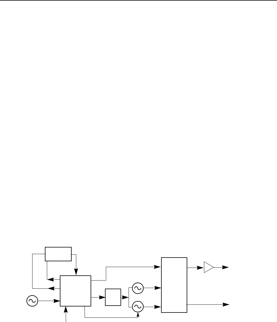
5.0 Frequency Generation Circuit
(
Refer to Figure 2-4 and the VHF Frequency Synthesizer schematic diagram
)
The Frequency Generation Circuit, shown in Figure 2-4, is composed of two main ICs, the
Fractional-N synthesizer (U3701), and the VCO/Buffer IC (U3801). Designed in conjunction to
maximize compatibility, the two ICs provide many of the functions that normally would require
additional circuits. The synthesizer block diagram illustrates the interconnect and support circuit
used in the region. Refer to the schematic for the reference designator.
Figure 2-4 VHF Frequency Generation Unit Block Diagram
The synthesizer is powered by regulated 5V and 3.3V which is provided from ICs U3711 and U3201
respectively. The 5V signal is supplied to pins 13 and 30 and the 3.3V signal is applied to pins 5, 20,
34 and 36 of U3701. The synthesizer in turn generates a superfiltered 5V which powers U3801.
Voltage
Multiplier
Synthesizer
U3701 Loop
Filter
VCOBIC
U3801
To
Mixer
To
PA Driver
VCP
Vmult1
Aux3
MOD Out
Modulating
Signal
Vmult2
Rx VCO Circuit
Tx VCO
TRB
16.8 MHz
Ref. Osc.
Rx Out
Tx Out
Circuit

Frequency Generation Circuit 2-9
In addition to the VCO, the synthesizer must interface with the logic and ASFIC circuitry.
Programming for the synthesizer is accomplished through the data, clock and chip select lines (pins
7, 8 and 9) from the microprocessor, U409. A 3.3V dc signal from pin 4 indicates to the
microprocessor that the synthesizer is locked.
Transmit modulation from the ASFIC is supplied to pin10 of U3701. Internally the audio is digitized
by the Fractional-N and applied to the loop divider to provide low-port modulation. The audio runs
through an internal attenuator for modulation balancing purposes before going out at pin 41 to the
VCO.
5.1 Synthesizer
The Fractional-N Synthesizer, shown in Figure 2-5, uses a 16.8MHz crystal (Y3761) to provide a
reference for the system. The LVFractN IC (U3701) further divides this to 2.1MHz, 2.225MHz, and
2.4MHz as reference frequencies. Together with C3761, C3762, C3763, R3761, and D3761, they
build up the reference oscillator that is capable of 2.5 ppm stability over temperatures of -30 to 85°C.
A 16.8MHz signal at pin 19 of U3701 is also provided for use by ASFIC and LVZIF (for all models
except those with PCB8486473Z04).
The loop filter which consist of C3721, C3722, R3721, R3722 and R3723 provides the necessary dc
steering voltage for the VCO and determines the amount of noise and spur passing through.
In achieving fast locking for the synthesizer, an internal adapt charge pump provides higher current
at pin 45 of U3701 to put the synthesizer within lock range. The required frequency is then locked by
normal mode charge pump at pin 43.
Both the normal and adapt charge pumps get their supply from the capacitive voltage multiplier
made up of C3701 to C3704 and triple diodes D3701, D3702. Two 3.3V square waves (180 degrees
out of phase) are first multiplied by four and then shifted, along with regulated 5V, to build up 13.5V
at pin 47 of U3701.
Figure 2-5 VHF Synthesizer Block Diagram.
DATA
CLK
CEX
MODIN
VCC, DC5V
XTAL1
XTAL2
WARP
PREIN
VCP
REFERENCE
OSCILLATOR
VOLTAGE
MULTIPLIER
VOLTAGE
CONTROLLED
OSCILLATOR
2-POLE
LOOP
FILTER
DATA (U409 PIN 100)
CLOCK (U409 PIN 1)
CSX (U409 PIN 2)
MOD IN (U404 PIN 40)
+5V (U3711 PIN 4)
7
8
9
10
13, 30
23
24
25
32
47
VMULT2 VMULT1
BIAS1
SFOUT
AUX3
AUX4
IADAPT
IOUT
GND
FREFOUT
LOCK 4
19
6, 22, 23, 24
43
45
3
2
28
14 15
40
FILTERED 5V
STEERING
LINE
LOCK (U409 PIN 56)
PRESCALER IN
LO RF INJECTION
TX RF INJECTION
(1ST STAGE OF PA
)
FREF (U3220 PIN 21 & U404 PIN 34)
39
BIAS2
41
DUAL
TSTRS
48
5V
R5
5, 20, 34, 36
(U3201 PIN 5)
AUX1
VDD, 3.3V MODOUT
U3701
LOW VOLTAGE
FRACTIONAL-N
SYNTHESIZER

2-10 THEORY OF OPERATION
5.2 Voltage Controlled Oscillator (VCO)
(
Refer to Figure 2-6 and the VHF Voltage Controlled Oscillator schematic diagram)
The VCOB IC (U3801), shown in Figure 2-6, in conjunction with the Fractional-N synthesizer
(U3701) generates RF in both the receive and the transmit modes of operation. The TRB line
(U3801 pin 19) determines which oscillator and buffer are enabled. A sample of the RF signal from
the enabled oscillator is routed from U3801 pin 12, through a low pass filter, to the prescaler input
(U3701 pin 32). After frequency comparison in the synthesizer, a resultant CONTROL VOLTAGE is
received at the VCO. This voltage is a DC voltage typically between 3.5V and 9.5V when the PLL is
locked on frequency.
Figure 2-6 VHF VCO Block Diagram
Presc
RX
TX
Matching
Network Low Pass
Filter
Attenuator
Pin8
Pin14
Pin10
(3701 Pin28)
VCC Buffers
TX RF Injection
U3701 Pin 32
AUX3 (U3701 Pin2)
Prescaler Out
Pin 12
Pin 19
Pin 20
TX/RX/BS
Switching Network
U3801
VCOBIC
Rx
Active Bias
Tx
Active Bias
Pin2
Rx-I adjust
Pin1
Tx-I adjust
Pins 9,11,17
Pin18
Vsens
Circuit
Pin15
Pin16
RX VCO
Circuit
TX VCO
Circuit
RX Tank
TX Tank
Pin7
Vcc-Superfilter
Collector/RF in
Pin4
Pin5
Pin6
RX
TX
(U3701 Pin28)
Rx-SW
Tx-SW
Vcc-Logic
(U3701 Pin28)
Steer Line
Voltage
(VCTRL)
Pin13
Pin3
TRB_IN
LO RF INJECTION

Frequency Generation Circuit 2-11
In the receive mode, U3801 pin 19 is low or grounded. This activates the receive VCO by enabling
the receive oscillator and the receive buffer of U3801. The RF signal at U3801 pin 8 is routed
through a matching network. The resulting LO RF INJECTION signal is applied to the mixer at
T3302.
During the transmit condition, when PTT is pressed, 3.2 volts is applied to U3801 pin 19. This
activates the transmit VCO by enabling the transmit oscillator and the transmit buffer of U3801. The
RF signal at U3801 pin 10 is injected into the input of the PA module (U3501 pin16). This RF signal
is the TX RF INJECTION. Also in transmit mode, the audio signal to be frequency modulated onto
the carrier is received through U3701, pin 41.
When a high impedance is applied to U3801 pin19, the VCO is operating in battery saver mode. In
this case, both the receive and transmit oscillators as well as the receive, transmit and prescaler
buffer are turned off.
Table 2-1 Level Shifter Logic
Desired
Mode AUX 4 AUX 3 TRB
Tx n.u. High (@3.2V) High (@3.2V)
Rx n.u. Low Low
Battery Saver n.u. Hi-Z/Float
(@1.6V)
Hi-Z/Float (@1.6V)

2-12 THEORY OF OPERATION
6.0 Voice Storage (GP1280)
(
Refer to Figure 2-7 and the VHF Voice Storage schematic diagram)
The Voice Storage feature is offered as standard in the GP1280 and as an Option board for
GP340/GP360/GP380 and GP640/GP680.
The Voice Storage feature enables users to:
■Record and Playback Personal Memo (Reminders, Notes, etc.).
■Send over-the-air an “Out-Of-Office” message when an incoming call is received but is not
available to take up call.
■Over-the-air recording of important voice message being received.
Figure 2-7 Audio path for voice storage connection to interface connector
VCCD
VSSA1
VSSA2
VSSA3
VSSD
XCLK
SCLK
SS
VCCA
MOSI
AMCAP
ANA_NEG
ANA_POS
AUDOUT
MISO
U700
ISD33000
C701 C702
1uF
100pF
C703
0.1uF
CR700
Vddd
C704
0.1uF
CLK
MISO
DATA
VS_CS
R701
18K
R702
18K
C707
0.1uF
U710-2
MC74HC4066
CNTL
VDD
VSS
560K
R708
Vddd
0.1uF
C719
RX_AUD_RTN
VS_GAINSEL
C713
0.1uF
FLAT_RX_SND
CNTL
VDD
VSS
U710-3
MC74HC4066
CNTL
VDD
VSS
U710-1
MC74HC4066
C715
0.1uF
EXT_MIC
U710-4
MC74HC4066
CNTL
VDD
VSS
VS_AUDSEL
C718
1000pF
R707
LM2904
U720-2
R706
56K
5.1K
.01uF
C711
1MEG
R709
C717
0.1uF
R710
470K
SWB+
Vddd
0.1uF
C714
R717
10K
R716
1.8K
LM2904
U720-1
C710
33uF
C705
0.1uF
Vddd
0.1uF
C708
1000pF
C709

Voice Storage (GP1280) 2-13
Audio routing to the Voice Storage circuitry during receive message recording, message playback,
personal memo recording and voice prompt transmit over the air are as follows:
Received Message Recording
The receive audio is tapped from the Rx_Aud_Rtn pin of the ASFIC_CMP during receive mode.
Message Playback
Message playback is via the FLAT_RX_SND pin of ASFIC_CMP. In the ASFIC_CMP, the signal is
routed via the Side-Tone path to the Receive path where playback audio is routed to the speaker.
Personal Memo Recording
In this mode, voice is pick-up at the Mic. and via the Side-Tone path will be directed to the
Rx_Aud_Rtn pin, which is then routed to the voice recording chip.
Voice Prompt transmit over the air
A personal voice prompt or Out-Of-Office Message which is stored in the IC can be transmitted over
the air through mic path in the ASFIC_CMP to the calling party. This feature is similar to the
Telephone Answering Machine feature when the person called is not available to attend the call.

2-14 THEORY OF OPERATION

Chapter 3
TROUBLESHOOTING CHARTS
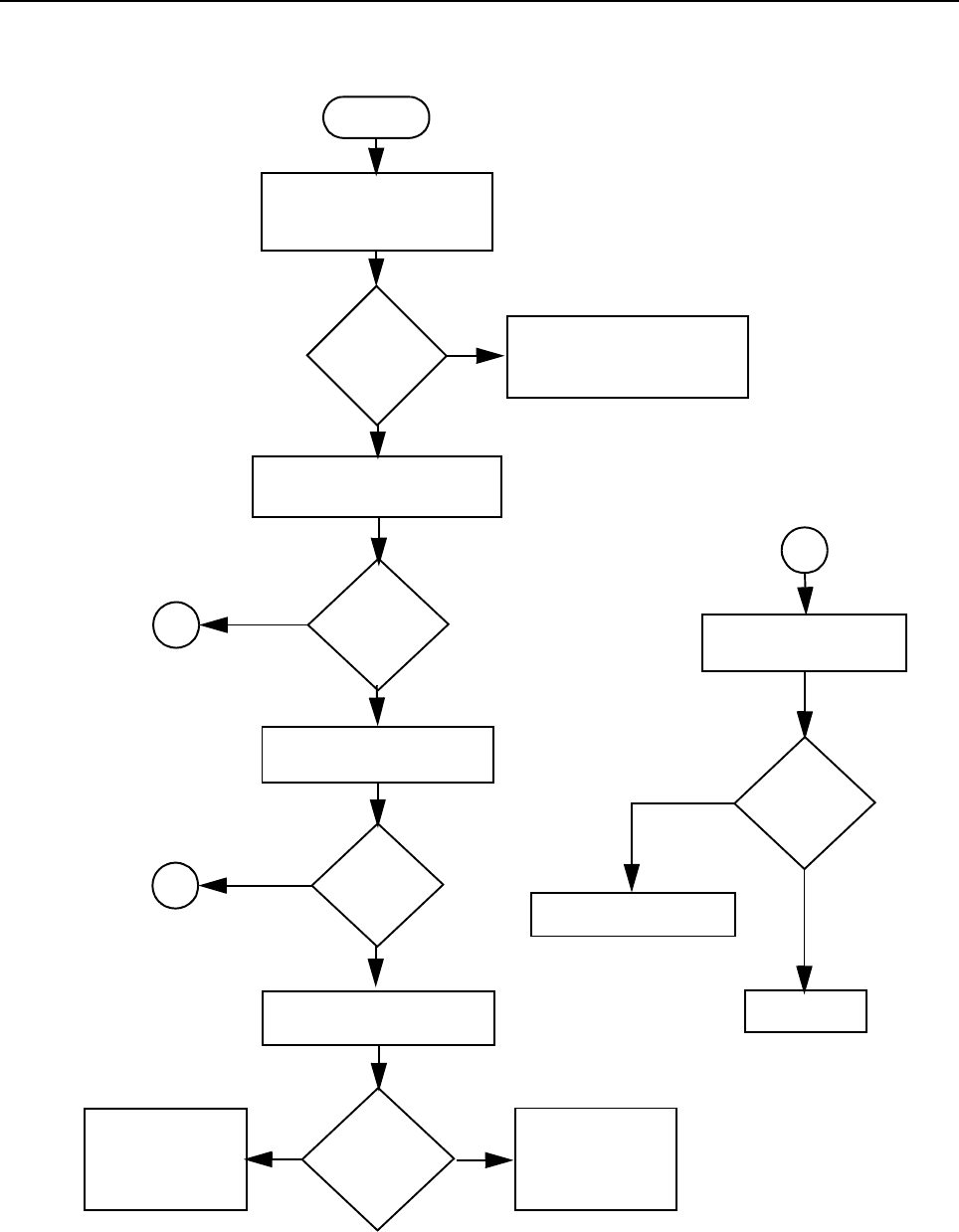
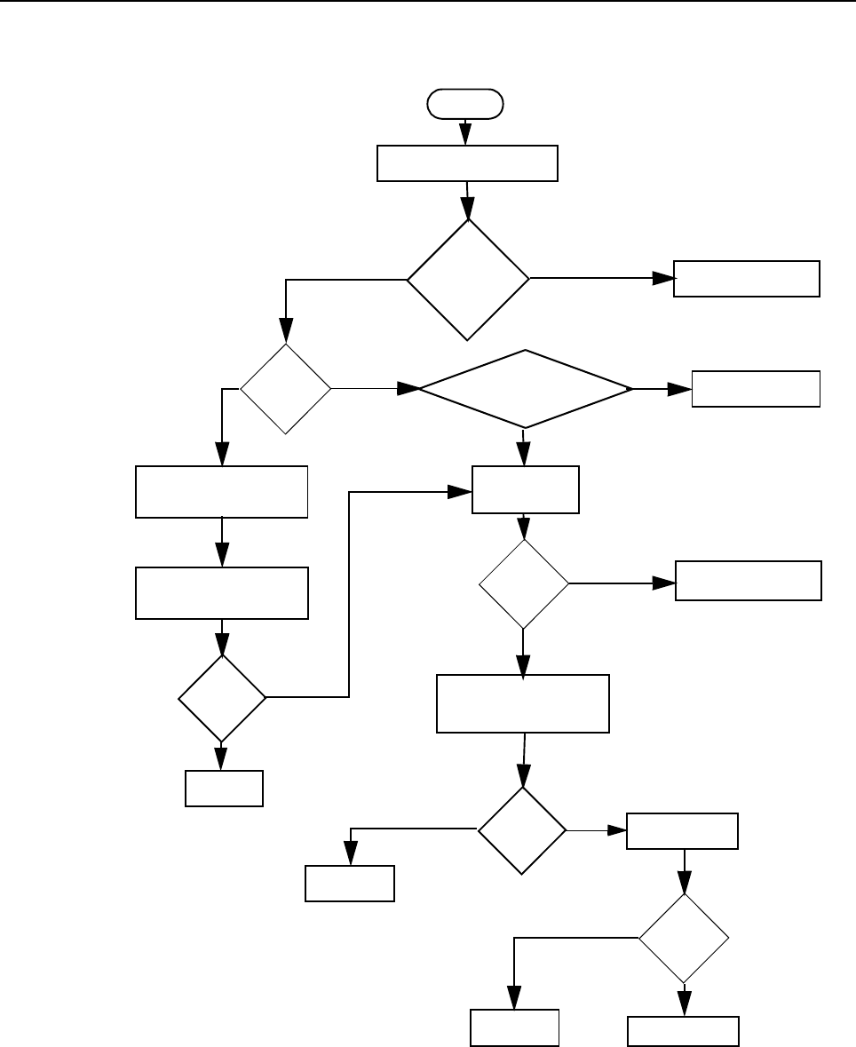
1.0 Troubleshooting Flow Chart for Receiver, for all models except
those with PCB 8486473Z04 (Sheet 1 of 2)
Activity
on U3220
LVZIF_SEL
pin?
16.8 MHz
at pin 21
U3220?
Check 2nd LO Control Voltage at C3279
Audio
at pin 27 of
U3220?
VCO
locked?
Bad SINAD
Bad 20dB Quieting
No Recovered Audio
START
Check Controller
Ye s
No
Spray of inject 1st IF into
XTAL Filter
IF Freq: 45.1MHz
Audio
heard?
B
Yes
No
B
Yes
Check FGU
No
No
A
A
Yes
Check Q3270 bias
circuitry for faults.
Rotate Freq. Knob
Check controller
Before replacing U3220, check 2nd
VCO Q3270. Check VCO O/P level,
C3272, C3273.
Ye s
No

3-2 TROUBLESHOOTING CHARTS
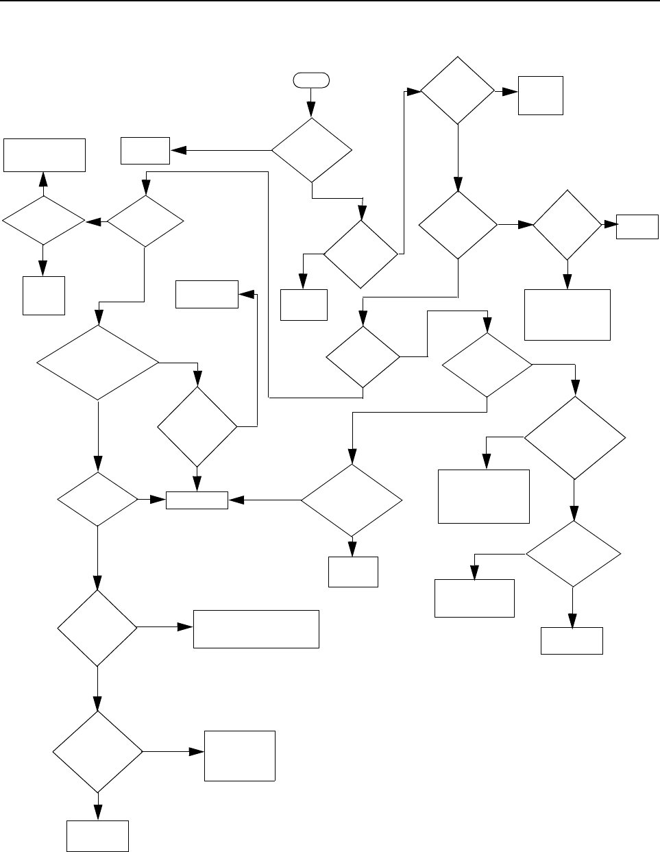
Troubleshooting Flow Chart for Receiver for all models except those
with PCB 8486473Z04 (Sheet 2 of 2)
Q3200
collector OK?
IF signal
present?
RF
Signal
at C3306
?
RF
Signal
at C3302
?
RF
Signal
at R3313
?
IF Signal
at C3200?
Check filter between
C3302 & C3306; program
filter to schematic test freq
and check varactor
voltages. Check Q3721, U3701
(pin 48) voltages
and U3711
Check harmonic filters L3531 & L3532,
C3532 and ant. switches D3521, D3551,
L3551, R3551,C3551, C3552, L3552.
Is R5
present
?
Trace IF signal
from C3200 to
Q3200. Check for
bad XTAL filter.
No
RF
Signal
at T3301
?
No
No
No or
Inject RF into J3501
Are
varactor
voltages
OK
?
No
Yes
Check RF amp
(Q3302) Stage.
Check filter between
C3313 & T3301.
Yes
Check T3301, T3302, CR3301,
R3321, R3322, R3320
Yes
1st LO O/P
OK?
Locked?
Yes
Check FGU
Yes
No
Yes Yes
Check for 2.9
VDC
No
No
No
Check U404 voltage. U404
can be selected by MCU
before replacing U404.
Check varactor filter.
No
Yes
Yes
Yes
A
A
B
weak RF
Before replacing
U3220, check
U3220 voltages;
trace IF signal
path.
Troubleshooting Flow Chart for Receiver, for models with PCB 8486473Z04 (Sheet 1 of 2) 3-3
2.0 Troubleshooting Flow Chart for Receiver, for models with PCB
8486473Z04 (Sheet 1 of 2)
Bad SINAD
Bad 20dB Quieting
No Recovered Audio
START
Audio at pin
8 of U3220?
Check Controller
(in the case of no audio)
OR ELSE go to “B”
Yes
No
Spray or inject 44.85MHz
into XTAL Filter Y3200
Audio heard?
B
Yes
No
Check 2nd LO
(44.395MHz) at C3274
LO Present?
B
Yes
Voltages
ok?
Biasing ok?
Check circuitry
around U3220.
Replace U3220
if defect
No
No
A
Yes
Check Q3200 bias
for faults.
Replace Q3200.
Go to B
Yes
No
Check voltages on
U3220
Check circuitry
around Y3202.
Replace Y3202
if defect
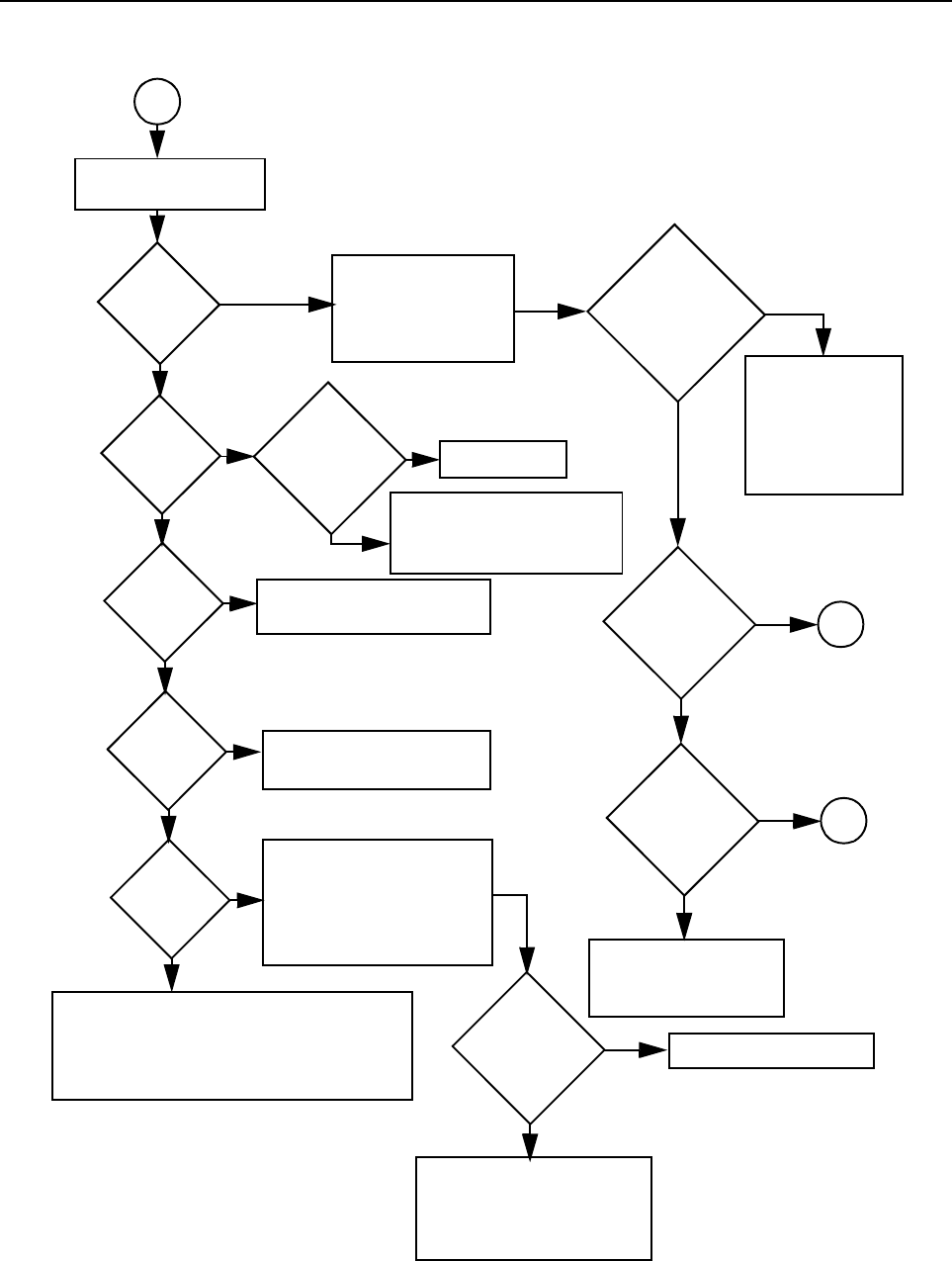
3-4 TROUBLESHOOTING CHARTS
Troubleshooting Flow Chart for Receiver, for models with PCB
8486473Z04 (Sheet 2 of 2)
IF Signal at
L3200?
No
RF Signal at
T3301?
RF Signal at
R3313?
No
RF Signal at
C3306?
No
RF Signal at
C3302?
No or
Check harmonic filter L3531 & L3532,
C3532 and ant. switches D3521, D3551,
L3551, R3551, C3551, C3552, L3552
Check filter between
C3302 & C3306; pro-
gram filter to schematic
test freq and check
varactor voltages.
Inject RF into J3501
Are varactor
voltages OK?
No
Yes
Check RF amp (Q3302)
Stage.
Check filter between
C3313 & T3301.
Yes
Check T3301, T3302,
CR3301, R3321, R3322,
R3323
Yes
1st LO O/P
OK?
Locked?
Yes
Check FGU
Yes
Trace IF signal
from L3200 to
Q3200. Check for
bad XTAL filter.
No
Yes Q3200 collec-
tor OK?
IF signal
present?
Before replacing
U3220, check
U3220 volt-
ages; trace IF
signal path.
Yes
Check for 2.9
VDC
Is R5
present?
Check Q3721,
U3701 (pin 48) volt-
ages and U247
No
No
No
Check U404 voltage and if
U404 can be selected by
MCU before replacing
U404.
Check varactor filter.
No
Yes
Yes
Yes
A
A
B
weak RF
Troubleshooting Flow Chart for Transmitter 3-5
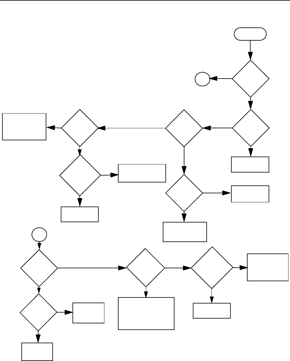
3.0 Troubleshooting Flow Chart for Transmitter
Is
Control Voltage High
or Low at TP3502
?
Is
There
B+ Bias for
Ant switch
D3521
?
START
No Power
Check Q3561
Is
Current
OK?
Check PCIC
1. Check Pin Diodes
2. Check Harmonic Filter
Inspect/Repair Tx.
Output Network
Is
Power
OK?
Done
Check Drive to
Module
Is Drive
OK
?
Troubleshoot VCO
Inspect PA Network/
Check Power Out of
U3501 at Cap C3512
Is
Power
OK?
Replace U3501
Is
Power OK
?
Replace Q3501
Done
Done
No
Yes
Yes No
No
Yes
Low
High
No
Yes
Yes No
Yes
No
3-6 TROUBLESHOOTING CHARTS
4.0 Troubleshooting Flow Chart for Synthesizer
5V
at pin 6 of
D3701
Is
information
from mP U409
correct
?
Is
U3701 Pin
18 AT 4.54
VDC?
Is U3701
Pin47 AT = 13
VDC
Is
U3701
Pin 19<0.7 VDC
in RX & >4.3 VDC
in TX?
Start
Visual
check of the
Board
OK?
Correct
Problem
Check 5V
Regulator
+5V
at U3701
Pin’s
13 & 30?
Is
16.8MHz
Signal at
U3701 Pin
19?
Check Y3761,
C3761, C3762,
C3763, D3761 &
R3761
Are
signals at
Pin’s 14 &15
of U3701
?
Check
L3701,
R3701
Check Q260,
Q261 & R260
U3701
pin 2 at >3V
in Tx and
<0.7V in
Rx
Remove
Shorts
Is
there a short
between Pin 47 and
Pins 14 & 15 of
U3701?
Replace or
resolder
necessary
components
Is RF level at
U3701 Pin 32
>-30 dBm?
Are
C3721,
C3722,C3723,
R3721, R3722,
R3723
OK?
Replace
U3701
If R3727, C3726 & C3727
are OK, then see VCO
troubleshooting chart
Are
Waveforms
at Pins 14 & 15
triangular?
Do
Pins 7,8 & 9
of U3701 toggle
when channel
is changed
?
Check prgramming
lines between U409
and U3701
Pins 7,8 & 9
Replace
U3701
Check uP U409
Troubleshooting
Chart
NO
YES
NO
YES
NO
YES
NO
YES
NO
NO
NO
YES
YES
NO
YES
YES
NO
YES
YES
YES
NO
NO
NO
NO
YES
NO
YES
YES
Check D3701,
D3702, U3701,
C3701 - C3707
3.3V
at U3701
pins 5, 20,
34 & 36
Is
16.8MHz
signal at
U3701 pin
23?
Replace
U3701
YES
NO
NO
YES
NO
YES
Replace
Check
U3201,
L3731
Troubleshooting Flow Chart for VCO 3-7
5.0 Troubleshooting Flow Chart for VCO
L3821,
L3822,
L3823,
O/C?
AUX 3 at
U3701
High?
U3801
Pin 19 =0V
AUX 3 at
U3701
High?
L3831,
L3832
L3833
O/C?
U3801
Pin 10
>1V?
Tx
Carrier?
VCTRL
0V or
13V?
START
No LO?
VCO OK
Check
R3829
TRB = 3.2V
Change L3831,
L3832
Change
U3801
Check U3701
Pin 2 for 3.2V
Change
U3701
Change
L3821,L3822,
L3823, L3825
Change
U3801
Change
U3801
Check for faulty parts
or dry joints of L3812,
C3806, R3806,
R3802, & L3801
A
A
No
No
Yes
Yes
Yes No
No
Yes
Yes
Yes
No
Yes
No
No
Yes Yes
No
No
Check R3811,
L3811 for dry
joint or faulty
No
Yes

3-8 TROUBLESHOOTING CHARTS
6.0 Troubleshooting Flow Chart for Receive Message/Personal
Memo Recording
Cannot Receive
Message
Check menu
whether record
incoming messages
turned on
Personal Memo
Recording
Check J400-34
Any audio?
Check keypad/
controller flex
interconnect
ok?
Assemble
properly
Change U700 or Voice
Storage option board
Turn on
“Record Incoming
Call”
Check Mic I/P at
J403-18 any audio?
Check Spkr/Mic
Flex Connection
J403
No
Yes
Yes
Yes
No
Yes
No

Troubleshooting Flow Chart for Message Playback 3-9
7.0 Troubleshooting Flow Chart for Message Playback
Cannot Playback
Message
Check keypad/
controller flex
interconnect ok?
Audio at J400-35?
Change U700 or
Voice Storage
Option Board
Change U404
No
Yes
Yes
No
Assemble
properly

3-10 TROUBLESHOOTING CHARTS

Chapter 4
VHF PCB/SCHEMATICS/PARTS LISTS
1.0 Allocation of Schematics and Circuit Boards
1.1 Controller Circuits
The VHF circuits are contained on the printed circuit board (PCB) which also contains the Controller
circuits. This Chapter shows the schematics for the VHF circuits only, refer to the Controller section
for details of the related Controller circuits . The PCB component layouts and the Parts Lists in this
Chapter show both the Controller and VHF circuit components. The VHF schematics and the related
PCB and parts list are shown in the tables below.
1.2 Voice Storage Facility
The Voice Storage facility is fitted to the GP1280 radio as standard and the schematics, component
layout and parts list for these circuits are shown in this Chapter. The Voice Storage facility may be
fitted to other radios in the GP Series as an option board; reference must be made to the Option
Board manual in this case. The Voice Storage schematic and the related PCB is shown in Tables
4-2 and 4-4 below.
Table 4-1 VHF Diagrams and Parts Lists
PCB :
8486062B12 Main Board Top Side
8486062B12 Main Board Bottom Side
8486062B14 Main Board Top Side
8486062B14 Main Board Bottom Side
Page 4-5
Page 4-6
Page 4-25
Page 4-26
SCHEMATICS
Controls and Switches
Receiver Front End
Receiver Back End
Synthesizer
Voltage Controlled Oscillator
Transmitter
Page 4-7
Page 4-8
Page 4-9
Page 4-10
Page 4-11
Page 4-12
Parts List
8486062B12
8486062B14
Page 4-13
Page 4-27

4-2 VHF PCB/SCHEMATICS/PARTS LISTS
Table 4-2 VHF GP1280 Diagrams and Parts Lists
PCB :
8486101B09 Main Board Top Side
8486101B09 Main Board Bottom Side
8486101B10 Main Board Top Side
8486101B10 Main Board Bottom Side
Page 4-17
Page 4-18
Page 4-31
Page 4-32
SCHEMATICS
Controls and Switches
Receiver Front End
Receiver Back End
Synthesizer
Voltage Controlled Oscillator
Transmitter
Voice Storage Circuits
Page 4-7
Page 4-8
Page 4-9
Page 4-10
Page 4-11
Page 4-12
Page 4-19
Parts List
8486101B09
8486101B10
Page 4-21
Page 4-33
Table 4-3 VHF Diagrams and Parts Lists
PCB :
8486062B16 Main Board Top Side
8486062B16 Main Board Bottom Side
8486062B17 Main Board Top Side
8486062B17 Main Board Bottom Side
Page 4-37
Page 4-38
Page 4-49
Page 4-50
SCHEMATICS
Controls and Switches
Receiver Front End
Receiver Back End
Synthesizer
Voltage Controlled Oscillator
Transmitter
Page 4-39
Page 4-40
Page 4-41
Page 4-42
Page 4-43
Page 4-44
Parts List
8486062B16
8486062B17
Page 4-45
Page 4-51

Allocation of Schematics and Circuit Boards 4-3
Table 4-4 VHF GP1280 Diagrams and Parts Lists
PCB :
8486101B11 Main Board Top Side
8486101B11 Main Board Bottom Side
Page 4-55
Page 4-56
SCHEMATICS
Controls and Switches
Receiver Front End
Receiver Back End
Synthesizer
Voltage Controlled Oscillator
Transmitter
Voice Storage Circuits
Page 4-39
Page 4-40
Page 4-41
Page 4-42
Page 4-43
Page 4-44
Page 4-19
Parts List
8486101B11 Page 4-57
Table 4-5 VHF Diagrams and Parts Lists
PCB :
8486473Z04 Main Board Top Side
8486473Z04 Main Board Bottom Side
Page 4-61
Page 4-62
SCHEMATICS
Controls and Switches
Receiver Front End
Receiver Back End
Synthesizer
Voltage Controlled Oscillator
Transmitter
Page 4-63
Page 4-64
Page 4-65
Page 4-66
Page 4-67
Page 4-68
Parts List
8486473Z04 Page 4-69

4-4 VHF PCB/SCHEMATICS/PARTS LISTS

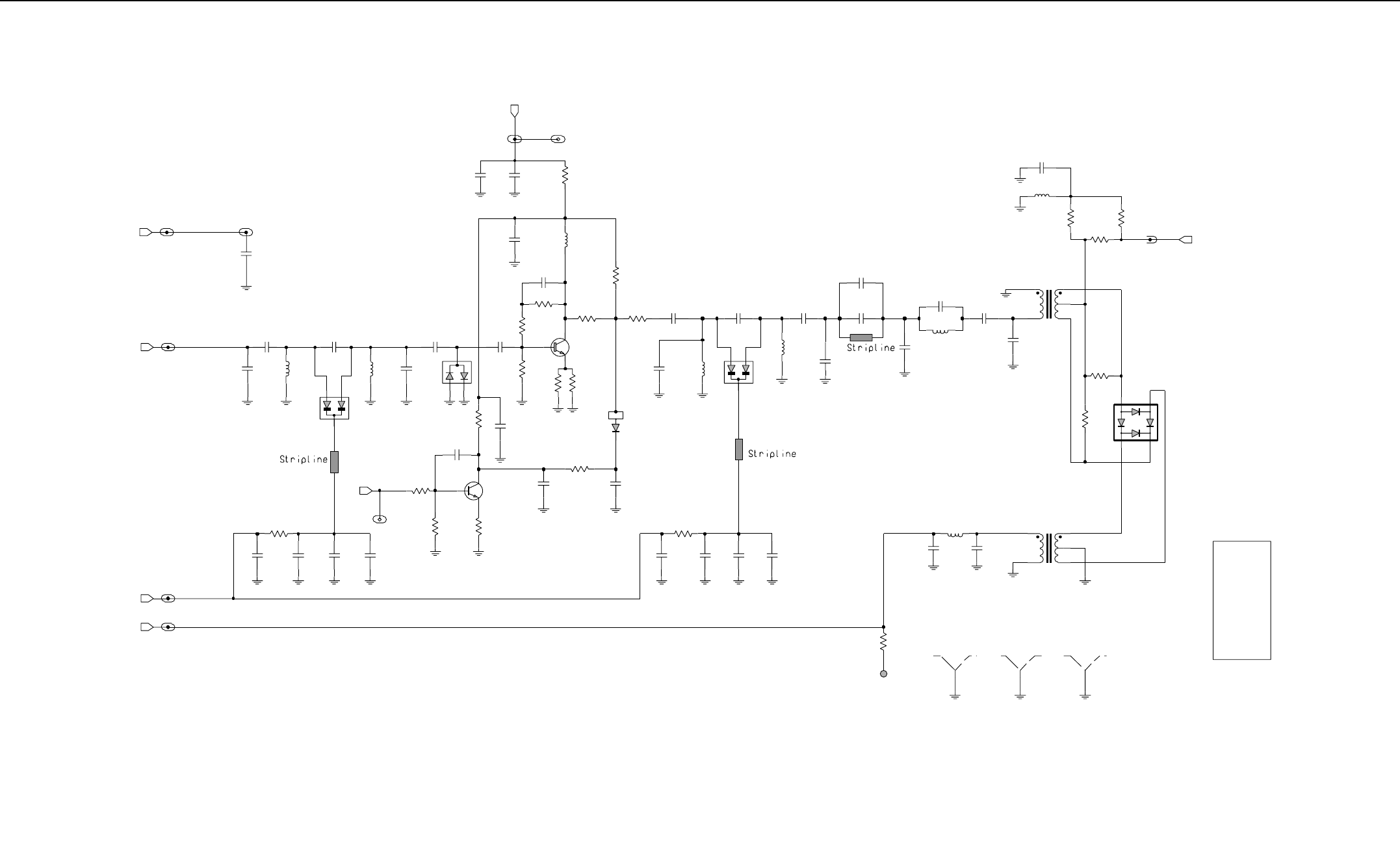
VHF PCB 8486062B12 / Schematics 4-5
2.0 VHF PCB 8486062B12 / Schematics
WARIS VHF RF Board
8486062B12/B13 TOP SIDE
CHECK
ONE
O.K. AS IS
O.K. AS MARKED
( )
( )
ISS. REVISION RLSE.
CORRECTED
AS
MARKED
ILLUSTRATOR DATEENGINEERDATE PROGRAM DISK
RLSE.
DWG. NO.
LETTERING SIZE:
REQUIRES:
EDITOR DATECHECKERDATE
Illustrator
RK 24/June/1999
ZWG0130072
C
ZWG0130072-C
C400
C401
C402
C423
C424
C425
C426
C427 C428
C429
C432
C441
C443 C444
C467
C471
C472
C473
C480
C482
C490
C491
C492
C493
C494
C495
C496
C497
CR412
CR413
E407
E408
E409
40
J400
J403
L400
Q400
Q403
Q405
Q417
R401
R402
R403
R405
R406
R407
R408
R410
R418
R421
R427
R428
R429
R435
R437
R450
R476
R477
R478
R481
R492
RT400
SH400
TP401
TP402
TP405
TP406
TP410
TP415
U405
RAM
U406
Flash
ROM
VR434
VR447
VR449
VR450
C403
C3706
C3712
C3713
C3714
C3741
C3742
C3743
C3744
C3746
C3752
C3754
C3822
C3824
C3825
C3828
C3829
C3830
C3832
C3834
C3835
C3836
C3842
CR440
D3831
D3832
L401
L3821
L3822
L3823
L3824
L3825
L3831
L3832 L3833
L3834
R416
R447 R448
R3701
R3741
R3751
R3821
R3828
R3833
R3835R3836
SH3801
U400
U3711
B503 B504
C502
C505
C521
C522
C3200
C3201
C3205
C3212 C3213
C3320
C3334
C3335
C3710
C3711
C 3722
C3724
C3745
C3753
L3200
L3309
L3312
PB501PB502PB503 PB504
Q3721
R3200
R3214
R3215
C3209
R3217
R3318
R3321
R3322
R3323
R3721
R3722
R3723
R3752
SH3701
T3302
TP3701
VR440
VR444
Y3200
IF Filter
Y3761
Reference
Oscillator
Crystal
C511
C512 C513
C514
C3202
C3203
C3206
C3207
C3208
R3218
Q3202
C3225
C3270 C3271
C3272
C3273
C3275
C3276
C3277
C 3278
C3279
C3280
C3503
C3512
C3513
C3514
C3517
C3519
C3521
C3523
C3524
C3525
C3527
C3528
C3531
C3532
C3534
C3535
C3536
C3537
C3539
C3541C3542
C3543
C3544
C3550
C3551
C3552
CR503
CR3303
D3270
D3521
D3551
L3201 L3202
L3270
L3271
L 3501
L3502
L3503
L3504
L3511
L3512
L3513
L3515
L3521
L3522
L3531
L3532
L3538
L3551
L3552
PB505
Q502
Q505
Q3200
Q3201
Q3270
R502
R506
R3202
R3203
R3205
R3206
R3207
R3208
R3209
R3211
R3270
R3271
R3272
R3273
R3274
R3275
R3276
R3513
R3541
R3542
R3543
R3551
SH3203
U3201
U3501
VR501
C520
C3214
C3306
C3307
C3308
C3309
C3310
C3311
C3313
C3314
C3318 C3327
C3329 C3330
C3331
C3332
C3338
C3501
C3504
C3505 C3518
C3546
C3547
C3721
C3826
C3833
D3302
D3821
L3304
L3305L3306
L3518
Q3302
Q3501
LDMOS
Driver IC
R501
R505
R3201
R3204
R3225
R3213
R3309
R3310
R3311
R3313
R3316
R3317
R3501
R3502R3503
R3512
R3544
R3545
R3546
R3547
R3548
R3822
R3823
R3834
SH3501
SH3502
T3301
C3204
C3502
R3212
R3505
SH3302 SH3303
C523
C3274
C3312
C3533
R3226
R3308 R3312
SH3201
TP3301
TP3702
C3319
R446
SH401
U407
EEPROM
C3215
C3210
R3210
4
3
2
22
20
1
21
4
3
43
23
4
3
6
4
3
6
43
4
5
22
21
8
7
32 17
16
1
1
4
5
8
16
8
9
3
1
8
1
64
3
6
34
1
3
4
6
2
1
5
2
5
51
1
1
5
1
1
1
1
1
20
1
C3715
1
VHF Main Board
Top Side
ZWG0130072-D
VHF (136-174 MHz) Main Board Top Side

4-6 VHF PCB 8486062B12 / Schematics
24
B501
C431
C433
C434
C436
C437
C453
C535
C3211
C3219
C3220
C3221
C3223
C3224
C3226
C3227
C3228
C3229
C3230
C3231
C3232
C3233
C3234
C3235
C3236
C3238
C3239
C3240
C3241
C3242
C3243
C3244
C3301
C3304
C3305
C3315C3316 C3317
C3321
C3322 C3323C3324
C3325
C3326
C3337
C3339
C3701
C3702
C3703
C3704
C3705
C3707
C3709
C3725
C3726
C3727
C3731
C3732
C3733
C3734
C3735
C3751
C3755
C3761
C 3762
CR411
CR3301
CR3302
D3301
D3701
D3702
F501
FL401
J3501
J3502
L505
L3221
L3301 L3303
L3308
L3701
L3731
Q416
Q3301
R414
R415
R419
R420
R426
R432
R460
R462
R463
R3220
R3221
R3222
R3223
R3224
R3304
R3305
R3307
R3314
R3315
R3319 R3320
R3324
R3702
R3703
R3704
R3705
R3726
R3727
R3762
R3763
S501
SH3702
U410
U3701
FRACN
Synthesizer
VR439
VR441 VR442
VR506
Y3762
C407
C408
C414
C415
C416
C419
C420
C421
C422
C430
C435
C440
C442
C445
C484
C447
C448
C449
C451
C452
C456
C458
C459
C463
C466
C475
C476
C479
C503
C3303
C3336
C3506
C3507 C3509
C3515
C3516
C3526
C3560
C3561
C3562
C3563
C3564
R3565
C3568
C3569
C3708
C3802
C3804
C3805
C3806
C3808
C3809
C3811 C3812
C3813
C3815
C3816
C3818
C3821
C3823
C3827
CR501
E400
E401
E402
E403
E404
E405
H3501
L410
L411
L3519
L3523
L3801
L3809
L3811
L3812
L3813
L3816
L3826
Q410
Q3801
R409
R411
R413
R423
R424
R425
R431
R445
R449
R457
R461
C483
R472
R473
R3303
R3306
R3519
R3561
R3562
R3563
R3564
R3571
R3572R3573
R3801
R3802
R3805
R3806
R3807
R3811
R3812
R3816
R3817
R3818
R3825
R3826
R3829
R3830
R3831
R3832
SH402
SH403
SH3202
SH3301
TP3502
U404
ASFIC
U409
Microprocessor
U420
Audio Pa
U3502
Power
Control
IC
U3503
VR432
VR433
VR448
C410
C481
C3237
C3302
C3508 C3803
C3810
Q3561
R434
R436
R471
R475
R3569
R3570
R3803
R3804
R3824
S502
U3220
LVZIF
C3801
R3808
SH3802
U3801
VCO
Buffer
R3222
E406
R400
C409
C446 C450
C3763
R3761
R3760
D3761
R3219
C3218
C3566
C447
C477
C478
C411
RT3301
R3301
R3566
R3567
C3565
C3571
WARIS VHF RF Board
8486062B12/B13 BOT SIDE
CHECK
ONE
O.K. AS IS
O.K. AS MARKED
( )
( )
CORRECTED
AS
MARKED
ILLUSTRATOR DATEENGINEERDATE PROGRAM DISK
DWG. NO.
EDITOR DATECHECKERDATE
Illustrator
RK 23/Nov/1998
ZWG0130073
ZWG0130073-C
17
9
25
11
120
10
2
3
4
4
C
8
C
2
2
35
4
1
48
36
37
25
24
12
13 1
2
3
3
2
3
4
48
36
37 25
24
12
13
1
11
1
20
10
4
1
48
36
37
25
24
12
13
3
75
50 25
1
1
1
5
100
8
16
32
VHF (136-174 MHz) Main Board Bottom Side
ZWG01300073-C

VHF PCB 8486062B12 / Schematics 4-7
UNSWB+
MECH_SWB+
16.8MHz
SWB+_1_SW MECHSWB+_1_SW
RED_LED
SWB+
Vdda
RTA3_1_SW
DACRx_1_SW
GREEN_LED_1_SW
PTT
VOL
RTA0
EMER
SB2
5V_2_SW
SB3
RTA1
RTA3
RTA2_1_SW
RTA0_1_SW
SB1
RESET_2_SW
RTA1_1_SW
CLK_4_SW
DATA
SB1_1_SW
CLK
RSSI
DEMOD
UNSWB+_2_SW
SQ_OUT
CLK_5_SW
RED_LED_1_SW
DATA_5_SW
DATA_4_SW
SB2_1_SW
5V_5_SW
16_8MHz_1_SW
LVZIF_SEL
CSX
Vdda_2_SW
LI_ION_1_SW
RESET
DACRx
SWB+_2_SW
RTA2
BATT_CODE
LVZIF_SEL_2_SW
DACRX_2_SW
RTA0
RTA1
RTA2
RTA3
SB1
SB2
SB3
SWB+
UNSWB+
VOL
Vdda
DATA_3_SW
BATT_CODE
EMER
GREEN_LED
LI_ION
MECH_SWB+
PTT
RED_LED
CLK_2_SW CLK_3_SW
LVZIF_SEL_1_SW
PTT_1_SW
16_8MHz_2_SW
CSX_1_SW
DATA_2_SW
SWB+_3_SW
CSX_2_SW
5V_1_SW
GREEN_LED
5V
Vdda_3_SW
VOL_1_SW
RESET_1_SW
5V_3_SW
SQ_OUT_1_SW
UNSW+_1_SW
CLK_1_SW
DEMOD_1_SW
BATT_CODE_1_SW
DATA_1_SW
RSSI_2_SW
LI_ION
DEMOD_2_SW
SQ_OUT_2_SW
Vdda_1_SW
5V_4_SW
EMER_1_SW
RSSI_1_SW
SB3_1_SW
ZWG0130024-A
ZWG0130024-A
VHF (136-174 MHz) Controls and Switches
4-8 VHF PCB 8486062B12 / Schematics
CR3303
R3306
R3324
2.2K
1K
NU
1K
R3320
R3311
NU
2.2pF
10
C3305
.022uF
C3318
C3321
C3311
330pF
C3324
150pF
33pF
Q3301
1K
R3319
NU
470nH
L3304
15pF
C3303
100K
R3317
10
R3314
R3316
470
100K
R3303
C3308
22pF
330pF
C3335
C3338
RX_IN_1_FE
470pF
150nH
L3309
R3321
C3307
150
100pF
39pF
C3317
12nH
L3303
150pF
C3313
RX_IN
R5
C3332
RX_INJ_1_FE
L3301
39pF
C3314
12nH 6.8pF
C3339
NU
10pF
33K
R3307
82pF
C3320
D3302
0.1uF
C3309
100pF
C3323
SH3303
SHIELDSHIELD
SH3302
SHIELDSHIELD
SH3301
SHIELDSHIELD
22
R3313 C3312
L3308
16pF
C3315
10nH
L3306
10pF
12nH
33nH
L3312
.022uF
C3337
R3309
C3304
5.6K
C3331
150pF
C3330
100pF100pF
0.1uF
C3326
NU
1000pF
C3325 330pF
C3327
CR3301
2
3
4
1
C3319
NU
2.7pF
0.1uF
C3306
330
R3315
C3334
L3305
20pF
12nH
DACRx
IF
VHF_RX_FE_1
0102726B12
C3322
100pF
33
R3312
R5_2_FE R5_3_FE
R3305
R3322
47K
R3323
220
18
C3316
RSSI_1_FE
DACRx_1_FE
3.3pF
2
IF_1_FE
XFMR
T3302
4
6
3
1
C3329
mgc_comps
330pF
C3301
RX_INJ
RSSI
5.6pF
C3310
NU
1pF
100K
R3304
D3301
1.5K
R3308
C3302
T3301
XFMR
4
6
3
1
2
150pF
mgc_comps
SMBV1032
CR3302
Q3302
10K
R3310
TP3301
470
R3318
ZWG0130023-B
UNSWB_PLUS_1_RX
UNSWB+
C3336
10uF
UNSWB_PLUS_2_RX
2.7V
VHF (136-174 MHz) Receiver Front End
ZWG0130023-B
VHF PCB 8486062B12 / Schematics 4-9
R3205
1K
NU
1µH
L3201
L3200
Vdda
1µH
C3241
1200pF
330pF
C3271
DATA
CLK
1K
R3209
RSSI_OUT
4
TESTA
16
TESTD
8
VAG
32
VAG_REF
25
VPP
9
PREAMP_OUT
47
PRE_AGC
48
PRE_IN
3
RED_VCC
1
RED_VSS
2
ROSE_VCC
30
ROSE_VSS
29
RSSI_FLT
5
GREEN_VCC
41
GREEN_VSS
43
15
IOUT
31
LIM
42
MIX_BYP
46
MIX_IN
MLPD_CR
24
PHASE_LOCK
26
DATA
DEMOD_HF
28
DEMOD_OUT
27
EMIT
11
EXTBS
6
21
FREF
GND
20
GOLD_VCC
10
GOLD_VSS
14
39
C3M
35
C3P
38
C4M
36
C4P
37
19
CEX
18
CLK
COL
13
17
12
BLUE_VCC
45
BLUE_VSS
44
BROWN_VCC
22
23
BRP_OFF
C1M
33
C1P
40
C2M
34
C2P
mgc_comps
U3220
AFC
7
BASE
4.7uF
32D83
C3211
0.33uF
C3238
1uH
L3221
L3202
1uH
100pF
C3203
R3220
4.7K
R3212
4.7K
0.1uF
C3222
IF
.01uF
C3244
1uF
C3234
1uF
C3231
C3235
0.22uF
2.4K
R3274
56pF
C3275
39K
R3207
5V_3_ZIF
RSSI
Q3201
16_8MHz_3_ZIF
R5_3_ZIF
12pF
NU
C3202
C3278
0102726B13
SQ_OUT
0.1uF
R3204
10
1uF
C3232
R3276
200K
82pF
C3277
GND
1
GND1
2
GND2
3
GND3
4
OUT 3
IN
6
TBD
XTAL
Y3200
2.2pF
C3207
C3280
10nF
D3270
C3279
16.8MHz
2.2uF
100K
R3206
.01uF
C3206
C3226
SH3203
SHIELD
0.1uF
5V SHIELD
C3274
33pF
C3237
100pF
R3223
C3233
1K
1uF
4.7uF
C3213
C3212
1uF
R3214
22
Q3200
MMBR941
R3203
R3221
10K
100
.022uF
C3239
R3200
R5
150
47
SQ_OUT_1_ZIF
SWB+
R3271
R3201
2.2K
C3204 C3205
.01uF 0.1uF
DATA_3_ZIF
CLK_3_ZIF
0.1uF
C3225
C3208
0.1uF
NU
100
R3208
10
R3224
0.22uF
C3201
C3240
NU
1.5pF
2.2K
1uF
R3213
C3209
C3221
.01uF
0.1uF
100
C3219
R3219
R3226
10
RSSI_1_ZIF
L3271
2.2uH
LVZIF_SEL_1_ZIF
DEMOD_1_ZIF
4.7K
R3202
R3275
1K
C3229
100pF
100K
R3222
NU
C3243
.022uF
.01uF
C3236
C3228
.01uF
1K
R3270
C3273
10pF
47pF
C3276
C3200
4.7uF
16pF
1
ON_OFF
VIN
5
VOUT
C3218
LP29801
U3201
2
GND
3
0
R3215
Vdda_3_ZIF
R3218
SWB_PLUS_3_ZIF
2.2K
10
R3211
4.7pF
C3272
IF_1_ZIF
R3272
.01uF
LVZIF_SEL
47K
C3227
R3273
DEMOD
47K
Q3270 1
3
2
SHIELD
SH3201
BFQ67W
SHIELD
SH3202
SHIELD
SHIELD
C3230
10pF
C3220
100pF
RSSI_2_ZIF
C3242
0.1uF
.022uF
C3270
C3223
0.1uF
0.1uF
C3224
L3270
Vdd_FILTERED5V
RSSI
100nH
Vdd_FILTERED
Vdd_FILTERED
Vdd_FILTERED
RSSI
Vdd_FILTERED Vdd_FILTERED
5V
Vdd_FILTERED
VHF_ZIF
ZWG0130025-B
NU
NU
NU
C3210 1000pF
10pF
C3215
Q3202
VSF_3_ZIF
VSF
5V
1K
R3225
0.1uF
C3214
4V_3.3V
R3210
2,2k
NU
NU
2.9V
1.5V
1.9V @ -47dBm
4,5V
3,8V
1.5V 1.5V
0.8V
3.3V
VHF (136-174 MHz) Receiver Back End
ZWG0130025-B
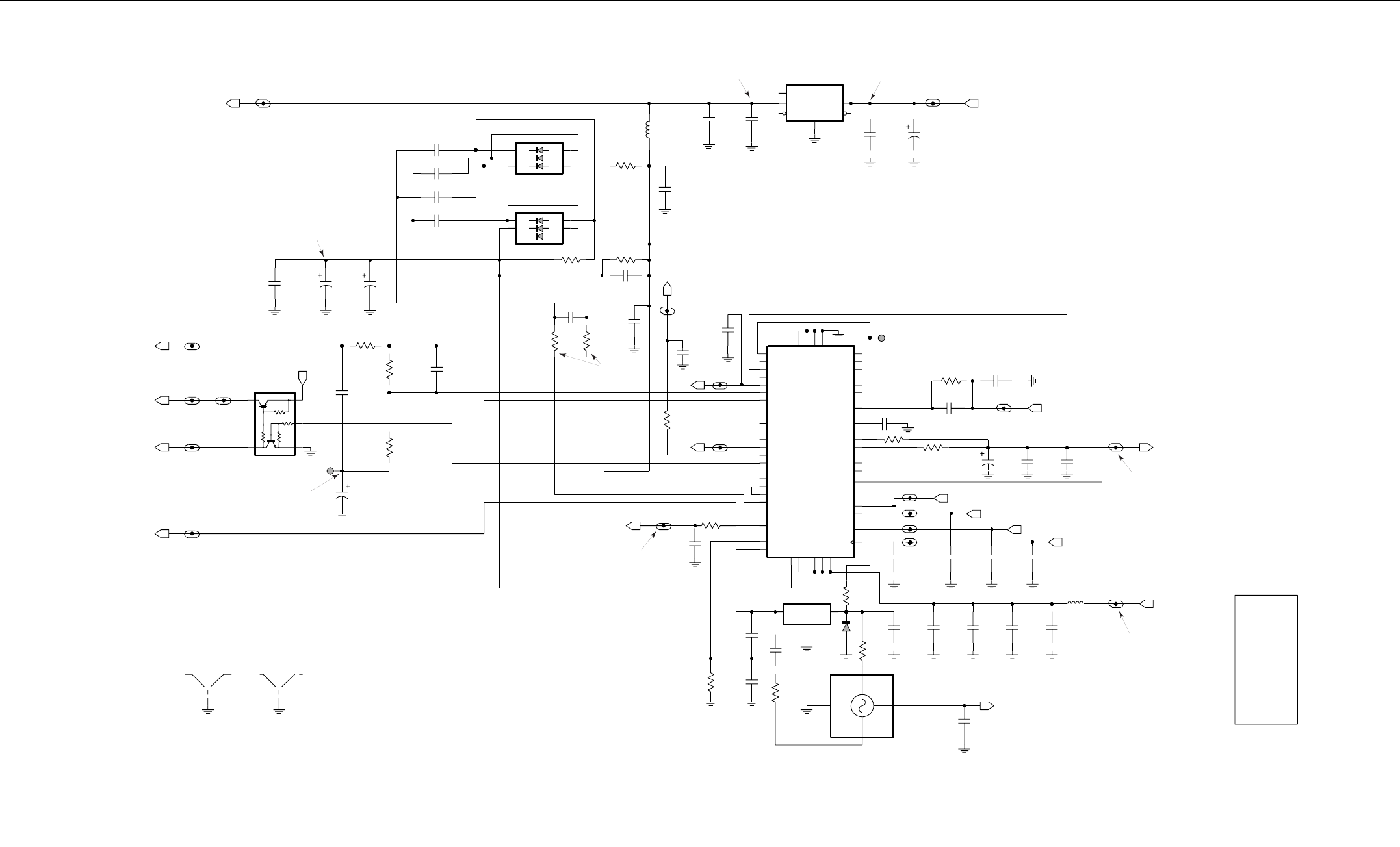
4-10 VHF PCB 8486062B12 / Schematics
1K
R3723
100
0.1uF
C3704
(SOURCE)
R3722
.01uF
C3701
.01uF
A1 6
A2 5
A3 4
K1
1K2
2K3
3
D3702
UMC5N
2
4
1
3
Q3721
UMC5N
C3762
C3761
330pF
56pF
C3703
.01uF
C3702 K2
3K3
.01uF
D3701
A1 6
A2 5
4
A3
1K1
2
.01uF
C3732
C3731
C3721
.01uF
0.1uF
C3724
1uF
L3731
2.2uH
0.1uF
C3712
2.2uF
C3713
10uF
C3711
2.2uF
C3755
2.2uF
C3733
L3701
C3746
390nH
220pF
C3745
220pF
C3744
220pF 220pF
C3743
R3752
330K R3751
200K C3753
4.7uF 1000pF
C3752 0.1uF
C3754
R3721
470
100pF
C3727
R3761
47K
D3761
C3706
4,7uF
C3722
0.1uF
C3705
150
R3703
0NU
R3702
R3701
0.1uF
C3708
100
5V SWB+
0102726B15
C3734
.01uF
C3763
1.6pF
C3742
220pF
R3762
NU
2.2K
VCTRL
LOCK
CSX
5V
R5
CLK
DATA
MODIN
16.8MHz 100
R3741
22pF
C3707
Vdda
0.1uF
C3709
150
R3704
33K
R3705
C3741
GND
3
IN
1OUT 2
NU
56pF
VCO_MOD
16.8MHz
Y3761
8.2pF
C3726
PRESC
TRB
VMULT2
VMULT3
VMULT4
VRO
WARP
XTAL1
XTAL2
VSF
SFCAP
SFIN
SFOUT
TEST1
TEST2
VBPASS
VCP
VMULT1
PD_GND
PD_VDD
PREIN
PRE_GND
PRE_VDD
PVREF
REFSEL
SFBASE
INDMULT
IOUT
LOCK
MODIN
MODOUT
NC1
NC2
NC3
CCOMP
CEX
CLK
DATA
DGND
DVDD
FREFOUT
IADAPT
AGND
AUX1
AUX2
AUX3
AUX4
AVDD
BIAS1
BIAS2
U3701
09Z8809Z88
ADAPTSW
SH3701
SHIELD
T5
R5_1_FN
SHIELD
PRESC_1_FN
SWB_PLUS_1_FN
VCTRL_1_FN
VSF_1_FN
R5_2_FN
T5_1_FN
VCO_MOD_1_FN
BIAS_ADJ_1_FN
TRB_1_FN
Vdda_1_FN
LOCK_1_FN
DATA_1_FN
5V_1_FN
CLK_1_FN
2.2uF
C3710
C3751
0.1uF
NU
R3763
NU
100
C3735
FADJ
4GND
3
OUT
1
VDD 5V
.01uF
NU
NU
OSC_16.8MHZ
Y3762
OSC_16.8MHZ
2
1
TP3702
1
TP3701
SHIELD
SH3702
SHIELD
NU
C3725
0.1uF
16_8MHz_1_FN
100K
R3727
MODIN_1_FN
CSX_1_FN
R3726
BIAS_ADJ
47K
NU
ADP3300
6ERR
1
GND
5
IN
2NR
4OUT
3
SD
VHF_FRACN
U3711
ADP3300
11
13
25
23
24
28
37
38
21
15
14
12
32
33
34
35
18
27
26
30
4
10
41
17
29
31
44
5
8
7
6
36
19
45
16
43
1
2
3
20
40
39
42
9
46
22
48
47
ZWG0130022-C
C3714
4,7uF
R3760
NU
0
470pF
C3715
400mV RMS
R: 5V
T: 0V
R: 0V
T: 5V
3.3V
120mV RMS
3Vpp
@1.05MHz
RF mV RMS measured with high impedance probe.
3.5 - 9.5V
@135-174MHz
13.2V
2.5V - 3.5V
4.55V
7.5V
5V
VHF (136-174 MHz) Synthesizer
ZWG0130022-C
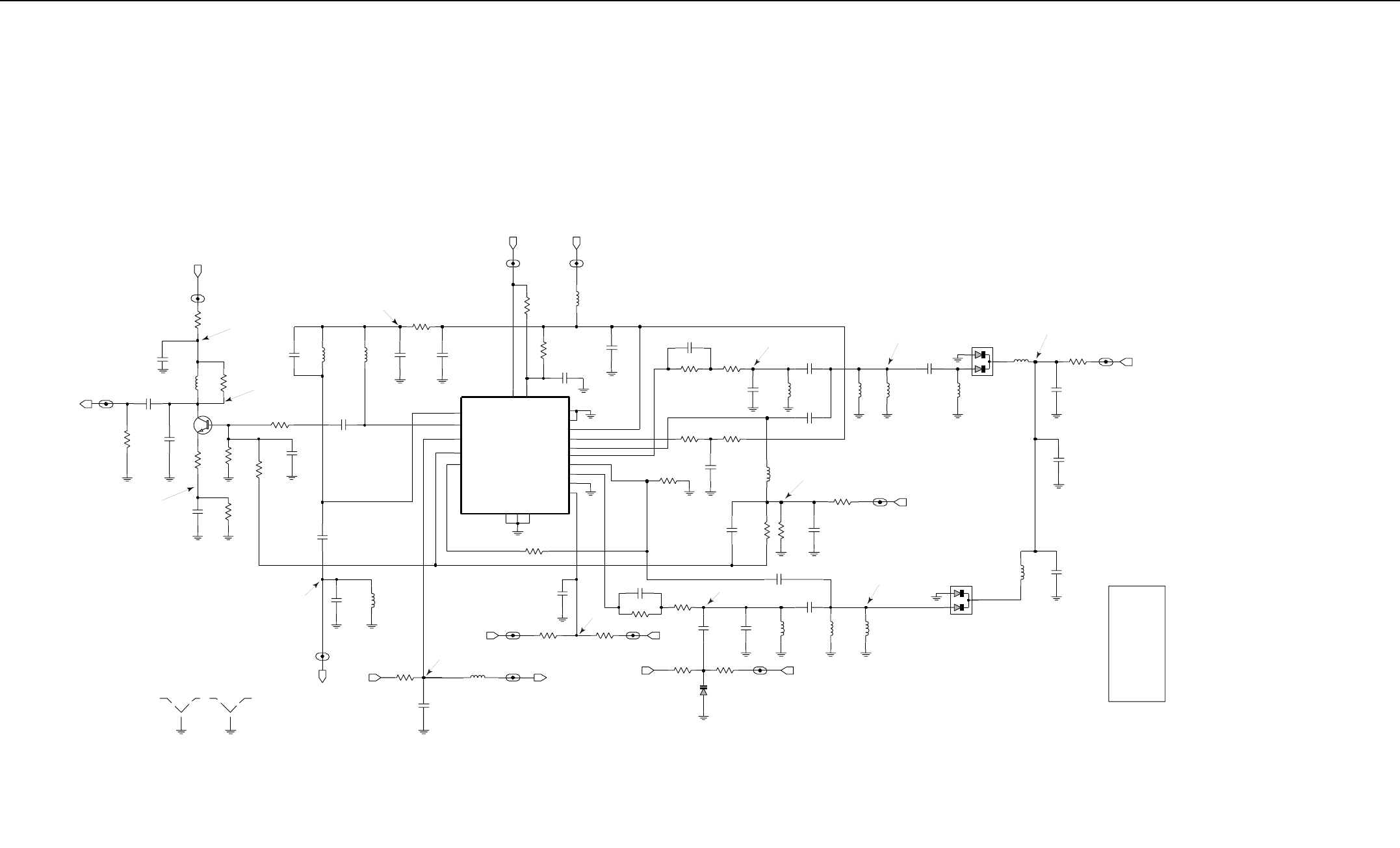
VHF PCB 8486062B12 / Schematics 4-11
NU
100K
R3812
4.7pF
15pF
C3833
C3836
C3822
1000pF
L3834
1uH
C3813
.01uF
6.8pF
1000pF
C3835
C3832
VSF_1_VCO
C3826
4.7pF
VCO_MOD_1_VCO
18
R3826
1
SHIELD
SH3802
SHIELD
1
SHIELD
SH3801
SHIELD
TX_INJ_1_VCO
L3824
1uH
R3835
47K
12K
10K
R3832
1K
R3831
R3816
10
R3808
1000pF
L3825
T5
C3815
100nH
C3842
1000pF
C3824
56pF
L3812
100nH
L3811
100nH
C3803
1000pF
0.1uF
VSF
RX_INJ_1_VCO
C3804
R3805
24K
NU0
R3830
L3821
56nH
C3806
100pF
Vdda
VSF
TRB
18
VCC_LOGIC
Q3801
3
SUPER_FLTR
TRB_IN
19
16
TX_BASE
15
TX_EMITTER
1
TX_IADJ
10
TX_OUT
13
TX_SWITCH
14
VCC_BUFFERS
9
GND_FLAG
GND_LOGIC
17
12
PRESC_OUT
5
RX_BASE
6
RX_EMITTER
2
RX_IADJ
8
RX_OUT
7
RX_SWITCH
4
COLL_RFIN
20
FLIP_IN
11
GND_BUFFERS
PRESC_1_VCO
U3801
50U54
47
10K
R3834
220
R3836
R3821
R3825
33
VCTRL_1_VCO
L3826
1uH
L3822
47nH
47
BIAS_ADJ
R3822
C3825
15pF
27nH
L3809
L3831
56nH
220
R3833
C3801
4.7pF
C3808
15pF
D3831
BIAS_ADJ_1_VCO
T5_1_VCO
R3806
22
D3832
R3801
220
100
R3802
R3803
220
C3802
22pF
NU
0.1uF
56nH
C3812
L3833
C3810
10pF
NU
L3816
100nH
R3811
100
0.22uF
C3827
C3823
.01uF
C3811
0.1uF
56pF
VCTRL
C3828
C3834
.01uF
100
R3828
C3809
PRESC
VCO_MOD
27pF
.01uF
C3829
R3818
0
NU
D3821
33K
R3823
10K
0102726B14
R3804
6.8pF
C3816
L3832
68nH
R3807
NU
C3821
.01uF
R5_1_VCO
C3818
.022uF
R3817
0
L3813
1uH
R3824
TRB_1_VCO
22K
Vdda_3_VCO
C3830
TX_INJ
R3829
68pF
R5
0
100nH
RX_INJ
L3801
VSF
L3823
47nH
VCO
NU
1K
ZWG0130020-B
C3805
4.7pF
T: 1V RMS
T: 250mV RMS
R:1.7V
T: 0V
R: 250mV RMS R: 1V RMS
R, T: 3.5V-9.5V
@ 135MHz-174MHz
R:4.6V
T: 0V
R:4V
T: 2.8V
800mV
RMS
3.3V
R:0V
T: 3.1V
3.1V
500mV
RMS
R:0.9V
T: 0V
RF mV RMS measured with high impedance probe.
4.55V
NU
100K
R3812
4.7pF
15pF
C3833
C3836
C3822
1000pF
L3834
1uH
C3813
.01uF
6.8pF
1000pF
C3835
C3832
VSF_1_VCO
C3826
4.7pF
VCO_MOD_1_VCO
18
R3826
1
SHIELD
SH3802
SHIELD
1
SHIELD
SH3801
SHIELD
TX_INJ_1_VCO
L3824
1uH
R3835
47K
12K
10K
R3832
1K
R3831
R3816
10
R3808
1000pF
L3825
T5
C3815
100nH
C3842
1000pF
C3824
56pF
L3812
100nH
L3811
100nH
C3803
1000pF
0.1uF
VSF
RX_INJ_1_VCO
C3804
R3805
24K
NU0
R3830
L3821
56nH
C3806
100pF
Vdda
VSF
TRB
18
VCC_LOGIC
Q3801
3
SUPER_FLTR
TRB_IN
19
16
TX_BASE
15
TX_EMITTER
1
TX_IADJ
10
TX_OUT
13
TX_SWITCH
14
VCC_BUFFERS
9
GND_FLAG
GND_LOGIC
17
12
PRESC_OUT
5
RX_BASE
6
RX_EMITTER
2
RX_IADJ
8
RX_OUT
7
RX_SWITCH
4
COLL_RFIN
20
FLIP_IN
11
GND_BUFFERS
PRESC_1_VCO
U3801
50U54
47
10K
R3834
220
R3836
R3821
R3825
33
VCTRL_1_VCO
L3826
1uH
L3822
47nH
47
BIAS_ADJ
R3822
C3825
15pF
27nH
L3809
L3831
56nH
220
R3833
C3801
4.7pF
C3808
15pF
D3831
BIAS_ADJ_1_VCO
T5_1_VCO
R3806
22
D3832
R3801
220
100
R3802
R3803
220
C3802
22pF
NU
0.1uF
56nH
C3812
L3833
C3810
10pF
NU
L3816
100nH
R3811
100
0.22uF
C3827
C3823
.01uF
C3811
0.1uF
56pF
VCTRL
C3828
C3834
.01uF
100
R3828
C3809
PRESC
VCO_MOD
27pF
.01uF
C3829
R3818
0
NU
D3821
33K
R3823
10K
0102726B14
R3804
6.8pF
C3816
L3832
68nH
R3807
NU
C3821
.01uF
R5_1_VCO
C3818
.022uF
R3817
0
L3813
1uH
R3824
TRB_1_VCO
22K
Vdda_3_VCO
C3830
TX_INJ
R3829
68pF
R5
0
100nH
RX_INJ
L3801
VSF
L3823
47nH
VCO
NU
1K
ZWG0130020-B
C3805
4.7pF
T: 1V RMS
T: 250mV RMS
R:1.7V
T: 0V
R: 250mV RMS R: 1V RMS
R, T: 3.5V-9.5V
@ 135MHz-174MHz
R:4.6V
T: 0V
R:4V
T: 2.8V
800mV
RMS
3.3V
R:0V
T: 3.1V
3.1V
500mV
RMS
R:0.9V
T: 0V
RF mV RMS measured with high impedance probe.
4.55V
VHF (136-174 MHz) Voltage Controlled Oscillator
ZWG0130020-B
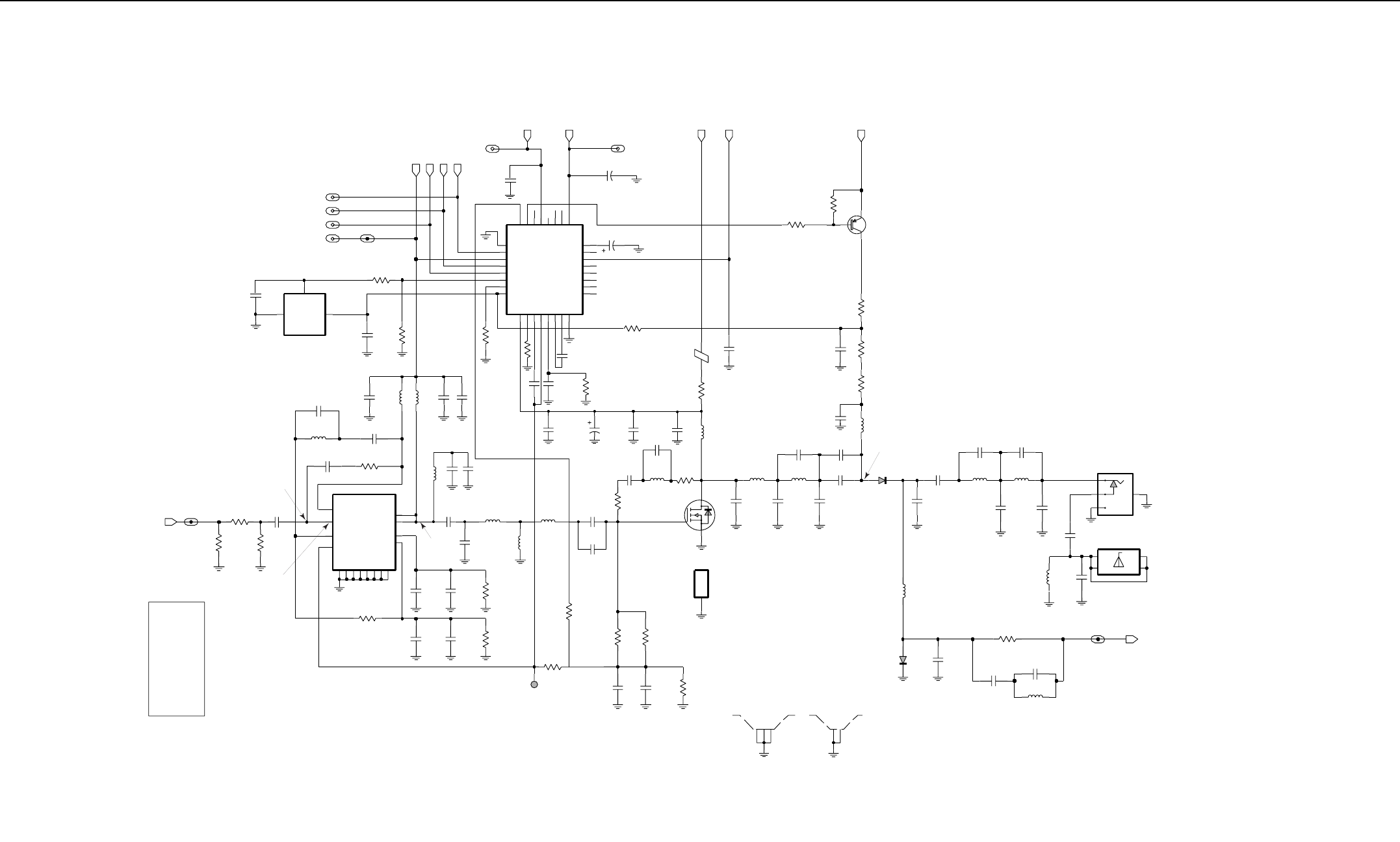
4-12 VHF PCB 8486062B12 / Schematics
C3535
5185963A15
1
Microstrip
LM50C
27pF 15pF
120pF
C3536
C3523
18pF
C3524
TAB3
4
TAB4
3300pF
C3568
J3502
ANTENNA_NUT
1TAB1
2TAB2
3
12 3
SHIELD
SH3501
SHIELD
1
RX_IN
5V
12
TP3502
UNSWB+
SHIELD
SH3502
SHIELD
Q3561
D
G
S
DATA
Q3501
330K
220pF
C3564
R3564
0.1
R3519
R3547
RX_IN_1_PA
12K
CSX
RESET
C3546
330pF
330pF
C3509
C3506
.022uF
68nH
7.66nH
L3504
L3513
47pF
C3512
VHF PA
100
R3544
UNSW_LPLUS_3_PA
0102726B11
UNSWB_LPLUS_2_PA
D3551
RESET_1_PA
33pF
330pF
C3503
C3501
300
R3503R3501
18
300
R3502
16
RFIN
11
G2
6
RFOUT1
RFOUT2 7
1
VCNTRL
NC3
10
NC4
15
GND1
4
GND2
5
GND3
12
GND4
13
2
VG1
3
VG2
U3501
NC1
8
NC2
9
5V_2_PA
UNSWB+
09Z67
16
V45
15
VG
6
VL
19
VLIM
17
VSH
DATA_2_PA
23
RX
32
T1
2
T2
30
TEMP
V1
20
14
V10
V2
18
V3
24
GND1
8
GND2
25
4
INT
OVI
31
11
Q
QX
10
1
RF
21
RS
CI
3
5
CJ
7
CL
26
CLK
12
CQ
CQX
13
28
DATA
9
F168
09Z46
U3502
22
ANO
BPOS
27
29
CEX
BEAD
L3519
BEAD
CLK_2_PA
CSX_2_PA
CLK
UNSWB+
UNSWB+
R3562
C3550
7.5pF
33K
100
11.03nH
R3545
L3512
C3534
4.7pF
C3533
7.5pF
R3546
33K
C3532
68pF
330pF
R3512
C3518
120
.022uF
C3504
1uH
L3523
C3526
C3525
.022uF
L3503
10pF
68nH
12K
R3561
.022uF
C3565
3300pF
3300pF
C3562
C3563
R3563
270K
C3561
.022uF
C3527
1.5pF
L3521
7.66nH
C3514
470pF
C3515
220pF
3300pF
C3521
C3569
.022uF
5.6K
R3571
R3569
R3572
120
120
R3573
120
7.66nH
56pF
L3552
C3551
C3552
39
68pF
R3551
R3570
100pF
10K
C3516
1uF
C3517
L3551
43.67nH
L3532
43.67nH43.67nH
L3531
23.75nH
L3522
C3505
33pF
R3505
5.6pF
330
C3539
1uF
C3519
22pF
C3560
30.54nH
L3518
39nH
L3538
L3515
13.85nH
18nH
L3511
C3544 R3542
330pF 5.6K
C3547
.022uF
R3541
NU
6.8K
R3543
100
C3531
18pF
C3537
20pF
HEATSINK
1
3
H3501
RF_JACK
J3501
GND 4
1
2
.022uF
C3543
330pF
C3541 C3542
30pF
.022uF
C3513
C3502
33pF
TX_INJ
5.6nH
L3501
GND
3
POS
VOUT
2
U3503
D3521
TX_INJ_1_PA
C3528
9.1pF
7.5k
R3548
330pF
C3507
C3506
.022uF
68nH
L3502
VD1
14
ZWG0130021-D
NU
NU
NU
C3566
100pF
R3565
330K
NU
100
R3513
C3570
330pF
0
NU
R3566
470pF
C3571
C3567
330pF
1.55VDC if VTP 3502 = 4.1VDC
1.44VDC if VTP 3502 = 3.8VDC
2V - 5V
RMS
> 200mV RMS
300 ~ 500mV RMS
Tx: 1.6VDC
Tx: 0.8VDC
3VDC for 5.5W
2.8VDC for 1W
4.0 - 4.2VDC for 5.5W
3.9 - 4.1VDC for 3W
3.7 - 4.0VDC for 1W
VHF (136-174 MHz) Transmitter
ZWG0130021-D
VHF PCB 8486062B12 Parts List 4-13
3.0 VHF PCB 8486062B12 Parts List
Circuit
Ref
Motorola
Part No Description
B501 0986237A02 CONN, CONTACT BATT
B503 3980502Z01 CONTACT, BACKUP B+
only GP360, GP380, GP680
B504 3980501Z01 CONTACT, BACKUP B-
only GP360, GP380, GP680
C3200 2113743N31 16.0 PF 5% COG
C3203 2113743N50 100 PF 5% COG
C3204 2113743L41 10000 PF 10%
C3205 2113928N01 CER CHIP 0.1UF 10% 6.3
C3206 2113743L41 10000 PF 10%
C3207 2113743N10 2.2 PF +-.25PF COG
C3209 2311049A07 TANT 10% 1.0UF
C3210 2113743L17 1000 PF 10%
C3211 2311049A56 TAN CHIP A/P 4.7 20 10
C3212 2311049A07 TANT 10% 1.0UF
C3213 2311049A56 TAN CHIP A/P 4.7 20 10
C3214 2113928N01 CER CHIP 0.1UF 10% 6.3
C3215 2113743N26 10.0 PF 5% COG
C3218 2311049A56 TAN CHIP A/P 4.7 20 10
C3219 2113928N01 CER CHIP 0.1UF 10% 6.3
C3220 2113743N26 10.0 PF 5% COG
C3221 2113743L41 10000 PF 10%
C3222 2113928N01 CER CHIP 0.1UF 10% 6.3
C3223 2113928N01 CER CHIP 0.1UF 10% 6.3
C3224 2113928N01 CER CHIP 0.1UF 10% 6.3
C3225 2113928N01 CER CHIP 0.1UF 10% 6.3
C3226 2113928N01 CER CHIP 0.1UF 10% 6.3
C3227 2113743L41 10000 PF 10%
C3228 2113743L41 10000 PF 10%
C3229 2113743N50 100 PF 5% COG
C3230 2113740F51 REEL CL1 +/-30 100
C3231 2180478Z20 MONOLITHIC CERAMIC (1.0UF)
C3232 2180478Z20 MONOLITHIC CERAMIC (1.0UF)
C3233 2180478Z20 MONOLITHIC CERAMIC (1.0UF)
C3234 2180478Z20 MONOLITHIC CERAMIC (1.0UF)
C3235 2113743A23 .220UF 10%
C3238 2113743A24 .330 UF 10% 16V
C3239 2113743E07 CER CHIP .022UF
C3240 2113743A23 .220UF 10%
C3241 2113743L19 1200 PF 10%
C3242 2109720D14 CER CHIP LOW DIST 0.1UF
C3243 2113743E07 CER CHIP .022UF
C3244 2113743L41 10000 PF 10%
C3270 2113743E07 CER CHIP .022UF
C3271 2113743L05 330 PF 10%
C3272 2113743N18 4.7 PF +-.25PF COG
C3273 2113743N26 10.0 PF 5% COG
C3274 2113743N38 33.0 PF 5% COG
C3275 2113743N44 56.0 PF 5% COG
C3276 2113743N42 47.0 PF 5% COG
C3277 2113743N48 82.0 PF 5% COG
C3278 2113743E07 CER CHIP .022UF
C3279 2311049A40 GLOBAL TANT 10% 2.2 UF
C3280 2113743L41 10000 PF 10%
C3301 2113743N20 5.6 PF +-.5PF COG
C3302 2113743N54 150 PF 5% COG
C3303 2113743N30 15.0PF 5% COG
C3304 2113743N54 150 PF 5% COG
C3306 2113928N01 CER CHIP 0.1UF 10% 6.3
C3307 2113743N50 100 PF 5% COG
C3308 2113743L05 330 PF 10%
C3309 2113928N01 CER CHIP 0.1UF 10% 6.3
C3311 2113743N54 150 PF 5% COG
C3312 2113743N31 16.0 PF 5% COG
C3313 2113743N54 150 PF 5% COG
C3315 2113743N26 10.0 PF 5% COG
C3316 2113743N14 3.3 PF +-.25PF COG
C3317 2113743N40 39.0 PF 5% COG
C3318 2113743M08 22000PF +80-20% Y5V
C3320 2113743N48 82.0 PF 5% COG
C3321 2113743L05 330 PF 10%
C3322 2113743N50 100 PF 5% COG
C3323 2113743N50 100 PF 5% COG
C3324 2113743N38 33.0 PF 5% COG
C3325 2113743L17 1000 PF 10%
C3327 2113743L05 330 PF 10%
C3329 2113743L05 330 PF 10%
C3330 2113743N50 100 PF 5% COG
C3331 2113743N50 100 PF 5% COG
C3332 2113743N40 39.0 PF 5% COG
C3334 2113743N33 20.0 PF 5% COG
C3335 2113743N34 22.0 PF 5% COG
C3336 2311049A18 TANT 10% 10UF
C3337 2113743M08 22000PF +80-20% Y5V
C3338 2113743L09 470 PF 10%
C3339 2113743N26 10.0 PF 5% COG
C3501 2113743L05 330 PF 10%
C3502 2113743N38 33.0 PF 5% COG
C3503 2113743N38 33.0 PF 5% COG
C3504 2113743M08 22000PF +80-20% Y5V
C3505 2113743N38 33.0 PF 5% COG
C3508 2113743M08 22000PF +80-20% Y5V
C3509 2113743L05 330 PF 10%
C3512 2113740F43 REEL CL1 +/-30 47
C3513 2113740F38 REEL CL1 +/-30 30
C3514 2113740F67 CL1 +/-30 470 5%
C3515 2113743L29 3300PF 10%
C3516 2311049A08 KEMET CAPS
C3517 2113740F51 REEL CL1 +/-30 100
C3518 2113740F63 CL1 +/-30 330 5%
C3519 2113740F35 REEL CL1 +/-30 22
C3521 2111078B51 RF 220 5 NPO 100V
C3523 2111078B44 RF 120 5 NPO 100V
C3524 2113740F33 REEL CL1 +/-30 18
C3525 2113740F27 REEL CL1 +/-30 10
C3526 2113743M08 22000PF +80-20% Y5V
C3528 2113740F26 REEL CL1 +/-30 9.1
C3531 2113740F34 REEL CL1 +/-30 20
C3532 2113740F47 REEL CL1 +/-30 68
C3533 2113740F24 REEL CL1+/-30 7.5
Circuit
Ref
Motorola
Part No Description
C3534 2113740F19 CHIP CAP, CER 4.7PF
C3535 2113740F37 REEL CL1+/-30 27
C3536 2113740F31 REEL CL1 +/-30 15
C3537 2113740F33 REEL CL1 +/-30 18
C3539 2113740F21 REEL CL1+/-30 5.6
C3541 2113743M08 22000PF +80-20% Y5V
C3542 2113743L05 330 PF 10%
C3543 2113743M08 22000PF +80-20% Y5V
C3544 2113743L05 330 PF 10%
C3546 2113743L05 330 PF 10%
C3547 2113743M08 22000PF +80-20% Y5V
C3550 2113743N23 7.5 PF +-.5PF COG
C3551 2113743N46 68.0 PF 5% COG
C3552 2113743N44 56.0 PF 5% COG
C3560 2311049A07 TANT 10% 1.0UF
C3561 2113743M08 22000PF +80-20% Y5V
C3562 2113743L29 3300PF 10%
C3563 2113743L29 3300PF 10%
C3564 2113743L01 220 PF 10%
C3565 2113743E07 CER CHIP .022UF
C3566 2113743N50 100 PF 5% COG
C3567 2113743L05 330 PF 10%
C3568 2113743L29 3300PF 10%
C3569 2113743M08 22000PF +80-20% Y5V
C3570 2113743L05 330 PF 10%
C3571 2113743L09 470 PF 10%
C3701 2113743L41 10000 PF 10%
C3702 2113743L41 10000 PF 10%
C3703 2113743L41 10000 PF 10%
C3704 2113743L41 10000 PF 10%
C3705 2113743E20 CHIP. 10 UF 10%
C3706 2311049J11 CAPACITOR TANT 10% 4.7UF
C3707 2113743N34 22.0 PF 5% COG
C3708 2113743M24 100000 PF +80-20% Y5V
C3709 2113743M24 100000 PF +80-20% Y5V
C3710 2104993J02 MONOLITHIC CERAMIC (2.2UF)
C3711 2311049A69 TAN CHIP 10.0 UF 20% 6.3V
C3712 2113743M24 100000 PF +80-20% Y5V
C3713 2311049A09 TANT 2.2 UF 10%
C3714 2311049J11 CAPACITOR TANT 10% 4.7UF
C3715 2113743L09 470 PF 10%
C3721 2113743E20 CHIP. 10 UF 10%
C3722 2113743E20 CHIP. 10 UF 10%
C3724 2311049A08 KEMET CAPS
C3726 2113743N24 8.2 PF + -.5PF COG
C3727 2113743N50 100 PF 5% COG
C3731 2113743L41 10000 PF 10%
C3732 2113743L41 10000 PF 10%
C3733 2104993J02 MONOLITHIC CERAMIC (2.2UF)
C3734 2113743L41 10000 PF 10%
C3742 2113743L01 220 PF 10%
C3743 2113743L01 220 PF 10%
C3744 2113743L01 220 PF 10%
C3745 2113743L01 220 PF 10%
C3746 2113743L01 220 PF 10%
C3752 2113743L17 1000 PF 10%
Circuit
Ref
Motorola
Part No Description
C3753 2311049A56 TAN CHIP A/P 4.7 20 10
C3754 2113743M24 100000 PF +80-20% Y5V
C3755 2104993J02 MONOLITHIC CERAMIC (2.2UF)
* C3761 2113743N44 56.0 PF 5% COG
* C3762 2113740F63 CL1 +/-30 330 5%
* C3763 2113743N08 1.6 PF +-.25PF COG
C3801 2113743N18 4.7 PF +-.25PF COG
C3803 2113743L17 1000 PF 10%
C3804 2113743E20 CHIP. 10 UF 10%
C3805 2113743N18 4.7 PF +-.25PF COG
C3806 2113743N50 100 PF 5% COG
C3808 2113743N30 15.0PF 5% COG
C3809 2113743N36 27.0 PF 5% COG
C3811 2113743M24 100000 PF +80-20% Y5V
C3812 2113743M24 100000 PF +80-20% Y5V
C3813 2113743L41 10000 PF 10%
C3815 2113743L17 1000 PF 10%
C3816 2113743N22 6.8 PF +-.5PF COG
C3818 2113743E07 CER CHIP .022UF
C3821 2113743L41 10000 PF 10%
C3822 2113743L17 1000 PF 10%
C3823 2113743L41 10000 PF 10%
C3824 2113743N44 56.0 PF 5% COG
C3825 2113743N30 15.0PF 5% COG
C3826 2113743N18 4.7 PF +-.25PF COG
C3827 2113743E07 CER CHIP .022UF
C3828 2109720D01 CER CHIP LOW DIS T .01UF
C3829 2109720D01 CER CHIP LOW DIS T .01UF
C3830 2113743N46 68.0 PF 5% COG
C3832 2113743L17 1000 PF 10%
C3833 2113743N18 4.7 PF +-.25PF COG
C3834 2113743N44 56.0 PF 5% COG
C3835 2113743N22 6.8 PF +-.5PF COG
C3836 2113743N30 15.0PF 5% COG
C3842 2113743L17 1000 PF 10%
C400 2113743L41 10000 PF 10%
C401 2113743M24 100000 PF +80-20% Y5V
C402 2113743M24 100000 PF +80-20% Y5V
C403 2113928D08 CERAMIC CHIP 10.0UF
C407 2113928N01 CER CHIP 0.1UF 10% 6.3
C408 2113743N50 100 PF 5% COG
C409 2113743M24 100000 PF +80-20% Y5V
C410 2113928N01 CER CHIP 0.1UF 10% 6.3
C411 2113743M24 100000 PF +80-20% Y5V
C414 2113743M24 100000 PF +80-20% Y5V
C415 2109720D01 CER CHIP LOW DIS T .01UF
C416 2113928N01 CER CHIP 0.1UF 10% 6.3
C419 2113743L41 10000 PF 10%
C420 2113743L41 10000 PF 10%
C421 2113928N01 CER CHIP 0.1UF 10% 6.3
C422 2113743M24 100000 PF +80-20% Y5V
C423 2113743N50 100 PF 5% COG
C424 2311049A59 TANT CHIP A/P 10UF 10% 6V
C425 2113743M24 100000 PF +80-20% Y5V
C426 2113743N50 100 PF 5% COG
C427 2113743N50 100 PF 5% COG
Circuit
Ref
Motorola
Part No Description

4-14 VHF PCB 8486062B12 Parts List
C428 2113743M24 100000 PF +80-20% Y5V
C429 2113743M24 100000 PF +80-20% Y5V
C430 2113928N01 CER CHIP 0.1UF 10% 6.3
C431 2113743N50 100 PF 5% COG
C433 2113743L41 10000 PF 10%
C434 2113743M24 100000 PF +80-20% Y5V
only GP360, GP380, GP680
C435 2113743M24 100000 PF +80-20% Y5V
C436 2113743N34 22.0 PF 5% COG
only GP360, GP380, GP680
C437 2113743N34 22.0 PF 5% COG
only GP360, GP380, GP680
C440 2113743G26 4.7UF 16V + 80-20%
C441 2113743L09 470 PF 10%
C442 2113743E20 CHIP. 10 UF 10%
C443 2113928N01 CER CHIP 0.1UF 10% 6.3
C444 2113743N50 100 PF 5% COG
C445 2113743L09 470 PF 10%
C446 2113743L09 470 PF 10%
C447 2113928N01 CER CHIP 0.1UF 10% 6.3
C448 2113928N01 CER CHIP 0.1UF 10% 6.3
C449 2113743N50 100 PF 5% COG
C451 2113743M08 22000PF +80-20% Y5V
C452 2113743G26 4.7UF 16V + 80-20%
C453 2113743N50 100 PF 5% COG
C456 2113743N50 100 PF 5% COG
C458 2113743N50 100 PF 5% COG
C459 2113743N50 100 PF 5% COG
C463 2113743N50 100 PF 5% COG
C466 2113743N50 100 PF 5% COG
C467 2113928N01 CER CHIP 0.1UF 10% 6.3
C471 2113743L09 470 PF 10%
C472 2113743L09 470 PF 10%
C473 2113743L09 470 PF 10%
C474 2113743L41 10000 PF 10%
C475 2113743H14 10.0 UF 16V +80-20%
C476 2113928D08 CERAMIC CHIP 10.0UF
C477 2113743L17 1000 PF 10%
C478 2113743L17 1000 PF 10%
C479 2113928N01 CER CHIP 0.1UF 10% 6.3
C480 2113928D08 CERAMIC CHIP 10.0UF
C481 2113928N01 CER CHIP 0.1UF 10% 6.3
C482 2113928N01 CER CHIP 0.1UF 10% 6.3
C483 2113743L09 470 PF 10%
C484 2113743L09 470 PF 10%
C490 2113743L09 470 PF 10%
C491 2113743L09 470 PF 10%
C492 2113743L09 470 PF 10%
C493 2113743N50 100 PF 5% COG
C494 2113743N50 100 PF 5% COG
C495 2113743L09 470 PF 10%
C496 2113743L09 470 PF 10%
C497 2113743L09 470 PF 10%
C502 2311049A05 TANT 10% 0.47UF
C503 2113743N50 100 PF 5% COG
C505 2113743N50 100 PF 5% COG
Circuit
Ref
Motorola
Part No Description
C511 2113743N50 100 PF 5% COG
C512 2113743N50 100 PF 5% COG
C513 2113743N50 100 PF 5% COG
C514 2113743N50 100 PF 5% COG
C520 2113743L41 10000 PF 10%
C521 2113743L41 10000 PF 10%
C522 2113743L41 10000 PF 10%
C523 2113743L41 10000 PF 10%
C535 2113743L17 1000 PF 10%
CR3301 4802245J42 RING QUAD SOT-143 PKG
CR3302 4805129M96 DIODE SMBV1032
CR3303 4880154K03 SOT MMBD353 DUAL SCHKY
CR411 4802245J47 SCHOTTKY BARRIER(RB471E)
CR412 4802245J62 SCHOTTKY BARRIER(RB471E)
CR413 4802245J62 SCHOTTKY BARRIER(RB471E)
CR440 4813833C02 DUAL 70V '5B' COMM CATH
CR501 4880107R01 RECTIFIER
CR503 4805729G49 LED RED/YEL
D3270 4862824C01 VARACTOR
D3301 4802081B58 DUAL SILCON (VARICAP)
D3302 4802081B58 DUAL SILCON (VARICAP)
D3521 4880973Z02 PIN DIODE
D3551 4880973Z02 PIN DIODE
D3701 4802233J09 TRIPLE SOT25-RH
D3702 4802233J09 TRIPLE SOT25-RH
* D3761 4862824C03 VARACTOR
D3821 4805649Q13 VCTR ISV 228
D3831 4805649Q13 VCTR ISV 228
D3832 4862824C01 VARACTOR
E400 2480640Z01 C/IND BK1005HM471 BEAD
E401 2480640Z01 C/IND BK1005HM471 BEAD
E402 2480640Z01 C/IND BK1005HM471 BEAD
E403 2480640Z01 C/IND BK1005HM471 BEAD
E404 2480640Z01 C/IND BK1005HM471 BEAD
E405 2480640Z01 C/IND BK1005HM471 BEAD
E406 2480640Z01 C/IND BK1005HM471 BEAD
E407 2480640Z01 C/IND BK1005HM471 BEAD
E408 2480640Z01 C/IND BK1005HM471 BEAD
E409 2480640Z01 C/IND BK1005HM471 BEAD
F501 6580542Z01 FUSE CHIP SMT TR/1608FF 3A
FL401 4870368G02 CLOCK OSC XTAL
only GP360, GP380, GP680
H3501 2680499Z01 HEAT SPREADER
J3501 0180117S05 RF JACK ASSEMBLY
J3502 0280519Z02 NUT, ANTENNA
J400 0905505Y04 CONN ZIF 40Pin
not in GP320
J403 0905505Y02 CONN ZIF MALE 20 PIN
L3200 2462587N68 CHIP IND 1000 NH 5%
L3202 2462587N68 CHIP IND 1000 NH 5%
L3221 2462587N68 CHIP IND 1000 NH 5%
L3270 2462587T15 IND CHIP 100NH 5% LOW PRO
L3271 2462587Q20 IND CHIP 2,200NH 20%
L3301 2462587T35 IND CHIP 12NH 5% LOW PRO
L3303 2462587T35 IND CHIP 12NH 5% LOW PRO
L3304 2462587T23 IND CHIP 470NH 5% LOW PRO
Circuit
Ref
Motorola
Part No Description
L3305 2462587T35 IND CHIP 12NH 5% LOW PRO
L3306 2462587T35 IND CHIP 12NH 5% LOW PRO
L3308 2462587T34 IND CHIP 10NH 5% LOW PRO
L3309 2462587N55 CHIP IND 150 NH 5%
L3312 2462587V28 CHIP IND 33 NH 5% 0805
L3501 2413926H09 IND CHIP 5.6 NH +/- 0.3NH
L3503 2462587V32 CHIP IND 68NH 5% 0805
L3504 2462587N51 CHIP IND 68 NH 5%
L3511 2462587N44 CHIP IND 18 NH 5%
L3512 2479990B01 AIR WOUND GREEN 11.03NH
L3513 2479990A02 AIR WOUND GREEN 7.66NH
L3515 2479990C03 AIR WOUND GREEN 13.85NH
L3518 2462587N48 CHIP IND 39 NH 5%
L3519 2484657R01 INDUCTOR BEAD CHIP
L3521 2479990A02 AIR WOUND GREEN 7.66NH
L3522 2479990E01 COIL AIR WOUND GREEN 23.75
L3523 2462587N68 CHIP IND 1000 NH 5%
L3531 2479990N01 AIR WOUND GREEN 43.67NH
L3532 2479990N01 AIR WOUND GREEN 43.67NH
L3538 2479990M01 AIR WOUND GREEN 30.54NH
L3551 2479990N01 AIR WOUND GREEN 43.67NH
L3552 2479990A02 AIR WOUND GREEN 7.66NH
L3701 2462587Q42 IND CHIP 390NH 10%
L3731 2462587Q20 IND CHIP 2,200NH 20%
L3801 2462587V34 CHIP IND 100NH 5% 0805
L3809 2462587V27 CHIP IND 27 NH 5% 0805
L3811 2462587V34 CHIP IND 100NH 5% 0805
L3812 2462587V34 CHIP IND 100NH 5% 0805
L3813 2462587Q47 IND CHIP 1000 NH 10%
L3816 2462587V34 CHIP IND 100NH 5% 0805
L3821 2462587N50 CHIP IND 56 NH 5%
L3822 2462587N49 CHIP IND 47 NH 5%
L3823 2462587N49 CHIP IND 47 NH 5%
L3824 2462587N68 CHIP IND 1000 NH 5%
L3825 2462587V34 CHIP IND 100NH 5%
L3826 2462587N68 CHIP IND 1000 NH 5%
L3831 2462587N50 CHIP IND 56 NH 5%
L3832 2462587N51 CHIP IND 68 NH 5%
L3833 2462587N50 CHIP IND 56 NH 5%
L3834 2462587N68 CHIP IND 1000 NH 5%
L400 2462587Q42 IND CHIP 390NH 10%
L401 2462587Q42 IND CHIP 390NH 10%
L410 2462587Q42 IND CHIP 390NH 10%
L411 2462587Q42 IND CHIP 390NH 10%
L505 2462587Q42 IND CHIP 390NH 10%
PB501 4080523Z01 SWITCH, TACT
PB502 4080523Z01 SWITCH, TACT
PB503 4080523Z01 SWITCH, TACT
not in GP320
PB504 4080523Z01 SWITCH, TACT
PB505 4080523Z01 SWITCH, TACT
not in GP320
Q3200 4813827A07 TSTR NPN SML SIG
MMBR941LT1
Q3201 4880214G02 TSTR MMBT3904
Q3202 4880214G02 TSTR MMBT3904
Circuit
Ref
Motorola
Part No Description
Q3270 4805218N63 RF TRANS SOT 323 BFQ67W
Q3301 4880214G02 TSTR MMBT3904
Q3302 4813827A07 TSTR NPN MMBR941LT1
Q3501 4802245J55 TSTR POWER FIELD EFFECT
Q3561 4813824A17 XSTR PNP40V .2A B=100-300
Q3721 4802245J50 TSTR DUAL NPN/PNP UMC5N
Q3801 4813827A07 TSTR NPN MMBR941LT1
Q400 4809579E18 MOSFET P-CHAN TP010IT
Q403 4880214G02 TSTR MMBT3904
Q405 4802245J54 UMG5N DIGITAL TRANSISTOR
Q410 4802245J54 UMG5N DIGITAL TRANSISTOR
Q416 4809579E18 MOSFET P-CHAN TP010IT
only GP360, GP380, GP680
Q417 4802245J50 TSTR DUAL NPN/PNP UMC5N
Q502 5180159R01 DUAL TRANS NPNS
Q505 4880214G02 TSTR MMBT3904
R3200 0662057M54 150 5% 20X40
R3201 0662057M82 2200 5% 20X40
R3202 0662057M90 4700 5% 20X40
R3203 0662057M98 10K 5% 20X40
R3204 0662057M26 10 5% 20X40
R3205 0662057M74 1000 5% 20X40
R3206 0662057N23 100K 5% 20X40
R3207 0662057N13 39K 5% 20X40
R3208 0662057M50 100 5% 20X40
R3209 0662057M74 1000 5% 20X40
R3210 0662057M82 2200 5% 20X40
R3211 0662057M82 2200 5% 20X40
R3212 0662057M90 4700 5% 20X40
R3213 0662057M82 2200 5% 20X40
R3214 0662057M34 22 5% 20X 40
R3219 0662057M50 100 5% 20X40
R3220 0662057M90 4700 5% 20X40
R3221 0662057M50 100 5% 20X40
R3224 0662057M26 10 5% 20X40
R3225 0662057M74 1000 5% 20X40
R3226 0662057M26 10 5% 20X40
R3270 0662057M74 1000 5% 20X40
R3271 0662057M42 47 5% 20X40
R3272 0662057N15 47K 5% 20X40
R3273 0662057N15 47K 5% 20X40
R3274 0662057M83 2400 5% 20X40
R3275 0662057M74 1000 5% 20X40
R3276 0662057N30 200K 5% 20X40
R3303 0662057N23 100K 5% 20X40
R3304 0662057N23 100K 5% 20X40
R3305 0662057N19 68K 5% 20X40
R3306 0662057M82 2200 5% 20X40
R3307 0662057N11 33K 5% 20X40
R3308 0662057M78 1500 5% 20X40
R3309 0662057M92 5600 5% 20X40
R3310 0662057M98 10K 5% 20X40
R3311 0662057M26 10 5% 20X40
R3312 0662057M38 33 5% 20X40
R3313 0662057M34 22 5% 20X 40
R3314 0662057M26 10 5% 20X40
Circuit
Ref
Motorola
Part No Description

VHF PCB 8486062B12 Parts List 4-15
* Motorola Depot Servicing only
Reference designators with an asterisk indicate
components which are not field replaceable
because they need to be calibrated with
specialized factory equipment after installation.
Radios in which these parts have been replaced in
the field will be off frequency at temperature
extremes.
R3315 0662057M62 330 5% 20X40
R3316 0662057M66 470 5% 20X40
R3317 0662057N23 100K 5% 20X40
R3318 0662057M66 470 5% 20X40
R3321 0662057M54 150 5% 20X40
R3322 0662057M58 220 5% 20X40
R3323 0662057M32 18 5% 20X40
R3324 0662057M58 220 5% 20X40
R3501 0662057M61 300 5% 20X40
R3502 0662057M32 18 5% 20X40
R3503 0662057M61 300 5% 20X40
R3505 0662057M62 330 5% 20X40
R3512 0662057A27 120 OHMS 5%
R3513 0662057A25 100 OHMS 5%
R3519 0680539Z01 POWER METAL STRIP
R3542 0662057M92 5600 5% 20X40
R3543 0662057M50 100 5% 20X40
R3544 0662057A25 100 OHMS 5%
R3545 0662057A25 100 OHMS 5%
R3546 0662057N11 33K 5% 20X40
R3547 0662057N01 12K 5% 20X40
R3548 0662057M95 7500 55 20X40
R3551 0662057M40 39 5% 20X40
R3561 0662057N01 12K 5% 20X40
R3562 0662057N11 33K 5% 20X40
R3563 0662057N33 270K 5% 20X40
R3564 0662057N35 330K 5% 20X40
R3569 0662057M92 5600 5% 20X40
R3570 0662057M98 10K 5% 20X40
R3571 0662057A27 120 OHMS 5%
R3572 0662057A27 120 OHMS 5%
R3573 0662057A27 120 OHMS 5%
R3701 0662057M50 100 5% 20X40
R3703 0662057M54 150 5% 20X40
R3704 0662057M54 150 5% 20X40
R3705 0662057N11 33K 5% 20X40
R3721 0662057M66 470 5% 20X40
R3722 0662057M74 1000 5% 20X40
R3723 0662057M50 100 5% 20X40
R3727 0662057N23 100K 5% 20X40
R3741 0662057M50 100 5% 20X40
R3751 0662057N30 200K 5% 20X40
R3752 0662057N35 330K 5% 20X40
R3761 0662057N15 47K 5% 20X40
R3802 0662057M50 100 5% 20X40
R3803 0662057M58 220 5% 20X40
R3804 0662057M98 10K 5% 20X40
R3805 0662057N08 24K 5% 20X40
R3806 0662057M34 22 5% 20X 40
R3808 0662057M26 10 5% 20X40
R3811 0662057M50 100 5% 20X40
R3816 0662057M74 1000 5% 20X40
R3817 0662057M01 0 5% 20X40
R3821 0662057M58 220 5% 20X40
R3822 0662057M42 47 5% 20X40
R3823 0662057N11 33K 5% 20X40
Circuit
Ref
Motorola
Part No Description
R3824 0662057N07 22K 5% 20X40
R3825 0662057M38 33 5% 20X40
R3826 0662057M32 18 5% 20X40
R3828 0662057M50 100 5% 20X40
R3829 0662057M01 0 5% 20X40
R3831 0662057M98 10K 5% 20X40
R3832 0662057N01 12K 5% 20X40
R3833 0662057M58 220 5% 20X40
R3834 0662057M42 47 5% 20X40
R3835 0662057N15 47K 5% 20X40
R3836 0662057M98 10K 5% 20X40
R400 0662057N15 47K 5% 20X40
R401 0662057M01 0 5% 20X40
R405 0662057M01 0 5% 20X40
R406 0662057N20 75K 5% 20X40
R407 0662057N19 68K 5% 20X40
R409 0662057M98 10K 5% 20X40
R410 0662057N23 100K 5% 20X40
R411 0662057M98 10K 5% 20X40
R413 0662057M01 0 5% 20X40
R414 0662057V34 180K 1% 1/16W
R415 0662057V26 91K 1% 1/16W
R416 0662057N13 39K 5% 20X40
R418 0662057M01 0 5% 20X40
R419 0662057M67 0 5% 20X40
only GP360, GP380, GP680
R420 0662057B46 10.0 MEG OHMS 5%
only GP360, GP380, GP680
R421 0662057M81 2000 5% 20X40
R423 0662057N21 82K 5% 20X40
R424 0662057N12 36K 5% 20X40
R425 0662057N10 30K 5% 20X40
R426 0662057N35 330K 5% 20X40
only GP360, GP380, GP680
R427 0662057M84 2700 5% 20X40
R428 0662057M10 2.2 5% 20X40
R429 0662057M98 10K 5% 20X40
R431 0662057N39 470K 5% 20X40
R432 0662057N16 51K 5% 20X40
R434 0662057M62 330 5% 20X40
R435 0662057M81 2000 5% 20X40
R436 0662057M01 0 5% 20X40
R445 0662057N08 24K 5% 20X40
R446 0662057N31 RES, CHIP 220K 5% 20X40
R447 0662057N51 RES, CHIP 1.5 MEG 5% 20X40
R448 0662057N33 270K 5% 20X40
R449 0662057N08 24K 5% 20X40
R450 0683962T45 68 5-1
R457 0662057M98 10K 5% 20X40
R460 0662057M90 4700 5% 20X40
R461 0662057M56 180 5% 20X40
only GP360, GP380, GP680
R462 0662057M98 10K 5% 20X40
only GP360, GP380, GP680
R463 0662057M61 300 5% 20X40
R471 0662057M92 5600 5% 20X40
Circuit
Ref
Motorola
Part No Description
R472 0662057M93 6200 5% 20X40
R473 0662057M26 10 5% 20X40
R475 0662057M01 0 5% 20X40
R476 0662057N08 24K 5% 20X40
R477 0662057M74 1000 5% 20X40
R478 0662057M98 10K 5% 20X40
R481 0662057N08 24K 5% 20X40
R492 0662057M01 0 5% 20X40
R501 0662057M70 680 5% 20X40
R502 0662057M56 180 5% 20X40
R505 0662057M98 10K 5% 20X40
R506 0662057N15 47K 5% 20X40
RT400 0680590Z01 THERMISTOR_33K
S501 4080710Z01 SWITCH (FREQUENCY)
only GP340, GP640
S501 4080710Z02 SWITCH (FREQUENCY)
only GP360, GP380, GP680
S502 1880619Z01 POTENTIOMETER, VOLUME
SH3201 2602023X08 SHIELD
SH3202 2686081B02 SHIELD
SH3203 2686081B03 SHIELD
SH3301 2686081B01 SHIELD
SH3302 2686081B05 SHIELD
SH3303 2686081B06 SHIELD
SH3501 2686081B03 SHIELD
SH3502 2686081B04 SHIELD
SH3701 2680511Z01 SHIELD SYNTHESIZER
SH3702 2680511Z01 SHIELD SYNTHESIZER
SH3801 2680513Z01 SHIELD VCO TOP
SH3802 2680514Z01 SHIELD VCO BOTTOM/LVZIF
SH400 2680505Z01 CONTROLLER TOP LEFT
SH401 2680506Z01 CONTROLLER TOP RIGHT
SH402 2680515Z01 CONTROLLER BOTTOM LEFT
SH403 2680516Z01 CONTROLLER BTM RIGHT
T3301 2580541Z01 BALUN TRANSFORMER
T3302 2580541Z01 BALUN TRANSFORMER
U3201 5102463J58 3.3V REG IN SOT23-5 PKG
U3220 5109632D83 IC LVZIF 2.2 H60G 48TQFP
U3501 5105109Z67 IC LDMOS DRIVER VHF/UHF
U3502 5185765B01 IC POWER CONTROL PASS 2.3
U3503 5185963A15 IC TEMP SENSOR 1M50C
U3701 5185963A27 IC FRACN AT25016 48 PIN GFP
U3711 5105739X05 IC 5V REGULATOR
U3801 5105750U54 IC VCO BUFFER
U400 5102463J40 REG 3.3V, LP2951CMM-3.3
U404 5185963A53 IC ASFIC CMP TQFP 48PIN PKG
U405 5102463J36 STATIC_RAM_32KX8
* U406 5102463J60 IC 512KX8 FLASH ROM
* U407 5102463J64 16KX8 SPI SERIAL EEPROM
U409 5102226J56 68HC11FLO_PASS5 TQFP
U410 5102463J57 REG 3.3V, ILC7062CM-33
only GP360, GP380, GP680
U420 5102463J44 AUDIO AMPLIFIER TDA8547TS
VR432 4805656W08 ZENER QUAD
VR433 4805656W08 ZENER QUAD
VR434 4802245J51 ZENER DIODE; BZX284-C6V8"
Circuit
Ref
Motorola
Part No Description
VR439 4880140L15 10V ZENER
VR447 4802245J53 ZENER_DIODE; BZX284-C10
VR448 4802245J53 ZENER_DIODE; BZX284-C10
VR449 4802245J53 ZENER_DIODE; BZX284-C10
VR450 4802245J53 ZENER_DIODE; BZX284-C10
VR501 4813830A18 6.8V 5% 225MWMMBZ5235B_
VR506 4802245J51 ZENER DIODE; BZX284-C6V8
Y3200 9186153B01 XTAL FILTER, SMD 45.1MHz
Y3761 4802245J49 CRYSTL 16.8MHZ WITH CLIP
Circuit
Ref
Motorola
Part No Description

4-16 VHF PCB 8486062B12 Parts List
Intentionally Left Blank
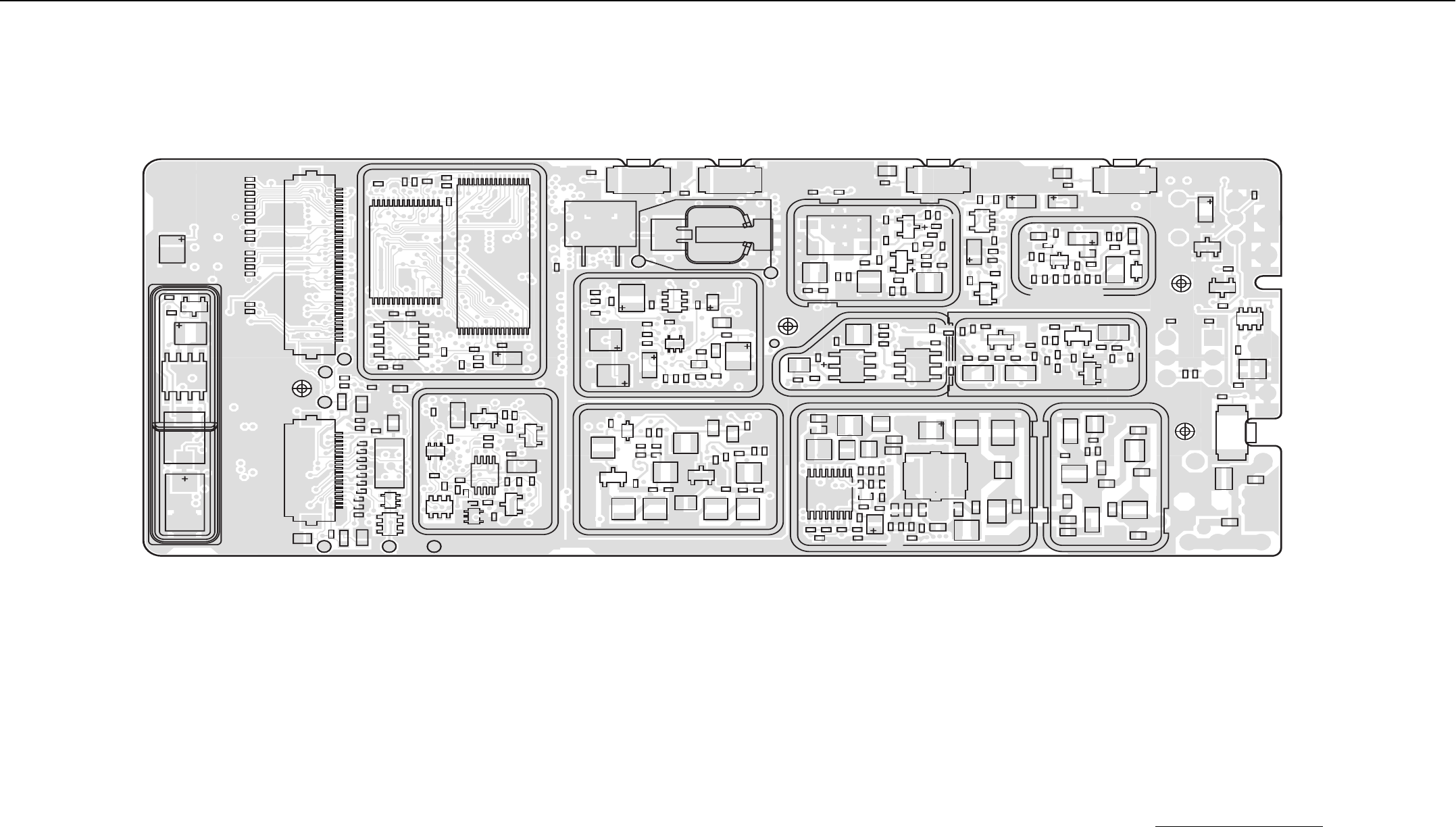
VHF PCB 8486101B09 / Schematics (GP1280) 4-17
4.0 VHF PCB 8486101B09 / Schematics (GP1280)
B503 B504
C400
C401
C402
C403
C423
C424
C425
C426
C427 C428
C429
C432
C441
C443 C444
C467
C471
C472
C473
C480
C482
C490
C491
C492
C493
C494
C495
C496
C497
C502
C505
C511
C512 C513
C514
C519
C520
C521
C522
C523
C601
C602
C603
C710
C3200
C3201
C3202
C3203
C3204
C3205
C3206
C3207
C3208
C3209
C3210
C3212 C3213
C3214
C3215
C3225
C3270C3271
C3272
C3273
C3274
C3275
C3276
C3277
C3278
C3279
C3280
C3306
C3307
C3308
C3309
C3310
C3311
C3312
C3313
C3314
C3318
C3319
C3320
C3327
C3329 C3330
C3331
C3332
C3334
C3335 C3338
C3501
C3502
C3503
C3504
C3505
C3512
C3513
C3514
C3517
C3518
C3519
C3521 C3523
C3524
C3525
C3527
C3528
C3531
C3532
C3533
C3534
C3535
C3536
C3537
C3539
C3541C3542
C3543
C3544
C3546
C3547
C3550
C3551
C3552
C3706
C3710
C3711
C3712
C3713
C3714
C3715
C3721
C3722
C3724
C3741
C3742
C3743
C3744
C3745
C3746
C3752
C3753
C3754
C3822
C3824C3825
C3826
C3828
C3829
C3830
C3832 C3833
C3834
C3835
C3836
C3842
C4001
C4002
C4003
C4004
C4005
C4007
C4008
C4009
C4010
C4011
C4012
C4013
C4014
C4015
C4016
CR412
CR413
CR440
4
3
2
CR503
CR601
CR3303
D3270
D3302
D3521
D3551
D3821
D3831
D3832
1
40
J400
22
20
1
21
J403
L400
L401
L601
L3200
L3201
L3202
L3270
L3271
L3304
L3305L3306
L3309
L3312
L3501
L3502
L3503
L3504
L3511 L3512
L3513
L3515
L3518
L3521
L3522
L3531
L3532
L3538
L3551
L3552
L3821
L3822
L3823
L3824
L3825
L3831
L3832 L3833
L3834
PB501PB502PB503 PB504
PB505
Q400
Q403
4
3
Q405
4
3
Q411
43
Q417
Q502
Q505
Q3200
Q3201
Q3202
Q3270
Q3302
1
23
Q3501
4
3
Q3721
R401
R402
R403
R405
R406
R407
R408
R410
R416
R418
R421
R427
R428
R429
R435
R437
R446
R447 R448
R450
R476
R477
R478
R481
R492
R499
R501
R502
R505
R506
R625
R3200
R3201
R3202
R3203
R3204
R3205
R3206
R3207
R3208
R3209
R3210
R3211
R3212
R3213
R3214 R3215
R3218
R3225 R3226
R3270
R3271
R3272
R3273
R3274
R3275
R3276
R3308
R3309
R3310
R3311
R3312
R3313
R3316
R3317
R3318
R3321
R3322
R3323
R3501
R3502 R3503
R3505 R3512
R3513
R3541
R3542
R3543
R3544
R3545
R3546
R3547
R3548
R3551
R3701
R3721
R3722
R3723
R3741
R3751
R3752
R3821
R3822
R3823
R3828
R3833 R3834
R3835
R3836
R4007
R4008
R4009
RT400
SH400
SH401
SH700
SH3201
SH3203
SH3302 SH3303
SH3501
SH3502
SH3701
SH3801
6
4
3
T3301
6
43
T3302
TP401
TP402
TP405
TP406
TP410
TP415
TP3301
TP3701
TP3702
4
58
U400
22
21
8
71
U405
Reference
Oscillator
Crystal
32 17
16
1
U406
IF Filter
1
45
8
U407
EEPROM
14
58
U601
U3201
1
16
8
9
U3501
LDMOS
Driver IC
U3711
VR434
VR440
VR444
VR447
VR449
VR450
VR501
Y3200
3
Y3761
1
15
5
1
5
1
1
1
5
28
1
1
WARIS VHF RF Board
8486101B10 TOP SIDE
CHECK
ONE
O.K. AS IS
O.K. AS MARKED
( )
( )
ISS. REVISION RLSE.
CORRECTED
AS
MARKED
ILLUSTRATOR DATEENGINEERDATE PROGRAM DISK
RLSE.
DWG. NO.
LETTERING SIZE:
REQUIRES:
EDITOR DATECHECKERDATE
Illustrator
RK 16/Aug/1999
ZWG0130096
B
ZWG0130096-B
VHF (136-174 MHz) Main Board Top Side
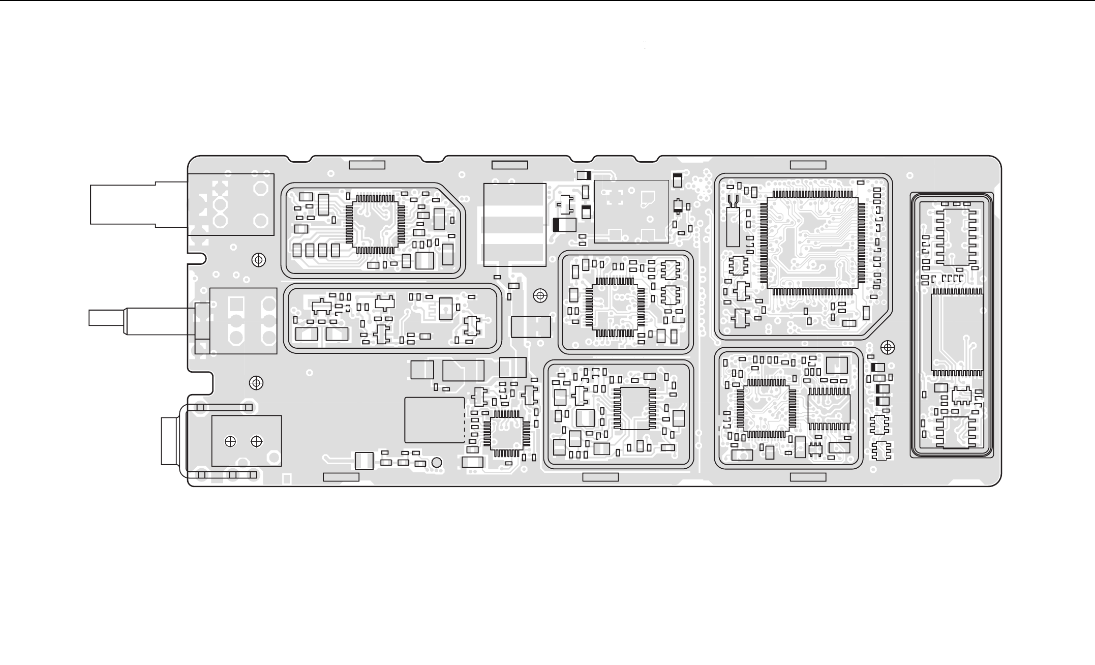
4-18 VHF PCB 8486101B09 / Schematics (GP1280)
ZWG0130097-B
1
2
3
B501
C407
C408
C409
C410
C411 C414
C415
C416
C419
C420
C421
C422
C430
C431
C433
C434
C435
C436
C437
C440
C442
C445
C446
C447
C448
C449
C450
C451
C452
C453
C456
C458
C459
C463
C466
C474
C475
C476
C477
C478
C479
C481
C483
C484
C503
C535
C701
C702
C703
C704
C705
C706
C707
C708C709
C711
C713
C714 C715
C717
C718
C719
C3211
C3218
C3219
C3220
C3221
C3222
C3223
C3224
C3226
C3227
C3228
C3229
C3230
C3231
C3232
C3233
C3234
C3235
C3236
C3237
C3238
C3239
C3240 C3241
C3242
C3243
C3244
C3301
C3302 C3303 C3304
C3305
C3315
C3316
C3317
C3321
C3322C3323C3324
C3325
C3326
C3336
C3337
C3339
C3506
C3507 C3508
C3509
C3515
C3516
C3526
C3560
C3561
C3562
C3563
C3564
C3565
C3566
C3567
C3568
C3569 C3570
C3571
C3701
C3702
C3703
C3704
C3705
C3707
C3708
C3709
C3725
C3726
C3727
C3731
C3732
C3733
C3734
C3735
C3751
C3755
C3761
C3762
C3763
C3801
C3802
C3803
C3804
C3805
C3806
C3808
C3809
C3810
C3811 C3812
C3813
C3815
C3816
C3818
C3821
C3823
C3827
C4006
C4020
C4021
CR411
CR501
CR700
CR3301
CR3302
D3301
D3701D3702
D3761
E400
F501
3
FL401
H3501
2
3
4
J3501
J3502
L410
L411
L505
L3221
L3301 L3303
L3308
L3519
L3523
L3701
L3731
L3801
L3809
L3811
L3812
L3813
L3816
L3826
M701 M702 M703
M704 M705 M706
4
3
Q410
Q416
Q3301
Q3561
Q3801
R400
R409
R411
R413
R414
R415
R419
R420
R423
R424
R425
R426
R431
R432
R434
R436
R445
R449
R457
R460
R461
R462
R463
R471
R472
R473
R475
R626
R627
R701
R702
R703
R704
R705
R706
R707
R708
R709
R710
R716
R717
R3219
R3220
R3221
R3222
R3223
R3224
R3301
R3303
R3304
R3305
R3306
R3307
R3314
R3315
R3319 R3320
R3324
R3519
R3561
R3562
R3563
R3564
R3565
R3566
R3569 R3570
R3571
R3572R3573
R3702
R3703
R3704
R3705
R3726
R3727
R3760 R3761
R3762
R3763
R3801
R3802
R3803
R3804
R3805
R3806
R3807
R3808
R3811
R3812
R3816
R3817
R3818
R3824
R3825
R3826
R3829
R3830
R3831
R3832
R4001
R4002
R4003
R4004
R4005
R4006
RT3301
2
C
8
C
4
S501
4
5
3
2S502
SH402
SH403
SH701
SH3202
SH3301
SH3702
SH3802
TP3502
1
37 25
13
U404
ASFIC
1
76
51 26
U409
Microprocessor
U410
11
1
20
10
U420
Audio PA
28 15
14
1
U700
8
7
114
U710
1
45
8
U720
1
37
25 13
U3220
LVZIF
1
17
9
25
U3502
Power
Control IC
U3503
1
37
25 13
U3701
FRACN
Synthesizer
11
120
10
U3801
VCO
Buffer
VR432
VR433
VR439
VR441
VR442
VR448
VR483
VR484
VR506
2
34
Y3762
48
1
1
5
32
100
R499
R498
VHF (136-174 MHz) Main Board Bottom Side
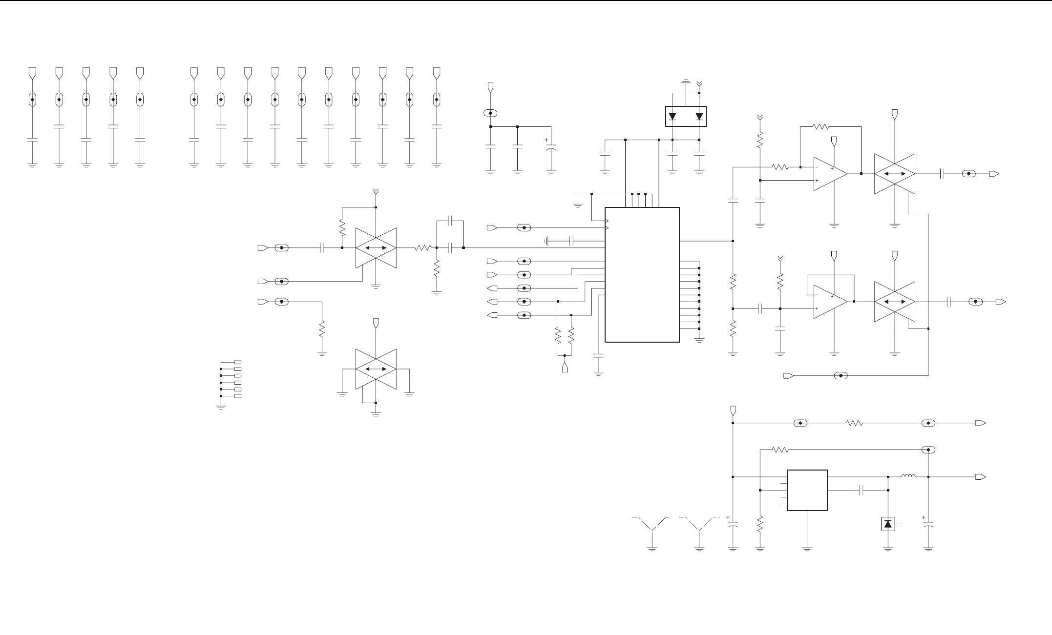
VHF PCB 8486101B09 / Schematics (GP1280) 4-19
Vddd_key
Vddd_voice
C4001
NU
SWB+_key
C4002
100pF
SWB+_voice
RESET_key
100pF
C4003
RESET_voice
MISO_key
C4004
NU
MISO_voice
NU
C4005
DATA_key
DATA_voice
C4007
NU
D0_Voice
D0_key
D1_voice
D1_key
C4008
NU
D2_voice
D2_key
C4009
NU
D3_voice
D3_key
NU
C4010
D4_voice
D4_key
C4011
NU
D5_voice
D5_key
D6_key
NU
C4012
D6_voice
NU
C4013
CLK_voice
A0_voice
D7_voice
D7_key
A0_key
CLK_key
NU
C4014
NU
C4016
NU
C4015
IF_Vddd_1_VOICE
Vddd
0.1uF
C708 C709
1000pF
C710
33uF 1uF
C701
5
3
1
2
4
CR700
C702
100pF
0.1uF C703
Vddd
U700
ISD33000
4
NC2 13
NC3 14
NC4 15
NC5 16
NC6 19
NC7 21
NC8 23
NC9
20
AUDOUT
3
NC1
27
NC10 28
NC11
6XCLK
2RAC
8SCLK
9SS
25 ANA_POS
INT
5
11 MISO
10 MOSI
AMCAP
22
24 ANA_NEG
12
VSSD
26
VCCA
7
VCCD
1
VSSA1 18
VSSA2 17
VSSA3
IF_CLK_1_VOICE
IF_DATA_1_VOICE
IF_VS_INT_1_VOICE
IF_MISO_1_VOICE
IF_VS_CS_1_VOICE
DATA
VS_CS
CLK
MISO
IF_VS_RAC_1_VOICE
VS_RAC
VS_INT
C704
0.1uF
39K R705
R704 39K
C705
0.1uF
Vddd
CNTL
5
43
14
VDD
VSS
7
MC74HC4066
U710-2
18K
R701
Vddd
C707
0.1uF
R702
18K
NU
C706
IF_RX_AUD_RTN_1_VOICE
IF_VS_GAINSEL_1_VOICE
IF_PRIME_ID_1_VOICE
C719
0.1uF
PRIME_ID
VS_GAINSEL
RX_AUD_RTN
R708
560K
1K
R703
Vddd
89
VDD
14
VSS
7
U710-3
MC74HC4066
CNTL
6
M702
M701
M706
M704
M705
M703
C601
NU
SH701
SHIELD
SH700
SHIELD
NU
R626
R627
NU
NU
C602
SYNC
VIN VSW 8
CB 1
FB
GND
6
ON_OFF
SS
U601
NU
NU
R625
IF_VS_AUDSEL_1_VOICE
IF_SWB_PLUS_1_VOICE
VS_AUDSEL
L601
NU
C603
NU
CR601
NU
IF_4V_3_3V_1_VOICE
IF_INT_EXT_Vdd_1_VOICE
INT_EXT_Vdd
4V_3.3V
SWB+
C714
0.1uF
12K
R716
C717
R710
0.1uF
470K
Vddd R717
2
3
8
4
2.2K
U720-1
SWB+
1
7
VSS
MC74HC4066
U710-1
CNTL
13
12 VDD
14
C713
0.1uF
Vddd
IF_FLAT_RX_SND_1_VOICE
FLAT_RX_SND
0.1uF
C715 IF_EXT_MIC_1_VOICE
EXT_MIC
U710-4
CNTL
12
1110 VDD
14
VSS
7
MC74HC4066
Vddd
6
5
7
8
4
U720-2
1MEG
R709
C718
1000pF
SWB+
5.1K
R707
R706
56K
.01uF
C711
Vddd
GORE pads
3
7
4
5
2
ZMY0130493-O
VHF (136-174 MHz) GP1280 - Voice Storage Schematic

4-20 VHF PCB 8486101B09 / Schematics (GP1280)
Intentionally Left Blank

VHF PCB 8086101B09 Parts List (GP1280) 4-21
5.0 VHF PCB 8086101B09 Parts List
(GP1280)
Circuit
Ref
Motorola
Part No Description
B501 0986237A01 CONN, CONTACT BATTERY
B503 3980502Z01 CONTACT, BACKUP B+
B504 3980501Z01 CONTACT, BACKUP B-
C3200 2113743N31 16.0 PF 5%
C3203 2113743N50 100 PF 5%
C3204 2113743L41 10000 PF 10%
C3205 2113928N01 0.1UF 10% 6.3
C3206 2113743L41 10000 PF 10%
C3207 2113743N10 2.2 PF +-.25PF
C3209 2311049A07 TANT 10% 1.0UF
C3210 2113743L17 1000 PF 10%
C3211 2311049A56 TAN CHIP A/P 4.7 20 10
C3212 2311049A07 TANT 10% 1.0UF
C3213 2311049A56 TAN CHIP A/P 4.7 20 10
C3214 2113928N01 CERAMIC CHIP 10.0UF
C3215 2113743N26 10.0 PF 5%
C3218 2311049A56 TAN CHIP A/P 4.7 20 10
C3219 2113928N01 CERAMIC CHIP 10.0UF
C3220 2113743N26 10.0 PF 5%
C3221 2113743L41 10000 PF 10%
C3222 2113928N01 CERAMIC CHIP 10.0UF
C3223 2113928N01 0.1UF 10% 6.3
C3224 2113928N01 0.1UF 10% 6.3
C3225 2113928N01 0.1UF 10% 6.3
C3226 2113928N01 0.1UF 10% 6.3
C3227 2113743L41 10000 PF 10%
C3228 2113743L41 10000 PF 10%
C3229 2113743N50 100 PF 5%
C3230 2113740F51 REEL CL1 +/-30 100
C3231 2180478Z20 MONOLITH CERAMIC (1.0UF)
C3232 2180478Z20 MONOLITH CERAMIC (1.0UF)
C3233 2180478Z20 MONOLITH CERAMIC (1.0UF)
C3234 2180478Z20 MONOLITH CERAMIC (1.0UF)
C3235 2113743A23 .220UF 10%
C3238 2113743A24 .330 UF 10% 16V
C3239 2113743E07 .022UF
C3240 2113743A23 .220UF 10%
C3241 2113743L19 1200 PF 10%
C3242 2109720D14 LOW DIST 0.1UF
C3243 2113743E07 .022UF
C3244 2113743L41 10000 PF 10%
C3270 2113743E07 .022UF
C3271 2113743L05 330 PF 10%
C3272 2113743N18 4.7 PF +-.25PF
C3273 2113743N26 10.0 PF 5%
C3274 2113743N38 33.0 PF 5%
C3275 2113743N44 56.0 PF 5%
C3276 2113743N42 47.0 PF 5%
C3277 2113743N48 82.0 PF 5%
C3278 2113743E07 .022UF
C3279 2311049A40 GLOBAL TANT 10% 2.2 UF
C3280 2113743L41 10000 PF 10%
C3301 2113743N20 5.6 PF +-.5PF
C3302 2113743N54 150 PF 5%
C3303 2113743N30 15.0PF 5%
C3304 2113743N54 150 PF 5%
C3306 2113928N01 0.1UF 10% 6.3
C3307 2113743N50 100 PF 5%
C3308 2113743L05 330 PF 10%
C3309 2113928N01 0.1UF 10% 6.3
C3311 2113743N54 150 PF 5%
C3312 2113743N31 16.0 PF 5%
C3313 2113743N54 150 PF 5%
C3315 2113743N26 10.0 PF 5%
C3316 2113743N14 3.3 PF +-.25PF
C3317 2113743N40 39.0 PF 5%
C3318 2113743M08 22000PF +80-20% Y5V
C3320 2113743N48 82.0 PF 5%
C3321 2113743L05 330 PF 10%
C3322 2113743N50 100 PF 5%
C3323 2113743N50 100 PF 5%
C3324 2113743N38 33.0 PF 5%
C3325 2113743L17 1000 PF 10%
C3327 2113743L05 330 PF 10%
C3329 2113743L05 330 PF 10%
C3330 2113743N50 100 PF 5%
C3331 2113743N50 100 PF 5%
C3332 2113743N40 39.0 PF 5%
C3334 2113743N33 20.0 PF 5%
C3335 2113743N34 22.0 PF 5%
C3336 2311049A18 CAP. TANT 10% 10UF
C3337 2113743M08 22000PF +80-20% Y5V
C3338 2113743L09 470 PF 10%
C3339 2113743N26 10.0 PF 5%
C3501 2113743L05 330 PF 10%
C3502 2113743N38 33.0 PF 5%
C3503 2113743N38 33.0 PF 5%
C3504 2113743M08 22000PF +80-20% Y5V
C3505 2113743N38 33.0 PF 5%
C3508 2113743M08 22000PF +80-20% Y5V
C3509 2113743L05 330 PF 10%
C3512 2113740F43 REEL CL1 +/-30 47
C3513 2113740F38 REEL CL1 +/-30 30
C3514 2113740F67 CL1 +/-30 470 5%
C3515 2113743L29 3300PF 10%
C3516 2311049A08 KEMET CAPS
C3517 2113740F51 REEL CL1 +/-30 100
C3518 2113740F63 CL1 +/-30 330 5%
Circuit
Ref
Motorola
Part No Description
C3519 2113740F35 REEL CL1 +/-30 22
C3521 2111078B51 RF 220 5 NPO 100V
C3523 2111078B44 RF 120 5 NPO 100V
C3524 2113740F33 REEL CL1 +/-30 18
C3525 2113740F27 REEL CL1 +/-30 10
C3526 2113743M08 22000PF +80-20% Y5V
C3528 2113740F26 REEL CL1 +/-30 9.1
C3531 2113740F34 REEL CL1 +/-30 20
C3532 2113740F47 REEL CL1 +/-30 68
C3533 2113740F24 REEL CL1+/-30 7.5
C3534 2113740F19 CHIP CAP, CER 4.7PF
C3535 2113740F37 REEL CL1+/-30 27
C3536 2113740F31 REEL CL1 +/-30 15
C3537 2113740F33 REEL CL1 +/-30 18
C3539 2113740F21 REEL CL1+/-30 5.6
C3541 2113743M08 22000PF +80-20% Y5V
C3542 2113743L05 330 PF 10%
C3543 2113743M08 22000PF +80-20% Y5V
C3544 2113743L05 330 PF 10%
C3546 2113743L05 330 PF 10%
C3547 2113743M08 22000PF +80-20% Y5V
C3550 2113743N23 7.5 PF +-.5PF
C3551 2113743N46 68.0 PF 5%
C3552 2113743N44 56.0 PF 5%
C3560 2311049A07 TANT 10% 1.0UF
C3561 2113743M08 22000PF +80-20% Y5V
C3562 2113743L29 3300PF 10%
C3563 2113743L29 3300PF 10%
C3564 2113743L01 220 PF 10%
C3565 2113743E07 .022UF
C3566 2113743N50 100 PF 5%
C3567 2113743L05 330 PF 10%
C3568 2113743L29 3300PF 10%
C3569 2113743M08 22000PF +80-20% Y5V
C3570 2113743L05 330 PF 10%
C3571 2113743L09 470 PF 10%
C3701 2113743L41 10000 PF 10%
C3702 2113743L41 10000 PF 10%
C3703 2113743L41 10000 PF 10%
C3704 2113743L41 10000 PF 10%
C3705 2113743E20 CHIP. 10 UF 10%
C3706 2311049J11 CAPACITOR TANT 10% 4.7UF
C3707 2113743N34 22.0 PF 5%
C3708 2113743M24 100000 PF +80-20% Y5V
C3709 2113743M24 100000 PF +80-20% Y5V
C3710 2104993J02 MONOLITH CERAMIC (2.2UF)
C3711 2311049A69 TAN CHIP 10.0 UF 20% 6.3V
C3712 2113743M24 100000 PF +80-20% Y5V
C3713 2311049A09 TANT 2.2 UF 10%
C3714 2311049J11 CAPACITOR TANT 10% 4.7UF
C3715 2113743L09 470 PF 10%
Circuit
Ref
Motorola
Part No Description
C3721 2113743E20 CHIP. 10 UF 10%
C3722 2113743E20 CHIP. 10 UF 10%
C3724 2311049A08 KEMET CAPS
C3726 2113743N24 8.2 PF + -.5PF
C3727 2113743N50 100 PF 5%
C3731 2113743L41 10000 PF 10%
C3732 2113743L41 10000 PF 10%
C3733 2104993J02 MONOLITH CERAMIC (2.2UF)
C3734 2113743L41 10000 PF 10%
C3742 2113743L01 220 PF 10%
C3743 2113743L01 220 PF 10%
C3744 2113743L01 220 PF 10%
C3745 2113743L01 220 PF 10%
C3746 2113743L01 220 PF 10%
C3752 2113743L17 1000 PF 10%
C3753 2311049A56 TAN CHIP A/P 4.7 20 10
C3754 2113743M24 100000 PF +80-20% Y5V
C3755 2104993J02 MONOLITH CERAMIC (2.2UF)
* C3761 2113743N44 56.0 PF 5%
* C3762 2113740F63 330 CL1 +/-30 5%
* C3763 2113743N08 1.6 PF +-.25PF
C3801 2113743N18 4.7 PF +-.25PF
C3803 2113743L17 1000 PF 10%
C3804 2113743E20 CHIP. 10 UF 10%
C3805 2113743N18 4.7 PF +-.25PF
C3806 2113743N50 100 PF 5%
C3808 2113743N30 15.0PF 5%
C3809 2113743N36 27.0 PF 5%
C3811 2113743M24 100000 PF +80-20% Y5V
C3812 2113743M24 100000 PF +80-20% Y5V
C3813 2113743L41 10000 PF 10%
C3815 2113743L17 1000 PF 10%
C3816 2113743N22 6.8 PF +-.5PF
C3818 2113743E07 .022UF
C3821 2113743L41 10000 PF 10%
C3822 2113743L17 1000 PF 10%
C3823 2113743L41 10000 PF 10%
C3824 2113743N44 56.0 PF 5%
C3825 2113743N30 15.0PF 5%
C3826 2113743N18 4.7 PF +-.25PF
C3827 2113743E07 .022UF
C3828 2109720D01 LOW DIS T .01UF
C3829 2109720D01 LOW DIS T .01UF
C3830 2113743N46 68.0 PF 5%
C3832 2113743L17 1000 PF 10%
C3833 2113743N18 4.7 PF +-.25PF
C3834 2113743N44 56.0 PF 5%
C3835 2113743N22 6.8 PF +-.5PF
C3836 2113743N30 15.0PF 5%
C3842 2113743L17 1000 PF 10%
C400 2113743L41 10000 PF 10%
Circuit
Ref
Motorola
Part No Description

4-22 VHF PCB 8086101B09 Parts List (GP1280)
C4001 2113743N50 100 PF 5%
C4002 2113743N50 100 PF 5%
C4003 2113743N50 100 PF 5%
C401 2113743M24 100000 PF +80-20% Y5V
C402 2113743M24 100000 PF +80-20% Y5V
C4020 2113743L17 1000 PF 10%
C4021 2113743L17 1000 PF 10%
C403 2113928D08 CERAMIC CHIP 10.0UF
C407 2113928N01 0.1UF 10% 6.3
C408 2113743N50 100 PF 5%
C409 2113743M24 100000 PF +80-20% Y5V
C410 2113928N01 0.1UF 10% 6.3
C411 2113743M24 100000 PF +80-20% Y5V
C414 2113743M24 100000 PF +80-20% Y5V
C415 2109720D01 LOW DIS T .01UF
C416 2113928N01 0.1UF 10% 6.3
C419 2113743L41 10000 PF 10%
C420 2113743L41 10000 PF 10%
C421 2113928N01 0.1UF 10% 6.3
C422 2113743M24 100000 PF +80-20% Y5V
C423 2113743N50 100 PF 5%
C424 2311049A59 TANT CHIP A/P 10UF 10% 6V
C425 2113743M24 100000 PF +80-20% Y5V
C426 2113743N50 100 PF 5%
C427 2113743N50 100 PF 5%
C428 2113743M24 100000 PF +80-20% Y5V
C429 2113743M24 100000 PF +80-20% Y5V
C430 2113928N01 0.1UF 10% 6.3
C431 2113743N50 100 PF 5%
C433 2113743L41 10000 PF 10%
C434 2113743M24 100000 PF +80-20% Y5V
C435 2113743M24 100000 PF +80-20% Y5V
C436 2113743N34 22.0 PF 5%
C437 2113743N34 22.0 PF 5%
C440 2113743G26 4.7UF 16V + 80-20%
C441 2113743L09 470 PF 10%
C442 2113743E20 10 UF 10%
C443 2113928N01 CERAMIC CHIP 10.0UF
C444 2113743N50 100 PF 5%
C445 2113743L09 470 PF 10%
C446 2113743L09 470 PF 10%
C447 2113928N01 CERAMIC CHIP 10.0UF
C448 2113928N01 CERAMIC CHIP 10.0UF
C449 2113743N50 100 PF 5%
C451 2113743M08 22000PF +80-20% Y5V
C452 2113743G26 4.7UF 16V + 80-20%
C453 2113743N50 100 PF 5%
C456 2113743N50 100 PF 5%
C458 2113743N50 100 PF 5%
C459 2113743N50 100 PF 5%
C463 2113743N50 100 PF 5%
Circuit
Ref
Motorola
Part No Description
C466 2113743N50 100 PF 5%
C467 2113928N01 0.1UF 10% 6.3
C471 2113743L09 470 PF 10%
C472 2113743L09 470 PF 10%
C473 2113743L09 470 PF 10%
C474 2113743L41 10000 PF 10%
C475 2113743H14 10.0 UF 16V +80-20%
C476 2113928D08 CERAMIC CHIP 10.0UF
C477 2113743L17 1000 PF 10%
C478 2113743L17 1000 PF 10%
C479 2113928N01 0.1UF 10% 6.3
C480 2113928D08 CERAMIC CHIP 10.0UF
C481 2113928N01 0.1UF 10% 6.3
C482 2113928N01 0.1UF 10% 6.3
C483 2113743L09 470 PF 10%
C484 2113743L09 470 PF 10%
C490 2113743L09 470 PF 10%
C491 2113743L09 470 PF 10%
C492 2113743L09 470 PF 10%
C493 2113743N50 100 PF 5%
C494 2113743N50 100 PF 5%
C495 2113743L09 470 PF 10%
C496 2113743L09 470 PF 10%
C497 2113743L09 470 PF 10%
C502 2311049A05 TANT 10% 0.47UF
C503 2113743N50 100 PF 5%
C505 2113743N50 100 PF 5%
C511 2113743N50 100 PF 5%
C512 2113743N50 100 PF 5%
C513 2113743N50 100 PF 5%
C514 2113743N50 100 PF 5%
C520 2113743L41 10000 PF 10%
C521 2113743L41 10000 PF 10%
C522 2113743L41 10000 PF 10%
C523 2113743L41 10000 PF 10%
C535 2113743L17 1000 PF 10%
C701 2180478Z20 MONOLITHIC CER (1.0UF)
C702 2113928N01 0.1UF 10% 6.3
C703 2113743N50 100 PF 5%
C704 2113928N01 0.1UF 10% 6.3
C705 2113928N01 0.1UF 10% 6.3
C707 2113928N01 0.1UF 10% 6.3
C708 2113928N01 0.1UF 10% 6.3
C709 2113743L17 1000 PF 10%
C711 2113743L41 10000 PF 10%
C713 2113928N01 0.1UF 10% 6.3
C714 2113928N01 0.1UF 10% 6.3
C715 2113928N01 0.1UF 10% 6.3
C717 2113928N01 0.1UF 10% 6.3
C718 2113743L17 1000 PF 10%
C719 2113928N01 0.1UF 10% 6.3
Circuit
Ref
Motorola
Part No Description
CR3301 4802245J42 RING QUAD SOT-143 PKG
CR3302 4805129M96 DIODE DUAL
CR3303 4880154K03 SOT MMBD353 DUAL SCHTKY
CR411 4802245J47 SCHOTTKY BARIER(RB471E)
CR411 4802245J62 DIODE SCHOTTKY, RB731U
CR412 4802245J62 DIODE SCHOTTKY, RB731U
CR413 4802245J62 DIODE SCHOTTKY, RB731U
CR440 4813833C02 DUAL 70V '5B' COMM CATH
CR501 4880107R01 RECTIFIER
CR503 4805729G49 DIODE RED/YEL
CR700 4802245J47 SCHOTTKY BARIER(RB471E)
D3270 4862824C01 DIODE VARACTOR
D3301 4802081B58 DUAL SILCON (VARICAP)
D3302 4802081B58 DUAL SILCON (VARICAP)
D3521 4880973Z02 PIN DIODE
D3551 4880973Z02 PIN DIODE
D3701 4802233J09 DIODE TRIPLE SOT25-RH
D3702 4802233J09 DIODE TRIPLE SOT25-RH
* D3761 4862824C03 DIODE VARACTOR
D3821 4805649Q13 DIODE VCTR ISV 228
D3831 4805649Q13 DIODE VCTR ISV 228
D3832 4862824C01 DIODE VARACTOR
E400 2480640Z01 C/IND BK1005HM471 BEAD
F501 6580542Z01 FUSE SMT TR/1608FF 3A
FL401 4870368G02 REFLOW CLOCK OSC XTAL
H3501 2680499Z01 HEAT SPREADER
J3501 0180117S05 RF JACK ASSEMBLY
J3502 0280519Z02 NUT, ANTENNA
J400 0905505Y04 CONN ZIF HORIZONTAL
J403 0905505Y02 CONN MALE 20 PIN ZIF
L3200 2462587N68 CHIP IND 1000 NH 5%
L3202 2462587N68 CHIP IND 1000 NH 5%
L3221 2462587N68 CHIP IND 1000 NH 5%
L3270 2462587T15 IND 100NH 5% LOW PRO
L3271 2462587Q20 IND CHIP 2,200NH 20%
L3301 2462587T35 IND CHIP 12NH 5% LOW PRO
L3303 2462587T35 IND CHIP 12NH 5% LOW PRO
L3304 2462587T23 IND CHIP 470NH 5%LOW PRO
L3305 2462587T35 IND CHIP 12NH 5% LOW PRO
L3306 2462587T35 IND CHIP 12NH 5% LOW PRO
L3308 2462587T34 IND CHIP 10NH 5% LOW PRO
L3309 2462587N55 CHIP IND 150 NH 5%
L3312 2462587V28 CHIP IND 33 NH 5% 0805
L3501 2413926H09 IND CHIP 5.6 NH +/- 0.3NH
L3503 2462587V32 CHIP IND 68NH 5% 0805
L3504 2462587N51 CHIP IND 68 NH 5%
L3511 2462587N44 CHIP IND 18 NH 5%
L3512 2479990B01 AIR WND COIL/GRN 11.03NH
L3513 2479990A02 AIR WND COIL/GRN 7.66NH
L3515 2479990C03 AIR WND COIL/GRN 13.85NH
L3518 2462587N48 CHIP IND 39 NH 5%
Circuit
Ref
Motorola
Part No Description
L3519 2484657R01 INDUCTOR BEAD CHIP
L3521 2479990A02 AIR WND COIL/GRN 7.66NH
L3522 2479990E01 COIL AIR WND/GRN 23.75
L3523 2462587N68 CHIP IND 1000 NH 5%
L3531 2479990N01 AIR WND COIL/GRN 43.67NH
L3532 2479990N01 AIR WND COIL/GRN 43.67NH
L3538 2479990M01 AIR WND COIL/GRN 30.54NH
L3551 2479990N01 AIR WND COIL/GRN 43.67NH
L3552 2479990A02 AIR WND COIL/GRN 7.66NH
L3701 2462587Q42 IND CHIP 390NH 10%
L3731 2462587Q20 IND CHIP 2,200NH 20%
L3801 2462587V34 CHIP IND 100NH 5% 0805
L3809 2462587V27 CHIP IND 27 NH 5% 0805
L3811 2462587V34 CHIP IND 100NH 5% 0805
L3812 2462587V34 CHIP IND 100NH 5% 0805
L3813 2462587Q47 IND CHIP 1000 NH 10%
L3816 2462587V34 CHIP IND 100NH 5% 0805
L3821 2462587N50 CHIP IND 56 NH 5%
L3822 2462587N49 CHIP IND 47 NH 5%
L3823 2462587N49 CHIP IND 47 NH 5%
L3824 2462587N68 CHIP IND 1000 NH 5%
L3825 2462587V34 CHIP IND 100NH 5% 0805
L3826 2462587N68 CHIP IND 1000 NH 5%
L3831 2462587N50 CHIP IND 56 NH 5%
L3832 2462587N51 CHIP IND 68 NH 5%
L3833 2462587N50 CHIP IND 56 NH 5%
L3834 2462587N68 CHIP IND 1000 NH 5%
L400 2462587Q42 IND CHIP 390NH 10%
L401 2462587Q42 IND CHIP 390NH 10%
L410 2462587Q42 IND CHIP 390NH 10%
L411 2462587Q42 IND CHIP 390NH 10%
L505 2462587Q42 IND CHIP 390NH 10%
M701 7585651Z01 PAD, FLEXIBLE
M702 7585651Z01 PAD, FLEXIBLE
M703 7585651Z01 PAD, FLEXIBLE
M704 7585651Z01 PAD, FLEXIBLE
M705 7585651Z01 PAD, FLEXIBLE
M706 7585651Z01 PAD, FLEXIBLE
PB501 4080523Z01 SWITCH, TACT
PB502 4080523Z01 SWITCH, TACT
PB503 4080523Z01 SWITCH, TACT
PB504 4080523Z01 SWITCH, TACT
PB505 4080523Z01 SWITCH, TACT
Q3200 4813827A07 NPNSML SIG MMBR941LT1 7Y
Q3201 4880214G02 TSTR MMBT3904
Q3202 4880214G02 TSTR MMBT3904
Q3270 4805218N63 RF TRANS SOT 323 BFQ67W
Q3301 4880214G02 TSTR MMBT3904
Q3302 4813827A07 NPNSML SIG MMBR941LT1 7Y
Q3501 4802245J55 POWER FIELD EFFECT
Q3561 4813824A17 XSTR PNP40V .2A B=100-300
Circuit
Ref
Motorola
Part No Description

VHF PCB 8086101B09 Parts List (GP1280) 4-23
Q3721 4802245J50 DUAL NPN/PNP UMC5N
Q3801 4813827A07 NPNSML SIG MMBR941LT1 7Y
Q400 4809579E18 MOSFET P-CHAN TP010IT
Q403 4880214G02 TSTR MMBT3904
Q405 4802245J54 UMG5N DIGITAL TRANSIS-
TOR
Q410 4802245J54 UMG5N DIGITAL TRANSIS-
TOR
Q416 4809579E18 MOSFET P-CHAN TP010IT
Q417 4802245J50 DUAL NPN/PNP UMC5N
Q502 5180159R01 DUAL TRANS NPNS
Q505 4880214G02 TSTR MMBT3904
R3200 0662057M54 150 5% 20X40
R3201 0662057M82 2200 5% 20X40
R3202 0662057M90 4700 5% 20X40
R3203 0662057M98 10K 5% 20X40
R3204 0662057M26 10 5% 20X40
R3205 0662057M74 1000 5% 20X40
R3206 0662057N23 100K 5% 20X40
R3207 0662057N13 39K 5% 20X40
R3208 0662057M50 100 5% 20X40
R3209 0662057M74 1000 5% 20X40
R3210 0662057M82 2200 5% 20X40
R3211 0662057M82 2200 5% 20X40
R3212 0662057M90 4700 5% 20X40
R3213 0662057M82 2200 5% 20X40
R3214 0662057M34 22 5% 20X 40
R3219 0662057M50 100 5% 20X40
R3220 0662057M90 4700 5% 20X40
R3221 0662057M50 100 5% 20X40
R3224 0662057M26 10 5% 20X40
R3225 0662057M74 1000 5% 20X40
R3226 0662057M26 10 5% 20X40
R3270 0662057M74 1000 5% 20X40
R3271 0662057M42 47 5% 20X40
R3272 0662057N15 47K 5% 20X40
R3273 0662057N15 47K 5% 20X40
R3274 0662057M83 2400 5% 20X40
R3275 0662057M74 1000 5% 20X40
R3276 0662057N30 200K 5% 20X40
R3303 0662057N23 100K 5% 20X40
R3304 0662057N23 100K 5% 20X40
R3305 0662057N19 68K 5% 20X40
R3306 0662057M82 2200 5% 20X40
R3307 0662057N11 33K 5% 20X40
R3308 0662057M78 1500 5% 20X40
R3309 0662057M92 5600 5% 20X40
R3310 0662057M98 10K 5% 20X40
R3311 0662057M26 10 5% 20X40
R3312 0662057M38 33 5% 20X40
R3313 0662057M34 22 5% 20X 40
Circuit
Ref
Motorola
Part No Description
R3314 0662057M26 10 5% 20X40
R3315 0662057M62 330 5% 20X40
R3316 0662057M66 470 5% 20X40
R3317 0662057N23 100K 5% 20X40
R3318 0662057M66 470 5% 20X40
R3321 0662057M54 150 5% 20X40
R3322 0662057M58 220 5% 20X40
R3323 0662057M32 18 5% 20X40
R3324 0662057M58 220 5% 20X40
R3501 0662057M61 300 5% 20X40
R3502 0662057M32 18 5% 20X40
R3503 0662057M61 300 5% 20X40
R3505 0662057M62 330 5% 20X40
R3512 0662057A27 120 OHMS 5%
R3513 0662057A25 100 OHMS 5%
R3519 0680539Z01 PWR METAL STRIP RES
R3542 0662057M92 5600 5% 20X40
R3543 0662057M50 100 5% 20X40
R3544 0662057A25 100 OHMS 5%
R3545 0662057A25 100 OHMS 5%
R3546 0662057N11 33K 5% 20X40
R3547 0662057N01 12K 5% 20X40
R3548 0662057M95 7500 55 20X40
R3551 0662057M40 39 5% 20X40
R3561 0662057N01 12K 5% 20X40
R3562 0662057N11 33K 5% 20X40
R3563 0662057N33 270K 5% 20X40
R3564 0662057N35 330K 5% 20X40
R3569 0662057M92 5600 5% 20X40
R3570 0662057M98 10K 5% 20X40
R3571 0662057A27 120 OHMS 5%
R3572 0662057A27 120 OHMS 5%
R3573 0662057A27 120 OHMS 5%
R3701 0662057M50 100 5% 20X40
R3703 0662057M54 150 5% 20X40
R3704 0662057M54 150 5% 20X40
R3705 0662057N11 33K 5% 20X40
R3721 0662057M66 470 5% 20X40
R3722 0662057M74 1000 5% 20X40
R3723 0662057M50 100 5% 20X40
R3727 0662057N23 100K 5% 20X40
R3741 0662057M50 100 5% 20X40
R3751 0662057N30 200K 5% 20X40
R3752 0662057N35 330K 5% 20X40
R3761 0662057N15 47K 5% 20X40
R3802 0662057M50 100 5% 20X40
R3803 0662057M58 220 5% 20X40
R3804 0662057M98 10K 5% 20X40
R3805 0662057N08 24K 5% 20X40
R3806 0662057M34 22 5% 20X 40
R3808 0662057M26 10 5% 20X40
Circuit
Ref
Motorola
Part No Description
R3811 0662057M50 100 5% 20X40
R3816 0662057M74 1000 5% 20X40
R3817 0662057M01 0 5% 20X40
R3821 0662057M58 220 5% 20X40
R3822 0662057M42 47 5% 20X40
R3823 0662057N11 33K 5% 20X40
R3824 0662057N07 22K 5% 20X40
R3825 0662057M38 33 5% 20X40
R3826 0662057M32 18 5% 20X40
R3828 0662057M50 100 5% 20X40
R3829 0662057M01 0 5% 20X40
R3831 0662057M98 10K 5% 20X40
R3832 0662057N01 12K 5% 20X40
R3833 0662057M58 220 5% 20X40
R3834 0662057M42 47 5% 20X40
R3835 0662057N15 47K 5% 20X40
R3836 0662057M98 10K 5% 20X40
R400 0662057N15 47K 5% 20X40
R4001 0662057M74 1000 5% 20X40
R4002 0662057M74 1000 5% 20X40
R4003 0662057M74 1000 5% 20X40
R4004 0662057M74 1000 5% 20X40
R4005 0662057M74 1000 5% 20X40
R4006 0662057M74 1000 5% 20X40
R4007 0662057M74 1000 5% 20X40
R4008 0662057M74 1000 5% 20X40
R4009 0662057M74 1000 5% 20X40
R401 0662057M01 0 5% 20X40
R405 0662057M01 0 5% 20X40
R406 0662057N20 75K 5% 20X40
R407 0662057N19 68K 5% 20X40
R409 0662057M98 10K 5% 20X40
R410 0662057N23 100K 5% 20X40
R411 0662057M98 10K 5% 20X40
R413 0662057M01 0 5% 20X40
R414 0662057V34 180K 1% 1/16W
R415 0662057V26 91K 1% 1/16W
R416 0662057N13 39K 5% 20X40
R418 0662057M01 0 5% 20X40
R419 0662057M67 0 5% 20X40
R420 0662057B46 10.0 MEG OHMS 5%
R421 0662057M81 2000 5% 20X40
R423 0662057N21 82K 5% 20X40
R424 0662057N12 36K 5% 20X40
R425 0662057N10 30K 5% 20X40
R426 0662057N35 330K 5% 20X40
R427 0662057M84 2700 5% 20X40
R428 0662057M10 2.2 5% 20X40
R429 0662057M98 10K 5% 20X40
R431 0662057N39 470K 5% 20X40
R432 0662057N16 51K 5% 20X40
Circuit
Ref
Motorola
Part No Description
R434 0662057M62 330 5% 20X40
R435 0662057M81 2000 5% 20X40
R436 0662057M01 0 5% 20X40
R445 0662057N08 24K 5% 20X40
R446 0662057N31 220K 5% 20X40
R447 0662057N51 1.5 MEG 5% 20X40
R448 0662057N33 270K 5% 20X40
R449 0662057N08 24K 5% 20X40
R450 0683962T45 68 5-1
R457 0662057M98 10K 5% 20X40
R460 0662057M90 4700 5% 20X40
R461 0662057M56 180 5% 20X40
R462 0662057M98 10K 5% 20X40
R463 0662057M61 300 5% 20X40
R471 0662057M92 5600 5% 20X40
R472 0662057M93 6200 5% 20X40
R473 0662057M26 10 5% 20X40
R475 0662057M01 0 5% 20X40
R476 0662057N08 24K 5% 20X40
R477 0662057M74 1000 5% 20X40
R478 0662057M98 10K 5% 20X40
R481 0662057N08 24K 5% 20X40
R492 0662057M01 0 5% 20X40
R499 0662057M98 10K 5% 20X40
R501 0662057M70 680 5% 20X40
R502 0662057M56 180 5% 20X40
R505 0662057M98 10K 5% 20X40
R506 0662057N15 47K 5% 20X40
R701 0662057N05 18K 5% 20X40
R702 0662057N05 18K 5% 20X40
R703 0662057M74 1000 5% 20X40
R704 0662057N13 39K 5% 20X40
R705 0662057N13 39K 5% 20X40
R706 0662057N17 56K 5% 20X40
R707 0662057M91 5100 5% 20X40
R708 0662057N41 560K 5% 20X40
R709 0662057N47 1.0 MEG 5% 20X40
R710 0662057N39 470K 5% 20X40
R716 0662057N01 12K 5% 20X40
R717 0662057M82 2200 5% 20X40
RT400 0680590Z01 THERMISTOR_33K
S501 4080710Z02 SWITCH (FREQUENCY)
S502 1880619Z01 POTENTIOMETER, VOLUME
SH3201 2602023X08 SHIELD
SH3202 2686081B02 SHIELD
SH3203 2686081B03 SHIELD
SH3301 2686081B01 SHIELD
SH3302 2686081B05 SHIELD
SH3303 2686081B06 SHIELD
SH3501 2686081B03 SHIELD
SH3502 2686081B04 SHIELD
Circuit
Ref
Motorola
Part No Description

4-24 VHF PCB 8086101B09 Parts List (GP1280)
* Motorola Depot Servicing only
Reference designators with an asterisk indicate
components which are not field replaceable
because they need to be calibrated with
specialized factory equipment after installation.
Radios in which these parts have been replaced in
the field will be off frequency at temperature
extremes.
SH3701 2680511Z01 SHIELD SYNTHESIZER
SH3702 2680511Z01 SHIELD SYNTHESIZER
SH3801 2680513Z01 SHIELD VCO TOP
SH3802 2680514Z01 SHIELD VCO BOTTOM/LVZIF
SH400 2680505Z01 CTRL TOP LEFT
SH401 2680506Z01 CTRL TOP RIGHT
SH402 2680515Z01 CTRL BOTTOM LEFT
SH403 2680516Z01 CTRL BTM RIGHT
SH701 2680677Z01 (VOICE STORAGE BOTTOM)
T3301 2580541Z01 BALUN TRANSFORMER
T3302 2580541Z01 BALUN TRANSFORMER
U3201 5102463J58 3.3V REG IN SOT23-5 PKG
U3220 5109632D83 LVZIF 2.2 H60G 48TQFP
U3501 5105109Z67 IC LDMOS DRIVER VHF/UHF
U3502 5185765B01 IC PWR CONTROL PASS 2.3
U3503 5185963A15 IC TEMP SENSOR 1M50C
U3701 5185963A27 IC AT25016 48 PIN GFP
U3711 5105739X05 IC SOT 5V HI-PRECISION
REG
U3801 5105750U54 IC PKG DIE VCO BUFFER
U400 5102463J40 REG 3.3V, LP2951CMM-3.3
U404 5185963A53 IC ASFIC CMP TQFP 48 PIN
U405 5102463J36 STATIC_RAM_32KX8
* U406 5102463J60 512X8 FLASH (AT49LV040)
* U407 5102463J64 16KX8 SPI SERIAL EEPROM
U409 5102226J56 68HC11FLO_PASS5 TQFP
U410 5102463J57 REG 3.3V, ILC7062CM-33
U411 4802245J54 UMG5N DIGITAL TRANSIS-
TOR
U420 5102463J44 AUDIO AMP TDA8547TS
U700 5109152M01 IC EEPROM ISD3312OE1
U710 5102463J52 74HC4066D QUAD ANLOG SW
U720 5113818A01 SING SPLY LM2904DR
VR432 4805656W08 DIODE ZENER QUAD
VR433 4805656W08 DIODE ZENER QUAD
VR434 4802245J51 ZENER DIODE; BZX284-C6V8
VR439 4880140L15 10V ZENER
VR447 4802245J53 ZENER_DIODE; BZX284-C10
VR448 4802245J53 ZENER_DIODE; BZX284-C10
VR449 4802245J53 ZENER_DIODE; BZX284-C10
VR450 4802245J53 ZENER_DIODE; BZX284-C10
VR483 4802245J53 ZENER_DIODE; BZX284-C10
VR484 4802245J53 ZENER_DIODE; BZX284-C10
VR501 4813830A18 6.8V 5% 225MWMMBZ5235B_
VR506 4802245J51 ZENER DIODE; BZX284-C6V8
Y3200 4802245J43 MONOLITH/ XTAL FLTR
Y3761 4802245J49 XTAL 16.8MHZ WITH CLIP
8486101B09 PCB WARIS P VHF GP1280
Circuit
Ref
Motorola
Part No Description
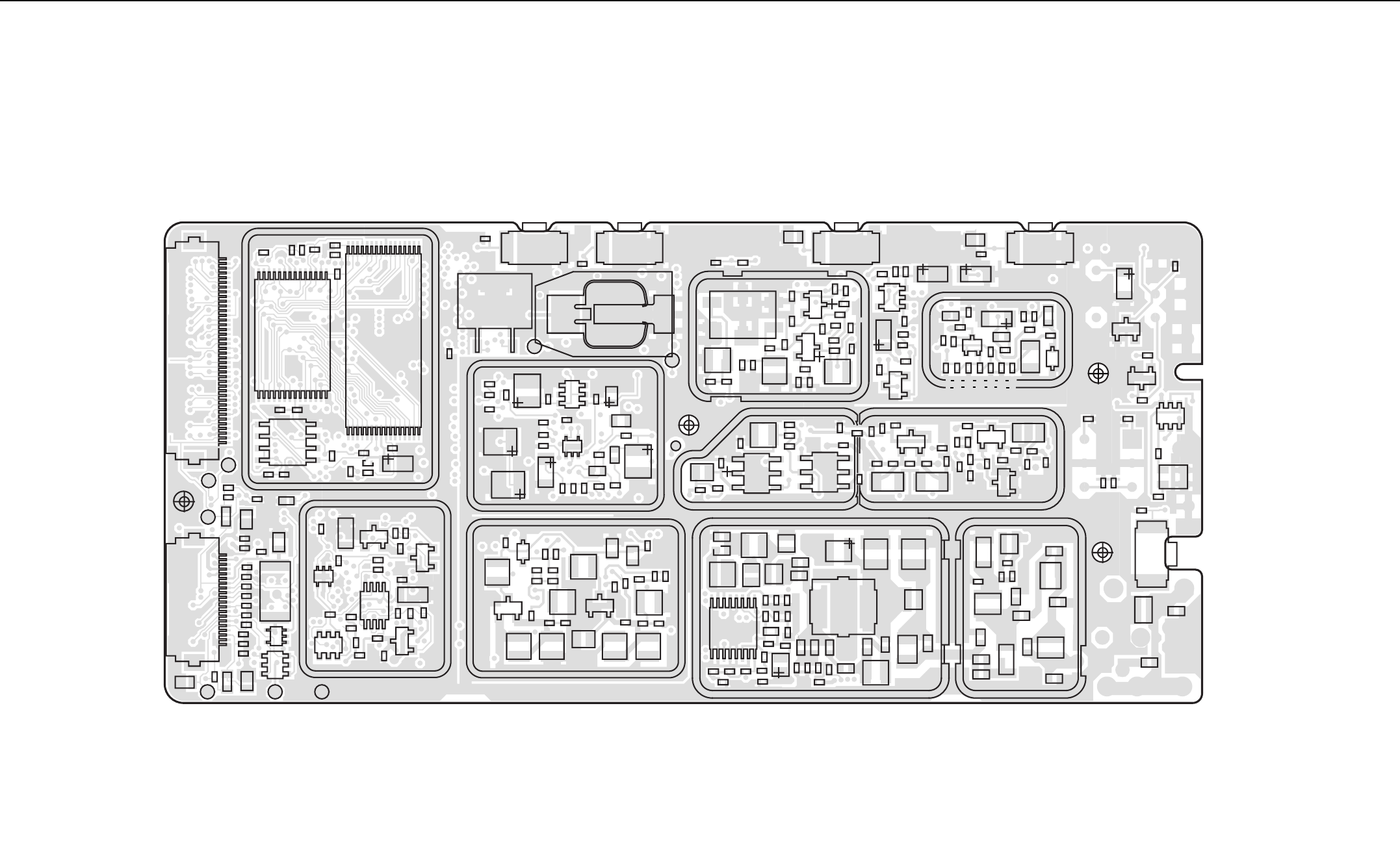
VHF PCB 8486062B14 4-25
6.0 VHF PCB 8486062B14
ZWG0130072-E
C400
C401
C402
C423
C424
C425
C426
C427 C428
C429
C432
C441
C443 C444
C467
C471
C472
C473
C480
C482
C490
C491
C492
C493
C494
C495
C496
C497
CR412
CR413
E407
E408
E409
40
J400
J403
L400
Q400
Q403
Q405
Q417
R401
R402
R403
R405
R406
R407
R408
R410
R418
R421
R427
R428
R429
R435
R437
R450
R476
R477
R478
R481
R492
RT400
SH400
TP401
TP402
TP405
TP406
TP410
TP415
U405
RAM
U406
Flash
ROM
VR434
VR447
VR449
VR450
C403
C3706
C3712
C3713
C3714
C3741
C3742
C3743
C3744
C3746
C3752
C3754
C3822
C3824
C3825
C3828
C3829
C3830
C3832
C3834
C3835
C3836
C3842
CR440
D3831
D3832
L401
L3821
L3822
L3823
L3824
L3825
L3831
L3832 L3833
L3834
R416
R447 R448
R3701
R3741
R3751
R3821
R3828
R3833
R3835R3836
SH3801
U400
U3711
B503 B504
C502
C505
C521
C522
C3200
C3201
C3205
C3212 C3213
C3320
C3334
C3335
C3710
C3711
C 3722 C3724
C3745
C3753
L3200
L3309
L3312
PB501PB502PB503 PB504
Q3721
R3200
R3214
R3215
C3209
R3217
R3318
R3321
R3322
R3323
R3721
R3722
R3723
R3752
SH3701
T3302
TP3701
VR440
VR444
Y3200
IF Filter
Y3761
Reference
Oscillator
Crystal
C511
C512 C513
C514
C3202
C3203
C3206
C3207
C3208
R3218
Q3202
C3225
C3270 C3271
C3272
C3273
C3275
C3276
C3277
C 3278
C3279
C3280
C3503
C3512
C3513
C3514
C3517
C3519
C3521
C3523
C3524
C3525
C3527
C3528
C3531
C3532
C3534
C3535
C3536
C3537
C3539
C3541C3542
C3543
C3544
C3550
C3551
C3552
CR503
CR3303
D3270
D3521
D3551
L3201 L3202
L3270
L3271
L 3501
L3502
L3503
L3504
L3511
L3512
L3513
L3515
L3521
L3522
L3531
L3532
L3538
L3551
L3552
PB505
Q502
Q505
Q3200
Q3201
Q3270
R502
R506
R3202
R3203
R3205
R3206
R3207
R3208
R3209
R3211
R3270
R3271
R3272
R3273
R3274
R3275
R3276
R3513
R3541
R3542
R3543
R3551
SH3203
U3201
U3501
VR501
C520
C3214
C3306
C3307
C3308
C3309
C3310
C3311
C3313
C3314
C3318 C3327
C3329 C3330
C3331
C3332
C3338
C3501
C3504
C3505 C3518
C3546
C3547
C3721
C3826
C3833
D3302
D3821
L3304
L3305L3306
L3518
Q3302
Q3501
LDMOS
Driver IC
R501
R505
R3201
R3204
R3225
R3213
R3309
R3310
R3311
R3313
R3316
R3317
R3501
R3502R3503
R3512
R3544
R3545
R3546
R3547
R3548
R3822
R3823
R3834
SH3501
SH3502
T3301
C3204
C3502
R3212
R3505
SH3302 SH3303
C523
C3274
C3312
C3533
R3226
R3308 R3312
SH3201
TP3301
TP3702
C3319
R446
SH401
U407
EEPROM
C3215
C3210
R3210
4
3
2
22
20
1
21
4
3
43
23
4
3
6
4
3
6
43
4
5
22
21
8
7
32 17
16
1
1
4
5
8
16
8
9
3
1
8
1
64
3
6
34
1
3
4
6
2
1
5
2
5
51
1
1
5
1
1
1
1
1
20
1
C3715
VHF (136-174 MHz) Main Board Top Side
ZWG0130072-E
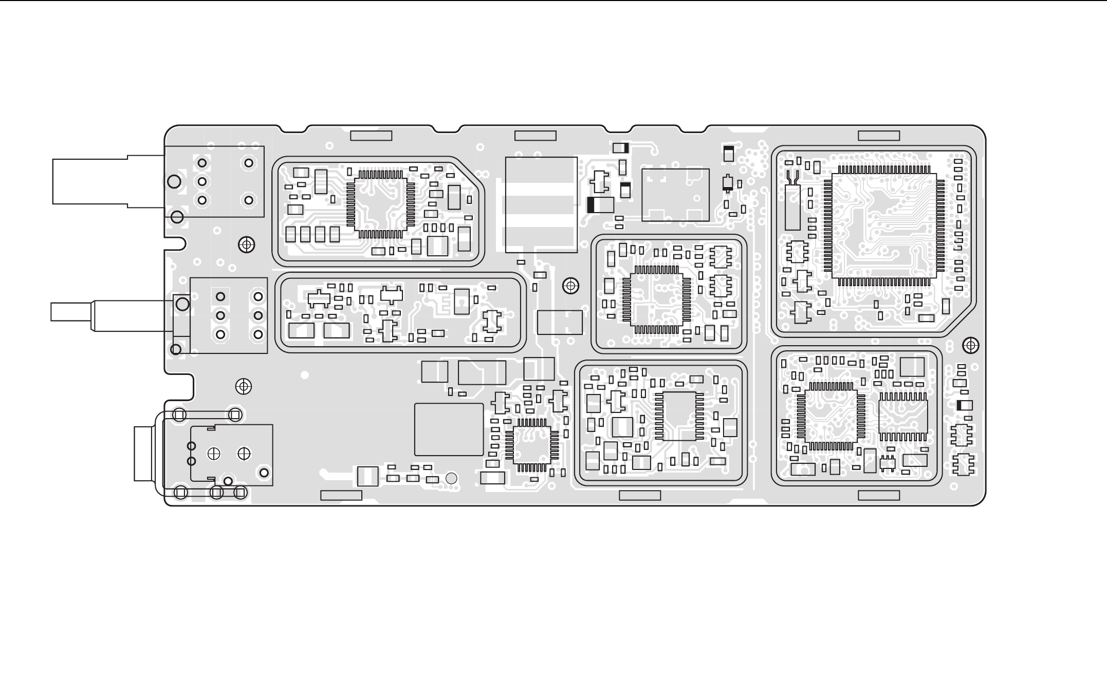
4-26 VHF PCB 8486062B14
1
2
3
B501
C407
C408
C409
C410
C411
C414
C415
C416
C419
C420
C421 C422
C430
C431
C433
C434
C435
C436
C437
C440
C442
C445
C446
C447
C448
C449
C450
C451
C452
C453
C456
C458
C459
C463
C466
C474
C475
C476
C477
C478
C479
C481
C483
C484
C503
C535
C3211
C3218
C3219
C3220
C3221
C3222
C3223
C3224
C3226
C3227
C3228
C3229
C3230
C3231 C3232 C3233 C3234
C3235
C3236
C3237
C3238
C3239
C3240
C3241
C3242
C3243
C3244
C3301 C3302 C3303 C3304
C3305
C3315
C3316
C3317
C3321
C3322 C3323 C3324
C3325
C3326
C3336
C3337
C3339
C3506
C3507
C3508
C3509
C3515
C3516
C3526
C3560
C3561
C3562
C3563
C3564
C3565
C3566
C3567
C3568
C3569
C3570
C3571
C3701
C3702
C3703
C3704
C3705
C3707
C3708
C3709
C3725
C3726
C3727
C3731
C3732
C3733
C3734
C3735
C3751
C3755
C3761
C3762
C3763
C3801
C3802
C3803
C3804
C3805
C3806
C3808
C3809
C3810
C3811 C3812
C3813
C3815
C3816
C3818
C3821
C3823
C3827
C4020
C4021
CR411
CR501
CR3301
CR3302
D3301
D3701
D3702
D3761
E400
E401
E402
E403
E404
E405
E406
F501
3
FL401
H3501
2
3
4
1
J3501
J3502
L410
L411
L505
L3221
L3301 L3303
L3308
L3519
L3523
L3701
L3731
L3801
L3809
L3811
L3812 L3813
L3816
L3826
M100
M101
M300
M301 M400
M401
4
3
Q410
Q416
Q3301
Q3561
Q3801
R400
R409
R411
R413
R414
R415
R419
R420
R423
R424
R425
R426
R431
R432
R434
R436
R445
R449
R457
R460
R461
R462
R463
R471
R472
R473
R475
R498
R499
R3219
R3220
R3221
R3222
R3223
R3224
R3301
R3303
R3304
R3305
R3306
R3307
R3314
R3315
R3319 R3320
R3324
R3519
R3561
R3562
R3563
R3564
R3565
R3566
R3569
R3570
R3571
R3572R3573
R3702
R3703
R3704
R3705
R3726
R3727
R3760
R3761
R3762
R3763
R3801
R3802
R3803
R3804
R3805R3806
R3807
R3808
R3811
R3812
R3816
R3817R3818
R3824
R3825
R3826
R3829
R3830
R3831
R3832
RT3301
2
C
8
C
4
S501
4
5
3
2
S502
SH402
SH403
SH3202
SH3301
SH3702
SH3802
TP3502
1
37 25
13
1
76
51
26
U410
11
1
20
10
1
37
25 13
1
17
9
25
U3503
1
37
25 13
11
120
10
VR432
VR433
VR439
VR441 VR442
VR448
VR506
2
34
Y3762
1
2
1
1
34
6
U3701
FRACN
Synthesizer
U404
ASFIC
U409
Microprocessor
U420
Audio Pa
U3502
Power
Control
IC
U3220
LVZIF
U3801
VCO
Buffer
1
1
ZWG0130073-D
ZWG0130073-D
VHF (136-174 MHz) Main Board Bottom Side
VHF PCB 8486062B14 Parts List 4-27
7.0 VHF PCB 8486062B14 Parts List
Circuit
Ref
Motorola
Part No Description
B501 0986237A02 CONN, CONTACT BATT
B503 3980502Z01 CONTACT, BACKUP B+
only GP360, GP380, GP680
B504 3980501Z01 CONTACT, BACKUP B-
only GP360, GP380, GP680
C3200 2113743N31 16.0 PF 5% COG
C3203 2113743N50 100 PF 5% COG
C3204 2113743L41 10000 PF 10%
C3205 2113928N01 CER CHIP 0.1UF 10% 6.3
C3206 2113743L41 10000 PF 10%
C3207 2113743N10 2.2 PF +-.25PF COG
C3209 2311049A07 TANT 10% 1.0UF
C3210 2113743L17 1000 PF 10%
C3211 2311049A56 TAN CHIP A/P 4.7 20 10
C3212 2311049A07 TANT 10% 1.0UF
C3213 2311049A56 TAN CHIP A/P 4.7 20 10
C3214 2113928N01 CER CHIP 0.1UF 10% 6.3
C3215 2113743N26 10.0 PF 5% COG
C3218 2311049A56 TAN CHIP A/P 4.7 20 10
C3219 2113928N01 CER CHIP 0.1UF 10% 6.3
C3220 2113743N26 10.0 PF 5% COG
C3221 2113743L41 10000 PF 10%
C3222 2113928N01 CER CHIP 0.1UF 10% 6.3
C3223 2113928N01 CER CHIP 0.1UF 10% 6.3
C3224 2113928N01 CER CHIP 0.1UF 10% 6.3
C3225 2113928N01 CER CHIP 0.1UF 10% 6.3
C3226 2113928N01 CER CHIP 0.1UF 10% 6.3
C3227 2113743L41 10000 PF 10%
C3228 2113743L41 10000 PF 10%
C3229 2113743N50 100 PF 5% COG
C3230 2113740F51 REEL CL1 +/-30 100
C3231 2180478Z20 MONOLITHIC CERAMIC (1.0UF)
C3232 2180478Z20 MONOLITHIC CERAMIC (1.0UF)
C3233 2180478Z20 MONOLITHIC CERAMIC (1.0UF)
C3234 2180478Z20 MONOLITHIC CERAMIC (1.0UF)
C3235 2113743A23 .220UF 10%
C3238 2113743A24 .330 UF 10% 16V
C3239 2113743E07 CER CHIP .022UF
C3240 2113743A23 .220UF 10%
C3241 2113743L19 1200 PF 10%
C3242 2109720D14 CER CHIP LOW DIST 0.1UF
C3243 2113743E07 CER CHIP .022UF
C3244 2113743L41 10000 PF 10%
C3270 2113743E07 CER CHIP .022UF
C3271 2113743L05 330 PF 10%
C3272 2113743N18 4.7 PF +-.25PF COG
C3273 2113743N26 10.0 PF 5% COG
C3274 2113743N38 33.0 PF 5% COG
C3275 2113743N44 56.0 PF 5% COG
C3276 2113743N42 47.0 PF 5% COG
C3277 2113743N48 82.0 PF 5% COG
C3278 2113743E07 CER CHIP .022UF
C3279 2311049A40 GLOBAL TANT 10% 2.2 UF
C3280 2113743L41 10000 PF 10%
C3301 2113743N20 5.6 PF +-.5PF COG
C3302 2113743N54 150 PF 5% COG
C3303 2113743N30 15.0PF 5% COG
C3304 2113743N54 150 PF 5% COG
C3306 2113928N01 CER CHIP 0.1UF 10% 6.3
C3307 2113743N50 100 PF 5% COG
C3308 2113743L05 330 PF 10%
C3309 2113928N01 CER CHIP 0.1UF 10% 6.3
C3311 2113743N54 150 PF 5% COG
C3312 2113743N31 16.0 PF 5% COG
C3313 2113743N54 150 PF 5% COG
C3315 2113743N26 10.0 PF 5% COG
C3316 2113743N14 3.3 PF +-.25PF COG
C3317 2113743N40 39.0 PF 5% COG
C3318 2113743M08 22000PF +80-20% Y5V
C3320 2113743N48 82.0 PF 5% COG
C3321 2113743L05 330 PF 10%
C3322 2113743N50 100 PF 5% COG
C3323 2113743N50 100 PF 5% COG
C3324 2113743N38 33.0 PF 5% COG
C3325 2113743L17 1000 PF 10%
C3327 2113743L05 330 PF 10%
C3329 2113743L05 330 PF 10%
C3330 2113743N50 100 PF 5% COG
C3331 2113743N50 100 PF 5% COG
C3332 2113743N40 39.0 PF 5% COG
C3334 2113743N33 20.0 PF 5% COG
C3335 2113743N34 22.0 PF 5% COG
C3336 2311049A18 TANT 10% 10UF
C3337 2113743M08 22000PF +80-20% Y5V
C3338 2113743L09 470 PF 10%
C3339 2113743N26 10.0 PF 5% COG
C3501 2113743L05 330 PF 10%
C3502 2113743N38 33.0 PF 5% COG
C3503 2113743N38 33.0 PF 5% COG
C3504 2113743M08 22000PF +80-20% Y5V
C3505 2113743N38 33.0 PF 5% COG
C3508 2113743M08 22000PF +80-20% Y5V
C3509 2113743L05 330 PF 10%
C3512 2113740F43 REEL CL1 +/-30 47
C3513 2113740F38 REEL CL1 +/-30 30
C3514 2113740F67 CL1 +/-30 470 5%
C3515 2113743L29 3300PF 10%
C3516 2311049A08 KEMET CAPS
C3517 2113740F51 REEL CL1 +/-30 100
C3518 2113740F63 CL1 +/-30 330 5%
C3519 2113740F35 REEL CL1 +/-30 22
C3521 2111078B51 RF 220 5 NPO 100V
C3523 2111078B44 RF 120 5 NPO 100V
C3524 2113740F33 REEL CL1 +/-30 18
C3525 2113740F27 REEL CL1 +/-30 10
C3526 2113743M08 22000PF +80-20% Y5V
C3528 2113740F26 REEL CL1 +/-30 9.1
C3531 2113740F34 REEL CL1 +/-30 20
C3532 2113740F47 REEL CL1 +/-30 68
Circuit
Ref
Motorola
Part No Description
C3533 2113740F24 REEL CL1+/-30 7.5
C3534 2113740F19 CHIP CAP, CER 4.7PF
C3535 2113740F37 REEL CL1+/-30 27
C3536 2113740F31 REEL CL1 +/-30 15
C3537 2113740F33 REEL CL1 +/-30 18
C3539 2113740F21 REEL CL1+/-30 5.6
C3541 2113743M08 22000PF +80-20% Y5V
C3542 2113743L05 330 PF 10%
C3543 2113743M08 22000PF +80-20% Y5V
C3544 2113743L05 330 PF 10%
C3546 2113743L05 330 PF 10%
C3547 2113743M08 22000PF +80-20% Y5V
C3550 2113743N23 7.5 PF +-.5PF COG
C3551 2113743N46 68.0 PF 5% COG
C3552 2113743N44 56.0 PF 5% COG
C3560 2311049A07 TANT 10% 1.0UF
C3561 2113743M08 22000PF +80-20% Y5V
C3562 2113743L29 3300PF 10%
C3563 2113743L29 3300PF 10%
C3564 2113743L01 220 PF 10%
C3565 2113743E07 CER CHIP .022UF
C3566 2113743N50 100 PF 5% COG
C3567 2113743L05 330 PF 10%
C3568 2113743L29 3300PF 10%
C3569 2113743M08 22000PF +80-20% Y5V
C3570 2113743L05 330 PF 10%
C3571 2113743L09 470 PF 10%
C3701 2113743L41 10000 PF 10%
C3702 2113743L41 10000 PF 10%
C3703 2113743L41 10000 PF 10%
C3704 2113743L41 10000 PF 10%
C3705 2113743E20 CHIP. 10 UF 10%
C3706 2311049J11 CAPACITOR TANT 10% 4.7UF
C3707 2113743N34 22.0 PF 5% COG
C3708 2113743M24 100000 PF +80-20% Y5V
C3709 2113743M24 100000 PF +80-20% Y5V
C3710 2104993J02 MONOLITHIC CERAMIC (2.2UF)
C3711 2311049A69 TAN CHIP 10.0 UF 20% 6.3V
C3712 2113743M24 100000 PF +80-20% Y5V
C3713 2311049A09 TANT 2.2 UF 10%
C3714 2311049J11 CAPACITOR TANT 10% 4.7UF
C3715 2113743L09 470 PF 10%
C3721 2113743E20 CHIP. 10 UF 10%
C3722 2113743E20 CHIP. 10 UF 10%
C3724 2311049A08 KEMET CAPS
C3726 2113743N24 8.2 PF + -.5PF COG
C3727 2113743N50 100 PF 5% COG
C3731 2113743L41 10000 PF 10%
C3732 2113743L41 10000 PF 10%
C3733 2104993J02 MONOLITHIC CERAMIC (2.2UF)
C3734 2113743L41 10000 PF 10%
C3742 2113743L01 220 PF 10%
C3743 2113743L01 220 PF 10%
C3744 2113743L01 220 PF 10%
C3745 2113743L01 220 PF 10%
C3746 2113743L01 220 PF 10%
Circuit
Ref
Motorola
Part No Description
C3752 2113743L17 1000 PF 10%
C3753 2311049A56 TAN CHIP A/P 4.7 20 10
C3754 2113743M24 100000 PF +80-20% Y5V
C3755 2104993J02 MONOLITHIC CERAMIC (2.2UF)
* C3761 2113743N44 56.0 PF 5% COG
* C3762 2113740F63 CL1 +/-30 330 5%
* C3763 2113743N08 1.6 PF +-.25PF COG
C3801 2113743N18 4.7 PF +-.25PF COG
C3803 2113743L17 1000 PF 10%
C3804 2113743E20 CHIP. 10 UF 10%
C3805 2113743N18 4.7 PF +-.25PF COG
C3806 2113743N50 100 PF 5% COG
C3808 2113743N30 15.0PF 5% COG
C3809 2113743N36 27.0 PF 5% COG
C3811 2113743M24 100000 PF +80-20% Y5V
C3812 2113743M24 100000 PF +80-20% Y5V
C3813 2113743L41 10000 PF 10%
C3815 2113743L17 1000 PF 10%
C3816 2113743N22 6.8 PF +-.5PF COG
C3818 2113743E07 CER CHIP .022UF
C3821 2113743L41 10000 PF 10%
C3822 2113743L17 1000 PF 10%
C3823 2113743L41 10000 PF 10%
C3824 2113743N44 56.0 PF 5% COG
C3825 2113743N30 15.0PF 5% COG
C3826 2113743N18 4.7 PF +-.25PF COG
C3827 2113743E07 CER CHIP .022UF
C3828 2109720D01 CER CHIP LOW DIS T .01UF
C3829 2109720D01 CER CHIP LOW DIS T .01UF
C3830 2113743N46 68.0 PF 5% COG
C3832 2113743L17 1000 PF 10%
C3833 2113743N18 4.7 PF +-.25PF COG
C3834 2113743N44 56.0 PF 5% COG
C3835 2113743N22 6.8 PF +-.5PF COG
C3836 2113743N30 15.0PF 5% COG
C3842 2113743L17 1000 PF 10%
C400 2113743L41 10000 PF 10%
C401 2113743M24 100000 PF +80-20% Y5V
C402 2113743M24 100000 PF +80-20% Y5V
C403 2113928D08 CERAMIC CHIP 10.0UF
C407 2113928N01 CER CHIP 0.1UF 10% 6.3
C408 2113743N50 100 PF 5% COG
C409 2113743M24 100000 PF +80-20% Y5V
C410 2113928N01 CER CHIP 0.1UF 10% 6.3
C411 2113743M24 100000 PF +80-20% Y5V
C414 2113743M24 100000 PF +80-20% Y5V
C415 2109720D01 CER CHIP LOW DIS T .01UF
C416 2113928N01 CER CHIP 0.1UF 10% 6.3
C419 2113743L41 10000 PF 10%
C420 2113743L41 10000 PF 10%
C421 2113928N01 CER CHIP 0.1UF 10% 6.3
C422 2113743M24 100000 PF +80-20% Y5V
C423 2113743N50 100 PF 5% COG
C424 2311049A59 TANT CHIP A/P 10UF 10% 6V
C425 2113743M24 100000 PF +80-20% Y5V
C426 2113743N50 100 PF 5% COG
Circuit
Ref
Motorola
Part No Description
4-28 VHF PCB 8486062B14 Parts List
C427 2113743N50 100 PF 5% COG
C428 2113743M24 100000 PF +80-20% Y5V
C429 2113743M24 100000 PF +80-20% Y5V
C430 2113928N01 CER CHIP 0.1UF 10% 6.3
C431 2113743N50 100 PF 5% COG
C433 2113743L41 10000 PF 10%
C434 2113743M24 100000 PF +80-20% Y5V
only GP360, GP380, GP680
C435 2113743M24 100000 PF +80-20% Y5V
C436 2113743N34 22.0 PF 5% COG
only GP360, GP380, GP680
C437 2113743N34 22.0 PF 5% COG
only GP360, GP380, GP680
C440 2113743G26 4.7UF 16V + 80-20%
C441 2113743L09 470 PF 10%
C442 2113743E20 CHIP. 10 UF 10%
C443 2113928N01 CER CHIP 0.1UF 10% 6.3
C444 2113743N50 100 PF 5% COG
C445 2113743L09 470 PF 10%
C446 2113743L09 470 PF 10%
C447 2113928N01 CER CHIP 0.1UF 10% 6.3
C448 2113928N01 CER CHIP 0.1UF 10% 6.3
C449 2113743N50 100 PF 5% COG
C451 2113743M08 22000PF +80-20% Y5V
C452 2113743G26 4.7UF 16V + 80-20%
C453 2113743N50 100 PF 5% COG
C456 2113743N50 100 PF 5% COG
C458 2113743N50 100 PF 5% COG
C459 2113743N50 100 PF 5% COG
C463 2113743N50 100 PF 5% COG
C466 2113743N50 100 PF 5% COG
C467 2113928N01 CER CHIP 0.1UF 10% 6.3
C471 2113743L09 470 PF 10%
C472 2113743L09 470 PF 10%
C473 2113743L09 470 PF 10%
C474 2113743L41 10000 PF 10%
C475 2113743H14 10.0 UF 16V +80-20%
C476 2113928D08 CERAMIC CHIP 10.0UF
C477 2113743L17 1000 PF 10%
C478 2113743L17 1000 PF 10%
C479 2113928N01 CER CHIP 0.1UF 10% 6.3
C480 2113928D08 CERAMIC CHIP 10.0UF
C481 2113928N01 CER CHIP 0.1UF 10% 6.3
C482 2113928N01 CER CHIP 0.1UF 10% 6.3
C483 2113743L09 470 PF 10%
C484 2113743L09 470 PF 10%
C490 2113743L09 470 PF 10%
C491 2113743L09 470 PF 10%
C492 2113743L09 470 PF 10%
C493 2113743N50 100 PF 5% COG
C494 2113743N50 100 PF 5% COG
C495 2113743L09 470 PF 10%
C496 2113743L09 470 PF 10%
C497 2113743L09 470 PF 10%
C4020 2113743L17 1000PF 10%
Placed on PCB 8486062B14 only
Circuit
Ref
Motorola
Part No Description
C4021 2113743L17 1000PF 10%
Placed on PCB 8486062B14 only
C502 2311049A05 TANT 10% 0.47UF
C503 2113743N50 100 PF 5% COG
C505 2113743N50 100 PF 5% COG
C511 2113743N50 100 PF 5% COG
C512 2113743N50 100 PF 5% COG
C513 2113743N50 100 PF 5% COG
C514 2113743N50 100 PF 5% COG
C520 2113743L41 10000 PF 10%
C521 2113743L41 10000 PF 10%
C522 2113743L41 10000 PF 10%
C523 2113743L41 10000 PF 10%
C535 2113743L17 1000 PF 10%
CR3301 4802245J42 RING QUAD SOT-143 PKG
CR3302 4805129M96 DIODE SMBV1032
CR3303 4880154K03 SOT MMBD353 DUAL SCHKY
CR411** 4802245J47 SCHOTTKY BARRIER(RB471E)
CR412** 4802245J47 SCHOTTKY BARRIER(RB471E)
CR413** 4802245J47 SCHOTTKY BARRIER(RB471E)
**Placed on PCB 8486062B12 only
CR411*** 4802245J62 SCHOTTKY BARRIER(RB731U)
CR412*** 4802245J62 SCHOTTKY BARRIER(RB731U)
CR413*** 4802245J62 SCHOTTKY BARRIER(RB731U)
***Placed on PCB 8486062B14 only
CR440 4813833C02 DUAL 70V '5B' COMM CATH
CR501 4880107R01 RECTIFIER
CR503 4805729G49 LED RED/YEL
D3270 4862824C01 VARACTOR
D3301 4802081B58 DUAL SILCON (VARICAP)
D3302 4802081B58 DUAL SILCON (VARICAP)
D3521 4880973Z02 PIN DIODE
D3551 4880973Z02 PIN DIODE
D3701 4802233J09 TRIPLE SOT25-RH
D3702 4802233J09 TRIPLE SOT25-RH
* D3761 4862824C03 VARACTOR
D3821 4805649Q13 VCTR ISV 228
D3831 4805649Q13 VCTR ISV 228
D3832 4862824C01 VARACTOR
E400 2480640Z01 C/IND BK1005HM471 BEAD
E401 2480640Z01 C/IND BK1005HM471 BEAD
E402 2480640Z01 C/IND BK1005HM471 BEAD
E403 2480640Z01 C/IND BK1005HM471 BEAD
E404 2480640Z01 C/IND BK1005HM471 BEAD
E405 2480640Z01 C/IND BK1005HM471 BEAD
E406 2480640Z01 C/IND BK1005HM471 BEAD
E407 2480640Z01 C/IND BK1005HM471 BEAD
E408 2480640Z01 C/IND BK1005HM471 BEAD
E409 2480640Z01 C/IND BK1005HM471 BEAD
F501 6580542Z01 FUSE CHIP SMT TR/1608FF 3A
FL401 4870368G02 CLOCK OSC XTAL
only GP360, GP380, GP680
H3501 2680499Z01 HEAT SPREADER
J3501 0180117S05 RF JACK ASSEMBLY
J3502 0280519Z02 NUT, ANTENNA
J400 0905505Y04 CONN ZIF 40Pin
Circuit
Ref
Motorola
Part No Description
not in GP320
J403 0905505Y02 CONN ZIF MALE 20 PIN
L3200 2462587N68 CHIP IND 1000 NH 5%
L3202 2462587N68 CHIP IND 1000 NH 5%
L3221 2462587N68 CHIP IND 1000 NH 5%
L3270 2462587T15 IND CHIP 100NH 5% LOW PRO
L3271 2462587Q20 IND CHIP 2,200NH 20%
L3301 2462587T35 IND CHIP 12NH 5% LOW PRO
L3303 2462587T35 IND CHIP 12NH 5% LOW PRO
L3304 2462587T23 IND CHIP 470NH 5% LOW PRO
L3305 2462587T35 IND CHIP 12NH 5% LOW PRO
L3306 2462587T35 IND CHIP 12NH 5% LOW PRO
L3308 2462587T34 IND CHIP 10NH 5% LOW PRO
L3309 2462587N55 CHIP IND 150 NH 5%
L3312 2462587V28 CHIP IND 33 NH 5% 0805
L3501 2413926H09 IND CHIP 5.6 NH +/- 0.3NH
L3503 2462587V32 CHIP IND 68NH 5% 0805
L3504 2462587N51 CHIP IND 68 NH 5%
L3511 2462587N44 CHIP IND 18 NH 5%
L3512 2479990B01 AIR WOUND GREEN 11.03NH
L3513 2479990A02 AIR WOUND GREEN 7.66NH
L3515 2479990C03 AIR WOUND GREEN 13.85NH
L3518 2462587N48 CHIP IND 39 NH 5%
L3519 2484657R01 INDUCTOR BEAD CHIP
L3521 2479990A02 AIR WOUND GREEN 7.66NH
L3522 2479990E01 COIL AIR WOUND GREEN 23.75
L3523 2462587N68 CHIP IND 1000 NH 5%
L3531 2479990N01 AIR WOUND GREEN 43.67NH
L3532 2479990N01 AIR WOUND GREEN 43.67NH
L3538 2479990M01 AIR WOUND GREEN 30.54NH
L3551 2479990N01 AIR WOUND GREEN 43.67NH
L3552 2479990A02 AIR WOUND GREEN 7.66NH
L3701 2462587Q42 IND CHIP 390NH 10%
L3731 2462587Q20 IND CHIP 2,200NH 20%
L3801 2462587V34 CHIP IND 100NH 5% 0805
L3809 2462587V27 CHIP IND 27 NH 5% 0805
L3811 2462587V34 CHIP IND 100NH 5% 0805
L3812 2462587V34 CHIP IND 100NH 5% 0805
L3813 2462587Q47 IND CHIP 1000 NH 10%
L3816 2462587V34 CHIP IND 100NH 5% 0805
L3821 2462587N50 CHIP IND 56 NH 5%
L3822 2462587N49 CHIP IND 47 NH 5%
L3823 2462587N49 CHIP IND 47 NH 5%
L3824 2462587N68 CHIP IND 1000 NH 5%
L3825 2462587V34 CHIP IND 100NH 5%
L3826 2462587N68 CHIP IND 1000 NH 5%
L3831 2462587N50 CHIP IND 56 NH 5%
L3832 2462587N51 CHIP IND 68 NH 5%
L3833 2462587N50 CHIP IND 56 NH 5%
L3834 2462587N68 CHIP IND 1000 NH 5%
L400 2462587Q42 IND CHIP 390NH 10%
L401 2462587Q42 IND CHIP 390NH 10%
L410 2462587Q42 IND CHIP 390NH 10%
L411 2462587Q42 IND CHIP 390NH 10%
L505 2462587Q42 IND CHIP 390NH 10%
PB501 4080523Z01 SWITCH, TACT
Circuit
Ref
Motorola
Part No Description
PB502 4080523Z01 SWITCH, TACT
PB503 4080523Z01 SWITCH, TACT
not in GP320
PB504 4080523Z01 SWITCH, TACT
PB505 4080523Z01 SWITCH, TACT
not in GP320
Q3200 4813827A07 TSTR NPN SML SIG
MMBR941LT1
Q3201 4880214G02 TSTR MMBT3904
Q3202 4880214G02 TSTR MMBT3904
Q3270 4805218N63 RF TRANS SOT 323 BFQ67W
Q3301 4880214G02 TSTR MMBT3904
Q3302 4813827A07 TSTR NPN MMBR941LT1
Q3501 4802245J55 TSTR POWER FIELD EFFECT
Q3561 4813824A17 XSTR PNP40V .2A B=100-300
Q3721 4802245J50 TSTR DUAL NPN/PNP UMC5N
Q3801 4813827A07 TSTR NPN MMBR941LT1
Q400 4809579E18 MOSFET P-CHAN TP010IT
Q403 4880214G02 TSTR MMBT3904
Q405 4802245J54 UMG5N DIGITAL TRANSISTOR
Q410 4802245J54 UMG5N DIGITAL TRANSISTOR
Q416 4809579E18 MOSFET P-CHAN TP010IT
only GP360, GP380, GP680
Q417 4802245J50 TSTR DUAL NPN/PNP UMC5N
Q502 5180159R01 DUAL TRANS NPNS
Q505 4880214G02 TSTR MMBT3904
R3200 0662057M54 150 5% 20X40
R3201 0662057M82 2200 5% 20X40
R3202 0662057M90 4700 5% 20X40
R3203 0662057M98 10K 5% 20X40
R3204 0662057M26 10 5% 20X40
R3205 0662057M74 1000 5% 20X40
R3206 0662057N23 100K 5% 20X40
R3207 0662057N13 39K 5% 20X40
R3208 0662057M50 100 5% 20X40
R3209 0662057M74 1000 5% 20X40
R3210 0662057M82 2200 5% 20X40
R3211 0662057M82 2200 5% 20X40
R3212 0662057M90 4700 5% 20X40
R3213 0662057M82 2200 5% 20X40
R3214 0662057M34 22 5% 20X 40
R3219 0662057M50 100 5% 20X40
R3220 0662057M90 4700 5% 20X40
R3221 0662057M50 100 5% 20X40
R3224 0662057M26 10 5% 20X40
R3225 0662057M74 1000 5% 20X40
R3226 0662057M26 10 5% 20X40
R3270 0662057M74 1000 5% 20X40
R3271 0662057M42 47 5% 20X40
R3272 0662057N15 47K 5% 20X40
R3273 0662057N15 47K 5% 20X40
R3274 0662057M83 2400 5% 20X40
R3275 0662057M74 1000 5% 20X40
R3276 0662057N30 200K 5% 20X40
R3303 0662057N23 100K 5% 20X40
R3304 0662057N23 100K 5% 20X40
Circuit
Ref
Motorola
Part No Description
VHF PCB 8486062B14 Parts List 4-29
* Motorola Depot Servicing only
Reference designators with an asterisk indicate
components which are not field replaceable
because they need to be calibrated with
specialized factory equipment after installation.
Radios in which these parts have been replaced in
the field will be off frequency at temperature
extremes.
R3305 0662057N19 68K 5% 20X40
R3306 0662057M82 2200 5% 20X40
R3307 0662057N11 33K 5% 20X40
R3308 0662057M78 1500 5% 20X40
R3309 0662057M92 5600 5% 20X40
R3310 0662057M98 10K 5% 20X40
R3311 0662057M26 10 5% 20X40
R3312 0662057M38 33 5% 20X40
R3313 0662057M34 22 5% 20X 40
R3314 0662057M26 10 5% 20X40
R3315 0662057M62 330 5% 20X40
R3316 0662057M66 470 5% 20X40
R3317 0662057N23 100K 5% 20X40
R3318 0662057M66 470 5% 20X40
R3321 0662057M54 150 5% 20X40
R3322 0662057M58 220 5% 20X40
R3323 0662057M32 18 5% 20X40
R3324 0662057M58 220 5% 20X40
R3501 0662057M61 300 5% 20X40
R3502 0662057M32 18 5% 20X40
R3503 0662057M61 300 5% 20X40
R3505 0662057M62 330 5% 20X40
R3512 0662057A27 120 OHMS 5%
R3513 0662057A25 100 OHMS 5%
R3519 0680539Z01 POWER METAL STRIP
R3542 0662057M92 5600 5% 20X40
R3543 0662057M50 100 5% 20X40
R3544 0662057A25 100 OHMS 5%
R3545 0662057A25 100 OHMS 5%
R3546 0662057N11 33K 5% 20X40
R3547 0662057N01 12K 5% 20X40
R3548 0662057M95 7500 55 20X40
R3551 0662057M40 39 5% 20X40
R3561 0662057N01 12K 5% 20X40
R3562 0662057N11 33K 5% 20X40
R3563 0662057N33 270K 5% 20X40
R3564 0662057N35 330K 5% 20X40
R3569 0662057M92 5600 5% 20X40
R3570 0662057M98 10K 5% 20X40
R3571 0662057A27 120 OHMS 5%
R3572 0662057A27 120 OHMS 5%
R3573 0662057A27 120 OHMS 5%
R3701 0662057M50 100 5% 20X40
R3703 0662057M54 150 5% 20X40
R3704 0662057M54 150 5% 20X40
R3705 0662057N11 33K 5% 20X40
R3721 0662057M66 470 5% 20X40
R3722 0662057M74 1000 5% 20X40
R3723 0662057M50 100 5% 20X40
R3727 0662057N23 100K 5% 20X40
R3741 0662057M50 100 5% 20X40
R3751 0662057N30 200K 5% 20X40
R3752 0662057N35 330K 5% 20X40
R3761 0662057N15 47K 5% 20X40
R3802 0662057M50 100 5% 20X40
R3803 0662057M58 220 5% 20X40
Circuit
Ref
Motorola
Part No Description
R3804 0662057M98 10K 5% 20X40
R3805 0662057N08 24K 5% 20X40
R3806 0662057M34 22 5% 20X 40
R3808 0662057M26 10 5% 20X40
R3811 0662057M50 100 5% 20X40
R3816 0662057M74 1000 5% 20X40
R3817 0662057M01 0 5% 20X40
R3821 0662057M58 220 5% 20X40
R3822 0662057M42 47 5% 20X40
R3823 0662057N11 33K 5% 20X40
R3824 0662057N07 22K 5% 20X40
R3825 0662057M38 33 5% 20X40
R3826 0662057M32 18 5% 20X40
R3828 0662057M50 100 5% 20X40
R3829 0662057M01 0 5% 20X40
R3831 0662057M98 10K 5% 20X40
R3832 0662057N01 12K 5% 20X40
R3833 0662057M58 220 5% 20X40
R3834 0662057M42 47 5% 20X40
R3835 0662057N15 47K 5% 20X40
R3836 0662057M98 10K 5% 20X40
R400 0662057N15 47K 5% 20X40
R401 0662057M01 0 5% 20X40
R405 0662057M01 0 5% 20X40
R406 0662057N20 75K 5% 20X40
R407 0662057N19 68K 5% 20X40
R409 0662057M98 10K 5% 20X40
R410 0662057N23 100K 5% 20X40
R411 0662057M98 10K 5% 20X40
R413 0662057M01 0 5% 20X40
R414 0662057V34 180K 1% 1/16W
R415 0662057V26 91K 1% 1/16W
R416 0662057N13 39K 5% 20X40
R418 0662057M01 0 5% 20X40
R419 0662057M67 0 5% 20X40
only GP360, GP380, GP680
R420 0662057B46 10.0 MEG OHMS 5%
only GP360, GP380, GP680
R421 0662057M81 2000 5% 20X40
R423 0662057N21 82K 5% 20X40
R424 0662057N12 36K 5% 20X40
R425 0662057N10 30K 5% 20X40
R426 0662057N35 330K 5% 20X40
only GP360, GP380, GP680
R427 0662057M84 2700 5% 20X40
R428 0662057M10 2.2 5% 20X40
R429 0662057M98 10K 5% 20X40
R431 0662057N39 470K 5% 20X40
R432 0662057N16 51K 5% 20X40
R434 0662057M62 330 5% 20X40
R435 0662057M81 2000 5% 20X40
R436 0662057M01 0 5% 20X40
R445 0662057N08 24K 5% 20X40
R446 0662057N31 RES, CHIP 220K 5% 20X40
R447 0662057N51 RES, CHIP 1.5 MEG 5% 20X40
R448 0662057N33 270K 5% 20X40
Circuit
Ref
Motorola
Part No Description
R449 0662057N08 24K 5% 20X40
R450 0683962T45 68 5-1
R457 0662057M98 10K 5% 20X40
R460 0662057M90 4700 5% 20X40
R461 0662057M56 180 5% 20X40
only GP360, GP380, GP680
R462 0662057M98 10K 5% 20X40
only GP360, GP380, GP680
R463 0662057M61 300 5% 20X40
R471 0662057M92 5600 5% 20X40
R472 0662057M93 6200 5% 20X40
R473 0662057M26 10 5% 20X40
R475 0662057M01 0 5% 20X40
R476 0662057N08 24K 5% 20X40
R477 0662057M74 1000 5% 20X40
R478 0662057M98 10K 5% 20X40
R481 0662057N08 24K 5% 20X40
R492 0662057M01 0 5% 20X40
R498 0662057M98 10K 5% 20X40
Placed on PCB 8486062B14 only
R499 0662057M98 10K 5% 20X40
Placed on PCB 8486062B14 only
R501 0662057M70 680 5% 20X40
R502 0662057M56 180 5% 20X40
R505 0662057M98 10K 5% 20X40
R506 0662057N15 47K 5% 20X40
RT400 0680590Z01 THERMISTOR_33K
S501 4080710Z01 SWITCH (FREQUENCY)
only GP340, GP640
S501 4080710Z02 SWITCH (FREQUENCY)
only GP360, GP380, GP680
S502 1880619Z01 POTENTIOMETER, VOLUME
SH3201 2602023X08 SHIELD
SH3202 2686081B02 SHIELD
SH3203 2686081B03 SHIELD
SH3301 2686081B01 SHIELD
SH3302 2686081B05 SHIELD
SH3303 2686081B06 SHIELD
SH3501 2686081B03 SHIELD
SH3502 2686081B04 SHIELD
SH3701 2680511Z01 SHIELD SYNTHESIZER
SH3702 2680511Z01 SHIELD SYNTHESIZER
SH3801 2680513Z01 SHIELD VCO TOP
SH3802 2680514Z01 SHIELD VCO BOTTOM/LVZIF
SH400 2680505Z01 CONTROLLER TOP LEFT
SH401 2680506Z01 CONTROLLER TOP RIGHT
SH402 2680515Z01 CONTROLLER BOTTOM LEFT
SH403 2680516Z01 CONTROLLER BTM RIGHT
T3301 2580541Z01 BALUN TRANSFORMER
T3302 2580541Z01 BALUN TRANSFORMER
U3201 5102463J58 3.3V REG IN SOT23-5 PKG
U3220 5109632D83 IC LVZIF 2.2 H60G 48TQFP
U3501 5105109Z67 IC LDMOS DRIVER VHF/UHF
U3502 5185765B01 IC POWER CONTROL PASS 2.3
U3503 5185963A15 IC TEMP SENSOR 1M50C
U3701 5185963A27 IC FRACN AT25016 48 PIN GFP
Circuit
Ref
Motorola
Part No Description
U3711 5105739X05 IC 5V REGULATOR
U3801 5105750U54 IC VCO BUFFER
U400 5102463J40 REG 3.3V, LP2951CMM-3.3
U404 5185963A53 IC ASFIC CMP TQFP 48PIN PKG
U405 5102463J36 STATIC_RAM_32KX8
* U406 5102463J60 IC 512KX8 FLASH ROM
* U407 5102463J64 16KX8 SPI SERIAL EEPROM
U409 5102226J56 68HC11FLO_PASS5 TQFP
U410 5102463J57 REG 3.3V, ILC7062CM-33
only GP360, GP380, GP680
U420 5102463J44 AUDIO AMPLIFIER TDA8547TS
VR432 4805656W08 ZENER QUAD
VR433 4805656W08 ZENER QUAD
VR434 4802245J51 ZENER DIODE; BZX284-C6V8"
VR439 4880140L15 10V ZENER
VR447 4802245J53 ZENER_DIODE; BZX284-C10
VR448 4802245J53 ZENER_DIODE; BZX284-C10
VR449 4802245J53 ZENER_DIODE; BZX284-C10
VR450 4802245J53 ZENER_DIODE; BZX284-C10
VR501 4813830A18 6.8V 5% 225MWMMBZ5235B_
VR506 4802245J51 ZENER DIODE; BZX284-C6V8
Y3200 9186153B01 XTAL FILTER, SMD 45.1MHz
Y3761 4802245J49 CRYSTL 16.8MHZ WITH CLIP
8486062B12/
8486062B14
PCB WARIS VHF GP680
Circuit
Ref
Motorola
Part No Description

4-30 VHF PCB 8486062B14 Parts List
Intentionally Left Blank

VHF PCB 8486101B10 4-31
8.0 VHF PCB 8486101B10
B503 B504
C400
C401
C402
C403
C423
C424
C425
C426
C427 C428
C429
C432
C441
C443 C444
C467
C471
C472
C473
C480
C482
C490
C491
C492
C493
C494
C495
C496
C497
C502
C505
C511
C512 C513
C514
C519
C520
C521
C522
C523
C601
C602
C603
C710
C3200
C3201
C3202
C3203
C3204
C3205
C3206
C3207
C3208
C3209
C3210
C3212 C3213
C3214
C3215
C3225
C3270C3271
C3272
C3273
C3274
C3275
C3276
C3277
C3278
C3279
C3280
C3306
C3307
C3308
C3309
C3310
C3311
C3312
C3313
C3314
C3318
C3319
C3320
C3327
C3329 C3330
C3331
C3332
C3334
C3335 C3338
C3501
C3502
C3503
C3504
C3505
C3512
C3513
C3514
C3517
C3518
C3519
C3521 C3523
C3524
C3525
C3527
C3528
C3531
C3532
C3533
C3534
C3535
C3536
C3537
C3539
C3541C3542
C3543
C3544
C3546
C3547
C3550
C3551
C3552
C3706
C3710
C3711
C3712
C3713
C3714
C3715
C3721
C3722
C3724
C3741
C3742
C3743
C3744
C3745
C3746
C3752
C3753
C3754
C3822
C3824C3825
C3826
C3828
C3829
C3830
C3832 C3833
C3834
C3835
C3836
C3842
C4001
C4002
C4003
C4004
C4005
C4007
C4008
C4009
C4010
C4011
C4012
C4013
C4014
C4015
C4016
CR412
CR413
CR440
4
3
2
CR503
CR601
CR3303
D3270
D3302
D3521
D3551
D3821
D3831
D3832
1
40
J400
22
20
1
21
J403
L400
L401
L601
L3200
L3201
L3202
L3270
L3271
L3304
L3305L3306
L3309
L3312
L3501
L3502
L3503
L3504
L3511 L3512
L3513
L3515
L3518
L3521
L3522
L3531
L3532
L3538
L3551
L3552
L3821
L3822
L3823
L3824
L3825
L3831
L3832 L3833
L3834
PB501PB502PB503 PB504
PB505
Q400
Q403
4
3
Q405
4
3
Q411
43
Q417
Q502
Q505
Q3200
Q3201
Q3202
Q3270
Q3302
1
23
Q3501
4
3
Q3721
R401
R402
R403
R405
R406
R407
R408
R410
R416
R418
R421
R427
R428
R429
R435
R437
R446
R447 R448
R450
R476
R477
R478
R481
R492
R499
R501
R502
R505
R506
R625
R3200
R3201
R3202
R3203
R3204
R3205
R3206
R3207
R3208
R3209
R3210
R3211
R3212
R3213
R3214 R3215
R3218
R3225 R3226
R3270
R3271
R3272
R3273
R3274
R3275
R3276
R3308
R3309
R3310
R3311
R3312
R3313
R3316
R3317
R3318
R3321
R3322
R3323
R3501
R3502 R3503
R3505 R3512
R3513
R3541
R3542
R3543
R3544
R3545
R3546
R3547
R3548
R3551
R3701
R3721
R3722
R3723
R3741
R3751
R3752
R3821
R3822
R3823
R3828
R3833 R3834
R3835
R3836
R4007
R4008
R4009
RT400
SH400
SH401
SH700
SH3201
SH3203
SH3302 SH3303
SH3501
SH3502
SH3701
SH3801
6
4
3
T3301
6
43
T3302
TP401
TP402
TP405
TP406
TP410
TP415
TP3301
TP3701
TP3702
4
58
U400
22
21
8
71
U405
Reference
Oscillator
Crystal
32 17
16
1
U406
IF Filter
1
45
8
U407
EEPROM
14
58
U601
U3201
1
16
8
9
U3501
LDMOS
Driver IC
U3711
VR434
VR440
VR444
VR447
VR449
VR450
VR501
Y3200
3
Y3761
1
15
5
1
5
1
1
1
5
28
1
1
ZWG0130096-B
ZWG0130096-B
VHF (136-174 MHz) Main Board Top Side
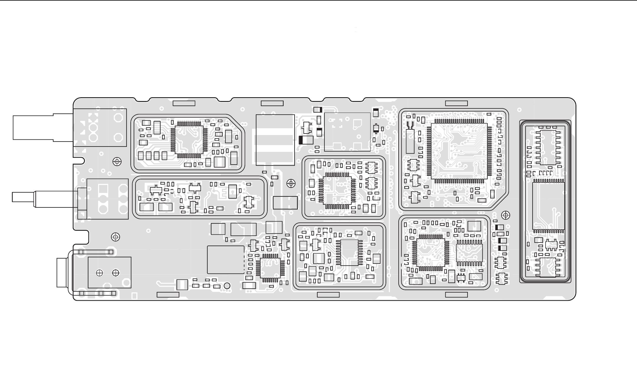
4-32 VHF PCB 8486101B10
ZWG0130097-B
1
2
3
B501
C407
C408
C409
C410
C411 C414
C415
C416
C419
C420
C421
C422
C430
C431
C433
C434
C435
C436
C437
C440
C442
C445
C446
C447
C448
C449
C450
C451
C452
C453
C456
C458
C459
C463
C466
C474
C475
C476
C477
C478
C479
C481
C483
C484
C503
C535
C701
C702
C703
C704
C705
C706
C707
C708C709
C711
C713
C714 C715
C717
C718
C719
C3211
C3218
C3219
C3220
C3221
C3222
C3223
C3224
C3226
C3227
C3228
C3229
C3230
C3231
C3232
C3233
C3234
C3235
C3236
C3237
C3238
C3239
C3240 C3241
C3242
C3243
C3244
C3301
C3302 C3303 C3304
C3305
C3315
C3316
C3317
C3321
C3322C3323C3324
C3325
C3326
C3336
C3337
C3339
C3506
C3507 C3508
C3509
C3515
C3516
C3526
C3560
C3561
C3562
C3563
C3564
C3565
C3566
C3567
C3568
C3569 C3570
C3571
C3701
C3702
C3703
C3704
C3705
C3707
C3708
C3709
C3725
C3726
C3727
C3731
C3732
C3733
C3734
C3735
C3751
C3755
C3761
C3762
C3763
C3801
C3802
C3803
C3804
C3805
C3806
C3808
C3809
C3810
C3811 C3812
C3813
C3815
C3816
C3818
C3821
C3823
C3827
C4006
C4020
C4021
CR411
CR501
CR700
CR3301
CR3302
D3301
D3701D3702
D3761
E400
F501
3
FL401
H3501
2
3
4
J3501
J3502
L410
L411
L505
L3221
L3301 L3303
L3308
L3519
L3523
L3701
L3731
L3801
L3809
L3811
L3812
L3813
L3816
L3826
M701 M702 M703
M704 M705 M706
4
3
Q410
Q416
Q3301
Q3561
Q3801
R400
R409
R411
R413
R414
R415
R419
R420
R423
R424
R425
R426
R431
R432
R434
R436
R445
R449
R457
R460
R461
R462
R463
R471
R472
R473
R475
R626
R627
R701
R702
R703
R704
R705
R706
R707
R708
R709
R710
R716
R717
R3219
R3220
R3221
R3222
R3223
R3224
R3301
R3303
R3304
R3305
R3306
R3307
R3314
R3315
R3319 R3320
R3324
R3519
R3561
R3562
R3563
R3564
R3565
R3566
R3569 R3570
R3571
R3572R3573
R3702
R3703
R3704
R3705
R3726
R3727
R3760 R3761
R3762
R3763
R3801
R3802
R3803
R3804
R3805
R3806
R3807
R3808
R3811
R3812
R3816
R3817
R3818
R3824
R3825
R3826
R3829
R3830
R3831
R3832
R4001
R4002
R4003
R4004
R4005
R4006
RT3301
2
C
8
C
4
S501
4
5
3
2S502
SH402
SH403
SH701
SH3202
SH3301
SH3702
SH3802
TP3502
1
37 25
13
U404
ASFIC
1
76
51 26
U409
Microprocessor
U410
11
1
20
10
U420
Audio PA
28 15
14
1
U700
8
7
114
U710
1
45
8
U720
1
37
25 13
U3220
LVZIF
1
17
9
25
U3502
Power
Control IC
U3503
1
37
25 13
U3701
FRACN
Synthesizer
11
120
10
U3801
VCO
Buffer
VR432
VR433
VR439
VR441
VR442
VR448
VR483
VR484
VR506
2
34
Y3762
48
1
1
5
32
100
R499
R498
ZWG0130097-B
VHF (136-174 MHz) Main Board Bottom Side

VHF PCB 8486101B10 Parts List (GP1280) 4-33
9.0 VHF PCB 8486101B10 Parts List
(GP1280)
Circuit
Ref
Motorola
Part No Description
B501 0986237A01 CONN, CONTACT BATTERY
B503 3980502Z01 CONTACT, BACKUP B+
B504 3980501Z01 CONTACT, BACKUP B-
C3200 2113743N31 16.0 PF 5%
C3203 2113743N50 100 PF 5%
C3204 2113743L41 10000 PF 10%
C3205 2113928N01 0.1UF 10% 6.3
C3206 2113743L41 10000 PF 10%
C3207 2113743N10 2.2 PF +-.25PF
C3209 2311049A07 TANT 10% 1.0UF
C3210 2113743L17 1000 PF 10%
C3211 2311049A56 TAN CHIP A/P 4.7 20 10
C3212 2311049A07 TANT 10% 1.0UF
C3213 2311049A56 TAN CHIP A/P 4.7 20 10
C3214 2113928N01 CERAMIC CHIP 10.0UF
C3215 2113743N26 10.0 PF 5%
C3218 2311049A56 TAN CHIP A/P 4.7 20 10
C3219 2113928N01 CERAMIC CHIP 10.0UF
C3220 2113743N26 10.0 PF 5%
C3221 2113743L41 10000 PF 10%
C3222 2113928N01 CERAMIC CHIP 10.0UF
C3223 2113928N01 0.1UF 10% 6.3
C3224 2113928N01 0.1UF 10% 6.3
C3225 2113928N01 0.1UF 10% 6.3
C3226 2113928N01 0.1UF 10% 6.3
C3227 2113743L41 10000 PF 10%
C3228 2113743L41 10000 PF 10%
C3229 2113743N50 100 PF 5%
C3230 2113740F51 REEL CL1 +/-30 100
C3231 2180478Z20 MONOLITH CERAMIC (1.0UF)
C3232 2180478Z20 MONOLITH CERAMIC (1.0UF)
C3233 2180478Z20 MONOLITH CERAMIC (1.0UF)
C3234 2180478Z20 MONOLITH CERAMIC (1.0UF)
C3235 2113743A23 .220UF 10%
C3238 2113743A24 .330 UF 10% 16V
C3239 2113743E07 .022UF
C3240 2113743A23 .220UF 10%
C3241 2113743L19 1200 PF 10%
C3242 2109720D14 LOW DIST 0.1UF
C3243 2113743E07 .022UF
C3244 2113743L41 10000 PF 10%
C3270 2113743E07 .022UF
C3271 2113743L05 330 PF 10%
C3272 2113743N18 4.7 PF +-.25PF
C3273 2113743N26 10.0 PF 5%
C3274 2113743N38 33.0 PF 5%
C3275 2113743N44 56.0 PF 5%
C3276 2113743N42 47.0 PF 5%
C3277 2113743N48 82.0 PF 5%
C3278 2113743E07 .022UF
C3279 2311049A40 GLOBAL TANT 10% 2.2 UF
C3280 2113743L41 10000 PF 10%
C3301 2113743N20 5.6 PF +-.5PF
C3302 2113743N54 150 PF 5%
C3303 2113743N30 15.0PF 5%
C3304 2113743N54 150 PF 5%
C3306 2113928N01 0.1UF 10% 6.3
C3307 2113743N50 100 PF 5%
C3308 2113743L05 330 PF 10%
C3309 2113928N01 0.1UF 10% 6.3
C3311 2113743N54 150 PF 5%
C3312 2113743N31 16.0 PF 5%
C3313 2113743N54 150 PF 5%
C3315 2113743N26 10.0 PF 5%
C3316 2113743N14 3.3 PF +-.25PF
C3317 2113743N40 39.0 PF 5%
C3318 2113743M08 22000PF +80-20% Y5V
C3320 2113743N48 82.0 PF 5%
C3321 2113743L05 330 PF 10%
C3322 2113743N50 100 PF 5%
C3323 2113743N50 100 PF 5%
C3324 2113743N38 33.0 PF 5%
C3325 2113743L17 1000 PF 10%
C3327 2113743L05 330 PF 10%
C3329 2113743L05 330 PF 10%
C3330 2113743N50 100 PF 5%
C3331 2113743N50 100 PF 5%
C3332 2113743N40 39.0 PF 5%
C3334 2113743N33 20.0 PF 5%
C3335 2113743N34 22.0 PF 5%
C3336 2311049A18 CAP. TANT 10% 10UF
C3337 2113743M08 22000PF +80-20% Y5V
C3338 2113743L09 470 PF 10%
C3339 2113743N26 10.0 PF 5%
C3501 2113743L05 330 PF 10%
C3502 2113743N38 33.0 PF 5%
C3503 2113743N38 33.0 PF 5%
C3504 2113743M08 22000PF +80-20% Y5V
C3505 2113743N38 33.0 PF 5%
C3508 2113743M08 22000PF +80-20% Y5V
C3509 2113743L05 330 PF 10%
C3512 2113740F43 REEL CL1 +/-30 47
C3513 2113740F38 REEL CL1 +/-30 30
C3514 2113740F67 CL1 +/-30 470 5%
C3515 2113743L29 3300PF 10%
C3516 2311049A08 KEMET CAPS
C3517 2113740F51 REEL CL1 +/-30 100
C3518 2113740F63 CL1 +/-30 330 5%
Circuit
Ref
Motorola
Part No Description
C3519 2113740F35 REEL CL1 +/-30 22
C3521 2111078B51 RF 220 5 NPO 100V
C3523 2111078B44 RF 120 5 NPO 100V
C3524 2113740F33 REEL CL1 +/-30 18
C3525 2113740F27 REEL CL1 +/-30 10
C3526 2113743M08 22000PF +80-20% Y5V
C3528 2113740F26 REEL CL1 +/-30 9.1
C3531 2113740F34 REEL CL1 +/-30 20
C3532 2113740F47 REEL CL1 +/-30 68
C3533 2113740F24 REEL CL1+/-30 7.5
C3534 2113740F19 CHIP CAP, CER 4.7PF
C3535 2113740F37 REEL CL1+/-30 27
C3536 2113740F31 REEL CL1 +/-30 15
C3537 2113740F33 REEL CL1 +/-30 18
C3539 2113740F21 REEL CL1+/-30 5.6
C3541 2113743M08 22000PF +80-20% Y5V
C3542 2113743L05 330 PF 10%
C3543 2113743M08 22000PF +80-20% Y5V
C3544 2113743L05 330 PF 10%
C3546 2113743L05 330 PF 10%
C3547 2113743M08 22000PF +80-20% Y5V
C3550 2113743N23 7.5 PF +-.5PF
C3551 2113743N46 68.0 PF 5%
C3552 2113743N44 56.0 PF 5%
C3560 2311049A07 TANT 10% 1.0UF
C3561 2113743M08 22000PF +80-20% Y5V
C3562 2113743L29 3300PF 10%
C3563 2113743L29 3300PF 10%
C3564 2113743L01 220 PF 10%
C3565 2113743E07 .022UF
C3566 2113743N50 100 PF 5%
C3567 2113743L05 330 PF 10%
C3568 2113743L29 3300PF 10%
C3569 2113743M08 22000PF +80-20% Y5V
C3570 2113743L05 330 PF 10%
C3571 2113743L09 470 PF 10%
C3701 2113743L41 10000 PF 10%
C3702 2113743L41 10000 PF 10%
C3703 2113743L41 10000 PF 10%
C3704 2113743L41 10000 PF 10%
C3705 2113743E20 CHIP. 10 UF 10%
C3706 2311049J11 CAPACITOR TANT 10% 4.7UF
C3707 2113743N34 22.0 PF 5%
C3708 2113743M24 100000 PF +80-20% Y5V
C3709 2113743M24 100000 PF +80-20% Y5V
C3710 2104993J02 MONOLITH CERAMIC (2.2UF)
C3711 2311049A69 TAN CHIP 10.0 UF 20% 6.3V
C3712 2113743M24 100000 PF +80-20% Y5V
C3713 2311049A09 TANT 2.2 UF 10%
C3714 2311049J11 CAPACITOR TANT 10% 4.7UF
C3715 2113743L09 470 PF 10%
Circuit
Ref
Motorola
Part No Description
C3721 2113743E20 CHIP. 10 UF 10%
C3722 2113743E20 CHIP. 10 UF 10%
C3724 2311049A08 KEMET CAPS
C3726 2113743N24 8.2 PF + -.5PF
C3727 2113743N50 100 PF 5%
C3731 2113743L41 10000 PF 10%
C3732 2113743L41 10000 PF 10%
C3733 2104993J02 MONOLITH CERAMIC (2.2UF)
C3734 2113743L41 10000 PF 10%
C3742 2113743L01 220 PF 10%
C3743 2113743L01 220 PF 10%
C3744 2113743L01 220 PF 10%
C3745 2113743L01 220 PF 10%
C3746 2113743L01 220 PF 10%
C3752 2113743L17 1000 PF 10%
C3753 2311049A56 TAN CHIP A/P 4.7 20 10
C3754 2113743M24 100000 PF +80-20% Y5V
C3755 2104993J02 MONOLITH CERAMIC (2.2UF)
* C3761 2113743N44 56.0 PF 5%
* C3762 2113740F63 330 CL1 +/-30 5%
* C3763 2113743N08 1.6 PF +-.25PF
C3801 2113743N18 4.7 PF +-.25PF
C3803 2113743L17 1000 PF 10%
C3804 2113743E20 CHIP. 10 UF 10%
C3805 2113743N18 4.7 PF +-.25PF
C3806 2113743N50 100 PF 5%
C3808 2113743N30 15.0PF 5%
C3809 2113743N36 27.0 PF 5%
C3811 2113743M24 100000 PF +80-20% Y5V
C3812 2113743M24 100000 PF +80-20% Y5V
C3813 2113743L41 10000 PF 10%
C3815 2113743L17 1000 PF 10%
C3816 2113743N22 6.8 PF +-.5PF
C3818 2113743E07 .022UF
C3821 2113743L41 10000 PF 10%
C3822 2113743L17 1000 PF 10%
C3823 2113743L41 10000 PF 10%
C3824 2113743N44 56.0 PF 5%
C3825 2113743N30 15.0PF 5%
C3826 2113743N18 4.7 PF +-.25PF
C3827 2113743E07 .022UF
C3828 2109720D01 LOW DIS T .01UF
C3829 2109720D01 LOW DIS T .01UF
C3830 2113743N46 68.0 PF 5%
C3832 2113743L17 1000 PF 10%
C3833 2113743N18 4.7 PF +-.25PF
C3834 2113743N44 56.0 PF 5%
C3835 2113743N22 6.8 PF +-.5PF
C3836 2113743N30 15.0PF 5%
C3842 2113743L17 1000 PF 10%
C400 2113743L41 10000 PF 10%
Circuit
Ref
Motorola
Part No Description

4-34 VHF PCB 8486101B10 Parts List (GP1280)
C4001 2113743N50 100 PF 5%
C4002 2113743N50 100 PF 5%
C4003 2113743N50 100 PF 5%
C401 2113743M24 100000 PF +80-20% Y5V
C402 2113743M24 100000 PF +80-20% Y5V
C4020 2113743L17 1000 PF 10%
C4021 2113743L17 1000 PF 10%
C403 2113928D08 CERAMIC CHIP 10.0UF
C407 2113928N01 0.1UF 10% 6.3
C408 2113743N50 100 PF 5%
C409 2113743M24 100000 PF +80-20% Y5V
C410 2113928N01 0.1UF 10% 6.3
C411 2113743M24 100000 PF +80-20% Y5V
C414 2113743M24 100000 PF +80-20% Y5V
C415 2109720D01 LOW DIS T .01UF
C416 2113928N01 0.1UF 10% 6.3
C419 2113743L41 10000 PF 10%
C420 2113743L41 10000 PF 10%
C421 2113928N01 0.1UF 10% 6.3
C422 2113743M24 100000 PF +80-20% Y5V
C423 2113743N50 100 PF 5%
C424 2311049A59 TANT CHIP A/P 10UF 10% 6V
C425 2113743M24 100000 PF +80-20% Y5V
C426 2113743N50 100 PF 5%
C427 2113743N50 100 PF 5%
C428 2113743M24 100000 PF +80-20% Y5V
C429 2113743M24 100000 PF +80-20% Y5V
C430 2113928N01 0.1UF 10% 6.3
C431 2113743N50 100 PF 5%
C433 2113743L41 10000 PF 10%
C434 2113743M24 100000 PF +80-20% Y5V
C435 2113743M24 100000 PF +80-20% Y5V
C436 2113743N34 22.0 PF 5%
C437 2113743N34 22.0 PF 5%
C440 2113743G26 4.7UF 16V + 80-20%
C441 2113743L09 470 PF 10%
C442 2113743E20 10 UF 10%
C443 2113928N01 CERAMIC CHIP 10.0UF
C444 2113743N50 100 PF 5%
C445 2113743L09 470 PF 10%
C446 2113743L09 470 PF 10%
C447 2113928N01 CERAMIC CHIP 10.0UF
C448 2113928N01 CERAMIC CHIP 10.0UF
C449 2113743N50 100 PF 5%
C451 2113743M08 22000PF +80-20% Y5V
C452 2113743G26 4.7UF 16V + 80-20%
C453 2113743N50 100 PF 5%
C456 2113743N50 100 PF 5%
C458 2113743N50 100 PF 5%
C459 2113743N50 100 PF 5%
C463 2113743N50 100 PF 5%
Circuit
Ref
Motorola
Part No Description
C466 2113743N50 100 PF 5%
C467 2113928N01 0.1UF 10% 6.3
C471 2113743L09 470 PF 10%
C472 2113743L09 470 PF 10%
C473 2113743L09 470 PF 10%
C474 2113743L41 10000 PF 10%
C475 2113743H14 10.0 UF 16V +80-20%
C476 2113928D08 CERAMIC CHIP 10.0UF
C477 2113743L17 1000 PF 10%
C478 2113743L17 1000 PF 10%
C479 2113928N01 0.1UF 10% 6.3
C480 2113928D08 CERAMIC CHIP 10.0UF
C481 2113928N01 0.1UF 10% 6.3
C482 2113928N01 0.1UF 10% 6.3
C483 2113743L09 470 PF 10%
C484 2113743L09 470 PF 10%
C490 2113743L09 470 PF 10%
C491 2113743L09 470 PF 10%
C492 2113743L09 470 PF 10%
C493 2113743N50 100 PF 5%
C494 2113743N50 100 PF 5%
C495 2113743L09 470 PF 10%
C496 2113743L09 470 PF 10%
C497 2113743L09 470 PF 10%
C502 2311049A05 TANT 10% 0.47UF
C503 2113743N50 100 PF 5%
C505 2113743N50 100 PF 5%
C511 2113743N50 100 PF 5%
C512 2113743N50 100 PF 5%
C513 2113743N50 100 PF 5%
C514 2113743N50 100 PF 5%
C520 2113743L41 10000 PF 10%
C521 2113743L41 10000 PF 10%
C522 2113743L41 10000 PF 10%
C523 2113743L41 10000 PF 10%
C535 2113743L17 1000 PF 10%
C701 2180478Z20 MONOLITHIC CER (1.0UF)
C702 2113928N01 0.1UF 10% 6.3
C703 2113743N50 100 PF 5%
C704 2113928N01 0.1UF 10% 6.3
C705 2113928N01 0.1UF 10% 6.3
C707 2113928N01 0.1UF 10% 6.3
C708 2113928N01 0.1UF 10% 6.3
C709 2113743L17 1000 PF 10%
C711 2113743L41 10000 PF 10%
C713 2113928N01 0.1UF 10% 6.3
C714 2113928N01 0.1UF 10% 6.3
C715 2113928N01 0.1UF 10% 6.3
C717 2113928N01 0.1UF 10% 6.3
C718 2113743L17 1000 PF 10%
C719 2113928N01 0.1UF 10% 6.3
Circuit
Ref
Motorola
Part No Description
CR3301 4802245J42 RING QUAD SOT-143 PKG
CR3302 4805129M96 DIODE DUAL
CR3303 4880154K03 SOT MMBD353 DUAL SCHTKY
CR411 4802245J47 SCHOTTKY BARIER(RB471E)
Placed on PCB 8486101B09 only
CR412 4802245J62 DIODE SCHOTTKY, RB731U
CR413 4802245J62 DIODE SCHOTTKY, RB731U
CR440 4813833C02 DUAL 70V '5B' COMM CATH
CR501 4880107R01 RECTIFIER
CR503 4805729G49 DIODE RED/YEL
CR700 4802245J47 SCHOTTKY BARIER(RB471E)
D3270 4862824C01 DIODE VARACTOR
D3301 4802081B58 DUAL SILCON (VARICAP)
D3302 4802081B58 DUAL SILCON (VARICAP)
D3521 4880973Z02 PIN DIODE
D3551 4880973Z02 PIN DIODE
D3701 4802233J09 DIODE TRIPLE SOT25-RH
D3702 4802233J09 DIODE TRIPLE SOT25-RH
* D3761 4862824C03 DIODE VARACTOR
D3821 4805649Q13 DIODE VCTR ISV 228
D3831 4805649Q13 DIODE VCTR ISV 228
D3832 4862824C01 DIODE VARACTOR
E400 2480640Z01 C/IND BK1005HM471 BEAD
F501 6580542Z01 FUSE SMT TR/1608FF 3A
FL401 4870368G02 REFLOW CLOCK OSC XTAL
H3501 2680499Z01 HEAT SPREADER
J3501 0180117S05 RF JACK ASSEMBLY
J3502 0280519Z02 NUT, ANTENNA
J400 0905505Y04 CONN ZIF HORIZONTAL
J403 0905505Y02 CONN MALE 20 PIN ZIF
L3200 2462587N68 CHIP IND 1000 NH 5%
L3202 2462587N68 CHIP IND 1000 NH 5%
L3221 2462587N68 CHIP IND 1000 NH 5%
L3270 2462587T15 IND 100NH 5% LOW PRO
L3271 2462587Q20 IND CHIP 2,200NH 20%
L3301 2462587T35 IND CHIP 12NH 5% LOW PRO
L3303 2462587T35 IND CHIP 12NH 5% LOW PRO
L3304 2462587T23 IND CHIP 470NH 5%LOW PRO
L3305 2462587T35 IND CHIP 12NH 5% LOW PRO
L3306 2462587T35 IND CHIP 12NH 5% LOW PRO
L3308 2462587T34 IND CHIP 10NH 5% LOW PRO
L3309 2462587N55 CHIP IND 150 NH 5%
L3312 2462587V28 CHIP IND 33 NH 5% 0805
L3501 2413926H09 IND CHIP 5.6 NH +/- 0.3NH
L3503 2462587V32 CHIP IND 68NH 5% 0805
L3504 2462587N51 CHIP IND 68 NH 5%
L3511 2462587N44 CHIP IND 18 NH 5%
L3512 2479990B01 AIR WND COIL/GRN 11.03NH
L3513 2479990A02 AIR WND COIL/GRN 7.66NH
L3515 2479990C03 AIR WND COIL/GRN 13.85NH
L3518 2462587N48 CHIP IND 39 NH 5%
Circuit
Ref
Motorola
Part No Description
L3519 2484657R01 INDUCTOR BEAD CHIP
L3521 2479990A02 AIR WND COIL/GRN 7.66NH
L3522 2479990E01 COIL AIR WND/GRN 23.75
L3523 2462587N68 CHIP IND 1000 NH 5%
L3531 2479990N01 AIR WND COIL/GRN 43.67NH
L3532 2479990N01 AIR WND COIL/GRN 43.67NH
L3538 2479990M01 AIR WND COIL/GRN 30.54NH
L3551 2479990N01 AIR WND COIL/GRN 43.67NH
L3552 2479990A02 AIR WND COIL/GRN 7.66NH
L3701 2462587Q42 IND CHIP 390NH 10%
L3731 2462587Q20 IND CHIP 2,200NH 20%
L3801 2462587V34 CHIP IND 100NH 5% 0805
L3809 2462587V27 CHIP IND 27 NH 5% 0805
L3811 2462587V34 CHIP IND 100NH 5% 0805
L3812 2462587V34 CHIP IND 100NH 5% 0805
L3813 2462587Q47 IND CHIP 1000 NH 10%
L3816 2462587V34 CHIP IND 100NH 5% 0805
L3821 2462587N50 CHIP IND 56 NH 5%
L3822 2462587N49 CHIP IND 47 NH 5%
L3823 2462587N49 CHIP IND 47 NH 5%
L3824 2462587N68 CHIP IND 1000 NH 5%
L3825 2462587V34 CHIP IND 100NH 5% 0805
L3826 2462587N68 CHIP IND 1000 NH 5%
L3831 2462587N50 CHIP IND 56 NH 5%
L3832 2462587N51 CHIP IND 68 NH 5%
L3833 2462587N50 CHIP IND 56 NH 5%
L3834 2462587N68 CHIP IND 1000 NH 5%
L400 2462587Q42 IND CHIP 390NH 10%
L401 2462587Q42 IND CHIP 390NH 10%
L410 2462587Q42 IND CHIP 390NH 10%
L411 2462587Q42 IND CHIP 390NH 10%
L505 2462587Q42 IND CHIP 390NH 10%
M701 7585651Z01 PAD, FLEXIBLE
M702 7585651Z01 PAD, FLEXIBLE
M703 7585651Z01 PAD, FLEXIBLE
M704 7585651Z01 PAD, FLEXIBLE
M705 7585651Z01 PAD, FLEXIBLE
M706 7585651Z01 PAD, FLEXIBLE
PB501 4080523Z01 SWITCH, TACT
PB502 4080523Z01 SWITCH, TACT
PB503 4080523Z01 SWITCH, TACT
PB504 4080523Z01 SWITCH, TACT
PB505 4080523Z01 SWITCH, TACT
Q3200 4813827A07 NPNSML SIG MMBR941LT1 7Y
Q3201 4880214G02 TSTR MMBT3904
Q3202 4880214G02 TSTR MMBT3904
Q3270 4805218N63 RF TRANS SOT 323 BFQ67W
Q3301 4880214G02 TSTR MMBT3904
Q3302 4813827A07 NPNSML SIG MMBR941LT1 7Y
Q3501 4802245J55 POWER FIELD EFFECT
Q3561 4813824A17 XSTR PNP40V .2A B=100-300
Circuit
Ref
Motorola
Part No Description

VHF PCB 8486101B10 Parts List (GP1280) 4-35
Q3721 4802245J50 DUAL NPN/PNP UMC5N
Q3801 4813827A07 NPNSML SIG MMBR941LT1 7Y
Q400 4809579E18 MOSFET P-CHAN TP010IT
Q403 4880214G02 TSTR MMBT3904
Q405 4802245J54 UMG5N DIGITAL TRANSISTOR
Q410 4802245J54 UMG5N DIGITAL TRANSISTOR
Q416 4809579E18 MOSFET P-CHAN TP010IT
Q417 4802245J50 DUAL NPN/PNP UMC5N
Q502 5180159R01 DUAL TRANS NPNS
Q505 4880214G02 TSTR MMBT3904
R3200 0662057M54 150 5% 20X40
R3201 0662057M82 2200 5% 20X40
R3202 0662057M90 4700 5% 20X40
R3203 0662057M98 10K 5% 20X40
R3204 0662057M26 10 5% 20X40
R3205 0662057M74 1000 5% 20X40
R3206 0662057N23 100K 5% 20X40
R3207 0662057N13 39K 5% 20X40
R3208 0662057M50 100 5% 20X40
R3209 0662057M74 1000 5% 20X40
R3210 0662057M82 2200 5% 20X40
R3211 0662057M82 2200 5% 20X40
R3212 0662057M90 4700 5% 20X40
R3213 0662057M82 2200 5% 20X40
R3214 0662057M34 22 5% 20X 40
R3219 0662057M50 100 5% 20X40
R3220 0662057M90 4700 5% 20X40
R3221 0662057M50 100 5% 20X40
R3224 0662057M26 10 5% 20X40
R3225 0662057M74 1000 5% 20X40
R3226 0662057M26 10 5% 20X40
R3270 0662057M74 1000 5% 20X40
R3271 0662057M42 47 5% 20X40
R3272 0662057N15 47K 5% 20X40
R3273 0662057N15 47K 5% 20X40
R3274 0662057M83 2400 5% 20X40
R3275 0662057M74 1000 5% 20X40
R3276 0662057N30 200K 5% 20X40
R3303 0662057N23 100K 5% 20X40
R3304 0662057N23 100K 5% 20X40
R3305 0662057N19 68K 5% 20X40
R3306 0662057M82 2200 5% 20X40
R3307 0662057N11 33K 5% 20X40
R3308 0662057M78 1500 5% 20X40
R3309 0662057M92 5600 5% 20X40
R3310 0662057M98 10K 5% 20X40
R3311 0662057M26 10 5% 20X40
R3312 0662057M38 33 5% 20X40
R3313 0662057M34 22 5% 20X 40
R3314 0662057M26 10 5% 20X40
R3315 0662057M62 330 5% 20X40
Circuit
Ref
Motorola
Part No Description
R3316 0662057M66 470 5% 20X40
R3317 0662057N23 100K 5% 20X40
R3318 0662057M66 470 5% 20X40
R3321 0662057M54 150 5% 20X40
R3322 0662057M58 220 5% 20X40
R3323 0662057M32 18 5% 20X40
R3324 0662057M58 220 5% 20X40
R3501 0662057M61 300 5% 20X40
R3502 0662057M32 18 5% 20X40
R3503 0662057M61 300 5% 20X40
R3505 0662057M62 330 5% 20X40
R3512 0662057A27 120 OHMS 5%
R3513 0662057A25 100 OHMS 5%
R3519 0680539Z01 PWR METAL STRIP RES
R3542 0662057M92 5600 5% 20X40
R3543 0662057M50 100 5% 20X40
R3544 0662057A25 100 OHMS 5%
R3545 0662057A25 100 OHMS 5%
R3546 0662057N11 33K 5% 20X40
R3547 0662057N01 12K 5% 20X40
R3548 0662057M95 7500 55 20X40
R3551 0662057M40 39 5% 20X40
R3561 0662057N01 12K 5% 20X40
R3562 0662057N11 33K 5% 20X40
R3563 0662057N33 270K 5% 20X40
R3564 0662057N35 330K 5% 20X40
R3569 0662057M92 5600 5% 20X40
R3570 0662057M98 10K 5% 20X40
R3571 0662057A27 120 OHMS 5%
R3572 0662057A27 120 OHMS 5%
R3573 0662057A27 120 OHMS 5%
R3701 0662057M50 100 5% 20X40
R3703 0662057M54 150 5% 20X40
R3704 0662057M54 150 5% 20X40
R3705 0662057N11 33K 5% 20X40
R3721 0662057M66 470 5% 20X40
R3722 0662057M74 1000 5% 20X40
R3723 0662057M50 100 5% 20X40
R3727 0662057N23 100K 5% 20X40
R3741 0662057M50 100 5% 20X40
R3751 0662057N30 200K 5% 20X40
R3752 0662057N35 330K 5% 20X40
R3761 0662057N15 47K 5% 20X40
R3802 0662057M50 100 5% 20X40
R3803 0662057M58 220 5% 20X40
R3804 0662057M98 10K 5% 20X40
R3805 0662057N08 24K 5% 20X40
R3806 0662057M34 22 5% 20X 40
R3808 0662057M26 10 5% 20X40
R3811 0662057M50 100 5% 20X40
R3816 0662057M74 1000 5% 20X40
Circuit
Ref
Motorola
Part No Description
R3817 0662057M01 0 5% 20X40
R3821 0662057M58 220 5% 20X40
R3822 0662057M42 47 5% 20X40
R3823 0662057N11 33K 5% 20X40
R3824 0662057N07 22K 5% 20X40
R3825 0662057M38 33 5% 20X40
R3826 0662057M32 18 5% 20X40
R3828 0662057M50 100 5% 20X40
R3829 0662057M01 0 5% 20X40
R3831 0662057M98 10K 5% 20X40
R3832 0662057N01 12K 5% 20X40
R3833 0662057M58 220 5% 20X40
R3834 0662057M42 47 5% 20X40
R3835 0662057N15 47K 5% 20X40
R3836 0662057M98 10K 5% 20X40
R400 0662057N15 47K 5% 20X40
R4001 0662057M74 1000 5% 20X40
R4002 0662057M74 1000 5% 20X40
R4003 0662057M74 1000 5% 20X40
R4004 0662057M74 1000 5% 20X40
R4005 0662057M74 1000 5% 20X40
R4006 0662057M74 1000 5% 20X40
R4007 0662057M74 1000 5% 20X40
R4008 0662057M74 1000 5% 20X40
R4009 0662057M74 1000 5% 20X40
R401 0662057M01 0 5% 20X40
R405 0662057M01 0 5% 20X40
R406 0662057N20 75K 5% 20X40
R407 0662057N19 68K 5% 20X40
R409 0662057M98 10K 5% 20X40
R410 0662057N23 100K 5% 20X40
R411 0662057M98 10K 5% 20X40
R413 0662057M01 0 5% 20X40
R414 0662057V34 180K 1% 1/16W
R415 0662057V26 91K 1% 1/16W
R416 0662057N13 39K 5% 20X40
R418 0662057M01 0 5% 20X40
R419 0662057M67 0 5% 20X40
R420 0662057B46 10.0 MEG OHMS 5%
R421 0662057M81 2000 5% 20X40
R423 0662057N21 82K 5% 20X40
R424 0662057N12 36K 5% 20X40
R425 0662057N10 30K 5% 20X40
R426 0662057N35 330K 5% 20X40
R427 0662057M84 2700 5% 20X40
R428 0662057M10 2.2 5% 20X40
R429 0662057M98 10K 5% 20X40
R431 0662057N39 470K 5% 20X40
R432 0662057N16 51K 5% 20X40
R434 0662057M62 330 5% 20X40
R435 0662057M81 2000 5% 20X40
Circuit
Ref
Motorola
Part No Description
R436 0662057M01 0 5% 20X40
R445 0662057N08 24K 5% 20X40
R446 0662057N31 220K 5% 20X40
R447 0662057N51 1.5 MEG 5% 20X40
R448 0662057N33 270K 5% 20X40
R449 0662057N08 24K 5% 20X40
R450 0683962T45 68 5-1
R457 0662057M98 10K 5% 20X40
R460 0662057M90 4700 5% 20X40
R461 0662057M56 180 5% 20X40
R462 0662057M98 10K 5% 20X40
R463 0662057M61 300 5% 20X40
R471 0662057M92 5600 5% 20X40
R472 0662057M93 6200 5% 20X40
R473 0662057M26 10 5% 20X40
R475 0662057M01 0 5% 20X40
R476 0662057N08 24K 5% 20X40
R477 0662057M74 1000 5% 20X40
R478 0662057M98 10K 5% 20X40
R481 0662057N08 24K 5% 20X40
R492 0662057M01 0 5% 20X40
R498 0662057M98 10K 5% 20X40
Placed not on PCB 8486101B09
R499 0662057M98 10K 5% 20X40
R501 0662057M70 680 5% 20X40
R502 0662057M56 180 5% 20X40
R505 0662057M98 10K 5% 20X40
R506 0662057N15 47K 5% 20X40
R701 0662057N05 18K 5% 20X40
R702 0662057N05 18K 5% 20X40
R703 0662057M74 1000 5% 20X40
R704 0662057N13 39K 5% 20X40
R705 0662057N13 39K 5% 20X40
R706 0662057N17 56K 5% 20X40
R707 0662057M91 5100 5% 20X40
R708 0662057N41 560K 5% 20X40
R709 0662057N47 1.0 MEG 5% 20X40
R710 0662057N39 470K 5% 20X40
R716 0662057N01 12K 5% 20X40
R717 0662057M82 2200 5% 20X40
RT400 0680590Z01 THERMISTOR_33K
S501 4080710Z02 SWITCH (FREQUENCY)
S502 1880619Z01 POTENTIOMETER, VOLUME
SH3201 2602023X08 SHIELD
SH3202 2686081B02 SHIELD
SH3203 2686081B03 SHIELD
SH3301 2686081B01 SHIELD
SH3302 2686081B05 SHIELD
SH3303 2686081B06 SHIELD
SH3501 2686081B03 SHIELD
SH3502 2686081B04 SHIELD
Circuit
Ref
Motorola
Part No Description

4-36 VHF PCB 8486101B10 Parts List (GP1280)
* Motorola Depot Servicing only
Reference designators with an asterisk indicate
components which are not field replaceable
because they need to be calibrated with
specialized factory equipment after installation.
Radios in which these parts have been replaced in
the field will be off frequency at temperature
extremes.
SH3701 2680511Z01 SHIELD SYNTHESIZER
SH3702 2680511Z01 SHIELD SYNTHESIZER
SH3801 2680513Z01 SHIELD VCO TOP
SH3802 2680514Z01 SHIELD VCO BOTTOM/LVZIF
SH400 2680505Z01 CTRL TOP LEFT
SH401 2680506Z01 CTRL TOP RIGHT
SH402 2680515Z01 CTRL BOTTOM LEFT
SH403 2680516Z01 CTRL BTM RIGHT
SH701 2680677Z01 (VOICE STORAGE BOTTOM)
T3301 2580541Z01 BALUN TRANSFORMER
T3302 2580541Z01 BALUN TRANSFORMER
U3201 5102463J58 3.3V REG IN SOT23-5 PKG
U3220 5109632D83 LVZIF 2.2 H60G 48TQFP
U3501 5105109Z67 IC LDMOS DRIVER VHF/UHF
U3502 5185765B01 IC PWR CONTROL PASS 2.3
U3503 5185963A15 IC TEMP SENSOR 1M50C
U3701 5185963A27 IC AT25016 48 PIN GFP
U3711 5105739X05 IC SOT 5V HI-PRECISION REG
U3801 5105750U54 IC PKG DIE VCO BUFFER
U400 5102463J40 REG 3.3V, LP2951CMM-3.3
U404 5185963A53 IC ASFIC CMP TQFP 48 PIN
U405 5102463J36 STATIC_RAM_32KX8
* U406 5102463J60 512X8 FLASH (AT49LV040)
* U407 5102463J64 16KX8 SPI SERIAL EEPROM
U409 5102226J56 68HC11FLO_PASS5 TQFP
U410 5102463J57 REG 3.3V, ILC7062CM-33
U411 4802245J54 UMG5N DIGITAL TRANSISTOR
Placed on PCB 8486101B09 only
U420 5102463J44 AUDIO AMP TDA8547TS
U700 5109152M01 IC EEPROM ISD3312OE1
U710 5102463J52 74HC4066D QUAD ANLOG SW
U720 5113818A01 SING SPLY LM2904DR
VR432 4805656W08 DIODE ZENER QUAD
VR433 4805656W08 DIODE ZENER QUAD
VR434 4802245J51 ZENER DIODE; BZX284-C6V8
VR439 4880140L15 10V ZENER
VR447 4802245J53 ZENER_DIODE; BZX284-C10
VR448 4802245J53 ZENER_DIODE; BZX284-C10
VR449 4802245J53 ZENER_DIODE; BZX284-C10
VR450 4802245J53 ZENER_DIODE; BZX284-C10
VR483 4802245J53 ZENER_DIODE; BZX284-C10
VR484 4802245J53 ZENER_DIODE; BZX284-C10
VR501 4813830A18 6.8V 5% 225MWMMBZ5235B_
VR506 4802245J51 ZENER DIODE; BZX284-C6V8
Y3200 4802245J43 MONOLITH/ XTAL FLTR
Y3761 4802245J49 XTAL 16.8MHZ WITH CLIP
8486101B09
8486101B10
PCBs WARIS VHF GP1280
Circuit
Ref
Motorola
Part No Description

VHF PCB 8486062B16 / Schematics 4-37
10.0 VHF PCB 8486062B16 / Schematics
1
6
1
B503 B504
C400
C401
C402
C403
C423
C424
C425
C426
C427 C428
C429
C432
C441
C443 C444
C467
C471
C472
C473
C480
C482
C490
C491
C492
C493
C494
C495
C496
C497
C502
C505
C511
C512 C513
C514
C520
C521
C522
C523
C3200
C3201 C3202
C3203 C3204
C3205
C3206
C3207
C3208
C3209
C3210
C3212 C3213
C3214
C3215
C3225
C3270C3271
C3272
C3273
C3274
C3275
C3276
C3277
C3278
C3279
C3280
C3306
C3307
C3308
C3309
C3310
C3311
C3312
C3313C3314
C3318
C3319
C3320
C3327
C3329 C3330
C3331
C3332
C3334
C3335
C3338
C3501
C3502
C3503
C3504
C3505
C3512
C3513
C3514
C3517
C3518
C3519
C3521 C3523
C3524
C3525
C3527
C3528
C3531
C3532
C3533
C3534
C3535
C3536
C3537
C3539
C3541 C3542
C3543
C3544
C3546
C3547
C3550
C3551
C3552
C3706
C3710
C3711
C3712
C3713
C3714
C3715
C3721
C3722 C3724
C3741
C3742
C3743
C3744
C3745
C3746
C3752
C3753
C3754
C3822
C3824
C3825
C3826
C3828
C3829
C3830
C3832 C3833
C3834
C3835
C3836
C3842
CR412
CR413
CR440
4
3
2
CR503
CR3303
D3270
D3302
D3521
D3551
D3821
D3831
D3832
E407
E408
E409
1
40
J400
22
20
1
21
J403
L400 L401
L3200
L3201 L3202
L3270
L3271
L3304
L3305L3306
L3309
L3312
L 3501
L3503
L3504
L3511
L3512
L3513
L3515
L3518
L3521
L3522
L3531
L3532
L3538
L3551
L3552
L3821
L3822L3823
L3824
L3825
L3831
L3832 L3833
L3834
PB501PB502PB503 PB504
PB505
Q400
Q403
4
3
Q405
43Q417
Q502
Q505
Q3200
Q3201
Q3202
Q3270
Q3302
1
23
4
3
Q3721
R401
R402
R403
R405
R406
R407
R408
R410
R416
R418
R421
R427
R428
R429
R435
R437
R447 R448
R450
R451
R452 R453 R454
R455 R456
R476
R477
R478
R481
R492
R501
R502
R505
R506
R3200
R3201
R3202
R3203
R3204
R3205
R3206
R3207
R3208
R3209
R3210
R3211
R3212
R3213
R3214
R3215
R3218
R3225
R3226
R3270
R3271
R3272
R3273
R3274
R3275
R3276
R3308
R3309
R3310
R3311
R3312
R3313
R3316
R3317
R3318
R3321
R3322
R3323
R3501
R3502
R3503
R3505
R3506
R3507
R 3512
R3513
R3541
R3542
R3543
R 3544
R 3545
R3546
R3547
R3548
R3551
R3701
R3721
R3722
R3723
R3741
R3751
R3752
R3821
R3822
R3823
R3828
R3833 R3834
R3835
R3836
RT400
SH400
SH401
SH3201
SH3203
SH3302 SH3303
SH3501
SH3502
SH3701
SH3801
6
4
3
T3301
6
43
T3302
TP401
TP402
TP405 TP406
TP410
TP415
TP3301
TP3701
TP3702
4
58
U400
22
21
8
71
32 17
16
1
1
4
5
8
U407
U3201
1
16
8
9
U3501
U3711
VR434
VR440
VR444
VR447
VR449
VR450
VR501
64
3
1
1
1
1
6
1
28
1
6
Q3501
LDMOS
Driver IC
Y3200
IF Filter
U405
RAM
U406
Flash
ROM
Y3761
Reference
Oscillator
Crystal
20
VHF (136-174 MHz) Main Board Top Side
ZWG0130561-O

4-38 VHF PCB 8486062B16 / Schematics
3
2
1
B501
C407
C408
C409
C410
C411 C414
C415
C416
C419
C420
C421 C422
C430
C431
C433
C434
C435
C436
C437
C440
C442
C445
C446
C447
C448
C449
C450
C451
C452
C453
C456
C458
C459
C463
C466
C474
C475
C476
C477
C478
C479
C481
C483
C484
C503
C535
C3211
C3218
C3219
C3220
C3221
C3222
C3223
C3224
C3226
C3227
C3228
C3229
C3230
C3231 C3232C3233 C3234
C3235
C3236
C3237
C3238
C3239
C3240 C3241
C3242
C3243
C3244
C3301
C3302 C3303 C3304
C3305
C3315
C3316
C3317
C3321
C3322 C3323 C3324
C3325
C3326
C3336
C3337
C3339
C3508
C3509
C3515
C3516
C3526
C3560
C3561
C3562
C3563
C3564
C3565
C3566
C3567
C3568
C3569 C3570
C3571
C3701
C3702
C3703
C3704
C3705
C3707
C3708
C3709
C3725
C3726
C3727
C3731
C3732
C3733
C3734
C3735
C3751
C3755
C3761
C3762
C3763
C3801
C3802
C3803
C3804
C3805
C3806
C3808
C3809
C3810
C3811 C3812
C3813
C3815
C3816
C3818
C3821
C3823 C3827
C4020
C4021
CR411
CR501
CR3301
CR3302
D3301
D3701D3702
D3761
E400
E401
E402
E403
E404
E405
E406
F501
3
FL401
H3501
2
3
4
1
J3501
J3502
L410
L411
L505
L3221
L3301 L3303
L3308
L3519
L3523
L3701
L3731
L3801
L3809
L3811
L3812 L3813
L3816
L3826
M100
M101
M300
M301 M400
M401
4
3
Q410
Q416
Q3301
Q3561
Q3801
R400
R409
R411
R413
R414
R415
R419
R420
R423
R424
R425
R426
R431
R432
R434
R436
R445
R449
R457
R460
R461
R462
R463
R471
R472
R473
R475 R498
R499
R3219
R3220
R3221
R3222
R3223
R3224
R3301
R3303
R3304
R3305
R3306
R3307
R3314
R3315
R3319
R3320
R3324
R3519
R3561
R3562
R3563
R3564
R3565
R3566
R3569
R3570
R3571
R3572
R3573
R3702
R3703
R3704
R3705
R3726
R3727
R3760 R3761
R3762
R3763
R3801
R3802
R3803
R3804
R3805
R3806
R3807
R3808
R3811
R3812
R3816
R3817
R3818
R3824
R3825
R3826
R3829
R3830
R3831
R3832
RT3301
2
C
8
C
4
S501
4
5
3
2
S502
SH402
SH403
SH3202
SH3301
SH3702
SH3802
TP3502
1
37 25
13
1
76
51 26
U410
11
1
20
10
1
37
25 13
1
17
9
25
U3503
1
37
25 13
11
120
10
VR432
VR433
VR439
VR441 VR442
VR448
VR460
VR506
VR3501
2
34
Y3762
1
48
1
48
100
48
48
1
6
U420
Audio Pa
U404
ASFIC
U3801
VCO
Buffer
U3701
FRACN
Synthesizer
U409
Microprocessor
U3220
LVZIF
U3502
Power
Control
IC
99
c
REV J
8486062B16
ZWG0130562-O
VHF (136-174 MHz) Main Board Bot Side

VHF PCB 8486062B16 / Schematics 4-39
VHF (136-174 MHz) Controls and Switches
VOL
MECH_SWB+
Vdda
6.8V
VR501
HIGH
TAB1 6
TAB2
7
2
mgc_comps
4
1
LOW
5
3
S502
C502
0.47uF
C505
100pF
UNSWB+
1000pF
C535
100pF
C503
CR501
VR439
10V
21
24V
F501
BATT_CODE
SB1
EMER
LI_ION
VR506
6.8V
L505
390nH
B501
DATA
NEG
POS
B503
B504
.01uF
C520
.01uF
C521
1
2
SWITCH
PB505
VR440
NU
6.8V
PB501
1
2
SWITCH
PB504
12
SWITCH
NU
6.8V
VR444
PTT
PB502
1
2
SWITCH
VR441
NU
6.8V C522
.01uF
SB2
PB503
1
2
SWITCH
NU
6.8V
VR442 C523
.01uF
SB3
M100
M101
SWB+
Vdda
4
347K
R506
R505
10K
Q505
5
1
6
2
Q502
RED_LED
R501
680
680
CR503
24
13
R502
180
180
RTA2
RTA0
RTA1
RTA3
S501
SWITCH
GND1
PC0
PC1
PC2 PC3
C0
C1
GND
1
2
48
C0
C1
9
7
100pF
C511 C512
100pF
C513
100pF 100pF
C514
GREEN_LED
ZMY0130482-A
4-40 VHF PCB 8486062B16 / Schematics
VHF (136-174 MHz) Receiver Front End
UNSWB_PLUS_1_RX
UNSWB+
10uF
C3336
UNSWB_PLUS_2_RX
R5
C3337
.022uF
C3309
0.1uF
R5_2_FE
470
R3316
R5_3_FE
RX_IN
RX_IN_1_FE
L3301
12nH
C3302
150pF
C3301
5.6pF
L3303
12nH
C3303
15pF
D3301
150pF
C3304
R3307
33K
C3305
2.2pF
NU
CR3303
R3308
1.5K
22
R3313
330pF
C3308
10K
R3310
L3304
470nH
C3307
100pF
0.1uF
C3306
R3315
330
Q3302
C3338
470pF
R3312
3310
R3311
R3309
5.6K
SMBV1032
CR3302
12nH
L3305
150pF
C3311
C3310
1pF
NU
10
R3314
6.8pF
NU
C3314
D3302
150pF
C3313
10pF
12nH
C3315
L3306
C3312
16pF
C3316
3.3pF
Stripline
C3319
2.7pF
NU
C3318
.022uF
C3339
10pF
10pF
L3308
10nH
39pF
C3317
4
6
3
1
2
T3301
82pF
C3320
18
R3323 IF_1_FE
150nH
150
L3309
R3321 R3322
220
IF
R3319
1K
NU
1
CR3301
2
34
R3320
1K
NU
RF BALUN
XFMR
C3329
330pF C3331
100pF
C3330
100pF
C3332
39pF
100K
R3317
DACRx_1_FE
M301
M300
RX_INJ_1_FE
DACRx
RX_INJ
C3321
330pF 100pF
C3322 C3323
100pF 33pF
C3324
R3303
100K
Stripline
NU
33K
R3301
RT3301
NU
33.0K
R3305
68K
C3326
0.1uF
NU
R3304
100K Q3301
220
R3324
R3306
2.2K
C3325
1000pF 330pF
C3327
IF BALUN
4
6T3302
XFMR
20pF
C3334
22pF
C3335
33nH
L3312
470
R3318
TP3301
1
SHIELD
SH3303SH3302
SHIELD
SH3301
SHIELD
111
3
1
2
Stripline
RSSI
DUMMY
ZMY0130456-A
VHF PCB 8486062B16 / Schematics 4-41
VHF (136-174 MHz) Receiver Back End
R3209
1K
C3208
0.1uF
NU
R3207
Q3201
39K
100K
R3206
R3208
100
RSSI
XTAL
Y3200
0.1uF
.01uF C3205
C3204
2.2K
R3201
R5
150
R3200
R5_3_ZIF
1uH
L3200
IF_1_ZIF C3200
16pF
C3201
1.5pF
NU
1GND
GND1
2
4GND2
5GND3
3
OUT
6IN
L3201
1uH
NU
C3202
NU
12pF 10K
R3203
2.2K
R3211
100pF
C3203
4.7K
R3202
2.2K
R3210
MMBR941
Q3200
10
R3204
L3202
1uH
R3212
4.7K
C3210
1000pF
1K
R3205
C3206
.01uF
C3207
2.2pF
100pF
C3230
4.7uF
C3218
.01uF
C3221
R3219
100
0.1uF
C3222
C3219
0.1uF
5V Vdd_FILTERED
.022uF
C3243
C3244
.01uF
R3222
100K
C3238
0.33uF
48
43
42
46
47
41
38
37
44
40
39
45
TESTA
TESTD
VAG_REF
PRE_AGC
PRE_IN
RED_VCC
RED_VSS
ROSE_VCC
ROSE_VSS
RSSI_FLT
RSSI_OUT
GREEN_VSS
IOUT
MIX_BYP
MIX_IN
MLPD_CR
PHASE_LOCK
PREAMP_OUT
DEMOD_OUT
EMIT
EXTBS
FREF
GND
GOLD_VCC
GOLD_VSS
GREEN_VCC
C3P
CEX
CLK
COL
DATA
DEMOD_HF
BLUE_VSS
BROWN_VCC
BRP_OFF
C1P
C2P
BASE
BLUE_VCC
U3220
mgc_comps
C3234
1uF
8
32
VAG
25
9VPP
3
1
2
30
29
5
4
LIM 31
26
27
11
6
10
36
C4M
C4P
28
33
C1M
34
C2M
35
C3M
7AFC
12
16
15
24
21
20
14
19
18
13
17
22
23
C3240
0.22uF
Vdd_FILTEREDVdd_FILTERED
0.1uF
C3225
100pF
C3229
C3220
10pF
4.7K
R3220
L3221
1uH
C3239
.022uF
C3228
.01uF
0.1uF
C3226
R3221
100
DEMOD
SQ_OUT
Vdd_FILTERED
C3224
0.1uF
0.22uF
C3235
C3237
1K 100pF
NU
R3223
R3224
10
C3236
.01uF
C3233
1uF
C3232
1uF
C3231
1uF
DEMOD_1_ZIF
0.1uF
C3223
C3242
0.1uF
1200pF
C3241
C3227
.01uF
CLK_3_ZIF
DATA_3_ZIF
16_8MHz_3_ZIF
LVZIF_SEL_1_ZIF
Vdd_FILTERED
SH3202
SHIELD
1
SHIELD
1
2
3
SH3203
RSSI_1_ZIF
RSSI
1uF
C3209
RSSI_2_ZIF
2.2K
R3213
RSSI
5V
VSF
5V_3_ZIF
VSF_3_ZIF
0.1uF
C3214
R3225
1K
Q3202
5V
5V
IF
Vdd_FILTERED
10
R3226
Vdd_FILTERED
(SOURCE)
SWB+
SWB_PLUS_3_ZIF R3214
22
4V_3.3V_ZIF 0
NU
R3215
10pF
C3215
10uF
C3212 3
1
2
5
4
VOUT
LP2980
GND
NCON_OFF*
VIN
U3201
10
NU
R3218
4.7uF
C3211
Vdda
Vdda_3_ZIF
C3213
4.7uF
CLK
LVZIF_SEL
DATA
16.8MHz
.022uF
C3270
C3271
330pF
BFQ67W
1
3
2
Q3270
C3274
33pF
C3272
4.7pF
10pF
C3273
R3270
1K
C3275
56pF
47
R3271
L3270
100nH 200K
R3276
47K
R3273
R3272
47K
13pf
C3276
D3270
C3277
82pF
2.2uH
L3271
C3280
.01uF
2.2uF
C3279
C3278
.022uF
R3275
1K
2.4K
R3274
SH3201
SHIELD
1
ZMY0130481-B
ZMY0130481-B
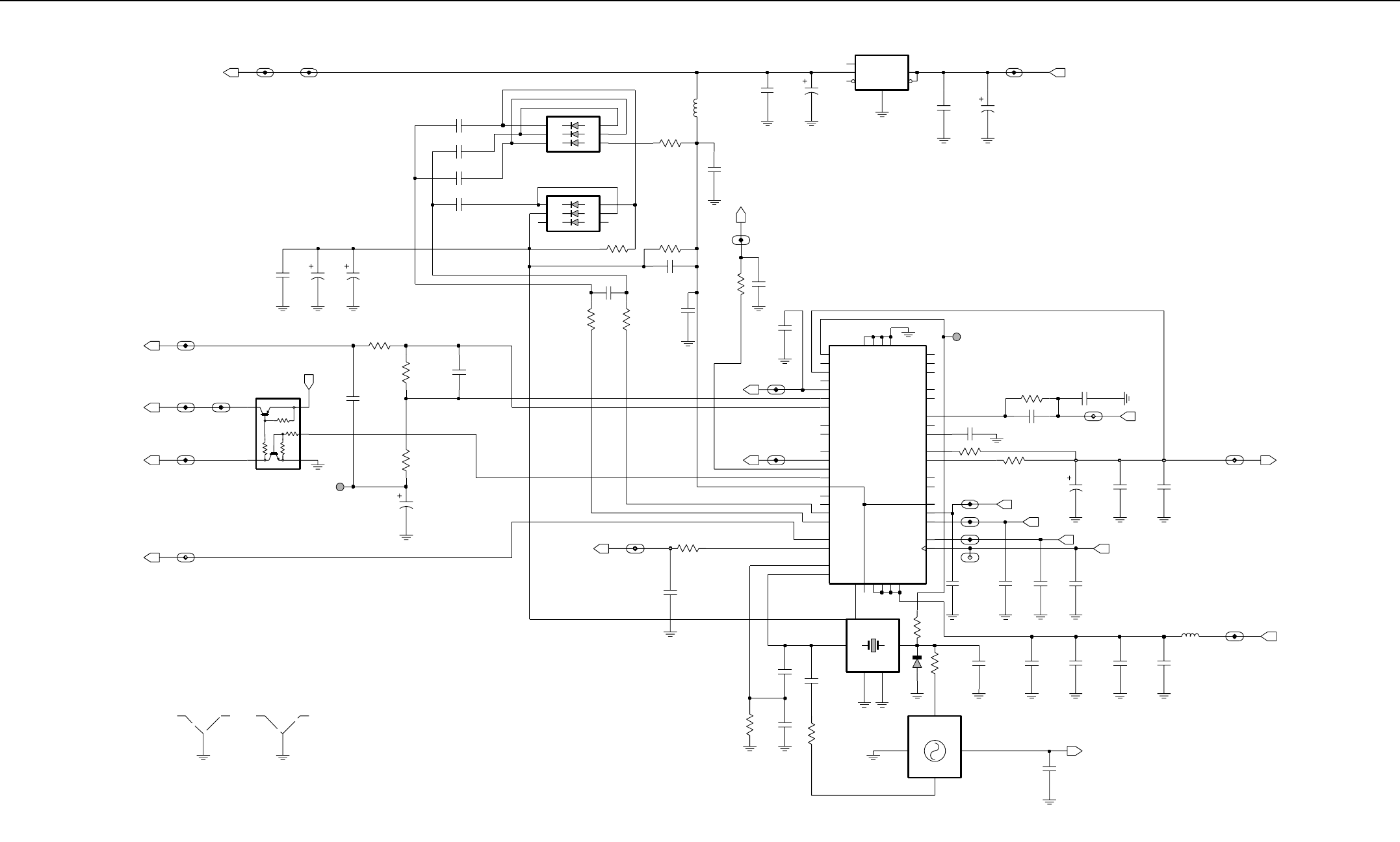
4-42 VHF PCB 8486062B16 / Schematics
VHF (136-174 MHz) Synthesizer
TRB
SH3702
SHIELD
SHIELD
1
SH3701
SHIELD
SHIELD
1
VCO_MOD
R5
T5
VCTRL
VCO_MOD_1_FN
VCTRL_1_FN
T5_1_FN
R5_1_FN R5_2_FN
5V
4
1
3
Q3721
2
UMC5N
47K
47K
10K
47K
4.7uF
C3714
4.7uF
C3706C3705
0.1uF
5V
5V_1_FN 5V_2_FN
(SOURCE)
R3722
1K
0.1uF
C3721
470
R3721
100
R3723
C3722
0.1uF
C3724
TP3701 1
1uF
C3704
.01uF
.01uF
C3702
C3701
.01uF
.01uF
C3703
4
1K1
2K2
3K3
D3701
A1 6
A2 5
A3
K2
2K3
3
D3702
A1 6
A2 5
A3 4
K1
1
R3702
0
NU
C3709
0.1uF
R3704
150
C3707
22pF
33K
R3705
0.1uF
C3708
R3703
150
BIAS_ADJ
100
R3701
470pF
C3715 C3711
10uF
L3701
390nH
BIAS_ADJ_1_FN
2.2uF
C3710
2.2uF
C3713
6ERR
1GND
5
IN
2NR
4OUT 3
SD
U3711
mgc_comps
SWB_PLUS_1_FN
C3712
0.1uF
SWB+
C3746
220pF
C3725
0.1uF
NU
LOCK_1_FN
R3726
47K
NU
LOCK
16_8MHz_1_FN
100
R3741
C3741
NU
56pF
16.8MHz
.01uF
NU
C3735
100
R3763
NU
R3762
NU
2.2K
56pF
C3761
330pF
C3762
100K
R3727 C3726
8.2pF
100pF
C3727
PRESC_1_FN
2.2uF
C3755
MODIN_1_FN
DATA_1_FN
CSX_1_FN
R3752
330K
C3753
4.7uF
200K
R3751
DATA
MODIN
C3752
1000pF
CSX
CLK_1_FN
220pF
C3744 C3742
220pF C3745
220pF
C3743
220pF
CLK
5V
.01uF C3732
.01uF
C3731
R3760
0
0
NU
1.6pF
C3763
C3751
0.1uF
NU
4
VCC
1
VCNTL
2GND
3OUT
NU
OSC_16.8MHZ
16.8MHz
VSF
VSF_1_FN
PRESC
0.1uF
C3754
Vdda
Vdda_1_FN
L3731
2.2uH
C3734
.01uF
C3733
2.2uF
47K
R3761
D3761
GND
1
GND1
4
OUT3
IN
6
16.8MHz
44
33
6
22
1TP3702
18
27
26
17
29
31
32
40
39
42
24
38
15
14
12
11
28
37
41
19
45
43
4
3
46
48
1
2
25
16
TRB_1_FN
21
35
30
10
9
8
7
23
47
13
34
5
36
20
mgc_comps
U3701
WARP
TEST2
REFSEL
SFBASE
SFCAP
SFOUT
TEST1
NC1
NC2
NC3
PD_GND
PREIN
PRE_GND
DGND
IADAPT
INDMULT
IOUT
LOCK CCOMP
ADAPTSW
AGND
VMULT1
VMULT2
VMULT3
VMULT4
MODOUT
FREFOUT
AUX4
AUX1
AUX2
AUX3
VBPASS
PVREF
SFIN
MODIN
BIAS1
BIAS2
CEX
CLK
DATA
VRO
XTAL1
XTAL2
VCP
PRE_VDD
PD_VDD
DVDD
AVDD
ZMY0130483-A
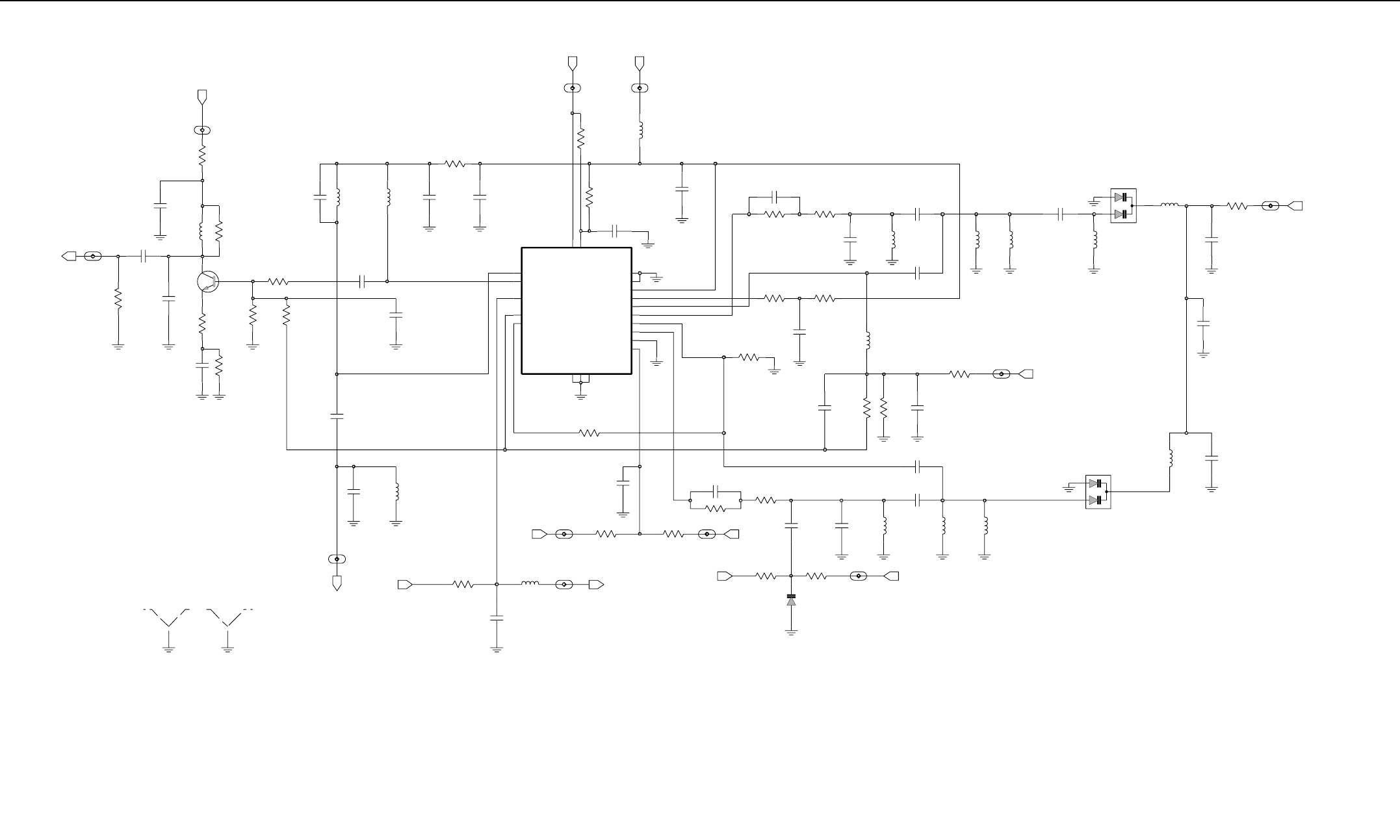
VHF PCB 8486062B16 / Schematics 4-43
VHF (136-174 MHz) Voltage Controlled Oscillator
R5
R3802
100
R5_1_VCO
0.1uF
C3804
1K
R3807
NU
1K
L3801
100nH
RX_INJ
Q3801
RX_INJ_1_VCO
C3802
22pF
NU
220
NU
R3801
C3801
4.7pF
0.1uF
C3812L3811
100nH
100
R3811
C3810
10pF
NU 0.1uF
C3811L3812
100nH
Vdda VSF
VSF_1_VCO
Vdda_3_VCO
R3817
0
0
L3813
1uH
0
NU
0
R3818
C3818
.022uF
TX_OUT
TX_SWITCH
RX_OUT
RX_SWITCH
PRESC_OUT
VCC_BUFFERS
VCC_LOGIC
14
18
U3801
10
13
8
7
12
2
3
19
16
15
1
4
20
5
6
RX_IADJ
SUPER_FLTR
TRB_IN
TX_BASE
TX_EMITTER
TX_IADJ
COLL_RFIN
FLIP_IN
RX_BASE
RX_EMITTER
GND_BUFFERS
GND_FLAG
GND_LOGIC
11
9
17
10
10
R3808
24K
R3805R3804
10K
R3803
220
C3803
1000pF
R3806
22
C3805
4.7pF
100pF
C3806
27nH
L3809
15pF
C3808
27pF
C3809
TX_INJ_1_VCO
C3822
1000pF
C3813
.01uF
47
R3822R3821
220 L3821
56nH
C3824
56pF
C3826
4.7pF
C3825
15pF
L3826
1uH
R3825
33
R3831
10K
18
R3826
R3823
33K
.01uF
C3821 C3827
.022uF
.01uF
C3823
R3824
22K
PRESC_1_VCO
1K 100nH
R3816 L3816
C3816
PRESC
6.8pF
VSF
TX_INJ
T5 TRB
C3832
1000pF
R3833
220
1000pF
C3815
R3830
T5_1_VCO
0
R3829 TRB_1_VCO
0
R3832
12K
47
R3834
VCO_MOD_1_VCO
47K
R3835
VSF
R3836
10K
VCO_MOD
D3832
4.7pF
C3833 L3831
56nH56pF
C3834
C3836
15pF
C3835
6.8pF
L3832
68nH
L3833
56nH
100K
R3812
BIAS_ADJ_1_VCO
BIAS_ADJ
NU
L3824
1uH
L3822
47nH
D3821
L3825
100nH
68pF
C3830
47nH
L3823
C3829
0.1uF
0.1uF
C3828
R3828
100
VCTRL_1_VCO
VCTRL
1uH
L3834 C3842
1000pF
D3831
SHIELD
1
SHIELD
1
SH3802SH3801
ZMY0130485-A
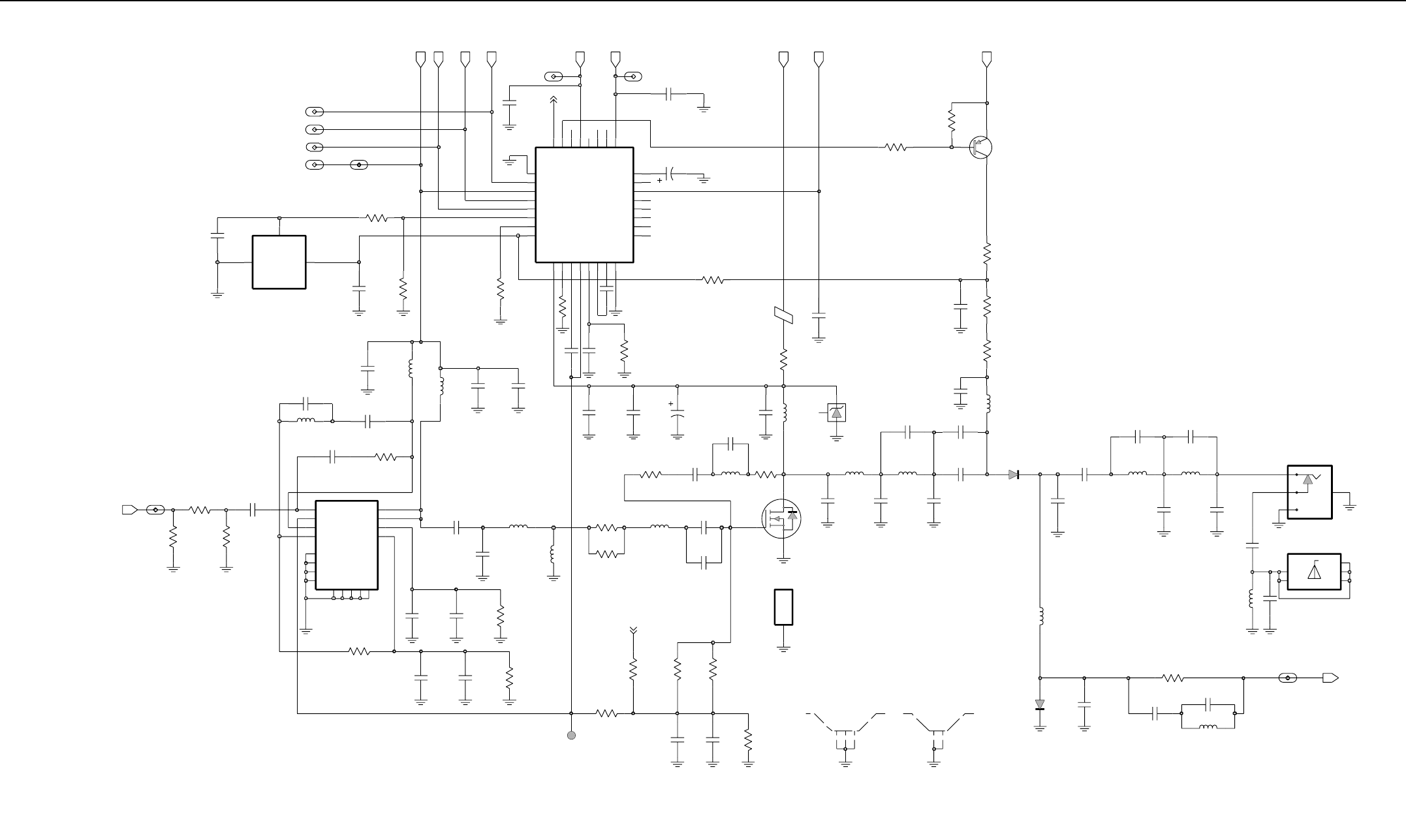
4-44 VHF PCB 8486062B16 / Schematics
VHF (136-174 MHz) Transmitter
DATA CLK
CSX
UNSWB+
CSX_2_PA
UNSWB_LPLUS_2_PA
UNSW_LPLUS_3_PA
CLK_2_PA
DATA_2_PA
C3566
100pF
2
U3503
GND
3POS
VOUT
12K
R3561
R3562
33K
C3561
.022uF
LM50C
5185963A15
330pF
C3501
300
R3501 R3503
300
TX_INJ_1_PA
18
R3502
TX_INJ
C3504
.022uF
33pF
C3502
5.6nH
L3501
470
R3505
330pF
C3505
C3503
33pF
68nH
L3503
.022uF
C3508
330pF
C3509
68nH
L3504
330pF
C3567
330K
NU
R3565
220pF
C3564
3300pF
C3562
3300pF
C3563
330K
R3564
.022uF
C3565
270K
R3563
RFOUT2
1VCNTRL
14 VD1 2
VG1 3
VG2
12
GND4
13
8NC1
9NC2
10 NC3
15 NC4
16 RFIN RFOUT1 6
7
EP
17
11 G2
GND1
4
GND2
5
GND3
09Z67
U3501
330pF
C3544
100
R3543
C3543
.022uF
330pF
C3542
5.6K
R3542
.022uF
C3541 R3541
NU
6.8K
L3511
18nH
L3512
11.03nH
47pF
C3512
30pF
C3513
3.9
R3507
R3506
3.9 L3513
7.66nH 470pF
C3514
100pF
C3517
C3516
1uF
22pF
C3519
100
R3513
R3512
3300pF
C3515
330pF
C3518 L3518
39nH
120
D
G
S
Q3501
HEATSINK
H3501
C3527
1.5pF
NU
120pF
C3523
18pF
C3524
L3521
7.66nH
220pF
C3521
.022uF
C3528
9.1pF
23.75nH
L3522
13.85nH
L3515
C3525
10pF
VR3501
10V
C3526
Microstrio
100
R3545
7.5K
R3548
100
R3544
BIAS_TUNING
330pF
C3546
R3546
33K
12K
R3547
.022uF
C3547
TP3502
3300pF
C3568
0
R3566
R3519
0.1
BEAD
L3519
C3570
470pF
C3571
RESET
RESET_1_PA 5V_2_PA
5V
BIAS_TUNING
330pF
UNSWB+
UNSWB+
10K
NU
R3570
R3569
NU
5.6K NU
Q3561
UNSWB+
R3571
NU
120
120
R3572
120
R3573
C3569
.022uF
L3523
1uH
D3521
43.67nH
L3551
C3536
15pF
7.5pF
C3533
C3532
68pF
43.67nH
L3531
43.67nH
L3532
C3535
27pF
C3534
4.7pF
20pF
C3531
4
1
2
3
J3501
RF_JACK
GND
18pF
C3537
TAB5 5
1TAB1
2TAB2
3
TAB3 4
TAB4
ANTENNA_NUT
J3502
5.6pF
C3539
30.54nH
L3538
39
R3551
56pF
C3552
RX_IN_1_PA
RX_IN
C3551
68pF
D3551
7.66nH
L3552
7.5pF
C3550
19
17
20
18
24
22
21
23
14
16
15
11
10
12
13
9
30
31
26
28
25
32
27
29
6
2
1
7
8
4
3
5
TEMP
RSET
CLK
DATA
GND2
ANO
BPOS
CEX
VL
T1
INT
RFIN
CL
GND1
CI
CJ
VG
V10
V45
Q
QX
CQ
CQX
F168
VLIM
V5EXT
VAR1
VAR2
VAR3
NA
RS
RX
H99S-4
U3502
C3560
1uF
1
SHIELD
SH3502SH3501
SHIELD
1
2
1
2
3
ZMY0130484-A

VHF PCB 8486062B16 Parts List 4-45
11.0 VHF PCB 8486062B16 Parts List
Circuit
Ref
Motorola
Part No Description
B501 0986237A02 Connector, Contact Battery
B503 3980502Z01 Backup battery B+
only GP360, GP380, GP680
B504 3980501Z01 Backup battery B-
only GP360, GP380, GP680
C3200 2113743N31 16pF
C3203 2113743N50 100pF
C3204 2113743L41 10000pF, 10%
C3205 2113928N01 0.1uF, 10%
C3206 2113743L41 10000pF, 10%
C3207 2113743N10 2.2pF
C3209 2311049A07 1uF
C3210 2113743L17 1000pF, 10%
C3211 2311049A56 4.7uF, 20%, 10V
C3212 2311049A57 10uF
C3213 2311049A56 4.7uF, 20%, 10V
C3214 2113928N01 0.1uF, 10%
C3215 2113743N26 10pF
C3218 2311049A56 4.7uF, 20%, 10V
C3219 2113928N01 0.1uF, 10%
C3220 2113743N26 10pF
C3221 2113743L41 10000pF, 10%
C3222 2113928N01 0.1uF, 10%
C3223 2113928N01 0.1uF, 10%
C3224 2113928N01 0.1uF, 10%
C3225 2113928N01 0.1uF, 10%
C3226 2113928N01 0.1uF, 10%
C3227 2113743L41 10000pF, 10%
C3228 2113743L41 10000pF, 10%
C3229 2113743N50 100pF
C3230 2113740F51 100pF
C3231 2180478Z20 1uF
C3232 2180478Z20 1uF
C3233 2180478Z20 1uF
C3234 2180478Z20 1uF
C3235 2113743A23 0.220uF
C3238 2113743A24 0.330uF
C3239 2113743E07 0.022uF
C3240 2113743A23 0.220uF
C3241 2113743L19 1200pF
C3242 2109720D14 0.1uF
C3243 2113743E07 0.022uF
C3244 2113743L41 10000pF, 10%
C3270 2113743E07 0.022uF
C3271 2113743L05 330pF
C3272 2113743N18 4.7pF
C3273 2113743N26 10pF
C3274 2113743N38 33pF
C3275 2113743N44 56pF
C3276 2113743N42 47pF
C3277 2113743N48 82pF
C3278 2113743E07 0.022uF
C3279 2311049A40 2.2uF, 10%, 16V
C3280 2113743L41 10000pF, 10%
C3301 2113743N20 5.6pF
C3302 2113743N54 150pF
C3303 2113743N30 15pF
C3304 2113743N54 150pF
C3306 2113928N01 0.1uF, 10%
C3307 2113743N50 100pF
C3308 2113743L05 330pF
C3309 2113928N01 0.1uF, 10%
C3311 2113743N54 150pF
C3312 2113743N31 16pF
C3313 2113743N54 150pF
C3315 2113743N26 10pF
C3316 2113743N14 3.3pF
C3317 2113743N40 39pF
C3318 2113743M08 22000pF, +80/-20%
C3320 2113743N48 82pF
C3321 2113743L05 330pF
C3322 2113743N50 100pF
C3323 2113743N50 100pF
C3324 2113743N38 33pF
C3325 2113743L17 1000pF, 10%
C3327 2113743L05 330pF
C3329 2113743L05 330pF
C3330 2113743N50 100pF
C3331 2113743N50 100pF
C3332 2113743N40 39pF
C3334 2113743N33 20pF
C3335 2113743N34 22pF
C3336 2311049A18 10uF
C3337 2113743M08 22000pF, +80/-20%
C3338 2113743L09 470pF, 10%
C3339 2113743N26 10pF
C3501 2113743L05 330pF
C3502 2113743N38 33pF
C3503 2113743N38 33pF
C3504 2113743M08 22000pF, +80/-20%
C3505 2113743N38 33pF
C3508 2113743M08 22000pF, +80/-20%
C3509 2113743L05 330pF
C3512 2113740F43 47pF
C3513 2113740F38 30pF
C3514 2113740F47 68pF
C3515 2113743L29 3300pF
C3516 2311049A08 1uF
C3517 2113740F47 68pF
Circuit
Ref
Motorola
Part No Description
C3521 2111078B51 220pF
C3523 2111078B44 120pF
C3524 2113740F33 18pF
C3525 2113740F27 10pF
C3526 2113743M08 22000pF, +80/-20%
C3528 2113740F27 10pF
C3531 2113740F34 20pF
C3532 2113740F47 68pF
C3533 2113740F24 7.5pF
C3534 2113740F19 4.7pF
C3535 2113740F37 27pF
C3536 2113740F31 15pF
C3537 2113740F33 18pF
C3539 2113740F29 12pF
C3541 2113743M08 22000pF, +80/-20%
C3542 2113743L05 330pF
C3543 2113743M08 22000pF, +80/-20%
C3544 2113743L05 330pF
C3546 2113743L05 330pF
C3547 2113743M08 22000pF, +80/-20%
C3550 2113743N23 7.5pF
C3551 2113743N46 68pF
C3552 2113743N44 56pF
C3560 2311049A07 1uF
C3561 2113743M08 22000pF, +80/-20%
C3562 2113743L29 3300pF
C3563 2113743L29 3300pF
C3564 2113743L01 220pF
C3565 2113743E07 0.022uF
C3566 2113743N50 100pF
C3567 2113743L05 330pF
C3568 2113743L29 3300pF
C3569 2113743M08 22000pF, +80/-20%
C3570 2113743L05 330pF
C3571 2113743L09 470pF, 10%
C3701 2113743L41 10000pF, 10%
C3702 2113743L41 10000pF, 10%
C3703 2113743L41 10000pF, 10%
C3704 2113743L41 10000pF, 10%
C3705 2113743E20 0.10uF, 10%
C3706 2311049J11 4.7uF
C3707 2113743N34 22pF
C3708 2113928N01 0.1uF, 10%
C3709 2113928N01 0.1uF, 10%
C3710 2104993J02 2.2uF
C3711 2311049A69 10uF
C3712 2113928N01 0.1uF, 10%
C3713 2311049A09 2.2uF
C3714 2311049J11 4.7uF
C3715 2113743L09 470pF, 10%
C3721 2113743E20 0.10uF, 10%
Circuit
Ref
Motorola
Part No Description
C3722 2113743E20 0.10uF, 10%
C3724 2311049A08 1uF
C3726 2113743N24 8.2pF
C3727 2113743N50 100pF
C3731 2113743L41 10000pF, 10%
C3732 2113743L41 10000pF, 10%
C3733 2104993J02 2.2uF
C3734 2113743L41 10000pF, 10%
C3742 2113743L01 220pF
C3743 2113743L01 220pF
C3744 2113743L01 220pF
C3745 2113743L01 220pF
C3746 2113743L01 220pF
C3752 2113743L17 1000pF, 10%
C3753 2311049A56 4.7uF, 20%, 10V
C3754 2113928N01 0.1uF, 10%
C3755 2104993J02 2.2uF
* C3761 2113743N44 56pF
* C3762 2113740F63 330pF
* C3763 2113743N08 1.6pF
C3801 2113743N18 4.7pF
C3803 2113743L17 1000pF, 10%
C3804 2113743E20 0.10uF, 10%
C3805 2113743N18 4.7pF
C3806 2113743N50 100pF
C3808 2113743N30 15pF
C3809 2113743N36 27pF
C3811 2113928N01 0.1uF, 10%
C3812 2113928N01 0.1uF, 10%
C3813 2113743L41 10000pF, 10%
C3815 2113743L17 1000pF, 10%
C3816 2113743N22 6.8pF
C3818 2113743E07 0.022uF
C3821 2113743L41 10000pF, 10%
C3822 2113743L17 1000pF, 10%
C3823 2113743L41 10000pF, 10%
C3824 2113743N44 56pF
C3825 2113743N30 15pF
C3826 2113743N18 4.7pF
C3827 2113743E07 0.022uF
C3828 2185895Z01 0.01uF, 10%
C3829 2185895Z01 0.01uF, 10%
C3830 2113743N46 68pF
C3832 2113743L17 1000pF, 10%
C3833 2113743N18 4.7pF
C3834 2113743N44 56pF
C3835 2113743N22 6.8pF
C3836 2113743N30 15pF
C3842 2113743L17 1000pF, 10%
C400 2113743L41 10000pF, 10%
C401 2113928N01 0.1uF, 10%
Circuit
Ref
Motorola
Part No Description

4-46 VHF PCB 8486062B16 Parts List
C402 2113928N01 0.1uF, 10%
C4020 2113743L17 1000pF, 10%
C4021 2113743L17 1000pF, 10%
C403 2113928D08 10uF, +/-80%/-20%
C407 2113928N01 0.1uF, 10%
C408 2113743N50 100pF
C409 2113928N01 0.1uF, 10%
C410 2113928N01 0.1uF, 10%
C411 2113928N01 0.1uF, 10%
C414 2113928N01 0.1uF, 10%
C415 2185895Z01 0.01uF, 10%
C416 2113928N01 0.1uF, 10%
C419 2113743L41 10000pF, 10%
C420 2113743L41 10000pF, 10%
C421 2113928N01 0.1uF, 10%
C422 2113928N01 0.1uF, 10%
C423 2113743N50 100pF
C424 2311049A59 10uF, 10%, 6V
C425 2113928N01 0.1uF, 10%
C426 2113743N50 100pF
C427 2113743N50 100pF
C428 2113928N01 0.1uF, 10%
C429 2113928N01 0.1uF, 10%
C430 2113928N01 0.1uF, 10%
C431 2113743N50 100pF
C433 2113743L41 10000pF, 10%
C434 2113928N01 0.1uF, 10%
only GP360, GP380, GP680
C435 2113928N01 0.1uF, 10%
C436 2113743N34 22pF
only GP360, GP380, GP680
C437 2113743N34 22pF
only GP360, GP380, GP680
C440 2113743G26 4.7F, + 80/-20%
C441 2113743L09 470pF, 10%
C442 2113743E20 0.10uF, 10%
C443 2113928N01 0.1uF, 10%
C444 2113743N50 100pF
C445 2113743L09 470pF, 10%
C446 2113743L09 470pF, 10%
C447 2113928N01 0.1uF, 10%
C448 2113928N01 0.1uF, 10%
C449 2113743N50 100pF
C451 2113743M08 22000pF, +80/-20%
C452 2113743B29 1uF
C453 2113743N50 100pF
C456 2113743N50 100pF
C458 2113743N50 100pF
C459 2113743N50 100pF
C463 2113743N50 100pF
C466 2113743N50 100pF
Circuit
Ref
Motorola
Part No Description
C467 2113928N01 0.1uF, 10%
C471 2113743L09 470pF, 10%
C472 2113743L09 470pF, 10%
C473 2113743L09 470pF, 10%
C474 2113743L41 10000pF, 10%
C475 2113743H14 10uF, +80/-20%
C476 2113928D08 10uF, +/-80%/-20%
C477 2113743L17 1000pF, 10%
C478 2113743L17 1000pF, 10%
C479 2113928N01 0.1uF, 10%
C480 2113928D08 10uF, +/-80%/-20%
C481 2113928N01 0.1uF, 10%
C482 2113928N01 0.1uF, 10%
C483 2113743L09 470pF, 10%
C484 2113743L09 470pF, 10%
C490 2113743L09 470pF, 10%
C491 2113743L09 470pF, 10%
C492 2113743L09 470pF, 10%
C493 2113743N50 100pF
C494 2113743N50 100pF
C495 2113743L09 470pF, 10%
C496 2113743L09 470pF, 10%
C497 2113743L09 470pF, 10%
C502 2311049A05 0.47uF, 10%, 25V
C503 2113743N50 100pF
C505 2113743N50 100pF
C511 2113743N50 100pF
C512 2113743N50 100pF
C513 2113743N50 100pF
C514 2113743N50 100pF
C520 2113743L41 10000pF, 10%
C521 2113743L41 10000pF, 10%
C522 2113743L41 10000pF, 10%
C523 2113743L41 10000pF, 10%
C535 2113743L17 1000pF, 10%
CR3301 4802245J42 Ring Quad diode
CR3302 4805129M96 Dual Bonds Pin Diode, RH
Reeled
CR3303 4880154K03 Dual common anode-cathode
diode
CR411 4802245J62 Schottky diode
CR412 4802245J62 Schottky diode
CR413 4802245J62 Schottky diode
CR440 4813833C02 Dual Diode Common Cathode
CR501 4880107R01 Rectifier
CR503 4805729G49 LED Red/Yellow
D3270 4862824C01 Varactor
D3301 4802081B58 Dual Diode
D3302 4802081B58 Dual Diode
D3521 4880973Z02 Pin diode
D3551 4880973Z02 Pin diode
Circuit
Ref
Motorola
Part No Description
D3701 4802233J09 Triple diode
D3702 4802233J09 Triple diode
* D3761 4862824C03 Varactor
D3821 4805649Q13 Varactor
D3831 4805649Q13 Varactor
D3832 4862824C01 Varactor
E400 2480640Z01 Ferrite bead
E401 2480640Z01 Ferrite bead
E402 2480640Z01 Ferrite bead
E403 2480640Z01 Ferrite bead
E404 2480640Z01 Ferrite bead
E405 2480640Z01 Ferrite bead
E406 2480640Z01 Ferrite bead
E407 2480640Z01 Ferrite bead
E408 2480640Z01 Ferrite bead
E409 2480640Z01 Ferrite bead
F501 6580542Z01 3A Fuse
FL401 4870368G02 Real Time Clock Osciall XTAL
only GP360, GP380, GP680
H3501 2680499Z01 Heat spreader
J3501 0985613Z01 RF Jack
J3502 0280519Z02 Antenna_Nut
J400 0905505Y04 40-pin connector
J403 0905505Y02 20-pin connector
L3200 2462587N68 1uH
L3202 2462587N68 1uH
L3221 2462587N68 1uH
L3270 2462587T15 100nH
L3271 2462587Q20 2.2uF
L3301 2462587T35 12nH
L3303 2462587T35 12nH
L3304 2462587T23 470nH
L3305 2462587T35 12nH
L3306 2462587T35 12nH
L3308 2462587T34 10nH
L3309 2462587N55 150nH
L3312 2462587V28 33nH
L3501 2413926H09 5.6nH
L3503 2462587V32 68nH
L3504 2462587N51 68nH
L3511 2462587N44 18nH
L3512 2479990B01 11.03nH
L3513 2479990A02 7.66nH, 10%
L3515 2479990C03 13.85nH
L3519 2484657R01 Ferrite bead
L3521 2479990A02 7.66nH, 10%
L3522 2479990E01 23.75nH
L3523 2462587N68 1uH
L3531 2479990N01 43.67nH
L3532 2479990N01 43.67nH
L3538 2479990M01 30.54nH
Circuit
Ref
Motorola
Part No Description
L3551 2479990N01 43.67nH
L3552 2479990A02 7.66nH, 10%
L3701 2462587Q42 390nH, 10%
L3731 2462587Q20 2.2uF
L3801 2462587V34 100nH
L3809 2462587V27 27nH
L3811 2462587V34 100nH
L3812 2462587V34 100nH
L3813 2462587Q47 1000nH, 10%, QF45
L3816 2462587V34 100nH
L3821 2462587N50 56nH
L3822 2462587N49 47nH
L3823 2462587N49 47nH
L3824 2462587N68 1uH
L3825 2462587V34 100nH
L3826 2462587N68 1uH
L3831 2462587N50 56nH
L3832 2462587N51 68nH
L3833 2462587N50 56nH
L3834 2462587N68 1uH
L400 2462587Q42 390nH, 10%
L401 2462587Q42 390nH, 10%
L410 2462587Q42 390nH, 10%
L411 2462587Q42 390nH, 10%
L505 2462587Q42 390nH, 10%
PB501 4080523Z01 Tactile, Pushbutton
PB502 4080523Z01 Tactile, Pushbutton
PB503 4080523Z01 Tactile, Pushbutton
not in GP320
PB504 4080523Z01 Tactile, Pushbutton
PB505 4080523Z01 Tactile, Pushbutton
not in GP320
Q3200 4813827A07 NPN Transistor
Q3201 4880214G02 NPN Transistor
Q3202 4880214G02 NPN Transistor
Q3270 4805218N63 RF Transistor
Q3301 4880214G02 NPN Transistor
Q3302 4813827A07 NPN Transistor
Q3501 4813828A08 FET
Q3561 4813824A17 PNP Transistor
Q3721 4802245J50 Dual NPN/PNP Transistor
Q3801 4813827A07 NPN Transistor
Q400 4809579E18 Mosfet P - channel
Q403 4813824A17 PNP Transistor
Q405 4802245J54 Dual NPN Transistor
Q410 4802245J54 Dual NPN Transistor
Q416 4809579E18 Mosfet P - channel
only GP360, GP380, GP680
Q417 4802245J50 Dual NPN/PNP Transistor
Q502 5180159R01 Dual NPN Transistor
Q505 4880214G02 NPN Transistor
Circuit
Ref
Motorola
Part No Description

VHF PCB 8486062B16 Parts List 4-47
R3200 0662057M54 150
R3201 0662057M82 2200
R3202 0662057M90 4700
R3203 0662057M98 10k
R3204 0662057M26 10
R3205 0662057M74 1000
R3206 0662057N23 100K
R3207 0662057N13 39K
R3208 0662057M50 100
R3209 0662057M74 1000
R3210 0662057M82 2200
R3211 0662057M82 2200
R3212 0662057M90 4700
R3213 0662057M82 2200
R3214 0662057M34 22
R3219 0662057M50 100
R3220 0662057M90 4700
R3221 0662057M50 100
R3224 0662057M26 10
R3225 0662057M74 1000
R3226 0662057M26 10
R3270 0662057M74 1000
R3271 0662057M42 47
R3272 0662057N15 47K
R3273 0662057N15 47K
R3274 0662057M83 2400
R3275 0662057M74 1000
R3276 0662057N30 200K
R3303 0662057N23 100K
R3304 0662057N23 100K
R3305 0662057N19 68K
R3306 0662057M82 2200
R3307 0662057N11 33K
R3308 0662057M78 1500
R3309 0662057M92 5600
R3310 0662057M98 10k
R3311 0662057M26 10
R3312 0662057M38 33
R3313 0662057M34 22
R3314 0662057M26 10
R3315 0662057M62 330
R3316 0662057M66 470
R3317 0662057N23 100K
R3318 0662057M66 470
R3321 0662057M54 150
R3322 0662057M58 220
R3323 0662057M32 18
R3324 0662057M58 220
R3501 0662057M61 300
R3502 0662057M32 18
R3503 0662057M61 300
Circuit
Ref
Motorola
Part No Description
R3505 0662057M62 330
R3506 0662057B62 3.9
R3507 0662057B62 3.9
R3519 0680539Z01 0.1
R3541 0662057N13 39K
R3542 0662057M92 5600
R3543 0662057M50 100
R3544 0662057A25 100
R3545 0662057A25 100
R3546 0662057N01 12K
R3547 0662057N11 33K
R3548 0662057N07 22K
R3551 0662057M40 39
R3561 0662057N01 12K
R3562 0662057N11 33K
R3563 0662057N33 270K
R3564 0662057N35 330K
R3569 0662057M92 5600
R3570 0662057M98 10k
R3571 0662057A27 120
R3572 0662057A27 120
R3573 0662057A27 120
R3701 0662057M50 100
R3703 0662057M54 150
R3704 0662057M54 150
R3705 0662057N11 33K
R3721 0662057M66 470
R3722 0662057M74 1000
R3723 0662057M50 100
R3727 0662057N23 100K
R3741 0662057M50 100
R3751 0662057N30 200K
R3752 0662057N35 330K
R3761 0662057N15 47K
R3802 0662057M50 100
R3803 0662057M58 220
R3804 0662057M98 10k
R3805 0662057N08 24K
R3806 0662057M34 22
R3808 0662057M26 10
R3811 0662057M50 100
R3816 0662057M74 1000
R3817 0662057M01 0
R3821 0662057M58 220
R3822 0662057M42 47
R3823 0662057N11 33K
R3824 0662057N07 22K
R3825 0662057M38 33
R3826 0662057M32 18
R3828 0662057M50 100
R3829 0662057M01 0
Circuit
Ref
Motorola
Part No Description
R3831 0662057M98 10k
R3832 0662057N01 12K
R3833 0662057M58 220
R3834 0662057M42 47
R3835 0662057N15 47K
R3836 0662057M98 10k
R400 0662057N15 47K
R401 0662057M01 0
R405 0662057M01 0
R406 0662057N20 75K
R407 0662057N19 68K
R409 0662057M98 10k
R410 0662057N23 100K
R411 0662057M98 10k
R413 0662057M01 0
R414 0662057V34 180K
R415 0662057V26 91K
R416 0662057M98 10k
R418 0662057M01 0
R419 0662057M67 510
only GP360, GP380, GP680
R420 0662057B46 10M
only GP360, GP380, GP680
R421 0662057M81 2000
R423 0662057N21 82K
R424 0662057N12 36K
R425 0662057N10 30K
R426 0662057N35 330K
only GP360, GP380, GP680
R427 0662057M84 2700
R428 0662057M10 2.2
R429 0662057M98 10k
R431 0662057N39 470K
R432 0662057N16 51K
R434 0662057M62 330
R435 0662057M81 2000
R436 0662057M01 0
R445 0662057N08 24K
R447 0662057N51 1.5M
R448 0662057M98 10k
R449 0662057N08 24K
R450 0683962T45 68 ohms, 1W
R451 0662057N03 15K
R452 0662057N23 100K
R456 0662057M01 0
R457 0662057M98 10k
R460 0662057M90 4700
R461 0662057M56 180
only GP360, GP380, GP680
R462 0662057M98 10k
only GP360, GP380, GP680
Circuit
Ref
Motorola
Part No Description
R463 0662057M61 300
R471 0662057M92 5600
R472 0662057M93 6200
R473 0662057M26 10
R475 0662057M01 0
R476 0662057N08 24K
R477 0662057M74 1000
R478 0662057M98 10k
R481 0662057N08 24K
R492 0662057M01 0
R498 0662057M98 10k
R499 0662057M98 10k
R501 0662057M70 680
R502 0662057M56 180
R505 0662057M98 10k
R506 0662057N15 47K
RT400 0680590Z01 THERMISTOR 33K
S501 4080710Z01 Frequency Switch
only GP340, GP640
S501 4080710Z02 Frequency Switch
only GP360, GP380, GP680
S502 1880619Z02 Volume Switch
SH3201 2602023X08 Rx Backend Top Shield
SH3202 2686081B02 LVZIF shields
SH3203 2686081B03 45.1MHz Xtal Filter Shield
SH3301 2686081B01 Rx Frontend Bottom Shield
SH3302 2686081B05 Mixer Shield
SH3303 2686081B06 Rx Frontend Top Shield
SH3501 2686081B03 Harmonic Filter Shield
SH3502 2686081B04 PA driver Shield
SH3701 2680511Z01 Synthesizer top shield
SH3702 2680511Z01 Synthesizer bottom shield
SH3801 2680513Z01 VCO Top Shield
SH3802 2680514Z01 VCO Bottom Shield
SH400 2680505Z01 Controller Memory Shield
SH401 2680506Z01 Controller on-off shield
SH402 2680515Z01 Controller Microprocessor
shield
SH403 2680516Z01 Controller Asfic_Cmp/Audio
PA shield
T3301 2580541Z01 Balun transformer
T3302 2580541Z01 Balun transformer
U3201 5102463J58 3.3V Regulator
U3220 5109632D83 LVZIF IC
U3501 5185130C65 VHF/UHF/800 MHZ LDMOS
Driver
U3502 5185765B28 PCIC
U3503 5185963A15 Temperature Sense
U3701 5185963A27 LVFRACN Synthesizer IC
U3711 5105739X05 5V Regulator
U3801 5105750U54 VCO BUFFER IC
Circuit
Ref
Motorola
Part No Description

4-48 VHF PCB 8486062B16 Parts List
* Motorola Depot Servicing only
Reference designators with an asterisk indicate
components which are not field replaceable
because they need to be calibrated with
specialized factory equipment after installation.
Radios in which these parts have been replaced in
the field will be off frequency at temperature
extremes.
U400 5102463J40 3.3V Regulator
U404 5185963A53 ASFIC_CMP
U405 5102463J36 Static_RAM_32KX8
* U406 5102463J60 512K X 8 Flash Memory
* U407 5102463J64 16k X 8 EEPROM
U409 5102226J56 Microprocessor IC
U410 5102463J57 3.3V Regulator
only GP360, GP380, GP680
U420 5102463J44 Audio PA
VR3501 4880140L17 Zener diode-12V
VR432 4805656W08 5.6V Zener diode
VR433 4805656W08 5.6V Zener diode
VR434 4802245J73 ZENER DIODE-6.8V
VR439 4880140L17 Zener diode-12V
VR447 4802245J74 ZENER DIODE-10V
VR448 4802245J74 ZENER DIODE-10V
VR449 4802245J74 ZENER DIODE-10V
VR450 4802245J74 ZENER DIODE-10V
VR460 4802245J73 ZENER DIODE-6.8V
VR501 4802245J73 ZENER DIODE-6.8V
VR506 4802245J73 ZENER DIODE-6.8V
Y3200 9186153B01 Crystal Filter
Y3761 4805875Z04 16.8MHz Xtal oscillator (SMD)
5480678Z01 PCB Bar Code Label
8486062B16 VHF main PC Board
Circuit
Ref
Motorola
Part No Description
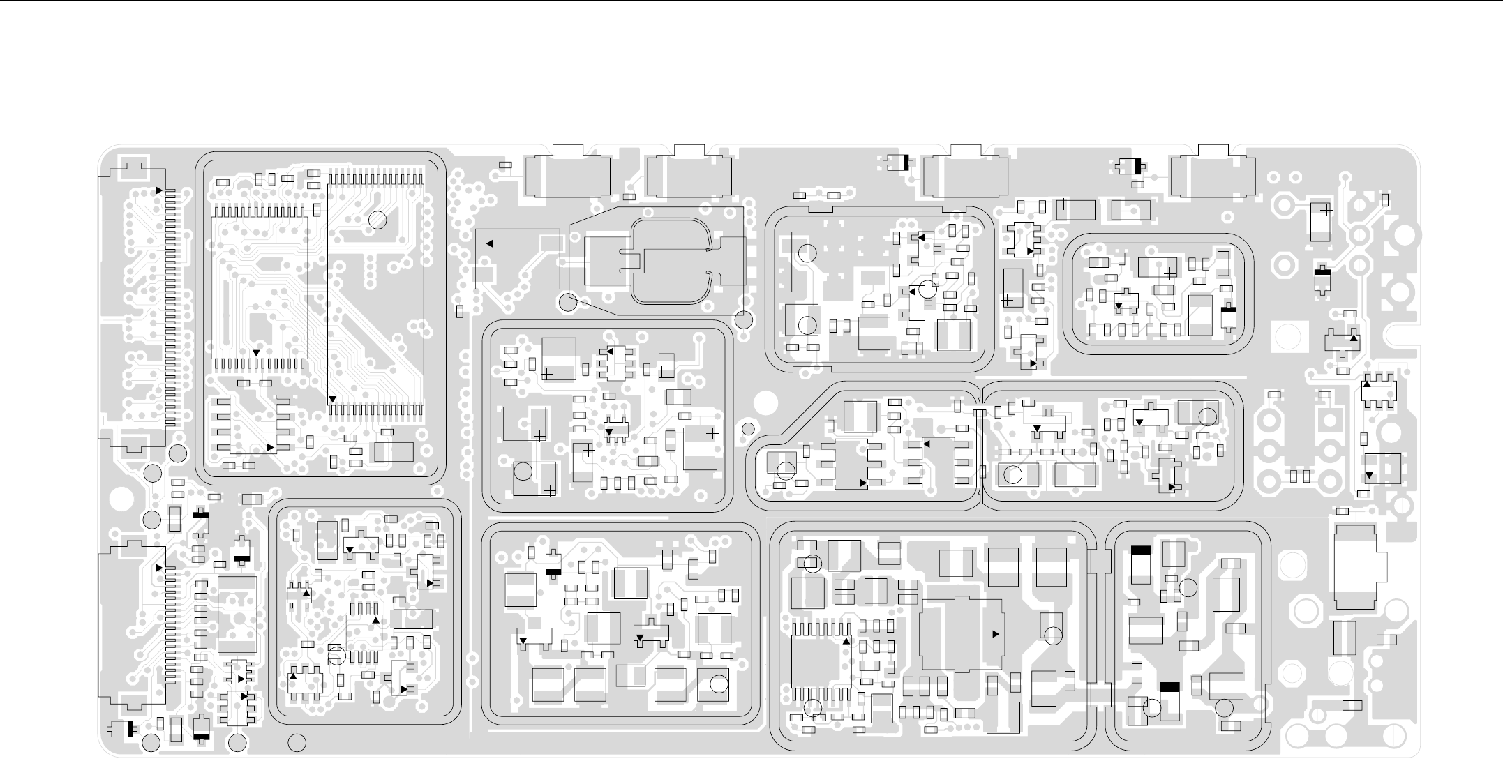
VHF PCB 8486062B17 / Schematics 4-49
12.0 VHF PCB 8486062B17 / Schematics
C423
C424
C425
C426
C427 C428
C429
E407
E408
E409
R408
R410
R418
R428
R429
R437
R478
R492
SH400
22
21
8
7
1
U405
32 17
16
1
U406
1
4
58
U407
C443 C444
C471
C472
C473
1
21
L401
R435
R450
RT400
TP401
TP402
TP410
VR447
VR449
22
20
J403
C441
C490
C491
C492
C493
C494
C495
C496
C497
CR413
L400
4
3
Q417
R421
R477
TP405
TP406 TP415
VR434
VR450
C400
C401
C402
C403
C467
C480
C482
CR412
CR440
Q400
Q403
4
3
Q405
R401
R402
R403
R405
R406
R407
R416
R427
R447
R448
R451
R452
R453
R454
R455
R456
R476
R481
SH401
4
58
U400
C3706
C3710
C3711
C3712
C3713
C3714
C3715
C3721
C3722
C3724
C3741
C3742
C3743
C3744
C3745
C3746
C3752
C3753
C3754
4
3
Q3721
R3701
R3721
R3722
R3723
R3741
R3751
R3752
SH3701
U3711
B503
B504
C432
C522
C523
PB502PB503
TP3701
TP3702
6
43
1
Y3761
C3822
C3824
C3825
C3826
C3828
C3829
C3830
C3832 C3833
C3834
C3835
C3836
C3842
D3821
D3831
D3832
L3821
L3822
L3823
L3824
L3825
L3831
L3832
L3833
L3834
R3821
R3822
R3823
R3828
R3833 R3834
R3835
R3836
SH3801
C3200C3201
C3202
C3203
C3204
C3205
C3206
C3207
C3208
C3210
L3200
L3201
L3202
PB504
Q3200
Q3201
R3200
R3201
R3202
R3203
R3204
R3205
R3206
R3207
R3208
R3209
R3210
R3211
R3212
SH3203
VR444
Y3200
C3318
C3320
C3329
C3334
C3335
L3309
L3312
R3317
R3318
R3321
R3322
R3323
SH3302
6
4
3
T3301
64
3
T3302
TP3301
C3306
C3307
C3308
C3309
C3310
C3311
C3312
C3313
C3314
C3319
C3327
C3330
C3331
C3332
C3338
CR3303
D3302
L3304
L3305
L3306
Q3302
R3308
R3309 R3310
R3311
R3312
R3313
R3316
SH3303
C3501
C3502
C3503
C3504
C3505
C3512
C3513
C3514
C3517
C3518
C3519
C3521
C3523
C3527
C3541
C3542
C3543
C3544
C3546
C3547
L3501
L3503
L3504
L3511
L3512
L3513
L3515
L3518
L3521
L3522
1
2
3
Q3501
R3501
R3502 R3503
R3505
R3506
R3507
R3512
R3513
R3541
R3542
R3543
R3544
R3545
R3546
R3547
R3548
SH3502
1
16
8
9
U3501
C3524
C3525
C3528
C3531
C3532
C3533
C3534
C3535
C3536
C3550
C3551
C3552
D3521
D3551
L3531
L3532
L3551
L3552
R3551
SH3501
C3225
C3270
C3271
C3272
C3273
C3274
C3275
C3276
C3277
C3278
C3279
C3280
D3270
L3270
L3271
Q3270
R3226
R3270
R3271
R3272
R3273
R3274
R3275
R3276
SH3201
C521
C3209
C3212 C3213
C3214
C3215
Q3202
R3213
R3214
R3215
R3218
R3225
U3201
PB501
VR440
C502
C505
C511
C513
C514
C520
C3537
C3539
4
3
2
CR503
L3538
PB505
Q502
Q505
R501
R502
R505
R506
VR501
J400
1
40
C512
VHF (136-174 MHz) Main Board Top Side

4-50 VHF PCB 8486062B17 / Schematics
2
3
4
1
J3501
J3502
M100M300
M301M400
M401
2C8
C4
S501
4
53
2S502
SH402
C3725
C3733
C3734
L3731
R3726
R3808
R3825
VR433
C442
C445
C483
C484
R473
VR432
VR448
C474
C477
C447
C448
R498
R499
R431
R423
C475
R424
R472
11
1
20
10
U420
C450
C476
C478
4
3
Q410
R471
C414
C415
C430 C440
C451
C452
SH403
13
VR460
C407
C408
C409
C410
C411
C416
C419
C420
C421
C422
C446
C481
R400
R413
R425
R434
R436
R445
R449
R475
1
37
25
U404
C479
C449
C458
C459
C463
C466
C4020
C4021
E400
E401
E402
E403
E404
E405
E406
L410
L411
1
76
51
26
U409
C453
C456
R409
R411
R432
R457
C431
C433
C434
C435
C436
C437
CR411
3
FL401
Q416
R414
R415
R419
R420
R426
R460
R461
R462
R463
U410
C3801
C3802
C3803
C3804
C3805
C3806
C3808
C3809
C3810
C3811
C3812
C3813
C3815
C3816
C3818
C3821
C3823
C3827
L3801 L3809
L3811
L3812
L3813
L3816
L3826
Q3801
R3801
R3802
R3803
R3804
R3805
R3806
R3807
R3811
R3812
R3816
R3817
R3818
R3824
R3826
R3829
R3830 R3831
R3832
SH3802
11
1
20
10
U3801
C3701
C3702
C3703
C3704
C3705
C3707
C3708
C3709
C3726
C3727
C3731
C3732
C3755
C3761
C3762
D3701
D3702
L3701
R3702
R3703
R3704
R3705
R3727
R3762
1
37
25
13
U3701
C3735
C3751
C3763
CR501
D3761
L505
R3760
R3761
R3763
VR439
VR441
VR442
VR506
2
34
Y3762
C503
C535
C3336
F501
C3508 C3509
C3566
C3567
C3568
C3570
C3571
L3519
Q3561
R3561
R3562
R3563
R3569
R3570
1
17
9
25
U3502
C3515
C3516
C3526
C3560
C3561
C3562
C3563
C3564
C3565 C3569
H3501
L3523
R3519
R3564
R3565
R3566
R3571 R3572 R3573
TP3502
VR3501
U3503
32
1
B501
M101
SH3702
C3211
C3218
C3219
C3220
C3221
C3222
C3223
C3224
C3226
C3227
C3228
C3229
C3230
C3231
C3232
C3233
C3234
C3235
C3236
C3237
C3238
C3239
C3240
C3241
C3242
C3243
C3244
L3221
R3219
R3220
R3221
R3222
R3223
R3224
SH3202
1
37
25
13
U3220
C3301
C3302
C3303
C3304
C3305
C3315
C3316
C3317
C3321
C3322
C3323
C3324
C3325
C3326
C3337 C3339
CR3301
CR3302 D3301
L3301L3303
L3308
Q3301
R3301
R3303
R3304
R3305
R3306
R3307
R3314
R3315
R3319
R3320
R3324
RT3301
SH3301
VHF (136-174 MHz) Main Board Bot Side
VHF PCB 8486062B17 4-51
13.0 VHF PCB 8486062B17
Circuit
Ref
Motorola
Part No Description
B501 0986237A02 Connector, Contact Battery
B503 3980502Z01 Backup battery B+
only GP360, GP380, GP680
B504 3980501Z01 Backup battery B-
only GP360, GP380, GP680
C3200 2113743N31 16pF
C3203 2113743N50 100pF
C3204 2113743L41 10000pF, 10%
C3205 2113928N01 0.1uF, 10%
C3206 2113743L41 10000pF, 10%
C3207 2113743N10 2.2pF
C3209 2311049A07 1uF
C3210 2113743L17 1000pF, 10%
C3211 2311049A56 4.7uF, 20%, 10V
C3212 2311049A57 10uF
C3213 2311049A56 4.7uF, 20%, 10V
C3214 2113928N01 0.1uF, 10%
C3215 2113743N26 10pF
C3218 2311049A56 4.7uF, 20%, 10V
C3219 2113928N01 0.1uF, 10%
C3220 2113743N26 10pF
C3221 2113743L41 10000pF, 10%
C3222 2113928N01 0.1uF, 10%
C3223 2113928N01 0.1uF, 10%
C3224 2113928N01 0.1uF, 10%
C3225 2113928N01 0.1uF, 10%
C3226 2113928N01 0.1uF, 10%
C3227 2113743L41 10000pF, 10%
C3228 2113743L41 10000pF, 10%
C3229 2113743N50 100pF
C3230 2113740F51 100pF
C3231 2180478Z20 1uF
C3232 2180478Z20 1uF
C3233 2180478Z20 1uF
C3234 2180478Z20 1uF
C3235 2113743A23 0.220uF
C3238 2113743A24 0.330uF
C3239 2113743E07 0.022uF
C3240 2113743A23 0.220uF
C3241 2113743L19 1200pF
C3242 2109720D14 0.1uF
C3243 2113743E07 0.022uF
C3244 2113743L41 10000pF, 10%
C3270 2113743E07 0.022uF
C3271 2113743L05 330pF
C3272 2113743N18 4.7pF
C3273 2113743N26 10pF
C3274 2113743N38 33pF
C3275 2113743N44 56pF
C3276 2113743N42 47pF
C3277 2113743N48 82pF
C3278 2113743E07 0.022uF
C3279 2311049A40 2.2uF, 10%, 16V
C3280 2113743L41 10000pF, 10%
C3301 2113743N20 5.6pF
C3302 2113743N54 150pF
C3303 2113743N30 15pF
C3304 2113743N54 150pF
C3306 2113928N01 0.1uF, 10%
C3307 2113743N50 100pF
C3308 2113743L05 330pF
C3309 2113928N01 0.1uF, 10%
C3311 2113743N54 150pF
C3312 2113743N31 16pF
C3313 2113743N54 150pF
C3315 2113743N26 10pF
C3316 2113743N14 3.3pF
C3317 2113743N40 39pF
C3318 2113743M08 22000pF, +80/-20%
C3320 2113743N48 82pF
C3321 2113743L05 330pF
C3322 2113743N50 100pF
C3323 2113743N50 100pF
C3324 2113743N38 33pF
C3325 2113743L17 1000pF, 10%
C3327 2113743L05 330pF
C3329 2113743L05 330pF
C3330 2113743N50 100pF
C3331 2113743N50 100pF
C3332 2113743N40 39pF
C3334 2113743N33 20pF
C3335 2113743N34 22pF
C3336 2311049A18 10uF
C3337 2113743M08 22000pF, +80/-20%
C3338 2113743L09 470pF, 10%
C3339 2113743N26 10pF
C3501 2113743L05 330pF
C3502 2113743N38 33pF
C3503 2113743N38 33pF
C3504 2113743M08 22000pF, +80/-20%
C3505 2113743N38 33pF
C3508 2113743M08 22000pF, +80/-20%
C3509 2113743L05 330pF
C3512 2113740F43 47pF
C3513 2113740F38 30pF
C3514 2113740F47 68pF
C3515 2113743L29 3300pF
C3516 2311049A08 1uF
C3517 2113740F47 68pF
C3521 2111078B51 220pF
Circuit
Ref
Motorola
Part No Description
C3523 2111078B44 120pF
C3524 2113740F33 18pF
C3525 2113740F27 10pF
C3526 2113743M08 22000pF, +80/-20%
C3528 2113740F27 10pF
C3531 2113740F34 20pF
C3532 2113740F47 68pF
C3533 2113740F24 7.5pF
C3534 2113740F19 4.7pF
C3535 2113740F37 27pF
C3536 2113740F31 15pF
C3537 2113740F33 18pF
C3539 2113740F29 12pF
C3541 2113743M08 22000pF, +80/-20%
C3542 2113743L05 330pF
C3543 2113743M08 22000pF, +80/-20%
C3544 2113743L05 330pF
C3546 2113743L05 330pF
C3547 2113743M08 22000pF, +80/-20%
C3550 2113743N23 7.5pF
C3551 2113743N46 68pF
C3552 2113743N44 56pF
C3560 2311049A07 1uF
C3561 2113743M08 22000pF, +80/-20%
C3562 2113743L29 3300pF
C3563 2113743L29 3300pF
C3564 2113743L01 220pF
C3565 2113743E07 0.022uF
C3566 2113743N50 100pF
C3567 2113743L05 330pF
C3568 2113743L29 3300pF
C3569 2113743M08 22000pF, +80/-20%
C3570 2113743L05 330pF
C3571 2113743L09 470pF, 10%
C3701 2113743L41 10000pF, 10%
C3702 2113743L41 10000pF, 10%
C3703 2113743L41 10000pF, 10%
C3704 2113743L41 10000pF, 10%
C3705 2113743E20 0.10uF, 10%
C3706 2311049J11 4.7uF
C3707 2113743N34 22pF
C3708 2113928N01 0.1uF, 10%
C3709 2113928N01 0.1uF, 10%
C3710 2104993J02 2.2uF
C3711 2311049A69 10uF
C3712 2113928N01 0.1uF, 10%
C3713 2311049A09 2.2uF
C3714 2311049J11 4.7uF
C3715 2113743L09 470pF, 10%
C3721 2113743E20 0.10uF, 10%
C3722 2113743E20 0.10uF, 10%
Circuit
Ref
Motorola
Part No Description
C3724 2311049A08 1uF
C3726 2113743N24 8.2pF
C3727 2113743N50 100pF
C3731 2113743L41 10000pF, 10%
C3732 2113743L41 10000pF, 10%
C3733 2104993J02 2.2uF
C3734 2113743L41 10000pF, 10%
C3742 2113743L01 220pF
C3743 2113743L01 220pF
C3744 2113743L01 220pF
C3745 2113743L01 220pF
C3746 2113743L01 220pF
C3752 2113743L17 1000pF, 10%
C3753 2311049A56 4.7uF, 20%, 10V
C3754 2113928N01 0.1uF, 10%
C3755 2104993J02 2.2uF
* C3761 2113743N44 56pF
* C3762 2113740F63 330pF
* C3763 2113743N08 1.6pF
C3801 2113743N18 4.7pF
C3803 2113743L17 1000pF, 10%
C3804 2113743E20 0.10uF, 10%
C3805 2113743N18 4.7pF
C3806 2113743N50 100pF
C3808 2113743N30 15pF
C3809 2113743N36 27pF
C3811 2113928N01 0.1uF, 10%
C3812 2113928N01 0.1uF, 10%
C3813 2113743L41 10000pF, 10%
C3815 2113743L17 1000pF, 10%
C3816 2113743N22 6.8pF
C3818 2113743E07 0.022uF
C3821 2113743L41 10000pF, 10%
C3822 2113743L17 1000pF, 10%
C3823 2113743L41 10000pF, 10%
C3824 2113743N44 56pF
C3825 2113743N30 15pF
C3826 2113743N18 4.7pF
C3827 2113743E07 0.022uF
C3828 2185895Z01 0.01uF, 10%
C3829 2185895Z01 0.01uF, 10%
C3830 2113743N46 68pF
C3832 2113743L17 1000pF, 10%
C3833 2113743N18 4.7pF
C3834 2113743N44 56pF
C3835 2113743N22 6.8pF
C3836 2113743N30 15pF
C3842 2113743L17 1000pF, 10%
C400 2113743L41 10000pF, 10%
C401 2113928N01 0.1uF, 10%
C402 2113928N01 0.1uF, 10%
Circuit
Ref
Motorola
Part No Description

4-52 VHF PCB 8486062B17
C4020 2113743L17 1000pF, 10%
C4021 2113743L17 1000pF, 10%
C403 2113928D08 10uF, +/-80%/-20%
C407 2113928N01 0.1uF, 10%
C408 2113743N50 100pF
C409 2113928N01 0.1uF, 10%
C410 2113928N01 0.1uF, 10%
C411 2113928N01 0.1uF, 10%
C414 2113928N01 0.1uF, 10%
C415 2185895Z01 0.01uF, 10%
C416 2113928N01 0.1uF, 10%
C419 2113743L41 10000pF, 10%
C420 2113743L41 10000pF, 10%
C421 2113928N01 0.1uF, 10%
C422 2113928N01 0.1uF, 10%
C423 2113743N50 100pF
C424 2311049A59 10uF, 10%, 6V
C425 2113928N01 0.1uF, 10%
C426 2113743N50 100pF
C427 2113743N50 100pF
C428 2113928N01 0.1uF, 10%
C429 2113928N01 0.1uF, 10%
C430 2113928N01 0.1uF, 10%
C431 2113743N50 100pF
C433 2113743L41 10000pF, 10%
C434 2113928N01 0.1uF, 10%
only GP360, GP380, GP680
C435 2113928N01 0.1uF, 10%
C436 2113743N34 22pF
only GP360, GP380, GP680
C437 2113743N34 22pF
only GP360, GP380, GP680
C440 2113743G26 4.7F, + 80/-20%
C441 2113743L09 470pF, 10%
C442 2113743E20 0.10uF, 10%
C443 2113928N01 0.1uF, 10%
C444 2113743N50 100pF
C445 2113743L09 470pF, 10%
C446 2113743L09 470pF, 10%
C447 2113928N01 0.1uF, 10%
C448 2113928N01 0.1uF, 10%
C449 2113743N50 100pF
C451 2113743M08 22000pF, +80/-20%
C452 2113743B29 1uF
C453 2113743N50 100pF
C456 2113743N50 100pF
C458 2113743N50 100pF
C459 2113743N50 100pF
C463 2113743N50 100pF
C466 2113743N50 100pF
C467 2113928N01 0.1uF, 10%
Circuit
Ref
Motorola
Part No Description
C471 2113743L09 470pF, 10%
C472 2113743L09 470pF, 10%
C473 2113743L09 470pF, 10%
C474 2113743L41 10000pF, 10%
C475 2113743H14 10uF, +80/-20%
C476 2113928D08 10uF, +/-80%/-20%
C477 2113743L17 1000pF, 10%
C478 2113743L17 1000pF, 10%
C479 2113928N01 0.1uF, 10%
C480 2113928D08 10uF, +/-80%/-20%
C481 2113928N01 0.1uF, 10%
C482 2113928N01 0.1uF, 10%
C483 2113743L09 470pF, 10%
C484 2113743L09 470pF, 10%
C490 2113743L09 470pF, 10%
C491 2113743L09 470pF, 10%
C492 2113743L09 470pF, 10%
C493 2113743N50 100pF
C494 2113743N50 100pF
C495 2113743L09 470pF, 10%
C496 2113743L09 470pF, 10%
C497 2113743L09 470pF, 10%
C502 2311049A05 0.47uF, 10%, 25V
C503 2113743N50 100pF
C505 2113743N50 100pF
C511 2113743N50 100pF
C512 2113743N50 100pF
C513 2113743N50 100pF
C514 2113743N50 100pF
C520 2113743L41 10000pF, 10%
C521 2113743L41 10000pF, 10%
C522 2113743L41 10000pF, 10%
C523 2113743L41 10000pF, 10%
C535 2113743L17 1000pF, 10%
CR3301 4802245J42 Ring Quad diode
CR3302 4805129M96 Dual Bonds Pin Diode, RH
Reeled
CR3303 4880154K03 Dual common anode-cathode
diode
CR411 4802245J62 Schottky diode
CR412 4802245J62 Schottky diode
CR413 4802245J62 Schottky diode
CR440 4813833C02 Dual Diode Common Cathode
CR501 4880107R01 Rectifier
CR503 4805729G49 LED Red/Yellow
D3270 4862824C01 Varactor
D3301 4802081B58 Dual Diode
D3302 4802081B58 Dual Diode
D3521 4880973Z02 Pin diode
D3551 4880973Z02 Pin diode
D3701 4802233J09 Triple diode
Circuit
Ref
Motorola
Part No Description
D3702 4802233J09 Triple diode
* D3761 4862824C03 Varactor
D3821 4805649Q13 Varactor
D3831 4805649Q13 Varactor
D3832 4862824C01 Varactor
E400 2480640Z01 Ferrite bead
E401 2480640Z01 Ferrite bead
E402 2480640Z01 Ferrite bead
E403 2480640Z01 Ferrite bead
E404 2480640Z01 Ferrite bead
E405 2480640Z01 Ferrite bead
E406 2480640Z01 Ferrite bead
E407 2480640Z01 Ferrite bead
E408 2480640Z01 Ferrite bead
E409 2480640Z01 Ferrite bead
F501 6580542Z01 3A Fuse
FL401 4870368G02 Real Time Clock Osciall XTAL
only GP360, GP380, GP680
H3501 2680499Z01 Heat spreader
J3501 0985613Z01 RF Jack
J3502 0280519Z02 Antenna_Nut
J400 0905505Y04 40-pin connector
J403 0905505Y02 20-pin connector
L3200 2462587N68 1uH
L3202 2462587N68 1uH
L3221 2462587N68 1uH
L3270 2462587T15 100nH
L3271 2462587Q20 2.2uF
L3301 2462587T35 12nH
L3303 2462587T35 12nH
L3304 2462587T23 470nH
L3305 2462587T35 12nH
L3306 2462587T35 12nH
L3308 2462587T34 10nH
L3309 2462587N55 150nH
L3312 2462587V28 33nH
L3501 2413926H09 5.6nH
L3503 2462587V32 68nH
L3504 2462587N51 68nH
L3511 2462587N44 18nH
L3512 2479990B01 11.03nH
L3513 2479990A02 7.66nH, 10%
L3515 2479990C03 13.85nH
L3519 2484657R01 Ferrite bead
L3521 2479990A02 7.66nH, 10%
L3522 2479990E01 23.75nH
L3523 2462587N68 1uH
L3531 2479990N01 43.67nH
L3532 2479990N01 43.67nH
L3538 2479990M01 30.54nH
L3551 2479990N01 43.67nH
Circuit
Ref
Motorola
Part No Description
L3552 2479990A02 7.66nH, 10%
L3701 2462587Q42 390nH, 10%
L3731 2462587Q20 2.2uF
L3801 2462587V34 100nH
L3809 2462587V27 27nH
L3811 2462587V34 100nH
L3812 2462587V34 100nH
L3813 2462587Q47 1000nH, 10%, QF45
L3816 2462587V34 100nH
L3821 2462587N50 56nH
L3822 2462587N49 47nH
L3823 2462587N49 47nH
L3824 2462587N68 1uH
L3825 2462587V34 100nH
L3826 2462587N68 1uH
L3831 2462587N50 56nH
L3832 2462587N51 68nH
L3833 2462587N50 56nH
L3834 2462587N68 1uH
L400 2462587Q42 390nH, 10%
L401 2462587Q42 390nH, 10%
L410 2462587Q42 390nH, 10%
L411 2462587Q42 390nH, 10%
L505 2462587Q42 390nH, 10%
PB501 4080523Z01 Tactile, Pushbutton
PB502 4080523Z01 Tactile, Pushbutton
PB503 4080523Z01 Tactile, Pushbutton
not in GP320
PB504 4080523Z01 Tactile, Pushbutton
PB505 4080523Z01 Tactile, Pushbutton
not in GP320
Q3200 4813827A07 NPN Transistor
Q3201 4880214G02 NPN Transistor
Q3202 4880214G02 NPN Transistor
Q3270 4805218N63 RF Transistor
Q3301 4880214G02 NPN Transistor
Q3302 4813827A07 NPN Transistor
Q3501 4813828A08 FET
Q3561 4813824A17 PNP Transistor
Q3721 4802245J50 Dual NPN/PNP Transistor
Q3801 4813827A07 NPN Transistor
Q400 4809579E18 Mosfet P - channel
Q403 4813824A17 PNP Transistor
Q405 4802245J54 Dual NPN Transistor
Q410 4802245J54 Dual NPN Transistor
Q416 4809579E18 Mosfet P - channel
only GP360, GP380, GP680
Q417 4802245J50 Dual NPN/PNP Transistor
Q502 5180159R01 Dual NPN Transistor
Q505 4880214G02 NPN Transistor
R3200 0662057M54 150
Circuit
Ref
Motorola
Part No Description

VHF PCB 8486062B17 4-53
R3201 0662057M82 2200
R3202 0662057M90 4700
R3203 0662057M98 10k
R3204 0662057M26 10
R3205 0662057M74 1000
R3206 0662057N23 100K
R3207 0662057N13 39K
R3208 0662057M50 100
R3209 0662057M74 1000
R3210 0662057M82 2200
R3211 0662057M82 2200
R3212 0662057M90 4700
R3213 0662057M82 2200
R3214 0662057M34 22
R3219 0662057M50 100
R3220 0662057M90 4700
R3221 0662057M50 100
R3224 0662057M26 10
R3225 0662057M74 1000
R3226 0662057M26 10
R3270 0662057M74 1000
R3271 0662057M42 47
R3272 0662057N15 47K
R3273 0662057N15 47K
R3274 0662057M83 2400
R3275 0662057M74 1000
R3276 0662057N30 200K
R3303 0662057N23 100K
R3304 0662057N23 100K
R3305 0662057N19 68K
R3306 0662057M82 2200
R3307 0662057N11 33K
R3308 0662057M78 1500
R3309 0662057M92 5600
R3310 0662057M98 10k
R3311 0662057M26 10
R3312 0662057M38 33
R3313 0662057M34 22
R3314 0662057M26 10
R3315 0662057M62 330
R3316 0662057M66 470
R3317 0662057N23 100K
R3318 0662057M66 470
R3321 0662057M54 150
R3322 0662057M58 220
R3323 0662057M32 18
R3324 0662057M58 220
R3501 0662057M61 300
R3502 0662057M32 18
R3503 0662057M61 300
R3505 0662057M62 330
Circuit
Ref
Motorola
Part No Description
R3506 0662057B62 3.9
R3507 0662057B62 3.9
R3519 0680539Z01 0.1
R3541 0662057N13 39K
R3542 0662057M92 5600
R3543 0662057M50 100
R3544 0662057A25 100
R3545 0662057A25 100
R3546 0662057N01 12K
R3547 0662057N11 33K
R3548 0662057N07 22K
R3551 0662057M40 39
R3561 0662057N01 12K
R3562 0662057N11 33K
R3563 0662057N33 270K
R3564 0662057N35 330K
R3569 0662057M92 5600
R3570 0662057M98 10k
R3571 0662057A27 120
R3572 0662057A27 120
R3573 0662057A27 120
R3701 0662057M50 100
R3703 0662057M54 150
R3704 0662057M54 150
R3705 0662057N11 33K
R3721 0662057M66 470
R3722 0662057M74 1000
R3723 0662057M50 100
R3727 0662057N23 100K
R3741 0662057M50 100
R3751 0662057N30 200K
R3752 0662057N35 330K
R3761 0662057N15 47K
R3802 0662057M50 100
R3803 0662057M58 220
R3804 0662057M98 10k
R3805 0662057N08 24K
R3806 0662057M34 22
R3808 0662057M26 10
R3811 0662057M50 100
R3816 0662057M74 1000
R3817 0662057M01 0
R3821 0662057M58 220
R3822 0662057M42 47
R3823 0662057N11 33K
R3824 0662057N07 22K
R3825 0662057M38 33
R3826 0662057M32 18
R3828 0662057M50 100
R3829 0662057M01 0
R3831 0662057M98 10k
Circuit
Ref
Motorola
Part No Description
R3832 0662057N01 12K
R3833 0662057M58 220
R3834 0662057M42 47
R3835 0662057N15 47K
R3836 0662057M98 10k
R400 0662057N15 47K
R401 0662057M01 0
R405 0662057M01 0
R406 0662057N20 75K
R407 0662057N19 68K
R409 0662057M98 10k
R410 0662057N23 100K
R411 0662057M98 10k
R413 0662057M01 0
R414 0662057V34 180K
R415 0662057V26 91K
R416 0662057M98 10k
R418 0662057M01 0
R419 0662057M67 510
only GP360, GP380, GP680
R420 0662057B46 10M
only GP360, GP380, GP680
R421 0662057M81 2000
R423 0662057N21 82K
R424 0662057N12 36K
R425 0662057N10 30K
R426 0662057N35 330K
only GP360, GP380, GP680
R427 0662057M84 2700
R428 0662057M10 2.2
R429 0662057M98 10k
R431 0662057N39 470K
R432 0662057N16 51K
R434 0662057M62 330
R435 0662057M81 2000
R436 0662057M01 0
R445 0662057N08 24K
R447 0662057N51 1.5M
R448 0662057M98 10k
R449 0662057N08 24K
R450 0683962T45 68 ohms, 1W
R451 0662057N03 15K
R452 0662057N23 100K
R456 0662057M01 0
R457 0662057M98 10k
R460 0662057M90 4700
R461 0662057M56 180
only GP360, GP380, GP680
R462 0662057M98 10k
only GP360, GP380, GP680
R463 0662057M61 300
Circuit
Ref
Motorola
Part No Description
R471 0662057M92 5600
R472 0662057M93 6200
R473 0662057M26 10
R475 0662057M01 0
R476 0662057N08 24K
R477 0662057M74 1000
R478 0662057M98 10k
R481 0662057N08 24K
R492 0662057M01 0
R498 0662057M98 10k
R499 0662057M98 10k
R501 0662057M70 680
R502 0662057M56 180
R505 0662057M98 10k
R506 0662057N15 47K
RT400 0680590Z01 THERMISTOR 33K
S501 4080710Z01 Frequency Switch
only GP340, GP640
S501 4080710Z02 Frequency Switch
only GP360, GP380, GP680
S502 1880619Z02 Volume Switch
SH3201 2602023X08 Rx Backend Top Shield
SH3202 2686081B02 LVZIF shields
SH3203 2686081B03 45.1MHz Xtal Filter Shield
SH3301 2686081B01 Rx Frontend Bottom Shield
SH3302 2686081B05 Mixer Shield
SH3303 2686081B06 Rx Frontend Top Shield
SH3501 2686081B03 Harmonic Filter Shield
SH3502 2686081B04 PA driver Shield
SH3701 2680511Z01 Synthesizer top shield
SH3702 2680511Z01 Synthesizer bottom shield
SH3801 2680513Z01 VCO Top Shield
SH3802 2680514Z01 VCO Bottom Shield
SH400 2680505Z01 Controller Memory Shield
SH401 2680506Z01 Controller on-off shield
SH402 2680515Z01 Controller Microprocessor
shield
SH403 2680516Z01 Controller Asfic_Cmp/Audio
PA shield
T3301 2580541Z01 Balun transformer
T3302 2580541Z01 Balun transformer
U3201 5102463J58 3.3V Regulator
U3220 5109632D83 LVZIF IC
U3501 5185130C65 VHF/UHF/800 MHZ LDMOS
Driver
U3502 5185765B28 PCIC
U3503 5185963A15 Temperature Sense
U3701 5185963A27 LVFRACN Synthesizer IC
U3711 5105739X05 5V Regulator
U3801 5105750U54 VCO BUFFER IC
U400 5102463J40 3.3V Regulator
Circuit
Ref
Motorola
Part No Description

4-54 VHF PCB 8486062B17
* Motorola Depot Servicing only
Reference designators with an asterisk indicate
components which are not field replaceable
because they need to be calibrated with
specialized factory equipment after installation.
Radios in which these parts have been replaced in
the field will be off frequency at temperature
extremes.
U404 5185963A53 ASFIC_CMP
U405 5102463J36 Static_RAM_32KX8
* U406 5102463J60 512K X 8 Flash Memory
* U407 5102463J64 16k X 8 EEPROM
U409 5102226J56 Microprocessor IC
U410 5102463J57 3.3V Regulator
only GP360, GP380, GP680
U420 5102463J44 Audio PA
VR3501 4880140L17 Zener diode-12V
VR432 4805656W08 5.6V Zener diode
VR433 4805656W08 5.6V Zener diode
VR434 4802245J73 ZENER DIODE-6.8V
VR439 4880140L17 Zener diode-12V
VR447 4802245J74 ZENER DIODE-10V
VR448 4802245J74 ZENER DIODE-10V
VR449 4802245J74 ZENER DIODE-10V
VR450 4802245J74 ZENER DIODE-10V
VR460 4802245J73 ZENER DIODE-6.8V
VR501 4802245J73 ZENER DIODE-6.8V
VR506 4802245J73 ZENER DIODE-6.8V
Y3200 9186153B01 Crystal Filter
Y3761 4805875Z04 16.8MHz Xtal oscillator (SMD)
5480678Z01 PCB Bar Code Label
8486062B16 VHF main PC Board
8486062B17 VHF main PC Board
Circuit
Ref
Motorola
Part No Description
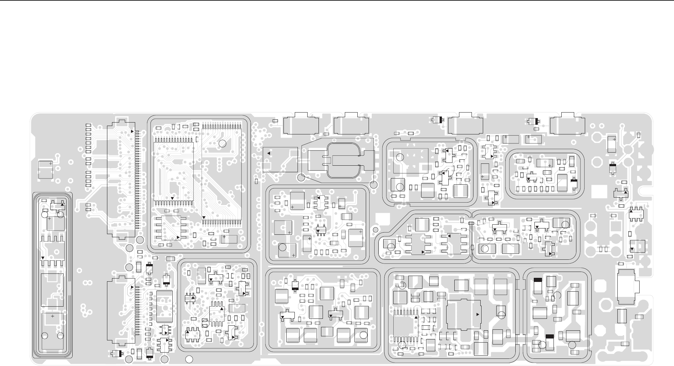
VHF PCB 8486101B11 / Schematic 4-55
14.0 VHF PCB 8486101B11 / Schematic
C601
C602
C603
CR601
L601
R625
SH700
14
58
U601
C4003
C4004
C4005
C4007
C4008
C4009
C4010
C4011
C4012
C4013
C4014
C4015
C4016
C4001
C4002
C710
1
40
J400
C423
C424
C425C426
C427
C428
C429
R408
R410
R418
R428
R429
R437
R478
R492
R4007
R4008
R4009
SH400
22
21
8
71
U405
32 17
16
1
U406
14
58
U407
B503
B504
C432
C522
C523
PB502PB503
TP3701
TP3702
6
43
1
Y3761
C3200
C3201
C3202
C3203
C3204
C3205
C3206
C3207
C3208
C3210
L3200
L3201
L3202
Q3200
Q3201
R3200
R3201
R3202
R3203
R3204
R3205
R3206
R3207R3208
R3209
R3210
R3211
R3212
SH3203
Y3200
PB504
VR444
C3209
C3214
C3215
Q3202
R3213
R3214
R3215
R3218
R3225
U3201
C3225
C3270
C3271
C3272
C3273
C3274
C3275
C3276
C3277
C3278
C3279
C3280
D3270
L3270
L3271
Q3270
R3226
R3270
R3271
R3272
R3273
R3274
R3275
R3276
SH3201
C521
C3213
PB501
VR440
C3212
C3524
C3525
C3528
C3531
C3532
C3533
C3534
C3535
C3536
C3550
C3551
C3552
D3521
D3551
L3531
L3532
L3551
L3552
R3551
SH3501
C511
C512 C513
C514
C520
4
3
2
CR503
Q502
R501
R502
R505
C502
C505
Q505
R506
VR501
C3537
C3539
L3538
PB505
C441
C443 C444
C471
C472
C473
C490
C491
C492
C493
C494
C495
C496
C497
CR413
22
20
1
21
J403
L400 L401
4
3
Q417
R421
R435
R450
R477
RT400
TP401
TP402
TP405 TP406
TP410
VR434 VR447
VR449
VR450 SH401
TP415
C400
C401
C402
C403
C467
C480
C482
CR412
CR440
Q400
Q403
4
3
Q405
R401
R402
R403
R405
R406
R407
R416
R427
R447
R448
R451
R452
R453 R454
R455
R456
R476
R481
4
58
U400
C3822
C3824
C3825
C3826
C3828
C3829
C3830
C3832 C3833
C3834
C3835
C3836
C3842
D3821
D3831
D3832
L3821
L3822
L3823
L3824
L3825
L3831
L3832
L3833
L3834
R3821
R3822
R3823
R3828
R3833 R3834
R3835
R3836
SH3801
C3706
C3710
C3711
C3712
C3713
C3714
C3715
C3721
C3722
C3724
C3741
C3742 C3743
C3744
C3745
C3746
C3752
C3753
C3754
4
3
Q3721
R3701
R3721
R3722
R3723
R3741
R3751
R3752
SH3701
U3711
TP3301
C3314
C3318
C3319
C3320
C3329
C3334
C3335
L3309
L3312
R3317
R3318
R3321
R3322
R3323
SH3302
6
4
3
T3301
64
3
T3302
C3306
C3307
C3308
C3309
C3310
C3311
C3312
C3313
C3327
C3330
C3331
C3332
C3338
CR3303
D3302
L3304
L3305L3306
Q3302
R3308R3309
R3310
R3311
R3312
R3313
R3316
SH3303
C3501
C3502
C3503
C3504
C3505
C3512
C3513
C3514
C3517
C3518
C3519 C3521
C3523
C3527
C3541
C3542
C3543
C3544
C3546
C3547
L3501
L3503
L3504
L3511
L3512
L3513
L3515
L3518
L3521
L3522
1
2
3
Q3501
R3501
R3502 R3503
R3505
R3506
R3507
R3512
R3513
R3541
R3542
R3543
R3544
R3545
R3546
R3547
R3548
SH3502
1
16
8
9
U3501
VHF (136-174 MHz) Main Board Top Side
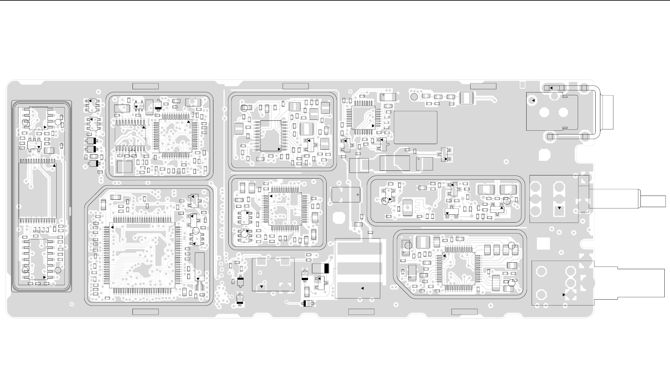
4-56 VHF PCB 8486101B11 / Schematic
VHF (136-174 MHz) Main Board Bot Side
C701
C702
C703
C713
C717
C718
CR700
R626
R627
R704
R705
R710
R716
R717
1
4
58
U720
2815
14
1
U700
SH701
C704
C705
C706
C707
C708 C709
C711
C714
C715
C719
R701
R702
R703
R706
R707
R708
R709
8
7
1
14
U710
C442
C445
C483
C484
R473
VR432 VR433
VR448
VR483
VR484
C408
C409
C410
C411
C414
C415
C430 C440
C446
C450
C451
C452
M401
4
3
Q410
R434
R436
SH403
1
13
U404
1
U420
VR460
C476
C478
R471
10
C407
C416
C419
C420
C421
C422
C447
C448
C474
C475
C477
C479
C481
R400
R413
R423
R424
R425
R431
R445 R449
R472
R475
R498
R499
37
25
11 20
C3806
C3812
C3813
C3815
C3816
C3818
C3827
L3813
L3816
R3812
R3816
R3817
R3818
R3826
R3829
R3830 R3831
R3832
11
1
20
10
U3801
C3802
C3805
C3823
R3801
R3803
SH3802
C3803
C3810
C3811
C3821
L3811
L3812
L3826
Q3801
R3804
R3805
R3806
R3808
R3811
C3801
C3804
C3808
C3809
L3801 L3809
R3802
R3807
R3824
R3825
C3701
C3702
C3703
C3704
C3705
C3707
C3708
C3709
C3725
C3726
C3727
C3731
C3732
C3733
C3734
C3755
C3761
C3762
D3701
D3702
L3701
L3731
R3702
R3703
R3704
R3705
R3726
R3727
R3762
SH3702
1
37
25
13
U3701
C431
C433
C434
C435
C436
C437
C449
C453
C456
C458
C459
C463
C466
C4006
C4020
C4021
CR411
E400
3
FL401
L410
L411
M400
Q416
R409
R411
R414
R415
R419
R420
R426
R432
R457
R460
R461
R462
R463
R4001
R4002
R4003
R4004
R4005
R4006
SH402
1
76
51
26
U409
U410
C3211
C3218
C3219
C3220
C3221
C3222
C3223
C3224
C3226
C3227
C3228
C3229
C3230
C3231
C3232
C3233
C3234
C3235
C3236
C3237
C3238
C3239
C3240
C3241
C3242
C3243
C3244
L3221
R3219
R3220
R3221
R3222
R3223
R3224
SH3202
1
37
25
13
U3220
M301
C3315
C3316
C3317
C3321
C3323
C3324
C3325
C3326
C3337 C3339
CR3301
CR3302
L3308
Q3301
R3301
R3304
R3305
R3306
R3307
R3314
R3315
R3319
R3320
R3324
RT3301
SH3301
C3301
C3302C3303C3304
C3305
C3322
D3301
L3301L3303
R3303
C503
C535
C3336
C3516
F501
L3519
R3519
C3735
C3751
C3763
CR501
D3761
L505
R3760
R3761
R3763
VR439
VR441
VR442
VR506
2
34
Y3762
4
53
2S502
2C8
C4
S501
32
1
B501
M101
M300
C3508 C3509
C3560
C3561
C3562
C3563
C3565
C3566
C3567
C3568
C3570
C3571
Q3561
R3561
R3562
R3563
R3564
R3565
R3569R3570
1
17
9
25
U3502
U3503
C3515
C3526
C3564
C3569
H3501
L3523
R3566
R3571 R3572 R3573
TP3502
VR3501
M100
2
3
4
1
J3501
J3502

VHF PCB 8486101B11 Parts List 4-57
15.0 VHF PCB 8486101B11 Parts List
Circuit
Ref.
Motorola
Part No. Description
B501 0986237A02 Battery Contact Module
B503 3980502Z01 Backup Contact, B +
B504 3980501Z01 Backup Contact, B -
C3200 2113743N31 16pF
C3201 NOTPLACED
C3202 NOTPLACED
C3203 2113743N50 100pF
C3204 2113743L41 10000pF
C3205 2113928N01 0.1uF
C3206 2113743L41 10000pF
C3207 2113743N10 2.2pF
C3208 NOTPLACED
C3209 2311049A07 1uF
C3210 2113743L17 1000pF
C3211 2311049A56 4.7uF
C3212 2311049A57 10uF
C3213 2311049A56 4.7uF
C3214 2113928N01 0.1uF
C3215 2113743N26 10pF
C3218 2311049A56 4.7uF
C3219 2113928N01 0.1uF
C3220 2113743N26 10pF
C3221 2113743L41 10000pF
C3222 2113928N01 0.1uF
C3223 2113928N01 0.1uF
C3224 2113928N01 0.1uF
C3225 2113928N01 0.1uF
C3226 2113928N01 0.1uF
C3227 2113743L41 10000pF
C3228 2113743L41 10000pF
C3229 2113743N50 100pF
C3230 2113740F51 100
C3231 2180478Z20 1uF
C3232 2180478Z20 1uF
C3233 2180478Z20 1uF
C3234 2180478Z20 1uF
C3235 2113743A23 0.220uF
C3236 NOTPLACED
C3237 NOTPLACED
C3238 2113743A24 0.330uF
C3239 2113743E07 0.022uF
C3240 2113743A23 0.220uF
C3241 2113743L19 1200pF
C3242 2109720D14 0.1uF
C3243 2113743E07 0.022uF
C3244 2113743L41 10000pF
C3270 2113743E07 0.022uF
C3271 2113743L05 330pF
C3272 2113743N18 4.7pF
C3273 2113743N26 10pF
C3274 2113743N38 33pF
C3275 2113743N44 56pF
C3276 2113743N42 47pF
C3277 2113743N48 82pF
C3278 2113743E07 0.022uF
C3279 2311049A40 2.2uF
C3280 2113743L41 10000pF
C3301 2113743N20 5.6pF
C3302 2113743N54 150pF
C3303 2113743N30 15pF
C3304 2113743N54 150pF
C3305 NOTPLACED
C3306 2113928N01 0.1uF
C3307 2113743N50 100pF
C3308 2113743L05 330pF
C3309 2113928N01 0.1uF
C3310 NOTPLACED
C3311 2113743N54 150pF
C3312 2113743N31 16pF
C3313 2113743N54 150pF
C3314 NOTPLACED
C3315 2113743N26 10pF
C3316 2113743N14 3.3pF
C3317 2113743N40 39pF
C3318 2113743M08 22000pF
C3319 NOTPLACED
C3320 2113743N48 82pF
C3321 2113743L05 330pF
C3322 2113743N50 100pF
C3323 2113743N50 100pF
C3324 2113743N38 33pF
C3325 2113743L17 1000pF
C3326 NOTPLACED
C3327 2113743L05 330pF
C3329 2113743L05 330pF
C3330 2113743N50 100pF
C3331 2113743N50 100pF
C3332 2113743N40 39pF
C3334 2113743N33 20pF
C3335 2113743N34 22pF
C3336 2311049A96 33uF
C3337 2113743M08 22000pF
C3338 2113743L09 470pF
Circuit
Ref.
Motorola
Part No. Description
C3339 2113743N26 10pF
C3501 2113743L05 330pF
C3502 2113743N38 33pF
C3503 2113743N38 33pF
C3504 2113743M08 22000pF
C3505 2113743N38 33pF
C3508 2113743M08 22000pF
C3509 2113743L05 330pF
C3512 2113740F43 47
C3513 2113740F38 30
C3514 2113740F47 68
C3515 2113743L29 3300pF
C3516 2311049A08 1uF
C3517 2113740F47 68
C3518 NOTPLACED
C3519 NOTPLACED
C3521 2111078B51 220
C3523 2111078B44 120
C3524 2113740F34 20
C3525 2113740F27 10
C3526 2113743M08 22000pF
C3527 NOTPLACED
C3528 2113740F27 10
C3531 2113740F36 24
C3532 2113740F52 110
C3533 2113740F24 7.5
C3534 2113740F23 6.8
C3535 2113740F37 27
C3536 2113740F31 15
C3537 2113740F33 18
C3539 2113740F29 12
C3541 2113743M08 22000pF
C3542 2113743L05 330pF
C3543 2113743M08 22000pF
C3544 2113743L05 330pF
C3546 2113743L05 330pF
C3547 2113743M08 22000pF
C3550 2113743N23 7.5pF
C3551 2113743N46 68pF
C3552 2113743N44 56pF
C3560 2311049A07 1uF
C3561 2113743M08 22000pF
C3562 2113743L29 3300pF
C3563 2113743L29 3300pF
C3564 2113743L01 220pF
C3565 2113743E07 0.022uF
C3566 2113743N50 100pF
Circuit
Ref.
Motorola
Part No. Description
C3567 2113743L05 330pF
C3568 2113743L29 3300pF
C3569 2113743M08 22000pF
C3570 2113743L05 330pF
C3571 2113743L09 470pF
C3701 2113743L41 10000pF
C3702 2113743L41 10000pF
C3703 2113743L41 10000pF
C3704 2113743L41 10000pF
C3705 2113743E20 0.1uF
C3706 2311049J11 4.7uF
C3707 2113743N34 22pF
C3708 2113928N01 0.1uF
C3709 2113928N01 0.1uF
C3710 2104993J02 2.2uF
C3711 2311049A69 10uF
C3712 2113928N01 0.1uF
C3713 2311049A09 2.2uF
C3714 2311049J11 4.7uF
C3715 2113743L09 470pF
C3721 2113743E20 0.1uF
C3722 2113743E20 0.1uF
C3724 2311049A08 1uF
C3725 NOTPLACED
C3726 2113743N24 8.2pF
C3727 2113743N50 100pF
C3731 2113743L41 10000pF
C3732 2113743L41 10000pF
C3733 2104993J02 2.2uF
C3734 2113743L41 10000pF
C3735 NOTPLACED
C3741 NOTPLACED
C3742 2113743L01 220pF
C3743 2113743L01 220pF
C3744 2113743L01 220pF
C3745 2113743L01 220pF
C3746 2113743L01 220pF
C3751 NOTPLACED
C3752 2113743L17 1000pF
C3753 2311049A56 4.7uF
C3754 2113928N01 0.1uF
C3755 2104993J02 2.2uF
C3761 2113743N42 47pF
C3762 2113740F63 330
C3763 NOTPLACED
C3801 2113743N18 4.7pF
C3802 NOTPLACED
Circuit
Ref.
Motorola
Part No. Description
4-58 VHF PCB 8486101B11 Parts List
C3803 2113743L17 1000pF
C3804 2113743E20 0.1uF
C3805 2113743N18 4.7pF
C3806 2113743N50 100pF
C3808 2113743N30 15pF
C3809 2113743N36 27pF
C3810 NOTPLACED
C3811 2113928N01 0.1uF
C3812 2113928N01 0.1uF
C3813 2113743L41 10000pF
C3815 2113743L17 1000pF
C3816 2113743N22 6.8pF
C3818 2113743E07 0.022uF
C3821 2113743L41 10000pF
C3822 2113743L17 1000pF
C3823 2113743L41 10000pF
C3824 2113743N44 56pF
C3825 2113743N30 15pF
C3826 2113743N18 4.7pF
C3827 2113743E07 0.022uF
C3828 2185895Z01 0.01uF
C3829 2185895Z01 0.01uF
C3830 2113743N46 68pF
C3832 2113743L17 1000pF
C3833 2113743N18 4.7pF
C3834 2113743N44 56pF
C3835 2113743N22 6.8pF
C3836 2113743N30 15pF
C3842 2113743L17 1000pF
C400 2113743L41 10000pF
C4001 NOTPLACED
C4002 NOTPLACED
C4003 NOTPLACED
C4004 NOTPLACED
C4005 NOTPLACED
C4007 NOTPLACED
C4008 NOTPLACED
C4009 NOTPLACED
C401 2113928N01 0.1uF
C4010 NOTPLACED
C4011 NOTPLACED
C4012 NOTPLACED
C4013 NOTPLACED
C4014 NOTPLACED
C4015 NOTPLACED
C4016 NOTPLACED
C402 2113928N01 0.1uF
Circuit
Ref.
Motorola
Part No. Description
C4020 2113743L17 1000pF
C4021 2113743L17 1000pF
C403 2113743G24 2.2uF
C407 2113928N01 0.1uF
C408 2113743N50 100pF
C409 2113928N01 0.1uF
C410 2113928N01 0.1uF
C411 2113928N01 0.1uF
C414 2113928N01 0.1uF
C415 2185895Z01 0.01uF
C416 2113928N01 0.1uF
C419 2113743L41 10000pF
C420 2113743L41 10000pF
C421 2113928N01 0.1uF
C422 2113928N01 0.1uF
C423 2113743N50 100pF
C424 2311049A59 10uF
C425 2113928N01 0.1uF
C426 2113743N50 100pF
C427 2113743N50 100pF
C428 2113928N01 0.1uF
C429 2113928N01 0.1uF
C430 2113928N01 0.1uF
C431 2113743N50 100pF
C432 NOTPLACED
C433 2113743L41 10000pF
C434 2113928N01 0.1uF
C435 2113928N01 0.1uF
C436 2113743N34 22pF
C437 2113743N34 22pF
C440 2113743G26 4.7uF
C441 2113743L09 470pF
C442 2113743E20 0.1uF
C443 2113928N01 0.1uF
C444 2113743N50 100pF
C445 2113743L09 470pF
C446 2113743L09 470pF
C447 2113928N01 0.1uF
C448 2113928N01 0.1uF
C449 2113743N50 100pF
C450 NOTPLACED
C451 2113743M08 22000pF
C452 2113743B29 1uF
C453 2113743N50 100pF
C456 2113743N50 100pF
C458 2113743N50 100pF
C459 2113743N50 100pF
Circuit
Ref.
Motorola
Part No. Description
C463 2113743N50 100pF
C466 2113743N50 100pF
C467 2113928N01 0.1uF
C471 2113743L09 470pF
C472 2113743L09 470pF
C473 2113743L09 470pF
C474 2113743L41 10000pF
C475 2113743H14 10uF
C476 2113928D08 10uF
C477 2113743L17 1000pF
C478 2113743L17 1000pF
C479 2113928N01 0.1uF
C480 2113928D08 10uF
C481 2113928N01 0.1uF
C482 2113928N01 0.1uF
C483 2113743L09 470pF
C484 2113743L09 470pF
C490 2113743L09 470pF
C491 2113743L09 470pF
C492 2113743L09 470pF
C493 2113743N50 100pF
C494 2113743N50 100pF
C495 2113743L09 470pF
C496 2113743L09 470pF
C497 2113743L09 470pF
C502 2311049A05 0.47uF
C503 2113743N50 100pF
C505 2113743N50 100pF
C511 2113743N50 100pF
C512 2113743N50 100pF
C513 2113743N50 100pF
C514 2113743N50 100pF
C520 2113743L41 10000pF
C521 2113743L41 10000pF
C522 2113743L41 10000pF
C523 2113743L41 10000pF
C535 2113743L17 1000pF
C601 NOTPLACED
C602 NOTPLACED
C603 NOTPLACED
C701 2180478Z20 1uF
C702 2113928N01 0.1uF
C703 2113743N50 100pF
C704 2113928N01 0.1uF
C705 2113928N01 0.1uF
C706 NOTPLACED
C707 2113928N01 0.1uF
Circuit
Ref.
Motorola
Part No. Description
C708 2113928N01 0.1uF
C709 2113743L17 1000pF
C711 2113743L41 10000pF
C713 2113928N01 0.1uF
C714 2113928N01 0.1uF
C715 2113928N01 0.1uF
C717 2113928N01 0.1uF
C718 2113743L17 1000pF
C719 2113928N01 0.1uF
CR3301 4802245J42 Ring Quad Diode
CR3302 4805129M96 Dual Bonds Pin Diode
CR3303 4880154K03 Dual Schottky Diode
CR411 4802245J62 Schottky diode
CR412 4802245J62 Schottky diode
CR413 4802245J62 Schottky diode
CR440 4813833C02 Dual Common Cathode
Diode
CR501 4880107R01 Rectifier
CR503 4805729G49 Red/Yellow LED
CR601 NOTPLACED
CR700 4802245J47 Diode Schottky
D3270 4862824C01 Varactor
D3301 4802081B58 Dual Diode
D3302 4802081B58 Dual Diode
D3521 4880973Z02 Pin Diode
D3551 4880973Z02 Pin Diode
D3701 4802233J09 Triple diode
D3702 4802233J09 Triple diode
D3761 4862824C03 Varactor
D3821 4805649Q13 Varactor
D3831 4805649Q13 Varactor
D3832 4862824C01 Varactor
E400 2480640Z01 Ferrite Bead
F501 6580542Z01 Fuse 3A
FL401 4870368G02 Real Time Clock Oscillator
Xtal 38.4kHz
H3501 2680499Z01 Heat Spreader
J3501 0985613Z01 RF Jack
J3502 0280519Z02 Antenna Nut
J400 0905505Y04 40-Pin Connector
J403 0905505Y02 20-Pin Connector
L3200 2462587N68 1000nH
L3201 NOTPLACED
L3202 2462587N68 1000nH
L3221 2462587N68 1000nH
L3270 2462587T15 100nH
L3271 2462587Q20 2,200nH
Circuit
Ref.
Motorola
Part No. Description
VHF PCB 8486101B11 Parts List 4-59
L3301 2462587T35 12nH
L3303 2462587T35 12nH
L3304 2462587T23 470nH
L3305 2462587T35 12nH
L3306 2462587T35 12nH
L3308 2462587T34 10nH
L3309 2462587N55 150nH
L3312 2462587V28 33nH
L3501 2413926H09 5.6nH
L3503 2462587V32 68nH
L3504 2462587N51 68nH
L3511 2462587N44 18nH
L3512 2479990B01 11.03nH
L3513 2479990A02 7.66nH
L3515 2479990C03 13.85nH
L3518 NOTPLACED
L3519 2484657R01 Ferrite Bead
L3521 2479990A02 7.66nH
L3522 2479990E01 23.75nH
L3523 2462587N68 1000nH
L3531 2479990N01 43.67nH
L3532 2479990N01 43.67nH
L3538 2479990M01 30.54nH
L3551 2479990N01 43.67nH
L3552 2479990A02 7.66nH
L3701 2462587Q42 390nH
L3731 2462587Q20 2,200nH
L3801 2462587V34 100nH
L3809 2462587V27 27nH
L3811 2462587V34 100nH
L3812 2462587V34 100nH
L3813 2462587Q47 1000nH
L3816 2462587V34 100nH
L3821 2462587N50 56nH
L3822 2462587N49 47nH
L3823 2462587N49 47nH
L3824 2462587N68 1000nH
L3825 2462587V34 100nH
L3826 2462587N68 1000nH
L3831 2462587N50 56nH
L3832 2462587N51 68nH
L3833 2462587N50 56nH
L3834 2462587N68 1000nH
L400 2462587Q42 390nH
L401 2462587Q42 390nH
L410 2462587Q42 390nH
L411 2462587Q42 390nH
Circuit
Ref.
Motorola
Part No. Description
L505 2462587Q42 390nH
L601 NOTPLACED
M100 7585651Z01 EMI Pad
M101 7585651Z01 EMI Pad
M300 7585651Z01 EMI Pad
M301 7585651Z01 EMI Pad
M400 7585651Z01 EMI Pad
M401 7585651Z01 EMI Pad
PB501 4080523Z02 Tactile Switch
PB502 4080523Z02 Tactile Switch
PB503 4080523Z02 Tactile Switch
PB504 4080523Z02 Tactile Switch
PB505 4080523Z02 Tactile Switch
Q3200 4802197J95 NPN Transistor
Q3201 4880214G02 NPN Transistor
Q3202 4880214G02 NPN Transistor
Q3270 4805218N63 RF NPN Transistor
Q3301 4880214G02 NPN Transistor
Q3302 4802197J95 NPN Transistor
Q3501 4813828A08 RF Power Amplifier
Q3561 4813824A17 PNP Transistor
Q3721 4809939C05 DUAL NPN/PNP Transistor
Q3801 4802197J95 NPN Transistor
Q400 4809579E18 MOSFET P-Channel
Q403 4813824A17 NPN Transistor
Q405 4802245J54 Dual NPN Transistor
Q410 4802245J54 Dual NPN Transistor
Q416 4809579E18 MOSFET P-Channel
Q417 4809939C05 DUAL NPN/PNP Transistor
Q502 5180159R01 Dual NPN Transistor
Q505 4880214G02 NPN Transistor
R3200 0662057M54 150
R3201 0662057M82 2.2K
R3202 0662057M90 4.7K
R3203 0662057M98 10K
R3204 0662057M26 10
R3205 0662057M74 1K
R3206 0662057N23 100K
R3207 0662057N13 39K
R3208 0662057M50 100
R3209 0662057M74 1K
R3210 0662057M82 2.2K
R3211 0662057M82 2.2K
R3212 0662057M90 4.7K
R3213 0662057M82 2.2K
R3214 0662057M34 22
R3215 NOTPLACED
Circuit
Ref.
Motorola
Part No. Description
R3218 NOTPLACED
R3219 0662057M50 100
R3220 0662057M90 4.7K
R3221 0662057M50 100
R3222 NOTPLACED
R3223 NOTPLACED
R3224 0662057M26 10
R3225 0662057M74 1K
R3226 0662057M26 10
R3270 0662057M74 1K
R3271 0662057M42 47
R3272 0662057N15 47K
R3273 0662057N15 47K
R3274 0662057M83 2.4K
R3275 0662057M74 1K
R3276 0662057N30 200K
R3301 NOTPLACED
R3303 0662057N23 100K
R3304 0662057N23 100K
R3305 0662057N19 68K
R3306 0662057M82 2.2K
R3307 0662057N11 33K
R3308 0662057M78 1.5K
R3309 0662057M92 5.6K
R3310 0662057M98 10K
R3311 0662057M26 10
R3312 0662057M38 33
R3313 0662057M34 22
R3314 0662057M26 10
R3315 0662057M62 330
R3316 0662057M66 470
R3317 0662057N23 100K
R3318 0662057M66 470
R3319 NOTPLACED
R3320 NOTPLACED
R3321 0662057M54 150
R3322 0662057M58 220
R3323 0662057M32 18
R3324 0662057M58 220
R3501 0662057M61 300
R3502 0662057M32 18
R3503 0662057M61 300
R3505 0662057M62 330
R3506 0662057B62 3.9
R3507 0662057B62 3.9
R3512 NOTPLACED
R3513 NOTPLACED
Circuit
Ref.
Motorola
Part No. Description
R3519 0680539Z01 0.1
R3541 0662057N13 39K
R3542 0662057M92 5.6K
R3543 0662057M50 100
R3544 0662057A25 100
R3545 0662057A25 100
R3546 0662057N01 12K
R3547 0662057N11 33K
R3548 0662057N07 22K
R3551 0662057M40 39
R3561 0662057N01 12K
R3562 0662057N11 33K
R3563 0662057N33 270K
R3564 0662057N35 330K
R3565 NOTPLACED
R3566 NOTPLACED
R3569 0662057M92 5.6K
R3570 0662057M98 10K
R3571 0662057A27 120
R3572 0662057A27 120
R3573 0662057A27 120
R3701 0662057M50 100
R3702 NOTPLACED
R3703 0662057M54 150
R3704 0662057M54 150
R3705 0662057N11 33K
R3721 0662057M66 470
R3722 0662057M68 560
R3723 0662057M50 100
R3726 NOTPLACED
R3727 0662057N23 100K
R3741 0662057M50 100
R3751 0662057N30 200K
R3752 0662057N29 180K
R3760 NOTPLACED
R3761 0662057N15 47K
R3762 NOTPLACED
R3763 NOTPLACED
R3801 NOTPLACED
R3802 0662057M50 100
R3803 0662057M58 220
R3804 0662057M98 10K
R3805 0662057N08 24K
R3806 0662057M34 22
R3807 NOTPLACED
R3808 0662057M26 10
R3811 0662057M50 100
Circuit
Ref.
Motorola
Part No. Description
VHF PCB 8486101B11 Parts List 4-60
* Motorola Depot Servicing only
Reference designators with an asterisk indicate
components which are not field replaceable
because they need to be calibrated with
specialized factory equipment after installation.
Radios in which these parts have been replaced in
the field will be off frequency at temperature
extremes.
R3812 NOTPLACED
R3816 0662057M74 1K
R3817 0662057M01 0
R3818 NOTPLACED
R3821 0662057M58 220
R3822 0662057M42 47
R3823 0662057N11 33K
R3824 0662057N07 22K
R3825 0662057M38 33
R3826 0662057M32 18
R3828 0662057M50 100
R3829 0662057M01 0
R3830 NOTPLACED
R3831 0662057M98 10K
R3832 0662057N01 12K
R3833 0662057M58 220
R3834 0662057M42 47
R3835 0662057N15 47K
R3836 0662057M98 10K
R400 0662057N15 47K
R4001 0662057M74 1K
R4002 0662057M74 1K
R4003 0662057M74 1K
R4004 0662057M74 1K
R4005 0662057M74 1K
R4006 0662057M74 1K
R4007 0662057M74 1K
R4008 0662057M74 1K
R4009 0662057M74 1K
R401 0662057M01 0
R402 NOTPLACED
R403 NOTPLACED
R405 0662057M01 0
R406 0662057N20 75K
R407 0662057N19 68K
R408 NOTPLACED
R409 0662057M98 10K
R410 0662057N23 100K
R411 0662057M98 10K
R413 0662057M01 0
R414 0662057V34 180K
R415 0662057V26 91K
R416 0662057M98 10K
R418 0662057M01 0
R419 0662057M67 510
R420 0662057B46 10M
R421 0662057M81 2K
Circuit
Ref.
Motorola
Part No. Description
R423 0662057N21 82K
R424 0662057N12 36K
R425 0662057N10 30K
R426 0662057N35 330K
R427 0662057M84 2.7K
R428 0662057M10 2.2
R429 0662057N20 75K
R431 0662057N39 470K
R432 0662057N16 51K
R434 0662057M62 330
R435 0662057M81 2K
R436 0662057M01 0
R437 NOTPLACED
R445 0662057N08 24K
R447 0662057N23 100K
R448 0662057M98 10K
R449 0662057N08 24K
R450 0683962T45 68
R451 0662057N03 15K
R452 0662057N23 100K
R453 NOTPLACED
R454 NOTPLACED
R455 NOTPLACED
R456 0662057M01 0
R457 0662057M98 10K
R460 0662057M90 4.7K
R461 0662057M56 180
R462 0662057M98 10K
R463 0662057M61 300
R471 0662057N06 20K
R472 0662057M93 6.2K
R473 0662057M26 10
R475 0662057M01 0
R476 0662057N35 330K
R477 0662057M74 1K
R478 0662057M98 10K
R481 0662057N08 24K
R492 0662057M01 0
R498 0662057M98 10K
R499 0662057M98 10K
R501 0662057M70 680
R502 0662057M56 180
R505 0662057M98 10K
R506 0662057N15 47K
R625 NOTPLACED
R626 NOTPLACED
R627 NOTPLACED
Circuit
Ref.
Motorola
Part No. Description
R701 0662057N05 18K
R702 0662057N05 18K
R703 0662057M74 1K
R704 0662057N13 39K
R705 0662057N13 39K
R706 0662057N17 56K
R707 0662057M91 5.1K
R708 0662057N41 560K
R709 0662057N47 1M
R710 0662057N39 470K
R716 0662057N01 12K
R717 0662057M82 2.2K
RT3301 NOTPLACED
RT400 0680590Z01 THERMISTOR_33K
S501 4080710Z02 Frequency Switch
S502 1880619Z02 POTENTIOMETER
(VOLUME)
SH3201 2602023X08 Rx Backend Top Shield
SH3202 2686081B02 LVZIF shields
SH3203 2686081B03 45.1MHz Xtal Filter Shield
SH3301 2686081B01 Receiver Front-End Bottom
Shield
SH3302 2686081B05 Mixer Shield
SH3303 2686081B06 Receiver Front-End Top
Shield
SH3501 2686081B03 Harmonic Filter Shield
SH3502 2686081B04 PA driver Shield
SH3701 2680511Z01 Synthesizer Top Shield
SH3702 2680511Z01 Synthesizer Bottom Shield
SH3801 2680513Z01 VCO Resonators Shield
SH3802 2680514Z01 VCO Buffer IC Shield
SH400 2680505Z01 Controller Memory Shield
SH401 2680506Z01 Controller On-off Shield
SH402 2680515Z01 Microprocessor Shield
SH403 2680516Z01 Asfic_Cmp, Audio PA Shield
SH701 2680677Z01 Voice Storage Shield
T3301 2580541Z02 Balun Transformer
T3302 2580541Z02 Balun Transformer
U3201 5102463J58 3.3V Regulator
U3220 5109632D83 LVZIF IC
U3501 5185130C65 LDMOS Driver IC
U3502 5185765B26 PCIC
U3503 5185963A15 Temperature sensor
U3701 5185963A27 LVFRACN Synthesizer IC
U3711 5105739X05 5V Regulator
U3801 5105750U54 VCO BUFFER IC
U400 5102463J40 3.3V Regulator
Circuit
Ref.
Motorola
Part No. Description
U404 5185130C53 ASFIC_CMP IC
U405 5102463J36 Static RAM_32K X 8
U406 5102463J60 Flash ROM_512K X 8
U407 5102495J05 EEPROM_16K X 8
U409 5102226J56 Micro Processor
U410 5102463J57 3.3V Regulator
U420 5102463J44 Audio PA
U601 NOTPLACED
U700 5185770M01 IC Voice Storage
U710 5102463J52 QUAD ANALOG SWITCH IC
U720 5113818A01 SING Supply IC
VR3501 4880140L17 ZENER DIODE - 12V
VR432 4805656W08 5.6V Zener diode
VR433 4805656W08 5.6V Zener diode
VR434 4802245J73 ZENER DIODE-6.8V
VR439 4880140L17 ZENER DIODE - 12V
VR440 NOTPLACED
VR441 NOTPLACED
VR442 NOTPLACED
VR444 NOTPLACED
VR447 4802245J74 ZENER DIODE-10V
VR448 4802245J74 ZENER DIODE-10V
VR449 4802245J74 ZENER DIODE-10V
VR450 4802245J75 ZENER DIODE-12V
VR460 4802245J73 ZENER DIODE-6.8V
VR483 4802245J74 ZENER DIODE-10V
VR484 4802245J74 ZENER DIODE-10V
VR501 4802245J73 ZENER DIODE-6.8V
VR506 4802245J73 ZENER DIODE-6.8V
Y3200 9186153B01 Crystal Filter
Y3761 4805875Z04 16.8MHz Xtal Oscillator
Y3762 NOTPLACED
8486101B11 VHF GP1280 Main PC Board
Circuit
Ref.
Motorola
Part No. Description
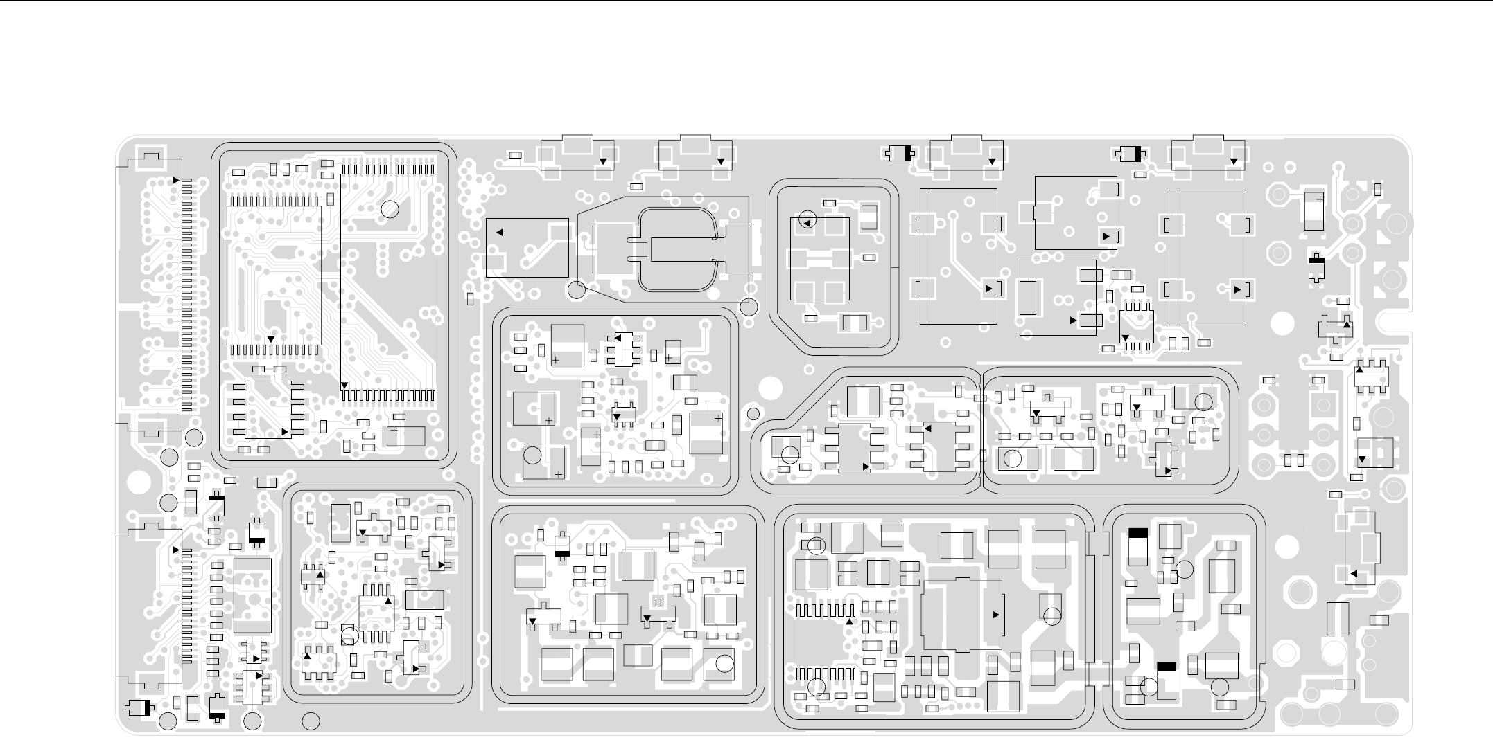
VHF PCB 8486473Z04 / Schematics 4-61
16.0 VHF PCB 8486473Z04 / Schematics
1
40
J400
C423
C425C426
E407
E408
E409
R410
R418
R437
22
21
8
71
U405
32 17
16
1
U406
4
5
C432
C424
C427 C428
C429
R408
R428
R429
R478
R492
SH400
1
8
U407
C443 C444
C471
C472
C473
1
21
L401
R435 RT400
TP401
TP402
TP410
VR447
VR449
C441
C490
C491
C492
C493
C494
C495
C496
C497
CR413
22
20
J403
L400
4
3
Q417
R421
R450
R477
TP405
TP406
VR434
VR450
C400
C401
C402
C403
C467
C480
C482
CR412
CR440
Q400
Q403
4
3
Q405
R401
R402
R403
R405
R406
R407
R416
R427
R447
R448
R451
R452
R453 R454
R455
R456
R476
R481
SH401
TP415
4
58
U400
C3822
C3824
C3825
C3826
C3828
C3829
C3830
C3832 C3833
C3834
C3835
C3836
C3842
D3821
D3831
D3832
L3821
L3822
L3823
L3824
L3825
L3831
L3832
L3833
L3834
R3821
R3822
R3823
R3828
R3833 R3834
R3835
R3836
SH3801
C3706
C3710
C3711
C3712
C3713
C3714
C3715
C3721
C3722
C3724
C3741
C3742
C3743
C3744
C3745
C3746
C3752
C3753
C3754
4
3
Q3721
R3701
R3721
R3722
R3723
R3741
R3751
R3752
SH3701
U3711
B503
B504
C522
C523
1
23
5
PB502
1
23
5
PB503
TP3701
TP3702
6
43
1
Y3761
C3201
C3202
C3206
L3200
L3203
1
23
5
PB504
SH3203
VR444
2
3
456
Y3200
43
2
Y3203
C521
C3208
C3225
C3278
1
23
5
PB501
R3205
R3208
R3211
R3275
4
58
U3221
VR440
2
Y3202
43
2
Y3204
Y3205
C3306
C3307
C3308
C3309
C3310
C3311
C3312
C3313C3314
C3327
C3330
C3331
C3338
CR3303
D3302
L3304
L3305L3306
Q3302
R3308
R3309 R3310
R3311
R3312
R3313
R3316
SH3303
C3318
C3329
C3332
R3317
C3319
C3320
C3334
C3335
L3309
L3312
R3318
R3321
R3322
R3323
SH3302
6
4
3
T3301
64
3
T3302
TP3301
C3501
C3502
C3503
C3504
C3505
C3512
C3513
C3514
C3517
C3518
C3519 C3521
C3523
C3527
C3541
C3542
C3543
C3544
C3546
C3547
L3501
L3503
L3504
L3511
L3512
L3513
L3515
L3518
L3521
L3522
1
2
3
Q3501
R3501
R3502 R3503
R3505
R3506
R3507
R3512
R3513
R3541
R3542
R3543
R3544
R3545
R3546
R3547
R3548
SH3502
1
16
8
9
U3501
C3524
C3525
C3528
C3531
C3532
C3533
C3534
C3535
C3536
C3550
C3551
C3552
D3521
D3551
L3531
L3532
L3551
L3552
R3551
SH3501
C511
C514
C520
C3537
C3539
4
3
2
CR503
L3538
1
23
5
PB505
R501
R502
C502
C505
C512 C513 Q502
Q505
R505
R506
VR501
VHF (136-174 MHz) Main Board Top Side

4-62 VHF PCB 8486473Z04 / Schematics
C442
C445
C483
C484
R473
VR432 VR433
VR448
C408
C409
C410
C411
C414
C415
C430 C440
C446
C450 C451
C452
C476
C478
4
3
Q410
R434
R436
R471
SH403
1
13
U404
11
1
20
10
U420
VR460
C416
C422
C447
C448
C474
C475
C477
R423
R424
R431
R472
R498
R499
C407
C419
C420
C421
C479
C481
R400
R413
R425
R445 R449
R475
37
25
C453
C456
C498
L410
L411
R409
R411
R432
R457
C449
C458
C459
C463
C466
C4020
C4021
E400
E401
E402
E403
E404
E405
E406
26 1
76
51
U409
C431
C433
C434
C435
CR411
Q416
R415
R419
R460
R461
R462
SH402
U410
C436
C437
3
FL401
R414
R420
R426
R463
C3812
C3813
C3815
C3816
C3818
C3827
L3813
L3816
R3812
R3816
R3817
R3818
R3826
R3829
R3830 R3831
R3832
11
1
20
10
U3801
C3801
C3802
C3803
C3804
C3805
C3806
C3808 C3809
C3810
C3811
C3821
C3823
L3801 L3809
L3811
L3812
L3826
Q3801
R3801
R3802
R3803
R3804
R3805
R3806
R3807
R3808
R3811
R3824
R3825
SH3802
C3701
C3702
C3703
C3704
C3707
C3731
C3732
C3761
C3762
D3701
L3701
R3703
R3704
R3762
SH3702
C3705
C3708
C3709
C3725
C3726
C3727
C3733
C3734
C3755
D3702 L3731
R3702
R3705
R3726
R3727
1
37
25
13
U3701
C328 C359
C390
C3763
D3761
R374
R377
R378
R3761
VR442
C3212
R373
R375
R3214
R3215
1
4
58
U303
C337
C358
C383 C3213
C3215
CR501
L505
R370
R371
R372
R376
U3201
VR439
VR441
VR506
C3508 C3509
C3560
C3561
C3562
C3563
C3565
C3566
C3567
C3568
C3570
C3571
Q3561
R3561
R3562
R3563
R3564
R3565
R3569
R3570
1
17
9
25
U3502
U3503
C3515
C3516
C3564
L3519 R3519
C503
C535
C3336
F501
C3315
C3316
C3317
C3337 C3339
CR3301
L3308
R3301
R3304
R3305
R3319
R3320 RT3301
SH3301
C3301
C3302
C3303
C3304
C3305
C3321
C3322
C3323
C3324
C3325
C3326
CR3302 D3301
L3301L3303
Q3301
R3303
R3306
R3307
R3314
R3315
R3324
2C8
C4
S501
C3200
C3205
C3207
C3210
C3218
C3222
C3226
C3228
C3230
CR3201
CR3202
CR3203
L3202
Q3200
R3200
R3201
R3202
R3203
R3204
R3209
R3212
R3220
R3221
C3203
C3209
C3221
C3231
C3232
C3233 C3234
C3236
C3238
C3274
C3275
C3279
L3270
Q3270
R3206
R3207
R3213
R3222
R3223
R3224
R3226
R3270
R3271
R3273
R3274
R3276
SH3202
11
1
20
10
U3220
43
2
Y3201
C3526
C3569
H3501
L3523
R3566
R3571 R3572 R3573
TP3502
VR3501
2
3
4
1
J3501
J3502
4
53
2S502
32
1
B501
VHF (136-174 MHz) Main Board Bottom Side
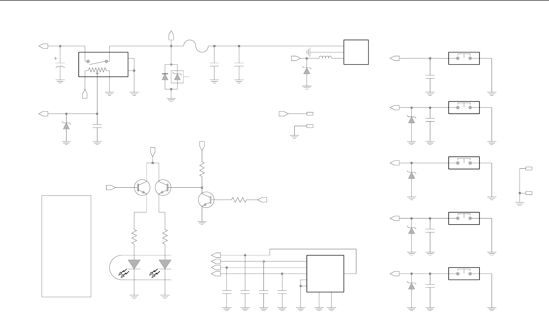
VHF PCB 8486473Z04 / Schematics 4-63
ZMY0130482-A
VOL
MECH_SWB+
Vdda
6.8V
VR501
HIGH
TAB1 6
TAB2
7
2
mgc_comps
4
1
LOW
5
3
S502
C502
0.47uF
C505
100pF
UNSWB+
1000pF
1000pF
C535
100pF
C503
CR501
VR439
10V
21
24V
F501
BATT_CODE
SB1
EMER
LI_ION
VR506
6.8V
L505
390nH
B501
DATA
NEG
POS
B503
B504
.01uF
C520
.01uF
C521
1
2
SWITCH
PB505
VR440
NU
6.8V
PB501
1
2
SWITCH
PB504
12
SWITCH
NU
6.8V
VR444
PTT
PB502
1
2
SWITCH
VR441
NU
6.8V C522
.01uF
SB2
PB503
1
2
SWITCH
NU
6.8V
VR442 C523
.01uF
SB3
M100
M101
SWB+
Vdda
4
347K
R506
R505
10K
Q505
5
1
6
2
Q502
switch
RED_LED
R501
680
680
CR503
24
13
R502
180
180
RTA2
RTA0
RTA1
RTA3
S501
SWITCH
GND1
PC0
PC1
PC2 PC3
C0
C1
GND
1
2
48
C0
C1
9
7
100pF
C511 C512
100pF
C513
100pF 100pF
C514
o
switch
GREEN_LED
VHF (136-174 MHz) Controls and Switches

4-64 VHF PCB 8486473Z04 / Schematics
G
UNSWB_PLUS_1_RX
C3336
10uF
UNSWB+
UNSWB_PLUS_2_RX
G
L3301
12nH
RX_IN
C3302
150pF
RX_IN_1_FE
5.6pF
C3301
C3303
15pF
D3301
CR3303
L3303
12nH
C3304
150pF
33K
R3307
NU
C3305
NU
C3326
470pF
C3338
470pF
R3304
100K
R3308
1.5K
R3311
NU
7.5K
R3309
5.1
R3312
0.1uF
C3306
Q3302
39
R3313
L3304
470nH
R3315
330
C3308
330pF
100pF
C3307
2.7K
R3310
16pF
C3312
150pF
C3311
R3314
27
D3302
NU
C3310 L3305
12nH
12nH
SMBV1032
SMBV1032
CR3302
10nH
L3308
C3317
30pF
C3316
3.3pF
10pF
12nH
C3315
L3306
NU
C3314
150pF
C3313
10pF
C3339
C3318
.022uF
NU
C3319
RF BALUN
4
6
3
1
2
T3301
R3320
NU
1
CR3301
2
34
R3319
NU
G
L3309
150nH
IF_1_FE
0
R3323
R3322
R3321
51
IF
C3320
82pF
NU
G
R5_2_FE
C3309
0.1uF
0.1uF
470
470
R3316
.022uF
C3337
R5_3_FE
R5
G
G
DACRx_1_FE
RX_INJ
RX_INJ_1_FE
DACRx
DUMMY
G
C3324
33pF
R3303
100K
C3321
330pF
RSSI
RSSI_1_FE
C3322
100pF
C3323
100pF
R3305
68K
NU
RT3301
220
R3324
220
R3301
NU
Q3301
R3306
2.2K
C3325
1000pF C3327
330pF
100pF
C3330 100pF
C3331 39pF
100K
C3332
R3317
330pF
C3329
SH3302
1
SHIELDSHIELD
SH3301
11
SHIELD
SH3303
TP3301
1
R3318
470
L3312
33nH
20pF
C3335
22pF
C3334
4
6
3
1
2
T3302
IF BALUN
VHF (136-174 MHz) Receiver Front End
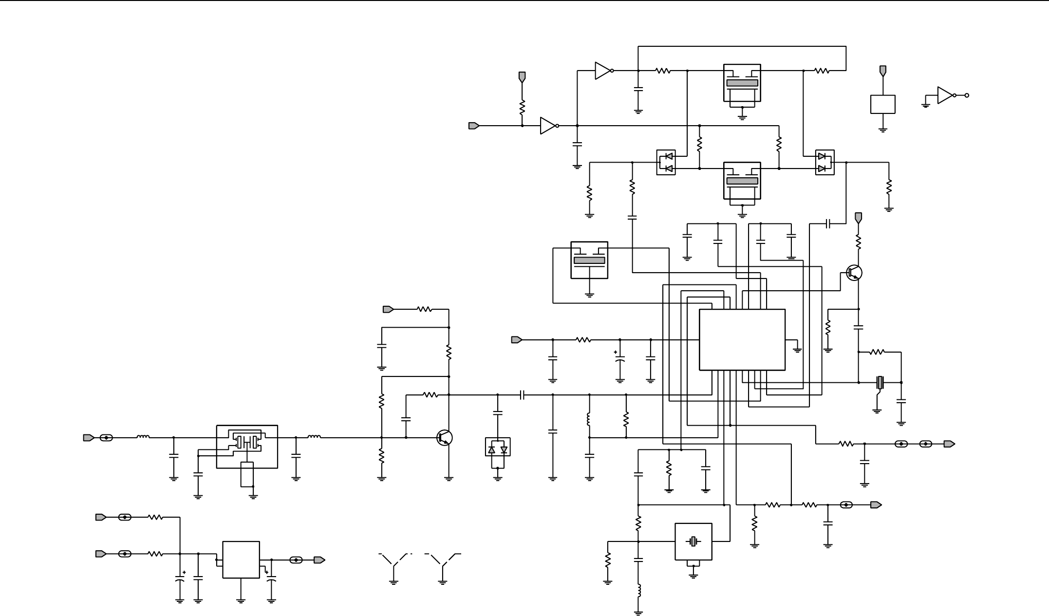
VHF PCB 8486473Z04 / Schematics 4-65
G
G
BW_SEL
TC7W04F
U3221-2
5V
62
100K
R3276 0.1uF
C3225
TC7W04F
U3221-1
17
R3209
39K
C3208
0.1uF
C3238
R3207
0.1uF
12K
R3206
910
CR3202
3
IN 2
OUT
Y3205
CFUCJ455E
3
GND
1
1
2
C3234
0.1uF
0.1uF C3233 0.1uF
C3231
0.1uF
C3232
C3226
0.1uF
R3205
43K
3
GND1
4
GND2
IN
1OUT 2
CFWC455G
Y3204
R3211
39K
1
2
CR3203
3
R3212
20K
3
GND1
GND2
4
1IN 2
OUT
Y3203
CFWC455E
G
U3221-4
PWR_GND
4
GND
8
VCC NC
35
U3221-3
TC7W04F
5V
G
5V
R3208
20K
R3226
390
MMBT3904
Q3270
13
2
120pF
1.2K
R3275
C3279
1.8K
R3274
GRSSI
12K
R3213
RSSI_2_ZIF
RSSI_1
0.1uF
C3209
3
21
455KHz
Y3202
45B02
0.1uF
C3278
G
DISC_OUT
680
4700pF
R3222
C3236
DISC_OUT
R3223
12K
10K
R3224
C3274
30pF
15K
R3273
0.1uF
C3230
C3203
30pF
Y3201
GND
2
GND1
4
OUT
31
IN
TSS-2 44.395MHz
R3270
1K
C3275
24pF
1uH
R3271
NU
L3270
G
C3228
0.1uF
C3221
0.1uF
10uF
C3218
51
R3221
5V
R3220
NU
1.2uH
L3202
C3200
2.7pF
4.7pF
C3207
C3222
0.1uF
12K
R3203
CR3201
Q3200
R3202
27K
C3210
0.1uF
R3204
4.7K
G
5V
R3200
820
620
R3201
0.1uF
C3205
680nH
L3203
C3202
NU
2
CC1
5
CC2
1
GND1
4
GND2
3
IN
6
OUT
44.85MHz
MXF45
Y3200
G
C3201
16pF
IF_1 680nH
L3200
C3206
9.1pF
IF
G
G
22
R3214
SWB+
4V_3.3V
4V_3.3V
NU
0
R3215
SWB_PLUS_3
G
Vdda_3
C3213
4.7uF
GND
2
4
NC
ON_OFF*
3VIN
1VOUT 5Vdda
10pF
C3215
C3212
1uF
U3201
LP2980
SHIELD
SH3202
11
SH3203
SHIELD
RSSI_FEED
9
VCC
6
LIM_DEC2
12
MIXOUT 20
OSCIN
4OSCOUT 3
QUADIN
10
RFIN
1
RFIN_DEC
2
RSSIOUT 5
GND 15
IFAMPIN
18 IFAMPOUT 16
IFAMP_DEC1
19 IFAMP_DEC2 17
LIMIN
14 LIMOUT 11
LIM_DEC1 13
U3220
SA616
AUDIOOUT
8
AUDIO_FEED
7
VHF (136-174 MHz) Receiver Back End
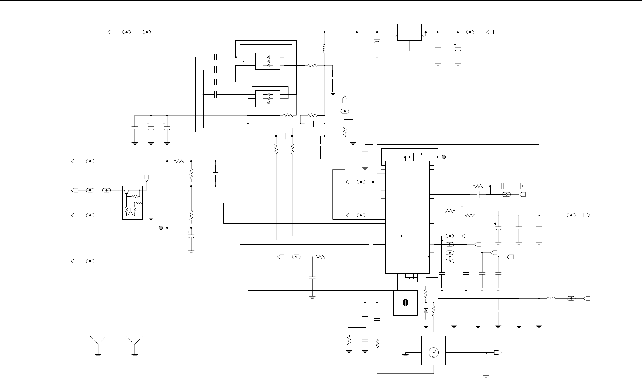
4-66 VHF PCB 8486473Z04 / Schematics
TRB
SH3702
SHIELD
SHIELD
1
SH3701
SHIELD
SHIELD
1
VCO_MOD
R5
T5
VCTRL
VCO_MOD_1_FN
VCTRL_1_FN
T5_1_FN
R5_1_FN R5_2_FN
5V
4
1
3
Q3721
2
UMC5N
47K
47K
10K
47K
4.7uF
C3714
4.7uF
C3706C3705
0.1uF
5V
5V_1_FN 5V_2_FN
(SOURCE)
R3722
1K
0.1uF
C3721
470
R3721
100
R3723
C3722
0.1uF
C3724
TP3701 1
1uF
C3704
.01uF
.01uF
C3702
C3701
.01uF
.01uF
C3703
4
1K1
2K2
3K3
D3701
A1 6
A2 5
A3
K2
2K3
3
D3702
A1 6
A2 5
A3 4
K1
1
R3702
0
NU
C3709
0.1uF
R3704
150
C3707
22pF
33K
R3705
0.1uF
C3708
R3703
150
BIAS_ADJ
100
R3701
470pF
C3715 C3711
10uF
L3701
390nH
BIAS_ADJ_1_FN
2.2uF
C3710
2.2uF
C3713
6ERR
1GND
5
IN
2NR
4OUT 3
SD
U3711
mgc_comps
SWB_PLUS_1_FN
C3712
0.1uF
SWB+
C3746
220pF
C3725
0.1uF
NU
LOCK_1_FN
R3726
47K
NU
LOCK
16_8MHz_1_FN
100
R3741
C3741
NU
56pF
16.8MHz
.01uF
NU
C3735
100
R3763
NU
R3762
NU
2.2K
56pF
C3761
330pF
C3762
100K
R3727 C3726
8.2pF
100pF
C3727
PRESC_1_FN
2.2uF
C3755
MODIN_1_FN
DATA_1_FN
CSX_1_FN
R3752
330K
C3753
4.7uF
200K
R3751
DATA
MODIN
C3752
1000pF
CSX
CLK_1_FN
220pF
C3744 C3742
220pF C3745
220pF
C3743
220pF
CLK
5V
.01uF C3732
.01uF
C3731
R3760
0
0
NU
1.6pF
C3763
C3751
0.1uF
NU
4
VCC
1
VCNTL
2GND
3OUT
NU
OSC_16.8MHZ
16.8MHz
VSF
VSF_1_FN
PRESC
0.1uF
C3754
Vdda
Vdda_1_FN
L3731
2.2uH
C3734
.01uF
C3733
2.2uF
47K
R3761
D3761
GND
1
GND1
4
OUT3
IN
6
16.8MHz
44
33
6
22
1TP3702
18
27
26
17
29
31
32
40
39
42
24
38
15
14
12
11
28
37
41
19
45
43
4
3
46
48
1
2
25
16
TRB_1_FN
21
35
30
10
9
8
7
23
47
13
34
5
36
20
mgc_comps
U3701
WARP
TEST2
REFSEL
SFBASE
SFCAP
SFOUT
TEST1
NC1
NC2
NC3
PD_GND
PREIN
PRE_GND
DGND
IADAPT
INDMULT
IOUT
LOCK CCOMP
ADAPTSW
AGND
VMULT1
VMULT2
VMULT3
VMULT4
MODOUT
FREFOUT
AUX4
AUX1
AUX2
AUX3
VBPASS
PVREF
SFIN
MODIN
BIAS1
BIAS2
CEX
CLK
DATA
VRO
XTAL1
XTAL2
VCP
PRE_VDD
PD_VDD
DVDD
AVDD
ZMY0130483-A
VHF (136-174 MHz) Synthesizer
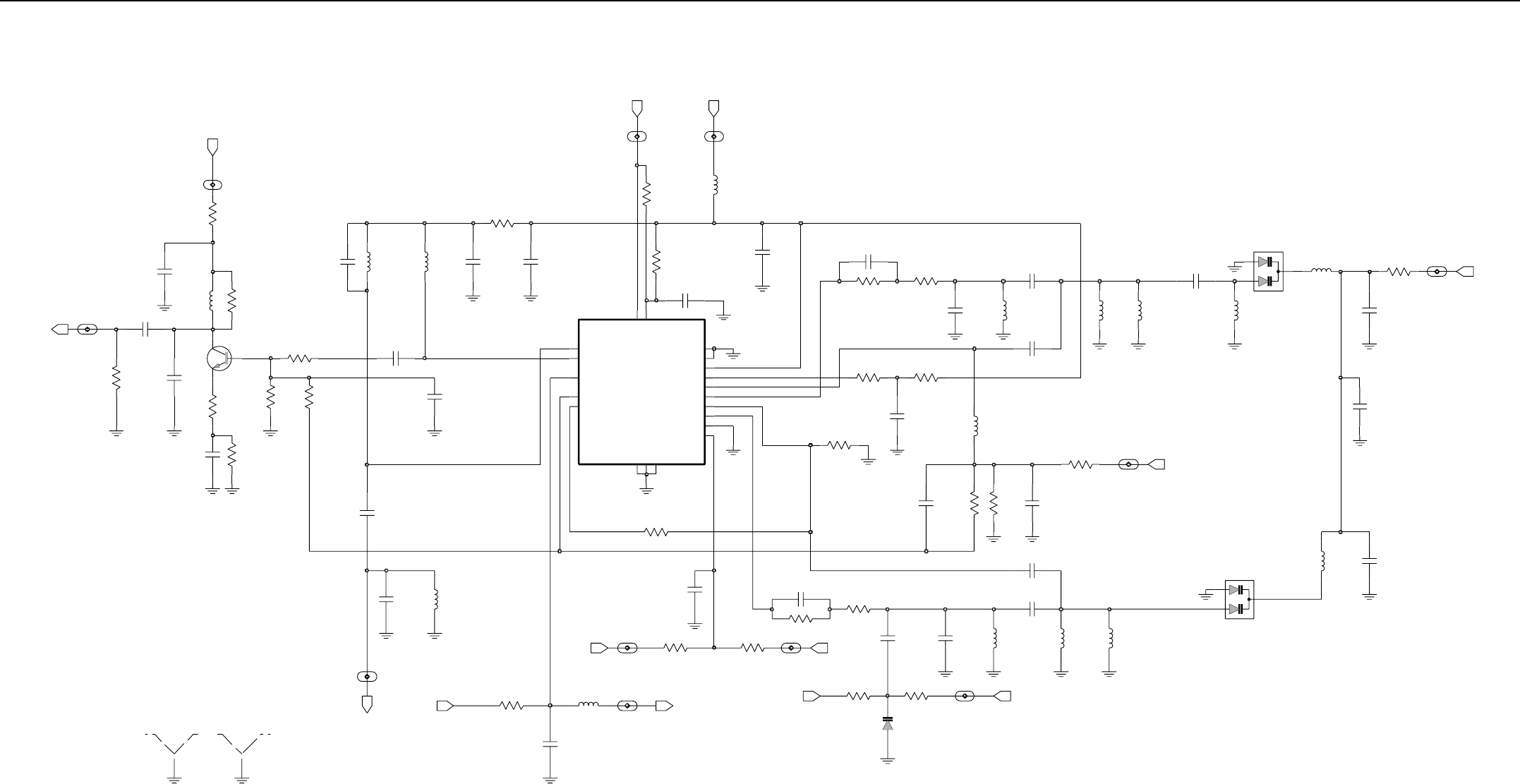
VHF PCB 8486473Z04 / Schematics 4-67
R5
R3802
100
R5_1_VCO
0.1uF
C3804
1K
R3807
NU
1K
L3801
100nH
RX_INJ
Q3801
RX_INJ_1_VCO
C3802
22pF
NU
220
NU
R3801
C3801
4.7pF
0.1uF
C3812L3811
100nH
100
R3811
C3810
10pF
NU 0.1uF
C3811L3812
100nH
Vdda VSF
VSF_1_VCO
Vdda_3_VCO
R3817
0
0
L3813
1uH
0
NU
0
R3818
C3818
.022uF
TX_OUT
TX_SWITCH
RX_OUT
RX_SWITCH
PRESC_OUT
VCC_BUFFERS
VCC_LOGIC
14
18
U3801
10
13
8
7
12
2
3
19
16
15
1
4
20
5
6
RX_IADJ
SUPER_FLTR
TRB_IN
TX_BASE
TX_EMITTER
TX_IADJ
COLL_RFIN
FLIP_IN
RX_BASE
RX_EMITTER
GND_BUFFERS
GND_FLAG
GND_LOGIC
11
9
17
10
10
R3808
24K
R3805R3804
10K
R3803
220
C3803
1000pF
R3806
22
C3805
4.7pF
100pF
C3806
27nH
L3809
15pF
C3808
27pF
C3809
TX_INJ_1_VCO
C3822
1000pF
C3813
.01uF
47
R3822R3821
220 L3821
56nH
C3824
56pF
C3826
4.7pF
C3825
15pF
L3826
1uH
R3825
33
R3831
10K
18
R3826
R3823
33K
.01uF
C3821 C3827
.022uF
.01uF
C3823
R3824
22K
PRESC_1_VCO
1K 100nH
R3816 L3816
C3816
PRESC
6.8pF
VSF
TX_INJ
T5 TRB
C3832
1000pF
R3833
220
1000pF
C3815
R3830
T5_1_VCO
0
R3829 TRB_1_VCO
0
R3832
12K
47
R3834
VCO_MOD_1_VCO
47K
R3835
VSF
R3836
10K
VCO_MOD
D3832
4.7pF
C3833 L3831
56nH56pF
C3834
C3836
15pF
C3835
6.8pF
L3832
68nH
L3833
56nH
100K
R3812
BIAS_ADJ_1_VCO
BIAS_ADJ
NU
L3824
1uH
L3822
47nH
D3821
L3825
100nH
68pF
C3830
47nH
L3823
C3829
0.1uF
0.1uF
C3828
R3828
100
VCTRL_1_VCO
VCTRL
1uH
L3834 C3842
1000pF
D3831
SHIELD
1
SHIELD
1
SH3802SH3801
VHF (136-174 MHz) Voltage Controlled Oscillator

4-68 VHF PCB 8486473Z04 / Schematics
DATA CLK
CSX
UNSWB+
CSX_2_PA
UNSWB_LPLUS_2_PA
UNSW_LPLUS_3_PA
CLK_2_PA
DATA_2_PA
C3566
100pF
2
U3503
GND
3POS
VOUT
12K
R3561
R3562
33K
C3561
.022uF
LM50C
5185963A15
330pF
C3501
300
R3501 R3503
300
TX_INJ_1_PA
18
R3502
TX_INJ
C3504
.022uF
33pF
C3502
5.6nH
L3501
470
R3505
330pF
C3505
C3503
33pF
68nH
L3503
.022uF
C3508
330pF
C3509
68nH
L3504
330pF
C3567
330K
NU
R3565
220pF
C3564
3300pF
C3562
3300pF
C3563
330K
R3564
.022uF
C3565
270K
R3563
RFOUT2
1
VCNTRL
14
VD1
2
VG1
3
VG2
12
GND4
13
8
NC1
9
NC2
10
NC3
15
NC4
16
RFIN RFOUT1
6
7
EP
17
11
G2
GND1
4
GND2
5
GND3
C65
U3501
330pF
C3544
100
R3543
C3543
.022uF
330pF
C3542
5.6K
R3542
.022uF
C3541 R3541
NU
6.8K
L3511
18nH
L3512
11.03nH
47pF
C3512
30pF
C3513
0
R3507
R3506
0
L3513
7.66nH 470pF
C3514
100pF
C3517
C3516
1uF
22pF
C3519
100
R3513
R3512
3300pF
C3515
330pF
C3518 L3518
39nH
120
D
G
S
Q3501
HEATSINK
H3501
C3527
1.5pF
NU
120pF
C3523
18pF
C3524
L3521
7.66nH
220pF
C3521
.022uF
C3528
9.1pF
23.75nH
L3522
13.85nH
L3515
C3525
10pF
VR3501
10V
C3526
Microstrio
100
R3545
7.5K
R3548
100
R3544
BIAS_TUNING
330pF
C3546 R3546
33K
12K
R3547
.022uF
C3547
TP3502
1
3300pF
C3568
0
R3566
R3519
0.1
BEAD
L3519
C3570
470pF
C3571
RESET
RESET_1_PA 5V_2_PA
5V
BIAS_TUNING
330pF
UNSWB+
UNSWB+
10K
NU
R3570
R3569
NU
5.6K
NU
Q3561
UNSWB+
R3571
NU
120
120
R3572
120
R3573
C3569
.022uF
L3523
1uH
D3521
43.67nH
L3551
C3536
15pF
7.5pF
C3533
C3532
68pF
43.67nH
L3531
43.67nH
L3532
C3535
27pF
C3534
4.7pF
20pF
C3531 4
1
2
3
J3501
RF_JACK
GND
18pF
C3537
TAB5
5
1
TAB1
2
TAB2
3
TAB3
4
TAB4
ANTENNA_NUT
J3502
5.6pF
C3539
30.54nH
L3538
39
R3551
56pF
C3552
RX_IN_1_PA
RX_IN
C3551
68pF
D3551
7.66nH
L3552
7.5pF
C3550
19
17
20
18
24
22
21
23
14
16
15
11
10
12
13
9
30
31
26
28
25
32
27
29
6
2
1
7
8
4
3
5
TEMP
RSET
CLK
DATA
GND2
ANO
BPOS
CEX
VL
T1
INT
RFIN
CL
GND1
CI
CJ
VG
V10
V45
Q
QX
CQ
CQX
F168
VLIM
V5EXT
VAR1
VAR2
VAR3
NA
RS
RX
H99S-4
U3502
C3560
1uF
1
SHIELD
SH3502SH3501
SHIELD
1
2
1
2
3
ZMY0130484-A
VHF (136-174 MHz) Transmitter

VHF PCB 8486473Z04 Radio Parts List 4-69
17.0 VHF PCB 8486473Z04 Radio
Parts List
Circuit
Ref
Motorola
Part No. Description
B501 0986237A02 Battery Contact Module
B503 3980502Z01 Backup Contact, B + (not
placed in non-display radios)
B504 3980501Z01 Backup Contact, B - (not
placed in non-display radios)
C3200 2113743N12 2.7pF
C3201 2113743N31 16pF
C3202 NOT PLACED
C3203 2113743N37 30pF
C3205 2113743M24 100000pF
C3206 2109445U26 9.1
C3207 2113743N18 4.7pF
C3208 2113743M24 100000pF
C3209 2113743M24 100000pF
C3210 2113743M24 100000pF
C3212 2311049A07 1uF
C3213 2311049A56 4.7uF
C3215 2113743N26 10pF
C3218 2311049A59 10uF
C3221 2113743E20 0.1uF
C3222 2113743M24 100000pF
C3225 2113743M24 100000pF
C3226 2113743M24 100000pF
C3228 2113743M24 100000pF
C3230 2113743M24 100000pF
C3231 2113743M24 100000pF
C3232 2113743M24 100000pF
C3233 2113743M24 100000pF
C3234 2113743M24 100000pF
C3236 2113743L33 4700pF
C3238 2113743M24 100000pF
C3274 2113743N37 30pF
C3275 2113743N35 24pF
C3278 2113743E20 0.1uF
C3279 2113743N52 120pF
C328 2113743M24 100000pF
C3301 2113743N20 5.6pF
C3302 2113743N54 150pF
C3303 2113743N30 15pF
C3304 2113743N54 150pF
C3305 NOT PLACED
C3306 2113928N01 0.1uF
C3307 2113743N50 100pF
C3308 2113743L05 330pF
C3309 2113928N01 0.1uF
C3310 NOT PLACED
C3311 2113743N54 150pF
C3312 2113743N31 16pF
C3313 2113743N54 150pF
C3314 NOT PLACED
C3315 2113743N26 10pF
C3316 2113743N14 3.3pF
C3317 2113743N37 30pF
C3318 2113743M08 22000pF
C3319 NOT PLACED
C3320 2113743N48 82pF
C3321 2113743L05 330pF
C3322 2113743N50 100pF
C3323 2113743N50 100pF
C3324 2113743N38 33pF
C3325 2113743L17 1000pF
C3326 NOT PLACED
C3327 2113743L05 330pF
C3329 2113743L05 330pF
C3330 2113743N50 100pF
C3331 2113743N50 100pF
C3332 2113743N40 39pF
C3334 2113743N33 20pF
C3335 2113743N34 22pF
C3336 2311049A96 33uF
C3337 2113743M08 22000pF
C3338 2113743L09 470pF
C3339 2113743N26 10pF
C337 2113928P04 1uF
C3501 2113743L05 330pF
Circuit
Ref
Motorola
Part No. Description
C3502 2113743N38 33pF
C3503 2113743N38 33pF
C3504 2113743M08 22000pF
C3505 2113743N38 33pF
C3508 2113743M08 22000pF
C3509 2113743L05 330pF
C3512 2113740F43 47pF
C3513 2113740F38 30pF
C3514 2113740F47 68pF
C3515 2113743L29 3300pF
C3516 2311049A08 1uF
C3517 2113740F47 68pF
C3518 NOT PLACED
C3519 NOT PLACED
C3521 2111078B51 220pF
C3523 2111078B44 120pF
C3524 2113740F34 20pF
C3525 2113740F27 10pF
C3526 2113743M08 22000pF
C3527 NOT PLACED
C3528 2113740F27 10pF
C3531 2113740F34 20pF
C3532 2113740F47 68pF
C3533 2113740F24 7.5pF
C3534 2113740F19 4.7pF
C3535 2113740F37 27pF
C3536 2113740F31 15pF
C3537 2113740F33 18pF
C3539 2113740F29 12pF
C3541 2113743M08 22000pF
C3542 2113743L05 330pF
C3543 2113743M08 22000pF
C3544 2113743L05 330pF
C3546 2113743L05 330pF
C3547 2113743M08 22000pF
C3550 2113743N23 7.5pF
C3551 2113743N46 68pF
C3552 2113743N44 56pF
Circuit
Ref
Motorola
Part No. Description
C3560 2311049A07 1uF
C3561 2113743M08 22000pF
C3562 2113743L29 3300pF
C3563 2113743L29 3300pF
C3564 2113743L01 220pF
C3565 2113743E07 0.022uF
C3566 2113743N50 100pF
C3567 2113743L05 330pF
C3568 2113743L29 3300pF
C3569 2113743M08 22000pF
C3570 2113743L05 330pF
C3571 2113743L09 470pF
C358 2113743N22 6.8pF
C359 2113743N31 16pF
C3701 2113743L41 10000pF
C3702 2113743L41 10000pF
C3703 2113743L41 10000pF
C3704 2113743L41 10000pF
C3705 2113743E20 0.1uF
C3706 2311049J11 4.7uF
C3707 2113743N34 22pF
C3708 2113928N01 0.1uF
C3709 2113928N01 0.1uF
C3710 2104993J02 2.2uF
C3711 2311049A69 10uF
C3712 2113928N01 0.1uF
C3713 2311049A09 2.2uF
C3714 2311049J11 4.7uF
C3715 2113743L09 470pF
C3721 2113743E20 0.1uF
C3722 2113743E20 0.1uF
C3724 2311049A08 1uF
C3725 NOT PLACED
C3726 2113743N24 8.2pF
C3727 2113743N50 100pF
C3731 2113743L41 10000pF
C3732 2113743L41 10000pF
C3733 2104993J02 2.2uF
Circuit
Ref
Motorola
Part No. Description

4-70 VHF PCB 8486473Z04 Radio Parts List
C3734 2113743L41 10000pF
C3741 NOT PLACED
C3742 2113743L01 220pF
C3743 2113743L01 220pF
C3744 2113743L01 220pF
C3745 2113743L01 220pF
C3746 2113743L01 220pF
C3752 2113743L17 1000pF
C3753 2311049A56 4.7uF
C3754 2113928N01 0.1uF
C3755 2104993J02 2.2uF
C3761 2113743N42 47pF
C3762 2113740F63 330pF
C3763 NOT PLACED
C3801 2113743N18 4.7pF
C3802 NOT PLACED
C3803 2113743L17 1000pF
C3804 2113743E20 0.1uF
C3805 2113743N18 4.7pF
C3806 2113743N50 100pF
C3808 2113743N30 15pF
C3809 2113743N36 27pF
C3810 NOT PLACED
C3811 2113928N01 0.1uF
C3812 2113928N01 0.1uF
C3813 2113743L41 10000pF
C3815 2113743L17 1000pF
C3816 2113743N22 6.8pF
C3818 2113743E07 0.022uF
C3821 2113743L41 10000pF
C3822 2113743L17 1000pF
C3823 2113743L41 10000pF
C3824 2113743N44 56pF
C3825 2113743N30 15pF
C3826 2113743N18 4.7pF
C3827 2113743E07 0.022uF
C3828 2185895Z01 0.01uF
C3829 2185895Z01 0.01uF
Circuit
Ref
Motorola
Part No. Description
C383 2113743N43 51pF
C3830 2113743N46 68pF
C3832 2113743L17 1000pF
C3833 2113743N18 4.7pF
C3834 2113743N44 56pF
C3835 2113743N22 6.8pF
C3836 2113743N30 15pF
C3842 2113743L17 1000pF
C390 2113743N43 51pF
C400 2113743L41 10000pF
C401 2113928N01 0.1uF
C402 2113928N01 0.1uF
C4020 NOT PLACED
C4021 NOT PLACED
C403 2113743G24 2.2uF
C407 2113928N01 0.1uF
C408 2113743N50 100pF
C409 2113928N01 0.1uF
C410 2113928N01 0.1uF
C411 2113928N01 0.1uF
C414 2113928N01 0.1uF
C415 2185895Z01 0.01uF
C416 2113928N01 0.1uF
C419 2113743L41 10000pF
C420 2113743L41 10000pF
C421 2113928N01 0.1uF
C422 2113928N01 0.1uF
C423 2113743N50 100pF
C424 2311049A59 10uF
C425 2113928N01 0.1uF
C426 2113743N50 100pF
C427 2113743N50 100pF
C428 2113928N01 0.1uF
C429 2113928N01 0.1uF
C430 2113928N01 0.1uF
C431 2113743N50 100pF
C432 NOT PLACED
C433 2113743L41 10000pF
Circuit
Ref
Motorola
Part No. Description
C434 2113928N01 0.1uF (not placed in
non-display radios)
C435 2113928N01 0.1uF
C436 2113743N34 22pF (not placed in
non-display radios)
C437 2113743N34 22pF (not placed in
non-display radios)
C440 2113743G26 4.7uF
C441 2113743L09 470pF
C442 2113743E20 0.1uF
C443 2113928N01 0.1uF
C444 2113743N50 100pF
C445 2113743L09 470pF
C446 2113743L09 470pF
C447 2113928N01 0.1uF
C448 2113928N01 0.1uF
C449 2113743N50 100pF
C450 NOT PLACED
C451 2113743M08 22000pF
C452 2113743B29 1uF
C453 2113743N50 100pF
C456 2113743N50 100pF
C458 2113743N50 100pF
C459 2113743N50 100pF
C463 2113743N50 100pF
C466 2113743N50 100pF
C467 2113928N01 0.1uF
C471 2113743L09 470pF
C472 2113743L09 470pF
C473 2113743L09 470pF
C474 2113743L41 10000pF
C475 2113743H14 10uF
C476 2113928D08 10uF
C477 2113743L17 1000pF
C478 2113743L17 1000pF
C479 2113928N01 0.1uF
C480 2113928D08 10uF
C481 2113928N01 0.1uF
C482 2113928N01 0.1uF
Circuit
Ref
Motorola
Part No. Description
C483 2113743L09 470pF
C484 2113743L09 470pF
C490 2113743L09 470pF
C491 2113743L09 470pF
C492 2113743L09 470pF
C493 2113743N50 100pF
C494 2113743N50 100pF
C495 2113743L09 470pF
C496 2113743L09 470pF
C497 2113743L09 470pF
C498 NOT PLACED
C502 2311049A05 0.47uF
C503 2113743N50 100pF
C505 2113743N50 100pF
C511 2113743N50 100pF
C512 2113743N50 100pF
C513 2113743N50 100pF
C514 2113743N50 100pF
C520 2113743L41 10000pF
C521 2113743L41 10000pF
C522 2113743L41 10000pF
C523 2113743L41 10000pF
C535 2113743L17 1000pF
CR3201 4813825A19 Schottky Diode
CR3202 4802245J97 Band Switching Diode
CR3203 4802245J97 Band Switching Diode
CR3301 4802245J42 Ring Quad Diode
CR3302 4805129M96 Dual Diode
CR3303 4880154K03 Dual Diode
CR411 4802245J62 Schottkt Diode
CR412 4802245J62 Schottkt Diode
CR413 4802245J62 Schottkt Diode
CR440 4813833C02 Dual Diode
CR501 4880107R01 Rectifier
CR503 4805729G49 Red / Yellow LED
D3301 4802081B58 Dual Diode
D3302 4802081B58 Dual Diode
D3521 4880973Z02 Pin Diode
Circuit
Ref
Motorola
Part No. Description
VHF PCB 8486473Z04 Radio Parts List 4-71
D3551 4880973Z02 Pin Diode
D3701 4802233J09 Triple Diode
D3702 4802233J09 Triple Diode
D3761 4862824C03 Varactor Diode
D3821 4805649Q13 Varactor Diode
D3831 4805649Q13 Varactor Diode
D3832 4862824C01 Varactor Diode
E400 2480640Z01 Ferrite Bead
E401 2480640Z01 Ferrite Bead
E402 2480640Z01 Ferrite Bead
E403 2480640Z01 Ferrite Bead
E404 2480640Z01 Ferrite Bead
E405 2480640Z01 Ferrite Bead
E406 2480640Z01 Ferrite Bead
E407 2480640Z01 Ferrite Bead
E408 2480640Z01 Ferrite Bead
E409 2480640Z01 Ferrite Bead
F501 6580542Z01 Fuse 3A
FL401 4870368G02
Real Time Clock Xtal Oscillator
38.4kHz (not placed in
non-display radios)
H3501 2680499Z01 Heat Spreader
J3501 0985613Z01 RF Jack
J3502 0280519Z02 Antenna Nut
J400 0905505Y04 40-Pin Connector
J403 0905505Y02 20-Pin Connector
L3200 2413926K33 680nH
L3202 2413923A25 1200nH
L3203 2413926K33 680nH
L3270 2462587N68 1000nH
L3301 2462587T35 12nH
L3303 2462587T35 12nH
L3304 2462587T23 470nH
L3305 2462587T35 12nH
L3306 2462587T35 12nH
L3308 2462587T34 10nH
L3309 2462587N55 150nH
L3312 2462587V28 33nH
L3501 2413926H09 5.6nH
Circuit
Ref
Motorola
Part No. Description
L3503 2462587V32 68nH
L3504 2462587N51 68nH
L3511 2462587N44 18nH
L3512 2479990B01 11.03nH
L3513 2479990A02 7.66nH
L3515 2479990C03 1385nH
L3518 NOT PLACED
L3519 2484657R01 Ferrite Bead
L3521 2479990A02 7.66nH
L3522 2479990E01 23.75nH
L3523 2462587N68 1000nH
L3531 2479990N01 43.67nH
L3532 2479990N01 43.67nH
L3538 2479990M01 30.54nH
L3551 2479990N01 43.67nH
L3552 2479990A02 7.66nH
L3701 2462587Q42 390nH
L3731 2462587Q20 2200nH
L3801 2462587V34 100nH
L3809 2462587V27 27nH
L3811 2462587V34 100nH
L3812 2462587V34 100nH
L3813 2462587Q47 1000nH
L3816 2462587V34 100nH
L3821 2462587N50 56nH
L3822 2462587N49 47nH
L3823 2462587N49 47nH
L3824 2462587N68 1000nH
L3825 2462587V34 100nH
L3826 2462587N68 1000nH
L3831 2462587N50 56nH
L3832 2462587N51 68nH
L3833 2462587N50 56nH
L3834 2462587N68 1000nH
L400 2462587Q42 390nH
L401 2462587Q42 390nH
L410 2462587Q42 390nH
L411 2462587Q42 390nH
Circuit
Ref
Motorola
Part No. Description
L505 2462587Q42 390nH
PB501 4086470Z01 Tactile Switch
PB502 4086470Z01 Tactile Switch
PB503 4086470Z01 Tactile Switch
PB504 4086470Z01 Tactile Switch
PB505 4086470Z01 Tactile Switch
Q3200 4802197J95 NPN Transistor
Q3270 4813824A10 NPN Transistor
Q3301 4880214G02 NPN Transistor
Q3302 4802197J95 NPN Transistor
Q3501 4813828A08 RF Power Amplifier
Q3561 4813824A17 PNP Transistor
Q3721 4809939C05 Dual NPN/PNP Transistor
Q3801 4802197J95 NPN Transistor
Q400 4809579E18 MOSFET P-chan Transistor
Q403 4813824A17 PNP Transistor
Q405 4802245J54 Dual NPN Transistor
Q410 4802245J54 Dual NPN Transistor
Q416 4809579E18
MOSFET P-chan Transistor
(not placed in
non-display radios)
Q417 4809939C05 Dual NPN/PNP Transistor
Q502 5180159R01 Dual NPN Transistor
Q505 4880214G02 NPN Transistor
R3200 0662057M72 820
R3201 0662057M69 620
R3202 0662057N09 27K
R3203 0662057N01 12K
R3204 0662057M90 4700
R3205 0662057N06 20K
R3206 0662057M73 910
R3207 0662057N01 12K
R3208 0662057N06 20K
R3209 0662057N13 39K
R3211 0662057N13 39K
R3212 0662057N06 20K
R3213 0662057N01 12K
R3214 0662057M34 22
R3215 0662057M01 0
Circuit
Ref
Motorola
Part No. Description
R3220 NOT PLACED
R3221 0662057M43 51
R3222 0662057M70 680
R3223 0662057V04 12K
R3224 0662057V02 10K
R3226 0662057M64 390
R3270 0662057M74 1000
R3271 NOT PLACED
R3273 0662057N03 15K
R3274 0662057M80 1800
R3275 0662057M76 1200
R3276 0662057N23 100K
R3301 NOT PLACED
R3303 0662057N23 100K
R3304 0662057N23 100K
R3305 0662057N18 62K
R3306 0662057M82 2200
R3307 0662057N11 33K
R3308 0662057M78 1500
R3309 0662057M95 7500
R3310 0662057M84 2700
R3311 NOT PLACED
R3312 0662057M19 5.1
R3313 0662057M40 39
R3314 0662057M35 24
R3315 0662057M62 330
R3316 0662057M66 470
R3317 0662057N23 100K
R3318 0662057M66 470
R3319 NOT PLACED
R3320 NOT PLACED
R3321 0662057M43 51
R3322 NOT PLACED
R3323 0662057M01 0
R3324 0662057M58 220
R3501 0662057M61 300
R3502 0662057M32 18
R3503 0662057M61 300
Circuit
Ref
Motorola
Part No. Description
4-72 VHF PCB 8486473Z04 Radio Parts List
R3505 0662057M62 330
R3506 0662057B62 3.9
R3507 0662057B62 3.9
R3512 NOT PLACED
R3513 NOT PLACED
R3519 0680539Z01 0.1
R3541 0662057N13 39K
R3542 0662057M92 5600
R3543 0662057M50 100
R3544 0662057A25 100
R3545 0662057A25 100
R3546 0662057N01 12K
R3547 0662057N11 33K
R3548 0662057N07 22K
R3551 0662057M40 39
R3561 0662057N01 12K
R3562 0662057N11 33K
R3563 0662057N33 270K
R3564 0662057N35 330K
R3565 NOT PLACED
R3566 NOT PLACED
R3569 0662057M92 5600
R3570 0662057M98 10K
R3571 0662057A27 120
R3572 0662057A27 120
R3573 0662057A27 120
R370 NOT PLACED
R3701 0662057M50 100
R3702 NOT PLACED
R3703 0662057M54 150
R3704 0662057M54 150
R3705 0662057N11 33K
R371 0662057N23 100K
R372 0662057N28 160K
R3721 0662057M66 470
R3722 0662057M68 560
R3723 0662057M50 100
R3726 NOT PLACED
Circuit
Ref
Motorola
Part No. Description
R3727 0662057N23 100K
R373 NOT PLACED
R374 0662057N23 100K
R3741 0662057M50 100
R375 NOT PLACED
R3751 0662057N30 200K
R3752 0662057N29 180K
R376 0662057M01 0
R3761 0662057N15 47K
R3762 NOT PLACED
R377 0662057N23 100K
R378 0662057N23 100K
R3801 NOT PLACED
R3802 0662057M50 100
R3803 0662057M58 220
R3804 0662057M98 10K
R3805 0662057N08 24K
R3806 0662057M34 22
R3807 NOT PLACED
R3808 0662057M26 10
R3811 0662057M50 100
R3812 NOT PLACED
R3816 0662057M74 1000
R3817 0662057M01 0
R3818 NOT PLACED
R3821 0662057M58 220
R3822 0662057M42 47
R3823 0662057N11 33K
R3824 0662057N07 22K
R3825 0662057M38 33
R3826 0662057M32 18
R3828 0662057M50 100
R3829 0662057M01 0
R3830 NOT PLACED
R3831 0662057M98 10K
R3832 0662057N01 12K
R3833 0662057M58 220
R3834 0662057M42 47
Circuit
Ref
Motorola
Part No. Description
R3835 0662057N15 47K
R3836 0662057M98 10K
R400 0662057N15 47K
R401 0662057M01 0
R402 NOT PLACED
R403 NOT PLACED
R405 0662057M01 0
R406 0662057N20 75K
R407 0662057N19 68K
R408 NOT PLACED
R409 0662057M98 10K
R410 0662057N23 100K
R411 0662057M98 10K
R413 0662057M01 0
R414 0662057V34 180K
R415 0662057V26 91K
R416 0662057M98 10K
R418 0662057M01 0
R419 0662057M67 510 (not placed in
non-display radios)
R420 0662057B46 10M (not placed in
non-display radios)
R421 0662057M81 2000
R423 0662057N21 82K
R424 0662057N12 36K
R425 0662057N10 30K
R426 0662057N35 330K (not placed in
non-display radios)
R427 0662057M84 2700
R428 0662057M10 2.2
R429 0662057N20 75K
R431 0662057N39 470K
R432 0662057N16 51K
R434 0662057M62 330
R435 0662057M81 2000
R436 0662057M01 0
R437 NOT PLACED
R445 0662057N08 24K
R447 0662057N23 100K
Circuit
Ref
Motorola
Part No. Description
R448 0662057M98 10K
R449 0662057N08 24K
R450 0683962T45 68
R451 0662057N03 15K
R452 0662057N23 100K
R453 NOT PLACED
R454 NOT PLACED
R455 NOT PLACED
R456 0662057M01 0
R457 0662057M98 10K
R460 0662057M90 4700
R461 0662057M56 180 (not placed in
non-display radios)
R462 0662057M98 10K (not placed in
non-display radios)
R463 0662057M61 300
R471 0662057N06 20K
R472 0662057M93 6200
R473 0662057M26 10
R475 0662057M01 0
R476 0662057N35 330K
R477 0662057M74 1000
R478 0662057M98 10K
R481 0662057N08 24K
R492 0662057M01 0
R498 0662057M98 10K
R499 0662057M98 10K
R501 0662057M70 680
R502 0662057M56 180
R505 0662057M98 10K
R506 0662057N15 47K
RT3301 NOT PLACED
RT400 0680590Z01 Thermistor_33K
S501 4080710Z01 Frequency Switch (For non-
display radios only)
S501 4080710Z02 Frequency Switch (For display
radios only)
S502 1880619Z02 Volume / On-off Switch
SH3202 2686539Z01 IFIC Shield
Circuit
Ref
Motorola
Part No. Description
VHF PCB 8486473Z04 Radio Parts List 4-73
* Motorola Depot Servicing only
Reference designators with an asterisk indicate
components which are not field replaceable
because they need to be calibrated with
specialized factory equipment after installation.
Radios in which these parts have been replaced in
the field will be off frequency at temperature
extremes.
SH3203 2686527Z01 Crystal Filter Shield
SH3301 2686081B01 Receiver Back-End Bottom
Shield
SH3302 2686081B05 Mixer Diode Shield
SH3303 2686081B06 Receiver Front-End Shield
SH3501 2686081B03 Harmonic Filter Shield
SH3502 2686081B04 PA Shield
SH3701 2680511Z01 Synthesizer Top Shield
SH3702 2680511Z01 Synthesizer Bottom Shield
SH3801 2680513Z01 VCO Top Shield
SH3802 2680514Z01 VCO Buffer IC Shield
SH400 2680505Z01 Controller Memory Shield
SH401 2680506Z01 Controller On-off Shield
SH402 2680515Z01 Microprocessor Shield
SH403 2680516Z01 Asfic_Cmp, Audio PA Shield
T3301 2580541Z02 Balun Transformer
T3302 2580541Z02 Balun Transformer
U303 5113818A01 IC Sing Supply
U3201 5102463J58 3.3V Regulator
U3220 5186144B01 IF IC
U3221 5109522E10 Inverter IC
U3501 5185130C65 ASFIC CMP IC
U3502 5185765B26 LDMOS Driver IC
U3503 5185963A15 PCIC
U3701 5185963A27 Temperature Sensor
U3711 5105739X05 5V Regulator
U3801 5105750U54 VCO Buffer IC
U400 5102463J40 3.3V Regulator
U404 5185130C53 LV FRAC-N IC
U405 5102463J36 Static RAM 32K X 8
U406 *5102463J60 Flash ROM 512K X 8
U407 *5102495J05 EEPROM 16K X 8
U409 5102226J56 Microprocessor IC
U410 5102463J57 3.3V Regulator (not placed in
non-display radios)
U420 5102463J44 Audio PA
VR3501 4880140L17 Zener Diode
VR432 4805656W08 Zener Diode
VR433 4805656W08 Zener Diode
Circuit
Ref
Motorola
Part No. Description
VR434 4802245J73 Zener Diode 6.8V
VR439 4880140L17 Zener Diode
VR440 NOT PLACED
VR441 NOT PLACED
VR442 NOT PLACED
VR444 NOT PLACED
VR447 4802245J74 Zener Diode 10V
VR448 4802245J74 Zener Diode 10V
VR449 4802245J74 Zener Diode 10V
VR450 4802245J75 Zener Diode 12V
VR460 4802245J73 Zener Diode 6.8V
VR501 4802245J73 Zener Diode 6.8V
VR506 4802245J73 Zener Diode 6.8V
Y3200 9180022M11 44.85MHZ Crystal Filter
Y3201 4802245J84 44.395MHz Crystal Oscillator
Y3202 9186145B02 455KHZ Discriminator
Y3203 9180469V05 455KHz 6-Pole Ceramic Filter
Y3204 9180469V03 455KHz 6-Pole Ceramic Filter
Y3205 9180468V05 455KHz 4-Pole Ceramic Filter
Y3761 4805875Z04 16.8 MHz Crystal Oscillator
8486473Z04 VHF PC Board
Circuit
Ref
Motorola
Part No. Description

4-74 VHF PCB 8486473Z04 Radio Parts List
Intentionally Left Blank
