Intel® 64 And IA 32 Architectures Software Developer’s Manual Ation Changes 320014 003US Developers
User Manual: 320014-003US
Open the PDF directly: View PDF ![]() .
.
Page Count: 1299 [warning: Documents this large are best viewed by clicking the View PDF Link!]
- Revision History
- Preface
- Summary Tables of Changes
- Documentation Changes
- 1. Updates to Chapter 5, Volume 1
- Chapter 5 Instruction Set Summary
- 5.1 General-Purpose Instructions
- 5.1.1 Data Transfer Instructions
- 5.1.2 Binary Arithmetic Instructions
- 5.1.3 Decimal Arithmetic Instructions
- 5.1.4 Logical Instructions
- 5.1.5 Shift and Rotate Instructions
- 5.1.6 Bit and Byte Instructions
- 5.1.7 Control Transfer Instructions
- 5.1.8 String Instructions
- 5.1.9 I/O Instructions
- 5.1.10 Enter and Leave Instructions
- 5.1.11 Flag Control (EFLAG) Instructions
- 5.1.12 Segment Register Instructions
- 5.1.13 Miscellaneous Instructions
- 5.1.14 User Mode Extended Sate Save/Restore Instructions
- 5.1.15 Random Number Generator Instructions
- 5.1.16 BMI1, BMI2
- 5.2 x87 FPU Instructions
- 5.3 x87 FPU AND SIMD State Management Instructions
- 5.4 MMX™ Instructions
- 5.5 SSE Instructions
- 5.6 SSE2 Instructions
- 5.7 SSE3 Instructions
- 5.7.1 SSE3 x87-FP Integer Conversion Instruction
- 5.7.2 SSE3 Specialized 128-bit Unaligned Data Load Instruction
- 5.7.3 SSE3 SIMD Floating-Point Packed ADD/SUB Instructions
- 5.7.4 SSE3 SIMD Floating-Point Horizontal ADD/SUB Instructions
- 5.7.5 SSE3 SIMD Floating-Point LOAD/MOVE/DUPLICATE Instructions
- 5.7.6 SSE3 Agent Synchronization Instructions
- 5.8 Supplemental Streaming SIMD Extensions 3 (SSSE3) Instructions
- 5.9 SSE4 Instructions
- 5.10 SSE4.1 Instructions
- 5.10.1 Dword Multiply Instructions
- 5.10.2 Floating-Point Dot Product Instructions
- 5.10.3 Streaming Load Hint Instruction
- 5.10.4 Packed Blending Instructions
- 5.10.5 Packed Integer MIN/MAX Instructions
- 5.10.6 Floating-Point Round Instructions with Selectable Rounding Mode
- 5.10.7 Insertion and Extractions from XMM Registers
- 5.10.8 Packed Integer Format Conversions
- 5.10.9 Improved Sums of Absolute Differences (SAD) for 4-Byte Blocks
- 5.10.10 Horizontal Search
- 5.10.11 Packed Test
- 5.10.12 Packed Qword Equality Comparisons
- 5.10.13 Dword Packing With Unsigned Saturation
- 5.11 SSE4.2 Instruction Set
- 5.12 AESNI and PCLMULQDQ
- 5.13 Intel® Advanced Vector Extensions (Intel® AVX)
- 5.14 16-bit Floating-Point Conversion
- 5.15 Fused-Multiply-ADD (FMA)
- 5.16 Intel® Advanced Vector Extensions 2 (Intel® AVX2)
- 5.17 Intel® Transactional Synchronization Extensions (Intel® TSX)
- 5.18 Intel® SHA Extensions
- 5.19 Intel® Advanced Vector Extensions 512 (Intel® AVX-512)
- 5.20 System Instructions
- 5.21 64-Bit Mode Instructions
- 5.22 Virtual-Machine Extensions
- 5.23 Safer Mode Extensions
- 5.24 Intel® Memory Protection Extensions
- 5.25 Intel® Security Guard Extensions
- 5.1 General-Purpose Instructions
- Chapter 5 Instruction Set Summary
- 2. Updates to Chapter 16, Volume 1
- Chapter 16 Programming with Intel® Transactional Synchronization Extensions
- 16.1 Overview
- 16.2 Intel® Transactional Synchronization Extensions
- 16.3 Intel® TSX Application Programming Model
- Chapter 16 Programming with Intel® Transactional Synchronization Extensions
- 3. Updates to Chapter 18, Volume 1
- 4. Updates to Chapter 2, Volume 2A
- Chapter 2 Instruction Format
- 2.1 Instruction Format for Protected Mode, real-address Mode, and virtual-8086 mode
- 2.2 IA-32e Mode
- 2.3 Intel® Advanced Vector Extensions (Intel® AVX)
- 2.3.1 Instruction Format
- 2.3.2 VEX and the LOCK prefix
- 2.3.3 VEX and the 66H, F2H, and F3H prefixes
- 2.3.4 VEX and the REX prefix
- 2.3.5 The VEX Prefix
- 2.3.6 Instruction Operand Encoding and VEX.vvvv, ModR/M
- 2.3.7 The Opcode Byte
- 2.3.8 The MODRM, SIB, and Displacement Bytes
- 2.3.9 The Third Source Operand (Immediate Byte)
- 2.3.10 AVX Instructions and the Upper 128-bits of YMM registers
- 2.3.11 AVX Instruction Length
- 2.3.12 Vector SIB (VSIB) Memory Addressing
- 2.4 AVX and SSE Instruction Exception Specification
- 2.4.1 Exceptions Type 1 (Aligned memory reference)
- 2.4.2 Exceptions Type 2 (>=16 Byte Memory Reference, Unaligned)
- 2.4.3 Exceptions Type 3 (<16 Byte memory argument)
- 2.4.4 Exceptions Type 4 (>=16 Byte mem arg no alignment, no floating-point exceptions)
- 2.4.5 Exceptions Type 5 (<16 Byte mem arg and no FP exceptions)
- 2.4.6 Exceptions Type 6 (VEX-Encoded Instructions Without Legacy SSE Analogues)
- 2.4.7 Exceptions Type 7 (No FP exceptions, no memory arg)
- 2.4.8 Exceptions Type 8 (AVX and no memory argument)
- 2.4.9 Exception Type 11 (VEX-only, mem arg no AC, floating-point exceptions)
- 2.4.10 Exception Type 12 (VEX-only, VSIB mem arg, no AC, no floating-point exceptions)
- 2.5 VEX Encoding Support for GPR Instructions
- 2.6 Intel® AVX-512 Encoding
- 2.6.1 Instruction Format and EVEX
- 2.6.2 Register Specifier Encoding and EVEX
- 2.6.3 Opmask Register Encoding
- 2.6.4 Masking Support in EVEX
- 2.6.5 Compressed Displacement (disp8*N) Support in EVEX
- 2.6.6 EVEX Encoding of Broadcast/Rounding/SAE Support
- 2.6.7 Embedded Broadcast Support in EVEX
- 2.6.8 Static Rounding Support in EVEX
- 2.6.9 SAE Support in EVEX
- 2.6.10 Vector Length Orthogonality
- 2.6.11 #UD Equations for EVEX
- 2.6.12 Device Not Available
- 2.6.13 Scalar Instructions
- 2.7 Exception Classifications of EVEX-Encoded instructions
- 2.7.1 Exceptions Type E1 and E1NF of EVEX-Encoded Instructions
- 2.7.2 Exceptions Type E2 of EVEX-Encoded Instructions
- 2.7.3 Exceptions Type E3 and E3NF of EVEX-Encoded Instructions
- 2.7.4 Exceptions Type E4 and E4NF of EVEX-Encoded Instructions
- 2.7.5 Exceptions Type E5 and E5NF
- 2.7.6 Exceptions Type E6 and E6NF
- 2.7.7 Exceptions Type E7NM
- 2.7.8 Exceptions Type E9 and E9NF
- 2.7.9 Exceptions Type E10
- 2.7.10 Exception Type E11 (EVEX-only, mem arg no AC, floating-point exceptions)
- 2.7.11 Exception Type E12 and E12NP (VSIB mem arg, no AC, no floating-point exceptions)
- 2.8 Exception Classifications of Opmask instructions
- Chapter 2 Instruction Format
- 5. Updates to Chapter 3, Volume 2A
- 6. Updates to Chapter 4, Volume 2B
- 7. Updates to Chapter 9, Volume 3A
- Chapter 9 Processor Management and Initialization
- 9.1 Initialization Overview
- 9.2 x87 FPU Initialization
- 9.3 Cache Enabling
- 9.4 Model-Specific Registers (MSRs)
- 9.5 Memory Type Range Registers (MTRRs)
- 9.6 Initializing SSE/SSE2/SSE3/SSSE3 Extensions
- 9.7 Software Initialization for Real-Address Mode Operation
- 9.8 Software Initialization for Protected-Mode Operation
- 9.9 Mode Switching
- 9.10 Initialization and Mode Switching Example
- 9.11 Microcode Update Facilities
- 9.11.1 Microcode Update
- 9.11.2 Optional Extended Signature Table
- 9.11.3 Processor Identification
- 9.11.4 Platform Identification
- 9.11.5 Microcode Update Checksum
- 9.11.6 Microcode Update Loader
- 9.11.7 Update Signature and Verification
- 9.11.8 Optional Processor Microcode Update Specifications
- 9.11.8.1 Responsibilities of the BIOS
- 9.11.8.2 Responsibilities of the Calling Program
- 9.11.8.3 Microcode Update Functions
- 9.11.8.4 INT 15H-based Interface
- 9.11.8.5 Function 00H—Presence Test
- 9.11.8.6 Function 01H—Write Microcode Update Data
- 9.11.8.7 Function 02H—Microcode Update Control
- 9.11.8.8 Function 03H—Read Microcode Update Data
- 9.11.8.9 Return Codes
- Chapter 9 Processor Management and Initialization
- 8. Updates to Chapter 16, Volume 3B
- Chapter 16 Interpreting Machine-Check Error Codes
- 16.1 Incremental Decoding Information: Processor Family 06H Machine Error Codes For Machine Check
- 16.2 Incremental Decoding Information: Intel Core 2 Processor Family Machine Error Codes For Machine Check
- 16.3 Incremental Decoding Information: Processor Family with CPUID DisplayFamily_DisplayModel Signature 06_1AH, Machine Error Codes For Machine Check
- 16.4 Incremental Decoding Information: Processor Family with CPUID DisplayFamily_DisplayModel Signature 06_2DH, Machine Error Codes For Machine Check
- 16.5 Incremental Decoding Information: Processor Family with CPUID DisplayFamily_DisplayModel Signature 06_3EH, Machine Error Codes For Machine Check
- 16.6 Incremental Decoding Information: Processor Family with CPUID DisplayFamily_DisplayModel Signature 06_3FH, Machine Error Codes For Machine Check
- 16.7 Incremental Decoding Information: Processor Family with CPUID DisplayFamily_DisplayModel Signature 06_56H, Machine Error Codes For Machine Check
- 16.8 Incremental Decoding Information: Processor Family with CPUID DisplayFamily_DisplayModel Signature 06_4FH, Machine Error Codes For Machine Check
- 16.9 Incremental Decoding Information: Processor Family with CPUID DisplayFamily_DisplayModel Signature 06_55H, Machine Error Codes For Machine Check
- 16.10 Incremental Decoding Information: Processor Family with CPUID DisplayFamily_DisplayModel Signature 06_5FH, Machine Error Codes For Machine Check
- 16.11 Incremental Decoding Information: Processor Family 0FH Machine Error Codes For Machine Check
- Chapter 16 Interpreting Machine-Check Error Codes
- 9. Updates to Chapter 17, Volume 3B
- Chapter 17 Debug, Branch Profile, TSC, and Resource Monitoring Features
- 17.1 Overview of Debug Support Facilities
- 17.2 Debug Registers
- 17.3 Debug Exceptions
- 17.4 Last Branch, Interrupt, and Exception Recording Overview
- 17.4.1 IA32_DEBUGCTL MSR
- 17.4.2 Monitoring Branches, Exceptions, and Interrupts
- 17.4.3 Single-Stepping on Branches
- 17.4.4 Branch Trace Messages
- 17.4.5 Branch Trace Store (BTS)
- 17.4.6 CPL-Qualified Branch Trace Mechanism
- 17.4.7 Freezing LBR and Performance Counters on PMI
- 17.4.8 LBR Stack
- 17.4.9 BTS and DS Save Area
- 17.5 Last Branch, Interrupt, and Exception Recording (Intel® Core™ 2 Duo and Intel® Atom™ Processors)
- 17.6 Last Branch, Call Stack, Interrupt, and Exception Recording for Processors based on Goldmont Microarchitecture
- 17.7 Last Branch, Interrupt, and Exception Recording for Processors based on Intel® Microarchitecture code name Nehalem
- 17.8 Last Branch, Interrupt, and Exception Recording for Processors based on Intel® Microarchitecture code name Sandy Bridge
- 17.9 Last Branch, Call Stack, Interrupt, and Exception Recording for Processors based on Haswell Microarchitecture
- 17.10 Last Branch, Call Stack, Interrupt, and Exception Recording for Processors based on Skylake Microarchitecture
- 17.11 Last Branch, Interrupt, and Exception Recording (Processors based on Intel NetBurst® Microarchitecture)
- 17.12 Last Branch, Interrupt, and Exception Recording (Intel® Core™ Solo and Intel® Core™ Duo Processors)
- 17.13 Last Branch, Interrupt, and Exception Recording (Pentium M Processors)
- 17.14 Last Branch, Interrupt, and Exception Recording (P6 Family Processors)
- 17.15 Time-Stamp Counter
- 17.16 Intel® Resource Director Technology (Intel® RDT) Monitoring Features
- 17.16.1 Overview of Cache Monitoring Technology and Memory Bandwidth Monitoring
- 17.16.2 Enabling Monitoring: Usage Flow
- 17.16.3 Enumeration and Detecting Support of Cache Monitoring Technology and Memory Bandwidth Monitoring
- 17.16.4 Monitoring Resource Type and Capability Enumeration
- 17.16.5 Feature-Specific Enumeration
- 17.16.6 Monitoring Resource RMID Association
- 17.16.7 Monitoring Resource Selection and Reporting Infrastructure
- 17.16.8 Monitoring Programming Considerations
- 17.17 Intel® Resource Director Technology (Intel® RDT) Allocation Features
- 17.17.1 Cache Allocation Technology Architecture
- 17.17.2 Code and Data Prioritization (CDP) Technology
- 17.17.3 Enabling Cache Allocation Technology Usage Flow
- 17.17.3.1 Enumeration and Detection Support of Cache Allocation Technology
- 17.17.3.2 Cache Allocation Technology: Resource Type and Capability Enumeration
- 17.17.3.3 Cache Allocation Technology: Cache Mask Configuration
- 17.17.3.4 Class of Service to Cache Mask Association: Common Across Allocation Features
- 17.17.4 Code and Data Prioritization (CDP): Enumerating and Enabling L3 CDP Technology
- 17.17.5 Cache Allocation Technology Programming Considerations
- Chapter 17 Debug, Branch Profile, TSC, and Resource Monitoring Features
- 10. Updates to Chapter 18, Volume 3B
- Chapter 18 Performance Monitoring
- 18.1 Performance Monitoring Overview
- 18.2 Architectural Performance Monitoring
- 18.3 Performance Monitoring (Intel® Core™ Solo and Intel® Core™ Duo Processors)
- 18.4 Performance Monitoring (Processors Based on Intel® Core™ Microarchitecture)
- 18.5 Performance Monitoring (45 nm and 32 nm Intel® Atom™ Processors)
- 18.6 Performance Monitoring for Silvermont Microarchitecture
- 18.7 Performance Monitoring for Goldmont Microarchitecture
- 18.8 Performance Monitoring for Processors Based on Intel® Microarchitecture Code Name Nehalem
- 18.8.1 Enhancements of Performance Monitoring in the Processor Core
- 18.8.2 Performance Monitoring Facility in the Uncore
- 18.8.3 Intel® Xeon® Processor 7500 Series Performance Monitoring Facility
- 18.8.4 Performance Monitoring for Processors Based on Intel® Microarchitecture Code Name Westmere
- 18.8.5 Intel® Xeon® Processor E7 Family Performance Monitoring Facility
- 18.9 Performance Monitoring for Processors Based on Intel® Microarchitecture Code Name Sandy Bridge
- 18.9.1 Global Counter Control Facilities In Intel® Microarchitecture Code Name Sandy Bridge
- 18.9.2 Counter Coalescence
- 18.9.3 Full Width Writes to Performance Counters
- 18.9.4 PEBS Support in Intel® Microarchitecture Code Name Sandy Bridge
- 18.9.5 Off-core Response Performance Monitoring
- 18.9.6 Uncore Performance Monitoring Facilities In Intel® Core™ i7-2xxx, Intel® Core™ i5- 2xxx, Intel® Core™ i3-2xxx Processor Series
- 18.9.7 Intel® Xeon® Processor E5 Family Performance Monitoring Facility
- 18.9.8 Intel® Xeon® Processor E5 Family Uncore Performance Monitoring Facility
- 18.10 3rd Generation Intel® Core™ Processor Performance Monitoring Facility
- 18.11 4th Generation Intel® Core™ Processor Performance Monitoring Facility
- 18.11.1 Processor Event Based Sampling (PEBS) Facility
- 18.11.2 PEBS Data Format
- 18.11.3 PEBS Data Address Profiling
- 18.11.4 Off-core Response Performance Monitoring
- 18.11.5 Performance Monitoring and Intel® TSX
- 18.11.6 Uncore Performance Monitoring Facilities in the 4th Generation Intel® Core™ Processors
- 18.11.7 Intel® Xeon® Processor E5 v3 Family Uncore Performance Monitoring Facility
- 18.12 5th Generation Intel® Core™ Processor and Intel® Core™ M Processor Performance Monitoring Facility
- 18.13 6th Generation Intel® Core™ Processor and 7th Generation Intel® Core™ Processor Performance Monitoring Facility
- 18.14 Intel® Xeon Phi™ Processor 7200/5200/3200 Performance Monitoring
- 18.15 Performance Monitoring (Processors Based on Intel NetBurst® Microarchitecture)
- 18.15.1 ESCR MSRs
- 18.15.2 Performance Counters
- 18.15.3 CCCR MSRs
- 18.15.4 Debug Store (DS) Mechanism
- 18.15.5 Programming the Performance Counters for Non-Retirement Events
- 18.15.5.1 Selecting Events to Count
- 18.15.5.2 Filtering Events
- 18.15.5.3 Starting Event Counting
- 18.15.5.4 Reading a Performance Counter’s Count
- 18.15.5.5 Halting Event Counting
- 18.15.5.6 Cascading Counters
- 18.15.5.7 EXTENDED CASCADING
- 18.15.5.8 Generating an Interrupt on Overflow
- 18.15.5.9 Counter Usage Guideline
- 18.15.6 At-Retirement Counting
- 18.15.7 Processor Event-Based Sampling (PEBS)
- 18.15.8 Operating System Implications
- 18.16 Performance Monitoring and Intel Hyper-Threading Technology in Processors Based on Intel NetBurst® Microarchitecture
- 18.17 Counting Clocks on systems with Intel Hyper-Threading Technology in Processors Based on Intel NetBurst® Microarchitecture
- 18.18 Counting Clocks
- 18.18.1 Non-Halted Reference Clockticks
- 18.18.2 Cycle Counting and Opportunistic Processor Operation
- 18.18.3 Determining the Processor Base Frequency
- 18.18.3.1 For Intel® Processors Based on Microarchitecture Code Name Sandy Bridge, Ivy Bridge, Haswell and Broadwell
- 18.18.3.2 For Intel® Processors Based on Microarchitecture Code Name Nehalem
- 18.18.3.3 For Intel® Atom™ Processors Based on the Silvermont Microarchitecture (Including Intel Processors Based on Airmont Microarchitecture)
- 18.18.3.4 For Intel® Core™ 2 Processor Family and for Intel® Xeon® Processors Based on Intel Core Microarchitecture
- 18.19 IA32_PERF_CAPABILITIES MSR Enumeration
- 18.20 Performance Monitoring and Dual-Core Technology
- 18.21 Performance Monitoring on 64-bit Intel Xeon Processor MP with Up to 8-MByte L3 Cache
- 18.22 Performance Monitoring on L3 and Caching Bus Controller sub-systems
- 18.23 Performance Monitoring (P6 Family Processor)
- 18.24 Performance Monitoring (Pentium Processors)
- Chapter 18 Performance Monitoring
- 11. Updates to Chapter 19, Volume 3B
- Chapter 19 Performance-Monitoring Events
- 19.1 Architectural Performance-Monitoring Events
- 19.2 Performance Monitoring Events for 6th Generation Intel® Core™ Processor and 7th Generation Intel® Core™ Processor
- 19.3 Performance Monitoring Events for the Intel® Core™ M and 5th Generation Intel® Core™ ProcessorS
- 19.4 Performance Monitoring Events for the 4th Generation Intel® Core™ ProcessorS
- 19.5 Performance Monitoring Events for 3rd Generation Intel® Core™ ProcessorS
- 19.6 Performance Monitoring Events for 2nd Generation Intel® Core™ i7-2xxx, Intel® Core™ i5-2xxx, Intel® Core™ i3-2xxx Processor Series
- 19.7 Performance Monitoring Events for Intel® Core™ i7 Processor Family and Intel® Xeon® Processor Family
- 19.8 Performance Monitoring Events for processors based on Intel® microarchitecture Code Name Westmere
- 19.9 Performance Monitoring Events for Intel® Xeon® Processor 5200, 5400 Series and Intel® Core™2 Extreme Processors QX 9000 Series
- 19.10 Performance Monitoring Events for Intel® Xeon® Processor 3000, 3200, 5100, 5300 Series and Intel® Core™2 Duo ProcessorS
- 19.11 Performance Monitoring Events for Processors Based on the Goldmont Microarchitecture
- 19.12 Performance Monitoring Events for Processors Based on the Silvermont Microarchitecture
- 19.13 Performance Monitoring Events for 45 nm and 32 nm Intel® Atom™ Processors
- 19.14 Performance Monitoring Events for Intel® Core™ Solo and Intel® Core™ Duo Processors
- 19.15 Pentium® 4 and Intel® Xeon® Processor Performance- Monitoring Events
- 19.16 Performance Monitoring Events for Intel® Pentium® M Processors
- 19.17 P6 Family Processor Performance-Monitoring Events
- 19.18 Pentium Processor Performance-Monitoring Events
- Chapter 19 Performance-Monitoring Events
- 12. Updates to Chapter 24, Volume 3B
- Chapter 24 Virtual Machine Control Structures
- 24.1 Overview
- 24.2 Format of the VMCS Region
- 24.3 Organization of VMCS Data
- 24.4 Guest-State Area
- 24.5 Host-State Area
- 24.6 VM-Execution Control Fields
- 24.6.1 Pin-Based VM-Execution Controls
- 24.6.2 Processor-Based VM-Execution Controls
- 24.6.3 Exception Bitmap
- 24.6.4 I/O-Bitmap Addresses
- 24.6.5 Time-Stamp Counter Offset and Multiplier
- 24.6.6 Guest/Host Masks and Read Shadows for CR0 and CR4
- 24.6.7 CR3-Target Controls
- 24.6.8 Controls for APIC Virtualization
- 24.6.9 MSR-Bitmap Address
- 24.6.10 Executive-VMCS Pointer
- 24.6.11 Extended-Page-Table Pointer (EPTP)
- 24.6.12 Virtual-Processor Identifier (VPID)
- 24.6.13 Controls for PAUSE-Loop Exiting
- 24.6.14 VM-Function Controls
- 24.6.15 VMCS Shadowing Bitmap Addresses
- 24.6.16 ENCLS-Exiting Bitmap
- 24.6.17 Control Field for Page-Modification Logging
- 24.6.18 Controls for Virtualization Exceptions
- 24.6.19 XSS-Exiting Bitmap
- 24.7 VM-Exit Control Fields
- 24.8 VM-Entry Control Fields
- 24.9 VM-Exit Information Fields
- 24.10 VMCS Types: Ordinary and Shadow
- 24.11 Software Use of the VMCS and Related Structures
- Chapter 24 Virtual Machine Control Structures
- 13. Updates to Chapter 26, Volume 3C
- Chapter 26 VM Entries
- 26.1 Basic VM-Entry Checks
- 26.2 Checks on VMX Controls and Host-State Area
- 26.3 Checking and Loading Guest State
- 26.3.1 Checks on the Guest State Area
- 26.3.1.1 Checks on Guest Control Registers, Debug Registers, and MSRs
- 26.3.1.2 Checks on Guest Segment Registers
- 26.3.1.3 Checks on Guest Descriptor-Table Registers
- 26.3.1.4 Checks on Guest RIP and RFLAGS
- 26.3.1.5 Checks on Guest Non-Register State
- 26.3.1.6 Checks on Guest Page-Directory-Pointer-Table Entries
- 26.3.2 Loading Guest State
- 26.3.3 Clearing Address-Range Monitoring
- 26.3.1 Checks on the Guest State Area
- 26.4 Loading MSRs
- 26.5 Event Injection
- 26.6 Special Features of VM Entry
- 26.6.1 Interruptibility State
- 26.6.2 Activity State
- 26.6.3 Delivery of Pending Debug Exceptions after VM Entry
- 26.6.4 VMX-Preemption Timer
- 26.6.5 Interrupt-Window Exiting and Virtual-Interrupt Delivery
- 26.6.6 NMI-Window Exiting
- 26.6.7 VM Exits Induced by the TPR Threshold
- 26.6.8 Pending MTF VM Exits
- 26.6.9 VM Entries and Advanced Debugging Features
- 26.7 VM-Entry Failures During or After Loading Guest State
- 26.8 Machine-Check Events During VM Entry
- Chapter 26 VM Entries
- 14. Updates to Chapter 27, Volume 3C
- Chapter 27 VM Exits
- 27.1 Architectural State Before a VM Exit
- 27.2 Recording VM-Exit Information and Updating VM-Entry Control Fields
- 27.3 Saving Guest State
- 27.4 Saving MSRs
- 27.5 Loading Host State
- 27.5.1 Loading Host Control Registers, Debug Registers, MSRs
- 27.5.2 Loading Host Segment and Descriptor-Table Registers
- 27.5.3 Loading Host RIP, RSP, and RFLAGS
- 27.5.4 Checking and Loading Host Page-Directory-Pointer-Table Entries
- 27.5.5 Updating Non-Register State
- 27.5.6 Clearing Address-Range Monitoring
- 27.6 Loading MSRs
- 27.7 VMX Aborts
- 27.8 Machine-Check Events During VM Exit
- Chapter 27 VM Exits
- 15. Updates to Chapter 28, Volume 3C
- Chapter 28 VMX Support for Address Translation
- 28.1 Virtual Processor Identifiers (VPIDs)
- 28.2 The Extended Page Table Mechanism (EPT)
- 28.3 Caching Translation Information
- Chapter 28 VMX Support for Address Translation
- 16. Updates to Chapter 30, Volume 3C
- Chapter 30 VMX Instruction Reference
- 30.1 Overview
- 30.2 Conventions
- 30.3 VMX Instructions
- INVEPT— Invalidate Translations Derived from EPT
- INVVPID— Invalidate Translations Based on VPID
- VMCALL—Call to VM Monitor
- VMCLEAR—Clear Virtual-Machine Control Structure
- VMFUNC—Invoke VM function
- VMLAUNCH/VMRESUME—Launch/Resume Virtual Machine
- VMPTRLD—Load Pointer to Virtual-Machine Control Structure
- VMPTRST—Store Pointer to Virtual-Machine Control Structure
- VMREAD—Read Field from Virtual-Machine Control Structure
- VMRESUME—Resume Virtual Machine
- VMWRITE—Write Field to Virtual-Machine Control Structure
- VMXOFF—Leave VMX Operation
- VMXON—Enter VMX Operation
- 30.4 VM Instruction Error Numbers
- Chapter 30 VMX Instruction Reference
- 17. Updates to Chapter 34, Volume 3C
- Chapter 34 System Management Mode
- 34.1 System Management Mode Overview
- 34.2 System Management Interrupt (SMI)
- 34.3 Switching Between SMM and the Other Processor Operating Modes
- 34.4 SMRAM
- 34.5 SMI Handler Execution Environment
- 34.6 Exceptions and Interrupts Within SMM
- 34.7 Managing Synchronous and Asynchronous System Management Interrupts
- 34.8 NMI Handling While in SMM
- 34.9 SMM Revision Identifier
- 34.10 Auto HALT Restart
- 34.11 SMBASE Relocation
- 34.12 I/O Instruction Restart
- 34.13 SMM Multiple-Processor Considerations
- 34.14 Default Treatment of SMIs and SMM with VMX Operation and SMX Operation
- 34.15 Dual-Monitor Treatment of SMIs and SMM
- 34.15.1 Dual-Monitor Treatment Overview
- 34.15.2 SMM VM Exits
- 34.15.3 Operation of the SMM-Transfer Monitor
- 34.15.4 VM Entries that Return from SMM
- 34.15.4.1 Checks on the Executive-VMCS Pointer Field
- 34.15.4.2 Checks on VM-Execution Control Fields
- 34.15.4.3 Checks on VM-Entry Control Fields
- 34.15.4.4 Checks on the Guest State Area
- 34.15.4.5 Loading Guest State
- 34.15.4.6 VMX-Preemption Timer
- 34.15.4.7 Updating the Current-VMCS and SMM-Transfer VMCS Pointers
- 34.15.4.8 VM Exits Induced by VM Entry
- 34.15.4.9 SMI Blocking
- 34.15.4.10 Failures of VM Entries That Return from SMM
- 34.15.5 Enabling the Dual-Monitor Treatment
- 34.15.6 Activating the Dual-Monitor Treatment
- 34.15.7 Deactivating the Dual-Monitor Treatment
- 34.16 SMI and Processor Extended State Management
- 34.17 Model-Specific System Management Enhancement
- Chapter 34 System Management Mode
- 18. Updates to Chapter 35, Volume 3C
- Chapter 35 Model-Specific Registers (MSRs)
- 35.1 Architectural MSRs
- 35.2 MSRs In the Intel® Core™ 2 Processor Family
- 35.3 MSRs In the 45 nm and 32 nm Intel® Atom™ Processor Family
- 35.4 MSRs In Intel Processors Based on Silvermont Microarchitecture
- 35.5 MSRs In Next Generation Intel Atom Processors
- 35.6 MSRs In the Intel® Microarchitecture Code Name Nehalem
- 35.7 MSRs In the Intel® Xeon® Processor 5600 Series (Based on Intel® Microarchitecture Code Name Westmere)
- 35.8 MSRs In the Intel® Xeon® Processor E7 Family (Based on Intel® Microarchitecture Code Name Westmere)
- 35.9 MSRs In Intel® Processor Family Based on Intel® Microarchitecture Code Name Sandy Bridge
- 35.10 MSRs In the 3rd Generation Intel® Core™ Processor Family (Based on Intel® microarchitecture code name Ivy Bridge)
- 35.11 MSRs In the 4th Generation Intel® Core™ Processors (Based on Haswell Microarchitecture)
- 35.12 MSRs In Intel® Xeon® Processor E5 v3 and E7 v3 Product Family
- 35.13 MSRs In Intel® Core™ M Processors and 5th Generation Intel Core Processors
- 35.14 MSRs In Intel® Xeon® Processors E5 v4 Family
- 35.15 MSRs In the 6th Generation Intel® Core™ Processors
- 35.16 MSRs In Future Intel® Xeon® Processors
- 35.17 MSRs In Intel® Xeon Phi™ Processor 3200/5200/7200 Series
- 35.18 MSRs In the Pentium® 4 and Intel® Xeon® Processors
- 35.19 MSRs In Intel® Core™ Solo and Intel® Core™ Duo Processors
- 35.20 MSRs In the Pentium M Processor
- 35.21 MSRs In the P6 Family Processors
- 35.22 MSRs in Pentium Processors
- 35.23 MSR Index
- Chapter 35 Model-Specific Registers (MSRs)
- 19. Updates to Chapter 38, Volume 3D
- Chapter 38 Enclave Access Control and Data Structures
- 38.1 Overview of Enclave Execution Environment
- 38.2 Terminology
- 38.3 Access-control Requirements
- 38.4 Segment-based Access Control
- 38.5 Page-based Access Control
- 38.6 Intel® SGX Data Structures Overview
- 38.7 SGX Enclave Control Structure (SECS)
- 38.8 Thread Control Structure (TCS)
- 38.9 State Save Area (SSA) Frame
- 38.10 Page Information (PAGEINFO)
- 38.11 Security Information (SECINFO)
- 38.12 Paging Crypto MetaData (PCMD)
- 38.13 Enclave Signature Structure (SIGSTRUCT)
- 38.14 EINIT Token Structure (EINITTOKEN)
- 38.15 Report (REPORT)
- 38.16 Report Target Info (TARGETINFO)
- 38.17 Key Request (KEYREQUEST)
- 38.18 Version Array (VA)
- 38.19 Enclave Page Cache Map (EPCM)
- Chapter 38 Enclave Access Control and Data Structures
- 20. Updates to Chapter 39, Volume 3D
- Chapter 39 Enclave Operation
- 39.1 Constructing an Enclave
- 1. The application hands over the enclave content along with additional information required by the enclave creation API to the enclave creation service running at privilege level 0.
- 39.1.1 ECREATE
- 39.1.2 EADD and EEXTEND Interaction
- 39.1.3 EINIT Interaction
- 39.1.4 Intel® SGX Launch Control Configuration
- 39.2 Enclave Entry and Exiting
- 39.3 Calling Enclave Procedures
- 39.4 Intel® SGX Key and Attestation
- 39.5 EPC and Management of EPC Pages
- 39.5.1 EPC Implementation
- 39.5.2 OS Management of EPC Pages
- 39.5.3 Eviction of Enclave Pages
- 39.5.4 Loading an Enclave Page
- 39.5.5 Eviction of an SECS Page
- 39.5.6 Eviction of a Version Array Page
- 39.5.7 Allocating a Regular Page
- 39.5.8 Allocating a TCS Page
- 39.5.9 Trimming a Page
- 39.5.10 Restricting the EPCM Permissions of a Page
- 39.5.11 Extending the EPCM Permissions of a Page
- 39.6 Changes to Instruction Behavior Inside an Enclave
- 39.1 Constructing an Enclave
- Chapter 39 Enclave Operation
- 21. Updates to Chapter 42, Volume 3D
- Chapter 42 Intel® SGX Interactions with IA32 and Intel® 64 Architecture
- 42.1 Intel® SGX Availability in Various Processor Modes
- 42.2 IA32_FEATURE_CONTROL
- 42.3 Interactions with Segmentation
- 42.4 Interactions with Paging
- 42.5 Interactions with VMX
- 42.6 Intel® SGX Interactions with Architecturally-visible Events
- 42.7 Interactions with the Processor Extended State and Miscellaneous State
- 42.7.1 Requirements and Architecture Overview
- 42.7.2 Relevant Fields in Various Data Structures
- 42.7.3 Processor Extended States and ENCLS[ECREATE]
- 42.7.4 Processor Extended States and ENCLU[EENTER]
- 42.7.5 Processor Extended States and AEX
- 42.7.6 Processor Extended States and ENCLU[ERESUME]
- 42.7.7 Processor Extended States and ENCLU[EEXIT]
- 42.7.8 Processor Extended States and ENCLU[EREPORT]
- 42.7.9 Processor Extended States and ENCLU[EGETKEY]
- 42.8 Interactions with SMM
- 42.9 Interactions of INIT, SIPI, and Wait-for-SIPI with Intel® SGX
- 42.10 Interactions with DMA
- 42.11 Interactions with TXT
- 42.12 Interactions with Caching of Linear-address Translations
- 42.13 Interactions with Intel® Transactional Synchronization Extensions (Intel® TSX)
- 42.14 Intel® SGX Interactions with S states
- 42.15 Intel® SGX Interactions with Machine Check Architecture (MCA)
- 42.16 Intel® SGX INTERACTIONS WITH PROTECTED MODE VIRTUAL INTERRUPTS
- 42.17 Intel SGX Interaction with Protection Keys
- Chapter 42 Intel® SGX Interactions with IA32 and Intel® 64 Architecture
- 22. Updates to Appendix A, Volume 3D
- Appendix A VMX Capability Reporting Facility
- 1. Updates to Chapter 5, Volume 1

Document Number: 252046-052
Intel® 64 and IA-32 Architectures
Software Developer’s Manual
Documentation Changes
September 2016
Notice: The Intel® 64 and IA-32 architectures may contain design defects or errors known as errata
that may cause the product to deviate from published specifications. Current characterized errata are
documented in the specification updates.

2Intel
® 64 and IA-32 Architectures Software Developer’s Manual Documentation Changes
Intel technologies features and benefits depend on system configuration and may require enabled hardware, software, or service
activation. Learn more at intel.com, or from the OEM or retailer.
No computer system can be absolutely secure. Intel does not assume any liability for lost or stolen data or systems or any damages
resulting from such losses.
You may not use or facilitate the use of this document in connection with any infringement or other legal analysis concerning Intel
products described herein. You agree to grant Intel a non-exclusive, royalty-free license to any patent claim thereafter drafted
which includes subject matter disclosed herein.
No license (express or implied, by estoppel or otherwise) to any intellectual property rights is granted by this document.
The products described may contain design defects or errors known as errata which may cause the product to deviate from pub-
lished specifications. Current characterized errata are available on request.
This document contains information on products, services and/or processes in development. All information provided here is sub-
ject to change without notice. Contact your Intel representative to obtain the latest Intel product specifications and roadmaps
Copies of documents which have an order number and are referenced in this document, or other Intel literature, may be obtained
by calling 1-800-548-4725, or by visiting http://www.intel.com/design/literature.htm.
Intel, the Intel logo, Intel Atom, Intel Core, Intel SpeedStep, MMX, Pentium, VTune, and Xeon are trademarks of Intel Corporation
in the U.S. and/or other countries.
*Other names and brands may be claimed as the property of others.
Copyright © 1997-2016, Intel Corporation. All Rights Reserved.

Intel® 64 and IA-32 Architectures Software Developer’s Manual Documentation Changes 3
Contents
Revision History . . . . . . . . . . . . . . . . . . . . . . . . . . . . . . . . . . . . . . . . . . . 4
Preface. . . . . . . . . . . . . . . . . . . . . . . . . . . . . . . . . . . . . . . . . . . . . . . . . . 7
Summary Tables of Changes . . . . . . . . . . . . . . . . . . . . . . . . . . . . . . . . . 8
Documentation Changes. . . . . . . . . . . . . . . . . . . . . . . . . . . . . . . . . . . . . 9

Revision History
4Intel
® 64 and IA-32 Architectures Software Developer’s Manual Documentation Changes
Revision History
Revision Description Date
-001 • Initial release November 2002
-002
• Added 1-10 Documentation Changes.
• Removed old Documentation Changes items that already have been
incorporated in the published Software Developer’s manual
December 2002
-003
• Added 9 -17 Documentation Changes.
• Removed Documentation Change #6 - References to bits Gen and Len
Deleted.
• Removed Documentation Change #4 - VIF Information Added to CLI
Discussion
February 2003
-004 • Removed Documentation changes 1-17.
•Added Documentation changes 1-24. June 2003
-005 • Removed Documentation Changes 1-24.
• Added Documentation Changes 1-15. September 2003
-006 • Added Documentation Changes 16- 34. November 2003
-007 • Updated Documentation changes 14, 16, 17, and 28.
• Added Documentation Changes 35-45. January 2004
-008 • Removed Documentation Changes 1-45.
• Added Documentation Changes 1-5. March 2004
-009 • Added Documentation Changes 7-27. May 2004
-010 • Removed Documentation Changes 1-27.
• Added Documentation Changes 1. August 2004
-011 • Added Documentation Changes 2-28. November 2004
-012 • Removed Documentation Changes 1-28.
• Added Documentation Changes 1-16. March 2005
-013
• Updated title.
• There are no Documentation Changes for this revision of the
document.
July 2005
-014 • Added Documentation Changes 1-21. September 2005
-015 • Removed Documentation Changes 1-21.
• Added Documentation Changes 1-20. March 9, 2006
-016 • Added Documentation changes 21-23. March 27, 2006
-017 • Removed Documentation Changes 1-23.
• Added Documentation Changes 1-36. September 2006
-018 • Added Documentation Changes 37-42. October 2006
-019 • Removed Documentation Changes 1-42.
• Added Documentation Changes 1-19. March 2007
-020 • Added Documentation Changes 20-27. May 2007
-021 • Removed Documentation Changes 1-27.
• Added Documentation Changes 1-6 November 2007
-022 • Removed Documentation Changes 1-6
• Added Documentation Changes 1-6 August 2008
-023 • Removed Documentation Changes 1-6
• Added Documentation Changes 1-21 March 2009

Revision History
Intel® 64 and IA-32 Architectures Software Developer’s Manual Documentation Changes 5
-024 • Removed Documentation Changes 1-21
• Added Documentation Changes 1-16 June 2009
-025 • Removed Documentation Changes 1-16
• Added Documentation Changes 1-18 September 2009
-026 • Removed Documentation Changes 1-18
• Added Documentation Changes 1-15 December 2009
-027 • Removed Documentation Changes 1-15
• Added Documentation Changes 1-24 March 2010
-028 • Removed Documentation Changes 1-24
• Added Documentation Changes 1-29 June 2010
-029 • Removed Documentation Changes 1-29
• Added Documentation Changes 1-29 September 2010
-030 • Removed Documentation Changes 1-29
• Added Documentation Changes 1-29 January 2011
-031 • Removed Documentation Changes 1-29
• Added Documentation Changes 1-29 April 2011
-032 • Removed Documentation Changes 1-29
• Added Documentation Changes 1-14 May 2011
-033 • Removed Documentation Changes 1-14
• Added Documentation Changes 1-38 October 2011
-034 • Removed Documentation Changes 1-38
• Added Documentation Changes 1-16 December 2011
-035 • Removed Documentation Changes 1-16
• Added Documentation Changes 1-18 March 2012
-036 • Removed Documentation Changes 1-18
• Added Documentation Changes 1-17 May 2012
-037 • Removed Documentation Changes 1-17
• Added Documentation Changes 1-28 August 2012
-038 • Removed Documentation Changes 1-28
• Add Documentation Changes 1-22 January 2013
-039 • Removed Documentation Changes 1-22
• Add Documentation Changes 1-17 June 2013
-040 • Removed Documentation Changes 1-17
• Add Documentation Changes 1-24 September 2013
-041 • Removed Documentation Changes 1-24
• Add Documentation Changes 1-20 February 2014
-042 • Removed Documentation Changes 1-20
• Add Documentation Changes 1-8 February 2014
-043 • Removed Documentation Changes 1-8
• Add Documentation Changes 1-43 June 2014
-044 • Removed Documentation Changes 1-43
• Add Documentation Changes 1-12 September 2014
-045 • Removed Documentation Changes 1-12
• Add Documentation Changes 1-22 January 2015
-046 • Removed Documentation Changes 1-22
• Add Documentation Changes 1-25 April 2015
-047 • Removed Documentation Changes 1-25
• Add Documentation Changes 1-19 June 2015
Revision Description Date

Revision History
6Intel
® 64 and IA-32 Architectures Software Developer’s Manual Documentation Changes
§
-048 • Removed Documentation Changes 1-19
• Add Documentation Changes 1-33 September 2015
-049 • Removed Documentation Changes 1-33
• Add Documentation Changes 1-33 December 2015
-050 • Removed Documentation Changes 1-33
• Add Documentation Changes 1-9 April 2016
-051 • Removed Documentation Changes 1-9
• Add Documentation Changes 1-20 June 2016
-052 • Removed Documentation Changes 1-20
• Add Documentation Changes 1-22 September 2016
Revision Description Date

Intel® 64 and IA-32 Architectures Software Developer’s Manual Documentation Changes 7
Preface
This document is an update to the specifications contained in the Affected Documents table below. This
document is a compilation of device and documentation errata, specification clarifications and changes. It is
intended for hardware system manufacturers and software developers of applications, operating systems, or
tools.
Affected Documents
Nomenclature
Documentation Changes include typos, errors, or omissions from the current published specifications. These
will be incorporated in any new release of the specification.
Document Title Document Number/
Location
Intel® 64 and IA-32 Architectures Software Developer’s Manual, Volume 1: Basic Architecture 253665
Intel® 64 and IA-32 Architectures Software Developer’s Manual, Volume 2A: Instruction Set
Reference, A-L 253666
Intel® 64 and IA-32 Architectures Software Developer’s Manual, Volume 2B: Instruction Set
Reference, M-U 253667
Intel® 64 and IA-32 Architectures Software Developer’s Manual, Volume 2C: Instruction Set
Reference, V-Z 326018
Intel® 64 and IA-32 Architectures Software Developer’s Manual, Volume 2D: Instruction Set
Reference 334569
Intel® 64 and IA-32 Architectures Software Developer’s Manual, Volume 3A: System
Programming Guide, Part 1 253668
Intel® 64 and IA-32 Architectures Software Developer’s Manual, Volume 3B: System
Programming Guide, Part 2 253669
Intel® 64 and IA-32 Architectures Software Developer’s Manual, Volume 3C: System
Programming Guide, Part 3 326019
Intel® 64 and IA-32 Architectures Software Developer’s Manual, Volume 3D: System
Programming Guide, Part 4 332831

Intel® 64 and IA-32 Architectures Software Developer’s Manual Documentation Changes 8
Summary Tables of Changes
The following table indicates documentation changes which apply to the Intel® 64 and IA-32 architectures. This
table uses the following notations:
Codes Used in Summary Tables
Change bar to left of table row indicates this erratum is either new or modified from the previous version of the
document.
Documentation Changes
No. DOCUMENTATION CHANGES
1Updates to Chapter 5, Volume 1
2Updates to Chapter 16, Volume 1
3Updates to Chapter 18, Volume 1
4Updates to Chapter 2, Volume 2A
5Updates to Chapter 3, Volume 2A
6Updates to Chapter 4, Volume 2B
7Updates to Chapter 9, Volume 3A
8Updates to Chapter 16, Volume 3B
9Updates to Chapter 17, Volume 3B
10 Updates to Chapter 18, Volume 3B
11 Updates to Chapter 19, Volume 3B
12 Updates to Chapter 24, Volume 3B
13 Updates to Chapter 26, Volume 3C
14 Updates to Chapter 27, Volume 3C
15 Updates to Chapter 28, Volume 3C
16 Updates to Chapter 30, Volume 3C
17 Updates to Chapter 34, Volume 3C
18 Updates to Chapter 35, Volume 3C
19 Updates to Chapter 38, Volume 3D
20 Updates to Chapter 39, Volume 3D
21 Updates to Chapter 42, Volume 3D
22 Updates to Appendix A, Volume 3D

Intel® 64 and IA-32 Architectures Software Developer’s Manual Documentation Changes 9
Documentation Changes
Changes to the Intel® 64 and IA-32 Architectures Software Developer’s Manual volumes follow, and are listed
by chapter. Only chapters with changes are included in this document.
Intel® 64 and IA-32 Architectures Software Developer’s Manual Documentation Changes 10
Intel® 64 and IA-32 Architectures Software Developer’s Manual Documentation Changes 11
1. Updates to Chapter 5, Volume 1
Change bars show changes to Chapter 5 of the Intel® 64 and IA-32 Architectures Software Developer’s Manual,
Volume 1: Basic Architecture.
------------------------------------------------------------------------------------------
Change to this chapter: typo fix (SHA!NEXTE --> SHA1NEXTE).

Vol. 1 5-1
CHAPTER 5
INSTRUCTION SET SUMMARY
This chapter provides an abridged overview of Intel 64 and IA-32 instructions. Instructions are divided into the
following groups:
•General purpose
•x87 FPU
•x87 FPU and SIMD state management
•Intel® MMX technology
•SSE extensions
•SSE2 extensions
•SSE3 extensions
•SSSE3 extensions
•SSE4 extensions
•AESNI and PCLMULQDQ
•Intel® AVX extensions
•F16C, RDRAND, RDSEED, FS/GS base access
•FMA extensions
•Intel® AVX2 extensions
•Intel® Transactional Synchronization extensions
•System instructions
•IA-32e mode: 64-bit mode instructions
•VMX instructions
•SMX instructions
•ADCX and ADOX
•Intel® Memory Protection Extensions
•Intel® Security Guard Extensions
Table 5-1 lists the groups and IA-32 processors that support each group. More recent instruction set extensions are
listed in Table 5-2. Within these groups, most instructions are collected into functional subgroups.
Table 5-1. Instruction Groups in Intel 64 and IA-32 Processors
Instruction Set
Architecture Intel 64 and IA-32 Processor Support
General Purpose All Intel 64 and IA-32 processors.
x87 FPU Intel486, Pentium, Pentium with MMX Technology, Celeron, Pentium Pro, Pentium II, Pentium II Xeon,
Pentium III, Pentium III Xeon, Pentium 4, Intel Xeon processors, Pentium M, Intel Core Solo, Intel Core Duo,
Intel Core 2 Duo processors, Intel Atom processors.
x87 FPU and SIMD State
Management
Pentium II, Pentium II Xeon, Pentium III, Pentium III Xeon, Pentium 4, Intel Xeon processors, Pentium M,
Intel Core Solo, Intel Core Duo, Intel Core 2 Duo processors, Intel Atom processors.
MMX Technology Pentium with MMX Technology, Celeron, Pentium II, Pentium II Xeon, Pentium III, Pentium III Xeon, Pentium
4, Intel Xeon processors, Pentium M, Intel Core Solo, Intel Core Duo, Intel Core 2 Duo processors, Intel Atom
processors.
SSE Extensions Pentium III, Pentium III Xeon, Pentium 4, Intel Xeon processors, Pentium M, Intel Core Solo, Intel Core Duo,
Intel Core 2 Duo processors, Intel Atom processors.

5-2 Vol. 1
INSTRUCTION SET SUMMARY
The following sections list instructions in each major group and subgroup. Given for each instruction is its
mnemonic and descriptive names. When two or more mnemonics are given (for example, CMOVA/CMOVNBE), they
represent different mnemonics for the same instruction opcode. Assemblers support redundant mnemonics for
some instructions to make it easier to read code listings. For instance, CMOVA (Conditional move if above) and
CMOVNBE (Conditional move if not below or equal) represent the same condition. For detailed information about
specific instructions, see the Intel® 64 and IA-32 Architectures Software Developer’s Manual, Volumes 2A, 2B, 2C
&2D.
SSE2 Extensions Pentium 4, Intel Xeon processors, Pentium M, Intel Core Solo, Intel Core Duo, Intel Core 2 Duo processors,
Intel Atom processors.
SSE3 Extensions Pentium 4 supporting HT Technology (built on 90nm process technology), Intel Core Solo, Intel Core Duo,
Intel Core 2 Duo processors, Intel Xeon processor 3xxxx, 5xxx, 7xxx Series, Intel Atom processors.
SSSE3 Extensions Intel Xeon processor 3xxx, 5100, 5200, 5300, 5400, 5500, 5600, 7300, 7400, 7500 series, Intel Core 2
Extreme processors QX6000 series, Intel Core 2 Duo, Intel Core 2 Quad processors, Intel Pentium Dual-Core
processors, Intel Atom processors.
IA-32e mode: 64-bit
mode instructions
Intel 64 processors.
System Instructions Intel 64 and IA-32 processors.
VMX Instructions Intel 64 and IA-32 processors supporting Intel Virtualization Technology.
SMX Instructions Intel Core 2 Duo processor E6x50, E8xxx; Intel Core 2 Quad processor Q9xxx.
Table 5-2. Recent Instruction Set Extensions Introduction in Intel 64 and IA-32 Processors
Instruction Set
Architecture Processor Generation Introduction
SSE4.1 Extensions Intel Xeon processor 3100, 3300, 5200, 5400, 7400, 7500 series, Intel Core 2 Extreme processors
QX9000 series, Intel Core 2 Quad processor Q9000 series, Intel Core 2 Duo processors 8000 series, T9000
series.
SSE4.2 Extensions,
CRC32, POPCNT
Intel Core i7 965 processor, Intel Xeon processors X3400, X3500, X5500, X6500, X7500 series.
AESNI, PCLMULQDQ InteL Xeon processor E7 series, Intel Xeon processors X3600, X5600, Intel Core i7 980X processor; Use
CPUID to verify presence of AESNI and PCLMULQDQ across Intel Core processor families.
Intel AVX Intel Xeon processor E3 and E5 families; 2nd Generation Intel Core i7, i5, i3 processor 2xxx families.
F16C, RDRAND, FS/GS
base access
3rd Generation Intel Core processors, Intel Xeon processor E3-1200 v2 product family, Next Generation
Intel Xeon processors, Intel Xeon processor E5 v2 and E7 v2 families.
FMA, AVX2, BMI1, BMI2,
INVPCID
Intel Xeon processor E3-1200 v3 product family; 4th Generation Intel Core processor family.
TSX Intel Xeon processor E7 v3 product family.
ADX, RDSEED, CLAC,
STAC
Intel Core M processor family; 5th Generation Intel Core processor family.
CLFLUSHOPT, XSAVEC,
XSAVES, MPX, SGX1
6th Generation Intel Core processor family.
Table 5-1. Instruction Groups in Intel 64 and IA-32 Processors (Contd.)
Instruction Set
Architecture Intel 64 and IA-32 Processor Support

Vol. 1 5-3
INSTRUCTION SET SUMMARY
5.1 GENERAL-PURPOSE INSTRUCTIONS
The general-purpose instructions preform basic data movement, arithmetic, logic, program flow, and string opera-
tions that programmers commonly use to write application and system software to run on Intel 64 and IA-32
processors. They operate on data contained in memory, in the general-purpose registers (EAX, EBX, ECX, EDX,
EDI, ESI, EBP, and ESP) and in the EFLAGS register. They also operate on address information contained in
memory, the general-purpose registers, and the segment registers (CS, DS, SS, ES, FS, and GS).
This group of instructions includes the data transfer, binary integer arithmetic, decimal arithmetic, logic operations,
shift and rotate, bit and byte operations, program control, string, flag control, segment register operations, and
miscellaneous subgroups. The sections that following introduce each subgroup.
For more detailed information on general purpose-instructions, see Chapter 7, “Programming With General-
Purpose Instructions.”
5.1.1 Data Transfer Instructions
The data transfer instructions move data between memory and the general-purpose and segment registers. They
also perform specific operations such as conditional moves, stack access, and data conversion.
MOV Move data between general-purpose registers; move data between memory and general-
purpose or segment registers; move immediates to general-purpose registers.
CMOVE/CMOVZ Conditional move if equal/Conditional move if zero.
CMOVNE/CMOVNZ Conditional move if not equal/Conditional move if not zero.
CMOVA/CMOVNBE Conditional move if above/Conditional move if not below or equal.
CMOVAE/CMOVNB Conditional move if above or equal/Conditional move if not below.
CMOVB/CMOVNAE Conditional move if below/Conditional move if not above or equal.
CMOVBE/CMOVNA Conditional move if below or equal/Conditional move if not above.
CMOVG/CMOVNLE Conditional move if greater/Conditional move if not less or equal.
CMOVGE/CMOVNL Conditional move if greater or equal/Conditional move if not less.
CMOVL/CMOVNGE Conditional move if less/Conditional move if not greater or equal.
CMOVLE/CMOVNG Conditional move if less or equal/Conditional move if not greater.
CMOVC Conditional move if carry.
CMOVNC Conditional move if not carry.
CMOVO Conditional move if overflow.
CMOVNO Conditional move if not overflow.
CMOVS Conditional move if sign (negative).
CMOVNS Conditional move if not sign (non-negative).
CMOVP/CMOVPE Conditional move if parity/Conditional move if parity even.
CMOVNP/CMOVPO Conditional move if not parity/Conditional move if parity odd.
XCHG Exchange.
BSWAP Byte swap.
XADD Exchange and add.
CMPXCHG Compare and exchange.
CMPXCHG8B Compare and exchange 8 bytes.
PUSH Push onto stack.
POP Pop off of stack.
PUSHA/PUSHAD Push general-purpose registers onto stack.
POPA/POPAD Pop general-purpose registers from stack.
CWD/CDQ Convert word to doubleword/Convert doubleword to quadword.
CBW/CWDE Convert byte to word/Convert word to doubleword in EAX register.
MOVSX Move and sign extend.

5-4 Vol. 1
INSTRUCTION SET SUMMARY
MOVZX Move and zero extend.
5.1.2 Binary Arithmetic Instructions
The binary arithmetic instructions perform basic binary integer computations on byte, word, and doubleword inte-
gers located in memory and/or the general purpose registers.
ADCX Unsigned integer add with carry.
ADOX Unsigned integer add with overflow.
ADD Integer add.
ADC Add with carry.
SUB Subtract.
SBB Subtract with borrow.
IMUL Signed multiply.
MUL Unsigned multiply.
IDIV Signed divide.
DIV Unsigned divide.
INC Increment.
DEC Decrement.
NEG Negate.
CMP Compare.
5.1.3 Decimal Arithmetic Instructions
The decimal arithmetic instructions perform decimal arithmetic on binary coded decimal (BCD) data.
DAA Decimal adjust after addition.
DAS Decimal adjust after subtraction.
AAA ASCII adjust after addition.
AAS ASCII adjust after subtraction.
AAM ASCII adjust after multiplication.
AAD ASCII adjust before division.
5.1.4 Logical Instructions
The logical instructions perform basic AND, OR, XOR, and NOT logical operations on byte, word, and doubleword
values.
AND Perform bitwise logical AND.
OR Perform bitwise logical OR.
XOR Perform bitwise logical exclusive OR.
NOT Perform bitwise logical NOT.
5.1.5 Shift and Rotate Instructions
The shift and rotate instructions shift and rotate the bits in word and doubleword operands.
SAR Shift arithmetic right.
SHR Shift logical right.
SAL/SHL Shift arithmetic left/Shift logical left.
SHRD Shift right double.

Vol. 1 5-5
INSTRUCTION SET SUMMARY
SHLD Shift left double.
ROR Rotate right.
ROL Rotate left.
RCR Rotate through carry right.
RCL Rotate through carry left.
5.1.6 Bit and Byte Instructions
Bit instructions test and modify individual bits in word and doubleword operands. Byte instructions set the value of
a byte operand to indicate the status of flags in the EFLAGS register.
BT Bit test.
BTS Bit test and set.
BTR Bit test and reset.
BTC Bit test and complement.
BSF Bit scan forward.
BSR Bit scan reverse.
SETE/SETZ Set byte if equal/Set byte if zero.
SETNE/SETNZ Set byte if not equal/Set byte if not zero.
SETA/SETNBE Set byte if above/Set byte if not below or equal.
SETAE/SETNB/SETNC Set byte if above or equal/Set byte if not below/Set byte if not carry.
SETB/SETNAE/SETC Set byte if below/Set byte if not above or equal/Set byte if carry.
SETBE/SETNA Set byte if below or equal/Set byte if not above.
SETG/SETNLE Set byte if greater/Set byte if not less or equal.
SETGE/SETNL Set byte if greater or equal/Set byte if not less.
SETL/SETNGE Set byte if less/Set byte if not greater or equal.
SETLE/SETNG Set byte if less or equal/Set byte if not greater.
SETS Set byte if sign (negative).
SETNS Set byte if not sign (non-negative).
SETO Set byte if overflow.
SETNO Set byte if not overflow.
SETPE/SETP Set byte if parity even/Set byte if parity.
SETPO/SETNP Set byte if parity odd/Set byte if not parity.
TEST Logical compare.
CRC321Provides hardware acceleration to calculate cyclic redundancy checks for fast and efficient
implementation of data integrity protocols.
POPCNT2This instruction calculates of number of bits set to 1 in the second operand (source) and
returns the count in the first operand (a destination register).
5.1.7 Control Transfer Instructions
The control transfer instructions provide jump, conditional jump, loop, and call and return operations to control
program flow.
JMP Jump.
JE/JZ Jump if equal/Jump if zero.
JNE/JNZ Jump if not equal/Jump if not zero.
1. Processor support of CRC32 is enumerated by CPUID.01:ECX[SSE4.2] = 1
2. Processor support of POPCNT is enumerated by CPUID.01:ECX[POPCNT] = 1

5-6 Vol. 1
INSTRUCTION SET SUMMARY
JA/JNBE Jump if above/Jump if not below or equal.
JAE/JNB Jump if above or equal/Jump if not below.
JB/JNAE Jump if below/Jump if not above or equal.
JBE/JNA Jump if below or equal/Jump if not above.
JG/JNLE Jump if greater/Jump if not less or equal.
JGE/JNL Jump if greater or equal/Jump if not less.
JL/JNGE Jump if less/Jump if not greater or equal.
JLE/JNG Jump if less or equal/Jump if not greater.
JC Jump if carry.
JNC Jump if not carry.
JO Jump if overflow.
JNO Jump if not overflow.
JS Jump if sign (negative).
JNS Jump if not sign (non-negative).
JPO/JNP Jump if parity odd/Jump if not parity.
JPE/JP Jump if parity even/Jump if parity.
JCXZ/JECXZ Jump register CX zero/Jump register ECX zero.
LOOP Loop with ECX counter.
LOOPZ/LOOPE Loop with ECX and zero/Loop with ECX and equal.
LOOPNZ/LOOPNE Loop with ECX and not zero/Loop with ECX and not equal.
CALL Call procedure.
RET Return.
IRET Return from interrupt.
INT Software interrupt.
INTO Interrupt on overflow.
BOUND Detect value out of range.
ENTER High-level procedure entry.
LEAVE High-level procedure exit.
5.1.8 String Instructions
The string instructions operate on strings of bytes, allowing them to be moved to and from memory.
MOVS/MOVSB Move string/Move byte string.
MOVS/MOVSW Move string/Move word string.
MOVS/MOVSD Move string/Move doubleword string.
CMPS/CMPSB Compare string/Compare byte string.
CMPS/CMPSW Compare string/Compare word string.
CMPS/CMPSD Compare string/Compare doubleword string.
SCAS/SCASB Scan string/Scan byte string.
SCAS/SCASW Scan string/Scan word string.
SCAS/SCASD Scan string/Scan doubleword string.
LODS/LODSB Load string/Load byte string.
LODS/LODSW Load string/Load word string.
LODS/LODSD Load string/Load doubleword string.
STOS/STOSB Store string/Store byte string.
STOS/STOSW Store string/Store word string.

Vol. 1 5-7
INSTRUCTION SET SUMMARY
STOS/STOSD Store string/Store doubleword string.
REP Repeat while ECX not zero.
REPE/REPZ Repeat while equal/Repeat while zero.
REPNE/REPNZ Repeat while not equal/Repeat while not zero.
5.1.9 I/O Instructions
These instructions move data between the processor’s I/O ports and a register or memory.
IN Read from a port.
OUT Write to a port.
INS/INSB Input string from port/Input byte string from port.
INS/INSW Input string from port/Input word string from port.
INS/INSD Input string from port/Input doubleword string from port.
OUTS/OUTSB Output string to port/Output byte string to port.
OUTS/OUTSW Output string to port/Output word string to port.
OUTS/OUTSD Output string to port/Output doubleword string to port.
5.1.10 Enter and Leave Instructions
These instructions provide machine-language support for procedure calls in block-structured languages.
ENTER High-level procedure entry.
LEAVE High-level procedure exit.
5.1.11 Flag Control (EFLAG) Instructions
The flag control instructions operate on the flags in the EFLAGS register.
STC Set carry flag.
CLC Clear the carry flag.
CMC Complement the carry flag.
CLD Clear the direction flag.
STD Set direction flag.
LAHF Load flags into AH register.
SAHF Store AH register into flags.
PUSHF/PUSHFD Push EFLAGS onto stack.
POPF/POPFD Pop EFLAGS from stack.
STI Set interrupt flag.
CLI Clear the interrupt flag.
5.1.12 Segment Register Instructions
The segment register instructions allow far pointers (segment addresses) to be loaded into the segment registers.
LDS Load far pointer using DS.
LES Load far pointer using ES.
LFS Load far pointer using FS.
LGS Load far pointer using GS.
LSS Load far pointer using SS.

5-8 Vol. 1
INSTRUCTION SET SUMMARY
5.1.13 Miscellaneous Instructions
The miscellaneous instructions provide such functions as loading an effective address, executing a “no-operation,”
and retrieving processor identification information.
LEA Load effective address.
NOP No operation.
UD2 Undefined instruction.
XLAT/XLATB Table lookup translation.
CPUID Processor identification.
MOVBE1Move data after swapping data bytes.
PREFETCHW Prefetch data into cache in anticipation of write.
PREFETCHWT1 Prefetch hint T1 with intent to write.
CLFLUSH Flushes and invalidates a memory operand and its associated cache line from all levels of
the processor’s cache hierarchy.
CLFLUSHOPT Flushes and invalidates a memory operand and its associated cache line from all levels of
the processor’s cache hierarchy with optimized memory system throughput.
5.1.14 User Mode Extended Sate Save/Restore Instructions
XSAVE Save processor extended states to memory.
XSAVEC Save processor extended states with compaction to memory.
XSAVEOPT Save processor extended states to memory, optimized.
XRSTOR Restore processor extended states from memory.
XGETBV Reads the state of an extended control register.
5.1.15 Random Number Generator Instructions
RDRAND Retrieves a random number generated from hardware.
RDSEED Retrieves a random number generated from hardware.
5.1.16 BMI1, BMI2
ANDN Bitwise AND of first source with inverted 2nd source operands.
BEXTR Contiguous bitwise extract.
BLSI Extract lowest set bit.
BLSMSK Set all lower bits below first set bit to 1.
BLSR Reset lowest set bit.
BZHI Zero high bits starting from specified bit position.
LZCNT Count the number leading zero bits.
MULX Unsigned multiply without affecting arithmetic flags.
PDEP Parallel deposit of bits using a mask.
PEXT Parallel extraction of bits using a mask.
RORX Rotate right without affecting arithmetic flags.
SARX Shift arithmetic right.
SHLX Shift logic left.
SHRX Shift logic right.
TZCNT Count the number trailing zero bits.
1. Processor support of MOVBE is enumerated by CPUID.01:ECX.MOVBE[bit 22] = 1.

Vol. 1 5-9
INSTRUCTION SET SUMMARY
5.1.16.1 Detection of VEX-encoded GPR Instructions, LZCNT and TZCNT, PREFETCHW
VEX-encoded general-purpose instructions do not operate on any vector registers.
There are separate feature flags for the following subsets of instructions that operate on general purpose registers,
and the detection requirements for hardware support are:
CPUID.(EAX=07H, ECX=0H):EBX.BMI1[bit 3]: if 1 indicates the processor supports the first group of advanced bit
manipulation extensions (ANDN, BEXTR, BLSI, BLSMSK, BLSR, TZCNT);
CPUID.(EAX=07H, ECX=0H):EBX.BMI2[bit 8]: if 1 indicates the processor supports the second group of advanced
bit manipulation extensions (BZHI, MULX, PDEP, PEXT, RORX, SARX, SHLX, SHRX);
CPUID.EAX=80000001H:ECX.LZCNT[bit 5]: if 1 indicates the processor supports the LZCNT instruction.
CPUID.EAX=80000001H:ECX.PREFTEHCHW[bit 8]: if 1 indicates the processor supports the PREFTEHCHW instruc-
tion. CPUID.(EAX=07H, ECX=0H):ECX.PREFTEHCHWT1[bit 0]: if 1 indicates the processor supports the
PREFTEHCHWT1 instruction.
5.2 X87 FPU INSTRUCTIONS
The x87 FPU instructions are executed by the processor’s x87 FPU. These instructions operate on floating-point,
integer, and binary-coded decimal (BCD) operands. For more detail on x87 FPU instructions, see Chapter 8,
“Programming with the x87 FPU.”
These instructions are divided into the following subgroups: data transfer, load constants, and FPU control instruc-
tions. The sections that follow introduce each subgroup.
5.2.1 x87 FPU Data Transfer Instructions
The data transfer instructions move floating-point, integer, and BCD values between memory and the x87 FPU
registers. They also perform conditional move operations on floating-point operands.
FLD Load floating-point value.
FST Store floating-point value.
FSTP Store floating-point value and pop.
FILD Load integer.
FIST Store integer.
FISTP1Store integer and pop.
FBLD Load BCD.
FBSTP Store BCD and pop.
FXCH Exchange registers.
FCMOVE Floating-point conditional move if equal.
FCMOVNE Floating-point conditional move if not equal.
FCMOVB Floating-point conditional move if below.
FCMOVBE Floating-point conditional move if below or equal.
FCMOVNB Floating-point conditional move if not below.
FCMOVNBE Floating-point conditional move if not below or equal.
FCMOVU Floating-point conditional move if unordered.
FCMOVNU Floating-point conditional move if not unordered.
5.2.2 x87 FPU Basic Arithmetic Instructions
The basic arithmetic instructions perform basic arithmetic operations on floating-point and integer operands.
1. SSE3 provides an instruction FISTTP for integer conversion.

5-10 Vol. 1
INSTRUCTION SET SUMMARY
FADD Add floating-point
FADDP Add floating-point and pop
FIADD Add integer
FSUB Subtract floating-point
FSUBP Subtract floating-point and pop
FISUB Subtract integer
FSUBR Subtract floating-point reverse
FSUBRP Subtract floating-point reverse and pop
FISUBR Subtract integer reverse
FMUL Multiply floating-point
FMULP Multiply floating-point and pop
FIMUL Multiply integer
FDIV Divide floating-point
FDIVP Divide floating-point and pop
FIDIV Divide integer
FDIVR Divide floating-point reverse
FDIVRP Divide floating-point reverse and pop
FIDIVR Divide integer reverse
FPREM Partial remainder
FPREM1 IEEE Partial remainder
FABS Absolute value
FCHS Change sign
FRNDINT Round to integer
FSCALE Scale by power of two
FSQRT Square root
FXTRACT Extract exponent and significand
5.2.3 x87 FPU Comparison Instructions
The compare instructions examine or compare floating-point or integer operands.
FCOM Compare floating-point.
FCOMP Compare floating-point and pop.
FCOMPP Compare floating-point and pop twice.
FUCOM Unordered compare floating-point.
FUCOMP Unordered compare floating-point and pop.
FUCOMPP Unordered compare floating-point and pop twice.
FICOM Compare integer.
FICOMP Compare integer and pop.
FCOMI Compare floating-point and set EFLAGS.
FUCOMI Unordered compare floating-point and set EFLAGS.
FCOMIP Compare floating-point, set EFLAGS, and pop.
FUCOMIP Unordered compare floating-point, set EFLAGS, and pop.
FTST Test floating-point (compare with 0.0).
FXAM Examine floating-point.

Vol. 1 5-11
INSTRUCTION SET SUMMARY
5.2.4 x87 FPU Transcendental Instructions
The transcendental instructions perform basic trigonometric and logarithmic operations on floating-point oper-
ands.
FSIN Sine
FCOS Cosine
FSINCOS Sine and cosine
FPTAN Partial tangent
FPATAN Partial arctangent
F2XM1 2x − 1
FYL2X y∗log2x
FYL2XP1 y∗log2(x+1)
5.2.5 x87 FPU Load Constants Instructions
The load constants instructions load common constants, such as π, into the x87 floating-point registers.
FLD1 Load +1.0
FLDZ Load +0.0
FLDPI Load π
FLDL2E Load log2e
FLDLN2 Load loge2
FLDL2T Load log210
FLDLG2 Load log102
5.2.6 x87 FPU Control Instructions
The x87 FPU control instructions operate on the x87 FPU register stack and save and restore the x87 FPU state.
FINCSTP Increment FPU register stack pointer.
FDECSTP Decrement FPU register stack pointer.
FFREE Free floating-point register.
FINIT Initialize FPU after checking error conditions.
FNINIT Initialize FPU without checking error conditions.
FCLEX Clear floating-point exception flags after checking for error conditions.
FNCLEX Clear floating-point exception flags without checking for error conditions.
FSTCW Store FPU control word after checking error conditions.
FNSTCW Store FPU control word without checking error conditions.
FLDCW Load FPU control word.
FSTENV Store FPU environment after checking error conditions.
FNSTENV Store FPU environment without checking error conditions.
FLDENV Load FPU environment.
FSAVE Save FPU state after checking error conditions.
FNSAVE Save FPU state without checking error conditions.
FRSTOR Restore FPU state.
FSTSW Store FPU status word after checking error conditions.
FNSTSW Store FPU status word without checking error conditions.
WAIT/FWAIT Wait for FPU.
FNOP FPU no operation.

5-12 Vol. 1
INSTRUCTION SET SUMMARY
5.3 X87 FPU AND SIMD STATE MANAGEMENT INSTRUCTIONS
Two state management instructions were introduced into the IA-32 architecture with the Pentium II processor
family:
FXSAVE Save x87 FPU and SIMD state.
FXRSTOR Restore x87 FPU and SIMD state.
Initially, these instructions operated only on the x87 FPU (and MMX) registers to perform a fast save and restore,
respectively, of the x87 FPU and MMX state. With the introduction of SSE extensions in the Pentium III processor
family, these instructions were expanded to also save and restore the state of the XMM and MXCSR registers. Intel
64 architecture also supports these instructions.
See Section 10.5, “FXSAVE and FXRSTOR Instructions,” for more detail.
5.4 MMX™ INSTRUCTIONS
Four extensions have been introduced into the IA-32 architecture to permit IA-32 processors to perform single-
instruction multiple-data (SIMD) operations. These extensions include the MMX technology, SSE extensions, SSE2
extensions, and SSE3 extensions. For a discussion that puts SIMD instructions in their historical context, see
Section 2.2.7, “SIMD Instructions.”
MMX instructions operate on packed byte, word, doubleword, or quadword integer operands contained in memory,
in MMX registers, and/or in general-purpose registers. For more detail on these instructions, see Chapter 9,
“Programming with Intel® MMX™ Technology.”
MMX instructions can only be executed on Intel 64 and IA-32 processors that support the MMX technology. Support
for these instructions can be detected with the CPUID instruction. See the description of the CPUID instruction in
Chapter 3, “Instruction Set Reference, A-L,” of the Intel® 64 and IA-32 Architectures Software Developer’s Manual,
Volume 2A.
MMX instructions are divided into the following subgroups: data transfer, conversion, packed arithmetic, compar-
ison, logical, shift and rotate, and state management instructions. The sections that follow introduce each
subgroup.
5.4.1 MMX Data Transfer Instructions
The data transfer instructions move doubleword and quadword operands between MMX registers and between MMX
registers and memory.
MOVD Move doubleword.
MOVQ Move quadword.
5.4.2 MMX Conversion Instructions
The conversion instructions pack and unpack bytes, words, and doublewords
PACKSSWB Pack words into bytes with signed saturation.
PACKSSDW Pack doublewords into words with signed saturation.
PACKUSWB Pack words into bytes with unsigned saturation.
PUNPCKHBW Unpack high-order bytes.
PUNPCKHWD Unpack high-order words.
PUNPCKHDQ Unpack high-order doublewords.
PUNPCKLBW Unpack low-order bytes.
PUNPCKLWD Unpack low-order words.
PUNPCKLDQ Unpack low-order doublewords.

Vol. 1 5-13
INSTRUCTION SET SUMMARY
5.4.3 MMX Packed Arithmetic Instructions
The packed arithmetic instructions perform packed integer arithmetic on packed byte, word, and doubleword inte-
gers.
PADDB Add packed byte integers.
PADDW Add packed word integers.
PADDD Add packed doubleword integers.
PADDSB Add packed signed byte integers with signed saturation.
PADDSW Add packed signed word integers with signed saturation.
PADDUSB Add packed unsigned byte integers with unsigned saturation.
PADDUSW Add packed unsigned word integers with unsigned saturation.
PSUBB Subtract packed byte integers.
PSUBW Subtract packed word integers.
PSUBD Subtract packed doubleword integers.
PSUBSB Subtract packed signed byte integers with signed saturation.
PSUBSW Subtract packed signed word integers with signed saturation.
PSUBUSB Subtract packed unsigned byte integers with unsigned saturation.
PSUBUSW Subtract packed unsigned word integers with unsigned saturation.
PMULHW Multiply packed signed word integers and store high result.
PMULLW Multiply packed signed word integers and store low result.
PMADDWD Multiply and add packed word integers.
5.4.4 MMX Comparison Instructions
The compare instructions compare packed bytes, words, or doublewords.
PCMPEQB Compare packed bytes for equal.
PCMPEQW Compare packed words for equal.
PCMPEQD Compare packed doublewords for equal.
PCMPGTB Compare packed signed byte integers for greater than.
PCMPGTW Compare packed signed word integers for greater than.
PCMPGTD Compare packed signed doubleword integers for greater than.
5.4.5 MMX Logical Instructions
The logical instructions perform AND, AND NOT, OR, and XOR operations on quadword operands.
PAND Bitwise logical AND.
PANDN Bitwise logical AND NOT.
POR Bitwise logical OR.
PXOR Bitwise logical exclusive OR.
5.4.6 MMX Shift and Rotate Instructions
The shift and rotate instructions shift and rotate packed bytes, words, or doublewords, or quadwords in 64-bit
operands.
PSLLW Shift packed words left logical.
PSLLD Shift packed doublewords left logical.
PSLLQ Shift packed quadword left logical.
PSRLW Shift packed words right logical.
PSRLD Shift packed doublewords right logical.
PSRLQ Shift packed quadword right logical.

5-14 Vol. 1
INSTRUCTION SET SUMMARY
PSRAW Shift packed words right arithmetic.
PSRAD Shift packed doublewords right arithmetic.
5.4.7 MMX State Management Instructions
The EMMS instruction clears the MMX state from the MMX registers.
EMMS Empty MMX state.
5.5 SSE INSTRUCTIONS
SSE instructions represent an extension of the SIMD execution model introduced with the MMX technology. For
more detail on these instructions, see Chapter 10, “Programming with Intel® Streaming SIMD Extensions (Intel®
SSE).”
SSE instructions can only be executed on Intel 64 and IA-32 processors that support SSE extensions. Support for
these instructions can be detected with the CPUID instruction. See the description of the CPUID instruction in
Chapter 3, “Instruction Set Reference, A-L,” of the Intel® 64 and IA-32 Architectures Software Developer’s Manual,
Volume 2A.
SSE instructions are divided into four subgroups (note that the first subgroup has subordinate subgroups of its
own):
•SIMD single-precision floating-point instructions that operate on the XMM registers.
•MXCSR state management instructions.
•64-bit SIMD integer instructions that operate on the MMX registers.
•Cacheability control, prefetch, and instruction ordering instructions.
The following sections provide an overview of these groups.
5.5.1 SSE SIMD Single-Precision Floating-Point Instructions
These instructions operate on packed and scalar single-precision floating-point values located in XMM registers
and/or memory. This subgroup is further divided into the following subordinate subgroups: data transfer, packed
arithmetic, comparison, logical, shuffle and unpack, and conversion instructions.
5.5.1.1 SSE Data Transfer Instructions
SSE data transfer instructions move packed and scalar single-precision floating-point operands between XMM
registers and between XMM registers and memory.
MOVAPS Move four aligned packed single-precision floating-point values between XMM registers or
between and XMM register and memory.
MOVUPS Move four unaligned packed single-precision floating-point values between XMM registers
or between and XMM register and memory.
MOVHPS Move two packed single-precision floating-point values to an from the high quadword of an
XMM register and memory.
MOVHLPS Move two packed single-precision floating-point values from the high quadword of an XMM
register to the low quadword of another XMM register.
MOVLPS Move two packed single-precision floating-point values to an from the low quadword of an
XMM register and memory.
MOVLHPS Move two packed single-precision floating-point values from the low quadword of an XMM
register to the high quadword of another XMM register.
MOVMSKPS Extract sign mask from four packed single-precision floating-point values.

Vol. 1 5-15
INSTRUCTION SET SUMMARY
MOVSS Move scalar single-precision floating-point value between XMM registers or between an
XMM register and memory.
5.5.1.2 SSE Packed Arithmetic Instructions
SSE packed arithmetic instructions perform packed and scalar arithmetic operations on packed and scalar single-
precision floating-point operands.
ADDPS Add packed single-precision floating-point values.
ADDSS Add scalar single-precision floating-point values.
SUBPS Subtract packed single-precision floating-point values.
SUBSS Subtract scalar single-precision floating-point values.
MULPS Multiply packed single-precision floating-point values.
MULSS Multiply scalar single-precision floating-point values.
DIVPS Divide packed single-precision floating-point values.
DIVSS Divide scalar single-precision floating-point values.
RCPPS Compute reciprocals of packed single-precision floating-point values.
RCPSS Compute reciprocal of scalar single-precision floating-point values.
SQRTPS Compute square roots of packed single-precision floating-point values.
SQRTSS Compute square root of scalar single-precision floating-point values.
RSQRTPS Compute reciprocals of square roots of packed single-precision floating-point values.
RSQRTSS Compute reciprocal of square root of scalar single-precision floating-point values.
MAXPS Return maximum packed single-precision floating-point values.
MAXSS Return maximum scalar single-precision floating-point values.
MINPS Return minimum packed single-precision floating-point values.
MINSS Return minimum scalar single-precision floating-point values.
5.5.1.3 SSE Comparison Instructions
SSE compare instructions compare packed and scalar single-precision floating-point operands.
CMPPS Compare packed single-precision floating-point values.
CMPSS Compare scalar single-precision floating-point values.
COMISS Perform ordered comparison of scalar single-precision floating-point values and set flags in
EFLAGS register.
UCOMISS Perform unordered comparison of scalar single-precision floating-point values and set flags
in EFLAGS register.
5.5.1.4 SSE Logical Instructions
SSE logical instructions perform bitwise AND, AND NOT, OR, and XOR operations on packed single-precision
floating-point operands.
ANDPS Perform bitwise logical AND of packed single-precision floating-point values.
ANDNPS Perform bitwise logical AND NOT of packed single-precision floating-point values.
ORPS Perform bitwise logical OR of packed single-precision floating-point values.
XORPS Perform bitwise logical XOR of packed single-precision floating-point values.
5.5.1.5 SSE Shuffle and Unpack Instructions
SSE shuffle and unpack instructions shuffle or interleave single-precision floating-point values in packed single-
precision floating-point operands.
SHUFPS Shuffles values in packed single-precision floating-point operands.

5-16 Vol. 1
INSTRUCTION SET SUMMARY
UNPCKHPS Unpacks and interleaves the two high-order values from two single-precision floating-point
operands.
UNPCKLPS Unpacks and interleaves the two low-order values from two single-precision floating-point
operands.
5.5.1.6 SSE Conversion Instructions
SSE conversion instructions convert packed and individual doubleword integers into packed and scalar single-preci-
sion floating-point values and vice versa.
CVTPI2PS Convert packed doubleword integers to packed single-precision floating-point values.
CVTSI2SS Convert doubleword integer to scalar single-precision floating-point value.
CVTPS2PI Convert packed single-precision floating-point values to packed doubleword integers.
CVTTPS2PI Convert with truncation packed single-precision floating-point values to packed double-
word integers.
CVTSS2SI Convert a scalar single-precision floating-point value to a doubleword integer.
CVTTSS2SI Convert with truncation a scalar single-precision floating-point value to a scalar double-
word integer.
5.5.2 SSE MXCSR State Management Instructions
MXCSR state management instructions allow saving and restoring the state of the MXCSR control and status
register.
LDMXCSR Load MXCSR register.
STMXCSR Save MXCSR register state.
5.5.3 SSE 64-Bit SIMD Integer Instructions
These SSE 64-bit SIMD integer instructions perform additional operations on packed bytes, words, or doublewords
contained in MMX registers. They represent enhancements to the MMX instruction set described in Section 5.4,
“MMX™ Instructions.”
PAVGB Compute a
verage of packed unsigned byte integers.
PAVGW Compute a
verage of packed unsigned word integers.
PEXTRW Extract word.
PINSRW Insert word.
PMAXUB Maximum of packed unsigned byte integers.
PMAXSW Maximum of packed signed word integers.
PMINUB Minimum of packed unsigned byte integers.
PMINSW Minimum of packed signed word integers.
PMOVMSKB Move byte mask.
PMULHUW Multiply packed unsigned integers and store high result.
PSADBW Compute sum of absolute differences.
PSHUFW Shuffle packed integer word in MMX register.
5.5.4 SSE Cacheability Control, Prefetch, and Instruction Ordering Instructions
The cacheability control instructions provide control over the caching of non-temporal data when storing data from
the MMX and XMM registers to memory. The PREFETCHh allows data to be prefetched to a selected cache level. The
SFENCE instruction controls instruction ordering on store operations.
MASKMOVQ
Non-temporal store of selected bytes from an MMX register into memory.

Vol. 1 5-17
INSTRUCTION SET SUMMARY
MOVNTQ Non-temporal store of quadword from an MMX register into memory.
MOVNTPS Non-temporal store of four packed single-precision floating-point values from an XMM
register into memory.
PREFETCHh Load 32 or more of bytes from memory to a selected level of the processor’s cache hier-
archy
SFENCE Serializes store operations.
5.6 SSE2 INSTRUCTIONS
SSE2 extensions represent an extension of the SIMD execution model introduced with MMX technology and the
SSE extensions. SSE2 instructions operate on packed double-precision floating-point operands and on packed
byte, word, doubleword, and quadword operands located in the XMM registers. For more detail on these instruc-
tions, see Chapter 11, “Programming with Intel® Streaming SIMD Extensions 2 (Intel® SSE2).”
SSE2 instructions can only be executed on Intel 64 and IA-32 processors that support the SSE2 extensions.
Support for these instructions can be detected with the CPUID instruction. See the description of the CPUID
instruction in Chapter 3, “Instruction Set Reference, A-L,” of the Intel® 64 and IA-32 Architectures Software
Developer’s Manual, Volume 2A.
These instructions are divided into four subgroups (note that the first subgroup is further divided into subordinate
subgroups):
•Packed and scalar double-precision floating-point instructions.
•Packed single-precision floating-point conversion instructions.
•128-bit SIMD integer instructions.
•Cacheability-control and instruction ordering instructions.
The following sections give an overview of each subgroup.
5.6.1 SSE2 Packed and Scalar Double-Precision Floating-Point Instructions
SSE2 packed and scalar double-precision floating-point instructions are divided into the following subordinate
subgroups: data movement, arithmetic, comparison, conversion, logical, and shuffle operations on double-preci-
sion floating-point operands. These are introduced in the sections that follow.
5.6.1.1 SSE2 Data Movement Instructions
SSE2 data movement instructions move double-precision floating-point data between XMM registers and between
XMM registers and memory.
MOVAPD Move two aligned packed double-precision floating-point values between XMM registers or
between and XMM register and memory.
MOVUPD Move two unaligned packed double-precision floating-point values between XMM registers
or between and XMM register and memory.
MOVHPD Move high packed double-precision floating-point value to an from the high quadword of
an XMM register and memory.
MOVLPD Move low packed single-precision floating-point value to an from the low quadword of an
XMM register and memory.
MOVMSKPD Extract sign mask from two packed double-precision floating-point values.
MOVSD Move scalar double-precision floating-point value between XMM registers or between an
XMM register and memory.

5-18 Vol. 1
INSTRUCTION SET SUMMARY
5.6.1.2 SSE2 Packed Arithmetic Instructions
The arithmetic instructions perform addition, subtraction, multiply, divide, square root, and maximum/minimum
operations on packed and scalar double-precision floating-point operands.
ADDPD Add packed double-precision floating-point values.
ADDSD Add scalar double precision floating-point values.
SUBPD Subtract scalar double-precision floating-point values.
SUBSD Subtract scalar double-precision floating-point values.
MULPD Multiply packed double-precision floating-point values.
MULSD Multiply scalar double-precision floating-point values.
DIVPD Divide packed double-precision floating-point values.
DIVSD Divide scalar double-precision floating-point values.
SQRTPD Compute packed square roots of packed double-precision floating-point values.
SQRTSD Compute scalar square root of scalar double-precision floating-point values.
MAXPD Return maximum packed double-precision floating-point values.
MAXSD Return maximum scalar double-precision floating-point values.
MINPD Return minimum packed double-precision floating-point values.
MINSD Return minimum scalar double-precision floating-point values.
5.6.1.3 SSE2 Logical Instructions
SSE2 logical instructions preform AND, AND NOT, OR, and XOR operations on packed double-precision floating-
point values.
ANDPD Perform bitwise logical AND of packed double-precision floating-point values.
ANDNPD Perform bitwise logical AND NOT of packed double-precision floating-point values.
ORPD Perform bitwise logical OR of packed double-precision floating-point values.
XORPD Perform bitwise logical XOR of packed double-precision floating-point values.
5.6.1.4 SSE2 Compare Instructions
SSE2 compare instructions compare packed and scalar double-precision floating-point values and return the
results of the comparison either to the destination operand or to the EFLAGS register.
CMPPD Compare packed double-precision floating-point values.
CMPSD Compare scalar double-precision floating-point values.
COMISD Perform ordered comparison of scalar double-precision floating-point values and set flags
in EFLAGS register.
UCOMISD Perform unordered comparison of scalar double-precision floating-point values and set
flags in EFLAGS register.
5.6.1.5 SSE2 Shuffle and Unpack Instructions
SSE2 shuffle and unpack instructions shuffle or interleave double-precision floating-point values in packed double-
precision floating-point operands.
SHUFPD Shuffles values in packed double-precision floating-point operands.
UNPCKHPD Unpacks and interleaves the high values from two packed double-precision floating-point
operands.
UNPCKLPD Unpacks and interleaves the low values from two packed double-precision floating-point
operands.

Vol. 1 5-19
INSTRUCTION SET SUMMARY
5.6.1.6 SSE2 Conversion Instructions
SSE2 conversion instructions convert packed and individual doubleword integers into packed and scalar double-
precision floating-point values and vice versa. They also convert between packed and scalar single-precision and
double-precision floating-point values.
CVTPD2PI Convert packed double-precision floating-point values to packed doubleword integers.
CVTTPD2PI Convert with truncation packed double-precision floating-point values to packed double-
word integers.
CVTPI2PD Convert packed doubleword integers to packed double-precision floating-point values.
CVTPD2DQ Convert packed double-precision floating-point values to packed doubleword integers.
CVTTPD2DQ Convert with truncation packed double-precision floating-point values to packed double-
word integers.
CVTDQ2PD Convert packed doubleword integers to packed double-precision floating-point values.
CVTPS2PD Convert packed single-precision floating-point values to packed double-precision floating-
point values.
CVTPD2PS Convert packed double-precision floating-point values to packed single-precision floating-
point values.
CVTSS2SD Convert scalar single-precision floating-point values to scalar double-precision floating-
point values.
CVTSD2SS Convert scalar double-precision floating-point values to scalar single-precision floating-
point values.
CVTSD2SI Convert scalar double-precision floating-point values to a doubleword integer.
CVTTSD2SI Convert with truncation scalar double-precision floating-point values to scalar doubleword
integers.
CVTSI2SD Convert doubleword integer to scalar double-precision floating-point value.
5.6.2 SSE2 Packed Single-Precision Floating-Point Instructions
SSE2 packed single-precision floating-point instructions perform conversion operations on single-precision
floating-point and integer operands. These instructions represent enhancements to the SSE single-precision
floating-point instructions.
CVTDQ2PS Convert packed doubleword integers to packed single-precision floating-point values.
CVTPS2DQ Convert packed single-precision floating-point values to packed doubleword integers.
CVTTPS2DQ Convert with truncation packed single-precision floating-point values to packed double-
word integers.
5.6.3 SSE2 128-Bit SIMD Integer Instructions
SSE2 SIMD integer instructions perform additional operations on packed words, doublewords, and quadwords
contained in XMM and MMX registers.
MOVDQA Move aligned double quadword.
MOVDQU Move unaligned double quadword.
MOVQ2DQ Move quadword integer from MMX to XMM registers.
MOVDQ2Q Move quadword integer from XMM to MMX registers.
PMULUDQ Multiply packed unsigned doubleword integers.
PADDQ Add packed quadword integers.
PSUBQ Subtract packed quadword integers.
PSHUFLW Shuffle packed low words.
PSHUFHW Shuffle packed high words.
PSHUFD Shuffle packed doublewords.

5-20 Vol. 1
INSTRUCTION SET SUMMARY
PSLLDQ Shift double quadword left logical.
PSRLDQ Shift double quadword right logical.
PUNPCKHQDQ Unpack high quadwords.
PUNPCKLQDQ Unpack low quadwords.
5.6.4 SSE2 Cacheability Control and Ordering Instructions
SSE2 cacheability control instructions provide additional operations for caching of non-temporal data when storing
data from XMM registers to memory. LFENCE and MFENCE provide additional control of instruction ordering on
store operations.
CLFLUSH See Section 5.1.13.
LFENCE Serializes load operations.
MFENCE Serializes load and store operations.
PAUSE Improves the performance of “spin-wait loops”.
MASKMOVDQU
Non-temporal store of selected bytes from
an XMM register into memory.
MOVNTPD Non-temporal store of two packed double-precision floating-point values from an XMM
register into memory.
MOVNTDQ Non-temporal store of double quadword from an XMM register into memory.
MOVNTI Non-temporal store of a doubleword from a general-purpose register into memory.
5.7 SSE3 INSTRUCTIONS
The SSE3 extensions offers 13 instructions that accelerate performance of Streaming SIMD Extensions technology,
Streaming SIMD Extensions 2 technology, and x87-FP math capabilities. These instructions can be grouped into the
following categories:
•One x87FPU instruction used in integer conversion.
•One SIMD integer instruction that addresses unaligned data loads.
•Two SIMD floating-point packed ADD/SUB instructions.
•Four SIMD floating-point horizontal ADD/SUB instructions.
•Three SIMD floating-point LOAD/MOVE/DUPLICATE instructions.
•Two thread synchronization instructions.
SSE3 instructions can only be executed on Intel 64 and IA-32 processors that support SSE3 extensions. Support
for these instructions can be detected with the CPUID instruction. See the description of the CPUID instruction in
Chapter 3, “Instruction Set Reference, A-L,” of the Intel® 64 and IA-32 Architectures Software Developer’s Manual,
Volume 2A.
The sections that follow describe each subgroup.
5.7.1 SSE3 x87-FP Integer Conversion Instruction
FISTTP Behaves like the FISTP instruction but uses truncation, irrespective of the rounding mode
specified in the floating-point control word (FCW).
5.7.2 SSE3 Specialized 128-bit Unaligned Data Load Instruction
LDDQU Special 128-bit unaligned load designed to avoid cache line splits.

Vol. 1 5-21
INSTRUCTION SET SUMMARY
5.7.3 SSE3 SIMD Floating-Point Packed ADD/SUB Instructions
ADDSUBPS Performs single-precision addition on the second and fourth pairs of 32-bit data elements
within the operands; single-precision subtraction on the first and third pairs.
ADDSUBPD Performs double-precision addition on the second pair of quadwords, and double-precision
subtraction on the first pair.
5.7.4 SSE3 SIMD Floating-Point Horizontal ADD/SUB Instructions
HADDPS Performs a single-precision addition on contiguous data elements. The first data element
of the result is obtained by adding the first and second elements of the first operand; the
second element by adding the third and fourth elements of the first operand; the third by
adding the first and second elements of the second operand; and the fourth by adding the
third and fourth elements of the second operand.
HSUBPS Performs a single-precision subtraction on contiguous data elements. The first data
element of the result is obtained by subtracting the second element of the first operand
from the first element of the first operand; the second element by subtracting the fourth
element of the first operand from the third element of the first operand; the third by
subtracting the second element of the second operand from the first element of the second
operand; and the fourth by subtracting the fourth element of the second operand from the
third element of the second operand.
HADDPD Performs a double-precision addition on contiguous data elements. The first data element
of the result is obtained by adding the first and second elements of the first operand; the
second element by adding the first and second elements of the second operand.
HSUBPD Performs a double-precision subtraction on contiguous data elements. The first data
element of the result is obtained by subtracting the second element of the first operand
from the first element of the first operand; the second element by subtracting the second
element of the second operand from the first element of the second operand.
5.7.5 SSE3 SIMD Floating-Point LOAD/MOVE/DUPLICATE Instructions
MOVSHDUP Loads/moves 128 bits; duplicating the second and fourth 32-bit data elements.
MOVSLDUP Loads/moves 128 bits; duplicating the first and third 32-bit data elements.
MOVDDUP Loads/moves 64 bits (bits[63:0] if the source is a register) and returns the same 64 bits in
both the lower and upper halves of the 128-bit result register; duplicates the 64 bits from
the source.
5.7.6 SSE3 Agent Synchronization Instructions
MONITOR Sets up an address range used to monitor write-back stores.
MWAIT Enables a logical processor to enter into an optimized state while waiting for a write-back
store to the address range set up by the MONITOR instruction.
5.8 SUPPLEMENTAL STREAMING SIMD EXTENSIONS 3 (SSSE3) INSTRUCTIONS
SSSE3 provide 32 instructions (represented by 14 mnemonics) to accelerate computations on packed integers.
These include:
•Twelve instructions that perform horizontal addition or subtraction operations.
•Six instructions that evaluate absolute values.
•Two instructions that perform multiply and add operations and speed up the evaluation of dot products.
•Two instructions that accelerate packed-integer multiply operations and produce integer values with scaling.
•Two instructions that perform a byte-wise, in-place shuffle according to the second shuffle control operand.

5-22 Vol. 1
INSTRUCTION SET SUMMARY
•Six instructions that negate packed integers in the destination operand if the signs of the corresponding
element in the source operand is less than zero.
•Two instructions that align data from the composite of two operands.
SSSE3 instructions can only be executed on Intel 64 and IA-32 processors that support SSSE3 extensions. Support
for these instructions can be detected with the CPUID instruction. See the description of the CPUID instruction in
Chapter 3, “Instruction Set Reference, A-L,” of the Intel® 64 and IA-32 Architectures Software Developer’s Manual,
Volume 2A.
The sections that follow describe each subgroup.
5.8.1 Horizontal Addition/Subtraction
PHADDW Adds two adjacent, signed 16-bit integers horizontally from the source and destination
operands and packs the signed 16-bit results to the destination operand.
PHADDSW Adds two adjacent, signed 16-bit integers horizontally from the source and destination
operands and packs the signed, saturated 16-bit results to the destination operand.
PHADDD Adds two adjacent, signed 32-bit integers horizontally from the source and destination
operands and packs the signed 32-bit results to the destination operand.
PHSUBW Performs horizontal subtraction on each adjacent pair of 16-bit signed integers by
subtracting the most significant word from the least significant word of each pair in the
source and destination operands. The signed 16-bit results are packed and written to the
destination operand.
PHSUBSW Performs horizontal subtraction on each adjacent pair of 16-bit signed integers by
subtracting the most significant word from the least significant word of each pair in the
source and destination operands. The signed, saturated 16-bit results are packed and
written to the destination operand.
PHSUBD Performs horizontal subtraction on each adjacent pair of 32-bit signed integers by
subtracting the most significant doubleword from the least significant double word of each
pair in the source and destination operands. The signed 32-bit results are packed and
written to the destination operand.
5.8.2 Packed Absolute Values
PABSB Computes the absolute value of each signed byte data element.
PABSW Computes the absolute value of each signed 16-bit data element.
PABSD Computes the absolute value of each signed 32-bit data element.
5.8.3 Multiply and Add Packed Signed and Unsigned Bytes
PMADDUBSW Multiplies each unsigned byte value with the corresponding signed byte value to produce
an intermediate, 16-bit signed integer. Each adjacent pair of 16-bit signed values are
added horizontally. The signed, saturated 16-bit results are packed to the destination
operand.
5.8.4 Packed Multiply High with Round and Scale
PMULHRSW Multiplies vertically each signed 16-bit integer from the destination operand with the corre-
sponding signed 16-bit integer of the source operand, producing intermediate, signed 32-
bit integers. Each intermediate 32-bit integer is truncated to the 18 most significant bits.
Rounding is always performed by adding 1 to the least significant bit of the 18-bit interme-
diate result. The final result is obtained by selecting the 16 bits immediately to the right of
the most significant bit of each 18-bit intermediate result and packed to the destination
operand.

Vol. 1 5-23
INSTRUCTION SET SUMMARY
5.8.5 Packed Shuffle Bytes
PSHUFB Permutes each byte in place, according to a shuffle control mask. The least significant
three or four bits of each shuffle control byte of the control mask form the shuffle index.
The shuffle mask is unaffected. If the most significant bit (bit 7) of a shuffle control byte is
set, the constant zero is written in the result byte.
5.8.6 Packed Sign
PSIGNB/W/D Negates each signed integer element of the destination operand if the sign of the corre-
sponding data element in the source operand is less than zero.
5.8.7 Packed Align Right
PALIGNR Source operand is appended after the destination operand forming an intermediate value
of twice the width of an operand. The result is extracted from the intermediate value into
the destination operand by selecting the 128 bit or 64 bit value that are right-aligned to the
byte offset specified by the immediate value.
5.9 SSE4 INSTRUCTIONS
Intel® Streaming SIMD Extensions 4 (SSE4) introduces 54 new instructions. 47 of the SSE4 instructions are
referred to as SSE4.1 in this document, 7 new SSE4 instructions are referred to as SSE4.2.
SSE4.1 is targeted to improve the performance of media, imaging, and 3D workloads. SSE4.1 adds instructions
that improve compiler vectorization and significantly increase support for packed dword computation. The tech-
nology also provides a hint that can improve memory throughput when reading from uncacheable WC memory
type.
The 47 SSE4.1 instructions include:
•Two instructions perform packed dword multiplies.
•Two instructions perform floating-point dot products with input/output selects.
•One instruction performs a load with a streaming hint.
•Six instructions simplify packed blending.
•Eight instructions expand support for packed integer MIN/MAX.
•Four instructions support floating-point round with selectable rounding mode and precision exception override.
•Seven instructions improve data insertion and extractions from XMM registers
•Twelve instructions improve packed integer format conversions (sign and zero extensions).
•One instruction improves SAD (sum absolute difference) generation for small block sizes.
•One instruction aids horizontal searching operations.
•One instruction improves masked comparisons.
•One instruction adds qword packed equality comparisons.
•One instruction adds dword packing with unsigned saturation.
The SSE4.2 instructions operating on XMM registers include:
•String and text processing that can take advantage of single-instruction multiple-data programming
techniques.
•A SIMD integer instruction that enhances the capability of the 128-bit integer SIMD capability in SSE4.1.

5-24 Vol. 1
INSTRUCTION SET SUMMARY
5.10 SSE4.1 INSTRUCTIONS
SSE4.1 instructions can use an XMM register as a source or destination. Programming SSE4.1 is similar to
programming 128-bit Integer SIMD and floating-point SIMD instructions in SSE/SSE2/SSE3/SSSE3. SSE4.1 does
not provide any 64-bit integer SIMD instructions operating on MMX registers. The sections that follow describe each
subgroup.
5.10.1 Dword Multiply Instructions
PMULLD Returns four lower 32-bits of the 64-bit results of signed 32-bit integer multiplies.
PMULDQ Returns two 64-bit signed result of signed 32-bit integer multiplies.
5.10.2 Floating-Point Dot Product Instructions
DPPD Perform double-precision dot product for up to 2 elements and broadcast.
DPPS Perform single-precision dot products for up to 4 elements and broadcast.
5.10.3 Streaming Load Hint Instruction
MOVNTDQA Provides a non-temporal hint that can cause adjacent 16-byte items within an aligned 64-
byte region (a streaming line) to be fetched and held in a small set of temporary buffers
(“streaming load buffers”). Subsequent streaming loads to other aligned 16-byte items in
the same streaming line may be supplied from the streaming load buffer and can improve
throughput.
5.10.4 Packed Blending Instructions
BLENDPD Conditionally copies specified double-precision floating-point data elements in the source
operand to the corresponding data elements in the destination, using an immediate byte
control.
BLENDPS Conditionally copies specified single-precision floating-point data elements in the source
operand to the corresponding data elements in the destination, using an immediate byte
control.
BLENDVPD Conditionally copies specified double-precision floating-point data elements in the source
operand to the corresponding data elements in the destination, using an implied mask.
BLENDVPS Conditionally copies specified single-precision floating-point data elements in the source
operand to the corresponding data elements in the destination, using an implied mask.
PBLENDVB Conditionally copies specified byte elements in the source operand to the corresponding
elements in the destination, using an implied mask.
PBLENDW Conditionally copies specified word elements in the source operand to the corresponding
elements in the destination, using an immediate byte control.
5.10.5 Packed Integer MIN/MAX Instructions
PMINUW Compare packed unsigned word integers.
PMINUD Compare packed unsigned dword integers.
PMINSB Compare packed signed byte integers.
PMINSD Compare packed signed dword integers.
PMAXUW Compare packed unsigned word integers.
PMAXUD Compare packed unsigned dword integers.
PMAXSB Compare packed signed byte integers.

Vol. 1 5-25
INSTRUCTION SET SUMMARY
PMAXSD Compare packed signed dword integers.
5.10.6 Floating-Point Round Instructions with Selectable Rounding Mode
ROUNDPS Round packed single precision floating-point values into integer values and return rounded
floating-point values.
ROUNDPD Round packed double precision floating-point values into integer values and return
rounded floating-point values.
ROUNDSS Round the low packed single precision floating-point value into an integer value and return
a rounded floating-point value.
ROUNDSD Round the low packed double precision floating-point value into an integer value and
return a rounded floating-point value.
5.10.7 Insertion and Extractions from XMM Registers
EXTRACTPS Extracts a single-precision floating-point value from a specified offset in an XMM register
and stores the result to memory or a general-purpose register.
INSERTPS Inserts a single-precision floating-point value from either a 32-bit memory location or
selected from a specified offset in an XMM register to a specified offset in the destination
XMM register. In addition, INSERTPS allows zeroing out selected data elements in the
destination, using a mask.
PINSRB Insert a byte value from a register or memory into an XMM register.
PINSRD Insert a dword value from 32-bit register or memory into an XMM register.
PINSRQ Insert a qword value from 64-bit register or memory into an XMM register.
PEXTRB Extract a byte from an XMM register and insert the value into a general-purpose register or
memory.
PEXTRW Extract a word from an XMM register and insert the value into a general-purpose register
or memory.
PEXTRD Extract a dword from an XMM register and insert the value into a general-purpose register
or memory.
PEXTRQ Extract a qword from an XMM register and insert the value into a general-purpose register
or memory.
5.10.8 Packed Integer Format Conversions
PMOVSXBW Sign extend the lower 8-bit integer of each packed word element into packed signed word
integers.
PMOVZXBW Zero extend the lower 8-bit integer of each packed word element into packed signed word
integers.
PMOVSXBD Sign extend the lower 8-bit integer of each packed dword element into packed signed
dword integers.
PMOVZXBD Zero extend the lower 8-bit integer of each packed dword element into packed signed
dword integers.
PMOVSXWD Sign extend the lower 16-bit integer of each packed dword element into packed signed
dword integers.
PMOVZXWD Zero extend the lower 16-bit integer of each packed dword element into packed signed
dword integers..
PMOVSXBQ Sign extend the lower 8-bit integer of each packed qword element into packed signed
qword integers.
PMOVZXBQ Zero extend the lower 8-bit integer of each packed qword element into packed signed
qword integers.

5-26 Vol. 1
INSTRUCTION SET SUMMARY
PMOVSXWQ Sign extend the lower 16-bit integer of each packed qword element into packed signed
qword integers.
PMOVZXWQ Zero extend the lower 16-bit integer of each packed qword element into packed signed
qword integers.
PMOVSXDQ Sign extend the lower 32-bit integer of each packed qword element into packed signed
qword integers.
PMOVZXDQ Zero extend the lower 32-bit integer of each packed qword element into packed signed
qword integers.
5.10.9 Improved Sums of Absolute Differences (SAD) for 4-Byte Blocks
MPSADBW Performs eight 4-byte wide Sum of Absolute Differences operations to produce eight word
integers.
5.10.10 Horizontal Search
PHMINPOSUW Finds the value and location of the minimum unsigned word from one of 8 horizontally
packed unsigned words. The resulting value and location (offset within the source) are
packed into the low dword of the destination XMM register.
5.10.11 Packed Test
PTEST Performs a logical AND between the destination with this mask and sets the ZF flag if the
result is zero. The CF flag (zero for TEST) is set if the inverted mask AND’d with the desti-
nation is all zeroes.
5.10.12 Packed Qword Equality Comparisons
PCMPEQQ 128-bit packed qword equality test.
5.10.13 Dword Packing With Unsigned Saturation
PACKUSDW PACKUSDW packs dword to word with unsigned saturation.
5.11 SSE4.2 INSTRUCTION SET
Five of the SSE4.2 instructions operate on XMM register as a source or destination. These include four text/string
processing instructions and one packed quadword compare SIMD instruction. Programming these five SSE4.2
instructions is similar to programming 128-bit Integer SIMD in SSE2/SSSE3. SSE4.2 does not provide any 64-bit
integer SIMD instructions.
CRC32 operates on general-purpose registers and is summarized in Section 5.1.6. The sections that follow summa-
rize each subgroup.
5.11.1 String and Text Processing Instructions
PCMPESTRI Packed compare explicit-length strings, return index in ECX/RCX.
PCMPESTRM Packed compare explicit-length strings, return mask in XMM0.
PCMPISTRI Packed compare implicit-length strings, return index in ECX/RCX.
PCMPISTRM Packed compare implicit-length strings, return mask in XMM0.

Vol. 1 5-27
INSTRUCTION SET SUMMARY
5.11.2 Packed Comparison SIMD integer Instruction
PCMPGTQ Performs logical compare of greater-than on packed integer quadwords.
5.12 AESNI AND PCLMULQDQ
Six AESNI instructions operate on XMM registers to provide accelerated primitives for block encryption/decryption
using Advanced Encryption Standard (FIPS-197). The PCLMULQDQ instruction performs carry-less multiplication
for two binary numbers up to 64-bit wide.
AESDEC Perform an AES decryption round using an 128-bit state and a round key.
AESDECLAST Perform the last AES decryption round using an 128-bit state and a round key.
AESENC Perform an AES encryption round using an 128-bit state and a round key.
AESENCLAST Perform the last AES encryption round using an 128-bit state and a round key.
AESIMC Perform an inverse mix column transformation primitive.
AESKEYGENASSIST Assist the creation of round keys with a key expansion schedule.
PCLMULQDQ Perform carryless multiplication of two 64-bit numbers.
5.13 INTEL® ADVANCED VECTOR EXTENSIONS (INTEL® AVX)
Intel® Advanced Vector Extensions (AVX) promotes legacy 128-bit SIMD instruction sets that operate on XMM
register set to use a “vector extension“ (VEX) prefix and operates on 256-bit vector registers (YMM). Almost all
prior generations of 128-bit SIMD instructions that operates on XMM (but not on MMX registers) are promoted to
support three-operand syntax with VEX-128 encoding.
VEX-prefix encoded AVX instructions support 256-bit and 128-bit floating-point operations by extending the legacy
128-bit SIMD floating-point instructions to support three-operand syntax.
Additional functional enhancements are also provided with VEX-encoded AVX instructions.
The list of AVX instructions are listed in the following tables:
•Table 14-2 lists 256-bit and 128-bit floating-point arithmetic instructions promoted from legacy 128-bit SIMD
instruction sets.
•Table 14-3 lists 256-bit and 128-bit data movement and processing instructions promoted from legacy 128-bit
SIMD instruction sets.
•Table 14-4 lists functional enhancements of 256-bit AVX instructions not available from legacy 128-bit SIMD
instruction sets.
•Table 14-5 lists 128-bit integer and floating-point instructions promoted from legacy 128-bit SIMD instruction
sets.
•Table 14-6 lists functional enhancements of 128-bit AVX instructions not available from legacy 128-bit SIMD
instruction sets.
•Table 14-7 lists 128-bit data movement and processing instructions promoted from legacy instruction sets.
5.14 16-BIT FLOATING-POINT CONVERSION
Conversion between single-precision floating-point (32-bit) and half-precision FP (16-bit) data are provided by
VCVTPS2PH, VCVTPH2PS:
VCVTPH2PS Convert eight/four data element containing 16-bit floating-point data into eight/four
single-precision floating-point data.
VCVTPS2PH Convert eight/four data element containing single-precision floating-point data into
eight/four 16-bit floating-point data.

5-28 Vol. 1
INSTRUCTION SET SUMMARY
5.15 FUSED-MULTIPLY-ADD (FMA)
FMA extensions enhances Intel AVX with high-throughput, arithmetic capabilities covering fused multiply-add,
fused multiply-subtract, fused multiply add/subtract interleave, signed-reversed multiply on fused multiply-add
and multiply-subtract. FMA extensions provide 36 256-bit floating-point instructions to perform computation on
256-bit vectors and additional 128-bit and scalar FMA instructions.
•Table 14-15 lists FMA instruction sets.
5.16 INTEL® ADVANCED VECTOR EXTENSIONS 2 (INTEL® AVX2)
Intel® AVX2 extends Intel AVX by promoting most of the 128-bit SIMD integer instructions with 256-bit numeric
processing capabilities. Intel AVX2 instructions follow the same programming model as AVX instructions.
In addition, AVX2 provide enhanced functionalities for broadcast/permute operations on data elements, vector
shift instructions with variable-shift count per data element, and instructions to fetch non-contiguous data
elements from memory.
•Table 14-18 lists promoted vector integer instructions in AVX2.
•Table 14-19 lists new instructions in AVX2 that complements AVX.
5.17 INTEL® TRANSACTIONAL SYNCHRONIZATION EXTENSIONS (INTEL® TSX)
XABORT Abort an RTM transaction execution.
XACQUIRE Prefix hint to the beginning of an HLE transaction region.
XRELEASE Prefix hint to the end of an HLE transaction region.
XBEGIN Transaction begin of an RTM transaction region.
XEND Transaction end of an RTM transaction region.
XTEST Test if executing in a transactional region.
5.18 INTEL® SHA EXTENSIONS
Intel® SHA extensions provide a set of instructions that target the acceleration of the Secure Hash Algorithm
(SHA), specifically the SHA-1 and SHA-256 variants.
SHA1MSG1 Perform an intermediate calculation for the next four SHA1 message dwords from the
previous message dwords.
SHA1MSG2 Perform the final calculation for the next four SHA1 message dwords from the intermediate
message dwords.
SHA1NEXTE Calculate SHA1 state E after four rounds.
SHA1RNDS4 Perform four rounds of SHA1 operations.
SHA256MSG1 Perform an intermediate calculation for the next four SHA256 message dwords.
SHA256MSG2 Perform the final calculation for the next four SHA256 message dwords.
SHA256RNDS2 Perform two rounds of SHA256 operations.
5.19 INTEL® ADVANCED VECTOR EXTENSIONS 512 (INTEL® AVX-512)
The Intel® AVX-512 family comprises a collection of 512-bit SIMD instruction sets to accelerate a diverse range of
applications. Intel AVX-512 instructions provide a wide range of functionality that support programming in 512-bit,
256 and 128-bit vector register, plus support for opmask registers and instructions operating on opmask registers.
The collection of 512-bit SIMD instruction sets in Intel AVX-512 include new functionality not available in Intel AVX
and Intel AVX2, and promoted instructions similar to equivalent ones in Intel AVX / Intel AVX2 but with enhance-

Vol. 1 5-29
INSTRUCTION SET SUMMARY
ment provided by opmask registers not available to VEX-encoded Intel AVX / Intel AVX2. Some instruction
mnemonics in AVX / AVX2 that are promoted into AVX-512 can be replaced by new instruction mnemonics that are
available only with EVEX encoding, e.g., VBROADCASTF128 into VBROADCASTF32X4. Details of EVEX instruction
encoding are discussed in Section 2.6, “Intel® AVX-512 Encoding” of the Intel® 64 and IA-32 Architectures Soft-
ware Developer’s Manual, Volume 2A.
512-bit instruction mnemonics in AVX-512F that are not AVX/AVX2 promotions include:
VALIGND/Q Perform dword/qword alignment of two concatenated source vectors.
VBLENDMPD/PS Replace the VBLENDVPD/PS instructions (using opmask as select control).
VCOMPRESSPD/PS Compress packed DP or SP elements of a vector.
VCVT(T)PD2UDQ Convert packed DP FP elements of a vector to packed unsigned 32-bit integers.
VCVT(T)PS2UDQ Convert packed SP FP elements of a vector to packed unsigned 32-bit integers.
VCVTQQ2PD/PS Convert packed signed 64-bit integers to packed DP/SP FP elements.
VCVT(T)SD2USI Convert the low DP FP element of a vector to an unsigned integer.
VCVT(T)SS2USI Convert the low SP FP element of a vector to an unsigned integer.
VCVTUDQ2PD/PS Convert packed unsigned 32-bit integers to packed DP/SP FP elements.
VCVTUSI2USD/S Convert an unsigned integer to the low DP/SP FP element and merge to a vector.
VEXPANDPD/PS Expand packed DP or SP elements of a vector.
VEXTRACTF32X4/64X4 Extract a vector from a full-length vector with 32/64-bit granular update.
VEXTRACTI32X4/64X4 Extract a vector from a full-length vector with 32/64-bit granular update.
VFIXUPIMMPD/PS Perform fix-up to special values in DP/SP FP vectors.
VFIXUPIMMSD/SS Perform fix-up to special values of the low DP/SP FP element.
VGETEXPPD/PS Convert the exponent of DP/SP FP elements of a vector into FP values.
VGETEXPSD/SS Convert the exponent of the low DP/SP FP element in a vector into FP value.
VGETMANTPD/PS Convert the mantissa of DP/SP FP elements of a vector into FP values.
VGETMANTSD/SS Convert the mantissa of the low DP/SP FP element of a vector into FP value.
VINSERTF32X4/64X4 Insert a 128/256-bit vector into a full-length vector with 32/64-bit granular update.
VMOVDQA32/64 VMOVDQA with 32/64-bit granular conditional update.
VMOVDQU32/64 VMOVDQU with 32/64-bit granular conditional update.
VPBLENDMD/Q Blend dword/qword elements using opmask as select control.
VPBROADCASTD/Q Broadcast from general-purpose register to vector register.
VPCMPD/UD Compare packed signed/unsigned dwords using specified primitive.
VPCMPQ/UQ Compare packed signed/unsigned quadwords using specified primitive.
VPCOMPRESSQ/D Compress packed 64/32-bit elements of a vector.
VPERMI2D/Q Full permute of two tables of dword/qword elements overwriting the index vector.
VPERMI2PD/PS Full permute of two tables of DP/SP elements overwriting the index vector.
VPERMT2D/Q Full permute of two tables of dword/qword elements overwriting one source table.
VPERMT2PD/PS Full permute of two tables of DP/SP elements overwriting one source table.
VPEXPANDD/Q Expand packed dword/qword elements of a vector.
VPMAXSQ Compute maximum of packed signed 64-bit integer elements.
VPMAXUD/UQ Compute maximum of packed unsigned 32/64-bit integer elements.
VPMINSQ Compute minimum of packed signed 64-bit integer elements.
VPMINUD/UQ Compute minimum of packed unsigned 32/64-bit integer elements.
VPMOV(S|US)QB Down convert qword elements in a vector to byte elements using truncation (saturation |
unsigned saturation).
VPMOV(S|US)QW Down convert qword elements in a vector to word elements using truncation (saturation |
unsigned saturation).
VPMOV(S|US)QD Down convert qword elements in a vector to dword elements using truncation (saturation
| unsigned saturation).

5-30 Vol. 1
INSTRUCTION SET SUMMARY
VPMOV(S|US)DB Down convert dword elements in a vector to byte elements using truncation (saturation |
unsigned saturation).
VPMOV(S|US)DW Down convert dword elements in a vector to word elements using truncation (saturation |
unsigned saturation).
VPROLD/Q Rotate dword/qword element left by a constant shift count with conditional update.
VPROLVD/Q Rotate dword/qword element left by shift counts specified in a vector with conditional
update.
VPRORD/Q Rotate dword/qword element right by a constant shift count with conditional update.
VPRORRD/Q Rotate dword/qword element right by shift counts specified in a vector with conditional
update.
VPSCATTERDD/DQ Scatter dword/qword elements in a vector to memory using dword indices.
VPSCATTERQD/QQ Scatter dword/qword elements in a vector to memory using qword indices.
VPSRAQ Shift qwords right by a constant shift count and shifting in sign bits.
VPSRAVQ Shift qwords right by shift counts in a vector and shifting in sign bits.
VPTESTNMD/Q Perform bitwise NAND of dword/qword elements of two vectors and write results to
opmask.
VPTERLOGD/Q Perform bitwise ternary logic operation of three vectors with 32/64 bit granular conditional
update.
VPTESTMD/Q Perform bitwise AND of dword/qword elements of two vectors and write results to opmask.
VRCP14PD/PS Compute approximate reciprocals of packed DP/SP FP elements of a vector.
VRCP14SD/SS Compute the approximate reciprocal of the low DP/SP FP element of a vector.
VRNDSCALEPD/PS Round packed DP/SP FP elements of a vector to specified number of fraction bits.
VRNDSCALESD/SS Round the low DP/SP FP element of a vector to specified number of fraction bits.
VRSQRT14PD/PS Compute approximate reciprocals of square roots of packed DP/SP FP elements of a vector.
VRSQRT14SD/SS Compute the approximate reciprocal of square root of the low DP/SP FP element of a
vector.
VSCALEPD/PS Multiply packed DP/SP FP elements of a vector by powers of two with exponents specified
in a second vector.
VSCALESD/SS Multiply the low DP/SP FP element of a vector by powers of two with exponent specified in
the corresponding element of a second vector.
VSCATTERDD/DQ Scatter SP/DP FP elements in a vector to memory using dword indices.
VSCATTERQD/QQ Scatter SP/DP FP elements in a vector to memory using qword indices.
VSHUFF32X4/64X2 Shuffle 128-bit lanes of a vector with 32/64 bit granular conditional update.
VSHUFI32X4/64X2 Shuffle 128-bit lanes of a vector with 32/64 bit granular conditional update.
512-bit instruction mnemonics in AVX-512DQ that are not AVX/AVX2 promotions include:
VCVT(T)PD2QQ Convert packed DP FP elements of a vector to packed signed 64-bit integers.
VCVT(T)PD2UQQ Convert packed DP FP elements of a vector to packed unsigned 64-bit integers.
VCVT(T)PS2QQ Convert packed SP FP elements of a vector to packed signed 64-bit integers.
VCVT(T)PS2UQQ Convert packed SP FP elements of a vector to packed unsigned 64-bit integers.
VCVTUQQ2PD/PS Convert packed unsigned 64-bit integers to packed DP/SP FP elements.
VEXTRACTF64X2 Extract a vector from a full-length vector with 64-bit granular update.
VEXTRACTI64X2 Extract a vector from a full-length vector with 64-bit granular update.
VFPCLASSPD/PS Test packed DP/SP FP elements in a vector by numeric/special-value category.
VFPCLASSSD/SS Test the low DP/SP FP element by numeric/special-value category.
VINSERTF64X2 Insert a 128-bit vector into a full-length vector with 64-bit granular update.
VINSERTI64X2 Insert a 128-bit vector into a full-length vector with 64-bit granular update.
VPMOVM2D/Q Convert opmask register to vector register in 32/64-bit granularity.

Vol. 1 5-31
INSTRUCTION SET SUMMARY
VPMOVB2D/Q2M Convert a vector register in 32/64-bit granularity to an opmask register.
VPMULLQ Multiply packed signed 64-bit integer elements of two vectors and store low 64-bit signed
result.
VRANGEPD/PS Perform RANGE operation on each pair of DP/SP FP elements of two vectors using specified
range primitive in imm8.
VRANGESD/SS Perform RANGE operation on the pair of low DP/SP FP element of two vectors using speci-
fied range primitive in imm8.
VREDUCEPD/PS Perform Reduction operation on packed DP/SP FP elements of a vector using specified
reduction primitive in imm8.
VREDUCESD/SS Perform Reduction operation on the low DP/SP FP element of a vector using specified
reduction primitive in imm8.
512-bit instruction mnemonics in AVX-512BW that are not AVX/AVX2 promotions include:
VDBPSADBW Double block packed Sum-Absolute-Differences on unsigned bytes.
VMOVDQU8/16 VMOVDQU with 8/16-bit granular conditional update.
VPBLENDMB Replaces the VPBLENDVB instruction (using opmask as select control).
VPBLENDMW Blend word elements using opmask as select control.
VPBROADCASTB/W Broadcast from general-purpose register to vector register.
VPCMPB/UB Compare packed signed/unsigned bytes using specified primitive.
VPCMPW/UW Compare packed signed/unsigned words using specified primitive.
VPERMW Permute packed word elements.
VPERMI2B/W Full permute from two tables of byte/word elements overwriting the index vector.
VPMOVM2B/W Convert opmask register to vector register in 8/16-bit granularity.
VPMOVB2M/W2M Convert a vector register in 8/16-bit granularity to an opmask register.
VPMOV(S|US)WB Down convert word elements in a vector to byte elements using truncation (saturation |
unsigned saturation).
VPSLLVW Shift word elements in a vector left by shift counts in a vector.
VPSRAVW Shift words right by shift counts in a vector and shifting in sign bits.
VPSRLVW Shift word elements in a vector right by shift counts in a vector.
VPTESTNMB/W Perform bitwise NAND of byte/word elements of two vectors and write results to opmask.
VPTESTMB/W Perform bitwise AND of byte/word elements of two vectors and write results to opmask.
512-bit instruction mnemonics in AVX-512CD that are not AVX/AVX2 promotions include:
VPBROADCASTM Broadcast from opmask register to vector register.
VPCONFLICTD/Q Detect conflicts within a vector of packed 32/64-bit integers.
VPLZCNTD/Q Count the number of leading zero bits of packed dword/qword elements.
Opmask instructions include:
KADDB/W/D/Q Add two 8/16/32/64-bit opmasks.
KANDB/W/D/Q Logical AND two 8/16/32/64-bit opmasks.
KANDNB/W/D/Q Logical AND NOT two 8/16/32/64-bit opmasks.
KMOVB/W/D/Q Move from or move to opmask register of 8/16/32/64-bit data.
KNOTB/W/D/Q Bitwise NOT of two 8/16/32/64-bit opmasks.
KORB/W/D/Q Logical OR two 8/16/32/64-bit opmasks.
KORTESTB/W/D/Q Update EFLAGS according to the result of bitwise OR of two 8/16/32/64-bit opmasks.
KSHIFTLB/W/D/Q Shift left 8/16/32/64-bit opmask by specified count.
KSHIFTRB/W/D/Q Shift right 8/16/32/64-bit opmask by specified count.

5-32 Vol. 1
INSTRUCTION SET SUMMARY
KTESTB/W/D/Q Update EFLAGS according to the result of bitwise TEST of two 8/16/32/64-bit opmasks.
KUNPCKBW/WD/DQ Unpack and interleave two 8/16/32-bit opmasks into 16/32/64-bit mask.
KXNORB/W/D/Q Bitwise logical XNOR of two 8/16/32/64-bit opmasks.
KXORB/W/D/Q Logical XOR of two 8/16/32/64-bit opmasks.
512-bit instruction mnemonics in AVX-512ER include:
VEXP2PD/PS Compute approximate base-2 exponential of packed DP/SP FP elements of a vector.
VEXP2SD/SS Compute approximate base-2 exponential of the low DP/SP FP element of a vector.
VRCP28PD/PS Compute approximate reciprocals to 28 bits of packed DP/SP FP elements of a vector.
VRCP28SD/SS Compute the approximate reciprocal to 28 bits of the low DP/SP FP element of a vector.
VRSQRT28PD/PS Compute approximate reciprocals of square roots to 28 bits of packed DP/SP FP elements
of a vector.
VRSQRT28SD/SS Compute the approximate reciprocal of square root to 28 bits of the low DP/SP FP element
of a vector.
512-bit instruction mnemonics in AVX-512PF include:
VGATHERPF0DPD/PS Sparse prefetch of packed DP/SP FP vector with T0 hint using dword indices.
VGATHERPF0QPD/PS Sparse prefetch of packed DP/SP FP vector with T0 hint using qword indices.
VGATHERPF1DPD/PS Sparse prefetch of packed DP/SP FP vector with T1 hint using dword indices.
VGATHERPF1QPD/PS Sparse prefetch of packed DP/SP FP vector with T1 hint using qword indices.
VSCATTERPF0DPD/PS Sparse prefetch of packed DP/SP FP vector with T0 hint to write using dword indices.
VSCATTERPF0QPD/PS Sparse prefetch of packed DP/SP FP vector with T0 hint to write using qword indices.
VSCATTERPF1DPD/PS Sparse prefetch of packed DP/SP FP vector with T1 hint to write using dword indices.
VSCATTERPF1QPD/PS Sparse prefetch of packed DP/SP FP vector with T1 hint to write using qword indices.
5.20 SYSTEM INSTRUCTIONS
The following system instructions are used to control those functions of the processor that are provided to support
for operating systems and executives.
CLAC Clear AC Flag in EFLAGS register.
STAC Set AC Flag in EFLAGS register.
LGDT Load global descriptor table (GDT) register.
SGDT Store global descriptor table (GDT) register.
LLDT Load local descriptor table (LDT) register.
SLDT Store local descriptor table (LDT) register.
LTR Load task register.
STR Store task register.
LIDT Load interrupt descriptor table (IDT) register.
SIDT Store interrupt descriptor table (IDT) register.
MOV Load and store control registers.
LMSW Load machine status word.
SMSW Store machine status word.
CLTS Clear the task-switched flag.
ARPL Adjust requested privilege level.
LAR Load access rights.
LSL Load segment limit.

Vol. 1 5-33
INSTRUCTION SET SUMMARY
VERR Verify segment for reading
VERW Verify segment for writing.
MOV Load and store debug registers.
INVD Invalidate cache, no writeback.
WBINVD Invalidate cache, with writeback.
INVLPG Invalidate TLB Entry.
INVPCID Invalidate Process-Context Identifier.
LOCK (prefix) Lock Bus.
HLT Halt processor.
RSM Return from system management mode (SMM).
RDMSR Read model-specific register.
WRMSR Write model-specific register.
RDPMC Read performance monitoring counters.
RDTSC Read time stamp counter.
RDTSCP Read time stamp counter and processor ID.
SYSENTER Fast System Call, transfers to a flat protected mode kernel at CPL = 0.
SYSEXIT Fast System Call, transfers to a flat protected mode kernel at CPL = 3.
XSAVE Save processor extended states to memory.
XSAVEC Save processor extended states with compaction to memory.
XSAVEOPT Save processor extended states to memory, optimized.
XSAVES Save processor supervisor-mode extended states to memory.
XRSTOR Restore processor extended states from memory.
XRSTORS Restore processor supervisor-mode extended states from memory.
XGETBV Reads the state of an extended control register.
XSETBV Writes the state of an extended control register.
RDFSBASE Reads from FS base address at any privilege level.
RDGSBASE Reads from GS base address at any privilege level.
WRFSBASE Writes to FS base address at any privilege level.
WRGSBASE Writes to GS base address at any privilege level.
5.21 64-BIT MODE INSTRUCTIONS
The following instructions are introduced in 64-bit mode. This mode is a sub-mode of IA-32e mode.
CDQE Convert doubleword to quadword.
CMPSQ Compare string operands.
CMPXCHG16B Compare RDX:RAX with m128.
LODSQ Load qword at address (R)SI into RAX.
MOVSQ Move qword from address (R)SI to (R)DI.
MOVZX (64-bits) Move bytes/words to doublewords/quadwords, zero-extension.
STOSQ Store RAX at address RDI.
SWAPGS Exchanges current GS base register value with value in MSR address C0000102H.
SYSCALL Fast call to privilege level 0 system procedures.
SYSRET Return from fast systemcall.

5-34 Vol. 1
INSTRUCTION SET SUMMARY
5.22 VIRTUAL-MACHINE EXTENSIONS
The behavior of the VMCS-maintenance instructions is summarized below:
VMPTRLD Takes a single 64-bit source operand in memory. It makes the referenced VMCS active and
current.
VMPTRST Takes a single 64-bit destination operand that is in memory. Current-VMCS pointer is
stored into the destination operand.
VMCLEAR Takes a single 64-bit operand in memory. The instruction sets the launch state of the VMCS
referenced by the operand to “clear”, renders that VMCS inactive, and ensures that data
for the VMCS have been written to the VMCS-data area in the referenced VMCS region.
VMREAD Reads a component from the VMCS (the encoding of that field is given in a register
operand) and stores it into a destination operand.
VMWRITE Writes a component to the VMCS (the encoding of that field is given in a register operand)
from a source operand.
The behavior of the VMX management instructions is summarized below:
VMLAUNCH Launches a virtual machine managed by the VMCS. A VM entry occurs, transferring control
to the VM.
VMRESUME Resumes a virtual machine managed by the VMCS. A VM entry occurs, transferring control
to the VM.
VMXOFF Causes the processor to leave VMX operation.
VMXON Takes a single 64-bit source operand in memory. It causes a logical processor to enter VMX
root operation and to use the memory referenced by the operand to support VMX opera-
tion.
The behavior of the VMX-specific TLB-management instructions is summarized below:
INVEPT Invalidate cached Extended Page Table (EPT) mappings in the processor to synchronize
address translation in virtual machines with memory-resident EPT pages.
INVVPID Invalidate cached mappings of address translation based on the Virtual Processor ID
(VPID).
None of the instructions above can be executed in compatibility mode; they generate invalid-opcode exceptions if
executed in compatibility mode.
The behavior of the guest-available instructions is summarized below:
VMCALL Allows a guest in VMX non-root operation to call the VMM for service. A VM exit occurs,
transferring control to the VMM.
VMFUNC This instruction allows software in VMX non-root operation to invoke a VM function, which
is processor functionality enabled and configured by software in VMX root operation. No
VM exit occurs.
5.23 SAFER MODE EXTENSIONS
The behavior of the GETSEC instruction leaves of the Safer Mode Extensions (SMX) are summarized below:
GETSEC[CAPABILITIES]Returns the available leaf functions of the GETSEC instruction.
GETSEC[ENTERACCS] Loads an authenticated code chipset module and enters authenticated code execution
mode.
GETSEC[EXITAC] Exits authenticated code execution mode.
GETSEC[SENTER] Establishes a Measured Launched Environment (MLE) which has its dynamic root of trust
anchored to a chipset supporting Intel Trusted Execution Technology.
GETSEC[SEXIT] Exits the MLE.
GETSEC[PARAMETERS] Returns SMX related parameter information.
GETSEC[SMCRTL] SMX mode control.
GETSEC[WAKEUP] Wakes up sleeping logical processors inside an MLE.

Vol. 1 5-35
INSTRUCTION SET SUMMARY
5.24 INTEL® MEMORY PROTECTION EXTENSIONS
Intel Memory Protection Extensions (MPX) provides a set of instructions to enable software to add robust bounds
checking capability to memory references. Details of Intel MPX are described in Chapter 17, “Intel® MPX”.
BNDMK Create a LowerBound and a UpperBound in a register.
BNDCL Check the address of a memory reference against a LowerBound.
BNDCU Check the address of a memory reference against an UpperBound in 1’s compliment form.
BNDCN Check the address of a memory reference against an UpperBound not in 1’s compliment
form.
BNDMOV Copy or load from memory of the LowerBound and UpperBound to a register.
BNDMOV Store to memory of the LowerBound and UpperBound from a register.
BNDLDX Load bounds using address translation.
BNDSTX Store bounds using address translation.
5.25 INTEL® SECURITY GUARD EXTENSIONS
Intel Security Guard Extensions (SGX) provide two sets of instruction leaf functions to enable application
software to instantiate a protected container, referred to as an enclave. The enclave instructions are organized as
leaf functions under two instruction mnemonics: ENCLS (ring 0) and ENCLU (ring 3). Details of Intel SGX are
described in CHAPTER 37 through CHAPTER 43 of Intel® 64 and IA-32 Architectures Software Developer’s
Manual, Volume 3D.
The first implementation of Intel SGX is also referred to as SGX1, it is introduced with the 6th Generation Intel
Core Processors. The leaf functions supported in SGX1 is shown in Table 5-3.
Table 5-3. Supervisor and User Mode Enclave Instruction Leaf Functions in Long-Form of SGX1
Supervisor Instruction Description User Instruction Description
ENCLS[EADD] Add a page ENCLU[EENTER] Enter an Enclave
ENCLS[EBLOCK] Block an EPC page ENCLU[EEXIT] Exit an Enclave
ENCLS[ECREATE] Create an enclave ENCLU[EGETKEY] Create a cryptographic key
ENCLS[EDBGRD] Read data by debugger ENCLU[EREPORT] Create a cryptographic report
ENCLS[EDBGWR] Write data by debugger ENCLU[ERESUME] Re-enter an Enclave
ENCLS[EEXTEND] Extend EPC page measurement
ENCLS[EINIT] Initialize an enclave
ENCLS[ELDB] Load an EPC page as blocked
ENCLS[ELDU] Load an EPC page as unblocked
ENCLS[EPA] Add version array
ENCLS[EREMOVE] Remove a page from EPC
ENCLS[ETRACK] Activate EBLOCK checks
ENCLS[EWB] Write back/invalidate an EPC page

5-36 Vol. 1
INSTRUCTION SET SUMMARY
Intel® 64 and IA-32 Architectures Software Developer’s Manual Documentation Changes 9
2. Updates to Chapter 16, Volume 1
Change bars show changes to Chapter 16 of the Intel® 64 and IA-32 Architectures Software Developer’s Manual,
Volume 1: Basic Architecture.
------------------------------------------------------------------------------------------
Change to this chapter: add instructions ENCLS and ENCLU to list of instructions that will abort transactional
execution on any implementation.

Vol. 1 16-1
CHAPTER 16
PROGRAMMING WITH INTEL® TRANSACTIONAL SYNCHRONIZATION
EXTENSIONS
16.1 OVERVIEW
This chapter describes the software programming interface to the Intel® Transactional Synchronization Extensions
of the Intel 64 architecture.
Multithreaded applications take advantage of increasing number of cores to achieve high performance. However,
writing multi-threaded applications requires programmers to reason about data sharing among multiple threads.
Access to shared data typically requires synchronization mechanisms. These mechanisms ensure multiple threads
update shared data by serializing operations on the shared data, often through the use of a critical section
protected by a lock. Since serialization limits concurrency, programmers try to limit synchronization overheads.
They do this either through minimizing the use of synchronization or through the use of fine-grain locks; where
multiple locks each protect different shared data. Unfortunately, this process is difficult and error prone; a missed
or incorrect synchronization can cause an application to fail. Conservatively adding synchronization and using
coarser granularity locks, where a few locks each protect many items of shared data, helps avoid correctness prob-
lems but limits performance due to excessive serialization. While programmers must use static information to
determine when to serialize, the determination as to whether actually to serialize is best done dynamically.
Intel® Transactional Synchronization Extensions aim to improve the performance of lock-protected critical sections
while maintaining the lock-based programming model.
16.2 INTEL® TRANSACTIONAL SYNCHRONIZATION EXTENSIONS
Intel® Transactional Synchronization Extensions (Intel® TSX) allow the processor to determine dynamically
whether threads need to serialize through lock-protected critical sections, and to perform serialization only when
required. This lets the hardware expose and exploit concurrency hidden in an application due to dynamically
unnecessary synchronization through a technique known as lock elision.
With lock elision, the hardware executes the programmer-specified critical sections (also referred to as transac-
tional regions) transactionally. In such an execution, the lock variable is only read within the transactional region;
it is not written to (and therefore not acquired) with the expectation that the lock variable remains unchanged after
the transactional region, thus exposing concurrency.
If the transactional execution completes successfully, then the hardware ensures that all memory operations
performed within the transactional region will appear to have occurred instantaneously when viewed from other
logical processors, a process referred to as an atomic commit. Any updates performed within the transactional
region are made visible to other processors only on an atomic commit.
Since a successful transactional execution ensures an atomic commit, the processor can execute the programmer-
specified code section optimistically without synchronization. If synchronization was unnecessary for that specific
execution, execution can commit without any cross-thread serialization.
If the transactional execution is unsuccessful, the processor cannot commit the updates atomically. When this
happens, the processor will roll back the execution, a process referred to as a transactional abort. On a transac-
tional abort, the processor will discard all updates performed in the region, restore architectural state to appear as
if the optimistic execution never occurred, and resume execution non-transactionally. Depending on the policy in
place, lock elision may be retried or the lock may be explicitly acquired to ensure forward progress.
Intel TSX provides two software interfaces for programmers.
•Hardware Lock Elision (HLE) is a legacy compatible instruction set extension (comprising the XACQUIRE and
XRELEASE prefixes).
•Restricted Transactional Memory (RTM) is a new instruction set interface (comprising the XBEGIN and XEND
instructions).

16-2 Vol. 1
PROGRAMMING WITH INTEL® TRANSACTIONAL SYNCHRONIZATION EXTENSIONS
Programmers who would like to run Intel TSX-enabled software on legacy hardware would use the HLE interface to
implement lock elision. On the other hand, programmers who do not have legacy hardware requirements and who
deal with more complex locking primitives would use the RTM software interface of Intel TSX to implement lock
elision. In the latter case when using new instructions, the programmer must always provide a non-transactional
path (which would have code to eventually acquire the lock being elided) to execute following a transactional abort
and must not rely on the transactional execution alone.
In addition, Intel TSX also provides the XTEST instruction to test whether a logical processor is executing transac-
tionally, and the XABORT instruction to abort a transactional region.
A processor can perform a transactional abort for numerous reasons. A primary cause is due to conflicting accesses
between the transactionally executing logical processor and another logical processor. Such conflicting accesses
may prevent a successful transactional execution. Memory addresses read from within a transactional region
constitute the read-set of the transactional region and addresses written to within the transactional region consti-
tute the write-set of the transactional region. Intel TSX maintains the read- and write-sets at the granularity of a
cache line.
A conflicting data access occurs if another logical processor either reads a location that is part of the transactional
region’s write-set or writes a location that is a part of either the read- or write-set of the transactional region. We
refer to this as a data conflict. Since Intel TSX detects data conflicts at the granularity of a cache line, unrelated
data locations placed in the same cache line will be detected as conflicts. Transactional aborts may also occur due
to limited transactional resources. For example, the amount of data accessed in the region may exceed an imple-
mentation-specific capacity. Additionally, some instructions and system events may cause transactional aborts.
16.2.1 HLE Software Interface
HLE provides two new instruction prefix hints: XACQUIRE and XRELEASE.
The programmer uses the XACQUIRE prefix in front of the instruction that is used to acquire the lock that is
protecting the critical section. The processor treats the indication as a hint to elide the write associated with the
lock acquire operation. Even though the lock acquire has an associated write operation to the lock, the processor
does not add the address of the lock to the transactional region’s write-set nor does it issue any write requests to
the lock. Instead, the address of the lock is added to the read-set. The logical processor enters transactional execu-
tion. If the lock was available before the XACQUIRE prefixed instruction, all other processors will continue to see it
as available afterwards. Since the transactionally executing logical processor neither added the address of the lock
to its write-set nor performed externally visible write operations to it, other logical processors can read the lock
without causing a data conflict. This allows other logical processors to also enter and concurrently execute the crit-
ical section protected by the lock. The processor automatically detects any data conflicts that occur during the
transactional execution and will perform a transactional abort if necessary.
Even though the eliding processor did not perform any external write operations to the lock, the hardware ensures
program order of operations on the lock. If the eliding processor itself reads the value of the lock in the critical
section, it will appear as if the processor had acquired the lock, i.e. the read will return the non-elided value. This
behavior makes an HLE execution functionally equivalent to an execution without the HLE prefixes.
The programmer uses the XRELEASE prefix in front of the instruction that is used to release the lock protecting the
critical section. This involves a write to the lock. If the instruction is restoring the value of the lock to the value it
had prior to the XACQUIRE prefixed lock acquire operation on the same lock, then the processor elides the external
write request associated with the release of the lock and does not add the address of the lock to the write-set. The
processor then attempts to commit the transactional execution.
With HLE, if multiple threads execute critical sections protected by the same lock but they do not perform any
conflicting operations on each other’s data, then the threads can execute concurrently and without serialization.
Even though the software uses lock acquisition operations on a common lock, the hardware recognizes this, elides
the lock, and executes the critical sections on the two threads without requiring any communication through the
lock — if such communication was dynamically unnecessary.
If the processor is unable to execute the region transactionally, it will execute the region non-transactionally and
without elision. HLE enabled software has the same forward progress guarantees as the underlying non-HLE lock-
based execution. For successful HLE execution, the lock and the critical section code must follow certain guidelines
(discussed in Section 16.3.3 and Section 16.3.8). These guidelines only affect performance; not following these
guidelines will not cause a functional failure.

Vol. 1 16-3
PROGRAMMING WITH INTEL® TRANSACTIONAL SYNCHRONIZATION EXTENSIONS
Hardware without HLE support will ignore the XACQUIRE and XRELEASE prefix hints and will not perform any
elision since these prefixes correspond to the REPNE/REPE IA-32 prefixes which are ignored on the instructions
where XACQUIRE and XRELEASE are valid. Importantly, HLE is compatible with the existing lock-based program-
ming model. Improper use of hints will not cause functional bugs though it may expose latent bugs already in the
code.
16.2.2 RTM Software Interface
RTM provides three new instructions: XBEGIN, XEND, and XABORT.
Software uses the XBEGIN instruction to specify the start of the transactional region and the XEND instruction to
specify the end of the transactional region. The XBEGIN instruction takes an operand that provides a relative offset
to the fallback instruction address if the transactional region could not be successfully executed transactionally.
Software using these instructions to implement lock elision must test the lock within the transactional region, and
only if free should try to commit. Further, the software may also define a policy to retry if the lock is not free.
A processor may abort transactional execution for many reasons. The hardware automatically detects transactional
abort conditions and restarts execution from the fallback instruction address with the architectural state corre-
sponding to that at the start of the XBEGIN instruction and the EAX register updated to describe the abort status.
The XABORT instruction allows programmers to abort the execution of a transactional region explicitly. The
XABORT instruction takes an 8 bit immediate argument that is loaded into the EAX register and will thus be avail-
able to software following a transactional abort.
Hardware provides no guarantees as to whether a transactional execution will ever successfully commit. Program-
mers must always provide an alternative code sequence in the fallback path to guarantee forward progress. When
using the instructions for lock elision, this may be as simple as acquiring a lock and executing the specified code
region non-transactionally. Further, a transactional region that always aborts on a given implementation may
complete transactionally on a future implementation. Therefore, programmers must ensure the code paths for the
transactional region and the alternative code sequence are functionally tested.
If the RTM software interface is used for anything other than lock elision, the programmer must similarly ensure
that the fallback path is inter-operable with the transactionally executing path.
16.3 INTEL® TSX APPLICATION PROGRAMMING MODEL
16.3.1 Detection of Transactional Synchronization Support
16.3.1.1 Detection of HLE Support
A processor supports HLE execution if CPUID.07H.EBX.HLE [bit 4] = 1. However, an application can use the HLE
prefixes (XACQUIRE and XRELEASE) without checking whether the processor supports HLE. Processors without
HLE support ignore these prefixes and will execute the code without entering transactional execution.
16.3.1.2 Detection of RTM Support
A processor supports RTM execution if CPUID.07H.EBX.RTM [bit 11] = 1. An application must check if the processor
supports RTM before it uses the RTM instructions (XBEGIN, XEND, XABORT). These instructions will generate a
#UD exception when used on a processor that does not support RTM.
16.3.1.3 Detection of XTEST Instruction
A processor supports the XTEST instruction if it supports either HLE or RTM. An application must check either of
these feature flags before using the XTEST instruction. This instruction will generate a #UD exception when used
on a processor that does not support either HLE or RTM.

16-4 Vol. 1
PROGRAMMING WITH INTEL® TRANSACTIONAL SYNCHRONIZATION EXTENSIONS
16.3.2 Querying Transactional Execution Status
The XTEST instruction can be used to determine the transactional status of a transactional region specified by HLE
or RTM. Note, while the HLE prefixes are ignored on processors that do not support HLE, the XTEST instruction will
generate a #UD exception when used on processors that do not support either HLE or RTM.
16.3.3 Requirements for HLE Locks
For HLE execution to successfully commit transactionally, the lock must satisfy certain properties and access to the
lock must follow certain guidelines.
•An XRELEASE prefixed instruction must restore the value of the elided lock to the value it had before the lock
acquisition. This allows hardware to safely elide locks by not adding them to the write-set. The data size and
data address of the lock release (XRELEASE prefixed) instruction must match that of the lock acquire
(XACQUIRE prefixed) and the lock must not cross a cache line boundary.
•Software should not write to the elided lock inside a transactional HLE region with any instruction other than an
XRELEASE prefixed instruction, otherwise it may cause a transactional abort. In addition, recursive locks
(where a thread acquires the same lock multiple times without first releasing the lock) may also cause a trans-
actional abort. Note that software can observe the result of the elided lock acquire inside the critical section.
Such a read operation will return the value of the write to the lock.
The processor automatically detects violations to these guidelines, and safely transitions to a non-transactional
execution without elision. Since Intel TSX detects conflicts at the granularity of a cache line, writes to data collo-
cated on the same cache line as the elided lock may be detected as data conflicts by other logical processors eliding
the same lock.
16.3.4 Transactional Nesting
Both HLE- and RTM-based transactional executions support nested transactional regions. However, a transactional
abort restores state to the operation that started transactional execution: either the outermost XACQUIRE prefixed
HLE eligible instruction or the outermost XBEGIN instruction. The processor treats all nested transactional regions
as one monolithic transactional region.
16.3.4.1 HLE Nesting and Elision
Programmers can nest HLE regions up to an implementation specific depth of MAX_HLE_NEST_COUNT. Each logical
processor tracks the nesting count internally but this count is not available to software. An XACQUIRE prefixed HLE-
eligible instruction increments the nesting count, and an XRELEASE prefixed HLE-eligible instruction decrements it.
The logical processor enters transactional execution when the nesting count goes from zero to one. The logical
processor attempts to commit only when the nesting count becomes zero. A transactional abort may occur if the
nesting count exceeds MAX_HLE_NEST_COUNT.
In addition to supporting nested HLE regions, the processor can also elide multiple nested locks. The processor
tracks a lock for elision beginning with the XACQUIRE prefixed HLE eligible instruction for that lock and ending with
the XRELEASE prefixed HLE eligible instruction for that same lock. The processor can, at any one time, track up to
a MAX_HLE_ELIDED_LOCKS number of locks. For example, if the implementation supports a
MAX_HLE_ELIDED_LOCKS value of two and if the programmer nests three HLE identified critical sections (by
performing XACQUIRE prefixed HLE eligible instructions on three distinct locks without performing an intervening
XRELEASE prefixed HLE eligible instruction on any one of the locks), then the first two locks will be elided, but the
third won't be elided (but will be added to the transaction’s write-set). However, the execution will still continue
transactionally. Once an XRELEASE for one of the two elided locks is encountered, a subsequent lock acquired
through the XACQUIRE prefixed HLE eligible instruction will be elided.
The processor attempts to commit the HLE execution when all elided XACQUIRE and XRELEASE pairs have been
matched, the nesting count goes to zero, and the locks have satisfied the requirements described earlier. If execu-
tion cannot commit atomically, then execution transitions to a non-transactional execution without elision as if the
first instruction did not have an XACQUIRE prefix.

Vol. 1 16-5
PROGRAMMING WITH INTEL® TRANSACTIONAL SYNCHRONIZATION EXTENSIONS
16.3.4.2 RTM Nesting
Programmers can nest RTM-based transactional regions up to an implementation specific
MAX_RTM_NEST_COUNT. The logical processor tracks the nesting count internally but this count is not available to
software. An XBEGIN instruction increments the nesting count, and an XEND instruction decrements it. The logical
processor attempts to commit only if the nesting count becomes zero. A transactional abort occurs if the nesting
count exceeds MAX_RTM_NEST_COUNT.
16.3.4.3 Nesting HLE and RTM
HLE and RTM provide two alternative software interfaces to a common transactional execution capability. The
behavior when HLE and RTM are nested together—HLE inside RTM or RTM inside HLE—is implementation specific.
However, in all cases, the implementation will maintain HLE and RTM semantics. An implementation may choose to
ignore HLE hints when used inside RTM regions, and may cause a transactional abort when RTM instructions are
used inside HLE regions. In the latter case, the transition from transactional to non-transactional execution occurs
seamlessly since the processor will re-execute the HLE region without actually doing elision, and then execute the
RTM instructions.
16.3.5 RTM Abort Status Definition
RTM uses the EAX register to communicate abort status to software. Following an RTM abort the EAX register has
the following definition.
The EAX abort status for RTM only provides causes for aborts. It does not by itself encode whether an abort or
commit occurred for the RTM region. The value of EAX can be 0 following an RTM abort. For example, a CPUID
instruction when used inside an RTM region causes a transactional abort and may not satisfy the requirements for
setting any of the EAX bits. This may result in an EAX value of 0.
16.3.6 RTM Memory Ordering
A successful RTM commit causes all memory operations in the RTM region to appear to execute atomically. A
successfully committed RTM region consisting of an XBEGIN followed by an XEND, even with no memory operations
in the RTM region, has the same ordering semantics as a LOCK prefixed instruction.
The XBEGIN instruction does not have fencing semantics. However, if an RTM execution aborts, all memory
updates from within the RTM region are discarded and never made visible to any other logical processor.
Table 16-1. RTM Abort Status Definition
EAX Register Bit
Position
Meaning
0 Set if abort caused by XABORT instruction.
1 If set, the transactional execution may succeed on a retry. This bit is always clear if bit 0 is set.
2 Set if another logical processor conflicted with a memory address that was part of the transactional execution
that aborted.
3 Set if an internal buffer to track transactional state overflowed.
4 Set if a debug exception (#DB) or breakpoint exception (#BP) was hit.
5 Set if an abort occurred during execution of a nested transactional execution.
23:6 Reserved.
31:24 XABORT argument (only valid if bit 0 set, otherwise reserved).

16-6 Vol. 1
PROGRAMMING WITH INTEL® TRANSACTIONAL SYNCHRONIZATION EXTENSIONS
16.3.7 RTM-Enabled Debugger Support
Any debug exception (#DB) or breakpoint exception (#BP) inside an RTM region causes a transactional abort and,
by default, redirects control flow to the fallback instruction address with architectural state recovered and bit 4 in
EAX set. However, to allow software debuggers to intercept execution on debug or breakpoint exceptions, the RTM
architecture provides additional capability called advanced debugging of RTM transactional regions.
Advanced debugging of RTM transactional regions is enabled if bit 11 of DR7 and bit 15 of the IA32_DEBUGCTL MSR
are both 1. In this case, any RTM transactional abort due to a #DB or #BP causes execution to roll back to just
before the XBEGIN instruction (EAX is restored to the value it had before XBEGIN) and then delivers a #DB. (A #DB
is delivered even if the transactional abort was caused by a #BP.) DR6[16] is cleared to indicate that the exception
resulted from a debug or breakpoint exception inside an RTM region. See also Section 17.3.3, “Debug Exceptions,
Breakpoint Exceptions, and Restricted Transactional Memory (RTM),” of Intel® 64 and IA-32 Architectures Soft-
ware Developer’s Manual, Volume 3B.
16.3.8 Programming Considerations
Typical programmer-identified regions are expected to execute transactionally and to commit successfully.
However, Intel TSX does not provide any such guarantee. A transactional execution may abort for many reasons.
To take full advantage of the transactional capabilities, programmers should follow certain guidelines to increase
the probability of their transactional execution committing successfully.
This section discusses various events that may cause transactional aborts. The architecture ensures that updates
performed within a transactional region that subsequently aborts execution will never become visible. Only a
committed transactional execution updates architectural state. Transactional aborts never cause functional failures
and only affect performance.
16.3.8.1 Instruction Based Considerations
Programmers can use any instruction safely inside a transactional region. Further, programmers can use the Intel
TSX instructions and prefixes at any privilege level. However, some instructions will always abort the transactional
execution and cause execution to seamlessly and safely transition to a non-transactional path.
Intel TSX allows for most common instructions to be used inside transactional regions without causing aborts. The
following operations inside a transactional region do not typically cause an abort.
•Operations on the instruction pointer register, general purpose registers (GPRs) and the status flags (CF, OF, SF,
PF, AF, and ZF).
•Operations on XMM and YMM registers and the MXCSR register
However, programmers must be careful when intermixing SSE and AVX operations inside a transactional region.
Intermixing SSE instructions accessing XMM registers and AVX instructions accessing YMM registers may cause
transactional regions to abort.
CLD and STD instructions when used inside transactional regions may cause aborts if they change the value of the
DF flag. However, if DF is 1, the STD instruction will not cause an abort. Similarly, if DF is 0, the CLD instruction will
not cause an abort.
Instructions not enumerated here as causing abort when used inside a transactional region will typically not cause
the execution to abort (examples include but are not limited to MFENCE, LFENCE, SFENCE, RDTSC, RDTSCP, etc.).
The following instructions will abort transactional execution on any implementation:
•XABORT
•CPUID
•PAUSE
•ENCLS
•ENCLU
In addition, in some implementations, the following instructions may always cause transactional aborts. These
instructions are not expected to be commonly used inside typical transactional regions. However, programmers
must not rely on these instructions to force a transactional abort, since whether they cause transactional aborts is
implementation dependent.

Vol. 1 16-7
PROGRAMMING WITH INTEL® TRANSACTIONAL SYNCHRONIZATION EXTENSIONS
•Operations on X87 and MMX architecture state. This includes all MMX and X87 instructions, including the
FXRSTOR and FXSAVE instructions.
•Update to non-status portion of EFLAGS: CLI, STI, POPFD, POPFQ.
•Instructions that update segment registers, debug registers and/or control registers: MOV to
DS/ES/FS/GS/SS, POP DS/ES/FS/GS/SS, LDS, LES, LFS, LGS, LSS, SWAPGS, WRFSBASE, WRGSBASE, LGDT,
SGDT, LIDT, SIDT, LLDT, SLDT, LTR, STR, Far CALL, Far JMP, Far RET, IRET, MOV to DRx, MOV to
CR0/CR2/CR3/CR4/CR8, CLTS and LMSW.
•Ring transitions: SYSENTER, SYSCALL, SYSEXIT, and SYSRET.
•TLB and Cacheability control: CLFLUSH, CLFLUSHOPT, INVD, WBINVD, INVLPG, INVPCID, and memory instruc-
tions with a non-temporal hint (V/MOVNTDQA, V/MOVNTDQ, V/MOVNTI, V/MOVNTPD, V/MOVNTPS,
V/MOVNTQ, V/MASKMOVQ, and V/MASKMOVDQU).
•Processor state save: XSAVE, XSAVEOPT, and XRSTOR.
•Interrupts: INTn, INTO.
•IO: IN, INS, REP INS, OUT, OUTS, REP OUTS and their variants.
•VMX: VMPTRLD, VMPTRST, VMCLEAR, VMREAD, VMWRITE, VMCALL, VMLAUNCH, VMRESUME, VMXOFF,
VMXON, INVEPT, INVVPID, and VMFUNC.
•SMX: GETSEC.
•UD2, RSM, RDMSR, WRMSR, HLT, MONITOR, MWAIT, XSETBV, VZEROUPPER, MASKMOVQ, and
V/MASKMOVDQU.
16.3.8.2 Runtime Considerations
In addition to the instruction-based considerations, runtime events may cause transactional execution to abort.
These may be due to data access patterns or micro-architectural implementation causes. Keep in mind that the
following list is not a comprehensive discussion of all abort causes.
Any fault or trap in a transactional region that must be exposed to software will be suppressed. Transactional
execution will abort and execution will transition to a non-transactional execution, as if the fault or trap had never
occurred. If any exception is not masked, that will result in a transactional abort and it will be as if the exception
had never occurred.
When executed in VMX non-root operation, certain instructions may result in a VM exit. When such instructions are
executed inside a transactional region, then instead of causing a VM exit, they will cause a transactional abort and
the execution will appear as if instruction that would have caused a VM exit never executed.
Synchronous exception events (#DE, #OF, #NP, #SS, #GP, #BR, #UD, #AC, #XM, #PF, #NM, #TS, #MF, #DB,
#BP/INT3) that occur during transactional execution may cause an execution not to commit transactionally, and
require a non-transactional execution. These events are suppressed as if they had never occurred. With HLE, since
the non-transactional code path is identical to the transactional code path, these events will typically re-appear
when the instruction that caused the exception is re-executed non-transactionally, causing the associated synchro-
nous events to be delivered appropriately in the non-transactional execution. The same behavior also applies to
synchronous events (EPT violations, EPT misconfigurations, and accesses to the APIC-access page) that occur in
VMX non-root operation.
Asynchronous events (NMI, SMI, INTR, IPI, PMI, etc.) occurring during transactional execution may cause the
transactional execution to abort and transition to a non-transactional execution. The asynchronous events will be
pended and handled after the transactional abort is processed. The same behavior also applies to asynchronous
events (VMX-preemption timer expiry, virtual-interrupt delivery, and interrupt-window exiting) that occur in VMX
non-root operation.
Transactional execution only supports write-back cacheable memory type operations. A transactional region may
always abort if it includes operations on any other memory type. This includes instruction fetches to UC memory
type.
Memory accesses within a transactional region may require the processor to set the Accessed and Dirty flags of the
referenced page table entry. The behavior of how the processor handles this is implementation specific. Some
implementations may allow the updates to these flags to become externally visible even if the transactional region
subsequently aborts. Some Intel TSX implementations may choose to abort the transactional execution if these
flags need to be updated. Further, a processor's page-table walk may generate accesses to its own transactionally

16-8 Vol. 1
PROGRAMMING WITH INTEL® TRANSACTIONAL SYNCHRONIZATION EXTENSIONS
written but uncommitted state. Some Intel TSX implementations may choose to abort the execution of a transac-
tional region in such situations. Regardless, the architecture ensures that, if the transactional region aborts, then
the transactionally written state will not be made architecturally visible through the behavior of structures such as
TLBs.
Executing self-modifying code transactionally may also cause transactional aborts. Programmers must continue to
follow the Intel recommended guidelines for writing self-modifying and cross-modifying code even when employing
Intel TSX.
While an Intel TSX implementation will typically provide sufficient resources for executing common transactional
regions, implementation constraints and excessive sizes for transactional regions may cause a transactional execu-
tion to abort and transition to a non-transactional execution. The architecture provides no guarantee of the amount
of resources available to do transactional execution and does not guarantee that a transactional execution will ever
succeed.
Conflicting requests to a cache line accessed within a transactional region may prevent the transactional region
from executing successfully. For example, if logical processor P0 reads line A in a transactional region and another
logical processor P1 writes A (either inside or outside a transactional region) then logical processor P0 may abort if
logical processor P1’s write interferes with processor P0's ability to execute transactionally. Similarly, if P0 writes
line A in a transactional region and P1reads or writes A (either inside or outside a transactional region), then P0
may abort if P1's access to A interferes with P0's ability to execute transactionally. In addition, other coherence
traffic may at times appear as conflicting requests and may cause aborts. While these false conflicts may happen,
they are expected to be uncommon. The conflict resolution policy to determine whether P0 or P1 aborts in the
above scenarios is implementation specific.
Intel® 64 and IA-32 Architectures Software Developer’s Manual Documentation Changes 19
3. Updates to Chapter 18, Volume 1
Change bars show changes to Chapter 18 of the Intel® 64 and IA-32 Architectures Software Developer’s Manual,
Volume 1: Basic Architecture.
------------------------------------------------------------------------------------------
Change to this chapter: MMIO updates.

Vol. 1 18-1
CHAPTER 18
INPUT/OUTPUT
In addition to transferring data to and from external memory, IA-32 processors can also transfer data to and from
input/output ports (I/O ports). I/O ports are created in system hardware by circuity that decodes the control, data,
and address pins on the processor. These I/O ports are then configured to communicate with peripheral devices. An
I/O port can be an input port, an output port, or a bidirectional port. Some I/O ports are used for transmitting data,
such as to and from the transmit and receive registers, respectively, of a serial interface device. Other I/O ports are
used to control peripheral devices, such as the control registers of a disk controller.
This chapter describes the processor’s I/O architecture. The topics discussed include:
•I/O port addressing
•I/O instructions
•I/O protection mechanism
18.1 I/O PORT ADDRESSING
The processor permits applications to access I/O ports in either of two ways:
•Through a separate I/O address space
•Through memory-mapped I/O
Accessing I/O ports through the I/O address space is handled through a set of I/O instructions and a special I/O
protection mechanism. Accessing I/O ports through memory-mapped I/O is handled with the processor’s general-
purpose move and string instructions, with protection provided through segmentation or paging. I/O ports can be
mapped so that they appear in the I/O address space or the physical-memory address space (memory mapped
I/O) or both.
One benefit of using the I/O address space is that writes to I/O ports are guaranteed to be completed before the
next instruction in the instruction stream is executed. Thus, I/O writes to control system hardware cause the hard-
ware to be set to its new state before any other instructions are executed. See Section 18.6, “Ordering I/O,” for
more information on serializing of I/O operations.
18.2 I/O PORT HARDWARE
From a hardware point of view, I/O addressing is handled through the processor’s address lines. For the P6 family,
Pentium 4, and Intel Xeon processors, the request command lines signal whether the address lines are being driven
with a memory address or an I/O address; for Pentium processors and earlier IA-32 processors, the M/IO# pin indi-
cates a memory address (1) or an I/O address (0). When the separate I/O address space is selected, it is the
responsibility of the hardware to decode the memory-I/O bus transaction to select I/O ports rather than memory.
Data is transmitted between the processor and an I/O device through the data lines.
18.3 I/O ADDRESS SPACE
The processor’s I/O address space is separate and distinct from the physical-memory address space. The I/O
address space consists of 216 (64K) individually addressable 8-bit I/O ports, numbered 0 through FFFFH. I/O port
addresses 0F8H through 0FFH are reserved. Do not assign I/O ports to these addresses. The result of an attempt
to address beyond the I/O address space limit of FFFFH is implementation-specific; see the Developer’s Manuals for
specific processors for more details.
Any two consecutive 8-bit ports can be treated as a 16-bit port, and any four consecutive ports can be a 32-bit port.
In this manner, the processor can transfer 8, 16, or 32 bits to or from a device in the I/O address space. Like words
in memory, 16-bit ports should be aligned to even addresses (0, 2, 4, ...) so that all 16 bits can be transferred in a

18-2 Vol. 1
INPUT/OUTPUT
single bus cycle. Likewise, 32-bit ports should be aligned to addresses that are multiples of four (0, 4, 8, ...). The
processor supports data transfers to unaligned ports, but there is a performance penalty because one or more
extra bus cycle must be used.
The exact order of bus cycles used to access unaligned ports is undefined and is not guaranteed to remain the same
in future IA-32 processors. If hardware or software requires that I/O ports be written to in a particular order, that
order must be specified explicitly. For example, to load a word-length I/O port at address 2H and then another word
port at 4H, two word-length writes must be used, rather than a single doubleword write at 2H.
Note that the processor does not mask parity errors for bus cycles to the I/O address space. Accessing I/O ports
through the I/O address space is thus a possible source of parity errors.
18.3.1 Memory-Mapped I/O
I/O devices that respond like memory components can be accessed through the processor’s physical-memory
address space (see Figure 18-1). When using memory-mapped I/O, any of the processor’s instructions that refer-
ence memory can be used to access an I/O port located at a physical-memory address. For example, the MOV
instruction can transfer data between any register and a memory-mapped I/O port. The AND, OR, and TEST
instructions may be used to manipulate bits in the control and status registers of a memory-mapped peripheral
device.
Certain instructions may take an exception or VM exit after completing a memory access (either a read or a write)
to a memory-mapped I/O address. This exception or VM exit could be due to the instruction performing multiple
memory accesses (e.g., MOVS, PUSH mem, POP mem, PUSHAD, etc.) or could be due to the ordering of exceptions
or VM exits within the instruction (e.g., a DIV mem that takes a #DE or a CALL that causes a task switch VM exit).
If software later re-executes that instruction (e.g., after an IRET or VMRESUME), the MMIO (memory-mapped I/O)
access may occur again. If the memory-mapped I/O access has a side-effect, that side-effect may be executed
each time the memory-mapped I/O access occurs. If that is problematic, software must ensure that exceptions or
VM exits do not occur after accessing the MMIO.
When using memory-mapped I/O, caching of the address space mapped for I/O operations must be prevented.
With the Pentium 4, Intel Xeon, and P6 family processors, caching of I/O accesses can be prevented by using
memory type range registers (MTRRs) to map the address space used for the memory-mapped I/O as uncacheable
(UC). See Chapter 11, “Memory Cache Control” in the Intel® 64 and IA-32 Architectures Software Developer’s
Manual, Volume 3A, for a complete discussion of the MTRRs.
The Pentium and Intel486 processors do not support MTRRs. Instead, they provide the KEN# pin, which when held
inactive (high) prevents caching of all addresses sent out on the system bus. To use this pin, external address
decoding logic is required to block caching in specific address spaces.
Figure 18-1. Memory-Mapped I/O
FFFF
I/O Port
EPROM
RAM
Physical Memory
0
I/O Port
I/O Port

Vol. 1 18-3
INPUT/OUTPUT
All the IA-32 processors that have on-chip caches also provide the PCD (page-level cache disable) flag in page
table and page directory entries. This flag allows caching to be disabled on a page-by-page basis. See “Page-Direc-
tory and Page-Table Entries” in Chapter 4 of in the Intel® 64 and IA-32 Architectures Software Developer’s Manual,
Volume 3A.
18.4 I/O INSTRUCTIONS
The processor’s I/O instructions provide access to I/O ports through the I/O address space. (These instructions
cannot be used to access memory-mapped I/O ports.) There are two groups of I/O instructions:
•Those that transfer a single item (byte, word, or doubleword) between an I/O port and a general-purpose
register
•Those that transfer strings of items (strings of bytes, words, or doublewords) between an I/O port and memory
The register I/O instructions IN (input from I/O port) and OUT (output to I/O port) move data between I/O ports
and the EAX register (32-bit I/O), the AX register (16-bit I/O), or the AL (8-bit I/O) register. The address of the I/O
port can be given with an immediate value or a value in the DX register.
The string I/O instructions INS (input string from I/O port) and OUTS (output string to I/O port) move data
between an I/O port and a memory location. The address of the I/O port being accessed is given in the DX register;
the source or destination memory address is given in the DS:ESI or ES:EDI register, respectively.
When used with the repeat prefix REP, the INS and OUTS instructions perform string (or block) input or output
operations. The repeat prefix REP modifies the INS and OUTS instructions to transfer blocks of data between an I/O
port and memory. Here, the ESI or EDI register is incremented or decremented (according to the setting of the DF
flag in the EFLAGS register) after each byte, word, or doubleword is transferred between the selected I/O port and
memory.
See the references for IN, INS, OUT, and OUTS in Chapter 3 and Chapter 4 of the Intel® 64 and IA-32 Architectures
Software Developer’s Manual, Volumes 2A & 2B, for more information on these instructions.
18.5 PROTECTED-MODE I/O
When the processor is running in protected mode, the following protection mechanisms regulate access to I/O
ports:
•When accessing I/O ports through the I/O address space, two protection devices control access:
— The I/O privilege level (IOPL) field in the EFLAGS register
— The I/O permission bit map of a task state segment (TSS)
•When accessing memory-mapped I/O ports, the normal segmentation and paging protection and the MTRRs
(in processors that support them) also affect access to I/O ports. See Chapter 5, “Protection” and Chapter 11,
“Memory Cache Control” in the Intel® 64 and IA-32 Architectures Software Developer’s Manual, Volume 3A,
for a complete discussion of memory protection.
The following sections describe the protection mechanisms available when accessing I/O ports in the I/O address
space with the I/O instructions.
18.5.1 I/O Privilege Level
In systems where I/O protection is used, the IOPL field in the EFLAGS register controls access to the I/O address
space by restricting use of selected instructions. This protection mechanism permits the operating system or exec-
utive to set the privilege level needed to perform I/O. In a typical protection ring model, access to the I/O address
space is restricted to privilege levels 0 and 1. Here, the kernel and the device drivers are allowed to perform I/O,
while less privileged device drivers and application programs are denied access to the I/O address space. Applica-
tion programs must then make calls to the operating system to perform I/O.
The following instructions can be executed only if the current privilege level (CPL) of the program or task currently
executing is less than or equal to the IOPL: IN, INS, OUT, OUTS, CLI (clear interrupt-enable flag), and STI (set
18-4 Vol. 1
INPUT/OUTPUT
interrupt-enable flag). These instructions are called I/O sensitive instructions, because they are sensitive to the
IOPL field. Any attempt by a less privileged program or task to use an I/O sensitive instruction results in a general-
protection exception (#GP) being signaled. Because each task has its own copy of the EFLAGS register, each task
can have a different IOPL.
The I/O permission bit map in the TSS can be used to modify the effect of the IOPL on I/O sensitive instructions,
allowing access to some I/O ports by less privileged programs or tasks (see Section 18.5.2, “I/O Permission Bit
Map”).
A program or task can change its IOPL only with the POPF and IRET instructions; however, such changes are privi-
leged. No procedure may change the current IOPL unless it is running at privilege level 0. An attempt by a less priv-
ileged procedure to change the IOPL does not result in an exception; the IOPL simply remains unchanged.
The POPF instruction also may be used to change the state of the IF flag (as can the CLI and STI instructions);
however, the POPF instruction in this case is also I/O sensitive. A procedure may use the POPF instruction to change
the setting of the IF flag only if the CPL is less than or equal to the current IOPL. An attempt by a less privileged
procedure to change the IF flag does not result in an exception; the IF flag simply remains unchanged.
18.5.2 I/O Permission Bit Map
The I/O permission bit map is a device for permitting limited access to I/O ports by less privileged programs or
tasks and for tasks operating in virtual-8086 mode. The I/O permission bit map is located in the TSS (see
Figure 18-2) for the currently running task or program. The address of the first byte of the I/O permission bit map
is given in the I/O map base address field of the TSS. The size of the I/O permission bit map and its location in the
TSS are variable.
Because each task has its own TSS, each task has its own I/O permission bit map. Access to individual I/O ports
can thus be granted to individual tasks.
If in protected mode and the CPL is less than or equal to the current IOPL, the processor allows all I/O operations
to proceed. If the CPL is greater than the IOPL or if the processor is operating in virtual-8086 mode, the processor
checks the I/O permission bit map to determine if access to a particular I/O port is allowed. Each bit in the map
corresponds to an I/O port byte address. For example, the control bit for I/O port address 29H in the I/O address
space is found at bit position 1 of the sixth byte in the bit map. Before granting I/O access, the processor tests all
the bits corresponding to the I/O port being addressed. For a doubleword access, for example, the processors tests
the four bits corresponding to the four adjacent 8-bit port addresses. If any tested bit is set, a general-protection
exception (#GP) is signaled. If all tested bits are clear, the I/O operation is allowed to proceed.
Figure 18-2. I/O Permission Bit Map
I/O Map Base
Task State Segment (TSS)
64H
31 24 23 0
11111111
I/O Permission Bit Map
0
I/O map base
must not
exceed DFFFH.
Last byte of
bitmap must be
followed by a
byte with all
bits set.

Vol. 1 18-5
INPUT/OUTPUT
Because I/O port addresses are not necessarily aligned to word and doubleword boundaries, the processor reads
two bytes from the I/O permission bit map for every access to an I/O port. To prevent exceptions from being gener-
ated when the ports with the highest addresses are accessed, an extra byte needs to be included in the TSS imme-
diately after the table. This byte must have all of its bits set, and it must be within the segment limit.
It is not necessary for the I/O permission bit map to represent all the I/O addresses. I/O addresses not spanned by
the map are treated as if they had set bits in the map. For example, if the TSS segment limit is 10 bytes past the
bit-map base address, the map has 11 bytes and the first 80 I/O ports are mapped. Higher addresses in the I/O
address space generate exceptions.
If the I/O bit map base address is greater than or equal to the TSS segment limit, there is no I/O permission map,
and all I/O instructions generate exceptions when the CPL is greater than the current IOPL.
18.6 ORDERING I/O
When controlling I/O devices it is often important that memory and I/O operations be carried out in precisely the
order programmed. For example, a program may write a command to an I/O port, then read the status of the I/O
device from another I/O port. It is important that the status returned be the status of the device after it receives
the command, not before.
When using memory-mapped I/O, caution should be taken to avoid situations in which the programmed order is
not preserved by the processor. To optimize performance, the processor allows cacheable memory reads to be
reordered ahead of buffered writes in most situations. Internally, processor reads (cache hits) can be reordered
around buffered writes. When using memory-mapped I/O, therefore, it is possible that an I/O read might be
performed before the memory write of a previous instruction. The recommended method of enforcing program
ordering of memory-mapped I/O accesses with the Pentium 4, Intel Xeon, and P6 family processors is to use the
MTRRs to make the memory mapped I/O address space uncacheable; for the Pentium and Intel486 processors,
either the KEN# pin or the PCD flags can be used for this purpose (see Section 18.3.1, “Memory-Mapped I/O”).
When the target of a read or write is in an uncacheable region of memory, memory reordering does not occur
externally at the processor’s pins (that is, reads and writes appear in-order). Designating a memory mapped I/O
region of the address space as uncacheable insures that reads and writes of I/O devices are carried out in program
order. See Chapter 11, “Memory Cache Control” in the Intel® 64 and IA-32 Architectures Software Developer’s
Manual, Volume 3A, for more information on using MTRRs.
Another method of enforcing program order is to insert one of the serializing instructions, such as the CPUID
instruction, between operations. See Chapter 8, “Multiple-Processor Management” in the Intel® 64 and IA-32
Architectures Software Developer’s Manual, Volume 3A, for more information on serialization of instructions.
It should be noted that the chip set being used to support the processor (bus controller, memory controller, and/or
I/O controller) may post writes to uncacheable memory which can lead to out-of-order execution of memory
accesses. In situations where out-of-order processing of memory accesses by the chip set can potentially cause
faulty memory-mapped I/O processing, code must be written to force synchronization and ordering of I/O opera-
tions. Serializing instructions can often be used for this purpose.
When the I/O address space is used instead of memory-mapped I/O, the situation is different in two respects:
•The processor never buffers I/O writes. Therefore, strict ordering of I/O operations is enforced by the
processor. (As with memory-mapped I/O, it is possible for a chip set to post writes in certain I/O ranges.)
•The processor synchronizes I/O instruction execution with external bus activity (see Table 18-1).

18-6 Vol. 1
INPUT/OUTPUT
Table 18-1. I/O Instruction Serialization
Instruction Being
Executed
Processor Delays Execution of …Until Completion of …
Current Instruction? Next Instruction? Pending Stores? Current Store?
IN Yes Yes
INS Yes Yes
REP INS Yes Yes
OUT Yes Yes Yes
OUTS Yes Yes Yes
REP OUTS Yes Yes Yes
Intel® 64 and IA-32 Architectures Software Developer’s Manual Documentation Changes 27
4. Updates to Chapter 2, Volume 2A
Change bars show changes to Chapter 2 of the Intel® 64 and IA-32 Architectures Software Developer’s Manual,
Volume 2A: Instruction Set Reference, A-L.
------------------------------------------------------------------------------------------
Changes to this chapter include removal of is4 EVEX references.
Vol. 2A 2-1
CHAPTER 2
INSTRUCTION FORMAT
This chapter describes the instruction format for all Intel 64 and IA-32 processors. The instruction format for
protected mode, real-address mode and virtual-8086 mode is described in Section 2.1. Increments provided for
IA-32e mode and its sub-modes are described in Section 2.2.
2.1 INSTRUCTION FORMAT FOR PROTECTED MODE, REAL-ADDRESS MODE,
AND VIRTUAL-8086 MODE
The Intel 64 and IA-32 architectures instruction encodings are subsets of the format shown in Figure 2-1. Instruc-
tions consist of optional instruction prefixes (in any order), primary opcode bytes (up to three bytes), an
addressing-form specifier (if required) consisting of the ModR/M byte and sometimes the SIB (Scale-Index-Base)
byte, a displacement (if required), and an immediate data field (if required).
2.1.1 Instruction Prefixes
Instruction prefixes are divided into four groups, each with a set of allowable prefix codes. For each instruction, it
is only useful to include up to one prefix code from each of the four groups (Groups 1, 2, 3, 4). Groups 1 through 4
may be placed in any order relative to each other.
•Group 1
— Lock and repeat prefixes:
•LOCK prefix is encoded using F0H.
•REPNE/REPNZ prefix is encoded using F2H. Repeat-Not-Zero prefix applies only to string and
input/output instructions. (F2H is also used as a mandatory prefix for some instructions.)
•REP or REPE/REPZ is encoded using F3H. The repeat prefix applies only to string and input/output
instructions. F3H is also used as a mandatory prefix for POPCNT, LZCNT and ADOX instructions.
— Bound prefix is encoded using F2H if the following conditions are true:
•CPUID.(EAX=07H, ECX=0):EBX.MPX[bit 14] is set.
Figure 2-1. Intel 64 and IA-32 Architectures Instruction Format
Instruction
Prefixes Opcode ModR/M SIB Displacement Immediate
Mod R/M
Reg/
Opcode
0
2
76
53
Scale Base
0
2
76
53
Index
Immediate
data of
1, 2, or 4
bytes or none3
Address
displacement
of 1, 2, or 4
bytes or none3
1 byte
(if required)
1 byte
(if required)
1-, 2-, or 3-byte
opcode
Prefixes of
1 byte each
(optional)1, 2
1. The REX prefix is optional, but if used must be immediately before the opcode; see Section
2.2.1, “REX Prefixes” for additional information.
2. For VEX encoding information, see Section 2.3, “Intel® Advanced Vector Extensions (Intel®
AVX)”.
3. Some rare instructions can take an 8B immediate or 8B displacement.

2-2 Vol. 2A
INSTRUCTION FORMAT
•BNDCFGU.EN and/or IA32_BNDCFGS.EN is set.
•When the F2 prefix precedes a near CALL, a near RET, a near JMP, or a near Jcc instruction (see Chapter
17, “Intel® MPX,” of the Intel® 64 and IA-32 Architectures Software Developer’s Manual, Volume 1).
•Group 2
— Segment override prefixes:
•2EH—CS segment override (use with any branch instruction is reserved).
•36H—SS segment override prefix (use with any branch instruction is reserved).
•3EH—DS segment override prefix (use with any branch instruction is reserved).
•26H—ES segment override prefix (use with any branch instruction is reserved).
•64H—FS segment override prefix (use with any branch instruction is reserved).
•65H—GS segment override prefix (use with any branch instruction is reserved).
— Branch hints1:
•2EH—Branch not taken (used only with Jcc instructions).
•3EH—Branch taken (used only with Jcc instructions).
•Group 3
•Operand-size override prefix is encoded using 66H (66H is also used as a mandatory prefix for some
instructions).
•Group 4
•67H—Address-size override prefix.
The LOCK prefix (F0H) forces an operation that ensures exclusive use of shared memory in a multiprocessor envi-
ronment. See “LOCK—Assert LOCK# Signal Prefix” in Chapter 3, “Instruction Set Reference, A-L,” for a description
of this prefix.
Repeat prefixes (F2H, F3H) cause an instruction to be repeated for each element of a string. Use these prefixes
only with string and I/O instructions (MOVS, CMPS, SCAS, LODS, STOS, INS, and OUTS). Use of repeat prefixes
and/or undefined opcodes with other Intel 64 or IA-32 instructions is reserved; such use may cause unpredictable
behavior.
Some instructions may use F2H,F3H as a mandatory prefix to express distinct functionality.
Branch hint prefixes (2EH, 3EH) allow a program to give a hint to the processor about the most likely code path for
a branch. Use these prefixes only with conditional branch instructions (Jcc). Other use of branch hint prefixes
and/or other undefined opcodes with Intel 64 or IA-32 instructions is reserved; such use may cause unpredictable
behavior.
The operand-size override prefix allows a program to switch between 16- and 32-bit operand sizes. Either size can
be the default; use of the prefix selects the non-default size.
Some SSE2/SSE3/SSSE3/SSE4 instructions and instructions using a three-byte sequence of primary opcode bytes
may use 66H as a mandatory prefix to express distinct functionality.
Other use of the 66H prefix is reserved; such use may cause unpredictable behavior.
The address-size override prefix (67H) allows programs to switch between 16- and 32-bit addressing. Either size
can be the default; the prefix selects the non-default size. Using this prefix and/or other undefined opcodes when
operands for the instruction do not reside in memory is reserved; such use may cause unpredictable behavior.
1. Some earlier microarchitectures used these as branch hints, but recent generations have not and they are reserved for future hint
usage.

Vol. 2A 2-3
INSTRUCTION FORMAT
2.1.2 Opcodes
A primary opcode can be 1, 2, or 3 bytes in length. An additional 3-bit opcode field is sometimes encoded in the
ModR/M byte. Smaller fields can be defined within the primary opcode. Such fields define the direction of opera-
tion, size of displacements, register encoding, condition codes, or sign extension. Encoding fields used by an
opcode vary depending on the class of operation.
Two-byte opcode formats for general-purpose and SIMD instructions consist of one of the following:
•An escape opcode byte 0FH as the primary opcode and a second opcode byte.
•A mandatory prefix (66H, F2H, or F3H), an escape opcode byte, and a second opcode byte (same as previous
bullet).
For example, CVTDQ2PD consists of the following sequence: F3 0F E6. The first byte is a mandatory prefix (it is not
considered as a repeat prefix).
Three-byte opcode formats for general-purpose and SIMD instructions consist of one of the following:
•An escape opcode byte 0FH as the primary opcode, plus two additional opcode bytes.
•A mandatory prefix (66H, F2H, or F3H), an escape opcode byte, plus two additional opcode bytes (same as
previous bullet).
For example, PHADDW for XMM registers consists of the following sequence: 66 0F 38 01. The first byte is the
mandatory prefix.
Valid opcode expressions are defined in Appendix A and Appendix B.
2.1.3 ModR/M and SIB Bytes
Many instructions that refer to an operand in memory have an addressing-form specifier byte (called the ModR/M
byte) following the primary opcode. The ModR/M byte contains three fields of information:
•The mod field combines with the r/m field to form 32 possible values: eight registers and 24 addressing modes.
•The reg/opcode field specifies either a register number or three more bits of opcode information. The purpose
of the reg/opcode field is specified in the primary opcode.
•The r/m field can specify a register as an operand or it can be combined with the mod field to encode an
addressing mode. Sometimes, certain combinations of the mod field and the r/m field are used to express
opcode information for some instructions.
Certain encodings of the ModR/M byte require a second addressing byte (the SIB byte). The base-plus-index and
scale-plus-index forms of 32-bit addressing require the SIB byte. The SIB byte includes the following fields:
•The scale field specifies the scale factor.
•The index field specifies the register number of the index register.
•The base field specifies the register number of the base register.
See Section 2.1.5 for the encodings of the ModR/M and SIB bytes.
2.1.4 Displacement and Immediate Bytes
Some addressing forms include a displacement immediately following the ModR/M byte (or the SIB byte if one is
present). If a displacement is required, it can be 1, 2, or 4 bytes.
If an instruction specifies an immediate operand, the operand always follows any displacement bytes. An imme-
diate operand can be 1, 2 or 4 bytes.

2-4 Vol. 2A
INSTRUCTION FORMAT
2.1.5 Addressing-Mode Encoding of ModR/M and SIB Bytes
The values and corresponding addressing forms of the ModR/M and SIB bytes are shown in Table 2-1 through Table
2-3: 16-bit addressing forms specified by the ModR/M byte are in Table 2-1 and 32-bit addressing forms are in
Table 2-2. Table 2-3 shows 32-bit addressing forms specified by the SIB byte. In cases where the reg/opcode field
in the ModR/M byte represents an extended opcode, valid encodings are shown in Appendix B.
In Table 2-1 and Table 2-2, the Effective Address column lists 32 effective addresses that can be assigned to the
first operand of an instruction by using the Mod and R/M fields of the ModR/M byte. The first 24 options provide
ways of specifying a memory location; the last eight (Mod = 11B) provide ways of specifying general-purpose, MMX
technology and XMM registers.
The Mod and R/M columns in Table 2-1 and Table 2-2 give the binary encodings of the Mod and R/M fields required
to obtain the effective address listed in the first column. For example: see the row indicated by Mod = 11B, R/M =
000B. The row identifies the general-purpose registers EAX, AX or AL; MMX technology register MM0; or XMM
register XMM0. The register used is determined by the opcode byte and the operand-size attribute.
Now look at the seventh row in either table (labeled “REG =”). This row specifies the use of the 3-bit Reg/Opcode
field when the field is used to give the location of a second operand. The second operand must be a general-
purpose, MMX technology, or XMM register. Rows one through five list the registers that may correspond to the
value in the table. Again, the register used is determined by the opcode byte along with the operand-size attribute.
If the instruction does not require a second operand, then the Reg/Opcode field may be used as an opcode exten-
sion. This use is represented by the sixth row in the tables (labeled “/digit (Opcode)”). Note that values in row six
are represented in decimal form.
The body of Table 2-1 and Table 2-2 (under the label “Value of ModR/M Byte (in Hexadecimal)”) contains a 32 by
8 array that presents all of 256 values of the ModR/M byte (in hexadecimal). Bits 3, 4 and 5 are specified by the
column of the table in which a byte resides. The row specifies bits 0, 1 and 2; and bits 6 and 7. The figure below
demonstrates interpretation of one table value.
Figure 2-2. Table Interpretation of ModR/M Byte (C8H)
Mod 11
RM 000
REG = 001
C8H 11001000
/digit (Opcode);

Vol. 2A 2-5
INSTRUCTION FORMAT
NOTES:
1. The default segment register is SS for the effective addresses containing a BP index, DS for other effective addresses.
2. The disp16 nomenclature denotes a 16-bit displacement that follows the ModR/M byte and that is added to the index.
3. The disp8 nomenclature denotes an 8-bit displacement that follows the ModR/M byte and that is sign-extended and added to the
index.
Table 2-1. 16-Bit Addressing Forms with the ModR/M Byte
r8(/r)
r16(/r)
r32(/r)
mm(/r)
xmm(/r)
(In decimal) /digit (Opcode)
(In binary) REG =
AL
AX
EAX
MM0
XMM0
0
000
CL
CX
ECX
MM1
XMM1
1
001
DL
DX
EDX
MM2
XMM2
2
010
BL
BX
EBX
MM3
XMM3
3
011
AH
SP
ESP
MM4
XMM4
4
100
CH
BP1
EBP
MM5
XMM5
5
101
DH
SI
ESI
MM6
XMM6
6
110
BH
DI
EDI
MM7
XMM7
7
111
Effective Address Mod R/M Value of ModR/M Byte (in Hexadecimal)
[BX+SI]
[BX+DI]
[BP+SI]
[BP+DI]
[SI]
[DI]
disp162
[BX]
00 000
001
010
011
100
101
110
111
00
01
02
03
04
05
06
07
08
09
0A
0B
0C
0D
0E
0F
10
11
12
13
14
15
16
17
18
19
1A
1B
1C
1D
1E
1F
20
21
22
23
24
25
26
27
28
29
2A
2B
2C
2D
2E
2F
30
31
32
33
34
35
36
37
38
39
3A
3B
3C
3D
3E
3F
[BX+SI]+disp83
[BX+DI]+disp8
[BP+SI]+disp8
[BP+DI]+disp8
[SI]+disp8
[DI]+disp8
[BP]+disp8
[BX]+disp8
01 000
001
010
011
100
101
110
111
40
41
42
43
44
45
46
47
48
49
4A
4B
4C
4D
4E
4F
50
51
52
53
54
55
56
57
58
59
5A
5B
5C
5D
5E
5F
60
61
62
63
64
65
66
67
68
69
6A
6B
6C
6D
6E
6F
70
71
72
73
74
75
76
77
78
79
7A
7B
7C
7D
7E
7F
[BX+SI]+disp16
[BX+DI]+disp16
[BP+SI]+disp16
[BP+DI]+disp16
[SI]+disp16
[DI]+disp16
[BP]+disp16
[BX]+disp16
10 000
001
010
011
100
101
110
111
80
81
82
83
84
85
86
87
88
89
8A
8B
8C
8D
8E
8F
90
91
92
93
94
95
96
97
98
99
9A
9B
9C
9D
9E
9F
A0
A1
A2
A3
A4
A5
A6
A7
A8
A9
AA
AB
AC
AD
AE
AF
B0
B1
B2
B3
B4
B5
B6
B7
B8
B9
BA
BB
BC
BD
BE
BF
EAX/AX/AL/MM0/XMM0
ECX/CX/CL/MM1/XMM1
EDX/DX/DL/MM2/XMM2
EBX/BX/BL/MM3/XMM3
ESP/SP/AHMM4/XMM4
EBP/BP/CH/MM5/XMM5
ESI/SI/DH/MM6/XMM6
EDI/DI/BH/MM7/XMM7
11 000
001
010
011
100
101
110
111
C0
C1
C2
C3
C4
C5
C6
C7
C8
C9
CA
CB
CC
CD
CE
CF
D0
D1
D2
D3
D4
D5
D6
D7
D8
D9
DA
DB
DC
DD
DE
DF
E0
EQ
E2
E3
E4
E5
E6
E7
E8
E9
EA
EB
EC
ED
EE
EF
F0
F1
F2
F3
F4
F5
F6
F7
F8
F9
FA
FB
FC
FD
FE
FF

2-6 Vol. 2A
INSTRUCTION FORMAT
NOTES:
1. The [--][--] nomenclature means a SIB follows the ModR/M byte.
2. The disp32 nomenclature denotes a 32-bit displacement that follows the ModR/M byte (or the SIB byte if one is present) and that is
added to the index.
3. The disp8 nomenclature denotes an 8-bit displacement that follows the ModR/M byte (or the SIB byte if one is present) and that is
sign-extended and added to the index.
Table 2-3 is organized to give 256 possible values of the SIB byte (in hexadecimal). General purpose registers used
as a base are indicated across the top of the table, along with corresponding values for the SIB byte’s base field.
Table rows in the body of the table indicate the register used as the index (SIB byte bits 3, 4 and 5) and the scaling
factor (determined by SIB byte bits 6 and 7).
Table 2-2. 32-Bit Addressing Forms with the ModR/M Byte
r8(/r)
r16(/r)
r32(/r)
mm(/r)
xmm(/r)
(In decimal) /digit (Opcode)
(In binary) REG =
AL
AX
EAX
MM0
XMM0
0
000
CL
CX
ECX
MM1
XMM1
1
001
DL
DX
EDX
MM2
XMM2
2
010
BL
BX
EBX
MM3
XMM3
3
011
AH
SP
ESP
MM4
XMM4
4
100
CH
BP
EBP
MM5
XMM5
5
101
DH
SI
ESI
MM6
XMM6
6
110
BH
DI
EDI
MM7
XMM7
7
111
Effective Address Mod R/M Value of ModR/M Byte (in Hexadecimal)
[EAX]
[ECX]
[EDX]
[EBX]
[--][--]1
disp322
[ESI]
[EDI]
00 000
001
010
011
100
101
110
111
00
01
02
03
04
05
06
07
08
09
0A
0B
0C
0D
0E
0F
10
11
12
13
14
15
16
17
18
19
1A
1B
1C
1D
1E
1F
20
21
22
23
24
25
26
27
28
29
2A
2B
2C
2D
2E
2F
30
31
32
33
34
35
36
37
38
39
3A
3B
3C
3D
3E
3F
[EAX]+disp83
[ECX]+disp8
[EDX]+disp8
[EBX]+disp8
[--][--]+disp8
[EBP]+disp8
[ESI]+disp8
[EDI]+disp8
01 000
001
010
011
100
101
110
111
40
41
42
43
44
45
46
47
48
49
4A
4B
4C
4D
4E
4F
50
51
52
53
54
55
56
57
58
59
5A
5B
5C
5D
5E
5F
60
61
62
63
64
65
66
67
68
69
6A
6B
6C
6D
6E
6F
70
71
72
73
74
75
76
77
78
79
7A
7B
7C
7D
7E
7F
[EAX]+disp32
[ECX]+disp32
[EDX]+disp32
[EBX]+disp32
[--][--]+disp32
[EBP]+disp32
[ESI]+disp32
[EDI]+disp32
10 000
001
010
011
100
101
110
111
80
81
82
83
84
85
86
87
88
89
8A
8B
8C
8D
8E
8F
90
91
92
93
94
95
96
97
98
99
9A
9B
9C
9D
9E
9F
A0
A1
A2
A3
A4
A5
A6
A7
A8
A9
AA
AB
AC
AD
AE
AF
B0
B1
B2
B3
B4
B5
B6
B7
B8
B9
BA
BB
BC
BD
BE
BF
EAX/AX/AL/MM0/XMM0
ECX/CX/CL/MM/XMM1
EDX/DX/DL/MM2/XMM2
EBX/BX/BL/MM3/XMM3
ESP/SP/AH/MM4/XMM4
EBP/BP/CH/MM5/XMM5
ESI/SI/DH/MM6/XMM6
EDI/DI/BH/MM7/XMM7
11 000
001
010
011
100
101
110
111
C0
C1
C2
C3
C4
C5
C6
C7
C8
C9
CA
CB
CC
CD
CE
CF
D0
D1
D2
D3
D4
D5
D6
D7
D8
D9
DA
DB
DC
DD
DE
DF
E0
E1
E2
E3
E4
E5
E6
E7
E8
E9
EA
EB
EC
ED
EE
EF
F0
F1
F2
F3
F4
F5
F6
F7
F8
F9
FA
FB
FC
FD
FE
FF

Vol. 2A 2-7
INSTRUCTION FORMAT
NOTES:
1. The [*] nomenclature means a disp32 with no base if the MOD is 00B. Otherwise, [*] means disp8 or disp32 + [EBP]. This provides the
following address modes:
MOD bits Effective Address
00 [scaled index] + disp32
01 [scaled index] + disp8 + [EBP]
10 [scaled index] + disp32 + [EBP]
2.2 IA-32E MODE
IA-32e mode has two sub-modes. These are:
•Compatibility Mode. Enables a 64-bit operating system to run most legacy protected mode software
unmodified.
•64-Bit Mode. Enables a 64-bit operating system to run applications written to access 64-bit address space.
Table 2-3. 32-Bit Addressing Forms with the SIB Byte
r32
(In decimal) Base =
(In binary) Base =
EAX
0
000
ECX
1
001
EDX
2
010
EBX
3
011
ESP
4
100
[*]
5
101
ESI
6
110
EDI
7
111
Scaled Index SS Index Value of SIB Byte (in Hexadecimal)
[EAX]
[ECX]
[EDX]
[EBX]
none
[EBP]
[ESI]
[EDI]
00 000
001
010
011
100
101
110
111
00
08
10
18
20
28
30
38
01
09
11
19
21
29
31
39
02
0A
12
1A
22
2A
32
3A
03
0B
13
1B
23
2B
33
3B
04
0C
14
1C
24
2C
34
3C
05
0D
15
1D
25
2D
35
3D
06
0E
16
1E
26
2E
36
3E
07
0F
17
1F
27
2F
37
3F
[EAX*2]
[ECX*2]
[EDX*2]
[EBX*2]
none
[EBP*2]
[ESI*2]
[EDI*2]
01 000
001
010
011
100
101
110
111
40
48
50
58
60
68
70
78
41
49
51
59
61
69
71
79
42
4A
52
5A
62
6A
72
7A
43
4B
53
5B
63
6B
73
7B
44
4C
54
5C
64
6C
74
7C
45
4D
55
5D
65
6D
75
7D
46
4E
56
5E
66
6E
76
7E
47
4F
57
5F
67
6F
77
7F
[EAX*4]
[ECX*4]
[EDX*4]
[EBX*4]
none
[EBP*4]
[ESI*4]
[EDI*4]
10 000
001
010
011
100
101
110
111
80
88
90
98
A0
A8
B0
B8
81
89
91
99
A1
A9
B1
B9
82
8A
92
9A
A2
AA
B2
BA
83
8B
93
9B
A3
AB
B3
BB
84
8C
94
9C
A4
AC
B4
BC
85
8D
95
9D
A5
AD
B5
BD
86
8E
96
9E
A6
AE
B6
BE
87
8F
97
9F
A7
AF
B7
BF
[EAX*8]
[ECX*8]
[EDX*8]
[EBX*8]
none
[EBP*8]
[ESI*8]
[EDI*8]
11 000
001
010
011
100
101
110
111
C0
C8
D0
D8
E0
E8
F0
F8
C1
C9
D1
D9
E1
E9
F1
F9
C2
CA
D2
DA
E2
EA
F2
FA
C3
CB
D3
DB
E3
EB
F3
FB
C4
CC
D4
DC
E4
EC
F4
FC
C5
CD
D5
DD
E5
ED
F5
FD
C6
CE
D6
DE
E6
EE
F6
FE
C7
CF
D7
DF
E7
EF
F7
FF

2-8 Vol. 2A
INSTRUCTION FORMAT
2.2.1 REX Prefixes
REX prefixes are instruction-prefix bytes used in 64-bit mode. They do the following:
•Specify GPRs and SSE registers.
•Specify 64-bit operand size.
•Specify extended control registers.
Not all instructions require a REX prefix in 64-bit mode. A prefix is necessary only if an instruction references one
of the extended registers or uses a 64-bit operand. If a REX prefix is used when it has no meaning, it is ignored.
Only one REX prefix is allowed per instruction. If used, the REX prefix byte must immediately precede the opcode
byte or the escape opcode byte (0FH). When a REX prefix is used in conjunction with an instruction containing a
mandatory prefix, the mandatory prefix must come before the REX so the REX prefix can be immediately preceding
the opcode or the escape byte. For example, CVTDQ2PD with a REX prefix should have REX placed between F3 and
0F E6. Other placements are ignored. The instruction-size limit of 15 bytes still applies to instructions with a REX
prefix. See Figure 2-3.
2.2.1.1 Encoding
Intel 64 and IA-32 instruction formats specify up to three registers by using 3-bit fields in the encoding, depending
on the format:
•ModR/M: the reg and r/m fields of the ModR/M byte.
•ModR/M with SIB: the reg field of the ModR/M byte, the base and index fields of the SIB (scale, index, base)
byte.
•Instructions without ModR/M: the reg field of the opcode.
In 64-bit mode, these formats do not change. Bits needed to define fields in the 64-bit context are provided by the
addition of REX prefixes.
2.2.1.2 More on REX Prefix Fields
REX prefixes are a set of 16 opcodes that span one row of the opcode map and occupy entries 40H to 4FH. These
opcodes represent valid instructions (INC or DEC) in IA-32 operating modes and in compatibility mode. In 64-bit
mode, the same opcodes represent the instruction prefix REX and are not treated as individual instructions.
The single-byte-opcode forms of the INC/DEC instructions are not available in 64-bit mode. INC/DEC functionality
is still available using ModR/M forms of the same instructions (opcodes FF/0 and FF/1).
See Table 2-4 for a summary of the REX prefix format. Figure 2-4 though Figure 2-7 show examples of REX prefix
fields in use. Some combinations of REX prefix fields are invalid. In such cases, the prefix is ignored. Some addi-
tional information follows:
•Setting REX.W can be used to determine the operand size but does not solely determine operand width. Like
the 66H size prefix, 64-bit operand size override has no effect on byte-specific operations.
•For non-byte operations: if a 66H prefix is used with prefix (REX.W = 1), 66H is ignored.
•If a 66H override is used with REX and REX.W = 0, the operand size is 16 bits.
Figure 2-3. Prefix Ordering in 64-bit Mode
REX
Immediate data
of 1, 2, or 4
bytes or none
Address
displacement of
1, 2, or 4 bytes
1 byte
(if required)
1 byte
(if required)
1-, 2-, or
3-byte
opcode
(optional)
Grp 1, Grp
2, Grp 3,
Grp 4
(optional)
Legacy
Prefix Opcode ModR/M SIB Displacement Immediate
Prefixes
Vol. 2A 2-9
INSTRUCTION FORMAT
•REX.R modifies the ModR/M reg field when that field encodes a GPR, SSE, control or debug register. REX.R is
ignored when ModR/M specifies other registers or defines an extended opcode.
•REX.X bit modifies the SIB index field.
•REX.B either modifies the base in the ModR/M r/m field or SIB base field; or it modifies the opcode reg field
used for accessing GPRs.
Table 2-4. REX Prefix Fields [BITS: 0100WRXB]
Field Name Bit Position Definition
- 7:4 0100
W 3 0 = Operand size determined by CS.D
1 = 64 Bit Operand Size
R 2 Extension of the ModR/M reg field
X 1 Extension of the SIB index field
B 0 Extension of the ModR/M r/m field, SIB base field, or Opcode reg field
Figure 2-4. Memory Addressing Without an SIB Byte; REX.X Not Used
Figure 2-5. Register-Register Addressing (No Memory Operand); REX.X Not Used
REX PREFIX
0100WR0B
Opcode mod
≠11
reg r/m
Rrrr Bbbb
ModRM Byte
rrr bbb
OM17Xfig1-3
REX PREFIX
0100WR0B
Opcode mod
11
reg r/m
Rrrr Bbbb
ModRM Byte
rrr bbb
OM17Xfig1-4
2-10 Vol. 2A
INSTRUCTION FORMAT
In the IA-32 architecture, byte registers (AH, AL, BH, BL, CH, CL, DH, and DL) are encoded in the ModR/M byte’s
reg field, the r/m field or the opcode reg field as registers 0 through 7. REX prefixes provide an additional
addressing capability for byte-registers that makes the least-significant byte of GPRs available for byte operations.
Certain combinations of the fields of the ModR/M byte and the SIB byte have special meaning for register encod-
ings. For some combinations, fields expanded by the REX prefix are not decoded. Table 2-5 describes how each
case behaves.
Figure 2-6. Memory Addressing With a SIB Byte
Figure 2-7. Register Operand Coded in Opcode Byte; REX.X & REX.R Not Used
mod
≠ 11
ModRM Byte
r/m
100
reg
rrr
scale
ss
SIB Byte
REX PREFIX
0100WRXB
Opcode
Rrrr
base
Bbbb
bbb
Xxxx
index
xxx
OM17Xfig1-5
REX PREFIX
0100W00B
Opcode
Bbbb
reg
bbb
OM17Xfig1-6

Vol. 2A 2-11
INSTRUCTION FORMAT
2.2.1.3 Displacement
Addressing in 64-bit mode uses existing 32-bit ModR/M and SIB encodings. The ModR/M and SIB displacement
sizes do not change. They remain 8 bits or 32 bits and are sign-extended to 64 bits.
2.2.1.4 Direct Memory-Offset MOVs
In 64-bit mode, direct memory-offset forms of the MOV instruction are extended to specify a 64-bit immediate
absolute address. This address is called a moffset. No prefix is needed to specify this 64-bit memory offset. For
these MOV instructions, the size of the memory offset follows the address-size default (64 bits in 64-bit mode). See
Table 2-6.
2.2.1.5 Immediates
In 64-bit mode, the typical size of immediate operands remains 32 bits. When the operand size is 64 bits, the
processor sign-extends all immediates to 64 bits prior to their use.
Support for 64-bit immediate operands is accomplished by expanding the semantics of the existing move (MOV
reg, imm16/32) instructions. These instructions (opcodes B8H – BFH) move 16-bits or 32-bits of immediate data
(depending on the effective operand size) into a GPR. When the effective operand size is 64 bits, these instructions
can be used to load an immediate into a GPR. A REX prefix is needed to override the 32-bit default operand size to
a 64-bit operand size.
For example:
48 B8 8877665544332211 MOV RAX,1122334455667788H
Table 2-5. Special Cases of REX Encodings
ModR/M or
SIB
Sub-field
Encodings
Compatibility Mode
Operation
Compatibility Mode
Implications Additional Implications
ModR/M Byte mod ≠ 11 SIB byte present. SIB byte required for
ESP-based addressing.
REX prefix adds a fourth bit (b) which is not decoded
(don't care).
SIB byte also required for R12-based addressing.
r/m =
b*100(ESP)
ModR/M Byte mod = 0 Base register not
used.
EBP without a
displacement must be
done using
mod = 01 with
displacement of 0.
REX prefix adds a fourth bit (b) which is not decoded
(don't care).
Using RBP or R13 without displacement must be done
using mod = 01 with a displacement of 0.
r/m =
b*101(EBP)
SIB Byte index =
0100(ESP)
Index register not
used.
ESP cannot be used as
an index register.
REX prefix adds a fourth bit (b) which is decoded.
There are no additional implications. The expanded
index field allows distinguishing RSP from R12,
therefore R12 can be used as an index.
SIB Byte base =
0101(EBP)
Base register is
unused if mod = 0.
Base register depends
on mod encoding.
REX prefix adds a fourth bit (b) which is not decoded.
This requires explicit displacement to be used with
EBP/RBP or R13.
NOTES:
* Don’t care about value of REX.B
Table 2-6. Direct Memory Offset Form of MOV
Opcode Instruction
A0 MOV AL, moffset
A1 MOV EAX, moffset
A2 MOV moffset, AL
A3 MOV moffset, EAX

2-12 Vol. 2A
INSTRUCTION FORMAT
2.2.1.6 RIP-Relative Addressing
A new addressing form, RIP-relative (relative instruction-pointer) addressing, is implemented in 64-bit mode. An
effective address is formed by adding displacement to the 64-bit RIP of the next instruction.
In IA-32 architecture and compatibility mode, addressing relative to the instruction pointer is available only with
control-transfer instructions. In 64-bit mode, instructions that use ModR/M addressing can use RIP-relative
addressing. Without RIP-relative addressing, all ModR/M modes address memory relative to zero.
RIP-relative addressing allows specific ModR/M modes to address memory relative to the 64-bit RIP using a signed
32-bit displacement. This provides an offset range of ±2GB from the RIP. Table 2-7 shows the ModR/M and SIB
encodings for RIP-relative addressing. Redundant forms of 32-bit displacement-addressing exist in the current
ModR/M and SIB encodings. There is one ModR/M encoding and there are several SIB encodings. RIP-relative
addressing is encoded using a redundant form.
In 64-bit mode, the ModR/M Disp32 (32-bit displacement) encoding is re-defined to be RIP+Disp32 rather than
displacement-only. See Table 2-7.
The ModR/M encoding for RIP-relative addressing does not depend on using a prefix. Specifically, the r/m bit field
encoding of 101B (used to select RIP-relative addressing) is not affected by the REX prefix. For example, selecting
R13 (REX.B = 1, r/m = 101B) with mod = 00B still results in RIP-relative addressing. The 4-bit r/m field of REX.B
combined with ModR/M is not fully decoded. In order to address R13 with no displacement, software must encode
R13 + 0 using a 1-byte displacement of zero.
RIP-relative addressing is enabled by 64-bit mode, not by a 64-bit address-size. The use of the address-size prefix
does not disable RIP-relative addressing. The effect of the address-size prefix is to truncate and zero-extend the
computed effective address to 32 bits.
2.2.1.7 Default 64-Bit Operand Size
In 64-bit mode, two groups of instructions have a default operand size of 64 bits (do not need a REX prefix for this
operand size). These are:
•Near branches.
•All instructions, except far branches, that implicitly reference the RSP.
2.2.2 Additional Encodings for Control and Debug Registers
In 64-bit mode, more encodings for control and debug registers are available. The REX.R bit is used to modify the
ModR/M reg field when that field encodes a control or debug register (see Table 2-4). These encodings enable the
processor to address CR8-CR15 and DR8- DR15. An additional control register (CR8) is defined in 64-bit mode. CR8
becomes the Task Priority Register (TPR).
In the first implementation of IA-32e mode, CR9-CR15 and DR8-DR15 are not implemented. Any attempt to access
unimplemented registers results in an invalid-opcode exception (#UD).
Table 2-7. RIP-Relative Addressing
ModR/M and SIB Sub-field Encodings Compatibility Mode
Operation
64-bit Mode
Operation
Additional Implications in 64-bit mode
ModR/M Byte mod = 00 Disp32 RIP + Disp32 Must use SIB form with normal (zero-based)
displacement addressing
r/m = 101 (none)
SIB Byte base = 101 (none) if mod = 00, Disp32 Same as legacy None
index = 100 (none)
scale = 0, 1, 2, 4

Vol. 2A 2-13
INSTRUCTION FORMAT
2.3 INTEL® ADVANCED VECTOR EXTENSIONS (INTEL® AVX)
Intel AVX instructions are encoded using an encoding scheme that combines prefix bytes, opcode extension field,
operand encoding fields, and vector length encoding capability into a new prefix, referred to as VEX. In the VEX
encoding scheme, the VEX prefix may be two or three bytes long, depending on the instruction semantics. Despite
the two-byte or three-byte length of the VEX prefix, the VEX encoding format provides a more compact represen-
tation/packing of the components of encoding an instruction in Intel 64 architecture. The VEX encoding scheme
also allows more headroom for future growth of Intel 64 architecture.
2.3.1 Instruction Format
Instruction encoding using VEX prefix provides several advantages:
•Instruction syntax support for three operands and up-to four operands when necessary. For example, the third
source register used by VBLENDVPD is encoded using bits 7:4 of the immediate byte.
•Encoding support for vector length of 128 bits (using XMM registers) and 256 bits (using YMM registers).
•Encoding support for instruction syntax of non-destructive source operands.
•Elimination of escape opcode byte (0FH), SIMD prefix byte (66H, F2H, F3H) via a compact bit field represen-
tation within the VEX prefix.
•Elimination of the need to use REX prefix to encode the extended half of general-purpose register sets (R8-
R15) for direct register access, memory addressing, or accessing XMM8-XMM15 (including YMM8-YMM15).
•Flexible and more compact bit fields are provided in the VEX prefix to retain the full functionality provided by
REX prefix. REX.W, REX.X, REX.B functionalities are provided in the three-byte VEX prefix only because only a
subset of SIMD instructions need them.
•Extensibility for future instruction extensions without significant instruction length increase.
Figure 2-8 shows the Intel 64 instruction encoding format with VEX prefix support. Legacy instruction without a
VEX prefix is fully supported and unchanged. The use of VEX prefix in an Intel 64 instruction is optional, but a VEX
prefix is required for Intel 64 instructions that operate on YMM registers or support three and four operand syntax.
VEX prefix is not a constant-valued, “single-purpose” byte like 0FH, 66H, F2H, F3H in legacy SSE instructions. VEX
prefix provides substantially richer capability than the REX prefix.
Figure 2-8. Instruction Encoding Format with VEX Prefix
2.3.2 VEX and the LOCK prefix
Any VEX-encoded instruction with a LOCK prefix preceding VEX will #UD.
2.3.3 VEX and the 66H, F2H, and F3H prefixes
Any VEX-encoded instruction with a 66H, F2H, or F3H prefix preceding VEX will #UD.
2.3.4 VEX and the REX prefix
Any VEX-encoded instruction with a REX prefix proceeding VEX will #UD.
ModR/M
1
[Prefixes] [VEX]
OPCODE
[SIB]
[DISP] [IMM]
2,3
1
0,1 0,1,2,4 0,1# Bytes

2-14 Vol. 2A
INSTRUCTION FORMAT
2.3.5 The VEX Prefix
The VEX prefix is encoded in either the two-byte form (the first byte must be C5H) or in the three-byte form (the
first byte must be C4H). The two-byte VEX is used mainly for 128-bit, scalar, and the most common 256-bit AVX
instructions; while the three-byte VEX provides a compact replacement of REX and 3-byte opcode instructions
(including AVX and FMA instructions). Beyond the first byte of the VEX prefix, it consists of a number of bit fields
providing specific capability, they are shown in Figure 2-9.
The bit fields of the VEX prefix can be summarized by its functional purposes:
•Non-destructive source register encoding (applicable to three and four operand syntax): This is the first source
operand in the instruction syntax. It is represented by the notation, VEX.vvvv. This field is encoded using 1’s
complement form (inverted form), i.e. XMM0/YMM0/R0 is encoded as 1111B, XMM15/YMM15/R15 is encoded
as 0000B.
•Vector length encoding: This 1-bit field represented by the notation VEX.L. L= 0 means vector length is 128 bits
wide, L=1 means 256 bit vector. The value of this field is written as VEX.128 or VEX.256 in this document to
distinguish encoded values of other VEX bit fields.
•REX prefix functionality: Full REX prefix functionality is provided in the three-byte form of VEX prefix. However
the VEX bit fields providing REX functionality are encoded using 1’s complement form, i.e. XMM0/YMM0/R0 is
encoded as 1111B, XMM15/YMM15/R15 is encoded as 0000B.
— Two-byte form of the VEX prefix only provides the equivalent functionality of REX.R, using 1’s complement
encoding. This is represented as VEX.R.
— Three-byte form of the VEX prefix provides REX.R, REX.X, REX.B functionality using 1’s complement
encoding and three dedicated bit fields represented as VEX.R, VEX.X, VEX.B.
— Three-byte form of the VEX prefix provides the functionality of REX.W only to specific instructions that need
to override default 32-bit operand size for a general purpose register to 64-bit size in 64-bit mode. For
those applicable instructions, VEX.W field provides the same functionality as REX.W. VEX.W field can
provide completely different functionality for other instructions.
Consequently, the use of REX prefix with VEX encoded instructions is not allowed. However, the intent of the
REX prefix for expanding register set is reserved for future instruction set extensions using VEX prefix
encoding format.
•Compaction of SIMD prefix: Legacy SSE instructions effectively use SIMD prefixes (66H, F2H, F3H) as an
opcode extension field. VEX prefix encoding allows the functional capability of such legacy SSE instructions
(operating on XMM registers, bits 255:128 of corresponding YMM unmodified) to be encoded using the VEX.pp
field without the presence of any SIMD prefix. The VEX-encoded 128-bit instruction will zero-out bits 255:128
of the destination register. VEX-encoded instruction may have 128 bit vector length or 256 bits length.
•Compaction of two-byte and three-byte opcode: More recently introduced legacy SSE instructions employ two
and three-byte opcode. The one or two leading bytes are: 0FH, and 0FH 3AH/0FH 38H. The one-byte escape
(0FH) and two-byte escape (0FH 3AH, 0FH 38H) can also be interpreted as an opcode extension field. The
VEX.mmmmm field provides compaction to allow many legacy instruction to be encoded without the constant
byte sequence, 0FH, 0FH 3AH, 0FH 38H. These VEX-encoded instruction may have 128 bit vector length or 256
bits length.
The VEX prefix is required to be the last prefix and immediately precedes the opcode bytes. It must follow any
other prefixes. If VEX prefix is present a REX prefix is not supported.
The 3-byte VEX leaves room for future expansion with 3 reserved bits. REX and the 66h/F2h/F3h prefixes are
reclaimed for future use.
VEX prefix has a two-byte form and a three byte form. If an instruction syntax can be encoded using the two-byte
form, it can also be encoded using the three byte form of VEX. The latter increases the length of the instruction by
one byte. This may be helpful in some situations for code alignment.
The VEX prefix supports 256-bit versions of floating-point SSE, SSE2, SSE3, and SSE4 instructions. Note, certain
new instruction functionality can only be encoded with the VEX prefix.
The VEX prefix will #UD on any instruction containing MMX register sources or destinations.

Vol. 2A 2-15
INSTRUCTION FORMAT
Figure 2-9. VEX bit fields
The following subsections describe the various fields in two or three-byte VEX prefix.
2.3.5.1 VEX Byte 0, bits[7:0]
VEX Byte 0, bits [7:0] must contain the value 11000101b (C5h) or 11000100b (C4h). The 3-byte VEX uses the C4h
first byte, while the 2-byte VEX uses the C5h first byte.
2.3.5.2 VEX Byte 1, bit [7] - ‘R’
VEX Byte 1, bit [7] contains a bit analogous to a bit inverted REX.R. In protected and compatibility modes the bit
must be set to ‘1’ otherwise the instruction is LES or LDS.
11000100
1
670
vvvv
103 2
L
7
R: REX.R in 1’s complement (inverted) form
00000: Reserved for future use (will #UD)
00001: implied 0F leading opcode byte
00010: implied 0F 38 leading opcode bytes
00011: implied 0F 3A leading opcode bytes
00100-11111: Reserved for future use (will #UD)
Byte 0 Byte 2
(Bit Position)
vvvv: a register specifier (in 1’s complement form) or 1111 if unused.
670
R X B
Byte 1
pp: opcode extension providing equivalent functionality of a SIMD prefix
W: opcode specific (use like REX.W, or used for opcode
m-mmmm
5
m-mmmm:
W
L: Vector Length
0: Same as REX.R=1 (64-bit mode only)
1: Same as REX.R=0 (must be 1 in 32-bit mode)
4
pp
3-byte VEX
11000101
1
670
vvvv
103 2
L
7
R pp 2-byte VEX
B: REX.B in 1’s complement (inverted) form
0: Same as REX.B=1 (64-bit mode only)
1: Same as REX.B=0 (Ignored in 32-bit mode).
extension, or ignored, depending on the opcode byte)
0: scalar or 128-bit vector
1: 256-bit vector
00: None
01: 66
10: F3
11: F2
0: Same as REX.X=1 (64-bit mode only)
1: Same as REX.X=0 (must be 1 in 32-bit mode)
X: REX.X in 1’s complement (inverted) form

2-16 Vol. 2A
INSTRUCTION FORMAT
This bit is present in both 2- and 3-byte VEX prefixes.
The usage of WRXB bits for legacy instructions is explained in detail section 2.2.1.2 of Intel 64 and IA-32 Architec-
tures Software developer’s manual, Volume 2A.
This bit is stored in bit inverted format.
2.3.5.3 3-byte VEX byte 1, bit[6] - ‘X’
Bit[6] of the 3-byte VEX byte 1 encodes a bit analogous to a bit inverted REX.X. It is an extension of the SIB Index
field in 64-bit modes. In 32-bit modes, this bit must be set to ‘1’ otherwise the instruction is LES or LDS.
This bit is available only in the 3-byte VEX prefix.
This bit is stored in bit inverted format.
2.3.5.4 3-byte VEX byte 1, bit[5] - ‘B’
Bit[5] of the 3-byte VEX byte 1 encodes a bit analogous to a bit inverted REX.B. In 64-bit modes, it is an extension
of the ModR/M r/m field, or the SIB base field. In 32-bit modes, this bit is ignored.
This bit is available only in the 3-byte VEX prefix.
This bit is stored in bit inverted format.
2.3.5.5 3-byte VEX byte 2, bit[7] - ‘W’
Bit[7] of the 3-byte VEX byte 2 is represented by the notation VEX.W. It can provide following functions, depending
on the specific opcode.
• For AVX instructions that have equivalent legacy SSE instructions (typically these SSE instructions have a
general-purpose register operand with its operand size attribute promotable by REX.W), if REX.W promotes
the operand size attribute of the general-purpose register operand in legacy SSE instruction, VEX.W has same
meaning in the corresponding AVX equivalent form. In 32-bit modes, VEX.W is silently ignored.
• For AVX instructions that have equivalent legacy SSE instructions (typically these SSE instructions have oper-
ands with their operand size attribute fixed and not promotable by REX.W), if REX.W is don’t care in legacy
SSE instruction, VEX.W is ignored in the corresponding AVX equivalent form irrespective of mode.
• For new AVX instructions where VEX.W has no defined function (typically these meant the combination of the
opcode byte and VEX.mmmmm did not have any equivalent SSE functions), VEX.W is reserved as zero and
setting to other than zero will cause instruction to #UD.
2.3.5.6 2-byte VEX Byte 1, bits[6:3] and 3-byte VEX Byte 2, bits [6:3]- ‘vvvv’ the Source or Dest
Register Specifier
In 32-bit mode the VEX first byte C4 and C5 alias onto the LES and LDS instructions. To maintain compatibility with
existing programs the VEX 2nd byte, bits [7:6] must be 11b. To achieve this, the VEX payload bits are selected to
place only inverted, 64-bit valid fields (extended register selectors) in these upper bits.
The 2-byte VEX Byte 1, bits [6:3] and the 3-byte VEX, Byte 2, bits [6:3] encode a field (shorthand VEX.vvvv) that
for instructions with 2 or more source registers and an XMM or YMM or memory destination encodes the first source
register specifier stored in inverted (1’s complement) form.
VEX.vvvv is not used by the instructions with one source (except certain shifts, see below) or on instructions with
no XMM or YMM or memory destination. If an instruction does not use VEX.vvvv then it should be set to 1111b
otherwise instruction will #UD.
In 64-bit mode all 4 bits may be used. See Table 2-8 for the encoding of the XMM or YMM registers. In 32-bit and
16-bit modes bit 6 must be 1 (if bit 6 is not 1, the 2-byte VEX version will generate LDS instruction and the 3-byte
VEX version will ignore this bit).

Vol. 2A 2-17
INSTRUCTION FORMAT
Table 2-8. VEX.vvvv to register name mapping
The VEX.vvvv field is encoded in bit inverted format for accessing a register operand.
2.3.6 Instruction Operand Encoding and VEX.vvvv, ModR/M
VEX-encoded instructions support three-operand and four-operand instruction syntax. Some VEX-encoded
instructions have syntax with less than three operands, e.g. VEX-encoded pack shift instructions support one
source operand and one destination operand).
The roles of VEX.vvvv, reg field of ModR/M byte (ModR/M.reg), r/m field of ModR/M byte (ModR/M.r/m) with
respect to encoding destination and source operands vary with different type of instruction syntax.
The role of VEX.vvvv can be summarized to three situations:
•VEX.vvvv encodes the first source register operand, specified in inverted (1’s complement) form and is valid for
instructions with 2 or more source operands.
•VEX.vvvv encodes the destination register operand, specified in 1’s complement form for certain vector shifts.
The instructions where VEX.vvvv is used as a destination are listed in Table 2-9. The notation in the “Opcode”
column in Table 2-9 is described in detail in section 3.1.1.
•VEX.vvvv does not encode any operand, the field is reserved and should contain 1111b.
Table 2-9. Instructions with a VEX.vvvv destination
VEX.vvvv Dest Register Valid in Legacy/Compatibility 32-bit modes?
1111B XMM0/YMM0 Valid
1110B XMM1/YMM1 Valid
1101B XMM2/YMM2 Valid
1100B XMM3/YMM3 Valid
1011B XMM4/YMM4 Valid
1010B XMM5/YMM5 Valid
1001B XMM6/YMM6 Valid
1000B XMM7/YMM7 Valid
0111B XMM8/YMM8 Invalid
0110B XMM9/YMM9 Invalid
0101B XMM10/YMM10 Invalid
0100B XMM11/YMM11 Invalid
0011B XMM12/YMM12 Invalid
0010B XMM13/YMM13 Invalid
0001B XMM14/YMM14 Invalid
0000B XMM15/YMM15 Invalid
Opcode Instruction mnemonic
VEX.NDD.128.66.0F 73 /7 ib VPSLLDQ xmm1, xmm2, imm8
VEX.NDD.128.66.0F 73 /3 ib VPSRLDQ xmm1, xmm2, imm8
VEX.NDD.128.66.0F 71 /2 ib VPSRLW xmm1, xmm2, imm8
VEX.NDD.128.66.0F 72 /2 ib VPSRLD xmm1, xmm2, imm8
VEX.NDD.128.66.0F 73 /2 ib VPSRLQ xmm1, xmm2, imm8
VEX.NDD.128.66.0F 71 /4 ib VPSRAW xmm1, xmm2, imm8
VEX.NDD.128.66.0F 72 /4 ib VPSRAD xmm1, xmm2, imm8
VEX.NDD.128.66.0F 71 /6 ib VPSLLW xmm1, xmm2, imm8
VEX.NDD.128.66.0F 72 /6 ib VPSLLD xmm1, xmm2, imm8
VEX.NDD.128.66.0F 73 /6 ib VPSLLQ xmm1, xmm2, imm8
2-18 Vol. 2A
INSTRUCTION FORMAT
The role of ModR/M.r/m field can be summarized to two situations:
•ModR/M.r/m encodes the instruction operand that references a memory address.
•For some instructions that do not support memory addressing semantics, ModR/M.r/m encodes either the
destination register operand or a source register operand.
The role of ModR/M.reg field can be summarized to two situations:
•ModR/M.reg encodes either the destination register operand or a source register operand.
•For some instructions, ModR/M.reg is treated as an opcode extension and not used to encode any instruction
operand.
For instruction syntax that support four operands, VEX.vvvv, ModR/M.r/m, ModR/M.reg encodes three of the four
operands. The role of bits 7:4 of the immediate byte serves the following situation:
•Imm8[7:4] encodes the third source register operand.
2.3.6.1 3-byte VEX byte 1, bits[4:0] - “m-mmmm”
Bits[4:0] of the 3-byte VEX byte 1 encode an implied leading opcode byte (0F, 0F 38, or 0F 3A). Several bits are
reserved for future use and will #UD unless 0.
Table 2-10. VEX.m-mmmm interpretation
VEX.m-mmmm is only available on the 3-byte VEX. The 2-byte VEX implies a leading 0Fh opcode byte.
2.3.6.2 2-byte VEX byte 1, bit[2], and 3-byte VEX byte 2, bit [2]- “L”
The vector length field, VEX.L, is encoded in bit[2] of either the second byte of 2-byte VEX, or the third byte of 3-
byte VEX. If “VEX.L = 1”, it indicates 256-bit vector operation. “VEX.L = 0” indicates scalar and 128-bit vector
operations.
The instruction VZEROUPPER is a special case that is encoded with VEX.L = 0, although its operation zero’s bits
255:128 of all YMM registers accessible in the current operating mode.
See the following table.
Table 2-11. VEX.L interpretation
2.3.6.3 2-byte VEX byte 1, bits[1:0], and 3-byte VEX byte 2, bits [1:0]- “pp”
Up to one implied prefix is encoded by bits[1:0] of either the 2-byte VEX byte 1 or the 3-byte VEX byte 2. The prefix
behaves as if it was encoded prior to VEX, but after all other encoded prefixes.
See the following table.
VEX.m-mmmm Implied Leading Opcode Bytes
00000B Reserved
00001B 0F
00010B 0F 38
00011B 0F 3A
00100-11111B Reserved
(2-byte VEX) 0F
VEX.L Vector Length
0 128-bit (or 32/64-bit scalar)
1256-bit

Vol. 2A 2-19
INSTRUCTION FORMAT
Table 2-12. VEX.pp interpretation
2.3.7 The Opcode Byte
One (and only one) opcode byte follows the 2 or 3 byte VEX. Legal opcodes are specified in Appendix B, in color.
Any instruction that uses illegal opcode will #UD.
2.3.8 The MODRM, SIB, and Displacement Bytes
The encodings are unchanged but the interpretation of reg_field or rm_field differs (see above).
2.3.9 The Third Source Operand (Immediate Byte)
VEX-encoded instructions can support instruction with a four operand syntax. VBLENDVPD, VBLENDVPS, and
PBLENDVB use imm8[7:4] to encode one of the source registers.
2.3.10 AVX Instructions and the Upper 128-bits of YMM registers
If an instruction with a destination XMM register is encoded with a VEX prefix, the processor zeroes the upper bits
(above bit 128) of the equivalent YMM register. Legacy SSE instructions without VEX preserve the upper bits.
2.3.10.1 Vector Length Transition and Programming Considerations
An instruction encoded with a VEX.128 prefix that loads a YMM register operand operates as follows:
•Data is loaded into bits 127:0 of the register
•Bits above bit 127 in the register are cleared.
Thus, such an instruction clears bits 255:128 of a destination YMM register on processors with a maximum vector-
register width of 256 bits. In the event that future processors extend the vector registers to greater widths, an
instruction encoded with a VEX.128 or VEX.256 prefix will also clear any bits beyond bit 255. (This is in contrast
with legacy SSE instructions, which have no VEX prefix; these modify only bits 127:0 of any destination register
operand.)
Programmers should bear in mind that instructions encoded with VEX.128 and VEX.256 prefixes will clear any
future extensions to the vector registers. A calling function that uses such extensions should save their state before
calling legacy functions. This is not possible for involuntary calls (e.g., into an interrupt-service routine). It is
recommended that software handling involuntary calls accommodate this by not executing instructions encoded
with VEX.128 and VEX.256 prefixes. In the event that it is not possible or desirable to restrict these instructions,
then software must take special care to avoid actions that would, on future processors, zero the upper bits of
vector registers.
Processors that support further vector-register extensions (defining bits beyond bit 255) will also extend the
XSAVE and XRSTOR instructions to save and restore these extensions. To ensure forward compatibility, software
that handles involuntary calls and that uses instructions encoded with VEX.128 and VEX.256 prefixes should first
save and then restore the vector registers (with any extensions) using the XSAVE and XRSTOR instructions with
save/restore masks that set bits that correspond to all vector-register extensions. Ideally, software should rely on
a mechanism that is cognizant of which bits to set. (E.g., an OS mechanism that sets the save/restore mask bits
for all vector-register extensions that are enabled in XCR0.) Saving and restoring state with instructions other than
XSAVE and XRSTOR will, on future processors with wider vector registers, corrupt the extended state of the vector
registers - even if doing so functions correctly on processors supporting 256-bit vector registers. (The same is true
pp Implies this prefix after other prefixes but before VEX
00B None
01B 66
10B F3
11B F2

2-20 Vol. 2A
INSTRUCTION FORMAT
if XSAVE and XRSTOR are used with a save/restore mask that does not set bits corresponding to all supported
extensions to the vector registers.)
2.3.11 AVX Instruction Length
The AVX instructions described in this document (including VEX and ignoring other prefixes) do not exceed 11
bytes in length, but may increase in the future. The maximum length of an Intel 64 and IA-32 instruction remains
15 bytes.
2.3.12 Vector SIB (VSIB) Memory Addressing
In Intel® Advanced Vector Extensions 2 (Intel® AVX2), an SIB byte that follows the ModR/M byte can support VSIB
memory addressing to an array of linear addresses. VSIB addressing is only supported in a subset of Intel AVX2
instructions. VSIB memory addressing requires 32-bit or 64-bit effective address. In 32-bit mode, VSIB addressing
is not supported when address size attribute is overridden to 16 bits. In 16-bit protected mode, VSIB memory
addressing is permitted if address size attribute is overridden to 32 bits. Additionally, VSIB memory addressing is
supported only with VEX prefix.
In VSIB memory addressing, the SIB byte consists of:
•The scale field (bit 7:6) specifies the scale factor.
•The index field (bits 5:3) specifies the register number of the vector index register, each element in the vector
register specifies an index.
•The base field (bits 2:0) specifies the register number of the base register.
Table 2-3 shows the 32-bit VSIB addressing form. It is organized to give 256 possible values of the SIB byte (in
hexadecimal). General purpose registers used as a base are indicated across the top of the table, along with corre-
sponding values for the SIB byte’s base field. The register names also include R8L-R15L applicable only in 64-bit
mode (when address size override prefix is used, but the value of VEX.B is not shown in Table 2-3). In 32-bit mode,
R8L-R15L does not apply.
Table rows in the body of the table indicate the vector index register used as the index field and each supported
scaling factor shown separately. Vector registers used in the index field can be XMM or YMM registers. The left-
most column includes vector registers VR8-VR15 (i.e. XMM8/YMM8-XMM15/YMM15), which are only available in
64-bit mode and does not apply if encoding in 32-bit mode.
Table 2-13. 32-Bit VSIB Addressing Forms of the SIB Byte
r32
(In decimal) Base =
(In binary) Base =
EAX/
R8L
0
000
ECX/
R9L
1
001
EDX/
R10L
2
010
EBX/
R11L
3
011
ESP/
R12L
4
100
EBP/
R13L1
5
101
ESI/
R14L
6
110
EDI/
R15L
7
111
Scaled Index SS Index Value of SIB Byte (in Hexadecimal)
VR0/VR8
VR1/VR9
VR2/VR10
VR3/VR11
VR4/VR12
VR5/VR13
VR6/VR14
VR7/VR15
*1 00 000
001
010
011
100
101
110
111
00
08
10
18
20
28
30
38
01
09
11
19
21
29
31
39
02
0A
12
1A
22
2A
32
3A
03
0B
13
1B
23
2B
33
3B
04
0C
14
1C
24
2C
34
3C
05
0D
15
1D
25
2D
35
3D
06
0E
16
1E
26
2E
36
3E
07
0F
17
1F
27
2F
37
3F
VR0/VR8
VR1/VR9
VR2/VR10
VR3/VR11
VR4/VR12
VR5/VR13
VR6/VR14
VR7/VR15
*2 01 000
001
010
011
100
101
110
111
40
48
50
58
60
68
70
78
41
49
51
59
61
69
71
79
42
4A
52
5A
62
6A
72
7A
43
4B
53
5B
63
6B
73
7B
44
4C
54
5C
64
6C
74
7C
45
4D
55
5D
65
6D
75
7D
46
4E
56
5E
66
6E
76
7E
47
4F
57
5F
67
6F
77
7F

Vol. 2A 2-21
INSTRUCTION FORMAT
2.3.12.1 64-bit Mode VSIB Memory Addressing
In 64-bit mode VSIB memory addressing uses the VEX.B field and the base field of the SIB byte to encode one of
the 16 general-purpose register as the base register. The VEX.X field and the index field of the SIB byte encode one
of the 16 vector registers as the vector index register.
In 64-bit mode the top row of Table 2-13 base register should be interpreted as the full 64-bit of each register.
2.4 AVX AND SSE INSTRUCTION EXCEPTION SPECIFICATION
To look up the exceptions of legacy 128-bit SIMD instruction, 128-bit VEX-encoded instructions, and 256-bit VEX-
encoded instruction, Table 2-14 summarizes the exception behavior into separate classes, with detailed exception
conditions defined in sub-sections 2.4.1 through 2.5.1. For example, ADDPS contains the entry:
“See Exceptions Type 2”
In this entry, “Type2” can be looked up in Table 2-14.
The instruction’s corresponding CPUID feature flag can be identified in the fourth column of the Instruction
summary table.
Note: #UD on CPUID feature flags=0 is not guaranteed in a virtualized environment if the hardware supports the
feature flag.
NOTE
Instructions that operate only with MMX, X87, or general-purpose registers are not covered by the
exception classes defined in this section. For instructions that operate on MMX registers, see
Section 22.25.3, “Exception Conditions of Legacy SIMD Instructions Operating on MMX Registers”
in the Intel® 64 and IA-32 Architectures Software Developer’s Manual, Volume 3B.
VR0/VR8
VR1/VR9
VR2/VR10
VR3/VR11
VR4/VR12
VR5/VR13
VR6/VR14
VR7/VR15
*4 10 000
001
010
011
100
101
110
111
80
88
90
98
A0
A8
B0
B8
81
89
91
89
A1
A9
B1
B9
82
8A
92
9A
A2
AA
B2
BA
83
8B
93
9B
A3
AB
B3
BB
84
8C
94
9C
A4
AC
B4
BC
85
8D
95
9D
A5
AD
B5
BD
86
8E
96
9E
A6
AE
B6
BE
87
8F
97
9F
A7
AF
B7
BF
VR0/VR8
VR1/VR9
VR2/VR10
VR3/VR11
VR4/VR12
VR5/VR13
VR6/VR14
VR7/VR15
*8 11 000
001
010
011
100
101
110
111
C0
C8
D0
D8
E0
E8
F0
F8
C1
C9
D1
D9
E1
E9
F1
F9
C2
CA
D2
DA
E2
EA
F2
FA
C3
CB
D3
DB
E3
EB
F3
FB
C4
CC
D4
DC
E4
EC
F4
FC
C5
CD
D5
DD
E5
ED
F5
FD
C6
CE
D6
DE
E6
EE
F6
FE
C7
CF
D7
DF
E7
EF
F7
FF
NOTES:
1. If ModR/M.mod = 00b, the base address is zero, then effective address is computed as [scaled vector index] + disp32. Otherwise the
base address is computed as [EBP/R13]+ disp, the displacement is either 8 bit or 32 bit depending on the value of ModR/M.mod:
MOD Effective Address
00b [Scaled Vector Register] + Disp32
01b [Scaled Vector Register] + Disp8 + [EBP/R13]
10b [Scaled Vector Register] + Disp32 + [EBP/R13]
Table 2-13. 32-Bit VSIB Addressing Forms of the SIB Byte (Contd.)

2-22 Vol. 2A
INSTRUCTION FORMAT
Table 2-14. Exception class description
See Table 2-15 for lists of instructions in each exception class.
Exception Class Instruction set Mem arg Floating-Point
Exceptions (#XM)
Type 1 AVX,
Legacy SSE
16/32 byte explicitly
aligned None
Type 2 AVX,
Legacy SSE
16/32 byte not explicitly
aligned Yes
Type 3 AVX,
Legacy SSE < 16 byte Yes
Type 4 AVX,
Legacy SSE
16/32 byte not explicitly
aligned No
Type 5 AVX,
Legacy SSE < 16 byte No
Type 6 AVX (no Legacy SSE) Varies (At present, none do)
Type 7 AVX,
Legacy SSE None None
Type 8 AVX None None
Type 11 F16C 8 or 16 byte, Not explicitly
aligned, no AC#
Yes
Type 12 AVX2 Not explicitly aligned, no
AC#
No

Vol. 2A 2-23
INSTRUCTION FORMAT
Table 2-15. Instructions in each Exception Class
(*) - Additional exception restrictions are present - see the Instruction description for details
(**) - Instruction behavior on alignment check reporting with mask bits of less than all 1s are the same as with mask bits of all 1s, i.e. no
alignment checks are performed.
Exception Class Instruction
Type 1 (V)MOVAPD, (V)MOVAPS, (V)MOVDQA, (V)MOVNTDQ, (V)MOVNTDQA, (V)MOVNTPD, (V)MOVNTPS
Type 2
(V)ADDPD, (V)ADDPS, (V)ADDSUBPD, (V)ADDSUBPS, (V)CMPPD, (V)CMPPS, (V)CVTDQ2PS, (V)CVTPD2DQ,
(V)CVTPD2PS, (V)CVTPS2DQ, (V)CVTTPD2DQ, (V)CVTTPS2DQ, (V)DIVPD, (V)DIVPS, (V)DPPD*, (V)DPPS*,
VFMADD132PD, VFMADD213PD, VFMADD231PD, VFMADD132PS, VFMADD213PS, VFMADD231PS,
VFMADDSUB132PD, VFMADDSUB213PD, VFMADDSUB231PD, VFMADDSUB132PS, VFMADDSUB213PS,
VFMADDSUB231PS, VFMSUBADD132PD, VFMSUBADD213PD, VFMSUBADD231PD, VFMSUBADD132PS,
VFMSUBADD213PS, VFMSUBADD231PS, VFMSUB132PD, VFMSUB213PD, VFMSUB231PD, VFMSUB132PS,
VFMSUB213PS, VFMSUB231PS, VFNMADD132PD, VFNMADD213PD, VFNMADD231PD, VFNMADD132PS,
VFNMADD213PS, VFNMADD231PS, VFNMSUB132PD, VFNMSUB213PD, VFNMSUB231PD, VFNMSUB132PS,
VFNMSUB213PS, VFNMSUB231PS, (V)HADDPD, (V)HADDPS, (V)HSUBPD, (V)HSUBPS, (V)MAXPD, (V)MAXPS,
(V)MINPD, (V)MINPS, (V)MULPD, (V)MULPS, (V)ROUNDPS, (V)SQRTPD, (V)SQRTPS, (V)SUBPD, (V)SUBPS
Type 3
(V)ADDSD, (V)ADDSS, (V)CMPSD, (V)CMPSS, (V)COMISD, (V)COMISS, (V)CVTPS2PD, (V)CVTSD2SI, (V)CVTSD2SS,
(V)CVTSI2SD, (V)CVTSI2SS, (V)CVTSS2SD, (V)CVTSS2SI, (V)CVTTSD2SI, (V)CVTTSS2SI, (V)DIVSD, (V)DIVSS,
VFMADD132SD, VFMADD213SD, VFMADD231SD, VFMADD132SS, VFMADD213SS, VFMADD231SS,
VFMSUB132SD, VFMSUB213SD, VFMSUB231SD, VFMSUB132SS, VFMSUB213SS, VFMSUB231SS,
VFNMADD132SD, VFNMADD213SD, VFNMADD231SD, VFNMADD132SS, VFNMADD213SS, VFNMADD231SS,
VFNMSUB132SD, VFNMSUB213SD, VFNMSUB231SD, VFNMSUB132SS, VFNMSUB213SS, VFNMSUB231SS,
(V)MAXSD, (V)MAXSS, (V)MINSD, (V)MINSS, (V)MULSD, (V)MULSS, (V)ROUNDSD, (V)ROUNDSS, (V)SQRTSD,
(V)SQRTSS, (V)SUBSD, (V)SUBSS, (V)UCOMISD, (V)UCOMISS
Type 4
(V)AESDEC, (V)AESDECLAST, (V)AESENC, (V)AESENCLAST, (V)AESIMC, (V)AESKEYGENASSIST, (V)ANDPD,
(V)ANDPS, (V)ANDNPD, (V)ANDNPS, (V)BLENDPD, (V)BLENDPS, VBLENDVPD, VBLENDVPS, (V)LDDQU***,
(V)MASKMOVDQU, (V)PTEST, VTESTPS, VTESTPD, (V)MOVDQU*, (V)MOVSHDUP, (V)MOVSLDUP, (V)MOVUPD*,
(V)MOVUPS*, (V)MPSADBW, (V)ORPD, (V)ORPS, (V)PABSB, (V)PABSW, (V)PABSD, (V)PACKSSWB, (V)PACKSSDW,
(V)PACKUSWB, (V)PACKUSDW, (V)PADDB, (V)PADDW, (V)PADDD, (V)PADDQ, (V)PADDSB, (V)PADDSW,
(V)PADDUSB, (V)PADDUSW, (V)PALIGNR, (V)PAND, (V)PANDN, (V)PAVGB, (V)PAVGW, (V)PBLENDVB,
(V)PBLENDW, (V)PCMP(E/I)STRI/M***, (V)PCMPEQB, (V)PCMPEQW, (V)PCMPEQD, (V)PCMPEQQ, (V)PCMPGTB,
(V)PCMPGTW, (V)PCMPGTD, (V)PCMPGTQ, (V)PCLMULQDQ, (V)PHADDW, (V)PHADDD, (V)PHADDSW,
(V)PHMINPOSUW, (V)PHSUBD, (V)PHSUBW, (V)PHSUBSW, (V)PMADDWD, (V)PMADDUBSW, (V)PMAXSB,
(V)PMAXSW, (V)PMAXSD, (V)PMAXUB, (V)PMAXUW, (V)PMAXUD, (V)PMINSB, (V)PMINSW, (V)PMINSD,
(V)PMINUB, (V)PMINUW, (V)PMINUD, (V)PMULHUW, (V)PMULHRSW, (V)PMULHW, (V)PMULLW, (V)PMULLD,
(V)PMULUDQ, (V)PMULDQ, (V)POR, (V)PSADBW, (V)PSHUFB, (V)PSHUFD, (V)PSHUFHW, (V)PSHUFLW, (V)PSIGNB,
(V)PSIGNW, (V)PSIGND, (V)PSLLW, (V)PSLLD, (V)PSLLQ, (V)PSRAW, (V)PSRAD, (V)PSRLW, (V)PSRLD, (V)PSRLQ,
(V)PSUBB, (V)PSUBW, (V)PSUBD, (V)PSUBQ, (V)PSUBSB, (V)PSUBSW, (V)PUNPCKHBW, (V)PUNPCKHWD,
(V)PUNPCKHDQ, (V)PUNPCKHQDQ, (V)PUNPCKLBW, (V)PUNPCKLWD, (V)PUNPCKLDQ, (V)PUNPCKLQDQ,
(V)PXOR, (V)RCPPS, (V)RSQRTPS, (V)SHUFPD, (V)SHUFPS, (V)UNPCKHPD, (V)UNPCKHPS, (V)UNPCKLPD,
(V)UNPCKLPS, (V)XORPD, (V)XORPS, VPBLENDD, VPERMD, VPERMPS, VPERMPD, VPERMQ, VPSLLVD, VPSLLVQ,
VPSRAVD, VPSRLVD, VPSRLVQ, VPERMILPD, VPERMILPS, VPERM2F128
Type 5
(V)CVTDQ2PD, (V)EXTRACTPS, (V)INSERTPS, (V)MOVD, (V)MOVQ, (V)MOVDDUP, (V)MOVLPD, (V)MOVLPS,
(V)MOVHPD, (V)MOVHPS, (V)MOVSD, (V)MOVSS, (V)PEXTRB, (V)PEXTRD, (V)PEXTRW, (V)PEXTRQ, (V)PINSRB,
(V)PINSRD, (V)PINSRW, (V)PINSRQ, (V)RCPSS, (V)RSQRTSS, (V)PMOVSX/ZX, VLDMXCSR*, VSTMXCSR
Type 6
VEXTRACTF128, VBROADCASTSS, VBROADCASTSD, VBROADCASTF128, VINSERTF128, VMASKMOVPS**,
VMASKMOVPD**, VPMASKMOVD, VPMASKMOVQ, VBROADCASTI128, VPBROADCASTB, VPBROADCASTD,
VPBROADCASTW, VPBROADCASTQ, VEXTRACTI128, VINSERTI128, VPERM2I128
Type 7 (V)MOVLHPS, (V)MOVHLPS, (V)MOVMSKPD, (V)MOVMSKPS, (V)PMOVMSKB, (V)PSLLDQ, (V)PSRLDQ, (V)PSLLW,
(V)PSLLD, (V)PSLLQ, (V)PSRAW, (V)PSRAD, (V)PSRLW, (V)PSRLD, (V)PSRLQ
Type 8 VZEROALL, VZEROUPPER
Type 11 VCVTPH2PS, VCVTPS2PH
Type 12 VGATHERDPS, VGATHERDPD, VGATHERQPS, VGATHERQPD, VPGATHERDD, VPGATHERDQ, VPGATHERQD,
VPGATHERQQ

2-24 Vol. 2A
INSTRUCTION FORMAT
(***) - PCMPESTRI, PCMPESTRM, PCMPISTRI, PCMPISTRM and LDDQU instructions do not cause #GP if the memory operand is not
aligned to 16-Byte boundary.
Table 2-15 classifies exception behaviors for AVX instructions. Within each class of exception conditions that are
listed in Table 2-18 through Table 2-27, certain subsets of AVX instructions may be subject to #UD exception
depending on the encoded value of the VEX.L field. Table 2-17 provides supplemental information of AVX instruc-
tions that may be subject to #UD exception if encoded with incorrect values in the VEX.W or VEX.L field.
Table 2-16. #UD Exception and VEX.W=1 Encoding
Exception Class #UD If VEX.W = 1 in all modes #UD If VEX.W = 1 in
non-64-bit modes
Type 1
Type 2
Type 3
Type 4 VBLENDVPD, VBLENDVPS, VPBLENDVB, VTESTPD, VTESTPS, VPBLENDD, VPERMD,
VPERMPS, VPERM2I128, VPSRAVD, VPERMILPD, VPERMILPS, VPERM2F128
Type 5 VPEXTRQ, VPINSRQ,
Type 6
VEXTRACTF128, VBROADCASTSS, VBROADCASTSD, VBROADCASTF128,
VINSERTF128, VMASKMOVPS, VMASKMOVPD, VBROADCASTI128,
VPBROADCASTB/W/D, VEXTRACTI128, VINSERTI128
Type 7
Type 8
Type 11 VCVTPH2PS, VCVTPS2PH
Type 12

Vol. 2A 2-25
INSTRUCTION FORMAT
Table 2-17. #UD Exception and VEX.L Field Encoding
Exception
Class #UD If VEX.L = 0 #UD If (VEX.L = 1 && AVX2 not present && AVX
present)
#UD If (VEX.L = 1 && AVX2
present)
Type 1 VMOVNTDQA
Type 2 VDPPD VDPPD
Type 3
Type 4
VMASKMOVDQU, VMPSADBW, VPABSB/W/D,
VPACKSSWB/DW, VPACKUSWB/DW, VPADDB/W/D,
VPADDQ, VPADDSB/W, VPADDUSB/W, VPALIGNR, VPAND,
VPANDN, VPAVGB/W, VPBLENDVB, VPBLENDW,
VPCMP(E/I)STRI/M, VPCMPEQB/W/D/Q, VPCMPGTB/W/D/Q,
VPHADDW/D, VPHADDSW, VPHMINPOSUW, VPHSUBD/W,
VPHSUBSW, VPMADDWD, VPMADDUBSW, VPMAXSB/W/D,
VPMAXUB/W/D, VPMINSB/W/D, VPMINUB/W/D,
VPMULHUW, VPMULHRSW, VPMULHW/LW, VPMULLD,
VPMULUDQ, VPMULDQ, VPOR, VPSADBW, VPSHUFB/D,
VPSHUFHW/LW, VPSIGNB/W/D, VPSLLW/D/Q, VPSRAW/D,
VPSRLW/D/Q, VPSUBB/W/D/Q, VPSUBSB/W,
VPUNPCKHBW/WD/DQ, VPUNPCKHQDQ,
VPUNPCKLBW/WD/DQ, VPUNPCKLQDQ, VPXOR
VPCMP(E/I)STRI/M,
PHMINPOSUW
Type 5
VEXTRACTPS, VINSERTPS, VMOVD, VMOVQ, VMOVLPD,
VMOVLPS, VMOVHPD, VMOVHPS, VPEXTRB, VPEXTRD,
VPEXTRW, VPEXTRQ, VPINSRB, VPINSRD, VPINSRW,
VPINSRQ, VPMOVSX/ZX, VLDMXCSR, VSTMXCSR
Same as column 3
Type 6
VEXTRACTF128,
VPERM2F128,
VBROADCASTSD,
VBROADCASTF128,
VINSERTF128,
Type 7
VMOVLHPS, VMOVHLPS, VPMOVMSKB, VPSLLDQ,
VPSRLDQ, VPSLLW, VPSLLD, VPSLLQ, VPSRAW, VPSRAD,
VPSRLW, VPSRLD, VPSRLQ
VMOVLHPS, VMOVHLPS
Type 8
Type 11
Type 12

2-26 Vol. 2A
INSTRUCTION FORMAT
2.4.1 Exceptions Type 1 (Aligned memory reference)
Table 2-18. Type 1 Class Exception Conditions
Exception
Real
Virtual-8086
Protected and
Compatibility
64-bit
Cause of Exception
Invalid Opcode,
#UD
XX VEX prefix.
XX
VEX prefix:
If XCR0[2:1] ≠ ‘11b’.
If CR4.OSXSAVE[bit 18]=0.
XXXX
Legacy SSE instruction:
If CR0.EM[bit 2] = 1.
If CR4.OSFXSR[bit 9] = 0.
X X X X If preceded by a LOCK prefix (F0H).
X X If any REX, F2, F3, or 66 prefixes precede a VEX prefix.
X X X X If any corresponding CPUID feature flag is ‘0’.
Device Not Avail-
able, #NM X X X X If CR0.TS[bit 3]=1.
Stack, SS(0) X For an illegal address in the SS segment.
X If a memory address referencing the SS segment is in a non-canonical form.
General Protec-
tion, #GP(0)
XX
VEX.256: Memory operand is not 32-byte aligned.
VEX.128: Memory operand is not 16-byte aligned.
X X X X Legacy SSE: Memory operand is not 16-byte aligned.
XFor an illegal memory operand effective address in the CS, DS, ES, FS or GS seg-
ments.
X If the memory address is in a non-canonical form.
X X If any part of the operand lies outside the effective address space from 0 to FFFFH.
Page Fault
#PF(fault-code) X X X For a page fault.

Vol. 2A 2-27
INSTRUCTION FORMAT
2.4.2 Exceptions Type 2 (>=16 Byte Memory Reference, Unaligned)
Table 2-19. Type 2 Class Exception Conditions
Exception
Real
Virtual 8086
Protected and
Compatibility
64-bit
Cause of Exception
Invalid Opcode,
#UD
XX VEX prefix.
X X X X If an unmasked SIMD floating-point exception and CR4.OSXMMEXCPT[bit 10] = 0.
XX
VEX prefix:
If XCR0[2:1] ≠ ‘11b’.
If CR4.OSXSAVE[bit 18]=0.
XX XX
Legacy SSE instruction:
If CR0.EM[bit 2] = 1.
If CR4.OSFXSR[bit 9] = 0.
X X X X If preceded by a LOCK prefix (F0H).
X X If any REX, F2, F3, or 66 prefixes precede a VEX prefix.
X X X X If any corresponding CPUID feature flag is ‘0’.
Device Not Avail-
able, #NM X X X X If CR0.TS[bit 3]=1.
Stack, SS(0) X For an illegal address in the SS segment.
X If a memory address referencing the SS segment is in a non-canonical form.
General Protec-
tion, #GP(0)
X X X X Legacy SSE: Memory operand is not 16-byte aligned.
X For an illegal memory operand effective address in the CS, DS, ES, FS or GS segments.
X If the memory address is in a non-canonical form.
X X If any part of the operand lies outside the effective address space from 0 to FFFFH.
Page Fault
#PF(fault-code) X X X For a page fault.
SIMD Floating-
point Exception,
#XM
X X X X If an unmasked SIMD floating-point exception and CR4.OSXMMEXCPT[bit 10] = 1.

2-28 Vol. 2A
INSTRUCTION FORMAT
2.4.3 Exceptions Type 3 (<16 Byte memory argument)
Table 2-20. Type 3 Class Exception Conditions
Exception
Real
Virtual-8086
Protected and
Compatibility
64-bit
Cause of Exception
Invalid Opcode, #UD
XX VEX prefix.
X X X X If an unmasked SIMD floating-point exception and CR4.OSXMMEXCPT[bit 10] = 0.
XX
VEX prefix:
If XCR0[2:1] ≠ ‘11b’.
If CR4.OSXSAVE[bit 18]=0.
XXXX
Legacy SSE instruction:
If CR0.EM[bit 2] = 1.
If CR4.OSFXSR[bit 9] = 0.
X X X X If preceded by a LOCK prefix (F0H).
X X If any REX, F2, F3, or 66 prefixes precede a VEX prefix.
X X X X If any corresponding CPUID feature flag is ‘0’.
Device Not Available,
#NM X X X X If CR0.TS[bit 3]=1.
Stack, SS(0) X For an illegal address in the SS segment.
X If a memory address referencing the SS segment is in a non-canonical form.
General Protection,
#GP(0)
XFor an illegal memory operand effective address in the CS, DS, ES, FS or GS seg-
ments.
X If the memory address is in a non-canonical form.
XX If any part of the operand lies outside the effective address space from 0 to
FFFFH.
Page Fault
#PF(fault-code) X X X For a page fault.
Alignment Check
#AC(0) XXX
If alignment checking is enabled and an unaligned memory reference of 8 Bytes or
less is made while the current privilege level is 3.
SIMD Floating-point
Exception, #XM X X X X If an unmasked SIMD floating-point exception and CR4.OSXMMEXCPT[bit 10] = 1.

Vol. 2A 2-29
INSTRUCTION FORMAT
2.4.4 Exceptions Type 4 (>=16 Byte mem arg no alignment, no floating-point exceptions)
Table 2-21. Type 4 Class Exception Conditions
Exception
Real
Virtual-8086
Protected and
Compatibility
64-bit
Cause of Exception
Invalid Opcode, #UD
XX VEX prefix.
XX
VEX prefix:
If XCR0[2:1] ≠ ‘11b’.
If CR4.OSXSAVE[bit 18]=0.
XXXX
Legacy SSE instruction:
If CR0.EM[bit 2] = 1.
If CR4.OSFXSR[bit 9] = 0.
X X X X If preceded by a LOCK prefix (F0H).
X X If any REX, F2, F3, or 66 prefixes precede a VEX prefix.
X X X X If any corresponding CPUID feature flag is ‘0’.
Device Not Available,
#NM X X X X If CR0.TS[bit 3]=1.
Stack, SS(0) X For an illegal address in the SS segment.
X If a memory address referencing the SS segment is in a non-canonical form.
General Protection,
#GP(0)
XXXX
Legacy SSE: Memory operand is not 16-byte aligned.1
NOTES:
1. PCMPESTRI, PCMPESTRM, PCMPISTRI, PCMPISTRM and LDDQU instructions do not cause #GP if the memory operand is not aligned to
16-Byte boundary.
XFor an illegal memory operand effective address in the CS, DS, ES, FS or GS seg-
ments.
X If the memory address is in a non-canonical form.
XX If any part of the operand lies outside the effective address space from 0 to
FFFFH.
Page Fault
#PF(fault-code) X X X For a page fault.

2-30 Vol. 2A
INSTRUCTION FORMAT
2.4.5 Exceptions Type 5 (<16 Byte mem arg and no FP exceptions)
Table 2-22. Type 5 Class Exception Conditions
Exception
Real
Virtual-8086
Protected and
Compatibility
64-bit
Cause of Exception
Invalid Opcode, #UD
XX VEX prefix.
XX
VEX prefix:
If XCR0[2:1] ≠ ‘11b’.
If CR4.OSXSAVE[bit 18]=0.
XXXX
Legacy SSE instruction:
If CR0.EM[bit 2] = 1.
If CR4.OSFXSR[bit 9] = 0.
X X X X If preceded by a LOCK prefix (F0H).
X X If any REX, F2, F3, or 66 prefixes precede a VEX prefix.
X X X X If any corresponding CPUID feature flag is ‘0’.
Device Not Available,
#NM XXXXIf CR0.TS[bit 3]=1.
Stack, SS(0) X For an illegal address in the SS segment.
X If a memory address referencing the SS segment is in a non-canonical form.
General Protection,
#GP(0)
XFor an illegal memory operand effective address in the CS, DS, ES, FS or GS seg-
ments.
X If the memory address is in a non-canonical form.
XX If any part of the operand lies outside the effective address space from 0 to
FFFFH.
Page Fault
#PF(fault-code) X X X For a page fault.
Alignment Check
#AC(0) XXX
If alignment checking is enabled and an unaligned memory reference is made
while the current privilege level is 3.

Vol. 2A 2-31
INSTRUCTION FORMAT
2.4.6 Exceptions Type 6 (VEX-Encoded Instructions Without Legacy SSE Analogues)
Note: At present, the AVX instructions in this category do not generate floating-point exceptions.
Table 2-23. Type 6 Class Exception Conditions
Exception
Real
Virtual-8086
Protected and
Compatibility
64-bit
Cause of Exception
Invalid Opcode, #UD
XX VEX prefix.
XX
If XCR0[2:1] ≠ ‘11b’.
If CR4.OSXSAVE[bit 18]=0.
X X If preceded by a LOCK prefix (F0H).
X X If any REX, F2, F3, or 66 prefixes precede a VEX prefix.
X X If any corresponding CPUID feature flag is ‘0’.
Device Not Available,
#NM X X If CR0.TS[bit 3]=1.
Stack, SS(0) X For an illegal address in the SS segment.
X If a memory address referencing the SS segment is in a non-canonical form.
General Protection,
#GP(0)
XFor an illegal memory operand effective address in the CS, DS, ES, FS or GS seg-
ments.
X If the memory address is in a non-canonical form.
Page Fault
#PF(fault-code) X X For a page fault.
Alignment Check
#AC(0) XX
For 4 or 8 byte memory references if alignment checking is enabled and an
unaligned memory reference is made while the current privilege level is 3.
2-32 Vol. 2A
INSTRUCTION FORMAT
2.4.7 Exceptions Type 7 (No FP exceptions, no memory arg)
Table 2-24. Type 7 Class Exception Conditions
2.4.8 Exceptions Type 8 (AVX and no memory argument)
Table 2-25. Type 8 Class Exception Conditions
Exception
Real
Virtual-8086
Protected and
Compatibility
64-bit
Cause of Exception
Invalid Opcode, #UD
XX VEX prefix.
XX
VEX prefix:
If XCR0[2:1] ≠ ‘11b’.
If CR4.OSXSAVE[bit 18]=0.
XXXX
Legacy SSE instruction:
If CR0.EM[bit 2] = 1.
If CR4.OSFXSR[bit 9] = 0.
X X X X If preceded by a LOCK prefix (F0H).
X X If any REX, F2, F3, or 66 prefixes precede a VEX prefix.
X X X X If any corresponding CPUID feature flag is ‘0’.
Device Not Available,
#NM XXIf CR0.TS[bit 3]=1.
Exception
Real
Virtual-8086
Protected and
Compatibility
64-bit
Cause of Exception
Invalid Opcode, #UD X X Always in Real or Virtual-8086 mode.
XX
If XCR0[2:1] ≠ ‘11b’.
If CR4.OSXSAVE[bit 18]=0.
If CPUID.01H.ECX.AVX[bit 28]=0.
If VEX.vvvv ≠ 1111B.
X X X X If proceeded by a LOCK prefix (F0H).
Device Not Available,
#NM
X X If CR0.TS[bit 3]=1.

Vol. 2A 2-33
INSTRUCTION FORMAT
2.4.9 Exception Type 11 (VEX-only, mem arg no AC, floating-point exceptions)
Table 2-26. Type 11 Class Exception Conditions
Exception
Real
Virtual-8086
Protected and
Compatibility
64-bit
Cause of Exception
Invalid Opcode, #UD X X VEX prefix.
XXVEX prefix:
If XCR0[2:1] ≠ ‘11b’.
If CR4.OSXSAVE[bit 18]=0.
X X X X If preceded by a LOCK prefix (F0H).
X X If any REX, F2, F3, or 66 prefixes precede a VEX prefix.
X X X X If any corresponding CPUID feature flag is ‘0’.
Device Not Avail-
able, #NM
X X X X If CR0.TS[bit 3]=1.
Stack, SS(0) X For an illegal address in the SS segment.
X If a memory address referencing the SS segment is in a non-canonical form.
General Protection,
#GP(0)
X For an illegal memory operand effective address in the CS, DS, ES, FS or GS seg-
ments.
X If the memory address is in a non-canonical form.
X X If any part of the operand lies outside the effective address space from 0 to
FFFFH.
Page Fault #PF
(fault-code)
X X X For a page fault.
SIMD Floating-Point
Exception, #XM
X X X X If an unmasked SIMD floating-point exception and CR4.OSXMMEXCPT[bit 10] = 1.

2-34 Vol. 2A
INSTRUCTION FORMAT
2.4.10 Exception Type 12 (VEX-only, VSIB mem arg, no AC, no floating-point exceptions)
2.5 VEX ENCODING SUPPORT FOR GPR INSTRUCTIONS
VEX prefix may be used to encode instructions that operate on neither YMM nor XMM registers. VEX-encoded
general-purpose-register instructions have the following properties:
•Instruction syntax support for three encodable operands.
•Encoding support for instruction syntax of non-destructive source operand, destination operand encoded via
VEX.vvvv, and destructive three-operand syntax.
•Elimination of escape opcode byte (0FH), two-byte escape via a compact bit field representation within the VEX
prefix.
•Elimination of the need to use REX prefix to encode the extended half of general-purpose register sets (R8-R15)
for direct register access or memory addressing.
•Flexible and more compact bit fields are provided in the VEX prefix to retain the full functionality provided by
REX prefix. REX.W, REX.X, REX.B functionalities are provided in the three-byte VEX prefix only.
•VEX-encoded GPR instructions are encoded with VEX.L=0.
Table 2-27. Type 12 Class Exception Conditions
Exception
Real
Virtual-8086
Protected and
Compatibility
64-bit
Cause of Exception
Invalid Opcode, #UD X X VEX prefix.
XXVEX prefix:
If XCR0[2:1] ≠ ‘11b’.
If CR4.OSXSAVE[bit 18]=0.
X X X X If preceded by a LOCK prefix (F0H).
X X If any REX, F2, F3, or 66 prefixes precede a VEX prefix.
X X X NA If address size attribute is 16 bit.
X X X X If ModR/M.mod = ‘11b’.
XX X XIf ModR/M.rm ≠ ‘100b’.
X X X X If any corresponding CPUID feature flag is ‘0’.
X X X X If any vector register is used more than once between the destination register,
mask register and the index register in VSIB addressing.
Device Not Available,
#NM
X X X X If CR0.TS[bit 3]=1.
Stack, SS(0) X For an illegal address in the SS segment.
X If a memory address referencing the SS segment is in a non-canonical form.
General Protection,
#GP(0)
X For an illegal memory operand effective address in the CS, DS, ES, FS or GS seg-
ments.
X If the memory address is in a non-canonical form.
X X If any part of the operand lies outside the effective address space from 0 to
FFFFH.
Page Fault #PF (fault-
code)
X X X For a page fault.
Vol. 2A 2-35
INSTRUCTION FORMAT
Any VEX-encoded GPR instruction with a 66H, F2H, or F3H prefix preceding VEX will #UD.
Any VEX-encoded GPR instruction with a REX prefix proceeding VEX will #UD.
VEX-encoded GPR instructions are not supported in real and virtual 8086 modes.
2.5.1 Exception Conditions for VEX-Encoded GPR Instructions
The exception conditions applicable to VEX-encoded GPR instruction differs from those of legacy GPR instructions.
Table 2-28 lists VEX-encoded GPR instructions. The exception conditions for VEX-encoded GRP instructions are
found in Table 2-29 for those instructions which have a default operand size of 32 bits and 16-bit operand size is
not encodable.
(*) - Additional exception restrictions are present - see the Instruction description for details.
2.6 INTEL® AVX-512 ENCODING
The majority of the Intel AVX-512 family of instructions (operating on 512/256/128-bit vector register operands)
are encoded using a new prefix (called EVEX). Opmask instructions (operating on opmask register operands) are
encoded using the VEX prefix. The EVEX prefix has some parts resembling the instruction encoding scheme using
the VEX prefix, and many other capabilities not available with the VEX prefix.
The significant feature differences between EVEX and VEX are summarized below.
Table 2-28. VEX-Encoded GPR Instructions
Exception Class Instruction
See Ta b le 2 -29 ANDN, BLSI, BLSMSK, BLSR, BZHI, MULX, PDEP, PEXT, RORX, SARX, SHLX, SHRX
Table 2-29. Exception Definition (VEX-Encoded GPR Instructions)
Exception
Real
Virtual-8086
Protected and
Compatibility
64-bit
Cause of Exception
Invalid Opcode, #UD X X X X If BMI1/BMI2 CPUID feature flag is ‘0’.
X X If a VEX prefix is present.
X X If any REX, F2, F3, or 66 prefixes precede a VEX prefix.
Stack, SS(0) X X X For an illegal address in the SS segment.
X If a memory address referencing the SS segment is in a non-canonical form.
General Protection,
#GP(0)
X For an illegal memory operand effective address in the CS, DS, ES, FS or GS seg-
ments.
If the DS, ES, FS, or GS register is used to access memory and it contains a null
segment selector.
X If the memory address is in a non-canonical form.
X X If any part of the operand lies outside the effective address space from 0 to
FFFFH.
Page Fault #PF(fault-
code)
X X X For a page fault.
Alignment Check
#AC(0)
X X X If alignment checking is enabled and an unaligned memory reference is made
while the current privilege level is 3.
2-36 Vol. 2A
INSTRUCTION FORMAT
•EVEX is a 4-Byte prefix (the first byte must be 62H); VEX is either a 2-Byte (C5H is the first byte) or 3-Byte
(C4H is the first byte) prefix.
•EVEX prefix can encode 32 vector registers (XMM/YMM/ZMM) in 64-bit mode.
•EVEX prefix can encode an opmask register for conditional processing or selection control in EVEX-encoded
vector instructions. Opmask instructions, whose source/destination operands are opmask registers and treat
the content of an opmask register as a single value, are encoded using the VEX prefix.
•EVEX memory addressing with disp8 form uses a compressed disp8 encoding scheme to improve the encoding
density of the instruction byte stream.
•EVEX prefix can encode functionality that are specific to instruction classes (e.g., packed instruction with
“load+op” semantic can support embedded broadcast functionality, floating-point instruction with rounding
semantic can support static rounding functionality, floating-point instruction with non-rounding arithmetic
semantic can support “suppress all exceptions” functionality).
2.6.1 Instruction Format and EVEX
The placement of the EVEX prefix in an IA instruction is represented in Figure 2-10.
The EVEX prefix is a 4-byte prefix, with the first two bytes derived from unused encoding form of the 32-bit-mode-
only BOUND instruction. The layout of the EVEX prefix is shown in Figure 2-11. The first byte must be 62H, followed
by three payload bytes, denoted as P0, P1, and P2 individually or collectively as P[23:0] (see Figure 2-11).
Figure 2-10. AVX-512 Instruction Format and the EVEX Prefix
Figure 2-11. Bit Field Layout of the EVEX Prefix
[Immediate][Prefixes] [Disp32][SIB]ModR/MOpcodeEVEX
# of bytes: 4 11141
[Disp8*N]
1
EVEX 62H P0 P1 P2
P0
765432 01
RXBR’0 0 mm
P1
765432 01
Wvvvv1 pp
P2
765432 01
zL’LbV’a aa
P[7:0]
P[15:8]
P[23:16]

Vol. 2A 2-37
INSTRUCTION FORMAT
The bit fields in P[23:0] are divided into the following functional groups (Table 2-30 provides a tabular summary):
•Reserved bits: P[3:2] must be 0, otherwise #UD.
•Fixed-value bit: P[10] must be 1, otherwise #UD.
•Compressed legacy prefix/escape bytes: P[1:0] is identical to the lowest 2 bits of VEX.mmmmm; P[9:8] is
identical to VEX.pp.
•Operand specifier modifier bits for vector register, general purpose register, memory addressing: P[7:5] allows
access to the next set of 8 registers beyond the low 8 registers when combined with ModR/M register specifiers.
•Operand specifier modifier bit for vector register: P[4] (or EVEX.R’) allows access to the high 16 vector register
set when combined with P[7] and ModR/M.reg specifier; P[6] can also provide access to a high 16 vector
register when SIB or VSIB addressing are not needed.
•Non-destructive source /vector index operand specifier: P[19] and P[14:11] encode the second source vector
register operand in a non-destructive source syntax, vector index register operand can access an upper 16
vector register using P[19].
•Op-mask register specifiers: P[18:16] encodes op-mask register set k0-k7 in instructions operating on vector
registers.
•EVEX.W: P[15] is similar to VEX.W which serves either as opcode extension bit or operand size promotion to
64-bit in 64-bit mode.
•Vector destination merging/zeroing: P[23] encodes the destination result behavior which either zeroes the
masked elements or leave masked element unchanged.
•Broadcast/Static-rounding/SAE context bit: P[20] encodes multiple functionality, which differs across different
classes of instructions and can affect the meaning of the remaining field (EVEX.L’L). The functionality for the
following instruction classes are:
— Broadcasting a single element across the destination vector register: this applies to the instruction class
with Load+Op semantic where one of the source operand is from memory.
— Redirect L’L field (P[22:21]) as static rounding control for floating-point instructions with rounding
semantic. Static rounding control overrides MXCSR.RC field and implies “Suppress all exceptions” (SAE).
— Enable SAE for floating -point instructions with arithmetic semantic that is not rounding.
— For instruction classes outside of the afore-mentioned three classes, setting EVEX.b will cause #UD.
Table 2-30. EVEX Prefix Bit Field Functional Grouping
Notation Bit field Group Position Comment
-- Reserved P[3 : 2] Must be 0.
-- Fixed Value P[10] Must be 1.
EVEX.mm Compressed legacy escape P[1: 0] Identical to low two bits of VEX.mmmmm.
EVEX.pp Compressed legacy prefix P[9 : 8] Identical to VEX.pp.
EVEX.RXB Next-8 register specifier modifier P[7 : 5] Combine with ModR/M.reg, ModR/M.rm (base, index/vidx).
EVEXR’ High-16 register specifier modifier P[4] Combine with EVEX.R and ModR/M.reg.
EVEXX High-16 register specifier modifier P[6] Combine with EVEX.B and ModR/M.rm, when SIB/VSIB absent.
EVEX.vvvv NDS register specifier P[14 : 11] Same as VEX.vvvv.
EVEXV’ High-16 NDS/VIDX register specifier P[19] Combine with EVEX.vvvv or when VSIB present.
EVEX.aaa Embedded opmask register specifier P[18 : 16]
EVEX.W Osize promotion/Opcode extension P[15]
EVEX.z Zeroing/Merging P[23]
EVEX.b Broadcast/RC/SAE Context P[20]
EVEX.L’L Vector length/RC P[22 : 21]

2-38 Vol. 2A
INSTRUCTION FORMAT
•Vector length/rounding control specifier: P[22:21] can serve one of three options.
— Vector length information for packed vector instructions.
— Ignored for instructions operating on vector register content as a single data element.
— Rounding control for floating-point instructions that have a rounding semantic and whose source and
destination operands are all vector registers.
2.6.2 Register Specifier Encoding and EVEX
EVEX-encoded instruction can access 8 opmask registers, 16 general-purpose registers and 32 vector registers in
64-bit mode (8 general-purpose registers and 8 vector registers in non-64-bit modes). EVEX-encoding can support
instruction syntax that access up to 4 instruction operands. Normal memory addressing modes and VSIB memory
addressing are supported with EVEX prefix encoding. The mapping of register operands used by various instruction
syntax and memory addressing in 64-bit mode are shown in Table 2-31. Opmask register encoding is described in
Section 2.6.3.
The mapping of register operands used by various instruction syntax and memory addressing in 32-bit modes are
shown in Table 2-32.
2.6.3 Opmask Register Encoding
There are eight opmask registers, k0-k7. Opmask register encoding falls into two categories:
•Opmask registers that are the source or destination operands of an instruction treating the content of opmask
register as a scalar value, are encoded using the VEX prefix scheme. It can support up to three operands using
standard modR/M byte’s reg field and rm field and VEX.vvvv. Such a scalar opmask instruction does not support
conditional update of the destination operand.
•An opmask register providing conditional processing and/or conditional update of the destination register of a
vector instruction is encoded using EVEX.aaa field (see Section 2.6.4).
Table 2-31. 32-Register Support in 64-bit Mode Using EVEX with Embedded REX Bits
41
NOTES:
1. Not applicable for accessing general purpose registers.
3[2:0] Reg. Type Common Usages
REG EVEX.R’ REX.R modrm.reg GPR, Vector Destination or Source
NDS/NDD EVEX.V’ EVEX.vvvv GPR, Vector 2ndSource or Destination
RM EVEX.X EVEX.B modrm.r/m GPR, Vector 1st Source or Destination
BASE 0EVEX.B modrm.r/m GPR memory addressing
INDEX 0EVEX.X sib.index GPR memory addressing
VIDX EVEX.V’ EVEX.X sib.index Vector VSIB memory addressing
Table 2-32. EVEX Encoding Register Specifiers in 32-bit Mode
[2:0] Reg. Type Common Usages
REG modrm.reg GPR, Vector Destination or Source
NDS/NDD EVEX.vvv GPR, Vector 2nd Source or Destination
RM modrm.r/m GPR, Vector 1st Source or Destination
BASE modrm.r/m GPR Memory Addressing
INDEX sib.index GPR Memory Addressing
VIDX sib.index Vector VSIB Memory Addressing

Vol. 2A 2-39
INSTRUCTION FORMAT
•An opmask register serving as the destination or source operand of a vector instruction is encoded using
standard modR/M byte’s reg field and rm fields.
2.6.4 Masking Support in EVEX
EVEX can encode an opmask register to conditionally control per-element computational operation and updating of
result of an instruction to the destination operand. The predicate operand is known as the opmask register. The
EVEX.aaa field, P[18:16] of the EVEX prefix, is used to encode one out of a set of eight 64-bit architectural regis-
ters. Note that from this set of 8 architectural registers, only k1 through k7 can be addressed as predicate oper-
ands. k0 can be used as a regular source or destination but cannot be encoded as a predicate operand.
AVX-512 instructions support two types of masking with EVEX.z bit (P[23]) controlling the type of masking:
•Merging-masking, which is the default type of masking for EVEX-encoded vector instructions, preserves the old
value of each element of the destination where the corresponding mask bit has a 0. It corresponds to the case
of EVEX.z = 0.
•Zeroing-masking, is enabled by having the EVEX.z bit set to 1. In this case, an element of the destination is set
to 0 when the corresponding mask bit has a 0 value.
AVX-512 Foundation instructions can be divided into the following groups:
•Instructions which support “zeroing-masking”.
— Also allow merging-masking.
•Instructions which require aaa = 000.
— Do not allow any form of masking.
•Instructions which allow merging-masking but do not allow zeroing-masking.
— Require EVEX.z to be set to 0.
— This group is mostly composed of instructions that write to memory.
•Instructions which require aaa <> 000 do not allow EVEX.z to be set to 1.
— Allow merging-masking and do not allow zeroing-masking, e.g., gather instructions.
2.6.5 Compressed Displacement (disp8*N) Support in EVEX
For memory addressing using disp8 form, EVEX-encoded instructions always use a compressed displacement
scheme by multiplying disp8 in conjunction with a scaling factor N that is determined based on the vector length,
the value of EVEX.b bit (embedded broadcast) and the input element size of the instruction. In general, the factor
N corresponds to the number of bytes characterizing the internal memory operation of the input operand (e.g., 64
when the accessing a full 512-bit memory vector). The scale factor N is listed in Table 2-34 and Table 2-35 below,
where EVEX encoded instructions are classified using the tupletype attribute. The scale factor N of each tupletype
is listed based on the vector length (VL) and other factors affecting it.
Table 2-34 covers EVEX-encoded instructions which has a load semantic in conjunction with additional computa-
tional or data element movement operation, operating either on the full vector or half vector (due to conversion of
Table 2-33. Opmask Register Specifier Encoding
[2:0] Register Access Common Usages
REG modrm.reg k0-k7 Source
NDS VEX.vvvv k0-k7 2nd Source
RM modrm.r/m k0-7 1st Source
{k1} EVEX.aaa k01-k7
NOTES:
1. Instructions that overwrite the conditional mask in opmask do not permit using k0 as the embedded mask.
Opmask

2-40 Vol. 2A
INSTRUCTION FORMAT
numerical precision from a wider format to narrower format). EVEX.b is supported for such instructions for data
element sizes which are either dword or qword (see Section 2.6.11).
EVEX-encoded instruction that are pure load/store, and “Load+op” instruction semantic that operate on data
element size less then dword do not support broadcasting using EVEX.b. These are listed in Table 2-35. Table 2-35
also includes many broadcast instructions which perform broadcast using a subset of data elements without using
EVEX.b. These instructions and a few data element size conversion instruction are covered in Table 2-35. Instruc-
tion classified in Table 2-35 do not use EVEX.b and EVEX.b must be 0, otherwise #UD will occur.
The tupletype abbreviation will be referenced in the instruction operand encoding table in the reference page of
each instruction, providing the cross reference for the scaling factor N to encoding memory addressing operand.
Note that the disp8*N rules still apply when using 16b addressing.
2.6.6 EVEX Encoding of Broadcast/Rounding/SAE Support
EVEX.b can provide three types of encoding context, depending on the instruction classes:
Table 2-34. Compressed Displacement (DISP8*N) Affected by Embedded Broadcast
TupleType EVEX.b InputSize EVEX.W Broadcast N (VL=128) N (VL=256) N (VL= 512) Comment
Full Vector
(FV)
032bit 0 none 16 32 64
Load+Op (Full Vector
Dword/Qword)
1 32bit 0 {1tox} 4 4 4
064bit 1 none 16 32 64
1 64bit 1 {1tox} 8 8 8
Half Vector
(HV)
0 32bit 0 none 8 16 32 Load+Op (Half Vector)
1 32bit 0 {1tox} 4 4 4
Table 2-35. EVEX DISP8*N for Instructions Not Affected by Embedded Broadcast
TupleType InputSize EVEX.W N (VL= 128) N (VL= 256) N (VL= 512) Comment
Full Vector Mem (FVM) N/A N/A 16 32 64 Load/store or subDword full vector
Tuple1 Scalar (T1S)
8bit N/A 1 1 1
1Tuple less than Full Vector
16bit N/A 2 2 2
32bit 0 4 4 4
64bit 1 8 8 8
Tuple1 Fixed (T1F) 32bit N/A 4 4 4 1 Tuple memsize not affected by
EVEX.W
64bit N/A 8 8 8
Tuple2 (T2) 32bit 0 8 8 8 Broadcast (2 elements)
64bit 1 NA 16 16
Tuple4 (T4) 32bit 0 NA 16 16 Broadcast (4 elements)
64bit 1 NA NA 32
Tuple8 (T8) 32bit 0 NA NA 32 Broadcast (8 elements)
Half Mem (HVM) N/A N/A 8 16 32 SubQword Conversion
QuarterMem (QVM) N/A N/A 4 8 16 SubDword Conversion
OctMem (OVM) N/A N/A 2 4 8 SubWord Conversion
Mem128 (M128) N/A N/A 16 16 16 Shift count from memory
MOVDDUP (DUP) N/A N/A 8 32 64 VMOVDDUP

Vol. 2A 2-41
INSTRUCTION FORMAT
•Embedded broadcasting of one data element from a source memory operand to the destination for vector
instructions with “load+op” semantic.
•Static rounding control overriding MXCSR.RC for floating-point instructions with rounding semantic.
•“Suppress All exceptions” (SAE) overriding MXCSR mask control for floating-point arithmetic instructions that
do not have rounding semantic.
2.6.7 Embedded Broadcast Support in EVEX
EVEX encodes an embedded broadcast functionality that is supported on many vector instructions with 32-bit
(double word or single-precision floating-point) and 64-bit data elements, and when the source operand is from
memory. EVEX.b (P[20]) bit is used to enable broadcast on load-op instructions. When enabled, only one element
is loaded from memory and broadcasted to all other elements instead of loading the full memory size.
The following instruction classes do not support embedded broadcasting:
•Instructions with only one scalar result is written to the vector destination.
•Instructions with explicit broadcast functionality provided by its opcode.
•Instruction semantic is a pure load or a pure store operation.
2.6.8 Static Rounding Support in EVEX
Static rounding control embedded in the EVEX encoding system applies only to register-to-register flavor of
floating-point instructions with rounding semantic at two distinct vector lengths: (i) scalar, (ii) 512-bit. In both
cases, the field EVEX.L’L expresses rounding mode control overriding MXCSR.RC if EVEX.b is set. When EVEX.b is
set, “suppress all exceptions” is implied. The processor behave as if all MXCSR masking controls are set.
2.6.9 SAE Support in EVEX
The EVEX encoding system allows arithmetic floating-point instructions without rounding semantic to be encoded
with the SAE attribute. This capability applies to scalar and 512-bit vector lengths, register-to-register only, by
setting EVEX.b. When EVEX.b is set, “suppress all exceptions” is implied. The processor behaves as if all MXCSR
masking controls are set.
2.6.10 Vector Length Orthogonality
The architecture of EVEX encoding scheme can support SIMD instructions operating at multiple vector lengths.
Many AVX-512 Foundation instructions operate at 512-bit vector length. The vector length of EVEX encoded vector
instructions are generally determined using the L’L field in EVEX prefix, except for 512-bit floating-point, reg-reg
instructions with rounding semantic. The table below shows the vector length corresponding to various values of
the L’L bits. When EVEX is used to encode scalar instructions, L’L is generally ignored.
When EVEX.b bit is set for a register-register instructions with floating-point rounding semantic, the same two bits
P2[6:5] specifies rounding mode for the instruction, with implied SAE behavior. The mapping of different instruc-
tion classes relative to the embedded broadcast/rounding/SAE control and the EVEX.L’L fields are summarized in
Table 2-36.
Table 2-36. EVEX Embedded Broadcast/Rounding/SAE and Vector Length on Vector Instructions
Position P2[4] P2[6:5] P2[6:5]
Broadcast/Rounding/SAE Context EVEX.b EVEX.L’L EVEX.RC
Reg-reg, FP Instructions w/ rounding semantic Enable static rounding
control (SAE implied)
Vector length Implied
(512 bit or scalar)
00b: SAE + RNE
01b: SAE + RD
10b: SAE + RU
11b: SAE + RZ

2-42 Vol. 2A
INSTRUCTION FORMAT
2.6.11 #UD Equations for EVEX
Instructions encoded using EVEX can face three types of UD conditions: state dependent, opcode independent and
opcode dependent.
2.6.11.1 State Dependent #UD
In general, attempts of execute an instruction, which required OS support for incremental extended state compo-
nent, will #UD if required state components were not enabled by OS. Table 2-37 lists instruction categories with
respect to required processor state components. Attempts to execute a given category of instructions while
enabled states were less than the required bit vector in XCR0 shown in Table 2-37 will cause #UD.
2.6.11.2 Opcode Independent #UD
A number of bit fields in EVEX encoded instruction must obey mode-specific but opcode-independent patterns
listed in Table 2-38.
2.6.11.3 Opcode Dependent #UD
This section describes legal values for the rest of the EVEX bit fields. Table 2-39 lists the #UD conditions of EVEX
prefix bit fields which encodes or modifies register operands.
FP Instructions w/o rounding semantic, can cause #XF SAE control 00b: 128-bit
01b: 256-bit
10b: 512-bit
11b: Reserved (#UD)
NA
Load+op Instructions w/ memory source Broadcast Control NA
Other Instructions (
Explicit Load/Store/Broadcast/Gather/Scatter)
Must be 0 (otherwise
#UD)
NA
Table 2-37. OS XSAVE Enabling Requirements of Instruction Categories
Instruction Categories Vector Register State Access Required XCR0 Bit Vector [7:0]
Legacy SIMD prefix encoded Instructions (e.g SSE) XMM xxxxxx11b
VEX-encoded instructions operating on YMM YMM xxxxx111b
EVEX-encoded 128-bit instructions ZMM 111xx111b
EVEX-encoded 256-bit instructions ZMM 111xx111b
EVEX-encoded 512-bit instructions ZMM 111xx111b
VEX-encoded instructions operating on opmask k-reg xx1xxx11b
Table 2-38. Opcode Independent, State Dependent EVEX Bit Fields
Position Notation 64-bit #UD Non-64-bit #UD
P[3 : 2] -- if > 0 if > 0
P[10] -- if 0 if 0
P[1: 0] EVEX.mm if 00b if 00b
P[7 : 6] EVEX.RX None (valid) None (BOUND if EVEX.RX != 11b)
Table 2-39. #UD Conditions of Operand-Encoding EVEX Prefix Bit Fields
Notation Position Operand Encoding 64-bit #UD Non-64-bit #UD
Table 2-36. EVEX Embedded Broadcast/Rounding/SAE and Vector Length on Vector Instructions
Position P2[4] P2[6:5] P2[6:5]
Broadcast/Rounding/SAE Context EVEX.b EVEX.L’L EVEX.RC

Vol. 2A 2-43
INSTRUCTION FORMAT
Table 2-40 lists the #UD conditions of instruction encoding of opmask register using EVEX.aaa and EVEX.z
Table 2-41 lists the #UD conditions of EVEX bit fields that depends on the context of EVEX.b.
EVEX.R P[7] ModRM.reg encodes k-reg if EVEX.R = 0 None (BOUND if
EVEX.RX != 11b)
ModRM.reg is opcode extension None (ignored)
ModRM.reg encodes all other registers None (valid)
EVEX.X P[6] ModRM.r/m encodes ZMM/YMM/XMM None (valid)
ModRM.r/m encodes k-reg or GPR None (ignored)
ModRM.r/m without SIB/VSIB None (ignored)
ModRM.r/m with SIB/VSIB None (valid)
EVEX.B P[5] ModRM.r/m encodes k-reg None (ignored) None (ignored)
ModRM.r/m encodes other registers None (valid)
ModRM.r/m base present None (valid)
ModRM.r/m base not present None (ignored)
EVEXR’ P[4] ModRM.reg encodes k-reg or GPR if 0 None (ignored)
ModRM.reg is opcode extension None (ignored)
ModRM.reg encodes ZMM/YMM/XMM None (valid)
EVEX.vvvv P[14 : 11] vvvv encodes ZMM/YMM/XMM None (valid) None (valid)
P[14] ignored
Otherwise if != 1111b if != 1111b
EVEXV’ P[19] Encodes ZMM/YMM/XMM None (valid) if 0
Otherwise if 0 if 0
Table 2-40. #UD Conditions of Opmask Related Encoding Field
Notation Position Operand Encoding 64-bit #UD Non-64-bit #UD
EVEX.aaa P[18 : 16] Instructions do not use opmask for conditional processing1.
NOTES:
1. E.g., VBROADCASTMxxx, VPMOVM2x, VPMOVx2M.
if aaa != 000b if aaa != 000b
Opmask used as conditional processing mask and updated
at completion2.
2. E.g., Gather/Scatter family.
if aaa = 000b if aaa = 000b;
Opmask used as conditional processing. None (valid3)
3. aaa can take any value. A value of 000 indicates that there is no masking on the instruction; in this case, all elements will be pro-
cessed as if there was a mask of ‘all ones’ regardless of the actual value in K0.
None (valid1)
EVEX.z P[23] Vector instruction using opmask as source or destination4.
4. E.g., VFPCLASSPD/PS, VCMPB/D/Q/W family, VPMOVM2x, VPMOVx2M.
if EVEX.z != 0 if EVEX.z != 0
Store instructions or gather/scatter instructions. if EVEX.z != 0 if EVEX.z != 0
Instruction supporting conditional processing mask with
EVEX.aaa = 000b.
if EVEX.z != 0 if EVEX.z != 0
Table 2-41. #UD Conditions Dependent on EVEX.b Context
Notation Position Operand Encoding 64-bit #UD Non-64-bit #UD
Table 2-39. #UD Conditions of Operand-Encoding EVEX Prefix Bit Fields (Contd.)

2-44 Vol. 2A
INSTRUCTION FORMAT
2.6.12 Device Not Available
EVEX-encoded instructions follow the same rules when it comes to generating #NM (Device Not Available) excep-
tion. In particular, it is generated when CR0.TS[bit 3]= 1.
2.6.13 Scalar Instructions
EVEX-encoded scalar SIMD instructions can access up to 32 registers in 64-bit mode. Scalar instructions support
masking (using the least significant bit of the opmask register), but broadcasting is not supported.
2.7 EXCEPTION CLASSIFICATIONS OF EVEX-ENCODED INSTRUCTIONS
The exception behavior of EVEX-encoded instructions can be classified into the classes shown in the rest of this
section. The classification of EVEX-encoded instructions follow a similar framework as those of AVX and AVX2
instructions using the VEX prefix. Exception types for EVEX-encoded instructions are named in the style of
“E##” or with a suffix “E##XX”. The “##” designation generally follows that of AVX/AVX2 instructions. The
majority of EVEX encoded instruction with “Load+op” semantic supports memory fault suppression, which is repre-
sented by E##. The instructions with “Load+op” semantic but do not support fault suppression are named
“E##NF”. A summary table of exception classes by class names are shown below.
EVEX.L’Lb P[22 : 20] Reg-reg, FP instructions with rounding semantic. None (valid1)None (valid
1)
Other reg-reg, FP instructions that can cause #XF. None (valid2)None (valid
2)
Other reg-mem instructions in Table 2-34. None (valid3)None (valid
3)
Other instruction classes4 in Table 2-35. If EVEX.b > 0 If EVEX.b > 0
NOTES:
1. L’L specifies rounding control, see Table 2-36, supports {er} syntax.
2. L’L specifies vector length, see Table 2-36, supports {sae} syntax.
3. L’L specifies vector length, see Table 2-36, supports embedded broadcast syntax
4. L’L specifies either vector length or ignored.
Table 2-42. EVEX-Encoded Instruction Exception Class Summary
Exception Class Instruction set Mem arg (#XM)
Type E1 Vector Moves/Load/Stores Explicitly aligned, w/ fault suppression None
Type E1NF Vector Non-temporal Stores Explicitly aligned, no fault suppression None
Type E2 FP Vector Load+op Support fault suppression Yes
Type E2NF FP Vector Load+op No fault suppression Yes
Type E3 FP Scalar/Partial Vector, Load+Op Support fault suppression Yes
Type E3NF FP Scalar/Partial Vector, Load+Op No fault suppression Yes
Type E4 Integer Vector Load+op Support fault suppression No
Type E4NF Integer Vector Load+op No fault suppression No
Type E5 Legacy-like Promotion Varies, Support fault suppression No
Type E5NF Legacy-like Promotion Varies, No fault suppression No
Type E6 Post AVX Promotion Varies, w/ fault suppression No
Type E6NF Post AVX Promotion Varies, no fault suppression No
Table 2-41. #UD Conditions Dependent on EVEX.b Context (Contd.)

Vol. 2A 2-45
INSTRUCTION FORMAT
Table 2-43 lists EVEX-encoded instruction mnemonic by exception classes.
Type E7NM Register-to-register op None None
Type E9NF Miscellaneous 128-bit Vector-length Specific, no fault suppression None
Type E10 Non-XF Scalar Vector Length ignored, w/ fault suppression None
Type E10NF Non-XF Scalar Vector Length ignored, no fault suppression None
Type E11 VCVTPH2PS Half Vector Length, w/ fault suppression Yes
Type E11NF VCVTPS2PH Half Vector Length, no fault suppression Yes
Type E12 Gather and Scatter Family VSIB addressing, w/ fault suppression None
Type E12NP Gather and Scatter Prefetch Family VSIB addressing, w/o page fault None
Table 2-43. EVEX Instructions in each Exception Class
Exception Class Instruction
Type E1 VMOVAPD, VMOVAPS, VMOVDQA32, VMOVDQA64
Type E1NF VMOVNTDQ, VMOVNTDQA, VMOVNTPD, VMOVNTPS
Type E2
VADDPD, VADDPS, VCMPPD, VCMPPS, VCVTDQ2PS, VCVTPD2DQ, VCVTPD2PS, VCVTPS2DQ, VCVTTPD2DQ,
VCVTTPS2DQ, VDIVPD, VDIVPS, VFMADDxxxPD, VFMADDxxxPS, VFMSUBADDxxxPD, VFMSUBADDxxxPS,
VFMSUBxxxPD, VFMSUBxxxPS, VFNMADDxxxPD, VFNMADDxxxPS, VFNMSUBxxxPD, VFNMSUBxxxPS, VMAXPD,
VMAXPS, VMINPD, VMINPS, VMULPD, VMULPS, VSQRTPD, VSQRTPS, VSUBPD, VSUBPS
VCVTPD2QQ, VCVTPD2UQQ, VCVTPD2UDQ, VCVTPS2UDQS, VCVTQQ2PD, VCVTQQ2PS, VCVTTPD2DQ,
VCVTTPD2QQ, VCVTTPD2UDQ, VCVTTPD2UQQ, VCVTTPS2DQ, VCVTTPS2UDQ, VCVTUDQ2PS, VCVTUQQ2PD,
VCVTUQQ2PS, VFIXUPIMMPD, VFIXUPIMMPS, VGETEXPPD, VGETEXPPS, VGETMANTPD, VGETMANTPS, VRANGEPD,
VRANGEPS, VREDUCEPD, VREDUCEPS, VRNDSCALEPD, VRNDSCALEPS, VSCALEFPD, VSCALEFPS, VRCP28PD,
VRCP28PS, VRSQRT28PD, VRSQRT28PS
Type E3
VADDSD, VADDSS, VCMPSD, VCMPSS, VCVTPS2PD, VCVTSD2SS, VCVTSS2SD, VDIVSD, VDIVSS, VMAXSD, VMAXSS,
VMINSD, VMINSS, VMULSD, VMULSS, VSQRTSD, VSQRTSS, VSUBSD, VSUBSS
VCVTPS2QQ, VCVTPS2UQQ, VCVTTPS2QQ, VCVTTPS2UQQ, VFMADDxxxSD, VFMADDxxxSS, VFMSUBxxxSD,
VFMSUBxxxSS, VFNMADDxxxSD, VFNMADDxxxSS, VFNMSUBxxxSD, VFNMSUBxxxSS, VFIXUPIMMSD,
VFIXUPIMMSS, VGETEXPSD, VGETEXPSS, VGETMANTSD, VGETMANTSS, VRANGESD, VRANGESS, VREDUCESD,
VREDUCESS, VRNDSCALESD, VRNDSCALESS, VSCALEFSD, VSCALEFSS, VRCP28SD, VRCP28SS, VRSQRT28SD,
VRSQRT28SS
Type E3NF
VCOMISD, VCOMISS, VCVTSD2SI, VCVTSI2SD, VCVTSI2SS, VCVTSS2SI, VCVTTSD2SI, VCVTTSS2SI, VUCOMISD,
VUCOMISS
VCVTSD2USI, VCVTTSD2USI, VCVTSS2USI, VCVTTSS2USI, VCVTUSI2SD, VCVTUSI2SS
Table 2-42. EVEX-Encoded Instruction Exception Class Summary
Exception Class Instruction set Mem arg (#XM)

2-46 Vol. 2A
INSTRUCTION FORMAT
Type E4
VANDPD, VANDPS, VANDNPD, VANDNPS, VORPD, VORPS, VPABSD, VPABSQ, VPADDD, VPADDQ, VPANDD, VPANDQ,
VPANDND, VPANDNQ, VPCMPEQD, VPCMPEQQ, VPCMPGTD, VPCMPGTQ, VPMAXSD, VPMAXSQ, VPMAXUD,
VPMAXUQ, VPMINSD, VPMINSQ, VPMINUD, VPMINUQ, VPMULLD, VPMULLQ, VPMULUDQ, VPMULDQ, VPORD,
VPORQ, VPSUBD, VPSUBQ, VPXORD, VPXORQ, VXORPD, VXORPS, VPSLLVD, VPSLLVQ,
VBLENDMPD, VBLENDMPS, VPBLENDMD, VPBLENDMQ, VFPCLASSPD, VFPCLASSPS, VPCMPD, VPCMPQ, VPCMPUD,
VPCMPUQ, VPLZCNTD, VPLZCNTQ, VPROLD, VPROLQ, (VPSLLD, VPSLLQ, VPSRAD, VPSRAQ, VPSRLD, VPSRLQ)1,
VPTERNLOGD, VPTERNLOGQ, VPTESTMD, VPTESTMQ, VPTESTNMD, VPTESTNMQ, VRCP14PD, VRCP14PS,
VRSQRT14PD, VRSQRT14PS, VPCONFLICTD, VPCONFLICTQ, VPSRAVW, VPSRAVD, VPSRAVW, VPSRAVQ,
VPMADD52LUQ, VPMADD52HUQ
E4.nb2
VMOVUPD, VMOVUPS, VMOVDQU8, VMOVDQU16, VMOVDQU32, VMOVDQU64, VPCMPB, VPCMPW, VPCMPUB,
VPCMPUW, VEXPANDPD, VEXPANDPS, VPCOMPRESSD, VPCOMPRESSQ, VPEXPANDD, VPEXPANDQ,
VCOMPRESSPD, VCOMPRESSPS, VPABSB, VPABSW, VPADDB, VPADDW, VPADDSB, VPADDSW, VPADDUSB,
VPADDUSW, VPAVGB, VPAVGW, VPCMPEQB, VPCMPEQW, VPCMPGTB, VPCMPGTW, VPMAXSB, VPMAXSW,
VPMAXUB, VPMAXUW, VPMINSB, VPMINSW, VPMINUB, VPMINUW, VPMULHRSW, VPMULHUW, VPMULHW,
VPMULLW, VPSUBB, VPSUBW, VPSUBSB, VPSUBSW, VPTESTMB, VPTESTMW, VPTESTNMB, VPTESTNMW, VPSLLW,
VPSRAW, VPSRLW, VPSLLVW, VPSRLVW
Type E4NF
VPACKSSDW, VPACKUSDW VPSHUFD, VPUNPCKHDQ, VPUNPCKHQDQ, VPUNPCKLDQ, VPUNPCKLQDQ, VSHUFPD,
VSHUFPS, VUNPCKHPD, VUNPCKHPS, VUNPCKLPD, VUNPCKLPS, VPERMD, VPERMPS, VPERMPD, VPERMQ,
VALIGND, VALIGNQ, VPERMI2D, VPERMI2PS, VPERMI2PD, VPERMI2Q, VPERMT2D, VPERMT2PS, VPERMT2Q,
VPERMT2PD, VPERMILPD, VPERMILPS, VSHUFI32X4, VSHUFI64X2, VSHUFF32X4, VSHUFF64X2,
VPMULTISHIFTQB
E4NF.nb2
VDBPSADBW, VPACKSSWB, VPACKUSWB, VPALIGNR, VPMADDWD, VPMADDUBSW, VMOVSHDUP, VMOVSLDUP,
VPSADBW, VPSHUFB, VPSHUFHW, VPSHUFLW, VPSLLDQ, VPSRLDQ, VPSLLW, VPSRAW, VPSRLW, (VPSLLD,
VPSLLQ, VPSRAD, VPSRAQ, VPSRLD, VPSRLQ)3, VPUNPCKHBW, VPUNPCKHWD, VPUNPCKLBW, VPUNPCKLWD,
VPERMW, VPERMI2W, VPERMT2W, VPERMB, VPERMI2B, VPERMT2B
Type E5
VCVTDQ2PD, PMOVSXBW, PMOVSXBW, PMOVSXBD, PMOVSXBQ, PMOVSXWD, PMOVSXWQ, PMOVSXDQ,
PMOVZXBW, PMOVZXBD, PMOVZXBQ, PMOVZXWD, PMOVZXWQ, PMOVZXDQ
VCVTUDQ2PD
Type E5NF VMOVDDUP
Type E6
VBROADCASTSS, VBROADCASTSD, VBROADCASTF32X4, VBROADCASTI32X4, VPBROADCASTB, VPBROADCASTD,
VPBROADCASTW, VPBROADCASTQ,
VBROADCASTF32X2, VBROADCASTF32X4, VBROADCASTF64X2, VBROADCASTF32X8, VBROADCASTF64X4,
VBROADCASTI32X2, VBROADCASTI32X4, VBROADCASTI64X2, VBROADCASTI32X8, VBROADCASTI64X4,
VFPCLASSSD, VFPCLASSSS, VPMOVQB, VPMOVSQB, VPMOVUSQB, VPMOVQW, VPMOVSQW, VPMOVUSQW,
VPMOVQD, VPMOVSQD, VPMOVUSQD, VPMOVDB, VPMOVSDB, VPMOVUSDB, VPMOVDW, VPMOVSDW,
VPMOVUSDW
Type E6NF
VEXTRACTF32X4, VEXTRACTF64X2, VEXTRACTF32X8, VINSERTF32X4, VINSERTF64X2, VINSERTF64X4,
VINSERTF32X8, VINSERTI32X4, VINSERTI64X2, VINSERTI64X4, VINSERTI32X8, VEXTRACTI32X4,
VEXTRACTI64X2, VEXTRACTI32X8, VEXTRACTI64X4, VPBROADCASTMB2Q, VPBROADCASTMW2D, VPMOVWB,
VPMOVSWB, VPMOVUSWB
Type
E7NM.1284
VMOVLHPS, VMOVHLPS
Type E7NM. (VPBROADCASTD, VPBROADCASTQ, VPBROADCASTB, VPBROADCASTW)5, VPMOVM2B, VPMOVM2D, VPMOVM2Q,
VPMOVM2W, VPMOVB2M, VPMOVD2M, VPMOVQ2M, VPMOVW2M
Table 2-43. EVEX Instructions in each Exception Class (Contd.)
Exception Class Instruction

Vol. 2A 2-47
INSTRUCTION FORMAT
Type E9NF VEXTRACTPS, VINSERTPS, VMOVHPD, VMOVHPS, VMOVLPD, VMOVLPS, VMOVD, VMOVQ, VPEXTRB, VPEXTRD,
VPEXTRW, VPEXTRQ, VPINSRB, VPINSRD, VPINSRW, VPINSRQ
Type E10 VMOVSD, VMOVSS, VRCP14SD, VRCP14SS, VRSQRT14SD, VRSQRT14SS,
Type E10NF (VCVTSI2SD, VCVTUSI2SD)6
Type E11 VCVTPH2PS, VCVTPS2PH
Type E12
VGATHERDPS, VGATHERDPD, VGATHERQPS, VGATHERQPD, VPGATHERDD, VPGATHERDQ, VPGATHERQD,
VPGATHERQQ, VPSCATTERDD, VPSCATTERDQ, VPSCATTERQD, VPSCATTERQQ, VSCATTERDPD, VSCATTERDPS,
VSCATTERQPD, VSCATTERQPS
Type E12NP
VGATHERPF0DPD, VGATHERPF0DPS, VGATHERPF0QPD, VGATHERPF0QPS, VGATHERPF1DPD, VGATHERPF1DPS,
VGATHERPF1QPD, VGATHERPF1QPS, VSCATTERPF0DPD, VSCATTERPF0DPS, VSCATTERPF0QPD,
VSCATTERPF0QPS, VSCATTERPF1DPD, VSCATTERPF1DPS, VSCATTERPF1QPD, VSCATTERPF1QPS
NOTES:
1. Operand encoding FVI tupletype with immediate.
2. Embedded broadcast is not supported with the “.nb” suffix.
3. Operand encoding M128 tupletype.
4. #UD raised if EVEX.L’L !=00b (VL=128).
5. The source operand is a general purpose register.
6. W0 encoding only.
Table 2-43. EVEX Instructions in each Exception Class (Contd.)
Exception Class Instruction

2-48 Vol. 2A
INSTRUCTION FORMAT
2.7.1 Exceptions Type E1 and E1NF of EVEX-Encoded Instructions
EVEX-encoded instructions with memory alignment restrictions, and supporting memory fault suppression follow
exception class E1.
Table 2-44. Type E1 Class Exception Conditions
Exception
Real
Virtual 80x86
Protected and
Compatibility
64-bit
Cause of Exception
Invalid Opcode,
#UD
X X If EVEX prefix present.
XX
If CR4.OSXSAVE[bit 18]=0.
If any one of following conditions applies:
• State requirement, Table 2-37 not met.
• Opcode independent #UD condition in Table 2-38.
• Operand encoding #UD conditions in Table 2-39.
• Opmask encoding #UD condition of Table 2-40.
• If EVEX.b != 0.
• If EVEX.L’L != 10b (VL=512).
X X X X If preceded by a LOCK prefix (F0H).
X X If any REX, F2, F3, or 66 prefixes precede a EVEX prefix.
X X X X If any corresponding CPUID feature flag is ‘0’.
Device Not Avail-
able, #NM X X X X If CR0.TS[bit 3]=1.
Stack, SS(0)
X If fault suppression not set, and an illegal address in the SS segment.
XIf fault suppression not set, and a memory address referencing the SS segment is in
a non-canonical form.
General Protection,
#GP(0)
XX
EVEX.512: Memory operand is not 64-byte aligned.
EVEX.256: Memory operand is not 32-byte aligned.
EVEX.128: Memory operand is not 16-byte aligned.
XIf fault suppression not set, and an illegal memory operand effective address in the
CS, DS, ES, FS or GS segments.
X If fault suppression not set, and the memory address is in a non-canonical form.
XX If fault suppression not set, and any part of the operand lies outside the effective
address space from 0 to FFFFH.
Page Fault
#PF(fault-code) X X X If fault suppression not set, and a page fault.

Vol. 2A 2-49
INSTRUCTION FORMAT
EVEX-encoded instructions with memory alignment restrictions, but do not support memory fault suppression
follow exception class E1NF.
Table 2-45. Type E1NF Class Exception Conditions
Exception
Real
Virtual 80x86
Protected and
Compatibility
64-bit
Cause of Exception
Invalid Opcode,
#UD
X X If EVEX prefix present.
XX
If CR4.OSXSAVE[bit 18]=0.
If any one of following conditions applies:
• State requirement, Table 2-37 not met.
• Opcode independent #UD condition in Table 2-38.
• Operand encoding #UD conditions in Table 2-39.
• Opmask encoding #UD condition of Table 2-40.
• If EVEX.b != 0.
• If EVEX.L’L != 10b (VL=512).
X X X X If preceded by a LOCK prefix (F0H).
X X If any REX, F2, F3, or 66 prefixes precede a EVEX prefix.
X X X X If any corresponding CPUID feature flag is ‘0’.
Device Not Avail-
able, #NM X X X X If CR0.TS[bit 3]=1.
Stack, SS(0) X For an illegal address in the SS segment.
X If a memory address referencing the SS segment is in a non-canonical form.
General Protection,
#GP(0)
XX
EVEX.512: Memory operand is not 64-byte aligned.
EVEX.256: Memory operand is not 32-byte aligned.
EVEX.128: Memory operand is not 16-byte aligned.
XFor an illegal memory operand effective address in the CS, DS, ES, FS or GS seg-
ments.
X If the memory address is in a non-canonical form.
X X If any part of the operand lies outside the effective address space from 0 to FFFFH.
Page Fault
#PF(fault-code) X X X For a page fault.

2-50 Vol. 2A
INSTRUCTION FORMAT
2.7.2 Exceptions Type E2 of EVEX-Encoded Instructions
EVEX-encoded vector instructions with arithmetic semantic follow exception class E2.
Table 2-46. Type E2 Class Exception Conditions
Exception
Real
Virtual 8086
Protected and
Compatibility
64-bit
Cause of Exception
Invalid Opcode,
#UD
X X If EVEX prefix present.
X X X X If an unmasked SIMD floating-point exception and CR4.OSXMMEXCPT[bit 10] = 0.
XX
If CR4.OSXSAVE[bit 18]=0.
If any one of following conditions applies:
• State requirement, Table 2-37 not met.
• Opcode independent #UD condition in Table 2-38.
• Operand encoding #UD conditions in Table 2-39.
• Opmask encoding #UD condition of Table 2-40.
• If EVEX.L’L != 10b (VL=512).
X X X X If preceded by a LOCK prefix (F0H).
X X If any REX, F2, F3, or 66 prefixes precede a EVEX prefix.
X X X X If any corresponding CPUID feature flag is ‘0’.
Device Not Avail-
able, #NM XX XXIf CR0.TS[bit 3]=1.
Stack, SS(0)
X If fault suppression not set, and an illegal address in the SS segment.
XIf fault suppression not set, and a memory address referencing the SS segment is in a
non-canonical form.
General Protec-
tion, #GP(0)
XIf fault suppression not set, and an illegal memory operand effective address in the CS,
DS, ES, FS or GS segments.
X If fault suppression not set, and the memory address is in a non-canonical form.
XX If fault suppression not set, and any part of the operand lies outside the effective
address space from 0 to FFFFH.
Page Fault
#PF(fault-code) X X X If fault suppression not set, and a page fault.
SIMD Floating-
point Exception,
#XM
XX XX
If an unmasked SIMD floating-point exception, {sae} or {er} not set, and CR4.OSXMMEX-
CPT[bit 10] = 1.

Vol. 2A 2-51
INSTRUCTION FORMAT
2.7.3 Exceptions Type E3 and E3NF of EVEX-Encoded Instructions
EVEX-encoded scalar instructions with arithmetic semantic that support memory fault suppression follow excep-
tion class E3.
Table 2-47. Type E3 Class Exception Conditions
Exception
Real
Virtual 80x86
Protected and
Compatibility
64-bit
Cause of Exception
Invalid Opcode, #UD
X X If EVEX prefix present.
X X X X If an unmasked SIMD floating-point exception and CR4.OSXMMEXCPT[bit 10] = 0.
XX
If CR4.OSXSAVE[bit 18]=0.
If any one of following conditions applies:
• State requirement, Table 2-37 not met.
• Opcode independent #UD condition in Table 2-38.
• Operand encoding #UD conditions in Table 2-39.
• Opmask encoding #UD condition of Table 2-40.
• If EVEX.b != 0.
X X X X If preceded by a LOCK prefix (F0H).
X X If any REX, F2, F3, or 66 prefixes precede a EVEX prefix.
X X X X If any corresponding CPUID feature flag is ‘0’.
Device Not Available,
#NM X X X X If CR0.TS[bit 3]=1.
Stack, SS(0)
X If fault suppression not set, and an illegal address in the SS segment.
XIf fault suppression not set, and a memory address referencing the SS segment is
in a non-canonical form.
General Protection,
#GP(0)
XIf fault suppression not set, and an illegal memory operand effective address in
the CS, DS, ES, FS or GS segments.
X If fault suppression not set, and the memory address is in a non-canonical form.
XX If fault suppression not set, and any part of the operand lies outside the effective
address space from 0 to FFFFH.
Page Fault #PF(fault-
code) X X X If fault suppression not set, and a page fault.
Alignment Check
#AC(0) XXX
If alignment checking is enabled and an unaligned memory reference of 8 bytes
or less is made while the current privilege level is 3.
SIMD Floating-point
Exception, #XM XXXX
If an unmasked SIMD floating-point exception, {sae} or {er} not set, and CR4.OSX-
MMEXCPT[bit 10] = 1.

2-52 Vol. 2A
INSTRUCTION FORMAT
EVEX-encoded scalar instructions with arithmetic semantic that do not support memory fault suppression follow
exception class E3NF.
Table 2-48. Type E3NF Class Exception Conditions
Exception
Real
Virtual 80x86
Protected and
Compatibility
64-bit
Cause of Exception
Invalid Opcode, #UD
X X EVEX prefix.
X X X X If an unmasked SIMD floating-point exception and CR4.OSXMMEXCPT[bit 10] = 0.
XX
If CR4.OSXSAVE[bit 18]=0.
If any one of following conditions applies:
• State requirement, Table 2-37 not met.
• Opcode independent #UD condition in Table 2-38.
• Operand encoding #UD conditions in Table 2-39.
• Opmask encoding #UD condition of Table 2-40.
• If EVEX.b != 0.
X X X X If preceded by a LOCK prefix (F0H).
X X If any REX, F2, F3, or 66 prefixes precede a EVEX prefix.
X X X X If any corresponding CPUID feature flag is ‘0’.
Device Not Available,
#NM X X X X If CR0.TS[bit 3]=1.
Stack, SS(0) X For an illegal address in the SS segment.
X If a memory address referencing the SS segment is in a non-canonical form.
General Protection,
#GP(0)
XFor an illegal memory operand effective address in the CS, DS, ES, FS or GS seg-
ments.
X If the memory address is in a non-canonical form.
XX If any part of the operand lies outside the effective address space from 0 to
FFFFH.
Page Fault #PF(fault-
code) X X X For a page fault.
Alignment Check
#AC(0) XXX
If alignment checking is enabled and an unaligned memory reference of 8 bytes
or less is made while the current privilege level is 3.
SIMD Floating-point
Exception, #XM XXXX
If an unmasked SIMD floating-point exception, {sae} or {er} not set, and CR4.OSX-
MMEXCPT[bit 10] = 1.

Vol. 2A 2-53
INSTRUCTION FORMAT
2.7.4 Exceptions Type E4 and E4NF of EVEX-Encoded Instructions
EVEX-encoded vector instructions that cause no SIMD FP exception and support memory fault suppression follow
exception class E4.
Table 2-49. Type E4 Class Exception Conditions
Exception
Real
Virtual 80x86
Protected and
Compatibility
64-bit
Cause of Exception
Invalid Opcode, #UD
X X If EVEX prefix present.
XX
If CR4.OSXSAVE[bit 18]=0.
If any one of following conditions applies:
• State requirement, Table 2-37 not met.
• Opcode independent #UD condition in Table 2-38.
• Operand encoding #UD conditions in Table 2-39.
• Opmask encoding #UD condition of Table 2-40.
• If EVEX.b != 0 and in E4.nb subclass (see E4.nb entries in Table 2-43).
• If EVEX.L’L != 10b (VL=512).
X X X X If preceded by a LOCK prefix (F0H).
X X If any REX, F2, F3, or 66 prefixes precede a EVEX prefix.
X X X X If any corresponding CPUID feature flag is ‘0’.
Device Not Available,
#NM XXXXIf CR0.TS[bit 3]=1.
Stack, SS(0)
X If fault suppression not set, and an illegal address in the SS segment.
XIf fault suppression not set, and a memory address referencing the SS segment is
in a non-canonical form.
General Protection,
#GP(0)
XIf fault suppression not set, and an illegal memory operand effective address in
the CS, DS, ES, FS or GS segments.
X If fault suppression not set, and the memory address is in a non-canonical form.
XX If fault suppression not set, and any part of the operand lies outside the effective
address space from 0 to FFFFH.
Page Fault #PF(fault-
code) X X X If fault suppression not set, and a page fault.

2-54 Vol. 2A
INSTRUCTION FORMAT
EVEX-encoded vector instructions that do not cause SIMD FP exception nor support memory fault suppression
follow exception class E4NF.
Table 2-50. Type E4NF Class Exception Conditions
Exception
Real
Virtual 80x86
Protected and
Compatibility
64-bit
Cause of Exception
Invalid Opcode, #UD
X X If EVEX prefix present.
XX
If CR4.OSXSAVE[bit 18]=0.
If any one of following conditions applies:
• State requirement, Table 2-37 not met.
• Opcode independent #UD condition in Table 2-38.
• Operand encoding #UD conditions in Table 2-39.
• Opmask encoding #UD condition of Table 2-40.
• If EVEX.b != 0 and in E4NF.nb subclass (see E4NF.nb entries in Table 2-43).
• If EVEX.L’L != 10b (VL=512).
X X X X If preceded by a LOCK prefix (F0H).
X X If any REX, F2, F3, or 66 prefixes precede a EVEX prefix.
X X X X If any corresponding CPUID feature flag is ‘0’.
Device Not Available,
#NM X X X X If CR0.TS[bit 3]=1.
Stack, SS(0) X For an illegal address in the SS segment.
X If a memory address referencing the SS segment is in a non-canonical form.
General Protection,
#GP(0)
XFor an illegal memory operand effective address in the CS, DS, ES, FS or GS seg-
ments.
X If the memory address is in a non-canonical form.
XX If any part of the operand lies outside the effective address space from 0 to
FFFFH.
Page Fault #PF(fault-
code) X X X For a page fault.

Vol. 2A 2-55
INSTRUCTION FORMAT
2.7.5 Exceptions Type E5 and E5NF
EVEX-encoded scalar/partial-vector instructions that cause no SIMD FP exception and support memory fault
suppression follow exception class E5.
EVEX-encoded scalar/partial vector instructions that do not cause SIMD FP exception nor support memory fault
suppression follow exception class E5NF.
Table 2-51. Type E5 Class Exception Conditions
Exception
Real
Virtual 80x86
Protected and
Compatibility
64-bit
Cause of Exception
Invalid Opcode, #UD
X X If EVEX prefix present.
XX
If CR4.OSXSAVE[bit 18]=0.
If any one of following conditions applies:
• State requirement, Table 2-37 not met.
• Opcode independent #UD condition in Table 2-38.
• Operand encoding #UD conditions in Table 2-39.
• Opmask encoding #UD condition of Table 2-40.
•If EVEX.b != 0.
• If EVEX.L’L != 10b (VL=512).
X X X X If preceded by a LOCK prefix (F0H).
X X If any REX, F2, F3, or 66 prefixes precede a EVEX prefix.
X X X X If any corresponding CPUID feature flag is ‘0’.
Device Not Available,
#NM XXXXIf CR0.TS[bit 3]=1.
Stack, SS(0)
X If fault suppression not set, and an illegal address in the SS segment.
XIf fault suppression not set, and a memory address referencing the SS segment is
in a non-canonical form.
General Protection,
#GP(0)
XIf fault suppression not set, and an illegal memory operand effective address in the
CS, DS, ES, FS or GS segments.
X If fault suppression not set, and the memory address is in a non-canonical form.
XX If fault suppression not set, and any part of the operand lies outside the effective
address space from 0 to FFFFH.
Page Fault #PF(fault-
code) X X X If fault suppression not set, and a page fault.
Alignment Check
#AC(0) XXX
If alignment checking is enabled and an unaligned memory reference of 8 bytes or
less is made while the current privilege level is 3.

2-56 Vol. 2A
INSTRUCTION FORMAT
Table 2-52. Type E5NF Class Exception Conditions
Exception
Real
Virtual 80x86
Protected and
Compatibility
64-bit
Cause of Exception
Invalid Opcode, #UD
X X If EVEX prefix present.
XX
If CR4.OSXSAVE[bit 18]=0.
If any one of following conditions applies:
• State requirement, Table 2-37 not met.
• Opcode independent #UD condition in Table 2-38.
• Operand encoding #UD conditions in Table 2-39.
• Opmask encoding #UD condition of Table 2-40.
• If EVEX.b != 0.
• If EVEX.L’L != 10b (VL=512).
X X X X If preceded by a LOCK prefix (F0H).
X X If any REX, F2, F3, or 66 prefixes precede a EVEX prefix.
X X X X If any corresponding CPUID feature flag is ‘0’.
Device Not Available,
#NM X X X X If CR0.TS[bit 3]=1.
Stack, SS(0) X If an illegal address in the SS segment.
X If a memory address referencing the SS segment is in a non-canonical form.
General Protection,
#GP(0)
X If an illegal memory operand effective address in the CS, DS, ES, FS or GS segments.
X If the memory address is in a non-canonical form.
XX If any part of the operand lies outside the effective address space from 0 to
FFFFH.
Page Fault #PF(fault-
code) X X X For a page fault.
Alignment Check
#AC(0) XXX
If alignment checking is enabled and an unaligned memory reference of 8 bytes or
less is made while the current privilege level is 3.

Vol. 2A 2-57
INSTRUCTION FORMAT
2.7.6 Exceptions Type E6 and E6NF
Table 2-53. Type E6 Class Exception Conditions
Exception
Real
Virtual 80x86
Protected and
Compatibility
64-bit
Cause of Exception
Invalid Opcode, #UD
X X If EVEX prefix present.
XX
If CR4.OSXSAVE[bit 18]=0.
If any one of following conditions applies:
• State requirement, Table 2-37 not met.
• Opcode independent #UD condition in Table 2-38.
• Operand encoding #UD conditions in Table 2-39.
• Opmask encoding #UD condition of Table 2-40.
• If EVEX.b != 0.
• If EVEX.L’L != 10b (VL=512).
X X If preceded by a LOCK prefix (F0H).
X X If any REX, F2, F3, or 66 prefixes precede a EVEX prefix.
X X If any corresponding CPUID feature flag is ‘0’.
Device Not Available,
#NM X X If CR0.TS[bit 3]=1.
Stack, SS(0)
X If fault suppression not set, and an illegal address in the SS segment.
XIf fault suppression not set, and a memory address referencing the SS segment is
in a non-canonical form.
General Protection,
#GP(0)
XIf fault suppression not set, and an illegal memory operand effective address in the
CS, DS, ES, FS or GS segments.
X If fault suppression not set, and the memory address is in a non-canonical form.
Page Fault #PF(fault-
code) X X If fault suppression not set, and a page fault.
Alignment Check
#AC(0) XX
For 4 or 8 byte memory references if alignment checking is enabled and an
unaligned memory reference of 8 bytes or less is made while the current privilege
level is 3.

2-58 Vol. 2A
INSTRUCTION FORMAT
EVEX-encoded instructions that do not cause SIMD FP exception nor support memory fault suppression follow
exception class E6NF.
Table 2-54. Type E6NF Class Exception Conditions
Exception
Real
Virtual 80x86
Protected and
Compatibility
64-bit
Cause of Exception
Invalid Opcode, #UD X X If EVEX prefix present.
XX
If CR4.OSXSAVE[bit 18]=0.
If any one of following conditions applies:
• State requirement, Table 2-37 not met.
• Opcode independent #UD condition in Table 2-38.
• Operand encoding #UD conditions in Table 2-39.
• Opmask encoding #UD condition of Table 2-40.
• If EVEX.b != 0.
• If EVEX.L’L != 10b (VL=512).
X X If preceded by a LOCK prefix (F0H).
X X If any REX, F2, F3, or 66 prefixes precede a EVEX prefix.
X X If any corresponding CPUID feature flag is ‘0’.
Device Not Available,
#NM XXIf CR0.TS[bit 3]=1.
Stack, SS(0) X For an illegal address in the SS segment.
X If a memory address referencing the SS segment is in a non-canonical form.
General Protection,
#GP(0)
XFor an illegal memory operand effective address in the CS, DS, ES, FS or GS seg-
ments.
X If the memory address is in a non-canonical form.
Page Fault #PF(fault-
code) X X For a page fault.
Alignment Check
#AC(0) XX
For 4 or 8 byte memory references if alignment checking is enabled and an
unaligned memory reference of 8 bytes or less is made while the current privilege
level is 3.
Vol. 2A 2-59
INSTRUCTION FORMAT
2.7.7 Exceptions Type E7NM
EVEX-encoded instructions that cause no SIMD FP exception and do not reference memory follow exception class
E7NM.
Table 2-55. Type E7NM Class Exception Conditions
Exception
Real
Virtual 80x86
Protected and
Compatibility
64-bit
Cause of Exception
Invalid Opcode, #UD
X X If EVEX prefix present.
XX
If CR4.OSXSAVE[bit 18]=0.
If any one of following conditions applies:
• State requirement, Table 2-37 not met.
• Opcode independent #UD condition in Table 2-38.
• Operand encoding #UD conditions in Table 2-39.
• Opmask encoding #UD condition of Table 2-40.
• If EVEX.b != 0.
• Instruction specific EVEX.L’L restriction not met.
X X X X If preceded by a LOCK prefix (F0H).
X X If any REX, F2, F3, or 66 prefixes precede a EVEX prefix.
X X X X If any corresponding CPUID feature flag is ‘0’.
Device Not Available,
#NM X X If CR0.TS[bit 3]=1.

2-60 Vol. 2A
INSTRUCTION FORMAT
2.7.8 Exceptions Type E9 and E9NF
EVEX-encoded vector or partial-vector instructions that do not cause no SIMD FP exception and support memory
fault suppression follow exception class E9.
Table 2-56. Type E9 Class Exception Conditions
Exception
Real
Virtual 80x86
Protected and
Compatibility
64-bit
Cause of Exception
Invalid Opcode, #UD
X X If EVEX prefix present.
XX
If CR4.OSXSAVE[bit 18]=0.
If any one of following conditions applies:
• State requirement, Table 2-37 not met.
• Opcode independent #UD condition in Table 2-38.
• Operand encoding #UD conditions in Table 2-39.
• Opmask encoding #UD condition of Table 2-40.
• If EVEX.b != 0.
• If EVEX.L’L != 00b (VL=128).
X X X X If preceded by a LOCK prefix (F0H).
X X If any REX, F2, F3, or 66 prefixes precede a EVEX prefix.
X X X X If any corresponding CPUID feature flag is ‘0’.
Device Not Available,
#NM X X X X If CR0.TS[bit 3]=1.
Stack, SS(0)
X If fault suppression not set, and an illegal address in the SS segment.
XIf fault suppression not set, and a memory address referencing the SS segment is
in a non-canonical form.
General Protection,
#GP(0)
XIf fault suppression not set, and an illegal memory operand effective address in the
CS, DS, ES, FS or GS segments.
X If fault suppression not set, and the memory address is in a non-canonical form.
XX If fault suppression not set, and any part of the operand lies outside the effective
address space from 0 to FFFFH.
Page Fault #PF(fault-
code) X X X If fault suppression not set, and a page fault.
Alignment Check
#AC(0) XXX
If alignment checking is enabled and an unaligned memory reference of 8 bytes or
less is made while the current privilege level is 3.
Vol. 2A 2-61
INSTRUCTION FORMAT
EVEX-encoded vector or partial-vector instructions that must be encoded with VEX.L’L = 0, do not cause SIMD FP
exception nor support memory fault suppression follow exception class E9NF.
Table 2-57. Type E9NF Class Exception Conditions
Exception
Real
Virtual 80x86
Protected and
Compatibility
64-bit
Cause of Exception
Invalid Opcode, #UD
X X If EVEX prefix present.
XX
If CR4.OSXSAVE[bit 18]=0.
If any one of following conditions applies:
• State requirement, Table 2-37 not met.
• Opcode independent #UD condition in Table 2-38.
• Operand encoding #UD conditions in Table 2-39.
• Opmask encoding #UD condition of Table 2-40.
•If EVEX.b != 0.
• If EVEX.L’L != 00b (VL=128).
X X X X If preceded by a LOCK prefix (F0H).
X X If any REX, F2, F3, or 66 prefixes precede a EVEX prefix.
X X X X If any corresponding CPUID feature flag is ‘0’.
Device Not Available,
#NM XXXXIf CR0.TS[bit 3]=1.
Stack, SS(0) X If an illegal address in the SS segment.
X If a memory address referencing the SS segment is in a non-canonical form.
General Protection,
#GP(0)
X If an illegal memory operand effective address in the CS, DS, ES, FS or GS segments.
X If the memory address is in a non-canonical form.
XX If any part of the operand lies outside the effective address space from 0 to
FFFFH.
Page Fault #PF(fault-
code) X X X For a page fault.
Alignment Check
#AC(0) XXX
If alignment checking is enabled and an unaligned memory reference is made while
the current privilege level is 3.

2-62 Vol. 2A
INSTRUCTION FORMAT
2.7.9 Exceptions Type E10
EVEX-encoded scalar instructions that ignore EVEX.L’L vector length encoding and do not cause no SIMD FP excep-
tion, support memory fault suppression follow exception class E10.
Table 2-58. Type E10 Class Exception Conditions
Exception
Real
Virtual 80x86
Protected and
Compatibility
64-bit
Cause of Exception
Invalid Opcode, #UD
X X If EVEX prefix present.
XX
If CR4.OSXSAVE[bit 18]=0.
If any one of following conditions applies:
• State requirement, Table 2-37 not met.
• Opcode independent #UD condition in Table 2-38.
• Operand encoding #UD conditions in Table 2-39.
• Opmask encoding #UD condition of Table 2-40.
• If EVEX.b != 0.
X X X X If preceded by a LOCK prefix (F0H).
X X If any REX, F2, F3, or 66 prefixes precede a EVEX prefix.
X X X X If any corresponding CPUID feature flag is ‘0’.
Device Not Available,
#NM X X X X If CR0.TS[bit 3]=1.
Stack, SS(0)
X If fault suppression not set, and an illegal address in the SS segment.
XIf fault suppression not set, and a memory address referencing the SS segment is
in a non-canonical form.
General Protection,
#GP(0)
XIf fault suppression not set, and an illegal memory operand effective address in the
CS, DS, ES, FS or GS segments.
X If fault suppression not set, and the memory address is in a non-canonical form.
XX If fault suppression not set, and any part of the operand lies outside the effective
address space from 0 to FFFFH.
Page Fault #PF(fault-
code) X X X If fault suppression not set, and a page fault.
Alignment Check
#AC(0) XXX
If alignment checking is enabled and an unaligned memory reference of 8 bytes or
less is made while the current privilege level is 3.

Vol. 2A 2-63
INSTRUCTION FORMAT
EVEX-encoded scalar instructions that must be encoded with VEX.L’L = 0, do not cause SIMD FP exception nor
support memory fault suppression follow exception class E10NF.
Table 2-59. Type E10NF Class Exception Conditions
Exception
Real
Virtual 80x86
Protected and
Compatibility
64-bit
Cause of Exception
Invalid Opcode, #UD
X X If EVEX prefix present.
XX
If CR4.OSXSAVE[bit 18]=0.
If any one of following conditions applies:
• State requirement, Table 2-37 not met.
• Opcode independent #UD condition in Table 2-38.
• Operand encoding #UD conditions in Table 2-39.
• Opmask encoding #UD condition of Table 2-40.
•If EVEX.b != 0.
X X X X If preceded by a LOCK prefix (F0H).
X X If any REX, F2, F3, or 66 prefixes precede a EVEX prefix.
X X X X If any corresponding CPUID feature flag is ‘0’.
Device Not Available,
#NM XXXXIf CR0.TS[bit 3]=1.
Stack, SS(0)
X If fault suppression not set, and an illegal address in the SS segment.
XIf fault suppression not set, and a memory address referencing the SS segment is
in a non-canonical form.
General Protection,
#GP(0)
XIf fault suppression not set, and an illegal memory operand effective address in the
CS, DS, ES, FS or GS segments.
X If fault suppression not set, and the memory address is in a non-canonical form.
XX If fault suppression not set, and any part of the operand lies outside the effective
address space from 0 to FFFFH.
Page Fault #PF(fault-
code) X X X If fault suppression not set, and a page fault.
Alignment Check
#AC(0) XXX
If alignment checking is enabled and an unaligned memory reference of 8 bytes or
less is made while the current privilege level is 3.

2-64 Vol. 2A
INSTRUCTION FORMAT
2.7.10 Exception Type E11 (EVEX-only, mem arg no AC, floating-point exceptions)
EVEX-encoded instructions that can cause SIMD FP exception, memory operand support fault suppression but do
not cause #AC follow exception class E11.
Table 2-60. Type E11 Class Exception Conditions
Exception
Real
Virtual 80x86
Protected and
Compatibility
64-bit
Cause of Exception
Invalid Opcode, #UD X X If EVEX prefix present.
X X If CR4.OSXSAVE[bit 18]=0.
If any one of following conditions applies:
• State requirement, Table 2-37 not met.
• Opcode independent #UD condition in Table 2-38.
• Operand encoding #UD conditions in Table 2-39.
• Opmask encoding #UD condition of Table 2-40.
• If EVEX.b != 0.
• If EVEX.L’L != 10b (VL=512).
X X X X If preceded by a LOCK prefix (F0H).
X X If any REX, F2, F3, or 66 prefixes precede a EVEX prefix.
X X X X If any corresponding CPUID feature flag is ‘0’.
Device Not Available,
#NM
X X X X If CR0.TS[bit 3]=1.
Stack, SS(0) X If fault suppression not set, and an illegal address in the SS segment.
X If fault suppression not set, and a memory address referencing the SS segment is
in a non-canonical form.
General Protection,
#GP(0)
X If fault suppression not set, and an illegal memory operand effective address in the
CS, DS, ES, FS or GS segments.
X If fault suppression not set, and the memory address is in a non-canonical form.
X X If fault suppression not set, and any part of the operand lies outside the effective
address space from 0 to FFFFH.
Page Fault #PF (fault-
code)
X X X If fault suppression not set, and a page fault.
SIMD Floating-Point
Exception, #XM
X X X X If an unmasked SIMD floating-point exception, {sae} not set, and CR4.OSXMMEX-
CPT[bit 10] = 1.

Vol. 2A 2-65
INSTRUCTION FORMAT
2.7.11 Exception Type E12 and E12NP (VSIB mem arg, no AC, no floating-point exceptions)
Table 2-61. Type E12 Class Exception Conditions
Exception
Real
Virtual 80x86
Protected and
Compatibility
64-bit
Cause of Exception
Invalid Opcode, #UD X X If EVEX prefix present.
X X If CR4.OSXSAVE[bit 18]=0.
If any one of following conditions applies:
• State requirement, Table 2-37 not met.
• Opcode independent #UD condition in Table 2-38.
• Operand encoding #UD conditions in Table 2-39.
• Opmask encoding #UD condition of Table 2-40.
• If EVEX.b != 0.
• If EVEX.L’L != 10b (VL=512).
• If vvvv != 1111b.
X X X X If preceded by a LOCK prefix (F0H).
X X If any REX, F2, F3, or 66 prefixes precede a VEX prefix.
X X X NA If address size attribute is 16 bit.
XX X XIf ModR/M.mod = ‘11b’.
X X X X If ModR/M.rm != ‘100b’.
X X X X If any corresponding CPUID feature flag is ‘0’.
X X X X If k0 is used (gather or scatter operation).
X X X X If index = destination register (gather operation).
Device Not Available,
#NM
XX X XIf CR0.TS[bit 3]=1.
Stack, SS(0) X For an illegal address in the SS segment.
X If a memory address referencing the SS segment is in a non-canonical form.
General Protection,
#GP(0)
X For an illegal memory operand effective address in the CS, DS, ES, FS or GS seg-
ments.
X If the memory address is in a non-canonical form.
X X If any part of the operand lies outside the effective address space from 0 to
FFFFH.
Page Fault #PF (fault-
code)
X X X For a page fault.

2-66 Vol. 2A
INSTRUCTION FORMAT
EVEX-encoded prefetch instructions that do not cause #PF follow exception class E12NP.
Table 2-62. Type E12NP Class Exception Conditions
Exception
Real
Virtual 80x86
Protected and
Compatibility
64-bit
Cause of Exception
Invalid Opcode, #UD X X If EVEX prefix present.
X X If CR4.OSXSAVE[bit 18]=0.
If any one of following conditions applies:
• State requirement, Table 2-37 not met.
• Opcode independent #UD condition in Table 2-38.
• Operand encoding #UD conditions in Table 2-39.
• Opmask encoding #UD condition of Table 2-40.
• If EVEX.b != 0.
• If EVEX.L’L != 10b (VL=512).
X X X X If preceded by a LOCK prefix (F0H).
X X If any REX, F2, F3, or 66 prefixes precede a VEX prefix.
X X X NA If address size attribute is 16 bit.
X X X X If ModR/M.mod = ‘11b’.
X X X X If ModR/M.rm != ‘100b’.
X X X X If any corresponding CPUID feature flag is ‘0’.
X X X X If k0 is used (gather or scatter operation).
Device Not Available,
#NM
X X X X If CR0.TS[bit 3]=1.
Stack, SS(0) X For an illegal address in the SS segment.
X If a memory address referencing the SS segment is in a non-canonical form.
General Protection,
#GP(0)
X For an illegal memory operand effective address in the CS, DS, ES, FS or GS seg-
ments.
X If the memory address is in a non-canonical form.
X X If any part of the operand lies outside the effective address space from 0 to
FFFFH.
Vol. 2A 2-67
INSTRUCTION FORMAT
2.8 EXCEPTION CLASSIFICATIONS OF OPMASK INSTRUCTIONS
The exception behavior of VEX-encoded opmask instructions are listed below.
Exception conditions of Opmask instructions that do not address memory are listed as Type K20.
Table 2-63. TYPE K20 Exception Definition (VEX-Encoded OpMask Instructions w/o Memory Arg)
Exception
Real
Virtual 80x86
Protected and
Compatibility
64-bit
Cause of Exception
Invalid Opcode, #UD X X X X If relevant CPUID feature flag is ‘0’.
X X If a VEX prefix is present.
X X If CR4.OSXSAVE[bit 18]=0.
If any one of following conditions applies:
• State requirement, Table 2-37 not met.
• Opcode independent #UD condition in Table 2-38.
• Operand encoding #UD conditions in Table 2-39.
X X If any REX, F2, F3, or 66 prefixes precede a VEX prefix.
X X If ModRM:[7:6] != 11b.
Device Not Available,
#NM X X X X If CR0.TS[bit 3]=1.

2-68 Vol. 2A
INSTRUCTION FORMAT
Exception conditions of Opmask instructions that address memory are listed as Type K21.
Table 2-64. TYPE K21 Exception Definition (VEX-Encoded OpMask Instructions Addressing Memory)
Exception
Real
Virtual 80x86
Protected and
Compatibility
64-bit
Cause of Exception
Invalid Opcode, #UD X X X X If relevant CPUID feature flag is ‘0’.
X X If a VEX prefix is present.
X X If CR4.OSXSAVE[bit 18]=0.
If any one of following conditions applies:
• State requirement, Table 2-37 not met.
• Opcode independent #UD condition in Table 2-38.
• Operand encoding #UD conditions in Table 2-39.
Device Not Available,
#NM X X X X If CR0.TS[bit 3]=1.
X X If any REX, F2, F3, or 66 prefixes precede a VEX prefix.
Stack, SS(0) X X X For an illegal address in the SS segment.
X If a memory address referencing the SS segment is in a non-canonical form.
General Protection,
#GP(0)
X For an illegal memory operand effective address in the CS, DS, ES, FS or GS seg-
ments.
If the DS, ES, FS, or GS register is used to access memory and it contains a null
segment selector.
X If the memory address is in a non-canonical form.
X X If any part of the operand lies outside the effective address space from 0 to
FFFFH.
Page Fault #PF(fault-
code)
X X X For a page fault.
Alignment Check
#AC(0)
X X X If alignment checking is enabled and an unaligned memory reference of 8 bytes or
less is made while the current privilege level is 3.
Intel® 64 and IA-32 Architectures Software Developer’s Manual Documentation Changes 27
5. Updates to Chapter 3, Volume 2A
Change bars show changes to Chapter 3 of the Intel® 64 and IA-32 Architectures Software Developer’s Manual,
Volume 2A: Instruction Set Reference, A-L.
------------------------------------------------------------------------------------------
Changes to this chapter include updates to the following instructions:
ADD (fixed typo in description where CF and OF flags were reversed)
BEXTR (removed unnecessary footnote; information already covered in operand encoding table)
BZHI (removed unnecessary footnote; information already covered in operand encoding table)
CLAC (added CPUID feature flag column to table)
CLWB (new instruction added to chapter)
CPUID (updated leaf 15H)
INS/INSB/INSW/INSD (added information that the instruction may do the I/O read before an exception or VM
exit)

Vol. 2A 3-1
CHAPTER 3
INSTRUCTION SET REFERENCE, A-L
This chapter describes the instruction set for the Intel 64 and IA-32 architectures (A-L) in IA-32e, protected,
virtual-8086, and real-address modes of operation. The set includes general-purpose, x87 FPU, MMX,
SSE/SSE2/SSE3/SSSE3/SSE4, AESNI/PCLMULQDQ, AVX and system instructions. See also Chapter 4, “Instruction
Set Reference, M-U,” in the Intel® 64 and IA-32 Architectures Software Developer’s Manual, Volume 2B, and
Chapter 5, “Instruction Set Reference, V-Z,” in the Intel® 64 and IA-32 Architectures Software Developer’s
Manual, Volume 2C.
For each instruction, each operand combination is described. A description of the instruction and its operand, an
operational description, a description of the effect of the instructions on flags in the EFLAGS register, and a
summary of exceptions that can be generated are also provided.
3.1 INTERPRETING THE INSTRUCTION REFERENCE PAGES
This section describes the format of information contained in the instruction reference pages in this chapter. It
explains notational conventions and abbreviations used in these sections.
3.1.1 Instruction Format
The following is an example of the format used for each instruction description in this chapter. The heading below
introduces the example. The table below provides an example summary table.
CMC—Complement Carry Flag [this is an example]
Instruction Operand Encoding
Opcode Instruction Op/En 64/32-bit
Mode
CPUID
Feature Flag
Description
F5 CMC A V/V NP Complement carry flag.
Op/En Operand 1 Operand 2 Operand 3 Operand 4
NP NA NA NA NA

INSTRUCTION SET REFERENCE, A-L
3-2 Vol. 2A
3.1.1.1 Opcode Column in the Instruction Summary Table (Instructions without VEX Prefix)
The “Opcode” column in the table above shows the object code produced for each form of the instruction. When
possible, codes are given as hexadecimal bytes in the same order in which they appear in memory. Definitions of
entries other than hexadecimal bytes are as follows:
•REX.W — Indicates the use of a REX prefix that affects operand size or instruction semantics. The ordering of
the REX prefix and other optional/mandatory instruction prefixes are discussed Chapter 2. Note that REX
prefixes that promote legacy instructions to 64-bit behavior are not listed explicitly in the opcode column.
•/digit — A digit between 0 and 7 indicates that the ModR/M byte of the instruction uses only the r/m (register
or memory) operand. The reg field contains the digit that provides an extension to the instruction's opcode.
•/r — Indicates that the ModR/M byte of the instruction contains a register operand and an r/m operand.
•cb, cw, cd, cp, co, ct — A 1-byte (cb), 2-byte (cw), 4-byte (cd), 6-byte (cp), 8-byte (co) or 10-byte (ct) value
following the opcode. This value is used to specify a code offset and possibly a new value for the code segment
register.
•ib, iw, id, io — A 1-byte (ib), 2-byte (iw), 4-byte (id) or 8-byte (io) immediate operand to the instruction that
follows the opcode, ModR/M bytes or scale-indexing bytes. The opcode determines if the operand is a signed
value. All words, doublewords and quadwords are given with the low-order byte first.
•+rb, +rw, +rd, +ro — Indicated the lower 3 bits of the opcode byte is used to encode the register operand
without a modR/M byte. The instruction lists the corresponding hexadecimal value of the opcode byte with low
3 bits as 000b. In non-64-bit mode, a register code, from 0 through 7, is added to the hexadecimal value of the
opcode byte. In 64-bit mode, indicates the four bit field of REX.b and opcode[2:0] field encodes the register
operand of the instruction. “+ro” is applicable only in 64-bit mode. See Table 3-1 for the codes.
•+i — A number used in floating-point instructions when one of the operands is ST(i) from the FPU register stack.
The number i (which can range from 0 to 7) is added to the hexadecimal byte given at the left of the plus sign
to form a single opcode byte.
Table 3-1. Register Codes Associated With +rb, +rw, +rd, +ro
byte register word register dword register quadword register
(64-Bit Mode only)
Register
REX.B
Reg Field
Register
REX.B
Reg Field
Register
REX.B
Reg Field
Register
REX.B
Reg Field
AL None 0 AX None 0 EAX None 0 RAX None 0
CL None 1 CX None 1 ECX None 1 RCX None 1
DL None 2 DX None 2 EDX None 2 RDX None 2
BL None 3 BX None 3 EBX None 3 RBX None 3
AH Not
encodab
le (N.E.)
4 SP None 4 ESP None 4 N/A N/A N/A
CH N.E. 5 BP None 5 EBP None 5 N/A N/A N/A
DH N.E. 6 SI None 6 ESI None 6 N/A N/A N/A
BH N.E. 7 DI None 7 EDI None 7 N/A N/A N/A
SPL Yes 4 SP None 4 ESP None 4 RSP None 4
BPL Yes 5 BP None 5 EBP None 5 RBP None 5
SIL Yes 6 SI None 6 ESI None 6 RSI None 6
DIL Yes 7 DI None 7 EDI None 7 RDI None 7
Registers R8 - R15 (see below): Available in 64-Bit Mode Only
R8L Yes 0 R8W Yes 0 R8D Yes 0 R8 Yes 0
R9L Yes 1 R9W Yes 1 R9D Yes 1 R9 Yes 1
R10L Yes 2 R10W Yes 2 R10D Yes 2 R10 Yes 2

INSTRUCTION SET REFERENCE, A-L
Vol. 2A 3-3
3.1.1.2 Opcode Column in the Instruction Summary Table (Instructions with VEX prefix)
In the Instruction Summary Table, the Opcode column presents each instruction encoded using the VEX prefix in
following form (including the modR/M byte if applicable, the immediate byte if applicable):
VEX.[NDS].[128,256].[66,F2,F3].0F/0F3A/0F38.[W0,W1] opcode [/r] [/ib,/is4]
•VEX — Indicates the presence of the VEX prefix is required. The VEX prefix can be encoded using the three-
byte form (the first byte is C4H), or using the two-byte form (the first byte is C5H). The two-byte form of VEX
only applies to those instructions that do not require the following fields to be encoded: VEX.mmmmm, VEX.W,
VEX.X, VEX.B. Refer to Section 2.3 for more detail on the VEX prefix.
The encoding of various sub-fields of the VEX prefix is described using the following notations:
—NDS, NDD, DDS: Specifies that VEX.vvvv field is valid for the encoding of a register operand:
•VEX.NDS: VEX.vvvv encodes the first source register in an instruction syntax where the content of
source registers will be preserved.
•VEX.NDD: VEX.vvvv encodes the destination register that cannot be encoded by ModR/M:reg field.
•VEX.DDS: VEX.vvvv encodes the second source register in a three-operand instruction syntax where
the content of first source register will be overwritten by the result.
•If none of NDS, NDD, and DDS is present, VEX.vvvv must be 1111b (i.e. VEX.vvvv does not encode an
operand). The VEX.vvvv field can be encoded using either the 2-byte or 3-byte form of the VEX prefix.
—128,256: VEX.L field can be 0 (denoted by VEX.128 or VEX.LZ) or 1 (denoted by VEX.256). The VEX.L field
can be encoded using either the 2-byte or 3-byte form of the VEX prefix. The presence of the notation
VEX.256 or VEX.128 in the opcode column should be interpreted as follows:
•If VEX.256 is present in the opcode column: The semantics of the instruction must be encoded with
VEX.L = 1. An attempt to encode this instruction with VEX.L= 0 can result in one of two situations: (a)
if VEX.128 version is defined, the processor will behave according to the defined VEX.128 behavior; (b)
an #UD occurs if there is no VEX.128 version defined.
•If VEX.128 is present in the opcode column but there is no VEX.256 version defined for the same
opcode byte: Two situations apply: (a) For VEX-encoded, 128-bit SIMD integer instructions, software
must encode the instruction with VEX.L = 0. The processor will treat the opcode byte encoded with
VEX.L= 1 by causing an #UD exception; (b) For VEX-encoded, 128-bit packed floating-point instruc-
tions, software must encode the instruction with VEX.L = 0. The processor will treat the opcode byte
encoded with VEX.L= 1 by causing an #UD exception (e.g. VMOVLPS).
•If VEX.LIG is present in the opcode column: The VEX.L value is ignored. This generally applies to VEX-
encoded scalar SIMD floating-point instructions. Scalar SIMD floating-point instruction can be distin-
guished from the mnemonic of the instruction. Generally, the last two letters of the instruction
mnemonic would be either “SS“, “SD“, or “SI“ for SIMD floating-point conversion instructions.
•If VEX.LZ is present in the opcode column: The VEX.L must be encoded to be 0B, an #UD occurs if
VEX.L is not zero.
R11L Yes 3 R11W Yes 3 R11D Yes 3 R11 Yes 3
R12L Yes 4 R12W Yes 4 R12D Yes 4 R12 Yes 4
R13L Yes 5 R13W Yes 5 R13D Yes 5 R13 Yes 5
R14L Yes 6 R14W Yes 6 R14D Yes 6 R14 Yes 6
R15L Yes 7 R15W Yes 7 R15D Yes 7 R15 Yes 7
Table 3-1. Register Codes Associated With +rb, +rw, +rd, +ro (Contd.)
byte register word register dword register quadword register
(64-Bit Mode only)
Register
REX.B
Reg Field
Register
REX.B
Reg Field
Register
REX.B
Reg Field
Register
REX.B
Reg Field

INSTRUCTION SET REFERENCE, A-L
3-4 Vol. 2A
—66,F2,F3: The presence or absence of these values map to the VEX.pp field encodings. If absent, this
corresponds to VEX.pp=00B. If present, the corresponding VEX.pp value affects the “opcode” byte in the
same way as if a SIMD prefix (66H, F2H or F3H) does to the ensuing opcode byte. Thus a non-zero encoding
of VEX.pp may be considered as an implied 66H/F2H/F3H prefix. The VEX.pp field may be encoded using
either the 2-byte or 3-byte form of the VEX prefix.
—0F,0F3A,0F38: The presence maps to a valid encoding of the VEX.mmmmm field. Only three encoded
values of VEX.mmmmm are defined as valid, corresponding to the escape byte sequence of 0FH, 0F3AH
and 0F38H. The effect of a valid VEX.mmmmm encoding on the ensuing opcode byte is same as if the corre-
sponding escape byte sequence on the ensuing opcode byte for non-VEX encoded instructions. Thus a valid
encoding of VEX.mmmmm may be consider as an implies escape byte sequence of either 0FH, 0F3AH or
0F38H. The VEX.mmmmm field must be encoded using the 3-byte form of VEX prefix.
—0F,0F3A,0F38 and 2-byte/3-byte VEX: The presence of 0F3A and 0F38 in the opcode column implies
that opcode can only be encoded by the three-byte form of VEX. The presence of 0F in the opcode column
does not preclude the opcode to be encoded by the two-byte of VEX if the semantics of the opcode does not
require any subfield of VEX not present in the two-byte form of the VEX prefix.
—W0: VEX.W=0.
—W1: VEX.W=1.
— The presence of W0/W1 in the opcode column applies to two situations: (a) it is treated as an extended
opcode bit, (b) the instruction semantics support an operand size promotion to 64-bit of a general-purpose
register operand or a 32-bit memory operand. The presence of W1 in the opcode column implies the opcode
must be encoded using the 3-byte form of the VEX prefix. The presence of W0 in the opcode column does
not preclude the opcode to be encoded using the C5H form of the VEX prefix, if the semantics of the opcode
does not require other VEX subfields not present in the two-byte form of the VEX prefix. Please see Section
2.3 on the subfield definitions within VEX.
—WIG: can use C5H form (if not requiring VEX.mmmmm) or VEX.W value is ignored in the C4H form of VEX
prefix.
— If WIG is present, the instruction may be encoded using either the two-byte form or the three-byte form of
VEX. When encoding the instruction using the three-byte form of VEX, the value of VEX.W is ignored.
•opcode — Instruction opcode.
•/is4 — An 8-bit immediate byte is present containing a source register specifier in either imm8[7:4] (for 64-
bit mode) or imm8[6:4] (for 32-bit mode), and instruction-specific payload in imm8[3:0].
•In general, the encoding o f VEX.R, VEX.X, VEX.B field are not shown explicitly in the opcode column. The
encoding scheme of VEX.R, VEX.X, VEX.B fields must follow the rules defined in Section 2.3.
EVEX.[NDS/NDD/DDS].[128,256,512,LIG].[66,F2,F3].0F/0F3A/0F38.[W0,W1,WIG] opcode [/r] [ib]
•EVEX — The EVEX prefix is encoded using the four-byte form (the first byte is 62H). Refer to Section 4.2 for
more detail on the EVEX prefix.
The encoding of various sub-fields of the EVEX prefix is described using the following notations:
—NDS, NDD, DDS: implies that EVEX.vvvv (and EVEX.v’) field is valid for the encoding of an operand. It may
specify either the source register (NDS) or the destination register (NDD). DDS expresses a syntax where
vvvv encodes the second source register in a three-operand instruction syntax where the content of first
source register will be overwritten by the result. If both NDS and NDD absent (i.e. EVEX.vvvv does not
encode an operand), EVEX.vvvv must be 1111b (and EVEX.v’ must be 1b).
—128, 256, 512, LIG: This corresponds to the vector length; three values are allowed by EVEX: 512-bit,
256-bit and 128-bit. Alternatively, vector length is ignored (LIG) for certain instructions; this typically
applies to scalar instructions operating on one data element of a vector register.
—66,F2,F3: The presence of these value maps to the EVEX.pp field encodings. The corresponding VEX.pp
value affects the “opcode” byte in the same way as if a SIMD prefix (66H, F2H or F3H) does to the ensuing
opcode byte. Thus a non-zero encoding of VEX.pp may be considered as an implied 66H/F2H/F3H prefix.
—0F,0F3A,0F38: The presence maps to a valid encoding of the EVEX.mmm field. Only three encoded values
of EVEX.mmm are defined as valid, corresponding to the escape byte sequence of 0FH, 0F3AH and 0F38H.

INSTRUCTION SET REFERENCE, A-L
Vol. 2A 3-5
The effect of a valid EVEX.mmm encoding on the ensuing opcode byte is the same as if the corresponding
escape byte sequence on the ensuing opcode byte for non-EVEX encoded instructions. Thus a valid
encoding of EVEX.mmm may be considered as an implied escape byte sequence of either 0FH, 0F3AH or
0F38H.
—W0: EVEX.W=0.
—W1: EVEX.W=1.
—WIG: EVEX.W bit ignored
•opcode — Instruction opcode.
•In general, the encoding of EVEX.R and R’, EVEX.X and X’, and EVEX.B and B’ fields are not shown explicitly in
the opcode column.
3.1.1.3 Instruction Column in the Opcode Summary Table
The “Instruction” column gives the syntax of the instruction statement as it would appear in an ASM386 program.
The following is a list of the symbols used to represent operands in the instruction statements:
•rel8 — A relative address in the range from 128 bytes before the end of the instruction to 127 bytes after the
end of the instruction.
•rel16, rel32 — A relative address within the same code segment as the instruction assembled. The rel16
symbol applies to instructions with an operand-size attribute of 16 bits; the rel32 symbol applies to instructions
with an operand-size attribute of 32 bits.
•ptr16:16, ptr16:32 — A far pointer, typically to a code segment different from that of the instruction. The
notation 16:16 indicates that the value of the pointer has two parts. The value to the left of the colon is a 16-
bit selector or value destined for the code segment register. The value to the right corresponds to the offset
within the destination segment. The ptr16:16 symbol is used when the instruction's operand-size attribute is
16 bits; the ptr16:32 symbol is used when the operand-size attribute is 32 bits.
•r8 — One of the byte general-purpose registers: AL, CL, DL, BL, AH, CH, DH, BH, BPL, SPL, DIL and SIL; or one
of the byte registers (R8L - R15L) available when using REX.R and 64-bit mode.
•r16 — One of the word general-purpose registers: AX, CX, DX, BX, SP, BP, SI, DI; or one of the word registers
(R8-R15) available when using REX.R and 64-bit mode.
•r32 — One of the doubleword general-purpose registers: EAX, ECX, EDX, EBX, ESP, EBP, ESI, EDI; or one of
the doubleword registers (R8D - R15D) available when using REX.R in 64-bit mode.
•r64 — One of the quadword general-purpose registers: RAX, RBX, RCX, RDX, RDI, RSI, RBP, RSP, R8–R15.
These are available when using REX.R and 64-bit mode.
•imm8 — An immediate byte value. The imm8 symbol is a signed number between –128 and +127 inclusive.
For instructions in which imm8 is combined with a word or doubleword operand, the immediate value is sign-
extended to form a word or doubleword. The upper byte of the word is filled with the topmost bit of the
immediate value.
•imm16 — An immediate word value used for instructions whose operand-size attribute is 16 bits. This is a
number between –32,768 and +32,767 inclusive.
•imm32 — An immediate doubleword value used for instructions whose operand-size attribute is 32
bits. It allows the use of a number between +2,147,483,647 and –2,147,483,648 inclusive.
•imm64 — An immediate quadword value used for instructions whose operand-size attribute is 64 bits.
The value allows the use of a number between +9,223,372,036,854,775,807 and –
9,223,372,036,854,775,808 inclusive.
•r/m8 — A byte operand that is either the contents of a byte general-purpose register (AL, CL, DL, BL, AH, CH,
DH, BH, BPL, SPL, DIL and SIL) or a byte from memory. Byte registers R8L - R15L are available using REX.R in
64-bit mode.
•r/m16 — A word general-purpose register or memory operand used for instructions whose operand-size
attribute is 16 bits. The word general-purpose registers are: AX, CX, DX, BX, SP, BP, SI, DI. The contents of
memory are found at the address provided by the effective address computation. Word registers R8W - R15W
are available using REX.R in 64-bit mode.

ADD—Add
INSTRUCTION SET REFERENCE, A-L
Vol. 2A 3-31
ADD—Add
Instruction Operand Encoding
Description
Adds the destination operand (first operand) and the source operand (second operand) and then stores the result
in the destination operand. The destination operand can be a register or a memory location; the source operand
can be an immediate, a register, or a memory location. (However, two memory operands cannot be used in one
instruction.) When an immediate value is used as an operand, it is sign-extended to the length of the destination
operand format.
The ADD instruction performs integer addition. It evaluates the result for both signed and unsigned integer oper-
ands and sets the CF and OF flags to indicate a carry (overflow) in the signed or unsigned result, respectively. The
SF flag indicates the sign of the signed result.
Opcode Instruction Op/
En
64-bit
Mode
Compat/
Leg Mode
Description
04 ib ADD AL, imm8 IValid Valid Add imm8 to AL.
05 iw ADD AX, imm16 IValid Valid Add imm16 to AX.
05 id ADD EAX, imm32 IValid Valid Add imm32 to EAX.
REX.W + 05 id ADD RAX, imm32 IValid N.E. Add imm32 sign-extended to 64-bits to RAX.
80 /0 ib ADD r/m8, imm8 MI Valid Valid Add imm8 to r/m8.
REX + 80 /0 ib ADD r/m8*, imm8 MI Valid N.E. Add sign-extended imm8 to r/m64.
81 /0 iw ADD r/m16, imm16 MI Valid Valid Add imm16 to r/m16.
81 /0 id ADD r/m32, imm32 MI Valid Valid Add imm32 to r/m32.
REX.W + 81 /0 id ADD r/m64, imm32 MI Valid N.E. Add imm32 sign-extended to 64-bits to
r/m64.
83 /0 ib ADD r/m16, imm8 MI Valid Valid Add sign-extended imm8 to r/m16.
83 /0 ib ADD r/m32, imm8 MI Valid Valid Add sign-extended imm8 to r/m32.
REX.W + 83 /0 ib ADD r/m64, imm8 MI Valid N.E. Add sign-extended imm8 to r/m64.
00 /rADD r/m8, r8 MR Valid Valid Add r8 to r/m8.
REX + 00 /rADD r/m8*, r8*MR Valid N.E. Add r8 to r/m8.
01 /rADD r/m16, r16 MR Valid Valid Add r16 to r/m16.
01 /rADD r/m32, r32 MR Valid Valid Add r32 to r/m32.
REX.W + 01 /rADD r/m64, r64 MR Valid N.E. Add r64 to r/m64.
02 /rADD r8, r/m8 RM Valid Valid Add r/m8 to r8.
REX + 02 /rADD r8*, r/m8*RM Valid N.E. Add r/m8 to r8.
03 /rADD r16, r/m16 RM Valid Valid Add r/m16 to r16.
03 /rADD r32, r/m32 RM Valid Valid Add r/m32 to r32.
REX.W + 03 /rADD r64, r/m64 RM Valid N.E. Add r/m64 to r64.
NOTES:
*In 64-bit mode, r/m8 can not be encoded to access the following byte registers if a REX prefix is used: AH, BH, CH, DH.
Op/En Operand 1 Operand 2 Operand 3 Operand 4
RM ModRM:reg (r, w) ModRM:r/m (r) NA NA
MR ModRM:r/m (r, w) ModRM:reg (r) NA NA
MI ModRM:r/m (r, w) imm8 NA NA
I AL/AX/EAX/RAX imm8 NA NA

ADD—Add
INSTRUCTION SET REFERENCE, A-L
3-32 Vol. 2A
This instruction can be used with a LOCK prefix to allow the instruction to be executed atomically.
In 64-bit mode, the instruction’s default operation size is 32 bits. Using a REX prefix in the form of REX.R permits
access to additional registers (R8-R15). Using a REX prefix in the form of REX.W promotes operation to 64 bits. See
the summary chart at the beginning of this section for encoding data and limits.
Operation
DEST ← DEST + SRC;
Flags Affected
The OF, SF, ZF, AF, CF, and PF flags are set according to the result.
Protected Mode Exceptions
#GP(0) If the destination is located in a non-writable segment.
If a memory operand effective address is outside the CS, DS, ES, FS, or GS segment limit.
If the DS, ES, FS, or GS register is used to access memory and it contains a NULL segment
selector.
#SS(0) If a memory operand effective address is outside the SS segment limit.
#PF(fault-code) If a page fault occurs.
#AC(0) If alignment checking is enabled and an unaligned memory reference is made while the
current privilege level is 3.
#UD If the LOCK prefix is used but the destination is not a memory operand.
Real-Address Mode Exceptions
#GP If a memory operand effective address is outside the CS, DS, ES, FS, or GS segment limit.
#SS If a memory operand effective address is outside the SS segment limit.
#UD If the LOCK prefix is used but the destination is not a memory operand.
Virtual-8086 Mode Exceptions
#GP(0) If a memory operand effective address is outside the CS, DS, ES, FS, or GS segment limit.
#SS(0) If a memory operand effective address is outside the SS segment limit.
#PF(fault-code) If a page fault occurs.
#AC(0) If alignment checking is enabled and an unaligned memory reference is made.
#UD If the LOCK prefix is used but the destination is not a memory operand.
Compatibility Mode Exceptions
Same exceptions as in protected mode.
64-Bit Mode Exceptions
#SS(0) If a memory address referencing the SS segment is in a non-canonical form.
#GP(0) If the memory address is in a non-canonical form.
#PF(fault-code) If a page fault occurs.
#AC(0) If alignment checking is enabled and an unaligned memory reference is made while the
current privilege level is 3.
#UD If the LOCK prefix is used but the destination is not a memory operand.
BEXTR — Bit Field Extract
INSTRUCTION SET REFERENCE, A-L
3-80 Vol. 2A
BEXTR — Bit Field Extract
Instruction Operand Encoding
Description
Extracts contiguous bits from the first source operand (the second operand) using an index value and length value
specified in the second source operand (the third operand). Bit 7:0 of the second source operand specifies the
starting bit position of bit extraction. A START value exceeding the operand size will not extract any bits from the
second source operand. Bit 15:8 of the second source operand specifies the maximum number of bits (LENGTH)
beginning at the START position to extract. Only bit positions up to (OperandSize -1) of the first source operand are
extracted. The extracted bits are written to the destination register, starting from the least significant bit. All higher
order bits in the destination operand (starting at bit position LENGTH) are zeroed. The destination register is
cleared if no bits are extracted.
This instruction is not supported in real mode and virtual-8086 mode. The operand size is always 32 bits if not in
64-bit mode. In 64-bit mode operand size 64 requires VEX.W1. VEX.W1 is ignored in non-64-bit modes. An
attempt to execute this instruction with VEX.L not equal to 0 will cause #UD.
Operation
START ← SRC2[7:0];
LEN ← SRC2[15:8];
TEMP ← ZERO_EXTEND_TO_512 (SRC1 );
DEST ← ZERO_EXTEND(TEMP[START+LEN -1: START]);
ZF ← (DEST = 0);
Flags Affected
ZF is updated based on the result. AF, SF, and PF are undefined. All other flags are cleared.
Intel C/C++ Compiler Intrinsic Equivalent
BEXTR: unsigned __int32 _bextr_u32(unsigned __int32 src, unsigned __int32 start. unsigned __int32 len);
BEXTR: unsigned __int64 _bextr_u64(unsigned __int64 src, unsigned __int32 start. unsigned __int32 len);
SIMD Floating-Point Exceptions
None
Other Exceptions
See Section 2.5.1, “Exception Conditions for VEX-Encoded GPR Instructions”, Table 2-29; additionally
#UD If VEX.W = 1.
Opcode/Instruction Op/
En
64/32
-bit
Mode
CPUID
Feature
Flag
Description
VEX.NDS.LZ.0F38.W0 F7 /r
BEXTR r32a, r/m32, r32b
RMV V/V BMI1 Contiguous bitwise extract from r/m32 using r32b as control; store
result in r32a.
VEX.NDS.LZ.0F38.W1 F7 /r
BEXTR r64a, r/m64, r64b
RMV V/N.E. BMI1 Contiguous bitwise extract from r/m64 using r64b as control; store
result in r64a
Op/En Operand 1 Operand 2 Operand 3 Operand 4
RMV ModRM:reg (w) ModRM:r/m (r) VEX.vvvv (r) NA

BZHI — Zero High Bits Starting with Specified Bit Position
INSTRUCTION SET REFERENCE, A-L
Vol. 2A 3-121
BZHI — Zero High Bits Starting with Specified Bit Position
Instruction Operand Encoding
Description
BZHI copies the bits of the first source operand (the second operand) into the destination operand (the first
operand) and clears the higher bits in the destination according to the INDEX value specified by the second source
operand (the third operand). The INDEX is specified by bits 7:0 of the second source operand. The INDEX value is
saturated at the value of OperandSize -1. CF is set, if the number contained in the 8 low bits of the third operand
is greater than OperandSize -1.
This instruction is not supported in real mode and virtual-8086 mode. The operand size is always 32 bits if not in
64-bit mode. In 64-bit mode operand size 64 requires VEX.W1. VEX.W1 is ignored in non-64-bit modes. An
attempt to execute this instruction with VEX.L not equal to 0 will cause #UD.
Operation
N ← SRC2[7:0]
DEST ← SRC1
IF (N < OperandSize)
DEST[OperandSize-1:N] ← 0
FI
IF (N > OperandSize - 1)
CF ← 1
ELSE
CF ← 0
FI
Flags Affected
ZF, CF and SF flags are updated based on the result. OF flag is cleared. AF and PF flags are undefined.
Intel C/C++ Compiler Intrinsic Equivalent
BZHI: unsigned __int32 _bzhi_u32(unsigned __int32 src, unsigned __int32 index);
BZHI: unsigned __int64 _bzhi_u64(unsigned __int64 src, unsigned __int32 index);
SIMD Floating-Point Exceptions
None
Other Exceptions
See Section 2.5.1, “Exception Conditions for VEX-Encoded GPR Instructions”, Table 2-29; additionally
#UD If VEX.W = 1.
Opcode/Instruction Op/
En
64/32
-bit
Mode
CPUID
Feature
Flag
Description
VEX.NDS.LZ.0F38.W0 F5 /r
BZHI r32a, r/m32, r32b
RMV V/V BMI2 Zero bits in r/m32 starting with the position in r32b, write result to
r32a.
VEX.NDS.LZ.0F38.W1 F5 /r
BZHI r64a, r/m64, r64b
RMV V/N.E. BMI2 Zero bits in r/m64 starting with the position in r64b, write result to
r64a.
Op/En Operand 1 Operand 2 Operand 3 Operand 4
RMV ModRM:reg (w) ModRM:r/m (r) VEX.vvvv (r) NA

CLAC—Clear AC Flag in EFLAGS Register
INSTRUCTION SET REFERENCE, A-L
3-136 Vol. 2A
CLAC—Clear AC Flag in EFLAGS Register
Instruction Operand Encoding
Description
Clears the AC flag bit in EFLAGS register. This disables any alignment checking of user-mode data accesses. If the
SMAP bit is set in the CR4 register, this disallows explicit supervisor-mode data accesses to user-mode pages.
This instruction's operation is the same in non-64-bit modes and 64-bit mode. Attempts to execute CLAC when
CPL > 0 cause #UD.
Operation
EFLAGS.AC ← 0;
Flags Affected
AC cleared. Other flags are unaffected.
Protected Mode Exceptions
#UD If the LOCK prefix is used.
If the CPL > 0.
If CPUID.(EAX=07H, ECX=0H):EBX.SMAP[bit 20] = 0.
Real-Address Mode Exceptions
#UD If the LOCK prefix is used.
If CPUID.(EAX=07H, ECX=0H):EBX.SMAP[bit 20] = 0.
Virtual-8086 Mode Exceptions
#UD The CLAC instruction is not recognized in virtual-8086 mode.
Compatibility Mode Exceptions
#UD If the LOCK prefix is used.
If the CPL > 0.
If CPUID.(EAX=07H, ECX=0H):EBX.SMAP[bit 20] = 0.
64-Bit Mode Exceptions
#UD If the LOCK prefix is used.
If the CPL > 0.
If CPUID.(EAX=07H, ECX=0H):EBX.SMAP[bit 20] = 0.
Opcode/
Instruction
Op /
En
64/32 bit
Mode
Support
CPUID
Feature
Flag
Description
0F 01 CA
CLAC
NP V/V SMAP Clear the AC flag in the EFLAGS register.
Op/En Operand 1 Operand 2 Operand 3 Operand 4
NP NA NA NA NA

CLWB—Cache Line Write Back
INSTRUCTION SET REFERENCE, A-L
3-146 Vol. 2A
CLWB—Cache Line Write Back
Instruction Operand Encoding1
Description
Writes back to memory the cache line (if modified) that contains the linear address specified with the memory
operand from any level of the cache hierarchy in the cache coherence domain. The line may be retained in the
cache hierarchy in non-modified state. Retaining the line in the cache hierarchy is a performance optimization
(treated as a hint by hardware) to reduce the possibility of cache miss on a subsequent access. Hardware may
choose to retain the line at any of the levels in the cache hierarchy, and in some cases, may invalidate the line from
the cache hierarchy. The source operand is a byte memory location.
The availability of CLWB instruction is indicated by the presence of the CPUID feature flag CLWB (bit 24 of the EBX
register, see “CPUID — CPU Identification” in this chapter). The aligned cache line size affected is also indicated
with the CPUID instruction (bits 8 through 15 of the EBX register when the initial value in the EAX register is 1).
The memory attribute of the page containing the affected line has no effect on the behavior of this instruction. It
should be noted that processors are free to speculatively fetch and cache data from system memory regions that
are assigned a memory-type allowing for speculative reads (such as, the WB, WC, and WT memory types).
PREFETCHh instructions can be used to provide the processor with hints for this speculative behavior. Because this
speculative fetching can occur at any time and is not tied to instruction execution, the CLWB instruction is not
ordered with respect to PREFETCHh instructions or any of the speculative fetching mechanisms (that is, data can
be speculatively loaded into a cache line just before, during, or after the execution of a CLWB instruction that refer-
ences the cache line).
CLWB instruction is ordered only by store-fencing operations. For example, software can use an SFENCE, MFENCE,
XCHG, or LOCK-prefixed instructions to ensure that previous stores are included in the write-back. CLWB instruc-
tion need not be ordered by another CLWB or CLFLUSHOPT instruction. CLWB is implicitly ordered with older stores
executed by the logical processor to the same address.
For usages that require only writing back modified data from cache lines to memory (do not require the line to be
invalidated), and expect to subsequently access the data, software is recommended to use CLWB (with appropriate
fencing) instead of CLFLUSH or CLFLUSHOPT for improved performance.
The CLWB instruction can be used at all privilege levels and is subject to all permission checking and faults associ-
ated with a byte load. Like a load, the CLWB instruction sets the accessed flag but not the dirty flag in the page
tables.
In some implementations, the CLWB instruction may always cause transactional abort with Transactional Synchro-
nization Extensions (TSX). CLWB instruction is not expected to be commonly used inside typical transactional
regions. However, programmers must not rely on CLWB instruction to force a transactional abort, since whether
they cause transactional abort is implementation dependent.
Operation
Cache_Line_Write_Back(m8);
Flags Affected
None.
Opcode/
Instruction
Op/
En
64/32 bit
Mode
Support
CPUID
Feature Flag
Description
66 0F AE /6
CLWB m8
MV/V CLWB Writes back modified cache line containing m8, and may
retain the line in cache hierarchy in non-modified state.
Op/En Operand 1 Operand 2 Operand 3 Operand 4
MModRM:r/m (w) NA NA NA
1. ModRM.MOD != 011B

CLWB—Cache Line Write Back
INSTRUCTION SET REFERENCE, A-L
Vol. 2A 3-147
C/C++ Compiler Intrinsic Equivalent
CLWB void _mm_clwb(void const *p);
Protected Mode Exceptions
#UD If the LOCK prefix is used.
If CPUID.(EAX=07H, ECX=0H):EBX.CLWB[bit 24] = 0.
#GP(0) For an illegal memory operand effective address in the CS, DS, ES, FS or GS segments.
#SS(0) For an illegal address in the SS segment.
#PF(fault-code) For a page fault.
Real-Address Mode Exceptions
#UD If the LOCK prefix is used.
If CPUID.(EAX=07H, ECX=0H):EBX.CLWB[bit 24] = 0.
#GP If any part of the operand lies outside the effective address space from 0 to FFFFH.
Virtual-8086 Mode Exceptions
Same exceptions as in real address mode.
#PF(fault-code) For a page fault.
Compatibility Mode Exceptions
Same exceptions as in protected mode.
64-Bit Mode Exceptions
#UD If the LOCK prefix is used.
If CPUID.(EAX=07H, ECX=0H):EBX.CLWB[bit 24] = 0.
#SS(0) If a memory address referencing the SS segment is in a non-canonical form.
#GP(0) If the memory address is in a non-canonical form.
#PF(fault-code) For a page fault.

INS/INSB/INSW/INSD—Input from Port to String
INSTRUCTION SET REFERENCE, A-L
3-450 Vol. 2A
INS/INSB/INSW/INSD—Input from Port to String
Instruction Operand Encoding
Description
Copies the data from the I/O port specified with the source operand (second operand) to the destination operand
(first operand). The source operand is an I/O port address (from 0 to 65,535) that is read from the DX register. The
destination operand is a memory location, the address of which is read from either the ES:DI, ES:EDI or the RDI
registers (depending on the address-size attribute of the instruction, 16, 32 or 64, respectively). (The ES segment
cannot be overridden with a segment override prefix.) The size of the I/O port being accessed (that is, the size of
the source and destination operands) is determined by the opcode for an 8-bit I/O port or by the operand-size attri-
bute of the instruction for a 16- or 32-bit I/O port.
At the assembly-code level, two forms of this instruction are allowed: the “explicit-operands” form and the “no-
operands” form. The explicit-operands form (specified with the INS mnemonic) allows the source and destination
operands to be specified explicitly. Here, the source operand must be “DX,” and the destination operand should be
a symbol that indicates the size of the I/O port and the destination address. This explicit-operands form is provided
to allow documentation; however, note that the documentation provided by this form can be misleading. That is,
the destination operand symbol must specify the correct type (size) of the operand (byte, word, or doubleword),
but it does not have to specify the correct location. The location is always specified by the ES:(E)DI registers,
which must be loaded correctly before the INS instruction is executed.
The no-operands form provides “short forms” of the byte, word, and doubleword versions of the INS instructions.
Here also DX is assumed by the processor to be the source operand and ES:(E)DI is assumed to be the destination
operand. The size of the I/O port is specified with the choice of mnemonic: INSB (byte), INSW (word), or INSD
(doubleword).
After the byte, word, or doubleword is transfer from the I/O port to the memory location, the DI/EDI/RDI register
is incremented or decremented automatically according to the setting of the DF flag in the EFLAGS register. (If the
DF flag is 0, the (E)DI register is incremented; if the DF flag is 1, the (E)DI register is decremented.) The (E)DI
register is incremented or decremented by 1 for byte operations, by 2 for word operations, or by 4 for doubleword
operations.
Opcode Instruction Op/
En
64-Bit
Mode
Compat/
Leg Mode
Description
6C INS m8, DX NP Valid Valid Input byte from I/O port specified in DX into
memory location specified in ES:(E)DI or RDI.*
6D INS m16, DX NP Valid Valid Input word from I/O port specified in DX into
memory location specified in ES:(E)DI or RDI.1
6D INS m32, DX NP Valid Valid Input doubleword from I/O port specified in DX
into memory location specified in ES:(E)DI or
RDI.1
6C INSB NP Valid Valid Input byte from I/O port specified in DX into
memory location specified with ES:(E)DI or
RDI.1
6D INSW NP Valid Valid Input word from I/O port specified in DX into
memory location specified in ES:(E)DI or RDI.1
6D INSD NP Valid Valid Input doubleword from I/O port specified in DX
into memory location specified in ES:(E)DI or
RDI.1
NOTES:
* In 64-bit mode, only 64-bit (RDI) and 32-bit (EDI) address sizes are supported. In non-64-bit mode, only 32-bit (EDI) and 16-bit (DI)
address sizes are supported.
Op/En Operand 1 Operand 2 Operand 3 Operand 4
NP NA NA NA NA

INS/INSB/INSW/INSD—Input from Port to String
INSTRUCTION SET REFERENCE, A-L
Vol. 2A 3-451
The INS, INSB, INSW, and INSD instructions can be preceded by the REP prefix for block input of ECX bytes, words,
or doublewords. See “REP/REPE/REPZ /REPNE/REPNZ—Repeat String Operation Prefix” in Chapter 4 of the Intel®
64 and IA-32 Architectures Software Developer’s Manual, Volume 2B, for a description of the REP prefix.
These instructions are only useful for accessing I/O ports located in the processor’s I/O address space. See Chapter
18, “Input/Output,” in the Intel® 64 and IA-32 Architectures Software Developer’s Manual, Volume 1, for more
information on accessing I/O ports in the I/O address space.
In 64-bit mode, default address size is 64 bits, 32 bit address size is supported using the prefix 67H. The address
of the memory destination is specified by RDI or EDI. 16-bit address size is not supported in 64-bit mode. The
operand size is not promoted.
These instructions may read from the I/O port without writing to the memory location if an exception or VM exit
occurs due to the write (e.g. #PF). If this would be problematic, for example because the I/O port read has side-
effects, software should ensure the write to the memory location does not cause an exception or VM exit.
Operation
IF ((PE = 1) and ((CPL > IOPL) or (VM = 1)))
THEN (* Protected mode with CPL > IOPL or virtual-8086 mode *)
IF (Any I/O Permission Bit for I/O port being accessed = 1)
THEN (* I/O operation is not allowed *)
#GP(0);
ELSE (* I/O operation is allowed *)
DEST ← SRC; (* Read from I/O port *)
FI;
ELSE (Real Mode or Protected Mode with CPL IOPL *)
DEST ← SRC; (* Read from I/O port *)
FI;
Non-64-bit Mode:
IF (Byte transfer)
THEN IF DF = 0
THEN (E)DI ← (E)DI + 1;
ELSE (E)DI ← (E)DI – 1; FI;
ELSE IF (Word transfer)
THEN IF DF = 0
THEN (E)DI ← (E)DI + 2;
ELSE (E)DI ← (E)DI – 2; FI;
ELSE (* Doubleword transfer *)
THEN IF DF = 0
THEN (E)DI ← (E)DI + 4;
ELSE (E)DI ← (E)DI – 4; FI;
FI;
FI;
FI64-bit Mode:
IF (Byte transfer)
THEN IF DF = 0
THEN (E|R)DI ← (E|R)DI + 1;
ELSE (E|R)DI ← (E|R)DI – 1; FI;
ELSE IF (Word transfer)
THEN IF DF = 0
THEN (E)DI ← (E)DI + 2;
ELSE (E)DI ← (E)DI – 2; FI;
ELSE (* Doubleword transfer *)

INS/INSB/INSW/INSD—Input from Port to String
INSTRUCTION SET REFERENCE, A-L
3-452 Vol. 2A
THEN IF DF = 0
THEN (E|R)DI ← (E|R)DI + 4;
ELSE (E|R)DI ← (E|R)DI – 4; FI;
FI;
FI;
Flags Affected
None
Protected Mode Exceptions
#GP(0) If the CPL is greater than (has less privilege) the I/O privilege level (IOPL) and any of the
corresponding I/O permission bits in TSS for the I/O port being accessed is 1.
If the destination is located in a non-writable segment.
If an illegal memory operand effective address in the ES segments is given.
#PF(fault-code) If a page fault occurs.
#AC(0) If alignment checking is enabled and an unaligned memory reference is made while the
current privilege level is 3.
#UD If the LOCK prefix is used.
Real-Address Mode Exceptions
#GP If a memory operand effective address is outside the CS, DS, ES, FS, or GS segment limit.
#SS If a memory operand effective address is outside the SS segment limit.
#UD If the LOCK prefix is used.
Virtual-8086 Mode Exceptions
#GP(0) If any of the I/O permission bits in the TSS for the I/O port being accessed is 1.
#PF(fault-code) If a page fault occurs.
#AC(0) If alignment checking is enabled and an unaligned memory reference is made.
#UD If the LOCK prefix is used.
Compatibility Mode Exceptions
Same exceptions as in protected mode.
64-Bit Mode Exceptions
#SS(0) If a memory address referencing the SS segment is in a non-canonical form.
#GP(0) If the CPL is greater than (has less privilege) the I/O privilege level (IOPL) and any of the
corresponding I/O permission bits in TSS for the I/O port being accessed is 1.
If the memory address is in a non-canonical form.
#PF(fault-code) If a page fault occurs.
#AC(0) If alignment checking is enabled and an unaligned memory reference is made while the
current privilege level is 3.
#UD If the LOCK prefix is used.
Intel® 64 and IA-32 Architectures Software Developer’s Manual Documentation Changes 9
6. Updates to Chapter 4, Volume 2B
Change bars show changes to Chapter 4 of the Intel® 64 and IA-32 Architectures Software Developer’s Manual,
Volume 2B: Instruction Set Reference, M-U.
------------------------------------------------------------------------------------------
Changes to this chapter include updates to the following instructions:
MOV (fixed typo in opcode REX.W + C7 /0 io --> REX.W + C7 /0 id)
PCMPESTRI/M (updated opcode/instruction box to drop .WIG extension, and removed reference of RCX)
PINSRQ (fixed typo in operation section: 32 --> 64)
REP/REPE/REPZ/REPNE/REPNZ (added information that the REP INS instruction may do the I/O read before an
exception or VM exit)
STAC (added CPUID feature flag column to table)

MOV—Move
INSTRUCTION SET REFERENCE, M-U
Vol. 2B 4-35
MOV—Move
Opcode Instruction Op/
En
64-Bit
Mode
Compat/
Leg Mode
Description
88 /rMOV r/m8,r8 MR Valid Valid Move r8 to r/m8.
REX + 88 /rMOV r/m8***,r8*** MR Valid N.E. Move r8 to r/m8.
89 /rMOV r/m16,r16 MR Valid Valid Move r16 to r/m16.
89 /rMOV r/m32,r32 MR Valid Valid Move r32 to r/m32.
REX.W + 89 /rMOV r/m64,r64 MR Valid N.E. Move r64 to r/m64.
8A /rMOV r8,r/m8 RM Valid Valid Move r/m8 to r8.
REX + 8A /rMOV r8***,r/m8*** RM Valid N.E. Move r/m8 to r8.
8B /rMOV r16,r/m16 RM Valid Valid Move r/m16 to r16.
8B /rMOV r32,r/m32 RM Valid Valid Move r/m32 to r32.
REX.W + 8B /rMOV r64,r/m64 RM Valid N.E. Move r/m64 to r64.
8C /rMOV r/m16,Sreg** MR Valid Valid Move segment register to r/m16.
REX.W + 8C /rMOV r/m64,Sreg** MR Valid Valid Move zero extended 16-bit segment register
to r/m64.
8E /rMOV Sreg,r/m16** RM Valid Valid Move r/m16 to segment register.
REX.W + 8E /rMOV Sreg,r/m64** RM Valid Valid Move lower 16 bits of r/m64 to segment
register.
A0 MOV AL,moffs8* FD Valid Valid Move byte at (seg:offset) to AL.
REX.W + A0 MOV AL,moffs8*FD ValidN.E.Move byte at (offset) to AL.
A1 MOV AX,moffs16* FD Valid Valid Move word at (seg:offset) to AX.
A1 MOV EAX,moffs32* FD Valid Valid Move doubleword at (seg:offset) to EAX.
REX.W + A1 MOV RAX,moffs64* FD Valid N.E. Move quadword at (offset) to RAX.
A2 MOV moffs8,AL TD Valid Valid Move AL to (seg:offset).
REX.W + A2 MOV moffs8***,AL TD Valid N.E. Move AL to (offset).
A3 MOV moffs16*,AX TD Valid Valid Move AX to (seg:offset).
A3 MOV moffs32*,EAX TD Valid Valid Move EAX to (seg:offset).
REX.W + A3 MOV moffs64*,RAX TD Valid N.E. Move RAX to (offset).
B0+ rb ib MOV r8, imm8 OI Valid Valid Move imm8 to r8.
REX + B0+ rb ib MOV r8***, imm8 OI Valid N.E. Move imm8 to r8.
B8+ rw iw MOV r16, imm16 OI Valid Valid Move imm16 to r16.
B8+ rd id MOV r32, imm32 OI Valid Valid Move imm32 to r32.
REX.W + B8+ rd io MOV r64, imm64 OI Valid N.E. Move imm64 to r64.
C6 /0 ib MOV r/m8, imm8 MI Valid Valid Move imm8 to r/m8.
REX + C6 /0 ib MOV r/m8***, imm8 MI Valid N.E. Move imm8 to r/m8.
C7 /0 iw MOV r/m16, imm16 MI Valid Valid Move imm16 to r/m16.
C7 /0 id MOV r/m32, imm32 MI Valid Valid Move imm32 to r/m32.
REX.W + C7 /0 id MOV r/m64, imm32 MI Valid N.E. Move imm32 sign extended to 64-bits to
r/m64.

MOV—Move
INSTRUCTION SET REFERENCE, M-U
4-36 Vol. 2B
Instruction Operand Encoding
Description
Copies the second operand (source operand) to the first operand (destination operand). The source operand can be
an immediate value, general-purpose register, segment register, or memory location; the destination register can
be a general-purpose register, segment register, or memory location. Both operands must be the same size, which
can be a byte, a word, a doubleword, or a quadword.
The MOV instruction cannot be used to load the CS register. Attempting to do so results in an invalid opcode excep-
tion (#UD). To load the CS register, use the far JMP, CALL, or RET instruction.
If the destination operand is a segment register (DS, ES, FS, GS, or SS), the source operand must be a valid
segment selector. In protected mode, moving a segment selector into a segment register automatically causes the
segment descriptor information associated with that segment selector to be loaded into the hidden (shadow) part
of the segment register. While loading this information, the segment selector and segment descriptor information
is validated (see the “Operation” algorithm below). The segment descriptor data is obtained from the GDT or LDT
entry for the specified segment selector.
A NULL segment selector (values 0000-0003) can be loaded into the DS, ES, FS, and GS registers without causing
a protection exception. However, any subsequent attempt to reference a segment whose corresponding segment
register is loaded with a NULL value causes a general protection exception (#GP) and no memory reference occurs.
Loading the SS register with a MOV instruction inhibits all interrupts until after the execution of the next instruc-
tion. This operation allows a stack pointer to be loaded into the ESP register with the next instruction (MOV ESP,
stack-pointer value) before an interrupt occurs1. Be aware that the LSS instruction offers a more efficient
method of loading the SS and ESP registers.
When executing MOV Reg, Sreg, the processor copies the content of Sreg to the 16 least significant bits of the
general-purpose register. The upper bits of the destination register are zero for most IA-32 processors (Pentium
NOTES:
*The moffs8, moffs16, moffs32 and moffs64 operands specify a simple offset relative to the segment base, where 8, 16, 32 and 64
refer to the size of the data. The address-size attribute of the instruction determines the size of the offset, either 16, 32 or 64
bits.
** In 32-bit mode, the assembler may insert the 16-bit operand-size prefix with this instruction (see the following “Description” sec-
tion for further information).
***In 64-bit mode, r/m8 can not be encoded to access the following byte registers if a REX prefix is used: AH, BH, CH, DH.
Op/En Operand 1 Operand 2 Operand 3 Operand 4
MR ModRM:r/m (w) ModRM:reg (r) NA NA
RM ModRM:reg (w) ModRM:r/m (r) NA NA
FD AL/AX/EAX/RAX Moffs NA NA
TD Moffs (w) AL/AX/EAX/RAX NA NA
OI opcode + rd (w) imm8/16/32/64 NA NA
MI ModRM:r/m (w) imm8/16/32/64 NA NA
1. If a code instruction breakpoint (for debug) is placed on an instruction located immediately after a MOV SS instruction, the break-
point may not be triggered. However, in a sequence of instructions that load the SS register, only the first instruction in the
sequence is guaranteed to delay an interrupt.
In the following sequence, interrupts may be recognized before MOV ESP, EBP executes:
MOV SS, EDX
MOV SS, EAX
MOV ESP, EBP

MOV—Move
INSTRUCTION SET REFERENCE, M-U
Vol. 2B 4-37
Pro processors and later) and all Intel 64 processors, with the exception that bits 31:16 are undefined for Intel
Quark X1000 processors, Pentium and earlier processors.
In 64-bit mode, the instruction’s default operation size is 32 bits. Use of the REX.R prefix permits access to addi-
tional registers (R8-R15). Use of the REX.W prefix promotes operation to 64 bits. See the summary chart at the
beginning of this section for encoding data and limits.
Operation
DEST ← SRC;
Loading a segment register while in protected mode results in special checks and actions, as described in the
following listing. These checks are performed on the segment selector and the segment descriptor to which it
points.
IF SS is loaded
THEN
IF segment selector is NULL
THEN #GP(0); FI;
IF segment selector index is outside descriptor table limits
or segment selector's RPL ≠ CPL
or segment is not a writable data segment
or DPL ≠ CPL
THEN #GP(selector); FI;
IF segment not marked present
THEN #SS(selector);
ELSE
SS ← segment selector;
SS ← segment descriptor; FI;
FI;
IF DS, ES, FS, or GS is loaded with non-NULL selector
THEN
IF segment selector index is outside descriptor table limits
or segment is not a data or readable code segment
or ((segment is a data or nonconforming code segment)
or ((RPL > DPL) and (CPL > DPL))
THEN #GP(selector); FI;
IF segment not marked present
THEN #NP(selector);
ELSE
SegmentRegister ← segment selector;
SegmentRegister ← segment descriptor; FI;
FI;
IF DS, ES, FS, or GS is loaded with NULL selector
THEN
SegmentRegister ← segment selector;
SegmentRegister ← segment descriptor;
FI;
Flags Affected
None

MOV—Move
INSTRUCTION SET REFERENCE, M-U
4-38 Vol. 2B
Protected Mode Exceptions
#GP(0) If attempt is made to load SS register with NULL segment selector.
If the destination operand is in a non-writable segment.
If a memory operand effective address is outside the CS, DS, ES, FS, or GS segment limit.
If the DS, ES, FS, or GS register contains a NULL segment selector.
#GP(selector) If segment selector index is outside descriptor table limits.
If the SS register is being loaded and the segment selector's RPL and the segment descriptor’s
DPL are not equal to the CPL.
If the SS register is being loaded and the segment pointed to is a
non-writable data segment.
If the DS, ES, FS, or GS register is being loaded and the segment pointed to is not a data or
readable code segment.
If the DS, ES, FS, or GS register is being loaded and the segment pointed to is a data or
nonconforming code segment, but both the RPL and the CPL are greater than the DPL.
#SS(0) If a memory operand effective address is outside the SS segment limit.
#SS(selector) If the SS register is being loaded and the segment pointed to is marked not present.
#NP If the DS, ES, FS, or GS register is being loaded and the segment pointed to is marked not
present.
#PF(fault-code) If a page fault occurs.
#AC(0) If alignment checking is enabled and an unaligned memory reference is made while the
current privilege level is 3.
#UD If attempt is made to load the CS register.
If the LOCK prefix is used.
Real-Address Mode Exceptions
#GP If a memory operand effective address is outside the CS, DS, ES, FS, or GS segment limit.
#SS If a memory operand effective address is outside the SS segment limit.
#UD If attempt is made to load the CS register.
If the LOCK prefix is used.
Virtual-8086 Mode Exceptions
#GP(0) If a memory operand effective address is outside the CS, DS, ES, FS, or GS segment limit.
#SS(0) If a memory operand effective address is outside the SS segment limit.
#PF(fault-code) If a page fault occurs.
#AC(0) If alignment checking is enabled and an unaligned memory reference is made.
#UD If attempt is made to load the CS register.
If the LOCK prefix is used.
Compatibility Mode Exceptions
Same exceptions as in protected mode.
PCMPESTRI — Packed Compare Explicit Length Strings, Return Index
INSTRUCTION SET REFERENCE, M-U
Vol. 2B 4-253
PCMPESTRI — Packed Compare Explicit Length Strings, Return Index
Instruction Operand Encoding
Description
The instruction compares and processes data from two string fragments based on the encoded value in the Imm8
Control Byte (see Section 4.1, “Imm8 Control Byte Operation for PCMPESTRI / PCMPESTRM / PCMPISTRI / PCMP-
ISTRM”), and generates an index stored to the count register (ECX).
Each string fragment is represented by two values. The first value is an xmm (or possibly m128 for the second
operand) which contains the data elements of the string (byte or word data). The second value is stored in an input
length register. The input length register is EAX/RAX (for xmm1) or EDX/RDX (for xmm2/m128). The length repre-
sents the number of bytes/words which are valid for the respective xmm/m128 data.
The length of each input is interpreted as being the absolute-value of the value in the length register. The absolute-
value computation saturates to 16 (for bytes) and 8 (for words), based on the value of imm8[bit3] when the value
in the length register is greater than 16 (8) or less than -16 (-8).
The comparison and aggregation operations are performed according to the encoded value of Imm8 bit fields (see
Section 4.1). The index of the first (or last, according to imm8[6]) set bit of IntRes2 (see Section 4.1.4) is returned
in ECX. If no bits are set in IntRes2, ECX is set to 16 (8).
Note that the Arithmetic Flags are written in a non-standard manner in order to supply the most relevant informa-
tion:
CFlag – Reset if IntRes2 is equal to zero, set otherwise
ZFlag – Set if absolute-value of EDX is < 16 (8), reset otherwise
SFlag – Set if absolute-value of EAX is < 16 (8), reset otherwise
OFlag – IntRes2[0]
AFlag – Reset
PFlag – Reset
Effective Operand Size
Intel C/C++ Compiler Intrinsic Equivalent For Returning Index
int _mm_cmpestri (__m128i a, int la, __m128i b, int lb, const int mode);
Opcode/
Instruction
Op/
En
64/32 bit
Mode
Support
CPUID
Feature
Flag
Description
66 0F 3A 61 /r imm8
PCMPESTRI xmm1, xmm2/m128, imm8
RMI V/V SSE4_2 Perform a packed comparison of string data
with explicit lengths, generating an index, and
storing the result in ECX.
VEX.128.66.0F3A 61 /r ib
VPCMPESTRI xmm1, xmm2/m128, imm8
RMI V/V AVX Perform a packed comparison of string data
with explicit lengths, generating an index, and
storing the result in ECX.
Op/En Operand 1 Operand 2 Operand 3 Operand 4
RMI ModRM:reg (r) ModRM:r/m (r) imm8 NA
Operating mode/size Operand 1 Operand 2 Length 1 Length 2 Result
16 bit xmm xmm/m128 EAX EDX ECX
32 bit xmm xmm/m128 EAX EDX ECX
64 bit xmm xmm/m128 EAX EDX ECX
64 bit + REX.W xmm xmm/m128 RAX RDX ECX

PCMPESTRI — Packed Compare Explicit Length Strings, Return Index
INSTRUCTION SET REFERENCE, M-U
4-254 Vol. 2B
Intel C/C++ Compiler Intrinsics For Reading EFlag Results
int _mm_cmpestra (__m128i a, int la, __m128i b, int lb, const int mode);
int _mm_cmpestrc (__m128i a, int la, __m128i b, int lb, const int mode);
int _mm_cmpestro (__m128i a, int la, __m128i b, int lb, const int mode);
int _mm_cmpestrs (__m128i a, int la, __m128i b, int lb, const int mode);
int _mm_cmpestrz (__m128i a, int la, __m128i b, int lb, const int mode);
SIMD Floating-Point Exceptions
None.
Other Exceptions
See Exceptions Type 4; additionally, this instruction does not cause #GP if the memory operand is not aligned to 16
Byte boundary, and
#UD If VEX.L = 1.
If VEX.vvvv ≠ 1111B.
PCMPESTRM — Packed Compare Explicit Length Strings, Return Mask
INSTRUCTION SET REFERENCE, M-U
Vol. 2B 4-255
PCMPESTRM — Packed Compare Explicit Length Strings, Return Mask
Instruction Operand Encoding
Description
The instruction compares data from two string fragments based on the encoded value in the imm8 contol byte (see
Section 4.1, “Imm8 Control Byte Operation for PCMPESTRI / PCMPESTRM / PCMPISTRI / PCMPISTRM”), and gener-
ates a mask stored to XMM0.
Each string fragment is represented by two values. The first value is an xmm (or possibly m128 for the second
operand) which contains the data elements of the string (byte or word data). The second value is stored in an input
length register. The input length register is EAX/RAX (for xmm1) or EDX/RDX (for xmm2/m128). The length repre-
sents the number of bytes/words which are valid for the respective xmm/m128 data.
The length of each input is interpreted as being the absolute-value of the value in the length register. The absolute-
value computation saturates to 16 (for bytes) and 8 (for words), based on the value of imm8[bit3] when the value
in the length register is greater than 16 (8) or less than -16 (-8).
The comparison and aggregation operations are performed according to the encoded value of Imm8 bit fields (see
Section 4.1). As defined by imm8[6], IntRes2 is then either stored to the least significant bits of XMM0 (zero
extended to 128 bits) or expanded into a byte/word-mask and then stored to XMM0.
Note that the Arithmetic Flags are written in a non-standard manner in order to supply the most relevant informa-
tion:
CFlag – Reset if IntRes2 is equal to zero, set otherwise
ZFlag – Set if absolute-value of EDX is < 16 (8), reset otherwise
SFlag – Set if absolute-value of EAX is < 16 (8), reset otherwise
OFlag –IntRes2[0]
AFlag – Reset
PFlag – Reset
Note: In VEX.128 encoded versions, bits (VLMAX-1:128) of XMM0 are zeroed. VEX.vvvv is reserved and must be
1111b, VEX.L must be 0, otherwise the instruction will #UD.
Opcode/
Instruction
Op/
En
64/32 bit
Mode
Support
CPUID
Feature
Flag
Description
66 0F 3A 60 /r imm8
PCMPESTRM xmm1, xmm2/m128, imm8
RMI V/V SSE4_2 Perform a packed comparison of string data
with explicit lengths, generating a mask, and
storing the result in XMM0
VEX.128.66.0F3A 60 /r ib
VPCMPESTRM xmm1, xmm2/m128, imm8
RMI V/V AVX Perform a packed comparison of string data
with explicit lengths, generating a mask, and
storing the result in XMM0.
Op/En Operand 1 Operand 2 Operand 3 Operand 4
RMI ModRM:reg (r) ModRM:r/m (r) imm8 NA

PCMPESTRM — Packed Compare Explicit Length Strings, Return Mask
INSTRUCTION SET REFERENCE, M-U
4-256 Vol. 2B
Effective Operand Size
Intel C/C++ Compiler Intrinsic Equivalent For Returning Mask
__m128i _mm_cmpestrm (__m128i a, int la, __m128i b, int lb, const int mode);
Intel C/C++ Compiler Intrinsics For Reading EFlag Results
int _mm_cmpestra (__m128i a, int la, __m128i b, int lb, const int mode);
int _mm_cmpestrc (__m128i a, int la, __m128i b, int lb, const int mode);
int _mm_cmpestro (__m128i a, int la, __m128i b, int lb, const int mode);
int _mm_cmpestrs (__m128i a, int la, __m128i b, int lb, const int mode);
int _mm_cmpestrz (__m128i a, int la, __m128i b, int lb, const int mode);
SIMD Floating-Point Exceptions
None.
Other Exceptions
See Exceptions Type 4; additionally, this instruction does not cause #GP if the memory operand is not aligned to 16
Byte boundary, and
#UD If VEX.L = 1.
If VEX.vvvv ≠ 1111B.
Operating mode/size Operand1 Operand 2 Length1 Length2 Result
16 bit xmm xmm/m128 EAX EDX XMM0
32 bit xmm xmm/m128 EAX EDX XMM0
64 bit xmm xmm/m128 EAX EDX XMM0
64 bit + REX.W xmm xmm/m128 RAX RDX XMM0
PCMPISTRI — Packed Compare Implicit Length Strings, Return Index
INSTRUCTION SET REFERENCE, M-U
4-266 Vol. 2B
PCMPISTRI — Packed Compare Implicit Length Strings, Return Index
Instruction Operand Encoding
Description
The instruction compares data from two strings based on the encoded value in the Imm8 Control Byte (see Section
4.1, “Imm8 Control Byte Operation for PCMPESTRI / PCMPESTRM / PCMPISTRI / PCMPISTRM”), and generates an
index stored to ECX.
Each string is represented by a single value. The value is an xmm (or possibly m128 for the second operand) which
contains the data elements of the string (byte or word data). Each input byte/word is augmented with a
valid/invalid tag. A byte/word is considered valid only if it has a lower index than the least significant null
byte/word. (The least significant null byte/word is also considered invalid.)
The comparison and aggregation operations are performed according to the encoded value of Imm8 bit fields (see
Section 4.1). The index of the first (or last, according to imm8[6]) set bit of IntRes2 is returned in ECX. If no bits
are set in IntRes2, ECX is set to 16 (8).
Note that the Arithmetic Flags are written in a non-standard manner in order to supply the most relevant informa-
tion:
CFlag – Reset if IntRes2 is equal to zero, set otherwise
ZFlag – Set if any byte/word of xmm2/mem128 is null, reset otherwise
SFlag – Set if any byte/word of xmm1 is null, reset otherwise
OFlag –IntRes2[0]
AFlag – Reset
PFlag – Reset
Note: In VEX.128 encoded version, VEX.vvvv is reserved and must be 1111b, VEX.L must be 0, otherwise the
instruction will #UD.
Effective Operand Size
Intel C/C++ Compiler Intrinsic Equivalent For Returning Index
int _mm_cmpistri (__m128i a, __m128i b, const int mode);
Opcode/
Instruction
Op/
En
64/32 bit
Mode
Support
CPUID
Feature
Flag
Description
66 0F 3A 63 /r imm8
PCMPISTRI xmm1, xmm2/m128, imm8
RM V/V SSE4_2 Perform a packed comparison of string data
with implicit lengths, generating an index, and
storing the result in ECX.
VEX.128.66.0F3A.WIG 63 /r ib
VPCMPISTRI xmm1, xmm2/m128, imm8
RM V/V AVX Perform a packed comparison of string data
with implicit lengths, generating an index, and
storing the result in ECX.
Op/En Operand 1 Operand 2 Operand 3 Operand 4
RM ModRM:reg (r) ModRM:r/m (r) imm8 NA
Operating mode/size Operand1 Operand 2 Result
16 bit xmm xmm/m128 ECX
32 bit xmm xmm/m128 ECX
64 bit xmm xmm/m128 ECX

PCMPISTRI — Packed Compare Implicit Length Strings, Return Index
INSTRUCTION SET REFERENCE, M-U
Vol. 2B 4-267
Intel C/C++ Compiler Intrinsics For Reading EFlag Results
int _mm_cmpistra (__m128i a, __m128i b, const int mode);
int _mm_cmpistrc (__m128i a, __m128i b, const int mode);
int _mm_cmpistro (__m128i a, __m128i b, const int mode);
int _mm_cmpistrs (__m128i a, __m128i b, const int mode);
int _mm_cmpistrz (__m128i a, __m128i b, const int mode);
SIMD Floating-Point Exceptions
None.
Other Exceptions
See Exceptions Type 4; additionally, this instruction does not cause #GP if the memory operand is not aligned to
16 Byte boundary, and
#UD If VEX.L = 1.
If VEX.vvvv ≠ 1111B.
PCMPISTRM — Packed Compare Implicit Length Strings, Return Mask
INSTRUCTION SET REFERENCE, M-U
4-268 Vol. 2B
PCMPISTRM — Packed Compare Implicit Length Strings, Return Mask
Instruction Operand Encoding
Description
The instruction compares data from two strings based on the encoded value in the imm8 byte (see Section 4.1,
“Imm8 Control Byte Operation for PCMPESTRI / PCMPESTRM / PCMPISTRI / PCMPISTRM”) generating a mask
stored to XMM0.
Each string is represented by a single value. The value is an xmm (or possibly m128 for the second operand) which
contains the data elements of the string (byte or word data). Each input byte/word is augmented with a
valid/invalid tag. A byte/word is considered valid only if it has a lower index than the least significant null
byte/word. (The least significant null byte/word is also considered invalid.)
The comparison and aggregation operation are performed according to the encoded value of Imm8 bit fields (see
Section 4.1). As defined by imm8[6], IntRes2 is then either stored to the least significant bits of XMM0 (zero
extended to 128 bits) or expanded into a byte/word-mask and then stored to XMM0.
Note that the Arithmetic Flags are written in a non-standard manner in order to supply the most relevant informa-
tion:
CFlag – Reset if IntRes2 is equal to zero, set otherwise
ZFlag – Set if any byte/word of xmm2/mem128 is null, reset otherwise
SFlag – Set if any byte/word of xmm1 is null, reset otherwise
OFlag – IntRes2[0]
AFlag – Reset
PFlag – Reset
Note: In VEX.128 encoded versions, bits (VLMAX-1:128) of XMM0 are zeroed. VEX.vvvv is reserved and must be
1111b, VEX.L must be 0, otherwise the instruction will #UD.
Effective Operand Size
Intel C/C++ Compiler Intrinsic Equivalent For Returning Mask
__m128i _mm_cmpistrm (__m128i a, __m128i b, const int mode);
Opcode/
Instruction
Op/
En
64/32 bit
Mode
Support
CPUID
Feature
Flag
Description
66 0F 3A 62 /r imm8
PCMPISTRM xmm1, xmm2/m128, imm8
RM V/V SSE4_2 Perform a packed comparison of string data
with implicit lengths, generating a mask, and
storing the result in XMM0.
VEX.128.66.0F3A.WIG 62 /r ib
VPCMPISTRM xmm1, xmm2/m128, imm8
RM V/V AVX Perform a packed comparison of string data
with implicit lengths, generating a Mask, and
storing the result in XMM0.
Op/En Operand 1 Operand 2 Operand 3 Operand 4
RM ModRM:reg (r) ModRM:r/m (r) imm8 NA
Operating mode/size Operand1 Operand 2 Result
16 bit xmm xmm/m128 XMM0
32 bit xmm xmm/m128 XMM0
64 bit xmm xmm/m128 XMM0

PCMPISTRM — Packed Compare Implicit Length Strings, Return Mask
INSTRUCTION SET REFERENCE, M-U
Vol. 2B 4-269
Intel C/C++ Compiler Intrinsics For Reading EFlag Results
int _mm_cmpistra (__m128i a, __m128i b, const int mode);
int _mm_cmpistrc (__m128i a, __m128i b, const int mode);
int _mm_cmpistro (__m128i a, __m128i b, const int mode);
int _mm_cmpistrs (__m128i a, __m128i b, const int mode);
int _mm_cmpistrz (__m128i a, __m128i b, const int mode);
SIMD Floating-Point Exceptions
None.
Other Exceptions
See Exceptions Type 4; additionally, this instruction does not cause #GP if the memory operand is not aligned to
16 Byte boundary, and
#UD If VEX.L = 1.
If VEX.vvvv ≠ 1111B.

PINSRB/PINSRD/PINSRQ — Insert Byte/Dword/Qword
INSTRUCTION SET REFERENCE, M-U
Vol. 2B 4-293
PINSRB/PINSRD/PINSRQ — Insert Byte/Dword/Qword
Instruction Operand Encoding
Description
Copies a byte/dword/qword from the source operand (second operand) and inserts it in the destination operand
(first operand) at the location specified with the count operand (third operand). (The other elements in the desti-
nation register are left untouched.) The source operand can be a general-purpose register or a memory location.
(When the source operand is a general-purpose register, PINSRB copies the low byte of the register.) The destina-
tion operand is an XMM register. The count operand is an 8-bit immediate. When specifying a qword[dword, byte]
location in an XMM register, the [2, 4] least-significant bit(s) of the count operand specify the location.
In 64-bit mode and not encoded with VEX/EVEX, using a REX prefix in the form of REX.R permits this instruction to
access additional registers (XMM8-XMM15, R8-15). Use of REX.W permits the use of 64 bit general purpose regis-
ters.
Opcode/
Instruction
Op/ En 64/32 bit
Mode
Support
CPUID
Feature
Flag
Description
66 0F 3A 20 /r ib
PINSRB xmm1, r32/m8, imm8
RMI V/V SSE4_1 Insert a byte integer value from r32/m8 into
xmm1 at the destination element in xmm1
specified by imm8.
66 0F 3A 22 /r ib
PINSRD xmm1, r/m32, imm8
RMI V/V SSE4_1 Insert a dword integer value from r/m32 into
the xmm1 at the destination element
specified by imm8.
66 REX.W 0F 3A 22 /r ib
PINSRQ xmm1, r/m64, imm8
RMI V/N. E. SSE4_1 Insert a qword integer value from r/m64 into
the xmm1 at the destination element
specified by imm8.
VEX.NDS.128.66.0F3A.W0 20 /r ib
VPINSRB xmm1, xmm2, r32/m8, imm8
RVMI V1/V AVX Merge a byte integer value from r32/m8 and
rest from xmm2 into xmm1 at the byte offset
in imm8.
VEX.NDS.128.66.0F3A.W0 22 /r ib
VPINSRD xmm1, xmm2, r/m32, imm8
RVMI V/V AVX Insert a dword integer value from r32/m32
and rest from xmm2 into xmm1 at the dword
offset in imm8.
VEX.NDS.128.66.0F3A.W1 22 /r ib
VPINSRQ xmm1, xmm2, r/m64, imm8
RVMI V/I AVX Insert a qword integer value from r64/m64
and rest from xmm2 into xmm1 at the qword
offset in imm8.
EVEX.NDS.128.66.0F3A.WIG 20 /r ib
VPINSRB xmm1, xmm2, r32/m8, imm8
T1S-
RVMI
V/V AVX512BW Merge a byte integer value from r32/m8 and
rest from xmm2 into xmm1 at the byte offset
in imm8.
EVEX.NDS.128.66.0F3A.W0 22 /r ib
VPINSRD xmm1, xmm2, r32/m32, imm8
T1S-
RVMI
V/V AVX512DQ Insert a dword integer value from r32/m32
and rest from xmm2 into xmm1 at the dword
offset in imm8.
EVEX.NDS.128.66.0F3A.W1 22 /r ib
VPINSRQ xmm1, xmm2, r64/m64, imm8
T1S-
RVMI
V/N.E.1AVX512DQ Insert a qword integer value from r64/m64
and rest from xmm2 into xmm1 at the qword
offset in imm8.
NOTES:
1. In 64-bit mode, VEX.W1 is ignored for VPINSRB (similar to legacy REX.W=1 prefix with PINSRB).
Op/En Operand 1 Operand 2 Operand 3 Operand 4
RMI ModRM:reg (w) ModRM:r/m (r) imm8 NA
RVMI ModRM:reg (w) VEX.vvvv (r) ModRM:r/m (r) imm8
T1S-RVMI ModRM:reg (w) EVEX.vvvv (r) ModRM:r/m (r) Imm8

PINSRB/PINSRD/PINSRQ — Insert Byte/Dword/Qword
INSTRUCTION SET REFERENCE, M-U
4-294 Vol. 2B
128-bit Legacy SSE version: Bits (VLMAX-1:128) of the corresponding YMM destination register remain
unchanged.
VEX.128 encoded version: Bits (VLMAX-1:128) of the destination register are zeroed. VEX.L must be 0, otherwise
the instruction will #UD. Attempt to execute VPINSRQ in non-64-bit mode will cause #UD.
EVEX.128 encoded version: Bits (VLMAX-1:128) of the destination register are zeroed. EVEX.L’L must be 0, other-
wise the instruction will #UD.
Operation
CASE OF
PINSRB: SEL COUNT[3:0];
MASK (0FFH << (SEL * 8));
TEMP (((SRC[7:0] << (SEL *8)) AND MASK);
PINSRD: SEL COUNT[1:0];
MASK (0FFFFFFFFH << (SEL * 32));
TEMP (((SRC << (SEL *32)) AND MASK) ;
PINSRQ: SEL COUNT[0]
MASK (0FFFFFFFFFFFFFFFFH << (SEL * 64));
TEMP (((SRC << (SEL *64)) AND MASK) ;
ESAC;
DEST ((DEST AND NOT MASK) OR TEMP);
VPINSRB (VEX/EVEX encoded version)
SEL imm8[3:0]
DEST[127:0] write_b_element(SEL, SRC2, SRC1)
DEST[VLMAX-1:128] 0
VPINSRD (VEX/EVEX encoded version)
SEL imm8[1:0]
DEST[127:0] write_d_element(SEL, SRC2, SRC1)
DEST[VLMAX-1:128] 0
VPINSRQ (VEX/EVEX encoded version)
SEL imm8[0]
DEST[127:0] write_q_element(SEL, SRC2, SRC1)
DEST[VLMAX-1:128] 0
Intel C/C++ Compiler Intrinsic Equivalent
PINSRB: __m128i _mm_insert_epi8 (__m128i s1, int s2, const int ndx);
PINSRD: __m128i _mm_insert_epi32 (__m128i s2, int s, const int ndx);
PINSRQ: __m128i _mm_insert_epi64(__m128i s2, __int64 s, const int ndx);
Flags Affected
None.
SIMD Floating-Point Exceptions
None.
Other Exceptions
EVEX-encoded instruction, see Exceptions Type 5;
EVEX-encoded instruction, see Exceptions Type E9NF.

PINSRB/PINSRD/PINSRQ — Insert Byte/Dword/Qword
INSTRUCTION SET REFERENCE, M-U
Vol. 2B 4-295
#UD If VEX.L = 1 or EVEX.L’L > 0.
If VPINSRQ in non-64-bit mode with VEX.W=1.

REP/REPE/REPZ/REPNE/REPNZ—Repeat String Operation Prefix
INSTRUCTION SET REFERENCE, M-U
Vol. 2B 4-549
REP/REPE/REPZ/REPNE/REPNZ—Repeat String Operation Prefix
Opcode Instruction Op/
En
64-Bit
Mode
Compat/
Leg Mode
Description
F3 6C REP INS m8, DX NP Valid Valid Input (E)CX bytes from port DX into ES:[(E)DI].
F3 6C REP INS m8, DX NP Valid N.E. Input RCX bytes from port DX into [RDI].
F3 6D REP INS m16, DX NP Valid Valid Input (E)CX words from port DX into ES:[(E)DI.]
F3 6D REP INS m32, DX NP Valid Valid Input (E)CX doublewords from port DX into
ES:[(E)DI].
F3 6D REP INS r/m32, DX NP Valid N.E. Input RCX default size from port DX into [RDI].
F3 A4 REP MOVS m8, m8 NP Valid Valid Move (E)CX bytes from DS:[(E)SI] to ES:[(E)DI].
F3 REX.W A4 REP MOVS m8, m8 NP Valid N.E. Move RCX bytes from [RSI] to [RDI].
F3 A5 REP MOVS m16, m16 NP Valid Valid Move (E)CX words from DS:[(E)SI] to ES:[(E)DI].
F3 A5 REP MOVS m32, m32 NP Valid Valid Move (E)CX doublewords from DS:[(E)SI] to
ES:[(E)DI].
F3 REX.W A5 REP MOVS m64, m64 NP Valid N.E. Move RCX quadwords from [RSI] to [RDI].
F3 6E REP OUTS DX, r/m8 NP Valid Valid Output (E)CX bytes from DS:[(E)SI] to port DX.
F3 REX.W 6E REP OUTS DX, r/m8* NP Valid N.E. Output RCX bytes from [RSI] to port DX.
F3 6F REP OUTS DX, r/m16 NP Valid Valid Output (E)CX words from DS:[(E)SI] to port DX.
F3 6F REP OUTS DX, r/m32 NP Valid Valid Output (E)CX doublewords from DS:[(E)SI] to
port DX.
F3 REX.W 6F REP OUTS DX, r/m32 NP Valid N.E. Output RCX default size from [RSI] to port DX.
F3 AC REP LODS AL NP Valid Valid Load (E)CX bytes from DS:[(E)SI] to AL.
F3 REX.W AC REP LODS AL NP Valid N.E. Load RCX bytes from [RSI] to AL.
F3 AD REP LODS AX NP Valid Valid Load (E)CX words from DS:[(E)SI] to AX.
F3 AD REP LODS EAX NP Valid Valid Load (E)CX doublewords from DS:[(E)SI] to
EAX.
F3 REX.W AD REP LODS RAX NP Valid N.E. Load RCX quadwords from [RSI] to RAX.
F3 AA REP STOS m8 NP Valid Valid Fill (E)CX bytes at ES:[(E)DI] with AL.
F3 REX.W AA REP STOS m8 NP Valid N.E. Fill RCX bytes at [RDI] with AL.
F3 AB REP STOS m16 NP Valid Valid Fill (E)CX words at ES:[(E)DI] with AX.
F3 AB REP STOS m32 NP Valid Valid Fill (E)CX doublewords at ES:[(E)DI] with EAX.
F3 REX.W AB REP STOS m64 NP Valid N.E. Fill RCX quadwords at [RDI] with RAX.
F3 A6 REPE CMPS m8, m8 NP Valid Valid Find nonmatching bytes in ES:[(E)DI] and
DS:[(E)SI].
F3 REX.W A6 REPE CMPS m8, m8 NP Valid N.E. Find non-matching bytes in [RDI] and [RSI].
F3 A7 REPE CMPS m16, m16 NP Valid Valid Find nonmatching words in ES:[(E)DI] and
DS:[(E)SI].
F3 A7 REPE CMPS m32, m32 NP Valid Valid Find nonmatching doublewords in ES:[(E)DI]
and DS:[(E)SI].
F3 REX.W A7 REPE CMPS m64, m64 NP Valid N.E. Find non-matching quadwords in [RDI] and
[RSI].
F3 AE REPE SCAS m8 NP Valid Valid Find non-AL byte starting at ES:[(E)DI].
F3 REX.W AE REPE SCAS m8 NP Valid N.E. Find non-AL byte starting at [RDI].
F3 AF REPE SCAS m16 NP Valid Valid Find non-AX word starting at ES:[(E)DI].
F3 AF REPE SCAS m32 NP Valid Valid Find non-EAX doubleword starting at
ES:[(E)DI].

REP/REPE/REPZ/REPNE/REPNZ—Repeat String Operation Prefix
INSTRUCTION SET REFERENCE, M-U
4-550 Vol. 2B
Instruction Operand Encoding
Description
Repeats a string instruction the number of times specified in the count register or until the indicated condition of
the ZF flag is no longer met. The REP (repeat), REPE (repeat while equal), REPNE (repeat while not equal), REPZ
(repeat while zero), and REPNZ (repeat while not zero) mnemonics are prefixes that can be added to one of the
string instructions. The REP prefix can be added to the INS, OUTS, MOVS, LODS, and STOS instructions, and the
REPE, REPNE, REPZ, and REPNZ prefixes can be added to the CMPS and SCAS instructions. (The REPZ and REPNZ
prefixes are synonymous forms of the REPE and REPNE prefixes, respectively.) The F3H prefix is defined for the
following instructions and undefined for the rest:
•F3H as REP/REPE/REPZ for string and input/output instruction.
•F3H is a mandatory prefix for POPCNT, LZCNT, and ADOX.
The REP prefixes apply only to one string instruction at a time. To repeat a block of instructions, use the LOOP
instruction or another looping construct. All of these repeat prefixes cause the associated instruction to be repeated
until the count in register is decremented to 0. See Table 4-17.
F3 REX.W AF REPE SCAS m64 NP Valid N.E. Find non-RAX quadword starting at [RDI].
F2 A6 REPNE CMPS m8, m8 NP Valid Valid Find matching bytes in ES:[(E)DI] and DS:[(E)SI].
F2 REX.W A6 REPNE CMPS m8, m8 NP Valid N.E. Find matching bytes in [RDI] and [RSI].
F2 A7 REPNE CMPS m16, m16 NP Valid Valid Find matching words in ES:[(E)DI] and
DS:[(E)SI].
F2 A7 REPNE CMPS m32, m32 NP Valid Valid Find matching doublewords in ES:[(E)DI] and
DS:[(E)SI].
F2 REX.W A7 REPNE CMPS m64, m64 NP Valid N.E. Find matching doublewords in [RDI] and [RSI].
F2 AE REPNE SCAS m8 NP Valid Valid Find AL, starting at ES:[(E)DI].
F2 REX.W AE REPNE SCAS m8 NP Valid N.E. Find AL, starting at [RDI].
F2 AF REPNE SCAS m16 NP Valid Valid Find AX, starting at ES:[(E)DI].
F2 AF REPNE SCAS m32 NP Valid Valid Find EAX, starting at ES:[(E)DI].
F2 REX.W AF REPNE SCAS m64 NP Valid N.E. Find RAX, starting at [RDI].
NOTES:
* In 64-bit mode, r/m8 can not be encoded to access the following byte registers if a REX prefix is used: AH, BH, CH, DH.
Op/En Operand 1 Operand 2 Operand 3 Operand 4
NP NA NA NA NA
Table 4-17. Repeat Prefixes
Repeat Prefix Termination Condition 1* Termination Condition 2
REP RCX or (E)CX = 0 None
REPE/REPZ RCX or (E)CX = 0ZF = 0
REPNE/REPNZ RCX or (E)CX = 0 ZF = 1
NOTES:
* Count register is CX, ECX or RCX by default, depending on attributes of the operating modes.
Opcode Instruction Op/
En
64-Bit
Mode
Compat/
Leg Mode
Description

REP/REPE/REPZ/REPNE/REPNZ—Repeat String Operation Prefix
INSTRUCTION SET REFERENCE, M-U
Vol. 2B 4-551
The REPE, REPNE, REPZ, and REPNZ prefixes also check the state of the ZF flag after each iteration and terminate
the repeat loop if the ZF flag is not in the specified state. When both termination conditions are tested, the cause
of a repeat termination can be determined either by testing the count register with a JECXZ instruction or by
testing the ZF flag (with a JZ, JNZ, or JNE instruction).
When the REPE/REPZ and REPNE/REPNZ prefixes are used, the ZF flag does not require initialization because both
the CMPS and SCAS instructions affect the ZF flag according to the results of the comparisons they make.
A repeating string operation can be suspended by an exception or interrupt. When this happens, the state of the
registers is preserved to allow the string operation to be resumed upon a return from the exception or interrupt
handler. The source and destination registers point to the next string elements to be operated on, the EIP register
points to the string instruction, and the ECX register has the value it held following the last successful iteration of
the instruction. This mechanism allows long string operations to proceed without affecting the interrupt response
time of the system.
When a fault occurs during the execution of a CMPS or SCAS instruction that is prefixed with REPE or REPNE, the
EFLAGS value is restored to the state prior to the execution of the instruction. Since the SCAS and CMPS instruc-
tions do not use EFLAGS as an input, the processor can resume the instruction after the page fault handler.
Use the REP INS and REP OUTS instructions with caution. Not all I/O ports can handle the rate at which these
instructions execute. Note that a REP STOS instruction is the fastest way to initialize a large block of memory.
In 64-bit mode, the operand size of the count register is associated with the address size attribute. Thus the default
count register is RCX; REX.W has no effect on the address size and the count register. In 64-bit mode, if 67H is
used to override address size attribute, the count register is ECX and any implicit source/destination operand will
use the corresponding 32-bit index register. See the summary chart at the beginning of this section for encoding
data and limits.
REP INS may read from the I/O port without writing to the memory location if an exception or VM exit occurs due
to the write (e.g. #PF). If this would be problematic, for example because the I/O port read has side-effects, soft-
ware should ensure the write to the memory location does not cause an exception or VM exit.
Operation
IF AddressSize = 16
THEN
Use CX for CountReg;
Implicit Source/Dest operand for memory use of SI/DI;
ELSE IF AddressSize = 64
THEN Use RCX for CountReg;
Implicit Source/Dest operand for memory use of RSI/RDI;
ELSE
Use ECX for CountReg;
Implicit Source/Dest operand for memory use of ESI/EDI;
FI;
WHILE CountReg ≠ 0
DO
Service pending interrupts (if any);
Execute associated string instruction;
CountReg ← (CountReg – 1);
IF CountReg = 0
THEN exit WHILE loop; FI;
IF (Repeat prefix is REPZ or REPE) and (ZF = 0)
or (Repeat prefix is REPNZ or REPNE) and (ZF = 1)
THEN exit WHILE loop; FI;
OD;
Flags Affected
None; however, the CMPS and SCAS instructions do set the status flags in the EFLAGS register.

REP/REPE/REPZ/REPNE/REPNZ—Repeat String Operation Prefix
INSTRUCTION SET REFERENCE, M-U
4-552 Vol. 2B
Exceptions (All Operating Modes)
Exceptions may be generated by an instruction associated with the prefix.
64-Bit Mode Exceptions
#GP(0) If the memory address is in a non-canonical form.

STAC—Set AC Flag in EFLAGS Register
INSTRUCTION SET REFERENCE, M-U
4-642 Vol. 2B
STAC—Set AC Flag in EFLAGS Register
Instruction Operand Encoding
Description
Sets the AC flag bit in EFLAGS register. This may enable alignment checking of user-mode data accesses. This
allows explicit supervisor-mode data accesses to user-mode pages even if the SMAP bit is set in the CR4 register.
This instruction's operation is the same in non-64-bit modes and 64-bit mode. Attempts to execute STAC when
CPL > 0 cause #UD.
Operation
EFLAGS.AC ← 1;
Flags Affected
AC set. Other flags are unaffected.
Protected Mode Exceptions
#UD If the LOCK prefix is used.
If the CPL > 0.
If CPUID.(EAX=07H, ECX=0H):EBX.SMAP[bit 20] = 0.
Real-Address Mode Exceptions
#UD If the LOCK prefix is used.
If CPUID.(EAX=07H, ECX=0H):EBX.SMAP[bit 20] = 0.
Virtual-8086 Mode Exceptions
#UD The STAC instruction is not recognized in virtual-8086 mode.
Compatibility Mode Exceptions
#UD If the LOCK prefix is used.
If the CPL > 0.
If CPUID.(EAX=07H, ECX=0H):EBX.SMAP[bit 20] = 0.
64-Bit Mode Exceptions
#UD If the LOCK prefix is used.
If the CPL > 0.
If CPUID.(EAX=07H, ECX=0H):EBX.SMAP[bit 20] = 0.
Opcode/
Instruction
Op /
En
64/32 bit
Mode
Support
CPUID
Feature
Flag
Description
0F 01 CB
STAC
NP V/V SMAP Set the AC flag in the EFLAGS register.
Op/En Operand 1 Operand 2 Operand 3 Operand 4
NP NA NA NA NA
Intel® 64 and IA-32 Architectures Software Developer’s Manual Documentation Changes 9
7. Updates to Chapter 9, Volume 3A
Change bars show changes to Chapter 9 of the Intel® 64 and IA-32 Architectures Software Developer’s Manual,
Volume 3A: System Programming Guide, Part 1.
------------------------------------------------------------------------------------------
Change to this chapter: update to table 9-1 (correction to power up and reset values of XCR0).

Vol. 3A 9-1
CHAPTER 9
PROCESSOR MANAGEMENT AND INITIALIZATION
This chapter describes the facilities provided for managing processor wide functions and for initializing the
processor. The subjects covered include: processor initialization, x87 FPU initialization, processor configuration,
feature determination, mode switching, the MSRs (in the Pentium, P6 family, Pentium 4, and Intel Xeon proces-
sors), and the MTRRs (in the P6 family, Pentium 4, and Intel Xeon processors).
9.1 INITIALIZATION OVERVIEW
Following power-up or an assertion of the RESET# pin, each processor on the system bus performs a hardware
initialization of the processor (known as a hardware reset) and an optional built-in self-test (BIST). A hardware
reset sets each processor’s registers to a known state and places the processor in real-address mode. It also inval-
idates the internal caches, translation lookaside buffers (TLBs) and the branch target buffer (BTB). At this point,
the action taken depends on the processor family:
•Pentium 4 processors (CPUID DisplayFamily 0FH) — All the processors on the system bus (including a
single processor in a uniprocessor system) execute the multiple processor (MP) initialization protocol. The
processor that is selected through this protocol as the bootstrap processor (BSP) then immediately starts
executing software-initialization code in the current code segment beginning at the offset in the EIP register.
The application (non-BSP) processors (APs) go into a Wait For Startup IPI (SIPI) state while the BSP is
executing initialization code. See Section 8.4, “Multiple-Processor (MP) Initialization,” for more details. Note
that in a uniprocessor system, the single Pentium 4 or Intel Xeon processor automatically becomes the BSP.
•IA-32 and Intel 64 processors (CPUID DisplayFamily 06H) — The action taken is the same as for the
Pentium 4 processors (as described in the previous paragraph).
•Pentium processors — In either a single- or dual- processor system, a single Pentium processor is always
pre-designated as the primary processor. Following a reset, the primary processor behaves as follows in both
single- and dual-processor systems. Using the dual-processor (DP) ready initialization protocol, the primary
processor immediately starts executing software-initialization code in the current code segment beginning at
the offset in the EIP register. The secondary processor (if there is one) goes into a halt state.
•Intel486 processor — The primary processor (or single processor in a uniprocessor system) immediately
starts executing software-initialization code in the current code segment beginning at the offset in the EIP
register. (The Intel486 does not automatically execute a DP or MP initialization protocol to determine which
processor is the primary processor.)
The software-initialization code performs all system-specific initialization of the BSP or primary processor and the
system logic.
At this point, for MP (or DP) systems, the BSP (or primary) processor wakes up each AP (or secondary) processor
to enable those processors to execute self-configuration code.
When all processors are initialized, configured, and synchronized, the BSP or primary processor begins executing
an initial operating-system or executive task.
The x87 FPU is also initialized to a known state during hardware reset. x87 FPU software initialization code can then
be executed to perform operations such as setting the precision of the x87 FPU and the exception masks. No special
initialization of the x87 FPU is required to switch operating modes.
Asserting the INIT# pin on the processor invokes a similar response to a hardware reset. The major difference is
that during an INIT, the internal caches, MSRs, MTRRs, and x87 FPU state are left unchanged (although, the TLBs
and BTB are invalidated as with a hardware reset). An INIT provides a method for switching from protected to real-
address mode while maintaining the contents of the internal caches.
9-2 Vol. 3A
PROCESSOR MANAGEMENT AND INITIALIZATION
9.1.1 Processor State After Reset
Following power-up, The state of control register CR0 is 60000010H (see Figure 9-1). This places the processor is
in real-address mode with paging disabled.
The state of the flags and other registers following power-up for the Pentium 4, Pentium Pro, and Pentium proces-
sors are shown in Section 22.39, “Initial State of Pentium, Pentium Pro and Pentium 4 Processors” of the Intel® 64
and IA-32 Architectures Software Developer’s Manual, Volume 3B.
Table 9-1 shows processor states of IA-32 and Intel 64 processors with CPUID DisplayFamily signature of 06H at
the following events: power-up, RESET, and INIT. In a few cases, the behavior of some registers behave slightly
different across warm RESET, the variant cases are marked in Table 9-1 and described in more detail in Table 9-2.
Figure 9-1. Contents of CR0 Register after Reset
Table 9-1. IA-32 and Intel 64 Processor States Following Power-up, Reset, or INIT
Register Power up Reset INIT
EFLAGS100000002H 00000002H 00000002H
EIP 0000FFF0H 0000FFF0H 0000FFF0H
CR0 60000010H260000010H260000010H2
CR2, CR3, CR4 00000000H 00000000H 00000000H
CS Selector = F000H
Base = FFFF0000H
Limit = FFFFH
AR = Present, R/W, Accessed
Selector = F000H
Base = FFFF0000H
Limit = FFFFH
AR = Present, R/W, Accessed
Selector = F000H
Base = FFFF0000H
Limit = FFFFH
AR = Present, R/W, Accessed
SS, DS, ES, FS, GS Selector = 0000H
Base = 00000000H
Limit = FFFFH
AR = Present, R/W, Accessed
Selector = 0000H
Base = 00000000H
Limit = FFFFH
AR = Present, R/W, Accessed
Selector = 0000H
Base = 00000000H
Limit = FFFFH
AR = Present, R/W, Accessed
EDX 000n06xxH3 000n06xxH3 000n06xxH3
EAX 040404
EBX, ECX, ESI, EDI, EBP, ESP 00000000H 00000000H 00000000H
ST0 through ST75+0.0 +0.0 FINIT/FNINIT: Unchanged
External x87 FPU error reporting: 0
(Not used): 1
No task switch: 0
x87 FPU instructions not trapped: 0
WAIT/FWAIT instructions not trapped: 0
Real-address mode: 0
31 19 16 15 0
P
E
123456
1718
282930
M
P
E
M
1
N
ET
S
P
GC
DN
WW
P
A
M
Paging disabled: 0
Alignment check disabled: 0
Caching disabled: 1
Not write-through disabled: 1
Write-protect disabled: 0
Reserved Reserved

Vol. 3A 9-3
PROCESSOR MANAGEMENT AND INITIALIZATION
x87 FPU Control Word50040H 0040H FINIT/FNINIT: 037FH
x87 FPU Status Word50000H 0000H FINIT/FNINIT: 0000H
x87 FPU Tag Word55555H 5555H FINIT/FNINIT: FFFFH
x87 FPU Data Operand and
CS Seg. Selectors5
0000H 0000H FINIT/FNINIT: 0000H
x87 FPU Data Operand and
Inst. Pointers5
00000000H 00000000H FINIT/FNINIT: 00000000H
MM0 through MM750000000000000000H 0000000000000000H INIT or FINIT/FNINIT: Unchanged
XMM0 through XMM7 0H 0H Unchanged
MXCSR 1F80H 1F80H Unchanged
GDTR, IDTR Base = 00000000H
Limit = FFFFH
AR = Present, R/W
Base = 00000000H
Limit = FFFFH
AR = Present, R/W
Base = 00000000H
Limit = FFFFH
AR = Present, R/W
LDTR, Task Register Selector = 0000H
Base = 00000000H
Limit = FFFFH
AR = Present, R/W
Selector = 0000H
Base = 00000000H
Limit = FFFFH
AR = Present, R/W
Selector = 0000H
Base = 00000000H
Limit = FFFFH
AR = Present, R/W
DR0, DR1, DR2, DR3 00000000H 00000000H 00000000H
DR6 FFFF0FF0H FFFF0FF0H FFFF0FF0H
DR7 00000400H 00000400H 00000400H
R8-R15 0000000000000000H 0000000000000000H 0000000000000000H
XMM8-XMM15 0H 0H Unchanged
XCR0 1H 1H Unchanged
IA32_XSS 0H 0H 0H
YMM_H[255:128] 0H 0H Unchanged
BNDCFGU 0H 0H 0H
BND0-BND3 0H 0H 0H
IA32_BNDCFGS 0H 0H 0H
OPMASK 0H 0H Unchanged
ZMM_H[511:256] 0H 0H Unchanged
ZMMHi16[511:0] 0H 0H Unchanged
PKRU 0H 0H Unchanged
Intel Processor Trace MSRs 0H 0HWUnchanged
Time-Stamp Counter 0H 0HWUnchanged
IA32_TSC_AUX 0H 0H Unchanged
IA32_TSC_ADJUST 0H 0H Unchanged
IA32_TSC_DEADLINE 0H 0H Unchanged
IA32_SYSENTER_CS/ESP/EIP 0H 0H Unchanged
IA32_EFER 0000000000000000H 0000000000000000H 0000000000000000H
IA32_STAR/LSTAR 0H 0H Unchanged
IA32_FS_BASE/GS_BASE 0H 0H 0H
Table 9-1. IA-32 and Intel 64 Processor States Following Power-up, Reset, or INIT (Contd.)
Register Power up Reset INIT

9-4 Vol. 3A
PROCESSOR MANAGEMENT AND INITIALIZATION
IA32_PMCx,
IA32_PERFEVTSELx
0H 0H Unchanged
IA32_FIXED_CTRx,
IA32_FIXED_CTR_CTRL,
Global Perf Counter Controls
0H 0H Unchanged
Data and Code Cache, TLBs Invalid6Invalid6Unchanged
Fixed MTRRs Disabled Disabled Unchanged
Variable MTRRs Disabled Disabled Unchanged
Machine-Check Banks Undefined UndefinedWUnchanged
Last Branch Record Stack 0 0WUnchanged
APIC Enabled Enabled Unchanged
X2APIC Disabled Disabled Unchanged
MSR_FEATURE_CONFIG 0 0WUnchanged
IA32_DEBUG_INTERFACE 0 0WUnchanged
NOTES:
1. The 10 most-significant bits of the EFLAGS register are undefined following a reset. Software should not depend on the states of
any of these bits.
2. The CD and NW flags are unchanged, bit 4 is set to 1, all other bits are cleared.
3. Where “n” is the Extended Model Value for the respective processor, and “xx” = don’t care.
4. If Built-In Self-Test (BIST) is invoked on power up or reset, EAX is 0 only if all tests passed. (BIST cannot be invoked during an INIT.)
5. The state of the x87 FPU and MMX registers is not changed by the execution of an INIT.
6. Internal caches are invalid after power-up and RESET, but left unchanged with an INIT.
W: Warm RESET behavior differs from power-on RESET with details listed in Table 9-2.
Table 9-2. Variance of RESET Values in Selected Intel Architecture Processors
State XREF Value Feature Flag or DisplayFamily_DisplayModel Signatures
Time-Stamp Counter Warm RESET Unmodified across warm
Reset
06_2DH, 06_3EH
Machine-Check Banks Warm RESET IA32_MCi_Status banks are
unmodified across warm
Reset
06_2DH, 06_3EH, 06_3FH, 06_4FH, 06_56H
Last Branch Record Stack Warm RESET LBR stack MSRs are
unmodified across warm
Reset
06_1AH, 06_1CH, DisplayFamiy= 06 and DisplayModel >1DH
MSR_FEATURE_CONFIG Warm RESET Unmodified across warm
Reset
06_2AH, 06_2CH, 06_2DH, 06_2FH, 06_3AH,
DisplayFamiy= 06 and DisplayModel >37H
Intel Processor Trace
MSRs
Warm RESET Clears
IA32_RTIT_CTL.TraceEn,
the rest of MSRs are
unmodified
If CPUID.(EAX=14H, ECX=0H):EBX[bit 2] = 1
IA32_DEBUG_INTERFACE Warm RESET Unmodified across warm
Reset
If CPUID.01H:ECX.[11] = 1
Table 9-1. IA-32 and Intel 64 Processor States Following Power-up, Reset, or INIT (Contd.)
Register Power up Reset INIT
Vol. 3A 9-5
PROCESSOR MANAGEMENT AND INITIALIZATION
9.1.2 Processor Built-In Self-Test (BIST)
Hardware may request that the BIST be performed at power-up. The EAX register is cleared (0H) if the processor
passes the BIST. A nonzero value in the EAX register after the BIST indicates that a processor fault was detected.
If the BIST is not requested, the contents of the EAX register after a hardware reset is 0H.
The overhead for performing a BIST varies between processor families. For example, the BIST takes approximately
30 million processor clock periods to execute on the Pentium 4 processor. This clock count is model-specific; Intel
reserves the right to change the number of periods for any Intel 64 or IA-32 processor, without notification.
9.1.3 Model and Stepping Information
Following a hardware reset, the EDX register contains component identification and revision information (see
Figure 9-2). For example, the model, family, and processor type returned for the first processor in the Intel
Pentium 4 family is as follows: model (0000B), family (1111B), and processor type (00B).
The stepping ID field contains a unique identifier for the processor’s stepping ID or revision level. The extended
family and extended model fields were added to the IA-32 architecture in the Pentium 4 processors.
9.1.4 First Instruction Executed
The first instruction that is fetched and executed following a hardware reset is located at physical address
FFFFFFF0H. This address is 16 bytes below the processor’s uppermost physical address. The EPROM containing the
software-initialization code must be located at this address.
The address FFFFFFF0H is beyond the 1-MByte addressable range of the processor while in real-address mode. The
processor is initialized to this starting address as follows. The CS register has two parts: the visible segment
selector part and the hidden base address part. In real-address mode, the base address is normally formed by
shifting the 16-bit segment selector value 4 bits to the left to produce a 20-bit base address. However, during a
hardware reset, the segment selector in the CS register is loaded with F000H and the base address is loaded with
FFFF0000H. The starting address is thus formed by adding the base address to the value in the EIP register (that
is, FFFF0000 + FFF0H = FFFFFFF0H).
The first time the CS register is loaded with a new value after a hardware reset, the processor will follow the normal
rule for address translation in real-address mode (that is, [CS base address = CS segment selector * 16]). To
insure that the base address in the CS register remains unchanged until the EPROM based software-initialization
code is completed, the code must not contain a far jump or far call or allow an interrupt to occur (which would
cause the CS selector value to be changed).
9.2 X87 FPU INITIALIZATION
Software-initialization code can determine the whether the processor contains an x87 FPU by using the CPUID
instruction. The code must then initialize the x87 FPU and set flags in control register CR0 to reflect the state of the
x87 FPU environment.
Figure 9-2. Version Information in the EDX Register after Reset
31 12 11 8 7 4 3 0
EDX
Family (1111B for the Pentium 4 Processor Family)
Model (Beginning with 0000B)
1314
Processor Type
Model
Family Stepping
ID
15
Model
Extended
Extended
Family
1619202728
Reserved

9-6 Vol. 3A
PROCESSOR MANAGEMENT AND INITIALIZATION
A hardware reset places the x87 FPU in the state shown in Table 9-1. This state is different from the state the x87
FPU is placed in following the execution of an FINIT or FNINIT instruction (also shown in Table 9-1). If the x87 FPU
is to be used, the software-initialization code should execute an FINIT/FNINIT instruction following a hardware
reset. These instructions, tag all data registers as empty, clear all the exception masks, set the TOP-of-stack value
to 0, and select the default rounding and precision controls setting (round to nearest and 64-bit precision).
If the processor is reset by asserting the INIT# pin, the x87 FPU state is not changed.
9.2.1 Configuring the x87 FPU Environment
Initialization code must load the appropriate values into the MP, EM, and NE flags of control register CR0. These bits
are cleared on hardware reset of the processor. Figure 9-3 shows the suggested settings for these flags, depending
on the IA-32 processor being initialized. Initialization code can test for the type of processor present before setting
or clearing these flags.
The EM flag determines whether floating-point instructions are executed by the x87 FPU (EM is cleared) or a
device-not-available exception (#NM) is generated for all floating-point instructions so that an exception handler
can emulate the floating-point operation (EM = 1). Ordinarily, the EM flag is cleared when an x87 FPU or math
coprocessor is present and set if they are not present. If the EM flag is set and no x87 FPU, math coprocessor, or
floating-point emulator is present, the processor will hang when a floating-point instruction is executed.
The MP flag determines whether WAIT/FWAIT instructions react to the setting of the TS flag. If the MP flag is clear,
WAIT/FWAIT instructions ignore the setting of the TS flag; if the MP flag is set, they will generate a device-not-
available exception (#NM) if the TS flag is set. Generally, the MP flag should be set for processors with an inte-
grated x87 FPU and clear for processors without an integrated x87 FPU and without a math coprocessor present.
However, an operating system can choose to save the floating-point context at every context switch, in which case
there would be no need to set the MP bit.
Table 2-2 shows the actions taken for floating-point and WAIT/FWAIT instructions based on the settings of the EM,
MP, and TS flags.
The NE flag determines whether unmasked floating-point exceptions are handled by generating a floating-point
error exception internally (NE is set, native mode) or through an external interrupt (NE is cleared). In systems
where an external interrupt controller is used to invoke numeric exception handlers (such as MS-DOS-based
systems), the NE bit should be cleared.
9.2.2 Setting the Processor for x87 FPU Software Emulation
Setting the EM flag causes the processor to generate a device-not-available exception (#NM) and trap to a software
exception handler whenever it encounters a floating-point instruction. (Table 9-3 shows when it is appropriate to
use this flag.) Setting this flag has two functions:
•It allows x87 FPU code to run on an IA-32 processor that has neither an integrated x87 FPU nor is connected to
an external math coprocessor, by using a floating-point emulator.
•It allows floating-point code to be executed using a special or nonstandard floating-point emulator, selected for
a particular application, regardless of whether an x87 FPU or math coprocessor is present.
Table 9-3. Recommended Settings of EM and MP Flags on IA-32 Processors
EM MP NE IA-32 processor
1 0 1 Intel486™ SX, Intel386™ DX, and Intel386™ SX processors only, without the presence of a math
coprocessor.
011 or 0
*Pentium 4, Intel Xeon, P6 family, Pentium, Intel486™ DX, and Intel 487 SX processors, and
Intel386 DX and Intel386 SX processors when a companion math coprocessor is present.
011 or 0
*More recent Intel 64 or IA-32 processors
NOTE:
* The setting of the NE flag depends on the operating system being used.

Vol. 3A 9-7
PROCESSOR MANAGEMENT AND INITIALIZATION
To emulate floating-point instructions, the EM, MP, and NE flag in control register CR0 should be set as shown in
Table 9-4.
Regardless of the value of the EM bit, the Intel486 SX processor generates a device-not-available exception (#NM)
upon encountering any floating-point instruction.
9.3 CACHE ENABLING
IA-32 processors (beginning with the Intel486 processor) and Intel 64 processors contain internal instruction and
data caches. These caches are enabled by clearing the CD and NW flags in control register CR0. (They are set
during a hardware reset.) Because all internal cache lines are invalid following reset initialization, it is not neces-
sary to invalidate the cache before enabling caching. Any external caches may require initialization and invalidation
using a system-specific initialization and invalidation code sequence.
Depending on the hardware and operating system or executive requirements, additional configuration of the
processor’s caching facilities will probably be required. Beginning with the Intel486 processor, page-level caching
can be controlled with the PCD and PWT flags in page-directory and page-table entries. Beginning with the P6
family processors, the memory type range registers (MTRRs) control the caching characteristics of the regions of
physical memory. (For the Intel486 and Pentium processors, external hardware can be used to control the caching
characteristics of regions of physical memory.) See Chapter 11, “Memory Cache Control,” for detailed information
on configuration of the caching facilities in the Pentium 4, Intel Xeon, and P6 family processors and system
memory.
9.4 MODEL-SPECIFIC REGISTERS (MSRS)
Most IA-32 processors (starting from Pentium processors) and Intel 64 processors contain a model-specific regis-
ters (MSRs). A given MSR may not be supported across all families and models for Intel 64 and IA-32 processors.
Some MSRs are designated as architectural to simplify software programming; a feature introduced by an architec-
tural MSR is expected to be supported in future processors. Non-architectural MSRs are not guaranteed to be
supported or to have the same functions on future processors.
MSRs that provide control for a number of hardware and software-related features, include:
•Performance-monitoring counters (see Chapter 23, “Introduction to Virtual Machine Extensions”).
•Debug extensions (see Chapter 23, “Introduction to Virtual Machine Extensions.”).
•Machine-check exception capability and its accompanying machine-check architecture (see Chapter 15,
“Machine-Check Architecture”).
•MTRRs (see Section 11.11, “Memory Type Range Registers (MTRRs)”).
•Thermal and power management.
•Instruction-specific support (for example: SYSENTER, SYSEXIT, SWAPGS, etc.).
•Processor feature/mode support (for example: IA32_EFER, IA32_FEATURE_CONTROL).
The MSRs can be read and written to using the RDMSR and WRMSR instructions, respectively.
When performing software initialization of an IA-32 or Intel 64 processor, many of the MSRs will need to be initial-
ized to set up things like performance-monitoring events, run-time machine checks, and memory types for phys-
ical memory.
Table 9-4. Software Emulation Settings of EM, MP, and NE Flags
CR0 Bit Value
EM 1
MP 0
NE 1

9-8 Vol. 3A
PROCESSOR MANAGEMENT AND INITIALIZATION
Lists of available performance-monitoring events are given in Chapter 19, “Performance Monitoring Events”, and
lists of available MSRs are given in Chapter 35, “Model-Specific Registers (MSRs)” The references earlier in this
section show where the functions of the various groups of MSRs are described in this manual.
9.5 MEMORY TYPE RANGE REGISTERS (MTRRS)
Memory type range registers (MTRRs) were introduced into the IA-32 architecture with the Pentium Pro processor.
They allow the type of caching (or no caching) to be specified in system memory for selected physical address
ranges. They allow memory accesses to be optimized for various types of memory such as RAM, ROM, frame buffer
memory, and memory-mapped I/O devices.
In general, initializing the MTRRs is normally handled by the software initialization code or BIOS and is not an oper-
ating system or executive function. At the very least, all the MTRRs must be cleared to 0, which selects the
uncached (UC) memory type. See Section 11.11, “Memory Type Range Registers (MTRRs),” for detailed informa-
tion on the MTRRs.
9.6 INITIALIZING SSE/SSE2/SSE3/SSSE3 EXTENSIONS
For processors that contain SSE/SSE2/SSE3/SSSE3 extensions, steps must be taken when initializing the
processor to allow execution of these instructions.
1. Check the CPUID feature flags for the presence of the SSE/SSE2/SSE3/SSSE3 extensions (respectively: EDX
bits 25 and 26, ECX bit 0 and 9) and support for the FXSAVE and FXRSTOR instructions (EDX bit 24). Also check
for support for the CLFLUSH instruction (EDX bit 19). The CPUID feature flags are loaded in the EDX and ECX
registers when the CPUID instruction is executed with a 1 in the EAX register.
2. Set the OSFXSR flag (bit 9 in control register CR4) to indicate that the operating system supports saving and
restoring the SSE/SSE2/SSE3/SSSE3 execution environment (XMM and MXCSR registers) with the FXSAVE and
FXRSTOR instructions, respectively. See Section 2.5, “Control Registers,” for a description of the OSFXSR flag.
3. Set the OSXMMEXCPT flag (bit 10 in control register CR4) to indicate that the operating system supports the
handling of SSE/SSE2/SSE3 SIMD floating-point exceptions (#XM). See Section 2.5, “Control Registers,” for a
description of the OSXMMEXCPT flag.
4. Set the mask bits and flags in the MXCSR register according to the mode of operation desired for
SSE/SSE2/SSE3 SIMD floating-point instructions. See “MXCSR Control and Status Register” in Chapter 10,
“Programming with Streaming SIMD Extensions (SSE),” of the Intel® 64 and IA-32 Architectures Software
Developer’s Manual, Volume 1, for a detailed description of the bits and flags in the MXCSR register.
9.7 SOFTWARE INITIALIZATION FOR REAL-ADDRESS MODE OPERATION
Following a hardware reset (either through a power-up or the assertion of the RESET# pin) the processor is placed
in real-address mode and begins executing software initialization code from physical address FFFFFFF0H. Software
initialization code must first set up the necessary data structures for handling basic system functions, such as a
real-mode IDT for handling interrupts and exceptions. If the processor is to remain in real-address mode, software
must then load additional operating-system or executive code modules and data structures to allow reliable execu-
tion of application programs in real-address mode.
If the processor is going to operate in protected mode, software must load the necessary data structures to operate
in protected mode and then switch to protected mode. The protected-mode data structures that must be loaded
are described in Section 9.8, “Software Initialization for Protected-Mode Operation.”
9.7.1 Real-Address Mode IDT
In real-address mode, the only system data structure that must be loaded into memory is the IDT (also called the
“interrupt vector table”). By default, the address of the base of the IDT is physical address 0H. This address can be

Vol. 3A 9-9
PROCESSOR MANAGEMENT AND INITIALIZATION
changed by using the LIDT instruction to change the base address value in the IDTR. Software initialization code
needs to load interrupt- and exception-handler pointers into the IDT before interrupts can be enabled.
The actual interrupt- and exception-handler code can be contained either in EPROM or RAM; however, the code
must be located within the 1-MByte addressable range of the processor in real-address mode. If the handler code
is to be stored in RAM, it must be loaded along with the IDT.
9.7.2 NMI Interrupt Handling
The NMI interrupt is always enabled (except when multiple NMIs are nested). If the IDT and the NMI interrupt
handler need to be loaded into RAM, there will be a period of time following hardware reset when an NMI interrupt
cannot be handled. During this time, hardware must provide a mechanism to prevent an NMI interrupt from halting
code execution until the IDT and the necessary NMI handler software is loaded. Here are two examples of how
NMIs can be handled during the initial states of processor initialization:
•A simple IDT and NMI interrupt handler can be provided in EPROM. This allows an NMI interrupt to be handled
immediately after reset initialization.
•The system hardware can provide a mechanism to enable and disable NMIs by passing the NMI# signal through
an AND gate controlled by a flag in an I/O port. Hardware can clear the flag when the processor is reset, and
software can set the flag when it is ready to handle NMI interrupts.
9.8 SOFTWARE INITIALIZATION FOR PROTECTED-MODE OPERATION
The processor is placed in real-address mode following a hardware reset. At this point in the initialization process,
some basic data structures and code modules must be loaded into physical memory to support further initialization
of the processor, as described in Section 9.7, “Software Initialization for Real-Address Mode Operation.” Before the
processor can be switched to protected mode, the software initialization code must load a minimum number of
protected mode data structures and code modules into memory to support reliable operation of the processor in
protected mode. These data structures include the following:
•A IDT.
•A GDT.
•A TSS.
•(Optional) An LDT.
•If paging is to be used, at least one page directory and one page table.
•A code segment that contains the code to be executed when the processor switches to protected mode.
•One or more code modules that contain the necessary interrupt and exception handlers.
Software initialization code must also initialize the following system registers before the processor can be switched
to protected mode:
•The GDTR.
•(Optional.) The IDTR. This register can also be initialized immediately after switching to protected mode, prior
to enabling interrupts.
•Control registers CR1 through CR4.
•(Pentium 4, Intel Xeon, and P6 family processors only.) The memory type range registers (MTRRs).
With these data structures, code modules, and system registers initialized, the processor can be switched to
protected mode by loading control register CR0 with a value that sets the PE flag (bit 0).
9.8.1 Protected-Mode System Data Structures
The contents of the protected-mode system data structures loaded into memory during software initialization,
depend largely on the type of memory management the protected-mode operating-system or executive is going to
support: flat, flat with paging, segmented, or segmented with paging.

9-10 Vol. 3A
PROCESSOR MANAGEMENT AND INITIALIZATION
To implement a flat memory model without paging, software initialization code must at a minimum load a GDT with
one code and one data-segment descriptor. A null descriptor in the first GDT entry is also required. The stack can
be placed in a normal read/write data segment, so no dedicated descriptor for the stack is required. A flat memory
model with paging also requires a page directory and at least one page table (unless all pages are 4 MBytes in
which case only a page directory is required). See Section 9.8.3, “Initializing Paging.”
Before the GDT can be used, the base address and limit for the GDT must be loaded into the GDTR register using
an LGDT instruction.
A multi-segmented model may require additional segments for the operating system, as well as segments and LDTs
for each application program. LDTs require segment descriptors in the GDT. Some operating systems allocate new
segments and LDTs as they are needed. This provides maximum flexibility for handling a dynamic programming
environment. However, many operating systems use a single LDT for all tasks, allocating GDT entries in advance.
An embedded system, such as a process controller, might pre-allocate a fixed number of segments and LDTs for a
fixed number of application programs. This would be a simple and efficient way to structure the software environ-
ment of a real-time system.
9.8.2 Initializing Protected-Mode Exceptions and Interrupts
Software initialization code must at a minimum load a protected-mode IDT with gate descriptor for each exception
vector that the processor can generate. If interrupt or trap gates are used, the gate descriptors can all point to the
same code segment, which contains the necessary exception handlers. If task gates are used, one TSS and accom-
panying code, data, and task segments are required for each exception handler called with a task gate.
If hardware allows interrupts to be generated, gate descriptors must be provided in the IDT for one or more inter-
rupt handlers.
Before the IDT can be used, the base address and limit for the IDT must be loaded into the IDTR register using an
LIDT instruction. This operation is typically carried out immediately after switching to protected mode.
9.8.3 Initializing Paging
Paging is controlled by the PG flag in control register CR0. When this flag is clear (its state following a hardware
reset), the paging mechanism is turned off; when it is set, paging is enabled. Before setting the PG flag, the
following data structures and registers must be initialized:
•Software must load at least one page directory and one page table into physical memory. The page table can
be eliminated if the page directory contains a directory entry pointing to itself (here, the page directory and
page table reside in the same page), or if only 4-MByte pages are used.
•Control register CR3 (also called the PDBR register) is loaded with the physical base address of the page
directory.
•(Optional) Software may provide one set of code and data descriptors in the GDT or in an LDT for supervisor
mode and another set for user mode.
With this paging initialization complete, paging is enabled and the processor is switched to protected mode at the
same time by loading control register CR0 with an image in which the PG and PE flags are set. (Paging cannot be
enabled before the processor is switched to protected mode.)
9.8.4 Initializing Multitasking
If the multitasking mechanism is not going to be used and changes between privilege levels are not allowed, it is
not necessary load a TSS into memory or to initialize the task register.
If the multitasking mechanism is going to be used and/or changes between privilege levels are allowed, software
initialization code must load at least one TSS and an accompanying TSS descriptor. (A TSS is required to change
privilege levels because pointers to the privileged-level 0, 1, and 2 stack segments and the stack pointers for these
stacks are obtained from the TSS.) TSS descriptors must not be marked as busy when they are created; they
should be marked busy by the processor only as a side-effect of performing a task switch. As with descriptors for
LDTs, TSS descriptors reside in the GDT.

Vol. 3A 9-11
PROCESSOR MANAGEMENT AND INITIALIZATION
After the processor has switched to protected mode, the LTR instruction can be used to load a segment selector for
a TSS descriptor into the task register. This instruction marks the TSS descriptor as busy, but does not perform a
task switch. The processor can, however, use the TSS to locate pointers to privilege-level 0, 1, and 2 stacks. The
segment selector for the TSS must be loaded before software performs its first task switch in protected mode,
because a task switch copies the current task state into the TSS.
After the LTR instruction has been executed, further operations on the task register are performed by task
switching. As with other segments and LDTs, TSSs and TSS descriptors can be either pre-allocated or allocated as
needed.
9.8.5 Initializing IA-32e Mode
On Intel 64 processors, the IA32_EFER MSR is cleared on system reset. The operating system must be in protected
mode with paging enabled before attempting to initialize IA-32e mode. IA-32e mode operation also requires phys-
ical-address extensions with four levels of enhanced paging structures (see Section 4.5, “IA-32e Paging”).
Operating systems should follow this sequence to initialize IA-32e mode:
1. Starting from protected mode, disable paging by setting CR0.PG = 0. Use the MOV CR0 instruction to disable
paging (the instruction must be located in an identity-mapped page).
2. Enable physical-address extensions (PAE) by setting CR4.PAE = 1. Failure to enable PAE will result in a #GP
fault when an attempt is made to initialize IA-32e mode.
3. Load CR3 with the physical base address of the Level 4 page map table (PML4).
4. Enable IA-32e mode by setting IA32_EFER.LME = 1.
5. Enable paging by setting CR0.PG = 1. This causes the processor to set the IA32_EFER.LMA bit to 1. The MOV
CR0 instruction that enables paging and the following instructions must be located in an identity-mapped page
(until such time that a branch to non-identity mapped pages can be effected).
64-bit mode paging tables must be located in the first 4 GBytes of physical-address space prior to activating IA-32e
mode. This is necessary because the MOV CR3 instruction used to initialize the page-directory base must be
executed in legacy mode prior to activating IA-32e mode (setting CR0.PG = 1 to enable paging). Because MOV CR3
is executed in protected mode, only the lower 32 bits of the register are written, limiting the table location to the
low 4 GBytes of memory. Software can relocate the page tables anywhere in physical memory after IA-32e mode
is activated.
The processor performs 64-bit mode consistency checks whenever software attempts to modify any of the enable
bits directly involved in activating IA-32e mode (IA32_EFER.LME, CR0.PG, and CR4.PAE). It will generate a general
protection fault (#GP) if consistency checks fail. 64-bit mode consistency checks ensure that the processor does
not enter an undefined mode or state with unpredictable behavior.
64-bit mode consistency checks fail in the following circumstances:
•An attempt is made to enable or disable IA-32e mode while paging is enabled.
•IA-32e mode is enabled and an attempt is made to enable paging prior to enabling physical-address extensions
(PAE).
•IA-32e mode is active and an attempt is made to disable physical-address extensions (PAE).
•If the current CS has the L-bit set on an attempt to activate IA-32e mode.
•If the TR contains a 16-bit TSS.
9.8.5.1 IA-32e Mode System Data Structures
After activating IA-32e mode, the system-descriptor-table registers (GDTR, LDTR, IDTR, TR) continue to reference
legacy protected-mode descriptor tables. Tables referenced by the descriptors all reside in the lower 4 GBytes of
linear-address space. After activating IA-32e mode, 64-bit operating-systems should use the LGDT, LLDT, LIDT,
and LTR instructions to load the system-descriptor-table registers with references to 64-bit descriptor tables.

9-12 Vol. 3A
PROCESSOR MANAGEMENT AND INITIALIZATION
9.8.5.2 IA-32e Mode Interrupts and Exceptions
Software must not allow exceptions or interrupts to occur between the time IA-32e mode is activated and the
update of the interrupt-descriptor-table register (IDTR) that establishes references to a 64-bit interrupt-descriptor
table (IDT). This is because the IDT remains in legacy form immediately after IA-32e mode is activated.
If an interrupt or exception occurs prior to updating the IDTR, a legacy 32-bit interrupt gate will be referenced and
interpreted as a 64-bit interrupt gate with unpredictable results. External interrupts can be disabled by using the
CLI instruction.
Non-maskable interrupts (NMI) must be disabled using external hardware.
9.8.5.3 64-bit Mode and Compatibility Mode Operation
IA-32e mode uses two code segment-descriptor bits (CS.L and CS.D, see Figure 3-8) to control the operating modes
after IA-32e mode is initialized. If CS.L = 1 and CS.D = 0, the processor is running in 64-bit mode. With this
encoding, the default operand size is 32 bits and default address size is 64 bits. Using instruction prefixes, operand
size can be changed to 64 bits or 16 bits; address size can be changed to 32 bits.
When IA-32e mode is active and CS.L = 0, the processor operates in compatibility mode. In this mode, CS.D
controls default operand and address sizes exactly as it does in the IA-32 architecture. Setting CS.D = 1 specifies
default operand and address size as 32 bits. Clearing CS.D to 0 specifies default operand and address size as 16
bits (the CS.L = 1, CS.D = 1 bit combination is reserved).
Compatibility mode execution is selected on a code-segment basis. This mode allows legacy applications to coexist
with 64-bit applications running in 64-bit mode. An operating system running in IA-32e mode can execute existing
16-bit and 32-bit applications by clearing their code-segment descriptor’s CS.L bit to 0.
In compatibility mode, the following system-level mechanisms continue to operate using the IA-32e-mode archi-
tectural semantics:
•Linear-to-physical address translation uses the 64-bit mode extended page-translation mechanism.
•Interrupts and exceptions are handled using the 64-bit mode mechanisms.
•System calls (calls through call gates and SYSENTER/SYSEXIT) are handled using the IA-32e mode
mechanisms.
9.8.5.4 Switching Out of IA-32e Mode Operation
To return from IA-32e mode to paged-protected mode operation. Operating systems must use the following
sequence:
1. Switch to compatibility mode.
2. Deactivate IA-32e mode by clearing CR0.PG = 0. This causes the processor to set IA32_EFER.LMA = 0. The
MOV CR0 instruction used to disable paging and subsequent instructions must be located in an identity-mapped
page.
3. Load CR3 with the physical base address of the legacy page-table-directory base address.
4. Disable IA-32e mode by setting IA32_EFER.LME = 0.
5. Enable legacy paged-protected mode by setting CR0.PG = 1
6. A branch instruction must follow the MOV CR0 that enables paging. Both the MOV CR0 and the branch
instruction must be located in an identity-mapped page.
Registers only available in 64-bit mode (R8-R15 and XMM8-XMM15) are preserved across transitions from 64-bit
mode into compatibility mode then back into 64-bit mode. However, values of R8-R15 and XMM8-XMM15 are unde-
fined after transitions from 64-bit mode through compatibility mode to legacy or real mode and then back through
compatibility mode to 64-bit mode.

Vol. 3A 9-13
PROCESSOR MANAGEMENT AND INITIALIZATION
9.9 MODE SWITCHING
To use the processor in protected mode after hardware or software reset, a mode switch must be performed from
real-address mode. Once in protected mode, software generally does not need to return to real-address mode. To
run software written to run in real-address mode (8086 mode), it is generally more convenient to run the software
in virtual-8086 mode, than to switch back to real-address mode.
9.9.1 Switching to Protected Mode
Before switching to protected mode from real mode, a minimum set of system data structures and code modules
must be loaded into memory, as described in Section 9.8, “Software Initialization for Protected-Mode Operation.”
Once these tables are created, software initialization code can switch into protected mode.
Protected mode is entered by executing a MOV CR0 instruction that sets the PE flag in the CR0 register. (In the
same instruction, the PG flag in register CR0 can be set to enable paging.) Execution in protected mode begins with
a CPL of 0.
Intel 64 and IA-32 processors have slightly different requirements for switching to protected mode. To insure
upwards and downwards code compatibility with Intel 64 and IA-32 processors, we recommend that you follow
these steps:
1. Disable interrupts. A CLI instruction disables maskable hardware interrupts. NMI interrupts can be disabled
with external circuitry. (Software must guarantee that no exceptions or interrupts are generated during the
mode switching operation.)
2. Execute the LGDT instruction to load the GDTR register with the base address of the GDT.
3. Execute a MOV CR0 instruction that sets the PE flag (and optionally the PG flag) in control register CR0.
4. Immediately following the MOV CR0 instruction, execute a far JMP or far CALL instruction. (This operation is
typically a far jump or call to the next instruction in the instruction stream.)
5. The JMP or CALL instruction immediately after the MOV CR0 instruction changes the flow of execution and
serializes the processor.
6. If paging is enabled, the code for the MOV CR0 instruction and the JMP or CALL instruction must come from a
page that is identity mapped (that is, the linear address before the jump is the same as the physical address
after paging and protected mode is enabled). The target instruction for the JMP or CALL instruction does not
need to be identity mapped.
7. If a local descriptor table is going to be used, execute the LLDT instruction to load the segment selector for the
LDT in the LDTR register.
8. Execute the LTR instruction to load the task register with a segment selector to the initial protected-mode task
or to a writable area of memory that can be used to store TSS information on a task switch.
9. After entering protected mode, the segment registers continue to hold the contents they had in real-address
mode. The JMP or CALL instruction in step 4 resets the CS register. Perform one of the following operations to
update the contents of the remaining segment registers.
— Reload segment registers DS, SS, ES, FS, and GS. If the ES, FS, and/or GS registers are not going to be
used, load them with a null selector.
— Perform a JMP or CALL instruction to a new task, which automatically resets the values of the segment
registers and branches to a new code segment.
10. Execute the LIDT instruction to load the IDTR register with the address and limit of the protected-mode IDT.
11. Execute the STI instruction to enable maskable hardware interrupts and perform the necessary hardware
operation to enable NMI interrupts.
Random failures can occur if other instructions exist between steps 3 and 4 above. Failures will be readily seen in
some situations, such as when instructions that reference memory are inserted between steps 3 and 4 while in
system management mode.

9-14 Vol. 3A
PROCESSOR MANAGEMENT AND INITIALIZATION
9.9.2 Switching Back to Real-Address Mode
The processor switches from protected mode back to real-address mode if software clears the PE bit in the CR0
register with a MOV CR0 instruction. A procedure that re-enters real-address mode should perform the following
steps:
1. Disable interrupts. A CLI instruction disables maskable hardware interrupts. NMI interrupts can be disabled
with external circuitry.
2. If paging is enabled, perform the following operations:
— Transfer program control to linear addresses that are identity mapped to physical addresses (that is, linear
addresses equal physical addresses).
— Insure that the GDT and IDT are in identity mapped pages.
— Clear the PG bit in the CR0 register.
— Move 0H into the CR3 register to flush the TLB.
3. Transfer program control to a readable segment that has a limit of 64 KBytes (FFFFH). This operation loads the
CS register with the segment limit required in real-address mode.
4. Load segment registers SS, DS, ES, FS, and GS with a selector for a descriptor containing the following values,
which are appropriate for real-address mode:
— Limit = 64 KBytes (0FFFFH)
— Byte granular (G = 0)
—Expand up (E = 0)
— Writable (W = 1)
—Present (P = 1)
— Base = any value
The segment registers must be loaded with non-null segment selectors or the segment registers will be
unusable in real-address mode. Note that if the segment registers are not reloaded, execution continues using
the descriptor attributes loaded during protected mode.
5. Execute an LIDT instruction to point to a real-address mode interrupt table that is within the 1-MByte real-
address mode address range.
6. Clear the PE flag in the CR0 register to switch to real-address mode.
7. Execute a far JMP instruction to jump to a real-address mode program. This operation flushes the instruction
queue and loads the appropriate base-address value in the CS register.
8. Load the SS, DS, ES, FS, and GS registers as needed by the real-address mode code. If any of the registers are
not going to be used in real-address mode, write 0s to them.
9. Execute the STI instruction to enable maskable hardware interrupts and perform the necessary hardware
operation to enable NMI interrupts.
NOTE
All the code that is executed in steps 1 through 9 must be in a single page and the linear addresses
in that page must be identity mapped to physical addresses.
9.10 INITIALIZATION AND MODE SWITCHING EXAMPLE
This section provides an initialization and mode switching example that can be incorporated into an application.
This code was originally written to initialize the Intel386 processor, but it will execute successfully on the Pentium
4, Intel Xeon, P6 family, Pentium, and Intel486 processors. The code in this example is intended to reside in EPROM
and to run following a hardware reset of the processor. The function of the code is to do the following:
•Establish a basic real-address mode operating environment.
Vol. 3A 9-15
PROCESSOR MANAGEMENT AND INITIALIZATION
•Load the necessary protected-mode system data structures into RAM.
•Load the system registers with the necessary pointers to the data structures and the appropriate flag settings
for protected-mode operation.
•Switch the processor to protected mode.
Figure 9-3 shows the physical memory layout for the processor following a hardware reset and the starting point
of this example. The EPROM that contains the initialization code resides at the upper end of the processor’s physical
memory address range, starting at address FFFFFFFFH and going down from there. The address of the first instruc-
tion to be executed is at FFFFFFF0H, the default starting address for the processor following a hardware reset.
The main steps carried out in this example are summarized in Table 9-5. The source listing for the example (with
the filename STARTUP.ASM) is given in Example 9-1. The line numbers given in Table 9-5 refer to the source listing.
The following are some additional notes concerning this example:
•When the processor is switched into protected mode, the original code segment base-address value of
FFFF0000H (located in the hidden part of the CS register) is retained and execution continues from the current
offset in the EIP register. The processor will thus continue to execute code in the EPROM until a far jump or call
is made to a new code segment, at which time, the base address in the CS register will be changed.
•Maskable hardware interrupts are disabled after a hardware reset and should remain disabled until the
necessary interrupt handlers have been installed. The NMI interrupt is not disabled following a reset. The NMI#
pin must thus be inhibited from being asserted until an NMI handler has been loaded and made available to the
processor.
•The use of a temporary GDT allows simple transfer of tables from the EPROM to anywhere in the RAM area. A
GDT entry is constructed with its base pointing to address 0 and a limit of 4 GBytes. When the DS and ES
registers are loaded with this descriptor, the temporary GDT is no longer needed and can be replaced by the
application GDT.
•This code loads one TSS and no LDTs. If more TSSs exist in the application, they must be loaded into RAM. If
there are LDTs they may be loaded as well.
Figure 9-3. Processor State After Reset
0
FFFF FFFFH
After Reset
[CS.BASE+EIP] FFFF FFF0H
EIP = 0000 FFF0H
[SP, DS, SS, ES]
FFFF 0000H
64K EPROM
CS.BASE = FFFF 0000H
DS.BASE = 0H
ES.BASE = 0H
SS.BASE = 0H
ESP = 0H

9-16 Vol. 3A
PROCESSOR MANAGEMENT AND INITIALIZATION
9.10.1 Assembler Usage
In this example, the Intel assembler ASM386 and build tools BLD386 are used to assemble and build the initializa-
tion code module. The following assumptions are used when using the Intel ASM386 and BLD386 tools.
•The ASM386 will generate the right operand size opcodes according to the code-segment attribute. The
attribute is assigned either by the ASM386 invocation controls or in the code-segment definition.
•If a code segment that is going to run in real-address mode is defined, it must be set to a USE 16 attribute. If
a 32-bit operand is used in an instruction in this code segment (for example, MOV EAX, EBX), the assembler
automatically generates an operand prefix for the instruction that forces the processor to execute a 32-bit
operation, even though its default code-segment attribute is 16-bit.
•Intel's ASM386 assembler allows specific use of the 16- or 32-bit instructions, for example, LGDTW, LGDTD,
IRETD. If the generic instruction LGDT is used, the default- segment attribute will be used to generate the right
opcode.
9.10.2 STARTUP.ASM Listing
Example 9-1 provides high-level sample code designed to move the processor into protected mode. This listing
does not include any opcode and offset information.
Table 9-5. Main Initialization Steps in STARTUP.ASM Source Listing
STARTUP.ASM Line
Numbers
Description
From To
157 157 Jump (short) to the entry code in the EPROM
162 169 Construct a temporary GDT in RAM with one entry:
0 - null
1 - R/W data segment, base = 0, limit = 4 GBytes
171 172 Load the GDTR to point to the temporary GDT
174 177 Load CR0 with PE flag set to switch to protected mode
179 181 Jump near to clear real mode instruction queue
184 186 Load DS, ES registers with GDT[1] descriptor, so both point to the entire physical memory space
188 195 Perform specific board initialization that is imposed by the new protected mode
196 218 Copy the application's GDT from ROM into RAM
220 238 Copy the application's IDT from ROM into RAM
241 243 Load application's GDTR
244 245 Load application's IDTR
247 261 Copy the application's TSS from ROM into RAM
263 267 Update TSS descriptor and other aliases in GDT (GDT alias or IDT alias)
277 277 Load the task register (without task switch) using LTR instruction
282 286 Load SS, ESP with the value found in the application's TSS
287 287 Push EFLAGS value found in the application's TSS
288 288 Push CS value found in the application's TSS
289 289 Push EIP value found in the application's TSS
290 293 Load DS, ES with the value found in the application's TSS
296 296 Perform IRET; pop the above values and enter the application code

Vol. 3A 9-17
PROCESSOR MANAGEMENT AND INITIALIZATION
Example 9-1. STARTUP.ASM
MS-DOS* 5.0(045-N) 386(TM) MACRO ASSEMBLER STARTUP 09:44:51 08/19/92 PAGE 1
MS-DOS 5.0(045-N) 386(TM) MACRO ASSEMBLER V4.0, ASSEMBLY OF MODULE STARTUP
OBJECT MODULE PLACED IN startup.obj
ASSEMBLER INVOKED BY: f:\386tools\ASM386.EXE startup.a58 pw (132 )
LINE SOURCE
1 NAME STARTUP
2
3 ;;;;;;;;;;;;;;;;;;;;;;;;;;;;;;;;;;;;;;;;;;;;
4 ;
5 ; ASSUMPTIONS:
6 ;
7 ; 1. The bottom 64K of memory is ram, and can be used for
8 ; scratch space by this module.
9 ;
10 ; 2. The system has sufficient free usable ram to copy the
11 ; initial GDT, IDT, and TSS
12 ;
13 ;;;;;;;;;;;;;;;;;;;;;;;;;;;;;;;;;;;;;;;;;;;;;;;;;;;;;;;;;;;;;;
14
15 ; configuration data - must match with build definition
16
17 CS_BASE EQU 0FFFF0000H
18
19 ; CS_BASE is the linear address of the segment STARTUP_CODE
20 ; - this is specified in the build language file
21
22 RAM_START EQU 400H
23
24 ; RAM_START is the start of free, usable ram in the linear
25 ; memory space. The GDT, IDT, and initial TSS will be
26 ; copied above this space, and a small data segment will be
27 ; discarded at this linear address. The 32-bit word at
28 ; RAM_START will contain the linear address of the first
29 ; free byte above the copied tables - this may be useful if
30 ; a memory manager is used.
31
32 TSS_INDEX EQU 10
33
34 ; TSS_INDEX is the index of the TSS of the first task to
35 ; run after startup
36
37
38 ;;;;;;;;;;;;;;;;;;;;;;;;;;;;;;;;;;;;;;;;;;;;;;;;;;;;;;;;;;;;
39
40 ; ------------------------- STRUCTURES and EQU ---------------
41 ; structures for system data
42
43 ; TSS structure
44 TASK_STATE STRUC
45 link DW ?

9-18 Vol. 3A
PROCESSOR MANAGEMENT AND INITIALIZATION
46 link_h DW ?
47 ESP0 DD ?
48 SS0 DW ?
49 SS0_h DW ?
50 ESP1 DD ?
51 SS1 DW ?
52 SS1_h DW ?
53 ESP2 DD ?
54 SS2 DW ?
55 SS2_h DW ?
56 CR3_reg DD ?
57 EIP_reg DD ?
58 EFLAGS_regDD ?
59 EAX_reg DD ?
60 ECX_reg DD ?
61 EDX_reg DD ?
62 EBX_reg DD ?
63 ESP_reg DD ?
64 EBP_reg DD ?
65 ESI_reg DD ?
66 EDI_reg DD ?
67 ES_reg DW ?
68 ES_h DW ?
69 CS_reg DW ?
70 CS_h DW ?
71 SS_reg DW ?
72 SS_h DW ?
73 DS_reg DW ?
74 DS_h DW ?
75 FS_reg DW ?
76 FS_h DW ?
77 GS_reg DW ?
78 GS_h DW ?
79 LDT_reg DW ?
80 LDT_h DW ?
81 TRAP_reg DW ?
82 IO_map_baseDW ?
83 TASK_STATE ENDS
84
85 ; basic structure of a descriptor
86 DESC STRUC
87 lim_0_15 DW ?
88 bas_0_15 DW ?
89 bas_16_23DB ?
90 access DB ?
91 gran DB ?
92 bas_24_31DB ?
93 DESC ENDS
94
95 ; structure for use with LGDT and LIDT instructions
96 TABLE_REG STRUC
97 table_limDW ?
98 table_linearDD ?
99 TABLE_REG ENDS

Vol. 3A 9-19
PROCESSOR MANAGEMENT AND INITIALIZATION
100
101 ; offset of GDT and IDT descriptors in builder generated GDT
102 GDT_DESC_OFF EQU 1*SIZE(DESC)
103 IDT_DESC_OFF EQU 2*SIZE(DESC)
104
105 ; equates for building temporary GDT in RAM
106 LINEAR_SEL EQU 1*SIZE (DESC)
107 LINEAR_PROTO_LO EQU 00000FFFFH ; LINEAR_ALIAS
108 LINEAR_PROTO_HI EQU 000CF9200H
109
110 ; Protection Enable Bit in CR0
111 PE_BIT EQU 1B
112
113 ; ------------------------------------------------------------
114
115 ; ------------------------- DATA SEGMENT----------------------
116
117 ; Initially, this data segment starts at linear 0, according
118 ; to the processor’s power-up state.
119
120 STARTUP_DATA SEGMENT RW
121
122 free_mem_linear_base LABEL DWORD
123 TEMP_GDT LABEL BYTE ; must be first in segment
124 TEMP_GDT_NULL_DESC DESC <>
125 TEMP_GDT_LINEAR_DESC DESC <>
126
127 ; scratch areas for LGDT and LIDT instructions
128 TEMP_GDT_SCRATCH TABLE_REG <>
129 APP_GDT_RAM TABLE_REG <>
130 APP_IDT_RAM TABLE_REG <>
131 ; align end_data
132 fill DW ?
133
134 ; last thing in this segment - should be on a dword boundary
135 end_data LABEL BYTE
136
137 STARTUP_DATA ENDS
138 ; ------------------------------------------------------------
139
140
141 ; ------------------------- CODE SEGMENT----------------------
142 STARTUP_CODE SEGMENT ER PUBLIC USE16
143
144 ; filled in by builder
145 PUBLIC GDT_EPROM
146 GDT_EPROM TABLE_REG <>
147
148 ; filled in by builder
149 PUBLIC IDT_EPROM
150 IDT_EPROM TABLE_REG <>
151
152 ; entry point into startup code - the bootstrap will vector
153 ; here with a near JMP generated by the builder. This

9-20 Vol. 3A
PROCESSOR MANAGEMENT AND INITIALIZATION
154 ; label must be in the top 64K of linear memory.
155
156 PUBLIC STARTUP
157 STARTUP:
158
159 ; DS,ES address the bottom 64K of flat linear memory
160 ASSUME DS:STARTUP_DATA, ES:STARTUP_DATA
161 ; See Figure 9-4
162 ; load GDTR with temporary GDT
163 LEA EBX,TEMP_GDT ; build the TEMP_GDT in low ram,
164 MOV DWORD PTR [EBX],0 ; where we can address
165 MOV DWORD PTR [EBX]+4,0
166 MOV DWORD PTR [EBX]+8, LINEAR_PROTO_LO
167 MOV DWORD PTR [EBX]+12, LINEAR_PROTO_HI
168 MOV TEMP_GDT_scratch.table_linear,EBX
169 MOV TEMP_GDT_scratch.table_lim,15
170
171 DB 66H; execute a 32 bit LGDT
172 LGDT TEMP_GDT_scratch
173
174 ; enter protected mode
175 MOV EBX,CR0
176 OR EBX,PE_BIT
177 MOV CR0,EBX
178
179 ; clear prefetch queue
180 JMP CLEAR_LABEL
181 CLEAR_LABEL:
182
183 ; make DS and ES address 4G of linear memory
184 MOV CX,LINEAR_SEL
185 MOV DS,CX
186 MOV ES,CX
187
188 ; do board specific initialization
189 ;
190 ;
191 ; ......
192 ;
193
194
195 ; See Figure 9-5
196 ; copy EPROM GDT to ram at:
197 ; RAM_START + size (STARTUP_DATA)
198 MOV EAX,RAM_START
199 ADD EAX,OFFSET (end_data)
200 MOV EBX,RAM_START
201 MOV ECX, CS_BASE
202 ADD ECX, OFFSET (GDT_EPROM)
203 MOV ESI, [ECX].table_linear
204 MOV EDI,EAX
205 MOVZX ECX, [ECX].table_lim
206 MOV APP_GDT_ram[EBX].table_lim,CX

Vol. 3A 9-21
PROCESSOR MANAGEMENT AND INITIALIZATION
207 INC ECX
208 MOV EDX,EAX
209 MOV APP_GDT_ram[EBX].table_linear,EAX
210 ADD EAX,ECX
211 REP MOVS BYTE PTR ES:[EDI],BYTE PTR DS:[ESI]
212
213 ; fixup GDT base in descriptor
214 MOV ECX,EDX
215 MOV [EDX].bas_0_15+GDT_DESC_OFF,CX
216 ROR ECX,16
217 MOV [EDX].bas_16_23+GDT_DESC_OFF,CL
218 MOV [EDX].bas_24_31+GDT_DESC_OFF,CH
219
220 ; copy EPROM IDT to ram at:
221 ; RAM_START+size(STARTUP_DATA)+SIZE (EPROM GDT)
222 MOV ECX, CS_BASE
223 ADD ECX, OFFSET (IDT_EPROM)
224 MOV ESI, [ECX].table_linear
225 MOV EDI,EAX
226 MOVZX ECX, [ECX].table_lim
227 MOV APP_IDT_ram[EBX].table_lim,CX
228 INC ECX
229 MOV APP_IDT_ram[EBX].table_linear,EAX
230 MOV EBX,EAX
231 ADD EAX,ECX
232 REP MOVS BYTE PTR ES:[EDI],BYTE PTR DS:[ESI]
233
234 ; fixup IDT pointer in GDT
235 MOV [EDX].bas_0_15+IDT_DESC_OFF,BX
236 ROR EBX,16
237 MOV [EDX].bas_16_23+IDT_DESC_OFF,BL
238 MOV [EDX].bas_24_31+IDT_DESC_OFF,BH
239
240 ; load GDTR and IDTR
241 MOV EBX,RAM_START
242 DB 66H ; execute a 32 bit LGDT
243 LGDT APP_GDT_ram[EBX]
244 DB 66H ; execute a 32 bit LIDT
245 LIDT APP_IDT_ram[EBX]
246
247 ; move the TSS
248 MOV EDI,EAX
249 MOV EBX,TSS_INDEX*SIZE(DESC)
250 MOV ECX,GDT_DESC_OFF ;build linear address for TSS
251 MOV GS,CX
252 MOV DH,GS:[EBX].bas_24_31
253 MOV DL,GS:[EBX].bas_16_23
254 ROL EDX,16
255 MOV DX,GS:[EBX].bas_0_15
256 MOV ESI,EDX
257 LSL ECX,EBX
258 INC ECX
259 MOV EDX,EAX
260 ADD EAX,ECX

9-22 Vol. 3A
PROCESSOR MANAGEMENT AND INITIALIZATION
261 REP MOVS BYTE PTR ES:[EDI],BYTE PTR DS:[ESI]
262
263 ; fixup TSS pointer
264 MOV GS:[EBX].bas_0_15,DX
265 ROL EDX,16
266 MOV GS:[EBX].bas_24_31,DH
267 MOV GS:[EBX].bas_16_23,DL
268 ROL EDX,16
269 ;save start of free ram at linear location RAMSTART
270 MOV free_mem_linear_base+RAM_START,EAX
271
272 ;assume no LDT used in the initial task - if necessary,
273 ;code to move the LDT could be added, and should resemble
274 ;that used to move the TSS
275
276 ; load task register
277 LTR BX ; No task switch, only descriptor loading
278 ; See Figure 9-6
279 ; load minimal set of registers necessary to simulate task
280 ; switch
281
282
283 MOV AX,[EDX].SS_reg ; start loading registers
284 MOV EDI,[EDX].ESP_reg
285 MOV SS,AX
286 MOV ESP,EDI ; stack now valid
287 PUSH DWORD PTR [EDX].EFLAGS_reg
288 PUSH DWORD PTR [EDX].CS_reg
289 PUSH DWORD PTR [EDX].EIP_reg
290 MOV AX,[EDX].DS_reg
291 MOV BX,[EDX].ES_reg
292 MOV DS,AX ; DS and ES no longer linear memory
293 MOV ES,BX
294
295 ; simulate far jump to initial task
296 IRETD
297
298 STARTUP_CODE ENDS
*** WARNING #377 IN 298, (PASS 2) SEGMENT CONTAINS PRIVILEGED INSTRUCTION(S)
299
300 END STARTUP, DS:STARTUP_DATA, SS:STARTUP_DATA
301
302
ASSEMBLY COMPLETE, 1 WARNING, NO ERRORS.
Vol. 3A 9-23
PROCESSOR MANAGEMENT AND INITIALIZATION
Figure 9-4. Constructing Temporary GDT and Switching to Protected Mode (Lines 162-172 of List File)
FFFF FFFFH
Base=0, Limit=4G
START: [CS.BASE+EIP]
TEMP_GDT
• Jump near start
FFFF 0000H
• Construct TEMP_GDT
• LGDT
• Move to protected mode
DS, ES = GDT[1] 4 GB
0
GDT [1]
GDT [0]
GDT_SCRATCH
Base
Limit
9-24 Vol. 3A
PROCESSOR MANAGEMENT AND INITIALIZATION
Figure 9-5. Moving the GDT, IDT, and TSS from ROM to RAM (Lines 196-261 of List File)
FFFF FFFFH
GDT RAM
• Move the GDT, IDT, TSS
• Fix Aliases
• LTR
0
RAM_START
TSS
IDT
GDT
TSS RAM
IDT RAM
from ROM to RAM

Vol. 3A 9-25
PROCESSOR MANAGEMENT AND INITIALIZATION
9.10.3 MAIN.ASM Source Code
The file MAIN.ASM shown in Example 9-2 defines the data and stack segments for this application and can be
substituted with the main module task written in a high-level language that is invoked by the IRET instruction
executed by STARTUP.ASM.
Example 9-2. MAIN.ASM
NAME main_module
data SEGMENT RW
dw 1000 dup(?)
DATA ENDS
stack stackseg 800
CODE SEGMENT ER use32 PUBLIC
main_start:
nop
nop
nop
CODE ENDS
END main_start, ds:data, ss:stack
9.10.4 Supporting Files
The batch file shown in Example 9-3 can be used to assemble the source code files STARTUP.ASM and MAIN.ASM
and build the final application.
Figure 9-6. Task Switching (Lines 282-296 of List File)
GDT RAM RAM_START
TSS RAM
IDT RAM
GDT Alias
IDT Alias
DS
EIP
EFLAGS
CS
SS
0
ES
ESP
•
•
•
•
•
•
SS = TSS.SS
ESP = TSS.ESP
PUSH TSS.EFLAG
PUSH TSS.CS
PUSH TSS.EIP
ES = TSS.ES
DS = TSS.DS
IRET
GDT

9-26 Vol. 3A
PROCESSOR MANAGEMENT AND INITIALIZATION
Example 9-3. Batch File to Assemble and Build the Application
ASM386 STARTUP.ASM
ASM386 MAIN.ASM
BLD386 STARTUP.OBJ, MAIN.OBJ buildfile(EPROM.BLD) bootstrap(STARTUP) Bootload
BLD386 performs several operations in this example:
It allocates physical memory location to segments and tables.
It generates tables using the build file and the input files.
It links object files and resolves references.
It generates a boot-loadable file to be programmed into the EPROM.
Example 9-4 shows the build file used as an input to BLD386 to perform the above functions.
Example 9-4. Build File
INIT_BLD_EXAMPLE;
SEGMENT
*SEGMENTS(DPL = 0)
, startup.startup_code(BASE = 0FFFF0000H)
;
TASK
BOOT_TASK(OBJECT = startup, INITIAL,DPL = 0,
NOT INTENABLED)
, PROTECTED_MODE_TASK(OBJECT = main_module,DPL = 0,
NOT INTENABLED)
;
TABLE
GDT (
LOCATION = GDT_EPROM
, ENTRY = (
10: PROTECTED_MODE_TASK
, startup.startup_code
, startup.startup_data
, main_module.data
, main_module.code
, main_module.stack
)
),
IDT (
LOCATION = IDT_EPROM
);
MEMORY
(
RESERVE = (0..3FFFH
-- Area for the GDT, IDT, TSS copied from ROM
, 60000H..0FFFEFFFFH)
, RANGE = (ROM_AREA = ROM (0FFFF0000H..0FFFFFFFFH))
-- Eprom size 64K
, RANGE = (RAM_AREA = RAM (4000H..05FFFFH))

Vol. 3A 9-27
PROCESSOR MANAGEMENT AND INITIALIZATION
);
END
Table 9-6 shows the relationship of each build item with an ASM source file.
9.11 MICROCODE UPDATE FACILITIES
The P6 family and later processors have the capability to correct errata by loading an Intel-supplied data block into
the processor. The data block is called a microcode update. This section describes the mechanisms the BIOS needs
to provide in order to use this feature during system initialization. It also describes a specification that permits the
incorporation of future updates into a system BIOS.
Intel considers the release of a microcode update for a silicon revision to be the equivalent of a processor stepping
and completes a full-stepping level validation for releases of microcode updates.
A microcode update is used to correct errata in the processor. The BIOS, which has an update loader, is responsible
for loading the update on processors during system initialization (Figure 9-7). There are two steps to this process:
the first is to incorporate the necessary update data blocks into the BIOS; the second is to load update data blocks
into the processor.
Table 9-6. Relationship Between BLD Item and ASM Source File
Item ASM386 and Startup.A58 BLD386 Controls
and BLD file
Effect
Bootstrap public startup
startup:
bootstrap
start(startup)
Near jump at 0FFFFFFF0H to
start.
GDT location public GDT_EPROM
GDT_EPROM TABLE_REG <>
TABLE
GDT(location = GDT_EPROM)
The location of the GDT will be
programmed into the
GDT_EPROM location.
IDT location public IDT_EPROM
IDT_EPROM TABLE_REG <>
TABLE
IDT(location = IDT_EPROM
The location of the IDT will be
programmed into the
IDT_EPROM location.
RAM start RAM_START equ 400H memory (reserve = (0..3FFFH)) RAM_START is used as the ram
destination for moving the
tables. It must be excluded from
the application's segment area.
Location of the
application TSS in
the GDT
TSS_INDEX EQU 10 TABLE GDT(
ENTRY = (10: PROTECTED_MODE_
TASK))
Put the descriptor of the
application TSS in GDT entry 10.
EPROM size and
location
size and location of the initialization
code
SEGMENT startup.code (base =
0FFFF0000H) ...memory (RANGE(
ROM_AREA = ROM(x..y))
Initialization code size must be
less than 64K and resides at
upper most 64K of the 4-GByte
memory space.

9-28 Vol. 3A
PROCESSOR MANAGEMENT AND INITIALIZATION
9.11.1 Microcode Update
A microcode update consists of an Intel-supplied binary that contains a descriptive header and data. No executable
code resides within the update. Each microcode update is tailored for a specific list of processor signatures. A
mismatch of the processor’s signature with the signature contained in the update will result in a failure to load. A
processor signature includes the extended family, extended model, type, family, model, and stepping of the
processor (starting with processor family 0fH, model 03H, a given microcode update may be associated with one of
multiple processor signatures; see Section 9.11.2 for detail).
Microcode updates are composed of a multi-byte header, followed by encrypted data and then by an optional
extended signature table. Table 9-7 provides a definition of the fields; Table 9-8 shows the format of an update.
The header is 48 bytes. The first 4 bytes of the header contain the header version. The update header and its
reserved fields are interpreted by software based upon the header version. An encoding scheme guards against
tampering and provides a means for determining the authenticity of any given update. For microcode updates with
a data size field equal to 00000000H, the size of the microcode update is 2048 bytes. The first 48 bytes contain the
microcode update header. The remaining 2000 bytes contain encrypted data.
For microcode updates with a data size not equal to 00000000H, the total size field specifies the size of the micro-
code update. The first 48 bytes contain the microcode update header. The second part of the microcode update is
the encrypted data. The data size field of the microcode update header specifies the encrypted data size, its value
must be a multiple of the size of DWORD. The total size field of the microcode update header specifies the
encrypted data size plus the header size; its value must be in multiples of 1024 bytes (1 KBytes). The optional
extended signature table if implemented follows the encrypted data, and its size is calculated by (Total Size – (Data
Size + 48)).
NOTE
The optional extended signature table is supported starting with processor family 0FH, model 03H.
.
Figure 9-7. Applying Microcode Updates
Table 9-7. Microcode Update Field Definitions
Field Name Offset (bytes) Length
(bytes)
Description
Header Version 0 4 Version number of the update header.
Update Revision 4 4 Unique version number for the update, the basis for the update
signature provided by the processor to indicate the current update
functioning within the processor. Used by the BIOS to authenticate
the update and verify that the processor loads successfully. The
value in this field cannot be used for processor stepping identification
alone. This is a signed 32-bit number.
Date 8 4 Date of the update creation in binary format: mmddyyyy (e.g.
07/18/98 is 07181998H).
CPU
BIOS
Update
Blocks
New Update
Update
Loader

Vol. 3A 9-29
PROCESSOR MANAGEMENT AND INITIALIZATION
Processor Signature 12 4 Extended family, extended model, type, family, model, and stepping
of processor that requires this particular update revision (e.g.,
00000650H). Each microcode update is designed specifically for a
given extended family, extended model, type, family, model, and
stepping of the processor.
The BIOS uses the processor signature field in conjunction with the
CPUID instruction to determine whether or not an update is
appropriate to load on a processor. The information encoded within
this field exactly corresponds to the bit representations returned by
the CPUID instruction.
Checksum 16 4 Checksum of Update Data and Header. Used to verify the integrity of
the update header and data. Checksum is correct when the
summation of all the DWORDs (including the extended Processor
Signature Table) that comprise the microcode update result in
00000000H.
Loader Revision 20 4 Version number of the loader program needed to correctly load this
update. The initial version is 00000001H.
Processor Flags 24 4 Platform type information is encoded in the lower 8 bits of this 4-
byte field. Each bit represents a particular platform type for a given
CPUID. The BIOS uses the processor flags field in conjunction with
the platform Id bits in MSR (17H) to determine whether or not an
update is appropriate to load on a processor. Multiple bits may be set
representing support for multiple platform IDs.
Data Size 28 4 Specifies the size of the encrypted data in bytes, and must be a
multiple of DWORDs. If this value is 00000000H, then the microcode
update encrypted data is 2000 bytes (or 500 DWORDs).
Total Size 32 4 Specifies the total size of the microcode update in bytes. It is the
summation of the header size, the encrypted data size and the size of
the optional extended signature table. This value is always a multiple
of 1024.
Reserved 36 12 Reserved fields for future expansion
Update Data 48 Data Size or
2000
Update data
Extended Signature
Count
Data Size + 48 4 Specifies the number of extended signature structures (Processor
Signature[n], processor flags[n] and checksum[n]) that exist in this
microcode update.
Extended Checksum Data Size + 52 4 Checksum of update extended processor signature table. Used to
verify the integrity of the extended processor signature table.
Checksum is correct when the summation of the DWORDs that
comprise the extended processor signature table results in
00000000H.
Reserved Data Size + 56 12 Reserved fields
Table 9-7. Microcode Update Field Definitions (Contd.)
Field Name Offset (bytes) Length
(bytes)
Description
9-30 Vol. 3A
PROCESSOR MANAGEMENT AND INITIALIZATION
Processor Signature[n] Data Size + 68 +
(n * 12)
4Extended family, extended model, type, family, model, and stepping
of processor that requires this particular update revision (e.g.,
00000650H). Each microcode update is designed specifically for a
given extended family, extended model, type, family, model, and
stepping of the processor.
The BIOS uses the processor signature field in conjunction with the
CPUID instruction to determine whether or not an update is
appropriate to load on a processor. The information encoded within
this field exactly corresponds to the bit representations returned by
the CPUID instruction.
Processor Flags[n] Data Size + 72 +
(n * 12)
4 Platform type information is encoded in the lower 8 bits of this 4-
byte field. Each bit represents a particular platform type for a given
CPUID. The BIOS uses the processor flags field in conjunction with
the platform Id bits in MSR (17H) to determine whether or not an
update is appropriate to load on a processor. Multiple bits may be set
representing support for multiple platform IDs.
Checksum[n] Data Size + 76 +
(n * 12)
4 Used by utility software to decompose a microcode update into
multiple microcode updates where each of the new updates is
constructed without the optional Extended Processor Signature
Table.
To calculate the Checksum, substitute the Primary Processor
Signature entry and the Processor Flags entry with the
corresponding Extended Patch entry. Delete the Extended Processor
Signature Table entries. The Checksum is correct when the
summation of all DWORDs that comprise the created Extended
Processor Patch results in 00000000H.
Table 9-8. Microcode Update Format
31 24 16 8 0 Bytes
Header Version 0
Update Revision 4
Month: 8 Day: 8 Year: 16 8
Processor Signature (CPUID) 12
Res: 4
Extended
Family: 8
Extended
Mode: 4
Reserved: 2
Type: 2
Family: 4
Model: 4
Stepping: 4
Checksum 16
Loader Revision 20
Processor Flags 24
Reserved (24 bits)
P7
P6
P5
P4
P3
P2
P1
P0
Data Size 28
Total Size 32
Reserved (12 Bytes) 36
Table 9-7. Microcode Update Field Definitions (Contd.)
Field Name Offset (bytes) Length
(bytes)
Description

Vol. 3A 9-31
PROCESSOR MANAGEMENT AND INITIALIZATION
9.11.2 Optional Extended Signature Table
The extended signature table is a structure that may be appended to the end of the encrypted data when the
encrypted data only supports a single processor signature (optional case). The extended signature table will always
be present when the encrypted data supports multiple processor steppings and/or models (required case).
The extended signature table consists of a 20-byte extended signature header structure, which contains the
extended signature count, the extended processor signature table checksum, and 12 reserved bytes (Table 9-9).
Following the extended signature header structure, the extended signature table contains 0-to-n extended
processor signature structures.
Each processor signature structure consist of the processor signature, processor flags, and a checksum
(Table 9-10).
The extended signature count in the extended signature header structure indicates the number of processor signa-
ture structures that exist in the extended signature table.
The extended processor signature table checksum is a checksum of all DWORDs that comprise the extended signa-
ture table. That includes the extended signature count, extended processor signature table checksum, 12 reserved
bytes and the n processor signature structures. A valid extended signature table exists when the result of a
DWORD checksum is 00000000H.
Update Data (Data Size bytes, or 2000 Bytes if Data Size = 00000000H) 48
Extended Signature Count ‘n’ Data Size +
48
Extended Processor Signature Table Checksum Data Size +
52
Reserved (12 Bytes) Data Size +
56
Processor Signature[n] Data Size +
68 +
(n * 12)
Processor Flags[n] Data Size +
72 +
(n * 12)
Checksum[n] Data Size +
76 +
(n * 12)
Table 9-9. Extended Processor Signature Table Header Structure
Extended Signature Count ‘n’ Data Size + 48
Extended Processor Signature Table Checksum Data Size + 52
Reserved (12 Bytes) Data Size + 56
Table 9-10. Processor Signature Structure
Processor Signature[n] Data Size + 68 + (n * 12)
Processor Flags[n] Data Size + 72 + (n * 12)
Checksum[n] Data Size + 76 + (n * 12)
Table 9-8. Microcode Update Format (Contd.)
31 24 16 8 0 Bytes

9-32 Vol. 3A
PROCESSOR MANAGEMENT AND INITIALIZATION
9.11.3 Processor Identification
Each microcode update is designed to for a specific processor or set of processors. To determine the correct micro-
code update to load, software must ensure that one of the processor signatures embedded in the microcode update
matches the 32-bit processor signature returned by the CPUID instruction when executed by the target processor
with EAX = 1. Attempting to load a microcode update that does not match a processor signature embedded in the
microcode update with the processor signature returned by CPUID will cause the BIOS to reject the update.
Example 9-5 shows how to check for a valid processor signature match between the processor and microcode
update.
Example 9-5. Pseudo Code to Validate the Processor Signature
ProcessorSignature ← CPUID(1):EAX
If (Update.HeaderVersion = 00000001h)
{
// first check the ProcessorSignature field
If (ProcessorSignature = Update.ProcessorSignature)
Success
// if extended signature is present
Else If (Update.TotalSize > (Update.DataSize + 48))
{
//
// Assume the Data Size has been used to calculate the
// location of Update.ProcessorSignature[0].
//
For (N ← 0; ((N < Update.ExtendedSignatureCount) AND
(ProcessorSignature ≠ Update.ProcessorSignature[N])); N++);
// if the loops ended when the iteration count is
// less than the number of processor signatures in
// the table, we have a match
If (N < Update.ExtendedSignatureCount)
Success
Else
Fail
}
Else
Fail
Else
Fail
9.11.4 Platform Identification
In addition to verifying the processor signature, the intended processor platform type must be determined to prop-
erly target the microcode update. The intended processor platform type is determined by reading the
IA32_PLATFORM_ID register, (MSR 17H). This 64-bit register must be read using the RDMSR instruction.
The three platform ID bits, when read as a binary coded decimal (BCD) number, indicate the bit position in the
microcode update header’s processor flags field associated with the installed processor. The processor flags in the
48-byte header and the processor flags field associated with the extended processor signature structures may have
multiple bits set. Each set bit represents a different platform ID that the update supports.
Register Name: IA32_PLATFORM_ID
MSR Address: 017H

Vol. 3A 9-33
PROCESSOR MANAGEMENT AND INITIALIZATION
Access: Read Only
IA32_PLATFORM_ID is a 64-bit register accessed only when referenced as a Qword through a RDMSR instruction.
To validate the platform information, software may implement an algorithm similar to the algorithms in
Example 9-6.
Example 9-6. Pseudo Code Example of Processor Flags Test
Flag ← 1 << IA32_PLATFORM_ID[52:50]
If (Update.HeaderVersion = 00000001h)
{
If (Update.ProcessorFlags & Flag)
{
Load Update
}
Else
{
//
// Assume the Data Size has been used to calculate the
// location of Update.ProcessorSignature[N] and a match
// on Update.ProcessorSignature[N] has already succeeded
//
If (Update.ProcessorFlags[n] & Flag)
{
Load Update
}
}
}
9.11.5 Microcode Update Checksum
Each microcode update contains a DWORD checksum located in the update header. It is software’s responsibility to
ensure that a microcode update is not corrupt. To check for a corrupt microcode update, software must perform a
unsigned DWORD (32-bit) checksum of the microcode update. Even though some fields are signed, the checksum
Table 9-11. Processor Flags
Bit Descriptions
63:53 Reserved
52:50 Platform Id Bits (RO). The field gives information concerning the intended platform for the processor. See also Table 9-8.
52 51 50
000Processor Flag 0
001Processor Flag 1
010Processor Flag 2
011Processor Flag 3
100Processor Flag 4
101Processor Flag 5
110Processor Flag 6
111Processor Flag 7
49:0 Reserved

9-34 Vol. 3A
PROCESSOR MANAGEMENT AND INITIALIZATION
procedure treats all DWORDs as unsigned. Microcode updates with a header version equal to 00000001H must sum
all DWORDs that comprise the microcode update. A valid checksum check will yield a value of 00000000H. Any
other value indicates the microcode update is corrupt and should not be loaded.
The checksum algorithm shown by the pseudo code in Example 9-7 treats the microcode update as an array of
unsigned DWORDs. If the data size DWORD field at byte offset 32 equals 00000000H, the size of the encrypted
data is 2000 bytes, resulting in 500 DWORDs. Otherwise the microcode update size in DWORDs = (Total Size / 4),
where the total size is a multiple of 1024 bytes (1 KBytes).
Example 9-7. Pseudo Code Example of Checksum Test
N ← 512
If (Update.DataSize ≠ 00000000H)
N ← Update.TotalSize / 4
ChkSum ← 0
For (I ← 0; I < N; I++)
{
ChkSum ← ChkSum + MicrocodeUpdate[I]
}
If (ChkSum = 00000000H)
Success
Else
Fail
9.11.6 Microcode Update Loader
This section describes an update loader used to load an update into a P6 family or later processors. It also discusses
the requirements placed on the BIOS to ensure proper loading. The update loader described contains the minimal
instructions needed to load an update. The specific instruction sequence that is required to load an update is
dependent upon the loader revision field contained within the update header. This revision is expected to change
infrequently (potentially, only when new processor models are introduced).
Example 9-8 below represents the update loader with a loader revision of 00000001H. Note that the microcode
update must be aligned on a 16-byte boundary and the size of the microcode update must be 1-KByte granular.
Example 9-8. Assembly Code Example of Simple Microcode Update Loader
mov ecx,79h ; MSR to write in ECX
xor eax,eax ; clear EAX
xor ebx,ebx ; clear EBX
mov ax,cs ; Segment of microcode update
shl eax,4
mov bx,offset Update ; Offset of microcode update
add eax,ebx ; Linear Address of Update in EAX
add eax,48d ; Offset of the Update Data within the Update
xor edx,edx ; Zero in EDX
WRMSR ; microcode update trigger
The loader shown in Example 9-8 assumes that update is the address of a microcode update (header and data)
embedded within the code segment of the BIOS. It also assumes that the processor is operating in real mode. The
data may reside anywhere in memory, aligned on a 16-byte boundary, that is accessible by the processor within its
current operating mode.
Before the BIOS executes the microcode update trigger (WRMSR) instruction, the following must be true:

Vol. 3A 9-35
PROCESSOR MANAGEMENT AND INITIALIZATION
•In 64-bit mode, EAX contains the lower 32-bits of the microcode update linear address. In protected mode, EAX
contains the full 32-bit linear address of the microcode update.
•In 64-bit mode, EDX contains the upper 32-bits of the microcode update linear address. In protected mode,
EDX equals zero.
•ECX contains 79H (address of IA32_BIOS_UPDT_TRIG).
Other requirements are:
•If the update is loaded while the processor is in real mode, then the update data may not cross a segment
boundary.
•If the update is loaded while the processor is in real mode, then the update data may not exceed a segment
limit.
•If paging is enabled, pages that are currently present must map the update data.
•The microcode update data requires a 16-byte boundary alignment.
9.11.6.1 Hard Resets in Update Loading
The effects of a loaded update are cleared from the processor upon a hard reset. Therefore, each time a hard reset
is asserted during the BIOS POST, the update must be reloaded on all processors that observed the reset. The
effects of a loaded update are, however, maintained across a processor INIT. There are no side effects caused by
loading an update into a processor multiple times.
9.11.6.2 Update in a Multiprocessor System
A multiprocessor (MP) system requires loading each processor with update data appropriate for its CPUID and plat-
form ID bits. The BIOS is responsible for ensuring that this requirement is met and that the loader is located in a
module executed by all processors in the system. If a system design permits multiple steppings of Pentium 4, Intel
Xeon, and P6 family processors to exist concurrently; then the BIOS must verify individual processors against the
update header information to ensure appropriate loading. Given these considerations, it is most practical to load
the update during MP initialization.
9.11.6.3 Update in a System Supporting Intel Hyper-Threading Technology
Intel Hyper-Threading Technology has implications on the loading of the microcode update. The update must be
loaded for each core in a physical processor. Thus, for a processor supporting Intel Hyper-Threading Technology,
only one logical processor per core is required to load the microcode update. Each individual logical processor can
independently load the update. However, MP initialization must provide some mechanism (e.g. a software sema-
phore) to force serialization of microcode update loads and to prevent simultaneous load attempts to the same
core.
9.11.6.4 Update in a System Supporting Dual-Core Technology
Dual-core technology has implications on the loading of the microcode update. The microcode update facility is not
shared between processor cores in the same physical package. The update must be loaded for each core in a phys-
ical processor.
If processor core supports Intel Hyper-Threading Technology, the guideline described in Section 9.11.6.3 also
applies.
9.11.6.5 Update Loader Enhancements
The update loader presented in Section 9.11.6, “Microcode Update Loader,” is a minimal implementation that can
be enhanced to provide additional functionality. Potential enhancements are described below:
•BIOS can incorporate multiple updates to support multiple steppings of the Pentium 4, Intel Xeon, and P6
family processors. This feature provides for operating in a mixed stepping environment on an MP system and
enables a user to upgrade to a later version of the processor. In this case, modify the loader to check the CPUID

9-36 Vol. 3A
PROCESSOR MANAGEMENT AND INITIALIZATION
and platform ID bits of the processor that it is running on against the available headers before loading a
particular update. The number of updates is only limited by available BIOS space.
•A loader can load the update and test the processor to determine if the update was loaded correctly. See
Section 9.11.7, “Update Signature and Verification.”
•A loader can verify the integrity of the update data by performing a checksum on the double words of the
update summing to zero. See Section 9.11.5, “Microcode Update Checksum.”
•A loader can provide power-on messages indicating successful loading of an update.
9.11.7 Update Signature and Verification
The P6 family and later processors provide capabilities to verify the authenticity of a particular update and to iden-
tify the current update revision. This section describes the model-specific extensions of processors that support
this feature. The update verification method below assumes that the BIOS will only verify an update that is more
recent than the revision currently loaded in the processor.
CPUID returns a value in a model specific register in addition to its usual register return values. The semantics of
CPUID cause it to deposit an update ID value in the 64-bit model-specific register at address 08BH
(IA32_BIOS_SIGN_ID). If no update is present in the processor, the value in the MSR remains unmodified. The
BIOS must pre-load a zero into the MSR before executing CPUID. If a read of the MSR at 8BH still returns zero after
executing CPUID, this indicates that no update is present.
The update ID value returned in the EDX register after RDMSR executes indicates the revision of the update loaded
in the processor. This value, in combination with the CPUID value returned in the EAX register, uniquely identifies a
particular update. The signature ID can be directly compared with the update revision field in a microcode update
header for verification of a correct load. No consecutive updates released for a given stepping of a processor may
share the same signature. The processor signature returned by CPUID differentiates updates for different step-
pings.
9.11.7.1 Determining the Signature
An update that is successfully loaded into the processor provides a signature that matches the update revision of
the currently functioning revision. This signature is available any time after the actual update has been loaded.
Requesting the signature does not have a negative impact upon a loaded update.
The procedure for determining this signature shown in Example 9-9.
Example 9-9. Assembly Code to Retrieve the Update Revision
MOV ECX, 08BH ;IA32_BIOS_SIGN_ID
XOR EAX, EAX ;clear EAX
XOR EDX, EDX ;clear EDX
WRMSR ;Load 0 to MSR at 8BH
MOV EAX, 1
cpuid
MOV ECX, 08BH ;IA32_BIOS_SIGN_ID
rdmsr ;Read Model Specific Register
If there is an update active in the processor, its revision is returned in the EDX register after the RDMSR instruction
executes.
IA32_BIOS_SIGN_ID Microcode Update Signature Register
MSR Address: 08BH Accessed as a Qword
Default Value: XXXX XXXX XXXX XXXXh
Access: Read/Write
The IA32_BIOS_SIGN_ID register is used to report the microcode update signature when CPUID executes. The
signature is returned in the upper DWORD (Table 9-12).

Vol. 3A 9-37
PROCESSOR MANAGEMENT AND INITIALIZATION
9.11.7.2 Authenticating the Update
An update may be authenticated by the BIOS using the signature primitive, described above, and the algorithm in
Example 9-10.
Example 9-10. Pseudo Code to Authenticate the Update
Z ← Obtain Update Revision from the Update Header to be authenticated;
X ← Obtain Current Update Signature from MSR 8BH;
If (Z > X)
{
Load Update that is to be authenticated;
Y ← Obtain New Signature from MSR 8BH;
If (Z = Y)
Success
Else
Fail
}
Else
Fail
Example 9-10 requires that the BIOS only authenticate updates that contain a numerically larger revision than the
currently loaded revision, where Current Signature (X) < New Update Revision (Z). A processor with no loaded
update is considered to have a revision equal to zero.
This authentication procedure relies upon the decoding provided by the processor to verify an update from a poten-
tially hostile source. As an example, this mechanism in conjunction with other safeguards provides security for
dynamically incorporating field updates into the BIOS.
9.11.8 Optional Processor Microcode Update Specifications
This section an interface that an OEM-BIOS may provide to its client system software to manage processor micro-
code updates. System software may choose to build its own facility to manage microcode updates (e.g. similar to
the facility described in Section 9.11.6) or rely on a facility provided by the BIOS to perform microcode updates.
Sections 9.11.8.1-9.11.8.9 describes an extension (Function 0D042H) to the real mode INT 15H service. INT 15H
0D042H function is one of several alternatives that a BIOS may choose to implement microcode update facility and
offer to its client application (e.g. an OS). Other alternative microcode update facility that BIOS can choose are
dependent on platform-specific capabilities, including the Capsule Update mechanism from the UEFI specification
(www.uefi.org). In this discussion, the application is referred to as the calling program or caller.
The real mode INT15 call specification described here is an Intel extension to an OEM BIOS. This extension allows
an application to read and modify the contents of the microcode update data in NVRAM. The update loader, which
is part of the system BIOS, cannot be updated by the interface. All of the functions defined in the specification must
be implemented for a system to be considered compliant with the specification. The INT15 functions are accessible
only from real mode.
Table 9-12. Microcode Update Signature
Bit Description
63:32 Microcode update signature. This field contains the signature of the currently loaded microcode update when read following
the execution of the CPUID instruction, function 1. It is required that this register field be pre-loaded with zero prior to
executing the CPUID, function 1. If the field remains equal to zero, then there is no microcode update loaded. Another non-
zero value will be the signature.
31:0 Reserved.

9-38 Vol. 3A
PROCESSOR MANAGEMENT AND INITIALIZATION
9.11.8.1 Responsibilities of the BIOS
If a BIOS passes the presence test (INT 15H, AX = 0D042H, BL = 0H), it must implement all of the sub-functions
defined in the INT 15H, AX = 0D042H specification. There are no optional functions. BIOS must load the appropriate
update for each processor during system initialization.
A Header Version of an update block containing the value 0FFFFFFFFH indicates that the update block is unused and
available for storing a new update.
The BIOS is responsible for providing a region of non-volatile storage (NVRAM) for each potential processor step-
ping within a system. This storage unit consists of one or more update blocks. An update block is a contiguous
2048-byte block of memory. The BIOS for a single processor system need only provide update blocks to store one
microcode update. If the BIOS for a multiple processor system is intended to support mixed processor steppings,
then the BIOS needs to provide enough update blocks to store each unique microcode update or for each processor
socket on the OEM’s system board.
The BIOS is responsible for managing the NVRAM update blocks. This includes garbage collection, such as
removing microcode updates that exist in NVRAM for which a corresponding processor does not exist in the system.
This specification only provides the mechanism for ensuring security, the uniqueness of an entry, and that stale
entries are not loaded. The actual update block management is implementation specific on a per-BIOS basis.
As an example, the BIOS may use update blocks sequentially in ascending order with CPU signatures sorted versus
the first available block. In addition, garbage collection may be implemented as a setup option to clear all NVRAM
slots or as BIOS code that searches and eliminates unused entries during boot.
NOTES
For IA-32 processors starting with family 0FH and model 03H and Intel 64 processors, the
microcode update may be as large as 16 KBytes. Thus, BIOS must allocate 8 update blocks for each
microcode update. In a MP system, a common microcode update may be sufficient for each socket
in the system.
For IA-32 processors earlier than family 0FH and model 03H, the microcode update is 2 KBytes. An
MP-capable BIOS that supports multiple steppings must allocate a block for each socket in the
system.
A single-processor BIOS that supports variable-sized microcode update and fixed-sized microcode
update must allocate one 16-KByte region and a second region of at least 2 KBytes.
The following algorithm (Example 9-11) describes the steps performed during BIOS initialization used to load the
updates into the processor(s). The algorithm assumes:
•The BIOS ensures that no update contained within NVRAM has a header version or loader version that does not
match one currently supported by the BIOS.
•The update contains a correct checksum.
•The BIOS ensures that (at most) one update exists for each processor stepping.
•Older update revisions are not allowed to overwrite more recent ones.
These requirements are checked by the BIOS during the execution of the write update function of this interface.
The BIOS sequentially scans through all of the update blocks in NVRAM starting with index 0. The BIOS scans until
it finds an update where the processor fields in the header match the processor signature (extended family,
extended model, type, family, model, and stepping) as well as the platform bits of the current processor.
Example 9-11. Pseudo Code, Checks Required Prior to Loading an Update
For each processor in the system
{
Determine the Processor Signature via CPUID function 1;
Determine the Platform Bits ← 1 << IA32_PLATFORM_ID[52:50];
For (I ← UpdateBlock 0, I < NumOfBlocks; I++)
{
If (Update.Header_Version = 00000001H)
{

Vol. 3A 9-39
PROCESSOR MANAGEMENT AND INITIALIZATION
If ((Update.ProcessorSignature = Processor Signature) &&
(Update.ProcessorFlags & Platform Bits))
{
Load Update.UpdateData into the Processor;
Verify update was correctly loaded into the processor
Go on to next processor
Break;
}
Else If (Update.TotalSize > (Update.DataSize + 48))
{
N ← 0
While (N < Update.ExtendedSignatureCount)
{
If ((Update.ProcessorSignature[N] =
Processor Signature) &&
(Update.ProcessorFlags[N] & Platform Bits))
{
Load Update.UpdateData into the Processor;
Verify update correctly loaded into the processor
Go on to next processor
Break;
}
N ← N + 1
}
I ← I + (Update.TotalSize / 2048)
If ((Update.TotalSize MOD 2048) = 0)
I ← I + 1
}
}
}
}
NOTES
The platform Id bits in IA32_PLATFORM_ID are encoded as a three-bit binary coded decimal field.
The platform bits in the microcode update header are individually bit encoded. The algorithm must
do a translation from one format to the other prior to doing a check.
When performing the INT 15H, 0D042H functions, the BIOS must assume that the caller has no knowledge of plat-
form specific requirements. It is the responsibility of BIOS calls to manage all chipset and platform specific prereq-
uisites for managing the NVRAM device. When writing the update data using the Write Update sub-function, the
BIOS must maintain implementation specific data requirements (such as the update of NVRAM checksum). The
BIOS should also attempt to verify the success of write operations on the storage device used to record the update.
9.11.8.2 Responsibilities of the Calling Program
This section of the document lists the responsibilities of a calling program using the interface specifications to load
microcode update(s) into BIOS NVRAM.
•The calling program should call the INT 15H, 0D042H functions from a pure real mode program and should be
executing on a system that is running in pure real mode.
•The caller should issue the presence test function (sub function 0) and verify the signature and return codes of
that function.
•It is important that the calling program provides the required scratch RAM buffers for the BIOS and the proper
stack size as specified in the interface definition.
•The calling program should read any update data that already exists in the BIOS in order to make decisions
about the appropriateness of loading the update. The BIOS must refuse to overwrite a newer update with an

9-40 Vol. 3A
PROCESSOR MANAGEMENT AND INITIALIZATION
older version. The update header contains information about version and processor specifics for the calling
program to make an intelligent decision about loading.
•There can be no ambiguous updates. The BIOS must refuse to allow multiple updates for the same CPU to exist
at the same time; it also must refuse to load updates for processors that don’t exist on the system.
•The calling application should implement a verify function that is run after the update write function success-
fully completes. This function reads back the update and verifies that the BIOS returned an image identical to
the one that was written.
Example 9-12 represents a calling program.
Example 9-12. INT 15 DO42 Calling Program Pseudo-code
//
// We must be in real mode
//
If the system is not in Real mode exit
//
// Detect presence of Genuine Intel processor(s) that can be updated
// using(CPUID)
//
If no Intel processors exist that can be updated exit
//
// Detect the presence of the Intel microcode update extensions
//
If the BIOS fails the PresenceTestexit
//
// If the APIC is enabled, see if any other processors are out there
//
Read IA32_APICBASE
If APIC enabled
{
Send Broadcast Message to all processors except self via APIC
Have all processors execute CPUID, record the Processor Signature
(i.e.,Extended Family, Extended Model, Type, Family, Model, Stepping)
Have all processors read IA32_PLATFORM_ID[52:50], record Platform
Id Bits
If current processor cannot be updated
exit
}
//
// Determine the number of unique update blocks needed for this system
//
NumBlocks = 0
For each processor
{
If ((this is a unique processor stepping) AND
(we have a unique update in the database for this processor))
{
Checksum the update from the database;
If Checksum fails
exit
NumBlocks ← NumBlocks + size of microcode update / 2048
}
}
//
// Do we have enough update slots for all CPUs?
//

Vol. 3A 9-41
PROCESSOR MANAGEMENT AND INITIALIZATION
If there are more blocks required to support the unique processor steppings than update blocks
provided by the BIOS exit
//
// Do we need any update blocks at all? If not, we are done
//
If (NumBlocks = 0)
exit
//
// Record updates for processors in NVRAM.
//
For (I=0; I<NumBlocks; I++)
{
//
// Load each Update
//
Issue the WriteUpdate function
If (STORAGE_FULL) returned
{
Display Error -- BIOS is not managing NVRAM appropriately
exit
}
If (INVALID_REVISION) returned
{
Display Message: More recent update already loaded in NVRAM for
this stepping
continue
}
If any other error returned
{
Display Diagnostic
exit
}
//
// Verify the update was loaded correctly
//
Issue the ReadUpdate function
If an error occurred
{
Display Diagnostic
exit
}
//
// Compare the Update read to that written
//
If (Update read ≠ Update written)
{
Display Diagnostic
exit
}
I ← I + (size of microcode update / 2048)
}
//
// Enable Update Loading, and inform user

9-42 Vol. 3A
PROCESSOR MANAGEMENT AND INITIALIZATION
//
Issue the Update Control function with Task = Enable.
9.11.8.3 Microcode Update Functions
Table 9-13 defines the processor microcode update functions that implementations of INT 15H 0D042H must
support.
9.11.8.4 INT 15H-based Interface
If an OEM-BIOS is implementing INT 15H 0D042H interface and offer to its client, the BIOS should allow additional
microcode updates to be added to system flash.
The program that calls this interface is responsible for providing three 64-kilobyte RAM areas for BIOS use during
calls to the read and write functions. These RAM scratch pads can be used by the BIOS for any purpose, but only
for the duration of the function call. The calling routine places real mode segments pointing to the RAM blocks in
the CX, DX and SI registers. Calls to functions in this interface must be made with a minimum of 32 kilobytes of
stack available to the BIOS.
In general, each function returns with CF cleared and AH contains the returned status. The general return codes
and other constant definitions are listed in Section 9.11.8.9, “Return Codes.”
The OEM error field (AL) is provided for the OEM to return additional error information specific to the platform. If
the BIOS provides no additional information about the error, OEM error must be set to SUCCESS. The OEM error
field is undefined if AH contains either SUCCESS (00H) or NOT_IMPLEMENTED (86H). In all other cases, it must be
set with either SUCCESS or a value meaningful to the OEM.
The following sections describe functions provided by the INT15H-based interface.
9.11.8.5 Function 00H—Presence Test
This function verifies that the BIOS has implemented required microcode update functions. Table 9-14 lists the
parameters and return codes for the function.
Table 9-13. Microcode Update Functions
Microcode Update Function Function
Number
Description Required/Optional
Presence test 00H Returns information about the supported functions. Required
Write update data 01H Writes one of the update data areas (slots). Required
Update control 02H Globally controls the loading of updates. Required
Read update data 03H Reads one of the update data areas (slots). Required
Table 9-14. Parameters for the Presence Test
Input
AX Function Code 0D042H
BL Sub-function 00H - Presence test
Output
CF Carry Flag Carry Set - Failure - AH contains status
Carry Clear - All return values valid
AH Return Code
AL OEM Error Additional OEM information.
EBX Signature Part 1 'INTE' - Part one of the signature
ECX Signature Part 2 'LPEP'- Part two of the signature
EDX Loader Version Version number of the microcode update loader

Vol. 3A 9-43
PROCESSOR MANAGEMENT AND INITIALIZATION
In order to assure that the BIOS function is present, the caller must verify the carry flag, the return code, and the
64-bit signature. The update count reflects the number of 2048-byte blocks available for storage within one non-
volatile RAM.
The loader version number refers to the revision of the update loader program that is included in the system BIOS
image.
9.11.8.6 Function 01H—Write Microcode Update Data
This function integrates a new microcode update into the BIOS storage device. Table 9-15 lists the parameters and
return codes for the function.
SI Update Count Number of 2048 update blocks in NVRAM the BIOS allocated to storing
microcode updates
Return Codes (see Table 9-19 for code definitions
SUCCESS The function completed successfully.
NOT_IMPLEMENTED The function is not implemented.
Table 9-15. Parameters for the Write Update Data Function
Input
AX Function Code 0D042H
BL Sub-function 01H - Write update
ES:DI Update Address Real Mode pointer to the Intel Update structure. This buffer is 2048 bytes in
length if the processor supports only fixed-size microcode update or...
Real Mode pointer to the Intel Update structure. This buffer is 64 KBytes in
length if the processor supports a variable-size microcode update.
CX Scratch Pad1 Real mode segment address of 64 KBytes of RAM block
DX Scratch Pad2 Real mode segment address of 64 KBytes of RAM block
SI Scratch Pad3 Real mode segment address of 64 KBytes of RAM block
SS:SP Stack pointer 32 KBytes of stack minimum
Output
CF Carry Flag Carry Set - Failure - AH Contains status
Carry Clear - All return values valid
AH Return Code Status of the call
AL OEM Error Additional OEM information
Return Codes (see Table 9-19 for code definitions
SUCCESS The function completed successfully.
NOT_IMPLEMENTED The function is not implemented.
WRITE_FAILURE A failure occurred because of the inability to write the storage device.
ERASE_FAILURE A failure occurred because of the inability to erase the storage device.
READ_FAILURE A failure occurred because of the inability to read the storage device.
Table 9-14. Parameters for the Presence Test (Contd.)
Input

9-44 Vol. 3A
PROCESSOR MANAGEMENT AND INITIALIZATION
Description
The BIOS is responsible for selecting an appropriate update block in the non-volatile storage for storing the new
update. This BIOS is also responsible for ensuring the integrity of the information provided by the caller, including
authenticating the proposed update before incorporating it into storage.
Before writing the update block into NVRAM, the BIOS should ensure that the update structure meets the following
criteria in the following order:
1. The update header version should be equal to an update header version recognized by the BIOS.
2. The update loader version in the update header should be equal to the update loader version contained within
the BIOS image.
3. The update block must checksum. This checksum is computed as a 32-bit summation of all double words in the
structure, including the header, data, and processor signature table.
The BIOS selects update block(s) in non-volatile storage for storing the candidate update. The BIOS can select any
available update block as long as it guarantees that only a single update exists for any given processor stepping in
non-volatile storage. If the update block selected already contains an update, the following additional criteria apply
to overwrite it:
•The processor signature in the proposed update must be equal to the processor signature in the header of the
current update in NVRAM (Processor Signature + platform ID bits).
•The update revision in the proposed update should be greater than the update revision in the header of the
current update in NVRAM.
If no unused update blocks are available and the above criteria are not met, the BIOS can overwrite update
block(s) for a processor stepping that is no longer present in the system. This can be done by scanning the update
blocks and comparing the processor steppings, identified in the MP Specification table, to the processor steppings
that currently exist in the system.
Finally, before storing the proposed update in NVRAM, the BIOS must verify the authenticity of the update via the
mechanism described in Section 9.11.6, “Microcode Update Loader.” This includes loading the update into the
current processor, executing the CPUID instruction, reading MSR 08Bh, and comparing a calculated value with the
update revision in the proposed update header for equality.
When performing the write update function, the BIOS must record the entire update, including the header, the
update data, and the extended processor signature table (if applicable). When writing an update, the original
contents may be overwritten, assuming the above criteria have been met. It is the responsibility of the BIOS to
ensure that more recent updates are not overwritten through the use of this BIOS call, and that only a single
update exists within the NVRAM for any processor stepping and platform ID.
Figure 9-8 and Figure 9-9 show the process the BIOS follows to choose an update block and ensure the integrity of
the data when it stores the new microcode update.
STORAGE_FULL The BIOS non-volatile storage area is unable to accommodate the update
because all available update blocks are filled with updates that are needed for
processors in the system.
CPU_NOT_PRESENT The processor stepping does not currently exist in the system.
INVALID_HEADER The update header contains a header or loader version that is not recognized by
the BIOS.
INVALID_HEADER_CS The update does not checksum correctly.
SECURITY_FAILURE The processor rejected the update.
INVALID_REVISION The same or more recent revision of the update exists in the storage device.
Table 9-15. Parameters for the Write Update Data Function (Contd.)
Input
Vol. 3A 9-45
PROCESSOR MANAGEMENT AND INITIALIZATION
Figure 9-8. Microcode Update Write Operation Flow [1]
1
Valid Update
Header Version?
Loader Revision Match
BIOS’s Loader?
Does Update Match A
CPU in The System
Write Microcode Update
Does Update
Checksum Correctly?
Yes
Yes
Yes
N
oRetur n
CPU_NOT_PRESENT
No Retur n
INVALID_HEADER
N
oRetur n
INVALID_HEADER
No Retur n
INVALID_HEADER_CS
9-46 Vol. 3A
PROCESSOR MANAGEMENT AND INITIALIZATION
9.11.8.7 Function 02H—Microcode Update Control
This function enables loading of binary updates into the processor. Table 9-16 lists the parameters and return codes
for the function.
Figure 9-9. Microcode Update Write Operation Flow [2]
Return
INVALID_REVISION
Yes
1
Update Revision Newer
Than NVRAM Update?
Update Pass
A
uthenticity Test?
Return
SECURITY_FAILURE
Yes
Update NMRAM Record
Return
SUCCESS
Update Matching CPU
A
lready In NVRAM?
Space Available in
NVRAM?
Yes
No
Return
STORAGE_FULL
Replacement
policy implemented?
No
No
No
Yes Yes

Vol. 3A 9-47
PROCESSOR MANAGEMENT AND INITIALIZATION
This control is provided on a global basis for all updates and processors. The caller can determine the current status
of update loading (enabled or disabled) without changing the state. The function does not allow the caller to disable
loading of binary updates, as this poses a security risk.
The caller specifies the requested operation by placing one of the values from Table 9-17 in the BH register. After
successfully completing this function, the BL register contains either the enable or the disable designator. Note that
if the function fails, the update status return value is undefined.
The READ_FAILURE error code returned by this function has meaning only if the control function is implemented in
the BIOS NVRAM. The state of this feature (enabled/disabled) can also be implemented using CMOS RAM bits
where READ failure errors cannot occur.
9.11.8.8 Function 03H—Read Microcode Update Data
This function reads a currently installed microcode update from the BIOS storage into a caller-provided RAM buffer.
Table 9-18 lists the parameters and return codes.
Table 9-16. Parameters for the Control Update Sub-function
Input
AX Function Code 0D042H
BL Sub-function 02H - Control update
BH Task See the description below.
CX Scratch Pad1 Real mode segment of 64 KBytes of RAM block
DX Scratch Pad2 Real mode segment of 64 KBytes of RAM block
SI Scratch Pad3 Real mode segment of 64 KBytes of RAM block
SS:SP Stack pointer 32 kilobytes of stack minimum
Output
CF Carry Flag Carry Set - Failure - AH contains status
Carry Clear - All return values valid.
AH Return Code Status of the call
AL OEM Error Additional OEM Information.
BL Update Status Either enable or disable indicator
Return Codes (see Table 9-19 for code definitions)
SUCCESS Function completed successfully.
READ_FAILURE A failure occurred because of the inability to read the storage device.
Table 9-17. Mnemonic Values
Mnemonic Value Meaning
Enable 1 Enable the Update loading at initialization time.
Query 2 Determine the current state of the update control without changing its status.
Table 9-18. Parameters for the Read Microcode Update Data Function
Input
AX Function Code 0D042H
BL Sub-function 03H - Read Update
ES:DI Buffer Address Real Mode pointer to the Intel Update structure that
will be written with the binary data

9-48 Vol. 3A
PROCESSOR MANAGEMENT AND INITIALIZATION
The read function enables the caller to read any microcode update data that already exists in a BIOS and make
decisions about the addition of new updates. As a result of a successful call, the BIOS copies the microcode update
into the location pointed to by ES:DI, with the contents of all Update block(s) that are used to store the specified
microcode update.
If the specified block is not a header block, but does contain valid data from a microcode update that spans multiple
update blocks, then the BIOS must return Failure with the NOT_EMPTY error code in AH.
An update block is considered unused and available for storing a new update if its Header Version contains the
value 0FFFFFFFFH after return from this function call. The actual implementation of NVRAM storage management
is not specified here and is BIOS dependent. As an example, the actual data value used to represent an empty
block by the BIOS may be zero, rather than 0FFFFFFFFH. The BIOS is responsible for translating this information
into the header provided by this function.
9.11.8.9 Return Codes
After the call has been made, the return codes listed in Table 9-19 are available in the AH register.
ECX Scratch Pad1 Real Mode Segment address of 64 KBytes of RAM
Block (lower 16 bits)
ECX Scratch Pad2 Real Mode Segment address of 64 KBytes of RAM
Block (upper 16 bits)
DX Scratch Pad3 Real Mode Segment address of 64 KBytes of RAM
Block
SS:SP Stack pointer 32 KBytes of Stack Minimum
SI Update Number This is the index number of the update block to be
read. This value is zero based and must be less than
the update count returned from the presence test
function.
Output
CF Carry Flag Carry Set - Failure - AH contains Status
Carry Clear - All return values are
valid.
AH Return Code Status of the Call
AL OEM Error Additional OEM Information
Return Codes (see Table 9-19 for code definitions)
SUCCESS The function completed successfully.
READ_FAILURE There was a failure because of the inability to read the
storage device.
UPDATE_NUM_INVALID Update number exceeds the maximum number of
update blocks implemented by the BIOS.
NOT_EMPTY The specified update block is a subsequent block in use
to store a valid microcode update that spans multiple
blocks.
The specified block is not a header block and is not
empty.
Table 9-18. Parameters for the Read Microcode Update Data Function (Contd.)

Vol. 3A 9-49
PROCESSOR MANAGEMENT AND INITIALIZATION
Table 9-19. Return Code Definitions
Return Code Value Description
SUCCESS 00H The function completed successfully.
NOT_IMPLEMENTED 86H The function is not implemented.
ERASE_FAILURE 90H A failure because of the inability to erase the storage device.
WRITE_FAILURE 91H A failure because of the inability to write the storage device.
READ_FAILURE 92H A failure because of the inability to read the storage device.
STORAGE_FULL 93H The BIOS non-volatile storage area is unable to accommodate the update
because all available update blocks are filled with updates that are needed
for processors in the system.
CPU_NOT_PRESENT 94H The processor stepping does not currently exist in the system.
INVALID_HEADER 95H The update header contains a header or loader version that is not
recognized by the BIOS.
INVALID_HEADER_CS 96H The update does not checksum correctly.
SECURITY_FAILURE 97H The update was rejected by the processor.
INVALID_REVISION 98H The same or more recent revision of the update exists in the storage device.
UPDATE_NUM_INVALID 99H The update number exceeds the maximum number of update blocks
implemented by the BIOS.
NOT_EMPTY 9AH The specified update block is a subsequent block in use to store a valid
microcode update that spans multiple blocks.
The specified block is not a header block and is not empty.

9-50 Vol. 3A
PROCESSOR MANAGEMENT AND INITIALIZATION
Intel® 64 and IA-32 Architectures Software Developer’s Manual Documentation Changes 9
8. Updates to Chapter 16, Volume 3B
Change bars show changes to Chapter 16 of the Intel® 64 and IA-32 Architectures Software Developer’s Manual,
Volume 3B: System Programming Guide, Part 2.
------------------------------------------------------------------------------------------
Changes include adding mirror bits info for processors based on Broadwell and Skylake, and new section 16.10
added for processors with CPUID DisplayFamily_DisplayModel signature 06_5FH.
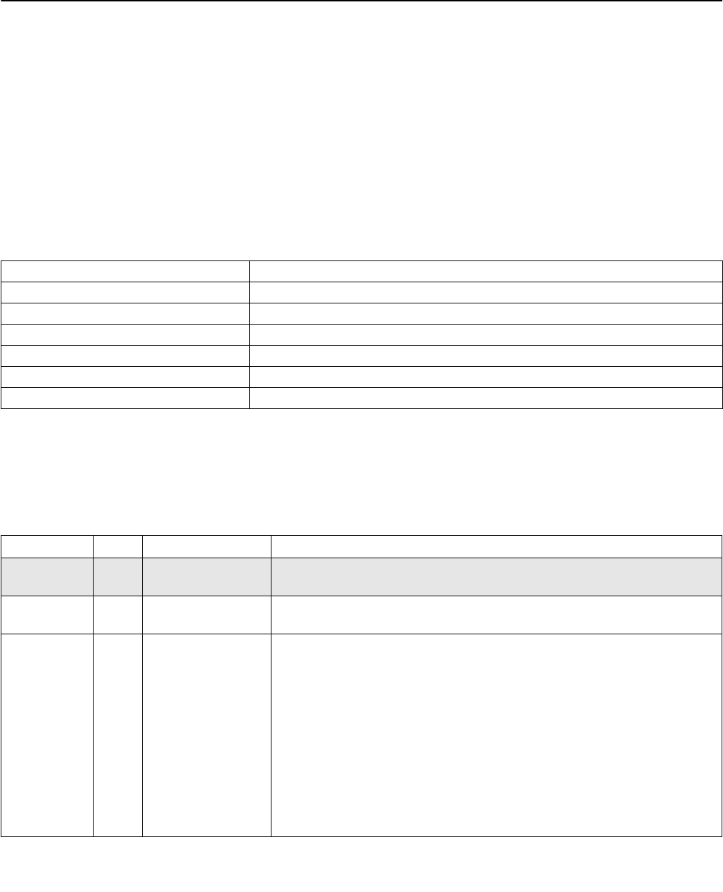
Vol. 3B 16-1
CHAPTER 16
INTERPRETING MACHINE-CHECK
ERROR CODES
Encoding of the model-specific and other information fields is different across processor families. The differences
are documented in the following sections.
16.1 INCREMENTAL DECODING INFORMATION: PROCESSOR FAMILY 06H
MACHINE ERROR CODES FOR MACHINE CHECK
Section 16.1 provides information for interpreting additional model-specific fields for external bus errors relating to
processor family 06H. The references to processor family 06H refers to only IA-32 processors with CPUID signa-
tures listed in Table 16-1.
These errors are reported in the IA32_MCi_STATUS MSRs. They are reported architecturally as compound errors
with a general form of 0000 1PPT RRRR IILL in the MCA error code field. See Chapter 15 for information on the
interpretation of compound error codes. Incremental decoding information is listed in Table 16-2.
Table 16-1. CPUID DisplayFamily_DisplayModel Signatures for Processor Family 06H
DisplayFamily_DisplayModel Processor Families/Processor Number Series
06_0EH Intel Core Duo, Intel Core Solo processors
06_0DH Intel Pentium M processor
06_09H Intel Pentium M processor
06_7H, 06_08H, 06_0AH, 06_0BH Intel Pentium III Xeon Processor, Intel Pentium III Processor
06_03H, 06_05H Intel Pentium II Xeon Processor, Intel Pentium II Processor
06_01H Intel Pentium Pro Processor
Table 16-2. Incremental Decoding Information: Processor Family 06H Machine Error Codes For Machine Check
Type Bit No. Bit Function Bit Description
MCA error
codes1
15:0
Model specific
errors
18:16 Reserved Reserved
Model specific
errors
24:19 Bus queue request
type
000000 for BQ_DCU_READ_TYPE error
000010 for BQ_IFU_DEMAND_TYPE error
000011 for BQ_IFU_DEMAND_NC_TYPE error
000100 for BQ_DCU_RFO_TYPE error
000101 for BQ_DCU_RFO_LOCK_TYPE error
000110 for BQ_DCU_ITOM_TYPE error
001000 for BQ_DCU_WB_TYPE error
001010 for BQ_DCU_WCEVICT_TYPE error
001011 for BQ_DCU_WCLINE_TYPE error
001100 for BQ_DCU_BTM_TYPE error

16-2 Vol. 3B
INTERPRETING MACHINE-CHECK ERROR CODES
001101 for BQ_DCU_INTACK_TYPE error
001110 for BQ_DCU_INVALL2_TYPE error
001111 for BQ_DCU_FLUSHL2_TYPE error
010000 for BQ_DCU_PART_RD_TYPE error
010010 for BQ_DCU_PART_WR_TYPE error
010100 for BQ_DCU_SPEC_CYC_TYPE error
011000 for BQ_DCU_IO_RD_TYPE error
011001 for BQ_DCU_IO_WR_TYPE error
011100 for BQ_DCU_LOCK_RD_TYPE error
011110 for BQ_DCU_SPLOCK_RD_TYPE error
011101 for BQ_DCU_LOCK_WR_TYPE error
Model specific
errors
27:25 Bus queue error type 000 for BQ_ERR_HARD_TYPE error
001 for BQ_ERR_DOUBLE_TYPE error
010 for BQ_ERR_AERR2_TYPE error
100 for BQ_ERR_SINGLE_TYPE error
101 for BQ_ERR_AERR1_TYPE error
Model specific
errors
28 FRC error 1 if FRC error active
29 BERR 1 if BERR is driven
30 Internal BINIT 1 if BINIT driven for this processor
31 Reserved Reserved
Other
information
34:32 Reserved Reserved
35 External BINIT 1 if BINIT is received from external bus.
36 Response parity error This bit is asserted in IA32_MCi_STATUS if this component has received a parity
error on the RS[2:0]# pins for a response transaction. The RS signals are checked
by the RSP# external pin.
37 Bus BINIT This bit is asserted in IA32_MCi_STATUS if this component has received a hard
error response on a split transaction one access that has needed to be split across
the 64-bit external bus interface into two accesses).
38 Timeout BINIT This bit is asserted in IA32_MCi_STATUS if this component has experienced a ROB
time-out, which indicates that no micro-instruction has been retired for a
predetermined period of time.
A ROB time-out occurs when the 15-bit ROB time-out counter carries a 1 out of its
high order bit. 2 The timer is cleared when a micro-instruction retires, an exception
is detected by the core processor, RESET is asserted, or when a ROB BINIT occurs.
The ROB time-out counter is prescaled by the 8-bit PIC timer which is a divide by
128 of the bus clock the bus clock is 1:2, 1:3, 1:4 of the core clock). When a carry
out of the 8-bit PIC timer occurs, the ROB counter counts up by one. While this bit
is asserted, it cannot be overwritten by another error.
41:39 Reserved Reserved
42 Hard error This bit is asserted in IA32_MCi_STATUS if this component has initiated a bus
transactions which has received a hard error response. While this bit is asserted, it
cannot be overwritten.
Table 16-2. Incremental Decoding Information: Processor Family 06H Machine Error Codes For Machine Check
Type Bit No. Bit Function Bit Description

Vol. 3B 16-3
INTERPRETING MACHINE-CHECK ERROR CODES
16.2 INCREMENTAL DECODING INFORMATION: INTEL CORE 2 PROCESSOR
FAMILY MACHINE ERROR CODES FOR MACHINE CHECK
Table 16-4 provides information for interpreting additional model-specific fields for external bus errors relating to
processor based on Intel Core microarchitecture, which implements the P4 bus specification. Table 16-3 lists the
CPUID signatures for Intel 64 processors that are covered by Table 16-4. These errors are reported in the
IA32_MCi_STATUS MSRs. They are reported architecturally as compound errors with a general form of
0000 1PPT RRRR IILL in the MCA error code field. See Chapter 15 for information on the interpretation of
compound error codes.
43 IERR This bit is asserted in IA32_MCi_STATUS if this component has experienced a
failure that causes the IERR pin to be asserted. While this bit is asserted, it cannot
be overwritten.
44 AERR This bit is asserted in IA32_MCi_STATUS if this component has initiated 2 failing
bus transactions which have failed due to Address Parity Errors AERR asserted).
While this bit is asserted, it cannot be overwritten.
45 UECC The Uncorrectable ECC error bit is asserted in IA32_MCi_STATUS for uncorrected
ECC errors. While this bit is asserted, the ECC syndrome field will not be
overwritten.
46 CECC The correctable ECC error bit is asserted in IA32_MCi_STATUS for corrected ECC
errors.
54:47 ECC syndrome The ECC syndrome field in IA32_MCi_STATUS contains the 8-bit ECC syndrome only
if the error was a correctable/uncorrectable ECC error and there wasn't a previous
valid ECC error syndrome logged in IA32_MCi_STATUS.
A previous valid ECC error in IA32_MCi_STATUS is indicated by
IA32_MCi_STATUS.bit45 uncorrectable error occurred) being asserted. After
processing an ECC error, machine-check handling software should clear
IA32_MCi_STATUS.bit45 so that future ECC error syndromes can be logged.
56:55 Reserved Reserved.
Status register
validity
indicators1
63:57
NOTES:
1. These fields are architecturally defined. Refer to Chapter 15, “Machine-Check Architecture,” for more information.
2. For processors with a CPUID signature of 06_0EH, a ROB time-out occurs when the 23-bit ROB time-out counter carries a 1 out of its
high order bit.
Table 16-3. CPUID DisplayFamily_DisplayModel Signatures for Processors Based on Intel Core Microarchitecture
DisplayFamily_DisplayModel Processor Families/Processor Number Series
06_1DH Intel Xeon Processor 7400 series.
06_17H Intel Xeon Processor 5200, 5400 series, Intel Core 2 Quad processor Q9650.
06_0FH Intel Xeon Processor 3000, 3200, 5100, 5300, 7300 series, Intel Core 2 Quad, Intel Core 2 Extreme,
Intel Core 2 Duo processors, Intel Pentium dual-core processors.
Table 16-2. Incremental Decoding Information: Processor Family 06H Machine Error Codes For Machine Check
Type Bit No. Bit Function Bit Description

16-4 Vol. 3B
INTERPRETING MACHINE-CHECK ERROR CODES
Table 16-4. Incremental Bus Error Codes of Machine Check for Processors
Based on Intel Core Microarchitecture
Type Bit No. Bit Function Bit Description
MCA error
codes1
15:0
Model specific
errors
18:16 Reserved Reserved
Model specific
errors
24:19 Bus queue request
type
‘000001 for BQ_PREF_READ_TYPE error
000000 for BQ_DCU_READ_TYPE error
000010 for BQ_IFU_DEMAND_TYPE error
000011 for BQ_IFU_DEMAND_NC_TYPE error
000100 for BQ_DCU_RFO_TYPE error
000101 for BQ_DCU_RFO_LOCK_TYPE error
000110 for BQ_DCU_ITOM_TYPE error
001000 for BQ_DCU_WB_TYPE error
001010 for BQ_DCU_WCEVICT_TYPE error
001011 for BQ_DCU_WCLINE_TYPE error
001100 for BQ_DCU_BTM_TYPE error
001101 for BQ_DCU_INTACK_TYPE error
001110 for BQ_DCU_INVALL2_TYPE error
001111 for BQ_DCU_FLUSHL2_TYPE error
010000 for BQ_DCU_PART_RD_TYPE error
010010 for BQ_DCU_PART_WR_TYPE error
010100 for BQ_DCU_SPEC_CYC_TYPE error
011000 for BQ_DCU_IO_RD_TYPE error
011001 for BQ_DCU_IO_WR_TYPE error
011100 for BQ_DCU_LOCK_RD_TYPE error
011110 for BQ_DCU_SPLOCK_RD_TYPE error
011101 for BQ_DCU_LOCK_WR_TYPE error
100100 for BQ_L2_WI_RFO_TYPE error
100110 for BQ_L2_WI_ITOM_TYPE error
Model specific
errors
27:25 Bus queue error type ‘001 for Address Parity Error
‘010 for Response Hard Error
‘011 for Response Parity Error
Model specific
errors
28 MCE Driven 1 if MCE is driven
29 MCE Observed 1 if MCE is observed
30 Internal BINIT 1 if BINIT driven for this processor
31 BINIT Observed 1 if BINIT is observed for this processor
Other
information
33:32 Reserved Reserved
34 PIC and FSB data
parity
Data Parity detected on either PIC or FSB access
35 Reserved Reserved

Vol. 3B 16-5
INTERPRETING MACHINE-CHECK ERROR CODES
16.2.1 Model-Specific Machine Check Error Codes for Intel Xeon Processor 7400 Series
Intel Xeon processor 7400 series has machine check register banks that generally follows the description of
Chapter 15 and Section 16.2. Additional error codes specific to Intel Xeon processor 7400 series is describe in this
section.
MC4_STATUS[63:0] is the main error logging for the processor’s L3 and front side bus errors for Intel Xeon
processor 7400 series. It supports the L3 Errors, Bus and Interconnect Errors Compound Error Codes in the MCA
Error Code Field.
36 Response parity error This bit is asserted in IA32_MCi_STATUS if this component has received a parity
error on the RS[2:0]# pins for a response transaction. The RS signals are checked
by the RSP# external pin.
37 FSB address parity Address parity error detected:
1 = Address parity error detected
0 = No address parity error
38 Timeout BINIT This bit is asserted in IA32_MCi_STATUS if this component has experienced a ROB
time-out, which indicates that no micro-instruction has been retired for a
predetermined period of time.
A ROB time-out occurs when the 23-bit ROB time-out counter carries a 1 out of its
high order bit. The timer is cleared when a micro-instruction retires, an exception is
detected by the core processor, RESET is asserted, or when a ROB BINIT occurs.
The ROB time-out counter is prescaled by the 8-bit PIC timer which is a divide by
128 of the bus clock the bus clock is 1:2, 1:3, 1:4 of the core clock). When a carry
out of the 8-bit PIC timer occurs, the ROB counter counts up by one. While this bit
is asserted, it cannot be overwritten by another error.
41:39 Reserved Reserved
42 Hard error This bit is asserted in IA32_MCi_STATUS if this component has initiated a bus
transactions which has received a hard error response. While this bit is asserted, it
cannot be overwritten.
43 IERR This bit is asserted in IA32_MCi_STATUS if this component has experienced a
failure that causes the IERR pin to be asserted. While this bit is asserted, it cannot
be overwritten.
44 Reserved Reserved
45 Reserved Reserved
46 Reserved Reserved
54:47 Reserved Reserved
56:55 Reserved Reserved.
Status register
validity
indicators1
63:57
NOTES:
1. These fields are architecturally defined. Refer to Chapter 15, “Machine-Check Architecture,” for more information.
Table 16-4. Incremental Bus Error Codes of Machine Check for Processors
Based on Intel Core Microarchitecture (Contd.)
Type Bit No. Bit Function Bit Description

16-6 Vol. 3B
INTERPRETING MACHINE-CHECK ERROR CODES
16.2.1.1 Processor Machine Check Status Register
Incremental MCA Error Code Definition
Intel Xeon processor 7400 series use compound MCA Error Codes for logging its Bus internal machine check
errors, L3 Errors, and Bus/Interconnect Errors. It defines incremental Machine Check error types
(IA32_MC6_STATUS[15:0]) beyond those defined in Chapter 15. Table 16-5 lists these incremental MCA error
code types that apply to IA32_MC6_STATUS. Error code details are specified in MC6_STATUS [31:16] (see
Section 16.2.2), the “Model Specific Error Code” field. The information in the “Other_Info” field
(MC4_STATUS[56:32]) is common to the three processor error types and contains a correctable event count and
specifies the MC6_MISC register format.
The Bold faced binary encodings are the only encodings used by the processor for MC4_STATUS[15:0].
16.2.2 Intel Xeon Processor 7400 Model Specific Error Code Field
16.2.2.1 Processor Model Specific Error Code Field
Type B: Bus and Interconnect Error
Note: The Model Specific Error Code field in MC6_STATUS (bits 31:16).
Table 16-5. Incremental MCA Error Code Types for Intel Xeon Processor 7400
Processor MCA_Error_Code (MC6_STATUS[15:0])
Type Error Code Binary Encoding Meaning
C Internal Error 0000 0100 0000 0000 Internal Error Type Code
BBus and
Interconnect
Error
0000 100x 0000 1111 Not used but this encoding is reserved for compatibility with other MCA
implementations
0000 101x 0000 1111 Not used but this encoding is reserved for compatibility with other MCA
implementations
0000 110x 0000 1111 Not used but this encoding is reserved for compatibility with other MCA
implementations
0000 1110 0000 1111 Bus and Interconnection Error Type Code
0000 1111 0000 1111 Not used but this encoding is reserved for compatibility with other MCA
implementations
Table 16-6. Type B Bus and Interconnect Error Codes
Bit Num Sub-Field Name Description
16 FSB Request Parity Parity error detected during FSB request phase
19:17 Reserved
20 FSB Hard Fail Response “Hard Failure“ response received for a local transaction
21 FSB Response Parity Parity error on FSB response field detected
22 FSB Data Parity FSB data parity error on inbound data detected
31:23 --- Reserved

Vol. 3B 16-7
INTERPRETING MACHINE-CHECK ERROR CODES
16.2.2.2 Processor Model Specific Error Code Field
Type C: Cache Bus Controller Error
16.3 INCREMENTAL DECODING INFORMATION: PROCESSOR FAMILY WITH
CPUID DISPLAYFAMILY_DISPLAYMODEL SIGNATURE 06_1AH, MACHINE
ERROR CODES FOR MACHINE CHECK
Table 16-8 through Table 16-12 provide information for interpreting additional model-specific fields for memory
controller errors relating to the processor family with CPUID DisplayFamily_DisplaySignature 06_1AH, which
supports Intel QuickPath Interconnect links. Incremental MC error codes related to the Intel QPI links are reported
in the register banks IA32_MC0 and IA32_MC1, incremental error codes for internal machine check is reported in
the register bank IA32_MC7, and incremental error codes for the memory controller unit is reported in the register
banks IA32_MC8.
Table 16-7. Type C Cache Bus Controller Error Codes
MC4_STATUS[31:16] (MSCE) Value Error Description
0000_0000_0000_0001 0001H Inclusion Error from Core 0
0000_0000_0000_0010 0002H Inclusion Error from Core 1
0000_0000_0000_0011 0003H Write Exclusive Error from Core 0
0000_0000_0000_0100 0004H Write Exclusive Error from Core 1
0000_0000_0000_0101 0005H Inclusion Error from FSB
0000_0000_0000_0110 0006H SNP Stall Error from FSB
0000_0000_0000_0111 0007H Write Stall Error from FSB
0000_0000_0000_1000 0008H FSB Arb Timeout Error
0000_0000_0000_1010 000AH Inclusion Error from Core 2
0000_0000_0000_1011 000BH Write Exclusive Error from Core 2
0000_0010_0000_0000 0200H Internal Timeout error
0000_0011_0000_0000 0300H Internal Timeout Error
0000_0100_0000_0000 0400H Intel® Cache Safe Technology Queue Full Error or Disabled-ways-in-a-set overflow
0000_0101_0000_0000 0500H Quiet cycle Timeout Error (correctable)
1100_0000_0000_0010 C002H Correctable ECC event on outgoing Core 0 data
1100_0000_0000_0100 C004H Correctable ECC event on outgoing Core 1 data
1100_0000_0000_1000 C008H Correctable ECC event on outgoing Core 2 data
1110_0000_0000_0010 E002H Uncorrectable ECC error on outgoing Core 0 data
1110_0000_0000_0100 E004H Uncorrectable ECC error on outgoing Core 1 data
1110_0000_0000_1000 E008H Uncorrectable ECC error on outgoing Core 2 data
— all other encodings — Reserved

16-8 Vol. 3B
INTERPRETING MACHINE-CHECK ERROR CODES
16.3.1 Intel QPI Machine Check Errors
Table 16-8. Intel QPI Machine Check Error Codes for IA32_MC0_STATUS and IA32_MC1_STATUS
Table 16-9. Intel QPI Machine Check Error Codes for IA32_MC0_MISC and IA32_MC1_MISC
16.3.2 Internal Machine Check Errors
Table 16-10. Machine Check Error Codes for IA32_MC7_STATUS
Type Bit No. Bit Function Bit Description
MCA error codes1
NOTES:
1. These fields are architecturally defined. Refer to Chapter 15, “Machine-Check Architecture,” for more information.
15:0 MCACOD Bus error format: 1PPTRRRRIILL
Model specific errors
16 Header Parity if 1, QPI Header had bad parity
17 Data Parity If 1, QPI Data packet had bad parity
18 Retries Exceeded If 1, number of QPI retries was exceeded
19 Received Poison if 1, Received a data packet that was marked as poisoned by the sender
21:20 Reserved Reserved
22 Unsupported Message If 1, QPI received a message encoding it does not support
23 Unsupported Credit If 1, QPI credit type is not supported.
24 Receive Flit Overrun If 1, Sender sent too many QPI flits to the receiver.
25 Received Failed
Response
If 1, Indicates that sender sent a failed response to receiver.
26 Receiver Clock Jitter If 1, clock jitter detected in the internal QPI clocking
56:27 Reserved Reserved
Status register
validity indicators1
63:57
Type Bit No. Bit Function Bit Description
Model specific errors1
NOTES:
1. Which of these fields are valid depends on the error type.
7:0 QPI Opcode Message class and opcode from the packet with the error
13:8 RTId QPI Request Transaction ID
15:14 Reserved Reserved
18:16 RHNID QPI Requestor/Home Node ID
23:19 Reserved Reserved
24 IIB QPI Interleave/Head Indication Bit
Type Bit No. Bit Function Bit Description
MCA error codes1 15:0 MCACOD
Model specific errors

Vol. 3B 16-9
INTERPRETING MACHINE-CHECK ERROR CODES
16.3.3 Memory Controller Errors
23:16 Reserved Reserved
31:24 Reserved except for
the following
00h - No Error
03h - Reset firmware did not complete
08h - Received an invalid CMPD
0Ah - Invalid Power Management Request
0Dh - Invalid S-state transition
11h - VID controller does not match POC controller selected
1Ah - MSID from POC does not match CPU MSID
56:32 Reserved Reserved
Status register validity
indicators1
63:57
NOTES:
1. These fields are architecturally defined. Refer to Chapter 15, “Machine-Check Architecture,” for more information.
Table 16-11. Incremental Memory Controller Error Codes of Machine Check for IA32_MC8_STATUS
Type Bit No. Bit Function Bit Description
MCA error codes1
NOTES:
1. These fields are architecturally defined. Refer to Chapter 15, “Machine-Check Architecture,” for more information.
15:0 MCACOD Memory error format: 1MMMCCCC
Model specific errors
16 Read ECC error if 1, ECC occurred on a read
17 RAS ECC error If 1, ECC occurred on a scrub
18 Write parity error If 1, bad parity on a write
19 Redundancy loss if 1, Error in half of redundant memory
20 Reserved Reserved
21 Memory range error If 1, Memory access out of range
22 RTID out of range If 1, Internal ID invalid
23 Address parity error If 1, bad address parity
24 Byte enable parity
error
If 1, bad enable parity
Other information 37:25 Reserved Reserved
52:38 CORE_ERR_CNT Corrected error count
56:53 Reserved Reserved
Status register validity
indicators1
63:57
Type Bit No. Bit Function Bit Description

16-10 Vol. 3B
INTERPRETING MACHINE-CHECK ERROR CODES
Table 16-12. Incremental Memory Controller Error Codes of Machine Check for IA32_MC8_MISC
16.4 INCREMENTAL DECODING INFORMATION: PROCESSOR FAMILY WITH CPUID
DISPLAYFAMILY_DISPLAYMODEL SIGNATURE 06_2DH, MACHINE ERROR
CODES FOR MACHINE CHECK
Table 16-13 through Table 16-15 provide information for interpreting additional model-specific fields for memory
controller errors relating to the processor family with CPUID DisplayFamily_DisplaySignature 06_2DH, which
supports Intel QuickPath Interconnect links. Incremental MC error codes related to the Intel QPI links are reported
in the register banks IA32_MC6 and IA32_MC7, incremental error codes for internal machine check error from PCU
controller is reported in the register bank IA32_MC4, and incremental error codes for the memory controller unit is
reported in the register banks IA32_MC8-IA32_MC11.
16.4.1 Internal Machine Check Errors
Table 16-13. Machine Check Error Codes for IA32_MC4_STATUS
Type Bit No. Bit Function Bit Description
Model specific errors1
NOTES:
1. Which of these fields are valid depends on the error type.
7:0 RTId Transaction Tracker ID
15:8 Reserved Reserved
17:16 DIMM DIMM ID which got the error
19:18 Channel Channel ID which got the error
31:20 Reserved Reserved
63:32 Syndrome ECC Syndrome
Type Bit No. Bit Function Bit Description
MCA error
codes1
15:0 MCACOD
Model specific
errors
19:16 Reserved except for
the following
0000b - No Error
0001b - Non_IMem_Sel
0010b - I_Parity_Error
0011b - Bad_OpCode
0100b - I_Stack_Underflow
0101b - I_Stack_Overflow
0110b - D_Stack_Underflow
0111b - D_Stack_Overflow
1000b - Non-DMem_Sel
1001b - D_Parity_Error

Vol. 3B 16-11
INTERPRETING MACHINE-CHECK ERROR CODES
16.4.2 Intel QPI Machine Check Errors
Table 16-14. Intel QPI MC Error Codes for IA32_MC6_STATUS and IA32_MC7_STATUS
16.4.3 Integrated Memory Controller Machine Check Errors
MC error codes associated with integrated memory controllers are reported in the MSRs IA32_MC8_STATUS-
IA32_MC11_STATUS. The supported error codes are follows the architectural MCACOD definition type 1MMMCCCC
(see Chapter 15, “Machine-Check Architecture,”). MSR_ERROR_CONTROL.[bit 1] can enable additional informa-
23:20 Reserved Reserved
31:24 Reserved except for
the following
00h - No Error
0Dh - MC_IMC_FORCE_SR_S3_TIMEOUT
0Eh - MC_CPD_UNCPD_ST_TIMEOUT
0Fh - MC_PKGS_SAFE_WP_TIMEOUT
43h - MC_PECI_MAILBOX_QUIESCE_TIMEOUT
5Ch - MC_MORE_THAN_ONE_LT_AGENT
60h - MC_INVALID_PKGS_REQ_PCH
61h - MC_INVALID_PKGS_REQ_QPI
62h - MC_INVALID_PKGS_RES_QPI
63h - MC_INVALID_PKGC_RES_PCH
64h - MC_INVALID_PKG_STATE_CONFIG
70h - MC_WATCHDG_TIMEOUT_PKGC_SLAVE
71h - MC_WATCHDG_TIMEOUT_PKGC_MASTER
72h - MC_WATCHDG_TIMEOUT_PKGS_MASTER
7ah - MC_HA_FAILSTS_CHANGE_DETECTED
81h - MC_RECOVERABLE_DIE_THERMAL_TOO_HOT
56:32 Reserved Reserved
Status register
validity
indicators1
63:57
NOTES:
1. These fields are architecturally defined. Refer to Chapter 15, “Machine-Check Architecture,” for more information.
Type Bit No. Bit Function Bit Description
MCA error
codes1
NOTES:
1. These fields are architecturally defined. Refer to Chapter 15, “Machine-Check Architecture,” for more information.
15:0 MCACOD Bus error format: 1PPTRRRRIILL
Model specific
errors
56:16 Reserved Reserved
Status register
validity
indicators1
63:57
Type Bit No. Bit Function Bit Description

16-12 Vol. 3B
INTERPRETING MACHINE-CHECK ERROR CODES
tion logging of the IMC. The additional error information logged by the IMC is stored in IA32_MCi_STATUS and
IA32_MCi_MISC; (i = 8, 11).
Table 16-15. Intel IMC MC Error Codes for IA32_MCi_STATUS (i= 8, 11)
Table 16-16. Intel IMC MC Error Codes for IA32_MCi_MISC (i= 8, 11)
Type Bit No. Bit Function Bit Description
MCA error codes1
NOTES:
1. These fields are architecturally defined. Refer to Chapter 15, “Machine-Check Architecture,” for more information.
15:0 MCACOD Bus error format: 1PPTRRRRIILL
Model specific
errors
31:16 Reserved except for
the following
001H - Address parity error
002H - HA Wrt buffer Data parity error
004H - HA Wrt byte enable parity error
008H - Corrected patrol scrub error
010H - Uncorrected patrol scrub error
020H - Corrected spare error
040H - Uncorrected spare error
Model specific
errors
36:32 Other info When MSR_ERROR_CONTROL.[1] is set, allows the iMC to log first device
error when corrected error is detected during normal read.
37 Reserved Reserved
56:38 See Chapter 15, “Machine-Check Architecture,”
Status register
validity indicators1
63:57
Type Bit No. Bit Function Bit Description
MCA addr info1
NOTES:
1. These fields are architecturally defined. Refer to Chapter 15, “Machine-Check Architecture,” for more information.
8:0 See Chapter 15, “Machine-Check Architecture,”
Model specific
errors
13:9 • When MSR_ERROR_CONTROL.[1] is set, allows the iMC to log second device
error when corrected error is detected during normal read.
• Otherwise contain parity error if MCi_Status indicates HA_WB_Data or
HA_W_BE parity error.
Model specific
errors
29:14 ErrMask_1stErrDev When MSR_ERROR_CONTROL.[1] is set, allows the iMC to log first-device error bit
mask.
Model specific
errors
45:30 ErrMask_2ndErrDev When MSR_ERROR_CONTROL.[1] is set, allows the iMC to log second-device error
bit mask.
50:46 FailRank_1stErrDev When MSR_ERROR_CONTROL.[1] is set, allows the iMC to log first-device error
failing rank.
55:51 FailRank_2ndErrDev When MSR_ERROR_CONTROL.[1] is set, allows the iMC to log second-device error
failing rank.
58:56 Reserved Reserved
61:59 Reserved Reserved
62 Valid_1stErrDev When MSR_ERROR_CONTROL.[1] is set, indicates the iMC has logged valid data
from the first correctable error in a memory device.
63 Valid_2ndErrDev When MSR_ERROR_CONTROL.[1] is set, indicates the iMC has logged valid data due
to a second correctable error in a memory device. Use this information only after
there is valid first error info indicated by bit 62.

Vol. 3B 16-13
INTERPRETING MACHINE-CHECK ERROR CODES
16.5 INCREMENTAL DECODING INFORMATION: PROCESSOR FAMILY WITH
CPUID DISPLAYFAMILY_DISPLAYMODEL SIGNATURE 06_3EH, MACHINE
ERROR CODES FOR MACHINE CHECK
Intel Xeon processor E5 v2 family and Intel Xeon processor E7 v2 family are based on the Ivy Bridge-EP microar-
chitecture and can be identified with CPUID DisplayFamily_DisplaySignature 06_3EH. Incremental error codes for
internal machine check error from PCU controller is reported in the register bank IA32_MC4, Table lists model-
specific fields to interpret error codes applicable to IA32_MC4_STATUS. Incremental MC error codes related to the
Intel QPI links are reported in the register banks IA32_MC5. Information listed in Table 16-14 for QPI MC error code
apply to IA32_MC5_STATUS. Incremental error codes for the memory controller unit is reported in the register
banks IA32_MC9-IA32_MC16. Table 16-18 lists model-specific error codes apply to IA32_MCi_STATUS, i = 9-16.
16.5.1 Internal Machine Check Errors
Table 16-17. Machine Check Error Codes for IA32_MC4_STATUS
Type Bit No. Bit Function Bit Description
MCA error codes1 15:0 MCACOD
Model specific errors 19:16 Reserved except for
the following
0000b - No Error
0001b - Non_IMem_Sel
0010b - I_Parity_Error
0011b - Bad_OpCode
0100b - I_Stack_Underflow
0101b - I_Stack_Overflow
0110b - D_Stack_Underflow
0111b - D_Stack_Overflow
1000b - Non-DMem_Sel
1001b - D_Parity_Error
23:20 Reserved Reserved
31:24 Reserved except for
the following
00h - No Error
0Dh - MC_IMC_FORCE_SR_S3_TIMEOUT
0Eh - MC_CPD_UNCPD_ST_TIMEOUT
0Fh - MC_PKGS_SAFE_WP_TIMEOUT
43h - MC_PECI_MAILBOX_QUIESCE_TIMEOUT
44h - MC_CRITICAL_VR_FAILED
45h - MC_ICC_MAX-NOTSUPPORTED
5Ch - MC_MORE_THAN_ONE_LT_AGENT
60h - MC_INVALID_PKGS_REQ_PCH
61h - MC_INVALID_PKGS_REQ_QPI
62h - MC_INVALID_PKGS_RES_QPI
63h - MC_INVALID_PKGC_RES_PCH
64h - MC_INVALID_PKG_STATE_CONFIG
70h - MC_WATCHDG_TIMEOUT_PKGC_SLAVE
71h - MC_WATCHDG_TIMEOUT_PKGC_MASTER
72h - MC_WATCHDG_TIMEOUT_PKGS_MASTER

16-14 Vol. 3B
INTERPRETING MACHINE-CHECK ERROR CODES
16.5.2 Integrated Memory Controller Machine Check Errors
MC error codes associated with integrated memory controllers are reported in the MSRs IA32_MC9_STATUS-
IA32_MC16_STATUS. The supported error codes are follows the architectural MCACOD definition type 1MMMCCCC
(see Chapter 15, “Machine-Check Architecture,”).
MSR_ERROR_CONTROL.[bit 1] can enable additional information logging of the IMC. The additional error informa-
tion logged by the IMC is stored in IA32_MCi_STATUS and IA32_MCi_MISC; (i = 9-16).
Table 16-18. Intel IMC MC Error Codes for IA32_MCi_STATUS (i= 9-16)
7Ah - MC_HA_FAILSTS_CHANGE_DETECTED
7Bh - MC_PCIE_R2PCIE-RW_BLOCK_ACK_TIMEOUT
81h - MC_RECOVERABLE_DIE_THERMAL_TOO_HOT
56:32 Reserved Reserved
Status register
validity indicators1
63:57
NOTES:
1. These fields are architecturally defined. Refer to Chapter 15, “Machine-Check Architecture,” for more information.
Type Bit No. Bit Function Bit Description
MCA error codes1
NOTES:
1. These fields are architecturally defined. Refer to Chapter 15, “Machine-Check Architecture,” for more information.
15:0 MCACOD Memory Controller error format: 000F 0000 1MMM CCCC
Model specific
errors
31:16 Reserved except for
the following
001H - Address parity error
002H - HA Wrt buffer Data parity error
004H - HA Wrt byte enable parity error
008H - Corrected patrol scrub error
010H - Uncorrected patrol scrub error
020H - Corrected spare error
040H - Uncorrected spare error
080H - Corrected memory read error. (Only applicable with iMC’s “Additional
Error logging” Mode-1 enabled.)
100H - iMC, WDB, parity errors
36:32 Other info When MSR_ERROR_CONTROL.[1] is set, logs an encoded value from the first error
device.
37 Reserved Reserved
56:38 See Chapter 15, “Machine-Check Architecture,”
Status register
validity indicators1
63:57
Type Bit No. Bit Function Bit Description

Vol. 3B 16-15
INTERPRETING MACHINE-CHECK ERROR CODES
Table 16-19. Intel IMC MC Error Codes for IA32_MCi_MISC (i= 9-16)
16.6 INCREMENTAL DECODING INFORMATION: PROCESSOR FAMILY WITH
CPUID DISPLAYFAMILY_DISPLAYMODEL SIGNATURE 06_3FH, MACHINE
ERROR CODES FOR MACHINE CHECK
Intel Xeon processor E5 v3 family is based on the Haswell-E microarchitecture and can be identified with CPUID
DisplayFamily_DisplaySignature 06_3FH. Incremental error codes for internal machine check error from PCU
controller is reported in the register bank IA32_MC4, Table 16-20 lists model-specific fields to interpret error codes
applicable to IA32_MC4_STATUS. Incremental MC error codes related to the Intel QPI links are reported in the
register banks IA32_MC5, IA32_MC20, and IA32_MC21. Information listed in Table 16-21 for QPI MC error codes.
Incremental error codes for the memory controller unit is reported in the register banks IA32_MC9-IA32_MC16.
Table 16-22 lists model-specific error codes apply to IA32_MCi_STATUS, i = 9-16.
Type Bit No. Bit Function Bit Description
MCA addr info1
NOTES:
1. These fields are architecturally defined. Refer to Chapter 15, “Machine-Check Architecture,” for more information.
8:0 See Chapter 15, “Machine-Check Architecture,”
Model specific
errors
13:9 If the error logged is MCWrDataPar error or MCWrBEPar error, this field is the WDB
ID that has the parity error. OR if the second error logged is a correctable read
error, MC logs the second error device in this field.
Model specific
errors
29:14 ErrMask_1stErrDev When MSR_ERROR_CONTROL.[1] is set, allows the iMC to log first-device error bit
mask.
Model specific
errors
45:30 ErrMask_2ndErrDev When MSR_ERROR_CONTROL.[1] is set, allows the iMC to log second-device error
bit mask.
50:46 FailRank_1stErrDev When MSR_ERROR_CONTROL.[1] is set, allows the iMC to log first-device error
failing rank.
55:51 FailRank_2ndErrDev When MSR_ERROR_CONTROL.[1] is set, allows the iMC to log second-device error
failing rank.
61:56 Reserved
62 Valid_1stErrDev When MSR_ERROR_CONTROL.[1] is set, indicates the iMC has logged valid data
from a correctable error from memory read associated with first error device.
63 Valid_2ndErrDev When MSR_ERROR_CONTROL.[1] is set, indicates the iMC has logged valid data due
to a second correctable error in a memory device. Use this information only after
there is valid first error info indicated by bit 62.

16-16 Vol. 3B
INTERPRETING MACHINE-CHECK ERROR CODES
16.6.1 Internal Machine Check Errors
Table 16-20. Machine Check Error Codes for IA32_MC4_STATUS
Type Bit No. Bit Function Bit Description
MCA error codes1
NOTES:
1. These fields are architecturally defined. Refer to Chapter 15, “Machine-Check Architecture,” for more information.
15:0 MCACOD
MCACOD215:0 Internal Errors 0402h - PCU internal Errors
0403h - PCU internal Errors
0406h - Intel TXT Errors
0407h - Other UBOX internal Errors.
On an IERR caused by a core 3-strike the IA32_MC3_STATUS (MLC) is copied
to the IA32_MC4_STATUS (After a 3-strike, the core MCA banks will be
unavailable).
Model specific errors 19:16 Reserved except for
the following
0000b - No Error
00xxb - PCU internal error
23:20 Reserved Reserved
31:24 Reserved except for
the following
00h - No Error
09h - MC_MESSAGE_CHANNEL_TIMEOUT
13h - MC_DMI_TRAINING_TIMEOUT
15h - MC_DMI_CPU_RESET_ACK_TIMEOUT
1Eh - MC_VR_ICC_MAX_LT_FUSED_ICC_MAX
25h - MC_SVID_COMMAND_TIMEOUT
29h - MC_VR_VOUT_MAC_LT_FUSED_SVID
2Bh - MC_PKGC_WATCHDOG_HANG_CBZ_DOWN
2Ch - MC_PKGC_WATCHDOG_HANG_CBZ_UP
44h - MC_CRITICAL_VR_FAILED
46h - MC_VID_RAMP_DOWN_FAILED
49h - MC_SVID_WRITE_REG_VOUT_MAX_FAILED
4Bh - MC_BOOT_VID_TIMEOUT. Timeout setting boot VID for DRAM 0.
4Fh - MC_SVID_COMMAND_ERROR.
52h - MC_FIVR_CATAS_OVERVOL_FAULT.
53h - MC_FIVR_CATAS_OVERCUR_FAULT.
57h - MC_SVID_PKGC_REQUEST_FAILED
58h - MC_SVID_IMON_REQUEST_FAILED
59h - MC_SVID_ALERT_REQUEST_FAILED
62h - MC_INVALID_PKGS_RSP_QPI
64h - MC_INVALID_PKG_STATE_CONFIG
67h - MC_HA_IMC_RW_BLOCK_ACK_TIMEOUT
6Ah - MC_MSGCH_PMREQ_CMP_TIMEOUT
72h - MC_WATCHDG_TIMEOUT_PKGS_MASTER
81h - MC_RECOVERABLE_DIE_THERMAL_TOO_HOT
56:32 Reserved Reserved
Status register
validity indicators1
63:57

Vol. 3B 16-17
INTERPRETING MACHINE-CHECK ERROR CODES
16.6.2 Intel QPI Machine Check Errors
MC error codes associated with the Intel QPI agents are reported in the MSRs IA32_MC5_STATUS,
IA32_MC20_STATUS, and IA32_MC21_STATUS. The supported error codes follow the architectural MCACOD defi-
nition type 1PPTRRRRIILL (see Chapter 15, “Machine-Check Architecture,”).
Table 16-21 lists model-specific fields to interpret error codes applicable to IA32_MC5_STATUS,
IA32_MC20_STATUS, and IA32_MC21_STATUS.
Table 16-21. Intel QPI MC Error Codes for IA32_MCi_STATUS (i = 5, 20, 21)
16.6.3 Integrated Memory Controller Machine Check Errors
MC error codes associated with integrated memory controllers are reported in the MSRs IA32_MC9_STATUS-
IA32_MC16_STATUS. The supported error codes follow the architectural MCACOD definition type 1MMMCCCC (see
Chapter 15, “Machine-Check Architecture,”).
MSR_ERROR_CONTROL.[bit 1] can enable additional information logging of the IMC. The additional error informa-
tion logged by the IMC is stored in IA32_MCi_STATUS and IA32_MCi_MISC; (i = 9-16).
2. The internal error codes may be model-specific.
Type Bit No. Bit Function Bit Description
MCA error
codes1
NOTES:
1. These fields are architecturally defined. Refer to Chapter 15, “Machine-Check Architecture,” for more information.
15:0 MCACOD Bus error format: 1PPTRRRRIILL
Model specific
errors
31:16 MSCOD 02h - Intel QPI physical layer detected drift buffer alarm.
03h - Intel QPI physical layer detected latency buffer rollover.
10h - Intel QPI link layer detected control error from R3QPI.
11h - Rx entered LLR abort state on CRC error.
12h - Unsupported or undefined packet.
13h - Intel QPI link layer control error.
15h - RBT used un-initialized value.
20h - Intel QPI physical layer detected a QPI in-band reset but aborted initialization
21h - Link failover data self-healing
22h - Phy detected in-band reset (no width change).
23h - Link failover clock failover
30h -Rx detected CRC error - successful LLR after Phy re-init.
31h -Rx detected CRC error - successful LLR without Phy re-init.
All other values are reserved.
37:32 Reserved Reserved
52:38 Corrected Error Cnt
56:53 Reserved Reserved
Status register
validity
indicators1
63:57

16-18 Vol. 3B
INTERPRETING MACHINE-CHECK ERROR CODES
Table 16-22. Intel IMC MC Error Codes for IA32_MCi_STATUS (i= 9-16)
Table 16-23. Intel IMC MC Error Codes for IA32_MCi_MISC (i= 9-16)
Type Bit No. Bit Function Bit Description
MCA error codes1
NOTES:
1. These fields are architecturally defined. Refer to Chapter 15, “Machine-Check Architecture,” for more information.
15:0 MCACOD Memory Controller error format: 0000 0000 1MMM CCCC
Model specific
errors
31:16 Reserved except for
the following
0001H - DDR3 address parity error
0002H - Uncorrected HA write data error
0004H - Uncorrected HA data byte enable error
0008H - Corrected patrol scrub error
0010H - Uncorrected patrol scrub error
0020H - Corrected spare error
0040H - Uncorrected spare error
0080H - Corrected memory read error. (Only applicable with iMC’s “Additional
Error logging” Mode-1 enabled.)
0100H - iMC, write data buffer parity errors
0200H - DDR4 command address parity error
36:32 Other info When MSR_ERROR_CONTROL.[1] is set, logs an encoded value from the first error
device.
37 Reserved Reserved
56:38 See Chapter 15, “Machine-Check Architecture,”
Status register
validity indicators1
63:57
Type Bit No. Bit Function Bit Description
MCA addr info1 8:0 See Chapter 15, “Machine-Check Architecture,”
Model specific
errors
13:9 If the error logged is MCWrDataPar error or MCWrBEPar error, this field is the WDB
ID that has the parity error. OR if the second error logged is a correctable read
error, MC logs the second error device in this field.
Model specific
errors
29:14 ErrMask_1stErrDev When MSR_ERROR_CONTROL.[1] is set, allows the iMC to log first-device error bit
mask.
Model specific
errors
45:30 ErrMask_2ndErrDev When MSR_ERROR_CONTROL.[1] is set, allows the iMC to log second-device error
bit mask.
50:46 FailRank_1stErrDev When MSR_ERROR_CONTROL.[1] is set, allows the iMC to log first-device error
failing rank.
55:51 FailRank_2ndErrDev When MSR_ERROR_CONTROL.[1] is set, allows the iMC to log second-device error
failing rank.
61:56 Reserved
62 Valid_1stErrDev When MSR_ERROR_CONTROL.[1] is set, indicates the iMC has logged valid data
from a correctable error from memory read associated with first error device.
63 Valid_2ndErrDev When MSR_ERROR_CONTROL.[1] is set, indicates the iMC has logged valid data due
to a second correctable error in a memory device. Use this information only after
there is valid first error info indicated by bit 62.

Vol. 3B 16-19
INTERPRETING MACHINE-CHECK ERROR CODES
16.7 INCREMENTAL DECODING INFORMATION: PROCESSOR FAMILY WITH
CPUID DISPLAYFAMILY_DISPLAYMODEL SIGNATURE 06_56H, MACHINE
ERROR CODES FOR MACHINE CHECK
Intel Xeon processor D family is based on the Broadwell microarchitecture and can be identified with CPUID
DisplayFamily_DisplaySignature 06_56H. Incremental error codes for internal machine check error from PCU
controller is reported in the register bank IA32_MC4, Table 16-24 lists model-specific fields to interpret error codes
applicable to IA32_MC4_STATUS. Incremental error codes for the memory controller unit is reported in the register
banks IA32_MC9-IA32_MC10. Table 16-18 lists model-specific error codes apply to IA32_MCi_STATUS, i = 9-10.
16.7.1 Internal Machine Check Errors
Table 16-24. Machine Check Error Codes for IA32_MC4_STATUS
NOTES:
1. These fields are architecturally defined. Refer to Chapter 15, “Machine-Check Architecture,” for more information.
Type Bit No. Bit Function Bit Description
MCA error codes1 15:0 MCACOD
MCACOD215:0 internal Errors 0402h - PCU internal Errors
0403h - internal Errors
0406h - Intel TXT Errors
0407h - Other UBOX internal Errors.
On an IERR caused by a core 3-strike the IA32_MC3_STATUS (MLC) is copied
to the IA32_MC4_STATUS (After a 3-strike, the core MCA banks will be
unavailable).
Model specific errors 19:16 Reserved except for
the following
0000b - No Error
00x1b - PCU internal error
001xb - PCU internal error
23:20 Reserved except for
the following
x1xxb - UBOX error
31:24 Reserved except for
the following
00h - No Error
09h - MC_MESSAGE_CHANNEL_TIMEOUT
13h - MC_DMI_TRAINING_TIMEOUT
15h - MC_DMI_CPU_RESET_ACK_TIMEOUT
1Eh - MC_VR_ICC_MAX_LT_FUSED_ICC_MAX
25h - MC_SVID_COMMAND_TIMEOUT
26h - MCA_PKGC_DIRECT_WAKE_RING_TIMEOUT
29h - MC_VR_VOUT_MAC_LT_FUSED_SVID
2Bh - MC_PKGC_WATCHDOG_HANG_CBZ_DOWN
2Ch - MC_PKGC_WATCHDOG_HANG_CBZ_UP
44h - MC_CRITICAL_VR_FAILED
46h - MC_VID_RAMP_DOWN_FAILED
49h - MC_SVID_WRITE_REG_VOUT_MAX_FAILED

16-20 Vol. 3B
INTERPRETING MACHINE-CHECK ERROR CODES
16.7.2 Integrated Memory Controller Machine Check Errors
MC error codes associated with integrated memory controllers are reported in the MSRs IA32_MC9_STATUS-
IA32_MC10_STATUS. The supported error codes follow the architectural MCACOD definition type 1MMMCCCC (see
Chapter 15, “Machine-Check Architecture,”).
MSR_ERROR_CONTROL.[bit 1] can enable additional information logging of the IMC. The additional error informa-
tion logged by the IMC is stored in IA32_MCi_STATUS and IA32_MCi_MISC; (i = 9-10).
Table 16-25. Intel IMC MC Error Codes for IA32_MCi_STATUS (i= 9-10)
4Bh - MC_PP1_BOOT_VID_TIMEOUT. Timeout setting boot VID for DRAM 0.
4Fh - MC_SVID_COMMAND_ERROR.
52h - MC_FIVR_CATAS_OVERVOL_FAULT.
53h - MC_FIVR_CATAS_OVERCUR_FAULT.
57h - MC_SVID_PKGC_REQUEST_FAILED
58h - MC_SVID_IMON_REQUEST_FAILED
59h - MC_SVID_ALERT_REQUEST_FAILED
62h - MC_INVALID_PKGS_RSP_QPI
64h - MC_INVALID_PKG_STATE_CONFIG
67h - MC_HA_IMC_RW_BLOCK_ACK_TIMEOUT
6Ah - MC_MSGCH_PMREQ_CMP_TIMEOUT
72h - MC_WATCHDG_TIMEOUT_PKGS_MASTER
81h - MC_RECOVERABLE_DIE_THERMAL_TOO_HOT
56:32 Reserved Reserved
Status register
validity indicators1
63:57
NOTES:
1. These fields are architecturally defined. Refer to Chapter 15, “Machine-Check Architecture,” for more information.
2. The internal error codes may be model-specific.
Type Bit No. Bit Function Bit Description
MCA error codes1 15:0 MCACOD Memory Controller error format: 0000 0000 1MMM CCCC
Model specific
errors
31:16 Reserved except for
the following
0001H - DDR3 address parity error
0002H - Uncorrected HA write data error
0004H - Uncorrected HA data byte enable error
0008H - Corrected patrol scrub error
0010H - Uncorrected patrol scrub error
0100H - iMC, write data buffer parity errors
0200H - DDR4 command address parity error
36:32 Other info Reserved
37 Reserved Reserved
56:38 See Chapter 15, “Machine-Check Architecture,”
Status register
validity indicators1
63:57
Type Bit No. Bit Function Bit Description

Vol. 3B 16-21
INTERPRETING MACHINE-CHECK ERROR CODES
16.8 INCREMENTAL DECODING INFORMATION: PROCESSOR FAMILY WITH
CPUID DISPLAYFAMILY_DISPLAYMODEL SIGNATURE 06_4FH, MACHINE
ERROR CODES FOR MACHINE CHECK
Next Generation Intel Xeon processor E5 family is based on the Broadwell microarchitecture and can be identified
with CPUID DisplayFamily_DisplaySignature 06_4FH. Incremental error codes for internal machine check error
from PCU controller is reported in the register bank IA32_MC4, Table 16-20 in Section 16.6.1lists model-specific
fields to interpret error codes applicable to IA32_MC4_STATUS.
Incremental MC error codes related to the Intel QPI links are reported in the register banks IA32_MC5,
IA32_MC20, and IA32_MC21. Information listed in Table 16-21 of Section 16.6.1 covers QPI MC error codes.
16.8.1 Integrated Memory Controller Machine Check Errors
MC error codes associated with integrated memory controllers are reported in the MSRs IA32_MC9_STATUS-
IA32_MC16_STATUS. The supported error codes follow the architectural MCACOD definition type 1MMMCCCC (see
Chapter 15, “Machine-Check Architecture”).
Table 16-26 lists model-specific error codes apply to IA32_MCi_STATUS, i = 9-16.
Table 16-26. Intel IMC MC Error Codes for IA32_MCi_STATUS (i= 9-16)
NOTES:
1. These fields are architecturally defined. Refer to Chapter 15, “Machine-Check Architecture,” for more information.
Type Bit No. Bit Function Bit Description
MCA error codes1
NOTES:
1. These fields are architecturally defined. Refer to Chapter 15, “Machine-Check Architecture,” for more information.
15:0 MCACOD Memory Controller error format: 0000 0000 1MMM CCCC
Model specific
errors
31:16 Reserved except for
the following
0001H - DDR3 address parity error
0002H - Uncorrected HA write data error
0004H - Uncorrected HA data byte enable error
0008H - Corrected patrol scrub error
0010H - Uncorrected patrol scrub error
0020H - Corrected spare error
0040H - Uncorrected spare error
0100H - iMC, write data buffer parity errors
0200H - DDR4 command address parity error
36:32 Other info Reserved
37 Reserved Reserved
56:38 See Chapter 15, “Machine-Check Architecture,”
Status register
validity indicators1
63:57

16-22 Vol. 3B
INTERPRETING MACHINE-CHECK ERROR CODES
16.8.2 Home Agent Machine Check Errors
MC error codes associated with mirrored memory corrections are reported in the MSRs IA32_MC7_MISC and
IA32_MC8_MISC. Table 16-27 lists model-specific error codes apply to IA32_MCi_MISC, i = 7, 8.
Table 16-27. Intel HA MC Error Codes for IA32_MCi_MISC (i= 7, 8)
16.9 INCREMENTAL DECODING INFORMATION: PROCESSOR FAMILY WITH CPUID
DISPLAYFAMILY_DISPLAYMODEL SIGNATURE 06_55H, MACHINE ERROR
CODES FOR MACHINE CHECK
In future Intel Xeon processors with CPUID DisplayFamily_DisplaySignature 06_55H, incremental error codes for
internal machine check errors from the PCU controller are reported in the register bank IA32_MC4. Table 16-28 in
Section 16.9.1 lists model-specific fields to interpret error codes applicable to IA32_MC4_STATUS.
16.9.1 Internal Machine Check Errors
Table 16-28. Machine Check Error Codes for IA32_MC4_STATUS
Bit No. Bit Function Bit Description
5:0 LSB See Figure 15-8.
8:6 Address Mode See Table 15-3.
40:9 Reserved Reserved
41 Failover Error occurred at a pair of mirrored memory channels. Error was corrected by mirroring with
channel failover.
42 Mirrorcorr Error was corrected by mirroring and primary channel scrubbed successfully.
63:43 Reserved Reserved
Type Bit No. Bit Function Bit Description
MCA error codes1 15:0 MCACOD
MCACOD215:0 internal Errors 0402h - PCU internal Errors
0403h - PCU internal Errors
0406h - Intel TXT Errors
0407h - Other UBOX internal Errors.
On an IERR caused by a core 3-strike the IA32_MC3_STATUS (MLC) is copied
to the IA32_MC4_STATUS (After a 3-strike, the core MCA banks will be
unavailable).
Model specific errors 19:16 Reserved except for
the following
0000b - No Error
00xxb - PCU internal error

Vol. 3B 16-23
INTERPRETING MACHINE-CHECK ERROR CODES
23:20 Reserved Reserved
31:24 Reserved except for
the following
00h - No Error
0Dh - MCA_DMI_TRAINING_TIMEOUT
0Fh - MCA_DMI_CPU_RESET_ACK_TIMEOUT
10h - MCA_MORE_THAN_ONE_LT_AGENT
1Eh - MCA_BIOS_RST_CPL_INVALID_SEQ
1Fh - MCA_BIOS_INVALID_PKG_STATE_CONFIG
25h - MCA_MESSAGE_CHANNEL_TIMEOUT
27h - MCA_MSGCH_PMREQ_CMP_TIMEOUT
30h - MCA_PKGC_DIRECT_WAKE_RING_TIMEOUT
31h - MCA_PKGC_INVALID_RSP_PCH
33h - MCA_PKGC_WATCHDOG_HANG_CBZ_DOWN
34h - MCA_PKGC_WATCHDOG_HANG_CBZ_UP
38h - MCA_PKGC_WATCHDOG_HANG_C3_UP_SF
40h - MCA_SVID_VCCIN_VR_ICC_MAX_FAILURE
41h - MCA_SVID_COMMAND_TIMEOUT
42h - MCA_SVID_VCCIN_VR_VOUT_MAX_FAILURE
43h - MCA_SVID_CPU_VR_CAPABILITY_ERROR
44h - MCA_SVID_CRITICAL_VR_FAILED
45h - MCA_SVID_SA_ITD_ERROR
46h - MCA_SVID_READ_REG_FAILED
47h - MCA_SVID_WRITE_REG_FAILED
48h - MCA_SVID_PKGC_INIT_FAILED
49h - MCA_SVID_PKGC_CONFIG_FAILED
4Ah - MCA_SVID_PKGC_REQUEST_FAILED
4Bh - MCA_SVID_IMON_REQUEST_FAILED
4Ch - MCA_SVID_ALERT_REQUEST_FAILED
4Dh - MCA_SVID_MCP_VP_ABSENT_OR_RAMP_ERROR
4Eh - MCA_SVID_UNEXPECTED_MCP_VP_DETECTED
51h - MCA_FIVR_CATAS_OVERVOL_FAULT
52h - MCA_FIVR_CATAS_OVERCUR_FAULT
58h - MCA_WATCHDG_TIMEOUT_PKGC_SLAVE
59h - MCA_WATCHDG_TIMEOUT_PKGC_MASTER
5Ah - MCA_WATCHDG_TIMEOUT_PKGS_MASTER
61h - MCA_PKGS_CPD_UNPCD_TIMEOUT
63h - MCA_PKGS_INVALID_REQ_PCH
64h - MCA_PKGS_INVALID_REQ_INTERNAL
65h - MCA_PKGS_INVALID_RSP_INTERNAL
6Bh - MCA_PKGS_SMBUS_VPP_PAUSE_TIMEOUT
81h - MC_RECOVERABLE_DIE_THERMAL_TOO_HOT
52:32 Reserved Reserved
54:53 CORR_ERR_STATUS Reserved
Type Bit No. Bit Function Bit Description

16-24 Vol. 3B
INTERPRETING MACHINE-CHECK ERROR CODES
16.9.2 Interconnect Machine Check Errors
MC error codes associated with the link interconnect agents are reported in the MSRs IA32_MC5_STATUS,
IA32_MC12_STATUS, IA32_MC19_STATUS. The supported error codes follow the architectural MCACOD definition
type 1PPTRRRRIILL (see Chapter 15, “Machine-Check Architecture”).
Table 16-29 lists model-specific fields to interpret error codes applicable to IA32_MCi_STATUS, i= 5, 12, 19.
Table 16-29. Interconnect MC Error Codes for IA32_MCi_STATUS, i = 5, 12, 19
56:55 Reserved Reserved
Status register
validity indicators1
63:57
NOTES:
1. These fields are architecturally defined. Refer to Chapter 15, “Machine-Check Architecture,” for more information.
2. The internal error codes may be model-specific.
Type Bit No. Bit Function Bit Description
MCA error
codes1
15:0 MCACOD Bus error format: 1PPTRRRRIILL
The two supported compound error codes:
- 0x0C0F - Unsupported/Undefined Packet
- 0x0E0F - For all other corrected and uncorrected errors
Model specific
errors
21:16 MSCOD The encoding of Uncorrectable (UC) errors are:
00h - UC Phy Initialization Failure.
01h - UC Phy detected drift buffer alarm.
02h - UC Phy detected latency buffer rollover.
10h - UC link layer Rx detected CRC error: unsuccessful LLR entered abort state
11h - UC LL Rx unsupported or undefined packet.
12h - UC LL or Phy control error.
13h - UC LL Rx parameter exchange exception.
1fh - UC LL detected control error from the link-mesh interface
The encoding of correctable (COR) errors are:
20h - COR Phy initialization abort
21h - COR Phy reset
22h - COR Phy lane failure, recovery in x8 width.
23h - COR Phy L0c error corrected without Phy reset
24h - COR Phy L0c error triggering Phy reset
25h - COR Phy L0p exit error corrected with Phy reset
30h - COR LL Rx detected CRC error - successful LLR without Phy re-init.
31h - COR LL Rx detected CRC error - successful LLR with Phy re-init.
All other values are reserved.
Type Bit No. Bit Function Bit Description

Vol. 3B 16-25
INTERPRETING MACHINE-CHECK ERROR CODES
16.9.3 Integrated Memory Controller Machine Check Errors
MC error codes associated with integrated memory controllers are reported in the MSRs IA32_MC13_STATUS-
IA32_MC16_STATUS. The supported error codes follow the architectural MCACOD definition type 1MMMCCCC (see
Chapter 15, “Machine-Check Architecture”).
31:22 MSCOD_SPARE The definition below applies to MSCOD 12h (UC LL or Phy Control Errors)
[Bit 22] : Phy Control Error
[Bit 23] : Unexpected Retry.Ack flit
[Bit 24] : Unexpected Retry.Req flit
[Bit 25] : RF parity error
[Bit 26] : Routeback Table error
[Bit 27] : unexpected Tx Protocol flit (EOP, Header or Data)
[Bit 28] : Rx Header-or-Credit BGF credit overflow/underflow
[Bit 29] : Link Layer Reset still in progress when Phy enters L0 (Phy training should
not be enabled until after LL reset is complete as indicated by
KTILCL.LinkLayerReset going back to 0).
[Bit 30] : Link Layer reset initiated while protocol traffic not idle
[Bit 31] : Link Layer Tx Parity Error
37:32 Reserved Reserved
52:38 Corrected Error Cnt
56:53 Reserved Reserved
Status register
validity
indicators1
63:57
NOTES:
1. These fields are architecturally defined. Refer to Chapter 15, “Machine-Check Architecture,” for more information.
Type Bit No. Bit Function Bit Description

16-26 Vol. 3B
INTERPRETING MACHINE-CHECK ERROR CODES
Table 16-30. Intel IMC MC Error Codes for IA32_MCi_STATUS (i= 13-16)
16.9.4 M2M Machine Check Errors
MC error codes associated with M2M are reported in the MSRs IA32_MC7_STATUS, IA32_MC8_STATUS. The
supported error codes follow the architectural MCACOD definition type 1MMMCCCC (see Chapter 15, “Machine-
Check Architecture,”).
Type Bit No. Bit Function Bit Description
MCA error codes1
NOTES:
1. These fields are architecturally defined. Refer to Chapter 15, “Machine-Check Architecture,” for more information.
15:0 MCACOD Memory Controller error format: 0000 0000 1MMM CCCC
Model specific
errors
31:16 Reserved except for
the following
0001H - Address parity error
0002H - HA write data parity error
0004H - HA write byte enable parity error
0008H - Corrected patrol scrub error
0010H - Uncorrected patrol scrub error
0020H - Corrected spare error
0040H - Uncorrected spare error
0080H - Any HA read error
0100H - WDB read parity error
0200H - DDR4 command address parity error
0400H - Uncorrected address parity error
0800H - Unrecognized request type
0801H - Read response to an invalid scoreboard entry
0802H - Unexpected read response
0803H - DDR4 completion to an invalid scoreboard entry
0804H - Completion to an invalid scoreboard entry
0805H - Completion FIFO overflow
0806H - Correctable parity error
0807H - Uncorrectable error
0808H - Interrupt received while outstanding interrupt was not ACKed
0809H - ERID FIFO overflow
080aH - Error on Write credits
080bH - Error on Read credits
080cH - Scheduler error
080dH - Error event
36:32 Other info MC logs the first error device. This is an encoded 5-bit value of the device.
37 Reserved Reserved
56:38 See Chapter 15, “Machine-Check Architecture,”
Status register
validity indicators1
63:57

Vol. 3B 16-27
INTERPRETING MACHINE-CHECK ERROR CODES
Table 16-31. M2M MC Error Codes for IA32_MCi_STATUS (i= 7-8)
16.9.5 Home Agent Machine Check Errors
MC error codes associated with mirrored memory corrections are reported in the MSRs IA32_MC7_MISC and
IA32_MC8_MISC. Table 16-32 lists model-specific error codes apply to IA32_MCi_MISC, i = 7, 8.
Table 16-32. Intel HA MC Error Codes for IA32_MCi_MISC (i= 7, 8)
Type Bit No. Bit Function Bit Description
MCA error codes1
NOTES:
1. These fields are architecturally defined. Refer to Chapter 15, “Machine-Check Architecture,” for more information.
15:0 MCACOD Compound error format: 0000 0000 1MMM CCCC
Model specific
errors
16 MscodDataRdErr Logged an MC read data error
17 Reserved Reserved
18 MscodPtlWrErr Logged an MC partial write data error
19 MscodFullWrErr Logged a full write data error
20 MscodBgfErr Logged an M2M clock-domain-crossing buffer (BGF) error
21 MscodTimeOut Logged an M2M time out
22 MscodParErr Logged an M2M tracker parity error
23 MscodBucket1Err Logged a fatal Bucket1 error
31:24 Reserved Reserved
36:32 Other info MC logs the first error device. This is an encoded 5-bit value of the device.
37 Reserved Reserved
56:38 See Chapter 15, “Machine-Check Architecture,”
Status register
validity indicators1
63:57
Bit No. Bit Function Bit Description
5:0 LSB See Figure 15-8.
8:6 Address Mode See Table 15-3.
40:9 Reserved Reserved
61:41 Reserved Reserved
62 Mirrorcorr Error was corrected by mirroring and primary channel scrubbed successfully.
63 Failover Error occurred at a pair of mirrored memory channels. Error was corrected by mirroring with
channel failover.

16-28 Vol. 3B
INTERPRETING MACHINE-CHECK ERROR CODES
16.10 INCREMENTAL DECODING INFORMATION: PROCESSOR FAMILY WITH CPUID
DISPLAYFAMILY_DISPLAYMODEL SIGNATURE 06_5FH, MACHINE ERROR
CODES FOR MACHINE CHECK
In future Intel® Atom™ processors based on Goldmont Microarchitecture with CPUID
DisplayFamily_DisplaySignature 06_5FH (code name Denverton), incremental error codes for the memory
controller unit are reported in the register banks IA32_MC6 and IA32_MC7. Table 16-33 in Section 16.10.1 lists
model-specific fields to interpret error codes applicable to IA32_MCi_STATUS, i = 6, 7.
16.10.1 Integrated Memory Controller Machine Check Errors
MC error codes associated with integrated memory controllers are reported in the MSRs IA32_MC6_STATUS and
IA32_MC7_STATUS. The supported error codes follow the architectural MCACOD definition type 1MMMCCCC (see
Chapter 15, “Machine-Check Architecture”).
Table 16-33. Intel IMC MC Error Codes for IA32_MCi_STATUS (i= 6, 7)
Type Bit No. Bit Function Bit Description
MCA error codes1
NOTES:
1. These fields are architecturally defined. Refer to Chapter 15, “Machine-Check Architecture,” for more information.
15:0 MCACOD
Model specific errors 31:16 Reserved except for
the following
01h - Cmd/Addr parity
02h - Corrected Demand/Patrol Scrub Error
04h - Uncorrected patrol scrub error
08h - Uncorrected demand read error
10h - WDB read ECC
36:32 Other info
37 Reserved
56:38 See Chapter 15, “Machine-Check Architecture”.
Status register
validity indicators1
63:57

Vol. 3B 16-29
INTERPRETING MACHINE-CHECK ERROR CODES
16.11 INCREMENTAL DECODING INFORMATION: PROCESSOR FAMILY 0FH
MACHINE ERROR CODES FOR MACHINE CHECK
Table 16-34 provides information for interpreting additional family 0FH model-specific fields for external bus
errors. These errors are reported in the IA32_MCi_STATUS MSRs. They are reported architecturally) as compound
errors with a general form of 0000 1PPT RRRR IILL in the MCA error code field. See Chapter 15 for information on
the interpretation of compound error codes.
Table 16-10 provides information on interpreting additional family 0FH, model specific fields for cache hierarchy
errors. These errors are reported in one of the IA32_MCi_STATUS MSRs. These errors are reported, architecturally,
as compound errors with a general form of 0000 0001 RRRR TTLL in the MCA error code field. See Chapter 15 for
how to interpret the compound error code.
16.11.1 Model-Specific Machine Check Error Codes for Intel Xeon Processor MP 7100 Series
Intel Xeon processor MP 7100 series has 5 register banks which contains information related to Machine Check
Errors. MCi_STATUS[63:0] refers to all 5 register banks. MC0_STATUS[63:0] through MC3_STATUS[63:0] is the
same as on previous generation of Intel Xeon processors within Family 0FH. MC4_STATUS[63:0] is the main error
Table 16-34. Incremental Decoding Information: Processor Family 0FH Machine Error Codes For Machine Check
Type Bit No. Bit Function Bit Description
MCA error
codes1
NOTES:
1. These fields are architecturally defined. Refer to Chapter 15, “Machine-Check Architecture,” for more information.
15:0
Model-specific
error codes
16 FSB address parity Address parity error detected:
1 = Address parity error detected
0 = No address parity error
17 Response hard fail Hardware failure detected on response
18 Response parity Parity error detected on response
19 PIC and FSB data parity Data Parity detected on either PIC or FSB access
20 Processor Signature =
00000F04H: Invalid PIC
request
All other processors:
Reserved
Processor Signature = 00000F04H. Indicates error due to an invalid PIC
request access was made to PIC space with WB memory):
1 = Invalid PIC request error
0 = No Invalid PIC request error
Reserved
21 Pad state machine The state machine that tracks P and N data-strobe relative timing has
become unsynchronized or a glitch has been detected.
22 Pad strobe glitch Data strobe glitch
23 Pad address glitch Address strobe glitch
Other
Information
56:24 Reserved Reserved
Status register
validity
indicators1
63:57

16-30 Vol. 3B
INTERPRETING MACHINE-CHECK ERROR CODES
logging for the processor’s L3 and front side bus errors. It supports the L3 Errors, Bus and Interconnect Errors
Compound Error Codes in the MCA Error Code Field.
16.11.1.1 Processor Machine Check Status Register
MCA Error Code Definition
Intel Xeon processor MP 7100 series use compound MCA Error Codes for logging its CBC internal machine check
errors, L3 Errors, and Bus/Interconnect Errors. It defines additional Machine Check error types
(IA32_MC4_STATUS[15:0]) beyond those defined in Chapter 15. Table 16-36 lists these model-specific MCA error
codes. Error code details are specified in MC4_STATUS [31:16] (see Section 16.11.3), the “Model Specific Error
Code” field. The information in the “Other_Info” field (MC4_STATUS[56:32]) is common to the three processor
error types and contains a correctable event count and specifies the MC4_MISC register format.
Table 16-35. MCi_STATUS Register Bit Definition
Bit Field Name Bits Description
MCA_Error_Code 15:0 Specifies the machine check architecture defined error code for the machine check error condition
detected. The machine check architecture defined error codes are guaranteed to be the same for all
Intel Architecture processors that implement the machine check architecture. See tables below
Model_Specific_E
rror_Code
31:16 Specifies the model specific error code that uniquely identifies the machine check error condition
detected. The model specific error codes may differ among Intel Architecture processors for the same
Machine Check Error condition. See tables below
Other_Info 56:32 The functions of the bits in this field are implementation specific and are not part of the machine check
architecture. Software that is intended to be portable among Intel Architecture processors should not
rely on the values in this field.
PCC 57 Processor Context Corrupt flag indicates that the state of the processor might have been corrupted by
the error condition detected and that reliable restarting of the processor may not be possible. When
clear, this flag indicates that the error did not affect the processor's state. This bit will always be set for
MC errors which are not corrected.
ADDRV 58 MC_ADDR register valid flag indicates that the MC_ADDR register contains the address where the error
occurred. When clear, this flag indicates that the MC_ADDR register does not contain the address where
the error occurred. The MC_ADDR register should not be read if the ADDRV bit is clear.
MISCV 59 MC_MISC register valid flag indicates that the MC_MISC register contains additional
information regarding the error. When clear, this flag indicates that the MC_MISC register does not
contain additional information regarding the error. MC_MISC should not be read if the MISCV bit is not
set.
EN 60 Error enabled flag indicates that reporting of the machine check exception for this error was enabled by
the associated flag bit of the MC_CTL register. Note that correctable errors do not have associated
enable bits in the MC_CTL register so the EN bit should be clear when a correctable error is logged.
UC 61 Error uncorrected flag indicates that the processor did not correct the error condition. When clear, this
flag indicates that the processor was able to correct the event condition.
OVER 62 Machine check overflow flag indicates that a machine check error occurred while the results of a
previous error were still in the register bank (i.e., the VAL bit was already set in the
MC_STATUS register). The processor sets the OVER flag and software is responsible for clearing it.
Enabled errors are written over disabled errors, and uncorrected errors are written over corrected
events. Uncorrected errors are not written over previous valid uncorrected errors.
VAL 63 MC_STATUS register valid flag indicates that the information within the MC_STATUS register is valid.
When this flag is set, the processor follows the rules given for the OVER flag in the MC_STATUS register
when overwriting previously valid entries. The processor sets the VAL flag and software is responsible
for clearing it.

Vol. 3B 16-31
INTERPRETING MACHINE-CHECK ERROR CODES
The Bold faced binary encodings are the only encodings used by the processor for MC4_STATUS[15:0].
16.11.2 Other_Info Field (all MCA Error Types)
The MC4_STATUS[56:32] field is common to the processor's three MCA error types (A, B & C).
Table 16-36. Incremental MCA Error Code for Intel Xeon Processor MP 7100
Processor MCA_Error_Code (MC4_STATUS[15:0])
Type Error Code Binary Encoding Meaning
C Internal Error 0000 0100 0000 0000 Internal Error Type Code
A L3 Tag Error 0000 0001 0000 1011 L3 Tag Error Type Code
BBus and
Interconnect
Error
0000 100x 0000 1111 Not used but this encoding is reserved for compatibility with other MCA
implementations
0000 101x 0000 1111 Not used but this encoding is reserved for compatibility with other MCA
implementations
0000 110x 0000 1111 Not used but this encoding is reserved for compatibility with other MCA
implementations
0000 1110 0000 1111 Bus and Interconnection Error Type Code
0000 1111 0000 1111 Not used but this encoding is reserved for compatibility with other MCA
implementations
Table 16-37. Other Information Field Bit Definition
Bit Field Name Bits Description
39:32 8-bit Correctable
Event Count
Holds a count of the number of correctable events since cold reset. This is a saturating counter;
the counter begins at 1 (with the first error) and saturates at a count of 255.
41:40 MC4_MISC
format type
The value in this field specifies the format of information in the MC4_MISC register. Currently,
only two values are defined. Valid only when MISCV is asserted.
43:42 – Reserved
51:44 ECC syndrome ECC syndrome value for a correctable ECC event when the “Valid ECC syndrome” bit is asserted
52 Valid ECC
syndrome
Set when correctable ECC event supplies the ECC syndrome
54:53 Threshold-Based
Error Status
00: No tracking - No hardware status tracking is provided for the structure reporting this event.
01: Green - Status tracking is provided for the structure posting the event; the current status is
green (below threshold).
10: Yellow - Status tracking is provided for the structure posting the event; the current status is
yellow (above threshold).
11: Reserved for future use
Valid only if Valid bit (bit 63) is set
Undefined if the UC bit (bit 61) is set
56:55 – Reserved

16-32 Vol. 3B
INTERPRETING MACHINE-CHECK ERROR CODES
16.11.3 Processor Model Specific Error Code Field
16.11.3.1 MCA Error Type A: L3 Error
Note: The Model Specific Error Code field in MC4_STATUS (bits 31:16).
16.11.3.2 Processor Model Specific Error Code Field Type B: Bus and Interconnect Error
Note: The Model Specific Error Code field in MC4_STATUS (bits 31:16).
Exactly one of the bits defined in the preceding table will be set for a Bus and Interconnect Error. The Data ECC can
be correctable or uncorrectable (the MC4_STATUS.UC bit, of course, distinguishes between correctable and uncor-
rectable cases with the Other_Info field possibly providing the ECC Syndrome for correctable errors). All other
errors for this processor MCA Error Type are uncorrectable.
Table 16-38. Type A: L3 Error Codes
Bit
Num
Sub-Field
Name
Description Legal Value(s)
18:16 L3 Error
Code
Describes the L3
error
encountered
000 - No error
001 - More than one way reporting a correctable event
010 - More than one way reporting an uncorrectable error
011 - More than one way reporting a tag hit
100 - No error
101 - One way reporting a correctable event
110 - One way reporting an uncorrectable error
111 - One or more ways reporting a correctable event while one or more ways are
reporting an uncorrectable error
20:19 – Reserved 00
31:21 – Fixed pattern 0010_0000_000
Table 16-39. Type B Bus and Interconnect Error Codes
Bit Num Sub-Field Name Description
16 FSB Request Parity Parity error detected during FSB request phase
17 Core0 Addr Parity Parity error detected on Core 0 request’s address field
18 Core1 Addr Parity Parity error detected on Core 1 request’s address field
19 Reserved
20 FSB Response Parity Parity error on FSB response field detected
21 FSB Data Parity FSB data parity error on inbound data detected
22 Core0 Data Parity Data parity error on data received from Core 0 detected
23 Core1 Data Parity Data parity error on data received from Core 1 detected
24 IDS Parity Detected an Enhanced Defer parity error (phase A or phase B)
25 FSB Inbound Data ECC Data ECC event to error on inbound data (correctable or uncorrectable)
26 FSB Data Glitch Pad logic detected a data strobe ‘glitch’ (or sequencing error)
27 FSB Address Glitch Pad logic detected a request strobe ‘glitch’ (or sequencing error)
31:28 --- Reserved

Vol. 3B 16-33
INTERPRETING MACHINE-CHECK ERROR CODES
16.11.3.3 Processor Model Specific Error Code Field Type C: Cache Bus Controller Error
Table 16-40. Type C Cache Bus Controller Error Codes
MC4_STATUS[31:16] (MSCE) Value Error Description
0000_0000_0000_0001 0001H Inclusion Error from Core 0
0000_0000_0000_0010 0002H Inclusion Error from Core 1
0000_0000_0000_0011 0003H Write Exclusive Error from Core 0
0000_0000_0000_0100 0004H Write Exclusive Error from Core 1
0000_0000_0000_0101 0005H Inclusion Error from FSB
0000_0000_0000_0110 0006H SNP Stall Error from FSB
0000_0000_0000_0111 0007H Write Stall Error from FSB
0000_0000_0000_1000 0008H FSB Arb Timeout Error
0000_0000_0000_1001 0009H CBC OOD Queue Underflow/overflow
0000_0001_0000_0000 0100H Enhanced Intel SpeedStep Technology TM1-TM2 Error
0000_0010_0000_0000 0200H Internal Timeout error
0000_0011_0000_0000 0300H Internal Timeout Error
0000_0100_0000_0000 0400H Intel® Cache Safe Technology Queue Full Error or Disabled-ways-in-a-set overflow
1100_0000_0000_0001 C001H Correctable ECC event on outgoing FSB data
1100_0000_0000_0010 C002H Correctable ECC event on outgoing Core 0 data
1100_0000_0000_0100 C004H Correctable ECC event on outgoing Core 1 data
1110_0000_0000_0001 E001H Uncorrectable ECC error on outgoing FSB data
1110_0000_0000_0010 E002H Uncorrectable ECC error on outgoing Core 0 data
1110_0000_0000_0100 E004H Uncorrectable ECC error on outgoing Core 1 data
— all other encodings — Reserved

16-34 Vol. 3B
INTERPRETING MACHINE-CHECK ERROR CODES
All errors - except for the correctable ECC types - in this table are uncorrectable. The correctable ECC events may
supply the ECC syndrome in the Other_Info field of the MC4_STATUS MSR.
Table 16-41. Decoding Family 0FH Machine Check Codes for Cache Hierarchy Errors
Type Bit No. Bit Function Bit Description
MCA error
codes1
NOTES:
1. These fields are architecturally defined. Refer to Chapter 15, “Machine-Check Architecture,” for more information.
15:0
Model
specific error
codes
17:16 Tag Error Code Contains the tag error code for this machine check error:
00 = No error detected
01 = Parity error on tag miss with a clean line
10 = Parity error/multiple tag match on tag hit
11 = Parity error/multiple tag match on tag miss
19:18 Data Error Code Contains the data error code for this machine check error:
00 = No error detected
01 = Single bit error
10 = Double bit error on a clean line
11 = Double bit error on a modified line
20 L3 Error This bit is set if the machine check error originated in the L3 it can be ignored for
invalid PIC request errors):
1 = L3 error
0 = L2 error
21 Invalid PIC Request Indicates error due to invalid PIC request access was made to PIC space with WB
memory):
1 = Invalid PIC request error
0 = No invalid PIC request error
31:22 Reserved Reserved
Other
Information
39:32 8-bit Error Count Holds a count of the number of errors since reset. The counter begins at 0 for the
first error and saturates at a count of 255.
56:40 Reserved Reserved
Status
register
validity
indicators1
63:57
Intel® 64 and IA-32 Architectures Software Developer’s Manual Documentation Changes 29
9. Updates to Chapter 17, Volume 3B
Change bars show changes to Chapter 17 of the Intel® 64 and IA-32 Architectures Software Developer’s Manual,
Volume 3B: System Programming Guide, Part 2.
------------------------------------------------------------------------------------------
Changes to this chapter include LBR updates.

Vol. 3B 17-1
CHAPTER 17
DEBUG, BRANCH PROFILE, TSC, AND RESOURCE MONITORING
FEATURES
Intel 64 and IA-32 architectures provide debug facilities for use in debugging code and monitoring performance.
These facilities are valuable for debugging application software, system software, and multitasking operating
systems. Debug support is accessed using debug registers (DR0 through DR7) and model-specific registers
(MSRs):
•Debug registers hold the addresses of memory and I/O locations called breakpoints. Breakpoints are user-
selected locations in a program, a data-storage area in memory, or specific I/O ports. They are set where a
programmer or system designer wishes to halt execution of a program and examine the state of the processor
by invoking debugger software. A debug exception (#DB) is generated when a memory or I/O access is made
to a breakpoint address.
•MSRs monitor branches, interrupts, and exceptions; they record addresses of the last branch, interrupt or
exception taken and the last branch taken before an interrupt or exception.
•Time stamp counter is described in Section 17.15, “Time-Stamp Counter”.
•Features which allow monitoring of shared platform resources such as the L3 cache are described in Section
17.16, “Intel® Resource Director Technology (Intel® RDT) Monitoring Features”.
•Features which enable control over shared platform resources are described in Section 17.17, “Intel® Resource
Director Technology (Intel® RDT) Allocation Features”.
17.1 OVERVIEW OF DEBUG SUPPORT FACILITIES
The following processor facilities support debugging and performance monitoring:
•Debug exception (#DB) — Transfers program control to a debug procedure or task when a debug event
occurs.
•Breakpoint exception (#BP) — See breakpoint instruction (INT 3) below.
•Breakpoint-address registers (DR0 through DR3) — Specifies the addresses of up to 4 breakpoints.
•Debug status register (DR6) — Reports the conditions that were in effect when a debug or breakpoint
exception was generated.
•Debug control register (DR7) — Specifies the forms of memory or I/O access that cause breakpoints to be
generated.
•T (trap) flag, TSS — Generates a debug exception (#DB) when an attempt is made to switch to a task with
the T flag set in its TSS.
•RF (resume) flag, EFLAGS register — Suppresses multiple exceptions to the same instruction.
•TF (trap) flag, EFLAGS register — Generates a debug exception (#DB) after every execution of an
instruction.
•Breakpoint instruction (INT 3) — Generates a breakpoint exception (#BP) that transfers program control to
the debugger procedure or task. This instruction is an alternative way to set code breakpoints. It is especially
useful when more than four breakpoints are desired, or when breakpoints are being placed in the source code.
•Last branch recording facilities — Store branch records in the last branch record (LBR) stack MSRs for the
most recent taken branches, interrupts, and/or exceptions in MSRs. A branch record consist of a branch-from
and a branch-to instruction address. Send branch records out on the system bus as branch trace messages
(BTMs).
These facilities allow a debugger to be called as a separate task or as a procedure in the context of the current
program or task. The following conditions can be used to invoke the debugger:
•Task switch to a specific task.
•Execution of the breakpoint instruction.
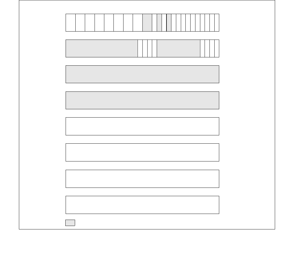
17-2 Vol. 3B
DEBUG, BRANCH PROFILE, TSC, AND RESOURCE MONITORING FEATURES
•Execution of any instruction.
•Execution of an instruction at a specified address.
•Read or write to a specified memory address/range.
•Write to a specified memory address/range.
•Input from a specified I/O address/range.
•Output to a specified I/O address/range.
•Attempt to change the contents of a debug register.
17.2 DEBUG REGISTERS
Eight debug registers (see Figure 17-1 for 32-bit operation and Figure 17-2 for 64-bit operation) control the debug
operation of the processor. These registers can be written to and read using the move to/from debug register form
of the MOV instruction. A debug register may be the source or destination operand for one of these instructions.
Figure 17-1. Debug Registers
31 24 23 22 21 20 19 16 15 13
14 12 11 870
DR7
L
Reserved
0
123456
910
1718
252627282930
G
0
L
1
L
2
L
3
G
3
L
E
G
EG
2G
1
0 0
G
D
R/W
0
LEN
0
R/W
1
LEN
1
R/W
2
LEN
2
R/W
3
LEN
3
31 16 15 13
14 12 11 870
DR6
B
0
123456
910
B
1
B
2
B
3
011 11 1 111
B
D
B
S
B
T
31 0
DR5
31 0
DR4
31 0
DR3
Breakpoint 3 Linear Address
31 0
DR2Breakpoint 2 Linear Address
31 0
DR1
Breakpoint 1 Linear Address
31 0
DR0Breakpoint 0 Linear Address
0
Reserved (set to 1)
1
R
T
M
R
T
M

Vol. 3B 17-3
DEBUG, BRANCH PROFILE, TSC, AND RESOURCE MONITORING FEATURES
Debug registers are privileged resources; a MOV instruction that accesses these registers can only be executed in
real-address mode, in SMM or in protected mode at a CPL of 0. An attempt to read or write the debug registers
from any other privilege level generates a general-protection exception (#GP).
The primary function of the debug registers is to set up and monitor from 1 to 4 breakpoints, numbered 0 though
3. For each breakpoint, the following information can be specified:
•The linear address where the breakpoint is to occur.
•The length of the breakpoint location: 1, 2, 4, or 8 bytes (refer to the notes in Section 17.2.4).
•The operation that must be performed at the address for a debug exception to be generated.
•Whether the breakpoint is enabled.
•Whether the breakpoint condition was present when the debug exception was generated.
The following paragraphs describe the functions of flags and fields in the debug registers.
17.2.1 Debug Address Registers (DR0-DR3)
Each of the debug-address registers (DR0 through DR3) holds the 32-bit linear address of a breakpoint (see
Figure 17-1). Breakpoint comparisons are made before physical address translation occurs. The contents of debug
register DR7 further specifies breakpoint conditions.
17.2.2 Debug Registers DR4 and DR5
Debug registers DR4 and DR5 are reserved when debug extensions are enabled (when the DE flag in control
register CR4 is set) and attempts to reference the DR4 and DR5 registers cause invalid-opcode exceptions (#UD).
When debug extensions are not enabled (when the DE flag is clear), these registers are aliased to debug registers
DR6 and DR7.
17.2.3 Debug Status Register (DR6)
The debug status register (DR6) reports debug conditions that were sampled at the time the last debug exception
was generated (see Figure 17-1). Updates to this register only occur when an exception is generated. The flags in
this register show the following information:
•B0 through B3 (breakpoint condition detected) flags (bits 0 through 3) — Indicates (when set) that its
associated breakpoint condition was met when a debug exception was generated. These flags are set if the
condition described for each breakpoint by the LENn, and R/Wn flags in debug control register DR7 is true.
They may or may not be set if the breakpoint is not enabled by the Ln or the Gn flags in register DR7. Therefore
on a #DB, a debug handler should check only those B0-B3 bits which correspond to an enabled breakpoint.
•BD (debug register access detected) flag (bit 13) — Indicates that the next instruction in the instruction
stream accesses one of the debug registers (DR0 through DR7). This flag is enabled when the GD (general
detect) flag in debug control register DR7 is set. See Section 17.2.4, “Debug Control Register (DR7),” for
further explanation of the purpose of this flag.
•BS (single step) flag (bit 14) — Indicates (when set) that the debug exception was triggered by the single-
step execution mode (enabled with the TF flag in the EFLAGS register). The single-step mode is the highest-
priority debug exception. When the BS flag is set, any of the other debug status bits also may be set.
•BT (task switch) flag (bit 15) — Indicates (when set) that the debug exception resulted from a task switch
where the T flag (debug trap flag) in the TSS of the target task was set. See Section 7.2.1, “Task-State
Segment (TSS),” for the format of a TSS. There is no flag in debug control register DR7 to enable or disable this
exception; the T flag of the TSS is the only enabling flag.
•RTM (restricted transactional memory) flag (bit 16) — Indicates (when clear) that a debug exception
(#DB) or breakpoint exception (#BP) occurred inside an RTM region while advanced debugging of RTM trans-
actional regions was enabled (see Section 17.3.3). This bit is set for any other debug exception (including all
those that occur when advanced debugging of RTM transactional regions is not enabled). This bit is always 1 if
the processor does not support RTM.

17-4 Vol. 3B
DEBUG, BRANCH PROFILE, TSC, AND RESOURCE MONITORING FEATURES
Certain debug exceptions may clear bits 0-3. The remaining contents of the DR6 register are never cleared by the
processor. To avoid confusion in identifying debug exceptions, debug handlers should clear the register (except
bit 16, which they should set) before returning to the interrupted task.
17.2.4 Debug Control Register (DR7)
The debug control register (DR7) enables or disables breakpoints and sets breakpoint conditions (see Figure 17-1).
The flags and fields in this register control the following things:
•L0 through L3 (local breakpoint enable) flags (bits 0, 2, 4, and 6) — Enables (when set) the breakpoint
condition for the associated breakpoint for the current task. When a breakpoint condition is detected and its
associated Ln flag is set, a debug exception is generated. The processor automatically clears these flags on
every task switch to avoid unwanted breakpoint conditions in the new task.
•G0 through G3 (global breakpoint enable) flags (bits 1, 3, 5, and 7) — Enables (when set) the
breakpoint condition for the associated breakpoint for all tasks. When a breakpoint condition is detected and its
associated Gn flag is set, a debug exception is generated. The processor does not clear these flags on a task
switch, allowing a breakpoint to be enabled for all tasks.
•LE and GE (local and global exact breakpoint enable) flags (bits 8, 9) — This feature is not supported in
the P6 family processors, later IA-32 processors, and Intel 64 processors. When set, these flags cause the
processor to detect the exact instruction that caused a data breakpoint condition. For backward and forward
compatibility with other Intel processors, we recommend that the LE and GE flags be set to 1 if exact
breakpoints are required.
•RTM (restricted transactional memory) flag (bit 11) — Enables (when set) advanced debugging of RTM
transactional regions (see Section 17.3.3). This advanced debugging is enabled only if IA32_DEBUGCTL.RTM is
also set.
•GD (general detect enable) flag (bit 13) — Enables (when set) debug-register protection, which causes a
debug exception to be generated prior to any MOV instruction that accesses a debug register. When such a
condition is detected, the BD flag in debug status register DR6 is set prior to generating the exception. This
condition is provided to support in-circuit emulators.
When the emulator needs to access the debug registers, emulator software can set the GD flag to prevent
interference from the program currently executing on the processor.
The processor clears the GD flag upon entering to the debug exception handler, to allow the handler access to
the debug registers.
•R/W0 through R/W3 (read/write) fields (bits 16, 17, 20, 21, 24, 25, 28, and 29) — Specifies the
breakpoint condition for the corresponding breakpoint. The DE (debug extensions) flag in control register CR4
determines how the bits in the R/Wn fields are interpreted. When the DE flag is set, the processor interprets
bits as follows:
00 — Break on instruction execution only.
01 — Break on data writes only.
10 — Break on I/O reads or writes.
11 — Break on data reads or writes but not instruction fetches.
When the DE flag is clear, the processor interprets the R/Wn bits the same as for the Intel386™ and Intel486™
processors, which is as follows:
00 — Break on instruction execution only.
01 — Break on data writes only.
10 — Undefined.
11 — Break on data reads or writes but not instruction fetches.
•LEN0 through LEN3 (Length) fields (bits 18, 19, 22, 23, 26, 27, 30, and 31) — Specify the size of the
memory location at the address specified in the corresponding breakpoint address register (DR0 through DR3).
These fields are interpreted as follows:
00 — 1-byte length.
01 — 2-byte length.
10 — Undefined (or 8 byte length, see note below).
11 — 4-byte length.

Vol. 3B 17-5
DEBUG, BRANCH PROFILE, TSC, AND RESOURCE MONITORING FEATURES
If the corresponding RWn field in register DR7 is 00 (instruction execution), then the LENn field should also be 00.
The effect of using other lengths is undefined. See Section 17.2.5, “Breakpoint Field Recognition,” below.
NOTES
For Pentium® 4 and Intel® Xeon® processors with a CPUID signature corresponding to family 15
(model 3, 4, and 6), break point conditions permit specifying 8-byte length on data read/write with
an of encoding 10B in the LENn field.
Encoding 10B is also supported in processors based on Intel Core microarchitecture or enhanced
Intel Core microarchitecture, the respective CPUID signatures corresponding to family 6, model 15,
and family 6, DisplayModel value 23 (see CPUID instruction in Chapter 3, “Instruction Set
Reference, A-L” in the Intel® 64 and IA-32 Architectures Software Developer’s Manual, Volume
2A). The Encoding 10B is supported in processors based on Intel® Atom™ microarchitecture, with
CPUID signature of family 6, DisplayModel value 1CH. The encoding 10B is undefined for other
processors.
17.2.5 Breakpoint Field Recognition
Breakpoint address registers (debug registers DR0 through DR3) and the LENn fields for each breakpoint define a
range of sequential byte addresses for a data or I/O breakpoint. The LENn fields permit specification of a 1-, 2-, 4-
or 8-byte range, beginning at the linear address specified in the corresponding debug register (DRn). Two-byte
ranges must be aligned on word boundaries; 4-byte ranges must be aligned on doubleword boundaries, 8-byte
ranges must be aligned on quadword boundaries. I/O addresses are zero-extended (from 16 to 32 bits, for
comparison with the breakpoint address in the selected debug register). These requirements are enforced by the
processor; it uses LENn field bits to mask the lower address bits in the debug registers. Unaligned data or I/O
breakpoint addresses do not yield valid results.
A data breakpoint for reading or writing data is triggered if any of the bytes participating in an access is within the
range defined by a breakpoint address register and its LENn field. Table 17-1 provides an example setup of debug
registers and data accesses that would subsequently trap or not trap on the breakpoints.
A data breakpoint for an unaligned operand can be constructed using two breakpoints, where each breakpoint is
byte-aligned and the two breakpoints together cover the operand. The breakpoints generate exceptions only for
the operand, not for neighboring bytes.
Instruction breakpoint addresses must have a length specification of 1 byte (the LENn field is set to 00). Code
breakpoints for other operand sizes are undefined. The processor recognizes an instruction breakpoint address
only when it points to the first byte of an instruction. If the instruction has prefixes, the breakpoint address must
point to the first prefix.

17-6 Vol. 3B
DEBUG, BRANCH PROFILE, TSC, AND RESOURCE MONITORING FEATURES
17.2.6 Debug Registers and Intel® 64 Processors
For Intel 64 architecture processors, debug registers DR0–DR7 are 64 bits. In 16-bit or 32-bit modes (protected
mode and compatibility mode), writes to a debug register fill the upper 32 bits with zeros. Reads from a debug
register return the lower 32 bits. In 64-bit mode, MOV DRn instructions read or write all 64 bits. Operand-size
prefixes are ignored.
In 64-bit mode, the upper 32 bits of DR6 and DR7 are reserved and must be written with zeros. Writing 1 to any of
the upper 32 bits results in a #GP(0) exception (see Figure 17-2). All 64 bits of DR0–DR3 are writable by software.
However, MOV DRn instructions do not check that addresses written to DR0–DR3 are in the linear-address limits of
the processor implementation (address matching is supported only on valid addresses generated by the processor
implementation). Break point conditions for 8-byte memory read/writes are supported in all modes.
17.3 DEBUG EXCEPTIONS
The Intel 64 and IA-32 architectures dedicate two interrupt vectors to handling debug exceptions: vector 1 (debug
exception, #DB) and vector 3 (breakpoint exception, #BP). The following sections describe how these exceptions
are generated and typical exception handler operations.
Table 17-1. Breakpoint Examples
Debug Register Setup
Debug Register R/WnBreakpoint Address LENn
DR0
DR1
DR2
DR3
R/W0 = 11 (Read/Write)
R/W1 = 01 (Write)
R/W2 = 11 (Read/Write)
R/W3 = 01 (Write)
A0001H
A0002H
B0002H
C0000H
LEN0 = 00 (1 byte)
LEN1 = 00 (1 byte)
LEN2 = 01) (2 bytes)
LEN3 = 11 (4 bytes)
Data Accesses
Operation Address Access Length
(In Bytes)
Data operations that trap
- Read or write
- Read or write
- Write
- Write
- Read or write
- Read or write
- Read or write
- Write
- Write
- Write
A0001H
A0001H
A0002H
A0002H
B0001H
B0002H
B0002H
C0000H
C0001H
C0003H
1
2
1
2
4
1
2
4
2
1
Data operations that do not trap
- Read or write
- Read
- Read or write
- Read or write
- Read
- Read or write
A0000H
A0002H
A0003H
B0000H
C0000H
C0004H
1
1
4
2
2
4
Vol. 3B 17-7
DEBUG, BRANCH PROFILE, TSC, AND RESOURCE MONITORING FEATURES
17.3.1 Debug Exception (#DB)—Interrupt Vector 1
The debug-exception handler is usually a debugger program or part of a larger software system. The processor
generates a debug exception for any of several conditions. The debugger checks flags in the DR6 and DR7 registers
to determine which condition caused the exception and which other conditions might apply. Table 17-2 shows the
states of these flags following the generation of each kind of breakpoint condition.
Instruction-breakpoint and general-detect condition (see Section 17.3.1.3, “General-Detect Exception Condition”)
result in faults; other debug-exception conditions result in traps. The debug exception may report one or both at
one time. The following sections describe each class of debug exception.
Figure 17-2. DR6/DR7 Layout on Processors Supporting Intel® 64 Architecture
31 24 23 22 21 20 19 16 15 13
14 12 11 870
DR7
L
Reserved
0
123456
910
1718
252627282930
G
0
L
1
L
2
L
3
G
3
L
E
G
EG
2G
1
G
D
R/W
0
LEN
0
R/W
1
LEN
1
R/W
2
LEN
2
R/W
3
LEN
3
31 16 15 13
14 12 11 870
DR6
B
0
123456
910
B
1
B
2
B
3
0111111111
B
D
B
S
B
T
63 32
63 32
DR6
DR7
00 001
Reserved (set to 1)
63 0
DR3
Breakpoint 3 Linear Address
63 0
DR2Breakpoint 2 Linear Address
63 0
DR1
Breakpoint 1 Linear Address
63 0
DR0Breakpoint 0 Linear Address
63 0
DR5
63 0
DR4

17-8 Vol. 3B
DEBUG, BRANCH PROFILE, TSC, AND RESOURCE MONITORING FEATURES
See also: Chapter 6, “Interrupt 1—Debug Exception (#DB),” in the Intel® 64 and IA-32 Architectures Software
Developer’s Manual, Volume 3A.
17.3.1.1 Instruction-Breakpoint Exception Condition
The processor reports an instruction breakpoint when it attempts to execute an instruction at an address specified
in a breakpoint-address register (DR0 through DR3) that has been set up to detect instruction execution (R/W flag
is set to 0). Upon reporting the instruction breakpoint, the processor generates a fault-class, debug exception
(#DB) before it executes the target instruction for the breakpoint.
Instruction breakpoints are the highest priority debug exceptions. They are serviced before any other exceptions
detected during the decoding or execution of an instruction. However, if a code instruction breakpoint is placed on
an instruction located immediately after a POP SS/MOV SS instruction, the breakpoint may not be triggered. In
most situations, POP SS/MOV SS will inhibit such interrupts (see “MOV—Move” and “POP—Pop a Value from the
Stack” in Chapter 4 of the Intel® 64 and IA-32 Architectures Software Developer’s Manual, Volume 2B).
Because the debug exception for an instruction breakpoint is generated before the instruction is executed, if the
instruction breakpoint is not removed by the exception handler; the processor will detect the instruction breakpoint
again when the instruction is restarted and generate another debug exception. To prevent looping on an instruction
breakpoint, the Intel 64 and IA-32 architectures provide the RF flag (resume flag) in the EFLAGS register (see
Section 2.3, “System Flags and Fields in the EFLAGS Register,” in the Intel® 64 and IA-32 Architectures Software
Developer’s Manual, Volume 3A). When the RF flag is set, the processor ignores instruction breakpoints.
All Intel 64 and IA-32 processors manage the RF flag as follows. The RF Flag is cleared at the start of the instruction
after the check for code breakpoint, CS limit violation and FP exceptions. Task Switches and IRETD/IRETQ instruc-
tions transfer the RF image from the TSS/stack to the EFLAGS register.
When calling an event handler, Intel 64 and IA-32 processors establish the value of the RF flag in the EFLAGS image
pushed on the stack:
•For any fault-class exception except a debug exception generated in response to an instruction breakpoint, the
value pushed for RF is 1.
•For any interrupt arriving after any iteration of a repeated string instruction but the last iteration, the value
pushed for RF is 1.
•For any trap-class exception generated by any iteration of a repeated string instruction but the last iteration,
the value pushed for RF is 1.
•For other cases, the value pushed for RF is the value that was in EFLAG.RF at the time the event handler was
called. This includes:
— Debug exceptions generated in response to instruction breakpoints
Table 17-2. Debug Exception Conditions
Debug or Breakpoint Condition DR6 Flags Tested DR7 Flags Tested Exception Class
Single-step trap BS = 1 Trap
Instruction breakpoint, at addresses defined by DRn and
LENn
Bn = 1 and
(Gn or Ln = 1)
R/Wn = 0 Fault
Data write breakpoint, at addresses defined by DRn and
LENn
Bn = 1 and
(Gn or Ln = 1)
R/Wn = 1 Trap
I/O read or write breakpoint, at addresses defined by DRn
and LENn
Bn = 1 and
(Gn or Ln = 1)
R/Wn = 2 Trap
Data read or write (but not instruction fetches), at
addresses defined by DRn and LENn
Bn = 1 and
(Gn or Ln = 1)
R/Wn = 3 Trap
General detect fault, resulting from an attempt to modify
debug registers (usually in conjunction with in-circuit
emulation)
BD = 1 Fault
Task switch BT = 1 Trap

Vol. 3B 17-9
DEBUG, BRANCH PROFILE, TSC, AND RESOURCE MONITORING FEATURES
— Hardware-generated interrupts arriving between instructions (including those arriving after the last
iteration of a repeated string instruction)
— Trap-class exceptions generated after an instruction completes (including those generated after the last
iteration of a repeated string instruction)
— Software-generated interrupts (RF is pushed as 0, since it was cleared at the start of the software interrupt)
As noted above, the processor does not set the RF flag prior to calling the debug exception handler for debug
exceptions resulting from instruction breakpoints. The debug exception handler can prevent recurrence of the
instruction breakpoint by setting the RF flag in the EFLAGS image on the stack. If the RF flag in the EFLAGS image
is set when the processor returns from the exception handler, it is copied into the RF flag in the EFLAGS register by
IRETD/IRETQ or a task switch that causes the return. The processor then ignores instruction breakpoints for the
duration of the next instruction. (Note that the POPF, POPFD, and IRET instructions do not transfer the RF image
into the EFLAGS register.) Setting the RF flag does not prevent other types of debug-exception conditions (such as,
I/O or data breakpoints) from being detected, nor does it prevent non-debug exceptions from being generated.
For the Pentium processor, when an instruction breakpoint coincides with another fault-type exception (such as a
page fault), the processor may generate one spurious debug exception after the second exception has been
handled, even though the debug exception handler set the RF flag in the EFLAGS image. To prevent a spurious
exception with Pentium processors, all fault-class exception handlers should set the RF flag in the EFLAGS image.
17.3.1.2 Data Memory and I/O Breakpoint Exception Conditions
Data memory and I/O breakpoints are reported when the processor attempts to access a memory or I/O address
specified in a breakpoint-address register (DR0 through DR3) that has been set up to detect data or I/O accesses
(R/W flag is set to 1, 2, or 3). The processor generates the exception after it executes the instruction that made the
access, so these breakpoint condition causes a trap-class exception to be generated.
Because data breakpoints are traps, an instruction that writes memory overwrites the original data before the
debug exception generated by a data breakpoint is generated. If a debugger needs to save the contents of a write
breakpoint location, it should save the original contents before setting the breakpoint. The handler can report the
saved value after the breakpoint is triggered. The address in the debug registers can be used to locate the new
value stored by the instruction that triggered the breakpoint.
If a data breakpoint is detected during an iteration of a string instruction executed with fast-string operation (see
Section 7.3.9.3 of Intel® 64 and IA-32 Architectures Software Developer’s Manual, Volume 1), delivery of the
resulting debug exception may be delayed until completion of the corresponding group of iterations.
Intel486 and later processors ignore the GE and LE flags in DR7. In Intel386 processors, exact data breakpoint
matching does not occur unless it is enabled by setting the LE and/or the GE flags.
For repeated INS and OUTS instructions that generate an I/O-breakpoint debug exception, the processor gener-
ates the exception after the completion of the first iteration. Repeated INS and OUTS instructions generate a data-
breakpoint debug exception after the iteration in which the memory address breakpoint location is accessed.
17.3.1.3 General-Detect Exception Condition
When the GD flag in DR7 is set, the general-detect debug exception occurs when a program attempts to access any
of the debug registers (DR0 through DR7) at the same time they are being used by another application, such as an
emulator or debugger. This protection feature guarantees full control over the debug registers when required. The
debug exception handler can detect this condition by checking the state of the BD flag in the DR6 register. The
processor generates the exception before it executes the MOV instruction that accesses a debug register, which
causes a fault-class exception to be generated.
17.3.1.4 Single-Step Exception Condition
The processor generates a single-step debug exception if (while an instruction is being executed) it detects that the
TF flag in the EFLAGS register is set. The exception is a trap-class exception, because the exception is generated
after the instruction is executed. The processor will not generate this exception after the instruction that sets the
TF flag. For example, if the POPF instruction is used to set the TF flag, a single-step trap does not occur until after
the instruction that follows the POPF instruction.

17-10 Vol. 3B
DEBUG, BRANCH PROFILE, TSC, AND RESOURCE MONITORING FEATURES
The processor clears the TF flag before calling the exception handler. If the TF flag was set in a TSS at the time of
a task switch, the exception occurs after the first instruction is executed in the new task.
The TF flag normally is not cleared by privilege changes inside a task. The INT n and INTO instructions, however,
do clear this flag. Therefore, software debuggers that single-step code must recognize and emulate INT n or INTO
instructions rather than executing them directly. To maintain protection, the operating system should check the
CPL after any single-step trap to see if single stepping should continue at the current privilege level.
The interrupt priorities guarantee that, if an external interrupt occurs, single stepping stops. When both an external
interrupt and a single-step interrupt occur together, the single-step interrupt is processed first. This operation
clears the TF flag. After saving the return address or switching tasks, the external interrupt input is examined
before the first instruction of the single-step handler executes. If the external interrupt is still pending, then it is
serviced. The external interrupt handler does not run in single-step mode. To single step an interrupt handler,
single step an INT n instruction that calls the interrupt handler.
17.3.1.5 Task-Switch Exception Condition
The processor generates a debug exception after a task switch if the T flag of the new task's TSS is set. This excep-
tion is generated after program control has passed to the new task, and prior to the execution of the first instruc-
tion of that task. The exception handler can detect this condition by examining the BT flag of the DR6 register.
If entry 1 (#DB) in the IDT is a task gate, the T bit of the corresponding TSS should not be set. Failure to observe
this rule will put the processor in a loop.
17.3.2 Breakpoint Exception (#BP)—Interrupt Vector 3
The breakpoint exception (interrupt 3) is caused by execution of an INT 3 instruction. See Chapter 6, “Interrupt
3—Breakpoint Exception (#BP).” Debuggers use break exceptions in the same way that they use the breakpoint
registers; that is, as a mechanism for suspending program execution to examine registers and memory locations.
With earlier IA-32 processors, breakpoint exceptions are used extensively for setting instruction breakpoints.
With the Intel386 and later IA-32 processors, it is more convenient to set breakpoints with the breakpoint-address
registers (DR0 through DR3). However, the breakpoint exception still is useful for breakpointing debuggers,
because a breakpoint exception can call a separate exception handler. The breakpoint exception is also useful when
it is necessary to set more breakpoints than there are debug registers or when breakpoints are being placed in the
source code of a program under development.
17.3.3 Debug Exceptions, Breakpoint Exceptions, and Restricted Transactional Memory
(RTM)
Chapter 16, “Programming with Intel® Transactional Synchronization Extensions,” of Intel® 64 and IA-32 Archi-
tectures Software Developer’s Manual, Volume 1 describes Restricted Transactional Memory (RTM). This is an
instruction-set interface that allows software to identify transactional regions (or critical sections) using the
XBEGIN and XEND instructions.
Execution of an RTM transactional region begins with an XBEGIN instruction. If execution of the region successfully
reaches an XEND instruction, the processor ensures that all memory operations performed within the region
appear to have occurred instantaneously when viewed from other logical processors. Execution of an RTM transac-
tion region does not succeed if the processor cannot commit the updates atomically. When this happens, the
processor rolls back the execution, a process referred to as a transactional abort. In this case, the processor
discards all updates performed in the region, restores architectural state to appear as if the execution had not
occurred, and resumes execution at a fallback instruction address that was specified with the XBEGIN instruction.
If debug exception (#DB) or breakpoint exception (#BP) occurs within an RTM transaction region, a transactional
abort occurs, the processor sets EAX[4], and no exception is delivered.
Software can enable advanced debugging of RTM transactional regions by setting DR7.RTM[bit 11] and
IA32_DEBUGCTL.RTM[bit 15]. If these bits are both set, the transactional abort caused by a #DB or #BP within an
RTM transaction region does not resume execution at the fallback instruction address specified with the XBEGIN
instruction that begin the region. Instead, execution is resumed at that XBEGIN instruction, and a #DB is delivered.

Vol. 3B 17-11
DEBUG, BRANCH PROFILE, TSC, AND RESOURCE MONITORING FEATURES
(A #DB is delivered even if the transactional abort was caused by a #BP.) Such a #DB will clear DR6.RTM[bit 16]
(all other debug exceptions set DR6[16]).
17.4 LAST BRANCH, INTERRUPT, AND EXCEPTION RECORDING OVERVIEW
P6 family processors introduced the ability to set breakpoints on taken branches, interrupts, and exceptions, and
to single-step from one branch to the next. This capability has been modified and extended in the Pentium 4, Intel
Xeon, Pentium M, Intel® Core™ Solo, Intel® Core™ Duo, Intel® Core™2 Duo, Intel® Core™ i7 and Intel® Atom™
processors to allow logging of branch trace messages in a branch trace store (BTS) buffer in memory.
See the following sections for processor specific implementation of last branch, interrupt and exception recording:
— Section 17.5, “Last Branch, Interrupt, and Exception Recording (Intel® Core™ 2 Duo and Intel® Atom™
Processors)”
— Section 17.6, “Last Branch, Call Stack, Interrupt, and Exception Recording for Processors based on
Goldmont Microarchitecture”
— Section 17.7, “Last Branch, Interrupt, and Exception Recording for Processors based on Intel® Microarchi-
tecture code name Nehalem”
— Section 17.8, “Last Branch, Interrupt, and Exception Recording for Processors based on Intel® Microarchi-
tecture code name Sandy Bridge”
— Section 17.9, “Last Branch, Call Stack, Interrupt, and Exception Recording for Processors based on Haswell
Microarchitecture”
— Section 17.10, “Last Branch, Call Stack, Interrupt, and Exception Recording for Processors based on
Skylake Microarchitecture”
— Section 17.12, “Last Branch, Interrupt, and Exception Recording (Intel® Core™ Solo and Intel® Core™
Duo Processors)”
— Section 17.13, “Last Branch, Interrupt, and Exception Recording (Pentium M Processors)”
— Section 17.14, “Last Branch, Interrupt, and Exception Recording (P6 Family Processors)”
The following subsections of Section 17.4 describe common features of profiling branches. These features are
generally enabled using the IA32_DEBUGCTL MSR (older processor may have implemented a subset or model-
specific features, see definitions of MSR_DEBUGCTLA, MSR_DEBUGCTLB, MSR_DEBUGCTL).
17.4.1 IA32_DEBUGCTL MSR
The IA32_DEBUGCTL MSR provides bit field controls to enable debug trace interrupts, debug trace stores, trace
messages enable, single stepping on branches, last branch record recording, and to control freezing of LBR stack
or performance counters on a PMI request. IA32_DEBUGCTL MSR is located at register address 01D9H.
See Figure 17-3 for the MSR layout and the bullets below for a description of the flags:
•LBR (last branch/interrupt/exception) flag (bit 0) — When set, the processor records a running trace of
the most recent branches, interrupts, and/or exceptions taken by the processor (prior to a debug exception
being generated) in the last branch record (LBR) stack. For more information, see the Section 17.5.1, “LBR
Stack” (Intel® Core™2 Duo and Intel® Atom™ Processor Family) and Section 17.7.1, “LBR Stack” (processors
based on Intel® Microarchitecture code name Nehalem).
•BTF (single-step on branches) flag (bit 1) — When set, the processor treats the TF flag in the EFLAGS
register as a “single-step on branches” flag rather than a “single-step on instructions” flag. This mechanism
allows single-stepping the processor on taken branches. See Section 17.4.3, “Single-Stepping on Branches,”
for more information about the BTF flag.
•TR (trace message enable) flag (bit 6) — When set, branch trace messages are enabled. When the
processor detects a taken branch, interrupt, or exception; it sends the branch record out on the system bus as
a branch trace message (BTM). See Section 17.4.4, “Branch Trace Messages,” for more information about the
TR flag.

17-12 Vol. 3B
DEBUG, BRANCH PROFILE, TSC, AND RESOURCE MONITORING FEATURES
•BTS (branch trace store) flag (bit 7) — When set, the flag enables BTS facilities to log BTMs to a memory-
resident BTS buffer that is part of the DS save area. See Section 17.4.9, “BTS and DS Save Area.”
•BTINT (branch trace interrupt) flag (bit 8) — When set, the BTS facilities generate an interrupt when the
BTS buffer is full. When clear, BTMs are logged to the BTS buffer in a circular fashion. See Section 17.4.5, “Branch
Trace Store (BTS),” for a description of this mechanism.
•BTS_OFF_OS (branch trace off in privileged code) flag (bit 9) — When set, BTS or BTM is skipped if CPL
is 0. See Section 17.11.2.
•BTS_OFF_USR (branch trace off in user code) flag (bit 10) — When set, BTS or BTM is skipped if CPL is
greater than 0. See Section 17.11.2.
•FREEZE_LBRS_ON_PMI flag (bit 11) — When set, the LBR stack is frozen on a hardware PMI request (e.g.
when a counter overflows and is configured to trigger PMI). See Section 17.4.7 for details.
•FREEZE_PERFMON_ON_PMI flag (bit 12) — When set, the performance counters (IA32_PMCx and
IA32_FIXED_CTRx) are frozen on a PMI request. See Section 17.4.7 for details.
•FREEZE_WHILE_SMM_EN (bit 14) — If this bit is set, upon the delivery of an SMI, the processor will clear all
the enable bits of IA32_PERF_GLOBAL_CTRL, save a copy of the content of IA32_DEBUGCTL and disable LBR,
BTF, TR, and BTS fields of IA32_DEBUGCTL before transferring control to the SMI handler. Subsequently, the
enable bits of IA32_PERF_GLOBAL_CTRL will be set to 1, the saved copy of IA32_DEBUGCTL prior to SMI
delivery will be restored, after the SMI handler issues RSM to complete its service. Note that system software
must check if the processor supports the IA32_DEBUGCTL.FREEZE_WHILE_SMM_EN control bit.
IA32_DEBUGCTL.FREEZE_WHILE_SMM_EN is supported if
IA32_PERF_CAPABILITIES.FREEZE_WHILE_SMM[Bit 12] is reporting 1. See Section 18.19 for details of
detecting the presence of IA32_PERF_CAPABILITIES MSR.
•RTM (bit 15) — If this bit is set, advanced debugging of RTM transactional regions is enabled if DR7.RTM is
also set. See Section 17.3.3.
17.4.2 Monitoring Branches, Exceptions, and Interrupts
When the LBR flag (bit 0) in the IA32_DEBUGCTL MSR is set, the processor automatically begins recording branch
records for taken branches, interrupts, and exceptions (except for debug exceptions) in the LBR stack MSRs.
When the processor generates a debug exception (#DB), it automatically clears the LBR flag before executing the
exception handler. This action does not clear previously stored LBR stack MSRs.
A debugger can use the linear addresses in the LBR stack to re-set breakpoints in the breakpoint address registers
(DR0 through DR3). This allows a backward trace from the manifestation of a particular bug toward its source.
Figure 17-3. IA32_DEBUGCTL MSR for Processors based
on Intel Core microarchitecture
31
TR — Trace messages enable
BTINT — Branch trace interrupt
BTF — Single-step on branches
LBR — Last branch/interrupt/exception
Reserved
87654321 0
BTS — Branch trace store
Reserved
910
BTS_OFF_OS — BTS off in OS
BTS_OFF_USR — BTS off in user code
FREEZE_LBRS_ON_PMI
FREEZE_PERFMON_ON_PMI
1112
14
FREEZE_WHILE_SMM_EN
15
RTM

Vol. 3B 17-13
DEBUG, BRANCH PROFILE, TSC, AND RESOURCE MONITORING FEATURES
On some processors, if the LBR flag is cleared and TR flag in the IA32_DEBUGCTL MSR remains set, the processor
will continue to update LBR stack MSRs. This is because those processors use the entries in the LBR stack in the
process of generating BTM/BTS records. A #DB does not automatically clear the TR flag.
17.4.3 Single-Stepping on Branches
When software sets both the BTF flag (bit 1) in the IA32_DEBUGCTL MSR and the TF flag in the EFLAGS register,
the processor generates a single-step debug exception only after instructions that cause a branch.1 This mecha-
nism allows a debugger to single-step on control transfers caused by branches. This “branch single stepping” helps
isolate a bug to a particular block of code before instruction single-stepping further narrows the search. The
processor clears the BTF flag when it generates a debug exception. The debugger must set the BTF flag before
resuming program execution to continue single-stepping on branches.
17.4.4 Branch Trace Messages
Setting the TR flag (bit 6) in the IA32_DEBUGCTL MSR enables branch trace messages (BTMs). Thereafter, when
the processor detects a branch, exception, or interrupt, it sends a branch record out on the system bus as a BTM.
A debugging device that is monitoring the system bus can read these messages and synchronize operations with
taken branch, interrupt, and exception events.
When interrupts or exceptions occur in conjunction with a taken branch, additional BTMs are sent out on the bus,
as described in Section 17.4.2, “Monitoring Branches, Exceptions, and Interrupts.”
For P6 processor family, Pentium M processor family, processors based on Intel Core microarchitecture, TR and LBR
bits can not be set at the same time due to hardware limitation. The content of LBR stack is undefined when TR is
set.
For processors with Intel NetBurst microarchitecture, Intel Atom processors, and Intel Core and related Intel Xeon
processors both starting with the Nehalem microarchitecture, the processor can collect branch records in the LBR
stack and at the same time send/store BTMs when both the TR and LBR flags are set in the IA32_DEBUGCTL MSR
(or the equivalent MSR_DEBUGCTLA, MSR_DEBUGCTLB).
The following exception applies:
•BTM may not be observable on Intel Atom processor families that do not provide an externally visible system
bus (i.e., processors based on the Silvermont microarchitecture or later).
17.4.4.1 Branch Trace Message Visibility
Branch trace message (BTM) visibility is implementation specific and limited to systems with a front side bus
(FSB). BTMs may not be visible to newer system link interfaces or a system bus that deviates from a traditional
FSB.
17.4.5 Branch Trace Store (BTS)
A trace of taken branches, interrupts, and exceptions is useful for debugging code by providing a method of deter-
mining the decision path taken to reach a particular code location. The LBR flag (bit 0) of IA32_DEBUGCTL provides
a mechanism for capturing records of taken branches, interrupts, and exceptions and saving them in the last
branch record (LBR) stack MSRs, setting the TR flag for sending them out onto the system bus as BTMs. The branch
trace store (BTS) mechanism provides the additional capability of saving the branch records in a memory-resident
BTS buffer, which is part of the DS save area. The BTS buffer can be configured to be circular so that the most
recent branch records are always available or it can be configured to generate an interrupt when the buffer is
nearly full so that all the branch records can be saved. The BTINT flag (bit 8) can be used to enable the generation
of interrupt when the BTS buffer is full. See Section 17.4.9.2, “Setting Up the DS Save Area.” for additional details.
1. Executions of CALL, IRET, and JMP that cause task switches never cause single-step debug exceptions (regardless of the value of the
BTF flag). A debugger desiring debug exceptions on switches to a task should set the T flag (debug trap flag) in the TSS of that task.
See Section 7.2.1, “Task-State Segment (TSS).”

17-14 Vol. 3B
DEBUG, BRANCH PROFILE, TSC, AND RESOURCE MONITORING FEATURES
Setting this flag (BTS) alone can greatly reduce the performance of the processor. CPL-qualified branch trace
storing mechanism can help mitigate the performance impact of sending/logging branch trace messages.
17.4.6 CPL-Qualified Branch Trace Mechanism
CPL-qualified branch trace mechanism is available to a subset of Intel 64 and IA-32 processors that support the
branch trace storing mechanism. The processor supports the CPL-qualified branch trace mechanism if
CPUID.01H:ECX[bit 4] = 1.
The CPL-qualified branch trace mechanism is described in Section 17.4.9.4. System software can selectively specify
CPL qualification to not send/store Branch Trace Messages associated with a specified privilege level. Two bit fields,
BTS_OFF_USR (bit 10) and BTS_OFF_OS (bit 9), are provided in the debug control register to specify the CPL of
BTMs that will not be logged in the BTS buffer or sent on the bus.
17.4.7 Freezing LBR and Performance Counters on PMI
Many issues may generate a performance monitoring interrupt (PMI); a PMI service handler will need to determine
cause to handle the situation. Two capabilities that allow a PMI service routine to improve branch tracing and
performance monitoring are available for processors supporting architectural performance monitoring version 2 or
greater (i.e. CPUID.0AH:EAX[7:0] > 1). These capabilities provides the following interface in IA32_DEBUGCTL to
reduce runtime overhead of PMI servicing, profiler-contributed skew effects on analysis or counter metrics:
•Freezing LBRs on PMI (bit 11)— Allows the PMI service routine to ensure the content in the LBR stack are
associated with the target workload and not polluted by the branch flows of handling the PMI. Depending on the
version ID enumerated by CPUID.0AH:EAX.ArchPerfMonVerID[bits 7:0], two flavors are supported:
— Legacy Freeze_LBR_on_PMI is supported for ArchPerfMonVerID <= 3 and ArchPerfMonVerID >1. If
IA32_DEBUGCTL.Freeze_LBR_On_PMI = 1, the LBR is frozen on the overflowed condition of the buffer
area, the processor clears the LBR bit (bit 0) in IA32_DEBUGCTL. Software must then re-enable
IA32_DEBUGCTL.LBR to resume recording branches. When using this feature, software should be careful
about writes to IA32_DEBUGCTL to avoid re-enabling LBRs by accident if they were just disabled.
— Streamlined Freeze_LBR_on_PMI is supported for ArchPerfMonVerID >= 4. If
IA32_DEBUGCTL.Freeze_LBR_On_PMI = 1, the processor behaves as follows:
•sets IA32_PERF_GLOBAL_STATUS.LBR_Frz =1 to disable recording, but does not change the LBR bit
(bit 0) in IA32_DEBUGCTL. The LBRs are frozen on the overflowed condition of the buffer area.
•Freezing PMCs on PMI (bit 12) — Allows the PMI service routine to ensure the content in the performance
counters are associated with the target workload and not polluted by the PMI and activities within the PMI
service routine. Depending on the version ID enumerated by CPUID.0AH:EAX.ArchPerfMonVerID[bits 7:0], two
flavors are supported:
— Legacy Freeze_Perfmon_on_PMI is supported for ArchPerfMonVerID <= 3 and ArchPerfMonVerID >1. If
IA32_DEBUGCTL.Freeze_Perfmon_On_PMI = 1, the performance counters are frozen on the counter
overflowed condition when the processor clears the IA32_PERF_GLOBAL_CTRL MSR (see Figure 18-3). The
PMCs affected include both general-purpose counters and fixed-function counters (see Section 18.4.1,
“Fixed-function Performance Counters”). Software must re-enable counts by writing 1s to the corre-
sponding enable bits in IA32_PERF_GLOBAL_CTRL before leaving a PMI service routine to continue counter
operation.
— Streamlined Freeze_Perfmon_on_PMI is supported for ArchPerfMonVerID >= 4. The processor behaves as
follows:
•sets IA32_PERF_GLOBAL_STATUS.CTR_Frz =1 to disable counting on a counter overflow condition, but
does not change the IA32_PERF_GLOBAL_CTRL MSR.
Freezing LBRs and PMCs on PMIs (both legacy and streamlined operation) occur when one of the following applies:
•A performance counter had an overflow and was programmed to signal a PMI in case of an overflow.
— For the general-purpose counters; enabling PMI is done by setting bit 20 of the IA32_PERFEVTSELx
register.

Vol. 3B 17-15
DEBUG, BRANCH PROFILE, TSC, AND RESOURCE MONITORING FEATURES
— For the fixed-function counters; enabling PMI is done by setting the 3rd bit in the corresponding 4-bit
control field of the MSR_PERF_FIXED_CTR_CTRL register (see Figure 18-1) or IA32_FIXED_CTR_CTRL MSR
(see Figure 18-2).
•The PEBS buffer is almost full and reaches the interrupt threshold.
•The BTS buffer is almost full and reaches the interrupt threshold.
Table 17-3 compares the interaction of the processor with the PMI handler using the legacy versus streamlined
Freeza_Perfmon_On_PMI interface.
Table 17-3. Legacy and Streamlined Operation with Freeze_Perfmon_On_PMI = 1, Counter Overflowed
17.4.8 LBR Stack
The last branch record stack and top-of-stack (TOS) pointer MSRs are supported across Intel 64 and IA-32
processor families. However, the number of MSRs in the LBR stack and the valid range of TOS pointer value can
vary between different processor families. Table 17-4 lists the LBR stack size and TOS pointer range for several
processor families according to the CPUID signatures of DisplayFamily_DisplayModel encoding (see CPUID instruc-
tion in Chapter 3 of Intel® 64 and IA-32 Architectures Software Developer’s Manual, Volume 2A).
Legacy Freeze_Perfmon_On_PMI Streamlined Freeze_Perfmon_On_PMI Comment
Processor freezes the counters on overflow Processor freezes the counters on overflow Unchanged
Processor clears IA32_PERF_GLOBAL_CTRL Processor set
IA32_PERF_GLOBAL_STATUS.CTR_FTZ
Handler reads IA32_PERF_GLOBAL_STATUS
(0x38E) to examine which counter(s) overflowed
mask = RDMSR(0x38E) Similar
Handler services the PMI Handler services the PMI Unchanged
Handler writes 1s to
IA32_PERF_GLOBAL_OVF_CTL (0x390)
Handler writes mask into
IA32_PERF_GLOBAL_OVF_RESET (0x390)
Processor clears IA32_PERF_GLOBAL_STATUS Processor clears IA32_PERF_GLOBAL_STATUS Unchanged
Handler re-enables IA32_PERF_GLOBAL_CTRL None Reduced software overhead
Table 17-4. LBR Stack Size and TOS Pointer Range
DisplayFamily_DisplayModel Size of LBR Stack Component of an LBR Entry Range of TOS Pointer
06_5CH, 06_5FH 32 FROM_IP, TO_IP 0 to 31
06_4EH, 06_5EH, 06_8EH, 06_9EH 32 FROM_IP, TO_IP, LBR_INFO1
NOTES:
1. See Section 17.10.
0 to 31
06_3DH, 06_47H, 06_4FH, 06_56H 16 FROM_IP, TO_IP 0 to 15
06_3CH, 06_45H, 06_46H, 06_3FH 16 FROM_IP, TO_IP 0 to 15
06_2AH, 06_2DH, 06_3AH, 06_3EH 16 FROM_IP, TO_IP 0 to 15
06_1AH, 06_1EH, 06_1FH, 06_2EH, 06_25H,
06_2CH, 06_2FH
16 FROM_IP, TO_IP 0 to 15
06_17H, 06_1DH 4FROM_IP, TO_IP0 to 3
06_0FH 4FROM_IP, TO_IP0 to 3
06_37H, 06_4AH, 06_4CH, 06_4DH, 06_5AH,
06_5DH
8FROM_IP, TO_IP0 to 7
06_1CH, 06_26H, 06_27H, 06_35H, 06_36H 8FROM_IP, TO_IP0 to 7

17-16 Vol. 3B
DEBUG, BRANCH PROFILE, TSC, AND RESOURCE MONITORING FEATURES
The last branch recording mechanism tracks not only branch instructions (like JMP, Jcc, LOOP and CALL instruc-
tions), but also other operations that cause a change in the instruction pointer (like external interrupts, traps and
faults). The branch recording mechanisms generally employs a set of MSRs, referred to as last branch record (LBR)
stack. The size and exact locations of the LBR stack are generally model-specific (see Chapter 35, “Model-Specific
Registers (MSRs)” of Intel® 64 and IA-32 Architectures Software Developer’s Manual, Volume 3C for model-
specific MSR addresses).
•Last Branch Record (LBR) Stack — The LBR consists of N pairs of MSRs (N is listed in the LBR stack size
column of Table 17-4) that store source and destination address of recent branches (see Figure 17-3):
— MSR_LASTBRANCH_0_FROM_IP (address is model specific) through the next consecutive (N-1) MSR
address store source addresses.
— MSR_LASTBRANCH_0_TO_IP (address is model specific ) through the next consecutive (N-1) MSR address
store destination addresses.
•Last Branch Record Top-of-Stack (TOS) Pointer — The lowest significant M bits of the TOS Pointer MSR
(MSR_LASTBRANCH_TOS, address is model specific) contains an M-bit pointer to the MSR in the LBR stack that
contains the most recent branch, interrupt, or exception recorded. The valid range of the M-bit POS pointer is
given in Table 17-4.
17.4.8.1 LBR Stack and Intel® 64 Processors
LBR MSRs are 64-bits. In 64-bit mode, last branch records store the full address. Outside of 64-bit mode, the upper
32-bits of branch addresses will be stored as 0.
Software should query an architectural MSR IA32_PERF_CAPABILITIES[5:0] about the format of the address that
is stored in the LBR stack. Four formats are defined by the following encoding:
—000000B (32-bit record format) — Stores 32-bit offset in current CS of respective source/destination,
—000001B (64-bit LIP record format) — Stores 64-bit linear address of respective source/destination,
—000010B (64-bit EIP record format) — Stores 64-bit offset (effective address) of respective
source/destination.
—000011B (64-bit EIP record format) and Flags — Stores 64-bit offset (effective address) of respective
source/destination. Misprediction info is reported in the upper bit of 'FROM' registers in the LBR stack. See
LBR stack details below for flag support and definition.
—000100B (64-bit EIP record format), Flags and TSX — Stores 64-bit offset (effective address) of
respective source/destination. Misprediction and TSX info are reported in the upper bits of ‘FROM’ registers
in the LBR stack.
—000101B (64-bit EIP record format), Flags, TSX, LBR_INFO — Stores 64-bit offset (effective
address) of respective source/destination. Misprediction, TSX, and elapsed cycles since the last LBR update
are reported in the LBR_INFO MSR stack.
—000110B (64-bit EIP record format), Flags, Cycles — Stores 64-bit linear address (CS.Base +
effective address) of respective source/destination. Misprediction info is reported in the upper bits of
Figure 17-4. 64-bit Address Layout of LBR MSR
63
Source Address
0
0
63
Destination Address
MSR_LASTBRANCH_0_FROM_IP through MSR_LASTBRANCH_(N-1)_FROM_IP
MSR_LASTBRANCH_0_TO_IP through MSR_LASTBRANCH_(N-1)_TO_IP

Vol. 3B 17-17
DEBUG, BRANCH PROFILE, TSC, AND RESOURCE MONITORING FEATURES
'FROM' registers in the LBR stack. Elapsed cycles since the last LBR update are reported in the upper 16 bits
of the 'TO' registers in the LBR stack (see Section 17.6).
Processor’s support for the architectural MSR IA32_PERF_CAPABILITIES is provided by
CPUID.01H:ECX[PERF_CAPAB_MSR] (bit 15).
17.4.8.2 LBR Stack and IA-32 Processors
The LBR MSRs in IA-32 processors introduced prior to Intel 64 architecture store the 32-bit “To Linear Address” and
“From Linear Address“ using the high and low half of each 64-bit MSR.
17.4.8.3 Last Exception Records and Intel 64 Architecture
Intel 64 and IA-32 processors also provide MSRs that store the branch record for the last branch taken prior to an
exception or an interrupt. The location of the last exception record (LER) MSRs are model specific. The MSRs that
store last exception records are 64-bits. If IA-32e mode is disabled, only the lower 32-bits of the address is
recorded. If IA-32e mode is enabled, the processor writes 64-bit values into the MSR. In 64-bit mode, last excep-
tion records store 64-bit addresses; in compatibility mode, the upper 32-bits of last exception records are cleared.
17.4.9 BTS and DS Save Area
The Debug store (DS) feature flag (bit 21), returned by CPUID.1:EDX[21] indicates that the processor provides
the debug store (DS) mechanism. The DS mechanism allows:
•BTMs to be stored in a memory-resident BTS buffer. See Section 17.4.5, “Branch Trace Store (BTS).”
•Processor event-based sampling (PEBS) also uses the DS save area provided by debug store mechanism. The
capability of PEBS varies across different microarchitectures. See Section 18.4.4, “Processor Event Based
Sampling (PEBS),” and the relevant PEBS sub-sections across the core PMU sections in Chapter 18, “Perfor-
mance Monitoring.”.
When CPUID.1:EDX[21] is set:
•The BTS_UNAVAILABLE and PEBS_UNAVAILABLE flags in the IA32_MISC_ENABLE MSR indicate (when clear)
the availability of the BTS and PEBS facilities, including the ability to set the BTS and BTINT bits in the
appropriate DEBUGCTL MSR.
•The IA32_DS_AREA MSR exists and points to the DS save area.
The debug store (DS) save area is a software-designated area of memory that is used to collect the following two
types of information:
•Branch records — When the BTS flag in the IA32_DEBUGCTL MSR is set, a branch record is stored in the BTS
buffer in the DS save area whenever a taken branch, interrupt, or exception is detected.
•PEBS records — When a performance counter is configured for PEBS, a PEBS record is stored in the PEBS
buffer in the DS save area after the counter overflow occurs. This record contains the architectural state of the
processor (state of the 8 general purpose registers, EIP register, and EFLAGS register) at the next occurrence
of the PEBS event that caused the counter to overflow. When the state information has been logged, the
counter is automatically reset to a specified value, and event counting begins again. The content layout of a
PEBS record varies across different implementations that support PEBS. See Section 18.4.4.2 for details of
enumerating PEBS record format.

17-18 Vol. 3B
DEBUG, BRANCH PROFILE, TSC, AND RESOURCE MONITORING FEATURES
NOTES
Prior to processors based on the Goldmont microarchitecture, PEBS facility only supports a subset
of implementation-specific precise events. See Section 18.7.1 for a PEBS enhancement that can
generate records for both precise and non-precise events.
The DS save area and recording mechanism are disabled on INIT, processor Reset or transition to
system-management mode (SMM) or IA-32e mode. It is similarly disabled on the generation of a
machine-check exception on 45nm and 32nm Intel Atom processors and on processors with
Netburst or Intel Core microarchitecture.
The BTS and PEBS facilities may not be available on all processors. The availability of these facilities
is indicated by the BTS_UNAVAILABLE and PEBS_UNAVAILABLE flags, respectively, in the
IA32_MISC_ENABLE MSR (see Chapter 35).
The DS save area is divided into three parts (see Figure 17-5): buffer management area, branch trace store (BTS)
buffer, and PEBS buffer. The buffer management area is used to define the location and size of the BTS and PEBS
buffers. The processor then uses the buffer management area to keep track of the branch and/or PEBS records in
their respective buffers and to record the performance counter reset value. The linear address of the first byte of
the DS buffer management area is specified with the IA32_DS_AREA MSR.
The fields in the buffer management area are as follows:
•BTS buffer base — Linear address of the first byte of the BTS buffer. This address should point to a natural
doubleword boundary.
•BTS index — Linear address of the first byte of the next BTS record to be written to. Initially, this address
should be the same as the address in the BTS buffer base field.
•BTS absolute maximum — Linear address of the next byte past the end of the BTS buffer. This address should
be a multiple of the BTS record size (12 bytes) plus 1.
•BTS interrupt threshold — Linear address of the BTS record on which an interrupt is to be generated. This
address must point to an offset from the BTS buffer base that is a multiple of the BTS record size. Also, it must
be several records short of the BTS absolute maximum address to allow a pending interrupt to be handled prior
to processor writing the BTS absolute maximum record.
•PEBS buffer base — Linear address of the first byte of the PEBS buffer. This address should point to a natural
doubleword boundary.
•PEBS index — Linear address of the first byte of the next PEBS record to be written to. Initially, this address
should be the same as the address in the PEBS buffer base field.
•PEBS absolute maximum — Linear address of the next byte past the end of the PEBS buffer. This address
should be a multiple of the PEBS record size (40 bytes) plus 1.
•PEBS interrupt threshold — Linear address of the PEBS record on which an interrupt is to be generated. This
address must point to an offset from the PEBS buffer base that is a multiple of the PEBS record size. Also, it
must be several records short of the PEBS absolute maximum address to allow a pending interrupt to be
handled prior to processor writing the PEBS absolute maximum record.
•PEBS counter reset value — A 40-bit value that the counter is to be reset to after state information has
collected following counter overflow. This value allows state information to be collected after a preset number
of events have been counted.
Vol. 3B 17-19
DEBUG, BRANCH PROFILE, TSC, AND RESOURCE MONITORING FEATURES
Figures 17-6 shows the structure of a 12-byte branch record in the BTS buffer. The fields in each record are as
follows:
•Last branch from — Linear address of the instruction from which the branch, interrupt, or exception was
taken.
•Last branch to — Linear address of the branch target or the first instruction in the interrupt or exception
service routine.
•Branch predicted — Bit 4 of field indicates whether the branch that was taken was predicted (set) or not
predicted (clear).
Figure 17-5. DS Save Area
Figure 17-6. 32-bit Branch Trace Record Format
BTS Buffer Base
BTS Index
BTS Absolute
BTS Interrupt
PEBS Absolute
PEBS Interrupt
PEBS
Maximum
Maximum
Threshold
PEBS Index
PEBS Buffer Base
Threshold
Counter Reset
Reserved
0H
4H
8H
CH
10H
14H
18H
1CH
20H
24H
30H
Branch Record 0
Branch Record 1
Branch Record n
PEBS Record 0
PEBS Record 1
PEBS Record n
BTS Buffer
PEBS Buffer
DS Buffer Management Area
IA32_DS_AREA MSR
Last Branch From
Last Branch To
Branch Predicted
0H
4H
8H
0
31 4

17-20 Vol. 3B
DEBUG, BRANCH PROFILE, TSC, AND RESOURCE MONITORING FEATURES
Figure 17-7 shows the structure of the 40-byte PEBS records. Nominally the register values are those at the begin-
ning of the instruction that caused the event. However, there are cases where the registers may be logged in a
partially modified state. The linear IP field shows the value in the EIP register translated from an offset into the
current code segment to a linear address.
17.4.9.1 64 Bit Format of the DS Save Area
When DTES64 = 1 (CPUID.1.ECX[2] = 1), the structure of the DS save area is shown in Figure 17-8.
When DTES64 = 0 (CPUID.1.ECX[2] = 0) and IA-32e mode is active, the structure of the DS save area is shown in
Figure 17-8. If IA-32e mode is not active the structure of the DS save area is as shown in Figure 17-6.
Figure 17-7. PEBS Record Format
EFLAGS
0H
4H
8H
0
31
Linear IP
10H
18H
14H
1CH
20H
24H
CH
EAX
EBX
ECX
EDX
ESI
EDI
EBP
ESP
Vol. 3B 17-21
DEBUG, BRANCH PROFILE, TSC, AND RESOURCE MONITORING FEATURES
The IA32_DS_AREA MSR holds the 64-bit linear address of the first byte of the DS buffer management area. The
structure of a branch trace record is similar to that shown in Figure 17-6, but each field is 8 bytes in length. This
makes each BTS record 24 bytes (see Figure 17-9). The structure of a PEBS record is similar to that shown in
Figure 17-7, but each field is 8 bytes in length and architectural states include register R8 through R15. This makes
the size of a PEBS record in 64-bit mode 144 bytes (see Figure 17-10).
Figure 17-8. IA-32e Mode DS Save Area
Figure 17-9. 64-bit Branch Trace Record Format
BTS Buffer Base
BTS Index
BTS Absolute
BTS Interrupt
PEBS Absolute
PEBS Interrupt
PEBS
Maximum
Maximum
Threshold
PEBS Index
PEBS Buffer Base
Threshold
Counter Reset
Reserved
0H
8H
10H
18H
20H
28H
30H
38H
40H
48H
50H
Branch Record 0
Branch Record 1
Branch Record n
PEBS Record 0
PEBS Record 1
PEBS Record n
BTS Buffer
PEBS Buffer
DS Buffer Management Area
IA32_DS_AREA MSR
Last Branch From
Last Branch To
Branch Predicted
0H
8H
10H
0
63 4

17-22 Vol. 3B
DEBUG, BRANCH PROFILE, TSC, AND RESOURCE MONITORING FEATURES
Fields in the buffer management area of a DS save area are described in Section 17.4.9.
The format of a branch trace record and a PEBS record are the same as the 64-bit record formats shown in Figures
17-9 and Figures 17-10, with the exception that the branch predicted bit is not supported by Intel Core microarchi-
tecture or Intel Atom microarchitecture. The 64-bit record formats for BTS and PEBS apply to DS save area for all
operating modes.
The procedures used to program IA32_DEBUGCTL MSR to set up a BTS buffer or a CPL-qualified BTS are described
in Section 17.4.9.3 and Section 17.4.9.4.
Required elements for writing a DS interrupt service routine are largely the same on processors that support using
DS Save area for BTS or PEBS records. However, on processors based on Intel NetBurst® microarchitecture, re-
enabling counting requires writing to CCCRs. But a DS interrupt service routine on processors supporting architec-
tural performance monitoring should:
•Re-enable the enable bits in IA32_PERF_GLOBAL_CTRL MSR if it is servicing an overflow PMI due to PEBS.
•Clear overflow indications by writing to IA32_PERF_GLOBAL_OVF_CTRL when a counting configuration is
changed. This includes bit 62 (ClrOvfBuffer) and the overflow indication of counters used in either PEBS or
general-purpose counting (specifically: bits 0 or 1; see Figures 18-3).
17.4.9.2 Setting Up the DS Save Area
To save branch records with the BTS buffer, the DS save area must first be set up in memory as described in the
following procedure (See Section 18.4.4.1, “Setting up the PEBS Buffer,” for instructions for setting up a PEBS
buffer, respectively, in the DS save area):
1. Create the DS buffer management information area in memory (see Section 17.4.9, “BTS and DS Save Area,”
and Section 17.4.9.1, “64 Bit Format of the DS Save Area”). Also see the additional notes in this section.
2. Write the base linear address of the DS buffer management area into the IA32_DS_AREA MSR.
3. Set up the performance counter entry in the xAPIC LVT for fixed delivery and edge sensitive. See Section
10.5.1, “Local Vector Table.”
4. Establish an interrupt handler in the IDT for the vector associated with the performance counter entry in the
xAPIC LVT.
Figure 17-10. 64-bit PEBS Record Format
RFLAGS
0H
8H
10H
0
63
RIP
20H
30H
28H
38H
40H
48H
18H
RAX
RBX
RCX
RDX
RSI
RDI
RBP
RSP
R8
...
R15
50H
...
88H

Vol. 3B 17-23
DEBUG, BRANCH PROFILE, TSC, AND RESOURCE MONITORING FEATURES
5. Write an interrupt service routine to handle the interrupt. See Section 17.4.9.5, “Writing the DS Interrupt
Service Routine.”
The following restrictions should be applied to the DS save area.
•The three DS save area sections should be allocated from a non-paged pool, and marked accessed and dirty. It
is the responsibility of the operating system to keep the pages that contain the buffer present and to mark
them accessed and dirty. The implication is that the operating system cannot do “lazy” page-table entry
propagation for these pages.
•The DS save area can be larger than a page, but the pages must be mapped to contiguous linear addresses.
The buffer may share a page, so it need not be aligned on a 4-KByte boundary. For performance reasons, the
base of the buffer must be aligned on a doubleword boundary and should be aligned on a cache line boundary.
•It is recommended that the buffer size for the BTS buffer and the PEBS buffer be an integer multiple of the
corresponding record sizes.
•The precise event records buffer should be large enough to hold the number of precise event records that can
occur while waiting for the interrupt to be serviced.
•The DS save area should be in kernel space. It must not be on the same page as code, to avoid triggering self-
modifying code actions.
•There are no memory type restrictions on the buffers, although it is recommended that the buffers be
designated as WB memory type for performance considerations.
•Either the system must be prevented from entering A20M mode while DS save area is active, or bit 20 of all
addresses within buffer bounds must be 0.
•Pages that contain buffers must be mapped to the same physical addresses for all processes, such that any
change to control register CR3 will not change the DS addresses.
•The DS save area is expected to used only on systems with an enabled APIC. The LVT Performance Counter
entry in the APCI must be initialized to use an interrupt gate instead of the trap gate.
17.4.9.3 Setting Up the BTS Buffer
Three flags in the MSR_DEBUGCTLA MSR (see Table 17-5), IA32_DEBUGCTL (see Figure 17-3), or
MSR_DEBUGCTLB (see Figure 17-16) control the generation of branch records and storing of them in the BTS
buffer; these are TR, BTS, and BTINT. The TR flag enables the generation of BTMs. The BTS flag determines
whether the BTMs are sent out on the system bus (clear) or stored in the BTS buffer (set). BTMs cannot be simul-
taneously sent to the system bus and logged in the BTS buffer. The BTINT flag enables the generation of an inter-
rupt when the BTS buffer is full. When this flag is clear, the BTS buffer is a circular buffer.
The following procedure describes how to set up a DS Save area to collect branch records in the BTS buffer:
1. Place values in the BTS buffer base, BTS index, BTS absolute maximum, and BTS interrupt threshold fields of
the DS buffer management area to set up the BTS buffer in memory.
2. Set the TR and BTS flags in the IA32_DEBUGCTL for Intel Core Solo and Intel Core Duo processors or later
processors (or MSR_DEBUGCTLA MSR for processors based on Intel NetBurst Microarchitecture; or
MSR_DEBUGCTLB for Pentium M processors).
3. Clear the BTINT flag in the corresponding IA32_DEBUGCTL (or MSR_DEBUGCTLA MSR; or MSR_DEBUGCTLB)
if a circular BTS buffer is desired.
Table 17-5. IA32_DEBUGCTL Flag Encodings
TR BTS BTINT Description
0 X X Branch trace messages (BTMs) off
1 0 X Generate BTMs
1 1 0 Store BTMs in the BTS buffer, used here as a circular buffer
1 1 1 Store BTMs in the BTS buffer, and generate an interrupt when the buffer is nearly full

17-24 Vol. 3B
DEBUG, BRANCH PROFILE, TSC, AND RESOURCE MONITORING FEATURES
NOTES
If the buffer size is set to less than the minimum allowable value (i.e. BTS absolute maximum < 1
+ size of BTS record), the results of BTS is undefined.
In order to prevent generating an interrupt, when working with circular BTS buffer, SW need to set
BTS interrupt threshold to a value greater than BTS absolute maximum (fields of the DS buffer
management area). It's not enough to clear the BTINT flag itself only.
17.4.9.4 Setting Up CPL-Qualified BTS
If the processor supports CPL-qualified last branch recording mechanism, the generation of branch records and
storing of them in the BTS buffer are determined by: TR, BTS, BTS_OFF_OS, BTS_OFF_USR, and BTINT. The
encoding of these five bits are shown in Table 17-6.
17.4.9.5 Writing the DS Interrupt Service Routine
The BTS, non-precise event-based sampling, and PEBS facilities share the same interrupt vector and interrupt
service routine (called the debug store interrupt service routine or DS ISR). To handle BTS, non-precise event-
based sampling, and PEBS interrupts: separate handler routines must be included in the DS ISR. Use the following
guidelines when writing a DS ISR to handle BTS, non-precise event-based sampling, and/or PEBS interrupts.
•The DS interrupt service routine (ISR) must be part of a kernel driver and operate at a current privilege level of
0 to secure the buffer storage area.
•Because the BTS, non-precise event-based sampling, and PEBS facilities share the same interrupt vector, the
DS ISR must check for all the possible causes of interrupts from these facilities and pass control on to the
appropriate handler.
BTS and PEBS buffer overflow would be the sources of the interrupt if the buffer index matches/exceeds the
interrupt threshold specified. Detection of non-precise event-based sampling as the source of the interrupt is
accomplished by checking for counter overflow.
•There must be separate save areas, buffers, and state for each processor in an MP system.
•Upon entering the ISR, branch trace messages and PEBS should be disabled to prevent race conditions during
access to the DS save area. This is done by clearing TR flag in the IA32_DEBUGCTL (or MSR_DEBUGCTLA MSR)
and by clearing the precise event enable flag in the MSR_PEBS_ENABLE MSR. These settings should be
restored to their original values when exiting the ISR.
•The processor will not disable the DS save area when the buffer is full and the circular mode has not been
selected. The current DS setting must be retained and restored by the ISR on exit.
Table 17-6. CPL-Qualified Branch Trace Store Encodings
TR BTS BTS_OFF_OS BTS_OFF_USR BTINT Description
0 X X X X Branch trace messages (BTMs) off
1 0 X X X Generates BTMs but do not store BTMs
1 1 0 0 0 Store all BTMs in the BTS buffer, used here as a circular buffer
1 1 1 0 0 Store BTMs with CPL > 0 in the BTS buffer
1 1 0 1 0 Store BTMs with CPL = 0 in the BTS buffer
1 1 1 1 X Generate BTMs but do not store BTMs
1 1 0 0 1 Store all BTMs in the BTS buffer; generate an interrupt when the
buffer is nearly full
1 1 1 0 1 Store BTMs with CPL > 0 in the BTS buffer; generate an interrupt
when the buffer is nearly full
1 1 0 1 1 Store BTMs with CPL = 0 in the BTS buffer; generate an interrupt
when the buffer is nearly full

Vol. 3B 17-25
DEBUG, BRANCH PROFILE, TSC, AND RESOURCE MONITORING FEATURES
•After reading the data in the appropriate buffer, up to but not including the current index into the buffer, the ISR
must reset the buffer index to the beginning of the buffer. Otherwise, everything up to the index will look like
new entries upon the next invocation of the ISR.
•The ISR must clear the mask bit in the performance counter LVT entry.
•The ISR must re-enable the counters to count via IA32_PERF_GLOBAL_CTRL/IA32_PERF_GLOBAL_OVF_CTRL
if it is servicing an overflow PMI due to PEBS (or via CCCR's ENABLE bit on processor based on Intel NetBurst
microarchitecture).
•The Pentium 4 Processor and Intel Xeon Processor mask PMIs upon receiving an interrupt. Clear this condition
before leaving the interrupt handler.
17.5 LAST BRANCH, INTERRUPT, AND EXCEPTION RECORDING (INTEL® CORE™ 2
DUO AND INTEL® ATOM™ PROCESSORS)
The Intel Core 2 Duo processor family and Intel Xeon processors based on Intel Core microarchitecture or
enhanced Intel Core microarchitecture provide last branch interrupt and exception recording. The facilities
described in this section also apply to 45 nm and 32 nm Intel Atom processors. These capabilities are similar to
those found in Pentium 4 processors, including support for the following facilities:
•Debug Trace and Branch Recording Control — The IA32_DEBUGCTL MSR provide bit fields for software to
configure mechanisms related to debug trace, branch recording, branch trace store, and performance counter
operations. See Section 17.4.1 for a description of the flags. See Figure 17-3 for the MSR layout.
•Last branch record (LBR) stack — There are a collection of MSR pairs that store the source and destination
addresses related to recently executed branches. See Section 17.5.1.
•Monitoring and single-stepping of branches, exceptions, and interrupts
— See Section 17.4.2 and Section 17.4.3. In addition, the ability to freeze the LBR stack on a PMI request is
available.
— 45 nm and 32 nm Intel Atom processors clear the TR flag when the FREEZE_LBRS_ON_PMI flag is set.
•Branch trace messages — See Section 17.4.4.
•Last exception records — See Section 17.11.3.
•Branch trace store and CPL-qualified BTS — See Section 17.4.5.
•FREEZE_LBRS_ON_PMI flag (bit 11) — see Section 17.4.7 for legacy Freeze_LBRs_On_PMI operation.
•FREEZE_PERFMON_ON_PMI flag (bit 12) — see Section 17.4.7 for legacy Freeze_Perfmon_On_PMI
operation.
•FREEZE_WHILE_SMM_EN (bit 14) — FREEZE_WHILE_SMM_EN is supported if
IA32_PERF_CAPABILITIES.FREEZE_WHILE_SMM[Bit 12] is reporting 1. See Section 17.4.1.
17.5.1 LBR Stack
The last branch record stack and top-of-stack (TOS) pointer MSRs are supported across Intel Core 2, Intel Atom
processor families, and Intel processors based on Intel NetBurst microarchitecture.
Four pairs of MSRs are supported in the LBR stack for Intel Core 2 processors families and Intel processors based
on Intel NetBurst microarchitecture:
•Last Branch Record (LBR) Stack
— MSR_LASTBRANCH_0_FROM_IP (address 40H) through MSR_LASTBRANCH_3_FROM_IP (address 43H)
store source addresses
— MSR_LASTBRANCH_0_TO_IP (address 60H) through MSR_LASTBRANCH_3_TO_IP (address 63H) store
destination addresses

17-26 Vol. 3B
DEBUG, BRANCH PROFILE, TSC, AND RESOURCE MONITORING FEATURES
•Last Branch Record Top-of-Stack (TOS) Pointer — The lowest significant 2 bits of the TOS Pointer MSR
(MSR_LASTBRANCH_TOS, address 1C9H) contains a pointer to the MSR in the LBR stack that contains the most
recent branch, interrupt, or exception recorded.
Eight pairs of MSRs are supported in the LBR stack for 45 nm and 32 nm Intel Atom processors:
•Last Branch Record (LBR) Stack
— MSR_LASTBRANCH_0_FROM_IP (address 40H) through MSR_LASTBRANCH_7_FROM_IP (address 47H)
store source addresses
— MSR_LASTBRANCH_0_TO_IP (address 60H) through MSR_LASTBRANCH_7_TO_IP (address 67H) store
destination addresses
•Last Branch Record Top-of-Stack (TOS) Pointer — The lowest significant 3 bits of the TOS Pointer MSR
(MSR_LASTBRANCH_TOS, address 1C9H) contains a pointer to the MSR in the LBR stack that contains the most
recent branch, interrupt, or exception recorded.
The address format written in the FROM_IP/TO_IP MSRS may differ between processors. Software should query
IA32_PERF_CAPABILITIES[5:0] and consult Section 17.4.8.1. The behavior of the MSR_LER_TO_LIP and the
MSR_LER_FROM_LIP MSRs corresponds to that of the LastExceptionToIP and LastExceptionFromIP MSRs found in
P6 family processors.
17.5.2 LBR Stack in Intel Atom Processors based on the Silvermont Microarchitecture
The last branch record stack and top-of-stack (TOS) pointer MSRs are supported in Intel Atom processors based on
the Silvermont and Airmont microarchitectures. Eight pairs of MSRs are supported in the LBR stack.
LBR filtering is supported. Filtering of LBRs based on a combination of CPL and branch type conditions is supported.
When LBR filtering is enabled, the LBR stack only captures the subset of branches that are specified by
MSR_LBR_SELECT. The layout of MSR_LBR_SELECT is described in Table 17-11.
17.6 LAST BRANCH, CALL STACK, INTERRUPT, AND EXCEPTION RECORDING
FOR PROCESSORS BASED ON GOLDMONT MICROARCHITECTURE
Next generation Intel Atom processors are based on the Goldmont microarchitecture. Processors based on the
Goldmont microarchitecture extend the capabilities described in Section 17.5.2 with the following enhancements:
•Supports new LBR format encoding 00110b in IA32_PERF_CAPABILITIES[5:0].
•Size of LBR stack increased to 32. Each entry includes MSR_LASTBRANCH_x_FROM_IP (address 0x680..0x69f)
and MSR_LASTBRANCH_x_TO_IP (address 0x6c0..0x6df).
• LBR call stack filtering supported. The layout of MSR_LBR_SELECT is described in Table 17-13.
• Elapsed cycle information is added to MSR_LASTBRANCH_x_TO_IP. Format is shown in Table 17-7.
• Misprediction info is reported in the upper bits of MSR_LASTBRANCH_x_FROM_IP. MISPRED bit format is
shown in Table 17-8.
• Streamlined Freeze_LBRs_On_PMI operation; see Section 17.10.2.
• LBR MSRs may be cleared when MWAIT is used to request a C-state that is numerically higher than C1; see
Section 17.10.3.
Table 17-7. MSR_LASTBRANCH_x_TO_IP for the Goldmont Microarchitecture
Bit Field Bit Offset Access Description
Data 47:0 R/O This is the “branch to“ address. See Section 17.4.8.1 for address format.
Cycle Count
(Saturating)
63:48 R/0 Elapsed core clocks since last update to the LBR stack.
Vol. 3B 17-27
DEBUG, BRANCH PROFILE, TSC, AND RESOURCE MONITORING FEATURES
17.7 LAST BRANCH, INTERRUPT, AND EXCEPTION RECORDING FOR
PROCESSORS BASED ON INTEL® MICROARCHITECTURE CODE NAME
NEHALEM
The processors based on Intel® microarchitecture code name Nehalem and Intel® microarchitecture code name
Westmere support last branch interrupt and exception recording. These capabilities are similar to those found in
Intel Core 2 processors and adds additional capabilities:
•Debug Trace and Branch Recording Control — The IA32_DEBUGCTL MSR provides bit fields for software to
configure mechanisms related to debug trace, branch recording, branch trace store, and performance counter
operations. See Section 17.4.1 for a description of the flags. See Figure 17-11 for the MSR layout.
•Last branch record (LBR) stack — There are 16 MSR pairs that store the source and destination addresses
related to recently executed branches. See Section 17.7.1.
•Monitoring and single-stepping of branches, exceptions, and interrupts — See Section 17.4.2 and
Section 17.4.3. In addition, the ability to freeze the LBR stack on a PMI request is available.
•Branch trace messages — The IA32_DEBUGCTL MSR provides bit fields for software to enable each logical
processor to generate branch trace messages. See Section 17.4.4. However, not all BTM messages are
observable using the Intel® QPI link.
•Last exception records — See Section 17.11.3.
•Branch trace store and CPL-qualified BTS — See Section 17.4.6 and Section 17.4.5.
•FREEZE_LBRS_ON_PMI flag (bit 11) — see Section 17.4.7 for legacy Freeze_LBRs_On_PMI operation.
•FREEZE_PERFMON_ON_PMI flag (bit 12) — see Section 17.4.7 for legacy Freeze_Perfmon_On_PMI
operation.
•UNCORE_PMI_EN (bit 13) — When set. this logical processor is enabled to receive an counter overflow
interrupt form the uncore.
•FREEZE_WHILE_SMM_EN (bit 14) — FREEZE_WHILE_SMM_EN is supported if
IA32_PERF_CAPABILITIES.FREEZE_WHILE_SMM[Bit 12] is reporting 1. See Section 17.4.1.
Processors based on Intel microarchitecture code name Nehalem provide additional capabilities:
•Independent control of uncore PMI — The IA32_DEBUGCTL MSR provides a bit field (see Figure 17-11) for
software to enable each logical processor to receive an uncore counter overflow interrupt.
•LBR filtering — Processors based on Intel microarchitecture code name Nehalem support filtering of LBR
based on combination of CPL and branch type conditions. When LBR filtering is enabled, the LBR stack only
captures the subset of branches that are specified by MSR_LBR_SELECT.
Figure 17-11. IA32_DEBUGCTL MSR for Processors based
on Intel microarchitecture code name Nehalem
31
TR — Trace messages enable
BTINT — Branch trace interrupt
BTF — Single-step on branches
LBR — Last branch/interrupt/exception
Reserved
87654321 0
BTS — Branch trace store
Reserved
910
BTS_OFF_OS — BTS off in OS
BTS_OFF_USR — BTS off in user code
FREEZE_LBRS_ON_PMI
FREEZE_PERFMON_ON_PMI
11
12
14
FREEZE_WHILE_SMM_EN
UNCORE_PMI_EN
13

17-28 Vol. 3B
DEBUG, BRANCH PROFILE, TSC, AND RESOURCE MONITORING FEATURES
17.7.1 LBR Stack
Processors based on Intel microarchitecture code name Nehalem provide 16 pairs of MSR to record last branch
record information. The layout of each MSR pair is shown in Table 17-8 and Table 17-9.
Processors based on Intel microarchitecture code name Nehalem have an LBR MSR Stack as shown in Table 17-10.
Table 17-10. LBR Stack Size and TOS Pointer Range
17.7.2 Filtering of Last Branch Records
MSR_LBR_SELECT is cleared to zero at RESET, and LBR filtering is disabled, i.e. all branches will be captured.
MSR_LBR_SELECT provides bit fields to specify the conditions of subsets of branches that will not be captured in
the LBR. The layout of MSR_LBR_SELECT is shown in Table 17-11.
Table 17-8. MSR_LASTBRANCH_x_FROM_IP
Bit Field Bit Offset Access Description
Data 47:0 R/O This is the “branch from“ address. See Section 17.4.8.1 for address format.
SIGN_EXt 62:48 R/0 Signed extension of bit 47 of this register.
MISPRED 63 R/O When set, indicates either the target of the branch was mispredicted and/or the
direction (taken/non-taken) was mispredicted; otherwise, the target branch was
predicted.
Table 17-9. MSR_LASTBRANCH_x_TO_IP
Bit Field Bit Offset Access Description
Data 47:0 R/O This is the “branch to“ address. See Section 17.4.8.1 for address format
SIGN_EXt 63:48 R/0 Signed extension of bit 47 of this register.
DisplayFamily_DisplayModel Size of LBR Stack Range of TOS Pointer
06_1AH 16 0 to 15
Table 17-11. MSR_LBR_SELECT for Intel microarchitecture code name Nehalem
Bit Field Bit Offset Access Description
CPL_EQ_0 0 R/W When set, do not capture branches occurring in ring 0
CPL_NEQ_0 1 R/W When set, do not capture branches occurring in ring >0
JCC 2 R/W When set, do not capture conditional branches
NEAR_REL_CALL 3 R/W When set, do not capture near relative calls
NEAR_IND_CALL 4 R/W When set, do not capture near indirect calls
NEAR_RET 5 R/W When set, do not capture near returns
NEAR_IND_JMP 6 R/W When set, do not capture near indirect jumps
NEAR_REL_JMP 7 R/W When set, do not capture near relative jumps
FAR_BRANCH 8 R/W When set, do not capture far branches
Reserved 63:9 Must be zero

Vol. 3B 17-29
DEBUG, BRANCH PROFILE, TSC, AND RESOURCE MONITORING FEATURES
17.8 LAST BRANCH, INTERRUPT, AND EXCEPTION RECORDING FOR
PROCESSORS BASED ON INTEL® MICROARCHITECTURE CODE NAME
SANDY BRIDGE
Generally, all of the last branch record, interrupt and exception recording facility described in Section 17.7, “Last
Branch, Interrupt, and Exception Recording for Processors based on Intel® Microarchitecture code name
Nehalem”, apply to processors based on Intel microarchitecture code name Sandy Bridge. For processors based on
Intel microarchitecture code name Ivy Bridge, the same holds true.
One difference of note i s t hat MSR_LBR_SELECT is shared between two logical processors in the same core. In Intel
microarchitecture code name Sandy Bridge, each logical processor has its own MSR_LBR_SELECT. The filtering
semantics for “Near_ind_jmp” and “Near_rel_jmp” has been enhanced, see Table 17-12.
17.9 LAST BRANCH, CALL STACK, INTERRUPT, AND EXCEPTION RECORDING
FOR PROCESSORS BASED ON HASWELL MICROARCHITECTURE
Generally, all of the last branch record, interrupt and exception recording facility described in Section 17.8, “Last
Branch, Interrupt, and Exception Recording for Processors based on Intel® Microarchitecture code name Sandy
Bridge”, apply to next generation processors based on Intel microarchitecture code name Haswell.
The LBR facility also supports an alternate capability to profile call stack profiles. Configuring the LBR facility to
conduct call stack profiling is by writing 1 to the MSR_LBR_SELECT.EN_CALLSTACK[bit 9]; see Table 17-13. If
MSR_LBR_SELECT.EN_CALLSTACK is clear, the LBR facility will capture branches normally as described in Section
17.8.
Table 17-12. MSR_LBR_SELECT for Intel® microarchitecture code name Sandy Bridge
Bit Field Bit Offset Access Description
CPL_EQ_0 0 R/W When set, do not capture branches occurring in ring 0
CPL_NEQ_0 1 R/W When set, do not capture branches occurring in ring >0
JCC 2 R/W When set, do not capture conditional branches
NEAR_REL_CALL 3 R/W When set, do not capture near relative calls
NEAR_IND_CALL 4 R/W When set, do not capture near indirect calls
NEAR_RET 5 R/W When set, do not capture near returns
NEAR_IND_JMP 6 R/W When set, do not capture near indirect jumps except near indirect calls and near returns
NEAR_REL_JMP 7 R/W When set, do not capture near relative jumps except near relative calls.
FAR_BRANCH 8 R/W When set, do not capture far branches
Reserved 63:9 Must be zero
Table 17-13. MSR_LBR_SELECT for Intel® microarchitecture code name Haswell
Bit Field Bit Offset Access Description
CPL_EQ_0 0 R/W When set, do not capture branches occurring in ring 0
CPL_NEQ_0 1 R/W When set, do not capture branches occurring in ring >0
JCC 2 R/W When set, do not capture conditional branches
NEAR_REL_CALL 3 R/W When set, do not capture near relative calls
NEAR_IND_CALL 4 R/W When set, do not capture near indirect calls
NEAR_RET 5 R/W When set, do not capture near returns
NEAR_IND_JMP 6 R/W When set, do not capture near indirect jumps except near indirect calls and near returns
NEAR_REL_JMP 7 R/W When set, do not capture near relative jumps except near relative calls.

17-30 Vol. 3B
DEBUG, BRANCH PROFILE, TSC, AND RESOURCE MONITORING FEATURES
The call stack profiling capability is an enhancement of the LBR facility. The LBR stack is a ring buffer typically used
to profile control flow transitions resulting from branches. However, the finite depth of the LBR stack often become
less effective when profiling certain high-level languages (e.g. C++), where a transition of the execution flow is
accompanied by a large number of leaf function calls, each of which returns an individual parameter to form the list
of parameters for the main execution function call. A long list of such parameters returned by the leaf functions
would serve to flush the data captured in the LBR stack, often losing the main execution context.
When the call stack feature is enabled, the LBR stack will capture unfiltered call data normally, but as return
instructions are executed the last captured branch record is flushed from the on-chip registers in a last-in first-out
(LIFO) manner. Thus, branch information relative to leaf functions will not be captured, while preserving the call
stack information of the main line execution path.
The configuration of the call stack facility is summarized below:
•Set IA32_DEBUGCTL.LBR (bit 0) to enable the LBR stack to capture branch records. The source and target
addresses of the call branches will be captured in the 16 pairs of From/To LBR MSRs that form the LBR stack.
•Program the Top of Stack (TOS) MSR that points to the last valid from/to pair. This register is incremented by
1, modulo 16, before recording the next pair of addresses.
•Program the branch filtering bits of MSR_LBR_SELECT (bits 0:8) as desired.
•Program the MSR_LBR_SELECT to enable LIFO filtering of return instructions with:
— The following bits in MSR_LBR_SELECT must be set to ‘1’: JCC, NEAR_IND_JMP, NEAR_REL_JMP,
FAR_BRANCH, EN_CALLSTACK;
— The following bits in MSR_LBR_SELECT must be cleared: NEAR_REL_CALL, NEAR-IND_CALL, NEAR_RET;
— At most one of CPL_EQ_0, CPL_NEQ_0 is set.
Note that when call stack profiling is enabled, “zero length calls” are excluded from writing into the LBRs. (A “zero
length call” uses the attribute of the call instruction to push the immediate instruction pointer on to the stack and
then pops off that address into a register. This is accomplished without any matching return on the call.)
17.9.1 LBR Stack Enhancement
Processors based on Intel microarchitecture code name Haswell provide 16 pairs of MSR to record last branch
record information. The layout of each MSR pair is enumerated by IA32_PERF_CAPABILITIES[5:0] = 04H, and is
shown in Table 17-14 and Table 17-9.
FAR_BRANCH 8 R/W When set, do not capture far branches
EN_CALLSTACK19 Enable LBR stack to use LIFO filtering to capture Call stack profile
Reserved 63:10 Must be zero
NOTES:
1. Must set valid combination of bits 0-8 in conjunction with bit 9 (as described below), otherwise the contents of the LBR MSRs are
undefined.
Table 17-14. MSR_LASTBRANCH_x_FROM_IP with TSX Information
Bit Field Bit Offset Access Description
Data 47:0 R/O This is the “branch from“ address. See Section 17.4.8.1 for address format.
SIGN_EXT 60:48 R/0 Signed extension of bit 47 of this register.
TSX_ABORT 61 R/0 When set, indicates a TSX Abort entry
LBR_FROM: EIP at the time of the TSX Abort
LBR_TO: EIP of the start of HLE region, or EIP of the RTM Abort Handler
IN_TSX 62 R/0 When set, indicates the entry occurred in a TSX region
Table 17-13. MSR_LBR_SELECT for Intel® microarchitecture code name Haswell
Bit Field Bit Offset Access Description
Vol. 3B 17-31
DEBUG, BRANCH PROFILE, TSC, AND RESOURCE MONITORING FEATURES
17.10 LAST BRANCH, CALL STACK, INTERRUPT, AND EXCEPTION RECORDING
FOR PROCESSORS BASED ON SKYLAKE MICROARCHITECTURE
Processors based on the Skylake microarchitecture provide a number of enhancement with storing last branch
records:
•enumeration of new LBR format: encoding 00101b in IA32_PERF_CAPABILITIES[5:0] is supported, see Section
17.4.8.1.
•Each LBR stack entry consists of a triplets of MSRs:
— MSR_LASTBRANCH_x_FROM_IP, the layout is simplified, see Table 17-9.
— MSR_LASTBRANCH_x_TO_IP, the layout is the same as Table 17-9.
— MSR_LBR_INFO_x, stores branch prediction flag, TSX info, and elapsed cycle data.
•Size of LBR stack increased to 32.
Processors based on the Skylake microarchitecture supports the same LBR filtering capabilities as described in
Table 17-13.
Table 17-15. LBR Stack Size and TOS Pointer Range
17.10.1 MSR_LBR_INFO_x MSR
The layout of each MSR_LBR_INFO_x MSR is shown in Table 17-16.
MISPRED 63 R/O When set, indicates either the target of the branch was mispredicted and/or the
direction (taken/non-taken) was mispredicted; otherwise, the target branch was
predicted.
DisplayFamily_DisplayModel Size of LBR Stack Range of TOS Pointer
06_4EH, 06_5EH 32 0 to 31
Table 17-16. MSR_LBR_INFO_x
Bit Field Bit Offset Access Description
Cycle Count
(saturating)
15:0 R/O Elapsed core clocks since last update to the LBR stack
Reserved 60:16 R/O Reserved
TSX_ABORT 61 R/0 When set, indicates a TSX Abort entry
LBR_FROM: EIP at the time of the TSX Abort
LBR_TO: EIP of the start of HLE region OR
EIP of the RTM Abort Handler
IN_TSX 62 R/0 When set, indicates the entry occurred in a TSX region.
MISPRED 63 R/O When set, indicates either the target of the branch was mispredicted and/or the
direction (taken/non-taken) was mispredicted; otherwise, the target branch was
predicted.
Table 17-14. MSR_LASTBRANCH_x_FROM_IP with TSX Information (Contd.)
Bit Field Bit Offset Access Description

17-32 Vol. 3B
DEBUG, BRANCH PROFILE, TSC, AND RESOURCE MONITORING FEATURES
17.10.2 Streamlined Freeze_LBRs_On_PMI Operation
The FREEZE_LBRS_ON_PMI feature causes the LBRs to be frozen on a hardware request for a PMI. This prevents
the LBRs from being overwritten by new branches, allowing the PMI handler to examine the control flow that
preceded the PMI generation. Architectural performance monitoring version 4 and above supports a streamlined
FREEZE_LBRs_ON_PMI operation for PMI service routine that replaces the legacy FREEZE_LBRs_ON_PMI operation
(see Section 17.4.7).
While the legacy FREEZE_LBRS_ON_PMI clear the LBR bit in the IA32_DEBUGCTL MSR on a PMI request, the
streamlined FREEZE_LBRS_ON_PMI will set the LBR_FRZ bit in IA32_PERF_GLOBAL_STATUS. Branches will not
cause the LBRs to be updated when LBR_FRZ is set. Software can clear LBR_FRZ at the same time as it clears over-
flow bits by setting the LBR_FRZ bit as well as the needed overflow bit when writing to
IA32_PERF_GLOBAL_STATUS_RESET MSR.
This streamlined behavior avoids race conditions between software and processor writes to IA32_DEBUGCTL that
are possible with FREEZE_LBRS_ON_PMI clearing of the LBR enable.
17.10.3 LBR Behavior and Deep C-State
When MWAIT is used to request a C-state that is numerically higher than C1, then LBR state may be initialized to
zero depending on optimized “waiting” state that is selected by the processor The affected LBR states include the
FROM, TO, INFO, LAST_BRANCH, LER and LBR_TOS registers. The LBR enable bit and LBR_FROZEN bit are not
affected. The LBR-time of the first LBR record inserted after an exit from such a C-state request will be zero.
17.11 LAST BRANCH, INTERRUPT, AND EXCEPTION RECORDING (PROCESSORS
BASED ON INTEL NETBURST® MICROARCHITECTURE)
Pentium 4 and Intel Xeon processors based on Intel NetBurst microarchitecture provide the following methods for
recording taken branches, interrupts and exceptions:
•Store branch records in the last branch record (LBR) stack MSRs for the most recent taken branches,
interrupts, and/or exceptions in MSRs. A branch record consist of a branch-from and a branch-to instruction
address.
•Send the branch records out on the system bus as branch trace messages (BTMs).
•Log BTMs in a memory-resident branch trace store (BTS) buffer.
To support these functions, the processor provides the following MSRs and related facilities:
•MSR_DEBUGCTLA MSR — Enables last branch, interrupt, and exception recording; single-stepping on taken
branches; branch trace messages (BTMs); and branch trace store (BTS). This register is named DebugCtlMSR
in the P6 family processors.
•Debug store (DS) feature flag (CPUID.1:EDX.DS[bit 21]) — Indicates that the processor provides the
debug store (DS) mechanism, which allows BTMs to be stored in a memory-resident BTS buffer.
•CPL-qualified debug store (DS) feature flag (CPUID.1:ECX.DS-CPL[bit 4]) — Indicates that the
processor provides a CPL-qualified debug store (DS) mechanism, which allows software to selectively skip
sending and storing BTMs, according to specified current privilege level settings, into a memory-resident BTS
buffer.
•IA32_MISC_ENABLE MSR — Indicates that the processor provides the BTS facilities.
•Last branch record (LBR) stack — The LBR stack is a circular stack that consists of four MSRs
(MSR_LASTBRANCH_0 through MSR_LASTBRANCH_3) for the Pentium 4 and Intel Xeon processor family
[CPUID family 0FH, models 0H-02H]. The LBR stack consists of 16 MSR pairs
(MSR_LASTBRANCH_0_FROM_IP through MSR_LASTBRANCH_15_FROM_IP and
MSR_LASTBRANCH_0_TO_IP through MSR_LASTBRANCH_15_TO_IP) for the Pentium 4 and Intel Xeon
processor family [CPUID family 0FH, model 03H].
•Last branch record top-of-stack (TOS) pointer — The TOS Pointer MSR contains a 2-bit pointer (0-3) to
the MSR in the LBR stack that contains the most recent branch, interrupt, or exception recorded for the Pentium
Vol. 3B 17-33
DEBUG, BRANCH PROFILE, TSC, AND RESOURCE MONITORING FEATURES
4 and Intel Xeon processor family [CPUID family 0FH, models 0H-02H]. This pointer becomes a 4-bit pointer
(0-15) for the Pentium 4 and Intel Xeon processor family [CPUID family 0FH, model 03H]. See also: Table
17-17, Figure 17-12, and Section 17.11.2, “LBR Stack for Processors Based on Intel NetBurst® Microarchi-
tecture.”
•Last exception record — See Section 17.11.3, “Last Exception Records.”
17.11.1 MSR_DEBUGCTLA MSR
The MSR_DEBUGCTLA MSR enables and disables the various last branch recording mechanisms described in the
previous section. This register can be written to using the WRMSR instruction, when operating at privilege level 0
or when in real-address mode. A protected-mode operating system procedure is required to provide user access to
this register. Figure 17-12 shows the flags in the MSR_DEBUGCTLA MSR. The functions of these flags are as
follows:
•LBR (last branch/interrupt/exception) flag (bit 0) — When set, the processor records a running trace of
the most recent branches, interrupts, and/or exceptions taken by the processor (prior to a debug exception
being generated) in the last branch record (LBR) stack. Each branch, interrupt, or exception is recorded as a
64-bit branch record. The processor clears this flag whenever a debug exception is generated (for example,
when an instruction or data breakpoint or a single-step trap occurs). See Section 17.11.2, “LBR Stack for
Processors Based on Intel NetBurst® Microarchitecture.”
•BTF (single-step on branches) flag (bit 1) — When set, the processor treats the TF flag in the EFLAGS
register as a “single-step on branches” flag rather than a “single-step on instructions” flag. This mechanism
allows single-stepping the processor on taken branches. See Section 17.4.3, “Single-Stepping on Branches.”
•TR (trace message enable) flag (bit 2) — When set, branch trace messages are enabled. Thereafter, when
the processor detects a taken branch, interrupt, or exception, it sends the branch record out on the system bus
as a branch trace message (BTM). See Section 17.4.4, “Branch Trace Messages.”
•BTS (branch trace store) flag (bit 3) — When set, enables the BTS facilities to log BTMs to a memory-
resident BTS buffer that is part of the DS save area. See Section 17.4.9, “BTS and DS Save Area.”
•BTINT (branch trace interrupt) flag (bits 4) — When set, the BTS facilities generate an interrupt when the
BTS buffer is full. When clear, BTMs are logged to the BTS buffer in a circular fashion. See Section 17.4.5, “Branch
Trace Store (BTS).”
•BTS_OFF_OS (disable ring 0 branch trace store) flag (bit 5) — When set, enables the BTS facilities to
skip sending/logging CPL_0 BTMs to the memory-resident BTS buffer. See Section 17.11.2, “LBR Stack for
Processors Based on Intel NetBurst® Microarchitecture.”
•BTS_OFF_USR (disable ring 0 branch trace store) flag (bit 6) — When set, enables the BTS facilities to
skip sending/logging non-CPL_0 BTMs to the memory-resident BTS buffer. See Section 17.11.2, “LBR Stack for
Processors Based on Intel NetBurst® Microarchitecture.”
Figure 17-12. MSR_DEBUGCTLA MSR for Pentium 4 and Intel Xeon Processors
31
TR — Trace messages enable
BTINT — Branch trace interrupt
BTF — Single-step on branches
LBR — Last branch/interrupt/exception
543210
BTS — Branch trace store
Reserved
6
7
BTS_OFF_OS — Disable storing CPL_0 BTS
BTS_OFF_USR — Disable storing non-CPL_0 BTS

17-34 Vol. 3B
DEBUG, BRANCH PROFILE, TSC, AND RESOURCE MONITORING FEATURES
NOTE
The initial implementation of BTS_OFF_USR and BTS_OFF_OS in MSR_DEBUGCTLA is shown in
Figure 17-12. The BTS_OFF_USR and BTS_OFF_OS fields may be implemented on other model-
specific debug control register at different locations.
See Chapter 35, “Model-Specific Registers (MSRs),” for a detailed description of each of the last branch recording
MSRs.
17.11.2 LBR Stack for Processors Based on Intel NetBurst® Microarchitecture
The LBR stack is made up of LBR MSRs that are treated by the processor as a circular stack. The TOS pointer
(MSR_LASTBRANCH_TOS MSR) points to the LBR MSR (or LBR MSR pair) that contains the most recent (last)
branch record placed on the stack. Prior to placing a new branch record on the stack, the TOS is incremented by 1.
When the TOS pointer reaches it maximum value, it wraps around to 0. See Table 17-17 and Figure 17-12.
Table 17-17. LBR MSR Stack Size and TOS Pointer Range for the Pentium® 4 and the Intel®Xeon®Processor Family
The registers in the LBR MSR stack and the MSR_LASTBRANCH_TOS MSR are read-only and can be read using the
RDMSR instruction.
Figure 17-13 shows the layout of a branch record in an LBR MSR (or MSR pair). Each branch record consists of two
linear addresses, which represent the “from” and “to” instruction pointers for a branch, interrupt, or exception. The
contents of the from and to addresses differ, depending on the source of the branch:
•Taken branch — If the record is for a taken branch, the “from” address is the address of the branch instruction
and the “to” address is the target instruction of the branch.
•Interrupt — If the record is for an interrupt, the “from” address the return instruction pointer (RIP) saved for
the interrupt and the “to” address is the address of the first instruction in the interrupt handler routine. The RIP
is the linear address of the next instruction to be executed upon returning from the interrupt handler.
•Exception — If the record is for an exception, the “from” address is the linear address of the instruction that
caused the exception to be generated and the “to” address is the address of the first instruction in the exception
handler routine.
DisplayFamily_DisplayModel Size of LBR Stack Range of TOS Pointer
Family 0FH, Models 0H-02H; MSRs at locations 1DBH-1DEH. 40 to 3
Family 0FH, Models; MSRs at locations 680H-68FH. 16 0 to 15
Family 0FH, Model 03H; MSRs at locations 6C0H-6CFH. 16 0 to 15

Vol. 3B 17-35
DEBUG, BRANCH PROFILE, TSC, AND RESOURCE MONITORING FEATURES
Additional information is saved if an exception or interrupt occurs in conjunction with a branch instruction. If a
branch instruction generates a trap type exception, two branch records are stored in the LBR stack: a branch
record for the branch instruction followed by a branch record for the exception.
If a branch instruction is immediately followed by an interrupt, a branch record is stored in the LBR stack for the
branch instruction followed by a record for the interrupt.
17.11.3 Last Exception Records
The Pentium 4, Intel Xeon, Pentium M, Intel® Core™ Solo, Intel® Core™ Duo, Intel® Core™2 Duo, Intel® Core™ i7
and Intel® Atom™ processors provide two MSRs (the MSR_LER_TO_LIP and the MSR_LER_FROM_LIP MSRs) that
duplicate the functions of the LastExceptionToIP and LastExceptionFromIP MSRs found in the P6 family processors.
The MSR_LER_TO_LIP and MSR_LER_FROM_LIP MSRs contain a branch record for the last branch that the
processor took prior to an exception or interrupt being generated.
17.12 LAST BRANCH, INTERRUPT, AND EXCEPTION RECORDING (INTEL® CORE™
SOLO AND INTEL® CORE™ DUO PROCESSORS)
Intel Core Solo and Intel Core Duo processors provide last branch interrupt and exception recording. This capability
is almost identical to that found in Pentium 4 and Intel Xeon processors. There are differences in the stack and in
some MSR names and locations.
Note the following:
•IA32_DEBUGCTL MSR — Enables debug trace interrupt, debug trace store, trace messages enable,
performance monitoring breakpoint flags, single stepping on branches, and last branch. IA32_DEBUGCTL MSR
is located at register address 01D9H.
See Figure 17-14 for the layout and the entries below for a description of the flags:
—LBR (last branch/interrupt/exception) flag (bit 0) — When set, the processor records a running trace
of the most recent branches, interrupts, and/or exceptions taken by the processor (prior to a debug
exception being generated) in the last branch record (LBR) stack. For more information, see the “Last
Branch Record (LBR) Stack” below.
—BTF (single-step on branches) flag (bit 1) — When set, the processor treats the TF flag in the EFLAGS
register as a “single-step on branches” flag rather than a “single-step on instructions” flag. This mechanism
Figure 17-13. LBR MSR Branch Record Layout for the Pentium 4
and Intel Xeon Processor Family
63
From Linear Address
0
To Linear Address
63
From Linear Address
0
0
63
To Linear Address
32 - 31
MSR_LASTBRANCH_0 through MSR_LASTBRANCH_3
CPUID Family 0FH, Models 0H-02H
Reserved
CPUID Family 0FH, Model 03H-04H
Reserved
MSR_LASTBRANCH_0_FROM_IP through MSR_LASTBRANCH_15_FROM_IP
32 - 31
32 - 31
MSR_LASTBRANCH_0_TO_IP through MSR_LASTBRANCH_15_TO_IP
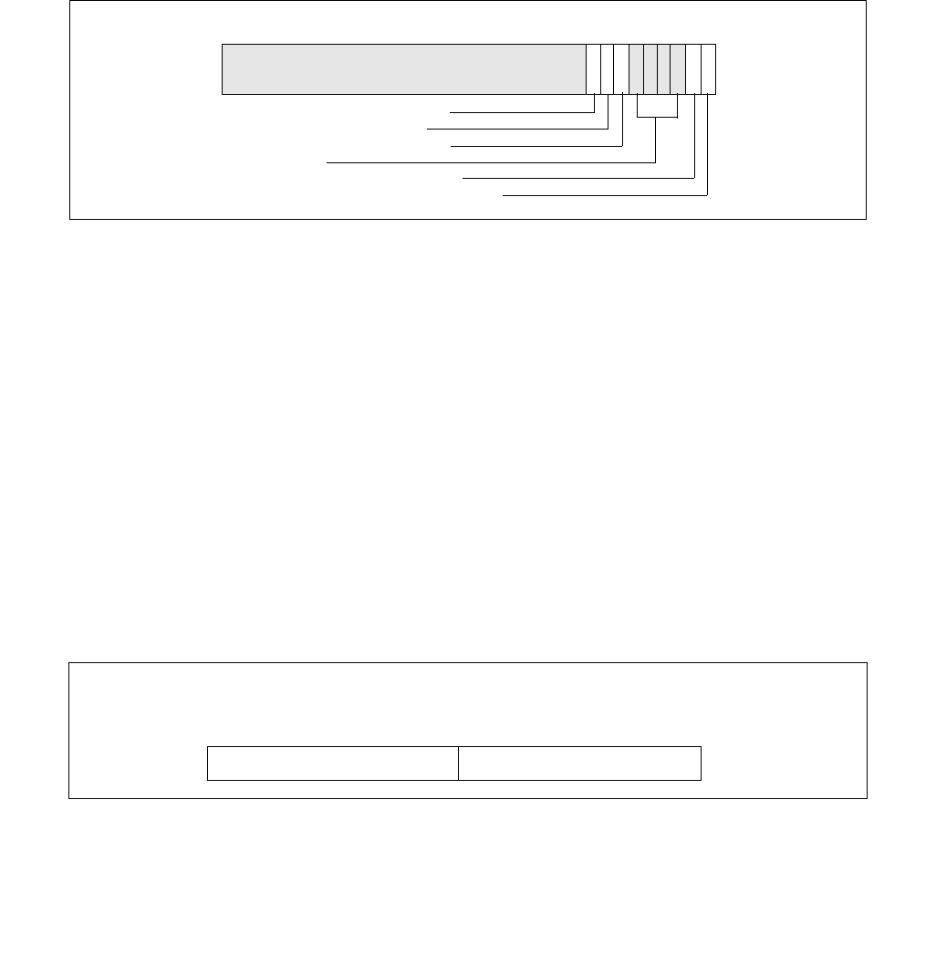
17-36 Vol. 3B
DEBUG, BRANCH PROFILE, TSC, AND RESOURCE MONITORING FEATURES
allows single-stepping the processor on taken branches. See Section 17.4.3, “Single-Stepping on
Branches,” for more information about the BTF flag.
—TR (trace message enable) flag (bit 6) — When set, branch trace messages are enabled. When the
processor detects a taken branch, interrupt, or exception; it sends the branch record out on the system bus
as a branch trace message (BTM). See Section 17.4.4, “Branch Trace Messages,” for more information
about the TR flag.
—BTS (branch trace store) flag (bit 7) — When set, the flag enables BTS facilities to log BTMs to a
memory-resident BTS buffer that is part of the DS save area. See Section 17.4.9, “BTS and DS Save Area.”
—BTINT (branch trace interrupt) flag (bits 8) — When set, the BTS facilities generate an interrupt when
the BTS buffer is full. When clear, BTMs are logged to the BTS buffer in a circular fashion. See Section 17.4.5,
“Branch Trace Store (BTS),” for a description of this mechanism.
•Debug store (DS) feature flag (bit 21), returned by the CPUID instruction — Indicates that the
processor provides the debug store (DS) mechanism, which allows BTMs to be stored in a memory-resident
BTS buffer. See Section 17.4.5, “Branch Trace Store (BTS).”
•Last Branch Record (LBR) Stack — The LBR stack consists of 8 MSRs (MSR_LASTBRANCH_0 through
MSR_LASTBRANCH_7); bits 31-0 hold the ‘from’ address, bits 63-32 hold the ‘to’ address (MSR addresses start
at 40H). See Figure 17-15.
•Last Branch Record Top-of-Stack (TOS) Pointer — The TOS Pointer MSR contains a 3-bit pointer (bits 2-0)
to the MSR in the LBR stack that contains the most recent branch, interrupt, or exception recorded. For Intel
Core Solo and Intel Core Duo processors, this MSR is located at register address 01C9H.
For compatibility, the Intel Core Solo and Intel Core Duo processors provide two 32-bit MSRs (the
MSR_LER_TO_LIP and the MSR_LER_FROM_LIP MSRs) that duplicate functions of the LastExceptionToIP and Last-
ExceptionFromIP MSRs found in P6 family processors.
For details, see Section 17.10, “Last Branch, Call Stack, Interrupt, and Exception Recording for Processors based
on Skylake Microarchitecture,” and Section 35.19, “MSRs In Intel® Core™ Solo and Intel® Core™ Duo Processors”
Figure 17-14. IA32_DEBUGCTL MSR for Intel Core Solo
and Intel Core Duo Processors
Figure 17-15. LBR Branch Record Layout for the Intel Core Solo
and Intel Core Duo Processor
31
TR — Trace messages enable
BTINT — Branch trace interrupt
BTF — Single-step on branches
LBR — Last branch/interrupt/exception
Reserved
87654321 0
BTS — Branch trace store
Reserved
0
63
From Linear Address
To Linear Address
32 - 31
MSR_LASTBRANCH_0 through MSR_LASTBRANCH_7

Vol. 3B 17-37
DEBUG, BRANCH PROFILE, TSC, AND RESOURCE MONITORING FEATURES
17.13 LAST BRANCH, INTERRUPT, AND EXCEPTION
RECORDING (PENTIUM M PROCESSORS)
Like the Pentium 4 and Intel Xeon processor family, Pentium M processors provide last branch interrupt and excep-
tion recording. The capability operates almost identically to that found in Pentium 4 and Intel Xeon processors.
There are differences in the shape of the stack and in some MSR names and locations. Note the following:
•MSR_DEBUGCTLB MSR — Enables debug trace interrupt, debug trace store, trace messages enable,
performance monitoring breakpoint flags, single stepping on branches, and last branch. For Pentium M
processors, this MSR is located at register address 01D9H. See Figure 17-16 and the entries below for a
description of the flags.
—LBR (last branch/interrupt/exception) flag (bit 0) — When set, the processor records a running trace
of the most recent branches, interrupts, and/or exceptions taken by the processor (prior to a debug
exception being generated) in the last branch record (LBR) stack. For more information, see the “Last
Branch Record (LBR) Stack” bullet below.
—BTF (single-step on branches) flag (bit 1) — When set, the processor treats the TF flag in the EFLAGS
register as a “single-step on branches” flag rather than a “single-step on instructions” flag. This mechanism
allows single-stepping the processor on taken branches. See Section 17.4.3, “Single-Stepping on
Branches,” for more information about the BTF flag.
—PBi (performance monitoring/breakpoint pins) flags (bits 5-2) — When these flags are set, the
performance monitoring/breakpoint pins on the processor (BP0#, BP1#, BP2#, and BP3#) report
breakpoint matches in the corresponding breakpoint-address registers (DR0 through DR3). The processor
asserts then deasserts the corresponding BPi# pin when a breakpoint match occurs. When a PBi flag is
clear, the performance monitoring/breakpoint pins report performance events. Processor execution is not
affected by reporting performance events.
—TR (trace message enable) flag (bit 6) — When set, branch trace messages are enabled. When the
processor detects a taken branch, interrupt, or exception, it sends the branch record out on the system bus
as a branch trace message (BTM). See Section 17.4.4, “Branch Trace Messages,” for more information
about the TR flag.
—BTS (branch trace store) flag (bit 7) — When set, enables the BTS facilities to log BTMs to a memory-
resident BTS buffer that is part of the DS save area. See Section 17.4.9, “BTS and DS Save Area.”
—BTINT (branch trace interrupt) flag (bits 8) — When set, the BTS facilities generate an interrupt when
the BTS buffer is full. When clear, BTMs are logged to the BTS buffer in a circular fashion. See Section 17.4.5,
“Branch Trace Store (BTS),” for a description of this mechanism.
•Debug store (DS) feature flag (bit 21), returned by the CPUID instruction — Indicates that the
processor provides the debug store (DS) mechanism, which allows BTMs to be stored in a memory-resident
BTS buffer. See Section 17.4.5, “Branch Trace Store (BTS).”
Figure 17-16. MSR_DEBUGCTLB MSR for Pentium M Processors
31
TR — Trace messages enable
BTINT — Branch trace interrupt
BTF — Single-step on branches
LBR — Last branch/interrupt/exception
Reserved
87654321 0
BTS — Branch trace store
PB3/2/1/0 — Performance monitoring breakpoint flags

17-38 Vol. 3B
DEBUG, BRANCH PROFILE, TSC, AND RESOURCE MONITORING FEATURES
•Last Branch Record (LBR) Stack — The LBR stack consists of 8 MSRs (MSR_LASTBRANCH_0 through
MSR_LASTBRANCH_7); bits 31-0 hold the ‘from’ address, bits 63-32 hold the ‘to’ address. For Pentium M
Processors, these pairs are located at register addresses 040H-047H. See Figure 17-17.
•Last Branch Record Top-of-Stack (TOS) Pointer — The TOS Pointer MSR contains a 3-bit pointer (bits 2-0)
to the MSR in the LBR stack that contains the most recent branch, interrupt, or exception recorded. For Pentium
M Processors, this MSR is located at register address 01C9H.
For more detail on these capabilities, see Section 17.11.3, “Last Exception Records,” and Section 35.20, “MSRs In
the Pentium M Processor.”
17.14 LAST BRANCH, INTERRUPT, AND EXCEPTION
RECORDING (P6 FAMILY PROCESSORS)
The P6 family processors provide five MSRs for recording the last branch, interrupt, or exception taken by the
processor: DEBUGCTLMSR, LastBranchToIP, LastBranchFromIP, LastExceptionToIP, and LastExceptionFromIP.
These registers can be used to collect last branch records, to set breakpoints on branches, interrupts, and excep-
tions, and to single-step from one branch to the next.
See Chapter 35, “Model-Specific Registers (MSRs),” for a detailed description of each of the last branch recording
MSRs.
17.14.1 DEBUGCTLMSR Register
The version of the DEBUGCTLMSR register found in the P6 family processors enables last branch, interrupt, and
exception recording; taken branch breakpoints; the breakpoint reporting pins; and trace messages. This register
can be written to using the WRMSR instruction, when operating at privilege level 0 or when in real-address mode.
A protected-mode operating system procedure is required to provide user access to this register. Figure 17-18
shows the flags in the DEBUGCTLMSR register for the P6 family processors. The functions of these flags are as
follows:
•LBR (last branch/interrupt/exception) flag (bit 0) — When set, the processor records the source and
target addresses (in the LastBranchToIP, LastBranchFromIP, LastExceptionToIP, and LastExceptionFromIP
MSRs) for the last branch and the last exception or interrupt taken by the processor prior to a debug exception
being generated. The processor clears this flag whenever a debug exception, such as an instruction or data
breakpoint or single-step trap occurs.
Figure 17-17. LBR Branch Record Layout for the Pentium M Processor
0
63
From Linear Address
To Linear Address
32 - 31
MSR_LASTBRANCH_0 through MSR_LASTBRANCH_7

Vol. 3B 17-39
DEBUG, BRANCH PROFILE, TSC, AND RESOURCE MONITORING FEATURES
•BTF (single-step on branches) flag (bit 1) — When set, the processor treats the TF flag in the EFLAGS
register as a “single-step on branches” flag. See Section 17.4.3, “Single-Stepping on Branches.”
•PBi (performance monitoring/breakpoint pins) flags (bits 2 through 5) — When these flags are set,
the performance monitoring/breakpoint pins on the processor (BP0#, BP1#, BP2#, and BP3#) report
breakpoint matches in the corresponding breakpoint-address registers (DR0 through DR3). The processor
asserts then deasserts the corresponding BPi# pin when a breakpoint match occurs. When a PBi flag is clear,
the performance monitoring/breakpoint pins report performance events. Processor execution is not affected by
reporting performance events.
•TR (trace message enable) flag (bit 6) — When set, trace messages are enabled as described in Section
17.4.4, “Branch Trace Messages.” Setting this flag greatly reduces the performance of the processor. When
trace messages are enabled, the values stored in the LastBranchToIP, LastBranchFromIP, LastExceptionToIP,
and LastExceptionFromIP MSRs are undefined.
17.14.2 Last Branch and Last Exception MSRs
The LastBranchToIP and LastBranchFromIP MSRs are 32-bit registers for recording the instruction pointers for the
last branch, interrupt, or exception that the processor took prior to a debug exception being generated. When a
branch occurs, the processor loads the address of the branch instruction into the LastBranchFromIP MSR and loads
the target address for the branch into the LastBranchToIP MSR.
When an interrupt or exception occurs (other than a debug exception), the address of the instruction that was
interrupted by the exception or interrupt is loaded into the LastBranchFromIP MSR and the address of the excep-
tion or interrupt handler that is called is loaded into the LastBranchToIP MSR.
The LastExceptionToIP and LastExceptionFromIP MSRs (also 32-bit registers) record the instruction pointers for
the last branch that the processor took prior to an exception or interrupt being generated. When an exception or
interrupt occurs, the contents of the LastBranchToIP and LastBranchFromIP MSRs are copied into these registers
before the to and from addresses of the exception or interrupt are recorded in the LastBranchToIP and LastBranch-
FromIP MSRs.
These registers can be read using the RDMSR instruction.
Note that the values stored in the LastBranchToIP, LastBranchFromIP, LastExceptionToIP, and LastExceptionFromIP
MSRs are offsets into the current code segment, as opposed to linear addresses, which are saved in last branch
records for the Pentium 4 and Intel Xeon processors.
17.14.3 Monitoring Branches, Exceptions, and Interrupts
When the LBR flag in the DEBUGCTLMSR register is set, the processor automatically begins recording branches
that it takes, exceptions that are generated (except for debug exceptions), and interrupts that are serviced. Each
time a branch, exception, or interrupt occurs, the processor records the to and from instruction pointers in the
LastBranchToIP and LastBranchFromIP MSRs. In addition, for interrupts and exceptions, the processor copies the
contents of the LastBranchToIP and LastBranchFromIP MSRs into the LastExceptionToIP and LastExceptionFromIP
MSRs prior to recording the to and from addresses of the interrupt or exception.
Figure 17-18. DEBUGCTLMSR Register (P6 Family Processors)
31
TR — Trace messages enable
PBi — Performance monitoring/breakpoint pins
BTF — Single-step on branches
LBR — Last branch/interrupt/exception
76543210
P
B
2
P
B
1
P
B
0
B
T
F
T
R
L
B
R
P
B
3
Reserved

17-40 Vol. 3B
DEBUG, BRANCH PROFILE, TSC, AND RESOURCE MONITORING FEATURES
When the processor generates a debug exception (#DB), it automatically clears the LBR flag before executing the
exception handler, but does not touch the last branch and last exception MSRs. The addresses for the last branch,
interrupt, or exception taken are thus retained in the LastBranchToIP and LastBranchFromIP MSRs and the
addresses of the last branch prior to an interrupt or exception are retained in the LastExceptionToIP, and LastEx-
ceptionFromIP MSRs.
The debugger can use the last branch, interrupt, and/or exception addresses in combination with code-segment
selectors retrieved from the stack to reset breakpoints in the breakpoint-address registers (DR0 through DR3),
allowing a backward trace from the manifestation of a particular bug toward its source. Because the instruction
pointers recorded in the LastBranchToIP, LastBranchFromIP, LastExceptionToIP, and LastExceptionFromIP MSRs are
offsets into a code segment, software must determine the segment base address of the code segment associated
with the control transfer to calculate the linear address to be placed in the breakpoint-address registers. The
segment base address can be determined by reading the segment selector for the code segment from the stack
and using it to locate the segment descriptor for the segment in the GDT or LDT. The segment base address can
then be read from the segment descriptor.
Before resuming program execution from a debug-exception handler, the handler must set the LBR flag again to re-
enable last branch and last exception/interrupt recording.
17.15 TIME-STAMP COUNTER
The Intel 64 and IA-32 architectures (beginning with the Pentium processor) define a time-stamp counter mecha-
nism that can be used to monitor and identify the relative time occurrence of processor events. The counter’s archi-
tecture includes the following components:
•TSC flag — A feature bit that indicates the availability of the time-stamp counter. The counter is available in an
if the function CPUID.1:EDX.TSC[bit 4] = 1.
•IA32_TIME_STAMP_COUNTER MSR (called TSC MSR in P6 family and Pentium processors) — The MSR used
as the counter.
•RDTSC instruction — An instruction used to read the time-stamp counter.
•TSD flag — A control register flag is used to enable or disable the time-stamp counter (enabled if
CR4.TSD[bit 2] = 1).
The time-stamp counter (as implemented in the P6 family, Pentium, Pentium M, Pentium 4, Intel Xeon, Intel Core
Solo and Intel Core Duo processors and later processors) is a 64-bit counter that is set to 0 following a RESET of
the processor. Following a RESET, the counter increments even when the processor is halted by the HLT instruction
or the external STPCLK# pin. Note that the assertion of the external DPSLP# pin may cause the time-stamp
counter to stop.
Processor families increment the time-stamp counter differently:
•For Pentium M processors (family [06H], models [09H, 0DH]); for Pentium 4 processors, Intel Xeon processors
(family [0FH], models [00H, 01H, or 02H]); and for P6 family processors: the time-stamp counter increments
with every internal processor clock cycle.
The internal processor clock cycle is determined by the current core-clock to bus-clock ratio. Intel®
SpeedStep® technology transitions may also impact the processor clock.
•For Pentium 4 processors, Intel Xeon processors (family [0FH], models [03H and higher]); for Intel Core Solo
and Intel Core Duo processors (family [06H], model [0EH]); for the Intel Xeon processor 5100 series and Intel
Core 2 Duo processors (family [06H], model [0FH]); for Intel Core 2 and Intel Xeon processors (family [06H],
DisplayModel [17H]); for Intel Atom processors (family [06H],
DisplayModel [1CH]): the time-stamp counter increments at a constant rate. That rate may be set by the
maximum core-clock to bus-clock ratio of the processor or may be set by the maximum resolved frequency at
which the processor is booted. The maximum resolved frequency may differ from the processor base
frequency, see Section 18.18.2 for more detail. On certain processors, the TSC frequency may not be the same
as the frequency in the brand string.
The specific processor configuration determines the behavior. Constant TSC behavior ensures that the duration
of each clock tick is uniform and supports the use of the TSC as a wall clock timer even if the processor core
changes frequency. This is the architectural behavior moving forward.

Vol. 3B 17-41
DEBUG, BRANCH PROFILE, TSC, AND RESOURCE MONITORING FEATURES
NOTE
To determine average processor clock frequency, Intel recommends the use of performance
monitoring logic to count processor core clocks over the period of time for which the average is
required. See Section 18.17, “Counting Clocks on systems with Intel Hyper-Threading Technology
in Processors Based on Intel NetBurst® Microarchitecture,” and Chapter 19, “Performance-
Monitoring Events,” for more information.
The RDTSC instruction reads the time-stamp counter and is guaranteed to return a monotonically increasing
unique value whenever executed, except for a 64-bit counter wraparound. Intel guarantees that the time-stamp
counter will not wraparound within 10 years after being reset. The period for counter wrap is longer for Pentium 4,
Intel Xeon, P6 family, and Pentium processors.
Normally, the RDTSC instruction can be executed by programs and procedures running at any privilege level and in
virtual-8086 mode. The TSD flag allows use of this instruction to be restricted to programs and procedures running
at privilege level 0. A secure operating system would set the TSD flag during system initialization to disable user
access to the time-stamp counter. An operating system that disables user access to the time-stamp counter should
emulate the instruction through a user-accessible programming interface.
The RDTSC instruction is not serializing or ordered with other instructions. It does not necessarily wait until all
previous instructions have been executed before reading the counter. Similarly, subsequent instructions may begin
execution before the RDTSC instruction operation is performed.
The RDMSR and WRMSR instructions read and write the time-stamp counter, treating the time-stamp counter as
an ordinary MSR (address 10H). In the Pentium 4, Intel Xeon, and P6 family processors, all 64-bits of the time-
stamp counter are read using RDMSR (just as with RDTSC). When WRMSR is used to write the time-stamp counter
on processors before family [0FH], models [03H, 04H]: only the low-order 32-bits of the time-stamp counter can
be written (the high-order 32 bits are cleared to 0). For family [0FH], models [03H, 04H, 06H]; for family [06H]],
model [0EH, 0FH]; for family [06H]], DisplayModel [17H, 1AH, 1CH, 1DH]: all 64 bits are writable.
17.15.1 Invariant TSC
The time stamp counter in newer processors may support an enhancement, referred to as invariant TSC.
Processor’s support for invariant TSC is indicated by CPUID.80000007H:EDX[8].
The invariant TSC will run at a constant rate in all ACPI P-, C-. and T-states. This is the architectural behavior
moving forward. On processors with invariant TSC support, the OS may use the TSC for wall clock timer services
(instead of ACPI or HPET timers). TSC reads are much more efficient and do not incur the overhead associated with
a ring transition or access to a platform resource.
17.15.2 IA32_TSC_AUX Register and RDTSCP Support
Processors based on Intel microarchitecture code name Nehalem provide an auxiliary TSC register, IA32_TSC_AUX
that is designed to be used in conjunction with IA32_TSC. IA32_TSC_AUX provides a 32-bit field that is initialized
by privileged software with a signature value (for example, a logical processor ID).
The primary usage of IA32_TSC_AUX in conjunction with IA32_TSC is to allow software to read the 64-bit time
stamp in IA32_TSC and signature value in IA32_TSC_AUX with the instruction RDTSCP in an atomic operation.
RDTSCP returns the 64-bit time stamp in EDX:EAX and the 32-bit TSC_AUX signature value in ECX. The atomicity
of RDTSCP ensures that no context switch can occur between the reads of the TSC and TSC_AUX values.
Support for RDTSCP is indicated by CPUID.80000001H:EDX[27]. As with RDTSC instruction, non-ring 0 access is
controlled by CR4.TSD (Time Stamp Disable flag).
User mode software can use RDTSCP to detect if CPU migration has occurred between successive reads of the TSC.
It can also be used to adjust for per-CPU differences in TSC values in a NUMA system.

17-42 Vol. 3B
DEBUG, BRANCH PROFILE, TSC, AND RESOURCE MONITORING FEATURES
17.15.3 Time-Stamp Counter Adjustment
Software can modify the value of the time-stamp counter (TSC) of a logical processor by using the WRMSR instruc-
tion to write to the IA32_TIME_STAMP_COUNTER MSR (address 10H). Because such a write applies only to that
logical processor, software seeking to synchronize the TSC values of multiple logical processors must perform these
writes on each logical processor. It may be difficult for software to do this in a way than ensures that all logical
processors will have the same value for the TSC at a given point in time.
The synchronization of TSC adjustment can be simplified by using the 64-bit IA32_TSC_ADJUST MSR (address
3BH). Like the IA32_TIME_STAMP_COUNTER MSR, the IA32_TSC_ADJUST MSR is maintained separately for each
logical processor. A logical processor maintains and uses the IA32_TSC_ADJUST MSR as follows:
•On RESET, the value of the IA32_TSC_ADJUST MSR is 0.
•If an execution of WRMSR to the IA32_TIME_STAMP_COUNTER MSR adds (or subtracts) value X from the TSC,
the logical processor also adds (or subtracts) value X from the IA32_TSC_ADJUST MSR.
•If an execution of WRMSR to the IA32_TSC_ADJUST MSR adds (or subtracts) value X from that MSR, the logical
processor also adds (or subtracts) value X from the TSC.
Unlike the TSC, the value of the IA32_TSC_ADJUST MSR changes only in response to WRMSR (either to the MSR
itself, or to the IA32_TIME_STAMP_COUNTER MSR). Its value does not otherwise change as time elapses. Software
seeking to adjust the TSC can do so by using WRMSR to write the same value to the IA32_TSC_ADJUST MSR on
each logical processor.
Processor support for the IA32_TSC_ADJUST MSR is indicated by CPUID.(EAX=07H, ECX=0H):EBX.TSC_ADJUST
(bit 1).
17.15.4 Invariant Time-Keeping
The invariant TSC is based on the invariant timekeeping hardware (called Always Running Timer or ART), that runs
at the core crystal clock frequency. The ratio defined by CPUID leaf 15H expresses the frequency relationship
between the ART hardware and TSC.
If CPUID.15H:EBX[31:0] != 0 and CPUID.80000007H:EDX[InvariantTSC] = 1, the following linearity relationship
holds between TSC and the ART hardware:
TSC_Value = (ART_Value * CPUID.15H:EBX[31:0] )/ CPUID.15H:EAX[31:0] + K
Where 'K' is an offset that can be adjusted by a privileged agent2.
When ART hardware is reset, both invariant TSC and K are also reset.
17.16 INTEL® RESOURCE DIRECTOR TECHNOLOGY (INTEL® RDT) MONITORING
FEATURES
The Intel Resource Director Technology (Intel RDT) feature set provides a set of monitoring capabilities including
Cache Monitoring Technology (CMT) and Memory Bandwidth Monitoring (MBM). The Intel® Xeon® processor E5 v3
family introduced resource monitoring capability in each logical processor to measure specific platform shared
resource metrics, for example, L3 cache occupancy. The programming interface for these monitoring features is
described in this section. Two features within the monitoring feature set provided are described - Cache Monitoring
Technology (CMT) and Memory Bandwidth Monitoring.
Cache Monitoring Technology (CMT) allows an Operating System, Hypervisor or similar system management agent
to determine the usage of cache by applications running on the platform. The initial implementation is directed at
L3 cache monitoring (currently the last level cache in most server platforms).
Memory Bandwidth Monitoring (MBM), introduced in the Intel® Xeon® processor E5 v4 family, builds on the CMT
infrastructure to allow monitoring of bandwidth from one level of the cache hierarchy to the next - in this case
2. IA32_TSC_ADJUST MSR and the TSC-offset field in the VM execution controls of VMCS are some of the common interfaces that priv-
ileged software can use to manage the time stamp counter for keeping time

Vol. 3B 17-43
DEBUG, BRANCH PROFILE, TSC, AND RESOURCE MONITORING FEATURES
focusing on the L3 cache, which is typically backed directly by system memory. As a result of this implementation,
memory bandwidth can be monitored.
The monitoring mechanisms described provide the following key shared infrastructure features:
•A mechanism to enumerate the presence of the monitoring capabilities within the platform (via a CPUID feature
bit).
•A framework to enumerate the details of each sub-feature (including CMT and MBM, as discussed later, via
CPUID leaves and sub-leaves).
•A mechanism for the OS or Hypervisor to indicate a software-defined ID for each of the software threads (appli-
cations, virtual machines, etc.) that are scheduled to run on a logical processor. These identifiers are known as
Resource Monitoring IDs (RMIDs).
•Mechanisms in hardware to monitor cache occupancy and bandwidth statistics as applicable to a given product
generation on a per software-id basis.
•Mechanisms for the OS or Hypervisor to read back the collected metrics such as L3 occupancy or Memory
Bandwidth for a given software ID at any point during runtime.
17.16.1 Overview of Cache Monitoring Technology and Memory Bandwidth Monitoring
The shared resource monitoring features described in this chapter provide a layer of abstraction between applica-
tions and logical processors through the use of Resource Monitoring IDs (RMIDs). Each logical processor in the
system can be assigned an RMID independently, or multiple logical processors can be assigned to the same RMID
value (e.g., to track an application with multiple threads). For each logical processor, only one RMID value is active
at a time. This is enforced by the IA32_PQR_ASSOC MSR, which specifies the active RMID of a logical processor.
Writing to this MSR by software changes the active RMID of the logical processor from an old value to a new value.
The underlying platform shared resource monitoring hardware tracks cache metrics such as cache utilization and
misses as a result of memory accesses according to the RMIDs and reports monitored data via a counter register
(IA32_QM_CTR). The specific event types supported vary by generation and can be enumerated via CPUID. Before
reading back monitored data software must configure an event selection MSR (IA32_QM_EVTSEL) to specify which
metric is to be reported, and the specific RMID for which the data should be returned.
Processor support of the monitoring framework and sub-features such as CMT is reported via the CPUID instruc-
tion. The resource type available to the monitoring framework is enumerated via a new leaf function in CPUID.
Reading and writing to the monitoring MSRs requires the RDMSR and WRMSR instructions.
The Cache Monitoring Technology feature set provides the following unique mechanisms:
•A mechanism to enumerate the presence and details of the CMT feature as applicable to a given level of the
cache hierarchy, independent of other monitoring features.
•CMT-specific event codes to read occupancy for a given level of the cache hierarchy.
The Memory Bandwidth Monitoring feature provides the following unique mechanisms:
•A mechanism to enumerate the presence and details of the MBM feature as applicable to a given level of the
cache hierarchy, independent of other monitoring features.
•MBM-specific event codes to read bandwidth out to the next level of the hierarchy and various sub-event codes
to read more specific metrics as discussed later (e.g., total bandwidth vs. bandwidth only from local memory
controllers on the same package).
17.16.2 Enabling Monitoring: Usage Flow
Figure 17-19 illustrates the key steps for OS/VMM to detect support of shared resource monitoring features such
as CMT and enable resource monitoring for available resource types and monitoring events.
17-44 Vol. 3B
DEBUG, BRANCH PROFILE, TSC, AND RESOURCE MONITORING FEATURES
17.16.3 Enumeration and Detecting Support of Cache Monitoring Technology and Memory
Bandwidth Monitoring
Software can query processor support of shared resource monitoring features capabilities by executing CPUID
instruction with EAX = 07H, ECX = 0H as input. If CPUID.(EAX=07H, ECX=0):EBX.PQM[bit 12] reports 1, the
processor provides the following programming interfaces for shared resource monitoring, including Cache Moni-
toring Technology:
•CPUID leaf function 0FH (Shared Resource Monitoring Enumeration leaf) provides information on available
resource types (see Section 17.16.4), and monitoring capabilities for each resource type (see Section 17.16.5).
Note CMT and MBM capabilities are enumerated as separate event vectors using shared enumeration infra-
structure under a given resource type.
•IA32_PQR_ASSOC.RMID: The per-logical-processor MSR, IA32_PQR_ASSOC, that OS/VMM can use to assign
an RMID to each logical processor, see Section 17.16.6.
•IA32_QM_EVTSEL: This MSR specifies an Event ID (EvtID) and an RMID which the platform uses to look up and
provide monitoring data in the monitoring counter, IA32_QM_CTR, see Section 17.16.7.
•IA32_QM_CTR: This MSR reports monitored resource data when available along with bits to allow software to
check for error conditions and verify data validity.
Software must follow the following sequence of enumeration to discover Cache Monitoring Technology capabilities:
1. Execute CPUID with EAX=0 to discover the “cpuid_maxLeaf” supported in the processor;
2. If cpuid_maxLeaf >= 7, then execute CPUID with EAX=7, ECX= 0 to verify CPUID.(EAX=07H,
ECX=0):EBX.PQM[bit 12] is set;
3. If CPUID.(EAX=07H, ECX=0):EBX.PQM[bit 12] = 1, then execute CPUID with EAX=0FH, ECX= 0 to query
available resource types that support monitoring;
4. If CPUID.(EAX=0FH, ECX=0):EDX.L3[bit 1] = 1, then execute CPUID with EAX=0FH, ECX= 1 to query the
specific capabilities of L3 Cache Monitoring Technology (CMT) and Memory Bandwidth Monitoring.
5. If CPUID.(EAX=0FH, ECX=0):EDX reports additional resource types supporting monitoring, then execute
CPUID with EAX=0FH, ECX set to a corresponding resource type ID (ResID) as enumerated by the bit position
of CPUID.(EAX=0FH, ECX=0):EDX.
17.16.4 Monitoring Resource Type and Capability Enumeration
CPUID leaf function 0FH (Shared Resource Monitoring Enumeration leaf) provides one sub-leaf (sub-function 0)
that reports shared enumeration infrastructure, and one or more sub-functions that report feature-specific
enumeration data:
•Monitoring leaf sub-function 0 enumerates available resources that support monitoring, i.e. executing CPUID
with EAX=0FH and ECX=0H. In the initial implementation, L3 cache is the only resource type available. Each
Figure 17-19. Platform Shared Resource Monitoring Usage Flow
CPUID.(7,0):EBX.12
On OS/VMM Initialization
CPUID.(0FH,0):EDX[31:1]
PQM Capability
Enumeration
IA32_PQR_ASSOC.RMID
On Context Switch
Set RMID to monitor
the scheduled app
Periodical Resource
IA32_QM_EVTSEL
Configure event type
Read monitored data
CPUID.(0FH,1):ECX[31:0]
CPUID.(0FH,1):EDX[31:0]
CPUID.(0FH,1):EBX[31:0]
CPUID[ WRMSR RDMSR/WRMSR
Selection/Reporting
IA32_QM_CTR
CPUID.(0FH,0):EBX[31:0]

Vol. 3B 17-45
DEBUG, BRANCH PROFILE, TSC, AND RESOURCE MONITORING FEATURES
supported resource type is represented by a bit in CPUID.(EAX=0FH, ECX=0):EDX[31:1]. The bit position
corresponds to the sub-leaf index (ResID) that software must use to query details of the monitoring capability
of that resource type (see Figure 17-21 and Figure 17-22). Reserved bits of CPUID.(EAX=0FH,
ECX=0):EDX[31:2] correspond to unsupported sub-leaves of the CPUID.0FH leaf. Additionally,
CPUID.(EAX=0FH, ECX=0H):EBX reports the highest RMID value of any resource type that supports
monitoring in the processor.
17.16.5 Feature-Specific Enumeration
Each additional sub-leaf of CPUID.(EAX=0FH, ECX=ResID) enumerates the specific details for software to program
Monitoring MSRs using the resource type associated with the given ResID.
Note that in future Monitoring implementations the meanings of the returned registers may vary in other sub-
leaves that are not yet defined. The registers will be specified and defined on a per-ResID basis.
For each supported Cache Monitoring resource type, hardware supports only a finite number of RMIDs.
CPUID.(EAX=0FH, ECX=1H).ECX enumerates the highest RMID value that can be monitored with this resource
type, see Figure 17-21.
CPUID.(EAX=0FH, ECX=1H).EDX specifies a bit vector that is used to look up the EventID (See Figure 17-22 and
Table 17-18) that software must program with IA32_QM_EVTSEL in order to retrieve event data. After software
configures IA32_QMEVTSEL with the desired RMID and EventID, i t c an re a d the resulting data from I A3 2_QM_CTR.
The raw numerical value reported from IA32_QM_CTR can be converted to the final value (occupancy in bytes or
bandwidth in bytes per sampled time period) by multiplying the counter value by the value from CPUID.(EAX=0FH,
ECX=1H).EBX, see Figure 17-21.
Figure 17-20. CPUID.(EAX=0FH, ECX=0H) Monitoring Resource Type Enumeration
Figure 17-21. L3 Cache Monitoring Capability Enumeration Data (CPUID.(EAX=0FH, ECX=1H) )
0
2
31
CPUID.(EAX=0FH, ECX=0H) Output: (EAX: Reserved; ECX: Reserved)
EDX L
EBX 0
31
Highest RMID Value of Any Resource Type (Zero-Based)
3
1
Reserved
CPUID.(EAX=0FH, ECX=1H) Output: (EAX: Reserved)
ECX 0
31
Highest RMID Value of This Resource Type (Zero-Based)
EBX 0
31
Upscaling Factor to Total Occupancy (Bytes) Upscaling Factor
MaxRMID
17-46 Vol. 3B
DEBUG, BRANCH PROFILE, TSC, AND RESOURCE MONITORING FEATURES
17.16.5.1 Cache Monitoring Technology
On processors for which Cache Monitoring Technology supports the L3 cache occupancy event, CPUID.(EAX=0FH,
ECX=1H).EDX would return with only bit 0 set. The corresponding event ID can be looked up from Table 17-18. The
L3 occupancy data accumulated in IA32_QM_CTR can be converted to total occupancy (in bytes) by multiplying
with CPUID.(EAX=0FH, ECX=1H).EBX.
Event codes for Cache Monitoring Technology are discussed in the next section.
17.16.5.2 Memory Bandwidth Monitoring
On processors that monitoring supports Memory Bandwidth Monitoring using ResID=1 (L3), two additional bits will
be set in the vector at CPUID.(EAX=0FH, ECX=1H).EDX:
•CPUID.(EAX=0FH, ECX=1H).EDX[bit 1]: indicates the L3 total external bandwidth monitoring event is
supported if set. This event monitors the L3 total external bandwidth to the next level of the cache hierarchy,
including all demand and prefetch misses from the L3 to the next hierarchy of the memory system. In most
platforms, this represents memory bandwidth.
•CPUID.(EAX=0FH, ECX=1H).EDX[bit 2]: indicates L3 local memory bandwidth monitoring event is supported if
set. This event monitors the L3 external bandwidth satisfied by the local memory. In most platforms that
support this event, L3 requests are likely serviced by a memory system with non-uniform memory architecture.
This allows bandwidth to off-package memory resources to be tracked by subtracting total from local bandwidth
(for instance, bandwidth over QPI to a memory controller on another physical processor could be tracked by
subtraction).
The corresponding Event ID can be looked up from Table 17-18. The L3 bandwidth data accumulated in
IA32_QM_CTR can be converted to total bandwidth (in bytes) using CPUID.(EAX=0FH, ECX=1H).EBX.
Table 17-18. Monitoring Supported Event IDs
17.16.6 Monitoring Resource RMID Association
After Monitoring and sub-features has been enumerated, software can begin using the monitoring features. The
first step is to associate a given software thread (or multiple threads as part of an application, VM, group of appli-
cations or other abstraction) with an RMID.
Note that the process of associating an RMID with a given software thread is the same for all shared resource moni-
toring features (CMT, MBM), and a given RMID number has the same meaning from the viewpoint of any logical
processors in a package. Stated another way, a thread may be associated in a 1:1 mapping with an RMID, and that
Figure 17-22. L3 Cache Monitoring Capability Enumeration Event Type Bit Vector (CPUID.(EAX=0FH, ECX=1H) )
Event Type Event ID Context
L3 Cache Occupancy 01H Cache Monitoring Technology
L3 Total External Bandwidth 02H MBM
L3 Local External Bandwidth 03H MBM
Reserved All other event codes N/A
0231
EDX
1
Reserved
EventTypeBitMask 3
L3 Occupancy
L3 Total BW
L3 Local BW

Vol. 3B 17-47
DEBUG, BRANCH PROFILE, TSC, AND RESOURCE MONITORING FEATURES
RMID may allow cache occupancy, memory bandwidth information or other monitoring data to be read back later
with monitoring event codes (retrieving data is discussed in a previous section).
The association of an application thread with an RMID requires an OS to program the per-logical-processor MSR
IA32_PQR_ASSOC at context swap time (updates may also be made at any other arbitrary points during program
execution such as application phase changes). The IA32_PQR_ASSOC MSR specifies the active RMID that moni-
toring hardware will use to tag internal operations, such as L3 cache requests. The layout of the MSR is shown in
Figure 17-23. Software specifies the active RMID to monitor in the IA32_PQR_ASSOC.RMID field. The width of the
RMID field can vary from one implementation to another, and is derived from Ceil (LOG2 ( 1 + CPUID.(EAX=0FH,
ECX=0):EBX[31:0])). The value of IA32_PQR_ASSOC after power-on is 0.
In the initial implementation, the width of the RMID field is up to 10 bits wide, zero-referenced and fully encoded.
However, software must use CPUID to query the maximum RMID supported by the processor. If a value larger than
the maximum RMID is written to IA32_PQR_ASSOC.RMID, a #GP(0) fault will be generated.
RMIDs have a global scope within the physical package- if an RMID is assigned to one logical processor then the
same RMID can be used to read multiple thread attributes later (for example, L3 cache occupancy or external
bandwidth from the L3 to the next level of the cache hierarchy). In a multiple LLC platform the RMIDs are to be
reassigned by the OS or VMM scheduler when an application is migrated across LLCs.
Note that in a situation where Monitoring supports multiple resource types, some upper range of RMIDs (e.g. RMID
31) may only be supported by one resource type but not by another resource type.
17.16.7 Monitoring Resource Selection and Reporting Infrastructure
The reporting mechanism for Cache Monitoring Technology and other related features is architecturally exposed as
an MSR pair that can be programmed and read to measure various metrics such as the L3 cache occupancy (CMT)
and bandwidths (MBM) depending on the level of Monitoring support provided by the platform. Data is reported
back on a per-RMID basis. These events do not trigger based on event counts or trigger APIC interrupts (e.g. no
Performance Monitoring Interrupt occurs based on counts). Rather, they are used to sample counts explicitly.
The MSR pair for the shared resource monitoring features (CMT, MBM) is separate from and not shared with archi-
tectural Perfmon counters, meaning software can use these monitoring features simultaneously with the Perfmon
counters.
Access to the aggregated monitoring information is accomplished through the following programmable monitoring
MSRs:
•IA32_QM_EVTSEL: This MSR provides a role similar to the event select MSRs for programmable performance
monitoring described in Chapter 18. The simplified layout of the MSR is shown in Figure 17-24. Bits
IA32_QM_EVTSEL.EvtID (bits 7:0) specify an event code of a supported resource type for hardware to report
monitored data associated with IA32_QM_EVTSEL.RMID (bits 41:32). Software can configure
IA32_QM_EVTSEL.RMID with any RMID that is active within the physical processor. The width of
IA32_QM_EVTSEL.RMID matches that of IA32_PQR_ASSOC.RMID. Supported event codes for the
IA32_QM_EVTSEL register are shown in Table 17-18. Note that valid event codes may not necessarily map
directly to the bit position used to enumerate support for the resource via CPUID.
Software can program an RMID / Event ID pair into the IA32_QM_EVTSEL MSR bit field to select an RMID to
read a particular counter for a given resource. The currently supported list of Monitoring Event IDs is discussed
in Section 17.16.5, which covers feature-specific details.
Figure 17-23. IA32_PQR_ASSOC MSR
0
10
63
Width of IA32_PQR_ASSOC.RMID field: Log2 ( CPUID.(EAX=0FH, ECX=0H).EBX[31:0] +1)
RMID
9
Reserved IA32_PQR_ASSOC
Reserved for CLOS*
32 31
*See Section 17.15
17-48 Vol. 3B
DEBUG, BRANCH PROFILE, TSC, AND RESOURCE MONITORING FEATURES
Thread access to the IA32_QM_EVTSEL and IA32_QM_CTR MSR pair should be serialized to avoid situations
where one thread changes the RMID/EvtID just before another thread reads monitoring data from
IA32_QM_CTR.
•IA32_QM_CTR: This MSR reports monitored data when available. It contains three bit fields. If software
configures an unsupported RMID or event type in IA32_QM_EVTSEL, then IA32_QM_CTR.Error (bit 63) will be
set, indicating there is no valid data to report. If IA32_QM_CTR.Unavailable (bit 62) is set, it indicates
monitored data for the RMID is not available, and IA32_QM_CTR.data (bits 61:0) should be ignored. Therefore,
IA32_QM_CTR.data (bits 61:0) is valid only if bit 63 and 62 are both clear. For Cache Monitoring Technology,
software can convert IA32_QM_CTR.data into cache occupancy or bandwidth metrics expressed in bytes by
multiplying with the conversion factor from CPUID.(EAX=0FH, ECX=1H).EBX.
17.16.8 Monitoring Programming Considerations
Figure 17-23 illustrates how system software can program IA32_QOSEVTSEL and IA32_QM_CTR to perform
resource monitoring.
Though the field provided in IA32_QM_CTR allows for up to 62 bits of data to be returned, often a subset of bits are
used. With Cache Monitoring Technology for instance, the number of bits used will be proportional to the base-two
logarithm of the total cache size divided by the Upscaling Factor from CPUID.
In Memory Bandwidth Monitoring the initial counter size is 24 bits, and retrieving the value at 1Hz or faster is suffi-
cient to ensure at most one rollover per sampling period. Any future changes to counter width will be enumerated
to software.
Figure 17-24. IA32_QM_EVTSEL and IA32_QM_CTR MSRs
Figure 17-25. Software Usage of Cache Monitoring Resources
063
IA32_QM_CTR
U
61
E Resource Monitoring Data
03163
RMID
7
Reserved IA32_QM_EVTSEL
Reserved
41 3242 8
EvtID
RMID
063
Monitoring Data
IA32_QM_CTR MSR
62
Availability
Error
763
Reserved
41
RMID
Resource Monitoring ID
0
EvtID
32
Reserved
Event ID
IA32_QOSEVTSEL MSR
System Software
Event ID Counter Data

Vol. 3B 17-49
DEBUG, BRANCH PROFILE, TSC, AND RESOURCE MONITORING FEATURES
17.16.8.1 Monitoring Dynamic Configuration
Both the IA32_QM_EVTSEL and IA32_PQR_ASSOC registers are accessible and modifiable at any time during
execution using RDMSR/WRMSR unless otherwise noted. When writing to these MSRs a #GP(0) will be generated
if any of the following conditions occur:
•A reserved bit is modified,
•An RMID exceeding the maxRMID is used.
17.16.8.2 Monitoring Operation With Power Saving Features
Note that some advanced power management features such as deep package C-states may shrink the L3 cache
and cause CMT occupancy count to be reduced. MBM bandwidth counts may increase due to flushing cached data
out of L3.
17.16.8.3 Monitoring Operation with Other Operating Modes
The states in IA32_PQR_ASSOC and monitoring counter are unmodified across an SMI delivery. Thus, the execu-
tion of SMM handler code and SMM handler’s data can manifest as spurious contribution in the monitored data.
It is possible for an SMM handler to minimize the impact on of spurious contribution in the QOS monitoring coun-
ters by reserving a dedicated RMID for monitoring the SMM handler. Such an SMM handler can save the previously
configured QOS Monitoring state immediately upon entering SMM, and restoring the QOS monitoring state back to
the prev-SMM RMID upon exit.
17.16.8.4 Monitoring Operation with RAS Features
In general the Reliability, Availability and Serviceability (RAS) features present in Intel Platforms are not expected
to significantly affect shared resource monitoring counts. In cases where software RAS features cause memory
copies or cache accesses these may be tracked and may influence the shared resource monitoring counter values.
17.17 INTEL® RESOURCE DIRECTOR TECHNOLOGY (INTEL® RDT) ALLOCATION
FEATURES
The Intel Resource Director Technology (Intel RDT) feature set provides a set of allocation (resource control) capa-
bilities including Cache Allocation Technology (CAT) and Code and Data Prioritization (CDP). The Intel Xeon
processor E5 v4 family (and subset of communication-focused Intel Xeon processors E5 v3 family) introduce capa-
bilities to configure and make use of the Cache Allocation Technology (CAT) mechanisms on the L3 cache. Some
future Intel platforms may also provide support for control over the L2 cache, with capabilities as described below.
The programming interface for Cache Allocation Technology and for the more general allocation capabilities are
described in the rest of this chapter.
Cache Allocation Technology enables an Operating System (OS), Hypervisor /Virtual Machine Manager (VMM) or
similar system service management agent to specify the amount of cache space into which an application can fill
(as a hint to hardware - certain features such as power management may override CAT settings). Specialized user-
level implementations with minimal OS support are also possible, though not necessarily recommended (see notes
below for OS/Hypervisor with respect to ring 3 software and virtual guests). Depending on the processor famility,
L2 or L3 cache allocation capability may be provided, and the technology is designed to scale across multiple cache
levels and technology generations.
Software can determine which levels are supported in a give platform programmatically using CPUID as described
in the following sections.
The CAT mechanisms defined in this document provide the following key features:
•A mechanism to enumerate platform Cache Allocation Technology capabilities and available resource types that
provides CAT control capabilities. For implementations that support Cache Allocation Technology, CPUID
provides enumeration support to query which levels of the cache hierarchy are supported and specific CAT
capabilities, such as the max allocation bitmask size,
17-50 Vol. 3B
DEBUG, BRANCH PROFILE, TSC, AND RESOURCE MONITORING FEATURES
•A mechanism for the OS or Hypervisor to configure the amount of a resource available to a particular Class of
Service via a list of allocation bitmasks,
•Mechanisms for the OS or Hypervisor to signal the Class of Service to which an application belongs, and
•Hardware mechanisms to guide the LLC fill policy when an application has been designated to belong to a
specific Class of Service.
Note that for many usages, an OS or Hypervisor may not want to expose Cache Allocation Technology mechanisms
to Ring3 software or virtualized guests.
The Cache Allocation Technology feature enables more cache resources (i.e. cache space) to be made available for
high priority applications based on guidance from the execution environment as shown in Figure 17-26. The archi-
tecture also allows dynamic resource reassignment during runtime to further optimize the performance of the high
priority application with minimal degradation to the low priority app. Additionally, resources can be rebalanced for
system throughput benefit across uses cases of OSes, VMMs, containers and other scenarios by managing the
CPUID and MSR interfaces. This section describes the hardware and software support required in the platform
including what is required of the execution environment (i.e. OS/VMM) to support such resource control. Note that
in Figure 17-26 the L3 Cache is shown as an example resource.
17.17.1 Cache Allocation Technology Architecture
The fundamental goal of Cache Allocation Technology is to enable resource allocation based on application priority
or Class of Service (COS or CLOS). The processor exposes a set of Classes of Service into which applications (or
individual threads) can be assigned. Cache allocation for the respective applications or threads is then restricted
based on the class with which they are associated. Each Class of Service can be configured using capacity bitmasks
(CBMs) which represent capacity and indicate the degree of overlap and isolation between classes. For each logical
processor there is a register exposed (referred to here as the IA32_PQR_ASSOC MSR or PQR) to allow the OS/VMM
to specify a COS when an application, thread or VM is scheduled.
The usage of Classes of Service (COS) are consistent across resources - and a COS may have multiple re-source
control attributes attached, which reduces software overhead at context swap time. Rather than adding new types
of COS tags per resource for instance, the COS management overhead is constant. Cache allocation for the indi-
cated application/thread/VM is then controlled automatically by the hardware based on the class and the bitmask
associated with that class. Bitmasks are configured via the IA32_resourceType_MASK_n MSRs, where
resourceType indicates a resource type (e.g. “L3” for the L3 cache) and n indicates a COS number.
The basic ingredients of Cache Allocation Technology are as follows:
•An architecturally exposed mechanism using CPUID to indicate whether CAT is supported, and what resource
types are available which can be controlled,
•For each available resourceType, CPUID also enumerates the total number of Classes of Services and the length
of the capacity bitmasks that can be used to enforce cache allocation to applications on the platform,
•An architecturally exposed mechanism to allow the execution environment (OS/VMM) to configure the behavior
of different classes of service using the bitmasks available,
Figure 17-26. Cache Allocation Technology Allocates More Resource to High Priority Applications
Without CAT
Core 0
Shared LLC, Low priority got more cache
Lo Pri App
Hi Pri App
Core 1 Core 0
Shared LLC, High priority got more cache
Lo Pri App
Hi Pri App
Core 1
With CAT
Vol. 3B 17-51
DEBUG, BRANCH PROFILE, TSC, AND RESOURCE MONITORING FEATURES
•An architecturally exposed mechanism to allow the execution environment (OS/VMM) to assign a COS to an
executing software thread (i.e. associating the active CR3 of a logical processor with the COS in
IA32_PQR_ASSOC),
•Implementation-dependent mechanisms to indicate which COS is associated with a memory access and to
enforce the cache allocation on a per COS basis.
A capacity bitmask (CBM) provides a hint to the hardware indicating the cache space an application should be
limited to as well as providing an indication of overlap and isolation in the CAT-capable cache from other applica-
tions contending for the cache. The bitlength of the capacity mask available generally depends on the configuration
of the cache and is specified in the enumeration process for CAT in CPUID (this may vary between models in a
processor family as well). Similarly, other parameters such as the number of supported COS may vary for each
resource type, and these details can be enumerated via CPUID.
Sample cache capacity bitmasks for a bitlength of 8 are shown in Figure 17-27. Please note that all (and only)
contiguous '1' combinations are allowed (e.g. FFFFH, 0FF0H, 003CH, etc.). Attempts to program a value without
contiguous '1's (including zero) will result in a general protection fault (#GP(0)). It is generally expected that in
way-based implementations, one capacity mask bit corresponds to some number of ways in cache, but the specific
mapping is implementation-dependent. In all cases, a mask bit set to '1' specifies that a particular Class of Service
can allocate into the cache subset represented by that bit. A value of '0' in a mask bit specifies that a Class of
Service cannot allocate into the given cache subset. In general, allocating more cache to a given application is
usually beneficial to its performance.
Figure 17-27 also shows three examples of sets of Cache Capacity Bitmasks. For simplicity these are represented
as 8-bit vectors, though this may vary depending on the implementation and how the mask is mapped to the avail-
able cache capacity. The first example shows the default case where all 4 Classes of Service (the total number of
COS are implementation-dependent) have full access to the cache. The second case shows an overlapped case,
which would allow some lower-priority threads share cache space with the highest priority threads. The third case
Figure 17-27. Examples of Cache Capacity Bitmasks
M7 M6 M5 M4 M3 M2 M1 M0
AAAAAAAA
AAAAAAAA
AAAAAAAA
AAAAAAAA
COS0
COS1
COS2
COS3
Default Bitmask
M7 M6 M5 M4 M3 M2 M1 M0
AAAA
A A
A
A
COS0
COS1
COS2
COS3
Isolated Bitmask
M7 M6 M5 M4 M3 M2 M1 M0
AAAAAAAA
AAAA
A A
A
COS0
COS1
COS2
COS3
Overlapped Bitmask
17-52 Vol. 3B
DEBUG, BRANCH PROFILE, TSC, AND RESOURCE MONITORING FEATURES
shows various non-overlapped partitioning schemes. As a matter of software policy for extensibility COS0 should
typically be considered and configured as the highest priority COS, followed by COS1, and so on, though there is
no hardware restriction enforcing this mapping. When the system boots all threads are initialized to COS0, which
has full access to the cache by default.
Though the representation of the CBMs looks similar to a way-based mapping they are independent of any specific
enforcement implementation (e.g. way partitioning.) Rather, this is a convenient manner to represent capacity,
overlap and isolation of cache space. For example, executing a POPCNT instruction (population count of set bits) on
the capacity bitmask can provide the fraction of cache space that a class of service can allocate into. In addition to
the fraction, the exact location of the bits also shows whether the class of service overlaps with other classes of
service or is entirely isolated in terms of cache space used.
Figure 17-28 shows how the Cache Capacity Bitmasks and the per-logical-processor Class of Service are logically
used to enable Cache Allocation Technology. All (and only) contiguous 1's in the CBM are permitted. The length of
CBM may vary from resource to resource or between processor generations and can be enumerated using CPUID.
From the available mask set and based on the goals of the OS/VMM (shared or isolated cache, etc.) bitmasks are
selected and associated with different classes of service. For the available Classes of Service the associated CBMs
can be programmed via the global set of CAT configuration registers (in the case of L3 CAT, via the
IA32_L3_MASK_n MSRs, where “n” is the Class of Service, starting from zero). In all architectural implementations
supporting CPUID it is possible to change the CBMs dynamically, during program execution, unless stated other-
wise by Intel.
The currently running application's Class of Service is communicated to the hardware through the per-logical-
processor PQR MSR (IA32_PQR_ASSOC MSR). When the OS schedules an application thread on a logical processor,
the application thread is associated with a specific COS (i.e. the corresponding COS in the PQR) and all requests to
the CAT-capable resource from that logical processor are tagged with that COS (in other words, the application
thread is configured to belong to a specific COS). The cache subsystem uses this tagged request information to
enforce QoS. The capacity bitmask may be mapped into a way bitmask (or a similar enforcement entity based on
the implementation) at the cache before it is applied to the allocation policy. For example, the capacity bitmask can
be an 8-bit mask and the enforcement may be accomplished using a 16-way bitmask for a cache enforcement
implementation based on way partitioning.
Figure 17-28. Class of Service and Cache Capacity Bitmasks
Set 1
Set 2
....
Cache Subsystem
Config
Tag with Cache
Enforcement
Set n
way 1
......
way 16
Enforce Mask
Capacity bitmask 3
COS 3
Capacity bitmask 3
COS 2
Capacity bitmask 3
COS 1
Capacity bitmask 3
COS 0
Cache Allocation
Transaction
COS
COS = 2
Mem Request
Class of Service
Application
Memory Request
Set Class of Service
Association
in IA32_PQR
OS Context
Switch
Configure CBM for
Enum/Confg
each Class of Service
Enumerate
Enforcement
Vol. 3B 17-53
DEBUG, BRANCH PROFILE, TSC, AND RESOURCE MONITORING FEATURES
The following sections describe extensions of CAT such as Code and Data Prioritization (CDP), followed by details
on specific features such as L3 CAT, L3 CDP, and L2 CAT. Depending on the specific processor a mix of features may
be supported, and CPUID provides enumeration capabilities to enable software to detect the set of supported
features.
17.17.2 Code and Data Prioritization (CDP) Technology
Code and Data Prioritization Technology is an extension of CAT. CDP enables isolation and separate prioritization of
code and data fetches to the L3 cache in a software configurable manner, which can enable workload prioritization
and tuning of cache capacity to the characteristics of the workload. CDP extends Cache Allocation Technology (CAT)
by providing separate code and data masks per Class of Service (COS).
By default, CDP is disabled on the processor. If the CAT MSRs are used without enabling CDP, the processor oper-
ates in a traditional CAT-only mode. When CDP is enabled,
•the CAT mask MSRs are re-mapped into interleaved pairs of mask MSRs for data or code fetches (see
Figure 17-29),
•the range of COS for CAT is re-indexed, with the lower-half of the COS range available for CDP.
Using the CDP feature, virtual isolation between code and data can be configured on the L3 cache if desired, similar
to how some processor cache levels provide separate L1 data and L1 instruction caches.
Like the CAT feature, CDP may be dynamically configured by privileged software at any point during normal system
operation, including dynamically enabling or disabling the feature provided that certain software configuration
requirements are met (see Section 17.17.4).
An example of the operating mode of CDP is shown in Figure 17-29. Shown at the top are traditional CAT usage
models where capacity masks map 1:1 with a COS number to enable control over the cache space which a given
COS (and thus applications, threads or VMs) may occupy. Shown at the bottom are example mask configurations
where CDP is enabled, and each COS number maps 1:2 to two masks, one for code and one for data. This enables
code and data to be either overlapped or isolated to varying degrees either globally or on a per-COS basis,
depending on application and system needs.
Figure 17-29. Code and Data Capacity Bitmasks of CDP
1111000000000000
00001 1 0000000000
0000001111100000
0000000001110000
0000000000001111
0000000000001111
COS0.Data
COS0.Code
COS1.Data
COS1.Code
CAT with
1111000000000000
0000111100000000
000000001 1 000000
0000000011111111
COS0
COS1
COS2
COS3
Traditional
CAT
CDP
Other COS.Data
Example of Code/Data Prioritization Usage - 16 bit Capacity Masks
Example of CAT-Only Usage - 16 bit Capacity Masks
Other COS.Code
17-54 Vol. 3B
DEBUG, BRANCH PROFILE, TSC, AND RESOURCE MONITORING FEATURES
When CDP is enabled, the existing mask space for CAT-only operation is split. As an example if the system supports
16 CAT-only COS, when CDP is enabled the same MSR interfaces are used, however half of the masks correspond
to code, half correspond to data, and the effective number of COS is reduced by half. Code/Data masks are defined
per-COS and interleaved in the MSR space as described in subsequent sections.
17.17.3 Enabling Cache Allocation Technology Usage Flow
Figure 17-30 illustrates the key steps for OS/VMM to detect support of Cache Allocation Technology and enable
priority-based resource allocation for a CAT-capable resource.
Enumeration and configuration of L2 CAT is similar to L3 CAT, however CPUID details and MSR addresses differ.
Common CLOS are used across the features.
17.17.3.1 Enumeration and Detection Support of Cache Allocation Technology
Software can query processor support of CAT capabilities by executing CPUID instruction with EAX = 07H, ECX =
0H as input. If CPUID.(EAX=07H, ECX=0):EBX.PQE[bit 15] reports 1, the processor supports software control over
shared processor resources. Software must use CPUID leaf 10H to enumerate additional details of available
resource types, classes of services and capability bitmasks. The programming interfaces provided by Cache Alloca-
tion Technology include:
•CPUID leaf function 10H (Cache Allocation Technology Enumeration leaf) and its sub-functions provide
information on available resource types, and CAT capability for each resource type (see Section 17.17.3.2).
•IA32_L3_MASK_n: A range of MSRs is provided for each resource type, each MSR within that range specifying
a software-configured capacity bitmask for each class of service. For L3 with Cache Allocation support, the CBM
is specified using one of the IA32_L3_QOS_MASK_n MSR, where 'n' corresponds to a number within the
supported range of COS, i.e. the range between 0 and CPUID.(EAX=10H, ECX=ResID):EDX[15:0], inclusive.
See Section 17.17.3.3 for details.
•IA32_L2_MASK_n: A range of MSRs is provided for L2 Cache Allocation Technology, enabling software control
over the amount of L2 cache available for each CLOS. Similar to L3 CAT, a CBM is specified for each CLOS using
the set of registers, IA32_L2_QOS_MASK_n MSR, where 'n' ranges from zero to the maximum CLOS number
reported for L2 CAT in CPUID. See Section 17.17.3.3 for details.
The L2 mask MSRs are scoped at the same level as the L2 cache (similarly, the L3 mask MSRs are scoped at the
same level as the L3 cache). Software may determine which logical processors share an MSR (for instance local
to a core, or shared across multiple cores) by performing a write to one of these MSRs and noting which logical
threads observe the change. Example flows for a similar method to determine register scope are described in
Section 15.5.2, “System Software Recommendation for Managing CMCI and Machine Check Resources”.
Software may also use CPUID leaf 4 to determine the maximum number of logical processor IDs that may share
a given level of the cache.
Figure 17-30. Cache Allocation Technology Usage Flow
CPUID.(7,0):EBX.15
On OS/VMM Initialization
CPUID.(10H,0):EBX[31:1]
CQE Capability
Enumeration
IA32_L3_QOS_MASK_0
Cache Allocation Configuration
...
Configure CBM
per COS
On Context Switch
IA32_PQR_ASSOC
Set COS for scheduled
thread context
A32_L3_QOS_MASK_n
CPUID.(10H,1):EAX[4:0]
CPUID.(10H,1):EDX[15:0]
CPUID.(10H,1):EBX[
CPUID[ WRMSR WRMSR
Vol. 3B 17-55
DEBUG, BRANCH PROFILE, TSC, AND RESOURCE MONITORING FEATURES
•IA32_PQR_ASSOC.CLOS: The IA32_PQR_ASSOC MSR provides a COS field that OS/VMM can use to assign a
logical processor to an available COS. The set of COS are common across all allocation features, meaning that
multiple features may be supported in the same processor without additional software COS management
overhead at context swap time. See Section 17.17.3.4 for details.
17.17.3.2 Cache Allocation Technology: Resource Type and Capability Enumeration
CPUID leaf function 10H (Cache Allocation Technology Enumeration leaf) provides two or more sub-functions:
•CAT Enumeration leaf sub-function 0 enumerates available resource types that support allocation control, i.e.
by executing CPUID with EAX=10H and ECX=0H. Each supported resource type is represented by a bit field in
CPUID.(EAX=10H, ECX=0):EBX[31:1]. The bit position of each set bit corresponds to a Resource ID (ResID),
for instance ResID=1 is used to indicate L3 CAT support, and ResID=2 indicates L2 CAT support. The ResID is
also the sub-leaf index that software must use to query details of the CAT capability of that resource type (see
Figure 17-31).
— EAX[4:0] reports the length of the capacity bitmask length using minus-one notation, i.e. a value of 15
corresponds to the capability bitmask having length of 16 bits. Bits 31:5 of EAX are reserved.
•Sub-functions of CPUID.EAX=10H with a non-zero ECX input matching a supported ResID enumerate the
specific enforcement details of the corresponding ResID. The capabilities enumerated include the length of the
capacity bitmasks and the number of Classes of Service for a given ResID. Software should query the capability
of each available ResID that supports CAT from a sub-leaf of leaf 10H using the sub-leaf index reported by the
corresponding non-zero bit in CPUID.(EAX=10H, ECX=0):EBX[31:1] in order to obtain additional feature
details.
•CAT capability for L3 is enumerated by CPUID.(EAX=10H, ECX=1H), see Figure 17-32. The specific CAT
capabilities reported by CPUID.(EAX=10H, ECX=1) are:
Figure 17-31. CPUID.(EAX=10H, ECX=0H) Available Resource Type Identification
Figure 17-32. L3 Cache Allocation Technology and CDP Enumeration
0
2
31
CPUID.(EAX=10H, ECX=0H) Output: (EAX: Reserved; ECX: Reserved; EDX: Reserved)
EBX L
3
1
Reserved L
2
3
0
16
31
CPUID.(EAX=10H, ECX=ResID=1) Output:
EDX
ECX 0
31
Reserved
15
EBX 0
31
Bitmask of Shareable Resource with Other executing entities
Reserved COS_MAX
0
5
31
EAX
4
Reserved CBM_LEN
12
CDP

17-56 Vol. 3B
DEBUG, BRANCH PROFILE, TSC, AND RESOURCE MONITORING FEATURES
— CPUID.(EAX=10H, ECX=ResID=1):EAX[4:0] reports the length of the capacity bitmask length using
minus-one notation, i.e. a value of 15 corresponds to the capability bitmask having length of 16 bits. Bits
31:5 of EAX are reserved.
— CPUID.(EAX=10H, ECX=1):EBX[31:0] reports a bit mask. Each set bit within the length of the CBM
indicates the corresponding unit of the L3 allocation may be used by other entities in the platform (e.g. an
integrated graphics engine or hardware units outside the processor core and have direct access to L3). Each
cleared bit within the length of the CBM indicates the corresponding allocation unit can be configured to
implement a priority-based allocation scheme chosen by an OS/VMM without interference with other
hardware agents in the system. Bits outside the length of the CBM are reserved.
— CPUID.(EAX=10H, ECX=1):ECX.CDP[bit 2]: If 1, indicates Code and Data Prioritization Technology is
supported (see Section 17.17.4). Other bits of CPUID.(EAX=10H, ECX=1):ECX are reserved.
— CPUID.(EAX=10H, ECX=1):EDX[15:0] reports the maximum COS supported for the resource (COS are
zero-referenced, meaning a reported value of '15' would indicate 16 total supported COS). Bits 31:16 are
reserved.
•CAT capability for L2 is enumerated by CPUID.(EAX=10H, ECX=2H), see Figure 17-33. The specific CAT
capabilities reported by CPUID.(EAX=10H, ECX=2) are:
— CPUID.(EAX=10H, ECX=ResID=2):EAX[4:0] reports the length of the capacity bitmask length using
minus-one notation, i.e. a value of 15 corresponds to the capability bitmask having length of 16 bits. Bits
31:5 of EAX are reserved.
— CPUID.(EAX=10H, ECX=2):EBX[31:0] reports a bit mask. Each set bit within the length of the CBM
indicates the corresponding unit of the L2 allocation may be used by other entities in the platform. Each
cleared bit within the length of the CBM indicates the corresponding allocation unit can be configured to
implement a priority-based allocation scheme chosen by an OS/VMM without interference with other
hardware agents in the system. Bits outside the length of the CBM are reserved.
— CPUID.(EAX=10H, ECX=2):ECX: reserved.
— CPUID.(EAX=10H, ECX=2):EDX[15:0] reports the maximum COS supported for the resource (COS are
zero-referenced, meaning a reported value of '15' would indicate 16 total supported COS). Bits 31:16 are
reserved.
A note on migration of Classes of Service (COS): Software should minimize migrations of COS across logical
processors (across threads or cores), as a reduction in the performance of the Cache Allocation Technology feature
may result if COS are migrated frequently. This is aligned with the industry-standard practice of minimizing unnec-
essary thread migrations across processor cores in order to avoid excessive time spent warming up processor
Figure 17-33. L2 Cache Allocation Technology
0
16
31
CPUID.(EAX=10H, ECX=ResID=2) Output:
EDX
ECX 0
31
Reserved
15
EBX 0
31
Bitmask of Shareable Resource with Other executing entities
Reserved COS_MAX
0
5
31
EAX
4
Reserved CBM_LEN

Vol. 3B 17-57
DEBUG, BRANCH PROFILE, TSC, AND RESOURCE MONITORING FEATURES
caches after a migration. In general, for best performance, minimize thread migration and COS migration across
processor logical threads and processor cores.
17.17.3.3 Cache Allocation Technology: Cache Mask Configuration
After determining the length of the capacity bitmasks (CBM) and number of COS supported using CPUID (see
Section 17.17.3.2), each COS needs to be programmed with a CBM to dictate its available cache via a write to the
corresponding IA32_resourceType_MASK_n register, where 'n' corresponds to a number within the supported
range of COS, i.e. the range between 0 and CPUID.(EAX=10H, ECX=ResID):EDX[15:0], inclusive, and
'resourceType' corresponds to a specific resource as enumerated by the set bits of CPUID.(EAX=10H,
ECX=0):EAX[31:1], for instance, ‘L2’ or ‘L3’ cache.
A hierarchy of MSRs is reserved for Cache Allocation Technology registers of the form
IA32_resourceType_MASK_n:
•from 0C90H through 0D8FH (inclusive), providing support for multiple sub-ranges to support varying resource
types. The first supported resourceType is 'L3', corresponding to the L3 cache in a platform. The MSRs range
from 0C90H through 0D0FH (inclusive), enables support for up to 128 L3 CAT Classes of Service.
•Within the same CAT range hierarchy, another set of registers is defined for resourceType 'L2', corresponding
to the L2 cache in a platform, and MSRs IA32_L2_MASK_n are defined for n=[0,63] at addresses 0D10H
through 0D4FH (inclusive).
Figure 17-34 and Figure 17-35 provide an overview of the relevant registers.
All CAT configuration registers can be accessed using the standard RDMSR / WRMSR instructions.
Note that once L3 or L2 CAT masks are configured, threads can be grouped into Classes of Service (COS) using the
IA32_PQR_ASSOC MSR as described in Section 17.17.3.4 (Class of Service (COS) to Cache Mask Association:
Common Across Allocation Features)
Figure 17-34. IA32_PQR_ASSOC, IA32_L3_MASK_n MSRs
Figure 17-35. IA32_L2_MASK_n MSRs
0
10
63
RMID
9
Reserved IA32_PQR_ASSOC
IA32_L3_MASK_n
03163
Reserved IA32_L3_MASK_0
32
Bit_Mask
31
COS
.... 03163
Reserved
32
Bit_Mask
IA32_L2_MASK_n
03163
Reserved IA32_L2_MASK_0
32
Bit_Mask
.... 03163
Reserved
32
Bit_Mask

17-58 Vol. 3B
DEBUG, BRANCH PROFILE, TSC, AND RESOURCE MONITORING FEATURES
17.17.3.4 Class of Service to Cache Mask Association: Common Across Allocation Features
After configuring the available classes of service with the preferred set of capacity bitmasks, the OS/VMM can set
the IA32_PQR_ASSOC.COS of a logical processor to the class of service with the desired CBM when a thread
context switch occurs. This allows the OS/VMM to indicate which class of service an executing thread/VM belongs
within. Each logical processor contains an instance of the IA32_PQR_ASSOC register at MSR location 0C8FH, and
Figure 17-34 shows the bit field layout for this register. Bits[63:32] contain the COS field for each logical processor.
Note that placing the RMID field within the same PQR register enables both RMID and CLOS to be swapped at
context swap time for simultaneous use of monitoring and allocation features with a single register write for effi-
ciency.
When CDP is enabled, Specifying a COS value in IA32_PQR_ASSOC.COS greater than MAX_COS_CDP =(
CPUID.(EAX=10H, ECX=1):EDX[15:0] >> 1) will cause undefined performance impact to code and data fetches.
Note that if the IA32_PQR_ASSOC.COS is never written then the CAT capability defaults to using COS 0, which in
turn is set to the default mask in IA32_L3_MASK_0 - which is all “1”s (on reset). This essentially disables the
enforcement feature by default or for legacy operating systems and software.
See Section 17.17.5, “Cache Allocation Technology Programming Considerations” for important COS programming
considerations including maximum values when using CAT and CDP.
17.17.4 Code and Data Prioritization (CDP): Enumerating and Enabling L3 CDP Technology
CDP is an extension of CAT. The presence of the CDP feature is enumerated via CPUID.(EAX=10H,
ECX=1):ECX.CDP[bit 2] (see Figure 17-32). Most of the CPUID.(EAX=10H, ECX=1) sub-leaf data that applies to
CAT also apply to CDP. However, CPUID.(EAX=10H, ECX=1):EDX.COS_MAX_CAT specifies the maximum COS
applicable to CAT-only operation. For CDP operations, COS_MAX_CDP is equal to (CPUID.(EAX=10H,
ECX=1):EDX.COS_MAX_CAT >>1).
If CPUID.(EAX=10H, ECX=1):ECX.CDP[bit 2] =1, the processor supports CDP and provides a new MSR
IA32_L3_QOS_CFG at address 0C81H. The layout of IA32_L3_QOS_CFG is shown in Figure 17-36. The bit field
definition of IA32_L3_QOS_CFG are:
•Bit 0: L3 CDP Enable. If set, enables CDP, maps CAT mask MSRs into pairs of Data Mask and Code Mask MSRs.
The maximum allowed value to write into IA32_PQR_ASSOC.COS is COS_MAX_CDP.
•Bits 63:1: Reserved. Attempts to write to reserved bits result in a #GP(0).
IA32_L3_QOS_CFG default values are all 0s at RESET, the mask MSRs are all 1s. Hence. all logical processors are
initialized in COS0 allocated with the entire L3 with CDP disabled, until software programs CAT and CDP.
Before enabling or disabling CDP, software should write all 1's to all of the CAT/CDP masks to ensure proper
behavior (e.g., the IA32_L3_QOS_Mask_n set of MSRs). When enabling CDP, software should also ensure that only
COS number which are valid in CDP operation is used, otherwise undefined behavior may result. For instance in a
case with 16 CAT COS, since COS are reduced by half when CDP is enabled, software should ensure that only COS
0-7 are in use before enabling CDP (along with writing 1's to all mask bits before enabling or disabling CDP).
Software should also account for the fact that mask interpretations change when CDP is enabled or disabled,
meaning for instance that a CAT mask for a given COS may become a code mask for a different Class of Service
Figure 17-36. Layout of IA32_L3_QOS_CFG
0263 1
Reserved
IA32_L3_QOS_CFG 3
L3 CDP Enable

Vol. 3B 17-59
DEBUG, BRANCH PROFILE, TSC, AND RESOURCE MONITORING FEATURES
when CDP is enabled. In order to simplify this behavior and prevent unintended remapping software should
consider resetting all threads to COS[0] before enabling or disabling CDP.
17.17.4.1 Mapping Between L3 CDP Masks and CAT Masks
When CDP is enabled, the existing CAT mask MSR space is re-mapped to provide a code mask and a data mask per
COS. The re-mapping is shown in
Table 17-19. Re-indexing of COS Numbers and Mapping to CAT/CDP Mask MSRs
One can derive the MSR address for the data mask or code mask for a given COS number ‘n’ by:
•data_mask_address (n) = base + (n <<1), where base is the address of IA32_L3_QOS_MASK_0.
•code_mask_address (n) = base + (n <<1) +1.
When CDP is enabled, each COS is mapped 1:2 with mask MSRs, with one mask enabling programmatic control
over data fill location and one mask enabling control over data placement. A variety of overlapped and isolated
mask configurations are possible (see the example in Figure 17-29).
Mask MSR field definitions remain the same. Capacity masks must be formed of contiguous set bits, with a length
of 1 bit or longer and should not exceed the maximum mask length specified in CPUID. As examples, valid masks
on a cache with max bitmask length of 16b (from CPUID) include 0xFFFF, 0xFF00, 0x00FF, 0x00F0, 0x0001,
0x0003 and so on. Maximum valid mask lengths are unchanged whether CDP is enabled or disabled, and writes of
invalid mask values may lead to undefined behavior. Writes to reserved bits will generate #GP(0).
17.17.4.2 L3 CAT: Disabling CDP
Before enabling or disabling CDP, software should write all 1's to all of the CAT/CDP masks to ensure proper
behavior (e.g., the IA32_L3_QOS_Mask_n set of MSRs).
Software should also account for the fact that mask interpretations change when CDP is enabled or disabled,
meaning for instance that a CAT mask for a given COS may become a code mask for a different Class of Service
when CDP is enabled. In order to simplify this behavior and prevent unintended remapping software should
consider resetting all threads to COS[0] before enabling or disabling CDP.
17.17.5 Cache Allocation Technology Programming Considerations
17.17.5.1 Cache Allocation Technology Dynamic Configuration
Both the CAT masks and CQM registers are accessible and modifiable at any time during execution using
RDMSR/WRMSR unless otherwise noted. When writing to these MSRs a #GP(0) will be generated if any of the
following conditions occur:
•A reserved bit is modified,
Mask MSR CAT-only Operation CDP Operation
IA32_L3_QOS_Mask_0 COS0 COS0.Data
IA32_L3_QOS_Mask_1 COS1 COS0.Code
IA32_L3_QOS_Mask_2 COS2 COS1.Data
IA32_L3_QOS_Mask_3 COS3 COS1.Code
IA32_L3_QOS_Mask_4 COS4 COS2.Data
IA32_L3_QOS_Mask_5 COS5 COS2.Code
.... .... ....
IA32_L3_QOS_Mask_’2n’ COS’2n’ COS’n’.Data
IA32_L3_QOS_Mask_’2n+1’ COS’2n+1’ COS’n’.Code

17-60 Vol. 3B
DEBUG, BRANCH PROFILE, TSC, AND RESOURCE MONITORING FEATURES
•Accessing a QOS mask register outside the supported COS (the max COS number is specified in
CPUID.(EAX=10H, ECX=ResID):EDX[15:0]), or
•Writing a COS greater than the supported maximum (specified as the maximum value of CPUID.(EAX=10H,
ECX=ResID):EDX[15:0] for all valid ResID values) is written to the IA32_PQR_ASSOC.CLOS field.
When CDP is enabled, specifying a COS value in IA32_PQR_ASSOC.COS outside of the lower half of the COS space
will cause undefined performance impact to code and data fetches due to MSR space re-indexing into code/data
masks when CDP is enabled.
When reading the IA32_PQR_ASSOC register the currently programmed COS on the core will be returned.
When reading an IA32_resourceType_MASK_n register the current capacity bit mask for COS 'n' will be returned.
As noted previously, software should minimize migrations of COS across logical processors (across threads or
cores), as a reduction in the accuracy of the Cache Allocation feature may result if COS are migrated frequently.
This is aligned with the industry standard practice of minimizing unnecessary thread migrations across processor
cores in order to avoid excessive time spent warming up processor caches after a migration. In general, for best
performance, minimize thread migration and COS migration across processor logical threads and processor cores.
17.17.5.2 Cache Allocation Technology Operation With Power Saving Features
Note that the Cache Allocation Technology feature cannot be used to enforce cache coherency, and that some
advanced power management features such as C-states which may shrink or power off various caches within the
system may interfere with CAT hints - in such cases the CAT bitmasks are ignored and the other features take
precedence. If the highest possible level of CAT differentiation or determinism is required, disable any power-
saving features which shrink the caches or power off caches. The details of the power management interfaces are
typically implementation-specific, but can be found at Intel® 64 and IA-32 Architectures Software Developer’s
Manual, Volume 3C.
If software requires differentiation between threads but not absolute determinism then in many cases it is possible
to leave power-saving cache shrink features enabled, which can provide substantial power savings and increase
battery life in mobile platforms. In such cases when the caches are powered off (e.g., package C-states) the entire
cache of a portion thereof may be powered off. Upon resuming an active state any new incoming data to the cache
will be filled subject to the cache capacity bitmasks. Any data in the cache prior to the cache shrink or power off
may have been flushed to memory during the process of entering the idle state, however, and is not guaranteed to
remain in the cache. If differentiation between threads is the goal of system software then this model allows
substantial power savings while continuing to deliver performance differentiation. If system software needs
optimal determinism then power saving modes which flush portions of the caches and power them off should be
disabled.
NOTE
IA32_PQR_ASSOC is saved and restored across C6 entry/exit. Similarly, the mask register contents
are saved across package C-state entry/exit and are not lost.
17.17.5.3 Cache Allocation Technology Operation with Other Operating Modes
The states in IA32_PQR_ASSOC and mask registers are unmodified across an SMI delivery. Thus, the execution of
SMM handler code can interact with the Cache Allocation Technology resource and manifest some degree of non-
determinism to the non-SMM software stack. An SMM handler may also perform certain system-level or power
management practices that affect CAT operation.
It is possible for an SMM handler to minimize the impact on data determinism in the cache by reserving a COS with
a dedicated partition in the cache. Such an SMM handler can switch to the dedicated COS immediately upon
entering SMM, and switching back to the previously running COS upon exit.

Vol. 3B 17-61
DEBUG, BRANCH PROFILE, TSC, AND RESOURCE MONITORING FEATURES
17.17.5.4 Associating Threads with CAT/CDP Classes of Service
Threads are associated with Classes of Service (CLOS) via the per-logical-processor IA32_PQR_ASSOC MSR. The
same COS concept applies to both CAT and CDP (for instance, COS[5] means the same thing whether CAT or CDP
is in use, and the COS has associated resource usage constraint attributes including cache capacity masks). The
mapping of COS to mask MSRs does change when CDP is enabled, according to the following guidelines:
•In CAT-only Mode - one set of bitmasks in one mask MSR control both code and data.
— Each COS number map 1:1 with a capacity mask on the applicable resource (e.g., L3 cache).
•When CDP is enabled,
— Two mask sets exist for each COS number, one for code, one for data.
— Masks for code/data are interleaved in the MSR address space (see Table 17-19).

17-62 Vol. 3B
DEBUG, BRANCH PROFILE, TSC, AND RESOURCE MONITORING FEATURES
Intel® 64 and IA-32 Architectures Software Developer’s Manual Documentation Changes 17
10.Updates to Chapter 18, Volume 3B
Change bars show changes to Chapter 18 of the Intel® 64 and IA-32 Architectures Software Developer’s Manual,
Volume 3B: System Programming Guide, Part 2.
------------------------------------------------------------------------------------------
Changes include updates to clock information throughout the chapter and additional events added to table 18-47
(MSR_OFFCORE_RSP_x Request_Type Definition (Haswell microarchitecture)).

Vol. 3B 18-1
CHAPTER 18
PERFORMANCE MONITORING
Intel 64 and IA-32 architectures provide facilities for monitoring performance via a PMU (Performance Monitoring
Unit).
18.1 PERFORMANCE MONITORING OVERVIEW
Performance monitoring was introduced in the Pentium processor with a set of model-specific performance-moni-
toring counter MSRs. These counters permit selection of processor performance parameters to be monitored and
measured. The information obtained from these counters can be used for tuning system and compiler perfor-
mance.
In Intel P6 family of processors, the performance monitoring mechanism was enhanced to permit a wider selection
of events to be monitored and to allow greater control events to be monitored. Next, Intel processors based on
Intel NetBurst microarchitecture introduced a distributed style of performance monitoring mechanism and perfor-
mance events.
The performance monitoring mechanisms and performance events defined for the Pentium, P6 family, and Intel
processors based on Intel NetBurst microarchitecture are not architectural. They are all model specific (not
compatible among processor families). Intel Core Solo and Intel Core Duo processors support a set of architectural
performance events and a set of non-architectural performance events. Newer Intel processor generations support
enhanced architectural performance events and non-architectural performance events.
Starting with Intel Core Solo and Intel Core Duo processors, there are two classes of performance monitoring capa-
bilities. The first class supports events for monitoring performance using counting or interrupt-based event
sampling usage. These events are non-architectural and vary from one processor model to another. They are
similar to those available in Pentium M processors. These non-architectural performance monitoring events are
specific to the microarchitecture and may change with enhancements. They are discussed in Section 18.3, “Perfor-
mance Monitoring (Intel® Core™ Solo and Intel® Core™ Duo Processors).” Non-architectural events for a given
microarchitecture cannot be enumerated using CPUID; and they are listed in Chapter 19, “Performance-
Monitoring Events.”
The second class of performance monitoring capabilities is referred to as architectural performance monitoring.
This class supports the same counting and Interrupt-based event sampling usages, with a smaller set of available
events. The visible behavior of architectural performance events is consistent across processor implementations.
Availability of architectural performance monitoring capabilities is enumerated using the CPUID.0AH. These events
are discussed in Section 18.2.
See also:
— Section 18.2, “Architectural Performance Monitoring”
— Section 18.3, “Performance Monitoring (Intel® Core™ Solo and Intel® Core™ Duo Processors)”
— Section 18.4, “Performance Monitoring (Processors Based on Intel® Core™ Microarchitecture)”
— Section 18.5, “Performance Monitoring (45 nm and 32 nm Intel® Atom™ Processors)”
— Section 18.6, “Performance Monitoring for Silvermont Microarchitecture”
— Section 18.7, “Performance Monitoring for Goldmont Microarchitecture”
— Section 18.8, “Performance Monitoring for Processors Based on Intel® Microarchitecture Code Name
Nehalem”
— Section 18.8.4, “Performance Monitoring for Processors Based on Intel® Microarchitecture Code Name
Westmere”
— Section 18.9, “Performance Monitoring for Processors Based on Intel® Microarchitecture Code Name Sandy
Bridge”
— Section 18.9.8, “Intel® Xeon® Processor E5 Family Uncore Performance Monitoring Facility”

18-2 Vol. 3B
PERFORMANCE MONITORING
— Section 18.10, “3rd Generation Intel® Core™ Processor Performance Monitoring Facility”
— Section 18.11, “4th Generation Intel® Core™ Processor Performance Monitoring Facility”
— Section 18.12, “5th Generation Intel® Core™ Processor and Intel® Core™ M Processor Performance
Monitoring Facility”
— Section 18.13, “6th Generation Intel® Core™ Processor and 7th Generation Intel® Core™ Processor
Performance Monitoring Facility”
— Section 18.14, “Intel® Xeon Phi™ Processor 7200/5200/3200 Performance Monitoring”
— Section 18.15, “Performance Monitoring (Processors Based on Intel NetBurst® Microarchitecture)”
— Section 18.16, “Performance Monitoring and Intel Hyper-Threading Technology in Processors Based on Intel
NetBurst® Microarchitecture”
— Section 18.20, “Performance Monitoring and Dual-Core Technology”
— Section 18.21, “Performance Monitoring on 64-bit Intel Xeon Processor MP with Up to 8-MByte L3 Cache”
— Section 18.23, “Performance Monitoring (P6 Family Processor)”
— Section 18.24, “Performance Monitoring (Pentium Processors)”
18.2 ARCHITECTURAL PERFORMANCE MONITORING
Performance monitoring events are architectural when they behave consistently across microarchitectures. Intel
Core Solo and Intel Core Duo processors introduced architectural performance monitoring. The feature provides a
mechanism for software to enumerate performance events and provides configuration and counting facilities for
events.
Architectural performance monitoring does allow for enhancement across processor implementations. The
CPUID.0AH leaf provides version ID for each enhancement. Intel Core Solo and Intel Core Duo processors support
base level functionality identified by version ID of 1. Processors based on Intel Core microarchitecture support, at
a minimum, the base level functionality of architectural performance monitoring. Intel Core 2 Duo processor T
7700 and newer processors based on Intel Core microarchitecture support both the base level functionality and
enhanced architectural performance monitoring identified by version ID of 2.
45 nm and 32 nm Intel Atom processors and Intel Atom processors based on the Silvermont microarchitecture
support the functionality provided by versionID 1, 2, and 3; CPUID.0AH:EAX[7:0] reports versionID = 3 to indicate
the aggregate of architectural performance monitoring capabilities. Intel Atom processors based on the Airmont
microarchitecture support the same performance monitoring capabilities as those based on the Silvermont micro-
architecture.
Intel Core processors and related Intel Xeon processor families based on the Nehalem through Broadwell microar-
chitectures support version ID 1, 2, and 3. Intel processors based on the Skylake and Kaby Lake microarchitectures
support versionID 4.
Next generation Intel Atom processors are based on the Goldmont microarchitecture. Intel processors based on the
Goldmont microarchitecture support versionID 4.
18.2.1 Architectural Performance Monitoring Version 1
Configuring an architectural performance monitoring event involves programming performance event select regis-
ters. There are a finite number of performance event select MSRs (IA32_PERFEVTSELx MSRs). The result of a
performance monitoring event is reported in a performance monitoring counter (IA32_PMCx MSR). Performance
monitoring counters are paired with performance monitoring select registers.
Performance monitoring select registers and counters are architectural in the following respects:
•Bit field layout of IA32_PERFEVTSELx is consistent across microarchitectures.
•Addresses of IA32_PERFEVTSELx MSRs remain the same across microarchitectures.
•Addresses of IA32_PMC MSRs remain the same across microarchitectures.
Vol. 3B 18-3
PERFORMANCE MONITORING
•Each logical processor has its own set of IA32_PERFEVTSELx and IA32_PMCx MSRs. Configuration facilities and
counters are not shared between logical processors sharing a processor core.
Architectural performance monitoring provides a CPUID mechanism for enumerating the following information:
•Number of performance monitoring counters available in a logical processor (each IA32_PERFEVTSELx MSR is
paired to the corresponding IA32_PMCx MSR)
•Number of bits supported in each IA32_PMCx
•Number of architectural performance monitoring events supported in a logical processor
Software can use CPUID to discover architectural performance monitoring availability (CPUID.0AH). The architec-
tural performance monitoring leaf provides an identifier corresponding to the version number of architectural
performance monitoring available in the processor.
The version identifier is retrieved by querying CPUID.0AH:EAX[bits 7:0] (see Chapter 3, “Instruction Set Refer-
ence, A-L,” in the Intel® 64 and IA-32 Architectures Software Developer’s Manual, Volume 2A). If the version iden-
tifier is greater than zero, architectural performance monitoring capability is supported. Software queries the
CPUID.0AH for the version identifier first; it then analyzes the value returned in CPUID.0AH.EAX, CPUID.0AH.EBX
to determine the facilities available.
In the initial implementation of architectural performance monitoring; software can determine how many
IA32_PERFEVTSELx/ IA32_PMCx MSR pairs are supported per core, the bit-width of PMC, and the number of archi-
tectural performance monitoring events available.
18.2.1.1 Architectural Performance Monitoring Version 1 Facilities
Architectural performance monitoring facilities include a set of performance monitoring counters and performance
event select registers. These MSRs have the following properties:
•IA32_PMCx MSRs start at address 0C1H and occupy a contiguous block of MSR address space; the number of
MSRs per logical processor is reported using CPUID.0AH:EAX[15:8].
•IA32_PERFEVTSELx MSRs start at address 186H and occupy a contiguous block of MSR address space. Each
performance event select register is paired with a corresponding performance counter in the 0C1H address
block.
•The bit width of an IA32_PMCx MSR is reported using the CPUID.0AH:EAX[23:16]. This the number of valid bits
for read operation. On write operations, the lower-order 32 bits of the MSR may be written with any value, and
the high-order bits are sign-extended from the value of bit 31.
•Bit field layout of IA32_PERFEVTSELx MSRs is defined architecturally.
See Figure 18-1 for the bit field layout of IA32_PERFEVTSELx MSRs. The bit fields are:
•Event select field (bits 0 through 7) — Selects the event logic unit used to detect microarchitectural
conditions (see Table 18-1, for a list of architectural events and their 8-bit codes). The set of values for this field
is defined architecturally; each value corresponds to an event logic unit for use with an architectural
performance event. The number of architectural events is queried using CPUID.0AH:EAX. A processor may
support only a subset of pre-defined values.
Figure 18-1. Layout of IA32_PERFEVTSELx MSRs
31
INV—Invert counter mask
EN—Enable counters
INT—APIC interrupt enable
PC—Pin control
870
Event Select
E—Edge detect
OS—Operating system mode
USR—User Mode
Counter Mask E
E
N
I
N
T
19 1618 15172021222324
Reserved
I
N
V
P
C
U
S
R
O
SUnit Mask (UMASK)
(CMASK)
63

18-4 Vol. 3B
PERFORMANCE MONITORING
•Unit mask (UMASK) field (bits 8 through 15) — These bits qualify the condition that the selected event
logic unit detects. Valid UMASK values for each event logic unit are specific to the unit. For each architectural
performance event, its corresponding UMASK value defines a specific microarchitectural condition.
A pre-defined microarchitectural condition associated with an architectural event may not be applicable to a
given processor. The processor then reports only a subset of pre-defined architectural events. Pre-defined
architectural events are listed in Table 18-1; support for pre-defined architectural events is enumerated using
CPUID.0AH:EBX. Architectural performance events available in the initial implementation are listed in Table
19-1.
•USR (user mode) flag (bit 16) — Specifies that the selected microarchitectural condition is counted when
the logical processor is operating at privilege levels 1, 2 or 3. This flag can be used with the OS flag.
•OS (operating system mode) flag (bit 17) — Specifies that the selected microarchitectural condition is
counted when the logical processor is operating at privilege level 0. This flag can be used with the USR flag.
•E (edge detect) flag (bit 18) — Enables (when set) edge detection of the selected microarchitectural
condition. The logical processor counts the number of deasserted to asserted transitions for any condition that
can be expressed by the other fields. The mechanism does not permit back-to-back assertions to be distin-
guished.
This mechanism allows software to measure not only the fraction of time spent in a particular state, but also the
average length of time spent in such a state (for example, the time spent waiting for an interrupt to be
serviced).
•PC (pin control) flag (bit 19) — When set, the logical processor toggles the PMi pins and increments the
counter when performance-monitoring events occur; when clear, the processor toggles the PMi pins when the
counter overflows. The toggling of a pin is defined as assertion of the pin for a single bus clock followed by
deassertion.
•INT (APIC interrupt enable) flag (bit 20) — When set, the logical processor generates an exception
through its local APIC on counter overflow.
•EN (Enable Counters) Flag (bit 22) — When set, performance counting is enabled in the corresponding
performance-monitoring counter; when clear, the corresponding counter is disabled. The event logic unit for a
UMASK must be disabled by setting IA32_PERFEVTSELx[bit 22] = 0, before writing to IA32_PMCx.
•INV (invert) flag (bit 23) — When set, inverts the counter-mask (CMASK) comparison, so that both greater
than or equal to and less than comparisons can be made (0: greater than or equal; 1: less than). Note if
counter-mask is programmed to zero, INV flag is ignored.
•Counter mask (CMASK) field (bits 24 through 31) — When this field is not zero, a logical processor
compares this mask to the events count of the detected microarchitectural condition during a single cycle. If
the event count is greater than or equal to this mask, the counter is incremented by one. Otherwise the counter
is not incremented.
This mask is intended for software to characterize microarchitectural conditions that can count multiple
occurrences per cycle (for example, two or more instructions retired per clock; or bus queue occupations). If
the counter-mask field is 0, then the counter is incremented each cycle by the event count associated with
multiple occurrences.
18.2.1.2 Pre-defined Architectural Performance Events
Table 18-1 lists architecturally defined events.
Table 18-1. UMask and Event Select Encodings for Pre-Defined Architectural Performance Events
Bit Position
CPUID.AH.EBX
Event Name UMask Event Select
0 UnHalted Core Cycles 00H 3CH
1 Instruction Retired 00H C0H
2 UnHalted Reference Cycles 01H 3CH
3LLC Reference 4FH 2EH
4 LLC Misses 41H 2EH

Vol. 3B 18-5
PERFORMANCE MONITORING
A processor that supports architectural performance monitoring may not support all the predefined architectural
performance events (Table 18-1). The non-zero bits in CPUID.0AH:EBX indicate the events that are not available.
The behavior of each architectural performance event is expected to be consistent on all processors that support
that event. Minor variations between microarchitectures are noted below:
•UnHalted Core Cycles — Event select 3CH, Umask 00H
This event counts core clock cycles when the clock signal on a specific core is running (not halted). The counter
does not advance in the following conditions:
— an ACPI C-state other than C0 for normal operation
—HLT
— STPCLK# pin asserted
— being throttled by TM1
— during the frequency switching phase of a performance state transition (see Chapter 14, “Power and
Thermal Management”)
The performance counter for this event counts across performance state transitions using different core clock
frequencies
•Instructions Retired — Event select C0H, Umask 00H
This event counts the number of instructions at retirement. For instructions that consist of multiple micro-ops,
this event counts the retirement of the last micro-op of the instruction. An instruction with a REP prefix counts
as one instruction (not per iteration). Faults before the retirement of the last micro-op of a multi-ops instruction
are not counted.
This event does not increment under VM-exit conditions. Counters continue counting during hardware
interrupts, traps, and inside interrupt handlers.
•UnHalted Reference Cycles — Event select 3CH, Umask 01H
This event counts reference clock cycles at a fixed frequency while the clock signal on the core is running. The
event counts at a fixed frequency, irrespective of core frequency changes due to performance state transitions.
Processors may implement this behavior differently. Current implementations use the core crystal clock, TSC
or the bus clock. Because the rate may differ between implementations, software should calibrate it to a time
source with known frequency.
•Last Level Cache References — Event select 2EH, Umask 4FH
This event counts requests originating from the core that reference a cache line in the last level cache. The
event count includes speculation and cache line fills due to the first-level cache hardware prefetcher, but may
exclude cache line fills due to other hardware-prefetchers.
Because cache hierarchy, cache sizes and other implementation-specific characteristics; value comparison to
estimate performance differences is not recommended.
•Last Level Cache Misses — Event select 2EH, Umask 41H
This event counts each cache miss condition for references to the last level cache. The event count may include
speculation and cache line fills due to the first-level cache hardware prefetcher, but may exclude cache line fills
due to other hardware-prefetchers.
Because cache hierarchy, cache sizes and other implementation-specific characteristics; value comparison to
estimate performance differences is not recommended.
•Branch Instructions Retired — Event select C4H, Umask 00H
This event counts branch instructions at retirement. It counts the retirement of the last micro-op of a branch
instruction.
•All Branch Mispredict Retired — Event select C5H, Umask 00H
5 Branch Instruction Retired 00H C4H
6Branch Misses Retired00H C5H
Table 18-1. UMask and Event Select Encodings for Pre-Defined Architectural Performance Events

18-6 Vol. 3B
PERFORMANCE MONITORING
This event counts mispredicted branch instructions at retirement. It counts the retirement of the last micro-op
of a branch instruction in the architectural path of execution and experienced misprediction in the branch
prediction hardware.
Branch prediction hardware is implementation-specific across microarchitectures; value comparison to
estimate performance differences is not recommended.
NOTE
Programming decisions or software precisians on functionality should not be based on the event
values or dependent on the existence of performance monitoring events.
18.2.2 Architectural Performance Monitoring Version 2
The enhanced features provided by architectural performance monitoring version 2 include the following:
•Fixed-function performance counter register and associated control register — Three of the architec-
tural performance events are counted using three fixed-function MSRs (IA32_FIXED_CTR0 through
IA32_FIXED_CTR2). Each of the fixed-function PMC can count only one architectural performance event.
Configuring the fixed-function PMCs is done by writing to bit fields in the MSR (IA32_FIXED_CTR_CTRL) located
at address 38DH. Unlike configuring performance events for general-purpose PMCs (IA32_PMCx) via UMASK
field in (IA32_PERFEVTSELx), configuring, programming IA32_FIXED_CTR_CTRL for fixed-function PMCs do
not require any UMASK.
•Simplified event programming — Most frequent operation in programming performance events are
enabling/disabling event counting and checking the status of counter overflows. Architectural performance
event version 2 provides three architectural MSRs:
— IA32_PERF_GLOBAL_CTRL allows software to enable/disable event counting of all or any combination of
fixed-function PMCs (IA32_FIXED_CTRx) or any general-purpose PMCs via a single WRMSR.
— IA32_PERF_GLOBAL_STATUS allows software to query counter overflow conditions on any combination of
fixed-function PMCs or general-purpose PMCs via a single RDMSR.
— IA32_PERF_GLOBAL_OVF_CTRL allows software to clear counter overflow conditions on any combination of
fixed-function PMCs or general-purpose PMCs via a single WRMSR.
•PMI Overhead Mitigation — Architectural performance monitoring version 2 introduces two bit field interface
in IA32_DEBUGCTL for PMI service routine to accumulate performance monitoring data and LBR records with
reduced perturbation from servicing the PMI. The two bit fields are:
— IA32_DEBUGCTL.Freeze_LBR_On_PMI(bit 11). In architectural performance monitoring version 2, only the
legacy semantic behavior is supported. See Section 17.4.7 for details of the legacy Freeze LBRs on PMI
control.
— IA32_DEBUGCTL.Freeze_PerfMon_On_PMI(bit 12). In architectural performance monitoring version 2, only
the legacy semantic behavior is supported. See Section 17.4.7 for details of the legacy Freeze LBRs on PMI
control.
The facilities provided by architectural performance monitoring version 2 can be queried from CPUID leaf 0AH by
examining the content of register EDX:
•Bits 0 through 4 of CPUID.0AH.EDX indicates the number of fixed-function performance counters available per
core,
•Bits 5 through 12 of CPUID.0AH.EDX indicates the bit-width of fixed-function performance counters. Bits
beyond the width of the fixed-function counter are reserved and must be written as zeros.
NOTE
Early generation of processors based on Intel Core microarchitecture may report in
CPUID.0AH:EDX of support for version 2 but indicating incorrect information of version 2 facilities.
The IA32_FIXED_CTR_CTRL MSR include multiple sets of 4-bit field, each 4 bit field controls the operation of a
fixed-function performance counter. Figure 18-2 shows the layout of 4-bit controls for each fixed-function PMC.
Two sub-fields are currently defined within each control. The definitions of the bit fields are:
Vol. 3B 18-7
PERFORMANCE MONITORING
•Enable field (lowest 2 bits within each 4-bit control) — When bit 0 is set, performance counting is
enabled in the corresponding fixed-function performance counter to increment while the target condition
associated with the architecture performance event occurred at ring 0. When bit 1 is set, performance counting
is enabled in the corresponding fixed-function performance counter to increment while the target condition
associated with the architecture performance event occurred at ring greater than 0. Writing 0 to both bits stops
the performance counter. Writing a value of 11B enables the counter to increment irrespective of privilege
levels.
•PMI field (the fourth bit within each 4-bit control) — When set, the logical processor generates an
exception through its local APIC on overflow condition of the respective fixed-function counter.
IA32_PERF_GLOBAL_CTRL MSR provides single-bit controls to enable counting of each performance counter.
Figure 18-3 shows the layout of IA32_PERF_GLOBAL_CTRL. Each enable bit in IA32_PERF_GLOBAL_CTRL is
AND’ed with the enable bits for all privilege levels in the respective IA32_PERFEVTSELx or
IA32_PERF_FIXED_CTR_CTRL MSRs to start/stop the counting of respective counters. Counting is enabled if the
AND’ed results is true; counting is disabled when the result is false.
The behavior of the fixed function performance counters supported by architectural performance version 2 is
expected to be consistent on all processors that support those counters, and is defined as follows.
Figure 18-2. Layout of IA32_FIXED_CTR_CTRL MSR
Figure 18-3. Layout of IA32_PERF_GLOBAL_CTRL MSR
Cntr2 — Controls for IA32_FIXED_CTR2
Cntr1 — Controls for IA32_FIXED_CTR1
PMI — Enable PMI on overflow
Cntr0 — Controls for IA32_FIXED_CTR0
87 0
ENABLE — 0: disable; 1: OS; 2: User; 3: All ring levels
E
N
P
M
I
11 312 1
Reserved
63 2
E
N
E
N
495
P
PM
MI
I
IA32_FIXED_CTR2 enable
IA32_FIXED_CTR1 enable
IA32_FIXED_CTR0 enable
IA32_PMC1 enable
210
IA32_PMC0 enable
3132333435
Reserved
63

18-8 Vol. 3B
PERFORMANCE MONITORING
IA32_PERF_GLOBAL_STATUS MSR provides single-bit status for software to query the overflow condition of each
performance counter. IA32_PERF_GLOBAL_STATUS[bit 62] indicates overflow conditions of the DS area data
buffer. IA32_PERF_GLOBAL_STATUS[bit 63] provides a CondChgd bit to indicate changes to the state of perfor-
mance monitoring hardware. Figure 18-4 shows the layout of IA32_PERF_GLOBAL_STATUS. A value of 1 in bits 0,
1, 32 through 34 indicates a counter overflow condition has occurred in the associated counter.
When a performance counter is configured for PEBS, overflow condition in the counter generates a performance-
monitoring interrupt signaling a PEBS event. On a PEBS event, the processor stores data records into the buffer
area (see Section 18.15.5), clears the counter overflow status., and sets the “OvfBuffer” bit in
IA32_PERF_GLOBAL_STATUS.
Table 18-2. Association of Fixed-Function Performance Counters with Architectural Performance Events
Fixed-Function Performance Counter Address Event Mask Mnemonic Description
MSR_PERF_FIXED_CTR0/IA32_FIXED_CTR0 309H INST_RETIRED.ANY This event counts the number of
instructions that retire execution. For
instructions that consist of multiple
uops, this event counts the
retirement of the last uop of the
instruction. The counter continues
counting during hardware interrupts,
traps, and in-side interrupt handlers.
MSR_PERF_FIXED_CTR1//IA32_FIXED_CTR1 30AH CPU_CLK_UNHALTED.THREAD
CPU_CLK_UNHALTED.CORE
The CPU_CLK_UNHALTED.THREAD
event counts the number of core
cycles while the logical processor is
not in a halt state.
If there is only one logical processor
in a processor core,
CPU_CLK_UNHALTED.CORE counts
the unhalted cycles of the processor
core.
The core frequency may change from
time to time due to transitions
associated with Enhanced Intel
SpeedStep Technology or TM2. For
this reason this event may have a
changing ratio with regards to time.
MSR_PERF_FIXED_CTR2//IA32_FIXED_CTR2 30BH CPU_CLK_UNHALTED.REF_TSC This event counts the number of
reference cycles at the TSC rate
when the core is not in a halt state
and not in a TM stop-clock state. The
core enters the halt state when it is
running the HLT instruction or the
MWAIT instruction. This event is not
affected by core frequency changes
(e.g., P states) but counts at the same
frequency as the time stamp counter.
This event can approximate elapsed
time while the core was not in a halt
state and not in a TM stopclock state.
Vol. 3B 18-9
PERFORMANCE MONITORING
IA32_PERF_GLOBAL_OVF_CTL MSR allows software to clear overflow indicator(s) of any general-purpose or fixed-
function counters via a single WRMSR. Software should clear overflow indications when
•Setting up new values in the event select and/or UMASK field for counting or interrupt-based event sampling.
•Reloading counter values to continue collecting next sample.
•Disabling event counting or interrupt-based event sampling.
The layout of IA32_PERF_GLOBAL_OVF_CTL is shown in Figure 18-5.
18.2.3 Architectural Performance Monitoring Version 3
Processors supporting architectural performance monitoring version 3 also supports version 1 and 2, as well as
capability enumerated by CPUID leaf 0AH. Specifically, version 3 provides the following enhancement in perfor-
mance monitoring facilities if a processor core comprising of more than one logical processor, i.e. a processor core
supporting Intel Hyper-Threading Technology or simultaneous multi-threading capability:
•Anythread counting for processor core supporting two or more logical processors. The interface that supports
AnyThread counting include:
— Each IA32_PERFEVTSELx MSR (starting at MSR address 186H) support the bit field layout defined in Figure
18-6.
Figure 18-4. Layout of IA32_PERF_GLOBAL_STATUS MSR
Figure 18-5. Layout of IA32_PERF_GLOBAL_OVF_CTRL MSR
62
IA32_FIXED_CTR2 Overflow
IA32_FIXED_CTR1 Overflow
IA32_FIXED_CTR0 Overflow
IA32_PMC1 Overflow
210
IA32_PMC0 Overflow
3132333435
Reserved
63
CondChgd
OvfDSBuffer
62
IA32_FIXED_CTR2 ClrOverflow
IA32_FIXED_CTR1 ClrOverflow
IA32_FIXED_CTR0 ClrOverflow
IA32_PMC1 ClrOverflow
210
IA32_PMC0 ClrOverflow
3132333435
Reserved
63
ClrCondChgd
ClrOvfDSBuffer
18-10 Vol. 3B
PERFORMANCE MONITORING
Bit 21 (AnyThread) of IA32_PERFEVTSELx is supported in architectural performance monitoring version 3 for
processor core comprising of two or more logical processors. When set to 1, it enables counting the associated
event conditions (including matching the thread’s CPL with the OS/USR setting of IA32_PERFEVTSELx)
occurring across all logical processors sharing a processor core. When bit 21 is 0, the counter only increments
the associated event conditions (including matching the thread’s CPL with the OS/USR setting of
IA32_PERFEVTSELx) occurring in the logical processor which programmed the IA32_PERFEVTSELx MSR.
— Each fixed-function performance counter IA32_FIXED_CTRx (starting at MSR address 309H) is configured
by a 4-bit control block in the IA32_PERF_FIXED_CTR_CTRL MSR. The control block also allow thread-
specificity configuration using an AnyThread bit. The layout of IA32_PERF_FIXED_CTR_CTRL MSR is shown.
Each control block for a fixed-function performance counter provides a AnyThread (bit position 2 + 4*N, N=
0, 1, etc.) bit. When set to 1, it enables counting the associated event conditions (including matching the
thread’s CPL with the ENABLE setting of the corresponding control block of IA32_PERF_FIXED_CTR_CTRL)
occurring across all logical processors sharing a processor core. When an AnyThread bit is 0 in
IA32_PERF_FIXED_CTR_CTRL, the corresponding fixed counter only increments the associated event
conditions occurring in the logical processor which programmed the IA32_PERF_FIXED_CTR_CTRL MSR.
•The IA32_PERF_GLOBAL_CTRL, IA32_PERF_GLOBAL_STATUS, IA32_PERF_GLOBAL_OVF_CTRL MSRs provide
single-bit controls/status for each general-purpose and fixed-function performance counter. Figure 18-8 and
Figure 18-9 show the layout of these MSRs for N general-purpose performance counters (where N is reported
by CPUID.0AH:EAX[15:8]) and three fixed-function counters.
Note: The number of general-purpose performance monitoring counters (i.e. N in Figure 18-9) can vary across
processor generations within a processor family, across processor families, or could be different depending on
the configuration chosen at boot time in the BIOS regarding Intel Hyper Threading Technology, (e.g. N=2 for 45
nm Intel Atom processors; N =4 for processors based on the Nehalem microarchitecture; for processors based
Figure 18-6. Layout of IA32_PERFEVTSELx MSRs Supporting Architectural Performance Monitoring Version 3
Figure 18-7. IA32_FIXED_CTR_CTRL MSR Supporting Architectural Performance Monitoring Version 3
31
INV—Invert counter mask
EN—Enable counters
INT—APIC interrupt enable
PC—Pin control
870
Event Select
E—Edge detect
OS—Operating system mode
USR—User Mode
Counter Mask E
E
N
I
N
T
19 1618 15172021222324
Reserved
I
N
V
P
C
U
S
R
O
SUnit Mask (UMASK)
(CMASK)
63
ANY—Any Thread
A
N
Y
Cntr2 — Controls for IA32_FIXED_CTR2
Cntr1 — Controls for IA32_FIXED_CTR1
PMI — Enable PMI on overflow on IA32_FIXED_CTR0
AnyThread — AnyThread for IA32_FIXED_CTR0
87 0
ENABLE — IA32_FIXED_CTR0. 0: disable; 1: OS; 2: User; 3: All ring levels
E
N
P
M
I
11 312 1
Reserved
63 2
E
N
E
N
495
P
PM
MI
I
A
N
Y
A
N
Y
A
N
Y
Vol. 3B 18-11
PERFORMANCE MONITORING
on the Sandy Bridge microarchitecture, N = 4 if Intel Hyper Threading Technology is active and N=8 if not
active).
18.2.3.1 AnyThread Counting and Software Evolution
The motivation for characterizing software workload over multiple software threads running on multiple logical
processors of the same processor core originates from a time earlier than the introduction of the AnyThread inter-
face in IA32_PERFEVTSELx and IA32_FIXED_CTR_CTRL. While Anythread counting provides some benefits in
simple software environments of an earlier era, the evolution contemporary software environments introduce
certain concepts and pre-requisites that AnyThread counting does not comply with.
Figure 18-8. Layout of Global Performance Monitoring Control MSR
Figure 18-9. Global Performance Monitoring Overflow Status and Control MSRs
IA32_FIXED_CTR2 enable
IA32_FIXED_CTR1 enable
IA32_FIXED_CTR0 enable
IA32_PMC(N-1) enable
.. 10
.................... enable
3132333435
Reserved
63 ..N
IA32_PMC1 enable
IA32_PMC0 enable
Global Enable Controls IA32_PERF_GLOBAL_CTRL
62
IA32_FIXED_CTR2 Overflow
IA32_FIXED_CTR1 Overflow
IA32_FIXED_CTR0 Overflow
IA32_PMC1 Overflow
.. 10
IA32_PMC0 Overflow
3132333435
63
CondChgd
OvfDSBuffer
..N
...................... Overflow
IA32_PMC(N-1) Overflow
Global Overflow Status IA32_PERF_GLOBAL_STATUS
62
IA32_FIXED_CTR2 ClrOverflow
IA32_FIXED_CTR1 ClrOverflow
IA32_FIXED_CTR0 ClrOverflow
IA32_PMC1 ClrOverflow
.. 1 0
IA32_PMC0 ClrOverflow
3132333435
63
ClrCondChgd
ClrOvfDSBuffer
Global Overflow Status IA32_PERF_GLOBAL_OVF_CTRL
........................ ClrOverflow
IA32_PMC(N-1) ClrOverflow
N..
ClrOvfUncore
OvfUncore
61

18-12 Vol. 3B
PERFORMANCE MONITORING
One example is the proliferation of software environments that support multiple virtual machines (VM) under VMX
(see Chapter 23, “Introduction to Virtual-Machine Extensions”) where each VM represents a domain separated
from one another.
A Virtual Machine Monitor (VMM) that manages the VMs may allow individual VM to employ performance moni-
toring facilities to profiles the performance characteristics of a workload. The use of the Anythread interface in
IA32_PERFEVTSELx and IA32_FIXED_CTR_CTRL is discouraged with software environments supporting virtualiza-
tion or requiring domain separation.
Specifically, Intel recommends VMM:
•configure the MSR bitmap to cause VM-exits for WRMSR to IA32_PERFEVTSELx and IA32_FIXED_CTR_CTRL in
VMX non-Root operation (see CHAPTER 24 for additional information),
•clear the AnyThread bit of IA32_PERFEVTSELx and IA32_FIXED_CTR_CTRL in the MSR-load lists for VM exits
and VM entries (see CHAPTER 24, CHAPTER 26, and CHAPTER 27).
Even when operating in simpler legacy software environments which might not emphasize the pre-requisites of a
virtualized software environment, the use of the AnyThread interface should be moderated and follow any event-
specific guidance where explicitly noted (see relevant sections of Chapter 19, “Performance Monitoring Events”).
18.2.4 Architectural Performance Monitoring Version 4
Processors supporting architectural performance monitoring version 4 also supports version 1, 2, and 3, as well as
capability enumerated by CPUID leaf 0AH. Version 4 introduced a streamlined PMI overhead mitigation interface
that replaces the legacy semantic behavior but retains the same control interface in
IA32_DEBUGCTL.Freeze_LBRs_On_PMI and Freeze_PerfMon_On_PMI. Specifically version 4 provides the following
enhancement:
•New indicators (LBR_FRZ, CTR_FRZ) in IA32_PERF_GLOBAL_STATUS, see Section 18.2.4.1.
•Streamlined Freeze/PMI Overhead management interfaces to use IA32_DEBUGCTL.Freeze_LBRs_On_PMI and
IA32_DEBUGCTL.Freeze_PerfMon_On_PMI: see Section 18.2.4.1. Legacy semantics of Freeze_LBRs_On_PMI
and Freeze_PerfMon_On_PMI (applicable to version 2 and 3) are not supported with version 4 or higher.
•Fine-grain separation of control interface to manage overflow/status of IA32_PERF_GLOBAL_STATUS and read-
only performance counter enabling interface in IA32_PERF_GLOBAL_STATUS: see Section 18.2.4.2.
•Performance monitoring resource in-use MSR to facilitate cooperative sharing protocol between perfmon-
managing privilege agents.
18.2.4.1 Enhancement in IA32_PERF_GLOBAL_STATUS
The IA32_PERF_GLOBAL_STATUS MSR provides the following indicators with architectural performance monitoring
version 4:
•IA32_PERF_GLOBAL_STATUS.LBR_FRZ[bit 58]: This bit is set due to the following conditions:
— IA32_DEBUGCTL.FREEZE_LBR_ON_PMI has been set by the profiling agent, and
— A performance counter, configured to generate PMI, has overflowed to signal a PMI. Consequently the LBR
stack is frozen.
Effectively, the IA32_PERF_GLOBAL_STATUS.LBR_FRZ bit also serve as an read-only control to enable
capturing data in the LBR stack. To enable capturing LBR records, the following expression must hold with
architectural perfmon version 4 or higher:
— (IA32_DEBUGCTL.LBR & (!IA32_PERF_GLOBAL_STATUS.LBR_FRZ) ) =1
•IA32_PERF_GLOBAL_STATUS.CTR_FRZ[bit 59]: This bit is set due to the following conditions:
— IA32_DEBUGCTL.FREEZE_PERFMON_ON_PMI has been set by the profiling agent, and
— A performance counter, configured to generate PMI, has overflowed to signal a PMI. Consequently, all the
performance counters are frozen.
Vol. 3B 18-13
PERFORMANCE MONITORING
Effectively, the IA32_PERF_GLOBAL_STATUS.CTR_FRZ bit also serve as an read-only control to enable
programmable performance counters and fixed counters in the core PMU. To enable counting with the
performance counters, the following expression must hold with architectural perfmon version 4 or higher:
•(IA32_PERFEVTSELn.EN & IA32_PERF_GLOBAL_CTRL.PMCn &
(!IA32_PERF_GLOBAL_STATUS.CTR_FRZ) ) = 1 for programmable counter ‘n’, or
•(IA32_PERF_FIXED_CRTL.ENi & IA32_PERF_GLOBAL_CTRL.FCi &
(!IA32_PERF_GLOBAL_STATUS.CTR_FRZ) ) = 1 for fixed counter ‘i’
The read-only enable interface IA32_PERF_GLOBAL_STATUS.CTR_FRZ provides a more efficient flow for a PMI
handler to use IA32_DEBUGCTL.Freeza_Perfmon_On_PMI to filter out data that may distort target workload anal-
ysis, see Table 17-3. It should be noted the IA32_PERF_GLOBAL_CTRL register continue to serve as the primary
interface to control all performance counters of the logical processor.
For example, when the Freeze-On-PMI mode is not being used, a PMI handler would be setting
IA32_PERF_GLOBAL_CTRL as the very last step to commence the overall operation after configuring the individual
counter registers, controls and PEBS facility. This does not only assure atomic monitoring but also avoids unneces-
sary complications (e.g. race conditions) when software attempts to change the core PMU configuration while some
counters are kept enabled.
Additionally, IA32_PERF_GLOBAL_STATUS.TraceToPAPMI[bit 55]: On processors that support Intel Processor Trace
and configured to store trace output packets to physical memory using the ToPA scheme, bit 55 is set when a PMI
occurred due to a ToPA entry memory buffer was completely filled.
IA32_PERF_GLOBAL_STATUS also provides an indicator to distinguish interaction of performance monitoring oper-
ations with other side-band activities, which apply Intel SGX on processors that support SGX (For additional infor-
mation about Intel SGX, see “Intel® Software Guard Extensions Programming Reference”.):
•IA32_PERF_GLOBAL_STATUS.ASCI[bit 60]: This bit is set when data accumulated in any of the configured
performance counters (i.e. IA32_PMCx or IA32_FIXED_CTRx) may include contributions from direct or indirect
operation of Intel SGX to protect an enclave (since the last time IA32_PERF_GLOBAL_STATUS.ASCI was
cleared).
Note, a processor’s support for IA32_PERF_GLOBAL_STATUS.TraceToPAPMI[bit 55] is enumerated as a result of
CPUID enumerated capability of Intel Processor Trace and the use of the ToPA buffer scheme. Support of
IA32_PERF_GLOBAL_STATUS.ASCI[bit 60] is enumerated by the CPUID enumeration of Intel SGX.
18.2.4.2 IA32_PERF_GLOBAL_STATUS_RESET and IA32_PERF_GLOBAL_STATUS_SET MSRS
With architectural performance monitoring version 3 and lower, clearing of the set bits in
IA32_PERF_GLOBAL_STATUS MSR by software is done via IA32_PERF_GLOBAL_OVF_CTRL MSR. Starting with
architectural performance monitoring version 4, software can manage the overflow and other indicators in
IA32_PERF_GLOBAL_STATUS using separate interfaces to set or clear individual bits.
Figure 18-10. IA32_PERF_GLOBAL_STATUS MSR and Architectural Perfmon Version 4
Reserved
62
IA32_FIXED_CTR2 Overflow
IA32_FIXED_CTR1 Overflow
IA32_FIXED_CTR0 Overflow
TraceToPAPMI
.. 1 0
IA32_PMC0 Overflow
3132333435
63
CondChgd
OvfDSBuffer
..N
...................... Overflow
IA32_PMC(N-1) Overflow
OvfUncore
61
IA32_PMC1 Overflow
60 59 58 55
ASCI
LBR_Frz
CTR_Frz
18-14 Vol. 3B
PERFORMANCE MONITORING
The address and the architecturally-defined bits of IA32_PERF_GLOBAL_OVF_CTRL is inherited by
IA32_PERF_GLOBAL_STATUS_RESET (see Figure 18-11). Further, IA32_PERF_GLOBAL_STATUS_RESET provides
additional bit fields to clear the new indicators in IA32_PERF_GLOBAL_STATUS described in Section 18.2.4.1.
The IA32_PERF_GLOBAL_STATUS_SET MSR is introduced with architectural performance monitoring version 4. It
allows software to set individual bits in IA32_PERF_GLOBAL_STATUS. The IA32_PERF_GLOBAL_STATUS_SET
interface can be used by a VMM to virtualize the state of IA32_PERF_GLOBAL_STATUS across VMs.
18.2.4.3 IA32_PERF_GLOBAL_INUSE MSR
In a contemporary software environment, multiple privileged service agents may wish to employ the processor’s
performance monitoring facilities. The IA32_MISC_ENABLE.PERFMON_AVAILABLE[bit 7] interface could not serve
the need of multiple agent adequately. A white paper, “Performance Monitoring Unit Sharing Guideline”1, proposed
a cooperative sharing protocol that is voluntary for participating software agents.
Architectural performance monitoring version 4 introduces a new MSR, IA32_PERF_GLOBAL_INUSE, that simplifies
the task of multiple cooperating agents to implement the sharing protocol.
The layout of IA32_PERF_GLOBAL_INUSE is shown in Figure 18-13.
Figure 18-11. IA32_PERF_GLOBAL_STATUS_RESET MSR and Architectural Perfmon Version 4
Figure 18-12. IA32_PERF_GLOBAL_STATUS_SET MSR and Architectural Perfmon Version 4
1. Available at http://www.intel.com/sdm
Reserved
62
Clr IA32_FIXED_CTR2 Ovf
Clr IA32_FIXED_CTR1 Ovf
Clr IA32_FIXED_CTR0 Ovf
Clr TraceToPAPMI
.. 10
Clr IA32_PMC0 Ovf
3132333435
63
Clr CondChgd
Clr OvfDSBuffer
..N
Clr ...................... Ovf
Clr IA32_PMC(N-1) Ovf
Clr OvfUncore
61
Clr IA32_PMC1 Ovf
60 59 58 55
Clr ASCI
Clr LBR_Frz
Clr CTR_Frz
Reserved
62
Set IA32_FIXED_CTR2 Ovf
Set IA32_FIXED_CTR1 Ovf
Set IA32_FIXED_CTR0 Ovf
Set TraceToPAPMI
.. 1 0
Set IA32_PMC0 Ovf
3132333435
63
Set CondChgd
Set OvfDSBuffer
..N
Set ...................... Ovf
Set IA32_PMC(N-1) Ovf
Set OvfUncore
61
Set IA32_PMC1 Ovf
60 59 58 55
Set ASCI
Set LBR_Frz
Set CTR_Frz

Vol. 3B 18-15
PERFORMANCE MONITORING
The IA32_PERF_GLOBAL_INUSE MSR provides an “InUse” bit for each programmable performance counter and
fixed counter in the processor. Additionally, it includes an indicator if the PMI mechanism has been configured by a
profiling agent.
•IA32_PERF_GLOBAL_INUSE.PERFEVTSEL0_InUse[bit 0]: This bit reflects the logical state of
(IA32_PERFEVTSEL0[7:0] != 0).
•IA32_PERF_GLOBAL_INUSE.PERFEVTSEL1_InUse[bit 1]: This bit reflects the logical state of
(IA32_PERFEVTSEL1[7:0] != 0).
•IA32_PERF_GLOBAL_INUSE.PERFEVTSEL2_InUse[bit 2]: This bit reflects the logical state of
(IA32_PERFEVTSEL2[7:0] != 0).
•IA32_PERF_GLOBAL_INUSE.PERFEVTSELn_InUse[bit n]: This bit reflects the logical state of
(IA32_PERFEVTSELn[7:0] != 0), n < CPUID.0AH:EAX[15:8].
•IA32_PERF_GLOBAL_INUSE.FC0_InUse[bit 32]: This bit reflects the logical state of
(IA32_FIXED_CTR_CTRL[1:0] != 0).
•IA32_PERF_GLOBAL_INUSE.FC1_InUse[bit 33]: This bit reflects the logical state of
(IA32_FIXED_CTR_CTRL[5:4] != 0).
•IA32_PERF_GLOBAL_INUSE.FC2_InUse[bit 34]: This bit reflects the logical state of
(IA32_FIXED_CTR_CTRL[9:8] != 0).
•IA32_PERF_GLOBAL_INUSE.PMI_InUse[bit 32]: This bit is set if any one of the following bit is set:
— IA32_PERFEVTSELn.INT[bit 20], n < CPUID.0AH:EAX[15:8];
— IA32_FIXED_CTR_CTRL.ENi_PMI, i = 0, 1, 2;
— IA32_PEBS_ENABLES.EN_PMCi, i = 0, 1, 2, 3
18.2.5 Full-Width Writes to Performance Counter Registers
The general-purpose performance counter registers IA32_PMCx are writable via WRMSR instruction. However, the
value written into IA32_PMCx by WRMSR is the signed extended 64-bit value of the EAX[31:0] input of WRMSR.
A processor that supports full-width writes to the general-purpose performance counters enumerated by
CPUID.0AH:EAX[15:8] will set IA32_PERF_CAPABILITIES[13] to enumerate its full-width-write capability See
Figure 18-49.
If IA32_PERF_CAPABILITIES.FW_WRITE[bit 13] =1, each IA32_PMCi is accompanied by a corresponding alias
address starting at 4C1H for IA32_A_PMC0.
The bit width of the performance monitoring counters is specified in CPUID.0AH:EAX[23:16].
Figure 18-13. IA32_PERF_GLOBAL_INUSE MSR and Architectural Perfmon Version 4
Reserved
PMI InUse
FIXED_CTR2 InUse
FIXED_CTR1 InUse
.. 10
PERFEVTSEL0 InUse
3132333435
63 ..N
....................... InUse
PERFEVTSEL(N-1) InUse
PERFEVTSEL1 InUse
FIXED_CTR0 InUse
N = CPUID.0AH:EAX[15:8]
18-16 Vol. 3B
PERFORMANCE MONITORING
If IA32_A_PMCi is present, the 64-bit input value (EDX:EAX) of WRMSR to IA32_A_PMCi will cause IA32_PMCi to
be updated by:
COUNTERWIDTH = CPUID.0AH:EAX[23:16] bit width of the performance monitoring counter
IA32_PMCi[COUNTERWIDTH-1:32] ← EDX[COUNTERWIDTH-33:0]);
IA32_PMCi[31:0] ← EAX[31:0];
EDX[63:COUNTERWIDTH] are reserved
18.3 PERFORMANCE MONITORING (INTEL® CORE™ SOLO AND INTEL® CORE™ DUO
PROCESSORS)
In Intel Core Solo and Intel Core Duo processors, non-architectural performance monitoring events are
programmed using the same facilities (see Figure 18-1) used for architectural performance events.
Non-architectural performance events use event select values that are model-specific. Event mask (Umask) values
are also specific to event logic units. Some microarchitectural conditions detectable by a Umask value may have
specificity related to processor topology (see Section 8.6, “Detecting Hardware Multi-Threading Support and
Topology,” in the Intel® 64 and IA-32 Architectures Software Developer’s Manual, Volume 3A). As a result, the unit
mask field (for example, IA32_PERFEVTSELx[bits 15:8]) may contain sub-fields that specify topology information
of processor cores.
The sub-field layout within the Umask field may support two-bit encoding that qualifies the relationship between a
microarchitectural condition and the originating core. This data is shown in Table 18-3. The two-bit encoding for
core-specificity is only supported for a subset of Umask values (see Chapter 19, “Performance Monitoring Events”)
and for Intel Core Duo processors. Such events are referred to as core-specific events.
Some microarchitectural conditions allow detection specificity only at the boundary of physical processors. Some
bus events belong to this category, providing specificity between the originating physical processor (a bus agent)
versus other agents on the bus. Sub-field encoding for agent specificity is shown in Table 18-4.
Some microarchitectural conditions are detectable only from the originating core. In such cases, unit mask does
not support core-specificity or agent-specificity encodings. These are referred to as core-only conditions.
Some microarchitectural conditions allow detection specificity that includes or excludes the action of hardware
prefetches. A two-bit encoding may be supported to qualify hardware prefetch actions. Typically, this applies only
to some L2 or bus events. The sub-field encoding for hardware prefetch qualification is shown in Table 18-5.
Table 18-3. Core Specificity Encoding within a Non-Architectural Umask
IA32_PERFEVTSELx MSRs
Bit 15:14 Encoding Description
11B All cores
10B Reserved
01B This core
00B Reserved
Table 18-4. Agent Specificity Encoding within a Non-Architectural Umask
IA32_PERFEVTSELx MSRs
Bit 13 Encoding Description
0This agent
1 Include all agents

Vol. 3B 18-17
PERFORMANCE MONITORING
Some performance events may (a) support none of the three event-specific qualification encodings (b) may
support core-specificity and agent specificity simultaneously (c) or may support core-specificity and hardware
prefetch qualification simultaneously. Agent-specificity and hardware prefetch qualification are mutually exclusive.
In addition, some L2 events permit qualifications that distinguish cache coherent states. The sub-field definition for
cache coherency state qualification is shown in Table 18-6. If no bits in the MESI qualification sub-field are set for
an event that requires setting MESI qualification bits, the event count will not increment.
18.4 PERFORMANCE MONITORING (PROCESSORS BASED ON INTEL® CORE™
MICROARCHITECTURE)
In addition to architectural performance monitoring, processors based on the Intel Core microarchitecture support
non-architectural performance monitoring events.
Architectural performance events can be collected using general-purpose performance counters. Non-architectural
performance events can be collected using general-purpose performance counters (coupled with two
IA32_PERFEVTSELx MSRs for detailed event configurations), or fixed-function performance counters (see Section
18.4.1). IA32_PERFEVTSELx MSRs are architectural; their layout is shown in Figure 18-1. Starting with Intel Core
2 processor T 7700, fixed-function performance counters and associated counter control and status MSR becomes
part of architectural performance monitoring version 2 facilities (see also Section 18.2.2).
Non-architectural performance events in processors based on Intel Core microarchitecture use event select values
that are model-specific. Valid event mask (Umask) bits are listed in Chapter 19. The UMASK field may contain sub-
fields identical to those listed in Table 18-3, Table 18-4, Table 18-5, and Table 18-6. One or more of these sub-
fields may apply to specific events on an event-by-event basis. Details are listed in Table 19-23 in Chapter 19,
“Performance-Monitoring Events.”
In addition, the UMASK filed may also contain a sub-field that allows detection specificity related to snoop
responses. Bits of the snoop response qualification sub-field are defined in Table 18-7.
Table 18-5. HW Prefetch Qualification Encoding within a Non-Architectural Umask
IA32_PERFEVTSELx MSRs
Bit 13:12 Encoding Description
11B All inclusive
10B Reserved
01B Hardware prefetch only
00B Exclude hardware prefetch
Table 18-6. MESI Qualification Definitions within a Non-Architectural Umask
IA32_PERFEVTSELx MSRs
Bit Position 11:8 Description
Bit 11 Counts modified state
Bit 10 Counts exclusive state
Bit 9 Counts shared state
Bit 8 Counts Invalid state

18-18 Vol. 3B
PERFORMANCE MONITORING
There are also non-architectural events that support qualification of different types of snoop operation. The corre-
sponding bit field for snoop type qualification are listed in Table 18-8.
No more than one sub-field of MESI, snoop response, and snoop type qualification sub-fields can be supported in a
performance event.
NOTE
Software must write known values to the performance counters prior to enabling the counters. The
content of general-purpose counters and fixed-function counters are undefined after INIT or RESET.
18.4.1 Fixed-function Performance Counters
Processors based on Intel Core microarchitecture provide three fixed-function performance counters. Bits beyond
the width of the fixed counter are reserved and must be written as zeros. Model-specific fixed-function perfor-
mance counters on processors that support Architectural Perfmon version 1 are 40 bits wide.
Each of the fixed-function counter is dedicated to count a pre-defined performance monitoring events. See Table
18-2 for details of the PMC addresses and what these events count.
Programming the fixed-function performance counters does not involve any of the IA32_PERFEVTSELx MSRs, and
does not require specifying any event masks. Instead, the MSR MSR_PERF_FIXED_CTR_CTRL provides multiple
sets of 4-bit fields; each 4-bit field controls the operation of a fixed-function performance counter (PMC). See
Figures 18-14. Two sub-fields are defined for each control. See Figure 18-14; bit fields are:
•Enable field (low 2 bits in each 4-bit control) — When bit 0 is set, performance counting is enabled in the
corresponding fixed-function performance counter to increment when the target condition associated with the
architecture performance event occurs at ring 0.
When bit 1 is set, performance counting is enabled in the corresponding fixed-function performance counter to
increment when the target condition associated with the architecture performance event occurs at ring greater
than 0.
Writing 0 to both bits stops the performance counter. Writing 11B causes the counter to increment irrespective
of privilege levels.
Table 18-7. Bus Snoop Qualification Definitions within a Non-Architectural Umask
IA32_PERFEVTSELx MSRs
Bit Position 11:8 Description
Bit 11 HITM response
Bit 10 Reserved
Bit 9 HIT response
Bit 8 CLEAN response
Table 18-8. Snoop Type Qualification Definitions within a Non-Architectural Umask
IA32_PERFEVTSELx MSRs
Bit Position 9:8 Description
Bit 9 CMP2I snoops
Bit 8 CMP2S snoops
Vol. 3B 18-19
PERFORMANCE MONITORING
•PMI field (fourth bit in each 4-bit control) — When set, the logical processor generates an exception
through its local APIC on overflow condition of the respective fixed-function counter.
18.4.2 Global Counter Control Facilities
Processors based on Intel Core microarchitecture provides simplified performance counter control that simplifies
the most frequent operations in programming performance events, i.e. enabling/disabling event counting and
checking the status of counter overflows. This is done by the following three MSRs:
•MSR_PERF_GLOBAL_CTRL enables/disables event counting for all or any combination of fixed-function PMCs
(MSR_PERF_FIXED_CTRx) or general-purpose PMCs via a single WRMSR.
•MSR_PERF_GLOBAL_STATUS allows software to query counter overflow conditions on any combination of
fixed-function PMCs (MSR_PERF_FIXED_CTRx) or general-purpose PMCs via a single RDMSR.
•MSR_PERF_GLOBAL_OVF_CTRL allows software to clear counter overflow conditions on any combination of
fixed-function PMCs (MSR_PERF_FIXED_CTRx) or general-purpose PMCs via a single WRMSR.
MSR_PERF_GLOBAL_CTRL MSR provides single-bit controls to enable counting in each performance counter (see
Figure 18-15). Each enable bit in MSR_PERF_GLOBAL_CTRL is AND’ed with the enable bits for all privilege levels in
the respective IA32_PERFEVTSELx or MSR_PERF_FIXED_CTR_CTRL MSRs to start/stop the counting of respective
counters. Counting is enabled if the AND’ed results is true; counting is disabled when the result is false.
Figure 18-14. Layout of MSR_PERF_FIXED_CTR_CTRL MSR
Figure 18-15. Layout of MSR_PERF_GLOBAL_CTRL MSR
Cntr2 — Controls for MSR_PERF_FIXED_CTR2
Cntr1 — Controls for MSR_PERF_FIXED_CTR1
PMI — Enable PMI on overflow
Cntr0 — Controls for MSR_PERF_FIXED_CTR0
87 0
ENABLE — 0: disable; 1: OS; 2: User; 3: All ring levels
E
N
P
M
I
11 312 1
Reserved
63 2
E
N
E
N
495
P
PM
MI
I
FIXED_CTR2 enable
FIXED_CTR1 enable
FIXED_CTR0 enable
PMC1 enable
210
PMC0 enable
3132333435
Reserved
63

18-20 Vol. 3B
PERFORMANCE MONITORING
MSR_PERF_GLOBAL_STATUS MSR provides single-bit status used by software to query the overflow condition of
each performance counter. MSR_PERF_GLOBAL_STATUS[bit 62] indicates overflow conditions of the DS area data
buffer. MSR_PERF_GLOBAL_STATUS[bit 63] provides a CondChgd bit to indicate changes to the state of perfor-
mance monitoring hardware (see Figure 18-16). A value of 1 in bits 34:32, 1, 0 indicates an overflow condition has
occurred in the associated counter.
When a performance counter is configured for PEBS, an overflow condition in the counter will arm PEBS. On the
subsequent event following overflow, the processor will generate a PEBS event. On a PEBS event, the processor will
perform bounds checks based on the parameters defined in the DS Save Area (see Section 17.4.9). Upon
successful bounds checks, the processor will store the data record in the defined buffer area, clear the counter
overflow status, and reload the counter. If the bounds checks fail, the PEBS will be skipped entirely. In the event
that the PEBS buffer fills up, the processor will set the OvfBuffer bit in MSR_PERF_GLOBAL_STATUS.
MSR_PERF_GLOBAL_OVF_CTL MSR allows software to clear overflow the indicators for general-purpose or fixed-
function counters via a single WRMSR (see Figure 18-17). Clear overflow indications when:
•Setting up new values in the event select and/or UMASK field for counting or interrupt-based event sampling.
•Reloading counter values to continue collecting next sample.
•Disabling event counting or interrupt-based event sampling.
Figure 18-16. Layout of MSR_PERF_GLOBAL_STATUS MSR
Figure 18-17. Layout of MSR_PERF_GLOBAL_OVF_CTRL MSR
62
FIXED_CTR2 Overflow
FIXED_CTR1 Overflow
FIXED_CTR0 Overflow
PMC1 Overflow
210
PMC0 Overflow
3132333435
Reserved
63
CondChgd
OvfBuffer
62
FIXED_CTR2 ClrOverflow
FIXED_CTR1 ClrOverflow
FIXED_CTR0 ClrOverflow
PMC1 ClrOverflow
210
PMC0 ClrOverflow
3132333435
Reserved
63
ClrCondChgd
ClrOvfBuffer

Vol. 3B 18-21
PERFORMANCE MONITORING
18.4.3 At-Retirement Events
Many non-architectural performance events are impacted by the speculative nature of out-of-order execution. A
subset of non-architectural performance events on processors based on Intel Core microarchitecture are enhanced
with a tagging mechanism (similar to that found in Intel NetBurst® microarchitecture) that exclude contributions
that arise from speculative execution. The at-retirement events available in processors based on Intel Core micro-
architecture does not require special MSR programming control (see Section 18.15.6, “At-Retirement Counting”),
but is limited to IA32_PMC0. See Table 18-9 for a list of events available to processors based on Intel Core micro-
architecture.
18.4.4 Processor Event Based Sampling (PEBS)
Processors based on Intel Core microarchitecture also support processor event based sampling (PEBS). This
feature was introduced by processors based on Intel NetBurst microarchitecture.
PEBS uses a debug store mechanism and a performance monitoring interrupt to store a set of architectural state
information for the processor. The information provides architectural state of the instruction executed after the
instruction that caused the event (See Section 18.4.4.2 and Section 17.4.9).
In cases where the same instruction causes BTS and PEBS to be activated, PEBS is processed before BTS are
processed. The PMI request is held until the processor completes processing of PEBS and BTS.
For processors based on Intel Core microarchitecture, precise events that can be used with PEBS are listed in
Table 18-10. The procedure for detecting availability of PEBS is the same as described in Section 18.15.7.1.
Table 18-9. At-Retirement Performance Events for Intel Core Microarchitecture
Event Name UMask Event Select
ITLB_MISS_RETIRED 00H C9H
MEM_LOAD_RETIRED.L1D_MISS 01H CBH
MEM_LOAD_RETIRED.L1D_LINE_MISS 02H CBH
MEM_LOAD_RETIRED.L2_MISS 04H CBH
MEM_LOAD_RETIRED.L2_LINE_MISS 08H CBH
MEM_LOAD_RETIRED.DTLB_MISS 10H CBH
Table 18-10. PEBS Performance Events for Intel Core Microarchitecture
Event Name UMask Event Select
INSTR_RETIRED.ANY_P 00H C0H
X87_OPS_RETIRED.ANY FEH C1H
BR_INST_RETIRED.MISPRED 00H C5H
SIMD_INST_RETIRED.ANY 1FH C7H
MEM_LOAD_RETIRED.L1D_MISS 01H CBH
MEM_LOAD_RETIRED.L1D_LINE_MISS 02H CBH
MEM_LOAD_RETIRED.L2_MISS 04H CBH
MEM_LOAD_RETIRED.L2_LINE_MISS 08H CBH
MEM_LOAD_RETIRED.DTLB_MISS 10H CBH

18-22 Vol. 3B
PERFORMANCE MONITORING
18.4.4.1 Setting up the PEBS Buffer
For processors based on Intel Core microarchitecture, PEBS is available using IA32_PMC0 only. Use the following
procedure to set up the processor and IA32_PMC0 counter for PEBS:
1. Set up the precise event buffering facilities. Place values in the precise event buffer base, precise event index,
precise event absolute maximum, precise event interrupt threshold, and precise event counter reset fields of
the DS buffer management area. In processors based on Intel Core microarchitecture, PEBS records consist of
64-bit address entries. See Figure 17-8 to set up the precise event records buffer in memory.
2. Enable PEBS. Set the Enable PEBS on PMC0 flag (bit 0) in IA32_PEBS_ENABLE MSR.
3. Set up the IA32_PMC0 performance counter and IA32_PERFEVTSEL0 for an event listed in Table 18-10.
18.4.4.2 PEBS Record Format
The PEBS record format may be extended across different processor implementations. The
IA32_PERF_CAPABILITES MSR defines a mechanism for software to handle the evolution of PEBS record format in
processors that support architectural performance monitoring with version id equals 2 or higher. The bit fields of
IA32_PERF_CAPABILITES are defined in Table 35-2 of Chapter 35, “Model-Specific Registers (MSRs)”. The relevant
bit fields that governs PEBS are:
•PEBSTrap [bit 6]: When set, PEBS recording is trap-like. After the PEBS-enabled counter has overflowed, PEBS
record is recorded for the next PEBS-able event at the completion of the sampled instruction causing the PEBS
event. When clear, PEBS recording is fault-like. The PEBS record is recorded before the sampled instruction
causing the PEBS event.
•PEBSSaveArchRegs [bit 7]: When set, PEBS will save architectural register and state information according to
the encoded value of the PEBSRecordFormat field. When clear, only the return instruction pointer and flags are
recorded. On processors based on Intel Core microarchitecture, this bit is always 1
•PEBSRecordFormat [bits 11:8]: Valid encodings are:
— 0000B: Only general-purpose registers, instruction pointer and RFLAGS registers are saved in each PEBS
record (seeSection 18.15.7).
— 0001B: PEBS record includes additional information of IA32_PERF_GLOBAL_STATUS and load latency data.
(seeSection 18.8.1.1).
— 0010B: PEBS record includes additional information of IA32_PERF_GLOBAL_STATUS, load latency data,
and TSX tuning information. (seeSection 18.11.2).
— 0011B: PEBS record includes additional information of load latency data, TSX tuning information, TSC data,
and the applicable counter field replaces IA32_PERF_GLOBAL_STATUS at offset 90H. (see Section
18.13.1.1).
18.4.4.3 Writing a PEBS Interrupt Service Routine
The PEBS facilities share the same interrupt vector and interrupt service routine (called the DS ISR) with the Inter-
rupt-based event sampling and BTS facilities. To handle PEBS interrupts, PEBS handler code must be included in
the DS ISR. See Section 17.4.9.1, “64 Bit Format of the DS Save Area,” for guidelines when writing the DS ISR.
The service routine can query MSR_PERF_GLOBAL_STATUS to determine which counter(s) caused of overflow
condition. The service routine should clear overflow indicator by writing to MSR_PERF_GLOBAL_OVF_CTL.

Vol. 3B 18-23
PERFORMANCE MONITORING
A comparison of the sequence of requirements to program PEBS for processors based on Intel Core and Intel
NetBurst microarchitectures is listed in Table 18-11.
18.4.4.4 Re-configuring PEBS Facilities
When software needs to reconfigure PEBS facilities, it should allow a quiescent period between stopping the prior
event counting and setting up a new PEBS event. The quiescent period is to allow any latent residual PEBS records
to complete its capture at their previously specified buffer address (provided by IA32_DS_AREA).
Table 18-11. Requirements to Program PEBS
For Processors based on Intel Core
microarchitecture
For Processors based on Intel NetBurst
microarchitecture
Verify PEBS support of
processor/OS
• IA32_MISC_ENABLE.EMON_AVAILABE (bit 7) is set.
• IA32_MISC_ENABLE.PEBS_UNAVAILABE (bit 12) is clear.
Ensure counters are in disabled On initial set up or changing event
configurations, write
MSR_PERF_GLOBAL_CTRL MSR (38FH) with 0.
On subsequent entries:
• Clear all counters if “Counter Freeze on PMI“
is not enabled.
• If IA32_DebugCTL.Freeze is enabled,
counters are automatically disabled.
Counters MUST be stopped before writing.1
NOTES:
1. Counters read while enabled are not guaranteed to be precise with event counts that occur in timing proximity to the RDMSR.
Optional
Disable PEBS. Clear ENABLE PMC0 bit in IA32_PEBS_ENABLE
MSR (3F1H).
Optional
Check overflow conditions. Check MSR_PERF_GLOBAL_STATUS MSR
(38EH) handle any overflow conditions.
Check OVF flag of each CCCR for overflow
condition
Clear overflow status. Clear MSR_PERF_GLOBAL_STATUS MSR
(38EH) using IA32_PERF_GLOBAL_OVF_CTRL
MSR (390H).
Clear OVF flag of each CCCR.
Write “sample-after“ values. Configure the counter(s) with the sample after value.
Configure specific counter
configuration MSR.
• Set local enable bit 22 - 1.
• Do NOT set local counter PMI/INT bit, bit 20
- 0.
• Event programmed must be PEBS capable.
• Set appropriate OVF_PMI bits - 1.
• Only CCCR for MSR_IQ_COUNTER4 support
PEBS.
Allocate buffer for PEBS states. Allocate a buffer in memory for the precise information.
Program the IA32_DS_AREA MSR. Program the IA32_DS_AREA MSR.
Configure the PEBS buffer
management records.
Configure the PEBS buffer management records in the DS buffer management area.
Configure/Enable PEBS. Set Enable PMC0 bit in IA32_PEBS_ENABLE
MSR (3F1H).
Configure MSR_PEBS_ENABLE,
MSR_PEBS_MATRIX_VERT and
MSR_PEBS_MATRIX_HORZ as needed.
Enable counters. Set Enable bits in MSR_PERF_GLOBAL_CTRL
MSR (38FH).
Set each CCCR enable bit 12 - 1.

18-24 Vol. 3B
PERFORMANCE MONITORING
18.5 PERFORMANCE MONITORING (45 NM AND 32 NM INTEL® ATOM™
PROCESSORS)
45 nm and 32 nm Intel Atom processors report architectural performance monitoring versionID = 3 (supporting
the aggregate capabilities of versionID 1, 2, and 3; see Section 18.2.3) and a host of non-architectural monitoring
capabilities. These 45 nm and 32 nm Intel Atom processors provide two general-purpose performance counters
(IA32_PMC0, IA32_PMC1) and three fixed-function performance counters (IA32_FIXED_CTR0, IA32_FIXED_CTR1,
IA32_FIXED_CTR2).
Non-architectural performance monitoring in Intel Atom processor family uses the IA32_PERFEVTSELx MSR to
configure a set of non-architecture performance monitoring events to be counted by the corresponding general-
purpose performance counter. The list of non-architectural performance monitoring events is listed in Table 19-26.
Architectural and non-architectural performance monitoring events in 45 nm and 32 nm Intel Atom processors
support thread qualification using bit 21 (AnyThread) of IA32_PERFEVTSELx MSR, i.e. if
IA32_PERFEVTSELx.AnyThread =1, event counts include monitored conditions due to either logical processors in
the same processor core.
The bit fields within each IA32_PERFEVTSELx MSR are defined in Figure 18-6 and described in Section 18.2.1.1 and
Section 18.2.3.
Valid event mask (Umask) bits are listed in Chapter 19. The UMASK field may contain sub-fields that provide the
same qualifying actions like those listed in Table 18-3, Table 18-4, Table 18-5, and Table 18-6. One or more of
these sub-fields may apply to specific events on an event-by-event basis. Details are listed in Table 19-26 in
Chapter 19, “Performance-Monitoring Events.” Precise Event Based Monitoring is supported using IA32_PMC0 (see
also Section 17.4.9, “BTS and DS Save Area”).
18.6 PERFORMANCE MONITORING FOR SILVERMONT MICROARCHITECTURE
Intel processors based on the Silvermont microarchitecture report architectural performance monitoring versionID
= 3 (see Section 18.2.3) and a host of non-architectural monitoring capabilities. Intel processors based on the
Silvermont microarchitecture provide two general-purpose performance counters (IA32_PMC0, IA32_PMC1) and
three fixed-function performance counters (IA32_FIXED_CTR0, IA32_FIXED_CTR1, IA32_FIXED_CTR2). Intel
Atom processors based on the Airmont microarchitecture support the same performance monitoring capabilities as
those based on the Silvermont microarchitecture.
Non-architectural performance monitoring in the Silvermont microarchitecture uses the IA32_PERFEVTSELx MSR
to configure a set of non-architecture performance monitoring events to be counted by the corresponding general-
purpose performance counter. The list of non-architectural performance monitoring events is listed in Table 19-25.
The bit fields (except bit 21) within each IA32_PERFEVTSELx MSR are defined in Figure 18-6 and described in
Section 18.2.1.1 and Section 18.2.3. Architectural and non-architectural performance monitoring events in the
Silvermont microarchitecture ignore the AnyThread qualification regardless of its setting in IA32_PERFEVTSELx
MSR.
18.6.1 Enhancements of Performance Monitoring in the Processor Core
The notable enhancements in the monitoring of performance events in the processor core include:
•The width of counter reported by CPUID.0AH:EAX[23:16] is 40 bits.
•Off-core response counting facility. This facility in the processor core allows software to count certain
transaction responses between the processor core to sub-systems outside the processor core (uncore).
Counting off-core response requires additional event qualification configuration facility in conjunction with
IA32_PERFEVTSELx. Two off-core response MSRs are provided to use in conjunction with specific event codes
that must be specified with IA32_PERFEVTSELx.
•Average request latency measurement. The off-core response counting facility can be combined to use two
performance counters to count the occurrences and weighted cycles of transaction requests.

Vol. 3B 18-25
PERFORMANCE MONITORING
18.6.1.1 Processor Event Based Sampling (PEBS)
In the Silvermont microarchitecture, the PEBS facility can be used with precise events. PEBS is supported using
IA32_PMC0 (see also Section 17.4.9).
PEBS uses a debug store mechanism to store a set of architectural state information for the processor. The infor-
mation provides architectural state of the instruction executed after the instruction that caused the event (See
Section 18.4.4).
The list of precise events supported in the Silvermont microarchitecture is shown in Table 18-12.
Table 18-12. PEBS Performance Events for the Silvermont Microarchitecture
Event Name Event Select Sub-event UMask
BR_INST_RETIRED C4H ALL_BRANCHES 00H
JCC 7EH
TAKEN_JCC FEH
CALL F9H
REL_CALL FDH
IND_CALL FBH
NON_RETURN_IND EBH
FAR_BRANCH BFH
RETURN F7H
BR_MISP_RETIRED C5H ALL_BRANCHES 00H
JCC 7EH
TAKEN_JCC FEH
IND_CALL FBH
NON_RETURN_IND EBH
RETURN F7H
MEM_UOPS_RETIRED 04H L2_HIT_LOADS 02H
L2_MISS_LOADS 04H
DLTB_MISS_LOADS 08H
HITM 20H
REHABQ 03H LD_BLOCK_ST_FORWARD 01H
LD_SPLITS 08H

18-26 Vol. 3B
PERFORMANCE MONITORING
PEBS Record Format The PEBS record format supported by processors based on the Intel Silvermont microarchi-
tecture is shown in Table 18-13, and each field in the PEBS record is 64 bits long.
18.6.2 Offcore Response Event
Event number 0B7H support offcore response monitoring using an associated configuration MSR,
MSR_OFFCORE_RSP0 (address 1A6H) in conjunction with umask value 01H or MSR_OFFCORE_RSP1 (address
1A7H) in conjunction with umask value 02H. Table 18-14 lists the event code, mask value and additional off-core
configuration MSR that must be programmed to count off-core response events using IA32_PMCx.
In the Silvermont microarchitecture, each MSR_OFFCORE_RSPx is shared by two processor cores.
The layout of MSR_OFFCORE_RSP0 and MSR_OFFCORE_RSP1 are shown in Figure 18-18 and Figure 18-19. Bits
15:0 specifies the request type of a transaction request to the uncore. Bits 30:16 specifies supplier information,
bits 37:31 specifies snoop response information.
Additionally, MSR_OFFCORE_RSP0 provides bit 38 to enable measurement of average latency of specific type of
offcore transaction requests using two programmable counter simultaneously, see Section 18.6.3 for details.
Table 18-13. PEBS Record Format for the Silvermont Microarchitecture
Byte Offset Field Byte Offset Field
00H R/EFLAGS 60H R10
08H R/EIP 68H R11
10H R/EAX 70H R12
18H R/EBX 78H R13
20H R/ECX 80H R14
28H R/EDX 88H R15
30H R/ESI 90H IA32_PERF_GLOBAL_STATUS
38H R/EDI 98H Reserved
40H R/EBP A0H Reserved
48H R/ESP A8H Reserved
50H R8 B0H EventingRIP
58H R9 B8H Reserved
Table 18-14. OffCore Response Event Encoding
Counter Event code UMask Required Off-core Response MSR
PMC0-1 B7H 01H MSR_OFFCORE_RSP0 (address 1A6H)
PMC0-1 B7H 02H MSR_OFFCORE_RSP1 (address 1A7H)
Vol. 3B 18-27
PERFORMANCE MONITORING
Figure 18-18. Request_Type Fields for MSR_OFFCORE_RSPx
Table 18-15. MSR_OFFCORE_RSPx Request_Type Field Definition
Bit Name Offset Description
DMND_DATA_RD 0 (R/W). Counts the number of demand and DCU prefetch data reads of full and partial cachelines as
well as demand data page table entry cacheline reads. Does not count L2 data read prefetches or
instruction fetches.
DMND_RFO 1 (R/W). Counts the number of demand and DCU prefetch reads for ownership (RFO) requests
generated by a write to data cacheline. Does not count L2 RFO prefetches.
DMND_IFETCH 2 (R/W). Counts the number of demand and DCU prefetch instruction cacheline reads. Does not count
L2 code read prefetches.
WB 3 (R/W). Counts the number of writeback (modified to exclusive) transactions.
PF_DATA_RD 4 (R/W). Counts the number of data cacheline reads generated by L2 prefetchers.
PF_RFO 5 (R/W). Counts the number of RFO requests generated by L2 prefetchers.
PF_IFETCH 6 (R/W). Counts the number of code reads generated by L2 prefetchers.
PARTIAL_READ 7 (R/W). Counts the number of demand reads of partial cache lines (including UC and WC).
PARTIAL_WRITE 8 (R/W). Counts the number of demand RFO requests to write to partial cache lines (includes UC, WT
and WP)
UC_IFETCH 9 (R/W). Counts the number of UC instruction fetches.
BUS_LOCKS 10 (R/W). Bus lock and split lock requests
STRM_ST 11 (R/W). Streaming store requests
SW_PREFETCH 12 (R/W). Counts software prefetch requests
PF_DATA_RD 13 (R/W). Counts DCU hardware prefetcher data read requests
PARTIAL_STRM_ST 14 (R/W). Streaming store requests
ANY 15 (R/W). Any request that crosses IDI, including I/O.
RESPONSE TYPE — Other (R/W)
REQUEST TYPE — PARTIAL_STRM_ST (R/W)
87 0
REQUEST TYPE — STRM_ST (R/W)
11 312 1
Reserved
63 2
495610131415
REQUEST TYPE — BUS_LOCKS (R/W)
REQUEST TYPE — UC_IFETCH (R/W)
REQUEST TYPE — PARTIAL_WRITE (R/W)
REQUEST TYPE — PARTIAL_READ (R/W)
REQUEST TYPE — PF_IFETCH (R/W)
REQUEST TYPE — PF_RFO (R/W)
REQUEST TYPE — PF_DATA_RD (R/W)
REQUEST TYPE — WB (R/W)
REQUEST TYPE — DMND_IFETCH (R/W)
REQUEST TYPE — DMND_RFO (R/W)
REQUEST TYPE — DMND_DATA_RD (R/W)
RESET Value — 00000000_00000000H
37
See Figure 18-30
REQUEST TYPE — PF_DATA_RD (R/W)
REQUEST TYPE — SW_PREFETCH (R/W)
18-28 Vol. 3B
PERFORMANCE MONITORING
To properly program this extra register, software must set at least one request type bit (Table 18-15) and a valid
response type pattern (Table 18-16, Table 18-17). Otherwise, the event count reported will be zero. It is permis-
sible and useful to set multiple request and response type bits in order to obtain various classes of off-core
response events. Although MSR_OFFCORE_RSPx allow an agent software to program numerous combinations that
meet the above guideline, not all combinations produce meaningful data.
To specify a complete offcore response filter, software must properly program bits in the request and response type
fields. A valid request type must have at least one bit set in the non-reserved bits of 15:0. A valid response type
must be a non-zero value of the following expression:
ANY | [(‘OR’ of Supplier Info Bits) & (‘OR’ of Snoop Info Bits)]
If “ANY” bit is set, the supplier and snoop info bits are ignored.
Figure 18-19. Response_Supplier and Snoop Info Fields for MSR_OFFCORE_RSPx
Table 18-16. MSR_OFFCORE_RSP_x Response Supplier Info Field Definition
Subtype Bit Name Offset Description
Common ANY_RESPONSE 16 (R/W). Catch all value for any response types.
Supplier Info Reserved 17 Reserved
L2_HIT 18 (R/W). Cache reference hit L2 in either M/E/S states.
Reserved 30:19 Reserved
RESPONSE TYPE — NON_DRAM (R/W)
RSPNS_SNOOP — HITM (R/W)
16
RESERVED
33 1934 17
Reserved
63 18
2031 212232353637
RSPNS_SNOOP — SNOOP_HIT (R/W)
RSPNS_SNOOP — SNOOP_MISS (R/W)
RESERVED
RSPNS_SNOOP — SNOOP_NONE (R/W)
RESERVED
RSPNS_SUPPLIER — L2_HIT (R/W)
RESERVED
RSPNS_SUPPLIER — ANY (R/W)
RESET Value — 00000000_00000000H
38
AVG LATENCY — ENABLE AVG LATENCY(R/W)

Vol. 3B 18-29
PERFORMANCE MONITORING
18.6.3 Average Offcore Request Latency Measurement
Average latency for offcore transactions can be determined by using both MSR_OFFCORE_RSP registers. Using two
performance monitoring counters, program the two OFFCORE_RESPONSE event encodings into the corresponding
IA32_PERFEVTSELx MSRs. Count the weighted cycles via MSR_OFFCORE_RSP0 by programming a request type in
MSR_OFFCORE_RSP0.[15:0] and setting MSR_OFFCORE_RSP0.OUTSTANDING[38] to 1, white setting the
remaining bits to 0. Count the number of requests via MSR_OFFCORE_RSP1 by programming the same request
type from MSR_OFFCORE_RSP0 into MSR_OFFCORE_RSP1[bit 15:0], and setting
MSR_OFFCORE_RSP1.ANY_RESPONSE[16] = 1, while setting the remaining bits to 0. The average latency can be
obtained by dividing the value of the IA32_PMCx register that counted weight cycles by the register that counted
requests.
18.7 PERFORMANCE MONITORING FOR GOLDMONT MICROARCHITECTURE
Next generation Intel Atom processors are based on the Goldmont microarchitecture. They report architectural
performance monitoring versionID = 4 (see Section 18.2.4) and support non-architectural monitoring capabilities
described in this section.
Architectural performance monitoring version 4 capabilities are described in Section 18.2.4.
The bit fields (except bit 21) within each IA32_PERFEVTSELx MSR are defined in Figure 18-6 and described in
Section 18.2.1.1 and Section 18.2.3. Architectural and non-architectural performance monitoring events in the
Goldmont microarchitecture ignore the AnyThread qualification regardless of its setting in the IA32_PERFEVTSELx
MSR.
The core PMU’s capability is similar to that of the Silvermont microarchitecture described in Section 18.6 , with
some differences and enhancements summarized in Table 18-18.
Table 18-17. MSR_OFFCORE_RSPx Snoop Info Field Definition
Subtype Bit Name Offset Description
Snoop
Info
SNP_NONE 31 (R/W). No details on snoop-related information.
Reserved 32 Reserved
SNOOP_MISS 33 (R/W). Counts the number of snoop misses when L2 misses.
SNOOP_HIT 34 (R/W). Counts the number of snoops hit in the other module where no modified copies
were found.
Reserved 35 Reserved
HITM 36 (R/W). Counts the number of snoops hit in the other module where modified copies
were found in other core's L1 cache.
NON_DRAM 37 (R/W). Target was non-DRAM system address. This includes MMIO transactions.
AVG_LATENCY 38 (R/W). Enable average latency measurement by counting weighted cycles of
outstanding offcore requests of the request type specified in bits 15:0 and any
response (bits 37:16 cleared to 0).
This bit is available in MSR_OFFCORE_RESP0. The weighted cycles is accumulated in the
specified programmable counter IA32_PMCx and the occurrence of specified requests
are counted in the other programmable counter.

18-30 Vol. 3B
PERFORMANCE MONITORING
Table 18-18. Core PMU Comparison Between the Goldmont and Silvermont Microarchitectures
Box The Goldmont microarchitecture The Silvermont microarchitecture Comment
# of Fixed counters per core 3 3 Use CPUID to enumerate
# of counters.
# of general-purpose
counters per core
42
Counter width (R,W) R:48, W: 32/48 R:40, W:32 See Section 18.2.2.
Architectural Performance
Monitoring version ID
4 3 Use CPUID to enumerate
# of counters.
PMI Overhead Mitigation • Freeze_Perfmon_on_PMI with
streamlined semantics.
•Freeze_on_LBR with legacy
semantics for branch profiling.
• Freeze_while_SMM.
•Freeze_Perfmon_on_PMI with
legacy semantics.
•Freeze_on_LBR with legacy
semantics for branch profiling.
• Freeze_while_SMM.
See Section 17.4.7.
Legacy semantics not
supported with version 4
or higher.
Counter and Buffer
Overflow Status
Management
•Query via
IA32_PERF_GLOBAL_STATUS
•Reset via
IA32_PERF_GLOBAL_STATUS_R
ESET
•Set via
IA32_PERF_GLOBAL_STATUS_S
ET
• Query via
IA32_PERF_GLOBAL_STATUS
•Reset via
IA32_PERF_GLOBAL_OVF_CTRL
See Section 18.2.4.
IA32_PERF_GLOBAL_STATU
S Indicators of
Overflow/Overhead/Interfer
ence
• Individual counter overflow
• PEBS buffer overflow
•ToPA buffer overflow
• CTR_Frz, LBR_Frz
• Individual counter overflow
•PEBS buffer overflow
See Section 18.2.4.
Enable control in
IA32_PERF_GLOBAL_STATU
S
• CTR_Frz,
•LBR_Frz
No See Section 18.2.4.1.
Perfmon Counter In-Use
Indicator
Query IA32_PERF_GLOBAL_INUSE No See Section 18.2.4.3.
Processor Event Based
Sampling (PEBS) Events
General-Purpose Counter 0 only.
Supports all events (precise and
non-precise). Precise events are
listed in Table 18-19.
See Section 18.6.1.1. General-
Purpose Counter 0 only. Only
supports precise events (see
Table 18-12).
IA32_PMC0 only.
PEBS record format
encoding
0011b 0010b
Reduce skid PEBS IA32_PMC0 only No
Data Address Profiling Yes No
PEBS record layout Table 18-20; enhanced fields at
offsets 90H- 98H; and TSC record
field at C0H.
Table 18-13.
PEBS EventingIP Yes Yes
Off-core Response Event MSR 1A6H and 1A7H, each core
has its own register.
MSR 1A6H and 1A7H, shared by a
pair of cores.
Nehalem supports 1A6H
only.

Vol. 3B 18-31
PERFORMANCE MONITORING
18.7.1 Processor Event Based Sampling (PEBS)
Processor event based sampling (PEBS) on the Goldmont microarchitecture is enhanced over prior generations
with respect to sampling support of precise events and non-precise events. In the Goldmont microarchitecture,
PEBS is supported using IA32_PMC0 for all events (see Section 17.4.9).
PEBS uses a debug store mechanism to store a set of architectural state information for the processor at the time
the sample was generated.
Precise events work the same way as on the Silvermont microarchitecture. They can capture precise eventingIP
associated with a retired instruction that caused the event. The PEBS record provides architectural state of the
instruction executed after the instruction that caused the event (See Section 18.4.4 and Section 17.4.9). The PEBS
record also provides architectural state of the processor after the instruction that caused the event completes. The
list of precise events supported in the Goldmont microarchitecture is shown in Table 18-19.
In the Goldmont microarchitecture, the PEBS facility also supports the use of non-precise events to record
processor state information into PEBS records with the same format as with precise events.
However, a non-precise event may not be attributable to a particular retired instruction or the time of instruction
execution. When the counter overflows, a PEBS record will be generated at the next opportunity. Consider the
event ICACHE.HIT. When the counter overflows, the processor is fetching future instructions. The PEBS record will
be generated at the next opportunity and capture the state at the processor's current retirement point. Other
examples of a non-precise events are CPU_CLK_UNHALTED.CORE_P and HARDWARE_INTERRUPTS.RECEIVED.
There may be many instructions in various stages of execution, multiple or zero instructions being retired each
cycle as CPU_CLK_UNHALTED.CORE_P increments. HARDWARE_INTERRUPTS.RECEIVED increments independent
of any instructions being executed. The PEBS record will be generated at the next opportunity, capturing the
processor state when the machine received the interrupt, even if interrupts are masked. The PEBS facility thus
allows for identification of the instructions which were executing when the event overflowed.
After generating a record, the PEBS facility reloads the counter and resumes execution, just as is done for precise
events. Unlike interrupt-based sampling, which requires an interrupt service routine to collect the sample and
reload the counter, the PEBS facility can collect samples even when interrupts are masked and without using NMI.
Since a PEBS record is generated immediately when a counter for a non-precise event is enabled, it may also be
generated after an overflow is set by an MSR write to IA32_PERF_GLOBAL_STATUS_SET.
Table 18-19. Precise Events Supported by the Goldmont Microarchitecture
Event Name Event Select Sub-event UMask
LD_BLOCKS 03H DATA_UNKNOWN 01H
STORE_FORWARD 02H
4K_ALIAS 04H
UTLB_MISS 08H
ALL_BLOCK 10H
MISALIGN_MEM_REF 13H LOAD_PAGE_SPLIT 02H
STORE_PAGE_SPLIT 04H
INST_RETIRED C0H ANY 00H
UOPS_RETITRED C2H ANY 00H
LD_SPLITSMS 01H
BR_INST_RETIRED C4H ALL_BRANCHES 00H
JCC 7EH
TAKEN_JCC FEH
CALL F9H
REL_CALL FDH
IND_CALL FBH
NON_RETURN_IND EBH
FAR_BRANCH BFH

18-32 Vol. 3B
PERFORMANCE MONITORING
The PEBS record format supported by processors based on the Intel Silvermont microarchitecture is shown in
Table 18-13, and each field in the PEBS record is 64 bits long.
On Goldmont microarchitecture, all 64 bits of architectural registers are written into the PEBS record regardless of
processor mode.
RETURN F7H
BR_MISP_RETIRED C5H ALL_BRANCHES 00H
JCC 7EH
TAKEN_JCC FEH
IND_CALL FBH
NON_RETURN_IND EBH
RETURN F7H
MEM_UOPS_RETIRED D0H ALL_LOADS 81H
ALL_STORES 82H
ALL 83H
DLTB_MISS_LOADS 11H
DLTB_MISS_STORES 12H
DLTB_MISS 13H
MEM_LOAD_UOPS_RETIRED D1H L1_HIT 01H
L2_HIT 02H
L1_MISS 08H
L2_MISS 10H
HITM 20H
WCB_HIT 40H
DRAM_HIT 80H
Table 18-20. PEBS Record Format for the Goldmont Microarchitecture
Byte Offset Field Byte Offset Field
00H R/EFLAGS 68H R11
08H R/EIP 70H R12
10H R/EAX 78H R13
18H R/EBX 80H R14
20H R/ECX 88H R15
28H R/EDX 90H Applicable Counters
30H R/ESI 98H Data Linear Address
38H R/EDI A0H Reserved
40H R/EBP A8H Reserved
48H R/ESP B0H EventingRIP
50H R8 B8H Reserved
58H R9 C0H TSC
60H R10
Table 18-19. Precise Events Supported by the Goldmont Microarchitecture (Contd.)
Event Name Event Select Sub-event UMask

Vol. 3B 18-33
PERFORMANCE MONITORING
With PEBS record format encoding 0011b, offset 90H reports the “applicable counter” field, which is a multi-
counter PEBS resolution index allowing software to correlate the PEBS record entry with the eventing PEBS over-
flow when multiple counters are configured to record PEBS records. Additionally, offset C0H captures a snapshot of
the TSC that provides a time line annotation for each PEBS record entry.
18.7.1.1 PEBS Data Linear Address Profiling
Goldmont supports the Data Linear Address field introduced in Haswell. It does not support the Data Source
Encoding or Latency Value fields that are also part of Data Address Profiling. The fields are present in the record but
are reserved.
For Goldmont, the Data Linear Address field will record the linear address of memory accesses in the previous
instruction (e.g. the one that triggered a precise event that caused the PEBS record to be generated).
18.7.1.2 Reduced Skid PEBS
For precise events, upon triggering a PEBS assist, there will be a finite delay between the time the counter over-
flows and when the microcode starts to carry out its data collection obligations. The Reduced Skid mechanism miti-
gates the “skid” problem by providing an early indication of when the counter is about to overflow, allowing the
machine to more precisely trap on the instruction that actually caused the counter overflow thus greatly reducing
skid.
This mechanism is a superset of the PDIR mechanism available in the Sandy Bridge microarchitecture. See Section
18.9.4.4
In the Goldmont microarchitecture, the mechanism applies to all precise events including, INST_RETIRED, except
for UOPS_RETIRED. However, the Reduced Skid mechanism is disabled for any counter when the INV, ANY, E, or
CMASK fields are set.
To ensure the Reduced Skid mechanism operates correctly, disable PEBS via the IA32_PEBS_ENABLE or
IA32_PERF_GLOBAL_CTRL MSRs before writing to the configuration registers (IA32_PERFEVTSELx) or to the coun-
ters (IA32_PMCx and IA32_A_PMCx).
18.7.1.3 Enhancements to IA32_PERF_GLOBAL_STATUS.OvfDSBuffer[62]
In addition to IA32_PERF_GLOBAL_STATUS.OvfDSBuffer[62] being set when PEBS_Index reaches the
PEBS_Interrupt_Theshold, the bit is also set when PEBS_Index is out of bounds. That is, the bit will be set when
PEBS_Index < PEBS_Buffer_Base or PEBS_Index > PEBS_Absolute_Maximum. Note that when an out of bound
condition is encountered, the overflow bits in IA32_PERF_GLOBAL_STATUS will be cleared according to Applicable
Counters, however the IA32_PMCx values will not be reloaded with the Reset values stored in the DS_AREA.
18.7.2 Offcore Response Event
Event number 0B7H support offcore response monitoring using an associated configuration MSR,
MSR_OFFCORE_RSP0 (address 1A6H) in conjunction with umask value 01H or MSR_OFFCORE_RSP1 (address
1A7H) in conjunction with umask value 02H. Table 18-14 lists the event code, mask value and additional off-core
configuration MSR that must be programmed to count off-core response events using IA32_PMCx.
The Goldmont microarchitecture provides unique pairs of MSR_OFFCORE_RSPx registers per core.
The layout of MSR_OFFCORE_RSP0 and MSR_OFFCORE_RSP1 are organized as follows:
•Bits 15:0 specifies the request type of a transaction request to the uncore. This is described in Table 18-21.
•Bits 30:16 specifies common supplier information or an L2 Hit, and is described in Table 18-16.
•If L2 misses, then Bits 37:31 can be used to specify snoop response information and is described in
Table 18-22.
•For outstanding requests, bit 38 can enable measurement of average latency of specific type of offcore
transaction requests using two programmable counter simultaneously; see Section 18.6.3 for details.

18-34 Vol. 3B
PERFORMANCE MONITORING
To properly program this extra register, software must set at least one request type bit (Table 18-15) and a valid
response type pattern (either Table 18-16 or Table 18-22). Otherwise, the event count reported will be zero. It is
permissible and useful to set multiple request and response type bits in order to obtain various classes of off-core
response events. Although MSR_OFFCORE_RSPx allow an agent software to program numerous combinations that
meet the above guideline, not all combinations produce meaningful data.
Table 18-21. MSR_OFFCORE_RSPx Request_Type Field Definition
Bit Name Offset Description
DEMAND_DATA_RD 0 (R/W) Counts cacheline read requests due to demand reads (excludes prefetches).
DEMAND_RFO 1 (R/W) Counts cacheline read for ownership (RFO) requests due to demand writes
(excludes prefetches).
DEMAND_CODE_RD 2 (R/W) Counts demand instruction cacheline and I-side prefetch requests that miss the
instruction cache.
COREWB 3 (R/W) Counts writeback transactions caused by L1 or L2 cache evictions.
PF_L2_DATA_RD 4 (R/W) Counts data cacheline reads generated by hardware L2 cache prefetcher.
PF_L2_RFO 5 (R/W) Counts reads for ownership (RFO) requests generated by L2 prefetcher.
Reserved 6 Reserved.
PARTIAL_READS 7 (R/W) Counts demand data partial reads, including data in uncacheable (UC) or
uncacheable (WC) write combining memory types.
PARTIAL_WRITES 8 (R/W) Counts partial writes, including uncacheable (UC), write through (WT) and write
protected (WP) memory type writes.
UC_CODE_READS 9 (R/W) Counts code reads in uncacheable (UC) memory region.
BUS_LOCKS 10 (R/W) Counts bus lock and split lock requests.
FULL_STREAMING_STORES 11 (R/W) Counts full cacheline writes due to streaming stores.
SW_PREFETCH 12 (R/W) Counts cacheline requests due to software prefetch instructions.
PF_L1_DATA_RD 13 (R/W) Counts data cacheline reads generated by hardware L1 data cache prefetcher.
PARTIAL_STREAMING_STORES 14 (R/W) Counts partial cacheline writes due to streaming stores.
ANY_REQUEST 15 (R/W) Counts requests to the uncore subsystem.
Table 18-22. MSR_OFFCORE_RSPx For L2 Miss and Outstanding Requests
Subtype Bit Name Offset Description
L2_MISS
(Snoop Info)
Reserved 32:31 Reserved
L2_MISS.SNOOP_MISS_O
R_NO_SNOOP_NEEDED
33 (R/W). A true miss to this module, for which a snoop request missed the other
module or no snoop was performed/needed.
L2_MISS.HIT_OTHER_CO
RE_NO_FWD
34 (R/W) A snoop hit in the other processor module, but no data forwarding is
required.
Reserved 35 Reserved
L2_MISS.HITM_OTHER_C
ORE
36 (R/W) Counts the number of snoops hit in the other module or other core's L1
where modified copies were found.
L2_MISS.NON_DRAM 37 (R/W) Target was a non-DRAM system address. This includes MMIO transactions.
Outstanding
requests1
OUTSTANDING 38 (R/W) Counts weighted cycles of outstanding offcore requests of the request type
specified in bits 15:0, from the time the XQ receives the request and any
response is received. Bits 37:16 must be set to 0. This bit is only available in
MSR_OFFCORE_RESP0.

Vol. 3B 18-35
PERFORMANCE MONITORING
To specify a complete offcore response filter, software must properly program bits in the request and response type
fields. A valid request type must have at least one bit set in the non-reserved bits of 15:0. A valid response type
must be a non-zero value of the following expression:
[ANY ‘OR’ (L2 Hit) ] ‘XOR’ ( Snoop Info Bits) ‘XOR’ (Avg Latency)
18.7.3 Average Offcore Request Latency Measurement
In Goldmont microarachitecture, measurement of average latency of offcore transaction requests is the same as
described in Section 18.6.3.
18.8 PERFORMANCE MONITORING FOR PROCESSORS BASED ON INTEL®
MICROARCHITECTURE CODE NAME NEHALEM
Intel Core i7 processor family2 supports architectural performance monitoring capability with version ID 3 (see
Section 18.2.3) and a host of non-architectural monitoring capabilities. The Intel Core i7 processor family is based
on Intel® microarchitecture code name Nehalem, and provides four general-purpose performance counters
(IA32_PMC0, IA32_PMC1, IA32_PMC2, IA32_PMC3) and three fixed-function performance counters
(IA32_FIXED_CTR0, IA32_FIXED_CTR1, IA32_FIXED_CTR2) in the processor core.
Non-architectural performance monitoring in Intel Core i7 processor family uses the IA32_PERFEVTSELx MSR to
configure a set of non-architecture performance monitoring events to be counted by the corresponding general-
purpose performance counter. The list of non-architectural performance monitoring events is listed in Table 19-26.
Non-architectural performance monitoring events fall into two broad categories:
•Performance monitoring events in the processor core: These include many events that are similar to
performance monitoring events available to processor based on Intel Core microarchitecture. Additionally,
there are several enhancements in the performance monitoring capability for detecting microarchitectural
conditions in the processor core or in the interaction of the processor core to the off-core sub-systems in the
physical processor package. The off-core sub-systems in the physical processor package is loosely referred to
as “uncore“.
•Performance monitoring events in the uncore: The uncore sub-system is shared by more than one processor
cores in the physical processor package. It provides additional performance monitoring facility outside of
IA32_PMCx and performance monitoring events that are specific to the uncore sub-system.
Architectural and non-architectural performance monitoring events in Intel Core i7 processor family support thread
qualification using bit 21 of IA32_PERFEVTSELx MSR.
The bit fields within each IA32_PERFEVTSELx MSR are defined in Figure 18-6 and described in Section 18.2.1.1 and
Section 18.2.3.
NOTES:
1. See Section 18.6.3, “Average Offcore Request Latency Measurement” for details on how to use this bit to extract average latency.
2. Intel Xeon processor 5500 series and 3400 series are also based on Intel microarchitecture code name Nehalem, so the perfor-
mance monitoring facilities described in this section generally also apply.
18-36 Vol. 3B
PERFORMANCE MONITORING
18.8.1 Enhancements of Performance Monitoring in the Processor Core
The notable enhancements in the monitoring of performance events in the processor core include:
•Four general purpose performance counters, IA32_PMCx, associated counter configuration MSRs,
IA32_PERFEVTSELx, and global counter control MSR supporting simplified control of four counters. Each of the
four performance counter can support processor event based sampling (PEBS) and thread-qualification of
architectural and non-architectural performance events. Width of IA32_PMCx supported by hardware has been
increased. The width of counter reported by CPUID.0AH:EAX[23:16] is 48 bits. The PEBS facility in Intel micro-
architecture code name Nehalem has been enhanced to include new data format to capture additional infor-
mation, such as load latency.
•Load latency sampling facility. Average latency of memory load operation can be sampled using load-latency
facility in processors based on Intel microarchitecture code name Nehalem. This field measures the load
latency from load's first dispatch of till final data writeback from the memory subsystem. The latency is
reported for retired demand load operations and in core cycles (it accounts for re-dispatches). This facility is
used in conjunction with the PEBS facility.
•Off-core response counting facility. This facility in the processor core allows software to count certain
transaction responses between the processor core to sub-systems outside the processor core (uncore).
Counting off-core response requires additional event qualification configuration facility in conjunction with
IA32_PERFEVTSELx. Two off-core response MSRs are provided to use in conjunction with specific event codes
that must be specified with IA32_PERFEVTSELx.
18.8.1.1 Processor Event Based Sampling (PEBS)
All four general-purpose performance counters, IA32_PMCx, can be used for PEBS if the performance event
supports PEBS. Software uses IA32_MISC_ENABLE[7] and IA32_MISC_ENABLE[12] to detect whether the perfor-
mance monitoring facility and PEBS functionality are supported in the processor. The MSR IA32_PEBS_ENABLE
provides 4 bits that software must use to enable which IA32_PMCx overflow condition will cause the PEBS record
to be captured.
Additionally, the PEBS record is expanded to allow latency information to be captured. The MSR
IA32_PEBS_ENABLE provides 4 additional bits that software must use to enable latency data recording in the PEBS
record upon the respective IA32_PMCx overflow condition. The layout of IA32_PEBS_ENABLE for processors based
on Intel microarchitecture code name Nehalem is shown in Figure 18-21.
Figure 18-20. IA32_PERF_GLOBAL_STATUS MSR
CHG (R/W)
OVF_PMI (R/W)
87 0
32 31
Reserved
63 2
4
31 56
62 6061
OVF_PC7 (R/O), if CCNT>7
OVF_PC6 (R/O), if CCNT>6
OVF_PC5 (R/O), if CCNT>5
OVF_PC4 (R/O), if CCNT>4
OVF_PC3 (R/O)
OVF_PC2 (R/O)
OVF_PC1 (R/O)
OVF_PC0 (R/O)
RESET Value — 00000000_00000000H
OVF_FC2 (R/O)
OVF_FC1 (R/O)
353433
OVF_FC0 (R/O)
CCNT: CPUID.AH:EAX[15:8]
Vol. 3B 18-37
PERFORMANCE MONITORING
When a counter is enabled to capture machine state (PEBS_EN_PMCx = 1), the processor will write machine state
information to a memory buffer specified by software as detailed below. When the counter IA32_PMCx overflows
from maximum count to zero, the PEBS hardware is armed.
Upon occurrence of the next PEBS event, the PEBS hardware triggers an assist and causes a PEBS record to be
written. The format of the PEBS record is indicated by the bit field IA32_PERF_CAPABILITIES[11:8] (see
Figure 18-49).
The behavior of PEBS assists is reported by IA32_PERF_CAPABILITIES[6] (see Figure 18-49). The return instruc-
tion pointer (RIP) reported in the PEBS record will point to the instruction after (+1) the instruction that causes the
PEBS assist. The machine state reported in the PEBS record is the machine state after the instruction that causes
the PEBS assist is retired. For instance, if the instructions:
mov eax, [eax] ; causes PEBS assist
nop
are executed, the PEBS record will report the address of the nop, and the value of EAX in the PEBS record will show
the value read from memory, not the target address of the read operation.
The PEBS record format is shown in Table 18-23, and each field in the PEBS record is 64 bits long. The PEBS record
format, along with debug/store area storage format, does not change regardless of IA-32e mode is active or not.
CPUID.01H:ECX.DTES64[bit 2] reports whether the processor's DS storage format support is mode-independent.
When set, it uses 64-bit DS storage format.
Figure 18-21. Layout of IA32_PEBS_ENABLE MSR
LL_EN_PMC3 (R/W)
LL_EN_PMC2 (R/W)
87 0
LL_EN_PMC1 (R/W)
32 3
33 1
Reserved
63 24
31 5
6
343536
PEBS_EN_PMC3 (R/W)
PEBS_EN_PMC2 (R/W)
PEBS_EN_PMC1 (R/W)
PEBS_EN_PMC0 (R/W)
LL_EN_PMC0 (R/W)
RESET Value — 00000000_00000000H

18-38 Vol. 3B
PERFORMANCE MONITORING
In IA-32e mode, the full 64-bit value is written to the register. If the processor is not operating in IA-32e mode, 32-
bit value is written to registers with bits 63:32 zeroed. Registers not defined when the processor is not in IA-32e
mode are written to zero.
Bytes AFH:90H are enhancement to the PEBS record format. Support for this enhanced PEBS record format is indi-
cated by IA32_PERF_CAPABILITIES[11:8] encoding of 0001B.
The value written to bytes 97H:90H is the state of the IA32_PERF_GLOBAL_STATUS register before the PEBS assist
occurred. This value is written so software can determine which counters overflowed when this PEBS record was
written. Note that this field indicates the overflow status for all counters, regardless of whether they were
programmed for PEBS or not.
Programming PEBS Facility
Only a subset of non-architectural performance events in the processor support PEBS. The subset of precise events
are listed in Table 18-10. In addition to using IA32_PERFEVTSELx to specify event unit/mask settings and setting
the EN_PMCx bit in the IA32_PEBS_ENABLE register for the respective counter, the software must also initialize the
DS_BUFFER_MANAGEMENT_AREA data structure in memory to support capturing PEBS records for precise events.
NOTE
PEBS events are only valid when the following fields of IA32_PERFEVTSELx are all zero: AnyThread,
Edge, Invert, CMask.
The beginning linear address of the DS_BUFFER_MANAGEMENT_AREA data structure must be programmed into
the IA32_DS_AREA register. The layout of the DS_BUFFER_MANAGEMENT_AREA is shown in Figure 18-22.
•PEBS Buffer Base: This field is programmed with the linear address of the first byte of the PEBS buffer
allocated by software. The processor reads this field to determine the base address of the PEBS buffer. Software
should allocate this memory from the non-paged pool.
•PEBS Index: This field is initially programmed with the same value as the PEBS Buffer Base field, or the
beginning linear address of the PEBS buffer. The processor reads this field to determine the location of the next
PEBS record to write to. After a PEBS record has been written, the processor also updates this field with the
address of the next PEBS record to be written. The figure above illustrates the state of PEBS Index after the first
PEBS record is written.
•PEBS Absolute Maximum: This field represents the absolute address of the maximum length of the allocated
PEBS buffer plus the starting address of the PEBS buffer. The processor will not write any PEBS record beyond
the end of PEBS buffer, when PEBS Index equals PEBS Absolute Maximum. No signaling is generated when
PEBS buffer is full. Software must reset the PEBS Index field to the beginning of the PEBS buffer address to
continue capturing PEBS records.
Table 18-23. PEBS Record Format for Intel Core i7 Processor Family
Byte Offset Field Byte Offset Field
00H R/EFLAGS 58H R9
08H R/EIP 60H R10
10H R/EAX 68H R11
18H R/EBX 70H R12
20H R/ECX 78H R13
28H R/EDX 80H R14
30H R/ESI 88H R15
38H R/EDI 90H IA32_PERF_GLOBAL_STATUS
40H R/EBP 98H Data Linear Address
48H R/ESP A0H Data Source Encoding
50H R8 A8H Latency value (core cycles)
Vol. 3B 18-39
PERFORMANCE MONITORING
•PEBS Interrupt Threshold: This field specifies the threshold value to trigger a performance interrupt and
notify software that the PEBS buffer is nearly full. This field is programmed with the linear address of the first
byte of the PEBS record within the PEBS buffer that represents the threshold record. After the processor writes
a PEBS record and updates PEBS Index, if the PEBS Index reaches the threshold value of this field, the
processor will generate a performance interrupt. This is the same interrupt that is generated by a performance
counter overflow, as programmed in the Performance Monitoring Counters vector in the Local Vector Table of
the Local APIC. When a performance interrupt due to PEBS buffer full is generated, the
IA32_PERF_GLOBAL_STATUS.PEBS_Ovf bit will be set.
•PEBS CounterX Reset: This field allows software to set up PEBS counter overflow condition to occur at a rate
useful for profiling workload, thereby generating multiple PEBS records to facilitate characterizing the profile
the execution of test code. After each PEBS record is written, the processor checks each counter to see if it
overflowed and was enabled for PEBS (the corresponding bit in IA32_PEBS_ENABLED was set). If these
conditions are met, then the reset value for each overflowed counter is loaded from the DS Buffer Management
Area. For example, if counter IA32_PMC0 caused a PEBS record to be written, then the value of “PEBS Counter
0 Reset” would be written to counter IA32_PMC0. If a counter is not enabled for PEBS, its value will not be
modified by the PEBS assist.
Performance Counter Prioritization
Performance monitoring interrupts are triggered by a counter transitioning from maximum count to zero
(assuming IA32_PerfEvtSelX.INT is set). This same transition will cause PEBS hardware to arm, but not trigger.
PEBS hardware triggers upon detection of the first PEBS event after the PEBS hardware has been armed (a 0 to 1
transition of the counter). At this point, a PEBS assist will be undertaken by the processor.
Figure 18-22. PEBS Programming Environment
BTS Buffer Base
BTS Index
BTS Absolute
BTS Interrupt
PEBS Absolute
PEBS Interrupt
PEBS
Maximum
Maximum
Threshold
PEBS Index
PEBS Buffer Base
Threshold
Counter0 Reset
Reserved
0H
8H
10H
18H
20H
28H
30H
38H
40H
48H
50H
Branch Record 0
Branch Record 1
Branch Record n
PEBS Record 0
PEBS Record 1
PEBS Record n
BTS Buffer
PEBS Buffer
DS Buffer Management Area
IA32_DS_AREA MSR
58H
60H
PEBS
Counter1 Reset
PEBS
Counter2 Reset
PEBS
Counter3 Reset

18-40 Vol. 3B
PERFORMANCE MONITORING
Performance counters (fixed and general-purpose) are prioritized in index order. That is, counter IA32_PMC0 takes
precedence over all other counters. Counter IA32_PMC1 takes precedence over counters IA32_PMC2 and
IA32_PMC3, and so on. This means that if simultaneous overflows or PEBS assists occur, the appropriate action will
be taken for the highest priority performance counter. For example, if IA32_PMC1 cause an overflow interrupt and
IA32_PMC2 causes an PEBS assist simultaneously, then the overflow interrupt will be serviced first.
The PEBS threshold interrupt is triggered by the PEBS assist, and is by definition prioritized lower than the PEBS
assist. Hardware will not generate separate interrupts for each counter that simultaneously overflows. General-
purpose performance counters are prioritized over fixed counters.
If a counter is programmed with a precise (PEBS-enabled) event and programmed to generate a counter overflow
interrupt, the PEBS assist is serviced before the counter overflow interrupt is serviced. If in addition the PEBS inter-
rupt threshold is met, the
threshold interrupt is generated after the PEBS assist completes, followed by the counter overflow interrupt (two
separate interrupts are generated).
Uncore counters may be programmed to interrupt one or more processor cores (see Section 18.8.2). It is possible
for interrupts posted from the uncore facility to occur coincident with counter overflow interrupts from the
processor core. Software must check core and uncore status registers to determine the exact origin of counter
overflow interrupts.
18.8.1.2 Load Latency Performance Monitoring Facility
The load latency facility provides software a means to characterize the average load latency to different levels of
cache/memory hierarchy. This facility requires processor supporting enhanced PEBS record format in the PEBS
buffer, see Table 18-23. This field measures the load latency from load's first dispatch of till final data writeback
from the memory subsystem. The latency is reported for retired demand load operations and in core cycles (it
accounts for re-dispatches).
To use this feature software must assure:
•One of the IA32_PERFEVTSELx MSR is programmed to specify the event unit MEM_INST_RETIRED, and the
LATENCY_ABOVE_THRESHOLD event mask must be specified (IA32_PerfEvtSelX[15:0] = 100H). The corre-
sponding counter IA32_PMCx will accumulate event counts for architecturally visible loads which exceed the
programmed latency threshold specified separately in a MSR. Stores are ignored when this event is
programmed. The CMASK or INV fields of the IA32_PerfEvtSelX register used for counting load latency must be
0. Writing other values will result in undefined behavior.
•The MSR_PEBS_LD_LAT_THRESHOLD MSR is programmed with the desired latency threshold in core clock
cycles. Loads with latencies greater than this value are eligible for counting and latency data reporting. The
minimum value that may be programmed in this register is 3 (the minimum detectable load latency is 4 core
clock cycles).
•The PEBS enable bit in the IA32_PEBS_ENABLE register is set for the corresponding IA32_PMCx counter
register. This means that both the PEBS_EN_CTRX and LL_EN_CTRX bits must be set for the counter(s) of
interest. For example, to enable load latency on counter IA32_PMC0, the IA32_PEBS_ENABLE register must be
programmed with the 64-bit value 00000001_00000001H.
When the load-latency facility is enabled, load operations are randomly selected by hardware and tagged to carry
information related to data source locality and latency. Latency and data source information of tagged loads are
updated internally.
When a PEBS assist occurs, the last update of latency and data source information are captured by the assist and
written as part of the PEBS record. The PEBS sample after value (SAV), specified in PEBS CounterX Reset, operates
orthogonally to the tagging mechanism. Loads are randomly tagged to collect latency data. The SAV controls the
number of tagged loads with latency information that will be written into the PEBS record field by the PEBS assists.
The load latency data written to the PEBS record will be for the last tagged load operation which retired just before
the PEBS assist was invoked.
The load-latency information written into a PEBS record (see Table 18-23, bytes AFH:98H) consists of:
•Data Linear Address: This is the linear address of the target of the load operation.
•Latency Value: This is the elapsed cycles of the tagged load operation between dispatch to GO, measured in
processor core clock domain.
Vol. 3B 18-41
PERFORMANCE MONITORING
•Data Source: The encoded value indicates the origin of the data obtained by the load instruction. The
encoding is shown in Table 18-24. In the descriptions local memory refers to system memory physically
attached to a processor package, and remote memory referrals to system memory physically attached to
another processor package.
The layout of MSR_PEBS_LD_LAT_THRESHOLD is shown in Figure 18-23.
Bits 15:0 specifies the threshold load latency in core clock cycles. Performance events with latencies greater than
this value are counted in IA32_PMCx and their latency information is reported in the PEBS record. Otherwise, they
are ignored. The minimum value that may be programmed in this field is 3.
Table 18-24. Data Source Encoding for Load Latency Record
Encoding Description
00H Unknown L3 cache miss
01H Minimal latency core cache hit. This request was satisfied by the L1 data cache.
02H Pending core cache HIT. Outstanding core cache miss to same cache-line address was already underway.
03H This data request was satisfied by the L2.
04H L3 HIT. Local or Remote home requests that hit L3 cache in the uncore with no coherency actions required (snooping).
05H L3 HIT. Local or Remote home requests that hit the L3 cache and was serviced by another processor core with a cross
core snoop where no modified copies were found. (clean).
06H L3 HIT. Local or Remote home requests that hit the L3 cache and was serviced by another processor core with a cross
core snoop where modified copies were found. (HITM).
07H1
NOTES:
1. Bit 7 is supported only for processor with CPUID DisplayFamily_DisplayModel signature of 06_2A, and 06_2E; otherwise it is
reserved.
Reserved/LLC Snoop HitM. Local or Remote home requests that hit the last level cache and was serviced by another
core with a cross core snoop where modified copies found
08H L3 MISS. Local homed requests that missed the L3 cache and was serviced by forwarded data following a cross
package snoop where no modified copies found. (Remote home requests are not counted).
09H Reserved
0AH L3 MISS. Local home requests that missed the L3 cache and was serviced by local DRAM (go to shared state).
0BH L3 MISS. Remote home requests that missed the L3 cache and was serviced by remote DRAM (go to shared state).
0CH L3 MISS. Local home requests that missed the L3 cache and was serviced by local DRAM (go to exclusive state).
0DH L3 MISS. Remote home requests that missed the L3 cache and was serviced by remote DRAM (go to exclusive state).
0EH I/O, Request of input/output operation
0FH The request was to un-cacheable memory.
Figure 18-23. Layout of MSR_PEBS_LD_LAT MSR
1615 0
Reserved
63
THRHLD - Load latency threshold
RESET Value — 00000000_00000000H
18-42 Vol. 3B
PERFORMANCE MONITORING
18.8.1.3 Off-core Response Performance Monitoring in the Processor Core
Programming a performance event using the off-core response facility can choose any of the four
IA32_PERFEVTSELx MSR with specific event codes and predefine mask bit value. Each event code for off-core
response monitoring requires programming an associated configuration MSR, MSR_OFFCORE_RSP_0. There is only
one off-core response configuration MSR. Table 18-25 lists the event code, mask value and additional off-core
configuration MSR that must be programmed to count off-core response events using IA32_PMCx.
The layout of MSR_OFFCORE_RSP_0 is shown in Figure 18-24. Bits 7:0 specifies the request type of a transaction
request to the uncore. Bits 15:8 specifies the response of the uncore subsystem.
Table 18-25. Off-Core Response Event Encoding
Event code in
IA32_PERFEVTSELx
Mask Value in
IA32_PERFEVTSELx Required Off-core Response MSR
B7H 01H MSR_OFFCORE_RSP_0 (address 1A6H)
Figure 18-24. Layout of MSR_OFFCORE_RSP_0 and MSR_OFFCORE_RSP_1 to Configure Off-core Response Events
Table 18-26. MSR_OFFCORE_RSP_0 and MSR_OFFCORE_RSP_1 Bit Field Definition
Bit Name Offset Description
DMND_DATA_RD 0 (R/W). Counts the number of demand and DCU prefetch data reads of full and partial cachelines as well
as demand data page table entry cacheline reads. Does not count L2 data read prefetches or
instruction fetches.
DMND_RFO 1 (R/W). Counts the number of demand and DCU prefetch reads for ownership (RFO) requests generated
by a write to data cacheline. Does not count L2 RFO.
DMND_IFETCH 2 (R/W). Counts the number of demand and DCU prefetch instruction cacheline reads. Does not count L2
code read prefetches.
WB 3 (R/W). Counts the number of writeback (modified to exclusive) transactions.
PF_DATA_RD 4 (R/W). Counts the number of data cacheline reads generated by L2 prefetchers.
PF_RFO 5 (R/W). Counts the number of RFO requests generated by L2 prefetchers.
RESPONSE TYPE — NON_DRAM (R/W)
RESPONSE TYPE — LOCAL_DRAM (R/W)
RESPONSE TYPE — REMOTE_DRAM (R/W)
RESPONSE TYPE — REMOTE_CACHE_FWD (R/W)
87 0
RESPONSE TYPE — RESERVED
11 312 1
Reserved
63 2
495610131415
RESPONSE TYPE — OTHER_CORE_HITM (R/W)
RESPONSE TYPE — OTHER_CORE_HIT_SNP (R/W)
RESPONSE TYPE — UNCORE_HIT (R/W)
REQUEST TYPE — OTHER (R/W)
REQUEST TYPE — PF_IFETCH (R/W)
REQUEST TYPE — PF_RFO (R/W)
REQUEST TYPE — PF_DATA_RD (R/W)
REQUEST TYPE — WB (R/W)
REQUEST TYPE — DMND_IFETCH (R/W)
REQUEST TYPE — DMND_RFO (R/W)
REQUEST TYPE — DMND_DATA_RD (R/W)
RESET Value — 00000000_00000000H

Vol. 3B 18-43
PERFORMANCE MONITORING
18.8.2 Performance Monitoring Facility in the Uncore
The “uncore” in Intel microarchitecture code name Nehalem refers to subsystems in the physical processor
package that are shared by multiple processor cores. Some of the sub-systems in the uncore include the L3 cache,
Intel QuickPath Interconnect link logic, and integrated memory controller. The performance monitoring facilities
inside the uncore operates in the same clock domain as the uncore (U-clock domain), which is usually different
from the processor core clock domain. The uncore performance monitoring facilities described in this section apply
to Intel Xeon processor 5500 series and processors with the following CPUID signatures: 06_1AH, 06_1EH, 06_1FH
(see Chapter 35). An overview of the uncore performance monitoring facilities is described separately.
The performance monitoring facilities available in the U-clock domain consist of:
•Eight General-purpose counters (MSR_UNCORE_PerfCntr0 through MSR_UNCORE_PerfCntr7). The counters
are 48 bits wide. Each counter is associated with a configuration MSR, MSR_UNCORE_PerfEvtSelx, to specify
event code, event mask and other event qualification fields. A set of global uncore performance counter
enabling/overflow/status control MSRs are also provided for software.
•Performance monitoring in the uncore provides an address/opcode match MSR that provides event qualification
control based on address value or QPI command opcode.
•One fixed-function counter, MSR_UNCORE_FixedCntr0. The fixed-function uncore counter increments at the
rate of the U-clock when enabled.
The frequency of the uncore clock domain can be determined from the uncore clock ratio which is available in
the PCI configuration space register at offset C0H under device number 0 and Function 0.
18.8.2.1 Uncore Performance Monitoring Management Facility
MSR_UNCORE_PERF_GLOBAL_CTRL provides bit fields to enable/disable general-purpose and fixed-function coun-
ters in the uncore. Figure 18-25 shows the layout of MSR_UNCORE_PERF_GLOBAL_CTRL for an uncore that is
shared by four processor cores in a physical package.
•EN_PCn (bit n, n = 0, 7): When set, enables counting for the general-purpose uncore counter
MSR_UNCORE_PerfCntr n.
•EN_FC0 (bit 32): When set, enables counting for the fixed-function uncore counter MSR_UNCORE_FixedCntr0.
PF_IFETCH 6 (R/W). Counts the number of code reads generated by L2 prefetchers.
OTHER 7 (R/W). Counts one of the following transaction types, including L3 invalidate, I/O, full or partial writes,
WC or non-temporal stores, CLFLUSH, Fences, lock, unlock, split lock.
UNCORE_HIT 8 (R/W). L3 Hit: local or remote home requests that hit L3 cache in the uncore with no coherency actions
required (snooping).
OTHER_CORE_HI
T_SNP
9 (R/W). L3 Hit: local or remote home requests that hit L3 cache in the uncore and was serviced by
another core with a cross core snoop where no modified copies were found (clean).
OTHER_CORE_HI
TM
10 (R/W). L3 Hit: local or remote home requests that hit L3 cache in the uncore and was serviced by
another core with a cross core snoop where modified copies were found (HITM).
Reserved 11 Reserved
REMOTE_CACHE_
FWD
12 (R/W). L3 Miss: local homed requests that missed the L3 cache and was serviced by forwarded data
following a cross package snoop where no modified copies found. (Remote home requests are not
counted)
REMOTE_DRAM 13 (R/W). L3 Miss: remote home requests that missed the L3 cache and were serviced by remote DRAM.
LOCAL_DRAM 14 (R/W). L3 Miss: local home requests that missed the L3 cache and were serviced by local DRAM.
NON_DRAM 15 (R/W). Non-DRAM requests that were serviced by IOH.
Table 18-26. MSR_OFFCORE_RSP_0 and MSR_OFFCORE_RSP_1 Bit Field Definition (Contd.)
Bit Name Offset Description
18-44 Vol. 3B
PERFORMANCE MONITORING
•EN_PMI_COREn (bit n, n = 0, 3 if four cores are present): When set, processor core n is programmed to receive
an interrupt signal from any interrupt enabled uncore counter. PMI delivery due to an uncore counter overflow
is enabled by setting IA32_DEBUGCTL.Offcore_PMI_EN to 1.
•PMI_FRZ (bit 63): When set, all U-clock uncore counters are disabled when any one of them signals a
performance interrupt. Software must explicitly re-enable the counter by setting the enable bits in
MSR_UNCORE_PERF_GLOBAL_CTRL upon exit from the ISR.
MSR_UNCORE_PERF_GLOBAL_STATUS provides overflow status of the U-clock performance counters in the
uncore. This is a read-only register. If an overflow status bit is set the corresponding counter has overflowed. The
register provides a condition change bit (bit 63) which can be quickly checked by software to determine if a signif-
icant change has occurred since the last time the condition change status was cleared. Figure 18-26 shows the
layout of MSR_UNCORE_PERF_GLOBAL_STATUS.
•OVF_PCn (bit n, n = 0, 7): When set, indicates general-purpose uncore counter MSR_UNCORE_PerfCntr n has
overflowed.
•OVF_FC0 (bit 32): When set, indicates the fixed-function uncore counter MSR_UNCORE_FixedCntr0 has
overflowed.
•OVF_PMI (bit 61): When set indicates that an uncore counter overflowed and generated an interrupt request.
•CHG (bit 63): When set indicates that at least one status bit in MSR_UNCORE_PERF_GLOBAL_STATUS register
has changed state.
MSR_UNCORE_PERF_GLOBAL_OVF_CTRL allows software to clear the status bits in the
UNCORE_PERF_GLOBAL_STATUS register. This is a write-only register, and individual status bits in the global
status register are cleared by writing a binary one to the corresponding bit in this register. Writing zero to any bit
position in this register has no effect on the uncore PMU hardware.
Figure 18-25. Layout of MSR_UNCORE_PERF_GLOBAL_CTRL MSR
PMI_FRZ (R/W)
EN_PMI_CORE3 (R/W)
EN_PMI_CORE2 (R/W)
EN_PMI_CORE1 (R/W)
87 0
EN_PMI_CORE0 (R/W)
32 3
48 1
Reserved
63 2
4
31 56
62 495051
EN_PC7 (R/W)
EN_PC6 (R/W)
EN_PC5 (R/W)
EN_PC4 (R/W)
EN_PC3 (R/W)
EN_PC2 (R/W)
EN_PC1 (R/W)
EN_PC0 (R/W)
EN_FC0 (R/W)
RESET Value — 00000000_00000000H

Vol. 3B 18-45
PERFORMANCE MONITORING
Figure 18-27 shows the layout of MSR_UNCORE_PERF_GLOBAL_OVF_CTRL.
•CLR_OVF_PCn (bit n, n = 0, 7): Set this bit to clear the overflow status for general-purpose uncore counter
MSR_UNCORE_PerfCntr n. Writing a value other than 1 is ignored.
•CLR_OVF_FC0 (bit 32): Set this bit to clear the overflow status for the fixed-function uncore counter
MSR_UNCORE_FixedCntr0. Writing a value other than 1 is ignored.
•CLR_OVF_PMI (bit 61): Set this bit to clear the OVF_PMI flag in MSR_UNCORE_PERF_GLOBAL_STATUS. Writing
a value other than 1 is ignored.
•CLR_CHG (bit 63): Set this bit to clear the CHG flag in MSR_UNCORE_PERF_GLOBAL_STATUS register. Writing
a value other than 1 is ignored.
Figure 18-26. Layout of MSR_UNCORE_PERF_GLOBAL_STATUS MSR
Figure 18-27. Layout of MSR_UNCORE_PERF_GLOBAL_OVF_CTRL MSR
CHG (R/W)
OVF_PMI (R/W)
87 0
32 31
Reserved
63 2
4
31 56
62 6061
OVF_PC7 (R/O)
OVF_PC6 (R/O)
OVF_PC5 (R/O)
OVF_PC4 (R/O)
OVF_PC3 (R/O)
OVF_PC2 (R/O)
OVF_PC1 (R/O)
OVF_PC0 (R/O)
OVF_FC0 (R/O)
RESET Value — 00000000_00000000H
CLR_CHG (WO1)
CLR_OVF_PMI (WO1)
87 0
32 31
Reserved
63 2
4
31 56
62 6061
CLR_OVF_PC7 (WO1)
CLR_OVF_PC6 (WO1)
CLR_OVF_PC5 (WO1)
CLR_OVF_PC4 (WO1)
CLR_OVF_PC3 (WO1)
CLR_OVF_PC2 (WO1)
CLR_OVF_PC1 (WO1)
CLR_OVF_PC0 (WO1)
CLR_OVF_FC0 (WO1)
RESET Value — 00000000_00000000H
18-46 Vol. 3B
PERFORMANCE MONITORING
18.8.2.2 Uncore Performance Event Configuration Facility
MSR_UNCORE_PerfEvtSel0 through MSR_UNCORE_PerfEvtSel7 are used to select performance event and
configure the counting behavior of the respective uncore performance counter. Each uncore PerfEvtSel MSR is
paired with an uncore performance counter. Each uncore counter must be locally configured using the corre-
sponding MSR_UNCORE_PerfEvtSelx and counting must be enabled using the respective EN_PCx bit in
MSR_UNCORE_PERF_GLOBAL_CTRL. Figure 18-28 shows the layout of MSR_UNCORE_PERFEVTSELx.
•Event Select (bits 7:0): Selects the event logic unit used to detect uncore events.
•Unit Mask (bits 15:8) : Condition qualifiers for the event selection logic specified in the Event Select field.
•OCC_CTR_RST (bit17): When set causes the queue occupancy counter associated with this event to be cleared
(zeroed). Writing a zero to this bit will be ignored. It will always read as a zero.
•Edge Detect (bit 18): When set causes the counter to increment when a deasserted to asserted transition
occurs for the conditions that can be expressed by any of the fields in this register.
•PMI (bit 20): When set, the uncore will generate an interrupt request when this counter overflowed. This
request will be routed to the logical processors as enabled in the PMI enable bits (EN_PMI_COREx) in the
register MSR_UNCORE_PERF_GLOBAL_CTRL.
•EN (bit 22): When clear, this counter is locally disabled. When set, this counter is locally enabled and counting
starts when the corresponding EN_PCx bit in MSR_UNCORE_PERF_GLOBAL_CTRL is set.
•INV (bit 23): When clear, the Counter Mask field is interpreted as greater than or equal to. When set, the
Counter Mask field is interpreted as less than.
•Counter Mask (bits 31:24): When this field is clear, it has no effect on counting. When set to a value other than
zero, the logical processor compares this field to the event counts on each core clock cycle. If INV is clear and
the event counts are greater than or equal to this field, the counter is incremented by one. If INV is set and the
event counts are less than this field, the counter is incremented by one. Otherwise the counter is not incre-
mented.
Figure 18-29 shows the layout of MSR_UNCORE_FIXED_CTR_CTRL.
Figure 18-28. Layout of MSR_UNCORE_PERFEVTSELx MSRs
Figure 18-29. Layout of MSR_UNCORE_FIXED_CTR_CTRL MSR
31
INV—Invert counter mask
EN—Enable counters
E—Edge detect
OCC_CTR_RST—Rest Queue Occ
870
Event Select
Counter Mask
19 1618 15172021222324
Reserved
Unit Mask (UMASK)
(CMASK)
63
PMI—Enable PMI on overflow
RESET Value — 00000000_00000000H
87 031
Reserved
63 245
6
PMI - Generate PMI on overflow
EN - Enable
RESET Value — 00000000_00000000H
Vol. 3B 18-47
PERFORMANCE MONITORING
•EN (bit 0): When clear, the uncore fixed-function counter is locally disabled. When set, it is locally enabled and
counting starts when the EN_FC0 bit in MSR_UNCORE_PERF_GLOBAL_CTRL is set.
•PMI (bit 2): When set, the uncore will generate an interrupt request when the uncore fixed-function counter
overflowed. This request will be routed to the logical processors as enabled in the PMI enable bits
(EN_PMI_COREx) in the register MSR_UNCORE_PERF_GLOBAL_CTRL.
Both the general-purpose counters (MSR_UNCORE_PerfCntr) and the fixed-function counter
(MSR_UNCORE_FixedCntr0) are 48 bits wide. They support both counting and interrupt based sampling usages.
The event logic unit can filter event counts to specific regions of code or transaction types incoming to the home
node logic.
18.8.2.3 Uncore Address/Opcode Match MSR
The Event Select field [7:0] of MSR_UNCORE_PERFEVTSELx is used to select different uncore event logic unit.
When the event “ADDR_OPCODE_MATCH” is selected in the Event Select field, software can filter uncore perfor-
mance events according to transaction address and certain transaction responses. The address filter and transac-
tion response filtering requires the use of MSR_UNCORE_ADDR_OPCODE_MATCH register. The layout is shown in
Figure 18-30.
•Addr (bits 39:3): The physical address to match if “MatchSel“ field is set to select address match. The uncore
performance counter will increment if the lowest 40-bit incoming physical address (excluding bits 2:0) for a
transaction request matches bits 39:3.
•Opcode (bits 47:40) : Bits 47:40 allow software to filter uncore transactions based on QPI link message
class/packed header opcode. These bits are consists two sub-fields:
— Bits 43:40 specify the QPI packet header opcode,
— Bits 47:44 specify the QPI message classes.
Table 18-27 lists the encodings supported in the opcode field.
Figure 18-30. Layout of MSR_UNCORE_ADDR_OPCODE_MATCH MSR
60
MatchSel—Select addr/Opcode
Opcode—Opcode and Message
320
40 394748
Reserved
ADDR
63
ADDR—Bits 39:4 of physical address
RESET Value — 00000000_00000000H
Opcode

18-48 Vol. 3B
PERFORMANCE MONITORING
•MatchSel (bits 63:61): Software specifies the match criteria according to the following encoding:
— 000B: Disable addr_opcode match hardware
— 100B: Count if only the address field matches,
— 010B: Count if only the opcode field matches
— 110B: Count if either opcode field matches or the address field matches
— 001B: Count only if both opcode and address field match
— Other encoding are reserved
18.8.3 Intel® Xeon® Processor 7500 Series Performance Monitoring Facility
The performance monitoring facility in the processor core of Intel® Xeon® processor 7500 series are the same as
those supported in Intel Xeon processor 5500 series. The uncore subsystem in Intel Xeon processor 7500 series are
significantly different The uncore performance monitoring facility consist of many distributed units associated with
individual logic control units (referred to as boxes) within the uncore subsystem. A high level block diagram of the
various box units of the uncore is shown in Figure 18-31.
Uncore PMUs are programmed via MSR interfaces. Each of the distributed uncore PMU units have several general-
purpose counters. Each counter requires an associated event select MSR, and may require additional MSRs to
configure sub-event conditions. The uncore PMU MSRs associated with each box can be categorized based on its
functional scope: per-counter, per-box, or global across the uncore. The number counters available in each box
type are different. Each box generally provides a set of MSRs to enable/disable, check status/overflow of multiple
counters within each box.
Table 18-27. Opcode Field Encoding for MSR_UNCORE_ADDR_OPCODE_MATCH
Opcode [43:40] QPI Message Class
Home Request
[47:44] = 0000B
Snoop Response
[47:44] = 0001B
Data Response
[47:44] = 1110B
1
DMND_IFETCH 2 2
WB 3 3
PF_DATA_RD 4 4
PF_RFO 5 5
PF_IFETCH 6 6
OTHER 7 7
NON_DRAM 15 15
Vol. 3B 18-49
PERFORMANCE MONITORING
Table 18-28 summarizes the number MSRs for uncore PMU for each box.
The W-Box provides 4 general-purpose counters, each requiring an event select configuration MSR, similar to the
general-purpose counters in other boxes. There is also a fixed-function counter that increments clockticks in the
uncore clock domain.
For C,S,B,M,R, and W boxes, each box provides an MSR to enable/disable counting, configuring PMI of multiple
counters within the same box, this is somewhat similar the “global control“ programming interface,
IA32_PERF_GLOBAL_CTRL, offered in the core PMU. Similarly status information and counter overflow control for
multiple counters within the same box are also provided in C,S,B,M,R, and W boxes.
In the U-Box, MSR_U_PMON_GLOBAL_CTL provides overall uncore PMU enable/disable and PMI configuration
control. The scope of status information in the U-box is at per-box granularity, in contrast to the per-box status
information MSR (in the C,S,B,M,R, and W boxes) providing status information of individual counter overflow. The
difference in scope also apply to the overflow control MSR in the U-Box versus those in the other Boxes.
Figure 18-31. Distributed Units of the Uncore of Intel® Xeon® Processor 7500 Series
Table 18-28. Uncore PMU MSR Summary
Box # of Boxes Counters per Box
Counter
Width
General
Purpose
Global
Enable Sub-control MSRs
C-Box 8 6 48 Yes per-box None
S-Box 2 4 48 Yes per-box Match/Mask
B-Box 2 4 48 Yes per-box Match/Mask
M-Box 2 6 48 Yes per-box Yes
R-Box 1 16 ( 2 port, 8 per port) 48 Yes per-box Yes
W-Box 1 4 48 Yes per-box None
148Noper-boxNone
U-Box 1 1 48 Yes uncore None
PBox
L3 Cache
PBoxPBox PBox UBox
WBox
RBox BBoxBBoxMBox MBox PBoxPBox
SBox SBox
CBox CBoxCBoxCBox CBoxCBox CBox
CBox
4 Intel QPI Links
SMI Channels
SMI Channels

18-50 Vol. 3B
PERFORMANCE MONITORING
The individual MSRs that provide uncore PMU interfaces are listed in Chapter 35, Table 35-15 under the general
naming style of MSR_%box#%_PMON_%scope_function%, where %box#% designates the type of box and zero-
based index if there are more the one box of the same type, %scope_function% follows the examples below:
•Multi-counter enabling MSRs: MSR_U_PMON_GLOBAL_CTL, MSR_S0_PMON_BOX_CTL,
MSR_C7_PMON_BOX_CTL, etc.
•Multi-counter status MSRs: MSR_U_PMON_GLOBAL_STATUS, MSR_S0_PMON_BOX_STATUS,
MSR_C7_PMON_BOX_STATUS, etc.
•Multi-counter overflow control MSRs: MSR_U_PMON_GLOBAL_OVF_CTL, MSR_S0_PMON_BOX_OVF_CTL,
MSR_C7_PMON_BOX_OVF_CTL, etc.
•Performance counters MSRs: the scope is implicitly per counter, e.g. MSR_U_PMON_CTR,
MSR_S0_PMON_CTR0, MSR_C7_PMON_CTR5, etc.
•Event select MSRs: the scope is implicitly per counter, e.g. MSR_U_PMON_EVNT_SEL,
MSR_S0_PMON_EVNT_SEL0, MSR_C7_PMON_EVNT_SEL5, etc
•Sub-control MSRs: the scope is implicitly per-box granularity, e.g. MSR_M0_PMON_TIMESTAMP,
MSR_R0_PMON_IPERF0_P1, MSR_S1_PMON_MATCH.
Details of uncore PMU MSR bit field definitions can be found in a separate document “Intel Xeon Processor 7500
Series Uncore Performance Monitoring Guide“.
18.8.4 Performance Monitoring for Processors Based on Intel® Microarchitecture Code Name
Westmere
All of the performance monitoring programming interfaces (architectural and non-architectural core PMU facilities,
and uncore PMU) described in Section 18.8 also apply to processors based on Intel® microarchitecture code name
Westmere.
Table 18-25 describes a non-architectural performance monitoring event (event code 0B7H) and associated
MSR_OFFCORE_RSP_0 (address 1A6H) in the core PMU. This event and a second functionally equivalent offcore
response event using event code 0BBH and MSR_OFFCORE_RSP_1 (address 1A7H) are supported in processors
based on Intel microarchitecture code name Westmere. The event code and event mask definitions of Non-archi-
tectural performance monitoring events are listed in Table 19-26.
The load latency facility is the same as described in Section 18.8.1.2, but added enhancement to provide more
information in the data source encoding field of each load latency record. The additional information relates to
STLB_MISS and LOCK, see Table 18-33.
18.8.5 Intel® Xeon® Processor E7 Family Performance Monitoring Facility
The performance monitoring facility in the processor core of the Intel® Xeon® processor E7 family is the same as
those supported in the Intel Xeon processor 5600 series3. The uncore subsystem in the Intel Xeon processor E7
family is similar to those of the Intel Xeon processor 7500 series. The high level construction of the uncore sub-
system is similar to that shown in Figure 18-31, with the additional capability that up to 10 C-Box units are
supported.
Table 18-29 summarizes the number MSRs for uncore PMU for each box.
3. Exceptions are indicated for event code 0FH in Table 19-19; and valid bits of data source encoding field of each load
latency record is limited to bits 5:4 of Tab le 18 -3 3.
Table 18-29. Uncore PMU MSR Summary for Intel® Xeon® Processor E7 Family
Box # of Boxes Counters per Box
Counter
Width
General
Purpose
Global
Enable Sub-control MSRs
C-Box 10 6 48 Yes per-box None
S-Box 2 4 48 Yes per-box Match/Mask

Vol. 3B 18-51
PERFORMANCE MONITORING
Details of the uncore performance monitoring facility of Intel Xeon Processor E7 family is available in the “Intel®
Xeon® Processor E7 Uncore Performance Monitoring Programming Reference Manual”.
18.9 PERFORMANCE MONITORING FOR PROCESSORS BASED ON INTEL®
MICROARCHITECTURE CODE NAME SANDY BRIDGE
Intel® Core™ i7-2xxx, Intel® Core™ i5-2xxx, Intel® Core™ i3-2xxx processor series, and Intel® Xeon® processor
E3-1200 family are based on Intel microarchitecture code name Sandy Bridge; this section describes the perfor-
mance monitoring facilities provided in the processor core. The core PMU supports architectural performance moni-
toring capability with version ID 3 (see Section 18.2.3) and a host of non-architectural monitoring capabilities.
Architectural performance monitoring version 3 capabilities are described in Section 18.2.3.
The core PMU’s capability is similar to those described in Section 18.8.1 and Section 18.8.4, with some differences
and enhancements relative to Intel microarchitecture code name Westmere summarized in Table 18-30.
B-Box 2 4 48 Yes per-box Match/Mask
M-Box 2 6 48 Yes per-box Yes
R-Box 1 16 ( 2 port, 8 per port) 48 Yes per-box Yes
W-Box 1 4 48 Yes per-box None
148Noper-boxNone
U-Box 1 1 48 Yes uncore None
Table 18-30. Core PMU Comparison
Box
Intel® microarchitecture code
name Sandy Bridge
Intel® microarchitecture code
name Westmere Comment
# of Fixed counters per
thread
3 3 Use CPUID to enumerate # of
counters.
# of general-purpose
counters per core
88
Counter width (R,W) R:48, W: 32/48 R:48, W:32 See Section 18.2.2.
# of programmable counters
per thread
4 or (8 if a core not shared by two
threads)
4 Use CPUID to enumerate # of
counters.
PMI Overhead Mitigation • Freeze_Perfmon_on_PMI with
legacy semantics.
•Freeze_on_LBR with legacy
semantics for branch profiling.
• Freeze_while_SMM.
•Freeze_Perfmon_on_PMI
with legacy semantics.
•Freeze_on_LBR with legacy
semantics for branch
profiling.
• Freeze_while_SMM.
See Section 17.4.7.
Processor Event Based
Sampling (PEBS) Events
See Table 18-32.See Table 18-10.IA32_PMC4-IA32_PMC7 do
not support PEBS.
PEBS-Load Latency See Section 18.9.4.2;
• Data source encoding
• STLB miss encoding
• Lock transaction encoding
Data source encoding
PEBS-Precise Store Section 18.9.4.3 No
Table 18-29. Uncore PMU MSR Summary for Intel® Xeon® Processor E7 Family
Box # of Boxes Counters per Box
Counter
Width
General
Purpose
Global
Enable Sub-control MSRs
18-52 Vol. 3B
PERFORMANCE MONITORING
18.9.1 Global Counter Control Facilities In Intel® Microarchitecture Code Name Sandy Bridge
The number of general-purpose performance counters visible to a logical processor can vary across Processors
based on Intel microarchitecture code name Sandy Bridge. Software must use CPUID to determine the number
performance counters/event select registers (See Section 18.2.1.1).
Figure 18-15 depicts the layout of IA32_PERF_GLOBAL_CTRL MSR. The enable bits (PMC4_EN, PMC5_EN,
PMC6_EN, PMC7_EN) corresponding to IA32_PMC4-IA32_PMC7 are valid only if CPUID.0AH:EAX[15:8] reports a
value of ‘8’. If CPUID.0AH:EAX[15:8] = 4, attempts to set the invalid bits will cause #GP.
Each enable bit in IA32_PERF_GLOBAL_CTRL is AND’ed with the enable bits for all privilege levels in the respective
IA32_PERFEVTSELx or IA32_PERF_FIXED_CTR_CTRL MSRs to start/stop the counting of respective counters.
Counting is enabled if the AND’ed results is true; counting is disabled when the result is false.
IA32_PERF_GLOBAL_STATUS MSR provides single-bit status used by software to query the overflow condition of
each performance counter. IA32_PERF_GLOBAL_STATUS[bit 62] indicates overflow conditions of the DS area data
buffer (see Figure 18-33). A value of 1 in each bit of the PMCx_OVF field indicates an overflow condition has
occurred in the associated counter.
PEBS-PDIR Yes (using precise
INST_RETIRED.ALL).
No
Off-core Response Event MSR 1A6H and 1A7H, extended
request and response types.
MSR 1A6H and 1A7H, limited
response types.
Nehalem supports 1A6H
only.
Figure 18-32. IA32_PERF_GLOBAL_CTRL MSR in Intel® Microarchitecture Code Name Sandy Bridge
Table 18-30. Core PMU Comparison (Contd.)
Box
Intel® microarchitecture code
name Sandy Bridge
Intel® microarchitecture code
name Westmere Comment
FIXED_CTR2 enable
FIXED_CTR1 enable
FIXED_CTR0 enable
PMC7_EN (if PMC7 present)
210
PMC6_EN (if PMC6 present)
3132333435
Reserved
63
PMC5_EN (if PMC5 present)
PMC4_EN (if PMC4 present)
PMC3_EN
PMC2_EN
PMC1_EN
Valid if CPUID.0AH:EAX[15:8] = 8, else reserved.
PMC0_EN
87 65 43
Vol. 3B 18-53
PERFORMANCE MONITORING
When a performance counter is configured for PEBS, an overflow condition in the counter will arm PEBS. On the
subsequent event following overflow, the processor will generate a PEBS event. On a PEBS event, the processor will
perform bounds checks based on the parameters defined in the DS Save Area (see Section 17.4.9). Upon
successful bounds checks, the processor will store the data record in the defined buffer area, clear the counter
overflow status, and reload the counter. If the bounds checks fail, the PEBS will be skipped entirely. In the event
that the PEBS buffer fills up, the processor will set the OvfBuffer bit in MSR_PERF_GLOBAL_STATUS.
IA32_PERF_GLOBAL_OVF_CTL MSR allows software to clear overflow the indicators for general-purpose or fixed-
function counters via a single WRMSR (see Figure 18-34). Clear overflow indications when:
•Setting up new values in the event select and/or UMASK field for counting or interrupt based sampling
•Reloading counter values to continue sampling
•Disabling event counting or interrupt based sampling
Figure 18-33. IA32_PERF_GLOBAL_STATUS MSR in Intel® Microarchitecture Code Name Sandy Bridge
Figure 18-34. IA32_PERF_GLOBAL_OVF_CTRL MSR in Intel microarchitecture code name Sandy Bridge
62
FIXED_CTR2 Overflow (RO)
FIXED_CTR1 Overflow (RO)
FIXED_CTR0 Overflow (RO)
PMC7_OVF (RO, If PMC7 present)
210
PMC6_OVF (RO, If PMC6 present)
3132333435
Reserved
63
CondChgd
Ovf_DSBuffer
87 65 43
PMC5_OVF (RO, If PMC5 present)
PMC4_OVF (RO, If PMC4 present)
PMC3_OVF (RO)
PMC2_OVF (RO)
PMC1_OVF (RO)
PMC0_OVF (RO)
Valid if CPUID.0AH:EAX[15:8] = 8; else reserved
Ovf_UncorePMU
61
62
FIXED_CTR2 ClrOverflow
FIXED_CTR1 ClrOverflow
FIXED_CTR0 ClrOverflow
PMC7_ClrOvf (if PMC7 present)
210
PMC6_ClrOvf (if PMC6 present)
3132333435
Reserved
63
ClrCondChgd
ClrOvfDSBuffer
87 65 43
PMC5_ClrOvf (if PMC5 present)
PMC4_ClrOvf (if PMC4 present)
PMC3_ClrOvf
PMC2_ClrOvf
PMC1_ClrOvf
PMC0_ClrOvf
Valid if CPUID.0AH:EAX[15:8] = 8; else reserved
ClrOvfUncore

18-54 Vol. 3B
PERFORMANCE MONITORING
18.9.2 Counter Coalescence
In processors based on Intel microarchitecture code name Sandy Bridge, each processor core implements eight
general-purpose counters. CPUID.0AH:EAX[15:8] will report either 4 or 8 depending specific processor’s product
features.
If a processor core is shared by two logical processors, each logical processors can access 4 counters (IA32_PMC0-
IA32_PMC3). This is the same as in the prior generation for processors based on Intel microarchitecture code name
Nehalem.
If a processor core is not shared by two logical processors, all eight general-purpose counters are visible, and
CPUID.0AH:EAX[15:8] reports 8. IA32_PMC4-IA32_PMC7 occupy MSR addresses 0C5H through 0C8H. Each
counter is accompanied by an event select MSR (IA32_PERFEVTSEL4-IA32_PERFEVTSEL7).
If CPUID.0AH:EAX[15:8] report 4, access to IA32_PMC4-IA32_PMC7, IA32_PMC4-IA32_PMC7 will cause #GP.
Writing 1’s to bit position 7:4 of IA32_PERF_GLOBAL_CTRL, IA32_PERF_GLOBAL_STATUS, or
IA32_PERF_GLOBAL_OVF_CTL will also cause #GP.
18.9.3 Full Width Writes to Performance Counters
Processors based on Intel microarchitecture code name Sandy Bridge support full-width writes to the general-
purpose counters, IA32_PMCx. Support of full-width writes are enumerated by
IA32_PERF_CAPABILITIES.FW_WRITES[13] (see Section 18.2.4).
The default behavior of IA32_PMCx is unchanged, i.e. WRMSR to IA32_PMCx results in a sign-extended 32-bit
value of the input EAX written into IA32_PMCx. Full-width writes must issue WRMSR to a dedicated alias MSR
address for each IA32_PMCx.
Software must check the presence of full-width write capability and the presence of the alias address IA32_A_PMCx
by testing IA32_PERF_CAPABILITIES[13].
18.9.4 PEBS Support in Intel® Microarchitecture Code Name Sandy Bridge
Processors based on Intel microarchitecture code name Sandy Bridge support PEBS, similar to those offered in
prior generation, with several enhanced features. The key components and differences of PEBS facility relative to
Intel microarchitecture code name Westmere is summarized in Table 18-31.
Table 18-31. PEBS Facility Comparison
Box
Intel® microarchitecture code name
Sandy Bridge
Intel® microarchitecture
code name Westmere Comment
Valid IA32_PMCx PMC0-PMC3 PMC0-PMC3 No PEBS on PMC4-PMC7.
PEBS Buffer Programming Section 18.8.1.1 Section 18.8.1.1 Unchanged
IA32_PEBS_ENABLE
Layout
Figure 18-35 Figure 18-21
PEBS record layout Physical Layout same as Table 18-23. Table 18-23 Enhanced fields at offsets 98H,
A0H, A8H.
PEBS Events See Table 18-32. See Table 18-10. IA32_PMC4-IA32_PMC7 do not
support PEBS.
PEBS-Load Latency See Table 18-33. Tab le 18 -2 4
PEBS-Precise Store Yes; see Section 18.9.4.3. No IA32_PMC3 only
PEBS-PDIR Yes No IA32_PMC1 only
PEBS skid from EventingIP 1 (or 2 if micro+macro fusion) 1
SAMPLING Restriction Small SAV(CountDown) value incur higher overhead than prior
generation.
Vol. 3B 18-55
PERFORMANCE MONITORING
Only IA32_PMC0 through IA32_PMC3 support PEBS.
NOTE
PEBS events are only valid when the following fields of IA32_PERFEVTSELx are all zero: AnyThread,
Edge, Invert, CMask.
In a PMU with PDIR capability, PEBS behavior is unpredictable if IA32_PERFEVTSELx or IA32_PMCx
is changed for a PEBS-enabled counter while an event is being counted. To avoid this, changes to
the programming or value of a PEBS-enabled counter should be performed when the counter is
disabled.
In IA32_PEBS_ENABLE MSR, bit 63 is defined as PS_ENABLE: When set, this enables IA32_PMC3 to capture
precise store information. Only IA32_PMC3 supports the precise store facility. In typical usage of PEBS, the bit
fields in IA32_PEBS_ENABLE are written to when the agent software starts PEBS operation; the enabled bit fields
should be modified only when re-programming another PEBS event or cleared when the agent uses the perfor-
mance counters for non-PEBS operations.
18.9.4.1 PEBS Record Format
The layout of PEBS records physically identical to those shown in Table 18-23, but the fields at offset 98H, A0H and
A8H have been enhanced to support additional PEBS capabilities.
•Load/Store Data Linear Address (Offset 98H): This field will contain the linear address of the source of the load,
or linear address of the destination of the store.
•Data Source /Store Status (Offset A0H):When load latency is enabled, this field will contain three piece of
information (including an encoded value indicating the source which satisfied the load operation). The source
field encodings are detailed in Table 18-24. When precise store is enabled, this field will contain information
indicating the status of the store, as detailed in Table 19.
•Latency Value/0 (Offset A8H): When load latency is enabled, this field contains the latency in cycles to service
the load. This field is not meaningful when precise store is enabled and will be written to zero in that case. Upon
writing the PEBS record, microcode clears the overflow status bits in the IA32_PERF_GLOBAL_STATUS corre-
sponding to those counters that both overflowed and were enabled in the IA32_PEBS_ENABLE register. The
status bits of other counters remain unaffected.
The number PEBS events has expanded. The list of PEBS events supported in Intel microarchitecture code name
Sandy Bridge is shown in Table 18-32.
Figure 18-35. Layout of IA32_PEBS_ENABLE MSR
LL_EN_PMC3 (R/W)
LL_EN_PMC2 (R/W)
87 0
LL_EN_PMC1 (R/W)
32 3
33 1
Reserved
63 24
31 5
6
343536
PEBS_EN_PMC3 (R/W)
PEBS_EN_PMC2 (R/W)
PEBS_EN_PMC1 (R/W)
PEBS_EN_PMC0 (R/W)
LL_EN_PMC0 (R/W)
RESET Value — 00000000_00000000H
62
PS_EN (R/W)

18-56 Vol. 3B
PERFORMANCE MONITORING
18.9.4.2 Load Latency Performance Monitoring Facility
The load latency facility in Intel microarchitecture code name Sandy Bridge is similar to that in prior microarchitec-
ture. It provides software a means to characterize the average load latency to different levels of cache/memory
hierarchy. This facility requires processor supporting enhanced PEBS record format in the PEBS buffer, see
Table 18-23 and Section 18.9.4.1. This field measures the load latency from load's first dispatch of till final data
writeback from the memory subsystem. The latency is reported for retired demand load operations and in core
cycles (it accounts for re-dispatches).
To use this feature software must assure:
•One of the IA32_PERFEVTSELx MSR is programmed to specify the event unit MEM_TRANS_RETIRED, and the
LATENCY_ABOVE_THRESHOLD event mask must be specified (IA32_PerfEvtSelX[15:0] = 1CDH). The corre-
sponding counter IA32_PMCx will accumulate event counts for architecturally visible loads which exceed the
Table 18-32. PEBS Performance Events for Intel® Microarchitecture Code Name Sandy Bridge
Event Name Event Select Sub-event UMask
INST_RETIRED C0H PREC_DIST 01H1
NOTES:
1. Only available on IA32_PMC1.
UOPS_RETIRED C2H All 01H
Retire_Slots 02H
BR_INST_RETIRED C4H Conditional 01H
Near_Call 02H
All_branches 04H
Near_Return 08H
Near_Taken 20H
BR_MISP_RETIRED C5H Conditional 01H
Near_Call 02H
All_branches 04H
Not_Taken 10H
Taken 20H
MEM_UOPS_RETIRED D0H STLB_MISS_LOADS 11H
STLB_MISS_STORE 12H
LOCK_LOADS 21H
SPLIT_LOADS 41H
SPLIT_STORES 42H
ALL_LOADS 81H
ALL_STORES 82H
MEM_LOAD_UOPS_RETIRED D1H L1_Hit 01H
L2_Hit 02H
L3_Hit 04H
Hit_LFB 40H
MEM_LOAD_UOPS_LLC_HIT_RETIRED D2H XSNP_Miss 01H
XSNP_Hit 02H
XSNP_Hitm 04H
XSNP_None 08H

Vol. 3B 18-57
PERFORMANCE MONITORING
programmed latency threshold specified separately in a MSR. Stores are ignored when this event is
programmed. The CMASK or INV fields of the IA32_PerfEvtSelX register used for counting load latency must be
0. Writing other values will result in undefined behavior.
•The MSR_PEBS_LD_LAT_THRESHOLD MSR is programmed with the desired latency threshold in core clock
cycles. Loads with latencies greater than this value are eligible for counting and latency data reporting. The
minimum value that may be programmed in this register is 3 (the minimum detectable load latency is 4 core
clock cycles).
•The PEBS enable bit in the IA32_PEBS_ENABLE register is set for the corresponding IA32_PMCx counter
register. This means that both the PEBS_EN_CTRX and LL_EN_CTRX bits must be set for the counter(s) of
interest. For example, to enable load latency on counter IA32_PMC0, the IA32_PEBS_ENABLE register must be
programmed with the 64-bit value 00000001.00000001H.
•When Load latency event is enabled, no other PEBS event can be configured with other counters.
When the load-latency facility is enabled, load operations are randomly selected by hardware and tagged to carry
information related to data source locality and latency. Latency and data source information of tagged loads are
updated internally. The MEM_TRANS_RETIRED event for load latency counts only tagged retired loads. If a load is
cancelled it will not be counted and the internal state of the load latency facility will not be updated. In this case the
hardware will tag the next available load.
When a PEBS assist occurs, the last update of latency and data source information are captured by the assist and
written as part of the PEBS record. The PEBS sample after value (SAV), specified in PEBS CounterX Reset, operates
orthogonally to the tagging mechanism. Loads are randomly tagged to collect latency data. The SAV controls the
number of tagged loads with latency information that will be written into the PEBS record field by the PEBS assists.
The load latency data written to the PEBS record will be for the last tagged load operation which retired just before
the PEBS assist was invoked.
The physical layout of the PEBS records is the same as shown in Table 18-23. The specificity of Data Source entry
at offset A0H has been enhanced to report three piece of information.
The layout of MSR_PEBS_LD_LAT_THRESHOLD is the same as shown in Figure 18-23.
18.9.4.3 Precise Store Facility
Processors based on Intel microarchitecture code name Sandy Bridge offer a precise store capability that comple-
ments the load latency facility. It provides a means to profile store memory references in the system.
Precise stores leverage the PEBS facility and provide additional information about sampled stores. Having precise
memory reference events with linear address information for both loads and stores can help programmers improve
data structure layout, eliminate remote node references, and identify cache-line conflicts in NUMA systems.
Only IA32_PMC3 can be used to capture precise store information. After enabling this facility, counter overflows
will initiate the generation of PEBS records as previously described in PEBS. Upon counter overflow hardware
captures the linear address and other status information of the next store that retires. This information is then
written to the PEBS record.
To enable the precise store facility, software must complete the following steps. Please note that the precise store
facility relies on the PEBS facility, so the PEBS configuration requirements must be completed before attempting to
capture precise store information.
Table 18-33. Layout of Data Source Field of Load Latency Record
Field Position Description
Source 3:0 See Tab l e 18 -24
STLB_MISS 4 0: The load did not miss the STLB (hit the DTLB or STLB).
1: The load missed the STLB.
Lock 5 0: The load was not part of a locked transaction.
1: The load was part of a locked transaction.
Reserved 63:6 Reserved

18-58 Vol. 3B
PERFORMANCE MONITORING
•Complete the PEBS configuration steps.
•Program the MEM_TRANS_RETIRED.PRECISE_STORE event in IA32_PERFEVTSEL3. Only counter 3
(IA32_PMC3) supports collection of precise store information.
•Set IA32_PEBS_ENABLE[3] and IA32_PEBS_ENABLE[63]. This enables IA32_PMC3 as a PEBS counter and
enables the precise store facility, respectively.
The precise store information written into a PEBS record affects entries at offset 98H, A0H and A8H of Table 18-23.
The specificity of Data Source entry at offset A0H has been enhanced to report three piece of information.
18.9.4.4 Precise Distribution of Instructions Retired (PDIR)
Upon triggering a PEBS assist, there will be a finite delay between the time the counter overflows and when the
microcode starts to carry out its data collection obligations. INST_RETIRED is a very common event that is used to
sample where performance bottleneck happened and to help identify its location in instruction address space. Even
if the delay is constant in core clock space, it invariably manifest as variable “skids” in instruction address space.
This creates a challenge for programmers to profile a workload and pinpoint the location of bottlenecks.
The core PMU in processors based on Intel microarchitecture code name Sandy Bridge include a facility referred to
as precise distribution of Instruction Retired (PDIR).
The PDIR facility mitigates the “skid” problem by providing an early indication of when the INST_RETIRED counter
is about to overflow, allowing the machine to more precisely trap on the instruction that actually caused the counter
overflow thus eliminating skid.
PDIR applies only to the INST_RETIRED.ALL precise event, and must use IA32_PMC1 with PerfEvtSel1 property
configured and bit 1 in the IA32_PEBS_ENABLE set to 1. INST_RETIRED.ALL is a non-architectural performance
event, it is not supported in prior generation microarchitectures. Additionally, on processors with CPUID
DisplayFamily_DisplayModel signatures of 06_2A and 06_2D, the tool that programs PDIR should quiesce the rest
of the programmable counters in the core when PDIR is active.
18.9.5 Off-core Response Performance Monitoring
The core PMU in processors based on Intel microarchitecture code name Sandy Bridge provides off-core response
facility similar to prior generation. Off-core response can be programmed only with a specific pair of event select
and counter MSR, and with specific event codes and predefine mask bit value in a dedicated MSR to specify attri-
butes of the off-core transaction. Two event codes are dedicated for off-core response event programming. Each
event code for off-core response monitoring requires programming an associated configuration MSR,
MSR_OFFCORE_RSP_x. Table 18-35 lists the event code, mask value and additional off-core configuration MSR
that must be programmed to count off-core response events using IA32_PMCx.
Table 18-34. Layout of Precise Store Information In PEBS Record
Field Offset Description
Store Data
Linear Address
98H The linear address of the destination of the store.
Store Status A0H L1D Hit (Bit 0): The store hit the data cache closest to the core (lowest latency cache) if this bit is set,
otherwise the store missed the data cache.
STLB Miss (bit 4): The store missed the STLB if set, otherwise the store hit the STLB
Locked Access (bit 5): The store was part of a locked access if set, otherwise the store was not part of a
locked access.
Reserved A8H Reserved
Vol. 3B 18-59
PERFORMANCE MONITORING
The layout of MSR_OFFCORE_RSP_0 and MSR_OFFCORE_RSP_1 are shown in Figure 18-36 and Figure 18-37. Bits
15:0 specifies the request type of a transaction request to the uncore. Bits 30:16 specifies supplier information,
bits 37:31 specifies snoop response information.
Table 18-35. Off-Core Response Event Encoding
Counter Event code UMask Required Off-core Response MSR
PMC0-3 B7H 01H MSR_OFFCORE_RSP_0 (address 1A6H)
PMC0-3 BBH 01H MSR_OFFCORE_RSP_1 (address 1A7H)
Figure 18-36. Request_Type Fields for MSR_OFFCORE_RSP_x
Table 18-36. MSR_OFFCORE_RSP_x Request_Type Field Definition
Bit Name Offset Description
DMND_DATA_RD 0 (R/W). Counts the number of demand data reads of full and partial cachelines as well as demand data
page table entry cacheline reads. Does not count L2 data read prefetches or instruction fetches.
DMND_RFO 1 (R/W). Counts the number of demand and DCU prefetch reads for ownership (RFO) requests generated
by a write to data cacheline. Does not count L2 RFO prefetches.
DMND_IFETCH 2 (R/W). Counts the number of demand and DCU prefetch instruction cacheline reads. Does not count L2
code read prefetches.
WB 3 (R/W). Counts the number of writeback (modified to exclusive) transactions.
PF_DATA_RD 4 (R/W). Counts the number of data cacheline reads generated by L2 prefetchers.
PF_RFO 5 (R/W). Counts the number of RFO requests generated by L2 prefetchers.
PF_IFETCH 6 (R/W). Counts the number of code reads generated by L2 prefetchers.
PF_LLC_DATA_RD 7 (R/W). L2 prefetcher to L3 for loads.
PF_LLC_RFO 8 (R/W). RFO requests generated by L2 prefetcher
PF_LLC_IFETCH 9 (R/W). L2 prefetcher to L3 for instruction fetches.
BUS_LOCKS 10 (R/W). Bus lock and split lock requests
STRM_ST 11 (R/W). Streaming store requests
OTHER 15 (R/W). Any other request that crosses IDI, including I/O.
RESPONSE TYPE — Other (R/W)
RESERVED
87 0
REQUEST TYPE — STRM_ST (R/W)
11 312 1
Reserved
63 2
495610131415
REQUEST TYPE — BUS_LOCKS (R/W)
REQUEST TYPE — PF_LLC_IFETCH (R/W)
REQUEST TYPE — PF_LLC_RFO (R/W)
REQUEST TYPE — PF_LLC_DATA_RD (R/W)
REQUEST TYPE — PF_IFETCH (R/W)
REQUEST TYPE — PF_RFO (R/W)
REQUEST TYPE — PF_DATA_RD (R/W)
REQUEST TYPE — WB (R/W)
REQUEST TYPE — DMND_IFETCH (R/W)
REQUEST TYPE — DMND_RFO (R/W)
REQUEST TYPE — DMND_DATA_RD (R/W)
RESET Value — 00000000_00000000H
37
See Figure 18-30
18-60 Vol. 3B
PERFORMANCE MONITORING
To properly program this extra register, software must set at least one request type bit and a valid response type
pattern. Otherwise, the event count reported will be zero. It is permissible and useful to set multiple request and
response type bits in order to obtain various classes of off-core response events. Although MSR_OFFCORE_RSP_x
allow an agent software to program numerous combinations that meet the above guideline, not all combinations
produce meaningful data.
To specify a complete offcore response filter, software must properly program bits in the request and response type
fields. A valid request type must have at least one bit set in the non-reserved bits of 15:0. A valid response type
must be a non-zero value of the following expression:
ANY | [(‘OR’ of Supplier Info Bits) & (‘OR’ of Snoop Info Bits)]
If “ANY“ bit is set, the supplier and snoop info bits are ignored.
Figure 18-37. Response_Supplier and Snoop Info Fields for MSR_OFFCORE_RSP_x
Table 18-37. MSR_OFFCORE_RSP_x Response Supplier Info Field Definition
Subtype Bit Name Offset Description
Common Any 16 (R/W). Catch all value for any response types.
Supplier
Info
NO_SUPP 17 (R/W). No Supplier Information available
LLC_HITM 18 (R/W). M-state initial lookup stat in L3.
LLC_HITE 19 (R/W). E-state
LLC_HITS 20 (R/W). S-state
LLC_HITF 21 (R/W). F-state
LOCAL 22 (R/W). Local DRAM Controller
Reserved 30:23 Reserved
RESPONSE TYPE — NON_DRAM (R/W)
RSPNS_SNOOP — HITM (R/W)
16
RSPNS_SNOOP — HIT_FWD
33 1934 17
Reserved
63 18
2031 212232353637
RSPNS_SNOOP — HIT_NO_FWD (R/W)
RSPNS_SNOOP — SNP_MISS (R/W)
RSPNS_SNOOP — SNP_NOT_NEEDED (R/W)
RSPNS_SNOOP — SNPl_NONE (R/W)
RSPNS_SUPPLIER — RESERVED
RSPNS_SUPPLIER — LLC_HITF (R/W)
RSPNS_SUPPLIER — LLC_HITS (R/W)
RSPNS_SUPPLIER — LLC_HITE (R/W)
RSPNS_SUPPLIER — LLC_HITM (R/W)
RSPNS_SUPPLIER — No_SUPP (R/W)
RSPNS_SUPPLIER — ANY (R/W)
RESET Value — 00000000_00000000H
RSPNS_SUPPLIER — Local
Vol. 3B 18-61
PERFORMANCE MONITORING
18.9.6 Uncore Performance Monitoring Facilities In Intel® Core™ i7-2xxx, Intel® Core™ i5-
2xxx, Intel® Core™ i3-2xxx Processor Series
The uncore sub-system in Intel® Core™ i7-2xxx, Intel® Core™ i5-2xxx, Intel® Core™ i3-2xxx processor series
provides a unified L3 that can support up to four processor cores. The L3 cache consists multiple slices, each slice
interface with a processor via a coherence engine, referred to as a C-Box. Each C-Box provides dedicated facility of
MSRs to select uncore performance monitoring events and each C-Box event select MSR is paired with a counter
register, similar in style as those described in Section 18.8.2.2. The ARB unit in the uncore also provides its local
performance counters and event select MSRs. The layout of the event select MSRs in the C-Boxes and the ARB unit
are shown in Figure 18-38.
Table 18-38. MSR_OFFCORE_RSP_x Snoop Info Field Definition
Subtype Bit Name Offset Description
Snoop
Info
SNP_NONE 31 (R/W). No details on snoop-related information
SNP_NOT_NEEDED 32 (R/W). No snoop was needed to satisfy the request.
SNP_MISS 33 (R/W). A snoop was needed and it missed all snooped caches:
-For LLC Hit, ReslHitl was returned by all cores
-For LLC Miss, Rspl was returned by all sockets and data was returned from DRAM.
SNP_NO_FWD 34 (R/W). A snoop was needed and it hits in at least one snooped cache. Hit denotes a cache-
line was valid before snoop effect. This includes:
-Snoop Hit w/ Invalidation (LLC Hit, RFO)
-Snoop Hit, Left Shared (LLC Hit/Miss, IFetch/Data_RD)
-Snoop Hit w/ Invalidation and No Forward (LLC Miss, RFO Hit S)
In the LLC Miss case, data is returned from DRAM.
SNP_FWD 35 (R/W). A snoop was needed and data was forwarded from a remote socket. This includes:
-Snoop Forward Clean, Left Shared (LLC Hit/Miss, IFetch/Data_RD/RFT).
HITM 36 (R/W). A snoop was needed and it HitM-ed in local or remote cache. HitM denotes a cache-
line was in modified state before effect as a results of snoop. This includes:
-Snoop HitM w/ WB (LLC miss, IFetch/Data_RD)
-Snoop Forward Modified w/ Invalidation (LLC Hit/Miss, RFO)
-Snoop MtoS (LLC Hit, IFetch/Data_RD).
NON_DRAM 37 (R/W). Target was non-DRAM system address. This includes MMIO transactions.
Figure 18-38. Layout of Uncore PERFEVTSEL MSR for a C-Box Unit or the ARB Unit
28
INV—Invert counter mask
EN—Enable counter
E—Edge detect
87 0
Event Select
Counter Mask
19 1618 15172021222324
Reserved
Unit Mask (UMASK)
(CMASK)
63
OVF_EN—Overflow forwarding
RESET Value — 00000000_00000000H
18-62 Vol. 3B
PERFORMANCE MONITORING
The bit fields of the uncore event select MSRs for a C-box unit or the ARB unit are summarized below:
•Event_Select (bits 7:0) and UMASK (bits 15:8): Specifies the microarchitectural condition to count in a local
uncore PMU counter, see Table 19-16.
•E (bit 18): Enables edge detection filtering, if 1.
•OVF_EN (bit 20): Enables the overflow indicator from the uncore counter forwarded to
MSR_UNC_PERF_GLOBAL_CTRL, if 1.
•EN (bit 22): Enables the local counter associated with this event select MSR.
•INV (bit 23): Event count increments with non-negative value if 0, with negated value if 1.
•CMASK (bits 28:24): Specifies a positive threshold value to filter raw event count input.
At the uncore domain level, there is a master set of control MSRs that centrally manages all the performance moni-
toring facility of uncore units. Figure 18-39 shows the layout of the uncore domain global control.
When an uncore counter overflows, a PMI can be routed to a processor core. Bits 3:0 of
MSR_UNC_PERF_GLOBAL_CTRL can be used to select which processor core to handle the uncore PMI. Software
must then write to bit 13 of IA32_DEBUGCTL (at address 1D9H) to enable this capability.
•PMI_SEL_Core#: Enables the forwarding of an uncore PMI request to a processor core, if 1. If bit 30 (WakePMI)
is ‘1’, a wake request is sent to the respective processor core prior to sending the PMI.
•EN: Enables the fixed uncore counter, the ARB counters, and the CBO counters in the uncore PMU, if 1. This bit
is cleared if bit 31 (FREEZE) is set and any enabled uncore counters overflow.
•WakePMI: Controls sending a wake request to any halted processor core before issuing the uncore PMI request.
If a processor core was halted and not sent a wake request, the uncore PMI will not be serviced by the
processor core.
•FREEZE: Provides the capability to freeze all uncore counters when an overflow condition occurs in a unit
counter. When this bit is set, and a counter overflow occurs, the uncore PMU logic will clear the global enable bit
(bit 29).
Figure 18-39. Layout of MSR_UNC_PERF_GLOBAL_CTRL MSR for Uncore
FREEZE—Freeze counters
EN—Enable all uncore counters
0
2829303132
Reserved
63
WakePMI—Wake cores on PMI
RESET Value — 00000000_00000000H
4321
PMI_Sel_Core3 — Uncore PMI to core 3
PMI_Sel_Core2 — Uncore PMI to core 2
PMI_Sel_Core1 — Uncore PMI to core 1
PMI_Sel_Core0 — Uncore PMI to core 0

Vol. 3B 18-63
PERFORMANCE MONITORING
Additionally, there is also a fixed counter, counting uncore clockticks, for the uncore domain. Table 18-39 summa-
rizes the number MSRs for uncore PMU for each box.
18.9.6.1 Uncore Performance Monitoring Events
There are certain restrictions on the uncore performance counters in each C-Box. Specifically,
•Occupancy events are supported only with counter 0 but not counter 1.
Other uncore C-Box events can be programmed with either counter 0 or 1.
The C-Box uncore performance events described in Table 19-16 can collect performance characteristics of transac-
tions initiated by processor core. In that respect, they are similar to various sub-events in the
OFFCORE_RESPONSE family of performance events in the core PMU. Information such as data supplier locality
(LLC HIT/MISS) and snoop responses can be collected via OFFCORE_RESPONSE and qualified on a per-thread
basis.
On the other hand, uncore performance event logic can not associate its counts with the same level of per-thread
qualification attributes as the core PMU events can. Therefore, whenever similar event programming capabilities
are available from both core PMU and uncore PMU, the recommendation is that utilizing the core PMU events may
be less affected by artifacts, complex interactions and other factors.
18.9.7 Intel® Xeon® Processor E5 Family Performance Monitoring Facility
The Intel® Xeon® Processor E5 Family (and Intel® Core™ i7-3930K Processor) are based on Intel microarchitec-
ture code name Sandy Bridge-E. While the processor cores share the same microarchitecture as those of the Intel®
Xeon® Processor E3 Family and 2nd generation Intel Core i7-2xxx, Intel Core i5-2xxx, Intel Core i3-2xxx processor
series, the uncore subsystems are different. An overview of the uncore performance monitoring facilities of the
Intel Xeon processor E5 family (and Intel Core i7-3930K processor) is described in Section 18.9.8.
Thus, the performance monitoring facilities in the processor core generally are the same as those described in
Section 18.9 through Section 18.9.5. However, the MSR_OFFCORE_RSP_0/MSR_OFFCORE_RSP_1 Response
Supplier Info field shown in Table 18-37 applies to Intel Core Processors with CPUID signature of
DisplayFamily_DisplayModel encoding of 06_2AH; Intel Xeon processor with CPUID signature of
DisplayFamily_DisplayModel encoding of 06_2DH supports an additional field for remote DRAM controller shown in
Table 18-40. Additionally, the are some small differences in the non-architectural performance monitoring events
(see Table 19-14).
Table 18-39. Uncore PMU MSR Summary
Box # of Boxes
Counters per
Box
Counter
Width
General
Purpose
Global
Enable Comment
C-Box SKU specific 2 44 Yes Per-box Up to 4, seeTable 35-19
MSR_UNC_CBO_CONFIG
ARB 1 2 44 Yes Uncore
Fixed
Counter
N.A. N.A. 48 No Uncore

18-64 Vol. 3B
PERFORMANCE MONITORING
18.9.8 Intel® Xeon® Processor E5 Family Uncore Performance Monitoring Facility
The uncore subsystem in the Intel Xeon processor E5-2600 product family has some similarities with those of the
Intel Xeon processor E7 family. Within the uncore subsystem, localized performance counter sets are provided at
logic control unit scope. For example, each Cbox caching agent has a set of local performance counters, and the
power controller unit (PCU) has its own local performance counters. Up to 8 C-Box units are supported in the
uncore sub-system.
Table 18-41 summarizes the uncore PMU facilities providing MSR interfaces.
Details of the uncore performance monitoring facility of Intel Xeon Processor E5 family is available in “Intel®
Xeon® Processor E5 Uncore Performance Monitoring Programming Reference Manual”. The MSR-based uncore PMU
interfaces are listed in Table 35-22.
18.10 3RD GENERATION INTEL® CORE™ PROCESSOR PERFORMANCE
MONITORING FACILITY
The 3rd generation Intel® Core™ processor family and Intel® Xeon® processor E3-1200v2 product family are
based on the Ivy Bridge microarchitecture. The performance monitoring facilities in the processor core generally
are the same as those described in Section 18.9 through Section 18.9.5. The non-architectural performance moni-
toring events supported by the processor core are listed in Table 19-14.
18.10.1 Intel® Xeon® Processor E5 v2 and E7 v2 Family Uncore Performance Monitoring
Facility
The uncore subsystem in the Intel Xeon processor E5 v2 and Intel Xeon Processor E7 v2 product families are based
on the Ivy Bridge-E microarchitecture. There are some similarities with those of the Intel Xeon processor E5 family
based on the Sandy Bridge microarchitecture. Within the uncore subsystem, localized performance counter sets
are provided at logic control unit scope.
Table 18-40. MSR_OFFCORE_RSP_x Supplier Info Field Definitions
Subtype Bit Name Offset Description
Common Any 16 (R/W). Catch all value for any response types.
Supplier Info NO_SUPP 17 (R/W). No Supplier Information available
LLC_HITM 18 (R/W). M-state initial lookup stat in L3.
LLC_HITE 19 (R/W). E-state
LLC_HITS 20 (R/W). S-state
LLC_HITF 21 (R/W). F-state
LOCAL 22 (R/W). Local DRAM Controller
Remote 30:23 (R/W): Remote DRAM Controller (either all 0s or all 1s)
Table 18-41. Uncore PMU MSR Summary for Intel® Xeon® Processor E5 Family
Box # of Boxes Counters per Box
Counter
Width
General
Purpose
Global
Enable Sub-control MSRs
C-Box 8 4 44 Yes per-box None
PCU 1 4 48 Yes per-box Match/Mask
U-Box 1 2 44 Yes uncore None

Vol. 3B 18-65
PERFORMANCE MONITORING
Details of the uncore performance monitoring facility of Intel Xeon Processor E5 v2 and Intel Xeon Processor E7 v2
families are available in “Intel® Xeon® Processor E5 v2 and E7 v2 Uncore Performance Monitoring Programming
Reference Manual”. The MSR-based uncore PMU interfaces are listed in Table 35-26.
18.11 4TH GENERATION INTEL® CORE™ PROCESSOR PERFORMANCE
MONITORING FACILITY
The 4th generation Intel® Core™ processor and Intel® Xeon® processor E3-1200 v3 product family are based on
the Haswell microarchitecture. The core PMU supports architectural performance monitoring capability with version
ID 3 (see Section 18.2.3) and a host of non-architectural monitoring capabilities.
Architectural performance monitoring version 3 capabilities are described in Section 18.2.3.
The core PMU’s capability is similar to those described in Section 18.9 through Section 18.9.5, with some differ-
ences and enhancements summarized in Table 18-42. Additionally, the core PMU provides some enhancement to
support performance monitoring when the target workload contains instruction streams using Intel® Transactional
Synchronization Extensions (TSX), see Section 18.11.5. For details of Intel TSX, see Chapter 16, “Programming with
Intel® Transactional Synchronization Extensions” of Intel® 64 and IA-32 Architectures Software Developer’s
Manual, Volume 1.
Table 18-42. Core PMU Comparison
Box
Intel® microarchitecture code
name Haswell
Intel® microarchitecture code
name Sandy Bridge Comment
# of Fixed counters per thread 3 3
# of general-purpose counters
per core
88
Counter width (R,W) R:48, W: 32/48 R:48, W: 32/48 See Section 18.2.2.
# of programmable counters per
thread
4 or (8 if a core not shared by two
threads)
4 or (8 if a core not shared by
two threads)
Use CPUID to enumerate
# of counters.
PMI Overhead Mitigation • Freeze_Perfmon_on_PMI with
legacy semantics.
•Freeze_on_LBR with legacy
semantics for branch profiling.
• Freeze_while_SMM.
•Freeze_Perfmon_on_PMI
with legacy semantics.
•Freeze_on_LBR with legacy
semantics for branch
profiling.
• Freeze_while_SMM.
See Section 17.4.7.
Processor Event Based Sampling
(PEBS) Events
See Table 18-32 and Section
18.11.5.1.
See Table 18-32. IA32_PMC4-IA32_PMC7
do not support PEBS.
PEBS-Load Latency See Section 18.9.4.2. See Section 18.9.4.2.
PEBS-Precise Store No, replaced by Data Address
profiling.
Section 18.9.4.3
PEBS-PDIR Yes (using precise
INST_RETIRED.ALL)
Yes (using precise
INST_RETIRED.ALL)
PEBS-EventingIP Yes No
Data Address Profiling Yes No
LBR Profiling Yes Yes
Call Stack Profiling Yes, see Section 17.9. No Use LBR facility.
Off-core Response Event MSR 1A6H and 1A7H; extended
request and response types.
MSR 1A6H and 1A7H; extended
request and response types.
Intel TSX support for Perfmon See Section 18.11.5. No

18-66 Vol. 3B
PERFORMANCE MONITORING
18.11.1 Processor Event Based Sampling (PEBS) Facility
The PEBS facility in the 4th Generation Intel Core processor is similar to those in processors based on Intel micro-
architecture code name Sandy Bridge, with several enhanced features. The key components and differences of
PEBS facility relative to Intel microarchitecture code name Sandy Bridge is summarized in Table 18-43.
Only IA32_PMC0 through IA32_PMC3 support PEBS.
NOTE
PEBS events are only valid when the following fields of IA32_PERFEVTSELx are all zero: AnyThread,
Edge, Invert, CMask.
In a PMU with PDIR capability, PEBS behavior is unpredictable if IA32_PERFEVTSELx or IA32_PMCx
is changed for a PEBS-enabled counter while an event is being counted. To avoid this, changes to
the programming or value of a PEBS-enabled counter should be performed when the counter is
disabled.
18.11.2 PEBS Data Format
The PEBS record format for the 4th Generation Intel Core processor is shown in Table 18-44. The PEBS record
format, along with debug/store area storage format, does not change regardless of whether IA-32e mode is active
or not. CPUID.01H:ECX.DTES64[bit 2] reports whether the processor's DS storage format support is mode-inde-
pendent. When set, it uses 64-bit DS storage format.
Table 18-43. PEBS Facility Comparison
Box
Intel® microarchitecture code
name Haswell
Intel® microarchitecture code
name Sandy Bridge Comment
Valid IA32_PMCx PMC0-PMC3 PMC0-PMC3 No PEBS on PMC4-PMC7
PEBS Buffer Programming Section 18.8.1.1 Section 18.8.1.1 Unchanged
IA32_PEBS_ENABLE Layout Figure 18-21 Figure 18-35
PEBS record layout Table 18-44; enhanced fields at
offsets 98H, A0H, A8H, B0H.
Table 18-23; enhanced fields
at offsets 98H, A0H, A8H.
Precise Events See Table 18-32. See Table 18-32. IA32_PMC4-IA32_PMC7 do not
support PEBS.
PEBS-Load Latency See Table 18-33. Table 18-33
PEBS-Precise Store No, replaced by data address
profiling.
Yes; see Section 18.9.4.3.
PEBS-PDIR Yes Yes IA32_PMC1 only.
PEBS skid from EventingIP 1 (or 2 if micro+macro fusion) 1
SAMPLING Restriction Small SAV(CountDown) value incur higher overhead than prior
generation.

Vol. 3B 18-67
PERFORMANCE MONITORING
The layout of PEBS records are almost identical to those shown in Table 18-23. Offset B0H is a new field that
records the eventing IP address of the retired instruction that triggered the PEBS assist.
The PEBS records at offsets 98H, A0H, and ABH record data gathered from three of the PEBS capabilities in prior
processor generations: load latency facility (Section 18.9.4.2), PDIR (Section 18.9.4.4), and the equivalent capa-
bility of precise store in prior generation (see Section 18.11.3).
In the core PMU of the 4th generation Intel Core processor, load latency facility and PDIR capabilities are
unchanged. However, precise store is replaced by an enhanced capability, data address profiling, that is not
restricted to store address. Data address profiling also records information in PEBS records at offsets 98H, A0H,
and ABH.
18.11.3 PEBS Data Address Profiling
The Data Linear Address facility is also abbreviated as DataLA. The facility is a replacement or extension of the
precise store facility in previous processor generations. The DataLA facility complements the load latency facility by
providing a means to profile load and store memory references in the system, leverages the PEBS facility, and
provides additional information about sampled loads and stores. Having precise memory reference events with
linear address information for both loads and stores provides information to improve data structure layout, elimi-
nate remote node references, and identify cache-line conflicts in NUMA systems.
The DataLA facility in the 4th generation processor supports the following events configured to use PEBS:
Table 18-44. PEBS Record Format for 4th Generation Intel Core Processor Family
Byte Offset Field Byte Offset Field
00H R/EFLAGS 60H R10
08H R/EIP 68H R11
10H R/EAX 70H R12
18H R/EBX 78H R13
20H R/ECX 80H R14
28H R/EDX 88H R15
30H R/ESI 90H IA32_PERF_GLOBAL_STATUS
38H R/EDI 98H Data Linear Address
40H R/EBP A0H Data Source Encoding
48H R/ESP A8H Latency value (core cycles)
50H R8 B0H EventingIP
58H R9 B8H TX Abort Information (Section 18.11.5.1)
Table 18-45. Precise Events That Supports Data Linear Address Profiling
Event Name Event Name
MEM_UOPS_RETIRED.STLB_MISS_LOADS MEM_UOPS_RETIRED.STLB_MISS_STORES
MEM_UOPS_RETIRED.LOCK_LOADS MEM_UOPS_RETIRED.SPLIT_STORES
MEM_UOPS_RETIRED.SPLIT_LOADS MEM_UOPS_RETIRED.ALL_STORES
MEM_UOPS_RETIRED.ALL_LOADS MEM_LOAD_UOPS_LLC_MISS_RETIRED.LOCAL_DRAM
MEM_LOAD_UOPS_RETIRED.L1_HIT MEM_LOAD_UOPS_RETIRED.L2_HIT
MEM_LOAD_UOPS_RETIRED.L3_HIT MEM_LOAD_UOPS_RETIRED.L1_MISS
MEM_LOAD_UOPS_RETIRED.L2_MISS MEM_LOAD_UOPS_RETIRED.L3_MISS
MEM_LOAD_UOPS_RETIRED.HIT_LFB MEM_LOAD_UOPS_L3_HIT_RETIRED.XSNP_MISS

18-68 Vol. 3B
PERFORMANCE MONITORING
DataLA can use any one of the IA32_PMC0-IA32_PMC3 counters. Counter overflows will initiate the generation of
PEBS records. Upon counter overflow, hardware captures the linear address and possible other status information
of the retiring memory uop. This information is then written to the PEBS record that is subsequently generated.
To enable the DataLA facility, software must complete the following steps. Please note that the DataLA facility relies
on the PEBS facility, so the PEBS configuration requirements must be completed before attempting to capture
DataLA information.
•Complete the PEBS configuration steps.
•Program the an event listed in Table 18-45 using any one of IA32_PERFEVTSEL0-IA32_PERFEVTSEL3.
•Set the corresponding IA32_PEBS_ENABLE.PEBS_EN_CTRx bit. This enables the corresponding IA32_PMCx as
a PEBS counter and enables the DataLA facility.
When the DataLA facility is enabled, the relevant information written into a PEBS record affects entries at offsets
98H, A0H and A8H, as shown in Table 18-46.
18.11.3.1 EventingIP Record
The PEBS record layout for processors based on Intel microarchitecture code name Haswell adds a new field at
offset 0B0H. This is the eventingIP field that records the IP address of the retired instruction that triggered the
PEBS assist. The EIP/RIP field at offset 08H records the IP address of the next instruction to be executed following
the PEBS assist.
18.11.4 Off-core Response Performance Monitoring
The core PMU facility to collect off-core response events are similar to those described in Section 18.9.5. The event
codes are listed in Table 18-35. Each event code for off-core response monitoring requires programming an asso-
ciated configuration MSR, MSR_OFFCORE_RSP_x. Software must program MSR_OFFCORE_RSP_x according to:
•Transaction request type encoding (bits 15:0): see Table 18-47.
•Supplier information (bits 30:16): see Table 18-48.
•Snoop response information (bits 37:31): see Table 18-38.
MEM_LOAD_UOPS_L3_HIT_RETIRED.XSNP_HIT MEM_LOAD_UOPS_L3_HIT_RETIRED.XSNP_HITM
UOPS_RETIRED.ALL (if load or store is tagged) MEM_LOAD_UOPS_LLC_HIT_RETIRED.XSNP_NONE
Table 18-46. Layout of Data Linear Address Information In PEBS Record
Field Offset Description
Data Linear
Address
98H The linear address of the load or the destination of the store.
Store Status A0H • DCU Hit (Bit 0): The store hit the data cache closest to the core (L1 cache) if this bit is set, otherwise
the store missed the data cache. This information is valid only for the following store events:
UOPS_RETIRED.ALL (if store is tagged),
MEM_UOPS_RETIRED.STLB_MISS_STORES,
MEM_UOPS_RETIRED.SPLIT_STORES, MEM_UOPS_RETIRED.ALL_STORES
• Other bits are zero, The STLB_MISS, LOCK bit information can be obtained by programming the
corresponding store event in Table 18-45.
Reserved A8H Always zero.
Table 18-45. Precise Events That Supports Data Linear Address Profiling (Contd.)
Event Name Event Name

Vol. 3B 18-69
PERFORMANCE MONITORING
The supplier information field listed in Table 18-48. The fields vary across products (according to CPUID signa-
tures) and is noted in the description.
Table 18-47. MSR_OFFCORE_RSP_x Request_Type Definition (Haswell microarchitecture)
Bit Name Offset Description
DMND_DATA_RD 0 (R/W). Counts the number of demand data reads of full and partial cachelines as well as demand data
page table entry cacheline reads. Does not count L2 data read prefetches or instruction fetches.
DMND_RFO 1 (R/W). Counts the number of demand and DCU prefetch reads for ownership (RFO) requests generated
by a write to data cacheline. Does not count L2 RFO prefetches.
DMND_IFETCH 2 (R/W). Counts the number of demand and DCU prefetch instruction cacheline reads. Does not count L2
code read prefetches.
COREWB 3 (R/W). Counts the number of modified cachelines written back.
PF_DATA_RD 4 (R/W). Counts the number of data cacheline reads generated by L2 prefetchers.
PF_RFO 5 (R/W). Counts the number of RFO requests generated by L2 prefetchers.
PF_IFETCH 6 (R/W). Counts the number of code reads generated by L2 prefetchers.
PF_L3_DATA_RD 7 (R/W). Counts the number of data cacheline reads generated by L3 prefetchers.
PF_L3_RFO 8 (R/W). Counts the number of RFO requests generated by L3 prefetchers.
PF_L3_CODE_RD 9 (R/W). Counts the number of code reads generated by L3 prefetchers.
SPLIT_LOCK_UC_
LOCK
10 (R/W). Counts the number of lock requests that split across two cachelines or are to UC memory.
STRM_ST 11 (R/W). Counts the number of streaming store requests electronically.
Reserved 12-14 Reserved
OTHER 15 (R/W). Any other request that crosses IDI, including I/O.
Table 18-48. MSR_OFFCORE_RSP_x Supplier Info Field Definition (CPUID Signature 06_3CH, 06_46H)
Subtype Bit Name Offset Description
Common Any 16 (R/W). Catch all value for any response types.
Supplier
Info
NO_SUPP 17 (R/W). No Supplier Information available
L3_HITM 18 (R/W). M-state initial lookup stat in L3.
L3_HITE 19 (R/W). E-state
L3_HITS 20 (R/W). S-state
Reserved 21 Reserved
LOCAL 22 (R/W). Local DRAM Controller
Reserved 30:23 Reserved

18-70 Vol. 3B
PERFORMANCE MONITORING
18.11.4.1 Off-core Response Performance Monitoring in Intel Xeon Processors E5 v3 Series
Table 18-48 lists the supplier information field that apply to Intel Xeon processor E5 v3 series (CPUID signature
06_3FH).
18.11.5 Performance Monitoring and Intel® TSX
Chapter 16 of Intel® 64 and IA-32 Architectures Software Developer’s Manual, Volume 1 describes the details of
Intel® Transactional Synchronization Extensions (Intel TSX). This section describes performance monitoring
support for Intel TSX.
If a processor supports Intel TSX, the core PMU enhances it’s IA32_PERFEVTSELx MSR with two additional bit fields
for event filtering. Support for Intel TSX is indicated by either (a) CPUID.(EAX=7, ECX=0):RTM[bit 11]=1, or (b) if
CPUID.07H.EBX.HLE [bit 4] = 1. The TSX-enhanced layout of IA32_PERFEVTSELx is shown in Figure 18-40. The
two additional bit fields are:
Table 18-49. MSR_OFFCORE_RSP_x Supplier Info Field Definition (CPUID Signature 06_45H)
Subtype Bit Name Offset Description
Common Any 16 (R/W). Catch all value for any response types.
Supplier
Info
NO_SUPP 17 (R/W). No Supplier Information available
L3_HITM 18 (R/W). M-state initial lookup stat in L3.
L3_HITE 19 (R/W). E-state
L3_HITS 20 (R/W). S-state
Reserved 21 Reserved
L4_HIT_LOCAL_L4 22 (R/W). L4 Cache
L4_HIT_REMOTE_HOP0_L4 23 (R/W). L4 Cache
L4_HIT_REMOTE_HOP1_L4 24 (R/W). L4 Cache
L4_HIT_REMOTE_HOP2P_L4 25 (R/W). L4 Cache
Reserved 30:26 Reserved
Table 18-50. MSR_OFFCORE_RSP_x Supplier Info Field Definition
Subtype Bit Name Offset Description
Common Any 16 (R/W). Catch all value for any response types.
Supplier
Info
NO_SUPP 17 (R/W). No Supplier Information available
L3_HITM 18 (R/W). M-state initial lookup stat in L3.
L3_HITE 19 (R/W). E-state
L3_HITS 20 (R/W). S-state
L3_HITF 21 (R/W). F-state
LOCAL 22 (R/W). Local DRAM Controller
Reserved 26:23 Reserved
L3_MISS_REMOTE_HOP0 27 (R/W). Hop 0 Remote supplier
L3_MISS_REMOTE_HOP1 28 (R/W). Hop 1 Remote supplier
L3_MISS_REMOTE_HOP2P 29 (R/W). Hop 2 or more Remote supplier
Reserved 30 Reserved
Vol. 3B 18-71
PERFORMANCE MONITORING
•IN_TX (bit 32): When set, the counter will only include counts that occurred inside a transactional region,
regardless of whether that region was aborted or committed. This bit may only be set if the processor supports
HLE or RTM.
•IN_TXCP (bit 33): When set, the counter will not include counts that occurred inside of an aborted transac-
tional region. This bit may only be set if the processor supports HLE or RTM. This bit may only be set for
IA32_PERFEVTSEL2.
When the IA32_PERFEVTSELx MSR is programmed with both IN_TX=0 and IN_TXCP=0 on a processor that
supports Intel TSX, the result in a counter may include detectable conditions associated with a transaction code
region for its aborted execution (if any) and completed execution.
In the initial implementation, software may need to take pre-caution when using the IN_TXCP bit. see Table 35-27.
A common usage of setting IN_TXCP=1 is to capture the number of events that were discarded due to a transac-
tional abort. With IA32_PMC2 configured to count in such a manner, then when a transactional region aborts, the
value for that counter is restored to the value it had prior to the aborted transactional region. As a result, any
updates performed to the counter during the aborted transactional region are discarded.
On the other hand, setting IN_TX=1 can be used to drill down on the performance characteristics of transactional
code regions. When a PMCx is configured with the corresponding IA32_PERFEVTSELx.IN_TX=1, only eventing
conditions that occur inside transactional code regions are propagated to the event logic and reflected in the
counter result. Eventing conditions specified by IA32_PERFEVTSELx but occurring outside a transactional region
are discarded. The following example illustrates using three counters to drill down cycles spent inside and outside
of transactional regions:
•Program IA32_PERFEVTSEL2 to count Unhalted_Core_Cycles with (IN_TXCP=1, IN_TX=0), such that
IA32_PMC2 will count cycles spent due to aborted TSX transactions;
•Program IA32_PERFEVTSEL0 to count Unhalted_Core_Cycles with (IN_TXCP=0, IN_TX=1), such that
IA32_PMC0 will count cycles spent by the transactional code regions;
•Program IA32_PERFEVTSEL1 to count Unhalted_Core_Cycles with (IN_TXCP=0, IN_TX=0), such that
IA32_PMC1 will count total cycles spent by the non-transactional code and transactional code regions.
Additionally, a number of performance events are solely focused on characterizing the execution of Intel TSX trans-
actional code, they are listed in Table 19-8.
18.11.5.1 Intel TSX and PEBS Support
If a PEBS event would have occurred inside a transactional region, then the transactional region first aborts, and
then the PEBS event is processed.
Figure 18-40. Layout of IA32_PERFEVTSELx MSRs Supporting Intel TSX
31
INV—Invert counter mask
EN—Enable counters
INT—APIC interrupt enable
PC—Pin control
870
Event Select
E—Edge detect
OS—Operating system mode
USR—User Mode
Counter Mask E
E
N
I
N
T
19 1618 15172021222324
Reserved I
N
V
P
C
U
S
R
O
SUnit Mask (UMASK)
(CMASK)
63
ANY—Any Thread
A
N
Y
34
IN_TX—In Trans. Rgn
IN_TXCP—In Tx exclude abort (PERFEVTSEL2 Only)

18-72 Vol. 3B
PERFORMANCE MONITORING
Two of the TSX performance monitoring events in Table 19-8 also support using PEBS facility to capture additional
information. They are:
•HLE_RETIRED.ABORT ED (encoding C8H mask 04H),
•RTM_RETIRED.ABORTED (encoding C9H mask 04H).
A transactional abort (HLE_RETIRED.ABORTED,RTM_RETIRED.ABORTED) can also be programmed to cause PEBS
events. In this scenario, a PEBS event is processed following the abort.
Pending a PEBS record inside of a transactional region will cause a transactional abort. If a PEBS record was pended
at the time of the abort or on an overflow of the TSX PEBS events listed above, only the following PEBS entries will
be valid (enumerated by PEBS entry offset B8H bits[33:32] to indicate an HLE abort or an RTM abort):
•Offset B0H: EventingIP,
•Offset B8H: TX Abort Information
These fields are set for all PEBS events.
•Offset 08H (RIP/EIP) corresponds to the instruction following the outermost XACQUIRE in HLE or the first
instruction of the fallback handler of the outermost XBEGIN instruction in RTM. This is useful to identify the
aborted transactional region.
In the case of HLE, an aborted transaction will restart execution deterministically at the start of the HLE region. In
the case of RTM, an aborted transaction will transfer execution to the RTM fallback handler.
The layout of the TX Abort Information field is given in Table 18-51.
18.11.6 Uncore Performance Monitoring Facilities in the 4th Generation Intel® Core™
Processors
The uncore sub-system in the 4th Generation Intel® Core™ processors provides its own performance monitoring
facility. The uncore PMU facility provides dedicated MSRs to select uncore performance monitoring events in a
similar manner as those described in Section 18.9.6.
The ARB unit and each C-Box provide local pairs of event select MSR and counter register. The layout of the event
select MSRs in the C-Boxes are identical as shown in Figure 18-38.
At the uncore domain level, there is a master set of control MSRs that centrally manages all the performance moni-
toring facility of uncore units. Figure 18-39 shows the layout of the uncore domain global control.
Table 18-51. TX Abort Information Field Definition
Bit Name Offset Description
Cycles_Last_TX 31:0 The number of cycles in the last TSX region, regardless of whether that region had aborted or
committed.
HLE_Abort 32 If set, the abort information corresponds to an aborted HLE execution
RTM_Abort 33 If set, the abort information corresponds to an aborted RTM execution
Instruction_Abort 34 If set, the abort was associated with the instruction corresponding to the eventing IP (offset
0B0H) within the transactional region.
Non_Instruction_Abort 35 If set, the instruction corresponding to the eventing IP may not necessarily be related to the
transactional abort.
Retry 36 If set, retrying the transactional execution may have succeeded.
Data_Conflict 37 If set, another logical processor conflicted with a memory address that was part of the
transactional region that aborted.
Capacity Writes 38 If set, the transactional region aborted due to exceeding resources for transactional writes.
Capacity Reads 39 If set, the transactional region aborted due to exceeding resources for transactional reads.
Reserved 63:40 Reserved
Vol. 3B 18-73
PERFORMANCE MONITORING
Additionally, there is also a fixed counter, counting uncore clockticks, for the uncore domain. Table 18-39 summa-
rizes the number MSRs for uncore PMU for each box.
The uncore performance events for the C-Box and ARB units are listed in Table 19-9.
18.11.7 Intel® Xeon® Processor E5 v3 Family Uncore Performance Monitoring Facility
Details of the uncore performance monitoring facility of Intel Xeon Processor E5 v3 families are available in “Intel®
Xeon® Processor E5 v3 Uncore Performance Monitoring Programming Reference Manual”. The MSR-based uncore
PMU interfaces are listed in Table 35-31.
18.12 5TH GENERATION INTEL® CORE™ PROCESSOR AND INTEL® CORE™ M
PROCESSOR PERFORMANCE MONITORING FACILITY
The 5th Generation Intel® Core™ processor and the Intel® Core™ M processor families are based on the Broadwell
microarchitecture. The core PMU supports architectural performance monitoring capability with version ID 3 (see
Section 18.2.3) and a host of non-architectural monitoring capabilities.
Architectural performance monitoring version 3 capabilities are described in Section 18.2.3.
The core PMU has the same capability as those described in Section 18.11. IA32_PERF_GLOBAL_STATUS provide a
bit indicator (bit 55) for PMI handler to distinguish PMI due to output buffer overflow condition due to accumulating
packet data from Intel Processor Trace.
Table 18-52. Uncore PMU MSR Summary
Box # of Boxes
Counters per
Box
Counter
Width
General
Purpose
Global
Enable Comment
C-Box SKU specific 2 44 Yes Per-box Up to 4, seeTable 35-19
MSR_UNC_CBO_CONFIG
ARB 1 2 44 Yes Uncore
Fixed Counter N.A. N.A. 48 No Uncore
Figure 18-41. IA32_PERF_GLOBAL_STATUS MSR in Broadwell Microarchitecture
62
FIXED_CTR2 Overflow (RO)
FIXED_CTR1 Overflow (RO)
FIXED_CTR0 Overflow (RO)
PMC7_OVF (RO, If PMC7 present)
210
PMC6_OVF (RO, If PMC6 present)
3132333435
Reserved
63
CondChgd
Ovf_Buffer
87 65 43
PMC5_OVF (RO, If PMC5 present)
PMC4_OVF (RO, If PMC4 present)
PMC3_OVF (RO)
PMC2_OVF (RO)
PMC1_OVF (RO)
PMC0_OVF (RO)
Valid if CPUID.0AH:EAX[15:8] = 8; else reserved
Ovf_UncorePMU
61
Trace_ToPA_PMI
55
18-74 Vol. 3B
PERFORMANCE MONITORING
Details of Intel Processor Trace is described in Chapter 36, “Intel® Processor Trace”.
IA32_PERF_GLOBAL_OVF_CTRL MSR provide a corresponding reset control bit.
The specifics of non-architectural performance events are listed in Chapter 19, “Performance Monitoring Events”.
18.13 6TH GENERATION INTEL® CORE™ PROCESSOR AND 7TH GENERATION
INTEL® CORE™ PROCESSOR PERFORMANCE MONITORING FACILITY
The 6th generation Intel® Core™ processor is based on the Skylake microarchitecture. The 7th generation Intel®
Core™ processor is based on the Kaby Lake microarchitecture. The core PMU supports architectural performance
monitoring capability with version ID 4 (see Section 18.2.4) and a host of non-architectural monitoring capabilities.
Architectural performance monitoring version 4 capabilities are described in Section 18.2.4.
The core PMU’s capability is similar to those described in Section 18.9 through Section 18.9.5, with some differ-
ences and enhancements summarized in Table 18-42. Additionally, the core PMU provides some enhancement to
support performance monitoring when the target workload contains instruction streams using Intel® Transactional
Synchronization Extensions (TSX), see Section 18.11.5. For details of Intel TSX, see Chapter 16, “Programming with
Intel® Transactional Synchronization Extensions” of Intel® 64 and IA-32 Architectures Software Developer’s
Manual, Volume 1.
Performance monitoring result may be affected by side-band activity on processors that support Intel SGX, details
are described in Chapter 43, “Enclave Code Debug and Profiling”.
Figure 18-42. IA32_PERF_GLOBAL_OVF_CTRL MSR in Broadwell microarchitecture
62
FIXED_CTR2 ClrOverflow
FIXED_CTR1 ClrOverflow
FIXED_CTR0 ClrOverflow
PMC7_ClrOvf (if PMC7 present)
210
PMC6_ClrOvf (if PMC6 present)
3132333435
Reserved
63
ClrCondChgd
ClrOvfDSBuffer
87 65 43
PMC5_ClrOvf (if PMC5 present)
PMC4_ClrOvf (if PMC4 present)
PMC3_ClrOvf
PMC2_ClrOvf
PMC1_ClrOvf
PMC0_ClrOvf
Valid if CPUID.0AH:EAX[15:8] = 8; else reserved
ClrOvfUncore
ClrTraceToPA_PMI
61 55

Vol. 3B 18-75
PERFORMANCE MONITORING
18.13.1 Processor Event Based Sampling (PEBS) Facility
The PEBS facility in the 6th and 7th generation Intel Core processors provides a number enhancement relative to
PEBS in processors based on Haswell/Broadwell microarchitectures. The key components and differences of PEBS
facility relative to Haswell/Broadwell microarchitecture is summarized in Table 18-54.
Table 18-53. Core PMU Comparison
Box
Intel® microarchitecture code name
Skylake and Kaby Lake
Intel® microarchitecture code
name Haswell and Broadwell Comment
# of Fixed counters per thread 3 3
# of general-purpose counters
per core
88
Counter width (R,W) R:48, W: 32/48 R:48, W: 32/48 See Section 18.2.2.
# of programmable counters
per thread
4 or (8 if a core not shared by two
threads)
4 or (8 if a core not shared by two
threads)
CPUID enumerates
# of counters.
Architectural Perfmon version 4 3 See Section 18.2.4
PMI Overhead Mitigation • Freeze_Perfmon_on_PMI with
streamlined semantics.
• Freeze_on_LBR with streamlined
semantics.
• Freeze_while_SMM.
• Freeze_Perfmon_on_PMI with
legacy semantics.
•Freeze_on_LBR with legacy
semantics for branch profiling.
• Freeze_while_SMM.
See Section 17.4.7.
Legacy semantics
not supported with
version 4 or higher.
Counter and Buffer Overflow
Status Management
•Query via
IA32_PERF_GLOBAL_STATUS
•Reset via
IA32_PERF_GLOBAL_STATUS_RESET
•Set via
IA32_PERF_GLOBAL_STATUS_SET
• Query via
IA32_PERF_GLOBAL_STATUS
•Reset via
IA32_PERF_GLOBAL_OVF_CTRL
See Section 18.2.4.
IA32_PERF_GLOBAL_STATUS
Indicators of
Overflow/Overhead/Interferen
ce
• Individual counter overflow
• PEBS buffer overflow
•ToPA buffer overflow
• CTR_Frz, LBR_Frz, ASCI
• Individual counter overflow
•PEBS buffer overflow
• ToPA buffer overflow (applicable
to Broadwell microarchitecture)
See Section 18.2.4.
Enable control in
IA32_PERF_GLOBAL_STATUS
•CTR_Frz,
•LBR_Frz
NA See Section
18.2.4.1.
Perfmon Counter In-Use
Indicator
Query IA32_PERF_GLOBAL_INUSE NA See Section
18.2.4.3.
Precise Events See Table 18-56. See Table 18-32. IA32_PMC4-PMC7
do not support
PEBS.
PEBS for front end events See Section 18.13.1.4; No
LBR Record Format Encoding 000101b 000100b Section 17.4.8.1
LBR Size 32 entries 16 entries
LBR Entry From_IP/To_IP/LBR_Info triplet From_IP/To_IP pair Section 17.10
LBR Timing Yes No Section 17.10.1
Call Stack Profiling Yes, see Section 17.9 Yes, see Section 17.9 Use LBR facility
Off-core Response Event MSR 1A6H and 1A7H; Extended request
and response types.
MSR 1A6H and 1A7H; Extended
request and response types.
Intel TSX support for Perfmon See Section 18.11.5; See Section 18.11.5;

18-76 Vol. 3B
PERFORMANCE MONITORING
Only IA32_PMC0 through IA32_PMC3 support PEBS.
NOTES
Precise events are only valid when the following fields of IA32_PERFEVTSELx are all zero:
AnyThread, Edge, Invert, CMask.
In a PMU with PDIR capability, PEBS behavior is unpredictable if IA32_PERFEVTSELx or IA32_PMCx
is changed for a PEBS-enabled counter while an event is being counted. To avoid this, changes to
the programming or value of a PEBS-enabled counter should be performed when the counter is
disabled.
18.13.1.1 PEBS Data Format
The PEBS record format for the 6th and 7th generation Intel Core processors is reporting with encoding 0011b in
IA32_PERF_CAPABILITIES[11:8]. The lay out is shown in Table 18-55. The PEBS record format, along with
debug/store area storage format, does not change regardless of whether IA-32e mode is active or not.
CPUID.01H:ECX.DTES64[bit 2] reports whether the processor's DS storage format support is mode-independent.
When set, it uses 64-bit DS storage format.
Table 18-54. PEBS Facility Comparison
Box
Intel® microarchitecture code
name Skylake and Kaby Lake
Intel® microarchitecture code
name Haswell and Broadwell Comment
Valid IA32_PMCx PMC0-PMC3 PMC0-PMC3 No PEBS on PMC4-PMC7.
PEBS Buffer Programming Section 18.8.1.1 Section 18.8.1.1 Unchanged
IA32_PEBS_ENABLE Layout Figure 18-21 Figure 18-21
PEBS-EventingIP Yes Yes
PEBS record format encoding 0011b 0010b
PEBS record layout Table 18-55; enhanced fields
at offsets 98H- B8H; and TSC
record field at C0H.
Table 18-44; enhanced fields at
offsets 98H, A0H, A8H, B0H.
Multi-counter PEBS
resolution
PEBS record 90H resolves the
eventing counter overflow.
PEBS record 90H reflects
IA32_PERF_GLOBAL_STATUS.
Precise Events See Table 18-56. See Table 18-32. IA32_PMC4-IA32_PMC7 do not
support PEBS.
PEBS-PDIR Yes Yes IA32_PMC1 only.
PEBS-Load Latency See Section 18.9.4.2. See Section 18.9.4.2.
Data Address Profiling Yes Yes
FrontEnd event support FrontEnd_Retried event and
MSR_PEBS_FRONTEND.
No IA32_PMC0-PMC3 only.

Vol. 3B 18-77
PERFORMANCE MONITORING
The layout of PEBS records are largely identical to those shown in Table 18-44.
The PEBS records at offsets 98H, A0H, and ABH record data gathered from three of the PEBS capabilities in prior
processor generations: load latency facility (Section 18.9.4.2), PDIR (Section 18.9.4.4), and data address profiling
(Section 18.11.3).
In the core PMU of the 6th and 7th generation Intel Core processors, load latency facility and PDIR capabilities and
data address profiling are unchanged relative to the 4th and 5th generation Intel Core processors. Similarly,
precise store is replaced by data address profiling.
With format 0010b, a snapshot of the IA32_PERF_GLOBAL_STATUS may be useful to resolve the situations when
more than one of IA32_PMICx have been configured to collect PEBS data and two consecutive overflows of the
PEBS-enabled counters are sufficiently far apart in time. It is also possible for the image at 90H to indicate multiple
PEBS-enabled counters have overflowed. In the latter scenario, software cannot to correlate the PEBS record entry
to the multiple overflowed bits.
With PEBS record format encoding 0011b, offset 90H reports the “applicable counter” field, which is a multi-
counter PEBS resolution index allowing software to correlate the PEBS record entry with the eventing PEBS over-
flow when multiple counters are configured to record PEBS records. Additionally, offset C0H captures a snapshot of
the TSC that provides a time line annotation for each PEBS record entry.
18.13.1.2 PEBS Events
The list of precise events supported for PEBS in the Skylake and Kaby Lake microarchitectures is shown in
Table 18-56.
Table 18-55. PEBS Record Format for 6th Generation Intel Core Processor
and 7th Generation Intel Core Processor Families
Byte Offset Field Byte Offset Field
00H R/EFLAGS 68H R11
08H R/EIP 70H R12
10H R/EAX 78H R13
18H R/EBX 80H R14
20H R/ECX 88H R15
28H R/EDX 90H Applicable Counter
30H R/ESI 98H Data Linear Address
38H R/EDI A0H Data Source Encoding
40H R/EBP A8H Latency value (core cycles)
48H R/ESP B0H EventingIP
50H R8 B8H TX Abort Information (Section 18.11.5.1)
58H R9 C0H TSC
60H R10

18-78 Vol. 3B
PERFORMANCE MONITORING
18.13.1.3 Data Address Profiling
The PEBS Data address profiling on the 6th and 7th generation Intel Core processors is largely unchanged from
prior generation. When the DataLA facility is enabled, the relevant information written into a PEBS record affects
entries at offsets 98H, A0H and A8H, as shown in Table 18-46.
Table 18-56. Precise Events for the Skylake and Kaby Lake Microarchitectures
Event Name Event Select Sub-event UMask
INST_RETIRED C0H PREC_DIST101H
ALL_CYCLES201H
OTHER_ASSISTS C1H ANY 3FH
BR_INST_RETIRED C4H CONDITIONAL 01H
NEAR_CALL 02H
ALL_BRANCHES 04H
NEAR_RETURN 08H
NEAR_TAKEN 20H
FAR_BRACHES 40H
BR_MISP_RETIRED C5H CONDITIONAL 01H
ALL_BRANCHES 04H
NEAR_TAKEN 20H
FRONTEND_RETIRED C6H <Programmable3>01H
HLE_RETIRED C8H ABORTED 04H
RTM_RETIRED C9H ABORTED 04H
MEM_INST_RETIRED2D0H LOCK_LOADS 21H
SPLIT_LOADS 41H
SPLIT_STORES 42H
ALL_LOADS 81H
ALL_STORES 82H
MEM_LOAD_RETIRED4D1H L1_HIT 01H
L2_HIT 02H
L3_HIT 04H
L1_MISS 08H
L2_MISS 10H
L3_MISS 20H
HIT_LFB 40H
MEM_LOAD_L3_HIT_RETIRED2D2H XSNP_MISS 01H
XSNP_HIT 02H
XSNP_HITM 04H
XSNP_NONE 08H
NOTES:
1. Only available on IA32_PMC1.
2. INST_RETIRED.ALL_CYCLES is configured with additional parameters of cmask = 10 and INV = 1
3. Subevents are specified using MSR_PEBS_FRONTEND, see Section 18.13.2
4. Instruction with at least one load uop experiencing the condition specified in the UMask.

Vol. 3B 18-79
PERFORMANCE MONITORING
18.13.1.4 PEBS Facility for Front End Events
In the 6th and 7th generation Intel Core processors, the PEBS facility has been extended to allow capturing PEBS
data for some microarchitectural conditions related to front end events. The frontend microarchitectural conditions
supported by PEBS requires the following interfaces:
•The IA32_PERFEVTSELx MSR must select “FrontEnd_Retired” (C6H) in the EventSelect field (bits 7:0) and
umask = 01H,
•The “FRONTEND_RETIRED” event employs a new MSR, MSR_PEBS_FRONTEND, to specify the supported
frontend event details, see Table 18-58.
•Program the PEBS_EN_PMCx field of IA32_PEBS_ENABLE MSR as required.
Note the AnyThread field of IA32_PERFEVTSELx is ignored by the processor for the “FRONTEND_RETIRED” event.
The sub-event encodings supported by MSR_PEBS_FRONTEND.EVTSEL is given in Table 18-58.
Table 18-57. Layout of Data Linear Address Information In PEBS Record
Field Offset Description
Data Linear
Address
98H The linear address of the load or the destination of the store.
Store Status A0H • DCU Hit (Bit 0): The store hit the data cache closest to the core (L1 cache) if this bit is set, otherwise
the store missed the data cache. This information is valid only for the following store events:
UOPS_RETIRED.ALL (if store is tagged),
MEM_INST_RETIRED.STLB_MISS_STORES,
MEM_INST_RETIRED.ALL_STORES,
MEM_INST_RETIRED.SPLIT_STORES.
• Other bits are zero.
Reserved A8H Always zero.
Table 18-58. FrontEnd_Retired Sub-Event Encodings Supported by MSR_PEBS_FRONTEND.EVTSEL
Sub-Event Name EVTSEL Description
DSB_MISS 11H Retired Instructions which experienced decode stream buffer (DSB) miss.
L1I_MISS 12H The fetch of retired Instructions which experienced Instruction L1 Cache true miss1. Additional
requests to the same cache line as an in-flight L1I cache miss will not be counted.
NOTES:
1. A true miss is the first miss for a cacheline/page (excluding secondary misses that fall into same cacheline/page).
L2_MISS 13H The fetch of retired Instructions which experienced L2 Cache true miss. Additional requests to the
same cache line as an in-flight MLC cache miss will not be counted.
ITLB_MISS 14H The fetch of retired Instructions which experienced ITLB true miss. Additional requests to the same
cache line as an in-flight ITLB miss will not be counted.
STLB_MISS 15H The fetch of retired Instructions which experienced STLB true miss. Additional requests to the
same cache line as an in-flight STLB miss will not be counted.
IDQ_READ_BUBBLES 6H An IDQ read bubble is defined as any one of the 4 allocation slots of IDQ that is not filled by the
front-end on any cycle where there is no back end stall. Using the threshold and latency fields in
MSR_PEBS_FRONTEND allows counting of IDQ read bubbles of various magnitude and duration.
Latency controls the number of cycles and Threshold controls the number of allocation slots that
contain bubbles.
The event counts if and only if a sequence of at least FE_LATENCY consecutive cycles contain at
least FE_TRESHOLD number of bubbles each.

18-80 Vol. 3B
PERFORMANCE MONITORING
The layout of MSR_PEBS_FRONTEND is given in Table 18-59.
18.13.1.5 FRONTEND_RETIRED
The FRONTEND_RETIRED event is designed to help software developers identify exact instructions that caused
front-end issues. There are some instances in which the event will, by design, the under-counting scenarios include
the following:
•The event counts only retired (non-speculative) Frontend events, i.e. events from just true program execution
path are counted.
•The event will count once per cacheline (at most). If a cacheline contains multiple instructions which caused
front-end misses, the count will be only 1 for that line.
•If the multibyte sequence of an instruction spans across two cachelines and causes a miss it will be recorded
once. If there were additional misses in the second cacheline, they will not be counted separately.
•If a multi-uop instruction exceeds the allocation width of one cycle, the bubbles associated with these uops will
be counted once per that instruction.
•If 2 instructions are fused (macro-fusion), and either of them or both cause front-end misses, it will be counted
once for the fused instruction.
•If a frontend (miss) event occurs outside instruction boundary (e.g. due to processor handling of architectural
event), it may be reported for the next instruction to retire.
18.13.2 Off-core Response Performance Monitoring
The core PMU facility to collect off-core response events are similar to those described in Section 18.9.5. Each
event code for off-core response monitoring requires programming an associated configuration MSR,
MSR_OFFCORE_RSP_x. Software must program MSR_OFFCORE_RSP_x according to:
•Transaction request type encoding (bits 15:0): see Table 18-60.
•Supplier information (bits 30:16): see Table 18-61.
•Snoop response information (bits 37:31): see Table 18-62.
Table 18-59. MSR_PEBS_FRONTEND Layout
Bit Name Offset Description
EVTSEL 7:0 Encodes the sub-event within FrontEnd_Retired that can use PEBS facility, see Table 18-58.
IDQ_Bubble_Length 19:8 Specifies the threshold of continuously elapsed cycles for the specified width of bubbles when
counting IDQ_READ_BUBBLES event.
IDQ_Bubble_Width 22:20 Specifies the threshold of simultaneous bubbles when counting IDQ_READ_BUBBLES event.
Reserved 63:23 Reserved
Table 18-60. MSR_OFFCORE_RSP_x Request_Type Definition (Skylake and Kaby Lake Microarchitectures)
Bit Name Offset Description
DMND_DATA_RD 0 (R/W). Counts the number of demand data reads of full and partial cachelines as well as demand data
page table entry cacheline reads. Does not count hw or sw prefetches.
DMND_RFO 1 (R/W). Counts the number of demand reads for ownership (RFO) requests generated by a write to data
cacheline. Does not count L2 RFO prefetches.
DMND_IFETCH 2 (R/W). Counts the number of demand and DCU prefetch instruction cacheline reads. Does not count L2
code read prefetches.
Reserved 6:3 Reserved
PF_L3_DATA_RD 7 (R/W). Counts the number of MLC prefetches into L3.

Vol. 3B 18-81
PERFORMANCE MONITORING
Table 18-61 lists the supplier information field that applies to 6th and 7th generation Intel Core processors. (6th
generation Intel Core processor CPUID signature: 06_4EH, 06_5EH; 7th generation Intel Core processor CPUID
signature: 06_8EH, 06_9EH).
Table 18-62 lists the snoop information field that apply to processors with CPUID signature 06_4EH, 06_5EH and
06_8EH, 06_9E.
PF_L3_RFO 8 (R/W). Counts the number of RFO requests generated by MLC prefetches to L3.
Reserved 10:9 Reserved
STRM_ST 11 (R/W). Counts the number of streaming store requests.
Reserved 14:12 Reserved
OTHER 15 (R/W). Any other request that crosses IDI, including I/O.
Table 18-61. MSR_OFFCORE_RSP_x Supplier Info Field Definition (CPUID Signature 06_4EH, 06_5EH
and 06_8EH, 06_9EH)
Subtype Bit Name Offset Description
Common Any 16 (R/W). Catch all value for any response types.
Supplier
Info
NO_SUPP 17 (R/W). No Supplier Information available.
L3_HITM 18 (R/W). M-state initial lookup stat in L3.
L3_HITE 19 (R/W). E-state
L3_HITS 20 (R/W). S-state
Reserved 21 Reserved
L4_HIT 22 (R/W). L4 Cache (if L4 is present in the processor)
Reserved 25:23 Reserved
DRAM 26 (R/W). Local Node
Reserved 29:27 Reserved
SPL_HIT 30 (R/W). L4 cache super line hit (if L4 is present in the processor)
Table 18-60. MSR_OFFCORE_RSP_x Request_Type Definition (Skylake and Kaby Lake Microarchitectures)
Bit Name Offset Description

18-82 Vol. 3B
PERFORMANCE MONITORING
18.14 INTEL® XEON PHI™ PROCESSOR 7200/5200/3200 PERFORMANCE
MONITORING
The Intel® Xeon Phi™ processor 7200/5200/3200 series are based on the Knights Landing microarchitecture. The
performance monitoring capabilities are distributed between its tiles (pair of processor cores) and untile
(connecting many tiles in a physical processor package). Functional details of the tiles and untile of the Knights
Landing microarchitecture can be found in Chapter 16 of Intel® 64 and IA-32 Architectures Optimization Reference
Manual.
The PMU inside a processor core supports architectural performance monitoring capability with version ID 3.
A complete description of the tile and untile PMU programming interfaces for Intel Xeon Phi processors based on
the Knights Landing microarchitecture can be found in the Technical Document section at
http://www.intel.com/content/www/us/en/processors/xeon/xeon-phi-detail.html.
Performance monitoring events supported by the tile and untile PMU can be found at
http://www.intel.com/content/www/us/en/processors/xeon/xeon-phi-detail.html and at https://down-
load.01.org/perfmon/.
Table 18-62. MSR_OFFCORE_RSP_x Snoop Info Field Definition (CPUID Signature 06_4EH, 06_5EH
and 06_8EH, 06_9E)
Subtype Bit Name Offset Description
Snoop Info SNOOP_NONE 31 (R/W). No details on snoop-related information
SNOOP_NOT_NEEDED 32 (R/W). No snoop was needed to satisfy the request.
SNOOP_MISS 33 (R/W). A snoop was needed and it missed all snooped caches:
-For LLC Hit, ReslHitl was returned by all cores
-For LLC Miss, Rspl was returned by all sockets and data was returned
from DRAM.
SNOOP_HIT_NO_FWD 34 (R/W). A snoop was needed and it hits in at least one snooped cache.
Hit denotes a cache-line was valid before snoop effect. This includes:
-Snoop Hit w/ Invalidation (LLC Hit, RFO)
-Snoop Hit, Left Shared (LLC Hit/Miss, IFetch/Data_RD)
-Snoop Hit w/ Invalidation and No Forward (LLC Miss, RFO Hit S)
In the LLC Miss case, data is returned from DRAM.
SNOOP_HIT_WITH_FWD 35 (R/W). A snoop was needed and data was forwarded from a remote
socket. This includes:
-Snoop Forward Clean, Left Shared (LLC Hit/Miss,
IFetch/Data_RD/RFT).
SNOOP_HITM 36 (R/W). A snoop was needed and it HitM-ed in local or remote cache.
HitM denotes a cache-line was in modified state before effect as a
results of snoop. This includes:
-Snoop HitM w/ WB (LLC miss, IFetch/Data_RD)
-Snoop Forward Modified w/ Invalidation (LLC Hit/Miss, RFO)
-Snoop MtoS (LLC Hit, IFetch/Data_RD).
SNOOP_NON_DRAM 37 (R/W). Target was non-DRAM system address. This includes MMIO
transactions.

Vol. 3B 18-83
PERFORMANCE MONITORING
18.15 PERFORMANCE MONITORING (PROCESSORS BASED ON INTEL NETBURST®
MICROARCHITECTURE)
The performance monitoring mechanism provided in processors based on Intel NetBurst microarchitecture is
different from that provided in the P6 family and Pentium processors. While the general concept of selecting,
filtering, counting, and reading performance events through the WRMSR, RDMSR, and RDPMC instructions is
unchanged, the setup mechanism and MSR layouts are incompatible with the P6 family and Pentium processor
mechanisms. Also, the RDPMC instruction has been extended to support faster reading of counters and to read all
performance counters available in processors based on Intel NetBurst microarchitecture.
The event monitoring mechanism consists of the following facilities:
•The IA32_MISC_ENABLE MSR, which indicates the availability in an Intel 64 or IA-32 processor of the
performance monitoring and processor event-based sampling (PEBS) facilities.
•Event selection control (ESCR) MSRs for selecting events to be monitored with specific performance counters.
The number available differs by family and model (43 to 45).
•18 performance counter MSRs for counting events.
•18 counter configuration control (CCCR) MSRs, with one CCCR associated with each performance counter.
CCCRs sets up an associated performance counter for a specific method of counting.
•A debug store (DS) save area in memory for storing PEBS records.
•The IA32_DS_AREA MSR, which establishes the location of the DS save area.
•The debug store (DS) feature flag (bit 21) returned by the CPUID instruction, which indicates the availability of
the DS mechanism.
•The MSR_PEBS_ENABLE MSR, which enables the PEBS facilities and replay tagging used in at-retirement event
counting.
•A set of predefined events and event metrics that simplify the setting up of the performance counters to count
specific events.
Table 18-63 lists the performance counters and their associated CCCRs, along with the ESCRs that select events to
be counted for each performance counter. Predefined event metrics and events are listed in Chapter 19, “Perfor-
mance-Monitoring Events.”
Table 18-63. Performance Counter MSRs and Associated CCCR and
ESCR MSRs (Processors Based on Intel NetBurst Microarchitecture)
Counter CCCR ESCR
Name No. Addr Name Addr Name No. Addr
MSR_BPU_COUNTER0 0 300H MSR_BPU_CCCR0 360H MSR_BSU_ESCR0
MSR_FSB_ESCR0
MSR_MOB_ESCR0
MSR_PMH_ESCR0
MSR_BPU_ESCR0
MSR_IS_ESCR0
MSR_ITLB_ESCR0
MSR_IX_ESCR0
7
6
2
4
0
1
3
5
3A0H
3A2H
3AAH
3ACH
3B2H
3B4H
3B6H
3C8H
MSR_BPU_COUNTER1 1 301H MSR_BPU_CCCR1 361H MSR_BSU_ESCR0
MSR_FSB_ESCR0
MSR_MOB_ESCR0
MSR_PMH_ESCR0
MSR_BPU_ESCR0
MSR_IS_ESCR0
MSR_ITLB_ESCR0
MSR_IX_ESCR0
7
6
2
4
0
1
3
5
3A0H
3A2H
3AAH
3ACH
3B2H
3B4H
3B6H
3C8H

18-84 Vol. 3B
PERFORMANCE MONITORING
MSR_BPU_COUNTER2 2 302H MSR_BPU_CCCR2 362H MSR_BSU_ESCR1
MSR_FSB_ESCR1
MSR_MOB_ESCR1
MSR_PMH_ESCR1
MSR_BPU_ESCR1
MSR_IS_ESCR1
MSR_ITLB_ESCR1
MSR_IX_ESCR1
7
6
2
4
0
1
3
5
3A1H
3A3H
3ABH
3ADH
3B3H
3B5H
3B7H
3C9H
MSR_BPU_COUNTER3 3 303H MSR_BPU_CCCR3 363H MSR_BSU_ESCR1
MSR_FSB_ESCR1
MSR_MOB_ESCR1
MSR_PMH_ESCR1
MSR_BPU_ESCR1
MSR_IS_ESCR1
MSR_ITLB_ESCR1
MSR_IX_ESCR1
7
6
2
4
0
1
3
5
3A1H
3A3H
3ABH
3ADH
3B3H
3B5H
3B7H
3C9H
MSR_MS_COUNTER0 4 304H MSR_MS_CCCR0 364H MSR_MS_ESCR0
MSR_TBPU_ESCR0
MSR_TC_ESCR0
0
2
1
3C0H
3C2H
3C4H
MSR_MS_COUNTER1 5 305H MSR_MS_CCCR1 365H MSR_MS_ESCR0
MSR_TBPU_ESCR0
MSR_TC_ESCR0
0
2
1
3C0H
3C2H
3C4H
MSR_MS_COUNTER2 6 306H MSR_MS_CCCR2 366H MSR_MS_ESCR1
MSR_TBPU_ESCR1
MSR_TC_ESCR1
0
2
1
3C1H
3C3H
3C5H
MSR_MS_COUNTER3 7 307H MSR_MS_CCCR3 367H MSR_MS_ESCR1
MSR_TBPU_ESCR1
MSR_TC_ESCR1
0
2
1
3C1H
3C3H
3C5H
MSR_FLAME_COUNTER0 8 308H MSR_FLAME_CCCR0 368H MSR_FIRM_ESCR0
MSR_FLAME_ESCR0
MSR_DAC_ESCR0
MSR_SAAT_ESCR0
MSR_U2L_ESCR0
1
0
5
2
3
3A4H
3A6H
3A8H
3AEH
3B0H
MSR_FLAME_COUNTER1 9 309H MSR_FLAME_CCCR1 369H MSR_FIRM_ESCR0
MSR_FLAME_ESCR0
MSR_DAC_ESCR0
MSR_SAAT_ESCR0
MSR_U2L_ESCR0
1
0
5
2
3
3A4H
3A6H
3A8H
3AEH
3B0H
MSR_FLAME_COUNTER2 10 30AH MSR_FLAME_CCCR2 36AH MSR_FIRM_ESCR1
MSR_FLAME_ESCR1
MSR_DAC_ESCR1
MSR_SAAT_ESCR1
MSR_U2L_ESCR1
1
0
5
2
3
3A5H
3A7H
3A9H
3AFH
3B1H
MSR_FLAME_COUNTER3 11 30BH MSR_FLAME_CCCR3 36BH MSR_FIRM_ESCR1
MSR_FLAME_ESCR1
MSR_DAC_ESCR1
MSR_SAAT_ESCR1
MSR_U2L_ESCR1
1
0
5
2
3
3A5H
3A7H
3A9H
3AFH
3B1H
MSR_IQ_COUNTER0 12 30CH MSR_IQ_CCCR0 36CH MSR_CRU_ESCR0
MSR_CRU_ESCR2
MSR_CRU_ESCR4
MSR_IQ_ESCR01
MSR_RAT_ESCR0
MSR_SSU_ESCR0
MSR_ALF_ESCR0
4
5
6
0
2
3
1
3B8H
3CCH
3E0H
3BAH
3BCH
3BEH
3CAH
Table 18-63. Performance Counter MSRs and Associated CCCR and
ESCR MSRs (Processors Based on Intel NetBurst Microarchitecture) (Contd.)
Counter CCCR ESCR
Name No. Addr Name Addr Name No. Addr

Vol. 3B 18-85
PERFORMANCE MONITORING
The types of events that can be counted with these performance monitoring facilities are divided into two classes:
non-retirement events and at-retirement events.
•Non-retirement events (see Table 19-28) are events that occur any time during instruction execution (such as
bus transactions or cache transactions).
•At-retirement events (see Table 19-29) are events that are counted at the retirement stage of instruction
execution, which allows finer granularity in counting events and capturing machine state.
The at-retirement counting mechanism includes facilities for tagging μops that have encountered a particular
performance event during instruction execution. Tagging allows events to be sorted between those that
occurred on an execution path that resulted in architectural state being committed at retirement as well as
events that occurred on an execution path where the results were eventually cancelled and never committed to
architectural state (such as, the execution of a mispredicted branch).
The Pentium 4 and Intel Xeon processor performance monitoring facilities support the three usage models
described below. The first two models can be used to count both non-retirement and at-retirement events; the
third model is used to count a subset of at-retirement events:
•Event counting — A performance counter is configured to count one or more types of events. While the
counter is counting, software reads the counter at selected intervals to determine the number of events that
have been counted between the intervals.
MSR_IQ_COUNTER1 13 30DH MSR_IQ_CCCR1 36DH MSR_CRU_ESCR0
MSR_CRU_ESCR2
MSR_CRU_ESCR4
MSR_IQ_ESCR01
MSR_RAT_ESCR0
MSR_SSU_ESCR0
MSR_ALF_ESCR0
4
5
6
0
2
3
1
3B8H
3CCH
3E0H
3BAH
3BCH
3BEH
3CAH
MSR_IQ_COUNTER2 14 30EH MSR_IQ_CCCR2 36EH MSR_CRU_ESCR1
MSR_CRU_ESCR3
MSR_CRU_ESCR5
MSR_IQ_ESCR11
MSR_RAT_ESCR1
MSR_ALF_ESCR1
4
5
6
0
2
1
3B9H
3CDH
3E1H
3BBH
3BDH
3CBH
MSR_IQ_COUNTER3 15 30FH MSR_IQ_CCCR3 36FH MSR_CRU_ESCR1
MSR_CRU_ESCR3
MSR_CRU_ESCR5
MSR_IQ_ESCR11
MSR_RAT_ESCR1
MSR_ALF_ESCR1
4
5
6
0
2
1
3B9H
3CDH
3E1H
3BBH
3BDH
3CBH
MSR_IQ_COUNTER4 16 310H MSR_IQ_CCCR4 370H MSR_CRU_ESCR0
MSR_CRU_ESCR2
MSR_CRU_ESCR4
MSR_IQ_ESCR01
MSR_RAT_ESCR0
MSR_SSU_ESCR0
MSR_ALF_ESCR0
4
5
6
0
2
3
1
3B8H
3CCH
3E0H
3BAH
3BCH
3BEH
3CAH
MSR_IQ_COUNTER5 17 311H MSR_IQ_CCCR5 371H MSR_CRU_ESCR1
MSR_CRU_ESCR3
MSR_CRU_ESCR5
MSR_IQ_ESCR11
MSR_RAT_ESCR1
MSR_ALF_ESCR1
4
5
6
0
2
1
3B9H
3CDH
3E1H
3BBH
3BDH
3CBH
NOTES:
1. MSR_IQ_ESCR0 and MSR_IQ_ESCR1 are available only on early processor builds (family 0FH, models 01H-02H). These MSRs are not
available on later versions.
Table 18-63. Performance Counter MSRs and Associated CCCR and
ESCR MSRs (Processors Based on Intel NetBurst Microarchitecture) (Contd.)
Counter CCCR ESCR
Name No. Addr Name Addr Name No. Addr
18-86 Vol. 3B
PERFORMANCE MONITORING
•Interrupt-based event sampling — A performance counter is configured to count one or more types of
events and to generate an interrupt when it overflows. To trigger an overflow, the counter is preset to a
modulus value that will cause the counter to overflow after a specific number of events have been counted.
When the counter overflows, the processor generates a performance monitoring interrupt (PMI). The interrupt
service routine for the PMI then records the return instruction pointer (RIP), resets the modulus, and restarts
the counter. Code performance can be analyzed by examining the distribution of RIPs with a tool like the
VTune™ Performance Analyzer.
•Processor event-based sampling (PEBS) — In PEBS, the processor writes a record of the architectural
state of the processor to a memory buffer after the counter overflows. The records of architectural state
provide additional information for use in performance tuning. Processor-based event sampling can be used to
count only a subset of at-retirement events. PEBS captures more precise processor state information compared
to interrupt based event sampling, because the latter need to use the interrupt service routine to re-construct
the architectural states of processor.
The following sections describe the MSRs and data structures used for performance monitoring in the Pentium 4
and Intel Xeon processors.
18.15.1 ESCR MSRs
The 45 ESCR MSRs (see Table 18-63) allow software to select specific events to be countered. Each ESCR is usually
associated with a pair of performance counters (see Table 18-63) and each performance counter has several ESCRs
associated with it (allowing the events counted to be selected from a variety of events).
Figure 18-43 shows the layout of an ESCR MSR. The functions of the flags and fields are:
•USR flag, bit 2 — When set, events are counted when the processor is operating at a current privilege level
(CPL) of 1, 2, or 3. These privilege levels are generally used by application code and unprotected operating
system code.
•OS flag, bit 3 — When set, events are counted when the processor is operating at CPL of 0. This privilege level
is generally reserved for protected operating system code. (When both the OS and USR flags are set, events
are counted at all privilege levels.)
•Tag enable, bit 4 — When set, enables tagging of μops to assist in at-retirement event counting; when clear,
disables tagging. See Section 18.15.6, “At-Retirement Counting.”
•Tag value field, bits 5 through 8 — Selects a tag value to associate with a μop to assist in at-retirement
event counting.
•Event mask field, bits 9 through 24 — Selects events to be counted from the event class selected with the
event select field.
•Event select field, bits 25 through 30) — Selects a class of events to be counted. The events within this
class that are counted are selected with the event mask field.
Figure 18-43. Event Selection Control Register (ESCR) for Pentium 4
and Intel Xeon Processors without Intel HT Technology Support
31 24 8 0123492530
63 32
Reserved
Event Mask
Event
Select
USR
OS
5
Tag Enable
Tag
Value
Reserved

Vol. 3B 18-87
PERFORMANCE MONITORING
When setting up an ESCR, the event select field is used to select a specific class of events to count, such as retired
branches. The event mask field is then used to select one or more of the specific events within the class to be
counted. For example, when counting retired branches, four different events can be counted: branch not taken
predicted, branch not taken mispredicted, branch taken predicted, and branch taken mispredicted. The OS and
USR flags allow counts to be enabled for events that occur when operating system code and/or application code are
being executed. If neither the OS nor USR flag is set, no events will be counted.
The ESCRs are initialized to all 0s on reset. The flags and fields of an ESCR are configured by writing to the ESCR
using the WRMSR instruction. Table 18-63 gives the addresses of the ESCR MSRs.
Writing to an ESCR MSR does not enable counting with its associated performance counter; it only selects the event
or events to be counted. The CCCR for the selected performance counter must also be configured. Configuration of
the CCCR includes selecting the ESCR and enabling the counter.
18.15.2 Performance Counters
The performance counters in conjunction with the counter configuration control registers (CCCRs) are used for
filtering and counting the events selected by the ESCRs. Processors based on Intel NetBurst microarchitecture
provide 18 performance counters organized into 9 pairs. A pair of performance counters is associated with a partic-
ular subset of events and ESCR’s (see Table 18-63). The counter pairs are partitioned into four groups:
•The BPU group, includes two performance counter pairs:
— MSR_BPU_COUNTER0 and MSR_BPU_COUNTER1.
— MSR_BPU_COUNTER2 and MSR_BPU_COUNTER3.
•The MS group, includes two performance counter pairs:
— MSR_MS_COUNTER0 and MSR_MS_COUNTER1.
— MSR_MS_COUNTER2 and MSR_MS_COUNTER3.
•The FLAME group, includes two performance counter pairs:
— MSR_FLAME_COUNTER0 and MSR_FLAME_COUNTER1.
— MSR_FLAME_COUNTER2 and MSR_FLAME_COUNTER3.
•The IQ group, includes three performance counter pairs:
— MSR_IQ_COUNTER0 and MSR_IQ_COUNTER1.
— MSR_IQ_COUNTER2 and MSR_IQ_COUNTER3.
— MSR_IQ_COUNTER4 and MSR_IQ_COUNTER5.
The MSR_IQ_COUNTER4 counter in the IQ group provides support for the PEBS.
Alternate counters in each group can be cascaded: the first counter in one pair can start the first counter in the
second pair and vice versa. A similar cascading is possible for the second counters in each pair. For example, within
the BPU group of counters, MSR_BPU_COUNTER0 can start MSR_BPU_COUNTER2 and vice versa, and
MSR_BPU_COUNTER1 can start MSR_BPU_COUNTER3 and vice versa (see Section 18.15.5.6, “Cascading Coun-
ters”). The cascade flag in the CCCR register for the performance counter enables the cascading of counters.
Each performance counter is 40-bits wide (see Figure 18-44). The RDPMC instruction is intended to allow reading
of either the full counter-width (40-bits) or the low 32-bits of the counter. Reading the low 32-bits is faster than
reading the full counter width and is appropriate in situations where the count is small enough to be contained in
32 bits.
The RDPMC instruction can be used by programs or procedures running at any privilege level and in virtual-8086
mode to read these counters. The PCE flag in control register CR4 (bit 8) allows the use of this instruction to be
restricted to only programs and procedures running at privilege level 0.

18-88 Vol. 3B
PERFORMANCE MONITORING
The RDPMC instruction is not serializing or ordered with other instructions. Thus, it does not necessarily wait until
all previous instructions have been executed before reading the counter. Similarly, subsequent instructions may
begin execution before the RDPMC instruction operation is performed.
Only the operating system, executing at privilege level 0, can directly manipulate the performance counters, using
the RDMSR and WRMSR instructions. A secure operating system would clear the PCE flag during system initializa-
tion to disable direct user access to the performance-monitoring counters, but provide a user-accessible program-
ming interface that emulates the RDPMC instruction.
Some uses of the performance counters require the counters to be preset before counting begins (that is, before
the counter is enabled). This can be accomplished by writing to the counter using the WRMSR instruction. To set a
counter to a specified number of counts before overflow, enter a 2s complement negative integer in the counter.
The counter will then count from the preset value up to -1 and overflow. Writing to a performance counter in a
Pentium 4 or Intel Xeon processor with the WRMSR instruction causes all 40 bits of the counter to be written.
18.15.3 CCCR MSRs
Each of the 18 performance counters has one CCCR MSR associated with it (see Table 18-63). The CCCRs control
the filtering and counting of events as well as interrupt generation. Figure 18-45 shows the layout of an CCCR MSR.
The functions of the flags and fields are as follows:
•Enable flag, bit 12 — When set, enables counting; when clear, the counter is disabled. This flag is cleared on
reset.
•ESCR select field, bits 13 through 15 — Identifies the ESCR to be used to select events to be counted with
the counter associated with the CCCR.
•Compare flag, bit 18 — When set, enables filtering of the event count; when clear, disables filtering. The
filtering method is selected with the threshold, complement, and edge flags.
•Complement flag, bit 19 — Selects how the incoming event count is compared with the threshold value.
When set, event counts that are less than or equal to the threshold value result in a single count being delivered
to the performance counter; when clear, counts greater than the threshold value result in a count being
delivered to the performance counter (see Section 18.15.5.2, “Filtering Events”). The complement flag is not
active unless the compare flag is set.
•Threshold field, bits 20 through 23 — Selects the threshold value to be used for comparisons. The
processor examines this field only when the compare flag is set, and uses the complement flag setting to
determine the type of threshold comparison to be made. The useful range of values that can be entered in this
field depend on the type of event being counted (see Section 18.15.5.2, “Filtering Events”).
•Edge flag, bit 24 — When set, enables rising edge (false-to-true) edge detection of the threshold comparison
output for filtering event counts; when clear, rising edge detection is disabled. This flag is active only when the
compare flag is set.
Figure 18-44. Performance Counter (Pentium 4 and Intel Xeon Processors)
63 32
Reserved
31 0
Counter
39
Counter
Vol. 3B 18-89
PERFORMANCE MONITORING
•FORCE_OVF flag, bit 25 — When set, forces a counter overflow on every counter increment; when clear,
overflow only occurs when the counter actually overflows.
•OVF_PMI flag, bit 26 — When set, causes a performance monitor interrupt (PMI) to be generated when the
counter overflows occurs; when clear, disables PMI generation. Note that the PMI is generated on the next
event count after the counter has overflowed.
•Cascade flag, bit 30 — When set, enables counting on one counter of a counter pair when its alternate
counter in the other the counter pair in the same counter group overflows (see Section 18.15.2, “Performance
Counters,” for further details); when clear, disables cascading of counters.
•OVF flag, bit 31 — Indicates that the counter has overflowed when set. This flag is a sticky flag that must be
explicitly cleared by software.
The CCCRs are initialized to all 0s on reset.
The events that an enabled performance counter actually counts are selected and filtered by the following flags and
fields in the ESCR and CCCR registers and in the qualification order given:
1. The event select and event mask fields in the ESCR select a class of events to be counted and one or more
event types within the class, respectively.
2. The OS and USR flags in the ESCR selected the privilege levels at which events will be counted.
3. The ESCR select field of the CCCR selects the ESCR. Since each counter has several ESCRs associated with it,
one ESCR must be chosen to select the classes of events that may be counted.
4. The compare and complement flags and the threshold field of the CCCR select an optional threshold to be used
in qualifying an event count.
5. The edge flag in the CCCR allows events to be counted only on rising-edge transitions.
The qualification order in the above list implies that the filtered output of one “stage” forms the input for the next.
For instance, events filtered using the privilege level flags can be further qualified by the compare and complement
flags and the threshold field, and an event that matched the threshold criteria, can be further qualified by edge
detection.
The uses of the flags and fields in the CCCRs are discussed in greater detail in Section 18.15.5, “Programming the
Performance Counters for Non-Retirement Events.”
Figure 18-45. Counter Configuration Control Register (CCCR)
63 32
Reserved
Reserved
Reserved: Must be set to 11B
Compare
Enable
31 24 23 20 19 16 15 12 11 0
1718
2526272930
Edge
FORCE_OVF
OVF_PMI
Threshold
Cascade
OVF
Complement
Reserved
13
ESCR
Select
Reserved

18-90 Vol. 3B
PERFORMANCE MONITORING
18.15.4 Debug Store (DS) Mechanism
The debug store (DS) mechanism was introduced with processors based on Intel NetBurst microarchitecture to
allow various types of information to be collected in memory-resident buffers for use in debugging and tuning
programs. The DS mechanism can be used to collect two types of information: branch records and processor event-
based sampling (PEBS) records. The availability of the DS mechanism in a processor is indicated with the DS
feature flag (bit 21) returned by the CPUID instruction.
See Section 17.4.5, “Branch Trace Store (BTS),” and Section 18.15.7, “Processor Event-Based Sampling (PEBS),”
for a description of these facilities. Records collected with the DS mechanism are saved in the DS save area. See
Section 17.4.9, “BTS and DS Save Area.”
18.15.5 Programming the Performance Counters for Non-Retirement Events
The basic steps to program a performance counter and to count events include the following:
1. Select the event or events to be counted.
2. For each event, select an ESCR that supports the event using the values in the ESCR restrictions row in Table
19-28, Chapter 19.
3. Match the CCCR Select value and ESCR name in Table 19-28 to a value listed in Table 18-63; select a CCCR and
performance counter.
4. Set up an ESCR for the specific event or events to be counted and the privilege levels at which the are to be
counted.
5. Set up the CCCR for the performance counter by selecting the ESCR and the desired event filters.
6. Set up the CCCR for optional cascading of event counts, so that when the selected counter overflows its
alternate counter starts.
7. Set up the CCCR to generate an optional performance monitor interrupt (PMI) when the counter overflows. If
PMI generation is enabled, the local APIC must be set up to deliver the interrupt to the processor and a handler
for the interrupt must be in place.
8. Enable the counter to begin counting.
18.15.5.1 Selecting Events to Count
Table 19-29 in Chapter 19 lists a set of at-retirement events for processors based on Intel NetBurst microarchitec-
ture. For each event listed in Table 19-29, setup information is provided. Table 18-64 gives an example of one of
the events.
Table 18-64. Event Example
Event Name Event Parameters Parameter Value Description
branch_retired Counts the retirement of a branch. Specify one or more mask bits to select
any combination of branch taken, not-taken, predicted and mispredicted.
ESCR restrictions MSR_CRU_ESCR2
MSR_CRU_ESCR3
See Table 15-3 for the addresses of the ESCR MSRs.
Counter numbers per
ESCR
ESCR2: 12, 13, 16
ESCR3: 14, 15, 17
The counter numbers associated with each ESCR are provided. The
performance counters and corresponding CCCRs can be obtained from
Table 15-3.
ESCR Event Select 06H ESCR[31:25]
ESCR Event Mask
Bit 0: MMNP
1: MMNM
2: MMTP
3: MMTM
ESCR[24:9]
Branch Not-taken Predicted
Branch Not-taken Mispredicted
Branch Taken Predicted
Branch Taken Mispredicted

Vol. 3B 18-91
PERFORMANCE MONITORING
For Table 19-28 and Table 19-29, Chapter 19, the name of the event is listed in the Event Name column and param-
eters that define the event and other information are listed in the Event Parameters column. The Parameter Value
and Description columns give specific parameters for the event and additional description information. Entries in
the Event Parameters column are described below.
•ESCR restrictions — Lists the ESCRs that can be used to program the event. Typically only one ESCR is
needed to count an event.
•Counter numbers per ESCR — Lists which performance counters are associated with each ESCR. Table 18-63
gives the name of the counter and CCCR for each counter number. Typically only one counter is needed to count
the event.
•ESCR event select — Gives the value to be placed in the event select field of the ESCR to select the event.
•ESCR event mask — Gives the value to be placed in the Event Mask field of the ESCR to select sub-events to
be counted. The parameter value column defines the documented bits with relative bit position offset starting
from 0, where the absolute bit position of relative offset 0 is bit 9 of the ESCR. All undocumented bits are
reserved and should be set to 0.
•CCCR select — Gives the value to be placed in the ESCR select field of the CCCR associated with the counter
to select the ESCR to be used to define the event. This value is not the address of the ESCR; it is the number of
the ESCR from the Number column in Table 18-63.
•Event specific notes — Gives additional information about the event, such as the name of the same or a
similar event defined for the P6 family processors.
•Can support PEBS — Indicates if PEBS is supported for the event (only supplied for at-retirement events
listed in Table 19-29.)
•Requires additional MSR for tagging — Indicates which if any additional MSRs must be programmed to
count the events (only supplied for the at-retirement events listed in Table 19-29.)
NOTE
The performance-monitoring events listed in Chapter 19, “Performance-Monitoring Events,” are
intended to be used as guides for performance tuning. The counter values reported are not
guaranteed to be absolutely accurate and should be used as a relative guide for tuning. Known
discrepancies are documented where applicable.
The following procedure shows how to set up a performance counter for basic counting; that is, the counter is set
up to count a specified event indefinitely, wrapping around whenever it reaches its maximum count. This procedure
is continued through the following four sections.
Using information in Table 19-28, Chapter 19, an event to be counted can be selected as follows:
1. Select the event to be counted.
2. Select the ESCR to be used to select events to be counted from the ESCRs field.
3. Select the number of the counter to be used to count the event from the Counter Numbers Per ESCR field.
4. Determine the name of the counter and the CCCR associated with the counter, and determine the MSR
addresses of the counter, CCCR, and ESCR from Table 18-63.
5. Use the WRMSR instruction to write the ESCR Event Select and ESCR Event Mask values into the appropriate
fields in the ESCR. At the same time set or clear the USR and OS flags in the ESCR as desired.
CCCR Select 05H CCCR[15:13]
Event Specific Notes P6: EMON_BR_INST_RETIRED
Can Support PEBS No
Requires Additional
MSRs for Tagging
No
Table 18-64. Event Example (Contd.)
Event Name Event Parameters Parameter Value Description

18-92 Vol. 3B
PERFORMANCE MONITORING
6. Use the WRMSR instruction to write the CCCR Select value into the appropriate field in the CCCR.
NOTE
Typically all the fields and flags of the CCCR will be written with one WRMSR instruction; however,
in this procedure, several WRMSR writes are used to more clearly demonstrate the uses of the
various CCCR fields and flags.
This setup procedure is continued in the next section, Section 18.15.5.2, “Filtering Events.”
18.15.5.2 Filtering Events
Each counter receives up to 4 input lines from the processor hardware from which it is counting events. The counter
treats these inputs as binary inputs (input 0 has a value of 1, input 1 has a value of 2, input 3 has a value of 4, and
input 3 has a value of 8). When a counter is enabled, it adds this binary input value to the counter value on each
clock cycle. For each clock cycle, the value added to the counter can then range from 0 (no event) to 15.
For many events, only the 0 input line is active, so the counter is merely counting the clock cycles during which the
0 input is asserted. However, for some events two or more input lines are used. Here, the counters threshold
setting can be used to filter events. The compare, complement, threshold, and edge fields control the filtering of
counter increments by input value.
If the compare flag is set, then a “greater than” or a “less than or equal to” comparison of the input value vs. a
threshold value can be made. The complement flag selects “less than or equal to” (flag set) or “greater than” (flag
clear). The threshold field selects a threshold value of from 0 to 15. For example, if the complement flag is cleared
and the threshold field is set to 6, than any input value of 7 or greater on the 4 inputs to the counter will cause the
counter to be incremented by 1, and any value less than 7 will cause an increment of 0 (or no increment) of the
counter. Conversely, if the complement flag is set, any value from 0 to 6 will increment the counter and any value
from 7 to 15 will not increment the counter. Note that when a threshold condition has been satisfied, the input to
the counter is always 1, not the input value that is presented to the threshold filter.
The edge flag provides further filtering of the counter inputs when a threshold comparison is being made. The edge
flag is only active when the compare flag is set. When the edge flag is set, the resulting output from the threshold
filter (a value of 0 or 1) is used as an input to the edge filter. Each clock cycle, the edge filter examines the last and
current input values and sends a count to the counter only when it detects a “rising edge” event; that is, a false-to-
true transition. Figure 18-46 illustrates rising edge filtering.
The following procedure shows how to configure a CCCR to filter events using the threshold filter and the edge filter.
This procedure is a continuation of the setup procedure introduced in Section 18.15.5.1, “Selecting Events to
Count.”
7. (Optional) To set up the counter for threshold filtering, use the WRMSR instruction to write values in the CCCR
compare and complement flags and the threshold field:
— Set the compare flag.
— Set or clear the complement flag for less than or equal to or greater than comparisons, respectively.
— Enter a value from 0 to 15 in the threshold field.
8. (Optional) Select rising edge filtering by setting the CCCR edge flag.
This setup procedure is continued in the next section, Section 18.15.5.3, “Starting Event Counting.”

Vol. 3B 18-93
PERFORMANCE MONITORING
18.15.5.3 Starting Event Counting
Event counting by a performance counter can be initiated in either of two ways. The typical way is to set the enable
flag in the counter’s CCCR. Following the instruction to set the enable flag, event counting begins and continues
until it is stopped (see Section 18.15.5.5, “Halting Event Counting”).
The following procedural step shows how to start event counting. This step is a continuation of the setup procedure
introduced in Section 18.15.5.2, “Filtering Events.”
9. To start event counting, use the WRMSR instruction to set the CCCR enable flag for the performance counter.
This setup procedure is continued in the next section, Section 18.15.5.4, “Reading a Performance Counter’s
Count.”
The second way that a counter can be started by using the cascade feature. Here, the overflow of one counter auto-
matically starts its alternate counter (see Section 18.15.5.6, “Cascading Counters”).
18.15.5.4 Reading a Performance Counter’s Count
Performance counters can be read using either the RDPMC or RDMSR instructions. The enhanced functions of the
RDPMC instruction (including fast read) are described in Section 18.15.2, “Performance Counters.” These instruc-
tions can be used to read a performance counter while it is counting or when it is stopped.
The following procedural step shows how to read the event counter. This step is a continuation of the setup proce-
dure introduced in Section 18.15.5.3, “Starting Event Counting.”
10. To read a performance counters current event count, execute the RDPMC instruction with the counter number
obtained from Table 18-63 used as an operand.
This setup procedure is continued in the next section, Section 18.15.5.5, “Halting Event Counting.”
18.15.5.5 Halting Event Counting
After a performance counter has been started (enabled), it continues counting indefinitely. If the counter overflows
(goes one count past its maximum count), it wraps around and continues counting. When the counter wraps
around, it sets its OVF flag to indicate that the counter has overflowed. The OVF flag is a sticky flag that indicates
that the counter has overflowed at least once since the OVF bit was last cleared.
To halt counting, the CCCR enable flag for the counter must be cleared.
The following procedural step shows how to stop event counting. This step is a continuation of the setup procedure
introduced in Section 18.15.5.4, “Reading a Performance Counter’s Count.”
11. To stop event counting, execute a WRMSR instruction to clear the CCCR enable flag for the performance
counter.
To halt a cascaded counter (a counter that was started when its alternate counter overflowed), either clear the
Cascade flag in the cascaded counter’s CCCR MSR or clear the OVF flag in the alternate counter’s CCCR MSR.
Figure 18-46. Effects of Edge Filtering
Output from
Threshold Filter
Counter Increments
On Rising Edge
(False-to-True)
Processor Clock

18-94 Vol. 3B
PERFORMANCE MONITORING
18.15.5.6 Cascading Counters
As described in Section 18.15.2, “Performance Counters,” eighteen performance counters are implemented in
pairs. Nine pairs of counters and associated CCCRs are further organized as four blocks: BPU, MS, FLAME, and IQ
(see Table 18-63). The first three blocks contain two pairs each. The IQ block contains three pairs of counters (12
through 17) with associated CCCRs (MSR_IQ_CCCR0 through MSR_IQ_CCCR5).
The first 8 counter pairs (0 through 15) can be programmed using ESCRs to detect performance monitoring events.
Pairs of ESCRs in each of the four blocks allow many different types of events to be counted. The cascade flag in the
CCCR MSR allows nested monitoring of events to be performed by cascading one counter to a second counter
located in another pair in the same block (see Figure 18-45 for the location of the flag).
Counters 0 and 1 form the first pair in the BPU block. Either counter 0 or 1 can be programmed to detect an event
via MSR_MO B_ESCR0. Counters 0 and 2 can be cascaded in any order, as can counters 1 and 3. It’s possible to set
up 4 counters in the same block to cascade on two pairs of independent events. The pairing described also applies
to subsequent blocks. Since the IQ PUB has two extra counters, cascading operates somewhat differently if 16 and
17 are involved. In the IQ block, counter 16 can only be cascaded from counter 14 (not from 12); counter 14
cannot be cascaded from counter 16 using the CCCR cascade bit mechanism. Similar restrictions apply to counter
17.
Example 18-1. Counting Events
Assume a scenario where counter X is set up to count 200 occurrences of event A; then counter Y is set up to count
400 occurrences of event B. Each counter is set up to count a specific event and overflow to the next counter. In the
above example, counter X is preset for a count of -200 and counter Y for a count of -400; this setup causes the
counters to overflow on the 200th and 400th counts respectively.
Continuing this scenario, counter X is set up to count indefinitely and wraparound on overflow. This is described in
the basic performance counter setup procedure that begins in Section 18.15.5.1, “Selecting Events to Count.”
Counter Y is set up with the cascade flag in its associated CCCR MSR set to 1 and its enable flag set to 0.
To begin the nested counting, the enable bit for the counter X is set. Once enabled, counter X counts until it over-
flows. At this point, counter Y is automatically enabled and begins counting. Thus counter X overflows after 200
occurrences of event A. Counter Y then starts, counting 400 occurrences of event B before overflowing. When
performance counters are cascaded, the counter Y would typically be set up to generate an interrupt on overflow.
This is described in Section 18.15.5.8, “Generating an Interrupt on Overflow.”
The cascading counters mechanism can be used to count a single event. The counting begins on one counter then
continues on the second counter after the first counter overflows. This technique doubles the number of event
counts that can be recorded, since the contents of the two counters can be added together.

Vol. 3B 18-95
PERFORMANCE MONITORING
18.15.5.7 EXTENDED CASCADING
Extended cascading is a model-specific feature in the Intel NetBurst microarchitecture with CPUID
DisplayFamily_DisplayModel 0F_02, 0F_03, 0F_04, 0F_06. This feature uses bit 11 in CCCRs associated with the IQ
block. See Table 18-65.
The extended cascading feature can be adapted to the Interrupt based sampling usage model for performance
monitoring. However, it is known that performance counters do not generate PMI in cascade mode or extended
cascade mode due to an erratum. This erratum applies to processors with CPUID DisplayFamily_DisplayModel
signature of 0F_02. For processors with CPUID DisplayFamily_DisplayModel signature of 0F_00 and 0F_01, the
erratum applies to processors with stepping encoding greater than 09H.
Counters 16 and 17 in the IQ block are frequently used in processor event-based sampling or at-retirement
counting of events indicating a stalled condition in the pipeline. Neither counter 16 or 17 can initiate the cascading
of counter pairs using the cascade bit in a CCCR.
Extended cascading permits performance monitoring tools to use counters 16 and 17 to initiate cascading of two
counters in the IQ block. Extended cascading from counter 16 and 17 is conceptually similar to cascading other
counters, but instead of using CASCADE bit of a CCCR, one of the four CASCNTxINTOy bits is used.
Example 18-2. Scenario for Extended Cascading
A usage scenario for extended cascading is to sample instructions retired on logical processor 1 after the first 4096
instructions retired on logical processor 0. A procedure to program extended cascading in this scenario is outlined
below:
1. Write the value 0 to counter 12.
2. Write the value 04000603H to MSR_CRU_ESCR0 (corresponding to selecting the NBOGNTAG and NBOGTAG
event masks with qualification restricted to logical processor 1).
3. Write the value 04038800H to MSR_IQ_CCCR0. This enables CASCNT4INTO0 and OVF_PMI. An ISR can sample
on instruction addresses in this case (do not set ENABLE, or CASCADE).
4. Write the value FFFFF000H into counter 16.1.
5. Write the value 0400060CH to MSR_CRU_ESCR2 (corresponding to selecting the NBOGNTAG and NBOGTAG
event masks with qualification restricted to logical processor 0).
6. Write the value 00039000H to MSR_IQ_CCCR4 (set ENABLE bit, but not OVF_PMI).
Another use for cascading is to locate stalled execution in a multithreaded application. Assume MOB replays in
thread B cause thread A to stall. Getting a sample of the stalled execution in this scenario could be accomplished
by:
1. Set up counter B to count MOB replays on thread B.
2. Set up counter A to count resource stalls on thread A; set its force overflow bit and the appropriate CASCNTx-
INTOy bit.
3. Use the performance monitoring interrupt to capture the program execution data of the stalled thread.
Table 18-65. CCR Names and Bit Positions
CCCR Name:Bit Position Bit Name Description
MSR_IQ_CCCR1|2:11 Reserved
MSR_IQ_CCCR0:11 CASCNT4INTO0 Allow counter 4 to cascade into counter 0
MSR_IQ_CCCR3:11 CASCNT5INTO3 Allow counter 5 to cascade into counter 3
MSR_IQ_CCCR4:11 CASCNT5INTO4 Allow counter 5 to cascade into counter 4
MSR_IQ_CCCR5:11 CASCNT4INTO5 Allow counter 4 to cascade into counter 5

18-96 Vol. 3B
PERFORMANCE MONITORING
18.15.5.8 Generating an Interrupt on Overflow
Any performance counter can be configured to generate a performance monitor interrupt (PMI) if the counter over-
flows. The PMI interrupt service routine can then collect information about the state of the processor or program
when overflow occurred. This information can then be used with a tool like the Intel® VTune™ Performance
Analyzer to analyze and tune program performance.
To enable an interrupt on counter overflow, the OVR_PMI flag in the counter’s associated CCCR MSR must be set.
When overflow occurs, a PMI is generated through the local APIC. (Here, the performance counter entry in the local
vector table [LVT] is set up to deliver the interrupt generated by the PMI to the processor.)
The PMI service routine can use the OVF flag to determine which counter overflowed when multiple counters have
been configured to generate PMIs. Also, note that these processors mask PMIs upon receiving an interrupt. Clear
this condition before leaving the interrupt handler.
When generating interrupts on overflow, the performance counter being used should be preset to value that will
cause an overflow after a specified number of events are counted plus 1. The simplest way to select the preset
value is to write a negative number into the counter, as described in Section 18.15.5.6, “Cascading Counters.”
Here, however, if an interrupt is to be generated after 100 event counts, the counter should be preset to minus 100
plus 1 (-100 + 1), or -99. The counter will then overflow after it counts 99 events and generate an interrupt on the
next (100th) event counted. The difference of 1 for this count enables the interrupt to be generated immediately
after the selected event count has been reached, instead of waiting for the overflow to be propagation through the
counter.
Because of latency in the microarchitecture between the generation of events and the generation of interrupts on
overflow, it is sometimes difficult to generate an interrupt close to an event that caused it. In these situations, the
FORCE_OVF flag in the CCCR can be used to improve reporting. Setting this flag causes the counter to overflow on
every counter increment, which in turn triggers an interrupt after every counter increment.
18.15.5.9 Counter Usage Guideline
There are some instances where the user must take care to configure counting logic properly, so that it is not
powered down. To use any ESCR, even when it is being used just for tagging, (any) one of the counters that the
particular ESCR (or its paired ESCR) can be connected to should be enabled. If this is not done, 0 counts may
result. Likewise, to use any counter, there must be some event selected in a corresponding ESCR (other than
no_event, which generally has a select value of 0).
18.15.6 At-Retirement Counting
At-retirement counting provides a means counting only events that represent work committed to architectural
state and ignoring work that was performed speculatively and later discarded.
One example of this speculative activity is branch prediction. When a branch misprediction occurs, the results of
instructions that were decoded and executed down the mispredicted path are canceled. If a performance counter
was set up to count all executed instructions, the count would include instructions whose results were canceled as
well as those whose results committed to architectural state.
To provide finer granularity in event counting in these situations, the performance monitoring facilities provided in
the Pentium 4 and Intel Xeon processors provide a mechanism for tagging events and then counting only those
tagged events that represent committed results. This mechanism is called “at-retirement counting.”
Tables 19-29 through 19-33 list predefined at-retirement events and event metrics that can be used to for tagging
events when using at retirement counting. The following terminology is used in describing at-retirement counting:
•Bogus, non-bogus, retire — In at-retirement event descriptions, the term “bogus” refers to instructions or
μops that must be canceled because they are on a path taken from a mispredicted branch. The terms “retired”
and “non-bogus” refer to instructions or μops along the path that results in committed architectural state
changes as required by the program being executed. Thus instructions and μops are either bogus or non-bogus,
but not both. Several of the Pentium 4 and Intel Xeon processors’ performance monitoring events (such as,
Instruction_Retired and Uops_Retired in Table 19-29) can count instructions or μops that are retired based on
the characterization of bogus” versus non-bogus.

Vol. 3B 18-97
PERFORMANCE MONITORING
•Tagging — Tagging is a means of marking μops that have encountered a particular performance event so they
can be counted at retirement. During the course of execution, the same event can happen more than once per
μop and a direct count of the event would not provide an indication of how many μops encountered that event.
The tagging mechanisms allow a μop to be tagged once during its lifetime and thus counted once at retirement.
The retired suffix is used for performance metrics that increment a count once per μop, rather than once per
event. For example, a μop may encounter a cache miss more than once during its life time, but a “Miss Retired”
metric (that counts the number of retired μops that encountered a cache miss) will increment only once for that
μop. A “Miss Retired” metric would be useful for characterizing the performance of the cache hierarchy for a
particular instruction sequence. Details of various performance metrics and how these can be constructed
using the Pentium 4 and Intel Xeon processors performance events are provided in the Intel Pentium 4
Processor Optimization Reference Manual (see Section 1.4, “Related Literature”).
•Replay — To maximize performance for the common case, the Intel NetBurst microarchitecture aggressively
schedules μops for execution before all the conditions for correct execution are guaranteed to be satisfied. In
the event that all of these conditions are not satisfied, μops must be reissued. The mechanism that the Pentium
4 and Intel Xeon processors use for this reissuing of μops is called replay. Some examples of replay causes are
cache misses, dependence violations, and unforeseen resource constraints. In normal operation, some number
of replays is common and unavoidable. An excessive number of replays is an indication of a performance
problem.
•Assist — When the hardware needs the assistance of microcode to deal with some event, the machine takes
an assist. One example of this is an underflow condition in the input operands of a floating-point operation. The
hardware must internally modify the format of the operands in order to perform the computation. Assists clear
the entire machine of μops before they begin and are costly.
18.15.6.1 Using At-Retirement Counting
Processors based on Intel NetBurst microarchitecture allow counting both events and μops that encountered a
specified event. For a subset of the at-retirement events listed in Table 19-29, a μop may be tagged when it
encounters that event. The tagging mechanisms can be used in Interrupt-based event sampling, and a subset of
these mechanisms can be used in PEBS. There are four independent tagging mechanisms, and each mechanism
uses a different event to count μops tagged with that mechanism:
•Front-end tagging — This mechanism pertains to the tagging of μops that encountered front-end events (for
example, trace cache and instruction counts) and are counted with the Front_end_event event
•Execution tagging — This mechanism pertains to the tagging of μops that encountered execution events (for
example, instruction types) and are counted with the Execution_Event event.
•Replay tagging — This mechanism pertains to tagging of μops whose retirement is replayed (for example, a
cache miss) and are counted with the Replay_event event. Branch mispredictions are also tagged with this
mechanism.
•No tags — This mechanism does not use tags. It uses the Instr_retired and the Uops_ retired events.
Each tagging mechanism is independent from all others; that is, a μop that has been tagged using one mechanism
will not be detected with another mechanism’s tagged-μop detector. For example, if μops are tagged using the
front-end tagging mechanisms, the Replay_event will not count those as tagged μops unless they are also tagged
using the replay tagging mechanism. However, execution tags allow up to four different types of μops to be counted
at retirement through execution tagging.
The independence of tagging mechanisms does not hold when using PEBS. When using PEBS, only one tagging
mechanism should be used at a time.
Certain kinds of μops that cannot be tagged, including I/O, uncacheable and locked accesses, returns, and far
transfers.
Table 19-29 lists the performance monitoring events that support at-retirement counting: specifically the
Front_end_event, Execution_event, Replay_event, Inst_retired and Uops_retired events. The following sections
describe the tagging mechanisms for using these events to tag μop and count tagged μops.

18-98 Vol. 3B
PERFORMANCE MONITORING
18.15.6.2 Tagging Mechanism for Front_end_event
The Front_end_event counts μops that have been tagged as encountering any of the following events:
•μop decode events — Tagg ing μops for μop decode events requires specifying bits in the ESCR associated with
the performance-monitoring event, Uop_type.
•Trace cache events — Tagging μops for trace cache events may require specifying certain bits in the
MSR_TC_PRECISE_EVENT MSR (see Table 19-31).
Table 19-29 describes the Front_end_event and Table 19-31 describes metrics that are used to set up a
Front_end_event count.
The MSRs specified in the Table 19-29 that are supported by the front-end tagging mechanism must be set and one
or both of the NBOGUS and BOGUS bits in the Front_end_event event mask must be set to count events. None of
the events currently supported requires the use of the MSR_TC_PRECISE_EVENT MSR.
18.15.6.3 Tagging Mechanism For Execution_event
Table 19-29 describes the Execution_event and Table 19-32 describes metrics that are used to set up an
Execution_event count.
The execution tagging mechanism differs from other tagging mechanisms in how it causes tagging. One upstream
ESCR is used to specify an event to detect and to specify a tag value (bits 5 through 8) to identify that event. A
second downstream ESCR is used to detect μops that have been tagged with that tag value identifier using
Execution_event for the event selection.
The upstream ESCR that counts the event must have its tag enable flag (bit 4) set and must have an appropriate
tag value mask entered in its tag value field. The 4-bit tag value mask specifies which of tag bits should be set for
a particular μop. The value selected for the tag value should coincide with the event mask selected in the down-
stream ESCR. For example, if a tag value of 1 is set, then the event mask of NBOGUS0 should be enabled, corre-
spondingly in the downstream ESCR. The downstream ESCR detects and counts tagged μops. The normal (not tag
value) mask bits in the downstream ESCR specify which tag bits to count. If any one of the tag bits selected by the
mask is set, the related counter is incremented by one. This mechanism is summarized in the Table 19-32 metrics
that are supported by the execution tagging mechanism. The tag enable and tag value bits are irrelevant for the
downstream ESCR used to select the Execution_event.
The four separate tag bits allow the user to simultaneously but distinctly count up to four execution events at
retirement. (This applies for interrupt-based event sampling. There are additional restrictions for PEBS as noted in
Section 18.15.7.3, “Setting Up the PEBS Buffer.”) It is also possible to detect or count combinations of events by
setting multiple tag value bits in the upstream ESCR or multiple mask bits in the downstream ESCR. For example,
use a tag value of 3H in the upstream ESCR and use NBOGUS0/NBOGUS1 in the downstream ESCR event mask.
18.15.6.4 Tagging Mechanism for Replay_event
Table 19-29 describes the Replay_event and Table 19-33 describes metrics that are used to set up an Replay_event
count.
The replay mechanism enables tagging of μops for a subset of all replays before retirement. Use of the replay
mechanism requires selecting the type of μop that may experience the replay in the MSR_PEBS_MATRIX_VERT
MSR and selecting the type of event in the MSR_PEBS_ENABLE MSR. Replay tagging must also be enabled with the
UOP_Tag flag (bit 24) in the MSR_PEBS_ENABLE MSR.
The Table 19-33 lists the metrics that are support the replay tagging mechanism and the at-retirement events that
use the replay tagging mechanism, and specifies how the appropriate MSRs need to be configured. The replay tags
defined in Table A-5 also enable Processor Event-Based Sampling (PEBS, see Section 17.4.9). Each of these replay
tags can also be used in normal sampling by not setting Bit 24 nor Bit 25 in IA_32_PEBS_ENABLE_MSR. Each of
these metrics requires that the Replay_Event (see Table 19-29) be used to count the tagged μops.

Vol. 3B 18-99
PERFORMANCE MONITORING
18.15.7 Processor Event-Based Sampling (PEBS)
The debug store (DS) mechanism in processors based on Intel NetBurst microarchitecture allow two types of infor-
mation to be collected for use in debugging and tuning programs: PEBS records and BTS records. See Section
17.4.5, “Branch Trace Store (BTS),” for a description of the BTS mechanism.
PEBS permits the saving of precise architectural information associated with one or more performance events in
the precise event records buffer, which is part of the DS save area (see Section 17.4.9, “BTS and DS Save Area”).
To use this mechanism, a counter is configured to overflow after it has counted a preset number of events. After
the counter overflows, the processor copies the current state of the general-purpose and EFLAGS registers and
instruction pointer into a record in the precise event records buffer. The processor then resets the count in the
performance counter and restarts the counter. When the precise event records buffer is nearly full, an interrupt is
generated, allowing the precise event records to be saved. A circular buffer is not supported for precise event
records.
PEBS is supported only for a subset of the at-retirement events: Execution_event, Front_end_event, and
Replay_event. Also, PEBS can only be carried out using the one performance counter, the MSR_IQ_COUNTER4
MSR.
In processors based on Intel Core microarchitecture, a similar PEBS mechanism is also supported using
IA32_PMC0 and IA32_PERFEVTSEL0 MSRs (See Section 18.4.4).
18.15.7.1 Detection of the Availability of the PEBS Facilities
The DS feature flag (bit 21) returned by the CPUID instruction indicates (when set) the availability of the DS mech-
anism in the processor, which supports the PEBS (and BTS) facilities. When this bit is set, the following PEBS facil-
ities are available:
•The PEBS_UNAVAILABLE flag in the IA32_MISC_ENABLE MSR indicates (when clear) the availability of the
PEBS facilities, including the MSR_PEBS_ENABLE MSR.
•The enable PEBS flag (bit 24) in the MSR_PEBS_ENABLE MSR allows PEBS to be enabled (set) or disabled
(clear).
•The IA32_DS_AREA MSR can be programmed to point to the DS save area.
18.15.7.2 Setting Up the DS Save Area
Section 17.4.9.2, “Setting Up the DS Save Area,” describes how to set up and enable the DS save area. This proce-
dure is common for PEBS and BTS.
18.15.7.3 Setting Up the PEBS Buffer
Only the MSR_IQ_COUNTER4 performance counter can be used for PEBS. Use the following procedure to set up the
processor and this counter for PEBS:
1. Set up the precise event buffering facilities. Place values in the precise event buffer base, precise event index,
precise event absolute maximum, and precise event interrupt threshold, and precise event counter reset fields
of the DS buffer management area (see Figure 17-5) to set up the precise event records buffer in memory.
2. Enable PEBS. Set the Enable PEBS flag (bit 24) in MSR_PEBS_ENABLE MSR.
3. Set up the MSR_IQ_COUNTER4 performance counter and its associated CCCR and one or more ESCRs for PEBS
as described in Tables 19-29 through 19-33.
18.15.7.4 Writing a PEBS Interrupt Service Routine
The PEBS facilities share the same interrupt vector and interrupt service routine (called the DS ISR) with the non-
precise event-based sampling and BTS facilities. To handle PEBS interrupts, PEBS handler code must be included in
the DS ISR. See Section 17.4.9.5, “Writing the DS Interrupt Service Routine,” for guidelines for writing the DS ISR.

18-100 Vol. 3B
PERFORMANCE MONITORING
18.15.7.5 Other DS Mechanism Implications
The DS mechanism is not available in the SMM. It is disabled on transition to the SMM mode. Similarly the DS
mechanism is disabled on the generation of a machine check exception and is cleared on processor RESET and INIT.
The DS mechanism is available in real address mode.
18.15.8 Operating System Implications
The DS mechanism can be used by the operating system as a debugging extension to facilitate failure analysis.
When using this facility, a 25 to 30 times slowdown can be expected due to the effects of the trace store occurring
on every taken branch.
Depending upon intended usage, the instruction pointers that are part of the branch records or the PEBS records
need to have an association with the corresponding process. One solution requires the ability for the DS specific
operating system module to be chained to the context switch. A separate buffer can then be maintained for each
process of interest and the MSR pointing to the configuration area saved and setup appropriately on each context
switch.
If the BTS facility has been enabled, then it must be disabled and state stored on transition of the system to a sleep
state in which processor context is lost. The state must be restored on return from the sleep state.
It is required that an interrupt gate be used for the DS interrupt as opposed to a trap gate to prevent the generation
of an endless interrupt loop.
Pages that contain buffers must have mappings to the same physical address for all processes/logical processors,
such that any change to CR3 will not change DS addresses. If this requirement cannot be satisfied (that is, the
feature is enabled on a per thread/process basis), then the operating system must ensure that the feature is
enabled/disabled appropriately in the context switch code.
18.16 PERFORMANCE MONITORING AND INTEL HYPER-THREADING
TECHNOLOGY IN PROCESSORS BASED ON INTEL NETBURST®
MICROARCHITECTURE
The performance monitoring capability of processors based on Intel NetBurst microarchitecture and supporting
Intel Hyper-Threading Technology is similar to that described in Section 18.15. However, the capability is extended
so that:
•Performance counters can be programmed to select events qualified by logical processor IDs.
•Performance monitoring interrupts can be directed to a specific logical processor within the physical processor.
The sections below describe performance counters, event qualification by logical processor ID, and special purpose
bits in ESCRs/CCCRs. They also describe MSR_PEBS_ENABLE, MSR_PEBS_MATRIX_VERT, and
MSR_TC_PRECISE_EVENT.
18.16.1 ESCR MSRs
Figure 18-47 shows the layout of an ESCR MSR in processors supporting Intel Hyper-Threading Technology.
The functions of the flags and fields are as follows:
•T1_USR flag, bit 0 — When set, events are counted when thread 1 (logical processor 1) is executing at a
current privilege level (CPL) of 1, 2, or 3. These privilege levels are generally used by application code and
unprotected operating system code.

Vol. 3B 18-101
PERFORMANCE MONITORING
•T1_OS flag, bit 1 — When set, events are counted when thread 1 (logical processor 1) is executing at CPL of
0. This privilege level is generally reserved for protected operating system code. (When both the T1_OS and
T1_USR flags are set, thread 1 events are counted at all privilege levels.)
•T0_USR flag, bit 2 — When set, events are counted when thread 0 (logical processor 0) is executing at a CPL
of 1, 2, or 3.
•T0_OS flag, bit 3 — When set, events are counted when thread 0 (logical processor 0) is executing at CPL of
0. (When both the T0_OS and T0_USR flags are set, thread 0 events are counted at all privilege levels.)
•Tag enable, bit 4 — When set, enables tagging of μops to assist in at-retirement event counting; when clear,
disables tagging. See Section 18.15.6, “At-Retirement Counting.”
•Tag value field, bits 5 through 8 — Selects a tag value to associate with a μop to assist in at-retirement
event counting.
•Event mask field, bits 9 through 24 — Selects events to be counted from the event class selected with the
event select field.
•Event select field, bits 25 through 30) — Selects a class of events to be counted. The events within this
class that are counted are selected with the event mask field.
The T0_OS and T0_USR flags and the T1_OS and T1_USR flags allow event counting and sampling to be specified
for a specific logical processor (0 or 1) within an Intel Xeon processor MP (See also: Section 8.4.5, “Identifying
Logical Processors in an MP System,” in the Intel® 64 and IA-32 Architectures Software Developer’s Manual,
Volume 3A).
Not all performance monitoring events can be detected within an Intel Xeon processor MP on a per logical
processor basis (see Section 18.16.4, “Performance Monitoring Events”). Some sub-events (specified by an event
mask bits) are counted or sampled without regard to which logical processor is associated with the detected event.
18.16.2 CCCR MSRs
Figure 18-48 shows the layout of a CCCR MSR in processors supporting Intel Hyper-Threading Technology. The
functions of the flags and fields are as follows:
•Enable flag, bit 12 — When set, enables counting; when clear, the counter is disabled. This flag is cleared on
reset
•ESCR select field, bits 13 through 15 — Identifies the ESCR to be used to select events to be counted with
the counter associated with the CCCR.
•Active thread field, bits 16 and 17 — Enables counting depending on which logical processors are active
(executing a thread). This field enables filtering of events based on the state (active or inactive) of the logical
processors. The encodings of this field are as follows:
Figure 18-47. Event Selection Control Register (ESCR) for the Pentium 4 Processor, Intel Xeon Processor and Intel
Xeon Processor MP Supporting Hyper-Threading Technology
31 24 8 0123492530
63 32
Reserved
Event Mask
Event
Select
T0_USR
T0_OS
5
Tag Enable
Tag
Value
T1_USR
T1_OS
Reserved

18-102 Vol. 3B
PERFORMANCE MONITORING
00 — None. Count only when neither logical processor is active.
01 — Single. Count only when one logical processor is active (either 0 or 1).
10 — Both. Count only when both logical processors are active.
11 — Any. Count when either logical processor is active.
A halted logical processor or a logical processor in the “wait for SIPI” state is considered inactive.
•Compare flag, bit 18 — When set, enables filtering of the event count; when clear, disables filtering. The
filtering method is selected with the threshold, complement, and edge flags.
•Complement flag, bit 19 — Selects how the incoming event count is compared with the threshold value.
When set, event counts that are less than or equal to the threshold value result in a single count being delivered
to the performance counter; when clear, counts greater than the threshold value result in a count being
delivered to the performance counter (see Section 18.15.5.2, “Filtering Events”). The compare flag is not active
unless the compare flag is set.
•Threshold field, bits 20 through 23 — Selects the threshold value to be used for comparisons. The
processor examines this field only when the compare flag is set, and uses the complement flag setting to
determine the type of threshold comparison to be made. The useful range of values that can be entered in this
field depend on the type of event being counted (see Section 18.15.5.2, “Filtering Events”).
•Edge flag, bit 24 — When set, enables rising edge (false-to-true) edge detection of the threshold comparison
output for filtering event counts; when clear, rising edge detection is disabled. This flag is active only when the
compare flag is set.
•FORCE_OVF flag, bit 25 — When set, forces a counter overflow on every counter increment; when clear,
overflow only occurs when the counter actually overflows.
•OVF_PMI_T0 flag, bit 26 — When set, causes a performance monitor interrupt (PMI) to be sent to logical
processor 0 when the counter overflows occurs; when clear, disables PMI generation for logical processor 0.
Note that the PMI is generate on the next event count after the counter has overflowed.
•OVF_PMI_T1 flag, bit 27 — When set, causes a performance monitor interrupt (PMI) to be sent to logical
processor 1 when the counter overflows occurs; when clear, disables PMI generation for logical processor 1.
Note that the PMI is generate on the next event count after the counter has overflowed.
Figure 18-48. Counter Configuration Control Register (CCCR)
63 32
Reserved
Reserved
Active Thread
Compare
Enable
31 24 23 20 19 16 15 12 11 0
1718
2526272930
Edge
FORCE_OVF
OVF_PMI_T0
Threshold
Cascade
OVF
Complement
Reserved
13
ESCR
Select
OVF_PMI_T1
Reserved

Vol. 3B 18-103
PERFORMANCE MONITORING
•Cascade flag, bit 30 — When set, enables counting on one counter of a counter pair when its alternate
counter in the other the counter pair in the same counter group overflows (see Section 18.15.2, “Performance
Counters,” for further details); when clear, disables cascading of counters.
•OVF flag, bit 31 — Indicates that the counter has overflowed when set. This flag is a sticky flag that must be
explicitly cleared by software.
18.16.3 IA32_PEBS_ENABLE MSR
In a processor supporting Intel Hyper-Threading Technology and based on the Intel NetBurst microarchitecture,
PEBS is enabled and qualified with two bits in the MSR_PEBS_ENABLE MSR: bit 25 (ENABLE_PEBS_MY_THR) and
26 (ENABLE_PEBS_OTH_THR) respectively. These bits do not explicitly identify a specific logical processor by logic
processor ID(T0 or T1); instead, they allow a software agent to enable PEBS for subsequent threads of execution
on the same logical processor on which the agent is running (“my thread”) or for the other logical processor in the
physical package on which the agent is not running (“other thread”).
PEBS is supported for only a subset of the at-retirement events: Execution_event, Front_end_event, and
Replay_event. Also, PEBS can be carried out only with two performance counters: MSR_IQ_CCCR4 (MSR address
370H) for logical processor 0 and MSR_IQ_CCCR5 (MSR address 371H) for logical processor 1.
Performance monitoring tools should use a processor affinity mask to bind the kernel mode components that need
to modify the ENABLE_PEBS_MY_THR and ENABLE_PEBS_OTH_THR bits in the MSR_PEBS_ENABLE MSR to a
specific logical processor. This is to prevent these kernel mode components from migrating between different
logical processors due to OS scheduling.
18.16.4 Performance Monitoring Events
All of the events listed in Table 19-28 and 19-29 are available in an Intel Xeon processor MP. When Intel Hyper-
Threading Technology is active, many performance monitoring events can be can be qualified by the logical
processor ID, which corresponds to bit 0 of the initial APIC ID. This allows for counting an event in any or all of the
logical processors. However, not all the events have this logic processor specificity, or thread specificity.
Here, each event falls into one of two categories:
•Thread specific (TS) — The event can be qualified as occurring on a specific logical processor.
•Thread independent (TI) — The event cannot be qualified as being associated with a specific logical
processor.
Table 19-34 gives logical processor specific information (TS or TI) for each of the events described in Tables 19-28
and 19-29. If for example, a TS event occurred in logical processor T0, the counting of the event (as shown in Table
18-66) depends only on the setting of the T0_USR and T0_OS flags in the ESCR being used to set up the event
counter. The T1_USR and T1_OS flags have no effect on the count.
Table 18-66. Effect of Logical Processor and CPL Qualification
for Logical-Processor-Specific (TS) Events
T1_OS/T1_USR = 00 T1_OS/T1_USR = 01 T1_OS/T1_USR = 11 T1_OS/T1_USR = 10
T0_OS/T0_USR = 00 Zero count Counts while T1 in USR Counts while T1 in OS or
USR
Counts while T1 in OS
T0_OS/T0_USR = 01 Counts while T0 in USR Counts while T0 in USR
or T1 in USR
Counts while (a) T0 in
USR or (b) T1 in OS or (c)
T1 in USR
Counts while (a) T0 in OS
or (b) T1 in OS
T0_OS/T0_USR = 11 Counts while T0 in OS or
USR
Counts while (a) T0 in OS
or (b) T0 in USR or (c) T1
in USR
Counts irrespective of
CPL, T0, T1
Counts while (a) T0 in OS
or (b) or T0 in USR or (c)
T1 in OS
T0_OS/T0_USR = 10 Counts T0 in OS Counts T0 in OS or T1 in
USR
Counts while (a)T0 in Os
or (b) T1 in OS or (c) T1
in USR
Counts while (a) T0 in OS
or (b) T1 in OS

18-104 Vol. 3B
PERFORMANCE MONITORING
When a bit in the event mask field is TI, the effect of specifying bit-0-3 of the associated ESCR are described in
Table 15-6. For events that are marked as TI in Chapter 19, the effect of selectively specifying T0_USR, T0_OS,
T1_USR, T1_OS bits is shown in Table 18-67.
18.17 COUNTING CLOCKS ON SYSTEMS WITH INTEL HYPER-THREADING
TECHNOLOGY IN PROCESSORS BASED ON INTEL NETBURST®
MICROARCHITECTURE
18.17.1 Non-Halted Clockticks
Use the following procedure to program ESCRs and CCCRs to obtain non-halted clockticks on processors based on
Intel NetBurst microarchitecture:
1. Select an ESCR for the global_power_events and specify the RUNNING sub-event mask and the desired
T0_OS/T0_USR/T1_OS/T1_USR bits for the targeted processor.
2. Select an appropriate counter.
3. Enable counting in the CCCR for that counter by setting the enable bit.
18.17.2 Non-Sleep Clockticks
Performance monitoring counters can be configured to count clockticks whenever the performance monitoring
hardware is not powered-down. To count Non-sleep Clockticks with a performance-monitoring counter, do the
following:
1. Select one of the 18 counters.
2. Select any of the ESCRs whose events the selected counter can count. Set its event select to anything other
than “no_event”; the counter may be disabled if this is not done.
3. Turn threshold comparison on in the CCCR by setting the compare bit to “1”.
4. Set the threshold to “15” and the complement to “1” in the CCCR. Since no event can exceed this threshold, the
threshold condition is met every cycle and the counter counts every cycle. Note that this overrides any qualifi-
cation (e.g. by CPL) specified in the ESCR.
5. Enable counting in the CCCR for the counter by setting the enable bit.
In most cases, the counts produced by the non-halted and non-sleep metrics are equivalent if the physical package
supports one logical processor and is not placed in a power-saving state. Operating systems may execute an HLT
instruction and place a physical processor in a power-saving state.
On processors that support Intel Hyper-Threading Technology (Intel HT Technology), each physical package can
support two or more logical processors. Current implementation of Intel HT Technology provides two logical proces-
Table 18-67. Effect of Logical Processor and CPL Qualification
for Non-logical-Processor-specific (TI) Events
T1_OS/T1_USR = 00 T1_OS/T1_USR = 01 T1_OS/T1_USR = 11 T1_OS/T1_USR = 10
T0_OS/T0_USR = 00 Zero count Counts while (a) T0 in
USR or (b) T1 in USR
Counts irrespective of
CPL, T0, T1
Counts while (a) T0 in OS
or (b) T1 in OS
T0_OS/T0_USR = 01 Counts while (a) T0 in
USR or (b) T1 in USR
Counts while (a) T0 in
USR or (b) T1 in USR
Counts irrespective of
CPL, T0, T1
Counts irrespective of
CPL, T0, T1
T0_OS/T0_USR = 11 Counts irrespective of
CPL, T0, T1
Counts irrespective of
CPL, T0, T1
Counts irrespective of
CPL, T0, T1
Counts irrespective of
CPL, T0, T1
T0_OS/T0_USR = 0 Counts while (a) T0 in OS
or (b) T1 in OS
Counts irrespective of
CPL, T0, T1
Counts irrespective of
CPL, T0, T1
Counts while (a) T0 in OS
or (b) T1 in OS

Vol. 3B 18-105
PERFORMANCE MONITORING
sors for each physical processor. While both logical processors can execute two threads simultaneously, one logical
processor may halt to allow the other logical processor to execute without sharing execution resources between
two logical processors.
Non-halted Clockticks can be set up to count the number of processor clock cycles for each logical processor when-
ever the logical processor is not halted (the count may include some portion of the clock cycles for that logical
processor to complete a transition to a halted state). Physical processors that support Intel HT Technology enter
into a power-saving state if all logical processors halt.
The Non-sleep Clockticks mechanism uses a filtering mechanism in CCCRs. The mechanism will continue to incre-
ment as long as one logical processor is not halted or in a power-saving state. Applications may cause a processor
to enter into a power-saving state by using an OS service that transfers control to an OS's idle loop. The idle loop
then may place the processor into a power-saving state after an implementation-dependent period if there is no
work for the processor.
18.18 COUNTING CLOCKS
The count of cycles, also known as clockticks, forms the basis for measuring how long a program takes to execute.
Clockticks are also used as part of efficiency ratios like cycles per instruction (CPI). Processor clocks may stop
ticking under circumstances like the following:
•The processor is halted when there is nothing for the CPU to do. For example, the processor may halt to save
power while the computer is servicing an I/O request. When Intel Hyper-Threading Technology is enabled, both
logical processors must be halted for performance-monitoring counters to be powered down.
•The processor is asleep as a result of being halted or because of a power-management scheme. There are
different levels of sleep. In the some deep sleep levels, the time-stamp counter stops counting.
In addition, processor core clocks may undergo transitions at different ratios relative to the processor’s bus clock
frequency. Some of the situations that can cause processor core clock to undergo frequency transitions include:
•TM2 transitions
•Enhanced Intel SpeedStep Technology transitions (P-state transitions)
For Intel processors that support TM2, the processor core clocks may operate at a frequency that differs from the
Processor Base frequency (as indicated by processor frequency information reported by CPUID instruction). See
Section 18.18.2 for more detail.
Due to the above considerations there are several important clocks referenced in this manual:
•Base Clock — The frequency of this clock is the frequency of the processor when the processor is not in turbo
mode, and not being throttled via Intel SpeedStep.
•Maximum Clock — This is the maximum frequency of the processor when turbo mode is at the highest point.
•Bus Clock — These clockticks increment at a fixed frequency and help coordinate the bus on some systems.
•Core Crystal Clock — This is a clock that runs at fixed frequency; it coordinates the clocks on all packages
across the system.
•Non-halted Clockticks — Measures clock cycles in which the specified logical processor is not halted and is
not in any power-saving state. When Intel Hyper-Threading Technology is enabled, ticks can be measured on a
per-logical-processor basis. There are also performance events on dual-core processors that measure
clockticks per logical processor when the processor is not halted.
•Non-sleep Clockticks — Measures clock cycles in which the specified physical processor is not in a sleep
mode or in a power-saving state. These ticks cannot be measured on a logical-processor basis.
•Time-stamp Counter — See Section 17.15, “Time-Stamp Counter”.
•Reference Clockticks — TM2 or Enhanced Intel SpeedStep technology are two examples of processor
features that can cause processor core clockticks to represent non-uniform tick intervals due to change of bus
ratios. Performance events that counts clockticks of a constant reference frequency was introduced Intel Core
Duo and Intel Core Solo processors. The mechanism is further enhanced on processors based on Intel Core
microarchitecture.

18-106 Vol. 3B
PERFORMANCE MONITORING
Some processor models permit clock cycles to be measured when the physical processor is not in deep sleep (by
using the time-stamp counter and the RDTSC instruction). Note that such ticks cannot be measured on a per-
logical-processor basis. See Section 17.15, “Time-Stamp Counter,” for detail on processor capabilities.
The first two methods use performance counters and can be set up to cause an interrupt upon overflow (for
sampling). They may also be useful where it is easier for a tool to read a performance counter than to use a time
stamp counter (the timestamp counter is accessed using the RDTSC instruction).
For applications with a significant amount of I/O, there are two ratios of interest:
•Non-halted CPI — Non-halted clockticks/instructions retired measures the CPI for phases where the CPU was
being used. This ratio can be measured on a logical-processor basis when Intel Hyper-Threading Technology is
enabled.
•Nominal CPI — Time-stamp counter ticks/instructions retired measures the CPI over the duration of a
program, including those periods when the machine halts while waiting for I/O.
18.18.1 Non-Halted Reference Clockticks
Software can use UnHalted Reference Cycles on either a general purpose performance counter using event mask
0x3C and umask 0x01 or on fixed function performance counter 2 to count at a constant rate. These events count
at a consistent rate irrespective of P-state, TM2, or frequency transitions that may occur to the processor. The
UnHalted Reference Cycles event may count differently on the general purpose event and fixed counter.
18.18.2 Cycle Counting and Opportunistic Processor Operation
As a result of the state transitions due to opportunistic processor performance operation (see Chapter 14, “Power
and Thermal Management”), a logical processor or a processor core can operate at frequency different from the
Processor Base frequency.
The following items are expected to hold true irrespective of when opportunistic processor operation causes state
transitions:
•The time stamp counter operates at a fixed-rate frequency of the processor.
•The IA32_MPERF counter increments at a fixed frequency irrespective of any transitions caused by opportu-
nistic processor operation.
•The IA32_FIXED_CTR2 counter increments at the same TSC frequency irrespective of any transitions caused by
opportunistic processor operation.
•The Local APIC timer operation is unaffected by opportunistic processor operation.
•The TSC, IA32_MPERF, and IA32_FIXED_CTR2 operate at close to the maximum non-turbo frequency, which is
equal to the product of scalable bus frequency and maximum non-turbo ratio.
18.18.3 Determining the Processor Base Frequency
For Intel processors in which the nominal core crystal clock frequency is enumerated in CPUID.15H.ECX and the
core crystal clock ratio is encoded in CPUID.15H (see Table 3-8 “Information Returned by CPUID Instruction”), the
nominal TSC frequency can be determined by using the following equation:
Nominal TSC frequency = ( CPUID.15H.ECX[31:0] * CPUID.15H.EBX[31:0] ) ÷ CPUID.15H.EAX[31:0]
For Intel processors in which CPUID.15H.EBX[31:0] ÷ CPUID.0x15.EAX[31:0] is enumerated but CPUID.15H.ECX
is not enumerated, Table 18-68 can be used to look up the nominal core crystal clock frequency.

Vol. 3B 18-107
PERFORMANCE MONITORING
18.18.3.1 For Intel® Processors Based on Microarchitecture Code Name Sandy Bridge, Ivy Bridge,
Haswell and Broadwell
The scalable bus frequency is encoded in the bit field MSR_PLATFORM_INFO[15:8] and the nominal TSC frequency
can be determined by multiplying this number by a bus speed of 100 MHz.
18.18.3.2 For Intel® Processors Based on Microarchitecture Code Name Nehalem
The scalable bus frequency is encoded in the bit field MSR_PLATFORM_INFO[15:8] and the nominal TSC frequency
can be determined by multiplying this number by a bus speed of 133.33 MHz.
18.18.3.3 For Intel® Atom™ Processors Based on the Silvermont Microarchitecture (Including Intel
Processors Based on Airmont Microarchitecture)
The nominal TSC frequency can be obtained by multiplying the maximum resolved bus ratio, which can be read
from MSR_PLATFORM_ID[13:8], by the scalable bus frequency. The scalable bus frequency is encoded in the bit
field MSR_FSB_FREQ[2:0] for Intel Atom processors based on the Silvermont microarchitecture, and in bit field
MSR_FSB_FREQ[3:0] for processors based on the Airmont microarchitecture; see Chapter 35, “Model-Specific
Registers (MSRs)”.
18.18.3.4 For Intel® Core™ 2 Processor Family and for Intel® Xeon® Processors Based on Intel Core
Microarchitecture
For processors based on Intel Core microarchitecture, the scalable bus frequency is encoded in the bit field
MSR_FSB_FREQ[2:0] at (0CDH), see Chapter 35, “Model-Specific Registers (MSRs)”. The maximum resolved bus
ratio can be read from the following bit field:
•If XE operation is disabled, the maximum resolved bus ratio can be read in MSR_PLATFORM_ID[12:8]. It
corresponds to the Processor Base frequency.
•IF XE operation is enabled, the maximum resolved bus ratio is given in MSR_PERF_STATUS[44:40], it
corresponds to the maximum XE operation frequency configured by BIOS.
XE operation of an Intel 64 processor is implementation specific. XE operation can be enabled only by BIOS. If
MSR_PERF_STATUS[31] is set, XE operation is enabled. The MSR_PERF_STATUS[31] field is read-only.
18.19 IA32_PERF_CAPABILITIES MSR ENUMERATION
The layout of IA32_PERF_CAPABILITIES MSR is shown in Figure 18-49, it provides enumeration of a variety of
interfaces:
•IA32_PERF_CAPABILITIES.LBR_FMT[bits 5:0]: encodes the LBR format, details are described in Section
17.4.8.1.
Table 18-68. Nominal Core Crystal Clock Frequency
Processor Families/Processor Number Series1Nominal Core Crystal Clock Frequency
6th and 7th generation Intel® Core™ processors (does not include Intel® Xeon®
processors)
24 MHz
Next Generation Intel® Atom™ processors based on Goldmont Microarchitecture with
CPUID signature 06_5CH (does not include Intel Xeon processors)
19.2 MHz
NOTES:
1. For any processor in which CPUID.15H is enumerated and MSR_PLATFORM_INFO[15:8] (which gives the scalable bus frequency) is
available, a more accurate frequency can be obtained by using CPUID.15H.
18-108 Vol. 3B
PERFORMANCE MONITORING
•IA32_PERF_CAPABILITIES.PEBSTrap[6]: Trap/Fault-like indicator of PEBS recording assist, see Section
18.4.4.2.
•IA32_PERF_CAPABILITIES.PEBSArchRegs[7]: Indicator of PEBS assist save architectural registers, see Section
18.4.4.2.
•IA32_PERF_CAPABILITIES.PEBS_FMT[bits 11:8]: Specifies the encoding of the layout of PEBS records, see
Section 18.4.4.2.
•IA32_PERF_CAPABILITIES.SMM_FRZ[12]: Indicates IA32_DEBUGCTL.FREEZE_WHILE_SMM is supported if 1,
see Section 18.19.1.
•IA32_PERF_CAPABILITIES.FULL_WRITE[13]: Indicates the processor supports IA32_A_PMCx interface for
updating bits 32 and above of IA32_PMCx, see Section 18.2.5.
18.19.1 Filtering of SMM Handler Overhead
When performance monitoring facilities and/or branch profiling facilities (see Section 17.5, “Last Branch, Interrupt,
and Exception Recording (Intel® Core™ 2 Duo and Intel® Atom™ Processors)”) are enabled, these facilities
capture event counts, branch records and branch trace messages occurring in a logical processor. The occurrence
of interrupts, instruction streams due to various interrupt handlers all contribute to the results recorded by these
facilities.
If CPUID.01H:ECX.PDCM[bit 15] is 1, the processor supports the IA32_PERF_CAPABILITIES MSR. If
IA32_PERF_CAPABILITIES.FREEZE_WHILE_SMM[Bit 12] is 1, the processor supports the ability for system soft-
ware using performance monitoring and/or branch profiling facilities to filter out the effects of servicing system
management interrupts.
If the FREEZE_WHILE_SMM capability is enabled on a logical processor and after an SMI is delivered, the processor
will clear all the enable bits of IA32_PERF_GLOBAL_CTRL, save a copy of the content of IA32_DEBUGCTL and
disable LBR, BTF, TR, and BTS fields of IA32_DEBUGCTL before transferring control to the SMI handler.
The enable bits of IA32_PERF_GLOBAL_CTRL will be set to 1, the saved copy of IA32_DEBUGCTL prior to SMI
delivery will be restored , after the SMI handler issues RSM to complete its servicing.
It is the responsibility of the SMM code to ensure the state of the performance monitoring and branch profiling facil-
ities are preserved upon entry or until prior to exiting the SMM. If any of this state is modified due to actions by the
SMM code, the SMM code is required to restore such state to the values present at entry to the SMM handler.
System software is allowed to set IA32_DEBUGCTL.FREEZE_WHILE_SMM_EN[bit 14] to 1 only supported as indi-
cated by IA32_PERF_CAPABILITIES.FREEZE_WHILE_SMM[Bit 12] reporting 1.
18.20 PERFORMANCE MONITORING AND DUAL-CORE TECHNOLOGY
The performance monitoring capability of dual-core processors duplicates the microarchitectural resources of a
single-core processor implementation. Each processor core has dedicated performance monitoring resources.
Figure 18-49. Layout of IA32_PERF_CAPABILITIES MSR
SMM_FREEZE (R/O)
PEBS_REC_FMT (R/O)
87 0
12 31
Reserved
63 2
4
11 56
PEBS_TRAP (R/O)
LBR_FMT (R/O)
PEBS_ARCH_REG (R/O)
13
FW_WRITE (R/O)
Vol. 3B 18-109
PERFORMANCE MONITORING
In the case of Pentium D processor, each logical processor is associated with dedicated resources for performance
monitoring. In the case of Pentium processor Extreme edition, each processor core has dedicated resources, but
two logical processors in the same core share performance monitoring resources (see Section 18.16, “Performance
Monitoring and Intel Hyper-Threading Technology in Processors Based on Intel NetBurst® Microarchitecture”).
18.21 PERFORMANCE MONITORING ON 64-BIT INTEL XEON PROCESSOR MP
WITH UP TO 8-MBYTE L3 CACHE
The 64-bit Intel Xeon processor MP with up to 8-MByte L3 cache has a CPUID signature of family [0FH], model
[03H or 04H]. Performance monitoring capabilities available to Pentium 4 and Intel Xeon processors with the same
values (see Section 18.1 and Section 18.16) apply to the 64-bit Intel Xeon processor MP with an L3 cache.
The level 3 cache is connected between the system bus and IOQ through additional control logic. See Figure 18-50.
Additional performance monitoring capabilities and facilities unique to 64-bit Intel Xeon processor MP with an L3
cache are described in this section. The facility for monitoring events consists of a set of dedicated model-specific
registers (MSRs), each dedicated to a specific event. Programming of these MSRs requires using RDMSR/WRMSR
instructions with 64-bit values.
The lower 32-bits of the MSRs at addresses 107CC through 107D3 are treated as 32 bit performance counter regis-
ters. These performance counters can be accessed using RDPMC instruction with the index starting from 18
through 25. The EDX register returns zero when reading these 8 PMCs.
The performance monitoring capabilities consist of four events. These are:
•IBUSQ event — This event detects the occurrence of micro-architectural conditions related to the iBUSQ unit.
It provides two MSRs: MSR_IFSB_IBUSQ0 and MSR_IFSB_IBUSQ1. Configure sub-event qualification and
enable/disable functions using the high 32 bits of these MSRs. The low 32 bits act as a 32-bit event counter.
Counting starts after software writes a non-zero value to one or more of the upper 32 bits. See Figure 18-51.
Figure 18-50. Block Diagram of 64-bit Intel Xeon Processor MP with 8-MByte L3
iBUSQ and iSNPQ
System Bus
3rd Level Cache
8 or 4 -way
IOQ
iFSB
Processor Core
(Front end, Execution,
Retirement, L1, L2
18-110 Vol. 3B
PERFORMANCE MONITORING
•ISNPQ event — This event detects the occurrence of microarchitectural conditions related to the iSNPQ unit.
It provides two MSRs: MSR_IFSB_ISNPQ0 and MSR_IFSB_ISNPQ1. Configure sub-event qualifications and
enable/disable functions using the high 32 bits of the MSRs. The low 32-bits act as a 32-bit event counter.
Counting starts after software writes a non-zero value to one or more of the upper 32-bits. See Figure 18-52.
•EFSB event — This event can detect the occurrence of micro-architectural conditions related to the iFSB unit
or system bus. It provides two MSRs: MSR_EFSB_DRDY0 and MSR_EFSB_DRDY1. Configure sub-event qualifi-
cations and enable/disable functions using the high 32 bits of the 64-bit MSR. The low 32-bit act as a 32-bit
event counter. Counting starts after software writes a non-zero value to one or more of the qualification bits in
the upper 32-bits of the MSR. See Figure 18-53.
Figure 18-51. MSR_IFSB_IBUSQx, Addresses: 107CCH and 107CDH
Figure 18-52. MSR_IFSB_ISNPQx, Addresses: 107CEH and 107CFH
L3_state_match
46 3845 37 36 3334
Saturate
Fill_match
Eviction_match
Snoop_match
Type_match
T1_match
T0_match
Reserved
63 56 55 48 3249
57585960 35
11
32 bit event count
MSR_IFSB_IBUSQx, Addresses: 107CCH and 107CDH
31 0
L3_state_match
46 3845 37 36 3334
Saturate
Snoop_match
Type_match
T1_match
T0_match
Reserved
63 56 55 48 32
57585960 35
39
Agent_match
MSR_IFSB_ISNPQx, Addresses: 107CEH and 107CFH
32 bit event count
0
31

Vol. 3B 18-111
PERFORMANCE MONITORING
•IBUSQ Latency event — This event accumulates weighted cycle counts for latency measurement of transac-
tions in the iBUSQ unit. The count is enabled by setting MSR_IFSB_CTRL6[bit 26] to 1; the count freezes after
software sets MSR_IFSB_CTRL6[bit 26] to 0. MSR_IFSB_CNTR7 acts as a 64-bit event counter for this event.
See Figure 18-54.
18.22 PERFORMANCE MONITORING ON L3 AND CACHING BUS CONTROLLER
SUB-SYSTEMS
The Intel Xeon processor 7400 series and Dual-Core Intel Xeon processor 7100 series employ a distinct L3/caching
bus controller sub-system. These sub-system have a unique set of performance monitoring capability and
programming interfaces that are largely common between these two processor families.
Intel Xeon processor 7400 series are based on 45 nm enhanced Intel Core microarchitecture. The CPUID signature
is indicated by DisplayFamily_DisplayModel value of 06_1DH (see CPUID instruction in Chapter 3, “Instruction Set
Reference, A-L” in the Intel® 64 and IA-32 Architectures Software Developer’s Manual, Volume 2A). Intel Xeon
processor 7400 series have six processor cores that share an L3 cache.
Dual-Core Intel Xeon processor 7100 series are based on Intel NetBurst microarchitecture, have a CPUID signature
of family [0FH], model [06H] and a unified L3 cache shared between two cores. Each core in an Intel Xeon
processor 7100 series supports Intel Hyper-Threading Technology, providing two logical processors per core.
Both Intel Xeon processor 7400 series and Intel Xeon processor 7100 series support multi-processor configurations
using system bus interfaces. In Intel Xeon processor 7400 series, the L3/caching bus controller sub-system
Figure 18-53. MSR_EFSB_DRDYx, Addresses: 107D0H and 107D1H
Figure 18-54. MSR_IFSB_CTL6, Address: 107D2H;
MSR_IFSB_CNTR7, Address: 107D3H
Other
49 38
50 37 36 3334
Saturate
Own Reserved
63 56 55 48 32
57585960 35
39
31 0
32 bit event count
MSR_EFSB_DRDYx, Addresses: 107D0H and 107D1H
Reserved
MSR_IFSB_CTL6 Address: 107D2H
MSR_IFSB_CNTR7 Address: 107D3H
Enable
63 0
5759
63 0
64 bit event count
18-112 Vol. 3B
PERFORMANCE MONITORING
provides three Simple Direct Interface (SDI) to service transactions originated the XQ-replacement SDI logic in
each dual-core modules. In Intel Xeon processor 7100 series, the IOQ logic in each processor core is replaced with
a Simple Direct Interface (SDI) logic. The L3 cache is connected between the system bus and the SDI through addi-
tional control logic. See Figure 18-55 for the block configuration of six processor cores and the L3/Caching bus
controller sub-system in Intel Xeon processor 7400 series. Figure 18-55 shows the block configuration of two
processor cores (four logical processors) and the L3/Caching bus controller sub-system in Intel Xeon processor
7100 series.
Almost all of the performance monitoring capabilities available to processor cores with the same CPUID signatures
(see Section 18.1 and Section 18.16) apply to Intel Xeon processor 7100 series. The MSRs used by performance
monitoring interface are shared between two logical processors in the same processor core.
The performance monitoring capabilities available to processor with DisplayFamily_DisplayModel signature 06_17H
also apply to Intel Xeon processor 7400 series. Each processor core provides its own set of MSRs for performance
monitoring interface.
The IOQ_allocation and IOQ_active_entries events are not supported in Intel Xeon processor 7100 series and 7400
series. Additional performance monitoring capabilities applicable to the L3/caching bus controller sub-system are
described in this section.
Figure 18-55. Block Diagram of Intel Xeon Processor 7400 Series
SDI interface
L2
SDI interface
L2
L3
GBSQ, GSNPQ,
GINTQ, ...
FSB
SDI
SDI interface
L2
Core Core Core Core Core Core

Vol. 3B 18-113
PERFORMANCE MONITORING
18.22.1 Overview of Performance Monitoring with L3/Caching Bus Controller
The facility for monitoring events consists of a set of dedicated model-specific registers (MSRs). There are eight
event select/counting MSRs that are dedicated to counting events associated with specified microarchitectural
conditions. Programming of these MSRs requires using RDMSR/WRMSR instructions with 64-bit values. In addition,
an MSR MSR_EMON_L3_GL_CTL provides simplified interface to control freezing, resetting, re-enabling operation
of any combination of these event select/counting MSRs.
The eight MSRs dedicated to count occurrences of specific conditions are further divided to count three sub-classes
of microarchitectural conditions:
•Two MSRs (MSR_EMON_L3_CTR_CTL0 and MSR_EMON_L3_CTR_CTL1) are dedicated to counting GBSQ
events. Up to two GBSQ events can be programmed and counted simultaneously.
•Two MSRs (MSR_EMON_L3_CTR_CTL2 and MSR_EMON_L3_CTR_CTL3) are dedicated to counting GSNPQ
events. Up to two GBSQ events can be programmed and counted simultaneously.
•Four MSRs (MSR_EMON_L3_CTR_CTL4, MSR_EMON_L3_CTR_CTL5, MSR_EMON_L3_CTR_CTL6, and
MSR_EMON_L3_CTR_CTL7) are dedicated to counting external bus operations.
The bit fields in each of eight MSRs share the following common characteristics:
•Bits 63:32 is the event control field that includes an event mask and other bit fields that control counter
operation. The event mask field specifies details of the microarchitectural condition, and its definition differs
across GBSQ, GSNPQ, FSB.
•Bits 31:0 is the event count field. If the specified condition is met during each relevant clock domain of the
event logic, the matched condition signals the counter logic to increment the associated event count field. The
lower 32-bits of these 8 MSRs at addresses 107CC through 107D3 are treated as 32 bit performance counter
registers.
In Dual-Core Intel Xeon processor 7100 series, the uncore performance counters can be accessed using RDPMC
instruction with the index starting from 18 through 25. The EDX register returns zero when reading these 8 PMCs.
In Intel Xeon processor 7400 series, RDPMC with ECX between 2 and 9 can be used to access the eight uncore
performance counter/control registers.
Figure 18-56. Block Diagram of Intel Xeon Processor 7100 Series
SDI interface
Processor core
SDI interface
Processor core
L3
GBSQ, GSNPQ,
GINTQ, ...
FSB
SDI
Logica
l
processor
Logica
l
processor
Logica
l
processor
Logica
l
processor
18-114 Vol. 3B
PERFORMANCE MONITORING
18.22.2 GBSQ Event Interface
The layout of MSR_EMON_L3_CTR_CTL0 and MSR_EMON_L3_CTR_CTL1 is given in Figure 18-57. Counting starts
after software writes a non-zero value to one or more of the upper 32 bits.
The event mask field (bits 58:32) consists of the following eight attributes:
•Agent_Select (bits 35:32): The definition of this field differs slightly between Intel Xeon processor 7100 and
7400.
For Intel Xeon processor 7100 series, each bit specifies a logical processor in the physical package. The lower
two bits corresponds to two logical processors in the first processor core, the upper two bits corresponds to two
logical processors in the second processor core. 0FH encoding matches transactions from any logical processor.
For Intel Xeon processor 7400 series, each bit of [34:32] specifies the SDI logic of a dual-core module as the
originator of the transaction. A value of 0111B in bits [35:32] specifies transaction from any processor core.
•Data_Flow (bits 37:36): Bit 36 specifies demand transactions, bit 37 specifies prefetch transactions.
•Type_Match (bits 43:38): Specifies transaction types. If all six bits are set, event count will include all
transaction types.
•Snoop_Match: (bits 46:44): The three bits specify (in ascending bit position) clean snoop result, HIT snoop
result, and HITM snoop results respectively.
•L3_State (bits 53:47): Each bit specifies an L2 coherency state.
•Core_Module_Select (bits 55:54): The valid encodings for L3 lookup differ slightly between Intel Xeon
processor 7100 and 7400.
For Intel Xeon processor 7100 series,
— 00B: Match transactions from any core in the physical package
— 01B: Match transactions from this core only
— 10B: Match transactions from the other core in the physical package
— 11B: Match transaction from both cores in the physical package
For Intel Xeon processor 7400 series,
— 00B: Match transactions from any dual-core module in the physical package
— 01B: Match transactions from this dual-core module only
— 10B: Match transactions from either one of the other two dual-core modules in the physical package
Figure 18-57. MSR_EMON_L3_CTR_CTL0/1, Addresses: 107CCH/107CDH
Core_module_select
44 3843 37 3654 53
Saturate
Cross_snoop
Fill_eviction
Snoop_match
Type_match
Data_flow
Agent_select
Reserved
63 56 55 46 324757
585960 35
32 bit event count
0
31
MSR_EMON_L3_CTR_CTL0/1, Addresses: 107CCH/107CDH
L3_state

Vol. 3B 18-115
PERFORMANCE MONITORING
— 11B: Match transaction from more than one dual-core modules in the physical package
•Fill_Eviction (bits 57:56): The valid encodings are
— 00B: Match any transactions
— 01B: Match transactions that fill L3
— 10B: Match transactions that fill L3 without an eviction
— 11B: Match transaction fill L3 with an eviction
•Cross_Snoop (bit 58): The encodings are \
— 0B: Match any transactions
— 1B: Match cross snoop transactions
For each counting clock domain, if all eight attributes match, event logic signals to increment the event count field.
18.22.3 GSNPQ Event Interface
The layout of MSR_EMON_L3_CTR_CTL2 and MSR_EMON_L3_CTR_CTL3 is given in Figure 18-58. Counting starts
after software writes a non-zero value to one or more of the upper 32 bits.
The event mask field (bits 58:32) consists of the following six attributes:
•Agent_Select (bits 37:32): The definition of this field differs slightly between Intel Xeon processor 7100 and
7400.
•For Intel Xeon processor 7100 series, each of the lowest 4 bits specifies a logical processor in the physical
package. The lowest two bits corresponds to two logical processors in the first processor core, the next two bits
corresponds to two logical processors in the second processor core. Bit 36 specifies other symmetric agent
transactions. Bit 37 specifies central agent transactions. 3FH encoding matches transactions from any logical
processor.
For Intel Xeon processor 7400 series, each of the lowest 3 bits specifies a dual-core module in the physical
package. Bit 37 specifies central agent transactions.
•Type_Match (bits 43:38): Specifies transaction types. If all six bits are set, event count will include any
transaction types.
•Snoop_Match: (bits 46:44): The three bits specify (in ascending bit position) clean snoop result, HIT snoop
result, and HITM snoop results respectively.
•L2_State (bits 53:47): Each bit specifies an L3 coherency state.
•Core_Module_Select (bits 56:54): Bit 56 enables Core_Module_Select matching. If bit 56 is clear,
Core_Module_Select encoding is ignored. The valid encodings for the lower two bits (bit 55, 54) differ slightly
between Intel Xeon processor 7100 and 7400.
For Intel Xeon processor 7100 series, if bit 56 is set, the valid encodings for the lower two bits (bit 55, 54) are
— 00B: Match transactions from only one core (irrespective which core) in the physical package
— 01B: Match transactions from this core and not the other core
— 10B: Match transactions from the other core in the physical package, but not this core
— 11B: Match transaction from both cores in the physical package
For Intel Xeon processor 7400 series, if bit 56 is set, the valid encodings for the lower two bits (bit 55, 54) are
— 00B: Match transactions from only one dual-core module (irrespective which module) in the physical
package.
— 01B: Match transactions from one or more dual-core modules.
— 10B: Match transactions from two or more dual-core modules.
— 11B: Match transaction from all three dual-core modules in the physical package.
•Block_Snoop (bit 57): specifies blocked snoop.
For each counting clock domain, if all six attributes match, event logic signals to increment the event count field.
18-116 Vol. 3B
PERFORMANCE MONITORING
18.22.4 FSB Event Interface
The layout of MSR_EMON_L3_CTR_CTL4 through MSR_EMON_L3_CTR_CTL7 is given in Figure 18-59. Counting
starts after software writes a non-zero value to one or more of the upper 32 bits.
The event mask field (bits 58:32) is organized as follows:
•Bit 58: must set to 1.
•FSB_Submask (bits 57:32): Specifies FSB-specific sub-event mask.
The FSB sub-event mask defines a set of independent attributes. The event logic signals to increment the associ-
ated event count field if one of the attribute matches. Some of the sub-event mask bit counts durations. A duration
event increments at most once per cycle.
18.22.4.1 FSB Sub-Event Mask Interface
•FSB_type (bit 37:32): Specifies different FSB transaction types originated from this physical package
•FSB_L_clear (bit 38): Count clean snoop results from any source for transaction originated from this physical
package
•FSB_L_hit (bit 39): Count HIT snoop results from any source for transaction originated from this physical
package
Figure 18-58. MSR_EMON_L3_CTR_CTL2/3, Addresses: 107CEH/107CFH
Figure 18-59. MSR_EMON_L3_CTR_CTL4/5/6/7, Addresses: 107D0H-107D3H
L2_state
46 3844 37 36
43
54
Saturate
Snoop_match
Type_match
Reserved
63 56 55 47 32
57585960 53 39
Agent_match
MSR_EMON_L3_CTR_CTL2/3, Addresses: 107CEH/107CFH
Block_snoop
Core_select
32 bit event count
0
31
1
49 38
50 37 36 3334
Saturate
FSB submask
Reserved
63 56 55 48 32
57585960 35
39
MSR_EMON_L3_CTR_CTL4/5/6/7, Addresses: 107D0H-107D3H
32 bit event count
0
31

Vol. 3B 18-117
PERFORMANCE MONITORING
•FSB_L_hitm (bit 40): Count HITM snoop results from any source for transaction originated from this physical
package
•FSB_L_defer (bit 41): Count DEFER responses to this processor’s transactions
•FSB_L_retry (bit 42): Count RETRY responses to this processor’s transactions
•FSB_L_snoop_stall (bit 43): Count snoop stalls to this processor’s transactions
•FSB_DBSY (bit 44): Count DBSY assertions by this processor (without a concurrent DRDY)
•FSB_DRDY (bit 45): Count DRDY assertions by this processor
•FSB_BNR (bit 46): Count BNR assertions by this processor
•FSB_IOQ_empty (bit 47): Counts each bus clocks when the IOQ is empty
•FSB_IOQ_full (bit 48): Counts each bus clocks when the IOQ is full
•FSB_IOQ_active (bit 49): Counts each bus clocks when there is at least one entry in the IOQ
•FSB_WW_data (bit 50): Counts back-to-back write transaction’s data phase.
•FSB_WW_issue (bit 51): Counts back-to-back write transaction request pairs issued by this processor.
•FSB_WR_issue (bit 52): Counts back-to-back write-read transaction request pairs issued by this processor.
•FSB_RW_issue (bit 53): Counts back-to-back read-write transaction request pairs issued by this processor.
•FSB_other_DBSY (bit 54): Count DBSY assertions by another agent (without a concurrent DRDY)
•FSB_other_DRDY (bit 55): Count DRDY assertions by another agent
•FSB_other_snoop_stall (bit 56): Count snoop stalls on the FSB due to another agent
•FSB_other_BNR (bit 57): Count BNR assertions from another agent
18.22.5 Common Event Control Interface
The MSR_EMON_L3_GL_CTL MSR provides simplified access to query overflow status of the GBSQ, GSNPQ, FSB
event counters. It also provides control bit fields to freeze, unfreeze, or reset those counters. The following bit
fields are supported:
•GL_freeze_cmd (bit 0): Freeze the event counters specified by the GL_event_select field.
•GL_unfreeze_cmd (bit 1): Unfreeze the event counters specified by the GL_event_select field.
•GL_reset_cmd (bit 2): Clear the event count field of the event counters specified by the GL_event_select field.
The event select field is not affected.
•GL_event_select (bit 23:16): Selects one or more event counters to subject to specified command operations
indicated by bits 2:0. Bit 16 corresponds to MSR_EMON_L3_CTR_CTL0, bit 23 corresponds to
MSR_EMON_L3_CTR_CTL7.
•GL_event_status (bit 55:48): Indicates the overflow status of each event counters. Bit 48 corresponds to
MSR_EMON_L3_CTR_CTL0, bit 55 corresponds to MSR_EMON_L3_CTR_CTL7.
In the event control field (bits 63:32) of each MSR, if the saturate control (bit 59, see Figure 18-57 for example) is
set, the event logic forces the value FFFF_FFFFH into the event count field instead of incrementing it.
18.23 PERFORMANCE MONITORING (P6 FAMILY PROCESSOR)
The P6 family processors provide two 40-bit performance counters, allowing two types of events to be monitored
simultaneously. These can either count events or measure duration. When counting events, a counter increments
each time a specified event takes place or a specified number of events takes place. When measuring duration, it
counts the number of processor clocks that occur while a specified condition is true. The counters can count events
or measure durations that occur at any privilege level.
Table 19-37, Chapter 19, lists the events that can be counted with the P6 family performance monitoring counters.
18-118 Vol. 3B
PERFORMANCE MONITORING
NOTE
The performance-monitoring events listed in Chapter 19 are intended to be used as guides for
performance tuning. Counter values reported are not guaranteed to be accurate and should be
used as a relative guide for tuning. Known discrepancies are documented where applicable.
The performance-monitoring counters are supported by four MSRs: the performance event select MSRs
(PerfEvtSel0 and PerfEvtSel1) and the performance counter MSRs (PerfCtr0 and PerfCtr1). These registers can be
read from and written to using the RDMSR and WRMSR instructions, respectively. They can be accessed using
these instructions only when operating at privilege level 0. The PerfCtr0 and PerfCtr1 MSRs can be read from any
privilege level using the RDPMC (read performance-monitoring counters) instruction.
NOTE
The PerfEvtSel0, PerfEvtSel1, PerfCtr0, and PerfCtr1 MSRs and the events listed in Table 19-37 are
model-specific for P6 family processors. They are not guaranteed to be available in other IA-32
processors.
18.23.1 PerfEvtSel0 and PerfEvtSel1 MSRs
The PerfEvtSel0 and PerfEvtSel1 MSRs control the operation of the performance-monitoring counters, with one
register used to set up each counter. They specify the events to be counted, how they should be counted, and the
privilege levels at which counting should take place. Figure 18-60 shows the flags and fields in these MSRs.
The functions of the flags and fields in the PerfEvtSel0 and PerfEvtSel1 MSRs are as follows:
•Event select field (bits 0 through 7) — Selects the event logic unit to detect certain microarchitectural
conditions (see Table 19-37, for a list of events and their 8-bit codes).
•Unit mask (UMASK) field (bits 8 through 15) — Further qualifies the event logic unit selected in the event
select field to detect a specific microarchitectural condition. For example, for some cache events, the mask is
used as a MESI-protocol qualifier of cache states (see Table 19-37).
•USR (user mode) flag (bit 16) — Specifies that events are counted only when the processor is operating at
privilege levels 1, 2 or 3. This flag can be used in conjunction with the OS flag.
•OS (operating system mode) flag (bit 17) — Specifies that events are counted only when the processor is
operating at privilege level 0. This flag can be used in conjunction with the USR flag.
•E (edge detect) flag (bit 18) — Enables (when set) edge detection of events. The processor counts the
number of deasserted to asserted transitions of any condition that can be expressed by the other fields. The
mechanism is limited in that it does not permit back-to-back assertions to be distinguished. This mechanism
allows software to measure not only the fraction of time spent in a particular state, but also the average length
of time spent in such a state (for example, the time spent waiting for an interrupt to be serviced).
Figure 18-60. PerfEvtSel0 and PerfEvtSel1 MSRs
31
INV—Invert counter mask
EN—Enable counters*
INT—APIC interrupt enable
PC—Pin control
870
Event Select
E—Edge detect
OS—Operating system mode
USR—User Mode *Only available in PerfEvtSel0.
Counter Mask E
E
N
I
N
T
19 1618 15172021222324
Reserved
I
N
V
P
C
U
S
R
O
SUnit Mask (UMASK)
(CMASK)

Vol. 3B 18-119
PERFORMANCE MONITORING
•PC (pin control) flag (bit 19) — When set, the processor toggles the PMi pins and increments the counter
when performance-monitoring events occur; when clear, the processor toggles the PMi pins when the counter
overflows. The toggling of a pin is defined as assertion of the pin for a single bus clock followed by deassertion.
•INT (APIC interrupt enable) flag (bit 20) — When set, the processor generates an exception through its
local APIC on counter overflow.
•EN (Enable Counters) Flag (bit 22) — This flag is only present in the PerfEvtSel0 MSR. When set,
performance counting is enabled in both performance-monitoring counters; when clear, both counters are
disabled.
•INV (invert) flag (bit 23) — When set, inverts the counter-mask (CMASK) comparison, so that both greater
than or equal to and less than comparisons can be made (0: greater than or equal; 1: less than). Note if
counter-mask is programmed to zero, INV flag is ignored.
•Counter mask (CMASK) field (bits 24 through 31) — When nonzero, the processor compares this mask to
the number of events counted during a single cycle. If the event count is greater than or equal to this mask, the
counter is incremented by one. Otherwise the counter is not incremented. This mask can be used to count
events only if multiple occurrences happen per clock (for example, two or more instructions retired per clock).
If the counter-mask field is 0, then the counter is incremented each cycle by the number of events that
occurred that cycle.
18.23.2 PerfCtr0 and PerfCtr1 MSRs
The performance-counter MSRs (PerfCtr0 and PerfCtr1) contain the event or duration counts for the selected
events being counted. The RDPMC instruction can be used by programs or procedures running at any privilege level
and in virtual-8086 mode to read these counters. The PCE flag in control register CR4 (bit 8) allows the use of this
instruction to be restricted to only programs and procedures running at privilege level 0.
The RDPMC instruction is not serializing or ordered with other instructions. Thus, it does not necessarily wait until
all previous instructions have been executed before reading the counter. Similarly, subsequent instructions may
begin execution before the RDPMC instruction operation is performed.
Only the operating system, executing at privilege level 0, can directly manipulate the performance counters, using
the RDMSR and WRMSR instructions. A secure operating system would clear the PCE flag during system initializa-
tion to disable direct user access to the performance-monitoring counters, but provide a user-accessible program-
ming interface that emulates the RDPMC instruction.
The WRMSR instruction cannot arbitrarily write to the performance-monitoring counter MSRs (PerfCtr0 and
PerfCtr1). Instead, the lower-order 32 bits of each MSR may be written with any value, and the high-order 8 bits
are sign-extended according to the value of bit 31. This operation allows writing both positive and negative values
to the performance counters.
18.23.3 Starting and Stopping the Performance-Monitoring Counters
The performance-monitoring counters are started by writing valid setup information in the PerfEvtSel0 and/or
PerfEvtSel1 MSRs and setting the enable counters flag in the PerfEvtSel0 MSR. If the setup is valid, the counters
begin counting following the execution of a WRMSR instruction that sets the enable counter flag. The counters can
be stopped by clearing the enable counters flag or by clearing all the bits in the PerfEvtSel0 and PerfEvtSel1 MSRs.
Counter 1 alone can be stopped by clearing the PerfEvtSel1 MSR.

18-120 Vol. 3B
PERFORMANCE MONITORING
18.23.4 Event and Time-Stamp Monitoring Software
To use the performance-monitoring counters and time-stamp counter, the operating system needs to provide an
event-monitoring device driver. This driver should include procedures for handling the following operations:
•Feature checking
•Initialize and start counters
•Stop counters
•Read the event counters
•Read the time-stamp counter
The event monitor feature determination procedure must check whether the current processor supports the perfor-
mance-monitoring counters and time-stamp counter. This procedure compares the family and model of the
processor returned by the CPUID instruction with those of processors known to support performance monitoring.
(The Pentium and P6 family processors support performance counters.) The procedure also checks the MSR and
TSC flags returned to register EDX by the CPUID instruction to determine if the MSRs and the RDTSC instruction are
supported.
The initialize and start counters procedure sets the PerfEvtSel0 and/or PerfEvtSel1 MSRs for the events to be
counted and the method used to count them and initializes the counter MSRs (PerfCtr0 and PerfCtr1) to starting
counts. The stop counters procedure stops the performance counters (see Section 18.23.3, “Starting and Stopping
the Performance-Monitoring Counters”).
The read counters procedure reads the values in the PerfCtr0 and PerfCtr1 MSRs, and a read time-stamp counter
procedure reads the time-stamp counter. These procedures would be provided in lieu of enabling the RDTSC and
RDPMC instructions that allow application code to read the counters.
18.23.5 Monitoring Counter Overflow
The P6 family processors provide the option of generating a local APIC interrupt when a performance-monitoring
counter overflows. This mechanism is enabled by setting the interrupt enable flag in either the PerfEvtSel0 or the
PerfEvtSel1 MSR. The primary use of this option is for statistical performance sampling.
To use this option, the operating system should do the following things on the processor for which performance
events are required to be monitored:
•Provide an interrupt vector for handling the counter-overflow interrupt.
•Initialize the APIC PERF local vector entry to enable handling of performance-monitor counter overflow events.
•Provide an entry in the IDT that points to a stub exception handler that returns without executing any instruc-
tions.
•Provide an event monitor driver that provides the actual interrupt handler and modifies the reserved IDT entry
to point to its interrupt routine.
When interrupted by a counter overflow, the interrupt handler needs to perform the following actions:
•Save the instruction pointer (EIP register), code-segment selector, TSS segment selector, counter values and
other relevant information at the time of the interrupt.
•Reset the counter to its initial setting and return from the interrupt.
An event monitor application utility or another application program can read the information collected for analysis
of the performance of the profiled application.
18.24 PERFORMANCE MONITORING (PENTIUM PROCESSORS)
The Pentium processor provides two 40-bit performance counters, which can be used to count events or measure
duration. The counters are supported by three MSRs: the control and event select MSR (CESR) and the perfor-
mance counter MSRs (CTR0 and CTR1). These can be read from and written to using the RDMSR and WRMSR
instructions, respectively. They can be accessed using these instructions only when operating at privilege level 0.
Vol. 3B 18-121
PERFORMANCE MONITORING
Each counter has an associated external pin (PM0/BP0 and PM1/BP1), which can be used to indicate the state of
the counter to external hardware.
NOTES
The CESR, CTR0, and CTR1 MSRs and the events listed in Table 19-38 are model-specific for the
Pentium processor.
The performance-monitoring events listed in Chapter 19 are intended to be used as guides for
performance tuning. Counter values reported are not guaranteed to be accurate and should be
used as a relative guide for tuning. Known discrepancies are documented where applicable.
18.24.1 Control and Event Select Register (CESR)
The 32-bit control and event select MSR (CESR) controls the operation of performance-monitoring counters CTR0
and CTR1 and the associated pins (see Figure 18-61). To control each counter, the CESR register contains a 6-bit
event select field (ES0 and ES1), a pin control flag (PC0 and PC1), and a 3-bit counter control field (CC0 and CC1).
The functions of these fields are as follows:
•ES0 and ES1 (event select) fields (bits 0-5, bits 16-21) — Selects (by entering an event code in the field)
up to two events to be monitored. See Table 19-38 for a list of available event codes.
•CC0 and CC1 (counter control) fields (bits 6-8, bits 22-24) — Controls the operation of the counter.
Control codes are as follows:
000 — Count nothing (counter disabled)
001 — Count the selected event while CPL is 0, 1, or 2
010 — Count the selected event while CPL is 3
011 — Count the selected event regardless of CPL
100 — Count nothing (counter disabled)
101 — Count clocks (duration) while CPL is 0, 1, or 2
110 — Count clocks (duration) while CPL is 3
111 — Count clocks (duration) regardless of CPL
The highest order bit selects between counting events and counting clocks (duration); the middle bit enables
counting when the CPL is 3; and the low-order bit enables counting when the CPL is 0, 1, or 2.
•PC0 and PC1 (pin control) flags (bits 9, 25) — Selects the function of the external performance-monitoring
counter pin (PM0/BP0 and PM1/BP1). Setting one of these flags to 1 causes the processor to assert its
associated pin when the counter has overflowed; setting the flag to 0 causes the pin to be asserted when the
counter has been incremented. These flags permit the pins to be individually programmed to indicate the
Figure 18-61. CESR MSR (Pentium Processor Only)
31
PC1—Pin control 1
CC1—Counter control 1
ES1—Event select 1
PC0—Pin control 0
80
CC0—Counter control 0
ES0—Event select 0
16 152122
24
Reserved
95
6
ESO
CC0
P
C
0
ES1CC1
P
C
1
2526 10

18-122 Vol. 3B
PERFORMANCE MONITORING
overflow or incremented condition. The external signalling of the event on the pins will lag the internal event by
a few clocks as the signals are latched and buffered.
While a counter need not be stopped to sample its contents, it must be stopped and cleared or preset before
switching to a new event. It is not possible to set one counter separately. If only one event needs to be changed,
the CESR register must be read, the appropriate bits modified, and all bits must then be written back to CESR. At
reset, all bits in the CESR register are cleared.
18.24.2 Use of the Performance-Monitoring Pins
When performance-monitor pins PM0/BP0 and/or PM1/BP1 are configured to indicate when the performance-
monitor counter has incremented and an “occurrence event” is being counted, the associated pin is asserted (high)
each time the event occurs. When a “duration event” is being counted, the associated PM pin is asserted for the
entire duration of the event. When the performance-monitor pins are configured to indicate when the counter has
overflowed, the associated PM pin is asserted when the counter has overflowed.
When the PM0/BP0 and/or PM1/BP1 pins are configured to signal that a counter has incremented, it should be
noted that although the counters may increment by 1 or 2 in a single clock, the pins can only indicate that the event
occurred. Moreover, since the internal clock frequency may be higher than the external clock frequency, a single
external clock may correspond to multiple internal clocks.
A “count up to” function may be provided when the event pin is programmed to signal an overflow of the counter.
Because the counters are 40 bits, a carry out of bit 39 indicates an overflow. A counter may be preset to a specific
value less then 240 − 1. After the counter has been enabled and the prescribed number of events has transpired,
the counter will overflow.
Approximately 5 clocks later, the overflow is indicated externally and appropriate action, such as signaling an inter-
rupt, may then be taken.
The PM0/BP0 and PM1/BP1 pins also serve to indicate breakpoint matches during in-circuit emulation, during which
time the counter increment or overflow function of these pins is not available. After RESET, the PM0/BP0 and
PM1/BP1 pins are configured for performance monitoring, however a hardware debugger may reconfigure these
pins to indicate breakpoint matches.
18.24.3 Events Counted
Events that performance-monitoring counters can be set to count and record (using CTR0 and CTR1) are divided in
two categories: occurrence and duration:
•Occurrence events — Counts are incremented each time an event takes place. If PM0/BP0 or PM1/BP1 pins
are used to indicate when a counter increments, the pins are asserted each clock counters increment. But if an
event happens twice in one clock, the counter increments by 2 (the pins are asserted only once).
•Duration events — Counters increment the total number of clocks that the condition is true. When used to
indicate when counters increment, PM0/BP0 and/or PM1/BP1 pins are asserted for the duration.
Intel® 64 and IA-32 Architectures Software Developer’s Manual Documentation Changes 11
11.Updates to Chapter 19, Volume 3B
Change bars show changes to Chapter 19 of the Intel® 64 and IA-32 Architectures Software Developer’s Manual,
Volume 3B: System Programming Guide, Part 2.
------------------------------------------------------------------------------------------
Changes include updates to descriptions of events in tables 19-1, 19-2 and 19-3. Table 19-3 applies to both
Skylake microarchitecture and Kaby Lake microarchitecture.

Vol. 3B 19-1
CHAPTER 19
PERFORMANCE-MONITORING EVENTS
This chapter lists the performance-monitoring events that can be monitored with the Intel 64 or IA-32 processors.
The ability to monitor performance events and the events that can be monitored in these processors are mostly
model-specific, except for architectural performance events, described in Section 19.1.
Non-architectural performance events (i.e. model-specific events) are listed for each generation of microarchitec-
ture:
•Section 19.2 - Processors based on Skylake microarchitecture
•Section 19.3 - Processors based on Broadwell microarchitecture
•Section 19.4 - Processors based on Haswell microarchitecture
•Section 19.4.1 - Processors based on Haswell-E microarchitecture
•Section 19.5 - Processors based on Ivy Bridge microarchitecture
•Section 19.5.1 - Processors based on Ivy Bridge-E microarchitecture
•Section 19.6 - Processors based on Sandy Bridge microarchitecture
•Section 19.7 - Processors based on Intel® microarchitecture code name Nehalem
•Section 19.8 - Processors based on Intel® microarchitecture code name Westmere
•Section 19.9 - Processors based on Enhanced Intel® Core™ microarchitecture
•Section 19.10 - Processors based on Intel® Core™ microarchitecture
•Section 19.11 - Processors based on the Goldmont microarchitecture
•Section 19.12 - Processors based on the Silvermont microarchitecture
•Section 19.12.1 - Processors based on the Airmont microarchitecture
•Section 19.13 - 45 nm and 32 nm Intel® Atom™ Processors
•Section 19.14 - Intel® Core™ Solo and Intel® Core™ Duo processors
•Section 19.15 - Processors based on Intel NetBurst® microarchitecture
•Section 19.16 - Pentium® M family processors
•Section 19.17 - P6 family processors
•Section 19.18 - Pentium® processors
NOTE
These performance-monitoring events are intended to be used as guides for performance tuning.
The counter values reported by the performance-monitoring events are approximate and believed
to be useful as relative guides for tuning software. Known discrepancies are documented where
applicable.
All performance event encodings not documented in the appropriate tables for the given processor
are considered reserved, and their use will result in undefined counter updates with associated
overflow actions.
The event tables listed this chapter provide information for tool developers to support architectural
and non-architectural performance monitoring events. The tables are up to date at processor
launch, but are subject to changes. The most up to date event tables and additional details of
performance event implementation for end-user (including additional details beyond event
code/umask) can found at the “perfmon” repository provided by The Intel Open Source Technology
Center (https://download.01.org/perfmon/).

19-2 Vol. 3B
PERFORMANCE-MONITORING EVENTS
19.1 ARCHITECTURAL PERFORMANCE-MONITORING EVENTS
Architectural performance events are introduced in Intel Core Solo and Intel Core Duo processors. They are also
supported on processors based on Intel Core microarchitecture. Table 19-1 lists pre-defined architectural perfor-
mance events that can be configured using general-purpose performance counters and associated event-select
registers.
Fixed-function performance counters count only events defined in Table 19-2.
Table 19-1. Architectural Performance Events
Event
Num. Event Mask Name
Umask
Value Description
3CH UnHalted Core Cycles 00H Counts core clock cycles whenever the logical processor is in C0 state
(not halted). The frequency of this event varies with state transitions in
the core.
3CH UnHalted Reference Cycles1
NOTES:
1. Current implementations count at core crystal clock, TSC, or bus clock frequency.
01H Counts at a fixed frequency whenever the logical processor is in C0
state (not halted).
C0H Instructions Retired 00H Counts when the last uop of an instruction retires.
2EH LLC Reference 4FH Accesses to the LLC, in which the data is present (hit) or not present
(miss).
2EH LLC Misses 41H Accesses to the LLC in which the data is not present (miss).
C4H Branch Instruction Retired 00H Counts when the last uop of a branch instruction retires.
C5H Branch Misses Retired 00H Counts when the last uop of a branch instruction retires which
corrected misprediction of the branch prediction hardware at execution
time.
Table 19-2. Fixed-Function Performance Counter and Pre-defined Performance Events
Fixed-Function Performance
Counter Address Event Mask Mnemonic Description
IA32_PERF_FIXED_CTR0 309H Inst_Retired.Any This event counts the number of instructions that retire
execution. For instructions that consist of multiple micro-
ops, this event counts the retirement of the last micro-op
of the instruction. The counter continues counting during
hardware interrupts, traps, and inside interrupt handlers.
IA32_PERF_FIXED_CTR1 30AH CPU_CLK_UNHALTED.THRE
AD/CPU_CLK_UNHALTED.C
ORE/CPU_CLK_UNHALTED.
THREAD_ANY
The CPU_CLK_UNHALTED.THREAD event counts the
number of core cycles while the logical processor is not in
a halt state.
If there is only one logical processor in a processor core,
CPU_CLK_UNHALTED.CORE counts the unhalted cycles of
the processor core.
If there are more than one logical processor in a processor
core, CPU_CLK_UNHALTED.THREAD_ANY is supported by
programming IA32_FIXED_CTR_CTRL[bit 6]AnyThread =
1.
The core frequency may change from time to time due to
transitions associated with Enhanced Intel SpeedStep
Technology or TM2. For this reason this event may have a
changing ratio with regards to time.

Vol. 3B 19-3
PERFORMANCE-MONITORING EVENTS
19.2 PERFORMANCE MONITORING EVENTS FOR 6TH GENERATION INTEL®
CORE™ PROCESSOR AND 7TH GENERATION INTEL® CORE™ PROCESSOR
6th Generation Intel® Core™ processors are based on the Skylake microarchitecture. They support the architec-
tural performance-monitoring events listed in Table 19-1. Fixed counters in the core PMU support the architecture
events defined in Table 19-2. Non-architectural performance-monitoring events in the processor core are listed in
Table 19-3. The events in Table 19-3 apply to processors with CPUID signature of DisplayFamily_DisplayModel
encoding with the following values: 06_4EH and 06_5EH. Table 19-8 lists performance events supporting Intel TSX
(see Section 18.11.5) and the events are applicable to processors based on Skylake microarchitecture. Where
Skylake microarchitecture implements TSX-related event semantics that differ from Table 19-8, they are listed in
Table 19-4.
7th Generation Intel® Core™ processors are based on the Kaby Lake microarchitecture. Non-architectural perfor-
mance-monitoring events in the processor core are listed in Table 19-3. The events in Table 19-3 apply to proces-
sors with CPUID signature of DisplayFamily_DisplayModel encoding with the following values: 06_8EH and
06_9EH.
The comment column in Table 19-3 uses abbreviated letters to indicate additional conditions applicable to the
Event Mask Mnemonic. For event umasks listed in Table 19-3 that do not show “AnyT”, users should refrain from
programming “AnyThread =1” in IA32_PERF_EVTSELx.
IA32_PERF_FIXED_CTR2 30BH CPU_CLK_UNHALTED.REF_
TSC
This event counts the number of reference cycles at the
TSC rate when the core is not in a halt state and not in a
TM stop-clock state. The core enters the halt state when
it is running the HLT instruction or the MWAIT instruction.
This event is not affected by core frequency changes (e.g.,
P states) but counts at the same frequency as the time
stamp counter. This event can approximate elapsed time
while the core was not in a halt state and not in a TM
stopclock state.
Table 19-3. Non-Architectural Performance Events of the Processor Core Supported by
Skylake Microarchitecture and Kaby Lake Microarchitecture
Event
Num.
Umask
Value Event Mask Mnemonic Description Comment
03H 02H LD_BLOCKS.STORE_FORWARD Loads blocked by overlapping with store buffer that
cannot be forwarded.
03H 08H LD_BLOCKS.NO_SR The number of times that split load operations are
temporarily blocked because all resources for handling
the split accesses are in use.
07H 01H LD_BLOCKS_PARTIAL.ADDRESS
_ALIAS
False dependencies in MOB due to partial compare on
address.
08H 01H DTLB_LOAD_MISSES.MISS_CAUS
ES_A_WALK
Load misses in all TLB levels that cause a page walk of
any page size.
08H 0EH DTLB_LOAD_MISSES.WALK_COM
PLETED
Load misses in all TLB levels causes a page walk that
completes. (All page sizes.)
08H 10H DTLB_LOAD_MISSES.WALK_PEN
DING
Counts 1 per cycle for each PMH that is busy with a
page walk for a load.
08H 10H DTLB_LOAD_MISSES.WALK_ACT
IVE
Cycles when at least one PMH is busy with a walk for a
load.
CMSK1
08H 20H DTLB_LOAD_MISSES.STLB_HIT Loads that miss the DTLB but hit STLB.
Table 19-2. Fixed-Function Performance Counter and Pre-defined Performance Events (Contd.)
Fixed-Function Performance
Counter Address Event Mask Mnemonic Description

19-4 Vol. 3B
PERFORMANCE-MONITORING EVENTS
0DH 01H INT_MISC.RECOVERY_CYCLES Core cycles the allocator was stalled due to recovery
from earlier machine clear event for this thread (for
example, misprediction or memory order conflict).
0DH 01H INT_MISC.RECOVERY_CYCLES_A
NY
Core cycles the allocator was stalled due to recovery
from earlier machine clear event for any logical thread
in this processor core.
AnyT
0DH 80H INT_MISC.CLEAR_RESTEER_CYC
LES
Cycles the issue-stage is waiting for front end to fetch
from resteered path following branch misprediction or
machine clear events.
0EH 01H UOPS_ISSUED.ANY The number of uops issued by the RAT to RS.
0EH 01H UOPS_ISSUED.STALL_CYCLES Cycles when the RAT does not issue uops to RS for the
thread.
CMSK1, INV
0EH 02H UOPS_ISSUED.VECTOR_WIDTH_
MISMATCH
Uops inserted at issue-stage in order to preserve upper
bits of vector registers.
0EH 20H UOPS_ISSUED.SLOW_LEA Number of slow LEA or similar uops allocated. Such uop
has 3 sources (for example, 2 sources + immediate)
regardless of whether it is a result of LEA instruction or
not.
14H 01H ARITH.FPU_DIVIDER_ACTIVE Cycles when divider is busy executing divide or square
root operations. Accounts for FP operations including
integer divides.
24H 21H L2_RQSTS.DEMAND_DATA_RD_
MISS
Demand Data Read requests that missed L2, no rejects.
24H 22H L2_RQSTS.RFO_MISS RFO requests that missed L2.
24H 24H L2_RQSTS.CODE_RD_MISS L2 cache misses when fetching instructions.
24H 27H L2_RQSTS.ALL_DEMAND_MISS Demand requests that missed L2.
24H 38H L2_RQSTS.PF_MISS Requests from the L1/L2/L3 hardware prefetchers or
load software prefetches that miss L2 cache.
24H 3FH L2_RQSTS.MISS All requests that missed L2.
24H 41H L2_RQSTS.DEMAND_DATA_RD_
HIT
Demand Data Read requests that hit L2 cache.
24H 42H L2_RQSTS.RFO_HIT RFO requests that hit L2 cache.
24H 44H L2_RQSTS.CODE_RD_HIT L2 cache hits when fetching instructions.
24H D8H L2_RQSTS.PF_HIT Prefetches that hit L2.
24H E1H L2_RQSTS.ALL_DEMAND_DATA
_RD
All demand data read requests to L2.
24H E2H L2_RQSTS.ALL_RFO All L RFO requests to L2.
24H E4H L2_RQSTS.ALL_CODE_RD All L2 code requests.
24H E7H L2_RQSTS.ALL_DEMAND_REFE
RENCES
All demand requests to L2.
24H F8H L2_RQSTS.ALL_PF All requests from the L1/L2/L3 hardware prefetchers
or load software prefetches.
24H EFH L2_RQSTS.REFERENCES All requests to L2.
2EH 4FH LONGEST_LAT_CACHE.REFEREN
CE
This event counts requests originating from the core
that reference a cache line in the L3 cache.
See Table 19-1.
Table 19-3. Non-Architectural Performance Events of the Processor Core Supported by
Skylake Microarchitecture and Kaby Lake Microarchitecture (Contd.)
Event
Num.
Umask
Value Event Mask Mnemonic Description Comment

Vol. 3B 19-5
PERFORMANCE-MONITORING EVENTS
2EH 41H LONGEST_LAT_CACHE.MISS This event counts each cache miss condition for
references to the L3 cache.
See Table 19-1.
3CH 00H CPU_CLK_UNHALTED.THREAD_
P
Cycles while the logical processor is not in a halt state. See Table 19-1.
3CH 00H CPU_CLK_UNHALTED.THREAD_
P_ANY
Cycles while at least one logical processor is not in a
halt state.
AnyT
3CH 01H CPU_CLK_THREAD_UNHALTED.
REF_XCLK
Core crystal clock cycles when the thread is unhalted. See Table 19-1.
3CH 01H CPU_CLK_THREAD_UNHALTED.
REF_XCLK_ANY
Core crystal clock cycles when at least one thread on
the physical core is unhalted.
AnyT
3CH 02H CPU_CLK_THREAD_UNHALTED.
ONE_THREAD_ACTIVE
Core crystal clock cycles when this thread is unhalted
and the other thread is halted.
48H 01H L1D_PEND_MISS.PENDING Increments the number of outstanding L1D misses
every cycle.
48H 01H L1D_PEND_MISS.PENDING_CYCL
ES
Cycles with at least one outstanding L1D misses from
this logical processor.
CMSK1
48H 01H L1D_PEND_MISS.PENDING_CYCL
ES_ANY
Cycles with at least one outstanding L1D misses from
any logical processor in this core.
CMSK1, AnyT
48H 02H L1D_PEND_MISS.FB_FULL Number of times a request needed a FB entry but there
was no entry available for it. That is, the FB
unavailability was the dominant reason for blocking the
request. A request includes cacheable/uncacheable
demand that is load, store or SW prefetch. HWP are
excluded.
49H 01H DTLB_STORE_MISSES.MISS_CAU
SES_A_WALK
Store misses in all TLB levels that cause page walks.
49H 0EH DTLB_STORE_MISSES.WALK_CO
MPLETED
Counts completed page walks in any TLB levels due to
store misses (all page sizes).
49H 10H DTLB_STORE_MISSES.WALK_PE
NDING
Counts 1 per cycle for each PMH that is busy with a
page walk for a store.
49H 10H DTLB_STORE_MISSES.WALK_AC
TIVE
Cycles when at least one PMH is busy with a page walk
for a store.
CMSK1
49H 20H DTLB_STORE_MISSES.STLB_HIT Store misses that missed DTLB but hit STLB.
4CH 01H LOAD_HIT_PRE.HW_PF Demand load dispatches that hit fill buffer allocated for
software prefetch.
4FH 10H EPT.WALK_PENDING Counts 1 per cycle for each PMH that is busy with an
EPT walk for any request type.
51H 01H L1D.REPLACEMENT Counts the number of lines brought into the L1 data
cache.
5EH 01H RS_EVENTS.EMPTY_CYCLES Cycles the RS is empty for the thread.
5EH 01H RS_EVENTS.EMPTY_END Counts end of periods where the Reservation Station
(RS) was empty. Could be useful to precisely locate
Front-end Latency Bound issues.
CMSK1, INV
60H 01H OFFCORE_REQUESTS_OUTSTAN
DING.DEMAND_DATA_RD
Increment each cycle of the number of offcore
outstanding Demand Data Read transactions in SQ to
uncore.
Table 19-3. Non-Architectural Performance Events of the Processor Core Supported by
Skylake Microarchitecture and Kaby Lake Microarchitecture (Contd.)
Event
Num.
Umask
Value Event Mask Mnemonic Description Comment

19-6 Vol. 3B
PERFORMANCE-MONITORING EVENTS
60H 01H OFFCORE_REQUESTS_OUTSTAN
DING.CYCLES_WITH_DEMAND_D
ATA_RD
Cycles with at least one offcore outstanding Demand
Data Read transactions in SQ to uncore.
CMSK1
60H 01H OFFCORE_REQUESTS_OUTSTAN
DING.DEMAND_DATA_RD_GE_6
Cycles with at least 6 offcore outstanding Demand Data
Read transactions in SQ to uncore.
CMSK6
60H 02H OFFCORE_REQUESTS_OUTSTAN
DING.DEMAND_CODE_RD
Increment each cycle of the number of offcore
outstanding demand code read transactions in SQ to
uncore.
60H 02H OFFCORE_REQUESTS_OUTSTAN
DING.CYCLES_WITH_DEMAND_C
ODE_RD
Cycles with at least one offcore outstanding demand
code read transactions in SQ to uncore.
CMSK1
60H 04H OFFCORE_REQUESTS_OUTSTAN
DING.DEMAND_RFO
Increment each cycle of the number of offcore
outstanding RFO store transactions in SQ to uncore. Set
Cmask=1 to count cycles.
60H 04H OFFCORE_REQUESTS_OUTSTAN
DING.CYCLES_WITH_DEMAND_R
FO
Cycles with at least one offcore outstanding RFO
transactions in SQ to uncore.
CMSK1
60H 08H OFFCORE_REQUESTS_OUTSTAN
DING.ALL_DATA_RD
Increment each cycle of the number of offcore
outstanding cacheable data read transactions in SQ to
uncore. Set Cmask=1 to count cycles.
60H 08H OFFCORE_REQUESTS_OUTSTAN
DING.CYCLES_WITH_DATA_RD
Cycles with at least one offcore outstanding data read
transactions in SQ to uncore.
CMSK1
60H 10H OFFCORE_REQUESTS_OUTSTAN
DING.L3_MISS_DEMAND_DATA_
RD
Increment each cycle of the number of offcore
outstanding demand data read requests from SQ that
missed L3.
60H 10H OFFCORE_REQUESTS_OUTSTAN
DING.CYCLES_WITH_L3_MISS_D
EMAND_DATA_RD
Cycles with at least one offcore outstanding demand
data read requests from SQ that missed L3.
CMSK1
60H 10H OFFCORE_REQUESTS_OUTSTAN
DING.L3_MISS_DEMAND_DATA_
RD_GE_6
Cycles with at least one offcore outstanding demand
data read requests from SQ that missed L3.
CMSK6
63H 02H LOCK_CYCLES.CACHE_LOCK_DU
RATION
Cycles in which the L1D is locked.
79H 04H IDQ.MITE_UOPS Increment each cycle # of uops delivered to IDQ from
MITE path.
79H 04H IDQ.MITE_CYCLES Cycles when uops are being delivered to IDQ from MITE
path.
CMSK1
79H 08H IDQ.DSB_UOPS Increment each cycle. # of uops delivered to IDQ from
DSB path.
79H 08H IDQ.DSB_CYCLES Cycles when uops are being delivered to IDQ from DSB
path.
CMSK1
79H 10H IDQ.MS_DSB_UOPS Increment each cycle # of uops delivered to IDQ by DSB
when MS_busy.
79H 18H IDQ.ALL_DSB_CYCLES_ANY_UO
PS
Cycles DSB is delivered at least one uops. CMSK1
79H 18H IDQ.ALL_DSB_CYCLES_4_UOPS Cycles DSB is delivered four uops. CMSK4
Table 19-3. Non-Architectural Performance Events of the Processor Core Supported by
Skylake Microarchitecture and Kaby Lake Microarchitecture (Contd.)
Event
Num.
Umask
Value Event Mask Mnemonic Description Comment

Vol. 3B 19-7
PERFORMANCE-MONITORING EVENTS
79H 20H IDQ.MS_MITE_UOPS Increment each cycle # of uops delivered to IDQ by
MITE when MS_busy.
79H 24H IDQ.ALL_MITE_CYCLES_ANY_UO
PS
Counts cycles MITE is delivered at least one uops. CMSK1
79H 24H IDQ.ALL_MITE_CYCLES_4_UOPS Counts cycles MITE is delivered four uops. CMSK4
79H 30H IDQ.MS_UOPS Increment each cycle # of uops delivered to IDQ while
MS is busy.
79H 30H IDQ.MS_SWITCHES Number of switches from DSB or MITE to MS. EDG
79H 30H IDQ.MS_CYCLES Cycles MS is delivered at least one uops. CMSK1
80H 04H ICACHE_16B.IFDATA_STALL Cycles where a code fetch is stalled due to L1
instruction cache miss.
80H 04H ICACHE_64B.IFDATA_STALL Cycles where a code fetch is stalled due to L1
instruction cache tag miss.
83H 01H ICACHE_64B.IFTAG_HIT Instruction fetch tag lookups that hit in the instruction
cache (L1I). Counts at 64-byte cache-line granularity.
83H 02H ICACHE_64B.IFTAG_MISS Instruction fetch tag lookups that miss in the
instruction cache (L1I). Counts at 64-byte cache-line
granularity.
85H 01H ITLB_MISSES.MISS_CAUSES_A_
WALK
Misses at all ITLB levels that cause page walks.
85H 0EH ITLB_MISSES.WALK_COMPLETE
D
Counts completed page walks in any TLB level due to
code fetch misses (all page sizes).
85H 10H ITLB_MISSES.WALK_PENDING Counts 1 per cycle for each PMH that is busy with a
page walk for an instruction fetch request.
85H 20H ITLB_MISSES.STLB_HIT ITLB misses that hit STLB.
87H 01H ILD_STALL.LCP Stalls caused by changing prefix length of the
instruction.
9CH 01H IDQ_UOPS_NOT_DELIVERED.CO
RE
Count issue pipeline slots where no uop was delivered
from the front end to the back end when there is no
back-end stall.
9CH 01H IDQ_UOPS_NOT_DELIVERED.CYC
LES_0_UOP_DELIV.CORE
Cycles which 4 issue pipeline slots had no uop delivered
from the front end to the back end when there is no
back-end stall.
CMSK4
9CH 01H IDQ_UOPS_NOT_DELIVERED.CYC
LES_LE_n_UOP_DELIV.CORE
Cycles which “4-n” issue pipeline slots had no uop
delivered from the front end to the back end when
there is no back-end stall.
Set CMSK = 4-n; n = 1,
2, 3
9CH 01H IDQ_UOPS_NOT_DELIVERED.CYC
LES_FE_WAS_OK
Cycles which front end delivered 4 uops or the RAT was
stalling FE.
CMSK, INV
A1H 01H UOPS_DISPATCHED_PORT.PORT
_0
Counts the number of cycles in which a uop is
dispatched to port 0.
A1H 02H UOPS_DISPATCHED_PORT.PORT
_1
Counts the number of cycles in which a uop is
dispatched to port 1.
A1H 04H UOPS_DISPATCHED_PORT.PORT
_2
Counts the number of cycles in which a uop is
dispatched to port 2.
A1H 08H UOPS_DISPATCHED_PORT.PORT
_3
Counts the number of cycles in which a uop is
dispatched to port 3.
Table 19-3. Non-Architectural Performance Events of the Processor Core Supported by
Skylake Microarchitecture and Kaby Lake Microarchitecture (Contd.)
Event
Num.
Umask
Value Event Mask Mnemonic Description Comment

19-8 Vol. 3B
PERFORMANCE-MONITORING EVENTS
A1H 10H UOPS_DISPATCHED_PORT.PORT
_4
Counts the number of cycles in which a uop is
dispatched to port 4.
A1H 20H UOPS_DISPATCHED_PORT.PORT
_5
Counts the number of cycles in which a uop is
dispatched to port 5.
A1H 40H UOPS_DISPATCHED_PORT.PORT
_6
Counts the number of cycles in which a uop is
dispatched to port 6.
A1H 80H UOPS_DISPATCHED_PORT.PORT
_7
Counts the number of cycles in which a uop is
dispatched to port 7.
A2H 01H RESOURCE_STALLS.ANY Resource-related stall cycles.
A2H 08H RESOURCE_STALLS.SB Cycles stalled due to no store buffers available (not
including draining form sync).
A3H 01H CYCLE_ACTIVITY.CYCLES_L2_MI
SS
Cycles while L2 cache miss demand load is outstanding. CMSK1
A3H 02H CYCLE_ACTIVITY.CYCLES_L3_MI
SS
Cycles while L3 cache miss demand load is outstanding. CMSK2
A3H 04H CYCLE_ACTIVITY.STALLS_TOTAL Total execution stalls. CMSK4
A3H 05H CYCLE_ACTIVITY.STALLS_L2_MI
SS
Execution stalls while L2 cache miss demand load is
outstanding.
CMSK5
A3H 06H CYCLE_ACTIVITY.STALLS_L3_MI
SS
Execution stalls while L3 cache miss demand load is
outstanding.
CMSK6
A3H 08H CYCLE_ACTIVITY.CYCLES_L1D_M
ISS
Cycles while L1 data cache miss demand load is
outstanding.
CMSK8
A3H 0CH CYCLE_ACTIVITY.STALLS_L1D_M
ISS
Execution stalls while L1 data cache miss demand load
is outstanding.
CMSK12
A3H 10H CYCLE_ACTIVITY.CYCLES_MEM_
ANY
Cycles while memory subsystem has an outstanding
load.
CMSK16
A3H 14H CYCLE_ACTIVITY.STALLS_MEM_
ANY
Execution stalls while memory subsystem has an
outstanding load.
CMSK20
A6H 01H EXE_ACTIVITY.EXE_BOUND_0_P
ORTS
Cycles for which no uops began execution, the
Reservation Station was not empty, the Store Buffer
was full and there was no outstanding load.
A6H 02H EXE_ACTIVITY.1_PORTS_UTIL Cycles for which one uop began execution on any port,
and the Reservation Station was not empty.
A6H 04H EXE_ACTIVITY.2_PORTS_UTIL Cycles for which two uops began execution, and the
Reservation Station was not empty.
A6H 08H EXE_ACTIVITY.3_PORTS_UTIL Cycles for which three uops began execution, and the
Reservation Station was not empty.
A6H 04H EXE_ACTIVITY.4_PORTS_UTIL Cycles for which four uops began execution, and the
Reservation Station was not empty.
A6H 40H EXE_ACTIVITY.BOUND_ON_STO
RES
Cycles where the Store Buffer was full and no
outstanding load.
A8H 01H LSD.UOPS Number of uops delivered by the LSD.
A8H 01H LSD.CYCLES_ACTIVE Cycles with at least one uop delivered by the LSD and
none from the decoder.
CMSK1
Table 19-3. Non-Architectural Performance Events of the Processor Core Supported by
Skylake Microarchitecture and Kaby Lake Microarchitecture (Contd.)
Event
Num.
Umask
Value Event Mask Mnemonic Description Comment

Vol. 3B 19-9
PERFORMANCE-MONITORING EVENTS
A8H 01H LSD.CYCLES_4_UOPS Cycles with 4 uops delivered by the LSD and none from
the decoder.
CMSK4
ABH 02H DSB2MITE_SWITCHES.PENALTY
_CYCLES
DSB-to-MITE switch true penalty cycles.
AEH 01H ITLB.ITLB_FLUSH Flushing of the Instruction TLB (ITLB) pages, includes
4k/2M/4M pages.
B0H 01H OFFCORE_REQUESTS.DEMAND_
DATA_RD
Demand data read requests sent to uncore.
B0H 02H OFFCORE_REQUESTS.DEMAND_
CODE_RD
Demand code read requests sent to uncore.
B0H 04H OFFCORE_REQUESTS.DEMAND_
RFO
Demand RFO read requests sent to uncore, including
regular RFOs, locks, ItoM.
B0H 08H OFFCORE_REQUESTS.ALL_DATA
_RD
Data read requests sent to uncore (demand and
prefetch).
B0H 10H OFFCORE_REQUESTS.L3_MISS_
DEMAND_DATA_RD
Demand data read requests that missed L3.
B0H 80H OFFCORE_REQUESTS.ALL_REQU
ESTS
Any memory transaction that reached the SQ.
B1H 01H UOPS_EXECUTED.THREAD Counts the number of uops that begin execution across
all ports.
B1H 01H UOPS_EXECUTED.STALL_CYCLE
S
Cycles where there were no uops that began execution. CMSK, INV
B1H 01H UOPS_EXECUTED.CYCLES_GE_1
_UOP_EXEC
Cycles where there was at least one uop that began
execution.
CMSK1
B1H 01H UOPS_EXECUTED.CYCLES_GE_2
_UOP_EXEC
Cycles where there were at least two uops that began
execution.
CMSK2
B1H 01H UOPS_EXECUTED.CYCLES_GE_3
_UOP_EXEC
Cycles where there were at least three uops that began
execution.
CMSK3
B1H 01H UOPS_EXECUTED.CYCLES_GE_4
_UOP_EXEC
Cycles where there were at least four uops that began
execution.
CMSK4
B1H 02H UOPS_EXECUTED.CORE Counts the number of uops from any logical processor
in this core that begin execution.
B1H 02H UOPS_EXECUTED.CORE_CYCLES
_GE_1
Cycles where there was at least one uop, from any
logical processor in this core, that began execution.
CMSK1
B1H 02H UOPS_EXECUTED.CORE_CYCLES
_GE_2
Cycles where there were at least two uops, from any
logical processor in this core, that began execution.
CMSK2
B1H 02H UOPS_EXECUTED.CORE_CYCLES
_GE_3
Cycles where there were at least three uops, from any
logical processor in this core, that began execution.
CMSK3
B1H 02H UOPS_EXECUTED.CORE_CYCLES
_GE_4
Cycles where there were at least four uops, from any
logical processor in this core, that began execution.
CMSK4
B1H 02H UOPS_EXECUTED.CORE_CYCLES
_NONE
Cycles where there were no uops from any logical
processor in this core that began execution.
CMSK1, INV
B1H 10H UOPS_EXECUTED.X87 Counts the number of X87 uops that begin execution.
B2H 01H OFF_CORE_REQUEST_BUFFER.S
Q_FULL
Offcore requests buffer cannot take more entries for
this core.
Table 19-3. Non-Architectural Performance Events of the Processor Core Supported by
Skylake Microarchitecture and Kaby Lake Microarchitecture (Contd.)
Event
Num.
Umask
Value Event Mask Mnemonic Description Comment

19-10 Vol. 3B
PERFORMANCE-MONITORING EVENTS
B7H 01H OFF_CORE_RESPONSE_0 See Section 18.9.5, “Off-core Response Performance
Monitoring”.
Requires MSR 01A6H
BBH 01H OFF_CORE_RESPONSE_1 See Section 18.9.5, “Off-core Response Performance
Monitoring”.
Requires MSR 01A7H
BDH 01H TLB_FLUSH.DTLB_THREAD DTLB flush attempts of the thread-specific entries.
BDH 01H TLB_FLUSH.STLB_ANY STLB flush attempts.
C0H 00H INST_RETIRED.ANY_P Number of instructions at retirement. See Table 19-1.
C0H 01H INST_RETIRED.PREC_DIST Precise instruction retired event with HW to reduce
effect of PEBS shadow in IP distribution.
PMC1 only;
C0H 01H INST_RETIRED.TOTAL_CYCLES Number of cycles using always true condition applied to
PEBS instructions retired event.
CMSK10, PS
C1H 3FH OTHER_ASSISTS.ANY Number of times a microcode assist is invoked by HW
other than FP-assist. Examples include AD (page Access
Dirty) and AVX* related assists.
C2H 01H UOPS_RETIRED.STALL_CYCLES Cycles without actually retired uops. CMSK1, INV
C2H 01H UOPS_RETIRED.TOTAL_CYCLES Cycles with less than 10 actually retired uops. CMSK10, INV
C2H 02H UOPS_RETIRED.RETIRE_SLOTS Retirement slots used.
C3H 01H MACHINE_CLEARS.COUNT Number of machine clears of any type. CMSK1, EDG
C3H 02H MACHINE_CLEARS.MEMORY_OR
DERING
Counts the number of machine clears due to memory
order conflicts.
C3H 04H MACHINE_CLEARS.SMC Number of self-modifying-code machine clears
detected.
C4H 00H BR_INST_RETIRED.ALL_BRANC
HES
Branch instructions that retired. See Table 19-1.
C4H 01H BR_INST_RETIRED.CONDITIONA
L
Counts the number of conditional branch instructions
retired.
PS
C4H 02H BR_INST_RETIRED.NEAR_CALL Direct and indirect near call instructions retired. PS
C4H 04H BR_INST_RETIRED.ALL_BRANC
HES
Counts the number of branch instructions retired. PS
C4H 08H BR_INST_RETIRED.NEAR_RETU
RN
Counts the number of near return instructions retired. PS
C4H 10H BR_INST_RETIRED.NOT_TAKEN Counts the number of not taken branch instructions
retired.
C4H 20H BR_INST_RETIRED.NEAR_TAKE
N
Number of near taken branches retired. PS
C4H 40H BR_INST_RETIRED.FAR_BRANC
H
Number of far branches retired. PS
C5H 00H BR_MISP_RETIRED.ALL_BRANC
HES
Mispredicted branch instructions at retirement. See Table 19-1.
C5H 01H BR_MISP_RETIRED.CONDITIONA
L
Mispredicted conditional branch instructions retired. PS
C5H 04H BR_MISP_RETIRED.ALL_BRANC
HES
Mispredicted macro branch instructions retired. PS
C5H 20H BR_MISP_RETIRED.NEAR_TAKE
N
Number of near branch instructions retired that were
mispredicted and taken.
PS
Table 19-3. Non-Architectural Performance Events of the Processor Core Supported by
Skylake Microarchitecture and Kaby Lake Microarchitecture (Contd.)
Event
Num.
Umask
Value Event Mask Mnemonic Description Comment

Vol. 3B 19-11
PERFORMANCE-MONITORING EVENTS
C6H 01H FRONTEND_RETIRED.DSB_MISS Retired instructions which experienced DSB miss.
Specify MSR_PEBS_FRONTEND.EVTSEL=11H.
PS
C6H 01H FRONTEND_RETIRED.L1I_MISS Retired instructions which experienced instruction L1
cache true miss. Specify
MSR_PEBS_FRONTEND.EVTSEL=12H.
PS
C6H 01H FRONTEND_RETIRED.L2_MISS Retired instructions which experienced L2 cache true
miss. Specify MSR_PEBS_FRONTEND.EVTSEL=13H.
PS
C6H 01H FRONTEND_RETIRED.ITLB_MISS Retired instructions which experienced ITLB true miss.
Specify MSR_PEBS_FRONTEND.EVTSEL=14H.
PS
C6H 01H FRONTEND_RETIRED.STLB_MIS
S
Retired instructions which experienced STLB true miss.
Specify MSR_PEBS_FRONTEND.EVTSEL=15H.
PS
C6H 01H FRONTEND_RETIRED.LATENCY_
GE_16
Retired instructions that are fetched after an interval
where the front end delivered no uops for at least 16
cycles. Specify the following fields in
MSR_PEBS_FRONTEND: EVTSEL=16H,
IDQ_Bubble_Length =16, IDQ_Bubble_Width = 4.
PS
C6H 01H FRONTEND_RETIRED.LATENCY_
GE_2_BUBBLES_GE_m
Retired instructions that are fetched after an interval
where the front end had ‘m’ IDQ slots delivered, no uops
for at least 2 cycles. Specify the following fields in
MSR_PEBS_FRONTEND: EVTSEL=16H,
IDQ_Bubble_Length =2, IDQ_Bubble_Width = m.
PS, m = 1, 2, 3
C7H 01H FP_ARITH_INST_RETIRED.SCAL
AR_DOUBLE
Number of double-precision, floating-point, scalar
SSE/AVX computational instructions that are retired.
Each scalar FMA instruction counts as 2.
Software may treat
each count as one DP
FLOP.
C7H 02H FP_ARITH_INST_RETIRED.SCAL
AR_SINGLE
Number of single-precision, floating-point, scalar
SSE/AVX computational instructions that are retired.
Each scalar FMA instruction counts as 2.
Software may treat
each count as one SP
FLOP.
C7H 04H FP_ARITH_INST_RETIRED.128B
_PACKED_DOUBLE
Number of double-precision, floating-point, 128-bit
SSE/AVX computational instructions that are retired.
Each 128-bit FMA or (V)DPPD instruction counts as 2.
Software may treat
each count as two DP
FLOPs.
C7H 08H FP_ARITH_INST_RETIRED.128B
_PACKED_SINGLE
Number of single-precision, floating-point, 128-bit
SSE/AVX computational instructions that are retired.
Each 128-bit FMA or (V)DPPS instruction counts as 2.
Software may treat
each count as four SP
FLOPs.
C7H 10H FP_ARITH_INST_RETIRED.256B
_PACKED_DOUBLE
Number of double-precision, floating-point, 256-bit
SSE/AVX computational instructions that are retired.
Each 256-bit FMA instruction counts as 2.
Software may treat
each count as four DP
FLOPs.
C7H 20H FP_ARITH_INST_RETIRED.256B
_PACKED_SINGLE
Number of single-precision, floating-point, 256-bit
SSE/AVX computational instructions that are retired.
Each 256-bit FMA or VDPPS instruction counts as 2.
Software may treat
each count as eight
SP FLOPs.
CAH 1EH FP_ASSIST.ANY Cycles with any input/output SSE* or FP assists. CMSK1
CBH 01H HW_INTERRUPTS.RECEIVED Number of hardware interrupts received by the
processor.
CDH 01H MEM_TRANS_RETIRED.LOAD_L
ATENCY
Randomly sampled loads whose latency is above a user
defined threshold. A small fraction of the overall loads
are sampled due to randomization.
Specify threshold in
MSR 3F6H.
PSDLA
D0H 11H MEM_INST_RETIRED.STLB_MISS
_LOADS
Retired load instructions that miss the STLB. PSDLA
Table 19-3. Non-Architectural Performance Events of the Processor Core Supported by
Skylake Microarchitecture and Kaby Lake Microarchitecture (Contd.)
Event
Num.
Umask
Value Event Mask Mnemonic Description Comment

19-12 Vol. 3B
PERFORMANCE-MONITORING EVENTS
D0H 12H MEM_INST_RETIRED.STLB_MISS
_STORES
Retired store instructions that miss the STLB. PSDLA
D0H 21H MEM_INST_RETIRED.LOCK_LOA
DS
Retired load instructions with locked access. PSDLA
D0H 41H MEM_INST_RETIRED.SPLIT_LOA
DS
Number of load instructions retired with cache-line
splits that may impact performance.
PSDLA
D0H 42H MEM_INST_RETIRED.SPLIT_STO
RES
Number of store instructions retired with line-split. PSDLA
D0H 81H MEM_INST_RETIRED.ALL_LOAD
S
All retired load instructions. PSDLA
D0H 82H MEM_INST_RETIRED.ALL_STOR
ES
All retired store instructions. PSDLA
D1H 01H MEM_LOAD_RETIRED.L1_HIT Retired load instructions with L1 cache hits as data
sources.
PSDLA
D1H 02H MEM_LOAD_RETIRED.L2_HIT Retired load instructions with L2 cache hits as data
sources.
PSDLA
D1H 04H MEM_LOAD_RETIRED.L3_HIT Retired load instructions with L3 cache hits as data
sources.
PSDLA
D1H 08H MEM_LOAD_RETIRED.L1_MISS Retired load instructions missed L1 cache as data
sources.
PSDLA
D1H 10H MEM_LOAD_RETIRED.L2_MISS Retired load instructions missed L2. Unknown data
source excluded.
PSDLA
D1H 20H MEM_LOAD_RETIRED.L3_MISS Retired load instructions missed L3. Excludes unknown
data source.
PSDLA
D1H 40H MEM_LOAD_RETIRED.FB_HIT Retired load instructions where data sources were load
uops missed L1 but hit FB due to preceding miss to the
same cache line with data not ready.
PSDLA
D2H 01H MEM_LOAD_L3_HIT_RETIRED.X
SNP_MISS
Retired load instructions where data sources were L3
hit and cross-core snoop missed in on-pkg core cache.
PSDLA
D2H 02H MEM_LOAD_L3_HIT_RETIRED.X
SNP_HIT
Retired load Instructions where data sources were L3
and cross-core snoop hits in on-pkg core cache.
PSDLA
D2H 04H MEM_LOAD_L3_HIT_RETIRED.X
SNP_HITM
Retired load instructions where data sources were HitM
responses from shared L3.
PSDLA
D2H 08H MEM_LOAD_L3_HIT_RETIRED.X
SNP_NONE
Retired load instructions where data sources were hits
in L3 without snoops required.
PSDLA
E6H 01H BACLEARS.ANY Number of front end re-steers due to BPU
misprediction.
F0H 40H L2_TRANS.L2_WB L2 writebacks that access L2 cache.
Table 19-3. Non-Architectural Performance Events of the Processor Core Supported by
Skylake Microarchitecture and Kaby Lake Microarchitecture (Contd.)
Event
Num.
Umask
Value Event Mask Mnemonic Description Comment

Vol. 3B 19-13
PERFORMANCE-MONITORING EVENTS
Table 19-8 lists performance events supporting Intel TSX (see Section 18.11.5) and the events are applicable to
processors based on Skylake microarchitecture. Where Skylake microarchitecture implements TSX-related event
semantics that differ from Table 19-8, they are listed in Table 19-4.
19.3 PERFORMANCE MONITORING EVENTS FOR THE INTEL®CORE™ M AND 5TH
GENERATION INTEL® CORE™ PROCESSORS
The Intel® Core™ M processors, the 5th generation Intel® Core™ processors and the Intel Xeon processor E3 1200
v4 product family are based on the Broadwell microarchitecture. They support the architectural performance-
monitoring events listed in Table 19-1. Non-architectural performance-monitoring events in the processor core are
listed in Table 19-5. The events in Table 19-5 apply to processors with CPUID signature of
DisplayFamily_DisplayModel encoding with the following values: 06_3DH and 06_47H. Table 19-8 lists perfor-
mance events supporting Intel TSX (see Section 18.11.5) and the events are available on processors based on
Broadwell microarchitecture. Fixed counters in the core PMU support the architecture events defined in Table 19-2.
Non-architectural performance monitoring events that are located in the uncore sub-system are implementation
specific between different platforms using processors based on Broadwell microarchitecture and with different
DisplayFamily_DisplayModel signatures. Processors with CPUID signature of DisplayFamily_DisplayModel 06_3DH
and 06_47H support uncore performance events listed in Table 19-9.
F1H 07H L2_LINES_IN.ALL L2 cache lines filling L2.
CMSK1: Counter Mask = 1 required; CMSK4: CounterMask = 4 required; CMSK6: CounterMask = 6 required; CMSK8: CounterMask = 8
required; CMSK10: CounterMask = 10 required; CMSK12: CounterMask = 12 required; CMSK16: CounterMask = 16 required; CMSK20:
CounterMask = 20 required.
AnyT: AnyThread = 1 required.
INV: Invert = 1 required.
EDG: EDGE = 1 required.
PSDLA: Also supports PEBS and DataLA.
PS: Also supports PEBS.
Table 19-4. Intel® TSX Performance Event Addendum in Processors based on Skylake Microarchitecture
Event
Num.
Umask
Value Event Mask Mnemonic Description Comment
54H 02H TX_MEM.ABORT_CAPACITY Number of times a transactional abort was signaled due
to a data capacity limitation for transactional reads or
writes.
Table 19-5. Non-Architectural Performance Events of the Processor Core Supported by Broadwell
Microarchitecture
Event
Num.
Umask
Value Event Mask Mnemonic Description Comment
03H 02H LD_BLOCKS.STORE_FORWARD Loads blocked by overlapping with store buffer that
cannot be forwarded.
03H 08H LD_BLOCKS.NO_SR The number of times that split load operations are
temporarily blocked because all resources for
handling the split accesses are in use.
Table 19-3. Non-Architectural Performance Events of the Processor Core Supported by
Skylake Microarchitecture and Kaby Lake Microarchitecture (Contd.)
Event
Num.
Umask
Value Event Mask Mnemonic Description Comment

19-14 Vol. 3B
PERFORMANCE-MONITORING EVENTS
05H 01H MISALIGN_MEM_REF.LOADS Speculative cache-line split load uops dispatched to
L1D.
05H 02H MISALIGN_MEM_REF.STORES Speculative cache-line split store-address uops
dispatched to L1D.
07H 01H LD_BLOCKS_PARTIAL.ADDRESS
_ALIAS
False dependencies in MOB due to partial compare
on address.
08H 01H DTLB_LOAD_MISSES.MISS_CAUS
ES_A_WALK
Load misses in all TLB levels that cause a page walk
of any page size.
08H 02H DTLB_LOAD_MISSES.WALK_COM
PLETED_4K
Completed page walks due to demand load misses
that caused 4K page walks in any TLB levels.
08H 10H DTLB_LOAD_MISSES.WALK_DUR
ATION
Cycle PMH is busy with a walk.
08H 20H DTLB_LOAD_MISSES.STLB_HIT_
4K
Load misses that missed DTLB but hit STLB (4K).
0DH 03H INT_MISC.RECOVERY_CYCLES Cycles waiting to recover after Machine Clears
except JEClear. Set Cmask= 1.
Set Edge to count
occurrences.
0EH 01H UOPS_ISSUED.ANY Increments each cycle the # of uops issued by the
RAT to RS. Set Cmask = 1, Inv = 1, Any= 1to count
stalled cycles of this core.
Set Cmask = 1, Inv = 1to
count stalled cycles.
0EH 10H UOPS_ISSUED.FLAGS_MERGE Number of flags-merge uops allocated. Such uops
add delay.
0EH 20H UOPS_ISSUED.SLOW_LEA Number of slow LEA or similar uops allocated. Such
uop has 3 sources (for example, 2 sources +
immediate) regardless of whether it is a result of
LEA instruction or not.
0EH 40H UOPS_ISSUED.SiNGLE_MUL Number of multiply packed/scalar single precision
uops allocated.
14H 01H ARITH.FPU_DIV_ACTIVE Cycles when divider is busy executing divide
operations.
24H 21H L2_RQSTS.DEMAND_DATA_RD_
MISS
Demand data read requests that missed L2, no
rejects.
24H 41H L2_RQSTS.DEMAND_DATA_RD_
HIT
Demand data read requests that hit L2 cache.
24H 50H L2_RQSTS.L2_PF_HIT Counts all L2 HW prefetcher requests that hit L2.
24H 30H L2_RQSTS.L2_PF_MISS Counts all L2 HW prefetcher requests that missed
L2.
24H E1H L2_RQSTS.ALL_DEMAND_DATA
_RD
Counts any demand and L1 HW prefetch data load
requests to L2.
24H E2H L2_RQSTS.ALL_RFO Counts all L2 store RFO requests.
24H E4H L2_RQSTS.ALL_CODE_RD Counts all L2 code requests.
24H F8H L2_RQSTS.ALL_PF Counts all L2 HW prefetcher requests.
27H 50H L2_DEMAND_RQSTS.WB_HIT Not rejected writebacks that hit L2 cache.
2EH 4FH LONGEST_LAT_CACHE.REFEREN
CE
This event counts requests originating from the core
that reference a cache line in the last level cache.
See Table 19-1.
Table 19-5. Non-Architectural Performance Events of the Processor Core Supported by Broadwell
Microarchitecture (Contd.)
Event
Num.
Umask
Value Event Mask Mnemonic Description Comment

Vol. 3B 19-15
PERFORMANCE-MONITORING EVENTS
2EH 41H LONGEST_LAT_CACHE.MISS This event counts each cache miss condition for
references to the last level cache.
See Table 19-1.
3CH 00H CPU_CLK_UNHALTED.THREAD_
P
Counts the number of thread cycles while the thread
is not in a halt state. The thread enters the halt state
when it is running the HLT instruction. The core
frequency may change from time to time due to
power or thermal throttling.
See Table 19-1.
3CH 01H CPU_CLK_THREAD_UNHALTED.
REF_XCLK
Increments at the frequency of XCLK (100 MHz)
when not halted.
See Table 19-1.
48H 01H L1D_PEND_MISS.PENDING Increments the number of outstanding L1D misses
every cycle. Set Cmask = 1 and Edge =1 to count
occurrences.
Counter 2 only.
Set Cmask = 1 to count
cycles.
49H 01H DTLB_STORE_MISSES.MISS_CAU
SES_A_WALK
Miss in all TLB levels causes a page walk of any page
size (4K/2M/4M/1G).
49H 02H DTLB_STORE_MISSES.WALK_CO
MPLETED_4K
Completed page walks due to store misses in one or
more TLB levels of 4K page structure.
49H 10H DTLB_STORE_MISSES.WALK_DU
RATION
Cycles PMH is busy with this walk.
49H 20H DTLB_STORE_MISSES.STLB_HIT
_4K
Store misses that missed DTLB but hit STLB (4K).
4CH 02H LOAD_HIT_PRE.HW_PF Non-SW-prefetch load dispatches that hit fill buffer
allocated for H/W prefetch.
4FH 10H EPT.WALK_CYCLES Cycles of Extended Page Table walks.
51H 01H L1D.REPLACEMENT Counts the number of lines brought into the L1 data
cache.
58H 04H MOVE_ELIMINATION.INT_NOT_E
LIMINATED
Number of integer move elimination candidate uops
that were not eliminated.
58H 08H MOVE_ELIMINATION.SIMD_NOT_
ELIMINATED
Number of SIMD move elimination candidate uops
that were not eliminated.
58H 01H MOVE_ELIMINATION.INT_ELIMIN
ATED
Number of integer move elimination candidate uops
that were eliminated.
58H 02H MOVE_ELIMINATION.SIMD_ELIMI
NATED
Number of SIMD move elimination candidate uops
that were eliminated.
5CH 01H CPL_CYCLES.RING0 Unhalted core cycles when the thread is in ring 0. Use Edge to count
transition.
5CH 02H CPL_CYCLES.RING123 Unhalted core cycles when the thread is not in ring 0.
5EH 01H RS_EVENTS.EMPTY_CYCLES Cycles the RS is empty for the thread.
60H 01H OFFCORE_REQUESTS_OUTSTAN
DING.DEMAND_DATA_RD
Offcore outstanding demand data read transactions
in SQ to uncore. Set Cmask=1 to count cycles.
Use only when HTT is off.
60H 02H OFFCORE_REQUESTS_OUTSTAN
DING.DEMAND_CODE_RD
Offcore outstanding demand code read transactions
in SQ to uncore. Set Cmask=1 to count cycles.
Use only when HTT is off.
60H 04H OFFCORE_REQUESTS_OUTSTAN
DING.DEMAND_RFO
Offcore outstanding RFO store transactions in SQ to
uncore. Set Cmask=1 to count cycles.
Use only when HTT is off.
60H 08H OFFCORE_REQUESTS_OUTSTAN
DING.ALL_DATA_RD
Offcore outstanding cacheable data read
transactions in SQ to uncore. Set Cmask=1 to count
cycles.
Use only when HTT is off.
Table 19-5. Non-Architectural Performance Events of the Processor Core Supported by Broadwell
Microarchitecture (Contd.)
Event
Num.
Umask
Value Event Mask Mnemonic Description Comment

19-16 Vol. 3B
PERFORMANCE-MONITORING EVENTS
63H 01H LOCK_CYCLES.SPLIT_LOCK_UC_
LOCK_DURATION
Cycles in which the L1D and L2 are locked, due to a
UC lock or split lock.
63H 02H LOCK_CYCLES.CACHE_LOCK_DU
RATION
Cycles in which the L1D is locked.
79H 02H IDQ.EMPTY Counts cycles the IDQ is empty.
79H 04H IDQ.MITE_UOPS Increment each cycle # of uops delivered to IDQ from
MITE path. Set Cmask = 1 to count cycles.
Can combine Umask 04H
and 20H.
79H 08H IDQ.DSB_UOPS Increment each cycle # of uops delivered to IDQ from
DSB path. Set Cmask = 1 to count cycles.
Can combine Umask 08H
and 10H.
79H 10H IDQ.MS_DSB_UOPS Increment each cycle # of uops delivered to IDQ
when MS_busy by DSB. Set Cmask = 1 to count
cycles. Add Edge=1 to count # of delivery.
Can combine Umask 04H,
08H.
79H 20H IDQ.MS_MITE_UOPS Increment each cycle # of uops delivered to IDQ
when MS_busy by MITE. Set Cmask = 1 to count
cycles.
Can combine Umask 04H,
08H.
79H 30H IDQ.MS_UOPS Increment each cycle # of uops delivered to IDQ from
MS by either DSB or MITE. Set Cmask = 1 to count
cycles.
Can combine Umask 04H,
08H.
79H 18H IDQ.ALL_DSB_CYCLES_ANY_UO
PS
Counts cycles DSB is delivered at least one uops. Set
Cmask = 1.
79H 18H IDQ.ALL_DSB_CYCLES_4_UOPS Counts cycles DSB is delivered four uops. Set Cmask
= 4.
79H 24H IDQ.ALL_MITE_CYCLES_ANY_UO
PS
Counts cycles MITE is delivered at least one uop. Set
Cmask = 1.
79H 24H IDQ.ALL_MITE_CYCLES_4_UOPS Counts cycles MITE is delivered four uops. Set Cmask
= 4.
79H 3CH IDQ.MITE_ALL_UOPS Number of uops delivered to IDQ from any path.
80H 02H ICACHE.MISSES Number of Instruction Cache, Streaming Buffer and
Victim Cache Misses. Includes UC accesses.
85H 01H ITLB_MISSES.MISS_CAUSES_A_
WALK
Misses in ITLB that cause a page walk of any page
size.
85H 02H ITLB_MISSES.WALK_COMPLETE
D_4K
Completed page walks due to misses in ITLB 4K page
entries.
85H 10H ITLB_MISSES.WALK_DURATION Cycle PMH is busy with a walk.
85H 20H ITLB_MISSES.STLB_HIT_4K ITLB misses that hit STLB (4K).
87H 01H ILD_STALL.LCP Stalls caused by changing prefix length of the
instruction.
88H 01H BR_INST_EXEC.COND Qualify conditional near branch instructions
executed, but not necessarily retired.
Must combine with
umask 40H, 80H.
88H 02H BR_INST_EXEC.DIRECT_JMP Qualify all unconditional near branch instructions
excluding calls and indirect branches.
Must combine with
umask 80H.
88H 04H BR_INST_EXEC.INDIRECT_JMP_
NON_CALL_RET
Qualify executed indirect near branch instructions
that are not calls or returns.
Must combine with
umask 80H.
88H 08H BR_INST_EXEC.RETURN_NEAR Qualify indirect near branches that have a return
mnemonic.
Must combine with
umask 80H.
Table 19-5. Non-Architectural Performance Events of the Processor Core Supported by Broadwell
Microarchitecture (Contd.)
Event
Num.
Umask
Value Event Mask Mnemonic Description Comment

Vol. 3B 19-17
PERFORMANCE-MONITORING EVENTS
88H 10H BR_INST_EXEC.DIRECT_NEAR_C
ALL
Qualify unconditional near call branch instructions,
excluding non-call branch, executed.
Must combine with
umask 80H.
88H 20H BR_INST_EXEC.INDIRECT_NEAR
_CALL
Qualify indirect near calls, including both register and
memory indirect, executed.
Must combine with
umask 80H.
88H 40H BR_INST_EXEC.NONTAKEN Qualify non-taken near branches executed. Applicable to umask 01H
only.
88H 80H BR_INST_EXEC.TAKEN Qualify taken near branches executed. Must combine
with 01H,02H, 04H, 08H, 10H, 20H.
88H FFH BR_INST_EXEC.ALL_BRANCHES Counts all near executed branches (not necessarily
retired).
89H 01H BR_MISP_EXEC.COND Qualify conditional near branch instructions
mispredicted.
Must combine with
umask 40H, 80H.
89H 04H BR_MISP_EXEC.INDIRECT_JMP_
NON_CALL_RET
Qualify mispredicted indirect near branch
instructions that are not calls or returns.
Must combine with
umask 80H.
89H 08H BR_MISP_EXEC.RETURN_NEAR Qualify mispredicted indirect near branches that
have a return mnemonic.
Must combine with
umask 80H.
89H 10H BR_MISP_EXEC.DIRECT_NEAR_C
ALL
Qualify mispredicted unconditional near call branch
instructions, excluding non-call branch, executed.
Must combine with
umask 80H.
89H 20H BR_MISP_EXEC.INDIRECT_NEAR
_CALL
Qualify mispredicted indirect near calls, including
both register and memory indirect, executed.
Must combine with
umask 80H.
89H 40H BR_MISP_EXEC.NONTAKEN Qualify mispredicted non-taken near branches
executed.
Applicable to umask 01H
only.
89H 80H BR_MISP_EXEC.TAKEN Qualify mispredicted taken near branches executed.
Must combine with 01H,02H, 04H, 08H, 10H, 20H.
89H FFH BR_MISP_EXEC.ALL_BRANCHES Counts all near executed branches (not necessarily
retired).
9CH 01H IDQ_UOPS_NOT_DELIVERED.CO
RE
Count issue pipeline slots where no uop was
delivered from the front end to the back end when
there is no back end stall.
Use Cmask to qualify uop
b/w.
A1H 01H UOPS_DISPATCHED_PORT.PORT
_0
Counts the number of cycles in which a uop is
dispatched to port 0.
Set AnyThread to count
per core.
A1H 02H UOPS_DISPATCHED_PORT.PORT
_1
Counts the number of cycles in which a uop is
dispatched to port 1.
Set AnyThread to count
per core.
A1H 04H UOPS_DISPATCHED_PORT.PORT
_2
Counts the number of cycles in which a uop is
dispatched to port 2.
Set AnyThread to count
per core.
A1H 08H UOPS_DISPATCHED_PORT.PORT
_3
Counts the number of cycles in which a uop is
dispatched to port 3.
Set AnyThread to count
per core.
A1H 10H UOPS_DISPATCHED_PORT.PORT
_4
Counts the number of cycles in which a uop is
dispatched to port 4.
Set AnyThread to count
per core.
A1H 20H UOPS_DISPATCHED_PORT.PORT
_5
Counts the number of cycles in which a uop is
dispatched to port 5.
Set AnyThread to count
per core.
A1H 40H UOPS_DISPATCHED_PORT.PORT
_6
Counts the number of cycles in which a uop is
dispatched to port 6.
Set AnyThread to count
per core.
A1H 80H UOPS_DISPATCHED_PORT.PORT
_7
Counts the number of cycles in which a uop is
dispatched to port 7.
Set AnyThread to count
per core.
Table 19-5. Non-Architectural Performance Events of the Processor Core Supported by Broadwell
Microarchitecture (Contd.)
Event
Num.
Umask
Value Event Mask Mnemonic Description Comment

19-18 Vol. 3B
PERFORMANCE-MONITORING EVENTS
A2H 01H RESOURCE_STALLS.ANY Cycles Allocation is stalled due to resource related
reason.
A2H 04H RESOURCE_STALLS.RS Cycles stalled due to no eligible RS entry available.
A2H 08H RESOURCE_STALLS.SB Cycles stalled due to no store buffers available (not
including draining form sync).
A2H 10H RESOURCE_STALLS.ROB Cycles stalled due to re-order buffer full.
A8H 01H LSD.UOPS Number of uops delivered by the LSD.
ABH 02H DSB2MITE_SWITCHES.PENALTY
_CYCLES
Cycles of delay due to Decode Stream Buffer to MITE
switches.
AEH 01H ITLB.ITLB_FLUSH Counts the number of ITLB flushes; includes
4k/2M/4M pages.
B0H 01H OFFCORE_REQUESTS.DEMAND_
DATA_RD
Demand data read requests sent to uncore. Use only when HTT is off.
B0H 02H OFFCORE_REQUESTS.DEMAND_
CODE_RD
Demand code read requests sent to uncore. Use only when HTT is off.
B0H 04H OFFCORE_REQUESTS.DEMAND_
RFO
Demand RFO read requests sent to uncore, including
regular RFOs, locks, ItoM.
Use only when HTT is off.
B0H 08H OFFCORE_REQUESTS.ALL_DATA
_RD
Data read requests sent to uncore (demand and
prefetch).
Use only when HTT is off.
B1H 01H UOPS_EXECUTED.THREAD Counts total number of uops to be executed per-
logical-processor each cycle.
Use Cmask to count stall
cycles.
B1H 02H UOPS_EXECUTED.CORE Counts total number of uops to be executed per-core
each cycle.
Do not need to set ANY.
B7H 01H OFF_CORE_RESPONSE_0 See Section 18.9.5, “Off-core Response Performance
Monitoring”.
Requires MSR 01A6H.
BBH 01H OFF_CORE_RESPONSE_1 See Section 18.9.5, “Off-core Response Performance
Monitoring”.
Requires MSR 01A7H.
BCH 11H PAGE_WALKER_LOADS.DTLB_L1 Number of DTLB page walker loads that hit in the
L1+FB.
BCH 21H PAGE_WALKER_LOADS.ITLB_L1 Number of ITLB page walker loads that hit in the
L1+FB.
BCH 12H PAGE_WALKER_LOADS.DTLB_L2 Number of DTLB page walker loads that hit in the L2.
BCH 22H PAGE_WALKER_LOADS.ITLB_L2 Number of ITLB page walker loads that hit in the L2.
BCH 14H PAGE_WALKER_LOADS.DTLB_L3 Number of DTLB page walker loads that hit in the L3.
BCH 24H PAGE_WALKER_LOADS.ITLB_L3 Number of ITLB page walker loads that hit in the L3.
BCH 18H PAGE_WALKER_LOADS.DTLB_M
EMORY
Number of DTLB page walker loads from memory.
C0H 00H INST_RETIRED.ANY_P Number of instructions at retirement. See Table 19-1.
C0H 01H INST_RETIRED.PREC_DIST Precise instruction retired event with HW to reduce
effect of PEBS shadow in IP distribution.
PMC1 only.
C0H 02H INST_RETIRED.X87 FP operations retired. X87 FP operations that have
no exceptions.
C1H 08H OTHER_ASSISTS.AVX_TO_SSE Number of transitions from AVX-256 to legacy SSE
when penalty applicable.
Table 19-5. Non-Architectural Performance Events of the Processor Core Supported by Broadwell
Microarchitecture (Contd.)
Event
Num.
Umask
Value Event Mask Mnemonic Description Comment

Vol. 3B 19-19
PERFORMANCE-MONITORING EVENTS
C1H 10H OTHER_ASSISTS.SSE_TO_AVX Number of transitions from SSE to AVX-256 when
penalty applicable.
C1H 40H OTHER_ASSISTS.ANY_WB_ASSI
ST
Number of microcode assists invoked by HW upon
uop writeback.
C2H 01H UOPS_RETIRED.ALL Counts the number of micro-ops retired.
Use cmask=1 and invert to count active cycles or
stalled cycles.
Supports PEBS and
DataLA, use Any=1 for
core granular.
C2H 02H UOPS_RETIRED.RETIRE_SLOTS Counts the number of retirement slots used each
cycle.
Supports PEBS.
C3H 01H MACHINE_CLEARS.CYCLES Counts cycles while a machine clears stalled forward
progress of a logical processor or a processor core.
C3H 02H MACHINE_CLEARS.MEMORY_OR
DERING
Counts the number of machine clears due to memory
order conflicts.
C3H 04H MACHINE_CLEARS.SMC Number of self-modifying-code machine clears
detected.
C3H 20H MACHINE_CLEARS.MASKMOV Counts the number of executed AVX masked load
operations that refer to an illegal address range with
the mask bits set to 0.
C4H 00H BR_INST_RETIRED.ALL_BRANC
HES
Branch instructions at retirement. See Table 19-1.
C4H 01H BR_INST_RETIRED.CONDITIONA
L
Counts the number of conditional branch instructions
retired.
Supports PEBS.
C4H 02H BR_INST_RETIRED.NEAR_CALL Direct and indirect near call instructions retired. Supports PEBS.
C4H 04H BR_INST_RETIRED.ALL_BRANC
HES
Counts the number of branch instructions retired. Supports PEBS.
C4H 08H BR_INST_RETIRED.NEAR_RETU
RN
Counts the number of near return instructions
retired.
Supports PEBS.
C4H 10H BR_INST_RETIRED.NOT_TAKEN Counts the number of not taken branch instructions
retired.
C4H 20H BR_INST_RETIRED.NEAR_TAKE
N
Number of near taken branches retired. Supports PEBS.
C4H 40H BR_INST_RETIRED.FAR_BRANC
H
Number of far branches retired.
C5H 00H BR_MISP_RETIRED.ALL_BRANC
HES
Mispredicted branch instructions at retirement. See Table 19-1.
C5H 01H BR_MISP_RETIRED.CONDITIONA
L
Mispredicted conditional branch instructions retired. Supports PEBS.
C5H 04H BR_MISP_RETIRED.ALL_BRANC
HES
Mispredicted macro branch instructions retired. Supports PEBS.
CAH 02H FP_ASSIST.X87_OUTPUT Number of X87 FP assists due to output values.
CAH 04H FP_ASSIST.X87_INPUT Number of X87 FP assists due to input values.
CAH 08H FP_ASSIST.SIMD_OUTPUT Number of SIMD FP assists due to output values.
CAH 10H FP_ASSIST.SIMD_INPUT Number of SIMD FP assists due to input values.
CAH 1EH FP_ASSIST.ANY Cycles with any input/output SSE* or FP assists.
Table 19-5. Non-Architectural Performance Events of the Processor Core Supported by Broadwell
Microarchitecture (Contd.)
Event
Num.
Umask
Value Event Mask Mnemonic Description Comment

19-20 Vol. 3B
PERFORMANCE-MONITORING EVENTS
CCH 20H ROB_MISC_EVENTS.LBR_INSER
TS
Count cases of saving new LBR records by hardware.
CDH 01H MEM_TRANS_RETIRED.LOAD_L
ATENCY
Randomly sampled loads whose latency is above a
user defined threshold. A small fraction of the overall
loads are sampled due to randomization.
Specify threshold in MSR
3F6H.
D0H 11H MEM_UOPS_RETIRED.STLB_MIS
S_LOADS
Retired load uops that miss the STLB. Supports PEBS and
DataLA.
D0H 12H MEM_UOPS_RETIRED.STLB_MIS
S_STORES
Retired store uops that miss the STLB. Supports PEBS and
DataLA.
D0H 21H MEM_UOPS_RETIRED.LOCK_LOA
DS
Retired load uops with locked access. Supports PEBS and
DataLA.
D0H 41H MEM_UOPS_RETIRED.SPLIT_LO
ADS
Retired load uops that split across a cacheline
boundary.
Supports PEBS and
DataLA.
D0H 42H MEM_UOPS_RETIRED.SPLIT_ST
ORES
Retired store uops that split across a cacheline
boundary.
Supports PEBS and
DataLA.
D0H 81H MEM_UOPS_RETIRED.ALL_LOAD
S
All retired load uops. Supports PEBS and
DataLA.
D0H 82H MEM_UOPS_RETIRED.ALL_STOR
ES
All retired store uops. Supports PEBS and
DataLA.
D1H 01H MEM_LOAD_UOPS_RETIRED.L1_
HIT
Retired load uops with L1 cache hits as data sources. Supports PEBS and
DataLA.
D1H 02H MEM_LOAD_UOPS_RETIRED.L2_
HIT
Retired load uops with L2 cache hits as data sources. Supports PEBS and
DataLA.
D1H 04H MEM_LOAD_UOPS_RETIRED.L3_
HIT
Retired load uops with L3 cache hits as data sources. Supports PEBS and
DataLA.
D1H 08H MEM_LOAD_UOPS_RETIRED.L1_
MISS
Retired load uops missed L1 cache as data sources. Supports PEBS and
DataLA.
D1H 10H MEM_LOAD_UOPS_RETIRED.L2_
MISS
Retired load uops missed L2. Unknown data source
excluded.
Supports PEBS and
DataLA.
D1H 20H MEM_LOAD_UOPS_RETIRED.L3_
MISS
Retired load uops missed L3. Excludes unknown data
source.
Supports PEBS and
DataLA.
D1H 40H MEM_LOAD_UOPS_RETIRED.HIT
_LFB
Retired load uops where data sources were load
uops missed L1 but hit FB due to preceding miss to
the same cache line with data not ready.
Supports PEBS and
DataLA.
D2H 01H MEM_LOAD_UOPS_L3_HIT_RETI
RED.XSNP_MISS
Retired load uops where data sources were L3 hit
and cross-core snoop missed in on-pkg core cache.
Supports PEBS and
DataLA.
D2H 02H MEM_LOAD_UOPS_L3_HIT_RETI
RED.XSNP_HIT
Retired load uops where data sources were L3 and
cross-core snoop hits in on-pkg core cache.
Supports PEBS and
DataLA.
D2H 04H MEM_LOAD_UOPS_L3_HIT_RETI
RED.XSNP_HITM
Retired load uops where data sources were HitM
responses from shared L3.
Supports PEBS and
DataLA.
D2H 08H MEM_LOAD_UOPS_L3_HIT_RETI
RED.XSNP_NONE
Retired load uops where data sources were hits in
L3 without snoops required.
Supports PEBS and
DataLA.
D3H 01H MEM_LOAD_UOPS_L3_MISS_RE
TIRED.LOCAL_DRAM
Retired load uops where data sources missed L3 but
serviced from local dram.
Supports PEBS and
DataLA.
F0H 01H L2_TRANS.DEMAND_DATA_RD Demand data read requests that access L2 cache.
F0H 02H L2_TRANS.RFO RFO requests that access L2 cache.
Table 19-5. Non-Architectural Performance Events of the Processor Core Supported by Broadwell
Microarchitecture (Contd.)
Event
Num.
Umask
Value Event Mask Mnemonic Description Comment

Vol. 3B 19-21
PERFORMANCE-MONITORING EVENTS
Table 19-8 lists performance events supporting Intel TSX (see Section 18.11.5) and the events are applicable to
processors based on Broadwell microarchitecture. Where Broadwell microarchitecture implements TSX-related
event semantics that differ from Table 19-8, they are listed in Table 19-6.
19.4 PERFORMANCE MONITORING EVENTS FOR THE 4TH GENERATION
INTEL®CORE™ PROCESSORS
4th generation Intel® Core™ processors and Intel Xeon processor E3-1200 v3 product family are based on the
Haswell microarchitecture. They support the architectural performance-monitoring events listed in Table 19-1.
Non-architectural performance-monitoring events in the processor core are listed in Table 19-7. The events in
Table 19-7 apply to processors with CPUID signature of DisplayFamily_DisplayModel encoding with the following
values: 06_3CH, 06_45H and 06_46H. Table 19-8 lists performance events focused on supporting Intel TSX (see
Section 18.11.5). Fixed counters in the core PMU support the architecture events defined in Table 19-2.
Additional information on event specifics (e.g., derivative events using specific IA32_PERFEVTSELx modifiers, limi-
tations, special notes and recommendations) can be found at http://software.intel.com/en-us/forums/software-
tuning-performance-optimization-platform-monitoring.
F0H 04H L2_TRANS.CODE_RD L2 cache accesses when fetching instructions.
F0H 08H L2_TRANS.ALL_PF Any MLC or L3 HW prefetch accessing L2, including
rejects.
F0H 10H L2_TRANS.L1D_WB L1D writebacks that access L2 cache.
F0H 20H L2_TRANS.L2_FILL L2 fill requests that access L2 cache.
F0H 40H L2_TRANS.L2_WB L2 writebacks that access L2 cache.
F0H 80H L2_TRANS.ALL_REQUESTS Transactions accessing L2 pipe.
F1H 01H L2_LINES_IN.I L2 cache lines in I state filling L2. Counting does not cover
rejects.
F1H 02H L2_LINES_IN.S L2 cache lines in S state filling L2. Counting does not cover
rejects.
F1H 04H L2_LINES_IN.E L2 cache lines in E state filling L2. Counting does not cover
rejects.
F1H 07H L2_LINES_IN.ALL L2 cache lines filling L2. Counting does not cover
rejects.
F2H 05H L2_LINES_OUT.DEMAND_CLEAN Clean L2 cache lines evicted by demand.
Table 19-6. Intel® TSX Performance Event Addendum in Processors Based on Broadwell Microarchitecture
Event
Num.
Umask
Value Event Mask Mnemonic Description Comment
54H 02H TX_MEM.ABORT_CAPACITY Number of times a transactional abort was signaled due
to a data capacity limitation for transactional reads or
writes.
Table 19-5. Non-Architectural Performance Events of the Processor Core Supported by Broadwell
Microarchitecture (Contd.)
Event
Num.
Umask
Value Event Mask Mnemonic Description Comment

19-22 Vol. 3B
PERFORMANCE-MONITORING EVENTS
Table 19-7. Non-Architectural Performance Events in the Processor Core of
4th Generation Intel® Core™ Processors
Event
Num.
Umask
Value Event Mask Mnemonic Description Comment
03H 02H LD_BLOCKS.STORE_FORWARD Loads blocked by overlapping with store buffer that
cannot be forwarded.
03H 08H LD_BLOCKS.NO_SR The number of times that split load operations are
temporarily blocked because all resources for
handling the split accesses are in use.
05H 01H MISALIGN_MEM_REF.LOADS Speculative cache-line split load uops dispatched to
L1D.
05H 02H MISALIGN_MEM_REF.STORES Speculative cache-line split store-address uops
dispatched to L1D.
07H 01H LD_BLOCKS_PARTIAL.ADDRESS
_ALIAS
False dependencies in MOB due to partial compare
on address.
08H 01H DTLB_LOAD_MISSES.MISS_CAUS
ES_A_WALK
Misses in all TLB levels that cause a page walk of any
page size.
08H 02H DTLB_LOAD_MISSES.WALK_COM
PLETED_4K
Completed page walks due to demand load misses
that caused 4K page walks in any TLB levels.
08H 04H DTLB_LOAD_MISSES.WALK_COM
PLETED_2M_4M
Completed page walks due to demand load misses
that caused 2M/4M page walks in any TLB levels.
08H 0EH DTLB_LOAD_MISSES.WALK_COM
PLETED
Completed page walks in any TLB of any page size
due to demand load misses.
08H 10H DTLB_LOAD_MISSES.WALK_DUR
ATION
Cycle PMH is busy with a walk.
08H 20H DTLB_LOAD_MISSES.STLB_HIT_
4K
Load misses that missed DTLB but hit STLB (4K).
08H 40H DTLB_LOAD_MISSES.STLB_HIT_
2M
Load misses that missed DTLB but hit STLB (2M).
08H 60H DTLB_LOAD_MISSES.STLB_HIT Number of cache load STLB hits. No page walk.
08H 80H DTLB_LOAD_MISSES.PDE_CACH
E_MISS
DTLB demand load misses with low part of linear-to-
physical address translation missed.
0DH 03H INT_MISC.RECOVERY_CYCLES Cycles waiting to recover after Machine Clears
except JEClear. Set Cmask= 1.
Set Edge to count
occurrences.
0EH 01H UOPS_ISSUED.ANY Increments each cycle the # of uops issued by the
RAT to RS. Set Cmask = 1, Inv = 1, Any= 1 to count
stalled cycles of this core.
Set Cmask = 1, Inv = 1to
count stalled cycles.
0EH 10H UOPS_ISSUED.FLAGS_MERGE Number of flags-merge uops allocated. Such uops
add delay.
0EH 20H UOPS_ISSUED.SLOW_LEA Number of slow LEA or similar uops allocated. Such
uop has 3 sources (for example, 2 sources +
immediate) regardless of whether it is a result of
LEA instruction or not.
0EH 40H UOPS_ISSUED.SiNGLE_MUL Number of multiply packed/scalar single precision
uops allocated.
24H 21H L2_RQSTS.DEMAND_DATA_RD_
MISS
Demand data read requests that missed L2, no
rejects.
24H 41H L2_RQSTS.DEMAND_DATA_RD_
HIT
Demand data read requests that hit L2 cache.

Vol. 3B 19-23
PERFORMANCE-MONITORING EVENTS
24H E1H L2_RQSTS.ALL_DEMAND_DATA
_RD
Counts any demand and L1 HW prefetch data load
requests to L2.
24H 42H L2_RQSTS.RFO_HIT Counts the number of store RFO requests that hit
the L2 cache.
24H 22H L2_RQSTS.RFO_MISS Counts the number of store RFO requests that miss
the L2 cache.
24H E2H L2_RQSTS.ALL_RFO Counts all L2 store RFO requests.
24H 44H L2_RQSTS.CODE_RD_HIT Number of instruction fetches that hit the L2 cache.
24H 24H L2_RQSTS.CODE_RD_MISS Number of instruction fetches that missed the L2
cache.
24H 27H L2_RQSTS.ALL_DEMAND_MISS Demand requests that miss L2 cache.
24H E7H L2_RQSTS.ALL_DEMAND_REFE
RENCES
Demand requests to L2 cache.
24H E4H L2_RQSTS.ALL_CODE_RD Counts all L2 code requests.
24H 50H L2_RQSTS.L2_PF_HIT Counts all L2 HW prefetcher requests that hit L2.
24H 30H L2_RQSTS.L2_PF_MISS Counts all L2 HW prefetcher requests that missed
L2.
24H F8H L2_RQSTS.ALL_PF Counts all L2 HW prefetcher requests.
24H 3FH L2_RQSTS.MISS All requests that missed L2.
24H FFH L2_RQSTS.REFERENCES All requests to L2 cache.
27H 50H L2_DEMAND_RQSTS.WB_HIT Not rejected writebacks that hit L2 cache.
2EH 4FH LONGEST_LAT_CACHE.REFEREN
CE
This event counts requests originating from the core
that reference a cache line in the last level cache.
See Table 19-1.
2EH 41H LONGEST_LAT_CACHE.MISS This event counts each cache miss condition for
references to the last level cache.
See Table 19-1.
3CH 00H CPU_CLK_UNHALTED.THREAD_
P
Counts the number of thread cycles while the thread
is not in a halt state. The thread enters the halt state
when it is running the HLT instruction. The core
frequency may change from time to time due to
power or thermal throttling.
See Table 19-1.
3CH 01H CPU_CLK_THREAD_UNHALTED.
REF_XCLK
Increments at the frequency of XCLK (100 MHz)
when not halted.
See Table 19-1.
48H 01H L1D_PEND_MISS.PENDING Increments the number of outstanding L1D misses
every cycle. Set Cmask = 1 and Edge =1 to count
occurrences.
Counter 2 only.
Set Cmask = 1 to count
cycles.
49H 01H DTLB_STORE_MISSES.MISS_CAU
SES_A_WALK
Miss in all TLB levels causes a page walk of any page
size (4K/2M/4M/1G).
49H 02H DTLB_STORE_MISSES.WALK_CO
MPLETED_4K
Completed page walks due to store misses in one or
more TLB levels of 4K page structure.
49H 04H DTLB_STORE_MISSES.WALK_CO
MPLETED_2M_4M
Completed page walks due to store misses in one or
more TLB levels of 2M/4M page structure.
49H 0EH DTLB_STORE_MISSES.WALK_CO
MPLETED
Completed page walks due to store miss in any TLB
levels of any page size (4K/2M/4M/1G).
49H 10H DTLB_STORE_MISSES.WALK_DU
RATION
Cycles PMH is busy with this walk.
Table 19-7. Non-Architectural Performance Events in the Processor Core of
4th Generation Intel® Core™ Processors (Contd.)
Event
Num.
Umask
Value Event Mask Mnemonic Description Comment

19-24 Vol. 3B
PERFORMANCE-MONITORING EVENTS
49H 20H DTLB_STORE_MISSES.STLB_HIT
_4K
Store misses that missed DTLB but hit STLB (4K).
49H 40H DTLB_STORE_MISSES.STLB_HIT
_2M
Store misses that missed DTLB but hit STLB (2M).
49H 60H DTLB_STORE_MISSES.STLB_HIT Store operations that miss the first TLB level but hit
the second and do not cause page walks.
49H 80H DTLB_STORE_MISSES.PDE_CAC
HE_MISS
DTLB store misses with low part of linear-to-physical
address translation missed.
4CH 01H LOAD_HIT_PRE.SW_PF Non-SW-prefetch load dispatches that hit fill buffer
allocated for S/W prefetch.
4CH 02H LOAD_HIT_PRE.HW_PF Non-SW-prefetch load dispatches that hit fill buffer
allocated for H/W prefetch.
51H 01H L1D.REPLACEMENT Counts the number of lines brought into the L1 data
cache.
58H 04H MOVE_ELIMINATION.INT_NOT_E
LIMINATED
Number of integer move elimination candidate uops
that were not eliminated.
58H 08H MOVE_ELIMINATION.SIMD_NOT_
ELIMINATED
Number of SIMD move elimination candidate uops
that were not eliminated.
58H 01H MOVE_ELIMINATION.INT_ELIMIN
ATED
Number of integer move elimination candidate uops
that were eliminated.
58H 02H MOVE_ELIMINATION.SIMD_ELIMI
NATED
Number of SIMD move elimination candidate uops
that were eliminated.
5CH 01H CPL_CYCLES.RING0 Unhalted core cycles when the thread is in ring 0. Use Edge to count
transition.
5CH 02H CPL_CYCLES.RING123 Unhalted core cycles when the thread is not in ring 0.
5EH 01H RS_EVENTS.EMPTY_CYCLES Cycles the RS is empty for the thread.
60H 01H OFFCORE_REQUESTS_OUTSTAN
DING.DEMAND_DATA_RD
Offcore outstanding demand data read transactions
in SQ to uncore. Set Cmask=1 to count cycles.
Use only when HTT is off.
60H 02H OFFCORE_REQUESTS_OUTSTAN
DING.DEMAND_CODE_RD
Offcore outstanding Demand code Read transactions
in SQ to uncore. Set Cmask=1 to count cycles.
Use only when HTT is off.
60H 04H OFFCORE_REQUESTS_OUTSTAN
DING.DEMAND_RFO
Offcore outstanding RFO store transactions in SQ to
uncore. Set Cmask=1 to count cycles.
Use only when HTT is off.
60H 08H OFFCORE_REQUESTS_OUTSTAN
DING.ALL_DATA_RD
Offcore outstanding cacheable data read
transactions in SQ to uncore. Set Cmask=1 to count
cycles.
Use only when HTT is off.
63H 01H LOCK_CYCLES.SPLIT_LOCK_UC_
LOCK_DURATION
Cycles in which the L1D and L2 are locked, due to a
UC lock or split lock.
63H 02H LOCK_CYCLES.CACHE_LOCK_DU
RATION
Cycles in which the L1D is locked.
79H 02H IDQ.EMPTY Counts cycles the IDQ is empty.
79H 04H IDQ.MITE_UOPS Increment each cycle # of uops delivered to IDQ from
MITE path. Set Cmask = 1 to count cycles.
Can combine Umask 04H
and 20H.
79H 08H IDQ.DSB_UOPS Increment each cycle. # of uops delivered to IDQ
from DSB path. Set Cmask = 1 to count cycles.
Can combine Umask 08H
and 10H.
Table 19-7. Non-Architectural Performance Events in the Processor Core of
4th Generation Intel® Core™ Processors (Contd.)
Event
Num.
Umask
Value Event Mask Mnemonic Description Comment

Vol. 3B 19-25
PERFORMANCE-MONITORING EVENTS
79H 10H IDQ.MS_DSB_UOPS Increment each cycle # of uops delivered to IDQ
when MS_busy by DSB. Set Cmask = 1 to count
cycles. Add Edge=1 to count # of delivery.
Can combine Umask 04H,
08H.
79H 20H IDQ.MS_MITE_UOPS Increment each cycle # of uops delivered to IDQ
when MS_busy by MITE. Set Cmask = 1 to count
cycles.
Can combine Umask 04H,
08H.
79H 30H IDQ.MS_UOPS Increment each cycle # of uops delivered to IDQ from
MS by either DSB or MITE. Set Cmask = 1 to count
cycles.
Can combine Umask 04H,
08H.
79H 18H IDQ.ALL_DSB_CYCLES_ANY_UO
PS
Counts cycles DSB is delivered at least one uops. Set
Cmask = 1.
79H 18H IDQ.ALL_DSB_CYCLES_4_UOPS Counts cycles DSB is delivered four uops. Set Cmask
= 4.
79H 24H IDQ.ALL_MITE_CYCLES_ANY_UO
PS
Counts cycles MITE is delivered at least one uop. Set
Cmask = 1.
79H 24H IDQ.ALL_MITE_CYCLES_4_UOPS Counts cycles MITE is delivered four uops. Set Cmask
= 4.
79H 3CH IDQ.MITE_ALL_UOPS # of uops delivered to IDQ from any path.
80H 02H ICACHE.MISSES Number of Instruction Cache, Streaming Buffer and
Victim Cache Misses. Includes UC accesses.
85H 01H ITLB_MISSES.MISS_CAUSES_A_
WALK
Misses in ITLB that causes a page walk of any page
size.
85H 02H ITLB_MISSES.WALK_COMPLETE
D_4K
Completed page walks due to misses in ITLB 4K page
entries.
85H 04H ITLB_MISSES.WALK_COMPLETE
D_2M_4M
Completed page walks due to misses in ITLB 2M/4M
page entries.
85H 0EH ITLB_MISSES.WALK_COMPLETE
D
Completed page walks in ITLB of any page size.
85H 10H ITLB_MISSES.WALK_DURATION Cycle PMH is busy with a walk.
85H 20H ITLB_MISSES.STLB_HIT_4K ITLB misses that hit STLB (4K).
85H 40H ITLB_MISSES.STLB_HIT_2M ITLB misses that hit STLB (2M).
85H 60H ITLB_MISSES.STLB_HIT ITLB misses that hit STLB. No page walk.
87H 01H ILD_STALL.LCP Stalls caused by changing prefix length of the
instruction.
87H 04H ILD_STALL.IQ_FULL Stall cycles due to IQ is full.
88H 01H BR_INST_EXEC.COND Qualify conditional near branch instructions
executed, but not necessarily retired.
Must combine with
umask 40H, 80H.
88H 02H BR_INST_EXEC.DIRECT_JMP Qualify all unconditional near branch instructions
excluding calls and indirect branches.
Must combine with
umask 80H.
88H 04H BR_INST_EXEC.INDIRECT_JMP_
NON_CALL_RET
Qualify executed indirect near branch instructions
that are not calls or returns.
Must combine with
umask 80H.
88H 08H BR_INST_EXEC.RETURN_NEAR Qualify indirect near branches that have a return
mnemonic.
Must combine with
umask 80H.
88H 10H BR_INST_EXEC.DIRECT_NEAR_C
ALL
Qualify unconditional near call branch instructions,
excluding non-call branch, executed.
Must combine with
umask 80H.
Table 19-7. Non-Architectural Performance Events in the Processor Core of
4th Generation Intel® Core™ Processors (Contd.)
Event
Num.
Umask
Value Event Mask Mnemonic Description Comment

19-26 Vol. 3B
PERFORMANCE-MONITORING EVENTS
88H 20H BR_INST_EXEC.INDIRECT_NEAR
_CALL
Qualify indirect near calls, including both register and
memory indirect, executed.
Must combine with
umask 80H.
88H 40H BR_INST_EXEC.NONTAKEN Qualify non-taken near branches executed. Applicable to umask 01H
only.
88H 80H BR_INST_EXEC.TAKEN Qualify taken near branches executed. Must combine
with 01H,02H, 04H, 08H, 10H, 20H.
88H FFH BR_INST_EXEC.ALL_BRANCHES Counts all near executed branches (not necessarily
retired).
89H 01H BR_MISP_EXEC.COND Qualify conditional near branch instructions
mispredicted.
Must combine with
umask 40H, 80H.
89H 04H BR_MISP_EXEC.INDIRECT_JMP_
NON_CALL_RET
Qualify mispredicted indirect near branch
instructions that are not calls or returns.
Must combine with
umask 80H.
89H 08H BR_MISP_EXEC.RETURN_NEAR Qualify mispredicted indirect near branches that
have a return mnemonic.
Must combine with
umask 80H.
89H 10H BR_MISP_EXEC.DIRECT_NEAR_C
ALL
Qualify mispredicted unconditional near call branch
instructions, excluding non-call branch, executed.
Must combine with
umask 80H.
89H 20H BR_MISP_EXEC.INDIRECT_NEAR
_CALL
Qualify mispredicted indirect near calls, including
both register and memory indirect, executed.
Must combine with
umask 80H.
89H 40H BR_MISP_EXEC.NONTAKEN Qualify mispredicted non-taken near branches
executed.
Applicable to umask 01H
only.
89H 80H BR_MISP_EXEC.TAKEN Qualify mispredicted taken near branches executed.
Must combine with 01H,02H, 04H, 08H, 10H, 20H.
89H FFH BR_MISP_EXEC.ALL_BRANCHES Counts all near executed branches (not necessarily
retired).
9CH 01H IDQ_UOPS_NOT_DELIVERED.CO
RE
Count issue pipeline slots where no uop was
delivered from the front end to the back end when
there is no back-end stall.
Use Cmask to qualify uop
b/w.
A1H 01H UOPS_EXECUTED_PORT.PORT_
0
Cycles which a uop is dispatched on port 0 in this
thread.
Set AnyThread to count
per core.
A1H 02H UOPS_EXECUTED_PORT.PORT_
1
Cycles which a uop is dispatched on port 1 in this
thread.
Set AnyThread to count
per core.
A1H 04H UOPS_EXECUTED_PORT.PORT_
2
Cycles which a uop is dispatched on port 2 in this
thread.
Set AnyThread to count
per core.
A1H 08H UOPS_EXECUTED_PORT.PORT_
3
Cycles which a uop is dispatched on port 3 in this
thread.
Set AnyThread to count
per core.
A1H 10H UOPS_EXECUTED_PORT.PORT_
4
Cycles which a uop is dispatched on port 4 in this
thread.
Set AnyThread to count
per core.
A1H 20H UOPS_EXECUTED_PORT.PORT_
5
Cycles which a uop is dispatched on port 5 in this
thread.
Set AnyThread to count
per core.
A1H 40H UOPS_EXECUTED_PORT.PORT_
6
Cycles which a uop is dispatched on port 6 in this
thread.
Set AnyThread to count
per core.
A1H 80H UOPS_EXECUTED_PORT.PORT_
7
Cycles which a uop is dispatched on port 7 in this
thread
Set AnyThread to count
per core.
A2H 01H RESOURCE_STALLS.ANY Cycles allocation is stalled due to resource related
reason.
A2H 04H RESOURCE_STALLS.RS Cycles stalled due to no eligible RS entry available.
Table 19-7. Non-Architectural Performance Events in the Processor Core of
4th Generation Intel® Core™ Processors (Contd.)
Event
Num.
Umask
Value Event Mask Mnemonic Description Comment

Vol. 3B 19-27
PERFORMANCE-MONITORING EVENTS
A2H 08H RESOURCE_STALLS.SB Cycles stalled due to no store buffers available (not
including draining form sync).
A2H 10H RESOURCE_STALLS.ROB Cycles stalled due to re-order buffer full.
A3H 01H CYCLE_ACTIVITY.CYCLES_L2_PE
NDING
Cycles with pending L2 miss loads. Set Cmask=2 to
count cycle.
Use only when HTT is off.
A3H 02H CYCLE_ACTIVITY.CYCLES_LDM_
PENDING
Cycles with pending memory loads. Set Cmask=2 to
count cycle.
A3H 05H CYCLE_ACTIVITY.STALLS_L2_PE
NDING
Number of loads missed L2. Use only when HTT is off.
A3H 08H CYCLE_ACTIVITY.CYCLES_L1D_P
ENDING
Cycles with pending L1 data cache miss loads. Set
Cmask=8 to count cycle.
PMC2 only.
A3H 0CH CYCLE_ACTIVITY.STALLS_L1D_P
ENDING
Execution stalls due to L1 data cache miss loads. Set
Cmask=0CH.
PMC2 only.
A8H 01H LSD.UOPS Number of uops delivered by the LSD.
AEH 01H ITLB.ITLB_FLUSH Counts the number of ITLB flushes, includes
4k/2M/4M pages.
B0H 01H OFFCORE_REQUESTS.DEMAND_
DATA_RD
Demand data read requests sent to uncore. Use only when HTT is off.
B0H 02H OFFCORE_REQUESTS.DEMAND_
CODE_RD
Demand code read requests sent to uncore. Use only when HTT is off.
B0H 04H OFFCORE_REQUESTS.DEMAND_
RFO
Demand RFO read requests sent to uncore, including
regular RFOs, locks, ItoM.
Use only when HTT is off.
B0H 08H OFFCORE_REQUESTS.ALL_DATA
_RD
Data read requests sent to uncore (demand and
prefetch).
Use only when HTT is off.
B1H 02H UOPS_EXECUTED.CORE Counts total number of uops to be executed per-core
each cycle.
Do not need to set ANY.
B7H 01H OFF_CORE_RESPONSE_0 See Table 18-48 or Table 18-49. Requires MSR 01A6H.
BBH 01H OFF_CORE_RESPONSE_1 See Table 18-48 or Table 18-49. Requires MSR 01A7H.
BCH 11H PAGE_WALKER_LOADS.DTLB_L1 Number of DTLB page walker loads that hit in the
L1+FB.
BCH 21H PAGE_WALKER_LOADS.ITLB_L1 Number of ITLB page walker loads that hit in the
L1+FB.
BCH 12H PAGE_WALKER_LOADS.DTLB_L2 Number of DTLB page walker loads that hit in the L2.
BCH 22H PAGE_WALKER_LOADS.ITLB_L2 Number of ITLB page walker loads that hit in the L2.
BCH 14H PAGE_WALKER_LOADS.DTLB_L3 Number of DTLB page walker loads that hit in the L3.
BCH 24H PAGE_WALKER_LOADS.ITLB_L3 Number of ITLB page walker loads that hit in the L3.
BCH 18H PAGE_WALKER_LOADS.DTLB_M
EMORY
Number of DTLB page walker loads from memory.
BCH 28H PAGE_WALKER_LOADS.ITLB_ME
MORY
Number of ITLB page walker loads from memory.
BDH 01H TLB_FLUSH.DTLB_THREAD DTLB flush attempts of the thread-specific entries.
BDH 20H TLB_FLUSH.STLB_ANY Count number of STLB flush attempts.
C0H 00H INST_RETIRED.ANY_P Number of instructions at retirement. See Table 19-1.
Table 19-7. Non-Architectural Performance Events in the Processor Core of
4th Generation Intel® Core™ Processors (Contd.)
Event
Num.
Umask
Value Event Mask Mnemonic Description Comment

19-28 Vol. 3B
PERFORMANCE-MONITORING EVENTS
C0H 01H INST_RETIRED.PREC_DIST Precise instruction retired event with HW to reduce
effect of PEBS shadow in IP distribution.
PMC1 only.
C1H 08H OTHER_ASSISTS.AVX_TO_SSE Number of transitions from AVX-256 to legacy SSE
when penalty applicable.
C1H 10H OTHER_ASSISTS.SSE_TO_AVX Number of transitions from SSE to AVX-256 when
penalty applicable.
C1H 40H OTHER_ASSISTS.ANY_WB_ASSI
ST
Number of microcode assists invoked by HW upon
uop writeback.
C2H 01H UOPS_RETIRED.ALL Counts the number of micro-ops retired. Use
Cmask=1 and invert to count active cycles or stalled
cycles.
Supports PEBS and
DataLA; use Any=1 for
core granular.
C2H 02H UOPS_RETIRED.RETIRE_SLOTS Counts the number of retirement slots used each
cycle.
Supports PEBS.
C3H 02H MACHINE_CLEARS.MEMORY_OR
DERING
Counts the number of machine clears due to memory
order conflicts.
C3H 04H MACHINE_CLEARS.SMC Number of self-modifying-code machine clears
detected.
C3H 20H MACHINE_CLEARS.MASKMOV Counts the number of executed AVX masked load
operations that refer to an illegal address range with
the mask bits set to 0.
C4H 00H BR_INST_RETIRED.ALL_BRANC
HES
Branch instructions at retirement. See Table 19-1.
C4H 01H BR_INST_RETIRED.CONDITIONA
L
Counts the number of conditional branch instructions
retired.
Supports PEBS.
C4H 02H BR_INST_RETIRED.NEAR_CALL Direct and indirect near call instructions retired. Supports PEBS.
C4H 04H BR_INST_RETIRED.ALL_BRANC
HES
Counts the number of branch instructions retired. Supports PEBS.
C4H 08H BR_INST_RETIRED.NEAR_RETU
RN
Counts the number of near return instructions
retired.
Supports PEBS.
C4H 10H BR_INST_RETIRED.NOT_TAKEN Counts the number of not taken branch instructions
retired.
C4H 20H BR_INST_RETIRED.NEAR_TAKE
N
Number of near taken branches retired. Supports PEBS.
C4H 40H BR_INST_RETIRED.FAR_BRANC
H
Number of far branches retired.
C5H 00H BR_MISP_RETIRED.ALL_BRANC
HES
Mispredicted branch instructions at retirement. See Table 19-1.
C5H 01H BR_MISP_RETIRED.CONDITIONA
L
Mispredicted conditional branch instructions retired. Supports PEBS.
C5H 04H BR_MISP_RETIRED.ALL_BRANC
HES
Mispredicted macro branch instructions retired. Supports PEBS.
C5H 20H BR_MISP_RETIRED.NEAR_TAKE
N
Number of near branch instructions retired that
were taken but mispredicted.
CAH 02H FP_ASSIST.X87_OUTPUT Number of X87 FP assists due to output values.
CAH 04H FP_ASSIST.X87_INPUT Number of X87 FP assists due to input values.
Table 19-7. Non-Architectural Performance Events in the Processor Core of
4th Generation Intel® Core™ Processors (Contd.)
Event
Num.
Umask
Value Event Mask Mnemonic Description Comment

Vol. 3B 19-29
PERFORMANCE-MONITORING EVENTS
CAH 08H FP_ASSIST.SIMD_OUTPUT Number of SIMD FP assists due to output values.
CAH 10H FP_ASSIST.SIMD_INPUT Number of SIMD FP assists due to input values.
CAH 1EH FP_ASSIST.ANY Cycles with any input/output SSE* or FP assists.
CCH 20H ROB_MISC_EVENTS.LBR_INSER
TS
Count cases of saving new LBR records by hardware.
CDH 01H MEM_TRANS_RETIRED.LOAD_L
ATENCY
Randomly sampled loads whose latency is above a
user defined threshold. A small fraction of the overall
loads are sampled due to randomization.
Specify threshold in MSR
3F6H.
D0H 11H MEM_UOPS_RETIRED.STLB_MIS
S_LOADS
Retired load uops that miss the STLB. Supports PEBS and
DataLA.
D0H 12H MEM_UOPS_RETIRED.STLB_MIS
S_STORES
Retired store uops that miss the STLB. Supports PEBS and
DataLA.
D0H 21H MEM_UOPS_RETIRED.LOCK_LOA
DS
Retired load uops with locked access. Supports PEBS and
DataLA.
D0H 41H MEM_UOPS_RETIRED.SPLIT_LO
ADS
Retired load uops that split across a cacheline
boundary.
Supports PEBS and
DataLA.
D0H 42H MEM_UOPS_RETIRED.SPLIT_ST
ORES
Retired store uops that split across a cacheline
boundary.
Supports PEBS and
DataLA.
D0H 81H MEM_UOPS_RETIRED.ALL_LOAD
S
All retired load uops. Supports PEBS and
DataLA.
D0H 82H MEM_UOPS_RETIRED.ALL_STOR
ES
All retired store uops. Supports PEBS and
DataLA.
D1H 01H MEM_LOAD_UOPS_RETIRED.L1_
HIT
Retired load uops with L1 cache hits as data sources. Supports PEBS and
DataLA.
D1H 02H MEM_LOAD_UOPS_RETIRED.L2_
HIT
Retired load uops with L2 cache hits as data sources. Supports PEBS and
DataLA.
D1H 04H MEM_LOAD_UOPS_RETIRED.L3_
HIT
Retired load uops with L3 cache hits as data sources. Supports PEBS and
DataLA.
D1H 08H MEM_LOAD_UOPS_RETIRED.L1_
MISS
Retired load uops missed L1 cache as data sources. Supports PEBS and
DataLA.
D1H 10H MEM_LOAD_UOPS_RETIRED.L2_
MISS
Retired load uops missed L2. Unknown data source
excluded.
Supports PEBS and
DataLA.
D1H 20H MEM_LOAD_UOPS_RETIRED.L3_
MISS
Retired load uops missed L3. Excludes unknown data
source .
Supports PEBS and
DataLA.
D1H 40H MEM_LOAD_UOPS_RETIRED.HIT
_LFB
Retired load uops which data sources were load uops
missed L1 but hit FB due to preceding miss to the
same cache line with data not ready.
Supports PEBS and
DataLA.
D2H 01H MEM_LOAD_UOPS_L3_HIT_RETI
RED.XSNP_MISS
Retired load uops which data sources were L3 hit
and cross-core snoop missed in on-pkg core cache.
Supports PEBS and
DataLA.
D2H 02H MEM_LOAD_UOPS_L3_HIT_RETI
RED.XSNP_HIT
Retired load uops which data sources were L3 and
cross-core snoop hits in on-pkg core cache.
Supports PEBS and
DataLA.
D2H 04H MEM_LOAD_UOPS_L3_HIT_RETI
RED.XSNP_HITM
Retired load uops which data sources were HitM
responses from shared L3.
Supports PEBS and
DataLA.
D2H 08H MEM_LOAD_UOPS_L3_HIT_RETI
RED.XSNP_NONE
Retired load uops which data sources were hits in L3
without snoops required.
Supports PEBS and
DataLA.
Table 19-7. Non-Architectural Performance Events in the Processor Core of
4th Generation Intel® Core™ Processors (Contd.)
Event
Num.
Umask
Value Event Mask Mnemonic Description Comment

19-30 Vol. 3B
PERFORMANCE-MONITORING EVENTS
D3H 01H MEM_LOAD_UOPS_L3_MISS_RE
TIRED.LOCAL_DRAM
Retired load uops which data sources missed L3 but
serviced from local dram.
Supports PEBS and
DataLA.
E6H 1FH BACLEARS.ANY Number of front end re-steers due to BPU
misprediction.
F0H 01H L2_TRANS.DEMAND_DATA_RD Demand data read requests that access L2 cache.
F0H 02H L2_TRANS.RFO RFO requests that access L2 cache.
F0H 04H L2_TRANS.CODE_RD L2 cache accesses when fetching instructions.
F0H 08H L2_TRANS.ALL_PF Any MLC or L3 HW prefetch accessing L2, including
rejects.
F0H 10H L2_TRANS.L1D_WB L1D writebacks that access L2 cache.
F0H 20H L2_TRANS.L2_FILL L2 fill requests that access L2 cache.
F0H 40H L2_TRANS.L2_WB L2 writebacks that access L2 cache.
F0H 80H L2_TRANS.ALL_REQUESTS Transactions accessing L2 pipe.
F1H 01H L2_LINES_IN.I L2 cache lines in I state filling L2. Counting does not cover
rejects.
F1H 02H L2_LINES_IN.S L2 cache lines in S state filling L2. Counting does not cover
rejects.
F1H 04H L2_LINES_IN.E L2 cache lines in E state filling L2. Counting does not cover
rejects.
F1H 07H L2_LINES_IN.ALL L2 cache lines filling L2. Counting does not cover
rejects.
F2H 05H L2_LINES_OUT.DEMAND_CLEAN Clean L2 cache lines evicted by demand.
F2H 06H L2_LINES_OUT.DEMAND_DIRTY Dirty L2 cache lines evicted by demand.
Table 19-8. Intel TSX Performance Events in Processors Based on Haswell Microarchitecture
Event
Num.
Umask
Value Event Mask Mnemonic Description Comment
54H 01H TX_MEM.ABORT_CONFLICT Number of times a transactional abort was signaled due
to a data conflict on a transactionally accessed address.
54H 02H TX_MEM.ABORT_CAPACITY_W
RITE
Number of times a transactional abort was signaled due
to a data capacity limitation for transactional writes.
54H 04H TX_MEM.ABORT_HLE_STORE_
TO_ELIDED_LOCK
Number of times a HLE transactional region aborted due
to a non XRELEASE prefixed instruction writing to an
elided lock in the elision buffer.
54H 08H TX_MEM.ABORT_HLE_ELISION
_BUFFER_NOT_EMPTY
Number of times an HLE transactional execution aborted
due to NoAllocatedElisionBuffer being non-zero.
54H 10H TX_MEM.ABORT_HLE_ELISION
_BUFFER_MISMATCH
Number of times an HLE transactional execution aborted
due to XRELEASE lock not satisfying the address and
value requirements in the elision buffer.
54H 20H TX_MEM.ABORT_HLE_ELISION
_BUFFER_UNSUPPORTED_ALI
GNMENT
Number of times an HLE transactional execution aborted
due to an unsupported read alignment from the elision
buffer.
54H 40H TX_MEM.HLE_ELISION_BUFFE
R_FULL
Number of times HLE lock could not be elided due to
ElisionBufferAvailable being zero.
Table 19-7. Non-Architectural Performance Events in the Processor Core of
4th Generation Intel® Core™ Processors (Contd.)
Event
Num.
Umask
Value Event Mask Mnemonic Description Comment

Vol. 3B 19-31
PERFORMANCE-MONITORING EVENTS
5DH 01H TX_EXEC.MISC1 Counts the number of times a class of instructions that
may cause a transactional abort was executed. Since this
is the count of execution, it may not always cause a
transactional abort.
5DH 02H TX_EXEC.MISC2 Counts the number of times a class of instructions (for
example, vzeroupper) that may cause a transactional
abort was executed inside a transactional region.
5DH 04H TX_EXEC.MISC3 Counts the number of times an instruction execution
caused the transactional nest count supported to be
exceeded.
5DH 08H TX_EXEC.MISC4 Counts the number of times an XBEGIN instruction was
executed inside an HLE transactional region.
5DH 10H TX_EXEC.MISC5 Counts the number of times an instruction with HLE-
XACQUIRE semantic was executed inside an RTM
transactional region.
C8H 01H HLE_RETIRED.START Number of times an HLE execution started. IF HLE is supported.
C8H 02H HLE_RETIRED.COMMIT Number of times an HLE execution successfully
committed.
C8H 04H HLE_RETIRED.ABORTED Number of times an HLE execution aborted due to any
reasons (multiple categories may count as one). Supports
PEBS.
C8H 08H HLE_RETIRED.ABORTED_MEM Number of times an HLE execution aborted due to
various memory events (for example, read/write
capacity and conflicts).
C8H 10H HLE_RETIRED.ABORTED_TIME
R
Number of times an HLE execution aborted due to
uncommon conditions.
C8H 20H HLE_RETIRED.ABORTED_UNFR
IENDLY
Number of times an HLE execution aborted due to HLE-
unfriendly instructions.
C8H 40H HLE_RETIRED.ABORTED_MEM
TYPE
Number of times an HLE execution aborted due to
incompatible memory type.
C8H 80H HLE_RETIRED.ABORTED_EVEN
TS
Number of times an HLE execution aborted due to none
of the previous 4 categories (for example, interrupts).
C9H 01H RTM_RETIRED.START Number of times an RTM execution started. IF RTM is supported.
C9H 02H RTM_RETIRED.COMMIT Number of times an RTM execution successfully
committed.
C9H 04H RTM_RETIRED.ABORTED Number of times an RTM execution aborted due to any
reasons (multiple categories may count as one). Supports
PEBS.
Table 19-8. Intel TSX Performance Events in Processors Based on Haswell Microarchitecture
Event
Num.
Umask
Value Event Mask Mnemonic Description Comment

19-32 Vol. 3B
PERFORMANCE-MONITORING EVENTS
Non-architectural performance monitoring events that are located in the uncore sub-system are implementation
specific between different platforms using processors based on Haswell microarchitecture and with different
DisplayFamily_DisplayModel signatures. Processors with CPUID signature of DisplayFamily_DisplayModel 06_3CH
and 06_45H support performance events listed in Table 19-9.
C9H 08H RTM_RETIRED.ABORTED_MEM Number of times an RTM execution aborted due to
various memory events (for example, read/write
capacity and conflicts).
IF RTM is supported.
C9H 10H RTM_RETIRED.ABORTED_TIME
R
Number of times an RTM execution aborted due to
uncommon conditions.
C9H 20H RTM_RETIRED.ABORTED_UNF
RIENDLY
Number of times an RTM execution aborted due to HLE-
unfriendly instructions.
C9H 40H RTM_RETIRED.ABORTED_MEM
TYPE
Number of times an RTM execution aborted due to
incompatible memory type.
C9H 80H RTM_RETIRED.ABORTED_EVE
NTS
Number of times an RTM execution aborted due to none
of the previous 4 categories (for example, interrupt).
Table 19-9. Non-Architectural Uncore Performance Events in the 4th Generation Intel® Core™ Processors
Event
Num.1
Umask
Value Event Mask Mnemonic Description Comment
22H 01H UNC_CBO_XSNP_RESPONSE.M
ISS
A snoop misses in some processor core. Must combine with
one of the umask
values of 20H, 40H,
80H.
22H 02H UNC_CBO_XSNP_RESPONSE.I
NVAL
A snoop invalidates a non-modified line in some
processor core.
22H 04H UNC_CBO_XSNP_RESPONSE.H
IT
A snoop hits a non-modified line in some processor
core.
22H 08H UNC_CBO_XSNP_RESPONSE.H
ITM
A snoop hits a modified line in some processor core.
22H 10H UNC_CBO_XSNP_RESPONSE.I
NVAL_M
A snoop invalidates a modified line in some processor
core.
22H 20H UNC_CBO_XSNP_RESPONSE.E
XTERNAL_FILTER
Filter on cross-core snoops initiated by this Cbox due
to external snoop request.
Must combine with at
least one of 01H, 02H,
04H, 08H, 10H.
22H 40H UNC_CBO_XSNP_RESPONSE.X
CORE_FILTER
Filter on cross-core snoops initiated by this Cbox due
to processor core memory request.
22H 80H UNC_CBO_XSNP_RESPONSE.E
VICTION_FILTER
Filter on cross-core snoops initiated by this Cbox due
to L3 eviction.
34H 01H UNC_CBO_CACHE_LOOKUP.M L3 lookup request that access cache and found line in
M-state.
Must combine with
one of the umask
values of 10H, 20H,
40H, 80H.
34H 06H UNC_CBO_CACHE_LOOKUP.ES L3 lookup request that access cache and found line in E
or S state.
34H 08H UNC_CBO_CACHE_LOOKUP.I L3 lookup request that access cache and found line in I-
state.
34H 10H UNC_CBO_CACHE_LOOKUP.RE
AD_FILTER
Filter on processor core initiated cacheable read
requests. Must combine with at least one of 01H, 02H,
04H, 08H.
Table 19-8. Intel TSX Performance Events in Processors Based on Haswell Microarchitecture
Event
Num.
Umask
Value Event Mask Mnemonic Description Comment

Vol. 3B 19-33
PERFORMANCE-MONITORING EVENTS
19.4.1 Performance Monitoring Events in the Processor Core of Intel Xeon Processor E5 v3
Family
Non-architectural performance monitoring events in the processor core that are applicable only to Intel Xeon
processor E5 v3 family based on the Haswell-E microarchitecture, with CPUID signature of
DisplayFamily_DisplayModel 06_3FH, are listed in Table 19-10. The performance events listed in Table 19-7 and
Table 19-8 also apply Intel Xeon processor E5 v3 family, except that the OFF_CORE_RESPONSE_x event listed in
Table 19-7 should reference Table 18-50.
Uncore performance monitoring events for Intel Xeon Processor E5 v3 families are described in “Intel® Xeon®
Processor E5 v3 Uncore Performance Monitoring Programming Reference Manual”.
34H 20H UNC_CBO_CACHE_LOOKUP.WR
ITE_FILTER
Filter on processor core initiated cacheable write
requests. Must combine with at least one of 01H, 02H,
04H, 08H.
34H 40H UNC_CBO_CACHE_LOOKUP.EX
TSNP_FILTER
Filter on external snoop requests. Must combine with
at least one of 01H, 02H, 04H, 08H.
34H 80H UNC_CBO_CACHE_LOOKUP.AN
Y_REQUEST_FILTER
Filter on any IRQ or IPQ initiated requests including
uncacheable, non-coherent requests. Must combine
with at least one of 01H, 02H, 04H, 08H.
80H 01H UNC_ARB_TRK_OCCUPANCY.A
LL
Counts cycles weighted by the number of requests
waiting for data returning from the memory controller.
Accounts for coherent and non-coherent requests
initiated by IA cores, processor graphic units, or L3.
Counter 0 only.
81H 01H UNC_ARB_TRK_REQUEST.ALL Counts the number of coherent and in-coherent
requests initiated by IA cores, processor graphic units,
or L3.
81H 20H UNC_ARB_TRK_REQUEST.WRI
TES
Counts the number of allocated write entries, include
full, partial, and L3 evictions.
81H 80H UNC_ARB_TRK_REQUEST.EVIC
TIONS
Counts the number of L3 evictions allocated.
83H 01H UNC_ARB_COH_TRK_OCCUPA
NCY.ALL
Cycles weighted by number of requests pending in
Coherency Tracker.
Counter 0 only.
84H 01H UNC_ARB_COH_TRK_REQUES
T.ALL
Number of requests allocated in Coherency Tracker.
NOTES:
1. The uncore events must be programmed using MSRs located in specific performance monitoring units in the uncore. UNC_CBO*
events are supported using MSR_UNC_CBO* MSRs; UNC_ARB* events are supported using MSR_UNC_ARB*MSRs.
Table 19-10. Non-Architectural Performance Events Applicable only to the Processor Core of
Intel® Xeon® Processor E5 v3 Family
Event
Num.
Umask
Value Event Mask Mnemonic Description Comment
D3H 04H MEM_LOAD_UOPS_L3_MISS_RE
TIRED.REMOTE_DRAM
Retired load uops whose data sources were remote
DRAM (snoop not needed, Snoop Miss).
Supports PEBS.
D3H 10H MEM_LOAD_UOPS_L3_MISS_RE
TIRED.REMOTE_HITM
Retired load uops whose data sources were remote
cache HITM.
Supports PEBS.
D3H 20H MEM_LOAD_UOPS_L3_MISS_RE
TIRED.REMOTE_FWD
Retired load uops whose data sources were forwards
from a remote cache.
Supports PEBS.
Table 19-9. Non-Architectural Uncore Performance Events in the 4th Generation Intel® Core™ Processors (Contd.)
Event
Num.1
Umask
Value Event Mask Mnemonic Description Comment

19-34 Vol. 3B
PERFORMANCE-MONITORING EVENTS
19.5 PERFORMANCE MONITORING EVENTS FOR 3RD GENERATION
INTEL®CORE™ PROCESSORS
3rd generation Intel® Core™ processors and Intel Xeon processor E3-1200 v2 product family are based on Intel
microarchitecture code name Ivy Bridge. They support architectural performance-monitoring events listed in Table
19-1. Non-architectural performance-monitoring events in the processor core are listed in Table 19-11. The events
in Table 19-11 apply to processors with CPUID signature of DisplayFamily_DisplayModel encoding with the
following values: 06_3AH. Fixed counters in the core PMU support the architecture events defined in Table 19-22.
Additional information on event specifics (e.g. derivative events using specific IA32_PERFEVTSELx modifiers, limi-
tations, special notes and recommendations) can be found at http://software.intel.com/en-us/forums/software-
tuning-performance-optimization-platform-monitoring.
Table 19-11. Non-Architectural Performance Events In the Processor Core of
3rd Generation Intel® Core™ i7, i5, i3 Processors
Event
Num.
Umask
Value Event Mask Mnemonic Description Comment
03H 02H LD_BLOCKS.STORE_FORWARD Loads blocked by overlapping with store buffer that
cannot be forwarded.
03H 08H LD_BLOCKS.NO_SR The number of times that split load operations are
temporarily blocked because all resources for
handling the split accesses are in use.
05H 01H MISALIGN_MEM_REF.LOADS Speculative cache-line split load uops dispatched to
L1D.
05H 02H MISALIGN_MEM_REF.STORES Speculative cache-line split Store-address uops
dispatched to L1D.
07H 01H LD_BLOCKS_PARTIAL.ADDRESS_
ALIAS
False dependencies in MOB due to partial compare
on address.
08H 81H DTLB_LOAD_MISSES.MISS_CAUSE
S_A_WALK
Misses in all TLB levels that cause a page walk of
any page size from demand loads.
08H 82H DTLB_LOAD_MISSES.WALK_COM
PLETED
Misses in all TLB levels that caused page walk
completed of any size by demand loads.
08H 84H DTLB_LOAD_MISSES.WALK_DUR
ATION
Cycle PMH is busy with a walk due to demand loads.
08H 88H DTLB_LOAD_MISSES.LARGE_PAG
E_WALK_DURATION
Page walk for a large page completed for Demand
load.
0EH 01H UOPS_ISSUED.ANY Increments each cycle the # of Uops issued by the
RAT to RS. Set Cmask = 1, Inv = 1, Any= 1to count
stalled cycles of this core.
Set Cmask = 1, Inv = 1to
count stalled cycles.
0EH 10H UOPS_ISSUED.FLAGS_MERGE Number of flags-merge uops allocated. Such uops
adds delay.
0EH 20H UOPS_ISSUED.SLOW_LEA Number of slow LEA or similar uops allocated. Such
uop has 3 sources (e.g. 2 sources + immediate)
regardless if as a result of LEA instruction or not.
0EH 40H UOPS_ISSUED.SiNGLE_MUL Number of multiply packed/scalar single precision
uops allocated.
10H 01H FP_COMP_OPS_EXE.X87 Counts number of X87 uops executed.
10H 10H FP_COMP_OPS_EXE.SSE_FP_PAC
KED_DOUBLE
Counts number of SSE* or AVX-128 double
precision FP packed uops executed.
10H 20H FP_COMP_OPS_EXE.SSE_FP_SCA
LAR_SINGLE
Counts number of SSE* or AVX-128 single precision
FP scalar uops executed.

Vol. 3B 19-35
PERFORMANCE-MONITORING EVENTS
10H 40H FP_COMP_OPS_EXE.SSE_PACKED
SINGLE
Counts number of SSE* or AVX-128 single precision
FP packed uops executed.
10H 80H FP_COMP_OPS_EXE.SSE_SCALAR
_DOUBLE
Counts number of SSE* or AVX-128 double
precision FP scalar uops executed.
11H 01H SIMD_FP_256.PACKED_SINGLE Counts 256-bit packed single-precision floating-
point instructions.
11H 02H SIMD_FP_256.PACKED_DOUBLE Counts 256-bit packed double-precision floating-
point instructions.
14H 01H ARITH.FPU_DIV_ACTIVE Cycles that the divider is active, includes INT and FP.
Set 'edge =1, cmask=1' to count the number of
divides.
24H 01H L2_RQSTS.DEMAND_DATA_RD_H
IT
Demand Data Read requests that hit L2 cache.
24H 03H L2_RQSTS.ALL_DEMAND_DATA_
RD
Counts any demand and L1 HW prefetch data load
requests to L2.
24H 04H L2_RQSTS.RFO_HITS Counts the number of store RFO requests that hit
the L2 cache.
24H 08H L2_RQSTS.RFO_MISS Counts the number of store RFO requests that miss
the L2 cache.
24H 0CH L2_RQSTS.ALL_RFO Counts all L2 store RFO requests.
24H 10H L2_RQSTS.CODE_RD_HIT Number of instruction fetches that hit the L2 cache.
24H 20H L2_RQSTS.CODE_RD_MISS Number of instruction fetches that missed the L2
cache.
24H 30H L2_RQSTS.ALL_CODE_RD Counts all L2 code requests.
24H 40H L2_RQSTS.PF_HIT Counts all L2 HW prefetcher requests that hit L2.
24H 80H L2_RQSTS.PF_MISS Counts all L2 HW prefetcher requests that missed
L2.
24H C0H L2_RQSTS.ALL_PF Counts all L2 HW prefetcher requests.
27H 01H L2_STORE_LOCK_RQSTS.MISS RFOs that miss cache lines.
27H 08H L2_STORE_LOCK_RQSTS.HIT_M RFOs that hit cache lines in M state.
27H 0FH L2_STORE_LOCK_RQSTS.ALL RFOs that access cache lines in any state.
28H 01H L2_L1D_WB_RQSTS.MISS Not rejected writebacks that missed LLC.
28H 04H L2_L1D_WB_RQSTS.HIT_E Not rejected writebacks from L1D to L2 cache lines
in E state.
28H 08H L2_L1D_WB_RQSTS.HIT_M Not rejected writebacks from L1D to L2 cache lines
in M state.
28H 0FH L2_L1D_WB_RQSTS.ALL Not rejected writebacks from L1D to L2 cache lines
in any state.
2EH 4FH LONGEST_LAT_CACHE.REFERENC
E
This event counts requests originating from the
core that reference a cache line in the last level
cache.
See Table 19-1
2EH 41H LONGEST_LAT_CACHE.MISS This event counts each cache miss condition for
references to the last level cache.
See Table 19-1
Table 19-11. Non-Architectural Performance Events In the Processor Core of
3rd Generation Intel® Core™ i7, i5, i3 Processors (Contd.)
Event
Num.
Umask
Value Event Mask Mnemonic Description Comment

19-36 Vol. 3B
PERFORMANCE-MONITORING EVENTS
3CH 00H CPU_CLK_UNHALTED.THREAD_P Counts the number of thread cycles while the
thread is not in a halt state. The thread enters the
halt state when it is running the HLT instruction.
The core frequency may change from time to time
due to power or thermal throttling.
See Table 19-1.
3CH 01H CPU_CLK_THREAD_UNHALTED.R
EF_XCLK
Increments at the frequency of XCLK (100 MHz)
when not halted.
See Table 19-1.
48H 01H L1D_PEND_MISS.PENDING Increments the number of outstanding L1D misses
every cycle. Set Cmask = 1 and Edge =1 to count
occurrences.
PMC2 only;
Set Cmask = 1 to count
cycles.
49H 01H DTLB_STORE_MISSES.MISS_CAUS
ES_A_WALK
Miss in all TLB levels causes a page walk of any
page size (4K/2M/4M/1G).
49H 02H DTLB_STORE_MISSES.WALK_CO
MPLETED
Miss in all TLB levels causes a page walk that
completes of any page size (4K/2M/4M/1G).
49H 04H DTLB_STORE_MISSES.WALK_DUR
ATION
Cycles PMH is busy with this walk.
49H 10H DTLB_STORE_MISSES.STLB_HIT Store operations that miss the first TLB level but hit
the second and do not cause page walks.
4CH 01H LOAD_HIT_PRE.SW_PF Non-SW-prefetch load dispatches that hit fill buffer
allocated for S/W prefetch.
4CH 02H LOAD_HIT_PRE.HW_PF Non-SW-prefetch load dispatches that hit fill buffer
allocated for H/W prefetch.
51H 01H L1D.REPLACEMENT Counts the number of lines brought into the L1 data
cache.
58H 04H MOVE_ELIMINATION.INT_NOT_EL
IMINATED
Number of integer Move Elimination candidate uops
that were not eliminated.
58H 08H MOVE_ELIMINATION.SIMD_NOT_E
LIMINATED
Number of SIMD Move Elimination candidate uops
that were not eliminated.
58H 01H MOVE_ELIMINATION.INT_ELIMINA
TED
Number of integer Move Elimination candidate uops
that were eliminated.
58H 02H MOVE_ELIMINATION.SIMD_ELIMIN
ATED
Number of SIMD Move Elimination candidate uops
that were eliminated.
5CH 01H CPL_CYCLES.RING0 Unhalted core cycles when the thread is in ring 0. Use Edge to count
transition.
5CH 02H CPL_CYCLES.RING123 Unhalted core cycles when the thread is not in ring
0.
5EH 01H RS_EVENTS.EMPTY_CYCLES Cycles the RS is empty for the thread.
5FH 04H DTLB_LOAD_MISSES.STLB_HIT Counts load operations that missed 1st level DTLB
but hit the 2nd level.
60H 01H OFFCORE_REQUESTS_OUTSTAN
DING.DEMAND_DATA_RD
Offcore outstanding Demand Data Read
transactions in SQ to uncore. Set Cmask=1 to count
cycles.
60H 02H OFFCORE_REQUESTS_OUTSTAN
DING.DEMAND_CODE_RD
Offcore outstanding Demand Code Read
transactions in SQ to uncore. Set Cmask=1 to count
cycles.
Table 19-11. Non-Architectural Performance Events In the Processor Core of
3rd Generation Intel® Core™ i7, i5, i3 Processors (Contd.)
Event
Num.
Umask
Value Event Mask Mnemonic Description Comment

Vol. 3B 19-37
PERFORMANCE-MONITORING EVENTS
60H 04H OFFCORE_REQUESTS_OUTSTAN
DING.DEMAND_RFO
Offcore outstanding RFO store transactions in SQ to
uncore. Set Cmask=1 to count cycles.
60H 08H OFFCORE_REQUESTS_OUTSTAN
DING.ALL_DATA_RD
Offcore outstanding cacheable data read
transactions in SQ to uncore. Set Cmask=1 to count
cycles.
63H 01H LOCK_CYCLES.SPLIT_LOCK_UC_L
OCK_DURATION
Cycles in which the L1D and L2 are locked, due to a
UC lock or split lock.
63H 02H LOCK_CYCLES.CACHE_LOCK_DUR
ATION
Cycles in which the L1D is locked.
79H 02H IDQ.EMPTY Counts cycles the IDQ is empty.
79H 04H IDQ.MITE_UOPS Increment each cycle # of uops delivered to IDQ
from MITE path. Set Cmask = 1 to count cycles.
Can combine Umask 04H
and 20H.
79H 08H IDQ.DSB_UOPS Increment each cycle. # of uops delivered to IDQ
from DSB path. Set Cmask = 1 to count cycles.
Can combine Umask 08H
and 10H.
79H 10H IDQ.MS_DSB_UOPS Increment each cycle # of uops delivered to IDQ
when MS_busy by DSB. Set Cmask = 1 to count
cycles. Add Edge=1 to count # of delivery.
Can combine Umask 04H,
08H.
79H 20H IDQ.MS_MITE_UOPS Increment each cycle # of uops delivered to IDQ
when MS_busy by MITE. Set Cmask = 1 to count
cycles.
Can combine Umask 04H,
08H.
79H 30H IDQ.MS_UOPS Increment each cycle # of uops delivered to IDQ
from MS by either DSB or MITE. Set Cmask = 1 to
count cycles.
Can combine Umask 04H,
08H.
79H 18H IDQ.ALL_DSB_CYCLES_ANY_UOP
S
Counts cycles DSB is delivered at least one uops.
Set Cmask = 1.
79H 18H IDQ.ALL_DSB_CYCLES_4_UOPS Counts cycles DSB is delivered four uops. Set Cmask
= 4.
79H 24H IDQ.ALL_MITE_CYCLES_ANY_UOP
S
Counts cycles MITE is delivered at least one uops.
Set Cmask = 1.
79H 24H IDQ.ALL_MITE_CYCLES_4_UOPS Counts cycles MITE is delivered four uops. Set
Cmask = 4.
79H 3CH IDQ.MITE_ALL_UOPS # of uops delivered to IDQ from any path.
80H 04H ICACHE.IFETCH_STALL Cycles where a code-fetch stalled due to L1
instruction-cache miss or an iTLB miss.
80H 02H ICACHE.MISSES Number of Instruction Cache, Streaming Buffer and
Victim Cache Misses. Includes UC accesses.
85H 01H ITLB_MISSES.MISS_CAUSES_A_W
ALK
Misses in all ITLB levels that cause page walks.
85H 02H ITLB_MISSES.WALK_COMPLETED Misses in all ITLB levels that cause completed page
walks.
85H 04H ITLB_MISSES.WALK_DURATION Cycle PMH is busy with a walk.
85H 10H ITLB_MISSES.STLB_HIT Number of cache load STLB hits. No page walk.
87H 01H ILD_STALL.LCP Stalls caused by changing prefix length of the
instruction.
87H 04H ILD_STALL.IQ_FULL Stall cycles due to IQ is full.
Table 19-11. Non-Architectural Performance Events In the Processor Core of
3rd Generation Intel® Core™ i7, i5, i3 Processors (Contd.)
Event
Num.
Umask
Value Event Mask Mnemonic Description Comment

19-38 Vol. 3B
PERFORMANCE-MONITORING EVENTS
88H 01H BR_INST_EXEC.COND Qualify conditional near branch instructions
executed, but not necessarily retired.
Must combine with
umask 40H, 80H.
88H 02H BR_INST_EXEC.DIRECT_JMP Qualify all unconditional near branch instructions
excluding calls and indirect branches.
Must combine with
umask 80H.
88H 04H BR_INST_EXEC.INDIRECT_JMP_N
ON_CALL_RET
Qualify executed indirect near branch instructions
that are not calls or returns.
Must combine with
umask 80H.
88H 08H BR_INST_EXEC.RETURN_NEAR Qualify indirect near branches that have a return
mnemonic.
Must combine with
umask 80H.
88H 10H BR_INST_EXEC.DIRECT_NEAR_C
ALL
Qualify unconditional near call branch instructions,
excluding non-call branch, executed.
Must combine with
umask 80H.
88H 20H BR_INST_EXEC.INDIRECT_NEAR_
CALL
Qualify indirect near calls, including both register
and memory indirect, executed.
Must combine with
umask 80H.
88H 40H BR_INST_EXEC.NONTAKEN Qualify non-taken near branches executed. Applicable to umask 01H
only.
88H 80H BR_INST_EXEC.TAKEN Qualify taken near branches executed. Must
combine with 01H,02H, 04H, 08H, 10H, 20H.
88H FFH BR_INST_EXEC.ALL_BRANCHES Counts all near executed branches (not necessarily
retired).
89H 01H BR_MISP_EXEC.COND Qualify conditional near branch instructions
mispredicted.
Must combine with
umask 40H, 80H.
89H 04H BR_MISP_EXEC.INDIRECT_JMP_N
ON_CALL_RET
Qualify mispredicted indirect near branch
instructions that are not calls or returns.
Must combine with
umask 80H.
89H 08H BR_MISP_EXEC.RETURN_NEAR Qualify mispredicted indirect near branches that
have a return mnemonic.
Must combine with
umask 80H.
89H 10H BR_MISP_EXEC.DIRECT_NEAR_C
ALL
Qualify mispredicted unconditional near call branch
instructions, excluding non-call branch, executed.
Must combine with
umask 80H.
89H 20H BR_MISP_EXEC.INDIRECT_NEAR_
CALL
Qualify mispredicted indirect near calls, including
both register and memory indirect, executed.
Must combine with
umask 80H.
89H 40H BR_MISP_EXEC.NONTAKEN Qualify mispredicted non-taken near branches
executed.
Applicable to umask 01H
only.
89H 80H BR_MISP_EXEC.TAKEN Qualify mispredicted taken near branches executed.
Must combine with 01H,02H, 04H, 08H, 10H, 20H.
89H FFH BR_MISP_EXEC.ALL_BRANCHES Counts all near executed branches (not necessarily
retired).
9CH 01H IDQ_UOPS_NOT_DELIVERED.COR
E
Count issue pipeline slots where no uop was
delivered from the front end to the back end when
there is no back-end stall.
Use Cmask to qualify uop
b/w.
A1H 01H UOPS_DISPATCHED_PORT.PORT_
0
Cycles which a Uop is dispatched on port 0.
A1H 02H UOPS_DISPATCHED_PORT.PORT_
1
Cycles which a Uop is dispatched on port 1.
A1H 0CH UOPS_DISPATCHED_PORT.PORT_
2
Cycles which a Uop is dispatched on port 2.
A1H 30H UOPS_DISPATCHED_PORT.PORT_
3
Cycles which a Uop is dispatched on port 3.
Table 19-11. Non-Architectural Performance Events In the Processor Core of
3rd Generation Intel® Core™ i7, i5, i3 Processors (Contd.)
Event
Num.
Umask
Value Event Mask Mnemonic Description Comment

Vol. 3B 19-39
PERFORMANCE-MONITORING EVENTS
A1H 40H UOPS_DISPATCHED_PORT.PORT_
4
Cycles which a Uop is dispatched on port 4.
A1H 80H UOPS_DISPATCHED_PORT.PORT_
5
Cycles which a Uop is dispatched on port 5.
A2H 01H RESOURCE_STALLS.ANY Cycles Allocation is stalled due to Resource Related
reason.
A2H 04H RESOURCE_STALLS.RS Cycles stalled due to no eligible RS entry available.
A2H 08H RESOURCE_STALLS.SB Cycles stalled due to no store buffers available (not
including draining form sync).
A2H 10H RESOURCE_STALLS.ROB Cycles stalled due to re-order buffer full.
A3H 01H CYCLE_ACTIVITY.CYCLES_L2_PEN
DING
Cycles with pending L2 miss loads. Set AnyThread
to count per core.
A3H 02H CYCLE_ACTIVITY.CYCLES_LDM_P
ENDING
Cycles with pending memory loads. Set AnyThread
to count per core.
Restricted to counters 0-
3 when HTT is disabled.
A3H 04H CYCLE_ACTIVITY.CYCLES_NO_EX
ECUTE
Cycles of dispatch stalls. Set AnyThread to count
per core.
Restricted to counters 0-
3 when HTT is disabled.
A3H 05H CYCLE_ACTIVITY.STALLS_L2_PEN
DING
Number of loads missed L2. Restricted to counters 0-
3 when HTT is disabled.
A3H 06H CYCLE_ACTIVITY.STALLS_LDM_P
ENDING
Restricted to counters 0-
3 when HTT is disabled.
A3H 08H CYCLE_ACTIVITY.CYCLES_L1D_PE
NDING
Cycles with pending L1 cache miss loads. Set
AnyThread to count per core.
PMC2 only.
A3H 0CH CYCLE_ACTIVITY.STALLS_L1D_PE
NDING
Execution stalls due to L1 data cache miss loads.
Set Cmask=0CH.
PMC2 only.
A8H 01H LSD.UOPS Number of Uops delivered by the LSD.
ABH 01H DSB2MITE_SWITCHES.COUNT Number of DSB to MITE switches.
ABH 02H DSB2MITE_SWITCHES.PENALTY_
CYCLES
Cycles DSB to MITE switches caused delay.
ACH 08H DSB_FILL.EXCEED_DSB_LINES DSB Fill encountered > 3 DSB lines.
AEH 01H ITLB.ITLB_FLUSH Counts the number of ITLB flushes, includes
4k/2M/4M pages.
B0H 01H OFFCORE_REQUESTS.DEMAND_D
ATA_RD
Demand data read requests sent to uncore.
B0H 02H OFFCORE_REQUESTS.DEMAND_C
ODE_RD
Demand code read requests sent to uncore.
B0H 04H OFFCORE_REQUESTS.DEMAND_R
FO
Demand RFO read requests sent to uncore,
including regular RFOs, locks, ItoM.
B0H 08H OFFCORE_REQUESTS.ALL_DATA_
RD
Data read requests sent to uncore (demand and
prefetch).
B1H 01H UOPS_EXECUTED.THREAD Counts total number of uops to be executed per-
thread each cycle. Set Cmask = 1, INV =1 to count
stall cycles.
B1H 02H UOPS_EXECUTED.CORE Counts total number of uops to be executed per-
core each cycle.
Do not need to set ANY.
Table 19-11. Non-Architectural Performance Events In the Processor Core of
3rd Generation Intel® Core™ i7, i5, i3 Processors (Contd.)
Event
Num.
Umask
Value Event Mask Mnemonic Description Comment

19-40 Vol. 3B
PERFORMANCE-MONITORING EVENTS
B7H 01H OFFCORE_RESPONSE_0 See Section 18.9.5, “Off-core Response
Performance Monitoring”.
Requires MSR 01A6H.
BBH 01H OFFCORE_RESPONSE_1 See Section 18.9.5, “Off-core Response
Performance Monitoring”.
Requires MSR 01A7H.
BDH 01H TLB_FLUSH.DTLB_THREAD DTLB flush attempts of the thread-specific entries.
BDH 20H TLB_FLUSH.STLB_ANY Count number of STLB flush attempts.
C0H 00H INST_RETIRED.ANY_P Number of instructions at retirement. See Table 19-1.
C0H 01H INST_RETIRED.PREC_DIST Precise instruction retired event with HW to reduce
effect of PEBS shadow in IP distribution.
PMC1 only.
C1H 08H OTHER_ASSISTS.AVX_STORE Number of assists associated with 256-bit AVX
store operations.
C1H 10H OTHER_ASSISTS.AVX_TO_SSE Number of transitions from AVX-256 to legacy SSE
when penalty applicable.
C1H 20H OTHER_ASSISTS.SSE_TO_AVX Number of transitions from SSE to AVX-256 when
penalty applicable.
C1H 80H OTHER_ASSISTS.WB Number of times microcode assist is invoked by
hardware upon uop writeback.
C2H 01H UOPS_RETIRED.ALL Counts the number of micro-ops retired, Use
cmask=1 and invert to count active cycles or stalled
cycles.
Supports PEBS, use
Any=1 for core granular.
C2H 02H UOPS_RETIRED.RETIRE_SLOTS Counts the number of retirement slots used each
cycle.
Supports PEBS.
C3H 02H MACHINE_CLEARS.MEMORY_ORD
ERING
Counts the number of machine clears due to
memory order conflicts.
C3H 04H MACHINE_CLEARS.SMC Number of self-modifying-code machine clears
detected.
C3H 20H MACHINE_CLEARS.MASKMOV Counts the number of executed AVX masked load
operations that refer to an illegal address range
with the mask bits set to 0.
C4H 00H BR_INST_RETIRED.ALL_BRANCH
ES
Branch instructions at retirement. See Table 19-1.
C4H 01H BR_INST_RETIRED.CONDITIONAL Counts the number of conditional branch
instructions retired.
Supports PEBS.
C4H 02H BR_INST_RETIRED.NEAR_CALL Direct and indirect near call instructions retired. Supports PEBS.
C4H 04H BR_INST_RETIRED.ALL_BRANCH
ES
Counts the number of branch instructions retired. Supports PEBS.
C4H 08H BR_INST_RETIRED.NEAR_RETUR
N
Counts the number of near return instructions
retired.
Supports PEBS.
C4H 10H BR_INST_RETIRED.NOT_TAKEN Counts the number of not taken branch instructions
retired.
Supports PEBS.
C4H 20H BR_INST_RETIRED.NEAR_TAKEN Number of near taken branches retired. Supports PEBS.
C4H 40H BR_INST_RETIRED.FAR_BRANCH Number of far branches retired. Supports PEBS.
C5H 00H BR_MISP_RETIRED.ALL_BRANCH
ES
Mispredicted branch instructions at retirement. See Table 19-1.
C5H 01H BR_MISP_RETIRED.CONDITIONAL Mispredicted conditional branch instructions retired. Supports PEBS.
Table 19-11. Non-Architectural Performance Events In the Processor Core of
3rd Generation Intel® Core™ i7, i5, i3 Processors (Contd.)
Event
Num.
Umask
Value Event Mask Mnemonic Description Comment

Vol. 3B 19-41
PERFORMANCE-MONITORING EVENTS
C5H 04H BR_MISP_RETIRED.ALL_BRANCH
ES
Mispredicted macro branch instructions retired. Supports PEBS.
C5H 20H BR_MISP_RETIRED.NEAR_TAKEN Mispredicted taken branch instructions retired. Supports PEBS.
CAH 02H FP_ASSIST.X87_OUTPUT Number of X87 FP assists due to output values. Supports PEBS.
CAH 04H FP_ASSIST.X87_INPUT Number of X87 FP assists due to input values. Supports PEBS.
CAH 08H FP_ASSIST.SIMD_OUTPUT Number of SIMD FP assists due to output values. Supports PEBS.
CAH 10H FP_ASSIST.SIMD_INPUT Number of SIMD FP assists due to input values.
CAH 1EH FP_ASSIST.ANY Cycles with any input/output SSE* or FP assists.
CCH 20H ROB_MISC_EVENTS.LBR_INSERT
S
Count cases of saving new LBR records by
hardware.
CDH 01H MEM_TRANS_RETIRED.LOAD_LA
TENCY
Randomly sampled loads whose latency is above a
user defined threshold. A small fraction of the
overall loads are sampled due to randomization.
Specify threshold in MSR
3F6H. PMC 3 only.
CDH 02H MEM_TRANS_RETIRED.PRECISE_
STORE
Sample stores and collect precise store operation
via PEBS record. PMC3 only.
See Section 18.9.4.3.
D0H 11H MEM_UOPS_RETIRED.STLB_MISS
_LOADS
Retired load uops that miss the STLB. Supports PEBS.
D0H 12H MEM_UOPS_RETIRED.STLB_MISS
_STORES
Retired store uops that miss the STLB. Supports PEBS.
D0H 21H MEM_UOPS_RETIRED.LOCK_LOA
DS
Retired load uops with locked access. Supports PEBS.
D0H 41H MEM_UOPS_RETIRED.SPLIT_LOA
DS
Retired load uops that split across a cacheline
boundary.
Supports PEBS.
D0H 42H MEM_UOPS_RETIRED.SPLIT_STO
RES
Retired store uops that split across a cacheline
boundary.
Supports PEBS.
D0H 81H MEM_UOPS_RETIRED.ALL_LOADS All retired load uops. Supports PEBS.
D0H 82H MEM_UOPS_RETIRED.ALL_STORE
S
All retired store uops. Supports PEBS.
D1H 01H MEM_LOAD_UOPS_RETIRED.L1_
HIT
Retired load uops with L1 cache hits as data
sources.
Supports PEBS.
D1H 02H MEM_LOAD_UOPS_RETIRED.L2_
HIT
Retired load uops with L2 cache hits as data
sources.
Supports PEBS.
D1H 04H MEM_LOAD_UOPS_RETIRED.LLC_
HIT
Retired load uops whose data source was LLC hit
with no snoop required.
Supports PEBS.
D1H 08H MEM_LOAD_UOPS_RETIRED.L1_
MISS
Retired load uops whose data source followed an
L1 miss.
Supports PEBS.
D1H 10H MEM_LOAD_UOPS_RETIRED.L2_
MISS
Retired load uops that missed L2, excluding
unknown sources.
Supports PEBS.
D1H 20H MEM_LOAD_UOPS_RETIRED.LLC_
MISS
Retired load uops whose data source is LLC miss. Supports PEBS.
Restricted to counters 0-
3 when HTT is disabled.
D1H 40H MEM_LOAD_UOPS_RETIRED.HIT_
LFB
Retired load uops which data sources were load
uops missed L1 but hit FB due to preceding miss to
the same cache line with data not ready.
Supports PEBS.
Table 19-11. Non-Architectural Performance Events In the Processor Core of
3rd Generation Intel® Core™ i7, i5, i3 Processors (Contd.)
Event
Num.
Umask
Value Event Mask Mnemonic Description Comment

19-42 Vol. 3B
PERFORMANCE-MONITORING EVENTS
19.5.1 Performance Monitoring Events in the Processor Core of Intel Xeon Processor E5 v2
Family and Intel Xeon Processor E7 v2 Family
Non-architectural performance monitoring events in the processor core that are applicable only to Intel Xeon
processor E5 v2 family and Intel Xeon processor E7 v2 family based on the Ivy Bridge-E microarchitecture, with
CPUID signature of DisplayFamily_DisplayModel 06_3EH, are listed in Table 19-12.
D2H 01H MEM_LOAD_UOPS_LLC_HIT_RETI
RED.XSNP_MISS
Retired load uops whose data source was an on-
package core cache LLC hit and cross-core snoop
missed.
Supports PEBS.
D2H 02H MEM_LOAD_UOPS_LLC_HIT_RETI
RED.XSNP_HIT
Retired load uops whose data source was an on-
package LLC hit and cross-core snoop hits.
Supports PEBS.
D2H 04H MEM_LOAD_UOPS_LLC_HIT_RETI
RED.XSNP_HITM
Retired load uops whose data source was an on-
package core cache with HitM responses.
Supports PEBS.
D2H 08H MEM_LOAD_UOPS_LLC_HIT_RETI
RED.XSNP_NONE
Retired load uops whose data source was LLC hit
with no snoop required.
Supports PEBS.
D3H 01H MEM_LOAD_UOPS_LLC_MISS_RE
TIRED.LOCAL_DRAM
Retired load uops whose data source was local
memory (cross-socket snoop not needed or missed).
Supports PEBS.
E6H 1FH BACLEARS.ANY Number of front end re-steers due to BPU
misprediction.
F0H 01H L2_TRANS.DEMAND_DATA_RD Demand Data Read requests that access L2 cache.
F0H 02H L2_TRANS.RFO RFO requests that access L2 cache.
F0H 04H L2_TRANS.CODE_RD L2 cache accesses when fetching instructions.
F0H 08H L2_TRANS.ALL_PF Any MLC or LLC HW prefetch accessing L2, including
rejects.
F0H 10H L2_TRANS.L1D_WB L1D writebacks that access L2 cache.
F0H 20H L2_TRANS.L2_FILL L2 fill requests that access L2 cache.
F0H 40H L2_TRANS.L2_WB L2 writebacks that access L2 cache.
F0H 80H L2_TRANS.ALL_REQUESTS Transactions accessing L2 pipe.
F1H 01H L2_LINES_IN.I L2 cache lines in I state filling L2. Counting does not cover
rejects.
F1H 02H L2_LINES_IN.S L2 cache lines in S state filling L2. Counting does not cover
rejects.
F1H 04H L2_LINES_IN.E L2 cache lines in E state filling L2. Counting does not cover
rejects.
F1H 07H L2_LINES_IN.ALL L2 cache lines filling L2. Counting does not cover
rejects.
F2H 01H L2_LINES_OUT.DEMAND_CLEAN Clean L2 cache lines evicted by demand.
F2H 02H L2_LINES_OUT.DEMAND_DIRTY Dirty L2 cache lines evicted by demand.
F2H 04H L2_LINES_OUT.PF_CLEAN Clean L2 cache lines evicted by the MLC prefetcher.
F2H 08H L2_LINES_OUT.PF_DIRTY Dirty L2 cache lines evicted by the MLC prefetcher.
F2H 0AH L2_LINES_OUT.DIRTY_ALL Dirty L2 cache lines filling the L2. Counting does not cover
rejects.
Table 19-11. Non-Architectural Performance Events In the Processor Core of
3rd Generation Intel® Core™ i7, i5, i3 Processors (Contd.)
Event
Num.
Umask
Value Event Mask Mnemonic Description Comment

Vol. 3B 19-43
PERFORMANCE-MONITORING EVENTS
19.6 PERFORMANCE MONITORING EVENTS FOR 2ND GENERATION
INTEL®CORE™ I7-2XXX, INTEL®CORE™ I5-2XXX, INTEL®CORE™ I3-2XXX
PROCESSOR SERIES
2nd generation Intel® Core™ i7-2xxx, Intel® Core™ i5-2xxx, Intel® Core™ i3-2xxx processor series, and Intel
Xeon processor E3-1200 product family are based on the Intel microarchitecture code name Sandy Bridge. They
support architectural performance-monitoring events listed in Table 19-1. Non-architectural performance-moni-
toring events in the processor core are listed in Table 19-13, Table 19-14, and Table 19-15. The events in Table
19-13 apply to processors with CPUID signature of DisplayFamily_DisplayModel encoding with the following
values: 06_2AH and 06_2DH. The events in Table 19-14 apply to processors with CPUID signature 06_2AH. The
events in Table 19-15 apply to processors with CPUID signature 06_2DH. Fixed counters in the core PMU support
the architecture events defined in Table 19-2.
Additional information on event specifics (e.g. derivative events using specific IA32_PERFEVTSELx modifiers, limi-
tations, special notes and recommendations) can be found at http://software.intel.com/en-us/forums/software-
tuning-performance-optimization-platform-monitoring.
Table 19-12. Non-Architectural Performance Events Applicable Only to the Processor Core of
Intel® Xeon® Processor E5 v2 Family and Intel® Xeon® Processor E7 v2 Family
Event
Num.
Umask
Value Event Mask Mnemonic Description Comment
D3H 03H MEM_LOAD_UOPS_LLC_MISS_R
ETIRED.LOCAL_DRAM
Retired load uops whose data sources were local
DRAM (snoop not needed, Snoop Miss, or Snoop Hit
data not forwarded).
Supports PEBS.
D3H 0CH MEM_LOAD_UOPS_LLC_MISS_R
ETIRED.REMOTE_DRAM
Retired load uops whose data source was remote
DRAM (snoop not needed, Snoop Miss, or Snoop Hit
data not forwarded).
Supports PEBS.
D3H 10H MEM_LOAD_UOPS_LLC_MISS_R
ETIRED.REMOTE_HITM
Retired load uops whose data sources were remote
HITM.
Supports PEBS.
D3H 20H MEM_LOAD_UOPS_LLC_MISS_R
ETIRED.REMOTE_FWD
Retired load uops whose data sources were forwards
from a remote cache.
Supports PEBS.
Table 19-13. Non-Architectural Performance Events In the Processor Core Common to 2nd Generation Intel® Core™
i7-2xxx, Intel® Core™ i5-2xxx, Intel® Core™ i3-2xxx Processor Series and Intel® Xeon® Processors E3 and E5 Family
Event
Num.
Umask
Value Event Mask Mnemonic Description Comment
03H 01H LD_BLOCKS.DATA_UNKNOWN Blocked loads due to store buffer blocks with
unknown data.
03H 02H LD_BLOCKS.STORE_FORWARD Loads blocked by overlapping with store buffer that
cannot be forwarded.
03H 08H LD_BLOCKS.NO_SR # of Split loads blocked due to resource not
available.
03H 10H LD_BLOCKS.ALL_BLOCK Number of cases where any load is blocked but has
no DCU miss.
05H 01H MISALIGN_MEM_REF.LOADS Speculative cache-line split load uops dispatched to
L1D.
05H 02H MISALIGN_MEM_REF.STORES Speculative cache-line split Store-address uops
dispatched to L1D.
07H 01H LD_BLOCKS_PARTIAL.ADDRES
S_ALIAS
False dependencies in MOB due to partial compare
on address.

19-44 Vol. 3B
PERFORMANCE-MONITORING EVENTS
07H 08H LD_BLOCKS_PARTIAL.ALL_STA
_BLOCK
The number of times that load operations are
temporarily blocked because of older stores, with
addresses that are not yet known. A load operation
may incur more than one block of this type.
08H 01H DTLB_LOAD_MISSES.MISS_CA
USES_A_WALK
Misses in all TLB levels that cause a page walk of
any page size.
08H 02H DTLB_LOAD_MISSES.WALK_CO
MPLETED
Misses in all TLB levels that caused page walk
completed of any size.
08H 04H DTLB_LOAD_MISSES.WALK_DU
RATION
Cycle PMH is busy with a walk.
08H 10H DTLB_LOAD_MISSES.STLB_HIT Number of cache load STLB hits. No page walk.
0DH 03H INT_MISC.RECOVERY_CYCLES Cycles waiting to recover after Machine Clears or
JEClear. Set Cmask= 1.
Set Edge to count
occurrences.
0DH 40H INT_MISC.RAT_STALL_CYCLES Cycles RAT external stall is sent to IDQ for this
thread.
0EH 01H UOPS_ISSUED.ANY Increments each cycle the # of Uops issued by the
RAT to RS. Set Cmask = 1, Inv = 1, Any= 1to count
stalled cycles of this core.
Set Cmask = 1, Inv = 1to
count stalled cycles.
10H 01H FP_COMP_OPS_EXE.X87 Counts number of X87 uops executed.
10H 10H FP_COMP_OPS_EXE.SSE_FP_P
ACKED_DOUBLE
Counts number of SSE* double precision FP packed
uops executed.
10H 20H FP_COMP_OPS_EXE.SSE_FP_S
CALAR_SINGLE
Counts number of SSE* single precision FP scalar
uops executed.
10H 40H FP_COMP_OPS_EXE.SSE_PACK
ED SINGLE
Counts number of SSE* single precision FP packed
uops executed.
10H 80H FP_COMP_OPS_EXE.SSE_SCAL
AR_DOUBLE
Counts number of SSE* double precision FP scalar
uops executed.
11H 01H SIMD_FP_256.PACKED_SINGLE Counts 256-bit packed single-precision floating-
point instructions.
11H 02H SIMD_FP_256.PACKED_DOUBL
E
Counts 256-bit packed double-precision floating-
point instructions.
14H 01H ARITH.FPU_DIV_ACTIVE Cycles that the divider is active, includes INT and FP.
Set 'edge =1, cmask=1' to count the number of
divides.
17H 01H INSTS_WRITTEN_TO_IQ.INSTS Counts the number of instructions written into the
IQ every cycle.
24H 01H L2_RQSTS.DEMAND_DATA_RD
_HIT
Demand Data Read requests that hit L2 cache.
24H 03H L2_RQSTS.ALL_DEMAND_DAT
A_RD
Counts any demand and L1 HW prefetch data load
requests to L2.
24H 04H L2_RQSTS.RFO_HITS Counts the number of store RFO requests that hit
the L2 cache.
24H 08H L2_RQSTS.RFO_MISS Counts the number of store RFO requests that miss
the L2 cache.
24H 0CH L2_RQSTS.ALL_RFO Counts all L2 store RFO requests.
24H 10H L2_RQSTS.CODE_RD_HIT Number of instruction fetches that hit the L2 cache.
Table 19-13. Non-Architectural Performance Events In the Processor Core Common to 2nd Generation Intel® Core™
i7-2xxx, Intel® Core™ i5-2xxx, Intel® Core™ i3-2xxx Processor Series and Intel® Xeon® Processors E3 and E5 Family
Event
Num.
Umask
Value Event Mask Mnemonic Description Comment

Vol. 3B 19-45
PERFORMANCE-MONITORING EVENTS
24H 20H L2_RQSTS.CODE_RD_MISS Number of instruction fetches that missed the L2
cache.
24H 30H L2_RQSTS.ALL_CODE_RD Counts all L2 code requests.
24H 40H L2_RQSTS.PF_HIT Requests from L2 Hardware prefetcher that hit L2.
24H 80H L2_RQSTS.PF_MISS Requests from L2 Hardware prefetcher that missed
L2.
24H C0H L2_RQSTS.ALL_PF Any requests from L2 Hardware prefetchers.
27H 01H L2_STORE_LOCK_RQSTS.MISS RFOs that miss cache lines.
27H 04H L2_STORE_LOCK_RQSTS.HIT_
E
RFOs that hit cache lines in E state.
27H 08H L2_STORE_LOCK_RQSTS.HIT_
M
RFOs that hit cache lines in M state.
27H 0FH L2_STORE_LOCK_RQSTS.ALL RFOs that access cache lines in any state.
28H 01H L2_L1D_WB_RQSTS.MISS Not rejected writebacks from L1D to L2 cache lines
that missed L2.
28H 02H L2_L1D_WB_RQSTS.HIT_S Not rejected writebacks from L1D to L2 cache lines
in S state.
28H 04H L2_L1D_WB_RQSTS.HIT_E Not rejected writebacks from L1D to L2 cache lines
in E state.
28H 08H L2_L1D_WB_RQSTS.HIT_M Not rejected writebacks from L1D to L2 cache lines
in M state.
28H 0FH L2_L1D_WB_RQSTS.ALL Not rejected writebacks from L1D to L2 cache.
2EH 4FH LONGEST_LAT_CACHE.REFERE
NCE
This event counts requests originating from the
core that reference a cache line in the last level
cache.
See Table 19-1.
2EH 41H LONGEST_LAT_CACHE.MISS This event counts each cache miss condition for
references to the last level cache.
See Table 19-1.
3CH 00H CPU_CLK_UNHALTED.THREAD
_P
Counts the number of thread cycles while the
thread is not in a halt state. The thread enters the
halt state when it is running the HLT instruction.
The core frequency may change from time to time
due to power or thermal throttling.
See Table 19-1.
3CH 01H CPU_CLK_THREAD_UNHALTED
.REF_XCLK
Increments at the frequency of XCLK (100 MHz)
when not halted.
See Table 19-1.
48H 01H L1D_PEND_MISS.PENDING Increments the number of outstanding L1D misses
every cycle. Set Cmask = 1 and Edge =1 to count
occurrences.
PMC2 only;
Set Cmask = 1 to count
cycles.
49H 01H DTLB_STORE_MISSES.MISS_CA
USES_A_WALK
Miss in all TLB levels causes a page walk of any page
size (4K/2M/4M/1G).
49H 02H DTLB_STORE_MISSES.WALK_C
OMPLETED
Miss in all TLB levels causes a page walk that
completes of any page size (4K/2M/4M/1G).
49H 04H DTLB_STORE_MISSES.WALK_D
URATION
Cycles PMH is busy with this walk.
49H 10H DTLB_STORE_MISSES.STLB_HI
T
Store operations that miss the first TLB level but hit
the second and do not cause page walks.
Table 19-13. Non-Architectural Performance Events In the Processor Core Common to 2nd Generation Intel® Core™
i7-2xxx, Intel® Core™ i5-2xxx, Intel® Core™ i3-2xxx Processor Series and Intel® Xeon® Processors E3 and E5 Family
Event
Num.
Umask
Value Event Mask Mnemonic Description Comment

19-46 Vol. 3B
PERFORMANCE-MONITORING EVENTS
4CH 01H LOAD_HIT_PRE.SW_PF Not SW-prefetch load dispatches that hit fill buffer
allocated for S/W prefetch.
4CH 02H LOAD_HIT_PRE.HW_PF Not SW-prefetch load dispatches that hit fill buffer
allocated for H/W prefetch.
4EH 02H HW_PRE_REQ.DL1_MISS Hardware Prefetch requests that miss the L1D
cache. A request is being counted each time it
access the cache & miss it, including if a block is
applicable or if hit the Fill Buffer for example.
This accounts for both L1
streamer and IP-based
(IPP) HW prefetchers.
51H 01H L1D.REPLACEMENT Counts the number of lines brought into the L1 data
cache.
51H 02H L1D.ALLOCATED_IN_M Counts the number of allocations of modified L1D
cache lines.
51H 04H L1D.EVICTION Counts the number of modified lines evicted from
the L1 data cache due to replacement.
51H 08H L1D.ALL_M_REPLACEMENT Cache lines in M state evicted out of L1D due to
Snoop HitM or dirty line replacement.
59H 20H PARTIAL_RAT_STALLS.FLAGS_
MERGE_UOP
Increments the number of flags-merge uops in flight
each cycle. Set Cmask = 1 to count cycles.
59H 40H PARTIAL_RAT_STALLS.SLOW_
LEA_WINDOW
Cycles with at least one slow LEA uop allocated.
59H 80H PARTIAL_RAT_STALLS.MUL_SI
NGLE_UOP
Number of Multiply packed/scalar single precision
uops allocated.
5BH 0CH RESOURCE_STALLS2.ALL_FL_
EMPTY
Cycles stalled due to free list empty. PMC0-3 only regardless
HTT.
5BH 0FH RESOURCE_STALLS2.ALL_PRF
_CONTROL
Cycles stalled due to control structures full for
physical registers.
5BH 40H RESOURCE_STALLS2.BOB_FUL
L
Cycles Allocator is stalled due Branch Order Buffer.
5BH 4FH RESOURCE_STALLS2.OOO_RS
RC
Cycles stalled due to out of order resources full.
5CH 01H CPL_CYCLES.RING0 Unhalted core cycles when the thread is in ring 0. Use Edge to count
transition.
5CH 02H CPL_CYCLES.RING123 Unhalted core cycles when the thread is not in ring
0.
5EH 01H RS_EVENTS.EMPTY_CYCLES Cycles the RS is empty for the thread.
60H 01H OFFCORE_REQUESTS_OUTSTA
NDING.DEMAND_DATA_RD
Offcore outstanding Demand Data Read
transactions in SQ to uncore. Set Cmask=1 to count
cycles.
60H 04H OFFCORE_REQUESTS_OUTSTA
NDING.DEMAND_RFO
Offcore outstanding RFO store transactions in SQ to
uncore. Set Cmask=1 to count cycles.
60H 08H OFFCORE_REQUESTS_OUTSTA
NDING.ALL_DATA_RD
Offcore outstanding cacheable data read
transactions in SQ to uncore. Set Cmask=1 to count
cycles.
63H 01H LOCK_CYCLES.SPLIT_LOCK_UC
_LOCK_DURATION
Cycles in which the L1D and L2 are locked, due to a
UC lock or split lock.
Table 19-13. Non-Architectural Performance Events In the Processor Core Common to 2nd Generation Intel® Core™
i7-2xxx, Intel® Core™ i5-2xxx, Intel® Core™ i3-2xxx Processor Series and Intel® Xeon® Processors E3 and E5 Family
Event
Num.
Umask
Value Event Mask Mnemonic Description Comment

Vol. 3B 19-47
PERFORMANCE-MONITORING EVENTS
63H 02H LOCK_CYCLES.CACHE_LOCK_D
URATION
Cycles in which the L1D is locked.
79H 02H IDQ.EMPTY Counts cycles the IDQ is empty.
79H 04H IDQ.MITE_UOPS Increment each cycle # of uops delivered to IDQ
from MITE path. Set Cmask = 1 to count cycles.
Can combine Umask 04H
and 20H.
79H 08H IDQ.DSB_UOPS Increment each cycle. # of uops delivered to IDQ
from DSB path. Set Cmask = 1 to count cycles.
Can combine Umask 08H
and 10H.
79H 10H IDQ.MS_DSB_UOPS Increment each cycle # of uops delivered to IDQ
when MS busy by DSB. Set Cmask = 1 to count
cycles MS is busy. Set Cmask=1 and Edge =1 to
count MS activations.
Can combine Umask 08H
and 10H.
79H 20H IDQ.MS_MITE_UOPS Increment each cycle # of uops delivered to IDQ
when MS is busy by MITE. Set Cmask = 1 to count
cycles.
Can combine Umask 04H
and 20H.
79H 30H IDQ.MS_UOPS Increment each cycle # of uops delivered to IDQ
from MS by either DSB or MITE. Set Cmask = 1 to
count cycles.
Can combine Umask 04H,
08H and 30H.
80H 02H ICACHE.MISSES Number of Instruction Cache, Streaming Buffer and
Victim Cache Misses. Includes UC accesses.
85H 01H ITLB_MISSES.MISS_CAUSES_A
_WALK
Misses in all ITLB levels that cause page walks.
85H 02H ITLB_MISSES.WALK_COMPLET
ED
Misses in all ITLB levels that cause completed page
walks.
85H 04H ITLB_MISSES.WALK_DURATIO
N
Cycle PMH is busy with a walk.
85H 10H ITLB_MISSES.STLB_HIT Number of cache load STLB hits. No page walk.
87H 01H ILD_STALL.LCP Stalls caused by changing prefix length of the
instruction.
87H 04H ILD_STALL.IQ_FULL Stall cycles due to IQ is full.
88H 41H BR_INST_EXEC.NONTAKEN_CO
NDITIONAL
Not-taken macro conditional branches.
88H 81H BR_INST_EXEC.TAKEN_CONDI
TIONAL
Taken speculative and retired conditional branches.
88H 82H BR_INST_EXEC.TAKEN_DIRECT
_JUMP
Taken speculative and retired conditional branches
excluding calls and indirects.
88H 84H BR_INST_EXEC.TAKEN_INDIRE
CT_JUMP_NON_CALL_RET
Taken speculative and retired indirect branches
excluding calls and returns.
88H 88H BR_INST_EXEC.TAKEN_INDIRE
CT_NEAR_RETURN
Taken speculative and retired indirect branches that
are returns.
88H 90H BR_INST_EXEC.TAKEN_DIRECT
_NEAR_CALL
Taken speculative and retired direct near calls.
88H A0H BR_INST_EXEC.TAKEN_INDIRE
CT_NEAR_CALL
Taken speculative and retired indirect near calls.
88H C1H BR_INST_EXEC.ALL_CONDITIO
NAL
Speculative and retired conditional branches.
Table 19-13. Non-Architectural Performance Events In the Processor Core Common to 2nd Generation Intel® Core™
i7-2xxx, Intel® Core™ i5-2xxx, Intel® Core™ i3-2xxx Processor Series and Intel® Xeon® Processors E3 and E5 Family
Event
Num.
Umask
Value Event Mask Mnemonic Description Comment

19-48 Vol. 3B
PERFORMANCE-MONITORING EVENTS
88H C2H BR_INST_EXEC.ALL_DIRECT_J
UMP
Speculative and retired conditional branches
excluding calls and indirects.
88H C4H BR_INST_EXEC.ALL_INDIRECT
_JUMP_NON_CALL_RET
Speculative and retired indirect branches excluding
calls and returns.
88H C8H BR_INST_EXEC.ALL_INDIRECT
_NEAR_RETURN
Speculative and retired indirect branches that are
returns.
88H D0H BR_INST_EXEC.ALL_NEAR_CA
LL
Speculative and retired direct near calls.
88H FFH BR_INST_EXEC.ALL_BRANCHE
S
Speculative and retired branches.
89H 41H BR_MISP_EXEC.NONTAKEN_CO
NDITIONAL
Not-taken mispredicted macro conditional branches.
89H 81H BR_MISP_EXEC.TAKEN_CONDI
TIONAL
Taken speculative and retired mispredicted
conditional branches.
89H 84H BR_MISP_EXEC.TAKEN_INDIRE
CT_JUMP_NON_CALL_RET
Taken speculative and retired mispredicted indirect
branches excluding calls and returns.
89H 88H BR_MISP_EXEC.TAKEN_RETUR
N_NEAR
Taken speculative and retired mispredicted indirect
branches that are returns.
89H 90H BR_MISP_EXEC.TAKEN_DIRECT
_NEAR_CALL
Taken speculative and retired mispredicted direct
near calls.
89H A0H BR_MISP_EXEC.TAKEN_INDIRE
CT_NEAR_CALL
Taken speculative and retired mispredicted indirect
near calls.
89H C1H BR_MISP_EXEC.ALL_CONDITIO
NAL
Speculative and retired mispredicted conditional
branches.
89H C4H BR_MISP_EXEC.ALL_INDIRECT
_JUMP_NON_CALL_RET
Speculative and retired mispredicted indirect
branches excluding calls and returns.
89H D0H BR_MISP_EXEC.ALL_NEAR_CA
LL
Speculative and retired mispredicted direct near
calls.
89H FFH BR_MISP_EXEC.ALL_BRANCHE
S
Speculative and retired mispredicted branches.
9CH 01H IDQ_UOPS_NOT_DELIVERED.C
ORE
Count issue pipeline slots where no uop was
delivered from the front end to the back end when
there is no back-end stall.
Use Cmask to qualify uop
b/w.
A1H 01H UOPS_DISPATCHED_PORT.POR
T_0
Cycles which a Uop is dispatched on port 0.
A1H 02H UOPS_DISPATCHED_PORT.POR
T_1
Cycles which a Uop is dispatched on port 1.
A1H 0CH UOPS_DISPATCHED_PORT.POR
T_2
Cycles which a Uop is dispatched on port 2.
A1H 30H UOPS_DISPATCHED_PORT.POR
T_3
Cycles which a Uop is dispatched on port 3.
A1H 40H UOPS_DISPATCHED_PORT.POR
T_4
Cycles which a Uop is dispatched on port 4.
A1H 80H UOPS_DISPATCHED_PORT.POR
T_5
Cycles which a Uop is dispatched on port 5.
Table 19-13. Non-Architectural Performance Events In the Processor Core Common to 2nd Generation Intel® Core™
i7-2xxx, Intel® Core™ i5-2xxx, Intel® Core™ i3-2xxx Processor Series and Intel® Xeon® Processors E3 and E5 Family
Event
Num.
Umask
Value Event Mask Mnemonic Description Comment

Vol. 3B 19-49
PERFORMANCE-MONITORING EVENTS
A2H 01H RESOURCE_STALLS.ANY Cycles Allocation is stalled due to Resource Related
reason.
A2H 02H RESOURCE_STALLS.LB Counts the cycles of stall due to lack of load buffers.
A2H 04H RESOURCE_STALLS.RS Cycles stalled due to no eligible RS entry available.
A2H 08H RESOURCE_STALLS.SB Cycles stalled due to no store buffers available (not
including draining form sync).
A2H 10H RESOURCE_STALLS.ROB Cycles stalled due to re-order buffer full.
A2H 20H RESOURCE_STALLS.FCSW Cycles stalled due to writing the FPU control word.
A3H 01H CYCLE_ACTIVITY.CYCLES_L2_P
ENDING
Cycles with pending L2 miss loads. Set AnyThread
to count per core.
A3H 02H CYCLE_ACTIVITY.CYCLES_L1D_
PENDING
Cycles with pending L1 cache miss loads. Set
AnyThread to count per core.
PMC2 only.
A3H 04H CYCLE_ACTIVITY.CYCLES_NO_
DISPATCH
Cycles of dispatch stalls. Set AnyThread to count per
core.
PMC0-3 only.
A3H 05H CYCLE_ACTIVITY.STALL_CYCLE
S_L2_PENDING
PMC0-3 only.
A3H 06H CYCLE_ACTIVITY.STALL_CYCLE
S_L1D_PENDING
PMC2 only.
A8H 01H LSD.UOPS Number of Uops delivered by the LSD.
ABH 01H DSB2MITE_SWITCHES.COUNT Number of DSB to MITE switches.
ABH 02H DSB2MITE_SWITCHES.PENALT
Y_CYCLES
Cycles DSB to MITE switches caused delay.
ACH 02H DSB_FILL.OTHER_CANCEL Cases of cancelling valid DSB fill not because of
exceeding way limit.
ACH 08H DSB_FILL.EXCEED_DSB_LINES DSB Fill encountered > 3 DSB lines.
AEH 01H ITLB.ITLB_FLUSH Counts the number of ITLB flushes; includes
4k/2M/4M pages.
B0H 01H OFFCORE_REQUESTS.DEMAND
_DATA_RD
Demand data read requests sent to uncore.
B0H 04H OFFCORE_REQUESTS.DEMAND
_RFO
Demand RFO read requests sent to uncore, including
regular RFOs, locks, ItoM.
B0H 08H OFFCORE_REQUESTS.ALL_DAT
A_RD
Data read requests sent to uncore (demand and
prefetch).
B1H 01H UOPS_DISPATCHED.THREAD Counts total number of uops to be dispatched per-
thread each cycle. Set Cmask = 1, INV =1 to count
stall cycles.
PMC0-3 only regardless
HTT.
B1H 02H UOPS_DISPATCHED.CORE Counts total number of uops to be dispatched per-
core each cycle.
Do not need to set ANY.
B2H 01H OFFCORE_REQUESTS_BUFFER
.SQ_FULL
Offcore requests buffer cannot take more entries
for this thread core.
B6H 01H AGU_BYPASS_CANCEL.COUNT Counts executed load operations with all the
following traits: 1. Addressing of the format [base +
offset], 2. The offset is between 1 and 2047, 3. The
address specified in the base register is in one page
and the address [base+offset] is in another page.
Table 19-13. Non-Architectural Performance Events In the Processor Core Common to 2nd Generation Intel® Core™
i7-2xxx, Intel® Core™ i5-2xxx, Intel® Core™ i3-2xxx Processor Series and Intel® Xeon® Processors E3 and E5 Family
Event
Num.
Umask
Value Event Mask Mnemonic Description Comment

19-50 Vol. 3B
PERFORMANCE-MONITORING EVENTS
B7H 01H OFF_CORE_RESPONSE_0 See Section 18.9.5, “Off-core Response
Performance Monitoring”.
Requires MSR 01A6H.
BBH 01H OFF_CORE_RESPONSE_1 See Section 18.9.5, “Off-core Response
Performance Monitoring”.
Requires MSR 01A7H.
BDH 01H TLB_FLUSH.DTLB_THREAD DTLB flush attempts of the thread-specific entries.
BDH 20H TLB_FLUSH.STLB_ANY Count number of STLB flush attempts.
BFH 05H L1D_BLOCKS.BANK_CONFLICT
_CYCLES
Cycles when dispatched loads are cancelled due to
L1D bank conflicts with other load ports.
Cmask=1.
C0H 00H INST_RETIRED.ANY_P Number of instructions at retirement. See Table 19-1.
C0H 01H INST_RETIRED.PREC_DIST Precise instruction retired event with HW to reduce
effect of PEBS shadow in IP distribution.
PMC1 only; must quiesce
other PMCs.
C1H 02H OTHER_ASSISTS.ITLB_MISS_R
ETIRED
Instructions that experienced an ITLB miss.
C1H 08H OTHER_ASSISTS.AVX_STORE Number of assists associated with 256-bit AVX
store operations.
C1H 10H OTHER_ASSISTS.AVX_TO_SSE Number of transitions from AVX-256 to legacy SSE
when penalty applicable.
C1H 20H OTHER_ASSISTS.SSE_TO_AVX Number of transitions from SSE to AVX-256 when
penalty applicable.
C2H 01H UOPS_RETIRED.ALL Counts the number of micro-ops retired, Use
cmask=1 and invert to count active cycles or stalled
cycles.
Supports PEBS.
C2H 02H UOPS_RETIRED.RETIRE_SLOTS Counts the number of retirement slots used each
cycle.
Supports PEBS.
C3H 02H MACHINE_CLEARS.MEMORY_O
RDERING
Counts the number of machine clears due to
memory order conflicts.
C3H 04H MACHINE_CLEARS.SMC Counts the number of times that a program writes
to a code section.
C3H 20H MACHINE_CLEARS.MASKMOV Counts the number of executed AVX masked load
operations that refer to an illegal address range
with the mask bits set to 0.
C4H 00H BR_INST_RETIRED.ALL_BRAN
CHES
Branch instructions at retirement. See Table 19-1.
C4H 01H BR_INST_RETIRED.CONDITION
AL
Counts the number of conditional branch
instructions retired.
Supports PEBS.
C4H 02H BR_INST_RETIRED.NEAR_CALL Direct and indirect near call instructions retired. Supports PEBS.
C4H 04H BR_INST_RETIRED.ALL_BRAN
CHES
Counts the number of branch instructions retired. Supports PEBS.
C4H 08H BR_INST_RETIRED.NEAR_RET
URN
Counts the number of near return instructions
retired.
Supports PEBS.
C4H 10H BR_INST_RETIRED.NOT_TAKE
N
Counts the number of not taken branch instructions
retired.
C4H 20H BR_INST_RETIRED.NEAR_TAK
EN
Number of near taken branches retired. Supports PEBS.
Table 19-13. Non-Architectural Performance Events In the Processor Core Common to 2nd Generation Intel® Core™
i7-2xxx, Intel® Core™ i5-2xxx, Intel® Core™ i3-2xxx Processor Series and Intel® Xeon® Processors E3 and E5 Family
Event
Num.
Umask
Value Event Mask Mnemonic Description Comment

Vol. 3B 19-51
PERFORMANCE-MONITORING EVENTS
C4H 40H BR_INST_RETIRED.FAR_BRAN
CH
Number of far branches retired.
C5H 00H BR_MISP_RETIRED.ALL_BRAN
CHES
Mispredicted branch instructions at retirement. See Table 19-1.
C5H 01H BR_MISP_RETIRED.CONDITION
AL
Mispredicted conditional branch instructions retired. Supports PEBS.
C5H 02H BR_MISP_RETIRED.NEAR_CAL
L
Direct and indirect mispredicted near call
instructions retired.
Supports PEBS.
C5H 04H BR_MISP_RETIRED.ALL_BRAN
CHES
Mispredicted macro branch instructions retired. Supports PEBS.
C5H 10H BR_MISP_RETIRED.NOT_TAKE
N
Mispredicted not taken branch instructions retired. Supports PEBS.
C5H 20H BR_MISP_RETIRED.TAKEN Mispredicted taken branch instructions retired. Supports PEBS.
CAH 02H FP_ASSIST.X87_OUTPUT Number of X87 assists due to output value.
CAH 04H FP_ASSIST.X87_INPUT Number of X87 assists due to input value.
CAH 08H FP_ASSIST.SIMD_OUTPUT Number of SIMD FP assists due to output values.
CAH 10H FP_ASSIST.SIMD_INPUT Number of SIMD FP assists due to input values.
CAH 1EH FP_ASSIST.ANY Cycles with any input/output SSE* or FP assists.
CCH 20H ROB_MISC_EVENTS.LBR_INSE
RTS
Count cases of saving new LBR records by
hardware.
CDH 01H MEM_TRANS_RETIRED.LOAD_
LATENCY
Randomly sampled loads whose latency is above a
user defined threshold. A small fraction of the
overall loads are sampled due to randomization.
PMC3 only.
Specify threshold in MSR
3F6H.
CDH 02H MEM_TRANS_RETIRED.PRECIS
E_STORE
Sample stores and collect precise store operation
via PEBS record. PMC3 only.
See Section 18.9.4.3.
D0H 11H MEM_UOPS_RETIRED.STLB_MI
SS_LOADS
Retired load uops that miss the STLB. Supports PEBS. PMC0-3
only regardless HTT.
D0H 12H MEM_UOPS_RETIRED.STLB_MI
SS_STORES
Retired store uops that miss the STLB. Supports PEBS. PMC0-3
only regardless HTT.
D0H 21H MEM_UOPS_RETIRED.LOCK_LO
ADS
Retired load uops with locked access. Supports PEBS. PMC0-3
only regardless HTT.
D0H 41H MEM_UOPS_RETIRED.SPLIT_L
OADS
Retired load uops that split across a cacheline
boundary.
Supports PEBS. PMC0-3
only regardless HTT.
D0H 42H MEM_UOPS_RETIRED.SPLIT_S
TORES
Retired store uops that split across a cacheline
boundary.
Supports PEBS. PMC0-3
only regardless HTT.
D0H 81H MEM_UOPS_RETIRED.ALL_LOA
DS
All retired load uops. Supports PEBS. PMC0-3
only regardless HTT.
D0H 82H MEM_UOPS_RETIRED.ALL_STO
RES
All retired store uops. Supports PEBS. PMC0-3
only regardless HTT.
D1H 01H MEM_LOAD_UOPS_RETIRED.L
1_HIT
Retired load uops with L1 cache hits as data
sources.
Supports PEBS. PMC0-3
only regardless HTT.
D1H 02H MEM_LOAD_UOPS_RETIRED.L
2_HIT
Retired load uops with L2 cache hits as data
sources.
Supports PEBS.
Table 19-13. Non-Architectural Performance Events In the Processor Core Common to 2nd Generation Intel® Core™
i7-2xxx, Intel® Core™ i5-2xxx, Intel® Core™ i3-2xxx Processor Series and Intel® Xeon® Processors E3 and E5 Family
Event
Num.
Umask
Value Event Mask Mnemonic Description Comment

19-52 Vol. 3B
PERFORMANCE-MONITORING EVENTS
D1H 04H MEM_LOAD_UOPS_RETIRED.LL
C_HIT
Retired load uops which data sources were data hits
in LLC without snoops required.
Supports PEBS.
D1H 20H MEM_LOAD_UOPS_RETIRED.LL
C_MISS
Retired load uops which data sources were data
missed LLC (excluding unknown data source).
Supports PEBS.
D1H 40H MEM_LOAD_UOPS_RETIRED.HI
T_LFB
Retired load uops which data sources were load
uops missed L1 but hit FB due to preceding miss to
the same cache line with data not ready.
Supports PEBS.
D2H 01H MEM_LOAD_UOPS_LLC_HIT_R
ETIRED.XSNP_MISS
Retired load uops whose data source was an on-
package core cache LLC hit and cross-core snoop
missed.
Supports PEBS.
D2H 02H MEM_LOAD_UOPS_LLC_HIT_R
ETIRED.XSNP_HIT
Retired load uops whose data source was an on-
package LLC hit and cross-core snoop hits.
Supports PEBS.
D2H 04H MEM_LOAD_UOPS_LLC_HIT_R
ETIRED.XSNP_HITM
Retired load uops whose data source was an on-
package core cache with HitM responses.
Supports PEBS.
D2H 08H MEM_LOAD_UOPS_LLC_HIT_R
ETIRED.XSNP_NONE
Retired load uops whose data source was LLC hit
with no snoop required.
Supports PEBS.
E6H 01H BACLEARS.ANY Counts the number of times the front end is re-
steered, mainly when the BPU cannot provide a
correct prediction and this is corrected by other
branch handling mechanisms at the front end.
F0H 01H L2_TRANS.DEMAND_DATA_RD Demand Data Read requests that access L2 cache.
F0H 02H L2_TRANS.RFO RFO requests that access L2 cache.
F0H 04H L2_TRANS.CODE_RD L2 cache accesses when fetching instructions.
F0H 08H L2_TRANS.ALL_PF L2 or LLC HW prefetches that access L2 cache. Including rejects.
F0H 10H L2_TRANS.L1D_WB L1D writebacks that access L2 cache.
F0H 20H L2_TRANS.L2_FILL L2 fill requests that access L2 cache.
F0H 40H L2_TRANS.L2_WB L2 writebacks that access L2 cache.
F0H 80H L2_TRANS.ALL_REQUESTS Transactions accessing L2 pipe.
F1H 01H L2_LINES_IN.I L2 cache lines in I state filling L2.Counting does not cover
rejects.
F1H 02H L2_LINES_IN.S L2 cache lines in S state filling L2. Counting does not cover
rejects.
F1H 04H L2_LINES_IN.E L2 cache lines in E state filling L2. Counting does not cover
rejects.
F1H 07H L2_LINES_IN.ALL L2 cache lines filling L2. Counting does not cover
rejects.
F2H 01H L2_LINES_OUT.DEMAND_CLEA
N
Clean L2 cache lines evicted by demand.
F2H 02H L2_LINES_OUT.DEMAND_DIRT
Y
Dirty L2 cache lines evicted by demand.
F2H 04H L2_LINES_OUT.PF_CLEAN Clean L2 cache lines evicted by L2 prefetch.
F2H 08H L2_LINES_OUT.PF_DIRTY Dirty L2 cache lines evicted by L2 prefetch.
F2H 0AH L2_LINES_OUT.DIRTY_ALL Dirty L2 cache lines filling the L2. Counting does not cover
rejects.
F4H 10H SQ_MISC.SPLIT_LOCK Split locks in SQ.
Table 19-13. Non-Architectural Performance Events In the Processor Core Common to 2nd Generation Intel® Core™
i7-2xxx, Intel® Core™ i5-2xxx, Intel® Core™ i3-2xxx Processor Series and Intel® Xeon® Processors E3 and E5 Family
Event
Num.
Umask
Value Event Mask Mnemonic Description Comment

Vol. 3B 19-53
PERFORMANCE-MONITORING EVENTS
Non-architecture performance monitoring events in the processor core that are applicable only to Intel processors
with CPUID signature of DisplayFamily_DisplayModel 06_2AH are listed in Table 19-14.
Table 19-14. Non-Architectural Performance Events applicable only to the Processor core for 2nd Generation Intel®
Core™ i7-2xxx, Intel® Core™ i5-2xxx, Intel® Core™ i3-2xxx Processor Series
Event
Num.
Umask
Value Event Mask Mnemonic Description Comment
D2H 01H MEM_LOAD_UOPS_LLC_HIT_R
ETIRED.XSNP_MISS
Retired load uops which data sources were LLC hit and
cross-core snoop missed in on-pkg core cache.
Supports PEBS. PMC0-
3 only regardless HTT.
D2H 02H MEM_LOAD_UOPS_LLC_HIT_R
ETIRED.XSNP_HIT
Retired load uops which data sources were LLC and
cross-core snoop hits in on-pkg core cache.
Supports PEBS.
D2H 04H MEM_LOAD_UOPS_LLC_HIT_R
ETIRED.XSNP_HITM
Retired load uops which data sources were HitM
responses from shared LLC.
Supports PEBS.
D2H 08H MEM_LOAD_UOPS_LLC_HIT_R
ETIRED.XSNP_NONE
Retired load uops which data sources were hits in LLC
without snoops required.
Supports PEBS.
D4H 02H MEM_LOAD_UOPS_MISC_RETI
RED.LLC_MISS
Retired load uops with unknown information as data
source in cache serviced the load.
Supports PEBS. PMC0-
3 only regardless HTT.
B7H/BBH 01H OFF_CORE_RESPONSE_N Sub-events of OFF_CORE_RESPONSE_N (suffix N = 0,
1) programmed using MSR 01A6H/01A7H with values
shown in the comment column.
OFFCORE_RESPONSE.ALL_CODE_RD.LLC_HIT_N 10003C0244H
OFFCORE_RESPONSE.ALL_CODE_RD.LLC_HIT.NO_SNOOP_NEEDED_N 1003C0244H
OFFCORE_RESPONSE.ALL_CODE_RD.LLC_HIT.SNOOP_MISS_N 2003C0244H
OFFCORE_RESPONSE.ALL_CODE_RD.LLC_HIT.MISS_DRAM_N 300400244H
OFFCORE_RESPONSE.ALL_DATA_RD.LLC_HIT.ANY_RESPONSE_N 3F803C0091H
OFFCORE_RESPONSE.ALL_DATA_RD.LLC_MISS.DRAM_N 300400091H
OFFCORE_RESPONSE.ALL_PF_CODE_RD.LLC_HIT.ANY_RESPONSE_N 3F803C0240H
OFFCORE_RESPONSE.ALL_PF_CODE_RD.LLC_HIT.HIT_OTHER_CORE_NO_FWD_N 4003C0240H
OFFCORE_RESPONSE.ALL_PF_CODE_RD.LLC_HIT.HITM_OTHER_CORE_N 10003C0240H
OFFCORE_RESPONSE.ALL_PF_CODE_RD.LLC_HIT.NO_SNOOP_NEEDED_N 1003C0240H
OFFCORE_RESPONSE.ALL_PF_CODE_RD.LLC_HIT.SNOOP_MISS_N 2003C0240H
OFFCORE_RESPONSE.ALL_PF_CODE_RD.LLC_MISS.DRAM_N 300400240H
OFFCORE_RESPONSE.ALL_PF_DATA_RD.LLC_MISS.DRAM_N 300400090H
OFFCORE_RESPONSE.ALL_PF_RFO.LLC_HIT.ANY_RESPONSE_N 3F803C0120H
OFFCORE_RESPONSE.ALL_PF_RFO.LLC_HIT.HIT_OTHER_CORE_NO_FWD_N 4003C0120H
OFFCORE_RESPONSE.ALL_PF_RFO.LLC_HIT.HITM_OTHER_CORE_N 10003C0120H
OFFCORE_RESPONSE.ALL_PF_RfO.LLC_HIT.NO_SNOOP_NEEDED_N 1003C0120H
OFFCORE_RESPONSE.ALL_PF_RFO.LLC_HIT.SNOOP_MISS_N 2003C0120H
OFFCORE_RESPONSE.ALL_PF_RFO.LLC_MISS.DRAM_N 300400120H
OFFCORE_RESPONSE.ALL_READS.LLC_MISS.DRAM_N 3004003F7H
OFFCORE_RESPONSE.ALL_RFO.LLC_HIT.ANY_RESPONSE_N 3F803C0122H
OFFCORE_RESPONSE.ALL_RFO.LLC_HIT.HIT_OTHER_CORE_NO_FWD_N 4003C0122H
OFFCORE_RESPONSE.ALL_RFO.LLC_HIT.HITM_OTHER_CORE_N 10003C0122H
OFFCORE_RESPONSE.ALL_RFO.LLC_HIT.NO_SNOOP_NEEDED_N 1003C0122H
OFFCORE_RESPONSE.ALL_RFO.LLC_HIT.SNOOP_MISS_N 2003C0122H
OFFCORE_RESPONSE.ALL_RFO.LLC_MISS.DRAM_N 300400122H

19-54 Vol. 3B
PERFORMANCE-MONITORING EVENTS
Non-architecture performance monitoring events in the processor core that are applicable only to Intel Xeon
processor E5 family (and Intel Core i7-3930 processor) based on Intel microarchitecture code name Sandy Bridge,
with CPUID signature of DisplayFamily_DisplayModel 06_2DH, are listed in Table 19-15.
OFFCORE_RESPONSE.DEMAND_CODE_RD.LLC_HIT.HIT_OTHER_CORE_NO_FWD_N 4003C0004H
OFFCORE_RESPONSE.DEMAND_CODE_RD.LLC_HIT.HITM_OTHER_CORE_N 10003C0004H
OFFCORE_RESPONSE.DEMAND_CODE_RD.LLC_HIT.NO_SNOOP_NEEDED_N 1003C0004H
OFFCORE_RESPONSE.DEMAND_CODE_RD.LLC_HIT.SNOOP_MISS_N 2003C0004H
OFFCORE_RESPONSE.DEMAND_CODE_RD.LLC_MISS.DRAM_N 300400004H
OFFCORE_RESPONSE.DEMAND_DATA_RD.LLC_MISS.DRAM_N 300400001H
OFFCORE_RESPONSE.DEMAND_RFO.LLC_HIT.ANY_RESPONSE_N 3F803C0002H
OFFCORE_RESPONSE.DEMAND_RFO.LLC_HIT.HIT_OTHER_CORE_NO_FWD_N 4003C0002H
OFFCORE_RESPONSE.DEMAND_RFO.LLC_HIT.HITM_OTHER_CORE_N 10003C0002H
OFFCORE_RESPONSE.DEMAND_RFO.LLC_HIT.NO_SNOOP_NEEDED_N 1003C0002H
OFFCORE_RESPONSE.DEMAND_RFO.LLC_HIT.SNOOP_MISS_N 2003C0002H
OFFCORE_RESPONSE.DEMAND_RFO.LLC_MISS.DRAM_N 300400002H
OFFCORE_RESPONSE.OTHER.ANY_RESPONSE_N 18000H
OFFCORE_RESPONSE.PF_L2_CODE_RD.LLC_HIT.HIT_OTHER_CORE_NO_FWD_N 4003C0040H
OFFCORE_RESPONSE.PF_L2_CODE_RD.LLC_HIT.HITM_OTHER_CORE_N 10003C0040H
OFFCORE_RESPONSE.PF_L2_CODE_RD.LLC_HIT.NO_SNOOP_NEEDED_N 1003C0040H
OFFCORE_RESPONSE.PF_L2_CODE_RD.LLC_HIT.SNOOP_MISS_N 2003C0040H
OFFCORE_RESPONSE.PF_L2_CODE_RD.LLC_MISS.DRAM_N 300400040H
OFFCORE_RESPONSE.PF_L2_DATA_RD.LLC_MISS.DRAM_N 300400010H
OFFCORE_RESPONSE.PF_L2_RFO.LLC_HIT.ANY_RESPONSE_N 3F803C0020H
OFFCORE_RESPONSE.PF_L2_RFO.LLC_HIT.HIT_OTHER_CORE_NO_FWD_N 4003C0020H
OFFCORE_RESPONSE.PF_L2_RFO.LLC_HIT.HITM_OTHER_CORE_N 10003C0020H
OFFCORE_RESPONSE.PF_L2_RFO.LLC_HIT.NO_SNOOP_NEEDED_N 1003C0020H
OFFCORE_RESPONSE.PF_L2_RFO.LLC_HIT.SNOOP_MISS_N 2003C0020H
OFFCORE_RESPONSE.PF_L2_RFO.LLC_MISS.DRAM_N 300400020H
OFFCORE_RESPONSE.PF_LLC_CODE_RD.LLC_HIT.HIT_OTHER_CORE_NO_FWD_N 4003C0200H
OFFCORE_RESPONSE.PF_LLC_CODE_RD.LLC_HIT.HITM_OTHER_CORE_N 10003C0200H
OFFCORE_RESPONSE.PF_LLC_CODE_RD.LLC_HIT.NO_SNOOP_NEEDED_N 1003C0200H
OFFCORE_RESPONSE.PF_LLC_CODE_RD.LLC_HIT.SNOOP_MISS_N 2003C0200H
OFFCORE_RESPONSE.PF_LLC_CODE_RD.LLC_MISS.DRAM_N 300400200H
OFFCORE_RESPONSE.PF_LLC_DATA_RD.LLC_MISS.DRAM_N 300400080H
OFFCORE_RESPONSE.PF_LLC_RFO.LLC_HIT.ANY_RESPONSE_N 3F803C0100H
OFFCORE_RESPONSE.PF_LLC_RFO.LLC_HIT.HIT_OTHER_CORE_NO_FWD_N 4003C0100H
OFFCORE_RESPONSE.PF_LLC_RFO.LLC_HIT.HITM_OTHER_CORE_N 10003C0100H
OFFCORE_RESPONSE.PF_LLC_RFO.LLC_HIT.NO_SNOOP_NEEDED_N 1003C0100H
OFFCORE_RESPONSE.PF_LLC_RFO.LLC_HIT.SNOOP_MISS_N 2003C0100H
OFFCORE_RESPONSE.PF_LLC_RFO.LLC_MISS.DRAM_N 300400100H
Table 19-14. Non-Architectural Performance Events applicable only to the Processor core for 2nd Generation Intel®
Core™ i7-2xxx, Intel® Core™ i5-2xxx, Intel® Core™ i3-2xxx Processor Series (Contd.)
Event
Num.
Umask
Value Event Mask Mnemonic Description Comment

Vol. 3B 19-55
PERFORMANCE-MONITORING EVENTS
Table 19-15. Non-Architectural Performance Events Applicable only to the Processor Core of
Intel® Xeon® Processor E5 Family
Event
Num.
Umask
Value Event Mask Mnemonic Description Comment
CDH 01H MEM_TRANS_RETIRED.LOAD_
LATENCY
Additional Configuration: Disable BL bypass and direct2core, and if the memory
is remotely homed. The count is not reliable If the memory is locally homed.
D1H 04H MEM_LOAD_UOPS_RETIRED.LL
C_HIT
Additional Configuration: Disable BL bypass. Supports PEBS.
D1H 20H MEM_LOAD_UOPS_RETIRED.LL
C_MISS
Additional Configuration: Disable BL bypass and direct2core. Supports PEBS.
D2H 01H MEM_LOAD_UOPS_LLC_HIT_R
ETIRED.XSNP_MISS
Additional Configuration: Disable bypass. Supports PEBS.
D2H 02H MEM_LOAD_UOPS_LLC_HIT_R
ETIRED.XSNP_HIT
Additional Configuration: Disable bypass. Supports PEBS.
D2H 04H MEM_LOAD_UOPS_LLC_HIT_R
ETIRED.XSNP_HITM
Additional Configuration: Disable bypass. Supports PEBS.
D2H 08H MEM_LOAD_UOPS_LLC_HIT_R
ETIRED.XSNP_NONE
Additional Configuration: Disable bypass. Supports PEBS.
D3H 01H MEM_LOAD_UOPS_LLC_MISS_
RETIRED.LOCAL_DRAM
Retired load uops which data sources were data
missed LLC but serviced by local DRAM. Supports
PEBS.
Disable BL bypass and
direct2core (see MSR
3C9H).
D3H 04H MEM_LOAD_UOPS_LLC_MISS_
RETIRED.REMOTE_DRAM
Retired load uops which data sources were data
missed LLC but serviced by remote DRAM. Supports
PEBS.
Disable BL bypass and
direct2core (see MSR
3C9H).
B7H/BB
H
01H OFF_CORE_RESPONSE_N Sub-events of OFF_CORE_RESPONSE_N (suffix N = 0,
1) programmed using MSR 01A6H/01A7H with values
shown in the comment column.
OFFCORE_RESPONSE.DEMAND_CODE_RD.LLC_MISS.ANY_RESPONSE_N 3FFFC00004H
OFFCORE_RESPONSE.DEMAND_CODE_RD.LLC_MISS.LOCAL_DRAM_N 600400004H
OFFCORE_RESPONSE.DEMAND_CODE_RD.LLC_MISS.REMOTE_DRAM_N 67F800004H
OFFCORE_RESPONSE.DEMAND_CODE_RD.LLC_MISS.REMOTE_HIT_FWD_N 87F800004H
OFFCORE_RESPONSE.DEMAND_CODE_RD.LLC_MISS.REMOTE_HITM_N 107FC00004H
OFFCORE_RESPONSE.DEMAND_DATA_RD.LLC_MISS.ANY_DRAM_N 67FC00001H
OFFCORE_RESPONSE.DEMAND_DATA_RD.LLC_MISS.ANY_RESPONSE_N 3F803C0001H
OFFCORE_RESPONSE.DEMAND_DATA_RD.LLC_MISS.LOCAL_DRAM_N 600400001H
OFFCORE_RESPONSE.DEMAND_DATA_RD.LLC_MISS.REMOTE_DRAM_N 67F800001H
OFFCORE_RESPONSE.DEMAND_DATA_RD.LLC_MISS.REMOTE_HIT_FWD_N 87F800001H
OFFCORE_RESPONSE.DEMAND_DATA_RD.LLC_MISS.REMOTE_HITM_N 107FC00001H
OFFCORE_RESPONSE.PF_L2_CODE_RD.LLC_MISS.ANY_RESPONSE_N 3F803C0040H
OFFCORE_RESPONSE.PF_L2_DATA_RD.LLC_MISS.ANY_DRAM_N 67FC00010H
OFFCORE_RESPONSE.PF_L2_DATA_RD.LLC_MISS.ANY_RESPONSE_N 3F803C0010H
OFFCORE_RESPONSE.PF_L2_DATA_RD.LLC_MISS.LOCAL_DRAM_N 600400010H
OFFCORE_RESPONSE.PF_L2_DATA_RD.LLC_MISS.REMOTE_DRAM_N 67F800010H
OFFCORE_RESPONSE.PF_L2_DATA_RD.LLC_MISS.REMOTE_HIT_FWD_N 87F800010H
OFFCORE_RESPONSE.PF_L2_DATA_RD.LLC_MISS.REMOTE_HITM_N 107FC00010H

19-56 Vol. 3B
PERFORMANCE-MONITORING EVENTS
Non-architectural Performance monitoring events that are located in the uncore sub-system are implementation
specific between different platforms using processors based on Intel microarchitecture code name Sandy Bridge.
Processors with CPUID signature of DisplayFamily_DisplayModel 06_2AH support performance events listed in
Table 19-16.
OFFCORE_RESPONSE.PF_LLC_CODE_RD.LLC_MISS.ANY_RESPONSE_N 3FFFC00200H
OFFCORE_RESPONSE.PF_LLC_DATA_RD.LLC_MISS.ANY_RESPONSE_N 3FFFC00080H
Table 19-16. Non-Architectural Performance Events In the Processor Uncore for 2nd Generation
Intel® Core™ i7-2xxx, Intel® Core™ i5-2xxx, Intel® Core™ i3-2xxx Processor Series
Event
Num.1
Umask
Value Event Mask Mnemonic Description Comment
22H 01H UNC_CBO_XSNP_RESPONSE.M
ISS
A snoop misses in some processor core. Must combine with
one of the umask
values of 20H, 40H,
80H.
22H 02H UNC_CBO_XSNP_RESPONSE.I
NVAL
A snoop invalidates a non-modified line in some
processor core.
22H 04H UNC_CBO_XSNP_RESPONSE.H
IT
A snoop hits a non-modified line in some processor
core.
22H 08H UNC_CBO_XSNP_RESPONSE.H
ITM
A snoop hits a modified line in some processor core.
22H 10H UNC_CBO_XSNP_RESPONSE.I
NVAL_M
A snoop invalidates a modified line in some processor
core.
22H 20H UNC_CBO_XSNP_RESPONSE.E
XTERNAL_FILTER
Filter on cross-core snoops initiated by this Cbox due
to external snoop request.
Must combine with at
least one of 01H, 02H,
04H, 08H, 10H.
22H 40H UNC_CBO_XSNP_RESPONSE.X
CORE_FILTER
Filter on cross-core snoops initiated by this Cbox due
to processor core memory request.
22H 80H UNC_CBO_XSNP_RESPONSE.E
VICTION_FILTER
Filter on cross-core snoops initiated by this Cbox due
to LLC eviction.
34H 01H UNC_CBO_CACHE_LOOKUP.M LLC lookup request that access cache and found line in
M-state.
Must combine with
one of the umask
values of 10H, 20H,
40H, 80H.
34H 02H UNC_CBO_CACHE_LOOKUP.E LLC lookup request that access cache and found line in
E-state.
34H 04H UNC_CBO_CACHE_LOOKUP.S LLC lookup request that access cache and found line in
S-state.
34H 08H UNC_CBO_CACHE_LOOKUP.I LLC lookup request that access cache and found line in
I-state.
34H 10H UNC_CBO_CACHE_LOOKUP.RE
AD_FILTER
Filter on processor core initiated cacheable read
requests. Must combine with at least one of 01H, 02H,
04H, 08H.
34H 20H UNC_CBO_CACHE_LOOKUP.WR
ITE_FILTER
Filter on processor core initiated cacheable write
requests. Must combine with at least one of 01H, 02H,
04H, 08H.
34H 40H UNC_CBO_CACHE_LOOKUP.EX
TSNP_FILTER
Filter on external snoop requests. Must combine with
at least one of 01H, 02H, 04H, 08H.
34H 80H UNC_CBO_CACHE_LOOKUP.AN
Y_REQUEST_FILTER
Filter on any IRQ or IPQ initiated requests including
uncacheable, non-coherent requests. Must combine
with at least one of 01H, 02H, 04H, 08H.
Table 19-15. Non-Architectural Performance Events Applicable only to the Processor Core of
Intel® Xeon® Processor E5 Family
Event
Num.
Umask
Value Event Mask Mnemonic Description Comment

Vol. 3B 19-57
PERFORMANCE-MONITORING EVENTS
19.7 PERFORMANCE MONITORING EVENTS FOR INTEL®CORE™ I7 PROCESSOR
FAMILY AND INTEL® XEON® PROCESSOR FAMILY
Processors based on the Intel microarchitecture code name Nehalem support the architectural and non-architec-
tural performance-monitoring events listed in Table 19-1 and Table 19-17. The events in Table 19-17 generally
applies to processors with CPUID signature of DisplayFamily_DisplayModel encoding with the following values:
06_1AH, 06_1EH, 06_1FH, and 06_2EH. However, Intel Xeon processors with CPUID signature of
DisplayFamily_DisplayModel 06_2EH have a small number of events that are not supported in processors with
CPUID signature 06_1AH, 06_1EH, and 06_1FH. These events are noted in the comment column.
In addition, these processors (CPUID signature of DisplayFamily_DisplayModel 06_1AH, 06_1EH, 06_1FH) also
support the following non-architectural, product-specific uncore performance-monitoring events listed in Table
19-18.
Fixed counters in the core PMU support the architecture events defined in Table 19-2.
80H 01H UNC_ARB_TRK_OCCUPANCY.A
LL
Counts cycles weighted by the number of requests
waiting for data returning from the memory controller.
Accounts for coherent and non-coherent requests
initiated by IA cores, processor graphic units, or LLC.
Counter 0 only.
81H 01H UNC_ARB_TRK_REQUEST.ALL Counts the number of coherent and in-coherent
requests initiated by IA cores, processor graphic units,
or LLC.
81H 20H UNC_ARB_TRK_REQUEST.WRI
TES
Counts the number of allocated write entries, include
full, partial, and LLC evictions.
81H 80H UNC_ARB_TRK_REQUEST.EVIC
TIONS
Counts the number of LLC evictions allocated.
83H 01H UNC_ARB_COH_TRK_OCCUPA
NCY.ALL
Cycles weighted by number of requests pending in
Coherency Tracker.
Counter 0 only.
84H 01H UNC_ARB_COH_TRK_REQUES
T.ALL
Number of requests allocated in Coherency Tracker.
NOTES:
1. The uncore events must be programmed using MSRs located in specific performance monitoring units in the uncore. UNC_CBO*
events are supported using MSR_UNC_CBO* MSRs; UNC_ARB* events are supported using MSR_UNC_ARB*MSRs.
Table 19-17. Non-Architectural Performance Events In the Processor Core for
Intel® Core™ i7 Processor and Intel® Xeon® Processor 5500 Series
Event
Num.
Umask
Value Event Mask Mnemonic Description Comment
04H 07H SB_DRAIN.ANY Counts the number of store buffer drains.
06H 04H STORE_BLOCKS.AT_RET Counts number of loads delayed with at-Retirement
block code. The following loads need to be executed
at retirement and wait for all senior stores on the
same thread to be drained: load splitting across 4K
boundary (page split), load accessing uncacheable
(UC or WC) memory, load lock, and load with page
table in UC or WC memory region.
06H 08H STORE_BLOCKS.L1D_BLOCK Cacheable loads delayed with L1D block code.
Table 19-16. Non-Architectural Performance Events In the Processor Uncore for 2nd Generation
Intel® Core™ i7-2xxx, Intel® Core™ i5-2xxx, Intel® Core™ i3-2xxx Processor Series (Contd.)
Event
Num.1
Umask
Value Event Mask Mnemonic Description Comment

19-58 Vol. 3B
PERFORMANCE-MONITORING EVENTS
07H 01H PARTIAL_ADDRESS_ALIAS Counts false dependency due to partial address
aliasing.
08H 01H DTLB_LOAD_MISSES.ANY Counts all load misses that cause a page walk.
08H 02H DTLB_LOAD_MISSES.WALK_CO
MPLETED
Counts number of completed page walks due to load
miss in the STLB.
08H 10H DTLB_LOAD_MISSES.STLB_HIT Number of cache load STLB hits.
08H 20H DTLB_LOAD_MISSES.PDE_MIS
S
Number of DTLB cache load misses where the low
part of the linear to physical address translation
was missed.
08H 80H DTLB_LOAD_MISSES.LARGE_W
ALK_COMPLETED
Counts number of completed large page walks due
to load miss in the STLB.
0BH 01H MEM_INST_RETIRED.LOADS Counts the number of instructions with an
architecturally-visible load retired on the
architected path.
0BH 02H MEM_INST_RETIRED.STORES Counts the number of instructions with an
architecturally-visible store retired on the
architected path.
0BH 10H MEM_INST_RETIRED.LATENCY
_ABOVE_THRESHOLD
Counts the number of instructions exceeding the
latency specified with ld_lat facility.
In conjunction with ld_lat
facility.
0CH 01H MEM_STORE_RETIRED.DTLB_
MISS
The event counts the number of retired stores that
missed the DTLB. The DTLB miss is not counted if
the store operation causes a fault. Does not counter
prefetches. Counts both primary and secondary
misses to the TLB.
0EH 01H UOPS_ISSUED.ANY Counts the number of Uops issued by the Register
Allocation Table to the Reservation Station, i.e. the
UOPs issued from the front end to the back end.
0EH 01H UOPS_ISSUED.STALLED_CYCLE
S
Counts the number of cycles no Uops issued by the
Register Allocation Table to the Reservation
Station, i.e. the UOPs issued from the front end to
the back end.
Set “invert=1, cmask =
1“.
0EH 02H UOPS_ISSUED.FUSED Counts the number of fused Uops that were issued
from the Register Allocation Table to the
Reservation Station.
0FH 01H MEM_UNCORE_RETIRED.L3_D
ATA_MISS_UNKNOWN
Counts number of memory load instructions retired
where the memory reference missed L3 and data
source is unknown.
Available only for CPUID
signature 06_2EH.
0FH 02H MEM_UNCORE_RETIRED.OTHE
R_CORE_L2_HITM
Counts number of memory load instructions retired
where the memory reference hit modified data in a
sibling core residing on the same socket.
0FH 08H MEM_UNCORE_RETIRED.REMO
TE_CACHE_LOCAL_HOME_HIT
Counts number of memory load instructions retired
where the memory reference missed the L1, L2 and
L3 caches and HIT in a remote socket's cache. Only
counts locally homed lines.
Table 19-17. Non-Architectural Performance Events In the Processor Core for
Intel® Core™ i7 Processor and Intel® Xeon® Processor 5500 Series (Contd.)
Event
Num.
Umask
Value Event Mask Mnemonic Description Comment

Vol. 3B 19-59
PERFORMANCE-MONITORING EVENTS
0FH 10H MEM_UNCORE_RETIRED.REMO
TE_DRAM
Counts number of memory load instructions retired
where the memory reference missed the L1, L2 and
L3 caches and was remotely homed. This includes
both DRAM access and HITM in a remote socket's
cache for remotely homed lines.
0FH 20H MEM_UNCORE_RETIRED.LOCA
L_DRAM
Counts number of memory load instructions retired
where the memory reference missed the L1, L2 and
L3 caches and required a local socket memory
reference. This includes locally homed cachelines
that were in a modified state in another socket.
0FH 80H MEM_UNCORE_RETIRED.UNCA
CHEABLE
Counts number of memory load instructions retired
where the memory reference missed the L1, L2 and
L3 caches and to perform I/O.
Available only for CPUID
signature 06_2EH.
10H 01H FP_COMP_OPS_EXE.X87 Counts the number of FP Computational Uops
Executed. The number of FADD, FSUB, FCOM,
FMULs, integer MULs and IMULs, FDIVs, FPREMs,
FSQRTS, integer DIVs, and IDIVs. This event does
not distinguish an FADD used in the middle of a
transcendental flow from a separate FADD
instruction.
10H 02H FP_COMP_OPS_EXE.MMX Counts number of MMX Uops executed.
10H 04H FP_COMP_OPS_EXE.SSE_FP Counts number of SSE and SSE2 FP uops executed.
10H 08H FP_COMP_OPS_EXE.SSE2_INT
EGER
Counts number of SSE2 integer uops executed.
10H 10H FP_COMP_OPS_EXE.SSE_FP_P
ACKED
Counts number of SSE FP packed uops executed.
10H 20H FP_COMP_OPS_EXE.SSE_FP_S
CALAR
Counts number of SSE FP scalar uops executed.
10H 40H FP_COMP_OPS_EXE.SSE_SING
LE_PRECISION
Counts number of SSE* FP single precision uops
executed.
10H 80H FP_COMP_OPS_EXE.SSE_DOU
BLE_PRECISION
Counts number of SSE* FP double precision uops
executed.
12H 01H SIMD_INT_128.PACKED_MPY Counts number of 128 bit SIMD integer multiply
operations.
12H 02H SIMD_INT_128.PACKED_SHIFT Counts number of 128 bit SIMD integer shift
operations.
12H 04H SIMD_INT_128.PACK Counts number of 128 bit SIMD integer pack
operations.
12H 08H SIMD_INT_128.UNPACK Counts number of 128 bit SIMD integer unpack
operations.
12H 10H SIMD_INT_128.PACKED_LOGIC
AL
Counts number of 128 bit SIMD integer logical
operations.
12H 20H SIMD_INT_128.PACKED_ARITH Counts number of 128 bit SIMD integer arithmetic
operations.
12H 40H SIMD_INT_128.SHUFFLE_MOV
E
Counts number of 128 bit SIMD integer shuffle and
move operations.
Table 19-17. Non-Architectural Performance Events In the Processor Core for
Intel® Core™ i7 Processor and Intel® Xeon® Processor 5500 Series (Contd.)
Event
Num.
Umask
Value Event Mask Mnemonic Description Comment

19-60 Vol. 3B
PERFORMANCE-MONITORING EVENTS
13H 01H LOAD_DISPATCH.RS Counts number of loads dispatched from the
Reservation Station that bypass the Memory Order
Buffer.
13H 02H LOAD_DISPATCH.RS_DELAYED Counts the number of delayed RS dispatches at the
stage latch. If an RS dispatch cannot bypass to LB, it
has another chance to dispatch from the one-cycle
delayed staging latch before it is written into the
LB.
13H 04H LOAD_DISPATCH.MOB Counts the number of loads dispatched from the
Reservation Station to the Memory Order Buffer.
13H 07H LOAD_DISPATCH.ANY Counts all loads dispatched from the Reservation
Station.
14H 01H ARITH.CYCLES_DIV_BUSY Counts the number of cycles the divider is busy
executing divide or square root operations. The
divide can be integer, X87 or Streaming SIMD
Extensions (SSE). The square root operation can be
either X87 or SSE.
Set 'edge =1, invert=1, cmask=1' to count the
number of divides.
Count may be incorrect
When SMT is on.
14H 02H ARITH.MUL Counts the number of multiply operations executed.
This includes integer as well as floating point
multiply operations but excludes DPPS mul and
MPSAD.
Count may be incorrect
When SMT is on.
17H 01H INST_QUEUE_WRITES Counts the number of instructions written into the
instruction queue every cycle.
18H 01H INST_DECODED.DEC0 Counts number of instructions that require decoder
0 to be decoded. Usually, this means that the
instruction maps to more than 1 uop.
19H 01H TWO_UOP_INSTS_DECODED An instruction that generates two uops was
decoded.
1EH 01H INST_QUEUE_WRITE_CYCLES This event counts the number of cycles during
which instructions are written to the instruction
queue. Dividing this counter by the number of
instructions written to the instruction queue
(INST_QUEUE_WRITES) yields the average number
of instructions decoded each cycle. If this number is
less than four and the pipe stalls, this indicates that
the decoder is failing to decode enough instructions
per cycle to sustain the 4-wide pipeline.
If SSE* instructions that
are 6 bytes or longer
arrive one after another,
then front end
throughput may limit
execution speed.
20H 01H LSD_OVERFLOW Counts number of loops that can’t stream from the
instruction queue.
24H 01H L2_RQSTS.LD_HIT Counts number of loads that hit the L2 cache. L2
loads include both L1D demand misses as well as
L1D prefetches. L2 loads can be rejected for various
reasons. Only non rejected loads are counted.
24H 02H L2_RQSTS.LD_MISS Counts the number of loads that miss the L2 cache.
L2 loads include both L1D demand misses as well as
L1D prefetches.
Table 19-17. Non-Architectural Performance Events In the Processor Core for
Intel® Core™ i7 Processor and Intel® Xeon® Processor 5500 Series (Contd.)
Event
Num.
Umask
Value Event Mask Mnemonic Description Comment

Vol. 3B 19-61
PERFORMANCE-MONITORING EVENTS
24H 03H L2_RQSTS.LOADS Counts all L2 load requests. L2 loads include both
L1D demand misses as well as L1D prefetches.
24H 04H L2_RQSTS.RFO_HIT Counts the number of store RFO requests that hit
the L2 cache. L2 RFO requests include both L1D
demand RFO misses as well as L1D RFO prefetches.
Count includes WC memory requests, where the
data is not fetched but the permission to write the
line is required.
24H 08H L2_RQSTS.RFO_MISS Counts the number of store RFO requests that miss
the L2 cache. L2 RFO requests include both L1D
demand RFO misses as well as L1D RFO prefetches.
24H 0CH L2_RQSTS.RFOS Counts all L2 store RFO requests. L2 RFO requests
include both L1D demand RFO misses as well as
L1D RFO prefetches.
24H 10H L2_RQSTS.IFETCH_HIT Counts number of instruction fetches that hit the
L2 cache. L2 instruction fetches include both L1I
demand misses as well as L1I instruction
prefetches.
24H 20H L2_RQSTS.IFETCH_MISS Counts number of instruction fetches that miss the
L2 cache. L2 instruction fetches include both L1I
demand misses as well as L1I instruction
prefetches.
24H 30H L2_RQSTS.IFETCHES Counts all instruction fetches. L2 instruction fetches
include both L1I demand misses as well as L1I
instruction prefetches.
24H 40H L2_RQSTS.PREFETCH_HIT Counts L2 prefetch hits for both code and data.
24H 80H L2_RQSTS.PREFETCH_MISS Counts L2 prefetch misses for both code and data.
24H C0H L2_RQSTS.PREFETCHES Counts all L2 prefetches for both code and data.
24H AAH L2_RQSTS.MISS Counts all L2 misses for both code and data.
24H FFH L2_RQSTS.REFERENCES Counts all L2 requests for both code and data.
26H 01H L2_DATA_RQSTS.DEMAND.I_S
TATE
Counts number of L2 data demand loads where the
cache line to be loaded is in the I (invalid) state, i.e., a
cache miss. L2 demand loads are both L1D demand
misses and L1D prefetches.
26H 02H L2_DATA_RQSTS.DEMAND.S_S
TATE
Counts number of L2 data demand loads where the
cache line to be loaded is in the S (shared) state. L2
demand loads are both L1D demand misses and L1D
prefetches.
26H 04H L2_DATA_RQSTS.DEMAND.E_S
TATE
Counts number of L2 data demand loads where the
cache line to be loaded is in the E (exclusive) state.
L2 demand loads are both L1D demand misses and
L1D prefetches.
26H 08H L2_DATA_RQSTS.DEMAND.M_
STATE
Counts number of L2 data demand loads where the
cache line to be loaded is in the M (modified) state.
L2 demand loads are both L1D demand misses and
L1D prefetches.
Table 19-17. Non-Architectural Performance Events In the Processor Core for
Intel® Core™ i7 Processor and Intel® Xeon® Processor 5500 Series (Contd.)
Event
Num.
Umask
Value Event Mask Mnemonic Description Comment

19-62 Vol. 3B
PERFORMANCE-MONITORING EVENTS
26H 0FH L2_DATA_RQSTS.DEMAND.ME
SI
Counts all L2 data demand requests. L2 demand
loads are both L1D demand misses and L1D
prefetches.
26H 10H L2_DATA_RQSTS.PREFETCH.I_
STATE
Counts number of L2 prefetch data loads where the
cache line to be loaded is in the I (invalid) state, i.e., a
cache miss.
26H 20H L2_DATA_RQSTS.PREFETCH.S
_STATE
Counts number of L2 prefetch data loads where the
cache line to be loaded is in the S (shared) state. A
prefetch RFO will miss on an S state line, while a
prefetch read will hit on an S state line.
26H 40H L2_DATA_RQSTS.PREFETCH.E
_STATE
Counts number of L2 prefetch data loads where the
cache line to be loaded is in the E (exclusive) state.
26H 80H L2_DATA_RQSTS.PREFETCH.M
_STATE
Counts number of L2 prefetch data loads where the
cache line to be loaded is in the M (modified) state.
26H F0H L2_DATA_RQSTS.PREFETCH.M
ESI
Counts all L2 prefetch requests.
26H FFH L2_DATA_RQSTS.ANY Counts all L2 data requests.
27H 01H L2_WRITE.RFO.I_STATE Counts number of L2 demand store RFO requests
where the cache line to be loaded is in the I (invalid)
state, i.e., a cache miss. The L1D prefetcher does
not issue a RFO prefetch.
This is a demand RFO
request.
27H 02H L2_WRITE.RFO.S_STATE Counts number of L2 store RFO requests where the
cache line to be loaded is in the S (shared) state.
The L1D prefetcher does not issue a RFO prefetch.
This is a demand RFO
request.
27H 08H L2_WRITE.RFO.M_STATE Counts number of L2 store RFO requests where the
cache line to be loaded is in the M (modified) state.
The L1D prefetcher does not issue a RFO prefetch.
This is a demand RFO
request.
27H 0EH L2_WRITE.RFO.HIT Counts number of L2 store RFO requests where the
cache line to be loaded is in either the S, E or M
states. The L1D prefetcher does not issue a RFO
prefetch.
This is a demand RFO
request.
27H 0FH L2_WRITE.RFO.MESI Counts all L2 store RFO requests. The L1D
prefetcher does not issue a RFO prefetch.
This is a demand RFO
request.
27H 10H L2_WRITE.LOCK.I_STATE Counts number of L2 demand lock RFO requests
where the cache line to be loaded is in the I (invalid)
state, for example, a cache miss.
27H 20H L2_WRITE.LOCK.S_STATE Counts number of L2 lock RFO requests where the
cache line to be loaded is in the S (shared) state.
27H 40H L2_WRITE.LOCK.E_STATE Counts number of L2 demand lock RFO requests
where the cache line to be loaded is in the E
(exclusive) state.
27H 80H L2_WRITE.LOCK.M_STATE Counts number of L2 demand lock RFO requests
where the cache line to be loaded is in the M
(modified) state.
27H E0H L2_WRITE.LOCK.HIT Counts number of L2 demand lock RFO requests
where the cache line to be loaded is in either the S,
E, or M state.
27H F0H L2_WRITE.LOCK.MESI Counts all L2 demand lock RFO requests.
Table 19-17. Non-Architectural Performance Events In the Processor Core for
Intel® Core™ i7 Processor and Intel® Xeon® Processor 5500 Series (Contd.)
Event
Num.
Umask
Value Event Mask Mnemonic Description Comment

Vol. 3B 19-63
PERFORMANCE-MONITORING EVENTS
28H 01H L1D_WB_L2.I_STATE Counts number of L1 writebacks to the L2 where
the cache line to be written is in the I (invalid) state,
i.e., a cache miss.
28H 02H L1D_WB_L2.S_STATE Counts number of L1 writebacks to the L2 where
the cache line to be written is in the S state.
28H 04H L1D_WB_L2.E_STATE Counts number of L1 writebacks to the L2 where
the cache line to be written is in the E (exclusive)
state.
28H 08H L1D_WB_L2.M_STATE Counts number of L1 writebacks to the L2 where
the cache line to be written is in the M (modified)
state.
28H 0FH L1D_WB_L2.MESI Counts all L1 writebacks to the L2 .
2EH 4FH L3_LAT_CACHE.REFERENCE This event counts requests originating from the
core that reference a cache line in the last level
cache. The event count includes speculative traffic
but excludes cache line fills due to a L2 hardware-
prefetch. Because cache hierarchy, cache sizes and
other implementation-specific characteristics; value
comparison to estimate performance differences is
not recommended.
See Table 19-1.
2EH 41H L3_LAT_CACHE.MISS This event counts each cache miss condition for
references to the last level cache. The event count
may include speculative traffic but excludes cache
line fills due to L2 hardware-prefetches. Because
cache hierarchy, cache sizes and other
implementation-specific characteristics; value
comparison to estimate performance differences is
not recommended.
See Table 19-1.
3CH 00H CPU_CLK_UNHALTED.THREAD
_P
Counts the number of thread cycles while the
thread is not in a halt state. The thread enters the
halt state when it is running the HLT instruction.
The core frequency may change from time to time
due to power or thermal throttling.
See Table 19-1.
3CH 01H CPU_CLK_UNHALTED.REF_P Increments at the frequency of TSC when not
halted.
See Table 19-1.
40H 01H L1D_CACHE_LD.I_STATE Counts L1 data cache read requests where the
cache line to be loaded is in the I (invalid) state, i.e.
the read request missed the cache.
Counter 0, 1 only.
40H 02H L1D_CACHE_LD.S_STATE Counts L1 data cache read requests where the
cache line to be loaded is in the S (shared) state.
Counter 0, 1 only.
40H 04H L1D_CACHE_LD.E_STATE Counts L1 data cache read requests where the
cache line to be loaded is in the E (exclusive) state.
Counter 0, 1 only.
40H 08H L1D_CACHE_LD.M_STATE Counts L1 data cache read requests where the
cache line to be loaded is in the M (modified) state.
Counter 0, 1 only.
40H 0FH L1D_CACHE_LD.MESI Counts L1 data cache read requests. Counter 0, 1 only.
41H 02H L1D_CACHE_ST.S_STATE Counts L1 data cache store RFO requests where the
cache line to be loaded is in the S (shared) state.
Counter 0, 1 only.
Table 19-17. Non-Architectural Performance Events In the Processor Core for
Intel® Core™ i7 Processor and Intel® Xeon® Processor 5500 Series (Contd.)
Event
Num.
Umask
Value Event Mask Mnemonic Description Comment

19-64 Vol. 3B
PERFORMANCE-MONITORING EVENTS
41H 04H L1D_CACHE_ST.E_STATE Counts L1 data cache store RFO requests where the
cache line to be loaded is in the E (exclusive) state.
Counter 0, 1 only.
41H 08H L1D_CACHE_ST.M_STATE Counts L1 data cache store RFO requests where
cache line to be loaded is in the M (modified) state.
Counter 0, 1 only.
42H 01H L1D_CACHE_LOCK.HIT Counts retired load locks that hit in the L1 data
cache or hit in an already allocated fill buffer. The
lock portion of the load lock transaction must hit in
the L1D.
The initial load will pull
the lock into the L1 data
cache. Counter 0, 1 only.
42H 02H L1D_CACHE_LOCK.S_STATE Counts L1 data cache retired load locks that hit the
target cache line in the shared state.
Counter 0, 1 only.
42H 04H L1D_CACHE_LOCK.E_STATE Counts L1 data cache retired load locks that hit the
target cache line in the exclusive state.
Counter 0, 1 only.
42H 08H L1D_CACHE_LOCK.M_STATE Counts L1 data cache retired load locks that hit the
target cache line in the modified state.
Counter 0, 1 only.
43H 01H L1D_ALL_REF.ANY Counts all references (uncached, speculated and
retired) to the L1 data cache, including all loads and
stores with any memory types. The event counts
memory accesses only when they are actually
performed. For example, a load blocked by unknown
store address and later performed is only counted
once.
The event does not
include non-memory
accesses, such as I/O
accesses. Counter 0, 1
only.
43H 02H L1D_ALL_REF.CACHEABLE Counts all data reads and writes (speculated and
retired) from cacheable memory, including locked
operations.
Counter 0, 1 only.
49H 01H DTLB_MISSES.ANY Counts the number of misses in the STLB which
causes a page walk.
49H 02H DTLB_MISSES.WALK_COMPLET
ED
Counts number of misses in the STLB which
resulted in a completed page walk.
49H 10H DTLB_MISSES.STLB_HIT Counts the number of DTLB first level misses that
hit in the second level TLB. This event is only
relevant if the core contains multiple DTLB levels.
49H 20H DTLB_MISSES.PDE_MISS Number of DTLB misses caused by low part of
address, includes references to 2M pages because
2M pages do not use the PDE.
49H 80H DTLB_MISSES.LARGE_WALK_C
OMPLETED
Counts number of misses in the STLB which
resulted in a completed page walk for large pages.
4CH 01H LOAD_HIT_PRE Counts load operations sent to the L1 data cache
while a previous SSE prefetch instruction to the
same cache line has started prefetching but has not
yet finished.
4EH 01H L1D_PREFETCH.REQUESTS Counts number of hardware prefetch requests
dispatched out of the prefetch FIFO.
Table 19-17. Non-Architectural Performance Events In the Processor Core for
Intel® Core™ i7 Processor and Intel® Xeon® Processor 5500 Series (Contd.)
Event
Num.
Umask
Value Event Mask Mnemonic Description Comment

Vol. 3B 19-65
PERFORMANCE-MONITORING EVENTS
4EH 02H L1D_PREFETCH.MISS Counts number of hardware prefetch requests that
miss the L1D. There are two prefetchers in the L1D.
A streamer, which predicts lines sequentially after
this one should be fetched, and the IP prefetcher
that remembers access patterns for the current
instruction. The streamer prefetcher stops on an
L1D hit, while the IP prefetcher does not.
4EH 04H L1D_PREFETCH.TRIGGERS Counts number of prefetch requests triggered by
the Finite State Machine and pushed into the
prefetch FIFO. Some of the prefetch requests are
dropped due to overwrites or competition between
the IP index prefetcher and streamer prefetcher.
The prefetch FIFO contains 4 entries.
51H 01H L1D.REPL Counts the number of lines brought into the L1 data
cache.
Counter 0, 1 only.
51H 02H L1D.M_REPL Counts the number of modified lines brought into
the L1 data cache.
Counter 0, 1 only.
51H 04H L1D.M_EVICT Counts the number of modified lines evicted from
the L1 data cache due to replacement.
Counter 0, 1 only.
51H 08H L1D.M_SNOOP_EVICT Counts the number of modified lines evicted from
the L1 data cache due to snoop HITM intervention.
Counter 0, 1 only.
52H 01H L1D_CACHE_PREFETCH_LOCK
_FB_HIT
Counts the number of cacheable load lock
speculated instructions accepted into the fill buffer.
53H 01H L1D_CACHE_LOCK_FB_HIT Counts the number of cacheable load lock
speculated or retired instructions accepted into the
fill buffer.
63H 01H CACHE_LOCK_CYCLES.L1D_L2 Cycle count during which the L1D and L2 are locked.
A lock is asserted when there is a locked memory
access, due to uncacheable memory, a locked
operation that spans two cache lines, or a page walk
from an uncacheable page table.
Counter 0, 1 only. L1D
and L2 locks have a very
high performance
penalty and it is highly
recommended to avoid
such accesses.
63H 02H CACHE_LOCK_CYCLES.L1D Counts the number of cycles that cacheline in the
L1 data cache unit is locked.
Counter 0, 1 only.
6CH 01H IO_TRANSACTIONS Counts the number of completed I/O transactions.
80H 01H L1I.HITS Counts all instruction fetches that hit the L1
instruction cache.
80H 02H L1I.MISSES Counts all instruction fetches that miss the L1I
cache. This includes instruction cache misses,
streaming buffer misses, victim cache misses and
uncacheable fetches. An instruction fetch miss is
counted only once and not once for every cycle it is
outstanding.
80H 03H L1I.READS Counts all instruction fetches, including uncacheable
fetches that bypass the L1I.
80H 04H L1I.CYCLES_STALLED Cycle counts for which an instruction fetch stalls
due to a L1I cache miss, ITLB miss or ITLB fault.
82H 01H LARGE_ITLB.HIT Counts number of large ITLB hits.
Table 19-17. Non-Architectural Performance Events In the Processor Core for
Intel® Core™ i7 Processor and Intel® Xeon® Processor 5500 Series (Contd.)
Event
Num.
Umask
Value Event Mask Mnemonic Description Comment

19-66 Vol. 3B
PERFORMANCE-MONITORING EVENTS
85H 01H ITLB_MISSES.ANY Counts the number of misses in all levels of the ITLB
which causes a page walk.
85H 02H ITLB_MISSES.WALK_COMPLET
ED
Counts number of misses in all levels of the ITLB
which resulted in a completed page walk.
87H 01H ILD_STALL.LCP Cycles Instruction Length Decoder stalls due to
length changing prefixes: 66, 67 or REX.W (for Intel
64) instructions which change the length of the
decoded instruction.
87H 02H ILD_STALL.MRU Instruction Length Decoder stall cycles due to Brand
Prediction Unit (PBU) Most Recently Used (MRU)
bypass.
87H 04H ILD_STALL.IQ_FULL Stall cycles due to a full instruction queue.
87H 08H ILD_STALL.REGEN Counts the number of regen stalls.
87H 0FH ILD_STALL.ANY Counts any cycles the Instruction Length Decoder is
stalled.
88H 01H BR_INST_EXEC.COND Counts the number of conditional near branch
instructions executed, but not necessarily retired.
88H 02H BR_INST_EXEC.DIRECT Counts all unconditional near branch instructions
excluding calls and indirect branches.
88H 04H BR_INST_EXEC.INDIRECT_NON
_CALL
Counts the number of executed indirect near
branch instructions that are not calls.
88H 07H BR_INST_EXEC.NON_CALLS Counts all non-call near branch instructions
executed, but not necessarily retired.
88H 08H BR_INST_EXEC.RETURN_NEA
R
Counts indirect near branches that have a return
mnemonic.
88H 10H BR_INST_EXEC.DIRECT_NEAR
_CALL
Counts unconditional near call branch instructions,
excluding non-call branch, executed.
88H 20H BR_INST_EXEC.INDIRECT_NEA
R_CALL
Counts indirect near calls, including both register
and memory indirect, executed.
88H 30H BR_INST_EXEC.NEAR_CALLS Counts all near call branches executed, but not
necessarily retired.
88H 40H BR_INST_EXEC.TAKEN Counts taken near branches executed, but not
necessarily retired.
88H 7FH BR_INST_EXEC.ANY Counts all near executed branches (not necessarily
retired). This includes only instructions and not
micro-op branches. Frequent branching is not
necessarily a major performance issue. However
frequent branch mispredictions may be a problem.
89H 01H BR_MISP_EXEC.COND Counts the number of mispredicted conditional near
branch instructions executed, but not necessarily
retired.
89H 02H BR_MISP_EXEC.DIRECT Counts mispredicted macro unconditional near
branch instructions, excluding calls and indirect
branches (should always be 0).
89H 04H BR_MISP_EXEC.INDIRECT_NO
N_CALL
Counts the number of executed mispredicted
indirect near branch instructions that are not calls.
Table 19-17. Non-Architectural Performance Events In the Processor Core for
Intel® Core™ i7 Processor and Intel® Xeon® Processor 5500 Series (Contd.)
Event
Num.
Umask
Value Event Mask Mnemonic Description Comment

Vol. 3B 19-67
PERFORMANCE-MONITORING EVENTS
89H 07H BR_MISP_EXEC.NON_CALLS Counts mispredicted non-call near branches
executed, but not necessarily retired.
89H 08H BR_MISP_EXEC.RETURN_NEA
R
Counts mispredicted indirect branches that have a
rear return mnemonic.
89H 10H BR_MISP_EXEC.DIRECT_NEAR
_CALL
Counts mispredicted non-indirect near calls
executed, (should always be 0).
89H 20H BR_MISP_EXEC.INDIRECT_NEA
R_CALL
Counts mispredicted indirect near calls executed,
including both register and memory indirect.
89H 30H BR_MISP_EXEC.NEAR_CALLS Counts all mispredicted near call branches executed,
but not necessarily retired.
89H 40H BR_MISP_EXEC.TAKEN Counts executed mispredicted near branches that
are taken, but not necessarily retired.
89H 7FH BR_MISP_EXEC.ANY Counts the number of mispredicted near branch
instructions that were executed, but not
necessarily retired.
A2H 01H RESOURCE_STALLS.ANY Counts the number of Allocator resource related
stalls. Includes register renaming buffer entries,
memory buffer entries. In addition to resource
related stalls, this event counts some other events.
Includes stalls arising during branch misprediction
recovery, such as if retirement of the mispredicted
branch is delayed and stalls arising while store
buffer is draining from synchronizing operations.
Does not include stalls
due to SuperQ (off core)
queue full, too many
cache misses, etc.
A2H 02H RESOURCE_STALLS.LOAD Counts the cycles of stall due to lack of load buffer
for load operation.
A2H 04H RESOURCE_STALLS.RS_FULL This event counts the number of cycles when the
number of instructions in the pipeline waiting for
execution reaches the limit the processor can
handle. A high count of this event indicates that
there are long latency operations in the pipe
(possibly load and store operations that miss the L2
cache, or instructions dependent upon instructions
further down the pipeline that have yet to retire.
When RS is full, new
instructions cannot enter
the reservation station
and start execution.
A2H 08H RESOURCE_STALLS.STORE This event counts the number of cycles that a
resource related stall will occur due to the number
of store instructions reaching the limit of the
pipeline, (i.e. all store buffers are used). The stall
ends when a store instruction commits its data to
the cache or memory.
A2H 10H RESOURCE_STALLS.ROB_FULL Counts the cycles of stall due to re-order buffer full.
A2H 20H RESOURCE_STALLS.FPCW Counts the number of cycles while execution was
stalled due to writing the floating-point unit (FPU)
control word.
A2H 40H RESOURCE_STALLS.MXCSR Stalls due to the MXCSR register rename occurring
to close to a previous MXCSR rename. The MXCSR
provides control and status for the MMX registers.
A2H 80H RESOURCE_STALLS.OTHER Counts the number of cycles while execution was
stalled due to other resource issues.
Table 19-17. Non-Architectural Performance Events In the Processor Core for
Intel® Core™ i7 Processor and Intel® Xeon® Processor 5500 Series (Contd.)
Event
Num.
Umask
Value Event Mask Mnemonic Description Comment

19-68 Vol. 3B
PERFORMANCE-MONITORING EVENTS
A6H 01H MACRO_INSTS.FUSIONS_DECO
DED
Counts the number of instructions decoded that are
macro-fused but not necessarily executed or
retired.
A7H 01H BACLEAR_FORCE_IQ Counts number of times a BACLEAR was forced by
the Instruction Queue. The IQ is also responsible for
providing conditional branch prediction direction
based on a static scheme and dynamic data
provided by the L2 Branch Prediction Unit. If the
conditional branch target is not found in the Target
Array and the IQ predicts that the branch is taken,
then the IQ will force the Branch Address Calculator
to issue a BACLEAR. Each BACLEAR asserted by the
BAC generates approximately an 8 cycle bubble in
the instruction fetch pipeline.
A8H 01H LSD.UOPS Counts the number of micro-ops delivered by loop
stream detector.
Use cmask=1 and invert
to count cycles.
AEH 01H ITLB_FLUSH Counts the number of ITLB flushes.
B0H 40H OFFCORE_REQUESTS.L1D_WR
ITEBACK
Counts number of L1D writebacks to the uncore.
B1H 01H UOPS_EXECUTED.PORT0 Counts number of uops executed that were issued
on port 0. Port 0 handles integer arithmetic, SIMD
and FP add uops.
B1H 02H UOPS_EXECUTED.PORT1 Counts number of uops executed that were issued
on port 1. Port 1 handles integer arithmetic, SIMD,
integer shift, FP multiply and FP divide uops.
B1H 04H UOPS_EXECUTED.PORT2_COR
E
Counts number of uops executed that were issued
on port 2. Port 2 handles the load uops. This is a
core count only and cannot be collected per thread.
B1H 08H UOPS_EXECUTED.PORT3_COR
E
Counts number of uops executed that were issued
on port 3. Port 3 handles store uops. This is a core
count only and cannot be collected per thread.
B1H 10H UOPS_EXECUTED.PORT4_COR
E
Counts number of uops executed that where issued
on port 4. Port 4 handles the value to be stored for
the store uops issued on port 3. This is a core count
only and cannot be collected per thread.
B1H 1FH UOPS_EXECUTED.CORE_ACTIV
E_CYCLES_NO_PORT5
Counts cycles when the uops executed were issued
from any ports except port 5. Use Cmask=1 for
active cycles; Cmask=0 for weighted cycles. Use
CMask=1, Invert=1 to count P0-4 stalled cycles. Use
Cmask=1, Edge=1, Invert=1 to count P0-4 stalls.
B1H 20H UOPS_EXECUTED.PORT5 Counts number of uops executed that where issued
on port 5.
B1H 3FH UOPS_EXECUTED.CORE_ACTIV
E_CYCLES
Counts cycles when the uops are executing. Use
Cmask=1 for active cycles; Cmask=0 for weighted
cycles. Use CMask=1, Invert=1 to count P0-4 stalled
cycles. Use Cmask=1, Edge=1, Invert=1 to count P0-
4 stalls.
B1H 40H UOPS_EXECUTED.PORT015 Counts number of uops executed that where issued
on port 0, 1, or 5.
Use cmask=1, invert=1
to count stall cycles.
Table 19-17. Non-Architectural Performance Events In the Processor Core for
Intel® Core™ i7 Processor and Intel® Xeon® Processor 5500 Series (Contd.)
Event
Num.
Umask
Value Event Mask Mnemonic Description Comment

Vol. 3B 19-69
PERFORMANCE-MONITORING EVENTS
B1H 80H UOPS_EXECUTED.PORT234 Counts number of uops executed that where issued
on port 2, 3, or 4.
B2H 01H OFFCORE_REQUESTS_SQ_FUL
L
Counts number of cycles the SQ is full to handle off-
core requests.
B7H 01H OFF_CORE_RESPONSE_0 See Section 18.8.1.3, “Off-core Response
Performance Monitoring in the Processor Core”.
Requires programming
MSR 01A6H.
B8H 01H SNOOP_RESPONSE.HIT Counts HIT snoop response sent by this thread in
response to a snoop request.
B8H 02H SNOOP_RESPONSE.HITE Counts HIT E snoop response sent by this thread in
response to a snoop request.
B8H 04H SNOOP_RESPONSE.HITM Counts HIT M snoop response sent by this thread in
response to a snoop request.
BBH 01H OFF_CORE_RESPONSE_1 See Section 18.8.4, “Performance Monitoring for
Processors Based on Intel® Microarchitecture Code
Name Westmere”.
Requires programming
MSR 01A7H.
C0H 00H INST_RETIRED.ANY_P See Table 19-1.
Notes: INST_RETIRED.ANY is counted by a
designated fixed counter. INST_RETIRED.ANY_P is
counted by a programmable counter and is an
architectural performance event. Event is
supported if CPUID.A.EBX[1] = 0.
Counting: Faulting
executions of
GETSEC/VM entry/VM
Exit/MWait will not count
as retired instructions.
C0H 02H INST_RETIRED.X87 Counts the number of MMX instructions retired.
C0H 04H INST_RETIRED.MMX Counts the number of floating point computational
operations retired: floating point computational
operations executed by the assist handler and sub-
operations of complex floating point instructions
like transcendental instructions.
C2H 01H UOPS_RETIRED.ANY Counts the number of micro-ops retired, (macro-
fused=1, micro-fused=2, others=1; maximum count
of 8 per cycle). Most instructions are composed of
one or two micro-ops. Some instructions are
decoded into longer sequences such as repeat
instructions, floating point transcendental
instructions, and assists.
Use cmask=1 and invert
to count active cycles or
stalled cycles.
C2H 02H UOPS_RETIRED.RETIRE_SLOTS Counts the number of retirement slots used each
cycle.
C2H 04H UOPS_RETIRED.MACRO_FUSE
D
Counts number of macro-fused uops retired.
C3H 01H MACHINE_CLEARS.CYCLES Counts the cycles machine clear is asserted.
C3H 02H MACHINE_CLEARS.MEM_ORDE
R
Counts the number of machine clears due to
memory order conflicts.
C3H 04H MACHINE_CLEARS.SMC Counts the number of times that a program writes
to a code section. Self-modifying code causes a
severe penalty in all Intel 64 and IA-32 processors.
The modified cache line is written back to the L2
and L3caches.
C4H 00H BR_INST_RETIRED.ALL_BRAN
CHES
Branch instructions at retirement. See Table 19-1.
Table 19-17. Non-Architectural Performance Events In the Processor Core for
Intel® Core™ i7 Processor and Intel® Xeon® Processor 5500 Series (Contd.)
Event
Num.
Umask
Value Event Mask Mnemonic Description Comment

19-70 Vol. 3B
PERFORMANCE-MONITORING EVENTS
C4H 01H BR_INST_RETIRED.CONDITION
AL
Counts the number of conditional branch
instructions retired.
C4H 02H BR_INST_RETIRED.NEAR_CAL
L
Counts the number of direct & indirect near
unconditional calls retired.
C5H 00H BR_MISP_RETIRED.ALL_BRAN
CHES
Mispredicted branch instructions at retirement. See Table 19-1.
C5H 02H BR_MISP_RETIRED.NEAR_CAL
L
Counts mispredicted direct & indirect near
unconditional retired calls.
C7H 01H SSEX_UOPS_RETIRED.PACKED
_SINGLE
Counts SIMD packed single-precision floating point
Uops retired.
C7H 02H SSEX_UOPS_RETIRED.SCALAR
_SINGLE
Counts SIMD scalar single-precision floating point
Uops retired.
C7H 04H SSEX_UOPS_RETIRED.PACKED
_DOUBLE
Counts SIMD packed double-precision floating point
Uops retired.
C7H 08H SSEX_UOPS_RETIRED.SCALAR
_DOUBLE
Counts SIMD scalar double-precision floating point
Uops retired.
C7H 10H SSEX_UOPS_RETIRED.VECTOR
_INTEGER
Counts 128-bit SIMD vector integer Uops retired.
C8H 20H ITLB_MISS_RETIRED Counts the number of retired instructions that
missed the ITLB when the instruction was fetched.
CBH 01H MEM_LOAD_RETIRED.L1D_HIT Counts number of retired loads that hit the L1 data
cache.
CBH 02H MEM_LOAD_RETIRED.L2_HIT Counts number of retired loads that hit the L2 data
cache.
CBH 04H MEM_LOAD_RETIRED.L3_UNS
HARED_HIT
Counts number of retired loads that hit their own,
unshared lines in the L3 cache.
CBH 08H MEM_LOAD_RETIRED.OTHER_
CORE_L2_HIT_HITM
Counts number of retired loads that hit in a sibling
core's L2 (on die core). Since the L3 is inclusive of all
cores on the package, this is an L3 hit. This counts
both clean and modified hits.
CBH 10H MEM_LOAD_RETIRED.L3_MISS Counts number of retired loads that miss the L3
cache. The load was satisfied by a remote socket,
local memory or an IOH.
CBH 40H MEM_LOAD_RETIRED.HIT_LFB Counts number of retired loads that miss the L1D
and the address is located in an allocated line fill
buffer and will soon be committed to cache. This is
counting secondary L1D misses.
CBH 80H MEM_LOAD_RETIRED.DTLB_MI
SS
Counts the number of retired loads that missed the
DTLB. The DTLB miss is not counted if the load
operation causes a fault. This event counts loads
from cacheable memory only. The event does not
count loads by software prefetches. Counts both
primary and secondary misses to the TLB.
CCH 01H FP_MMX_TRANS.TO_FP Counts the first floating-point instruction following
any MMX instruction. You can use this event to
estimate the penalties for the transitions between
floating-point and MMX technology states.
Table 19-17. Non-Architectural Performance Events In the Processor Core for
Intel® Core™ i7 Processor and Intel® Xeon® Processor 5500 Series (Contd.)
Event
Num.
Umask
Value Event Mask Mnemonic Description Comment

Vol. 3B 19-71
PERFORMANCE-MONITORING EVENTS
CCH 02H FP_MMX_TRANS.TO_MMX Counts the first MMX instruction following a
floating-point instruction. You can use this event to
estimate the penalties for the transitions between
floating-point and MMX technology states.
CCH 03H FP_MMX_TRANS.ANY Counts all transitions from floating point to MMX
instructions and from MMX instructions to floating
point instructions. You can use this event to
estimate the penalties for the transitions between
floating-point and MMX technology states.
D0H 01H MACRO_INSTS.DECODED Counts the number of instructions decoded, (but
not necessarily executed or retired).
D1H 02H UOPS_DECODED.MS Counts the number of Uops decoded by the
Microcode Sequencer, MS. The MS delivers uops
when the instruction is more than 4 uops long or a
microcode assist is occurring.
D1H 04H UOPS_DECODED.ESP_FOLDING Counts number of stack pointer (ESP) instructions
decoded: push, pop, call, ret, etc. ESP instructions do
not generate a Uop to increment or decrement ESP.
Instead, they update an ESP_Offset register that
keeps track of the delta to the current value of the
ESP register.
D1H 08H UOPS_DECODED.ESP_SYNC Counts number of stack pointer (ESP) sync
operations where an ESP instruction is corrected by
adding the ESP offset register to the current value
of the ESP register.
D2H 01H RAT_STALLS.FLAGS Counts the number of cycles during which
execution stalled due to several reasons, one of
which is a partial flag register stall. A partial register
stall may occur when two conditions are met: 1) an
instruction modifies some, but not all, of the flags in
the flag register and 2) the next instruction, which
depends on flags, depends on flags that were not
modified by this instruction.
D2H 02H RAT_STALLS.REGISTERS This event counts the number of cycles instruction
execution latency became longer than the defined
latency because the instruction used a register that
was partially written by previous instruction.
D2H 04H RAT_STALLS.ROB_READ_POR
T
Counts the number of cycles when ROB read port
stalls occurred, which did not allow new micro-ops
to enter the out-of-order pipeline. Note that, at this
stage in the pipeline, additional stalls may occur at
the same cycle and prevent the stalled micro-ops
from entering the pipe. In such a case, micro-ops
retry entering the execution pipe in the next cycle
and the ROB-read port stall is counted again.
D2H 08H RAT_STALLS.SCOREBOARD Counts the cycles where we stall due to
microarchitecturally required serialization.
Microcode scoreboarding stalls.
Table 19-17. Non-Architectural Performance Events In the Processor Core for
Intel® Core™ i7 Processor and Intel® Xeon® Processor 5500 Series (Contd.)
Event
Num.
Umask
Value Event Mask Mnemonic Description Comment

19-72 Vol. 3B
PERFORMANCE-MONITORING EVENTS
D2H 0FH RAT_STALLS.ANY Counts all Register Allocation Table stall cycles due
to: Cycles when ROB read port stalls occurred,
which did not allow new micro-ops to enter the
execution pipe. Cycles when partial register stalls
occurred. Cycles when flag stalls occurred. Cycles
floating-point unit (FPU) status word stalls occurred.
To count each of these conditions separately use
the events: RAT_STALLS.ROB_READ_PORT,
RAT_STALLS.PARTIAL, RAT_STALLS.FLAGS, and
RAT_STALLS.FPSW.
D4H 01H SEG_RENAME_STALLS Counts the number of stall cycles due to the lack of
renaming resources for the ES, DS, FS, and GS
segment registers. If a segment is renamed but not
retired and a second update to the same segment
occurs, a stall occurs in the front end of the pipeline
until the renamed segment retires.
D5H 01H ES_REG_RENAMES Counts the number of times the ES segment
register is renamed.
DBH 01H UOP_UNFUSION Counts unfusion events due to floating-point
exception to a fused uop.
E0H 01H BR_INST_DECODED Counts the number of branch instructions decoded.
E5H 01H BPU_MISSED_CALL_RET Counts number of times the Branch Prediction Unit
missed predicting a call or return branch.
E6H 01H BACLEAR.CLEAR Counts the number of times the front end is
resteered, mainly when the Branch Prediction Unit
cannot provide a correct prediction and this is
corrected by the Branch Address Calculator at the
front end. This can occur if the code has many
branches such that they cannot be consumed by
the BPU. Each BACLEAR asserted by the BAC
generates approximately an 8 cycle bubble in the
instruction fetch pipeline. The effect on total
execution time depends on the surrounding code.
E6H 02H BACLEAR.BAD_TARGET Counts number of Branch Address Calculator clears
(BACLEAR) asserted due to conditional branch
instructions in which there was a target hit but the
direction was wrong. Each BACLEAR asserted by
the BAC generates approximately an 8 cycle bubble
in the instruction fetch pipeline.
E8H 01H BPU_CLEARS.EARLY Counts early (normal) Branch Prediction Unit clears:
BPU predicted a taken branch after incorrectly
assuming that it was not taken.
The BPU clear leads to 2
cycle bubble in the front
end.
E8H 02H BPU_CLEARS.LATE Counts late Branch Prediction Unit clears due to
Most Recently Used conflicts. The PBU clear leads
to a 3 cycle bubble in the front end.
F0H 01H L2_TRANSACTIONS.LOAD Counts L2 load operations due to HW prefetch or
demand loads.
F0H 02H L2_TRANSACTIONS.RFO Counts L2 RFO operations due to HW prefetch or
demand RFOs.
Table 19-17. Non-Architectural Performance Events In the Processor Core for
Intel® Core™ i7 Processor and Intel® Xeon® Processor 5500 Series (Contd.)
Event
Num.
Umask
Value Event Mask Mnemonic Description Comment

Vol. 3B 19-73
PERFORMANCE-MONITORING EVENTS
F0H 04H L2_TRANSACTIONS.IFETCH Counts L2 instruction fetch operations due to HW
prefetch or demand ifetch.
F0H 08H L2_TRANSACTIONS.PREFETCH Counts L2 prefetch operations.
F0H 10H L2_TRANSACTIONS.L1D_WB Counts L1D writeback operations to the L2.
F0H 20H L2_TRANSACTIONS.FILL Counts L2 cache line fill operations due to load, RFO,
L1D writeback or prefetch.
F0H 40H L2_TRANSACTIONS.WB Counts L2 writeback operations to the L3.
F0H 80H L2_TRANSACTIONS.ANY Counts all L2 cache operations.
F1H 02H L2_LINES_IN.S_STATE Counts the number of cache lines allocated in the
L2 cache in the S (shared) state.
F1H 04H L2_LINES_IN.E_STATE Counts the number of cache lines allocated in the
L2 cache in the E (exclusive) state.
F1H 07H L2_LINES_IN.ANY Counts the number of cache lines allocated in the
L2 cache.
F2H 01H L2_LINES_OUT.DEMAND_CLEA
N
Counts L2 clean cache lines evicted by a demand
request.
F2H 02H L2_LINES_OUT.DEMAND_DIRT
Y
Counts L2 dirty (modified) cache lines evicted by a
demand request.
F2H 04H L2_LINES_OUT.PREFETCH_CLE
AN
Counts L2 clean cache line evicted by a prefetch
request.
F2H 08H L2_LINES_OUT.PREFETCH_DIR
TY
Counts L2 modified cache line evicted by a prefetch
request.
F2H 0FH L2_LINES_OUT.ANY Counts all L2 cache lines evicted for any reason.
F4H 10H SQ_MISC.SPLIT_LOCK Counts the number of SQ lock splits across a cache
line.
F6H 01H SQ_FULL_STALL_CYCLES Counts cycles the Super Queue is full. Neither of the
threads on this core will be able to access the
uncore.
F7H 01H FP_ASSIST.ALL Counts the number of floating point operations
executed that required micro-code assist
intervention. Assists are required in the following
cases: SSE instructions (denormal input when the
DAZ flag is off or underflow result when the FTZ
flag is off); x87 instructions (NaN or denormal are
loaded to a register or used as input from memory,
division by 0 or underflow output).
F7H 02H FP_ASSIST.OUTPUT Counts number of floating point micro-code assist
when the output value (destination register) is
invalid.
F7H 04H FP_ASSIST.INPUT Counts number of floating point micro-code assist
when the input value (one of the source operands
to an FP instruction) is invalid.
FDH 01H SIMD_INT_64.PACKED_MPY Counts number of SID integer 64 bit packed multiply
operations.
FDH 02H SIMD_INT_64.PACKED_SHIFT Counts number of SID integer 64 bit packed shift
operations.
Table 19-17. Non-Architectural Performance Events In the Processor Core for
Intel® Core™ i7 Processor and Intel® Xeon® Processor 5500 Series (Contd.)
Event
Num.
Umask
Value Event Mask Mnemonic Description Comment

19-74 Vol. 3B
PERFORMANCE-MONITORING EVENTS
Non-architectural performance monitoring events that are located in the uncore sub-system are implementation
specific between different platforms using processors based on Intel microarchitecture code name Nehalem.
Processors with CPUID signature of DisplayFamily_DisplayModel 06_1AH, 06_1EH, and 06_1FH support perfor-
mance events listed in Table 19-18.
FDH 04H SIMD_INT_64.PACK Counts number of SID integer 64 bit pack
operations.
FDH 08H SIMD_INT_64.UNPACK Counts number of SID integer 64 bit unpack
operations.
FDH 10H SIMD_INT_64.PACKED_LOGICA
L
Counts number of SID integer 64 bit logical
operations.
FDH 20H SIMD_INT_64.PACKED_ARITH Counts number of SID integer 64 bit arithmetic
operations.
FDH 40H SIMD_INT_64.SHUFFLE_MOVE Counts number of SID integer 64 bit shift or move
operations.
Table 19-18. Non-Architectural Performance Events In the Processor Uncore for
Intel® Core™ i7 Processor and Intel® Xeon® Processor 5500 Series
Event
Num.
Umask
Value Event Mask Mnemonic Description Comment
00H 01H UNC_GQ_CYCLES_FULL.READ_
TRACKER
Uncore cycles Global Queue read tracker is full.
00H 02H UNC_GQ_CYCLES_FULL.WRITE
_TRACKER
Uncore cycles Global Queue write tracker is full.
00H 04H UNC_GQ_CYCLES_FULL.PEER_
PROBE_TRACKER
Uncore cycles Global Queue peer probe tracker is full.
The peer probe tracker queue tracks snoops from the
IOH and remote sockets.
01H 01H UNC_GQ_CYCLES_NOT_EMPTY
.READ_TRACKER
Uncore cycles were Global Queue read tracker has at
least one valid entry.
01H 02H UNC_GQ_CYCLES_NOT_EMPTY
.WRITE_TRACKER
Uncore cycles were Global Queue write tracker has at
least one valid entry.
01H 04H UNC_GQ_CYCLES_NOT_EMPTY
.PEER_PROBE_TRACKER
Uncore cycles were Global Queue peer probe tracker
has at least one valid entry. The peer probe tracker
queue tracks IOH and remote socket snoops.
03H 01H UNC_GQ_ALLOC.READ_TRACK
ER
Counts the number of tread tracker allocate to
deallocate entries. The GQ read tracker allocate to
deallocate occupancy count is divided by the count to
obtain the average read tracker latency.
03H 02H UNC_GQ_ALLOC.RT_L3_MISS Counts the number GQ read tracker entries for which a
full cache line read has missed the L3. The GQ read
tracker L3 miss to fill occupancy count is divided by
this count to obtain the average cache line read L3
miss latency. The latency represents the time after
which the L3 has determined that the cache line has
missed. The time between a GQ read tracker allocation
and the L3 determining that the cache line has missed
is the average L3 hit latency. The total L3 cache line
read miss latency is the hit latency + L3 miss latency.
Table 19-17. Non-Architectural Performance Events In the Processor Core for
Intel® Core™ i7 Processor and Intel® Xeon® Processor 5500 Series (Contd.)
Event
Num.
Umask
Value Event Mask Mnemonic Description Comment

Vol. 3B 19-75
PERFORMANCE-MONITORING EVENTS
03H 04H UNC_GQ_ALLOC.RT_TO_L3_RE
SP
Counts the number of GQ read tracker entries that are
allocated in the read tracker queue that hit or miss the
L3. The GQ read tracker L3 hit occupancy count is
divided by this count to obtain the average L3 hit
latency.
03H 08H UNC_GQ_ALLOC.RT_TO_RTID_
ACQUIRED
Counts the number of GQ read tracker entries that are
allocated in the read tracker, have missed in the L3
and have not acquired a Request Transaction ID. The
GQ read tracker L3 miss to RTID acquired occupancy
count is divided by this count to obtain the average
latency for a read L3 miss to acquire an RTID.
03H 10H UNC_GQ_ALLOC.WT_TO_RTID
_ACQUIRED
Counts the number of GQ write tracker entries that
are allocated in the write tracker, have missed in the
L3 and have not acquired a Request Transaction ID.
The GQ write tracker L3 miss to RTID occupancy count
is divided by this count to obtain the average latency
for a write L3 miss to acquire an RTID.
03H 20H UNC_GQ_ALLOC.WRITE_TRAC
KER
Counts the number of GQ write tracker entries that
are allocated in the write tracker queue that miss the
L3. The GQ write tracker occupancy count is divided by
this count to obtain the average L3 write miss latency.
03H 40H UNC_GQ_ALLOC.PEER_PROBE
_TRACKER
Counts the number of GQ peer probe tracker (snoop)
entries that are allocated in the peer probe tracker
queue that miss the L3. The GQ peer probe occupancy
count is divided by this count to obtain the average L3
peer probe miss latency.
04H 01H UNC_GQ_DATA.FROM_QPI Cycles Global Queue Quickpath Interface input data
port is busy importing data from the Quickpath
Interface. Each cycle the input port can transfer 8 or
16 bytes of data.
04H 02H UNC_GQ_DATA.FROM_QMC Cycles Global Queue Quickpath Memory Interface input
data port is busy importing data from the Quickpath
Memory Interface. Each cycle the input port can
transfer 8 or 16 bytes of data.
04H 04H UNC_GQ_DATA.FROM_L3 Cycles GQ L3 input data port is busy importing data
from the Last Level Cache. Each cycle the input port
can transfer 32 bytes of data.
04H 08H UNC_GQ_DATA.FROM_CORES_
02
Cycles GQ Core 0 and 2 input data port is busy
importing data from processor cores 0 and 2. Each
cycle the input port can transfer 32 bytes of data.
04H 10H UNC_GQ_DATA.FROM_CORES_
13
Cycles GQ Core 1 and 3 input data port is busy
importing data from processor cores 1 and 3. Each
cycle the input port can transfer 32 bytes of data.
05H 01H UNC_GQ_DATA.TO_QPI_QMC Cycles GQ QPI and QMC output data port is busy
sending data to the Quickpath Interface or Quickpath
Memory Interface. Each cycle the output port can
transfer 32 bytes of data.
05H 02H UNC_GQ_DATA.TO_L3 Cycles GQ L3 output data port is busy sending data to
the Last Level Cache. Each cycle the output port can
transfer 32 bytes of data.
Table 19-18. Non-Architectural Performance Events In the Processor Uncore for
Intel® Core™ i7 Processor and Intel® Xeon® Processor 5500 Series (Contd.)
Event
Num.
Umask
Value Event Mask Mnemonic Description Comment

19-76 Vol. 3B
PERFORMANCE-MONITORING EVENTS
05H 04H UNC_GQ_DATA.TO_CORES Cycles GQ Core output data port is busy sending data
to the Cores. Each cycle the output port can transfer
32 bytes of data.
06H 01H UNC_SNP_RESP_TO_LOCAL_H
OME.I_STATE
Number of snoop responses to the local home that L3
does not have the referenced cache line.
06H 02H UNC_SNP_RESP_TO_LOCAL_H
OME.S_STATE
Number of snoop responses to the local home that L3
has the referenced line cached in the S state.
06H 04H UNC_SNP_RESP_TO_LOCAL_H
OME.FWD_S_STATE
Number of responses to code or data read snoops to
the local home that the L3 has the referenced cache
line in the E state. The L3 cache line state is changed
to the S state and the line is forwarded to the local
home in the S state.
06H 08H UNC_SNP_RESP_TO_LOCAL_H
OME.FWD_I_STATE
Number of responses to read invalidate snoops to the
local home that the L3 has the referenced cache line in
the M state. The L3 cache line state is invalidated and
the line is forwarded to the local home in the M state.
06H 10H UNC_SNP_RESP_TO_LOCAL_H
OME.CONFLICT
Number of conflict snoop responses sent to the local
home.
06H 20H UNC_SNP_RESP_TO_LOCAL_H
OME.WB
Number of responses to code or data read snoops to
the local home that the L3 has the referenced line
cached in the M state.
07H 01H UNC_SNP_RESP_TO_REMOTE
_HOME.I_STATE
Number of snoop responses to a remote home that L3
does not have the referenced cache line.
07H 02H UNC_SNP_RESP_TO_REMOTE
_HOME.S_STATE
Number of snoop responses to a remote home that L3
has the referenced line cached in the S state.
07H 04H UNC_SNP_RESP_TO_REMOTE
_HOME.FWD_S_STATE
Number of responses to code or data read snoops to a
remote home that the L3 has the referenced cache
line in the E state. The L3 cache line state is changed
to the S state and the line is forwarded to the remote
home in the S state.
07H 08H UNC_SNP_RESP_TO_REMOTE
_HOME.FWD_I_STATE
Number of responses to read invalidate snoops to a
remote home that the L3 has the referenced cache
line in the M state. The L3 cache line state is
invalidated and the line is forwarded to the remote
home in the M state.
07H 10H UNC_SNP_RESP_TO_REMOTE
_HOME.CONFLICT
Number of conflict snoop responses sent to the local
home.
07H 20H UNC_SNP_RESP_TO_REMOTE
_HOME.WB
Number of responses to code or data read snoops to a
remote home that the L3 has the referenced line
cached in the M state.
07H 24H UNC_SNP_RESP_TO_REMOTE
_HOME.HITM
Number of HITM snoop responses to a remote home.
08H 01H UNC_L3_HITS.READ Number of code read, data read and RFO requests that
hit in the L3.
08H 02H UNC_L3_HITS.WRITE Number of writeback requests that hit in the L3.
Writebacks from the cores will always result in L3 hits
due to the inclusive property of the L3.
Table 19-18. Non-Architectural Performance Events In the Processor Uncore for
Intel® Core™ i7 Processor and Intel® Xeon® Processor 5500 Series (Contd.)
Event
Num.
Umask
Value Event Mask Mnemonic Description Comment

Vol. 3B 19-77
PERFORMANCE-MONITORING EVENTS
08H 04H UNC_L3_HITS.PROBE Number of snoops from IOH or remote sockets that hit
in the L3.
08H 03H UNC_L3_HITS.ANY Number of reads and writes that hit the L3.
09H 01H UNC_L3_MISS.READ Number of code read, data read and RFO requests that
miss the L3.
09H 02H UNC_L3_MISS.WRITE Number of writeback requests that miss the L3.
Should always be zero as writebacks from the cores
will always result in L3 hits due to the inclusive
property of the L3.
09H 04H UNC_L3_MISS.PROBE Number of snoops from IOH or remote sockets that
miss the L3.
09H 03H UNC_L3_MISS.ANY Number of reads and writes that miss the L3.
0AH 01H UNC_L3_LINES_IN.M_STATE Counts the number of L3 lines allocated in M state. The
only time a cache line is allocated in the M state is
when the line was forwarded in M state is forwarded
due to a Snoop Read Invalidate Own request.
0AH 02H UNC_L3_LINES_IN.E_STATE Counts the number of L3 lines allocated in E state.
0AH 04H UNC_L3_LINES_IN.S_STATE Counts the number of L3 lines allocated in S state.
0AH 08H UNC_L3_LINES_IN.F_STATE Counts the number of L3 lines allocated in F state.
0AH 0FH UNC_L3_LINES_IN.ANY Counts the number of L3 lines allocated in any state.
0BH 01H UNC_L3_LINES_OUT.M_STATE Counts the number of L3 lines victimized that were in
the M state. When the victim cache line is in M state,
the line is written to its home cache agent which can
be either local or remote.
0BH 02H UNC_L3_LINES_OUT.E_STATE Counts the number of L3 lines victimized that were in
the E state.
0BH 04H UNC_L3_LINES_OUT.S_STATE Counts the number of L3 lines victimized that were in
the S state.
0BH 08H UNC_L3_LINES_OUT.I_STATE Counts the number of L3 lines victimized that were in
the I state.
0BH 10H UNC_L3_LINES_OUT.F_STATE Counts the number of L3 lines victimized that were in
the F state.
0BH 1FH UNC_L3_LINES_OUT.ANY Counts the number of L3 lines victimized in any state.
20H 01H UNC_QHL_REQUESTS.IOH_RE
ADS
Counts number of Quickpath Home Logic read
requests from the IOH.
20H 02H UNC_QHL_REQUESTS.IOH_WR
ITES
Counts number of Quickpath Home Logic write
requests from the IOH.
20H 04H UNC_QHL_REQUESTS.REMOTE
_READS
Counts number of Quickpath Home Logic read
requests from a remote socket.
20H 08H UNC_QHL_REQUESTS.REMOTE
_WRITES
Counts number of Quickpath Home Logic write
requests from a remote socket.
20H 10H UNC_QHL_REQUESTS.LOCAL_
READS
Counts number of Quickpath Home Logic read
requests from the local socket.
20H 20H UNC_QHL_REQUESTS.LOCAL_
WRITES
Counts number of Quickpath Home Logic write
requests from the local socket.
Table 19-18. Non-Architectural Performance Events In the Processor Uncore for
Intel® Core™ i7 Processor and Intel® Xeon® Processor 5500 Series (Contd.)
Event
Num.
Umask
Value Event Mask Mnemonic Description Comment

19-78 Vol. 3B
PERFORMANCE-MONITORING EVENTS
21H 01H UNC_QHL_CYCLES_FULL.IOH Counts uclk cycles all entries in the Quickpath Home
Logic IOH are full.
21H 02H UNC_QHL_CYCLES_FULL.REM
OTE
Counts uclk cycles all entries in the Quickpath Home
Logic remote tracker are full.
21H 04H UNC_QHL_CYCLES_FULL.LOCA
L
Counts uclk cycles all entries in the Quickpath Home
Logic local tracker are full.
22H 01H UNC_QHL_CYCLES_NOT_EMPT
Y.IOH
Counts uclk cycles all entries in the Quickpath Home
Logic IOH is busy.
22H 02H UNC_QHL_CYCLES_NOT_EMPT
Y.REMOTE
Counts uclk cycles all entries in the Quickpath Home
Logic remote tracker is busy.
22H 04H UNC_QHL_CYCLES_NOT_EMPT
Y.LOCAL
Counts uclk cycles all entries in the Quickpath Home
Logic local tracker is busy.
23H 01H UNC_QHL_OCCUPANCY.IOH QHL IOH tracker allocate to deallocate read occupancy.
23H 02H UNC_QHL_OCCUPANCY.REMOT
E
QHL remote tracker allocate to deallocate read
occupancy.
23H 04H UNC_QHL_OCCUPANCY.LOCAL QHL local tracker allocate to deallocate read
occupancy.
24H 02H UNC_QHL_ADDRESS_CONFLIC
TS.2WAY
Counts number of QHL Active Address Table (AAT)
entries that saw a max of 2 conflicts. The AAT is a
structure that tracks requests that are in conflict. The
requests themselves are in the home tracker entries.
The count is reported when an AAT entry deallocates.
24H 04H UNC_QHL_ADDRESS_CONFLIC
TS.3WAY
Counts number of QHL Active Address Table (AAT)
entries that saw a max of 3 conflicts. The AAT is a
structure that tracks requests that are in conflict. The
requests themselves are in the home tracker entries.
The count is reported when an AAT entry deallocates.
25H 01H UNC_QHL_CONFLICT_CYCLES.I
OH
Counts cycles the Quickpath Home Logic IOH Tracker
contains two or more requests with an address
conflict. A max of 3 requests can be in conflict.
25H 02H UNC_QHL_CONFLICT_CYCLES.
REMOTE
Counts cycles the Quickpath Home Logic Remote
Tracker contains two or more requests with an
address conflict. A max of 3 requests can be in conflict.
25H 04H UNC_QHL_CONFLICT_CYCLES.
LOCAL
Counts cycles the Quickpath Home Logic Local Tracker
contains two or more requests with an address
conflict. A max of 3 requests can be in conflict.
26H 01H UNC_QHL_TO_QMC_BYPASS Counts number or requests to the Quickpath Memory
Controller that bypass the Quickpath Home Logic. All
local accesses can be bypassed. For remote requests,
only read requests can be bypassed.
27H 01H UNC_QMC_NORMAL_FULL.RE
AD.CH0
Uncore cycles all the entries in the DRAM channel 0
medium or low priority queue are occupied with read
requests.
27H 02H UNC_QMC_NORMAL_FULL.RE
AD.CH1
Uncore cycles all the entries in the DRAM channel 1
medium or low priority queue are occupied with read
requests.
Table 19-18. Non-Architectural Performance Events In the Processor Uncore for
Intel® Core™ i7 Processor and Intel® Xeon® Processor 5500 Series (Contd.)
Event
Num.
Umask
Value Event Mask Mnemonic Description Comment

Vol. 3B 19-79
PERFORMANCE-MONITORING EVENTS
27H 04H UNC_QMC_NORMAL_FULL.RE
AD.CH2
Uncore cycles all the entries in the DRAM channel 2
medium or low priority queue are occupied with read
requests.
27H 08H UNC_QMC_NORMAL_FULL.WRI
TE.CH0
Uncore cycles all the entries in the DRAM channel 0
medium or low priority queue are occupied with write
requests.
27H 10H UNC_QMC_NORMAL_FULL.WRI
TE.CH1
Counts cycles all the entries in the DRAM channel 1
medium or low priority queue are occupied with write
requests.
27H 20H UNC_QMC_NORMAL_FULL.WRI
TE.CH2
Uncore cycles all the entries in the DRAM channel 2
medium or low priority queue are occupied with write
requests.
28H 01H UNC_QMC_ISOC_FULL.READ.C
H0
Counts cycles all the entries in the DRAM channel 0
high priority queue are occupied with isochronous
read requests.
28H 02H UNC_QMC_ISOC_FULL.READ.C
H1
Counts cycles all the entries in the DRAM channel
1high priority queue are occupied with isochronous
read requests.
28H 04H UNC_QMC_ISOC_FULL.READ.C
H2
Counts cycles all the entries in the DRAM channel 2
high priority queue are occupied with isochronous
read requests.
28H 08H UNC_QMC_ISOC_FULL.WRITE.C
H0
Counts cycles all the entries in the DRAM channel 0
high priority queue are occupied with isochronous
write requests.
28H 10H UNC_QMC_ISOC_FULL.WRITE.C
H1
Counts cycles all the entries in the DRAM channel 1
high priority queue are occupied with isochronous
write requests.
28H 20H UNC_QMC_ISOC_FULL.WRITE.C
H2
Counts cycles all the entries in the DRAM channel 2
high priority queue are occupied with isochronous
write requests.
29H 01H UNC_QMC_BUSY.READ.CH0 Counts cycles where Quickpath Memory Controller has
at least 1 outstanding read request to DRAM channel
0.
29H 02H UNC_QMC_BUSY.READ.CH1 Counts cycles where Quickpath Memory Controller has
at least 1 outstanding read request to DRAM channel
1.
29H 04H UNC_QMC_BUSY.READ.CH2 Counts cycles where Quickpath Memory Controller has
at least 1 outstanding read request to DRAM channel
2.
29H 08H UNC_QMC_BUSY.WRITE.CH0 Counts cycles where Quickpath Memory Controller has
at least 1 outstanding write request to DRAM channel
0.
29H 10H UNC_QMC_BUSY.WRITE.CH1 Counts cycles where Quickpath Memory Controller has
at least 1 outstanding write request to DRAM channel
1.
29H 20H UNC_QMC_BUSY.WRITE.CH2 Counts cycles where Quickpath Memory Controller has
at least 1 outstanding write request to DRAM channel
2.
Table 19-18. Non-Architectural Performance Events In the Processor Uncore for
Intel® Core™ i7 Processor and Intel® Xeon® Processor 5500 Series (Contd.)
Event
Num.
Umask
Value Event Mask Mnemonic Description Comment

19-80 Vol. 3B
PERFORMANCE-MONITORING EVENTS
2AH 01H UNC_QMC_OCCUPANCY.CH0 IMC channel 0 normal read request occupancy.
2AH 02H UNC_QMC_OCCUPANCY.CH1 IMC channel 1 normal read request occupancy.
2AH 04H UNC_QMC_OCCUPANCY.CH2 IMC channel 2 normal read request occupancy.
2BH 01H UNC_QMC_ISSOC_OCCUPANCY.
CH0
IMC channel 0 issoc read request occupancy.
2BH 02H UNC_QMC_ISSOC_OCCUPANCY.
CH1
IMC channel 1 issoc read request occupancy.
2BH 04H UNC_QMC_ISSOC_OCCUPANCY.
CH2
IMC channel 2 issoc read request occupancy.
2BH 07H UNC_QMC_ISSOC_READS.ANY IMC issoc read request occupancy.
2CH 01H UNC_QMC_NORMAL_READS.C
H0
Counts the number of Quickpath Memory Controller
channel 0 medium and low priority read requests. The
QMC channel 0 normal read occupancy divided by this
count provides the average QMC channel 0 read
latency.
2CH 02H UNC_QMC_NORMAL_READS.C
H1
Counts the number of Quickpath Memory Controller
channel 1 medium and low priority read requests. The
QMC channel 1 normal read occupancy divided by this
count provides the average QMC channel 1 read
latency.
2CH 04H UNC_QMC_NORMAL_READS.C
H2
Counts the number of Quickpath Memory Controller
channel 2 medium and low priority read requests. The
QMC channel 2 normal read occupancy divided by this
count provides the average QMC channel 2 read
latency.
2CH 07H UNC_QMC_NORMAL_READS.A
NY
Counts the number of Quickpath Memory Controller
medium and low priority read requests. The QMC
normal read occupancy divided by this count provides
the average QMC read latency.
2DH 01H UNC_QMC_HIGH_PRIORITY_RE
ADS.CH0
Counts the number of Quickpath Memory Controller
channel 0 high priority isochronous read requests.
2DH 02H UNC_QMC_HIGH_PRIORITY_RE
ADS.CH1
Counts the number of Quickpath Memory Controller
channel 1 high priority isochronous read requests.
2DH 04H UNC_QMC_HIGH_PRIORITY_RE
ADS.CH2
Counts the number of Quickpath Memory Controller
channel 2 high priority isochronous read requests.
2DH 07H UNC_QMC_HIGH_PRIORITY_RE
ADS.ANY
Counts the number of Quickpath Memory Controller
high priority isochronous read requests.
2EH 01H UNC_QMC_CRITICAL_PRIORIT
Y_READS.CH0
Counts the number of Quickpath Memory Controller
channel 0 critical priority isochronous read requests.
2EH 02H UNC_QMC_CRITICAL_PRIORIT
Y_READS.CH1
Counts the number of Quickpath Memory Controller
channel 1 critical priority isochronous read requests.
2EH 04H UNC_QMC_CRITICAL_PRIORIT
Y_READS.CH2
Counts the number of Quickpath Memory Controller
channel 2 critical priority isochronous read requests.
2EH 07H UNC_QMC_CRITICAL_PRIORIT
Y_READS.ANY
Counts the number of Quickpath Memory Controller
critical priority isochronous read requests.
2FH 01H UNC_QMC_WRITES.FULL.CH0 Counts number of full cache line writes to DRAM
channel 0.
Table 19-18. Non-Architectural Performance Events In the Processor Uncore for
Intel® Core™ i7 Processor and Intel® Xeon® Processor 5500 Series (Contd.)
Event
Num.
Umask
Value Event Mask Mnemonic Description Comment

Vol. 3B 19-81
PERFORMANCE-MONITORING EVENTS
2FH 02H UNC_QMC_WRITES.FULL.CH1 Counts number of full cache line writes to DRAM
channel 1.
2FH 04H UNC_QMC_WRITES.FULL.CH2 Counts number of full cache line writes to DRAM
channel 2.
2FH 07H UNC_QMC_WRITES.FULL.ANY Counts number of full cache line writes to DRAM.
2FH 08H UNC_QMC_WRITES.PARTIAL.C
H0
Counts number of partial cache line writes to DRAM
channel 0.
2FH 10H UNC_QMC_WRITES.PARTIAL.C
H1
Counts number of partial cache line writes to DRAM
channel 1.
2FH 20H UNC_QMC_WRITES.PARTIAL.C
H2
Counts number of partial cache line writes to DRAM
channel 2.
2FH 38H UNC_QMC_WRITES.PARTIAL.A
NY
Counts number of partial cache line writes to DRAM.
30H 01H UNC_QMC_CANCEL.CH0 Counts number of DRAM channel 0 cancel requests.
30H 02H UNC_QMC_CANCEL.CH1 Counts number of DRAM channel 1 cancel requests.
30H 04H UNC_QMC_CANCEL.CH2 Counts number of DRAM channel 2 cancel requests.
30H 07H UNC_QMC_CANCEL.ANY Counts number of DRAM cancel requests.
31H 01H UNC_QMC_PRIORITY_UPDATE
S.CH0
Counts number of DRAM channel 0 priority updates. A
priority update occurs when an ISOC high or critical
request is received by the QHL and there is a matching
request with normal priority that has already been
issued to the QMC. In this instance, the QHL will send
a priority update to QMC to expedite the request.
31H 02H UNC_QMC_PRIORITY_UPDATE
S.CH1
Counts number of DRAM channel 1 priority updates. A
priority update occurs when an ISOC high or critical
request is received by the QHL and there is a matching
request with normal priority that has already been
issued to the QMC. In this instance, the QHL will send a
priority update to QMC to expedite the request.
31H 04H UNC_QMC_PRIORITY_UPDATE
S.CH2
Counts number of DRAM channel 2 priority updates. A
priority update occurs when an ISOC high or critical
request is received by the QHL and there is a matching
request with normal priority that has already been
issued to the QMC. In this instance, the QHL will send
a priority update to QMC to expedite the request.
31H 07H UNC_QMC_PRIORITY_UPDATE
S.ANY
Counts number of DRAM priority updates. A priority
update occurs when an ISOC high or critical request is
received by the QHL and there is a matching request
with normal priority that has already been issued to
the QMC. In this instance, the QHL will send a priority
update to QMC to expedite the request.
33H 04H UNC_QHL_FRC_ACK_CNFLTS.L
OCAL
Counts number of Force Acknowledge Conflict
messages sent by the Quickpath Home Logic to the
local home.
Table 19-18. Non-Architectural Performance Events In the Processor Uncore for
Intel® Core™ i7 Processor and Intel® Xeon® Processor 5500 Series (Contd.)
Event
Num.
Umask
Value Event Mask Mnemonic Description Comment

19-82 Vol. 3B
PERFORMANCE-MONITORING EVENTS
40H 01H UNC_QPI_TX_STALLED_SINGL
E_FLIT.HOME.LINK_0
Counts cycles the Quickpath outbound link 0 HOME
virtual channel is stalled due to lack of a VNA and VN0
credit. Note that this event does not filter out when a
flit would not have been selected for arbitration
because another virtual channel is getting arbitrated.
40H 02H UNC_QPI_TX_STALLED_SINGL
E_FLIT.SNOOP.LINK_0
Counts cycles the Quickpath outbound link 0 SNOOP
virtual channel is stalled due to lack of a VNA and VN0
credit. Note that this event does not filter out when a
flit would not have been selected for arbitration
because another virtual channel is getting arbitrated.
40H 04H UNC_QPI_TX_STALLED_SINGL
E_FLIT.NDR.LINK_0
Counts cycles the Quickpath outbound link 0 non-data
response virtual channel is stalled due to lack of a VNA
and VN0 credit. Note that this event does not filter out
when a flit would not have been selected for
arbitration because another virtual channel is getting
arbitrated.
40H 08H UNC_QPI_TX_STALLED_SINGL
E_FLIT.HOME.LINK_1
Counts cycles the Quickpath outbound link 1 HOME
virtual channel is stalled due to lack of a VNA and VN0
credit. Note that this event does not filter out when a
flit would not have been selected for arbitration
because another virtual channel is getting arbitrated.
40H 10H UNC_QPI_TX_STALLED_SINGL
E_FLIT.SNOOP.LINK_1
Counts cycles the Quickpath outbound link 1 SNOOP
virtual channel is stalled due to lack of a VNA and VN0
credit. Note that this event does not filter out when a
flit would not have been selected for arbitration
because another virtual channel is getting arbitrated.
40H 20H UNC_QPI_TX_STALLED_SINGL
E_FLIT.NDR.LINK_1
Counts cycles the Quickpath outbound link 1 non-data
response virtual channel is stalled due to lack of a VNA
and VN0 credit. Note that this event does not filter out
when a flit would not have been selected for
arbitration because another virtual channel is getting
arbitrated.
40H 07H UNC_QPI_TX_STALLED_SINGL
E_FLIT.LINK_0
Counts cycles the Quickpath outbound link 0 virtual
channels are stalled due to lack of a VNA and VN0
credit. Note that this event does not filter out when a
flit would not have been selected for arbitration
because another virtual channel is getting arbitrated.
40H 38H UNC_QPI_TX_STALLED_SINGL
E_FLIT.LINK_1
Counts cycles the Quickpath outbound link 1 virtual
channels are stalled due to lack of a VNA and VN0
credit. Note that this event does not filter out when a
flit would not have been selected for arbitration
because another virtual channel is getting arbitrated.
41H 01H UNC_QPI_TX_STALLED_MULTI
_FLIT.DRS.LINK_0
Counts cycles the Quickpath outbound link 0 Data
Response virtual channel is stalled due to lack of VNA
and VN0 credits. Note that this event does not filter
out when a flit would not have been selected for
arbitration because another virtual channel is getting
arbitrated.
Table 19-18. Non-Architectural Performance Events In the Processor Uncore for
Intel® Core™ i7 Processor and Intel® Xeon® Processor 5500 Series (Contd.)
Event
Num.
Umask
Value Event Mask Mnemonic Description Comment

Vol. 3B 19-83
PERFORMANCE-MONITORING EVENTS
41H 02H UNC_QPI_TX_STALLED_MULTI
_FLIT.NCB.LINK_0
Counts cycles the Quickpath outbound link 0 Non-
Coherent Bypass virtual channel is stalled due to lack
of VNA and VN0 credits. Note that this event does not
filter out when a flit would not have been selected for
arbitration because another virtual channel is getting
arbitrated.
41H 04H UNC_QPI_TX_STALLED_MULTI
_FLIT.NCS.LINK_0
Counts cycles the Quickpath outbound link 0 Non-
Coherent Standard virtual channel is stalled due to lack
of VNA and VN0 credits. Note that this event does not
filter out when a flit would not have been selected for
arbitration because another virtual channel is getting
arbitrated.
41H 08H UNC_QPI_TX_STALLED_MULTI
_FLIT.DRS.LINK_1
Counts cycles the Quickpath outbound link 1 Data
Response virtual channel is stalled due to lack of VNA
and VN0 credits. Note that this event does not filter
out when a flit would not have been selected for
arbitration because another virtual channel is getting
arbitrated.
41H 10H UNC_QPI_TX_STALLED_MULTI
_FLIT.NCB.LINK_1
Counts cycles the Quickpath outbound link 1 Non-
Coherent Bypass virtual channel is stalled due to lack
of VNA and VN0 credits. Note that this event does not
filter out when a flit would not have been selected for
arbitration because another virtual channel is getting
arbitrated.
41H 20H UNC_QPI_TX_STALLED_MULTI
_FLIT.NCS.LINK_1
Counts cycles the Quickpath outbound link 1 Non-
Coherent Standard virtual channel is stalled due to lack
of VNA and VN0 credits. Note that this event does not
filter out when a flit would not have been selected for
arbitration because another virtual channel is getting
arbitrated.
41H 07H UNC_QPI_TX_STALLED_MULTI
_FLIT.LINK_0
Counts cycles the Quickpath outbound link 0 virtual
channels are stalled due to lack of VNA and VN0
credits. Note that this event does not filter out when a
flit would not have been selected for arbitration
because another virtual channel is getting arbitrated.
41H 38H UNC_QPI_TX_STALLED_MULTI
_FLIT.LINK_1
Counts cycles the Quickpath outbound link 1 virtual
channels are stalled due to lack of VNA and VN0
credits. Note that this event does not filter out when a
flit would not have been selected for arbitration
because another virtual channel is getting arbitrated.
42H 02H UNC_QPI_TX_HEADER.BUSY.LI
NK_0
Number of cycles that the header buffer in the
Quickpath Interface outbound link 0 is busy.
42H 08H UNC_QPI_TX_HEADER.BUSY.LI
NK_1
Number of cycles that the header buffer in the
Quickpath Interface outbound link 1 is busy.
43H 01H UNC_QPI_RX_NO_PPT_CREDI
T.STALLS.LINK_0
Number of cycles that snoop packets incoming to the
Quickpath Interface link 0 are stalled and not sent to
the GQ because the GQ Peer Probe Tracker (PPT) does
not have any available entries.
Table 19-18. Non-Architectural Performance Events In the Processor Uncore for
Intel® Core™ i7 Processor and Intel® Xeon® Processor 5500 Series (Contd.)
Event
Num.
Umask
Value Event Mask Mnemonic Description Comment

19-84 Vol. 3B
PERFORMANCE-MONITORING EVENTS
43H 02H UNC_QPI_RX_NO_PPT_CREDI
T.STALLS.LINK_1
Number of cycles that snoop packets incoming to the
Quickpath Interface link 1 are stalled and not sent to
the GQ because the GQ Peer Probe Tracker (PPT) does
not have any available entries.
60H 01H UNC_DRAM_OPEN.CH0 Counts number of DRAM Channel 0 open commands
issued either for read or write. To read or write data,
the referenced DRAM page must first be opened.
60H 02H UNC_DRAM_OPEN.CH1 Counts number of DRAM Channel 1 open commands
issued either for read or write. To read or write data,
the referenced DRAM page must first be opened.
60H 04H UNC_DRAM_OPEN.CH2 Counts number of DRAM Channel 2 open commands
issued either for read or write. To read or write data,
the referenced DRAM page must first be opened.
61H 01H UNC_DRAM_PAGE_CLOSE.CH0 DRAM channel 0 command issued to CLOSE a page due
to page idle timer expiration. Closing a page is done by
issuing a precharge.
61H 02H UNC_DRAM_PAGE_CLOSE.CH1 DRAM channel 1 command issued to CLOSE a page due
to page idle timer expiration. Closing a page is done by
issuing a precharge.
61H 04H UNC_DRAM_PAGE_CLOSE.CH2 DRAM channel 2 command issued to CLOSE a page due
to page idle timer expiration. Closing a page is done by
issuing a precharge.
62H 01H UNC_DRAM_PAGE_MISS.CH0 Counts the number of precharges (PRE) that were
issued to DRAM channel 0 because there was a page
miss. A page miss refers to a situation in which a page
is currently open and another page from the same
bank needs to be opened. The new page experiences a
page miss. Closing of the old page is done by issuing a
precharge.
62H 02H UNC_DRAM_PAGE_MISS.CH1 Counts the number of precharges (PRE) that were
issued to DRAM channel 1 because there was a page
miss. A page miss refers to a situation in which a page
is currently open and another page from the same
bank needs to be opened. The new page experiences a
page miss. Closing of the old page is done by issuing a
precharge.
62H 04H UNC_DRAM_PAGE_MISS.CH2 Counts the number of precharges (PRE) that were
issued to DRAM channel 2 because there was a page
miss. A page miss refers to a situation in which a page
is currently open and another page from the same
bank needs to be opened. The new page experiences a
page miss. Closing of the old page is done by issuing a
precharge.
63H 01H UNC_DRAM_READ_CAS.CH0 Counts the number of times a read CAS command was
issued on DRAM channel 0.
63H 02H UNC_DRAM_READ_CAS.AUTO
PRE_CH0
Counts the number of times a read CAS command was
issued on DRAM channel 0 where the command issued
used the auto-precharge (auto page close) mode.
Table 19-18. Non-Architectural Performance Events In the Processor Uncore for
Intel® Core™ i7 Processor and Intel® Xeon® Processor 5500 Series (Contd.)
Event
Num.
Umask
Value Event Mask Mnemonic Description Comment

Vol. 3B 19-85
PERFORMANCE-MONITORING EVENTS
63H 04H UNC_DRAM_READ_CAS.CH1 Counts the number of times a read CAS command was
issued on DRAM channel 1.
63H 08H UNC_DRAM_READ_CAS.AUTO
PRE_CH1
Counts the number of times a read CAS command was
issued on DRAM channel 1 where the command issued
used the auto-precharge (auto page close) mode.
63H 10H UNC_DRAM_READ_CAS.CH2 Counts the number of times a read CAS command was
issued on DRAM channel 2.
63H 20H UNC_DRAM_READ_CAS.AUTO
PRE_CH2
Counts the number of times a read CAS command was
issued on DRAM channel 2 where the command issued
used the auto-precharge (auto page close) mode.
64H 01H UNC_DRAM_WRITE_CAS.CH0 Counts the number of times a write CAS command was
issued on DRAM channel 0.
64H 02H UNC_DRAM_WRITE_CAS.AUTO
PRE_CH0
Counts the number of times a write CAS command was
issued on DRAM channel 0 where the command issued
used the auto-precharge (auto page close) mode.
64H 04H UNC_DRAM_WRITE_CAS.CH1 Counts the number of times a write CAS command was
issued on DRAM channel 1.
64H 08H UNC_DRAM_WRITE_CAS.AUTO
PRE_CH1
Counts the number of times a write CAS command was
issued on DRAM channel 1 where the command issued
used the auto-precharge (auto page close) mode.
64H 10H UNC_DRAM_WRITE_CAS.CH2 Counts the number of times a write CAS command was
issued on DRAM channel 2.
64H 20H UNC_DRAM_WRITE_CAS.AUTO
PRE_CH2
Counts the number of times a write CAS command was
issued on DRAM channel 2 where the command issued
used the auto-precharge (auto page close) mode.
65H 01H UNC_DRAM_REFRESH.CH0 Counts number of DRAM channel 0 refresh commands.
DRAM loses data content over time. In order to keep
correct data content, the data values have to be
refreshed periodically.
65H 02H UNC_DRAM_REFRESH.CH1 Counts number of DRAM channel 1 refresh commands.
DRAM loses data content over time. In order to keep
correct data content, the data values have to be
refreshed periodically.
65H 04H UNC_DRAM_REFRESH.CH2 Counts number of DRAM channel 2 refresh commands.
DRAM loses data content over time. In order to keep
correct data content, the data values have to be
refreshed periodically.
66H 01H UNC_DRAM_PRE_ALL.CH0 Counts number of DRAM Channel 0 precharge-all
(PREALL) commands that close all open pages in a
rank. PREALL is issued when the DRAM needs to be
refreshed or needs to go into a power down mode.
Table 19-18. Non-Architectural Performance Events In the Processor Uncore for
Intel® Core™ i7 Processor and Intel® Xeon® Processor 5500 Series (Contd.)
Event
Num.
Umask
Value Event Mask Mnemonic Description Comment

19-86 Vol. 3B
PERFORMANCE-MONITORING EVENTS
Intel Xeon processors with CPUID signature of DisplayFamily_DisplayModel 06_2EH have a distinct uncore sub-
system that is significantly different from the uncore found in processors with CPUID signature 06_1AH, 06_1EH,
and 06_1FH. Non-architectural Performance monitoring events for its uncore will be available in future documen-
tation.
19.8 PERFORMANCE MONITORING EVENTS FOR PROCESSORS BASED ON
INTEL®MICROARCHITECTURE CODE NAME WESTMERE
Intel 64 processors based on Intel® microarchitecture code name Westmere support the architectural and non-
architectural performance-monitoring events listed in Table 19-1 and Table 19-19. Table 19-19 applies to proces-
sors with CPUID signature of DisplayFamily_DisplayModel encoding with the following values: 06_25H, 06_2CH. In
addition, these processors (CPUID signature of DisplayFamily_DisplayModel 06_25H, 06_2CH) also support the
following non-architectural, product-specific uncore performance-monitoring events listed in Table 19-20. Fixed
counters support the architecture events defined in Table 19-2.
66H 02H UNC_DRAM_PRE_ALL.CH1 Counts number of DRAM Channel 1 precharge-all
(PREALL) commands that close all open pages in a
rank. PREALL is issued when the DRAM needs to be
refreshed or needs to go into a power down mode.
66H 04H UNC_DRAM_PRE_ALL.CH2 Counts number of DRAM Channel 2 precharge-all
(PREALL) commands that close all open pages in a
rank. PREALL is issued when the DRAM needs to be
refreshed or needs to go into a power down mode.
Table 19-19. Non-Architectural Performance Events In the Processor Core for
Processors Based on Intel® Microarchitecture Code Name Westmere
Event
Num.
Umask
Value Event Mask Mnemonic Description Comment
03H 02H LOAD_BLOCK.OVERLAP_STOR
E
Loads that partially overlap an earlier store.
04H 07H SB_DRAIN.ANY All Store buffer stall cycles.
05H 02H MISALIGN_MEMORY.STORE All store referenced with misaligned address.
06H 04H STORE_BLOCKS.AT_RET Counts number of loads delayed with at-Retirement
block code. The following loads need to be executed
at retirement and wait for all senior stores on the
same thread to be drained: load splitting across 4K
boundary (page split), load accessing uncacheable
(UC or WC) memory, load lock, and load with page
table in UC or WC memory region.
06H 08H STORE_BLOCKS.L1D_BLOCK Cacheable loads delayed with L1D block code.
07H 01H PARTIAL_ADDRESS_ALIAS Counts false dependency due to partial address
aliasing.
08H 01H DTLB_LOAD_MISSES.ANY Counts all load misses that cause a page walk.
08H 02H DTLB_LOAD_MISSES.WALK_C
OMPLETED
Counts number of completed page walks due to load
miss in the STLB.
08H 04H DTLB_LOAD_MISSES.WALK_CY
CLES
Cycles PMH is busy with a page walk due to a load
miss in the STLB.
Table 19-18. Non-Architectural Performance Events In the Processor Uncore for
Intel® Core™ i7 Processor and Intel® Xeon® Processor 5500 Series (Contd.)
Event
Num.
Umask
Value Event Mask Mnemonic Description Comment

Vol. 3B 19-87
PERFORMANCE-MONITORING EVENTS
08H 10H DTLB_LOAD_MISSES.STLB_HI
T
Number of cache load STLB hits.
08H 20H DTLB_LOAD_MISSES.PDE_MIS
S
Number of DTLB cache load misses where the low
part of the linear to physical address translation
was missed.
0BH 01H MEM_INST_RETIRED.LOADS Counts the number of instructions with an
architecturally-visible load retired on the
architected path.
0BH 02H MEM_INST_RETIRED.STORES Counts the number of instructions with an
architecturally-visible store retired on the
architected path.
0BH 10H MEM_INST_RETIRED.LATENCY
_ABOVE_THRESHOLD
Counts the number of instructions exceeding the
latency specified with ld_lat facility.
In conjunction with ld_lat
facility.
0CH 01H MEM_STORE_RETIRED.DTLB_
MISS
The event counts the number of retired stores that
missed the DTLB. The DTLB miss is not counted if
the store operation causes a fault. Does not counter
prefetches. Counts both primary and secondary
misses to the TLB.
0EH 01H UOPS_ISSUED.ANY Counts the number of Uops issued by the Register
Allocation Table to the Reservation Station, i.e. the
UOPs issued from the front end to the back end.
0EH 01H UOPS_ISSUED.STALLED_CYCL
ES
Counts the number of cycles no uops issued by the
Register Allocation Table to the Reservation
Station, i.e. the UOPs issued from the front end to
the back end.
Set “invert=1, cmask =
1“.
0EH 02H UOPS_ISSUED.FUSED Counts the number of fused Uops that were issued
from the Register Allocation Table to the
Reservation Station.
0FH 01H MEM_UNCORE_RETIRED.UNK
NOWN_SOURCE
Load instructions retired with unknown LLC miss
(Precise Event).
Applicable to one and
two sockets.
0FH 02H MEM_UNCORE_RETIRED.OHTE
R_CORE_L2_HIT
Load instructions retired that HIT modified data in
sibling core (Precise Event).
Applicable to one and
two sockets.
0FH 04H MEM_UNCORE_RETIRED.REMO
TE_HITM
Load instructions retired that HIT modified data in
remote socket (Precise Event).
Applicable to two
sockets only.
0FH 08H MEM_UNCORE_RETIRED.LOCA
L_DRAM_AND_REMOTE_CACH
E_HIT
Load instructions retired local dram and remote
cache HIT data sources (Precise Event).
Applicable to one and
two sockets.
0FH 10H MEM_UNCORE_RETIRED.REMO
TE_DRAM
Load instructions retired remote DRAM and remote
home-remote cache HITM (Precise Event).
Applicable to two
sockets only.
0FH 20H MEM_UNCORE_RETIRED.OTHE
R_LLC_MISS
Load instructions retired other LLC miss (Precise
Event).
Applicable to two
sockets only.
0FH 80H MEM_UNCORE_RETIRED.UNCA
CHEABLE
Load instructions retired I/O (Precise Event). Applicable to one and
two sockets.
Table 19-19. Non-Architectural Performance Events In the Processor Core for
Processors Based on Intel® Microarchitecture Code Name Westmere (Contd.)
Event
Num.
Umask
Value Event Mask Mnemonic Description Comment

19-88 Vol. 3B
PERFORMANCE-MONITORING EVENTS
10H 01H FP_COMP_OPS_EXE.X87 Counts the number of FP Computational Uops
Executed. The number of FADD, FSUB, FCOM,
FMULs, integer MULs and IMULs, FDIVs, FPREMs,
FSQRTS, integer DIVs, and IDIVs. This event does
not distinguish an FADD used in the middle of a
transcendental flow from a separate FADD
instruction.
10H 02H FP_COMP_OPS_EXE.MMX Counts number of MMX Uops executed.
10H 04H FP_COMP_OPS_EXE.SSE_FP Counts number of SSE and SSE2 FP uops executed.
10H 08H FP_COMP_OPS_EXE.SSE2_INT
EGER
Counts number of SSE2 integer uops executed.
10H 10H FP_COMP_OPS_EXE.SSE_FP_P
ACKED
Counts number of SSE FP packed uops executed.
10H 20H FP_COMP_OPS_EXE.SSE_FP_S
CALAR
Counts number of SSE FP scalar uops executed.
10H 40H FP_COMP_OPS_EXE.SSE_SING
LE_PRECISION
Counts number of SSE* FP single precision uops
executed.
10H 80H FP_COMP_OPS_EXE.SSE_DOU
BLE_PRECISION
Counts number of SSE* FP double precision uops
executed.
12H 01H SIMD_INT_128.PACKED_MPY Counts number of 128 bit SIMD integer multiply
operations.
12H 02H SIMD_INT_128.PACKED_SHIFT Counts number of 128 bit SIMD integer shift
operations.
12H 04H SIMD_INT_128.PACK Counts number of 128 bit SIMD integer pack
operations.
12H 08H SIMD_INT_128.UNPACK Counts number of 128 bit SIMD integer unpack
operations.
12H 10H SIMD_INT_128.PACKED_LOGIC
AL
Counts number of 128 bit SIMD integer logical
operations.
12H 20H SIMD_INT_128.PACKED_ARIT
H
Counts number of 128 bit SIMD integer arithmetic
operations.
12H 40H SIMD_INT_128.SHUFFLE_MOV
E
Counts number of 128 bit SIMD integer shuffle and
move operations.
13H 01H LOAD_DISPATCH.RS Counts number of loads dispatched from the
Reservation Station that bypass the Memory Order
Buffer.
13H 02H LOAD_DISPATCH.RS_DELAYED Counts the number of delayed RS dispatches at the
stage latch. If an RS dispatch cannot bypass to LB, it
has another chance to dispatch from the one-cycle
delayed staging latch before it is written into the
LB.
13H 04H LOAD_DISPATCH.MOB Counts the number of loads dispatched from the
Reservation Station to the Memory Order Buffer.
13H 07H LOAD_DISPATCH.ANY Counts all loads dispatched from the Reservation
Station.
Table 19-19. Non-Architectural Performance Events In the Processor Core for
Processors Based on Intel® Microarchitecture Code Name Westmere (Contd.)
Event
Num.
Umask
Value Event Mask Mnemonic Description Comment

Vol. 3B 19-89
PERFORMANCE-MONITORING EVENTS
14H 01H ARITH.CYCLES_DIV_BUSY Counts the number of cycles the divider is busy
executing divide or square root operations. The
divide can be integer, X87 or Streaming SIMD
Extensions (SSE). The square root operation can be
either X87 or SSE. Set 'edge =1, invert=1, cmask=1'
to count the number of divides.
Count may be incorrect
When SMT is on.
14H 02H ARITH.MUL Counts the number of multiply operations executed.
This includes integer as well as floating point
multiply operations but excludes DPPS mul and
MPSAD.
Count may be incorrect
When SMT is on.
17H 01H INST_QUEUE_WRITES Counts the number of instructions written into the
instruction queue every cycle.
18H 01H INST_DECODED.DEC0 Counts number of instructions that require decoder
0 to be decoded. Usually, this means that the
instruction maps to more than 1 uop.
19H 01H TWO_UOP_INSTS_DECODED An instruction that generates two uops was
decoded.
1EH 01H INST_QUEUE_WRITE_CYCLES This event counts the number of cycles during
which instructions are written to the instruction
queue. Dividing this counter by the number of
instructions written to the instruction queue
(INST_QUEUE_WRITES) yields the average number
of instructions decoded each cycle. If this number is
less than four and the pipe stalls, this indicates that
the decoder is failing to decode enough instructions
per cycle to sustain the 4-wide pipeline.
If SSE* instructions that
are 6 bytes or longer
arrive one after another,
then front end
throughput may limit
execution speed.
20H 01H LSD_OVERFLOW Number of loops that cannot stream from the
instruction queue.
24H 01H L2_RQSTS.LD_HIT Counts number of loads that hit the L2 cache. L2
loads include both L1D demand misses as well as
L1D prefetches. L2 loads can be rejected for various
reasons. Only non rejected loads are counted.
24H 02H L2_RQSTS.LD_MISS Counts the number of loads that miss the L2 cache.
L2 loads include both L1D demand misses as well as
L1D prefetches.
24H 03H L2_RQSTS.LOADS Counts all L2 load requests. L2 loads include both
L1D demand misses as well as L1D prefetches.
24H 04H L2_RQSTS.RFO_HIT Counts the number of store RFO requests that hit
the L2 cache. L2 RFO requests include both L1D
demand RFO misses as well as L1D RFO prefetches.
Count includes WC memory requests, where the
data is not fetched but the permission to write the
line is required.
24H 08H L2_RQSTS.RFO_MISS Counts the number of store RFO requests that miss
the L2 cache. L2 RFO requests include both L1D
demand RFO misses as well as L1D RFO prefetches.
24H 0CH L2_RQSTS.RFOS Counts all L2 store RFO requests. L2 RFO requests
include both L1D demand RFO misses as well as L1D
RFO prefetches.
Table 19-19. Non-Architectural Performance Events In the Processor Core for
Processors Based on Intel® Microarchitecture Code Name Westmere (Contd.)
Event
Num.
Umask
Value Event Mask Mnemonic Description Comment

19-90 Vol. 3B
PERFORMANCE-MONITORING EVENTS
24H 10H L2_RQSTS.IFETCH_HIT Counts number of instruction fetches that hit the
L2 cache. L2 instruction fetches include both L1I
demand misses as well as L1I instruction
prefetches.
24H 20H L2_RQSTS.IFETCH_MISS Counts number of instruction fetches that miss the
L2 cache. L2 instruction fetches include both L1I
demand misses as well as L1I instruction
prefetches.
24H 30H L2_RQSTS.IFETCHES Counts all instruction fetches. L2 instruction fetches
include both L1I demand misses as well as L1I
instruction prefetches.
24H 40H L2_RQSTS.PREFETCH_HIT Counts L2 prefetch hits for both code and data.
24H 80H L2_RQSTS.PREFETCH_MISS Counts L2 prefetch misses for both code and data.
24H C0H L2_RQSTS.PREFETCHES Counts all L2 prefetches for both code and data.
24H AAH L2_RQSTS.MISS Counts all L2 misses for both code and data.
24H FFH L2_RQSTS.REFERENCES Counts all L2 requests for both code and data.
26H 01H L2_DATA_RQSTS.DEMAND.I_S
TATE
Counts number of L2 data demand loads where the
cache line to be loaded is in the I (invalid) state, i.e., a
cache miss. L2 demand loads are both L1D demand
misses and L1D prefetches.
26H 02H L2_DATA_RQSTS.DEMAND.S_
STATE
Counts number of L2 data demand loads where the
cache line to be loaded is in the S (shared) state. L2
demand loads are both L1D demand misses and L1D
prefetches.
26H 04H L2_DATA_RQSTS.DEMAND.E_
STATE
Counts number of L2 data demand loads where the
cache line to be loaded is in the E (exclusive) state.
L2 demand loads are both L1D demand misses and
L1D prefetches.
26H 08H L2_DATA_RQSTS.DEMAND.M_
STATE
Counts number of L2 data demand loads where the
cache line to be loaded is in the M (modified) state.
L2 demand loads are both L1D demand misses and
L1D prefetches.
26H 0FH L2_DATA_RQSTS.DEMAND.ME
SI
Counts all L2 data demand requests. L2 demand
loads are both L1D demand misses and L1D
prefetches.
26H 10H L2_DATA_RQSTS.PREFETCH.I_
STATE
Counts number of L2 prefetch data loads where the
cache line to be loaded is in the I (invalid) state, i.e., a
cache miss.
26H 20H L2_DATA_RQSTS.PREFETCH.S
_STATE
Counts number of L2 prefetch data loads where the
cache line to be loaded is in the S (shared) state. A
prefetch RFO will miss on an S state line, while a
prefetch read will hit on an S state line.
26H 40H L2_DATA_RQSTS.PREFETCH.E
_STATE
Counts number of L2 prefetch data loads where the
cache line to be loaded is in the E (exclusive) state.
26H 80H L2_DATA_RQSTS.PREFETCH.M
_STATE
Counts number of L2 prefetch data loads where the
cache line to be loaded is in the M (modified) state.
26H F0H L2_DATA_RQSTS.PREFETCH.M
ESI
Counts all L2 prefetch requests.
Table 19-19. Non-Architectural Performance Events In the Processor Core for
Processors Based on Intel® Microarchitecture Code Name Westmere (Contd.)
Event
Num.
Umask
Value Event Mask Mnemonic Description Comment

Vol. 3B 19-91
PERFORMANCE-MONITORING EVENTS
26H FFH L2_DATA_RQSTS.ANY Counts all L2 data requests.
27H 01H L2_WRITE.RFO.I_STATE Counts number of L2 demand store RFO requests
where the cache line to be loaded is in the I (invalid)
state, i.e., a cache miss. The L1D prefetcher does
not issue a RFO prefetch.
This is a demand RFO
request.
27H 02H L2_WRITE.RFO.S_STATE Counts number of L2 store RFO requests where the
cache line to be loaded is in the S (shared) state.
The L1D prefetcher does not issue a RFO prefetch.
This is a demand RFO
request.
27H 08H L2_WRITE.RFO.M_STATE Counts number of L2 store RFO requests where the
cache line to be loaded is in the M (modified) state.
The L1D prefetcher does not issue a RFO prefetch.
This is a demand RFO
request.
27H 0EH L2_WRITE.RFO.HIT Counts number of L2 store RFO requests where the
cache line to be loaded is in either the S, E or M
states. The L1D prefetcher does not issue a RFO
prefetch.
This is a demand RFO
request.
27H 0FH L2_WRITE.RFO.MESI Counts all L2 store RFO requests. The L1D
prefetcher does not issue a RFO prefetch.
This is a demand RFO
request.
27H 10H L2_WRITE.LOCK.I_STATE Counts number of L2 demand lock RFO requests
where the cache line to be loaded is in the I (invalid)
state, i.e., a cache miss.
27H 20H L2_WRITE.LOCK.S_STATE Counts number of L2 lock RFO requests where the
cache line to be loaded is in the S (shared) state.
27H 40H L2_WRITE.LOCK.E_STATE Counts number of L2 demand lock RFO requests
where the cache line to be loaded is in the E
(exclusive) state.
27H 80H L2_WRITE.LOCK.M_STATE Counts number of L2 demand lock RFO requests
where the cache line to be loaded is in the M
(modified) state.
27H E0H L2_WRITE.LOCK.HIT Counts number of L2 demand lock RFO requests
where the cache line to be loaded is in either the S,
E, or M state.
27H F0H L2_WRITE.LOCK.MESI Counts all L2 demand lock RFO requests.
28H 01H L1D_WB_L2.I_STATE Counts number of L1 writebacks to the L2 where
the cache line to be written is in the I (invalid) state,
i.e., a cache miss.
28H 02H L1D_WB_L2.S_STATE Counts number of L1 writebacks to the L2 where
the cache line to be written is in the S state.
28H 04H L1D_WB_L2.E_STATE Counts number of L1 writebacks to the L2 where
the cache line to be written is in the E (exclusive)
state.
28H 08H L1D_WB_L2.M_STATE Counts number of L1 writebacks to the L2 where
the cache line to be written is in the M (modified)
state.
28H 0FH L1D_WB_L2.MESI Counts all L1 writebacks to the L2 .
Table 19-19. Non-Architectural Performance Events In the Processor Core for
Processors Based on Intel® Microarchitecture Code Name Westmere (Contd.)
Event
Num.
Umask
Value Event Mask Mnemonic Description Comment

19-92 Vol. 3B
PERFORMANCE-MONITORING EVENTS
2EH 41H L3_LAT_CACHE.MISS Counts uncore Last Level Cache misses. Because
cache hierarchy, cache sizes and other
implementation-specific characteristics; value
comparison to estimate performance differences is
not recommended.
See Table 19-1.
2EH 4FH L3_LAT_CACHE.REFERENCE Counts uncore Last Level Cache references.
Because cache hierarchy, cache sizes and other
implementation-specific characteristics; value
comparison to estimate performance differences is
not recommended.
See Table 19-1.
3CH 00H CPU_CLK_UNHALTED.THREAD
_P
Counts the number of thread cycles while the
thread is not in a halt state. The thread enters the
halt state when it is running the HLT instruction.
The core frequency may change from time to time
due to power or thermal throttling.
See Table 19-1.
3CH 01H CPU_CLK_UNHALTED.REF_P Increments at the frequency of TSC when not
halted.
See Table 19-1.
49H 01H DTLB_MISSES.ANY Counts the number of misses in the STLB which
causes a page walk.
49H 02H DTLB_MISSES.WALK_COMPLE
TED
Counts number of misses in the STLB which
resulted in a completed page walk.
49H 04H DTLB_MISSES.WALK_CYCLES Counts cycles of page walk due to misses in the
STLB.
49H 10H DTLB_MISSES.STLB_HIT Counts the number of DTLB first level misses that
hit in the second level TLB. This event is only
relevant if the core contains multiple DTLB levels.
49H 20H DTLB_MISSES.PDE_MISS Number of DTLB misses caused by low part of
address, includes references to 2M pages because
2M pages do not use the PDE.
49H 80H DTLB_MISSES.LARGE_WALK_C
OMPLETED
Counts number of completed large page walks due
to misses in the STLB.
4CH 01H LOAD_HIT_PRE Counts load operations sent to the L1 data cache
while a previous SSE prefetch instruction to the
same cache line has started prefetching but has not
yet finished.
Counter 0, 1 only.
4EH 01H L1D_PREFETCH.REQUESTS Counts number of hardware prefetch requests
dispatched out of the prefetch FIFO.
Counter 0, 1 only.
4EH 02H L1D_PREFETCH.MISS Counts number of hardware prefetch requests that
miss the L1D. There are two prefetchers in the L1D.
A streamer, which predicts lines sequentially after
this one should be fetched, and the IP prefetcher
that remembers access patterns for the current
instruction. The streamer prefetcher stops on an
L1D hit, while the IP prefetcher does not.
Counter 0, 1 only.
Table 19-19. Non-Architectural Performance Events In the Processor Core for
Processors Based on Intel® Microarchitecture Code Name Westmere (Contd.)
Event
Num.
Umask
Value Event Mask Mnemonic Description Comment

Vol. 3B 19-93
PERFORMANCE-MONITORING EVENTS
4EH 04H L1D_PREFETCH.TRIGGERS Counts number of prefetch requests triggered by
the Finite State Machine and pushed into the
prefetch FIFO. Some of the prefetch requests are
dropped due to overwrites or competition between
the IP index prefetcher and streamer prefetcher.
The prefetch FIFO contains 4 entries.
Counter 0, 1 only.
4FH 10H EPT.WALK_CYCLES Counts Extended Page walk cycles.
51H 01H L1D.REPL Counts the number of lines brought into the L1 data
cache.
Counter 0, 1 only.
51H 02H L1D.M_REPL Counts the number of modified lines brought into
the L1 data cache.
Counter 0, 1 only.
51H 04H L1D.M_EVICT Counts the number of modified lines evicted from
the L1 data cache due to replacement.
Counter 0, 1 only.
51H 08H L1D.M_SNOOP_EVICT Counts the number of modified lines evicted from
the L1 data cache due to snoop HITM intervention.
Counter 0, 1 only.
52H 01H L1D_CACHE_PREFETCH_LOCK
_FB_HIT
Counts the number of cacheable load lock
speculated instructions accepted into the fill buffer.
60H 01H OFFCORE_REQUESTS_OUTST
ANDING.DEMAND.READ_DATA
Counts weighted cycles of offcore demand data
read requests. Does not include L2 prefetch
requests.
Counter 0.
60H 02H OFFCORE_REQUESTS_OUTST
ANDING.DEMAND.READ_CODE
Counts weighted cycles of offcore demand code
read requests. Does not include L2 prefetch
requests.
Counter 0.
60H 04H OFFCORE_REQUESTS_OUTST
ANDING.DEMAND.RFO
Counts weighted cycles of offcore demand RFO
requests. Does not include L2 prefetch requests.
Counter 0.
60H 08H OFFCORE_REQUESTS_OUTST
ANDING.ANY.READ
Counts weighted cycles of offcore read requests of
any kind. Include L2 prefetch requests.
Counter 0.
63H 01H CACHE_LOCK_CYCLES.L1D_L2 Cycle count during which the L1D and L2 are locked.
A lock is asserted when there is a locked memory
access, due to uncacheable memory, a locked
operation that spans two cache lines, or a page walk
from an uncacheable page table. This event does
not cause locks, it merely detects them.
Counter 0, 1 only. L1D
and L2 locks have a very
high performance
penalty and it is highly
recommended to avoid
such accesses.
63H 02H CACHE_LOCK_CYCLES.L1D Counts the number of cycles that cacheline in the
L1 data cache unit is locked.
Counter 0, 1 only.
6CH 01H IO_TRANSACTIONS Counts the number of completed I/O transactions.
80H 01H L1I.HITS Counts all instruction fetches that hit the L1
instruction cache.
80H 02H L1I.MISSES Counts all instruction fetches that miss the L1I
cache. This includes instruction cache misses,
streaming buffer misses, victim cache misses and
uncacheable fetches. An instruction fetch miss is
counted only once and not once for every cycle it is
outstanding.
80H 03H L1I.READS Counts all instruction fetches, including uncacheable
fetches that bypass the L1I.
80H 04H L1I.CYCLES_STALLED Cycle counts for which an instruction fetch stalls
due to a L1I cache miss, ITLB miss or ITLB fault.
Table 19-19. Non-Architectural Performance Events In the Processor Core for
Processors Based on Intel® Microarchitecture Code Name Westmere (Contd.)
Event
Num.
Umask
Value Event Mask Mnemonic Description Comment

19-94 Vol. 3B
PERFORMANCE-MONITORING EVENTS
82H 01H LARGE_ITLB.HIT Counts number of large ITLB hits.
85H 01H ITLB_MISSES.ANY Counts the number of misses in all levels of the ITLB
which causes a page walk.
85H 02H ITLB_MISSES.WALK_COMPLET
ED
Counts number of misses in all levels of the ITLB
which resulted in a completed page walk.
85H 04H ITLB_MISSES.WALK_CYCLES Counts ITLB miss page walk cycles.
85H 10H ITLB_MISSES.STLB_HIT Counts number of ITLB first level miss but second
level hits.
85H 80H ITLB_MISSES.LARGE_WALK_C
OMPLETED
Counts number of completed large page walks due
to misses in the STLB.
87H 01H ILD_STALL.LCP Cycles Instruction Length Decoder stalls due to
length changing prefixes: 66, 67 or REX.W (for Intel
64) instructions which change the length of the
decoded instruction.
87H 02H ILD_STALL.MRU Instruction Length Decoder stall cycles due to Brand
Prediction Unit (PBU) Most Recently Used (MRU)
bypass.
87H 04H ILD_STALL.IQ_FULL Stall cycles due to a full instruction queue.
87H 08H ILD_STALL.REGEN Counts the number of regen stalls.
87H 0FH ILD_STALL.ANY Counts any cycles the Instruction Length Decoder is
stalled.
88H 01H BR_INST_EXEC.COND Counts the number of conditional near branch
instructions executed, but not necessarily retired.
88H 02H BR_INST_EXEC.DIRECT Counts all unconditional near branch instructions
excluding calls and indirect branches.
88H 04H BR_INST_EXEC.INDIRECT_NO
N_CALL
Counts the number of executed indirect near branch
instructions that are not calls.
88H 07H BR_INST_EXEC.NON_CALLS Counts all non-call near branch instructions
executed, but not necessarily retired.
88H 08H BR_INST_EXEC.RETURN_NEA
R
Counts indirect near branches that have a return
mnemonic.
88H 10H BR_INST_EXEC.DIRECT_NEAR
_CALL
Counts unconditional near call branch instructions,
excluding non-call branch, executed.
88H 20H BR_INST_EXEC.INDIRECT_NEA
R_CALL
Counts indirect near calls, including both register
and memory indirect, executed.
88H 30H BR_INST_EXEC.NEAR_CALLS Counts all near call branches executed, but not
necessarily retired.
88H 40H BR_INST_EXEC.TAKEN Counts taken near branches executed, but not
necessarily retired.
88H 7FH BR_INST_EXEC.ANY Counts all near executed branches (not necessarily
retired). This includes only instructions and not
micro-op branches. Frequent branching is not
necessarily a major performance issue. However
frequent branch mispredictions may be a problem.
Table 19-19. Non-Architectural Performance Events In the Processor Core for
Processors Based on Intel® Microarchitecture Code Name Westmere (Contd.)
Event
Num.
Umask
Value Event Mask Mnemonic Description Comment

Vol. 3B 19-95
PERFORMANCE-MONITORING EVENTS
89H 01H BR_MISP_EXEC.COND Counts the number of mispredicted conditional near
branch instructions executed, but not necessarily
retired.
89H 02H BR_MISP_EXEC.DIRECT Counts mispredicted macro unconditional near
branch instructions, excluding calls and indirect
branches (should always be 0).
89H 04H BR_MISP_EXEC.INDIRECT_NO
N_CALL
Counts the number of executed mispredicted
indirect near branch instructions that are not calls.
89H 07H BR_MISP_EXEC.NON_CALLS Counts mispredicted non-call near branches
executed, but not necessarily retired.
89H 08H BR_MISP_EXEC.RETURN_NEA
R
Counts mispredicted indirect branches that have a
rear return mnemonic.
89H 10H BR_MISP_EXEC.DIRECT_NEAR
_CALL
Counts mispredicted non-indirect near calls
executed, (should always be 0).
89H 20H BR_MISP_EXEC.INDIRECT_NE
AR_CALL
Counts mispredicted indirect near calls executed,
including both register and memory indirect.
89H 30H BR_MISP_EXEC.NEAR_CALLS Counts all mispredicted near call branches executed,
but not necessarily retired.
89H 40H BR_MISP_EXEC.TAKEN Counts executed mispredicted near branches that
are taken, but not necessarily retired.
89H 7FH BR_MISP_EXEC.ANY Counts the number of mispredicted near branch
instructions that were executed, but not
necessarily retired.
A2H 01H RESOURCE_STALLS.ANY Counts the number of Allocator resource related
stalls. Includes register renaming buffer entries,
memory buffer entries. In addition to resource
related stalls, this event counts some other events.
Includes stalls arising during branch misprediction
recovery, such as if retirement of the mispredicted
branch is delayed and stalls arising while store
buffer is draining from synchronizing operations.
Does not include stalls
due to SuperQ (off core)
queue full, too many
cache misses, etc.
A2H 02H RESOURCE_STALLS.LOAD Counts the cycles of stall due to lack of load buffer
for load operation.
A2H 04H RESOURCE_STALLS.RS_FULL This event counts the number of cycles when the
number of instructions in the pipeline waiting for
execution reaches the limit the processor can
handle. A high count of this event indicates that
there are long latency operations in the pipe
(possibly load and store operations that miss the L2
cache, or instructions dependent upon instructions
further down the pipeline that have yet to retire.
When RS is full, new
instructions cannot enter
the reservation station
and start execution.
A2H 08H RESOURCE_STALLS.STORE This event counts the number of cycles that a
resource related stall will occur due to the number
of store instructions reaching the limit of the
pipeline, (i.e. all store buffers are used). The stall
ends when a store instruction commits its data to
the cache or memory.
A2H 10H RESOURCE_STALLS.ROB_FULL Counts the cycles of stall due to re-order buffer full.
Table 19-19. Non-Architectural Performance Events In the Processor Core for
Processors Based on Intel® Microarchitecture Code Name Westmere (Contd.)
Event
Num.
Umask
Value Event Mask Mnemonic Description Comment

19-96 Vol. 3B
PERFORMANCE-MONITORING EVENTS
A2H 20H RESOURCE_STALLS.FPCW Counts the number of cycles while execution was
stalled due to writing the floating-point unit (FPU)
control word.
A2H 40H RESOURCE_STALLS.MXCSR Stalls due to the MXCSR register rename occurring
to close to a previous MXCSR rename. The MXCSR
provides control and status for the MMX registers.
A2H 80H RESOURCE_STALLS.OTHER Counts the number of cycles while execution was
stalled due to other resource issues.
A6H 01H MACRO_INSTS.FUSIONS_DECO
DED
Counts the number of instructions decoded that are
macro-fused but not necessarily executed or
retired.
A7H 01H BACLEAR_FORCE_IQ Counts number of times a BACLEAR was forced by
the Instruction Queue. The IQ is also responsible for
providing conditional branch prediction direction
based on a static scheme and dynamic data
provided by the L2 Branch Prediction Unit. If the
conditional branch target is not found in the Target
Array and the IQ predicts that the branch is taken,
then the IQ will force the Branch Address Calculator
to issue a BACLEAR. Each BACLEAR asserted by the
BAC generates approximately an 8 cycle bubble in
the instruction fetch pipeline.
A8H 01H LSD.UOPS Counts the number of micro-ops delivered by loop
stream detector.
Use cmask=1 and invert
to count cycles.
AEH 01H ITLB_FLUSH Counts the number of ITLB flushes.
B0H 01H OFFCORE_REQUESTS.DEMAN
D.READ_DATA
Counts number of offcore demand data read
requests. Does not count L2 prefetch requests.
B0H 02H OFFCORE_REQUESTS.DEMAN
D.READ_CODE
Counts number of offcore demand code read
requests. Does not count L2 prefetch requests.
B0H 04H OFFCORE_REQUESTS.DEMAN
D.RFO
Counts number of offcore demand RFO requests.
Does not count L2 prefetch requests.
B0H 08H OFFCORE_REQUESTS.ANY.REA
D
Counts number of offcore read requests. Includes
L2 prefetch requests.
B0H 10H OFFCORE_REQUESTS.ANY.RFO Counts number of offcore RFO requests. Includes L2
prefetch requests.
B0H 40H OFFCORE_REQUESTS.L1D_WR
ITEBACK
Counts number of L1D writebacks to the uncore.
B0H 80H OFFCORE_REQUESTS.ANY Counts all offcore requests.
B1H 01H UOPS_EXECUTED.PORT0 Counts number of uops executed that were issued
on port 0. Port 0 handles integer arithmetic, SIMD
and FP add uops.
B1H 02H UOPS_EXECUTED.PORT1 Counts number of uops executed that were issued
on port 1. Port 1 handles integer arithmetic, SIMD,
integer shift, FP multiply and FP divide uops.
B1H 04H UOPS_EXECUTED.PORT2_COR
E
Counts number of uops executed that were issued
on port 2. Port 2 handles the load uops. This is a
core count only and cannot be collected per thread.
Table 19-19. Non-Architectural Performance Events In the Processor Core for
Processors Based on Intel® Microarchitecture Code Name Westmere (Contd.)
Event
Num.
Umask
Value Event Mask Mnemonic Description Comment

Vol. 3B 19-97
PERFORMANCE-MONITORING EVENTS
B1H 08H UOPS_EXECUTED.PORT3_COR
E
Counts number of uops executed that were issued
on port 3. Port 3 handles store uops. This is a core
count only and cannot be collected per thread.
B1H 10H UOPS_EXECUTED.PORT4_COR
E
Counts number of uops executed that where issued
on port 4. Port 4 handles the value to be stored for
the store uops issued on port 3. This is a core count
only and cannot be collected per thread.
B1H 1FH UOPS_EXECUTED.CORE_ACTI
VE_CYCLES_NO_PORT5
Counts number of cycles there are one or more
uops being executed and were issued on ports 0-4.
This is a core count only and cannot be collected per
thread.
B1H 20H UOPS_EXECUTED.PORT5 Counts number of uops executed that where issued
on port 5.
B1H 3FH UOPS_EXECUTED.CORE_ACTI
VE_CYCLES
Counts number of cycles there are one or more
uops being executed on any ports. This is a core
count only and cannot be collected per thread.
B1H 40H UOPS_EXECUTED.PORT015 Counts number of uops executed that where issued
on port 0, 1, or 5.
Use cmask=1, invert=1
to count stall cycles.
B1H 80H UOPS_EXECUTED.PORT234 Counts number of uops executed that where issued
on port 2, 3, or 4.
B2H 01H OFFCORE_REQUESTS_SQ_FUL
L
Counts number of cycles the SQ is full to handle off-
core requests.
B3H 01H SNOOPQ_REQUESTS_OUTSTA
NDING.DATA
Counts weighted cycles of snoopq requests for
data. Counter 0 only.
Use cmask=1 to count
cycles not empty.
B3H 02H SNOOPQ_REQUESTS_OUTSTA
NDING.INVALIDATE
Counts weighted cycles of snoopq invalidate
requests. Counter 0 only.
Use cmask=1 to count
cycles not empty.
B3H 04H SNOOPQ_REQUESTS_OUTSTA
NDING.CODE
Counts weighted cycles of snoopq requests for
code. Counter 0 only.
Use cmask=1 to count
cycles not empty.
B4H 01H SNOOPQ_REQUESTS.CODE Counts the number of snoop code requests.
B4H 02H SNOOPQ_REQUESTS.DATA Counts the number of snoop data requests.
B4H 04H SNOOPQ_REQUESTS.INVALID
ATE
Counts the number of snoop invalidate requests.
B7H 01H OFF_CORE_RESPONSE_0 See Section 18.8.1.3, “Off-core Response
Performance Monitoring in the Processor Core”.
Requires programming
MSR 01A6H.
B8H 01H SNOOP_RESPONSE.HIT Counts HIT snoop response sent by this thread in
response to a snoop request.
B8H 02H SNOOP_RESPONSE.HITE Counts HIT E snoop response sent by this thread in
response to a snoop request.
B8H 04H SNOOP_RESPONSE.HITM Counts HIT M snoop response sent by this thread in
response to a snoop request.
BBH 01H OFF_CORE_RESPONSE_1 See Section 18.8.1.3, “Off-core Response
Performance Monitoring in the Processor Core”.
Use MSR 01A7H.
Table 19-19. Non-Architectural Performance Events In the Processor Core for
Processors Based on Intel® Microarchitecture Code Name Westmere (Contd.)
Event
Num.
Umask
Value Event Mask Mnemonic Description Comment

19-98 Vol. 3B
PERFORMANCE-MONITORING EVENTS
C0H 00H INST_RETIRED.ANY_P See Table 19-1.
Notes: INST_RETIRED.ANY is counted by a
designated fixed counter. INST_RETIRED.ANY_P is
counted by a programmable counter and is an
architectural performance event. Event is
supported if CPUID.A.EBX[1] = 0.
Counting: Faulting
executions of
GETSEC/VM entry/VM
Exit/MWait will not count
as retired instructions.
C0H 02H INST_RETIRED.X87 Counts the number of floating point computational
operations retired: floating point computational
operations executed by the assist handler and sub-
operations of complex floating point instructions
like transcendental instructions.
C0H 04H INST_RETIRED.MMX Counts the number of retired: MMX instructions.
C2H 01H UOPS_RETIRED.ANY Counts the number of micro-ops retired, (macro-
fused=1, micro-fused=2, others=1; maximum count
of 8 per cycle). Most instructions are composed of
one or two micro-ops. Some instructions are
decoded into longer sequences such as repeat
instructions, floating point transcendental
instructions, and assists.
Use cmask=1 and invert
to count active cycles or
stalled cycles.
C2H 02H UOPS_RETIRED.RETIRE_SLOT
S
Counts the number of retirement slots used each
cycle.
C2H 04H UOPS_RETIRED.MACRO_FUSE
D
Counts number of macro-fused uops retired.
C3H 01H MACHINE_CLEARS.CYCLES Counts the cycles machine clear is asserted.
C3H 02H MACHINE_CLEARS.MEM_ORDE
R
Counts the number of machine clears due to
memory order conflicts.
C3H 04H MACHINE_CLEARS.SMC Counts the number of times that a program writes
to a code section. Self-modifying code causes a
severe penalty in all Intel 64 and IA-32 processors.
The modified cache line is written back to the L2
and L3caches.
C4H 00H BR_INST_RETIRED.ALL_BRAN
CHES
Branch instructions at retirement. See Table 19-1.
C4H 01H BR_INST_RETIRED.CONDITION
AL
Counts the number of conditional branch
instructions retired.
C4H 02H BR_INST_RETIRED.NEAR_CAL
L
Counts the number of direct & indirect near
unconditional calls retired.
C5H 00H BR_MISP_RETIRED.ALL_BRAN
CHES
Mispredicted branch instructions at retirement. See Table 19-1.
C5H 01H BR_MISP_RETIRED.CONDITION
AL
Counts mispredicted conditional retired calls.
C5H 02H BR_MISP_RETIRED.NEAR_CAL
L
Counts mispredicted direct & indirect near
unconditional retired calls.
C5H 04H BR_MISP_RETIRED.ALL_BRAN
CHES
Counts all mispredicted retired calls.
C7H 01H SSEX_UOPS_RETIRED.PACKED
_SINGLE
Counts SIMD packed single-precision floating-point
uops retired.
Table 19-19. Non-Architectural Performance Events In the Processor Core for
Processors Based on Intel® Microarchitecture Code Name Westmere (Contd.)
Event
Num.
Umask
Value Event Mask Mnemonic Description Comment

Vol. 3B 19-99
PERFORMANCE-MONITORING EVENTS
C7H 02H SSEX_UOPS_RETIRED.SCALAR
_SINGLE
Counts SIMD scalar single-precision floating-point
uops retired.
C7H 04H SSEX_UOPS_RETIRED.PACKED
_DOUBLE
Counts SIMD packed double-precision floating-point
uops retired.
C7H 08H SSEX_UOPS_RETIRED.SCALAR
_DOUBLE
Counts SIMD scalar double-precision floating-point
uops retired.
C7H 10H SSEX_UOPS_RETIRED.VECTOR
_INTEGER
Counts 128-bit SIMD vector integer uops retired.
C8H 20H ITLB_MISS_RETIRED Counts the number of retired instructions that
missed the ITLB when the instruction was fetched.
CBH 01H MEM_LOAD_RETIRED.L1D_HIT Counts number of retired loads that hit the L1 data
cache.
CBH 02H MEM_LOAD_RETIRED.L2_HIT Counts number of retired loads that hit the L2 data
cache.
CBH 04H MEM_LOAD_RETIRED.L3_UNS
HARED_HIT
Counts number of retired loads that hit their own,
unshared lines in the L3 cache.
CBH 08H MEM_LOAD_RETIRED.OTHER_
CORE_L2_HIT_HITM
Counts number of retired loads that hit in a sibling
core's L2 (on die core). Since the L3 is inclusive of all
cores on the package, this is an L3 hit. This counts
both clean and modified hits.
CBH 10H MEM_LOAD_RETIRED.L3_MISS Counts number of retired loads that miss the L3
cache. The load was satisfied by a remote socket,
local memory or an IOH.
CBH 40H MEM_LOAD_RETIRED.HIT_LFB Counts number of retired loads that miss the L1D
and the address is located in an allocated line fill
buffer and will soon be committed to cache. This is
counting secondary L1D misses.
CBH 80H MEM_LOAD_RETIRED.DTLB_MI
SS
Counts the number of retired loads that missed the
DTLB. The DTLB miss is not counted if the load
operation causes a fault. This event counts loads
from cacheable memory only. The event does not
count loads by software prefetches. Counts both
primary and secondary misses to the TLB.
CCH 01H FP_MMX_TRANS.TO_FP Counts the first floating-point instruction following
any MMX instruction. You can use this event to
estimate the penalties for the transitions between
floating-point and MMX technology states.
CCH 02H FP_MMX_TRANS.TO_MMX Counts the first MMX instruction following a
floating-point instruction. You can use this event to
estimate the penalties for the transitions between
floating-point and MMX technology states.
CCH 03H FP_MMX_TRANS.ANY Counts all transitions from floating point to MMX
instructions and from MMX instructions to floating
point instructions. You can use this event to
estimate the penalties for the transitions between
floating-point and MMX technology states.
D0H 01H MACRO_INSTS.DECODED Counts the number of instructions decoded, (but not
necessarily executed or retired).
Table 19-19. Non-Architectural Performance Events In the Processor Core for
Processors Based on Intel® Microarchitecture Code Name Westmere (Contd.)
Event
Num.
Umask
Value Event Mask Mnemonic Description Comment

19-100 Vol. 3B
PERFORMANCE-MONITORING EVENTS
D1H 01H UOPS_DECODED.STALL_CYCLE
S
Counts the cycles of decoder stalls. INV=1, Cmask=
1.
D1H 02H UOPS_DECODED.MS Counts the number of Uops decoded by the
Microcode Sequencer, MS. The MS delivers uops
when the instruction is more than 4 uops long or a
microcode assist is occurring.
D1H 04H UOPS_DECODED.ESP_FOLDIN
G
Counts number of stack pointer (ESP) instructions
decoded: push, pop, call, ret, etc. ESP instructions do
not generate a Uop to increment or decrement ESP.
Instead, they update an ESP_Offset register that
keeps track of the delta to the current value of the
ESP register.
D1H 08H UOPS_DECODED.ESP_SYNC Counts number of stack pointer (ESP) sync
operations where an ESP instruction is corrected by
adding the ESP offset register to the current value
of the ESP register.
D2H 01H RAT_STALLS.FLAGS Counts the number of cycles during which
execution stalled due to several reasons, one of
which is a partial flag register stall. A partial register
stall may occur when two conditions are met: 1) an
instruction modifies some, but not all, of the flags in
the flag register and 2) the next instruction, which
depends on flags, depends on flags that were not
modified by this instruction.
D2H 02H RAT_STALLS.REGISTERS This event counts the number of cycles instruction
execution latency became longer than the defined
latency because the instruction used a register that
was partially written by previous instruction.
D2H 04H RAT_STALLS.ROB_READ_POR
T
Counts the number of cycles when ROB read port
stalls occurred, which did not allow new micro-ops
to enter the out-of-order pipeline. Note that, at this
stage in the pipeline, additional stalls may occur at
the same cycle and prevent the stalled micro-ops
from entering the pipe. In such a case, micro-ops
retry entering the execution pipe in the next cycle
and the ROB-read port stall is counted again.
D2H 08H RAT_STALLS.SCOREBOARD Counts the cycles where we stall due to
microarchitecturally required serialization.
Microcode scoreboarding stalls.
D2H 0FH RAT_STALLS.ANY Counts all Register Allocation Table stall cycles due
to: Cycles when ROB read port stalls occurred,
which did not allow new micro-ops to enter the
execution pipe, Cycles when partial register stalls
occurred, Cycles when flag stalls occurred, Cycles
floating-point unit (FPU) status word stalls occurred.
To count each of these conditions separately use
the events: RAT_STALLS.ROB_READ_PORT,
RAT_STALLS.PARTIAL, RAT_STALLS.FLAGS, and
RAT_STALLS.FPSW.
Table 19-19. Non-Architectural Performance Events In the Processor Core for
Processors Based on Intel® Microarchitecture Code Name Westmere (Contd.)
Event
Num.
Umask
Value Event Mask Mnemonic Description Comment

Vol. 3B 19-101
PERFORMANCE-MONITORING EVENTS
D4H 01H SEG_RENAME_STALLS Counts the number of stall cycles due to the lack of
renaming resources for the ES, DS, FS, and GS
segment registers. If a segment is renamed but not
retired and a second update to the same segment
occurs, a stall occurs in the front end of the pipeline
until the renamed segment retires.
D5H 01H ES_REG_RENAMES Counts the number of times the ES segment
register is renamed.
DBH 01H UOP_UNFUSION Counts unfusion events due to floating point
exception to a fused uop.
E0H 01H BR_INST_DECODED Counts the number of branch instructions decoded.
E5H 01H BPU_MISSED_CALL_RET Counts number of times the Branch Prediction Unit
missed predicting a call or return branch.
E6H 01H BACLEAR.CLEAR Counts the number of times the front end is
resteered, mainly when the Branch Prediction Unit
cannot provide a correct prediction and this is
corrected by the Branch Address Calculator at the
front end. This can occur if the code has many
branches such that they cannot be consumed by
the BPU. Each BACLEAR asserted by the BAC
generates approximately an 8 cycle bubble in the
instruction fetch pipeline. The effect on total
execution time depends on the surrounding code.
E6H 02H BACLEAR.BAD_TARGET Counts number of Branch Address Calculator clears
(BACLEAR) asserted due to conditional branch
instructions in which there was a target hit but the
direction was wrong. Each BACLEAR asserted by
the BAC generates approximately an 8 cycle bubble
in the instruction fetch pipeline.
E8H 01H BPU_CLEARS.EARLY Counts early (normal) Branch Prediction Unit clears:
BPU predicted a taken branch after incorrectly
assuming that it was not taken.
The BPU clear leads to 2
cycle bubble in the front
end.
E8H 02H BPU_CLEARS.LATE Counts late Branch Prediction Unit clears due to
Most Recently Used conflicts. The PBU clear leads
to a 3 cycle bubble in the front end.
ECH 01H THREAD_ACTIVE Counts cycles threads are active.
F0H 01H L2_TRANSACTIONS.LOAD Counts L2 load operations due to HW prefetch or
demand loads.
F0H 02H L2_TRANSACTIONS.RFO Counts L2 RFO operations due to HW prefetch or
demand RFOs.
F0H 04H L2_TRANSACTIONS.IFETCH Counts L2 instruction fetch operations due to HW
prefetch or demand ifetch.
F0H 08H L2_TRANSACTIONS.PREFETC
H
Counts L2 prefetch operations.
F0H 10H L2_TRANSACTIONS.L1D_WB Counts L1D writeback operations to the L2.
F0H 20H L2_TRANSACTIONS.FILL Counts L2 cache line fill operations due to load, RFO,
L1D writeback or prefetch.
F0H 40H L2_TRANSACTIONS.WB Counts L2 writeback operations to the L3.
Table 19-19. Non-Architectural Performance Events In the Processor Core for
Processors Based on Intel® Microarchitecture Code Name Westmere (Contd.)
Event
Num.
Umask
Value Event Mask Mnemonic Description Comment

19-102 Vol. 3B
PERFORMANCE-MONITORING EVENTS
F0H 80H L2_TRANSACTIONS.ANY Counts all L2 cache operations.
F1H 02H L2_LINES_IN.S_STATE Counts the number of cache lines allocated in the L2
cache in the S (shared) state.
F1H 04H L2_LINES_IN.E_STATE Counts the number of cache lines allocated in the L2
cache in the E (exclusive) state.
F1H 07H L2_LINES_IN.ANY Counts the number of cache lines allocated in the L2
cache.
F2H 01H L2_LINES_OUT.DEMAND_CLEA
N
Counts L2 clean cache lines evicted by a demand
request.
F2H 02H L2_LINES_OUT.DEMAND_DIRT
Y
Counts L2 dirty (modified) cache lines evicted by a
demand request.
F2H 04H L2_LINES_OUT.PREFETCH_CL
EAN
Counts L2 clean cache line evicted by a prefetch
request.
F2H 08H L2_LINES_OUT.PREFETCH_DIR
TY
Counts L2 modified cache line evicted by a prefetch
request.
F2H 0FH L2_LINES_OUT.ANY Counts all L2 cache lines evicted for any reason.
F4H 04H SQ_MISC.LRU_HINTS Counts number of Super Queue LRU hints sent to
L3.
F4H 10H SQ_MISC.SPLIT_LOCK Counts the number of SQ lock splits across a cache
line.
F6H 01H SQ_FULL_STALL_CYCLES Counts cycles the Super Queue is full. Neither of the
threads on this core will be able to access the
uncore.
F7H 01H FP_ASSIST.ALL Counts the number of floating point operations
executed that required micro-code assist
intervention. Assists are required in the following
cases: SSE instructions, (Denormal input when the
DAZ flag is off or Underflow result when the FTZ
flag is off): x87 instructions, (NaN or denormal are
loaded to a register or used as input from memory,
Division by 0 or Underflow output).
F7H 02H FP_ASSIST.OUTPUT Counts number of floating point micro-code assist
when the output value (destination register) is
invalid.
F7H 04H FP_ASSIST.INPUT Counts number of floating point micro-code assist
when the input value (one of the source operands
to an FP instruction) is invalid.
FDH 01H SIMD_INT_64.PACKED_MPY Counts number of SID integer 64 bit packed multiply
operations.
FDH 02H SIMD_INT_64.PACKED_SHIFT Counts number of SID integer 64 bit packed shift
operations.
FDH 04H SIMD_INT_64.PACK Counts number of SID integer 64 bit pack
operations.
FDH 08H SIMD_INT_64.UNPACK Counts number of SID integer 64 bit unpack
operations.
FDH 10H SIMD_INT_64.PACKED_LOGICA
L
Counts number of SID integer 64 bit logical
operations.
Table 19-19. Non-Architectural Performance Events In the Processor Core for
Processors Based on Intel® Microarchitecture Code Name Westmere (Contd.)
Event
Num.
Umask
Value Event Mask Mnemonic Description Comment

Vol. 3B 19-103
PERFORMANCE-MONITORING EVENTS
Non-architectural Performance monitoring events of the uncore sub-system for processors with CPUID signature of
DisplayFamily_DisplayModel 06_25H, 06_2CH, and 06_1FH support performance events listed in Table 19-20.
FDH 20H SIMD_INT_64.PACKED_ARITH Counts number of SID integer 64 bit arithmetic
operations.
FDH 40H SIMD_INT_64.SHUFFLE_MOVE Counts number of SID integer 64 bit shift or move
operations.
Table 19-20. Non-Architectural Performance Events In the Processor Uncore for
Processors Based on Intel® Microarchitecture Code Name Westmere
Event
Num.
Umask
Value Event Mask Mnemonic Description Comment
00H 01H UNC_GQ_CYCLES_FULL.READ_
TRACKER
Uncore cycles Global Queue read tracker is full.
00H 02H UNC_GQ_CYCLES_FULL.WRITE
_TRACKER
Uncore cycles Global Queue write tracker is full.
00H 04H UNC_GQ_CYCLES_FULL.PEER_
PROBE_TRACKER
Uncore cycles Global Queue peer probe tracker is full.
The peer probe tracker queue tracks snoops from the
IOH and remote sockets.
01H 01H UNC_GQ_CYCLES_NOT_EMPTY
.READ_TRACKER
Uncore cycles were Global Queue read tracker has at
least one valid entry.
01H 02H UNC_GQ_CYCLES_NOT_EMPTY
.WRITE_TRACKER
Uncore cycles were Global Queue write tracker has at
least one valid entry.
01H 04H UNC_GQ_CYCLES_NOT_EMPTY
.PEER_PROBE_TRACKER
Uncore cycles were Global Queue peer probe tracker
has at least one valid entry. The peer probe tracker
queue tracks IOH and remote socket snoops.
02H 01H UNC_GQ_OCCUPANCY.READ_T
RACKER
Increments the number of queue entries (code read,
data read, and RFOs) in the tread tracker. The GQ read
tracker allocate to deallocate occupancy count is
divided by the count to obtain the average read tracker
latency.
03H 01H UNC_GQ_ALLOC.READ_TRACK
ER
Counts the number of tread tracker allocate to
deallocate entries. The GQ read tracker allocate to
deallocate occupancy count is divided by the count to
obtain the average read tracker latency.
03H 02H UNC_GQ_ALLOC.RT_L3_MISS Counts the number GQ read tracker entries for which a
full cache line read has missed the L3. The GQ read
tracker L3 miss to fill occupancy count is divided by
this count to obtain the average cache line read L3
miss latency. The latency represents the time after
which the L3 has determined that the cache line has
missed. The time between a GQ read tracker allocation
and the L3 determining that the cache line has missed
is the average L3 hit latency. The total L3 cache line
read miss latency is the hit latency + L3 miss latency.
Table 19-19. Non-Architectural Performance Events In the Processor Core for
Processors Based on Intel® Microarchitecture Code Name Westmere (Contd.)
Event
Num.
Umask
Value Event Mask Mnemonic Description Comment

19-104 Vol. 3B
PERFORMANCE-MONITORING EVENTS
03H 04H UNC_GQ_ALLOC.RT_TO_L3_RE
SP
Counts the number of GQ read tracker entries that are
allocated in the read tracker queue that hit or miss the
L3. The GQ read tracker L3 hit occupancy count is
divided by this count to obtain the average L3 hit
latency.
03H 08H UNC_GQ_ALLOC.RT_TO_RTID_
ACQUIRED
Counts the number of GQ read tracker entries that are
allocated in the read tracker, have missed in the L3 and
have not acquired a Request Transaction ID. The GQ
read tracker L3 miss to RTID acquired occupancy count
is divided by this count to obtain the average latency
for a read L3 miss to acquire an RTID.
03H 10H UNC_GQ_ALLOC.WT_TO_RTID_
ACQUIRED
Counts the number of GQ write tracker entries that are
allocated in the write tracker, have missed in the L3
and have not acquired a Request Transaction ID. The
GQ write tracker L3 miss to RTID occupancy count is
divided by this count to obtain the average latency for
a write L3 miss to acquire an RTID.
03H 20H UNC_GQ_ALLOC.WRITE_TRAC
KER
Counts the number of GQ write tracker entries that are
allocated in the write tracker queue that miss the L3.
The GQ write tracker occupancy count is divided by
this count to obtain the average L3 write miss latency.
03H 40H UNC_GQ_ALLOC.PEER_PROBE
_TRACKER
Counts the number of GQ peer probe tracker (snoop)
entries that are allocated in the peer probe tracker
queue that miss the L3. The GQ peer probe occupancy
count is divided by this count to obtain the average L3
peer probe miss latency.
04H 01H UNC_GQ_DATA.FROM_QPI Cycles Global Queue Quickpath Interface input data
port is busy importing data from the Quickpath
Interface. Each cycle the input port can transfer 8 or
16 bytes of data.
04H 02H UNC_GQ_DATA.FROM_QMC Cycles Global Queue Quickpath Memory Interface input
data port is busy importing data from the Quickpath
Memory Interface. Each cycle the input port can
transfer 8 or 16 bytes of data.
04H 04H UNC_GQ_DATA.FROM_L3 Cycles GQ L3 input data port is busy importing data
from the Last Level Cache. Each cycle the input port
can transfer 32 bytes of data.
04H 08H UNC_GQ_DATA.FROM_CORES_
02
Cycles GQ Core 0 and 2 input data port is busy
importing data from processor cores 0 and 2. Each
cycle the input port can transfer 32 bytes of data.
04H 10H UNC_GQ_DATA.FROM_CORES_
13
Cycles GQ Core 1 and 3 input data port is busy
importing data from processor cores 1 and 3. Each
cycle the input port can transfer 32 bytes of data.
05H 01H UNC_GQ_DATA.TO_QPI_QMC Cycles GQ QPI and QMC output data port is busy
sending data to the Quickpath Interface or Quickpath
Memory Interface. Each cycle the output port can
transfer 32 bytes of data.
05H 02H UNC_GQ_DATA.TO_L3 Cycles GQ L3 output data port is busy sending data to
the Last Level Cache. Each cycle the output port can
transfer 32 bytes of data.
Table 19-20. Non-Architectural Performance Events In the Processor Uncore for
Processors Based on Intel® Microarchitecture Code Name Westmere (Contd.)
Event
Num.
Umask
Value Event Mask Mnemonic Description Comment

Vol. 3B 19-105
PERFORMANCE-MONITORING EVENTS
05H 04H UNC_GQ_DATA.TO_CORES Cycles GQ Core output data port is busy sending data
to the Cores. Each cycle the output port can transfer
32 bytes of data.
06H 01H UNC_SNP_RESP_TO_LOCAL_H
OME.I_STATE
Number of snoop responses to the local home that L3
does not have the referenced cache line.
06H 02H UNC_SNP_RESP_TO_LOCAL_H
OME.S_STATE
Number of snoop responses to the local home that L3
has the referenced line cached in the S state.
06H 04H UNC_SNP_RESP_TO_LOCAL_H
OME.FWD_S_STATE
Number of responses to code or data read snoops to
the local home that the L3 has the referenced cache
line in the E state. The L3 cache line state is changed
to the S state and the line is forwarded to the local
home in the S state.
06H 08H UNC_SNP_RESP_TO_LOCAL_H
OME.FWD_I_STATE
Number of responses to read invalidate snoops to the
local home that the L3 has the referenced cache line in
the M state. The L3 cache line state is invalidated and
the line is forwarded to the local home in the M state.
06H 10H UNC_SNP_RESP_TO_LOCAL_H
OME.CONFLICT
Number of conflict snoop responses sent to the local
home.
06H 20H UNC_SNP_RESP_TO_LOCAL_H
OME.WB
Number of responses to code or data read snoops to
the local home that the L3 has the referenced line
cached in the M state.
07H 01H UNC_SNP_RESP_TO_REMOTE_
HOME.I_STATE
Number of snoop responses to a remote home that L3
does not have the referenced cache line.
07H 02H UNC_SNP_RESP_TO_REMOTE_
HOME.S_STATE
Number of snoop responses to a remote home that L3
has the referenced line cached in the S state.
07H 04H UNC_SNP_RESP_TO_REMOTE_
HOME.FWD_S_STATE
Number of responses to code or data read snoops to a
remote home that the L3 has the referenced cache
line in the E state. The L3 cache line state is changed
to the S state and the line is forwarded to the remote
home in the S state.
07H 08H UNC_SNP_RESP_TO_REMOTE_
HOME.FWD_I_STATE
Number of responses to read invalidate snoops to a
remote home that the L3 has the referenced cache
line in the M state. The L3 cache line state is
invalidated and the line is forwarded to the remote
home in the M state.
07H 10H UNC_SNP_RESP_TO_REMOTE_
HOME.CONFLICT
Number of conflict snoop responses sent to the local
home.
07H 20H UNC_SNP_RESP_TO_REMOTE_
HOME.WB
Number of responses to code or data read snoops to a
remote home that the L3 has the referenced line
cached in the M state.
07H 24H UNC_SNP_RESP_TO_REMOTE_
HOME.HITM
Number of HITM snoop responses to a remote home.
08H 01H UNC_L3_HITS.READ Number of code read, data read and RFO requests that
hit in the L3.
08H 02H UNC_L3_HITS.WRITE Number of writeback requests that hit in the L3.
Writebacks from the cores will always result in L3 hits
due to the inclusive property of the L3.
Table 19-20. Non-Architectural Performance Events In the Processor Uncore for
Processors Based on Intel® Microarchitecture Code Name Westmere (Contd.)
Event
Num.
Umask
Value Event Mask Mnemonic Description Comment

19-106 Vol. 3B
PERFORMANCE-MONITORING EVENTS
08H 04H UNC_L3_HITS.PROBE Number of snoops from IOH or remote sockets that hit
in the L3.
08H 03H UNC_L3_HITS.ANY Number of reads and writes that hit the L3.
09H 01H UNC_L3_MISS.READ Number of code read, data read and RFO requests that
miss the L3.
09H 02H UNC_L3_MISS.WRITE Number of writeback requests that miss the L3.
Should always be zero as writebacks from the cores
will always result in L3 hits due to the inclusive
property of the L3.
09H 04H UNC_L3_MISS.PROBE Number of snoops from IOH or remote sockets that
miss the L3.
09H 03H UNC_L3_MISS.ANY Number of reads and writes that miss the L3.
0AH 01H UNC_L3_LINES_IN.M_STATE Counts the number of L3 lines allocated in M state. The
only time a cache line is allocated in the M state is
when the line was forwarded in M state is forwarded
due to a Snoop Read Invalidate Own request.
0AH 02H UNC_L3_LINES_IN.E_STATE Counts the number of L3 lines allocated in E state.
0AH 04H UNC_L3_LINES_IN.S_STATE Counts the number of L3 lines allocated in S state.
0AH 08H UNC_L3_LINES_IN.F_STATE Counts the number of L3 lines allocated in F state.
0AH 0FH UNC_L3_LINES_IN.ANY Counts the number of L3 lines allocated in any state.
0BH 01H UNC_L3_LINES_OUT.M_STATE Counts the number of L3 lines victimized that were in
the M state. When the victim cache line is in M state,
the line is written to its home cache agent which can
be either local or remote.
0BH 02H UNC_L3_LINES_OUT.E_STATE Counts the number of L3 lines victimized that were in
the E state.
0BH 04H UNC_L3_LINES_OUT.S_STATE Counts the number of L3 lines victimized that were in
the S state.
0BH 08H UNC_L3_LINES_OUT.I_STATE Counts the number of L3 lines victimized that were in
the I state.
0BH 10H UNC_L3_LINES_OUT.F_STATE Counts the number of L3 lines victimized that were in
the F state.
0BH 1FH UNC_L3_LINES_OUT.ANY Counts the number of L3 lines victimized in any state.
0CH 01H UNC_GQ_SNOOP.GOTO_S Counts the number of remote snoops that have
requested a cache line be set to the S state.
0CH 02H UNC_GQ_SNOOP.GOTO_I Counts the number of remote snoops that have
requested a cache line be set to the I state.
0CH 04H UNC_GQ_SNOOP.GOTO_S_HIT_
E
Counts the number of remote snoops that have
requested a cache line be set to the S state from E
state.
Requires writing MSR
301H with mask = 2H.
0CH 04H UNC_GQ_SNOOP.GOTO_S_HIT_
F
Counts the number of remote snoops that have
requested a cache line be set to the S state from F
(forward) state.
Requires writing MSR
301H with mask = 8H.
0CH 04H UNC_GQ_SNOOP.GOTO_S_HIT_
M
Counts the number of remote snoops that have
requested a cache line be set to the S state from M
state.
Requires writing MSR
301H with mask = 1H.
Table 19-20. Non-Architectural Performance Events In the Processor Uncore for
Processors Based on Intel® Microarchitecture Code Name Westmere (Contd.)
Event
Num.
Umask
Value Event Mask Mnemonic Description Comment

Vol. 3B 19-107
PERFORMANCE-MONITORING EVENTS
0CH 04H UNC_GQ_SNOOP.GOTO_S_HIT_
S
Counts the number of remote snoops that have
requested a cache line be set to the S state from S
state.
Requires writing MSR
301H with mask = 4H.
0CH 08H UNC_GQ_SNOOP.GOTO_I_HIT_
E
Counts the number of remote snoops that have
requested a cache line be set to the I state from E
state.
Requires writing MSR
301H with mask = 2H.
0CH 08H UNC_GQ_SNOOP.GOTO_I_HIT_
F
Counts the number of remote snoops that have
requested a cache line be set to the I state from F
(forward) state.
Requires writing MSR
301H with mask = 8H.
0CH 08H UNC_GQ_SNOOP.GOTO_I_HIT_
M
Counts the number of remote snoops that have
requested a cache line be set to the I state from M
state.
Requires writing MSR
301H with mask = 1H.
0CH 08H UNC_GQ_SNOOP.GOTO_I_HIT_
S
Counts the number of remote snoops that have
requested a cache line be set to the I state from S
state.
Requires writing MSR
301H with mask = 4H.
20H 01H UNC_QHL_REQUESTS.IOH_RE
ADS
Counts number of Quickpath Home Logic read requests
from the IOH.
20H 02H UNC_QHL_REQUESTS.IOH_WRI
TES
Counts number of Quickpath Home Logic write
requests from the IOH.
20H 04H UNC_QHL_REQUESTS.REMOTE
_READS
Counts number of Quickpath Home Logic read requests
from a remote socket.
20H 08H UNC_QHL_REQUESTS.REMOTE
_WRITES
Counts number of Quickpath Home Logic write
requests from a remote socket.
20H 10H UNC_QHL_REQUESTS.LOCAL_
READS
Counts number of Quickpath Home Logic read requests
from the local socket.
20H 20H UNC_QHL_REQUESTS.LOCAL_
WRITES
Counts number of Quickpath Home Logic write
requests from the local socket.
21H 01H UNC_QHL_CYCLES_FULL.IOH Counts uclk cycles all entries in the Quickpath Home
Logic IOH are full.
21H 02H UNC_QHL_CYCLES_FULL.REMO
TE
Counts uclk cycles all entries in the Quickpath Home
Logic remote tracker are full.
21H 04H UNC_QHL_CYCLES_FULL.LOCA
L
Counts uclk cycles all entries in the Quickpath Home
Logic local tracker are full.
22H 01H UNC_QHL_CYCLES_NOT_EMPT
Y.IOH
Counts uclk cycles all entries in the Quickpath Home
Logic IOH is busy.
22H 02H UNC_QHL_CYCLES_NOT_EMPT
Y.REMOTE
Counts uclk cycles all entries in the Quickpath Home
Logic remote tracker is busy.
22H 04H UNC_QHL_CYCLES_NOT_EMPT
Y.LOCAL
Counts uclk cycles all entries in the Quickpath Home
Logic local tracker is busy.
23H 01H UNC_QHL_OCCUPANCY.IOH QHL IOH tracker allocate to deallocate read occupancy.
23H 02H UNC_QHL_OCCUPANCY.REMOT
E
QHL remote tracker allocate to deallocate read
occupancy.
23H 04H UNC_QHL_OCCUPANCY.LOCAL QHL local tracker allocate to deallocate read
occupancy.
Table 19-20. Non-Architectural Performance Events In the Processor Uncore for
Processors Based on Intel® Microarchitecture Code Name Westmere (Contd.)
Event
Num.
Umask
Value Event Mask Mnemonic Description Comment

19-108 Vol. 3B
PERFORMANCE-MONITORING EVENTS
24H 02H UNC_QHL_ADDRESS_CONFLIC
TS.2WAY
Counts number of QHL Active Address Table (AAT)
entries that saw a max of 2 conflicts. The AAT is a
structure that tracks requests that are in conflict. The
requests themselves are in the home tracker entries.
The count is reported when an AAT entry deallocates.
24H 04H UNC_QHL_ADDRESS_CONFLIC
TS.3WAY
Counts number of QHL Active Address Table (AAT)
entries that saw a max of 3 conflicts. The AAT is a
structure that tracks requests that are in conflict. The
requests themselves are in the home tracker entries.
The count is reported when an AAT entry deallocates.
25H 01H UNC_QHL_CONFLICT_CYCLES.I
OH
Counts cycles the Quickpath Home Logic IOH Tracker
contains two or more requests with an address
conflict. A max of 3 requests can be in conflict.
25H 02H UNC_QHL_CONFLICT_CYCLES.
REMOTE
Counts cycles the Quickpath Home Logic Remote
Tracker contains two or more requests with an
address conflict. A max of 3 requests can be in conflict.
25H 04H UNC_QHL_CONFLICT_CYCLES.L
OCAL
Counts cycles the Quickpath Home Logic Local Tracker
contains two or more requests with an address
conflict. A max of 3 requests can be in conflict.
26H 01H UNC_QHL_TO_QMC_BYPASS Counts number or requests to the Quickpath Memory
Controller that bypass the Quickpath Home Logic. All
local accesses can be bypassed. For remote requests,
only read requests can be bypassed.
28H 01H UNC_QMC_ISOC_FULL.READ.C
H0
Counts cycles all the entries in the DRAM channel 0
high priority queue are occupied with isochronous read
requests.
28H 02H UNC_QMC_ISOC_FULL.READ.C
H1
Counts cycles all the entries in the DRAM channel
1high priority queue are occupied with isochronous
read requests.
28H 04H UNC_QMC_ISOC_FULL.READ.C
H2
Counts cycles all the entries in the DRAM channel 2
high priority queue are occupied with isochronous read
requests.
28H 08H UNC_QMC_ISOC_FULL.WRITE.C
H0
Counts cycles all the entries in the DRAM channel 0
high priority queue are occupied with isochronous
write requests.
28H 10H UNC_QMC_ISOC_FULL.WRITE.C
H1
Counts cycles all the entries in the DRAM channel 1
high priority queue are occupied with isochronous
write requests.
28H 20H UNC_QMC_ISOC_FULL.WRITE.C
H2
Counts cycles all the entries in the DRAM channel 2
high priority queue are occupied with isochronous
write requests.
29H 01H UNC_QMC_BUSY.READ.CH0 Counts cycles where Quickpath Memory Controller has
at least 1 outstanding read request to DRAM channel
0.
29H 02H UNC_QMC_BUSY.READ.CH1 Counts cycles where Quickpath Memory Controller has
at least 1 outstanding read request to DRAM channel
1.
Table 19-20. Non-Architectural Performance Events In the Processor Uncore for
Processors Based on Intel® Microarchitecture Code Name Westmere (Contd.)
Event
Num.
Umask
Value Event Mask Mnemonic Description Comment

Vol. 3B 19-109
PERFORMANCE-MONITORING EVENTS
29H 04H UNC_QMC_BUSY.READ.CH2 Counts cycles where Quickpath Memory Controller has
at least 1 outstanding read request to DRAM channel
2.
29H 08H UNC_QMC_BUSY.WRITE.CH0 Counts cycles where Quickpath Memory Controller has
at least 1 outstanding write request to DRAM channel
0.
29H 10H UNC_QMC_BUSY.WRITE.CH1 Counts cycles where Quickpath Memory Controller has
at least 1 outstanding write request to DRAM channel
1.
29H 20H UNC_QMC_BUSY.WRITE.CH2 Counts cycles where Quickpath Memory Controller has
at least 1 outstanding write request to DRAM channel
2.
2AH 01H UNC_QMC_OCCUPANCY.CH0 IMC channel 0 normal read request occupancy.
2AH 02H UNC_QMC_OCCUPANCY.CH1 IMC channel 1 normal read request occupancy.
2AH 04H UNC_QMC_OCCUPANCY.CH2 IMC channel 2 normal read request occupancy.
2AH 07H UNC_QMC_OCCUPANCY.ANY Normal read request occupancy for any channel.
2BH 01H UNC_QMC_ISSOC_OCCUPANCY.
CH0
IMC channel 0 issoc read request occupancy.
2BH 02H UNC_QMC_ISSOC_OCCUPANCY.
CH1
IMC channel 1 issoc read request occupancy.
2BH 04H UNC_QMC_ISSOC_OCCUPANCY.
CH2
IMC channel 2 issoc read request occupancy.
2BH 07H UNC_QMC_ISSOC_READS.ANY IMC issoc read request occupancy.
2CH 01H UNC_QMC_NORMAL_READS.C
H0
Counts the number of Quickpath Memory Controller
channel 0 medium and low priority read requests. The
QMC channel 0 normal read occupancy divided by this
count provides the average QMC channel 0 read
latency.
2CH 02H UNC_QMC_NORMAL_READS.C
H1
Counts the number of Quickpath Memory Controller
channel 1 medium and low priority read requests. The
QMC channel 1 normal read occupancy divided by this
count provides the average QMC channel 1 read
latency.
2CH 04H UNC_QMC_NORMAL_READS.C
H2
Counts the number of Quickpath Memory Controller
channel 2 medium and low priority read requests. The
QMC channel 2 normal read occupancy divided by this
count provides the average QMC channel 2 read
latency.
2CH 07H UNC_QMC_NORMAL_READS.A
NY
Counts the number of Quickpath Memory Controller
medium and low priority read requests. The QMC
normal read occupancy divided by this count provides
the average QMC read latency.
2DH 01H UNC_QMC_HIGH_PRIORITY_RE
ADS.CH0
Counts the number of Quickpath Memory Controller
channel 0 high priority isochronous read requests.
2DH 02H UNC_QMC_HIGH_PRIORITY_RE
ADS.CH1
Counts the number of Quickpath Memory Controller
channel 1 high priority isochronous read requests.
Table 19-20. Non-Architectural Performance Events In the Processor Uncore for
Processors Based on Intel® Microarchitecture Code Name Westmere (Contd.)
Event
Num.
Umask
Value Event Mask Mnemonic Description Comment

19-110 Vol. 3B
PERFORMANCE-MONITORING EVENTS
2DH 04H UNC_QMC_HIGH_PRIORITY_RE
ADS.CH2
Counts the number of Quickpath Memory Controller
channel 2 high priority isochronous read requests.
2DH 07H UNC_QMC_HIGH_PRIORITY_RE
ADS.ANY
Counts the number of Quickpath Memory Controller
high priority isochronous read requests.
2EH 01H UNC_QMC_CRITICAL_PRIORITY
_READS.CH0
Counts the number of Quickpath Memory Controller
channel 0 critical priority isochronous read requests.
2EH 02H UNC_QMC_CRITICAL_PRIORITY
_READS.CH1
Counts the number of Quickpath Memory Controller
channel 1 critical priority isochronous read requests.
2EH 04H UNC_QMC_CRITICAL_PRIORITY
_READS.CH2
Counts the number of Quickpath Memory Controller
channel 2 critical priority isochronous read requests.
2EH 07H UNC_QMC_CRITICAL_PRIORITY
_READS.ANY
Counts the number of Quickpath Memory Controller
critical priority isochronous read requests.
2FH 01H UNC_QMC_WRITES.FULL.CH0 Counts number of full cache line writes to DRAM
channel 0.
2FH 02H UNC_QMC_WRITES.FULL.CH1 Counts number of full cache line writes to DRAM
channel 1.
2FH 04H UNC_QMC_WRITES.FULL.CH2 Counts number of full cache line writes to DRAM
channel 2.
2FH 07H UNC_QMC_WRITES.FULL.ANY Counts number of full cache line writes to DRAM.
2FH 08H UNC_QMC_WRITES.PARTIAL.C
H0
Counts number of partial cache line writes to DRAM
channel 0.
2FH 10H UNC_QMC_WRITES.PARTIAL.C
H1
Counts number of partial cache line writes to DRAM
channel 1.
2FH 20H UNC_QMC_WRITES.PARTIAL.C
H2
Counts number of partial cache line writes to DRAM
channel 2.
2FH 38H UNC_QMC_WRITES.PARTIAL.A
NY
Counts number of partial cache line writes to DRAM.
30H 01H UNC_QMC_CANCEL.CH0 Counts number of DRAM channel 0 cancel requests.
30H 02H UNC_QMC_CANCEL.CH1 Counts number of DRAM channel 1 cancel requests.
30H 04H UNC_QMC_CANCEL.CH2 Counts number of DRAM channel 2 cancel requests.
30H 07H UNC_QMC_CANCEL.ANY Counts number of DRAM cancel requests.
31H 01H UNC_QMC_PRIORITY_UPDATE
S.CH0
Counts number of DRAM channel 0 priority updates. A
priority update occurs when an ISOC high or critical
request is received by the QHL and there is a matching
request with normal priority that has already been
issued to the QMC. In this instance, the QHL will send a
priority update to QMC to expedite the request.
31H 02H UNC_QMC_PRIORITY_UPDATE
S.CH1
Counts number of DRAM channel 1 priority updates. A
priority update occurs when an ISOC high or critical
request is received by the QHL and there is a matching
request with normal priority that has already been
issued to the QMC. In this instance, the QHL will send a
priority update to QMC to expedite the request.
Table 19-20. Non-Architectural Performance Events In the Processor Uncore for
Processors Based on Intel® Microarchitecture Code Name Westmere (Contd.)
Event
Num.
Umask
Value Event Mask Mnemonic Description Comment

Vol. 3B 19-111
PERFORMANCE-MONITORING EVENTS
31H 04H UNC_QMC_PRIORITY_UPDATE
S.CH2
Counts number of DRAM channel 2 priority updates. A
priority update occurs when an ISOC high or critical
request is received by the QHL and there is a matching
request with normal priority that has already been
issued to the QMC. In this instance, the QHL will send a
priority update to QMC to expedite the request.
31H 07H UNC_QMC_PRIORITY_UPDATE
S.ANY
Counts number of DRAM priority updates. A priority
update occurs when an ISOC high or critical request is
received by the QHL and there is a matching request
with normal priority that has already been issued to
the QMC. In this instance, the QHL will send a priority
update to QMC to expedite the request.
32H 01H UNC_IMC_RETRY.CH0 Counts number of IMC DRAM channel 0 retries. DRAM
retry only occurs when configured in RAS mode.
32H 02H UNC_IMC_RETRY.CH1 Counts number of IMC DRAM channel 1 retries. DRAM
retry only occurs when configured in RAS mode.
32H 04H UNC_IMC_RETRY.CH2 Counts number of IMC DRAM channel 2 retries. DRAM
retry only occurs when configured in RAS mode.
32H 07H UNC_IMC_RETRY.ANY Counts number of IMC DRAM retries from any channel.
DRAM retry only occurs when configured in RAS mode.
33H 01H UNC_QHL_FRC_ACK_CNFLTS.I
OH
Counts number of Force Acknowledge Conflict
messages sent by the Quickpath Home Logic to the
IOH.
33H 02H UNC_QHL_FRC_ACK_CNFLTS.R
EMOTE
Counts number of Force Acknowledge Conflict
messages sent by the Quickpath Home Logic to the
remote home.
33H 04H UNC_QHL_FRC_ACK_CNFLTS.L
OCAL
Counts number of Force Acknowledge Conflict
messages sent by the Quickpath Home Logic to the
local home.
33H 07H UNC_QHL_FRC_ACK_CNFLTS.A
NY
Counts number of Force Acknowledge Conflict
messages sent by the Quickpath Home Logic.
34H 01H UNC_QHL_SLEEPS.IOH_ORDER Counts number of occurrences a request was put to
sleep due to IOH ordering (write after read) conflicts.
While in the sleep state, the request is not eligible to
be scheduled to the QMC.
34H 02H UNC_QHL_SLEEPS.REMOTE_O
RDER
Counts number of occurrences a request was put to
sleep due to remote socket ordering (write after read)
conflicts. While in the sleep state, the request is not
eligible to be scheduled to the QMC.
34H 04H UNC_QHL_SLEEPS.LOCAL_ORD
ER
Counts number of occurrences a request was put to
sleep due to local socket ordering (write after read)
conflicts. While in the sleep state, the request is not
eligible to be scheduled to the QMC.
34H 08H UNC_QHL_SLEEPS.IOH_CONFLI
CT
Counts number of occurrences a request was put to
sleep due to IOH address conflicts. While in the sleep
state, the request is not eligible to be scheduled to the
QMC.
Table 19-20. Non-Architectural Performance Events In the Processor Uncore for
Processors Based on Intel® Microarchitecture Code Name Westmere (Contd.)
Event
Num.
Umask
Value Event Mask Mnemonic Description Comment

19-112 Vol. 3B
PERFORMANCE-MONITORING EVENTS
34H 10H UNC_QHL_SLEEPS.REMOTE_C
ONFLICT
Counts number of occurrences a request was put to
sleep due to remote socket address conflicts. While in
the sleep state, the request is not eligible to be
scheduled to the QMC.
34H 20H UNC_QHL_SLEEPS.LOCAL_CON
FLICT
Counts number of occurrences a request was put to
sleep due to local socket address conflicts. While in the
sleep state, the request is not eligible to be scheduled
to the QMC.
35H 01H UNC_ADDR_OPCODE_MATCH.I
OH
Counts number of requests from the IOH,
address/opcode of request is qualified by mask value
written to MSR 396H. The following mask values are
supported:
0: NONE
40000000_00000000H:RSPFWDI
40001A00_00000000H:RSPFWDS
40001D00_00000000H:RSPIWB
Match opcode/address
by writing MSR 396H
with mask supported
mask value.
35H 02H UNC_ADDR_OPCODE_MATCH.R
EMOTE
Counts number of requests from the remote socket,
address/opcode of request is qualified by mask value
written to MSR 396H. The following mask values are
supported:
0: NONE
40000000_00000000H:RSPFWDI
40001A00_00000000H:RSPFWDS
40001D00_00000000H:RSPIWB
Match opcode/address
by writing MSR 396H
with mask supported
mask value.
35H 04H UNC_ADDR_OPCODE_MATCH.L
OCAL
Counts number of requests from the local socket,
address/opcode of request is qualified by mask value
written to MSR 396H. The following mask values are
supported:
0: NONE
40000000_00000000H:RSPFWDI
40001A00_00000000H:RSPFWDS
40001D00_00000000H:RSPIWB
Match opcode/address
by writing MSR 396H
with mask supported
mask value.
40H 01H UNC_QPI_TX_STALLED_SINGL
E_FLIT.HOME.LINK_0
Counts cycles the Quickpath outbound link 0 HOME
virtual channel is stalled due to lack of a VNA and VN0
credit. Note that this event does not filter out when a
flit would not have been selected for arbitration
because another virtual channel is getting arbitrated.
40H 02H UNC_QPI_TX_STALLED_SINGL
E_FLIT.SNOOP.LINK_0
Counts cycles the Quickpath outbound link 0 SNOOP
virtual channel is stalled due to lack of a VNA and VN0
credit. Note that this event does not filter out when a
flit would not have been selected for arbitration
because another virtual channel is getting arbitrated.
40H 04H UNC_QPI_TX_STALLED_SINGL
E_FLIT.NDR.LINK_0
Counts cycles the Quickpath outbound link 0 non-data
response virtual channel is stalled due to lack of a VNA
and VN0 credit. Note that this event does not filter out
when a flit would not have been selected for
arbitration because another virtual channel is getting
arbitrated.
Table 19-20. Non-Architectural Performance Events In the Processor Uncore for
Processors Based on Intel® Microarchitecture Code Name Westmere (Contd.)
Event
Num.
Umask
Value Event Mask Mnemonic Description Comment

Vol. 3B 19-113
PERFORMANCE-MONITORING EVENTS
40H 08H UNC_QPI_TX_STALLED_SINGL
E_FLIT.HOME.LINK_1
Counts cycles the Quickpath outbound link 1 HOME
virtual channel is stalled due to lack of a VNA and VN0
credit. Note that this event does not filter out when a
flit would not have been selected for arbitration
because another virtual channel is getting arbitrated.
40H 10H UNC_QPI_TX_STALLED_SINGL
E_FLIT.SNOOP.LINK_1
Counts cycles the Quickpath outbound link 1 SNOOP
virtual channel is stalled due to lack of a VNA and VN0
credit. Note that this event does not filter out when a
flit would not have been selected for arbitration
because another virtual channel is getting arbitrated.
40H 20H UNC_QPI_TX_STALLED_SINGL
E_FLIT.NDR.LINK_1
Counts cycles the Quickpath outbound link 1 non-data
response virtual channel is stalled due to lack of a VNA
and VN0 credit. Note that this event does not filter out
when a flit would not have been selected for
arbitration because another virtual channel is getting
arbitrated.
40H 07H UNC_QPI_TX_STALLED_SINGL
E_FLIT.LINK_0
Counts cycles the Quickpath outbound link 0 virtual
channels are stalled due to lack of a VNA and VN0
credit. Note that this event does not filter out when a
flit would not have been selected for arbitration
because another virtual channel is getting arbitrated.
40H 38H UNC_QPI_TX_STALLED_SINGL
E_FLIT.LINK_1
Counts cycles the Quickpath outbound link 1 virtual
channels are stalled due to lack of a VNA and VN0
credit. Note that this event does not filter out when a
flit would not have been selected for arbitration
because another virtual channel is getting arbitrated.
41H 01H UNC_QPI_TX_STALLED_MULTI
_FLIT.DRS.LINK_0
Counts cycles the Quickpath outbound link 0 Data
Response virtual channel is stalled due to lack of VNA
and VN0 credits. Note that this event does not filter
out when a flit would not have been selected for
arbitration because another virtual channel is getting
arbitrated.
41H 02H UNC_QPI_TX_STALLED_MULTI
_FLIT.NCB.LINK_0
Counts cycles the Quickpath outbound link 0 Non-
Coherent Bypass virtual channel is stalled due to lack
of VNA and VN0 credits. Note that this event does not
filter out when a flit would not have been selected for
arbitration because another virtual channel is getting
arbitrated.
41H 04H UNC_QPI_TX_STALLED_MULTI
_FLIT.NCS.LINK_0
Counts cycles the Quickpath outbound link 0 Non-
Coherent Standard virtual channel is stalled due to lack
of VNA and VN0 credits. Note that this event does not
filter out when a flit would not have been selected for
arbitration because another virtual channel is getting
arbitrated.
41H 08H UNC_QPI_TX_STALLED_MULTI
_FLIT.DRS.LINK_1
Counts cycles the Quickpath outbound link 1 Data
Response virtual channel is stalled due to lack of VNA
and VN0 credits. Note that this event does not filter
out when a flit would not have been selected for
arbitration because another virtual channel is getting
arbitrated.
Table 19-20. Non-Architectural Performance Events In the Processor Uncore for
Processors Based on Intel® Microarchitecture Code Name Westmere (Contd.)
Event
Num.
Umask
Value Event Mask Mnemonic Description Comment

19-114 Vol. 3B
PERFORMANCE-MONITORING EVENTS
41H 10H UNC_QPI_TX_STALLED_MULTI
_FLIT.NCB.LINK_1
Counts cycles the Quickpath outbound link 1 Non-
Coherent Bypass virtual channel is stalled due to lack
of VNA and VN0 credits. Note that this event does not
filter out when a flit would not have been selected for
arbitration because another virtual channel is getting
arbitrated.
41H 20H UNC_QPI_TX_STALLED_MULTI
_FLIT.NCS.LINK_1
Counts cycles the Quickpath outbound link 1 Non-
Coherent Standard virtual channel is stalled due to lack
of VNA and VN0 credits. Note that this event does not
filter out when a flit would not have been selected for
arbitration because another virtual channel is getting
arbitrated.
41H 07H UNC_QPI_TX_STALLED_MULTI
_FLIT.LINK_0
Counts cycles the Quickpath outbound link 0 virtual
channels are stalled due to lack of VNA and VN0
credits. Note that this event does not filter out when a
flit would not have been selected for arbitration
because another virtual channel is getting arbitrated.
41H 38H UNC_QPI_TX_STALLED_MULTI
_FLIT.LINK_1
Counts cycles the Quickpath outbound link 1 virtual
channels are stalled due to lack of VNA and VN0
credits. Note that this event does not filter out when a
flit would not have been selected for arbitration
because another virtual channel is getting arbitrated.
42H 01H UNC_QPI_TX_HEADER.FULL.LI
NK_0
Number of cycles that the header buffer in the
Quickpath Interface outbound link 0 is full.
42H 02H UNC_QPI_TX_HEADER.BUSY.LI
NK_0
Number of cycles that the header buffer in the
Quickpath Interface outbound link 0 is busy.
42H 04H UNC_QPI_TX_HEADER.FULL.LI
NK_1
Number of cycles that the header buffer in the
Quickpath Interface outbound link 1 is full.
42H 08H UNC_QPI_TX_HEADER.BUSY.LI
NK_1
Number of cycles that the header buffer in the
Quickpath Interface outbound link 1 is busy.
43H 01H UNC_QPI_RX_NO_PPT_CREDI
T.STALLS.LINK_0
Number of cycles that snoop packets incoming to the
Quickpath Interface link 0 are stalled and not sent to
the GQ because the GQ Peer Probe Tracker (PPT) does
not have any available entries.
43H 02H UNC_QPI_RX_NO_PPT_CREDI
T.STALLS.LINK_1
Number of cycles that snoop packets incoming to the
Quickpath Interface link 1 are stalled and not sent to
the GQ because the GQ Peer Probe Tracker (PPT) does
not have any available entries.
60H 01H UNC_DRAM_OPEN.CH0 Counts number of DRAM Channel 0 open commands
issued either for read or write. To read or write data,
the referenced DRAM page must first be opened.
60H 02H UNC_DRAM_OPEN.CH1 Counts number of DRAM Channel 1 open commands
issued either for read or write. To read or write data,
the referenced DRAM page must first be opened.
60H 04H UNC_DRAM_OPEN.CH2 Counts number of DRAM Channel 2 open commands
issued either for read or write. To read or write data,
the referenced DRAM page must first be opened.
Table 19-20. Non-Architectural Performance Events In the Processor Uncore for
Processors Based on Intel® Microarchitecture Code Name Westmere (Contd.)
Event
Num.
Umask
Value Event Mask Mnemonic Description Comment

Vol. 3B 19-115
PERFORMANCE-MONITORING EVENTS
61H 01H UNC_DRAM_PAGE_CLOSE.CH0 DRAM channel 0 command issued to CLOSE a page due
to page idle timer expiration. Closing a page is done by
issuing a precharge.
61H 02H UNC_DRAM_PAGE_CLOSE.CH1 DRAM channel 1 command issued to CLOSE a page due
to page idle timer expiration. Closing a page is done by
issuing a precharge.
61H 04H UNC_DRAM_PAGE_CLOSE.CH2 DRAM channel 2 command issued to CLOSE a page due
to page idle timer expiration. Closing a page is done by
issuing a precharge.
62H 01H UNC_DRAM_PAGE_MISS.CH0 Counts the number of precharges (PRE) that were
issued to DRAM channel 0 because there was a page
miss. A page miss refers to a situation in which a page
is currently open and another page from the same
bank needs to be opened. The new page experiences a
page miss. Closing of the old page is done by issuing a
precharge.
62H 02H UNC_DRAM_PAGE_MISS.CH1 Counts the number of precharges (PRE) that were
issued to DRAM channel 1 because there was a page
miss. A page miss refers to a situation in which a page
is currently open and another page from the same
bank needs to be opened. The new page experiences a
page miss. Closing of the old page is done by issuing a
precharge.
62H 04H UNC_DRAM_PAGE_MISS.CH2 Counts the number of precharges (PRE) that were
issued to DRAM channel 2 because there was a page
miss. A page miss refers to a situation in which a page
is currently open and another page from the same
bank needs to be opened. The new page experiences a
page miss. Closing of the old page is done by issuing a
precharge.
63H 01H UNC_DRAM_READ_CAS.CH0 Counts the number of times a read CAS command was
issued on DRAM channel 0.
63H 02H UNC_DRAM_READ_CAS.AUTO
PRE_CH0
Counts the number of times a read CAS command was
issued on DRAM channel 0 where the command issued
used the auto-precharge (auto page close) mode.
63H 04H UNC_DRAM_READ_CAS.CH1 Counts the number of times a read CAS command was
issued on DRAM channel 1.
63H 08H UNC_DRAM_READ_CAS.AUTO
PRE_CH1
Counts the number of times a read CAS command was
issued on DRAM channel 1 where the command issued
used the auto-precharge (auto page close) mode.
63H 10H UNC_DRAM_READ_CAS.CH2 Counts the number of times a read CAS command was
issued on DRAM channel 2.
63H 20H UNC_DRAM_READ_CAS.AUTO
PRE_CH2
Counts the number of times a read CAS command was
issued on DRAM channel 2 where the command issued
used the auto-precharge (auto page close) mode.
64H 01H UNC_DRAM_WRITE_CAS.CH0 Counts the number of times a write CAS command was
issued on DRAM channel 0.
Table 19-20. Non-Architectural Performance Events In the Processor Uncore for
Processors Based on Intel® Microarchitecture Code Name Westmere (Contd.)
Event
Num.
Umask
Value Event Mask Mnemonic Description Comment

19-116 Vol. 3B
PERFORMANCE-MONITORING EVENTS
64H 02H UNC_DRAM_WRITE_CAS.AUTO
PRE_CH0
Counts the number of times a write CAS command was
issued on DRAM channel 0 where the command issued
used the auto-precharge (auto page close) mode.
64H 04H UNC_DRAM_WRITE_CAS.CH1 Counts the number of times a write CAS command was
issued on DRAM channel 1.
64H 08H UNC_DRAM_WRITE_CAS.AUTO
PRE_CH1
Counts the number of times a write CAS command was
issued on DRAM channel 1 where the command issued
used the auto-precharge (auto page close) mode.
64H 10H UNC_DRAM_WRITE_CAS.CH2 Counts the number of times a write CAS command was
issued on DRAM channel 2.
64H 20H UNC_DRAM_WRITE_CAS.AUTO
PRE_CH2
Counts the number of times a write CAS command was
issued on DRAM channel 2 where the command issued
used the auto-precharge (auto page close) mode.
65H 01H UNC_DRAM_REFRESH.CH0 Counts number of DRAM channel 0 refresh commands.
DRAM loses data content over time. In order to keep
correct data content, the data values have to be
refreshed periodically.
65H 02H UNC_DRAM_REFRESH.CH1 Counts number of DRAM channel 1 refresh commands.
DRAM loses data content over time. In order to keep
correct data content, the data values have to be
refreshed periodically.
65H 04H UNC_DRAM_REFRESH.CH2 Counts number of DRAM channel 2 refresh commands.
DRAM loses data content over time. In order to keep
correct data content, the data values have to be
refreshed periodically.
66H 01H UNC_DRAM_PRE_ALL.CH0 Counts number of DRAM Channel 0 precharge-all
(PREALL) commands that close all open pages in a rank.
PREALL is issued when the DRAM needs to be
refreshed or needs to go into a power down mode.
66H 02H UNC_DRAM_PRE_ALL.CH1 Counts number of DRAM Channel 1 precharge-all
(PREALL) commands that close all open pages in a rank.
PREALL is issued when the DRAM needs to be
refreshed or needs to go into a power down mode.
66H 04H UNC_DRAM_PRE_ALL.CH2 Counts number of DRAM Channel 2 precharge-all
(PREALL) commands that close all open pages in a rank.
PREALL is issued when the DRAM needs to be
refreshed or needs to go into a power down mode.
67H 01H UNC_DRAM_THERMAL_THROT
TLED
Uncore cycles DRAM was throttled due to its
temperature being above the thermal throttling
threshold.
80H 01H UNC_THERMAL_THROTTLING_
TEMP.CORE_0
Cycles that the PCU records that core 0 is above the
thermal throttling threshold temperature.
80H 02H UNC_THERMAL_THROTTLING_
TEMP.CORE_1
Cycles that the PCU records that core 1 is above the
thermal throttling threshold temperature.
80H 04H UNC_THERMAL_THROTTLING_
TEMP.CORE_2
Cycles that the PCU records that core 2 is above the
thermal throttling threshold temperature.
80H 08H UNC_THERMAL_THROTTLING_
TEMP.CORE_3
Cycles that the PCU records that core 3 is above the
thermal throttling threshold temperature.
Table 19-20. Non-Architectural Performance Events In the Processor Uncore for
Processors Based on Intel® Microarchitecture Code Name Westmere (Contd.)
Event
Num.
Umask
Value Event Mask Mnemonic Description Comment

Vol. 3B 19-117
PERFORMANCE-MONITORING EVENTS
19.9 PERFORMANCE MONITORING EVENTS FOR INTEL®XEON® PROCESSOR
5200, 5400 SERIES AND INTEL®CORE™2 EXTREME PROCESSORS QX
9000 SERIES
Processors based on the Enhanced Intel Core microarchitecture support the architectural and non-architectural
performance-monitoring events listed in Table 19-1 and Table 19-23. In addition, they also support the following
non-architectural performance-monitoring events listed in Table 19-21. Fixed counters support the architecture
events defined in Table 19-22.
81H 01H UNC_THERMAL_THROTTLED_
TEMP.CORE_0
Cycles that the PCU records that core 0 is in the power
throttled state due to core’s temperature being above
the thermal throttling threshold.
81H 02H UNC_THERMAL_THROTTLED_
TEMP.CORE_1
Cycles that the PCU records that core 1 is in the power
throttled state due to core’s temperature being above
the thermal throttling threshold.
81H 04H UNC_THERMAL_THROTTLED_
TEMP.CORE_2
Cycles that the PCU records that core 2 is in the power
throttled state due to core’s temperature being above
the thermal throttling threshold.
81H 08H UNC_THERMAL_THROTTLED_
TEMP.CORE_3
Cycles that the PCU records that core 3 is in the power
throttled state due to core’s temperature being above
the thermal throttling threshold.
82H 01H UNC_PROCHOT_ASSERTION Number of system assertions of PROCHOT indicating
the entire processor has exceeded the thermal limit.
83H 01H UNC_THERMAL_THROTTLING_
PROCHOT.CORE_0
Cycles that the PCU records that core 0 is a low power
state due to the system asserting PROCHOT the entire
processor has exceeded the thermal limit.
83H 02H UNC_THERMAL_THROTTLING_
PROCHOT.CORE_1
Cycles that the PCU records that core 1 is a low power
state due to the system asserting PROCHOT the entire
processor has exceeded the thermal limit.
83H 04H UNC_THERMAL_THROTTLING_
PROCHOT.CORE_2
Cycles that the PCU records that core 2 is a low power
state due to the system asserting PROCHOT the entire
processor has exceeded the thermal limit.
83H 08H UNC_THERMAL_THROTTLING_
PROCHOT.CORE_3
Cycles that the PCU records that core 3 is a low power
state due to the system asserting PROCHOT the entire
processor has exceeded the thermal limit.
84H 01H UNC_TURBO_MODE.CORE_0 Uncore cycles that core 0 is operating in turbo mode.
84H 02H UNC_TURBO_MODE.CORE_1 Uncore cycles that core 1 is operating in turbo mode.
84H 04H UNC_TURBO_MODE.CORE_2 Uncore cycles that core 2 is operating in turbo mode.
84H 08H UNC_TURBO_MODE.CORE_3 Uncore cycles that core 3 is operating in turbo mode.
85H 02H UNC_CYCLES_UNHALTED_L3_
FLL_ENABLE
Uncore cycles that at least one core is unhalted and all
L3 ways are enabled.
86H 01H UNC_CYCLES_UNHALTED_L3_
FLL_DISABLE
Uncore cycles that at least one core is unhalted and all
L3 ways are disabled.
Table 19-20. Non-Architectural Performance Events In the Processor Uncore for
Processors Based on Intel® Microarchitecture Code Name Westmere (Contd.)
Event
Num.
Umask
Value Event Mask Mnemonic Description Comment

19-118 Vol. 3B
PERFORMANCE-MONITORING EVENTS
19.10 PERFORMANCE MONITORING EVENTS FOR INTEL®XEON® PROCESSOR
3000, 3200, 5100, 5300 SERIES AND INTEL®CORE™2 DUO PROCESSORS
Processors based on the Intel® Core™ microarchitecture support architectural and non-architectural performance-
monitoring events.
Fixed-function performance counters are introduced first on processors based on Intel Core microarchitecture.
Table 19-22 lists pre-defined performance events that can be counted using fixed-function performance counters.
Table 19-21. Non-Architectural Performance Events for Processors Based on Enhanced Intel Core
Microarchitecture
Event
Num.
Umask
Value Event Mask Mnemonic Description Comment
C0H 08H INST_RETIRED.VM_HOST Instruction retired while in VMX root operations.
D2H 10H RAT_STAALS.OTHER_SERIALIZ
ATION_STALLS
This event counts the number of stalls due to other
RAT resource serialization not counted by Umask
value 0FH.
Table 19-22. Fixed-Function Performance Counter and Pre-defined Performance Events
Fixed-Function Performance
Counter Address Event Mask Mnemonic Description
MSR_PERF_FIXED_
CTR0/IA32_PERF_FIXED_CTR0
309H Inst_Retired.Any This event counts the number of instructions that
retire execution. For instructions that consist of
multiple micro-ops, this event counts the retirement
of the last micro-op of the instruction. The counter
continues counting during hardware interrupts, traps,
and inside interrupt handlers.
MSR_PERF_FIXED_
CTR1/IA32_PERF_FIXED_CTR1
30AH CPU_CLK_UNHALTED.CORE This event counts the number of core cycles while the
core is not in a halt state. The core enters the halt
state when it is running the HLT instruction. This
event is a component in many key event ratios.
The core frequency may change from time to time
due to transitions associated with Enhanced Intel
SpeedStep Technology or TM2. For this reason this
event may have a changing ratio with regards to time.
When the core frequency is constant, this event can
approximate elapsed time while the core was not in
halt state.
MSR_PERF_FIXED_
CTR2/IA32_PERF_FIXED_CTR2
30BH CPU_CLK_UNHALTED.REF This event counts the number of reference cycles
when the core is not in a halt state and not in a TM
stop-clock state. The core enters the halt state when
it is running the HLT instruction or the MWAIT
instruction.
This event is not affected by core frequency changes
(e.g., P states) but counts at the same frequency as
the time stamp counter. This event can approximate
elapsed time while the core was not in halt state and
not in a TM stop-clock state.
This event has a constant ratio with the
CPU_CLK_UNHALTED.BUS event.

Vol. 3B 19-119
PERFORMANCE-MONITORING EVENTS
Table 19-23 lists general-purpose non-architectural performance-monitoring events supported in processors based
on Intel® Core™ microarchitecture. For convenience, Table 19-23 also includes architectural events and describes
minor model-specific behavior where applicable. Software must use a general-purpose performance counter to
count events listed in Table 19-23.
Table 19-23. Non-Architectural Performance Events in Processors Based on Intel® Core™ Microarchitecture
Event
Num
Umask
Value Event Name Definition
Description and
Comment
03H 02H LOAD_BLOCK.STA Loads blocked by a
preceding store with
unknown address.
This event indicates that loads are blocked by preceding
stores. A load is blocked when there is a preceding store to
an address that is not yet calculated. The number of events
is greater or equal to the number of load operations that
were blocked.
If the load and the store are always to different addresses,
check why the memory disambiguation mechanism is not
working. To avoid such blocks, increase the distance
between the store and the following load so that the store
address is known at the time the load is dispatched.
03H 04H LOAD_BLOCK.STD Loads blocked by a
preceding store with
unknown data.
This event indicates that loads are blocked by preceding
stores. A load is blocked when there is a preceding store to
the same address and the stored data value is not yet
known. The number of events is greater or equal to the
number of load operations that were blocked.
To avoid such blocks, increase the distance between the
store and the dependent load, so that the store data is
known at the time the load is dispatched.
03H 08H LOAD_BLOCK.
OVERLAP_STORE
Loads that partially
overlap an earlier
store, or 4-Kbyte
aliased with a previous
store.
This event indicates that loads are blocked due to a variety
of reasons. Some of the triggers for this event are when a
load is blocked by a preceding store, in one of the following:
• Some of the loaded byte locations are written by the
preceding store and some are not.
• The load is from bytes written by the preceding store,
the store is aligned to its size and either:
• The load’s data size is one or two bytes and it is not
aligned to the store.
• The load’s data size is of four or eight bytes and the load
is misaligned.
• The load is from bytes written by the preceding store,
the store is misaligned and the load is not aligned on the
beginning of the store.
• The load is split over an eight byte boundary (excluding
16-byte loads).
• The load and store have the same offset relative to the
beginning of different 4-KByte pages. This case is also
called 4-KByte aliasing.
• In all these cases the load is blocked until after the
blocking store retires and the stored data is committed to
the cache hierarchy.
03H 10H LOAD_BLOCK.
UNTIL_RETIRE
Loads blocked until
retirement.
This event indicates that load operations were blocked until
retirement. The number of events is greater or equal to the
number of load operations that were blocked.
This includes mainly uncacheable loads and split loads (loads
that cross the cache line boundary) but may include other
cases where loads are blocked until retirement.

19-120 Vol. 3B
PERFORMANCE-MONITORING EVENTS
03H 20H LOAD_BLOCK.L1D Loads blocked by the
L1 data cache.
This event indicates that loads are blocked due to one or
more reasons. Some triggers for this event are:
• The number of L1 data cache misses exceeds the
maximum number of outstanding misses supported by
the processor. This includes misses generated as result of
demand fetches, software prefetches or hardware
prefetches.
• Cache line split loads.
• Partial reads, such as reads to un-cacheable memory, I/O
instructions and more.
• A locked load operation is in progress. The number of
events is greater or equal to the number of load
operations that were blocked.
04H 01H SB_DRAIN_
CYCLES
Cycles while stores are
blocked due to store
buffer drain.
This event counts every cycle during which the store buffer
is draining. This includes:
• Serializing operations such as CPUID
• Synchronizing operations such as XCHG
• Interrupt acknowledgment
• Other conditions, such as cache flushing
04H 02H STORE_BLOCK.
ORDER
Cycles while store is
waiting for a
preceding store to be
globally observed.
This event counts the total duration, in number of cycles,
which stores are waiting for a preceding stored cache line to
be observed by other cores.
This situation happens as a result of the strong store
ordering behavior, as defined in “Memory Ordering,” Chapter
8, Intel® 64 and IA-32 Architectures Software Developer’s
Manual, Volume 3A.
The stall may occur and be noticeable if there are many
cases when a store either misses the L1 data cache or hits a
cache line in the Shared state. If the store requires a bus
transaction to read the cache line then the stall ends when
snoop response for the bus transaction arrives.
04H08HSTORE_BLOCK.
SNOOP
A store is blocked due
to a conflict with an
external or internal
snoop.
This event counts the number of cycles the store port was
used for snooping the L1 data cache and a store was stalled
by the snoop. The store is typically resubmitted one cycle
later.
06H00H SEGMENT_REG_
LOADS
Number of segment
register loads.
This event counts the number of segment register load
operations. Instructions that load new values into segment
registers cause a penalty.
This event indicates performance issues in 16-bit code. If
this event occurs frequently, it may be useful to calculate
the number of instructions retired per segment register
load. If the resulting calculation is low (on average a small
number of instructions are executed between segment
register loads), then the code’s segment register usage
should be optimized.
As a result of branch misprediction, this event is speculative
and may include segment register loads that do not actually
occur. However, most segment register loads are internally
serialized and such speculative effects are minimized.
Table 19-23. Non-Architectural Performance Events in Processors Based on Intel® Core™ Microarchitecture (Contd.)
Event
Num
Umask
Value Event Name Definition
Description and
Comment

Vol. 3B 19-121
PERFORMANCE-MONITORING EVENTS
07H00H SSE_PRE_EXEC.
NTA
Streaming SIMD
Extensions (SSE)
Prefetch NTA
instructions executed.
This event counts the number of times the SSE instruction
prefetchNTA is executed.
This instruction prefetches the data to the L1 data cache.
07H01H SSE_PRE_EXEC.L1 Streaming SIMD
Extensions (SSE)
PrefetchT0
instructions executed.
This event counts the number of times the SSE instruction
prefetchT0 is executed. This instruction prefetches the data
to the L1 data cache and L2 cache.
07H02H SSE_PRE_EXEC.L2 Streaming SIMD
Extensions (SSE)
PrefetchT1 and
PrefetchT2
instructions executed.
This event counts the number of times the SSE instructions
prefetchT1 and prefetchT2 are executed. These
instructions prefetch the data to the L2 cache.
07H 03H SSE_PRE_
EXEC.STORES
Streaming SIMD
Extensions (SSE)
Weakly-ordered store
instructions executed.
This event counts the number of times SSE non-temporal
store instructions are executed.
08H01H DTLB_MISSES.
ANY
Memory accesses that
missed the DTLB.
This event counts the number of Data Table Lookaside
Buffer (DTLB) misses. The count includes misses detected
as a result of speculative accesses.
Typically a high count for this event indicates that the code
accesses a large number of data pages.
08H02H DTLB_MISSES
.MISS_LD
DTLB misses due to
load operations.
This event counts the number of Data Table Lookaside
Buffer (DTLB) misses due to load operations.
This count includes misses detected as a result of
speculative accesses.
08H04H DTLB_MISSES.L0_MISS_LD L0 DTLB misses due to
load operations.
This event counts the number of level 0 Data Table
Lookaside Buffer (DTLB0) misses due to load operations.
This count includes misses detected as a result of
speculative accesses. Loads that miss that DTLB0 and hit
the DTLB1 can incur two-cycle penalty.
08H08H DTLB_MISSES.
MISS_ST
TLB misses due to
store operations.
This event counts the number of Data Table Lookaside
Buffer (DTLB) misses due to store operations.
This count includes misses detected as a result of
speculative accesses. Address translation for store
operations is performed in the DTLB1.
09H 01H MEMORY_
DISAMBIGUATION.RESET
Memory
disambiguation reset
cycles.
This event counts the number of cycles during which
memory disambiguation misprediction occurs. As a result
the execution pipeline is cleaned and execution of the
mispredicted load instruction and all succeeding instructions
restarts.
This event occurs when the data address accessed by a load
instruction, collides infrequently with preceding stores, but
usually there is no collision. It happens rarely, and may have
a penalty of about 20 cycles.
09H 02H MEMORY_DISAMBIGUATIO
N.SUCCESS
Number of loads
successfully
disambiguated.
This event counts the number of load operations that were
successfully disambiguated. Loads are preceded by a store
with an unknown address, but they are not blocked.
Table 19-23. Non-Architectural Performance Events in Processors Based on Intel® Core™ Microarchitecture (Contd.)
Event
Num
Umask
Value Event Name Definition
Description and
Comment

19-122 Vol. 3B
PERFORMANCE-MONITORING EVENTS
0CH01HPAGE_WALKS
.COUNT
Number of page-walks
executed.
This event counts the number of page-walks executed due
to either a DTLB or ITLB miss.
The page walk duration, PAGE_WALKS.CYCLES, divided by
number of page walks is the average duration of a page
walk. The average can hint whether most of the page-walks
are satisfied by the caches or cause an L2 cache miss.
0CH02HPAGE_WALKS.
CYCLES
Duration of page-
walks in core cycles.
This event counts the duration of page-walks in core cycles.
The paging mode in use typically affects the duration of
page walks.
Page walk duration divided by number of page walks is the
average duration of page-walks. The average can hint at
whether most of the page-walks are satisfied by the caches
or cause an L2 cache miss.
10H00H FP_COMP_OPS
_EXE
Floating point
computational micro-
ops executed.
This event counts the number of floating point
computational micro-ops executed.
Use IA32_PMC0 only.
11H00H FP_ASSIST Floating point assists. This event counts the number of floating point operations
executed that required micro-code assist intervention.
Assists are required in the following cases:
• Streaming SIMD Extensions (SSE) instructions:
• Denormal input when the DAZ (Denormals Are Zeros) flag
is off
• Underflow result when the FTZ (Flush To Zero) flag is off
•X87 instructions:
• NaN or denormal are loaded to a register or used as input
from memory
• Division by 0
•Underflow output
Use IA32_PMC1 only.
12H00H MUL Multiply operations
executed.
This event counts the number of multiply operations
executed. This includes integer as well as floating point
multiply operations.
Use IA32_PMC1 only.
13H00HDIV Divide operations
executed.
This event counts the number of divide operations
executed. This includes integer divides, floating point
divides and square-root operations executed.
Use IA32_PMC1 only.
14H00HCYCLES_DIV
_BUSY
Cycles the divider
busy.
This event counts the number of cycles the divider is busy
executing divide or square root operations. The divide can
be integer, X87 or Streaming SIMD Extensions (SSE). The
square root operation can be either X87 or SSE.
Use IA32_PMC0 only.
18H00H IDLE_DURING
_DIV
Cycles the divider is
busy and all other
execution units are
idle.
This event counts the number of cycles the divider is busy
(with a divide or a square root operation) and no other
execution unit or load operation is in progress.
Load operations are assumed to hit the L1 data cache. This
event considers only micro-ops dispatched after the divider
started operating.
Use IA32_PMC0 only.
Table 19-23. Non-Architectural Performance Events in Processors Based on Intel® Core™ Microarchitecture (Contd.)
Event
Num
Umask
Value Event Name Definition
Description and
Comment

Vol. 3B 19-123
PERFORMANCE-MONITORING EVENTS
19H00H DELAYED_
BYPASS.FP
Delayed bypass to FP
operation.
This event counts the number of times floating point
operations use data immediately after the data was
generated by a non-floating point execution unit. Such cases
result in one penalty cycle due to data bypass between the
units.
Use IA32_PMC1 only.
19H01H DELAYED_
BYPASS.SIMD
Delayed bypass to
SIMD operation.
This event counts the number of times SIMD operations use
data immediately after the data was generated by a non-
SIMD execution unit. Such cases result in one penalty cycle
due to data bypass between the units.
Use IA32_PMC1 only.
19H02H DELAYED_
BYPASS.LOAD
Delayed bypass to
load operation.
This event counts the number of delayed bypass penalty
cycles that a load operation incurred.
When load operations use data immediately after the data
was generated by an integer execution unit, they may
(pending on certain dynamic internal conditions) incur one
penalty cycle due to delayed data bypass between the units.
Use IA32_PMC1 only.
21HSee
Table
18-3
L2_ADS.(Core) Cycles L2 address bus
is in use.
This event counts the number of cycles the L2 address bus
is being used for accesses to the L2 cache or bus queue. It
can count occurrences for this core or both cores.
23H See
Table
18-3
L2_DBUS_BUSY
_RD.(Core)
Cycles the L2
transfers data to the
core.
This event counts the number of cycles during which the L2
data bus is busy transferring data from the L2 cache to the
core. It counts for all L1 cache misses (data and instruction)
that hit the L2 cache.
This event can count occurrences for this core or both cores.
24H Com-
bined
mask
from
Table
18-3
and
Table
18-5
L2_LINES_IN.
(Core, Prefetch)
L2 cache misses. This event counts the number of cache lines allocated in the
L2 cache. Cache lines are allocated in the L2 cache as a
result of requests from the L1 data and instruction caches
and the L2 hardware prefetchers to cache lines that are
missing in the L2 cache.
This event can count occurrences for this core or both cores.
It can also count demand requests and L2 hardware
prefetch requests together or separately.
25HSee
Table
18-3
L2_M_LINES_IN.
(Core)
L2 cache line
modifications.
This event counts whenever a modified cache line is written
back from the L1 data cache to the L2 cache.
This event can count occurrences for this core or both cores.
26HSee
Table
18-3
and
Table
18-5
L2_LINES_OUT.
(Core, Prefetch)
L2 cache lines evicted. This event counts the number of L2 cache lines evicted.
This event can count occurrences for this core or both cores.
It can also count evictions due to demand requests and L2
hardware prefetch requests together or separately.
27HSee
Table
18-3
and
Table
18-5
L2_M_LINES_OUT.(Core,
Prefetch)
Modified lines evicted
from the L2 cache.
This event counts the number of L2 modified cache lines
evicted. These lines are written back to memory unless they
also exist in a modified-state in one of the L1 data caches.
This event can count occurrences for this core or both cores.
It can also count evictions due to demand requests and L2
hardware prefetch requests together or separately.
Table 19-23. Non-Architectural Performance Events in Processors Based on Intel® Core™ Microarchitecture (Contd.)
Event
Num
Umask
Value Event Name Definition
Description and
Comment

19-124 Vol. 3B
PERFORMANCE-MONITORING EVENTS
28HCom-
bined
mask
from
Table
18-3
and
Table
18-6
L2_IFETCH.(Core, Cache
Line State)
L2 cacheable
instruction fetch
requests.
This event counts the number of instruction cache line
requests from the IFU. It does not include fetch requests
from uncacheable memory. It does not include ITLB miss
accesses.
This event can count occurrences for this core or both cores.
It can also count accesses to cache lines at different MESI
states.
29HCombin
ed mask
from
Table
18-3,
Table
18-5,
and
Table
18-6
L2_LD.(Core, Prefetch,
Cache Line State)
L2 cache reads. This event counts L2 cache read requests coming from the
L1 data cache and L2 prefetchers.
The event can count occurrences:
• For this core or both cores.
• Due to demand requests and L2 hardware prefetch
requests together or separately.
• Of accesses to cache lines at different MESI states.
2AHSee
Table
18-3
and
Table
18-6
L2_ST.(Core, Cache Line
State)
L2 store requests. This event counts all store operations that miss the L1 data
cache and request the data from the L2 cache.
The event can count occurrences for this core or both cores.
It can also count accesses to cache lines at different MESI
states.
2BHSee
Table
18-3
and
Table
18-6
L2_LOCK.(Core, Cache Line
State)
L2 locked accesses. This event counts all locked accesses to cache lines that
miss the L1 data cache.
The event can count occurrences for this core or both cores.
It can also count accesses to cache lines at different MESI
states.
2EHSee
Table
18-3,
Table
18-5,
and
Table
18-6
L2_RQSTS.(Core, Prefetch,
Cache Line State)
L2 cache requests. This event counts all completed L2 cache requests. This
includes L1 data cache reads, writes, and locked accesses,
L1 data prefetch requests, instruction fetches, and all L2
hardware prefetch requests.
This event can count occurrences:
• For this core or both cores.
• Due to demand requests and L2 hardware prefetch
requests together, or separately.
• Of accesses to cache lines at different MESI states.
2EH41H L2_RQSTS.SELF.
DEMAND.I_STATE
L2 cache demand
requests from this
core that missed the
L2.
This event counts all completed L2 cache demand requests
from this core that miss the L2 cache. This includes L1 data
cache reads, writes, and locked accesses, L1 data prefetch
requests, and instruction fetches.
This is an architectural performance event.
2EH4FH L2_RQSTS.SELF.
DEMAND.MESI
L2 cache demand
requests from this
core.
This event counts all completed L2 cache demand requests
from this core. This includes L1 data cache reads, writes,
and locked accesses, L1 data prefetch requests, and
instruction fetches.
This is an architectural performance event.
Table 19-23. Non-Architectural Performance Events in Processors Based on Intel® Core™ Microarchitecture (Contd.)
Event
Num
Umask
Value Event Name Definition
Description and
Comment

Vol. 3B 19-125
PERFORMANCE-MONITORING EVENTS
30HSee
Table
18-3,
Table
18-5,
and
Table
18-6
L2_REJECT_BUSQ.(Core,
Prefetch, Cache Line State)
Rejected L2 cache
requests.
This event indicates that a pending L2 cache request that
requires a bus transaction is delayed from moving to the bus
queue. Some of the reasons for this event are:
• The bus queue is full.
• The bus queue already holds an entry for a cache line in
the same set.
The number of events is greater or equal to the number of
requests that were rejected.
• For this core or both cores.
• Due to demand requests and L2 hardware prefetch
requests together, or separately.
• Of accesses to cache lines at different MESI states.
32HSee
Table
18-3
L2_NO_REQ.(Core) Cycles no L2 cache
requests are pending.
This event counts the number of cycles that no L2 cache
requests were pending from a core. When using the
BOTH_CORE modifier, the event counts only if none of the
cores have a pending request. The event counts also when
one core is halted and the other is not halted.
The event can count occurrences for this core or both cores.
3AH00H EIST_TRANS Number of Enhanced
Intel SpeedStep
Technology (EIST)
transitions.
This event counts the number of transitions that include a
frequency change, either with or without voltage change.
This includes Enhanced Intel SpeedStep Technology (EIST)
and TM2 transitions.
The event is incremented only while the counting core is in
C0 state. Since transitions to higher-numbered CxE states
and TM2 transitions include a frequency change or voltage
transition, the event is incremented accordingly.
3BHC0HTHERMAL_TRIP Number of thermal
trips.
This event counts the number of thermal trips. A thermal
trip occurs whenever the processor temperature exceeds
the thermal trip threshold temperature.
Following a thermal trip, the processor automatically
reduces frequency and voltage. The processor checks the
temperature every millisecond and returns to normal when
the temperature falls below the thermal trip threshold
temperature.
3CH00HCPU_CLK_
UNHALTED.
CORE_P
Core cycles when core
is not halted.
This event counts the number of core cycles while the core
is not in a halt state. The core enters the halt state when it
is running the HLT instruction. This event is a component in
many key event ratios.
The core frequency may change due to transitions
associated with Enhanced Intel SpeedStep Technology or
TM2. For this reason, this event may have a changing ratio in
regard to time.
When the core frequency is constant, this event can give
approximate elapsed time while the core not in halt state.
This is an architectural performance event.
Table 19-23. Non-Architectural Performance Events in Processors Based on Intel® Core™ Microarchitecture (Contd.)
Event
Num
Umask
Value Event Name Definition
Description and
Comment

19-126 Vol. 3B
PERFORMANCE-MONITORING EVENTS
3CH01HCPU_CLK_
UNHALTED.BUS
Bus cycles when core
is not halted.
This event counts the number of bus cycles while the core is
not in the halt state. This event can give a measurement of
the elapsed time while the core was not in the halt state.
The core enters the halt state when it is running the HLT
instruction.
The event also has a constant ratio with
CPU_CLK_UNHALTED.REF event, which is the maximum bus
to processor frequency ratio.
Non-halted bus cycles are a component in many key event
ratios.
3CH02HCPU_CLK_
UNHALTED.NO
_OTHER
Bus cycles when core
is active and the other
is halted.
This event counts the number of bus cycles during which
the core remains non-halted and the other core on the
processor is halted.
This event can be used to determine the amount of
parallelism exploited by an application or a system. Divide
this event count by the bus frequency to determine the
amount of time that only one core was in use.
40HSee
Table
18-6
L1D_CACHE_LD.
(Cache Line State)
L1 cacheable data
reads.
This event counts the number of data reads from cacheable
memory. Locked reads are not counted.
41HSee
Table
18-6
L1D_CACHE_ST.
(Cache Line State)
L1 cacheable data
writes.
This event counts the number of data writes to cacheable
memory. Locked writes are not counted.
42HSee
Table
18-6
L1D_CACHE_
LOCK.(Cache Line State)
L1 data cacheable
locked reads.
This event counts the number of locked data reads from
cacheable memory.
42H 10HL1D_CACHE_
LOCK_DURATION
Duration of L1 data
cacheable locked
operation.
This event counts the number of cycles during which any
cache line is locked by any locking instruction.
Locking happens at retirement and therefore the event does
not occur for instructions that are speculatively executed.
Locking duration is shorter than locked instruction execution
duration.
43H 01H L1D_ALL_REF All references to the
L1 data cache.
This event counts all references to the L1 data cache,
including all loads and stores with any memory types.
The event counts memory accesses only when they are
actually performed. For example, a load blocked by unknown
store address and later performed is only counted once.
The event includes non-cacheable accesses, such as I/O
accesses.
43H02HL1D_ALL_
CACHE_REF
L1 Data cacheable
reads and writes.
This event counts the number of data reads and writes from
cacheable memory, including locked operations.
This event is a sum of:
• L1D_CACHE_LD.MESI
• L1D_CACHE_ST.MESI
• L1D_CACHE_LOCK.MESI
45H0FHL1D_REPL Cache lines allocated
in the L1 data cache.
This event counts the number of lines brought into the L1
data cache.
46H00H L1D_M_REPL Modified cache lines
allocated in the L1
data cache.
This event counts the number of modified lines brought into
the L1 data cache.
Table 19-23. Non-Architectural Performance Events in Processors Based on Intel® Core™ Microarchitecture (Contd.)
Event
Num
Umask
Value Event Name Definition
Description and
Comment

Vol. 3B 19-127
PERFORMANCE-MONITORING EVENTS
47H 00H L1D_M_EVICT Modified cache lines
evicted from the L1
data cache.
This event counts the number of modified lines evicted from
the L1 data cache, whether due to replacement or by snoop
HITM intervention.
48H00HL1D_PEND_
MISS
Total number of
outstanding L1 data
cache misses at any
cycle.
This event counts the number of outstanding L1 data cache
misses at any cycle. An L1 data cache miss is outstanding
from the cycle on which the miss is determined until the
first chunk of data is available. This event counts:
• All cacheable demand requests.
• L1 data cache hardware prefetch requests.
• Requests to write through memory.
• Requests to write combine memory.
Uncacheable requests are not counted. The count of this
event divided by the number of L1 data cache misses,
L1D_REPL, is the average duration in core cycles of an L1
data cache miss.
49H 01H L1D_SPLIT.LOADS Cache line split loads
from the L1 data
cache.
This event counts the number of load operations that span
two cache lines. Such load operations are also called split
loads. Split load operations are executed at retirement.
49H02HL1D_SPLIT.
STORES
Cache line split stores
to the L1 data cache.
This event counts the number of store operations that span
two cache lines.
4BH00HSSE_PRE_
MISS.NTA
Streaming SIMD
Extensions (SSE)
Prefetch NTA
instructions missing all
cache levels.
This event counts the number of times the SSE instructions
prefetchNTA were executed and missed all cache levels.
Due to speculation an executed instruction might not retire.
This instruction prefetches the data to the L1 data cache.
4BH01HSSE_PRE_
MISS.L1
Streaming SIMD
Extensions (SSE)
PrefetchT0
instructions missing all
cache levels.
This event counts the number of times the SSE instructions
prefetchT0 were executed and missed all cache levels.
Due to speculation executed instruction might not retire.
The prefetchT0 instruction prefetches data to the L2 cache
and L1 data cache.
4BH 02H SSE_PRE_
MISS.L2
Streaming SIMD
Extensions (SSE)
PrefetchT1 and
PrefetchT2
instructions missing all
cache levels.
This event counts the number of times the SSE instructions
prefetchT1 and prefetchT2 were executed and missed all
cache levels.
Due to speculation, an executed instruction might not retire.
The prefetchT1 and PrefetchNT2 instructions prefetch data
to the L2 cache.
4CH 00H LOAD_HIT_PRE Load operations
conflicting with a
software prefetch to
the same address.
This event counts load operations sent to the L1 data cache
while a previous Streaming SIMD Extensions (SSE) prefetch
instruction to the same cache line has started prefetching
but has not yet finished.
4EH 10H L1D_PREFETCH.
REQUESTS
L1 data cache prefetch
requests.
This event counts the number of times the L1 data cache
requested to prefetch a data cache line. Requests can be
rejected when the L2 cache is busy and resubmitted later or
lost.
All requests are counted, including those that are rejected.
Table 19-23. Non-Architectural Performance Events in Processors Based on Intel® Core™ Microarchitecture (Contd.)
Event
Num
Umask
Value Event Name Definition
Description and
Comment

19-128 Vol. 3B
PERFORMANCE-MONITORING EVENTS
60H See
Table
18-3
and
Table
18-4.
BUS_REQUEST_
OUTSTANDING.
(Core and Bus Agents)
Outstanding cacheable
data read bus
requests duration.
This event counts the number of pending full cache line read
transactions on the bus occurring in each cycle. A read
transaction is pending from the cycle it is sent on the bus
until the full cache line is received by the processor.
The event counts only full-line cacheable read requests from
either the L1 data cache or the L2 prefetchers. It does not
count Read for Ownership transactions, instruction byte
fetch transactions, or any other bus transaction.
61H See
Table
18-4.
BUS_BNR_DRV.
(Bus Agents)
Number of Bus Not
Ready signals
asserted.
This event counts the number of Bus Not Ready (BNR)
signals that the processor asserts on the bus to suspend
additional bus requests by other bus agents.
A bus agent asserts the BNR signal when the number of
data and snoop transactions is close to the maximum that
the bus can handle. To obtain the number of bus cycles
during which the BNR signal is asserted, multiply the event
count by two.
While this signal is asserted, new transactions cannot be
submitted on the bus. As a result, transaction latency may
have higher impact on program performance.
62HSee
Table
18-4.
BUS_DRDY_
CLOCKS.(Bus Agents)
Bus cycles when data
is sent on the bus.
This event counts the number of bus cycles during which
the DRDY (Data Ready) signal is asserted on the bus. The
DRDY signal is asserted when data is sent on the bus. With
the 'THIS_AGENT' mask this event counts the number of bus
cycles during which this agent (the processor) writes data
on the bus back to memory or to other bus agents. This
includes all explicit and implicit data writebacks, as well as
partial writes.
With the 'ALL_AGENTS' mask, this event counts the number
of bus cycles during which any bus agent sends data on the
bus. This includes all data reads and writes on the bus.
63HSee
Table
18-3
and
Table
18-4.
BUS_LOCK_
CLOCKS.(Core and Bus
Agents)
Bus cycles when a
LOCK signal asserted.
This event counts the number of bus cycles, during which
the LOCK signal is asserted on the bus. A LOCK signal is
asserted when there is a locked memory access, due to:
• Uncacheable memory.
• Locked operation that spans two cache lines.
• Page-walk from an uncacheable page table.
Bus locks have a very high performance penalty and it is
highly recommended to avoid such accesses.
64HSee
Table
18-3.
BUS_DATA_
RCV.(Core)
Bus cycles while
processor receives
data.
This event counts the number of bus cycles during which
the processor is busy receiving data.
65HSee
Table
18-3
and
Table
18-4.
BUS_TRANS_BRD.(Core
and Bus Agents)
Burst read bus
transactions.
This event counts the number of burst read transactions
including:
• L1 data cache read misses (and L1 data cache hardware
prefetches).
• L2 hardware prefetches by the DPL and L2 streamer.
• IFU read misses of cacheable lines.
It does not include RFO transactions.
Table 19-23. Non-Architectural Performance Events in Processors Based on Intel® Core™ Microarchitecture (Contd.)
Event
Num
Umask
Value Event Name Definition
Description and
Comment

Vol. 3B 19-129
PERFORMANCE-MONITORING EVENTS
66H See
Table
18-3
and
Table
18-4.
BUS_TRANS_RFO.(Core
and Bus Agents)
RFO bus transactions. This event counts the number of Read For Ownership (RFO)
bus transactions, due to store operations that miss the L1
data cache and the L2 cache. It also counts RFO bus
transactions due to locked operations.
67H See
Table
18-3
and
Table
18-4.
BUS_TRANS_WB.
(Core and Bus Agents)
Explicit writeback bus
transactions.
This event counts all explicit writeback bus transactions due
to dirty line evictions. It does not count implicit writebacks
due to invalidation by a snoop request.
68H See
Table
18-3
and
Table
18-4.
BUS_TRANS_
IFETCH.(Core and Bus
Agents)
Instruction-fetch bus
transactions.
This event counts all instruction fetch full cache line bus
transactions.
69HSee
Table
18-3
and
Table
18-4.
BUS_TRANS_
INVAL.(Core and Bus
Agents)
Invalidate bus
transactions.
This event counts all invalidate transactions. Invalidate
transactions are generated when:
• A store operation hits a shared line in the L2 cache.
• A full cache line write misses the L2 cache or hits a
shared line in the L2 cache.
6AH See
Table
18-3
and
Table
18-4.
BUS_TRANS_
PWR.(Core and Bus Agents)
Partial write bus
transaction.
This event counts partial write bus transactions.
6BH See
Table
18-3
and
Table
18-4.
BUS_TRANS
_P.(Core and Bus Agents)
Partial bus
transactions.
This event counts all (read and write) partial bus
transactions.
6CH See
Table
18-3
and
Table
18-4.
BUS_TRANS_IO.(Core and
Bus Agents)
IO bus transactions. This event counts the number of completed I/O bus
transactions as a result of IN and OUT instructions. The
count does not include memory mapped IO.
6DH See
Table
18-3
and
Table
18-4.
BUS_TRANS_
DEF.(Core and Bus Agents)
Deferred bus
transactions.
This event counts the number of deferred transactions.
Table 19-23. Non-Architectural Performance Events in Processors Based on Intel® Core™ Microarchitecture (Contd.)
Event
Num
Umask
Value Event Name Definition
Description and
Comment

19-130 Vol. 3B
PERFORMANCE-MONITORING EVENTS
6EHSee
Table
18-3
and
Table
18-4.
BUS_TRANS_
BURST.(Core and Bus
Agents)
Burst (full cache-line)
bus transactions.
This event counts burst (full cache line) transactions
including:
•Burst reads.
•RFOs.
•Explicit writebacks.
•Write combine lines.
6FH See
Table
18-3
and
Table
18-4.
BUS_TRANS_
MEM.(Core and Bus Agents)
Memory bus
transactions.
This event counts all memory bus transactions including:
•Burst transactions.
• Partial reads and writes - invalidate transactions.
The BUS_TRANS_MEM count is the sum of
BUS_TRANS_BURST, BUS_TRANS_P and BUS_TRANS_IVAL.
70H See
Table
18-3
and
Table
18-4.
BUS_TRANS_
ANY.(Core and Bus Agents)
All bus transactions. This event counts all bus transactions. This includes:
• Memory transactions.
• IO transactions (non memory-mapped).
• Deferred transaction completion.
• Other less frequent transactions, such as interrupts.
77H See
Table
18-3
and
Table
18-7.
EXT_SNOOP.
(Bus Agents, Snoop
Response)
External snoops. This event counts the snoop responses to bus transactions.
Responses can be counted separately by type and by bus
agent.
With the 'THIS_AGENT' mask, the event counts snoop
responses from this processor to bus transactions sent by
this processor. With the 'ALL_AGENTS' mask the event
counts all snoop responses seen on the bus.
78H See
Table
18-3
and
Table
18-8.
CMP_SNOOP.(Core, Snoop
Type)
L1 data cache
snooped by other core.
This event counts the number of times the L1 data cache is
snooped for a cache line that is needed by the other core in
the same processor. The cache line is either missing in the
L1 instruction or data caches of the other core, or is
available for reading only and the other core wishes to write
the cache line.
The snoop operation may change the cache line state. If the
other core issued a read request that hit this core in E state,
typically the state changes to S state in this core. If the
other core issued a read for ownership request (due a write
miss or hit to S state) that hits this core's cache line in E or S
state, this typically results in invalidation of the cache line in
this core. If the snoop hits a line in M state, the state is
changed at a later opportunity.
These snoops are performed through the L1 data cache
store port. Therefore, frequent snoops may conflict with
extensive stores to the L1 data cache, which may increase
store latency and impact performance.
7AH See
Table
18-4.
BUS_HIT_DRV.
(Bus Agents)
HIT signal asserted. This event counts the number of bus cycles during which
the processor drives the HIT# pin to signal HIT snoop
response.
7BH See
Table
18-4.
BUS_HITM_DRV.
(Bus Agents)
HITM signal asserted. This event counts the number of bus cycles during which
the processor drives the HITM# pin to signal HITM snoop
response.
Table 19-23. Non-Architectural Performance Events in Processors Based on Intel® Core™ Microarchitecture (Contd.)
Event
Num
Umask
Value Event Name Definition
Description and
Comment

Vol. 3B 19-131
PERFORMANCE-MONITORING EVENTS
7DH See
Table
18-3.
BUSQ_EMPTY.
(Core)
Bus queue empty. This event counts the number of cycles during which the
core did not have any pending transactions in the bus queue.
It also counts when the core is halted and the other core is
not halted.
This event can count occurrences for this core or both cores.
7EH See
Table
18-3
and
Table
18-4.
SNOOP_STALL_
DRV.(Core and Bus Agents)
Bus stalled for snoops. This event counts the number of times that the bus snoop
stall signal is asserted. To obtain the number of bus cycles
during which snoops on the bus are prohibited, multiply the
event count by two.
During the snoop stall cycles, no new bus transactions
requiring a snoop response can be initiated on the bus. A
bus agent asserts a snoop stall signal if it cannot response
to a snoop request within three bus cycles.
7FH See
Table
18-3.
BUS_IO_WAIT.
(Core)
IO requests waiting in
the bus queue.
This event counts the number of core cycles during which IO
requests wait in the bus queue. With the SELF modifier this
event counts IO requests per core.
With the BOTH_CORE modifier, this event increments by one
for any cycle for which there is a request from either core.
80H 00H L1I_READS Instruction fetches. This event counts all instruction fetches, including
uncacheable fetches that bypass the Instruction Fetch Unit
(IFU).
81H 00H L1I_MISSES Instruction Fetch Unit
misses.
This event counts all instruction fetches that miss the
Instruction Fetch Unit (IFU) or produce memory requests.
This includes uncacheable fetches.
An instruction fetch miss is counted only once and not once
for every cycle it is outstanding.
82H 02H ITLB.SMALL_MISS ITLB small page
misses.
This event counts the number of instruction fetches from
small pages that miss the ITLB.
82H 10H ITLB.LARGE_MISS ITLB large page
misses.
This event counts the number of instruction fetches from
large pages that miss the ITLB.
82H 40H ITLB.FLUSH ITLB flushes. This event counts the number of ITLB flushes. This usually
happens upon CR3 or CR0 writes, which are executed by
the operating system during process switches.
82H12H ITLB.MISSES ITLB misses. This event counts the number of instruction fetches from
either small or large pages that miss the ITLB.
83H02H INST_QUEUE.FULL Cycles during which
the instruction queue
is full.
This event counts the number of cycles during which the
instruction queue is full. In this situation, the core front end
stops fetching more instructions. This is an indication of
very long stalls in the back-end pipeline stages.
86H00HCYCLES_L1I_
MEM_STALLED
Cycles during which
instruction fetches
stalled.
This event counts the number of cycles for which an
instruction fetch stalls, including stalls due to any of the
following reasons:
• Instruction Fetch Unit cache misses.
• Instruction TLB misses.
• Instruction TLB faults.
87H00H ILD_STALL Instruction Length
Decoder stall cycles
due to a length
changing prefix.
This event counts the number of cycles during which the
instruction length decoder uses the slow length decoder.
Usually, instruction length decoding is done in one cycle.
When the slow decoder is used, instruction decoding
requires 6 cycles.
Table 19-23. Non-Architectural Performance Events in Processors Based on Intel® Core™ Microarchitecture (Contd.)
Event
Num
Umask
Value Event Name Definition
Description and
Comment

19-132 Vol. 3B
PERFORMANCE-MONITORING EVENTS
The slow decoder is used in the following cases:
• Operand override prefix (66H) preceding an instruction
with immediate data.
• Address override prefix (67H) preceding an instruction
with a modr/m in real, big real, 16-bit protected or 32-bit
protected modes.
To avoid instruction length decoding stalls, generate code
using imm8 or imm32 values instead of imm16 values. If
you must use an imm16 value, store the value in a register
using “mov reg, imm32” and use the register format of the
instruction.
88H 00H BR_INST_EXEC Branch instructions
executed.
This event counts all executed branches (not necessarily
retired). This includes only instructions and not micro-op
branches.
Frequent branching is not necessarily a major performance
issue. However frequent branch mispredictions may be a
problem.
89H 00H BR_MISSP_EXEC Mispredicted branch
instructions executed.
This event counts the number of mispredicted branch
instructions that were executed.
8AH 00H BR_BAC_
MISSP_EXEC
Branch instructions
mispredicted at
decoding.
This event counts the number of branch instructions that
were mispredicted at decoding.
8BH 00H BR_CND_EXEC Conditional branch
instructions executed.
This event counts the number of conditional branch
instructions executed, but not necessarily retired.
8CH 00H BR_CND_
MISSP_EXEC
Mispredicted
conditional branch
instructions executed.
This event counts the number of mispredicted conditional
branch instructions that were executed.
8DH 00H BR_IND_EXEC Indirect branch
instructions executed.
This event counts the number of indirect branch instructions
that were executed.
8EH 00H BR_IND_MISSP
_EXEC
Mispredicted indirect
branch instructions
executed.
This event counts the number of mispredicted indirect
branch instructions that were executed.
8FH 00H BR_RET_EXEC RET instructions
executed.
This event counts the number of RET instructions that were
executed.
90H 00H BR_RET_
MISSP_EXEC
Mispredicted RET
instructions executed.
This event counts the number of mispredicted RET
instructions that were executed.
91H 00H BR_RET_BAC_
MISSP_EXEC
RET instructions
executed mispredicted
at decoding.
This event counts the number of RET instructions that were
executed and were mispredicted at decoding.
92H 00H BR_CALL_EXEC CALL instructions
executed.
This event counts the number of CALL instructions
executed.
93H 00H BR_CALL_
MISSP_EXEC
Mispredicted CALL
instructions executed.
This event counts the number of mispredicted CALL
instructions that were executed.
94H 00H BR_IND_CALL_
EXEC
Indirect CALL
instructions executed.
This event counts the number of indirect CALL instructions
that were executed.
Table 19-23. Non-Architectural Performance Events in Processors Based on Intel® Core™ Microarchitecture (Contd.)
Event
Num
Umask
Value Event Name Definition
Description and
Comment

Vol. 3B 19-133
PERFORMANCE-MONITORING EVENTS
97H 00H BR_TKN_
BUBBLE_1
Branch predicted
taken with bubble 1.
The events BR_TKN_BUBBLE_1 and BR_TKN_BUBBLE_2
together count the number of times a taken branch
prediction incurred a one-cycle penalty. The penalty incurs
when:
• Too many taken branches are placed together. To avoid
this, unroll loops and add a non-taken branch in the
middle of the taken sequence.
• The branch target is unaligned. To avoid this, align the
branch target.
98H 00H BR_TKN_
BUBBLE_2
Branch predicted
taken with bubble 2.
The events BR_TKN_BUBBLE_1 and BR_TKN_BUBBLE_2
together count the number of times a taken branch
prediction incurred a one-cycle penalty. The penalty incurs
when:
• Too many taken branches are placed together. To avoid
this, unroll loops and add a non-taken branch in the
middle of the taken sequence.
• The branch target is unaligned. To avoid this, align the
branch target.
A0H 00H RS_UOPS_
DISPATCHED
Micro-ops dispatched
for execution.
This event counts the number of micro-ops dispatched for
execution. Up to six micro-ops can be dispatched in each
cycle.
A1H 01H RS_UOPS_
DISPATCHED.PORT0
Cycles micro-ops
dispatched for
execution on port 0.
This event counts the number of cycles for which micro-ops
dispatched for execution. Each cycle, at most one micro-op
can be dispatched on the port. Issue Ports are described in
Intel® 64 and IA-32 Architectures Optimization Reference
Manual. Use IA32_PMC0 only.
A1H 02H RS_UOPS_
DISPATCHED.PORT1
Cycles micro-ops
dispatched for
execution on port 1.
This event counts the number of cycles for which micro-ops
dispatched for execution. Each cycle, at most one micro-op
can be dispatched on the port. Use IA32_PMC0 only.
A1H 04H RS_UOPS_
DISPATCHED.PORT2
Cycles micro-ops
dispatched for
execution on port 2.
This event counts the number of cycles for which micro-ops
dispatched for execution. Each cycle, at most one micro-op
can be dispatched on the port. Use IA32_PMC0 only.
A1H 08H RS_UOPS_
DISPATCHED.PORT3
Cycles micro-ops
dispatched for
execution on port 3.
This event counts the number of cycles for which micro-ops
dispatched for execution. Each cycle, at most one micro-op
can be dispatched on the port. Use IA32_PMC0 only.
A1H 10H RS_UOPS_
DISPATCHED.PORT4
Cycles micro-ops
dispatched for
execution on port 4.
This event counts the number of cycles for which micro-ops
dispatched for execution. Each cycle, at most one micro-op
can be dispatched on the port. Use IA32_PMC0 only.
A1H 20H RS_UOPS_
DISPATCHED.PORT5
Cycles micro-ops
dispatched for
execution on port 5.
This event counts the number of cycles for which micro-ops
dispatched for execution. Each cycle, at most one micro-op
can be dispatched on the port. Use IA32_PMC0 only.
AAH 01H MACRO_INSTS.
DECODED
Instructions decoded. This event counts the number of instructions decoded (but
not necessarily executed or retired).
AAH 08H MACRO_INSTS.
CISC_DECODED
CISC Instructions
decoded.
This event counts the number of complex instructions
decoded. Complex instructions usually have more than four
micro-ops. Only one complex instruction can be decoded at a
time.
Table 19-23. Non-Architectural Performance Events in Processors Based on Intel® Core™ Microarchitecture (Contd.)
Event
Num
Umask
Value Event Name Definition
Description and
Comment

19-134 Vol. 3B
PERFORMANCE-MONITORING EVENTS
ABH 01H ESP.SYNCH ESP register content
synchron-ization.
This event counts the number of times that the ESP register
is explicitly used in the address expression of a load or store
operation, after it is implicitly used, for example by a push or
a pop instruction.
ESP synch micro-op uses resources from the rename pipe-
stage and up to retirement. The expected ratio of this event
divided by the number of ESP implicit changes is 0,2. If the
ratio is higher, consider rearranging your code to avoid ESP
synchronization events.
ABH 02H ESP.ADDITIONS ESP register automatic
additions.
This event counts the number of ESP additions performed
automatically by the decoder. A high count of this event is
good, since each automatic addition performed by the
decoder saves a micro-op from the execution units.
To maximize the number of ESP additions performed
automatically by the decoder, choose instructions that
implicitly use the ESP, such as PUSH, POP, CALL, and RET
instructions whenever possible.
B0H 00H SIMD_UOPS_EXEC SIMD micro-ops
executed (excluding
stores).
This event counts all the SIMD micro-ops executed. It does
not count MOVQ and MOVD stores from register to memory.
B1H 00H SIMD_SAT_UOP_
EXEC
SIMD saturated
arithmetic micro-ops
executed.
This event counts the number of SIMD saturated arithmetic
micro-ops executed.
B3H 01H SIMD_UOP_
TYPE_EXEC.MUL
SIMD packed multiply
micro-ops executed.
This event counts the number of SIMD packed multiply
micro-ops executed.
B3H 02H SIMD_UOP_TYPE_EXEC.SHI
FT
SIMD packed shift
micro-ops executed.
This event counts the number of SIMD packed shift micro-
ops executed.
B3H 04H SIMD_UOP_TYPE_EXEC.PA
CK
SIMD pack micro-ops
executed.
This event counts the number of SIMD pack micro-ops
executed.
B3H 08H SIMD_UOP_TYPE_EXEC.UN
PACK
SIMD unpack micro-
ops executed.
This event counts the number of SIMD unpack micro-ops
executed.
B3H 10H SIMD_UOP_TYPE_EXEC.LO
GICAL
SIMD packed logical
micro-ops executed.
This event counts the number of SIMD packed logical micro-
ops executed.
B3H 20H SIMD_UOP_TYPE_EXEC.ARI
THMETIC
SIMD packed
arithmetic micro-ops
executed.
This event counts the number of SIMD packed arithmetic
micro-ops executed.
C0H 00H INST_RETIRED.
ANY_P
Instructions retired. This event counts the number of instructions that retire
execution. For instructions that consist of multiple micro-
ops, this event counts the retirement of the last micro-op of
the instruction. The counter continues counting during
hardware interrupts, traps, and inside interrupt handlers.
INST_RETIRED.ANY_P is an architectural performance
event.
C0H 01H INST_RETIRED.
LOADS
Instructions retired,
which contain a load.
This event counts the number of instructions retired that
contain a load operation.
C0H 02H INST_RETIRED.
STORES
Instructions retired,
which contain a store.
This event counts the number of instructions retired that
contain a store operation.
Table 19-23. Non-Architectural Performance Events in Processors Based on Intel® Core™ Microarchitecture (Contd.)
Event
Num
Umask
Value Event Name Definition
Description and
Comment

Vol. 3B 19-135
PERFORMANCE-MONITORING EVENTS
C0H 04H INST_RETIRED.
OTHER
Instructions retired,
with no load or store
operation.
This event counts the number of instructions retired that do
not contain a load or a store operation.
C1H 01H X87_OPS_
RETIRED.FXCH
FXCH instructions
retired.
This event counts the number of FXCH instructions retired.
Modern compilers generate more efficient code and are less
likely to use this instruction. If you obtain a high count for
this event consider recompiling the code.
C1H FEH X87_OPS_
RETIRED.ANY
Retired floating-point
computational
operations (precise
event).
This event counts the number of floating-point
computational operations retired. It counts:
• Floating point computational operations executed by the
assist handler.
•Sub-operations of complex floating-point instructions like
transcendental instructions.
This event does not count:
• Floating-point computational operations that cause traps
or assists.
• Floating-point loads and stores.
When this event is captured with the precise event
mechanism, the collected samples contain the address of
the instruction that was executed immediately after the
instruction that caused the event.
C2H 01H UOPS_RETIRED.
LD_IND_BR
Fused load+op or
load+indirect branch
retired.
This event counts the number of retired micro-ops that
fused a load with another operation. This includes:
• Fusion of a load and an arithmetic operation, such as with
the following instruction: ADD EAX, [EBX] where the
content of the memory location specified by EBX register
is loaded, added to EXA register, and the result is stored
in EAX.
• Fusion of a load and a branch in an indirect branch
operation, such as with the following instructions:
• JMP [RDI+200]
•RET
• Fusion decreases the number of micro-ops in the
processor pipeline. A high value for this event count
indicates that the code is using the processor resources
effectively.
C2H 02H UOPS_RETIRED.
STD_STA
Fused store address +
data retired.
This event counts the number of store address calculations
that are fused with store data emission into one micro-op.
Traditionally, each store operation required two micro-ops.
This event counts fusion of retired micro-ops only. Fusion
decreases the number of micro-ops in the processor
pipeline. A high value for this event count indicates that the
code is using the processor resources effectively.
C2H 04H UOPS_RETIRED.
MACRO_FUSION
Retired instruction
pairs fused into one
micro-op.
This event counts the number of times CMP or TEST
instructions were fused with a conditional branch
instruction into one micro-op. It counts fusion by retired
micro-ops only.
Fusion decreases the number of micro-ops in the processor
pipeline. A high value for this event count indicates that the
code uses the processor resources more effectively.
Table 19-23. Non-Architectural Performance Events in Processors Based on Intel® Core™ Microarchitecture (Contd.)
Event
Num
Umask
Value Event Name Definition
Description and
Comment

19-136 Vol. 3B
PERFORMANCE-MONITORING EVENTS
C2H 07H UOPS_RETIRED.
FUSED
Fused micro-ops
retired.
This event counts the total number of retired fused micro-
ops. The counts include the following fusion types:
• Fusion of load operation with an arithmetic operation or
with an indirect branch (counted by event
UOPS_RETIRED.LD_IND_BR)
• Fusion of store address and data (counted by event
UOPS_RETIRED.STD_STA)
• Fusion of CMP or TEST instruction with a conditional
branch instruction (counted by event
UOPS_RETIRED.MACRO_FUSION)
Fusion decreases the number of micro-ops in the processor
pipeline. A high value for this event count indicates that the
code is using the processor resources effectively.
C2H 08H UOPS_RETIRED.
NON_FUSED
Non-fused micro-ops
retired.
This event counts the number of micro-ops retired that
were not fused.
C2H 0FH UOPS_RETIRED.
ANY
Micro-ops retired. This event counts the number of micro-ops retired. The
processor decodes complex macro instructions into a
sequence of simpler micro-ops. Most instructions are
composed of one or two micro-ops.
Some instructions are decoded into longer sequences such
as repeat instructions, floating point transcendental
instructions, and assists. In some cases micro-op sequences
are fused or whole instructions are fused into one micro-op.
See other UOPS_RETIRED events for differentiating retired
fused and non-fused micro-ops.
C3H 01H MACHINE_
NUKES.SMC
Self-Modifying Code
detected.
This event counts the number of times that a program
writes to a code section. Self-modifying code causes a
severe penalty in all Intel 64 and IA-32 processors.
C3H 04H MACHINE_NUKES.MEM_OR
DER
Execution pipeline
restart due to memory
ordering conflict or
memory
disambiguation
misprediction.
This event counts the number of times the pipeline is
restarted due to either multi-threaded memory ordering
conflicts or memory disambiguation misprediction.
A multi-threaded memory ordering conflict occurs when a
store, which is executed in another core, hits a load that is
executed out of order in this core but not yet retired. As a
result, the load needs to be restarted to satisfy the memory
ordering model.
See Chapter 8, “Multiple-Processor Management” in the
Intel® 64 and IA-32 Architectures Software Developer’s
Manual, Volume 3A.
To count memory disambiguation mispredictions, use the
event MEMORY_DISAMBIGUATION.RESET.
C4H 00H BR_INST_RETIRED.ANY Retired branch
instructions.
This event counts the number of branch instructions retired.
This is an architectural performance event.
C4H 01H BR_INST_RETIRED.PRED_N
OT_
TAKEN
Retired branch
instructions that were
predicted not-taken.
This event counts the number of branch instructions retired
that were correctly predicted to be not-taken.
C4H 02H BR_INST_RETIRED.MISPRE
D_NOT_
TAKEN
Retired branch
instructions that were
mispredicted not-
taken.
This event counts the number of branch instructions retired
that were mispredicted and not-taken.
Table 19-23. Non-Architectural Performance Events in Processors Based on Intel® Core™ Microarchitecture (Contd.)
Event
Num
Umask
Value Event Name Definition
Description and
Comment

Vol. 3B 19-137
PERFORMANCE-MONITORING EVENTS
C4H 04H BR_INST_RETIRED.PRED_T
AKEN
Retired branch
instructions that were
predicted taken.
This event counts the number of branch instructions retired
that were correctly predicted to be taken.
C4H 08H BR_INST_RETIRED.MISPRE
D_TAKEN
Retired branch
instructions that were
mispredicted taken.
This event counts the number of branch instructions retired
that were mispredicted and taken.
C4H 0CH BR_INST_RETIRED.TAKEN Retired taken branch
instructions.
This event counts the number of branches retired that were
taken.
C5H 00H BR_INST_RETIRED.MISPRE
D
Retired mispredicted
branch instructions.
(precise event)
This event counts the number of retired branch instructions
that were mispredicted by the processor. A branch
misprediction occurs when the processor predicts that the
branch would be taken, but it is not, or vice-versa.
This is an architectural performance event.
C6H 01H CYCLES_INT_
MASKED
Cycles during which
interrupts are
disabled.
This event counts the number of cycles during which
interrupts are disabled.
C6H 02H CYCLES_INT_
PENDING_AND
_MASKED
Cycles during which
interrupts are pending
and disabled.
This event counts the number of cycles during which there
are pending interrupts but interrupts are disabled.
C7H 01H SIMD_INST_
RETIRED.PACKED_SINGLE
Retired SSE packed-
single instructions.
This event counts the number of SSE packed-single
instructions retired.
C7H 02H SIMD_INST_
RETIRED.SCALAR_SINGLE
Retired SSE scalar-
single instructions.
This event counts the number of SSE scalar-single
instructions retired.
C7H 04H SIMD_INST_
RETIRED.PACKED_DOUBLE
Retired SSE2 packed-
double instructions.
This event counts the number of SSE2 packed-double
instructions retired.
C7H 08H SIMD_INST_
RETIRED.SCALAR_DOUBLE
Retired SSE2 scalar-
double instructions.
This event counts the number of SSE2 scalar-double
instructions retired.
C7H 10H SIMD_INST_
RETIRED.VECTOR
Retired SSE2 vector
integer instructions.
This event counts the number of SSE2 vector integer
instructions retired.
C7H 1FH SIMD_INST_
RETIRED.ANY
Retired Streaming
SIMD instructions
(precise event).
This event counts the overall number of retired SIMD
instructions that use XMM registers. To count each type of
SIMD instruction separately, use the following events:
• SIMD_INST_RETIRED.PACKED_SINGLE
• SIMD_INST_RETIRED.SCALAR_SINGLE
• SIMD_INST_RETIRED.PACKED_DOUBLE
• SIMD_INST_RETIRED.SCALAR_DOUBLE
• and SIMD_INST_RETIRED.VECTOR
When this event is captured with the precise event
mechanism, the collected samples contain the address of
the instruction that was executed immediately after the
instruction that caused the event.
C8H 00H HW_INT_RCV Hardware interrupts
received.
This event counts the number of hardware interrupts
received by the processor.
C9H 00H ITLB_MISS_
RETIRED
Retired instructions
that missed the ITLB.
This event counts the number of retired instructions that
missed the ITLB when they were fetched.
Table 19-23. Non-Architectural Performance Events in Processors Based on Intel® Core™ Microarchitecture (Contd.)
Event
Num
Umask
Value Event Name Definition
Description and
Comment

19-138 Vol. 3B
PERFORMANCE-MONITORING EVENTS
CAH 01H SIMD_COMP_
INST_RETIRED.
PACKED_SINGLE
Retired computational
SSE packed-single
instructions.
This event counts the number of computational SSE packed-
single instructions retired. Computational instructions
perform arithmetic computations (for example: add, multiply
and divide).
Instructions that perform load and store operations or
logical operations, like XOR, OR, and AND are not counted by
this event.
CAH 02H SIMD_COMP_
INST_RETIRED.
SCALAR_SINGLE
Retired computational
SSE scalar-single
instructions.
This event counts the number of computational SSE scalar-
single instructions retired. Computational instructions
perform arithmetic computations (for example: add, multiply
and divide).
Instructions that perform load and store operations or
logical operations, like XOR, OR, and AND are not counted by
this event.
CAH 04H SIMD_COMP_
INST_RETIRED.
PACKED_DOUBLE
Retired computational
SSE2 packed-double
instructions.
This event counts the number of computational SSE2
packed-double instructions retired. Computational
instructions perform arithmetic computations (for example:
add, multiply and divide).
Instructions that perform load and store operations or
logical operations, like XOR, OR, and AND are not counted by
this event.
CAH 08H SIMD_COMP_INST_RETIRE
D.SCALAR_DOUBLE
Retired computational
SSE2 scalar-double
instructions.
This event counts the number of computational SSE2 scalar-
double instructions retired. Computational instructions
perform arithmetic computations (for example: add, multiply
and divide).
Instructions that perform load and store operations or
logical operations, like XOR, OR, and AND are not counted by
this event.
CBH 01H MEM_LOAD_
RETIRED.L1D
_MISS
Retired loads that miss
the L1 data cache
(precise event).
This event counts the number of retired load operations
that missed the L1 data cache. This includes loads from
cache lines that are currently being fetched, due to a
previous L1 data cache miss to the same cache line.
This event counts loads from cacheable memory only. The
event does not count loads by software prefetches.
When this event is captured with the precise event
mechanism, the collected samples contain the address of
the instruction that was executed immediately after the
instruction that caused the event.
Use IA32_PMC0 only.
CBH 02H MEM_LOAD_
RETIRED.L1D_
LINE_MISS
L1 data cache line
missed by retired
loads (precise event).
This event counts the number of load operations that miss
the L1 data cache and send a request to the L2 cache to
fetch the missing cache line. That is the missing cache line
fetching has not yet started.
The event count is equal to the number of cache lines
fetched from the L2 cache by retired loads.
This event counts loads from cacheable memory only. The
event does not count loads by software prefetches.
The event might not be counted if the load is blocked (see
LOAD_BLOCK events).
Table 19-23. Non-Architectural Performance Events in Processors Based on Intel® Core™ Microarchitecture (Contd.)
Event
Num
Umask
Value Event Name Definition
Description and
Comment

Vol. 3B 19-139
PERFORMANCE-MONITORING EVENTS
When this event is captured with the precise event
mechanism, the collected samples contain the address of
the instruction that was executed immediately after the
instruction that caused the event.
Use IA32_PMC0 only.
CBH 04H MEM_LOAD_
RETIRED.L2_MISS
Retired loads that miss
the L2 cache (precise
event).
This event counts the number of retired load operations
that missed the L2 cache.
This event counts loads from cacheable memory only. It
does not count loads by software prefetches.
When this event is captured with the precise event
mechanism, the collected samples contain the address of
the instruction that was executed immediately after the
instruction that caused the event.
Use IA32_PMC0 only.
CBH 08H MEM_LOAD_
RETIRED.L2_LINE_MISS
L2 cache line missed
by retired loads
(precise event).
This event counts the number of load operations that miss
the L2 cache and result in a bus request to fetch the missing
cache line. That is the missing cache line fetching has not
yet started.
This event count is equal to the number of cache lines
fetched from memory by retired loads.
This event counts loads from cacheable memory only. The
event does not count loads by software prefetches.
The event might not be counted if the load is blocked (see
LOAD_BLOCK events).
When this event is captured with the precise event
mechanism, the collected samples contain the address of
the instruction that was executed immediately after the
instruction that caused the event.
Use IA32_PMC0 only.
CBH 10H MEM_LOAD_
RETIRED.DTLB_
MISS
Retired loads that miss
the DTLB (precise
event).
This event counts the number of retired loads that missed
the DTLB. The DTLB miss is not counted if the load
operation causes a fault.
This event counts loads from cacheable memory only. The
event does not count loads by software prefetches.
When this event is captured with the precise event
mechanism, the collected samples contain the address of
the instruction that was executed immediately after the
instruction that caused the event.
Use IA32_PMC0 only.
CCH 01H FP_MMX_TRANS_TO_MMX Transitions from
Floating Point to MMX
Instructions.
This event counts the first MMX instructions following a
floating-point instruction. Use this event to estimate the
penalties for the transitions between floating-point and
MMX states.
CCH 02H FP_MMX_TRANS_TO_FP Transitions from MMX
Instructions to
Floating Point
Instructions.
This event counts the first floating-point instructions
following any MMX instruction. Use this event to estimate
the penalties for the transitions between floating-point and
MMX states.
Table 19-23. Non-Architectural Performance Events in Processors Based on Intel® Core™ Microarchitecture (Contd.)
Event
Num
Umask
Value Event Name Definition
Description and
Comment

19-140 Vol. 3B
PERFORMANCE-MONITORING EVENTS
CDH 00H SIMD_ASSIST SIMD assists invoked. This event counts the number of SIMD assists invoked. SIMD
assists are invoked when an EMMS instruction is executed,
changing the MMX state in the floating point stack.
CEH 00H SIMD_INSTR_
RETIRED
SIMD Instructions
retired.
This event counts the number of retired SIMD instructions
that use MMX registers.
CFH 00H SIMD_SAT_INSTR_RETIRED Saturated arithmetic
instructions retired.
This event counts the number of saturated arithmetic SIMD
instructions that retired.
D2H 01H RAT_STALLS.
ROB_READ_PORT
ROB read port stalls
cycles.
This event counts the number of cycles when ROB read port
stalls occurred, which did not allow new micro-ops to enter
the out-of-order pipeline.
Note that, at this stage in the pipeline, additional stalls may
occur at the same cycle and prevent the stalled micro-ops
from entering the pipe. In such a case, micro-ops retry
entering the execution pipe in the next cycle and the ROB-
read-port stall is counted again.
D2H 02H RAT_STALLS.
PARTIAL_CYCLES
Partial register stall
cycles.
This event counts the number of cycles instruction
execution latency became longer than the defined latency
because the instruction uses a register that was partially
written by previous instructions.
D2H 04H RAT_STALLS.
FLAGS
Flag stall cycles. This event counts the number of cycles during which
execution stalled due to several reasons, one of which is a
partial flag register stall.
A partial register stall may occur when two conditions are
met:
• An instruction modifies some, but not all, of the flags in
the flag register.
• The next instruction, which depends on flags, depends on
flags that were not modified by this instruction.
D2H 08H RAT_STALLS.
FPSW
FPU status word stall. This event indicates that the FPU status word (FPSW) is
written. To obtain the number of times the FPSW is written
divide the event count by 2.
The FPSW is written by instructions with long latency; a
small count may indicate a high penalty.
D2H 0FH RAT_STALLS.
ANY
All RAT stall cycles. This event counts the number of stall cycles due to
conditions described by:
• RAT_STALLS.ROB_READ_PORT
•RAT_STALLS.PARTIAL
•RAT_STALLS.FLAGS
•RAT_STALLS.FPSW.
D4H 01H SEG_RENAME_
STALLS.ES
Segment rename stalls
- ES.
This event counts the number of stalls due to the lack of
renaming resources for the ES segment register. If a
segment is renamed, but not retired and a second update to
the same segment occurs, a stall occurs in the front end of
the pipeline until the renamed segment retires.
D4H 02H SEG_RENAME_
STALLS.DS
Segment rename stalls
- DS.
This event counts the number of stalls due to the lack of
renaming resources for the DS segment register. If a
segment is renamed, but not retired and a second update to
the same segment occurs, a stall occurs in the front end of
the pipeline until the renamed segment retires.
Table 19-23. Non-Architectural Performance Events in Processors Based on Intel® Core™ Microarchitecture (Contd.)
Event
Num
Umask
Value Event Name Definition
Description and
Comment

Vol. 3B 19-141
PERFORMANCE-MONITORING EVENTS
D4H 04H SEG_RENAME_
STALLS.FS
Segment rename stalls
- FS.
This event counts the number of stalls due to the lack of
renaming resources for the FS segment register.
If a segment is renamed, but not retired and a second
update to the same segment occurs, a stall occurs in the
front end of the pipeline until the renamed segment retires.
D4H 08H SEG_RENAME_
STALLS.GS
Segment rename stalls
- GS.
This event counts the number of stalls due to the lack of
renaming resources for the GS segment register.
If a segment is renamed, but not retired and a second
update to the same segment occurs, a stall occurs in the
front end of the pipeline until the renamed segment retires.
D4H 0FH SEG_RENAME_
STALLS.ANY
Any (ES/DS/FS/GS)
segment rename stall.
This event counts the number of stalls due to the lack of
renaming resources for the ES, DS, FS, and GS segment
registers.
If a segment is renamed but not retired and a second update
to the same segment occurs, a stall occurs in the front end
of the pipeline until the renamed segment retires.
D5H 01H SEG_REG_
RENAMES.ES
Segment renames -
ES.
This event counts the number of times the ES segment
register is renamed.
D5H 02H SEG_REG_
RENAMES.DS
Segment renames -
DS.
This event counts the number of times the DS segment
register is renamed.
D5H 04H SEG_REG_
RENAMES.FS
Segment renames -
FS.
This event counts the number of times the FS segment
register is renamed.
D5H 08H SEG_REG_
RENAMES.GS
Segment renames -
GS.
This event counts the number of times the GS segment
register is renamed.
D5H 0FH SEG_REG_
RENAMES.ANY
Any (ES/DS/FS/GS)
segment rename.
This event counts the number of times any of the four
segment registers (ES/DS/FS/GS) is renamed.
DCH 01H RESOURCE_
STALLS.ROB_FULL
Cycles during which
the ROB full.
This event counts the number of cycles when the number of
instructions in the pipeline waiting for retirement reaches
the limit the processor can handle.
A high count for this event indicates that there are long
latency operations in the pipe (possibly load and store
operations that miss the L2 cache, and other instructions
that depend on these cannot execute until the former
instructions complete execution). In this situation new
instructions cannot enter the pipe and start execution.
DCH 02H RESOURCE_
STALLS.RS_FULL
Cycles during which
the RS full.
This event counts the number of cycles when the number of
instructions in the pipeline waiting for execution reaches
the limit the processor can handle.
A high count of this event indicates that there are long
latency operations in the pipe (possibly load and store
operations that miss the L2 cache, and other instructions
that depend on these cannot execute until the former
instructions complete execution). In this situation new
instructions cannot enter the pipe and start execution.
Table 19-23. Non-Architectural Performance Events in Processors Based on Intel® Core™ Microarchitecture (Contd.)
Event
Num
Umask
Value Event Name Definition
Description and
Comment

19-142 Vol. 3B
PERFORMANCE-MONITORING EVENTS
DCH 04 RESOURCE_
STALLS.LD_ST
Cycles during which
the pipeline has
exceeded load or store
limit or waiting to
commit all stores.
This event counts the number of cycles while resource-
related stalls occur due to:
• The number of load instructions in the pipeline reached
the limit the processor can handle. The stall ends when a
loading instruction retires.
• The number of store instructions in the pipeline reached
the limit the processor can handle. The stall ends when a
storing instruction commits its data to the cache or
memory.
• There is an instruction in the pipe that can be executed
only when all previous stores complete and their data is
committed in the caches or memory. For example, the
SFENCE and MFENCE instructions require this behavior.
DCH 08H RESOURCE_
STALLS.FPCW
Cycles stalled due to
FPU control word
write.
This event counts the number of cycles while execution was
stalled due to writing the floating-point unit (FPU) control
word.
DCH 10H RESOURCE_
STALLS.BR_MISS_CLEAR
Cycles stalled due to
branch misprediction.
This event counts the number of cycles after a branch
misprediction is detected at execution until the branch and
all older micro-ops retire. During this time new micro-ops
cannot enter the out-of-order pipeline.
DCH 1FH RESOURCE_
STALLS.ANY
Resource related
stalls.
This event counts the number of cycles while resource-
related stalls occurs for any conditions described by the
following events:
• RESOURCE_STALLS.ROB_FULL
• RESOURCE_STALLS.RS_FULL
• RESOURCE_STALLS.LD_ST
• RESOURCE_STALLS.FPCW
• RESOURCE_STALLS.BR_MISS_CLEAR
E0H 00H BR_INST_
DECODED
Branch instructions
decoded.
This event counts the number of branch instructions
decoded.
E4H 00H BOGUS_BR Bogus branches. This event counts the number of byte sequences that were
mistakenly detected as taken branch instructions.
This results in a BACLEAR event. This occurs mainly after
task switches.
E6H 00H BACLEARS BACLEARS asserted. This event counts the number of times the front end is
resteered, mainly when the BPU cannot provide a correct
prediction and this is corrected by other branch handling
mechanisms at the front and. This can occur if the code has
many branches such that they cannot be consumed by the
BPU.
Each BACLEAR asserted costs approximately 7 cycles of
instruction fetch. The effect on total execution time
depends on the surrounding code.
F0H 00H PREF_RQSTS_UP Upward prefetches
issued from DPL.
This event counts the number of upward prefetches issued
from the Data Prefetch Logic (DPL) to the L2 cache. A
prefetch request issued to the L2 cache cannot be cancelled
and the requested cache line is fetched to the L2 cache.
F8H 00H PREF_RQSTS_DN Downward prefetches
issued from DPL.
This event counts the number of downward prefetches
issued from the Data Prefetch Logic (DPL) to the L2 cache. A
prefetch request issued to the L2 cache cannot be cancelled
and the requested cache line is fetched to the L2 cache.
Table 19-23. Non-Architectural Performance Events in Processors Based on Intel® Core™ Microarchitecture (Contd.)
Event
Num
Umask
Value Event Name Definition
Description and
Comment

Vol. 3B 19-143
PERFORMANCE-MONITORING EVENTS
19.11 PERFORMANCE MONITORING EVENTS FOR PROCESSORS BASED ON THE
GOLDMONT MICROARCHITECTURE
Next Generation Intel Atom processors based on the Goldmont microarchitecture support the architectural perfor-
mance-monitoring events listed in Table 19-1 and fixed-function performance events using a fixed counter. In addi-
tion, they also support the following non-architectural performance-monitoring events listed in Table 19-24. These
events also apply to processors with CPUID signatures of 06_5CH and 06_5FH.
Performance monitoring event descriptions may refer to terminology described in Section B.2, “Intel® Xeon®
processor 5500 Series,” in Appendix B of the Intel® 64 and IA-32 Architectures Optimization Reference Manual.
In Goldmont microarchitecture, performance monitoring events that support Processor Event Based Sampling
(PEBS) and PEBS records that contain processor state information that are associated with at-retirement tagging
are marked by “Precise Event”.
Table 19-24. Non-Architectural Performance Events for the Goldmont Microarchitecture
Event
Num.
Umask
Value Event Name Description Comment
03H 10H LD_BLOCKS.ALL_BLOCK Counts anytime a load that retires is blocked for any reason. Precise Event
03H 08H LD_BLOCKS.UTLB_MISS Counts loads blocked because they are unable to find their physical
address in the micro TLB (UTLB).
Precise Event
03H 02H LD_BLOCKS.STORE_FO
RWARD
Counts a load blocked from using a store forward because of an
address/size mismatch; only one of the loads blocked from each store
will be counted.
Precise Event
03H 01H LD_BLOCKS.DATA_UNK
NOWN
Counts a load blocked from using a store forward, but did not occur
because the store data was not available at the right time. The forward
might occur subsequently when the data is available.
Precise Event
03H 04H LD_BLOCKS.4K_ALIAS Counts loads that block because their address modulo 4K matches a
pending store.
Precise Event
05H 01H PAGE_WALKS.D_SIDE_C
YCLES
Counts every core cycle when a Data-side (walks due to data operation)
page walk is in progress.
05H 02H PAGE_WALKS.I_SIDE_CY
CLES
Counts every core cycle when an Instruction-side (walks due to an
instruction fetch) page walk is in progress.
05H 03H PAGE_WALKS.CYCLES Counts every core cycle a page-walk is in progress due to either a data
memory operation, or an instruction fetch.
0EH 00H UOPS_ISSUED.ANY Counts uops issued by the front end and allocated into the back end of
the machine. This event counts uops that retire as well as uops that
were speculatively executed but didn't retire. The sort of speculative
uops that might be counted includes, but is not limited to those uops
issued in the shadow of a mispredicted branch, those uops that are
inserted during an assist (such as for a denormal floating-point result),
and (previously allocated) uops that might be canceled during a
machine clear.
13H 02H MISALIGN_MEM_REF.LO
AD_PAGE_SPLIT
Counts when a memory load of a uop that spans a page boundary (a
split) is retired.
Precise Event
13H 04H MISALIGN_MEM_REF.ST
ORE_PAGE_SPLIT
Counts when a memory store of a uop that spans a page boundary (a
split) is retired.
Precise Event
2EH 4FH LONGEST_LAT_CACHE.
REFERENCE
Counts memory requests originating from the core that reference a
cache line in the L2 cache.
2EH 41H LONGEST_LAT_CACHE.
MISS
Counts memory requests originating from the core that miss in the L2
cache.

19-144 Vol. 3B
PERFORMANCE-MONITORING EVENTS
30H 00H L2_REJECT_XQ.ALL Counts the number of demand and prefetch transactions that the L2
XQ rejects due to a full or near full condition which likely indicates back
pressure from the intra-die interconnect (IDI) fabric. The XQ may reject
transactions from the L2Q (non-cacheable requests), L2 misses and L2
write-back victims.
31H 00H CORE_REJECT_L2Q.ALL Counts the number of demand and L1 prefetcher requests rejected by
the L2Q due to a full or nearly full condition which likely indicates back
pressure from L2Q. It also counts requests that would have gone
directly to the XQ, but are rejected due to a full or nearly full condition,
indicating back pressure from the IDI link. The L2Q may also reject
transactions from a core to ensure fairness between cores, or to delay
a core's dirty eviction when the address conflicts with incoming
external snoops.
3CH 00H CPU_CLK_UNHALTED.C
ORE_P
Core cycles when core is not halted. This event uses a programmable
general purpose performance counter.
3CH 01H CPU_CLK_UNHALTED.R
EF
Reference cycles when core is not halted. This event uses a
programmable general purpose performance counter.
51H 01H DL1.DIRTY_EVICTION Counts when a modified (dirty) cache line is evicted from the data L1
cache and needs to be written back to memory. No count will occur if
the evicted line is clean, and hence does not require a writeback.
80H 01H ICACHE.HIT Counts requests to the Instruction Cache (ICache) for one or more
bytes in an ICache Line and that cache line is in the Icache (hit). The
event strives to count on a cache line basis, so that multiple accesses
which hit in a single cache line count as one ICACHE.HIT. Specifically, the
event counts when straight line code crosses the cache line boundary,
or when a branch target is to a new line, and that cache line is in the
ICache. This event counts differently than Intel processors based on
the Silvermont microarchitecture.
80H 02H ICACHE.MISSES Counts requests to the Instruction Cache (ICache) for one or more
bytes in an ICache Line and that cache line is not in the Icache (miss).
The event strives to count on a cache line basis, so that multiple
accesses which miss in a single cache line count as one ICACHE.MISS.
Specifically, the event counts when straight line code crosses the cache
line boundary, or when a branch target is to a new line, and that cache
line is not in the ICache. This event counts differently than Intel
processors based on the Silvermont microarchitecture.
80H 03H ICACHE.ACCESSES Counts requests to the Instruction Cache (ICache) for one or more
bytes in an ICache Line. The event strives to count on a cache line basis,
so that multiple fetches to a single cache line count as one
ICACHE.ACCESS. Specifically, the event counts when accesses from
straight line code crosses the cache line boundary, or when a branch
target is to a new line. This event counts differently than Intel
processors based on the Silvermont microarchitecture.
81H 04H ITLB.MISS Counts the number of times the machine was unable to find a
translation in the Instruction Translation Lookaside Buffer (ITLB) for a
linear address of an instruction fetch. It counts when new translations
are filled into the ITLB. The event is speculative in nature, but will not
count translations (page walks) that are begun and not finished, or
translations that are finished but not filled into the ITLB.
Table 19-24. Non-Architectural Performance Events for the Goldmont Microarchitecture (Contd.)
Event
Num.
Umask
Value Event Name Description Comment

Vol. 3B 19-145
PERFORMANCE-MONITORING EVENTS
86H 02H FETCH_STALL.ICACHE_F
ILL_PENDING_CYCLES
Counts cycles that an ICache miss is outstanding, and instruction fetch
is stalled. That is, the decoder queue is able to accept bytes, but the
fetch unit is unable to provide bytes, while an Icache miss is
outstanding. Note this event is not the same as cycles to retrieve an
instruction due to an Icache miss. Rather, it is the part of the
Instruction Cache (ICache) miss time where no bytes are available for
the decoder.
9CH 00H UOPS_NOT_DELIVERED.
ANY
This event is used to measure front-end inefficiencies, i.e., when the
front end of the machine is not delivering uops to the back end and the
back end has not stalled. This event can be used to identify if the
machine is truly front-end bound. When this event occurs, it is an
indication that the front end of the machine is operating at less than its
theoretical peak performance.
Background: We can think of the processor pipeline as being divided
into 2 broader parts: the front end and the back end. The front end is
responsible for fetching the instruction, decoding into uops in machine
understandable format and putting them into a uop queue to be
consumed by the back end. The back end then takes these uops and
allocates the required resources. When all resources are ready, uops are
executed. If the back end is not ready to accept uops from the front
end, then we do not want to count these as front-end bottlenecks.
However, whenever we have bottlenecks in the back end, we will have
allocation unit stalls and eventually force the front end to wait until the
back end is ready to receive more uops. This event counts only when
the back end is requesting more micro-uops and the front end is not
able to provide them. When 3 uops are requested and no uops are
delivered, the event counts 3. When 3 are requested, and only 1 is
delivered, the event counts 2. When only 2 are delivered, the event
counts 1. Alternatively stated, the event will not count if 3 uops are
delivered, or if the back end is stalled and not requesting any uops at
all. Counts indicate missed opportunities for the front end to deliver a
uop to the back end. Some examples of conditions that cause front-end
efficiencies are: Icache misses, ITLB misses, and decoder restrictions
that limit the front-end bandwidth.
Known Issues: Some uops require multiple allocation slots. These uops
will not be charged as a front end 'not delivered' opportunity, and will
be regarded as a back-end problem. For example, the INC instruction
has one uop that requires 2 issue slots. A stream of INC instructions will
not count as UOPS_NOT_DELIVERED, even though only one instruction
can be issued per clock. The low uop issue rate for a stream of INC
instructions is considered to be a back-end issue.
B7H 01H,
02H
OFFCORE_RESPONSE Requires MSR_OFFCORE_RESP[0,1] to specify request type and
response. (Duplicated for both MSRs.)
C0H 00H INST_RETIRED.ANY_P Counts the number of instructions that retire execution. For
instructions that consist of multiple uops, this event counts the
retirement of the last uop of the instruction. The event continues
counting during hardware interrupts, traps, and inside interrupt
handlers. This is an architectural performance event. This event uses a
programmable general purpose performance counter. *This event is a
Precise Event: the EventingRIP field in the PEBS record is precise to the
address of the instruction which caused the event.
Note: Because PEBS records can be collected only on IA32_PMC0, only
one event can use the PEBS facility at a time.
Precise Event
Table 19-24. Non-Architectural Performance Events for the Goldmont Microarchitecture (Contd.)
Event
Num.
Umask
Value Event Name Description Comment

19-146 Vol. 3B
PERFORMANCE-MONITORING EVENTS
C2H 00H UOPS_RETIRED.ANY Counts uops which have retired. Precise Event
C2H 01H UOPS_RETIRED.MS Counts uops retired that are from the complex flows issued by the
micro-sequencer (MS). Counts both the uops from a micro-coded
instruction, and the uops that might be generated from a micro-coded
assist.
Precise Event
C3H 01H MACHINE_CLEARS.SMC Counts the number of times that the processor detects that a program
is writing to a code section and has to perform a machine clear because
of that modification. Self-modifying code (SMC) causes a severe penalty
in all Intel architecture processors.
C3H 02H MACHINE_CLEARS.MEM
ORY_ORDERING
Counts machine clears due to memory ordering issues. This occurs
when a snoop request happens and the machine is uncertain if memory
ordering will be preserved as another core is in the process of
modifying the data.
C3H 04H MACHINE_CLEARS.FP_A
SSIST
Counts machine clears due to floating-point (FP) operations needing
assists. For instance, if the result was a floating-point denormal, the
hardware clears the pipeline and reissues uops to produce the correct
IEEE compliant denormal result.
C3H 08H MACHINE_CLEARS.DISA
MBIGUATION
Counts machine clears due to memory disambiguation. Memory
disambiguation happens when a load which has been issued conflicts
with a previous un-retired store in the pipeline whose address was not
known at issue time, but is later resolved to be the same as the load
address.
C3H 00H MACHINE_CLEARS.ALL Counts machine clears for any reason.
C4H 00H BR_INST_RETIRED.ALL_
BRANCHES
Counts branch instructions retired for all branch types. This is an
architectural performance event.
Precise Event
C4H 7EH BR_INST_RETIRED.JCC Counts retired Jcc (Jump on Conditional Code/Jump if Condition is Met)
branch instructions retired, including both when the branch was taken
and when it was not taken.
Precise Event
C4H FEH BR_INST_RETIRED.TAK
EN_JCC
Counts Jcc (Jump on Conditional Code/Jump if Condition is Met) branch
instructions retired that were taken and does not count when the Jcc
branch instruction were not taken.
Precise Event
C4H F9H BR_INST_RETIRED.CALL Counts near CALL branch instructions retired. Precise Event
C4H FDH BR_INST_RETIRED.REL_
CALL
Counts near relative CALL branch instructions retired. Precise Event
C4H FBH BR_INST_RETIRED.IND_
CALL
Counts near indirect CALL branch instructions retired. Precise Event
C4H F7H BR_INST_RETIRED.RET
URN
Counts near return branch instructions retired. Precise Event
C4H EBH BR_INST_RETIRED.NON
_RETURN_IND
Counts near indirect call or near indirect jmp branch instructions retired. Precise Event
C4H BFH BR_INST_RETIRED.FAR
_BRANCH
Counts far branch instructions retired. This includes far jump, far call
and return, and Interrupt call and return.
Precise Event
C5H 00H BR_MISP_RETIRED.ALL
_BRANCHES
Counts mispredicted branch instructions retired including all branch
types.
Precise Event
C5H 7EH BR_MISP_RETIRED.JCC Counts mispredicted retired Jcc (Jump on Conditional Code/Jump if
Condition is Met) branch instructions retired, including both when the
branch was supposed to be taken and when it was not supposed to be
taken (but the processor predicted the opposite condition).
Precise Event
Table 19-24. Non-Architectural Performance Events for the Goldmont Microarchitecture (Contd.)
Event
Num.
Umask
Value Event Name Description Comment

Vol. 3B 19-147
PERFORMANCE-MONITORING EVENTS
C5H FEH BR_MISP_RETIRED.TAK
EN_JCC
Counts mispredicted retired Jcc (Jump on Conditional Code/Jump if
Condition is Met) branch instructions retired that were supposed to be
taken but the processor predicted that it would not be taken.
Precise Event
C5H FBH BR_MISP_RETIRED.IND_
CALL
Counts mispredicted near indirect CALL branch instructions retired,
where the target address taken was not what the processor predicted.
Precise Event
C5H F7H BR_MISP_RETIRED.RET
URN
Counts mispredicted near RET branch instructions retired, where the
return address taken was not what the processor predicted.
Precise Event
C5H EBH BR_MISP_RETIRED.NON
_RETURN_IND
Counts mispredicted branch instructions retired that were near indirect
call or near indirect jmp, where the target address taken was not what
the processor predicted.
Precise Event
CAH 01H ISSUE_SLOTS_NOT_CO
NSUMED.RESOURCE_FU
LL
Counts the number of issue slots per core cycle that were not
consumed because of a full resource in the back end. Including but not
limited to resources include the Re-order Buffer (ROB), reservation
stations (RS), load/store buffers, physical registers, or any other
needed machine resource that is currently unavailable. Note that uops
must be available for consumption in order for this event to fire. If a
uop is not available (Instruction Queue is empty), this event will not
count.
CAH 02H ISSUE_SLOTS_NOT_CO
NSUMED.RECOVERY
Counts the number of issue slots per core cycle that were not
consumed by the back end because allocation is stalled waiting for a
mispredicted jump to retire or other branch-like conditions (e.g. the
event is relevant during certain microcode flows). Counts all issue slots
blocked while within this window, including slots where uops were not
available in the Instruction Queue.
CAH 00H ISSUE_SLOTS_NOT_CO
NSUMED.ANY
Counts the number of issue slots per core cycle that were not
consumed by the back end due to either a full resource in the back end
(RESOURCE_FULL), or due to the processor recovering from some
event (RECOVERY).
CBH 01H HW_INTERRUPTS.RECEI
VED
Counts hardware interrupts received by the processor.
CBH 04H HW_INTERRUPTS.PENDI
NG_AND_MASKED
Counts core cycles during which there are pending interrupts, but
interrupts are masked (EFLAGS.IF = 0).
CDH 00H CYCLES_DIV_BUSY.ALL Counts core cycles if either divide unit is busy.
CDH 01H CYCLES_DIV_BUSY.IDIV Counts core cycles if the integer divide unit is busy.
CDH 02H CYCLES_DIV_BUSY.FPDI
V
Counts core cycles if the floating point divide unit is busy.
D0H 81H MEM_UOPS_RETIRED.A
LL_LOADS
Counts the number of load uops retired. Precise Event
D0H 82H MEM_UOPS_RETIRED.A
LL_STORES
Counts the number of store uops retired. Precise Event
D0H 83H MEM_UOPS_RETIRED.A
LL
Counts the number of memory uops retired that are either a load or a
store or both.
Precise Event
D0H 11H MEM_UOPS_RETIRED.D
TLB_MISS_LOADS
Counts load uops retired that caused a DTLB miss. Precise Event
D0H 12H MEM_UOPS_RETIRED.D
TLB_MISS_STORES
Counts store uops retired that caused a DTLB miss. Precise Event
Table 19-24. Non-Architectural Performance Events for the Goldmont Microarchitecture (Contd.)
Event
Num.
Umask
Value Event Name Description Comment

19-148 Vol. 3B
PERFORMANCE-MONITORING EVENTS
D0H 13H MEM_UOPS_RETIRED.D
TLB_MISS
Counts uops retired that had a DTLB miss on load, store or either.
Note that when two distinct memory operations to the same page miss
the DTLB, only one of them will be recorded as a DTLB miss.
Precise Event
D0H 21H MEM_UOPS_RETIRED.L
OCK_LOADS
Counts locked memory uops retired. This includes 'regular' locks and
bus locks. To specifically count bus locks only, see the offcore response
event. A locked access is one with a lock prefix, or an exchange to
memory.
Precise Event
D0H 41H MEM_UOPS_RETIRED.S
PLIT_LOADS
Counts load uops retired where the data requested spans a 64 byte
cache line boundary.
Precise Event
D0H 42H MEM_UOPS_RETIRED.S
PLIT_STORES
Counts store uops retired where the data requested spans a 64 byte
cache line boundary.
Precise Event
D0H 43H MEM_UOPS_RETIRED.S
PLIT
Counts memory uops retired where the data requested spans a 64
byte cache line boundary.
Precise Event
D1H 01H MEM_LOAD_UOPS_RETI
RED.L1_HIT
Counts load uops retired that hit the L1 data cache. Precise Event
D1H 08H MEM_LOAD_UOPS_RETI
RED.L1_MISS
Counts load uops retired that miss the L1 data cache. Precise Event
D1H 02H MEM_LOAD_UOPS_RETI
RED.L2_HIT
Counts load uops retired that hit in the L2 cache. Precise Event
0xD1H 10H MEM_LOAD_UOPS_RETI
RED.L2_MISS
Counts load uops retired that miss in the L2 cache. Precise Event
D1H 20H MEM_LOAD_UOPS_RETI
RED.HITM
Counts load uops retired where the cache line containing the data was
in the modified state of another core or modules cache (HITM). More
specifically, this means that when the load address was checked by
other caching agents (typically another processor) in the system, one
of those caching agents indicated that they had a dirty copy of the
data. Loads that obtain a HITM response incur greater latency than
most that is typical for a load. In addition, since HITM indicates that
some other processor had this data in its cache, it implies that the data
was shared between processors, or potentially was a lock or
semaphore value. This event is useful for locating sharing, false
sharing, and contended locks.
Precise Event
D1H 40H MEM_LOAD_UOPS_RETI
RED.WCB_HIT
Counts memory load uops retired where the data is retrieved from the
WCB (or fill buffer), indicating that the load found its data while that
data was in the process of being brought into the L1 cache. Typically a
load will receive this indication when some other load or prefetch
missed the L1 cache and was in the process of retrieving the cache line
containing the data, but that process had not yet finished (and written
the data back to the cache). For example, consider load X and Y, both
referencing the same cache line that is not in the L1 cache. If load X
misses cache first, it obtains and WCB (or fill buffer) begins the process
of requesting the data. When load Y requests the data, it will either hit
the WCB, or the L1 cache, depending on exactly what time the request
to Y occurs.
Precise Event
D1H 80H MEM_LOAD_UOPS_RETI
RED.DRAM_HIT
Counts memory load uops retired where the data is retrieved from
DRAM. Event is counted at retirement, so the speculative loads are
ignored. A memory load can hit (or miss) the L1 cache, hit (or miss) the
L2 cache, hit DRAM, hit in the WCB or receive a HITM response.
Precise Event
Table 19-24. Non-Architectural Performance Events for the Goldmont Microarchitecture (Contd.)
Event
Num.
Umask
Value Event Name Description Comment

Vol. 3B 19-149
PERFORMANCE-MONITORING EVENTS
19.12 PERFORMANCE MONITORING EVENTS FOR PROCESSORS BASED ON THE
SILVERMONT MICROARCHITECTURE
Processors based on the Silvermont microarchitecture support the architectural performance-monitoring events
listed in Table 19-1 and fixed-function performance events using fixed counter. In addition, they also support the
following non-architectural performance-monitoring events listed in Table 19-25. These processors have the CPUID
signatures of 06_37H, 06_4AH, 06_4DH, 06_5AH, and 06_5DH.
Performance monitoring event descriptions may refer to terminology described in Section B.2, “Intel® Xeon®
processor 5500 Series,” in Appendix B of the Intel® 64 and IA-32 Architectures Optimization Reference Manual.
E6H 01H BACLEARS.ALL Counts the number of times a BACLEAR is signaled for any reason,
including, but not limited to indirect branch/call, Jcc (Jump on Conditional
Code/Jump if Condition is Met) branch, unconditional branch/call, and
returns.
E6H 08H BACLEARS.RETURN Counts BACLEARS on return instructions.
E6H 10H BACLEARS.COND Counts BACLEARS on Jcc (Jump on Conditional Code/Jump if Condition is
Met) branches.
E7H 01H MS_DECODED.MS_ENTR
Y
Counts the number of times the Microcode Sequencer (MS) starts a
flow of uops from the MSROM. It does not count every time a uop is
read from the MSROM. The most common case that this counts is when
a micro-coded instruction is encountered by the front end of the
machine. Other cases include when an instruction encounters a fault,
trap, or microcode assist of any sort that initiates a flow of uops. The
event will count MS startups for uops that are speculative, and
subsequently cleared by branch mispredict or a machine clear.
E9H 01H DECODE_RESTRICTION.
PREDECODE_WRONG
Counts the number of times the prediction (from the pre-decode cache)
for instruction length is incorrect.
Table 19-25. Performance Events for Silvermont Microarchitecture
Event
Num.
Umask
Value Event Name Definition Description and Comment
03H01H REHABQ.LD_BLOCK_S
T_FORWARD
Loads blocked due to
store forward
restriction.
This event counts the number of retired loads that were
prohibited from receiving forwarded data from the store
because of address mismatch.
03H02H REHABQ.LD_BLOCK_S
TD_NOTREADY
Loads blocked due to
store data not ready.
This event counts the cases where a forward was technically
possible, but did not occur because the store data was not
available at the right time.
03H04H REHABQ.ST_SPLITS Store uops that split
cache line boundary.
This event counts the number of retire stores that experienced
cache line boundary splits.
03H08H REHABQ.LD_SPLITS Load uops that split
cache line boundary.
This event counts the number of retire loads that experienced
cache line boundary splits.
03H10HREHABQ.LOCK Uops with lock
semantics.
This event counts the number of retired memory operations
with lock semantics. These are either implicit locked instructions
such as the XCHG instruction or instructions with an explicit
LOCK prefix (F0H).
03H20H REHABQ.STA_FULL Store address buffer
full.
This event counts the number of retired stores that are delayed
because there is not a store address buffer available.
Table 19-24. Non-Architectural Performance Events for the Goldmont Microarchitecture (Contd.)
Event
Num.
Umask
Value Event Name Description Comment

19-150 Vol. 3B
PERFORMANCE-MONITORING EVENTS
03H40H REHABQ.ANY_LD Any reissued load uops. This event counts the number of load uops reissued from
Rehabq.
03H80H REHABQ.ANY_ST Any reissued store
uops.
This event counts the number of store uops reissued from
Rehabq.
04H 01H MEM_UOPS_RETIRED.L
1_MISS_LOADS
Loads retired that
missed L1 data cache.
This event counts the number of load ops retired that miss in L1
Data cache. Note that prefetch misses will not be counted.
04H 02H MEM_UOPS_RETIRED.L
2_HIT_LOADS
Loads retired that hit
L2.
This event counts the number of load micro-ops retired that hit
L2.
04H 04H MEM_UOPS_RETIRED.L
2_MISS_LOADS
Loads retired that
missed L2.
This event counts the number of load micro-ops retired that
missed L2.
04H 08H MEM_UOPS_RETIRED.
DTLB_MISS_LOADS
Loads missed DTLB. This event counts the number of load ops retired that had DTLB
miss.
04H 10H MEM_UOPS_RETIRED.
UTLB_MISS
Loads missed UTLB. This event counts the number of load ops retired that had UTLB
miss.
04H 20H MEM_UOPS_RETIRED.
HITM
Cross core or cross
module hitm.
This event counts the number of load ops retired that got data
from the other core or from the other module.
04H 40H MEM_UOPS_RETIRED.
ALL_LOADS
All Loads. This event counts the number of load ops retired.
04H 80H MEM_UOP_RETIRED.A
LL_STORES
All Stores. This event counts the number of store ops retired.
05H 01H PAGE_WALKS.D_SIDE_
CYCLES
Duration of D-side
page-walks in core
cycles.
This event counts every cycle when a D-side (walks due to a
load) page walk is in progress. Page walk duration divided by
number of page walks is the average duration of page-walks.
Edge trigger bit must be cleared. Set Edge to count the number
of page walks.
05H 02H PAGE_WALKS.I_SIDE_C
YCLES
Duration of I-side page-
walks in core cycles.
This event counts every cycle when an I-side (walks due to an
instruction fetch) page walk is in progress. Page walk duration
divided by number of page walks is the average duration of
page-walks.
Edge trigger bit must be cleared. Set Edge to count the number
of page walks.
05H 03H PAGE_WALKS.WALKS Total number of page-
walks that are
completed (I-side and
D-side).
This event counts when a data (D) page walk or an instruction (I)
page walk is completed or started. Since a page walk implies a
TLB miss, the number of TLB misses can be counted by counting
the number of pagewalks.
Edge trigger bit must be set. Clear Edge to count the number of
cycles.
2EH 41H LONGEST_LAT_CACHE.
MISS
L2 cache request
misses.
This event counts the total number of L2 cache references and
the number of L2 cache misses respectively.
L3 is not supported in Silvermont microarchitecture.
2EH 4FH LONGEST_LAT_CACHE.
REFERENCE
L2 cache requests
from this core.
This event counts requests originating from the core that
references a cache line in the L2 cache.
L3 is not supported in Silvermont microarchitecture.
30H 00H L2_REJECT_XQ.ALL Counts the number of
request from the L2
that were not accepted
into the XQ.
This event counts the number of demand and prefetch
transactions that the L2 XQ rejects due to a full or near full
condition which likely indicates back pressure from the IDI link.
The XQ may reject transactions from the L2Q (non-cacheable
requests), BBS (L2 misses) and WOB (L2 write-back victims).
Table 19-25. Performance Events for Silvermont Microarchitecture
Event
Num.
Umask
Value Event Name Definition Description and Comment

Vol. 3B 19-151
PERFORMANCE-MONITORING EVENTS
31H 00H CORE_REJECT_L2Q.ALL Counts the number of
request that were not
accepted into the L2Q
because the L2Q is
FULL.
This event counts the number of demand and L1 prefetcher
requests rejected by the L2Q due to a full or nearly full condition
which likely indicates back pressure from L2Q. It also counts
requests that would have gone directly to the XQ, but are
rejected due to a full or nearly full condition, indicating back
pressure from the IDI link. The L2Q may also reject transactions
from a core to insure fairness between cores, or to delay a core's
dirty eviction when the address conflicts incoming external
snoops. (Note that L2 prefetcher requests that are dropped are
not counted by this event.).
3CH 00H CPU_CLK_UNHALTED.C
ORE_P
Core cycles when core
is not halted.
This event counts the number of core cycles while the core is not
in a halt state. The core enters the halt state when it is running
the HLT instruction. In mobile systems the core frequency may
change from time to time. For this reason this event may have a
changing ratio with regards to time.
N/A N/A CPU_CLK_UNHALTED.C
ORE
Instructions retired. This uses the fixed counter 1 to count the same condition as
CPU_CLK_UNHALTED.CORE_P does.
3CH 01H CPU_CLK_UNHALTED.R
EF_P
Reference cycles when
core is not halted.
This event counts the number of reference cycles that the core
is not in a halt state. The core enters the halt state when it is
running the HLT instruction.
In mobile systems the core frequency may change from time.
This event is not affected by core frequency changes but counts
as if the core is running at the maximum frequency all the time.
N/A N/A CPU_CLK_UNHALTED.R
EF_TSC
Instructions retired. This uses the fixed counter 2 to count the same condition as
CPU_CLK_UNHALTED.REF_P does.
80H 01H ICACHE.HIT Instruction fetches
from Icache.
This event counts all instruction fetches from the instruction
cache.
80H 02H ICACHE.MISSES Icache miss. This event counts all instruction fetches that miss the
Instruction cache or produce memory requests. This includes
uncacheable fetches. An instruction fetch miss is counted only
once and not once for every cycle it is outstanding.
80H 03H ICACHE.ACCESSES Instruction fetches. This event counts all instruction fetches, including uncacheable
fetches.
B7H 01H OFFCORE_RESPONSE_
0
See Section 18.6.2. Requires MSR_OFFCORE_RESP0 to specify request type and
response.
B7H 02H OFFCORE_RESPONSE_
1
See Section 18.6.2. Requires MSR_OFFCORE_RESP1 to specify request type and
response.
C0H 00H INST_RETIRED.ANY_P Instructions retired
(PEBS supported with
IA32_PMC0).
This event counts the number of instructions that retire
execution. For instructions that consist of multiple micro-ops,
this event counts the retirement of the last micro-op of the
instruction. The counter continues counting during hardware
interrupts, traps, and inside interrupt handlers.
N/A N/A INST_RETIRED.ANY Instructions retired. This uses the fixed counter 0 to count the same condition as
INST_RETIRED.ANY_P does.
C2H 01H UOPS_RETIRED.MS MSROM micro-ops
retired.
This event counts the number of micro-ops retired that were
supplied from MSROM.
C2H 10H UOPS_RETIRED.ALL Micro-ops retired. This event counts the number of micro-ops retired.
C3H 01H MACHINE_CLEARS.SMC Self-Modifying Code
detected.
This event counts the number of times that a program writes to
a code section. Self-modifying code causes a severe penalty in all
Intel® architecture processors.
Table 19-25. Performance Events for Silvermont Microarchitecture
Event
Num.
Umask
Value Event Name Definition Description and Comment

19-152 Vol. 3B
PERFORMANCE-MONITORING EVENTS
C3H 02H MACHINE_CLEARS.ME
MORY_ORDERING
Stalls due to Memory
ordering.
This event counts the number of times that pipeline was cleared
due to memory ordering issues.
C3H 04H MACHINE_CLEARS.FP_
ASSIST
Stalls due to FP assists. This event counts the number of times that pipeline stalled due
to FP operations needing assists.
C3H 08H MACHINE_CLEARS.ALL Stalls due to any
causes.
This event counts the number of times that pipeline stalled due
to due to any causes (including SMC, MO, FP assist, etc.).
C4H 00H BR_INST_RETIRED.ALL
_BRANCHES
Retired branch
instructions.
This event counts the number of branch instructions retired.
C4H 7EH BR_INST_RETIRED.JCC Retired branch
instructions that were
conditional jumps.
This event counts the number of branch instructions retired that
were conditional jumps.
C4H BFH BR_INST_RETIRED.FAR
_BRANCH
Retired far branch
instructions.
This event counts the number of far branch instructions retired.
C4H EBH BR_INST_RETIRED.NO
N_RETURN_IND
Retired instructions of
near indirect Jmp or
call.
This event counts the number of branch instructions retired that
were near indirect call or near indirect jmp.
C4H F7H BR_INST_RETIRED.RET
URN
Retired near return
instructions.
This event counts the number of near RET branch instructions
retired.
C4H F9H BR_INST_RETIRED.CAL
L
Retired near call
instructions.
This event counts the number of near CALL branch instructions
retired.
C4H FBH BR_INST_RETIRED.IND
_CALL
Retired near indirect
call instructions.
This event counts the number of near indirect CALL branch
instructions retired.
C4H FDH BR_INST_RETIRED.REL
_CALL
Retired near relative
call instructions.
This event counts the number of near relative CALL branch
instructions retired.
C4H FEH BR_INST_RETIRED.TAK
EN_JCC
Retired conditional
jumps that were
predicted taken.
This event counts the number of branch instructions retired that
were conditional jumps and predicted taken.
C5H 00H BR_MISP_RETIRED.ALL
_BRANCHES
Retired mispredicted
branch instructions.
This event counts the number of mispredicted branch
instructions retired.
C5H 7EH BR_MISP_RETIRED.JCC Retired mispredicted
conditional jumps.
This event counts the number of mispredicted branch
instructions retired that were conditional jumps.
C5H BFH BR_MISP_RETIRED.FA
R
Retired mispredicted
far branch instructions.
This event counts the number of mispredicted far branch
instructions retired.
C5H EBH BR_MISP_RETIRED.NO
N_RETURN_IND
Retired mispredicted
instructions of near
indirect Jmp or call.
This event counts the number of mispredicted branch
instructions retired that were near indirect call or near indirect
jmp.
C5H F7H BR_MISP_RETIRED.RE
TURN
Retired mispredicted
near return
instructions.
This event counts the number of mispredicted near RET branch
instructions retired.
C5H F9H BR_MISP_RETIRED.CAL
L
Retired mispredicted
near call instructions.
This event counts the number of mispredicted near CALL branch
instructions retired.
C5H FBH BR_MISP_RETIRED.IND
_CALL
Retired mispredicted
near indirect call
instructions.
This event counts the number of mispredicted near indirect CALL
branch instructions retired.
C5H FDH BR_MISP_RETIRED.REL
_CALL
Retired mispredicted
near relative call
instructions
This event counts the number of mispredicted near relative CALL
branch instructions retired.
Table 19-25. Performance Events for Silvermont Microarchitecture
Event
Num.
Umask
Value Event Name Definition Description and Comment

Vol. 3B 19-153
PERFORMANCE-MONITORING EVENTS
19.12.1 Performance Monitoring Events for Processors Based on the Airmont
Microarchitecture
Intel processors based on the Airmont microarchitecture support the same architectural and the non-architectural
performance monitoring events as processors based on the Silvermont microarchitecture. All of the events listed
in Table 19-25 apply. These processors have the CPUID signatures that include 06_4CH.
C5H FEH BR_MISP_RETIRED.TA
KEN_JCC
Retired mispredicted
conditional jumps that
were predicted taken.
This event counts the number of mispredicted branch
instructions retired that were conditional jumps and predicted
taken.
CAH 01H NO_ALLOC_CYCLES.RO
B_FULL
Counts the number of
cycles when no uops
are allocated and the
ROB is full (less than 2
entries available).
Counts the number of cycles when no uops are allocated and the
ROB is full (less than 2 entries available).
CAH 20H NO_ALLOC_CYCLES.RA
T_STALL
Counts the number of
cycles when no uops
are allocated and a
RATstall is asserted.
Counts the number of cycles when no uops are allocated and a
RATstall is asserted.
CAH 3FH NO_ALLOC_CYCLES.AL
L
Front end not
delivering.
This event counts the number of cycles when the front end does
not provide any instructions to be allocated for any reason.
CAH 50H NO_ALLOC_CYCLES.NO
T_DELIVERED
Front end not
delivering back end not
stalled.
This event counts the number of cycles when the front end does
not provide any instructions to be allocated but the back end is
not stalled.
CBH 01H RS_FULL_STALL.MEC MEC RS full. This event counts the number of cycles the allocation pipe line
stalled due to the RS for the MEC cluster is full.
CBH 1FH RS_FULL_STALL.ALL Any RS full. This event counts the number of cycles that the allocation pipe
line stalled due to any one of the RS is full.
CDH 01H CYCLES_DIV_BUSY.AN
Y
Divider Busy. This event counts the number of cycles the divider is busy.
E6H 01H BACLEARS.ALL BACLEARS asserted for
any branch.
This event counts the number of baclears for any type of branch.
E6H 08H BACLEARS.RETURN BACLEARS asserted for
return branch.
This event counts the number of baclears for return branches.
E6H 10H BACLEARS.COND BACLEARS asserted for
conditional branch.
This event counts the number of baclears for conditional
branches.
E7H 01H MS_DECODED.MS_ENT
RY
MS Decode starts. This event counts the number of times the MSROM starts a flow
of UOPS.
Table 19-25. Performance Events for Silvermont Microarchitecture
Event
Num.
Umask
Value Event Name Definition Description and Comment

19-154 Vol. 3B
PERFORMANCE-MONITORING EVENTS
19.13 PERFORMANCE MONITORING EVENTS FOR 45 NM AND 32 NM
INTEL®ATOM™ PROCESSORS
45 nm and 32 nm processors based on the Intel® Atom™ microarchitecture support the architectural performance-
monitoring events listed in Table 19-1 and fixed-function performance events using fixed counter listed in Table
19-22. In addition, they also support the following non-architectural performance-monitoring events listed in Table
19-26.
Table 19-26. Non-Architectural Performance Events for 45 nm, 32 nm Intel® Atom™ Processors
Event
Num.
Umask
Value Event Name Definition Description and Comment
02H81HSTORe_FORWARDS.GO
OD
Good store forwards. This event counts the number of times store data was
forwarded directly to a load.
06H00H SEGMENT_REG_
LOADS.ANY
Number of segment
register loads.
This event counts the number of segment register load
operations. Instructions that load new values into segment
registers cause a penalty. This event indicates performance
issues in 16-bit code. If this event occurs frequently, it may be
useful to calculate the number of instructions retired per
segment register load. If the resulting calculation is low (on
average a small number of instructions are executed between
segment register loads), then the code’s segment register
usage should be optimized.
As a result of branch misprediction, this event is speculative and
may include segment register loads that do not actually occur.
However, most segment register loads are internally serialized
and such speculative effects are minimized.
07H01H PREFETCH.PREFETCHT
0
Streaming SIMD
Extensions (SSE)
PrefetchT0
instructions executed.
This event counts the number of times the SSE instruction
prefetchT0 is executed. This instruction prefetches the data to
the L1 data cache and L2 cache.
07H06H PREFETCH.SW_L2 Streaming SIMD
Extensions (SSE)
PrefetchT1 and
PrefetchT2
instructions executed.
This event counts the number of times the SSE instructions
prefetchT1 and prefetchT2 are executed. These instructions
prefetch the data to the L2 cache.
07H08H PREFETCH.PREFETCHN
TA
Streaming SIMD
Extensions (SSE)
Prefetch NTA
instructions executed.
This event counts the number of times the SSE instruction
prefetchNTA is executed. This instruction prefetches the data
to the L1 data cache.
08H 07H DATA_TLB_MISSES.DT
LB_MISS
Memory accesses that
missed the DTLB.
This event counts the number of Data Table Lookaside Buffer
(DTLB) misses. The count includes misses detected as a result
of speculative accesses. Typically a high count for this event
indicates that the code accesses a large number of data pages.
08H 05H DATA_TLB_MISSES.DT
LB_MISS_LD
DTLB misses due to
load operations.
This event counts the number of Data Table Lookaside Buffer
(DTLB) misses due to load operations. This count includes
misses detected as a result of speculative accesses.
08H 09H DATA_TLB_MISSES.L0
_DTLB_MISS_LD
L0_DTLB misses due to
load operations.
This event counts the number of L0_DTLB misses due to load
operations. This count includes misses detected as a result of
speculative accesses.
08H 06H DATA_TLB_MISSES.DT
LB_MISS_ST
DTLB misses due to
store operations.
This event counts the number of Data Table Lookaside Buffer
(DTLB) misses due to store operations. This count includes
misses detected as a result of speculative accesses.

Vol. 3B 19-155
PERFORMANCE-MONITORING EVENTS
0CH 03H PAGE_WALKS.WALKS Number of page-walks
executed.
This event counts the number of page-walks executed due to
either a DTLB or ITLB miss. The page walk duration,
PAGE_WALKS.CYCLES, divided by number of page walks is the
average duration of a page walk. This can hint to whether most
of the page-walks are satisfied by the caches or cause an L2
cache miss.
Edge trigger bit must be set.
0CH 03H PAGE_WALKS.CYCLES Duration of page-walks
in core cycles.
This event counts the duration of page-walks in core cycles. The
paging mode in use typically affects the duration of page walks.
Page walk duration divided by number of page walks is the
average duration of page-walks. This can hint at whether most
of the page-walks are satisfied by the caches or cause an L2
cache miss.
Edge trigger bit must be cleared.
10H 01H X87_COMP_OPS_EXE.
ANY.S
Floating point
computational micro-
ops executed.
This event counts the number of x87 floating point
computational micro-ops executed.
10H 81H X87_COMP_OPS_EXE.
ANY.AR
Floating point
computational micro-
ops retired.
This event counts the number of x87 floating point
computational micro-ops retired.
11H 01H FP_ASSIST Floating point assists. This event counts the number of floating point operations
executed that required micro-code assist intervention. These
assists are required in the following cases.
X87 instructions:
1. NaN or denormal are loaded to a register or used as input
from memory.
2. Division by 0.
3. Underflow output.
11H 81H FP_ASSIST.AR Floating point assists. This event counts the number of floating point operations
executed that required micro-code assist intervention. These
assists are required in the following cases.
X87 instructions:
1. NaN or denormal are loaded to a register or used as input
from memory.
2. Division by 0.
3. Underflow output.
12H 01H MUL.S Multiply operations
executed.
This event counts the number of multiply operations executed.
This includes integer as well as floating point multiply
operations.
12H 81H MUL.AR Multiply operations
retired.
This event counts the number of multiply operations retired.
This includes integer as well as floating point multiply
operations.
13H 01H DIV.S Divide operations
executed.
This event counts the number of divide operations executed.
This includes integer divides, floating point divides and square-
root operations executed.
13H 81H DIV.AR Divide operations
retired.
This event counts the number of divide operations retired. This
includes integer divides, floating point divides and square-root
operations executed.
Table 19-26. Non-Architectural Performance Events for 45 nm, 32 nm Intel® Atom™ Processors (Contd.)
Event
Num.
Umask
Value Event Name Definition Description and Comment

19-156 Vol. 3B
PERFORMANCE-MONITORING EVENTS
14H 01H CYCLES_DIV_BUSY Cycles the driver is
busy.
This event counts the number of cycles the divider is busy
executing divide or square root operations. The divide can be
integer, X87 or Streaming SIMD Extensions (SSE). The square
root operation can be either X87 or SSE.
21H See
Table
18-3
L2_ADS Cycles L2 address bus
is in use.
This event counts the number of cycles the L2 address bus is
being used for accesses to the L2 cache or bus queue.
This event can count occurrences for this core or both cores.
22H See
Table
18-3
L2_DBUS_BUSY Cycles the L2 cache
data bus is busy.
This event counts core cycles during which the L2 cache data
bus is busy transferring data from the L2 cache to the core. It
counts for all L1 cache misses (data and instruction) that hit the
L2 cache. The count will increment by two for a full cache-line
request.
24H See
Table
18-3
and
Table
18-5
L2_LINES_IN L2 cache misses. This event counts the number of cache lines allocated in the L2
cache. Cache lines are allocated in the L2 cache as a result of
requests from the L1 data and instruction caches and the L2
hardware prefetchers to cache lines that are missing in the L2
cache.
This event can count occurrences for this core or both cores.
This event can also count demand requests and L2 hardware
prefetch requests together or separately.
25H See
Table
18-3
L2_M_LINES_IN L2 cache line
modifications.
This event counts whenever a modified cache line is written
back from the L1 data cache to the L2 cache.
This event can count occurrences for this core or both cores.
26H See
Table
18-3
and
Table
18-5
L2_LINES_OUT L2 cache lines evicted. This event counts the number of L2 cache lines evicted.
This event can count occurrences for this core or both cores.
This event can also count evictions due to demand requests and
L2 hardware prefetch requests together or separately.
27H See
Table
18-3
and
Table
18-5
L2_M_LINES_OUT Modified lines evicted
from the L2 cache.
This event counts the number of L2 modified cache lines
evicted. These lines are written back to memory unless they
also exist in a shared-state in one of the L1 data caches.
This event can count occurrences for this core or both cores.
This event can also count evictions due to demand requests and
L2 hardware prefetch requests together or separately.
28H See
Table
18-3
and
Table
18-6
L2_IFETCH L2 cacheable
instruction fetch
requests.
This event counts the number of instruction cache line requests
from the ICache. It does not include fetch requests from
uncacheable memory. It does not include ITLB miss accesses.
This event can count occurrences for this core or both cores.
This event can also count accesses to cache lines at different
MESI states.
Table 19-26. Non-Architectural Performance Events for 45 nm, 32 nm Intel® Atom™ Processors (Contd.)
Event
Num.
Umask
Value Event Name Definition Description and Comment

Vol. 3B 19-157
PERFORMANCE-MONITORING EVENTS
29H See
Table
18-3,
Table
18-5
and
Table
18-6
L2_LD L2 cache reads. This event counts L2 cache read requests coming from the L1
data cache and L2 prefetchers.
This event can count occurrences for this core or both cores.
This event can count occurrences
- for this core or both cores.
- due to demand requests and L2 hardware prefetch requests
together or separately.
- of accesses to cache lines at different MESI states.
2AH See
Table
18-3
and
Table
18-6
L2_ST L2 store requests. This event counts all store operations that miss the L1 data
cache and request the data from the L2 cache.
This event can count occurrences for this core or both cores.
This event can also count accesses to cache lines at different
MESI states.
2BH See
Table
18-3
and
Table
18-6
L2_LOCK L2 locked accesses. This event counts all locked accesses to cache lines that miss
the L1 data cache.
This event can count occurrences for this core or both cores.
This event can also count accesses to cache lines at different
MESI states.
2EH See
Table
18-3,
Table
18-5
and
Table
18-6
L2_RQSTS L2 cache requests. This event counts all completed L2 cache requests. This
includes L1 data cache reads, writes, and locked accesses, L1
data prefetch requests, instruction fetches, and all L2 hardware
prefetch requests.
This event can count occurrences
- for this core or both cores.
- due to demand requests and L2 hardware prefetch requests
together, or separately.
- of accesses to cache lines at different MESI states.
2EH 41H L2_RQSTS.SELF.DEMA
ND.I_STATE
L2 cache demand
requests from this core
that missed the L2.
This event counts all completed L2 cache demand requests
from this core that miss the L2 cache. This includes L1 data
cache reads, writes, and locked accesses, L1 data prefetch
requests, and instruction fetches.
This is an architectural performance event.
2EH 4FH L2_RQSTS.SELF.DEMA
ND.MESI
L2 cache demand
requests from this
core.
This event counts all completed L2 cache demand requests
from this core. This includes L1 data cache reads, writes, and
locked accesses, L1 data prefetch requests, and instruction
fetches.
This is an architectural performance event.
Table 19-26. Non-Architectural Performance Events for 45 nm, 32 nm Intel® Atom™ Processors (Contd.)
Event
Num.
Umask
Value Event Name Definition Description and Comment

19-158 Vol. 3B
PERFORMANCE-MONITORING EVENTS
30H See
Table
18-3,
Table
18-5
and
Table
18-6
L2_REJECT_BUSQ Rejected L2 cache
requests.
This event indicates that a pending L2 cache request that
requires a bus transaction is delayed from moving to the bus
queue. Some of the reasons for this event are:
- The bus queue is full.
- The bus queue already holds an entry for a cache line in the
same set.
The number of events is greater or equal to the number of
requests that were rejected.
- For this core or both cores.
- Due to demand requests and L2 hardware prefetch requests
together, or separately.
- Of accesses to cache lines at different MESI states.
32H See
Table
18-3
L2_NO_REQ Cycles no L2 cache
requests are pending.
This event counts the number of cycles that no L2 cache
requests are pending.
3AH 00H EIST_TRANS Number of Enhanced
Intel SpeedStep(R)
Technology (EIST)
transitions.
This event counts the number of Enhanced Intel SpeedStep(R)
Technology (EIST) transitions that include a frequency change,
either with or without VID change. This event is incremented
only while the counting core is in C0 state. In situations where
an EIST transition was caused by hardware as a result of CxE
state transitions, those EIST transitions will also be registered
in this event.
Enhanced Intel Speedstep Technology transitions are commonly
initiated by OS, but can be initiated by HW internally. For
example: CxE states are C-states (C1,C2,C3…) which not only
place the CPU into a sleep state by turning off the clock and
other components, but also lower the voltage (which reduces
the leakage power consumption). The same is true for thermal
throttling transition which uses Enhanced Intel Speedstep
Technology internally.
3BH C0H THERMAL_TRIP Number of thermal
trips.
This event counts the number of thermal trips. A thermal trip
occurs whenever the processor temperature exceeds the
thermal trip threshold temperature. Following a thermal trip,
the processor automatically reduces frequency and voltage.
The processor checks the temperature every millisecond, and
returns to normal when the temperature falls below the
thermal trip threshold temperature.
Table 19-26. Non-Architectural Performance Events for 45 nm, 32 nm Intel® Atom™ Processors (Contd.)
Event
Num.
Umask
Value Event Name Definition Description and Comment

Vol. 3B 19-159
PERFORMANCE-MONITORING EVENTS
3CH 00H CPU_CLK_UNHALTED.C
ORE_P
Core cycles when core
is not halted.
This event counts the number of core cycles while the core is
not in a halt state. The core enters the halt state when it is
running the HLT instruction. This event is a component in many
key event ratios.
In mobile systems the core frequency may change from time to
time. For this reason this event may have a changing ratio with
regards to time. In systems with a constant core frequency, this
event can give you a measurement of the elapsed time while
the core was not in halt state by dividing the event count by the
core frequency.
-This is an architectural performance event.
- The event CPU_CLK_UNHALTED.CORE_P is counted by a
programmable counter.
- The event CPU_CLK_UNHALTED.CORE is counted by a
designated fixed counter, leaving the two programmable
counters available for other events.
3CH 01H CPU_CLK_UNHALTED.B
US
Bus cycles when core is
not halted.
This event counts the number of bus cycles while the core is not
in the halt state. This event can give you a measurement of the
elapsed time while the core was not in the halt state, by
dividing the event count by the bus frequency. The core enters
the halt state when it is running the HLT instruction.
The event also has a constant ratio with
CPU_CLK_UNHALTED.REF event, which is the maximum bus to
processor frequency ratio.
Non-halted bus cycles are a component in many key event
ratios.
3CH 02H CPU_CLK_UNHALTED.
NO_OTHER
Bus cycles when core is
active and the other is
halted.
This event counts the number of bus cycles during which the
core remains non-halted, and the other core on the processor is
halted.
This event can be used to determine the amount of parallelism
exploited by an application or a system. Divide this event count
by the bus frequency to determine the amount of time that
only one core was in use.
40H 21H L1D_CACHE.LD L1 Cacheable Data
Reads.
This event counts the number of data reads from cacheable
memory.
40H 22H L1D_CACHE.ST L1 Cacheable Data
Writes.
This event counts the number of data writes to cacheable
memory.
60H See
Table
18-3
and
Table
18-4.
BUS_REQUEST_OUTST
ANDING
Outstanding cacheable
data read bus requests
duration.
This event counts the number of pending full cache line read
transactions on the bus occurring in each cycle. A read
transaction is pending from the cycle it is sent on the bus until
the full cache line is received by the processor. NOTE: This
event is thread-independent and will not provide a count per
logical processor when AnyThr is disabled.
Table 19-26. Non-Architectural Performance Events for 45 nm, 32 nm Intel® Atom™ Processors (Contd.)
Event
Num.
Umask
Value Event Name Definition Description and Comment

19-160 Vol. 3B
PERFORMANCE-MONITORING EVENTS
61H See
Table
18-4.
BUS_BNR_DRV Number of Bus Not
Ready signals asserted.
This event counts the number of Bus Not Ready (BNR) signals
that the processor asserts on the bus to suspend additional bus
requests by other bus agents. A bus agent asserts the BNR
signal when the number of data and snoop transactions is close
to the maximum that the bus can handle.
While this signal is asserted, new transactions cannot be
submitted on the bus. As a result, transaction latency may have
higher impact on program performance. NOTE: This event is
thread-independent and will not provide a count per logical
processor when AnyThr is disabled.
62H See
Table
18-4.
BUS_DRDY_CLOCKS Bus cycles when data
is sent on the bus.
This event counts the number of bus cycles during which the
DRDY (Data Ready) signal is asserted on the bus. The DRDY
signal is asserted when data is sent on the bus.
This event counts the number of bus cycles during which this
agent (the processor) writes data on the bus back to memory or
to other bus agents. This includes all explicit and implicit data
writebacks, as well as partial writes.
Note: This event is thread-independent and will not provide a
count per logical processor when AnyThr is disabled.
63H See
Table
18-3
and
Table
18-4.
BUS_LOCK_CLOCKS Bus cycles when a
LOCK signal is asserted.
This event counts the number of bus cycles, during which the
LOCK signal is asserted on the bus. A LOCK signal is asserted
when there is a locked memory access, due to:
- Uncacheable memory.
- Locked operation that spans two cache lines.
- Page-walk from an uncacheable page table.
Bus locks have a very high performance penalty and it is highly
recommended to avoid such accesses. NOTE: This event is
thread-independent and will not provide a count per logical
processor when AnyThr is disabled.
64H See
Table
18-3.
BUS_DATA_RCV Bus cycles while
processor receives
data.
This event counts the number of cycles during which the
processor is busy receiving data. NOTE: This event is thread-
independent and will not provide a count per logical processor
when AnyThr is disabled.
65H See
Table
18-3
and
Table
18-4.
BUS_TRANS_BRD Burst read bus
transactions.
This event counts the number of burst read transactions
including:
- L1 data cache read misses (and L1 data cache hardware
prefetches).
- L2 hardware prefetches by the DPL and L2 streamer.
- IFU read misses of cacheable lines.
It does not include RFO transactions.
66H See
Table
18-3
and
Table
18-4.
BUS_TRANS_RFO RFO bus transactions. This event counts the number of Read For Ownership (RFO) bus
transactions, due to store operations that miss the L1 data
cache and the L2 cache. This event also counts RFO bus
transactions due to locked operations.
Table 19-26. Non-Architectural Performance Events for 45 nm, 32 nm Intel® Atom™ Processors (Contd.)
Event
Num.
Umask
Value Event Name Definition Description and Comment

Vol. 3B 19-161
PERFORMANCE-MONITORING EVENTS
67H See
Table
18-3
and
Table
18-4.
BUS_TRANS_WB Explicit writeback bus
transactions.
This event counts all explicit writeback bus transactions due to
dirty line evictions. It does not count implicit writebacks due to
invalidation by a snoop request.
68H See
Table
18-3
and
Table
18-4.
BUS_TRANS_IFETCH Instruction-fetch bus
transactions.
This event counts all instruction fetch full cache line bus
transactions.
69H See
Table
18-3
and
Table
18-4.
BUS_TRANS_INVAL Invalidate bus
transactions.
This event counts all invalidate transactions. Invalidate
transactions are generated when:
- A store operation hits a shared line in the L2 cache.
- A full cache line write misses the L2 cache or hits a shared line
in the L2 cache.
6AH See
Table
18-3
and
Table
18-4.
BUS_TRANS_PWR Partial write bus
transaction.
This event counts partial write bus transactions.
6BH See
Table
18-3
and
Table
18-4.
BUS_TRANS_P Partial bus
transactions.
This event counts all (read and write) partial bus transactions.
6CH See
Table
18-3
and
Table
18-4.
BUS_TRANS_IO IO bus transactions. This event counts the number of completed I/O bus
transactions as a result of IN and OUT instructions. The count
does not include memory mapped IO.
6DH See
Table
18-3
and
Table
18-4.
BUS_TRANS_DEF Deferred bus
transactions.
This event counts the number of deferred transactions.
6EH See
Table
18-3
and
Table
18-4.
BUS_TRANS_BURST Burst (full cache-line)
bus transactions.
This event counts burst (full cache line) transactions including:
- Burst reads.
- RFOs.
- Explicit writebacks.
- Write combine lines.
Table 19-26. Non-Architectural Performance Events for 45 nm, 32 nm Intel® Atom™ Processors (Contd.)
Event
Num.
Umask
Value Event Name Definition Description and Comment

19-162 Vol. 3B
PERFORMANCE-MONITORING EVENTS
6FH See
Table
18-3
and
Table
18-4.
BUS_TRANS_MEM Memory bus
transactions.
This event counts all memory bus transactions including:
- Burst transactions.
- Partial reads and writes.
- Invalidate transactions.
The BUS_TRANS_MEM count is the sum of
BUS_TRANS_BURST, BUS_TRANS_P and BUS_TRANS_INVAL.
70H See
Table
18-3
and
Table
18-4.
BUS_TRANS_ANY All bus transactions. This event counts all bus transactions. This includes:
- Memory transactions.
- IO transactions (non memory-mapped).
- Deferred transaction completion.
- Other less frequent transactions, such as interrupts.
77H See
Table
18-3
and
Table
18-6.
EXT_SNOOP External snoops. This event counts the snoop responses to bus transactions.
Responses can be counted separately by type and by bus agent.
Note: This event is thread-independent and will not provide a
count per logical processor when AnyThr is disabled.
7AH See
Table
18-4.
BUS_HIT_DRV HIT signal asserted. This event counts the number of bus cycles during which the
processor drives the HIT# pin to signal HIT snoop response.
Note: This event is thread-independent and will not provide a
count per logical processor when AnyThr is disabled.
7BH See
Table
18-4.
BUS_HITM_DRV HITM signal asserted. This event counts the number of bus cycles during which the
processor drives the HITM# pin to signal HITM snoop response.
NOTE: This event is thread-independent and will not provide a
count per logical processor when AnyThr is disabled.
7DH See
Table
18-3.
BUSQ_EMPTY Bus queue is empty. This event counts the number of cycles during which the core
did not have any pending transactions in the bus queue.
Note: This event is thread-independent and will not provide a
count per logical processor when AnyThr is disabled.
7EH See
Table
18-3
and
Table
18-4.
SNOOP_STALL_DRV Bus stalled for snoops. This event counts the number of times that the bus snoop stall
signal is asserted. During the snoop stall cycles no new bus
transactions requiring a snoop response can be initiated on the
bus.
Note: This event is thread-independent and will not provide a
count per logical processor when AnyThr is disabled.
7FH See
Table
18-3.
BUS_IO_WAIT IO requests waiting in
the bus queue.
This event counts the number of core cycles during which IO
requests wait in the bus queue. This event counts IO requests
from the core.
80H 03H ICACHE.ACCESSES Instruction fetches. This event counts all instruction fetches, including uncacheable
fetches.
80H 02H ICACHE.MISSES Icache miss. This event counts all instruction fetches that miss the
Instruction cache or produce memory requests. This includes
uncacheable fetches. An instruction fetch miss is counted only
once and not once for every cycle it is outstanding.
82H 04H ITLB.FLUSH ITLB flushes. This event counts the number of ITLB flushes.
82H 02H ITLB.MISSES ITLB misses. This event counts the number of instruction fetches that miss
the ITLB.
Table 19-26. Non-Architectural Performance Events for 45 nm, 32 nm Intel® Atom™ Processors (Contd.)
Event
Num.
Umask
Value Event Name Definition Description and Comment

Vol. 3B 19-163
PERFORMANCE-MONITORING EVENTS
AAH 02H MACRO_INSTS.CISC_DE
CODED
CISC macro instructions
decoded.
This event counts the number of complex instructions decoded,
but not necessarily executed or retired. Only one complex
instruction can be decoded at a time.
AAH 03H MACRO_INSTS.ALL_DE
CODED
All Instructions
decoded.
This event counts the number of instructions decoded.
B0H 00H SIMD_UOPS_EXEC.S SIMD micro-ops
executed (excluding
stores).
This event counts all the SIMD micro-ops executed. This event
does not count MOVQ and MOVD stores from register to
memory.
B0H 80H SIMD_UOPS_EXEC.AR SIMD micro-ops retired
(excluding stores).
This event counts the number of SIMD saturated arithmetic
micro-ops executed.
B1H 00H SIMD_SAT_UOP_EXEC.
S
SIMD saturated
arithmetic micro-ops
executed.
This event counts the number of SIMD saturated arithmetic
micro-ops executed.
B1H 80H SIMD_SAT_UOP_EXEC.
AR
SIMD saturated
arithmetic micro-ops
retired.
This event counts the number of SIMD saturated arithmetic
micro-ops retired.
B3H 01H SIMD_UOP_TYPE_EXE
C.MUL.S
SIMD packed multiply
micro-ops executed.
This event counts the number of SIMD packed multiply micro-
ops executed.
B3H 81H SIMD_UOP_TYPE_EXE
C.MUL.AR
SIMD packed multiply
micro-ops retired.
This event counts the number of SIMD packed multiply micro-
ops retired.
B3H 02H SIMD_UOP_TYPE_EXE
C.SHIFT.S
SIMD packed shift
micro-ops executed.
This event counts the number of SIMD packed shift micro-ops
executed.
B3H 82H SIMD_UOP_TYPE_EXE
C.SHIFT.AR
SIMD packed shift
micro-ops retired.
This event counts the number of SIMD packed shift micro-ops
retired.
B3H 04H SIMD_UOP_TYPE_EXE
C.PACK.S
SIMD pack micro-ops
executed.
This event counts the number of SIMD pack micro-ops executed.
B3H 84H SIMD_UOP_TYPE_EXE
C.PACK.AR
SIMD pack micro-ops
retired.
This event counts the number of SIMD pack micro-ops retired.
B3H 08H SIMD_UOP_TYPE_EXE
C.UNPACK.S
SIMD unpack micro-ops
executed.
This event counts the number of SIMD unpack micro-ops
executed.
B3H 88H SIMD_UOP_TYPE_EXE
C.UNPACK.AR
SIMD unpack micro-ops
retired.
This event counts the number of SIMD unpack micro-ops retired.
B3H 10H SIMD_UOP_TYPE_EXE
C.LOGICAL.S
SIMD packed logical
micro-ops executed.
This event counts the number of SIMD packed logical micro-ops
executed.
B3H 90H SIMD_UOP_TYPE_EXE
C.LOGICAL.AR
SIMD packed logical
micro-ops retired.
This event counts the number of SIMD packed logical micro-ops
retired.
B3H 20H SIMD_UOP_TYPE_EXE
C.ARITHMETIC.S
SIMD packed arithmetic
micro-ops executed.
This event counts the number of SIMD packed arithmetic micro-
ops executed.
B3H A0H SIMD_UOP_TYPE_EXE
C.ARITHMETIC.AR
SIMD packed arithmetic
micro-ops retired.
This event counts the number of SIMD packed arithmetic micro-
ops retired.
C0H 00H INST_RETIRED.ANY_P Instructions retired
(precise event).
This event counts the number of instructions that retire
execution. For instructions that consist of multiple micro-ops,
this event counts the retirement of the last micro-op of the
instruction. The counter continues counting during hardware
interrupts, traps, and inside interrupt handlers.
Table 19-26. Non-Architectural Performance Events for 45 nm, 32 nm Intel® Atom™ Processors (Contd.)
Event
Num.
Umask
Value Event Name Definition Description and Comment

19-164 Vol. 3B
PERFORMANCE-MONITORING EVENTS
N/A 00H INST_RETIRED.ANY Instructions retired. This event counts the number of instructions that retire
execution. For instructions that consist of multiple micro-ops,
this event counts the retirement of the last micro-op of the
instruction. The counter continues counting during hardware
interrupts, traps, and inside interrupt handlers.
C2H 10H UOPS_RETIRED.ANY Micro-ops retired. This event counts the number of micro-ops retired. The
processor decodes complex macro instructions into a sequence
of simpler micro-ops. Most instructions are composed of one or
two micro-ops. Some instructions are decoded into longer
sequences such as repeat instructions, floating point
transcendental instructions, and assists. In some cases micro-op
sequences are fused or whole instructions are fused into one
micro-op. See other UOPS_RETIRED events for differentiating
retired fused and non-fused micro-ops.
C3H 01H MACHINE_CLEARS.SMC Self-Modifying Code
detected.
This event counts the number of times that a program writes to
a code section. Self-modifying code causes a severe penalty in
all Intel® architecture processors.
C4H 00H BR_INST_RETIRED.AN
Y
Retired branch
instructions.
This event counts the number of branch instructions retired.
This is an architectural performance event.
C4H 01H BR_INST_RETIRED.PRE
D_NOT_TAKEN
Retired branch
instructions that were
predicted not-taken.
This event counts the number of branch instructions retired
that were correctly predicted to be not-taken.
C4H 02H BR_INST_RETIRED.MIS
PRED_NOT_TAKEN
Retired branch
instructions that were
mispredicted not-
taken.
This event counts the number of branch instructions retired
that were mispredicted and not-taken.
C4H 04H BR_INST_RETIRED.PRE
D_TAKEN
Retired branch
instructions that were
predicted taken.
This event counts the number of branch instructions retired
that were correctly predicted to be taken.
C4H 08H BR_INST_RETIRED.MIS
PRED_TAKEN
Retired branch
instructions that were
mispredicted taken.
This event counts the number of branch instructions retired
that were mispredicted and taken.
C4H 0AH BR_INST_RETIRED.MIS
PRED
Retired mispredicted
branch instructions
(precise event).
This event counts the number of retired branch instructions
that were mispredicted by the processor. A branch
misprediction occurs when the processor predicts that the
branch would be taken, but it is not, or vice-versa. Mispredicted
branches degrade the performance because the processor
starts executing instructions along a wrong path it predicts.
When the misprediction is discovered, all the instructions
executed in the wrong path must be discarded, and the
processor must start again on the correct path.
Using the Profile-Guided Optimization (PGO) features of the
Intel® C++ compiler may help reduce branch mispredictions. See
the compiler documentation for more information on this
feature.
Table 19-26. Non-Architectural Performance Events for 45 nm, 32 nm Intel® Atom™ Processors (Contd.)
Event
Num.
Umask
Value Event Name Definition Description and Comment

Vol. 3B 19-165
PERFORMANCE-MONITORING EVENTS
To determine the branch misprediction ratio, divide the
BR_INST_RETIRED.MISPRED event count by the number of
BR_INST_RETIRED.ANY event count. To determine the number
of mispredicted branches per instruction, divide the number of
mispredicted branches by the INST_RETIRED.ANY event count.
To measure the impact of the branch mispredictions use the
event RESOURCE_STALLS.BR_MISS_CLEAR.
Tips:
- See the optimization guide for tips on reducing branch
mispredictions.
- PGO's purpose is to have straight line code for the most
frequent execution paths, reducing branches taken and
increasing the “basic block” size, possibly also reducing the code
footprint or working-set.
C4H 0CH BR_INST_RETIRED.TAK
EN
Retired taken branch
instructions.
This event counts the number of branches retired that were
taken.
C4H 0FH BR_INST_RETIRED.AN
Y1
Retired branch
instructions.
This event counts the number of branch instructions retired
that were mispredicted. This event is a duplicate of
BR_INST_RETIRED.MISPRED.
C5H 00H BR_INST_RETIRED.MIS
PRED
Retired mispredicted
branch instructions
(precise event).
This event counts the number of retired branch instructions
that were mispredicted by the processor. A branch
misprediction occurs when the processor predicts that the
branch would be taken, but it is not, or vice-versa. Mispredicted
branches degrade the performance because the processor
starts executing instructions along a wrong path it predicts.
When the misprediction is discovered, all the instructions
executed in the wrong path must be discarded, and the
processor must start again on the correct path.
Using the Profile-Guided Optimization (PGO) features of the
Intel® C++ compiler may help reduce branch mispredictions. See
the compiler documentation for more information on this
feature.
To determine the branch misprediction ratio, divide the
BR_INST_RETIRED.MISPRED event count by the number of
BR_INST_RETIRED.ANY event count. To determine the number
of mispredicted branches per instruction, divide the number of
mispredicted branches by the INST_RETIRED.ANY event count.
To measure the impact of the branch mispredictions use the
event RESOURCE_STALLS.BR_MISS_CLEAR.
Tips:
- See the optimization guide for tips on reducing branch
mispredictions.
- PGO's purpose is to have straight line code for the most
frequent execution paths, reducing branches taken and
increasing the “basic block” size, possibly also reducing the code
footprint or working-set.
C6H 01H CYCLES_INT_MASKED.
CYCLES_INT_MASKED
Cycles during which
interrupts are disabled.
This event counts the number of cycles during which interrupts
are disabled.
C6H 02H CYCLES_INT_MASKED.
CYCLES_INT_PENDING
_AND_MASKED
Cycles during which
interrupts are pending
and disabled.
This event counts the number of cycles during which there are
pending interrupts but interrupts are disabled.
Table 19-26. Non-Architectural Performance Events for 45 nm, 32 nm Intel® Atom™ Processors (Contd.)
Event
Num.
Umask
Value Event Name Definition Description and Comment

19-166 Vol. 3B
PERFORMANCE-MONITORING EVENTS
C7H 01H SIMD_INST_RETIRED.P
ACKED_SINGLE
Retired Streaming
SIMD Extensions (SSE)
packed-single
instructions.
This event counts the number of SSE packed-single instructions
retired.
C7H 02H SIMD_INST_RETIRED.S
CALAR_SINGLE
Retired Streaming
SIMD Extensions (SSE)
scalar-single
instructions.
This event counts the number of SSE scalar-single instructions
retired.
C7H 04H SIMD_INST_RETIRED.P
ACKED_DOUBLE
Retired Streaming
SIMD Extensions 2
(SSE2) packed-double
instructions.
This event counts the number of SSE2 packed-double
instructions retired.
C7H 08H SIMD_INST_RETIRED.S
CALAR_DOUBLE
Retired Streaming
SIMD Extensions 2
(SSE2) scalar-double
instructions.
This event counts the number of SSE2 scalar-double
instructions retired.
C7H 10H SIMD_INST_RETIRED.V
ECTOR
Retired Streaming
SIMD Extensions 2
(SSE2) vector
instructions.
This event counts the number of SSE2 vector instructions
retired.
C7H 1FH SIMD_INST_RETIRED.A
NY
Retired Streaming
SIMD instructions.
This event counts the overall number of SIMD instructions
retired. To count each type of SIMD instruction separately, use
the following events:
SIMD_INST_RETIRED.PACKED_SINGLE
SIMD_INST_RETIRED.SCALAR_SINGLE
SIMD_INST_RETIRED.PACKED_DOUBLE
SIMD_INST_RETIRED.SCALAR_DOUBLE
SIMD_INST_RETIRED.VECTOR.
C8H 00H HW_INT_RCV Hardware interrupts
received.
This event counts the number of hardware interrupts received
by the processor. This event will count twice for dual-pipe
micro-ops.
CAH 01H SIMD_COMP_INST_RET
IRED.PACKED_SINGLE
Retired computational
Streaming SIMD
Extensions (SSE)
packed-single
instructions.
This event counts the number of computational SSE packed-
single instructions retired. Computational instructions perform
arithmetic computations, like add, multiply and divide.
Instructions that perform load and store operations or logical
operations, like XOR, OR, and AND are not counted by this
event.
CAH 02H SIMD_COMP_INST_RET
IRED.SCALAR_SINGLE
Retired computational
Streaming SIMD
Extensions (SSE)
scalar-single
instructions.
This event counts the number of computational SSE scalar-
single instructions retired. Computational instructions perform
arithmetic computations, like add, multiply and divide.
Instructions that perform load and store operations or logical
operations, like XOR, OR, and AND are not counted by this
event.
CAH 04H SIMD_COMP_INST_RET
IRED.PACKED_DOUBLE
Retired computational
Streaming SIMD
Extensions 2 (SSE2)
packed-double
instructions.
This event counts the number of computational SSE2 packed-
double instructions retired. Computational instructions perform
arithmetic computations, like add, multiply and divide.
Instructions that perform load and store operations or logical
operations, like XOR, OR, and AND are not counted by this
event.
Table 19-26. Non-Architectural Performance Events for 45 nm, 32 nm Intel® Atom™ Processors (Contd.)
Event
Num.
Umask
Value Event Name Definition Description and Comment

Vol. 3B 19-167
PERFORMANCE-MONITORING EVENTS
CAH 08H SIMD_COMP_INST_RET
IRED.SCALAR_DOUBLE
Retired computational
Streaming SIMD
Extensions 2 (SSE2)
scalar-double
instructions.
This event counts the number of computational SSE2 scalar-
double instructions retired. Computational instructions perform
arithmetic computations, like add, multiply and divide.
Instructions that perform load and store operations or logical
operations, like XOR, OR, and AND are not counted by this
event.
CBH 01H MEM_LOAD_RETIRED.L
2_HIT
Retired loads that hit
the L2 cache (precise
event).
This event counts the number of retired load operations that
missed the L1 data cache and hit the L2 cache.
CBH 02H MEM_LOAD_RETIRED.L
2_MISS
Retired loads that miss
the L2 cache (precise
event).
This event counts the number of retired load operations that
missed the L2 cache.
CBH 04H MEM_LOAD_RETIRED.D
TLB_MISS
Retired loads that miss
the DTLB (precise
event).
This event counts the number of retired loads that missed the
DTLB. The DTLB miss is not counted if the load operation causes
a fault.
CDH 00H SIMD_ASSIST SIMD assists invoked. This event counts the number of SIMD assists invoked. SIMD
assists are invoked when an EMMS instruction is executed after
MMX™ technology code has changed the MMX state in the
floating point stack. For example, these assists are required in
the following cases.
Streaming SIMD Extensions (SSE) instructions:
1. Denormal input when the DAZ (Denormals Are Zeros) flag is
off.
2. Underflow result when the FTZ (Flush To Zero) flag is off.
CEH 00H SIMD_INSTR_RETIRED SIMD Instructions
retired.
This event counts the number of SIMD instructions that retired.
CFH 00H SIMD_SAT_INSTR_RETI
RED
Saturated arithmetic
instructions retired.
This event counts the number of saturated arithmetic SIMD
instructions that retired.
E0H 01H BR_INST_DECODED Branch instructions
decoded.
This event counts the number of branch instructions decoded.
E4H 01H BOGUS_BR Bogus branches. This event counts the number of byte sequences that were
mistakenly detected as taken branch instructions. This results
in a BACLEAR event and the BTB is flushed. This occurs mainly
after task switches.
E6H 01H BACLEARS.ANY BACLEARS asserted. This event counts the number of times the front end is
redirected for a branch prediction, mainly when an early branch
prediction is corrected by other branch handling mechanisms in
the front end. This can occur if the code has many branches
such that they cannot be consumed by the branch predictor.
Each Baclear asserted costs approximately 7 cycles. The effect
on total execution time depends on the surrounding code.
Table 19-26. Non-Architectural Performance Events for 45 nm, 32 nm Intel® Atom™ Processors (Contd.)
Event
Num.
Umask
Value Event Name Definition Description and Comment

19-168 Vol. 3B
PERFORMANCE-MONITORING EVENTS
19.14 PERFORMANCE MONITORING EVENTS FOR INTEL® CORE™ SOLO AND
INTEL® CORE™ DUO PROCESSORS
Table 19-27 lists non-architectural performance events for Intel® Core™ Duo processors. If a non-architectural
event requires qualification in core specificity, it is indicated in the comment column. Table 19-27 also applies to
Intel® Core™ Solo processors; bits in the unit mask corresponding to core-specificity are reserved and should be
00B.
Table 19-27. Non-Architectural Performance Events in Intel® Core™ Solo and Intel® Core™ Duo Processors
Event
Num.
Event Mask
Mnemonic
Umask
Value Description Comment
03H LD_Blocks 00H Load operations delayed due to store buffer blocks.
The preceding store may be blocked due to
unknown address, unknown data, or conflict due to
partial overlap between the load and store.
04H SD_Drains 00H Cycles while draining store buffers.
05H Misalign_Mem_Ref 00H Misaligned data memory references (MOB splits of
loads and stores).
06H Seg_Reg_Loads 00H Segment register loads.
07H SSE_PrefNta_Ret 00H SSE software prefetch instruction PREFETCHNTA
retired.
07H SSE_PrefT1_Ret 01H SSE software prefetch instruction PREFETCHT1
retired.
07H SSE_PrefT2_Ret 02H SSE software prefetch instruction PREFETCHT2
retired.
07H SSE_NTStores_Ret 03H SSE streaming store instruction retired.
10H FP_Comps_Op_Exe 00H FP computational Instruction executed. FADD,
FSUB, FCOM, FMULs, MUL, IMUL, FDIVs, DIV, IDIV,
FPREMs, FSQRT are included; but exclude FADD or
FMUL used in the middle of a transcendental
instruction.
11H FP_Assist 00H FP exceptions experienced microcode assists. IA32_PMC1 only.
12H Mul 00H Multiply operations (a speculative count, including
FP and integer multiplies).
IA32_PMC1 only.
13H Div 00H Divide operations (a speculative count, including FP
and integer divisions).
IA32_PMC1 only.
14H Cycles_Div_Busy 00H Cycles the divider is busy. IA32_PMC0 only.
21H L2_ADS 00H L2 Address strobes. Requires core-
specificity.
22H Dbus_Busy 00H Core cycle during which data bus was busy
(increments by 4).
Requires core-
specificity.
23H Dbus_Busy_Rd 00H Cycles data bus is busy transferring data to a core
(increments by 4).
Requires core-
specificity.
24H L2_Lines_In 00H L2 cache lines allocated. Requires core-specificity
and HW prefetch
qualification.
25H L2_M_Lines_In 00H L2 Modified-state cache lines allocated. Requires core-
specificity.

Vol. 3B 19-169
PERFORMANCE-MONITORING EVENTS
26H L2_Lines_Out 00H L2 cache lines evicted. Requires core-specificity
and HW prefetch
qualification.
27H L2_M_Lines_Out 00H L2 Modified-state cache lines evicted.
28H L2_IFetch Requires MESI
qualification
L2 instruction fetches from instruction fetch unit
(includes speculative fetches).
Requires core-
specificity.
29H L2_LD Requires MESI
qualification
L2 cache reads. Requires core-
specificity.
2AH L2_ST Requires MESI
qualification
L2 cache writes (includes speculation). Requires core-
specificity.
2EH L2_Rqsts Requires MESI
qualification
L2 cache reference requests. Requires core-
specificity, HW prefetch
qualification.
30H L2_Reject_Cycles Requires MESI
qualification
Cycles L2 is busy and rejecting new requests.
32H L2_No_Request_
Cycles
Requires MESI
qualification
Cycles there is no request to access L2.
3AH EST_Trans_All 00H Any Intel Enhanced SpeedStep(R) Technology
transitions.
3AH EST_Trans_All 10H Intel Enhanced SpeedStep Technology frequency
transitions.
3BH Thermal_Trip C0H Duration in a thermal trip based on the current core
clock.
Use edge trigger to
count occurrence.
3CH NonHlt_Ref_Cycles 01H Non-halted bus cycles.
3CH Serial_Execution_
Cycles
02H Non-halted bus cycles of this core executing code
while the other core is halted.
40H DCache_Cache_LD Requires MESI
qualification
L1 cacheable data read operations.
41H DCache_Cache_ST Requires MESI
qualification
L1 cacheable data write operations.
42H DCache_Cache_
Lock
Requires MESI
qualification
L1 cacheable lock read operations to invalid state.
43H Data_Mem_Ref 01H L1 data read and writes of cacheable and non-
cacheable types.
44H Data_Mem_Cache_
Ref
02H L1 data cacheable read and write operations.
45H DCache_Repl 0FH L1 data cache line replacements.
46H DCache_M_Repl 00H L1 data M-state cache line allocated.
47H DCache_M_Evict 00H L1 data M-state cache line evicted.
48H DCache_Pend_Miss 00H Weighted cycles of L1 miss outstanding. Use Cmask =1 to count
duration.
49H Dtlb_Miss 00H Data references that missed TLB.
4BH SSE_PrefNta_Miss 00H PREFETCHNTA missed all caches.
4BH SSE_PrefT1_Miss 01H PREFETCHT1 missed all caches.
4BH SSE_PrefT2_Miss 02H PREFETCHT2 missed all caches.
4BH SSE_NTStores_
Miss
03H SSE streaming store instruction missed all caches.
Table 19-27. Non-Architectural Performance Events in Intel® Core™ Solo and Intel® Core™ Duo Processors (Contd.)
Event
Num.
Event Mask
Mnemonic
Umask
Value Description Comment

19-170 Vol. 3B
PERFORMANCE-MONITORING EVENTS
4FH L1_Pref_Req 00H L1 prefetch requests due to DCU cache misses. May overcount if
request re-submitted.
60H Bus_Req_
Outstanding
00; Requires core-
specificity, and agent
specificity
Weighted cycles of cacheable bus data read
requests. This event counts full-line read request
from DCU or HW prefetcher, but not RFO, write,
instruction fetches, or others.
Use Cmask =1 to count
duration.
Use Umask bit 12 to
include HWP or exclude
HWP separately.
61H Bus_BNR_Clocks 00H External bus cycles while BNR asserted.
62H Bus_DRDY_Clocks 00H External bus cycles while DRDY asserted. Requires agent
specificity.
63H Bus_Locks_Clocks 00H External bus cycles while bus lock signal asserted. Requires core
specificity.
64H Bus_Data_Rcv 40H Number of data chunks received by this processor.
65H Bus_Trans_Brd See comment. Burst read bus transactions (data or code). Requires core
specificity.
66H Bus_Trans_RFO See comment. Completed read for ownership (RFO) transactions. Requires agent
specificity.
Requires core
specificity.
Each transaction counts
its address strobe.
Retried transaction may
be counted more than
once.
68H Bus_Trans_Ifetch See comment. Completed instruction fetch transactions.
69H Bus_Trans_Inval See comment. Completed invalidate transactions.
6AH Bus_Trans_Pwr See comment. Completed partial write transactions.
6BH Bus_Trans_P See comment. Completed partial transactions (include partial read
+ partial write + line write).
6CH Bus_Trans_IO See comment. Completed I/O transactions (read and write).
6DH Bus_Trans_Def 20H Completed defer transactions. Requires core
specificity.
Retried transaction may
be counted more than
once.
67H Bus_Trans_WB C0H Completed writeback transactions from DCU (does
not include L2 writebacks).
Requires agent
specificity.
Each transaction counts
its address strobe.
Retried transaction may
be counted more than
once.
6EH Bus_Trans_Burst C0H Completed burst transactions (full line transactions
include reads, write, RFO, and writebacks).
6FH Bus_Trans_Mem C0H Completed memory transactions. This includes
Bus_Trans_Burst + Bus_Trans_P+Bus_Trans_Inval.
70H Bus_Trans_Any C0H Any completed bus transactions.
77H Bus_Snoops 00H Counts any snoop on the bus. Requires MESI
qualification.
Requires agent
specificity.
78H DCU_Snoop_To_
Share
01H DCU snoops to share-state L1 cache line due to L1
misses.
Requires core
specificity.
7DH Bus_Not_In_Use 00H Number of cycles there is no transaction from the
core.
Requires core
specificity.
7EH Bus_Snoop_Stall 00H Number of bus cycles while bus snoop is stalled.
Table 19-27. Non-Architectural Performance Events in Intel® Core™ Solo and Intel® Core™ Duo Processors (Contd.)
Event
Num.
Event Mask
Mnemonic
Umask
Value Description Comment

Vol. 3B 19-171
PERFORMANCE-MONITORING EVENTS
80H ICache_Reads 00H Number of instruction fetches from ICache,
streaming buffers (both cacheable and uncacheable
fetches).
81H ICache_Misses 00H Number of instruction fetch misses from ICache,
streaming buffers.
85H ITLB_Misses 00H Number of iITLB misses.
86H IFU_Mem_Stall 00H Cycles IFU is stalled while waiting for data from
memory.
87H ILD_Stall 00H Number of instruction length decoder stalls (Counts
number of LCP stalls).
88H Br_Inst_Exec 00H Branch instruction executed (includes speculation).
89H Br_Missp_Exec 00H Branch instructions executed and mispredicted at
execution (includes branches that do not have
prediction or mispredicted).
8AH Br_BAC_Missp_
Exec
00H Branch instructions executed that were
mispredicted at front end.
8BH Br_Cnd_Exec 00H Conditional branch instructions executed.
8CH Br_Cnd_Missp_
Exec
00H Conditional branch instructions executed that were
mispredicted.
8DH Br_Ind_Exec 00H Indirect branch instructions executed.
8EH Br_Ind_Missp_Exec 00H Indirect branch instructions executed that were
mispredicted.
8FH Br_Ret_Exec 00H Return branch instructions executed.
90H Br_Ret_Missp_Exec 00H Return branch instructions executed that were
mispredicted.
91H Br_Ret_BAC_Missp_
Exec
00H Return branch instructions executed that were
mispredicted at the front end.
92H Br_Call_Exec 00H Return call instructions executed.
93H Br_Call_Missp_Exec 00H Return call instructions executed that were
mispredicted.
94H Br_Ind_Call_Exec 00H Indirect call branch instructions executed.
A2H Resource_Stall 00H Cycles while there is a resource related stall
(renaming, buffer entries) as seen by allocator.
B0H MMX_Instr_Exec 00H Number of MMX instructions executed (does not
include MOVQ and MOVD stores).
B1H SIMD_Int_Sat_Exec 00H Number of SIMD Integer saturating instructions
executed.
B3H SIMD_Int_Pmul_
Exec
01H Number of SIMD Integer packed multiply
instructions executed.
B3H SIMD_Int_Psft_Exec 02H Number of SIMD Integer packed shift instructions
executed.
B3H SIMD_Int_Pck_Exec 04H Number of SIMD Integer pack operations instruction
executed.
B3H SIMD_Int_Upck_
Exec
08H Number of SIMD Integer unpack instructions
executed.
Table 19-27. Non-Architectural Performance Events in Intel® Core™ Solo and Intel® Core™ Duo Processors (Contd.)
Event
Num.
Event Mask
Mnemonic
Umask
Value Description Comment

19-172 Vol. 3B
PERFORMANCE-MONITORING EVENTS
B3H SIMD_Int_Plog_
Exec
10H Number of SIMD Integer packed logical instructions
executed.
B3H SIMD_Int_Pari_Exec 20H Number of SIMD Integer packed arithmetic
instructions executed.
C0H Instr_Ret 00H Number of instruction retired (Macro fused
instruction count as 2).
C1H FP_Comp_Instr_Ret 00H Number of FP compute instructions retired (X87
instruction or instruction that contains X87
operations).
Use IA32_PMC0 only.
C2H Uops_Ret 00H Number of micro-ops retired (include fused uops).
C3H SMC_Detected 00H Number of times self-modifying code condition
detected.
C4H Br_Instr_Ret 00H Number of branch instructions retired.
C5H Br_MisPred_Ret 00H Number of mispredicted branch instructions retired.
C6H Cycles_Int_Masked 00H Cycles while interrupt is disabled.
C7H Cycles_Int_Pedning_
Masked
00H Cycles while interrupt is disabled and interrupts are
pending.
C8H HW_Int_Rx 00H Number of hardware interrupts received.
C9H Br_Taken_Ret 00H Number of taken branch instruction retired.
CAH Br_MisPred_Taken_
Ret
00H Number of taken and mispredicted branch
instructions retired.
CCH MMX_FP_Trans 00H Number of transitions from MMX to X87.
CCH FP_MMX_Trans 01H Number of transitions from X87 to MMX.
CDH MMX_Assist 00H Number of EMMS executed.
CEH MMX_Instr_Ret 00H Number of MMX instruction retired.
D0H Instr_Decoded 00H Number of instruction decoded.
D7H ESP_Uops 00H Number of ESP folding instruction decoded.
D8H SIMD_FP_SP_Ret 00H Number of SSE/SSE2 single precision instructions
retired (packed and scalar).
D8H SIMD_FP_SP_S_
Ret
01H Number of SSE/SSE2 scalar single precision
instructions retired.
D8H SIMD_FP_DP_P_
Ret
02H Number of SSE/SSE2 packed double precision
instructions retired.
D8H SIMD_FP_DP_S_
Ret
03H Number of SSE/SSE2 scalar double precision
instructions retired.
D8H SIMD_Int_128_Ret 04H Number of SSE2 128 bit integer instructions
retired.
D9H SIMD_FP_SP_P_
Comp_Ret
00H Number of SSE/SSE2 packed single precision
compute instructions retired (does not include AND,
OR, XOR).
D9H SIMD_FP_SP_S_
Comp_Ret
01H Number of SSE/SSE2 scalar single precision
compute instructions retired (does not include AND,
OR, XOR).
Table 19-27. Non-Architectural Performance Events in Intel® Core™ Solo and Intel® Core™ Duo Processors (Contd.)
Event
Num.
Event Mask
Mnemonic
Umask
Value Description Comment

Vol. 3B 19-173
PERFORMANCE-MONITORING EVENTS
19.15 PENTIUM® 4 AND INTEL® XEON® PROCESSOR PERFORMANCE-
MONITORING EVENTS
Tables 19-28, 19-29 and 19-30 list performance-monitoring events that can be counted or sampled on processors
based on Intel NetBurst® microarchitecture. Table 19-28 lists the non-retirement events, and Table 19-29 lists the
at-retirement events. Tables 19-31, 19-32, and 19-33 describes three sets of parameters that are available for
three of the at-retirement counting events defined in Table 19-29. Table 19-34 shows which of the non-retirement
and at retirement events are logical processor specific (TS) (see Section 18.16.4, “Performance Monitoring
Events”) and which are non-logical processor specific (TI).
Some of the Pentium 4 and Intel Xeon processor performance-monitoring events may be available only to specific
models. The performance-monitoring events listed in Tables 19-28 and 19-29 apply to processors with CPUID
signature that matches family encoding 15, model encoding 0, 1, 2 3, 4, or 6. Table applies to processors with a
CPUID signature that matches family encoding 15, model encoding 3, 4 or 6.
The functionality of performance-monitoring events in Pentium 4 and Intel Xeon processors is also available when
IA-32e mode is enabled.
D9H SIMD_FP_DP_P_
Comp_Ret
02H Number of SSE/SSE2 packed double precision
compute instructions retired (does not include AND,
OR, XOR).
D9H SIMD_FP_DP_S_
Comp_Ret
03H Number of SSE/SSE2 scalar double precision
compute instructions retired (does not include AND,
OR, XOR).
DAH Fused_Uops_Ret 00H All fused uops retired.
DAH Fused_Ld_Uops_
Ret
01H Fused load uops retired.
DAH Fused_St_Uops_Ret 02H Fused store uops retired.
DBH Unfusion 00H Number of unfusion events in the ROB (due to
exception).
E0H Br_Instr_Decoded 00H Branch instructions decoded.
E2H BTB_Misses 00H Number of branches the BTB did not produce a
prediction.
E4H Br_Bogus 00H Number of bogus branches.
E6H BAClears 00H Number of BAClears asserted.
F0H Pref_Rqsts_Up 00H Number of hardware prefetch requests issued in
forward streams.
F8H Pref_Rqsts_Dn 00H Number of hardware prefetch requests issued in
backward streams.
Table 19-28. Performance Monitoring Events Supported by Intel NetBurst® Microarchitecture
for Non-Retirement Counting
Event Name Event Parameters Parameter Value Description
TC_deliver_mode This event counts the duration (in clock cycles) of the operating
modes of the trace cache and decode engine in the processor
package. The mode is specified by one or more of the event mask
bits.
Table 19-27. Non-Architectural Performance Events in Intel® Core™ Solo and Intel® Core™ Duo Processors (Contd.)
Event
Num.
Event Mask
Mnemonic
Umask
Value Description Comment

19-174 Vol. 3B
PERFORMANCE-MONITORING EVENTS
ESCR restrictions MSR_TC_ESCR0
MSR_TC_ESCR1
Counter numbers
per ESCR
ESCR0: 4, 5
ESCR1: 6, 7
ESCR Event Select 01H ESCR[31:25]
ESCR Event Mask
Bit
0: DD
1: DB
2: DI
ESCR[24:9]
Both logical processors are in deliver mode.
Logical processor 0 is in deliver mode and logical processor 1 is in
build mode.
Logical processor 0 is in deliver mode and logical processor 1 is
either halted, under a machine clear condition or transitioning to a
long microcode flow.
3: BD
4: BB
Logical processor 0 is in build mode and logical processor 1 is in
deliver mode.
Both logical processors are in build mode.
5: BI Logical processor 0 is in build mode and logical processor 1 is either
halted, under a machine clear condition or transitioning to a long
microcode flow.
6: ID
7: IB
Logical processor 0 is either halted, under a machine clear condition
or transitioning to a long microcode flow. Logical processor 1 is in
deliver mode.
Logical processor 0 is either halted, under a machine clear condition
or transitioning to a long microcode flow. Logical processor 1 is in
build mode.
CCCR Select 01H CCCR[15:13]
Event Specific
Notes
If only one logical processor is available from a physical processor
package, the event mask should be interpreted as logical processor 1
is halted. Event mask bit 2 was previously known as “DELIVER”, bit 5
was previously known as “BUILD”.
BPU_fetch_
request
This event counts instruction fetch requests of specified request
type by the Branch Prediction unit. Specify one or more mask bits to
qualify the request type(s).
ESCR restrictions MSR_BPU_ESCR0
MSR_BPU_ESCR1
Counter numbers
per ESCR
ESCR0: 0, 1
ESCR1: 2, 3
ESCR Event Select 03H ESCR[31:25]
Table 19-28. Performance Monitoring Events Supported by Intel NetBurst® Microarchitecture
for Non-Retirement Counting (Contd.)
Event Name Event Parameters Parameter Value Description

Vol. 3B 19-175
PERFORMANCE-MONITORING EVENTS
ESCR Event Mask
Bit 0: TCMISS
ESCR[24:9]
Trace cache lookup miss
CCCR Select 00H CCCR[15:13]
ITLB_reference This event counts translations using the Instruction Translation
Look-aside Buffer (ITLB).
ESCR restrictions MSR_ITLB_ESCR0
MSR_ITLB_ESCR1
Counter numbers
per ESCR
ESCR0: 0, 1
ESCR1: 2, 3
ESCR Event Select 18H ESCR[31:25]
ESCR Event Mask
Bit
0: HIT
1: MISS
2: HIT_UC
ESCR[24:9]
ITLB hit
ITLB miss
Uncacheable ITLB hit
CCCR Select 03H CCCR[15:13]
Event Specific
Notes
All page references regardless of the page size are looked up as
actual 4-KByte pages. Use the page_walk_type event with the
ITMISS mask for a more conservative count.
memory_cancel This event counts the canceling of various type of request in the
Data cache Address Control unit (DAC). Specify one or more mask
bits to select the type of requests that are canceled.
ESCR restrictions MSR_DAC_ESCR0
MSR_DAC_ESCR1
Counter numbers
per ESCR
ESCR0: 8, 9
ESCR1: 10, 11
ESCR Event Select 02H ESCR[31:25]
ESCR Event Mask
Bit
2: ST_RB_FULL
3: 64K_CONF
ESCR[24:9]
Replayed because no store request buffer is available.
Conflicts due to 64-KByte aliasing.
CCCR Select 05H CCCR[15:13]
Event Specific
Notes
All_CACHE_MISS includes uncacheable memory in count.
memory_
complete
This event counts the completion of a load split, store split,
uncacheable (UC) split, or UC load. Specify one or more mask bits to
select the operations to be counted.
ESCR restrictions MSR_SAAT_ESCR0
MSR_SAAT_ESCR1
Table 19-28. Performance Monitoring Events Supported by Intel NetBurst® Microarchitecture
for Non-Retirement Counting (Contd.)
Event Name Event Parameters Parameter Value Description

19-176 Vol. 3B
PERFORMANCE-MONITORING EVENTS
Counter numbers
per ESCR
ESCR0: 8, 9
ESCR1: 10, 11
ESCR Event Select 08H ESCR[31:25]
ESCR Event Mask
Bit
0: LSC
1: SSC
ESCR[24:9]
Load split completed, excluding UC/WC loads.
Any split stores completed.
CCCR Select 02H CCCR[15:13]
load_port_replay This event counts replayed events at the load port. Specify one or
more mask bits to select the cause of the replay.
ESCR restrictions MSR_SAAT_ESCR0
MSR_SAAT_ESCR1
Counter numbers
per ESCR
ESCR0: 8, 9
ESCR1: 10, 11
ESCR Event Select 04H ESCR[31:25]
ESCR Event Mask
Bit 1: SPLIT_LD
ESCR[24:9]
Split load.
CCCR Select 02H CCCR[15:13]
Event Specific
Notes
Must use ESCR1 for at-retirement counting.
store_port_replay This event counts replayed events at the store port. Specify one or
more mask bits to select the cause of the replay.
ESCR restrictions MSR_SAAT_ESCR0
MSR_SAAT_ESCR1
Counter numbers
per ESCR
ESCR0: 8, 9
ESCR1: 10, 11
ESCR Event Select 05H ESCR[31:25]
ESCR Event Mask
Bit 1: SPLIT_ST
ESCR[24:9]
Split store
CCCR Select 02H CCCR[15:13]
Event Specific
Notes
Must use ESCR1 for at-retirement counting.
MOB_load_replay This event triggers if the memory order buffer (MOB) caused a load
operation to be replayed. Specify one or more mask bits to select the
cause of the replay.
ESCR restrictions MSR_MOB_ESCR0
MSR_MOB_ESCR1
Counter numbers
per ESCR
ESCR0: 0, 1
ESCR1: 2, 3
ESCR Event Select 03H ESCR[31:25]
Table 19-28. Performance Monitoring Events Supported by Intel NetBurst® Microarchitecture
for Non-Retirement Counting (Contd.)
Event Name Event Parameters Parameter Value Description

Vol. 3B 19-177
PERFORMANCE-MONITORING EVENTS
ESCR Event Mask
Bit
1: NO_STA
3: NO_STD
ESCR[24:9]
Replayed because of unknown store address.
Replayed because of unknown store data.
4: PARTIAL_DATA
5: UNALGN_ADDR
Replayed because of partially overlapped data access between the
load and store operations.
Replayed because the lower 4 bits of the linear address do not
match between the load and store operations.
CCCR Select 02H CCCR[15:13]
page_walk_type This event counts various types of page walks that the page miss
handler (PMH) performs.
ESCR restrictions MSR_PMH_
ESCR0
MSR_PMH_
ESCR1
Counter numbers
per ESCR
ESCR0: 0, 1
ESCR1: 2, 3
ESCR Event Select 01H ESCR[31:25]
ESCR Event Mask
Bit
0: DTMISS
1: ITMISS
ESCR[24:9]
Page walk for a data TLB miss (either load or store).
Page walk for an instruction TLB miss.
CCCR Select 04H CCCR[15:13]
BSQ_cache
_reference
This event counts cache references (2nd level cache or 3rd level
cache) as seen by the bus unit.
Specify one or more mask bit to select an access according to the
access type (read type includes both load and RFO, write type
includes writebacks and evictions) and the access result (hit, misses).
ESCR restrictions MSR_BSU_
ESCR0
MSR_BSU_
ESCR1
Counter numbers
per ESCR
ESCR0: 0, 1
ESCR1: 2, 3
ESCR Event Select 0CH ESCR[31:25]
Table 19-28. Performance Monitoring Events Supported by Intel NetBurst® Microarchitecture
for Non-Retirement Counting (Contd.)
Event Name Event Parameters Parameter Value Description

19-178 Vol. 3B
PERFORMANCE-MONITORING EVENTS
Bit
0: RD_2ndL_HITS
1: RD_2ndL_HITE
2: RD_2ndL_HITM
3: RD_3rdL_HITS
ESCR[24:9]
Read 2nd level cache hit Shared (includes load and RFO).
Read 2nd level cache hit Exclusive (includes load and RFO).
Read 2nd level cache hit Modified (includes load and RFO).
Read 3rd level cache hit Shared (includes load and RFO).
4: RD_3rdL_HITE
5: RD_3rdL_HITM
Read 3rd level cache hit Exclusive (includes load and RFO).
Read 3rd level cache hit Modified (includes load and RFO).
ESCR Event Mask 8: RD_2ndL_MISS
9: RD_3rdL_MISS
10: WR_2ndL_MISS
Read 2nd level cache miss (includes load and RFO).
Read 3rd level cache miss (includes load and RFO).
A Writeback lookup from DAC misses the 2nd level cache (unlikely to
happen).
CCCR Select 07H CCCR[15:13]
Event Specific
Notes
1: The implementation of this event in current Pentium 4 and Xeon
processors treats either a load operation or a request for
ownership (RFO) request as a “read” type operation.
2: Currently this event causes both over and undercounting by as
much as a factor of two due to an erratum.
3: It is possible for a transaction that is started as a prefetch to
change the transaction's internal status, making it no longer a
prefetch. or change the access result status (hit, miss) as seen by
this event.
IOQ_allocation This event counts the various types of transactions on the bus. A
count is generated each time a transaction is allocated into the IOQ
that matches the specified mask bits. An allocated entry can be a
sector (64 bytes) or a chunks of 8 bytes.
Requests are counted once per retry. The event mask bits constitute
4 bit fields. A transaction type is specified by interpreting the values
of each bit field.
Specify one or more event mask bits in a bit field to select the value
of the bit field.
Each field (bits 0-4 are one field) are independent of and can be
ORed with the others. The request type field is further combined
with bit 5 and 6 to form a binary expression. Bits 7 and 8 form a bit
field to specify the memory type of the target address.
Bits 13 and 14 form a bit field to specify the source agent of the
request. Bit 15 affects read operation only. The event is triggered by
evaluating the logical expression: (((Request type) OR Bit 5 OR Bit 6)
OR (Memory type)) AND (Source agent).
Table 19-28. Performance Monitoring Events Supported by Intel NetBurst® Microarchitecture
for Non-Retirement Counting (Contd.)
Event Name Event Parameters Parameter Value Description

Vol. 3B 19-179
PERFORMANCE-MONITORING EVENTS
ESCR restrictions MSR_FSB_ESCR0,
MSR_FSB_ESCR1
Counter numbers
per ESCR
ESCR0: 0, 1;
ESCR1: 2, 3
ESCR Event Select 03H ESCR[31:25]
ESCR Event Mask
Bits
0-4 (single field)
5: ALL_READ
6: ALL_WRITE
7: MEM_UC
8: MEM_WC
ESCR[24:9]
Bus request type (use 00001 for invalid or default).
Count read entries.
Count write entries.
Count UC memory access entries.
Count WC memory access entries.
9: MEM_WT
10: MEM_WP
Count write-through (WT) memory access entries.
Count write-protected (WP) memory access entries.
11: MEM_WB
13: OWN
Count WB memory access entries.
Count all store requests driven by processor, as opposed to other
processor or DMA.
14: OTHER
15: PREFETCH
Count all requests driven by other processors or DMA.
Include HW and SW prefetch requests in the count.
CCCR Select 06H CCCR[15:13]
Event Specific
Notes
1: If PREFETCH bit is cleared, sectors fetched using prefetch are
excluded in the counts. If PREFETCH bit is set, all sectors or chunks
read are counted.
2: Specify the edge trigger in CCCR to avoid double counting.
3: The mapping of interpreted bit field values to transaction types
may differ with different processor model implementations of the
Pentium 4 processor family. Applications that program
performance monitoring events should use CPUID to determine
processor models when using this event. The logic equations that
trigger the event are model-specific (see 4a and 4b below).
4a:For Pentium 4 and Xeon Processors starting with CPUID Model
field encoding equal to 2 or greater, this event is triggered by
evaluating the logical expression ((Request type) and (Bit 5 or Bit
6) and (Memory type) and (Source agent)).
4b:For Pentium 4 and Xeon Processors with CPUID Model field
encoding less than 2, this event is triggered by evaluating the
logical expression [((Request type) or Bit 5 or Bit 6) or (Memory
type)] and (Source agent). Note that event mask bits for memory
type are ignored if either ALL_READ or ALL_WRITE is specified.
5: This event is known to ignore CPL in early implementations of
Pentium 4 and Xeon Processors. Both user requests and OS
requests are included in the count. This behavior is fixed starting
with Pentium 4 and Xeon Processors with CPUID signature F27H
(Family 15, Model 2, Stepping 7).
Table 19-28. Performance Monitoring Events Supported by Intel NetBurst® Microarchitecture
for Non-Retirement Counting (Contd.)
Event Name Event Parameters Parameter Value Description

19-180 Vol. 3B
PERFORMANCE-MONITORING EVENTS
6: For write-through (WT) and write-protected (WP) memory types,
this event counts reads as the number of 64-byte sectors. Writes
are counted by individual chunks.
7: For uncacheable (UC) memory types, this event counts the
number of 8-byte chunks allocated.
8: For Pentium 4 and Xeon Processors with CPUID Signature less
than F27H, only MSR_FSB_ESCR0 is available.
IOQ_active_
entries
This event counts the number of entries (clipped at 15) in the IOQ
that are active. An allocated entry can be a sector (64 bytes) or a
chunks of 8 bytes.
The event must be programmed in conjunction with IOQ_allocation.
Specify one or more event mask bits to select the transactions that
is counted.
ESCR restrictions MSR_FSB_ESCR1
Counter numbers
per ESCR
ESCR1: 2, 3
ESCR Event Select 01AH ESCR[30:25]
ESCR Event Mask
Bits
0-4 (single field)
5: ALL_READ
6: ALL_WRITE
7: MEM_UC
8: MEM_WC
ESCR[24:9]
Bus request type (use 00001 for invalid or default).
Count read entries.
Count write entries.
Count UC memory access entries.
Count WC memory access entries.
9: MEM_WT
10: MEM_WP
Count write-through (WT) memory access entries.
Count write-protected (WP) memory access entries.
11: MEM_WB
13: OWN
Count WB memory access entries.
Count all store requests driven by processor, as opposed to other
processor or DMA.
14: OTHER
15: PREFETCH
Count all requests driven by other processors or DMA.
Include HW and SW prefetch requests in the count.
CCCR Select 06H CCCR[15:13]
Event Specific
Notes
1: Specified desired mask bits in ESCR0 and ESCR1.
2: See the ioq_allocation event for descriptions of the mask bits.
3: Edge triggering should not be used when counting cycles.
4: The mapping of interpreted bit field values to transaction types
may differ across different processor model implementations of
the Pentium 4 processor family. Applications that programs
performance monitoring events should use the CPUID instruction
to detect processor models when using this event. The logical
expression that triggers this event as describe below:
5a:For Pentium 4 and Xeon Processors starting with CPUID MODEL
field encoding equal to 2 or greater, this event is triggered by
evaluating the logical expression ((Request type) and (Bit 5 or Bit
6) and (Memory type) and (Source agent)).
Table 19-28. Performance Monitoring Events Supported by Intel NetBurst® Microarchitecture
for Non-Retirement Counting (Contd.)
Event Name Event Parameters Parameter Value Description

Vol. 3B 19-181
PERFORMANCE-MONITORING EVENTS
5b:For Pentium 4 and Xeon Processors starting with CPUID MODEL
field encoding less than 2, this event is triggered by evaluating
the logical expression [((Request type) or Bit 5 or Bit 6) or
(Memory type)] and (Source agent). Event mask bits for memory
type are ignored if either ALL_READ or ALL_WRITE is specified.
5c: This event is known to ignore CPL in the current implementations
of Pentium 4 and Xeon Processors Both user requests and OS
requests are included in the count.
6: An allocated entry can be a full line (64 bytes) or in individual
chunks of 8 bytes.
FSB_data_
activity
This event increments once for each DRDY or DBSY event that
occurs on the front side bus. The event allows selection of a specific
DRDY or DBSY event.
ESCR restrictions MSR_FSB_ESCR0
MSR_FSB_ESCR1
Counter numbers
per ESCR
ESCR0: 0, 1
ESCR1: 2, 3
ESCR Event Select 17H ESCR[31:25]
ESCR Event Mask
Bit 0:
ESCR[24:9]
DRDY_DRV Count when this processor drives data onto the bus - includes writes
and implicit writebacks.
Asserted two processor clock cycles for partial writes and 4
processor clocks (usually in consecutive bus clocks) for full line
writes.
1: DRDY_OWN Count when this processor reads data from the bus - includes loads
and some PIC transactions. Asserted two processor clock cycles for
partial reads and 4 processor clocks (usually in consecutive bus
clocks) for full line reads.
Count DRDY events that we drive.
Count DRDY events sampled that we own.
2: DRDY_OTHER Count when data is on the bus but not being sampled by the
processor. It may or may not be being driven by this processor.
Asserted two processor clock cycles for partial transactions and 4
processor clocks (usually in consecutive bus clocks) for full line
transactions.
3: DBSY_DRV Count when this processor reserves the bus for use in the next bus
cycle in order to drive data. Asserted for two processor clock cycles
for full line writes and not at all for partial line writes.
May be asserted multiple times (in consecutive bus clocks) if we stall
the bus waiting for a cache lock to complete.
4: DBSY_OWN Count when some agent reserves the bus for use in the next bus
cycle to drive data that this processor will sample.
Asserted for two processor clock cycles for full line writes and not at
all for partial line writes. May be asserted multiple times (all one bus
clock apart) if we stall the bus for some reason.
Table 19-28. Performance Monitoring Events Supported by Intel NetBurst® Microarchitecture
for Non-Retirement Counting (Contd.)
Event Name Event Parameters Parameter Value Description

19-182 Vol. 3B
PERFORMANCE-MONITORING EVENTS
5:DBSY_OTHER Count when some agent reserves the bus for use in the next bus
cycle to drive data that this processor will NOT sample. It may or may
not be being driven by this processor.
Asserted two processor clock cycles for partial transactions and 4
processor clocks (usually in consecutive bus clocks) for full line
transactions.
CCCR Select 06H CCCR[15:13]
Event Specific
Notes
Specify edge trigger in the CCCR MSR to avoid double counting.
DRDY_OWN and DRDY_OTHER are mutually exclusive; similarly for
DBSY_OWN and DBSY_OTHER.
BSQ_allocation This event counts allocations in the Bus Sequence Unit (BSQ)
according to the specified mask bit encoding. The event mask bits
consist of four sub-groups:
•Request type.
• Request length.
• Memory type.
• Sub-group consisting mostly of independent bits (bits 5, 6, 7, 8, 9,
and 10).
Specify an encoding for each sub-group.
ESCR restrictions MSR_BSU_ESCR0
Counter numbers
per ESCR
ESCR0: 0, 1
ESCR Event Select 05H ESCR[31:25]
ESCR Event Mask Bit
0: REQ_TYPE0
1: REQ_TYPE1
ESCR[24:9]
Request type encoding (bit 0 and 1) are:
0 – Read (excludes read invalidate).
1 – Read invalidate.
2 – Write (other than writebacks).
3 – Writeback (evicted from cache). (public)
2: REQ_LEN0
3: REQ_LEN1
Request length encoding (bit 2, 3) are:
0 – 0 chunks
1 – 1 chunks
3 – 8 chunks
5: REQ_IO_TYPE
6: REQ_LOCK_
TYPE
7: REQ_CACHE_
TYPE
Request type is input or output.
Request type is bus lock.
Request type is cacheable.
8: REQ_SPLIT_
TYPE
9: REQ_DEM_TYPE
10: REQ_ORD_
TYPE
Request type is a bus 8-byte chunk split across 8-byte boundary.
Request type is a demand if set. Request type is HW.SW prefetch
if 0.
Request is an ordered type.
Table 19-28. Performance Monitoring Events Supported by Intel NetBurst® Microarchitecture
for Non-Retirement Counting (Contd.)
Event Name Event Parameters Parameter Value Description

Vol. 3B 19-183
PERFORMANCE-MONITORING EVENTS
11: MEM_TYPE0
12: MEM_TYPE1
13: MEM_TYPE2
Memory type encodings (bit 11-13) are:
0 – UC
1 – WC
4 – WT
5 – WP
6 – WB
CCCR Select 07H CCCR[15:13]
Event Specific
Notes
1: Specify edge trigger in CCCR to avoid double counting.
2: A writebacks to 3rd level cache from 2nd level cache counts as a
separate entry, this is in additional to the entry allocated for a
request to the bus.
3: A read request to WB memory type results in a request to the
64-byte sector, containing the target address, followed by a
prefetch request to an adjacent sector.
4: For Pentium 4 and Xeon processors with CPUID model encoding
value equals to 0 and 1, an allocated BSQ entry includes both the
demand sector and prefetched 2nd sector.
5: An allocated BSQ entry for a data chunk is any request less than
64 bytes.
6a:This event may undercount for requests of split type transactions
if the data address straddled across modulo-64 byte boundary.
6b:This event may undercount for requests of read request of
16-byte operands from WC or UC address.
6c:This event may undercount WC partial requests originated from
store operands that are
dwords.
bsq_active_
entries
This event represents the number of BSQ entries (clipped at 15)
currently active (valid) which meet the subevent mask criteria during
allocation in the BSQ. Active request entries are allocated on the BSQ
until de-allocated.
De-allocation of an entry does not necessarily imply the request is
filled. This event must be programmed in conjunction with
BSQ_allocation. Specify one or more event mask bits to select the
transactions that is counted.
ESCR restrictions ESCR1
Counter numbers
per ESCR
ESCR1: 2, 3
ESCR Event Select 06H ESCR[30:25]
ESCR Event Mask ESCR[24:9]
CCCR Select 07H CCCR[15:13]
Event Specific
Notes
1: Specified desired mask bits in ESCR0 and ESCR1.
2: See the BSQ_allocation event for descriptions of the mask bits.
3: Edge triggering should not be used when counting cycles.
4: This event can be used to estimate the latency of a transaction
from allocation to de-allocation in the BSQ. The latency observed
by BSQ_allocation includes the latency of FSB, plus additional
overhead.
Table 19-28. Performance Monitoring Events Supported by Intel NetBurst® Microarchitecture
for Non-Retirement Counting (Contd.)
Event Name Event Parameters Parameter Value Description

19-184 Vol. 3B
PERFORMANCE-MONITORING EVENTS
5: Additional overhead may include the time it takes to issue two
requests (the sector by demand and the adjacent sector via
prefetch). Since adjacent sector prefetches have lower priority
that demand fetches, on a heavily used system there is a high
probability that the adjacent sector prefetch will have to wait
until the next bus arbitration.
6: For Pentium 4 and Xeon processors with CPUID model encoding
value less than 3, this event is updated every clock.
7: For Pentium 4 and Xeon processors with CPUID model encoding
value equals to 3 or 4, this event is updated every other clock.
SSE_input_assist This event counts the number of times an assist is requested to
handle problems with input operands for SSE/SSE2/SSE3 operations;
most notably denormal source operands when the DAZ bit is not set.
Set bit 15 of the event mask to use this event.
ESCR restrictions MSR_FIRM_ESCR0
MSR_FIRM_ESCR1
Counter numbers
per ESCR
ESCR0: 8, 9
ESCR1: 10, 11
ESCR Event Select 34H ESCR[31:25]
ESCR Event Mask
15: ALL
ESCR[24:9]
Count assists for SSE/SSE2/SSE3 μops.
CCCR Select 01H CCCR[15:13]
Event Specific
Notes
1: Not all requests for assists are actually taken. This event is known
to overcount in that it counts requests for assists from
instructions on the non-retired path that do not incur a
performance penalty. An assist is actually taken only for non-
bogus μops. Any appreciable counts for this event are an
indication that the DAZ or FTZ bit should be set and/or the source
code should be changed to eliminate the condition.
2: Two common situations for an SSE/SSE2/SSE3 operation needing
an assist are: (1) when a denormal constant is used as an input and
the Denormals-Are-Zero (DAZ) mode is not set, (2) when the input
operand uses the underflowed result of a previous
SSE/SSE2/SSE3 operation and neither the DAZ nor Flush-To-Zero
(FTZ) modes are set.
3: Enabling the DAZ mode prevents SSE/SSE2/SSE3 operations from
needing assists in the first situation. Enabling the FTZ mode
prevents SSE/SSE2/SSE3 operations from needing assists in the
second situation.
packed_SP_uop This event increments for each packed single-precision μop,
specified through the event mask for detection.
ESCR restrictions MSR_FIRM_ESCR0
MSR_FIRM_ESCR1
Counter numbers
per ESCR
ESCR0: 8, 9
ESCR1: 10, 11
ESCR Event Select 08H ESCR[31:25]
Table 19-28. Performance Monitoring Events Supported by Intel NetBurst® Microarchitecture
for Non-Retirement Counting (Contd.)
Event Name Event Parameters Parameter Value Description

Vol. 3B 19-185
PERFORMANCE-MONITORING EVENTS
ESCR Event Mask
Bit 15: ALL
ESCR[24:9]
Count all μops operating on packed single-precision operands.
CCCR Select 01H CCCR[15:13]
Event Specific
Notes
1: If an instruction contains more than one packed SP μops, each
packed SP μop that is specified by the event mask will be counted.
2: This metric counts instances of packed memory μops in a repeat
move string.
packed_DP_uop This event increments for each packed double-precision μop,
specified through the event mask for detection.
ESCR restrictions MSR_FIRM_ESCR0
MSR_FIRM_ESCR1
Counter numbers
per ESCR
ESCR0: 8, 9
ESCR1: 10, 11
ESCR Event Select 0CH ESCR[31:25]
ESCR Event Mask
Bit 15: ALL
ESCR[24:9]
Count all μops operating on packed double-precision operands.
CCCR Select 01H CCCR[15:13]
Event Specific
Notes
If an instruction contains more than one packed DP μops, each
packed DP μop that is specified by the event mask will be counted.
scalar_SP_uop This event increments for each scalar single-precision μop, specified
through the event mask for detection.
ESCR restrictions MSR_FIRM_ESCR0
MSR_FIRM_ESCR1
Counter numbers
per ESCR
ESCR0: 8, 9
ESCR1: 10, 11
ESCR Event Select 0AH ESCR[31:25]
ESCR Event Mask
Bit 15: ALL
ESCR[24:9]
Count all μops operating on scalar single-precision operands.
CCCR Select 01H CCCR[15:13]
Event Specific
Notes
If an instruction contains more than one scalar SP μops, each scalar
SP μop that is specified by the event mask will be counted.
scalar_DP_uop This event increments for each scalar double-precision μop, specified
through the event mask for detection.
ESCR restrictions MSR_FIRM_ESCR0
MSR_FIRM_ESCR1
Counter numbers
per ESCR
ESCR0: 8, 9
ESCR1: 10, 11
ESCR Event Select 0EH ESCR[31:25]
ESCR Event Mask
Bit 15: ALL
ESCR[24:9]
Count all μops operating on scalar double-precision operands.
CCCR Select 01H CCCR[15:13]
Table 19-28. Performance Monitoring Events Supported by Intel NetBurst® Microarchitecture
for Non-Retirement Counting (Contd.)
Event Name Event Parameters Parameter Value Description

19-186 Vol. 3B
PERFORMANCE-MONITORING EVENTS
Event Specific
Notes
If an instruction contains more than one scalar DP μops, each scalar
DP μop that is specified by the event mask is counted.
64bit_MMX_uop This event increments for each MMX instruction, which operate on
64-bit SIMD operands.
ESCR restrictions MSR_FIRM_ESCR0
MSR_FIRM_ESCR1
Counter numbers
per ESCR
ESCR0: 8, 9
ESCR1: 10, 11
ESCR Event Select 02H ESCR[31:25]
ESCR Event Mask
Bit 15: ALL
ESCR[24:9]
Count all μops operating on 64- bit SIMD integer operands in memory
or MMX registers.
CCCR Select 01H CCCR[15:13]
Event Specific
Notes
If an instruction contains more than one 64-bit MMX μops, each 64-
bit MMX μop that is specified by the event mask will be counted.
128bit_MMX_uop This event increments for each integer SIMD SSE2 instruction, which
operate on 128-bit SIMD operands.
ESCR restrictions MSR_FIRM_ESCR0
MSR_FIRM_ESCR1
Counter numbers
per ESCR
ESCR0: 8, 9
ESCR1: 10, 11
ESCR Event Select 1AH ESCR[31:25]
ESCR Event Mask
Bit 15: ALL
ESCR[24:9]
Count all μops operating on 128-bit SIMD integer operands in
memory or XMM registers.
CCCR Select 01H CCCR[15:13]
Event Specific
Notes
If an instruction contains more than one 128-bit MMX μops, each
128-bit MMX μop that is specified by the event mask will be counted.
x87_FP_uop This event increments for each x87 floating-point μop, specified
through the event mask for detection.
ESCR restrictions MSR_FIRM_ESCR0
MSR_FIRM_ESCR1
Counter numbers
per ESCR
ESCR0: 8, 9
ESCR1: 10, 11
ESCR Event Select 04H ESCR[31:25]
ESCR Event Mask
Bit 15: ALL
ESCR[24:9]
Count all x87 FP μops.
CCCR Select 01H CCCR[15:13]
Table 19-28. Performance Monitoring Events Supported by Intel NetBurst® Microarchitecture
for Non-Retirement Counting (Contd.)
Event Name Event Parameters Parameter Value Description

Vol. 3B 19-187
PERFORMANCE-MONITORING EVENTS
Event Specific
Notes
1: If an instruction contains more than one x87 FP μops, each x87
FP μop that is specified by the event mask will be counted.
2: This event does not count x87 FP μop for load, store, move
between registers.
TC_misc This event counts miscellaneous events detected by the TC. The
counter will count twice for each occurrence.
ESCR restrictions MSR_TC_ESCR0
MSR_TC_ESCR1
Counter numbers
per ESCR
ESCR0: 4, 5
ESCR1: 6, 7
ESCR Event Select 06H ESCR[31:25]
CCCR Select 01H CCCR[15:13]
ESCR Event Mask
Bit 4: FLUSH
ESCR[24:9]
Number of flushes
global_power
_events
This event accumulates the time during which a processor is not
stopped.
ESCR restrictions MSR_FSB_ESCR0
MSR_FSB_ESCR1
Counter numbers
per ESCR
ESCR0: 0, 1
ESCR1: 2, 3
ESCR Event Select 013H ESCR[31:25]
ESCR Event Mask Bit 0: Running ESCR[24:9]
The processor is active (includes the handling of HLT STPCLK and
throttling.
CCCR Select 06H CCCR[15:13]
tc_ms_xfer This event counts the number of times that uop delivery changed
from TC to MS ROM.
ESCR restrictions MSR_MS_ESCR0
MSR_MS_ESCR1
Counter numbers
per ESCR
ESCR0: 4, 5
ESCR1: 6, 7
ESCR Event Select 05H ESCR[31:25]
ESCR Event Mask
Bit 0: CISC
ESCR[24:9]
A TC to MS transfer occurred.
CCCR Select 0H CCCR[15:13]
uop_queue_
writes
This event counts the number of valid uops written to the uop
queue. Specify one or more mask bits to select the source type of
writes.
ESCR restrictions MSR_MS_ESCR0
MSR_MS_ESCR1
Counter numbers
per ESCR
ESCR0: 4, 5
ESCR1: 6, 7
Table 19-28. Performance Monitoring Events Supported by Intel NetBurst® Microarchitecture
for Non-Retirement Counting (Contd.)
Event Name Event Parameters Parameter Value Description

19-188 Vol. 3B
PERFORMANCE-MONITORING EVENTS
ESCR Event Select 09H ESCR[31:25]
ESCR Event Mask
Bit
0: FROM_TC_
BUILD
ESCR[24:9]
The uops being written are from TC build mode.
1: FROM_TC_
DELIVER
2: FROM_ROM
The uops being written are from TC deliver mode.
The uops being written are from microcode ROM.
CCCR Select 0H CCCR[15:13]
retired_mispred
_branch_type
This event counts retiring mispredicted branches by type.
ESCR restrictions MSR_TBPU_ESCR0
MSR_TBPU_ESCR1
Counter numbers
per ESCR
ESCR0: 4, 5
ESCR1: 6, 7
ESCR Event Select 05H ESCR[30:25]
ESCR Event Mask
Bit
1: CONDITIONAL
2: CALL
ESCR[24:9]
Conditional jumps.
Indirect call branches.
3: RETURN
4: INDIRECT
Return branches.
Returns, indirect calls, or indirect jumps.
CCCR Select 02H CCCR[15:13]
Event Specific
Notes
This event may overcount conditional branches if:
• Mispredictions cause the trace cache and delivery engine to build
new traces.
• When the processor's pipeline is being cleared.
retired_branch
_type
This event counts retiring branches by type. Specify one or more
mask bits to qualify the branch by its type.
ESCR restrictions MSR_TBPU_ESCR0
MSR_TBPU_ESCR1
Counter numbers
per ESCR
ESCR0: 4, 5
ESCR1: 6, 7
ESCR Event Select 04H ESCR[30:25]
ESCR Event Mask
Bit
1: CONDITIONAL
2: CALL
ESCR[24:9]
Conditional jumps.
Direct or indirect calls.
3: RETURN
4: INDIRECT
Return branches.
Returns, indirect calls, or indirect jumps.
CCCR Select 02H CCCR[15:13]
Table 19-28. Performance Monitoring Events Supported by Intel NetBurst® Microarchitecture
for Non-Retirement Counting (Contd.)
Event Name Event Parameters Parameter Value Description

Vol. 3B 19-189
PERFORMANCE-MONITORING EVENTS
Event Specific
Notes
This event may overcount conditional branches if :
• Mispredictions cause the trace cache and delivery engine to build
new traces.
• When the processor's pipeline is being cleared.
resource_stall This event monitors the occurrence or latency of stalls in the
Allocator.
ESCR restrictions MSR_ALF_ESCR0
MSR_ALF_ESCR1
Counter numbers
per ESCR
ESCR0: 12, 13, 16
ESCR1: 14, 15, 17
ESCR Event Select 01H ESCR[30:25]
Event Masks
Bit
ESCR[24:9]
5: SBFULL A Stall due to lack of store buffers.
CCCR Select 01H CCCR[15:13]
Event Specific
Notes
This event may not be supported in all models of the processor
family.
WC_Buffer This event counts Write Combining Buffer operations that are
selected by the event mask.
ESCR restrictions MSR_DAC_ESCR0
MSR_DAC_ESCR1
Counter numbers
per ESCR
ESCR0: 8, 9
ESCR1: 10, 11
ESCR Event Select 05H ESCR[30:25]
Event Masks
Bit
ESCR[24:9]
0: WCB_EVICTS WC Buffer evictions of all causes.
1: WCB_FULL_
EVICT
WC Buffer eviction: no WC buffer is available.
CCCR Select 05H CCCR[15:13]
Event Specific
Notes
This event is useful for detecting the subset of 64K aliasing cases
that are more costly (i.e. 64K aliasing cases involving stores) as long
as there are no significant contributions due to write combining
buffer full or hit-modified conditions.
b2b_cycles This event can be configured to count the number back-to-back bus
cycles using sub-event mask bits 1 through 6.
ESCR restrictions MSR_FSB_ESCR0
MSR_FSB_ESCR1
Counter numbers
per ESCR
ESCR0: 0, 1
ESCR1: 2, 3
ESCR Event Select 016H ESCR[30:25]
Event Masks Bit ESCR[24:9]
Table 19-28. Performance Monitoring Events Supported by Intel NetBurst® Microarchitecture
for Non-Retirement Counting (Contd.)
Event Name Event Parameters Parameter Value Description

19-190 Vol. 3B
PERFORMANCE-MONITORING EVENTS
CCCR Select 03H CCCR[15:13]
Event Specific
Notes
This event may not be supported in all models of the processor
family.
bnr This event can be configured to count bus not ready conditions using
sub-event mask bits 0 through 2.
ESCR restrictions MSR_FSB_ESCR0
MSR_FSB_ESCR1
Counter numbers
per ESCR
ESCR0: 0, 1
ESCR1: 2, 3
ESCR Event Select 08H ESCR[30:25]
Event Masks Bit ESCR[24:9]
CCCR Select 03H CCCR[15:13]
Event Specific
Notes
This event may not be supported in all models of the processor
family.
snoop This event can be configured to count snoop hit modified bus traffic
using sub-event mask bits 2, 6 and 7.
ESCR restrictions MSR_FSB_ESCR0
MSR_FSB_ESCR1
Counter numbers
per ESCR
ESCR0: 0, 1
ESCR1: 2, 3
ESCR Event Select 06H ESCR[30:25]
Event Masks Bit ESCR[24:9]
CCCR Select 03H CCCR[15:13]
Event Specific
Notes
This event may not be supported in all models of the processor
family.
Response This event can be configured to count different types of responses
using sub-event mask bits 1,2, 8, and 9.
ESCR restrictions MSR_FSB_ESCR0
MSR_FSB_ESCR1
Counter numbers
per ESCR
ESCR0: 0, 1
ESCR1: 2, 3
ESCR Event Select 04H ESCR[30:25]
Event Masks Bit ESCR[24:9]
CCCR Select 03H CCCR[15:13]
Event Specific
Notes
This event may not be supported in all models of the processor
family.
Table 19-28. Performance Monitoring Events Supported by Intel NetBurst® Microarchitecture
for Non-Retirement Counting (Contd.)
Event Name Event Parameters Parameter Value Description

Vol. 3B 19-191
PERFORMANCE-MONITORING EVENTS
Table 19-29. Performance Monitoring Events For Intel NetBurst® Microarchitecture
for At-Retirement Counting
Event Name Event Parameters Parameter Value Description
front_end_event This event counts the retirement of tagged μops, which are specified
through the front-end tagging mechanism. The event mask specifies
bogus or non-bogus μops.
ESCR restrictions MSR_CRU_ESCR2
MSR_CRU_ESCR3
Counter numbers
per ESCR
ESCR2: 12, 13, 16
ESCR3: 14, 15, 17
ESCR Event Select 08H ESCR[31:25]
ESCR Event Mask
Bit
0: NBOGUS
1: BOGUS
ESCR[24:9]
The marked μops are not bogus.
The marked μops are bogus.
CCCR Select 05H CCCR[15:13]
Can Support PEBS Yes
Require Additional
MSRs for tagging
Selected ESCRs
and/or MSR_TC_
PRECISE_EVENT
See list of metrics supported by Front_end tagging in Table A-3
execution_event This event counts the retirement of tagged μops, which are specified
through the execution tagging mechanism.
The event mask allows from one to four types of μops to be
specified as either bogus or non-bogus μops to be tagged.
ESCR restrictions MSR_CRU_ESCR2
MSR_CRU_ESCR3
Counter numbers
per ESCR
ESCR2: 12, 13, 16
ESCR3: 14, 15, 17
ESCR Event Select 0CH ESCR[31:25]
ESCR Event Mask
Bit
0: NBOGUS0
1: NBOGUS1
2: NBOGUS2
3: NBOGUS3
4: BOGUS0
5: BOGUS1
6: BOGUS2
7: BOGUS3
ESCR[24:9]
The marked μops are not bogus.
The marked μops are not bogus.
The marked μops are not bogus.
The marked μops are not bogus.
The marked μops are bogus.
The marked μops are bogus.
The marked μops are bogus.
The marked μops are bogus.
CCCR Select 05H CCCR[15:13]
Event Specific
Notes
Each of the 4 slots to specify the bogus/non-bogus μops must be
coordinated with the 4 TagValue bits in the ESCR (for example,
NBOGUS0 must accompany a ‘1’ in the lowest bit of the TagValue
field in ESCR, NBOGUS1 must accompany a ‘1’ in the next but lowest
bit of the TagValue field).
Can Support PEBS Yes

19-192 Vol. 3B
PERFORMANCE-MONITORING EVENTS
Require Additional
MSRs for tagging
An ESCR for an
upstream event
See list of metrics supported by execution tagging in Table A-4.
replay_event This event counts the retirement of tagged μops, which are specified
through the replay tagging mechanism. The event mask specifies
bogus or non-bogus μops.
ESCR restrictions MSR_CRU_ESCR2
MSR_CRU_ESCR3
Counter numbers
per ESCR
ESCR2: 12, 13, 16
ESCR3: 14, 15, 17
ESCR Event Select 09H ESCR[31:25]
ESCR Event Mask
Bit
0: NBOGUS
1: BOGUS
ESCR[24:9]
The marked μops are not bogus.
The marked μops are bogus.
CCCR Select 05H CCCR[15:13]
Event Specific
Notes
Supports counting tagged μops with additional MSRs.
Can Support PEBS Yes
Require Additional
MSRs for tagging
IA32_PEBS_
ENABLE
MSR_PEBS_
MATRIX_VERT
Selected ESCR
See list of metrics supported by replay tagging in Table A-5.
instr_retired This event counts instructions that are retired during a clock cycle.
Mask bits specify bogus or non-bogus (and whether they are tagged
using the front-end tagging mechanism).
ESCR restrictions MSR_CRU_ESCR0
MSR_CRU_ESCR1
Counter numbers
per ESCR
ESCR0: 12, 13, 16
ESCR1: 14, 15, 17
ESCR Event Select 02H ESCR[31:25]
ESCR Event Mask
Bit
0: NBOGUSNTAG
1: NBOGUSTAG
ESCR[24:9]
Non-bogus instructions that are not tagged.
Non-bogus instructions that are tagged.
2: BOGUSNTAG
3: BOGUSTAG
Bogus instructions that are not tagged.
Bogus instructions that are tagged.
CCCR Select 04H CCCR[15:13]
Event Specific
Notes
1: The event count may vary depending on the microarchitectural
states of the processor when the event detection is enabled.
2: The event may count more than once for some instructions with
complex uop flows and were interrupted before retirement.
Table 19-29. Performance Monitoring Events For Intel NetBurst® Microarchitecture
for At-Retirement Counting (Contd.)
Event Name Event Parameters Parameter Value Description

Vol. 3B 19-193
PERFORMANCE-MONITORING EVENTS
Can Support PEBS No
uops_retired This event counts μops that are retired during a clock cycle. Mask bits
specify bogus or non-bogus.
ESCR restrictions MSR_CRU_ESCR0
MSR_CRU_ESCR1
Counter numbers
per ESCR
ESCR0: 12, 13, 16
ESCR1: 14, 15, 17
ESCR Event Select 01H ESCR[31:25]
ESCR Event Mask
Bit
0: NBOGUS
1: BOGUS
ESCR[24:9]
The marked μops are not bogus.
The marked μops are bogus.
CCCR Select 04H CCCR[15:13]
Event Specific
Notes
P6: EMON_UOPS_RETIRED
Can Support PEBS No
uop_type This event is used in conjunction with the front-end at-retirement
mechanism to tag load and store μops.
ESCR restrictions MSR_RAT_ESCR0
MSR_RAT_ESCR1
Counter numbers
per ESCR
ESCR0: 12, 13, 16
ESCR1: 14, 15, 17
ESCR Event Select 02H ESCR[31:25]
ESCR Event Mask
Bit
1: TAGLOADS
2: TAGSTORES
ESCR[24:9]
The μop is a load operation.
The μop is a store operation.
CCCR Select 02H CCCR[15:13]
Event Specific
Notes
Setting the TAGLOADS and TAGSTORES mask bits does not cause a
counter to increment. They are only used to tag uops.
Can Support PEBS No
branch_retired This event counts the retirement of a branch. Specify one or more
mask bits to select any combination of taken, not-taken, predicted
and mispredicted.
ESCR restrictions MSR_CRU_ESCR2
MSR_CRU_ESCR3
See Table 18-63 for the addresses of the ESCR MSRs
Counter numbers
per ESCR
ESCR2: 12, 13, 16
ESCR3: 14, 15, 17
The counter numbers associated with each ESCR are provided. The
performance counters and corresponding CCCRs can be obtained
from Table 18-63.
ESCR Event Select 06H ESCR[31:25]
Table 19-29. Performance Monitoring Events For Intel NetBurst® Microarchitecture
for At-Retirement Counting (Contd.)
Event Name Event Parameters Parameter Value Description

19-194 Vol. 3B
PERFORMANCE-MONITORING EVENTS
ESCR Event Mask
Bit
0: MMNP
1: MMNM
2: MMTP
3: MMTM
ESCR[24:9]
Branch not-taken predicted
Branch not-taken mispredicted
Branch taken predicted
Branch taken mispredicted
CCCR Select 05H CCCR[15:13]
Event Specific
Notes
P6: EMON_BR_INST_RETIRED
Can Support PEBS No
mispred_branch_
retired
This event represents the retirement of mispredicted branch
instructions.
ESCR restrictions MSR_CRU_ESCR0
MSR_CRU_ESCR1
Counter numbers
per ESCR
ESCR0: 12, 13, 16
ESCR1: 14, 15, 17
ESCR Event Select 03H ESCR[31:25]
ESCR Event Mask
Bit 0: NBOGUS
ESCR[24:9]
The retired instruction is not bogus.
CCCR Select 04H CCCR[15:13]
Can Support PEBS No
x87_assist This event counts the retirement of x87 instructions that required
special handling.
Specifies one or more event mask bits to select the type of
assistance.
ESCR restrictions MSR_CRU_ESCR2
MSR_CRU_ESCR3
Counter numbers
per ESCR
ESCR2: 12, 13, 16
ESCR3: 14, 15, 17
ESCR Event Select 03H ESCR[31:25]
ESCR Event Mask
Bit
0: FPSU
1: FPSO
ESCR[24:9]
Handle FP stack underflow.
Handle FP stack overflow.
2: POAO
3: POAU
4: PREA
Handle x87 output overflow.
Handle x87 output underflow.
Handle x87 input assist.
CCCR Select 05H CCCR[15:13]
Can Support PEBS No
Table 19-29. Performance Monitoring Events For Intel NetBurst® Microarchitecture
for At-Retirement Counting (Contd.)
Event Name Event Parameters Parameter Value Description

Vol. 3B 19-195
PERFORMANCE-MONITORING EVENTS
machine_clear This event increments according to the mask bit specified while the
entire pipeline of the machine is cleared. Specify one of the mask bit
to select the cause.
ESCR restrictions MSR_CRU_ESCR2
MSR_CRU_ESCR3
Counter numbers
per ESCR
ESCR2: 12, 13, 16
ESCR3: 14, 15, 17
ESCR Event Select 02H ESCR[31:25]
ESCR Event Mask
Bit
0: CLEAR
ESCR[24:9]
Counts for a portion of the many cycles while the machine is cleared
for any cause. Use Edge triggering for this bit only to get a count of
occurrence versus a duration.
2: MOCLEAR
6: SMCLEAR
Increments each time the machine is cleared due to memory ordering
issues.
Increments each time the machine is cleared due to self-modifying
code issues.
CCCR Select 05H CCCR[15:13]
Can Support PEBS No
Table 19-30. Intel NetBurst® Microarchitecture Model-Specific Performance Monitoring Events
(For Model Encoding 3, 4 or 6)
Event Name Event Parameters Parameter Value Description
instr_completed This event counts instructions that have completed and retired
during a clock cycle. Mask bits specify whether the instruction is
bogus or non-bogus and whether they are:
ESCR restrictions MSR_CRU_ESCR0
MSR_CRU_ESCR1
Counter numbers
per ESCR
ESCR0: 12, 13, 16
ESCR1: 14, 15, 17
ESCR Event Select 07H ESCR[31:25]
ESCR Event Mask
Bit
0: NBOGUS
1: BOGUS
ESCR[24:9]
Non-bogus instructions
Bogus instructions
CCCR Select 04H CCCR[15:13]
Event Specific
Notes
This metric differs from instr_retired, since it counts instructions
completed, rather than the number of times that instructions started.
Can Support PEBS No
Table 19-29. Performance Monitoring Events For Intel NetBurst® Microarchitecture
for At-Retirement Counting (Contd.)
Event Name Event Parameters Parameter Value Description

19-196 Vol. 3B
PERFORMANCE-MONITORING EVENTS
Table 19-31. List of Metrics Available for Front_end Tagging (For Front_end Event Only)
Front-end metric1MSR_
TC_PRECISE_EVENT
MSR Bit field
Additional MSR Event mask value for
Front_end_event
memory_loads None Set TAGLOADS bit in ESCR corresponding to
event Uop_Type.
NBOGUS
memory_stores None Set TAGSTORES bit in the ESCR corresponding
to event Uop_Type.
NBOGUS
NOTES:
1. There may be some undercounting of front end events when there is an overflow or underflow of the floating point stack.
Table 19-32. List of Metrics Available for Execution Tagging (For Execution Event Only)
Execution metric Upstream ESCR TagValue in
Upstream ESCR
Event mask value for
execution_event
packed_SP_retired Set ALL bit in event mask, TagUop bit in ESCR of
packed_SP_uop.
1NBOGUS0
packed_DP_retired Set ALL bit in event mask, TagUop bit in ESCR of
packed_DP_uop.
1NBOGUS0
scalar_SP_retired Set ALL bit in event mask, TagUop bit in ESCR of
scalar_SP_uop.
1NBOGUS0
scalar_DP_retired Set ALL bit in event mask, TagUop bit in ESCR of
scalar_DP_uop.
1NBOGUS0
128_bit_MMX_retired Set ALL bit in event mask, TagUop bit in ESCR of
128_bit_MMX_uop.
1NBOGUS0
64_bit_MMX_retired Set ALL bit in event mask, TagUop bit in ESCR of
64_bit_MMX_uop.
1NBOGUS0
X87_FP_retired Set ALL bit in event mask, TagUop bit in ESCR of
x87_FP_uop.
1NBOGUS0
X87_SIMD_memory_m
oves_retired
Set ALLP0, ALLP2 bits in event mask, TagUop bit in
ESCR of X87_SIMD_ moves_uop.
1NBOGUS0
Table 19-33. List of Metrics Available for Replay Tagging (For Replay Event Only)
Replay metric1IA32_PEBS_
ENABLE Field
to Set
MSR_PEBS_
MATRIX_VERT Bit
Field to Set
Additional MSR/ Event
Event Mask Value for
Replay_event
1stL_cache_load
_miss_retired
Bit 0, Bit 24,
Bit 25
Bit 0 None NBOGUS
2ndL_cache_load
_miss_retired2
Bit 1, Bit 24,
Bit 25
Bit 0 None NBOGUS
DTLB_load_miss
_retired
Bit 2, Bit 24,
Bit 25
Bit 0 None NBOGUS
DTLB_store_miss
_retired
Bit 2, Bit 24,
Bit 25
Bit 1 None NBOGUS
DTLB_all_miss
_retired
Bit 2, Bit 24,
Bit 25
Bit 0, Bit 1 None NBOGUS
Tagged_mispred_
branch
Bit 15, Bit 16, Bit 24,
Bit 25
Bit 4 None NBOGUS

Vol. 3B 19-197
PERFORMANCE-MONITORING EVENTS
MOB_load
_replay_retired3
Bit 9, Bit 24,
Bit 25
Bit 0 Select MOB_load_replay
event and set
PARTIAL_DATA and
UNALGN_ADDR bit.
NBOGUS
split_load_retired Bit 10, Bit 24,
Bit 25
Bit 0 Select load_port_replay
event with the
MSR_SAAT_ESCR1 MSR
and set the SPLIT_LD mask
bit.
NBOGUS
split_store_retired Bit 10, Bit 24,
Bit 25
Bit 1 Select store_port_replay
event with the
MSR_SAAT_ESCR0 MSR
and set the SPLIT_ST mask
bit.
NBOGUS
NOTES:
1. Certain kinds of μops cannot be tagged. These include I/O operations, UC and locked accesses, returns, and far transfers.
2. 2nd-level misses retired does not count all 2nd-level misses. It only includes those references that are found to be misses by the fast
detection logic and not those that are later found to be misses.
3. While there are several causes for a MOB replay, the event counted with this event mask setting is the case where the data from a
load that would otherwise be forwarded is not an aligned subset of the data from a preceding store.
Table 19-33. List of Metrics Available for Replay Tagging (For Replay Event Only) (Contd.)
Replay metric1IA32_PEBS_
ENABLE Field
to Set
MSR_PEBS_
MATRIX_VERT Bit
Field to Set
Additional MSR/ Event
Event Mask Value for
Replay_event

19-198 Vol. 3B
PERFORMANCE-MONITORING EVENTS
Table 19-34. Event Mask Qualification for Logical Processors
Event Type Event Name Event Masks, ESCR[24:9] TS or TI
Non-Retirement BPU_fetch_request Bit 0: TCMISS TS
Non-Retirement BSQ_allocation Bit
0: REQ_TYPE0 TS
1: REQ_TYPE1 TS
2: REQ_LEN0 TS
3: REQ_LEN1 TS
5: REQ_IO_TYPE TS
6: REQ_LOCK_TYPE TS
7: REQ_CACHE_TYPE TS
8: REQ_SPLIT_TYPE TS
9: REQ_DEM_TYPE TS
10: REQ_ORD_TYPE TS
11: MEM_TYPE0 TS
12: MEM_TYPE1 TS
13: MEM_TYPE2 TS
Non-Retirement BSQ_cache_reference Bit
0: RD_2ndL_HITS TS
1: RD_2ndL_HITE TS
2: RD_2ndL_HITM TS
3: RD_3rdL_HITS TS
4: RD_3rdL_HITE TS
5: RD_3rdL_HITM TS
6: WR_2ndL_HIT TS
7: WR_3rdL_HIT TS
8: RD_2ndL_MISS TS
9: RD_3rdL_MISS TS
10: WR_2ndL_MISS TS
11: WR_3rdL_MISS TS
Non-Retirement memory_cancel Bit
2: ST_RB_FULL TS
3: 64K_CONF TS
Non-Retirement SSE_input_assist Bit 15: ALL TI
Non-Retirement 64bit_MMX_uop Bit 15: ALL TI
Non-Retirement packed_DP_uop Bit 15: ALL TI
Non-Retirement packed_SP_uop Bit 15: ALL TI
Non-Retirement scalar_DP_uop Bit 15: ALL TI
Non-Retirement scalar_SP_uop Bit 15: ALL TI
Non-Retirement 128bit_MMX_uop Bit 15: ALL TI
Non-Retirement x87_FP_uop Bit 15: ALL TI

Vol. 3B 19-199
PERFORMANCE-MONITORING EVENTS
Non-Retirement x87_SIMD_moves_uop Bit
3: ALLP0 TI
4: ALLP2 TI
Non-Retirement FSB_data_activity Bit
0: DRDY_DRV TI
1: DRDY_OWN TI
2: DRDY_OTHER TI
3: DBSY_DRV TI
4: DBSY_OWN TI
5: DBSY_OTHER TI
Non-Retirement IOQ_allocation Bit
0: ReqA0 TS
1: ReqA1 TS
2: ReqA2 TS
3: ReqA3 TS
4: ReqA4 TS
5: ALL_READ TS
6: ALL_WRITE TS
7: MEM_UC TS
8: MEM_WC TS
9: MEM_WT TS
10: MEM_WP TS
11: MEM_WB TS
13: OWN TS
14: OTHER TS
15: PREFETCH TS
Non-Retirement IOQ_active_entries Bit
0: ReqA0
TS
1:ReqA1 TS
2: ReqA2 TS
3: ReqA3 TS
4: ReqA4 TS
5: ALL_READ TS
6: ALL_WRITE TS
7: MEM_UC TS
8: MEM_WC TS
9: MEM_WT TS
10: MEM_WP TS
11: MEM_WB TS
Table 19-34. Event Mask Qualification for Logical Processors (Contd.)
Event Type Event Name Event Masks, ESCR[24:9] TS or TI

19-200 Vol. 3B
PERFORMANCE-MONITORING EVENTS
13: OWN TS
14: OTHER TS
15: PREFETCH TS
Non-Retirement global_power_events Bit 0: RUNNING TS
Non-Retirement ITLB_reference Bit
0: HIT TS
1: MISS TS
2: HIT_UC TS
Non-Retirement MOB_load_replay Bit
1: NO_STA TS
3: NO_STD TS
4: PARTIAL_DATA TS
5: UNALGN_ADDR TS
Non-Retirement page_walk_type Bit
0: DTMISS TI
1: ITMISS TI
Non-Retirement uop_type Bit
1: TAGLOADS TS
2: TAGSTORES TS
Non-Retirement load_port_replay Bit 1: SPLIT_LD TS
Non-Retirement store_port_replay Bit 1: SPLIT_ST TS
Non-Retirement memory_complete Bit
0: LSC TS
1: SSC TS
2: USC TS
3: ULC TS
Non-Retirement retired_mispred_branch_
type
Bit
0: UNCONDITIONAL TS
1: CONDITIONAL TS
2: CALL TS
3: RETURN TS
4: INDIRECT TS
Non-Retirement retired_branch_type Bit
0: UNCONDITIONAL TS
1: CONDITIONAL TS
2: CALL TS
3: RETURN TS
4: INDIRECT TS
Table 19-34. Event Mask Qualification for Logical Processors (Contd.)
Event Type Event Name Event Masks, ESCR[24:9] TS or TI

Vol. 3B 19-201
PERFORMANCE-MONITORING EVENTS
Non-Retirement tc_ms_xfer Bit
0: CISC TS
Non-Retirement tc_misc Bit
4: FLUSH TS
Non-Retirement TC_deliver_mode Bit
0: DD TI
1: DB TI
2: DI TI
3: BD TI
4: BB TI
5: BI TI
6: ID TI
7: IB TI
Non-Retirement uop_queue_writes Bit
0: FROM_TC_BUILD TS
1: FROM_TC_DELIVER TS
2: FROM_ROM TS
Non-Retirement resource_stall Bit 5: SBFULL TS
Non-Retirement WC_Buffer Bit TI
0: WCB_EVICTS TI
1: WCB_FULL_EVICT TI
2: WCB_HITM_EVICT TI
At Retirement instr_retired Bit
0: NBOGUSNTAG TS
1: NBOGUSTAG TS
2: BOGUSNTAG TS
3: BOGUSTAG TS
At Retirement machine_clear Bit
0: CLEAR TS
2: MOCLEAR TS
6: SMCCLEAR TS
At Retirement front_end_event Bit
0: NBOGUS TS
1: BOGUS TS
At Retirement replay_event Bit
0: NBOGUS TS
1: BOGUS TS
At Retirement execution_event Bit
0: NONBOGUS0 TS
1: NONBOGUS1 TS
Table 19-34. Event Mask Qualification for Logical Processors (Contd.)
Event Type Event Name Event Masks, ESCR[24:9] TS or TI

19-202 Vol. 3B
PERFORMANCE-MONITORING EVENTS
19.16 PERFORMANCE MONITORING EVENTS FOR INTEL® PENTIUM® M
PROCESSORS
The Pentium M processor’s performance-monitoring events are based on monitoring events for the P6 family of
processors. All of these performance events are model specific for the Pentium M processor and are not available in
this form in other processors. Table 19-35 lists the Performance-Monitoring events that were added in the Pentium
M processor.
2: NONBOGUS2 TS
3: NONBOGUS3 TS
4: BOGUS0 TS
5: BOGUS1 TS
6: BOGUS2 TS
7: BOGUS3 TS
At Retirement x87_assist Bit
0: FPSU TS
1: FPSO TS
2: POAO TS
3: POAU TS
4: PREA TS
At Retirement branch_retired Bit
0: MMNP TS
1: MMNM TS
2: MMTP TS
3: MMTM TS
At Retirement mispred_branch_retired Bit 0: NBOGUS TS
At Retirement uops_retired Bit
0: NBOGUS TS
1: BOGUS TS
At Retirement instr_completed Bit
0: NBOGUS TS
1: BOGUS TS
Table 19-34. Event Mask Qualification for Logical Processors (Contd.)
Event Type Event Name Event Masks, ESCR[24:9] TS or TI

Vol. 3B 19-203
PERFORMANCE-MONITORING EVENTS
Table 19-35. Performance Monitoring Events on Intel® Pentium® M Processors
Name Hex Values Descriptions
Power Management
EMON_EST_TRANS 58H Number of Enhanced Intel SpeedStep technology transitions:
Mask = 00H - All transitions
Mask = 02H - Only Frequency transitions
EMON_THERMAL_TRIP 59H Duration/Occurrences in thermal trip; to count number of thermal trips: bit
22 in PerfEvtSel0/1 needs to be set to enable edge detect.
BPU
BR_INST_EXEC 88H Branch instructions that were executed (not necessarily retired).
BR_MISSP_EXEC 89H Branch instructions executed that were mispredicted at execution.
BR_BAC_MISSP_EXEC 8AH Branch instructions executed that were mispredicted at front end (BAC).
BR_CND_EXEC 8BH Conditional branch instructions that were executed.
BR_CND_MISSP_EXEC 8CH Conditional branch instructions executed that were mispredicted.
BR_IND_EXEC 8DH Indirect branch instructions executed.
BR_IND_MISSP_EXEC 8EH Indirect branch instructions executed that were mispredicted.
BR_RET_EXEC 8FH Return branch instructions executed.
BR_RET_MISSP_EXEC 90H Return branch instructions executed that were mispredicted at execution.
BR_RET_BAC_MISSP_EXEC 91H Return branch instructions executed that were mispredicted at front end
(BAC).
BR_CALL_EXEC 92H CALL instruction executed.
BR_CALL_MISSP_EXEC 93H CALL instruction executed and miss predicted.
BR_IND_CALL_EXEC 94H Indirect CALL instructions executed.
Decoder
EMON_SIMD_INSTR_RETIREDCEH Number of retired MMX instructions.
EMON_SYNCH_UOPS D3H Sync micro-ops
EMON_ESP_UOPS D7H Total number of micro-ops
EMON_FUSED_UOPS_RET DAH Number of retired fused micro-ops:
Mask = 0 - Fused micro-ops
Mask = 1 - Only load+Op micro-ops
Mask = 2 - Only std+sta micro-ops
EMON_UNFUSION DBH Number of unfusion events in the ROB, happened on a FP exception to a
fused µop.
Prefetcher
EMON_PREF_RQSTS_UP F0H Number of upward prefetches issued.
EMON_PREF_RQSTS_DN F8H Number of downward prefetches issued.

19-204 Vol. 3B
PERFORMANCE-MONITORING EVENTS
A number of P6 family processor performance monitoring events are modified for the Pentium M processor. Table
19-36 lists the performance monitoring events that were changed in the Pentium M processor, and differ from
performance monitoring events for the P6 family of processors.
19.17 P6 FAMILY PROCESSOR PERFORMANCE-MONITORING EVENTS
Table 19-37 lists the events that can be counted with the performance-monitoring counters and read with the
RDPMC instruction for the P6 family processors. The unit column gives the microarchitecture or bus unit that
produces the event; the event number column gives the hexadecimal number identifying the event; the mnemonic
event name column gives the name of the event; the unit mask column gives the unit mask required (if any); the
description column describes the event; and the comments column gives additional information about the event.
All of these performance events are model specific for the P6 family processors and are not available in this form in
the Pentium 4 processors or the Pentium processors. Some events (such as those added in later generations of the
P6 family processors) are only available in specific processors in the P6 family. All performance event encodings not
listed in Table 19-37 are reserved and their use will result in undefined counter results.
See the end of the table for notes related to certain entries in the table.
Table 19-36. Performance Monitoring Events Modified on Intel® Pentium® M Processors
Name Hex
Values
Descriptions
CPU_CLK_UNHALTED 79H Number of cycles during which the processor is not halted, and not in a thermal trip.
EMON_SSE_SSE2_INST_
RETIRED
D8H Streaming SIMD Extensions Instructions Retired:
Mask = 0 – SSE packed single and scalar single
Mask = 1 – SSE scalar-single
Mask = 2 – SSE2 packed-double
Mask = 3 – SSE2 scalar-double
EMON_SSE_SSE2_COMP_INST_
RETIRED
D9H Computational SSE Instructions Retired:
Mask = 0 – SSE packed single
Mask = 1 – SSE Scalar-single
Mask = 2 – SSE2 packed-double
Mask = 3 – SSE2 scalar-double
L2_LD 29H L2 data loads Mask[0] = 1 – count I state lines
Mask[1] = 1 – count S state lines
Mask[2] = 1 – count E state lines
Mask[3] = 1 – count M state lines
Mask[5:4]:
00H – Excluding hardware-prefetched lines
01H - Hardware-prefetched lines only
02H/03H – All (HW-prefetched lines and non HW --
Prefetched lines)
L2_LINES_IN 24H L2 lines allocated
L2_LINES_OUT 26H L2 lines evicted
L2_M_LINES_OUT 27H Lw M-state lines evicted

Vol. 3B 19-205
PERFORMANCE-MONITORING EVENTS
Table 19-37. Events That Can Be Counted with the P6 Family Performance-Monitoring Counters
Unit
Event
Num.
Mnemonic Event
Name
Unit
Mask Description Comments
Data Cache
Unit (DCU)
43H DATA_MEM_REFS 00H All loads from any memory type. All stores
to any memory type. Each part of a split is
counted separately. The internal logic counts
not only memory loads and stores, but also
internal retries.
80-bit floating-point accesses are double
counted, since they are decomposed into a
16-bit exponent load and a 64-bit mantissa
load. Memory accesses are only counted
when they are actually performed (such as a
load that gets squashed because a previous
cache miss is outstanding to the same
address, and which finally gets performed, is
only counted once).
Does not include I/O accesses, or other
nonmemory accesses.
45H DCU_LINES_IN 00H Total lines allocated in DCU.
46H DCU_M_LINES_IN 00H Number of M state lines allocated in DCU.
47H DCU_M_LINES_
OUT
00H Number of M state lines evicted from DCU.
This includes evictions via snoop HITM,
intervention or replacement.
48H DCU_MISS_
OUTSTANDING
00H Weighted number of cycles while a DCU miss
is outstanding, incremented by the number
of outstanding cache misses at any
particular time.
Cacheable read requests only are
considered.
Uncacheable requests are excluded.
Read-for-ownerships are counted, as well as
line fills, invalidates, and stores.
An access that also misses the L2
is short-changed by 2 cycles (i.e., if
counts N cycles, should be N+2
cycles).
Subsequent loads to the same
cache line will not result in any
additional counts.
Count value not precise, but still
useful.
Instruction
Fetch Unit
(IFU)
80H IFU_IFETCH 00H Number of instruction fetches, both
cacheable and noncacheable, including UC
fetches.
81H IFU_IFETCH_
MISS
00H Number of instruction fetch misses
All instruction fetches that do not hit the IFU
(i.e., that produce memory requests). This
includes UC accesses.
85H ITLB_MISS 00H Number of ITLB misses.
86H IFU_MEM_STALL 00H Number of cycles instruction fetch is stalled,
for any reason.
Includes IFU cache misses, ITLB misses, ITLB
faults, and other minor stalls.
87H ILD_STALL 00H Number of cycles that the instruction length
decoder is stalled.
L2 Cache128H L2_IFETCH MESI
0FH
Number of L2 instruction fetches.
This event indicates that a normal
instruction fetch was received by the L2.

19-206 Vol. 3B
PERFORMANCE-MONITORING EVENTS
The count includes only L2 cacheable
instruction fetches; it does not include UC
instruction fetches.
It does not include ITLB miss accesses.
29H L2_LD MESI
0FH
Number of L2 data loads.
This event indicates that a normal, unlocked,
load memory access was received by the L2.
It includes only L2 cacheable memory
accesses; it does not include I/O accesses,
other nonmemory accesses, or memory
accesses such as UC/WT memory accesses.
It does include L2 cacheable TLB miss
memory accesses.
2AH L2_ST MESI
0FH
Number of L2 data stores.
This event indicates that a normal, unlocked,
store memory access was received by the
L2.
it indicates that the DCU sent a read-for-
ownership request to the L2. It also includes
Invalid to Modified requests sent by the DCU
to the L2.
It includes only L2 cacheable memory
accesses; it does not include I/O accesses,
other nonmemory accesses, or memory
accesses such as UC/WT memory accesses.
It includes TLB miss memory accesses.
24H L2_LINES_IN 00H Number of lines allocated in the L2.
26H L2_LINES_OUT 00H Number of lines removed from the L2 for
any reason.
25H L2_M_LINES_INM 00H Number of modified lines allocated in the L2.
27H L2_M_LINES_
OUTM
00H Number of modified lines removed from the
L2 for any reason.
2EH L2_RQSTS MESI
0FH
Total number of L2 requests.
21H L2_ADS 00H Number of L2 address strobes.
22H L2_DBUS_BUSY 00H Number of cycles during which the L2 cache
data bus was busy.
23H L2_DBUS_BUSY_
RD
00H Number of cycles during which the data bus
was busy transferring read data from L2 to
the processor.
External
Bus Logic
(EBL)2
62H BUS_DRDY_
CLOCKS
00H
(Self)
20H
(Any)
Number of clocks during which DRDY# is
asserted.
Utilization of the external system data bus
during data transfers.
Unit Mask = 00H counts bus clocks
when the processor is driving
DRDY#.
Unit Mask = 20H counts in
processor clocks when any agent is
driving DRDY#.
Table 19-37. Events That Can Be Counted with the P6 Family Performance-Monitoring Counters (Contd.)
Unit
Event
Num.
Mnemonic Event
Name
Unit
Mask Description Comments

Vol. 3B 19-207
PERFORMANCE-MONITORING EVENTS
63H BUS_LOCK_
CLOCKS
00H
(Self)
20H
(Any)
Number of clocks during which LOCK# is
asserted on the external system bus.3
Always counts in processor clocks.
60H BUS_REQ_
OUTSTANDING
00H
(Self)
Number of bus requests outstanding.
This counter is incremented by the number
of cacheable read bus requests outstanding
in any given cycle.
Counts only DCU full-line cacheable
reads, not RFOs, writes, instruction
fetches, or anything else. Counts
“waiting for bus to complete” (last
data chunk received).
65H BUS_TRAN_BRD 00H
(Self)
20H
(Any)
Number of burst read transactions.
66H BUS_TRAN_RFO 00H
(Self)
20H
(Any)
Number of completed read for ownership
transactions.
67H BUS_TRANS_WB 00H
(Self)
20H
(Any)
Number of completed write back
transactions.
68H BUS_TRAN_
IFETCH
00H
(Self)
20H
(Any)
Number of completed instruction fetch
transactions.
69H BUS_TRAN_INVA
L
00H
(Self)
20H
(Any)
Number of completed invalidate
transactions.
6AH BUS_TRAN_PWR 00H
(Self)
20H
(Any)
Number of completed partial write
transactions.
6BH BUS_TRANS_P 00H
(Self)
20H
(Any)
Number of completed partial transactions.
6CH BUS_TRANS_IO 00H
(Self)
20H
(Any)
Number of completed I/O transactions.
6DH BUS_TRAN_DEF 00H
(Self)
20H
(Any)
Number of completed deferred transactions.
Table 19-37. Events That Can Be Counted with the P6 Family Performance-Monitoring Counters (Contd.)
Unit
Event
Num.
Mnemonic Event
Name
Unit
Mask Description Comments

19-208 Vol. 3B
PERFORMANCE-MONITORING EVENTS
6EH BUS_TRAN_
BURST
00H
(Self)
20H
(Any)
Number of completed burst transactions.
70H BUS_TRAN_ANY 00H
(Self)
20H
(Any)
Number of all completed bus transactions.
Address bus utilization can be calculated
knowing the minimum address bus
occupancy.
Includes special cycles, etc.
6FH BUS_TRAN_MEM 00H
(Self)
20H
(Any)
Number of completed memory transactions.
64H BUS_DATA_RCV 00H
(Self)
Number of bus clock cycles during which this
processor is receiving data.
61H BUS_BNR_DRV 00H
(Self)
Number of bus clock cycles during which this
processor is driving the BNR# pin.
7AH BUS_HIT_DRV 00H
(Self)
Number of bus clock cycles during which this
processor is driving the HIT# pin.
Includes cycles due to snoop stalls.
The event counts correctly, but
BPMi (breakpoint monitor) pins
function as follows based on the
setting of the PC bits (bit 19 in the
PerfEvtSel0 and PerfEvtSel1
registers):
• If the core-clock-to- bus-clock
ratio is 2:1 or 3:1, and a PC bit is
set, the BPMi pins will be
asserted for a single clock when
the counters overflow.
• If the PC bit is clear, the
processor toggles the BPMi pins
when the counter overflows.
• If the clock ratio is not 2:1 or 3:1,
the BPMi pins will not function
for these performance-
monitoring counter events.
7BH BUS_HITM_DRV 00H
(Self)
Number of bus clock cycles during which this
processor is driving the HITM# pin.
Includes cycles due to snoop stalls.
The event counts correctly, but
BPMi (breakpoint monitor) pins
function as follows based on the
setting of the PC bits (bit 19 in the
PerfEvtSel0 and PerfEvtSel1
registers):
• If the core-clock-to- bus-clock
ratio is 2:1 or 3:1, and a PC bit is
set, the BPMi pins will be
asserted for a single clock when
the counters overflow.
Table 19-37. Events That Can Be Counted with the P6 Family Performance-Monitoring Counters (Contd.)
Unit
Event
Num.
Mnemonic Event
Name
Unit
Mask Description Comments

Vol. 3B 19-209
PERFORMANCE-MONITORING EVENTS
• If the PC bit is clear, the
processor toggles the BPMipins
when the counter overflows.
• If the clock ratio is not 2:1 or 3:1,
the BPMi pins will not function
for these performance-
monitoring counter events.
7EH BUS_SNOOP_
STALL
00H
(Self)
Number of clock cycles during which the bus
is snoop stalled.
Floating-
Point Unit
C1H FLOPS 00H Number of computational floating-point
operations retired.
Excludes floating-point computational
operations that cause traps or assists.
Includes floating-point computational
operations executed by the assist handler.
Includes internal sub-operations for complex
floating-point instructions like
transcendentals.
Excludes floating-point loads and stores.
Counter 0 only.
10H FP_COMP_OPS_
EXE
00H Number of computational floating-point
operations executed.
The number of FADD, FSUB, FCOM, FMULs,
integer MULs and IMULs, FDIVs, FPREMs,
FSQRTS, integer DIVs, and IDIVs.
This number does not include the number of
cycles, but the number of operations.
This event does not distinguish an FADD
used in the middle of a transcendental flow
from a separate FADD instruction.
Counter 0 only.
11H FP_ASSIST 00H Number of floating-point exception cases
handled by microcode.
Counter 1 only.
This event includes counts due to
speculative execution.
12H MUL 00H Number of multiplies.
This count includes integer as well as FP
multiplies and is speculative.
Counter 1 only.
13H DIV 00H Number of divides.
This count includes integer as well as FP
divides and is speculative.
Counter 1 only.
14H CYCLES_DIV_
BUSY
00H Number of cycles during which the divider is
busy, and cannot accept new divides.
This includes integer and FP divides, FPREM,
FPSQRT, etc. and is speculative.
Counter 0 only.
Table 19-37. Events That Can Be Counted with the P6 Family Performance-Monitoring Counters (Contd.)
Unit
Event
Num.
Mnemonic Event
Name
Unit
Mask Description Comments

19-210 Vol. 3B
PERFORMANCE-MONITORING EVENTS
Memory
Ordering
03H LD_BLOCKS 00H Number of load operations delayed due to
store buffer blocks.
Includes counts caused by preceding stores
whose addresses are unknown, preceding
stores whose addresses are known but
whose data is unknown, and preceding
stores that conflicts with the load but which
incompletely overlap the load.
04H SB_DRAINS 00H Number of store buffer drain cycles.
Incremented every cycle the store buffer is
draining.
Draining is caused by serializing operations
like CPUID, synchronizing operations like
XCHG, interrupt acknowledgment, as well as
other conditions (such as cache flushing).
05H MISALIGN_
MEM_REF
00H Number of misaligned data memory
references.
Incremented by 1 every cycle, during which
either the processor’s load or store pipeline
dispatches a misaligned μop.
Counting is performed if it is the first or
second half, or if it is blocked, squashed, or
missed.
In this context, misaligned means crossing a
64-bit boundary.
MISALIGN_MEM_
REF is only an approximation to the
true number of misaligned memory
references.
The value returned is roughly
proportional to the number of
misaligned memory accesses (the
size of the problem).
07H EMON_KNI_PREF
_DISPATCHED
Number of Streaming SIMD extensions
prefetch/weakly-ordered instructions
dispatched (speculative prefetches are
included in counting):
Counters 0 and 1. Pentium III
processor only.
00H
01H
02H
03H
0: prefetch NTA
1: prefetch T1
2: prefetch T2
3: weakly ordered stores
4BH EMON_KNI_PREF
_MISS
Number of prefetch/weakly-ordered
instructions that miss all caches:
Counters 0 and 1. Pentium III
processor only.
00H
01H
02H
03H
0: prefetch NTA
1: prefetch T1
2: prefetch T2
3: weakly ordered stores
Instruction
Decoding
and
Retirement
C0H INST_RETIRED 00H Number of instructions retired. A hardware interrupt received
during/after the last iteration of
the REP STOS flow causes the
counter to undercount by 1
instruction.
An SMI received while executing a
HLT instruction will cause the
performance counter to not count
the RSM instruction and
undercount by 1.
Table 19-37. Events That Can Be Counted with the P6 Family Performance-Monitoring Counters (Contd.)
Unit
Event
Num.
Mnemonic Event
Name
Unit
Mask Description Comments

Vol. 3B 19-211
PERFORMANCE-MONITORING EVENTS
C2H UOPS_RETIRED 00H Number of μops retired.
D0H INST_DECODED 00H Number of instructions decoded.
D8H EMON_KNI_INST_
RETIRED
00H
01H
Number of Streaming SIMD extensions
retired:
0: packed & scalar
1: scalar
Counters 0 and 1. Pentium III
processor only.
D9H EMON_KNI_
COMP_
INST_RET
00H
01H
Number of Streaming SIMD extensions
computation instructions retired:
0: packed and scalar
1: scalar
Counters 0 and 1. Pentium III
processor only.
Interrupts C8H HW_INT_RX 00H Number of hardware interrupts received.
C6H CYCLES_INT_
MASKED
00H Number of processor cycles for which
interrupts are disabled.
C7H CYCLES_INT_
PENDING_
AND_MASKED
00H Number of processor cycles for which
interrupts are disabled and interrupts are
pending.
Branches C4H BR_INST_
RETIRED
00H Number of branch instructions retired.
C5H BR_MISS_PRED_
RETIRED
00H Number of mispredicted branches retired.
C9H BR_TAKEN_
RETIRED
00H Number of taken branches retired.
CAH BR_MISS_PRED_
TAKEN_RET
00H Number of taken mispredictions branches
retired.
E0H BR_INST_
DECODED
00H Number of branch instructions decoded.
E2H BTB_MISSES 00H Number of branches for which the BTB did
not produce a prediction.
E4H BR_BOGUS 00H Number of bogus branches.
E6H BACLEARS 00H Number of times BACLEAR is asserted.
This is the number of times that a static
branch prediction was made, in which the
branch decoder decided to make a branch
prediction because the BTB did not.
Stalls A2H RESOURCE_
STALLS
00H Incremented by 1 during every cycle for
which there is a resource related stall.
Includes register renaming buffer entries,
memory buffer entries.
Table 19-37. Events That Can Be Counted with the P6 Family Performance-Monitoring Counters (Contd.)
Unit
Event
Num.
Mnemonic Event
Name
Unit
Mask Description Comments

19-212 Vol. 3B
PERFORMANCE-MONITORING EVENTS
Does not include stalls due to bus queue full,
too many cache misses, etc.
In addition to resource related stalls, this
event counts some other events.
Includes stalls arising during branch
misprediction recovery, such as if retirement
of the mispredicted branch is delayed and
stalls arising while store buffer is draining
from synchronizing operations.
D2H PARTIAL_RAT_
STALLS
00H Number of cycles or events for partial stalls.
This includes flag partial stalls.
Segment
Register
Loads
06H SEGMENT_REG_
LOADS
00H Number of segment register loads.
Clocks 79H CPU_CLK_
UNHALTED
00H Number of cycles during which the
processor is not halted.
MMX Unit B0H MMX_INSTR_
EXEC
00H Number of MMX Instructions Executed. Available in Intel Celeron, Pentium II
and Pentium II Xeon processors
only.
Does not account for MOVQ and
MOVD stores from register to
memory.
B1H MMX_SAT_
INSTR_EXEC
00H Number of MMX Saturating Instructions
Executed.
Available in Pentium II and Pentium
III processors only.
B2H MMX_UOPS_
EXEC
0FH Number of MMX μops Executed. Available in Pentium II and Pentium
III processors only.
B3H MMX_INSTR_
TYPE_EXEC
01H
02H
04H
MMX packed multiply instructions executed.
MMX packed shift instructions executed.
MMX pack operation instructions executed.
Available in Pentium II and Pentium
III processors only.
08H
10H
20H
MMX unpack operation instructions
executed.
MMX packed logical instructions executed.
MMX packed arithmetic instructions
executed.
CCH FP_MMX_TRANS 00H
01H
Transitions from MMX instruction to
floating-point instructions.
Transitions from floating-point instructions
to MMX instructions.
Available in Pentium II and Pentium
III processors only.
CDH MMX_ASSIST 00H Number of MMX Assists (that is, the number
of EMMS instructions executed).
Available in Pentium II and Pentium
III processors only.
CEH MMX_INSTR_RET 00H Number of MMX Instructions Retired. Available in Pentium II processors
only.
Segment
Register
Renaming
D4H SEG_RENAME_
STALLS
Number of Segment Register Renaming
Stalls:
Available in Pentium II and Pentium
III processors only.
Table 19-37. Events That Can Be Counted with the P6 Family Performance-Monitoring Counters (Contd.)
Unit
Event
Num.
Mnemonic Event
Name
Unit
Mask Description Comments

Vol. 3B 19-213
PERFORMANCE-MONITORING EVENTS
19.18 PENTIUM PROCESSOR PERFORMANCE-MONITORING EVENTS
Table 19-38 lists the events that can be counted with the performance-monitoring counters for the Pentium
processor. The Event Number column gives the hexadecimal code that identifies the event and that is entered in
the ES0 or ES1 (event select) fields of the CESR MSR. The Mnemonic Event Name column gives the name of the
event, and the Description and Comments columns give detailed descriptions of the events. Most events can be
counted with either counter 0 or counter 1; however, some events can only be counted with only counter 0 or only
counter 1 (as noted).
NOTE
The events in the table that are shaded are implemented only in the Pentium processor with MMX
technology.
02H
04H
08H
0FH
Segment register ES
Segment register DS
Segment register FS
Segment register FS
Segment registers
ES + DS + FS + GS
D5H SEG_REG_
RENAMES
Number of Segment Register Renames: Available in Pentium II and Pentium
III processors only.
01H
02H
04H
08H
0FH
Segment register ES
Segment register DS
Segment register FS
Segment register FS
Segment registers
ES + DS + FS + GS
D6H RET_SEG_
RENAMES
00H Number of segment register rename events
retired.
Available in Pentium II and Pentium
III processors only.
NOTES:
1. Several L2 cache events, where noted, can be further qualified using the Unit Mask (UMSK) field in the PerfEvtSel0 and
PerfEvtSel1 registers. The lower 4 bits of the Unit Mask field are used in conjunction with L2 events to indicate the cache state or
cache states involved.
The P6 family processors identify cache states using the “MESI” protocol and consequently each bit in the Unit Mask field repre-
sents one of the four states: UMSK[3] = M (8H) state, UMSK[2] = E (4H) state, UMSK[1] = S (2H) state, and UMSK[0] = I (1H) state.
UMSK[3:0] = MESI” (FH) should be used to collect data for all states; UMSK = 0H, for the applicable events, will result in nothing
being counted.
2. All of the external bus logic (EBL) events, except where noted, can be further qualified using the Unit Mask (UMSK) field in the
PerfEvtSel0 and PerfEvtSel1 registers.
Bit 5 of the UMSK field is used in conjunction with the EBL events to indicate whether the processor should count transactions that
are self- generated (UMSK[5] = 0) or transactions that result from any processor on the bus (UMSK[5] = 1).
3. L2 cache locks, so it is possible to have a zero count.
Table 19-37. Events That Can Be Counted with the P6 Family Performance-Monitoring Counters (Contd.)
Unit
Event
Num.
Mnemonic Event
Name
Unit
Mask Description Comments

19-214 Vol. 3B
PERFORMANCE-MONITORING EVENTS
Table 19-38. Events That Can Be Counted with Pentium Processor Performance-Monitoring Counters
Event
Num.
Mnemonic Event
Name Description Comments
00H DATA_READ Number of memory data reads
(internal data cache hit and miss
combined).
Split cycle reads are counted individually. Data Memory
Reads that are part of TLB miss processing are not
included. These events may occur at a maximum of two
per clock. I/O is not included.
01H DATA_WRITE Number of memory data writes
(internal data cache hit and miss
combined); I/O not included.
Split cycle writes are counted individually. These events
may occur at a maximum of two per clock. I/O is not
included.
0H2 DATA_TLB_MISS Number of misses to the data cache
translation look-aside buffer.
03H DATA_READ_MISS Number of memory read accesses that
miss the internal data cache whether
or not the access is cacheable or
noncacheable.
Additional reads to the same cache line after the first
BRDY# of the burst line fill is returned but before the final
(fourth) BRDY# has been returned, will not cause the
counter to be incremented additional times.
Data accesses that are part of TLB miss processing are
not included. Accesses directed to I/O space are not
included.
04H DATA WRITE MISS Number of memory write accesses
that miss the internal data cache
whether or not the access is cacheable
or noncacheable.
Data accesses that are part of TLB miss processing are
not included. Accesses directed to I/O space are not
included.
05H WRITE_HIT_TO_
M-_OR_E-
STATE_LINES
Number of write hits to exclusive or
modified lines in the data cache.
These are the writes that may be held up if EWBE# is
inactive. These events may occur a maximum of two per
clock.
06H DATA_CACHE_
LINES_
WRITTEN_BACK
Number of dirty lines (all) that are
written back, regardless of the cause.
Replacements and internal and external snoops can all
cause writeback and are counted.
07H EXTERNAL_
SNOOPS
Number of accepted external snoops
whether they hit in the code cache or
data cache or neither.
Assertions of EADS# outside of the sampling interval are
not counted, and no internal snoops are counted.
08H EXTERNAL_DATA_
CACHE_SNOOP_
HITS
Number of external snoops to the data
cache.
Snoop hits to a valid line in either the data cache, the data
line fill buffer, or one of the write back buffers are all
counted as hits.
09H MEMORY ACCESSES
IN BOTH PIPES
Number of data memory reads or
writes that are paired in both pipes of
the pipeline.
These accesses are not necessarily run in parallel due to
cache misses, bank conflicts, etc.
0AH BANK CONFLICTS Number of actual bank conflicts.
0BH MISALIGNED DATA
MEMORY OR I/O
REFERENCES
Number of memory or I/O reads or
writes that are misaligned.
A 2- or 4-byte access is misaligned when it crosses a 4-
byte boundary; an 8-byte access is misaligned when it
crosses an 8-byte boundary. Ten byte accesses are
treated as two separate accesses of 8 and 2 bytes each.
0CH CODE READ Number of instruction reads; whether
the read is cacheable or noncacheable.
Individual 8-byte noncacheable instruction reads are
counted.
0DH CODE TLB MISS Number of instruction reads that miss
the code TLB whether the read is
cacheable or noncacheable.
Individual 8-byte noncacheable instruction reads are
counted.
0EH CODE CACHE MISS Number of instruction reads that miss
the internal code cache; whether the
read is cacheable or noncacheable.
Individual 8-byte noncacheable instruction reads are
counted.

Vol. 3B 19-215
PERFORMANCE-MONITORING EVENTS
0FH ANY SEGMENT
REGISTER LOADED
Number of writes into any segment
register in real or protected mode
including the LDTR, GDTR, IDTR, and
TR.
Segment loads are caused by explicit segment register
load instructions, far control transfers, and task switches.
Far control transfers and task switches causing a privilege
level change will signal this event twice. Interrupts and
exceptions may initiate a far control transfer.
10H Reserved
11H Reserved
12H Branches Number of taken and not taken
branches, including: conditional
branches, jumps, calls, returns,
software interrupts, and interrupt
returns.
Also counted as taken branches are serializing
instructions, VERR and VERW instructions, some segment
descriptor loads, hardware interrupts (including FLUSH#),
and programmatic exceptions that invoke a trap or fault
handler. The pipe is not necessarily flushed.
The number of branches actually executed is measured,
not the number of predicted branches.
13H BTB_HITS Number of BTB hits that occur. Hits are counted only for those instructions that are
actually executed.
14H TAKEN_BRANCH_
OR_BTB_HIT
Number of taken branches or BTB hits
that occur.
This event type is a logical OR of taken branches and BTB
hits. It represents an event that may cause a hit in the
BTB. Specifically, it is either a candidate for a space in the
BTB or it is already in the BTB.
15H PIPELINE FLUSHES Number of pipeline flushes that occur
Pipeline flushes are caused by BTB
misses on taken branches,
mispredictions, exceptions, interrupts,
and some segment descriptor loads.
The counter will not be incremented for serializing
instructions (serializing instructions cause the prefetch
queue to be flushed but will not trigger the Pipeline
Flushed event counter) and software interrupts (software
interrupts do not flush the pipeline).
16H INSTRUCTIONS_
EXECUTED
Number of instructions executed (up
to two per clock).
Invocations of a fault handler are considered instructions.
All hardware and software interrupts and exceptions will
also cause the count to be incremented. Repeat prefixed
string instructions will only increment this counter once
despite the fact that the repeat loop executes the same
instruction multiple times until the loop criteria is
satisfied.
This applies to all the Repeat string instruction prefixes
(i.e., REP, REPE, REPZ, REPNE, and REPNZ). This counter
will also only increment once per each HLT instruction
executed regardless of how many cycles the processor
remains in the HALT state.
17H INSTRUCTIONS_
EXECUTED_ V PIPE
Number of instructions executed in
the V_pipe.
The event indicates the number of
instructions that were paired.
This event is the same as the 16H event except it only
counts the number of instructions actually executed in
the V-pipe.
18H BUS_CYCLE_
DURATION
Number of clocks while a bus cycle is in
progress.
This event measures bus use.
The count includes HLDA, AHOLD, and BOFF# clocks.
19H WRITE_BUFFER_
FULL_STALL_
DURATION
Number of clocks while the pipeline is
stalled due to full write buffers.
Full write buffers stall data memory read misses, data
memory write misses, and data memory write hits to S-
state lines. Stalls on I/O accesses are not included.
Table 19-38. Events That Can Be Counted with Pentium Processor Performance-Monitoring Counters (Contd.)
Event
Num.
Mnemonic Event
Name Description Comments

19-216 Vol. 3B
PERFORMANCE-MONITORING EVENTS
1AH WAITING_FOR_
DATA_MEMORY_
READ_STALL_
DURATION
Number of clocks while the pipeline is
stalled while waiting for data memory
reads.
Data TLB Miss processing is also included in the count. The
pipeline stalls while a data memory read is in progress
including attempts to read that are not bypassed while a
line is being filled.
1BH STALL ON WRITE
TO AN E- OR M-
STATE LINE
Number of stalls on writes to E- or M-
state lines.
1CH LOCKED BUS CYCLE Number of locked bus cycles that occur
as the result of the LOCK prefix or
LOCK instruction, page-table updates,
and descriptor table updates.
Only the read portion of the locked read-modify-write is
counted. Split locked cycles (SCYC active) count as two
separate accesses. Cycles restarted due to BOFF# are not
re-counted.
1DH I/O READ OR WRITE
CYCLE
Number of bus cycles directed to I/O
space.
Misaligned I/O accesses will generate two bus cycles. Bus
cycles restarted due to BOFF# are not re-counted.
1EH NONCACHEABLE_
MEMORY_READS
Number of noncacheable instruction or
data memory read bus cycles.
The count includes read cycles caused
by TLB misses, but does not include
read cycles to I/O space.
Cycles restarted due to BOFF# are not re-counted.
1FH PIPELINE_AGI_
STALLS
Number of address generation
interlock (AGI) stalls.
An AGI occurring in both the U- and V-
pipelines in the same clock signals this
event twice.
An AGI occurs when the instruction in the execute stage
of either of U- or V-pipelines is writing to either the index
or base address register of an instruction in the D2
(address generation) stage of either the U- or V- pipelines.
20H Reserved
21H Reserved
22H FLOPS Number of floating-point operations
that occur.
Number of floating-point adds, subtracts, multiplies,
divides, remainders, and square roots are counted. The
transcendental instructions consist of multiple adds and
multiplies and will signal this event multiple times.
Instructions generating the divide-by-zero, negative
square root, special operand, or stack exceptions will not
be counted.
Instructions generating all other floating-point exceptions
will be counted. The integer multiply instructions and
other instructions which use the x87 FPU will be counted.
23H BREAKPOINT
MATCH ON DR0
REGISTER
Number of matches on register DR0
breakpoint.
The counters is incremented regardless if the breakpoints
are enabled or not. However, if breakpoints are not
enabled, code breakpoint matches will not be checked for
instructions executed in the V-pipe and will not cause this
counter to be incremented. (They are checked on
instruction executed in the U-pipe only when breakpoints
are not enabled.)
These events correspond to the signals driven on the
BP[3:0] pins. Refer to Chapter 17, “Debug, Branch Profile,
TSC, and Resource Monitoring Features” for more
information.
24H BREAKPOINT
MATCH ON DR1
REGISTER
Number of matches on register DR1
breakpoint.
See comment for 23H event.
Table 19-38. Events That Can Be Counted with Pentium Processor Performance-Monitoring Counters (Contd.)
Event
Num.
Mnemonic Event
Name Description Comments

Vol. 3B 19-217
PERFORMANCE-MONITORING EVENTS
25H BREAKPOINT
MATCH ON DR2
REGISTER
Number of matches on register DR2
breakpoint.
See comment for 23H event.
26H BREAKPOINT
MATCH ON DR3
REGISTER
Number of matches on register DR3
breakpoint.
See comment for 23H event.
27H HARDWARE
INTERRUPTS
Number of taken INTR and NMI
interrupts.
28H DATA_READ_OR_
WRITE
Number of memory data reads and/or
writes (internal data cache hit and
miss combined).
Split cycle reads and writes are counted individually. Data
Memory Reads that are part of TLB miss processing are
not included. These events may occur at a maximum of
two per clock. I/O is not included.
29H DATA_READ_MISS
OR_WRITE MISS
Number of memory read and/or write
accesses that miss the internal data
cache, whether or not the access is
cacheable or noncacheable.
Additional reads to the same cache line after the first
BRDY# of the burst line fill is returned but before the final
(fourth) BRDY# has been returned, will not cause the
counter to be incremented additional times.
Data accesses that are part of TLB miss processing are
not included. Accesses directed to I/O space are not
included.
2AH BUS_OWNERSHIP_
LATENCY
(Counter 0)
The time from LRM bus ownership
request to bus ownership granted
(that is, the time from the earlier of a
PBREQ (0), PHITM# or HITM#
assertion to a PBGNT assertion)
The ratio of the 2AH events counted on counter 0 and
counter 1 is the average stall time due to bus ownership
conflict.
2AH BUS OWNERSHIP
TRANSFERS
(Counter 1)
The number of buss ownership
transfers (that is, the number of
PBREQ (0) assertions
The ratio of the 2AH events counted on counter 0 and
counter 1 is the average stall time due to bus ownership
conflict.
2BH MMX_
INSTRUCTIONS_
EXECUTED_
U-PIPE (Counter 0)
Number of MMX instructions executed
in the U-pipe
2BH MMX_
INSTRUCTIONS_
EXECUTED_
V-PIPE (Counter 1)
Number of MMX instructions executed
in the V-pipe
2CH CACHE_M-
STATE_LINE_
SHARING
(Counter 0)
Number of times a processor identified
a hit to a modified line due to a
memory access in the other processor
(PHITM (O))
If the average memory latencies of the system are known,
this event enables the user to count the Write Backs on
PHITM(O) penalty and the Latency on Hit Modified(I)
penalty.
2CH CACHE_LINE_
SHARING
(Counter 1)
Number of shared data lines in the L1
cache (PHIT (O))
2DH EMMS_
INSTRUCTIONS_
EXECUTED (Counter
0)
Number of EMMS instructions
executed
Table 19-38. Events That Can Be Counted with Pentium Processor Performance-Monitoring Counters (Contd.)
Event
Num.
Mnemonic Event
Name Description Comments

19-218 Vol. 3B
PERFORMANCE-MONITORING EVENTS
2DH TRANSITIONS_
BETWEEN_MMX_
AND_FP_
INSTRUCTIONS
(Counter 1)
Number of transitions between MMX
and floating-point instructions or vice
versa
An even count indicates the processor
is in MMX state. an odd count indicates
it is in FP state.
This event counts the first floating-point instruction
following an MMX instruction or first MMX instruction
following a floating-point instruction.
The count may be used to estimate the penalty in
transitions between floating-point state and MMX state.
2EH BUS_UTILIZATION_
DUE_TO_
PROCESSOR_
ACTIVITY
(Counter 0)
Number of clocks the bus is busy due
to the processor’s own activity (the
bus activity that is caused by the
processor)
2EH WRITES_TO_
NONCACHEABLE_
MEMORY
(Counter 1)
Number of write accesses to
noncacheable memory
The count includes write cycles caused by TLB misses and
I/O write cycles.
Cycles restarted due to BOFF# are not re-counted.
2FH SATURATING_
MMX_
INSTRUCTIONS_
EXECUTED (Counter
0)
Number of saturating MMX
instructions executed, independently
of whether they actually saturated.
2FH SATURATIONS_
PERFORMED
(Counter 1)
Number of MMX instructions that used
saturating arithmetic when at least
one of its results actually saturated
If an MMX instruction operating on 4 doublewords
saturated in three out of the four results, the counter will
be incremented by one only.
30H NUMBER_OF_
CYCLES_NOT_IN_
HALT_STATE
(Counter 0)
Number of cycles the processor is not
idle due to HLT instruction
This event will enable the user to calculate “net CPI”. Note
that during the time that the processor is executing the
HLT instruction, the Time-Stamp Counter is not disabled.
Since this event is controlled by the Counter Controls CC0,
CC1 it can be used to calculate the CPI at CPL=3, which
the TSC cannot provide.
30H DATA_CACHE_
TLB_MISS_
STALL_DURATION
(Counter 1)
Number of clocks the pipeline is stalled
due to a data cache translation look-
aside buffer (TLB) miss
31H MMX_
INSTRUCTION_
DATA_READS
(Counter 0)
Number of MMX instruction data reads
31H MMX_
INSTRUCTION_
DATA_READ_
MISSES
(Counter 1)
Number of MMX instruction data read
misses
32H FLOATING_POINT_S
TALLS_DURATION
(Counter 0)
Number of clocks while pipe is stalled
due to a floating-point freeze
32H TAKEN_BRANCHES
(Counter 1)
Number of taken branches
Table 19-38. Events That Can Be Counted with Pentium Processor Performance-Monitoring Counters (Contd.)
Event
Num.
Mnemonic Event
Name Description Comments

Vol. 3B 19-219
PERFORMANCE-MONITORING EVENTS
33H D1_STARVATION_
AND_FIFO_IS_
EMPTY
(Counter 0)
Number of times D1 stage cannot
issue ANY instructions since the FIFO
buffer is empty
The D1 stage can issue 0, 1, or 2 instructions per clock if
those are available in an instructions FIFO buffer.
33H D1_STARVATION_
AND_ONLY_ONE_
INSTRUCTION_IN_
FIFO
(Counter 1)
Number of times the D1 stage issues a
single instruction (since the FIFO
buffer had just one instruction ready)
The D1 stage can issue 0, 1, or 2 instructions per clock if
those are available in an instructions FIFO buffer.
When combined with the previously defined events,
Instruction Executed (16H) and Instruction Executed in
the V-pipe (17H), this event enables the user to calculate
the numbers of time pairing rules prevented issuing of
two instructions.
34H MMX_
INSTRUCTION_
DATA_WRITES
(Counter 0)
Number of data writes caused by MMX
instructions
34H MMX_
INSTRUCTION_
DATA_WRITE_
MISSES
(Counter 1)
Number of data write misses caused
by MMX instructions
35H PIPELINE_
FLUSHES_DUE_
TO_WRONG_
BRANCH_
PREDICTIONS
(Counter 0)
Number of pipeline flushes due to
wrong branch predictions resolved in
either the E-stage or the WB-stage
The count includes any pipeline flush due to a branch that
the pipeline did not follow correctly. It includes cases
where a branch was not in the BTB, cases where a branch
was in the BTB but was mispredicted, and cases where a
branch was correctly predicted but to the wrong address.
Branches are resolved in either the Execute stage
(E-stage) or the Writeback stage (WB-stage). In the later
case, the misprediction penalty is larger by one clock. The
difference between the 35H event count in counter 0 and
counter 1 is the number of E-stage resolved branches.
35H PIPELINE_
FLUSHES_DUE_
TO_WRONG_
BRANCH_
PREDICTIONS_
RESOLVED_IN_
WB-STAGE
(Counter 1)
Number of pipeline flushes due to
wrong branch predictions resolved in
the WB-stage
See note for event 35H (Counter 0).
36H MISALIGNED_
DATA_MEMORY_
REFERENCE_ON_
MMX_
INSTRUCTIONS
(Counter 0)
Number of misaligned data memory
references when executing MMX
instructions
36H PIPELINE_
ISTALL_FOR_MMX_
INSTRUCTION_
DATA_MEMORY_
READS
(Counter 1)
Number clocks during pipeline stalls
caused by waits form MMX instruction
data memory reads
T3:
Table 19-38. Events That Can Be Counted with Pentium Processor Performance-Monitoring Counters (Contd.)
Event
Num.
Mnemonic Event
Name Description Comments

19-220 Vol. 3B
PERFORMANCE-MONITORING EVENTS
37H MISPREDICTED_
OR_
UNPREDICTED_
RETURNS
(Counter 1)
Number of returns predicted
incorrectly or not predicted at all
The count is the difference between the total number of
executed returns and the number of returns that were
correctly predicted. Only RET instructions are counted (for
example, IRET instructions are not counted).
37H PREDICTED_
RETURNS
(Counter 1)
Number of predicted returns (whether
they are predicted correctly and
incorrectly
Only RET instructions are counted (for example, IRET
instructions are not counted).
38H MMX_MULTIPLY_
UNIT_INTERLOCK
(Counter 0)
Number of clocks the pipe is stalled
since the destination of previous MMX
multiply instruction is not ready yet
The counter will not be incremented if there is another
cause for a stall. For each occurrence of a multiply
interlock, this event will be counted twice (if the stalled
instruction comes on the next clock after the multiply) or
by once (if the stalled instruction comes two clocks after
the multiply).
38H MOVD/MOVQ_
STORE_STALL_
DUE_TO_
PREVIOUS_MMX_
OPERATION
(Counter 1)
Number of clocks a MOVD/MOVQ
instruction store is stalled in D2 stage
due to a previous MMX operation with
a destination to be used in the store
instruction.
39H RETURNS
(Counter 0)
Number or returns executed. Only RET instructions are counted; IRET instructions are
not counted. Any exception taken on a RET instruction
and any interrupt recognized by the processor on the
instruction boundary prior to the execution of the RET
instruction will also cause this counter to be incremented.
39H Reserved
3AH BTB_FALSE_
ENTRIES
(Counter 0)
Number of false entries in the Branch
Target Buffer
False entries are causes for misprediction other than a
wrong prediction.
3AH BTB_MISS_
PREDICTION_ON_
NOT-TAKEN_
BRANCH
(Counter 1)
Number of times the BTB predicted a
not-taken branch as taken
3BH FULL_WRITE_
BUFFER_STALL_
DURATION_
WHILE_
EXECUTING_MMX_I
NSTRUCTIONS
(Counter 0)
Number of clocks while the pipeline is
stalled due to full write buffers while
executing MMX instructions
3BH STALL_ON_MMX_
INSTRUCTION_
WRITE_TO E-_OR_
M-STATE_LINE
(Counter 1)
Number of clocks during stalls on MMX
instructions writing to E- or M-state
lines
Table 19-38. Events That Can Be Counted with Pentium Processor Performance-Monitoring Counters (Contd.)
Event
Num.
Mnemonic Event
Name Description Comments
Intel® 64 and IA-32 Architectures Software Developer’s Manual Documentation Changes 27
12.Updates to Chapter 24, Volume 3B
Change bars show changes to Chapter 24 of the Intel® 64 and IA-32 Architectures Software Developer’s Manual,
Volume 3B: System Programming Guide, Part 2.
------------------------------------------------------------------------------------------
Changes include addition of information for mode-based execution control.

Vol. 3C 24-1
CHAPTER 24
VIRTUAL MACHINE CONTROL STRUCTURES
24.1 OVERVIEW
A logical processor uses virtual-machine control data structures (VMCSs) while it is in VMX operation. These
manage transitions into and out of VMX non-root operation (VM entries and VM exits) as well as processor behavior
in VMX non-root operation. This structure is manipulated by the new instructions VMCLEAR, VMPTRLD, VMREAD,
and VMWRITE.
A VMM can use a different VMCS for each virtual machine that it supports. For a virtual machine with multiple
logical processors (virtual processors), the VMM can use a different VMCS for each virtual processor.
A logical processor associates a region in memory with each VMCS. This region is called the VMCS region.1 Soft-
ware references a specific VMCS using the 64-bit physical address of the region (a VMCS pointer). VMCS pointers
must be aligned on a 4-KByte boundary (bits 11:0 must be zero). These pointers must not set bits beyond the
processor’s physical-address width.2,3
A logical processor may maintain a number of VMCSs that are active. The processor may optimize VMX operation
by maintaining the state of an active VMCS in memory, on the processor, or both. At any given time, at most one
of the active VMCSs is the current VMCS. (This document frequently uses the term “the VMCS” to refer to the
current VMCS.) The VMLAUNCH, VMREAD, VMRESUME, and VMWRITE instructions operate only on the current
VMCS.
The following items describe how a logical processor determines which VMCSs are active and which is current:
•The memory operand of the VMPTRLD instruction is the address of a VMCS. After execution of the instruction,
that VMCS is both active and current on the logical processor. Any other VMCS that had been active remains so,
but no other VMCS is current.
•The VMCS link pointer field in the current VMCS (see Section 24.4.2) is itself the address of a VMCS. If VM entry
is performed successfully with the 1-setting of the “VMCS shadowing” VM-execution control, the VMCS
referenced by the VMCS link pointer field becomes active on the logical processor. The identity of the current
VMCS does not change.
•The memory operand of the VMCLEAR instruction is also the address of a VMCS. After execution of the
instruction, that VMCS is neither active nor current on the logical processor. If the VMCS had been current on
the logical processor, the logical processor no longer has a current VMCS.
The VMPTRST instruction stores the address of the logical processor’s current VMCS into a specified memory loca-
tion (it stores the value FFFFFFFF_FFFFFFFFH if there is no current VMCS).
The launch state of a VMCS determines which VM-entry instruction should be used with that VMCS: the
VMLAUNCH instruction requires a VMCS whose launch state is “clear”; the VMRESUME instruction requires a VMCS
whose launch state is “launched”. A logical processor maintains a VMCS’s launch state in the corresponding VMCS
region. The following items describe how a logical processor manages the launch state of a VMCS:
•If the launch state of the current VMCS is “clear”, successful execution of the VMLAUNCH instruction changes
the launch state to “launched”.
•The memory operand of the VMCLEAR instruction is the address of a VMCS. After execution of the instruction,
the launch state of that VMCS is “clear”.
•There are no other ways to modify the launch state of a VMCS (it cannot be modified using VMWRITE) and there
is no direct way to discover it (it cannot be read using VMREAD).
1. The amount of memory required for a VMCS region is at most 4 KBytes. The exact size is implementation specific and can be deter-
mined by consulting the VMX capability MSR IA32_VMX_BASIC to determine the size of the VMCS region (see Appendix A.1).
2. Software can determine a processor’s physical-address width by executing CPUID with 80000008H in EAX. The physical-address
width is returned in bits 7:0 of EAX.
3. If IA32_VMX_BASIC[48] is read as 1, these pointers must not set any bits in the range 63:32; see Appendix A.1.
24-2 Vol. 3C
VIRTUAL MACHINE CONTROL STRUCTURES
Figure 24-1 illustrates the different states of a VMCS. It uses “X” to refer to the VMCS and “Y” to refer to any other
VMCS. Thus: “VMPTRLD X” always makes X current and active; “VMPTRLD Y” always makes X not current (because
it makes Y current); VMLAUNCH makes the launch state of X “launched” if X was current and its launch state was
“clear”; and VMCLEAR X always makes X inactive and not current and makes its launch state “clear”.
The figure does not illustrate operations that do not modify the VMCS state relative to these parameters (e.g.,
execution of VMPTRLD X when X is already current). Note that VMCLEAR X makes X “inactive, not current, and
clear,” even if X’s current state is not defined (e.g., even if X has not yet been initialized). See Section 24.11.3.
Because a shadow VMCS (see Section 24.10) cannot be used for VM entry, the launch state of a shadow VMCS is
not meaningful. Figure 24-1 does not illustrate all the ways in which a shadow VMCS may be made active.
24.2 FORMAT OF THE VMCS REGION
A VMCS region comprises up to 4-KBytes.1 The format of a VMCS region is given in Table 24-1.
The first 4 bytes of the VMCS region contain the VMCS revision identifier at bits 30:0.2 Processors that maintain
VMCS data in different formats (see below) use different VMCS revision identifiers. These identifiers enable soft-
Figure 24-1. States of VMCS X
Table 24-1. Format of the VMCS Region
Byte Offset Contents
0 Bits 30:0: VMCS revision identifier
Bit 31: shadow-VMCS indicator (see Section 24.10)
4VMX-abort indicator
8 VMCS data (implementation-specific format)
1. The exact size is implementation specific and can be determined by consulting the VMX capability MSR IA32_VMX_BASIC to deter-
mine the size of the VMCS region (see Appendix A.1).
Active
Not Current
Clear
Active
Current
Clear
Inactive
Not Current
Clear
Active
Not Current
Launched
Active
Current
Launched
VMPTRLD X
VMCLEAR X
VMLAUNCH
VMCLEAR X
VMCLEAR XVMCLEAR X
VMCLEAR X
Anything
Else
VMPTRLD X
VMPTRLD Y
VMPTRLD X
VMPTRLD Y

Vol. 3C 24-3
VIRTUAL MACHINE CONTROL STRUCTURES
ware to avoid using a VMCS region formatted for one processor on a processor that uses a different format.1 Bit 31
of this 4-byte region indicates whether the VMCS is a shadow VMCS (see Section 24.10).
Software should write the VMCS revision identifier to the VMCS region before using that region for a VMCS. The
VMCS revision identifier is never written by the processor; VMPTRLD fails if its operand references a VMCS region
whose VMCS revision identifier differs from that used by the processor. (VMPTRLD also fails if the shadow-VMCS
indicator is 1 and the processor does not support the 1-setting of the “VMCS shadowing” VM-execution control; see
Section 24.6.2) Software can discover the VMCS revision identifier that a processor uses by reading the VMX capa-
bility MSR IA32_VMX_BASIC (see Appendix A.1).
Software should clear or set the shadow-VMCS indicator depending on whether the VMCS is to be an ordinary
VMCS or a shadow VMCS (see Section 24.10). VMPTRLD fails if the shadow-VMCS indicator is set and the processor
does not support the 1-setting of the “VMCS shadowing” VM-execution control. Software can discover support for
this setting by reading the VMX capability MSR IA32_VMX_PROCBASED_CTLS2 (see Appendix A.3.3).
The next 4 bytes of the VMCS region are used for the VMX-abort indicator. The contents of these bits do not
control processor operation in any way. A logical processor writes a non-zero value into these bits if a VMX abort
occurs (see Section 27.7). Software may also write into this field.
The remainder of the VMCS region is used for VMCS data (those parts of the VMCS that control VMX non-root
operation and the VMX transitions). The format of these data is implementation-specific. VMCS data are discussed
in Section 24.3 through Section 24.9. To ensure proper behavior in VMX operation, software should maintain the
VMCS region and related structures (enumerated in Section 24.11.4) in writeback cacheable memory. Future
implementations may allow or require a different memory type2. Software should consult the VMX capability MSR
IA32_VMX_BASIC (see Appendix A.1).
24.3 ORGANIZATION OF VMCS DATA
The VMCS data are organized into six logical groups:
•Guest-state area. Processor state is saved into the guest-state area on VM exits and loaded from there on
VM entries.
•Host-state area. Processor state is loaded from the host-state area on VM exits.
•VM-execution control fields. These fields control processor behavior in VMX non-root operation. They
determine in part the causes of VM exits.
•VM-exit control fields. These fields control VM exits.
•VM-entry control fields. These fields control VM entries.
•VM-exit information fields. These fields receive information on VM exits and describe the cause and the
nature of VM exits. On some processors, these fields are read-only.3
The VM-execution control fields, the VM-exit control fields, and the VM-entry control fields are sometimes referred
to collectively as VMX controls.
2. Earlier versions of this manual specified that the VMCS revision identifier was a 32-bit field. For all processors produced prior to this
change, bit 31 of the VMCS revision identifier was 0.
1. Logical processors that use the same VMCS revision identifier use the same size for VMCS regions.
2. Alternatively, software may map any of these regions or structures with the UC memory type. Doing so is strongly discouraged
unless necessary as it will cause the performance of transitions using those structures to suffer significantly. In addition, the pro-
cessor will continue to use the memory type reported in the VMX capability MSR IA32_VMX_BASIC with exceptions noted in Appen-
dix A.1.
3. Software can discover whether these fields can be written by reading the VMX capability MSR IA32_VMX_MISC (see Appendix A.6).

24-4 Vol. 3C
VIRTUAL MACHINE CONTROL STRUCTURES
24.4 GUEST-STATE AREA
This section describes fields contained in the guest-state area of the VMCS. As noted earlier, processor state is
loaded from these fields on every VM entry (see Section 26.3.2) and stored into these fields on every VM exit (see
Section 27.3).
24.4.1 Guest Register State
The following fields in the guest-state area correspond to processor registers:
•Control registers CR0, CR3, and CR4 (64 bits each; 32 bits on processors that do not support Intel 64 archi-
tecture).
•Debug register DR7 (64 bits; 32 bits on processors that do not support Intel 64 architecture).
•RSP, RIP, and RFLAGS (64 bits each; 32 bits on processors that do not support Intel 64 architecture).1
•The following fields for each of the registers CS, SS, DS, ES, FS, GS, LDTR, and TR:
— Selector (16 bits).
— Base address (64 bits; 32 bits on processors that do not support Intel 64 architecture). The base-address
fields for CS, SS, DS, and ES have only 32 architecturally-defined bits; nevertheless, the corresponding
VMCS fields have 64 bits on processors that support Intel 64 architecture.
— Segment limit (32 bits). The limit field is always a measure in bytes.
— Access rights (32 bits). The format of this field is given in Table 24-2 and detailed as follows:
•The low 16 bits correspond to bits 23:8 of the upper 32 bits of a 64-bit segment descriptor. While bits
19:16 of code-segment and data-segment descriptors correspond to the upper 4 bits of the segment
limit, the corresponding bits (bits 11:8) are reserved in this VMCS field.
•Bit 16 indicates an unusable segment. Attempts to use such a segment fault except in 64-bit mode.
In general, a segment register is unusable if it has been loaded with a null selector.2
•Bits 31:17 are reserved.
1. This chapter uses the notation RAX, RIP, RSP, RFLAGS, etc. for processor registers because most processors that support VMX oper-
ation also support Intel 64 architecture. For processors that do not support Intel 64 architecture, this notation refers to the 32-bit
forms of those registers (EAX, EIP, ESP, EFLAGS, etc.). In a few places, notation such as EAX is used to refer specifically to lower 32
bits of the indicated register.
2. There are a few exceptions to this statement. For example, a segment with a non-null selector may be unusable following a task
switch that fails after its commit point; see “Interrupt 10—Invalid TSS Exception (#TS)” in Section 6.14, “Exception and Interrupt
Handling in 64-bit Mode,” of the Intel® 64 and IA-32 Architectures Software Developer’s Manual, Volume 3A. In contrast, the TR reg-
ister is usable after processor reset despite having a null selector; see Table 10-1 in the Intel® 64 and IA-32 Architectures Software
Developer’s Manual, Volume 3A.
Table 24-2. Format of Access Rights
Bit Position(s) Field
3:0 Segment type
4 S — Descriptor type (0 = system; 1 = code or data)
6:5 DPL — Descriptor privilege level
7 P — Segment present
11:8 Reserved
12 AVL — Available for use by system software

Vol. 3C 24-5
VIRTUAL MACHINE CONTROL STRUCTURES
The base address, segment limit, and access rights compose the “hidden” part (or “descriptor cache”) of each
segment register. These data are included in the VMCS because it is possible for a segment register’s descriptor
cache to be inconsistent with the segment descriptor in memory (in the GDT or the LDT) referenced by the
segment register’s selector.
The value of the DPL field for SS is always equal to the logical processor’s current privilege level (CPL).1
•The following fields for each of the registers GDTR and IDTR:
— Base address (64 bits; 32 bits on processors that do not support Intel 64 architecture).
— Limit (32 bits). The limit fields contain 32 bits even though these fields are specified as only 16 bits in the
architecture.
•The following MSRs:
— IA32_DEBUGCTL (64 bits)
— IA32_SYSENTER_CS (32 bits)
— IA32_SYSENTER_ESP and IA32_SYSENTER_EIP (64 bits; 32 bits on processors that do not support Intel 64
architecture)
— IA32_PERF_GLOBAL_CTRL (64 bits). This field is supported only on processors that support the 1-setting
of the “load IA32_PERF_GLOBAL_CTRL” VM-entry control.
— IA32_PAT (64 bits). This field is supported only on processors that support either the 1-setting of the “load
IA32_PAT” VM-entry control or that of the “save IA32_PAT” VM-exit control.
— IA32_EFER (64 bits). This field is supported only on processors that support either the 1-setting of the “load
IA32_EFER” VM-entry control or that of the “save IA32_EFER” VM-exit control.
— IA32_BNDCFGS (64 bits). This field is supported only on processors that support either the 1-setting of the
“load IA32_BNDCFGS” VM-entry control or that of the “clear IA32_BNDCFGS” VM-exit control.
•The register SMBASE (32 bits). This register contains the base address of the logical processor’s SMRAM image.
24.4.2 Guest Non-Register State
In addition to the register state described in Section 24.4.1, the guest-state area includes the following fields that
characterize guest state but which do not correspond to processor registers:
•Activity state (32 bits). This field identifies the logical processor’s activity state. When a logical processor is
executing instructions normally, it is in the active state. Execution of certain instructions and the occurrence
of certain events may cause a logical processor to transition to an inactive state in which it ceases to execute
instructions.
The following activity states are defined:2
—0: Active. The logical processor is executing instructions normally.
13 Reserved (except for CS)
L — 64-bit mode active (for CS only)
14 D/B — Default operation size (0 = 16-bit segment; 1 = 32-bit segment)
15 G — Granularity
16 Segment unusable (0 = usable; 1 = unusable)
31:17 Reserved
1. In protected mode, CPL is also associated with the RPL field in the CS selector. However, the RPL fields are not meaningful in real-
address mode or in virtual-8086 mode.
Table 24-2. Format of Access Rights (Contd.)
Bit Position(s) Field

24-6 Vol. 3C
VIRTUAL MACHINE CONTROL STRUCTURES
—1: HLT. The logical processor is inactive because it executed the HLT instruction.
—2: Shutdown. The logical processor is inactive because it incurred a triple fault1 or some other serious
error.
—3: Wait-for-SIPI. The logical processor is inactive because it is waiting for a startup-IPI (SIPI).
Future processors may include support for other activity states. Software should read the VMX capability MSR
IA32_VMX_MISC (see Appendix A.6) to determine what activity states are supported.
•Interruptibility state (32 bits). The IA-32 architecture includes features that permit certain events to be
blocked for a period of time. This field contains information about such blocking. Details and the format of this
field are given in Table 24-3.
•Pending debug exceptions (64 bits; 32 bits on processors that do not support Intel 64 architecture). IA-32
processors may recognize one or more debug exceptions without immediately delivering them.2 This field
contains information about such exceptions. This field is described in Table 24-4.
2. Execution of the MWAIT instruction may put a logical processor into an inactive state. However, this VMCS field never reflects this
state. See Section 27.1.
1. A triple fault occurs when a logical processor encounters an exception while attempting to deliver a double fault.
Table 24-3. Format of Interruptibility State
Bit
Position(s)
Bit Name Notes
0 Blocking by STI See the “STI—Set Interrupt Flag” section in Chapter 4 of the Intel® 64 and IA-32 Architectures
Software Developer’s Manual, Volume 2B.
Execution of STI with RFLAGS.IF = 0 blocks interrupts (and, optionally, other events) for one
instruction after its execution. Setting this bit indicates that this blocking is in effect.
1Blocking by
MOV SS
See the “MOV—Move a Value from the Stack” from Chapter 4 of the Intel® 64 and IA-32
Architectures Software Developer’s Manual, Volume 2B, and “POP—Pop a Value from the
Stack” from Chapter 4 of the Intel® 64 and IA-32 Architectures Software Developer’s Manual,
Volume 2B, and Section 6.8.3 in the Intel® 64 and IA-32 Architectures Software Developer’s
Manual, Volume 3A.
Execution of a MOV to SS or a POP to SS blocks interrupts for one instruction after its
execution. In addition, certain debug exceptions are inhibited between a MOV to SS or a POP to
SS and a subsequent instruction. Setting this bit indicates that the blocking of all these events
is in effect. This document uses the term “blocking by MOV SS,” but it applies equally to POP SS.
2 Blocking by SMI See Section 34.2. System-management interrupts (SMIs) are disabled while the processor is in
system-management mode (SMM). Setting this bit indicates that blocking of SMIs is in effect.
3 Blocking by NMI See Section 6.7.1 in the Intel® 64 and IA-32 Architectures Software Developer’s Manual,
Volume 3A and Section 34.8.
Delivery of a non-maskable interrupt (NMI) or a system-management interrupt (SMI) blocks
subsequent NMIs until the next execution of IRET. See Section 25.3 for how this behavior of
IRET may change in VMX non-root operation. Setting this bit indicates that blocking of NMIs is
in effect. Clearing this bit does not imply that NMIs are not (temporarily) blocked for other
reasons.
If the “virtual NMIs” VM-execution control (see Section 24.6.1) is 1, this bit does not control the
blocking of NMIs. Instead, it refers to “virtual-NMI blocking” (the fact that guest software is not
ready for an NMI).
4Enclave
interruption
A VM exit saves this bit as 1 to indicate that the VM exit was incident to enclave mode.
31:5 Reserved VM entry will fail if these bits are not 0. See Section 26.3.1.5.

Vol. 3C 24-7
VIRTUAL MACHINE CONTROL STRUCTURES
•VMCS link pointer (64 bits). If the “VMCS shadowing” VM-execution control is 1, the VMREAD and VMWRITE
instructions access the VMCS referenced by this pointer (see Section 24.10). Otherwise, software should set
this field to FFFFFFFF_FFFFFFFFH to avoid VM-entry failures (see Section 26.3.1.5).
•VMX-preemption timer value (32 bits). This field is supported only on processors that support the 1-setting
of the “activate VMX-preemption timer” VM-execution control. This field contains the value that the VMX-
preemption timer will use following the next VM entry with that setting. See Section 25.5.1 and Section 26.6.4.
•Page-directory-pointer-table entries (PDPTEs; 64 bits each). These four (4) fields (PDPTE0, PDPTE1,
PDPTE2, and PDPTE3) are supported only on processors that support the 1-setting of the “enable EPT” VM-
execution control. They correspond to the PDPTEs referenced by CR3 when PAE paging is in use (see Section
4.4 in the Intel® 64 and IA-32 Architectures Software Developer’s Manual, Volume 3A). They are used only if
the “enable EPT” VM-execution control is 1.
•Guest interrupt status (16 bits). This field is supported only on processors that support the 1-setting of the
“virtual-interrupt delivery” VM-execution control. It characterizes part of the guest’s virtual-APIC state and
does not correspond to any processor or APIC registers. It comprises two 8-bit subfields:
—Requesting virtual interrupt (RVI). This is the low byte of the guest interrupt status. The processor
treats this value as the vector of the highest priority virtual interrupt that is requesting service. (The value
0 implies that there is no such interrupt.)
—Servicing virtual interrupt (SVI). This is the high byte of the guest interrupt status. The processor
treats this value as the vector of the highest priority virtual interrupt that is in service. (The value 0 implies
that there is no such interrupt.)
2. For example, execution of a MOV to SS or a POP to SS may inhibit some debug exceptions for one instruction. See Section 6.8.3 of
Intel® 64 and IA-32 Architectures Software Developer’s Manual, Volume 3A. In addition, certain events incident to an instruction
(for example, an INIT signal) may take priority over debug traps generated by that instruction. See Table 6-2 in the Intel® 64 and
IA-32 Architectures Software Developer’s Manual, Volume 3A.
Table 24-4. Format of Pending-Debug-Exceptions
Bit
Position(s)
Bit Name Notes
3:0 B3 – B0 When set, each of these bits indicates that the corresponding breakpoint condition was met.
Any of these bits may be set even if the corresponding enabling bit in DR7 is not set.
11:4 Reserved VM entry fails if these bits are not 0. See Section 26.3.1.5.
12 Enabled
breakpoint
When set, this bit indicates that at least one data or I/O breakpoint was met and was enabled in
DR7.
13 Reserved VM entry fails if this bit is not 0. See Section 26.3.1.5.
14 BS When set, this bit indicates that a debug exception would have been triggered by single-step
execution mode.
15 Reserved VM entry fails if this bit is not 0. See Section 26.3.1.5.
16 RTM When set, this bit indicates that a debug exception (#DB) or a breakpoint exception (#BP)
occurred inside an RTM region while advanced debugging of RTM transactional regions was
enabled (see Section 16.3.7, “RTM-Enabled Debugger Support,” of Intel® 64 and IA-32
Architectures Software Developer’s Manual, Volume 1).1
63:17 Reserved VM entry fails if these bits are not 0. See Section 26.3.1.5. Bits 63:32 exist only on processors
that support Intel 64 architecture.
NOTES:
1. In general, the format of this field matches that of DR6. However, DR6 clears bit 16 to indicate an RTM-related exception, while this
field sets the bit to indicate that condition.

24-8 Vol. 3C
VIRTUAL MACHINE CONTROL STRUCTURES
See Chapter 29 for more information on the use of this field.
•PML index (16 bits). This field is supported only on processors that support the 1-setting of the “enable PML”
VM-execution control. It contains the logical index of the next entry in the page-modification log. Because the
page-modification log comprises 512 entries, the PML index is typically a value in the range 0–511. Details of
the page-modification log and use of the PML index are given in Section 28.2.5.
24.5 HOST-STATE AREA
This section describes fields contained in the host-state area of the VMCS. As noted earlier, processor state is
loaded from these fields on every VM exit (see Section 27.5).
All fields in the host-state area correspond to processor registers:
•CR0, CR3, and CR4 (64 bits each; 32 bits on processors that do not support Intel 64 architecture).
•RSP and RIP (64 bits each; 32 bits on processors that do not support Intel 64 architecture).
•Selector fields (16 bits each) for the segment registers CS, SS, DS, ES, FS, GS, and TR. There is no field in the
host-state area for the LDTR selector.
•Base-address fields for FS, GS, TR, GDTR, and IDTR (64 bits each; 32 bits on processors that do not support
Intel 64 architecture).
•The following MSRs:
— IA32_SYSENTER_CS (32 bits)
— IA32_SYSENTER_ESP and IA32_SYSENTER_EIP (64 bits; 32 bits on processors that do not support Intel 64
architecture).
— IA32_PERF_GLOBAL_CTRL (64 bits). This field is supported only on processors that support the 1-setting of
the “load IA32_PERF_GLOBAL_CTRL” VM-exit control.
— IA32_PAT (64 bits). This field is supported only on processors that support the 1-setting of the “load
IA32_PAT” VM-exit control.
— IA32_EFER (64 bits). This field is supported only on processors that support the 1-setting of the “load
IA32_EFER” VM-exit control.
In addition to the state identified here, some processor state components are loaded with fixed values on every
VM exit; there are no fields corresponding to these components in the host-state area. See Section 27.5 for details
of how state is loaded on VM exits.
24.6 VM-EXECUTION CONTROL FIELDS
The VM-execution control fields govern VMX non-root operation. These are described in Section 24.6.1 through
Section 24.6.8.
24.6.1 Pin-Based VM-Execution Controls
The pin-based VM-execution controls constitute a 32-bit vector that governs the handling of asynchronous events
(for example: interrupts).1 Table 24-5 lists the controls. See Chapter 27 for how these controls affect processor
behavior in VMX non-root operation.
1. Some asynchronous events cause VM exits regardless of the settings of the pin-based VM-execution controls (see Section 25.2).

Vol. 3C 24-9
VIRTUAL MACHINE CONTROL STRUCTURES
All other bits in this field are reserved, some to 0 and some to 1. Software should consult the VMX capability MSRs
IA32_VMX_PINBASED_CTLS and IA32_VMX_TRUE_PINBASED_CTLS (see Appendix A.3.1) to determine how to
set reserved bits. Failure to set reserved bits properly causes subsequent VM entries to fail (see Section 26.2.1.1).
The first processors to support the virtual-machine extensions supported only the 1-settings of bits 1, 2, and 4.
The VMX capability MSR IA32_VMX_PINBASED_CTLS will always report that these bits must be 1. Logical proces-
sors that support the 0-settings of any of these bits will support the VMX capability MSR
IA32_VMX_TRUE_PINBASED_CTLS MSR, and software should consult this MSR to discover support for the 0-
settings of these bits. Software that is not aware of the functionality of any one of these bits should set that bit to 1.
24.6.2 Processor-Based VM-Execution Controls
The processor-based VM-execution controls constitute two 32-bit vectors that govern the handling of synchronous
events, mainly those caused by the execution of specific instructions.1 These are the primary processor-based
VM-execution controls and the secondary processor-based VM-execution controls.
Table 24-6 lists the primary processor-based VM-execution controls. See Chapter 25 for more details of how these
controls affect processor behavior in VMX non-root operation.
Table 24-5. Definitions of Pin-Based VM-Execution Controls
Bit Position(s) Name Description
0 External-interrupt
exiting
If this control is 1, external interrupts cause VM exits. Otherwise, they are delivered normally
through the guest interrupt-descriptor table (IDT). If this control is 1, the value of RFLAGS.IF
does not affect interrupt blocking.
3 NMI exiting If this control is 1, non-maskable interrupts (NMIs) cause VM exits. Otherwise, they are
delivered normally using descriptor 2 of the IDT. This control also determines interactions
between IRET and blocking by NMI (see Section 25.3).
5 Virtual NMIs If this control is 1, NMIs are never blocked and the “blocking by NMI” bit (bit 3) in the
interruptibility-state field indicates “virtual-NMI blocking” (see Table 24-3). This control also
interacts with the “NMI-window exiting” VM-execution control (see Section 24.6.2).
6Activate VMX-
preemption timer
If this control is 1, the VMX-preemption timer counts down in VMX non-root operation; see
Section 25.5.1. A VM exit occurs when the timer counts down to zero; see Section 25.2.
7 Process posted
interrupts
If this control is 1, the processor treats interrupts with the posted-interrupt notification vector
(see Section 24.6.8) specially, updating the virtual-APIC page with posted-interrupt requests
(see Section 29.6).
1. Some instructions cause VM exits regardless of the settings of the processor-based VM-execution controls (see Section 25.1.2), as
do task switches (see Section 25.2).
Table 24-6. Definitions of Primary Processor-Based VM-Execution Controls
Bit Position(s) Name Description
2Interrupt-window
exiting
If this control is 1, a VM exit occurs at the beginning of any instruction if RFLAGS.IF = 1 and
there are no other blocking of interrupts (see Section 24.4.2).
3 Use TSC offsetting This control determines whether executions of RDTSC, executions of RDTSCP, and executions
of RDMSR that read from the IA32_TIME_STAMP_COUNTER MSR return a value modified by
the TSC offset field (see Section 24.6.5 and Section 25.3).
7 HLT exiting This control determines whether executions of HLT cause VM exits.
9 INVLPG exiting This determines whether executions of INVLPG cause VM exits.
10 MWAIT exiting This control determines whether executions of MWAIT cause VM exits.
11 RDPMC exiting This control determines whether executions of RDPMC cause VM exits.
12 RDTSC exiting This control determines whether executions of RDTSC and RDTSCP cause VM exits.

24-10 Vol. 3C
VIRTUAL MACHINE CONTROL STRUCTURES
All other bits in this field are reserved, some to 0 and some to 1. Software should consult the VMX capability MSRs
IA32_VMX_PROCBASED_CTLS and IA32_VMX_TRUE_PROCBASED_CTLS (see Appendix A.3.2) to determine how
to set reserved bits. Failure to set reserved bits properly causes subsequent VM entries to fail (see Section
26.2.1.1).
The first processors to support the virtual-machine extensions supported only the 1-settings of bits 1, 4–6, 8, 13–
16, and 26. The VMX capability MSR IA32_VMX_PROCBASED_CTLS will always report that these bits must be 1.
Logical processors that support the 0-settings of any of these bits will support the VMX capability MSR
IA32_VMX_TRUE_PROCBASED_CTLS MSR, and software should consult this MSR to discover support for the 0-
settings of these bits. Software that is not aware of the functionality of any one of these bits should set that bit to 1.
Bit 31 of the primary processor-based VM-execution controls determines whether the secondary processor-based
VM-execution controls are used. If that bit is 0, VM entry and VMX non-root operation function as if all the
secondary processor-based VM-execution controls were 0. Processors that support only the 0-setting of bit 31 of
the primary processor-based VM-execution controls do not support the secondary processor-based VM-execution
controls.
15 CR3-load exiting In conjunction with the CR3-target controls (see Section 24.6.7), this control determines
whether executions of MOV to CR3 cause VM exits. See Section 25.1.3.
The first processors to support the virtual-machine extensions supported only the 1-setting
of this control.
16 CR3-store exiting This control determines whether executions of MOV from CR3 cause VM exits.
The first processors to support the virtual-machine extensions supported only the 1-setting
of this control.
19 CR8-load exiting This control determines whether executions of MOV to CR8 cause VM exits.
20 CR8-store exiting This control determines whether executions of MOV from CR8 cause VM exits.
21 Use TPR shadow Setting this control to 1 enables TPR virtualization and other APIC-virtualization features. See
Chapter 29.
22 NMI-window
exiting
If this control is 1, a VM exit occurs at the beginning of any instruction if there is no virtual-
NMI blocking (see Section 24.4.2).
23 MOV-DR exiting This control determines whether executions of MOV DR cause VM exits.
24 Unconditional I/O
exiting
This control determines whether executions of I/O instructions (IN, INS/INSB/INSW/INSD, OUT,
and OUTS/OUTSB/OUTSW/OUTSD) cause VM exits.
25 Use I/O bitmaps This control determines whether I/O bitmaps are used to restrict executions of I/O instructions
(see Section 24.6.4 and Section 25.1.3).
For this control, “0” means “do not use I/O bitmaps” and “1” means “use I/O bitmaps.” If the I/O
bitmaps are used, the setting of the “unconditional I/O exiting” control is ignored.
27 Monitor trap flag If this control is 1, the monitor trap flag debugging feature is enabled. See Section 25.5.2.
28 Use MSR bitmaps This control determines whether MSR bitmaps are used to control execution of the RDMSR
and WRMSR instructions (see Section 24.6.9 and Section 25.1.3).
For this control, “0” means “do not use MSR bitmaps” and “1” means “use MSR bitmaps.” If the
MSR bitmaps are not used, all executions of the RDMSR and WRMSR instructions cause
VM exits.
29 MONITOR exiting This control determines whether executions of MONITOR cause VM exits.
30 PAUSE exiting This control determines whether executions of PAUSE cause VM exits.
31 Activate secondary
controls
This control determines whether the secondary processor-based VM-execution controls are
used. If this control is 0, the logical processor operates as if all the secondary processor-based
VM-execution controls were also 0.
Table 24-6. Definitions of Primary Processor-Based VM-Execution Controls (Contd.)
Bit Position(s) Name Description

Vol. 3C 24-11
VIRTUAL MACHINE CONTROL STRUCTURES
Table 24-7 lists the secondary processor-based VM-execution controls. See Chapter 25 for more details of how
these controls affect processor behavior in VMX non-root operation.
Table 24-7. Definitions of Secondary Processor-Based VM-Execution Controls
Bit Position(s) Name Description
0 Virtualize APIC
accesses
If this control is 1, the logical processor treats specially accesses to the page with the APIC-
access address. See Section 29.4.
1 Enable EPT If this control is 1, extended page tables (EPT) are enabled. See Section 28.2.
2 Descriptor-table
exiting
This control determines whether executions of LGDT, LIDT, LLDT, LTR, SGDT, SIDT, SLDT, and
STR cause VM exits.
3 Enable RDTSCP If this control is 0, any execution of RDTSCP causes an invalid-opcode exception (#UD).
4 Virtualize x2APIC
mode
If this control is 1, the logical processor treats specially RDMSR and WRMSR to APIC MSRs (in
the range 800H–8FFH). See Section 29.5.
5 Enable VPID If this control is 1, cached translations of linear addresses are associated with a virtual-
processor identifier (VPID). See Section 28.1.
6 WBINVD exiting This control determines whether executions of WBINVD cause VM exits.
7 Unrestricted guest This control determines whether guest software may run in unpaged protected mode or in real-
address mode.
8APIC-register
virtualization
If this control is 1, the logical processor virtualizes certain APIC accesses. See Section 29.4 and
Section 29.5.
9Virtual-interrupt
delivery
This controls enables the evaluation and delivery of pending virtual interrupts as well as the
emulation of writes to the APIC registers that control interrupt prioritization.
10 PAUSE-loop exiting This control determines whether a series of executions of PAUSE can cause a VM exit (see
Section 24.6.13 and Section 25.1.3).
11 RDRAND exiting This control determines whether executions of RDRAND cause VM exits.
12 Enable INVPCID If this control is 0, any execution of INVPCID causes a #UD.
13 Enable
VM functions
Setting this control to 1 enables use of the VMFUNC instruction in VMX non-root operation. See
Section 25.5.5.
14 VMCS shadowing If this control is 1, executions of VMREAD and VMWRITE in VMX non-root operation may access
a shadow VMCS (instead of causing VM exits). See Section 24.10 and Section 30.3.
15 Enable ENCLS
exiting
If this control is 1, executions of ENCLS consult the ENCLS-exiting bitmap to determine whether
the instruction causes a VM exit. See Section 24.6.16 and Section 25.1.3.
16 RDSEED exiting This control determines whether executions of RDSEED cause VM exits.
17 Enable PML If this control is 1, an access to a guest-physical address that sets an EPT dirty bit first adds an
entry to the page-modification log. See Section 28.2.5.
18 EPT-violation #VE If this control is 1, EPT violations may cause virtualization exceptions (#VE) instead of VM exits.
See Section 25.5.6.
19 Conceal VMX non-
root operation from
Intel PT
If this control is 1, Intel Processor Trace suppresses data packets that indicate the use of
virtualization (see Chapter 36).
20 Enable
XSAVES/XRSTORS
If this control is 0, any execution of XSAVES or XRSTORS causes a #UD.
22 Mode-based
execute control for
EPT
If this control is 1, EPT execute permissions are based on whether the linear address being
accessed is supervisor mode or user mode. See Chapter 28.
25 Use TSC scaling This control determines whether executions of RDTSC, executions of RDTSCP, and executions
of RDMSR that read from the IA32_TIME_STAMP_COUNTER MSR return a value modified by the
TSC multiplier field (see Section 24.6.5 and Section 25.3).

24-12 Vol. 3C
VIRTUAL MACHINE CONTROL STRUCTURES
All other bits in this field are reserved to 0. Software should consult the VMX capability MSR
IA32_VMX_PROCBASED_CTLS2 (see Appendix A.3.3) to determine which bits may be set to 1. Failure to clear
reserved bits causes subsequent VM entries to fail (see Section 26.2.1.1).
24.6.3 Exception Bitmap
The exception bitmap is a 32-bit field that contains one bit for each exception. When an exception occurs, its
vector is used to select a bit in this field. If the bit is 1, the exception causes a VM exit. If the bit is 0, the exception
is delivered normally through the IDT, using the descriptor corresponding to the exception’s vector.
Whether a page fault (exception with vector 14) causes a VM exit is determined by bit 14 in the exception bitmap
as well as the error code produced by the page fault and two 32-bit fields in the VMCS (the page-fault error-code
mask and page-fault error-code match). See Section 25.2 for details.
24.6.4 I/O-Bitmap Addresses
The VM-execution control fields include the 64-bit physical addresses of I/O bitmaps A and B (each of which are
4 KBytes in size). I/O bitmap A contains one bit for each I/O port in the range 0000H through 7FFFH; I/O bitmap B
contains bits for ports in the range 8000H through FFFFH.
A logical processor uses these bitmaps if and only if the “use I/O bitmaps” control is 1. If the bitmaps are used,
execution of an I/O instruction causes a VM exit if any bit in the I/O bitmaps corresponding to a port it accesses is
1. See Section 25.1.3 for details. If the bitmaps are used, their addresses must be 4-KByte aligned.
24.6.5 Time-Stamp Counter Offset and Multiplier
The VM-execution control fields include a 64-bit TSC-offset field. If the “RDTSC exiting” control is 0 and the “use
TSC offsetting” control is 1, this field controls executions of the RDTSC and RDTSCP instructions. It also controls
executions of the RDMSR instruction that read from the IA32_TIME_STAMP_COUNTER MSR. For all of these, the
value of the TSC offset is added to the value of the time-stamp counter, and the sum is returned to guest software
in EDX:EAX.
Processors that support the 1-setting of the “use TSC scaling” control also support a 64-bit TSC-multiplier field.
If this control is 1 (and the “RDTSC exiting” control is 0 and the “use TSC offsetting” control is 1), this field also
affects the executions of the RDTSC, RDTSCP, and RDMSR instructions identified above. Specifically, the contents
of the time-stamp counter is first multiplied by the TSC multiplier before adding the TSC offset.
See Chapter 27 for a detailed treatment of the behavior of RDTSC, RDTSCP, and RDMSR in VMX non-root operation.
24.6.6 Guest/Host Masks and Read Shadows for CR0 and CR4
VM-execution control fields include guest/host masks and read shadows for the CR0 and CR4 registers. These
fields control executions of instructions that access those registers (including CLTS, LMSW, MOV CR, and SMSW).
They are 64 bits on processors that support Intel 64 architecture and 32 bits on processors that do not.
In general, bits set to 1 in a guest/host mask correspond to bits “owned” by the host:
•Guest attempts to set them (using CLTS, LMSW, or MOV to CR) to values differing from the corresponding bits
in the corresponding read shadow cause VM exits.
•Guest reads (using MOV from CR or SMSW) return values for these bits from the corresponding read shadow.
Bits cleared to 0 correspond to bits “owned” by the guest; guest attempts to modify them succeed and guest reads
return values for these bits from the control register itself.
See Chapter 27 for details regarding how these fields affect VMX non-root operation.

Vol. 3C 24-13
VIRTUAL MACHINE CONTROL STRUCTURES
24.6.7 CR3-Target Controls
The VM-execution control fields include a set of 4 CR3-target values and a CR3-target count. The CR3-target
values each have 64 bits on processors that support Intel 64 architecture and 32 bits on processors that do not.
The CR3-target count has 32 bits on all processors.
An execution of MOV to CR3 in VMX non-root operation does not cause a VM exit if its source operand matches one
of these values. If the CR3-target count is n, only the first n CR3-target values are considered; if the CR3-target
count is 0, MOV to CR3 always causes a VM exit
There are no limitations on the values that can be written for the CR3-target values. VM entry fails (see Section
26.2) if the CR3-target count is greater than 4.
Future processors may support a different number of CR3-target values. Software should read the VMX capability
MSR IA32_VMX_MISC (see Appendix A.6) to determine the number of values supported.
24.6.8 Controls for APIC Virtualization
There are three mechanisms by which software accesses registers of the logical processor’s local APIC:
•If the local APIC is in xAPIC mode, it can perform memory-mapped accesses to addresses in the 4-KByte page
referenced by the physical address in the IA32_APIC_BASE MSR (see Section 10.4.4, “Local APIC Status and
Location” in the Intel® 64 and IA-32 Architectures Software Developer’s Manual, Volume 3A and Intel® 64
Architecture Processor Topology Enumeration).1
•If the local APIC is in x2APIC mode, it can accesses the local APIC’s registers using the RDMSR and WRMSR
instructions (see Intel® 64 Architecture Processor Topology Enumeration).
•In 64-bit mode, it can access the local APIC’s task-priority register (TPR) using the MOV CR8 instruction.
There are five processor-based VM-execution controls (see Section 24.6.2) that control such accesses. There are
“use TPR shadow”, “virtualize APIC accesses”, “virtualize x2APIC mode”, “virtual-interrupt delivery”, and “APIC-
register virtualization”. These controls interact with the following fields:
•APIC-access address (64 bits). This field contains the physical address of the 4-KByte APIC-access page.
If the “virtualize APIC accesses” VM-execution control is 1, access to this page may cause VM exits or be
virtualized by the processor. See Section 29.4.
The APIC-access address exists only on processors that support the 1-setting of the “virtualize APIC accesses”
VM-execution control.
•Virtual-APIC address (64 bits). This field contains the physical address of the 4-KByte virtual-APIC page.
The processor uses the virtual-APIC page to virtualize certain accesses to APIC registers and to manage virtual
interrupts; see Chapter 29.
Depending on the setting of the controls indicated earlier, the virtual-APIC page may be accessed by the
following operations:
— The MOV CR8 instructions (see Section 29.3).
— Accesses to the APIC-access page if, in addition, the “virtualize APIC accesses” VM-execution control is 1
(see Section 29.4).
— The RDMSR and WRMSR instructions if, in addition, the value of ECX is in the range 800H–8FFH (indicating
an APIC MSR) and the “virtualize x2APIC mode” VM-execution control is 1 (see Section 29.5).
If the “use TPR shadow” VM-execution control is 1, VM entry ensures that the virtual-APIC address is 4-KByte
aligned. The virtual-APIC address exists only on processors that support the 1-setting of the “use TPR shadow”
VM-execution control.
•TPR threshold (32 bits). Bits 3:0 of this field determine the threshold below which bits 7:4 of VTPR (see
Section 29.1.1) cannot fall. If the “virtual-interrupt delivery” VM-execution control is 0, a VM exit occurs after
an operation (e.g., an execution of MOV to CR8) that reduces the value of those bits below the TPR threshold.
See Section 29.1.2.
1. If the local APIC does not support x2APIC mode, it is always in xAPIC mode.

24-14 Vol. 3C
VIRTUAL MACHINE CONTROL STRUCTURES
The TPR threshold exists only on processors that support the 1-setting of the “use TPR shadow” VM-execution
control.
•EOI-exit bitmap (4 fields; 64 bits each). These fields are supported only on processors that support the 1-
setting of the “virtual-interrupt delivery” VM-execution control. They are used to determine which virtualized
writes to the APIC’s EOI register cause VM exits:
— EOI_EXIT0 contains bits for vectors from 0 (bit 0) to 63 (bit 63).
— EOI_EXIT1 contains bits for vectors from 64 (bit 0) to 127 (bit 63).
— EOI_EXIT2 contains bits for vectors from 128 (bit 0) to 191 (bit 63).
— EOI_EXIT3 contains bits for vectors from 192 (bit 0) to 255 (bit 63).
See Section 29.1.4 for more information on the use of this field.
•Posted-interrupt notification vector (16 bits). This field is supported only on processors that support the 1-
setting of the “process posted interrupts” VM-execution control. Its low 8 bits contain the interrupt vector that
is used to notify a logical processor that virtual interrupts have been posted. See Section 29.6 for more
information on the use of this field.
•Posted-interrupt descriptor address (64 bits). This field is supported only on processors that support the
1-setting of the “process posted interrupts” VM-execution control. It is the physical address of a 64-byte
aligned posted interrupt descriptor. See Section 29.6 for more information on the use of this field.
24.6.9 MSR-Bitmap Address
On processors that support the 1-setting of the “use MSR bitmaps” VM-execution control, the VM-execution control
fields include the 64-bit physical address of four contiguous MSR bitmaps, which are each 1-KByte in size. This
field does not exist on processors that do not support the 1-setting of that control. The four bitmaps are:
•Read bitmap for low MSRs (located at the MSR-bitmap address). This contains one bit for each MSR address
in the range 00000000H to 00001FFFH. The bit determines whether an execution of RDMSR applied to that
MSR causes a VM exit.
•Read bitmap for high MSRs (located at the MSR-bitmap address plus 1024). This contains one bit for each
MSR address in the range C0000000H toC0001FFFH. The bit determines whether an execution of RDMSR
applied to that MSR causes a VM exit.
•Write bitmap for low MSRs (located at the MSR-bitmap address plus 2048). This contains one bit for each
MSR address in the range 00000000H to 00001FFFH. The bit determines whether an execution of WRMSR
applied to that MSR causes a VM exit.
•Write bitmap for high MSRs (located at the MSR-bitmap address plus 3072). This contains one bit for each
MSR address in the range C0000000H toC0001FFFH. The bit determines whether an execution of WRMSR
applied to that MSR causes a VM exit.
A logical processor uses these bitmaps if and only if the “use MSR bitmaps” control is 1. If the bitmaps are used, an
execution of RDMSR or WRMSR causes a VM exit if the value of RCX is in neither of the ranges covered by the
bitmaps or if the appropriate bit in the MSR bitmaps (corresponding to the instruction and the RCX value) is 1. See
Section 25.1.3 for details. If the bitmaps are used, their address must be 4-KByte aligned.
24.6.10 Executive-VMCS Pointer
The executive-VMCS pointer is a 64-bit field used in the dual-monitor treatment of system-management interrupts
(SMIs) and system-management mode (SMM). SMM VM exits save this field as described in Section 34.15.2.
VM entries that return from SMM use this field as described in Section 34.15.4.

Vol. 3C 24-15
VIRTUAL MACHINE CONTROL STRUCTURES
24.6.11 Extended-Page-Table Pointer (EPTP)
The extended-page-table pointer (EPTP) contains the address of the base of EPT PML4 table (see Section
28.2.2), as well as other EPT configuration information. The format of this field is shown in Table 24-8.
The EPTP exists only on processors that support the 1-setting of the “enable EPT” VM-execution control.
24.6.12 Virtual-Processor Identifier (VPID)
The virtual-processor identifier (VPID) is a 16-bit field. It exists only on processors that support the 1-setting
of the “enable VPID” VM-execution control. See Section 28.1 for details regarding the use of this field.
24.6.13 Controls for PAUSE-Loop Exiting
On processors that support the 1-setting of the “PAUSE-loop exiting” VM-execution control, the VM-execution
control fields include the following 32-bit fields:
•PLE_Gap. Software can configure this field as an upper bound on the amount of time between two successive
executions of PAUSE in a loop.
•PLE_Window. Software can configure this field as an upper bound on the amount of time a guest is allowed to
execute in a PAUSE loop.
These fields measure time based on a counter that runs at the same rate as the timestamp counter (TSC). See
Section 25.1.3 for more details regarding PAUSE-loop exiting.
Table 24-8. Format of Extended-Page-Table Pointer
Bit
Position(s)
Field
2:0 EPT paging-structure memory type (see Section 28.2.6):
0 = Uncacheable (UC)
6= Write-back (WB)
Other values are reserved.1
NOTES:
1. Software should read the VMX capability MSR IA32_VMX_EPT_VPID_CAP (see Appendix A.10) to determine what EPT paging-struc-
ture memory types are supported.
5:3 This value is 1 less than the EPT page-walk length (see Section 28.2.2)
6 Setting this control to 1 enables accessed and dirty flags for EPT (see Section 28.2.4)2
2. Not all processors support accessed and dirty flags for EPT. Software should read the VMX capability MSR
IA32_VMX_EPT_VPID_CAP (see Appendix A.10) to determine whether the processor supports this feature.
11:7 Reserved
N–1:12 Bits N–1:12 of the physical address of the 4-KByte aligned EPT PML4 table3
3. N is the physical-address width supported by the logical processor. Software can determine a processor’s physical-address width by
executing CPUID with 80000008H in EAX. The physical-address width is returned in bits 7:0 of EAX.
63:N Reserved

24-16 Vol. 3C
VIRTUAL MACHINE CONTROL STRUCTURES
24.6.14 VM-Function Controls
The VM-function controls constitute a 64-bit vector that governs use of the VMFUNC instruction in VMX non-root
operation. This field is supported only on processors that support the 1-settings of both the “activate secondary
controls” primary processor-based VM-execution control and the “enable VM functions” secondary processor-
based VM-execution control.
Table 24-9 lists the VM-function controls. See Section 25.5.5 for more details of how these controls affect processor
behavior in VMX non-root operation.
All other bits in this field are reserved to 0. Software should consult the VMX capability MSR IA32_VMX_VMFUNC
(see Appendix A.11) to determine which bits are reserved. Failure to clear reserved bits causes subsequent
VM entries to fail (see Section 26.2.1.1).
Processors that support the 1-setting of the “EPTP switching” VM-function control also support a 64-bit field called
the EPTP-list address. This field contains the physical address of the 4-KByte EPTP list. The EPTP list comprises
512 8-Byte entries (each an EPTP value) and is used by the EPTP-switching VM function (see Section 25.5.5.3).
24.6.15 VMCS Shadowing Bitmap Addresses
On processors that support the 1-setting of the “VMCS shadowing” VM-execution control, the VM-execution control
fields include the 64-bit physical addresses of the VMREAD bitmap and the VMWRITE bitmap. Each bitmap is 4
KBytes in size and thus contains 32 KBits. The addresses are the VMREAD-bitmap address and the VMWRITE-
bitmap address.
If the “VMCS shadowing” VM-execution control is 1, executions of VMREAD and VMWRITE may consult these
bitmaps (see Section 24.10 and Section 30.3).
24.6.16 ENCLS-Exiting Bitmap
The ENCLS-exiting bitmap is a 64-bit field. If the “enable ENCLS exiting” VM-execution control is 1, execution of
ENCLS causes a VM exit if the bit in this field corresponding to the value of EAX is 1. If the bit is 0, the instruction
executes normally. See Section 25.1.3 for more information.
24.6.17 Control Field for Page-Modification Logging
The PML address is a 64-bit field. It is the 4-KByte aligned address of the page-modification log. The page-
modification log consists of 512 64-bit entries. It is used for the page-modification logging feature. Details of the
page-modification logging are given in Section 28.2.5.
If the “enable PML” VM-execution control is 1, VM entry ensures that the PML address is 4-KByte aligned. The PML
address exists only on processors that support the 1-setting of the “enable PML” VM-execution control.
24.6.18 Controls for Virtualization Exceptions
On processors that support the 1-setting of the “EPT-violation #VE” VM-execution control, the VM-execution
control fields include the following:
•Virtualization-exception information address (64 bits). This field contains the physical address of the
virtualization-exception information area. When a logical processor encounters a virtualization exception,
it saves virtualization-exception information at the virtualization-exception information address; see Section
25.5.6.2.
Table 24-9. Definitions of VM-Function Controls
Bit Position(s) Name Description
0 EPTP switching The EPTP-switching VM function changes the EPT pointer to a value chosen from the EPTP list.
See Section 25.5.5.3.

Vol. 3C 24-17
VIRTUAL MACHINE CONTROL STRUCTURES
•EPTP index (16 bits). When an EPT violation causes a virtualization exception, the processor writes the value
of this field to the virtualization-exception information area. The EPTP-switching VM function updates this field
(see Section 25.5.5.3).
24.6.19 XSS-Exiting Bitmap
On processors that support the 1-setting of the “enable XSAVES/XRSTORS” VM-execution control, the VM-execu-
tion control fields include a 64-bit XSS-exiting bitmap. If the “enable XSAVES/XRSTORS” VM-execution control is
1, executions of XSAVES and XRSTORS may consult this bitmap (see Section 25.1.3 and Section 25.3).
24.7 VM-EXIT CONTROL FIELDS
The VM-exit control fields govern the behavior of VM exits. They are discussed in Section 24.7.1 and Section
24.7.2.
24.7.1 VM-Exit Controls
The VM-exit controls constitute a 32-bit vector that governs the basic operation of VM exits. Table 24-10 lists the
controls supported. See Chapter 27 for complete details of how these controls affect VM exits.
Table 24-10. Definitions of VM-Exit Controls
Bit Position(s) Name Description
2 Save debug
controls
This control determines whether DR7 and the IA32_DEBUGCTL MSR are saved on VM exit.
The first processors to support the virtual-machine extensions supported only the 1-setting
of this control.
9 Host address-
space size
On processors that support Intel 64 architecture, this control determines whether a logical
processor is in 64-bit mode after the next VM exit. Its value is loaded into CS.L,
IA32_EFER.LME, and IA32_EFER.LMA on every VM exit.1
This control must be 0 on processors that do not support Intel 64 architecture.
12 Load
IA32_PERF_GLOB
AL_CTRL
This control determines whether the IA32_PERF_GLOBAL_CTRL MSR is loaded on VM exit.
15 Acknowledge
interrupt on exit
This control affects VM exits due to external interrupts:
• If such a VM exit occurs and this control is 1, the logical processor acknowledges the
interrupt controller, acquiring the interrupt’s vector. The vector is stored in the VM-exit
interruption-information field, which is marked valid.
• If such a VM exit occurs and this control is 0, the interrupt is not acknowledged and the
VM-exit interruption-information field is marked invalid.
18 Save IA32_PAT This control determines whether the IA32_PAT MSR is saved on VM exit.
19 Load IA32_PAT This control determines whether the IA32_PAT MSR is loaded on VM exit.
20 Save IA32_EFER This control determines whether the IA32_EFER MSR is saved on VM exit.
21 Load IA32_EFER This control determines whether the IA32_EFER MSR is loaded on VM exit.
22 Save VMX-
preemption timer
value
This control determines whether the value of the VMX-preemption timer is saved on VM exit.
23 Clear
IA32_BNDCFGS
This control determines whether the IA32_BNDCFGS MSR is cleared on VM exit.
24 Conceal VM exits
from Intel PT
If this control is 1, Intel Processor Trace does not produce a paging information packet (PIP) on
a VM exit (see Chapter 36).
24-18 Vol. 3C
VIRTUAL MACHINE CONTROL STRUCTURES
All other bits in this field are reserved, some to 0 and some to 1. Software should consult the VMX capability MSRs
IA32_VMX_EXIT_CTLS and IA32_VMX_TRUE_EXIT_CTLS (see Appendix A.4) to determine how it should set the
reserved bits. Failure to set reserved bits properly causes subsequent VM entries to fail (see Section 26.2.1.2).
The first processors to support the virtual-machine extensions supported only the 1-settings of bits 0–8, 10, 11,
13, 14, 16, and 17. The VMX capability MSR IA32_VMX_EXIT_CTLS always reports that these bits must be 1.
Logical processors that support the 0-settings of any of these bits will support the VMX capability MSR
IA32_VMX_TRUE_EXIT_CTLS MSR, and software should consult this MSR to discover support for the 0-settings of
these bits. Software that is not aware of the functionality of any one of these bits should set that bit to 1.
24.7.2 VM-Exit Controls for MSRs
A VMM may specify lists of MSRs to be stored and loaded on VM exits. The following VM-exit control fields deter-
mine how MSRs are stored on VM exits:
•VM-exit MSR-store count (32 bits). This field specifies the number of MSRs to be stored on VM exit. It is
recommended that this count not exceed 512 bytes.1 Otherwise, unpredictable processor behavior (including a
machine check) may result during VM exit.
•VM-exit MSR-store address (64 bits). This field contains the physical address of the VM-exit MSR-store area.
The area is a table of entries, 16 bytes per entry, where the number of entries is given by the VM-exit MSR-store
count. The format of each entry is given in Table 24-11. If the VM-exit MSR-store count is not zero, the address
must be 16-byte aligned.
See Section 27.4 for how this area is used on VM exits.
The following VM-exit control fields determine how MSRs are loaded on VM exits:
•VM-exit MSR-load count (32 bits). This field contains the number of MSRs to be loaded on VM exit. It is
recommended that this count not exceed 512 bytes. Otherwise, unpredictable processor behavior (including a
machine check) may result during VM exit.2
•VM-exit MSR-load address (64 bits). This field contains the physical address of the VM-exit MSR-load area.
The area is a table of entries, 16 bytes per entry, where the number of entries is given by the VM-exit MSR-load
count (see Table 24-11). If the VM-exit MSR-load count is not zero, the address must be 16-byte aligned.
See Section 27.6 for how this area is used on VM exits.
24.8 VM-ENTRY CONTROL FIELDS
The VM-entry control fields govern the behavior of VM entries. They are discussed in Sections 24.8.1 through
24.8.3.
NOTES:
1. Since Intel 64 architecture specifies that IA32_EFER.LMA is always set to the logical-AND of CR0.PG and IA32_EFER.LME, and since
CR0.PG is always 1 in VMX operation, IA32_EFER.LMA is always identical to IA32_EFER.LME in VMX operation.
1. Future implementations may allow more MSRs to be stored reliably. Software should consult the VMX capability MSR
IA32_VMX_MISC to determine the number supported (see Appendix A.6).
Table 24-11. Format of an MSR Entry
Bit Position(s) Contents
31:0 MSR index
63:32 Reserved
127:64 MSR data
2. Future implementations may allow more MSRs to be loaded reliably. Software should consult the VMX capability MSR
IA32_VMX_MISC to determine the number supported (see Appendix A.6).

Vol. 3C 24-19
VIRTUAL MACHINE CONTROL STRUCTURES
24.8.1 VM-Entry Controls
The VM-entry controls constitute a 32-bit vector that governs the basic operation of VM entries. Table 24-12 lists
the controls supported. See Chapter 24 for how these controls affect VM entries.
All other bits in this field are reserved, some to 0 and some to 1. Software should consult the VMX capability MSRs
IA32_VMX_ENTRY_CTLS and IA32_VMX_TRUE_ENTRY_CTLS (see Appendix A.5) to determine how it should set
the reserved bits. Failure to set reserved bits properly causes subsequent VM entries to fail (see Section 26.2.1.3).
The first processors to support the virtual-machine extensions supported only the 1-settings of bits 0–8 and 12.
The VMX capability MSR IA32_VMX_ENTRY_CTLS always reports that these bits must be 1. Logical processors that
support the 0-settings of any of these bits will support the VMX capability MSR IA32_VMX_TRUE_ENTRY_CTLS
MSR, and software should consult this MSR to discover support for the 0-settings of these bits. Software that is not
aware of the functionality of any one of these bits should set that bit to 1.
24.8.2 VM-Entry Controls for MSRs
A VMM may specify a list of MSRs to be loaded on VM entries. The following VM-entry control fields manage this
functionality:
•VM-entry MSR-load count (32 bits). This field contains the number of MSRs to be loaded on VM entry. It is
recommended that this count not exceed 512 bytes. Otherwise, unpredictable processor behavior (including a
machine check) may result during VM entry.1
Table 24-12. Definitions of VM-Entry Controls
Bit Position(s) Name Description
2 Load debug
controls
This control determines whether DR7 and the IA32_DEBUGCTL MSR are loaded on VM entry.
The first processors to support the virtual-machine extensions supported only the 1-setting of
this control.
9 IA-32e mode guest On processors that support Intel 64 architecture, this control determines whether the logical
processor is in IA-32e mode after VM entry. Its value is loaded into IA32_EFER.LMA as part of
VM entry.1
This control must be 0 on processors that do not support Intel 64 architecture.
NOTES:
1. Bit 5 of the IA32_VMX_MISC MSR is read as 1 on any logical processor that supports the 1-setting of the “unrestricted guest” VM-
execution control. If it is read as 1, every VM exit stores the value of IA32_EFER.LMA into the “IA-32e mode guest” VM-entry control
(see Section 27.2).
10 Entry to SMM This control determines whether the logical processor is in system-management mode (SMM)
after VM entry. This control must be 0 for any VM entry from outside SMM.
11 Deactivate dual-
monitor treatment
If set to 1, the default treatment of SMIs and SMM is in effect after the VM entry (see Section
34.15.7). This control must be 0 for any VM entry from outside SMM.
13 Load
IA32_PERF_GLOBA
L_CTRL
This control determines whether the IA32_PERF_GLOBAL_CTRL MSR is loaded on VM entry.
14 Load IA32_PAT This control determines whether the IA32_PAT MSR is loaded on VM entry.
15 Load IA32_EFER This control determines whether the IA32_EFER MSR is loaded on VM entry.
16 Load
IA32_BNDCFGS
This control determines whether the IA32_BNDCFGS MSR is loaded on VM entry.
17 Conceal VM entries
from Intel PT
If this control is 1, Intel Processor Trace does not produce a paging information packet (PIP) on
a VM entry (see Chapter 36).
1. Future implementations may allow more MSRs to be loaded reliably. Software should consult the VMX capability MSR
IA32_VMX_MISC to determine the number supported (see Appendix A.6).

24-20 Vol. 3C
VIRTUAL MACHINE CONTROL STRUCTURES
•VM-entry MSR-load address (64 bits). This field contains the physical address of the VM-entry MSR-load
area. The area is a table of entries, 16 bytes per entry, where the number of entries is given by the VM-entry
MSR-load count. The format of entries is described in Table 24-11. If the VM-entry MSR-load count is not zero,
the address must be 16-byte aligned.
See Section 26.4 for details of how this area is used on VM entries.
24.8.3 VM-Entry Controls for Event Injection
VM entry can be configured to conclude by delivering an event through the IDT (after all guest state and MSRs have
been loaded). This process is called event injection and is controlled by the following three VM-entry control
fields:
•VM-entry interruption-information field (32 bits). This field provides details about the event to be injected.
Table 24-13 describes the field.
—The vector (bits 7:0) determines which entry in the IDT is used or which other event is injected.
—The interruption type (bits 10:8) determines details of how the injection is performed. In general, a VMM
should use the type hardware exception for all exceptions other than breakpoint exceptions (#BP;
generated by INT3) and overflow exceptions (#OF; generated by INTO); it should use the type software
exception for #BP and #OF. The type other event is used for injection of events that are not delivered
through the IDT.
—For exceptions, the deliver-error-code bit (bit 11) determines whether delivery pushes an error code on
the guest stack.
— VM entry injects an event if and only if the valid bit (bit 31) is 1. The valid bit in this field is cleared on
every VM exit (see Section 27.2).
•VM-entry exception error code (32 bits). This field is used if and only if the valid bit (bit 31) and the deliver-
error-code bit (bit 11) are both set in the VM-entry interruption-information field.
•VM-entry instruction length (32 bits). For injection of events whose type is software interrupt, software
exception, or privileged software exception, this field is used to determine the value of RIP that is pushed on
the stack.
See Section 26.5 for details regarding the mechanics of event injection, including the use of the interruption type
and the VM-entry instruction length.
VM exits clear the valid bit (bit 31) in the VM-entry interruption-information field.
Table 24-13. Format of the VM-Entry Interruption-Information Field
Bit Position(s) Content
7:0 Vector of interrupt or exception
10:8 Interruption type:
0: External interrupt
1: Reserved
2: Non-maskable interrupt (NMI)
3: Hardware exception
4: Software interrupt
5: Privileged software exception
6: Software exception
7: Other event
11 Deliver error code (0 = do not deliver; 1 = deliver)
30:12 Reserved
31 Valid

Vol. 3C 24-21
VIRTUAL MACHINE CONTROL STRUCTURES
24.9 VM-EXIT INFORMATION FIELDS
The VMCS contains a section of fields that contain information about the most recent VM exit.
On some processors, attempts to write to these fields with VMWRITE fail (see “VMWRITE—Write Field to Virtual-
Machine Control Structure” in Chapter 30).1
24.9.1 Basic VM-Exit Information
The following VM-exit information fields provide basic information about a VM exit:
•Exit reason (32 bits). This field encodes the reason for the VM exit and has the structure given in Table 24-14.
— Bits 15:0 provide basic information about the cause of the VM exit (if bit 31 is clear) or of the VM-entry
failure (if bit 31 is set). Appendix C enumerates the basic exit reasons.
— Bit 28 is set only by an SMM VM exit (see Section 34.15.2) that took priority over an MTF VM exit (see
Section 25.5.2) that would have occurred had the SMM VM exit not occurred. See Section 34.15.2.3.
— Bit 29 is set if and only if the processor was in VMX root operation at the time the VM exit occurred. This can
happen only for SMM VM exits. See Section 34.15.2.
— Because some VM-entry failures load processor state from the host-state area (see Section 26.7), software
must be able to distinguish such cases from true VM exits. Bit 31 is used for that purpose.
•Exit qualification (64 bits; 32 bits on processors that do not support Intel 64 architecture). This field contains
additional information about the cause of VM exits due to the following: debug exceptions; page-fault
exceptions; start-up IPIs (SIPIs); task switches; INVEPT; INVLPG;INVVPID; LGDT; LIDT; LLDT; LTR; SGDT;
SIDT; SLDT; STR; VMCLEAR; VMPTRLD; VMPTRST; VMREAD; VMWRITE; VMXON; control-register accesses;
MOV DR; I/O instructions; and MWAIT. The format of the field depends on the cause of the VM exit. See Section
27.2.1 for details.
•Guest-linear address (64 bits; 32 bits on processors that do not support Intel 64 architecture). This field is
used in the following cases:
— VM exits due to attempts to execute LMSW with a memory operand.
— VM exits due to attempts to execute INS or OUTS.
— VM exits due to system-management interrupts (SMIs) that arrive immediately after retirement of I/O
instructions.
— Certain VM exits due to EPT violations
See Section 27.2.1 and Section 34.15.2.3 for details of when and how this field is used.
1. Software can discover whether these fields can be written by reading the VMX capability MSR IA32_VMX_MISC (see Appendix A.6).
Table 24-14. Format of Exit Reason
Bit Position(s) Contents
15:0 Basic exit reason
26:16 Reserved (cleared to 0)
27 A VM exit saves this bit as 1 to indicate that the VM exit was incident to enclave mode.
28 Pending MTF VM exit
29 VM exit from VMX root operation
30 Reserved (cleared to 0)
31 VM-entry failure (0 = true VM exit; 1 = VM-entry failure)

24-22 Vol. 3C
VIRTUAL MACHINE CONTROL STRUCTURES
•Guest-physical address (64 bits). This field is used VM exits due to EPT violations and EPT misconfigurations.
See Section 27.2.1 for details of when and how this field is used.
24.9.2 Information for VM Exits Due to Vectored Events
Event-specific information is provided for VM exits due to the following vectored events: exceptions (including
those generated by the instructions INT3, INTO, BOUND, and UD2); external interrupts that occur while the
“acknowledge interrupt on exit” VM-exit control is 1; and non-maskable interrupts (NMIs). This information is
provided in the following fields:
•VM-exit interruption information (32 bits). This field receives basic information associated with the event
causing the VM exit. Table 24-15 describes this field.
•VM-exit interruption error code (32 bits). For VM exits caused by hardware exceptions that would have
delivered an error code on the stack, this field receives that error code.
Section 27.2.2 provides details of how these fields are saved on VM exits.
24.9.3 Information for VM Exits That Occur During Event Delivery
Additional information is provided for VM exits that occur during event delivery in VMX non-root operation.1 This
information is provided in the following fields:
•IDT-vectoring information (32 bits). This field receives basic information associated with the event that was
being delivered when the VM exit occurred. Table 24-16 describes this field.
Table 24-15. Format of the VM-Exit Interruption-Information Field
Bit Position(s) Content
7:0 Vector of interrupt or exception
10:8 Interruption type:
0: External interrupt
1: Not used
2: Non-maskable interrupt (NMI)
3: Hardware exception
4–5: Not used
6: Software exception
7: Not used
11 Error code valid (0 = invalid; 1 = valid)
12 NMI unblocking due to IRET
30:13 Reserved (cleared to 0)
31 Valid
1. This includes cases in which the event delivery was caused by event injection as part of VM entry; see Section 26.5.1.2.

Vol. 3C 24-23
VIRTUAL MACHINE CONTROL STRUCTURES
•IDT-vectoring error code (32 bits). For VM exits the occur during delivery of hardware exceptions that would
have delivered an error code on the stack, this field receives that error code.
See Section 27.2.3 provides details of how these fields are saved on VM exits.
24.9.4 Information for VM Exits Due to Instruction Execution
The following fields are used for VM exits caused by attempts to execute certain instructions in VMX non-root oper-
ation:
•VM-exit instruction length (32 bits). For VM exits resulting from instruction execution, this field receives the
length in bytes of the instruction whose execution led to the VM exit.1 See Section 27.2.4 for details of when
and how this field is used.
•VM-exit instruction information (32 bits). This field is used for VM exits due to attempts to execute INS,
INVEPT, INVVPID, LIDT, LGDT, LLDT, LTR, OUTS, SIDT, SGDT, SLDT, STR, VMCLEAR, VMPTRLD, VMPTRST,
VMREAD, VMWRITE, or VMXON.2 The format of the field depends on the cause of the VM exit. See Section
27.2.4 for details.
The following fields (64 bits each; 32 bits on processors that do not support Intel 64 architecture) are used only for
VM exits due to SMIs that arrive immediately after retirement of I/O instructions. They provide information about
that I/O instruction:
•I/O RCX. The value of RCX before the I/O instruction started.
•I/O RSI. The value of RSI before the I/O instruction started.
•I/O RDI. The value of RDI before the I/O instruction started.
•I/O RIP. The value of RIP before the I/O instruction started (the RIP that addressed the I/O instruction).
24.9.5 VM-Instruction Error Field
The 32-bit VM-instruction error field does not provide information about the most recent VM exit. In fact, it is
not modified on VM exits. Instead, it provides information about errors encountered by a non-faulting execution of
one of the VMX instructions.
Table 24-16. Format of the IDT-Vectoring Information Field
Bit Position(s) Content
7:0 Vector of interrupt or exception
10:8 Interruption type:
0: External interrupt
1: Not used
2: Non-maskable interrupt (NMI)
3: Hardware exception
4: Software interrupt
5: Privileged software exception
6: Software exception
7: Not used
11 Error code valid (0 = invalid; 1 = valid)
12 Undefined
30:13 Reserved (cleared to 0)
31 Valid
1. This field is also used for VM exits that occur during the delivery of a software interrupt or software exception.
2. Whether the processor provides this information on VM exits due to attempts to execute INS or OUTS can be determined by con-
sulting the VMX capability MSR IA32_VMX_BASIC (see Appendix A.1).

24-24 Vol. 3C
VIRTUAL MACHINE CONTROL STRUCTURES
24.10 VMCS TYPES: ORDINARY AND SHADOW
Every VMCS is either an ordinary VMCS or a shadow VMCS. A VMCS’s type is determined by the shadow-VMCS
indicator in the VMCS region (this is the value of bit 31 of the first 4 bytes of the VMCS region; see Table 24-1): 0
indicates an ordinary VMCS, while 1 indicates a shadow VMCS. Shadow VMCSs are supported only on processors
that support the 1-setting of the “VMCS shadowing” VM-execution control (see Section 24.6.2).
A shadow VMCS differs from an ordinary VMCS in two ways:
•An ordinary VMCS can be used for VM entry but a shadow VMCS cannot. Attempts to perform VM entry when
the current VMCS is a shadow VMCS fail (see Section 26.1).
•The VMREAD and VMWRITE instructions can be used in VMX non-root operation to access a shadow VMCS but
not an ordinary VMCS. This fact results from the following:
— If the “VMCS shadowing” VM-execution control is 0, execution of the VMREAD and VMWRITE instructions in
VMX non-root operation always cause VM exits (see Section 25.1.3).
— If the “VMCS shadowing” VM-execution control is 1, execution of the VMREAD and VMWRITE instructions in
VMX non-root operation can access the VMCS referenced by the VMCS link pointer (see Section 30.3).
— If the “VMCS shadowing” VM-execution control is 1, VM entry ensures that any VMCS referenced by the
VMCS link pointer is a shadow VMCS (see Section 26.3.1.5).
In VMX root operation, both types of VMCSs can be accessed with the VMREAD and VMWRITE instructions.
Software should not modify the shadow-VMCS indicator in the VMCS region of a VMCS that is active. Doing so may
cause the VMCS to become corrupted (see Section 24.11.1). Before modifying the shadow-VMCS indicator, soft-
ware should execute VMCLEAR for the VMCS to ensure that it is not active.
24.11 SOFTWARE USE OF THE VMCS AND RELATED STRUCTURES
This section details guidelines that software should observe when using a VMCS and related structures. It also
provides descriptions of consequences for failing to follow guidelines.
24.11.1 Software Use of Virtual-Machine Control Structures
To ensure proper processor behavior, software should observe certain guidelines when using an active VMCS.
No VMCS should ever be active on more than one logical processor. If a VMCS is to be “migrated” from one logical
processor to another, the first logical processor should execute VMCLEAR for the VMCS (to make it inactive on that
logical processor and to ensure that all VMCS data are in memory) before the other logical processor executes
VMPTRLD for the VMCS (to make it active on the second logical processor).1 A VMCS that is made active on more
than one logical processor may become corrupted (see below).
Software should not modify the shadow-VMCS indicator (see Table 24-1) in the VMCS region of a VMCS that is
active. Doing so may cause the VMCS to become corrupted. Before modifying the shadow-VMCS indicator, software
should execute VMCLEAR for the VMCS to ensure that it is not active.
Software should use the VMREAD and VMWRITE instructions to access the different fields in the current VMCS (see
Section 24.11.2). Software should never access or modify the VMCS data of an active VMCS using ordinary
memory operations, in part because the format used to store the VMCS data is implementation-specific and not
architecturally defined, and also because a logical processor may maintain some VMCS data of an active VMCS on
the processor and not in the VMCS region. The following items detail some of the hazards of accessing VMCS data
using ordinary memory operations:
•Any data read from a VMCS with an ordinary memory read does not reliably reflect the state of the VMCS.
Results may vary from time to time or from logical processor to logical processor.
1. As noted in Section 24.1, execution of the VMPTRLD instruction makes a VMCS is active. In addition, VM entry makes active any
shadow VMCS referenced by the VMCS link pointer in the current VMCS. If a shadow VMCS is made active by VM entry, it is neces-
sary to execute VMCLEAR for that VMCS before allowing that VMCS to become active on another logical processor.

Vol. 3C 24-25
VIRTUAL MACHINE CONTROL STRUCTURES
•Writing to a VMCS with an ordinary memory write is not guaranteed to have a deterministic effect on the VMCS.
Doing so may cause the VMCS to become corrupted (see below).
(Software can avoid these hazards by removing any linear-address mappings to a VMCS region before executing a
VMPTRLD for that region and by not remapping it until after executing VMCLEAR for that region.)
If a logical processor leaves VMX operation, any VMCSs active on that logical processor may be corrupted (see
below). To prevent such corruption of a VMCS that may be used either after a return to VMX operation or on
another logical processor, software should execute VMCLEAR for that VMCS before executing the VMXOFF instruc-
tion or removing power from the processor (e.g., as part of a transition to the S3 and S4 power states).
This section has identified operations that may cause a VMCS to become corrupted. These operations may cause
the VMCS’s data to become undefined. Behavior may be unpredictable if that VMCS used subsequently on any
logical processor. The following items detail some hazards of VMCS corruption:
•VM entries may fail for unexplained reasons or may load undesired processor state.
•The processor may not correctly support VMX non-root operation as documented in Chapter 27 and may
generate unexpected VM exits.
•VM exits may load undesired processor state, save incorrect state into the VMCS, or cause the logical processor
to transition to a shutdown state.
24.11.2 VMREAD, VMWRITE, and Encodings of VMCS Fields
Every field of the VMCS is associated with a 32-bit value that is its encoding. The encoding is provided in an
operand to VMREAD and VMWRITE when software wishes to read or write that field. These instructions fail if given,
in 64-bit mode, an operand that sets an encoding bit beyond bit 32. See Chapter 30 for a description of these
instructions.
The structure of the 32-bit encodings of the VMCS components is determined principally by the width of the fields
and their function in the VMCS. See Table 24-17.
The following items detail the meaning of the bits in each encoding:
•Field width. Bits 14:13 encode the width of the field.
— A value of 0 indicates a 16-bit field.
— A value of 1 indicates a 64-bit field.
Table 24-17. Structure of VMCS Component Encoding
Bit Position(s) Contents
0 Access type (0 = full; 1 = high); must be full for 16-bit, 32-bit, and natural-width fields
9:1 Index
11:10 Type:
0: control
1: VM-exit information
2: guest state
3: host state
12 Reserved (must be 0)
14:13 Width:
0: 16-bit
1: 64-bit
2: 32-bit
3: natural-width
31:15 Reserved (must be 0)

24-26 Vol. 3C
VIRTUAL MACHINE CONTROL STRUCTURES
— A value of 2 indicates a 32-bit field.
— A value of 3 indicates a natural-width field. Such fields have 64 bits on processors that support Intel 64
architecture and 32 bits on processors that do not.
Fields whose encodings use value 1 are specially treated to allow 32-bit software access to all 64 bits of the
field. Such access is allowed by defining, for each such field, an encoding that allows direct access to the high
32 bits of the field. See below.
•Field type. Bits 11:10 encode the type of VMCS field: control, guest-state, host-state, or VM-exit information.
(The last category also includes the VM-instruction error field.)
•Index. Bits 9:1 distinguish components with the same field width and type.
•Access type. Bit 0 must be 0 for all fields except for 64-bit fields (those with field-width 1; see above). A
VMREAD or VMWRITE using an encoding with this bit cleared to 0 accesses the entire field. For a 64-bit field
with field-width 1, a VMREAD or VMWRITE using an encoding with this bit set to 1 accesses only the high 32 bits
of the field.
Appendix B gives the encodings of all fields in the VMCS.
The following describes the operation of VMREAD and VMWRITE based on processor mode, VMCS-field width, and
access type:
•16-bit fields:
— A VMREAD returns the value of the field in bits 15:0 of the destination operand; other bits of the destination
operand are cleared to 0.
— A VMWRITE writes the value of bits 15:0 of the source operand into the VMCS field; other bits of the source
operand are not used.
•32-bit fields:
— A VMREAD returns the value of the field in bits 31:0 of the destination operand; in 64-bit mode, bits 63:32
of the destination operand are cleared to 0.
— A VMWRITE writes the value of bits 31:0 of the source operand into the VMCS field; in 64-bit mode,
bits 63:32 of the source operand are not used.
•64-bit fields and natural-width fields using the full access type outside IA-32e mode.
— A VMREAD returns the value of bits 31:0 of the field in its destination operand; bits 63:32 of the field are
ignored.
— A VMWRITE writes the value of its source operand to bits 31:0 of the field and clears bits 63:32 of the field.
•64-bit fields and natural-width fields using the full access type in 64-bit mode (only on processors that support
Intel 64 architecture).
— A VMREAD returns the value of the field in bits 63:0 of the destination operand
— A VMWRITE writes the value of bits 63:0 of the source operand into the VMCS field.
•64-bit fields using the high access type.
— A VMREAD returns the value of bits 63:32 of the field in bits 31:0 of the destination operand; in 64-bit
mode, bits 63:32 of the destination operand are cleared to 0.
— A VMWRITE writes the value of bits 31:0 of the source operand to bits 63:32 of the field; in 64-bit mode,
bits 63:32 of the source operand are not used.
Software seeking to read a 64-bit field outside IA-32e mode can use VMREAD with the full access type (reading
bits 31:0 of the field) and VMREAD with the high access type (reading bits 63:32 of the field); the order of the two
VMREAD executions is not important. Software seeking to modify a 64-bit field outside IA-32e mode should first
use VMWRITE with the full access type (establishing bits 31:0 of the field while clearing bits 63:32) and then use
VMWRITE with the high access type (establishing bits 63:32 of the field).

Vol. 3C 24-27
VIRTUAL MACHINE CONTROL STRUCTURES
24.11.3 Initializing a VMCS
Software should initialize fields in a VMCS (using VMWRITE) before using the VMCS for VM entry. Failure to do so
may result in unpredictable behavior; for example, a VM entry may fail for unexplained reasons, or a successful
transition (VM entry or VM exit) may load processor state with unexpected values.
It is not necessary to initialize fields that the logical processor will not use. (For example, it is not necessary to
unitize the MSR-bitmap address if the “use MSR bitmaps” VM-execution control is 0.)
A processor maintains some VMCS information that cannot be modified with the VMWRITE instruction; this
includes a VMCS’s launch state (see Section 24.1). Such information may be stored in the VMCS data portion of a
VMCS region. Because the format of this information is implementation-specific, there is no way for software to
know, when it first allocates a region of memory for use as a VMCS region, how the processor will determine this
information from the contents of the memory region.
In addition to its other functions, the VMCLEAR instruction initializes any implementation-specific information in
the VMCS region referenced by its operand. To avoid the uncertainties of implementation-specific behavior, soft-
ware should execute VMCLEAR on a VMCS region before making the corresponding VMCS active with VMPTRLD for
the first time. (Figure 24-1 illustrates how execution of VMCLEAR puts a VMCS into a well-defined state.)
The following software usage is consistent with these limitations:
•VMCLEAR should be executed for a VMCS before it is used for VM entry for the first time.
•VMLAUNCH should be used for the first VM entry using a VMCS after VMCLEAR has been executed for that
VMCS.
•VMRESUME should be used for any subsequent VM entry using a VMCS (until the next execution of VMCLEAR
for the VMCS).
It is expected that, in general, VMRESUME will have lower latency than VMLAUNCH. Since “migrating” a VMCS from
one logical processor to another requires use of VMCLEAR (see Section 24.11.1), which sets the launch state of the
VMCS to “clear”, such migration requires the next VM entry to be performed using VMLAUNCH. Software devel-
opers can avoid the performance cost of increased VM-entry latency by avoiding unnecessary migration of a VMCS
from one logical processor to another.
24.11.4 Software Access to Related Structures
In addition to data in the VMCS region itself, VMX non-root operation can be controlled by data structures that are
referenced by pointers in a VMCS (for example, the I/O bitmaps). While the pointers to these data structures are
parts of the VMCS, the data structures themselves are not. They are not accessible using VMREAD and VMWRITE
but by ordinary memory writes.
Software should ensure that each such data structure is modified only when no logical processor with a current
VMCS that references it is in VMX non-root operation. Doing otherwise may lead to unpredictable behavior
(including behaviors identified in Section 24.11.1).
24.11.5 VMXON Region
Before executing VMXON, software allocates a region of memory (called the VMXON region)1 that the logical
processor uses to support VMX operation. The physical address of this region (the VMXON pointer) is provided in
an operand to VMXON. The VMXON pointer is subject to the limitations that apply to VMCS pointers:
•The VMXON pointer must be 4-KByte aligned (bits 11:0 must be zero).
•The VMXON pointer must not set any bits beyond the processor’s physical-address width.2,3
1. The amount of memory required for the VMXON region is the same as that required for a VMCS region. This size is implementation
specific and can be determined by consulting the VMX capability MSR IA32_VMX_BASIC (see Appendix A.1).
2. Software can determine a processor’s physical-address width by executing CPUID with 80000008H in EAX. The physical-address
width is returned in bits 7:0 of EAX.
3. If IA32_VMX_BASIC[48] is read as 1, the VMXON pointer must not set any bits in the range 63:32; see Appendix A.1.

24-28 Vol. 3C
VIRTUAL MACHINE CONTROL STRUCTURES
Before executing VMXON, software should write the VMCS revision identifier (see Section 24.2) to the VMXON
region. (Specifically, it should write the 31-bit VMCS revision identifier to bits 30:0 of the first 4 bytes of the VMXON
region; bit 31 should be cleared to 0.) It need not initialize the VMXON region in any other way. Software should
use a separate region for each logical processor and should not access or modify the VMXON region of a logical
processor between execution of VMXON and VMXOFF on that logical processor. Doing otherwise may lead to unpre-
dictable behavior (including behaviors identified in Section 24.11.1).
Intel® 64 and IA-32 Architectures Software Developer’s Manual Documentation Changes 11
13.Updates to Chapter 26, Volume 3C
Change bars show changes to Chapter 26 of the Intel® 64 and IA-32 Architectures Software Developer’s Manual,
Volume 3C: System Programming Guide, Part 3.
------------------------------------------------------------------------------------------
Changes include addition of information for mode-based execution control.

Vol. 3C 26-1
CHAPTER 26
VM ENTRIES
Software can enter VMX non-root operation using either of the VM-entry instructions VMLAUNCH and VMRESUME.
VMLAUNCH can be used only with a VMCS whose launch state is clear and VMRESUME can be used only with a
VMCS whose the launch state is launched. VMLAUNCH should be used for the first VM entry after VMCLEAR; VMRE-
SUME should be used for subsequent VM entries with the same VMCS.
Each VM entry performs the following steps in the order indicated:
1. Basic checks are performed to ensure that VM entry can commence
(Section 26.1).
2. The control and host-state areas of the VMCS are checked to ensure that they are proper for supporting VMX
non-root operation and that the VMCS is correctly configured to support the next VM exit (Section 26.2).
3. The following may be performed in parallel or in any order (Section 26.3):
•The guest-state area of the VMCS is checked to ensure that, after the VM entry completes, the state of the
logical processor is consistent with IA-32 and Intel 64 architectures.
•Processor state is loaded from the guest-state area and based on controls in the VMCS.
•Address-range monitoring is cleared.
4. MSRs are loaded from the VM-entry MSR-load area (Section 26.4).
5. If VMLAUNCH is being executed, the launch state of the VMCS is set to “launched.”
6. An event may be injected in the guest context (Section 26.5).
Steps 1–4 above perform checks that may cause VM entry to fail. Such failures occur in one of the following three
ways:
•Some of the checks in Section 26.1 may generate ordinary faults (for example, an invalid-opcode exception).
Such faults are delivered normally.
•Some of the checks in Section 26.1 and all the checks in Section 26.2 cause control to pass to the instruction
following the VM-entry instruction. The failure is indicated by setting RFLAGS.ZF1 (if there is a current VMCS)
or RFLAGS.CF (if there is no current VMCS). If there is a current VMCS, an error number indicating the cause of
the failure is stored in the VM-instruction error field. See Chapter 30 for the error numbers.
•The checks in Section 26.3 and Section 26.4 cause processor state to be loaded from the host-state area of the
VMCS (as would be done on a VM exit). Information about the failure is stored in the VM-exit information fields.
See Section 26.7 for details.
EFLAGS.TF = 1 causes a VM-entry instruction to generate a single-step debug exception only if failure of one of the
checks in Section 26.1 and Section 26.2 causes control to pass to the following instruction. A VM-entry does not
generate a single-step debug exception in any of the following cases: (1) the instruction generates a fault; (2)
failure of one of the checks in Section 26.3 or in loading MSRs causes processor state to be loaded from the host-
state area of the VMCS; or (3) the instruction passes all checks in Section 26.1, Section 26.2, and Section 26.3 and
there is no failure in loading MSRs.
Section 34.15 describes the dual-monitor treatment of system-management interrupts (SMIs) and system-
management mode (SMM). Under this treatment, code running in SMM returns using VM entries instead of the
RSM instruction. A VM entry returns from SMM if it is executed in SMM and the “entry to SMM” VM-entry control
is 0. VM entries that return from SMM differ from ordinary VM entries in ways that are detailed in Section 34.15.4.
1. This chapter uses the notation RAX, RIP, RSP, RFLAGS, etc. for processor registers because most processors that support VMX oper-
ation also support Intel 64 architecture. For IA-32 processors, this notation refers to the 32-bit forms of those registers (EAX, EIP,
ESP, EFLAGS, etc.). In a few places, notation such as EAX is used to refer specifically to lower 32 bits of the indicated register.

26-2 Vol. 3C
VM ENTRIES
26.1 BASIC VM-ENTRY CHECKS
Before a VM entry commences, the current state of the logical processor is checked in the following order:
1. If the logical processor is in virtual-8086 mode or compatibility mode, an invalid-opcode exception is
generated.
2. If the current privilege level (CPL) is not zero, a general-protection exception is generated.
3. If there is no current VMCS, RFLAGS.CF is set to 1 and control passes to the next instruction.
4. If there is a current VMCS but the current VMCS is a shadow VMCS (see Section 24.10), RFLAGS.CF is set to 1
and control passes to the next instruction.
5. If there is a current VMCS that is not a shadow VMCS, the following conditions are evaluated in order; any of
these cause VM entry to fail:
a. if there is MOV-SS blocking (see Table 24-3)
b. if the VM entry is invoked by VMLAUNCH and the VMCS launch state is not clear
c. if the VM entry is invoked by VMRESUME and the VMCS launch state is not launched
If any of these checks fail, RFLAGS.ZF is set to 1 and control passes to the next instruction. An error number
indicating the cause of the failure is stored in the VM-instruction error field. See Chapter 30 for the error
numbers.
26.2 CHECKS ON VMX CONTROLS AND HOST-STATE AREA
If the checks in Section 26.1 do not cause VM entry to fail, the control and host-state areas of the VMCS are
checked to ensure that they are proper for supporting VMX non-root operation, that the VMCS is correctly config-
ured to support the next VM exit, and that, after the next VM exit, the processor’s state is consistent with the Intel
64 and IA-32 architectures.
VM entry fails if any of these checks fail. When such failures occur, control is passed to the next instruction,
RFLAGS.ZF is set to 1 to indicate the failure, and the VM-instruction error field is loaded with an error number that
indicates whether the failure was due to the controls or the host-state area (see Chapter 30).
These checks may be performed in any order. Thus, an indication by error number of one cause (for example, host
state) does not imply that there are not also other errors. Different processors may thus give different error
numbers for the same VMCS. Some checks prevent establishment of settings (or combinations of settings) that are
currently reserved. Future processors may allow such settings (or combinations) and may not perform the corre-
sponding checks. The correctness of software should not rely on VM-entry failures resulting from the checks docu-
mented in this section.
The checks on the controls and the host-state area are presented in Section 26.2.1 through Section 26.2.4. These
sections reference VMCS fields that correspond to processor state. Unless otherwise stated, these references are
to fields in the host-state area.
26.2.1 Checks on VMX Controls
This section identifies VM-entry checks on the VMX control fields.
26.2.1.1 VM-Execution Control Fields
VM entries perform the following checks on the VM-execution control fields:1
•Reserved bits in the pin-based VM-execution controls must be set properly. Software may consult the VMX
capability MSRs to determine the proper settings (see Appendix A.3.1).
1. If the “activate secondary controls” primary processor-based VM-execution control is 0, VM entry operates as if each secondary pro-
cessor-based VM-execution control were 0.

Vol. 3C 26-3
VM ENTRIES
•Reserved bits in the primary processor-based VM-execution controls must be set properly. Software may
consult the VMX capability MSRs to determine the proper settings (see Appendix A.3.2).
•If the “activate secondary controls” primary processor-based VM-execution control is 1, reserved bits in the
secondary processor-based VM-execution controls must be cleared. Software may consult the VMX capability
MSRs to determine which bits are reserved (see Appendix A.3.3).
If the “activate secondary controls” primary processor-based VM-execution control is 0 (or if the processor
does not support the 1-setting of that control), no checks are performed on the secondary processor-based
VM-execution controls. The logical processor operates as if all the secondary processor-based VM-execution
controls were 0.
•The CR3-target count must not be greater than 4. Future processors may support a different number of CR3-
target values. Software should read the VMX capability MSR IA32_VMX_MISC to determine the number of
values supported (see Appendix A.6).
•If the “use I/O bitmaps” VM-execution control is 1, bits 11:0 of each I/O-bitmap address must be 0. Neither
address should set any bits beyond the processor’s physical-address width.1,2
•If the “use MSR bitmaps” VM-execution control is 1, bits 11:0 of the MSR-bitmap address must be 0. The
address should not set any bits beyond the processor’s physical-address width.3
•If the “use TPR shadow” VM-execution control is 1, the virtual-APIC address must satisfy the following checks:
— Bits 11:0 of the address must be 0.
— The address should not set any bits beyond the processor’s physical-address width.4
If all of the above checks are satisfied and the “use TPR shadow” VM-execution control is 1, bytes 3:1 of VTPR
(see Section 29.1.1) may be cleared (behavior may be implementation-specific).
The clearing of these bytes may occur even if the VM entry fails. This is true either if the failure causes control
to pass to the instruction following the VM-entry instruction or if it causes processor state to be loaded from
the host-state area of the VMCS.
•If the “use TPR shadow” VM-execution control is 1 and the “virtual-interrupt delivery” VM-execution control is
0, bits 31:4 of the TPR threshold VM-execution control field must be 0.5
•The following check is performed if the “use TPR shadow” VM-execution control is 1 and the “virtualize APIC
accesses” and “virtual-interrupt delivery” VM-execution controls are both 0: the value of bits 3:0 of the TPR
threshold VM-execution control field should not be greater than the value of bits 7:4 of VTPR (see Section
29.1.1).
•If the “NMI exiting” VM-execution control is 0, the “virtual NMIs” VM-execution control must be 0.
•If the “virtual NMIs” VM-execution control is 0, the “NMI-window exiting” VM-execution control must be 0.
•If the “virtualize APIC-accesses” VM-execution control is 1, the APIC-access address must satisfy the following
checks:
— Bits 11:0 of the address must be 0.
— The address should not set any bits beyond the processor’s physical-address width.6
•If the “use TPR shadow” VM-execution control is 0, the following VM-execution controls must also be 0:
“virtualize x2APIC mode”, “APIC-register virtualization”, and “virtual-interrupt delivery”.7
1. Software can determine a processor’s physical-address width by executing CPUID with 80000008H in EAX. The physical-address
width is returned in bits 7:0 of EAX.
2. If IA32_VMX_BASIC[48] is read as 1, these addresses must not set any bits in the range 63:32; see Appendix A.1.
3. If IA32_VMX_BASIC[48] is read as 1, this address must not set any bits in the range 63:32; see Appendix A.1.
4. If IA32_VMX_BASIC[48] is read as 1, this address must not set any bits in the range 63:32; see Appendix A.1.
5. “Virtual-interrupt delivery” is a secondary processor-based VM-execution control. If bit 31 of the primary processor-based VM-exe-
cution controls is 0, VM entry functions as if the “virtual-interrupt delivery” VM-execution control were 0. See Section 24.6.2.
6. If IA32_VMX_BASIC[48] is read as 1, this address must not set any bits in the range 63:32; see Appendix A.1.
7. “Virtualize x2APIC mode” and “APIC-register virtualization” are secondary processor-based VM-execution controls. If bit 31 of the
primary processor-based VM-execution controls is 0, VM entry functions as if these controls were 0. See Section 24.6.2.

26-4 Vol. 3C
VM ENTRIES
•If the “virtualize x2APIC mode” VM-execution control is 1, the “virtualize APIC accesses” VM-execution control
must be 0.
•If the “virtual-interrupt delivery” VM-execution control is 1, the “external-interrupt exiting” VM-execution
control must be 1.
•If the “process posted interrupts” VM-execution control is 1, the following must be true:1
— The “virtual-interrupt delivery” VM-execution control is 1.
— The “acknowledge interrupt on exit” VM-exit control is 1.
— The posted-interrupt notification vector has a value in the range 0–255 (bits 15:8 are all 0).
— Bits 5:0 of the posted-interrupt descriptor address are all 0.
— The posted-interrupt descriptor address does not set any bits beyond the processor's physical-address
width.2
•If the “enable VPID” VM-execution control is 1, the value of the VPID VM-execution control field must not be
0000H.3
•If the “enable EPT” VM-execution control is 1, the EPTP VM-execution control field (see Table 24-8 in Section
24.6.11) must satisfy the following checks:4
— The EPT memory type (bits 2:0) must be a value supported by the processor as indicated in the
IA32_VMX_EPT_VPID_CAP MSR (see Appendix A.10).
— Bits 5:3 (1 less than the EPT page-walk length) must be 3, indicating an EPT page-walk length of 4; see
Section 28.2.2.
— Bit 6 (enable bit for accessed and dirty flags for EPT) must be 0 if bit 21 of the IA32_VMX_EPT_VPID_CAP
MSR (see Appendix A.10) is read as 0, indicating that the processor does not support accessed and dirty
flags for EPT.
— Reserved bits 11:7 and 63:N (where N is the processor’s physical-address width) must all be 0.
•If the “enable PML” VM-execution control is 1, the “enable EPT” VM-execution control must also be 1.5 In
addition, the PML address must satisfy the following checks:
— Bits 11:0 of the address must be 0.
— The address should not set any bits beyond the processor’s physical-address width.6
•If either the “unrestricted guest” VM-execution control or the “mode-based execute control for EPT” VM-
execution control is 1, the “enable EPT” VM-execution control must also be 1.7
•If the “enable VM functions” processor-based VM-execution control is 1, reserved bits in the VM-function
controls must be clear.8 Software may consult the VMX capability MSRs to determine which bits are reserved
(see Appendix A.11). In addition, the following check is performed based on the setting of bits in the VM-
function controls (see Section 24.6.14):
1. “Process posted interrupts” is a secondary processor-based VM-execution control. If bit 31 of the primary processor-based VM-exe-
cution controls is 0, VM entry functions as if the “process posted interrupts” VM-execution control were 0. See Section 24.6.2.
2. If IA32_VMX_BASIC[48] is read as 1, this address must not set any bits in the range 63:32; see Appendix A.1.
3. “Enable VPID” is a secondary processor-based VM-execution control. If bit 31 of the primary processor-based VM-execution controls
is 0, VM entry functions as if the “enable VPID” VM-execution control were 0. See Section 24.6.2.
4. “Enable EPT” is a secondary processor-based VM-execution control. If bit 31 of the primary processor-based VM-execution controls
is 0, VM entry functions as if the “enable EPT” VM-execution control were 0. See Section 24.6.2.
5. “Enable PML” and “enable EPT” are both secondary processor-based VM-execution controls. If bit 31 of the primary processor-based
VM-execution controls is 0, VM entry functions as if both these controls were 0. See Section 24.6.2.
6. If IA32_VMX_BASIC[48] is read as 1, this address must not set any bits in the range 63:32; see Appendix A.1.
7. All these controls are secondary processor-based VM-execution controls. If bit 31 of the primary processor-based VM-execution con-
trols is 0, VM entry functions as if all these controls were 0. See Section 24.6.2.
8. “Enable VM functions” is a secondary processor-based VM-execution control. If bit 31 of the primary processor-based VM-execution
controls is 0, VM entry functions as if the “enable VM functions” VM-execution control were 0. See Section 24.6.2.

Vol. 3C 26-5
VM ENTRIES
— If “EPTP switching” VM-function control is 1, the “enable EPT” VM-execution control must also be 1. In
addition, the EPTP-list address must satisfy the following checks:
•Bits 11:0 of the address must be 0.
•The address must not set any bits beyond the processor’s physical-address width.
If the “enable VM functions” processor-based VM-execution control is 0, no checks are performed on the VM-
function controls.
•If the “VMCS shadowing” VM-execution control is 1, the VMREAD-bitmap and VMWRITE-bitmap addresses
must each satisfy the following checks:1
— Bits 11:0 of the address must be 0.
— The address must not set any bits beyond the processor’s physical-address width.
•If the “EPT-violation #VE” VM-execution control is 1, the virtualization-exception information address must
satisfy the following checks:2
— Bits 11:0 of the address must be 0.
— The address must not set any bits beyond the processor’s physical-address width.
26.2.1.2 VM-Exit Control Fields
VM entries perform the following checks on the VM-exit control fields.
•Reserved bits in the VM-exit controls must be set properly. Software may consult the VMX capability MSRs to
determine the proper settings (see Appendix A.4).
•If the “activate VMX-preemption timer” VM-execution control is 0, the “save VMX-preemption timer value” VM-
exit control must also be 0.
•The following checks are performed for the VM-exit MSR-store address if the VM-exit MSR-store count field is
non-zero:
— The lower 4 bits of the VM-exit MSR-store address must be 0. The address should not set any bits beyond
the processor’s physical-address width.3
— The address of the last byte in the VM-exit MSR-store area should not set any bits beyond the processor’s
physical-address width. The address of this last byte is VM-exit MSR-store address + (MSR count * 16) –
1. (The arithmetic used for the computation uses more bits than the processor’s physical-address width.)
If IA32_VMX_BASIC[48] is read as 1, neither address should set any bits in the range 63:32; see Appendix
A.1.
•The following checks are performed for the VM-exit MSR-load address if the VM-exit MSR-load count field is
non-zero:
— The lower 4 bits of the VM-exit MSR-load address must be 0. The address should not set any bits beyond
the processor’s physical-address width.
— The address of the last byte in the VM-exit MSR-load area should not set any bits beyond the processor’s
physical-address width. The address of this last byte is VM-exit MSR-load address + (MSR count * 16) – 1.
(The arithmetic used for the computation uses more bits than the processor’s physical-address width.)
If IA32_VMX_BASIC[48] is read as 1, neither address should set any bits in the range 63:32; see Appendix
A.1.
1. “VMCS shadowing” is a secondary processor-based VM-execution control. If bit 31 of the primary processor-based VM-execution
controls is 0, VM entry functions as if the “VMCS shadowing” VM-execution control were 0. See Section 24.6.2.
2. “EPT-violation #VE” is a secondary processor-based VM-execution control. If bit 31 of the primary processor-based VM-execution
controls is 0, VM entry functions as if the “EPT-violation #VE” VM-execution control were 0. See Section 24.6.2.
3. Software can determine a processor’s physical-address width by executing CPUID with 80000008H in EAX. The physical-address
width is returned in bits 7:0 of EAX.

26-6 Vol. 3C
VM ENTRIES
26.2.1.3 VM-Entry Control Fields
VM entries perform the following checks on the VM-entry control fields.
•Reserved bits in the VM-entry controls must be set properly. Software may consult the VMX capability MSRs to
determine the proper settings (see Appendix A.5).
•Fields relevant to VM-entry event injection must be set properly. These fields are the VM-entry interruption-
information field (see Table 24-13 in Section 24.8.3), the VM-entry exception error code, and the VM-entry
instruction length. If the valid bit (bit 31) in the VM-entry interruption-information field is 1, the following must
hold:
— The field’s interruption type (bits 10:8) is not set to a reserved value. Value 1 is reserved on all logical
processors; value 7 (other event) is reserved on logical processors that do not support the 1-setting of the
“monitor trap flag” VM-execution control.
— The field’s vector (bits 7:0) is consistent with the interruption type:
•If the interruption type is non-maskable interrupt (NMI), the vector is 2.
•If the interruption type is hardware exception, the vector is at most 31.
•If the interruption type is other event, the vector is 0 (pending MTF VM exit).
— The field's deliver-error-code bit (bit 11) is 1 if and only if (1) either (a) the "unrestricted guest" VM-
execution control is 0; or (b) bit 0 (corresponding to CR0.PE) is set in the CR0 field in the guest-state area;
(2) the interruption type is hardware exception; and (3) the vector indicates an exception that would
normally deliver an error code (8 = #DF; 10 = TS; 11 = #NP; 12 = #SS; 13 = #GP; 14 = #PF; or 17 =
#AC).
— Reserved bits in the field (30:12) are 0.
— If the deliver-error-code bit (bit 11) is 1, bits 31:15 of the VM-entry exception error-code field are 0.
— If the interruption type is software interrupt, software exception, or privileged software exception, the
VM-entry instruction-length field is in the range 0–15. A VM-entry instruction length of 0 is allowed only if
IA32_VMX_MISC[30] is read as 1; see Appendix A.6.
•The following checks are performed for the VM-entry MSR-load address if the VM-entry MSR-load count field is
non-zero:
— The lower 4 bits of the VM-entry MSR-load address must be 0. The address should not set any bits beyond
the processor’s physical-address width.1
— The address of the last byte in the VM-entry MSR-load area should not set any bits beyond the processor’s
physical-address width. The address of this last byte is VM-entry MSR-load address + (MSR count * 16) –
1. (The arithmetic used for the computation uses more bits than the processor’s physical-address width.)
If IA32_VMX_BASIC[48] is read as 1, neither address should set any bits in the range 63:32; see Appendix
A.1.
•If the processor is not in SMM, the “entry to SMM” and “deactivate dual-monitor treatment” VM-entry controls
must be 0.
•The “entry to SMM” and “deactivate dual-monitor treatment” VM-entry controls cannot both be 1.
26.2.2 Checks on Host Control Registers and MSRs
The following checks are performed on fields in the host-state area that correspond to control registers and MSRs:
•The CR0 field must not set any bit to a value not supported in VMX operation (see Section 23.8).2
•The CR4 field must not set any bit to a value not supported in VMX operation (see Section 23.8).
1. Software can determine a processor’s physical-address width by executing CPUID with 80000008H in EAX. The physical-address
width is returned in bits 7:0 of EAX.
2. The bits corresponding to CR0.NW (bit 29) and CR0.CD (bit 30) are never checked because the values of these bits are not changed
by VM exit; see Section 27.5.1.

Vol. 3C 26-7
VM ENTRIES
•On processors that support Intel 64 architecture, the CR3 field must be such that bits 63:52 and bits in the
range 51:32 beyond the processor’s physical-address width must be 0.1,2
•On processors that support Intel 64 architecture, the IA32_SYSENTER_ESP field and the IA32_SYSENTER_EIP
field must each contain a canonical address.
•If the “load IA32_PERF_GLOBAL_CTRL” VM-exit control is 1, bits reserved in the IA32_PERF_GLOBAL_CTRL
MSR must be 0 in the field for that register (see Figure 18-3).
•If the “load IA32_PAT” VM-exit control is 1, the value of the field for the IA32_PAT MSR must be one that could
be written by WRMSR without fault at CPL 0. Specifically, each of the 8 bytes in the field must have one of the
values 0 (UC), 1 (WC), 4 (WT), 5 (WP), 6 (WB), or 7 (UC-).
•If the “load IA32_EFER” VM-exit control is 1, bits reserved in the IA32_EFER MSR must be 0 in the field for that
register. In addition, the values of the LMA and LME bits in the field must each be that of the “host address-
space size” VM-exit control.
26.2.3 Checks on Host Segment and Descriptor-Table Registers
The following checks are performed on fields in the host-state area that correspond to segment and descriptor-
table registers:
•In the selector field for each of CS, SS, DS, ES, FS, GS and TR, the RPL (bits 1:0) and the TI flag (bit 2) must
be 0.
•The selector fields for CS and TR cannot be 0000H.
•The selector field for SS cannot be 0000H if the “host address-space size” VM-exit control is 0.
•On processors that support Intel 64 architecture, the base-address fields for FS, GS, GDTR, IDTR, and TR must
contain canonical addresses.
26.2.4 Checks Related to Address-Space Size
On processors that support Intel 64 architecture, the following checks related to address-space size are performed
on VMX controls and fields in the host-state area:
•If the logical processor is outside IA-32e mode (if IA32_EFER.LMA = 0) at the time of VM entry, the following
must hold:
— The “IA-32e mode guest” VM-entry control is 0.
— The “host address-space size” VM-exit control is 0.
•If the logical processor is in IA-32e mode (if IA32_EFER.LMA = 1) at the time of VM entry, the “host address-
space size” VM-exit control must be 1.
•If the “host address-space size” VM-exit control is 0, the following must hold:
— The “IA-32e mode guest” VM-entry control is 0.
— Bit 17 of the CR4 field (corresponding to CR4.PCIDE) is 0.
— Bits 63:32 in the RIP field is 0.
•If the “host address-space size” VM-exit control is 1, the following must hold:
— Bit 5 of the CR4 field (corresponding to CR4.PAE) is 1.
— The RIP field contains a canonical address.
On processors that do not support Intel 64 architecture, checks are performed to ensure that the “IA-32e mode
guest” VM-entry control and the “host address-space size” VM-exit control are both 0.
1. Software can determine a processor’s physical-address width by executing CPUID with 80000008H in EAX. The physical-address
width is returned in bits 7:0 of EAX.
2. Bit 63 of the CR3 field in the host-state area must be 0. This is true even though, If CR4.PCIDE = 1, bit 63 of the source operand to
MOV to CR3 is used to determine whether cached translation information is invalidated.

26-8 Vol. 3C
VM ENTRIES
26.3 CHECKING AND LOADING GUEST STATE
If all checks on the VMX controls and the host-state area pass (see Section 26.2), the following operations take
place concurrently: (1) the guest-state area of the VMCS is checked to ensure that, after the VM entry completes,
the state of the logical processor is consistent with IA-32 and Intel 64 architectures; (2) processor state is loaded
from the guest-state area or as specified by the VM-entry control fields; and (3) address-range monitoring is
cleared.
Because the checking and the loading occur concurrently, a failure may be discovered only after some state has
been loaded. For this reason, the logical processor responds to such failures by loading state from the host-state
area, as it would for a VM exit. See Section 26.7.
26.3.1 Checks on the Guest State Area
This section describes checks performed on fields in the guest-state area. These checks may be performed in any
order. Some checks prevent establishment of settings (or combinations of settings) that are currently reserved.
Future processors may allow such settings (or combinations) and may not perform the corresponding checks. The
correctness of software should not rely on VM-entry failures resulting from the checks documented in this section.
The following subsections reference fields that correspond to processor state. Unless otherwise stated, these refer-
ences are to fields in the guest-state area.
26.3.1.1 Checks on Guest Control Registers, Debug Registers, and MSRs
The following checks are performed on fields in the guest-state area corresponding to control registers, debug
registers, and MSRs:
•The CR0 field must not set any bit to a value not supported in VMX operation (see Section 23.8). The following
are exceptions:
— Bit 0 (corresponding to CR0.PE) and bit 31 (PG) are not checked if the “unrestricted guest” VM-execution
control is 1.1
— Bit 29 (corresponding to CR0.NW) and bit 30 (CD) are never checked because the values of these bits are
not changed by VM entry; see Section 26.3.2.1.
•If bit 31 in the CR0 field (corresponding to PG) is 1, bit 0 in that field (PE) must also be 1.2
•The CR4 field must not set any bit to a value not supported in VMX operation (see Section 23.8).
•If the “load debug controls” VM-entry control is 1, bits reserved in the IA32_DEBUGCTL MSR must be 0 in the
field for that register. The first processors to support the virtual-machine extensions supported only the 1-
setting of this control and thus performed this check unconditionally.
•The following checks are performed on processors that support Intel 64 architecture:
— If the “IA-32e mode guest” VM-entry control is 1, bit 31 in the CR0 field (corresponding to CR0.PG) and
bit 5 in the CR4 field (corresponding to CR4.PAE) must each be 1.3
— If the “IA-32e mode guest” VM-entry control is 0, bit 17 in the CR4 field (corresponding to CR4.PCIDE)
must be 0.
— The CR3 field must be such that bits 63:52 and bits in the range 51:32 beyond the processor’s physical-
address width are 0.4,5
1. “Unrestricted guest” is a secondary processor-based VM-execution control. If bit 31 of the primary processor-based VM-execution
controls is 0, VM entry functions as if the “unrestricted guest” VM-execution control were 0. See Section 24.6.2.
2. If the capability MSR IA32_VMX_CR0_FIXED0 reports that CR0.PE must be 1 in VMX operation, bit 0 in the CR0 field must be 1
unless the “unrestricted guest” VM-execution control and bit 31 of the primary processor-based VM-execution controls are both 1.
3. If the capability MSR IA32_VMX_CR0_FIXED0 reports that CR0.PG must be 1 in VMX operation, bit 31 in the CR0 field must be 1
unless the “unrestricted guest” VM-execution control and bit 31 of the primary processor-based VM-execution controls are both 1.
4. Software can determine a processor’s physical-address width by executing CPUID with 80000008H in EAX. The physical-address
width is returned in bits 7:0 of EAX.

Vol. 3C 26-9
VM ENTRIES
— If the “load debug controls” VM-entry control is 1, bits 63:32 in the DR7 field must be 0. The first
processors to support the virtual-machine extensions supported only the 1-setting of this control and thus
performed this check unconditionally (if they supported Intel 64 architecture).
— The IA32_SYSENTER_ESP field and the IA32_SYSENTER_EIP field must each contain a canonical address.
•If the “load IA32_PERF_GLOBAL_CTRL” VM-entry control is 1, bits reserved in the IA32_PERF_GLOBAL_CTRL
MSR must be 0 in the field for that register (see Figure 18-3).
•If the “load IA32_PAT” VM-entry control is 1, the value of the field for the IA32_PAT MSR must be one that could
be written by WRMSR without fault at CPL 0. Specifically, each of the 8 bytes in the field must have one of the
values 0 (UC), 1 (WC), 4 (WT), 5 (WP), 6 (WB), or 7 (UC-).
•If the “load IA32_EFER” VM-entry control is 1, the following checks are performed on the field for the
IA32_EFER MSR :
— Bits reserved in the IA32_EFER MSR must be 0.
— Bit 10 (corresponding to IA32_EFER.LMA) must equal the value of the “IA-32e mode guest” VM-entry
control. It must also be identical to bit 8 (LME) if bit 31 in the CR0 field (corresponding to CR0.PG) is 1.1
•If the “load IA32_BNDCFGS” VM-entry control is 1, the following checks are performed on the field for the
IA32_BNDCFGS MSR :
— Bits reserved in the IA32_BNDCFGS MSR must be 0.
— The linear address in bits 63:12 must be canonical.
26.3.1.2 Checks on Guest Segment Registers
This section specifies the checks on the fields for CS, SS, DS, ES, FS, GS, TR, and LDTR. The following terms are
used in defining these checks:
•The guest will be virtual-8086 if the VM flag (bit 17) is 1 in the RFLAGS field in the guest-state area.
•The guest will be IA-32e mode if the “IA-32e mode guest” VM-entry control is 1. (This is possible only on
processors that support Intel 64 architecture.)
•Any one of these registers is said to be usable if the unusable bit (bit 16) is 0 in the access-rights field for that
register.
The following are the checks on these fields:
•Selector fields.
— TR. The TI flag (bit 2) must be 0.
— LDTR. If LDTR is usable, the TI flag (bit 2) must be 0.
— SS. If the guest will not be virtual-8086 and the “unrestricted guest” VM-execution control is 0, the RPL
(bits 1:0) must equal the RPL of the selector field for CS.2
•Base-address fields.
— CS, SS, DS, ES, FS, GS. If the guest will be virtual-8086, the address must be the selector field shifted left
4 bits (multiplied by 16).
— The following checks are performed on processors that support Intel 64 architecture:
•TR, FS, GS. The address must be canonical.
•LDTR. If LDTR is usable, the address must be canonical.
•CS. Bits 63:32 of the address must be zero.
5. Bit 63 of the CR3 field in the guest-state area must be 0. This is true even though, If CR4.PCIDE = 1, bit 63 of the source operand to
MOV to CR3 is used to determine whether cached translation information is invalidated.
1. If the capability MSR IA32_VMX_CR0_FIXED0 reports that CR0.PG must be 1 in VMX operation, bit 31 in the CR0 field must be 1
unless the “unrestricted guest” VM-execution control and bit 31 of the primary processor-based VM-execution controls are both 1.
2. “Unrestricted guest” is a secondary processor-based VM-execution control. If bit 31 of the primary processor-based VM-execution
controls is 0, VM entry functions as if the “unrestricted guest” VM-execution control were 0. See Section 24.6.2.

26-10 Vol. 3C
VM ENTRIES
•SS, DS, ES. If the register is usable, bits 63:32 of the address must be zero.
•Limit fields for CS, SS, DS, ES, FS, GS. If the guest will be virtual-8086, the field must be 0000FFFFH.
•Access-rights fields.
— CS, SS, DS, ES, FS, GS.
•If the guest will be virtual-8086, the field must be 000000F3H. This implies the following:
— Bits 3:0 (Type) must be 3, indicating an expand-up read/write accessed data segment.
— Bit 4 (S) must be 1.
— Bits 6:5 (DPL) must be 3.
— Bit 7 (P) must be 1.
— Bits 11:8 (reserved), bit 12 (software available), bit 13 (reserved/L), bit 14 (D/B), bit 15 (G),
bit 16 (unusable), and bits 31:17 (reserved) must all be 0.
•If the guest will not be virtual-8086, the different sub-fields are considered separately:
— Bits 3:0 (Type).
•CS. The values allowed depend on the setting of the “unrestricted guest” VM-execution
control:
— If the control is 0, the Type must be 9, 11, 13, or 15 (accessed code segment).
— If the control is 1, the Type must be either 3 (read/write accessed expand-up data
segment) or one of 9, 11, 13, and 15 (accessed code segment).
•SS. If SS is usable, the Type must be 3 or 7 (read/write, accessed data segment).
•DS, ES, FS, GS. The following checks apply if the register is usable:
— Bit 0 of the Type must be 1 (accessed).
— If bit 3 of the Type is 1 (code segment), then bit 1 of the Type must be 1 (readable).
— Bit 4 (S). If the register is CS or if the register is usable, S must be 1.
— Bits 6:5 (DPL).
•CS.
— If the Type is 3 (read/write accessed expand-up data segment), the DPL must be 0. The
Type can be 3 only if the “unrestricted guest” VM-execution control is 1.
— If the Type is 9 or 11 (non-conforming code segment), the DPL must equal the DPL in the
access-rights field for SS.
— If the Type is 13 or 15 (conforming code segment), the DPL cannot be greater than the
DPL in the access-rights field for SS.
•SS.
— If the “unrestricted guest” VM-execution control is 0, the DPL must equal the RPL from the
selector field.
— The DPL must be 0 either if the Type in the access-rights field for CS is 3 (read/write
accessed expand-up data segment) or if bit 0 in the CR0 field (corresponding to CR0.PE) is
0.1
•DS, ES, FS, GS. The DPL cannot be less than the RPL in the selector field if (1) the
“unrestricted guest” VM-execution control is 0; (2) the register is usable; and (3) the Type in
the access-rights field is in the range 0 – 11 (data segment or non-conforming code segment).
— Bit 7 (P). If the register is CS or if the register is usable, P must be 1.
1. The following apply if either the “unrestricted guest” VM-execution control or bit 31 of the primary processor-based VM-execution
controls is 0: (1) bit 0 in the CR0 field must be 1 if the capability MSR IA32_VMX_CR0_FIXED0 reports that CR0.PE must be 1 in
VMX operation; and (2) the Type in the access-rights field for CS cannot be 3.

Vol. 3C 26-11
VM ENTRIES
— Bits 11:8 (reserved). If the register is CS or if the register is usable, these bits must all be 0.
— Bit 14 (D/B). For CS, D/B must be 0 if the guest will be IA-32e mode and the L bit (bit 13) in the
access-rights field is 1.
— Bit 15 (G). The following checks apply if the register is CS or if the register is usable:
•If any bit in the limit field in the range 11:0 is 0, G must be 0.
•If any bit in the limit field in the range 31:20 is 1, G must be 1.
— Bits 31:17 (reserved). If the register is CS or if the register is usable, these bits must all be 0.
— TR. The different sub-fields are considered separately:
•Bits 3:0 (Type).
— If the guest will not be IA-32e mode, the Type must be 3 (16-bit busy TSS) or 11 (32-bit busy
TSS).
— If the guest will be IA-32e mode, the Type must be 11 (64-bit busy TSS).
•Bit 4 (S). S must be 0.
•Bit 7 (P). P must be 1.
•Bits 11:8 (reserved). These bits must all be 0.
•Bit 15 (G).
— If any bit in the limit field in the range 11:0 is 0, G must be 0.
— If any bit in the limit field in the range 31:20 is 1, G must be 1.
•Bit 16 (Unusable). The unusable bit must be 0.
•Bits 31:17 (reserved). These bits must all be 0.
— LDTR. The following checks on the different sub-fields apply only if LDTR is usable:
•Bits 3:0 (Type). The Type must be 2 (LDT).
•Bit 4 (S). S must be 0.
•Bit 7 (P). P must be 1.
•Bits 11:8 (reserved). These bits must all be 0.
•Bit 15 (G).
— If any bit in the limit field in the range 11:0 is 0, G must be 0.
— If any bit in the limit field in the range 31:20 is 1, G must be 1.
•Bits 31:17 (reserved). These bits must all be 0.
26.3.1.3 Checks on Guest Descriptor-Table Registers
The following checks are performed on the fields for GDTR and IDTR:
•On processors that support Intel 64 architecture, the base-address fields must contain canonical addresses.
•Bits 31:16 of each limit field must be 0.
26.3.1.4 Checks on Guest RIP and RFLAGS
The following checks are performed on fields in the guest-state area corresponding to RIP and RFLAGS:
•RIP. The following checks are performed on processors that support Intel 64 architecture:
— Bits 63:32 must be 0 if the “IA-32e mode guest” VM-entry control is 0 or if the L bit (bit 13) in the access-
rights field for CS is 0.
— If the processor supports N < 64 linear-address bits, bits 63:N must be identical if the “IA-32e mode guest”
VM-entry control is 1 and the L bit in the access-rights field for CS is 1.1 (No check applies if the processor
supports 64 linear-address bits.)

26-12 Vol. 3C
VM ENTRIES
•RFLAGS.
— Reserved bits 63:22 (bits 31:22 on processors that do not support Intel 64 architecture), bit 15, bit 5 and
bit 3 must be 0 in the field, and reserved bit 1 must be 1.
— The VM flag (bit 17) must be 0 either if the “IA-32e mode guest” VM-entry control is 1 or if bit 0 in the CR0
field (corresponding to CR0.PE) is 0.1
— The IF flag (RFLAGS[bit 9]) must be 1 if the valid bit (bit 31) in the VM-entry interruption-information field
is 1 and the interruption type (bits 10:8) is external interrupt.
26.3.1.5 Checks on Guest Non-Register State
The following checks are performed on fields in the guest-state area corresponding to non-register state:
•Activity state.
— The activity-state field must contain a value in the range 0 – 3, indicating an activity state supported by the
implementation (see Section 24.4.2). Future processors may include support for other activity states.
Software should read the VMX capability MSR IA32_VMX_MISC (see Appendix A.6) to determine what
activity states are supported.
— The activity-state field must not indicate the HLT state if the DPL (bits 6:5) in the access-rights field for SS
is not 0.2
— The activity-state field must indicate the active state if the interruptibility-state field indicates blocking by
either MOV-SS or by STI (if either bit 0 or bit 1 in that field is 1).
— If the valid bit (bit 31) in the VM-entry interruption-information field is 1, the interruption to be delivered
(as defined by interruption type and vector) must not be one that would normally be blocked while a logical
processor is in the activity state corresponding to the contents of the activity-state field. The following
items enumerate the interruptions (as specified in the VM-entry interruption-information field) whose
injection is allowed for the different activity states:
•Active. Any interruption is allowed.
•HLT. The only events allowed are the following:
— Those with interruption type external interrupt or non-maskable interrupt (NMI).
— Those with interruption type hardware exception and vector 1 (debug exception) or vector 18
(machine-check exception).
— Those with interruption type other event and vector 0 (pending MTF VM exit).
See Table 24-13 in Section 24.8.3 for details regarding the format of the VM-entry interruption-
information field.
•Shutdown. Only NMIs and machine-check exceptions are allowed.
•Wait-for-SIPI. No interruptions are allowed.
— The activity-state field must not indicate the wait-for-SIPI state if the “entry to SMM” VM-entry control is 1.
•Interruptibility state.
— The reserved bits (bits 31:5) must be 0.
— The field cannot indicate blocking by both STI and MOV SS (bits 0 and 1 cannot both be 1).
— Bit 0 (blocking by STI) must be 0 if the IF flag (bit 9) is 0 in the RFLAGS field.
1. Software can determine the number N by executing CPUID with 80000008H in EAX. The number of linear-address bits supported is
returned in bits 15:8 of EAX.
1. If the capability MSR IA32_VMX_CR0_FIXED0 reports that CR0.PE must be 1 in VMX operation, bit 0 in the CR0 field must be 1
unless the “unrestricted guest” VM-execution control and bit 31 of the primary processor-based VM-execution controls are both 1.
2. As noted in Section 24.4.1, SS.DPL corresponds to the logical processor’s current privilege level (CPL).

Vol. 3C 26-13
VM ENTRIES
— Bit 0 (blocking by STI) and bit 1 (blocking by MOV-SS) must both be 0 if the valid bit (bit 31) in the
VM-entry interruption-information field is 1 and the interruption type (bits 10:8) in that field has value 0,
indicating external interrupt.
— Bit 1 (blocking by MOV-SS) must be 0 if the valid bit (bit 31) in the VM-entry interruption-information field
is 1 and the interruption type (bits 10:8) in that field has value 2, indicating non-maskable interrupt (NMI).
— Bit 2 (blocking by SMI) must be 0 if the processor is not in SMM.
— Bit 2 (blocking by SMI) must be 1 if the “entry to SMM” VM-entry control is 1.
— A processor may require bit 0 (blocking by STI) to be 0 if the valid bit (bit 31) in the VM-entry interruption-
information field is 1 and the interruption type (bits 10:8) in that field has value 2, indicating NMI. Other
processors may not make this requirement.
— Bit 3 (blocking by NMI) must be 0 if the “virtual NMIs” VM-execution control is 1, the valid bit (bit 31) in the
VM-entry interruption-information field is 1, and the interruption type (bits 10:8) in that field has value 2
(indicating NMI).
— If bit 4 (enclave interruption) is 1, bit 1 (blocking by MOV-SS) must be 0 and the processor must support
for SGX by enumerating CPUID.(EAX=07H,ECX=0):EBX.SGX[bit 2] as 1.
NOTE
If the “virtual NMIs” VM-execution control is 0, there is no requirement that bit 3 be 0 if the valid
bit in the VM-entry interruption-information field is 1 and the interruption type in that field has
value 2.
•Pending debug exceptions.
— Bits 11:4, bit 13, bit 15, and bits 63:17 (bits 31:17 on processors that do not support Intel 64 archi-
tecture) must be 0.
— The following checks are performed if any of the following holds: (1) the interruptibility-state field indicates
blocking by STI (bit 0 in that field is 1); (2) the interruptibility-state field indicates blocking by MOV SS
(bit 1 in that field is 1); or (3) the activity-state field indicates HLT:
•Bit 14 (BS) must be 1 if the TF flag (bit 8) in the RFLAGS field is 1 and the BTF flag (bit 1) in the
IA32_DEBUGCTL field is 0.
•Bit 14 (BS) must be 0 if the TF flag (bit 8) in the RFLAGS field is 0 or the BTF flag (bit 1) in the
IA32_DEBUGCTL field is 1.
— The following checks are performed if bit 16 (RTM) is 1:
•Bits 11:0, bits 15:13, and bits 63:17 (bits 31:17 on processors that do not support Intel 64 archi-
tecture) must be 0; bit 12 must be 1.
•The processor must support for RTM by enumerating CPUID.(EAX=07H,ECX=0):EBX[bit 11] as 1.
•The interruptibility-state field must not indicate blocking by MOV SS (bit 1 in that field must be 0).
•VMCS link pointer. The following checks apply if the field contains a value other than FFFFFFFF_FFFFFFFFH:
— Bits 11:0 must be 0.
— Bits beyond the processor’s physical-address width must be 0.1,2
— The 4 bytes located in memory referenced by the value of the field (as a physical address) must satisfy the
following:
•Bits 30:0 must contain the processor’s VMCS revision identifier (see Section 24.2).3
1. Software can determine a processor’s physical-address width by executing CPUID with 80000008H in EAX. The physical-address
width is returned in bits 7:0 of EAX.
2. If IA32_VMX_BASIC[48] is read as 1, this field must not set any bits in the range 63:32; see Appendix A.1.
3. Earlier versions of this manual specified that the VMCS revision identifier was a 32-bit field. For all processors produced prior to this
change, bit 31 of the VMCS revision identifier was 0.

26-14 Vol. 3C
VM ENTRIES
•Bit 31 must contain the setting of the “VMCS shadowing” VM-execution control.1 This implies that the
referenced VMCS is a shadow VMCS (see Section 24.10) if and only if the “VMCS shadowing” VM-
execution control is 1.
— If the processor is not in SMM or the “entry to SMM” VM-entry control is 1, the field must not contain the
current VMCS pointer.
— If the processor is in SMM and the “entry to SMM” VM-entry control is 0, the field must differ from the
executive-VMCS pointer.
26.3.1.6 Checks on Guest Page-Directory-Pointer-Table Entries
If CR0.PG =1, CR4.PAE = 1, and IA32_EFER.LME = 0, the logical processor uses PAE paging (see Section 4.4 in
the Intel® 64 and IA-32 Architectures Software Developer’s Manual, Volume 3A).2 When PAE paging is in use, the
physical address in CR3 references a table of page-directory-pointer-table entries (PDPTEs). A MOV to CR3
when PAE paging is in use checks the validity of the PDPTEs.
A VM entry is to a guest that uses PAE paging if (1) bit 31 (corresponding to CR0.PG) is set in the CR0 field in the
guest-state area; (2) bit 5 (corresponding to CR4.PAE) is set in the CR4 field; and (3) the “IA-32e mode guest”
VM-entry control is 0. Such a VM entry checks the validity of the PDPTEs:
•If the “enable EPT” VM-execution control is 0, VM entry checks the validity of the PDPTEs referenced by the CR3
field in the guest-state area if either (1) PAE paging was not in use before the VM entry; or (2) the value of CR3
is changing as a result of the VM entry. VM entry may check their validity even if neither (1) nor (2) hold.3
•If the “enable EPT” VM-execution control is 1, VM entry checks the validity of the PDPTE fields in the guest-state
area (see Section 24.4.2).
A VM entry to a guest that does not use PAE paging does not check the validity of any PDPTEs.
A VM entry that checks the validity of the PDPTEs uses the same checks that are used when CR3 is loaded with
MOV to CR3 when PAE paging is in use.4 If MOV to CR3 would cause a general-protection exception due to the
PDPTEs that would be loaded (e.g., because a reserved bit is set), the VM entry fails.
26.3.2 Loading Guest State
Processor state is updated on VM entries in the following ways:
•Some state is loaded from the guest-state area.
•Some state is determined by VM-entry controls.
•The page-directory pointers are loaded based on the values of certain control registers.
This loading may be performed in any order and in parallel with the checking of VMCS contents (see Section
26.3.1).
The loading of guest state is detailed in Section 26.3.2.1 to Section 26.3.2.4. These sections reference VMCS fields
that correspond to processor state. Unless otherwise stated, these references are to fields in the guest-state area.
In addition to the state loading described in this section, VM entries may load MSRs from the VM-entry MSR-load
area (see Section 26.4). This loading occurs only after the state loading described in this section and the checking
of VMCS contents described in Section 26.3.1.
1. “VMCS shadowing” is a secondary processor-based VM-execution control. If bit 31 of the primary processor-based VM-execution
controls is 0, VM entry functions as if the “VMCS shadowing” VM-execution control were 0. See Section 24.6.2.
2. On processors that support Intel 64 architecture, the physical-address extension may support more than 36 physical-address bits.
Software can determine the number physical-address bits supported by executing CPUID with 80000008H in EAX. The physical-
address width is returned in bits 7:0 of EAX.
3. “Enable EPT” is a secondary processor-based VM-execution control. If bit 31 of the primary processor-based VM-execution controls
is 0, VM entry functions as if the “enable EPT” VM-execution control were 0. See Section 24.6.2.
4. This implies that (1) bits 11:9 in each PDPTE are ignored; and (2) if bit 0 (present) is clear in one of the PDPTEs, bits 63:1 of that
PDPTE are ignored.

Vol. 3C 26-15
VM ENTRIES
26.3.2.1 Loading Guest Control Registers, Debug Registers, and MSRs
The following items describe how guest control registers, debug registers, and MSRs are loaded on VM entry:
•CR0 is loaded from the CR0 field with the exception of the following bits, which are never modified on VM entry:
ET (bit 4); reserved bits 15:6, 17, and 28:19; NW (bit 29) and CD (bit 30).1 The values of these bits in the CR0
field are ignored.
•CR3 and CR4 are loaded from the CR3 field and the CR4 field, respectively.
•If the “load debug controls” VM-entry control is 1, DR7 is loaded from the DR7 field with the exception that
bit 12 and bits 15:14 are always 0 and bit 10 is always 1. The values of these bits in the DR7 field are ignored.
The first processors to support the virtual-machine extensions supported only the 1-setting of the “load
debug controls” VM-entry control and thus always loaded DR7 from the DR7 field.
•The following describes how certain MSRs are loaded using fields in the guest-state area:
— If the “load debug controls” VM-entry control is 1, the IA32_DEBUGCTL MSR is loaded from the
IA32_DEBUGCTL field. The first processors to support the virtual-machine extensions supported only the 1-
setting of this control and thus always loaded the IA32_DEBUGCTL MSR from the IA32_DEBUGCTL field.
— The IA32_SYSENTER_CS MSR is loaded from the IA32_SYSENTER_CS field. Since this field has only 32
bits, bits 63:32 of the MSR are cleared to 0.
— The IA32_SYSENTER_ESP and IA32_SYSENTER_EIP MSRs are loaded from the IA32_SYSENTER_ESP field
and the IA32_SYSENTER_EIP field, respectively. On processors that do not support Intel 64 architecture,
these fields have only 32 bits; bits 63:32 of the MSRs are cleared to 0.
— The following are performed on processors that support Intel 64 architecture:
•The MSRs FS.base and GS.base are loaded from the base-address fields for FS and GS, respectively
(see Section 26.3.2.2).
•If the “load IA32_EFER” VM-entry control is 0, bits in the IA32_EFER MSR are modified as follows:
— IA32_EFER.LMA is loaded with the setting of the “IA-32e mode guest” VM-entry control.
— If CR0 is being loaded so that CR0.PG = 1, IA32_EFER.LME is also loaded with the setting of the
“IA-32e mode guest” VM-entry control.2 Otherwise, IA32_EFER.LME is unmodified.
See below for the case in which the “load IA32_EFER” VM-entry control is 1
— If the “load IA32_PERF_GLOBAL_CTRL” VM-entry control is 1, the IA32_PERF_GLOBAL_CTRL MSR is loaded
from the IA32_PERF_GLOBAL_CTRL field.
— If the “load IA32_PAT” VM-entry control is 1, the IA32_PAT MSR is loaded from the IA32_PAT field.
— If the “load IA32_EFER” VM-entry control is 1, the IA32_EFER MSR is loaded from the IA32_EFER field.
— If the “load IA32_BNDCFGS” VM-entry control is 1, the IA32_BNDCFGS MSR is loaded from the
IA32_BNDCFGS field.
With the exception of FS.base and GS.base, any of these MSRs is subsequently overwritten if it appears in the
VM-entry MSR-load area. See Section 26.4.
•The SMBASE register is unmodified by all VM entries except those that return from SMM.
1. Bits 15:6, bit 17, and bit 28:19 of CR0 and CR0.ET are unchanged by executions of MOV to CR0. Bits 15:6, bit 17, and bit 28:19 of
CR0 are always 0 and CR0.ET is always 1.
2. If the capability MSR IA32_VMX_CR0_FIXED0 reports that CR0.PG must be 1 in VMX operation, VM entry must be loading CR0 so
that CR0.PG = 1 unless the “unrestricted guest” VM-execution control and bit 31 of the primary processor-based VM-execution con-
trols are both 1.

26-16 Vol. 3C
VM ENTRIES
26.3.2.2 Loading Guest Segment Registers and Descriptor-Table Registers
For each of CS, SS, DS, ES, FS, GS, TR, and LDTR, fields are loaded from the guest-state area as follows:
•The unusable bit is loaded from the access-rights field. This bit can never be set for TR (see Section 26.3.1.2).
If it is set for one of the other registers, the following apply:
— For each of CS, SS, DS, ES, FS, and GS, uses of the segment cause faults (general-protection exception or
stack-fault exception) outside 64-bit mode, just as they would had the segment been loaded using a null
selector. This bit does not cause accesses to fault in 64-bit mode.
— If this bit is set for LDTR, uses of LDTR cause general-protection exceptions in all modes, just as they would
had LDTR been loaded using a null selector.
If this bit is clear for any of CS, SS, DS, ES, FS, GS, TR, and LDTR, a null selector value does not cause a fault
(general-protection exception or stack-fault exception).
•TR. The selector, base, limit, and access-rights fields are loaded.
•CS.
— The following fields are always loaded: selector, base address, limit, and (from the access-rights field) the
L, D, and G bits.
— For the other fields, the unusable bit of the access-rights field is consulted:
•If the unusable bit is 0, all of the access-rights field is loaded.
•If the unusable bit is 1, the remainder of CS access rights are undefined after VM entry.
•SS, DS, ES, FS, GS, and LDTR.
— The selector fields are loaded.
— For the other fields, the unusable bit of the corresponding access-rights field is consulted:
•If the unusable bit is 0, the base-address, limit, and access-rights fields are loaded.
•If the unusable bit is 1, the base address, the segment limit, and the remainder of the access rights are
undefined after VM entry with the following exceptions:
— Bits 3:0 of the base address for SS are cleared to 0.
— SS.DPL is always loaded from the SS access-rights field. This will be the current privilege level
(CPL) after the VM entry completes.
— SS.B is always set to 1.
— The base addresses for FS and GS are loaded from the corresponding fields in the VMCS. On
processors that support Intel 64 architecture, the values loaded for base addresses for FS and GS
are also manifest in the FS.base and GS.base MSRs.
— On processors that support Intel 64 architecture, the base address for LDTR is set to an undefined
but canonical value.
— On processors that support Intel 64 architecture, bits 63:32 of the base addresses for SS, DS, and
ES are cleared to 0.
GDTR and IDTR are loaded using the base and limit fields.
26.3.2.3 Loading Guest RIP, RSP, and RFLAGS
RSP, RIP, and RFLAGS are loaded from the RSP field, the RIP field, and the RFLAGS field, respectively. The following
items regard the upper 32 bits of these fields on VM entries that are not to 64-bit mode:
•Bits 63:32 of RSP are undefined outside 64-bit mode. Thus, a logical processor may ignore the contents of
bits 63:32 of the RSP field on VM entries that are not to 64-bit mode.
•As noted in Section 26.3.1.4, bits 63:32 of the RIP and RFLAGS fields must be 0 on VM entries that are not to
64-bit mode.

Vol. 3C 26-17
VM ENTRIES
26.3.2.4 Loading Page-Directory-Pointer-Table Entries
As noted in Section 26.3.1.6, the logical processor uses PAE paging if CR0.PG = 1, CR4.PAE = 1, and
IA32_EFER.LME = 0. A VM entry to a guest that uses PAE paging loads the PDPTEs into internal, non-architectural
registers based on the setting of the “enable EPT” VM-execution control:
•If the control is 0, the PDPTEs are loaded from the page-directory-pointer table referenced by the physical
address in the value of CR3 being loaded by the VM entry (see Section 26.3.2.1). The values loaded are treated
as physical addresses in VMX non-root operation.
•If the control is 1, the PDPTEs are loaded from corresponding fields in the guest-state area (see Section
24.4.2). The values loaded are treated as guest-physical addresses in VMX non-root operation.
26.3.2.5 Updating Non-Register State
Section 28.3 describes how the VMX architecture controls how a logical processor manages information in the TLBs
and paging-structure caches. The following items detail how VM entries invalidate cached mappings:
•If the “enable VPID” VM-execution control is 0, the logical processor invalidates linear mappings and combined
mappings associated with VPID 0000H (for all PCIDs); combined mappings for VPID 0000H are invalidated for
all EP4TA values (EP4TA is the value of bits 51:12 of EPTP).
•VM entries are not required to invalidate any guest-physical mappings, nor are they required to invalidate any
linear mappings or combined mappings if the “enable VPID” VM-execution control is 1.
If the “virtual-interrupt delivery” VM-execution control is 1, VM entry loads the values of RVI and SVI from the
guest interrupt-status field in the VMCS (see Section 24.4.2). After doing so, the logical processor first causes PPR
virtualization (Section 29.1.3) and then evaluates pending virtual interrupts (Section 29.2.1).
If a virtual interrupt is recognized, it may be delivered in VMX non-root operation immediately after VM entry
(including any specified event injection) completes; see Section 26.6.5. See Section 29.2.2 for details regarding
the delivery of virtual interrupts.
26.3.3 Clearing Address-Range Monitoring
The Intel 64 and IA-32 architectures allow software to monitor a specified address range using the MONITOR and
MWAIT instructions. See Section 8.10.4 in the Intel® 64 and IA-32 Architectures Software Developer’s Manual,
Volume 3A. VM entries clear any address-range monitoring that may be in effect.
26.4 LOADING MSRS
VM entries may load MSRs from the VM-entry MSR-load area (see Section 24.8.2). Specifically each entry in that
area (up to the number specified in the VM-entry MSR-load count) is processed in order by loading the MSR
indexed by bits 31:0 with the contents of bits 127:64 as they would be written by WRMSR.1
Processing of an entry fails in any of the following cases:
•The value of bits 31:0 is either C0000100H (the IA32_FS_BASE MSR) or C0000101 (the IA32_GS_BASE MSR).
•The value of bits 31:8 is 000008H, meaning that the indexed MSR is one that allows access to an APIC register
when the local APIC is in x2APIC mode.
•The value of bits 31:0 indicates an MSR that can be written only in system-management mode (SMM) and the
VM entry did not commence in SMM. (IA32_SMM_MONITOR_CTL is an MSR that can be written only in SMM.)
•The value of bits 31:0 indicates an MSR that cannot be loaded on VM entries for model-specific reasons. A
processor may prevent loading of certain MSRs even if they can normally be written by WRMSR. Such model-
specific behavior is documented in Chapter 35.
•Bits 63:32 are not all 0.
1. Because attempts to modify the value of IA32_EFER.LMA by WRMSR are ignored, attempts to modify it using the VM-entry MSR-
load area are also ignored.

26-18 Vol. 3C
VM ENTRIES
•An attempt to write bits 127:64 to the MSR indexed by bits 31:0 of the entry would cause a general-protection
exception if executed via WRMSR with CPL = 0.1
The VM entry fails if processing fails for any entry. The logical processor responds to such failures by loading state
from the host-state area, as it would for a VM exit. See Section 26.7.
If any MSR is being loaded in such a way that would architecturally require a TLB flush, the TLBs are updated so
that, after VM entry, the logical processor will not use any translations that were cached before the transition.
26.5 EVENT INJECTION
If the valid bit in the VM-entry interruption-information field (see Section 24.8.3) is 1, VM entry causes an event to
be delivered (or made pending) after all components of guest state have been loaded (including MSRs) and after
the VM-execution control fields have been established.
•If the interruption type in the field is 0 (external interrupt), 2 (non-maskable interrupt); 3 (hardware
exception), 4 (software interrupt), 5 (privileged software exception), or 6 (software exception), the event is
delivered as described in Section 26.5.1.
•If the interruption type in the field is 7 (other event) and the vector field is 0, an MTF VM exit is pending after
VM entry. See Section 26.5.2.
26.5.1 Vectored-Event Injection
VM entry delivers an injected vectored event within the guest context established by VM entry. This means that
delivery occurs after all components of guest state have been loaded (including MSRs) and after the VM-execution
control fields have been established.2 The event is delivered using the vector in that field to select a descriptor in
the IDT. Since event injection occurs after loading IDTR from the guest-state area, this is the guest IDT.
Section 26.5.1.1 provides details of vectored-event injection. In general, the event is delivered exactly as if it had
been generated normally.
If event delivery encounters a nested exception (for example, a general-protection exception because the vector
indicates a descriptor beyond the IDT limit), the exception bitmap is consulted using the vector of that exception:
•If the bit for the nested exception is 0, the nested exception is delivered normally. If the nested exception is
benign, it is delivered through the IDT. If it is contributory or a page fault, a double fault may be generated,
depending on the nature of the event whose delivery encountered the nested exception. See Chapter 6,
“Interrupt 8—Double Fault Exception (#DF)” in Intel® 64 and IA-32 Architectures Software Developer’s
Manual, Volume 3A.3
•If the bit for the nested exception is 1, a VM exit occurs. Section 26.5.1.2 details cases in which event injection
causes a VM exit.
26.5.1.1 Details of Vectored-Event Injection
The event-injection process is controlled by the contents of the VM-entry interruption information field (format
given in Table 24-13), the VM-entry exception error-code field, and the VM-entry instruction-length field. The
following items provide details of the process:
1. If CR0.PG = 1, WRMSR to the IA32_EFER MSR causes a general-protection exception if it would modify the LME bit. If VM entry has
established CR0.PG = 1, the IA32_EFER MSR should not be included in the VM-entry MSR-load area for the purpose of modifying the
LME bit.
2. This does not imply that injection of an exception or interrupt will cause a VM exit due to the settings of VM-execution control fields
(such as the exception bitmap) that would cause a VM exit if the event had occurred in VMX non-root operation. In contrast, a nested
exception encountered during event delivery may cause a VM exit; see Section 26.5.1.1.
3. Hardware exceptions with the following unused vectors are considered benign: 15 and 21–31. A hardware exception with vector 20
is considered benign unless the processor supports the 1-setting of the “EPT-violation #VE” VM-execution control; in that case, it
has the same severity as page faults.

Vol. 3C 26-19
VM ENTRIES
•The value pushed on the stack for RFLAGS is generally that which was loaded from the guest-state area. The
value pushed for the RF flag is not modified based on the type of event being delivered. However, the pushed
value of RFLAGS may be modified if a software interrupt is being injected into a guest that will be in virtual-
8086 mode (see below). After RFLAGS is pushed on the stack, the value in the RFLAGS register is modified as
is done normally when delivering an event through the IDT.
•The instruction pointer that is pushed on the stack depends on the type of event and whether nested
exceptions occur during its delivery. The term current guest RIP refers to the value to be loaded from the
guest-state area. The value pushed is determined as follows:1
— If VM entry successfully injects (with no nested exception) an event with interruption type external
interrupt, NMI, or hardware exception, the current guest RIP is pushed on the stack.
— If VM entry successfully injects (with no nested exception) an event with interruption type software
interrupt, privileged software exception, or software exception, the current guest RIP is incremented by the
VM-entry instruction length before being pushed on the stack.
— If VM entry encounters an exception while injecting an event and that exception does not cause a VM exit,
the current guest RIP is pushed on the stack regardless of event type or VM-entry instruction length. If the
encountered exception does cause a VM exit that saves RIP, the saved RIP is current guest RIP.
•If the deliver-error-code bit (bit 11) is set in the VM-entry interruption-information field, the contents of the
VM-entry exception error-code field is pushed on the stack as an error code would be pushed during delivery of
an exception.
•DR6, DR7, and the IA32_DEBUGCTL MSR are not modified by event injection, even if the event has vector 1
(normal deliveries of debug exceptions, which have vector 1, do update these registers).
•If VM entry is injecting a software interrupt and the guest will be in virtual-8086 mode (RFLAGS.VM = 1), no
general-protection exception can occur due to RFLAGS.IOPL < 3. A VM monitor should check RFLAGS.IOPL
before injecting such an event and, if desired, inject a general-protection exception instead of a software
interrupt.
•If VM entry is injecting a software interrupt and the guest will be in virtual-8086 mode with virtual-8086 mode
extensions (RFLAGS.VM = CR4.VME = 1), event delivery is subject to VME-based interrupt redirection based
on the software interrupt redirection bitmap in the task-state segment (TSS) as follows:
—If bitn in the bitmap is clear (where n is the number of the software interrupt), the interrupt is directed to
an 8086 program interrupt handler: the processor uses a 16-bit interrupt-vector table (IVT) located at
linear address zero. If the value of RFLAGS.IOPL is less than 3, the following modifications are made to the
value of RFLAGS that is pushed on the stack: IOPL is set to 3, and IF is set to the value of VIF.
—If bitn in the bitmap is set (where n is the number of the software interrupt), the interrupt is directed to a
protected-mode interrupt handler. (In other words, the injection is treated as described in the next item.)
In this case, the software interrupt does not invoke such a handler if RFLAGS.IOPL < 3 (a general-
protection exception occurs instead). However, as noted above, RFLAGS.IOPL cannot cause an injected
software interrupt to cause such a exception. Thus, in this case, the injection invokes a protected-mode
interrupt handler independent of the value of RFLAGS.IOPL.
Injection of events of other types are not subject to this redirection.
•If VM entry is injecting a software interrupt (not redirected as described above) or software exception, privilege
checking is performed on the IDT descriptor being accessed as would be the case for executions of INT n, INT3,
or INTO (the descriptor’s DPL cannot be less than CPL). There is no checking of RFLAGS.IOPL, even if the guest
will be in virtual-8086 mode. Failure of this check may lead to a nested exception. Injection of an event with
interruption type external interrupt, NMI, hardware exception, and privileged software exception, or with inter-
ruption type software interrupt and being redirected as described above, do not perform these checks.
•If VM entry is injecting a non-maskable interrupt (NMI) and the “virtual NMIs” VM-execution control is 1,
virtual-NMI blocking is in effect after VM entry.
•The transition causes a last-branch record to be logged if the LBR bit is set in the IA32_DEBUGCTL MSR. This is
true even for events such as debug exceptions, which normally clear the LBR bit before delivery.
1. While these items refer to RIP, the width of the value pushed (16 bits, 32 bits, or 64 bits) is determined normally.

26-20 Vol. 3C
VM ENTRIES
•The last-exception record MSRs (LERs) may be updated based on the setting of the LBR bit in the
IA32_DEBUGCTL MSR. Events such as debug exceptions, which normally clear the LBR bit before they are
delivered, and therefore do not normally update the LERs, may do so as part of VM-entry event injection.
•If injection of an event encounters a nested exception that does not itself cause a VM exit, the value of the EXT
bit (bit 0) in any error code pushed on the stack is determined as follows:
— If event being injected has interruption type external interrupt, NMI, hardware exception, or privileged
software exception and encounters a nested exception (but does not produce a double fault), the error code
for the first such exception encountered sets the EXT bit.
— If event being injected is a software interrupt or an software exception and encounters a nested exception
(but does not produce a double fault), the error code for the first such exception encountered clears the EXT
bit.
— If event delivery encounters a nested exception and delivery of that exception encounters another
exception (but does not produce a double fault), the error code for that exception sets the EXT bit. If a
double fault is produced, the error code for the double fault is 0000H (the EXT bit is clear).
26.5.1.2 VM Exits During Event Injection
An event being injected never causes a VM exit directly regardless of the settings of the VM-execution controls. For
example, setting the “NMI exiting” VM-execution control to 1 does not cause a VM exit due to injection of an NMI.
However, the event-delivery process may lead to a VM exit:
•If the vector in the VM-entry interruption-information field identifies a task gate in the IDT, the attempted task
switch may cause a VM exit just as it would had the injected event occurred during normal execution in VMX
non-root operation (see Section 25.4.2).
•If event delivery encounters a nested exception, a VM exit may occur depending on the contents of the
exception bitmap (see Section 25.2).
•If event delivery generates a double-fault exception (due to a nested exception); the logical processor
encounters another nested exception while attempting to call the double-fault handler; and that exception does
not cause a VM exit due to the exception bitmap; then a VM exit occurs due to triple fault (see Section 25.2).
•If event delivery injects a double-fault exception and encounters a nested exception that does not cause a
VM exit due to the exception bitmap, then a VM exit occurs due to triple fault (see Section 25.2).
•If the “virtualize APIC accesses” VM-execution control is 1 and event delivery generates an access to the APIC-
access page, that access is treated as described in Section 29.4 and may cause a VM exit.1
If the event-delivery process does cause a VM exit, the processor state before the VM exit is determined just as it
would be had the injected event occurred during normal execution in VMX non-root operation. If the injected event
directly accesses a task gate that cause a VM exit or if the first nested exception encountered causes a VM exit,
information about the injected event is saved in the IDT-vectoring information field (see Section 27.2.3).
26.5.1.3 Event Injection for VM Entries to Real-Address Mode
If VM entry is loading CR0.PE with 0, any injected vectored event is delivered as would normally be done in real-
address mode.2 Specifically, VM entry uses the vector provided in the VM-entry interruption-information field to
select a 4-byte entry from an interrupt-vector table at the linear address in IDTR.base. Further details are provided
in Section 15.1.4 in Volume 3A of the IA-32 Intel® Architecture Software Developer’s Manual.
Because bit 11 (deliver error code) in the VM-entry interruption-information field must be 0 if CR0.PE will be 0 after
VM entry (see Section 26.2.1.3), vectored events injected with CR0.PE = 0 do not push an error code on the stack.
This is consistent with event delivery in real-address mode.
1. “Virtualize APIC accesses” is a secondary processor-based VM-execution control. If bit 31 of the primary processor-based VM-execu-
tion controls is 0, VM entry functions as if the “virtualize APIC accesses” VM-execution control were 0. See Section 24.6.2.
2. If the capability MSR IA32_VMX_CR0_FIXED0 reports that CR0.PE must be 1 in VMX operation, VM entry must be loading CR0.PE
with 1 unless the “unrestricted guest” VM-execution control and bit 31 of the primary processor-based VM-execution controls are
both 1.

Vol. 3C 26-21
VM ENTRIES
If event delivery encounters a fault (due to a violation of IDTR.limit or of SS.limit), the fault is treated as if it had
occurred during event delivery in VMX non-root operation. Such a fault may lead to a VM exit as discussed in
Section 26.5.1.2.
26.5.2 Injection of Pending MTF VM Exits
If the interruption type in the VM-entry interruption-information field is 7 (other event) and the vector field is 0,
VM entry causes an MTF VM exit to be pending on the instruction boundary following VM entry. This is the case
even if the “monitor trap flag” VM-execution control is 0. See Section 25.5.2 for the treatment of pending MTF
VM exits.
26.6 SPECIAL FEATURES OF VM ENTRY
This section details a variety of features of VM entry. It uses the following terminology: a VM entry is vectoring if
the valid bit (bit 31) of the VM-entry interruption information field is 1 and the interruption type in the field is 0
(external interrupt), 2 (non-maskable interrupt); 3 (hardware exception), 4 (software interrupt), 5 (privileged
software exception), or 6 (software exception).
26.6.1 Interruptibility State
The interruptibility-state field in the guest-state area (see Table 24-3) contains bits that control blocking by STI,
blocking by MOV SS, and blocking by NMI. This field impacts event blocking after VM entry as follows:
•If the VM entry is vectoring, there is no blocking by STI or by MOV SS following the VM entry, regardless of the
contents of the interruptibility-state field.
•If the VM entry is not vectoring, the following apply:
— Events are blocked by STI if and only if bit 0 in the interruptibility-state field is 1. This blocking is cleared
after the guest executes one instruction or incurs an exception (including a debug exception made pending
by VM entry; see Section 26.6.3).
— Events are blocked by MOV SS if and only if bit 1 in the interruptibility-state field is 1. This may affect the
treatment of pending debug exceptions; see Section 26.6.3. This blocking is cleared after the guest
executes one instruction or incurs an exception (including a debug exception made pending by VM entry).
•The blocking of non-maskable interrupts (NMIs) is determined as follows:
— If the “virtual NMIs” VM-execution control is 0, NMIs are blocked if and only if bit 3 (blocking by NMI) in the
interruptibility-state field is 1. If the “NMI exiting” VM-execution control is 0, execution of the IRET
instruction removes this blocking (even if the instruction generates a fault). If the “NMI exiting” control is
1, IRET does not affect this blocking.
— The following items describe the use of bit 3 (blocking by NMI) in the interruptibility-state field if the
“virtual NMIs” VM-execution control is 1:
•The bit’s value does not affect the blocking of NMIs after VM entry. NMIs are not blocked in VMX non-
root operation (except for ordinary blocking for other reasons, such as by the MOV SS instruction, the
wait-for-SIPI state, etc.)
•The bit’s value determines whether there is virtual-NMI blocking after VM entry. If the bit is 1, virtual-
NMI blocking is in effect after VM entry. If the bit is 0, there is no virtual-NMI blocking after VM entry
unless the VM entry is injecting an NMI (see Section 26.5.1.1). Execution of IRET removes virtual-NMI
blocking (even if the instruction generates a fault).
If the “NMI exiting” VM-execution control is 0, the “virtual NMIs” control must be 0; see Section 26.2.1.1.
•Blocking of system-management interrupts (SMIs) is determined as follows:
— If the VM entry was not executed in system-management mode (SMM), SMI blocking is unchanged by
VM entry.

26-22 Vol. 3C
VM ENTRIES
— If the VM entry was executed in SMM, SMIs are blocked after VM entry if and only if the bit 2 in the inter-
ruptibility-state field is 1.
26.6.2 Activity State
The activity-state field in the guest-state area controls whether, after VM entry, the logical processor is active or in
one of the inactive states identified in Section 24.4.2. The use of this field is determined as follows:
•If the VM entry is vectoring, the logical processor is in the active state after VM entry. While the consistency
checks described in Section 26.3.1.5 on the activity-state field do apply in this case, the contents of the
activity-state field do not determine the activity state after VM entry.
•If the VM entry is not vectoring, the logical processor ends VM entry in the activity state specified in the guest-
state area. If VM entry ends with the logical processor in an inactive activity state, the VM entry generates any
special bus cycle that is normally generated when that activity state is entered from the active state. If
VM entry would end with the logical processor in the shutdown state and the logical processor is in SMX
operation,1 an Intel® TXT shutdown condition occurs. The error code used is 0000H, indicating “legacy
shutdown.” See Intel® Trusted Execution Technology Preliminary Architecture Specification.
•Some activity states unconditionally block certain events. The following blocking is in effect after any VM entry
that puts the processor in the indicated state:
— The active state blocks start-up IPIs (SIPIs). SIPIs that arrive while a logical processor is in the active state
and in VMX non-root operation are discarded and do not cause VM exits.
— The HLT state blocks start-up IPIs (SIPIs). SIPIs that arrive while a logical processor is in the HLT state and
in VMX non-root operation are discarded and do not cause VM exits.
— The shutdown state blocks external interrupts and SIPIs. External interrupts that arrive while a logical
processor is in the shutdown state and in VMX non-root operation do not cause VM exits even if the
“external-interrupt exiting” VM-execution control is 1. SIPIs that arrive while a logical processor is in the
shutdown state and in VMX non-root operation are discarded and do not cause VM exits.
— The wait-for-SIPI state blocks external interrupts, non-maskable interrupts (NMIs), INIT signals, and
system-management interrupts (SMIs). Such events do not cause VM exits if they arrive while a logical
processor is in the wait-for-SIPI state and in VMX non-root operation do not cause VM exits regardless of
the settings of the pin-based VM-execution controls.
26.6.3 Delivery of Pending Debug Exceptions after VM Entry
The pending debug exceptions field in the guest-state area indicates whether there are debug exceptions that have
not yet been delivered (see Section 24.4.2). This section describes how these are treated on VM entry.
There are no pending debug exceptions after VM entry if any of the following are true:
•The VM entry is vectoring with one of the following interruption types: external interrupt, non-maskable
interrupt (NMI), hardware exception, or privileged software exception.
•The interruptibility-state field does not indicate blocking by MOV SS and the VM entry is vectoring with either
of the following interruption type: software interrupt or software exception.
•The VM entry is not vectoring and the activity-state field indicates either shutdown or wait-for-SIPI.
If none of the above hold, the pending debug exceptions field specifies the debug exceptions that are pending for
the guest. There are valid pending debug exceptions if either the BS bit (bit 14) or the enable-breakpoint bit
(bit 12) is 1. If there are valid pending debug exceptions, they are handled as follows:
•If the VM entry is not vectoring, the pending debug exceptions are treated as they would had they been
encountered normally in guest execution:
— If the logical processor is not blocking such exceptions (the interruptibility-state field indicates no blocking
by MOV SS), a debug exception is delivered after VM entry (see below).
1. A logical processor is in SMX operation if GETSEC[SEXIT] has not been executed since the last execution of GETSEC[SENTER]. See
Chapter 6, “Safer Mode Extensions Reference,” in Intel® 64 and IA-32 Architectures Software Developer’s Manual, Volume 2B.

Vol. 3C 26-23
VM ENTRIES
— If the logical processor is blocking such exceptions (due to blocking by MOV SS), the pending debug
exceptions are held pending or lost as would normally be the case.
•If the VM entry is vectoring (with interruption type software interrupt or software exception and with blocking
by MOV SS), the following items apply:
— For injection of a software interrupt or of a software exception with vector 3 (#BP) or vector 4 (#OF), the
pending debug exceptions are treated as they would had they been encountered normally in guest
execution if the corresponding instruction (INT3 or INTO) were executed after a MOV SS that encountered
a debug trap.
— For injection of a software exception with a vector other than 3 and 4, the pending debug exceptions may
be lost or they may be delivered after injection (see below).
If there are no valid pending debug exceptions (as defined above), no pending debug exceptions are delivered after
VM entry.
If a pending debug exception is delivered after VM entry, it has the priority of “traps on the previous instruction”
(see Section 6.9 in the Intel® 64 and IA-32 Architectures Software Developer’s Manual, Volume 3A). Thus, INIT
signals and system-management interrupts (SMIs) take priority of such an exception, as do VM exits induced by
the TPR threshold (see Section 26.6.7) and pending MTF VM exits (see Section 26.6.8. The exception takes priority
over any pending non-maskable interrupt (NMI) or external interrupt and also over VM exits due to the 1-settings
of the “interrupt-window exiting” and “NMI-window exiting” VM-execution controls.
A pending debug exception delivered after VM entry causes a VM exit if the bit 1 (#DB) is 1 in the exception
bitmap. If it does not cause a VM exit, it updates DR6 normally.
26.6.4 VMX-Preemption Timer
If the “activate VMX-preemption timer” VM-execution control is 1, VM entry starts the VMX-preemption timer with
the unsigned value in the VMX-preemption timer-value field.
It is possible for the VMX-preemption timer to expire during VM entry (e.g., if the value in the VMX-preemption
timer-value field is zero). If this happens (and if the VM entry was not to the wait-for-SIPI state), a VM exit occurs
with its normal priority after any event injection and before execution of any instruction following VM entry. For
example, any pending debug exceptions established by VM entry (see Section 26.6.3) take priority over a timer-
induced VM exit. (The timer-induced VM exit will occur after delivery of the debug exception, unless that exception
or its delivery causes a different VM exit.)
See Section 25.5.1 for details of the operation of the VMX-preemption timer in VMX non-root operation, including
the blocking and priority of the VM exits that it causes.
26.6.5 Interrupt-Window Exiting and Virtual-Interrupt Delivery
If “interrupt-window exiting” VM-execution control is 1, an open interrupt window may cause a VM exit immedi-
ately after VM entry (see Section 25.2 for details). If the “interrupt-window exiting” VM-execution control is 0 but
the “virtual-interrupt delivery” VM-execution control is 1, a virtual interrupt may be delivered immediately after
VM entry (see Section 26.3.2.5 and Section 29.2.1).
The following items detail the treatment of these events:
•These events occur after any event injection specified for VM entry.
•Non-maskable interrupts (NMIs) and higher priority events take priority over these events. These events take
priority over external interrupts and lower priority events.
•These events wake the logical processor if it just entered the HLT state because of a VM entry (see Section
26.6.2). They do not occur if the logical processor just entered the shutdown state or the wait-for-SIPI state.
26.6.6 NMI-Window Exiting
The “NMI-window exiting” VM-execution control may cause a VM exit to occur immediately after VM entry (see
Section 25.2 for details).

26-24 Vol. 3C
VM ENTRIES
The following items detail the treatment of these VM exits:
•These VM exits follow event injection if such injection is specified for VM entry.
•Debug-trap exceptions (see Section 26.6.3) and higher priority events take priority over VM exits caused by
this control. VM exits caused by this control take priority over non-maskable interrupts (NMIs) and lower
priority events.
•VM exits caused by this control wake the logical processor if it just entered either the HLT state or the shutdown
state because of a VM entry (see Section 26.6.2). They do not occur if the logical processor just entered the
wait-for-SIPI state.
26.6.7 VM Exits Induced by the TPR Threshold
If the “use TPR shadow” and “virtualize APIC accesses” VM-execution controls are both 1 and the “virtual-interrupt
delivery” VM-execution control is 0, a VM exit occurs immediately after VM entry if the value of bits 3:0 of the TPR
threshold VM-execution control field is greater than the value of bits 7:4 of VTPR (see Section 29.1.1).1
The following items detail the treatment of these VM exits:
•The VM exits are not blocked if RFLAGS.IF = 0 or by the setting of bits in the interruptibility-state field in guest-
state area.
•The VM exits follow event injection if such injection is specified for VM entry.
•VM exits caused by this control take priority over system-management interrupts (SMIs), INIT signals, and
lower priority events. They thus have priority over the VM exits described in Section 26.6.5, Section 26.6.6,
and Section 26.6.8, as well as any interrupts or debug exceptions that may be pending at the time of VM entry.
•These VM exits wake the logical processor if it just entered the HLT state as part of a VM entry (see Section
26.6.2). They do not occur if the logical processor just entered the shutdown state or the wait-for-SIPI state.
If such a VM exit is suppressed because the processor just entered the shutdown state, it occurs after the
delivery of any event that cause the logical processor to leave the shutdown state while remaining in VMX
non-root operation (e.g., due to an NMI that occurs while the “NMI-exiting” VM-execution control is 0).
•The basic exit reason is “TPR below threshold.”
26.6.8 Pending MTF VM Exits
As noted in Section 26.5.2, VM entry may cause an MTF VM exit to be pending immediately after VM entry. The
following items detail the treatment of these VM exits:
•System-management interrupts (SMIs), INIT signals, and higher priority events take priority over these
VM exits. These VM exits take priority over debug-trap exceptions and lower priority events.
•These VM exits wake the logical processor if it just entered the HLT state because of a VM entry (see Section
26.6.2). They do not occur if the logical processor just entered the shutdown state or the wait-for-SIPI state.
26.6.9 VM Entries and Advanced Debugging Features
VM entries are not logged with last-branch records, do not produce branch-trace messages, and do not update the
branch-trace store.
1. “Virtualize APIC accesses” and “virtual-interrupt delivery” are secondary processor-based VM-execution controls. If bit 31 of the pri-
mary processor-based VM-execution controls is 0, VM entry functions as if these controls were 0. See Section 24.6.2.

Vol. 3C 26-25
VM ENTRIES
26.7 VM-ENTRY FAILURES DURING OR AFTER LOADING GUEST STATE
VM-entry failures due to the checks identified in Section 26.3.1 and failures during the MSR loading identified in
Section 26.4 are treated differently from those that occur earlier in VM entry. In these cases, the following steps
take place:
1. Information about the VM-entry failure is recorded in the VM-exit information fields:
—Exit reason.
•Bits 15:0 of this field contain the basic exit reason. It is loaded with a number indicating the general
cause of the VM-entry failure. The following numbers are used:
33. VM-entry failure due to invalid guest state. A VM entry failed one of the checks identified in Section
26.3.1.
34. VM-entry failure due to MSR loading. A VM entry failed in an attempt to load MSRs (see Section
26.4).
41. VM-entry failure due to machine-check event. A machine-check event occurred during VM entry
(see Section 26.8).
•Bit 31 is set to 1 to indicate a VM-entry failure.
•The remainder of the field (bits 30:16) is cleared.
— Exit qualification. This field is set based on the exit reason.
•VM-entry failure due to invalid guest state. In most cases, the exit qualification is cleared to 0. The
following non-zero values are used in the cases indicated:
1. Not used.
2. Failure was due to a problem loading the PDPTEs (see Section 26.3.1.6).
3. Failure was due to an attempt to inject a non-maskable interrupt (NMI) into a guest that is blocking
events through the STI blocking bit in the interruptibility-state field. Such failures are implemen-
tation-specific (see Section 26.3.1.5).
4. Failure was due to an invalid VMCS link pointer (see Section 26.3.1.5).
VM-entry checks on guest-state fields may be performed in any order. Thus, an indication by exit
qualification of one cause does not imply that there are not also other errors. Different processors
may give different exit qualifications for the same VMCS.
•VM-entry failure due to MSR loading. The exit qualification is loaded to indicate which entry in the
VM-entry MSR-load area caused the problem (1 for the first entry, 2 for the second, etc.).
— All other VM-exit information fields are unmodified.
2. Processor state is loaded as would be done on a VM exit (see Section 27.5). If this results in
[CR4.PAE & CR0.PG & ~IA32_EFER.LMA] = 1, page-directory-pointer-table entries (PDPTEs) may be checked
and loaded (see Section 27.5.4).
3. The state of blocking by NMI is what it was before VM entry.
4. MSRs are loaded as specified in the VM-exit MSR-load area (see Section 27.6).
Although this process resembles that of a VM exit, many steps taken during a VM exit do not occur for these
VM-entry failures:
•Most VM-exit information fields are not updated (see step 1 above).
•The valid bit in the VM-entry interruption-information field is not cleared.
•The guest-state area is not modified.
•No MSRs are saved into the VM-exit MSR-store area.
26.8 MACHINE-CHECK EVENTS DURING VM ENTRY
If a machine-check event occurs during a VM entry, one of the following occurs:

26-26 Vol. 3C
VM ENTRIES
•The machine-check event is handled as if it occurred before the VM entry:
— If CR4.MCE = 0, operation of the logical processor depends on whether the logical processor is in SMX
operation:1
•If the logical processor is in SMX operation, an Intel® TXT shutdown condition occurs. The error code
used is 000CH, indicating “unrecoverable machine-check condition.”
•If the logical processor is outside SMX operation, it goes to the shutdown state.
— If CR4.MCE = 1, a machine-check exception (#MC) is delivered through the IDT.
•The machine-check event is handled after VM entry completes:
— If the VM entry ends with CR4.MCE = 0, operation of the logical processor depends on whether the logical
processor is in SMX operation:
•If the logical processor is in SMX operation, an Intel® TXT shutdown condition occurs with error code
000CH (unrecoverable machine-check condition).
•If the logical processor is outside SMX operation, it goes to the shutdown state.
— If the VM entry ends with CR4.MCE = 1, a machine-check exception (#MC) is generated:
•If bit 18 (#MC) of the exception bitmap is 0, the exception is delivered through the guest IDT.
•If bit 18 of the exception bitmap is 1, the exception causes a VM exit.
•A VM-entry failure occurs as described in Section 26.7. The basic exit reason is 41, for “VM-entry failure due to
machine-check event.”
The first option is not used if the machine-check event occurs after any guest state has been loaded. The second
option is used only if VM entry is able to load all guest state.
1. A logical processor is in SMX operation if GETSEC[SEXIT] has not been executed since the last execution of GETSEC[SENTER]. A logi-
cal processor is outside SMX operation if GETSEC[SENTER] has not been executed or if GETSEC[SEXIT] was executed after the last
execution of GETSEC[SENTER]. See Chapter 6, “Safer Mode Extensions Reference,” in Intel® 64 and IA-32 Architectures Software
Developer’s Manual, Volume 2B.
Intel® 64 and IA-32 Architectures Software Developer’s Manual Documentation Changes 27
14.Updates to Chapter 27, Volume 3C
Change bars show changes to Chapter 27 of the Intel® 64 and IA-32 Architectures Software Developer’s Manual,
Volume 3C: System Programming Guide, Part 3.
------------------------------------------------------------------------------------------
Changes include addition of information for mode-based execution control.

Vol. 3C 27-1
CHAPTER 27
VM EXITS
VM exits occur in response to certain instructions and events in VMX non-root operation as detailed in Section 25.1
through Section 25.2. VM exits perform the following operations:
1. Information about the cause of the VM exit is recorded in the VM-exit information fields and VM-entry control
fields are modified as described in Section 27.2.
2. Processor state is saved in the guest-state area (Section 27.3).
3. MSRs may be saved in the VM-exit MSR-store area (Section 27.4). This step is not performed for SMM VM exits
that activate the dual-monitor treatment of SMIs and SMM.
4. The following may be performed in parallel and in any order (Section 27.5):
— Processor state is loaded based in part on the host-state area and some VM-exit controls. This step is not
performed for SMM VM exits that activate the dual-monitor treatment of SMIs and SMM. See Section
34.15.6 for information on how processor state is loaded by such VM exits.
— Address-range monitoring is cleared.
5. MSRs may be loaded from the VM-exit MSR-load area (Section 27.6). This step is not performed for SMM
VM exits that activate the dual-monitor treatment of SMIs and SMM.
VM exits are not logged with last-branch records, do not produce branch-trace messages, and do not update the
branch-trace store.
Section 27.1 clarifies the nature of the architectural state before a VM exit begins. The steps described above are
detailed in Section 27.2 through Section 27.6.
Section 34.15 describes the dual-monitor treatment of system-management interrupts (SMIs) and system-
management mode (SMM). Under this treatment, ordinary transitions to SMM are replaced by VM exits to a sepa-
rate SMM monitor. Called SMM VM exits, these are caused by the arrival of an SMI or the execution of VMCALL in
VMX root operation. SMM VM exits differ from other VM exits in ways that are detailed in Section 34.15.2.
27.1 ARCHITECTURAL STATE BEFORE A VM EXIT
This section describes the architectural state that exists before a VM exit, especially for VM exits caused by events
that would normally be delivered through the IDT. Note the following:
•An exception causes a VM exit directly if the bit corresponding to that exception is set in the exception bitmap.
A non-maskable interrupt (NMI) causes a VM exit directly if the “NMI exiting” VM-execution control is 1. An
external interrupt causes a VM exit directly if the “external-interrupt exiting” VM-execution control is 1. A start-
up IPI (SIPI) that arrives while a logical processor is in the wait-for-SIPI activity state causes a VM exit directly.
INIT signals that arrive while the processor is not in the wait-for-SIPI activity state cause VM exits directly.
•An exception, NMI, external interrupt, or software interrupt causes a VM exit indirectly if it does not do so
directly but delivery of the event causes a nested exception, double fault, task switch, APIC access (see Section
27.4), EPT violation, EPT misconfiguration, or page-modification log-full event that causes a VM exit.
•An event results in a VM exit if it causes a VM exit (directly or indirectly).
The following bullets detail when architectural state is and is not updated in response to VM exits:
•If an event causes a VM exit directly, it does not update architectural state as it would have if it had it not
caused the VM exit:
— A debug exception does not update DR6, DR7.GD, or IA32_DEBUGCTL.LBR. (Information about the nature
of the debug exception is saved in the exit qualification field.)
— A page fault does not update CR2. (The linear address causing the page fault is saved in the exit-qualifi-
cation field.)
— An NMI causes subsequent NMIs to be blocked, but only after the VM exit completes.

27-2 Vol. 3C
VM EXITS
— An external interrupt does not acknowledge the interrupt controller and the interrupt remains pending,
unless the “acknowledge interrupt on exit” VM-exit control is 1. In such a case, the interrupt controller is
acknowledged and the interrupt is no longer pending.
— The flags L0 – L3 in DR7 (bit 0, bit 2, bit 4, and bit 6) are not cleared when a task switch causes a VM exit.
— If a task switch causes a VM exit, none of the following are modified by the task switch: old task-state
segment (TSS); new TSS; old TSS descriptor; new TSS descriptor; RFLAGS.NT1; or the TR register.
— No last-exception record is made if the event that would do so directly causes a VM exit.
— If a machine-check exception causes a VM exit directly, this does not prevent machine-check MSRs from
being updated. These are updated by the machine-check event itself and not the resulting machine-check
exception.
— If the logical processor is in an inactive state (see Section 24.4.2) and not executing instructions, some
events may be blocked but others may return the logical processor to the active state. Unblocked events
may cause VM exits.2 If an unblocked event causes a VM exit directly, a return to the active state occurs
only after the VM exit completes.3 The VM exit generates any special bus cycle that is normally generated
when the active state is entered from that activity state.
MTF VM exits (see Section 25.5.2 and Section 26.6.8) are not blocked in the HLT activity state. If an MTF
VM exit occurs in the HLT activity state, the logical processor returns to the active state only after the
VM exit completes. MTF VM exits are blocked the shutdown state and the wait-for-SIPI state.
•If an event causes a VM exit indirectly, the event does update architectural state:
— A debug exception updates DR6, DR7, and the IA32_DEBUGCTL MSR. No debug exceptions are considered
pending.
— A page fault updates CR2.
— An NMI causes subsequent NMIs to be blocked before the VM exit commences.
— An external interrupt acknowledges the interrupt controller and the interrupt is no longer pending.
— If the logical processor had been in an inactive state, it enters the active state and, before the VM exit
commences, generates any special bus cycle that is normally generated when the active state is entered
from that activity state.
— There is no blocking by STI or by MOV SS when the VM exit commences.
— Processor state that is normally updated as part of delivery through the IDT (CS, RIP, SS, RSP, RFLAGS) is
not modified. However, the incomplete delivery of the event may write to the stack.
— The treatment of last-exception records is implementation dependent:
•Some processors make a last-exception record when beginning the delivery of an event through the IDT
(before it can encounter a nested exception). Such processors perform this update even if the event
encounters a nested exception that causes a VM exit (including the case where nested exceptions lead
to a triple fault).
•Other processors delay making a last-exception record until event delivery has reached some event
handler successfully (perhaps after one or more nested exceptions). Such processors do not update the
last-exception record if a VM exit or triple fault occurs before an event handler is reached.
•If the “virtual NMIs” VM-execution control is 1, VM entry injects an NMI, and delivery of the NMI causes a
nested exception, double fault, task switch, or APIC access that causes a VM exit, virtual-NMI blocking is in
effect before the VM exit commences.
1. This chapter uses the notation RAX, RIP, RSP, RFLAGS, etc. for processor registers because most processors that support VMX oper-
ation also support Intel 64 architecture. For processors that do not support Intel 64 architecture, this notation refers to the 32-bit
forms of those registers (EAX, EIP, ESP, EFLAGS, etc.). In a few places, notation such as EAX is used to refer specifically to lower 32
bits of the indicated register.
2. If a VM exit takes the processor from an inactive state resulting from execution of a specific instruction (HLT or MWAIT), the value
saved for RIP by that VM exit will reference the following instruction.
3. An exception is made if the logical processor had been inactive due to execution of MWAIT; in this case, it is considered to have
become active before the VM exit.

Vol. 3C 27-3
VM EXITS
•If a VM exit results from a fault, EPT violation, EPT misconfiguration, or page-modification log-full event is
encountered during execution of IRET and the “NMI exiting” VM-execution control is 0, any blocking by NMI is
cleared before the VM exit commences. However, the previous state of blocking by NMI may be recorded in the
VM-exit interruption-information field; see Section 27.2.2.
•If a VM exit results from a fault, EPT violation, EPT misconfiguration, or page-modification log-full event is
encountered during execution of IRET and the “virtual NMIs” VM-execution control is 1, virtual-NMI blocking is
cleared before the VM exit commences. However, the previous state of virtual-NMI blocking may be recorded
in the VM-exit interruption-information field; see Section 27.2.2.
•Suppose that a VM exit is caused directly by an x87 FPU Floating-Point Error (#MF) or by any of the following
events if the event was unblocked due to (and given priority over) an x87 FPU Floating-Point Error: an INIT
signal, an external interrupt, an NMI, an SMI; or a machine-check exception. In these cases, there is no
blocking by STI or by MOV SS when the VM exit commences.
•Normally, a last-branch record may be made when an event is delivered through the IDT. However, if such an
event results in a VM exit before delivery is complete, no last-branch record is made.
•If machine-check exception results in a VM exit, processor state is suspect and may result in suspect state
being saved to the guest-state area. A VM monitor should consult the RIPV and EIPV bits in the
IA32_MCG_STATUS MSR before resuming a guest that caused a VM exit resulting from a machine-check
exception.
•If a VM exit results from a fault, APIC access (see Section 29.4), EPT violation, EPT misconfiguration, or page-
modification log-full event is encountered while executing an instruction, data breakpoints due to that
instruction may have been recognized and information about them may be saved in the pending debug
exceptions field (see Section 27.3.4).
•The following VM exits are considered to happen after an instruction is executed:
— VM exits resulting from debug traps (single-step, I/O breakpoints, and data breakpoints).
— VM exits resulting from debug exceptions whose recognition was delayed by blocking by MOV SS.
— VM exits resulting from some machine-check exceptions.
— Trap-like VM exits due to execution of MOV to CR8 when the “CR8-load exiting” VM-execution control is 0
and the “use TPR shadow” VM-execution control is 1 (see Section 29.3). (Such VM exits can occur only from
64-bit mode and thus only on processors that support Intel 64 architecture.)
— Trap-like VM exits due to execution of WRMSR when the “use MSR bitmaps” VM-execution control is 1; the
value of ECX is in the range 800H–8FFH; and the bit corresponding to the ECX value in write bitmap for low
MSRs is 0; and the “virtualize x2APIC mode” VM-execution control is 1. See Section 29.5.
— VM exits caused by APIC-write emulation (see Section 29.4.3.2) that result from APIC accesses as part of
instruction execution.
For these VM exits, the instruction’s modifications to architectural state complete before the VM exit occurs.
Such modifications include those to the logical processor’s interruptibility state (see Table 24-3). If there had
been blocking by MOV SS, POP SS, or STI before the instruction executed, such blocking is no longer in effect.
A VM exit that occurs in enclave mode sets bit 27 of the exit-reason field and bit 4 of the guest interruptibility-state
field. Before such a VM exit is delivered, an Asynchronous Enclave Exit (AEX) occurs (see Chapter 40, “Enclave
Exiting Events”). An AEX modifies architectural state (Section 40.3). In particular, the processor establishes the
following architectural state as indicated:
•The following bits in RFLAGS are cleared: CF, PF, AF, ZF, SF, OF, and RF.
•FS and GS are restored to the values they had prior to the most recent enclave entry.
•RIP is loaded with the AEP of interrupted enclave thread.
•RSP is loaded from the URSP field in the enclave’s state-save area (SSA).

27-4 Vol. 3C
VM EXITS
27.2 RECORDING VM-EXIT INFORMATION AND UPDATING VM-ENTRY CONTROL
FIELDS
VM exits begin by recording information about the nature of and reason for the VM exit in the VM-exit information
fields. Section 27.2.1 to Section 27.2.4 detail the use of these fields.
In addition to updating the VM-exit information fields, the valid bit (bit 31) is cleared in the VM-entry interruption-
information field. If bit 5 of the IA32_VMX_MISC MSR (index 485H) is read as 1 (see Appendix A.6), the value of
IA32_EFER.LMA is stored into the “IA-32e mode guest” VM-entry control.1
27.2.1 Basic VM-Exit Information
Section 24.9.1 defines the basic VM-exit information fields. The following items detail their use.
•Exit reason.
— Bits 15:0 of this field contain the basic exit reason. It is loaded with a number indicating the general cause
of the VM exit. Appendix C lists the numbers used and their meaning.
— Bit 27 of this field is set to 1 if the VM exit occurred while the logical processor was in enclave mode.
Such VM exits includes those caused by interrupts, non-maskable interrupts, system-management
interrupts, INIT signals, and exceptions occurring in enclave mode as well as exceptions encountered
during the delivery of such events incident to enclave mode.
A VM exit also sets this bit if it is incident to delivery of an event injected by VM entry and the guest inter-
ruptibility-state field indicates an enclave interrupt (bit 4 of the field is 1).
— The remainder of the field (bits 31:28 and bits 26:16) is cleared to 0 (certain SMM VM exits may set some
of these bits; see Section 34.15.2.3).2
•Exit qualification. This field is saved for VM exits due to the following causes: debug exceptions; page-fault
exceptions; start-up IPIs (SIPIs); system-management interrupts (SMIs) that arrive immediately after the
retirement of I/O instructions; task switches; INVEPT; INVLPG; INVPCID; INVVPID; LGDT; LIDT; LLDT; LTR;
SGDT; SIDT; SLDT; STR; VMCLEAR; VMPTRLD; VMPTRST; VMREAD; VMWRITE; VMXON; XRSTORS; XSAVES;
control-register accesses; MOV DR; I/O instructions; MWAIT; accesses to the APIC-access page (see Section
29.4); EPT violations; EOI virtualization (see Section 29.1.4); APIC-write emulation (see Section 29.4.3.3);
and page-modification log full (see Section 28.2.5). For all other VM exits, this field is cleared. The following
items provide details:
— For a debug exception, the exit qualification contains information about the debug exception. The
information has the format given in Table 27-1.
1. Bit 5 of the IA32_VMX_MISC MSR is read as 1 on any logical processor that supports the 1-setting of the “unrestricted guest” VM-
execution control.
2. Bit 31 of this field is set on certain VM-entry failures; see Section 26.7.
Table 27-1. Exit Qualification for Debug Exceptions
Bit Position(s) Contents
3:0 B3 – B0. When set, each of these bits indicates that the corresponding breakpoint condition was met. Any of
these bits may be set even if its corresponding enabling bit in DR7 is not set.
12:4 Reserved (cleared to 0).
13 BD. When set, this bit indicates that the cause of the debug exception is “debug register access detected.”
14 BS. When set, this bit indicates that the cause of the debug exception is either the execution of a single
instruction (if RFLAGS.TF = 1 and IA32_DEBUGCTL.BTF = 0) or a taken branch (if
RFLAGS.TF = DEBUGCTL.BTF = 1).
63:15 Reserved (cleared to 0). Bits 63:32 exist only on processors that support Intel 64 architecture.

Vol. 3C 27-5
VM EXITS
— For a page-fault exception, the exit qualification contains the linear address that caused the page fault. On
processors that support Intel 64 architecture, bits 63:32 are cleared if the logical processor was not in 64-
bit mode before the VM exit.
If the page-fault exception occurred during execution of an instruction in enclave mode (and not during
delivery of an event incident to enclave mode), bits 11:0 of the exit qualification are cleared.
— For a start-up IPI (SIPI), the exit qualification contains the SIPI vector information in bits 7:0. Bits 63:8 of
the exit qualification are cleared to 0.
— For a task switch, the exit qualification contains details about the task switch, encoded as shown in
Table 27-2.
— For INVLPG, the exit qualification contains the linear-address operand of the instruction.
•On processors that support Intel 64 architecture, bits 63:32 are cleared if the logical processor was not
in 64-bit mode before the VM exit.
•If the INVLPG source operand specifies an unusable segment, the linear address specified in the exit
qualification will match the linear address that the INVLPG would have used if no VM exit occurred. This
address is not architecturally defined and may be implementation-specific.
— For INVEPT, INVPCID, INVVPID, LGDT, LIDT, LLDT, LTR, SGDT, SIDT, SLDT, STR, VMCLEAR, VMPTRLD,
VMPTRST, VMREAD, VMWRITE, VMXON, XRSTORS, and XSAVES, the exit qualification receives the value of
the instruction’s displacement field, which is sign-extended to 64 bits if necessary (32 bits on processors
that do not support Intel 64 architecture). If the instruction has no displacement (for example, has a
register operand), zero is stored into the exit qualification.
On processors that support Intel 64 architecture, an exception is made for RIP-relative addressing (used
only in 64-bit mode). Such addressing causes an instruction to use an address that is the sum of the
displacement field and the value of RIP that references the following instruction. In this case, the exit
qualification is loaded with the sum of the displacement field and the appropriate RIP value.
In all cases, bits of this field beyond the instruction’s address size are undefined. For example, suppose
that the address-size field in the VM-exit instruction-information field (see Section 24.9.4 and Section
27.2.4) reports an n-bit address size. Then bits 63:n (bits 31:n on processors that do not support Intel 64
architecture) of the instruction displacement are undefined.
— For a control-register access, the exit qualification contains information about the access and has the
format given in Table 27-3.
— For MOV DR, the exit qualification contains information about the instruction and has the format given in
Table 27-4.
— For an I/O instruction, the exit qualification contains information about the instruction and has the format
given in Table 27-5.
Table 27-2. Exit Qualification for Task Switch
Bit Position(s) Contents
15:0 Selector of task-state segment (TSS) to which the guest attempted to switch
29:16 Reserved (cleared to 0)
31:30 Source of task switch initiation:
0: CALL instruction
1: IRET instruction
2: JMP instruction
3: Task gate in IDT
63:32 Reserved (cleared to 0). These bits exist only on processors that support Intel 64 architecture.

27-6 Vol. 3C
VM EXITS
— For MWAIT, the exit qualification contains a value that indicates whether address-range monitoring
hardware was armed. The exit qualification is set either to 0 (if address-range monitoring hardware is not
armed) or to 1 (if address-range monitoring hardware is armed).
— For an APIC-access VM exit resulting from a linear access or a guest-physical access to the APIC-access
page (see Section 29.4), the exit qualification contains information about the access and has the format
given in Table 27-6.1
If the access to the APIC-access page occurred during execution of an instruction in enclave mode (and not
during delivery of an event incident to enclave mode), bits 11:0 of the exit qualification are cleared.
Such a VM exit that set bits 15:12 of the exit qualification to 0000b (data read during instruction execution)
or 0001b (data write during instruction execution) set bit 12—which distinguishes data read from data
write—to that which would have been stored in bit 1—W/R—of the page-fault error code had the access
caused a page fault instead of an APIC-access VM exit. This implies the following:
•For an APIC-access VM exit caused by the CLFLUSH and CLFLUSHOPT instructions, the access type is
“data read during instruction execution.”
•For an APIC-access VM exit caused by the ENTER instruction, the access type is “data write during
instruction execution.”
1. The exit qualification is undefined if the access was part of the logging of a branch record or a precise-event-based-sampling (PEBS)
record to the DS save area. It is recommended that software configure the paging structures so that no address in the DS save area
translates to an address on the APIC-access page.
Table 27-3. Exit Qualification for Control-Register Accesses
Bit Positions Contents
3:0 Number of control register (0 for CLTS and LMSW). Bit 3 is always 0 on processors that do not support Intel 64
architecture as they do not support CR8.
5:4 Access type:
0= MOV to CR
1 = MOV from CR
2= CLTS
3= LMSW
6 LMSW operand type:
0= register
1= memory
For CLTS and MOV CR, cleared to 0
7 Reserved (cleared to 0)
11:8 For MOV CR, the general-purpose register:
0= RAX
1= RCX
2= RDX
3= RBX
4= RSP
5= RBP
6= RSI
7= RDI
8–15 represent R8–R15, respectively (used only on processors that support Intel 64 architecture)
For CLTS and LMSW, cleared to 0
15:12 Reserved (cleared to 0)

Vol. 3C 27-7
VM EXITS
•For an APIC-access VM exit caused by the MASKMOVQ instruction or the MASKMOVDQU instruction, the
access type is “data write during instruction execution.”
•For an APIC-access VM exit caused by the MONITOR instruction, the access type is “data read during
instruction execution.”
Such a VM exit stores 1 for bit 31 for IDT-vectoring information field (see Section 27.2.3) if and only if it
sets bits 15:12 of the exit qualification to 0011b (linear access during event delivery) or 1010b (guest-
physical access during event delivery).
See Section 29.4.4 for further discussion of these instructions and APIC-access VM exits.
For APIC-access VM exits resulting from physical accesses to the APIC-access page (see Section 29.4.6),
the exit qualification is undefined.
— For an EPT violation, the exit qualification contains information about the access causing the EPT violation
and has the format given in Table 27-7.
As noted in that table, the format and meaning of the exit qualification depends on the setting of the
“mode-based execute control for EPT” VM-execution control and whether the processor supports advanced
VM-exit information for EPT violations.1
An EPT violation that occurs during as a result of execution of a read-modify-write operation sets bit 1 (data
write). Whether it also sets bit 0 (data read) is implementation-specific and, for a given implementation,
may differ for different kinds of read-modify-write operations.
31:16 For LMSW, the LMSW source data
For CLTS and MOV CR, cleared to 0
63:32 Reserved (cleared to 0). These bits exist only on processors that support Intel 64 architecture.
1. Software can determine whether advanced VM-exit information for EPT violations is supported by consulting the VMX capability
MSR IA32_VMX_EPT_VPID_CAP (see Appendix A.10).
Table 27-4. Exit Qualification for MOV DR
Bit Position(s) Contents
2:0 Number of debug register
3 Reserved (cleared to 0)
4 Direction of access (0 = MOV to DR; 1 = MOV from DR)
7:5 Reserved (cleared to 0)
11:8 General-purpose register:
0= RAX
1= RCX
2= RDX
3= RBX
4= RSP
5= RBP
6= RSI
7= RDI
8 –15 = R8 – R15, respectively
63:12 Reserved (cleared to 0)
Table 27-3. Exit Qualification for Control-Register Accesses (Contd.)
Bit Positions Contents

27-8 Vol. 3C
VM EXITS
Bit 12 is undefined in any of the following cases:
•If the “NMI exiting” VM-execution control is 1 and the “virtual NMIs” VM-execution control is 0.
•If the VM exit sets the valid bit in the IDT-vectoring information field (see Section 27.2.3).
Otherwise, bit 12 is defined as follows:
•If the “virtual NMIs” VM-execution control is 0, the EPT violation was caused by a memory access as
part of execution of the IRET instruction, and blocking by NMI (see Table 24-3) was in effect before
execution of IRET, bit 12 is set to 1.
Table 27-5. Exit Qualification for I/O Instructions
Bit Position(s) Contents
2:0 Size of access:
0= 1-byte
1= 2-byte
3= 4-byte
Other values not used
3 Direction of the attempted access (0 = OUT, 1 = IN)
4 String instruction (0 = not string; 1 = string)
5 REP prefixed (0 = not REP; 1 = REP)
6 Operand encoding (0 = DX, 1 = immediate)
15:7 Reserved (cleared to 0)
31:16 Port number (as specified in DX or in an immediate operand)
63:32 Reserved (cleared to 0). These bits exist only on processors that support Intel 64 architecture.
Table 27-6. Exit Qualification for APIC-Access VM Exits from Linear Accesses and Guest-Physical Accesses
Bit Position(s) Contents
11:0 • If the APIC-access VM exit is due to a linear access, the offset of access within the APIC page.
• Undefined if the APIC-access VM exit is due a guest-physical access
15:12 Access type:
0 = linear access for a data read during instruction execution
1 = linear access for a data write during instruction execution
2 = linear access for an instruction fetch
3 = linear access (read or write) during event delivery
10 = guest-physical access during event delivery
15 = guest-physical access for an instruction fetch or during instruction execution
Other values not used
63:16 Reserved (cleared to 0). Bits 63:32 exist only on processors that support Intel 64 architecture.

Vol. 3C 27-9
VM EXITS
•If the “virtual NMIs” VM-execution control is 1,the EPT violation was caused by a memory access as part
of execution of the IRET instruction, and virtual-NMI blocking was in effect before execution of IRET,
bit 12 is set to 1.
•For all other relevant VM exits, bit 12 is cleared to 0.
— For VM exits caused as part of EOI virtualization (Section 29.1.4), bits 7:0 of the exit qualification are set
to vector of the virtual interrupt that was dismissed by the EOI virtualization. Bits above bit 7 are cleared.
— For APIC-write VM exits (Section 29.4.3.3), bits 11:0 of the exit qualification are set to the page offset of
the write access that caused the VM exit.1 Bits above bit 11 are cleared.
— For a VM exit due to a page-modification log-full event (Section 28.2.5), only bit 12 of the exit qualification
is defined, and only in some cases. It is undefined in the following cases:
•If the “NMI exiting” VM-execution control is 1 and the “virtual NMIs” VM-execution control is 0.
•If the VM exit sets the valid bit in the IDT-vectoring information field (see Section 27.2.3).
Otherwise, it is defined as follows:
•If the “virtual NMIs” VM-execution control is 0, the page-modification log-full event was caused by a
memory access as part of execution of the IRET instruction, and blocking by NMI (see Table 24-3) was
in effect before execution of IRET, bit 12 is set to 1.
•If the “virtual NMIs” VM-execution control is 1,the page-modification log-full event was caused by a
memory access as part of execution of the IRET instruction, and virtual-NMI blocking was in effect
before execution of IRET, bit 12 is set to 1.
•For all other relevant VM exits, bit 12 is cleared to 0.
For these VM exits, all bits other than bit 12 are undefined.
•Guest-linear address. For some VM exits, this field receives a linear address that pertains to the VM exit. The
field is set for different VM exits as follows:
— VM exits due to attempts to execute LMSW with a memory operand. In these cases, this field receives the
linear address of that operand. Bits 63:32 are cleared if the logical processor was not in 64-bit mode before
the VM exit.
— VM exits due to attempts to execute INS or OUTS for which the relevant segment is usable (if the relevant
segment is not usable, the value is undefined). (ES is always the relevant segment for INS; for OUTS, the
relevant segment is DS unless overridden by an instruction prefix.) The linear address is the base address
of relevant segment plus (E)DI (for INS) or (E)SI (for OUTS). Bits 63:32 are cleared if the logical processor
was not in 64-bit mode before the VM exit.
1. Execution of WRMSR with ECX = 83FH (self-IPI MSR) can lead to an APIC-write VM exit; the exit qualification for such an APIC-write
VM exit is 3F0H.
Table 27-7. Exit Qualification for EPT Violations
Bit Position(s) Contents
0 Set if the access causing the EPT violation was a data read.1
1 Set if the access causing the EPT violation was a data write.1
2 Set if the access causing the EPT violation was an instruction fetch.
3 The logical-AND of bit 0 in the EPT paging-structure entries used to translate the guest-physical address of the
access causing the EPT violation (indicates whether the guest-physical address was readable).2
4 The logical-AND of bit 1 in the EPT paging-structure entries used to translate the guest-physical address of the
access causing the EPT violation (indicates whether the guest-physical address was writeable).

27-10 Vol. 3C
VM EXITS
— VM exits due to EPT violations that set bit 7 of the exit qualification (see Table 27-7; these are all EPT
violations except those resulting from an attempt to load the PDPTEs as of execution of the MOV CR
instruction). The linear address may translate to the guest-physical address whose access caused the EPT
violation. Alternatively, translation of the linear address may reference a paging-structure entry whose
access caused the EPT violation. Bits 63:32 are cleared if the logical processor was not in 64-bit mode
before the VM exit.
5 The logical-AND of bit 2 in the EPT paging-structure entries used to translate the guest-physical address of the
access causing the EPT violation.
If the “mode-based execute control for EPT” VM-execution control is 0, this indicates whether the guest-physical
address was executable. If that control is 1, this indicates whether the guest-physical address was executable
for supervisor-mode linear addresses.
6 If the “mode-based execute control” VM-execution control is 0, the value of this bit is undefined. If that control is
1, this bit is the logical-AND of bit 10 in the EPT paging-structures entries used to translate the guest-physical
address of the access causing the EPT violation. In this case, it indicates whether the guest-physical address was
executable for user-mode linear addresses.
7 Set if the guest linear-address field is valid.
The guest linear-address field is valid for all EPT violations except those resulting from an attempt to load the
guest PDPTEs as part of the execution of the MOV CR instruction.
8If bit7 is 1:
• Set if the access causing the EPT violation is to a guest-physical address that is the translation of a linear
address.
• Clear if the access causing the EPT violation is to a paging-structure entry as part of a page walk or the
update of an accessed or dirty bit.
Reserved if bit 7 is 0 (cleared to 0).
9 If bit 7 is 1, bit 8 is 1, and the processor supports advanced VM-exit information for EPT violations,3 this bit is 0
if the linear address is a supervisor-mode linear address and 1 if it is a user-mode linear address. (If CR0.PG = 0,
the translation of every linear address is a user-mode linear address and thus this bit will be 1.) Otherwise, this
bit is undefined.
10 If bit 7 is 1, bit 8 is 1, and the processor supports advanced VM-exit information for EPT violations,3 this bit is 0
if paging translates the linear address to a read-only page and 1 if it translates to a read/write page. (If CR0.PG =
0, every linear address is read/write and thus this bit will be 1.) Otherwise, this bit is undefined.
11 If bit 7 is 1, bit 8 is 1, and the processor supports advanced VM-exit information for EPT violations,3 this bit is 0
if paging translates the linear address to an executable page and 1 if it translates to an execute-disable page. (If
CR0.PG = 0, CR4.PAE = 0, or IA32_EFER.NXE = 0, every linear address is executable and thus this bit will be 0.)
Otherwise, this bit is undefined.
12 NMI unblocking due to IRET
63:13 Reserved (cleared to 0).
NOTES:
1. If accessed and dirty flags for EPT are enabled, processor accesses to guest paging-structure entries are treated as writes with
regard to EPT violations (see Section 28.2.3.2). If such an access causes an EPT violation, the processor sets both bit 0 and bit 1 of
the exit qualification.
2. Bits 5:3 are cleared to 0 if any of EPT paging-structure entries used to translate the guest-physical address of the access causing the
EPT violation is not present (see Section 28.2.2).
3. Software can determine whether advanced VM-exit information for EPT violations is supported by consulting the VMX capability
MSR IA32_VMX_EPT_VPID_CAP (see Appendix A.10).
Table 27-7. Exit Qualification for EPT Violations (Contd.)
Bit Position(s) Contents

Vol. 3C 27-11
VM EXITS
If the EPT violation occurred during execution of an instruction in enclave mode (and not during delivery of
an event incident to enclave mode), bits 11:0 of this field are cleared.
— For all other VM exits, the field is undefined.
•Guest-physical address. For a VM exit due to an EPT violation or an EPT misconfiguration, this field receives
the guest-physical address that caused the EPT violation or EPT misconfiguration. For all other VM exits, the
field is undefined.
If the EPT violation or EPT misconfiguration occurred during execution of an instruction in enclave mode (and
not during delivery of an event incident to enclave mode), bits 11:0 of this field are cleared.
27.2.2 Information for VM Exits Due to Vectored Events
Section 24.9.2 defines fields containing information for VM exits due to the following events: exceptions (including
those generated by the instructions INT3, INTO, BOUND, and UD2); external interrupts that occur while the
“acknowledge interrupt on exit” VM-exit control is 1; and non-maskable interrupts (NMIs). Such VM exits include
those that occur on an attempt at a task switch that causes an exception before generating the VM exit due to the
task switch that causes the VM exit.
The following items detail the use of these fields:
•VM-exit interruption information (format given in Table 24-15). The following items detail how this field is
established for VM exits due to these events:
— For an exception, bits 7:0 receive the exception vector (at most 31). For an NMI, bits 7:0 are set to 2. For
an external interrupt, bits 7:0 receive the vector.
— Bits 10:8 are set to 0 (external interrupt), 2 (non-maskable interrupt), 3 (hardware exception), or 6
(software exception). Hardware exceptions comprise all exceptions except breakpoint exceptions (#BP;
generated by INT3) and overflow exceptions (#OF; generated by INTO); these are software exceptions. (A
#BP that occurs in enclave mode is considered a hardware exception.) BOUND-range exceeded exceptions
(#BR; generated by BOUND) and invalid opcode exceptions (#UD) generated by UD2 are hardware
exceptions.
— Bit 11 is set to 1 if the VM exit is caused by a hardware exception that would have delivered an error code
on the stack. This bit is always 0 if the VM exit occurred while the logical processor was in real-address
mode (CR0.PE=0).1 If bit 11 is set to 1, the error code is placed in the VM-exit interruption error code (see
below).
— Bit 12 is undefined in any of the following cases:
•If the “NMI exiting” VM-execution control is 1 and the “virtual NMIs” VM-execution control is 0.
•If the VM exit sets the valid bit in the IDT-vectoring information field (see Section 27.2.3).
•If the VM exit is due to a double fault (the interruption type is hardware exception and the vector is 8).
Otherwise, bit 12 is defined as follows:
•If the “virtual NMIs” VM-execution control is 0, the VM exit is due to a fault on the IRET instruction
(other than a debug exception for an instruction breakpoint), and blocking by NMI (see Table 24-3) was
in effect before execution of IRET, bit 12 is set to 1.
•If the “virtual NMIs” VM-execution control is 1, the VM exit is due to a fault on the IRET instruction
(other than a debug exception for an instruction breakpoint), and virtual-NMI blocking was in effect
before execution of IRET, bit 12 is set to 1.
•For all other relevant VM exits, bit 12 is cleared to 0.2
— Bits 30:13 are always set to 0.
1. If the capability MSR IA32_VMX_CR0_FIXED0 reports that CR0.PE must be 1 in VMX operation, a logical processor cannot be in real-
address mode unless the “unrestricted guest” VM-execution control and bit 31 of the primary processor-based VM-execution con-
trols are both 1.
2. The conditions imply that, if the “NMI exiting” VM-execution control is 0 or the “virtual NMIs” VM-execution control is 1, bit12 is
always cleared to 0 by VM exits due to debug exceptions.

27-12 Vol. 3C
VM EXITS
— Bit 31 is always set to 1.
For other VM exits (including those due to external interrupts when the “acknowledge interrupt on exit” VM-exit
control is 0), the field is marked invalid (by clearing bit 31) and the remainder of the field is undefined.
•VM-exit interruption error code.
— For VM exits that set both bit 31 (valid) and bit 11 (error code valid) in the VM-exit interruption-information
field, this field receives the error code that would have been pushed on the stack had the event causing the
VM exit been delivered normally through the IDT. The EXT bit is set in this field exactly when it would be set
normally. For exceptions that occur during the delivery of double fault (if the IDT-vectoring information field
indicates a double fault), the EXT bit is set to 1, assuming that (1) that the exception would produce an
error code normally (if not incident to double-fault delivery) and (2) that the error code uses the EXT bit
(not for page faults, which use a different format).
— For other VM exits, the value of this field is undefined.
27.2.3 Information for VM Exits During Event Delivery
Section 24.9.3 defined fields containing information for VM exits that occur while delivering an event through the
IDT and as a result of any of the following cases:1
•A fault occurs during event delivery and causes a VM exit (because the bit associated with the fault is set to 1
in the exception bitmap).
•A task switch is invoked through a task gate in the IDT. The VM exit occurs due to the task switch only after the
initial checks of the task switch pass (see Section 25.4.2).
•Event delivery causes an APIC-access VM exit (see Section 29.4).
•An EPT violation, EPT misconfiguration, or page-modification log-full event that occurs during event delivery.
These fields are used for VM exits that occur during delivery of events injected as part of VM entry (see Section
26.5.1.2).
A VM exit is not considered to occur during event delivery in any of the following circumstances:
•The original event causes the VM exit directly (for example, because the original event is a non-maskable
interrupt (NMI) and the “NMI exiting” VM-execution control is 1).
•The original event results in a double-fault exception that causes the VM exit directly.
•The VM exit occurred as a result of fetching the first instruction of the handler invoked by the event delivery.
•The VM exit is caused by a triple fault.
The following items detail the use of these fields:
•IDT-vectoring information (format given in Table 24-16). The following items detail how this field is established
for VM exits that occur during event delivery:
— If the VM exit occurred during delivery of an exception, bits 7:0 receive the exception vector (at most 31).
If the VM exit occurred during delivery of an NMI, bits 7:0 are set to 2. If the VM exit occurred during
delivery of an external interrupt, bits 7:0 receive the vector.
— Bits 10:8 are set to indicate the type of event that was being delivered when the VM exit occurred: 0
(external interrupt), 2 (non-maskable interrupt), 3 (hardware exception), 4 (software interrupt), 5
(privileged software interrupt), or 6 (software exception).
Hardware exceptions comprise all exceptions except breakpoint exceptions (#BP; generated by INT3) and
overflow exceptions (#OF; generated by INTO); these are software exceptions. (A #BP that occurs in
enclave mode is considered a hardware exception.) BOUND-range exceeded exceptions (#BR; generated
by BOUND) and invalid opcode exceptions (#UD) generated by UD2 are hardware exceptions.
Bits 10:8 may indicate privileged software interrupt if such an event was injected as part of VM entry.
1. This includes the case in which a VM exit occurs while delivering a software interrupt (INT n) through the 16-bit IVT (interrupt vec-
tor table) that is used in virtual-8086 mode with virtual-machine extensions (if RFLAGS.VM = CR4.VME = 1).

Vol. 3C 27-13
VM EXITS
— Bit 11 is set to 1 if the VM exit occurred during delivery of a hardware exception that would have delivered
an error code on the stack. This bit is always 0 if the VM exit occurred while the logical processor was in
real-address mode (CR0.PE=0).1 If bit 11 is set to 1, the error code is placed in the IDT-vectoring error
code (see below).
— Bit 12 is undefined.
— Bits 30:13 are always set to 0.
— Bit 31 is always set to 1.
For other VM exits, the field is marked invalid (by clearing bit 31) and the remainder of the field is undefined.
•IDT-vectoring error code.
— For VM exits that set both bit 31 (valid) and bit 11 (error code valid) in the IDT-vectoring information field,
this field receives the error code that would have been pushed on the stack by the event that was being
delivered through the IDT at the time of the VM exit. The EXT bit is set in this field when it would be set
normally.
— For other VM exits, the value of this field is undefined.
27.2.4 Information for VM Exits Due to Instruction Execution
Section 24.9.4 defined fields containing information for VM exits that occur due to instruction execution. (The VM-
exit instruction length is also used for VM exits that occur during the delivery of a software interrupt or software
exception.) The following items detail their use.
•VM-exit instruction length. This field is used in the following cases:
— For fault-like VM exits due to attempts to execute one of the following instructions that cause VM exits
unconditionally (see Section 25.1.2) or based on the settings of VM-execution controls (see Section
25.1.3): CLTS, CPUID, ENCLS, GETSEC, HLT, IN, INS, INVD, INVEPT, INVLPG, INVPCID, INVVPID, LGDT,
LIDT, LLDT, LMSW, LTR, MONITOR, MOV CR, MOV DR, MWAIT, OUT, OUTS, PAUSE, RDMSR, RDPMC,
RDRAND, RDSEED, RDTSC, RDTSCP, RSM, SGDT, SIDT, SLDT, STR, VMCALL, VMCLEAR, VMLAUNCH,
VMPTRLD, VMPTRST, VMREAD, VMRESUME, VMWRITE, VMXOFF, VMXON, WBINVD, WRMSR, XRSTORS,
XSETBV, and XSAVES.2
— For VM exits due to software exceptions (those generated by executions of INT3 or INTO).
— For VM exits due to faults encountered during delivery of a software interrupt, privileged software
exception, or software exception.
— For VM exits due to attempts to effect a task switch via instruction execution. These are VM exits that
produce an exit reason indicating task switch and either of the following:
•An exit qualification indicating execution of CALL, IRET, or JMP instruction.
•An exit qualification indicating a task gate in the IDT and an IDT-vectoring information field indicating
that the task gate was encountered during delivery of a software interrupt, privileged software
exception, or software exception.
— For APIC-access VM exits resulting from accesses (see Section 29.4) during delivery of a software
interrupt, privileged software exception, or software exception.3
— For VM exits due executions of VMFUNC that fail because one of the following is true:
1. If the capability MSR IA32_VMX_CR0_FIXED0 reports that CR0.PE must be 1 in VMX operation, a logical processor cannot be in real-
address mode unless the “unrestricted guest” VM-execution control and bit 31 of the primary processor-based VM-execution con-
trols are both 1.
2. This item applies only to fault-like VM exits. It does not apply to trap-like VM exits following executions of the MOV to CR8 instruc-
tion when the “use TPR shadow” VM-execution control is 1 or to those following executions of the WRMSR instruction when the
“virtualize x2APIC mode” VM-execution control is 1.
3. The VM-exit instruction-length field is not defined following APIC-access VM exits resulting from physical accesses (see Section
29.4.6) even if encountered during delivery of a software interrupt, privileged software exception, or software exception.

27-14 Vol. 3C
VM EXITS
•EAX indicates a VM function that is not enabled (the bit at position EAX is 0 in the VM-function controls;
see Section 25.5.5.2).
•EAX = 0 and either ECX ≥ 512 or the value of ECX selects an invalid tentative EPTP value (see Section
25.5.5.3).
In all the above cases, this field receives the length in bytes (1–15) of the instruction (including any instruction
prefixes) whose execution led to the VM exit (see the next paragraph for one exception).
The cases of VM exits encountered during delivery of a software interrupt, privileged software exception, or
software exception include those encountered during delivery of events injected as part of VM entry (see
Section 26.5.1.2). If the original event was injected as part of VM entry, this field receives the value of the VM-
entry instruction length.
All VM exits other than those listed in the above items leave this field undefined.
If the VM exit occurred in enclave mode, this field is cleared (none of the previous items apply).
•VM-exit instruction information. For VM exits due to attempts to execute INS, INVEPT, INVPCID, INVVPID,
LIDT, LGDT, LLDT, LTR, OUTS, RDRAND, RDSEED, SIDT, SGDT, SLDT, STR, VMCLEAR, VMPTRLD, VMPTRST,
VMREAD, VMWRITE, VMXON, XRSTORS, or XSAVES, this field receives information about the instruction that
caused the VM exit. The format of the field depends on the identity of the instruction causing the VM exit:
— For VM exits due to attempts to execute INS or OUTS, the field has the format is given in Table 27-8.1
— For VM exits due to attempts to execute INVEPT, INVPCID, or INVVPID, the field has the format is given in
Table 27-9.
— For VM exits due to attempts to execute LIDT, LGDT, SIDT, or SGDT, the field has the format is given in
Table 27-10.
— For VM exits due to attempts to execute LLDT, LTR, SLDT, or STR, the field has the format is given in
Table 27-11.
— For VM exits due to attempts to execute RDRAND or RDSEED, the field has the format is given in
Table 27-12.
Table 27-8. Format of the VM-Exit Instruction-Information Field as Used for INS and OUTS
Bit Position(s) Content
6:0 Undefined.
9:7 Address size:
0: 16-bit
1: 32-bit
2: 64-bit (used only on processors that support Intel 64 architecture)
Other values not used.
14:10 Undefined.
17:15 Segment register:
0: ES
1: CS
2: SS
3: DS
4: FS
5: GS
Other values not used. Undefined for VM exits due to execution of INS.
31:18 Undefined.
1. The format of the field was undefined for these VM exits on the first processors to support the virtual-machine extensions. Soft-
ware can determine whether the format specified in Table 27-8 is used by consulting the VMX capability MSR IA32_VMX_BASIC
(see Appendix A.1).

Vol. 3C 27-15
VM EXITS
— For VM exits due to attempts to execute VMCLEAR, VMPTRLD, VMPTRST, VMXON, XRSTORS, or XSAVES,
the field has the format is given in Table 27-13.
— For VM exits due to attempts to execute VMREAD or VMWRITE, the field has the format is given in
Table 27-14.
For all other VM exits, the field is undefined, unless the VM exit occurred in enclave mode, in which case the
field is cleared.
•I/O RCX, I/O RSI, I/O RDI, I/O RIP. These fields are undefined except for SMM VM exits due to system-
management interrupts (SMIs) that arrive immediately after retirement of I/O instructions. See Section
34.15.2.3. Note that, if the VM exit occurred in enclave mode, these fields are all cleared.
Table 27-9. Format of the VM-Exit Instruction-Information Field as Used for INVEPT, INVPCID, and INVVPID
Bit Position(s) Content
1:0 Scaling:
0: no scaling
1: scale by 2
2: scale by 4
3: scale by 8 (used only on processors that support Intel 64 architecture)
Undefined for instructions with no index register (bit 22 is set).
6:2 Undefined.
9:7 Address size:
0: 16-bit
1: 32-bit
2: 64-bit (used only on processors that support Intel 64 architecture)
Other values not used.
10 Cleared to 0.
14:11 Undefined.
17:15 Segment register:
0: ES
1: CS
2: SS
3: DS
4: FS
5: GS
Other values not used.
21:18 IndexReg:
0= RAX
1= RCX
2= RDX
3= RBX
4= RSP
5= RBP
6= RSI
7= RDI
8–15 represent R8–R15, respectively (used only on processors that support Intel 64 architecture)
Undefined for instructions with no index register (bit 22 is set).
22 IndexReg invalid (0 = valid; 1 = invalid)
26:23 BaseReg (encoded as IndexReg above)
Undefined for memory instructions with no base register (bit 27 is set).
27 BaseReg invalid (0 = valid; 1 = invalid)
31:28 Reg2 (same encoding as IndexReg above)

27-16 Vol. 3C
VM EXITS
Table 27-10. Format of the VM-Exit Instruction-Information Field as Used for LIDT, LGDT, SIDT, or SGDT
Bit Position(s) Content
1:0 Scaling:
0: no scaling
1: scale by 2
2: scale by 4
3: scale by 8 (used only on processors that support Intel 64 architecture)
Undefined for instructions with no index register (bit 22 is set).
6:2 Undefined.
9:7 Address size:
0: 16-bit
1: 32-bit
2: 64-bit (used only on processors that support Intel 64 architecture)
Other values not used.
10 Cleared to 0.
11 Operand size:
0: 16-bit
1: 32-bit
Undefined for VM exits from 64-bit mode.
14:12 Undefined.
17:15 Segment register:
0: ES
1: CS
2: SS
3: DS
4: FS
5: GS
Other values not used.
21:18 IndexReg:
0= RAX
1= RCX
2= RDX
3= RBX
4= RSP
5= RBP
6= RSI
7= RDI
8–15 represent R8–R15, respectively (used only on processors that support Intel 64 architecture)
Undefined for instructions with no index register (bit 22 is set).
22 IndexReg invalid (0 = valid; 1 = invalid)
26:23 BaseReg (encoded as IndexReg above)
Undefined for instructions with no base register (bit 27 is set).
27 BaseReg invalid (0 = valid; 1 = invalid)
29:28 Instruction identity:
0: SGDT
1: SIDT
2: LGDT
3: LIDT

Vol. 3C 27-17
VM EXITS
31:30 Undefined.
Table 27-11. Format of the VM-Exit Instruction-Information Field as Used for LLDT, LTR, SLDT, and STR
Bit Position(s) Content
1:0 Scaling:
0: no scaling
1: scale by 2
2: scale by 4
3: scale by 8 (used only on processors that support Intel 64 architecture)
Undefined for register instructions (bit 10 is set) and for memory instructions with no index register (bit 10 is clear
and bit 22 is set).
2Undefined.
6:3 Reg1:
0= RAX
1= RCX
2= RDX
3= RBX
4= RSP
5= RBP
6= RSI
7= RDI
8–15 represent R8–R15, respectively (used only on processors that support Intel 64 architecture)
Undefined for memory instructions (bit 10 is clear).
9:7 Address size:
0: 16-bit
1: 32-bit
2: 64-bit (used only on processors that support Intel 64 architecture)
Other values not used. Undefined for register instructions (bit 10 is set).
10 Mem/Reg (0 = memory; 1 = register).
14:11 Undefined.
17:15 Segment register:
0: ES
1: CS
2: SS
3: DS
4: FS
5: GS
Other values not used. Undefined for register instructions (bit 10 is set).
21:18 IndexReg (encoded as Reg1 above)
Undefined for register instructions (bit 10 is set) and for memory instructions with no index register (bit 10 is clear
and bit 22 is set).
22 IndexReg invalid (0 = valid; 1 = invalid)
Undefined for register instructions (bit 10 is set).
26:23 BaseReg (encoded as Reg1 above)
Undefined for register instructions (bit 10 is set) and for memory instructions with no base register (bit 10 is clear
and bit 27 is set).
Table 27-10. Format of the VM-Exit Instruction-Information Field as Used for LIDT, LGDT, SIDT, or SGDT (Contd.)
Bit Position(s) Content

27-18 Vol. 3C
VM EXITS
27 BaseReg invalid (0 = valid; 1 = invalid)
Undefined for register instructions (bit 10 is set).
29:28 Instruction identity:
0: SLDT
1: STR
2: LLDT
3: LTR
31:30 Undefined.
Table 27-12. Format of the VM-Exit Instruction-Information Field as Used for RDRAND and RDSEED
Bit Position(s) Content
2:0 Undefined.
6:3 Destination register:
0= RAX
1= RCX
2= RDX
3= RBX
4= RSP
5= RBP
6= RSI
7= RDI
8–15 represent R8–R15, respectively (used only on processors that support Intel 64 architecture)
10:7 Undefined.
12:11 Operand size:
0: 16-bit
1: 32-bit
2: 64-bit
The value 3 is not used.
31:13 Undefined.
Table 27-13. Format of the VM-Exit Instruction-Information Field as Used for VMCLEAR, VMPTRLD, VMPTRST,
VMXON, XRSTORS, and XSAVES
Bit Position(s) Content
1:0 Scaling:
0: no scaling
1: scale by 2
2: scale by 4
3: scale by 8 (used only on processors that support Intel 64 architecture)
Undefined for instructions with no index register (bit 22 is set).
6:2 Undefined.
9:7 Address size:
0: 16-bit
1: 32-bit
2: 64-bit (used only on processors that support Intel 64 architecture)
Other values not used.
Table 27-11. Format of the VM-Exit Instruction-Information Field as Used for LLDT, LTR, SLDT, and STR (Contd.)
Bit Position(s) Content

Vol. 3C 27-19
VM EXITS
10 Cleared to 0.
14:11 Undefined.
17:15 Segment register:
0: ES
1: CS
2: SS
3: DS
4: FS
5: GS
Other values not used.
21:18 IndexReg:
0= RAX
1= RCX
2= RDX
3= RBX
4= RSP
5= RBP
6= RSI
7= RDI
8–15 represent R8–R15, respectively (used only on processors that support Intel 64 architecture)
Undefined for instructions with no index register (bit 22 is set).
22 IndexReg invalid (0 = valid; 1 = invalid)
26:23 BaseReg (encoded as IndexReg above)
Undefined for instructions with no base register (bit 27 is set).
27 BaseReg invalid (0 = valid; 1 = invalid)
31:28 Undefined.
Table 27-14. Format of the VM-Exit Instruction-Information Field as Used for VMREAD and VMWRITE
Bit Position(s) Content
1:0 Scaling:
0: no scaling
1: scale by 2
2: scale by 4
3: scale by 8 (used only on processors that support Intel 64 architecture)
Undefined for register instructions (bit 10 is set) and for memory instructions with no index register (bit 10 is clear
and bit 22 is set).
2Undefined.
Table 27-13. Format of the VM-Exit Instruction-Information Field as Used for VMCLEAR, VMPTRLD, VMPTRST,
VMXON, XRSTORS, and XSAVES (Contd.)
Bit Position(s) Content

27-20 Vol. 3C
VM EXITS
27.3 SAVING GUEST STATE
Each field in the guest-state area of the VMCS (see Section 24.4) is written with the corresponding component of
processor state. On processors that support Intel 64 architecture, the full values of each natural-width field (see
Section 24.11.2) is saved regardless of the mode of the logical processor before and after the VM exit.
In general, the state saved is that which was in the logical processor at the time the VM exit commences. See
Section 27.1 for a discussion of which architectural updates occur at that time.
Section 27.3.1 through Section 27.3.4 provide details for how certain components of processor state are saved.
These sections reference VMCS fields that correspond to processor state. Unless otherwise stated, these references
are to fields in the guest-state area.
6:3 Reg1:
0= RAX
1= RCX
2= RDX
3= RBX
4= RSP
5= RBP
6= RSI
7= RDI
8–15 represent R8–R15, respectively (used only on processors that support Intel 64 architecture)
Undefined for memory instructions (bit 10 is clear).
9:7 Address size:
0: 16-bit
1: 32-bit
2: 64-bit (used only on processors that support Intel 64 architecture)
Other values not used. Undefined for register instructions (bit 10 is set).
10 Mem/Reg (0 = memory; 1 = register).
14:11 Undefined.
17:15 Segment register:
0: ES
1: CS
2: SS
3: DS
4: FS
5: GS
Other values not used. Undefined for register instructions (bit 10 is set).
21:18 IndexReg (encoded as Reg1 above)
Undefined for register instructions (bit 10 is set) and for memory instructions with no index register (bit 10 is clear
and bit 22 is set).
22 IndexReg invalid (0 = valid; 1 = invalid)
Undefined for register instructions (bit 10 is set).
26:23 BaseReg (encoded as Reg1 above)
Undefined for register instructions (bit 10 is set) and for memory instructions with no base register (bit 10 is clear
and bit 27 is set).
27 BaseReg invalid (0 = valid; 1 = invalid)
Undefined for register instructions (bit 10 is set).
31:28 Reg2 (same encoding as Reg1 above)
Table 27-14. Format of the VM-Exit Instruction-Information Field as Used for VMREAD and VMWRITE (Contd.)
Bit Position(s) Content

Vol. 3C 27-21
VM EXITS
27.3.1 Saving Control Registers, Debug Registers, and MSRs
Contents of certain control registers, debug registers, and MSRs is saved as follows:
•The contents of CR0, CR3, CR4, and the IA32_SYSENTER_CS, IA32_SYSENTER_ESP, and IA32_SYSENTER_EIP
MSRs are saved into the corresponding fields. Bits 63:32 of the IA32_SYSENTER_CS MSR are not saved. On
processors that do not support Intel 64 architecture, bits 63:32 of the IA32_SYSENTER_ESP and
IA32_SYSENTER_EIP MSRs are not saved.
•If the “save debug controls” VM-exit control is 1, the contents of DR7 and the IA32_DEBUGCTL MSR are saved
into the corresponding fields. The first processors to support the virtual-machine extensions supported only the
1-setting of this control and thus always saved data into these fields.
•If the “save IA32_PAT” VM-exit control is 1, the contents of the IA32_PAT MSR are saved into the corresponding
field.
•If the “save IA32_EFER” VM-exit control is 1, the contents of the IA32_EFER MSR are saved into the corre-
sponding field.
•If the processor supports either the 1-setting of the “load IA32_BNDCFGS” VM-entry control or that of the
“clear IA32_BNDCFGS” VM-exit control, the contents of the IA32_BNDCFGS MSR are saved into the corre-
sponding field.
•The value of the SMBASE field is undefined after all VM exits except SMM VM exits. See Section 34.15.2.
27.3.2 Saving Segment Registers and Descriptor-Table Registers
For each segment register (CS, SS, DS, ES, FS, GS, LDTR, or TR), the values saved for the base-address, segment-
limit, and access rights are based on whether the register was unusable (see Section 24.4.1) before the VM exit:
•If the register was unusable, the values saved into the following fields are undefined: (1) base address;
(2) segment limit; and (3) bits 7:0 and bits 15:12 in the access-rights field. The following exceptions apply:
—CS.
•The base-address and segment-limit fields are saved.
•The L, D, and G bits are saved in the access-rights field.
— SS.
•DPL is saved in the access-rights field.
•On processors that support Intel 64 architecture, bits 63:32 of the value saved for the base address are
always zero.
— DS and ES. On processors that support Intel 64 architecture, bits 63:32 of the values saved for the base
addresses are always zero.
— FS and GS. The base-address field is saved.
— LDTR. The value saved for the base address is always canonical.
•If the register was not unusable, the values saved into the following fields are those which were in the register
before the VM exit: (1) base address; (2) segment limit; and (3) bits 7:0 and bits 15:12 in access rights.
•Bits 31:17 and 11:8 in the access-rights field are always cleared. Bit 16 is set to 1 if and only if the segment is
unusable.
The contents of the GDTR and IDTR registers are saved into the corresponding base-address and limit fields.
27.3.3 Saving RIP, RSP, and RFLAGS
The contents of the RIP, RSP, and RFLAGS registers are saved as follows:
•The value saved in the RIP field is determined by the nature and cause of the VM exit:
— If the VM exit occurred in enclave mode, the value saved is the AEP of interrupted enclave thread (the
remaining items do not apply).

27-22 Vol. 3C
VM EXITS
— If the VM exit occurs due to by an attempt to execute an instruction that causes VM exits unconditionally or
that has been configured to cause a VM exit via the VM-execution controls, the value saved references that
instruction.
— If the VM exit is caused by an occurrence of an INIT signal, a start-up IPI (SIPI), or system-management
interrupt (SMI), the value saved is that which was in RIP before the event occurred.
— If the VM exit occurs due to the 1-setting of either the “interrupt-window exiting” VM-execution control or
the “NMI-window exiting” VM-execution control, the value saved is that which would be in the register had
the VM exit not occurred.
— If the VM exit is due to an external interrupt, non-maskable interrupt (NMI), or hardware exception (as
defined in Section 27.2.2), the value saved is the return pointer that would have been saved (either on the
stack had the event been delivered through a trap or interrupt gate,1 or into the old task-state segment had
the event been delivered through a task gate).
— If the VM exit is due to a triple fault, the value saved is the return pointer that would have been saved
(either on the stack had the event been delivered through a trap or interrupt gate, or into the old task-state
segment had the event been delivered through a task gate) had delivery of the double fault not
encountered the nested exception that caused the triple fault.
— If the VM exit is due to a software exception (due to an execution of INT3 or INTO), the value saved
references the INT3 or INTO instruction that caused that exception.
— Suppose that the VM exit is due to a task switch that was caused by execution of CALL, IRET, or JMP or by
execution of a software interrupt (INT n) or software exception (due to execution of INT3 or INTO) that
encountered a task gate in the IDT. The value saved references the instruction that caused the task switch
(CALL, IRET, JMP, INT n, INT3, or INTO).
— Suppose that the VM exit is due to a task switch that was caused by a task gate in the IDT that was
encountered for any reason except the direct access by a software interrupt or software exception. The
value saved is that which would have been saved in the old task-state segment had the task switch
completed normally.
— If the VM exit is due to an execution of MOV to CR8 or WRMSR that reduced the value of bits 7:4 of VTPR
(see Section 29.1.1) below that of TPR threshold VM-execution control field (see Section 29.1.2), the value
saved references the instruction following the MOV to CR8 or WRMSR.
— If the VM exit was caused by APIC-write emulation (see Section 29.4.3.2) that results from an APIC access
as part of instruction execution, the value saved references the instruction following the one whose
execution caused the APIC-write emulation.
•The contents of the RSP register are saved into the RSP field.
•With the exception of the resume flag (RF; bit 16), the contents of the RFLAGS register is saved into the
RFLAGS field. RFLAGS.RF is saved as follows:
— If the VM exit occurred in enclave mode, the value saved is 0 (the remaining items do not apply).
— If the VM exit is caused directly by an event that would normally be delivered through the IDT, the value
saved is that which would appear in the saved RFLAGS image (either that which would be saved on the
stack had the event been delivered through a trap or interrupt gate2 or into the old task-state segment had
the event been delivered through a task gate) had the event been delivered through the IDT. See below for
VM exits due to task switches caused by task gates in the IDT.
— If the VM exit is caused by a triple fault, the value saved is that which the logical processor would have in
RF in the RFLAGS register had the triple fault taken the logical processor to the shutdown state.
— If the VM exit is caused by a task switch (including one caused by a task gate in the IDT), the value saved
is that which would have been saved in the RFLAGS image in the old task-state segment (TSS) had the task
switch completed normally without exception.
1. The reference here is to the full value of RIP before any truncation that would occur had the stack width been only 32 bits or 16
bits.
2. The reference here is to the full value of RFLAGS before any truncation that would occur had the stack width been only 32 bits or
16 bits.

Vol. 3C 27-23
VM EXITS
— If the VM exit is caused by an attempt to execute an instruction that unconditionally causes VM exits or one
that was configured to do with a VM-execution control, the value saved is 0.1
— For APIC-access VM exits and for VM exits caused by EPT violations EPT misconfigurations, and page-
modification log-full events, the value saved depends on whether the VM exit occurred during delivery of an
event through the IDT:
•If the VM exit stored 0 for bit 31 for IDT-vectoring information field (because the VM exit did not occur
during delivery of an event through the IDT; see Section 27.2.3), the value saved is 1.
•If the VM exit stored 1 for bit 31 for IDT-vectoring information field (because the VM exit did occur
during delivery of an event through the IDT), the value saved is the value that would have appeared in
the saved RFLAGS image had the event been delivered through the IDT (see above).
— For all other VM exits, the value saved is the value RFLAGS.RF had before the VM exit occurred.
27.3.4 Saving Non-Register State
Information corresponding to guest non-register state is saved as follows:
•The activity-state field is saved with the logical processor’s activity state before the VM exit.2 See Section 27.1
for details of how events leading to a VM exit may affect the activity state.
•The interruptibility-state field is saved to reflect the logical processor’s interruptibility before the VM exit.
— See Section 27.1 for details of how events leading to a VM exit may affect this state.
— VM exits that end outside system-management mode (SMM) save bit 2 (blocking by SMI) as 0 regardless
of the state of such blocking before the VM exit.
— Bit 3 (blocking by NMI) is treated specially if the “virtual NMIs” VM-execution control is 1. In this case, the
value saved for this field does not indicate the blocking of NMIs but rather the state of virtual-NMI blocking.
— Bit 4 (enclave interruption) is set to 1 if the VM exit occurred while the logical processor was in enclave
mode.
Such VM exits includes those caused by interrupts, non-maskable interrupts, system-management
interrupts, INIT signals, and exceptions occurring in enclave mode as well as exceptions encountered
during the delivery of such events incident to enclave mode.
A VM exit that is incident to delivery of an event injected by VM entry leaves this bit unmodified.
•The pending debug exceptions field is saved as clear for all VM exits except the following:
— A VM exit caused by an INIT signal, a machine-check exception, or a system-management interrupt (SMI).
— A VM exit with basic exit reason “TPR below threshold”,3 “virtualized EOI”, “APIC write”, or “monitor trap
flag.”
— VM exits that are not caused by debug exceptions and that occur while there is MOV-SS blocking of debug
exceptions.
For VM exits that do not clear the field, the value saved is determined as follows:
— Each of bits 3:0 may be set if it corresponds to a matched breakpoint. This may be true even if the corre-
sponding breakpoint is not enabled in DR7.
— Suppose that a VM exit is due to an INIT signal, a machine-check exception, or an SMI; or that a VM exit
has basic exit reason “TPR below threshold” or “monitor trap flag.” In this case, the value saved sets bits
corresponding to the causes of any debug exceptions that were pending at the time of the VM exit.
1. This is true even if RFLAGS.RF was 1 before the instruction was executed. If, in response to such a VM exit, a VM monitor re-enters
the guest to re-execute the instruction that caused the VM exit (for example, after clearing the VM-execution control that caused
the VM exit), the instruction may encounter a code breakpoint that has already been processed. A VM monitor can avoid this by set-
ting the guest value of RFLAGS.RF to 1 before resuming guest software.
2. If this activity state was an inactive state resulting from execution of a specific instruction (HLT or MWAIT), the value saved for RIP
by that VM exit will reference the following instruction.
3. This item includes VM exits that occur as a result of certain VM entries (Section 26.6.7).

27-24 Vol. 3C
VM EXITS
If the VM exit occurs immediately after VM entry, the value saved may match that which was loaded on
VM entry (see Section 26.6.3). Otherwise, the following items apply:
•Bit 12 (enabled breakpoint) is set to 1 in any of the following cases:
— If there was at least one matched data or I/O breakpoint that was enabled in DR7.
— If it had been set on VM entry, causing there to be valid pending debug exceptions (see Section
26.6.3) and the VM exit occurred before those exceptions were either delivered or lost.
— If the XBEGIN instruction was executed immediately before the VM exit and advanced debugging of
RTM transactional regions had been enabled (see Section 16.3.7, “RTM-Enabled Debugger
Support,” of Intel® 64 and IA-32 Architectures Software Developer’s Manual, Volume 1). (This does
not apply to VM exits with basic exit reason “monitor trap flag.”)
In other cases, bit 12 is cleared to 0.
•Bit 14 (BS) is set if RFLAGS.TF = 1 in either of the following cases:
— IA32_DEBUGCTL.BTF = 0 and the cause of a pending debug exception was the execution of a single
instruction.
— IA32_DEBUGCTL.BTF = 1 and the cause of a pending debug exception was a taken branch.
•Bit 16 (RTM) is set if a debug exception (#DB) or a breakpoint exception (#BP) occurred inside an RTM
region while advanced debugging of RTM transactional regions had been enabled. (This does not apply
to VM exits with basic exit reason “monitor trap flag.”)
— Suppose that a VM exit is due to another reason (but not a debug exception) and occurs while there is MOV-
SS blocking of debug exceptions. In this case, the value saved sets bits corresponding to the causes of any
debug exceptions that were pending at the time of the VM exit. If the VM exit occurs immediately after
VM entry (no instructions were executed in VMX non-root operation), the value saved may match that
which was loaded on VM entry (see Section 26.6.3). Otherwise, the following items apply:
•Bit 12 (enabled breakpoint) is set to 1 if there was at least one matched data or I/O breakpoint that was
enabled in DR7. Bit 12 is also set if it had been set on VM entry, causing there to be valid pending debug
exceptions (see Section 26.6.3) and the VM exit occurred before those exceptions were either delivered
or lost. In other cases, bit 12 is cleared to 0.
•The setting of bit 14 (BS) is implementation-specific. However, it is not set if RFLAGS.TF = 0 or
IA32_DEBUGCTL.BTF = 1.
— The reserved bits in the field are cleared.
•If the “save VMX-preemption timer value” VM-exit control is 1, the value of timer is saved into the VMX-
preemption timer-value field. This is the value loaded from this field on VM entry as subsequently decremented
(see Section 25.5.1). VM exits due to timer expiration save the value 0. Other VM exits may also save the value
0 if the timer expired during VM exit. (If the “save VMX-preemption timer value” VM-exit control is 0, VM exit
does not modify the value of the VMX-preemption timer-value field.)
•If the logical processor supports the 1-setting of the “enable EPT” VM-execution control, values are saved into
the four (4) PDPTE fields as follows:
— If the “enable EPT” VM-execution control is 1 and the logical processor was using PAE paging at the time of
the VM exit, the PDPTE values currently in use are saved:1
•The values saved into bits 11:9 of each of the fields is undefined.
•If the value saved into one of the fields has bit 0 (present) clear, the value saved into bits 63:1 of that
field is undefined. That value need not correspond to the value that was loaded by VM entry or to any
value that might have been loaded in VMX non-root operation.
•If the value saved into one of the fields has bit 0 (present) set, the value saved into bits 63:12 of the
field is a guest-physical address.
1. A logical processor uses PAE paging if CR0.PG = 1, CR4.PAE = 1 and IA32_EFER.LMA = 0. See Section 4.4 in the Intel® 64 and IA-32
Architectures Software Developer’s Manual, Volume 3A. “Enable EPT” is a secondary processor-based VM-execution control. If bit 31
of the primary processor-based VM-execution controls is 0, VM exit functions as if the “enable EPT” VM-execution control were 0.
See Section 24.6.2.

Vol. 3C 27-25
VM EXITS
— If the “enable EPT” VM-execution control is 0 or the logical processor was not using PAE paging at the time
of the VM exit, the values saved are undefined.
27.4 SAVING MSRS
After processor state is saved to the guest-state area, values of MSRs may be stored into the VM-exit MSR-store
area (see Section 24.7.2). Specifically each entry in that area (up to the number specified in the VM-exit MSR-store
count) is processed in order by storing the value of the MSR indexed by bits 31:0 (as they would be read by
RDMSR) into bits 127:64. Processing of an entry fails in either of the following cases:
•The value of bits 31:8 is 000008H, meaning that the indexed MSR is one that allows access to an APIC register
when the local APIC is in x2APIC mode.
•The value of bits 31:0 indicates an MSR that can be read only in system-management mode (SMM) and the
VM exit will not end in SMM. (IA32_SMBASE is an MSR that can be read only in SMM.)
•The value of bits 31:0 indicates an MSR that cannot be saved on VM exits for model-specific reasons. A
processor may prevent certain MSRs (based on the value of bits 31:0) from being stored on VM exits, even if
they can normally be read by RDMSR. Such model-specific behavior is documented in Chapter 35.
•Bits 63:32 of the entry are not all 0.
•An attempt to read the MSR indexed by bits 31:0 would cause a general-protection exception if executed via
RDMSR with CPL = 0.
A VMX abort occurs if processing fails for any entry. See Section 27.7.
27.5 LOADING HOST STATE
Processor state is updated on VM exits in the following ways:
•Some state is loaded from or otherwise determined by the contents of the host-state area.
•Some state is determined by VM-exit controls.
•Some state is established in the same way on every VM exit.
•The page-directory pointers are loaded based on the values of certain control registers.
This loading may be performed in any order.
On processors that support Intel 64 architecture, the full values of each 64-bit field loaded (for example, the base
address for GDTR) is loaded regardless of the mode of the logical processor before and after the VM exit.
The loading of host state is detailed in Section 27.5.1 to Section 27.5.5. These sections reference VMCS fields that
correspond to processor state. Unless otherwise stated, these references are to fields in the host-state area.
A logical processor is in IA-32e mode after a VM exit only if the “host address-space size” VM-exit control is 1. If
the logical processor was in IA-32e mode before the VM exit and this control is 0, a VMX abort occurs. See Section
27.7.
In addition to loading host state, VM exits clear address-range monitoring (Section 27.5.6).
After the state loading described in this section, VM exits may load MSRs from the VM-exit MSR-load area (see
Section 27.6). This loading occurs only after the state loading described in this section.
27.5.1 Loading Host Control Registers, Debug Registers, MSRs
VM exits load new values for controls registers, debug registers, and some MSRs:
•CR0, CR3, and CR4 are loaded from the CR0 field, the CR3 field, and the CR4 field, respectively, with the
following exceptions:
— The following bits are not modified:

27-26 Vol. 3C
VM EXITS
•For CR0, ET, CD, NW; bits 63:32 (on processors that support Intel 64 architecture), 28:19, 17, and
15:6; and any bits that are fixed in VMX operation (see Section 23.8).1
•For CR3, bits 63:52 and bits in the range 51:32 beyond the processor’s physical-address width (they
are cleared to 0).2 (This item applies only to processors that support Intel 64 architecture.)
•For CR4, any bits that are fixed in VMX operation (see Section 23.8).
— CR4.PAE is set to 1 if the “host address-space size” VM-exit control is 1.
— CR4.PCIDE is set to 0 if the “host address-space size” VM-exit control is 0.
•DR7 is set to 400H.
•The following MSRs are established as follows:
— The IA32_DEBUGCTL MSR is cleared to 00000000_00000000H.
— The IA32_SYSENTER_CS MSR is loaded from the IA32_SYSENTER_CS field. Since that field has only 32
bits, bits 63:32 of the MSR are cleared to 0.
— IA32_SYSENTER_ESP MSR and IA32_SYSENTER_EIP MSR are loaded from the IA32_SYSENTER_ESP field
and the IA32_SYSENTER_EIP field, respectively.
If the processor does not support the Intel 64 architecture, these fields have only 32 bits; bits 63:32 of the
MSRs are cleared to 0.
If the processor does support the Intel 64 architecture and the processor supports N < 64 linear-address
bits, each of bits 63:N is set to the value of bit N–1.3
— The following steps are performed on processors that support Intel 64 architecture:
•The MSRs FS.base and GS.base are loaded from the base-address fields for FS and GS, respectively
(see Section 27.5.2).
•The LMA and LME bits in the IA32_EFER MSR are each loaded with the setting of the “host address-
space size” VM-exit control.
— If the “load IA32_PERF_GLOBAL_CTRL” VM-exit control is 1, the IA32_PERF_GLOBAL_CTRL MSR is loaded
from the IA32_PERF_GLOBAL_CTRL field. Bits that are reserved in that MSR are maintained with their
reserved values.
— If the “load IA32_PAT” VM-exit control is 1, the IA32_PAT MSR is loaded from the IA32_PAT field. Bits that
are reserved in that MSR are maintained with their reserved values.
— If the “load IA32_EFER” VM-exit control is 1, the IA32_EFER MSR is loaded from the IA32_EFER field. Bits
that are reserved in that MSR are maintained with their reserved values.
— If the “clear IA32_BNDCFGS” VM-exit control is 1, the IA32_BNDCFGS MSR is cleared to
00000000_00000000H; otherwise, it is not modified.
With the exception of FS.base and GS.base, any of these MSRs is subsequently overwritten if it appears in the
VM-exit MSR-load area. See Section 27.6.
27.5.2 Loading Host Segment and Descriptor-Table Registers
Each of the registers CS, SS, DS, ES, FS, GS, and TR is loaded as follows (see below for the treatment of LDTR):
•The selector is loaded from the selector field. The segment is unusable if its selector is loaded with zero. The
checks specified Section 26.3.1.2 limit the selector values that may be loaded. In particular, CS and TR are
never loaded with zero and are thus never unusable. SS can be loaded with zero only on processors that
1. Bits 28:19, 17, and 15:6 of CR0 and CR0.ET are unchanged by executions of MOV to CR0. CR0.ET is always 1 and the other bits are
always 0.
2. Software can determine a processor’s physical-address width by executing CPUID with 80000008H in EAX. The physical-address
width is returned in bits 7:0 of EAX.
3. Software can determine the number N by executing CPUID with 80000008H in EAX. The number of linear-address bits supported is
returned in bits 15:8 of EAX.

Vol. 3C 27-27
VM EXITS
support Intel 64 architecture and only if the VM exit is to 64-bit mode (64-bit mode allows use of segments
marked unusable).
•The base address is set as follows:
— CS. Cleared to zero.
— SS, DS, and ES. Undefined if the segment is unusable; otherwise, cleared to zero.
— FS and GS. Undefined (but, on processors that support Intel 64 architecture, canonical) if the segment is
unusable and the VM exit is not to 64-bit mode; otherwise, loaded from the base-address field.
If the processor supports the Intel 64 architecture and the processor supports N < 64 linear-address bits,
each of bits 63:N is set to the value of bit N–1.1 The values loaded for base addresses for FS and GS are
also manifest in the FS.base and GS.base MSRs.
— TR. Loaded from the host-state area. If the processor supports the Intel 64 architecture and the processor
supports N < 64 linear-address bits, each of bits 63:N is set to the value of bit N–1.
•The segment limit is set as follows:
— CS. Set to FFFFFFFFH (corresponding to a descriptor limit of FFFFFH and a G-bit setting of 1).
— SS, DS, ES, FS, and GS. Undefined if the segment is unusable; otherwise, set to FFFFFFFFH.
— TR. Set to 00000067H.
•The type field and S bit are set as follows:
— CS. Type set to 11 and S set to 1 (execute/read, accessed, non-conforming code segment).
— SS, DS, ES, FS, and GS. Undefined if the segment is unusable; otherwise, type set to 3 and S set to 1
(read/write, accessed, expand-up data segment).
— TR. Type set to 11 and S set to 0 (busy 32-bit task-state segment).
•The DPL is set as follows:
— CS, SS, and TR. Set to 0. The current privilege level (CPL) will be 0 after the VM exit completes.
— DS, ES, FS, and GS. Undefined if the segment is unusable; otherwise, set to 0.
•The P bit is set as follows:
— CS, TR. Set to 1.
— SS, DS, ES, FS, and GS. Undefined if the segment is unusable; otherwise, set to 1.
•On processors that support Intel 64 architecture, CS.L is loaded with the setting of the “host address-space
size” VM-exit control. Because the value of this control is also loaded into IA32_EFER.LMA (see Section 27.5.1),
no VM exit is ever to compatibility mode (which requires IA32_EFER.LMA = 1 and CS.L = 0).
•D/B.
— CS. Loaded with the inverse of the setting of the “host address-space size” VM-exit control. For example, if
that control is 0, indicating a 32-bit guest, CS.D/B is set to 1.
— SS. Set to 1.
— DS, ES, FS, and GS. Undefined if the segment is unusable; otherwise, set to 1.
— TR. Set to 0.
•G.
— CS. Set to 1.
— SS, DS, ES, FS, and GS. Undefined if the segment is unusable; otherwise, set to 1.
— TR. Set to 0.
1. Software can determine the number N by executing CPUID with 80000008H in EAX. The number of linear-address bits supported is
returned in bits 15:8 of EAX.

27-28 Vol. 3C
VM EXITS
The host-state area does not contain a selector field for LDTR. LDTR is established as follows on all VM exits: the
selector is cleared to 0000H, the segment is marked unusable and is otherwise undefined (although the base
address is always canonical).
The base addresses for GDTR and IDTR are loaded from the GDTR base-address field and the IDTR base-address
field, respectively. If the processor supports the Intel 64 architecture and the processor supports N < 64 linear-
address bits, each of bits 63:N of each base address is set to the value of bit N–1 of that base address. The GDTR
and IDTR limits are each set to FFFFH.
27.5.3 Loading Host RIP, RSP, and RFLAGS
RIP and RSP are loaded from the RIP field and the RSP field, respectively. RFLAGS is cleared, except bit 1, which is
always set.
27.5.4 Checking and Loading Host Page-Directory-Pointer-Table Entries
If CR0.PG = 1, CR4.PAE = 1, and IA32_EFER.LMA = 0, the logical processor uses PAE paging. See Section 4.4 of
the Intel® 64 and IA-32 Architectures Software Developer’s Manual, Volume 3A.1 When in PAE paging is in use, the
physical address in CR3 references a table of page-directory-pointer-table entries (PDPTEs). A MOV to CR3
when PAE paging is in use checks the validity of the PDPTEs and, if they are valid, loads them into the processor
(into internal, non-architectural registers).
A VM exit is to a VMM that uses PAE paging if (1) bit 5 (corresponding to CR4.PAE) is set in the CR4 field in the host-
state area of the VMCS; and (2) the “host address-space size” VM-exit control is 0. Such a VM exit may check the
validity of the PDPTEs referenced by the CR3 field in the host-state area of the VMCS. Such a VM exit must check
their validity if either (1) PAE paging was not in use before the VM exit; or (2) the value of CR3 is changing as a
result of the VM exit. A VM exit to a VMM that does not use PAE paging must not check the validity of the PDPTEs.
A VM exit that checks the validity of the PDPTEs uses the same checks that are used when CR3 is loaded with
MOV to CR3 when PAE paging is in use. If MOV to CR3 would cause a general-protection exception due to the
PDPTEs that would be loaded (e.g., because a reserved bit is set), a VMX abort occurs (see Section 27.7). If a
VM exit to a VMM that uses PAE does not cause a VMX abort, the PDPTEs are loaded into the processor as would
MOV to CR3, using the value of CR3 being load by the VM exit.
27.5.5 Updating Non-Register State
VM exits affect the non-register state of a logical processor as follows:
•A logical processor is always in the active state after a VM exit.
•Event blocking is affected as follows:
— There is no blocking by STI or by MOV SS after a VM exit.
— VM exits caused directly by non-maskable interrupts (NMIs) cause blocking by NMI (see Table 24-3). Other
VM exits do not affect blocking by NMI. (See Section 27.1 for the case in which an NMI causes a VM exit
indirectly.)
•There are no pending debug exceptions after a VM exit.
Section 28.3 describes how the VMX architecture controls how a logical processor manages information in the TLBs
and paging-structure caches. The following items detail how VM exits invalidate cached mappings:
•If the “enable VPID” VM-execution control is 0, the logical processor invalidates linear mappings and combined
mappings associated with VPID 0000H (for all PCIDs); combined mappings for VPID 0000H are invalidated for
all EP4TA values (EP4TA is the value of bits 51:12 of EPTP).
1. On processors that support Intel 64 architecture, the physical-address extension may support more than 36 physical-address bits.
Software can determine a processor’s physical-address width by executing CPUID with 80000008H in EAX. The physical-address
width is returned in bits 7:0 of EAX.

Vol. 3C 27-29
VM EXITS
•VM exits are not required to invalidate any guest-physical mappings, nor are they required to invalidate any
linear mappings or combined mappings if the “enable VPID” VM-execution control is 1.
27.5.6 Clearing Address-Range Monitoring
The Intel 64 and IA-32 architectures allow software to monitor a specified address range using the MONITOR and
MWAIT instructions. See Section 8.10.4 in the Intel® 64 and IA-32 Architectures Software Developer’s Manual,
Volume 3A. VM exits clear any address-range monitoring that may be in effect.
27.6 LOADING MSRS
VM exits may load MSRs from the VM-exit MSR-load area (see Section 24.7.2). Specifically each entry in that area
(up to the number specified in the VM-exit MSR-load count) is processed in order by loading the MSR indexed by
bits 31:0 with the contents of bits 127:64 as they would be written by WRMSR.
Processing of an entry fails in any of the following cases:
•The value of bits 31:0 is either C0000100H (the IA32_FS_BASE MSR) or C0000101H (the IA32_GS_BASE
MSR).
•The value of bits 31:8 is 000008H, meaning that the indexed MSR is one that allows access to an APIC register
when the local APIC is in x2APIC mode.
•The value of bits 31:0 indicates an MSR that can be written only in system-management mode (SMM) and the
VM exit will not end in SMM. (IA32_SMM_MONITOR_CTL is an MSR that can be written only in SMM.)
•The value of bits 31:0 indicates an MSR that cannot be loaded on VM exits for model-specific reasons. A
processor may prevent loading of certain MSRs even if they can normally be written by WRMSR. Such model-
specific behavior is documented in Chapter 35.
•Bits 63:32 are not all 0.
•An attempt to write bits 127:64 to the MSR indexed by bits 31:0 of the entry would cause a general-protection
exception if executed via WRMSR with CPL = 0.1
If processing fails for any entry, a VMX abort occurs. See Section 27.7.
If any MSR is being loaded in such a way that would architecturally require a TLB flush, the TLBs are updated so
that, after VM exit, the logical processor does not use any translations that were cached before the transition.
27.7 VMX ABORTS
A problem encountered during a VM exit leads to a VMX abort. A VMX abort takes a logical processor into a shut-
down state as described below.
A VMX abort does not modify the VMCS data in the VMCS region of any active VMCS. The contents of these data
are thus suspect after the VMX abort.
On a VMX abort, a logical processor saves a nonzero 32-bit VMX-abort indicator field at byte offset 4 in the VMCS
region of the VMCS whose misconfiguration caused the failure (see Section 24.2). The following values are used:
1. There was a failure in saving guest MSRs (see Section 27.4).
2. Host checking of the page-directory-pointer-table entries (PDPTEs) failed (see Section 27.5.4).
3. The current VMCS has been corrupted (through writes to the corresponding VMCS region) in such a way that
the logical processor cannot complete the VM exit properly.
4. There was a failure on loading host MSRs (see Section 27.6).
1. Note the following about processors that support Intel 64 architecture. If CR0.PG = 1, WRMSR to the IA32_EFER MSR causes a gen-
eral-protection exception if it would modify the LME bit. Since CR0.PG is always 1 in VMX operation, the IA32_EFER MSR should not
be included in the VM-exit MSR-load area for the purpose of modifying the LME bit.

27-30 Vol. 3C
VM EXITS
5. There was a machine-check event during VM exit (see Section 27.8).
6. The logical processor was in IA-32e mode before the VM exit and the “host address-space size” VM-entry
control was 0 (see Section 27.5).
Some of these causes correspond to failures during the loading of state from the host-state area. Because the
loading of such state may be done in any order (see Section 27.5) a VM exit that might lead to a VMX abort for
multiple reasons (for example, the current VMCS may be corrupt and the host PDPTEs might not be properly
configured). In such cases, the VMX-abort indicator could correspond to any one of those reasons.
A logical processor never reads the VMX-abort indicator in a VMCS region and writes it only with one of the non-
zero values mentioned above. The VMX-abort indicator allows software on one logical processor to diagnose the
VMX-abort on another. For this reason, it is recommended that software running in VMX root operation zero the
VMX-abort indicator in the VMCS region of any VMCS that it uses.
After saving the VMX-abort indicator, operation of a logical processor experiencing a VMX abort depends on
whether the logical processor is in SMX operation:1
•If the logical processor is in SMX operation, an Intel® TXT shutdown condition occurs. The error code used is
000DH, indicating “VMX abort.” See Intel® Trusted Execution Technology Measured Launched Environment
Programming Guide.
•If the logical processor is outside SMX operation, it issues a special bus cycle (to notify the chipset) and enters
the VMX-abort shutdown state. RESET is the only event that wakes a logical processor from the VMX-abort
shutdown state. The following events do not affect a logical processor in this state: machine-check events; INIT
signals; external interrupts; non-maskable interrupts (NMIs); start-up IPIs (SIPIs); and system-management
interrupts (SMIs).
27.8 MACHINE-CHECK EVENTS DURING VM EXIT
If a machine-check event occurs during VM exit, one of the following occurs:
•The machine-check event is handled as if it occurred before the VM exit:
— If CR4.MCE = 0, operation of the logical processor depends on whether the logical processor is in SMX
operation:2
•If the logical processor is in SMX operation, an Intel® TXT shutdown condition occurs. The error code
used is 000CH, indicating “unrecoverable machine-check condition.”
•If the logical processor is outside SMX operation, it goes to the shutdown state.
— If CR4.MCE = 1, a machine-check exception (#MC) is generated:
•If bit 18 (#MC) of the exception bitmap is 0, the exception is delivered through the guest IDT.
•If bit 18 of the exception bitmap is 1, the exception causes a VM exit.
•The machine-check event is handled after VM exit completes:
— If the VM exit ends with CR4.MCE = 0, operation of the logical processor depends on whether the logical
processor is in SMX operation:
•If the logical processor is in SMX operation, an Intel® TXT shutdown condition occurs with error code
000CH (unrecoverable machine-check condition).
•If the logical processor is outside SMX operation, it goes to the shutdown state.
1. A logical processor is in SMX operation if GETSEC[SEXIT] has not been executed since the last execution of GETSEC[SENTER]. A logi-
cal processor is outside SMX operation if GETSEC[SENTER] has not been executed or if GETSEC[SEXIT] was executed after the last
execution of GETSEC[SENTER]. See Chapter 6, “Safer Mode Extensions Reference,” in Intel® 64 and IA-32 Architectures Software
Developer’s Manual, Volume 2B.
2. A logical processor is in SMX operation if GETSEC[SEXIT] has not been executed since the last execution of GETSEC[SENTER]. A logi-
cal processor is outside SMX operation if GETSEC[SENTER] has not been executed or if GETSEC[SEXIT] was executed after the last
execution of GETSEC[SENTER]. See Chapter 6, “Safer Mode Extensions Reference,” in Intel® 64 and IA-32 Architectures Software
Developer’s Manual, Volume 2B.

Vol. 3C 27-31
VM EXITS
— If the VM exit ends with CR4.MCE = 1, a machine-check exception (#MC) is delivered through the host IDT.
•A VMX abort is generated (see Section 27.7). The logical processor blocks events as done normally in
VMX abort. The VMX abort indicator is 5, for “machine-check event during VM exit.”
The first option is not used if the machine-check event occurs after any host state has been loaded. The second
option is used only if VM entry is able to load all host state.

27-32 Vol. 3C
VM EXITS
Intel® 64 and IA-32 Architectures Software Developer’s Manual Documentation Changes 9
15.Updates to Chapter 28, Volume 3C
Change bars show changes to Chapter 28 of the Intel® 64 and IA-32 Architectures Software Developer’s Manual,
Volume 3C: System Programming Guide, Part 3.
------------------------------------------------------------------------------------------
Changes include addition of information for mode-based execution control.

Vol. 3C 28-1
CHAPTER 28
VMX SUPPORT FOR ADDRESS TRANSLATION
The architecture for VMX operation includes two features that support address translation: virtual-processor iden-
tifiers (VPIDs) and the extended page-table mechanism (EPT). VPIDs are a mechanism for managing translations
of linear addresses. EPT defines a layer of address translation that augments the translation of linear addresses.
Section 28.1 details the architecture of VPIDs. Section 28.2 provides the details of EPT. Section 28.3 explains how
a logical processor may cache information from the paging structures, how it may use that cached information, and
how software can managed the cached information.
28.1 VIRTUAL PROCESSOR IDENTIFIERS (VPIDS)
The original architecture for VMX operation required VMX transitions to flush the TLBs and paging-structure caches.
This ensured that translations cached for the old linear-address space would not be used after the transition.
Virtual-processor identifiers (VPIDs) introduce to VMX operation a facility by which a logical processor may cache
information for multiple linear-address spaces. When VPIDs are used, VMX transitions may retain cached informa-
tion and the logical processor switches to a different linear-address space.
Section 28.3 details the mechanisms by which a logical processor manages information cached for multiple address
spaces. A logical processor may tag some cached information with a 16-bit VPID. This section specifies how the
current VPID is determined at any point in time:
•The current VPID is 0000H in the following situations:
— Outside VMX operation. (This includes operation in system-management mode under the default treatment
of SMIs and SMM with VMX operation; see Section 34.14.)
— In VMX root operation.
— In VMX non-root operation when the “enable VPID” VM-execution control is 0.
•If the logical processor is in VMX non-root operation and the “enable VPID” VM-execution control is 1, the
current VPID is the value of the VPID VM-execution control field in the VMCS. (VM entry ensures that this value
is never 0000H; see Section 26.2.1.1.)
VPIDs and PCIDs (see Section 4.10.1) can be used concurrently. When this is done, the processor associates
cached information with both a VPID and a PCID. Such information is used only if the current VPID and PCID both
match those associated with the cached information.
28.2 THE EXTENDED PAGE TABLE MECHANISM (EPT)
The extended page-table mechanism (EPT) is a feature that can be used to support the virtualization of physical
memory. When EPT is in use, certain addresses that would normally be treated as physical addresses (and used to
access memory) are instead treated as guest-physical addresses. Guest-physical addresses are translated by
traversing a set of EPT paging structures to produce physical addresses that are used to access memory.
•Section 28.2.1 gives an overview of EPT.
•Section 28.2.2 describes operation of EPT-based address translation.
•Section 28.2.3 discusses VM exits that may be caused by EPT.
•Section 28.2.6 describes interactions between EPT and memory typing.
28.2.1 EPT Overview
EPT is used when the “enable EPT” VM-execution control is 1.1 It translates the guest-physical addresses used in
VMX non-root operation and those used by VM entry for event injection.

28-2 Vol. 3C
VMX SUPPORT FOR ADDRESS TRANSLATION
The translation from guest-physical addresses to physical addresses is determined by a set of EPT paging struc-
tures. The EPT paging structures are similar to those used to translate linear addresses while the processor is in
IA-32e mode. Section 28.2.2 gives the details of the EPT paging structures.
If CR0.PG = 1, linear addresses are translated through paging structures referenced through control register CR3.
While the “enable EPT” VM-execution control is 1, these are called guest paging structures. There are no guest
paging structures if CR0.PG = 0.1
When the “enable EPT” VM-execution control is 1, the identity of guest-physical addresses depends on the value
of CR0.PG:
•If CR0.PG = 0, each linear address is treated as a guest-physical address.
•If CR0.PG = 1, guest-physical addresses are those derived from the contents of control register CR3 and the
guest paging structures. (This includes the values of the PDPTEs, which logical processors store in internal,
non-architectural registers.) The latter includes (in page-table entries and in other paging-structure entries for
which bit 7—PS—is 1) the addresses to which linear addresses are translated by the guest paging structures.
If CR0.PG = 1, the translation of a linear address to a physical address requires multiple translations of guest-phys-
ical addresses using EPT. Assume, for example, that CR4.PAE = CR4.PSE = 0. The translation of a 32-bit linear
address then operates as follows:
•Bits 31:22 of the linear address select an entry in the guest page directory located at the guest-physical
address in CR3. The guest-physical address of the guest page-directory entry (PDE) is translated through EPT
to determine the guest PDE’s physical address.
•Bits 21:12 of the linear address select an entry in the guest page table located at the guest-physical address in
the guest PDE. The guest-physical address of the guest page-table entry (PTE) is translated through EPT to
determine the guest PTE’s physical address.
•Bits 11:0 of the linear address is the offset in the page frame located at the guest-physical address in the guest
PTE. The guest-physical address determined by this offset is translated through EPT to determine the physical
address to which the original linear address translates.
In addition to translating a guest-physical address to a physical address, EPT specifies the privileges that software
is allowed when accessing the address. Attempts at disallowed accesses are called EPT violations and cause
VM exits. See Section 28.2.3.
A processor uses EPT to translate guest-physical addresses only when those addresses are used to access memory.
This principle implies the following:
•The MOV to CR3 instruction loads CR3 with a guest-physical address. Whether that address is translated
through EPT depends on whether PAE paging is being used.2
— If PAE paging is not being used, the instruction does not use that address to access memory and does not
cause it to be translated through EPT. (If CR0.PG = 1, the address will be translated through EPT on the
next memory accessing using a linear address.)
— If PAE paging is being used, the instruction loads the four (4) page-directory-pointer-table entries (PDPTEs)
from that address and it does cause the address to be translated through EPT.
•Section 4.4.1 identifies executions of MOV to CR0 and MOV to CR4 that load the PDPTEs from the guest-
physical address in CR3. Such executions cause that address to be translated through EPT.
•The PDPTEs contain guest-physical addresses. The instructions that load the PDPTEs (see above) do not use
those addresses to access memory and do not cause them to be translated through EPT. The address in a
PDPTE will be translated through EPT on the next memory accessing using a linear address that uses that
PDPTE.
1. “Enable EPT” is a secondary processor-based VM-execution control. If bit 31 of the primary processor-based VM-execution controls
is 0, the logical processor operates as if the “enable EPT” VM-execution control were 0. See Section 24.6.2.
1. If the capability MSR IA32_VMX_CR0_FIXED0 reports that CR0.PG must be 1 in VMX operation, CR0.PG can be 0 in VMX non-root
operation only if the “unrestricted guest” VM-execution control and bit 31 of the primary processor-based VM-execution controls are
both 1.
2. A logical processor uses PAE paging if CR0.PG = 1, CR4.PAE = 1 and IA32_EFER.LMA = 0. See Section 4.4 in the Intel® 64 and IA-32
Architectures Software Developer’s Manual, Volume 3A.

Vol. 3C 28-3
VMX SUPPORT FOR ADDRESS TRANSLATION
28.2.2 EPT Translation Mechanism
The EPT translation mechanism uses only bits 47:0 of each guest-physical address.1 It uses a page-walk length of
4, meaning that at most 4 EPT paging-structure entries are accessed to translate a guest-physical address.2
These 48 bits are partitioned by the logical processor to traverse the EPT paging structures:
•A 4-KByte naturally aligned EPT PML4 table is located at the physical address specified in bits 51:12 of the
extended-page-table pointer (EPTP), a VM-execution control field (see Table 24-8 in Section 24.6.11). An EPT
PML4 table comprises 512 64-bit entries (EPT PML4Es). An EPT PML4E is selected using the physical address
defined as follows:
— Bits 63:52 are all 0.
— Bits 51:12 are from the EPTP.
— Bits 11:3 are bits 47:39 of the guest-physical address.
— Bits 2:0 are all 0.
Because an EPT PML4E is identified using bits 47:39 of the guest-physical address, it controls access to a 512-
GByte region of the guest-physical-address space. The format of an EPT PML4E is given in Table 28-1.
1. No processors supporting the Intel 64 architecture support more than 48 physical-address bits. Thus, no such processor can pro-
duce a guest-physical address with more than 48 bits. An attempt to use such an address causes a page fault. An attempt to load
CR3 with such an address causes a general-protection fault. If PAE paging is being used, an attempt to load CR3 that would load a
PDPTE with such an address causes a general-protection fault.
2. Future processors may include support for other EPT page-walk lengths. Software should read the VMX capability MSR
IA32_VMX_EPT_VPID_CAP (see Appendix A.10) to determine what EPT page-walk lengths are supported.
Table 28-1. Format of an EPT PML4 Entry (PML4E) that References an EPT Page-Directory-Pointer Table
Bit
Position(s)
Contents
0 Read access; indicates whether reads are allowed from the 512-GByte region controlled by this entry
1 Write access; indicates whether writes are allowed from the 512-GByte region controlled by this entry
2 If the “mode-based execute control for EPT” VM-execution control is 0, execute access; indicates whether instruction
fetches are allowed from the 512-GByte region controlled by this entry
If that control is 1, execute access for supervisor-mode linear addresses; indicates whether instruction fetches are
allowed from supervisor-mode linear addresses in the 512-GByte region controlled by this entry
7:3 Reserved (must be 0)
8 If bit 6 of EPTP is 1, accessed flag for EPT; indicates whether software has accessed the 512-GByte region
controlled by this entry (see Section 28.2.4). Ignored if bit 6 of EPTP is 0
9Ignored
10 Execute access for user-mode linear addresses. If the “mode-based execute control for EPT” VM-execution control is
1, indicates whether instruction fetches are allowed from user-mode linear addresses in the 512-GByte region
controlled by this entry. If that control is 0, this bit is ignored.
11 Ignored
(N–1):12 Physical address of 4-KByte aligned EPT page-directory-pointer table referenced by this entry1
51:N Reserved (must be 0)
63:52 Ignored

28-4 Vol. 3C
VMX SUPPORT FOR ADDRESS TRANSLATION
•A 4-KByte naturally aligned EPT page-directory-pointer table is located at the physical address specified in
bits 51:12 of the EPT PML4E. An EPT page-directory-pointer table comprises 512 64-bit entries (EPT PDPTEs).
An EPT PDPTE is selected using the physical address defined as follows:
— Bits 63:52 are all 0.
— Bits 51:12 are from the EPT PML4E.
— Bits 11:3 are bits 38:30 of the guest-physical address.
— Bits 2:0 are all 0.
Because an EPT PDPTE is identified using bits 47:30 of the guest-physical address, it controls access to a 1-GByte
region of the guest-physical-address space. Use of the EPT PDPTE depends on the value of bit 7 in that entry:1
•If bit 7 of the EPT PDPTE is 1, the EPT PDPTE maps a 1-GByte page. The final physical address is computed as
follows:
— Bits 63:52 are all 0.
— Bits 51:30 are from the EPT PDPTE.
— Bits 29:0 are from the original guest-physical address.
The format of an EPT PDPTE that maps a 1-GByte page is given in Table 28-2.
•If bit 7 of the EPT PDPTE is 0, a 4-KByte naturally aligned EPT page directory is located at the physical address
specified in bits 51:12 of the EPT PDPTE. The format of an EPT PDPTE that references an EPT page directory is
given in Table 28-3.
NOTES:
1. N is the physical-address width supported by the processor. Software can determine a processor’s physical-address width by execut-
ing CPUID with 80000008H in EAX. The physical-address width is returned in bits 7:0 of EAX.
1. Not all processors allow bit 7 of an EPT PDPTE to be set to 1. Software should read the VMX capability MSR
IA32_VMX_EPT_VPID_CAP (see Appendix A.10) to determine whether this is allowed.

Vol. 3C 28-5
VMX SUPPORT FOR ADDRESS TRANSLATION
Table 28-2. Format of an EPT Page-Directory-Pointer-Table Entry (PDPTE) that Maps a 1-GByte Page
Bit
Position(s)
Contents
0 Read access; indicates whether reads are allowed from the 1-GByte page referenced by this entry
1 Write access; indicates whether writes are allowed from the 1-GByte page referenced by this entry
2 If the “mode-based execute control for EPT” VM-execution control is 0, execute access; indicates whether
instruction fetches are allowed from the 1-GByte page controlled by this entry
If that control is 1, execute access for supervisor-mode linear addresses; indicates whether instruction fetches are
allowed from supervisor-mode linear addresses in the 1-GByte page controlled by this entry
5:3 EPT memory type for this 1-GByte page (see Section 28.2.6)
6 Ignore PAT memory type for this 1-GByte page (see Section 28.2.6)
7 Must be 1 (otherwise, this entry references an EPT page directory)
8 If bit 6 of EPTP is 1, accessed flag for EPT; indicates whether software has accessed the 1-GByte page referenced
by this entry (see Section 28.2.4). Ignored if bit 6 of EPTP is 0
9 If bit 6 of EPTP is 1, dirty flag for EPT; indicates whether software has written to the 1-GByte page referenced by
this entry (see Section 28.2.4). Ignored if bit 6 of EPTP is 0
10 Execute access for user-mode linear addresses. If the “mode-based execute control for EPT” VM-execution control is
1, indicates whether instruction fetches are allowed from user-mode linear addresses in the 1-GByte page controlled
by this entry. If that control is 0, this bit is ignored.
11 Ignored
29:12 Reserved (must be 0)
(N–1):30 Physical address of the 1-GByte page referenced by this entry1
51:N Reserved (must be 0)
62:52 Ignored
63 Suppress #VE. If the “EPT-violation #VE” VM-execution control is 1, EPT violations caused by accesses to this page
are convertible to virtualization exceptions only if this bit is 0 (see Section 25.5.6.1). If “EPT-violation #VE” VM-
execution control is 0, this bit is ignored.
NOTES:
1. N is the physical-address width supported by the logical processor.

28-6 Vol. 3C
VMX SUPPORT FOR ADDRESS TRANSLATION
An EPT page-directory comprises 512 64-bit entries (PDEs). An EPT PDE is selected using the physical address
defined as follows:
— Bits 63:52 are all 0.
— Bits 51:12 are from the EPT PDPTE.
— Bits 11:3 are bits 29:21 of the guest-physical address.
— Bits 2:0 are all 0.
Because an EPT PDE is identified using bits 47:21 of the guest-physical address, it controls access to a 2-MByte
region of the guest-physical-address space. Use of the EPT PDE depends on the value of bit 7 in that entry:
•If bit 7 of the EPT PDE is 1, the EPT PDE maps a 2-MByte page. The final physical address is computed as
follows:
— Bits 63:52 are all 0.
— Bits 51:21 are from the EPT PDE.
— Bits 20:0 are from the original guest-physical address.
The format of an EPT PDE that maps a 2-MByte page is given in Table 28-4.
•If bit 7 of the EPT PDE is 0, a 4-KByte naturally aligned EPT page table is located at the physical address
specified in bits 51:12 of the EPT PDE. The format of an EPT PDE that references an EPT page table is given in
Table 28-5.
An EPT page table comprises 512 64-bit entries (PTEs). An EPT PTE is selected using a physical address defined
as follows:
— Bits 63:52 are all 0.
Table 28-3. Format of an EPT Page-Directory-Pointer-Table Entry (PDPTE) that References an EPT Page Directory
Bit
Position(s)
Contents
0 Read access; indicates whether reads are allowed from the 1-GByte region controlled by this entry
1 Write access; indicates whether writes are allowed from the 1-GByte region controlled by this entry
2 If the “mode-based execute control for EPT” VM-execution control is 0, execute access; indicates whether instruction
fetches are allowed from the 1-GByte region controlled by this entry
If that control is 1, execute access for supervisor-mode linear addresses; indicates whether instruction fetches are
allowed from supervisor-mode linear addresses in the 1-GByte region controlled by this entry
7:3 Reserved (must be 0)
8 If bit 6 of EPTP is 1, accessed flag for EPT; indicates whether software has accessed the 1-GByte region controlled
by this entry (see Section 28.2.4). Ignored if bit 6 of EPTP is 0
9Ignored
10 Execute access for user-mode linear addresses. If the “mode-based execute control for EPT” VM-execution control is
1, indicates whether instruction fetches are allowed from user-mode linear addresses in the 1-GByte region
controlled by this entry. If that control is 0, this bit is ignored.
11 Ignored
(N–1):12 Physical address of 4-KByte aligned EPT page directory referenced by this entry1
51:N Reserved (must be 0)
63:52 Ignored
NOTES:
1. N is the physical-address width supported by the logical processor.

Vol. 3C 28-7
VMX SUPPORT FOR ADDRESS TRANSLATION
— Bits 51:12 are from the EPT PDE.
— Bits 11:3 are bits 20:12 of the guest-physical address.
— Bits 2:0 are all 0.
•Because an EPT PTE is identified using bits 47:12 of the guest-physical address, every EPT PTE maps a 4-KByte
page. The final physical address is computed as follows:
— Bits 63:52 are all 0.
— Bits 51:12 are from the EPT PTE.
— Bits 11:0 are from the original guest-physical address.
The format of an EPT PTE is given in Table 28-6.
An EPT paging-structure entry is present if any of bits 2:0 is 1; otherwise, the entry is not present. The processor
ignores bits 62:3 and uses the entry neither to reference another EPT paging-structure entry nor to produce a
physical address. A reference using a guest-physical address whose translation encounters an EPT paging-struc-
Table 28-4. Format of an EPT Page-Directory Entry (PDE) that Maps a 2-MByte Page
Bit
Position(s)
Contents
0 Read access; indicates whether reads are allowed from the 2-MByte page referenced by this entry
1 Write access; indicates whether writes are allowed from the 2-MByte page referenced by this entry
2 If the “mode-based execute control for EPT” VM-execution control is 0, execute access; indicates whether instruction
fetches are allowed from the 2-MByte page controlled by this entry
If that control is 1, execute access for supervisor-mode linear addresses; indicates whether instruction fetches are
allowed from supervisor-mode linear addresses in the 2-MByte page controlled by this entry
5:3 EPT memory type for this 2-MByte page (see Section 28.2.6)
6 Ignore PAT memory type for this 2-MByte page (see Section 28.2.6)
7 Must be 1 (otherwise, this entry references an EPT page table)
8 If bit 6 of EPTP is 1, accessed flag for EPT; indicates whether software has accessed the 2-MByte page referenced
by this entry (see Section 28.2.4). Ignored if bit 6 of EPTP is 0
9 If bit 6 of EPTP is 1, dirty flag for EPT; indicates whether software has written to the 2-MByte page referenced by
this entry (see Section 28.2.4). Ignored if bit 6 of EPTP is 0
10 Execute access for user-mode linear addresses. If the “mode-based execute control for EPT” VM-execution control is
1, indicates whether instruction fetches are allowed from user-mode linear addresses in the 2-MByte page controlled
by this entry. If that control is 0, this bit is ignored.
11 Ignored
20:12 Reserved (must be 0)
(N–1):21 Physical address of the 2-MByte page referenced by this entry1
51:N Reserved (must be 0)
62:52 Ignored
63 Suppress #VE. If the “EPT-violation #VE” VM-execution control is 1, EPT violations caused by accesses to this page
are convertible to virtualization exceptions only if this bit is 0 (see Section 25.5.6.1). If “EPT-violation #VE” VM-
execution control is 0, this bit is ignored.
NOTES:
1. N is the physical-address width supported by the logical processor.

28-8 Vol. 3C
VMX SUPPORT FOR ADDRESS TRANSLATION
ture that is not present causes an EPT violation (see Section 28.2.3.2). (If the “EPT-violation #VE” VM-execution
control is 1, the EPT violation is convertible to a virtualization exception only if bit 63 is 0; see Section 25.5.6.1. If
the “EPT-violation #VE” VM-execution control is 0, this bit is ignored.)
NOTE
If the “mode-based execute control for EPT” VM-execution control is 1, an EPT paging-structure
entry is present if any of bits 2:0 or bit 10 is 1. If bits 2:0 are all 0 but bit 10 is 1, the entry is used
normally to reference another EPT paging-structure entry or to produce a physical address.
The discussion above describes how the EPT paging structures reference each other and how the logical processor
traverses those structures when translating a guest-physical address. It does not cover all details of the translation
process. Additional details are provided as follows:
•Situations in which the translation process may lead to VM exits (sometimes before the process completes) are
described in Section 28.2.3.
•Interactions between the EPT translation mechanism and memory typing are described in Section 28.2.6.
Figure 28-1 gives a summary of the formats of the EPTP and the EPT paging-structure entries. For the EPT paging
structure entries, it identifies separately the format of entries that map pages, those that reference other EPT
paging structures, and those that do neither because they are not present; bits 2:0 and bit 7 are highlighted
because they determine how a paging-structure entry is used. (Figure 28-1 does not comprehend the fact that, if
the “mode-based execute control for EPT” VM-execution control is 1, an entry is present if any of bits 2:0 or bit 10
is 1.)
Table 28-5. Format of an EPT Page-Directory Entry (PDE) that References an EPT Page Table
Bit
Position(s)
Contents
0 Read access; indicates whether reads are allowed from the 2-MByte region controlled by this entry
1 Write access; indicates whether writes are allowed from the 2-MByte region controlled by this entry
2 If the “mode-based execute control for EPT” VM-execution control is 0, execute access; indicates whether instruction
fetches are allowed from the 2-MByte region controlled by this entry
If that control is 1, execute access for supervisor-mode linear addresses; indicates whether instruction fetches are
allowed from supervisor-mode linear addresses in the 2-MByte region controlled by this entry
6:3 Reserved (must be 0)
7 Must be 0 (otherwise, this entry maps a 2-MByte page)
8 If bit 6 of EPTP is 1, accessed flag for EPT; indicates whether software has accessed the 2-MByte region controlled
by this entry (see Section 28.2.4). Ignored if bit 6 of EPTP is 0
9Ignored
10 Execute access for user-mode linear addresses. If the “mode-based execute control for EPT” VM-execution control is
1, indicates whether instruction fetches are allowed from user-mode linear addresses in the 2-MByte region
controlled by this entry. If that control is 0, this bit is ignored.
11 Ignored
(N–1):12 Physical address of 4-KByte aligned EPT page table referenced by this entry1
NOTES:
1. N is the physical-address width supported by the logical processor.
51:N Reserved (must be 0)
63:52 Ignored

Vol. 3C 28-9
VMX SUPPORT FOR ADDRESS TRANSLATION
28.2.3 EPT-Induced VM Exits
Accesses using guest-physical addresses may cause VM exits due to EPT misconfigurations, EPT violations, and
page-modification log-full events. An EPT misconfiguration occurs when, in the course of translating a guest-
physical address, the logical processor encounters an EPT paging-structure entry that contains an unsupported
value (see Section 28.2.3.1). An EPT violation occurs when there is no EPT misconfiguration but the EPT paging-
structure entries disallow an access using the guest-physical address (see Section 28.2.3.2). A page-modifica-
tion log-full event occurs when the logical processor determines a need to create a page-modification log entry
and the current log is full (see Section 28.2.5).
These events occur only due to an attempt to access memory with a guest-physical address. Loading CR3 with a
guest-physical address with the MOV to CR3 instruction can cause neither an EPT configuration nor an EPT violation
until that address is used to access a paging structure.1
If the “EPT-violation #VE” VM-execution control is 1, certain EPT violations may cause virtualization exceptions
instead of VM exits. See Section 25.5.6.1.
Table 28-6. Format of an EPT Page-Table Entry that Maps a 4-KByte Page
Bit
Position(s)
Contents
0 Read access; indicates whether reads are allowed from the 4-KByte page referenced by this entry
1 Write access; indicates whether writes are allowed from the 4-KByte page referenced by this entry
2 If the “mode-based execute control for EPT” VM-execution control is 0, execute access; indicates whether
instruction fetches are allowed from the 4-KByte page controlled by this entry
If that control is 1, execute access for supervisor-mode linear addresses; indicates whether instruction fetches are
allowed from supervisor-mode linear addresses in the 4-KByte page controlled by this entry
5:3 EPT memory type for this 4-KByte page (see Section 28.2.6)
6 Ignore PAT memory type for this 4-KByte page (see Section 28.2.6)
7Ignored
8 If bit 6 of EPTP is 1, accessed flag for EPT; indicates whether software has accessed the 4-KByte page referenced
by this entry (see Section 28.2.4). Ignored if bit 6 of EPTP is 0
9 If bit 6 of EPTP is 1, dirty flag for EPT; indicates whether software has written to the 4-KByte page referenced by
this entry (see Section 28.2.4). Ignored if bit 6 of EPTP is 0
10 Execute access for user-mode linear addresses. If the “mode-based execute control for EPT” VM-execution control is
1, indicates whether instruction fetches are allowed from user-mode linear addresses in the 4-KByte page controlled
by this entry. If that control is 0, this bit is ignored.
11 Ignored
(N–1):12 Physical address of the 4-KByte page referenced by this entry1
NOTES:
1. N is the physical-address width supported by the logical processor.
51:N Reserved (must be 0)
62:52 Ignored
63 Suppress #VE. If the “EPT-violation #VE” VM-execution control is 1, EPT violations caused by accesses to this page
are convertible to virtualization exceptions only if this bit is 0 (see Section 25.5.6.1). If “EPT-violation #VE” VM-
execution control is 0, this bit is ignored.

28-10 Vol. 3C
VMX SUPPORT FOR ADDRESS TRANSLATION
28.2.3.1 EPT Misconfigurations
An EPT misconfiguration occurs if translation of a guest-physical address encounters an EPT paging-structure that
meets any of the following conditions:
•Bit 0 of the entry is clear (indicating that data reads are not allowed) and bit 1 is set (indicating that data writes
are allowed).
•Either of the following if the processor does not support execute-only translations:
— Bit 0 of the entry is clear (indicating that data reads are not allowed) and bit 2 is set (indicating that
instruction fetches are allowed).1
— The “mode-based execute control for EPT” VM-execution control is 1, bit 0 of the entry is clear (indicating
that data reads are not allowed), and bit 10 is set (indicating that instruction fetches are allowed from user-
mode linear addresses).
Software should read the VMX capability MSR IA32_VMX_EPT_VPID_CAP to determine whether execute-only
translations are supported (see Appendix A.10).
•The entry is present (see Section 28.2.2) and one of the following holds:
— A reserved bit is set. This includes the setting of a bit in the range 51:12 that is beyond the logical
processor’s physical-address width.2 See Section 28.2.2 for details of which bits are reserved in which EPT
paging-structure entries.
— The entry is the last one used to translate a guest physical address (either an EPT PDE with bit 7 set to 1 or
an EPT PTE) and the value of bits 5:3 (EPT memory type) is 2, 3, or 7 (these values are reserved).
EPT misconfigurations result when an EPT paging-structure entry is configured with settings reserved for future
functionality. Software developers should be aware that such settings may be used in the future and that an EPT
paging-structure entry that causes an EPT misconfiguration on one processor might not do so in the future.
28.2.3.2 EPT Violations
An EPT violation may occur during an access using a guest-physical address whose translation does not cause an
EPT misconfiguration. An EPT violation occurs in any of the following situations:
•Translation of the guest-physical address encounters an EPT paging-structure entry that is not present (see
Section 28.2.2).
•The access is a data read and, for any byte to be read, bit 0 (read access) was clear in any of the EPT paging-
structure entries used to translate the guest-physical address of the byte. Reads by the logical processor of
guest paging structures to translate a linear address are considered to be data reads.
1. If the logical processor is using PAE paging—because CR0.PG = CR4.PAE = 1 and IA32_EFER.LMA = 0—the MOV to CR3 instruction
loads the PDPTEs from memory using the guest-physical address being loaded into CR3. In this case, therefore, the MOV to CR3
instruction may cause an EPT misconfiguration, an EPT violation, or a page-modification log-full event.
1. If the “mode-based execute control for EPT” VM-execution control is 1, setting bit 2 indicates that instruction fetches are allowed
from supervisor-mode linear addresses.
2. Software can determine a processor’s physical-address width by executing CPUID with 80000008H in EAX. The physical-address
width is returned in bits 7:0 of EAX.
Vol. 3C 28-11
VMX SUPPORT FOR ADDRESS TRANSLATION
•The access is a data write, for any byte to be written, bit 1 (write access) was clear in any of the EPT paging-
structure entries used to translate the guest-physical address of the byte. Writes by the logical processor to
guest paging structures to update accessed and dirty flags are considered to be data writes.
If bit 6 of the EPT pointer (EPTP) is 1 (enabling accessed and dirty flags for EPT), processor accesses to guest
paging-structure entries are treated as writes with regard to EPT violations. Thus, if bit 1 is clear in any of the
6
3
6
2
6
1
6
0
5
9
5
8
5
7
5
6
5
5
5
4
5
3
5
2
5
1M1M-1 3
2
3
1
3
0
2
9
2
8
2
7
2
6
2
5
2
4
2
3
2
2
2
1
2
0
1
9
1
8
1
7
1
6
1
5
1
4
1
3
1
2
1
1
1
09876543210
Reserved Address of EPT PML4 table Rsvd.
A
/
D
EPT
PWL–
1
EPT
PS
MT
EPTP2
Ignored Rsvd. Address of EPT page-directory-pointer table Ig
n.
X
U
3
Ig
n. A Reserved X
4WR PML4E:
present5
S
V
E6
Ignored 0 0 0
PML4E:
not
present
S
V
E
Ignored Rsvd.
Physical
address of
1GB page
Reserved Ig
n.
X
UDA1
I
P
A
T
EPT
MT XWR
PDPTE:
1GB
page
Ignored Rsvd. Address of EPT page directory Ig
n.
X
U
Ig
n. A0Rsvd. X W R
PDPTE:
page
directory
S
V
E
Ignored 0 0 0
PDTPE:
not
present
S
V
E
Ignored Rsvd. Physical address
of 2MB page Reserved Ig
n.
X
UDA1
I
P
A
T
EPT
MT XWR
PDE:
2MB
page
Ignored Rsvd. Address of EPT page table Ig
n.
X
U
Ig
n. A0Rsvd. X W R
PDE:
page
table
S
V
E
Ignored 0 0 0
PDE:
not
present
S
V
E
Ignored Rsvd. Physical address of 4KB page Ig
n.
X
UDA
I
g
n
I
P
A
T
EPT
MT XWR
PTE:
4KB
page
S
V
E
Ignored 0 0 0
PTE:
not
present
Figure 28-1. Formats of EPTP and EPT Paging-Structure Entries
NOTES:
1. M is an abbreviation for MAXPHYADDR.
2. See Section 24.6.11 for details of the EPTP.
3. Execute access for user-mode linear addresses. If the “mode-based execute control for EPT” VM-execution control is 0, this bit is
ignored.
4. Execute access. If the “mode-based execute control for EPT” VM-execution control is 1, this bit controls execute access for supervi-
sor-mode linear addresses.
5. If the “mode-based execute control for EPT” VM-execution control is 1, an EPT paging-structure entry is present if any of bits 2:0 or
bit 10 is 1. This table does not comprehend that fact.
6. Suppress #VE. If the “EPT-violation #VE” VM-execution control is 0, this bit is ignored.

28-12 Vol. 3C
VMX SUPPORT FOR ADDRESS TRANSLATION
EPT paging-structure entries used to translate the guest-physical address of a guest paging-structure entry, an
attempt to use that entry to translate a linear address causes an EPT violation.
(This does not apply to loads of the PDPTE registers by the MOV to CR instruction for PAE paging; see Section
4.4.1. Those loads of guest PDPTEs are treated as reads and do not cause EPT violations due to a guest-physical
address not being writable.)
•The access is an instruction fetch and the EPT paging structures prevent execute access to any of the bytes
being fetched. Whether this occurs depends upon the setting of the “mode-based execute control for EPT” VM-
execution control:
— If the control is 0, an instruction fetch from a byte is prevented if bit 2 (execute access) was clear in any of
the EPT paging-structure entries used to translate the guest-physical address of the byte.
— If the control is 1, an instruction fetch from a byte is prevented in either of the following cases:
•Paging maps the linear address of the byte as a supervisor-mode address and bit 2 (execute access for
supervisor-mode linear addresses) was clear in any of the EPT paging-structure entries used to
translate the guest-physical address of the byte.
Paging maps a linear address as a supervisor-mode address if the U/S flag (bit 2) is 0 in at least one of
the paging-structure entries controlling the translation of the linear address.
•Paging maps the linear address of the byte as a user-mode address and bit 10 (execute access for user-
mode linear addresses) was clear in any of the EPT paging-structure entries used to translate the guest-
physical address of the byte.
Paging maps a linear address as a user-mode address if the U/S flag is 1 in all of the paging-structure
entries controlling the translation of the linear address. If paging is disabled (CR0.PG = 0), every linear
address is a user-mode address.
28.2.3.3 Prioritization of EPT Misconfigurations and EPT Violations
The translation of a linear address to a physical address requires one or more translations of guest-physical
addresses using EPT (see Section 28.2.1). This section specifies the relative priority of EPT-induced VM exits with
respect to each other and to other events that may be encountered when accessing memory using a linear address.
For an access to a guest-physical address, determination of whether an EPT misconfiguration or an EPT violation
occurs is based on an iterative process:1
1. An EPT paging-structure entry is read (initially, this is an EPT PML4 entry):
a. If the entry is not present (see Section 28.2.2), an EPT violation occurs.
b. If the entry is present but its contents are not configured properly (see Section 28.2.3.1), an EPT miscon-
figuration occurs.
c. If the entry is present and its contents are configured properly, operation depends on whether the entry
references another EPT paging structure (whether it is an EPT PDE with bit 7 set to 1 or an EPT PTE):
i) If the entry does reference another EPT paging structure, an entry from that structure is accessed;
step 1 is executed for that other entry.
ii) Otherwise, the entry is used to produce the ultimate physical address (the translation of the original
guest-physical address); step 2 is executed.
2. Once the ultimate physical address is determined, the privileges determined by the EPT paging-structure
entries are evaluated:
a. If the access to the guest-physical address is not allowed by these privileges (see Section 28.2.3.2), an EPT
violation occurs.
b. If the access to the guest-physical address is allowed by these privileges, memory is accessed using the
ultimate physical address.
If CR0.PG = 1, the translation of a linear address is also an iterative process, with the processor first accessing an
entry in the guest paging structure referenced by the guest-physical address in CR3 (or, if PAE paging is in use, the
1. This is a simplification of the more detailed description given in Section 28.2.2.

Vol. 3C 28-13
VMX SUPPORT FOR ADDRESS TRANSLATION
guest-physical address in the appropriate PDPTE register), then accessing an entry in another guest paging struc-
ture referenced by the guest-physical address in the first guest paging-structure entry, etc. Each guest-physical
address is itself translated using EPT and may cause an EPT-induced VM exit. The following items detail how page
faults and EPT-induced VM exits are recognized during this iterative process:
1. An attempt is made to access a guest paging-structure entry with a guest-physical address (initially, the
address in CR3 or PDPTE register).
a. If the access fails because of an EPT misconfiguration or an EPT violation (see above), an EPT-induced
VM exit occurs.
b. If the access does not cause an EPT-induced VM exit, bit 0 (the present flag) of the entry is consulted:
i) If the present flag is 0 or any reserved bit is set, a page fault occurs.
ii) If the present flag is 1, no reserved bit is set, operation depends on whether the entry references
another guest paging structure (whether it is a guest PDE with PS = 1 or a guest PTE):
•If the entry does reference another guest paging structure, an entry from that structure is
accessed; step 1 is executed for that other entry.
•Otherwise, the entry is used to produce the ultimate guest-physical address (the translation of the
original linear address); step 2 is executed.
2. Once the ultimate guest-physical address is determined, the privileges determined by the guest paging-
structure entries are evaluated:
a. If the access to the linear address is not allowed by these privileges (e.g., it was a write to a read-only
page), a page fault occurs.
b. If the access to the linear address is allowed by these privileges, an attempt is made to access memory at
the ultimate guest-physical address:
i) If the access fails because of an EPT misconfiguration or an EPT violation (see above), an EPT-induced
VM exit occurs.
ii) If the access does not cause an EPT-induced VM exit, memory is accessed using the ultimate physical
address (the translation, using EPT, of the ultimate guest-physical address).
If CR0.PG = 0, a linear address is treated as a guest-physical address and is translated using EPT (see above). This
process, if it completes without an EPT violation or EPT misconfiguration, produces a physical address and deter-
mines the privileges allowed by the EPT paging-structure entries. If these privileges do not allow the access to the
physical address (see Section 28.2.3.2), an EPT violation occurs. Otherwise, memory is accessed using the phys-
ical address.
28.2.4 Accessed and Dirty Flags for EPT
The Intel 64 architecture supports accessed and dirty flags in ordinary paging-structure entries (see Section
4.8). Some processors also support corresponding flags in EPT paging-structure entries. Software should read the
VMX capability MSR IA32_VMX_EPT_VPID_CAP (see Appendix A.10) to determine whether the processor supports
this feature.
Software can enable accessed and dirty flags for EPT using bit 6 of the extended-page-table pointer (EPTP), a VM-
execution control field (see Table 24-8 in Section 24.6.11). If this bit is 1, the processor will set the accessed and
dirty flags for EPT as described below. In addition, setting this flag causes processor accesses to guest paging-
structure entries to be treated as writes (see below and Section 28.2.3.2).
For any EPT paging-structure entry that is used during guest-physical-address translation, bit 8 is the accessed
flag. For a EPT paging-structure entry that maps a page (as opposed to referencing another EPT paging structure),
bit 9 is the dirty flag.
Whenever the processor uses an EPT paging-structure entry as part of guest-physical-address translation, it sets
the accessed flag in that entry (if it is not already set).
Whenever there is a write to a guest-physical address, the processor sets the dirty flag (if it is not already set) in
the EPT paging-structure entry that identifies the final physical address for the guest-physical address (either an
EPT PTE or an EPT paging-structure entry in which bit 7 is 1).

28-14 Vol. 3C
VMX SUPPORT FOR ADDRESS TRANSLATION
When accessed and dirty flags for EPT are enabled, processor accesses to guest paging-structure entries are
treated as writes (see Section 28.2.3.2). Thus, such an access will cause the processor to set the dirty flag in the
EPT paging-structure entry that identifies the final physical address of the guest paging-structure entry.
(This does not apply to loads of the PDPTE registers for PAE paging by the MOV to CR instruction; see Section 4.4.1.
Those loads of guest PDPTEs are treated as reads and do not cause the processor to set the dirty flag in any EPT
paging-structure entry.)
These flags are “sticky,” meaning that, once set, the processor does not clear them; only software can clear them.
A processor may cache information from the EPT paging-structure entries in TLBs and paging-structure caches (see
Section 28.3). This fact implies that, if software changes an accessed flag or a dirty flag from 1 to 0, the processor
might not set the corresponding bit in memory on a subsequent access using an affected guest-physical address.
28.2.5 Page-Modification Logging
When accessed and dirty flags for EPT are enabled, software can track writes to guest-physical addresses using a
feature called page-modification logging.
Software can enable page-modification logging by setting the “enable PML” VM-execution control (see Table 24-7
in Section 24.6.2). When this control is 1, the processor adds entries to the page-modification log as described
below. The page-modification log is a 4-KByte region of memory located at the physical address in the PML address
VM-execution control field. The page-modification log consists of 512 64-bit entries; the PML index VM-execution
control field indicates the next entry to use.
Before allowing a guest-physical access, the processor may determine that it first needs to set an accessed or dirty
flag for EPT (see Section 28.2.4). When this happens, the processor examines the PML index. If the PML index is
not in the range 0–511, there is a page-modification log-full event and a VM exit occurs. In this case, the
accessed or dirty flag is not set, and the guest-physical access that triggered the event does not occur.
If instead the PML index is in the range 0–511, the processor proceeds to update accessed or dirty flags for EPT as
described in Section 28.2.4. If the processor updated a dirty flag for EPT (changing it from 0 to 1), it then operates
as follows:
1. The guest-physical address of the access is written to the page-modification log. Specifically, the guest-physical
address is written to physical address determined by adding 8 times the PML index to the PML address.
Bits 11:0 of the value written are always 0 (the guest-physical address written is thus 4-KByte aligned).
2. The PML index is decremented by 1 (this may cause the value to transition from 0 to FFFFH).
Because the processor decrements the PML index with each log entry, the value may transition from 0 to FFFFH. At
that point, no further logging will occur, as the processor will determine that the PML index is not in the range 0–
511 and will generate a page-modification log-full event (see above).
28.2.6 EPT and Memory Typing
This section specifies how a logical processor determines the memory type use for a memory access while EPT is in
use. (See Chapter 11, “Memory Cache Control” of Intel® 64 and IA-32 Architectures Software Developer’s Manual,
Volume 3A for details of memory typing in the Intel 64 architecture.) Section 28.2.6.1 explains how the memory
type is determined for accesses to the EPT paging structures. Section 28.2.6.2 explains how the memory type is
determined for an access using a guest-physical address that is translated using EPT.
28.2.6.1 Memory Type Used for Accessing EPT Paging Structures
This section explains how the memory type is determined for accesses to the EPT paging structures. The determi-
nation is based first on the value of bit 30 (cache disable—CD) in control register CR0:
•If CR0.CD = 0, the memory type used for any such reference is the EPT paging-structure memory type, which
is specified in bits 2:0 of the extended-page-table pointer (EPTP), a VM-execution control field (see Section
24.6.11). A value of 0 indicates the uncacheable type (UC), while a value of 6 indicates the write-back type
(WB). Other values are reserved.
•If CR0.CD = 1, the memory type used for any such reference is uncacheable (UC).

Vol. 3C 28-15
VMX SUPPORT FOR ADDRESS TRANSLATION
The MTRRs have no effect on the memory type used for an access to an EPT paging structure.
28.2.6.2 Memory Type Used for Translated Guest-Physical Addresses
The effective memory type of a memory access using a guest-physical address (an access that is translated
using EPT) is the memory type that is used to access memory. The effective memory type is based on the value of
bit 30 (cache disable—CD) in control register CR0; the last EPT paging-structure entry used to translate the guest-
physical address (either an EPT PDE with bit 7 set to 1 or an EPT PTE); and the PAT memory type (see below):
•The PAT memory type depends on the value of CR0.PG:
— If CR0.PG = 0, the PAT memory type is WB (writeback).1
— If CR0.PG = 1, the PAT memory type is the memory type selected from the IA32_PAT MSR as specified in
Section 11.12.3, “Selecting a Memory Type from the PAT”.2
•The EPT memory type is specified in bits 5:3 of the last EPT paging-structure entry: 0 = UC; 1 = WC; 4 =
WT; 5 = WP; and 6 = WB. Other values are reserved and cause EPT misconfigurations (see Section 28.2.3).
•If CR0.CD = 0, the effective memory type depends upon the value of bit 6 of the last EPT paging-structure
entry:
— If the value is 0, the effective memory type is the combination of the EPT memory type and the PAT
memory type specified in Table 11-7 in Section 11.5.2.2, using the EPT memory type in place of the MTRR
memory type.
— If the value is 1, the memory type used for the access is the EPT memory type. The PAT memory type is
ignored.
•If CR0.CD = 1, the effective memory type is UC.
The MTRRs have no effect on the memory type used for an access to a guest-physical address.
28.3 CACHING TRANSLATION INFORMATION
Processors supporting Intel®64 and IA-32 architectures may accelerate the address-translation process by
caching on the processor data from the structures in memory that control that process. Such caching is discussed
in Section 4.10, “Caching Translation Information” in the Intel® 64 and IA-32 Architectures Software Developer’s
Manual, Volume 3A. The current section describes how this caching interacts with the VMX architecture.
The VPID and EPT features of the architecture for VMX operation augment this caching architecture. EPT defines
the guest-physical address space and defines translations to that address space (from the linear-address space)
and from that address space (to the physical-address space). Both features control the ways in which a logical
processor may create and use information cached from the paging structures.
Section 28.3.1 describes the different kinds of information that may be cached. Section 28.3.2 specifies when such
information may be cached and how it may be used. Section 28.3.3 details how software can invalidate cached
information.
28.3.1 Information That May Be Cached
Section 4.10, “Caching Translation Information” in Intel® 64 and IA-32 Architectures Software Developer’s
Manual, Volume 3A identifies two kinds of translation-related information that may be cached by a logical
1. If the capability MSR IA32_VMX_CR0_FIXED0 reports that CR0.PG must be 1 in VMX operation, CR0.PG can be 0 in VMX non-root
operation only if the “unrestricted guest” VM-execution control and bit 31 of the primary processor-based VM-execution controls
are both 1.
2. Table 11-11 in Section 11.12.3, “Selecting a Memory Type from the PAT” illustrates how the PAT memory type is selected based on
the values of the PAT, PCD, and PWT bits in a page-table entry (or page-directory entry with PS = 1). For accesses to a guest paging-
structure entry X, the PAT memory type is selected from the table by using a value of 0 for the PAT bit with the values of PCD and
PWT from the paging-structure entry Y that references X (or from CR3 if X is in the root paging structure). With PAE paging, the PAT
memory type for accesses to the PDPTEs is WB.

28-16 Vol. 3C
VMX SUPPORT FOR ADDRESS TRANSLATION
processor: translations, which are mappings from linear page numbers to physical page frames, and paging-
structure caches, which map the upper bits of a linear page number to information from the paging-structure
entries used to translate linear addresses matching those upper bits.
The same kinds of information may be cached when VPIDs and EPT are in use. A logical processor may cache and
use such information based on its function. Information with different functionality is identified as follows:
•Linear mappings.1 There are two kinds:
— Linear translations. Each of these is a mapping from a linear page number to the physical page frame to
which it translates, along with information about access privileges and memory typing.
— Linear paging-structure-cache entries. Each of these is a mapping from the upper portion of a linear
address to the physical address of the paging structure used to translate the corresponding region of the
linear-address space, along with information about access privileges. For example, bits 47:39 of a linear
address would map to the address of the relevant page-directory-pointer table.
Linear mappings do not contain information from any EPT paging structure.
•Guest-physical mappings.2 There are two kinds:
— Guest-physical translations. Each of these is a mapping from a guest-physical page number to the physical
page frame to which it translates, along with information about access privileges and memory typing.
— Guest-physical paging-structure-cache entries. Each of these is a mapping from the upper portion of a
guest-physical address to the physical address of the EPT paging structure used to translate the corre-
sponding region of the guest-physical address space, along with information about access privileges.
The information in guest-physical mappings about access privileges and memory typing is derived from EPT
paging structures.
•Combined mappings.3 There are two kinds:
— Combined translations. Each of these is a mapping from a linear page number to the physical page frame to
which it translates, along with information about access privileges and memory typing.
— Combined paging-structure-cache entries. Each of these is a mapping from the upper portion of a linear
address to the physical address of the paging structure used to translate the corresponding region of the
linear-address space, along with information about access privileges.
The information in combined mappings about access privileges and memory typing is derived from both guest
paging structures and EPT paging structures.
28.3.2 Creating and Using Cached Translation Information
The following items detail the creation of the mappings described in the previous section:4
•The following items describe the creation of mappings while EPT is not in use (including execution outside VMX
non-root operation):
— Linear mappings may be created. They are derived from the paging structures referenced (directly or
indirectly) by the current value of CR3 and are associated with the current VPID and the current PCID.
— No linear mappings are created with information derived from paging-structure entries that are not present
(bit 0 is 0) or that set reserved bits. For example, if a PTE is not present, no linear mapping are created for
any linear page number whose translation would use that PTE.
— No guest-physical or combined mappings are created while EPT is not in use.
•The following items describe the creation of mappings while EPT is in use:
1. Earlier versions of this manual used the term “VPID-tagged” to identify linear mappings.
2. Earlier versions of this manual used the term “EPTP-tagged” to identify guest-physical mappings.
3. Earlier versions of this manual used the term “dual-tagged” to identify combined mappings.
4. This section associated cached information with the current VPID and PCID. If PCIDs are not supported or are not being used (e.g.,
because CR4.PCIDE = 0), all the information is implicitly associated with PCID 000H; see Section 4.10.1, “Process-Context Identifiers
(PCIDs),” in Intel® 64 and IA-32 Architectures Software Developer’s Manual, Volume 3A.

Vol. 3C 28-17
VMX SUPPORT FOR ADDRESS TRANSLATION
— Guest-physical mappings may be created. They are derived from the EPT paging structures referenced
(directly or indirectly) by bits 51:12 of the current EPTP. These 40 bits contain the address of the EPT-PML4-
table. (the notation EP4TA refers to those 40 bits). Newly created guest-physical mappings are associated
with the current EP4TA.
— Combined mappings may be created. They are derived from the EPT paging structures referenced (directly
or indirectly) by the current EP4TA. If CR0.PG = 1, they are also derived from the paging structures
referenced (directly or indirectly) by the current value of CR3. They are associated with the current VPID,
the current PCID, and the current EP4TA.1 No combined paging-structure-cache entries are created if
CR0.PG = 0.2
— No guest-physical mappings or combined mappings are created with information derived from EPT paging-
structure entries that are not present (see Section 28.2.2) or that are misconfigured (see Section
28.2.3.1).
— No combined mappings are created with information derived from guest paging-structure entries that are
not present or that set reserved bits.
— No linear mappings are created while EPT is in use.
The following items detail the use of the various mappings:
•If EPT is not in use (e.g., when outside VMX non-root operation), a logical processor may use cached mappings
as follows:
— For accesses using linear addresses, it may use linear mappings associated with the current VPID and the
current PCID. It may also use global TLB entries (linear mappings) associated with the current VPID and
any PCID.
— No guest-physical or combined mappings are used while EPT is not in use.
•If EPT is in use, a logical processor may use cached mappings as follows:
— For accesses using linear addresses, it may use combined mappings associated with the current VPID, the
current PCID, and the current EP4TA. It may also use global TLB entries (combined mappings) associated
with the current VPID, the current EP4TA, and any PCID.
— For accesses using guest-physical addresses, it may use guest-physical mappings associated with the
current EP4TA.
— No linear mappings are used while EPT is in use.
28.3.3 Invalidating Cached Translation Information
Software modifications of paging structures (including EPT paging structures) may result in inconsistencies
between those structures and the mappings cached by a logical processor. Certain operations invalidate informa-
tion cached by a logical processor and can be used to eliminate such inconsistencies.
28.3.3.1 Operations that Invalidate Cached Mappings
The following operations invalidate cached mappings as indicated:
•Operations that architecturally invalidate entries in the TLBs or paging-structure caches independent of VMX
operation (e.g., the INVLPG and INVPCID instructions) invalidate linear mappings and combined mappings.3
They are required to do so only for the current VPID (but, for combined mappings, all EP4TAs). Linear
1. At any given time, a logical processor may be caching combined mappings for a VPID and a PCID that are associated with different
EP4TAs. Similarly, it may be caching combined mappings for an EP4TA that are associated with different VPIDs and PCIDs.
2. If the capability MSR IA32_VMX_CR0_FIXED0 reports that CR0.PG must be 1 in VMX operation, CR0.PG can be 0 in VMX non-root
operation only if the “unrestricted guest” VM-execution control and bit 31 of the primary processor-based VM-execution controls
are both 1.
3. See Section 4.10.4, “Invalidation of TLBs and Paging-Structure Caches,” in the Intel® 64 and IA-32 Architectures Software Devel-
oper’s Manual, Volume 3A for an enumeration of operations that architecturally invalidate entries in the TLBs and paging-structure
caches independent of VMX operation.

28-18 Vol. 3C
VMX SUPPORT FOR ADDRESS TRANSLATION
mappings for the current VPID are invalidated even if EPT is in use.1 Combined mappings for the current
VPID are invalidated even if EPT is not in use.2
•An EPT violation invalidates any guest-physical mappings (associated with the current EP4TA) that would be
used to translate the guest-physical address that caused the EPT violation. If that guest-physical address was
the translation of a linear address, the EPT violation also invalidates any combined mappings for that linear
address associated with the current PCID, the current VPID and the current EP4TA.
•If the “enable VPID” VM-execution control is 0, VM entries and VM exits invalidate linear mappings and
combined mappings associated with VPID 0000H (for all PCIDs). Combined mappings for VPID 0000H are
invalidated for all EP4TAs.
•Execution of the INVVPID instruction invalidates linear mappings and combined mappings. Invalidation is
based on instruction operands, called the INVVPID type and the INVVPID descriptor. Four INVVPID types are
currently defined:
—Individual-address. If the INVVPID type is 0, the logical processor invalidates linear mappings and
combined mappings associated with the VPID specified in the INVVPID descriptor and that would be used
to translate the linear address specified in of the INVVPID descriptor. Linear mappings and combined
mappings for that VPID and linear address are invalidated for all PCIDs and, for combined mappings, all
EP4TAs. (The instruction may also invalidate mappings associated with other VPIDs and for other linear
addresses.)
—Single-context. If the INVVPID type is 1, the logical processor invalidates all linear mappings and
combined mappings associated with the VPID specified in the INVVPID descriptor. Linear mappings and
combined mappings for that VPID are invalidated for all PCIDs and, for combined mappings, all EP4TAs.
(The instruction may also invalidate mappings associated with other VPIDs.)
—All-context. If the INVVPID type is 2, the logical processor invalidates linear mappings and combined
mappings associated with all VPIDs except VPID 0000H and with all PCIDs. (The instruction may also
invalidate linear mappings with VPID 0000H.) Combined mappings are invalidated for all EP4TAs.
—Single-context-retaining-globals. If the INVVPID type is 3, the logical processor invalidates linear
mappings and combined mappings associated with the VPID specified in the INVVPID descriptor. Linear
mappings and combined mappings for that VPID are invalidated for all PCIDs and, for combined mappings,
all EP4TAs. The logical processor is not required to invalidate information that was used for global transla-
tions (although it may do so). See Section 4.10, “Caching Translation Information” for details regarding
global translations. (The instruction may also invalidate mappings associated with other VPIDs.)
See Chapter 30 for details of the INVVPID instruction. See Section 28.3.3.3 for guidelines regarding use of this
instruction.
•Execution of the INVEPT instruction invalidates guest-physical mappings and combined mappings. Invalidation
is based on instruction operands, called the INVEPT type and the INVEPT descriptor. Two INVEPT types are
currently defined:
—Single-context. If the INVEPT type is 1, the logical processor invalidates all guest-physical mappings and
combined mappings associated with the EP4TA specified in the INVEPT descriptor. Combined mappings for
that EP4TA are invalidated for all VPIDs and all PCIDs. (The instruction may invalidate mappings associated
with other EP4TAs.)
—All-context. If the INVEPT type is 2, the logical processor invalidates guest-physical mappings and
combined mappings associated with all EP4TAs (and, for combined mappings, for all VPIDs and PCIDs).
See Chapter 30 for details of the INVEPT instruction. See Section 28.3.3.4 for guidelines regarding use of this
instruction.
•A power-up or a reset invalidates all linear mappings, guest-physical mappings, and combined mappings.
1. While no linear mappings are created while EPT is in use, a logical processor may retain, while EPT is in use, linear mappings (for the
same VPID as the current one) there were created earlier, when EPT was not in use.
2. While no combined mappings are created while EPT is not in use, a logical processor may retain, while EPT is in not use, combined
mappings (for the same VPID as the current one) there were created earlier, when EPT was in use.

Vol. 3C 28-19
VMX SUPPORT FOR ADDRESS TRANSLATION
28.3.3.2 Operations that Need Not Invalidate Cached Mappings
The following items detail cases of operations that are not required to invalidate certain cached mappings:
•Operations that architecturally invalidate entries in the TLBs or paging-structure caches independent of VMX
operation are not required to invalidate any guest-physical mappings.
•The INVVPID instruction is not required to invalidate any guest-physical mappings.
•The INVEPT instruction is not required to invalidate any linear mappings.
•VMX transitions are not required to invalidate any guest-physical mappings. If the “enable VPID” VM-execution
control is 1, VMX transitions are not required to invalidate any linear mappings or combined mappings.
•The VMXOFF and VMXON instructions are not required to invalidate any linear mappings, guest-physical
mappings, or combined mappings.
A logical processor may invalidate any cached mappings at any time. For this reason, the operations identified
above may invalidate the indicated mappings despite the fact that doing so is not required.
28.3.3.3 Guidelines for Use of the INVVPID Instruction
The need for VMM software to use the INVVPID instruction depends on how that software is virtualizing memory
(e.g., see Section 32.3, “Memory Virtualization”).
If EPT is not in use, it is likely that the VMM is virtualizing the guest paging structures. Such a VMM may configure
the VMCS so that all or some of the operations that invalidate entries the TLBs and the paging-structure caches
(e.g., the INVLPG instruction) cause VM exits. If VMM software is emulating these operations, it may be necessary
to use the INVVPID instruction to ensure that the logical processor’s TLBs and the paging-structure caches are
appropriately invalidated.
Requirements of when software should use the INVVPID instruction depend on the specific algorithm being used
for page-table virtualization. The following items provide guidelines for software developers:
•Emulation of the INVLPG instruction may require execution of the INVVPID instruction as follows:
— The INVVPID type is individual-address (0).
— The VPID in the INVVPID descriptor is the one assigned to the virtual processor whose execution is being
emulated.
— The linear address in the INVVPID descriptor is that of the operand of the INVLPG instruction being
emulated.
•Some instructions invalidate all entries in the TLBs and paging-structure caches—except for global translations.
An example is the MOV to CR3 instruction. (See Section 4.10, “Caching Translation Information” in the Intel®
64 and IA-32 Architectures Software Developer’s Manual, Volume 3A for details regarding global translations.)
Emulation of such an instruction may require execution of the INVVPID instruction as follows:
— The INVVPID type is single-context-retaining-globals (3).
— The VPID in the INVVPID descriptor is the one assigned to the virtual processor whose execution is being
emulated.
•Some instructions invalidate all entries in the TLBs and paging-structure caches—including for global transla-
tions. An example is the MOV to CR4 instruction if the value of value of bit 4 (page global enable—PGE) is
changing. Emulation of such an instruction may require execution of the INVVPID instruction as follows:
— The INVVPID type is single-context (1).
— The VPID in the INVVPID descriptor is the one assigned to the virtual processor whose execution is being
emulated.
If EPT is not in use, the logical processor associates all mappings it creates with the current VPID, and it will use
such mappings to translate linear addresses. For that reason, a VMM should not use the same VPID for different
non-EPT guests that use different page tables. Doing so may result in one guest using translations that pertain to
the other.
If EPT is in use, the instructions enumerated above might not be configured to cause VM exits and the VMM might
not be emulating them. In that case, executions of the instructions by guest software properly invalidate the

28-20 Vol. 3C
VMX SUPPORT FOR ADDRESS TRANSLATION
required entries in the TLBs and paging-structure caches (see Section 28.3.3.1); execution of the INVVPID instruc-
tion is not required.
If EPT is in use, the logical processor associates all mappings it creates with the value of bits 51:12 of current EPTP.
If a VMM uses different EPTP values for different guests, it may use the same VPID for those guests. Doing so
cannot result in one guest using translations that pertain to the other.
The following guidelines apply more generally and are appropriate even if EPT is in use:
•As detailed in Section 29.4.5, an access to the APIC-access page might not cause an APIC-access VM exit if
software does not properly invalidate information that may be cached from the paging structures. If, at one
time, the current VPID on a logical processor was a non-zero value X, it is recommended that software use the
INVVPID instruction with the “single-context” INVVPID type and with VPID X in the INVVPID descriptor before
a VM entry on the same logical processor that establishes VPID X and either (a) the “virtualize APIC accesses”
VM-execution control was changed from 0 to 1; or (b) the value of the APIC-access address was changed.
•Software can use the INVVPID instruction with the “all-context” INVVPID type immediately after execution of
the VMXON instruction or immediately prior to execution of the VMXOFF instruction. Either prevents potentially
undesired retention of information cached from paging structures between separate uses of VMX operation.
28.3.3.4 Guidelines for Use of the INVEPT Instruction
The following items provide guidelines for use of the INVEPT instruction to invalidate information cached from the
EPT paging structures.
•Software should use the INVEPT instruction with the “single-context” INVEPT type after making any of the
following changes to an EPT paging-structure entry (the INVEPT descriptor should contain an EPTP value that
references — directly or indirectly — the modified EPT paging structure):
— Changing any of the privilege bits 2:0 from 1 to 0.1
— Changing the physical address in bits 51:12.
— Clearing bit 8 (the accessed flag) if accessed and dirty flags for EPT will be enabled.
— For an EPT PDPTE or an EPT PDE, changing bit 7 (which determines whether the entry maps a page).
—For the last EPT paging-structure entry used to translate a guest-physical address (an EPT PDPTE with bit 7
set to 1, an EPT PDE with bit 7 set to 1, or an EPT PTE), changing either bits 5:3 or bit 6. (These bits
determine the effective memory type of accesses using that EPT paging-structure entry; see Section
28.2.6.)
—For the last EPT paging-structure entry used to translate a guest-physical address (an EPT PDPTE with bit 7
set to 1, an EPT PDE with bit 7 set to 1, or an EPT PTE), clearing bit 9 (the dirty flag) if accessed and dirty
flags for EPT will be enabled.
•Software should use the INVEPT instruction with the “single-context” INVEPT type before a VM entry with an
EPTP value X such that X[6] = 1 (accessed and dirty flags for EPT are enabled) if the logical processor had
earlier been in VMX non-root operation with an EPTP value Y such that Y[6] = 0 (accessed and dirty flags for
EPT are not enabled) and Y[51:12] = X[51:12].
•Software may use the INVEPT instruction after modifying a present EPT paging-structure entry (see Section
28.2.2) to change any of the privilege bits 2:0 from 0 to 1.2 Failure to do so may cause an EPT violation that
would not otherwise occur. Because an EPT violation invalidates any mappings that would be used by the access
that caused the EPT violation (see Section 28.3.3.1), an EPT violation will not recur if the original access is
performed again, even if the INVEPT instruction is not executed.
•Because a logical processor does not cache any information derived from EPT paging-structure entries that are
not present (see Section 28.2.2) or misconfigured (see Section 28.2.3.1), it is not necessary to execute INVEPT
following modification of an EPT paging-structure entry that had been not present or misconfigured.
1. If the “mode-based execute control for EPT” VM-execution control is 1, software should use the INVEPT instruction changing privi-
lege bit 10 from 1 to 0.
2. If the “mode-based execute control for EPT” VM-execution control is 1, software may use the INVEPT instruction after modifying a
present EPT paging-structure entry to change privilege bit 10 from 0 to 1.

Vol. 3C 28-21
VMX SUPPORT FOR ADDRESS TRANSLATION
•As detailed in Section 29.4.5, an access to the APIC-access page might not cause an APIC-access VM exit if
software does not properly invalidate information that may be cached from the EPT paging structures. If EPT
was in use on a logical processor at one time with EPTP X, it is recommended that software use the INVEPT
instruction with the “single-context” INVEPT type and with EPTP X in the INVEPT descriptor before a VM entry
on the same logical processor that enables EPT with EPTP X and either (a) the “virtualize APIC accesses” VM-
execution control was changed from 0 to 1; or (b) the value of the APIC-access address was changed.
•Software can use the INVEPT instruction with the “all-context” INVEPT type immediately after execution of the
VMXON instruction or immediately prior to execution of the VMXOFF instruction. Either prevents potentially
undesired retention of information cached from EPT paging structures between separate uses of VMX
operation.
In a system containing more than one logical processor, software must account for the fact that information from
an EPT paging-structure entry may be cached on logical processors other than the one that modifies that entry. The
process of propagating the changes to a paging-structure entry is commonly referred to as “TLB shootdown.” A
discussion of TLB shootdown appears in Section 4.10.5, “Propagation of Paging-Structure Changes to Multiple
Processors,” in the Intel® 64 and IA-32 Architectures Software Developer’s Manual, Volume 3A.

28-22 Vol. 3C
VMX SUPPORT FOR ADDRESS TRANSLATION
Intel® 64 and IA-32 Architectures Software Developer’s Manual Documentation Changes 19
16.Updates to Chapter 30, Volume 3C
Change bars show changes to Chapter 30 of the Intel® 64 and IA-32 Architectures Software Developer’s Manual,
Volume 3C: System Programming Guide, Part 3.
------------------------------------------------------------------------------------------
Changes include updates to exceptions for the following instructions: INVEPT, INVVPID, VMCLEAR, VMLAUNCH,
VMPTRLD, VMPTRST, VMREAD, VMWRITE, VMXOFF, VMXON.

Vol. 3C 30-1
CHAPTER 30
VMX INSTRUCTION REFERENCE
NOTE
This chapter was previously located in the Intel® 64 and IA-32 Architectures Software Developer’s
Manual, Volume 2B as chapter 5.
30.1 OVERVIEW
This chapter describes the virtual-machine extensions (VMX) for the Intel 64 and IA-32 architectures. VMX is
intended to support virtualization of processor hardware and a system software layer acting as a host to multiple
guest software environments. The virtual-machine extensions (VMX) includes five instructions that manage the
virtual-machine control structure (VMCS), four instructions that manage VMX operation, two TLB-management
instructions, and two instructions for use by guest software. Additional details of VMX are described in Chapter 23
through Chapter 29.
The behavior of the VMCS-maintenance instructions is summarized below:
•VMPTRLD — This instruction takes a single 64-bit source operand that is in memory. It makes the referenced
VMCS active and current, loading the current-VMCS pointer with this operand and establishes the current VMCS
based on the contents of VMCS-data area in the referenced VMCS region. Because this makes the referenced
VMCS active, a logical processor may start maintaining on the processor some of the VMCS data for the VMCS.
•VMPTRST — This instruction takes a single 64-bit destination operand that is in memory. The current-VMCS
pointer is stored into the destination operand.
•VMCLEAR — This instruction takes a single 64-bit operand that is in memory. The instruction sets the launch
state of the VMCS referenced by the operand to “clear”, renders that VMCS inactive, and ensures that data for
the VMCS have been written to the VMCS-data area in the referenced VMCS region. If the operand is the same
as the current-VMCS pointer, that pointer is made invalid.
•VMREAD — This instruction reads a component from a VMCS (the encoding of that field is given in a register
operand) and stores it into a destination operand that may be a register or in memory.
•VMWRITE — This instruction writes a component to a VMCS (the encoding of that field is given in a register
operand) from a source operand that may be a register or in memory.
The behavior of the VMX management instructions is summarized below:
•VMLAUNCH — This instruction launches a virtual machine managed by the VMCS. A VM entry occurs, trans-
ferring control to the VM.
•VMRESUME — This instruction resumes a virtual machine managed by the VMCS. A VM entry occurs, trans-
ferring control to the VM.
•VMXOFF — This instruction causes the processor to leave VMX operation.
•VMXON — This instruction takes a single 64-bit source operand that is in memory. It causes a logical processor
to enter VMX root operation and to use the memory referenced by the operand to support VMX operation.
The behavior of the VMX-specific TLB-management instructions is summarized below:
•INVEPT — This instruction invalidates entries in the TLBs and paging-structure caches that were derived from
extended page tables (EPT).
•INVVPID — This instruction invalidates entries in the TLBs and paging-structure caches based on a Virtual-
Processor Identifier (VPID).
None of the instructions above can be executed in compatibility mode; they generate invalid-opcode exceptions if
executed in compatibility mode.
The behavior of the guest-available instructions is summarized below:
•VMCALL — This instruction allows software in VMX non-root operation to call the VMM for service. A VM exit
occurs, transferring control to the VMM.

30-2 Vol. 3C
VMX INSTRUCTION REFERENCE
•VMFUNC — This instruction allows software in VMX non-root operation to invoke a VM function (processor
functionality enabled and configured by software in VMX root operation) without a VM exit.
30.2 CONVENTIONS
The operation sections for the VMX instructions in Section 30.3 use the pseudo-function VMexit, which indicates
that the logical processor performs a VM exit.
The operation sections also use the pseudo-functions VMsucceed, VMfail, VMfailInvalid, and VMfailValid. These
pseudo-functions signal instruction success or failure by setting or clearing bits in RFLAGS and, in some cases, by
writing the VM-instruction error field. The following pseudocode fragments detail these functions:
VMsucceed:
CF ← 0;
PF ← 0;
AF ← 0;
ZF ← 0;
SF ← 0;
OF ← 0;
VMfail(ErrorNumber):
IF VMCS pointer is valid
THEN VMfailValid(ErrorNumber);
ELSE VMfailInvalid;
FI;
VMfailInvalid:
CF ← 1;
PF ← 0;
AF ← 0;
ZF ← 0;
SF ← 0;
OF ← 0;
VMfailValid(ErrorNumber):// executed only if there is a current VMCS
CF ← 0;
PF ← 0;
AF ← 0;
ZF ← 1;
SF ← 0;
OF ← 0;
Set the VM-instruction error field to ErrorNumber;
The different VM-instruction error numbers are enumerated in Section 30.4, “VM Instruction Error Numbers”.
30.3 VMX INSTRUCTIONS
This section provides detailed descriptions of the VMX instructions.

Vol. 3C 30-3
VMX INSTRUCTION REFERENCE
INVEPT— Invalidate Translations Derived from EPT
Description
Invalidates mappings in the translation lookaside buffers (TLBs) and paging-structure caches that were derived
from extended page tables (EPT). (See Chapter 28, “VMX Support for Address Translation”.) Invalidation is based
on the INVEPT type specified in the register operand and the INVEPT descriptor specified in the memory
operand.
Outside IA-32e mode, the register operand is always 32 bits, regardless of the value of CS.D; in 64-bit mode, the
register operand has 64 bits (the instruction cannot be executed in compatibility mode).
The INVEPT types supported by a logical processors are reported in the IA32_VMX_EPT_VPID_CAP MSR (see
Appendix A, “VMX Capability Reporting Facility”). There are two INVEPT types currently defined:
•Single-context invalidation. If the INVEPT type is 1, the logical processor invalidates all mappings associated
with bits 51:12 of the EPT pointer (EPTP) specified in the INVEPT descriptor. It may invalidate other mappings
as well.
•Global invalidation: If the INVEPT type is 2, the logical processor invalidates mappings associated with all
EPTPs.
If an unsupported INVEPT type is specified, the instruction fails.
INVEPT invalidates all the specified mappings for the indicated EPTP(s) regardless of the VPID and PCID values with
which those mappings may be associated.
The INVEPT descriptor comprises 128 bits and contains a 64-bit EPTP value in bits 63:0 (see Figure 30-1).
Operation
IF (not in VMX operation) or (CR0.PE = 0) or (RFLAGS.VM = 1) or (IA32_EFER.LMA = 1 and CS.L = 0)
THEN #UD;
ELSIF in VMX non-root operation
THEN VM exit;
ELSIF CPL > 0
THEN #GP(0);
ELSE
INVEPT_TYPE ← value of register operand;
IF IA32_VMX_EPT_VPID_CAP MSR indicates that processor does not support INVEPT_TYPE
THEN VMfail(Invalid operand to INVEPT/INVVPID);
ELSE // INVEPT_TYPE must be 1 or 2
INVEPT_DESC ← value of memory operand;
EPTP ← INVEPT_DESC[63:0];
Opcode Instruction Description
66 0F 38 80 INVEPT r64, m128 Invalidates EPT-derived entries in the TLBs and paging-structure caches (in 64-
bit mode)
66 0F 38 80 INVEPT r32, m128 Invalidates EPT-derived entries in the TLBs and paging-structure caches (outside
64-bit mode)
Figure 30-1. INVEPT Descriptor
127 64 63 0
Reserved (must be zero) EPT pointer (EPTP)

30-4 Vol. 3C
VMX INSTRUCTION REFERENCE
CASE INVEPT_TYPE OF
1: // single-context invalidation
IF VM entry with the “enable EPT“ VM execution control set to 1
would fail due to the EPTP value
THEN VMfail(Invalid operand to INVEPT/INVVPID);
ELSE
Invalidate mappings associated with EPTP[51:12];
VMsucceed;
FI;
BREAK;
2: // global invalidation
Invalidate mappings associated with all EPTPs;
VMsucceed;
BREAK;
ESAC;
FI;
FI;
Flags Affected
See the operation section and Section 30.2.
Protected Mode Exceptions
#GP(0) If the current privilege level is not 0.
If the memory operand effective address is outside the CS, DS, ES, FS, or GS segment limit.
If the DS, ES, FS, or GS register contains an unusable segment.
If the source operand is located in an execute-only code segment.
#PF(fault-code) If a page fault occurs in accessing the memory operand.
#SS(0) If the memory operand effective address is outside the SS segment limit.
If the SS register contains an unusable segment.
#UD If not in VMX operation.
If the logical processor does not support EPT (IA32_VMX_PROCBASED_CTLS2[33]=0).
If the logical processor supports EPT (IA32_VMX_PROCBASED_CTLS2[33]=1) but does not
support the INVEPT instruction (IA32_VMX_EPT_VPID_CAP[20]=0).
Real-Address Mode Exceptions
#UD The INVEPT instruction is not recognized in real-address mode.
Virtual-8086 Mode Exceptions
#UD The INVEPT instruction is not recognized in virtual-8086 mode.
Compatibility Mode Exceptions
#UD The INVEPT instruction is not recognized in compatibility mode.
64-Bit Mode Exceptions
#GP(0) If the current privilege level is not 0.
If the memory operand is in the CS, DS, ES, FS, or GS segments and the memory address is
in a non-canonical form.
#PF(fault-code) If a page fault occurs in accessing the memory operand.
#SS(0) If the memory operand is in the SS segment and the memory address is in a non-canonical
form.

Vol. 3C 30-5
VMX INSTRUCTION REFERENCE
#UD If not in VMX operation.
If the logical processor does not support EPT (IA32_VMX_PROCBASED_CTLS2[33]=0).
If the logical processor supports EPT (IA32_VMX_PROCBASED_CTLS2[33]=1) but does not
support the INVEPT instruction (IA32_VMX_EPT_VPID_CAP[20]=0).

30-6 Vol. 3C
VMX INSTRUCTION REFERENCE
INVVPID— Invalidate Translations Based on VPID
Description
Invalidates mappings in the translation lookaside buffers (TLBs) and paging-structure caches based on virtual-
processor identifier (VPID). (See Chapter 28, “VMX Support for Address Translation”.) Invalidation is based on
the INVVPID type specified in the register operand and the INVVPID descriptor specified in the memory
operand.
Outside IA-32e mode, the register operand is always 32 bits, regardless of the value of CS.D; in 64-bit mode, the
register operand has 64 bits (the instruction cannot be executed in compatibility mode).
The INVVPID types supported by a logical processors are reported in the IA32_VMX_EPT_VPID_CAP MSR (see
Appendix A, “VMX Capability Reporting Facility”). There are four INVVPID types currently defined:
•Individual-address invalidation: If the INVVPID type is 0, the logical processor invalidates mappings for the
linear address and VPID specified in the INVVPID descriptor. In some cases, it may invalidate mappings for
other linear addresses (or other VPIDs) as well.
•Single-context invalidation: If the INVVPID type is 1, the logical processor invalidates all mappings tagged with
the VPID specified in the INVVPID descriptor. In some cases, it may invalidate mappings for other VPIDs as
well.
•All-contexts invalidation: If the INVVPID type is 2, the logical processor invalidates all mappings tagged with all
VPIDs except VPID 0000H. In some cases, it may invalidate translations with VPID 0000H as well.
•Single-context invalidation, retaining global translations: If the INVVPID type is 3, the logical processor
invalidates all mappings tagged with the VPID specified in the INVVPID descriptor except global translations. In
some cases, it may invalidate global translations (and mappings with other VPIDs) as well. See the “Caching
Translation Information” section in Chapter 4 of the IA-32 Intel Architecture Software Developer’s Manual,
Volumes 3A for information about global translations.
If an unsupported INVVPID type is specified, the instruction fails.
INVVPID invalidates all the specified mappings for the indicated VPID(s) regardless of the EPTP and PCID values
with which those mappings may be associated.
The INVVPID descriptor comprises 128 bits and consists of a VPID and a linear address as shown in Figure 30-2.
Opcode Instruction Description
66 0F 38 81 INVVPID r64, m128 Invalidates entries in the TLBs and paging-structure caches based on VPID (in
64-bit mode)
66 0F 38 81 INVVPID r32, m128 Invalidates entries in the TLBs and paging-structure caches based on VPID
(outside 64-bit mode)
Figure 30-2. INVVPID Descriptor
127 64 63 01516
Reserved (must be zero)Linear Address VPID

Vol. 3C 30-7
VMX INSTRUCTION REFERENCE
Operation
IF (not in VMX operation) or (CR0.PE = 0) or (RFLAGS.VM = 1) or (IA32_EFER.LMA = 1 and CS.L = 0)
THEN #UD;
ELSIF in VMX non-root operation
THEN VM exit;
ELSIF CPL > 0
THEN #GP(0);
ELSE
INVVPID_TYPE ← value of register operand;
IF IA32_VMX_EPT_VPID_CAP MSR indicates that processor does not support
INVVPID_TYPE
THEN VMfail(Invalid operand to INVEPT/INVVPID);
ELSE // INVVPID_TYPE must be in the range 0–3
INVVPID_DESC ← value of memory operand;
IF INVVPID_DESC[63:16] ≠ 0
THEN VMfail(Invalid operand to INVEPT/INVVPID);
ELSE
CASE INVVPID_TYPE OF
0: // individual-address invalidation
VPID ← INVVPID_DESC[15:0];
IF VPID = 0
THEN VMfail(Invalid operand to INVEPT/INVVPID);
ELSE
GL_ADDR ← INVVPID_DESC[127:64];
IF (GL_ADDR is not in a canonical form)
THEN
VMfail(Invalid operand to INVEPT/INVVPID);
ELSE
Invalidate mappings for GL_ADDR tagged with VPID;
VMsucceed;
FI;
FI;
BREAK;
1: // single-context invalidation
VPID ← INVVPID_DESC[15:0];
IF VPID = 0
THEN VMfail(Invalid operand to INVEPT/INVVPID);
ELSE
Invalidate all mappings tagged with VPID;
VMsucceed;
FI;
BREAK;
2: // all-context invalidation
Invalidate all mappings tagged with all non-zero VPIDs;
VMsucceed;
BREAK;
3: // single-context invalidation retaining globals
VPID ← INVVPID_DESC[15:0];
IF VPID = 0
THEN VMfail(Invalid operand to INVEPT/INVVPID);
ELSE
Invalidate all mappings tagged with VPID except global translations;
VMsucceed;

30-8 Vol. 3C
VMX INSTRUCTION REFERENCE
FI;
BREAK;
ESAC;
FI;
FI;
FI;
Flags Affected
See the operation section and Section 30.2.
Protected Mode Exceptions
#GP(0) If the current privilege level is not 0.
If the memory operand effective address is outside the CS, DS, ES, FS, or GS segment limit.
If the DS, ES, FS, or GS register contains an unusable segment.
If the source operand is located in an execute-only code segment.
#PF(fault-code) If a page fault occurs in accessing the memory operand.
#SS(0) If the memory operand effective address is outside the SS segment limit.
If the SS register contains an unusable segment.
#UD If not in VMX operation.
If the logical processor does not support VPIDs (IA32_VMX_PROCBASED_CTLS2[37]=0).
If the logical processor supports VPIDs (IA32_VMX_PROCBASED_CTLS2[37]=1) but does not
support the INVVPID instruction (IA32_VMX_EPT_VPID_CAP[32]=0).
Real-Address Mode Exceptions
#UD The INVVPID instruction is not recognized in real-address mode.
Virtual-8086 Mode Exceptions
#UD The INVVPID instruction is not recognized in virtual-8086 mode.
Compatibility Mode Exceptions
#UD The INVVPID instruction is not recognized in compatibility mode.
64-Bit Mode Exceptions
#GP(0) If the current privilege level is not 0.
If the memory operand is in the CS, DS, ES, FS, or GS segments and the memory address is
in a non-canonical form.
#PF(fault-code) If a page fault occurs in accessing the memory operand.
#SS(0) If the memory destination operand is in the SS segment and the memory address is in a non-
canonical form.
#UD If not in VMX operation.
If the logical processor does not support VPIDs (IA32_VMX_PROCBASED_CTLS2[37]=0).
If the logical processor supports VPIDs (IA32_VMX_PROCBASED_CTLS2[37]=1) but does not
support the INVVPID instruction (IA32_VMX_EPT_VPID_CAP[32]=0).

Vol. 3C 30-9
VMX INSTRUCTION REFERENCE
VMCALL—Call to VM Monitor
Description
This instruction allows guest software can make a call for service into an underlying VM monitor. The details of the
programming interface for such calls are VMM-specific; this instruction does nothing more than cause a VM exit,
registering the appropriate exit reason.
Use of this instruction in VMX root operation invokes an SMM monitor (see Section 34.15.2). This invocation will
activate the dual-monitor treatment of system-management interrupts (SMIs) and system-management mode
(SMM) if it is not already active (see Section 34.15.6).
Operation
IF not in VMX operation
THEN #UD;
ELSIF in VMX non-root operation
THEN VM exit;
ELSIF (RFLAGS.VM = 1) or (IA32_EFER.LMA = 1 and CS.L = 0)
THEN #UD;
ELSIF CPL > 0
THEN #GP(0);
ELSIF in SMM or the logical processor does not support the dual-monitor treatment of SMIs and SMM or the valid bit in the
IA32_SMM_MONITOR_CTL MSR is clear
THEN VMfail (VMCALL executed in VMX root operation);
ELSIF dual-monitor treatment of SMIs and SMM is active
THEN perform an SMM VM exit (see Section 34.15.2);
ELSIF current-VMCS pointer is not valid
THEN VMfailInvalid;
ELSIF launch state of current VMCS is not clear
THEN VMfailValid(VMCALL with non-clear VMCS);
ELSIF VM-exit control fields are not valid (see Section 34.15.6.1)
THEN VMfailValid (VMCALL with invalid VM-exit control fields);
ELSE
enter SMM;
read revision identifier in MSEG;
IF revision identifier does not match that supported by processor
THEN
leave SMM;
VMfailValid(VMCALL with incorrect MSEG revision identifier);
ELSE
read SMM-monitor features field in MSEG (see Section 34.15.6.1);
IF features field is invalid
THEN
leave SMM;
VMfailValid(VMCALL with invalid SMM-monitor features);
ELSE activate dual-monitor treatment of SMIs and SMM (see Section 34.15.6);
FI;
FI;
FI;
Opcode Instruction Description
0F 01 C1 VMCALL Call to VM monitor by causing VM exit.

30-10 Vol. 3C
VMX INSTRUCTION REFERENCE
Flags Affected
See the operation section and Section 30.2.
Protected Mode Exceptions
#GP(0) If the current privilege level is not 0 and the logical processor is in VMX root operation.
#UD If executed outside VMX operation.
Real-Address Mode Exceptions
#UD If executed outside VMX operation.
Virtual-8086 Mode Exceptions
#UD If executed outside VMX non-root operation.
Compatibility Mode Exceptions
#UD If executed outside VMX non-root operation.
64-Bit Mode Exceptions
#UD If executed outside VMX operation.

Vol. 3C 30-11
VMX INSTRUCTION REFERENCE
VMCLEAR—Clear Virtual-Machine Control Structure
Description
This instruction applies to the VMCS whose VMCS region resides at the physical address contained in the instruc-
tion operand. The instruction ensures that VMCS data for that VMCS (some of these data may be currently main-
tained on the processor) are copied to the VMCS region in memory. It also initializes parts of the VMCS region (for
example, it sets the launch state of that VMCS to clear). See Chapter 24, “Virtual-Machine Control Structures”.
The operand of this instruction is always 64 bits and is always in memory. If the operand is the current-VMCS
pointer, then that pointer is made invalid (set to FFFFFFFF_FFFFFFFFH).
Note that the VMCLEAR instruction might not explicitly write any VMCS data to memory; the data may be already
resident in memory before the VMCLEAR is executed.
Operation
IF (register operand) or (not in VMX operation) or (CR0.PE = 0) or (RFLAGS.VM = 1) or (IA32_EFER.LMA = 1 and CS.L = 0)
THEN #UD;
ELSIF in VMX non-root operation
THEN VM exit;
ELSIF CPL > 0
THEN #GP(0);
ELSE
addr ← contents of 64-bit in-memory operand;
IF addr is not 4KB-aligned OR
addr sets any bits beyond the physical-address width1
THEN VMfail(VMCLEAR with invalid physical address);
ELSIF addr = VMXON pointer
THEN VMfail(VMCLEAR with VMXON pointer);
ELSE
ensure that data for VMCS referenced by the operand is in memory;
initialize implementation-specific data in VMCS region;
launch state of VMCS referenced by the operand ← “clear”
IF operand addr = current-VMCS pointer
THEN current-VMCS pointer ← FFFFFFFF_FFFFFFFFH;
FI;
VMsucceed;
FI;
FI;
Flags Affected
See the operation section and Section 30.2.
Protected Mode Exceptions
#GP(0) If the current privilege level is not 0.
If the memory operand effective address is outside the CS, DS, ES, FS, or GS segment limit.
If the DS, ES, FS, or GS register contains an unusable segment.
If the operand is located in an execute-only code segment.
Opcode Instruction Description
66 0F C7 /6 VMCLEAR m64 Copy VMCS data to VMCS region in memory.
1. If IA32_VMX_BASIC[48] is read as 1, VMfail occurs if addr sets any bits in the range 63:32; see Appendix A.1.

30-12 Vol. 3C
VMX INSTRUCTION REFERENCE
#PF(fault-code) If a page fault occurs in accessing the memory operand.
#SS(0) If the memory operand effective address is outside the SS segment limit.
If the SS register contains an unusable segment.
#UD If operand is a register.
If not in VMX operation.
Real-Address Mode Exceptions
#UD The VMCLEAR instruction is not recognized in real-address mode.
Virtual-8086 Mode Exceptions
#UD The VMCLEAR instruction is not recognized in virtual-8086 mode.
Compatibility Mode Exceptions
#UD The VMCLEAR instruction is not recognized in compatibility mode.
64-Bit Mode Exceptions
#GP(0) If the current privilege level is not 0.
If the source operand is in the CS, DS, ES, FS, or GS segments and the memory address is in
a non-canonical form.
#PF(fault-code) If a page fault occurs in accessing the memory operand.
#SS(0) If the source operand is in the SS segment and the memory address is in a non-canonical
form.
#UD If operand is a register.
If not in VMX operation.

Vol. 3C 30-13
VMX INSTRUCTION REFERENCE
VMFUNC—Invoke VM function
Description
This instruction allows software in VMX non-root operation to invoke a VM function, which is processor functionality
enabled and configured by software in VMX root operation. The value of EAX selects the specific VM function being
invoked.
The behavior of each VM function (including any additional fault checking) is specified in Section 25.5.5,
“VM Functions”.
Operation
Perform functionality of the VM function specified in EAX;
Flags Affected
Depends on the VM function specified in EAX. See Section 25.5.5, “VM Functions”.
Protected Mode Exceptions (not including those defined by specific VM functions)
#UD If executed outside VMX non-root operation.
If “enable VM functions” VM-execution control is 0.
If EAX ≥ 64.
Real-Address Mode Exceptions
Same exceptions as in protected mode.
Virtual-8086 Exceptions
Same exceptions as in protected mode.
Compatibility Mode Exceptions
Same exceptions as in protected mode.
64-Bit Mode Exceptions
Same exceptions as in protected mode.
Opcode Instruction Description
0F 01 D4 VMFUNC Invoke VM function specified in EAX.

30-14 Vol. 3C
VMX INSTRUCTION REFERENCE
VMLAUNCH/VMRESUME—Launch/Resume Virtual Machine
Description
Effects a VM entry managed by the current VMCS.
•VMLAUNCH fails if the launch state of current VMCS is not “clear”. If the instruction is successful, it sets the
launch state to “launched.”
•VMRESUME fails if the launch state of the current VMCS is not “launched.”
If VM entry is attempted, the logical processor performs a series of consistency checks as detailed in Chapter 26,
“VM Entries”. Failure to pass checks on the VMX controls or on the host-state area passes control to the instruction
following the VMLAUNCH or VMRESUME instruction. If these pass but checks on the guest-state area fail, the logical
processor loads state from the host-state area of the VMCS, passing control to the instruction referenced by the RIP
field in the host-state area.
VM entry is not allowed when events are blocked by MOV SS or POP SS. Neither VMLAUNCH nor VMRESUME should
be used immediately after either MOV to SS or POP to SS.
Operation
IF (not in VMX operation) or (CR0.PE = 0) or (RFLAGS.VM = 1) or (IA32_EFER.LMA = 1 and CS.L = 0)
THEN #UD;
ELSIF in VMX non-root operation
THEN VMexit;
ELSIF CPL > 0
THEN #GP(0);
ELSIF current-VMCS pointer is not valid
THEN VMfailInvalid;
ELSIF events are being blocked by MOV SS
THEN VMfailValid(VM entry with events blocked by MOV SS);
ELSIF (VMLAUNCH and launch state of current VMCS is not “clear”)
THEN VMfailValid(VMLAUNCH with non-clear VMCS);
ELSIF (VMRESUME and launch state of current VMCS is not “launched”)
THEN VMfailValid(VMRESUME with non-launched VMCS);
ELSE
Check settings of VMX controls and host-state area;
IF invalid settings
THEN VMfailValid(VM entry with invalid VMX-control field(s)) or
VMfailValid(VM entry with invalid host-state field(s)) or
VMfailValid(VM entry with invalid executive-VMCS pointer)) or
VMfailValid(VM entry with non-launched executive VMCS) or
VMfailValid(VM entry with executive-VMCS pointer not VMXON pointer) or
VMfailValid(VM entry with invalid VM-execution control fields in executive
VMCS)
as appropriate;
ELSE
Attempt to load guest state and PDPTRs as appropriate;
clear address-range monitoring;
IF failure in checking guest state or PDPTRs
THEN VM entry fails (see Section 26.7);
Opcode Instruction Description
0F 01 C2 VMLAUNCH Launch virtual machine managed by current VMCS.
0F 01 C3 VMRESUME Resume virtual machine managed by current VMCS.

Vol. 3C 30-15
VMX INSTRUCTION REFERENCE
ELSE
Attempt to load MSRs from VM-entry MSR-load area;
IF failure
THEN VM entry fails
(see Section 26.7);
ELSE
IF VMLAUNCH
THEN launch state of VMCS ← “launched”;
FI;
IF in SMM and “entry to SMM” VM-entry control is 0
THEN
IF “deactivate dual-monitor treatment” VM-entry
control is 0
THEN SMM-transfer VMCS pointer ←
current-VMCS pointer;
FI;
IF executive-VMCS pointer is VMXON pointer
THEN current-VMCS pointer ←
VMCS-link pointer;
ELSE current-VMCS pointer ←
executive-VMCS pointer;
FI;
leave SMM;
FI;
VM entry succeeds;
FI;
FI;
FI;
FI;
Further details of the operation of the VM-entry appear in Chapter 26.
Flags Affected
See the operation section and Section 30.2.
Protected Mode Exceptions
#GP(0) If the current privilege level is not 0.
#UD If executed outside VMX operation.
Real-Address Mode Exceptions
#UD The VMLAUNCH and VMRESUME instructions are not recognized in real-address mode.
Virtual-8086 Mode Exceptions
#UD The VMLAUNCH and VMRESUME instructions are not recognized in virtual-8086 mode.
Compatibility Mode Exceptions
#UD The VMLAUNCH and VMRESUME instructions are not recognized in compatibility mode.
64-Bit Mode Exceptions
#GP(0) If the current privilege level is not 0.
#UD If executed outside VMX operation.

30-16 Vol. 3C
VMX INSTRUCTION REFERENCE
VMPTRLD—Load Pointer to Virtual-Machine Control Structure
Description
Marks the current-VMCS pointer valid and loads it with the physical address in the instruction operand. The instruc-
tion fails if its operand is not properly aligned, sets unsupported physical-address bits, or is equal to the VMXON
pointer. In addition, the instruction fails if the 32 bits in memory referenced by the operand do not match the VMCS
revision identifier supported by this processor.1
The operand of this instruction is always 64 bits and is always in memory.
Operation
IF (register operand) or (not in VMX operation) or (CR0.PE = 0) or (RFLAGS.VM = 1) or (IA32_EFER.LMA = 1 and CS.L = 0)
THEN #UD;
ELSIF in VMX non-root operation
THEN VMexit;
ELSIF CPL > 0
THEN #GP(0);
ELSE
addr ← contents of 64-bit in-memory source operand;
IF addr is not 4KB-aligned OR
addr sets any bits beyond the physical-address width2
THEN VMfail(VMPTRLD with invalid physical address);
ELSIF addr = VMXON pointer
THEN VMfail(VMPTRLD with VMXON pointer);
ELSE
rev ← 32 bits located at physical address addr;
IF rev[30:0] ≠ VMCS revision identifier supported by processor OR
rev[31] = 1 AND processor does not support 1-setting of “VMCS shadowing”
THEN VMfail(VMPTRLD with incorrect VMCS revision identifier);
ELSE
current-VMCS pointer ← addr;
VMsucceed;
FI;
FI;
FI;
Flags Affected
See the operation section and Section 30.2.
Protected Mode Exceptions
#GP(0) If the current privilege level is not 0.
If the memory source operand effective address is outside the CS, DS, ES, FS, or GS segment
limit.
If the DS, ES, FS, or GS register contains an unusable segment.
Opcode Instruction Description
0F C7 /6 VMPTRLD m64 Loads the current VMCS pointer from memory.
1. Software should consult the VMX capability MSR VMX_BASIC to discover the VMCS revision identifier supported by this processor
(see Appendix A, “VMX Capability Reporting Facility”).
2. If IA32_VMX_BASIC[48] is read as 1, VMfail occurs if addr sets any bits in the range 63:32; see Appendix A.1.

Vol. 3C 30-17
VMX INSTRUCTION REFERENCE
If the source operand is located in an execute-only code segment.
#PF(fault-code) If a page fault occurs in accessing the memory source operand.
#SS(0) If the memory source operand effective address is outside the SS segment limit.
If the SS register contains an unusable segment.
#UD If operand is a register.
If not in VMX operation.
Real-Address Mode Exceptions
#UD The VMPTRLD instruction is not recognized in real-address mode.
Virtual-8086 Mode Exceptions
#UD The VMPTRLD instruction is not recognized in virtual-8086 mode.
Compatibility Mode Exceptions
#UD The VMPTRLD instruction is not recognized in compatibility mode.
64-Bit Mode Exceptions
#GP(0) If the current privilege level is not 0.
If the source operand is in the CS, DS, ES, FS, or GS segments and the memory address is in
a non-canonical form.
#PF(fault-code) If a page fault occurs in accessing the memory source operand.
#SS(0) If the source operand is in the SS segment and the memory address is in a non-canonical
form.
#UD If operand is a register.
If not in VMX operation.

30-18 Vol. 3C
VMX INSTRUCTION REFERENCE
VMPTRST—Store Pointer to Virtual-Machine Control Structure
Description
Stores the current-VMCS pointer into a specified memory address. The operand of this instruction is always 64 bits
and is always in memory.
Operation
IF (register operand) or (not in VMX operation) or (CR0.PE = 0) or (RFLAGS.VM = 1) or (IA32_EFER.LMA = 1 and CS.L = 0)
THEN #UD;
ELSIF in VMX non-root operation
THEN VMexit;
ELSIF CPL > 0
THEN #GP(0);
ELSE
64-bit in-memory destination operand ← current-VMCS pointer;
VMsucceed;
FI;
Flags Affected
See the operation section and Section 30.2.
Protected Mode Exceptions
#GP(0) If the current privilege level is not 0.
If the memory destination operand effective address is outside the CS, DS, ES, FS, or GS
segment limit.
If the DS, ES, FS, or GS register contains an unusable segment.
If the destination operand is located in a read-only data segment or any code segment.
#PF(fault-code) If a page fault occurs in accessing the memory destination operand.
#SS(0) If the memory destination operand effective address is outside the SS segment limit.
If the SS register contains an unusable segment.
#UD If operand is a register.
If not in VMX operation.
Real-Address Mode Exceptions
#UD The VMPTRST instruction is not recognized in real-address mode.
Virtual-8086 Mode Exceptions
#UD The VMPTRST instruction is not recognized in virtual-8086 mode.
Compatibility Mode Exceptions
#UD The VMPTRST instruction is not recognized in compatibility mode.
Opcode Instruction Description
0F C7 /7 VMPTRST m64 Stores the current VMCS pointer into memory.

Vol. 3C 30-19
VMX INSTRUCTION REFERENCE
64-Bit Mode Exceptions
#GP(0) If the current privilege level is not 0.
If the destination operand is in the CS, DS, ES, FS, or GS segments and the memory address
is in a non-canonical form.
#PF(fault-code) If a page fault occurs in accessing the memory destination operand.
#SS(0) If the destination operand is in the SS segment and the memory address is in a non-canonical
form.
#UD If operand is a register.
If not in VMX operation.

30-20 Vol. 3C
VMX INSTRUCTION REFERENCE
VMREAD—Read Field from Virtual-Machine Control Structure
Description
Reads a specified field from a VMCS and stores it into a specified destination operand (register or memory). In VMX
root operation, the instruction reads from the current VMCS. If executed in VMX non-root operation, the instruction
reads from the VMCS referenced by the VMCS link pointer field in the current VMCS.
The VMCS field is specified by the VMCS-field encoding contained in the register source operand. Outside IA-32e
mode, the source operand has 32 bits, regardless of the value of CS.D. In 64-bit mode, the source operand has 64
bits.
The effective size of the destination operand, which may be a register or in memory, is always 32 bits outside IA-
32e mode (the setting of CS.D is ignored with respect to operand size) and 64 bits in 64-bit mode. If the VMCS field
specified by the source operand is shorter than this effective operand size, the high bits of the destination operand
are cleared to 0. If the VMCS field is longer, then the high bits of the field are not read.
Note that any faults resulting from accessing a memory destination operand can occur only after determining, in
the operation section below, that the relevant VMCS pointer is valid and that the specified VMCS field is supported.
Operation
IF (not in VMX operation) or (CR0.PE = 0) or (RFLAGS.VM = 1) or (IA32_EFER.LMA = 1 and CS.L = 0)
THEN #UD;
ELSIF in VMX non-root operation AND (“VMCS shadowing” is 0 OR source operand sets bits in range 63:15 OR
VMREAD bit corresponding to bits 14:0 of source operand is 1)1
THEN VMexit;
ELSIF CPL > 0
THEN #GP(0);
ELSIF (in VMX root operation AND current-VMCS pointer is not valid) OR
(in VMX non-root operation AND VMCS link pointer is not valid)
THEN VMfailInvalid;
ELSIF source operand does not correspond to any VMCS field
THEN VMfailValid(VMREAD/VMWRITE from/to unsupported VMCS component);
ELSE
IF in VMX root operation
THEN destination operand ← contents of field indexed by source operand in current VMCS;
ELSE destination operand ← contents of field indexed by source operand in VMCS referenced by VMCS link pointer;
FI;
VMsucceed;
FI;
Flags Affected
See the operation section and Section 30.2.
Protected Mode Exceptions
#GP(0) If the current privilege level is not 0.
Opcode Instruction Description
0F 78 VMREAD r/m64, r64 Reads a specified VMCS field (in 64-bit mode).
0F 78 VMREAD r/m32, r32 Reads a specified VMCS field (outside 64-bit mode).
1. The VMREAD bit for a source operand is defined as follows. Let x be the value of bits 14:0 of the source operand and let addr be the
VMREAD-bitmap address. The corresponding VMREAD bit is in bit position x& 7 of the byte at physical address addr | (x » 3).

Vol. 3C 30-21
VMX INSTRUCTION REFERENCE
If a memory destination operand effective address is outside the CS, DS, ES, FS, or GS
segment limit.
If the DS, ES, FS, or GS register contains an unusable segment.
If the destination operand is located in a read-only data segment or any code segment.
#PF(fault-code) If a page fault occurs in accessing a memory destination operand.
#SS(0) If a memory destination operand effective address is outside the SS segment limit.
If the SS register contains an unusable segment.
#UD If not in VMX operation.
Real-Address Mode Exceptions
#UD The VMREAD instruction is not recognized in real-address mode.
Virtual-8086 Mode Exceptions
#UD The VMREAD instruction is not recognized in virtual-8086 mode.
Compatibility Mode Exceptions
#UD The VMREAD instruction is not recognized in compatibility mode.
64-Bit Mode Exceptions
#GP(0) If the current privilege level is not 0.
If the memory destination operand is in the CS, DS, ES, FS, or GS segments and the memory
address is in a non-canonical form.
#PF(fault-code) If a page fault occurs in accessing a memory destination operand.
#SS(0) If the memory destination operand is in the SS segment and the memory address is in a non-
canonical form.
#UD If not in VMX operation.

30-22 Vol. 3C
VMX INSTRUCTION REFERENCE
VMRESUME—Resume Virtual Machine
See VMLAUNCH/VMRESUME—Launch/Resume Virtual Machine.

Vol. 3C 30-23
VMX INSTRUCTION REFERENCE
VMWRITE—Write Field to Virtual-Machine Control Structure
Description
Writes the contents of a primary source operand (register or memory) to a specified field in a VMCS. In VMX root
operation, the instruction writes to the current VMCS. If executed in VMX non-root operation, the instruction writes
to the VMCS referenced by the VMCS link pointer field in the current VMCS.
The VMCS field is specified by the VMCS-field encoding contained in the register secondary source operand.
Outside IA-32e mode, the secondary source operand is always 32 bits, regardless of the value of CS.D. In 64-bit
mode, the secondary source operand has 64 bits.
The effective size of the primary source operand, which may be a register or in memory, is always 32 bits outside
IA-32e mode (the setting of CS.D is ignored with respect to operand size) and 64 bits in 64-bit mode. If the VMCS
field specified by the secondary source operand is shorter than this effective operand size, the high bits of the
primary source operand are ignored. If the VMCS field is longer, then the high bits of the field are cleared to 0.
Note that any faults resulting from accessing a memory source operand occur after determining, in the operation
section below, that the relevant VMCS pointer is valid but before determining if the destination VMCS field is
supported.
Operation
IF (not in VMX operation) or (CR0.PE = 0) or (RFLAGS.VM = 1) or (IA32_EFER.LMA = 1 and CS.L = 0)
THEN #UD;
ELSIF in VMX non-root operation AND (“VMCS shadowing” is 0 OR secondary source operand sets bits in range 63:15 OR
VMWRITE bit corresponding to bits 14:0 of secondary source operand is 1)1
THEN VMexit;
ELSIF CPL > 0
THEN #GP(0);
ELSIF (in VMX root operation AND current-VMCS pointer is not valid) OR
(in VMX non-root operation AND VMCS-link pointer is not valid)
THEN VMfailInvalid;
ELSIF secondary source operand does not correspond to any VMCS field
THEN VMfailValid(VMREAD/VMWRITE from/to unsupported VMCS component);
ELSIF VMCS field indexed by secondary source operand is a VM-exit information field AND
processor does not support writing to such fields2
THEN VMfailValid(VMWRITE to read-only VMCS component);
ELSE
IF in VMX root operation
THEN field indexed by secondary source operand in current VMCS ← primary source operand;
ELSE field indexed by secondary source operand in VMCS referenced by VMCS link pointer ← primary source operand;
FI;
VMsucceed;
FI;
Opcode Instruction Description
0F 79 VMWRITE r64, r/m64 Writes a specified VMCS field (in 64-bit mode)
0F 79 VMWRITE r32, r/m32 Writes a specified VMCS field (outside 64-bit mode)
1. The VMWRITE bit for a secondary source operand is defined as follows. Let x be the value of bits 14:0 of the secondary source oper-
and and let addr be the VMWRITE-bitmap address. The corresponding VMWRITE bit is in bit position x& 7 of the byte at physical
address addr | (x » 3).
2. Software can discover whether these fields can be written by reading the VMX capability MSR IA32_VMX_MISC (see Appendix A.6).

30-24 Vol. 3C
VMX INSTRUCTION REFERENCE
Flags Affected
See the operation section and Section 30.2.
Protected Mode Exceptions
#GP(0) If the current privilege level is not 0.
If a memory source operand effective address is outside the CS, DS, ES, FS, or GS segment
limit.
If the DS, ES, FS, or GS register contains an unusable segment.
If the source operand is located in an execute-only code segment.
#PF(fault-code) If a page fault occurs in accessing a memory source operand.
#SS(0) If a memory source operand effective address is outside the SS segment limit.
If the SS register contains an unusable segment.
#UD If not in VMX operation.
Real-Address Mode Exceptions
#UD The VMWRITE instruction is not recognized in real-address mode.
Virtual-8086 Mode Exceptions
#UD The VMWRITE instruction is not recognized in virtual-8086 mode.
Compatibility Mode Exceptions
#UD The VMWRITE instruction is not recognized in compatibility mode.
64-Bit Mode Exceptions
#GP(0) If the current privilege level is not 0.
If the memory source operand is in the CS, DS, ES, FS, or GS segments and the memory
address is in a non-canonical form.
#PF(fault-code) If a page fault occurs in accessing a memory source operand.
#SS(0) If the memory source operand is in the SS segment and the memory address is in a non-
canonical form.
#UD If not in VMX operation.

Vol. 3C 30-25
VMX INSTRUCTION REFERENCE
VMXOFF—Leave VMX Operation
Description
Takes the logical processor out of VMX operation, unblocks INIT signals, conditionally re-enables A20M, and clears
any address-range monitoring.1
Operation
IF (not in VMX operation) or (CR0.PE = 0) or (RFLAGS.VM = 1) or (IA32_EFER.LMA = 1 and CS.L = 0)
THEN #UD;
ELSIF in VMX non-root operation
THEN VMexit;
ELSIF CPL > 0
THEN #GP(0);
ELSIF dual-monitor treatment of SMIs and SMM is active
THEN VMfail(VMXOFF under dual-monitor treatment of SMIs and SMM);
ELSE
leave VMX operation;
unblock INIT;
IF IA32_SMM_MONITOR_CTL[2] = 02
THEN unblock SMIs;
IF outside SMX operation3
THEN unblock and enable A20M;
FI;
clear address-range monitoring;
VMsucceed;
FI;
Flags Affected
See the operation section and Section 30.2.
Protected Mode Exceptions
#GP(0) If executed in VMX root operation with CPL > 0.
#UD If executed outside VMX operation.
Real-Address Mode Exceptions
#UD The VMXOFF instruction is not recognized in real-address mode.
Virtual-8086 Mode Exceptions
#UD The VMXOFF instruction is not recognized in virtual-8086 mode.
Opcode Instruction Description
0F 01 C4 VMXOFF Leaves VMX operation.
1. See the information on MONITOR/MWAIT in Chapter 8, “Multiple-Processor Management,” of the Intel® 64 and IA-32 Architectures
Software Developer’s Manual, Volume 3A.
2. Setting IA32_SMM_MONITOR_CTL[bit 2] to 1 prevents VMXOFF from unblocking SMIs regardless of the value of the register’s value
bit (bit 0). Not all processors allow this bit to be set to 1. Software should consult the VMX capability MSR IA32_VMX_MISC (see
Appendix A.6) to determine whether this is allowed.
3. A logical processor is outside SMX operation if GETSEC[SENTER] has not been executed or if GETSEC[SEXIT] was executed after the
last execution of GETSEC[SENTER]. See Chapter 6, “Safer Mode Extensions Reference.”

30-26 Vol. 3C
VMX INSTRUCTION REFERENCE
Compatibility Mode Exceptions
#UD The VMXOFF instruction is not recognized in compatibility mode.
64-Bit Mode Exceptions
#GP(0) If executed in VMX root operation with CPL > 0.
#UD If executed outside VMX operation.

Vol. 3C 30-27
VMX INSTRUCTION REFERENCE
VMXON—Enter VMX Operation
Description
Puts the logical processor in VMX operation with no current VMCS, blocks INIT signals, disables A20M, and clears
any address-range monitoring established by the MONITOR instruction.1
The operand of this instruction is a 4KB-aligned physical address (the VMXON pointer) that references the VMXON
region, which the logical processor may use to support VMX operation. This operand is always 64 bits and is always
in memory.
Operation
IF (register operand) or (CR0.PE = 0) or (CR4.VMXE = 0) or (RFLAGS.VM = 1) or (IA32_EFER.LMA = 1 and CS.L = 0)
THEN #UD;
ELSIF not in VMX operation
THEN
IF (CPL > 0) or (in A20M mode) or
(the values of CR0 and CR4 are not supported in VMX operation; see Section 23.8) or
(bit 0 (lock bit) of IA32_FEATURE_CONTROL MSR is clear) or
(in SMX operation2 and bit 1 of IA32_FEATURE_CONTROL MSR is clear) or
(outside SMX operation and bit 2 of IA32_FEATURE_CONTROL MSR is clear)
THEN #GP(0);
ELSE
addr ← contents of 64-bit in-memory source operand;
IF addr is not 4KB-aligned or
addr sets any bits beyond the physical-address width3
THEN VMfailInvalid;
ELSE
rev ← 32 bits located at physical address addr;
IF rev[30:0] ≠ VMCS revision identifier supported by processor OR rev[31] = 1
THEN VMfailInvalid;
ELSE
current-VMCS pointer ← FFFFFFFF_FFFFFFFFH;
enter VMX operation;
block INIT signals;
block and disable A20M;
clear address-range monitoring;
IF the processor supports Intel PT but does not allow it to be used in VMX operation4
THEN IA32_RTIT_CTL.TraceEn ← 0;
FI;
VMsucceed;
Opcode Instruction Description
F3 0F C7 /6 VMXON m64 Enter VMX root operation.
1. See the information on MONITOR/MWAIT in Chapter 8, “Multiple-Processor Management,” of the Intel® 64 and IA-32 Architectures
Software Developer’s Manual, Volume 3A.
2. A logical processor is in SMX operation if GETSEC[SEXIT] has not been executed since the last execution of GETSEC[SENTER]. A logi-
cal processor is outside SMX operation if GETSEC[SENTER] has not been executed or if GETSEC[SEXIT] was executed after the last
execution of GETSEC[SENTER]. See Chapter 6, “Safer Mode Extensions Reference.”
3. If IA32_VMX_BASIC[48] is read as 1, VMfailInvalid occurs if addr sets any bits in the range 63:32; see Appendix A.1.
4. Software should read the VMX capability MSR IA32_VMX_MISC to determine whether the processor allows Intel PT to be used in
VMX operation (see Appendix A.6).

30-28 Vol. 3C
VMX INSTRUCTION REFERENCE
FI;
FI;
FI;
ELSIF in VMX non-root operation
THEN VMexit;
ELSIF CPL > 0
THEN #GP(0);
ELSE VMfail(“VMXON executed in VMX root operation”);
FI;
Flags Affected
See the operation section and Section 30.2.
Protected Mode Exceptions
#GP(0) If executed outside VMX operation with CPL>0 or with invalid CR0 or CR4 fixed bits.
If executed in A20M mode.
If the memory source operand effective address is outside the CS, DS, ES, FS, or GS segment
limit.
If the DS, ES, FS, or GS register contains an unusable segment.
If the source operand is located in an execute-only code segment.
If the value of the IA32_FEATURE_CONTROL MSR does not support entry to VMX operation in
the current processor mode.
#PF(fault-code) If a page fault occurs in accessing the memory source operand.
#SS(0) If the memory source operand effective address is outside the SS segment limit.
If the SS register contains an unusable segment.
#UD If operand is a register.
If executed with CR4.VMXE = 0.
Real-Address Mode Exceptions
#UD The VMXON instruction is not recognized in real-address mode.
Virtual-8086 Mode Exceptions
#UD The VMXON instruction is not recognized in virtual-8086 mode.
Compatibility Mode Exceptions
#UD The VMXON instruction is not recognized in compatibility mode.
64-Bit Mode Exceptions
#GP(0) If executed outside VMX operation with CPL > 0 or with invalid CR0 or CR4 fixed bits.
If executed in A20M mode.
If the source operand is in the CS, DS, ES, FS, or GS segments and the memory address is in
a non-canonical form.
If the value of the IA32_FEATURE_CONTROL MSR does not support entry to VMX operation in
the current processor mode.
#PF(fault-code) If a page fault occurs in accessing the memory source operand.
#SS(0) If the source operand is in the SS segment and the memory address is in a non-canonical
form.
#UD If operand is a register.
If executed with CR4.VMXE = 0.

Vol. 3C 30-29
VMX INSTRUCTION REFERENCE
30.4 VM INSTRUCTION ERROR NUMBERS
For certain error conditions, the VM-instruction error field is loaded with an error number to indicate the source of
the error. Table 30-1 lists VM-instruction error numbers.
Table 30-1. VM-Instruction Error Numbers
Error
Number Description
1 VMCALL executed in VMX root operation
2 VMCLEAR with invalid physical address
3 VMCLEAR with VMXON pointer
4 VMLAUNCH with non-clear VMCS
5 VMRESUME with non-launched VMCS
6 VMRESUME after VMXOFF (VMXOFF and VMXON between VMLAUNCH and VMRESUME)a
NOTES:
a. Earlier versions of this manual described this error as “VMRESUME with a corrupted VMCS”.
7 VM entry with invalid control field(s)b,c
b. VM-entry checks on control fields and host-state fields may be performed in any order. Thus, an indication by error number of one
cause does not imply that there are not also other errors. Different processors may give different error numbers for the same VMCS.
c. Error number 7 is not used for VM entries that return from SMM that fail due to invalid VM-execution control fields in the executive
VMCS. Error number 25 is used for these cases.
8 VM entry with invalid host-state field(s)b
9 VMPTRLD with invalid physical address
10 VMPTRLD with VMXON pointer
11 VMPTRLD with incorrect VMCS revision identifier
12 VMREAD/VMWRITE from/to unsupported VMCS component
13 VMWRITE to read-only VMCS component
15 VMXON executed in VMX root operation
16 VM entry with invalid executive-VMCS pointerb
17 VM entry with non-launched executive VMCSb
18 VM entry with executive-VMCS pointer not VMXON pointer (when attempting to deactivate the dual-monitor treatment of
SMIs and SMM)b
19 VMCALL with non-clear VMCS (when attempting to activate the dual-monitor treatment of SMIs and SMM)
20 VMCALL with invalid VM-exit control fields
22 VMCALL with incorrect MSEG revision identifier (when attempting to activate the dual-monitor treatment of SMIs and SMM)
23 VMXOFF under dual-monitor treatment of SMIs and SMM
24 VMCALL with invalid SMM-monitor features (when attempting to activate the dual-monitor treatment of SMIs and SMM)
25 VM entry with invalid VM-execution control fields in executive VMCS (when attempting to return from SMM)b,c
26 VM entry with events blocked by MOV SS.
28 Invalid operand to INVEPT/INVVPID.

30-30 Vol. 3C
VMX INSTRUCTION REFERENCE
Intel® 64 and IA-32 Architectures Software Developer’s Manual Documentation Changes 27
17.Updates to Chapter 34, Volume 3C
Change bars show changes to Chapter 34 of the Intel® 64 and IA-32 Architectures Software Developer’s Manual,
Volume 3C: System Programming Guide, Part 3.
------------------------------------------------------------------------------------------
Changes include updates to sections covering: Checks on VM-Entry Control Fields, Initial Checks, and Loading
Host State.

Vol. 3C 34-1
CHAPTER 34
SYSTEM MANAGEMENT MODE
This chapter describes aspects of IA-64 and IA-32 architecture used in system management mode (SMM).
SMM provides an alternate operating environment that can be used to monitor and manage various system
resources for more efficient energy usage, to control system hardware, and/or to run proprietary code. It was
introduced into the IA-32 architecture in the Intel386 SL processor (a mobile specialized version of the Intel386
processor). It is also available in the Pentium M, Pentium 4, Intel Xeon, P6 family, and Pentium and Intel486
processors (beginning with the enhanced versions of the Intel486 SL and Intel486 processors).
34.1 SYSTEM MANAGEMENT MODE OVERVIEW
SMM is a special-purpose operating mode provided for handling system-wide functions like power management,
system hardware control, or proprietary OEM-designed code. It is intended for use only by system firmware, not by
applications software or general-purpose systems software. The main benefit of SMM is that it offers a distinct and
easily isolated processor environment that operates transparently to the operating system or executive and soft-
ware applications.
When SMM is invoked through a system management interrupt (SMI), the processor saves the current state of the
processor (the processor’s context), then switches to a separate operating environment defined by a new address
space. The system management software executive (SMI handler) starts execution in that environment, and the
critical code and data of the SMI handler reside in a physical memory region (SMRAM) within that address space.
While in SMM, the processor executes SMI handler code to perform operations such as powering down unused disk
drives or monitors, executing proprietary code, or placing the whole system in a suspended state. When the SMI
handler has completed its operations, it executes a resume (RSM) instruction. This instruction causes the processor
to reload the saved context of the processor, switch back to protected or real mode, and resume executing the
interrupted application or operating-system program or task.
The following SMM mechanisms make it transparent to applications programs and operating systems:
•The only way to enter SMM is by means of an SMI.
•The processor executes SMM code in a separate address space that can be made inaccessible from the other
operating modes.
•Upon entering SMM, the processor saves the context of the interrupted program or task.
•All interrupts normally handled by the operating system are disabled upon entry into SMM.
•The RSM instruction can be executed only in SMM.
Section 34.3 describes transitions into and out of SMM. The execution environment after entering SMM is in real-
address mode with paging disabled (CR0.PE = CR0.PG = 0). In this initial execution environment, the SMI handler
can address up to 4 GBytes of memory and can execute all I/O and system instructions. Section 34.5 describes in
detail the initial SMM execution environment for an SMI handler and operation within that environment. The SMI
handler may subsequently switch to other operating modes while remaining in SMM.
NOTES
Software developers should be aware that, even if a logical processor was using the physical-
address extension (PAE) mechanism (introduced in the P6 family processors) or was in IA-32e
mode before an SMI, this will not be the case after the SMI is delivered. This is because delivery of
an SMI disables paging (see Table 34-4). (This does not apply if the dual-monitor treatment of SMIs
and SMM is active; see Section 34.15.)
34.1.1 System Management Mode and VMX Operation
Traditionally, SMM services system management interrupts and then resumes program execution (back to the soft-
ware stack consisting of executive and application software; see Section 34.2 through Section 34.13).

34-2 Vol. 3C
SYSTEM MANAGEMENT MODE
A virtual machine monitor (VMM) using VMX can act as a host to multiple virtual machines and each virtual machine
can support its own software stack of executive and application software. On processors that support VMX, virtual-
machine extensions may use system-management interrupts (SMIs) and system-management mode (SMM) in one
of two ways:
•Default treatment. System firmware handles SMIs. The processor saves architectural states and critical
states relevant to VMX operation upon entering SMM. When the firmware completes servicing SMIs, it uses
RSM to resume VMX operation.
•Dual-monitor treatment. Two VM monitors collaborate to control the servicing of SMIs: one VMM operates
outside of SMM to provide basic virtualization in support for guests; the other VMM operates inside SMM (while
in VMX operation) to support system-management functions. The former is referred to as executive monitor,
the latter SMM-transfer monitor (STM).1
The default treatment is described in Section 34.14, “Default Treatment of SMIs and SMM with VMX Operation and
SMX Operation”. Dual-monitor treatment of SMM is described in Section 34.15, “Dual-Monitor Treatment of SMIs
and SMM”.
34.2 SYSTEM MANAGEMENT INTERRUPT (SMI)
The only way to enter SMM is by signaling an SMI through the SMI# pin on the processor or through an SMI
message received through the APIC bus. The SMI is a nonmaskable external interrupt that operates independently
from the processor’s interrupt- and exception-handling mechanism and the local APIC. The SMI takes precedence
over an NMI and a maskable interrupt. SMM is non-reentrant; that is, the SMI is disabled while the processor is in
SMM.
NOTES
In the Pentium 4, Intel Xeon, and P6 family processors, when a processor that is designated as an
application processor during an MP initialization sequence is waiting for a startup IPI (SIPI), it is in
a mode where SMIs are masked. However if a SMI is received while an application processor is in
the wait for SIPI mode, the SMI will be pended. The processor then responds on receipt of a SIPI by
immediately servicing the pended SMI and going into SMM before handling the SIPI.
An SMI may be blocked for one instruction following execution of STI, MOV to SS, or POP into SS.
34.3 SWITCHING BETWEEN SMM AND THE OTHER
PROCESSOR OPERATING MODES
Figure 2-3 shows how the processor moves between SMM and the other processor operating modes (protected,
real-address, and virtual-8086). Signaling an SMI while the processor is in real-address, protected, or virtual-8086
modes always causes the processor to switch to SMM. Upon execution of the RSM instruction, the processor always
returns to the mode it was in when the SMI occurred.
34.3.1 Entering SMM
The processor always handles an SMI on an architecturally defined “interruptible” point in program execution
(which is commonly at an IA-32 architecture instruction boundary). When the processor receives an SMI, it waits
for all instructions to retire and for all stores to complete. The processor then saves its current context in SMRAM
(see Section 34.4), enters SMM, and begins to execute the SMI handler.
Upon entering SMM, the processor signals external hardware that SMI handling has begun. The signaling mecha-
nism used is implementation dependent. For the P6 family processors, an SMI acknowledge transaction is gener-
1. The dual-monitor treatment may not be supported by all processors. Software should consult the VMX capability MSR
IA32_VMX_BASIC (see Appendix A.1) to determine whether it is supported.

Vol. 3C 34-3
SYSTEM MANAGEMENT MODE
ated on the system bus and the multiplexed status signal EXF4 is asserted each time a bus transaction is generated
while the processor is in SMM. For the Pentium and Intel486 processors, the SMIACT# pin is asserted.
An SMI has a greater priority than debug exceptions and external interrupts. Thus, if an NMI, maskable hardware
interrupt, or a debug exception occurs at an instruction boundary along with an SMI, only the SMI is handled.
Subsequent SMI requests are not acknowledged while the processor is in SMM. The first SMI interrupt request that
occurs while the processor is in SMM (that is, after SMM has been acknowledged to external hardware) is latched
and serviced when the processor exits SMM with the RSM instruction. The processor will latch only one SMI while
in SMM.
See Section 34.5 for a detailed description of the execution environment when in SMM.
34.3.2 Exiting From SMM
The only way to exit SMM is to execute the RSM instruction. The RSM instruction is only available to the SMI
handler; if the processor is not in SMM, attempts to execute the RSM instruction result in an invalid-opcode excep-
tion (#UD) being generated.
The RSM instruction restores the processor’s context by loading the state save image from SMRAM back into the
processor’s registers. The processor then returns an SMIACK transaction on the system bus and returns program
control back to the interrupted program.
Upon successful completion of the RSM instruction, the processor signals external hardware that SMM has been
exited. For the P6 family processors, an SMI acknowledge transaction is generated on the system bus and the
multiplexed status signal EXF4 is no longer generated on bus cycles. For the Pentium and Intel486 processors, the
SMIACT# pin is deserted.
If the processor detects invalid state information saved in the SMRAM, it enters the shutdown state and generates
a special bus cycle to indicate it has entered shutdown state. Shutdown happens only in the following situations:
•A reserved bit in control register CR4 is set to 1 on a write to CR4. This error should not happen unless SMI
handler code modifies reserved areas of the SMRAM saved state map (see Section 34.4.1). CR4 is saved in the
state map in a reserved location and cannot be read or modified in its saved state.
•An illegal combination of bits is written to control register CR0, in particular PG set to 1 and PE set to 0, or NW
set to 1 and CD set to 0.
•CR4.PCIDE would be set to 1 and IA32_EFER.LMA to 0.
•(For the Pentium and Intel486 processors only.) If the address stored in the SMBASE register when an RSM
instruction is executed is not aligned on a 32-KByte boundary. This restriction does not apply to the P6 family
processors.
In the shutdown state, Intel processors stop executing instructions until a RESET#, INIT# or NMI# is asserted.
While Pentium family processors recognize the SMI# signal in shutdown state, P6 family and Intel486 processors
do not. Intel does not support using SMI# to recover from shutdown states for any processor family; the response
of processors in this circumstance is not well defined. On Pentium 4 and later processors, shutdown will inhibit
INTR and A20M but will not change any of the other inhibits. On these processors, NMIs will be inhibited if no action
is taken in the SMI handler to uninhibit them (see Section 34.8).
If the processor is in the HALT state when the SMI is received, the processor handles the return from SMM slightly
differently (see Section 34.10). Also, the SMBASE address can be changed on a return from SMM (see Section
34.11).
34.4 SMRAM
Upon entering SMM, the processor switches to a new address space. Because paging is disabled upon entering
SMM, this initial address space maps all memory accesses to the low 4 GBytes of the processor's physical address
space. The SMI handler's critical code and data reside in a memory region referred to as system-management RAM
(SMRAM). The processor uses a pre-defined region within SMRAM to save the processor's pre-SMI context. SMRAM
can also be used to store system management information (such as the system configuration and specific informa-
tion about powered-down devices) and OEM-specific information.

34-4 Vol. 3C
SYSTEM MANAGEMENT MODE
The default SMRAM size is 64 KBytes beginning at a base physical address in physical memory called the SMBASE
(see Figure 34-1). The SMBASE default value following a hardware reset is 30000H. The processor looks for the
first instruction of the SMI handler at the address [SMBASE + 8000H]. It stores the processor’s state in the area
from [SMBASE + FE00H] to [SMBASE + FFFFH]. See Section 34.4.1 for a description of the mapping of the state
save area.
The system logic is minimally required to decode the physical address range for the SMRAM from [SMBASE +
8000H] to [SMBASE + FFFFH]. A larger area can be decoded if needed. The size of this SMRAM can be between 32
KBytes and 4 GBytes.
The location of the SMRAM can be changed by changing the SMBASE value (see Section 34.11). It should be noted
that all processors in a multiple-processor system are initialized with the same SMBASE value (30000H). Initializa-
tion software must sequentially place each processor in SMM and change its SMBASE so that it does not overlap
those of other processors.
The actual physical location of the SMRAM can be in system memory or in a separate RAM memory. The processor
generates an SMI acknowledge transaction (P6 family processors) or asserts the SMIACT# pin (Pentium and
Intel486 processors) when the processor receives an SMI (see Section 34.3.1).
System logic can use the SMI acknowledge transaction or the assertion of the SMIACT# pin to decode accesses to
the SMRAM and redirect them (if desired) to specific SMRAM memory. If a separate RAM memory is used for
SMRAM, system logic should provide a programmable method of mapping the SMRAM into system memory space
when the processor is not in SMM. This mechanism will enable start-up procedures to initialize the SMRAM space
(that is, load the SMI handler) before executing the SMI handler during SMM.
34.4.1 SMRAM State Save Map
When an IA-32 processor that does not support Intel 64 architecture initially enters SMM, it writes its state to the
state save area of the SMRAM. The state save area begins at [SMBASE + 8000H + 7FFFH] and extends down to
[SMBASE + 8000H + 7E00H]. Table 34-1 shows the state save map. The offset in column 1 is relative to the
SMBASE value plus 8000H. Reserved spaces should not be used by software.
Some of the registers in the SMRAM state save area (marked YES in column 3) may be read and changed by the
SMI handler, with the changed values restored to the processor registers by the RSM instruction. Some register
images are read-only, and must not be modified (modifying these registers will result in unpredictable behavior).
An SMI handler should not rely on any values stored in an area that is marked as reserved.
Figure 34-1. SMRAM Usage
Start of State Save Area
SMBASE + FFFFH
SMBASE
SMBASE + 8000H
SMRAM
SMI Handler Entry Point

Vol. 3C 34-5
SYSTEM MANAGEMENT MODE
The following registers are saved (but not readable) and restored upon exiting SMM:
•Control register CR4. (This register is cleared to all 0s when entering SMM).
•The hidden segment descriptor information stored in segment registers CS, DS, ES, FS, GS, and SS.
If an SMI request is issued for the purpose of powering down the processor, the values of all reserved locations in
the SMM state save must be saved to nonvolatile memory.
The following state is not automatically saved and restored following an SMI and the RSM instruction, respectively:
Table 34-1. SMRAM State Save Map
Offset
(Added to SMBASE + 8000H)
Register Writable?
7FFCH CR0 No
7FF8H CR3 No
7FF4H EFLAGS Yes
7FF0H EIP Yes
7FECH EDI Yes
7FE8H ESI Yes
7FE4H EBP Yes
7FE0H ESP Yes
7FDCH EBX Yes
7FD8H EDX Yes
7FD4H ECX Yes
7FD0H EAX Yes
7FCCH DR6 No
7FC8H DR7 No
7FC4H TR1No
7FC0H Reserved No
7FBCH GS1No
7FB8H FS1No
7FB4H DS1No
7FB0H SS1No
7FACH CS1No
7FA8H ES1No
7FA4H I/O State Field, see Section 34.7 No
7FA0H I/O Memory Address Field, see Section 34.7 No
7F9FH-7F03H Reserved No
7F02H Auto HALT Restart Field (Word) Yes
7F00H I/O Instruction Restart Field (Word) Yes
7EFCH SMM Revision Identifier Field (Doubleword) No
7EF8H SMBASE Field (Doubleword) Yes
7EF7H - 7E00H Reserved No
NOTE:
1. The two most significant bytes are reserved.

34-6 Vol. 3C
SYSTEM MANAGEMENT MODE
•Debug registers DR0 through DR3.
•The x87 FPU registers.
•The MTRRs.
•Control register CR2.
•The model-specific registers (for the P6 family and Pentium processors) or test registers TR3 through TR7 (for
the Pentium and Intel486 processors).
•The state of the trap controller.
•The machine-check architecture registers.
•The APIC internal interrupt state (ISR, IRR, etc.).
•The microcode update state.
If an SMI is used to power down the processor, a power-on reset will be required before returning to SMM, which
will reset much of this state back to its default values. So an SMI handler that is going to trigger power down should
first read these registers listed above directly, and save them (along with the rest of RAM) to nonvolatile storage.
After the power-on reset, the continuation of the SMI handler should restore these values, along with the rest of
the system's state. Anytime the SMI handler changes these registers in the processor, it must also save and restore
them.
NOTES
A small subset of the MSRs (such as, the time-stamp counter and performance-monitoring
counters) are not arbitrarily writable and therefore cannot be saved and restored. SMM-based
power-down and restoration should only be performed with operating systems that do not use or
rely on the values of these registers.
Operating system developers should be aware of this fact and insure that their operating-system
assisted power-down and restoration software is immune to unexpected changes in these register
values.
34.4.1.1 SMRAM State Save Map and Intel 64 Architecture
When the processor initially enters SMM, it writes its state to the state save area of the SMRAM. The state save area
on an Intel 64 processor at [SMBASE + 8000H + 7FFFH] and extends to [SMBASE + 8000H + 7C00H].
Support for Intel 64 architecture is reported by CPUID.80000001:EDX[29] = 1. The layout of the SMRAM state save
map is shown in Table 34-3.
Additionally, the SMRAM state save map shown in Table 34-3 also applies to processors with the following CPUID
signatures listed in Table 34-2, irrespective of the value in CPUID.80000001:EDX[29].
Table 34-2. Processor Signatures and 64-bit SMRAM State Save Map Format
DisplayFamily_DisplayModel Processor Families/Processor Number Series
06_17H Intel Xeon Processor 5200, 5400 series, Intel Core 2 Quad processor Q9xxx, Intel Core 2 Duo
processors E8000, T9000,
06_0FH Intel Xeon Processor 3000, 3200, 5100, 5300, 7300 series, Intel Core 2 Quad, Intel Core 2 Extreme,
Intel Core 2 Duo processors, Intel Pentium dual-core processors
06_1CH 45 nm Intel® Atom™ processors

Vol. 3C 34-7
SYSTEM MANAGEMENT MODE
Table 34-3. SMRAM State Save Map for Intel 64 Architecture
Offset
(Added to SMBASE + 8000H)
Register Writable?
7FF8H CR0 No
7FF0H CR3 No
7FE8H RFLAGS Yes
7FE0H IA32_EFER Yes
7FD8H RIP Yes
7FD0H DR6 No
7FC8H DR7 No
7FC4H TR SEL1No
7FC0H LDTR SEL1No
7FBCH GS SEL1No
7FB8H FS SEL1No
7FB4H DS SEL1No
7FB0H SS SEL1No
7FACH CS SEL1No
7FA8H ES SEL1No
7FA4H IO_MISC No
7F9CH IO_MEM_ADDR No
7F94H RDI Yes
7F8CH RSI Yes
7F84H RBP Yes
7F7CH RSP Yes
7F74H RBX Yes
7F6CH RDX Yes
7F64H RCX Yes
7F5CH RAX Yes
7F54H R8 Yes
7F4CH R9 Yes
7F44H R10 Yes
7F3CH R11 Yes
7F34H R12 Yes
7F2CH R13 Yes
7F24H R14 Yes
7F1CH R15 Yes
7F1BH-7F04H Reserved No
7F02H Auto HALT Restart Field (Word) Yes
7F00H I/O Instruction Restart Field (Word) Yes
7EFCH SMM Revision Identifier Field (Doubleword) No
7EF8H SMBASE Field (Doubleword) Yes

34-8 Vol. 3C
SYSTEM MANAGEMENT MODE
34.4.2 SMRAM Caching
An IA-32 processor does not automatically write back and invalidate its caches before entering SMM or before
exiting SMM. Because of this behavior, care must be taken in the placement of the SMRAM in system memory and
in the caching of the SMRAM to prevent cache incoherence when switching back and forth between SMM and
protected mode operation. Either of the following three methods of locating the SMRAM in system memory will
guarantee cache coherency:
•Place the SRAM in a dedicated section of system memory that the operating system and applications are
prevented from accessing. Here, the SRAM can be designated as cacheable (WB, WT, or WC) for optimum
processor performance, without risking cache incoherence when entering or exiting SMM.
•Place the SRAM in a section of memory that overlaps an area used by the operating system (such as the video
memory), but designate the SMRAM as uncacheable (UC). This method prevents cache access when in SMM to
maintain cache coherency, but the use of uncacheable memory reduces the performance of SMM code.
•Place the SRAM in a section of system memory that overlaps an area used by the operating system and/or
application code, but explicitly flush (write back and invalidate) the caches upon entering and exiting SMM
mode. This method maintains cache coherency, but incurs the overhead of two complete cache flushes.
For Pentium 4, Intel Xeon, and P6 family processors, a combination of the first two methods of locating the SMRAM
is recommended. Here the SMRAM is split between an overlapping and a dedicated region of memory. Upon
entering SMM, the SMRAM space that is accessed overlaps video memory (typically located in low memory). This
SMRAM section is designated as UC memory. The initial SMM code then jumps to a second SMRAM section that is
located in a dedicated region of system memory (typically in high memory). This SMRAM section can be cached for
optimum processor performance.
7EF7H - 7EE4H Reserved No
7EE0H Setting of “enable EPT” VM-execution control No
7ED8H Value of EPTP VM-execution control field No
7ED7H - 7EA0H Reserved No
7E9CH LDT Base (lower 32 bits) No
7E98H Reserved No
7E94H IDT Base (lower 32 bits) No
7E90H Reserved No
7E8CH GDT Base (lower 32 bits) No
7E8BH - 7E44H Reserved No
7E40H CR4 No
7E3FH - 7DF0H Reserved No
7DE8H IO_RIP Yes
7DE7H - 7DDCH Reserved No
7DD8H IDT Base (Upper 32 bits) No
7DD4H LDT Base (Upper 32 bits) No
7DD0H GDT Base (Upper 32 bits) No
7DCFH - 7C00H Reserved No
NOTE:
1. The two most significant bytes are reserved.
Table 34-3. SMRAM State Save Map for Intel 64 Architecture (Contd.)
Offset
(Added to SMBASE + 8000H)
Register Writable?

Vol. 3C 34-9
SYSTEM MANAGEMENT MODE
For systems that explicitly flush the caches upon entering SMM (the third method described above), the cache flush
can be accomplished by asserting the FLUSH# pin at the same time as the request to enter SMM (generally initi-
ated by asserting the SMI# pin). The priorities of the FLUSH# and SMI# pins are such that the FLUSH# is serviced
first. To guarantee this behavior, the processor requires that the following constraints on the interaction of FLUSH#
and SMI# be met. In a system where the FLUSH# and SMI# pins are synchronous and the set up and hold times
are met, then the FLUSH# and SMI# pins may be asserted in the same clock. In asynchronous systems, the
FLUSH# pin must be asserted at least one clock before the SMI# pin to guarantee that the FLUSH# pin is serviced
first.
Upon leaving SMM (for systems that explicitly flush the caches), the WBINVD instruction should be executed prior
to leaving SMM to flush the caches.
NOTES
In systems based on the Pentium processor that use the FLUSH# pin to write back and invalidate
cache contents before entering SMM, the processor will prefetch at least one cache line in between
when the Flush Acknowledge cycle is run and the subsequent recognition of SMI# and the assertion
of SMIACT#.
It is the obligation of the system to ensure that these lines are not cached by returning KEN#
inactive to the Pentium processor.
34.4.2.1 System Management Range Registers (SMRR)
SMI handler code and data stored by SMM code resides in SMRAM. The SMRR interface is an enhancement in Intel
64 architecture to limit cacheable reference of addresses in SMRAM to code running in SMM. The SMRR interface
can be configured only by code running in SMM. Details of SMRR is described in Section 11.11.2.4.
34.5 SMI HANDLER EXECUTION ENVIRONMENT
Section 34.5.1 describes the initial execution environment for an SMI handler. An SMI handler may re-configure its
execution environment to other supported operating modes. Section 34.5.2 discusses modifications an SMI
handler can make to its execution environment.
34.5.1 Initial SMM Execution Environment
After saving the current context of the processor, the processor initializes its core registers to the values shown in
Table 34-4. Upon entering SMM, the PE and PG flags in control register CR0 are cleared, which places the processor
in an environment similar to real-address mode. The differences between the SMM execution environment and the
real-address mode execution environment are as follows:
•The addressable address space ranges from 0 to FFFFFFFFH (4 GBytes).
•The normal 64-KByte segment limit for real-address mode is increased to 4 GBytes.
•The default operand and address sizes are set to 16 bits, which restricts the addressable SMRAM address space
to the 1-MByte real-address mode limit for native real-address-mode code. However, operand-size and
address-size override prefixes can be used to access the address space beyond the 1-MByte.
Table 34-4. Processor Register Initialization in SMM
Register Contents
General-purpose registers Undefined
EFLAGS 00000002H
EIP 00008000H
CS selector SMM Base shifted right 4 bits (default 3000H)
CS base SMM Base (default 30000H)
DS, ES, FS, GS, SS Selectors 0000H

34-10 Vol. 3C
SYSTEM MANAGEMENT MODE
•Near jumps and calls can be made to anywhere in the 4-GByte address space if a 32-bit operand-size override
prefix is used. Due to the real-address-mode style of base-address formation, a far call or jump cannot transfer
control to a segment with a base address of more than 20 bits (1 MByte). However, since the segment limit in
SMM is 4 GBytes, offsets into a segment that go beyond the 1-MByte limit are allowed when using 32-bit
operand-size override prefixes. Any program control transfer that does not have a 32-bit operand-size override
prefix truncates the EIP value to the 16 low-order bits.
•Data and the stack can be located anywhere in the 4-GByte address space, but can be accessed only with a 32-
bit address-size override if they are located above 1 MByte. As with the code segment, the base address for a
data or stack segment cannot be more than 20 bits.
The value in segment register CS is automatically set to the default of 30000H for the SMBASE shifted 4 bits to the
right; that is, 3000H. The EIP register is set to 8000H. When the EIP value is added to shifted CS value (the
SMBASE), the resulting linear address points to the first instruction of the SMI handler.
The other segment registers (DS, SS, ES, FS, and GS) are cleared to 0 and their segment limits are set to 4 GBytes.
In this state, the SMRAM address space may be treated as a single flat 4-GByte linear address space. If a segment
register is loaded with a 16-bit value, that value is then shifted left by 4 bits and loaded into the segment base
(hidden part of the segment register). The limits and attributes are not modified.
Maskable hardware interrupts, exceptions, NMI interrupts, SMI interrupts, A20M interrupts, single-step traps,
breakpoint traps, and INIT operations are inhibited when the processor enters SMM. Maskable hardware interrupts,
exceptions, single-step traps, and breakpoint traps can be enabled in SMM if the SMM execution environment
provides and initializes an interrupt table and the necessary interrupt and exception handlers (see Section 34.6).
34.5.2 SMI Handler Operating Mode Switching
Within SMM, an SMI handler may change the processor's operating mode (e.g., to enable PAE paging, enter 64-bit
mode, etc.) after it has made proper preparation and initialization to do so. For example, if switching to 32-bit
protected mode, the SMI handler should follow the guidelines provided in Chapter 9, “Processor Management and
Initialization”. If the SMI handler does wish to change operating mode, it is responsible for executing the appro-
priate mode-transition code after each SMI.
It is recommended that the SMI handler make use of all means available to protect the integrity of its critical code
and data. In particular, it should use the system-management range register (SMRR) interface if it is available (see
Section 11.11.2.4). The SMRR interface can protect only the first 4 GBytes of the physical address space. The SMI
handler should take that fact into account if it uses operating modes that allow access to physical addresses beyond
that 4-GByte limit (e.g. PAE paging or 64-bit mode).
Execution of the RSM instruction restores the pre-SMI processor state from the SMRAM state-state map (see
Section 34.4.1) into which it was stored when the processor entered SMM. (The SMBASE field in the SMRAM state-
save map does not determine the state following RSM but rather the initial environment following the next entry to
SMM.) Any required change to operating mode is performed by the RSM instruction; there is no need for the SMI
handler to change modes explicitly prior to executing RSM.
34.6 EXCEPTIONS AND INTERRUPTS WITHIN SMM
When the processor enters SMM, all hardware interrupts are disabled in the following manner:
DS, ES, FS, GS, SS Bases 000000000H
DS, ES, FS, GS, SS Limits 0FFFFFFFFH
CR0 PE, EM, TS, and PG flags set to 0; others unmodified
CR4 Cleared to zero
DR6 Undefined
DR7 00000400H
Table 34-4. Processor Register Initialization in SMM

Vol. 3C 34-11
SYSTEM MANAGEMENT MODE
•The IF flag in the EFLAGS register is cleared, which inhibits maskable hardware interrupts from being
generated.
•The TF flag in the EFLAGS register is cleared, which disables single-step traps.
•Debug register DR7 is cleared, which disables breakpoint traps. (This action prevents a debugger from acciden-
tally breaking into an SMI handler if a debug breakpoint is set in normal address space that overlays code or
data in SMRAM.)
•NMI, SMI, and A20M interrupts are blocked by internal SMM logic. (See Section 34.8 for more information
about how NMIs are handled in SMM.)
Software-invoked interrupts and exceptions can still occur, and maskable hardware interrupts can be enabled by
setting the IF flag. Intel recommends that SMM code be written in so that it does not invoke software interrupts
(with the INT n, INTO, INT 3, or BOUND instructions) or generate exceptions.
If the SMI handler requires interrupt and exception handling, an SMM interrupt table and the necessary exception
and interrupt handlers must be created and initialized from within SMM. Until the interrupt table is correctly initial-
ized (using the LIDT instruction), exceptions and software interrupts will result in unpredictable processor
behavior.
The following restrictions apply when designing SMM interrupt and exception-handling facilities:
•The interrupt table should be located at linear address 0 and must contain real-address mode style interrupt
vectors (4 bytes containing CS and IP).
•Due to the real-address mode style of base address formation, an interrupt or exception cannot transfer control
to a segment with a base address of more that 20 bits.
•An interrupt or exception cannot transfer control to a segment offset of more than 16 bits (64 KBytes).
•When an exception or interrupt occurs, only the 16 least-significant bits of the return address (EIP) are pushed
onto the stack. If the offset of the interrupted procedure is greater than 64 KBytes, it is not possible for the
interrupt/exception handler to return control to that procedure. (One solution to this problem is for a handler
to adjust the return address on the stack.)
•The SMBASE relocation feature affects the way the processor will return from an interrupt or exception
generated while the SMI handler is executing. For example, if the SMBASE is relocated to above 1 MByte, but
the exception handlers are below 1 MByte, a normal return to the SMI handler is not possible. One solution is
to provide the exception handler with a mechanism for calculating a return address above 1 MByte from the 16-
bit return address on the stack, then use a 32-bit far call to return to the interrupted procedure.
•If an SMI handler needs access to the debug trap facilities, it must insure that an SMM accessible debug handler
is available and save the current contents of debug registers DR0 through DR3 (for later restoration). Debug
registers DR0 through DR3 and DR7 must then be initialized with the appropriate values.
•If an SMI handler needs access to the single-step mechanism, it must insure that an SMM accessible single-
step handler is available, and then set the TF flag in the EFLAGS register.
•If the SMI design requires the processor to respond to maskable hardware interrupts or software-generated
interrupts while in SMM, it must ensure that SMM accessible interrupt handlers are available and then set the
IF flag in the EFLAGS register (using the STI instruction). Software interrupts are not blocked upon entry to
SMM, so they do not need to be enabled.
34.7 MANAGING SYNCHRONOUS AND ASYNCHRONOUS
SYSTEM MANAGEMENT INTERRUPTS
When coding for a multiprocessor system or a system with Intel HT Technology, it was not always possible for an
SMI handler to distinguish between a synchronous SMI (triggered during an I/O instruction) and an asynchronous
SMI. To facilitate the discrimination of these two events, incremental state information has been added to the SMM
state save map.
Processors that have an SMM revision ID of 30004H or higher have the incremental state information described
below.
34-12 Vol. 3C
SYSTEM MANAGEMENT MODE
34.7.1 I/O State Implementation
Within the extended SMM state save map, a bit (IO_SMI) is provided that is set only when an SMI is either taken
immediately after a successful I/O instruction or is taken after a successful iteration of a REP I/O instruction (the
successful notion pertains to the processor point of view; not necessarily to the corresponding platform function).
When set, the IO_SMI bit provides a strong indication that the corresponding SMI was synchronous. In this case,
the SMM State Save Map also supplies the port address of the I/O operation. The IO_SMI bit and the I/O Port
Address may be used in conjunction with the information logged by the platform to confirm that the SMI was
indeed synchronous.
The IO_SMI bit by itself is a strong indication, not a guarantee, that the SMI is synchronous. This is because an
asynchronous SMI might coincidentally be taken after an I/O instruction. In such a case, the IO_SMI bit would still
be set in the SMM state save map.
Information characterizing the I/O instruction is saved in two locations in the SMM State Save Map (Table 34-5).
The IO_SMI bit also serves as a valid bit for the rest of the I/O information fields. The contents of these I/O infor-
mation fields are not defined when the IO_SMI bit is not set.
When IO_SMI is set, the other fields may be interpreted as follows:
•I/O length:
•001 – Byte
•010 – Word
•100 – Dword
•I/O instruction type (Table 34-6)
Table 34-5. I/O Instruction Information in the SMM State Save Map
State (SMM Rev. ID: 30004H or higher) Format
31 16 15 874310
I/0 State Field
SMRAM offset 7FA4
I/O Port
Reserved
I/O Type
I/O Length
IO_SMI
31 0
I/O Memory Address Field
SMRAM offset 7FA0
I/O Memory Address
Table 34-6. I/O Instruction Type Encodings
Instruction Encoding
IN Immediate 1001
IN DX 0001
OUT Immediate 1000
OUT DX 0000
INS 0011
OUTS 0010
REP INS 0111
REP OUTS 0110
Vol. 3C 34-13
SYSTEM MANAGEMENT MODE
34.8 NMI HANDLING WHILE IN SMM
NMI interrupts are blocked upon entry to the SMI handler. If an NMI request occurs during the SMI handler, it is
latched and serviced after the processor exits SMM. Only one NMI request will be latched during the SMI handler.
If an NMI request is pending when the processor executes the RSM instruction, the NMI is serviced before the next
instruction of the interrupted code sequence. This assumes that NMIs were not blocked before the SMI occurred. If
NMIs were blocked before the SMI occurred, they are blocked after execution of RSM.
Although NMI requests are blocked when the processor enters SMM, they may be enabled through software by
executing an IRET instruction. If the SMI handler requires the use of NMI interrupts, it should invoke a dummy
interrupt service routine for the purpose of executing an IRET instruction. Once an IRET instruction is executed,
NMI interrupt requests are serviced in the same “real mode” manner in which they are handled outside of SMM.
A special case can occur if an SMI handler nests inside an NMI handler and then another NMI occurs. During NMI
interrupt handling, NMI interrupts are disabled, so normally NMI interrupts are serviced and completed with an
IRET instruction one at a time. When the processor enters SMM while executing an NMI handler, the processor
saves the SMRAM state save map but does not save the attribute to keep NMI interrupts disabled. Potentially, an
NMI could be latched (while in SMM or upon exit) and serviced upon exit of SMM even though the previous NMI
handler has still not completed. One or more NMIs could thus be nested inside the first NMI handler. The NMI inter-
rupt handler should take this possibility into consideration.
Also, for the Pentium processor, exceptions that invoke a trap or fault handler will enable NMI interrupts from inside
of SMM. This behavior is implementation specific for the Pentium processor and is not part of the IA-32 architec-
ture.
34.9 SMM REVISION IDENTIFIER
The SMM revision identifier field is used to indicate the version of SMM and the SMM extensions that are supported
by the processor (see Figure 34-2). The SMM revision identifier is written during SMM entry and can be examined
in SMRAM space at offset 7EFCH. The lower word of the SMM revision identifier refers to the version of the base
SMM architecture.
The upper word of the SMM revision identifier refers to the extensions available. If the I/O instruction restart flag
(bit 16) is set, the processor supports the I/O instruction restart (see Section 34.12); if the SMBASE relocation flag
(bit 17) is set, SMRAM base address relocation is supported (see Section 34.11).
34.10 AUTO HALT RESTART
If the processor is in a HALT state (due to the prior execution of a HLT instruction) when it receives an SMI, the
processor records the fact in the auto HALT restart flag in the saved processor state (see Figure 34-3). (This flag is
located at offset 7F02H and bit 0 in the state save area of the SMRAM.)
If the processor sets the auto HALT restart flag upon entering SMM (indicating that the SMI occurred when the
processor was in the HALT state), the SMI handler has two options:
Figure 34-2. SMM Revision Identifier
SMM Revision Identifier
I/O Instruction Restart
SMBASE Relocation
Register Offset
7EFCH
31 0
Reserved
18 17 16 15

34-14 Vol. 3C
SYSTEM MANAGEMENT MODE
•It can leave the auto HALT restart flag set, which instructs the RSM instruction to return program control to the
HLT instruction. This option in effect causes the processor to re-enter the HALT state after handling the SMI.
(This is the default operation.)
•It can clear the auto HALT restart flag, which instructs the RSM instruction to return program control to the
instruction following the HLT instruction.
These options are summarized in Table 34-7. If the processor was not in a HALT state when the SMI was received
(the auto HALT restart flag is cleared), setting the flag to 1 will cause unpredictable behavior when the RSM instruc-
tion is executed.
If the HLT instruction is restarted, the processor will generate a memory access to fetch the HLT instruction (if it is
not in the internal cache), and execute a HLT bus transaction. This behavior results in multiple HLT bus transactions
for the same HLT instruction.
34.10.1 Executing the HLT Instruction in SMM
The HLT instruction should not be executed during SMM, unless interrupts have been enabled by setting the IF flag
in the EFLAGS register. If the processor is halted in SMM, the only event that can remove the processor from this
state is a maskable hardware interrupt or a hardware reset.
34.11 SMBASE RELOCATION
The default base address for the SMRAM is 30000H. This value is contained in an internal processor register called
the SMBASE register. The operating system or executive can relocate the SMRAM by setting the SMBASE field in the
saved state map (at offset 7EF8H) to a new value (see Figure 34-4). The RSM instruction reloads the internal
SMBASE register with the value in the SMBASE field each time it exits SMM. All subsequent SMI requests will use
the new SMBASE value to find the starting address for the SMI handler (at SMBASE + 8000H) and the SMRAM state
save area (from SMBASE + FE00H to SMBASE + FFFFH). (The processor resets the value in its internal SMBASE
register to 30000H on a RESET, but does not change it on an INIT.)
Figure 34-3. Auto HALT Restart Field
Table 34-7. Auto HALT Restart Flag Values
Value of Flag After
Entry to SMM
Value of Flag When
Exiting SMM
Action of Processor When Exiting SMM
0
0
1
1
0
1
0
1
Returns to next instruction in interrupted program or task.
Unpredictable.
Returns to next instruction after HLT instruction.
Returns to HALT state.
Auto HALT Restart
015
Reserved Register Offset
7F02H
1

Vol. 3C 34-15
SYSTEM MANAGEMENT MODE
In multiple-processor systems, initialization software must adjust the SMBASE value for each processor so that the
SMRAM state save areas for each processor do not overlap. (For Pentium and Intel486 processors, the SMBASE
values must be aligned on a 32-KByte boundary or the processor will enter shutdown state during the execution of
a RSM instruction.)
If the SMBASE relocation flag in the SMM revision identifier field is set, it indicates the ability to relocate the
SMBASE (see Section 34.9).
34.12 I/O INSTRUCTION RESTART
If the I/O instruction restart flag in the SMM revision identifier field is set (see Section 34.9), the I/O instruction
restart mechanism is present on the processor. This mechanism allows an interrupted I/O instruction to be re-
executed upon returning from SMM mode. For example, if an I/O instruction is used to access a powered-down I/O
device, a chip set supporting this device can intercept the access and respond by asserting SMI#. This action
invokes the SMI handler to power-up the device. Upon returning from the SMI handler, the I/O instruction restart
mechanism can be used to re-execute the I/O instruction that caused the SMI.
The I/O instruction restart field (at offset 7F00H in the SMM state-save area, see Figure 34-5) controls I/O instruc-
tion restart. When an RSM instruction is executed, if this field contains the value FFH, then the EIP register is modi-
fied to point to the I/O instruction that received the SMI request. The processor will then automatically re-execute
the I/O instruction that the SMI trapped. (The processor saves the necessary machine state to insure that re-
execution of the instruction is handled coherently.)
If the I/O instruction restart field contains the value 00H when the RSM instruction is executed, then the processor
begins program execution with the instruction following the I/O instruction. (When a repeat prefix is being used,
the next instruction may be the next I/O instruction in the repeat loop.) Not re-executing the interrupted I/O
instruction is the default behavior; the processor automatically initializes the I/O instruction restart field to 00H
upon entering SMM. Table 34-8 summarizes the states of the I/O instruction restart field.
The I/O instruction restart mechanism does not indicate the cause of the SMI. It is the responsibility of the SMI
handler to examine the state of the processor to determine the cause of the SMI and to determine if an I/O instruc-
tion was interrupted and should be restarted upon exiting SMM. If an SMI interrupt is signaled on a non-I/O
instruction boundary, setting the I/O instruction restart field to FFH prior to executing the RSM instruction will likely
result in a program error.
Figure 34-4. SMBASE Relocation Field
Figure 34-5. I/O Instruction Restart Field
Table 34-8. I/O Instruction Restart Field Values
Value of Flag After
Entry to SMM
Value of Flag When
Exiting SMM
Action of Processor When Exiting SMM
00H
00H
00H
FFH
Does not re-execute trapped I/O instruction.
Re-executes trapped I/O instruction.
031
SMM Base Register Offset
7EF8H
015
I/O Instruction Restart Field Register Offset
7F00H

34-16 Vol. 3C
SYSTEM MANAGEMENT MODE
34.12.1 Back-to-Back SMI Interrupts When I/O Instruction Restart Is Being Used
If an SMI interrupt is signaled while the processor is servicing an SMI interrupt that occurred on an I/O instruction
boundary, the processor will service the new SMI request before restarting the originally interrupted I/O instruc-
tion. If the I/O instruction restart field is set to FFH prior to returning from the second SMI handler, the EIP will point
to an address different from the originally interrupted I/O instruction, which will likely lead to a program error. To
avoid this situation, the SMI handler must be able to recognize the occurrence of back-to-back SMI interrupts when
I/O instruction restart is being used and insure that the handler sets the I/O instruction restart field to 00H prior to
returning from the second invocation of the SMI handler.
34.13 SMM MULTIPLE-PROCESSOR CONSIDERATIONS
The following should be noted when designing multiple-processor systems:
•Any processor in a multiprocessor system can respond to an SMM.
•Each processor needs its own SMRAM space. This space can be in system memory or in a separate RAM.
•The SMRAMs for different processors can be overlapped in the same memory space. The only stipulation is that
each processor needs its own state save area and its own dynamic data storage area. (Also, for the Pentium
and Intel486 processors, the SMBASE address must be located on a 32-KByte boundary.) Code and static data
can be shared among processors. Overlapping SMRAM spaces can be done more efficiently with the P6 family
processors because they do not require that the SMBASE address be on a 32-KByte boundary.
•The SMI handler will need to initialize the SMBASE for each processor.
•Processors can respond to local SMIs through their SMI# pins or to SMIs received through the APIC interface.
The APIC interface can distribute SMIs to different processors.
•Two or more processors can be executing in SMM at the same time.
•When operating Pentium processors in dual processing (DP) mode, the SMIACT# pin is driven only by the MRM
processor and should be sampled with ADS#. For additional details, see Chapter 14 of the Pentium Processor
Family User’s Manual, Volume 1.
SMM is not re-entrant, because the SMRAM State Save Map is fixed relative to the SMBASE. If there is a need to
support two or more processors in SMM mode at the same time then each processor should have dedicated SMRAM
spaces. This can be done by using the SMBASE Relocation feature (see Section 34.11).
34.14 DEFAULT TREATMENT OF SMIS AND SMM WITH VMX OPERATION AND
SMX OPERATION
Under the default treatment, the interactions of SMIs and SMM with VMX operation are few. This section details
those interactions. It also explains how this treatment affects SMX operation.
34.14.1 Default Treatment of SMI Delivery
Ordinary SMI delivery saves processor state into SMRAM and then loads state based on architectural definitions.
Under the default treatment, processors that support VMX operation perform SMI delivery as follows:
enter SMM;
save the following internal to the processor:
CR4.VMXE
an indication of whether the logical processor was in VMX operation (root or non-root)
IF the logical processor is in VMX operation
THEN
save current VMCS pointer internal to the processor;
leave VMX operation;
save VMX-critical state defined below;

Vol. 3C 34-17
SYSTEM MANAGEMENT MODE
FI;
IF the logical processor supports SMX operation
THEN
save internal to the logical processor an indication of whether the Intel® TXT private space is locked;
IF the TXT private space is unlocked
THEN lock the TXT private space;
FI;
FI;
CR4.VMXE ← 0;
perform ordinary SMI delivery:
save processor state in SMRAM;
set processor state to standard SMM values;1
invalidate linear mappings and combined mappings associated with VPID 0000H (for all PCIDs); combined mappings for VPID 0000H
are invalidated for all EP4TA values (EP4TA is the value of bits 51:12 of EPTP; see Section 28.3);
The pseudocode above makes reference to the saving of VMX-critical state. This state consists of the following:
(1) SS.DPL (the current privilege level); (2) RFLAGS.VM2; (3) the state of blocking by STI and by MOV SS (see
Table 24-3 in Section 24.4.2); (4) the state of virtual-NMI blocking (only if the processor is in VMX non-root oper-
ation and the “virtual NMIs” VM-execution control is 1); and (5) an indication of whether an MTF VM exit is pending
(see Section 25.5.2). These data may be saved internal to the processor or in the VMCS region of the current
VMCS. Processors that do not support SMI recognition while there is blocking by STI or by MOV SS need not save
the state of such blocking.
If the logical processor supports the 1-setting of the “enable EPT” VM-execution control and the logical processor
was in VMX non-root operation at the time of an SMI, it saves the value of that control into bit 0 of the 32-bit field
at offset SMBASE + 8000H + 7EE0H (SMBASE + FEE0H; see Table 34-3).3 If the logical processor was not in VMX
non-root operation at the time of the SMI, it saves 0 into that bit. If the logical processor saves 1 into that bit (it
was in VMX non-root operation and the “enable EPT” VM-execution control was 1), it saves the value of the EPT
pointer (EPTP) into the 64-bit field at offset SMBASE + 8000H + 7ED8H (SMBASE + FED8H).
Because SMI delivery causes a logical processor to leave VMX operation, all the controls associated with VMX non-
root operation are disabled in SMM and thus cannot cause VM exits while the logical processor in SMM.
34.14.2 Default Treatment of RSM
Ordinary execution of RSM restores processor state from SMRAM. Under the default treatment, processors that
support VMX operation perform RSM as follows:
IF VMXE = 1 in CR4 image in SMRAM
THEN fail and enter shutdown state;
ELSE
restore state normally from SMRAM;
invalidate linear mappings and combined mappings associated with all VPIDs and all PCIDs; combined mappings are invalidated
for all EP4TA values (EP4TA is the value of bits 51:12 of EPTP; see Section 28.3);
IF the logical processor supports SMX operation andthe Intel® TXT private space was unlocked at the time of the last SMI (as
saved)
THEN unlock the TXT private space;
FI;
CR4.VMXE ← value stored internally;
1. This causes the logical processor to block INIT signals, NMIs, and SMIs.
2. Section 34.14 and Section 34.15 use the notation RAX, RIP, RSP, RFLAGS, etc. for processor registers because most processors that
support VMX operation also support Intel 64 architecture. For processors that do not support Intel 64 architecture, this notation
refers to the 32-bit forms of these registers (EAX, EIP, ESP, EFLAGS, etc.). In a few places, notation such as EAX is used to refer spe-
cifically to the lower 32 bits of the register.
3. “Enable EPT” is a secondary processor-based VM-execution control. If bit 31 of the primary processor-based VM-execution controls
is 0, SMI functions as the “enable EPT” VM-execution control were 0. See Section 24.6.2.

34-18 Vol. 3C
SYSTEM MANAGEMENT MODE
IF internal storage indicates that the logical processor
had been in VMX operation (root or non-root)
THEN
enter VMX operation (root or non-root);
restore VMX-critical state as defined in Section 34.14.1;
set to their fixed values any bits in CR0 and CR4 whose values must be fixed in VMX operation (see Section 23.8);1
IF RFLAGS.VM = 0 AND (in VMX root operation OR the “unrestricted guest” VM-execution control is 0)2
THEN
CS.RPL ← SS.DPL;
SS.RPL ← SS.DPL;
FI;
restore current VMCS pointer;
FI;
leave SMM;
IF logical processor will be in VMX operation or in SMX operation after RSM
THEN block A20M and leave A20M mode;
FI;
FI;
RSM unblocks SMIs. It restores the state of blocking by NMI (see Table 24-3 in Section 24.4.2) as follows:
•If the RSM is not to VMX non-root operation or if the “virtual NMIs” VM-execution control will be 0, the state of
NMI blocking is restored normally.
•If the RSM is to VMX non-root operation and the “virtual NMIs” VM-execution control will be 1, NMIs are not
blocked after RSM. The state of virtual-NMI blocking is restored as part of VMX-critical state.
INIT signals are blocked after RSM if and only if the logical processor will be in VMX root operation.
If RSM returns a logical processor to VMX non-root operation, it re-establishes the controls associated with the
current VMCS. If the “interrupt-window exiting” VM-execution control is 1, a VM exit occurs immediately after RSM
if the enabling conditions apply. The same is true for the “NMI-window exiting” VM-execution control. Such
VM exits occur with their normal priority. See Section 25.2.
If an MTF VM exit was pending at the time of the previous SMI, an MTF VM exit is pending on the instruction
boundary following execution of RSM. The following items detail the treatment of MTF VM exits that may be
pending following RSM:
•System-management interrupts (SMIs), INIT signals, and higher priority events take priority over these MTF
VM exits. These MTF VM exits take priority over debug-trap exceptions and lower priority events.
•These MTF VM exits wake the logical processor if RSM caused the logical processor to enter the HLT state (see
Section 34.10). They do not occur if the logical processor just entered the shutdown state.
34.14.3 Protection of CR4.VMXE in SMM
Under the default treatment, CR4.VMXE is treated as a reserved bit while a logical processor is in SMM. Any
attempt by software running in SMM to set this bit causes a general-protection exception. In addition, software
cannot use VMX instructions or enter VMX operation while in SMM.
34.14.4 VMXOFF and SMI Unblocking
The VMXOFF instruction can be executed only with the default treatment (see Section 34.15.1) and only outside
SMM. If SMIs are blocked when VMXOFF is executed, VMXOFF unblocks them unless
1. If the RSM is to VMX non-root operation and both the “unrestricted guest” VM-execution control and bit 31 of the primary proces-
sor-based VM-execution controls will be 1, CR0.PE and CR0.PG retain the values that were loaded from SMRAM regardless of what is
reported in the capability MSR IA32_VMX_CR0_FIXED0.
2. “Unrestricted guest” is a secondary processor-based VM-execution control. If bit 31 of the primary processor-based VM-execution
controls is 0, VM entry functions as if the “unrestricted guest” VM-execution control were 0. See Section 24.6.2.

Vol. 3C 34-19
SYSTEM MANAGEMENT MODE
IA32_SMM_MONITOR_CTL[bit 2] is 1 (see Section 34.15.5 for details regarding this MSR).1 Section 34.15.7 iden-
tifies a case in which SMIs may be blocked when VMXOFF is executed.
Not all processors allow this bit to be set to 1. Software should consult the VMX capability MSR IA32_VMX_MISC
(see Appendix A.6) to determine whether this is allowed.
34.15 DUAL-MONITOR TREATMENT OF SMIs AND SMM
Dual-monitor treatment is activated through the cooperation of the executive monitor (the VMM that operates
outside of SMM to provide basic virtualization) and the SMM-transfer monitor (STM; the VMM that operates
inside SMM—while in VMX operation—to support system-management functions). Control is transferred to the STM
through VM exits; VM entries are used to return from SMM.
The dual-monitor treatment may not be supported by all processors. Software should consult the VMX capability
MSR IA32_VMX_BASIC (see Appendix A.1) to determine whether it is supported.
34.15.1 Dual-Monitor Treatment Overview
The dual-monitor treatment uses an executive monitor and an SMM-transfer monitor (STM). Transitions from the
executive monitor or its guests to the STM are called SMM VM exits and are discussed in Section 34.15.2. SMM
VM exits are caused by SMIs as well as executions of VMCALL in VMX root operation. The latter allow the executive
monitor to call the STM for service.
The STM runs in VMX root operation and uses VMX instructions to establish a VMCS and perform VM entries to its
own guests. This is done all inside SMM (see Section 34.15.3). The STM returns from SMM, not by using the RSM
instruction, but by using a VM entry that returns from SMM. Such VM entries are described in Section 34.15.4.
Initially, there is no STM and the default treatment (Section 34.14) is used. The dual-monitor treatment is not used
until it is enabled and activated. The steps to do this are described in Section 34.15.5 and Section 34.15.6.
It is not possible to leave VMX operation under the dual-monitor treatment; VMXOFF will fail if executed. The dual-
monitor treatment must be deactivated first. The STM deactivates dual-monitor treatment using a VM entry that
returns from SMM with the “deactivate dual-monitor treatment” VM-entry control set to 1 (see Section 34.15.7).
The executive monitor configures any VMCS that it uses for VM exits to the executive monitor. SMM VM exits, which
transfer control to the STM, use a different VMCS. Under the dual-monitor treatment, each logical processor uses
a separate VMCS called the SMM-transfer VMCS. When the dual-monitor treatment is active, the logical
processor maintains another VMCS pointer called the SMM-transfer VMCS pointer. The SMM-transfer VMCS
pointer is established when the dual-monitor treatment is activated.
34.15.2 SMM VM Exits
An SMM VM exit is a VM exit that begins outside SMM and that ends in SMM.
Unlike other VM exits, SMM VM exits can begin in VMX root operation. SMM VM exits result from the arrival of an
SMI outside SMM or from execution of VMCALL in VMX root operation outside SMM. Execution of VMCALL in VMX
root operation causes an SMM VM exit only if the valid bit is set in the IA32_SMM_MONITOR_CTL MSR (see Section
34.15.5).
Execution of VMCALL in VMX root operation causes an SMM VM exit even under the default treatment. This SMM
VM exit activates the dual-monitor treatment (see Section 34.15.6).
Differences between SMM VM exits and other VM exits are detailed in Sections 34.15.2.1 through 34.15.2.5.
Differences between SMM VM exits that activate the dual-monitor treatment and other SMM VM exits are described
in Section 34.15.6.
1. Setting IA32_SMM_MONITOR_CTL[bit 2] to 1 prevents VMXOFF from unblocking SMIs regardless of the value of the register’s valid
bit (bit 0).

34-20 Vol. 3C
SYSTEM MANAGEMENT MODE
34.15.2.1 Architectural State Before a VM Exit
System-management interrupts (SMIs) that cause SMM VM exits always do so directly. They do not save state to
SMRAM as they do under the default treatment.
34.15.2.2 Updating the Current-VMCS and Executive-VMCS Pointers
SMM VM exits begin by performing the following steps:
1. The executive-VMCS pointer field in the SMM-transfer VMCS is loaded as follows:
— If the SMM VM exit commenced in VMX non-root operation, it receives the current-VMCS pointer.
— If the SMM VM exit commenced in VMX root operation, it receives the VMXON pointer.
2. The current-VMCS pointer is loaded with the value of the SMM-transfer VMCS pointer.
The last step ensures that the current VMCS is the SMM-transfer VMCS. VM-exit information is recorded in that
VMCS, and VM-entry control fields in that VMCS are updated. State is saved into the guest-state area of that VMCS.
The VM-exit controls and host-state area of that VMCS determine how the VM exit operates.
34.15.2.3 Recording VM-Exit Information
SMM VM exits differ from other VM exit with regard to the way they record VM-exit information. The differences
follow.
•Exit reason.
— Bits 15:0 of this field contain the basic exit reason. The field is loaded with the reason for the SMM VM exit:
I/O SMI (an SMI arrived immediately after retirement of an I/O instruction), other SMI, or VMCALL. See
Appendix C, “VMX Basic Exit Reasons”.
— SMM VM exits are the only VM exits that may occur in VMX root operation. Because the SMM-transfer
monitor may need to know whether it was invoked from VMX root or VMX non-root operation, this
information is stored in bit 29 of the exit-reason field (see Table 24-14 in Section 24.9.1). The bit is set by
SMM VM exits from VMX root operation.
— If the SMM VM exit occurred in VMX non-root operation and an MTF VM exit was pending, bit 28 of the exit-
reason field is set; otherwise, it is cleared.
— Bits 27:16 and bits 31:30 are cleared.
•Exit qualification. For an SMM VM exit due an SMI that arrives immediately after the retirement of an I/O
instruction, the exit qualification contains information about the I/O instruction that retired immediately before
the SMI. It has the format given in Table 34-9.
Table 34-9. Exit Qualification for SMIs That Arrive Immediately After the Retirement of an I/O Instruction
Bit Position(s) Contents
2:0 Size of access:
0= 1-byte
1= 2-byte
3= 4-byte
Other values not used.
3 Direction of the attempted access (0 = OUT, 1 = IN)
4 String instruction (0 = not string; 1 = string)
5 REP prefixed (0 = not REP; 1 = REP)
6 Operand encoding (0 = DX, 1 = immediate)

Vol. 3C 34-21
SYSTEM MANAGEMENT MODE
•Guest linear address. This field is used for VM exits due to SMIs that arrive immediately after the retirement
of an INS or OUTS instruction for which the relevant segment (ES for INS; DS for OUTS unless overridden by
an instruction prefix) is usable. The field receives the value of the linear address generated by ES:(E)DI (for
INS) or segment:(E)SI (for OUTS; the default segment is DS but can be overridden by a segment override
prefix) at the time the instruction started. If the relevant segment is not usable, the value is undefined. On
processors that support Intel 64 architecture, bits 63:32 are clear if the logical processor was not in 64-bit
mode before the VM exit.
•I/O RCX, I/O RSI, I/O RDI, and I/O RIP. For an SMM VM exit due an SMI that arrives immediately after
the retirement of an I/O instruction, these fields receive the values that were in RCX, RSI, RDI, and RIP, respec-
tively, before the I/O instruction executed. Thus, the value saved for I/O RIP addresses the I/O instruction.
34.15.2.4 Saving Guest State
SMM VM exits save the contents of the SMBASE register into the corresponding field in the guest-state area.
The value of the VMX-preemption timer is saved into the corresponding field in the guest-state area if the “save
VMX-preemption timer value” VM-exit control is 1. That field becomes undefined if, in addition, either the SMM
VM exit is from VMX root operation or the SMM VM exit is from VMX non-root operation and the “activate VMX-
preemption timer” VM-execution control is 0.
34.15.2.5 Updating Non-Register State
SMM VM exits affect the non-register state of a logical processor as follows:
•SMM VM exits cause non-maskable interrupts (NMIs) to be blocked; they may be unblocked through execution
of IRET or through a VM entry (depending on the value loaded for the interruptibility state and the setting of
the “virtual NMIs” VM-execution control).
•SMM VM exits cause SMIs to be blocked; they may be unblocked by a VM entry that returns from SMM (see
Section 34.15.4).
SMM VM exits invalidate linear mappings and combined mappings associated with VPID 0000H for all PCIDs.
Combined mappings for VPID 0000H are invalidated for all EP4TA values (EP4TA is the value of bits 51:12 of EPTP;
see Section 28.3). (Ordinary VM exits are not required to perform such invalidation if the “enable VPID” VM-execu-
tion control is 1; see Section 27.5.5.)
34.15.3 Operation of the SMM-Transfer Monitor
Once invoked, the SMM-transfer monitor (STM) is in VMX root operation and can use VMX instructions to configure
VMCSs and to cause VM entries to virtual machines supported by those structures. As noted in Section 34.15.1, the
VMXOFF instruction cannot be used under the dual-monitor treatment and thus cannot be used by the STM.
The RSM instruction also cannot be used under the dual-monitor treatment. As noted in Section 25.1.3, it causes
a VM exit if executed in SMM in VMX non-root operation. If executed in VMX root operation, it causes an invalid-
opcode exception. The STM uses VM entries to return from SMM (see Section 34.15.4).
15:7 Reserved (cleared to 0)
31:16 Port number (as specified in the I/O instruction)
63:32 Reserved (cleared to 0). These bits exist only on processors
that support Intel 64 architecture.
Table 34-9. Exit Qualification for SMIs That Arrive Immediately After the Retirement of an I/O Instruction (Contd.)
Bit Position(s) Contents

34-22 Vol. 3C
SYSTEM MANAGEMENT MODE
34.15.4 VM Entries that Return from SMM
The SMM-transfer monitor (STM) returns from SMM using a VM entry with the “entry to SMM” VM-entry control
clear. VM entries that return from SMM reverse the effects of an SMM VM exit (see Section 34.15.2).
VM entries that return from SMM may differ from other VM entries in that they do not necessarily enter VMX non-
root operation. If the executive-VMCS pointer field in the current VMCS contains the VMXON pointer, the logical
processor remains in VMX root operation after VM entry.
For differences between VM entries that return from SMM and other VM entries see Sections 34.15.4.1 through
34.15.4.10.
34.15.4.1 Checks on the Executive-VMCS Pointer Field
VM entries that return from SMM perform the following checks on the executive-VMCS pointer field in the current
VMCS:
•Bits 11:0 must be 0.
•The pointer must not set any bits beyond the processor’s physical-address width.1,2
•The 32 bits located in memory referenced by the physical address in the pointer must contain the processor’s
VMCS revision identifier (see Section 24.2).
The checks above are performed before the checks described in Section 34.15.4.2 and before any of the following
checks:
•'If the “deactivate dual-monitor treatment” VM-entry control is 0 and the executive-VMCS pointer field does not
contain the VMXON pointer, the launch state of the executive VMCS (the VMCS referenced by the executive-
VMCS pointer field) must be launched (see Section 24.11.3).
•If the “deactivate dual-monitor treatment” VM-entry control is 1, the executive-VMCS pointer field must
contain the VMXON pointer (see Section 34.15.7).3
34.15.4.2 Checks on VM-Execution Control Fields
VM entries that return from SMM differ from other VM entries with regard to the checks performed on the VM-
execution control fields specified in Section 26.2.1.1. They do not apply the checks to the current VMCS. Instead,
VM-entry behavior depends on whether the executive-VMCS pointer field contains the VMXON pointer:
•If the executive-VMCS pointer field contains the VMXON pointer (the VM entry remains in VMX root operation),
the checks are not performed at all.
•If the executive-VMCS pointer field does not contain the VMXON pointer (the VM entry enters VMX non-root
operation), the checks are performed on the VM-execution control fields in the executive VMCS (the VMCS
referenced by the executive-VMCS pointer field in the current VMCS). These checks are performed after
checking the executive-VMCS pointer field itself (for proper alignment).
Other VM entries ensure that, if “activate VMX-preemption timer” VM-execution control is 0, the “save VMX-
preemption timer value” VM-exit control is also 0. This check is not performed by VM entries that return from SMM.
34.15.4.3 Checks on VM-Entry Control Fields
VM entries that return from SMM differ from other VM entries with regard to the checks performed on the VM-entry
control fields specified in Section 26.2.1.3.
1. Software can determine a processor’s physical-address width by executing CPUID with 80000008H in EAX. The physical-address
width is returned in bits 7:0 of EAX.
2. If IA32_VMX_BASIC[48] is read as 1, this pointer must not set any bits in the range 63:32; see Appendix A.1.
3. The STM can determine the VMXON pointer by reading the executive-VMCS pointer field in the current VMCS after the SMM VM exit
that activates the dual-monitor treatment.

Vol. 3C 34-23
SYSTEM MANAGEMENT MODE
Specifically, if the executive-VMCS pointer field contains the VMXON pointer (the VM entry remains in VMX root
operation), the VM-entry interruption-information field must not indicate injection of a pending MTF VM exit (see
Section 26.5.2). Specifically, the following cannot all be true for that field:
•the valid bit (bit 31) is 1
•the interruption type (bits 10:8) is 7 (other event); and
•the vector (bits 7:0) is 0 (pending MTF VM exit).
34.15.4.4 Checks on the Guest State Area
Section 26.3.1 specifies checks performed on fields in the guest-state area of the VMCS. Some of these checks are
conditioned on the settings of certain VM-execution controls (e.g., “virtual NMIs” or “unrestricted guest”).
VM entries that return from SMM modify these checks based on whether the executive-VMCS pointer field contains
the VMXON pointer:1
•If the executive-VMCS pointer field contains the VMXON pointer (the VM entry remains in VMX root operation),
the checks are performed as all relevant VM-execution controls were 0. (As a result, some checks may not be
performed at all.)
•If the executive-VMCS pointer field does not contain the VMXON pointer (the VM entry enters VMX non-root
operation), this check is performed based on the settings of the VM-execution controls in the executive VMCS
(the VMCS referenced by the executive-VMCS pointer field in the current VMCS).
For VM entries that return from SMM, the activity-state field must not indicate the wait-for-SIPI state if the execu-
tive-VMCS pointer field contains the VMXON pointer (the VM entry is to VMX root operation).
34.15.4.5 Loading Guest State
VM entries that return from SMM load the SMBASE register from the SMBASE field.
VM entries that return from SMM invalidate linear mappings and combined mappings associated with all VPIDs.
Combined mappings are invalidated for all EP4TA values (EP4TA is the value of bits 51:12 of EPTP; see Section
28.3). (Ordinary VM entries are required to perform such invalidation only for VPID 0000H and are not required to
do even that if the “enable VPID” VM-execution control is 1; see Section 26.3.2.5.)
34.15.4.6 VMX-Preemption Timer
A VM entry that returns from SMM activates the VMX-preemption timer only if the executive-VMCS pointer field
does not contain the VMXON pointer (the VM entry enters VMX non-root operation) and the “activate VMX-preemp-
tion timer” VM-execution control is 1 in the executive VMCS (the VMCS referenced by the executive-VMCS pointer
field). In this case, VM entry starts the VMX-preemption timer with the value in the VMX-preemption timer-value
field in the current VMCS.
34.15.4.7 Updating the Current-VMCS and SMM-Transfer VMCS Pointers
Successful VM entries (returning from SMM) load the SMM-transfer VMCS pointer with the current-VMCS pointer.
Following this, they load the current-VMCS pointer from a field in the current VMCS:
•If the executive-VMCS pointer field contains the VMXON pointer (the VM entry remains in VMX root operation),
the current-VMCS pointer is loaded from the VMCS-link pointer field.
•If the executive-VMCS pointer field does not contain the VMXON pointer (the VM entry enters VMX non-root
operation), the current-VMCS pointer is loaded with the value of the executive-VMCS pointer field.
If the VM entry successfully enters VMX non-root operation, the VM-execution controls in effect after the VM entry
are those from the new current VMCS. This includes any structures external to the VMCS referenced by VM-execu-
tion control fields.
1. The STM can determine the VMXON pointer by reading the executive-VMCS pointer field in the current VMCS after the SMM VM exit
that activates the dual-monitor treatment.

34-24 Vol. 3C
SYSTEM MANAGEMENT MODE
The updating of these VMCS pointers occurs before event injection. Event injection is determined, however, by the
VM-entry control fields in the VMCS that was current when the VM entry commenced.
34.15.4.8 VM Exits Induced by VM Entry
Section 26.5.1.2 describes how the event-delivery process invoked by event injection may lead to a VM exit.
Section 26.6.3 to Section 26.6.7 describe other situations that may cause a VM exit to occur immediately after a
VM entry.
Whether these VM exits occur is determined by the VM-execution control fields in the current VMCS. For VM entries
that return from SMM, they can occur only if the executive-VMCS pointer field does not contain the VMXON pointer
(the VM entry enters VMX non-root operation).
In this case, determination is based on the VM-execution control fields in the VMCS that is current after the
VM entry. This is the VMCS referenced by the value of the executive-VMCS pointer field at the time of the VM entry
(see Section 34.15.4.7). This VMCS also controls the delivery of such VM exits. Thus, VM exits induced by a
VM entry returning from SMM are to the executive monitor and not to the STM.
34.15.4.9 SMI Blocking
VM entries that return from SMM determine the blocking of system-management interrupts (SMIs) as follows:
•If the “deactivate dual-monitor treatment” VM-entry control is 0, SMIs are blocked after VM entry if and only if
the bit 2 in the interruptibility-state field is 1.
•If the “deactivate dual-monitor treatment” VM-entry control is 1, the blocking of SMIs depends on whether the
logical processor is in SMX operation:1
— If the logical processor is in SMX operation, SMIs are blocked after VM entry.
— If the logical processor is outside SMX operation, SMIs are unblocked after VM entry.
VM entries that return from SMM and that do not deactivate the dual-monitor treatment may leave SMIs blocked.
This feature exists to allow the STM to invoke functionality outside of SMM without unblocking SMIs.
34.15.4.10 Failures of VM Entries That Return from SMM
Section 26.7 describes the treatment of VM entries that fail during or after loading guest state. Such failures record
information in the VM-exit information fields and load processor state as would be done on a VM exit. The VMCS
used is the one that was current before the VM entry commenced. Control is thus transferred to the STM and the
logical processor remains in SMM.
34.15.5 Enabling the Dual-Monitor Treatment
Code and data for the SMM-transfer monitor (STM) reside in a region of SMRAM called the monitor segment
(MSEG). Code running in SMM determines the location of MSEG and establishes its content. This code is also
responsible for enabling the dual-monitor treatment.
SMM code enables the dual-monitor treatment and specifies the location of MSEG by writing to the
IA32_SMM_MONITOR_CTL MSR (index 9BH). The MSR has the following format:
•Bit 0 is the register’s valid bit. The STM may be invoked using VMCALL only if this bit is 1. Because VMCALL is
used to activate the dual-monitor treatment (see Section 34.15.6), the dual-monitor treatment cannot be
activated if the bit is 0. This bit is cleared when the logical processor is reset.
•Bit 1 is reserved.
1. A logical processor is in SMX operation if GETSEC[SEXIT] has not been executed since the last execution of GETSEC[SENTER]. A logi-
cal processor is outside SMX operation if GETSEC[SENTER] has not been executed or if GETSEC[SEXIT] was executed after the last
execution of GETSEC[SENTER]. See Chapter 6, “Safer Mode Extensions Reference‚” in the Intel® 64 and IA-32 Architectures Soft-
ware Developer’s Manual, Volume 2D.

Vol. 3C 34-25
SYSTEM MANAGEMENT MODE
•Bit 2 determines whether executions of VMXOFF unblock SMIs under the default treatment of SMIs and SMM.
Executions of VMXOFF unblock SMIs unless bit 2 is 1 (the value of bit 0 is irrelevant). See Section 34.14.4.
Certain leaf functions of the GETSEC instruction clear this bit (see Chapter 6, “Safer Mode Extensions
Reference,” in Intel® 64 and IA-32 Architectures Software Developer’s Manual, Volume 2D).
•Bits 11:3 are reserved.
•Bits 31:12 contain a value that, when shifted left 12 bits, is the physical address of MSEG (the MSEG base
address).
•Bits 63:32 are reserved.
The following items detail use of this MSR:
•The IA32_SMM_MONITOR_CTL MSR is supported only on processors that support the dual-monitor treatment.1
On other processors, accesses to the MSR using RDMSR or WRMSR generate a general-protection fault
(#GP(0)).
•A write to the IA32_SMM_MONITOR_CTL MSR using WRMSR generates a general-protection fault (#GP(0)) if
executed outside of SMM or if an attempt is made to set any reserved bit. An attempt to write to the
IA32_SMM_MONITOR_CTL MSR fails if made as part of a VM exit that does not end in SMM or part of a
VM entry that does not begin in SMM.
•Reads from the IA32_SMM_MONITOR_CTL MSR using RDMSR are allowed any time RDMSR is allowed. The
MSR may be read as part of any VM exit.
•The dual-monitor treatment can be activated only if the valid bit in the MSR is set to 1.
The 32 bytes located at the MSEG base address are called the MSEG header. The format of the MSEG header is
given in Table 34-10 (each field is 32 bits).
To ensure proper behavior in VMX operation, software should maintain the MSEG header in writeback cacheable
memory. Future implementations may allow or require a different memory type.2 Software should consult the VMX
capability MSR IA32_VMX_BASIC (see Appendix A.1).
SMM code should enable the dual-monitor treatment (by setting the valid bit in IA32_SMM_MONITOR_CTL MSR)
only after establishing the content of the MSEG header as follows:
1. Software should consult the VMX capability MSR IA32_VMX_BASIC (see Appendix A.1) to determine whether the dual-monitor
treatment is supported.
Table 34-10. Format of MSEG Header
Byte Offset Field
0 MSEG-header revision identifier
4 SMM-transfer monitor features
8GDTR limit
12 GDTR base offset
16 CS selector
20 EIP offset
24 ESP offset
28 CR3 offset
2. Alternatively, software may map the MSEG header with the UC memory type; this may be necessary, depending on how memory is
organized. Doing so is strongly discouraged unless necessary as it will cause the performance of transitions using those structures
to suffer significantly. In addition, the processor will continue to use the memory type reported in the VMX capability MSR
IA32_VMX_BASIC with exceptions noted in Appendix A.1.

34-26 Vol. 3C
SYSTEM MANAGEMENT MODE
•Bytes 3:0 contain the MSEG revision identifier. Different processors may use different MSEG revision identi-
fiers. These identifiers enable software to avoid using an MSEG header formatted for one processor on a
processor that uses a different format. Software can discover the MSEG revision identifier that a processor uses
by reading the VMX capability MSR IA32_VMX_MISC (see Appendix A.6).
•Bytes 7:4 contain the SMM-transfer monitor features field. Bits 31:1 of this field are reserved and must be
zero. Bit 0 of the field is the IA-32e mode SMM feature bit. It indicates whether the logical processor will be
in IA-32e mode after the STM is activated (see Section 34.15.6).
•Bytes 31:8 contain fields that determine how processor state is loaded when the STM is activated (see Section
34.15.6.5). SMM code should establish these fields so that activating of the STM invokes the STM’s initialization
code.
34.15.6 Activating the Dual-Monitor Treatment
The dual-monitor treatment may be enabled by SMM code as described in Section 34.15.5. The dual-monitor treat-
ment is activated only if it is enabled and only by the executive monitor. The executive monitor activates the dual-
monitor treatment by executing VMCALL in VMX root operation.
When VMCALL activates the dual-monitor treatment, it causes an SMM VM exit. Differences between this SMM
VM exit and other SMM VM exits are discussed in Sections 34.15.6.1 through 34.15.6.6. See also “VMCALL—Call to
VM Monitor” in Chapter 30.
34.15.6.1 Initial Checks
An execution of VMCALL attempts to activate the dual-monitor treatment if (1) the processor supports the dual-
monitor treatment;1 (2) the logical processor is in VMX root operation; (3) the logical processor is outside SMM and
the valid bit is set in the IA32_SMM_MONITOR_CTL MSR; (4) the logical processor is not in virtual-8086 mode and
not in compatibility mode; (5) CPL = 0; and (6) the dual-monitor treatment is not active.
Such an execution of VMCALL begins with some initial checks. These checks are performed before updating the
current-VMCS pointer and the executive-VMCS pointer field (see Section 34.15.2.2).
The VMCS that manages SMM VM exit caused by this VMCALL is the current VMCS established by the executive
monitor. The VMCALL performs the following checks on the current VMCS in the order indicated:
1. There must be a current VMCS pointer.
2. The launch state of the current VMCS must be clear.
3. Reserved bits in the VM-exit controls in the current VMCS must be set properly. Software may consult the VMX
capability MSR IA32_VMX_EXIT_CTLS to determine the proper settings (see Appendix A.4).
If any of these checks fail, subsequent checks are skipped and VMCALL fails. If all these checks succeed, the logical
processor uses the IA32_SMM_MONITOR_CTL MSR to determine the base address of MSEG. The following checks
are performed in the order indicated:
1. The logical processor reads the 32 bits at the base of MSEG and compares them to the processor’s MSEG
revision identifier.
2. The logical processor reads the SMM-transfer monitor features field:
— Bit 0 of the field is the IA-32e mode SMM feature bit, and it indicates whether the logical processor will be
in IA-32e mode after the SMM-transfer monitor (STM) is activated.
•If the VMCALL is executed on a processor that does not support Intel 64 architecture, the IA-32e mode
SMM feature bit must be 0.
•If the VMCALL is executed in 64-bit mode, the IA-32e mode SMM feature bit must be 1.
— Bits 31:1 of this field are currently reserved and must be zero.
If any of these checks fail, subsequent checks are skipped and the VMCALL fails.
1. Software should consult the VMX capability MSR IA32_VMX_BASIC (see Appendix A.1) to determine whether the dual-monitor
treatment is supported.

Vol. 3C 34-27
SYSTEM MANAGEMENT MODE
34.15.6.2 Updating the Current-VMCS and Executive-VMCS Pointers
Before performing the steps in Section 34.15.2.2, SMM VM exits that activate the dual-monitor treatment begin by
loading the SMM-transfer VMCS pointer with the value of the current-VMCS pointer.
34.15.6.3 Saving Guest State
As noted in Section 34.15.2.4, SMM VM exits save the contents of the SMBASE register into the corresponding field
in the guest-state area. While this is true also for SMM VM exits that activate the dual-monitor treatment, the
VMCS used for those VM exits exists outside SMRAM.
The SMM-transfer monitor (STM) can also discover the current value of the SMBASE register by using the RDMSR
instruction to read the IA32_SMBASE MSR (MSR address 9EH). The following items detail use of this MSR:
•The MSR is supported only if IA32_VMX_MISC[15] = 1 (see Appendix A.6).
•A write to the IA32_SMBASE MSR using WRMSR generates a general-protection fault (#GP(0)). An attempt to
write to the IA32_SMBASE MSR fails if made as part of a VM exit or part of a VM entry.
•A read from the IA32_SMBASE MSR using RDMSR generates a general-protection fault (#GP(0)) if executed
outside of SMM. An attempt to read from the IA32_SMBASE MSR fails if made as part of a VM exit that does not
end in SMM.
34.15.6.4 Saving MSRs
The VM-exit MSR-store area is not used by SMM VM exits that activate the dual-monitor treatment. No MSRs are
saved into that area.
34.15.6.5 Loading Host State
The VMCS that is current during an SMM VM exit that activates the dual-monitor treatment was established by the
executive monitor. It does not contain the VM-exit controls and host state required to initialize the STM. For this
reason, such SMM VM exits do not load processor state as described in Section 27.5. Instead, state is set to fixed
values or loaded based on the content of the MSEG header (see Table 34-10):
•CR0 is set to as follows:
— PG, NE, ET, MP, and PE are all set to 1.
— CD and NW are left unchanged.
— All other bits are cleared to 0.
•CR3 is set as follows:
— Bits 63:32 are cleared on processors that support IA-32e mode.
— Bits 31:12 are set to bits 31:12 of the sum of the MSEG base address and the CR3-offset field in the MSEG
header.
— Bits 11:5 and bits 2:0 are cleared (the corresponding bits in the CR3-offset field in the MSEG header are
ignored).
— Bits 4:3 are set to bits 4:3 of the CR3-offset field in the MSEG header.
•CR4 is set as follows:
— MCE, PGE, and PCIDE are cleared.
— PAE is set to the value of the IA-32e mode SMM feature bit.
— If the IA-32e mode SMM feature bit is clear, PSE is set to 1 if supported by the processor; if the bit is set,
PSE is cleared.
— All other bits are unchanged.
•DR7 is set to 400H.
•The IA32_DEBUGCTL MSR is cleared to 00000000_00000000H.

34-28 Vol. 3C
SYSTEM MANAGEMENT MODE
•The registers CS, SS, DS, ES, FS, and GS are loaded as follows:
— All registers are usable.
— CS.selector is loaded from the corresponding field in the MSEG header (the high 16 bits are ignored), with
bits 2:0 cleared to 0. If the result is 0000H, CS.selector is set to 0008H.
— The selectors for SS, DS, ES, FS, and GS are set to CS.selector+0008H. If the result is 0000H (if the CS
selector was FFF8H), these selectors are instead set to 0008H.
— The base addresses of all registers are cleared to zero.
— The segment limits for all registers are set to FFFFFFFFH.
— The AR bytes for the registers are set as follows:
•CS.Type is set to 11 (execute/read, accessed, non-conforming code segment).
•For SS, DS, ES, FS, and GS, the Type is set to 3 (read/write, accessed, expand-up data segment).
•The S bits for all registers are set to 1.
•The DPL for each register is set to 0.
•The P bits for all registers are set to 1.
•On processors that support Intel 64 architecture, CS.L is loaded with the value of the IA-32e mode SMM
feature bit.
•CS.D is loaded with the inverse of the value of the IA-32e mode SMM feature bit.
•For each of SS, DS, ES, FS, and GS, the D/B bit is set to 1.
•The G bits for all registers are set to 1.
•LDTR is unusable. The LDTR selector is cleared to 0000H, and the register is otherwise undefined (although the
base address is always canonical)
•GDTR.base is set to the sum of the MSEG base address and the GDTR base-offset field in the MSEG header
(bits 63:32 are always cleared on processors that support IA-32e mode). GDTR.limit is set to the corre-
sponding field in the MSEG header (the high 16 bits are ignored).
•IDTR.base is unchanged. IDTR.limit is cleared to 0000H.
•RIP is set to the sum of the MSEG base address and the value of the RIP-offset field in the MSEG header
(bits 63:32 are always cleared on logical processors that support IA-32e mode).
•RSP is set to the sum of the MSEG base address and the value of the RSP-offset field in the MSEG header
(bits 63:32 are always cleared on logical processor that supports IA-32e mode).
•RFLAGS is cleared, except bit 1, which is always set.
•The logical processor is left in the active state.
•Event blocking after the SMM VM exit is as follows:
— There is no blocking by STI or by MOV SS.
— There is blocking by non-maskable interrupts (NMIs) and by SMIs.
•There are no pending debug exceptions after the SMM VM exit.
•For processors that support IA-32e mode, the IA32_EFER MSR is modified so that LME and LMA both contain
the value of the IA-32e mode SMM feature bit.
If any of CR3[63:5], CR4.PAE, CR4.PSE, or IA32_EFER.LMA is changing, the TLBs are updated so that, after
VM exit, the logical processor does not use translations that were cached before the transition. This is not neces-
sary for changes that would not affect paging due to the settings of other bits (for example, changes to CR4.PSE if
IA32_EFER.LMA was 1 before and after the transition).
34.15.6.6 Loading MSRs
The VM-exit MSR-load area is not used by SMM VM exits that activate the dual-monitor treatment. No MSRs are
loaded from that area.

Vol. 3C 34-29
SYSTEM MANAGEMENT MODE
34.15.7 Deactivating the Dual-Monitor Treatment
The SMM-transfer monitor may deactivate the dual-monitor treatment and return the processor to default treat-
ment of SMIs and SMM (see Section 34.14). It does this by executing a VM entry with the “deactivate dual-monitor
treatment” VM-entry control set to 1.
As noted in Section 26.2.1.3 and Section 34.15.4.1, an attempt to deactivate the dual-monitor treatment fails in
the following situations: (1) the processor is not in SMM; (2) the “entry to SMM” VM-entry control is 1; or (3) the
executive-VMCS pointer does not contain the VMXON pointer (the VM entry is to VMX non-root operation).
As noted in Section 34.15.4.9, VM entries that deactivate the dual-monitor treatment ignore the SMI bit in the
interruptibility-state field of the guest-state area. Instead, the blocking of SMIs following such a VM entry depends
on whether the logical processor is in SMX operation:1
•If the logical processor is in SMX operation, SMIs are blocked after VM entry. SMIs may later be unblocked by
the VMXOFF instruction (see Section 34.14.4) or by certain leaf functions of the GETSEC instruction (see
Chapter 6, “Safer Mode Extensions Reference,” in Intel® 64 and IA-32 Architectures Software Developer’s
Manual, Volume 2D).
•If the logical processor is outside SMX operation, SMIs are unblocked after VM entry.
34.16 SMI AND PROCESSOR EXTENDED STATE MANAGEMENT
On processors that support processor extended states using XSAVE/XRSTOR (see Chapter 13, “Managing State
Using the XSAVE Feature Set” of the Intel® 64 and IA-32 Architectures Software Developer’s Manual, Volume 1),
the processor does not save any XSAVE/XRSTOR related state on an SMI. It is the responsibility of the SMI handler
code to properly preserve the state information (including CR4.OSXSAVE, XCR0, and possibly processor extended
states using XSAVE/XRSTOR). Therefore, the SMI handler must follow the rules described in Chapter 13,
“Managing State Using the XSAVE Feature Set” of the Intel® 64 and IA-32 Architectures Software Developer’s
Manual, Volume 1.
34.17 MODEL-SPECIFIC SYSTEM MANAGEMENT ENHANCEMENT
This section describes enhancement of system management features that apply only to the 4th generation Intel
Core processors. These features are model-specific. BIOS and SMM handler must use CPUID to enumerate
DisplayFamily_DisplayModel signature when programming with these interfaces.
34.17.1 SMM Handler Code Access Control
The BIOS may choose to restrict the address ranges of code that SMM handler executes. When SMM handler code
execution check is enabled, an attempt by the SMM handler to execute outside the ranges specified by SMRR (see
Section 34.4.2.1) will cause the assertion of an unrecoverable machine check exception (MCE).
The interface to enable SMM handler code access check resides in a per-package scope model-specific register
MSR_SMM_FEATURE_CONTROL at address 4E0H. An attempt to access MSR_SMM_FEATURE_CONTROL outside of
SMM will cause a #GP. Writes to MSR_SMM_FEATURE_CONTROL is further protected by configuration interface of
MSR_SMM_MCA_CAP at address 17DH.
Details of the interface of MSR_SMM_FEATURE_CONTROL and MSR_SMM_MCA_CAP are described in Table 35-27.
1. A logical processor is in SMX operation if GETSEC[SEXIT] has not been executed since the last execution of GETSEC[SENTER]. A logi-
cal processor is outside SMX operation if GETSEC[SENTER] has not been executed or if GETSEC[SEXIT] was executed after the last
execution of GETSEC[SENTER]. See Chapter 6, “Safer Mode Extensions Reference,” in Intel® 64 and IA-32 Architectures Software
Developer’s Manual, Volume 2B.

34-30 Vol. 3C
SYSTEM MANAGEMENT MODE
34.17.2 SMI Delivery Delay Reporting
Entry into the system management mode occurs at instruction boundary. In situations where a logical processor is
executing an instruction involving a long flow of internal operations, servicing an SMI by that logical processor will
be delayed. Delayed servicing of SMI of each logical processor due to executing long flows of internal operation in
a physical processor can be queried via a package-scope register MSR_SMM_DELAYED at address 4E2H.
The interface to enable reporting of SMI delivery delay due to long internal flows resides in a per-package scope
model-specific register MSR_SMM_DELAYED. An attempt to access MSR_SMM_DELAYED outside of SMM will cause
a #GP. Availability to MSR_SMM_DELAYED is protected by configuration interface of MSR_SMM_MCA_CAP at
address 17DH.
Details of the interface of MSR_SMM_DELAYED and MSR_SMM_MCA_CAP are described in Table 35-27.
34.17.3 Blocked SMI Reporting
A logical processor may have entered into a state and blocked from servicing other interrupts (including SMI).
Logical processors in a physical processor that are blocked in serving SMI can be queried in a package-scope
register MSR_SMM_BLOCKED at address 4E3H. An attempt to access MSR_SMM_BLOCKED outside of SMM will
cause a #GP.
Details of the interface of MSR_SMM_BLOCKED is described in Table 35-27.
Intel® 64 and IA-32 Architectures Software Developer’s Manual Documentation Changes 9
18.Updates to Chapter 35, Volume 3C
Change bars show changes to Chapter 35 of the Intel® 64 and IA-32 Architectures Software Developer’s Manual,
Volume 3C: System Programming Guide, Part 3.
------------------------------------------------------------------------------------------
Changes include associating Kaby Lake microarchitecture with CPUID DisplayFamily_DisplayModel Signature
06_8EH, 06_9EH, and minor updates to various MSRs.

Vol. 3C 35-1
CHAPTER 35
MODEL-SPECIFIC REGISTERS (MSRS)
This chapter lists MSRs across Intel processor families. All MSRs listed can be read with the RDMSR and written with
the WRMSR instructions.
Register addresses are given in both hexadecimal and decimal. The register name is the mnemonic register name
and the bit description describes individual bits in registers.
Model specific registers and its bit-fields may be supported for a finite range of processor families/models. To
distinguish between different processor family and/or models, software must use CPUID.01H leaf function to query
the combination of DisplayFamily and DisplayModel to determine model-specific availability of MSRs (see CPUID
instruction in Chapter 3, “Instruction Set Reference, A-L” in the Intel® 64 and IA-32 Architectures Software Devel-
oper’s Manual, Volume 2A). Table 35-1 lists the signature values of DisplayFamily and DisplayModel for various
processor families or processor number series.
Table 35-1. CPUID Signature Values of DisplayFamily_DisplayModel
DisplayFamily_DisplayModel Processor Families/Processor Number Series
06_57H Intel® Xeon Phi™ Processor 3200, 5200, 7200 Series
06_85H Future Intel® Xeon Phi™ Processor
06_8EH, 06_9EH 7th generation Intel® Core™ processors based on Kaby Lake microarchitecture
06_55H Future Intel® Xeon® Processors
06_4EH, 06_5EH 6th generation Intel Core processors and Intel Xeon processor E3-1500m v5 product family and E3-
1200 v5 product family based on Skylake microarchitecture
06_56H Intel Xeon processor D-1500 product family based on Broadwell microarchitecture
06_4FH Intel Xeon processor E5 v4 Family based on Broadwell microarchitecture, Intel Xeon processor E7 v4
Family, Intel Core i7-69xx Processor Extreme Edition
06_47H 5th generation Intel Core processors, Intel Xeon processor E3-1200 v4 product family based on
Broadwell microarchitecture
06_3DH Intel Core M-5xxx Processor, 5th generation Intel Core processors based on Broadwell
microarchitecture
06_3FH Intel Xeon processor E5-4600/2600/1600 v3 product families, Intel Xeon processor E7 v3 product
families based on Haswell-E microarchitecture, Intel Core i7-59xx Processor Extreme Edition
06_3CH, 06_45H, 06_46H 4th Generation Intel Core processor and Intel Xeon processor E3-1200 v3 product family based on
Haswell microarchitecture
06_3EH Intel Xeon processor E7-8800/4800/2800 v2 product families based on Ivy Bridge-E
microarchitecture
06_3EH Intel Xeon processor E5-2600/1600 v2 product families and Intel Xeon processor E5-2400 v2
product family based on Ivy Bridge-E microarchitecture, Intel Core i7-49xx Processor Extreme Edition
06_3AH 3rd Generation Intel Core Processor and Intel Xeon processor E3-1200 v2 product family based on Ivy
Bridge microarchitecture
06_2DH Intel Xeon processor E5 Family based on Intel microarchitecture code name Sandy Bridge, Intel Core
i7-39xx Processor Extreme Edition
06_2FH Intel Xeon Processor E7 Family
06_2AH Intel Xeon processor E3-1200 product family; 2nd Generation Intel Core i7, i5, i3 Processors 2xxx
Series
06_2EH Intel Xeon processor 7500, 6500 series
06_25H, 06_2CH Intel Xeon processors 3600, 5600 series, Intel Core i7, i5 and i3 Processors

35-2 Vol. 3C
MODEL-SPECIFIC REGISTERS (MSRS)
35.1 ARCHITECTURAL MSRS
Many MSRs have carried over from one generation of IA-32 processors to the next and to Intel 64 processors. A
subset of MSRs and associated bit fields, which do not change on future processor generations, are now considered
architectural MSRs. For historical reasons (beginning with the Pentium 4 processor), these “architectural MSRs”
were given the prefix “IA32_”. Table 35-2 lists the architectural MSRs, their addresses, their current names, their
names in previous IA-32 processors, and bit fields that are considered architectural. MSR addresses outside Table
35-2 and certain bit fields in an MSR address that may overlap with architectural MSR addresses are model-
specific. Code that accesses a machine specified MSR and that is executed on a processor that does not support
that MSR will generate an exception.
06_1EH, 06_1FH Intel Core i7 and i5 Processors
06_1AH Intel Core i7 Processor, Intel Xeon processor 3400, 3500, 5500 series
06_1DH Intel Xeon processor MP 7400 series
06_17H Intel Xeon processor 3100, 3300, 5200, 5400 series, Intel Core 2 Quad processors 8000, 9000
series
06_0FH Intel Xeon processor 3000, 3200, 5100, 5300, 7300 series, Intel Core 2 Quad processor 6000 series,
Intel Core 2 Extreme 6000 series, Intel Core 2 Duo 4000, 5000, 6000, 7000 series processors, Intel
Pentium dual-core processors
06_0EH Intel Core Duo, Intel Core Solo processors
06_0DH Intel Pentium M processor
06_5FH Future Intel® Atom™ processors based on Goldmont Microarchitecture (code name Denverton)
06_5CH Next Generation Intel Atom processors based on Goldmont Microarchitecture
06_4CH Intel Atom processor X7-Z8000 and X5-Z8000 series based on Airmont Microarchitecture
06_5DH Intel Atom processor X3-C3000 based on Silvermont Microarchitecture
06_5AH Intel Atom processor Z3500 series
06_4AH Intel Atom processor Z3400 series
06_37H Intel Atom processor E3000 series, Z3600 series, Z3700 series
06_4DH Intel Atom processor C2000 series
06_36H Intel Atom processor S1000 Series
06_1CH, 06_26H, 06_27H,
06_35H, 06_36H
Intel Atom processor family, Intel Atom processor D2000, N2000, E2000, Z2000, C1000 series
0F_06H Intel Xeon processor 7100, 5000 Series, Intel Xeon Processor MP, Intel Pentium 4, Pentium D
processors
0F_03H, 0F_04H Intel Xeon processor, Intel Xeon processor MP, Intel Pentium 4, Pentium D processors
06_09H Intel Pentium M processor
0F_02H Intel Xeon Processor, Intel Xeon processor MP, Intel Pentium 4 processors
0F_0H, 0F_01H Intel Xeon Processor, Intel Xeon processor MP, Intel Pentium 4 processors
06_7H, 06_08H, 06_0AH,
06_0BH
Intel Pentium III Xeon processor, Intel Pentium III processor
06_03H, 06_05H Intel Pentium II Xeon processor, Intel Pentium II processor
06_01H Intel Pentium Pro processor
05_01H, 05_02H, 05_04H Intel Pentium processor, Intel Pentium processor with MMX Technology
The Intel® Quark™ SoC X1000 processor can be identified by the signature of DisplayFamily_DisplayModel = 05_09H and
SteppingID = 0
Table 35-1. CPUID Signature (Contd.)Values of DisplayFamily_DisplayModel (Contd.)
DisplayFamily_DisplayModel Processor Families/Processor Number Series

Vol. 3C 35-3
MODEL-SPECIFIC REGISTERS (MSRS)
Architectural MSR or individual bit fields in an architectural MSR may be introduced or transitioned at the granu-
larity of certain processor family/model or the presence of certain CPUID feature flags. The right-most column of
Table 35-2 provides information on the introduction of each architectural MSR or its individual fields. This informa-
tion is expressed either as signature values of “DF_DM” (see Table 35-1) or via CPUID flags.
Certain bit field position may be related to the maximum physical address width, the value of which is expressed
as “MAXPHYADDR” in Table 35-2. “MAXPHYADDR” is reported by CPUID.8000_0008H leaf.
MSR address range between 40000000H - 400000FFH is marked as a specially reserved range. All existing and
future processors will not implement any features using any MSR in this range.
Table 35-2. IA-32 Architectural MSRs
Register
Address
Architectural MSR Name and bit
fields
(Former MSR Name) MSR/Bit Description
Comment
Hex Decimal
0H 0 IA32_P5_MC_ADDR (P5_MC_ADDR) See Section 35.22, “MSRs in Pentium
Processors.”
Pentium Processor
(05_01H)
1H 1 IA32_P5_MC_TYPE (P5_MC_TYPE) See Section 35.22, “MSRs in Pentium
Processors.”
DF_DM = 05_01H
6H 6 IA32_MONITOR_FILTER_SIZE See Section 8.10.5, “Monitor/Mwait
Address Range Determination.”
0F_03H
10H 16 IA32_TIME_STAMP_
COUNTER (TSC)
See Section 17.15, “Time-Stamp Counter.” 05_01H
17H 23 IA32_PLATFORM_ID
(MSR_PLATFORM_ID )
Platform ID (RO)
The operating system can use this MSR to
determine “slot” information for the
processor and the proper microcode update
to load.
06_01H
49:0 Reserved.
52:50 Platform Id (RO)
Contains information concerning the
intended platform for the processor.
52 51 50
0 0 0 Processor Flag 0
0 0 1 Processor Flag 1
0 1 0 Processor Flag 2
0 1 1 Processor Flag 3
1 0 0 Processor Flag 4
1 0 1 Processor Flag 5
1 1 0 Processor Flag 6
1 1 1 Processor Flag 7
63:53 Reserved.
1BH 27 IA32_APIC_BASE (APIC_BASE) 06_01H
7:0 Reserved
8BSP flag (R/W)
9 Reserved
10 Enable x2APIC mode 06_1AH
11 APIC Global Enable (R/W)
(MAXPHYADDR - 1):12 APIC Base (R/W)
63: MAXPHYADDR Reserved

35-4 Vol. 3C
MODEL-SPECIFIC REGISTERS (MSRS)
3AH 58 IA32_FEATURE_CONTROL Control Features in Intel 64 Processor
(R/W)
If any one enumeration
condition for defined bit
field holds
0 Lock bit (R/WO): (1 = locked). When set,
locks this MSR from being written, writes
to this bit will result in GP(0).
Note: Once the Lock bit is set, the contents
of this register cannot be modified.
Therefore the lock bit must be set after
configuring support for Intel Virtualization
Technology and prior to transferring control
to an option ROM or the OS. Hence, once
the Lock bit is set, the entire
IA32_FEATURE_CONTROL contents are
preserved across RESET when PWRGOOD is
not deasserted.
If any one enumeration
condition for defined bit
field position greater than
bit 0 holds
1 Enable VMX inside SMX operation (R/WL):
This bit enables a system executive to use
VMX in conjunction with SMX to support
Intel® Trusted Execution Technology.
BIOS must set this bit only when the CPUID
function 1 returns VMX feature flag and
SMX feature flag set (ECX bits 5 and 6
respectively).
If CPUID.01H:ECX[5] = 1
&& CPUID.01H:ECX[6] = 1
2 Enable VMX outside SMX operation (R/WL):
This bit enables VMX for system executive
that do not require SMX.
BIOS must set this bit only when the CPUID
function 1 returns VMX feature flag set
(ECX bit 5).
If CPUID.01H:ECX[5] = 1
7:3 Reserved
14:8 SENTER Local Function Enables (R/WL):
When set, each bit in the field represents
an enable control for a corresponding
SENTER function. This bit is supported only
if CPUID.1:ECX.[bit 6] is set
If CPUID.01H:ECX[6] = 1
15 SENTER Global Enable (R/WL): This bit must
be set to enable SENTER leaf functions.
This bit is supported only if
CPUID.1:ECX.[bit 6] is set
If CPUID.01H:ECX[6] = 1
16 Reserved
17 SGX Launch Control Enable (R/WL): This bit
must be set to enable runtime
reconfiguration of SGX Launch Control via
IA32_SGXLEPUBKEYHASHn MSR.
If CPUID.(EAX=07H,
ECX=0H): ECX[30] = 1
18 SGX Global Enable (R/WL): This bit must be
set to enable SGX leaf functions.
If CPUID.(EAX=07H,
ECX=0H): EBX[2] = 1
19 Reserved
Table 35-2. IA-32 Architectural MSRs (Contd.)
Register
Address
Architectural MSR Name and bit
fields
(Former MSR Name) MSR/Bit Description
Comment
Hex Decimal

Vol. 3C 35-5
MODEL-SPECIFIC REGISTERS (MSRS)
20 LMCE On (R/WL): When set, system
software can program the MSRs associated
with LMCE to configure delivery of some
machine check exceptions to a single logical
processor.
If IA32_MCG_CAP[27] = 1
63:21 Reserved
3BH 59 IA32_TSC_ADJUST Per Logical Processor TSC Adjust (R/Write
to clear)
If CPUID.(EAX=07H,
ECX=0H): EBX[1] = 1
63:0 THREAD_ADJUST:
Local offset value of the IA32_TSC for a
logical processor. Reset value is Zero. A
write to IA32_TSC will modify the local
offset in IA32_TSC_ADJUST and the
content of IA32_TSC, but does not affect
the internal invariant TSC hardware.
79H 121 IA32_BIOS_UPDT_TRIG
(BIOS_UPDT_TRIG)
BIOS Update Trigger (W)
Executing a WRMSR instruction to this MSR
causes a microcode update to be loaded
into the processor. See Section 9.11.6,
“Microcode Update Loader.”
A processor may prevent writing to this
MSR when loading guest states on VM
entries or saving guest states on VM exits.
06_01H
8BH 139 IA32_BIOS_SIGN_ID
(BIOS_SIGN/BBL_CR_D3)
BIOS Update Signature (RO)
Returns the microcode update signature
following the execution of CPUID.01H.
A processor may prevent writing to this
MSR when loading guest states on VM
entries or saving guest states on VM exits.
06_01H
31:0 Reserved
63:32 It is recommended that this field be pre-
loaded with 0 prior to executing CPUID.
If the field remains 0 following the
execution of CPUID; this indicates that no
microcode update is loaded. Any non-zero
value is the microcode update signature.
8CH 140 IA32_SGXLEPUBKEYHASH0 IA32_SGXLEPUBKEYHASH[63:0] (R/W)
Bits 63:0 of the SHA256 digest of the
SIGSTRUCT.MODULUS for SGX Launch
Enclave. On reset, the default value is the
digest of Intel’s signing key.
Read permitted If
CPUID.(EAX=12H,ECX=0H):
EAX[0]=1,
Write permitted if
CPUID.(EAX=12H,ECX=0H):
EAX[0]=1 &&
IA32_FEATURE_CONTROL[
17] = 1 &&
IA32_FEATURE_CONTROL[
0] = 1
Table 35-2. IA-32 Architectural MSRs (Contd.)
Register
Address
Architectural MSR Name and bit
fields
(Former MSR Name) MSR/Bit Description
Comment
Hex Decimal

35-6 Vol. 3C
MODEL-SPECIFIC REGISTERS (MSRS)
8DH 141 IA32_SGXLEPUBKEYHASH1 IA32_SGXLEPUBKEYHASH[127:64] (R/W)
Bits 127:64 of the SHA256 digest of the
SIGSTRUCT.MODULUS for SGX Launch
Enclave. On reset, the default value is the
digest of Intel’s signing key.
Read permitted If
CPUID.(EAX=12H,ECX=0H):
EAX[0]=1,
Write permitted if
CPUID.(EAX=12H,ECX=0H):
EAX[0]=1 &&
IA32_FEATURE_CONTROL[
17] = 1 &&
IA32_FEATURE_CONTROL[
0] = 1
8EH 142 IA32_SGXLEPUBKEYHASH2 IA32_SGXLEPUBKEYHASH[191:128] (R/W)
Bits 191:128 of the SHA256 digest of the
SIGSTRUCT.MODULUS for SGX Launch
Enclave. On reset, the default value is the
digest of Intel’s signing key.
Read permitted If
CPUID.(EAX=12H,ECX=0H):
EAX[0]=1,
Write permitted if
CPUID.(EAX=12H,ECX=0H):
EAX[0]=1 &&
IA32_FEATURE_CONTROL[
17] = 1 &&
IA32_FEATURE_CONTROL[
0] = 1
8FH 143 IA32_SGXLEPUBKEYHASH3 IA32_SGXLEPUBKEYHASH[255:192] (R/W)
Bits 255:192 of the SHA256 digest of the
SIGSTRUCT.MODULUS for SGX Launch
Enclave. On reset, the default value is the
digest of Intel’s signing key.
9BH 155 IA32_SMM_MONITOR_CTL SMM Monitor Configuration (R/W) If CPUID.01H: ECX[5]=1 ||
CPUID.01H: ECX[6] = 1
0Valid (R/W)
1 Reserved
2 Controls SMI unblocking by VMXOFF (see
Section 34.14.4)
If IA32_VMX_MISC[28]
11:3 Reserved
31:12 MSEG Base (R/W)
63:32 Reserved
9EH 158 IA32_SMBASE Base address of the logical processor’s
SMRAM image (RO, SMM only)
If IA32_VMX_MISC[15]
C1H 193 IA32_PMC0 (PERFCTR0) General Performance Counter 0 (R/W) If CPUID.0AH: EAX[15:8] >
0
C2H 194 IA32_PMC1 (PERFCTR1) General Performance Counter 1 (R/W) If CPUID.0AH: EAX[15:8] >
1
C3H 195 IA32_PMC2 General Performance Counter 2 (R/W) If CPUID.0AH: EAX[15:8] >
2
C4H 196 IA32_PMC3 General Performance Counter 3 (R/W) If CPUID.0AH: EAX[15:8] >
3
C5H 197 IA32_PMC4 General Performance Counter 4 (R/W) If CPUID.0AH: EAX[15:8] >
4
C6H 198 IA32_PMC5 General Performance Counter 5 (R/W) If CPUID.0AH: EAX[15:8] >
5
C7H 199 IA32_PMC6 General Performance Counter 6 (R/W) If CPUID.0AH: EAX[15:8] >
6
Table 35-2. IA-32 Architectural MSRs (Contd.)
Register
Address
Architectural MSR Name and bit
fields
(Former MSR Name) MSR/Bit Description
Comment
Hex Decimal

Vol. 3C 35-7
MODEL-SPECIFIC REGISTERS (MSRS)
C8H 200 IA32_PMC7 General Performance Counter 7 (R/W) If CPUID.0AH: EAX[15:8] >
7
E7H 231 IA32_MPERF TSC Frequency Clock Counter (R/Write to
clear)
If CPUID.06H: ECX[0] = 1
63:0 C0_MCNT: C0 TSC Frequency Clock Count
Increments at fixed interval (relative to TSC
freq.) when the logical processor is in C0.
Cleared upon overflow / wrap-around of
IA32_APERF.
E8H 232 IA32_APERF Actual Performance Clock Counter (R/Write
to clear).
If CPUID.06H: ECX[0] = 1
63:0 C0_ACNT: C0 Actual Frequency Clock
Count
Accumulates core clock counts at the
coordinated clock frequency, when the
logical processor is in C0.
Cleared upon overflow / wrap-around of
IA32_MPERF.
FEH 254 IA32_MTRRCAP (MTRRcap) MTRR Capability (RO) Section 11.11.2.1,
“IA32_MTRR_DEF_TYPE MSR.”
06_01H
7:0 VCNT: The number of variable memory
type ranges in the processor.
8 Fixed range MTRRs are supported when
set.
9 Reserved.
10 WC Supported when set.
11 SMRR Supported when set.
63:12 Reserved.
174H 372 IA32_SYSENTER_CS SYSENTER_CS_MSR (R/W) 06_01H
15:0 CS Selector
63:16 Reserved.
175H 373 IA32_SYSENTER_ESP SYSENTER_ESP_MSR (R/W) 06_01H
176H 374 IA32_SYSENTER_EIP SYSENTER_EIP_MSR (R/W) 06_01H
179H 377 IA32_MCG_CAP (MCG_CAP) Global Machine Check Capability (RO) 06_01H
7:0 Count: Number of reporting banks.
8 MCG_CTL_P: IA32_MCG_CTL is present if
this bit is set
9 MCG_EXT_P: Extended machine check
state registers are present if this bit is set
10 MCP_CMCI_P: Support for corrected MC
error event is present.
06_01H
Table 35-2. IA-32 Architectural MSRs (Contd.)
Register
Address
Architectural MSR Name and bit
fields
(Former MSR Name) MSR/Bit Description
Comment
Hex Decimal

35-8 Vol. 3C
MODEL-SPECIFIC REGISTERS (MSRS)
11 MCG_TES_P: Threshold-based error status
register are present if this bit is set.
15:12 Reserved
23:16 MCG_EXT_CNT: Number of extended
machine check state registers present.
24 MCG_SER_P: The processor supports
software error recovery if this bit is set.
25 Reserved.
26 MCG_ELOG_P: Indicates that the processor
allows platform firmware to be invoked
when an error is detected so that it may
provide additional platform specific
information in an ACPI format “Generic
Error Data Entry” that augments the data
included in machine check bank registers.
06_3EH
27 MCG_LMCE_P: Indicates that the processor
support extended state in
IA32_MCG_STATUS and associated
MSR necessary to configure Local
Machine Check Exception (LMCE).
06_3EH
63:28 Reserved.
17AH 378 IA32_MCG_STATUS (MCG_STATUS) Global Machine Check Status (R/W0) 06_01H
0 RIPV. Restart IP valid 06_01H
1 EIPV. Error IP valid 06_01H
2 MCIP. Machine check in progress 06_01H
3LMCE_S.If
IA32_MCG_CAP.LMCE_P[2
7] =1
63:4 Reserved.
17BH 379 IA32_MCG_CTL (MCG_CTL) Global Machine Check Control (R/W) If IA32_MCG_CAP.CTL_P[8]
=1
180H-
185H
384-
389
Reserved 06_0EH1
186H 390 IA32_PERFEVTSEL0 (PERFEVTSEL0) Performance Event Select Register 0 (R/W) If CPUID.0AH: EAX[15:8] >
0
7:0 Event Select: Selects a performance event
logic unit.
15:8 UMask: Qualifies the microarchitectural
condition to detect on the selected event
logic.
16 USR: Counts while in privilege level is not
ring 0.
17 OS: Counts while in privilege level is ring 0.
Table 35-2. IA-32 Architectural MSRs (Contd.)
Register
Address
Architectural MSR Name and bit
fields
(Former MSR Name) MSR/Bit Description
Comment
Hex Decimal

Vol. 3C 35-9
MODEL-SPECIFIC REGISTERS (MSRS)
18 Edge: Enables edge detection if set.
19 PC: enables pin control.
20 INT: enables interrupt on counter overflow.
21 AnyThread: When set to 1, it enables
counting the associated event conditions
occurring across all logical processors
sharing a processor core. When set to 0, the
counter only increments the associated
event conditions occurring in the logical
processor which programmed the MSR.
22 EN: enables the corresponding performance
counter to commence counting when this
bit is set.
23 INV: invert the CMASK.
31:24 CMASK: When CMASK is not zero, the
corresponding performance counter
increments each cycle if the event count is
greater than or equal to the CMASK.
63:32 Reserved.
187H 391 IA32_PERFEVTSEL1 (PERFEVTSEL1) Performance Event Select Register 1 (R/W) If CPUID.0AH: EAX[15:8] >
1
188H 392 IA32_PERFEVTSEL2 Performance Event Select Register 2 (R/W) If CPUID.0AH: EAX[15:8] >
2
189H 393 IA32_PERFEVTSEL3 Performance Event Select Register 3 (R/W) If CPUID.0AH: EAX[15:8] >
3
18AH-
197H
394-
407
Reserved 06_0EH2
198H 408 IA32_PERF_STATUS (RO) 0F_03H
15:0 Current performance State Value
63:16 Reserved.
199H 409 IA32_PERF_CTL (R/W) 0F_03H
15:0 Target performance State Value
31:16 Reserved.
32 IDA Engage. (R/W)
When set to 1: disengages IDA
06_0FH (Mobile only)
63:33 Reserved.
19AH 410 IA32_CLOCK_MODULATION Clock Modulation Control (R/W)
See Section 14.7.3, “Software Controlled
Clock Modulation.”
If CPUID.01H:EDX[22] = 1
0 Extended On-Demand Clock Modulation
Duty Cycle:
If CPUID.06H:EAX[5] = 1
Table 35-2. IA-32 Architectural MSRs (Contd.)
Register
Address
Architectural MSR Name and bit
fields
(Former MSR Name) MSR/Bit Description
Comment
Hex Decimal

35-10 Vol. 3C
MODEL-SPECIFIC REGISTERS (MSRS)
3:1 On-Demand Clock Modulation Duty Cycle:
Specific encoded values for target duty
cycle modulation.
If CPUID.01H:EDX[22] = 1
4 On-Demand Clock Modulation Enable: Set 1
to enable modulation.
If CPUID.01H:EDX[22] = 1
63:5 Reserved.
19BH 411 IA32_THERM_INTERRUPT Thermal Interrupt Control (R/W)
Enables and disables the generation of an
interrupt on temperature transitions
detected with the processor’s thermal
sensors and thermal monitor.
See Section 14.7.2, “Thermal Monitor.”
If CPUID.01H:EDX[22] = 1
0 High-Temperature Interrupt Enable If CPUID.01H:EDX[22] = 1
1 Low-Temperature Interrupt Enable If CPUID.01H:EDX[22] = 1
2 PROCHOT# Interrupt Enable If CPUID.01H:EDX[22] = 1
3 FORCEPR# Interrupt Enable If CPUID.01H:EDX[22] = 1
4 Critical Temperature Interrupt Enable If CPUID.01H:EDX[22] = 1
7:5 Reserved.
14:8 Threshold #1 Value If CPUID.01H:EDX[22] = 1
15 Threshold #1 Interrupt Enable If CPUID.01H:EDX[22] = 1
22:16 Threshold #2 Value If CPUID.01H:EDX[22] = 1
23 Threshold #2 Interrupt Enable If CPUID.01H:EDX[22] = 1
24 Power Limit Notification Enable If CPUID.06H:EAX[4] = 1
63:25 Reserved.
19CH 412 IA32_THERM_STATUS Thermal Status Information (RO)
Contains status information about the
processor’s thermal sensor and automatic
thermal monitoring facilities.
See Section 14.7.2, “Thermal Monitor”
If CPUID.01H:EDX[22] = 1
0 Thermal Status (RO): If CPUID.01H:EDX[22] = 1
1 Thermal Status Log (R/W): If CPUID.01H:EDX[22] = 1
2 PROCHOT # or FORCEPR# event (RO) If CPUID.01H:EDX[22] = 1
3 PROCHOT # or FORCEPR# log (R/WC0) If CPUID.01H:EDX[22] = 1
4 Critical Temperature Status (RO) If CPUID.01H:EDX[22] = 1
5 Critical Temperature Status log (R/WC0) If CPUID.01H:EDX[22] = 1
6 Thermal Threshold #1 Status (RO) If CPUID.01H:ECX[8] = 1
7 Thermal Threshold #1 log (R/WC0) If CPUID.01H:ECX[8] = 1
8 Thermal Threshold #2 Status (RO) If CPUID.01H:ECX[8] = 1
9 Thermal Threshold #2 log (R/WC0) If CPUID.01H:ECX[8] = 1
Table 35-2. IA-32 Architectural MSRs (Contd.)
Register
Address
Architectural MSR Name and bit
fields
(Former MSR Name) MSR/Bit Description
Comment
Hex Decimal

Vol. 3C 35-11
MODEL-SPECIFIC REGISTERS (MSRS)
10 Power Limitation Status (RO) If CPUID.06H:EAX[4] = 1
11 Power Limitation log (R/WC0) If CPUID.06H:EAX[4] = 1
12 Current Limit Status (RO) If CPUID.06H:EAX[7] = 1
13 Current Limit log (R/WC0) If CPUID.06H:EAX[7] = 1
14 Cross Domain Limit Status (RO) If CPUID.06H:EAX[7] = 1
15 Cross Domain Limit log (R/WC0) If CPUID.06H:EAX[7] = 1
22:16 Digital Readout (RO) If CPUID.06H:EAX[0] = 1
26:23 Reserved.
30:27 Resolution in Degrees Celsius (RO) If CPUID.06H:EAX[0] = 1
31 Reading Valid (RO) If CPUID.06H:EAX[0] = 1
63:32 Reserved.
1A0H 416 IA32_MISC_ENABLE Enable Misc. Processor Features (R/W)
Allows a variety of processor functions to
be enabled and disabled.
0Fast-Strings Enable
When set, the fast-strings feature (for REP
MOVS and REP STORS) is enabled (default);
when clear, fast-strings are disabled.
0F_0H
2:1 Reserved.
3Automatic Thermal Control Circuit Enable
(R/W)
1 = Setting this bit enables the thermal
control circuit (TCC) portion of the
Intel Thermal Monitor feature. This
allows the processor to automatically
reduce power consumption in
response to TCC activation.
0 = Disabled.
Note: In some products clearing this bit
might be ignored in critical thermal
conditions, and TM1, TM2 and adaptive
thermal throttling will still be activated.
The default value of this field varies with
product . See respective tables where
default value is listed.
0F_0H
6:4 Reserved
7Performance Monitoring Available (R)
1 = Performance monitoring enabled
0 = Performance monitoring disabled
0F_0H
10:8 Reserved.
Table 35-2. IA-32 Architectural MSRs (Contd.)
Register
Address
Architectural MSR Name and bit
fields
(Former MSR Name) MSR/Bit Description
Comment
Hex Decimal

35-12 Vol. 3C
MODEL-SPECIFIC REGISTERS (MSRS)
11 Branch Trace Storage Unavailable (RO)
1 = Processor doesn’t support branch
trace storage (BTS)
0 = BTS is supported
0F_0H
12 Processor Event Based Sampling (PEBS)
Unavailable (RO)
1 = PEBS is not supported;
0 = PEBS is supported.
06_0FH
15:13 Reserved.
16 Enhanced Intel SpeedStep Technology
Enable (R/W)
0= Enhanced Intel SpeedStep
Technology disabled
1 = Enhanced Intel SpeedStep
Technology enabled
If CPUID.01H: ECX[7] =1
17 Reserved.
18 ENABLE MONITOR FSM (R/W)
When this bit is set to 0, the MONITOR
feature flag is not set (CPUID.01H:ECX[bit
3] = 0). This indicates that
MONITOR/MWAIT are not supported.
Software attempts to execute
MONITOR/MWAIT will cause #UD when this
bit is 0.
When this bit is set to 1 (default),
MONITOR/MWAIT are supported
(CPUID.01H:ECX[bit 3] = 1).
If the SSE3 feature flag ECX[0] is not set
(CPUID.01H:ECX[bit 0] = 0), the OS must
not attempt to alter this bit. BIOS must
leave it in the default state. Writing this bit
when the SSE3 feature flag is set to 0 may
generate a #GP exception.
0F_03H
21:19 Reserved.
Table 35-2. IA-32 Architectural MSRs (Contd.)
Register
Address
Architectural MSR Name and bit
fields
(Former MSR Name) MSR/Bit Description
Comment
Hex Decimal

Vol. 3C 35-13
MODEL-SPECIFIC REGISTERS (MSRS)
22 Limit CPUID Maxval (R/W)
When this bit is set to 1, CPUID.00H returns
a maximum value in EAX[7:0] of 2.
BIOS should contain a setup question that
allows users to specify when the installed
OS does not support CPUID functions
greater than 2.
Before setting this bit, BIOS must execute
the CPUID.0H and examine the maximum
value returned in EAX[7:0]. If the maximum
value is greater than 2, this bit is
supported.
Otherwise, this bit is not supported. Setting
this bit when the maximum value is not
greater than 2 may generate a #GP
exception.
Setting this bit may cause unexpected
behavior in software that depends on the
availability of CPUID leaves greater than 2.
0F_03H
23 xTPR Message Disable (R/W)
When set to 1, xTPR messages are
disabled. xTPR messages are optional
messages that allow the processor to
inform the chipset of its priority.
if CPUID.01H:ECX[14] = 1
33:24 Reserved.
34 XD Bit Disable (R/W)
When set to 1, the Execute Disable Bit
feature (XD Bit) is disabled and the XD Bit
extended feature flag will be clear
(CPUID.80000001H: EDX[20]=0).
When set to a 0 (default), the Execute
Disable Bit feature (if available) allows the
OS to enable PAE paging and take
advantage of data only pages.
BIOS must not alter the contents of this bit
location, if XD bit is not supported. Writing
this bit to 1 when the XD Bit extended
feature flag is set to 0 may generate a #GP
exception.
if
CPUID.80000001H:EDX[2
0] = 1
63:35 Reserved.
1B0H 432 IA32_ENERGY_PERF_BIAS Performance Energy Bias Hint (R/W) if CPUID.6H:ECX[3] = 1
3:0 Power Policy Preference:
0 indicates preference to highest
performance.
15 indicates preference to maximize
energy saving.
63:4 Reserved.
Table 35-2. IA-32 Architectural MSRs (Contd.)
Register
Address
Architectural MSR Name and bit
fields
(Former MSR Name) MSR/Bit Description
Comment
Hex Decimal

35-14 Vol. 3C
MODEL-SPECIFIC REGISTERS (MSRS)
1B1H 433 IA32_PACKAGE_THERM_STATUS Package Thermal Status Information (RO)
Contains status information about the
package’s thermal sensor.
See Section 14.8, “Package Level Thermal
Management.”
If CPUID.06H: EAX[6] = 1
0 Pkg Thermal Status (RO):
1 Pkg Thermal Status Log (R/W):
2 Pkg PROCHOT # event (RO)
3Pkg PROCHOT # log (R/WC0)
4 Pkg Critical Temperature Status (RO)
5 Pkg Critical Temperature Status log
(R/WC0)
6 Pkg Thermal Threshold #1 Status (RO)
7 Pkg Thermal Threshold #1 log (R/WC0)
8 Pkg Thermal Threshold #2 Status (RO)
9 Pkg Thermal Threshold #1 log (R/WC0)
10 Pkg Power Limitation Status (RO)
11 Pkg Power Limitation log (R/WC0)
15:12 Reserved.
22:16 Pkg Digital Readout (RO)
63:23 Reserved.
1B2H 434 IA32_PACKAGE_THERM_INTERRUPT Pkg Thermal Interrupt Control (R/W)
Enables and disables the generation of an
interrupt on temperature transitions
detected with the package’s thermal
sensor.
See Section 14.8, “Package Level Thermal
Management.”
If CPUID.06H: EAX[6] = 1
0 Pkg High-Temperature Interrupt Enable
1 Pkg Low-Temperature Interrupt Enable
2 Pkg PROCHOT# Interrupt Enable
3 Reserved.
4 Pkg Overheat Interrupt Enable
7:5 Reserved.
14:8 Pkg Threshold #1 Value
15 Pkg Threshold #1 Interrupt Enable
22:16 Pkg Threshold #2 Value
23 Pkg Threshold #2 Interrupt Enable
24 Pkg Power Limit Notification Enable
Table 35-2. IA-32 Architectural MSRs (Contd.)
Register
Address
Architectural MSR Name and bit
fields
(Former MSR Name) MSR/Bit Description
Comment
Hex Decimal

Vol. 3C 35-15
MODEL-SPECIFIC REGISTERS (MSRS)
63:25 Reserved.
1D9H 473 IA32_DEBUGCTL (MSR_DEBUGCTLA,
MSR_DEBUGCTLB)
Trace/Profile Resource Control (R/W) 06_0EH
0 LBR: Setting this bit to 1 enables the
processor to record a running trace of the
most recent branches taken by the
processor in the LBR stack.
06_01H
1 BTF: Setting this bit to 1 enables the
processor to treat EFLAGS.TF as single-step
on branches instead of single-step on
instructions.
06_01H
5:2 Reserved.
6 TR: Setting this bit to 1 enables branch
trace messages to be sent.
06_0EH
7 BTS: Setting this bit enables branch trace
messages (BTMs) to be logged in a BTS
buffer.
06_0EH
8 BTINT: When clear, BTMs are logged in a
BTS buffer in circular fashion. When this bit
is set, an interrupt is generated by the BTS
facility when the BTS buffer is full.
06_0EH
9 1: BTS_OFF_OS: When set, BTS or BTM is
skipped if CPL = 0.
06_0FH
10 BTS_OFF_USR: When set, BTS or BTM is
skipped if CPL > 0.
06_0FH
11 FREEZE_LBRS_ON_PMI: When set, the LBR
stack is frozen on a PMI request.
If CPUID.01H: ECX[15] = 1
&& CPUID.0AH: EAX[7:0] >
1
12 FREEZE_PERFMON_ON_PMI: When set,
each ENABLE bit of the global counter
control MSR are frozen (address 38FH) on a
PMI request
If CPUID.01H: ECX[15] = 1
&& CPUID.0AH: EAX[7:0] >
1
13 ENABLE_UNCORE_PMI: When set, enables
the logical processor to receive and
generate PMI on behalf of the uncore.
06_1AH
14 FREEZE_WHILE_SMM: When set, freezes
perfmon and trace messages while in SMM.
If
IA32_PERF_CAPABILITIES[
12] = 1
15 RTM_DEBUG: When set, enables DR7 debug
bit on XBEGIN
If (CPUID.(EAX=07H,
ECX=0):EBX[11] = 1)
63:16 Reserved.
1F2H 498 IA32_SMRR_PHYSBASE SMRR Base Address (Writeable only in
SMM)
Base address of SMM memory range.
If
IA32_MTRRCAP.SMRR[11]
= 1
7:0 Type. Specifies memory type of the range.
Table 35-2. IA-32 Architectural MSRs (Contd.)
Register
Address
Architectural MSR Name and bit
fields
(Former MSR Name) MSR/Bit Description
Comment
Hex Decimal

35-16 Vol. 3C
MODEL-SPECIFIC REGISTERS (MSRS)
11:8 Reserved.
31:12 PhysBase.
SMRR physical Base Address.
63:32 Reserved.
1F3H 499 IA32_SMRR_PHYSMASK SMRR Range Mask. (Writeable only in
SMM)
Range Mask of SMM memory range.
If IA32_MTRRCAP[SMRR]
= 1
10:0 Reserved.
11 Valid
Enable range mask.
31:12 PhysMask
SMRR address range mask.
63:32 Reserved.
1F8H 504 IA32_PLATFORM_DCA_CAP DCA Capability (R) If CPUID.01H: ECX[18] = 1
1F9H 505 IA32_CPU_DCA_CAP If set, CPU supports Prefetch-Hint type. If CPUID.01H: ECX[18] = 1
1FAH 506 IA32_DCA_0_CAP DCA type 0 Status and Control register. If CPUID.01H: ECX[18] = 1
0 DCA_ACTIVE: Set by HW when DCA is fuse-
enabled and no defeatures are set.
2:1 TRANSACTION
6:3 DCA_TYPE
10:7 DCA_QUEUE_SIZE
12:11 Reserved.
16:13 DCA_DELAY: Writes will update the register
but have no HW side-effect.
23:17 Reserved.
24 SW_BLOCK: SW can request DCA block by
setting this bit.
25 Reserved.
26 HW_BLOCK: Set when DCA is blocked by
HW (e.g. CR0.CD = 1).
31:27 Reserved.
200H 512 IA32_MTRR_PHYSBASE0
(MTRRphysBase0)
See Section 11.11.2.3, “Variable Range
MTRRs.”
If CPUID.01H:
EDX.MTRR[12] =1
201H 513 IA32_MTRR_PHYSMASK0 MTRRphysMask0 If CPUID.01H:
EDX.MTRR[12] =1
202H 514 IA32_MTRR_PHYSBASE1 MTRRphysBase1 If CPUID.01H:
EDX.MTRR[12] =1
203H 515 IA32_MTRR_PHYSMASK1 MTRRphysMask1 If CPUID.01H:
EDX.MTRR[12] =1
Table 35-2. IA-32 Architectural MSRs (Contd.)
Register
Address
Architectural MSR Name and bit
fields
(Former MSR Name) MSR/Bit Description
Comment
Hex Decimal

Vol. 3C 35-17
MODEL-SPECIFIC REGISTERS (MSRS)
204H 516 IA32_MTRR_PHYSBASE2 MTRRphysBase2 If CPUID.01H:
EDX.MTRR[12] =1
205H 517 IA32_MTRR_PHYSMASK2 MTRRphysMask2 If CPUID.01H:
EDX.MTRR[12] =1
206H 518 IA32_MTRR_PHYSBASE3 MTRRphysBase3 If CPUID.01H:
EDX.MTRR[12] =1
207H 519 IA32_MTRR_PHYSMASK3 MTRRphysMask3 If CPUID.01H:
EDX.MTRR[12] =1
208H 520 IA32_MTRR_PHYSBASE4 MTRRphysBase4 If CPUID.01H:
EDX.MTRR[12] =1
209H 521 IA32_MTRR_PHYSMASK4 MTRRphysMask4 If CPUID.01H:
EDX.MTRR[12] =1
20AH 522 IA32_MTRR_PHYSBASE5 MTRRphysBase5 If CPUID.01H:
EDX.MTRR[12] =1
20BH 523 IA32_MTRR_PHYSMASK5 MTRRphysMask5 If CPUID.01H:
EDX.MTRR[12] =1
20CH 524 IA32_MTRR_PHYSBASE6 MTRRphysBase6 If CPUID.01H:
EDX.MTRR[12] =1
20DH 525 IA32_MTRR_PHYSMASK6 MTRRphysMask6 If CPUID.01H:
EDX.MTRR[12] =1
20EH 526 IA32_MTRR_PHYSBASE7 MTRRphysBase7 If CPUID.01H:
EDX.MTRR[12] =1
20FH 527 IA32_MTRR_PHYSMASK7 MTRRphysMask7 If CPUID.01H:
EDX.MTRR[12] =1
210H 528 IA32_MTRR_PHYSBASE8 MTRRphysBase8 if IA32_MTRRCAP[7:0] > 8
211H 529 IA32_MTRR_PHYSMASK8 MTRRphysMask8 if IA32_MTRRCAP[7:0] > 8
212H 530 IA32_MTRR_PHYSBASE9 MTRRphysBase9 if IA32_MTRRCAP[7:0] > 9
213H 531 IA32_MTRR_PHYSMASK9 MTRRphysMask9 if IA32_MTRRCAP[7:0] > 9
250H 592 IA32_MTRR_FIX64K_00000 MTRRfix64K_00000 If CPUID.01H:
EDX.MTRR[12] =1
258H 600 IA32_MTRR_FIX16K_80000 MTRRfix16K_80000 If CPUID.01H:
EDX.MTRR[12] =1
259H 601 IA32_MTRR_FIX16K_A0000 MTRRfix16K_A0000 If CPUID.01H:
EDX.MTRR[12] =1
268H 616 IA32_MTRR_FIX4K_C0000
(MTRRfix4K_C0000 )
See Section 11.11.2.2, “Fixed Range
MTRRs.”
If CPUID.01H:
EDX.MTRR[12] =1
269H 617 IA32_MTRR_FIX4K_C8000 MTRRfix4K_C8000 If CPUID.01H:
EDX.MTRR[12] =1
26AH 618 IA32_MTRR_FIX4K_D0000 MTRRfix4K_D0000 If CPUID.01H:
EDX.MTRR[12] =1
26BH 619 IA32_MTRR_FIX4K_D8000 MTRRfix4K_D8000 If CPUID.01H:
EDX.MTRR[12] =1
Table 35-2. IA-32 Architectural MSRs (Contd.)
Register
Address
Architectural MSR Name and bit
fields
(Former MSR Name) MSR/Bit Description
Comment
Hex Decimal

35-18 Vol. 3C
MODEL-SPECIFIC REGISTERS (MSRS)
26CH 620 IA32_MTRR_FIX4K_E0000 MTRRfix4K_E0000 If CPUID.01H:
EDX.MTRR[12] =1
26DH 621 IA32_MTRR_FIX4K_E8000 MTRRfix4K_E8000 If CPUID.01H:
EDX.MTRR[12] =1
26EH 622 IA32_MTRR_FIX4K_F0000 MTRRfix4K_F0000 If CPUID.01H:
EDX.MTRR[12] =1
26FH 623 IA32_MTRR_FIX4K_F8000 MTRRfix4K_F8000 If CPUID.01H:
EDX.MTRR[12] =1
277H 631 IA32_PAT IA32_PAT (R/W) If CPUID.01H:
EDX.MTRR[16] =1
2:0 PA0
7:3 Reserved.
10:8 PA1
15:11 Reserved.
18:16 PA2
23:19 Reserved.
26:24 PA3
31:27 Reserved.
34:32 PA4
39:35 Reserved.
42:40 PA5
47:43 Reserved.
50:48 PA6
55:51 Reserved.
58:56 PA7
63:59 Reserved.
280H 640 IA32_MC0_CTL2 (R/W) If IA32_MCG_CAP[10] = 1
&& IA32_MCG_CAP[7:0] >
0
14:0 Corrected error count threshold.
29:15 Reserved.
30 CMCI_EN
63:31 Reserved.
281H 641 IA32_MC1_CTL2 (R/W) same fields as IA32_MC0_CTL2. If IA32_MCG_CAP[10] = 1
&& IA32_MCG_CAP[7:0] >
1
282H 642 IA32_MC2_CTL2 (R/W) same fields as IA32_MC0_CTL2. If IA32_MCG_CAP[10] = 1
&& IA32_MCG_CAP[7:0] >
2
Table 35-2. IA-32 Architectural MSRs (Contd.)
Register
Address
Architectural MSR Name and bit
fields
(Former MSR Name) MSR/Bit Description
Comment
Hex Decimal

Vol. 3C 35-19
MODEL-SPECIFIC REGISTERS (MSRS)
283H 643 IA32_MC3_CTL2 (R/W) same fields as IA32_MC0_CTL2. If IA32_MCG_CAP[10] = 1
&& IA32_MCG_CAP[7:0] >
3
284H 644 IA32_MC4_CTL2 (R/W) same fields as IA32_MC0_CTL2. If IA32_MCG_CAP[10] = 1
&& IA32_MCG_CAP[7:0] >
4
285H 645 IA32_MC5_CTL2 (R/W) same fields as IA32_MC0_CTL2. If IA32_MCG_CAP[10] = 1
&& IA32_MCG_CAP[7:0] >
5
286H 646 IA32_MC6_CTL2 (R/W) same fields as IA32_MC0_CTL2. If IA32_MCG_CAP[10] = 1
&& IA32_MCG_CAP[7:0] >
6
287H 647 IA32_MC7_CTL2 (R/W) same fields as IA32_MC0_CTL2. If IA32_MCG_CAP[10] = 1
&& IA32_MCG_CAP[7:0] >
7
288H 648 IA32_MC8_CTL2 (R/W) same fields as IA32_MC0_CTL2. If IA32_MCG_CAP[10] = 1
&& IA32_MCG_CAP[7:0] >
8
289H 649 IA32_MC9_CTL2 (R/W) same fields as IA32_MC0_CTL2. If IA32_MCG_CAP[10] = 1
&& IA32_MCG_CAP[7:0] >
9
28AH 650 IA32_MC10_CTL2 (R/W) same fields as IA32_MC0_CTL2. If IA32_MCG_CAP[10] = 1
&& IA32_MCG_CAP[7:0] >
10
28BH 651 IA32_MC11_CTL2 (R/W) same fields as IA32_MC0_CTL2. If IA32_MCG_CAP[10] = 1
&& IA32_MCG_CAP[7:0] >
11
28CH 652 IA32_MC12_CTL2 (R/W) same fields as IA32_MC0_CTL2. If IA32_MCG_CAP[10] = 1
&& IA32_MCG_CAP[7:0] >
12
28DH 653 IA32_MC13_CTL2 (R/W) same fields as IA32_MC0_CTL2. If IA32_MCG_CAP[10] = 1
&& IA32_MCG_CAP[7:0] >
13
28EH 654 IA32_MC14_CTL2 (R/W) same fields as IA32_MC0_CTL2. If IA32_MCG_CAP[10] = 1
&& IA32_MCG_CAP[7:0] >
14
28FH 655 IA32_MC15_CTL2 (R/W) same fields as IA32_MC0_CTL2. If IA32_MCG_CAP[10] = 1
&& IA32_MCG_CAP[7:0] >
15
290H 656 IA32_MC16_CTL2 (R/W) same fields as IA32_MC0_CTL2. If IA32_MCG_CAP[10] = 1
&& IA32_MCG_CAP[7:0] >
16
291H 657 IA32_MC17_CTL2 (R/W) same fields as IA32_MC0_CTL2. If IA32_MCG_CAP[10] = 1
&& IA32_MCG_CAP[7:0] >
17
Table 35-2. IA-32 Architectural MSRs (Contd.)
Register
Address
Architectural MSR Name and bit
fields
(Former MSR Name) MSR/Bit Description
Comment
Hex Decimal

35-20 Vol. 3C
MODEL-SPECIFIC REGISTERS (MSRS)
292H 658 IA32_MC18_CTL2 (R/W) same fields as IA32_MC0_CTL2. If IA32_MCG_CAP[10] = 1
&& IA32_MCG_CAP[7:0] >
18
293H 659 IA32_MC19_CTL2 (R/W) same fields as IA32_MC0_CTL2. If IA32_MCG_CAP[10] = 1
&& IA32_MCG_CAP[7:0] >
19
294H 660 IA32_MC20_CTL2 (R/W) same fields as IA32_MC0_CTL2. If IA32_MCG_CAP[10] = 1
&& IA32_MCG_CAP[7:0] >
20
295H 661 IA32_MC21_CTL2 (R/W) same fields as IA32_MC0_CTL2. If IA32_MCG_CAP[10] = 1
&& IA32_MCG_CAP[7:0] >
21
296H 662 IA32_MC22_CTL2 (R/W) same fields as IA32_MC0_CTL2. If IA32_MCG_CAP[10] = 1
&& IA32_MCG_CAP[7:0] >
22
297H 663 IA32_MC23_CTL2 (R/W) same fields as IA32_MC0_CTL2. If IA32_MCG_CAP[10] = 1
&& IA32_MCG_CAP[7:0] >
23
298H 664 IA32_MC24_CTL2 (R/W) same fields as IA32_MC0_CTL2. If IA32_MCG_CAP[10] = 1
&& IA32_MCG_CAP[7:0] >
24
299H 665 IA32_MC25_CTL2 (R/W) same fields as IA32_MC0_CTL2. If IA32_MCG_CAP[10] = 1
&& IA32_MCG_CAP[7:0] >
25
29AH 666 IA32_MC26_CTL2 (R/W) same fields as IA32_MC0_CTL2. If IA32_MCG_CAP[10] = 1
&& IA32_MCG_CAP[7:0] >
26
29BH 667 IA32_MC27_CTL2 (R/W) same fields as IA32_MC0_CTL2. If IA32_MCG_CAP[10] = 1
&& IA32_MCG_CAP[7:0] >
27
29CH 668 IA32_MC28_CTL2 (R/W) same fields as IA32_MC0_CTL2. If IA32_MCG_CAP[10] = 1
&& IA32_MCG_CAP[7:0] >
28
29DH 669 IA32_MC29_CTL2 (R/W) same fields as IA32_MC0_CTL2. If IA32_MCG_CAP[10] = 1
&& IA32_MCG_CAP[7:0] >
29
29EH 670 IA32_MC30_CTL2 (R/W) same fields as IA32_MC0_CTL2. If IA32_MCG_CAP[10] = 1
&& IA32_MCG_CAP[7:0] >
30
29FH 671 IA32_MC31_CTL2 (R/W) same fields as IA32_MC0_CTL2. If IA32_MCG_CAP[10] = 1
&& IA32_MCG_CAP[7:0] >
31
2FFH 767 IA32_MTRR_DEF_TYPE MTRRdefType (R/W) If CPUID.01H:
EDX.MTRR[12] =1
2:0 Default Memory Type
9:3 Reserved.
Table 35-2. IA-32 Architectural MSRs (Contd.)
Register
Address
Architectural MSR Name and bit
fields
(Former MSR Name) MSR/Bit Description
Comment
Hex Decimal

Vol. 3C 35-21
MODEL-SPECIFIC REGISTERS (MSRS)
10 Fixed Range MTRR Enable
11 MTRR Enable
63:12 Reserved.
309H 777 IA32_FIXED_CTR0
(MSR_PERF_FIXED_CTR0)
Fixed-Function Performance Counter 0
(R/W): Counts Instr_Retired.Any.
If CPUID.0AH: EDX[4:0] > 0
30AH 778 IA32_FIXED_CTR1
(MSR_PERF_FIXED_CTR1)
Fixed-Function Performance Counter 1
(R/W): Counts CPU_CLK_Unhalted.Core
If CPUID.0AH: EDX[4:0] > 1
30BH 779 IA32_FIXED_CTR2
(MSR_PERF_FIXED_CTR2)
Fixed-Function Performance Counter 2
(R/W): Counts CPU_CLK_Unhalted.Ref
If CPUID.0AH: EDX[4:0] > 2
345H 837 IA32_PERF_CAPABILITIES RO If CPUID.01H: ECX[15] = 1
5:0 LBR format
6PEBS Trap
7 PEBSSaveArchRegs
11:8 PEBS Record Format
12 1: Freeze while SMM is supported.
13 1: Full width of counter writable via
IA32_A_PMCx.
63:14 Reserved.
38DH 909 IA32_FIXED_CTR_CTRL Fixed-Function Performance Counter
Control (R/W)
Counter increments while the results of
ANDing respective enable bit in
IA32_PERF_GLOBAL_CTRL with the
corresponding OS or USR bits in this MSR is
true.
If CPUID.0AH: EAX[7:0] > 1
0 EN0_OS: Enable Fixed Counter 0 to count
while CPL = 0.
1 EN0_Usr: Enable Fixed Counter 0 to count
while CPL > 0.
2 AnyThread: When set to 1, it enables
counting the associated event conditions
occurring across all logical processors
sharing a processor core. When set to 0, the
counter only increments the associated
event conditions occurring in the logical
processor which programmed the MSR.
If CPUID.0AH:
EAX[7:0] > 2
3EN0_PMI: Enable PMI when fixed counter 0
overflows.
4 EN1_OS: Enable Fixed Counter 1to count
while CPL = 0.
5 EN1_Usr: Enable Fixed Counter 1to count
while CPL > 0.
Table 35-2. IA-32 Architectural MSRs (Contd.)
Register
Address
Architectural MSR Name and bit
fields
(Former MSR Name) MSR/Bit Description
Comment
Hex Decimal

35-22 Vol. 3C
MODEL-SPECIFIC REGISTERS (MSRS)
6 AnyThread: When set to 1, it enables
counting the associated event conditions
occurring across all logical processors
sharing a processor core. When set to 0, the
counter only increments the associated
event conditions occurring in the logical
processor which programmed the MSR.
If CPUID.0AH:
EAX[7:0] > 2
7EN1_PMI: Enable PMI when fixed counter 1
overflows.
8 EN2_OS: Enable Fixed Counter 2 to count
while CPL = 0.
9 EN2_Usr: Enable Fixed Counter 2 to count
while CPL > 0.
10 AnyThread: When set to 1, it enables
counting the associated event conditions
occurring across all logical processors
sharing a processor core. When set to 0, the
counter only increments the associated
event conditions occurring in the logical
processor which programmed the MSR.
If CPUID.0AH:
EAX[7:0] > 2
11 EN2_PMI: Enable PMI when fixed counter 2
overflows.
63:12 Reserved.
38EH 910 IA32_PERF_GLOBAL_STATUS Global Performance Counter Status (RO) If CPUID.0AH: EAX[7:0] > 0
0 Ovf_PMC0: Overflow status of IA32_PMC0. If CPUID.0AH: EAX[15:8] >
0
1 Ovf_PMC1: Overflow status of IA32_PMC1. If CPUID.0AH: EAX[15:8] >
1
2 Ovf_PMC2: Overflow status of IA32_PMC2. If CPUID.0AH: EAX[15:8] >
2
3 Ovf_PMC3: Overflow status of IA32_PMC3. If CPUID.0AH: EAX[15:8] >
3
31:4 Reserved.
32 Ovf_FixedCtr0: Overflow status of
IA32_FIXED_CTR0.
If CPUID.0AH: EAX[7:0] > 1
33 Ovf_FixedCtr1: Overflow status of
IA32_FIXED_CTR1.
If CPUID.0AH: EAX[7:0] > 1
34 Ovf_FixedCtr2: Overflow status of
IA32_FIXED_CTR2.
If CPUID.0AH: EAX[7:0] > 1
54:35 Reserved.
55 Trace_ToPA_PMI: A PMI occurred due to a
ToPA entry memory buffer was completely
filled.
If (CPUID.(EAX=07H,
ECX=0):EBX[25] = 1) &&
IA32_RTIT_CTL.ToPA = 1
57:56 Reserved.
Table 35-2. IA-32 Architectural MSRs (Contd.)
Register
Address
Architectural MSR Name and bit
fields
(Former MSR Name) MSR/Bit Description
Comment
Hex Decimal

Vol. 3C 35-23
MODEL-SPECIFIC REGISTERS (MSRS)
58 LBR_Frz: LBRs are frozen due to
• IA32_DEBUGCTL.FREEZE_LBR_ON_PMI=1,
• The LBR stack overflowed
If CPUID.0AH: EAX[7:0] > 3
59 CTR_Frz: Performance counters in the core
PMU are frozen due to
• IA32_DEBUGCTL.FREEZE_PERFMON_ON_
PMI=1,
• one or more core PMU counters
overflowed.
If CPUID.0AH: EAX[7:0] > 3
60 ASCI: Data in the performance counters in
the core PMU may include contributions
from the direct or indirect operation intel
SGX to protect an enclave.
If CPUID.(EAX=07H,
ECX=0):EBX[2] = 1
61 Ovf_Uncore: Uncore counter overflow
status.
If CPUID.0AH: EAX[7:0] > 2
62 OvfBuf: DS SAVE area Buffer overflow
status.
If CPUID.0AH: EAX[7:0] > 0
63 CondChgd: status bits of this register has
changed.
If CPUID.0AH: EAX[7:0] > 0
38FH 911 IA32_PERF_GLOBAL_CTRL Global Performance Counter Control (R/W)
Counter increments while the result of
ANDing respective enable bit in this MSR
with the corresponding OS or USR bits in
the general-purpose or fixed counter
control MSR is true.
If CPUID.0AH: EAX[7:0] > 0
0 EN_PMC0 If CPUID.0AH: EAX[15:8] >
0
1 EN_PMC1 If CPUID.0AH: EAX[15:8] >
1
2 EN_PMC2 If CPUID.0AH: EAX[15:8] >
2
n EN_PMCn If CPUID.0AH: EAX[15:8] >
n
31:n+1 Reserved.
32 EN_FIXED_CTR0 If CPUID.0AH: EDX[4:0] > 0
33 EN_FIXED_CTR1 If CPUID.0AH: EDX[4:0] > 1
34 EN_FIXED_CTR2 If CPUID.0AH: EDX[4:0] > 2
63:35 Reserved.
390H 912 IA32_PERF_GLOBAL_OVF_CTRL Global Performance Counter Overflow
Control (R/W)
If CPUID.0AH: EAX[7:0] > 0
&& CPUID.0AH: EAX[7:0]
<= 3
0 Set 1 to Clear Ovf_PMC0 bit. If CPUID.0AH: EAX[15:8] >
0
1 Set 1 to Clear Ovf_PMC1 bit. If CPUID.0AH: EAX[15:8] >
1
Table 35-2. IA-32 Architectural MSRs (Contd.)
Register
Address
Architectural MSR Name and bit
fields
(Former MSR Name) MSR/Bit Description
Comment
Hex Decimal

35-24 Vol. 3C
MODEL-SPECIFIC REGISTERS (MSRS)
2 Set 1 to Clear Ovf_PMC2 bit. If CPUID.0AH: EAX[15:8] >
2
n Set 1 to Clear Ovf_PMCn bit. If CPUID.0AH: EAX[15:8] >
n
31:n Reserved.
32 Set 1 to Clear Ovf_FIXED_CTR0 bit. If CPUID.0AH: EDX[4:0] > 0
33 Set 1 to Clear Ovf_FIXED_CTR1 bit. If CPUID.0AH: EDX[4:0] > 1
34 Set 1 to Clear Ovf_FIXED_CTR2 bit. If CPUID.0AH: EDX[4:0] > 2
54:35 Reserved.
55 Set 1 to Clear Trace_ToPA_PMI bit. If (CPUID.(EAX=07H,
ECX=0):EBX[25] = 1) &&
IA32_RTIT_CTL.ToPA = 1
60:56 Reserved.
61 Set 1 to Clear Ovf_Uncore bit. 06_2EH
62 Set 1 to Clear OvfBuf: bit. If CPUID.0AH: EAX[7:0] > 0
63 Set to 1to clear CondChgd: bit. If CPUID.0AH: EAX[7:0] > 0
390H 912 IA32_PERF_GLOBAL_STATUS_RESET Global Performance Counter Overflow
Reset Control (R/W)
If CPUID.0AH: EAX[7:0] > 3
0 Set 1 to Clear Ovf_PMC0 bit. If CPUID.0AH: EAX[15:8] >
0
1 Set 1 to Clear Ovf_PMC1 bit. If CPUID.0AH: EAX[15:8] >
1
2 Set 1 to Clear Ovf_PMC2 bit. If CPUID.0AH: EAX[15:8] >
2
n Set 1 to Clear Ovf_PMCn bit. If CPUID.0AH: EAX[15:8] >
n
31:n Reserved.
32 Set 1 to Clear Ovf_FIXED_CTR0 bit. If CPUID.0AH: EDX[4:0] > 0
33 Set 1 to Clear Ovf_FIXED_CTR1 bit. If CPUID.0AH: EDX[4:0] > 1
34 Set 1 to Clear Ovf_FIXED_CTR2 bit. If CPUID.0AH: EDX[4:0] > 2
54:35 Reserved.
55 Set 1 to Clear Trace_ToPA_PMI bit. If (CPUID.(EAX=07H,
ECX=0):EBX[25] = 1) &&
IA32_RTIT_CTL.ToPA[8] =
1
57:56 Reserved.
58 Set 1 to Clear LBR_Frz bit. If CPUID.0AH: EAX[7:0] > 3
59 Set 1 to Clear CTR_Frz bit. If CPUID.0AH: EAX[7:0] > 3
58 Set 1 to Clear ASCI bit. If CPUID.0AH: EAX[7:0] > 3
61 Set 1 to Clear Ovf_Uncore bit. 06_2EH
62 Set 1 to Clear OvfBuf: bit. If CPUID.0AH: EAX[7:0] > 0
Table 35-2. IA-32 Architectural MSRs (Contd.)
Register
Address
Architectural MSR Name and bit
fields
(Former MSR Name) MSR/Bit Description
Comment
Hex Decimal

Vol. 3C 35-25
MODEL-SPECIFIC REGISTERS (MSRS)
63 Set to 1to clear CondChgd: bit. If CPUID.0AH: EAX[7:0] > 0
391H 913 IA32_PERF_GLOBAL_STATUS_SET Global Performance Counter Overflow Set
Control (R/W)
If CPUID.0AH: EAX[7:0] > 3
0 Set 1 to cause Ovf_PMC0 = 1. If CPUID.0AH: EAX[7:0] > 3
1 Set 1 to cause Ovf_PMC1 = 1 If CPUID.0AH: EAX[15:8] >
1
2 Set 1 to cause Ovf_PMC2 = 1 If CPUID.0AH: EAX[15:8] >
2
n Set 1 to cause Ovf_PMCn = 1 If CPUID.0AH: EAX[15:8] >
n
31:n Reserved.
32 Set 1 to cause Ovf_FIXED_CTR0 = 1. If CPUID.0AH: EAX[7:0] > 3
33 Set 1 to cause Ovf_FIXED_CTR1 = 1. If CPUID.0AH: EAX[7:0] > 3
34 Set 1 to cause Ovf_FIXED_CTR2 = 1. If CPUID.0AH: EAX[7:0] > 3
54:35 Reserved.
55 Set 1 to cause Trace_ToPA_PMI = 1. If CPUID.0AH: EAX[7:0] > 3
57:56 Reserved.
58 Set 1 to cause LBR_Frz = 1. If CPUID.0AH: EAX[7:0] > 3
59 Set 1 to cause CTR_Frz = 1. If CPUID.0AH: EAX[7:0] > 3
58 Set 1 to cause ASCI = 1. If CPUID.0AH: EAX[7:0] > 3
61 Set 1 to cause Ovf_Uncore = 1. If CPUID.0AH: EAX[7:0] > 3
62 Set 1 to cause OvfBuf = 1. If CPUID.0AH: EAX[7:0] > 3
63 Reserved
392H 914 IA32_PERF_GLOBAL_INUSE Indicator of core perfmon interface is in use
(RO)
If CPUID.0AH: EAX[7:0] > 3
0 IA32_PERFEVTSEL0 in use
1 IA32_PERFEVTSEL1 in use If CPUID.0AH: EAX[15:8] >
1
2 IA32_PERFEVTSEL2 in use If CPUID.0AH: EAX[15:8] >
2
n IA32_PERFEVTSELn in use If CPUID.0AH: EAX[15:8] >
n
31:n Reserved.
32 IA32_FIXED_CTR0 in use
33 IA32_FIXED_CTR1 in use
34 IA32_FIXED_CTR2 in use
62:35 Reserved or Model specific.
63 PMI in use.
3F1H 1009 IA32_PEBS_ENABLE PEBS Control (R/W)
Table 35-2. IA-32 Architectural MSRs (Contd.)
Register
Address
Architectural MSR Name and bit
fields
(Former MSR Name) MSR/Bit Description
Comment
Hex Decimal

35-26 Vol. 3C
MODEL-SPECIFIC REGISTERS (MSRS)
0 Enable PEBS on IA32_PMC0. 06_0FH
3:1 Reserved or Model specific.
31:4 Reserved.
35:32 Reserved or Model specific.
63:36 Reserved.
400H 1024 IA32_MC0_CTL MC0_CTL If IA32_MCG_CAP.CNT >0
401H 1025 IA32_MC0_STATUS MC0_STATUS If IA32_MCG_CAP.CNT >0
402H 1026 IA32_MC0_ADDR1MC0_ADDR If IA32_MCG_CAP.CNT >0
403H 1027 IA32_MC0_MISC MC0_MISC If IA32_MCG_CAP.CNT >0
404H 1028 IA32_MC1_CTL MC1_CTL If IA32_MCG_CAP.CNT >1
405H 1029 IA32_MC1_STATUS MC1_STATUS If IA32_MCG_CAP.CNT >1
406H 1030 IA32_MC1_ADDR2MC1_ADDR If IA32_MCG_CAP.CNT >1
407H 1031 IA32_MC1_MISC MC1_MISC If IA32_MCG_CAP.CNT >1
408H 1032 IA32_MC2_CTL MC2_CTL If IA32_MCG_CAP.CNT >2
409H 1033 IA32_MC2_STATUS MC2_STATUS If IA32_MCG_CAP.CNT >2
40AH 1034 IA32_MC2_ADDR1MC2_ADDR If IA32_MCG_CAP.CNT >2
40BH 1035 IA32_MC2_MISC MC2_MISC If IA32_MCG_CAP.CNT >2
40CH 1036 IA32_MC3_CTL MC3_CTL If IA32_MCG_CAP.CNT >3
40DH 1037 IA32_MC3_STATUS MC3_STATUS If IA32_MCG_CAP.CNT >3
40EH 1038 IA32_MC3_ADDR1MC3_ADDR If IA32_MCG_CAP.CNT >3
40FH 1039 IA32_MC3_MISC MC3_MISC If IA32_MCG_CAP.CNT >3
410H 1040 IA32_MC4_CTL MC4_CTL If IA32_MCG_CAP.CNT >4
411H 1041 IA32_MC4_STATUS MC4_STATUS If IA32_MCG_CAP.CNT >4
412H 1042 IA32_MC4_ADDR1MC4_ADDR If IA32_MCG_CAP.CNT >4
413H 1043 IA32_MC4_MISC MC4_MISC If IA32_MCG_CAP.CNT >4
414H 1044 IA32_MC5_CTL MC5_CTL If IA32_MCG_CAP.CNT >5
415H 1045 IA32_MC5_STATUS MC5_STATUS If IA32_MCG_CAP.CNT >5
416H 1046 IA32_MC5_ADDR1MC5_ADDR If IA32_MCG_CAP.CNT >5
417H 1047 IA32_MC5_MISC MC5_MISC If IA32_MCG_CAP.CNT >5
418H 1048 IA32_MC6_CTL MC6_CTL If IA32_MCG_CAP.CNT >6
419H 1049 IA32_MC6_STATUS MC6_STATUS If IA32_MCG_CAP.CNT >6
41AH 1050 IA32_MC6_ADDR1MC6_ADDR If IA32_MCG_CAP.CNT >6
41BH 1051 IA32_MC6_MISC MC6_MISC If IA32_MCG_CAP.CNT >6
41CH 1052 IA32_MC7_CTL MC7_CTL If IA32_MCG_CAP.CNT >7
41DH 1053 IA32_MC7_STATUS MC7_STATUS If IA32_MCG_CAP.CNT >7
41EH 1054 IA32_MC7_ADDR1MC7_ADDR If IA32_MCG_CAP.CNT >7
41FH 1055 IA32_MC7_MISC MC7_MISC If IA32_MCG_CAP.CNT >7
Table 35-2. IA-32 Architectural MSRs (Contd.)
Register
Address
Architectural MSR Name and bit
fields
(Former MSR Name) MSR/Bit Description
Comment
Hex Decimal

Vol. 3C 35-27
MODEL-SPECIFIC REGISTERS (MSRS)
420H 1056 IA32_MC8_CTL MC8_CTL If IA32_MCG_CAP.CNT >8
421H 1057 IA32_MC8_STATUS MC8_STATUS If IA32_MCG_CAP.CNT >8
422H 1058 IA32_MC8_ADDR1MC8_ADDR If IA32_MCG_CAP.CNT >8
423H 1059 IA32_MC8_MISC MC8_MISC If IA32_MCG_CAP.CNT >8
424H 1060 IA32_MC9_CTL MC9_CTL If IA32_MCG_CAP.CNT >9
425H 1061 IA32_MC9_STATUS MC9_STATUS If IA32_MCG_CAP.CNT >9
426H 1062 IA32_MC9_ADDR1MC9_ADDR If IA32_MCG_CAP.CNT >9
427H 1063 IA32_MC9_MISC MC9_MISC If IA32_MCG_CAP.CNT >9
428H 1064 IA32_MC10_CTL MC10_CTL If IA32_MCG_CAP.CNT >10
429H 1065 IA32_MC10_STATUS MC10_STATUS If IA32_MCG_CAP.CNT >10
42AH 1066 IA32_MC10_ADDR1MC10_ADDR If IA32_MCG_CAP.CNT >10
42BH 1067 IA32_MC10_MISC MC10_MISC If IA32_MCG_CAP.CNT >10
42CH 1068 IA32_MC11_CTL MC11_CTL If IA32_MCG_CAP.CNT >11
42DH 1069 IA32_MC11_STATUS MC11_STATUS If IA32_MCG_CAP.CNT >11
42EH 1070 IA32_MC11_ADDR1MC11_ADDR If IA32_MCG_CAP.CNT >11
42FH 1071 IA32_MC11_MISC MC11_MISC If IA32_MCG_CAP.CNT >11
430H 1072 IA32_MC12_CTL MC12_CTL If IA32_MCG_CAP.CNT >12
431H 1073 IA32_MC12_STATUS MC12_STATUS If IA32_MCG_CAP.CNT >12
432H 1074 IA32_MC12_ADDR1MC12_ADDR If IA32_MCG_CAP.CNT >12
433H 1075 IA32_MC12_MISC MC12_MISC If IA32_MCG_CAP.CNT >12
434H 1076 IA32_MC13_CTL MC13_CTL If IA32_MCG_CAP.CNT >13
435H 1077 IA32_MC13_STATUS MC13_STATUS If IA32_MCG_CAP.CNT >13
436H 1078 IA32_MC13_ADDR1MC13_ADDR If IA32_MCG_CAP.CNT >13
437H 1079 IA32_MC13_MISC MC13_MISC If IA32_MCG_CAP.CNT >13
438H 1080 IA32_MC14_CTL MC14_CTL If IA32_MCG_CAP.CNT >14
439H 1081 IA32_MC14_STATUS MC14_STATUS If IA32_MCG_CAP.CNT >14
43AH 1082 IA32_MC14_ADDR1MC14_ADDR If IA32_MCG_CAP.CNT >14
43BH 1083 IA32_MC14_MISC MC14_MISC If IA32_MCG_CAP.CNT >14
43CH 1084 IA32_MC15_CTL MC15_CTL If IA32_MCG_CAP.CNT >15
43DH 1085 IA32_MC15_STATUS MC15_STATUS If IA32_MCG_CAP.CNT >15
43EH 1086 IA32_MC15_ADDR1MC15_ADDR If IA32_MCG_CAP.CNT >15
43FH 1087 IA32_MC15_MISC MC15_MISC If IA32_MCG_CAP.CNT >15
440H 1088 IA32_MC16_CTL MC16_CTL If IA32_MCG_CAP.CNT >16
441H 1089 IA32_MC16_STATUS MC16_STATUS If IA32_MCG_CAP.CNT >16
442H 1090 IA32_MC16_ADDR1MC16_ADDR If IA32_MCG_CAP.CNT >16
443H 1091 IA32_MC16_MISC MC16_MISC If IA32_MCG_CAP.CNT >16
444H 1092 IA32_MC17_CTL MC17_CTL If IA32_MCG_CAP.CNT >17
Table 35-2. IA-32 Architectural MSRs (Contd.)
Register
Address
Architectural MSR Name and bit
fields
(Former MSR Name) MSR/Bit Description
Comment
Hex Decimal

35-28 Vol. 3C
MODEL-SPECIFIC REGISTERS (MSRS)
445H 1093 IA32_MC17_STATUS MC17_STATUS If IA32_MCG_CAP.CNT >17
446H 1094 IA32_MC17_ADDR1MC17_ADDR If IA32_MCG_CAP.CNT >17
447H 1095 IA32_MC17_MISC MC17_MISC If IA32_MCG_CAP.CNT >17
448H 1096 IA32_MC18_CTL MC18_CTL If IA32_MCG_CAP.CNT >18
449H 1097 IA32_MC18_STATUS MC18_STATUS If IA32_MCG_CAP.CNT >18
44AH 1098 IA32_MC18_ADDR1MC18_ADDR If IA32_MCG_CAP.CNT >18
44BH 1099 IA32_MC18_MISC MC18_MISC If IA32_MCG_CAP.CNT >18
44CH 1100 IA32_MC19_CTL MC19_CTL If IA32_MCG_CAP.CNT >19
44DH 1101 IA32_MC19_STATUS MC19_STATUS If IA32_MCG_CAP.CNT >19
44EH 1102 IA32_MC19_ADDR1MC19_ADDR If IA32_MCG_CAP.CNT >19
44FH 1103 IA32_MC19_MISC MC19_MISC If IA32_MCG_CAP.CNT >19
450H 1104 IA32_MC20_CTL MC20_CTL If IA32_MCG_CAP.CNT >20
451H 1105 IA32_MC20_STATUS MC20_STATUS If IA32_MCG_CAP.CNT >20
452H 1106 IA32_MC20_ADDR1MC20_ADDR If IA32_MCG_CAP.CNT >20
453H 1107 IA32_MC20_MISC MC20_MISC If IA32_MCG_CAP.CNT >20
454H 1108 IA32_MC21_CTL MC21_CTL If IA32_MCG_CAP.CNT >21
455H 1109 IA32_MC21_STATUS MC21_STATUS If IA32_MCG_CAP.CNT >21
456H 1110 IA32_MC21_ADDR1MC21_ADDR If IA32_MCG_CAP.CNT >21
457H 1111 IA32_MC21_MISC MC21_MISC If IA32_MCG_CAP.CNT >21
458H IA32_MC22_CTL MC22_CTL If IA32_MCG_CAP.CNT >22
459H IA32_MC22_STATUS MC22_STATUS If IA32_MCG_CAP.CNT >22
45AH IA32_MC22_ADDR1MC22_ADDR If IA32_MCG_CAP.CNT >22
45BH IA32_MC22_MISC MC22_MISC If IA32_MCG_CAP.CNT >22
45CH IA32_MC23_CTL MC23_CTL If IA32_MCG_CAP.CNT >23
45DH IA32_MC23_STATUS MC23_STATUS If IA32_MCG_CAP.CNT >23
45EH IA32_MC23_ADDR1MC23_ADDR If IA32_MCG_CAP.CNT >23
45FH IA32_MC23_MISC MC23_MISC If IA32_MCG_CAP.CNT >23
460H IA32_MC24_CTL MC24_CTL If IA32_MCG_CAP.CNT >24
461H IA32_MC24_STATUS MC24_STATUS If IA32_MCG_CAP.CNT >24
462H IA32_MC24_ADDR1MC24_ADDR If IA32_MCG_CAP.CNT >24
463H IA32_MC24_MISC MC24_MISC If IA32_MCG_CAP.CNT >24
464H IA32_MC25_CTL MC25_CTL If IA32_MCG_CAP.CNT >25
465H IA32_MC25_STATUS MC25_STATUS If IA32_MCG_CAP.CNT >25
466H IA32_MC25_ADDR1MC25_ADDR If IA32_MCG_CAP.CNT >25
467H IA32_MC25_MISC MC25_MISC If IA32_MCG_CAP.CNT >25
468H IA32_MC26_CTL MC26_CTL If IA32_MCG_CAP.CNT >26
469H IA32_MC26_STATUS MC26_STATUS If IA32_MCG_CAP.CNT >26
Table 35-2. IA-32 Architectural MSRs (Contd.)
Register
Address
Architectural MSR Name and bit
fields
(Former MSR Name) MSR/Bit Description
Comment
Hex Decimal

Vol. 3C 35-29
MODEL-SPECIFIC REGISTERS (MSRS)
46AH IA32_MC26_ADDR1MC26_ADDR If IA32_MCG_CAP.CNT >26
46BH IA32_MC26_MISC MC26_MISC If IA32_MCG_CAP.CNT >26
46CH IA32_MC27_CTL MC27_CTL If IA32_MCG_CAP.CNT >27
46DH IA32_MC27_STATUS MC27_STATUS If IA32_MCG_CAP.CNT >27
46EH IA32_MC27_ADDR1MC27_ADDR If IA32_MCG_CAP.CNT >27
46FH IA32_MC27_MISC MC27_MISC If IA32_MCG_CAP.CNT >27
470H IA32_MC28_CTL MC28_CTL If IA32_MCG_CAP.CNT >28
471H IA32_MC28_STATUS MC28_STATUS If IA32_MCG_CAP.CNT >28
472H IA32_MC28_ADDR1MC28_ADDR If IA32_MCG_CAP.CNT >28
473H IA32_MC28_MISC MC28_MISC If IA32_MCG_CAP.CNT >28
480H 1152 IA32_VMX_BASIC Reporting Register of Basic VMX
Capabilities (R/O)
See Appendix A.1, “Basic VMX Information.”
If CPUID.01H:ECX.[5] = 1
481H 1153 IA32_VMX_PINBASED_CTLS Capability Reporting Register of Pin-
based VM-execution Controls (R/O)
See Appendix A.3.1, “Pin-Based VM-
Execution Controls.”
If CPUID.01H:ECX.[5] = 1
482H 1154 IA32_VMX_PROCBASED_CTLS Capability Reporting Register of Primary
Processor-based VM-execution Controls
(R/O)
See Appendix A.3.2, “Primary Processor-
Based VM-Execution Controls.”
If CPUID.01H:ECX.[5] = 1
483H 1155 IA32_VMX_EXIT_CTLS Capability Reporting Register of VM-exit
Controls (R/O)
See Appendix A.4, “VM-Exit Controls.”
If CPUID.01H:ECX.[5] = 1
484H 1156 IA32_VMX_ENTRY_CTLS Capability Reporting Register of VM-
entry Controls (R/O)
See Appendix A.5, “VM-Entry Controls.”
If CPUID.01H:ECX.[5] = 1
485H 1157 IA32_VMX_MISC Reporting Register of Miscellaneous
VMX Capabilities (R/O)
See Appendix A.6, “Miscellaneous Data.”
If CPUID.01H:ECX.[5] = 1
486H 1158 IA32_VMX_CR0_FIXED0 Capability Reporting Register of CR0 Bits
Fixed to 0 (R/O)
See Appendix A.7, “VMX-Fixed Bits in CR0.”
If CPUID.01H:ECX.[5] = 1
487H 1159 IA32_VMX_CR0_FIXED1 Capability Reporting Register of CR0 Bits
Fixed to 1 (R/O)
See Appendix A.7, “VMX-Fixed Bits in CR0.”
If CPUID.01H:ECX.[5] = 1
488H 1160 IA32_VMX_CR4_FIXED0 Capability Reporting Register of CR4 Bits
Fixed to 0 (R/O)
See Appendix A.8, “VMX-Fixed Bits in CR4.”
If CPUID.01H:ECX.[5] = 1
Table 35-2. IA-32 Architectural MSRs (Contd.)
Register
Address
Architectural MSR Name and bit
fields
(Former MSR Name) MSR/Bit Description
Comment
Hex Decimal

35-30 Vol. 3C
MODEL-SPECIFIC REGISTERS (MSRS)
489H 1161 IA32_VMX_CR4_FIXED1 Capability Reporting Register of CR4 Bits
Fixed to 1 (R/O)
See Appendix A.8, “VMX-Fixed Bits in CR4.”
If CPUID.01H:ECX.[5] = 1
48AH 1162 IA32_VMX_VMCS_ENUM Capability Reporting Register of VMCS
Field Enumeration (R/O)
See Appendix A.9, “VMCS Enumeration.”
If CPUID.01H:ECX.[5] = 1
48BH 1163 IA32_VMX_PROCBASED_CTLS2 Capability Reporting Register of
Secondary Processor-based
VM-execution Controls (R/O)
See Appendix A.3.3, “Secondary Processor-
Based VM-Execution Controls.”
If ( CPUID.01H:ECX.[5] &&
IA32_VMX_PROCBASED_C
TLS[63])
48CH 1164 IA32_VMX_EPT_VPID_CAP Capability Reporting Register of EPT and
VPID (R/O)
See Appendix A.10, “VPID and EPT
Capabilities.”
If ( CPUID.01H:ECX.[5] &&
IA32_VMX_PROCBASED_C
TLS[63] && (
IA32_VMX_PROCBASED_C
TLS2[33] ||
IA32_VMX_PROCBASED_C
TLS2[37]) )
48DH 1165 IA32_VMX_TRUE_PINBASED_CTLS Capability Reporting Register of Pin-
based VM-execution Flex Controls (R/O)
See Appendix A.3.1, “Pin-Based VM-
Execution Controls.”
If ( CPUID.01H:ECX.[5] = 1
&& IA32_VMX_BASIC[55] )
48EH 1166 IA32_VMX_TRUE_PROCBASED_CTLS Capability Reporting Register of Primary
Processor-based VM-execution Flex
Controls (R/O)
See Appendix A.3.2, “Primary Processor-
Based VM-Execution Controls.”
If( CPUID.01H:ECX.[5] = 1
&& IA32_VMX_BASIC[55] )
48FH 1167 IA32_VMX_TRUE_EXIT_CTLS Capability Reporting Register of VM-exit
Flex Controls (R/O)
See Appendix A.4, “VM-Exit Controls.”
If( CPUID.01H:ECX.[5] = 1
&& IA32_VMX_BASIC[55] )
490H 1168 IA32_VMX_TRUE_ENTRY_CTLS Capability Reporting Register of VM-
entry Flex Controls (R/O)
See Appendix A.5, “VM-Entry Controls.”
If( CPUID.01H:ECX.[5] = 1
&& IA32_VMX_BASIC[55] )
491H 1169 IA32_VMX_VMFUNC Capability Reporting Register of VM-
function Controls (R/O)
If( CPUID.01H:ECX.[5] = 1
&& IA32_VMX_BASIC[55] )
4C1H 1217 IA32_A_PMC0 Full Width Writable IA32_PMC0 Alias (R/W) (If CPUID.0AH: EAX[15:8] >
0) &&
IA32_PERF_CAPABILITIES[
13] = 1
4C2H 1218 IA32_A_PMC1 Full Width Writable IA32_PMC1 Alias (R/W) (If CPUID.0AH: EAX[15:8] >
1) &&
IA32_PERF_CAPABILITIES[
13] = 1
Table 35-2. IA-32 Architectural MSRs (Contd.)
Register
Address
Architectural MSR Name and bit
fields
(Former MSR Name) MSR/Bit Description
Comment
Hex Decimal

Vol. 3C 35-31
MODEL-SPECIFIC REGISTERS (MSRS)
4C3H 1219 IA32_A_PMC2 Full Width Writable IA32_PMC2 Alias (R/W) (If CPUID.0AH: EAX[15:8] >
2) &&
IA32_PERF_CAPABILITIES[
13] = 1
4C4H 1220 IA32_A_PMC3 Full Width Writable IA32_PMC3 Alias (R/W) (If CPUID.0AH: EAX[15:8] >
3) &&
IA32_PERF_CAPABILITIES[
13] = 1
4C5H 1221 IA32_A_PMC4 Full Width Writable IA32_PMC4 Alias (R/W) (If CPUID.0AH: EAX[15:8] >
4) &&
IA32_PERF_CAPABILITIES[
13] = 1
4C6H 1222 IA32_A_PMC5 Full Width Writable IA32_PMC5 Alias (R/W) (If CPUID.0AH: EAX[15:8] >
5) &&
IA32_PERF_CAPABILITIES[
13] = 1
4C7H 1223 IA32_A_PMC6 Full Width Writable IA32_PMC6 Alias (R/W) (If CPUID.0AH: EAX[15:8] >
6) &&
IA32_PERF_CAPABILITIES[
13] = 1
4C8H 1224 IA32_A_PMC7 Full Width Writable IA32_PMC7 Alias (R/W) (If CPUID.0AH: EAX[15:8] >
7) &&
IA32_PERF_CAPABILITIES[
13] = 1
4D0H 1232 IA32_MCG_EXT_CTL (R/W) If IA32_MCG_CAP.LMCE_P
=1
0LMCE_EN.
63:1 Reserved.
500H 1280 IA32_SGX_SVN_STATUS Status and SVN Threshold of SGX Support
for ACM (RO).
If CPUID.(EAX=07H,
ECX=0H): EBX[2] = 1
0 Lock. See Section 42.11.3,
“Interactions with
Authenticated Code
Modules (ACMs)”.
15:1 Reserved.
23:16 SGX_SVN_SINIT. See Section 42.11.3,
“Interactions with
Authenticated Code
Modules (ACMs)”.
63:24 Reserved.
Table 35-2. IA-32 Architectural MSRs (Contd.)
Register
Address
Architectural MSR Name and bit
fields
(Former MSR Name) MSR/Bit Description
Comment
Hex Decimal

35-32 Vol. 3C
MODEL-SPECIFIC REGISTERS (MSRS)
560H 1376 IA32_RTIT_OUTPUT_BASE Trace Output Base Register (R/W) If ((CPUID.(EAX=07H,
ECX=0):EBX[25] = 1) && (
(CPUID.(EAX=14H,ECX=0):
ECX[0] = 1) ||
(CPUID.(EAX=14H,ECX=0):
ECX[2] = 1) ) )
6:0 Reserved
MAXPHYADDR3-1:7 Base physical address
63:MAXPHYADDR Reserved.
561H 1377 IA32_RTIT_OUTPUT_MASK_PTRS Trace Output Mask Pointers Register
(R/W)
If ((CPUID.(EAX=07H,
ECX=0):EBX[25] = 1) && (
(CPUID.(EAX=14H,ECX=0):
ECX[0] = 1) ||
(CPUID.(EAX=14H,ECX=0):
ECX[2] = 1) ) )
6:0 Reserved
31:7 MaskOrTableOffset
63:32 Output Offset.
570H 1392 IA32_RTIT_CTL Trace Control Register (R/W) If (CPUID.(EAX=07H,
ECX=0):EBX[25] = 1)
0TraceEn
1CYCEn If (CPUID.(EAX=07H,
ECX=0):EBX[1] = 1)
2OS
3User
5:4 Reserved,
6FabricEn If (CPUID.(EAX=07H,
ECX=0):ECX[3] = 1)
7CR3 filter
8ToPA
9MTCEn If (CPUID.(EAX=07H,
ECX=0):EBX[3] = 1)
10 TSCEn
11 DisRETC
12 Reserved, MBZ
13 BranchEn
17:14 MTCFreq If (CPUID.(EAX=07H,
ECX=0):EBX[3] = 1)
18 Reserved, MBZ
22:19 CYCThresh If (CPUID.(EAX=07H,
ECX=0):EBX[1] = 1)
23 Reserved, MBZ
Table 35-2. IA-32 Architectural MSRs (Contd.)
Register
Address
Architectural MSR Name and bit
fields
(Former MSR Name) MSR/Bit Description
Comment
Hex Decimal

Vol. 3C 35-33
MODEL-SPECIFIC REGISTERS (MSRS)
27:24 PSBFreq If (CPUID.(EAX=07H,
ECX=0):EBX[1] = 1)
31:28 Reserved, MBZ
35:32 ADDR0_CFG If (CPUID.(EAX=07H,
ECX=1):EAX[2:0] > 0)
39:36 ADDR1_CFG If (CPUID.(EAX=07H,
ECX=1):EAX[2:0] > 1)
43:40 ADDR2_CFG If (CPUID.(EAX=07H,
ECX=1):EAX[2:0] > 2)
47:44 ADDR3_CFG If (CPUID.(EAX=07H,
ECX=1):EAX[2:0] > 3)
63:48 Reserved, MBZ.
571H 1393 IA32_RTIT_STATUS Tracing Status Register (R/W) If (CPUID.(EAX=07H,
ECX=0):EBX[25] = 1)
0FilterEn, (writes ignored) If (CPUID.(EAX=07H,
ECX=0):EBX[2] = 1)
1ContexEn, (writes ignored)
2TriggerEn, (writes ignored)
3 Reserved
4Error
5Stopped
31:6 Reserved, MBZ
48:32 PacketByteCnt If (CPUID.(EAX=07H,
ECX=0):EBX[1] > 3)
63:49 Reserved.
572H 1394 IA32_RTIT_CR3_MATCH Trace Filter CR3 Match Register (R/W) If (CPUID.(EAX=07H,
ECX=0):EBX[25] = 1)
4:0 Reserved
63:5 CR3[63:5] value to match
580H 1408 IA32_RTIT_ADDR0_A Region 0 Start Address (R/W) If (CPUID.(EAX=07H,
ECX=1):EAX[2:0] > 0)
47:0 Virtual Address
63:48 SignExt_VA
581H 1409 IA32_RTIT_ADDR0_B Region 0 End Address (R/W) If (CPUID.(EAX=07H,
ECX=1):EAX[2:0] > 0)
47:0 Virtual Address
63:48 SignExt_VA
582H 1410 IA32_RTIT_ADDR1_A Region 1 Start Address (R/W) If (CPUID.(EAX=07H,
ECX=1):EAX[2:0] > 1)
47:0 Virtual Address
63:48 SignExt_VA
Table 35-2. IA-32 Architectural MSRs (Contd.)
Register
Address
Architectural MSR Name and bit
fields
(Former MSR Name) MSR/Bit Description
Comment
Hex Decimal

35-34 Vol. 3C
MODEL-SPECIFIC REGISTERS (MSRS)
583H 1411 IA32_RTIT_ADDR1_B Region 1 End Address (R/W) If (CPUID.(EAX=07H,
ECX=1):EAX[2:0] > 1)
47:0 Virtual Address
63:48 SignExt_VA
584H 1412 IA32_RTIT_ADDR2_A Region 2 Start Address (R/W) If (CPUID.(EAX=07H,
ECX=1):EAX[2:0] > 2)
47:0 Virtual Address
63:48 SignExt_VA
585H 1413 IA32_RTIT_ADDR2_B Region 2 End Address (R/W) If (CPUID.(EAX=07H,
ECX=1):EAX[2:0] > 2)
47:0 Virtual Address
63:48 SignExt_VA
586H 1414 IA32_RTIT_ADDR3_A Region 3 Start Address (R/W) If (CPUID.(EAX=07H,
ECX=1):EAX[2:0] > 3)
47:0 Virtual Address
63:48 SignExt_VA
587H 1415 IA32_RTIT_ADDR3_B Region 3 End Address (R/W) If (CPUID.(EAX=07H,
ECX=1):EAX[2:0] > 3)
47:0 Virtual Address
63:48 SignExt_VA
600H 1536 IA32_DS_AREA DS Save Area (R/W)
Points to the linear address of the first
byte of the DS buffer management area,
which is used to manage the BTS and PEBS
buffers.
See Section 18.12.4, “Debug Store (DS)
Mechanism.”
If( CPUID.01H:EDX.DS[21]
= 1
63:0 The linear address of the first byte of the
DS buffer management area, if IA-32e
mode is active.
31:0 The linear address of the first byte of the
DS buffer management area, if not in IA-
32e mode.
63:32 Reserved if not in IA-32e mode.
6E0H 1760 IA32_TSC_DEADLINE TSC Target of Local APIC’s TSC Deadline
Mode (R/W)
If CPUID.01H:ECX.[24] = 1
770H 1904 IA32_PM_ENABLE Enable/disable HWP (R/W) If CPUID.06H:EAX.[7] = 1
0HWP_ENABLE (R/W1-Once).
See Section 14.4.2, “Enabling HWP”
If CPUID.06H:EAX.[7] = 1
63:1 Reserved.
771H 1905 IA32_HWP_CAPABILITIES HWP Performance Range Enumeration
(RO)
If CPUID.06H:EAX.[7] = 1
Table 35-2. IA-32 Architectural MSRs (Contd.)
Register
Address
Architectural MSR Name and bit
fields
(Former MSR Name) MSR/Bit Description
Comment
Hex Decimal

Vol. 3C 35-35
MODEL-SPECIFIC REGISTERS (MSRS)
7:0 Highest_Performance
See Section 14.4.3, “HWP Performance
Range and Dynamic Capabilities”
If CPUID.06H:EAX.[7] = 1
15:8 Guaranteed_Performance
See Section 14.4.3, “HWP Performance
Range and Dynamic Capabilities”
If CPUID.06H:EAX.[7] = 1
23:16 Most_Efficient_Performance
See Section 14.4.3, “HWP Performance
Range and Dynamic Capabilities”
If CPUID.06H:EAX.[7] = 1
31:24 Lowest_Performance
See Section 14.4.3, “HWP Performance
Range and Dynamic Capabilities”
If CPUID.06H:EAX.[7] = 1
63:32 Reserved.
772H 1906 IA32_HWP_REQUEST_PKG Power Management Control Hints for All
Logical Processors in a Package (R/W)
If CPUID.06H:EAX.[11] = 1
7:0 Minimum_Performance
See Section 14.4.4, “Managing HWP”
If CPUID.06H:EAX.[11] = 1
15:8 Maximum_Performance
See Section 14.4.4, “Managing HWP”
If CPUID.06H:EAX.[11] = 1
23:16 Desired_Performance
See Section 14.4.4, “Managing HWP”
If CPUID.06H:EAX.[11] = 1
31:24 Energy_Performance_Preference
See Section 14.4.4, “Managing HWP”
If CPUID.06H:EAX.[11] = 1
&&
CPUID.06H:EAX.[10] = 1
41:32 Activity_Window
See Section 14.4.4, “Managing HWP”
If CPUID.06H:EAX.[11] = 1
&&
CPUID.06H:EAX.[9] = 1
63:42 Reserved.
773H 1907 IA32_HWP_INTERRUPT Control HWP Native Interrupts (R/W) If CPUID.06H:EAX.[8] = 1
0EN_Guaranteed_Performance_Change.
See Section 14.4.6, “HWP Notifications”
If CPUID.06H:EAX.[8] = 1
1EN_Excursion_Minimum.
See Section 14.4.6, “HWP Notifications”
If CPUID.06H:EAX.[8] = 1
63:2 Reserved.
774H 1908 IA32_HWP_REQUEST Power Management Control Hints to a
Logical Processor (R/W)
If CPUID.06H:EAX.[7] = 1
7:0 Minimum_Performance
See Section 14.4.4, “Managing HWP”
If CPUID.06H:EAX.[7] = 1
15:8 Maximum_Performance
See Section 14.4.4, “Managing HWP”
If CPUID.06H:EAX.[7] = 1
Table 35-2. IA-32 Architectural MSRs (Contd.)
Register
Address
Architectural MSR Name and bit
fields
(Former MSR Name) MSR/Bit Description
Comment
Hex Decimal

35-36 Vol. 3C
MODEL-SPECIFIC REGISTERS (MSRS)
23:16 Desired_Performance
See Section 14.4.4, “Managing HWP”
If CPUID.06H:EAX.[7] = 1
31:24 Energy_Performance_Preference
See Section 14.4.4, “Managing HWP”
If CPUID.06H:EAX.[7] = 1
&& CPUID.06H:EAX.[10] =
1
41:32 Activity_Window
See Section 14.4.4, “Managing HWP”
If CPUID.06H:EAX.[7] = 1
&& CPUID.06H:EAX.[9] = 1
42 Package_Control
See Section 14.4.4, “Managing HWP”
If CPUID.06H:EAX.[7] = 1
&& CPUID.06H:EAX.[11] =
1
63:43 Reserved.
777H 1911 IA32_HWP_STATUS Log bits indicating changes to
Guaranteed & excursions to Minimum
(R/W)
If CPUID.06H:EAX.[7] = 1
0Guaranteed_Performance_Change
(R/WC0).
See Section 14.4.5, “HWP Feedback”
If CPUID.06H:EAX.[7] = 1
1 Reserved.
2Excursion_To_Minimum (R/WC0).
See Section 14.4.5, “HWP Feedback”
If CPUID.06H:EAX.[7] = 1
63:3 Reserved.
802H 2050 IA32_X2APIC_APICID x2APIC ID Register (R/O)
See x2APIC Specification
If CPUID.01H:ECX[21] = 1
&& IA32_APIC_BASE.[10]
= 1
803H 2051 IA32_X2APIC_VERSION x2APIC Version Register (R/O) If CPUID.01H:ECX.[21] = 1
&& IA32_APIC_BASE.[10]
= 1
808H 2056 IA32_X2APIC_TPR x2APIC Task Priority Register (R/W) If CPUID.01H:ECX.[21] = 1
&& IA32_APIC_BASE.[10]
= 1
80AH 2058 IA32_X2APIC_PPR x2APIC Processor Priority Register (R/O) If CPUID.01H:ECX.[21] = 1
&& IA32_APIC_BASE.[10]
= 1
80BH 2059 IA32_X2APIC_EOI x2APIC EOI Register (W/O) If CPUID.01H:ECX.[21] = 1
&& IA32_APIC_BASE.[10]
= 1
80DH 2061 IA32_X2APIC_LDR x2APIC Logical Destination Register
(R/O)
If CPUID.01H:ECX.[21] = 1
&& IA32_APIC_BASE.[10]
= 1
80FH 2063 IA32_X2APIC_SIVR x2APIC Spurious Interrupt Vector
Register (R/W)
If CPUID.01H:ECX.[21] = 1
&& IA32_APIC_BASE.[10]
= 1
Table 35-2. IA-32 Architectural MSRs (Contd.)
Register
Address
Architectural MSR Name and bit
fields
(Former MSR Name) MSR/Bit Description
Comment
Hex Decimal

Vol. 3C 35-37
MODEL-SPECIFIC REGISTERS (MSRS)
810H 2064 IA32_X2APIC_ISR0 x2APIC In-Service Register Bits 31:0
(R/O)
If CPUID.01H:ECX.[21] = 1
&& IA32_APIC_BASE.[10]
= 1
811H 2065 IA32_X2APIC_ISR1 x2APIC In-Service Register Bits 63:32
(R/O)
If CPUID.01H:ECX.[21] = 1
&& IA32_APIC_BASE.[10]
= 1
812H 2066 IA32_X2APIC_ISR2 x2APIC In-Service Register Bits 95:64
(R/O)
If CPUID.01H:ECX.[21] = 1
&& IA32_APIC_BASE.[10]
= 1
813H 2067 IA32_X2APIC_ISR3 x2APIC In-Service Register Bits 127:96
(R/O)
If CPUID.01H:ECX.[21] = 1
&& IA32_APIC_BASE.[10]
= 1
814H 2068 IA32_X2APIC_ISR4 x2APIC In-Service Register Bits 159:128
(R/O)
If CPUID.01H:ECX.[21] = 1
&& IA32_APIC_BASE.[10]
= 1
815H 2069 IA32_X2APIC_ISR5 x2APIC In-Service Register Bits 191:160
(R/O)
If CPUID.01H:ECX.[21] = 1
&& IA32_APIC_BASE.[10]
= 1
816H 2070 IA32_X2APIC_ISR6 x2APIC In-Service Register Bits 223:192
(R/O)
If CPUID.01H:ECX.[21] = 1
&& IA32_APIC_BASE.[10]
= 1
817H 2071 IA32_X2APIC_ISR7 x2APIC In-Service Register Bits 255:224
(R/O)
If CPUID.01H:ECX.[21] = 1
&& IA32_APIC_BASE.[10]
= 1
818H 2072 IA32_X2APIC_TMR0 x2APIC Trigger Mode Register Bits 31:0
(R/O)
If CPUID.01H:ECX.[21] = 1
&& IA32_APIC_BASE.[10]
= 1
819H 2073 IA32_X2APIC_TMR1 x2APIC Trigger Mode Register Bits 63:32
(R/O)
If CPUID.01H:ECX.[21] = 1
&& IA32_APIC_BASE.[10]
= 1
81AH 2074 IA32_X2APIC_TMR2 x2APIC Trigger Mode Register Bits 95:64
(R/O)
If CPUID.01H:ECX.[21] = 1
&& IA32_APIC_BASE.[10]
= 1
81BH 2075 IA32_X2APIC_TMR3 x2APIC Trigger Mode Register Bits
127:96 (R/O)
If CPUID.01H:ECX.[21] = 1
&& IA32_APIC_BASE.[10]
= 1
81CH 2076 IA32_X2APIC_TMR4 x2APIC Trigger Mode Register Bits
159:128 (R/O)
If CPUID.01H:ECX.[21] = 1
&& IA32_APIC_BASE.[10]
= 1
81DH 2077 IA32_X2APIC_TMR5 x2APIC Trigger Mode Register Bits
191:160 (R/O)
If CPUID.01H:ECX.[21] = 1
&& IA32_APIC_BASE.[10]
= 1
81EH 2078 IA32_X2APIC_TMR6 x2APIC Trigger Mode Register Bits
223:192 (R/O)
If ( CPUID.01H:ECX.[21] = 1
&& IA32_APIC_BASE.[10]
= 1)
Table 35-2. IA-32 Architectural MSRs (Contd.)
Register
Address
Architectural MSR Name and bit
fields
(Former MSR Name) MSR/Bit Description
Comment
Hex Decimal

35-38 Vol. 3C
MODEL-SPECIFIC REGISTERS (MSRS)
81FH 2079 IA32_X2APIC_TMR7 x2APIC Trigger Mode Register Bits
255:224 (R/O)
If CPUID.01H:ECX.[21] = 1
&& IA32_APIC_BASE.[10]
= 1
820H 2080 IA32_X2APIC_IRR0 x2APIC Interrupt Request Register Bits
31:0 (R/O)
If CPUID.01H:ECX.[21] = 1
&& IA32_APIC_BASE.[10]
= 1
821H 2081 IA32_X2APIC_IRR1 x2APIC Interrupt Request Register Bits
63:32 (R/O)
If CPUID.01H:ECX.[21] = 1
&& IA32_APIC_BASE.[10]
= 1
822H 2082 IA32_X2APIC_IRR2 x2APIC Interrupt Request Register Bits
95:64 (R/O)
If CPUID.01H:ECX.[21] = 1
&& IA32_APIC_BASE.[10]
= 1
823H 2083 IA32_X2APIC_IRR3 x2APIC Interrupt Request Register Bits
127:96 (R/O)
If CPUID.01H:ECX.[21] = 1
&& IA32_APIC_BASE.[10]
= 1
824H 2084 IA32_X2APIC_IRR4 x2APIC Interrupt Request Register Bits
159:128 (R/O)
If CPUID.01H:ECX.[21] = 1
&& IA32_APIC_BASE.[10]
= 1
825H 2085 IA32_X2APIC_IRR5 x2APIC Interrupt Request Register Bits
191:160 (R/O)
If CPUID.01H:ECX.[21] = 1
&& IA32_APIC_BASE.[10]
= 1
826H 2086 IA32_X2APIC_IRR6 x2APIC Interrupt Request Register Bits
223:192 (R/O)
If CPUID.01H:ECX.[21] = 1
&& IA32_APIC_BASE.[10]
= 1
827H 2087 IA32_X2APIC_IRR7 x2APIC Interrupt Request Register Bits
255:224 (R/O)
If CPUID.01H:ECX.[21] = 1
&& IA32_APIC_BASE.[10]
= 1
828H 2088 IA32_X2APIC_ESR x2APIC Error Status Register (R/W) If CPUID.01H:ECX.[21] = 1
&& IA32_APIC_BASE.[10]
= 1
82FH 2095 IA32_X2APIC_LVT_CMCI x2APIC LVT Corrected Machine Check
Interrupt Register (R/W)
If CPUID.01H:ECX.[21] = 1
&& IA32_APIC_BASE.[10]
= 1
830H 2096 IA32_X2APIC_ICR x2APIC Interrupt Command Register
(R/W)
If CPUID.01H:ECX.[21] = 1
&& IA32_APIC_BASE.[10]
= 1
832H 2098 IA32_X2APIC_LVT_TIMER x2APIC LVT Timer Interrupt Register
(R/W)
If CPUID.01H:ECX.[21] = 1
&& IA32_APIC_BASE.[10]
= 1
833H 2099 IA32_X2APIC_LVT_THERMAL x2APIC LVT Thermal Sensor Interrupt
Register (R/W)
If CPUID.01H:ECX.[21] = 1
&& IA32_APIC_BASE.[10]
= 1
834H 2100 IA32_X2APIC_LVT_PMI x2APIC LVT Performance Monitor
Interrupt Register (R/W)
If CPUID.01H:ECX.[21] = 1
&& IA32_APIC_BASE.[10]
= 1
Table 35-2. IA-32 Architectural MSRs (Contd.)
Register
Address
Architectural MSR Name and bit
fields
(Former MSR Name) MSR/Bit Description
Comment
Hex Decimal

Vol. 3C 35-39
MODEL-SPECIFIC REGISTERS (MSRS)
835H 2101 IA32_X2APIC_LVT_LINT0 x2APIC LVT LINT0 Register (R/W) If CPUID.01H:ECX.[21] = 1
&& IA32_APIC_BASE.[10]
= 1
836H 2102 IA32_X2APIC_LVT_LINT1 x2APIC LVT LINT1 Register (R/W) If CPUID.01H:ECX.[21] = 1
&& IA32_APIC_BASE.[10]
= 1
837H 2103 IA32_X2APIC_LVT_ERROR x2APIC LVT Error Register (R/W) If CPUID.01H:ECX.[21] = 1
&& IA32_APIC_BASE.[10]
= 1
838H 2104 IA32_X2APIC_INIT_COUNT x2APIC Initial Count Register (R/W) If CPUID.01H:ECX.[21] = 1
&& IA32_APIC_BASE.[10]
= 1
839H 2105 IA32_X2APIC_CUR_COUNT x2APIC Current Count Register (R/O) If CPUID.01H:ECX.[21] = 1
&& IA32_APIC_BASE.[10]
= 1
83EH 2110 IA32_X2APIC_DIV_CONF x2APIC Divide Configuration Register
(R/W)
If CPUID.01H:ECX.[21] = 1
&& IA32_APIC_BASE.[10]
= 1
83FH 2111 IA32_X2APIC_SELF_IPI x2APIC Self IPI Register (W/O) If CPUID.01H:ECX.[21] = 1
&& IA32_APIC_BASE.[10]
= 1
C80H 3200 IA32_DEBUG_INTERFACE Silicon Debug Feature Control (R/W) If CPUID.01H:ECX.[11] = 1
0Enable (R/W)
BIOS set 1 to enable Silicon debug features.
Default is 0
If CPUID.01H:ECX.[11] = 1
29:1 Reserved.
30 Lock (R/W): If 1, locks any further change
to the MSR. The lock bit is set automatically
on the first SMI assertion even if not
explicitly set by BIOS. Default is 0.
If CPUID.01H:ECX.[11] = 1
31 Debug Occurred (R/O): This “sticky bit” is
set by hardware to indicate the status of
bit 0. Default is 0.
If CPUID.01H:ECX.[11] = 1
63:32 Reserved.
C81H 3201 IA32_L3_QOS_CFG L3 QOS Configuration (R/W) If ( CPUID.(EAX=10H,
ECX=1):ECX.[2] = 1 )
0Enable (R/W)
Set 1 to enable L3 CAT masks and COS to
operate in Code and Data Prioritization
(CDP) mode
63:1 Reserved.
C8DH 3213 IA32_QM_EVTSEL Monitoring Event Select Register (R/W) If ( CPUID.(EAX=07H,
ECX=0):EBX.[12] = 1 )
7:0 Event ID: ID of a supported monitoring
event to report via IA32_QM_CTR.
Table 35-2. IA-32 Architectural MSRs (Contd.)
Register
Address
Architectural MSR Name and bit
fields
(Former MSR Name) MSR/Bit Description
Comment
Hex Decimal

35-40 Vol. 3C
MODEL-SPECIFIC REGISTERS (MSRS)
31: 8 Reserved.
N+31:32 Resource Monitoring ID: ID for monitoring
hardware to report monitored data via
IA32_QM_CTR.
N = Ceil (Log2 (
CPUID.(EAX= 0FH,
ECX=0H).EBX[31:0] +1))
63:N+32 Reserved.
C8EH 3214 IA32_QM_CTR Monitoring Counter Register (R/O) If ( CPUID.(EAX=07H,
ECX=0):EBX.[12] = 1 )
61:0 Resource Monitored Data
62 Unavailable: If 1, indicates data for this
RMID is not available or not monitored for
this resource or RMID.
63 Error: If 1, indicates and unsupported RMID
or event type was written to
IA32_PQR_QM_EVTSEL.
C8FH 3215 IA32_PQR_ASSOC Resource Association Register (R/W) If ( (CPUID.(EAX=07H,
ECX=0):EBX[12] =1) or
(CPUID.(EAX=07H,
ECX=0):EBX[15] =1 ) )
N-1:0 Resource Monitoring ID (R/W): ID for
monitoring hardware to track internal
operation, e.g. memory access.
N = Ceil (Log2 (
CPUID.(EAX= 0FH,
ECX=0H).EBX[31:0] +1))
31:N Reserved
63:32 COS (R/W). The class of service
(COS) to enforce (on writes);
returns the current COS when
read.
If ( CPUID.(EAX=07H,
ECX=0):EBX.[15] = 1 )
C90H -
D8FH
Reserved MSR Address Space for CAT
Mask Registers
See Section 17.17.3.1, “Enumeration and
Detection Support of Cache Allocation
Technology”
C90H 3216 IA32_L3_MASK_0 L3 CAT Mask for COS0 (R/W) If (CPUID.(EAX=10H,
ECX=0H):EBX[1] != 0)
31:0 Capacity Bit Mask (R/W)
63:32 Reserved.
C90H+
n
3216+n IA32_L3_MASK_n L3 CAT Mask for COSn (R/W) n = CPUID.(EAX=10H,
ECX=1H):EDX[15:0]
31:0 Capacity Bit Mask (R/W)
63:32 Reserved.
D10H -
D4FH
Reserved MSR Address Space for L2
CAT Mask Registers
See Section 17.17.3.1, “Enumeration and
Detection Support of Cache Allocation
Technology”
Table 35-2. IA-32 Architectural MSRs (Contd.)
Register
Address
Architectural MSR Name and bit
fields
(Former MSR Name) MSR/Bit Description
Comment
Hex Decimal

Vol. 3C 35-41
MODEL-SPECIFIC REGISTERS (MSRS)
D10H 3344 IA32_L2_MASK_0 L2 CAT Mask for COS0 (R/W) If (CPUID.(EAX=10H,
ECX=0H):EBX[2] != 0)
31:0 Capacity Bit Mask (R/W)
63:32 Reserved.
D10H+
n
3344+n IA32_L2_MASK_n L2 CAT Mask for COSn (R/W) n = CPUID.(EAX=10H,
ECX=2H):EDX[15:0]
31:0 Capacity Bit Mask (R/W)
63:32 Reserved.
D90H 3472 IA32_BNDCFGS Supervisor State of MPX Configuration.
(R/W)
If (CPUID.(EAX=07H,
ECX=0H):EBX[14] = 1)
0EN: Enable Intel MPX in supervisor mode
1BNDPRESERVE: Preserve the bounds
registers for near branch instructions in the
absence of the BND prefix
11:2 Reserved, must be 0
63:12 Base Address of Bound Directory.
DA0H 3488 IA32_XSS Extended Supervisor State Mask (R/W) If( CPUID.(0DH, 1):EAX.[3]
= 1
7:0 Reserved
8Trace Packet Configuration State (R/W)
63:9 Reserved.
DB0H 3504 IA32_PKG_HDC_CTL Package Level Enable/disable HDC (R/W) If CPUID.06H:EAX.[13] = 1
0HDC_Pkg_Enable (R/W)
Force HDC idling or wake up HDC-idled
logical processors in the package. See
Section 14.5.2, “Package level Enabling
HDC”
If CPUID.06H:EAX.[13] = 1
63:1 Reserved.
DB1H 3505 IA32_PM_CTL1 Enable/disable HWP (R/W) If CPUID.06H:EAX.[13] = 1
0HDC_Allow_Block (R/W)
Allow/Block this logical processor for
package level HDC control. See Section
14.5.3
If CPUID.06H:EAX.[13] = 1
63:1 Reserved.
DB2H 3506 IA32_THREAD_STALL Per-Logical_Processor HDC Idle
Residency (R/0)
If CPUID.06H:EAX.[13] = 1
63:0 Stall_Cycle_Cnt (R/W)
Stalled cycles due to HDC forced idle on this
logical processor. See Section 14.5.4.1
If CPUID.06H:EAX.[13] = 1
Table 35-2. IA-32 Architectural MSRs (Contd.)
Register
Address
Architectural MSR Name and bit
fields
(Former MSR Name) MSR/Bit Description
Comment
Hex Decimal

35-42 Vol. 3C
MODEL-SPECIFIC REGISTERS (MSRS)
4000_
0000H
-
4000_
00FFH
Reserved MSR Address Space All existing and future processors will
not implement MSR in this range.
C000_
0080H
IA32_EFER Extended Feature Enables If (
CPUID.80000001H:EDX.[2
0] ||
CPUID.80000001H:EDX.[2
9])
0SYSCALL Enable: IA32_EFER.SCE (R/W)
Enables SYSCALL/SYSRET instructions in
64-bit mode.
7:1 Reserved.
8IA-32e Mode Enable: IA32_EFER.LME
(R/W)
Enables IA-32e mode operation.
9 Reserved.
10 IA-32e Mode Active: IA32_EFER.LMA (R)
Indicates IA-32e mode is active when set.
11 Execute Disable Bit Enable:
IA32_EFER.NXE (R/W)
63:12 Reserved.
C000_
0081H
IA32_STAR System Call Target Address (R/W) If
CPUID.80000001:EDX.[29]
= 1
C000_
0082H
IA32_LSTAR IA-32e Mode System Call Target Address
(R/W)
If
CPUID.80000001:EDX.[29]
= 1
C000_
0084H
IA32_FMASK System Call Flag Mask (R/W) If
CPUID.80000001:EDX.[29]
= 1
C000_
0100H
IA32_FS_BASE Map of BASE Address of FS (R/W) If
CPUID.80000001:EDX.[29]
= 1
C000_
0101H
IA32_GS_BASE Map of BASE Address of GS (R/W) If
CPUID.80000001:EDX.[29]
= 1
C000_
0102H
IA32_KERNEL_GS_BASE Swap Target of BASE Address of GS
(R/W)
If
CPUID.80000001:EDX.[29]
= 1
C000_
0103H
IA32_TSC_AUX Auxiliary TSC (RW) If CPUID.80000001H:
EDX[27] = 1
31:0 AUX: Auxiliary signature of TSC
63:32 Reserved.
Table 35-2. IA-32 Architectural MSRs (Contd.)
Register
Address
Architectural MSR Name and bit
fields
(Former MSR Name) MSR/Bit Description
Comment
Hex Decimal

Vol. 3C 35-43
MODEL-SPECIFIC REGISTERS (MSRS)
35.2 MSRS IN THE INTEL® CORE™ 2 PROCESSOR FAMILY
Table 35-3 lists model-specific registers (MSRs) for Intel Core 2 processor family and for Intel Xeon processors
based on Intel Core microarchitecture, architectural MSR addresses are also included in Table 35-3. These proces-
sors have a CPUID signature with DisplayFamily_DisplayModel of 06_0FH, see Table 35-1.
MSRs listed in Table 35-2 and Table 35-3 are also supported by processors based on the Enhanced Intel Core
microarchitecture. Processors based on the Enhanced Intel Core microarchitecture have the CPUID signature
DisplayFamily_DisplayModel of 06_17H.
The column “Shared/Unique” applies to multi-core processors based on Intel Core microarchitecture. “Unique”
means each processor core has a separate MSR, or a bit field in an MSR governs only a core independently.
“Shared” means the MSR or the bit field in an MSR address governs the operation of both processor cores.
NOTES:
1. In processors based on Intel NetBurst® microarchitecture, MSR addresses 180H-197H are supported, software must treat them as
model-specific. Starting with Intel Core Duo processors, MSR addresses 180H-185H, 188H-197H are reserved.
2. The *_ADDR MSRs may or may not be present; this depends on flag settings in IA32_MCi_STATUS. See Section 15.3.2.3 and Section
15.3.2.4 for more information.
3. MAXPHYADDR is reported by CPUID.80000008H:EAX[7:0].
Table 35-3. MSRs in Processors Based on Intel® Core™ Microarchitecture
Register
Address Register Name
Shared/
Unique Bit Description
Hex Dec
0H 0 IA32_P5_MC_ADDR Unique See Section 35.22, “MSRs in Pentium Processors.”
1H 1 IA32_P5_MC_TYPE Unique See Section 35.22, “MSRs in Pentium Processors.”
6H 6 IA32_MONITOR_FILTER_SIZ
E
Unique See Section 8.10.5, “Monitor/Mwait Address Range Determination.”
andTable 35-2.
10H 16 IA32_TIME_STAMP_COUNT
ER
Unique See Section 17.15, “Time-Stamp Counter,” and see Table 35-2.
17H 23 IA32_PLATFORM_ID Shared Platform ID (R)
See Table 35-2.
17H 23 MSR_PLATFORM_ID Shared Model Specific Platform ID (R)
7:0 Reserved.
12:8 Maximum Qualified Ratio (R)
The maximum allowed bus ratio.
49:13 Reserved.
52:50 See Table 35-2.
63:53 Reserved.
1BH 27 IA32_APIC_BASE Unique See Section 10.4.4, “Local APIC Status and Location.” and
Table 35-2.
2AH 42 MSR_EBL_CR_POWERON Shared Processor Hard Power-On Configuration (R/W)
Enables and disables processor features; (R) indicates current
processor configuration.
0 Reserved.

35-44 Vol. 3C
MODEL-SPECIFIC REGISTERS (MSRS)
1Data Error Checking Enable (R/W)
1 = Enabled; 0 = Disabled
Note: Not all processor implements R/W.
2Response Error Checking Enable (R/W)
1 = Enabled; 0 = Disabled
Note: Not all processor implements R/W.
3MCERR# Drive Enable (R/W)
1 = Enabled; 0 = Disabled
Note: Not all processor implements R/W.
4Address Parity Enable (R/W)
1 = Enabled; 0 = Disabled
Note: Not all processor implements R/W.
5Reserved.
6Reserved.
7BINIT# Driver Enable (R/W)
1 = Enabled; 0 = Disabled
Note: Not all processor implements R/W.
8Output Tri-state Enabled (R/O)
1 = Enabled; 0 = Disabled
9Execute BIST (R/O)
1 = Enabled; 0 = Disabled
10 MCERR# Observation Enabled (R/O)
1 = Enabled; 0 = Disabled
11 Intel TXT Capable Chipset. (R/O)
1 = Present; 0 = Not Present
12 BINIT# Observation Enabled (R/O)
1 = Enabled; 0 = Disabled
13 Reserved.
14 1 MByte Power on Reset Vector (R/O)
1 = 1 MByte; 0 = 4 GBytes
15 Reserved.
17:16 APIC Cluster ID (R/O)
18 N/2 Non-Integer Bus Ratio (R/O)
0 = Integer ratio; 1 = Non-integer ratio
19 Reserved.
21: 20 Symmetric Arbitration ID (R/O)
26:22 Integer Bus Frequency Ratio (R/O)
Table 35-3. MSRs in Processors Based on Intel® Core™ Microarchitecture (Contd.)
Register
Address Register Name
Shared/
Unique Bit Description
Hex Dec

Vol. 3C 35-45
MODEL-SPECIFIC REGISTERS (MSRS)
3AH 58 MSR_FEATURE_CONTROL Unique Control Features in Intel 64Processor (R/W)
See Table 35-2.
3UniqueSMRR Enable (R/WL)
When this bit is set and the lock bit is set makes the
SMRR_PHYS_BASE and SMRR_PHYS_MASK registers read visible
and writeable while in SMM.
40H 64 MSR_
LASTBRANCH_0_FROM_IP
Unique Last Branch Record 0 From IP (R/W)
One of four pairs of last branch record registers on the last branch
record stack. The From_IP part of the stack contains pointers to
the source instruction. See also:
• Last Branch Record Stack TOS at 1C9H
•Section 17.5
41H 65 MSR_
LASTBRANCH_1_FROM_IP
Unique Last Branch Record 1 From IP (R/W)
See description of MSR_LASTBRANCH_0_FROM_IP.
42H 66 MSR_
LASTBRANCH_2_FROM_IP
Unique Last Branch Record 2 From IP (R/W)
See description of MSR_LASTBRANCH_0_FROM_IP.
43H 67 MSR_
LASTBRANCH_3_FROM_IP
Unique Last Branch Record 3 From IP (R/W)
See description of MSR_LASTBRANCH_0_FROM_IP.
60H 96 MSR_
LASTBRANCH_0_TO_IP
Unique Last Branch Record 0 To IP (R/W)
One of four pairs of last branch record registers on the last branch
record stack. This To_IP part of the stack contains pointers to the
destination instruction.
61H 97 MSR_
LASTBRANCH_1_TO_IP
Unique Last Branch Record 1 To IP (R/W)
See description of MSR_LASTBRANCH_0_TO_IP.
62H 98 MSR_
LASTBRANCH_2_TO_IP
Unique Last Branch Record 2 To IP (R/W)
See description of MSR_LASTBRANCH_0_TO_IP.
63H 99 MSR_
LASTBRANCH_3_TO_IP
Unique Last Branch Record 3 To IP (R/W)
See description of MSR_LASTBRANCH_0_TO_IP.
79H 121 IA32_BIOS_UPDT_TRIG Unique BIOS Update Trigger Register (W)
See Table 35-2.
8BH 139 IA32_BIOS_SIGN_ID Unique BIOS Update Signature ID (RO)
See Table 35-2.
A0H 160 MSR_SMRR_PHYSBASE Unique System Management Mode Base Address register (WO in SMM)
Model-specific implementation of SMRR-like interface, read visible
and write only in SMM.
11:0 Reserved.
31:12 PhysBase. SMRR physical Base Address.
63:32 Reserved.
Table 35-3. MSRs in Processors Based on Intel® Core™ Microarchitecture (Contd.)
Register
Address Register Name
Shared/
Unique Bit Description
Hex Dec

35-46 Vol. 3C
MODEL-SPECIFIC REGISTERS (MSRS)
A1H 161 MSR_SMRR_PHYSMASK Unique System Management Mode Physical Address Mask register
(WO in SMM)
Model-specific implementation of SMRR-like interface, read visible
and write only in SMM.
10:0 Reserved.
11 Valid. Physical address base and range mask are valid.
31:12 PhysMask. SMRR physical address range mask.
63:32 Reserved.
C1H 193 IA32_PMC0 Unique Performance Counter Register
See Table 35-2.
C2H 194 IA32_PMC1 Unique Performance Counter Register
See Table 35-2.
CDH 205 MSR_FSB_FREQ Shared Scaleable Bus Speed(RO)
This field indicates the intended scaleable bus clock speed for
processors based on Intel Core microarchitecture:
2:0 • 101B: 100 MHz (FSB 400)
• 001B: 133 MHz (FSB 533)
• 011B: 167 MHz (FSB 667)
• 010B: 200 MHz (FSB 800)
• 000B: 267 MHz (FSB 1067)
• 100B: 333 MHz (FSB 1333)
133.33 MHz should be utilized if performing calculation with
System Bus Speed when encoding is 001B.
166.67 MHz should be utilized if performing calculation with
System Bus Speed when encoding is 011B.
266.67 MHz should be utilized if performing calculation with
System Bus Speed when encoding is 000B.
333.33 MHz should be utilized if performing calculation with
System Bus Speed when encoding is 100B.
63:3 Reserved.
CDH 205 MSR_FSB_FREQ Shared Scaleable Bus Speed(RO)
This field indicates the intended scaleable bus clock speed for
processors based on Enhanced Intel Core microarchitecture:
2:0 • 101B: 100 MHz (FSB 400)
• 001B: 133 MHz (FSB 533)
• 011B: 167 MHz (FSB 667)
• 010B: 200 MHz (FSB 800)
• 000B: 267 MHz (FSB 1067)
• 100B: 333 MHz (FSB 1333)
• 110B: 400 MHz (FSB 1600)
Table 35-3. MSRs in Processors Based on Intel® Core™ Microarchitecture (Contd.)
Register
Address Register Name
Shared/
Unique Bit Description
Hex Dec

Vol. 3C 35-47
MODEL-SPECIFIC REGISTERS (MSRS)
133.33 MHz should be utilized if performing calculation with
System Bus Speed when encoding is 001B.
166.67 MHz should be utilized if performing calculation with
System Bus Speed when encoding is 011B.
266.67 MHz should be utilized if performing calculation with
System Bus Speed when encoding is 110B.
333.33 MHz should be utilized if performing calculation with
System Bus Speed when encoding is 111B.
63:3 Reserved.
E7H 231 IA32_MPERF Unique Maximum Performance Frequency Clock Count (RW)
See Table 35-2.
E8H 232 IA32_APERF Unique Actual Performance Frequency Clock Count (RW)
See Table 35-2.
FEH 254 IA32_MTRRCAP Unique See Table 35-2.
11 Unique SMRR Capability Using MSR 0A0H and 0A1H (R)
11EH 281 MSR_BBL_CR_CTL3 Shared
0L2 Hardware Enabled (RO)
1 = If the L2 is hardware-enabled
0 = Indicates if the L2 is hardware-disabled
7:1 Reserved.
8L2 Enabled (R/W)
1 = L2 cache has been initialized
0 = Disabled (default)
Until this bit is set the processor will not respond to the WBINVD
instruction or the assertion of the FLUSH# input.
22:9 Reserved.
23 L2 Not Present (RO)
0 = L2 Present
1 = L2 Not Present
63:24 Reserved.
174H 372 IA32_SYSENTER_CS Unique See Table 35-2.
175H 373 IA32_SYSENTER_ESP Unique See Table 35-2.
176H 374 IA32_SYSENTER_EIP Unique See Table 35-2.
179H 377 IA32_MCG_CAP Unique See Table 35-2.
17AH 378 IA32_MCG_STATUS Unique
Table 35-3. MSRs in Processors Based on Intel® Core™ Microarchitecture (Contd.)
Register
Address Register Name
Shared/
Unique Bit Description
Hex Dec

35-48 Vol. 3C
MODEL-SPECIFIC REGISTERS (MSRS)
0RIPV
When set, bit indicates that the instruction addressed by the
instruction pointer pushed on the stack (when the machine check
was generated) can be used to restart the program. If cleared, the
program cannot be reliably restarted.
1EIPV
When set, bit indicates that the instruction addressed by the
instruction pointer pushed on the stack (when the machine check
was generated) is directly associated with the error.
2MCIP
When set, bit indicates that a machine check has been generated. If
a second machine check is detected while this bit is still set, the
processor enters a shutdown state. Software should write this bit
to 0 after processing a machine check exception.
63:3 Reserved.
186H 390 IA32_PERFEVTSEL0 Unique See Table 35-2.
187H 391 IA32_PERFEVTSEL1 Unique See Table 35-2.
198H 408 IA32_PERF_STATUS Shared See Table 35-2.
198H 408 MSR_PERF_STATUS Shared
15:0 Current Performance State Value.
30:16 Reserved.
31 XE Operation (R/O).
If set, XE operation is enabled. Default is cleared.
39:32 Reserved.
44:40 Maximum Bus Ratio (R/O)
Indicates maximum bus ratio configured for the processor.
45 Reserved.
46 Non-Integer Bus Ratio (R/O)
Indicates non-integer bus ratio is enabled. Applies processors
based on Enhanced Intel Core microarchitecture.
63:47 Reserved.
199H 409 IA32_PERF_CTL Unique See Table 35-2.
19AH 410 IA32_CLOCK_MODULATION Unique Clock Modulation (R/W)
See Table 35-2.
IA32_CLOCK_MODULATION MSR was originally named
IA32_THERM_CONTROL MSR.
19BH 411 IA32_THERM_INTERRUPT Unique Thermal Interrupt Control (R/W)
See Table 35-2.
19CH 412 IA32_THERM_STATUS Unique Thermal Monitor Status (R/W)
See Table 35-2.
Table 35-3. MSRs in Processors Based on Intel® Core™ Microarchitecture (Contd.)
Register
Address Register Name
Shared/
Unique Bit Description
Hex Dec

Vol. 3C 35-49
MODEL-SPECIFIC REGISTERS (MSRS)
19DH 413 MSR_THERM2_CTL Unique
15:0 Reserved.
16 TM_SELECT (R/W)
Mode of automatic thermal monitor:
0 = Thermal Monitor 1 (thermally-initiated on-die modulation of
the stop-clock duty cycle)
1 = Thermal Monitor 2 (thermally-initiated frequency transitions)
If bit 3 of the IA32_MISC_ENABLE register is cleared, TM_SELECT
has no effect. Neither TM1 nor TM2 are enabled.
63:16 Reserved.
1A0H 416 IA32_MISC_ENABLE Enable Misc. Processor Features (R/W)
Allows a variety of processor functions to be enabled and disabled.
0Fast-Strings Enable
See Table 35-2.
2:1 Reserved.
3UniqueAutomatic Thermal Control Circuit Enable (R/W)
See Table 35-2.
6:4 Reserved.
7SharedPerformance Monitoring Available (R)
See Table 35-2.
8 Reserved.
9Hardware Prefetcher Disable (R/W)
When set, disables the hardware prefetcher operation on streams
of data. When clear (default), enables the prefetch queue.
Disabling of the hardware prefetcher may impact processor
performance.
10 Shared FERR# Multiplexing Enable (R/W)
1 = FERR# asserted by the processor to indicate a pending break
event within the processor
0 = Indicates compatible FERR# signaling behavior
This bit must be set to 1 to support XAPIC interrupt model usage.
11 Shared Branch Trace Storage Unavailable (RO)
See Table 35-2.
12 Shared Processor Event Based Sampling Unavailable (RO)
See Table 35-2.
Table 35-3. MSRs in Processors Based on Intel® Core™ Microarchitecture (Contd.)
Register
Address Register Name
Shared/
Unique Bit Description
Hex Dec

35-50 Vol. 3C
MODEL-SPECIFIC REGISTERS (MSRS)
13 Shared TM2 Enable (R/W)
When this bit is set (1) and the thermal sensor indicates that the
die temperature is at the pre-determined threshold, the Thermal
Monitor 2 mechanism is engaged. TM2 will reduce the bus to core
ratio and voltage according to the value last written to
MSR_THERM2_CTL bits 15:0.
When this bit is clear (0, default), the processor does not change
the VID signals or the bus to core ratio when the processor enters
a thermally managed state.
The BIOS must enable this feature if the TM2 feature flag
(CPUID.1:ECX[8]) is set; if the TM2 feature flag is not set, this
feature is not supported and BIOS must not alter the contents of
the TM2 bit location.
The processor is operating out of specification if both this bit and
the TM1 bit are set to 0.
15:14 Reserved.
16 Shared Enhanced Intel SpeedStep Technology Enable (R/W)
See Table 35-2.
18 Shared ENABLE MONITOR FSM (R/W)
See Table 35-2.
19 Shared Adjacent Cache Line Prefetch Disable (R/W)
When set to 1, the processor fetches the cache line that contains
data currently required by the processor. When set to 0, the
processor fetches cache lines that comprise a cache line pair (128
bytes).
Single processor platforms should not set this bit. Server platforms
should set or clear this bit based on platform performance
observed in validation and testing.
BIOS may contain a setup option that controls the setting of this
bit.
20 Shared Enhanced Intel SpeedStep Technology Select Lock (R/WO)
When set, this bit causes the following bits to become read-only:
• Enhanced Intel SpeedStep Technology Select Lock (this bit),
• Enhanced Intel SpeedStep Technology Enable bit.
The bit must be set before an Enhanced Intel SpeedStep
Technology transition is requested. This bit is cleared on reset.
21 Reserved.
22 Shared Limit CPUID Maxval (R/W)
See Table 35-2.
23 Shared xTPR Message Disable (R/W)
See Table 35-2.
33:24 Reserved.
Table 35-3. MSRs in Processors Based on Intel® Core™ Microarchitecture (Contd.)
Register
Address Register Name
Shared/
Unique Bit Description
Hex Dec

Vol. 3C 35-51
MODEL-SPECIFIC REGISTERS (MSRS)
34 Unique XD Bit Disable (R/W)
See Table 35-2.
36:35 Reserved.
37 Unique DCU Prefetcher Disable (R/W)
When set to 1, The DCU L1 data cache prefetcher is disabled. The
default value after reset is 0. BIOS may write ‘1’ to disable this
feature.
The DCU prefetcher is an L1 data cache prefetcher. When the DCU
prefetcher detects multiple loads from the same line done within a
time limit, the DCU prefetcher assumes the next line will be
required. The next line is prefetched in to the L1 data cache from
memory or L2.
38 Shared IDA Disable (R/W)
When set to 1 on processors that support IDA, the Intel Dynamic
Acceleration feature (IDA) is disabled and the IDA_Enable feature
flag will be clear (CPUID.06H: EAX[1]=0).
When set to a 0 on processors that support IDA, CPUID.06H:
EAX[1] reports the processor’s support of IDA is enabled.
Note: the power-on default value is used by BIOS to detect
hardware support of IDA. If power-on default value is 1, IDA is
available in the processor. If power-on default value is 0, IDA is not
available.
39 Unique IP Prefetcher Disable (R/W)
When set to 1, The IP prefetcher is disabled. The default value
after reset is 0. BIOS may write ‘1’ to disable this feature.
The IP prefetcher is an L1 data cache prefetcher. The IP prefetcher
looks for sequential load history to determine whether to prefetch
the next expected data into the L1 cache from memory or L2.
63:40 Reserved.
1C9H 457 MSR_LASTBRANCH_TOS Unique Last Branch Record Stack TOS (R/W)
Contains an index (bits 0-3) that points to the MSR containing the
most recent branch record.
See MSR_LASTBRANCH_0_FROM_IP (at 40H).
1D9H 473 IA32_DEBUGCTL Unique Debug Control (R/W)
See Table 35-2
1DDH 477 MSR_LER_FROM_LIP Unique Last Exception Record From Linear IP (R)
Contains a pointer to the last branch instruction that the processor
executed prior to the last exception that was generated or the last
interrupt that was handled.
1DEH 478 MSR_LER_TO_LIP Unique Last Exception Record To Linear IP (R)
This area contains a pointer to the target of the last branch
instruction that the processor executed prior to the last exception
that was generated or the last interrupt that was handled.
Table 35-3. MSRs in Processors Based on Intel® Core™ Microarchitecture (Contd.)
Register
Address Register Name
Shared/
Unique Bit Description
Hex Dec

35-52 Vol. 3C
MODEL-SPECIFIC REGISTERS (MSRS)
200H 512 IA32_MTRR_PHYSBASE0 Unique See Table 35-2.
201H 513 IA32_MTRR_PHYSMASK0 Unique See Table 35-2.
202H 514 IA32_MTRR_PHYSBASE1 Unique See Table 35-2.
203H 515 IA32_MTRR_PHYSMASK1 Unique See Table 35-2.
204H 516 IA32_MTRR_PHYSBASE2 Unique See Table 35-2.
205H 517 IA32_MTRR_PHYSMASK2 Unique See Table 35-2.
206H 518 IA32_MTRR_PHYSBASE3 Unique See Table 35-2.
207H 519 IA32_MTRR_PHYSMASK3 Unique See Table 35-2.
208H 520 IA32_MTRR_PHYSBASE4 Unique See Table 35-2.
209H 521 IA32_MTRR_PHYSMASK4 Unique See Table 35-2.
20AH 522 IA32_MTRR_PHYSBASE5 Unique See Table 35-2.
20BH 523 IA32_MTRR_PHYSMASK5 Unique See Table 35-2.
20CH 524 IA32_MTRR_PHYSBASE6 Unique See Table 35-2.
20DH 525 IA32_MTRR_PHYSMASK6 Unique See Table 35-2.
20EH 526 IA32_MTRR_PHYSBASE7 Unique See Table 35-2.
20FH 527 IA32_MTRR_PHYSMASK7 Unique See Table 35-2.
250H 592 IA32_MTRR_FIX64K_
00000
Unique See Table 35-2.
258H 600 IA32_MTRR_FIX16K_
80000
Unique See Table 35-2.
259H 601 IA32_MTRR_FIX16K_
A0000
Unique See Table 35-2.
268H 616 IA32_MTRR_FIX4K_C0000 Unique See Table 35-2.
269H 617 IA32_MTRR_FIX4K_C8000 Unique See Table 35-2.
26AH 618 IA32_MTRR_FIX4K_D0000 Unique See Table 35-2.
26BH 619 IA32_MTRR_FIX4K_D8000 Unique See Table 35-2.
26CH 620 IA32_MTRR_FIX4K_E0000 Unique See Table 35-2.
26DH 621 IA32_MTRR_FIX4K_E8000 Unique See Table 35-2.
26EH 622 IA32_MTRR_FIX4K_F0000 Unique See Table 35-2.
26FH 623 IA32_MTRR_FIX4K_F8000 Unique See Table 35-2.
277H 631 IA32_PAT Unique See Table 35-2.
2FFH 767 IA32_MTRR_DEF_TYPE Unique Default Memory Types (R/W)
See Table 35-2.
309H 777 IA32_FIXED_CTR0 Unique Fixed-Function Performance Counter Register 0 (R/W)
See Table 35-2.
309H 777 MSR_PERF_FIXED_CTR0 Unique Fixed-Function Performance Counter Register 0 (R/W)
Table 35-3. MSRs in Processors Based on Intel® Core™ Microarchitecture (Contd.)
Register
Address Register Name
Shared/
Unique Bit Description
Hex Dec

Vol. 3C 35-53
MODEL-SPECIFIC REGISTERS (MSRS)
30AH 778 IA32_FIXED_CTR1 Unique Fixed-Function Performance Counter Register 1 (R/W)
See Table 35-2.
30AH 778 MSR_PERF_FIXED_CTR1 Unique Fixed-Function Performance Counter Register 1 (R/W)
30BH 779 IA32_FIXED_CTR2 Unique Fixed-Function Performance Counter Register 2 (R/W)
See Table 35-2.
30BH 779 MSR_PERF_FIXED_CTR2 Unique Fixed-Function Performance Counter Register 2 (R/W)
345H 837 IA32_PERF_CAPABILITIES Unique See Table 35-2. See Section 17.4.1, “IA32_DEBUGCTL MSR.”
345H 837 MSR_PERF_CAPABILITIES Unique RO. This applies to processors that do not support architectural
perfmon version 2.
5:0 LBR Format. See Table 35-2.
6PEBS Record Format.
7 PEBSSaveArchRegs. See Table 35-2.
63:8 Reserved.
38DH 909 IA32_FIXED_CTR_CTRL Unique Fixed-Function-Counter Control Register (R/W)
See Table 35-2.
38DH 909 MSR_PERF_FIXED_CTR_
CTRL
Unique Fixed-Function-Counter Control Register (R/W)
38EH 910 IA32_PERF_GLOBAL_
STATUS
Unique See Table 35-2. See Section 18.4.2, “Global Counter Control
Facilities.”
38EH 910 MSR_PERF_GLOBAL_STATU
S
Unique See Section 18.4.2, “Global Counter Control Facilities.”
38FH 911 IA32_PERF_GLOBAL_CTRL Unique See Table 35-2. See Section 18.4.2, “Global Counter Control
Facilities.”
38FH 911 MSR_PERF_GLOBAL_CTRL Unique See Section 18.4.2, “Global Counter Control Facilities.”
390H 912 IA32_PERF_GLOBAL_OVF_
CTRL
Unique See Table 35-2. See Section 18.4.2, “Global Counter Control
Facilities.”
390H 912 MSR_PERF_GLOBAL_OVF_
CTRL
Unique See Section 18.4.2, “Global Counter Control Facilities.”
3F1H 1009 MSR_PEBS_ENABLE Unique See Table 35-2. See Section 18.4.4, “Precise Event Based Sampling
(PEBS).”
0 Enable PEBS on IA32_PMC0. (R/W)
400H 1024 IA32_MC0_CTL Unique See Section 15.3.2.1, “IA32_MCi_CTL MSRs.”
401H 1025 IA32_MC0_STATUS Unique See Section 15.3.2.2, “IA32_MCi_STATUS MSRS.”
402H 1026 IA32_MC0_ADDR Unique See Section 15.3.2.3, “IA32_MCi_ADDR MSRs.”
The IA32_MC0_ADDR register is either not implemented or
contains no address if the ADDRV flag in the IA32_MC0_STATUS
register is clear.
When not implemented in the processor, all reads and writes to this
MSR will cause a general-protection exception.
Table 35-3. MSRs in Processors Based on Intel® Core™ Microarchitecture (Contd.)
Register
Address Register Name
Shared/
Unique Bit Description
Hex Dec

35-54 Vol. 3C
MODEL-SPECIFIC REGISTERS (MSRS)
404H 1028 IA32_MC1_CTL Unique See Section 15.3.2.1, “IA32_MCi_CTL MSRs.”
405H 1029 IA32_MC1_STATUS Unique See Section 15.3.2.2, “IA32_MCi_STATUS MSRS.”
406H 1030 IA32_MC1_ADDR Unique See Section 15.3.2.3, “IA32_MCi_ADDR MSRs.”
The IA32_MC1_ADDR register is either not implemented or
contains no address if the ADDRV flag in the IA32_MC1_STATUS
register is clear.
When not implemented in the processor, all reads and writes to this
MSR will cause a general-protection exception.
408H 1032 IA32_MC2_CTL Unique See Section 15.3.2.1, “IA32_MCi_CTL MSRs.”
409H 1033 IA32_MC2_STATUS Unique See Section 15.3.2.2, “IA32_MCi_STATUS MSRS.”
40AH 1034 IA32_MC2_ADDR Unique See Section 15.3.2.3, “IA32_MCi_ADDR MSRs.”
The IA32_MC2_ADDR register is either not implemented or
contains no address if the ADDRV flag in the IA32_MC2_STATUS
register is clear.
When not implemented in the processor, all reads and writes to this
MSR will cause a general-protection exception.
40CH 1036 IA32_MC4_CTL Unique See Section 15.3.2.1, “IA32_MCi_CTL MSRs.”
40DH 1037 IA32_MC4_STATUS Unique See Section 15.3.2.2, “IA32_MCi_STATUS MSRS.”
40EH 1038 IA32_MC4_ADDR Unique See Section 15.3.2.3, “IA32_MCi_ADDR MSRs.”
The MSR_MC4_ADDR register is either not implemented or
contains no address if the ADDRV flag in the MSR_MC4_STATUS
register is clear.
When not implemented in the processor, all reads and writes to this
MSR will cause a general-protection exception.
410H 1040 IA32_MC3_CTL See Section 15.3.2.1, “IA32_MCi_CTL MSRs.”
411H 1041 IA32_MC3_STATUS See Section 15.3.2.2, “IA32_MCi_STATUS MSRS.”
412H 1042 IA32_MC3_ADDR Unique See Section 15.3.2.3, “IA32_MCi_ADDR MSRs.”
The MSR_MC3_ADDR register is either not implemented or
contains no address if the ADDRV flag in the MSR_MC3_STATUS
register is clear.
When not implemented in the processor, all reads and writes to this
MSR will cause a general-protection exception.
413H 1043 IA32_MC3_MISC Unique
414H 1044 IA32_MC5_CTL Unique
415H 1045 IA32_MC5_STATUS Unique
416H 1046 IA32_MC5_ADDR Unique
417H 1047 IA32_MC5_MISC Unique
419H 1045 IA32_MC6_STATUS Unique Apply to Intel Xeon processor 7400 series (processor signature
06_1D) only. See Section 15.3.2.2, “IA32_MCi_STATUS MSRS.” and
Chapter 23.
Table 35-3. MSRs in Processors Based on Intel® Core™ Microarchitecture (Contd.)
Register
Address Register Name
Shared/
Unique Bit Description
Hex Dec

Vol. 3C 35-55
MODEL-SPECIFIC REGISTERS (MSRS)
480H 1152 IA32_VMX_BASIC Unique Reporting Register of Basic VMX Capabilities (R/O)
See Table 35-2.
See Appendix A.1, “Basic VMX Information.”
481H 1153 IA32_VMX_PINBASED_
CTLS
Unique Capability Reporting Register of Pin-based VM-execution
Controls (R/O)
See Table 35-2.
See Appendix A.3, “VM-Execution Controls.”
482H 1154 IA32_VMX_PROCBASED_
CTLS
Unique Capability Reporting Register of Primary Processor-based
VM-execution Controls (R/O)
See Appendix A.3, “VM-Execution Controls.”
483H 1155 IA32_VMX_EXIT_CTLS Unique Capability Reporting Register of VM-exit Controls (R/O)
See Table 35-2.
See Appendix A.4, “VM-Exit Controls.”
484H 1156 IA32_VMX_ENTRY_CTLS Unique Capability Reporting Register of VM-entry Controls (R/O)
See Table 35-2.
See Appendix A.5, “VM-Entry Controls.”
485H 1157 IA32_VMX_MISC Unique Reporting Register of Miscellaneous VMX Capabilities (R/O)
See Table 35-2.
See Appendix A.6, “Miscellaneous Data.”
486H 1158 IA32_VMX_CR0_FIXED0 Unique Capability Reporting Register of CR0 Bits Fixed to 0 (R/O)
See Table 35-2.
See Appendix A.7, “VMX-Fixed Bits in CR0.”
487H 1159 IA32_VMX_CR0_FIXED1 Unique Capability Reporting Register of CR0 Bits Fixed to 1 (R/O)
See Table 35-2.
See Appendix A.7, “VMX-Fixed Bits in CR0.”
488H 1160 IA32_VMX_CR4_FIXED0 Unique Capability Reporting Register of CR4 Bits Fixed to 0 (R/O)
See Table 35-2.
See Appendix A.8, “VMX-Fixed Bits in CR4.”
489H 1161 IA32_VMX_CR4_FIXED1 Unique Capability Reporting Register of CR4 Bits Fixed to 1 (R/O)
See Table 35-2.
See Appendix A.8, “VMX-Fixed Bits in CR4.”
48AH 1162 IA32_VMX_VMCS_ENUM Unique Capability Reporting Register of VMCS Field Enumeration (R/O)
See Table 35-2.
See Appendix A.9, “VMCS Enumeration.”
48BH 1163 IA32_VMX_PROCBASED_
CTLS2
Unique Capability Reporting Register of Secondary Processor-based
VM-execution Controls (R/O)
See Appendix A.3, “VM-Execution Controls.”
Table 35-3. MSRs in Processors Based on Intel® Core™ Microarchitecture (Contd.)
Register
Address Register Name
Shared/
Unique Bit Description
Hex Dec

35-56 Vol. 3C
MODEL-SPECIFIC REGISTERS (MSRS)
600H 1536 IA32_DS_AREA Unique DS Save Area (R/W)
See Table 35-2.
See Section 18.12.4, “Debug Store (DS) Mechanism.”
107CC
H
MSR_EMON_L3_CTR_CTL0 Unique GBUSQ Event Control/Counter Register (R/W)
Apply to Intel Xeon processor 7400 series (processor signature
06_1D) only. See Section 17.2.2
107CD
H
MSR_EMON_L3_CTR_CTL1 Unique GBUSQ Event Control/Counter Register (R/W)
Apply to Intel Xeon processor 7400 series (processor signature
06_1D) only. See Section 17.2.2
107CE
H
MSR_EMON_L3_CTR_CTL2 Unique GSNPQ Event Control/Counter Register (R/W)
Apply to Intel Xeon processor 7400 series (processor signature
06_1D) only. See Section 17.2.2
107CF
H
MSR_EMON_L3_CTR_CTL3 Unique GSNPQ Event Control/Counter Register (R/W)
Apply to Intel Xeon processor 7400 series (processor signature
06_1D) only. See Section 17.2.2
107D0
H
MSR_EMON_L3_CTR_CTL4 Unique FSB Event Control/Counter Register (R/W)
Apply to Intel Xeon processor 7400 series (processor signature
06_1D) only. See Section 17.2.2
107D1
H
MSR_EMON_L3_CTR_CTL5 Unique FSB Event Control/Counter Register (R/W)
Apply to Intel Xeon processor 7400 series (processor signature
06_1D) only. See Section 17.2.2
107D2
H
MSR_EMON_L3_CTR_CTL6 Unique FSB Event Control/Counter Register (R/W)
Apply to Intel Xeon processor 7400 series (processor signature
06_1D) only. See Section 17.2.2
107D3
H
MSR_EMON_L3_CTR_CTL7 Unique FSB Event Control/Counter Register (R/W)
Apply to Intel Xeon processor 7400 series (processor signature
06_1D) only. See Section 17.2.2
107D8
H
MSR_EMON_L3_GL_CTL Unique L3/FSB Common Control Register (R/W)
Apply to Intel Xeon processor 7400 series (processor signature
06_1D) only. See Section 17.2.2
C000_
0080H
IA32_EFER Unique Extended Feature Enables
See Table 35-2.
C000_
0081H
IA32_STAR Unique System Call Target Address (R/W)
See Table 35-2.
C000_
0082H
IA32_LSTAR Unique IA-32e Mode System Call Target Address (R/W)
See Table 35-2.
C000_
0084H
IA32_FMASK Unique System Call Flag Mask (R/W)
See Table 35-2.
C000_
0100H
IA32_FS_BASE Unique Map of BASE Address of FS (R/W)
See Table 35-2.
Table 35-3. MSRs in Processors Based on Intel® Core™ Microarchitecture (Contd.)
Register
Address Register Name
Shared/
Unique Bit Description
Hex Dec

Vol. 3C 35-57
MODEL-SPECIFIC REGISTERS (MSRS)
35.3 MSRS IN THE 45 NM AND 32 NM INTEL® ATOM™ PROCESSOR FAMILY
Table 35-4 lists model-specific registers (MSRs) for 45 nm and 32 nm Intel Atom processors, architectural MSR
addresses are also included in Table 35-4. These processors have a CPUID signature with
DisplayFamily_DisplayModel of 06_1CH, 06_26H, 06_27H, 06_35H and 06_36H; see Table 35-1.
The column “Shared/Unique” applies to logical processors sharing the same core in processors based on the Intel
Atom microarchitecture. “Unique” means each logical processor has a separate MSR, or a bit field in an MSR
governs only a logical processor. “Shared” means the MSR or the bit field in an MSR address governs the operation
of both logical processors in the same core.
C000_
0101H
IA32_GS_BASE Unique Map of BASE Address of GS (R/W)
See Table 35-2.
C000_
0102H
IA32_KERNEL_GS_BASE Unique Swap Target of BASE Address of GS (R/W) See Table 35-2.
Table 35-4. MSRs in 45 nm and 32 nm Intel® Atom™ Processor Family
Register
Address Register Name
Shared/
Unique Bit Description
Hex Dec
0H 0 IA32_P5_MC_ADDR Shared See Section 35.22, “MSRs in Pentium Processors.”
1H 1 IA32_P5_MC_TYPE Shared See Section 35.22, “MSRs in Pentium Processors.”
6H 6 IA32_MONITOR_FILTER_
SIZE
Unique See Section 8.10.5, “Monitor/Mwait Address Range Determination.”
andTable 35-2
10H 16 IA32_TIME_STAMP_
COUNTER
Unique See Section 17.15, “Time-Stamp Counter,” and see Table 35-2.
17H 23 IA32_PLATFORM_ID Shared Platform ID (R)
See Table 35-2.
17H 23 MSR_PLATFORM_ID Shared Model Specific Platform ID (R)
7:0 Reserved.
12:8 Maximum Qualified Ratio (R)
The maximum allowed bus ratio.
63:13 Reserved.
1BH 27 IA32_APIC_BASE Unique See Section 10.4.4, “Local APIC Status and Location,” and
Table 35-2.
2AH 42 MSR_EBL_CR_POWERON Shared Processor Hard Power-On Configuration (R/W) Enables and
disables processor features;
(R) indicates current processor configuration.
0 Reserved.
Table 35-3. MSRs in Processors Based on Intel® Core™ Microarchitecture (Contd.)
Register
Address Register Name
Shared/
Unique Bit Description
Hex Dec

35-58 Vol. 3C
MODEL-SPECIFIC REGISTERS (MSRS)
1Data Error Checking Enable (R/W)
1 = Enabled; 0 = Disabled
Always 0.
2Response Error Checking Enable (R/W)
1 = Enabled; 0 = Disabled
Always 0.
3AERR# Drive Enable (R/W)
1 = Enabled; 0 = Disabled
Always 0.
4BERR# Enable for initiator bus requests (R/W)
1 = Enabled; 0 = Disabled
Always 0.
5Reserved.
6Reserved.
7BINIT# Driver Enable (R/W)
1 = Enabled; 0 = Disabled
Always 0.
8Reserved.
9Execute BIST (R/O)
1 = Enabled; 0 = Disabled
10 AERR# Observation Enabled (R/O)
1 = Enabled; 0 = Disabled
Always 0.
11 Reserved.
12 BINIT# Observation Enabled (R/O)
1 = Enabled; 0 = Disabled
Always 0.
13 Reserved.
14 1 MByte Power on Reset Vector (R/O)
1 = 1 MByte; 0 = 4 GBytes
15 Reserved
17:16 APIC Cluster ID (R/O)
Always 00B.
19: 18 Reserved.
21: 20 Symmetric Arbitration ID (R/O)
Always 00B.
26:22 Integer Bus Frequency Ratio (R/O)
3AH 58 IA32_FEATURE_CONTROL Unique Control Features in Intel 64Processor (R/W)
See Table 35-2.
Table 35-4. MSRs in 45 nm and 32 nm Intel® Atom™ Processor Family (Contd.)
Register
Address Register Name
Shared/
Unique Bit Description
Hex Dec

Vol. 3C 35-59
MODEL-SPECIFIC REGISTERS (MSRS)
40H 64 MSR_
LASTBRANCH_0_FROM_IP
Unique Last Branch Record 0 From IP (R/W)
One of eight pairs of last branch record registers on the last branch
record stack. The From_IP part of the stack contains pointers to
the source instruction . See also:
• Last Branch Record Stack TOS at 1C9H
•Section 17.5
41H 65 MSR_
LASTBRANCH_1_FROM_IP
Unique Last Branch Record 1 From IP (R/W)
See description of MSR_LASTBRANCH_0_FROM_IP.
42H 66 MSR_
LASTBRANCH_2_FROM_IP
Unique Last Branch Record 2 From IP (R/W)
See description of MSR_LASTBRANCH_0_FROM_IP.
43H 67 MSR_
LASTBRANCH_3_FROM_IP
Unique Last Branch Record 3 From IP (R/W)
See description of MSR_LASTBRANCH_0_FROM_IP.
44H 68 MSR_
LASTBRANCH_4_FROM_IP
Unique Last Branch Record 4 From IP (R/W)
See description of MSR_LASTBRANCH_0_FROM_IP.
45H 69 MSR_
LASTBRANCH_5_FROM_IP
Unique Last Branch Record 5 From IP (R/W)
See description of MSR_LASTBRANCH_0_FROM_IP.
46H 70 MSR_
LASTBRANCH_6_FROM_IP
Unique Last Branch Record 6 From IP (R/W)
See description of MSR_LASTBRANCH_0_FROM_IP.
47H 71 MSR_
LASTBRANCH_7_FROM_IP
Unique Last Branch Record 7 From IP (R/W)
See description of MSR_LASTBRANCH_0_FROM_IP.
60H 96 MSR_
LASTBRANCH_0_TO_IP
Unique Last Branch Record 0 To IP (R/W)
One of eight pairs of last branch record registers on the last branch
record stack. The To_IP part of the stack contains pointers to the
destination instruction.
61H 97 MSR_
LASTBRANCH_1_TO_IP
Unique Last Branch Record 1 To IP (R/W)
See description of MSR_LASTBRANCH_0_TO_IP.
62H 98 MSR_
LASTBRANCH_2_TO_IP
Unique Last Branch Record 2 To IP (R/W)
See description of MSR_LASTBRANCH_0_TO_IP.
63H 99 MSR_
LASTBRANCH_3_TO_IP
Unique Last Branch Record 3 To IP (R/W)
See description of MSR_LASTBRANCH_0_TO_IP.
64H 100 MSR_
LASTBRANCH_4_TO_IP
Unique Last Branch Record 4 To IP (R/W)
See description of MSR_LASTBRANCH_0_TO_IP.
65H 101 MSR_
LASTBRANCH_5_TO_IP
Unique Last Branch Record 5 To IP (R/W)
See description of MSR_LASTBRANCH_0_TO_IP.
66H 102 MSR_
LASTBRANCH_6_TO_IP
Unique Last Branch Record 6 To IP (R/W)
See description of MSR_LASTBRANCH_0_TO_IP.
67H 103 MSR_
LASTBRANCH_7_TO_IP
Unique Last Branch Record 7 To IP (R/W)
See description of MSR_LASTBRANCH_0_TO_IP.
79H 121 IA32_BIOS_UPDT_TRIG Shared BIOS Update Trigger Register (W)
See Table 35-2.
Table 35-4. MSRs in 45 nm and 32 nm Intel® Atom™ Processor Family (Contd.)
Register
Address Register Name
Shared/
Unique Bit Description
Hex Dec

35-60 Vol. 3C
MODEL-SPECIFIC REGISTERS (MSRS)
8BH 139 IA32_BIOS_SIGN_ID Unique BIOS Update Signature ID (RO)
See Table 35-2.
C1H 193 IA32_PMC0 Unique Performance counter register
See Table 35-2.
C2H 194 IA32_PMC1 Unique Performance Counter Register
See Table 35-2.
CDH 205 MSR_FSB_FREQ Shared Scaleable Bus Speed(RO)
This field indicates the intended scaleable bus clock speed for
processors based on Intel Atom microarchitecture:
2:0 • 111B: 083 MHz (FSB 333)
• 101B: 100 MHz (FSB 400)
• 001B: 133 MHz (FSB 533)
• 011B: 167 MHz (FSB 667)
133.33 MHz should be utilized if performing calculation with
System Bus Speed when encoding is 001B.
166.67 MHz should be utilized if performing calculation with
System Bus Speed when encoding is 011B.
63:3 Reserved.
E7H 231 IA32_MPERF Unique Maximum Performance Frequency Clock Count (RW)
See Table 35-2.
E8H 232 IA32_APERF Unique Actual Performance Frequency Clock Count (RW)
See Table 35-2.
FEH 254 IA32_MTRRCAP Shared Memory Type Range Register (R)
See Table 35-2.
11EH 281 MSR_BBL_CR_CTL3 Shared
0L2 Hardware Enabled (RO)
1 = If the L2 is hardware-enabled
0 = Indicates if the L2 is hardware-disabled
7:1 Reserved.
8L2 Enabled. (R/W)
1 = L2 cache has been initialized
0 = Disabled (default)
Until this bit is set the processor will not respond to the WBINVD
instruction or the assertion of the FLUSH# input.
22:9 Reserved.
23 L2 Not Present (RO)
0 = L2 Present
1 = L2 Not Present
63:24 Reserved.
174H 372 IA32_SYSENTER_CS Unique See Table 35-2.
175H 373 IA32_SYSENTER_ESP Unique See Table 35-2.
Table 35-4. MSRs in 45 nm and 32 nm Intel® Atom™ Processor Family (Contd.)
Register
Address Register Name
Shared/
Unique Bit Description
Hex Dec

Vol. 3C 35-61
MODEL-SPECIFIC REGISTERS (MSRS)
176H 374 IA32_SYSENTER_EIP Unique See Table 35-2.
179H 377 IA32_MCG_CAP Unique See Table 35-2.
17AH 378 IA32_MCG_STATUS Unique
0RIPV
When set, bit indicates that the instruction addressed by the
instruction pointer pushed on the stack (when the machine check
was generated) can be used to restart the program. If cleared, the
program cannot be reliably restarted
1EIPV
When set, bit indicates that the instruction addressed by the
instruction pointer pushed on the stack (when the machine check
was generated) is directly associated with the error.
2MCIP
When set, bit indicates that a machine check has been generated. If
a second machine check is detected while this bit is still set, the
processor enters a shutdown state. Software should write this bit
to 0 after processing a machine check exception.
63:3 Reserved.
186H 390 IA32_PERFEVTSEL0 Unique See Table 35-2.
187H 391 IA32_PERFEVTSEL1 Unique See Table 35-2.
198H 408 IA32_PERF_STATUS Shared See Table 35-2.
198H 408 MSR_PERF_STATUS Shared
15:0 Current Performance State Value.
39:16 Reserved.
44:40 Maximum Bus Ratio (R/O)
Indicates maximum bus ratio configured for the processor.
63:45 Reserved.
199H 409 IA32_PERF_CTL Unique See Table 35-2.
19AH 410 IA32_CLOCK_MODULATION Unique Clock Modulation (R/W)
See Table 35-2.
IA32_CLOCK_MODULATION MSR was originally named
IA32_THERM_CONTROL MSR.
19BH 411 IA32_THERM_INTERRUPT Unique Thermal Interrupt Control (R/W)
See Table 35-2.
19CH 412 IA32_THERM_STATUS Unique Thermal Monitor Status (R/W)
See Table 35-2.
19DH 413 MSR_THERM2_CTL Shared
15:0 Reserved.
Table 35-4. MSRs in 45 nm and 32 nm Intel® Atom™ Processor Family (Contd.)
Register
Address Register Name
Shared/
Unique Bit Description
Hex Dec

35-62 Vol. 3C
MODEL-SPECIFIC REGISTERS (MSRS)
16 TM_SELECT (R/W)
Mode of automatic thermal monitor:
0 = Thermal Monitor 1 (thermally-initiated on-die modulation of
the stop-clock duty cycle)
1 = Thermal Monitor 2 (thermally-initiated frequency transitions)
If bit 3 of the IA32_MISC_ENABLE register is cleared, TM_SELECT
has no effect. Neither TM1 nor TM2 are enabled.
63:17 Reserved.
1A0H 416 IA32_MISC_ENABLE Unique Enable Misc. Processor Features (R/W)
Allows a variety of processor functions to be enabled and disabled.
0Fast-Strings Enable
See Table 35-2.
2:1 Reserved.
3UniqueAutomatic Thermal Control Circuit Enable (R/W)
See Table 35-2. Default value is 0.
6:4 Reserved.
7SharedPerformance Monitoring Available (R)
See Table 35-2.
8Reserved.
9Reserved.
10 Shared FERR# Multiplexing Enable (R/W)
1 = FERR# asserted by the processor to indicate a pending break
event within the processor
0 = Indicates compatible FERR# signaling behavior
This bit must be set to 1 to support XAPIC interrupt model usage.
11 Shared Branch Trace Storage Unavailable (RO)
See Table 35-2.
12 Shared Processor Event Based Sampling Unavailable (RO)
See Table 35-2.
13 Shared TM2 Enable (R/W)
When this bit is set (1) and the thermal sensor indicates that the
die temperature is at the pre-determined threshold, the Thermal
Monitor 2 mechanism is engaged. TM2 will reduce the bus to core
ratio and voltage according to the value last written to
MSR_THERM2_CTL bits 15:0.
Table 35-4. MSRs in 45 nm and 32 nm Intel® Atom™ Processor Family (Contd.)
Register
Address Register Name
Shared/
Unique Bit Description
Hex Dec

Vol. 3C 35-63
MODEL-SPECIFIC REGISTERS (MSRS)
When this bit is clear (0, default), the processor does not change
the VID signals or the bus to core ratio when the processor enters
a thermally managed state.
The BIOS must enable this feature if the TM2 feature flag
(CPUID.1:ECX[8]) is set; if the TM2 feature flag is not set, this
feature is not supported and BIOS must not alter the contents of
the TM2 bit location.
The processor is operating out of specification if both this bit and
the TM1 bit are set to 0.
15:14 Reserved.
16 Shared Enhanced Intel SpeedStep Technology Enable (R/W)
See Table 35-2.
18 Shared ENABLE MONITOR FSM (R/W)
See Table 35-2.
19 Reserved.
20 Shared Enhanced Intel SpeedStep Technology Select Lock (R/WO)
When set, this bit causes the following bits to become read-only:
• Enhanced Intel SpeedStep Technology Select Lock (this bit),
• Enhanced Intel SpeedStep Technology Enable bit.
The bit must be set before an Enhanced Intel SpeedStep
Technology transition is requested. This bit is cleared on reset.
21 Reserved.
22 Unique Limit CPUID Maxval (R/W)
See Table 35-2.
23 Shared xTPR Message Disable (R/W)
See Table 35-2.
33:24 Reserved.
34 Unique XD Bit Disable (R/W)
See Table 35-2.
63:35 Reserved.
1C9H 457 MSR_LASTBRANCH_TOS Unique Last Branch Record Stack TOS (R/W)
Contains an index (bits 0-2) that points to the MSR containing the
most recent branch record.
See MSR_LASTBRANCH_0_FROM_IP (at 40H).
1D9H 473 IA32_DEBUGCTL Unique Debug Control (R/W)
See Table 35-2.
1DDH 477 MSR_LER_FROM_LIP Unique Last Exception Record From Linear IP (R)
Contains a pointer to the last branch instruction that the processor
executed prior to the last exception that was generated or the last
interrupt that was handled.
Table 35-4. MSRs in 45 nm and 32 nm Intel® Atom™ Processor Family (Contd.)
Register
Address Register Name
Shared/
Unique Bit Description
Hex Dec

35-64 Vol. 3C
MODEL-SPECIFIC REGISTERS (MSRS)
1DEH 478 MSR_LER_TO_LIP Unique Last Exception Record To Linear IP (R)
This area contains a pointer to the target of the last branch
instruction that the processor executed prior to the last exception
that was generated or the last interrupt that was handled.
200H 512 IA32_MTRR_PHYSBASE0 Shared See Table 35-2.
201H 513 IA32_MTRR_PHYSMASK0 Shared See Table 35-2.
202H 514 IA32_MTRR_PHYSBASE1 Shared See Table 35-2.
203H 515 IA32_MTRR_PHYSMASK1 Shared See Table 35-2.
204H 516 IA32_MTRR_PHYSBASE2 Shared See Table 35-2.
205H 517 IA32_MTRR_PHYSMASK2 Shared See Table 35-2.
206H 518 IA32_MTRR_PHYSBASE3 Shared See Table 35-2.
207H 519 IA32_MTRR_PHYSMASK3 Shared See Table 35-2.
208H 520 IA32_MTRR_PHYSBASE4 Shared See Table 35-2.
209H 521 IA32_MTRR_PHYSMASK4 Shared See Table 35-2.
20AH 522 IA32_MTRR_PHYSBASE5 Shared See Table 35-2.
20BH 523 IA32_MTRR_PHYSMASK5 Shared See Table 35-2.
20CH 524 IA32_MTRR_PHYSBASE6 Shared See Table 35-2.
20DH 525 IA32_MTRR_PHYSMASK6 Shared See Table 35-2.
20EH 526 IA32_MTRR_PHYSBASE7 Shared See Table 35-2.
20FH 527 IA32_MTRR_PHYSMASK7 Shared See Table 35-2.
250H 592 IA32_MTRR_FIX64K_
00000
Shared See Table 35-2.
258H 600 IA32_MTRR_FIX16K_
80000
Shared See Table 35-2.
259H 601 IA32_MTRR_FIX16K_
A0000
Shared See Table 35-2.
268H 616 IA32_MTRR_FIX4K_C0000 Shared See Table 35-2.
269H 617 IA32_MTRR_FIX4K_C8000 Shared See Table 35-2.
26AH 618 IA32_MTRR_FIX4K_D0000 Shared See Table 35-2.
26BH 619 IA32_MTRR_FIX4K_D8000 Shared See Table 35-2.
26CH 620 IA32_MTRR_FIX4K_E0000 Shared See Table 35-2.
26DH 621 IA32_MTRR_FIX4K_E8000 Shared See Table 35-2.
26EH 622 IA32_MTRR_FIX4K_F0000 Shared See Table 35-2.
26FH 623 IA32_MTRR_FIX4K_F8000 Shared See Table 35-2.
277H 631 IA32_PAT Unique See Table 35-2.
309H 777 IA32_FIXED_CTR0 Unique Fixed-Function Performance Counter Register 0 (R/W)
See Table 35-2.
30AH 778 IA32_FIXED_CTR1 Unique Fixed-Function Performance Counter Register 1 (R/W)
See Table 35-2.
Table 35-4. MSRs in 45 nm and 32 nm Intel® Atom™ Processor Family (Contd.)
Register
Address Register Name
Shared/
Unique Bit Description
Hex Dec

Vol. 3C 35-65
MODEL-SPECIFIC REGISTERS (MSRS)
30BH 779 IA32_FIXED_CTR2 Unique Fixed-Function Performance Counter Register 2 (R/W)
See Table 35-2.
345H 837 IA32_PERF_CAPABILITIES Shared See Table 35-2. See Section 17.4.1, “IA32_DEBUGCTL MSR.”
38DH 909 IA32_FIXED_CTR_CTRL Unique Fixed-Function-Counter Control Register (R/W)
See Table 35-2.
38EH 910 IA32_PERF_GLOBAL_
STATUS
Unique See Table 35-2. See Section 18.4.2, “Global Counter Control
Facilities.”
38FH 911 IA32_PERF_GLOBAL_CTRL Unique See Table 35-2. See Section 18.4.2, “Global Counter Control
Facilities.”
390H 912 IA32_PERF_GLOBAL_OVF_
CTRL
Unique See Table 35-2. See Section 18.4.2, “Global Counter Control
Facilities.”
3F1H 1009 MSR_PEBS_ENABLE Unique See Table 35-2. See Section 18.4.4, “Precise Event Based Sampling
(PEBS).”
0 Enable PEBS on IA32_PMC0. (R/W)
400H 1024 IA32_MC0_CTL Shared See Section 15.3.2.1, “IA32_MCi_CTL MSRs.”
401H 1025 IA32_MC0_STATUS Shared See Section 15.3.2.2, “IA32_MCi_STATUS MSRS.”
402H 1026 IA32_MC0_ADDR Shared See Section 15.3.2.3, “IA32_MCi_ADDR MSRs.”
The IA32_MC0_ADDR register is either not implemented or
contains no address if the ADDRV flag in the IA32_MC0_STATUS
register is clear.
When not implemented in the processor, all reads and writes to this
MSR will cause a general-protection exception.
404H 1028 IA32_MC1_CTL Shared See Section 15.3.2.1, “IA32_MCi_CTL MSRs.”
405H 1029 IA32_MC1_STATUS Shared See Section 15.3.2.2, “IA32_MCi_STATUS MSRS.”
408H 1032 IA32_MC2_CTL Shared See Section 15.3.2.1, “IA32_MCi_CTL MSRs.”
409H 1033 IA32_MC2_STATUS Shared See Section 15.3.2.2, “IA32_MCi_STATUS MSRS.”
40AH 1034 IA32_MC2_ADDR Shared See Section 15.3.2.3, “IA32_MCi_ADDR MSRs.”
The IA32_MC2_ADDR register is either not implemented or
contains no address if the ADDRV flag in the IA32_MC2_STATUS
register is clear.
When not implemented in the processor, all reads and writes to this
MSR will cause a general-protection exception.
40CH 1036 IA32_MC3_CTL Shared See Section 15.3.2.1, “IA32_MCi_CTL MSRs.”
40DH 1037 IA32_MC3_STATUS Shared See Section 15.3.2.2, “IA32_MCi_STATUS MSRS.”
40EH 1038 IA32_MC3_ADDR Shared See Section 15.3.2.3, “IA32_MCi_ADDR MSRs.”
The MSR_MC3_ADDR register is either not implemented or
contains no address if the ADDRV flag in the MSR_MC3_STATUS
register is clear.
When not implemented in the processor, all reads and writes to this
MSR will cause a general-protection exception.
410H 1040 IA32_MC4_CTL Shared See Section 15.3.2.1, “IA32_MCi_CTL MSRs.”
411H 1041 IA32_MC4_STATUS Shared See Section 15.3.2.2, “IA32_MCi_STATUS MSRS.”
Table 35-4. MSRs in 45 nm and 32 nm Intel® Atom™ Processor Family (Contd.)
Register
Address Register Name
Shared/
Unique Bit Description
Hex Dec

35-66 Vol. 3C
MODEL-SPECIFIC REGISTERS (MSRS)
412H 1042 IA32_MC4_ADDR Shared See Section 15.3.2.3, “IA32_MCi_ADDR MSRs.”
The MSR_MC4_ADDR register is either not implemented or
contains no address if the ADDRV flag in the MSR_MC4_STATUS
register is clear.
When not implemented in the processor, all reads and writes to this
MSR will cause a general-protection exception.
480H 1152 IA32_VMX_BASIC Unique Reporting Register of Basic VMX Capabilities (R/O)
See Table 35-2.
See Appendix A.1, “Basic VMX Information.”
481H 1153 IA32_VMX_PINBASED_
CTLS
Unique Capability Reporting Register of Pin-based VM-execution
Controls (R/O)
See Table 35-2.
See Appendix A.3, “VM-Execution Controls.”
482H 1154 IA32_VMX_PROCBASED_
CTLS
Unique Capability Reporting Register of Primary Processor-based
VM-execution Controls (R/O)
See Appendix A.3, “VM-Execution Controls.”
483H 1155 IA32_VMX_EXIT_CTLS Unique Capability Reporting Register of VM-exit Controls (R/O)
See Table 35-2.
See Appendix A.4, “VM-Exit Controls.”
484H 1156 IA32_VMX_ENTRY_CTLS Unique Capability Reporting Register of VM-entry Controls (R/O)
See Table 35-2.
See Appendix A.5, “VM-Entry Controls.”
485H 1157 IA32_VMX_MISC Unique Reporting Register of Miscellaneous VMX Capabilities (R/O)
See Table 35-2.
See Appendix A.6, “Miscellaneous Data.”
486H 1158 IA32_VMX_CR0_FIXED0 Unique Capability Reporting Register of CR0 Bits Fixed to 0 (R/O)
See Table 35-2.
See Appendix A.7, “VMX-Fixed Bits in CR0.”
487H 1159 IA32_VMX_CR0_FIXED1 Unique Capability Reporting Register of CR0 Bits Fixed to 1 (R/O)
See Table 35-2.
See Appendix A.7, “VMX-Fixed Bits in CR0.”
488H 1160 IA32_VMX_CR4_FIXED0 Unique Capability Reporting Register of CR4 Bits Fixed to 0 (R/O)
See Table 35-2.
See Appendix A.8, “VMX-Fixed Bits in CR4.”
489H 1161 IA32_VMX_CR4_FIXED1 Unique Capability Reporting Register of CR4 Bits Fixed to 1 (R/O)
See Table 35-2.
See Appendix A.8, “VMX-Fixed Bits in CR4.”
48AH 1162 IA32_VMX_VMCS_ENUM Unique Capability Reporting Register of VMCS Field Enumeration (R/O)
See Table 35-2.
See Appendix A.9, “VMCS Enumeration.”
Table 35-4. MSRs in 45 nm and 32 nm Intel® Atom™ Processor Family (Contd.)
Register
Address Register Name
Shared/
Unique Bit Description
Hex Dec

Vol. 3C 35-67
MODEL-SPECIFIC REGISTERS (MSRS)
Table 35-5 lists model-specific registers (MSRs) that are specific to Intel® Atom™ processor with the CPUID signa-
ture with DisplayFamily_DisplayModel of 06_27H.
48BH 1163 IA32_VMX_PROCBASED_
CTLS2
Unique Capability Reporting Register of Secondary Processor-based
VM-execution Controls (R/O)
See Appendix A.3, “VM-Execution Controls.”
600H 1536 IA32_DS_AREA Unique DS Save Area (R/W)
See Table 35-2.
See Section 18.12.4, “Debug Store (DS) Mechanism.”
C000_
0080H
IA32_EFER Unique Extended Feature Enables
See Table 35-2.
C000_
0081H
IA32_STAR Unique System Call Target Address (R/W)
See Table 35-2.
C000_
0082H
IA32_LSTAR Unique IA-32e Mode System Call Target Address (R/W)
See Table 35-2.
C000_
0084H
IA32_FMASK Unique System Call Flag Mask (R/W)
See Table 35-2.
C000_
0100H
IA32_FS_BASE Unique Map of BASE Address of FS (R/W)
See Table 35-2.
C000_
0101H
IA32_GS_BASE Unique Map of BASE Address of GS (R/W)
See Table 35-2.
C000_
0102H
IA32_KERNEL_GS_BASE Unique Swap Target of BASE Address of GS (R/W) See Table 35-2.
Table 35-5. MSRs Supported by Intel® Atom™ Processors with CPUID Signature 06_27H
Register
Address Register Name
Scope
Bit Description
Hex Dec
3F8H 1016 MSR_PKG_C2_RESIDENCY Package Package C2 Residency
Note: C-state values are processor specific C-state code names,
unrelated to MWAIT extension C-state parameters or ACPI C-States
63:0 Package Package C2 Residency Counter. (R/O)
Time that this package is in processor-specific C2 states since last
reset. Counts at 1 Mhz frequency.
3F9H 1017 MSR_PKG_C4_RESIDENCY Package Package C4 Residency
Note: C-state values are processor specific C-state code names,
unrelated to MWAIT extension C-state parameters or ACPI C-States
63:0 Package Package C4 Residency Counter. (R/O)
Time that this package is in processor-specific C4 states since last
reset. Counts at 1 Mhz frequency.
Table 35-4. MSRs in 45 nm and 32 nm Intel® Atom™ Processor Family (Contd.)
Register
Address Register Name
Shared/
Unique Bit Description
Hex Dec

35-68 Vol. 3C
MODEL-SPECIFIC REGISTERS (MSRS)
35.4 MSRS IN INTEL PROCESSORS BASED ON SILVERMONT
MICROARCHITECTURE
Table 35-6 lists model-specific registers (MSRs) common to Intel processors based on the Silvermont microarchi-
tecture. These processors have a CPUID signature with DisplayFamily_DisplayModel of 06_37H, 06_4AH, 06_4DH,
06_5AH, and 06_5DH; see Table 35-1. The MSRs listed in Table 35-6 are also common to processors based on the
Airmont microarchitecture and newer microarchitectures for next generation Intel Atom processors.
Table 35-7 lists MSRs common to processors based on the Silvermont and Airmont microarchitectures, but not
newer microarchitectures.
Table 35-8, Table 35-9, and Table 35-10 lists MSRs that are model-specific across processors based on the Silver-
mont microarchitecture.
In the Silvermont microarchitecture, the scope column indicates the following: “Core” means each processor core
has a separate MSR, or a bit field not shared with another processor core. “Module” means the MSR or the bit field
is shared by a pair of processor cores in the physical package. “Package” means all processor cores in the physical
package share the same MSR or bit interface.
3FAH 1018 MSR_PKG_C6_RESIDENCY Package Package C6 Residency
Note: C-state values are processor specific C-state code names,
unrelated to MWAIT extension C-state parameters or ACPI C-States
63:0 Package Package C6 Residency Counter. (R/O)
Time that this package is in processor-specific C6 states since last
reset. Counts at 1 Mhz frequency.
Table 35-6. MSRs Common to the Silvermont Microarchitecture and Newer Microarchitectures for Intel Atom
Processors
Address
Register Name
Scope
Bit Description
Hex Dec
0H 0 IA32_P5_MC_ADDR Module See Section 35.22, “MSRs in Pentium Processors.”
1H 1 IA32_P5_MC_TYPE Module See Section 35.22, “MSRs in Pentium Processors.”
6H 6 IA32_MONITOR_FILTER_
SIZE
Core See Section 8.10.5, “Monitor/Mwait Address Range Determination.”
andTable 35-2
10H 16 IA32_TIME_STAMP_
COUNTER
Core See Section 17.15, “Time-Stamp Counter,” and see Table 35-2.
1BH 27 IA32_APIC_BASE Core See Section 10.4.4, “Local APIC Status and Location,” and
Table 35-2.
2AH 42 MSR_EBL_CR_POWERON Module Processor Hard Power-On Configuration (R/W) Writes ignored.
63:0 Reserved (R/O)
34H 52 MSR_SMI_COUNT Core SMI Counter (R/O)
31:0 SMI Count (R/O)
Running count of SMI events since last RESET.
63:32 Reserved.
Table 35-5. MSRs Supported by Intel® Atom™ Processors (Contd.)with CPUID Signature 06_27H
Register
Address Register Name
Scope
Bit Description
Hex Dec

Vol. 3C 35-69
MODEL-SPECIFIC REGISTERS (MSRS)
79H 121 IA32_BIOS_UPDT_TRIG Core BIOS Update Trigger Register (W)
See Table 35-2.
8BH 139 IA32_BIOS_SIGN_ID Core BIOS Update Signature ID (RO)
See Table 35-2.
C1H 193 IA32_PMC0 Core Performance counter register
See Table 35-2.
C2H 194 IA32_PMC1 Core Performance Counter Register
See Table 35-2.
E4H 228 MSR_PMG_IO_CAPTURE_
BASE
Module Power Management IO Redirection in C-state (R/W)
See http://biosbits.org.
15:0 LVL_2 Base Address (R/W)
Specifies the base address visible to software for IO redirection. If
IO MWAIT Redirection is enabled, reads to this address will be
consumed by the power management logic and decoded to MWAIT
instructions. When IO port address redirection is enabled, this is the
IO port address reported to the OS/software.
18:16 C-state Range (R/W)
Specifies the encoding value of the maximum C-State code name to
be included when IO read to MWAIT redirection is enabled by
MSR_PKG_CST_CONFIG_CONTROL[bit10]:
100b - C4 is the max C-State to include
110b - C6 is the max C-State to include
111b - C7 is the max C-State to include
63:19 Reserved.
E7H 231 IA32_MPERF Core Maximum Performance Frequency Clock Count (RW)
See Table 35-2.
E8H 232 IA32_APERF Core Actual Performance Frequency Clock Count (RW)
See Table 35-2.
FEH 254 IA32_MTRRCAP Core Memory Type Range Register (R)
See Table 35-2.
13CH 52 MSR_FEATURE_CONFIG Core AES Configuration (RW-L)
Privileged post-BIOS agent must provide a #GP handler to handle
unsuccessful read of this MSR.
1:0 AES Configuration (RW-L)
Upon a successful read of this MSR, the configuration of AES
instruction set availability is as follows:
11b: AES instructions are not available until next RESET.
otherwise, AES instructions are available.
Note, AES instruction set is not available if read is unsuccessful. If
the configuration is not 01b, AES instruction can be mis-configured
if a privileged agent unintentionally writes 11b.
63:2 Reserved.
Table 35-6. MSRs Common to the Silvermont Microarchitecture and Newer Microarchitectures for Intel Atom
Processors
Address
Register Name
Scope
Bit Description
Hex Dec

35-70 Vol. 3C
MODEL-SPECIFIC REGISTERS (MSRS)
174H 372 IA32_SYSENTER_CS Core See Table 35-2.
175H 373 IA32_SYSENTER_ESP Core See Table 35-2.
176H 374 IA32_SYSENTER_EIP Core See Table 35-2.
179H 377 IA32_MCG_CAP Core See Table 35-2.
17AH 378 IA32_MCG_STATUS Core
0RIPV
When set, bit indicates that the instruction addressed by the
instruction pointer pushed on the stack (when the machine check
was generated) can be used to restart the program. If cleared, the
program cannot be reliably restarted
1EIPV
When set, bit indicates that the instruction addressed by the
instruction pointer pushed on the stack (when the machine check
was generated) is directly associated with the error.
2MCIP
When set, bit indicates that a machine check has been generated. If
a second machine check is detected while this bit is still set, the
processor enters a shutdown state. Software should write this bit
to 0 after processing a machine check exception.
63:3 Reserved.
186H 390 IA32_PERFEVTSEL0 Core See Table 35-2.
7:0 Event Select
15:8 UMask
16 USR
17 OS
18 Edge
19 PC
20 INT
21 Reserved
22 EN
23 INV
31:24 CMASK
63:32 Reserved.
187H 391 IA32_PERFEVTSEL1 Core See Table 35-2.
198H 408 IA32_PERF_STATUS Module See Table 35-2.
199H 409 IA32_PERF_CTL Core See Table 35-2.
19AH 410 IA32_CLOCK_MODULATION Core Clock Modulation (R/W)
See Table 35-2.
IA32_CLOCK_MODULATION MSR was originally named
IA32_THERM_CONTROL MSR.
Table 35-6. MSRs Common to the Silvermont Microarchitecture and Newer Microarchitectures for Intel Atom
Processors
Address
Register Name
Scope
Bit Description
Hex Dec

Vol. 3C 35-71
MODEL-SPECIFIC REGISTERS (MSRS)
19BH 411 IA32_THERM_INTERRUPT Core Thermal Interrupt Control (R/W)
See Table 35-2.
19CH 412 IA32_THERM_STATUS Core Thermal Monitor Status (R/W)
See Table 35-2.
1A2H 418 MSR_
TEMPERATURE_TARGET
Package
15:0 Reserved.
23:16 Temperature Target (R)
The default thermal throttling or PROCHOT# activation
temperature in degree C, The effective temperature for thermal
throttling or PROCHOT# activation is “Temperature Target” +
“Target Offset”
29:24 Target Offset (R/W)
Specifies an offset in degrees C to adjust the throttling and
PROCHOT# activation temperature from the default target
specified in TEMPERATURE_TARGET (bits 23:16).
63:30 Reserved.
1A6H 422 MSR_OFFCORE_RSP_0 Module Offcore Response Event Select Register (R/W)
1A7H 423 MSR_OFFCORE_RSP_1 Module Offcore Response Event Select Register (R/W)
1B0H 432 IA32_ENERGY_PERF_BIAS Core See Table 35-2.
1D9H 473 IA32_DEBUGCTL Core Debug Control (R/W)
See Table 35-2.
1DDH 477 MSR_LER_FROM_LIP Core Last Exception Record From Linear IP (R)
Contains a pointer to the last branch instruction that the processor
executed prior to the last exception that was generated or the last
interrupt that was handled.
1DEH 478 MSR_LER_TO_LIP Core Last Exception Record To Linear IP (R)
This area contains a pointer to the target of the last branch
instruction that the processor executed prior to the last exception
that was generated or the last interrupt that was handled.
1F2H 498 IA32_SMRR_PHYSBASE Core See Table 35-2.
1F3H 499 IA32_SMRR_PHYSMASK Core See Table 35-2.
200H 512 IA32_MTRR_PHYSBASE0 Core See Table 35-2.
201H 513 IA32_MTRR_PHYSMASK0 Core See Table 35-2.
202H 514 IA32_MTRR_PHYSBASE1 Core See Table 35-2.
203H 515 IA32_MTRR_PHYSMASK1 Core See Table 35-2.
204H 516 IA32_MTRR_PHYSBASE2 Core See Table 35-2.
205H 517 IA32_MTRR_PHYSMASK2 Core See Table 35-2.
206H 518 IA32_MTRR_PHYSBASE3 Core See Table 35-2.
207H 519 IA32_MTRR_PHYSMASK3 Core See Table 35-2.
208H 520 IA32_MTRR_PHYSBASE4 Core See Table 35-2.
Table 35-6. MSRs Common to the Silvermont Microarchitecture and Newer Microarchitectures for Intel Atom
Processors
Address
Register Name
Scope
Bit Description
Hex Dec

35-72 Vol. 3C
MODEL-SPECIFIC REGISTERS (MSRS)
209H 521 IA32_MTRR_PHYSMASK4 Core See Table 35-2.
20AH 522 IA32_MTRR_PHYSBASE5 Core See Table 35-2.
20BH 523 IA32_MTRR_PHYSMASK5 Core See Table 35-2.
20CH 524 IA32_MTRR_PHYSBASE6 Core See Table 35-2.
20DH 525 IA32_MTRR_PHYSMASK6 Core See Table 35-2.
20EH 526 IA32_MTRR_PHYSBASE7 Core See Table 35-2.
20FH 527 IA32_MTRR_PHYSMASK7 Core See Table 35-2.
250H 592 IA32_MTRR_FIX64K_
00000
Core See Table 35-2.
258H 600 IA32_MTRR_FIX16K_
80000
Core See Table 35-2.
259H 601 IA32_MTRR_FIX16K_
A0000
Core See Table 35-2.
268H 616 IA32_MTRR_FIX4K_C0000 Core See Table 35-2.
269H 617 IA32_MTRR_FIX4K_C8000 Core See Table 35-2.
26AH 618 IA32_MTRR_FIX4K_D0000 Core See Table 35-2.
26BH 619 IA32_MTRR_FIX4K_D8000 Core See Table 35-2.
26CH 620 IA32_MTRR_FIX4K_E0000 Core See Table 35-2.
26DH 621 IA32_MTRR_FIX4K_E8000 Core See Table 35-2.
26EH 622 IA32_MTRR_FIX4K_F0000 Core See Table 35-2.
26FH 623 IA32_MTRR_FIX4K_F8000 Core See Table 35-2.
277H 631 IA32_PAT Core See Table 35-2.
2FFH 767 IA32_MTRR_DEF_TYPE Core Default Memory Types (R/W)
See Table 35-2.
309H 777 IA32_FIXED_CTR0 Core Fixed-Function Performance Counter Register 0 (R/W)
See Table 35-2.
30AH 778 IA32_FIXED_CTR1 Core Fixed-Function Performance Counter Register 1 (R/W)
See Table 35-2.
30BH 779 IA32_FIXED_CTR2 Core Fixed-Function Performance Counter Register 2 (R/W)
See Table 35-2.
345H 837 IA32_PERF_CAPABILITIES Core See Table 35-2. See Section 17.4.1, “IA32_DEBUGCTL MSR.”
38DH 909 IA32_FIXED_CTR_CTRL Core Fixed-Function-Counter Control Register (R/W)
See Table 35-2.
38FH 911 IA32_PERF_GLOBAL_CTRL Core See Table 35-2. See Section 18.4.2, “Global Counter Control
Facilities.”
3FDH 1021 MSR_CORE_C6_RESIDENCY Core Note: C-state values are processor specific C-state code names,
unrelated to MWAIT extension C-state parameters or ACPI C-
States.
Table 35-6. MSRs Common to the Silvermont Microarchitecture and Newer Microarchitectures for Intel Atom
Processors
Address
Register Name
Scope
Bit Description
Hex Dec

Vol. 3C 35-73
MODEL-SPECIFIC REGISTERS (MSRS)
63:0 CORE C6 Residency Counter. (R/O)
Value since last reset that this core is in processor-specific C6
states. Counts at the TSC Frequency.
400H 1024 IA32_MC0_CTL Module See Section 15.3.2.1, “IA32_MCi_CTL MSRs.”
401H 1025 IA32_MC0_STATUS Module See Section 15.3.2.2, “IA32_MCi_STATUS MSRS.”
402H 1026 IA32_MC0_ADDR Module See Section 15.3.2.3, “IA32_MCi_ADDR MSRs.”
The IA32_MC0_ADDR register is either not implemented or
contains no address if the ADDRV flag in the IA32_MC0_STATUS
register is clear.
When not implemented in the processor, all reads and writes to this
MSR will cause a general-protection exception.
404H 1028 IA32_MC1_CTL Module See Section 15.3.2.1, “IA32_MCi_CTL MSRs.”
405H 1029 IA32_MC1_STATUS Module See Section 15.3.2.2, “IA32_MCi_STATUS MSRS.”
408H 1032 IA32_MC2_CTL Module See Section 15.3.2.1, “IA32_MCi_CTL MSRs.”
409H 1033 IA32_MC2_STATUS Module See Section 15.3.2.2, “IA32_MCi_STATUS MSRS.”
40AH 1034 IA32_MC2_ADDR Module See Section 15.3.2.3, “IA32_MCi_ADDR MSRs.”
The IA32_MC2_ADDR register is either not implemented or
contains no address if the ADDRV flag in the IA32_MC2_STATUS
register is clear.
When not implemented in the processor, all reads and writes to this
MSR will cause a general-protection exception.
40CH 1036 IA32_MC3_CTL Core See Section 15.3.2.1, “IA32_MCi_CTL MSRs.”
40DH 1037 IA32_MC3_STATUS Core See Section 15.3.2.2, “IA32_MCi_STATUS MSRS.”
40EH 1038 IA32_MC3_ADDR Core See Section 15.3.2.3, “IA32_MCi_ADDR MSRs.”
The MSR_MC3_ADDR register is either not implemented or
contains no address if the ADDRV flag in the MSR_MC3_STATUS
register is clear.
When not implemented in the processor, all reads and writes to this
MSR will cause a general-protection exception.
410H 1040 IA32_MC4_CTL Core See Section 15.3.2.1, “IA32_MCi_CTL MSRs.”
411H 1041 IA32_MC4_STATUS Core See Section 15.3.2.2, “IA32_MCi_STATUS MSRS.”
412H 1042 IA32_MC4_ADDR Core See Section 15.3.2.3, “IA32_MCi_ADDR MSRs.”
The MSR_MC4_ADDR register is either not implemented or
contains no address if the ADDRV flag in the MSR_MC4_STATUS
register is clear.
When not implemented in the processor, all reads and writes to this
MSR will cause a general-protection exception.
414H 1044 IA32_MC5_CTL Package See Section 15.3.2.1, “IA32_MCi_CTL MSRs.”
415H 1045 IA32_MC5_STATUS Package See Section 15.3.2.2, “IA32_MCi_STATUS MSRS.”
Table 35-6. MSRs Common to the Silvermont Microarchitecture and Newer Microarchitectures for Intel Atom
Processors
Address
Register Name
Scope
Bit Description
Hex Dec

35-74 Vol. 3C
MODEL-SPECIFIC REGISTERS (MSRS)
416H 1046 IA32_MC5_ADDR Package See Section 15.3.2.3, “IA32_MCi_ADDR MSRs.”
The MSR_MC4_ADDR register is either not implemented or
contains no address if the ADDRV flag in the MSR_MC4_STATUS
register is clear.
When not implemented in the processor, all reads and writes to this
MSR will cause a general-protection exception.
480H 1152 IA32_VMX_BASIC Core Reporting Register of Basic VMX Capabilities (R/O)
See Table 35-2.
See Appendix A.1, “Basic VMX Information.”
481H 1153 IA32_VMX_PINBASED_
CTLS
Core Capability Reporting Register of Pin-based VM-execution
Controls (R/O)
See Table 35-2.
See Appendix A.3, “VM-Execution Controls.”
482H 1154 IA32_VMX_PROCBASED_
CTLS
Core Capability Reporting Register of Primary Processor-based
VM-execution Controls (R/O)
See Appendix A.3, “VM-Execution Controls.”
483H 1155 IA32_VMX_EXIT_CTLS Core Capability Reporting Register of VM-exit Controls (R/O)
See Table 35-2.
See Appendix A.4, “VM-Exit Controls.”
484H 1156 IA32_VMX_ENTRY_CTLS Core Capability Reporting Register of VM-entry Controls (R/O)
See Table 35-2.
See Appendix A.5, “VM-Entry Controls.”
485H 1157 IA32_VMX_MISC Core Reporting Register of Miscellaneous VMX Capabilities (R/O)
See Table 35-2.
See Appendix A.6, “Miscellaneous Data.”
486H 1158 IA32_VMX_CR0_FIXED0 Core Capability Reporting Register of CR0 Bits Fixed to 0 (R/O)
See Table 35-2.
See Appendix A.7, “VMX-Fixed Bits in CR0.”
487H 1159 IA32_VMX_CR0_FIXED1 Core Capability Reporting Register of CR0 Bits Fixed to 1 (R/O)
See Table 35-2.
See Appendix A.7, “VMX-Fixed Bits in CR0.”
488H 1160 IA32_VMX_CR4_FIXED0 Core Capability Reporting Register of CR4 Bits Fixed to 0 (R/O)
See Table 35-2.
See Appendix A.8, “VMX-Fixed Bits in CR4.”
489H 1161 IA32_VMX_CR4_FIXED1 Core Capability Reporting Register of CR4 Bits Fixed to 1 (R/O)
See Table 35-2.
See Appendix A.8, “VMX-Fixed Bits in CR4.”
48AH 1162 IA32_VMX_VMCS_ENUM Core Capability Reporting Register of VMCS Field Enumeration (R/O)
See Table 35-2.
See Appendix A.9, “VMCS Enumeration.”
Table 35-6. MSRs Common to the Silvermont Microarchitecture and Newer Microarchitectures for Intel Atom
Processors
Address
Register Name
Scope
Bit Description
Hex Dec

Vol. 3C 35-75
MODEL-SPECIFIC REGISTERS (MSRS)
48BH 1163 IA32_VMX_PROCBASED_
CTLS2
Core Capability Reporting Register of Secondary Processor-based
VM-execution Controls (R/O)
See Appendix A.3, “VM-Execution Controls.”
48CH 1164 IA32_VMX_EPT_VPID_ENU
M
Core Capability Reporting Register of EPT and VPID (R/O)
See Table 35-2
48DH 1165 IA32_VMX_TRUE_PINBASE
D_CTLS
Core Capability Reporting Register of Pin-based VM-execution Flex
Controls (R/O)
See Table 35-2
48EH 1166 IA32_VMX_TRUE_PROCBA
SED_CTLS
Core Capability Reporting Register of Primary Processor-based
VM-execution Flex Controls (R/O)
See Table 35-2
48FH 1167 IA32_VMX_TRUE_EXIT_CT
LS
Core Capability Reporting Register of VM-exit Flex Controls (R/O)
See Table 35-2
490H 1168 IA32_VMX_TRUE_ENTRY_C
TLS
Core Capability Reporting Register of VM-entry Flex Controls (R/O)
See Table 35-2
491H 1169 IA32_VMX_FMFUNC Core Capability Reporting Register of VM-function Controls (R/O)
See Table 35-2
4C1H 1217 IA32_A_PMC0 Core See Table 35-2.
4C2H 1218 IA32_A_PMC1 Core See Table 35-2.
600H 1536 IA32_DS_AREA Core DS Save Area (R/W)
See Table 35-2.
See Section 18.12.4, “Debug Store (DS) Mechanism.”
660H 1632 MSR_CORE_C1_RESIDENCY Core Note: C-state values are processor specific C-state code names,
unrelated to MWAIT extension C-state parameters or ACPI C-
States.
63:0 CORE C1 Residency Counter. (R/O)
Value since last reset that this core is in processor-specific C1
states. Counts at the TSC frequency.
6E0H 1760 IA32_TSC_DEADLINE Core TSC Target of Local APIC’s TSC Deadline Mode (R/W)
See Table 35-2
C000_
0080H
IA32_EFER Core Extended Feature Enables
See Table 35-2.
C000_
0081H
IA32_STAR Core System Call Target Address (R/W)
See Table 35-2.
C000_
0082H
IA32_LSTAR Core IA-32e Mode System Call Target Address (R/W)
See Table 35-2.
C000_
0084H
IA32_FMASK Core System Call Flag Mask (R/W)
See Table 35-2.
C000_
0100H
IA32_FS_BASE Core Map of BASE Address of FS (R/W)
See Table 35-2.
Table 35-6. MSRs Common to the Silvermont Microarchitecture and Newer Microarchitectures for Intel Atom
Processors
Address
Register Name
Scope
Bit Description
Hex Dec

35-76 Vol. 3C
MODEL-SPECIFIC REGISTERS (MSRS)
Table 35-7 lists model-specific registers (MSRs) that are common to Intel® Atom™ processors based on the Silver-
mont and Airmont microarchitectures but not newer microarchitectures.
C000_
0101H
IA32_GS_BASE Core Map of BASE Address of GS (R/W)
See Table 35-2.
C000_
0102H
IA32_KERNEL_GS_BASE Core Swap Target of BASE Address of GS (R/W) See Table 35-2.
C000_
0103H
IA32_TSC_AUX Core AUXILIARY TSC Signature. (R/W) See Table 35-2
Table 35-7. MSRs Common to the Silvermont and Airmont Microarchitectures
Register
Address Register Name
Scope
Bit Description
Hex Dec
17H 23 MSR_PLATFORM_ID Module Model Specific Platform ID (R)
7:0 Reserved.
13:8 Maximum Qualified Ratio (R)
The maximum allowed bus ratio.
49:13 Reserved.
52:50 See Table 35-2
63:33 Reserved.
3AH 58 IA32_FEATURE_CONTROL Core Control Features in Intel 64Processor (R/W)
See Table 35-2.
0Lock (R/WL)
1Reserved
2Enable VMX outside SMX operation (R/WL)
40H 64 MSR_
LASTBRANCH_0_FROM_IP
Core Last Branch Record 0 From IP (R/W)
One of eight pairs of last branch record registers on the last branch
record stack. The From_IP part of the stack contains pointers to
the source instruction. See also:
• Last Branch Record Stack TOS at 1C9H
• Section 17.5 and record format in Section 17.4.8.1
41H 65 MSR_
LASTBRANCH_1_FROM_IP
Core Last Branch Record 1 From IP (R/W)
See description of MSR_LASTBRANCH_0_FROM_IP.
42H 66 MSR_
LASTBRANCH_2_FROM_IP
Core Last Branch Record 2 From IP (R/W)
See description of MSR_LASTBRANCH_0_FROM_IP.
43H 67 MSR_
LASTBRANCH_3_FROM_IP
Core Last Branch Record 3 From IP (R/W)
See description of MSR_LASTBRANCH_0_FROM_IP.
44H 68 MSR_
LASTBRANCH_4_FROM_IP
Core Last Branch Record 4 From IP (R/W)
See description of MSR_LASTBRANCH_0_FROM_IP.
Table 35-6. MSRs Common to the Silvermont Microarchitecture and Newer Microarchitectures for Intel Atom
Processors
Address
Register Name
Scope
Bit Description
Hex Dec

Vol. 3C 35-77
MODEL-SPECIFIC REGISTERS (MSRS)
45H 69 MSR_
LASTBRANCH_5_FROM_IP
Core Last Branch Record 5 From IP (R/W)
See description of MSR_LASTBRANCH_0_FROM_IP.
46H 70 MSR_
LASTBRANCH_6_FROM_IP
Core Last Branch Record 6 From IP (R/W)
See description of MSR_LASTBRANCH_0_FROM_IP.
47H 71 MSR_
LASTBRANCH_7_FROM_IP
Core Last Branch Record 7 From IP (R/W)
See description of MSR_LASTBRANCH_0_FROM_IP.
60H 96 MSR_
LASTBRANCH_0_TO_IP
Core Last Branch Record 0 To IP (R/W)
One of eight pairs of last branch record registers on the last branch
record stack. The To_IP part of the stack contains pointers to the
destination instruction.
61H 97 MSR_
LASTBRANCH_1_TO_IP
Core Last Branch Record 1 To IP (R/W)
See description of MSR_LASTBRANCH_0_TO_IP.
62H 98 MSR_
LASTBRANCH_2_TO_IP
Core Last Branch Record 2 To IP (R/W)
See description of MSR_LASTBRANCH_0_TO_IP.
63H 99 MSR_
LASTBRANCH_3_TO_IP
Core Last Branch Record 3 To IP (R/W)
See description of MSR_LASTBRANCH_0_TO_IP.
64H 100 MSR_
LASTBRANCH_4_TO_IP
Core Last Branch Record 4 To IP (R/W)
See description of MSR_LASTBRANCH_0_TO_IP.
65H 101 MSR_
LASTBRANCH_5_TO_IP
Core Last Branch Record 5 To IP (R/W)
See description of MSR_LASTBRANCH_0_TO_IP.
66H 102 MSR_
LASTBRANCH_6_TO_IP
Core Last Branch Record 6 To IP (R/W)
See description of MSR_LASTBRANCH_0_TO_IP.
67H 103 MSR_
LASTBRANCH_7_TO_IP
Core Last Branch Record 7 To IP (R/W)
See description of MSR_LASTBRANCH_0_TO_IP.
CDH 205 MSR_FSB_FREQ Module Scaleable Bus Speed(RO)
This field indicates the intended scaleable bus clock speed for
processors based on Silvermont microarchitecture:
2:0 • 100B: 080.0 MHz
• 000B: 083.3 MHz
• 001B: 100.0 MHz
• 010B: 133.3 MHz
• 011B: 116.7 MHz
63:3 Reserved.
E2H 226 MSR_PKG_CST_CONFIG_
CONTROL
Module C-State Configuration Control (R/W)
Note: C-state values are processor specific C-state code names,
unrelated to MWAIT extension C-state parameters or ACPI C-
States.
See http://biosbits.org.
Table 35-7. MSRs Common to the Silvermont and Airmont Microarchitectures
Register
Address Register Name
Scope
Bit Description
Hex Dec

35-78 Vol. 3C
MODEL-SPECIFIC REGISTERS (MSRS)
2:0 Package C-State Limit (R/W)
Specifies the lowest processor-specific C-state code name
(consuming the least power). for the package. The default is set as
factory-configured package C-state limit.
The following C-state code name encodings are supported:
000b: C0 (no package C-sate support)
001b: C1 (Behavior is the same as 000b)
100b: C4
110b: C6
111b: C7 (Silvermont only).
9:3 Reserved.
10 I/O MWAIT Redirection Enable (R/W)
When set, will map IO_read instructions sent to IO register
specified by MSR_PMG_IO_CAPTURE_BASE to MWAIT instructions
14:11 Reserved.
15 CFG Lock (R/WO)
When set, lock bits 15:0 of this register until next reset.
63:16 Reserved.
11EH 281 MSR_BBL_CR_CTL3 Module
0L2 Hardware Enabled (RO)
1 = If the L2 is hardware-enabled
0 = Indicates if the L2 is hardware-disabled
7:1 Reserved.
8L2 Enabled. (R/W)
1 = L2 cache has been initialized
0 = Disabled (default)
Until this bit is set the processor will not respond to the WBINVD
instruction or the assertion of the FLUSH# input.
22:9 Reserved.
23 L2 Not Present (RO)
0 = L2 Present
1 = L2 Not Present
63:24 Reserved.
1A0H 416 IA32_MISC_ENABLE Enable Misc. Processor Features (R/W)
Allows a variety of processor functions to be enabled and disabled.
0CoreFast-Strings Enable
See Table 35-2.
2:1 Reserved.
3ModuleAutomatic Thermal Control Circuit Enable (R/W)
See Table 35-2. Default value is 0.
6:4 Reserved.
Table 35-7. MSRs Common to the Silvermont and Airmont Microarchitectures
Register
Address Register Name
Scope
Bit Description
Hex Dec

Vol. 3C 35-79
MODEL-SPECIFIC REGISTERS (MSRS)
7CorePerformance Monitoring Available (R)
See Table 35-2.
10:8 Reserved.
11 Core Branch Trace Storage Unavailable (RO)
See Table 35-2.
12 Core Processor Event Based Sampling Unavailable (RO)
See Table 35-2.
15:13 Reserved.
16 Module Enhanced Intel SpeedStep Technology Enable (R/W)
See Table 35-2.
18 Core ENABLE MONITOR FSM (R/W)
See Table 35-2.
21:19 Reserved.
22 Core Limit CPUID Maxval (R/W)
See Table 35-2.
23 Module xTPR Message Disable (R/W)
See Table 35-2.
33:24 Reserved.
34 Core XD Bit Disable (R/W)
See Table 35-2.
37:35 Reserved.
38 Module Turbo Mode Disable (R/W)
When set to 1 on processors that support Intel Turbo Boost
Technology, the turbo mode feature is disabled and the IDA_Enable
feature flag will be clear (CPUID.06H: EAX[1]=0).
When set to a 0 on processors that support IDA, CPUID.06H:
EAX[1] reports the processor’s support of turbo mode is enabled.
Note: the power-on default value is used by BIOS to detect
hardware support of turbo mode. If power-on default value is 1,
turbo mode is available in the processor. If power-on default value
is 0, turbo mode is not available.
63:39 Reserved.
1C8H 456 MSR_LBR_SELECT Core Last Branch Record Filtering Select Register (R/W)
See Section 17.7.2, “Filtering of Last Branch Records.”
0CPL_EQ_0
1CPL_NEQ_0
2JCC
3NEAR_REL_CALL
4NEAR_IND_CALL
5NEAR_RET
Table 35-7. MSRs Common to the Silvermont and Airmont Microarchitectures
Register
Address Register Name
Scope
Bit Description
Hex Dec

35-80 Vol. 3C
MODEL-SPECIFIC REGISTERS (MSRS)
35.4.1 MSRs with Model-Specific Behavior in the Silvermont Microarchitecture
Table 35-8 lists model-specific registers (MSRs) that are specific to Intel® Atom™ processor E3000 Series (CPUID
signature with DisplayFamily_DisplayModel of 06_37H) and Intel Atom processors (CPUID signatures with
DisplayFamily_DisplayModel of 06_4AH, 06_5AH, 06_5DH).
6NEAR_IND_JMP
7NEAR_REL_JMP
8FAR_BRANCH
63:9 Reserved.
1C9H 457 MSR_LASTBRANCH_TOS Core Last Branch Record Stack TOS (R/W)
Contains an index (bits 0-2) that points to the MSR containing the
most recent branch record.
See MSR_LASTBRANCH_0_FROM_IP.
38EH 910 IA32_PERF_GLOBAL_
STATUS
Core See Table 35-2. See Section 18.4.2, “Global Counter Control
Facilities.”
390H 912 IA32_PERF_GLOBAL_OVF_
CTRL
Core See Table 35-2. See Section 18.4.2, “Global Counter Control
Facilities.”
3F1H 1009 MSR_PEBS_ENABLE Core See Table 35-2. See Section 18.4.4, “Precise Event Based Sampling
(PEBS).”
0 Enable PEBS for precise event on IA32_PMC0. (R/W)
3FAH 1018 MSR_PKG_C6_RESIDENCY Package Note: C-state values are processor specific C-state code names,
unrelated to MWAIT extension C-state parameters or ACPI C-
States.
63:0 Package C6 Residency Counter. (R/O)
Value since last reset that this package is in processor-specific C6
states. Counts at the TSC Frequency.
664H 1636 MSR_MC6_RESIDENCY_COU
NTER
Module Module C6 Residency Counter (R/0)
Note: C-state values are processor specific C-state code names,
unrelated to MWAIT extension C-state parameters or ACPI C-
States.
63:0 Time that this module is in module-specific C6 states since last
reset. Counts at 1 Mhz frequency.
Table 35-8. Specific MSRs Supported by Intel® Atom™ Processors with CPUID Signatures 06_37H, 06_4AH,
06_5AH, 06_5DH
Register
Address Register Name
Scope
Bit Description
Hex Dec
606H 1542 MSR_RAPL_POWER_UNIT Package Unit Multipliers used in RAPL Interfaces (R/O)
See Section 14.9.1, “RAPL Interfaces.”
Table 35-7. MSRs Common to the Silvermont and Airmont Microarchitectures
Register
Address Register Name
Scope
Bit Description
Hex Dec

Vol. 3C 35-81
MODEL-SPECIFIC REGISTERS (MSRS)
Table 35-9 lists model-specific registers (MSRs) that are specific to Intel® Atom™ processor E3000 Series (CPUID
signature with DisplayFamily_DisplayModel of 06_37H).
3:0 Power Units.
Power related information (in milliWatts) is based on the multiplier,
2^PU; where PU is an unsigned integer represented by bits 3:0.
Default value is 0101b, indicating power unit is in 32 milliWatts
increment.
7:4 Reserved
12:8 Energy Status Units.
Energy related information (in microJoules) is based on the
multiplier, 2^ESU; where ESU is an unsigned integer represented
by bits 12:8. Default value is 00101b, indicating energy unit is in
32 microJoules increment.
15:13 Reserved
19:16 Time Unit.
The value is 0000b, indicating time unit is in one second.
63:20 Reserved
610H 1552 MSR_PKG_POWER_LIMIT Package PKG RAPL Power Limit Control (R/W)
14:0 Package Power Limit #1. (R/W)
See Section 14.9.3, “Package RAPL Domain.” and
MSR_RAPL_POWER_UNIT in Table 35-8.
15 Enable Power Limit #1. (R/W)
See Section 14.9.3, “Package RAPL Domain.”
16 Package Clamping Limitation #1. (R/W)
See Section 14.9.3, “Package RAPL Domain.”
23:17 Time Window for Power Limit #1. (R/W)
in unit of second. If 0 is specified in bits [23:17], defaults to 1
second window.
63:24 Reserved
611H 1553 MSR_PKG_ENERGY_STATUS Package PKG Energy Status (R/O)
See Section 14.9.3, “Package RAPL Domain.” and
MSR_RAPL_POWER_UNIT in Table 35-8
639H 1593 MSR_PP0_ENERGY_STATU
S
Package PP0 Energy Status (R/O)
See Section 14.9.4, “PP0/PP1 RAPL Domains.” and
MSR_RAPL_POWER_UNIT in Table 35-8
Table 35-8. Specific MSRs Supported by Intel® Atom™ Processors with CPUID Signatures 06_37H, 06_4AH,
06_5AH, 06_5DH
Register
Address Register Name
Scope
Bit Description
Hex Dec

35-82 Vol. 3C
MODEL-SPECIFIC REGISTERS (MSRS)
Table 35-10 lists model-specific registers (MSRs) that are specific to Intel® Atom™ processor C2000 Series (CPUID
signature with DisplayFamily_DisplayModel of 06_4DH).
Table 35-9. Specific MSRs Supported by Intel® Atom™ Processor E3000 Series with CPUID Signature 06_37H
Register
Address Register Name
Scope
Bit Description
Hex Dec
668H 1640 MSR_CC6_DEMOTION_POLI
CY_CONFIG
Package Core C6 demotion policy config MSR
63:0 Controls per-core C6 demotion policy. Writing a value of 0 disables
core level HW demotion policy.
669H 1641 MSR_MC6_DEMOTION_POLI
CY_CONFIG
Package Module C6 demotion policy config MSR
63:0 Controls module (i.e. two cores sharing the second-level cache) C6
demotion policy. Writing a value of 0 disables module level HW
demotion policy.
664H 1636 MSR_MC6_RESIDENCY_COU
NTER
Module Module C6 Residency Counter (R/0)
Note: C-state values are processor specific C-state code names,
unrelated to MWAIT extension C-state parameters or ACPI C-
States.
63:0 Time that this module is in module-specific C6 states since last
reset. Counts at 1 Mhz frequency.
Table 35-10. Specific MSRs Supported by Intel® Atom™ Processor C2000 Series with CPUID Signature 06_4DH
Register
Address Register Name
Scope
Bit Description
Hex Dec
1A4H 420 MSR_MISC_FEATURE_
CONTROL
Miscellaneous Feature Control (R/W)
0CoreL2 Hardware Prefetcher Disable (R/W)
If 1, disables the L2 hardware prefetcher, which fetches additional
lines of code or data into the L2 cache.
1Reserved
2CoreDCU Hardware Prefetcher Disable (R/W)
If 1, disables the L1 data cache prefetcher, which fetches the next
cache line into L1 data cache.
63:3 Reserved.
1ADH 429 MSR_TURBO_RATIO_LIMIT Package Maximum Ratio Limit of Turbo Mode (RW)
7:0 Package Maximum Ratio Limit for 1C
Maximum turbo ratio limit of 1 core active.
15:8 Package Maximum Ratio Limit for 2C
Maximum turbo ratio limit of 2 core active.
23:16 Package Maximum Ratio Limit for 3C
Maximum turbo ratio limit of 3 core active.
31:24 Package Maximum Ratio Limit for 4C
Maximum turbo ratio limit of 4 core active.

Vol. 3C 35-83
MODEL-SPECIFIC REGISTERS (MSRS)
35.4.2 MSRs In Intel Atom Processors Based on Airmont Microarchitecture
Intel Atom processor X7-Z8000 and X5-Z8000 series are based on the Airmont microarchitecture. These proces-
sors support MSRs listed in Table 35-6, Table 35-7, Table 35-8, and Table 35-11. These processors have a CPUID
signature with DisplayFamily_DisplayModel including 06_4CH; see Table 35-1.
39:32 Package Maximum Ratio Limit for 5C
Maximum turbo ratio limit of 5 core active.
47:40 Package Maximum Ratio Limit for 6C
Maximum turbo ratio limit of 6 core active.
55:48 Package Maximum Ratio Limit for 7C
Maximum turbo ratio limit of 7 core active.
63:56 Package Maximum Ratio Limit for 8C
Maximum turbo ratio limit of 8 core active.
606H 1542 MSR_RAPL_POWER_UNIT Package Unit Multipliers used in RAPL Interfaces (R/O)
See Section 14.9.1, “RAPL Interfaces.”
3:0 Power Units.
Power related information (in milliWatts) is based on the multiplier,
2^PU; where PU is an unsigned integer represented by bits 3:0.
Default value is 0101b, indicating power unit is in 32 milliWatts
increment.
7:4 Reserved
12:8 Energy Status Units.
Energy related information (in microJoules) is based on the
multiplier, 2^ESU; where ESU is an unsigned integer represented
by bits 12:8. Default value is 00101b, indicating energy unit is in
32 microJoules increment.
15:13 Reserved
19:16 Time Unit.
The value is 0000b, indicating time unit is in one second.
63:20 Reserved
610H 1552 MSR_PKG_POWER_LIMIT Package PKG RAPL Power Limit Control (R/W)
See Section 14.9.3, “Package RAPL Domain.”
66EH 1646 MSR_PKG_POWER_INFO Package PKG RAPL Parameter (R/0)
14:0 Thermal Spec Power. (R/0)
The unsigned integer value is the equivalent of thermal
specification power of the package domain. The unit of this field is
specified by the “Power Units” field of MSR_RAPL_POWER_UNIT
63:15 Reserved
Table 35-10. Specific MSRs Supported by Intel® Atom™ Processor C2000 Series (Contd.)with CPUID Signature
Register
Address Register Name
Scope
Bit Description
Hex Dec

35-84 Vol. 3C
MODEL-SPECIFIC REGISTERS (MSRS)
Table 35-11. MSRs in Intel Atom Processors Based on the Airmont Microarchitecture
Address
Register Name
Scope
Bit Description
Hex Dec
CDH 205 MSR_FSB_FREQ Module Scaleable Bus Speed(RO)
This field indicates the intended scaleable bus clock speed for
processors based on Airmont microarchitecture:
3:0 • 0000B: 083.3 MHz
• 0001B: 100.0 MHz
• 0010B: 133.3 MHz
• 0011B: 116.7 MHz
• 0100B: 080.0 MHz
• 0101B: 093.3 MHz
• 0110B: 090.0 MHz
• 0111B: 088.9 MHz
• 1000B: 087.5 MHz
63:5 Reserved.
E2H 226 MSR_PKG_CST_CONFIG_
CONTROL
Module C-State Configuration Control (R/W)
Note: C-state values are processor specific C-state code names,
unrelated to MWAIT extension C-state parameters or ACPI C-
States.
See http://biosbits.org.
2:0 Package C-State Limit (R/W)
Specifies the lowest processor-specific C-state code name
(consuming the least power). for the package. The default is set as
factory-configured package C-state limit.
The following C-state code name encodings are supported:
000b: No limit
001b: C1
010b: C2
110b: C6
111b: C7
9:3 Reserved.
10 I/O MWAIT Redirection Enable (R/W)
When set, will map IO_read instructions sent to IO register
specified by MSR_PMG_IO_CAPTURE_BASE to MWAIT instructions
14:11 Reserved.
15 CFG Lock (R/WO)
When set, lock bits 15:0 of this register until next reset.
63:16 Reserved.
E4H 228 MSR_PMG_IO_CAPTURE_
BASE
Module Power Management IO Redirection in C-state (R/W)
See http://biosbits.org.
15:0 LVL_2 Base Address (R/W)
Specifies the base address visible to software for IO redirection. If
IO MWAIT Redirection is enabled, reads to this address will be
consumed by the power management logic and decoded to MWAIT
instructions. When IO port address redirection is enabled, this is the
IO port address reported to the OS/software.

Vol. 3C 35-85
MODEL-SPECIFIC REGISTERS (MSRS)
35.5 MSRS IN NEXT GENERATION INTEL ATOM PROCESSORS
Next Generation Intel Atom processors are based on the Goldmont microarchitecture. These processors support
MSRs listed in Table 35-6 and Table 35-12. These processors have a CPUID signature with
DisplayFamily_DisplayModel including 06_5CH; see Table 35-1.
In the Goldmont microarchitecture, the scope column indicates the following: “Core” means each processor core
has a separate MSR, or a bit field not shared with another processor core. “Module” means the MSR or the bit field
is shared by a pair of processor cores in the physical package. “Package” means all processor cores in the physical
package share the same MSR or bit interface.
18:16 C-state Range (R/W)
Specifies the encoding value of the maximum C-State code name to
be included when IO read to MWAIT redirection is enabled by
MSR_PKG_CST_CONFIG_CONTROL[bit10]:
000b - C3 is the max C-State to include
001b - Deep Power Down Technology is the max C-State
010b - C7 is the max C-State to include
63:19 Reserved.
638H 1592 MSR_PP0_POWER_LIMIT Package PP0 RAPL Power Limit Control (R/W)
14:0 PP0 Power Limit #1. (R/W)
See Section 14.9.4, “PP0/PP1 RAPL Domains.” and
MSR_RAPL_POWER_UNIT in Table 35-8.
15 Enable Power Limit #1. (R/W)
See Section 14.9.4, “PP0/PP1 RAPL Domains.”
16 Reserved
23:17 Time Window for Power Limit #1. (R/W)
Specifies the time duration over which the average power must
remain below PP0_POWER_LIMIT #1(14:0). Supported Encodings:
0x0: 1 second time duration.
0x1: 5 second time duration (Default).
0x2: 10 second time duration.
0x3: 15 second time duration.
0x4: 20 second time duration.
0x5: 25 second time duration.
0x6: 30 second time duration.
0x7: 35 second time duration.
0x8: 40 second time duration.
0x9: 45 second time duration.
0xA: 50 second time duration.
0xB-0x7F - reserved.
63:24 Reserved
Table 35-11. MSRs in Intel Atom Processors Based on the Airmont Microarchitecture (Contd.)
Address
Register Name
Scope
Bit Description
Hex Dec

35-86 Vol. 3C
MODEL-SPECIFIC REGISTERS (MSRS)
Table 35-12. MSRs in Next Generation Intel Atom Processors Based on the Goldmont Microarchitecture
Address
Register Name
Scope
Bit Description
Hex Dec
17H 23 MSR_PLATFORM_ID Module Model Specific Platform ID (R)
49:0 Reserved.
52:50 See Table 35-2.
63:33 Reserved.
3AH 58 IA32_FEATURE_CONTROL Core Control Features in Intel 64Processor (R/W)
See Table 35-2.
0Lock (R/WL)
1Enable VMX inside SMX operation (R/WL)
2Enable VMX outside SMX operation (R/WL)
14:8 SENTER local functions enables (R/WL)
15 SENTER global functions enable (R/WL)
18 SGX global functions enable (R/WL)
63:19 Reserved.
3BH 59 IA32_TSC_ADJUST Core Per-Core TSC ADJUST (R/W)
See Table 35-2.
C3H 195 IA32_PMC2 Core Performance Counter Register
See Table 35-2.
C4H 196 IA32_PMC3 Core Performance Counter Register
See Table 35-2.
CEH 206 MSR_PLATFORM_INFO Package See http://biosbits.org.
7:0 Reserved.
15:8 Package Maximum Non-Turbo Ratio (R/O)
The is the ratio of the frequency that invariant TSC runs at.
Frequency = ratio * 100 MHz.
27:16 Reserved.
28 Package Programmable Ratio Limit for Turbo Mode (R/O)
When set to 1, indicates that Programmable Ratio Limits for Turbo
mode is enabled, and when set to 0, indicates Programmable Ratio
Limits for Turbo mode is disabled.
29 Package Programmable TDP Limit for Turbo Mode (R/O)
When set to 1, indicates that TDP Limits for Turbo mode are
programmable, and when set to 0, indicates TDP Limit for Turbo
mode is not programmable.
30 Package Programmable TJ OFFSET (R/O)
When set to 1, indicates that MSR_TEMPERATURE_TARGET.[27:24]
is valid and writable to specify an temperature offset.
39:31 Reserved.

Vol. 3C 35-87
MODEL-SPECIFIC REGISTERS (MSRS)
47:40 Package Maximum Efficiency Ratio (R/O)
The is the minimum ratio (maximum efficiency) that the processor
can operates, in units of 100MHz.
63:48 Reserved.
E2H 226 MSR_PKG_CST_CONFIG_
CONTROL
Core C-State Configuration Control (R/W)
Note: C-state values are processor specific C-state code names,
unrelated to MWAIT extension C-state parameters or ACPI C-
States.
See http://biosbits.org.
3:0 Package C-State Limit (R/W)
Specifies the lowest processor-specific C-state code name
(consuming the least power). for the package. The default is set as
factory-configured package C-state limit.
The following C-state code name encodings are supported:
0000b: No limit
0001b: C1
0010b: C3
0011b: C6
0100b: C7
0101b: C7S
0110b: C8
0111b: C9
1000b: C10
9:3 Reserved.
10 I/O MWAIT Redirection Enable (R/W)
When set, will map IO_read instructions sent to IO register
specified by MSR_PMG_IO_CAPTURE_BASE to MWAIT instructions
14:11 Reserved.
15 CFG Lock (R/WO)
When set, lock bits 15:0 of this register until next reset.
63:16 Reserved.
17DH 381 MSR_SMM_MCA_CAP Core Enhanced SMM Capabilities (SMM-RO)
Reports SMM capability Enhancement. Accessible only while in
SMM.
57:0 Reserved
58 SMM_Code_Access_Chk (SMM-RO)
If set to 1 indicates that the SMM code access restriction is
supported and the MSR_SMM_FEATURE_CONTROL is supported.
59 Long_Flow_Indication (SMM-RO)
If set to 1 indicates that the SMM long flow indicator is supported
and the MSR_SMM_DELAYED is supported.
63:60 Reserved
188H 392 IA32_PERFEVTSEL2 Core See Table 35-2.
Table 35-12. MSRs in Next Generation Intel Atom Processors Based on the Goldmont Microarchitecture (Contd.)
Address
Register Name
Scope
Bit Description
Hex Dec

35-88 Vol. 3C
MODEL-SPECIFIC REGISTERS (MSRS)
189H 393 IA32_PERFEVTSEL3 Core See Table 35-2.
1A0H 416 IA32_MISC_ENABLE Enable Misc. Processor Features (R/W)
Allows a variety of processor functions to be enabled and disabled.
0CoreFast-Strings Enable
See Table 35-2.
2:1 Reserved.
3PackageAutomatic Thermal Control Circuit Enable (R/W)
See Table 35-2. Default value is 1.
6:4 Reserved.
7CorePerformance Monitoring Available (R)
See Table 35-2.
10:8 Reserved.
11 Core Branch Trace Storage Unavailable (RO)
See Table 35-2.
12 Core Processor Event Based Sampling Unavailable (RO)
See Table 35-2.
15:13 Reserved.
16 Package Enhanced Intel SpeedStep Technology Enable (R/W)
See Table 35-2.
18 Core ENABLE MONITOR FSM (R/W)
See Table 35-2.
21:19 Reserved.
22 Core Limit CPUID Maxval (R/W)
See Table 35-2.
23 Package xTPR Message Disable (R/W)
See Table 35-2.
33:24 Reserved.
34 Core XD Bit Disable (R/W)
See Table 35-2.
37:35 Reserved.
38 Package Turbo Mode Disable (R/W)
When set to 1 on processors that support Intel Turbo Boost
Technology, the turbo mode feature is disabled and the IDA_Enable
feature flag will be clear (CPUID.06H: EAX[1]=0).
When set to a 0 on processors that support IDA, CPUID.06H:
EAX[1] reports the processor’s support of turbo mode is enabled.
Note: the power-on default value is used by BIOS to detect
hardware support of turbo mode. If power-on default value is 1,
turbo mode is available in the processor. If power-on default value
is 0, turbo mode is not available.
63:39 Reserved.
Table 35-12. MSRs in Next Generation Intel Atom Processors Based on the Goldmont Microarchitecture (Contd.)
Address
Register Name
Scope
Bit Description
Hex Dec

Vol. 3C 35-89
MODEL-SPECIFIC REGISTERS (MSRS)
1A4H 420 MSR_MISC_FEATURE_
CONTROL
Miscellaneous Feature Control (R/W)
0CoreL2 Hardware Prefetcher Disable (R/W)
If 1, disables the L2 hardware prefetcher, which fetches additional
lines of code or data into the L2 cache.
1Reserved
2CoreDCU Hardware Prefetcher Disable (R/W)
If 1, disables the L1 data cache prefetcher, which fetches the next
cache line into L1 data cache.
63:3 Reserved.
1AAH 426 MSR_MISC_PWR_MGMT Package See http://biosbits.org.
0EIST Hardware Coordination Disable (R/W)
When 0, enables hardware coordination of Enhanced Intel
Speedstep Technology request from processor cores; When 1,
disables hardware coordination of Enhanced Intel Speedstep
Technology requests.
21:1 Reserved.
22 Thermal Interrupt Coordination Enable (R/W)
If set, then thermal interrupt on one core is routed to all cores.
63:23 Reserved.
1ADH 429 MSR_TURBO_RATIO_LIMIT Package Maximum Ratio Limit of Turbo Mode by Core Groups (RW)
Specifies Maximum Ratio Limit for each Core Group. Max ratio
for groups with more cores must decrease monotonically.
For groups with less than 4 cores, the max ratio must be 32 or
less. For groups with 4-5 cores, the max ratio must be 22 or
less. For groups with more than 5 cores, the max ratio must be
16 or less.
7:0 Package Maximum Ratio Limit for Active cores in Group 0
Maximum turbo ratio limit when number of active cores is less or
equal to Group 0 threshold.
15:8 Package Maximum Ratio Limit for Active cores in Group 1
Maximum turbo ratio limit when number of active cores is less or
equal to Group 1 threshold and greater than Group 0 threshold.
23:16 Package Maximum Ratio Limit for Active cores in Group 2
Maximum turbo ratio limit when number of active cores is less or
equal to Group 2 threshold and greater than Group 1 threshold.
31:24 Package Maximum Ratio Limit for Active cores in Group 3
Maximum turbo ratio limit when number of active cores is less or
equal to Group 3 threshold and greater than Group 2 threshold.
39:32 Package Maximum Ratio Limit for Active cores in Group 4
Maximum turbo ratio limit when number of active cores is less or
equal to Group 4 threshold and greater than Group 3 threshold.
Table 35-12. MSRs in Next Generation Intel Atom Processors Based on the Goldmont Microarchitecture (Contd.)
Address
Register Name
Scope
Bit Description
Hex Dec

35-90 Vol. 3C
MODEL-SPECIFIC REGISTERS (MSRS)
47:40 Package Maximum Ratio Limit for Active cores in Group 5
Maximum turbo ratio limit when number of active cores is less or
equal to Group 5 threshold and greater than Group 4 threshold.
55:48 Package Maximum Ratio Limit for Active cores in Group 6
Maximum turbo ratio limit when number of active cores is less or
equal to Group 6 threshold and greater than Group 5 threshold.
63:56 Package Maximum Ratio Limit for Active cores in Group 7
Maximum turbo ratio limit when number of active cores is less or
equal to Group 7 threshold and greater than Group 6 threshold.
1AEH 430 MSR_TURBO_GROUP_CORE
CNT
Package Group Size of Active Cores for Turbo Mode Operation (RW)
Writes of 0 threshold is ignored
7:0 Package Group 0 Core Count Threshold
Maximum number of active cores to operate under Group 0 Max
Turbo Ratio limit.
15:8 Package Group 1 Core Count Threshold
Maximum number of active cores to operate under Group 1 Max
Turbo Ratio limit. Must be greater than Group 0 Core Count.
23:16 Package Group 2 Core Count Threshold
Maximum number of active cores to operate under Group 2 Max
Turbo Ratio limit. Must be greater than Group 1 Core Count.
31:24 Package Group 3 Core Count Threshold
Maximum number of active cores to operate under Group 3 Max
Turbo Ratio limit. Must be greater than Group 2 Core Count.
39:32 Package Group 4 Core Count Threshold
Maximum number of active cores to operate under Group 4 Max
Turbo Ratio limit. Must be greater than Group 3 Core Count.
47:40 Package Group 5 Core Count Threshold
Maximum number of active cores to operate under Group 5 Max
Turbo Ratio limit. Must be greater than Group 4 Core Count.
55:48 Package Group 6 Core Count Threshold
Maximum number of active cores to operate under Group 6 Max
Turbo Ratio limit. Must be greater than Group 5 Core Count.
63:56 Package Group 7 Core Count Threshold
Maximum number of active cores to operate under Group 7 Max
Turbo Ratio limit. Must be greater than Group 6 Core Count and not
less than the total number of processor cores in the package. E.g.
specify 255.
1C8H 456 MSR_LBR_SELECT Core Last Branch Record Filtering Select Register (R/W)
See Section 17.7.2, “Filtering of Last Branch Records.”
0CPL_EQ_0
1CPL_NEQ_0
2JCC
3NEAR_REL_CALL
Table 35-12. MSRs in Next Generation Intel Atom Processors Based on the Goldmont Microarchitecture (Contd.)
Address
Register Name
Scope
Bit Description
Hex Dec

Vol. 3C 35-91
MODEL-SPECIFIC REGISTERS (MSRS)
4NEAR_IND_CALL
5NEAR_RET
6NEAR_IND_JMP
7NEAR_REL_JMP
8FAR_BRANCH
9EN_CALL_STACK
63:10 Reserved.
1C9H 457 MSR_LASTBRANCH_TOS Core Last Branch Record Stack TOS (R/W)
Contains an index (bits 0-4) that points to the MSR containing the
most recent branch record.
See MSR_LASTBRANCH_0_FROM_IP.
1FCH 508 MSR_POWER_CTL Core Power Control Register. See http://biosbits.org.
0 Reserved.
1PackageC1E Enable (R/W)
When set to ‘1’, will enable the CPU to switch to the Minimum
Enhanced Intel SpeedStep Technology operating point when all
execution cores enter MWAIT (C1).
63:2 Reserved.
210H 528 IA32_MTRR_PHYSBASE8 Core See Table 35-2.
211H 529 IA32_MTRR_PHYSMASK8 Core See Table 35-2.
212H 530 IA32_MTRR_PHYSBASE9 Core See Table 35-2.
213H 531 IA32_MTRR_PHYSMASK9 Core See Table 35-2.
280H 640 IA32_MC0_CTL2 Module See Table 35-2.
281H 641 IA32_MC1_CTL2 Module See Table 35-2.
282H 642 IA32_MC2_CTL2 Core See Table 35-2.
283H 643 IA32_MC3_CTL2 Module See Table 35-2.
284H 644 IA32_MC4_CTL2 Package See Table 35-2.
285H 645 IA32_MC5_CTL2 Package See Table 35-2.
286H 646 IA32_MC6_CTL2 Package See Table 35-2.
300H 768 MSR_SGXOWNER0 Package Lower 64 Bit OwnerEpoch Component of SGX Key (RO).
63:0 Low 64 bits of an 128-bit external entropy value for key
derivation of an enclave.
301H 769 MSR_SGXOWNER1 Package Upper 64 Bit OwnerEpoch Component of SGX Key (RO).
63:0 Upper 64 bits of an 128-bit external entropy value for key
derivation of an enclave.
38EH 910 IA32_PERF_GLOBAL_
STATUS
Core See Table 35-2. See Section 18.2.2.3, “Full-Width Writes to
Performance Counter Registers.”
0Ovf_PMC0
1Ovf_PMC1
2Ovf_PMC2
Table 35-12. MSRs in Next Generation Intel Atom Processors Based on the Goldmont Microarchitecture (Contd.)
Address
Register Name
Scope
Bit Description
Hex Dec

35-92 Vol. 3C
MODEL-SPECIFIC REGISTERS (MSRS)
3Ovf_PMC3
31:4 Reserved.
32 Ovf_FixedCtr0
33 Ovf_FixedCtr1
34 Ovf_FixedCtr2
54:35 Reserved.
55 Trace_ToPA_PMI.
57:56 Reserved.
58 LBR_Frz.
59 CTR_Frz.
60 ASCI.
61 Ovf_Uncore
62 Ovf_BufDSSAVE
63 CondChgd
390H 912 IA32_PERF_GLOBAL_STAT
US_RESET
Core See Table 35-2. See Section 18.2.2.3, “Full-Width Writes to
Performance Counter Registers.”
0Set 1 to clear Ovf_PMC0
1Set 1 to clear Ovf_PMC1
2Set 1 to clear Ovf_PMC2
3Set 1 to clear Ovf_PMC3
31:4 Reserved.
32 Set 1 to clear Ovf_FixedCtr0
33 Set 1 to clear Ovf_FixedCtr1
34 Set 1 to clear Ovf_FixedCtr2
54:35 Reserved.
55 Set 1 to clear Trace_ToPA_PMI.
57:56 Reserved.
58 Set 1 to clear LBR_Frz.
59 Set 1 to clear CTR_Frz.
60 Set 1 to clear ASCI.
61 Set 1 to clear Ovf_Uncore
62 Set 1 to clear Ovf_BufDSSAVE
63 Set 1 to clear CondChgd
391H 913 IA32_PERF_GLOBAL_STAT
US_SET
Core See Table 35-2. See Section 18.2.2.3, “Full-Width Writes to
Performance Counter Registers.”
0Set 1 to cause Ovf_PMC0 = 1
1Set 1 to cause Ovf_PMC1 = 1
2Set 1 to cause Ovf_PMC2 = 1
Table 35-12. MSRs in Next Generation Intel Atom Processors Based on the Goldmont Microarchitecture (Contd.)
Address
Register Name
Scope
Bit Description
Hex Dec

Vol. 3C 35-93
MODEL-SPECIFIC REGISTERS (MSRS)
3Set 1 to cause Ovf_PMC3 = 1
31:4 Reserved.
32 Set 1 to cause Ovf_FixedCtr0 = 1
33 Set 1 to cause Ovf_FixedCtr1 = 1
34 Set 1 to cause Ovf_FixedCtr2 = 1
54:35 Reserved.
55 Set 1 to cause Trace_ToPA_PMI = 1
57:56 Reserved.
58 Set 1 to cause LBR_Frz = 1
59 Set 1 to cause CTR_Frz = 1
60 Set 1 to cause ASCI = 1
61 Set 1 to cause Ovf_Uncore
62 Set 1 to cause Ovf_BufDSSAVE
63 Reserved.
392H 914 IA32_PERF_GLOBAL_INUSE See Table 35-2.
3F1H 1009 MSR_PEBS_ENABLE Core See Table 35-2. See Section 18.4.4, “Precise Event Based Sampling
(PEBS).”
0 Enable PEBS trigger and recording for the programmed event
(precise or otherwise) on IA32_PMC0. (R/W)
3F8H 1016 MSR_PKG_C3_RESIDENCY Package Note: C-state values are processor specific C-state code names,
unrelated to MWAIT extension C-state parameters or ACPI C-
States.
63:0 Package C3 Residency Counter. (R/O)
Value since last reset that this package is in processor-specific C3
states. Count at the same frequency as the TSC.
3F9H 1017 MSR_PKG_C6_RESIDENCY Package Note: C-state values are processor specific C-state code names,
unrelated to MWAIT extension C-state parameters or ACPI C-
States.
63:0 Package C6 Residency Counter. (R/O)
Value since last reset that this package is in processor-specific C6
states. Count at the same frequency as the TSC.
3FCH 1020 MSR_CORE_C3_RESIDENCY Core Note: C-state values are processor specific C-state code names,
unrelated to MWAIT extension C-state parameters or ACPI C-
States.
63:0 CORE C3 Residency Counter. (R/O)
Value since last reset that this core is in processor-specific C3
states. Count at the same frequency as the TSC.
Table 35-12. MSRs in Next Generation Intel Atom Processors Based on the Goldmont Microarchitecture (Contd.)
Address
Register Name
Scope
Bit Description
Hex Dec

35-94 Vol. 3C
MODEL-SPECIFIC REGISTERS (MSRS)
406H 1030 IA32_MC1_ADDR Module See Section 15.3.2.3, “IA32_MCi_ADDR MSRs.”
The IA32_MC2_ADDR register is either not implemented or
contains no address if the ADDRV flag in the IA32_MC2_STATUS
register is clear.
When not implemented in the processor, all reads and writes to this
MSR will cause a general-protection exception.
418H 1048 IA32_MC6_CTL Package See Section 15.3.2.1, “IA32_MCi_CTL MSRs.”
419H 1049 IA32_MC6_STATUS Package See Section 15.3.2.2, “IA32_MCi_STATUS MSRS,” and Chapter 16.
41AH 1050 IA32_MC6_ADDR Package See Section 15.3.2.3, “IA32_MCi_ADDR MSRs.”
4C3H 1219 IA32_A_PMC2 Core See Table 35-2.
4C4H 1220 IA32_A_PMC3 Core See Table 35-2.
4E0H 1248 MSR_SMM_FEATURE_CONT
ROL
Package Enhanced SMM Feature Control (SMM-RW)
Reports SMM capability Enhancement. Accessible only while in
SMM.
0Lock (SMM-RWO)
When set to ‘1’ locks this register from further changes
1Reserved
2SMM_Code_Chk_En (SMM-RW)
This control bit is available only if MSR_SMM_MCA_CAP[58] == 1.
When set to ‘0’ (default) none of the logical processors are
prevented from executing SMM code outside the ranges defined by
the SMRR.
When set to ‘1’ any logical processor in the package that attempts
to execute SMM code not within the ranges defined by the SMRR
will assert an unrecoverable MCE.
63:3 Reserved
4E2H 1250 MSR_SMM_DELAYED Package SMM Delayed (SMM-RO)
Reports the interruptible state of all logical processors in the
package. Available only while in SMM and
MSR_SMM_MCA_CAP[LONG_FLOW_INDICATION] == 1.
N-1:0 LOG_PROC_STATE (SMM-RO)
Each bit represents a processor core of its state in a long flow of
internal operation which delays servicing an interrupt. The
corresponding bit will be set at the start of long events such as:
Microcode Update Load, C6, WBINVD, Ratio Change, Throttle.
The bit is automatically cleared at the end of each long event. The
reset value of this field is 0.
Only bit positions below N = CPUID.(EAX=0BH,
ECX=PKG_LVL):EBX[15:0] can be updated.
63:N Reserved
4E3H 1251 MSR_SMM_BLOCKED Package SMM Blocked (SMM-RO)
Reports the blocked state of all logical processors in the package.
Available only while in SMM.
Table 35-12. MSRs in Next Generation Intel Atom Processors Based on the Goldmont Microarchitecture (Contd.)
Address
Register Name
Scope
Bit Description
Hex Dec

Vol. 3C 35-95
MODEL-SPECIFIC REGISTERS (MSRS)
N-1:0 LOG_PROC_STATE (SMM-RO)
Each bit represents a processor core of its blocked state to service
an SMI. The corresponding bit will be set if the logical processor is
in one of the following states: Wait For SIPI or SENTER Sleep.
The reset value of this field is 0FFFH.
Only bit positions below N = CPUID.(EAX=0BH,
ECX=PKG_LVL):EBX[15:0] can be updated.
63:N Reserved
500H 1280 IA32_SGX_SVN_STATUS Core Status and SVN Threshold of SGX Support for ACM (RO).
0Lock. See Section 42.11.3, “Interactions with Authenticated Code
Modules (ACMs)”
15:1 Reserved.
23:16 SGX_SVN_SINIT. See Section 42.11.3, “Interactions with
Authenticated Code Modules (ACMs)”
63:24 Reserved.
560H 1376 IA32_RTIT_OUTPUT_BASE Core Trace Output Base Register (R/W). See Table 35-2.
561H 1377 IA32_RTIT_OUTPUT_MASK
_PTRS
Core Trace Output Mask Pointers Register (R/W). See Table 35-2.
570H 1392 IA32_RTIT_CTL Core Trace Control Register (R/W)
0TraceEn
1CYCEn
2OS
3User
6:4 Reserved, MBZ
7CR3 filter
8ToPA; writing 0 will #GP if also setting TraceEn
9MTCEn
10 TSCEn
11 DisRETC
12 Reserved, MBZ
13 BranchEn
17:14 MTCFreq
18 Reserved, MBZ
22:19 CYCThresh
23 Reserved, MBZ
27:24 PSBFreq
31:28 Reserved, MBZ
35:32 ADDR0_CFG
39:36 ADDR1_CFG
63:40 Reserved, MBZ.
Table 35-12. MSRs in Next Generation Intel Atom Processors Based on the Goldmont Microarchitecture (Contd.)
Address
Register Name
Scope
Bit Description
Hex Dec

35-96 Vol. 3C
MODEL-SPECIFIC REGISTERS (MSRS)
571H 1393 IA32_RTIT_STATUS Core Tracing Status Register (R/W)
0FilterEn, writes ignored.
1ContexEn, writes ignored.
2TriggerEn, writes ignored.
3Reserved
4Error (R/W)
5Stopped
31:6 Reserved. MBZ
48:32 PacketByteCnt
63:49 Reserved, MBZ.
572H 1394 IA32_RTIT_CR3_MATCH Core Trace Filter CR3 Match Register (R/W)
4:0 Reserved
63:5 CR3[63:5] value to match
580H 1408 IA32_RTIT_ADDR0_A Core Region 0 Start Address (R/W)
63:0 See Table 35-2.
581H 1409 IA32_RTIT_ADDR0_B Core Region 0 End Address (R/W)
63:0 See Table 35-2.
582H 1410 IA32_RTIT_ADDR1_A Core Region 1 Start Address (R/W)
63:0 See Table 35-2.
583H 1411 IA32_RTIT_ADDR1_B Core Region 1 End Address (R/W)
63:0 See Table 35-2.
606H 1542 MSR_RAPL_POWER_UNIT Package Unit Multipliers used in RAPL Interfaces (R/O)
See Section 14.9.1, “RAPL Interfaces.”
3:0 Power Units.
Power related information (in Watts) is in unit of, 1W/2^PU; where
PU is an unsigned integer represented by bits 3:0. Default value is
1000b, indicating power unit is in 3.9 milliWatts increment.
7:4 Reserved
12:8 Energy Status Units.
Energy related information (in Joules) is in unit of, 1Joule/ (2^ESU);
where ESU is an unsigned integer represented by bits 12:8. Default
value is 01110b, indicating energy unit is in 61 microJoules.
15:13 Reserved
19:16 Time Unit.
Time related information (in seconds) is in unit of, 1S/2^TU; where
TU is an unsigned integer represented by bits 19:16. Default value
is 1010b, indicating power unit is in 0.977 millisecond.
63:20 Reserved
Table 35-12. MSRs in Next Generation Intel Atom Processors Based on the Goldmont Microarchitecture (Contd.)
Address
Register Name
Scope
Bit Description
Hex Dec

Vol. 3C 35-97
MODEL-SPECIFIC REGISTERS (MSRS)
60AH 1546 MSR_PKGC3_IRTL Package Package C3 Interrupt Response Limit (R/W)
Note: C-state values are processor specific C-state code names,
unrelated to MWAIT extension C-state parameters or ACPI C-
States.
9:0 Interrupt response time limit (R/W)
Specifies the limit that should be used to decide if the package
should be put into a package C3 state.
12:10 Time Unit (R/W)
Specifies the encoding value of time unit of the interrupt response
time limit. See Table 35-18 for supported time unit encodings.
14:13 Reserved.
15 Valid (R/W)
Indicates whether the values in bits 12:0 are valid and can be used
by the processor for package C-sate management.
63:16 Reserved.
60BH 1547 MSR_PKGC_IRTL1 Package Package C6/C7S Interrupt Response Limit 1 (R/W)
This MSR defines the interrupt response time limit used by the
processor to manage transition to package C6 or C7S state.
Note: C-state values are processor specific C-state code names,
unrelated to MWAIT extension C-state parameters or ACPI C-
States.
9:0 Interrupt response time limit (R/W)
Specifies the limit that should be used to decide if the package
should be put into a package C6 or C7S state.
12:10 Time Unit (R/W)
Specifies the encoding value of time unit of the interrupt response
time limit. See Table 35-18 for supported time unit encodings
14:13 Reserved.
15 Valid (R/W)
Indicates whether the values in bits 12:0 are valid and can be used
by the processor for package C-sate management.
63:16 Reserved.
60CH 1548 MSR_PKGC_IRTL2 Package Package C7 Interrupt Response Limit 2 (R/W)
This MSR defines the interrupt response time limit used by the
processor to manage transition to package C7 state.
Note: C-state values are processor specific C-state code names,
unrelated to MWAIT extension C-state parameters or ACPI C-
States.
9:0 Interrupt response time limit (R/W)
Specifies the limit that should be used to decide if the package
should be put into a package C7 state.
12:10 Time Unit (R/W)
Specifies the encoding value of time unit of the interrupt response
time limit. See Table 35-18 for supported time unit encodings
Table 35-12. MSRs in Next Generation Intel Atom Processors Based on the Goldmont Microarchitecture (Contd.)
Address
Register Name
Scope
Bit Description
Hex Dec

35-98 Vol. 3C
MODEL-SPECIFIC REGISTERS (MSRS)
14:13 Reserved.
15 Valid (R/W)
Indicates whether the values in bits 12:0 are valid and can be used
by the processor for package C-sate management.
63:16 Reserved.
60DH 1549 MSR_PKG_C2_RESIDENCY Package Note: C-state values are processor specific C-state code names,
unrelated to MWAIT extension C-state parameters or ACPI C-
States.
63:0 Package C2 Residency Counter. (R/O)
Value since last reset that this package is in processor-specific C2
states. Count at the same frequency as the TSC.
610H 1552 MSR_PKG_POWER_LIMIT Package PKG RAPL Power Limit Control (R/W)
See Section 14.9.3, “Package RAPL Domain.”
611H 1553 MSR_PKG_ENERGY_STATUS Package PKG Energy Status (R/O)
See Section 14.9.3, “Package RAPL Domain.”
613H 1555 MSR_PKG_PERF_STATUS Package PKG Perf Status (R/O)
See Section 14.9.3, “Package RAPL Domain.”
614H 1556 MSR_PKG_POWER_INFO Package PKG RAPL Parameters (R/W)
14:0 Thermal Spec Power (R/W)
See Section 14.9.3, “Package RAPL Domain.”
15 Reserved.
30:16 Minimum Power (R/W)
See Section 14.9.3, “Package RAPL Domain.”
31 Reserved.
46:32 Maximum Power (R/W)
See Section 14.9.3, “Package RAPL Domain.”
47 Reserved.
54:48 Maximum Time Window (R/W)
Specified by 2^Y * (1.0 + Z/4.0) * Time_Unit, where “Y”
is the unsigned integer value represented. by bits
52:48, “Z” is an unsigned integer represented by bits
54:53. “Time_Unit” is specified by the “Time Units” field
of MSR_RAPL_POWER_UNIT
63:55 Reserved.
618H 1560 MSR_DRAM_POWER_LIMIT Package DRAM RAPL Power Limit Control (R/W)
See Section 14.9.5, “DRAM RAPL Domain.”
619H 1561 MSR_DRAM_ENERGY_
STATUS
Package DRAM Energy Status (R/O)
See Section 14.9.5, “DRAM RAPL Domain.”
61BH 1563 MSR_DRAM_PERF_STATUS Package DRAM Performance Throttling Status (R/O) See Section 14.9.5,
“DRAM RAPL Domain.”
61CH 1564 MSR_DRAM_POWER_INFO Package DRAM RAPL Parameters (R/W)
See Section 14.9.5, “DRAM RAPL Domain.”
Table 35-12. MSRs in Next Generation Intel Atom Processors Based on the Goldmont Microarchitecture (Contd.)
Address
Register Name
Scope
Bit Description
Hex Dec

Vol. 3C 35-99
MODEL-SPECIFIC REGISTERS (MSRS)
632H 1586 MSR_PKG_C10_RESIDENCY Package Note: C-state values are processor specific C-state code names,
63:0 Package C10 Residency Counter. (R/O)
Value since last reset that the entire SOC is in an S0i3 state. Count
at the same frequency as the TSC.
639H 1593 MSR_PP0_ENERGY_STATU
S
Package PP0 Energy Status (R/O)
See Section 14.9.4, “PP0/PP1 RAPL Domains.”
641H 1601 MSR_PP1_ENERGY_STATU
S
Package PP1 Energy Status (R/O)
See Section 14.9.4, “PP0/PP1 RAPL Domains.”
64CH 1612 MSR_TURBO_ACTIVATION_
RATIO
Package ConfigTDP Control (R/W)
7:0 MAX_NON_TURBO_RATIO (RW/L)
System BIOS can program this field.
30:8 Reserved.
31 TURBO_ACTIVATION_RATIO_Lock (RW/L)
When this bit is set, the content of this register is locked until a
reset.
63:32 Reserved.
64FH 1615 MSR_CORE_PERF_LIMIT_RE
ASONS
Package Indicator of Frequency Clipping in Processor Cores (R/W)
(frequency refers to processor core frequency)
0PROCHOT Status (R0)
When set, processor core frequency is reduced below the
operating system request due to assertion of external PROCHOT.
1Thermal Status (R0)
When set, frequency is reduced below the operating system
request due to a thermal event.
2Package-Level Power Limiting PL1 Status (R0)
When set, frequency is reduced below the operating system
request due to package-level power limiting PL1.
3Package-Level PL2 Power Limiting Status (R0)
When set, frequency is reduced below the operating system
request due to package-level power limiting PL2.
8:4 Reserved.
9Core Power Limiting Status (R0)
When set, frequency is reduced below the operating system
request due to domain-level power limiting.
10 VR Therm Alert Status (R0)
When set, frequency is reduced below the operating system
request due to a thermal alert from the Voltage Regulator.
11 Max Turbo Limit Status (R0)
When set, frequency is reduced below the operating system
request due to multi-core turbo limits.
Table 35-12. MSRs in Next Generation Intel Atom Processors Based on the Goldmont Microarchitecture (Contd.)
Address
Register Name
Scope
Bit Description
Hex Dec

35-100 Vol. 3C
MODEL-SPECIFIC REGISTERS (MSRS)
12 Electrical Design Point Status (R0)
When set, frequency is reduced below the operating system
request due to electrical design point constraints (e.g. maximum
electrical current consumption).
13 Turbo Transition Attenuation Status (R0)
When set, frequency is reduced below the operating system
request due to Turbo transition attenuation. This prevents
performance degradation due to frequent operating ratio changes.
14 Maximum Efficiency Frequency Status (R0)
When set, frequency is reduced below the maximum efficiency
frequency.
15 Reserved
16 PROCHOT Log
When set, indicates that the PROCHOT Status bit has asserted
since the log bit was last cleared.
This log bit will remain set until cleared by software writing 0.
17 Thermal Log
When set, indicates that the Thermal Status bit has asserted since
the log bit was last cleared.
This log bit will remain set until cleared by software writing 0.
18 Package-Level PL1 Power Limiting Log
When set, indicates that the Package Level PL1 Power Limiting
Status bit has asserted since the log bit was last cleared.
This log bit will remain set until cleared by software writing 0.
19 Package-Level PL2 Power Limiting Log
When set, indicates that the Package Level PL2 Power Limiting
Status bit has asserted since the log bit was last cleared.
This log bit will remain set until cleared by software writing 0.
24:20 Reserved.
25 Core Power Limiting Log
When set, indicates that the Core Power Limiting Status bit has
asserted since the log bit was last cleared.
This log bit will remain set until cleared by software writing 0.
26 VR Therm Alert Log
When set, indicates that the VR Therm Alert Status bit has
asserted since the log bit was last cleared.
This log bit will remain set until cleared by software writing 0.
27 Max Turbo Limit Log
When set, indicates that the Max Turbo Limit Status bit has
asserted since the log bit was last cleared.
This log bit will remain set until cleared by software writing 0.
Table 35-12. MSRs in Next Generation Intel Atom Processors Based on the Goldmont Microarchitecture (Contd.)
Address
Register Name
Scope
Bit Description
Hex Dec

Vol. 3C 35-101
MODEL-SPECIFIC REGISTERS (MSRS)
28 Electrical Design Point Log
When set, indicates that the EDP Status bit has asserted since the
log bit was last cleared.
This log bit will remain set until cleared by software writing 0.
29 Turbo Transition Attenuation Log
When set, indicates that the Turbo Transition Attenuation Status
bit has asserted since the log bit was last cleared.
This log bit will remain set until cleared by software writing 0.
30 Maximum Efficiency Frequency Log
When set, indicates that the Maximum Efficiency Frequency Status
bit has asserted since the log bit was last cleared.
This log bit will remain set until cleared by software writing 0.
63:31 Reserved.
680H 1664 MSR_
LASTBRANCH_0_FROM_IP
Core Last Branch Record 0 From IP (R/W)
One of 32 pairs of last branch record registers on the last branch
record stack. The From_IP part of the stack contains pointers to
the source instruction . See also:
• Last Branch Record Stack TOS at 1C9H
• Section 17.6 and record format in Section 17.4.8.1
0:47 From Linear Address (R/W)
62:48 Signed extension of bits 47:0.
63 Mispred
681H 1665 MSR_
LASTBRANCH_1_FROM_IP
Core Last Branch Record 1 From IP (R/W)
See description of MSR_LASTBRANCH_0_FROM_IP.
682H 1666 MSR_
LASTBRANCH_2_FROM_IP
Core Last Branch Record 2 From IP (R/W)
See description of MSR_LASTBRANCH_0_FROM_IP.
683H 1667 MSR_
LASTBRANCH_3_FROM_IP
Core Last Branch Record 3 From IP (R/W)
See description of MSR_LASTBRANCH_0_FROM_IP.
684H 1668 MSR_
LASTBRANCH_4_FROM_IP
Core Last Branch Record 4 From IP (R/W)
See description of MSR_LASTBRANCH_0_FROM_IP.
685H 1669 MSR_
LASTBRANCH_5_FROM_IP
Core Last Branch Record 5 From IP (R/W)
See description of MSR_LASTBRANCH_0_FROM_IP.
686H 1670 MSR_
LASTBRANCH_6_FROM_IP
Core Last Branch Record 6 From IP (R/W)
See description of MSR_LASTBRANCH_0_FROM_IP.
687H 1671 MSR_
LASTBRANCH_7_FROM_IP
Core Last Branch Record 7 From IP (R/W)
See description of MSR_LASTBRANCH_0_FROM_IP.
688H 1672 MSR_
LASTBRANCH_8_FROM_IP
Core Last Branch Record 8 From IP (R/W)
See description of MSR_LASTBRANCH_0_FROM_IP.
689H 1673 MSR_
LASTBRANCH_9_FROM_IP
Core Last Branch Record 9 From IP (R/W)
See description of MSR_LASTBRANCH_0_FROM_IP.
68AH 1674 MSR_
LASTBRANCH_10_FROM_IP
Core Last Branch Record 10 From IP (R/W)
See description of MSR_LASTBRANCH_0_FROM_IP.
Table 35-12. MSRs in Next Generation Intel Atom Processors Based on the Goldmont Microarchitecture (Contd.)
Address
Register Name
Scope
Bit Description
Hex Dec

35-102 Vol. 3C
MODEL-SPECIFIC REGISTERS (MSRS)
68BH 1675 MSR_
LASTBRANCH_11_FROM_IP
Core Last Branch Record 11 From IP (R/W)
See description of MSR_LASTBRANCH_0_FROM_IP.
68CH 1676 MSR_
LASTBRANCH_12_FROM_IP
Core Last Branch Record 12 From IP (R/W)
See description of MSR_LASTBRANCH_0_FROM_IP.
68DH 1677 MSR_
LASTBRANCH_13_FROM_IP
Core Last Branch Record 13 From IP (R/W)
See description of MSR_LASTBRANCH_0_FROM_IP.
68EH 1678 MSR_
LASTBRANCH_14_FROM_IP
Core Last Branch Record 14 From IP (R/W)
See description of MSR_LASTBRANCH_0_FROM_IP.
68FH 1679 MSR_
LASTBRANCH_15_FROM_IP
Core Last Branch Record 15 From IP (R/W)
See description of MSR_LASTBRANCH_0_FROM_IP.
690H 1680 MSR_
LASTBRANCH_16_FROM_IP
Core Last Branch Record 16 From IP (R/W)
See description of MSR_LASTBRANCH_0_FROM_IP.
691H 1681 MSR_
LASTBRANCH_17_FROM_IP
Core Last Branch Record 17 From IP (R/W)
See description of MSR_LASTBRANCH_0_FROM_IP.
692H 1682 MSR_
LASTBRANCH_18_FROM_IP
Core Last Branch Record 18 From IP (R/W)
See description of MSR_LASTBRANCH_0_FROM_IP.
693H 1683 MSR_
LASTBRANCH_19_FROM_IP
Core Last Branch Record 19From IP (R/W)
See description of MSR_LASTBRANCH_0_FROM_IP.
694H 1684 MSR_
LASTBRANCH_20_FROM_IP
Core Last Branch Record 20 From IP (R/W)
See description of MSR_LASTBRANCH_0_FROM_IP.
695H 1685 MSR_
LASTBRANCH_21_FROM_IP
Core Last Branch Record 21 From IP (R/W)
See description of MSR_LASTBRANCH_0_FROM_IP.
696H 1686 MSR_
LASTBRANCH_22_FROM_IP
Core Last Branch Record 22 From IP (R/W)
See description of MSR_LASTBRANCH_0_FROM_IP.
697H 1687 MSR_
LASTBRANCH_23_FROM_IP
Core Last Branch Record 23 From IP (R/W)
See description of MSR_LASTBRANCH_0_FROM_IP.
698H 1688 MSR_
LASTBRANCH_24_FROM_IP
Core Last Branch Record 24 From IP (R/W)
See description of MSR_LASTBRANCH_0_FROM_IP.
699H 1689 MSR_
LASTBRANCH_25_FROM_IP
Core Last Branch Record 25 From IP (R/W)
See description of MSR_LASTBRANCH_0_FROM_IP.
69AH 1690 MSR_
LASTBRANCH_26_FROM_IP
Core Last Branch Record 26 From IP (R/W)
See description of MSR_LASTBRANCH_0_FROM_IP.
69BH 1691 MSR_
LASTBRANCH_27_FROM_IP
Core Last Branch Record 27 From IP (R/W)
See description of MSR_LASTBRANCH_0_FROM_IP.
69CH 1692 MSR_
LASTBRANCH_28_FROM_IP
Core Last Branch Record 28 From IP (R/W)
See description of MSR_LASTBRANCH_0_FROM_IP.
69DH 1693 MSR_
LASTBRANCH_29_FROM_IP
Core Last Branch Record 29 From IP (R/W)
See description of MSR_LASTBRANCH_0_FROM_IP.
69EH 1694 MSR_
LASTBRANCH_30_FROM_IP
Core Last Branch Record 30 From IP (R/W)
See description of MSR_LASTBRANCH_0_FROM_IP.
Table 35-12. MSRs in Next Generation Intel Atom Processors Based on the Goldmont Microarchitecture (Contd.)
Address
Register Name
Scope
Bit Description
Hex Dec

Vol. 3C 35-103
MODEL-SPECIFIC REGISTERS (MSRS)
69FH 1695 MSR_
LASTBRANCH_31_FROM_IP
Core Last Branch Record 31 From IP (R/W)
See description of MSR_LASTBRANCH_0_FROM_IP.
6C0H 1728 MSR_
LASTBRANCH_0_TO_IP
Core Last Branch Record 0 To IP (R/W)
One of 32 pairs of last branch record registers on the last branch
record stack. The To_IP part of the stack contains pointers to the
Destination instruction and elapsed cycles from last LBR update.
See also:
•Section 17.6
0:47 Target Linear Address (R/W)
63:48 Elapsed cycles from last update to the LBR.
6C1H 1729 MSR_
LASTBRANCH_1_TO_IP
Core Last Branch Record 1 To IP (R/W)
See description of MSR_LASTBRANCH_0_TO_IP.
6C2H 1730 MSR_
LASTBRANCH_2_TO_IP
Core Last Branch Record 2 To IP (R/W)
See description of MSR_LASTBRANCH_0_TO_IP.
6C3H 1731 MSR_
LASTBRANCH_3_TO_IP
Core Last Branch Record 3 To IP (R/W)
See description of MSR_LASTBRANCH_0_TO_IP.
6C4H 1732 MSR_
LASTBRANCH_4_TO_IP
Core Last Branch Record 4 To IP (R/W)
See description of MSR_LASTBRANCH_0_TO_IP.
6C5H 1733 MSR_
LASTBRANCH_5_TO_IP
Core Last Branch Record 5 To IP (R/W)
See description of MSR_LASTBRANCH_0_TO_IP.
6C6H 1734 MSR_
LASTBRANCH_6_TO_IP
Core Last Branch Record 6 To IP (R/W)
See description of MSR_LASTBRANCH_0_TO_IP.
6C7H 1735 MSR_
LASTBRANCH_7_TO_IP
Core Last Branch Record 7 To IP (R/W)
See description of MSR_LASTBRANCH_0_TO_IP.
6C8H 1736 MSR_
LASTBRANCH_8_TO_IP
Core Last Branch Record 8 To IP (R/W)
See description of MSR_LASTBRANCH_0_TO_IP.
6C9H 1737 MSR_
LASTBRANCH_9_TO_IP
Core Last Branch Record 9 To IP (R/W)
See description of MSR_LASTBRANCH_0_TO_IP.
6CAH 1738 MSR_
LASTBRANCH_10_TO_IP
Core Last Branch Record 10 To IP (R/W)
See description of MSR_LASTBRANCH_0_TO_IP.
6CBH 1739 MSR_
LASTBRANCH_11_TO_IP
Core Last Branch Record 11 To IP (R/W)
See description of MSR_LASTBRANCH_0_TO_IP.
6CCH 1740 MSR_
LASTBRANCH_12_TO_IP
Core Last Branch Record 12 To IP (R/W)
See description of MSR_LASTBRANCH_0_TO_IP.
6CDH 1741 MSR_
LASTBRANCH_13_TO_IP
Core Last Branch Record 13 To IP (R/W)
See description of MSR_LASTBRANCH_0_TO_IP.
6CEH 1742 MSR_
LASTBRANCH_14_TO_IP
Core Last Branch Record 14 To IP (R/W)
See description of MSR_LASTBRANCH_0_TO_IP.
6CFH 1743 MSR_
LASTBRANCH_15_TO_IP
Core Last Branch Record 15 To IP (R/W)
See description of MSR_LASTBRANCH_0_TO_IP.
Table 35-12. MSRs in Next Generation Intel Atom Processors Based on the Goldmont Microarchitecture (Contd.)
Address
Register Name
Scope
Bit Description
Hex Dec

35-104 Vol. 3C
MODEL-SPECIFIC REGISTERS (MSRS)
6D0H 1744 MSR_
LASTBRANCH_16_TO_IP
Core Last Branch Record 16 To IP (R/W)
See description of MSR_LASTBRANCH_0_TO_IP.
6D1H 1745 MSR_
LASTBRANCH_17_TO_IP
Core Last Branch Record 17 To IP (R/W)
See description of MSR_LASTBRANCH_0_TO_IP.
6D2H 1746 MSR_
LASTBRANCH_18_TO_IP
Core Last Branch Record 18 To IP (R/W)
See description of MSR_LASTBRANCH_0_TO_IP.
6D3H 1747 MSR_
LASTBRANCH_19_TO_IP
Core Last Branch Record 19To IP (R/W)
See description of MSR_LASTBRANCH_0_TO_IP.
6D4H 1748 MSR_
LASTBRANCH_20_TO_IP
Core Last Branch Record 20 To IP (R/W)
See description of MSR_LASTBRANCH_0_TO_IP.
6D5H 1749 MSR_
LASTBRANCH_21_TO_IP
Core Last Branch Record 21 To IP (R/W)
See description of MSR_LASTBRANCH_0_TO_IP.
6D6H 1750 MSR_
LASTBRANCH_22_TO_IP
Core Last Branch Record 22 To IP (R/W)
See description of MSR_LASTBRANCH_0_TO_IP.
6D7H 1751 MSR_
LASTBRANCH_23_TO_IP
Core Last Branch Record 23 To IP (R/W)
See description of MSR_LASTBRANCH_0_TO_IP.
6D8H 1752 MSR_
LASTBRANCH_24_TO_IP
Core Last Branch Record 24 To IP (R/W)
See description of MSR_LASTBRANCH_0_TO_IP.
6D9H 1753 MSR_
LASTBRANCH_25_TO_IP
Core Last Branch Record 25 To IP (R/W)
See description of MSR_LASTBRANCH_0_TO_IP.
6DAH 1754 MSR_
LASTBRANCH_26_TO_IP
Core Last Branch Record 26 To IP (R/W)
See description of MSR_LASTBRANCH_0_TO_IP.
6DBH 1755 MSR_
LASTBRANCH_27_TO_IP
Core Last Branch Record 27 To IP (R/W)
See description of MSR_LASTBRANCH_0_TO_IP.
6DCH 1756 MSR_
LASTBRANCH_28_TO_IP
Core Last Branch Record 28 To IP (R/W)
See description of MSR_LASTBRANCH_0_TO_IP.
6DDH 1757 MSR_
LASTBRANCH_29_TO_IP
Core Last Branch Record 29 To IP (R/W)
See description of MSR_LASTBRANCH_0_TO_IP.
6DEH 1758 MSR_
LASTBRANCH_30_TO_IP
Core Last Branch Record 30 To IP (R/W)
See description of MSR_LASTBRANCH_0_TO_IP.
6DFH 1759 MSR_
LASTBRANCH_31_TO_IP
Core Last Branch Record 31 To IP (R/W)
See description of MSR_LASTBRANCH_0_TO_IP.
802H 2050 IA32_X2APIC_APICID Core x2APIC ID register (R/O) See x2APIC Specification.
803H 2051 IA32_X2APIC_VERSION Core x2APIC Version register (R/O)
808H 2056 IA32_X2APIC_TPR Core x2APIC Task Priority register (R/W)
80AH 2058 IA32_X2APIC_PPR Core x2APIC Processor Priority register (R/O)
80BH 2059 IA32_X2APIC_EOI Core x2APIC EOI register (W/O)
80DH 2061 IA32_X2APIC_LDR Core x2APIC Logical Destination register (R/O)
80FH 2063 IA32_X2APIC_SIVR Core x2APIC Spurious Interrupt Vector register (R/W)
Table 35-12. MSRs in Next Generation Intel Atom Processors Based on the Goldmont Microarchitecture (Contd.)
Address
Register Name
Scope
Bit Description
Hex Dec

Vol. 3C 35-105
MODEL-SPECIFIC REGISTERS (MSRS)
810H 2064 IA32_X2APIC_ISR0 Core x2APIC In-Service register bits [31:0] (R/O)
811H 2065 IA32_X2APIC_ISR1 Core x2APIC In-Service register bits [63:32] (R/O)
812H 2066 IA32_X2APIC_ISR2 Core x2APIC In-Service register bits [95:64] (R/O)
813H 2067 IA32_X2APIC_ISR3 Core x2APIC In-Service register bits [127:96] (R/O)
814H 2068 IA32_X2APIC_ISR4 Core x2APIC In-Service register bits [159:128] (R/O)
815H 2069 IA32_X2APIC_ISR5 Core x2APIC In-Service register bits [191:160] (R/O)
816H 2070 IA32_X2APIC_ISR6 Core x2APIC In-Service register bits [223:192] (R/O)
817H 2071 IA32_X2APIC_ISR7 Core x2APIC In-Service register bits [255:224] (R/O)
818H 2072 IA32_X2APIC_TMR0 Core x2APIC Trigger Mode register bits [31:0] (R/O)
819H 2073 IA32_X2APIC_TMR1 Core x2APIC Trigger Mode register bits [63:32] (R/O)
81AH 2074 IA32_X2APIC_TMR2 Core x2APIC Trigger Mode register bits [95:64] (R/O)
81BH 2075 IA32_X2APIC_TMR3 Core x2APIC Trigger Mode register bits [127:96] (R/O)
81CH 2076 IA32_X2APIC_TMR4 Core x2APIC Trigger Mode register bits [159:128] (R/O)
81DH 2077 IA32_X2APIC_TMR5 Core x2APIC Trigger Mode register bits [191:160] (R/O)
81EH 2078 IA32_X2APIC_TMR6 Core x2APIC Trigger Mode register bits [223:192] (R/O)
81FH 2079 IA32_X2APIC_TMR7 Core x2APIC Trigger Mode register bits [255:224] (R/O)
820H 2080 IA32_X2APIC_IRR0 Core x2APIC Interrupt Request register bits [31:0] (R/O)
821H 2081 IA32_X2APIC_IRR1 Core x2APIC Interrupt Request register bits [63:32] (R/O)
822H 2082 IA32_X2APIC_IRR2 Core x2APIC Interrupt Request register bits [95:64] (R/O)
823H 2083 IA32_X2APIC_IRR3 Core x2APIC Interrupt Request register bits [127:96] (R/O)
824H 2084 IA32_X2APIC_IRR4 Core x2APIC Interrupt Request register bits [159:128] (R/O)
825H 2085 IA32_X2APIC_IRR5 Core x2APIC Interrupt Request register bits [191:160] (R/O)
826H 2086 IA32_X2APIC_IRR6 Core x2APIC Interrupt Request register bits [223:192] (R/O)
827H 2087 IA32_X2APIC_IRR7 Core x2APIC Interrupt Request register bits [255:224] (R/O)
828H 2088 IA32_X2APIC_ESR Core x2APIC Error Status register (R/W)
82FH 2095 IA32_X2APIC_LVT_CMCI Core x2APIC LVT Corrected Machine Check Interrupt register (R/W)
830H 2096 IA32_X2APIC_ICR Core x2APIC Interrupt Command register (R/W)
832H 2098 IA32_X2APIC_LVT_TIMER Core x2APIC LVT Timer Interrupt register (R/W)
833H 2099 IA32_X2APIC_LVT_THERM
AL
Core x2APIC LVT Thermal Sensor Interrupt register (R/W)
834H 2100 IA32_X2APIC_LVT_PMI Core x2APIC LVT Performance Monitor register (R/W)
835H 2101 IA32_X2APIC_LVT_LINT0 Core x2APIC LVT LINT0 register (R/W)
836H 2102 IA32_X2APIC_LVT_LINT1 Core x2APIC LVT LINT1 register (R/W)
837H 2103 IA32_X2APIC_LVT_ERROR Core x2APIC LVT Error register (R/W)
838H 2104 IA32_X2APIC_INIT_COUNT Core x2APIC Initial Count register (R/W)
839H 2105 IA32_X2APIC_CUR_COUNT Core x2APIC Current Count register (R/O)
83EH 2110 IA32_X2APIC_DIV_CONF Core x2APIC Divide Configuration register (R/W)
83FH 2111 IA32_X2APIC_SELF_IPI Core x2APIC Self IPI register (W/O)
Table 35-12. MSRs in Next Generation Intel Atom Processors Based on the Goldmont Microarchitecture (Contd.)
Address
Register Name
Scope
Bit Description
Hex Dec

35-106 Vol. 3C
MODEL-SPECIFIC REGISTERS (MSRS)
35.6 MSRS IN THE INTEL® MICROARCHITECTURE CODE NAME NEHALEM
Table 35-13 lists model-specific registers (MSRs) that are common for Intel® microarchitecture code name
Nehalem. These include Intel Core i7 and i5 processor family. These processors have a CPUID signature with
DisplayFamily_DisplayModel of 06_1AH, 06_1EH, 06_1FH, 06_2EH, see Table 35-1. Additional MSRs specific to
06_1AH, 06_1EH, 06_1FH are listed in Table 35-14. Some MSRs listed in these tables are used by BIOS. More infor-
mation about these MSR can be found at http://biosbits.org.
The column “Scope” represents the package/core/thread scope of individual bit field of an MSR. “Thread” means
this bit field must be programmed on each logical processor independently. “Core” means the bit field must be
programmed on each processor core independently, logical processors in the same core will be affected by change
of this bit on the other logical processor in the same core. “Package” means the bit field must be programmed once
for each physical package. Change of a bit filed with a package scope will affect all logical processors in that phys-
ical package.
C8FH 3215 IA32_PQR_ASSOC Core Resource Association Register (R/W)
31:0 Reserved
33:32 COS (R/W).
63: 34 Reserved
D10H 3344 IA32_L2_QOS_MASK_0 Module L2 Class Of Service Mask - COS 0 (R/W)
if CPUID.(EAX=10H, ECX=1):EDX.COS_MAX[15:0] >=0
0:7 CBM: Bit vector of available L2 ways for COS 0 enforcement
63:8 Reserved
D11H 3345 IA32_L2_QOS_MASK_1 Module L2 Class Of Service Mask - COS 1 (R/W)
if CPUID.(EAX=10H, ECX=1):EDX.COS_MAX[15:0] >=1
0:7 CBM: Bit vector of available L2 ways for COS 0 enforcement
63:8 Reserved
D12H 3346 IA32_L2_QOS_MASK_2 Module L2 Class Of Service Mask - COS 2 (R/W)
if CPUID.(EAX=10H, ECX=1):EDX.COS_MAX[15:0] >=2
0:7 CBM: Bit vector of available L2 ways for COS 0 enforcement
63:8 Reserved
D13H 3347 IA32_L2_QOS_MASK_3 Package L2 Class Of Service Mask - COS 3 (R/W).
if CPUID.(EAX=10H, ECX=1):EDX.COS_MAX[15:0] >=3
0:19 CBM: Bit vector of available L2 ways for COS 3 enforcement
63:20 Reserved
D90H 3472 IA32_BNDCFGS Core See Table 35-2.
DA0H 3488 IA32_XSS Core See Table 35-2.
See Table 35-6, and Table 35-12 for MSR definitions applicable to processors with CPUID signature 06_5CH.
Table 35-12. MSRs in Next Generation Intel Atom Processors Based on the Goldmont Microarchitecture (Contd.)
Address
Register Name
Scope
Bit Description
Hex Dec

Vol. 3C 35-107
MODEL-SPECIFIC REGISTERS (MSRS)
Table 35-13. MSRs in Processors Based on Intel® Microarchitecture Code Name Nehalem
Register
Address Register Name
Scope
Bit Description
Hex Dec
0H 0 IA32_P5_MC_ADDR Thread See Section 35.22, “MSRs in Pentium Processors.”
1H 1 IA32_P5_MC_TYPE Thread See Section 35.22, “MSRs in Pentium Processors.”
6H 6 IA32_MONITOR_FILTER_
SIZE
Thread See Section 8.10.5, “Monitor/Mwait Address Range Determination,”
and Table 35-2.
10H 16 IA32_TIME_
STAMP_COUNTER
Thread See Section 17.15, “Time-Stamp Counter,” and see Table 35-2.
17H 23 IA32_PLATFORM_ID Package Platform ID (R)
See Table 35-2.
17H 23 MSR_PLATFORM_ID Package Model Specific Platform ID (R)
49:0 Reserved.
52:50 See Table 35-2.
63:53 Reserved.
1BH 27 IA32_APIC_BASE Thread See Section 10.4.4, “Local APIC Status and Location,” and
Table 35-2.
34H 52 MSR_SMI_COUNT Thread SMI Counter (R/O)
31:0 SMI Count (R/O)
Running count of SMI events since last RESET.
63:32 Reserved.
3AH 58 IA32_FEATURE_CONTROL Thread Control Features in Intel 64Processor (R/W)
See Table 35-2.
79H 121 IA32_BIOS_
UPDT_TRIG
Core BIOS Update Trigger Register (W)
See Table 35-2.
8BH 139 IA32_BIOS_
SIGN_ID
Thread BIOS Update Signature ID (RO)
See Table 35-2.
C1H 193 IA32_PMC0 Thread Performance Counter Register
See Table 35-2.
C2H 194 IA32_PMC1 Thread Performance Counter Register
See Table 35-2.
C3H 195 IA32_PMC2 Thread Performance Counter Register
See Table 35-2.
C4H 196 IA32_PMC3 Thread Performance Counter Register
See Table 35-2.
CEH 206 MSR_PLATFORM_INFO Package see http://biosbits.org.
7:0 Reserved.

35-108 Vol. 3C
MODEL-SPECIFIC REGISTERS (MSRS)
15:8 Package Maximum Non-Turbo Ratio (R/O)
The is the ratio of the frequency that invariant TSC runs at. The
invariant TSC frequency can be computed by multiplying this ratio
by 133.33 MHz.
27:16 Reserved.
28 Package Programmable Ratio Limit for Turbo Mode (R/O)
When set to 1, indicates that Programmable Ratio Limits for Turbo
mode is enabled, and when set to 0, indicates Programmable Ratio
Limits for Turbo mode is disabled.
29 Package Programmable TDC-TDP Limit for Turbo Mode (R/O)
When set to 1, indicates that TDC/TDP Limits for Turbo mode are
programmable, and when set to 0, indicates TDC and TDP Limits for
Turbo mode are not programmable.
39:30 Reserved.
47:40 Package Maximum Efficiency Ratio (R/O)
The is the minimum ratio (maximum efficiency) that the processor
can operates, in units of 133.33MHz.
63:48 Reserved.
E2H 226 MSR_PKG_CST_CONFIG_
CONTROL
Core C-State Configuration Control (R/W)
Note: C-state values are processor specific C-state code names,
unrelated to MWAIT extension C-state parameters or ACPI C-
States. See http://biosbits.org.
2:0 Package C-State Limit (R/W)
Specifies the lowest processor-specific C-state code name
(consuming the least power). for the package. The default is set as
factory-configured package C-state limit.
The following C-state code name encodings are supported:
000b: C0 (no package C-sate support)
001b: C1 (Behavior is the same as 000b)
010b: C3
011b: C6
100b: C7
101b and 110b: Reserved
111: No package C-state limit.
Note: This field cannot be used to limit package C-state to C3.
9:3 Reserved.
10 I/O MWAIT Redirection Enable (R/W)
When set, will map IO_read instructions sent to IO register
specified by MSR_PMG_IO_CAPTURE_BASE to MWAIT instructions.
14:11 Reserved.
15 CFG Lock (R/WO)
When set, lock bits 15:0 of this register until next reset.
Table 35-13. MSRs in Processors Based on Intel® Microarchitecture Code Name Nehalem (Contd.)
Register
Address Register Name
Scope
Bit Description
Hex Dec

Vol. 3C 35-109
MODEL-SPECIFIC REGISTERS (MSRS)
23:16 Reserved.
24 Interrupt filtering enable (R/W)
When set, processor cores in a deep C-State will wake only when
the event message is destined for that core. When 0, all processor
cores in a deep C-State will wake for an event message.
25 C3 state auto demotion enable (R/W)
When set, the processor will conditionally demote C6/C7 requests
to C3 based on uncore auto-demote information.
26 C1 state auto demotion enable (R/W)
When set, the processor will conditionally demote C3/C6/C7
requests to C1 based on uncore auto-demote information.
27 Enable C3 Undemotion (R/W)
28 Enable C1 Undemotion (R/W)
29 Package C State Demotion Enable (R/W)
30 Package C State UnDemotion Enable (R/W)
63:31 Reserved.
E4H 228 MSR_PMG_IO_CAPTURE_
BASE
Core Power Management IO Redirection in C-state (R/W)
See http://biosbits.org.
15:0 LVL_2 Base Address (R/W)
Specifies the base address visible to software for IO redirection. If
IO MWAIT Redirection is enabled, reads to this address will be
consumed by the power management logic and decoded to MWAIT
instructions. When IO port address redirection is enabled, this is the
IO port address reported to the OS/software.
18:16 C-state Range (R/W)
Specifies the encoding value of the maximum C-State code name to
be included when IO read to MWAIT redirection is enabled by
MSR_PKG_CST_CONFIG_CONTROL[bit10]:
000b - C3 is the max C-State to include
001b - C6 is the max C-State to include
010b - C7 is the max C-State to include
63:19 Reserved.
E7H 231 IA32_MPERF Thread Maximum Performance Frequency Clock Count (RW)
See Table 35-2.
E8H 232 IA32_APERF Thread Actual Performance Frequency Clock Count (RW)
See Table 35-2.
FEH 254 IA32_MTRRCAP Thread See Table 35-2.
174H 372 IA32_SYSENTER_CS Thread See Table 35-2.
175H 373 IA32_SYSENTER_ESP Thread See Table 35-2.
176H 374 IA32_SYSENTER_EIP Thread See Table 35-2.
Table 35-13. MSRs in Processors Based on Intel® Microarchitecture Code Name Nehalem (Contd.)
Register
Address Register Name
Scope
Bit Description
Hex Dec

35-110 Vol. 3C
MODEL-SPECIFIC REGISTERS (MSRS)
179H 377 IA32_MCG_CAP Thread See Table 35-2.
17AH 378 IA32_MCG_STATUS Thread
0RIPV
When set, bit indicates that the instruction addressed by the
instruction pointer pushed on the stack (when the machine check
was generated) can be used to restart the program. If cleared, the
program cannot be reliably restarted.
1EIPV
When set, bit indicates that the instruction addressed by the
instruction pointer pushed on the stack (when the machine check
was generated) is directly associated with the error.
2MCIP
When set, bit indicates that a machine check has been generated. If
a second machine check is detected while this bit is still set, the
processor enters a shutdown state. Software should write this bit
to 0 after processing a machine check exception.
63:3 Reserved.
186H 390 IA32_PERFEVTSEL0 Thread See Table 35-2.
7:0 Event Select
15:8 UMask
16 USR
17 OS
18 Edge
19 PC
20 INT
21 AnyThread
22 EN
23 INV
31:24 CMASK
63:32 Reserved.
187H 391 IA32_PERFEVTSEL1 Thread See Table 35-2.
188H 392 IA32_PERFEVTSEL2 Thread See Table 35-2.
189H 393 IA32_PERFEVTSEL3 Thread See Table 35-2.
198H 408 IA32_PERF_STATUS Core See Table 35-2.
15:0 Current Performance State Value.
63:16 Reserved.
199H 409 IA32_PERF_CTL Thread See Table 35-2.
Table 35-13. MSRs in Processors Based on Intel® Microarchitecture Code Name Nehalem (Contd.)
Register
Address Register Name
Scope
Bit Description
Hex Dec

Vol. 3C 35-111
MODEL-SPECIFIC REGISTERS (MSRS)
19AH 410 IA32_CLOCK_MODULATION Thread Clock Modulation (R/W)
See Table 35-2.
IA32_CLOCK_MODULATION MSR was originally named
IA32_THERM_CONTROL MSR.
0 Reserved.
3:1 On demand Clock Modulation Duty Cycle (R/W)
4On demand Clock Modulation Enable (R/W)
63:5 Reserved.
19BH 411 IA32_THERM_INTERRUPT Core Thermal Interrupt Control (R/W)
See Table 35-2.
19CH 412 IA32_THERM_STATUS Core Thermal Monitor Status (R/W)
See Table 35-2.
1A0H 416 IA32_MISC_ENABLE Enable Misc. Processor Features (R/W)
Allows a variety of processor functions to be enabled and disabled.
0ThreadFast-Strings Enable
See Table 35-2.
2:1 Reserved.
3ThreadAutomatic Thermal Control Circuit Enable (R/W)
See Table 35-2. Default value is 1.
6:4 Reserved.
7ThreadPerformance Monitoring Available (R)
See Table 35-2.
10:8 Reserved.
11 Thread Branch Trace Storage Unavailable (RO)
See Table 35-2.
12 Thread Processor Event Based Sampling Unavailable (RO)
See Table 35-2.
15:13 Reserved.
16 Package Enhanced Intel SpeedStep Technology Enable (R/W)
See Table 35-2.
18 Thread ENABLE MONITOR FSM. (R/W) See Table 35-2.
21:19 Reserved.
22 Thread Limit CPUID Maxval (R/W)
See Table 35-2.
23 Thread xTPR Message Disable (R/W)
See Table 35-2.
33:24 Reserved.
Table 35-13. MSRs in Processors Based on Intel® Microarchitecture Code Name Nehalem (Contd.)
Register
Address Register Name
Scope
Bit Description
Hex Dec

35-112 Vol. 3C
MODEL-SPECIFIC REGISTERS (MSRS)
34 Thread XD Bit Disable (R/W)
See Table 35-2.
37:35 Reserved.
38 Package Turbo Mode Disable (R/W)
When set to 1 on processors that support Intel Turbo Boost
Technology, the turbo mode feature is disabled and the IDA_Enable
feature flag will be clear (CPUID.06H: EAX[1]=0).
When set to a 0 on processors that support IDA, CPUID.06H:
EAX[1] reports the processor’s support of turbo mode is enabled.
Note: the power-on default value is used by BIOS to detect
hardware support of turbo mode. If power-on default value is 1,
turbo mode is available in the processor. If power-on default value
is 0, turbo mode is not available.
63:39 Reserved.
1A2H 418 MSR_
TEMPERATURE_TARGET
Thread
15:0 Reserved.
23:16 Temperature Target (R)
The minimum temperature at which PROCHOT# will be asserted.
The value is degree C.
63:24 Reserved.
1A4H 420 MSR_MISC_FEATURE_
CONTROL
Miscellaneous Feature Control (R/W)
0CoreL2 Hardware Prefetcher Disable (R/W)
If 1, disables the L2 hardware prefetcher, which fetches additional
lines of code or data into the L2 cache.
1CoreL2 Adjacent Cache Line Prefetcher Disable (R/W)
If 1, disables the adjacent cache line prefetcher, which fetches the
cache line that comprises a cache line pair (128 bytes).
2CoreDCU Hardware Prefetcher Disable (R/W)
If 1, disables the L1 data cache prefetcher, which fetches the next
cache line into L1 data cache.
3CoreDCU IP Prefetcher Disable (R/W)
If 1, disables the L1 data cache IP prefetcher, which uses
sequential load history (based on instruction Pointer of previous
loads) to determine whether to prefetch additional lines.
63:4 Reserved.
1A6H 422 MSR_OFFCORE_RSP_0 Thread Offcore Response Event Select Register (R/W)
1AAH 426 MSR_MISC_PWR_MGMT See http://biosbits.org.
Table 35-13. MSRs in Processors Based on Intel® Microarchitecture Code Name Nehalem (Contd.)
Register
Address Register Name
Scope
Bit Description
Hex Dec

Vol. 3C 35-113
MODEL-SPECIFIC REGISTERS (MSRS)
0PackageEIST Hardware Coordination Disable (R/W)
When 0, enables hardware coordination of Enhanced Intel
Speedstep Technology request from processor cores; When 1,
disables hardware coordination of Enhanced Intel Speedstep
Technology requests.
1ThreadEnergy/Performance Bias Enable (R/W)
This bit makes the IA32_ENERGY_PERF_BIAS register (MSR 1B0h)
visible to software with Ring 0 privileges. This bit’s status (1 or 0)
is also reflected by CPUID.(EAX=06h):ECX[3].
63:2 Reserved.
1ACH 428 MSR_TURBO_POWER_
CURRENT_LIMIT
See http://biosbits.org.
14:0 Package TDP Limit (R/W)
TDP limit in 1/8 Watt granularity.
15 Package TDP Limit Override Enable (R/W)
A value = 0 indicates override is not active, and a value = 1
indicates active.
30:16 Package TDC Limit (R/W)
TDC limit in 1/8 Amp granularity.
31 Package TDC Limit Override Enable (R/W)
A value = 0 indicates override is not active, and a value = 1
indicates active.
63:32 Reserved.
1ADH 429 MSR_TURBO_RATIO_LIMIT Package Maximum Ratio Limit of Turbo Mode
RO if MSR_PLATFORM_INFO.[28] = 0,
RW if MSR_PLATFORM_INFO.[28] = 1
7:0 Package Maximum Ratio Limit for 1C
Maximum turbo ratio limit of 1 core active.
15:8 Package Maximum Ratio Limit for 2C
Maximum turbo ratio limit of 2 core active.
23:16 Package Maximum Ratio Limit for 3C
Maximum turbo ratio limit of 3 core active.
31:24 Package Maximum Ratio Limit for 4C
Maximum turbo ratio limit of 4 core active.
63:32 Reserved.
1C8H 456 MSR_LBR_SELECT Core Last Branch Record Filtering Select Register (R/W)
See Section 17.7.2, “Filtering of Last Branch Records.”
0CPL_EQ_0
1CPL_NEQ_0
2JCC
Table 35-13. MSRs in Processors Based on Intel® Microarchitecture Code Name Nehalem (Contd.)
Register
Address Register Name
Scope
Bit Description
Hex Dec

35-114 Vol. 3C
MODEL-SPECIFIC REGISTERS (MSRS)
3NEAR_REL_CALL
4NEAR_IND_CALL
5NEAR_RET
6NEAR_IND_JMP
7NEAR_REL_JMP
8FAR_BRANCH
63:9 Reserved.
1C9H 457 MSR_LASTBRANCH_TOS Thread Last Branch Record Stack TOS (R/W)
Contains an index (bits 0-3) that points to the MSR containing the
most recent branch record.
See MSR_LASTBRANCH_0_FROM_IP (at 680H).
1D9H 473 IA32_DEBUGCTL Thread Debug Control (R/W)
See Table 35-2.
1DDH 477 MSR_LER_FROM_LIP Thread Last Exception Record From Linear IP (R)
Contains a pointer to the last branch instruction that the processor
executed prior to the last exception that was generated or the last
interrupt that was handled.
1DEH 478 MSR_LER_TO_LIP Thread Last Exception Record To Linear IP (R)
This area contains a pointer to the target of the last branch
instruction that the processor executed prior to the last exception
that was generated or the last interrupt that was handled.
1F2H 498 IA32_SMRR_PHYSBASE Core See Table 35-2.
1F3H 499 IA32_SMRR_PHYSMASK Core See Table 35-2.
1FCH 508 MSR_POWER_CTL Core Power Control Register. See http://biosbits.org.
0Reserved.
1PackageC1E Enable (R/W)
When set to ‘1’, will enable the CPU to switch to the Minimum
Enhanced Intel SpeedStep Technology operating point when all
execution cores enter MWAIT (C1).
63:2 Reserved.
200H 512 IA32_MTRR_PHYSBASE0 Thread See Table 35-2.
201H 513 IA32_MTRR_PHYSMASK0 Thread See Table 35-2.
202H 514 IA32_MTRR_PHYSBASE1 Thread See Table 35-2.
203H 515 IA32_MTRR_PHYSMASK1 Thread See Table 35-2.
204H 516 IA32_MTRR_PHYSBASE2 Thread See Table 35-2.
205H 517 IA32_MTRR_PHYSMASK2 Thread See Table 35-2.
206H 518 IA32_MTRR_PHYSBASE3 Thread See Table 35-2.
Table 35-13. MSRs in Processors Based on Intel® Microarchitecture Code Name Nehalem (Contd.)
Register
Address Register Name
Scope
Bit Description
Hex Dec

Vol. 3C 35-115
MODEL-SPECIFIC REGISTERS (MSRS)
207H 519 IA32_MTRR_PHYSMASK3 Thread See Table 35-2.
208H 520 IA32_MTRR_PHYSBASE4 Thread See Table 35-2.
209H 521 IA32_MTRR_PHYSMASK4 Thread See Table 35-2.
20AH 522 IA32_MTRR_PHYSBASE5 Thread See Table 35-2.
20BH 523 IA32_MTRR_PHYSMASK5 Thread See Table 35-2.
20CH 524 IA32_MTRR_PHYSBASE6 Thread See Table 35-2.
20DH 525 IA32_MTRR_PHYSMASK6 Thread See Table 35-2.
20EH 526 IA32_MTRR_PHYSBASE7 Thread See Table 35-2.
20FH 527 IA32_MTRR_PHYSMASK7 Thread See Table 35-2.
210H 528 IA32_MTRR_PHYSBASE8 Thread See Table 35-2.
211H 529 IA32_MTRR_PHYSMASK8 Thread See Table 35-2.
212H 530 IA32_MTRR_PHYSBASE9 Thread See Table 35-2.
213H 531 IA32_MTRR_PHYSMASK9 Thread See Table 35-2.
250H 592 IA32_MTRR_FIX64K_
00000
Thread See Table 35-2.
258H 600 IA32_MTRR_FIX16K_
80000
Thread See Table 35-2.
259H 601 IA32_MTRR_FIX16K_
A0000
Thread See Table 35-2.
268H 616 IA32_MTRR_FIX4K_C0000 Thread See Table 35-2.
269H 617 IA32_MTRR_FIX4K_C8000 Thread See Table 35-2.
26AH 618 IA32_MTRR_FIX4K_D0000 Thread See Table 35-2.
26BH 619 IA32_MTRR_FIX4K_D8000 Thread See Table 35-2.
26CH 620 IA32_MTRR_FIX4K_E0000 Thread See Table 35-2.
26DH 621 IA32_MTRR_FIX4K_E8000 Thread See Table 35-2.
26EH 622 IA32_MTRR_FIX4K_F0000 Thread See Table 35-2.
26FH 623 IA32_MTRR_FIX4K_F8000 Thread See Table 35-2.
277H 631 IA32_PAT Thread See Table 35-2.
280H 640 IA32_MC0_CTL2 Package See Table 35-2.
281H 641 IA32_MC1_CTL2 Package See Table 35-2.
282H 642 IA32_MC2_CTL2 Core See Table 35-2.
283H 643 IA32_MC3_CTL2 Core See Table 35-2.
284H 644 IA32_MC4_CTL2 Core See Table 35-2.
285H 645 IA32_MC5_CTL2 Core See Table 35-2.
286H 646 IA32_MC6_CTL2 Package See Table 35-2.
287H 647 IA32_MC7_CTL2 Package See Table 35-2.
288H 648 IA32_MC8_CTL2 Package See Table 35-2.
Table 35-13. MSRs in Processors Based on Intel® Microarchitecture Code Name Nehalem (Contd.)
Register
Address Register Name
Scope
Bit Description
Hex Dec

35-116 Vol. 3C
MODEL-SPECIFIC REGISTERS (MSRS)
2FFH 767 IA32_MTRR_DEF_TYPE Thread Default Memory Types (R/W)
See Table 35-2.
309H 777 IA32_FIXED_CTR0 Thread Fixed-Function Performance Counter Register 0 (R/W)
See Table 35-2.
30AH 778 IA32_FIXED_CTR1 Thread Fixed-Function Performance Counter Register 1 (R/W)
See Table 35-2.
30BH 779 IA32_FIXED_CTR2 Thread Fixed-Function Performance Counter Register 2 (R/W)
See Table 35-2.
345H 837 IA32_PERF_CAPABILITIES Thread See Table 35-2. See Section 17.4.1, “IA32_DEBUGCTL MSR.”
5:0 LBR Format. See Table 35-2.
6PEBS Record Format.
7 PEBSSaveArchRegs. See Table 35-2.
11:8 PEBS_REC_FORMAT. See Table 35-2.
12 SMM_FREEZE. See Table 35-2.
63:13 Reserved.
38DH 909 IA32_FIXED_CTR_CTRL Thread Fixed-Function-Counter Control Register (R/W)
See Table 35-2.
38EH 910 IA32_PERF_GLOBAL_
STATUS
Thread See Table 35-2. See Section 18.4.2, “Global Counter Control
Facilities.”
38EH 910 MSR_PERF_GLOBAL_STATU
S
Thread (RO)
61 UNC_Ovf
Uncore overflowed if 1.
38FH 911 IA32_PERF_GLOBAL_CTRL Thread See Table 35-2. See Section 18.4.2, “Global Counter Control
Facilities.”
390H 912 IA32_PERF_GLOBAL_OVF_
CTRL
Thread See Table 35-2. See Section 18.4.2, “Global Counter Control
Facilities.”
390H 912 MSR_PERF_GLOBAL_OVF_
CTRL
Thread (R/W)
61 CLR_UNC_Ovf
Set 1 to clear UNC_Ovf.
3F1H 1009 MSR_PEBS_ENABLE Thread See Section 18.7.1.1, “Precise Event Based Sampling (PEBS).”
0 Enable PEBS on IA32_PMC0. (R/W)
1 Enable PEBS on IA32_PMC1. (R/W)
2 Enable PEBS on IA32_PMC2. (R/W)
3 Enable PEBS on IA32_PMC3. (R/W)
31:4 Reserved.
32 Enable Load Latency on IA32_PMC0. (R/W)
Table 35-13. MSRs in Processors Based on Intel® Microarchitecture Code Name Nehalem (Contd.)
Register
Address Register Name
Scope
Bit Description
Hex Dec

Vol. 3C 35-117
MODEL-SPECIFIC REGISTERS (MSRS)
33 Enable Load Latency on IA32_PMC1. (R/W)
34 Enable Load Latency on IA32_PMC2. (R/W)
35 Enable Load Latency on IA32_PMC3. (R/W)
63:36 Reserved.
3F6H 1014 MSR_PEBS_LD_LAT Thread See Section 18.7.1.2, “Load Latency Performance Monitoring
Facility.”
15:0 Minimum threshold latency value of tagged load operation that will
be counted. (R/W)
63:36 Reserved.
3F8H 1016 MSR_PKG_C3_RESIDENCY Package Note: C-state values are processor specific C-state code names,
unrelated to MWAIT extension C-state parameters or ACPI C-
States.
63:0 Package C3 Residency Counter. (R/O)
Value since last reset that this package is in processor-specific C3
states. Count at the same frequency as the TSC.
3F9H 1017 MSR_PKG_C6_RESIDENCY Package Note: C-state values are processor specific C-state code names,
unrelated to MWAIT extension C-state parameters or ACPI C-
States.
63:0 Package C6 Residency Counter. (R/O)
Value since last reset that this package is in processor-specific C6
states. Count at the same frequency as the TSC.
3FAH 1018 MSR_PKG_C7_RESIDENCY Package Note: C-state values are processor specific C-state code names,
unrelated to MWAIT extension C-state parameters or ACPI C-
States.
63:0 Package C7 Residency Counter. (R/O)
Value since last reset that this package is in processor-specific C7
states. Count at the same frequency as the TSC.
3FCH 1020 MSR_CORE_C3_RESIDENCY Core Note: C-state values are processor specific C-state code names,
unrelated to MWAIT extension C-state parameters or ACPI C-
States.
63:0 CORE C3 Residency Counter. (R/O)
Value since last reset that this core is in processor-specific C3
states. Count at the same frequency as the TSC.
3FDH 1021 MSR_CORE_C6_RESIDENCY Core Note: C-state values are processor specific C-state code names,
unrelated to MWAIT extension C-state parameters or ACPI C-
States.
63:0 CORE C6 Residency Counter. (R/O)
Value since last reset that this core is in processor-specific C6
states. Count at the same frequency as the TSC.
400H 1024 IA32_MC0_CTL Package See Section 15.3.2.1, “IA32_MCi_CTL MSRs.”
401H 1025 IA32_MC0_STATUS Package See Section 15.3.2.2, “IA32_MCi_STATUS MSRS.”
Table 35-13. MSRs in Processors Based on Intel® Microarchitecture Code Name Nehalem (Contd.)
Register
Address Register Name
Scope
Bit Description
Hex Dec

35-118 Vol. 3C
MODEL-SPECIFIC REGISTERS (MSRS)
402H 1026 IA32_MC0_ADDR Package See Section 15.3.2.3, “IA32_MCi_ADDR MSRs.”
The IA32_MC0_ADDR register is either not implemented or
contains no address if the ADDRV flag in the IA32_MC0_STATUS
register is clear.
When not implemented in the processor, all reads and writes to this
MSR will cause a general-protection exception.
403H 1027 IA32_MC0_MISC Package See Section 15.3.2.4, “IA32_MCi_MISC MSRs.”
404H 1028 IA32_MC1_CTL Package See Section 15.3.2.1, “IA32_MCi_CTL MSRs.”
405H 1029 IA32_MC1_STATUS Package See Section 15.3.2.2, “IA32_MCi_STATUS MSRS.”
406H 1030 IA32_MC1_ADDR Package See Section 15.3.2.3, “IA32_MCi_ADDR MSRs.”
The IA32_MC1_ADDR register is either not implemented or
contains no address if the ADDRV flag in the IA32_MC1_STATUS
register is clear.
When not implemented in the processor, all reads and writes to this
MSR will cause a general-protection exception.
407H 1031 IA32_MC1_MISC Package See Section 15.3.2.4, “IA32_MCi_MISC MSRs.”
408H 1032 IA32_MC2_CTL Core See Section 15.3.2.1, “IA32_MCi_CTL MSRs.”
409H 1033 IA32_MC2_STATUS Core See Section 15.3.2.2, “IA32_MCi_STATUS MSRS.”
40AH 1034 IA32_MC2_ADDR Core See Section 15.3.2.3, “IA32_MCi_ADDR MSRs.”
The IA32_MC2_ADDR register is either not implemented or
contains no address if the ADDRV flag in the IA32_MC2_STATUS
register is clear.
When not implemented in the processor, all reads and writes to this
MSR will cause a general-protection exception.
40BH 1035 IA32_MC2_MISC Core See Section 15.3.2.4, “IA32_MCi_MISC MSRs.”
40CH 1036 IA32_MC3_CTL Core See Section 15.3.2.1, “IA32_MCi_CTL MSRs.”
40DH 1037 IA32_MC3_STATUS Core See Section 15.3.2.2, “IA32_MCi_STATUS MSRS.”
40EH 1038 IA32_MC3_ADDR Core See Section 15.3.2.3, “IA32_MCi_ADDR MSRs.”
The MSR_MC4_ADDR register is either not implemented or
contains no address if the ADDRV flag in the MSR_MC4_STATUS
register is clear.
When not implemented in the processor, all reads and writes to this
MSR will cause a general-protection exception.
40FH 1039 IA32_MC3_MISC Core See Section 15.3.2.4, “IA32_MCi_MISC MSRs.”
410H 1040 IA32_MC4_CTL Core See Section 15.3.2.1, “IA32_MCi_CTL MSRs.”
411H 1041 IA32_MC4_STATUS Core See Section 15.3.2.2, “IA32_MCi_STATUS MSRS.”
412H 1042 IA32_MC4_ADDR Core See Section 15.3.2.3, “IA32_MCi_ADDR MSRs.”
The MSR_MC3_ADDR register is either not implemented or
contains no address if the ADDRV flag in the MSR_MC3_STATUS
register is clear.
When not implemented in the processor, all reads and writes to this
MSR will cause a general-protection exception.
Table 35-13. MSRs in Processors Based on Intel® Microarchitecture Code Name Nehalem (Contd.)
Register
Address Register Name
Scope
Bit Description
Hex Dec

Vol. 3C 35-119
MODEL-SPECIFIC REGISTERS (MSRS)
413H 1043 IA32_MC4_MISC Core See Section 15.3.2.4, “IA32_MCi_MISC MSRs.”
414H 1044 IA32_MC5_CTL Core See Section 15.3.2.1, “IA32_MCi_CTL MSRs.”
415H 1045 IA32_MC5_STATUS Core See Section 15.3.2.2, “IA32_MCi_STATUS MSRS.”
416H 1046 IA32_MC5_ADDR Core See Section 15.3.2.3, “IA32_MCi_ADDR MSRs.”
417H 1047 IA32_MC5_MISC Core See Section 15.3.2.4, “IA32_MCi_MISC MSRs.”
418H 1048 IA32_MC6_CTL Package See Section 15.3.2.1, “IA32_MCi_CTL MSRs.”
419H 1049 IA32_MC6_STATUS Package See Section 15.3.2.2, “IA32_MCi_STATUS MSRS,” and Chapter 16.
41AH 1050 IA32_MC6_ADDR Package See Section 15.3.2.3, “IA32_MCi_ADDR MSRs.”
41BH 1051 IA32_MC6_MISC Package See Section 15.3.2.4, “IA32_MCi_MISC MSRs.”
41CH 1052 IA32_MC7_CTL Package See Section 15.3.2.1, “IA32_MCi_CTL MSRs.”
41DH 1053 IA32_MC7_STATUS Package See Section 15.3.2.2, “IA32_MCi_STATUS MSRS,” and Chapter 16.
41EH 1054 IA32_MC7_ADDR Package See Section 15.3.2.3, “IA32_MCi_ADDR MSRs.”
41FH 1055 IA32_MC7_MISC Package See Section 15.3.2.4, “IA32_MCi_MISC MSRs.”
420H 1056 IA32_MC8_CTL Package See Section 15.3.2.1, “IA32_MCi_CTL MSRs.”
421H 1057 IA32_MC8_STATUS Package See Section 15.3.2.2, “IA32_MCi_STATUS MSRS,” and Chapter 16.
422H 1058 IA32_MC8_ADDR Package See Section 15.3.2.3, “IA32_MCi_ADDR MSRs.”
423H 1059 IA32_MC8_MISC Package See Section 15.3.2.4, “IA32_MCi_MISC MSRs.”
480H 1152 IA32_VMX_BASIC Thread Reporting Register of Basic VMX Capabilities (R/O)
See Table 35-2.
See Appendix A.1, “Basic VMX Information.”
481H 1153 IA32_VMX_PINBASED_
CTLS
Thread Capability Reporting Register of Pin-based VM-execution
Controls (R/O)
See Table 35-2.
See Appendix A.3, “VM-Execution Controls.”
482H 1154 IA32_VMX_PROCBASED_
CTLS
Thread Capability Reporting Register of Primary Processor-based
VM-execution Controls (R/O)
See Appendix A.3, “VM-Execution Controls.”
483H 1155 IA32_VMX_EXIT_CTLS Thread Capability Reporting Register of VM-exit Controls (R/O)
See Table 35-2.
See Appendix A.4, “VM-Exit Controls.”
484H 1156 IA32_VMX_ENTRY_CTLS Thread Capability Reporting Register of VM-entry Controls (R/O)
See Table 35-2.
See Appendix A.5, “VM-Entry Controls.”
485H 1157 IA32_VMX_MISC Thread Reporting Register of Miscellaneous VMX Capabilities (R/O)
See Table 35-2.
See Appendix A.6, “Miscellaneous Data.”
Table 35-13. MSRs in Processors Based on Intel® Microarchitecture Code Name Nehalem (Contd.)
Register
Address Register Name
Scope
Bit Description
Hex Dec

35-120 Vol. 3C
MODEL-SPECIFIC REGISTERS (MSRS)
486H 1158 IA32_VMX_CR0_FIXED0 Thread Capability Reporting Register of CR0 Bits Fixed to 0 (R/O)
See Table 35-2.
See Appendix A.7, “VMX-Fixed Bits in CR0.”
487H 1159 IA32_VMX_CR0_FIXED1 Thread Capability Reporting Register of CR0 Bits Fixed to 1 (R/O)
See Table 35-2.
See Appendix A.7, “VMX-Fixed Bits in CR0.”
488H 1160 IA32_VMX_CR4_FIXED0 Thread Capability Reporting Register of CR4 Bits Fixed to 0 (R/O)
See Table 35-2.
See Appendix A.8, “VMX-Fixed Bits in CR4.”
489H 1161 IA32_VMX_CR4_FIXED1 Thread Capability Reporting Register of CR4 Bits Fixed to 1 (R/O)
See Table 35-2.
See Appendix A.8, “VMX-Fixed Bits in CR4.”
48AH 1162 IA32_VMX_VMCS_ENUM Thread Capability Reporting Register of VMCS Field Enumeration
(R/O).
See Table 35-2.
See Appendix A.9, “VMCS Enumeration.”
48BH 1163 IA32_VMX_PROCBASED_
CTLS2
Thread Capability Reporting Register of Secondary Processor-based
VM-execution Controls (R/O)
See Appendix A.3, “VM-Execution Controls.”
600H 1536 IA32_DS_AREA Thread DS Save Area (R/W)
See Table 35-2.
See Section 18.12.4, “Debug Store (DS) Mechanism.”
680H 1664 MSR_
LASTBRANCH_0_FROM_IP
Thread Last Branch Record 0 From IP (R/W)
One of sixteen pairs of last branch record registers on the last
branch record stack. The From_IP part of the stack contains
pointers to the source instruction. See also:
• Last Branch Record Stack TOS at 1C9H
• Section 17.7.1 and record format in Section 17.4.8.1
681H 1665 MSR_
LASTBRANCH_1_FROM_IP
Thread Last Branch Record 1 From IP (R/W)
See description of MSR_LASTBRANCH_0_FROM_IP.
682H 1666 MSR_
LASTBRANCH_2_FROM_IP
Thread Last Branch Record 2 From IP (R/W)
See description of MSR_LASTBRANCH_0_FROM_IP.
683H 1667 MSR_
LASTBRANCH_3_FROM_IP
Thread Last Branch Record 3 From IP (R/W)
See description of MSR_LASTBRANCH_0_FROM_IP.
684H 1668 MSR_
LASTBRANCH_4_FROM_IP
Thread Last Branch Record 4 From IP (R/W)
See description of MSR_LASTBRANCH_0_FROM_IP.
685H 1669 MSR_
LASTBRANCH_5_FROM_IP
Thread Last Branch Record 5 From IP (R/W)
See description of MSR_LASTBRANCH_0_FROM_IP.
686H 1670 MSR_
LASTBRANCH_6_FROM_IP
Thread Last Branch Record 6 From IP (R/W)
See description of MSR_LASTBRANCH_0_FROM_IP.
Table 35-13. MSRs in Processors Based on Intel® Microarchitecture Code Name Nehalem (Contd.)
Register
Address Register Name
Scope
Bit Description
Hex Dec

Vol. 3C 35-121
MODEL-SPECIFIC REGISTERS (MSRS)
687H 1671 MSR_
LASTBRANCH_7_FROM_IP
Thread Last Branch Record 7 From IP (R/W)
See description of MSR_LASTBRANCH_0_FROM_IP.
688H 1672 MSR_
LASTBRANCH_8_FROM_IP
Thread Last Branch Record 8 From IP (R/W)
See description of MSR_LASTBRANCH_0_FROM_IP.
689H 1673 MSR_
LASTBRANCH_9_FROM_IP
Thread Last Branch Record 9 From IP (R/W)
See description of MSR_LASTBRANCH_0_FROM_IP.
68AH 1674 MSR_
LASTBRANCH_10_FROM_IP
Thread Last Branch Record 10 From IP (R/W)
See description of MSR_LASTBRANCH_0_FROM_IP.
68BH 1675 MSR_
LASTBRANCH_11_FROM_IP
Thread Last Branch Record 11 From IP (R/W)
See description of MSR_LASTBRANCH_0_FROM_IP.
68CH 1676 MSR_
LASTBRANCH_12_FROM_IP
Thread Last Branch Record 12 From IP (R/W)
See description of MSR_LASTBRANCH_0_FROM_IP.
68DH 1677 MSR_
LASTBRANCH_13_FROM_IP
Thread Last Branch Record 13 From IP (R/W)
See description of MSR_LASTBRANCH_0_FROM_IP.
68EH 1678 MSR_
LASTBRANCH_14_FROM_IP
Thread Last Branch Record 14 From IP (R/W)
See description of MSR_LASTBRANCH_0_FROM_IP.
68FH 1679 MSR_
LASTBRANCH_15_FROM_IP
Thread Last Branch Record 15 From IP (R/W)
See description of MSR_LASTBRANCH_0_FROM_IP.
6C0H 1728 MSR_
LASTBRANCH_0_TO_IP
Thread Last Branch Record 0 To IP (R/W)
One of sixteen pairs of last branch record registers on the last
branch record stack. This part of the stack contains pointers to the
destination instruction.
6C1H 1729 MSR_
LASTBRANCH_1_TO_IP
Thread Last Branch Record 1 To IP (R/W)
See description of MSR_LASTBRANCH_0_TO_IP.
6C2H 1730 MSR_
LASTBRANCH_2_TO_IP
Thread Last Branch Record 2 To IP (R/W)
See description of MSR_LASTBRANCH_0_TO_IP.
6C3H 1731 MSR_
LASTBRANCH_3_TO_IP
Thread Last Branch Record 3 To IP (R/W)
See description of MSR_LASTBRANCH_0_TO_IP.
6C4H 1732 MSR_
LASTBRANCH_4_TO_IP
Thread Last Branch Record 4 To IP (R/W)
See description of MSR_LASTBRANCH_0_TO_IP.
6C5H 1733 MSR_
LASTBRANCH_5_TO_IP
Thread Last Branch Record 5 To IP (R/W)
See description of MSR_LASTBRANCH_0_TO_IP.
6C6H 1734 MSR_
LASTBRANCH_6_TO_IP
Thread Last Branch Record 6 To IP (R/W)
See description of MSR_LASTBRANCH_0_TO_IP.
6C7H 1735 MSR_
LASTBRANCH_7_TO_IP
Thread Last Branch Record 7 To IP (R/W)
See description of MSR_LASTBRANCH_0_TO_IP.
6C8H 1736 MSR_
LASTBRANCH_8_TO_IP
Thread Last Branch Record 8 To IP (R/W)
See description of MSR_LASTBRANCH_0_TO_IP.
Table 35-13. MSRs in Processors Based on Intel® Microarchitecture Code Name Nehalem (Contd.)
Register
Address Register Name
Scope
Bit Description
Hex Dec

35-122 Vol. 3C
MODEL-SPECIFIC REGISTERS (MSRS)
6C9H 1737 MSR_
LASTBRANCH_9_TO_IP
Thread Last Branch Record 9 To IP (R/W)
See description of MSR_LASTBRANCH_0_TO_IP.
6CAH 1738 MSR_
LASTBRANCH_10_TO_IP
Thread Last Branch Record 10 To IP (R/W)
See description of MSR_LASTBRANCH_0_TO_IP.
6CBH 1739 MSR_
LASTBRANCH_11_TO_IP
Thread Last Branch Record 11 To IP (R/W)
See description of MSR_LASTBRANCH_0_TO_IP.
6CCH 1740 MSR_
LASTBRANCH_12_TO_IP
Thread Last Branch Record 12 To IP (R/W)
See description of MSR_LASTBRANCH_0_TO_IP.
6CDH 1741 MSR_
LASTBRANCH_13_TO_IP
Thread Last Branch Record 13 To IP (R/W)
See description of MSR_LASTBRANCH_0_TO_IP.
6CEH 1742 MSR_
LASTBRANCH_14_TO_IP
Thread Last Branch Record 14 To IP (R/W)
See description of MSR_LASTBRANCH_0_TO_IP.
6CFH 1743 MSR_
LASTBRANCH_15_TO_IP
Thread Last Branch Record 15 To IP (R/W)
See description of MSR_LASTBRANCH_0_TO_IP.
802H 2050 IA32_X2APIC_APICID Thread x2APIC ID register (R/O) See x2APIC Specification.
803H 2051 IA32_X2APIC_VERSION Thread x2APIC Version register (R/O)
808H 2056 IA32_X2APIC_TPR Thread x2APIC Task Priority register (R/W)
80AH 2058 IA32_X2APIC_PPR Thread x2APIC Processor Priority register (R/O)
80BH 2059 IA32_X2APIC_EOI Thread x2APIC EOI register (W/O)
80DH 2061 IA32_X2APIC_LDR Thread x2APIC Logical Destination register (R/O)
80FH 2063 IA32_X2APIC_SIVR Thread x2APIC Spurious Interrupt Vector register (R/W)
810H 2064 IA32_X2APIC_ISR0 Thread x2APIC In-Service register bits [31:0] (R/O)
811H 2065 IA32_X2APIC_ISR1 Thread x2APIC In-Service register bits [63:32] (R/O)
812H 2066 IA32_X2APIC_ISR2 Thread x2APIC In-Service register bits [95:64] (R/O)
813H 2067 IA32_X2APIC_ISR3 Thread x2APIC In-Service register bits [127:96] (R/O)
814H 2068 IA32_X2APIC_ISR4 Thread x2APIC In-Service register bits [159:128] (R/O)
815H 2069 IA32_X2APIC_ISR5 Thread x2APIC In-Service register bits [191:160] (R/O)
816H 2070 IA32_X2APIC_ISR6 Thread x2APIC In-Service register bits [223:192] (R/O)
817H 2071 IA32_X2APIC_ISR7 Thread x2APIC In-Service register bits [255:224] (R/O)
818H 2072 IA32_X2APIC_TMR0 Thread x2APIC Trigger Mode register bits [31:0] (R/O)
819H 2073 IA32_X2APIC_TMR1 Thread x2APIC Trigger Mode register bits [63:32] (R/O)
81AH 2074 IA32_X2APIC_TMR2 Thread x2APIC Trigger Mode register bits [95:64] (R/O)
81BH 2075 IA32_X2APIC_TMR3 Thread x2APIC Trigger Mode register bits [127:96] (R/O)
81CH 2076 IA32_X2APIC_TMR4 Thread x2APIC Trigger Mode register bits [159:128] (R/O)
81DH 2077 IA32_X2APIC_TMR5 Thread x2APIC Trigger Mode register bits [191:160] (R/O)
81EH 2078 IA32_X2APIC_TMR6 Thread x2APIC Trigger Mode register bits [223:192] (R/O)
81FH 2079 IA32_X2APIC_TMR7 Thread x2APIC Trigger Mode register bits [255:224] (R/O)
Table 35-13. MSRs in Processors Based on Intel® Microarchitecture Code Name Nehalem (Contd.)
Register
Address Register Name
Scope
Bit Description
Hex Dec

Vol. 3C 35-123
MODEL-SPECIFIC REGISTERS (MSRS)
820H 2080 IA32_X2APIC_IRR0 Thread x2APIC Interrupt Request register bits [31:0] (R/O)
821H 2081 IA32_X2APIC_IRR1 Thread x2APIC Interrupt Request register bits [63:32] (R/O)
822H 2082 IA32_X2APIC_IRR2 Thread x2APIC Interrupt Request register bits [95:64] (R/O)
823H 2083 IA32_X2APIC_IRR3 Thread x2APIC Interrupt Request register bits [127:96] (R/O)
824H 2084 IA32_X2APIC_IRR4 Thread x2APIC Interrupt Request register bits [159:128] (R/O)
825H 2085 IA32_X2APIC_IRR5 Thread x2APIC Interrupt Request register bits [191:160] (R/O)
826H 2086 IA32_X2APIC_IRR6 Thread x2APIC Interrupt Request register bits [223:192] (R/O)
827H 2087 IA32_X2APIC_IRR7 Thread x2APIC Interrupt Request register bits [255:224] (R/O)
828H 2088 IA32_X2APIC_ESR Thread x2APIC Error Status register (R/W)
82FH 2095 IA32_X2APIC_LVT_CMCI Thread x2APIC LVT Corrected Machine Check Interrupt register (R/W)
830H 2096 IA32_X2APIC_ICR Thread x2APIC Interrupt Command register (R/W)
832H 2098 IA32_X2APIC_LVT_TIMER Thread x2APIC LVT Timer Interrupt register (R/W)
833H 2099 IA32_X2APIC_LVT_THERM
AL
Thread x2APIC LVT Thermal Sensor Interrupt register (R/W)
834H 2100 IA32_X2APIC_LVT_PMI Thread x2APIC LVT Performance Monitor register (R/W)
835H 2101 IA32_X2APIC_LVT_LINT0 Thread x2APIC LVT LINT0 register (R/W)
836H 2102 IA32_X2APIC_LVT_LINT1 Thread x2APIC LVT LINT1 register (R/W)
837H 2103 IA32_X2APIC_LVT_ERROR Thread x2APIC LVT Error register (R/W)
838H 2104 IA32_X2APIC_INIT_COUNT Thread x2APIC Initial Count register (R/W)
839H 2105 IA32_X2APIC_CUR_COUNT Thread x2APIC Current Count register (R/O)
83EH 2110 IA32_X2APIC_DIV_CONF Thread x2APIC Divide Configuration register (R/W)
83FH 2111 IA32_X2APIC_SELF_IPI Thread x2APIC Self IPI register (W/O)
C000_
0080H
IA32_EFER Thread Extended Feature Enables
See Table 35-2.
C000_
0081H
IA32_STAR Thread System Call Target Address (R/W)
See Table 35-2.
C000_
0082H
IA32_LSTAR Thread IA-32e Mode System Call Target Address (R/W)
See Table 35-2.
C000_
0084H
IA32_FMASK Thread System Call Flag Mask (R/W)
See Table 35-2.
C000_
0100H
IA32_FS_BASE Thread Map of BASE Address of FS (R/W)
See Table 35-2.
C000_
0101H
IA32_GS_BASE Thread Map of BASE Address of GS (R/W)
See Table 35-2.
C000_
0102H
IA32_KERNEL_GS_BASE Thread Swap Target of BASE Address of GS (R/W) See Table 35-2.
Table 35-13. MSRs in Processors Based on Intel® Microarchitecture Code Name Nehalem (Contd.)
Register
Address Register Name
Scope
Bit Description
Hex Dec

35-124 Vol. 3C
MODEL-SPECIFIC REGISTERS (MSRS)
35.6.1 Additional MSRs in the Intel® Xeon® Processor 5500 and 3400 Series
Intel Xeon Processor 5500 and 3400 series support additional model-specific registers listed in Table 35-14. These
MSRs also apply to Intel Core i7 and i5 processor family CPUID signature with DisplayFamily_DisplayModel of
06_1AH, 06_1EH and 06_1FH, see Table 35-1.
C000_
0103H
IA32_TSC_AUX Thread AUXILIARY TSC Signature. (R/W) See Table 35-2 and Section
17.15.2, “IA32_TSC_AUX Register and RDTSCP Support.”
Table 35-14. Additional MSRs in Intel® Xeon® Processor 5500 and 3400 Series
Register
Address Register Name
Scope
Bit Description
Hex Dec
1ADH 429 MSR_TURBO_RATIO_LIMIT Package Actual maximum turbo frequency is multiplied by 133.33MHz. (not
available to model 06_2EH)
7:0 Maximum Turbo Ratio Limit 1C (R/O)
Maximum Turbo mode ratio limit with 1 core active.
15:8 Maximum Turbo Ratio Limit 2C (R/O)
Maximum Turbo mode ratio limit with 2cores active.
23:16 Maximum Turbo Ratio Limit 3C (R/O)
Maximum Turbo mode ratio limit with 3cores active.
31:24 Maximum Turbo Ratio Limit 4C (R/O)
Maximum Turbo mode ratio limit with 4 cores active.
63:32 Reserved.
301H 769 MSR_GQ_SNOOP_MESF Package
0From M to S (R/W)
1From E to S (R/W)
2From S to S (R/W)
3From F to S (R/W)
4From M to I (R/W)
5From E to I (R/W)
6From S to I (R/W)
7From F to I (R/W)
63:8 Reserved.
391H 913 MSR_UNCORE_PERF_
GLOBAL_CTRL
Package See Section 18.7.2.1, “Uncore Performance Monitoring
Management Facility.”
392H 914 MSR_UNCORE_PERF_
GLOBAL_STATUS
Package See Section 18.7.2.1, “Uncore Performance Monitoring
Management Facility.”
393H 915 MSR_UNCORE_PERF_
GLOBAL_OVF_CTRL
Package See Section 18.7.2.1, “Uncore Performance Monitoring
Management Facility.”
Table 35-13. MSRs in Processors Based on Intel® Microarchitecture Code Name Nehalem (Contd.)
Register
Address Register Name
Scope
Bit Description
Hex Dec

Vol. 3C 35-125
MODEL-SPECIFIC REGISTERS (MSRS)
35.6.2 Additional MSRs in the Intel® Xeon® Processor 7500 Series
Intel Xeon Processor 7500 series support MSRs listed in Table 35-13 (except MSR address 1ADH) and additional
model-specific registers listed in Table 35-15. These processors have a CPUID signature with
DisplayFamily_DisplayModel of 06_2EH.
394H 916 MSR_UNCORE_FIXED_CTR0 Package See Section 18.7.2.1, “Uncore Performance Monitoring
Management Facility.”
395H 917 MSR_UNCORE_FIXED_CTR_
CTRL
Package See Section 18.7.2.1, “Uncore Performance Monitoring
Management Facility.”
396H 918 MSR_UNCORE_ADDR_
OPCODE_MATCH
Package See Section 18.7.2.3, “Uncore Address/Opcode Match MSR.”
3B0H 960 MSR_UNCORE_PMC0 Package See Section 18.7.2.2, “Uncore Performance Event Configuration
Facility.”
3B1H 961 MSR_UNCORE_PMC1 Package See Section 18.7.2.2, “Uncore Performance Event Configuration
Facility.”
3B2H 962 MSR_UNCORE_PMC2 Package See Section 18.7.2.2, “Uncore Performance Event Configuration
Facility.”
3B3H 963 MSR_UNCORE_PMC3 Package See Section 18.7.2.2, “Uncore Performance Event Configuration
Facility.”
3B4H 964 MSR_UNCORE_PMC4 Package See Section 18.7.2.2, “Uncore Performance Event Configuration
Facility.”
3B5H 965 MSR_UNCORE_PMC5 Package See Section 18.7.2.2, “Uncore Performance Event Configuration
Facility.”
3B6H 966 MSR_UNCORE_PMC6 Package See Section 18.7.2.2, “Uncore Performance Event Configuration
Facility.”
3B7H 967 MSR_UNCORE_PMC7 Package See Section 18.7.2.2, “Uncore Performance Event Configuration
Facility.”
3C0H 944 MSR_UNCORE_
PERFEVTSEL0
Package See Section 18.7.2.2, “Uncore Performance Event Configuration
Facility.”
3C1H 945 MSR_UNCORE_
PERFEVTSEL1
Package See Section 18.7.2.2, “Uncore Performance Event Configuration
Facility.”
3C2H 946 MSR_UNCORE_
PERFEVTSEL2
Package See Section 18.7.2.2, “Uncore Performance Event Configuration
Facility.”
3C3H 947 MSR_UNCORE_
PERFEVTSEL3
Package See Section 18.7.2.2, “Uncore Performance Event Configuration
Facility.”
3C4H 948 MSR_UNCORE_
PERFEVTSEL4
Package See Section 18.7.2.2, “Uncore Performance Event Configuration
Facility.”
3C5H 949 MSR_UNCORE_
PERFEVTSEL5
Package See Section 18.7.2.2, “Uncore Performance Event Configuration
Facility.”
3C6H 950 MSR_UNCORE_
PERFEVTSEL6
Package See Section 18.7.2.2, “Uncore Performance Event Configuration
Facility.”
3C7H 951 MSR_UNCORE_
PERFEVTSEL7
Package See Section 18.7.2.2, “Uncore Performance Event Configuration
Facility.”
Table 35-14. Additional MSRs in Intel® Xeon® Processor 5500 and 3400 Series (Contd.)
Register
Address Register Name
Scope
Bit Description
Hex Dec

35-126 Vol. 3C
MODEL-SPECIFIC REGISTERS (MSRS)
Table 35-15. Additional MSRs in Intel® Xeon® Processor 7500 Series
Register
Address Register Name
Scope
Bit Description
Hex Dec
1ADH 429 MSR_TURBO_RATIO_LIMIT Package Reserved
Attempt to read/write will cause #UD.
289H 649 IA32_MC9_CTL2 Package See Table 35-2.
28AH 650 IA32_MC10_CTL2 Package See Table 35-2.
28BH 651 IA32_MC11_CTL2 Package See Table 35-2.
28CH 652 IA32_MC12_CTL2 Package See Table 35-2.
28DH 653 IA32_MC13_CTL2 Package See Table 35-2.
28EH 654 IA32_MC14_CTL2 Package See Table 35-2.
28FH 655 IA32_MC15_CTL2 Package See Table 35-2.
290H 656 IA32_MC16_CTL2 Package See Table 35-2.
291H 657 IA32_MC17_CTL2 Package See Table 35-2.
292H 658 IA32_MC18_CTL2 Package See Table 35-2.
293H 659 IA32_MC19_CTL2 Package See Table 35-2.
294H 660 IA32_MC20_CTL2 Package See Table 35-2.
295H 661 IA32_MC21_CTL2 Package See Table 35-2.
394H 816 MSR_W_PMON_FIXED_CTR Package Uncore W-box perfmon fixed counter
395H 817 MSR_W_PMON_FIXED_
CTR_CTL
Package Uncore U-box perfmon fixed counter control MSR
424H 1060 IA32_MC9_CTL Package See Section 15.3.2.1, “IA32_MCi_CTL MSRs.”
425H 1061 IA32_MC9_STATUS Package See Section 15.3.2.2, “IA32_MCi_STATUS MSRS,” and Chapter 16.
426H 1062 IA32_MC9_ADDR Package See Section 15.3.2.3, “IA32_MCi_ADDR MSRs.”
427H 1063 IA32_MC9_MISC Package See Section 15.3.2.4, “IA32_MCi_MISC MSRs.”
428H 1064 IA32_MC10_CTL Package See Section 15.3.2.1, “IA32_MCi_CTL MSRs.”
429H 1065 IA32_MC10_STATUS Package See Section 15.3.2.2, “IA32_MCi_STATUS MSRS,” and Chapter 16.
42AH 1066 IA32_MC10_ADDR Package See Section 15.3.2.3, “IA32_MCi_ADDR MSRs.”
42BH 1067 IA32_MC10_MISC Package See Section 15.3.2.4, “IA32_MCi_MISC MSRs.”
42CH 1068 IA32_MC11_CTL Package See Section 15.3.2.1, “IA32_MCi_CTL MSRs.”
42DH 1069 IA32_MC11_STATUS Package See Section 15.3.2.2, “IA32_MCi_STATUS MSRS,” and Chapter 16.
42EH 1070 IA32_MC11_ADDR Package See Section 15.3.2.3, “IA32_MCi_ADDR MSRs.”
42FH 1071 IA32_MC11_MISC Package See Section 15.3.2.4, “IA32_MCi_MISC MSRs.”
430H 1072 IA32_MC12_CTL Package See Section 15.3.2.1, “IA32_MCi_CTL MSRs.”
431H 1073 IA32_MC12_STATUS Package See Section 15.3.2.2, “IA32_MCi_STATUS MSRS,” and Chapter 16.
432H 1074 IA32_MC12_ADDR Package See Section 15.3.2.3, “IA32_MCi_ADDR MSRs.”
433H 1075 IA32_MC12_MISC Package See Section 15.3.2.4, “IA32_MCi_MISC MSRs.”
434H 1076 IA32_MC13_CTL Package See Section 15.3.2.1, “IA32_MCi_CTL MSRs.”
435H 1077 IA32_MC13_STATUS Package See Section 15.3.2.2, “IA32_MCi_STATUS MSRS,” and Chapter 16.

Vol. 3C 35-127
MODEL-SPECIFIC REGISTERS (MSRS)
436H 1078 IA32_MC13_ADDR Package See Section 15.3.2.3, “IA32_MCi_ADDR MSRs.”
437H 1079 IA32_MC13_MISC Package See Section 15.3.2.4, “IA32_MCi_MISC MSRs.”
438H 1080 IA32_MC14_CTL Package See Section 15.3.2.1, “IA32_MCi_CTL MSRs.”
439H 1081 IA32_MC14_STATUS Package See Section 15.3.2.2, “IA32_MCi_STATUS MSRS,” and Chapter 16.
43AH 1082 IA32_MC14_ADDR Package See Section 15.3.2.3, “IA32_MCi_ADDR MSRs.”
43BH 1083 IA32_MC14_MISC Package See Section 15.3.2.4, “IA32_MCi_MISC MSRs.”
43CH 1084 IA32_MC15_CTL Package See Section 15.3.2.1, “IA32_MCi_CTL MSRs.”
43DH 1085 IA32_MC15_STATUS Package See Section 15.3.2.2, “IA32_MCi_STATUS MSRS,” and Chapter 16.
43EH 1086 IA32_MC15_ADDR Package See Section 15.3.2.3, “IA32_MCi_ADDR MSRs.”
43FH 1087 IA32_MC15_MISC Package See Section 15.3.2.4, “IA32_MCi_MISC MSRs.”
440H 1088 IA32_MC16_CTL Package See Section 15.3.2.1, “IA32_MCi_CTL MSRs.”
441H 1089 IA32_MC16_STATUS Package See Section 15.3.2.2, “IA32_MCi_STATUS MSRS,” and Chapter 16.
442H 1090 IA32_MC16_ADDR Package See Section 15.3.2.3, “IA32_MCi_ADDR MSRs.”
443H 1091 IA32_MC16_MISC Package See Section 15.3.2.4, “IA32_MCi_MISC MSRs.”
444H 1092 IA32_MC17_CTL Package See Section 15.3.2.1, “IA32_MCi_CTL MSRs.”
445H 1093 IA32_MC17_STATUS Package See Section 15.3.2.2, “IA32_MCi_STATUS MSRS,” and Chapter 16.
446H 1094 IA32_MC17_ADDR Package See Section 15.3.2.3, “IA32_MCi_ADDR MSRs.”
447H 1095 IA32_MC17_MISC Package See Section 15.3.2.4, “IA32_MCi_MISC MSRs.”
448H 1096 IA32_MC18_CTL Package See Section 15.3.2.1, “IA32_MCi_CTL MSRs.”
449H 1097 IA32_MC18_STATUS Package See Section 15.3.2.2, “IA32_MCi_STATUS MSRS,” and Chapter 16.
44AH 1098 IA32_MC18_ADDR Package See Section 15.3.2.3, “IA32_MCi_ADDR MSRs.”
44BH 1099 IA32_MC18_MISC Package See Section 15.3.2.4, “IA32_MCi_MISC MSRs.”
44CH 1100 IA32_MC19_CTL Package See Section 15.3.2.1, “IA32_MCi_CTL MSRs.”
44DH 1101 IA32_MC19_STATUS Package See Section 15.3.2.2, “IA32_MCi_STATUS MSRS,” and Chapter 16.
44EH 1102 IA32_MC19_ADDR Package See Section 15.3.2.3, “IA32_MCi_ADDR MSRs.”
44FH 1103 IA32_MC19_MISC Package See Section 15.3.2.4, “IA32_MCi_MISC MSRs.”
450H 1104 IA32_MC20_CTL Package See Section 15.3.2.1, “IA32_MCi_CTL MSRs.”
451H 1105 IA32_MC20_STATUS Package See Section 15.3.2.2, “IA32_MCi_STATUS MSRS,” and Chapter 16.
452H 1106 IA32_MC20_ADDR Package See Section 15.3.2.3, “IA32_MCi_ADDR MSRs.”
453H 1107 IA32_MC20_MISC Package See Section 15.3.2.4, “IA32_MCi_MISC MSRs.”
454H 1108 IA32_MC21_CTL Package See Section 15.3.2.1, “IA32_MCi_CTL MSRs.”
455H 1109 IA32_MC21_STATUS Package See Section 15.3.2.2, “IA32_MCi_STATUS MSRS,” and Chapter 16.
456H 1110 IA32_MC21_ADDR Package See Section 15.3.2.3, “IA32_MCi_ADDR MSRs.”
457H 1111 IA32_MC21_MISC Package See Section 15.3.2.4, “IA32_MCi_MISC MSRs.”
C00H 3072 MSR_U_PMON_GLOBAL_
CTRL
Package Uncore U-box perfmon global control MSR.
Table 35-15. Additional MSRs in Intel® Xeon® Processor 7500 Series (Contd.)
Register
Address Register Name
Scope
Bit Description
Hex Dec

35-128 Vol. 3C
MODEL-SPECIFIC REGISTERS (MSRS)
C01H 3073 MSR_U_PMON_GLOBAL_
STATUS
Package Uncore U-box perfmon global status MSR.
C02H 3074 MSR_U_PMON_GLOBAL_
OVF_CTRL
Package Uncore U-box perfmon global overflow control MSR.
C10H 3088 MSR_U_PMON_EVNT_SEL Package Uncore U-box perfmon event select MSR.
C11H 3089 MSR_U_PMON_CTR Package Uncore U-box perfmon counter MSR.
C20H 3104 MSR_B0_PMON_BOX_CTRL Package Uncore B-box 0 perfmon local box control MSR.
C21H 3105 MSR_B0_PMON_BOX_
STATUS
Package Uncore B-box 0 perfmon local box status MSR.
C22H 3106 MSR_B0_PMON_BOX_OVF_
CTRL
Package Uncore B-box 0 perfmon local box overflow control MSR.
C30H 3120 MSR_B0_PMON_EVNT_
SEL0
Package Uncore B-box 0 perfmon event select MSR.
C31H 3121 MSR_B0_PMON_CTR0 Package Uncore B-box 0 perfmon counter MSR.
C32H 3122 MSR_B0_PMON_EVNT_
SEL1
Package Uncore B-box 0 perfmon event select MSR.
C33H 3123 MSR_B0_PMON_CTR1 Package Uncore B-box 0 perfmon counter MSR.
C34H 3124 MSR_B0_PMON_EVNT_
SEL2
Package Uncore B-box 0 perfmon event select MSR.
C35H 3125 MSR_B0_PMON_CTR2 Package Uncore B-box 0 perfmon counter MSR.
C36H 3126 MSR_B0_PMON_EVNT_
SEL3
Package Uncore B-box 0 perfmon event select MSR.
C37H 3127 MSR_B0_PMON_CTR3 Package Uncore B-box 0 perfmon counter MSR.
C40H 3136 MSR_S0_PMON_BOX_CTRL Package Uncore S-box 0 perfmon local box control MSR.
C41H 3137 MSR_S0_PMON_BOX_
STATUS
Package Uncore S-box 0 perfmon local box status MSR.
C42H 3138 MSR_S0_PMON_BOX_OVF_
CTRL
Package Uncore S-box 0 perfmon local box overflow control MSR.
C50H 3152 MSR_S0_PMON_EVNT_
SEL0
Package Uncore S-box 0 perfmon event select MSR.
C51H 3153 MSR_S0_PMON_CTR0 Package Uncore S-box 0 perfmon counter MSR.
C52H 3154 MSR_S0_PMON_EVNT_
SEL1
Package Uncore S-box 0 perfmon event select MSR.
C53H 3155 MSR_S0_PMON_CTR1 Package Uncore S-box 0 perfmon counter MSR.
C54H 3156 MSR_S0_PMON_EVNT_
SEL2
Package Uncore S-box 0 perfmon event select MSR.
C55H 3157 MSR_S0_PMON_CTR2 Package Uncore S-box 0 perfmon counter MSR.
Table 35-15. Additional MSRs in Intel® Xeon® Processor 7500 Series (Contd.)
Register
Address Register Name
Scope
Bit Description
Hex Dec

Vol. 3C 35-129
MODEL-SPECIFIC REGISTERS (MSRS)
C56H 3158 MSR_S0_PMON_EVNT_
SEL3
Package Uncore S-box 0 perfmon event select MSR.
C57H 3159 MSR_S0_PMON_CTR3 Package Uncore S-box 0 perfmon counter MSR.
C60H 3168 MSR_B1_PMON_BOX_CTRL Package Uncore B-box 1 perfmon local box control MSR.
C61H 3169 MSR_B1_PMON_BOX_
STATUS
Package Uncore B-box 1 perfmon local box status MSR.
C62H 3170 MSR_B1_PMON_BOX_OVF_
CTRL
Package Uncore B-box 1 perfmon local box overflow control MSR.
C70H 3184 MSR_B1_PMON_EVNT_
SEL0
Package Uncore B-box 1 perfmon event select MSR.
C71H 3185 MSR_B1_PMON_CTR0 Package Uncore B-box 1 perfmon counter MSR.
C72H 3186 MSR_B1_PMON_EVNT_
SEL1
Package Uncore B-box 1 perfmon event select MSR.
C73H 3187 MSR_B1_PMON_CTR1 Package Uncore B-box 1 perfmon counter MSR.
C74H 3188 MSR_B1_PMON_EVNT_
SEL2
Package Uncore B-box 1 perfmon event select MSR.
C75H 3189 MSR_B1_PMON_CTR2 Package Uncore B-box 1 perfmon counter MSR.
C76H 3190 MSR_B1_PMON_EVNT_
SEL3
Package Uncore B-box 1vperfmon event select MSR.
C77H 3191 MSR_B1_PMON_CTR3 Package Uncore B-box 1 perfmon counter MSR.
C80H 3120 MSR_W_PMON_BOX_CTRL Package Uncore W-box perfmon local box control MSR.
C81H 3121 MSR_W_PMON_BOX_
STATUS
Package Uncore W-box perfmon local box status MSR.
C82H 3122 MSR_W_PMON_BOX_OVF_
CTRL
Package Uncore W-box perfmon local box overflow control MSR.
C90H 3136 MSR_W_PMON_EVNT_SEL0 Package Uncore W-box perfmon event select MSR.
C91H 3137 MSR_W_PMON_CTR0 Package Uncore W-box perfmon counter MSR.
C92H 3138 MSR_W_PMON_EVNT_SEL1 Package Uncore W-box perfmon event select MSR.
C93H 3139 MSR_W_PMON_CTR1 Package Uncore W-box perfmon counter MSR.
C94H 3140 MSR_W_PMON_EVNT_SEL2 Package Uncore W-box perfmon event select MSR.
C95H 3141 MSR_W_PMON_CTR2 Package Uncore W-box perfmon counter MSR.
C96H 3142 MSR_W_PMON_EVNT_SEL3 Package Uncore W-box perfmon event select MSR.
C97H 3143 MSR_W_PMON_CTR3 Package Uncore W-box perfmon counter MSR.
Table 35-15. Additional MSRs in Intel® Xeon® Processor 7500 Series (Contd.)
Register
Address Register Name
Scope
Bit Description
Hex Dec

35-130 Vol. 3C
MODEL-SPECIFIC REGISTERS (MSRS)
CA0H 3232 MSR_M0_PMON_BOX_CTRL Package Uncore M-box 0 perfmon local box control MSR.
CA1H 3233 MSR_M0_PMON_BOX_
STATUS
Package Uncore M-box 0 perfmon local box status MSR.
CA2H 3234 MSR_M0_PMON_BOX_
OVF_CTRL
Package Uncore M-box 0 perfmon local box overflow control MSR.
CA4H 3236 MSR_M0_PMON_
TIMESTAMP
Package Uncore M-box 0 perfmon time stamp unit select MSR.
CA5H 3237 MSR_M0_PMON_DSP Package Uncore M-box 0 perfmon DSP unit select MSR.
CA6H 3238 MSR_M0_PMON_ISS Package Uncore M-box 0 perfmon ISS unit select MSR.
CA7H 3239 MSR_M0_PMON_MAP Package Uncore M-box 0 perfmon MAP unit select MSR.
CA8H 3240 MSR_M0_PMON_MSC_THR Package Uncore M-box 0 perfmon MIC THR select MSR.
CA9H 3241 MSR_M0_PMON_PGT Package Uncore M-box 0 perfmon PGT unit select MSR.
CAAH 3242 MSR_M0_PMON_PLD Package Uncore M-box 0 perfmon PLD unit select MSR.
CABH 3243 MSR_M0_PMON_ZDP Package Uncore M-box 0 perfmon ZDP unit select MSR.
CB0H 3248 MSR_M0_PMON_EVNT_
SEL0
Package Uncore M-box 0 perfmon event select MSR.
CB1H 3249 MSR_M0_PMON_CTR0 Package Uncore M-box 0 perfmon counter MSR.
CB2H 3250 MSR_M0_PMON_EVNT_
SEL1
Package Uncore M-box 0 perfmon event select MSR.
CB3H 3251 MSR_M0_PMON_CTR1 Package Uncore M-box 0 perfmon counter MSR.
CB4H 3252 MSR_M0_PMON_EVNT_
SEL2
Package Uncore M-box 0 perfmon event select MSR.
CB5H 3253 MSR_M0_PMON_CTR2 Package Uncore M-box 0 perfmon counter MSR.
CB6H 3254 MSR_M0_PMON_EVNT_
SEL3
Package Uncore M-box 0 perfmon event select MSR.
CB7H 3255 MSR_M0_PMON_CTR3 Package Uncore M-box 0 perfmon counter MSR.
CB8H 3256 MSR_M0_PMON_EVNT_
SEL4
Package Uncore M-box 0 perfmon event select MSR.
CB9H 3257 MSR_M0_PMON_CTR4 Package Uncore M-box 0 perfmon counter MSR.
CBAH 3258 MSR_M0_PMON_EVNT_
SEL5
Package Uncore M-box 0 perfmon event select MSR.
CBBH 3259 MSR_M0_PMON_CTR5 Package Uncore M-box 0 perfmon counter MSR.
CC0H 3264 MSR_S1_PMON_BOX_CTRL Package Uncore S-box 1 perfmon local box control MSR.
CC1H 3265 MSR_S1_PMON_BOX_
STATUS
Package Uncore S-box 1 perfmon local box status MSR.
CC2H 3266 MSR_S1_PMON_BOX_OVF_
CTRL
Package Uncore S-box 1 perfmon local box overflow control MSR.
Table 35-15. Additional MSRs in Intel® Xeon® Processor 7500 Series (Contd.)
Register
Address Register Name
Scope
Bit Description
Hex Dec

Vol. 3C 35-131
MODEL-SPECIFIC REGISTERS (MSRS)
CD0H 3280 MSR_S1_PMON_EVNT_
SEL0
Package Uncore S-box 1 perfmon event select MSR.
CD1H 3281 MSR_S1_PMON_CTR0 Package Uncore S-box 1 perfmon counter MSR.
CD2H 3282 MSR_S1_PMON_EVNT_
SEL1
Package Uncore S-box 1 perfmon event select MSR.
CD3H 3283 MSR_S1_PMON_CTR1 Package Uncore S-box 1 perfmon counter MSR.
CD4H 3284 MSR_S1_PMON_EVNT_
SEL2
Package Uncore S-box 1 perfmon event select MSR.
CD5H 3285 MSR_S1_PMON_CTR2 Package Uncore S-box 1 perfmon counter MSR.
CD6H 3286 MSR_S1_PMON_EVNT_
SEL3
Package Uncore S-box 1 perfmon event select MSR.
CD7H 3287 MSR_S1_PMON_CTR3 Package Uncore S-box 1 perfmon counter MSR.
CE0H 3296 MSR_M1_PMON_BOX_CTRL Package Uncore M-box 1 perfmon local box control MSR.
CE1H 3297 MSR_M1_PMON_BOX_
STATUS
Package Uncore M-box 1 perfmon local box status MSR.
CE2H 3298 MSR_M1_PMON_BOX_
OVF_CTRL
Package Uncore M-box 1 perfmon local box overflow control MSR.
CE4H 3300 MSR_M1_PMON_
TIMESTAMP
Package Uncore M-box 1 perfmon time stamp unit select MSR.
CE5H 3301 MSR_M1_PMON_DSP Package Uncore M-box 1 perfmon DSP unit select MSR.
CE6H 3302 MSR_M1_PMON_ISS Package Uncore M-box 1 perfmon ISS unit select MSR.
CE7H 3303 MSR_M1_PMON_MAP Package Uncore M-box 1 perfmon MAP unit select MSR.
CE8H 3304 MSR_M1_PMON_MSC_THR Package Uncore M-box 1 perfmon MIC THR select MSR.
CE9H 3305 MSR_M1_PMON_PGT Package Uncore M-box 1 perfmon PGT unit select MSR.
CEAH 3306 MSR_M1_PMON_PLD Package Uncore M-box 1 perfmon PLD unit select MSR.
CEBH 3307 MSR_M1_PMON_ZDP Package Uncore M-box 1 perfmon ZDP unit select MSR.
CF0H 3312 MSR_M1_PMON_EVNT_
SEL0
Package Uncore M-box 1 perfmon event select MSR.
CF1H 3313 MSR_M1_PMON_CTR0 Package Uncore M-box 1 perfmon counter MSR.
CF2H 3314 MSR_M1_PMON_EVNT_
SEL1
Package Uncore M-box 1 perfmon event select MSR.
CF3H 3315 MSR_M1_PMON_CTR1 Package Uncore M-box 1 perfmon counter MSR.
CF4H 3316 MSR_M1_PMON_EVNT_
SEL2
Package Uncore M-box 1 perfmon event select MSR.
CF5H 3317 MSR_M1_PMON_CTR2 Package Uncore M-box 1 perfmon counter MSR.
CF6H 3318 MSR_M1_PMON_EVNT_
SEL3
Package Uncore M-box 1 perfmon event select MSR.
CF7H 3319 MSR_M1_PMON_CTR3 Package Uncore M-box 1 perfmon counter MSR.
Table 35-15. Additional MSRs in Intel® Xeon® Processor 7500 Series (Contd.)
Register
Address Register Name
Scope
Bit Description
Hex Dec

35-132 Vol. 3C
MODEL-SPECIFIC REGISTERS (MSRS)
CF8H 3320 MSR_M1_PMON_EVNT_
SEL4
Package Uncore M-box 1 perfmon event select MSR.
CF9H 3321 MSR_M1_PMON_CTR4 Package Uncore M-box 1 perfmon counter MSR.
CFAH 3322 MSR_M1_PMON_EVNT_
SEL5
Package Uncore M-box 1 perfmon event select MSR.
CFBH 3323 MSR_M1_PMON_CTR5 Package Uncore M-box 1 perfmon counter MSR.
D00H 3328 MSR_C0_PMON_BOX_CTRL Package Uncore C-box 0 perfmon local box control MSR.
D01H 3329 MSR_C0_PMON_BOX_
STATUS
Package Uncore C-box 0 perfmon local box status MSR.
D02H 3330 MSR_C0_PMON_BOX_OVF_
CTRL
Package Uncore C-box 0 perfmon local box overflow control MSR.
D10H 3344 MSR_C0_PMON_EVNT_
SEL0
Package Uncore C-box 0 perfmon event select MSR.
D11H 3345 MSR_C0_PMON_CTR0 Package Uncore C-box 0 perfmon counter MSR.
D12H 3346 MSR_C0_PMON_EVNT_
SEL1
Package Uncore C-box 0 perfmon event select MSR.
D13H 3347 MSR_C0_PMON_CTR1 Package Uncore C-box 0 perfmon counter MSR.
D14H 3348 MSR_C0_PMON_EVNT_
SEL2
Package Uncore C-box 0 perfmon event select MSR.
D15H 3349 MSR_C0_PMON_CTR2 Package Uncore C-box 0 perfmon counter MSR.
D16H 3350 MSR_C0_PMON_EVNT_
SEL3
Package Uncore C-box 0 perfmon event select MSR.
D17H 3351 MSR_C0_PMON_CTR3 Package Uncore C-box 0 perfmon counter MSR.
D18H 3352 MSR_C0_PMON_EVNT_
SEL4
Package Uncore C-box 0 perfmon event select MSR.
D19H 3353 MSR_C0_PMON_CTR4 Package Uncore C-box 0 perfmon counter MSR.
D1AH 3354 MSR_C0_PMON_EVNT_
SEL5
Package Uncore C-box 0 perfmon event select MSR.
D1BH 3355 MSR_C0_PMON_CTR5 Package Uncore C-box 0 perfmon counter MSR.
D20H 3360 MSR_C4_PMON_BOX_CTRL Package Uncore C-box 4 perfmon local box control MSR.
D21H 3361 MSR_C4_PMON_BOX_
STATUS
Package Uncore C-box 4 perfmon local box status MSR.
D22H 3362 MSR_C4_PMON_BOX_OVF_
CTRL
Package Uncore C-box 4 perfmon local box overflow control MSR.
D30H 3376 MSR_C4_PMON_EVNT_
SEL0
Package Uncore C-box 4 perfmon event select MSR.
D31H 3377 MSR_C4_PMON_CTR0 Package Uncore C-box 4 perfmon counter MSR.
Table 35-15. Additional MSRs in Intel® Xeon® Processor 7500 Series (Contd.)
Register
Address Register Name
Scope
Bit Description
Hex Dec

Vol. 3C 35-133
MODEL-SPECIFIC REGISTERS (MSRS)
D32H 3378 MSR_C4_PMON_EVNT_
SEL1
Package Uncore C-box 4 perfmon event select MSR.
D33H 3379 MSR_C4_PMON_CTR1 Package Uncore C-box 4 perfmon counter MSR.
D34H 3380 MSR_C4_PMON_EVNT_
SEL2
Package Uncore C-box 4 perfmon event select MSR.
D35H 3381 MSR_C4_PMON_CTR2 Package Uncore C-box 4 perfmon counter MSR.
D36H 3382 MSR_C4_PMON_EVNT_
SEL3
Package Uncore C-box 4 perfmon event select MSR.
D37H 3383 MSR_C4_PMON_CTR3 Package Uncore C-box 4 perfmon counter MSR.
D38H 3384 MSR_C4_PMON_EVNT_
SEL4
Package Uncore C-box 4 perfmon event select MSR.
D39H 3385 MSR_C4_PMON_CTR4 Package Uncore C-box 4 perfmon counter MSR.
D3AH 3386 MSR_C4_PMON_EVNT_
SEL5
Package Uncore C-box 4 perfmon event select MSR.
D3BH 3387 MSR_C4_PMON_CTR5 Package Uncore C-box 4 perfmon counter MSR.
D40H 3392 MSR_C2_PMON_BOX_CTRL Package Uncore C-box 2 perfmon local box control MSR.
D41H 3393 MSR_C2_PMON_BOX_
STATUS
Package Uncore C-box 2 perfmon local box status MSR.
D42H 3394 MSR_C2_PMON_BOX_OVF_
CTRL
Package Uncore C-box 2 perfmon local box overflow control MSR.
D50H 3408 MSR_C2_PMON_EVNT_
SEL0
Package Uncore C-box 2 perfmon event select MSR.
D51H 3409 MSR_C2_PMON_CTR0 Package Uncore C-box 2 perfmon counter MSR.
D52H 3410 MSR_C2_PMON_EVNT_
SEL1
Package Uncore C-box 2 perfmon event select MSR.
D53H 3411 MSR_C2_PMON_CTR1 Package Uncore C-box 2 perfmon counter MSR.
D54H 3412 MSR_C2_PMON_EVNT_
SEL2
Package Uncore C-box 2 perfmon event select MSR.
D55H 3413 MSR_C2_PMON_CTR2 Package Uncore C-box 2 perfmon counter MSR.
D56H 3414 MSR_C2_PMON_EVNT_
SEL3
Package Uncore C-box 2 perfmon event select MSR.
D57H 3415 MSR_C2_PMON_CTR3 Package Uncore C-box 2 perfmon counter MSR.
D58H 3416 MSR_C2_PMON_EVNT_
SEL4
Package Uncore C-box 2 perfmon event select MSR.
D59H 3417 MSR_C2_PMON_CTR4 Package Uncore C-box 2 perfmon counter MSR.
D5AH 3418 MSR_C2_PMON_EVNT_
SEL5
Package Uncore C-box 2 perfmon event select MSR.
D5BH 3419 MSR_C2_PMON_CTR5 Package Uncore C-box 2 perfmon counter MSR.
Table 35-15. Additional MSRs in Intel® Xeon® Processor 7500 Series (Contd.)
Register
Address Register Name
Scope
Bit Description
Hex Dec

35-134 Vol. 3C
MODEL-SPECIFIC REGISTERS (MSRS)
D60H 3424 MSR_C6_PMON_BOX_CTRL Package Uncore C-box 6 perfmon local box control MSR.
D61H 3425 MSR_C6_PMON_BOX_
STATUS
Package Uncore C-box 6 perfmon local box status MSR.
D62H 3426 MSR_C6_PMON_BOX_OVF_
CTRL
Package Uncore C-box 6 perfmon local box overflow control MSR.
D70H 3440 MSR_C6_PMON_EVNT_
SEL0
Package Uncore C-box 6 perfmon event select MSR.
D71H 3441 MSR_C6_PMON_CTR0 Package Uncore C-box 6 perfmon counter MSR.
D72H 3442 MSR_C6_PMON_EVNT_
SEL1
Package Uncore C-box 6 perfmon event select MSR.
D73H 3443 MSR_C6_PMON_CTR1 Package Uncore C-box 6 perfmon counter MSR.
D74H 3444 MSR_C6_PMON_EVNT_
SEL2
Package Uncore C-box 6 perfmon event select MSR.
D75H 3445 MSR_C6_PMON_CTR2 Package Uncore C-box 6 perfmon counter MSR.
D76H 3446 MSR_C6_PMON_EVNT_
SEL3
Package Uncore C-box 6 perfmon event select MSR.
D77H 3447 MSR_C6_PMON_CTR3 Package Uncore C-box 6 perfmon counter MSR.
D78H 3448 MSR_C6_PMON_EVNT_
SEL4
Package Uncore C-box 6 perfmon event select MSR.
D79H 3449 MSR_C6_PMON_CTR4 Package Uncore C-box 6 perfmon counter MSR.
D7AH 3450 MSR_C6_PMON_EVNT_
SEL5
Package Uncore C-box 6 perfmon event select MSR.
D7BH 3451 MSR_C6_PMON_CTR5 Package Uncore C-box 6 perfmon counter MSR.
D80H 3456 MSR_C1_PMON_BOX_CTRL Package Uncore C-box 1 perfmon local box control MSR.
D81H 3457 MSR_C1_PMON_BOX_
STATUS
Package Uncore C-box 1 perfmon local box status MSR.
D82H 3458 MSR_C1_PMON_BOX_OVF_
CTRL
Package Uncore C-box 1 perfmon local box overflow control MSR.
D90H 3472 MSR_C1_PMON_EVNT_
SEL0
Package Uncore C-box 1 perfmon event select MSR.
D91H 3473 MSR_C1_PMON_CTR0 Package Uncore C-box 1 perfmon counter MSR.
D92H 3474 MSR_C1_PMON_EVNT_
SEL1
Package Uncore C-box 1 perfmon event select MSR.
D93H 3475 MSR_C1_PMON_CTR1 Package Uncore C-box 1 perfmon counter MSR.
D94H 3476 MSR_C1_PMON_EVNT_
SEL2
Package Uncore C-box 1 perfmon event select MSR.
D95H 3477 MSR_C1_PMON_CTR2 Package Uncore C-box 1 perfmon counter MSR.
Table 35-15. Additional MSRs in Intel® Xeon® Processor 7500 Series (Contd.)
Register
Address Register Name
Scope
Bit Description
Hex Dec

Vol. 3C 35-135
MODEL-SPECIFIC REGISTERS (MSRS)
D96H 3478 MSR_C1_PMON_EVNT_
SEL3
Package Uncore C-box 1 perfmon event select MSR.
D97H 3479 MSR_C1_PMON_CTR3 Package Uncore C-box 1 perfmon counter MSR.
D98H 3480 MSR_C1_PMON_EVNT_
SEL4
Package Uncore C-box 1 perfmon event select MSR.
D99H 3481 MSR_C1_PMON_CTR4 Package Uncore C-box 1 perfmon counter MSR.
D9AH 3482 MSR_C1_PMON_EVNT_
SEL5
Package Uncore C-box 1 perfmon event select MSR.
D9BH 3483 MSR_C1_PMON_CTR5 Package Uncore C-box 1 perfmon counter MSR.
DA0H 3488 MSR_C5_PMON_BOX_CTRL Package Uncore C-box 5 perfmon local box control MSR.
DA1H 3489 MSR_C5_PMON_BOX_
STATUS
Package Uncore C-box 5 perfmon local box status MSR.
DA2H 3490 MSR_C5_PMON_BOX_OVF_
CTRL
Package Uncore C-box 5 perfmon local box overflow control MSR.
DB0H 3504 MSR_C5_PMON_EVNT_
SEL0
Package Uncore C-box 5 perfmon event select MSR.
DB1H 3505 MSR_C5_PMON_CTR0 Package Uncore C-box 5 perfmon counter MSR.
DB2H 3506 MSR_C5_PMON_EVNT_
SEL1
Package Uncore C-box 5 perfmon event select MSR.
DB3H 3507 MSR_C5_PMON_CTR1 Package Uncore C-box 5 perfmon counter MSR.
DB4H 3508 MSR_C5_PMON_EVNT_
SEL2
Package Uncore C-box 5 perfmon event select MSR.
DB5H 3509 MSR_C5_PMON_CTR2 Package Uncore C-box 5 perfmon counter MSR.
DB6H 3510 MSR_C5_PMON_EVNT_
SEL3
Package Uncore C-box 5 perfmon event select MSR.
DB7H 3511 MSR_C5_PMON_CTR3 Package Uncore C-box 5 perfmon counter MSR.
DB8H 3512 MSR_C5_PMON_EVNT_
SEL4
Package Uncore C-box 5 perfmon event select MSR.
DB9H 3513 MSR_C5_PMON_CTR4 Package Uncore C-box 5 perfmon counter MSR.
DBAH 3514 MSR_C5_PMON_EVNT_
SEL5
Package Uncore C-box 5 perfmon event select MSR.
DBBH 3515 MSR_C5_PMON_CTR5 Package Uncore C-box 5 perfmon counter MSR.
DC0H 3520 MSR_C3_PMON_BOX_CTRL Package Uncore C-box 3 perfmon local box control MSR.
DC1H 3521 MSR_C3_PMON_BOX_
STATUS
Package Uncore C-box 3 perfmon local box status MSR.
DC2H 3522 MSR_C3_PMON_BOX_OVF_
CTRL
Package Uncore C-box 3 perfmon local box overflow control MSR.
Table 35-15. Additional MSRs in Intel® Xeon® Processor 7500 Series (Contd.)
Register
Address Register Name
Scope
Bit Description
Hex Dec

35-136 Vol. 3C
MODEL-SPECIFIC REGISTERS (MSRS)
DD0H 3536 MSR_C3_PMON_EVNT_
SEL0
Package Uncore C-box 3 perfmon event select MSR.
DD1H 3537 MSR_C3_PMON_CTR0 Package Uncore C-box 3 perfmon counter MSR.
DD2H 3538 MSR_C3_PMON_EVNT_
SEL1
Package Uncore C-box 3 perfmon event select MSR.
DD3H 3539 MSR_C3_PMON_CTR1 Package Uncore C-box 3 perfmon counter MSR.
DD4H 3540 MSR_C3_PMON_EVNT_
SEL2
Package Uncore C-box 3 perfmon event select MSR.
DD5H 3541 MSR_C3_PMON_CTR2 Package Uncore C-box 3 perfmon counter MSR.
DD6H 3542 MSR_C3_PMON_EVNT_SEL
3
Package Uncore C-box 3 perfmon event select MSR.
DD7H 3543 MSR_C3_PMON_CTR3 Package Uncore C-box 3 perfmon counter MSR.
DD8H 3544 MSR_C3_PMON_EVNT_
SEL4
Package Uncore C-box 3 perfmon event select MSR.
DD9H 3545 MSR_C3_PMON_CTR4 Package Uncore C-box 3 perfmon counter MSR.
DDAH 3546 MSR_C3_PMON_EVNT_
SEL5
Package Uncore C-box 3 perfmon event select MSR.
DDBH 3547 MSR_C3_PMON_CTR5 Package Uncore C-box 3 perfmon counter MSR.
DE0H 3552 MSR_C7_PMON_BOX_CTRL Package Uncore C-box 7 perfmon local box control MSR.
DE1H 3553 MSR_C7_PMON_BOX_
STATUS
Package Uncore C-box 7 perfmon local box status MSR.
DE2H 3554 MSR_C7_PMON_BOX_OVF_
CTRL
Package Uncore C-box 7 perfmon local box overflow control MSR.
DF0H 3568 MSR_C7_PMON_EVNT_
SEL0
Package Uncore C-box 7 perfmon event select MSR.
DF1H 3569 MSR_C7_PMON_CTR0 Package Uncore C-box 7 perfmon counter MSR.
DF2H 3570 MSR_C7_PMON_EVNT_
SEL1
Package Uncore C-box 7 perfmon event select MSR.
DF3H 3571 MSR_C7_PMON_CTR1 Package Uncore C-box 7 perfmon counter MSR.
DF4H 3572 MSR_C7_PMON_EVNT_
SEL2
Package Uncore C-box 7 perfmon event select MSR.
DF5H 3573 MSR_C7_PMON_CTR2 Package Uncore C-box 7 perfmon counter MSR.
DF6H 3574 MSR_C7_PMON_EVNT_
SEL3
Package Uncore C-box 7 perfmon event select MSR.
DF7H 3575 MSR_C7_PMON_CTR3 Package Uncore C-box 7 perfmon counter MSR.
DF8H 3576 MSR_C7_PMON_EVNT_
SEL4
Package Uncore C-box 7 perfmon event select MSR.
DF9H 3577 MSR_C7_PMON_CTR4 Package Uncore C-box 7 perfmon counter MSR.
Table 35-15. Additional MSRs in Intel® Xeon® Processor 7500 Series (Contd.)
Register
Address Register Name
Scope
Bit Description
Hex Dec

Vol. 3C 35-137
MODEL-SPECIFIC REGISTERS (MSRS)
DFAH 3578 MSR_C7_PMON_EVNT_
SEL5
Package Uncore C-box 7 perfmon event select MSR.
DFBH 3579 MSR_C7_PMON_CTR5 Package Uncore C-box 7 perfmon counter MSR.
E00H 3584 MSR_R0_PMON_BOX_CTRL Package Uncore R-box 0 perfmon local box control MSR.
E01H 3585 MSR_R0_PMON_BOX_
STATUS
Package Uncore R-box 0 perfmon local box status MSR.
E02H 3586 MSR_R0_PMON_BOX_OVF_
CTRL
Package Uncore R-box 0 perfmon local box overflow control MSR.
E04H 3588 MSR_R0_PMON_IPERF0_P0 Package Uncore R-box 0 perfmon IPERF0 unit Port 0 select MSR.
E05H 3589 MSR_R0_PMON_IPERF0_P1 Package Uncore R-box 0 perfmon IPERF0 unit Port 1 select MSR.
E06H 3590 MSR_R0_PMON_IPERF0_P2 Package Uncore R-box 0 perfmon IPERF0 unit Port 2 select MSR.
E07H 3591 MSR_R0_PMON_IPERF0_P3 Package Uncore R-box 0 perfmon IPERF0 unit Port 3 select MSR.
E08H 3592 MSR_R0_PMON_IPERF0_P4 Package Uncore R-box 0 perfmon IPERF0 unit Port 4 select MSR.
E09H 3593 MSR_R0_PMON_IPERF0_P5 Package Uncore R-box 0 perfmon IPERF0 unit Port 5 select MSR.
E0AH 3594 MSR_R0_PMON_IPERF0_P6 Package Uncore R-box 0 perfmon IPERF0 unit Port 6 select MSR.
E0BH 3595 MSR_R0_PMON_IPERF0_P7 Package Uncore R-box 0 perfmon IPERF0 unit Port 7 select MSR.
E0CH 3596 MSR_R0_PMON_QLX_P0 Package Uncore R-box 0 perfmon QLX unit Port 0 select MSR.
E0DH 3597 MSR_R0_PMON_QLX_P1 Package Uncore R-box 0 perfmon QLX unit Port 1 select MSR.
E0EH 3598 MSR_R0_PMON_QLX_P2 Package Uncore R-box 0 perfmon QLX unit Port 2 select MSR.
E0FH 3599 MSR_R0_PMON_QLX_P3 Package Uncore R-box 0 perfmon QLX unit Port 3 select MSR.
E10H 3600 MSR_R0_PMON_EVNT_
SEL0
Package Uncore R-box 0 perfmon event select MSR.
E11H 3601 MSR_R0_PMON_CTR0 Package Uncore R-box 0 perfmon counter MSR.
E12H 3602 MSR_R0_PMON_EVNT_
SEL1
Package Uncore R-box 0 perfmon event select MSR.
E13H 3603 MSR_R0_PMON_CTR1 Package Uncore R-box 0 perfmon counter MSR.
E14H 3604 MSR_R0_PMON_EVNT_
SEL2
Package Uncore R-box 0 perfmon event select MSR.
E15H 3605 MSR_R0_PMON_CTR2 Package Uncore R-box 0 perfmon counter MSR.
E16H 3606 MSR_R0_PMON_EVNT_
SEL3
Package Uncore R-box 0 perfmon event select MSR.
E17H 3607 MSR_R0_PMON_CTR3 Package Uncore R-box 0 perfmon counter MSR.
E18H 3608 MSR_R0_PMON_EVNT_
SEL4
Package Uncore R-box 0 perfmon event select MSR.
E19H 3609 MSR_R0_PMON_CTR4 Package Uncore R-box 0 perfmon counter MSR.
E1AH 3610 MSR_R0_PMON_EVNT_
SEL5
Package Uncore R-box 0 perfmon event select MSR.
E1BH 3611 MSR_R0_PMON_CTR5 Package Uncore R-box 0 perfmon counter MSR.
Table 35-15. Additional MSRs in Intel® Xeon® Processor 7500 Series (Contd.)
Register
Address Register Name
Scope
Bit Description
Hex Dec

35-138 Vol. 3C
MODEL-SPECIFIC REGISTERS (MSRS)
E1CH 3612 MSR_R0_PMON_EVNT_
SEL6
Package Uncore R-box 0 perfmon event select MSR.
E1DH 3613 MSR_R0_PMON_CTR6 Package Uncore R-box 0 perfmon counter MSR.
E1EH 3614 MSR_R0_PMON_EVNT_
SEL7
Package Uncore R-box 0 perfmon event select MSR.
E1FH 3615 MSR_R0_PMON_CTR7 Package Uncore R-box 0 perfmon counter MSR.
E20H 3616 MSR_R1_PMON_BOX_CTRL Package Uncore R-box 1 perfmon local box control MSR.
E21H 3617 MSR_R1_PMON_BOX_
STATUS
Package Uncore R-box 1 perfmon local box status MSR.
E22H 3618 MSR_R1_PMON_BOX_OVF_
CTRL
Package Uncore R-box 1 perfmon local box overflow control MSR.
E24H 3620 MSR_R1_PMON_IPERF1_P8 Package Uncore R-box 1 perfmon IPERF1 unit Port 8 select MSR.
E25H 3621 MSR_R1_PMON_IPERF1_P9 Package Uncore R-box 1 perfmon IPERF1 unit Port 9 select MSR.
E26H 3622 MSR_R1_PMON_IPERF1_
P10
Package Uncore R-box 1 perfmon IPERF1 unit Port 10 select MSR.
E27H 3623 MSR_R1_PMON_IPERF1_
P11
Package Uncore R-box 1 perfmon IPERF1 unit Port 11 select MSR.
E28H 3624 MSR_R1_PMON_IPERF1_
P12
Package Uncore R-box 1 perfmon IPERF1 unit Port 12 select MSR.
E29H 3625 MSR_R1_PMON_IPERF1_
P13
Package Uncore R-box 1 perfmon IPERF1 unit Port 13 select MSR.
E2AH 3626 MSR_R1_PMON_IPERF1_
P14
Package Uncore R-box 1 perfmon IPERF1 unit Port 14 select MSR.
E2BH 3627 MSR_R1_PMON_IPERF1_
P15
Package Uncore R-box 1 perfmon IPERF1 unit Port 15 select MSR.
E2CH 3628 MSR_R1_PMON_QLX_P4 Package Uncore R-box 1 perfmon QLX unit Port 4 select MSR.
E2DH 3629 MSR_R1_PMON_QLX_P5 Package Uncore R-box 1 perfmon QLX unit Port 5 select MSR.
E2EH 3630 MSR_R1_PMON_QLX_P6 Package Uncore R-box 1 perfmon QLX unit Port 6 select MSR.
E2FH 3631 MSR_R1_PMON_QLX_P7 Package Uncore R-box 1 perfmon QLX unit Port 7 select MSR.
E30H 3632 MSR_R1_PMON_EVNT_
SEL8
Package Uncore R-box 1 perfmon event select MSR.
E31H 3633 MSR_R1_PMON_CTR8 Package Uncore R-box 1 perfmon counter MSR.
E32H 3634 MSR_R1_PMON_EVNT_
SEL9
Package Uncore R-box 1 perfmon event select MSR.
E33H 3635 MSR_R1_PMON_CTR9 Package Uncore R-box 1 perfmon counter MSR.
E34H 3636 MSR_R1_PMON_EVNT_
SEL10
Package Uncore R-box 1 perfmon event select MSR.
E35H 3637 MSR_R1_PMON_CTR10 Package Uncore R-box 1 perfmon counter MSR.
E36H 3638 MSR_R1_PMON_EVNT_
SEL11
Package Uncore R-box 1 perfmon event select MSR.
Table 35-15. Additional MSRs in Intel® Xeon® Processor 7500 Series (Contd.)
Register
Address Register Name
Scope
Bit Description
Hex Dec

Vol. 3C 35-139
MODEL-SPECIFIC REGISTERS (MSRS)
E37H 3639 MSR_R1_PMON_CTR11 Package Uncore R-box 1 perfmon counter MSR.
E38H 3640 MSR_R1_PMON_EVNT_
SEL12
Package Uncore R-box 1 perfmon event select MSR.
E39H 3641 MSR_R1_PMON_CTR12 Package Uncore R-box 1 perfmon counter MSR.
E3AH 3642 MSR_R1_PMON_EVNT_
SEL13
Package Uncore R-box 1 perfmon event select MSR.
E3BH 3643 MSR_R1_PMON_CTR13 Package Uncore R-box 1perfmon counter MSR.
E3CH 3644 MSR_R1_PMON_EVNT_
SEL14
Package Uncore R-box 1 perfmon event select MSR.
E3DH 3645 MSR_R1_PMON_CTR14 Package Uncore R-box 1 perfmon counter MSR.
E3EH 3646 MSR_R1_PMON_EVNT_
SEL15
Package Uncore R-box 1 perfmon event select MSR.
E3FH 3647 MSR_R1_PMON_CTR15 Package Uncore R-box 1 perfmon counter MSR.
E45H 3653 MSR_B0_PMON_MATCH Package Uncore B-box 0 perfmon local box match MSR.
E46H 3654 MSR_B0_PMON_MASK Package Uncore B-box 0 perfmon local box mask MSR.
E49H 3657 MSR_S0_PMON_MATCH Package Uncore S-box 0 perfmon local box match MSR.
E4AH 3658 MSR_S0_PMON_MASK Package Uncore S-box 0 perfmon local box mask MSR.
E4DH 3661 MSR_B1_PMON_MATCH Package Uncore B-box 1 perfmon local box match MSR.
E4EH 3662 MSR_B1_PMON_MASK Package Uncore B-box 1 perfmon local box mask MSR.
E54H 3668 MSR_M0_PMON_MM_
CONFIG
Package Uncore M-box 0 perfmon local box address match/mask config MSR.
E55H 3669 MSR_M0_PMON_ADDR_
MATCH
Package Uncore M-box 0 perfmon local box address match MSR.
E56H 3670 MSR_M0_PMON_ADDR_
MASK
Package Uncore M-box 0 perfmon local box address mask MSR.
E59H 3673 MSR_S1_PMON_MATCH Package Uncore S-box 1 perfmon local box match MSR.
E5AH 3674 MSR_S1_PMON_MASK Package Uncore S-box 1 perfmon local box mask MSR.
E5CH 3676 MSR_M1_PMON_MM_
CONFIG
Package Uncore M-box 1 perfmon local box address match/mask config MSR.
E5DH 3677 MSR_M1_PMON_ADDR_
MATCH
Package Uncore M-box 1 perfmon local box address match MSR.
E5EH 3678 MSR_M1_PMON_ADDR_
MASK
Package Uncore M-box 1 perfmon local box address mask MSR.
3B5H 965 MSR_UNCORE_PMC5 Package See Section 18.7.2.2, “Uncore Performance Event Configuration
Facility.”
Table 35-15. Additional MSRs in Intel® Xeon® Processor 7500 Series (Contd.)
Register
Address Register Name
Scope
Bit Description
Hex Dec

35-140 Vol. 3C
MODEL-SPECIFIC REGISTERS (MSRS)
35.7 MSRS IN THE INTEL® XEON® PROCESSOR 5600 SERIES (BASED ON INTEL®
MICROARCHITECTURE CODE NAME WESTMERE)
Intel® Xeon® Processor 5600 Series (based on Intel® microarchitecture code name Westmere) supports the MSR
interfaces listed in Table 35-13, Table 35-14, plus additional MSR listed in Table 35-16. These MSRs apply to Intel
Core i7, i5 and i3 processor family with CPUID signature DisplayFamily_DisplayModel of 06_25H and 06_2CH, see
Table 35-1.
Table 35-16. Additional MSRs Supported by Intel Processors
(Based on Intel® Microarchitecture Code Name Westmere)
Register
Address Register Name
Scope
Bit Description
Hex Dec
13CH 52 MSR_FEATURE_CONFIG Core AES Configuration (RW-L)
Privileged post-BIOS agent must provide a #GP handler to handle
unsuccessful read of this MSR.
1:0 AES Configuration (RW-L)
Upon a successful read of this MSR, the configuration of AES
instruction set availability is as follows:
11b: AES instructions are not available until next RESET.
otherwise, AES instructions are available.
Note, AES instruction set is not available if read is unsuccessful. If
the configuration is not 01b, AES instruction can be mis-configured
if a privileged agent unintentionally writes 11b.
63:2 Reserved.
1A7H 423 MSR_OFFCORE_RSP_1 Thread Offcore Response Event Select Register (R/W)
1ADH 429 MSR_TURBO_RATIO_LIMIT Package Maximum Ratio Limit of Turbo Mode
RO if MSR_PLATFORM_INFO.[28] = 0,
RW if MSR_PLATFORM_INFO.[28] = 1
7:0 Package Maximum Ratio Limit for 1C
Maximum turbo ratio limit of 1 core active.
15:8 Package Maximum Ratio Limit for 2C
Maximum turbo ratio limit of 2 core active.
23:16 Package Maximum Ratio Limit for 3C
Maximum turbo ratio limit of 3 core active.
31:24 Package Maximum Ratio Limit for 4C
Maximum turbo ratio limit of 4 core active.
39:32 Package Maximum Ratio Limit for 5C
Maximum turbo ratio limit of 5 core active.
47:40 Package Maximum Ratio Limit for 6C
Maximum turbo ratio limit of 6 core active.
63:48 Reserved.
1B0H 432 IA32_ENERGY_PERF_BIAS Package See Table 35-2.

Vol. 3C 35-141
MODEL-SPECIFIC REGISTERS (MSRS)
35.8 MSRS IN THE INTEL® XEON® PROCESSOR E7 FAMILY (BASED ON INTEL®
MICROARCHITECTURE CODE NAME WESTMERE)
Intel® Xeon® Processor E7 Family (based on Intel® microarchitecture code name Westmere) supports the MSR
interfaces listed in Table 35-13 (except MSR address 1ADH), Table 35-14, plus additional MSR listed in Table 35-17.
These processors have a CPUID signature with DisplayFamily_DisplayModel of 06_2FH.
Table 35-17. Additional MSRs Supported by Intel® Xeon® Processor E7 Family
Register
Address Register Name
Scope
Bit Description
Hex Dec
13CH 52 MSR_FEATURE_CONFIG Core AES Configuration (RW-L)
Privileged post-BIOS agent must provide a #GP handler to handle
unsuccessful read of this MSR.
1:0 AES Configuration (RW-L)
Upon a successful read of this MSR, the configuration of AES
instruction set availability is as follows:
11b: AES instructions are not available until next RESET.
otherwise, AES instructions are available.
Note, AES instruction set is not available if read is unsuccessful. If
the configuration is not 01b, AES instruction can be mis-configured
if a privileged agent unintentionally writes 11b.
63:2 Reserved.
1A7H 423 MSR_OFFCORE_RSP_1 Thread Offcore Response Event Select Register (R/W)
1ADH 429 MSR_TURBO_RATIO_LIMIT Package Reserved
Attempt to read/write will cause #UD.
1B0H 432 IA32_ENERGY_PERF_BIAS Package See Table 35-2.
F40H 3904 MSR_C8_PMON_BOX_CTRL Package Uncore C-box 8 perfmon local box control MSR.
F41H 3905 MSR_C8_PMON_BOX_
STATUS
Package Uncore C-box 8 perfmon local box status MSR.
F42H 3906 MSR_C8_PMON_BOX_OVF_
CTRL
Package Uncore C-box 8 perfmon local box overflow control MSR.
F50H 3920 MSR_C8_PMON_EVNT_
SEL0
Package Uncore C-box 8 perfmon event select MSR.
F51H 3921 MSR_C8_PMON_CTR0 Package Uncore C-box 8 perfmon counter MSR.
F52H 3922 MSR_C8_PMON_EVNT_
SEL1
Package Uncore C-box 8 perfmon event select MSR.
F53H 3923 MSR_C8_PMON_CTR1 Package Uncore C-box 8 perfmon counter MSR.
F54H 3924 MSR_C8_PMON_EVNT_
SEL2
Package Uncore C-box 8 perfmon event select MSR.
F55H 3925 MSR_C8_PMON_CTR2 Package Uncore C-box 8 perfmon counter MSR.
F56H 3926 MSR_C8_PMON_EVNT_
SEL3
Package Uncore C-box 8 perfmon event select MSR.
F57H 3927 MSR_C8_PMON_CTR3 Package Uncore C-box 8 perfmon counter MSR.

35-142 Vol. 3C
MODEL-SPECIFIC REGISTERS (MSRS)
35.9 MSRS IN INTEL® PROCESSOR FAMILY BASED ON INTEL®
MICROARCHITECTURE CODE NAME SANDY BRIDGE
Table 35-18 lists model-specific registers (MSRs) that are common to Intel® processor family based on Intel micro-
architecture code name Sandy Bridge. These processors have a CPUID signature with DisplayFamily_DisplayModel
of 06_2AH, 06_2DH, see Table 35-1. Additional MSRs specific to 06_2AH are listed in Table 35-19.
F58H 3928 MSR_C8_PMON_EVNT_
SEL4
Package Uncore C-box 8 perfmon event select MSR.
F59H 3929 MSR_C8_PMON_CTR4 Package Uncore C-box 8 perfmon counter MSR.
F5AH 3930 MSR_C8_PMON_EVNT_
SEL5
Package Uncore C-box 8 perfmon event select MSR.
F5BH 3931 MSR_C8_PMON_CTR5 Package Uncore C-box 8 perfmon counter MSR.
FC0H 4032 MSR_C9_PMON_BOX_CTRL Package Uncore C-box 9 perfmon local box control MSR.
FC1H 4033 MSR_C9_PMON_BOX_
STATUS
Package Uncore C-box 9 perfmon local box status MSR.
FC2H 4034 MSR_C9_PMON_BOX_OVF_
CTRL
Package Uncore C-box 9 perfmon local box overflow control MSR.
FD0H 4048 MSR_C9_PMON_EVNT_
SEL0
Package Uncore C-box 9 perfmon event select MSR.
FD1H 4049 MSR_C9_PMON_CTR0 Package Uncore C-box 9 perfmon counter MSR.
FD2H 4050 MSR_C9_PMON_EVNT_
SEL1
Package Uncore C-box 9 perfmon event select MSR.
FD3H 4051 MSR_C9_PMON_CTR1 Package Uncore C-box 9 perfmon counter MSR.
FD4H 4052 MSR_C9_PMON_EVNT_
SEL2
Package Uncore C-box 9 perfmon event select MSR.
FD5H 4053 MSR_C9_PMON_CTR2 Package Uncore C-box 9 perfmon counter MSR.
FD6H 4054 MSR_C9_PMON_EVNT_
SEL3
Package Uncore C-box 9 perfmon event select MSR.
FD7H 4055 MSR_C9_PMON_CTR3 Package Uncore C-box 9 perfmon counter MSR.
FD8H 4056 MSR_C9_PMON_EVNT_
SEL4
Package Uncore C-box 9 perfmon event select MSR.
FD9H 4057 MSR_C9_PMON_CTR4 Package Uncore C-box 9 perfmon counter MSR.
FDAH 4058 MSR_C9_PMON_EVNT_
SEL5
Package Uncore C-box 9 perfmon event select MSR.
FDBH 4059 MSR_C9_PMON_CTR5 Package Uncore C-box 9 perfmon counter MSR.
Table 35-17. Additional MSRs Supported by Intel® Xeon® Processor E7 Family (Contd.)
Register
Address Register Name
Scope
Bit Description
Hex Dec

Vol. 3C 35-143
MODEL-SPECIFIC REGISTERS (MSRS)
Table 35-18. MSRs Supported by Intel® Processors
based on Intel® microarchitecture code name Sandy Bridge
Register
Address Register Name
Scope
Bit Description
Hex Dec
0H 0 IA32_P5_MC_ADDR Thread See Section 35.22, “MSRs in Pentium Processors.”
1H 1 IA32_P5_MC_TYPE Thread See Section 35.22, “MSRs in Pentium Processors.”
6H 6 IA32_MONITOR_FILTER_
SIZE
Thread See Section 8.10.5, “Monitor/Mwait Address Range Determination,”
and Table 35-2.
10H 16 IA32_TIME_STAMP_
COUNTER
Thread See Section 17.15, “Time-Stamp Counter,” and see Table 35-2.
17H 23 IA32_PLATFORM_ID Package Platform ID (R)
See Table 35-2.
1BH 27 IA32_APIC_BASE Thread See Section 10.4.4, “Local APIC Status and Location,” and
Table 35-2.
34H 52 MSR_SMI_COUNT Thread SMI Counter (R/O)
31:0 SMI Count (R/O)
Count SMIs.
63:32 Reserved.
3AH 58 IA32_FEATURE_CONTROL Thread Control Features in Intel 64 Processor (R/W)
See Table 35-2.
0Lock (R/WL)
1Enable VMX inside SMX operation (R/WL)
2Enable VMX outside SMX operation (R/WL)
14:8 SENTER local functions enables (R/WL)
15 SENTER global functions enable (R/WL)
79H 121 IA32_BIOS_UPDT_TRIG Core BIOS Update Trigger Register (W)
See Table 35-2.
8BH 139 IA32_BIOS_SIGN_ID Thread BIOS Update Signature ID (RO)
See Table 35-2.
C1H 193 IA32_PMC0 Thread Performance Counter Register
See Table 35-2.
C2H 194 IA32_PMC1 Thread Performance Counter Register
See Table 35-2.
C3H 195 IA32_PMC2 Thread Performance Counter Register
See Table 35-2.
C4H 196 IA32_PMC3 Thread Performance Counter Register
See Table 35-2.
C5H 197 IA32_PMC4 Core Performance Counter Register (if core not shared by threads)
C6H 198 IA32_PMC5 Core Performance Counter Register (if core not shared by threads)
C7H 199 IA32_PMC6 Core Performance Counter Register (if core not shared by threads)
C8H 200 IA32_PMC7 Core Performance Counter Register (if core not shared by threads)

35-144 Vol. 3C
MODEL-SPECIFIC REGISTERS (MSRS)
CEH 206 MSR_PLATFORM_INFO Package See http://biosbits.org.
7:0 Reserved.
15:8 Package Maximum Non-Turbo Ratio (R/O)
The is the ratio of the frequency that invariant TSC runs at.
Frequency = ratio * 100 MHz.
27:16 Reserved.
28 Package Programmable Ratio Limit for Turbo Mode (R/O)
When set to 1, indicates that Programmable Ratio Limits for Turbo
mode is enabled, and when set to 0, indicates Programmable Ratio
Limits for Turbo mode is disabled.
29 Package Programmable TDP Limit for Turbo Mode (R/O)
When set to 1, indicates that TDP Limits for Turbo mode are
programmable, and when set to 0, indicates TDP Limit for Turbo
mode is not programmable.
39:30 Reserved.
47:40 Package Maximum Efficiency Ratio (R/O)
The is the minimum ratio (maximum efficiency) that the processor
can operates, in units of 100MHz.
63:48 Reserved.
E2H 226 MSR_PKG_CST_CONFIG_
CONTROL
Core C-State Configuration Control (R/W)
Note: C-state values are processor specific C-state code names,
unrelated to MWAIT extension C-state parameters or ACPI C-
States.
See http://biosbits.org.
2:0 Package C-State Limit (R/W)
Specifies the lowest processor-specific C-state code name
(consuming the least power). for the package. The default is set as
factory-configured package C-state limit.
The following C-state code name encodings are supported:
000b: C0/C1 (no package C-sate support)
001b: C2
010b: C6 no retention
011b: C6 retention
100b: C7
101b: C7s
111: No package C-state limit.
Note: This field cannot be used to limit package C-state to C3.
9:3 Reserved.
10 I/O MWAIT Redirection Enable (R/W)
When set, will map IO_read instructions sent to IO register
specified by MSR_PMG_IO_CAPTURE_BASE to MWAIT instructions
14:11 Reserved.
Table 35-18. MSRs Supported by Intel® Processors
based on Intel® microarchitecture code name Sandy Bridge (Contd.)
Register
Address Register Name
Scope
Bit Description
Hex Dec

Vol. 3C 35-145
MODEL-SPECIFIC REGISTERS (MSRS)
15 CFG Lock (R/WO)
When set, lock bits 15:0 of this register until next reset.
24:16 Reserved.
25 C3 state auto demotion enable (R/W)
When set, the processor will conditionally demote C6/C7 requests
to C3 based on uncore auto-demote information.
26 C1 state auto demotion enable (R/W)
When set, the processor will conditionally demote C3/C6/C7
requests to C1 based on uncore auto-demote information.
27 Enable C3 undemotion (R/W)
When set, enables undemotion from demoted C3.
28 Enable C1 undemotion (R/W)
When set, enables undemotion from demoted C1.
63:29 Reserved.
E4H 228 MSR_PMG_IO_CAPTURE_
BASE
Core Power Management IO Redirection in C-state (R/W)
See http://biosbits.org.
15:0 LVL_2 Base Address (R/W)
Specifies the base address visible to software for IO redirection. If
IO MWAIT Redirection is enabled, reads to this address will be
consumed by the power management logic and decoded to MWAIT
instructions. When IO port address redirection is enabled, this is
the IO port address reported to the OS/software.
18:16 C-state Range (R/W)
Specifies the encoding value of the maximum C-State code name
to be included when IO read to MWAIT redirection is enabled by
MSR_PKG_CST_CONFIG_CONTROL[bit10]:
000b - C3 is the max C-State to include
001b - C6 is the max C-State to include
010b - C7 is the max C-State to include
63:19 Reserved.
E7H 231 IA32_MPERF Thread Maximum Performance Frequency Clock Count (RW)
See Table 35-2.
E8H 232 IA32_APERF Thread Actual Performance Frequency Clock Count (RW)
See Table 35-2.
FEH 254 IA32_MTRRCAP Thread See Table 35-2.
13CH 52 MSR_FEATURE_CONFIG Core AES Configuration (RW-L)
Privileged post-BIOS agent must provide a #GP handler to handle
unsuccessful read of this MSR.
Table 35-18. MSRs Supported by Intel® Processors
based on Intel® microarchitecture code name Sandy Bridge (Contd.)
Register
Address Register Name
Scope
Bit Description
Hex Dec

35-146 Vol. 3C
MODEL-SPECIFIC REGISTERS (MSRS)
1:0 AES Configuration (RW-L)
Upon a successful read of this MSR, the configuration of AES
instruction set availability is as follows:
11b: AES instructions are not available until next RESET.
otherwise, AES instructions are available.
Note, AES instruction set is not available if read is unsuccessful. If
the configuration is not 01b, AES instruction can be mis-configured
if a privileged agent unintentionally writes 11b.
63:2 Reserved.
174H 372 IA32_SYSENTER_CS Thread See Table 35-2.
175H 373 IA32_SYSENTER_ESP Thread See Table 35-2.
176H 374 IA32_SYSENTER_EIP Thread See Table 35-2.
179H 377 IA32_MCG_CAP Thread See Table 35-2.
17AH 378 IA32_MCG_STATUS Thread
0RIPV
When set, bit indicates that the instruction addressed by the
instruction pointer pushed on the stack (when the machine check
was generated) can be used to restart the program. If cleared, the
program cannot be reliably restarted.
1EIPV
When set, bit indicates that the instruction addressed by the
instruction pointer pushed on the stack (when the machine check
was generated) is directly associated with the error.
2MCIP
When set, bit indicates that a machine check has been generated. If
a second machine check is detected while this bit is still set, the
processor enters a shutdown state. Software should write this bit
to 0 after processing a machine check exception.
63:3 Reserved.
186H 390 IA32_
PERFEVTSEL0
Thread See Table 35-2.
187H 391 IA32_
PERFEVTSEL1
Thread See Table 35-2.
188H 392 IA32_
PERFEVTSEL2
Thread See Table 35-2.
189H 393 IA32_
PERFEVTSEL3
Thread See Table 35-2.
18AH 394 IA32_
PERFEVTSEL4
Core See Table 35-2; If CPUID.0AH:EAX[15:8] = 8
18BH 395 IA32_
PERFEVTSEL5
Core See Table 35-2; If CPUID.0AH:EAX[15:8] = 8
18CH 396 IA32_
PERFEVTSEL6
Core See Table 35-2; If CPUID.0AH:EAX[15:8] = 8
Table 35-18. MSRs Supported by Intel® Processors
based on Intel® microarchitecture code name Sandy Bridge (Contd.)
Register
Address Register Name
Scope
Bit Description
Hex Dec

Vol. 3C 35-147
MODEL-SPECIFIC REGISTERS (MSRS)
18DH 397 IA32_
PERFEVTSEL7
Core See Table 35-2; If CPUID.0AH:EAX[15:8] = 8
198H 408 IA32_PERF_STATUS Package See Table 35-2.
15:0 Current Performance State Value.
63:16 Reserved.
198H 408 MSR_PERF_STATUS Package
47:32 Core Voltage (R/O)
P-state core voltage can be computed by
MSR_PERF_STATUS[37:32] * (float) 1/(2^13).
199H 409 IA32_PERF_CTL Thread See Table 35-2.
19AH 410 IA32_CLOCK_
MODULATION
Thread Clock Modulation (R/W)
See Table 35-2
IA32_CLOCK_MODULATION MSR was originally named
IA32_THERM_CONTROL MSR.
3:0 On demand Clock Modulation Duty Cycle (R/W)
In 6.25% increment
4On demand Clock Modulation Enable (R/W)
63:5 Reserved.
19BH 411 IA32_THERM_INTERRUPT Core Thermal Interrupt Control (R/W)
See Table 35-2.
19CH 412 IA32_THERM_STATUS Core Thermal Monitor Status (R/W)
See Table 35-2.
0Thermal status (RO)
See Table 35-2.
1Thermal status log (R/WC0)
See Table 35-2.
2PROTCHOT # or FORCEPR# status (RO)
See Table 35-2.
3PROTCHOT # or FORCEPR# log (R/WC0)
See Table 35-2.
4Critical Temperature status (RO)
See Table 35-2.
5Critical Temperature status log (R/WC0)
See Table 35-2.
6Thermal threshold #1 status (RO)
See Table 35-2.
7Thermal threshold #1 log (R/WC0)
See Table 35-2.
Table 35-18. MSRs Supported by Intel® Processors
based on Intel® microarchitecture code name Sandy Bridge (Contd.)
Register
Address Register Name
Scope
Bit Description
Hex Dec

35-148 Vol. 3C
MODEL-SPECIFIC REGISTERS (MSRS)
8Thermal threshold #2 status (RO)
See Table 35-2.
9Thermal threshold #2 log (R/WC0)
See Table 35-2.
10 Power Limitation status (RO)
See Table 35-2.
11 Power Limitation log (R/WC0)
See Table 35-2.
15:12 Reserved.
22:16 Digital Readout (RO)
See Table 35-2.
26:23 Reserved.
30:27 Resolution in degrees Celsius (RO)
See Table 35-2.
31 Reading Valid (RO)
See Table 35-2.
63:32 Reserved.
1A0H 416 IA32_MISC_ENABLE Enable Misc. Processor Features (R/W)
Allows a variety of processor functions to be enabled and disabled.
0ThreadFast-Strings Enable
See Table 35-2
6:1 Reserved.
7ThreadPerformance Monitoring Available (R)
See Table 35-2.
10:8 Reserved.
11 Thread Branch Trace Storage Unavailable (RO)
See Table 35-2.
12 Thread Processor Event Based Sampling Unavailable (RO)
See Table 35-2.
15:13 Reserved.
16 Package Enhanced Intel SpeedStep Technology Enable (R/W)
See Table 35-2.
18 Thread ENABLE MONITOR FSM. (R/W) See Table 35-2.
21:19 Reserved.
22 Thread Limit CPUID Maxval (R/W)
See Table 35-2.
23 Thread xTPR Message Disable (R/W)
See Table 35-2.
Table 35-18. MSRs Supported by Intel® Processors
based on Intel® microarchitecture code name Sandy Bridge (Contd.)
Register
Address Register Name
Scope
Bit Description
Hex Dec

Vol. 3C 35-149
MODEL-SPECIFIC REGISTERS (MSRS)
33:24 Reserved.
34 Thread XD Bit Disable (R/W)
See Table 35-2.
37:35 Reserved.
38 Package Turbo Mode Disable (R/W)
When set to 1 on processors that support Intel Turbo Boost
Technology, the turbo mode feature is disabled and the IDA_Enable
feature flag will be clear (CPUID.06H: EAX[1]=0).
When set to a 0 on processors that support IDA, CPUID.06H:
EAX[1] reports the processor’s support of turbo mode is enabled.
Note: the power-on default value is used by BIOS to detect
hardware support of turbo mode. If power-on default value is 1,
turbo mode is available in the processor. If power-on default value
is 0, turbo mode is not available.
63:39 Reserved.
1A2H 418 MSR_
TEMPERATURE_TARGET
Unique
15:0 Reserved.
23:16 Temperature Target (R)
The minimum temperature at which PROCHOT# will be asserted.
The value is degree C.
63:24 Reserved.
1A4H 420 MSR_MISC_FEATURE_
CONTROL
Miscellaneous Feature Control (R/W)
0CoreL2 Hardware Prefetcher Disable (R/W)
If 1, disables the L2 hardware prefetcher, which fetches additional
lines of code or data into the L2 cache.
1CoreL2 Adjacent Cache Line Prefetcher Disable (R/W)
If 1, disables the adjacent cache line prefetcher, which fetches the
cache line that comprises a cache line pair (128 bytes).
2CoreDCU Hardware Prefetcher Disable (R/W)
If 1, disables the L1 data cache prefetcher, which fetches the next
cache line into L1 data cache.
3CoreDCU IP Prefetcher Disable (R/W)
If 1, disables the L1 data cache IP prefetcher, which uses
sequential load history (based on instruction Pointer of previous
loads) to determine whether to prefetch additional lines.
63:4 Reserved.
1A6H 422 MSR_OFFCORE_RSP_0 Thread Offcore Response Event Select Register (R/W)
1A7H 422 MSR_OFFCORE_RSP_1 Thread Offcore Response Event Select Register (R/W)
1AAH 426 MSR_MISC_PWR_MGMT See http://biosbits.org.
1B0H 432 IA32_ENERGY_PERF_BIAS Package See Table 35-2.
Table 35-18. MSRs Supported by Intel® Processors
based on Intel® microarchitecture code name Sandy Bridge (Contd.)
Register
Address Register Name
Scope
Bit Description
Hex Dec

35-150 Vol. 3C
MODEL-SPECIFIC REGISTERS (MSRS)
1B1H 433 IA32_PACKAGE_THERM_
STATUS
Package See Table 35-2.
1B2H 434 IA32_PACKAGE_THERM_
INTERRUPT
Package See Table 35-2.
1C8H 456 MSR_LBR_SELECT Thread Last Branch Record Filtering Select Register (R/W)
See Section 17.7.2, “Filtering of Last Branch Records.”
0CPL_EQ_0
1CPL_NEQ_0
2JCC
3NEAR_REL_CALL
4NEAR_IND_CALL
5NEAR_RET
6NEAR_IND_JMP
7NEAR_REL_JMP
8FAR_BRANCH
63:9 Reserved.
1C9H 457 MSR_LASTBRANCH_TOS Thread Last Branch Record Stack TOS (R/W)
Contains an index (bits 0-3) that points to the MSR containing the
most recent branch record.
See MSR_LASTBRANCH_0_FROM_IP (at 680H).
1D9H 473 IA32_DEBUGCTL Thread Debug Control (R/W)
See Table 35-2.
0LBR: Last Branch Record
1BTF
5:2 Reserved.
6TR: Branch Trace
7BTS: Log Branch Trace Message to BTS buffer
8BTINT
9BTS_OFF_OS
10 BTS_OFF_USER
11 FREEZE_LBR_ON_PMI
12 FREEZE_PERFMON_ON_PMI
13 ENABLE_UNCORE_PMI
14 FREEZE_WHILE_SMM
63:15 Reserved.
Table 35-18. MSRs Supported by Intel® Processors
based on Intel® microarchitecture code name Sandy Bridge (Contd.)
Register
Address Register Name
Scope
Bit Description
Hex Dec

Vol. 3C 35-151
MODEL-SPECIFIC REGISTERS (MSRS)
1DDH 477 MSR_LER_FROM_LIP Thread Last Exception Record From Linear IP (R)
Contains a pointer to the last branch instruction that the processor
executed prior to the last exception that was generated or the last
interrupt that was handled.
1DEH 478 MSR_LER_TO_LIP Thread Last Exception Record To Linear IP (R)
This area contains a pointer to the target of the last branch
instruction that the processor executed prior to the last exception
that was generated or the last interrupt that was handled.
1F2H 498 IA32_SMRR_PHYSBASE Core See Table 35-2.
1F3H 499 IA32_SMRR_PHYSMASK Core See Table 35-2.
1FCH 508 MSR_POWER_CTL Core See http://biosbits.org.
200H 512 IA32_MTRR_PHYSBASE0 Thread See Table 35-2.
201H 513 IA32_MTRR_PHYSMASK0 Thread See Table 35-2.
202H 514 IA32_MTRR_PHYSBASE1 Thread See Table 35-2.
203H 515 IA32_MTRR_PHYSMASK1 Thread See Table 35-2.
204H 516 IA32_MTRR_PHYSBASE2 Thread See Table 35-2.
205H 517 IA32_MTRR_PHYSMASK2 Thread See Table 35-2.
206H 518 IA32_MTRR_PHYSBASE3 Thread See Table 35-2.
207H 519 IA32_MTRR_PHYSMASK3 Thread See Table 35-2.
208H 520 IA32_MTRR_PHYSBASE4 Thread See Table 35-2.
209H 521 IA32_MTRR_PHYSMASK4 Thread See Table 35-2.
20AH 522 IA32_MTRR_PHYSBASE5 Thread See Table 35-2.
20BH 523 IA32_MTRR_PHYSMASK5 Thread See Table 35-2.
20CH 524 IA32_MTRR_PHYSBASE6 Thread See Table 35-2.
20DH 525 IA32_MTRR_PHYSMASK6 Thread See Table 35-2.
20EH 526 IA32_MTRR_PHYSBASE7 Thread See Table 35-2.
20FH 527 IA32_MTRR_PHYSMASK7 Thread See Table 35-2.
210H 528 IA32_MTRR_PHYSBASE8 Thread See Table 35-2.
211H 529 IA32_MTRR_PHYSMASK8 Thread See Table 35-2.
212H 530 IA32_MTRR_PHYSBASE9 Thread See Table 35-2.
213H 531 IA32_MTRR_PHYSMASK9 Thread See Table 35-2.
250H 592 IA32_MTRR_FIX64K_
00000
Thread See Table 35-2.
258H 600 IA32_MTRR_FIX16K_
80000
Thread See Table 35-2.
259H 601 IA32_MTRR_FIX16K_
A0000
Thread See Table 35-2.
Table 35-18. MSRs Supported by Intel® Processors
based on Intel® microarchitecture code name Sandy Bridge (Contd.)
Register
Address Register Name
Scope
Bit Description
Hex Dec

35-152 Vol. 3C
MODEL-SPECIFIC REGISTERS (MSRS)
268H 616 IA32_MTRR_FIX4K_C0000 Thread See Table 35-2.
269H 617 IA32_MTRR_FIX4K_C8000 Thread See Table 35-2.
26AH 618 IA32_MTRR_FIX4K_D0000 Thread See Table 35-2.
26BH 619 IA32_MTRR_FIX4K_D8000 Thread See Table 35-2.
26CH 620 IA32_MTRR_FIX4K_E0000 Thread See Table 35-2.
26DH 621 IA32_MTRR_FIX4K_E8000 Thread See Table 35-2.
26EH 622 IA32_MTRR_FIX4K_F0000 Thread See Table 35-2.
26FH 623 IA32_MTRR_FIX4K_F8000 Thread See Table 35-2.
277H 631 IA32_PAT Thread See Table 35-2.
280H 640 IA32_MC0_CTL2 Core See Table 35-2.
281H 641 IA32_MC1_CTL2 Core See Table 35-2.
282H 642 IA32_MC2_CTL2 Core See Table 35-2.
283H 643 IA32_MC3_CTL2 Core See Table 35-2.
284H 644 IA32_MC4_CTL2 Package Always 0 (CMCI not supported).
2FFH 767 IA32_MTRR_DEF_TYPE Thread Default Memory Types (R/W)
See Table 35-2.
309H 777 IA32_FIXED_CTR0 Thread Fixed-Function Performance Counter Register 0 (R/W)
See Table 35-2.
30AH 778 IA32_FIXED_CTR1 Thread Fixed-Function Performance Counter Register 1 (R/W)
See Table 35-2.
30BH 779 IA32_FIXED_CTR2 Thread Fixed-Function Performance Counter Register 2 (R/W)
See Table 35-2.
345H 837 IA32_PERF_CAPABILITIES Thread See Table 35-2. See Section 17.4.1, “IA32_DEBUGCTL MSR.”
5:0 LBR Format. See Table 35-2.
6PEBS Record Format.
7 PEBSSaveArchRegs. See Table 35-2.
11:8 PEBS_REC_FORMAT. See Table 35-2.
12 SMM_FREEZE. See Table 35-2.
63:13 Reserved.
38DH 909 IA32_FIXED_CTR_CTRL Thread Fixed-Function-Counter Control Register (R/W)
See Table 35-2.
38EH 910 IA32_PERF_GLOBAL_
STATUS
See Table 35-2. See Section 18.4.2, “Global Counter Control
Facilities.”
0ThreadOvf_PMC0
1ThreadOvf_PMC1
2ThreadOvf_PMC2
Table 35-18. MSRs Supported by Intel® Processors
based on Intel® microarchitecture code name Sandy Bridge (Contd.)
Register
Address Register Name
Scope
Bit Description
Hex Dec

Vol. 3C 35-153
MODEL-SPECIFIC REGISTERS (MSRS)
3ThreadOvf_PMC3
4CoreOvf_PMC4 (if CPUID.0AH:EAX[15:8] > 4)
5CoreOvf_PMC5 (if CPUID.0AH:EAX[15:8] > 5)
6CoreOvf_PMC6 (if CPUID.0AH:EAX[15:8] > 6)
7CoreOvf_PMC7 (if CPUID.0AH:EAX[15:8] > 7)
31:8 Reserved.
32 Thread Ovf_FixedCtr0
33 Thread Ovf_FixedCtr1
34 Thread Ovf_FixedCtr2
60:35 Reserved.
61 Thread Ovf_Uncore
62 Thread Ovf_BufDSSAVE
63 Thread CondChgd
38FH 911 IA32_PERF_GLOBAL_CTRL Thread See Table 35-2. See Section 18.4.2, “Global Counter Control
Facilities.”
0ThreadSet 1 to enable PMC0 to count
1ThreadSet 1 to enable PMC1 to count
2ThreadSet 1 to enable PMC2 to count
3ThreadSet 1 to enable PMC3 to count
4CoreSet 1 to enable PMC4 to count (if CPUID.0AH:EAX[15:8] > 4)
5CoreSet 1 to enable PMC5 to count (if CPUID.0AH:EAX[15:8] > 5)
6CoreSet 1 to enable PMC6 to count (if CPUID.0AH:EAX[15:8] > 6)
7CoreSet 1 to enable PMC7 to count (if CPUID.0AH:EAX[15:8] > 7)
31:8 Reserved.
32 Thread Set 1 to enable FixedCtr0 to count
33 Thread Set 1 to enable FixedCtr1 to count
34 Thread Set 1 to enable FixedCtr2 to count
63:35 Reserved.
390H 912 IA32_PERF_GLOBAL_OVF_
CTRL
See Table 35-2. See Section 18.4.2, “Global Counter Control
Facilities.”
0ThreadSet 1 to clear Ovf_PMC0
1ThreadSet 1 to clear Ovf_PMC1
2ThreadSet 1 to clear Ovf_PMC2
3ThreadSet 1 to clear Ovf_PMC3
4CoreSet 1 to clear Ovf_PMC4 (if CPUID.0AH:EAX[15:8] > 4)
5CoreSet 1 to clear Ovf_PMC5 (if CPUID.0AH:EAX[15:8] > 5)
6CoreSet 1 to clear Ovf_PMC6 (if CPUID.0AH:EAX[15:8] > 6)
Table 35-18. MSRs Supported by Intel® Processors
based on Intel® microarchitecture code name Sandy Bridge (Contd.)
Register
Address Register Name
Scope
Bit Description
Hex Dec

35-154 Vol. 3C
MODEL-SPECIFIC REGISTERS (MSRS)
7CoreSet 1 to clear Ovf_PMC7 (if CPUID.0AH:EAX[15:8] > 7)
31:8 Reserved.
32 Thread Set 1 to clear Ovf_FixedCtr0
33 Thread Set 1 to clear Ovf_FixedCtr1
34 Thread Set 1 to clear Ovf_FixedCtr2
60:35 Reserved.
61 Thread Set 1 to clear Ovf_Uncore
62 Thread Set 1 to clear Ovf_BufDSSAVE
63 Thread Set 1 to clear CondChgd
3F1H 1009 MSR_PEBS_ENABLE Thread See Section 18.7.1.1, “Precise Event Based Sampling (PEBS).”
0 Enable PEBS on IA32_PMC0. (R/W)
1 Enable PEBS on IA32_PMC1. (R/W)
2 Enable PEBS on IA32_PMC2. (R/W)
3 Enable PEBS on IA32_PMC3. (R/W)
31:4 Reserved.
32 Enable Load Latency on IA32_PMC0. (R/W)
33 Enable Load Latency on IA32_PMC1. (R/W)
34 Enable Load Latency on IA32_PMC2. (R/W)
35 Enable Load Latency on IA32_PMC3. (R/W)
62:36 Reserved.
63 Enable Precise Store. (R/W)
3F6H 1014 MSR_PEBS_LD_LAT Thread see See Section 18.7.1.2, “Load Latency Performance Monitoring
Facility.”
15:0 Minimum threshold latency value of tagged load operation that will
be counted. (R/W)
63:36 Reserved.
3F8H 1016 MSR_PKG_C3_RESIDENCY Package Note: C-state values are processor specific C-state code names,
unrelated to MWAIT extension C-state parameters or ACPI C-
States.
63:0 Package C3 Residency Counter. (R/O)
Value since last reset that this package is in processor-specific C3
states. Count at the same frequency as the TSC.
3F9H 1017 MSR_PKG_C6_RESIDENCY Package Note: C-state values are processor specific C-state code names,
unrelated to MWAIT extension C-state parameters or ACPI C-
States.
63:0 Package C6 Residency Counter. (R/O)
Value since last reset that this package is in processor-specific C6
states. Count at the same frequency as the TSC.
Table 35-18. MSRs Supported by Intel® Processors
based on Intel® microarchitecture code name Sandy Bridge (Contd.)
Register
Address Register Name
Scope
Bit Description
Hex Dec

Vol. 3C 35-155
MODEL-SPECIFIC REGISTERS (MSRS)
3FAH 1018 MSR_PKG_C7_RESIDENCY Package Note: C-state values are processor specific C-state code names,
unrelated to MWAIT extension C-state parameters or ACPI C-
States.
63:0 Package C7 Residency Counter. (R/O)
Value since last reset that this package is in processor-specific C7
states. Count at the same frequency as the TSC.
3FCH 1020 MSR_CORE_C3_RESIDENCY Core Note: C-state values are processor specific C-state code names,
unrelated to MWAIT extension C-state parameters or ACPI C-
States.
63:0 CORE C3 Residency Counter. (R/O)
Value since last reset that this core is in processor-specific C3
states. Count at the same frequency as the TSC.
3FDH 1021 MSR_CORE_C6_RESIDENCY Core Note: C-state values are processor specific C-state code names,
unrelated to MWAIT extension C-state parameters or ACPI C-
States.
63:0 CORE C6 Residency Counter. (R/O)
Value since last reset that this core is in processor-specific C6
states. Count at the same frequency as the TSC.
3FEH 1022 MSR_CORE_C7_RESIDENCY Core Note: C-state values are processor specific C-state code names,
unrelated to MWAIT extension C-state parameters or ACPI C-
States.
63:0 CORE C7 Residency Counter. (R/O)
Value since last reset that this core is in processor-specific C7
states. Count at the same frequency as the TSC.
400H 1024 IA32_MC0_CTL Core See Section 15.3.2.1, “IA32_MCi_CTL MSRs.”
401H 1025 IA32_MC0_STATUS Core See Section 15.3.2.2, “IA32_MCi_STATUS MSRS,” and Chapter 16.
402H 1026 IA32_MC0_ADDR Core See Section 15.3.2.3, “IA32_MCi_ADDR MSRs.”
403H 1027 IA32_MC0_MISC Core See Section 15.3.2.4, “IA32_MCi_MISC MSRs.”
404H 1028 IA32_MC1_CTL Core See Section 15.3.2.1, “IA32_MCi_CTL MSRs.”
405H 1029 IA32_MC1_STATUS Core See Section 15.3.2.2, “IA32_MCi_STATUS MSRS,” and Chapter 16.
406H 1030 IA32_MC1_ADDR Core See Section 15.3.2.3, “IA32_MCi_ADDR MSRs.”
407H 1031 IA32_MC1_MISC Core See Section 15.3.2.4, “IA32_MCi_MISC MSRs.”
408H 1032 IA32_MC2_CTL Core See Section 15.3.2.1, “IA32_MCi_CTL MSRs.”
409H 1033 IA32_MC2_STATUS Core See Section 15.3.2.2, “IA32_MCi_STATUS MSRS,” and Chapter 16.
40AH 1034 IA32_MC2_ADDR Core See Section 15.3.2.3, “IA32_MCi_ADDR MSRs.”
40BH 1035 IA32_MC2_MISC Core See Section 15.3.2.4, “IA32_MCi_MISC MSRs.”
40CH 1036 IA32_MC3_CTL Core See Section 15.3.2.1, “IA32_MCi_CTL MSRs.”
40DH 1037 IA32_MC3_STATUS Core See Section 15.3.2.2, “IA32_MCi_STATUS MSRS,” and Chapter 16.
40EH 1038 IA32_MC3_ADDR Core See Section 15.3.2.3, “IA32_MCi_ADDR MSRs.”
40FH 1039 IA32_MC3_MISC Core See Section 15.3.2.4, “IA32_MCi_MISC MSRs.”
Table 35-18. MSRs Supported by Intel® Processors
based on Intel® microarchitecture code name Sandy Bridge (Contd.)
Register
Address Register Name
Scope
Bit Description
Hex Dec

35-156 Vol. 3C
MODEL-SPECIFIC REGISTERS (MSRS)
410H 1040 IA32_MC4_CTL Core See Section 15.3.2.1, “IA32_MCi_CTL MSRs.”
0PCU Hardware Error (R/W)
When set, enables signaling of PCU hardware detected errors.
1PCU Controller Error (R/W)
When set, enables signaling of PCU controller detected errors
2PCU Firmware Error (R/W)
When set, enables signaling of PCU firmware detected errors
63:2 Reserved.
411H 1041 IA32_MC4_STATUS Core See Section 15.3.2.2, “IA32_MCi_STATUS MSRS,” and Chapter 16.
480H 1152 IA32_VMX_BASIC Thread Reporting Register of Basic VMX Capabilities (R/O)
See Table 35-2.
See Appendix A.1, “Basic VMX Information.”
481H 1153 IA32_VMX_PINBASED_
CTLS
Thread Capability Reporting Register of Pin-based VM-execution
Controls (R/O)
See Table 35-2.
See Appendix A.3, “VM-Execution Controls.”
482H 1154 IA32_VMX_PROCBASED_
CTLS
Thread Capability Reporting Register of Primary Processor-based
VM-execution Controls (R/O)
See Appendix A.3, “VM-Execution Controls.”
483H 1155 IA32_VMX_EXIT_CTLS Thread Capability Reporting Register of VM-exit Controls (R/O)
See Table 35-2.
See Appendix A.4, “VM-Exit Controls.”
484H 1156 IA32_VMX_ENTRY_CTLS Thread Capability Reporting Register of VM-entry Controls (R/O)
See Table 35-2.
See Appendix A.5, “VM-Entry Controls.”
485H 1157 IA32_VMX_MISC Thread Reporting Register of Miscellaneous VMX Capabilities (R/O)
See Table 35-2.
See Appendix A.6, “Miscellaneous Data.”
486H 1158 IA32_VMX_CR0_FIXED0 Thread Capability Reporting Register of CR0 Bits Fixed to 0 (R/O)
See Table 35-2.
See Appendix A.7, “VMX-Fixed Bits in CR0.”
487H 1159 IA32_VMX_CR0_FIXED1 Thread Capability Reporting Register of CR0 Bits Fixed to 1 (R/O)
See Table 35-2.
See Appendix A.7, “VMX-Fixed Bits in CR0.”
488H 1160 IA32_VMX_CR4_FIXED0 Thread Capability Reporting Register of CR4 Bits Fixed to 0 (R/O)
See Table 35-2.
See Appendix A.8, “VMX-Fixed Bits in CR4.”
Table 35-18. MSRs Supported by Intel® Processors
based on Intel® microarchitecture code name Sandy Bridge (Contd.)
Register
Address Register Name
Scope
Bit Description
Hex Dec

Vol. 3C 35-157
MODEL-SPECIFIC REGISTERS (MSRS)
489H 1161 IA32_VMX_CR4_FIXED1 Thread Capability Reporting Register of CR4 Bits Fixed to 1 (R/O)
See Table 35-2.
See Appendix A.8, “VMX-Fixed Bits in CR4.”
48AH 1162 IA32_VMX_VMCS_ENUM Thread Capability Reporting Register of VMCS Field Enumeration (R/O)
See Table 35-2.
See Appendix A.9, “VMCS Enumeration.”
48BH 1163 IA32_VMX_PROCBASED_
CTLS2
Thread Capability Reporting Register of Secondary Processor-based
VM-execution Controls (R/O)
See Appendix A.3, “VM-Execution Controls.”
48CH 1164 IA32_VMX_EPT_VPID_ENU
M
Thread Capability Reporting Register of EPT and VPID (R/O)
See Table 35-2
48DH 1165 IA32_VMX_TRUE_PINBASE
D_CTLS
Thread Capability Reporting Register of Pin-based VM-execution Flex
Controls (R/O)
See Table 35-2
48EH 1166 IA32_VMX_TRUE_PROCBAS
ED_CTLS
Thread Capability Reporting Register of Primary Processor-based
VM-execution Flex Controls (R/O)
See Table 35-2
48FH 1167 IA32_VMX_TRUE_EXIT_CTL
S
Thread Capability Reporting Register of VM-exit Flex Controls (R/O)
See Table 35-2
490H 1168 IA32_VMX_TRUE_ENTRY_C
TLS
Thread Capability Reporting Register of VM-entry Flex Controls (R/O)
See Table 35-2
4C1H 1217 IA32_A_PMC0 Thread See Table 35-2.
4C2H 1218 IA32_A_PMC1 Thread See Table 35-2.
4C3H 1219 IA32_A_PMC2 Thread See Table 35-2.
4C4H 1220 IA32_A_PMC3 Thread See Table 35-2.
4C5H 1221 IA32_A_PMC4 Core See Table 35-2.
4C6H 1222 IA32_A_PMC5 Core See Table 35-2.
4C7H 1223 IA32_A_PMC6 Core See Table 35-2.
4C8H 1224 IA32_A_PMC7 Core See Table 35-2.
600H 1536 IA32_DS_AREA Thread DS Save Area (R/W)
See Table 35-2.
See Section 18.12.4, “Debug Store (DS) Mechanism.”
606H 1542 MSR_RAPL_POWER_UNIT Package Unit Multipliers used in RAPL Interfaces (R/O)
See Section 14.9.1, “RAPL Interfaces.”
60AH 1546 MSR_PKGC3_IRTL Package Package C3 Interrupt Response Limit (R/W)
Note: C-state values are processor specific C-state code names,
unrelated to MWAIT extension C-state parameters or ACPI C-
States.
Table 35-18. MSRs Supported by Intel® Processors
based on Intel® microarchitecture code name Sandy Bridge (Contd.)
Register
Address Register Name
Scope
Bit Description
Hex Dec

35-158 Vol. 3C
MODEL-SPECIFIC REGISTERS (MSRS)
9:0 Interrupt response time limit (R/W)
Specifies the limit that should be used to decide if the package
should be put into a package C3 state.
12:10 Time Unit (R/W)
Specifies the encoding value of time unit of the interrupt response
time limit. The following time unit encodings are supported:
000b: 1 ns
001b: 32 ns
010b: 1024 ns
011b: 32768 ns
100b: 1048576 ns
101b: 33554432 ns
14:13 Reserved.
15 Valid (R/W)
Indicates whether the values in bits 12:0 are valid and can be used
by the processor for package C-sate management.
63:16 Reserved.
60BH 1547 MSR_PKGC6_IRTL Package Package C6 Interrupt Response Limit (R/W)
This MSR defines the budget allocated for the package to exit from
C6 to a C0 state, where interrupt request can be delivered to the
core and serviced. Additional core-exit latency amy be applicable
depending on the actual C-state the core is in.
Note: C-state values are processor specific C-state code names,
unrelated to MWAIT extension C-state parameters or ACPI C-
States.
9:0 Interrupt response time limit (R/W)
Specifies the limit that should be used to decide if the package
should be put into a package C6 state.
12:10 Time Unit (R/W)
Specifies the encoding value of time unit of the interrupt response
time limit. The following time unit encodings are supported:
000b: 1 ns
001b: 32 ns
010b: 1024 ns
011b: 32768 ns
100b: 1048576 ns
101b: 33554432 ns
14:13 Reserved.
15 Valid (R/W)
Indicates whether the values in bits 12:0 are valid and can be used
by the processor for package C-sate management.
63:16 Reserved.
Table 35-18. MSRs Supported by Intel® Processors
based on Intel® microarchitecture code name Sandy Bridge (Contd.)
Register
Address Register Name
Scope
Bit Description
Hex Dec

Vol. 3C 35-159
MODEL-SPECIFIC REGISTERS (MSRS)
60DH 1549 MSR_PKG_C2_RESIDENCY Package Note: C-state values are processor specific C-state code names,
unrelated to MWAIT extension C-state parameters or ACPI C-
States.
63:0 Package C2 Residency Counter. (R/O)
Value since last reset that this package is in processor-specific C2
states. Count at the same frequency as the TSC.
610H 1552 MSR_PKG_POWER_LIMIT Package PKG RAPL Power Limit Control (R/W)
See Section 14.9.3, “Package RAPL Domain.”
611H 1553 MSR_PKG_ENERGY_STATUS Package PKG Energy Status (R/O)
See Section 14.9.3, “Package RAPL Domain.”
614H 1556 MSR_PKG_POWER_INFO Package PKG RAPL Parameters (R/W) See Section 14.9.3, “Package RAPL
Domain.”
638H 1592 MSR_PP0_POWER_LIMIT Package PP0 RAPL Power Limit Control (R/W)
See Section 14.9.4, “PP0/PP1 RAPL Domains.”
680H 1664 MSR_
LASTBRANCH_0_FROM_IP
Thread Last Branch Record 0 From IP (R/W)
One of sixteen pairs of last branch record registers on the last
branch record stack. This part of the stack contains pointers to the
source instruction. See also:
• Last Branch Record Stack TOS at 1C9H
• Section 17.7.1 and record format in Section 17.4.8.1
681H 1665 MSR_
LASTBRANCH_1_FROM_IP
Thread Last Branch Record 1 From IP (R/W)
See description of MSR_LASTBRANCH_0_FROM_IP.
682H 1666 MSR_
LASTBRANCH_2_FROM_IP
Thread Last Branch Record 2 From IP (R/W)
See description of MSR_LASTBRANCH_0_FROM_IP.
683H 1667 MSR_
LASTBRANCH_3_FROM_IP
Thread Last Branch Record 3 From IP (R/W)
See description of MSR_LASTBRANCH_0_FROM_IP.
684H 1668 MSR_
LASTBRANCH_4_FROM_IP
Thread Last Branch Record 4 From IP (R/W)
See description of MSR_LASTBRANCH_0_FROM_IP.
685H 1669 MSR_
LASTBRANCH_5_FROM_IP
Thread Last Branch Record 5 From IP (R/W)
See description of MSR_LASTBRANCH_0_FROM_IP.
686H 1670 MSR_
LASTBRANCH_6_FROM_IP
Thread Last Branch Record 6 From IP (R/W)
See description of MSR_LASTBRANCH_0_FROM_IP.
687H 1671 MSR_
LASTBRANCH_7_FROM_IP
Thread Last Branch Record 7 From IP (R/W)
See description of MSR_LASTBRANCH_0_FROM_IP.
688H 1672 MSR_
LASTBRANCH_8_FROM_IP
Thread Last Branch Record 8 From IP (R/W)
See description of MSR_LASTBRANCH_0_FROM_IP.
689H 1673 MSR_
LASTBRANCH_9_FROM_IP
Thread Last Branch Record 9 From IP (R/W)
See description of MSR_LASTBRANCH_0_FROM_IP.
68AH 1674 MSR_
LASTBRANCH_10_FROM_IP
Thread Last Branch Record 10 From IP (R/W)
See description of MSR_LASTBRANCH_0_FROM_IP.
Table 35-18. MSRs Supported by Intel® Processors
based on Intel® microarchitecture code name Sandy Bridge (Contd.)
Register
Address Register Name
Scope
Bit Description
Hex Dec

35-160 Vol. 3C
MODEL-SPECIFIC REGISTERS (MSRS)
68BH 1675 MSR_
LASTBRANCH_11_FROM_IP
Thread Last Branch Record 11 From IP (R/W)
See description of MSR_LASTBRANCH_0_FROM_IP.
68CH 1676 MSR_
LASTBRANCH_12_FROM_IP
Thread Last Branch Record 12 From IP (R/W)
See description of MSR_LASTBRANCH_0_FROM_IP.
68DH 1677 MSR_
LASTBRANCH_13_FROM_IP
Thread Last Branch Record 13 From IP (R/W)
See description of MSR_LASTBRANCH_0_FROM_IP.
68EH 1678 MSR_
LASTBRANCH_14_FROM_IP
Thread Last Branch Record 14 From IP (R/W)
See description of MSR_LASTBRANCH_0_FROM_IP.
68FH 1679 MSR_
LASTBRANCH_15_FROM_IP
Thread Last Branch Record 15 From IP (R/W)
See description of MSR_LASTBRANCH_0_FROM_IP.
6C0H 1728 MSR_
LASTBRANCH_0_TO_IP
Thread Last Branch Record 0 To IP (R/W)
One of sixteen pairs of last branch record registers on the last
branch record stack. This part of the stack contains pointers to the
destination instruction.
6C1H 1729 MSR_
LASTBRANCH_1_TO_IP
Thread Last Branch Record 1 To IP (R/W)
See description of MSR_LASTBRANCH_0_TO_IP.
6C2H 1730 MSR_
LASTBRANCH_2_TO_IP
Thread Last Branch Record 2 To IP (R/W)
See description of MSR_LASTBRANCH_0_TO_IP.
6C3H 1731 MSR_
LASTBRANCH_3_TO_IP
Thread Last Branch Record 3 To IP (R/W)
See description of MSR_LASTBRANCH_0_TO_IP.
6C4H 1732 MSR_
LASTBRANCH_4_TO_IP
Thread Last Branch Record 4 To IP (R/W)
See description of MSR_LASTBRANCH_0_TO_IP.
6C5H 1733 MSR_
LASTBRANCH_5_TO_IP
Thread Last Branch Record 5 To IP (R/W)
See description of MSR_LASTBRANCH_0_TO_IP.
6C6H 1734 MSR_
LASTBRANCH_6_TO_IP
Thread Last Branch Record 6 To IP (R/W)
See description of MSR_LASTBRANCH_0_TO_IP.
6C7H 1735 MSR_
LASTBRANCH_7_TO_IP
Thread Last Branch Record 7 To IP (R/W)
See description of MSR_LASTBRANCH_0_TO_IP.
6C8H 1736 MSR_
LASTBRANCH_8_TO_IP
Thread Last Branch Record 8 To IP (R/W)
See description of MSR_LASTBRANCH_0_TO_IP.
6C9H 1737 MSR_
LASTBRANCH_9_TO_IP
Thread Last Branch Record 9 To IP (R/W)
See description of MSR_LASTBRANCH_0_TO_IP.
6CAH 1738 MSR_
LASTBRANCH_10_TO_IP
Thread Last Branch Record 10 To IP (R/W)
See description of MSR_LASTBRANCH_0_TO_IP.
6CBH 1739 MSR_
LASTBRANCH_11_TO_IP
Thread Last Branch Record 11 To IP (R/W)
See description of MSR_LASTBRANCH_0_TO_IP.
6CCH 1740 MSR_
LASTBRANCH_12_TO_IP
Thread Last Branch Record 12 To IP (R/W)
See description of MSR_LASTBRANCH_0_TO_IP.
Table 35-18. MSRs Supported by Intel® Processors
based on Intel® microarchitecture code name Sandy Bridge (Contd.)
Register
Address Register Name
Scope
Bit Description
Hex Dec

Vol. 3C 35-161
MODEL-SPECIFIC REGISTERS (MSRS)
35.9.1 MSRs In 2nd Generation Intel® Core™ Processor Family (Based on Intel®
Microarchitecture Code Name Sandy Bridge)
Table 35-19 and Table 35-20 list model-specific registers (MSRs) that are specific to the 2nd generation Intel®
Core™ processor family (based on Intel microarchitecture code name Sandy Bridge). These processors have a
CPUID signature with DisplayFamily_DisplayModel of 06_2AH; see Table 35-1.
6CDH 1741 MSR_
LASTBRANCH_13_TO_IP
Thread Last Branch Record 13 To IP (R/W)
See description of MSR_LASTBRANCH_0_TO_IP.
6CEH 1742 MSR_
LASTBRANCH_14_TO_IP
Thread Last Branch Record 14 To IP (R/W)
See description of MSR_LASTBRANCH_0_TO_IP.
6CFH 1743 MSR_
LASTBRANCH_15_TO_IP
Thread Last Branch Record 15 To IP (R/W)
See description of MSR_LASTBRANCH_0_TO_IP.
6E0H 1760 IA32_TSC_DEADLINE Thread See Table 35-2.
802H-
83FH
X2APIC MSRs Thread See Table 35-2.
C000_
0080H
IA32_EFER Thread Extended Feature Enables
See Table 35-2.
C000_
0081H
IA32_STAR Thread System Call Target Address (R/W)
See Table 35-2.
C000_
0082H
IA32_LSTAR Thread IA-32e Mode System Call Target Address (R/W)
See Table 35-2.
C000_
0084H
IA32_FMASK Thread System Call Flag Mask (R/W)
See Table 35-2.
C000_
0100H
IA32_FS_BASE Thread Map of BASE Address of FS (R/W)
See Table 35-2.
C000_
0101H
IA32_GS_BASE Thread Map of BASE Address of GS (R/W)
See Table 35-2.
C000_
0102H
IA32_KERNEL_GS_BASE Thread Swap Target of BASE Address of GS (R/W)
See Table 35-2.
C000_
0103H
IA32_TSC_AUX Thread AUXILIARY TSC Signature (R/W)
See Table 35-2 and Section 17.15.2, “IA32_TSC_AUX Register and
RDTSCP Support.”
Table 35-18. MSRs Supported by Intel® Processors
based on Intel® microarchitecture code name Sandy Bridge (Contd.)
Register
Address Register Name
Scope
Bit Description
Hex Dec

35-162 Vol. 3C
MODEL-SPECIFIC REGISTERS (MSRS)
Table 35-19. MSRs Supported by 2nd Generation Intel® Core™ Processors (Intel® microarchitecture code name Sandy
Bridge)
Register
Address Register Name
Scope
Bit Description
Hex Dec
1ADH 429 MSR_TURBO_RATIO_LIMIT Package Maximum Ratio Limit of Turbo Mode
RO if MSR_PLATFORM_INFO.[28] = 0,
RW if MSR_PLATFORM_INFO.[28] = 1
7:0 Package Maximum Ratio Limit for 1C
Maximum turbo ratio limit of 1 core active.
15:8 Package Maximum Ratio Limit for 2C
Maximum turbo ratio limit of 2 core active.
23:16 Package Maximum Ratio Limit for 3C
Maximum turbo ratio limit of 3 core active.
31:24 Package Maximum Ratio Limit for 4C
Maximum turbo ratio limit of 4 core active.
63:32 Reserved.
60CH 1548 MSR_PKGC7_IRTL Package Package C7 Interrupt Response Limit (R/W)
This MSR defines the budget allocated for the package to exit
from C7 to a C0 state, where interrupt request can be delivered to
the core and serviced. Additional core-exit latency amy be
applicable depending on the actual C-state the core is in.
Note: C-state values are processor specific C-state code names,
unrelated to MWAIT extension C-state parameters or ACPI C-
States.
9:0 Interrupt response time limit (R/W)
Specifies the limit that should be used to decide if the package
should be put into a package C7 state.
12:10 Time Unit (R/W)
Specifies the encoding value of time unit of the interrupt response
time limit. The following time unit encodings are supported:
000b: 1 ns
001b: 32 ns
010b: 1024 ns
011b: 32768 ns
100b: 1048576 ns
101b: 33554432 ns
14:13 Reserved.
15 Valid (R/W)
Indicates whether the values in bits 12:0 are valid and can be used
by the processor for package C-sate management.
63:16 Reserved.
639H 1593 MSR_PP0_ENERGY_STATUS Package PP0 Energy Status (R/O)
See Section 14.9.4, “PP0/PP1 RAPL Domains.”

Vol. 3C 35-163
MODEL-SPECIFIC REGISTERS (MSRS)
Table 35-20 lists the MSRs of uncore PMU for Intel processors with CPUID signature 06_2AH.
63AH 1594 MSR_PP0_POLICY Package PP0 Balance Policy (R/W)
See Section 14.9.4, “PP0/PP1 RAPL Domains.”
640H 1600 MSR_PP1_POWER_LIMIT Package PP1 RAPL Power Limit Control (R/W)
See Section 14.9.4, “PP0/PP1 RAPL Domains.”
641H 1601 MSR_PP1_ENERGY_STATUS Package PP1 Energy Status (R/O)
See Section 14.9.4, “PP0/PP1 RAPL Domains.”
642H 1602 MSR_PP1_POLICY Package PP1 Balance Policy (R/W)
See Section 14.9.4, “PP0/PP1 RAPL Domains.”
See Table 35-18, Table 35-19, and Table 35-20 for MSR definitions applicable to processors with CPUID signature 06_2AH.
Table 35-20. Uncore PMU MSRs Supported by 2nd Generation Intel® Core™ Processors
Register
Address Register Name
Scope
Bit Description
Hex Dec
391H 913 MSR_UNC_PERF_GLOBAL_
CTRL
Package Uncore PMU global control
0 Slice 0 select
1 Slice 1 select
2 Slice 2 select
3 Slice 3 select
4 Slice 4 select
18:5 Reserved.
29 Enable all uncore counters
30 Enable wake on PMI
31 Enable Freezing counter when overflow
63:32 Reserved.
392H 914 MSR_UNC_PERF_GLOBAL_
STATUS
Package Uncore PMU main status
0 Fixed counter overflowed
1 An ARB counter overflowed
2Reserved
3 A CBox counter overflowed (on any slice)
63:4 Reserved.
394H 916 MSR_UNC_PERF_FIXED_
CTRL
Package Uncore fixed counter control (R/W)
19:0 Reserved
20 Enable overflow propagation
Table 35-19. MSRs Supported by 2nd Generation Intel® Core™ Processors (Intel® microarchitecture code name Sandy
Bridge) (Contd.)
Register
Address Register Name
Scope
Bit Description
Hex Dec

35-164 Vol. 3C
MODEL-SPECIFIC REGISTERS (MSRS)
21 Reserved
22 Enable counting
63:23 Reserved.
395H 917 MSR_UNC_PERF_FIXED_
CTR
Package Uncore fixed counter
47:0 Current count
63:48 Reserved.
396H 918 MSR_UNC_CBO_CONFIG Package Uncore C-Box configuration information (R/O)
3:0 Report the number of C-Box units with performance counters,
including processor cores and processor graphics“
63:4 Reserved.
3B0H 946 MSR_UNC_ARB_PERFCTR0 Package Uncore Arb unit, performance counter 0
3B1H 947 MSR_UNC_ARB_PERFCTR1 Package Uncore Arb unit, performance counter 1
3B2H 944 MSR_UNC_ARB_
PERFEVTSEL0
Package Uncore Arb unit, counter 0 event select MSR
3B3H 945 MSR_UNC_ARB_
PERFEVTSEL1
Package Uncore Arb unit, counter 1 event select MSR
700H 1792 MSR_UNC_CBO_0_
PERFEVTSEL0
Package Uncore C-Box 0, counter 0 event select MSR
701H 1793 MSR_UNC_CBO_0_
PERFEVTSEL1
Package Uncore C-Box 0, counter 1 event select MSR
702H 1794 MSR_UNC_CBO_0_
PERFEVTSEL2
Package Uncore C-Box 0, counter 2 event select MSR.
703H 1795 MSR_UNC_CBO_0_
PERFEVTSEL3
Package Uncore C-Box 0, counter 3 event select MSR.
705H 1797 MSR_UNC_CBO_0_UNIT_
STATUS
Package Uncore C-Box 0, unit status for counter 0-3
706H 1798 MSR_UNC_CBO_0_PERFCTR0 Package Uncore C-Box 0, performance counter 0
707H 1799 MSR_UNC_CBO_0_PERFCTR1 Package Uncore C-Box 0, performance counter 1
708H 1800 MSR_UNC_CBO_0_PERFCTR2 Package Uncore C-Box 0, performance counter 2.
709H 1801 MSR_UNC_CBO_0_PERFCTR3 Package Uncore C-Box 0, performance counter 3.
710H 1808 MSR_UNC_CBO_1_
PERFEVTSEL0
Package Uncore C-Box 1, counter 0 event select MSR
711H 1809 MSR_UNC_CBO_1_
PERFEVTSEL1
Package Uncore C-Box 1, counter 1 event select MSR
712H 1810 MSR_UNC_CBO_1_
PERFEVTSEL2
Package Uncore C-Box 1, counter 2 event select MSR.
713H 1811 MSR_UNC_CBO_1_
PERFEVTSEL3
Package Uncore C-Box 1, counter 3 event select MSR.
Table 35-20. Uncore PMU MSRs Supported by 2nd Generation Intel® Core™ Processors
Register
Address Register Name
Scope
Bit Description
Hex Dec

Vol. 3C 35-165
MODEL-SPECIFIC REGISTERS (MSRS)
715H 1813 MSR_UNC_CBO_1_UNIT_
STATUS
Package Uncore C-Box 1, unit status for counter 0-3
716H 1814 MSR_UNC_CBO_1_PERFCTR0 Package Uncore C-Box 1, performance counter 0
717H 1815 MSR_UNC_CBO_1_PERFCTR1 Package Uncore C-Box 1, performance counter 1
718H 1816 MSR_UNC_CBO_1_PERFCTR2 Package Uncore C-Box 1, performance counter 2.
719H 1817 MSR_UNC_CBO_1_PERFCTR3 Package Uncore C-Box 1, performance counter 3.
720H 1824 MSR_UNC_CBO_2_
PERFEVTSEL0
Package Uncore C-Box 2, counter 0 event select MSR
721H 1825 MSR_UNC_CBO_2_
PERFEVTSEL1
Package Uncore C-Box 2, counter 1 event select MSR
722H 1826 MSR_UNC_CBO_2_
PERFEVTSEL2
Package Uncore C-Box 2, counter 2 event select MSR.
723H 1827 MSR_UNC_CBO_2_
PERFEVTSEL3
Package Uncore C-Box 2, counter 3 event select MSR.
725H 1829 MSR_UNC_CBO_2_UNIT_
STATUS
Package Uncore C-Box 2, unit status for counter 0-3
726H 1830 MSR_UNC_CBO_2_PERFCTR0 Package Uncore C-Box 2, performance counter 0
727H 1831 MSR_UNC_CBO_2_PERFCTR1 Package Uncore C-Box 2, performance counter 1
728H 1832 MSR_UNC_CBO_3_PERFCTR2 Package Uncore C-Box 3, performance counter 2.
729H 1833 MSR_UNC_CBO_3_PERFCTR3 Package Uncore C-Box 3, performance counter 3.
730H 1840 MSR_UNC_CBO_3_
PERFEVTSEL0
Package Uncore C-Box 3, counter 0 event select MSR
731H 1841 MSR_UNC_CBO_3_
PERFEVTSEL1
Package Uncore C-Box 3, counter 1 event select MSR.
732H 1842 MSR_UNC_CBO_3_
PERFEVTSEL2
Package Uncore C-Box 3, counter 2 event select MSR.
733H 1843 MSR_UNC_CBO_3_
PERFEVTSEL3
Package Uncore C-Box 3, counter 3 event select MSR.
735H 1845 MSR_UNC_CBO_3_UNIT_
STATUS
Package Uncore C-Box 3, unit status for counter 0-3
736H 1846 MSR_UNC_CBO_3_PERFCTR0 Package Uncore C-Box 3, performance counter 0.
737H 1847 MSR_UNC_CBO_3_PERFCTR1 Package Uncore C-Box 3, performance counter 1.
738H 1848 MSR_UNC_CBO_3_PERFCTR2 Package Uncore C-Box 3, performance counter 2.
739H 1849 MSR_UNC_CBO_3_PERFCTR3 Package Uncore C-Box 3, performance counter 3.
740H 1856 MSR_UNC_CBO_4_
PERFEVTSEL0
Package Uncore C-Box 4, counter 0 event select MSR
741H 1857 MSR_UNC_CBO_4_
PERFEVTSEL1
Package Uncore C-Box 4, counter 1 event select MSR.
742H 1858 MSR_UNC_CBO_4_
PERFEVTSEL2
Package Uncore C-Box 4, counter 2 event select MSR.
Table 35-20. Uncore PMU MSRs Supported by 2nd Generation Intel® Core™ Processors
Register
Address Register Name
Scope
Bit Description
Hex Dec

35-166 Vol. 3C
MODEL-SPECIFIC REGISTERS (MSRS)
35.9.2 MSRs In Intel® Xeon® Processor E5 Family (Based on Intel® Microarchitecture Code
Name Sandy Bridge)
Table 35-21 lists additional model-specific registers (MSRs) that are specific to the Intel® Xeon® Processor E5
Family (based on Intel® microarchitecture code name Sandy Bridge). These processors have a CPUID signature
with DisplayFamily_DisplayModel of 06_2DH, and also supports MSRs listed in Table 35-18 and Table 35-22.
743H 1859 MSR_UNC_CBO_4_
PERFEVTSEL3
Package Uncore C-Box 4, counter 3 event select MSR.
745H 1861 MSR_UNC_CBO_4_UNIT_
STATUS
Package Uncore C-Box 4, unit status for counter 0-3
746H 1862 MSR_UNC_CBO_4_PERFCTR0 Package Uncore C-Box 4, performance counter 0.
747H 1863 MSR_UNC_CBO_4_PERFCTR1 Package Uncore C-Box 4, performance counter 1.
748H 1864 MSR_UNC_CBO_4_PERFCTR2 Package Uncore C-Box 4, performance counter 2.
749H 1865 MSR_UNC_CBO_4_PERFCTR3 Package Uncore C-Box 4, performance counter 3.
Table 35-21. Selected MSRs Supported by Intel® Xeon® Processors E5 Family (based on Sandy Bridge
microarchitecture)
Register
Address Register Name
Scope
Bit Description
Hex Dec
17FH 383 MSR_ERROR_CONTROL Package MC Bank Error Configuration (R/W)
0Reserved
1MemError Log Enable (R/W)
When set, enables IMC status bank to log additional info in bits
36:32.
63:2 Reserved.
1ADH 429 MSR_TURBO_RATIO_LIMIT Package Maximum Ratio Limit of Turbo Mode
RO if MSR_PLATFORM_INFO.[28] = 0,
RW if MSR_PLATFORM_INFO.[28] = 1
7:0 Package Maximum Ratio Limit for 1C
Maximum turbo ratio limit of 1 core active.
15:8 Package Maximum Ratio Limit for 2C
Maximum turbo ratio limit of 2 core active.
23:16 Package Maximum Ratio Limit for 3C
Maximum turbo ratio limit of 3 core active.
31:24 Package Maximum Ratio Limit for 4C
Maximum turbo ratio limit of 4 core active.
39:32 Package Maximum Ratio Limit for 5C
Maximum turbo ratio limit of 5 core active.
Table 35-20. Uncore PMU MSRs Supported by 2nd Generation Intel® Core™ Processors
Register
Address Register Name
Scope
Bit Description
Hex Dec

Vol. 3C 35-167
MODEL-SPECIFIC REGISTERS (MSRS)
47:40 Package Maximum Ratio Limit for 6C
Maximum turbo ratio limit of 6 core active.
55:48 Package Maximum Ratio Limit for 7C
Maximum turbo ratio limit of 7 core active.
63:56 Package Maximum Ratio Limit for 8C
Maximum turbo ratio limit of 8 core active.
285H 645 IA32_MC5_CTL2 Package See Table 35-2.
286H 646 IA32_MC6_CTL2 Package See Table 35-2.
287H 647 IA32_MC7_CTL2 Package See Table 35-2.
288H 648 IA32_MC8_CTL2 Package See Table 35-2.
289H 649 IA32_MC9_CTL2 Package See Table 35-2.
28AH 650 IA32_MC10_CTL2 Package See Table 35-2.
28BH 651 IA32_MC11_CTL2 Package See Table 35-2.
28CH 652 IA32_MC12_CTL2 Package See Table 35-2.
28DH 653 IA32_MC13_CTL2 Package See Table 35-2.
28EH 654 IA32_MC14_CTL2 Package See Table 35-2.
28FH 655 IA32_MC15_CTL2 Package See Table 35-2.
290H 656 IA32_MC16_CTL2 Package See Table 35-2.
291H 657 IA32_MC17_CTL2 Package See Table 35-2.
292H 658 IA32_MC18_CTL2 Package See Table 35-2.
293H 659 IA32_MC19_CTL2 Package See Table 35-2.
39CH 924 MSR_PEBS_NUM_ALT Package
0ENABLE_PEBS_NUM_ALT (RW)
Write 1 to enable alternate PEBS counting logic for specific events
requiring additional configuration, see Table 19-9
63:1 Reserved (must be zero).
414H 1044 IA32_MC5_CTL Package See Section 15.3.2.1, “IA32_MCi_CTL MSRs.”
415H 1045 IA32_MC5_STATUS Package See Section 15.3.2.2, “IA32_MCi_STATUS MSRS,” and Chapter 16.
416H 1046 IA32_MC5_ADDR Package See Section 15.3.2.3, “IA32_MCi_ADDR MSRs.”
417H 1047 IA32_MC5_MISC Package See Section 15.3.2.4, “IA32_MCi_MISC MSRs.”
418H 1048 IA32_MC6_CTL Package See Section 15.3.2.1, “IA32_MCi_CTL MSRs.”
419H 1049 IA32_MC6_STATUS Package See Section 15.3.2.2, “IA32_MCi_STATUS MSRS,” and Chapter 16.
41AH 1050 IA32_MC6_ADDR Package See Section 15.3.2.3, “IA32_MCi_ADDR MSRs.”
41BH 1051 IA32_MC6_MISC Package See Section 15.3.2.4, “IA32_MCi_MISC MSRs.”
41CH 1052 IA32_MC7_CTL Package See Section 15.3.2.1, “IA32_MCi_CTL MSRs.”
41DH 1053 IA32_MC7_STATUS Package See Section 15.3.2.2, “IA32_MCi_STATUS MSRS,” and Chapter 16.
41EH 1054 IA32_MC7_ADDR Package See Section 15.3.2.3, “IA32_MCi_ADDR MSRs.”
Table 35-21. Selected MSRs Supported by Intel® Xeon® Processors E5 Family (based on Sandy Bridge
microarchitecture) (Contd.)
Register
Address Register Name
Scope
Bit Description
Hex Dec

35-168 Vol. 3C
MODEL-SPECIFIC REGISTERS (MSRS)
41FH 1055 IA32_MC7_MISC Package See Section 15.3.2.4, “IA32_MCi_MISC MSRs.”
420H 1056 IA32_MC8_CTL Package See Section 15.3.2.1, “IA32_MCi_CTL MSRs.”
421H 1057 IA32_MC8_STATUS Package See Section 15.3.2.2, “IA32_MCi_STATUS MSRS,” and Chapter 16.
422H 1058 IA32_MC8_ADDR Package See Section 15.3.2.3, “IA32_MCi_ADDR MSRs.”
423H 1059 IA32_MC8_MISC Package See Section 15.3.2.4, “IA32_MCi_MISC MSRs.”
424H 1060 IA32_MC9_CTL Package See Section 15.3.2.1, “IA32_MCi_CTL MSRs.”
425H 1061 IA32_MC9_STATUS Package See Section 15.3.2.2, “IA32_MCi_STATUS MSRS,” and Chapter 16.
426H 1062 IA32_MC9_ADDR Package See Section 15.3.2.3, “IA32_MCi_ADDR MSRs.”
427H 1063 IA32_MC9_MISC Package See Section 15.3.2.4, “IA32_MCi_MISC MSRs.”
428H 1064 IA32_MC10_CTL Package See Section 15.3.2.1, “IA32_MCi_CTL MSRs.”
429H 1065 IA32_MC10_STATUS Package See Section 15.3.2.2, “IA32_MCi_STATUS MSRS,” and Chapter 16.
42AH 1066 IA32_MC10_ADDR Package See Section 15.3.2.3, “IA32_MCi_ADDR MSRs.”
42BH 1067 IA32_MC10_MISC Package See Section 15.3.2.4, “IA32_MCi_MISC MSRs.”
42CH 1068 IA32_MC11_CTL Package See Section 15.3.2.1, “IA32_MCi_CTL MSRs.”
42DH 1069 IA32_MC11_STATUS Package See Section 15.3.2.2, “IA32_MCi_STATUS MSRS,” and Chapter 16.
42EH 1070 IA32_MC11_ADDR Package See Section 15.3.2.3, “IA32_MCi_ADDR MSRs.”
42FH 1071 IA32_MC11_MISC Package See Section 15.3.2.4, “IA32_MCi_MISC MSRs.”
430H 1072 IA32_MC12_CTL Package See Section 15.3.2.1, “IA32_MCi_CTL MSRs.”
431H 1073 IA32_MC12_STATUS Package See Section 15.3.2.2, “IA32_MCi_STATUS MSRS,” and Chapter 16.
432H 1074 IA32_MC12_ADDR Package See Section 15.3.2.3, “IA32_MCi_ADDR MSRs.”
433H 1075 IA32_MC12_MISC Package See Section 15.3.2.4, “IA32_MCi_MISC MSRs.”
434H 1076 IA32_MC13_CTL Package See Section 15.3.2.1, “IA32_MCi_CTL MSRs.”
435H 1077 IA32_MC13_STATUS Package See Section 15.3.2.2, “IA32_MCi_STATUS MSRS,” and Chapter 16.
436H 1078 IA32_MC13_ADDR Package See Section 15.3.2.3, “IA32_MCi_ADDR MSRs.”
437H 1079 IA32_MC13_MISC Package See Section 15.3.2.4, “IA32_MCi_MISC MSRs.”
438H 1080 IA32_MC14_CTL Package See Section 15.3.2.1, “IA32_MCi_CTL MSRs.”
439H 1081 IA32_MC14_STATUS Package See Section 15.3.2.2, “IA32_MCi_STATUS MSRS,” and Chapter 16.
43AH 1082 IA32_MC14_ADDR Package See Section 15.3.2.3, “IA32_MCi_ADDR MSRs.”
43BH 1083 IA32_MC14_MISC Package See Section 15.3.2.4, “IA32_MCi_MISC MSRs.”
43CH 1084 IA32_MC15_CTL Package See Section 15.3.2.1, “IA32_MCi_CTL MSRs.”
43DH 1085 IA32_MC15_STATUS Package See Section 15.3.2.2, “IA32_MCi_STATUS MSRS,” and Chapter 16.
43EH 1086 IA32_MC15_ADDR Package See Section 15.3.2.3, “IA32_MCi_ADDR MSRs.”
43FH 1087 IA32_MC15_MISC Package See Section 15.3.2.4, “IA32_MCi_MISC MSRs.”
440H 1088 IA32_MC16_CTL Package See Section 15.3.2.1, “IA32_MCi_CTL MSRs.”
441H 1089 IA32_MC16_STATUS Package See Section 15.3.2.2, “IA32_MCi_STATUS MSRS,” and Chapter 16.
442H 1090 IA32_MC16_ADDR Package See Section 15.3.2.3, “IA32_MCi_ADDR MSRs.”
Table 35-21. Selected MSRs Supported by Intel® Xeon® Processors E5 Family (based on Sandy Bridge
microarchitecture) (Contd.)
Register
Address Register Name
Scope
Bit Description
Hex Dec

Vol. 3C 35-169
MODEL-SPECIFIC REGISTERS (MSRS)
35.9.3 Additional Uncore PMU MSRs in the Intel® Xeon® Processor E5 Family
Intel Xeon Processor E5 family is based on the Sandy Bridge microarchitecture. The MSR-based uncore PMU inter-
faces are listed in Table 35-22. For complete detail of the uncore PMU, refer to Intel Xeon Processor E5 Product
Family Uncore Performance Monitoring Guide. These processors have a CPUID signature with
DisplayFamily_DisplayModel of 06_2DH
443H 1091 IA32_MC16_MISC Package See Section 15.3.2.4, “IA32_MCi_MISC MSRs.”
444H 1092 IA32_MC17_CTL Package See Section 15.3.2.1, “IA32_MCi_CTL MSRs.”
445H 1093 IA32_MC17_STATUS Package See Section 15.3.2.2, “IA32_MCi_STATUS MSRS,” and Chapter 16.
446H 1094 IA32_MC17_ADDR Package See Section 15.3.2.3, “IA32_MCi_ADDR MSRs.”
447H 1095 IA32_MC17_MISC Package See Section 15.3.2.4, “IA32_MCi_MISC MSRs.”
448H 1096 IA32_MC18_CTL Package See Section 15.3.2.1, “IA32_MCi_CTL MSRs.”
449H 1097 IA32_MC18_STATUS Package See Section 15.3.2.2, “IA32_MCi_STATUS MSRS,” and Chapter 16.
44AH 1098 IA32_MC18_ADDR Package See Section 15.3.2.3, “IA32_MCi_ADDR MSRs.”
44BH 1099 IA32_MC18_MISC Package See Section 15.3.2.4, “IA32_MCi_MISC MSRs.”
44CH 1100 IA32_MC19_CTL Package See Section 15.3.2.1, “IA32_MCi_CTL MSRs.”
44DH 1101 IA32_MC19_STATUS Package See Section 15.3.2.2, “IA32_MCi_STATUS MSRS,” and Chapter 16.
44EH 1102 IA32_MC19_ADDR Package See Section 15.3.2.3, “IA32_MCi_ADDR MSRs.”
44FH 1103 IA32_MC19_MISC Package See Section 15.3.2.4, “IA32_MCi_MISC MSRs.”
613H 1555 MSR_PKG_PERF_STATUS Package Package RAPL Perf Status (R/O)
618H 1560 MSR_DRAM_POWER_LIMIT Package DRAM RAPL Power Limit Control (R/W)
See Section 14.9.5, “DRAM RAPL Domain.”
619H 1561 MSR_DRAM_ENERGY_
STATUS
Package DRAM Energy Status (R/O)
See Section 14.9.5, “DRAM RAPL Domain.”
61BH 1563 MSR_DRAM_PERF_STATUS Package DRAM Performance Throttling Status (R/O) See Section 14.9.5,
“DRAM RAPL Domain.”
61CH 1564 MSR_DRAM_POWER_INFO Package DRAM RAPL Parameters (R/W)
See Section 14.9.5, “DRAM RAPL Domain.”
639H 1593 MSR_PP0_ENERGY_STATU
S
Package PP0 Energy Status (R/O)
See Section 14.9.4, “PP0/PP1 RAPL Domains.”
See Table 35-18, Table 35-21, and Table 35-22 for MSR definitions applicable to processors with CPUID signature 06_2DH.
Table 35-22. Uncore PMU MSRs in Intel® Xeon® Processor E5 Family
Register
Address Register Name
Scope
Bit Description
Hex Dec
C08H MSR_U_PMON_UCLK_FIXED_CTL Package Uncore U-box UCLK fixed counter control
C09H MSR_U_PMON_UCLK_FIXED_CTR Package Uncore U-box UCLK fixed counter
Table 35-21. Selected MSRs Supported by Intel® Xeon® Processors E5 Family (based on Sandy Bridge
microarchitecture) (Contd.)
Register
Address Register Name
Scope
Bit Description
Hex Dec

35-170 Vol. 3C
MODEL-SPECIFIC REGISTERS (MSRS)
C10H MSR_U_PMON_EVNTSEL0 Package Uncore U-box perfmon event select for U-box counter 0.
C11H MSR_U_PMON_EVNTSEL1 Package Uncore U-box perfmon event select for U-box counter 1.
C16H MSR_U_PMON_CTR0 Package Uncore U-box perfmon counter 0
C17H MSR_U_PMON_CTR1 Package Uncore U-box perfmon counter 1
C24H MSR_PCU_PMON_BOX_CTL Package Uncore PCU perfmon for PCU-box-wide control
C30H MSR_PCU_PMON_EVNTSEL0 Package Uncore PCU perfmon event select for PCU counter 0.
C31H MSR_PCU_PMON_EVNTSEL1 Package Uncore PCU perfmon event select for PCU counter 1.
C32H MSR_PCU_PMON_EVNTSEL2 Package Uncore PCU perfmon event select for PCU counter 2.
C33H MSR_PCU_PMON_EVNTSEL3 Package Uncore PCU perfmon event select for PCU counter 3.
C34H MSR_PCU_PMON_BOX_FILTER Package Uncore PCU perfmon box-wide filter.
C36H MSR_PCU_PMON_CTR0 Package Uncore PCU perfmon counter 0.
C37H MSR_PCU_PMON_CTR1 Package Uncore PCU perfmon counter 1.
C38H MSR_PCU_PMON_CTR2 Package Uncore PCU perfmon counter 2.
C39H MSR_PCU_PMON_CTR3 Package Uncore PCU perfmon counter 3.
D04H MSR_C0_PMON_BOX_CTL Package Uncore C-box 0 perfmon local box wide control.
D10H MSR_C0_PMON_EVNTSEL0 Package Uncore C-box 0 perfmon event select for C-box 0 counter 0.
D11H MSR_C0_PMON_EVNTSEL1 Package Uncore C-box 0 perfmon event select for C-box 0 counter 1.
D12H MSR_C0_PMON_EVNTSEL2 Package Uncore C-box 0 perfmon event select for C-box 0 counter 2.
D13H MSR_C0_PMON_EVNTSEL3 Package Uncore C-box 0 perfmon event select for C-box 0 counter 3.
D14H MSR_C0_PMON_BOX_FILTER Package Uncore C-box 0 perfmon box wide filter.
D16H MSR_C0_PMON_CTR0 Package Uncore C-box 0 perfmon counter 0.
D17H MSR_C0_PMON_CTR1 Package Uncore C-box 0 perfmon counter 1.
D18H MSR_C0_PMON_CTR2 Package Uncore C-box 0 perfmon counter 2.
D19H MSR_C0_PMON_CTR3 Package Uncore C-box 0 perfmon counter 3.
D24H MSR_C1_PMON_BOX_CTL Package Uncore C-box 1 perfmon local box wide control.
D30H MSR_C1_PMON_EVNTSEL0 Package Uncore C-box 1 perfmon event select for C-box 1 counter 0.
D31H MSR_C1_PMON_EVNTSEL1 Package Uncore C-box 1 perfmon event select for C-box 1 counter 1.
D32H MSR_C1_PMON_EVNTSEL2 Package Uncore C-box 1 perfmon event select for C-box 1 counter 2.
D33H MSR_C1_PMON_EVNTSEL3 Package Uncore C-box 1 perfmon event select for C-box 1 counter 3.
D34H MSR_C1_PMON_BOX_FILTER Package Uncore C-box 1 perfmon box wide filter.
D36H MSR_C1_PMON_CTR0 Package Uncore C-box 1 perfmon counter 0.
D37H MSR_C1_PMON_CTR1 Package Uncore C-box 1 perfmon counter 1.
D38H MSR_C1_PMON_CTR2 Package Uncore C-box 1 perfmon counter 2.
D39H MSR_C1_PMON_CTR3 Package Uncore C-box 1 perfmon counter 3.
D44H MSR_C2_PMON_BOX_CTL Package Uncore C-box 2 perfmon local box wide control.
D50H MSR_C2_PMON_EVNTSEL0 Package Uncore C-box 2 perfmon event select for C-box 2 counter 0.
D51H MSR_C2_PMON_EVNTSEL1 Package Uncore C-box 2 perfmon event select for C-box 2 counter 1.
Table 35-22. Uncore PMU MSRs in Intel® Xeon® Processor E5 Family (Contd.)
Register
Address Register Name
Scope
Bit Description
Hex Dec

Vol. 3C 35-171
MODEL-SPECIFIC REGISTERS (MSRS)
D52H MSR_C2_PMON_EVNTSEL2 Package Uncore C-box 2 perfmon event select for C-box 2 counter 2.
D53H MSR_C2_PMON_EVNTSEL3 Package Uncore C-box 2 perfmon event select for C-box 2 counter 3.
D54H MSR_C2_PMON_BOX_FILTER Package Uncore C-box 2 perfmon box wide filter.
D56H MSR_C2_PMON_CTR0 Package Uncore C-box 2 perfmon counter 0.
D57H MSR_C2_PMON_CTR1 Package Uncore C-box 2 perfmon counter 1.
D58H MSR_C2_PMON_CTR2 Package Uncore C-box 2 perfmon counter 2.
D59H MSR_C2_PMON_CTR3 Package Uncore C-box 2 perfmon counter 3.
D64H MSR_C3_PMON_BOX_CTL Package Uncore C-box 3 perfmon local box wide control.
D70H MSR_C3_PMON_EVNTSEL0 Package Uncore C-box 3 perfmon event select for C-box 3 counter 0.
D71H MSR_C3_PMON_EVNTSEL1 Package Uncore C-box 3 perfmon event select for C-box 3 counter 1.
D72H MSR_C3_PMON_EVNTSEL2 Package Uncore C-box 3 perfmon event select for C-box 3 counter 2.
D73H MSR_C3_PMON_EVNTSEL3 Package Uncore C-box 3 perfmon event select for C-box 3 counter 3.
D74H MSR_C3_PMON_BOX_FILTER Package Uncore C-box 3 perfmon box wide filter.
D76H MSR_C3_PMON_CTR0 Package Uncore C-box 3 perfmon counter 0.
D77H MSR_C3_PMON_CTR1 Package Uncore C-box 3 perfmon counter 1.
D78H MSR_C3_PMON_CTR2 Package Uncore C-box 3 perfmon counter 2.
D79H MSR_C3_PMON_CTR3 Package Uncore C-box 3 perfmon counter 3.
D84H MSR_C4_PMON_BOX_CTL Package Uncore C-box 4 perfmon local box wide control.
D90H MSR_C4_PMON_EVNTSEL0 Package Uncore C-box 4 perfmon event select for C-box 4 counter 0.
D91H MSR_C4_PMON_EVNTSEL1 Package Uncore C-box 4 perfmon event select for C-box 4 counter 1.
D92H MSR_C4_PMON_EVNTSEL2 Package Uncore C-box 4 perfmon event select for C-box 4 counter 2.
D93H MSR_C4_PMON_EVNTSEL3 Package Uncore C-box 4 perfmon event select for C-box 4 counter 3.
D94H MSR_C4_PMON_BOX_FILTER Package Uncore C-box 4 perfmon box wide filter.
D96H MSR_C4_PMON_CTR0 Package Uncore C-box 4 perfmon counter 0.
D97H MSR_C4_PMON_CTR1 Package Uncore C-box 4 perfmon counter 1.
D98H MSR_C4_PMON_CTR2 Package Uncore C-box 4 perfmon counter 2.
D99H MSR_C4_PMON_CTR3 Package Uncore C-box 4 perfmon counter 3.
DA4H MSR_C5_PMON_BOX_CTL Package Uncore C-box 5 perfmon local box wide control.
DB0H MSR_C5_PMON_EVNTSEL0 Package Uncore C-box 5 perfmon event select for C-box 5 counter 0.
DB1H MSR_C5_PMON_EVNTSEL1 Package Uncore C-box 5 perfmon event select for C-box 5 counter 1.
DB2H MSR_C5_PMON_EVNTSEL2 Package Uncore C-box 5 perfmon event select for C-box 5 counter 2.
DB3H MSR_C5_PMON_EVNTSEL3 Package Uncore C-box 5 perfmon event select for C-box 5 counter 3.
DB4H MSR_C5_PMON_BOX_FILTER Package Uncore C-box 5 perfmon box wide filter.
DB6H MSR_C5_PMON_CTR0 Package Uncore C-box 5 perfmon counter 0.
DB7H MSR_C5_PMON_CTR1 Package Uncore C-box 5 perfmon counter 1.
DB8H MSR_C5_PMON_CTR2 Package Uncore C-box 5 perfmon counter 2.
DB9H MSR_C5_PMON_CTR3 Package Uncore C-box 5 perfmon counter 3.
Table 35-22. Uncore PMU MSRs in Intel® Xeon® Processor E5 Family (Contd.)
Register
Address Register Name
Scope
Bit Description
Hex Dec

35-172 Vol. 3C
MODEL-SPECIFIC REGISTERS (MSRS)
35.10 MSRS IN THE 3RD GENERATION INTEL® CORE™ PROCESSOR FAMILY
(BASED ON INTEL® MICROARCHITECTURE CODE NAME IVY BRIDGE)
The 3rd generation Intel® Core™ processor family and the Intel® Xeon® processor E3-1200v2 product family
(based on Intel microarchitecture code name Ivy Bridge) support the MSR interfaces listed in Table 35-18, Table
35-19, Table 35-20, and Table 35-23. These processors have a CPUID signature with DisplayFamily_DisplayModel
of 06_3AH.
DC4H MSR_C6_PMON_BOX_CTL Package Uncore C-box 6 perfmon local box wide control.
DD0H MSR_C6_PMON_EVNTSEL0 Package Uncore C-box 6 perfmon event select for C-box 6 counter 0.
DD1H MSR_C6_PMON_EVNTSEL1 Package Uncore C-box 6 perfmon event select for C-box 6 counter 1.
DD2H MSR_C6_PMON_EVNTSEL2 Package Uncore C-box 6 perfmon event select for C-box 6 counter 2.
DD3H MSR_C6_PMON_EVNTSEL3 Package Uncore C-box 6 perfmon event select for C-box 6 counter 3.
DD4H MSR_C6_PMON_BOX_FILTER Package Uncore C-box 6 perfmon box wide filter.
DD6H MSR_C6_PMON_CTR0 Package Uncore C-box 6 perfmon counter 0.
DD7H MSR_C6_PMON_CTR1 Package Uncore C-box 6 perfmon counter 1.
DD8H MSR_C6_PMON_CTR2 Package Uncore C-box 6 perfmon counter 2.
DD9H MSR_C6_PMON_CTR3 Package Uncore C-box 6 perfmon counter 3.
DE4H MSR_C7_PMON_BOX_CTL Package Uncore C-box 7 perfmon local box wide control.
DF0H MSR_C7_PMON_EVNTSEL0 Package Uncore C-box 7 perfmon event select for C-box 7 counter 0.
DF1H MSR_C7_PMON_EVNTSEL1 Package Uncore C-box 7 perfmon event select for C-box 7 counter 1.
DF2H MSR_C7_PMON_EVNTSEL2 Package Uncore C-box 7 perfmon event select for C-box 7 counter 2.
DF3H MSR_C7_PMON_EVNTSEL3 Package Uncore C-box 7 perfmon event select for C-box 7 counter 3.
DF4H MSR_C7_PMON_BOX_FILTER Package Uncore C-box 7 perfmon box wide filter.
DF6H MSR_C7_PMON_CTR0 Package Uncore C-box 7 perfmon counter 0.
DF7H MSR_C7_PMON_CTR1 Package Uncore C-box 7 perfmon counter 1.
DF8H MSR_C7_PMON_CTR2 Package Uncore C-box 7 perfmon counter 2.
DF9H MSR_C7_PMON_CTR3 Package Uncore C-box 7 perfmon counter 3.
Table 35-23. Additional MSRs Supported by 3rd Generation Intel® Core™ Processors (based on Intel®
microarchitecture code name Ivy Bridge)
Register
Address Register Name
Scope
Bit Description
Hex Dec
CEH 206 MSR_PLATFORM_INFO Package See http://biosbits.org.
7:0 Reserved.
15:8 Package Maximum Non-Turbo Ratio (R/O)
The is the ratio of the frequency that invariant TSC runs at.
Frequency = ratio * 100 MHz.
Table 35-22. Uncore PMU MSRs in Intel® Xeon® Processor E5 Family (Contd.)
Register
Address Register Name
Scope
Bit Description
Hex Dec

Vol. 3C 35-173
MODEL-SPECIFIC REGISTERS (MSRS)
27:16 Reserved.
28 Package Programmable Ratio Limit for Turbo Mode (R/O)
When set to 1, indicates that Programmable Ratio Limits for Turbo
mode is enabled, and when set to 0, indicates Programmable Ratio
Limits for Turbo mode is disabled.
29 Package Programmable TDP Limit for Turbo Mode (R/O)
When set to 1, indicates that TDP Limits for Turbo mode are
programmable, and when set to 0, indicates TDP Limit for Turbo
mode is not programmable.
31:30 Reserved.
32 Package Low Power Mode Support (LPM) (R/O)
When set to 1, indicates that LPM is supported, and when set to 0,
indicates LPM is not supported.
34:33 Package Number of ConfigTDP Levels (R/O)
00: Only Base TDP level available.
01: One additional TDP level available.
02: Two additional TDP level available.
11: Reserved
39:35 Reserved.
47:40 Package Maximum Efficiency Ratio (R/O)
The is the minimum ratio (maximum efficiency) that the processor
can operates, in units of 100MHz.
55:48 Package Minimum Operating Ratio (R/O)
Contains the minimum supported
operating ratio in units of 100 MHz.
63:56 Reserved.
E2H 226 MSR_PKG_CST_CONFIG_
CONTROL
Core C-State Configuration Control (R/W)
Note: C-state values are processor specific C-state code names,
unrelated to MWAIT extension C-state parameters or ACPI C-States.
See http://biosbits.org.
Table 35-23. Additional MSRs Supported by 3rd Generation Intel® Core™ Processors (based on Intel®
microarchitecture code name Ivy Bridge) (Contd.)
Register
Address Register Name
Scope
Bit Description
Hex Dec

35-174 Vol. 3C
MODEL-SPECIFIC REGISTERS (MSRS)
2:0 Package C-State Limit (R/W)
Specifies the lowest processor-specific C-state code name
(consuming the least power). for the package. The default is set as
factory-configured package C-state limit.
The following C-state code name encodings are supported:
000b: C0/C1 (no package C-sate support)
001b: C2
010b: C6 no retention
011b: C6 retention
100b: C7
101b: C7s
111: No package C-state limit.
Note: This field cannot be used to limit package C-state to C3.
9:3 Reserved.
10 I/O MWAIT Redirection Enable (R/W)
When set, will map IO_read instructions sent to IO register specified
by MSR_PMG_IO_CAPTURE_BASE to MWAIT instructions
14:11 Reserved.
15 CFG Lock (R/WO)
When set, lock bits 15:0 of this register until next reset.
24:16 Reserved.
25 C3 state auto demotion enable (R/W)
When set, the processor will conditionally demote C6/C7 requests
to C3 based on uncore auto-demote information.
26 C1 state auto demotion enable (R/W)
When set, the processor will conditionally demote C3/C6/C7
requests to C1 based on uncore auto-demote information.
27 Enable C3 undemotion (R/W)
When set, enables undemotion from demoted C3.
28 Enable C1 undemotion (R/W)
When set, enables undemotion from demoted C1.
63:29 Reserved.
639H 1593 MSR_PP0_ENERGY_STATUS Package PP0 Energy Status (R/O)
See Section 14.9.4, “PP0/PP1 RAPL Domains.”
648H 1608 MSR_CONFIG_TDP_
NOMINAL
Package Base TDP Ratio (R/O)
7:0 Config_TDP_Base
Base TDP level ratio to be used for this specific processor (in units
of 100 MHz).
63:8 Reserved.
Table 35-23. Additional MSRs Supported by 3rd Generation Intel® Core™ Processors (based on Intel®
microarchitecture code name Ivy Bridge) (Contd.)
Register
Address Register Name
Scope
Bit Description
Hex Dec

Vol. 3C 35-175
MODEL-SPECIFIC REGISTERS (MSRS)
649H 1609 MSR_CONFIG_TDP_LEVEL1 Package ConfigTDP Level 1 ratio and power level (R/O)
14:0 PKG_TDP_LVL1. Power setting for ConfigTDP Level 1.
15 Reserved
23:16 Config_TDP_LVL1_Ratio. ConfigTDP level 1 ratio to be used for this
specific processor.
31:24 Reserved
46:32 PKG_MAX_PWR_LVL1. Max Power setting allowed for ConfigTDP
Level 1.
47 Reserved
62:48 PKG_MIN_PWR_LVL1. MIN Power setting allowed for ConfigTDP
Level 1.
63 Reserved.
64AH 1610 MSR_CONFIG_TDP_LEVEL2 Package ConfigTDP Level 2 ratio and power level (R/O)
14:0 PKG_TDP_LVL2. Power setting for ConfigTDP Level 2.
15 Reserved
23:16 Config_TDP_LVL2_Ratio. ConfigTDP level 2 ratio to be used for this
specific processor.
31:24 Reserved
46:32 PKG_MAX_PWR_LVL2. Max Power setting allowed for ConfigTDP
Level 2.
47 Reserved
62:48 PKG_MIN_PWR_LVL2. MIN Power setting allowed for ConfigTDP
Level 2.
63 Reserved.
64BH 1611 MSR_CONFIG_TDP_
CONTROL
Package ConfigTDP Control (R/W)
1:0 TDP_LEVEL (RW/L)
System BIOS can program this field.
30:2 Reserved.
31 Config_TDP_Lock (RW/L)
When this bit is set, the content of this register is locked until a
reset.
63:32 Reserved.
64CH 1612 MSR_TURBO_ACTIVATION_
RATIO
Package ConfigTDP Control (R/W)
7:0 MAX_NON_TURBO_RATIO (RW/L)
System BIOS can program this field.
30:8 Reserved.
Table 35-23. Additional MSRs Supported by 3rd Generation Intel® Core™ Processors (based on Intel®
microarchitecture code name Ivy Bridge) (Contd.)
Register
Address Register Name
Scope
Bit Description
Hex Dec

35-176 Vol. 3C
MODEL-SPECIFIC REGISTERS (MSRS)
35.10.1 MSRs In Intel® Xeon® Processor E5 v2 Product Family (Based on Ivy Bridge-E
Microarchitecture)
Table 35-24 lists model-specific registers (MSRs) that are specific to the Intel® Xeon® Processor E5 v2 Product
Family (based on Ivy Bridge-E microarchitecture). These processors have a CPUID signature with
DisplayFamily_DisplayModel of 06_3EH, see Table 35-1. These processors supports the MSR interfaces listed in
Table 35-18, and Table 35-24.
31 TURBO_ACTIVATION_RATIO_Lock (RW/L)
When this bit is set, the content of this register is locked until a
reset.
63:32 Reserved.
See Table 35-18, Table 35-19 and Table 35-20 for other MSR definitions applicable to processors with CPUID signature
06_3AH
Table 35-24. MSRs Supported by Intel® Xeon® Processors E5 v2 Product Family (based on Ivy Bridge-E
microarchitecture)
Register
Address Register Name
Scope
Bit Description
Hex Dec
4EH 78 MSR_PPIN_CTL Package Protected Processor Inventory Number Enable Control (R/W)
0LockOut (R/WO)
Set 1to prevent further writes to MSR_PPIN_CTL. Writing 1 to
MSR_PPINCTL[bit 0] is permitted only if MSR_PPIN_CTL[bit 1] is
clear, Default is 0.
BIOS should provide an opt-in menu to enable the user to turn on
MSR_PPIN_CTL[bit 1] for privileged inventory initialization agent to
access MSR_PPIN. After reading MSR_PPIN, the privileged
inventory initialization agent should write ‘01b’ to MSR_PPIN_CTL
to disable further access to MSR_PPIN and prevent unauthorized
modification to MSR_PPIN_CTL.
1 Enable_PPIN (R/W)
If 1, enables MSR_PPIN to be accessible using RDMSR. Once set,
attempt to write 1 to MSR_PPIN_CTL[bit 0] will cause #GP.
If 0, an attempt to read MSR_PPIN will cause #GP. Default is 0.
63:2 Reserved.
4FH 79 MSR_PPIN Package Protected Processor Inventory Number (R/O)
Table 35-23. Additional MSRs Supported by 3rd Generation Intel® Core™ Processors (based on Intel®
microarchitecture code name Ivy Bridge) (Contd.)
Register
Address Register Name
Scope
Bit Description
Hex Dec

Vol. 3C 35-177
MODEL-SPECIFIC REGISTERS (MSRS)
63:0 Protected Processor Inventory Number (R/O)
A unique value within a given CPUID family/model/stepping
signature that a privileged inventory initialization agent can access
to identify each physical processor, when access to MSR_PPIN is
enabled. Access to MSR_PPIN is permitted only if
MSR_PPIN_CTL[bits 1:0] = ‘10b’
CEH 206 MSR_PLATFORM_INFO Package See http://biosbits.org.
7:0 Reserved.
15:8 Package Maximum Non-Turbo Ratio (R/O)
The is the ratio of the frequency that invariant TSC runs at.
Frequency = ratio * 100 MHz.
22:16 Reserved.
23 Package PPIN_CAP (R/O)
When set to 1, indicates that Protected Processor Inventory
Number (PPIN) capability can be enabled for privileged system
inventory agent to read PPIN from MSR_PPIN.
When set to 0, PPIN capability is not supported. An attempt to
access MSR_PPIN_CTL or MSR_PPIN will cause #GP.
27:24 Reserved.
28 Package Programmable Ratio Limit for Turbo Mode (R/O)
When set to 1, indicates that Programmable Ratio Limits for Turbo
mode is enabled, and when set to 0, indicates Programmable Ratio
Limits for Turbo mode is disabled.
29 Package Programmable TDP Limit for Turbo Mode (R/O)
When set to 1, indicates that TDP Limits for Turbo mode are
programmable, and when set to 0, indicates TDP Limit for Turbo
mode is not programmable.
30 Package Programmable TJ OFFSET (R/O)
When set to 1, indicates that MSR_TEMPERATURE_TARGET.[27:24]
is valid and writable to specify an temperature offset.
39:31 Reserved.
47:40 Package Maximum Efficiency Ratio (R/O)
The is the minimum ratio (maximum efficiency) that the processor
can operates, in units of 100MHz.
63:48 Reserved.
E2H 226 MSR_PKG_CST_CONFIG_
CONTROL
Core C-State Configuration Control (R/W)
Note: C-state values are processor specific C-state code names,
unrelated to MWAIT extension C-state parameters or ACPI C-
States.
See http://biosbits.org.
Table 35-24. MSRs Supported by Intel® Xeon® Processors E5 v2 Product Family (based on Ivy Bridge-E
microarchitecture) (Contd.)
Register
Address Register Name
Scope
Bit Description
Hex Dec

35-178 Vol. 3C
MODEL-SPECIFIC REGISTERS (MSRS)
2:0 Package C-State Limit (R/W)
Specifies the lowest processor-specific C-state code name
(consuming the least power). for the package. The default is set as
factory-configured package C-state limit.
The following C-state code name encodings are supported:
000b: C0/C1 (no package C-sate support)
001b: C2
010b: C6 no retention
011b: C6 retention
100b: C7
101b: C7s
111: No package C-state limit.
Note: This field cannot be used to limit package C-state to C3.
9:3 Reserved.
10 I/O MWAIT Redirection Enable (R/W)
When set, will map IO_read instructions sent to IO register
specified by MSR_PMG_IO_CAPTURE_BASE to MWAIT instructions
14:11 Reserved.
15 CFG Lock (R/WO)
When set, lock bits 15:0 of this register until next reset.
63:16 Reserved.
179H 377 IA32_MCG_CAP Thread Global Machine Check Capability (R/O)
7:0 Count
8MCG_CTL_P
9MCG_EXT_P
10 MCP_CMCI_P
11 MCG_TES_P
15:12 Reserved.
23:16 MCG_EXT_CNT
24 MCG_SER_P
25 Reserved.
26 MCG_ELOG_P
63:27 Reserved.
17FH 383 MSR_ERROR_CONTROL Package MC Bank Error Configuration (R/W)
0Reserved
1MemError Log Enable (R/W)
When set, enables IMC status bank to log additional info in bits
36:32.
63:2 Reserved.
Table 35-24. MSRs Supported by Intel® Xeon® Processors E5 v2 Product Family (based on Ivy Bridge-E
microarchitecture) (Contd.)
Register
Address Register Name
Scope
Bit Description
Hex Dec

Vol. 3C 35-179
MODEL-SPECIFIC REGISTERS (MSRS)
1A2H 418 MSR_
TEMPERATURE_TARGET
Package
15:0 Reserved.
23:16 Temperature Target (RO)
The minimum temperature at which PROCHOT# will be asserted.
The value is degree C.
27:24 TCC Activation Offset (R/W)
Specifies a temperature offset in degrees C from the temperature
target (bits 23:16). PROCHOT# will assert at the offset target
temperature. Write is permitted only MSR_PLATFORM_INFO.[30] is
set.
63:28 Reserved.
1AEH 430 MSR_TURBO_RATIO_LIMIT
1
Package Maximum Ratio Limit of Turbo Mode
RO if MSR_PLATFORM_INFO.[28] = 0,
RW if MSR_PLATFORM_INFO.[28] = 1
7:0 Package Maximum Ratio Limit for 9C
Maximum turbo ratio limit of 9 core active.
15:8 Package Maximum Ratio Limit for 10C
Maximum turbo ratio limit of 10core active.
23:16 Package Maximum Ratio Limit for 11C
Maximum turbo ratio limit of 11 core active.
31:24 Package Maximum Ratio Limit for 12C
Maximum turbo ratio limit of 12 core active.
63:32 Reserved
285H 645 IA32_MC5_CTL2 Package See Table 35-2.
286H 646 IA32_MC6_CTL2 Package See Table 35-2.
287H 647 IA32_MC7_CTL2 Package See Table 35-2.
288H 648 IA32_MC8_CTL2 Package See Table 35-2.
289H 649 IA32_MC9_CTL2 Package See Table 35-2.
28AH 650 IA32_MC10_CTL2 Package See Table 35-2.
28BH 651 IA32_MC11_CTL2 Package See Table 35-2.
28CH 652 IA32_MC12_CTL2 Package See Table 35-2.
28DH 653 IA32_MC13_CTL2 Package See Table 35-2.
28EH 654 IA32_MC14_CTL2 Package See Table 35-2.
28FH 655 IA32_MC15_CTL2 Package See Table 35-2.
290H 656 IA32_MC16_CTL2 Package See Table 35-2.
291H 657 IA32_MC17_CTL2 Package See Table 35-2.
292H 658 IA32_MC18_CTL2 Package See Table 35-2.
293H 659 IA32_MC19_CTL2 Package See Table 35-2.
Table 35-24. MSRs Supported by Intel® Xeon® Processors E5 v2 Product Family (based on Ivy Bridge-E
microarchitecture) (Contd.)
Register
Address Register Name
Scope
Bit Description
Hex Dec

35-180 Vol. 3C
MODEL-SPECIFIC REGISTERS (MSRS)
294H 660 IA32_MC20_CTL2 Package See Table 35-2.
295H 661 IA32_MC21_CTL2 Package See Table 35-2.
296H 662 IA32_MC22_CTL2 Package See Table 35-2.
297H 663 IA32_MC23_CTL2 Package See Table 35-2.
298H 664 IA32_MC24_CTL2 Package See Table 35-2.
299H 665 IA32_MC25_CTL2 Package See Table 35-2.
29AH 666 IA32_MC26_CTL2 Package See Table 35-2.
29BH 667 IA32_MC27_CTL2 Package See Table 35-2.
29CH 668 IA32_MC28_CTL2 Package See Table 35-2.
414H 1044 IA32_MC5_CTL Package See Section 15.3.2.1, “IA32_MCi_CTL MSRs.” through Section
15.3.2.4, “IA32_MCi_MISC MSRs.”.
Bank MC5 reports MC error from the Intel QPI module.
415H 1045 IA32_MC5_STATUS Package
416H 1046 IA32_MC5_ADDR Package
417H 1047 IA32_MC5_MISC Package
418H 1048 IA32_MC6_CTL Package See Section 15.3.2.1, “IA32_MCi_CTL MSRs.” through Section
15.3.2.4, “IA32_MCi_MISC MSRs.”.
Bank MC6 reports MC error from the integrated I/O module.
419H 1049 IA32_MC6_STATUS Package
41AH 1050 IA32_MC6_ADDR Package
41BH 1051 IA32_MC6_MISC Package
41CH 1052 IA32_MC7_CTL Package See Section 15.3.2.1, “IA32_MCi_CTL MSRs.” through Section
15.3.2.4, “IA32_MCi_MISC MSRs.”.
Banks MC7 and MC 8 report MC error from the two home agents.
41DH 1053 IA32_MC7_STATUS Package
41EH 1054 IA32_MC7_ADDR Package
41FH 1055 IA32_MC7_MISC Package
420H 1056 IA32_MC8_CTL Package See Section 15.3.2.1, “IA32_MCi_CTL MSRs.” through Section
15.3.2.4, “IA32_MCi_MISC MSRs.”.
Banks MC7 and MC 8 report MC error from the two home agents.
421H 1057 IA32_MC8_STATUS Package
422H 1058 IA32_MC8_ADDR Package
423H 1059 IA32_MC8_MISC Package
424H 1060 IA32_MC9_CTL Package See Section 15.3.2.1, “IA32_MCi_CTL MSRs.” through Section
15.3.2.4, “IA32_MCi_MISC MSRs.”.
Banks MC9 through MC 16 report MC error from each channel of
the integrated memory controllers.
425H 1061 IA32_MC9_STATUS Package
426H 1062 IA32_MC9_ADDR Package
427H 1063 IA32_MC9_MISC Package
428H 1064 IA32_MC10_CTL Package See Section 15.3.2.1, “IA32_MCi_CTL MSRs.” through Section
15.3.2.4, “IA32_MCi_MISC MSRs.”.
Banks MC9 through MC 16 report MC error from each channel of
the integrated memory controllers.
429H 1065 IA32_MC10_STATUS Package
42AH 1066 IA32_MC10_ADDR Package
42BH 1067 IA32_MC10_MISC Package
42CH 1068 IA32_MC11_CTL Package See Section 15.3.2.1, “IA32_MCi_CTL MSRs.”
Table 35-24. MSRs Supported by Intel® Xeon® Processors E5 v2 Product Family (based on Ivy Bridge-E
microarchitecture) (Contd.)
Register
Address Register Name
Scope
Bit Description
Hex Dec

Vol. 3C 35-181
MODEL-SPECIFIC REGISTERS (MSRS)
42DH 1069 IA32_MC11_STATUS Package Bank MC11 reports MC error from a specific channel of the
integrated memory controller.
42EH 1070 IA32_MC11_ADDR Package
42FH 1071 IA32_MC11_MISC Package
430H 1072 IA32_MC12_CTL Package See Section 15.3.2.1, “IA32_MCi_CTL MSRs.” through Section
15.3.2.4, “IA32_MCi_MISC MSRs.”.
Banks MC9 through MC 16 report MC error from each channel of
the integrated memory controllers.
431H 1073 IA32_MC12_STATUS Package
432H 1074 IA32_MC12_ADDR Package
433H 1075 IA32_MC12_MISC Package
434H 1076 IA32_MC13_CTL Package See Section 15.3.2.1, “IA32_MCi_CTL MSRs.” through Section
15.3.2.4, “IA32_MCi_MISC MSRs.”.
Banks MC9 through MC 16 report MC error from each channel of
the integrated memory controllers.
435H 1077 IA32_MC13_STATUS Package
436H 1078 IA32_MC13_ADDR Package
437H 1079 IA32_MC13_MISC Package
438H 1080 IA32_MC14_CTL Package See Section 15.3.2.1, “IA32_MCi_CTL MSRs.” through Section
15.3.2.4, “IA32_MCi_MISC MSRs.”.
Banks MC9 through MC 16 report MC error from each channel of
the integrated memory controllers.
439H 1081 IA32_MC14_STATUS Package
43AH 1082 IA32_MC14_ADDR Package
43BH 1083 IA32_MC14_MISC Package
43CH 1084 IA32_MC15_CTL Package See Section 15.3.2.1, “IA32_MCi_CTL MSRs.” through Section
15.3.2.4, “IA32_MCi_MISC MSRs.”.
Banks MC9 through MC 16 report MC error from each channel of
the integrated memory controllers.
43DH 1085 IA32_MC15_STATUS Package
43EH 1086 IA32_MC15_ADDR Package
43FH 1087 IA32_MC15_MISC Package
440H 1088 IA32_MC16_CTL Package See Section 15.3.2.1, “IA32_MCi_CTL MSRs.” through Section
15.3.2.4, “IA32_MCi_MISC MSRs.”.
Banks MC9 through MC 16 report MC error from each channel of
the integrated memory controllers.
441H 1089 IA32_MC16_STATUS Package
442H 1090 IA32_MC16_ADDR Package
443H 1091 IA32_MC16_MISC Package
444H 1092 IA32_MC17_CTL Package See Section 15.3.2.1, “IA32_MCi_CTL MSRs.” through Section
15.3.2.4, “IA32_MCi_MISC MSRs.”.
Bank MC17 reports MC error from a specific CBo (core broadcast)
and its corresponding slice of L3.
445H 1093 IA32_MC17_STATUS Package
446H 1094 IA32_MC17_ADDR Package
447H 1095 IA32_MC17_MISC Package
448H 1096 IA32_MC18_CTL Package See Section 15.3.2.1, “IA32_MCi_CTL MSRs.” through Section
15.3.2.4, “IA32_MCi_MISC MSRs.”.
Bank MC18 reports MC error from a specific CBo (core broadcast)
and its corresponding slice of L3.
449H 1097 IA32_MC18_STATUS Package
44AH 1098 IA32_MC18_ADDR Package
44BH 1099 IA32_MC18_MISC Package
44CH 1100 IA32_MC19_CTL Package See Section 15.3.2.1, “IA32_MCi_CTL MSRs.” through Section
15.3.2.4, “IA32_MCi_MISC MSRs.”.
Bank MC19 reports MC error from a specific CBo (core broadcast)
and its corresponding slice of L3.
44DH 1101 IA32_MC19_STATUS Package
44EH 1102 IA32_MC19_ADDR Package
44FH 1103 IA32_MC19_MISC Package
Table 35-24. MSRs Supported by Intel® Xeon® Processors E5 v2 Product Family (based on Ivy Bridge-E
microarchitecture) (Contd.)
Register
Address Register Name
Scope
Bit Description
Hex Dec

35-182 Vol. 3C
MODEL-SPECIFIC REGISTERS (MSRS)
450H 1104 IA32_MC20_CTL Package See Section 15.3.2.1, “IA32_MCi_CTL MSRs.”
451H 1105 IA32_MC20_STATUS Package Bank MC20 reports MC error from a specific CBo (core broadcast)
and its corresponding slice of L3.
452H 1106 IA32_MC20_ADDR Package
453H 1107 IA32_MC20_MISC Package
454H 1108 IA32_MC21_CTL Package See Section 15.3.2.1, “IA32_MCi_CTL MSRs.” through Section
15.3.2.4, “IA32_MCi_MISC MSRs.”.
Bank MC21 reports MC error from a specific CBo (core broadcast)
and its corresponding slice of L3.
455H 1109 IA32_MC21_STATUS Package
456H 1110 IA32_MC21_ADDR Package
457H 1111 IA32_MC21_MISC Package
458H 1112 IA32_MC22_CTL Package See Section 15.3.2.1, “IA32_MCi_CTL MSRs.” through Section
15.3.2.4, “IA32_MCi_MISC MSRs.”.
Bank MC22 reports MC error from a specific CBo (core broadcast)
and its corresponding slice of L3.
459H 1113 IA32_MC22_STATUS Package
45AH 1114 IA32_MC22_ADDR Package
45BH 1115 IA32_MC22_MISC Package
45CH 1116 IA32_MC23_CTL Package See Section 15.3.2.1, “IA32_MCi_CTL MSRs.” through Section
15.3.2.4, “IA32_MCi_MISC MSRs.”.
Bank MC23 reports MC error from a specific CBo (core broadcast)
and its corresponding slice of L3.
45DH 1117 IA32_MC23_STATUS Package
45EH 1118 IA32_MC23_ADDR Package
45FH 1119 IA32_MC23_MISC Package
460H 1120 IA32_MC24_CTL Package See Section 15.3.2.1, “IA32_MCi_CTL MSRs.” through Section
15.3.2.4, “IA32_MCi_MISC MSRs.”.
Bank MC24 reports MC error from a specific CBo (core broadcast)
and its corresponding slice of L3.
461H 1121 IA32_MC24_STATUS Package
462H 1122 IA32_MC24_ADDR Package
463H 1123 IA32_MC24_MISC Package
464H 1124 IA32_MC25_CTL Package See Section 15.3.2.1, “IA32_MCi_CTL MSRs.” through Section
15.3.2.4, “IA32_MCi_MISC MSRs.”.
Bank MC25 reports MC error from a specific CBo (core broadcast)
and its corresponding slice of L3.
465H 1125 IA32_MC25_STATUS Package
466H 1126 IA32_MC25_ADDR Package
467H 1127 IA32_MC2MISC Package
468H 1128 IA32_MC26_CTL Package See Section 15.3.2.1, “IA32_MCi_CTL MSRs.” through Section
15.3.2.4, “IA32_MCi_MISC MSRs.”.
Bank MC26 reports MC error from a specific CBo (core broadcast)
and its corresponding slice of L3.
469H 1129 IA32_MC26_STATUS Package
46AH 1130 IA32_MC26_ADDR Package
46BH 1131 IA32_MC26_MISC Package
46CH 1132 IA32_MC27_CTL Package See Section 15.3.2.1, “IA32_MCi_CTL MSRs.” through Section
15.3.2.4, “IA32_MCi_MISC MSRs.”.
Bank MC27 reports MC error from a specific CBo (core broadcast)
and its corresponding slice of L3.
46DH 1133 IA32_MC27_STATUS Package
46EH 1134 IA32_MC27_ADDR Package
46FH 1135 IA32_MC27_MISC Package
Table 35-24. MSRs Supported by Intel® Xeon® Processors E5 v2 Product Family (based on Ivy Bridge-E
microarchitecture) (Contd.)
Register
Address Register Name
Scope
Bit Description
Hex Dec

Vol. 3C 35-183
MODEL-SPECIFIC REGISTERS (MSRS)
35.10.2 Additional MSRs Supported by Intel® Xeon® Processor E7 v2 Family
Intel® Xeon® processor E7 v2 family (based on Ivy Bridge-E microarchitecture) with CPUID
DisplayFamily_DisplayModel signature 06_3EH supports the MSR interfaces listed in Table 35-18, Table 35-24, and
Table 35-25.
470H 1136 IA32_MC28_CTL Package See Section 15.3.2.1, “IA32_MCi_CTL MSRs.” through Section
15.3.2.4, “IA32_MCi_MISC MSRs.”.
Bank MC28 reports MC error from a specific CBo (core broadcast)
and its corresponding slice of L3.
471H 1137 IA32_MC28_STATUS Package
472H 1138 IA32_MC28_ADDR Package
473H 1139 IA32_MC28_MISC Package
613H 1555 MSR_PKG_PERF_STATUS Package Package RAPL Perf Status (R/O)
618H 1560 MSR_DRAM_POWER_LIMIT Package DRAM RAPL Power Limit Control (R/W)
See Section 14.9.5, “DRAM RAPL Domain.”
619H 1561 MSR_DRAM_ENERGY_
STATUS
Package DRAM Energy Status (R/O)
See Section 14.9.5, “DRAM RAPL Domain.”
61BH 1563 MSR_DRAM_PERF_STATUS Package DRAM Performance Throttling Status (R/O) See Section 14.9.5,
“DRAM RAPL Domain.”
61CH 1564 MSR_DRAM_POWER_INFO Package DRAM RAPL Parameters (R/W)
See Section 14.9.5, “DRAM RAPL Domain.”
639H 1593 MSR_PP0_ENERGY_STATU
S
Package PP0 Energy Status (R/O)
See Section 14.9.4, “PP0/PP1 RAPL Domains.”
See Table 35-18, for other MSR definitions applicable to Intel Xeon processor E5 v2 with CPUID signature 06_3EH
Table 35-25. Additional MSRs Supported by Intel® Xeon® Processor E7 v2 Family with DisplayFamily_DisplayModel
Signature 06_3EH
Register
Address Register Name
Scope
Bit Description
Hex Dec
3AH 58 IA32_FEATURE_CONTROL Thread Control Features in Intel 64 Processor (R/W)
See Table 35-2.
0Lock (R/WL)
1Enable VMX inside SMX operation (R/WL)
2Enable VMX outside SMX operation (R/WL)
14:8 SENTER local functions enables (R/WL)
15 SENTER global functions enable (R/WL)
63:16 Reserved.
179H 377 IA32_MCG_CAP Thread Global Machine Check Capability (R/O)
7:0 Count
8MCG_CTL_P
Table 35-24. MSRs Supported by Intel® Xeon® Processors E5 v2 Product Family (based on Ivy Bridge-E
microarchitecture) (Contd.)
Register
Address Register Name
Scope
Bit Description
Hex Dec

35-184 Vol. 3C
MODEL-SPECIFIC REGISTERS (MSRS)
9MCG_EXT_P
10 MCP_CMCI_P
11 MCG_TES_P
15:12 Reserved.
23:16 MCG_EXT_CNT
24 MCG_SER_P
63:25 Reserved.
17AH 378 IA32_MCG_STATUS Thread (R/W0)
0RIPV
1EIPV
2MCIP
3LMCE signaled
63:4 Reserved.
1AEH 430 MSR_TURBO_RATIO_LIMIT1 Package Maximum Ratio Limit of Turbo Mode
RO if MSR_PLATFORM_INFO.[28] = 0,
RW if MSR_PLATFORM_INFO.[28] = 1
7:0 Package Maximum Ratio Limit for 9C
Maximum turbo ratio limit of 9 core active.
15:8 Package Maximum Ratio Limit for 10C
Maximum turbo ratio limit of 10core active.
23:16 Package Maximum Ratio Limit for 11C
Maximum turbo ratio limit of 11 core active.
31:24 Package Maximum Ratio Limit for 12C
Maximum turbo ratio limit of 12 core active.
39:32 Package Maximum Ratio Limit for 13C
Maximum turbo ratio limit of 13 core active.
47:40 Package Maximum Ratio Limit for 14C
Maximum turbo ratio limit of 14 core active.
55:48 Package Maximum Ratio Limit for 15C
Maximum turbo ratio limit of 15 core active.
62:56 Reserved
63 Package Semaphore for Turbo Ratio Limit Configuration
If 1, the processor uses override configuration1 specified in
MSR_TURBO_RATIO_LIMIT and MSR_TURBO_RATIO_LIMIT1.
If 0, the processor uses factory-set configuration (Default).
29DH 669 IA32_MC29_CTL2 Package See Table 35-2.
29EH 670 IA32_MC30_CTL2 Package See Table 35-2.
29FH 671 IA32_MC31_CTL2 Package See Table 35-2.
Table 35-25. Additional MSRs Supported by Intel® Xeon® Processor E7 v2 Family with DisplayFamily_DisplayModel
Signature 06_3EH
Register
Address Register Name
Scope
Bit Description
Hex Dec

Vol. 3C 35-185
MODEL-SPECIFIC REGISTERS (MSRS)
3F1H 1009 MSR_PEBS_ENABLE Thread See Section 18.7.1.1, “Precise Event Based Sampling (PEBS).”
0 Enable PEBS on IA32_PMC0. (R/W)
1 Enable PEBS on IA32_PMC1. (R/W)
2 Enable PEBS on IA32_PMC2. (R/W)
3 Enable PEBS on IA32_PMC3. (R/W)
31:4 Reserved.
32 Enable Load Latency on IA32_PMC0. (R/W)
33 Enable Load Latency on IA32_PMC1. (R/W)
34 Enable Load Latency on IA32_PMC2. (R/W)
35 Enable Load Latency on IA32_PMC3. (R/W)
63:36 Reserved.
41BH 1051 IA32_MC6_MISC Package Misc MAC information of Integrated I/O. (R/O) see Section 15.3.2.4
5:0 Recoverable Address LSB
8:6 Address Mode
15:9 Reserved
31:16 PCI Express Requestor ID
39:32 PCI Express Segment Number
63:32 Reserved
474H 1140 IA32_MC29_CTL Package See Section 15.3.2.1, “IA32_MCi_CTL MSRs.” through Section
15.3.2.4, “IA32_MCi_MISC MSRs.”.
Bank MC29 reports MC error from a specific CBo (core broadcast) and
its corresponding slice of L3.
475H 1141 IA32_MC29_STATUS Package
476H 1142 IA32_MC29_ADDR Package
477H 1143 IA32_MC29_MISC Package
478H 1144 IA32_MC30_CTL Package See Section 15.3.2.1, “IA32_MCi_CTL MSRs.” through Section
15.3.2.4, “IA32_MCi_MISC MSRs.”.
Bank MC30 reports MC error from a specific CBo (core broadcast) and
its corresponding slice of L3.
479H 1145 IA32_MC30_STATUS Package
47AH 1146 IA32_MC30_ADDR Package
47BH 1147 IA32_MC30_MISC Package
47CH 1148 IA32_MC31_CTL Package See Section 15.3.2.1, “IA32_MCi_CTL MSRs.” through Section
15.3.2.4, “IA32_MCi_MISC MSRs.”.
Bank MC31 reports MC error from a specific CBo (core broadcast) and
its corresponding slice of L3.
47DH 1149 IA32_MC31_STATUS Package
47EH 1150 IA32_MC31_ADDR Package
47FH 1147 IA32_MC31_MISC Package
See Table 35-18, Table 35-24 for other MSR definitions applicable to Intel Xeon processor E7 v2 with CPUID signature 06_3AH.
NOTES:
1. An override configuration lower than the factory-set configuration is always supported. An override configuration higher than the
factory-set configuration is dependent on features specific to the processor and the platform.
Table 35-25. Additional MSRs Supported by Intel® Xeon® Processor E7 v2 Family with DisplayFamily_DisplayModel
Signature 06_3EH
Register
Address Register Name
Scope
Bit Description
Hex Dec

35-186 Vol. 3C
MODEL-SPECIFIC REGISTERS (MSRS)
35.10.3 Additional Uncore PMU MSRs in the Intel® Xeon® Processor E5 v2 and E7 v2 Families
Intel Xeon Processor E5 v2 and E7 v2 families are based on the Ivy Bridge-E microarchitecture. The MSR-based
uncore PMU interfaces are listed in Table 35-22 and Table 35-26. For complete detail of the uncore PMU, refer to
Intel Xeon Processor E5 v2 Product Family Uncore Performance Monitoring Guide. These processors have a CPUID
signature with DisplayFamily_DisplayModel of 06_3EH.
Table 35-26. Uncore PMU MSRs in Intel® Xeon® Processor E5 v2 and E7 v2 Families
Register
Address Register Name
Scope
Bit Description
Hex Dec
C00H MSR_PMON_GLOBAL_CTL Package Uncore perfmon per-socket global control.
C01H MSR_PMON_GLOBAL_STATUS Package Uncore perfmon per-socket global status.
C06H MSR_PMON_GLOBAL_CONFIG Package Uncore perfmon per-socket global configuration.
C15H MSR_U_PMON_BOX_STATUS Package Uncore U-box perfmon U-box wide status.
C35H MSR_PCU_PMON_BOX_STATUS Package Uncore PCU perfmon box wide status.
D1AH MSR_C0_PMON_BOX_FILTER1 Package Uncore C-box 0 perfmon box wide filter1.
D3AH MSR_C1_PMON_BOX_FILTER1 Package Uncore C-box 1 perfmon box wide filter1.
D5AH MSR_C2_PMON_BOX_FILTER1 Package Uncore C-box 2 perfmon box wide filter1.
D7AH MSR_C3_PMON_BOX_FILTER1 Package Uncore C-box 3 perfmon box wide filter1.
D9AH MSR_C4_PMON_BOX_FILTER1 Package Uncore C-box 4 perfmon box wide filter1.
DBAH MSR_C5_PMON_BOX_FILTER1 Package Uncore C-box 5 perfmon box wide filter1.
DDAH MSR_C6_PMON_BOX_FILTER1 Package Uncore C-box 6 perfmon box wide filter1.
DFAH MSR_C7_PMON_BOX_FILTER1 Package Uncore C-box 7 perfmon box wide filter1.
E04H MSR_C8_PMON_BOX_CTL Package Uncore C-box 8 perfmon local box wide control.
E10H MSR_C8_PMON_EVNTSEL0 Package Uncore C-box 8 perfmon event select for C-box 8 counter 0.
E11H MSR_C8_PMON_EVNTSEL1 Package Uncore C-box 8 perfmon event select for C-box 8 counter 1.
E12H MSR_C8_PMON_EVNTSEL2 Package Uncore C-box 8 perfmon event select for C-box 8 counter 2.
E13H MSR_C8_PMON_EVNTSEL3 Package Uncore C-box 8 perfmon event select for C-box 8 counter 3.
E14H MSR_C8_PMON_BOX_FILTER Package Uncore C-box 8 perfmon box wide filter.
E16H MSR_C8_PMON_CTR0 Package Uncore C-box 8 perfmon counter 0.
E17H MSR_C8_PMON_CTR1 Package Uncore C-box 8 perfmon counter 1.
E18H MSR_C8_PMON_CTR2 Package Uncore C-box 8 perfmon counter 2.
E19H MSR_C8_PMON_CTR3 Package Uncore C-box 8 perfmon counter 3.
E1AH MSR_C8_PMON_BOX_FILTER1 Package Uncore C-box 8 perfmon box wide filter1.
E24H MSR_C9_PMON_BOX_CTL Package Uncore C-box 9 perfmon local box wide control.
E30H MSR_C9_PMON_EVNTSEL0 Package Uncore C-box 9 perfmon event select for C-box 9 counter 0.
E31H MSR_C9_PMON_EVNTSEL1 Package Uncore C-box 9 perfmon event select for C-box 9 counter 1.
E32H MSR_C9_PMON_EVNTSEL2 Package Uncore C-box 9 perfmon event select for C-box 9 counter 2.
E33H MSR_C9_PMON_EVNTSEL3 Package Uncore C-box 9 perfmon event select for C-box 9 counter 3.
E34H MSR_C9_PMON_BOX_FILTER Package Uncore C-box 9 perfmon box wide filter.
E36H MSR_C9_PMON_CTR0 Package Uncore C-box 9 perfmon counter 0.
E37H MSR_C9_PMON_CTR1 Package Uncore C-box 9 perfmon counter 1.

Vol. 3C 35-187
MODEL-SPECIFIC REGISTERS (MSRS)
E38H MSR_C9_PMON_CTR2 Package Uncore C-box 9 perfmon counter 2.
E39H MSR_C9_PMON_CTR3 Package Uncore C-box 9 perfmon counter 3.
E3AH MSR_C9_PMON_BOX_FILTER1 Package Uncore C-box 9 perfmon box wide filter1.
E44H MSR_C10_PMON_BOX_CTL Package Uncore C-box 10 perfmon local box wide control.
E50H MSR_C10_PMON_EVNTSEL0 Package Uncore C-box 10 perfmon event select for C-box 10 counter 0.
E51H MSR_C10_PMON_EVNTSEL1 Package Uncore C-box 10 perfmon event select for C-box 10 counter 1.
E52H MSR_C10_PMON_EVNTSEL2 Package Uncore C-box 10 perfmon event select for C-box 10 counter 2.
E53H MSR_C10_PMON_EVNTSEL3 Package Uncore C-box 10 perfmon event select for C-box 10 counter 3.
E54H MSR_C10_PMON_BOX_FILTER Package Uncore C-box 10 perfmon box wide filter.
E56H MSR_C10_PMON_CTR0 Package Uncore C-box 10 perfmon counter 0.
E57H MSR_C10_PMON_CTR1 Package Uncore C-box 10 perfmon counter 1.
E58H MSR_C10_PMON_CTR2 Package Uncore C-box 10 perfmon counter 2.
E59H MSR_C10_PMON_CTR3 Package Uncore C-box 10 perfmon counter 3.
E5AH MSR_C10_PMON_BOX_FILTER1 Package Uncore C-box 10 perfmon box wide filter1.
E64H MSR_C11_PMON_BOX_CTL Package Uncore C-box 11 perfmon local box wide control.
E70H MSR_C11_PMON_EVNTSEL0 Package Uncore C-box 11 perfmon event select for C-box 11 counter 0.
E71H MSR_C11_PMON_EVNTSEL1 Package Uncore C-box 11 perfmon event select for C-box 11 counter 1.
E72H MSR_C11_PMON_EVNTSEL2 Package Uncore C-box 11 perfmon event select for C-box 11 counter 2.
E73H MSR_C11_PMON_EVNTSEL3 Package Uncore C-box 11 perfmon event select for C-box 11 counter 3.
E74H MSR_C11_PMON_BOX_FILTER Package Uncore C-box 11 perfmon box wide filter.
E76H MSR_C11_PMON_CTR0 Package Uncore C-box 11 perfmon counter 0.
E77H MSR_C11_PMON_CTR1 Package Uncore C-box 11 perfmon counter 1.
E78H MSR_C11_PMON_CTR2 Package Uncore C-box 11 perfmon counter 2.
E79H MSR_C11_PMON_CTR3 Package Uncore C-box 11 perfmon counter 3.
E7AH MSR_C11_PMON_BOX_FILTER1 Package Uncore C-box 11 perfmon box wide filter1.
E84H MSR_C12_PMON_BOX_CTL Package Uncore C-box 12 perfmon local box wide control.
E90H MSR_C12_PMON_EVNTSEL0 Package Uncore C-box 12 perfmon event select for C-box 12 counter 0.
E91H MSR_C12_PMON_EVNTSEL1 Package Uncore C-box 12 perfmon event select for C-box 12 counter 1.
E92H MSR_C12_PMON_EVNTSEL2 Package Uncore C-box 12 perfmon event select for C-box 12 counter 2.
E93H MSR_C12_PMON_EVNTSEL3 Package Uncore C-box 12 perfmon event select for C-box 12 counter 3.
E94H MSR_C12_PMON_BOX_FILTER Package Uncore C-box 12 perfmon box wide filter.
E96H MSR_C12_PMON_CTR0 Package Uncore C-box 12 perfmon counter 0.
E97H MSR_C12_PMON_CTR1 Package Uncore C-box 12 perfmon counter 1.
E98H MSR_C12_PMON_CTR2 Package Uncore C-box 12 perfmon counter 2.
E99H MSR_C12_PMON_CTR3 Package Uncore C-box 12 perfmon counter 3.
E9AH MSR_C12_PMON_BOX_FILTER1 Package Uncore C-box 12 perfmon box wide filter1.
EA4H MSR_C13_PMON_BOX_CTL Package Uncore C-box 13 perfmon local box wide control.
Table 35-26. Uncore PMU MSRs in Intel® Xeon® Processor E5 v2 and E7 v2 Families (Contd.)
Register
Address Register Name
Scope
Bit Description
Hex Dec

35-188 Vol. 3C
MODEL-SPECIFIC REGISTERS (MSRS)
35.11 MSRS IN THE 4TH GENERATION INTEL® CORE™ PROCESSORS (BASED ON
HASWELL MICROARCHITECTURE)
The 4th generation Intel® Core™ processor family and Intel® Xeon® processor E3-1200v3 product family (based
on Haswell microarchitecture), with CPUID DisplayFamily_DisplayModel signature 06_3CH/06_45H/06_46H,
support the MSR interfaces listed in Table 35-18, Table 35-19, Table 35-20, and Table 35-27. For an MSR listed in
Table 35-18 that also appears in Table 35-27, Table 35-27 supercede Table 35-18.
The MSRs listed in Table 35-27 also apply to processors based on Haswell-E microarchitecture (see Section 35.12).
EB0H MSR_C13_PMON_EVNTSEL0 Package Uncore C-box 13 perfmon event select for C-box 13 counter 0.
EB1H MSR_C13_PMON_EVNTSEL1 Package Uncore C-box 13 perfmon event select for C-box 13 counter 1.
EB2H MSR_C13_PMON_EVNTSEL2 Package Uncore C-box 13 perfmon event select for C-box 13 counter 2.
EB3H MSR_C13_PMON_EVNTSEL3 Package Uncore C-box 13 perfmon event select for C-box 13 counter 3.
EB4H MSR_C13_PMON_BOX_FILTER Package Uncore C-box 13 perfmon box wide filter.
EB6H MSR_C13_PMON_CTR0 Package Uncore C-box 13 perfmon counter 0.
EB7H MSR_C13_PMON_CTR1 Package Uncore C-box 13 perfmon counter 1.
EB8H MSR_C13_PMON_CTR2 Package Uncore C-box 13 perfmon counter 2.
EB9H MSR_C13_PMON_CTR3 Package Uncore C-box 13 perfmon counter 3.
EBAH MSR_C13_PMON_BOX_FILTER1 Package Uncore C-box 13 perfmon box wide filter1.
EC4H MSR_C14_PMON_BOX_CTL Package Uncore C-box 14 perfmon local box wide control.
ED0H MSR_C14_PMON_EVNTSEL0 Package Uncore C-box 14 perfmon event select for C-box 14 counter 0.
ED1H MSR_C14_PMON_EVNTSEL1 Package Uncore C-box 14 perfmon event select for C-box 14 counter 1.
ED2H MSR_C14_PMON_EVNTSEL2 Package Uncore C-box 14 perfmon event select for C-box 14 counter 2.
ED3H MSR_C14_PMON_EVNTSEL3 Package Uncore C-box 14 perfmon event select for C-box 14 counter 3.
ED4H MSR_C14_PMON_BOX_FILTER Package Uncore C-box 14 perfmon box wide filter.
ED6H MSR_C14_PMON_CTR0 Package Uncore C-box 14 perfmon counter 0.
ED7H MSR_C14_PMON_CTR1 Package Uncore C-box 14 perfmon counter 1.
ED8H MSR_C14_PMON_CTR2 Package Uncore C-box 14 perfmon counter 2.
ED9H MSR_C14_PMON_CTR3 Package Uncore C-box 14 perfmon counter 3.
EDAH MSR_C14_PMON_BOX_FILTER1 Package Uncore C-box 14 perfmon box wide filter1.
Table 35-27. Additional MSRs Supported by Processors based on the Haswell or Haswell-E microarchitectures
Register
Address Register Name
Scope
Bit Description
Hex Dec
3BH 59 IA32_TSC_ADJUST THREAD Per-Logical-Processor TSC ADJUST (R/W)
See Table 35-2.
CEH 206 MSR_PLATFORM_INFO Package
7:0 Reserved.
Table 35-26. Uncore PMU MSRs in Intel® Xeon® Processor E5 v2 and E7 v2 Families (Contd.)
Register
Address Register Name
Scope
Bit Description
Hex Dec

Vol. 3C 35-189
MODEL-SPECIFIC REGISTERS (MSRS)
15:8 Package Maximum Non-Turbo Ratio (R/O)
The is the ratio of the frequency that invariant TSC runs at.
Frequency = ratio * 100 MHz.
27:16 Reserved.
28 Package Programmable Ratio Limit for Turbo Mode (R/O)
When set to 1, indicates that Programmable Ratio Limits for Turbo
mode is enabled, and when set to 0, indicates Programmable Ratio
Limits for Turbo mode is disabled.
29 Package Programmable TDP Limit for Turbo Mode (R/O)
When set to 1, indicates that TDP Limits for Turbo mode are
programmable, and when set to 0, indicates TDP Limit for Turbo
mode is not programmable.
31:30 Reserved.
32 Package Low Power Mode Support (LPM) (R/O)
When set to 1, indicates that LPM is supported, and when set to 0,
indicates LPM is not supported.
34:33 Package Number of ConfigTDP Levels (R/O)
00: Only Base TDP level available.
01: One additional TDP level available.
02: Two additional TDP level available.
11: Reserved
39:35 Reserved.
47:40 Package Maximum Efficiency Ratio (R/O)
The is the minimum ratio (maximum efficiency) that the processor
can operates, in units of 100MHz.
55:48 Package Minimum Operating Ratio (R/O)
Contains the minimum supported
operating ratio in units of 100 MHz.
63:56 Reserved.
186H 390 IA32_PERFEVTSEL0 THREAD Performance Event Select for Counter 0 (R/W)
Supports all fields described inTable 35-2 and the fields below.
32 IN_TX: see Section 18.11.5.1
When IN_TX (bit 32) is set, AnyThread (bit 21) should be cleared to
prevent incorrect results
187H 391 IA32_PERFEVTSEL1 THREAD Performance Event Select for Counter 1 (R/W)
Supports all fields described inTable 35-2 and the fields below.
32 IN_TX: see Section 18.11.5.1
When IN_TX (bit 32) is set, AnyThread (bit 21) should be cleared to
prevent incorrect results
188H 392 IA32_PERFEVTSEL2 THREAD Performance Event Select for Counter 2 (R/W)
Supports all fields described inTable 35-2 and the fields below.
Table 35-27. Additional MSRs Supported by Processors based on the Haswell or Haswell-E microarchitectures
Register
Address Register Name
Scope
Bit Description
Hex Dec

35-190 Vol. 3C
MODEL-SPECIFIC REGISTERS (MSRS)
32 IN_TX: see Section 18.11.5.1
When IN_TX (bit 32) is set, AnyThread (bit 21) should be cleared to
prevent incorrect results
33 IN_TXCP: see Section 18.11.5.1
When IN_TXCP=1 & IN_TX=1 and in sampling, spurious PMI may
occur and transactions may continuously abort near overflow
conditions. Software should favor using IN_TXCP for counting over
sampling. If sampling, software should use large “sample-after”
value after clearing the counter configured to use IN_TXCP and
also always reset the counter even when no overflow condition
was reported.
189H 393 IA32_PERFEVTSEL3 THREAD Performance Event Select for Counter 3 (R/W)
Supports all fields described inTable 35-2 and the fields below.
32 IN_TX: see Section 18.11.5.1
When IN_TX (bit 32) is set, AnyThread (bit 21) should be cleared to
prevent incorrect results
1C8H 456 MSR_LBR_SELECT Thread Last Branch Record Filtering Select Register (R/W)
0CPL_EQ_0
1CPL_NEQ_0
2JCC
3NEAR_REL_CALL
4NEAR_IND_CALL
5NEAR_RET
6NEAR_IND_JMP
7NEAR_REL_JMP
8FAR_BRANCH
9EN_CALL_STACK
63:9 Reserved.
1D9H 473 IA32_DEBUGCTL Thread Debug Control (R/W)
See Table 35-2.
0LBR: Last Branch Record
1BTF
5:2 Reserved.
6TR: Branch Trace
7BTS: Log Branch Trace Message to BTS buffer
8BTINT
9BTS_OFF_OS
10 BTS_OFF_USER
11 FREEZE_LBR_ON_PMI
12 FREEZE_PERFMON_ON_PMI
Table 35-27. Additional MSRs Supported by Processors based on the Haswell or Haswell-E microarchitectures
Register
Address Register Name
Scope
Bit Description
Hex Dec

Vol. 3C 35-191
MODEL-SPECIFIC REGISTERS (MSRS)
13 ENABLE_UNCORE_PMI
14 FREEZE_WHILE_SMM
15 RTM_DEBUG
63:15 Reserved.
491H 1169 IA32_VMX_VMFUNC THREAD Capability Reporting Register of VM-function Controls (R/O)
See Table 35-2
60BH 1548 MSR_PKGC_IRTL1 Package Package C6/C7 Interrupt Response Limit 1 (R/W)
This MSR defines the interrupt response time limit used by the
processor to manage transition to package C6 or C7 state. The
latency programmed in this register is for the shorter-latency sub
C-states used by an MWAIT hint to C6 or C7 state.
Note: C-state values are processor specific C-state code names,
unrelated to MWAIT extension C-state parameters or ACPI C-States.
9:0 Interrupt response time limit (R/W)
Specifies the limit that should be used to decide if the package
should be put into a package C6 or C7 state.
12:10 Time Unit (R/W)
Specifies the encoding value of time unit of the interrupt response
time limit. See Table 35-18 for supported time unit encodings.
14:13 Reserved.
15 Valid (R/W)
Indicates whether the values in bits 12:0 are valid and can be used
by the processor for package C-sate management.
63:16 Reserved.
60CH 1548 MSR_PKGC_IRTL2 Package Package C6/C7 Interrupt Response Limit 2 (R/W)
This MSR defines the interrupt response time limit used by the
processor to manage transition to package C6 or C7 state. The
latency programmed in this register is for the longer-latency sub C-
states used by an MWAIT hint to C6 or C7 state.
Note: C-state values are processor specific C-state code names,
unrelated to MWAIT extension C-state parameters or ACPI C-States.
9:0 Interrupt response time limit (R/W)
Specifies the limit that should be used to decide if the package
should be put into a package C6 or C7 state.
12:10 Time Unit (R/W)
Specifies the encoding value of time unit of the interrupt response
time limit. See Table 35-18 for supported time unit encodings.
14:13 Reserved.
15 Valid (R/W)
Indicates whether the values in bits 12:0 are valid and can be used
by the processor for package C-sate management.
63:16 Reserved.
Table 35-27. Additional MSRs Supported by Processors based on the Haswell or Haswell-E microarchitectures
Register
Address Register Name
Scope
Bit Description
Hex Dec

35-192 Vol. 3C
MODEL-SPECIFIC REGISTERS (MSRS)
613H 1555 MSR_PKG_PERF_STATUS Package PKG Perf Status (R/O)
See Section 14.9.3, “Package RAPL Domain.”
619H 1561 MSR_DRAM_ENERGY_
STATUS
Package DRAM Energy Status (R/O)
See Section 14.9.5, “DRAM RAPL Domain.”
61BH 1563 MSR_DRAM_PERF_STATUS Package DRAM Performance Throttling Status (R/O) See Section 14.9.5,
“DRAM RAPL Domain.”
648H 1608 MSR_CONFIG_TDP_
NOMINAL
Package Base TDP Ratio (R/O)
7:0 Config_TDP_Base
Base TDP level ratio to be used for this specific processor (in units
of 100 MHz).
63:8 Reserved.
649H 1609 MSR_CONFIG_TDP_LEVEL1 Package ConfigTDP Level 1 ratio and power level (R/O)
14:0 PKG_TDP_LVL1. Power setting for ConfigTDP Level 1.
15 Reserved
23:16 Config_TDP_LVL1_Ratio. ConfigTDP level 1 ratio to be used for this
specific processor.
31:24 Reserved
46:32 PKG_MAX_PWR_LVL1. Max Power setting allowed for ConfigTDP
Level 1.
62:47 PKG_MIN_PWR_LVL1. MIN Power setting allowed for ConfigTDP
Level 1.
63 Reserved.
64AH 1610 MSR_CONFIG_TDP_LEVEL2 Package ConfigTDP Level 2 ratio and power level (R/O)
14:0 PKG_TDP_LVL2. Power setting for ConfigTDP Level 2.
15 Reserved
23:16 Config_TDP_LVL2_Ratio. ConfigTDP level 2 ratio to be used for this
specific processor.
31:24 Reserved
46:32 PKG_MAX_PWR_LVL2. Max Power setting allowed for ConfigTDP
Level 2.
62:47 PKG_MIN_PWR_LVL2. MIN Power setting allowed for ConfigTDP
Level 2.
63 Reserved.
64BH 1611 MSR_CONFIG_TDP_
CONTROL
Package ConfigTDP Control (R/W)
1:0 TDP_LEVEL (RW/L)
System BIOS can program this field.
30:2 Reserved.
Table 35-27. Additional MSRs Supported by Processors based on the Haswell or Haswell-E microarchitectures
Register
Address Register Name
Scope
Bit Description
Hex Dec

Vol. 3C 35-193
MODEL-SPECIFIC REGISTERS (MSRS)
35.11.1 MSRs in 4th Generation Intel® Core™ Processor Family (based on Haswell
Microarchitecture)
Table 35-28 lists model-specific registers (MSRs) that are specific to 4th generation Intel® Core™ processor family
and Intel® Xeon® processor E3-1200 v3 product family (based on Haswell microarchitecture). These processors
have a CPUID signature with DisplayFamily_DisplayModel of 06_3CH/06_45H/06_46H, see Table 35-1.
31 Config_TDP_Lock (RW/L)
When this bit is set, the content of this register is locked until a
reset.
63:32 Reserved.
64CH 1612 MSR_TURBO_ACTIVATION_
RATIO
Package ConfigTDP Control (R/W)
7:0 MAX_NON_TURBO_RATIO (RW/L)
System BIOS can program this field.
30:8 Reserved.
31 TURBO_ACTIVATION_RATIO_Lock (RW/L)
When this bit is set, the content of this register is locked until a
reset.
63:32 Reserved.
C80H 3200 IA32_DEBUG_INTERFACE Package Silicon Debug Feature Control (R/W)
See Table 35-2.
Table 35-28. MSRs Supported by 4th Generation Intel® Core™ Processors (Haswell microarchitecture)
Register
Address Register Name
Scope
Bit Description
Hex Dec
E2H 226 MSR_PKG_CST_CONFIG_
CONTROL
Core C-State Configuration Control (R/W)
Note: C-state values are processor specific C-state code names,
unrelated to MWAIT extension C-state parameters or ACPI C-
states.
See http://biosbits.org.
Table 35-27. Additional MSRs Supported by Processors based on the Haswell or Haswell-E microarchitectures
Register
Address Register Name
Scope
Bit Description
Hex Dec

35-194 Vol. 3C
MODEL-SPECIFIC REGISTERS (MSRS)
3:0 Package C-State Limit (R/W)
Specifies the lowest processor-specific C-state code name
(consuming the least power) for the package. The default is set as
factory-configured package C-state limit.
The following C-state code name encodings are supported:
0000b: C0/C1 (no package C-state support)
0001b: C2
0010b: C3
0011b: C6
0100b: C7
0101b: C7s
Package C states C7 are not available to processor with signature
06_3CH
9:4 Reserved
10 I/O MWAIT Redirection Enable (R/W)
14:11 Reserved
15 CFG Lock (R/WO)
24:16 Reserved
25 C3 State Auto Demotion Enable (R/W)
26 C1 State Auto Demotion Enable (R/W)
27 Enable C3 Undemotion (R/W)
28 Enable C1 Undemotion (R/W)
63:29 Reserved
17DH 390 MSR_SMM_MCA_CAP THREAD Enhanced SMM Capabilities (SMM-RO)
Reports SMM capability Enhancement. Accessible only while in
SMM.
57:0 Reserved
58 SMM_Code_Access_Chk (SMM-RO)
If set to 1 indicates that the SMM code access restriction is
supported and the MSR_SMM_FEATURE_CONTROL is supported.
59 Long_Flow_Indication (SMM-RO)
If set to 1 indicates that the SMM long flow indicator is supported
and the MSR_SMM_DELAYED is supported.
63:60 Reserved
1ADH 429 MSR_TURBO_RATIO_LIMIT Package Maximum Ratio Limit of Turbo Mode
RO if MSR_PLATFORM_INFO.[28] = 0,
RW if MSR_PLATFORM_INFO.[28] = 1
7:0 Package Maximum Ratio Limit for 1C
Maximum turbo ratio limit of 1 core active.
15:8 Package Maximum Ratio Limit for 2C
Maximum turbo ratio limit of 2 core active.
Table 35-28. MSRs Supported by 4th Generation Intel® Core™ Processors (Haswell microarchitecture) (Contd.)
Register
Address Register Name
Scope
Bit Description
Hex Dec

Vol. 3C 35-195
MODEL-SPECIFIC REGISTERS (MSRS)
23:16 Package Maximum Ratio Limit for 3C
Maximum turbo ratio limit of 3 core active.
31:24 Package Maximum Ratio Limit for 4C
Maximum turbo ratio limit of 4 core active.
63:32 Reserved.
391H 913 MSR_UNC_PERF_GLOBAL_
CTRL
Package Uncore PMU global control
0Core 0 select
1Core 1 select
2Core 2 select
3Core 3 select
18:4 Reserved.
29 Enable all uncore counters
30 Enable wake on PMI
31 Enable Freezing counter when overflow
63:32 Reserved.
392H 914 MSR_UNC_PERF_GLOBAL_
STATUS
Package Uncore PMU main status
0 Fixed counter overflowed
1 An ARB counter overflowed
2Reserved
3 A CBox counter overflowed (on any slice)
63:4 Reserved.
394H 916 MSR_UNC_PERF_FIXED_
CTRL
Package Uncore fixed counter control (R/W)
19:0 Reserved
20 Enable overflow propagation
21 Reserved
22 Enable counting
63:23 Reserved.
395H 917 MSR_UNC_PERF_FIXED_
CTR
Package Uncore fixed counter
47:0 Current count
63:48 Reserved.
396H 918 MSR_UNC_CBO_CONFIG Package Uncore C-Box configuration information (R/O)
3:0 Encoded number of C-Box, derive value by “-1“
63:4 Reserved.
3B0H 946 MSR_UNC_ARB_PERFCTR0 Package Uncore Arb unit, performance counter 0
Table 35-28. MSRs Supported by 4th Generation Intel® Core™ Processors (Haswell microarchitecture) (Contd.)
Register
Address Register Name
Scope
Bit Description
Hex Dec

35-196 Vol. 3C
MODEL-SPECIFIC REGISTERS (MSRS)
3B1H 947 MSR_UNC_ARB_PERFCTR1 Package Uncore Arb unit, performance counter 1
3B2H 944 MSR_UNC_ARB_
PERFEVTSEL0
Package Uncore Arb unit, counter 0 event select MSR
3B3H 945 MSR_UNC_ARB_
PERFEVTSEL1
Package Uncore Arb unit, counter 1 event select MSR
391H 913 MSR_UNC_PERF_GLOBAL_
CTRL
Package Uncore PMU global control
0Core 0 select
1Core 1 select
2Core 2 select
3Core 3 select
18:4 Reserved.
29 Enable all uncore counters
30 Enable wake on PMI
31 Enable Freezing counter when overflow
63:32 Reserved.
395H 917 MSR_UNC_PERF_FIXED_
CTR
Package Uncore fixed counter
47:0 Current count
63:48 Reserved.
3B3H 945 MSR_UNC_ARB_
PERFEVTSEL1
Package Uncore Arb unit, counter 1 event select MSR
4E0H 1248 MSR_SMM_FEATURE_CONTR
OL
Package Enhanced SMM Feature Control (SMM-RW)
Reports SMM capability Enhancement. Accessible only while in
SMM.
0Lock (SMM-RWO)
When set to ‘1’ locks this register from further changes
1Reserved
2SMM_Code_Chk_En (SMM-RW)
This control bit is available only if MSR_SMM_MCA_CAP[58] == 1.
When set to ‘0’ (default) none of the logical processors are
prevented from executing SMM code outside the ranges defined
by the SMRR.
When set to ‘1’ any logical processor in the package that attempts
to execute SMM code not within the ranges defined by the SMRR
will assert an unrecoverable MCE.
63:3 Reserved
4E2H 1250 MSR_SMM_DELAYED Package SMM Delayed (SMM-RO)
Reports the interruptible state of all logical processors in the
package. Available only while in SMM and
MSR_SMM_MCA_CAP[LONG_FLOW_INDICATION] == 1.
Table 35-28. MSRs Supported by 4th Generation Intel® Core™ Processors (Haswell microarchitecture) (Contd.)
Register
Address Register Name
Scope
Bit Description
Hex Dec

Vol. 3C 35-197
MODEL-SPECIFIC REGISTERS (MSRS)
N-1:0 LOG_PROC_STATE (SMM-RO)
Each bit represents a logical processor of its state in a long flow of
internal operation which delays servicing an interrupt. The
corresponding bit will be set at the start of long events such as:
Microcode Update Load, C6, WBINVD, Ratio Change, Throttle.
The bit is automatically cleared at the end of each long event. The
reset value of this field is 0.
Only bit positions below N = CPUID.(EAX=0BH,
ECX=PKG_LVL):EBX[15:0] can be updated.
63:N Reserved
4E3H 1251 MSR_SMM_BLOCKED Package SMM Blocked (SMM-RO)
Reports the blocked state of all logical processors in the package.
Available only while in SMM.
N-1:0 LOG_PROC_STATE (SMM-RO)
Each bit represents a logical processor of its blocked state to
service an SMI. The corresponding bit will be set if the logical
processor is in one of the following states: Wait For SIPI or
SENTER Sleep.
The reset value of this field is 0FFFH.
Only bit positions below N = CPUID.(EAX=0BH,
ECX=PKG_LVL):EBX[15:0] can be updated.
63:N Reserved
606H 1542 MSR_RAPL_POWER_UNIT Package Unit Multipliers used in RAPL Interfaces (R/O)
3:0 Package Power Units
See Section 14.9.1, “RAPL Interfaces.”
7:4 Package Reserved
12:8 Package Energy Status Units
Energy related information (in Joules) is based on the multiplier,
1/2^ESU; where ESU is an unsigned integer represented by bits
12:8. Default value is 0EH (or 61 micro-joules)
15:13 Package Reserved
19:16 Package Time Units
See Section 14.9.1, “RAPL Interfaces.”
63:20 Reserved
639H 1593 MSR_PP0_ENERGY_STATUS Package PP0 Energy Status (R/O)
See Section 14.9.4, “PP0/PP1 RAPL Domains.”
640H 1600 MSR_PP1_POWER_LIMIT Package PP1 RAPL Power Limit Control (R/W)
See Section 14.9.4, “PP0/PP1 RAPL Domains.”
641H 1601 MSR_PP1_ENERGY_STATUS Package PP1 Energy Status (R/O)
See Section 14.9.4, “PP0/PP1 RAPL Domains.”
642H 1602 MSR_PP1_POLICY Package PP1 Balance Policy (R/W)
See Section 14.9.4, “PP0/PP1 RAPL Domains.”
Table 35-28. MSRs Supported by 4th Generation Intel® Core™ Processors (Haswell microarchitecture) (Contd.)
Register
Address Register Name
Scope
Bit Description
Hex Dec

35-198 Vol. 3C
MODEL-SPECIFIC REGISTERS (MSRS)
690H 1680 MSR_CORE_PERF_LIMIT_REA
SONS
Package Indicator of Frequency Clipping in Processor Cores (R/W)
(frequency refers to processor core frequency)
0PROCHOT Status (R0)
When set, processor core frequency is reduced below the
operating system request due to assertion of external PROCHOT.
1Thermal Status (R0)
When set, frequency is reduced below the operating system
request due to a thermal event.
3:2 Reserved.
4Graphics Driver Status (R0)
When set, frequency is reduced below the operating system
request due to Processor Graphics driver override.
5Autonomous Utilization-Based Frequency Control Status (R0)
When set, frequency is reduced below the operating system
request because the processor has detected that utilization is
low.
6VR Therm Alert Status (R0)
When set, frequency is reduced below the operating system
request due to a thermal alert from the Voltage Regulator.
7Reserved.
8Electrical Design Point Status (R0)
When set, frequency is reduced below the operating system
request due to electrical design point constraints (e.g. maximum
electrical current consumption).
9Core Power Limiting Status (R0)
When set, frequency is reduced below the operating system
request due to domain-level power limiting.
10 Package-Level Power Limiting PL1 Status (R0)
When set, frequency is reduced below the operating system
request due to package-level power limiting PL1.
11 Package-Level PL2 Power Limiting Status (R0)
When set, frequency is reduced below the operating system
request due to package-level power limiting PL2.
12 Max Turbo Limit Status (R0)
When set, frequency is reduced below the operating system
request due to multi-core turbo limits.
13 Turbo Transition Attenuation Status (R0)
When set, frequency is reduced below the operating system
request due to Turbo transition attenuation. This prevents
performance degradation due to frequent operating ratio
changes.
15:14 Reserved
Table 35-28. MSRs Supported by 4th Generation Intel® Core™ Processors (Haswell microarchitecture) (Contd.)
Register
Address Register Name
Scope
Bit Description
Hex Dec

Vol. 3C 35-199
MODEL-SPECIFIC REGISTERS (MSRS)
16 PROCHOT Log
When set, indicates that the PROCHOT Status bit has asserted
since the log bit was last cleared.
This log bit will remain set until cleared by software writing 0.
17 Thermal Log
When set, indicates that the Thermal Status bit has asserted
since the log bit was last cleared.
This log bit will remain set until cleared by software writing 0.
19:18 Reserved.
20 Graphics Driver Log
When set, indicates that the Graphics Driver Status bit has
asserted since the log bit was last cleared.
This log bit will remain set until cleared by software writing 0.
21 Autonomous Utilization-Based Frequency Control Log
When set, indicates that the Autonomous Utilization-Based
Frequency Control Status bit has asserted since the log bit was
last cleared.
This log bit will remain set until cleared by software writing 0.
22 VR Therm Alert Log
When set, indicates that the VR Therm Alert Status bit has
asserted since the log bit was last cleared.
This log bit will remain set until cleared by software writing 0.
23 Reserved.
24 Electrical Design Point Log
When set, indicates that the EDP Status bit has asserted since the
log bit was last cleared.
This log bit will remain set until cleared by software writing 0.
25 Core Power Limiting Log
When set, indicates that the Core Power Limiting Status bit has
asserted since the log bit was last cleared.
This log bit will remain set until cleared by software writing 0.
26 Package-Level PL1 Power Limiting Log
When set, indicates that the Package Level PL1 Power Limiting
Status bit has asserted since the log bit was last cleared.
This log bit will remain set until cleared by software writing 0.
27 Package-Level PL2 Power Limiting Log
When set, indicates that the Package Level PL2 Power Limiting
Status bit has asserted since the log bit was last cleared.
This log bit will remain set until cleared by software writing 0.
28 Max Turbo Limit Log
When set, indicates that the Max Turbo Limit Status bit has
asserted since the log bit was last cleared.
This log bit will remain set until cleared by software writing 0.
Table 35-28. MSRs Supported by 4th Generation Intel® Core™ Processors (Haswell microarchitecture) (Contd.)
Register
Address Register Name
Scope
Bit Description
Hex Dec

35-200 Vol. 3C
MODEL-SPECIFIC REGISTERS (MSRS)
29 Turbo Transition Attenuation Log
When set, indicates that the Turbo Transition Attenuation Status
bit has asserted since the log bit was last cleared.
This log bit will remain set until cleared by software writing 0.
63:30 Reserved.
6B0H 1712 MSR_GRAPHICS_PERF_LIMIT_
REASONS
Package Indicator of Frequency Clipping in the Processor Graphics
(R/W)
(frequency refers to processor graphics frequency)
0PROCHOT Status (R0)
When set, frequency is reduced below the operating system
request due to assertion of external PROCHOT.
1Thermal Status (R0)
When set, frequency is reduced below the operating system
request due to a thermal event.
3:2 Reserved.
4Graphics Driver Status (R0)
When set, frequency is reduced below the operating system
request due to Processor Graphics driver override.
5Autonomous Utilization-Based Frequency Control Status (R0)
When set, frequency is reduced below the operating system
request because the processor has detected that utilization is low
6VR Therm Alert Status (R0)
When set, frequency is reduced below the operating system
request due to a thermal alert from the Voltage Regulator.
7Reserved.
8Electrical Design Point Status (R0)
When set, frequency is reduced below the operating system
request due to electrical design point constraints (e.g. maximum
electrical current consumption).
9Graphics Power Limiting Status (R0)
When set, frequency is reduced below the operating system
request due to domain-level power limiting.
10 Package-Level Power Limiting PL1 Status (R0)
When set, frequency is reduced below the operating system
request due to package-level power limiting PL1.
11 Package-Level PL2 Power Limiting Status (R0)
When set, frequency is reduced below the operating system
request due to package-level power limiting PL2.
15:12 Reserved
16 PROCHOT Log
When set, indicates that the PROCHOT Status bit has asserted
since the log bit was last cleared.
This log bit will remain set until cleared by software writing 0.
Table 35-28. MSRs Supported by 4th Generation Intel® Core™ Processors (Haswell microarchitecture) (Contd.)
Register
Address Register Name
Scope
Bit Description
Hex Dec

Vol. 3C 35-201
MODEL-SPECIFIC REGISTERS (MSRS)
17 Thermal Log
When set, indicates that the Thermal Status bit has asserted
since the log bit was last cleared.
This log bit will remain set until cleared by software writing 0.
19:18 Reserved.
20 Graphics Driver Log
When set, indicates that the Graphics Driver Status bit has
asserted since the log bit was last cleared.
This log bit will remain set until cleared by software writing 0.
21 Autonomous Utilization-Based Frequency Control Log
When set, indicates that the Autonomous Utilization-Based
Frequency Control Status bit has asserted since the log bit was
last cleared.
This log bit will remain set until cleared by software writing 0.
22 VR Therm Alert Log
When set, indicates that the VR Therm Alert Status bit has
asserted since the log bit was last cleared.
This log bit will remain set until cleared by software writing 0.
23 Reserved.
24 Electrical Design Point Log
When set, indicates that the EDP Status bit has asserted since the
log bit was last cleared.
This log bit will remain set until cleared by software writing 0.
25 Core Power Limiting Log
When set, indicates that the Core Power Limiting Status bit has
asserted since the log bit was last cleared.
This log bit will remain set until cleared by software writing 0.
26 Package-Level PL1 Power Limiting Log
When set, indicates that the Package Level PL1 Power Limiting
Status bit has asserted since the log bit was last cleared.
This log bit will remain set until cleared by software writing 0.
27 Package-Level PL2 Power Limiting Log
When set, indicates that the Package Level PL2 Power Limiting
Status bit has asserted since the log bit was last cleared.
This log bit will remain set until cleared by software writing 0.
28 Max Turbo Limit Log
When set, indicates that the Max Turbo Limit Status bit has
asserted since the log bit was last cleared.
This log bit will remain set until cleared by software writing 0.
29 Turbo Transition Attenuation Log
When set, indicates that the Turbo Transition Attenuation Status
bit has asserted since the log bit was last cleared.
This log bit will remain set until cleared by software writing 0.
Table 35-28. MSRs Supported by 4th Generation Intel® Core™ Processors (Haswell microarchitecture) (Contd.)
Register
Address Register Name
Scope
Bit Description
Hex Dec

35-202 Vol. 3C
MODEL-SPECIFIC REGISTERS (MSRS)
63:30 Reserved.
6B1H 1713 MSR_RING_PERF_LIMIT_REA
SONS
Package Indicator of Frequency Clipping in the Ring Interconnect (R/W)
(frequency refers to ring interconnect in the uncore)
0PROCHOT Status (R0)
When set, frequency is reduced below the operating system
request due to assertion of external PROCHOT.
1Thermal Status (R0)
When set, frequency is reduced below the operating system
request due to a thermal event.
5:2 Reserved.
6VR Therm Alert Status (R0)
When set, frequency is reduced below the operating system
request due to a thermal alert from the Voltage Regulator.
7Reserved.
8Electrical Design Point Status (R0)
When set, frequency is reduced below the operating system
request due to electrical design point constraints (e.g. maximum
electrical current consumption).
9Reserved.
10 Package-Level Power Limiting PL1 Status (R0)
When set, frequency is reduced below the operating system
request due to package-level power limiting PL1.
11 Package-Level PL2 Power Limiting Status (R0)
When set, frequency is reduced below the operating system
request due to package-level power limiting PL2.
15:12 Reserved
16 PROCHOT Log
When set, indicates that the PROCHOT Status bit has asserted
since the log bit was last cleared.
This log bit will remain set until cleared by software writing 0.
17 Thermal Log
When set, indicates that the Thermal Status bit has asserted
since the log bit was last cleared.
This log bit will remain set until cleared by software writing 0.
19:18 Reserved.
20 Graphics Driver Log
When set, indicates that the Graphics Driver Status bit has
asserted since the log bit was last cleared.
This log bit will remain set until cleared by software writing 0.
Table 35-28. MSRs Supported by 4th Generation Intel® Core™ Processors (Haswell microarchitecture) (Contd.)
Register
Address Register Name
Scope
Bit Description
Hex Dec

Vol. 3C 35-203
MODEL-SPECIFIC REGISTERS (MSRS)
21 Autonomous Utilization-Based Frequency Control Log
When set, indicates that the Autonomous Utilization-Based
Frequency Control Status bit has asserted since the log bit was
last cleared.
This log bit will remain set until cleared by software writing 0.
22 VR Therm Alert Log
When set, indicates that the VR Therm Alert Status bit has
asserted since the log bit was last cleared.
This log bit will remain set until cleared by software writing 0.
23 Reserved.
24 Electrical Design Point Log
When set, indicates that the EDP Status bit has asserted since the
log bit was last cleared.
This log bit will remain set until cleared by software writing 0.
25 Core Power Limiting Log
When set, indicates that the Core Power Limiting Status bit has
asserted since the log bit was last cleared.
This log bit will remain set until cleared by software writing 0.
26 Package-Level PL1 Power Limiting Log
When set, indicates that the Package Level PL1 Power Limiting
Status bit has asserted since the log bit was last cleared.
This log bit will remain set until cleared by software writing 0.
27 Package-Level PL2 Power Limiting Log
When set, indicates that the Package Level PL2 Power Limiting
Status bit has asserted since the log bit was last cleared.
This log bit will remain set until cleared by software writing 0.
28 Max Turbo Limit Log
When set, indicates that the Max Turbo Limit Status bit has
asserted since the log bit was last cleared.
This log bit will remain set until cleared by software writing 0.
29 Turbo Transition Attenuation Log
When set, indicates that the Turbo Transition Attenuation Status
bit has asserted since the log bit was last cleared.
This log bit will remain set until cleared by software writing 0.
63:30 Reserved.
700H 1792 MSR_UNC_CBO_0_
PERFEVTSEL0
Package Uncore C-Box 0, counter 0 event select MSR
701H 1793 MSR_UNC_CBO_0_
PERFEVTSEL1
Package Uncore C-Box 0, counter 1 event select MSR
706H 1798 MSR_UNC_CBO_0_PERFCTR0 Package Uncore C-Box 0, performance counter 0
707H 1799 MSR_UNC_CBO_0_PERFCTR1 Package Uncore C-Box 0, performance counter 1
Table 35-28. MSRs Supported by 4th Generation Intel® Core™ Processors (Haswell microarchitecture) (Contd.)
Register
Address Register Name
Scope
Bit Description
Hex Dec

35-204 Vol. 3C
MODEL-SPECIFIC REGISTERS (MSRS)
35.11.2 Additional Residency MSRs Supported in 4th Generation Intel® Core™ Processors
The 4th generation Intel® Core™ processor family (based on Haswell microarchitecture) with CPUID
DisplayFamily_DisplayModel signature 06_45H supports the MSR interfaces listed in Table 35-18, Table 35-19,
Table 35-27, Table 35-28, and Table 35-29.
710H 1808 MSR_UNC_CBO_1_
PERFEVTSEL0
Package Uncore C-Box 1, counter 0 event select MSR
711H 1809 MSR_UNC_CBO_1_
PERFEVTSEL1
Package Uncore C-Box 1, counter 1 event select MSR
716H 1814 MSR_UNC_CBO_1_PERFCTR0 Package Uncore C-Box 1, performance counter 0
717H 1815 MSR_UNC_CBO_1_PERFCTR1 Package Uncore C-Box 1, performance counter 1
720H 1824 MSR_UNC_CBO_2_
PERFEVTSEL0
Package Uncore C-Box 2, counter 0 event select MSR
721H 1824 MSR_UNC_CBO_2_
PERFEVTSEL1
Package Uncore C-Box 2, counter 1 event select MSR
726H 1830 MSR_UNC_CBO_2_PERFCTR0 Package Uncore C-Box 2, performance counter 0
727H 1831 MSR_UNC_CBO_2_PERFCTR1 Package Uncore C-Box 2, performance counter 1
730H 1840 MSR_UNC_CBO_3_
PERFEVTSEL0
Package Uncore C-Box 3, counter 0 event select MSR
731H 1841 MSR_UNC_CBO_3_
PERFEVTSEL1
Package Uncore C-Box 3, counter 1 event select MSR.
736H 1846 MSR_UNC_CBO_3_PERFCTR0 Package Uncore C-Box 3, performance counter 0.
737H 1847 MSR_UNC_CBO_3_PERFCTR1 Package Uncore C-Box 3, performance counter 1.
See Table 35-18, Table 35-19, Table 35-20, Table 35-23, Table 35-27 for other MSR definitions applicable to processors with CPUID
signatures 063CH, 06_46H.
Table 35-29. Additional Residency MSRs Supported by 4th Generation Intel® Core™ Processors with
DisplayFamily_DisplayModel Signature 06_45H
Register
Address Register Name
Scope
Bit Description
Hex Dec
E2H 226 MSR_PKG_CST_CONFIG_
CONTROL
Core C-State Configuration Control (R/W)
Note: C-state values are processor specific C-state code names,
unrelated to MWAIT extension C-state parameters or ACPI C-states.
See http://biosbits.org.
Table 35-28. MSRs Supported by 4th Generation Intel® Core™ Processors (Haswell microarchitecture) (Contd.)
Register
Address Register Name
Scope
Bit Description
Hex Dec

Vol. 3C 35-205
MODEL-SPECIFIC REGISTERS (MSRS)
3:0 Package C-State Limit (R/W)
Specifies the lowest processor-specific C-state code name
(consuming the least power) for the package. The default is set as
factory-configured package C-state limit.
The following C-state code name encodings are supported:
0000b: C0/C1 (no package C-state support)
0001b: C2
0010b: C3
0011b: C6
0100b: C7
0101b: C7s
0110b: C8
0111b: C9
1000b: C10
9:4 Reserved
10 I/O MWAIT Redirection Enable (R/W)
14:11 Reserved
15 CFG Lock (R/WO)
24:16 Reserved
25 C3 State Auto Demotion Enable (R/W)
26 C1 State Auto Demotion Enable (R/W)
27 Enable C3 Undemotion (R/W)
28 Enable C1 Undemotion (R/W)
63:29 Reserved
630H 1584 MSR_PKG_C8_RESIDENCY Package Note: C-state values are processor specific C-state code names,
unrelated to MWAIT extension C-state parameters or ACPI C-States.
59:0 Package C8 Residency Counter. (R/O)
Value since last reset that this package is in processor-specific C8
states. Count at the same frequency as the TSC.
63:60 Reserved
631H 1585 MSR_PKG_C9_RESIDENCY Package Note: C-state values are processor specific C-state code names,
unrelated to MWAIT extension C-state parameters or ACPI C-States.
59:0 Package C9 Residency Counter. (R/O)
Value since last reset that this package is in processor-specific C9
states. Count at the same frequency as the TSC.
63:60 Reserved
632H 1586 MSR_PKG_C10_RESIDENCY Package Note: C-state values are processor specific C-state code names,
unrelated to MWAIT extension C-state parameters or ACPI C-States.
Table 35-29. Additional Residency MSRs Supported by 4th Generation Intel® Core™ Processors with
DisplayFamily_DisplayModel Signature 06_45H
Register
Address Register Name
Scope
Bit Description
Hex Dec

35-206 Vol. 3C
MODEL-SPECIFIC REGISTERS (MSRS)
35.12 MSRS IN INTEL® XEON® PROCESSOR E5 V3 AND E7 V3 PRODUCT FAMILY
Intel® Xeon® processor E5 v3 family and Intel® Xeon® processor E7 v3 family are based on Haswell-E microarchi-
tecture (CPUID DisplayFamily_DisplayModel = 06_3F). These processors supports the MSR interfaces listed in
Table 35-18, Table 35-27, and Table 35-30.
59:0 Package C10 Residency Counter. (R/O)
Value since last reset that this package is in processor-specific C10
states. Count at the same frequency as the TSC.
63:60 Reserved
See Table 35-18, Table 35-19, Table 35-20, Table 35-27, Table 35-28 for other MSR definitions applicable to processors with CPUID
signature 06_45H.
Table 35-30. Additional MSRs Supported by Intel® Xeon® Processor E5 v3 Family
Register
Address Register Name
Scope
Bit Description
Hex Dec
35H 53 MSR_CORE_THREAD_COUN
T
Package Configured State of Enabled Processor Core Count and Logical
Processor Count (RO)
• After a Power-On RESET, enumerates factory configuration of
the number of processor cores and logical processors in the
physical package.
• Following the sequence of (i) BIOS modified a Configuration Mask
which selects a subset of processor cores to be active post
RESET and (ii) a RESET event after the modification, enumerates
the current configuration of enabled processor core count and
logical processor count in the physical package.
15:0 Core_COUNT (RO)
The number of processor cores that are currently enabled (by
either factory configuration or BIOS configuration) in the physical
package.
31:16 THREAD_COUNT (RO)
The number of logical processors that are currently enabled (by
either factory configuration or BIOS configuration) in the physical
package.
63:32 Reserved
53H 83 MSR_THREAD_ID_INFO Thread A Hardware Assigned ID for the Logical Processor (RO)
7:0 Logical_Processor_ID (RO)
An implementation-specific numerical. value physically assigned to
each logical processor. This ID is not related to Initial APIC ID or
x2APIC ID, it is unique within a physical package.
63:8 Reserved
Table 35-29. Additional Residency MSRs Supported by 4th Generation Intel® Core™ Processors with
DisplayFamily_DisplayModel Signature 06_45H
Register
Address Register Name
Scope
Bit Description
Hex Dec

Vol. 3C 35-207
MODEL-SPECIFIC REGISTERS (MSRS)
E2H 226 MSR_PKG_CST_CONFIG_
CONTROL
Core C-State Configuration Control (R/W)
Note: C-state values are processor specific C-state code names,
unrelated to MWAIT extension C-state parameters or ACPI C-states.
See http://biosbits.org.
2:0 Package C-State Limit (R/W)
Specifies the lowest processor-specific C-state code name
(consuming the least power) for the package. The default is set as
factory-configured package C-state limit.
The following C-state code name encodings are supported:
000b: C0/C1 (no package C-state support)
001b: C2
010b: C6 (non-retention)
011b: C6 (retention)
111b: No Package C state limits. All C states supported by the
processor are available.
9:3 Reserved
10 I/O MWAIT Redirection Enable (R/W)
14:11 Reserved
15 CFG Lock (R/WO)
24:16 Reserved
25 C3 State Auto Demotion Enable (R/W)
26 C1 State Auto Demotion Enable (R/W)
27 Enable C3 Undemotion (R/W)
28 Enable C1 Undemotion (R/W)
29 Package C State Demotion Enable (R/W)
30 Package C State UnDemotion Enable (R/W)
63:31 Reserved
179H 377 IA32_MCG_CAP Thread Global Machine Check Capability (R/O)
7:0 Count
8MCG_CTL_P
9MCG_EXT_P
10 MCP_CMCI_P
11 MCG_TES_P
15:12 Reserved.
23:16 MCG_EXT_CNT
24 MCG_SER_P
25 MCG_EM_P
26 MCG_ELOG_P
63:27 Reserved.
Table 35-30. Additional MSRs Supported by Intel® Xeon® Processor E5 v3 Family
Register
Address Register Name
Scope
Bit Description
Hex Dec

35-208 Vol. 3C
MODEL-SPECIFIC REGISTERS (MSRS)
17DH 390 MSR_SMM_MCA_CAP THREAD Enhanced SMM Capabilities (SMM-RO)
Reports SMM capability Enhancement. Accessible only while in
SMM.
57:0 Reserved
58 SMM_Code_Access_Chk (SMM-RO)
If set to 1 indicates that the SMM code access restriction is
supported and a host-space interface available to SMM handler.
59 Long_Flow_Indication (SMM-RO)
If set to 1 indicates that the SMM long flow indicator is supported
and a host-space interface available to SMM handler.
63:60 Reserved
17FH 383 MSR_ERROR_CONTROL Package MC Bank Error Configuration (R/W)
0Reserved
1MemError Log Enable (R/W)
When set, enables IMC status bank to log additional info in bits
36:32.
63:2 Reserved.
1ADH 429 MSR_TURBO_RATIO_LIMIT Package Maximum Ratio Limit of Turbo Mode
RO if MSR_PLATFORM_INFO.[28] = 0,
RW if MSR_PLATFORM_INFO.[28] = 1
7:0 Package Maximum Ratio Limit for 1C
Maximum turbo ratio limit of 1 core active.
15:8 Package Maximum Ratio Limit for 2C
Maximum turbo ratio limit of 2 core active.
23:16 Package Maximum Ratio Limit for 3C
Maximum turbo ratio limit of 3 core active.
31:24 Package Maximum Ratio Limit for 4C
Maximum turbo ratio limit of 4 core active.
39:32 Package Maximum Ratio Limit for 5C
Maximum turbo ratio limit of 5 core active.
47:40 Package Maximum Ratio Limit for 6C
Maximum turbo ratio limit of 6 core active.
55:48 Package Maximum Ratio Limit for 7C
Maximum turbo ratio limit of 7 core active.
63:56 Package Maximum Ratio Limit for 8C
Maximum turbo ratio limit of 8 core active.
1AEH 430 MSR_TURBO_RATIO_LIMIT1 Package Maximum Ratio Limit of Turbo Mode
RO if MSR_PLATFORM_INFO.[28] = 0,
RW if MSR_PLATFORM_INFO.[28] = 1
Table 35-30. Additional MSRs Supported by Intel® Xeon® Processor E5 v3 Family
Register
Address Register Name
Scope
Bit Description
Hex Dec

Vol. 3C 35-209
MODEL-SPECIFIC REGISTERS (MSRS)
7:0 Package Maximum Ratio Limit for 9C
Maximum turbo ratio limit of 9 core active.
15:8 Package Maximum Ratio Limit for 10C
Maximum turbo ratio limit of 10 core active.
23:16 Package Maximum Ratio Limit for 11C
Maximum turbo ratio limit of 11 core active.
31:24 Package Maximum Ratio Limit for 12C
Maximum turbo ratio limit of 12 core active.
39:32 Package Maximum Ratio Limit for 13C
Maximum turbo ratio limit of 13 core active.
47:40 Package Maximum Ratio Limit for 14C
Maximum turbo ratio limit of 14 core active.
55:48 Package Maximum Ratio Limit for 15C
Maximum turbo ratio limit of 15 core active.
63:56 Package Maximum Ratio Limit for16C
Maximum turbo ratio limit of 16 core active.
1AFH 431 MSR_TURBO_RATIO_LIMIT2 Package Maximum Ratio Limit of Turbo Mode
RO if MSR_PLATFORM_INFO.[28] = 0,
RW if MSR_PLATFORM_INFO.[28] = 1
7:0 Package Maximum Ratio Limit for 17C
Maximum turbo ratio limit of 17 core active.
15:8 Package Maximum Ratio Limit for 18C
Maximum turbo ratio limit of 18 core active.
62:16 Package Reserved
63 Package Semaphore for Turbo Ratio Limit Configuration
If 1, the processor uses override configuration1 specified in
MSR_TURBO_RATIO_LIMIT, MSR_TURBO_RATIO_LIMIT1 and
MSR_TURBO_RATIO_LIMIT2.
If 0, the processor uses factory-set configuration (Default).
414H 1044 IA32_MC5_CTL Package See Section 15.3.2.1, “IA32_MCi_CTL MSRs.” through Section
15.3.2.4, “IA32_MCi_MISC MSRs.”.
Bank MC5 reports MC error from the Intel QPI 0 module.
415H 1045 IA32_MC5_STATUS Package
416H 1046 IA32_MC5_ADDR Package
417H 1047 IA32_MC5_MISC Package
418H 1048 IA32_MC6_CTL Package See Section 15.3.2.1, “IA32_MCi_CTL MSRs.” through Section
15.3.2.4, “IA32_MCi_MISC MSRs.”.
Bank MC6 reports MC error from the integrated I/O module.
419H 1049 IA32_MC6_STATUS Package
41AH 1050 IA32_MC6_ADDR Package
41BH 1051 IA32_MC6_MISC Package
Table 35-30. Additional MSRs Supported by Intel® Xeon® Processor E5 v3 Family
Register
Address Register Name
Scope
Bit Description
Hex Dec

35-210 Vol. 3C
MODEL-SPECIFIC REGISTERS (MSRS)
41CH 1052 IA32_MC7_CTL Package See Section 15.3.2.1, “IA32_MCi_CTL MSRs.” through Section
15.3.2.4, “IA32_MCi_MISC MSRs.”.
Bank MC7 reports MC error from the home agent HA 0.
41DH 1053 IA32_MC7_STATUS Package
41EH 1054 IA32_MC7_ADDR Package
41FH 1055 IA32_MC7_MISC Package
420H 1056 IA32_MC8_CTL Package See Section 15.3.2.1, “IA32_MCi_CTL MSRs.” through Section
15.3.2.4, “IA32_MCi_MISC MSRs.”.
Bank MC8 reports MC error from the home agent HA 1.
421H 1057 IA32_MC8_STATUS Package
422H 1058 IA32_MC8_ADDR Package
423H 1059 IA32_MC8_MISC Package
424H 1060 IA32_MC9_CTL Package See Section 15.3.2.1, “IA32_MCi_CTL MSRs.” through Section
15.3.2.4, “IA32_MCi_MISC MSRs.”.
Banks MC9 through MC 16 report MC error from each channel of
the integrated memory controllers.
425H 1061 IA32_MC9_STATUS Package
426H 1062 IA32_MC9_ADDR Package
427H 1063 IA32_MC9_MISC Package
428H 1064 IA32_MC10_CTL Package See Section 15.3.2.1, “IA32_MCi_CTL MSRs.” through Section
15.3.2.4, “IA32_MCi_MISC MSRs.”.
Banks MC9 through MC 16 report MC error from each channel of
the integrated memory controllers.
429H 1065 IA32_MC10_STATUS Package
42AH 1066 IA32_MC10_ADDR Package
42BH 1067 IA32_MC10_MISC Package
42CH 1068 IA32_MC11_CTL Package See Section 15.3.2.1, “IA32_MCi_CTL MSRs.” through Section
15.3.2.4, “IA32_MCi_MISC MSRs.”.
Banks MC9 through MC 16 report MC error from each channel of
the integrated memory controllers.
42DH 1069 IA32_MC11_STATUS Package
42EH 1070 IA32_MC11_ADDR Package
42FH 1071 IA32_MC11_MISC Package
430H 1072 IA32_MC12_CTL Package See Section 15.3.2.1, “IA32_MCi_CTL MSRs.” through Section
15.3.2.4, “IA32_MCi_MISC MSRs.”.
Banks MC9 through MC 16 report MC error from each channel of
the integrated memory controllers.
431H 1073 IA32_MC12_STATUS Package
432H 1074 IA32_MC12_ADDR Package
433H 1075 IA32_MC12_MISC Package
434H 1076 IA32_MC13_CTL Package See Section 15.3.2.1, “IA32_MCi_CTL MSRs.” through Section
15.3.2.4, “IA32_MCi_MISC MSRs.”.
Banks MC9 through MC 16 report MC error from each channel of
the integrated memory controllers.
435H 1077 IA32_MC13_STATUS Package
436H 1078 IA32_MC13_ADDR Package
437H 1079 IA32_MC13_MISC Package
438H 1080 IA32_MC14_CTL Package See Section 15.3.2.1, “IA32_MCi_CTL MSRs.” through Section
15.3.2.4, “IA32_MCi_MISC MSRs.”.
Banks MC9 through MC 16 report MC error from each channel of
the integrated memory controllers.
439H 1081 IA32_MC14_STATUS Package
43AH 1082 IA32_MC14_ADDR Package
43BH 1083 IA32_MC14_MISC Package
43CH 1084 IA32_MC15_CTL Package See Section 15.3.2.1, “IA32_MCi_CTL MSRs.” through Section
15.3.2.4, “IA32_MCi_MISC MSRs.”.
Banks MC9 through MC 16 report MC error from each channel of
the integrated memory controllers.
43DH 1085 IA32_MC15_STATUS Package
43EH 1086 IA32_MC15_ADDR Package
43FH 1087 IA32_MC15_MISC Package
Table 35-30. Additional MSRs Supported by Intel® Xeon® Processor E5 v3 Family
Register
Address Register Name
Scope
Bit Description
Hex Dec

Vol. 3C 35-211
MODEL-SPECIFIC REGISTERS (MSRS)
440H 1088 IA32_MC16_CTL Package See Section 15.3.2.1, “IA32_MCi_CTL MSRs.” through Section
15.3.2.4, “IA32_MCi_MISC MSRs.”.
Banks MC9 through MC 16 report MC error from each channel of
the integrated memory controllers.
441H 1089 IA32_MC16_STATUS Package
442H 1090 IA32_MC16_ADDR Package
443H 1091 IA32_MC16_MISC Package
444H 1092 IA32_MC17_CTL Package See Section 15.3.2.1, “IA32_MCi_CTL MSRs.” through Section
15.3.2.4, “IA32_MCi_MISC MSRs.”.
Bank MC17 reports MC error from the following pair of CBo/L3
Slices (if the pair is present): CBo0, CBo3, CBo6, CBo9, CBo12,
CBo15.
445H 1093 IA32_MC17_STATUS Package
446H 1094 IA32_MC17_ADDR Package
447H 1095 IA32_MC17_MISC Package
448H 1096 IA32_MC18_CTL Package See Section 15.3.2.1, “IA32_MCi_CTL MSRs.” through Section
15.3.2.4, “IA32_MCi_MISC MSRs.”.
Bank MC18 reports MC error from the following pair of CBo/L3
Slices (if the pair is present): CBo1, CBo4, CBo7, CBo10, CBo13,
CBo16.
449H 1097 IA32_MC18_STATUS Package
44AH 1098 IA32_MC18_ADDR Package
44BH 1099 IA32_MC18_MISC Package
44CH 1100 IA32_MC19_CTL Package See Section 15.3.2.1, “IA32_MCi_CTL MSRs.” through Section
15.3.2.4, “IA32_MCi_MISC MSRs.”.
Bank MC19 reports MC error from the following pair of CBo/L3
Slices (if the pair is present): CBo2, CBo5, CBo8, CBo11, CBo14,
CBo17.
44DH 1101 IA32_MC19_STATUS Package
44EH 1102 IA32_MC19_ADDR Package
44FH 1103 IA32_MC19_MISC Package
450H 1104 IA32_MC20_CTL Package See Section 15.3.2.1, “IA32_MCi_CTL MSRs.” through Section
15.3.2.4, “IA32_MCi_MISC MSRs.”.
Bank MC20 reports MC error from the Intel QPI 1 module.
451H 1105 IA32_MC20_STATUS Package
452H 1106 IA32_MC20_ADDR Package
453H 1107 IA32_MC20_MISC Package
454H 1108 IA32_MC21_CTL Package See Section 15.3.2.1, “IA32_MCi_CTL MSRs.” through Section
15.3.2.4, “IA32_MCi_MISC MSRs.”.
Bank MC21 reports MC error from the Intel QPI 2 module.
455H 1109 IA32_MC21_STATUS Package
456H 1110 IA32_MC21_ADDR Package
457H 1111 IA32_MC21_MISC Package
606H 1542 MSR_RAPL_POWER_UNIT Package Unit Multipliers used in RAPL Interfaces (R/O)
3:0 Package Power Units
See Section 14.9.1, “RAPL Interfaces.”
7:4 Package Reserved
12:8 Package Energy Status Units
Energy related information (in Joules) is based on the multiplier,
1/2^ESU; where ESU is an unsigned integer represented by bits
12:8. Default value is 0EH (or 61 micro-joules)
15:13 Package Reserved
19:16 Package Time Units
See Section 14.9.1, “RAPL Interfaces.”
63:20 Reserved
618H 1560 MSR_DRAM_POWER_LIMIT Package DRAM RAPL Power Limit Control (R/W)
See Section 14.9.5, “DRAM RAPL Domain.”
Table 35-30. Additional MSRs Supported by Intel® Xeon® Processor E5 v3 Family
Register
Address Register Name
Scope
Bit Description
Hex Dec

35-212 Vol. 3C
MODEL-SPECIFIC REGISTERS (MSRS)
619H 1561 MSR_DRAM_ENERGY_
STATUS
Package DRAM Energy Status (R/O)
Energy Consumed by DRAM devices.
31:0 Energy in 15.3 micro-joules. Requires BIOS configuration to enable
DRAM RAPL mode 0 (Direct VR).
63:32 Reserved
61BH 1563 MSR_DRAM_PERF_STATUS Package DRAM Performance Throttling Status (R/O) See Section 14.9.5,
“DRAM RAPL Domain.”
61CH 1564 MSR_DRAM_POWER_INFO Package DRAM RAPL Parameters (R/W)
See Section 14.9.5, “DRAM RAPL Domain.”
61EH 1566 MSR_PCIE_PLL_RATIO Package Configuration of PCIE PLL Relative to BCLK(R/W)
1:0 Package PCIE Ratio (R/W)
00b: Use 5:5 mapping for100MHz operation (default)
01b: Use 5:4 mapping for125MHz operation
10b: Use 5:3 mapping for166MHz operation
11b: Use 5:2 mapping for250MHz operation
2PackageLPLL Select (R/W)
if 1, use configured setting of PCIE Ratio
3PackageLONG RESET (R/W)
if 1, wait additional time-out before re-locking Gen2/Gen3 PLLs.
63:4 Reserved
639H 1593 MSR_PP0_ENERGY_STATUS Package Reserved (R/O)
Reads return 0
690H 1680 MSR_CORE_PERF_LIMIT_RE
ASONS
Package Indicator of Frequency Clipping in Processor Cores (R/W)
(frequency refers to processor core frequency)
0PROCHOT Status (R0)
When set, processor core frequency is reduced below the operating
system request due to assertion of external PROCHOT.
1Thermal Status (R0)
When set, frequency is reduced below the operating system
request due to a thermal event.
2Power Budget Management Status (R0)
When set, frequency is reduced below the operating system
request due to PBM limit
3Platform Configuration Services Status (R0)
When set, frequency is reduced below the operating system
request due to PCS limit
4Reserved.
5Autonomous Utilization-Based Frequency Control Status (R0)
When set, frequency is reduced below the operating system
request because the processor has detected that utilization is low
Table 35-30. Additional MSRs Supported by Intel® Xeon® Processor E5 v3 Family
Register
Address Register Name
Scope
Bit Description
Hex Dec

Vol. 3C 35-213
MODEL-SPECIFIC REGISTERS (MSRS)
6VR Therm Alert Status (R0)
When set, frequency is reduced below the operating system
request due to a thermal alert from the Voltage Regulator.
7Reserved.
8Electrical Design Point Status (R0)
When set, frequency is reduced below the operating system
request due to electrical design point constraints (e.g. maximum
electrical current consumption).
9Reserved.
10 Multi-Core Turbo Status (R0)
When set, frequency is reduced below the operating system
request due to Multi-Core Turbo limits
12:11 Reserved.
13 Core Frequency P1 Status (R0)
When set, frequency is reduced below max non-turbo P1
14 Core Max n-core Turbo Frequency Limiting Status (R0)
When set, frequency is reduced below max n-core turbo frequency
15 Core Frequency Limiting Status (R0)
When set, frequency is reduced below the operating system
request.
16 PROCHOT Log
When set, indicates that the PROCHOT Status bit has asserted
since the log bit was last cleared.
This log bit will remain set until cleared by software writing 0.
17 Thermal Log
When set, indicates that the Thermal Status bit has asserted since
the log bit was last cleared.
This log bit will remain set until cleared by software writing 0.
18 Power Budget Management Log
When set, indicates that the PBM Status bit has asserted since the
log bit was last cleared.
This log bit will remain set until cleared by software writing 0.
19 Platform Configuration Services Log
When set, indicates that the PCS Status bit has asserted since the
log bit was last cleared.
This log bit will remain set until cleared by software writing 0.
20 Reserved.
21 Autonomous Utilization-Based Frequency Control Log
When set, indicates that the AUBFC Status bit has asserted since
the log bit was last cleared.
This log bit will remain set until cleared by software writing 0.
Table 35-30. Additional MSRs Supported by Intel® Xeon® Processor E5 v3 Family
Register
Address Register Name
Scope
Bit Description
Hex Dec

35-214 Vol. 3C
MODEL-SPECIFIC REGISTERS (MSRS)
22 VR Therm Alert Log
When set, indicates that the VR Therm Alert Status bit has
asserted since the log bit was last cleared.
This log bit will remain set until cleared by software writing 0.
23 Reserved.
24 Electrical Design Point Log
When set, indicates that the EDP Status bit has asserted since the
log bit was last cleared.
This log bit will remain set until cleared by software writing 0.
25 Reserved.
26 Multi-Core Turbo Log
When set, indicates that the Multi-Core Turbo Status bit has
asserted since the log bit was last cleared.
This log bit will remain set until cleared by software writing 0.
28:27 Reserved.
29 Core Frequency P1 Log
When set, indicates that the Core Frequency P1 Status bit has
asserted since the log bit was last cleared.
This log bit will remain set until cleared by software writing 0.
30 Core Max n-core Turbo Frequency Limiting Log
When set, indicates that the Core Max n-core Turbo Frequency
Limiting Status bit has asserted since the log bit was last cleared.
This log bit will remain set until cleared by software writing 0.
31 Core Frequency Limiting Log
When set, indicates that the Core Frequency Limiting Status bit has
asserted since the log bit was last cleared.
This log bit will remain set until cleared by software writing 0.
63:32 Reserved.
C8DH 3213 IA32_QM_EVTSEL THREAD Monitoring Event Select Register (R/W).
if CPUID.(EAX=07H, ECX=0):EBX.RDT-M[bit 12] = 1
7:0 EventID (RW)
Event encoding:
0x0: no monitoring
0x1: L3 occupancy monitoring
all other encoding reserved.
31:8 Reserved.
41:32 RMID (RW)
63:42 Reserved.
C8EH 3214 IA32_QM_CTR THREAD Monitoring Counter Register (R/O).
if CPUID.(EAX=07H, ECX=0):EBX.RDT-M[bit 12] = 1
61:0 Resource Monitored Data
Table 35-30. Additional MSRs Supported by Intel® Xeon® Processor E5 v3 Family
Register
Address Register Name
Scope
Bit Description
Hex Dec

Vol. 3C 35-215
MODEL-SPECIFIC REGISTERS (MSRS)
35.12.1 Additional Uncore PMU MSRs in the Intel® Xeon® Processor E5 v3 Family
Intel Xeon Processor E5 v3 and E7 v3 family are based on the Haswell-E microarchitecture. The MSR-based uncore
PMU interfaces are listed in Table 35-31. For complete detail of the uncore PMU, refer to Intel Xeon Processor E5 v3
Product Family Uncore Performance Monitoring Guide. These processors have a CPUID signature with
DisplayFamily_DisplayModel of 06_3FH.
62 Unavailable: If 1, indicates data for this RMID is not available or not
monitored for this resource or RMID.
63 Error: If 1, indicates and unsupported RMID or event type was
written to IA32_PQR_QM_EVTSEL.
C8FH 3215 IA32_PQR_ASSOC THREAD Resource Association Register (R/W).
9:0 RMID
63: 10 Reserved
See Table 35-18, Table 35-27 for other MSR definitions applicable to processors with CPUID signature 06_3FH.
NOTES:
1. An override configuration lower than the factory-set configuration is always supported. An override configuration higher than the fac-
tory-set configuration is dependent on features specific to the processor and the platform.
Table 35-31. Uncore PMU MSRs in Intel® Xeon® Processor E5 v3 Family
Register
Address Register Name
Scope
Bit Description
Hex Dec
700H MSR_PMON_GLOBAL_CTL Package Uncore perfmon per-socket global control.
701H MSR_PMON_GLOBAL_STATUS Package Uncore perfmon per-socket global status.
702H MSR_PMON_GLOBAL_CONFIG Package Uncore perfmon per-socket global configuration.
703H MSR_U_PMON_UCLK_FIXED_CTL Package Uncore U-box UCLK fixed counter control
704H MSR_U_PMON_UCLK_FIXED_CTR Package Uncore U-box UCLK fixed counter
705H MSR_U_PMON_EVNTSEL0 Package Uncore U-box perfmon event select for U-box counter 0.
706H MSR_U_PMON_EVNTSEL1 Package Uncore U-box perfmon event select for U-box counter 1.
708H MSR_U_PMON_BOX_STATUS Package Uncore U-box perfmon U-box wide status.
709H MSR_U_PMON_CTR0 Package Uncore U-box perfmon counter 0
70AH MSR_U_PMON_CTR1 Package Uncore U-box perfmon counter 1
710H MSR_PCU_PMON_BOX_CTL Package Uncore PCU perfmon for PCU-box-wide control
711H MSR_PCU_PMON_EVNTSEL0 Package Uncore PCU perfmon event select for PCU counter 0.
712H MSR_PCU_PMON_EVNTSEL1 Package Uncore PCU perfmon event select for PCU counter 1.
713H MSR_PCU_PMON_EVNTSEL2 Package Uncore PCU perfmon event select for PCU counter 2.
714H MSR_PCU_PMON_EVNTSEL3 Package Uncore PCU perfmon event select for PCU counter 3.
715H MSR_PCU_PMON_BOX_FILTER Package Uncore PCU perfmon box-wide filter.
716H MSR_PCU_PMON_BOX_STATUS Package Uncore PCU perfmon box wide status.
Table 35-30. Additional MSRs Supported by Intel® Xeon® Processor E5 v3 Family
Register
Address Register Name
Scope
Bit Description
Hex Dec

35-216 Vol. 3C
MODEL-SPECIFIC REGISTERS (MSRS)
717H MSR_PCU_PMON_CTR0 Package Uncore PCU perfmon counter 0.
718H MSR_PCU_PMON_CTR1 Package Uncore PCU perfmon counter 1.
719H MSR_PCU_PMON_CTR2 Package Uncore PCU perfmon counter 2.
71AH MSR_PCU_PMON_CTR3 Package Uncore PCU perfmon counter 3.
720H MSR_S0_PMON_BOX_CTL Package Uncore SBo 0 perfmon for SBo 0 box-wide control
721H MSR_S0_PMON_EVNTSEL0 Package Uncore SBo 0 perfmon event select for SBo 0 counter 0.
722H MSR_S0_PMON_EVNTSEL1 Package Uncore SBo 0 perfmon event select for SBo 0 counter 1.
723H MSR_S0_PMON_EVNTSEL2 Package Uncore SBo 0 perfmon event select for SBo 0 counter 2.
724H MSR_S0_PMON_EVNTSEL3 Package Uncore SBo 0 perfmon event select for SBo 0 counter 3.
725H MSR_S0_PMON_BOX_FILTER Package Uncore SBo 0 perfmon box-wide filter.
726H MSR_S0_PMON_CTR0 Package Uncore SBo 0 perfmon counter 0.
727H MSR_S0_PMON_CTR1 Package Uncore SBo 0 perfmon counter 1.
728H MSR_S0_PMON_CTR2 Package Uncore SBo 0 perfmon counter 2.
729H MSR_S0_PMON_CTR3 Package Uncore SBo 0 perfmon counter 3.
72AH MSR_S1_PMON_BOX_CTL Package Uncore SBo 1 perfmon for SBo 1 box-wide control
72BH MSR_S1_PMON_EVNTSEL0 Package Uncore SBo 1 perfmon event select for SBo 1 counter 0.
72CH MSR_S1_PMON_EVNTSEL1 Package Uncore SBo 1 perfmon event select for SBo 1 counter 1.
72DH MSR_S1_PMON_EVNTSEL2 Package Uncore SBo 1 perfmon event select for SBo 1 counter 2.
72EH MSR_S1_PMON_EVNTSEL3 Package Uncore SBo 1 perfmon event select for SBo 1 counter 3.
72FH MSR_S1_PMON_BOX_FILTER Package Uncore SBo 1 perfmon box-wide filter.
730H MSR_S1_PMON_CTR0 Package Uncore SBo 1 perfmon counter 0.
731H MSR_S1_PMON_CTR1 Package Uncore SBo 1 perfmon counter 1.
732H MSR_S1_PMON_CTR2 Package Uncore SBo 1 perfmon counter 2.
733H MSR_S1_PMON_CTR3 Package Uncore SBo 1 perfmon counter 3.
734H MSR_S2_PMON_BOX_CTL Package Uncore SBo 2 perfmon for SBo 2 box-wide control
735H MSR_S2_PMON_EVNTSEL0 Package Uncore SBo 2 perfmon event select for SBo 2 counter 0.
736H MSR_S2_PMON_EVNTSEL1 Package Uncore SBo 2 perfmon event select for SBo 2 counter 1.
737H MSR_S2_PMON_EVNTSEL2 Package Uncore SBo 2 perfmon event select for SBo 2 counter 2.
738H MSR_S2_PMON_EVNTSEL3 Package Uncore SBo 2 perfmon event select for SBo 2 counter 3.
739H MSR_S2_PMON_BOX_FILTER Package Uncore SBo 2 perfmon box-wide filter.
73AH MSR_S2_PMON_CTR0 Package Uncore SBo 2 perfmon counter 0.
73BH MSR_S2_PMON_CTR1 Package Uncore SBo 2 perfmon counter 1.
73CH MSR_S2_PMON_CTR2 Package Uncore SBo 2 perfmon counter 2.
73DH MSR_S2_PMON_CTR3 Package Uncore SBo 2 perfmon counter 3.
73EH MSR_S3_PMON_BOX_CTL Package Uncore SBo 3 perfmon for SBo 3 box-wide control
73FH MSR_S3_PMON_EVNTSEL0 Package Uncore SBo 3 perfmon event select for SBo 3 counter 0.
740H MSR_S3_PMON_EVNTSEL1 Package Uncore SBo 3 perfmon event select for SBo 3 counter 1.
Table 35-31. Uncore PMU MSRs in Intel® Xeon® Processor E5 v3 Family (Contd.)
Register
Address Register Name
Scope
Bit Description
Hex Dec

Vol. 3C 35-217
MODEL-SPECIFIC REGISTERS (MSRS)
741H MSR_S3_PMON_EVNTSEL2 Package Uncore SBo 3 perfmon event select for SBo 3 counter 2.
742H MSR_S3_PMON_EVNTSEL3 Package Uncore SBo 3 perfmon event select for SBo 3 counter 3.
743H MSR_S3_PMON_BOX_FILTER Package Uncore SBo 3 perfmon box-wide filter.
744H MSR_S3_PMON_CTR0 Package Uncore SBo 3 perfmon counter 0.
745H MSR_S3_PMON_CTR1 Package Uncore SBo 3 perfmon counter 1.
746H MSR_S3_PMON_CTR2 Package Uncore SBo 3 perfmon counter 2.
747H MSR_S3_PMON_CTR3 Package Uncore SBo 3 perfmon counter 3.
E00H MSR_C0_PMON_BOX_CTL Package Uncore C-box 0 perfmon for box-wide control
E01H MSR_C0_PMON_EVNTSEL0 Package Uncore C-box 0 perfmon event select for C-box 0 counter 0.
E02H MSR_C0_PMON_EVNTSEL1 Package Uncore C-box 0 perfmon event select for C-box 0 counter 1.
E03H MSR_C0_PMON_EVNTSEL2 Package Uncore C-box 0 perfmon event select for C-box 0 counter 2.
E04H MSR_C0_PMON_EVNTSEL3 Package Uncore C-box 0 perfmon event select for C-box 0 counter 3.
E05H MSR_C0_PMON_BOX_FILTER0 Package Uncore C-box 0 perfmon box wide filter 0.
E06H MSR_C0_PMON_BOX_FILTER1 Package Uncore C-box 0 perfmon box wide filter 1.
E07H MSR_C0_PMON_BOX_STATUS Package Uncore C-box 0 perfmon box wide status.
E08H MSR_C0_PMON_CTR0 Package Uncore C-box 0 perfmon counter 0.
E09H MSR_C0_PMON_CTR1 Package Uncore C-box 0 perfmon counter 1.
E0AH MSR_C0_PMON_CTR2 Package Uncore C-box 0 perfmon counter 2.
E0BH MSR_C0_PMON_CTR3 Package Uncore C-box 0 perfmon counter 3.
E10H MSR_C1_PMON_BOX_CTL Package Uncore C-box 1 perfmon for box-wide control
E11H MSR_C1_PMON_EVNTSEL0 Package Uncore C-box 1 perfmon event select for C-box 1 counter 0.
E12H MSR_C1_PMON_EVNTSEL1 Package Uncore C-box 1 perfmon event select for C-box 1 counter 1.
E13H MSR_C1_PMON_EVNTSEL2 Package Uncore C-box 1 perfmon event select for C-box 1 counter 2.
E14H MSR_C1_PMON_EVNTSEL3 Package Uncore C-box 1 perfmon event select for C-box 1 counter 3.
E15H MSR_C1_PMON_BOX_FILTER0 Package Uncore C-box 1 perfmon box wide filter 0.
E16H MSR_C1_PMON_BOX_FILTER1 Package Uncore C-box 1 perfmon box wide filter1.
E17H MSR_C1_PMON_BOX_STATUS Package Uncore C-box 1 perfmon box wide status.
E18H MSR_C1_PMON_CTR0 Package Uncore C-box 1 perfmon counter 0.
E19H MSR_C1_PMON_CTR1 Package Uncore C-box 1 perfmon counter 1.
E1AH MSR_C1_PMON_CTR2 Package Uncore C-box 1 perfmon counter 2.
E1BH MSR_C1_PMON_CTR3 Package Uncore C-box 1 perfmon counter 3.
E20H MSR_C2_PMON_BOX_CTL Package Uncore C-box 2 perfmon for box-wide control
E21H MSR_C2_PMON_EVNTSEL0 Package Uncore C-box 2 perfmon event select for C-box 2 counter 0.
E22H MSR_C2_PMON_EVNTSEL1 Package Uncore C-box 2 perfmon event select for C-box 2 counter 1.
E23H MSR_C2_PMON_EVNTSEL2 Package Uncore C-box 2 perfmon event select for C-box 2 counter 2.
E24H MSR_C2_PMON_EVNTSEL3 Package Uncore C-box 2 perfmon event select for C-box 2 counter 3.
E25H MSR_C2_PMON_BOX_FILTER0 Package Uncore C-box 2 perfmon box wide filter 0.
Table 35-31. Uncore PMU MSRs in Intel® Xeon® Processor E5 v3 Family (Contd.)
Register
Address Register Name
Scope
Bit Description
Hex Dec

35-218 Vol. 3C
MODEL-SPECIFIC REGISTERS (MSRS)
E26H MSR_C2_PMON_BOX_FILTER1 Package Uncore C-box 2 perfmon box wide filter1.
E27H MSR_C2_PMON_BOX_STATUS Package Uncore C-box 2 perfmon box wide status.
E28H MSR_C2_PMON_CTR0 Package Uncore C-box 2 perfmon counter 0.
E29H MSR_C2_PMON_CTR1 Package Uncore C-box 2 perfmon counter 1.
E2AH MSR_C2_PMON_CTR2 Package Uncore C-box 2 perfmon counter 2.
E2BH MSR_C2_PMON_CTR3 Package Uncore C-box 2 perfmon counter 3.
E30H MSR_C3_PMON_BOX_CTL Package Uncore C-box 3 perfmon for box-wide control
E31H MSR_C3_PMON_EVNTSEL0 Package Uncore C-box 3 perfmon event select for C-box 3 counter 0.
E32H MSR_C3_PMON_EVNTSEL1 Package Uncore C-box 3 perfmon event select for C-box 3 counter 1.
E33H MSR_C3_PMON_EVNTSEL2 Package Uncore C-box 3 perfmon event select for C-box 3 counter 2.
E34H MSR_C3_PMON_EVNTSEL3 Package Uncore C-box 3 perfmon event select for C-box 3 counter 3.
E35H MSR_C3_PMON_BOX_FILTER0 Package Uncore C-box 3 perfmon box wide filter 0.
E36H MSR_C3_PMON_BOX_FILTER1 Package Uncore C-box 3 perfmon box wide filter1.
E37H MSR_C3_PMON_BOX_STATUS Package Uncore C-box 3 perfmon box wide status.
E38H MSR_C3_PMON_CTR0 Package Uncore C-box 3 perfmon counter 0.
E39H MSR_C3_PMON_CTR1 Package Uncore C-box 3 perfmon counter 1.
E3AH MSR_C3_PMON_CTR2 Package Uncore C-box 3 perfmon counter 2.
E3BH MSR_C3_PMON_CTR3 Package Uncore C-box 3 perfmon counter 3.
E40H MSR_C4_PMON_BOX_CTL Package Uncore C-box 4 perfmon for box-wide control
E41H MSR_C4_PMON_EVNTSEL0 Package Uncore C-box 4 perfmon event select for C-box 4 counter 0.
E42H MSR_C4_PMON_EVNTSEL1 Package Uncore C-box 4 perfmon event select for C-box 4 counter 1.
E43H MSR_C4_PMON_EVNTSEL2 Package Uncore C-box 4 perfmon event select for C-box 4 counter 2.
E44H MSR_C4_PMON_EVNTSEL3 Package Uncore C-box 4 perfmon event select for C-box 4 counter 3.
E45H MSR_C4_PMON_BOX_FILTER0 Package Uncore C-box 4 perfmon box wide filter 0.
E46H MSR_C4_PMON_BOX_FILTER1 Package Uncore C-box 4 perfmon box wide filter1.
E47H MSR_C4_PMON_BOX_STATUS Package Uncore C-box 4 perfmon box wide status.
E48H MSR_C4_PMON_CTR0 Package Uncore C-box 4 perfmon counter 0.
E49H MSR_C4_PMON_CTR1 Package Uncore C-box 4 perfmon counter 1.
E4AH MSR_C4_PMON_CTR2 Package Uncore C-box 4 perfmon counter 2.
E4BH MSR_C4_PMON_CTR3 Package Uncore C-box 4 perfmon counter 3.
E50H MSR_C5_PMON_BOX_CTL Package Uncore C-box 5 perfmon for box-wide control
E51H MSR_C5_PMON_EVNTSEL0 Package Uncore C-box 5 perfmon event select for C-box 5 counter 0.
E52H MSR_C5_PMON_EVNTSEL1 Package Uncore C-box 5 perfmon event select for C-box 5 counter 1.
E53H MSR_C5_PMON_EVNTSEL2 Package Uncore C-box 5 perfmon event select for C-box 5 counter 2.
E54H MSR_C5_PMON_EVNTSEL3 Package Uncore C-box 5 perfmon event select for C-box 5 counter 3.
E55H MSR_C5_PMON_BOX_FILTER0 Package Uncore C-box 5 perfmon box wide filter 0.
E56H MSR_C5_PMON_BOX_FILTER1 Package Uncore C-box 5 perfmon box wide filter1.
Table 35-31. Uncore PMU MSRs in Intel® Xeon® Processor E5 v3 Family (Contd.)
Register
Address Register Name
Scope
Bit Description
Hex Dec

Vol. 3C 35-219
MODEL-SPECIFIC REGISTERS (MSRS)
E57H MSR_C5_PMON_BOX_STATUS Package Uncore C-box 5 perfmon box wide status.
E58H MSR_C5_PMON_CTR0 Package Uncore C-box 5 perfmon counter 0.
E59H MSR_C5_PMON_CTR1 Package Uncore C-box 5 perfmon counter 1.
E5AH MSR_C5_PMON_CTR2 Package Uncore C-box 5 perfmon counter 2.
E5BH MSR_C5_PMON_CTR3 Package Uncore C-box 5 perfmon counter 3.
E60H MSR_C6_PMON_BOX_CTL Package Uncore C-box 6 perfmon for box-wide control
E61H MSR_C6_PMON_EVNTSEL0 Package Uncore C-box 6 perfmon event select for C-box 6 counter 0.
E62H MSR_C6_PMON_EVNTSEL1 Package Uncore C-box 6 perfmon event select for C-box 6 counter 1.
E63H MSR_C6_PMON_EVNTSEL2 Package Uncore C-box 6 perfmon event select for C-box 6 counter 2.
E64H MSR_C6_PMON_EVNTSEL3 Package Uncore C-box 6 perfmon event select for C-box 6 counter 3.
E65H MSR_C6_PMON_BOX_FILTER0 Package Uncore C-box 6 perfmon box wide filter 0.
E66H MSR_C6_PMON_BOX_FILTER1 Package Uncore C-box 6 perfmon box wide filter1.
E67H MSR_C6_PMON_BOX_STATUS Package Uncore C-box 6 perfmon box wide status.
E68H MSR_C6_PMON_CTR0 Package Uncore C-box 6 perfmon counter 0.
E69H MSR_C6_PMON_CTR1 Package Uncore C-box 6 perfmon counter 1.
E6AH MSR_C6_PMON_CTR2 Package Uncore C-box 6 perfmon counter 2.
E6BH MSR_C6_PMON_CTR3 Package Uncore C-box 6 perfmon counter 3.
E70H MSR_C7_PMON_BOX_CTL Package Uncore C-box 7 perfmon for box-wide control.
E71H MSR_C7_PMON_EVNTSEL0 Package Uncore C-box 7 perfmon event select for C-box 7 counter 0.
E72H MSR_C7_PMON_EVNTSEL1 Package Uncore C-box 7 perfmon event select for C-box 7 counter 1.
E73H MSR_C7_PMON_EVNTSEL2 Package Uncore C-box 7 perfmon event select for C-box 7 counter 2.
E74H MSR_C7_PMON_EVNTSEL3 Package Uncore C-box 7 perfmon event select for C-box 7 counter 3.
E75H MSR_C7_PMON_BOX_FILTER0 Package Uncore C-box 7 perfmon box wide filter 0.
E76H MSR_C7_PMON_BOX_FILTER1 Package Uncore C-box 7 perfmon box wide filter1.
E77H MSR_C7_PMON_BOX_STATUS Package Uncore C-box 7 perfmon box wide status.
E78H MSR_C7_PMON_CTR0 Package Uncore C-box 7 perfmon counter 0.
E79H MSR_C7_PMON_CTR1 Package Uncore C-box 7 perfmon counter 1.
E7AH MSR_C7_PMON_CTR2 Package Uncore C-box 7 perfmon counter 2.
E7BH MSR_C7_PMON_CTR3 Package Uncore C-box 7 perfmon counter 3.
E80H MSR_C8_PMON_BOX_CTL Package Uncore C-box 8 perfmon local box wide control.
E81H MSR_C8_PMON_EVNTSEL0 Package Uncore C-box 8 perfmon event select for C-box 8 counter 0.
E82H MSR_C8_PMON_EVNTSEL1 Package Uncore C-box 8 perfmon event select for C-box 8 counter 1.
E83H MSR_C8_PMON_EVNTSEL2 Package Uncore C-box 8 perfmon event select for C-box 8 counter 2.
E84H MSR_C8_PMON_EVNTSEL3 Package Uncore C-box 8 perfmon event select for C-box 8 counter 3.
E85H MSR_C8_PMON_BOX_FILTER0 Package Uncore C-box 8 perfmon box wide filter0.
E86H MSR_C8_PMON_BOX_FILTER1 Package Uncore C-box 8 perfmon box wide filter1.
E87H MSR_C8_PMON_BOX_STATUS Package Uncore C-box 8 perfmon box wide status.
Table 35-31. Uncore PMU MSRs in Intel® Xeon® Processor E5 v3 Family (Contd.)
Register
Address Register Name
Scope
Bit Description
Hex Dec

35-220 Vol. 3C
MODEL-SPECIFIC REGISTERS (MSRS)
E88H MSR_C8_PMON_CTR0 Package Uncore C-box 8 perfmon counter 0.
E89H MSR_C8_PMON_CTR1 Package Uncore C-box 8 perfmon counter 1.
E8AH MSR_C8_PMON_CTR2 Package Uncore C-box 8 perfmon counter 2.
E8BH MSR_C8_PMON_CTR3 Package Uncore C-box 8 perfmon counter 3.
E90H MSR_C9_PMON_BOX_CTL Package Uncore C-box 9 perfmon local box wide control.
E91H MSR_C9_PMON_EVNTSEL0 Package Uncore C-box 9 perfmon event select for C-box 9 counter 0.
E92H MSR_C9_PMON_EVNTSEL1 Package Uncore C-box 9 perfmon event select for C-box 9 counter 1.
E93H MSR_C9_PMON_EVNTSEL2 Package Uncore C-box 9 perfmon event select for C-box 9 counter 2.
E94H MSR_C9_PMON_EVNTSEL3 Package Uncore C-box 9 perfmon event select for C-box 9 counter 3.
E95H MSR_C9_PMON_BOX_FILTER0 Package Uncore C-box 9 perfmon box wide filter0.
E96H MSR_C9_PMON_BOX_FILTER1 Package Uncore C-box 9 perfmon box wide filter1.
E97H MSR_C9_PMON_BOX_STATUS Package Uncore C-box 9 perfmon box wide status.
E98H MSR_C9_PMON_CTR0 Package Uncore C-box 9 perfmon counter 0.
E99H MSR_C9_PMON_CTR1 Package Uncore C-box 9 perfmon counter 1.
E9AH MSR_C9_PMON_CTR2 Package Uncore C-box 9 perfmon counter 2.
E9BH MSR_C9_PMON_CTR3 Package Uncore C-box 9 perfmon counter 3.
EA0H MSR_C10_PMON_BOX_CTL Package Uncore C-box 10 perfmon local box wide control.
EA1H MSR_C10_PMON_EVNTSEL0 Package Uncore C-box 10 perfmon event select for C-box 10 counter 0.
EA2H MSR_C10_PMON_EVNTSEL1 Package Uncore C-box 10 perfmon event select for C-box 10 counter 1.
EA3H MSR_C10_PMON_EVNTSEL2 Package Uncore C-box 10 perfmon event select for C-box 10 counter 2.
EA4H MSR_C10_PMON_EVNTSEL3 Package Uncore C-box 10 perfmon event select for C-box 10 counter 3.
EA5H MSR_C10_PMON_BOX_FILTER0 Package Uncore C-box 10 perfmon box wide filter0.
EA6H MSR_C10_PMON_BOX_FILTER1 Package Uncore C-box 10 perfmon box wide filter1.
EA7H MSR_C10_PMON_BOX_STATUS Package Uncore C-box 10 perfmon box wide status.
EA8H MSR_C10_PMON_CTR0 Package Uncore C-box 10 perfmon counter 0.
EA9H MSR_C10_PMON_CTR1 Package Uncore C-box 10 perfmon counter 1.
EAAH MSR_C10_PMON_CTR2 Package Uncore C-box 10 perfmon counter 2.
EABH MSR_C10_PMON_CTR3 Package Uncore C-box 10 perfmon counter 3.
EB0H MSR_C11_PMON_BOX_CTL Package Uncore C-box 11 perfmon local box wide control.
EB1H MSR_C11_PMON_EVNTSEL0 Package Uncore C-box 11 perfmon event select for C-box 11 counter 0.
EB2H MSR_C11_PMON_EVNTSEL1 Package Uncore C-box 11 perfmon event select for C-box 11 counter 1.
EB3H MSR_C11_PMON_EVNTSEL2 Package Uncore C-box 11 perfmon event select for C-box 11 counter 2.
EB4H MSR_C11_PMON_EVNTSEL3 Package Uncore C-box 11 perfmon event select for C-box 11 counter 3.
EB5H MSR_C11_PMON_BOX_FILTER0 Package Uncore C-box 11 perfmon box wide filter0.
EB6H MSR_C11_PMON_BOX_FILTER1 Package Uncore C-box 11 perfmon box wide filter1.
EB7H MSR_C11_PMON_BOX_STATUS Package Uncore C-box 11 perfmon box wide status.
EB8H MSR_C11_PMON_CTR0 Package Uncore C-box 11 perfmon counter 0.
Table 35-31. Uncore PMU MSRs in Intel® Xeon® Processor E5 v3 Family (Contd.)
Register
Address Register Name
Scope
Bit Description
Hex Dec

Vol. 3C 35-221
MODEL-SPECIFIC REGISTERS (MSRS)
EB9H MSR_C11_PMON_CTR1 Package Uncore C-box 11 perfmon counter 1.
EBAH MSR_C11_PMON_CTR2 Package Uncore C-box 11 perfmon counter 2.
EBBH MSR_C11_PMON_CTR3 Package Uncore C-box 11 perfmon counter 3.
EC0H MSR_C12_PMON_BOX_CTL Package Uncore C-box 12 perfmon local box wide control.
EC1H MSR_C12_PMON_EVNTSEL0 Package Uncore C-box 12 perfmon event select for C-box 12 counter 0.
EC2H MSR_C12_PMON_EVNTSEL1 Package Uncore C-box 12 perfmon event select for C-box 12 counter 1.
EC3H MSR_C12_PMON_EVNTSEL2 Package Uncore C-box 12 perfmon event select for C-box 12 counter 2.
EC4H MSR_C12_PMON_EVNTSEL3 Package Uncore C-box 12 perfmon event select for C-box 12 counter 3.
EC5H MSR_C12_PMON_BOX_FILTER0 Package Uncore C-box 12 perfmon box wide filter0.
EC6H MSR_C12_PMON_BOX_FILTER1 Package Uncore C-box 12 perfmon box wide filter1.
EC7H MSR_C12_PMON_BOX_STATUS Package Uncore C-box 12 perfmon box wide status.
EC8H MSR_C12_PMON_CTR0 Package Uncore C-box 12 perfmon counter 0.
EC9H MSR_C12_PMON_CTR1 Package Uncore C-box 12 perfmon counter 1.
ECAH MSR_C12_PMON_CTR2 Package Uncore C-box 12 perfmon counter 2.
ECBH MSR_C12_PMON_CTR3 Package Uncore C-box 12 perfmon counter 3.
ED0H MSR_C13_PMON_BOX_CTL Package Uncore C-box 13 perfmon local box wide control.
ED1H MSR_C13_PMON_EVNTSEL0 Package Uncore C-box 13 perfmon event select for C-box 13 counter 0.
ED2H MSR_C13_PMON_EVNTSEL1 Package Uncore C-box 13 perfmon event select for C-box 13 counter 1.
ED3H MSR_C13_PMON_EVNTSEL2 Package Uncore C-box 13 perfmon event select for C-box 13 counter 2.
ED4H MSR_C13_PMON_EVNTSEL3 Package Uncore C-box 13 perfmon event select for C-box 13 counter 3.
ED5H MSR_C13_PMON_BOX_FILTER0 Package Uncore C-box 13 perfmon box wide filter0.
ED6H MSR_C13_PMON_BOX_FILTER1 Package Uncore C-box 13 perfmon box wide filter1.
ED7H MSR_C13_PMON_BOX_STATUS Package Uncore C-box 13 perfmon box wide status.
ED8H MSR_C13_PMON_CTR0 Package Uncore C-box 13 perfmon counter 0.
ED9H MSR_C13_PMON_CTR1 Package Uncore C-box 13 perfmon counter 1.
EDAH MSR_C13_PMON_CTR2 Package Uncore C-box 13 perfmon counter 2.
EDBH MSR_C13_PMON_CTR3 Package Uncore C-box 13 perfmon counter 3.
EE0H MSR_C14_PMON_BOX_CTL Package Uncore C-box 14 perfmon local box wide control.
EE1H MSR_C14_PMON_EVNTSEL0 Package Uncore C-box 14 perfmon event select for C-box 14 counter 0.
EE2H MSR_C14_PMON_EVNTSEL1 Package Uncore C-box 14 perfmon event select for C-box 14 counter 1.
EE3H MSR_C14_PMON_EVNTSEL2 Package Uncore C-box 14 perfmon event select for C-box 14 counter 2.
EE4H MSR_C14_PMON_EVNTSEL3 Package Uncore C-box 14 perfmon event select for C-box 14 counter 3.
EE5H MSR_C14_PMON_BOX_FILTER Package Uncore C-box 14 perfmon box wide filter0.
EE6H MSR_C14_PMON_BOX_FILTER1 Package Uncore C-box 14 perfmon box wide filter1.
EE7H MSR_C14_PMON_BOX_STATUS Package Uncore C-box 14 perfmon box wide status.
EE8H MSR_C14_PMON_CTR0 Package Uncore C-box 14 perfmon counter 0.
EE9H MSR_C14_PMON_CTR1 Package Uncore C-box 14 perfmon counter 1.
Table 35-31. Uncore PMU MSRs in Intel® Xeon® Processor E5 v3 Family (Contd.)
Register
Address Register Name
Scope
Bit Description
Hex Dec

35-222 Vol. 3C
MODEL-SPECIFIC REGISTERS (MSRS)
EEAH MSR_C14_PMON_CTR2 Package Uncore C-box 14 perfmon counter 2.
EEBH MSR_C14_PMON_CTR3 Package Uncore C-box 14 perfmon counter 3.
EF0H MSR_C15_PMON_BOX_CTL Package Uncore C-box 15 perfmon local box wide control.
EF1H MSR_C15_PMON_EVNTSEL0 Package Uncore C-box 15 perfmon event select for C-box 15 counter 0.
EF2H MSR_C15_PMON_EVNTSEL1 Package Uncore C-box 15 perfmon event select for C-box 15 counter 1.
EF3H MSR_C15_PMON_EVNTSEL2 Package Uncore C-box 15 perfmon event select for C-box 15 counter 2.
EF4H MSR_C15_PMON_EVNTSEL3 Package Uncore C-box 15 perfmon event select for C-box 15 counter 3.
EF5H MSR_C15_PMON_BOX_FILTER0 Package Uncore C-box 15 perfmon box wide filter0.
EF6H MSR_C15_PMON_BOX_FILTER1 Package Uncore C-box 15 perfmon box wide filter1.
EF7H MSR_C15_PMON_BOX_STATUS Package Uncore C-box 15 perfmon box wide status.
EF8H MSR_C15_PMON_CTR0 Package Uncore C-box 15 perfmon counter 0.
EF9H MSR_C15_PMON_CTR1 Package Uncore C-box 15 perfmon counter 1.
EFAH MSR_C15_PMON_CTR2 Package Uncore C-box 15 perfmon counter 2.
EFBH MSR_C15_PMON_CTR3 Package Uncore C-box 15 perfmon counter 3.
F00H MSR_C16_PMON_BOX_CTL Package Uncore C-box 16 perfmon for box-wide control
F01H MSR_C16_PMON_EVNTSEL0 Package Uncore C-box 16 perfmon event select for C-box 16 counter 0.
F02H MSR_C16_PMON_EVNTSEL1 Package Uncore C-box 16 perfmon event select for C-box 16 counter 1.
F03H MSR_C16_PMON_EVNTSEL2 Package Uncore C-box 16 perfmon event select for C-box 16 counter 2.
F04H MSR_C16_PMON_EVNTSEL3 Package Uncore C-box 16 perfmon event select for C-box 16 counter 3.
F05H MSR_C16_PMON_BOX_FILTER0 Package Uncore C-box 16 perfmon box wide filter 0.
F06H MSR_C16_PMON_BOX_FILTER1 Package Uncore C-box 16 perfmon box wide filter 1.
F07H MSR_C16_PMON_BOX_STATUS Package Uncore C-box 16 perfmon box wide status.
F08H MSR_C16_PMON_CTR0 Package Uncore C-box 16 perfmon counter 0.
F09H MSR_C16_PMON_CTR1 Package Uncore C-box 16 perfmon counter 1.
F0AH MSR_C16_PMON_CTR2 Package Uncore C-box 16 perfmon counter 2.
E0BH MSR_C16_PMON_CTR3 Package Uncore C-box 16 perfmon counter 3.
F10H MSR_C17_PMON_BOX_CTL Package Uncore C-box 17 perfmon for box-wide control
F11H MSR_C17_PMON_EVNTSEL0 Package Uncore C-box 17 perfmon event select for C-box 17 counter 0.
F12H MSR_C17_PMON_EVNTSEL1 Package Uncore C-box 17 perfmon event select for C-box 17 counter 1.
F13H MSR_C17_PMON_EVNTSEL2 Package Uncore C-box 17 perfmon event select for C-box 17 counter 2.
F14H MSR_C17_PMON_EVNTSEL3 Package Uncore C-box 17 perfmon event select for C-box 17 counter 3.
F15H MSR_C17_PMON_BOX_FILTER0 Package Uncore C-box 17 perfmon box wide filter 0.
F16H MSR_C17_PMON_BOX_FILTER1 Package Uncore C-box 17 perfmon box wide filter1.
F17H MSR_C17_PMON_BOX_STATUS Package Uncore C-box 17 perfmon box wide status.
F18H MSR_C17_PMON_CTR0 Package Uncore C-box 17 perfmon counter 0.
F19H MSR_C17_PMON_CTR1 Package Uncore C-box 17 perfmon counter 1.
F1AH MSR_C17_PMON_CTR2 Package Uncore C-box 17 perfmon counter 2.
Table 35-31. Uncore PMU MSRs in Intel® Xeon® Processor E5 v3 Family (Contd.)
Register
Address Register Name
Scope
Bit Description
Hex Dec

Vol. 3C 35-223
MODEL-SPECIFIC REGISTERS (MSRS)
35.13 MSRS IN INTEL® CORE™ M PROCESSORS AND 5TH GENERATION INTEL
CORE PROCESSORS
The Intel® Core™ M-5xxx processors and 5th generation Intel® Core™ Processors, and Intel® Xeon® Processor
E3-1200 v4 family are based on the Broadwell microarchitecture. The Intel® Core™ M-5xxx processors and 5th
generation Intel® Core™ Processors have CPUID DisplayFamily_DisplayModel signature 06_3DH. Intel® Xeon®
Processor E3-1200 v4 family and the 5th generation Intel® Core™ Processors have CPUID
DisplayFamily_DisplayModel signature 06_47H. Processors with signatures 06_3DH and 06_47H support the MSR
interfaces listed in Table 35-18, Table 35-19, Table 35-20, Table 35-23, Table 35-27, Table 35-28, Table 35-32, and
Table 35-33. For an MSR listed in Table 35-33 that also appears in the model-specific tables of prior generations,
Table 35-33 supercede prior generation tables.
Table 35-32 lists MSRs that are common to processors based on the Broadwell microarchitectures (including CPUID
signatures 06_3DH, 06_47H, 06_4FH, and 06_56H).
F1BH MSR_C17_PMON_CTR3 Package Uncore C-box 17 perfmon counter 3.
Table 35-32. Additional MSRs Common to Processors Based the Broadwell Microarchitectures
Register
Address Register Name
Scope
Bit Description
Hex Dec
38EH 910 IA32_PERF_GLOBAL_
STATUS
Thread See Table 35-2. See Section 18.4.2, “Global Counter Control
Facilities.”
0Ovf_PMC0
1Ovf_PMC1
2Ovf_PMC2
3Ovf_PMC3
31:4 Reserved.
32 Ovf_FixedCtr0
33 Ovf_FixedCtr1
34 Ovf_FixedCtr2
54:35 Reserved.
55 Trace_ToPA_PMI. See Section 36.2.6.2, “Table of Physical
Addresses (ToPA).”
60:56 Reserved.
61 Ovf_Uncore
62 Ovf_BufDSSAVE
63 CondChgd
390H 912 IA32_PERF_GLOBAL_OVF_
CTRL
Thread See Table 35-2. See Section 18.4.2, “Global Counter Control
Facilities.”
0Set 1 to clear Ovf_PMC0
1Set 1 to clear Ovf_PMC1
Table 35-31. Uncore PMU MSRs in Intel® Xeon® Processor E5 v3 Family (Contd.)
Register
Address Register Name
Scope
Bit Description
Hex Dec

35-224 Vol. 3C
MODEL-SPECIFIC REGISTERS (MSRS)
2Set 1 to clear Ovf_PMC2
3Set 1 to clear Ovf_PMC3
31:4 Reserved.
32 Set 1 to clear Ovf_FixedCtr0
33 Set 1 to clear Ovf_FixedCtr1
34 Set 1 to clear Ovf_FixedCtr2
54:35 Reserved.
55 Set 1 to clear Trace_ToPA_PMI. See Section 36.2.6.2, “Table of
Physical Addresses (ToPA).”
60:56 Reserved.
61 Set 1 to clear Ovf_Uncore
62 Set 1 to clear Ovf_BufDSSAVE
63 Set 1 to clear CondChgd
560H 1376 IA32_RTIT_OUTPUT_BASE THREAD Trace Output Base Register (R/W)
6:0 Reserved.
MAXPHYADDR1-1:7 Base physical address.
63:MAXPHYADDR Reserved.
561H 1377 IA32_RTIT_OUTPUT_MASK
_PTRS
THREAD Trace Output Mask Pointers Register (R/W)
6:0 Reserved.
31:7 MaskOrTableOffset
63:32 Output Offset.
570H 1392 IA32_RTIT_CTL Thread Trace Control Register (R/W)
0TraceEn
1Reserved, MBZ.
2OS
3User
6:4 Reserved, MBZ
7CR3 filter
8ToPA; writing 0 will #GP if also setting TraceEn
9Reserved, MBZ
10 TSCEn
11 DisRETC
12 Reserved, MBZ
13 Reserved; writing 0 will #GP if also setting TraceEn
63:14 Reserved, MBZ.
571H 1393 IA32_RTIT_STATUS Thread Tracing Status Register (R/W)
Table 35-32. Additional MSRs Common to Processors Based the Broadwell Microarchitectures
Register
Address Register Name
Scope
Bit Description
Hex Dec

Vol. 3C 35-225
MODEL-SPECIFIC REGISTERS (MSRS)
Table 35-33 lists MSRs that are specific to Intel Core M processors and 5th Generation Intel Core Processors.
0 Reserved, writes ignored.
1ContexEn, writes ignored.
2TriggerEn, writes ignored.
3Reserved
4Error (R/W)
5Stopped
63:6 Reserved, MBZ.
572H 1394 IA32_RTIT_CR3_MATCH THREAD Trace Filter CR3 Match Register (R/W)
4:0 Reserved
63:5 CR3[63:5] value to match
NOTES:
1. MAXPHYADDR is reported by CPUID.80000008H:EAX[7:0].
Table 35-33. Additional MSRs Supported by Intel® Core™ M Processors and 5th Generation Intel® Core™ Processors
Register
Address Register Name
Scope
Bit Description
Hex Dec
E2H 226 MSR_PKG_CST_CONFIG_
CONTROL
Core C-State Configuration Control (R/W)
Note: C-state values are processor specific C-state code names,
unrelated to MWAIT extension C-state parameters or ACPI C-states.
See http://biosbits.org.
3:0 Package C-State Limit (R/W)
Specifies the lowest processor-specific C-state code name
(consuming the least power) for the package. The default is set as
factory-configured package C-state limit.
The following C-state code name encodings are supported:
0000b: C0/C1 (no package C-state support)
0001b: C2
0010b: C3
0011b: C6
0100b: C7
0101b: C7s
0110b: C8
0111b: C9
1000b: C10
9:4 Reserved
10 I/O MWAIT Redirection Enable (R/W)
Table 35-32. Additional MSRs Common to Processors Based the Broadwell Microarchitectures
Register
Address Register Name
Scope
Bit Description
Hex Dec

35-226 Vol. 3C
MODEL-SPECIFIC REGISTERS (MSRS)
35.14 MSRS IN INTEL® XEON® PROCESSORS E5 V4 FAMILY
The MSRs listed in Table 35-34 are available and common to Intel® Xeon® Processor D product Family (CPUID
DisplayFamily_DisplayModel = 06_56H) and to Intel Xeon processors E5 v4, E7 v4 families (CPUID
DisplayFamily_DisplayModel = 06_4FH). They are based on the Broadwell microarchitecture.
See Section 35.14.1 for lists of tables of MSRs that are supported by Intel® Xeon® Processor D Family.
14:11 Reserved
15 CFG Lock (R/WO)
24:16 Reserved
25 C3 State Auto Demotion Enable (R/W)
26 C1 State Auto Demotion Enable (R/W)
27 Enable C3 Undemotion (R/W)
28 Enable C1 Undemotion (R/W)
29 Enable Package C-State Auto-demotion (R/W)
30 Enable Package C-State Undemotion (R/W)
63:31 Reserved
1ADH 429 MSR_TURBO_RATIO_LIMIT Package Maximum Ratio Limit of Turbo Mode
RO if MSR_PLATFORM_INFO.[28] = 0,
RW if MSR_PLATFORM_INFO.[28] = 1
7:0 Package Maximum Ratio Limit for 1C
Maximum turbo ratio limit of 1 core active.
15:8 Package Maximum Ratio Limit for 2C
Maximum turbo ratio limit of 2 core active.
23:16 Package Maximum Ratio Limit for 3C
Maximum turbo ratio limit of 3 core active.
31:24 Package Maximum Ratio Limit for 4C
Maximum turbo ratio limit of 4 core active.
39:32 Package Maximum Ratio Limit for 5C
Maximum turbo ratio limit of 5core active.
47:40 Package Maximum Ratio Limit for 6C
Maximum turbo ratio limit of 6core active.
63:48 Reserved.
639H 1593 MSR_PP0_ENERGY_STATUS Package PP0 Energy Status (R/O)
See Section 14.9.4, “PP0/PP1 RAPL Domains.”
See Table 35-18, Table 35-19, Table 35-20, Table 35-23, Table 35-27, Table 35-28, Table 35-32 for other MSR definitions applicable
to processors with CPUID signature 06_3DH.
Table 35-33. Additional MSRs Supported by Intel® Core™ M Processors and 5th Generation Intel® Core™ Processors
Register
Address Register Name
Scope
Bit Description
Hex Dec

Vol. 3C 35-227
MODEL-SPECIFIC REGISTERS (MSRS)
Table 35-34. Additional MSRs Common to Intel® Xeon® Processor D and Intel Xeon Processors E5 v4 Family Based
on the Broadwell Microarchitecture
Register
Address Register Name
Scope
Bit Description
Hex Dec
4EH 78 MSR_PPIN_CTL Package Protected Processor Inventory Number Enable Control (R/W)
0LockOut (R/WO)
See Table 35-24.
1 Enable_PPIN (R/W)
See Table 35-24.
63:2 Reserved.
4FH 79 MSR_PPIN Package Protected Processor Inventory Number (R/O)
63:0 Protected Processor Inventory Number (R/O)
See Table 35-24.
CEH 206 MSR_PLATFORM_INFO Package See http://biosbits.org.
7:0 Reserved.
15:8 Package Maximum Non-Turbo Ratio (R/O)
See Table 35-24.
22:16 Reserved.
23 Package PPIN_CAP (R/O)
See Table 35-24.
27:24 Reserved.
28 Package Programmable Ratio Limit for Turbo Mode (R/O)
See Table 35-24.
29 Package Programmable TDP Limit for Turbo Mode (R/O)
See Table 35-24.
30 Package Programmable TJ OFFSET (R/O)
See Table 35-24.
39:31 Reserved.
47:40 Package Maximum Efficiency Ratio (R/O)
See Table 35-24.
63:48 Reserved.
E2H 226 MSR_PKG_CST_CONFIG_
CONTROL
Core C-State Configuration Control (R/W)
Note: C-state values are processor specific C-state code names,
unrelated to MWAIT extension C-state parameters or ACPI C-states.
See http://biosbits.org.

35-228 Vol. 3C
MODEL-SPECIFIC REGISTERS (MSRS)
2:0 Package C-State Limit (R/W)
Specifies the lowest processor-specific C-state code name
(consuming the least power) for the package. The default is set as
factory-configured package C-state limit.
The following C-state code name encodings are supported:
000b: C0/C1 (no package C-state support)
001b: C2
010b: C6 (non-retention)
011b: C6 (retention)
111b: No Package C state limits. All C states supported by the
processor are available.
9:3 Reserved
10 I/O MWAIT Redirection Enable (R/W)
14:11 Reserved
15 CFG Lock (R/WO)
16 Automatic C-State Conversion Enable (R/W)
If 1, the processor will convert HALT or MWAT(C1) to MWAIT(C6)
24:17 Reserved
25 C3 State Auto Demotion Enable (R/W)
26 C1 State Auto Demotion Enable (R/W)
27 Enable C3 Undemotion (R/W)
28 Enable C1 Undemotion (R/W)
29 Package C State Demotion Enable (R/W)
30 Package C State UnDemotion Enable (R/W)
63:31 Reserved
179H 377 IA32_MCG_CAP Thread Global Machine Check Capability (R/O)
7:0 Count
8MCG_CTL_P
9MCG_EXT_P
10 MCP_CMCI_P
11 MCG_TES_P
15:12 Reserved.
23:16 MCG_EXT_CNT
24 MCG_SER_P
25 MCG_EM_P
26 MCG_ELOG_P
63:27 Reserved.
Table 35-34. Additional MSRs Common to Intel® Xeon® Processor D and Intel Xeon Processors E5 v4 Family Based
on the Broadwell Microarchitecture
Register
Address Register Name
Scope
Bit Description
Hex Dec

Vol. 3C 35-229
MODEL-SPECIFIC REGISTERS (MSRS)
17DH 390 MSR_SMM_MCA_CAP THREAD Enhanced SMM Capabilities (SMM-RO)
Reports SMM capability Enhancement. Accessible only while in
SMM.
57:0 Reserved
58 SMM_Code_Access_Chk (SMM-RO)
If set to 1 indicates that the SMM code access restriction is
supported and a host-space interface available to SMM handler.
59 Long_Flow_Indication (SMM-RO)
If set to 1 indicates that the SMM long flow indicator is supported
and a host-space interface available to SMM handler.
63:60 Reserved
19CH 412 IA32_THERM_STATUS Core Thermal Monitor Status (R/W)
See Table 35-2.
0Thermal status (RO)
See Table 35-2.
1Thermal status log (R/WC0)
See Table 35-2.
2PROTCHOT # or FORCEPR# status (RO)
See Table 35-2.
3PROTCHOT # or FORCEPR# log (R/WC0)
See Table 35-2.
4Critical Temperature status (RO)
See Table 35-2.
5Critical Temperature status log (R/WC0)
See Table 35-2.
6Thermal threshold #1 status (RO)
See Table 35-2.
7Thermal threshold #1 log (R/WC0)
See Table 35-2.
8Thermal threshold #2 status (RO)
See Table 35-2.
9Thermal threshold #2 log (R/WC0)
See Table 35-2.
10 Power Limitation status (RO)
See Table 35-2.
11 Power Limitation log (R/WC0)
See Table 35-2.
12 Current Limit status (RO)
See Table 35-2.
Table 35-34. Additional MSRs Common to Intel® Xeon® Processor D and Intel Xeon Processors E5 v4 Family Based
on the Broadwell Microarchitecture
Register
Address Register Name
Scope
Bit Description
Hex Dec

35-230 Vol. 3C
MODEL-SPECIFIC REGISTERS (MSRS)
13 Current Limit log (R/WC0)
See Table 35-2.
14 Cross Domain Limit status (RO)
See Table 35-2.
15 Cross Domain Limit log (R/WC0)
See Table 35-2.
22:16 Digital Readout (RO)
See Table 35-2.
26:23 Reserved.
30:27 Resolution in degrees Celsius (RO)
See Table 35-2.
31 Reading Valid (RO)
See Table 35-2.
63:32 Reserved.
1A2H 418 MSR_
TEMPERATURE_TARGET
Package
15:0 Reserved.
23:16 Temperature Target (RO)
See Table 35-24.
27:24 TCC Activation Offset (R/W)
See Table 35-24.
63:28 Reserved.
1ADH 429 MSR_TURBO_RATIO_LIMIT Package Maximum Ratio Limit of Turbo Mode
RO if MSR_PLATFORM_INFO.[28] = 0,
RW if MSR_PLATFORM_INFO.[28] = 1
7:0 Package Maximum Ratio Limit for 1C
15:8 Package Maximum Ratio Limit for 2C
23:16 Package Maximum Ratio Limit for 3C
31:24 Package Maximum Ratio Limit for 4C
39:32 Package Maximum Ratio Limit for 5C
47:40 Package Maximum Ratio Limit for 6C
55:48 Package Maximum Ratio Limit for 7C
63:56 Package Maximum Ratio Limit for 8C
1AEH 430 MSR_TURBO_RATIO_LIMIT1 Package Maximum Ratio Limit of Turbo Mode
RO if MSR_PLATFORM_INFO.[28] = 0,
RW if MSR_PLATFORM_INFO.[28] = 1
7:0 Package Maximum Ratio Limit for 9C
15:8 Package Maximum Ratio Limit for 10C
Table 35-34. Additional MSRs Common to Intel® Xeon® Processor D and Intel Xeon Processors E5 v4 Family Based
on the Broadwell Microarchitecture
Register
Address Register Name
Scope
Bit Description
Hex Dec

Vol. 3C 35-231
MODEL-SPECIFIC REGISTERS (MSRS)
23:16 Package Maximum Ratio Limit for 11C
31:24 Package Maximum Ratio Limit for 12C
39:32 Package Maximum Ratio Limit for 13C
47:40 Package Maximum Ratio Limit for 14C
55:48 Package Maximum Ratio Limit for 15C
63:56 Package Maximum Ratio Limit for 16C
606H 1542 MSR_RAPL_POWER_UNIT Package Unit Multipliers used in RAPL Interfaces (R/O)
3:0 Package Power Units
See Section 14.9.1, “RAPL Interfaces.”
7:4 Package Reserved
12:8 Package Energy Status Units
Energy related information (in Joules) is based on the multiplier,
1/2^ESU; where ESU is an unsigned integer represented by bits
12:8. Default value is 0EH (or 61 micro-joules)
15:13 Package Reserved
19:16 Package Time Units
See Section 14.9.1, “RAPL Interfaces.”
63:20 Reserved
618H 1560 MSR_DRAM_POWER_LIMIT Package DRAM RAPL Power Limit Control (R/W)
See Section 14.9.5, “DRAM RAPL Domain.”
619H 1561 MSR_DRAM_ENERGY_
STATUS
Package DRAM Energy Status (R/O)
Energy consumed by DRAM devices
31:0 Energy in 15.3 micro-joules. Requires BIOS configuration to enable
DRAM RAPL mode 0 (Direct VR).
63:32 Reserved
61BH 1563 MSR_DRAM_PERF_STATUS Package DRAM Performance Throttling Status (R/O) See Section 14.9.5,
“DRAM RAPL Domain.”
61CH 1564 MSR_DRAM_POWER_INFO Package DRAM RAPL Parameters (R/W)
See Section 14.9.5, “DRAM RAPL Domain.”
639H 1593 MSR_PP0_ENERGY_STATUS Package Reserved (R/O)
Reads return 0
690H 1680 MSR_CORE_PERF_LIMIT_RE
ASONS
Package Indicator of Frequency Clipping in Processor Cores (R/W)
(frequency refers to processor core frequency)
0PROCHOT Status (R0)
When set, processor core frequency is reduced below the operating
system request due to assertion of external PROCHOT.
1Thermal Status (R0)
When set, frequency is reduced below the operating system
request due to a thermal event.
Table 35-34. Additional MSRs Common to Intel® Xeon® Processor D and Intel Xeon Processors E5 v4 Family Based
on the Broadwell Microarchitecture
Register
Address Register Name
Scope
Bit Description
Hex Dec

35-232 Vol. 3C
MODEL-SPECIFIC REGISTERS (MSRS)
2Power Budget Management Status (R0)
When set, frequency is reduced below the operating system
request due to PBM limit
3Platform Configuration Services Status (R0)
When set, frequency is reduced below the operating system
request due to PCS limit
4Reserved.
5Autonomous Utilization-Based Frequency Control Status (R0)
When set, frequency is reduced below the operating system
request because the processor has detected that utilization is low
6VR Therm Alert Status (R0)
When set, frequency is reduced below the operating system
request due to a thermal alert from the Voltage Regulator.
7Reserved.
8Electrical Design Point Status (R0)
When set, frequency is reduced below the operating system
request due to electrical design point constraints (e.g. maximum
electrical current consumption).
9Reserved.
10 Multi-Core Turbo Status (R0)
When set, frequency is reduced below the operating system
request due to Multi-Core Turbo limits
12:11 Reserved.
13 Core Frequency P1 Status (R0)
When set, frequency is reduced below max non-turbo P1
14 Core Max n-core Turbo Frequency Limiting Status (R0)
When set, frequency is reduced below max n-core turbo frequency
15 Core Frequency Limiting Status (R0)
When set, frequency is reduced below the operating system
request.
16 PROCHOT Log
When set, indicates that the PROCHOT Status bit has asserted
since the log bit was last cleared.
This log bit will remain set until cleared by software writing 0.
17 Thermal Log
When set, indicates that the Thermal Status bit has asserted since
the log bit was last cleared.
This log bit will remain set until cleared by software writing 0.
Table 35-34. Additional MSRs Common to Intel® Xeon® Processor D and Intel Xeon Processors E5 v4 Family Based
on the Broadwell Microarchitecture
Register
Address Register Name
Scope
Bit Description
Hex Dec

Vol. 3C 35-233
MODEL-SPECIFIC REGISTERS (MSRS)
18 Power Budget Management Log
When set, indicates that the PBM Status bit has asserted since the
log bit was last cleared.
This log bit will remain set until cleared by software writing 0.
19 Platform Configuration Services Log
When set, indicates that the PCS Status bit has asserted since the
log bit was last cleared.
This log bit will remain set until cleared by software writing 0.
20 Reserved.
21 Autonomous Utilization-Based Frequency Control Log
When set, indicates that the AUBFC Status bit has asserted since
the log bit was last cleared.
This log bit will remain set until cleared by software writing 0.
22 VR Therm Alert Log
When set, indicates that the VR Therm Alert Status bit has
asserted since the log bit was last cleared.
This log bit will remain set until cleared by software writing 0.
23 Reserved.
24 Electrical Design Point Log
When set, indicates that the EDP Status bit has asserted since the
log bit was last cleared.
This log bit will remain set until cleared by software writing 0.
25 Reserved.
26 Multi-Core Turbo Log
When set, indicates that the Multi-Core Turbo Status bit has
asserted since the log bit was last cleared.
This log bit will remain set until cleared by software writing 0.
28:27 Reserved.
29 Core Frequency P1 Log
When set, indicates that the Core Frequency P1 Status bit has
asserted since the log bit was last cleared.
This log bit will remain set until cleared by software writing 0.
30 Core Max n-core Turbo Frequency Limiting Log
When set, indicates that the Core Max n-core Turbo Frequency
Limiting Status bit has asserted since the log bit was last cleared.
This log bit will remain set until cleared by software writing 0.
31 Core Frequency Limiting Log
When set, indicates that the Core Frequency Limiting Status bit has
asserted since the log bit was last cleared.
This log bit will remain set until cleared by software writing 0.
63:32 Reserved.
Table 35-34. Additional MSRs Common to Intel® Xeon® Processor D and Intel Xeon Processors E5 v4 Family Based
on the Broadwell Microarchitecture
Register
Address Register Name
Scope
Bit Description
Hex Dec

35-234 Vol. 3C
MODEL-SPECIFIC REGISTERS (MSRS)
770H 1904 IA32_PM_ENABLE Package See Section 14.4.2, “Enabling HWP”
771H 1905 IA32_HWP_CAPABILITIES Thread See Section 14.4.3, “HWP Performance Range and Dynamic
Capabilities”
774H 1908 IA32_HWP_REQUEST Thread See Section 14.4.4, “Managing HWP”
7:0 Minimum Performance (R/W)
15:8 Maximum Performance (R/W)
23:16 Desired Performance (R/W)
63:24 Reserved.
777H 1911 IA32_HWP_STATUS Thread See Section 14.4.5, “HWP Feedback”
1:0 Reserved.
2Excursion to Minimum (RO)
63:3 Reserved.
C8DH 3213 IA32_QM_EVTSEL THREAD Monitoring Event Select Register (R/W)
if CPUID.(EAX=07H, ECX=0):EBX.RDT-M[bit 12] = 1
7:0 EventID (RW)
Event encoding:
0x00: no monitoring
0x01: L3 occupancy monitoring
0x02: Total memory bandwidth monitoring
0x03: Local memory bandwidth monitoring
All other encoding reserved
31:8 Reserved.
41:32 RMID (RW)
63:42 Reserved.
C8FH 3215 IA32_PQR_ASSOC THREAD Resource Association Register (R/W)
9:0 RMID
31:10 Reserved
51:32 COS (R/W).
63: 52 Reserved
C90H 3216 IA32_L3_QOS_MASK_0 Package L3 Class Of Service Mask - COS 0 (R/W)
if CPUID.(EAX=10H, ECX=1):EDX.COS_MAX[15:0] >=0
0:19 CBM: Bit vector of available L3 ways for COS 0 enforcement
63:20 Reserved
C91H 3217 IA32_L3_QOS_MASK_1 Package L3 Class Of Service Mask - COS 1 (R/W)
if CPUID.(EAX=10H, ECX=1):EDX.COS_MAX[15:0] >=1
0:19 CBM: Bit vector of available L3 ways for COS 1 enforcement
63:20 Reserved
Table 35-34. Additional MSRs Common to Intel® Xeon® Processor D and Intel Xeon Processors E5 v4 Family Based
on the Broadwell Microarchitecture
Register
Address Register Name
Scope
Bit Description
Hex Dec

Vol. 3C 35-235
MODEL-SPECIFIC REGISTERS (MSRS)
C92H 3218 IA32_L3_QOS_MASK_2 Package L3 Class Of Service Mask - COS 2 (R/W).
if CPUID.(EAX=10H, ECX=1):EDX.COS_MAX[15:0] >=2
0:19 CBM: Bit vector of available L3 ways for COS 2 enforcement
63:20 Reserved
C93H 3219 IA32_L3_QOS_MASK_3 Package L3 Class Of Service Mask - COS 3 (R/W).
if CPUID.(EAX=10H, ECX=1):EDX.COS_MAX[15:0] >=3
0:19 CBM: Bit vector of available L3 ways for COS 3 enforcement
63:20 Reserved
C94H 3220 IA32_L3_QOS_MASK_4 Package L3 Class Of Service Mask - COS 4 (R/W).
if CPUID.(EAX=10H, ECX=1):EDX.COS_MAX[15:0] >=4
0:19 CBM: Bit vector of available L3 ways for COS 4 enforcement
63:20 Reserved
C95H 3221 IA32_L3_QOS_MASK_5 Package L3 Class Of Service Mask - COS 5 (R/W).
if CPUID.(EAX=10H, ECX=1):EDX.COS_MAX[15:0] >=5
0:19 CBM: Bit vector of available L3 ways for COS 5 enforcement
63:20 Reserved
C96H 3222 IA32_L3_QOS_MASK_6 Package L3 Class Of Service Mask - COS 6 (R/W).
if CPUID.(EAX=10H, ECX=1):EDX.COS_MAX[15:0] >=6
0:19 CBM: Bit vector of available L3 ways for COS 6 enforcement
63:20 Reserved
C97H 3223 IA32_L3_QOS_MASK_7 Package L3 Class Of Service Mask - COS 7 (R/W).
if CPUID.(EAX=10H, ECX=1):EDX.COS_MAX[15:0] >=7
0:19 CBM: Bit vector of available L3 ways for COS 7 enforcement
63:20 Reserved
C98H 3224 IA32_L3_QOS_MASK_8 Package L3 Class Of Service Mask - COS 8 (R/W).
if CPUID.(EAX=10H, ECX=1):EDX.COS_MAX[15:0] >=8
0:19 CBM: Bit vector of available L3 ways for COS 8 enforcement
63:20 Reserved
C99H 3225 IA32_L3_QOS_MASK_9 Package L3 Class Of Service Mask - COS 9 (R/W).
if CPUID.(EAX=10H, ECX=1):EDX.COS_MAX[15:0] >=9
0:19 CBM: Bit vector of available L3 ways for COS 9 enforcement
63:20 Reserved
C9AH 3226 IA32_L3_QOS_MASK_10 Package L3 Class Of Service Mask - COS 10 (R/W).
if CPUID.(EAX=10H, ECX=1):EDX.COS_MAX[15:0]
>=10
0:19 CBM: Bit vector of available L3 ways for COS 10 enforcement
63:20 Reserved
Table 35-34. Additional MSRs Common to Intel® Xeon® Processor D and Intel Xeon Processors E5 v4 Family Based
on the Broadwell Microarchitecture
Register
Address Register Name
Scope
Bit Description
Hex Dec

35-236 Vol. 3C
MODEL-SPECIFIC REGISTERS (MSRS)
35.14.1 Additional MSRs Supported in the Intel® Xeon® Processor D Product Family
The MSRs listed in Table 35-35 are available to Intel® Xeon® Processor D Product Family (CPUID
DisplayFamily_DisplayModel = 06_56H). The Intel® Xeon® processor D product family is based on the Broadwell
microarchitecture and supports the MSR interfaces listed in Table 35-18, Table 35-27, Table 35-32, Table 35-34,
and Table 35-35.
C9BH 3227 IA32_L3_QOS_MASK_11 Package L3 Class Of Service Mask - COS 11 (R/W).
if CPUID.(EAX=10H, ECX=1):EDX.COS_MAX[15:0]
>=11
0:19 CBM: Bit vector of available L3 ways for COS 11 enforcement
63:20 Reserved
C9CH 3228 IA32_L3_QOS_MASK_12 Package L3 Class Of Service Mask - COS 12 (R/W).
if CPUID.(EAX=10H, ECX=1):EDX.COS_MAX[15:0]
>=12
0:19 CBM: Bit vector of available L3 ways for COS 12 enforcement
63:20 Reserved
C9DH 3229 IA32_L3_QOS_MASK_13 Package L3 Class Of Service Mask - COS 13 (R/W).
if CPUID.(EAX=10H, ECX=1):EDX.COS_MAX[15:0]
>=13
0:19 CBM: Bit vector of available L3 ways for COS 13 enforcement
63:20 Reserved
C9EH 3230 IA32_L3_QOS_MASK_14 Package L3 Class Of Service Mask - COS 14 (R/W).
if CPUID.(EAX=10H, ECX=1):EDX.COS_MAX[15:0]
>=14
0:19 CBM: Bit vector of available L3 ways for COS 14 enforcement
63:20 Reserved
C9FH 3231 IA32_L3_QOS_MASK_15 Package L3 Class Of Service Mask - COS 15 (R/W).
if CPUID.(EAX=10H, ECX=1):EDX.COS_MAX[15:0]
>=15
0:19 CBM: Bit vector of available L3 ways for COS 15 enforcement
63:20 Reserved
Table 35-35. Additional MSRs Supported by Intel® Xeon® Processor D with DisplayFamily_DisplayModel 06_56H
Register
Address Register Name
Scope
Bit Description
Hex Dec
1ACH 428 MSR_TURBO_RATIO_LIMIT3 Package Config Ratio Limit of Turbo Mode
RO if MSR_PLATFORM_INFO.[28] = 0,
RW if MSR_PLATFORM_INFO.[28] = 1
62:0 Package Reserved
Table 35-34. Additional MSRs Common to Intel® Xeon® Processor D and Intel Xeon Processors E5 v4 Family Based
on the Broadwell Microarchitecture
Register
Address Register Name
Scope
Bit Description
Hex Dec

Vol. 3C 35-237
MODEL-SPECIFIC REGISTERS (MSRS)
63 Package Semaphore for Turbo Ratio Limit Configuration
If 1, the processor uses override configuration1 specified in
MSR_TURBO_RATIO_LIMIT, MSR_TURBO_RATIO_LIMIT1.
If 0, the processor uses factory-set configuration (Default).
286H 646 IA32_MC6_CTL2 Package See Table 35-2.
287H 647 IA32_MC7_CTL2 Package See Table 35-2.
289H 649 IA32_MC9_CTL2 Package See Table 35-2.
28AH 650 IA32_MC10_CTL2 Package See Table 35-2.
291H 657 IA32_MC17_CTL2 Package See Table 35-2.
292H 658 IA32_MC18_CTL2 Package See Table 35-2.
293H 659 IA32_MC19_CTL2 Package See Table 35-2.
418H 1048 IA32_MC6_CTL Package See Section 15.3.2.1, “IA32_MCi_CTL MSRs.” through Section
15.3.2.4, “IA32_MCi_MISC MSRs.”.
Bank MC6 reports MC error from the integrated I/O module.
419H 1049 IA32_MC6_STATUS Package
41AH 1050 IA32_MC6_ADDR Package
41BH 1051 IA32_MC6_MISC Package
41CH 1052 IA32_MC7_CTL Package See Section 15.3.2.1, “IA32_MCi_CTL MSRs.” through Section
15.3.2.4, “IA32_MCi_MISC MSRs.”.
Bank MC7 reports MC error from the home agent HA 0.
41DH 1053 IA32_MC7_STATUS Package
41EH 1054 IA32_MC7_ADDR Package
41FH 1055 IA32_MC7_MISC Package
424H 1060 IA32_MC9_CTL Package See Section 15.3.2.1, “IA32_MCi_CTL MSRs.” through Section
15.3.2.4, “IA32_MCi_MISC MSRs.”.
Banks MC9 through MC 10 report MC error from each channel of
the integrated memory controllers.
425H 1061 IA32_MC9_STATUS Package
426H 1062 IA32_MC9_ADDR Package
427H 1063 IA32_MC9_MISC Package
428H 1064 IA32_MC10_CTL Package See Section 15.3.2.1, “IA32_MCi_CTL MSRs.” through Section
15.3.2.4, “IA32_MCi_MISC MSRs.”.
Banks MC9 through MC 10 report MC error from each channel of
the integrated memory controllers.
429H 1065 IA32_MC10_STATUS Package
42AH 1066 IA32_MC10_ADDR Package
42BH 1067 IA32_MC10_MISC Package
444H 1092 IA32_MC17_CTL Package See Section 15.3.2.1, “IA32_MCi_CTL MSRs.” through Section
15.3.2.4, “IA32_MCi_MISC MSRs.”.
Bank MC17 reports MC error from the following pair of CBo/L3
Slices (if the pair is present): CBo0, CBo3, CBo6, CBo9, CBo12,
CBo15.
445H 1093 IA32_MC17_STATUS Package
446H 1094 IA32_MC17_ADDR Package
447H 1095 IA32_MC17_MISC Package
448H 1096 IA32_MC18_CTL Package See Section 15.3.2.1, “IA32_MCi_CTL MSRs.” through Section
15.3.2.4, “IA32_MCi_MISC MSRs.”.
Bank MC18 reports MC error from the following pair of CBo/L3
Slices (if the pair is present): CBo1, CBo4, CBo7, CBo10, CBo13,
CBo16.
449H 1097 IA32_MC18_STATUS Package
44AH 1098 IA32_MC18_ADDR Package
44BH 1099 IA32_MC18_MISC Package
Table 35-35. Additional MSRs Supported by Intel® Xeon® Processor D with DisplayFamily_DisplayModel 06_56H
Register
Address Register Name
Scope
Bit Description
Hex Dec

35-238 Vol. 3C
MODEL-SPECIFIC REGISTERS (MSRS)
35.14.2 Additional MSRs Supported in Intel® Xeon® Processors E5 v4 and E7 v4 Families
The MSRs listed in Table 35-35 are available to Intel® Xeon® Processor E5 v4 and E7 v4 Families (CPUID
DisplayFamily_DisplayModel = 06_4FH). The Intel® Xeon® processor E5 v4 family is based on the Broadwell micro-
architecture and supports the MSR interfaces listed in Table 35-18, Table 35-19, Table 35-27, Table 35-32, Table
35-34, and Table 35-36.
44CH 1100 IA32_MC19_CTL Package See Section 15.3.2.1, “IA32_MCi_CTL MSRs.” through Section
15.3.2.4, “IA32_MCi_MISC MSRs.”.
Bank MC19 reports MC error from the following pair of CBo/L3
Slices (if the pair is present): CBo2, CBo5, CBo8, CBo11, CBo14,
CBo17.
44DH 1101 IA32_MC19_STATUS Package
44EH 1102 IA32_MC19_ADDR Package
44FH 1103 IA32_MC19_MISC Package
See Table 35-18, Table 35-27, Table 35-32, and Table 35-34 for other MSR definitions applicable to processors with CPUID signature
06_56H.
NOTES:
1. An override configuration lower than the factory-set configuration is always supported. An override configuration higher than the fac-
tory-set configuration is dependent on features specific to the processor and the platform.
Table 35-36. Additional MSRs Supported by Intel® Xeon® Processors with DisplayFamily_DisplayModel 06_4FH
Register
Address Register Name
Scope
Bit Description
Hex Dec
1ACH 428 MSR_TURBO_RATIO_LIMIT3 Package Config Ratio Limit of Turbo Mode
RO if MSR_PLATFORM_INFO.[28] = 0,
RW if MSR_PLATFORM_INFO.[28] = 1
62:0 Package Reserved
63 Package Semaphore for Turbo Ratio Limit Configuration
If 1, the processor uses override configuration1 specified in
MSR_TURBO_RATIO_LIMIT, MSR_TURBO_RATIO_LIMIT1 and
MSR_TURBO_RATIO_LIMIT2.
If 0, the processor uses factory-set configuration (Default).
285H 645 IA32_MC5_CTL2 Package See Table 35-2.
286H 646 IA32_MC6_CTL2 Package See Table 35-2.
287H 647 IA32_MC7_CTL2 Package See Table 35-2.
288H 648 IA32_MC8_CTL2 Package See Table 35-2.
289H 649 IA32_MC9_CTL2 Package See Table 35-2.
28AH 650 IA32_MC10_CTL2 Package See Table 35-2.
28BH 651 IA32_MC11_CTL2 Package See Table 35-2.
28CH 652 IA32_MC12_CTL2 Package See Table 35-2.
28DH 653 IA32_MC13_CTL2 Package See Table 35-2.
28EH 654 IA32_MC14_CTL2 Package See Table 35-2.
28FH 655 IA32_MC15_CTL2 Package See Table 35-2.
Table 35-35. Additional MSRs Supported by Intel® Xeon® Processor D with DisplayFamily_DisplayModel 06_56H
Register
Address Register Name
Scope
Bit Description
Hex Dec

Vol. 3C 35-239
MODEL-SPECIFIC REGISTERS (MSRS)
290H 656 IA32_MC16_CTL2 Package See Table 35-2.
291H 657 IA32_MC17_CTL2 Package See Table 35-2.
292H 658 IA32_MC18_CTL2 Package See Table 35-2.
293H 659 IA32_MC19_CTL2 Package See Table 35-2.
294H 660 IA32_MC20_CTL2 Package See Table 35-2.
295H 661 IA32_MC21_CTL2 Package See Table 35-2.
414H 1044 IA32_MC5_CTL Package See Section 15.3.2.1, “IA32_MCi_CTL MSRs.” through Section
15.3.2.4, “IA32_MCi_MISC MSRs.”.
Bank MC5 reports MC error from the Intel QPI 0 module.
415H 1045 IA32_MC5_STATUS Package
416H 1046 IA32_MC5_ADDR Package
417H 1047 IA32_MC5_MISC Package
418H 1048 IA32_MC6_CTL Package See Section 15.3.2.1, “IA32_MCi_CTL MSRs.” through Section
15.3.2.4, “IA32_MCi_MISC MSRs.”.
Bank MC6 reports MC error from the integrated I/O module.
419H 1049 IA32_MC6_STATUS Package
41AH 1050 IA32_MC6_ADDR Package
41BH 1051 IA32_MC6_MISC Package
41CH 1052 IA32_MC7_CTL Package See Section 15.3.2.1, “IA32_MCi_CTL MSRs.” through Section
15.3.2.4, “IA32_MCi_MISC MSRs.”.
Bank MC7 reports MC error from the home agent HA 0.
41DH 1053 IA32_MC7_STATUS Package
41EH 1054 IA32_MC7_ADDR Package
41FH 1055 IA32_MC7_MISC Package
420H 1056 IA32_MC8_CTL Package See Section 15.3.2.1, “IA32_MCi_CTL MSRs.” through Section
15.3.2.4, “IA32_MCi_MISC MSRs.”.
Bank MC8 reports MC error from the home agent HA 1.
421H 1057 IA32_MC8_STATUS Package
422H 1058 IA32_MC8_ADDR Package
423H 1059 IA32_MC8_MISC Package
424H 1060 IA32_MC9_CTL Package See Section 15.3.2.1, “IA32_MCi_CTL MSRs.” through Section
15.3.2.4, “IA32_MCi_MISC MSRs.”.
Banks MC9 through MC 16 report MC error from each channel of
the integrated memory controllers.
425H 1061 IA32_MC9_STATUS Package
426H 1062 IA32_MC9_ADDR Package
427H 1063 IA32_MC9_MISC Package
428H 1064 IA32_MC10_CTL Package See Section 15.3.2.1, “IA32_MCi_CTL MSRs.” through Section
15.3.2.4, “IA32_MCi_MISC MSRs.”.
Banks MC9 through MC 16 report MC error from each channel of
the integrated memory controllers.
429H 1065 IA32_MC10_STATUS Package
42AH 1066 IA32_MC10_ADDR Package
42BH 1067 IA32_MC10_MISC Package
42CH 1068 IA32_MC11_CTL Package See Section 15.3.2.1, “IA32_MCi_CTL MSRs.” through Section
15.3.2.4, “IA32_MCi_MISC MSRs.”.
Banks MC9 through MC 16 report MC error from each channel of
the integrated memory controllers.
42DH 1069 IA32_MC11_STATUS Package
42EH 1070 IA32_MC11_ADDR Package
42FH 1071 IA32_MC11_MISC Package
Table 35-36. Additional MSRs Supported by Intel® Xeon® Processors with DisplayFamily_DisplayModel 06_4FH
Register
Address Register Name
Scope
Bit Description
Hex Dec

35-240 Vol. 3C
MODEL-SPECIFIC REGISTERS (MSRS)
430H 1072 IA32_MC12_CTL Package See Section 15.3.2.1, “IA32_MCi_CTL MSRs.” through Section
15.3.2.4, “IA32_MCi_MISC MSRs.”.
Banks MC9 through MC 16 report MC error from each channel of
the integrated memory controllers.
431H 1073 IA32_MC12_STATUS Package
432H 1074 IA32_MC12_ADDR Package
433H 1075 IA32_MC12_MISC Package
434H 1076 IA32_MC13_CTL Package See Section 15.3.2.1, “IA32_MCi_CTL MSRs.” through Section
15.3.2.4, “IA32_MCi_MISC MSRs.”.
Banks MC9 through MC 16 report MC error from each channel of
the integrated memory controllers.
435H 1077 IA32_MC13_STATUS Package
436H 1078 IA32_MC13_ADDR Package
437H 1079 IA32_MC13_MISC Package
438H 1080 IA32_MC14_CTL Package See Section 15.3.2.1, “IA32_MCi_CTL MSRs.” through Section
15.3.2.4, “IA32_MCi_MISC MSRs.”.
Banks MC9 through MC 16 report MC error from each channel of
the integrated memory controllers.
439H 1081 IA32_MC14_STATUS Package
43AH 1082 IA32_MC14_ADDR Package
43BH 1083 IA32_MC14_MISC Package
43CH 1084 IA32_MC15_CTL Package See Section 15.3.2.1, “IA32_MCi_CTL MSRs.” through Section
15.3.2.4, “IA32_MCi_MISC MSRs.”.
Banks MC9 through MC 16 report MC error from each channel of
the integrated memory controllers.
43DH 1085 IA32_MC15_STATUS Package
43EH 1086 IA32_MC15_ADDR Package
43FH 1087 IA32_MC15_MISC Package
440H 1088 IA32_MC16_CTL Package See Section 15.3.2.1, “IA32_MCi_CTL MSRs.” through Section
15.3.2.4, “IA32_MCi_MISC MSRs.”.
Banks MC9 through MC 16 report MC error from each channel of
the integrated memory controllers.
441H 1089 IA32_MC16_STATUS Package
442H 1090 IA32_MC16_ADDR Package
443H 1091 IA32_MC16_MISC Package
444H 1092 IA32_MC17_CTL Package See Section 15.3.2.1, “IA32_MCi_CTL MSRs.” through Section
15.3.2.4, “IA32_MCi_MISC MSRs.”.
Bank MC17 reports MC error from the following pair of CBo/L3
Slices (if the pair is present): CBo0, CBo3, CBo6, CBo9, CBo12,
CBo15.
445H 1093 IA32_MC17_STATUS Package
446H 1094 IA32_MC17_ADDR Package
447H 1095 IA32_MC17_MISC Package
448H 1096 IA32_MC18_CTL Package See Section 15.3.2.1, “IA32_MCi_CTL MSRs.” through Section
15.3.2.4, “IA32_MCi_MISC MSRs.”.
Bank MC18 reports MC error from the following pair of CBo/L3
Slices (if the pair is present): CBo1, CBo4, CBo7, CBo10, CBo13,
CBo16.
449H 1097 IA32_MC18_STATUS Package
44AH 1098 IA32_MC18_ADDR Package
44BH 1099 IA32_MC18_MISC Package
44CH 1100 IA32_MC19_CTL Package See Section 15.3.2.1, “IA32_MCi_CTL MSRs.” through Section
15.3.2.4, “IA32_MCi_MISC MSRs.”.
Bank MC19 reports MC error from the following pair of CBo/L3
Slices (if the pair is present): CBo2, CBo5, CBo8, CBo11, CBo14,
CBo17.
44DH 1101 IA32_MC19_STATUS Package
44EH 1102 IA32_MC19_ADDR Package
44FH 1103 IA32_MC19_MISC Package
450H 1104 IA32_MC20_CTL Package See Section 15.3.2.1, “IA32_MCi_CTL MSRs.” through Section
15.3.2.4, “IA32_MCi_MISC MSRs.”.
Bank MC20 reports MC error from the Intel QPI 1 module.
451H 1105 IA32_MC20_STATUS Package
452H 1106 IA32_MC20_ADDR Package
453H 1107 IA32_MC20_MISC Package
Table 35-36. Additional MSRs Supported by Intel® Xeon® Processors with DisplayFamily_DisplayModel 06_4FH
Register
Address Register Name
Scope
Bit Description
Hex Dec

Vol. 3C 35-241
MODEL-SPECIFIC REGISTERS (MSRS)
35.15 MSRS IN THE 6TH GENERATION INTEL® CORE™ PROCESSORS
The 6th generation Intel® Core™ processor family is based on the Skylake microarchitecture. They have CPUID
DisplayFamily_DisplayModel signatures of 06_4EH and 06_5EH, supports the MSR interfaces listed in Table 35-18,
Table 35-19, Table 35-23, Table 35-27, Table 35-33, Table 35-37, and Table 35-38. For an MSR listed in Table 35-37
that also appears in the model-specific tables of prior generations, Table 35-37 supercede prior generation tables.
The notation of “Platform” in the Scope column (with respect to MSR_PLATFORM_ENERGY_COUNTER and
MSR_PLATFORM_POWER_LIMIT) is limited to the power-delivery domain and the specifics of the power delivery
integration may vary by platform vendor’s implementation.
454H 1108 IA32_MC21_CTL Package See Section 15.3.2.1, “IA32_MCi_CTL MSRs.” through Section
15.3.2.4, “IA32_MCi_MISC MSRs.”.
Bank MC21 reports MC error from the Intel QPI 2 module.
455H 1109 IA32_MC21_STATUS Package
456H 1110 IA32_MC21_ADDR Package
457H 1111 IA32_MC21_MISC Package
C81H 3201 IA32_L3_QOS_CFG Package Cache Allocation Technology Configuration (R/W)
0 CAT Enable. Set 1 to enable Cache Allocation Technology
63:1 Reserved.
See Table 35-18, Table 35-19, Table 35-27, and Table 35-28 for other MSR definitions applicable to processors with CPUID signature
06_45H.
NOTES:
1. An override configuration lower than the factory-set configuration is always supported. An override configuration higher than the fac-
tory-set configuration is dependent on features specific to the processor and the platform.
Table 35-37. Additional MSRs Supported by 6th Generation Intel® Core™ Processors Based on Skylake
Microarchitecture
Register
Address Register Name
Scope
Bit Description
Hex Dec
3AH 58 IA32_FEATURE_CONTROL Thread Control Features in Intel 64 Processor (R/W)
See Table 35-2.
0Lock (R/WL)
1Enable VMX inside SMX operation (R/WL)
2Enable VMX outside SMX operation (R/WL)
14:8 SENTER local functions enables (R/WL)
15 SENTER global functions enable (R/WL)
18 SGX global functions enable (R/WL)
20 LMCE_ON (R/WL)
63:21 Reserved.
FEH 254 IA32_MTRRCAP Thread MTRR Capality (RO, Architectural). See Table 35-2
Table 35-36. Additional MSRs Supported by Intel® Xeon® Processors with DisplayFamily_DisplayModel 06_4FH
Register
Address Register Name
Scope
Bit Description
Hex Dec

35-242 Vol. 3C
MODEL-SPECIFIC REGISTERS (MSRS)
19CH 412 IA32_THERM_STATUS Core Thermal Monitor Status (R/W)
See Table 35-2.
0Thermal status (RO)
See Table 35-2.
1Thermal status log (R/WC0)
See Table 35-2.
2PROTCHOT # or FORCEPR# status (RO)
See Table 35-2.
3PROTCHOT # or FORCEPR# log (R/WC0)
See Table 35-2.
4Critical Temperature status (RO)
See Table 35-2.
5Critical Temperature status log (R/WC0)
See Table 35-2.
6Thermal threshold #1 status (RO)
See Table 35-2.
7Thermal threshold #1 log (R/WC0)
See Table 35-2.
8Thermal threshold #2 status (RO)
See Table 35-2.
9Thermal threshold #2 log (R/WC0)
See Table 35-2.
10 Power Limitation status (RO)
See Table 35-2.
11 Power Limitation log (R/WC0)
See Table 35-2.
12 Current Limit status (RO)
See Table 35-2.
13 Current Limit log (R/WC0)
See Table 35-2.
14 Cross Domain Limit status (RO)
See Table 35-2.
15 Cross Domain Limit log (R/WC0)
See Table 35-2.
22:16 Digital Readout (RO)
See Table 35-2.
26:23 Reserved.
Table 35-37. Additional MSRs Supported by 6th Generation Intel® Core™ Processors Based on Skylake
Microarchitecture
Register
Address Register Name
Scope
Bit Description
Hex Dec

Vol. 3C 35-243
MODEL-SPECIFIC REGISTERS (MSRS)
30:27 Resolution in degrees Celsius (RO)
See Table 35-2.
31 Reading Valid (RO)
See Table 35-2.
63:32 Reserved.
1ADH 429 MSR_TURBO_RATIO_LIMIT Package Maximum Ratio Limit of Turbo Mode
RO if MSR_PLATFORM_INFO.[28] = 0,
RW if MSR_PLATFORM_INFO.[28] = 1
7:0 Package Maximum Ratio Limit for 1C
Maximum turbo ratio limit of 1 core active.
15:8 Package Maximum Ratio Limit for 2C
Maximum turbo ratio limit of 2 core active.
23:16 Package Maximum Ratio Limit for 3C
Maximum turbo ratio limit of 3 core active.
31:24 Package Maximum Ratio Limit for 4C
Maximum turbo ratio limit of 4 core active.
63:32 Reserved.
1C9H 457 MSR_LASTBRANCH_TOS Thread Last Branch Record Stack TOS (R/W)
Contains an index (bits 0-4) that points to the MSR containing the
most recent branch record.
300H 768 MSR_SGXOWNER0 Package Lower 64 Bit OwnerEpoch Component of SGX Key (RO).
63:0 Low 64 bits of an 128-bit external entropy value for key
derivation of an enclave.
301H 768 MSR_SGXOWNER1 Package Upper 64 Bit OwnerEpoch Component of SGX Key (RO).
63:0 Upper 64 bits of an 128-bit external entropy value for key
derivation of an enclave.
38EH 910 IA32_PERF_GLOBAL_
STATUS
See Table 35-2. See Section 18.2.2.3, “Full-Width Writes to
Performance Counter Registers.”
0ThreadOvf_PMC0
1ThreadOvf_PMC1
2ThreadOvf_PMC2
3ThreadOvf_PMC3
4ThreadOvf_PMC4 (if CPUID.0AH:EAX[15:8] > 4)
5ThreadOvf_PMC5 (if CPUID.0AH:EAX[15:8] > 5)
6ThreadOvf_PMC6 (if CPUID.0AH:EAX[15:8] > 6)
7ThreadOvf_PMC7 (if CPUID.0AH:EAX[15:8] > 7)
31:8 Reserved.
32 Thread Ovf_FixedCtr0
Table 35-37. Additional MSRs Supported by 6th Generation Intel® Core™ Processors Based on Skylake
Microarchitecture
Register
Address Register Name
Scope
Bit Description
Hex Dec

35-244 Vol. 3C
MODEL-SPECIFIC REGISTERS (MSRS)
33 Thread Ovf_FixedCtr1
34 Thread Ovf_FixedCtr2
54:35 Reserved.
55 Thread Trace_ToPA_PMI.
57:56 Reserved.
58 Thread LBR_Frz.
59 Thread CTR_Frz.
60 Thread ASCI.
61 Thread Ovf_Uncore
62 Thread Ovf_BufDSSAVE
63 Thread CondChgd
390H 912 IA32_PERF_GLOBAL_STAT
US_RESET
See Table 35-2. See Section 18.2.2.3, “Full-Width Writes to
Performance Counter Registers.”
0ThreadSet 1 to clear Ovf_PMC0
1ThreadSet 1 to clear Ovf_PMC1
2ThreadSet 1 to clear Ovf_PMC2
3ThreadSet 1 to clear Ovf_PMC3
4ThreadSet 1 to clear Ovf_PMC4 (if CPUID.0AH:EAX[15:8] > 4)
5ThreadSet 1 to clear Ovf_PMC5 (if CPUID.0AH:EAX[15:8] > 5)
6ThreadSet 1 to clear Ovf_PMC6 (if CPUID.0AH:EAX[15:8] > 6)
7ThreadSet 1 to clear Ovf_PMC7 (if CPUID.0AH:EAX[15:8] > 7)
31:8 Reserved.
32 Thread Set 1 to clear Ovf_FixedCtr0
33 Thread Set 1 to clear Ovf_FixedCtr1
34 Thread Set 1 to clear Ovf_FixedCtr2
54:35 Reserved.
55 Thread Set 1 to clear Trace_ToPA_PMI.
57:56 Reserved.
58 Thread Set 1 to clear LBR_Frz.
59 Thread Set 1 to clear CTR_Frz.
60 Thread Set 1 to clear ASCI.
61 Thread Set 1 to clear Ovf_Uncore
62 Thread Set 1 to clear Ovf_BufDSSAVE
63 Thread Set 1 to clear CondChgd
391H 913 IA32_PERF_GLOBAL_STAT
US_SET
See Table 35-2. See Section 18.2.2.3, “Full-Width Writes to
Performance Counter Registers.”
0ThreadSet 1 to cause Ovf_PMC0 = 1
Table 35-37. Additional MSRs Supported by 6th Generation Intel® Core™ Processors Based on Skylake
Microarchitecture
Register
Address Register Name
Scope
Bit Description
Hex Dec

Vol. 3C 35-245
MODEL-SPECIFIC REGISTERS (MSRS)
1ThreadSet 1 to cause Ovf_PMC1 = 1
2ThreadSet 1 to cause Ovf_PMC2 = 1
3ThreadSet 1 to cause Ovf_PMC3 = 1
4ThreadSet 1 to cause Ovf_PMC4=1 (if CPUID.0AH:EAX[15:8] > 4)
5ThreadSet 1 to cause Ovf_PMC5=1 (if CPUID.0AH:EAX[15:8] > 5)
6ThreadSet 1 to cause Ovf_PMC6=1 (if CPUID.0AH:EAX[15:8] > 6)
7ThreadSet 1 to cause Ovf_PMC7=1 (if CPUID.0AH:EAX[15:8] > 7)
31:8 Reserved.
32 Thread Set 1 to cause Ovf_FixedCtr0 = 1
33 Thread Set 1 to cause Ovf_FixedCtr1 = 1
34 Thread Set 1 to cause Ovf_FixedCtr2 = 1
54:35 Reserved.
55 Thread Set 1 to cause Trace_ToPA_PMI = 1
57:56 Reserved.
58 Thread Set 1 to cause LBR_Frz = 1
59 Thread Set 1 to cause CTR_Frz = 1
60 Thread Set 1 to cause ASCI = 1
61 Thread Set 1 to cause Ovf_Uncore
62 Thread Set 1 to cause Ovf_BufDSSAVE
63 Reserved.
392H 913 IA32_PERF_GLOBAL_INUSE See Table 35-2.
3F7H 1015 MSR_PEBS_FRONTEND Thread FrontEnd Precise Event Condition Select (R/W)
2:0 Event Code Select
3Reserved.
4Event Code Select High
7:5 Reserved.
19:8 IDQ_Bubble_Length Specifier
22:20 IDQ_Bubble_Width Specifier
63:23 Reserved
500H 1280 IA32_SGX_SVN_STATUS Thread Status and SVN Threshold of SGX Support for ACM (RO).
0Lock. See Section 42.11.3, “Interactions with Authenticated Code
Modules (ACMs)”
15:1 Reserved.
23:16 SGX_SVN_SINIT. See Section 42.11.3, “Interactions with
Authenticated Code Modules (ACMs)”
63:24 Reserved.
560H 1376 IA32_RTIT_OUTPUT_BASE Thread Trace Output Base Register (R/W). See Table 35-2.
Table 35-37. Additional MSRs Supported by 6th Generation Intel® Core™ Processors Based on Skylake
Microarchitecture
Register
Address Register Name
Scope
Bit Description
Hex Dec

35-246 Vol. 3C
MODEL-SPECIFIC REGISTERS (MSRS)
561H 1377 IA32_RTIT_OUTPUT_MASK
_PTRS
Thread Trace Output Mask Pointers Register (R/W). See Table 35-2.
570H 1392 IA32_RTIT_CTL Thread Trace Control Register (R/W)
0TraceEn
1CYCEn
2OS
3User
6:4 Reserved, MBZ
7CR3 filter
8ToPA; writing 0 will #GP if also setting TraceEn
9MTCEn
10 TSCEn
11 DisRETC
12 Reserved, MBZ
13 BranchEn
17:14 MTCFreq
18 Reserved, MBZ
22:19 CYCThresh
23 Reserved, MBZ
27:24 PSBFreq
31:28 Reserved, MBZ
35:32 ADDR0_CFG
39:36 ADDR1_CFG
63:40 Reserved, MBZ.
571H 1393 IA32_RTIT_STATUS Thread Tracing Status Register (R/W)
0FilterEn, writes ignored.
1ContexEn, writes ignored.
2TriggerEn, writes ignored.
3Reserved
4Error (R/W)
5Stopped
31:6 Reserved. MBZ
48:32 PacketByteCnt
63:49 Reserved, MBZ.
572H 1394 IA32_RTIT_CR3_MATCH Thread Trace Filter CR3 Match Register (R/W)
4:0 Reserved
Table 35-37. Additional MSRs Supported by 6th Generation Intel® Core™ Processors Based on Skylake
Microarchitecture
Register
Address Register Name
Scope
Bit Description
Hex Dec

Vol. 3C 35-247
MODEL-SPECIFIC REGISTERS (MSRS)
63:5 CR3[63:5] value to match
580H 1408 IA32_RTIT_ADDR0_A Thread Region 0 Start Address (R/W)
63:0 See Table 35-2.
581H 1409 IA32_RTIT_ADDR0_B Thread Region 0 End Address (R/W)
63:0 See Table 35-2.
582H 1410 IA32_RTIT_ADDR1_A Thread Region 1 Start Address (R/W)
63:0 See Table 35-2.
583H 1411 IA32_RTIT_ADDR1_B Thread Region 1 End Address (R/W)
63:0 See Table 35-2.
639H 1593 MSR_PP0_ENERGY_STATUS Package PP0 Energy Status (R/O)
See Section 14.9.4, “PP0/PP1 RAPL Domains.”
64DH 1613 MSR_PLATFORM_ENERGY_
COUNTER
Platform* Platform Energy Counter. (R/O).
This MSR is valid only if both platform vendor hardware
implementation and BIOS enablement support it. This MSR will read
0 if not valid.
31:0 Total energy consumed by all devices in the platform that receive
power from integrated power delivery mechanism, Included
platform devices are processor cores, SOC, memory, add-on or
peripheral devices that get powered directly from the platform
power delivery means. The energy units are specified in the
MSR_RAPL_POWER_UNIT.Enery_Status_Unit.
63:32 Reserved.
64EH 1614 MSR_PPERF Thread Productive Performance Count. (R/O).
63:0 Hardware’s view of workload scalability. See Section 14.4.5.1
64FH 1615 MSR_CORE_PERF_LIMIT_RE
ASONS
Package Indicator of Frequency Clipping in Processor Cores (R/W)
(frequency refers to processor core frequency)
0PROCHOT Status (R0)
When set, frequency is reduced below the operating system
request due to assertion of external PROCHOT.
1Thermal Status (R0)
When set, frequency is reduced below the operating system
request due to a thermal event.
3:2 Reserved.
4Residency State Regulation Status (R0)
When set, frequency is reduced below the operating system
request due to residency state regulation limit.
5Running Average Thermal Limit Status (R0)
When set, frequency is reduced below the operating system
request due to Running Average Thermal Limit (RATL).
Table 35-37. Additional MSRs Supported by 6th Generation Intel® Core™ Processors Based on Skylake
Microarchitecture
Register
Address Register Name
Scope
Bit Description
Hex Dec

35-248 Vol. 3C
MODEL-SPECIFIC REGISTERS (MSRS)
6VR Therm Alert Status (R0)
When set, frequency is reduced below the operating system
request due to a thermal alert from a processor Voltage Regulator
(VR).
7VR Therm Design Current Status (R0)
When set, frequency is reduced below the operating system
request due to VR thermal design current limit.
8Other Status (R0)
When set, frequency is reduced below the operating system
request due to electrical or other constraints.
9Reserved
10 Package/Platform-Level Power Limiting PL1 Status (R0)
When set, frequency is reduced below the operating system
request due to package/platform-level power limiting PL1.
11 Package/Platform-Level PL2 Power Limiting Status (R0)
When set, frequency is reduced below the operating system
request due to package/platform-level power limiting PL2/PL3.
12 Max Turbo Limit Status (R0)
When set, frequency is reduced below the operating system
request due to multi-core turbo limits.
13 Turbo Transition Attenuation Status (R0)
When set, frequency is reduced below the operating system
request due to Turbo transition attenuation. This prevents
performance degradation due to frequent operating ratio changes.
15:14 Reserved
16 PROCHOT Log
When set, indicates that the PROCHOT Status bit has asserted
since the log bit was last cleared.
This log bit will remain set until cleared by software writing 0.
17 Thermal Log
When set, indicates that the Thermal Status bit has asserted since
the log bit was last cleared.
This log bit will remain set until cleared by software writing 0.
19:18 Reserved.
20 Residency State Regulation Log
When set, indicates that the Residency State Regulation Status bit
has asserted since the log bit was last cleared.
This log bit will remain set until cleared by software writing 0.
21 Running Average Thermal Limit Log
When set, indicates that the RATL Status bit has asserted since the
log bit was last cleared.
This log bit will remain set until cleared by software writing 0.
Table 35-37. Additional MSRs Supported by 6th Generation Intel® Core™ Processors Based on Skylake
Microarchitecture
Register
Address Register Name
Scope
Bit Description
Hex Dec

Vol. 3C 35-249
MODEL-SPECIFIC REGISTERS (MSRS)
22 VR Therm Alert Log
When set, indicates that the VR Therm Alert Status bit has
asserted since the log bit was last cleared.
This log bit will remain set until cleared by software writing 0.
23 VR Thermal Design Current Log
When set, indicates that the VR TDC Status bit has asserted since
the log bit was last cleared.
This log bit will remain set until cleared by software writing 0.
24 Other Log
When set, indicates that the Other Status bit has asserted since
the log bit was last cleared.
This log bit will remain set until cleared by software writing 0.
25 Reserved
26 Package/Platform-Level PL1 Power Limiting Log
When set, indicates that the Package or Platform Level PL1 Power
Limiting Status bit has asserted since the log bit was last cleared.
This log bit will remain set until cleared by software writing 0.
27 Package/Platform-Level PL2 Power Limiting Log
When set, indicates that the Package or Platform Level PL2/PL3
Power Limiting Status bit has asserted since the log bit was last
cleared.
This log bit will remain set until cleared by software writing 0.
28 Max Turbo Limit Log
When set, indicates that the Max Turbo Limit Status bit has
asserted since the log bit was last cleared.
This log bit will remain set until cleared by software writing 0.
29 Turbo Transition Attenuation Log
When set, indicates that the Turbo Transition Attenuation Status
bit has asserted since the log bit was last cleared.
This log bit will remain set until cleared by software writing 0.
63:30 Reserved.
652H 1618 MSR_PKG_HDC_CONFIG Package HDC Configuration (R/W).
2:0 PKG_Cx_Monitor.
Configures Package Cx state threshold for
MSR_PKG_HDC_DEEP_RESIDENCY
63: 3 Reserved
653H 1619 MSR_CORE_HDC_
RESIDENCY
Core Core HDC Idle Residency. (R/O).
63:0 Core_Cx_Duty_Cycle_Cnt.
Table 35-37. Additional MSRs Supported by 6th Generation Intel® Core™ Processors Based on Skylake
Microarchitecture
Register
Address Register Name
Scope
Bit Description
Hex Dec

35-250 Vol. 3C
MODEL-SPECIFIC REGISTERS (MSRS)
655H 1621 MSR_PKG_HDC_SHALLOW_
RESIDENCY
Package Accumulate the cycles the package was in C2 state and at least one
logical processor was in forced idle. (R/O).
63:0 Pkg_C2_Duty_Cycle_Cnt.
656H 1622 MSR_PKG_HDC_DEEP_
RESIDENCY
Package Package Cx HDC Idle Residency. (R/O).
63:0 Pkg_Cx_Duty_Cycle_Cnt.
658H 1624 MSR_WEIGHTED_CORE_C0 Package Core-count Weighted C0 Residency. (R/O).
63:0 Increment at the same rate as the TSC. The increment each cycle is
weighted by the number of processor cores in the package that
reside in C0. If N cores are simultaneously in C0, then each cycle the
counter increments by N.
659H 1625 MSR_ANY_CORE_C0 Package Any Core C0 Residency. (R/O)
63:0 Increment at the same rate as the TSC. The increment each cycle is
one if any processor core in the package is in C0.
65AH 1626 MSR_ANY_GFXE_C0 Package Any Graphics Engine C0 Residency. (R/O)
63:0 Increment at the same rate as the TSC. The increment each cycle is
one if any processor graphic device’s compute engines are in C0.
65BH 1627 MSR_CORE_GFXE_OVERLA
P_C0
Package Core and Graphics Engine Overlapped C0 Residency. (R/O)
63:0 Increment at the same rate as the TSC. The increment each cycle is
one if at least one compute engine of the processor graphics is in
C0 and at least one processor core in the package is also in C0.
65CH 1628 MSR_PLATFORM_POWER_L
IMIT
Platform* Platform Power Limit Control (R/W-L)
Allows platform BIOS to limit power consumption of the platform
devices to the specified values. The Long Duration power
consumption is specified via Platform_Power_Limit_1 and
Platform_Power_Limit_1_Time. The Short Duration power
consumption limit is specified via the Platform_Power_Limit_2 with
duration chosen by the processor.
The processor implements an exponential-weighted algorithm in
the placement of the time windows.
14:0 Platform Power Limit #1.
Average Power limit value which the platform must not exceed
over a time window as specified by Power_Limit_1_TIME field.
The default value is the Thermal Design Power (TDP) and varies
with product skus. The unit is specified in MSR_RAPLPOWER_UNIT.
15 Enable Platform Power Limit #1.
When set, enables the processor to apply control policy such that
the platform power does not exceed Platform Power limit #1 over
the time window specified by Power Limit #1 Time Window.
Table 35-37. Additional MSRs Supported by 6th Generation Intel® Core™ Processors Based on Skylake
Microarchitecture
Register
Address Register Name
Scope
Bit Description
Hex Dec

Vol. 3C 35-251
MODEL-SPECIFIC REGISTERS (MSRS)
16 Platform Clamping Limitation #1.
When set, allows the processor to go below the OS requested P
states in order to maintain the power below specified Platform
Power Limit #1 value.
This bit is writeable only when CPUID (EAX=6):EAX[4] is set.
23:17 Time Window for Platform Power Limit #1.
Specifies the duration of the time window over which Platform
Power Limit 1 value should be maintained for sustained long
duration. This field is made up of two numbers from the following
equation:
Time Window = (float) ((1+(X/4))*(2^Y)), where:
X = POWER_LIMIT_1_TIME[23:22]
Y = POWER_LIMIT_1_TIME[21:17].
The maximum allowed value in this field is defined in
MSR_PKG_POWER_INFO[PKG_MAX_WIN].
The default value is 0DH, The unit is specified in
MSR_RAPLPOWER_UNIT[Time Unit].
31:24 Reserved
46:32 Platform Power Limit #2.
Average Power limit value which the platform must not exceed
over the Short Duration time window chosen by the processor.
The recommended default value is 1.25 times the Long Duration
Power Limit (i.e. Platform Power Limit # 1)
47 Enable Platform Power Limit #2.
When set, enables the processor to apply control policy such that
the platform power does not exceed Platform Power limit #2 over
the Short Duration time window.
48 Platform Clamping Limitation #2.
When set, allows the processor to go below the OS requested P
states in order to maintain the power below specified Platform
Power Limit #2 value.
62:49 Reserved
63 Lock. Setting this bit will lock all other bits of this MSR until system
RESET.
690H 1680 MSR_
LASTBRANCH_16_FROM_IP
Thread Last Branch Record 16 From IP (R/W)
One of 32 triplets of last branch record registers on the last branch
record stack. This part of the stack contains pointers to the source
instruction. See also:
• Last Branch Record Stack TOS at 1C9H
•Section 17.10
691H 1681 MSR_
LASTBRANCH_17_FROM_IP
Thread Last Branch Record 17 From IP (R/W)
See description of MSR_LASTBRANCH_0_FROM_IP.
Table 35-37. Additional MSRs Supported by 6th Generation Intel® Core™ Processors Based on Skylake
Microarchitecture
Register
Address Register Name
Scope
Bit Description
Hex Dec

35-252 Vol. 3C
MODEL-SPECIFIC REGISTERS (MSRS)
692H 1682 MSR_
LASTBRANCH_18_FROM_IP
Thread Last Branch Record 18 From IP (R/W)
See description of MSR_LASTBRANCH_0_FROM_IP.
693H 1683 MSR_
LASTBRANCH_19_FROM_IP
Thread Last Branch Record 19From IP (R/W)
See description of MSR_LASTBRANCH_0_FROM_IP.
694H 1684 MSR_
LASTBRANCH_20_FROM_IP
Thread Last Branch Record 20 From IP (R/W)
See description of MSR_LASTBRANCH_0_FROM_IP.
695H 1685 MSR_
LASTBRANCH_21_FROM_IP
Thread Last Branch Record 21 From IP (R/W)
See description of MSR_LASTBRANCH_0_FROM_IP.
696H 1686 MSR_
LASTBRANCH_22_FROM_IP
Thread Last Branch Record 22 From IP (R/W)
See description of MSR_LASTBRANCH_0_FROM_IP.
697H 1687 MSR_
LASTBRANCH_23_FROM_IP
Thread Last Branch Record 23 From IP (R/W)
See description of MSR_LASTBRANCH_0_FROM_IP.
698H 1688 MSR_
LASTBRANCH_24_FROM_IP
Thread Last Branch Record 24 From IP (R/W)
See description of MSR_LASTBRANCH_0_FROM_IP.
699H 1689 MSR_
LASTBRANCH_25_FROM_IP
Thread Last Branch Record 25 From IP (R/W)
See description of MSR_LASTBRANCH_0_FROM_IP.
69AH 1690 MSR_
LASTBRANCH_26_FROM_IP
Thread Last Branch Record 26 From IP (R/W)
See description of MSR_LASTBRANCH_0_FROM_IP.
69BH 1691 MSR_
LASTBRANCH_27_FROM_IP
Thread Last Branch Record 27 From IP (R/W)
See description of MSR_LASTBRANCH_0_FROM_IP.
69CH 1692 MSR_
LASTBRANCH_28_FROM_IP
Thread Last Branch Record 28 From IP (R/W)
See description of MSR_LASTBRANCH_0_FROM_IP.
69DH 1693 MSR_
LASTBRANCH_29_FROM_IP
Thread Last Branch Record 29 From IP (R/W)
See description of MSR_LASTBRANCH_0_FROM_IP.
69EH 1694 MSR_
LASTBRANCH_30_FROM_IP
Thread Last Branch Record 30 From IP (R/W)
See description of MSR_LASTBRANCH_0_FROM_IP.
69FH 1695 MSR_
LASTBRANCH_31_FROM_IP
Thread Last Branch Record 31 From IP (R/W)
See description of MSR_LASTBRANCH_0_FROM_IP.
6B0H 1712 MSR_GRAPHICS_PERF_LIMI
T_REASONS
Package Indicator of Frequency Clipping in the Processor Graphics (R/W)
(frequency refers to processor graphics frequency)
0PROCHOT Status (R0)
When set, frequency is reduced due to assertion of external
PROCHOT.
1Thermal Status (R0)
When set, frequency is reduced due to a thermal event.
4:2 Reserved.
5Running Average Thermal Limit Status (R0)
When set, frequency is reduced due to running average thermal
limit.
Table 35-37. Additional MSRs Supported by 6th Generation Intel® Core™ Processors Based on Skylake
Microarchitecture
Register
Address Register Name
Scope
Bit Description
Hex Dec

Vol. 3C 35-253
MODEL-SPECIFIC REGISTERS (MSRS)
6VR Therm Alert Status (R0)
When set, frequency is reduced due to a thermal alert from a
processor Voltage Regulator.
7VR Thermal Design Current Status (R0)
When set, frequency is reduced due to VR TDC limit.
8Other Status (R0)
When set, frequency is reduced due to electrical or other
constraints.
9Reserved
10 Package/Platform-Level Power Limiting PL1 Status (R0)
When set, frequency is reduced due to package/platform-level
power limiting PL1.
11 Package/Platform-Level PL2 Power Limiting Status (R0)
When set, frequency is reduced due to package/platform-level
power limiting PL2/PL3.
12 Inefficient Operation Status (R0)
When set, processor graphics frequency is operating below target
frequency.
15:13 Reserved
16 PROCHOT Log
When set, indicates that the PROCHOT Status bit has asserted
since the log bit was last cleared.
This log bit will remain set until cleared by software writing 0.
17 Thermal Log
When set, indicates that the Thermal Status bit has asserted since
the log bit was last cleared.
This log bit will remain set until cleared by software writing 0.
20:18 Reserved.
21 Running Average Thermal Limit Log
When set, indicates that the RATL Status bit has asserted since the
log bit was last cleared.
This log bit will remain set until cleared by software writing 0.
22 VR Therm Alert Log
When set, indicates that the VR Therm Alert Status bit has
asserted since the log bit was last cleared.
This log bit will remain set until cleared by software writing 0.
23 VR Thermal Design Current Log
When set, indicates that the VR Therm Alert Status bit has
asserted since the log bit was last cleared.
This log bit will remain set until cleared by software writing 0.
Table 35-37. Additional MSRs Supported by 6th Generation Intel® Core™ Processors Based on Skylake
Microarchitecture
Register
Address Register Name
Scope
Bit Description
Hex Dec

35-254 Vol. 3C
MODEL-SPECIFIC REGISTERS (MSRS)
24 Other Log
When set, indicates that the OTHER Status bit has asserted since
the log bit was last cleared.
This log bit will remain set until cleared by software writing 0.
25 Reserved
26 Package/Platform-Level PL1 Power Limiting Log
When set, indicates that the Package/Platform Level PL1 Power
Limiting Status bit has asserted since the log bit was last cleared.
This log bit will remain set until cleared by software writing 0.
27 Package/Platform-Level PL2 Power Limiting Log
When set, indicates that the Package/Platform Level PL2 Power
Limiting Status bit has asserted since the log bit was last cleared.
This log bit will remain set until cleared by software writing 0.
28 Inefficient Operation Log
When set, indicates that the Inefficient Operation Status bit has
asserted since the log bit was last cleared.
This log bit will remain set until cleared by software writing 0.
63:29 Reserved.
6B1H 1713 MSR_RING_PERF_LIMIT_RE
ASONS
Package Indicator of Frequency Clipping in the Ring Interconnect (R/W)
(frequency refers to ring interconnect in the uncore)
0PROCHOT Status (R0)
When set, frequency is reduced due to assertion of external
PROCHOT.
1Thermal Status (R0)
When set, frequency is reduced due to a thermal event.
4:2 Reserved.
5Running Average Thermal Limit Status (R0)
When set, frequency is reduced due to running average thermal
limit.
6VR Therm Alert Status (R0)
When set, frequency is reduced due to a thermal alert from a
processor Voltage Regulator.
7VR Thermal Design Current Status (R0)
When set, frequency is reduced due to VR TDC limit.
8Other Status (R0)
When set, frequency is reduced due to electrical or other
constraints.
9Reserved.
10 Package/Platform-Level Power Limiting PL1 Status (R0)
When set, frequency is reduced due to package/Platform-level
power limiting PL1.
Table 35-37. Additional MSRs Supported by 6th Generation Intel® Core™ Processors Based on Skylake
Microarchitecture
Register
Address Register Name
Scope
Bit Description
Hex Dec

Vol. 3C 35-255
MODEL-SPECIFIC REGISTERS (MSRS)
11 Package/Platform-Level PL2 Power Limiting Status (R0)
When set, frequency is reduced due to package/Platform-level
power limiting PL2/PL3.
15:12 Reserved
16 PROCHOT Log
When set, indicates that the PROCHOT Status bit has asserted
since the log bit was last cleared.
This log bit will remain set until cleared by software writing 0.
17 Thermal Log
When set, indicates that the Thermal Status bit has asserted since
the log bit was last cleared.
This log bit will remain set until cleared by software writing 0.
20:18 Reserved.
21 Running Average Thermal Limit Log
When set, indicates that the RATL Status bit has asserted since the
log bit was last cleared.
This log bit will remain set until cleared by software writing 0.
22 VR Therm Alert Log
When set, indicates that the VR Therm Alert Status bit has
asserted since the log bit was last cleared.
This log bit will remain set until cleared by software writing 0.
23 VR Thermal Design Current Log
When set, indicates that the VR Therm Alert Status bit has
asserted since the log bit was last cleared.
This log bit will remain set until cleared by software writing 0.
24 Other Log
When set, indicates that the OTHER Status bit has asserted since
the log bit was last cleared.
This log bit will remain set until cleared by software writing 0.
25 Reserved
26 Package/Platform-Level PL1 Power Limiting Log
When set, indicates that the Package/Platform Level PL1 Power
Limiting Status bit has asserted since the log bit was last cleared.
This log bit will remain set until cleared by software writing 0.
27 Package/Platform-Level PL2 Power Limiting Log
When set, indicates that the Package/Platform Level PL2 Power
Limiting Status bit has asserted since the log bit was last cleared.
This log bit will remain set until cleared by software writing 0.
63:28 Reserved.
Table 35-37. Additional MSRs Supported by 6th Generation Intel® Core™ Processors Based on Skylake
Microarchitecture
Register
Address Register Name
Scope
Bit Description
Hex Dec

35-256 Vol. 3C
MODEL-SPECIFIC REGISTERS (MSRS)
6D0H 1744 MSR_
LASTBRANCH_16_TO_IP
Thread Last Branch Record 16 To IP (R/W)
One of 32 triplets of last branch record registers on the last branch
record stack. This part of the stack contains pointers to the
destination instruction. See also:
• Last Branch Record Stack TOS at 1C9H
•Section 17.10
6D1H 1745 MSR_
LASTBRANCH_17_TO_IP
Thread Last Branch Record 17 To IP (R/W)
See description of MSR_LASTBRANCH_0_TO_IP.
6D2H 1746 MSR_
LASTBRANCH_18_TO_IP
Thread Last Branch Record 18 To IP (R/W)
See description of MSR_LASTBRANCH_0_TO_IP.
6D3H 1747 MSR_
LASTBRANCH_19_TO_IP
Thread Last Branch Record 19To IP (R/W)
See description of MSR_LASTBRANCH_0_TO_IP.
6D4H 1748 MSR_
LASTBRANCH_20_TO_IP
Thread Last Branch Record 20 To IP (R/W)
See description of MSR_LASTBRANCH_0_TO_IP.
6D5H 1749 MSR_
LASTBRANCH_21_TO_IP
Thread Last Branch Record 21 To IP (R/W)
See description of MSR_LASTBRANCH_0_TO_IP.
6D6H 1750 MSR_
LASTBRANCH_22_TO_IP
Thread Last Branch Record 22 To IP (R/W)
See description of MSR_LASTBRANCH_0_TO_IP.
6D7H 1751 MSR_
LASTBRANCH_23_TO_IP
Thread Last Branch Record 23 To IP (R/W)
See description of MSR_LASTBRANCH_0_TO_IP.
6D8H 1752 MSR_
LASTBRANCH_24_TO_IP
Thread Last Branch Record 24 To IP (R/W)
See description of MSR_LASTBRANCH_0_TO_IP.
6D9H 1753 MSR_
LASTBRANCH_25_TO_IP
Thread Last Branch Record 25 To IP (R/W)
See description of MSR_LASTBRANCH_0_TO_IP.
6DAH 1754 MSR_
LASTBRANCH_26_TO_IP
Thread Last Branch Record 26 To IP (R/W)
See description of MSR_LASTBRANCH_0_TO_IP.
6DBH 1755 MSR_
LASTBRANCH_27_TO_IP
Thread Last Branch Record 27 To IP (R/W)
See description of MSR_LASTBRANCH_0_TO_IP.
6DCH 1756 MSR_
LASTBRANCH_28_TO_IP
Thread Last Branch Record 28 To IP (R/W)
See description of MSR_LASTBRANCH_0_TO_IP.
6DDH 1757 MSR_
LASTBRANCH_29_TO_IP
Thread Last Branch Record 29 To IP (R/W)
See description of MSR_LASTBRANCH_0_TO_IP.
6DEH 1758 MSR_
LASTBRANCH_30_TO_IP
Thread Last Branch Record 30 To IP (R/W)
See description of MSR_LASTBRANCH_0_TO_IP.
6DFH 1759 MSR_
LASTBRANCH_31_TO_IP
Thread Last Branch Record 31 To IP (R/W)
See description of MSR_LASTBRANCH_0_TO_IP.
770H 1904 IA32_PM_ENABLE Package See Section 14.4.2, “Enabling HWP”
771H 1905 IA32_HWP_CAPABILITIES Thread See Section 14.4.3, “HWP Performance Range and Dynamic
Capabilities”
Table 35-37. Additional MSRs Supported by 6th Generation Intel® Core™ Processors Based on Skylake
Microarchitecture
Register
Address Register Name
Scope
Bit Description
Hex Dec

Vol. 3C 35-257
MODEL-SPECIFIC REGISTERS (MSRS)
772H 1906 IA32_HWP_REQUEST_PKG Package See Section 14.4.4, “Managing HWP”
773H 1907 IA32_HWP_INTERRUPT Thread See Section 14.4.6, “HWP Notifications”
774H 1908 IA32_HWP_REQUEST Thread See Section 14.4.4, “Managing HWP”
7:0 Minimum Performance (R/W).
15:8 Maximum Performance (R/W).
23:16 Desired Performance (R/W).
31:24 Energy/Performance Preference (R/W).
41:32 Activity Window (R/W).
42 Package Control (R/W).
63:43 Reserved.
777H 1911 IA32_HWP_STATUS Thread See Section 14.4.5, “HWP Feedback”
D90H 3472 IA32_BNDCFGS Thread See Table 35-2.
DA0H 3488 IA32_XSS Thread See Table 35-2.
DB0H 3504 IA32_PKG_HDC_CTL Package See Section 14.5.2, “Package level Enabling HDC”
DB1H 3505 IA32_PM_CTL1 Thread See Section 14.5.3, “Logical-Processor Level HDC Control”
DB2H 3506 IA32_THREAD_STALL Thread See Section 14.5.4.1, “IA32_THREAD_STALL”
DC0H 3520 MSR_LBR_INFO_0 Thread Last Branch Record 0 Additional Information (R/W)
One of 32 triplet of last branch record registers on the last branch
record stack. This part of the stack contains flag, TSX-related and
elapsed cycle information. See also:
• Last Branch Record Stack TOS at 1C9H
• Section 17.7.1, “LBR Stack.”
DC1H 3521 MSR_LBR_INFO_1 Thread Last Branch Record 1 Additional Information (R/W)
See description of MSR_LBR_INFO_0.
DC2H 3522 MSR_LBR_INFO_2 Thread Last Branch Record 2 Additional Information (R/W)
See description of MSR_LBR_INFO_0.
DC3H 3523 MSR_LBR_INFO_3 Thread Last Branch Record 3 Additional Information (R/W)
See description of MSR_LBR_INFO_0.
DC4H 3524 MSR_LBR_INFO_4 Thread Last Branch Record 4 Additional Information (R/W)
See description of MSR_LBR_INFO_0.
DC5H 3525 MSR_LBR_INFO_5 Thread Last Branch Record 5 Additional Information (R/W)
See description of MSR_LBR_INFO_0.
DC6H 3526 MSR_LBR_INFO_6 Thread Last Branch Record 6 Additional Information (R/W)
See description of MSR_LBR_INFO_0.
DC7H 3527 MSR_LBR_INFO_7 Thread Last Branch Record 7 Additional Information (R/W)
See description of MSR_LBR_INFO_0.
DC8H 3528 MSR_LBR_INFO_8 Thread Last Branch Record 8 Additional Information (R/W)
See description of MSR_LBR_INFO_0.
Table 35-37. Additional MSRs Supported by 6th Generation Intel® Core™ Processors Based on Skylake
Microarchitecture
Register
Address Register Name
Scope
Bit Description
Hex Dec

35-258 Vol. 3C
MODEL-SPECIFIC REGISTERS (MSRS)
DC9H 3529 MSR_LBR_INFO_9 Thread Last Branch Record 9 Additional Information (R/W)
See description of MSR_LBR_INFO_0.
DCAH 3530 MSR_LBR_INFO_10 Thread Last Branch Record 10 Additional Information (R/W)
See description of MSR_LBR_INFO_0.
DCBH 3531 MSR_LBR_INFO_11 Thread Last Branch Record 11 Additional Information (R/W)
See description of MSR_LBR_INFO_0.
DCCH 3532 MSR_LBR_INFO_12 Thread Last Branch Record 12 Additional Information (R/W)
See description of MSR_LBR_INFO_0.
DCDH 3533 MSR_LBR_INFO_13 Thread Last Branch Record 13 Additional Information (R/W)
See description of MSR_LBR_INFO_0.
DCEH 3534 MSR_LBR_INFO_14 Thread Last Branch Record 14 Additional Information (R/W)
See description of MSR_LBR_INFO_0.
DCFH 3535 MSR_LBR_INFO_15 Thread Last Branch Record 15 Additional Information (R/W)
See description of MSR_LBR_INFO_0.
DD0H 3536 MSR_LBR_INFO_16 Thread Last Branch Record 16 Additional Information (R/W)
See description of MSR_LBR_INFO_0.
DD1H 3537 MSR_LBR_INFO_17 Thread Last Branch Record 17 Additional Information (R/W)
See description of MSR_LBR_INFO_0.
DD2H 3538 MSR_LBR_INFO_18 Thread Last Branch Record 18 Additional Information (R/W)
See description of MSR_LBR_INFO_0.
DD3H 3539 MSR_LBR_INFO_19 Thread Last Branch Record 19 Additional Information (R/W)
See description of MSR_LBR_INFO_0.
DD4H 3520 MSR_LBR_INFO_20 Thread Last Branch Record 20 Additional Information (R/W)
See description of MSR_LBR_INFO_0.
DD5H 3521 MSR_LBR_INFO_21 Thread Last Branch Record 21 Additional Information (R/W)
See description of MSR_LBR_INFO_0.
DD6H 3522 MSR_LBR_INFO_22 Thread Last Branch Record 22 Additional Information (R/W)
See description of MSR_LBR_INFO_0.
DD7H 3523 MSR_LBR_INFO_23 Thread Last Branch Record 23 Additional Information (R/W)
See description of MSR_LBR_INFO_0.
DD8H 3524 MSR_LBR_INFO_24 Thread Last Branch Record 24 Additional Information (R/W)
See description of MSR_LBR_INFO_0.
DD9H 3525 MSR_LBR_INFO_25 Thread Last Branch Record 25 Additional Information (R/W)
See description of MSR_LBR_INFO_0.
DDAH 3526 MSR_LBR_INFO_26 Thread Last Branch Record 26 Additional Information (R/W)
See description of MSR_LBR_INFO_0.
DDBH 3527 MSR_LBR_INFO_27 Thread Last Branch Record 27 Additional Information (R/W)
See description of MSR_LBR_INFO_0.
Table 35-37. Additional MSRs Supported by 6th Generation Intel® Core™ Processors Based on Skylake
Microarchitecture
Register
Address Register Name
Scope
Bit Description
Hex Dec

Vol. 3C 35-259
MODEL-SPECIFIC REGISTERS (MSRS)
Table 35-38 lists the MSRs of uncore PMU for Intel processors with CPUID DisplayFamily_DisplayModel signatures of
06_4EH and 06_5EH.
DDCH 3528 MSR_LBR_INFO_28 Thread Last Branch Record 28 Additional Information (R/W)
See description of MSR_LBR_INFO_0.
DDDH 3529 MSR_LBR_INFO_29 Thread Last Branch Record 29 Additional Information (R/W)
See description of MSR_LBR_INFO_0.
DDEH 3530 MSR_LBR_INFO_30 Thread Last Branch Record 30 Additional Information (R/W)
See description of MSR_LBR_INFO_0.
DDFH 3531 MSR_LBR_INFO_31 Thread Last Branch Record 31 Additional Information (R/W)
See description of MSR_LBR_INFO_0.
Table 35-38. Uncore PMU MSRs Supported by 6th Generation Intel® Core™ Processors
Register
Address Register Name
Scope
Bit Description
Hex Dec
394H 916 MSR_UNC_PERF_FIXED_
CTRL
Package Uncore fixed counter control (R/W)
19:0 Reserved
20 Enable overflow propagation
21 Reserved
22 Enable counting
63:23 Reserved.
395H 917 MSR_UNC_PERF_FIXED_
CTR
Package Uncore fixed counter
43:0 Current count
63:44 Reserved.
396H 918 MSR_UNC_CBO_CONFIG Package Uncore C-Box configuration information (R/O)
3:0 Specifies the number of C-Box units with programmable
counters (including processor cores and processor graphics),
63:4 Reserved.
3B0H 946 MSR_UNC_ARB_PERFCTR0 Package Uncore Arb unit, performance counter 0
3B1H 947 MSR_UNC_ARB_PERFCTR1 Package Uncore Arb unit, performance counter 1
3B2H 944 MSR_UNC_ARB_
PERFEVTSEL0
Package Uncore Arb unit, counter 0 event select MSR
3B3H 945 MSR_UNC_ARB_
PERFEVTSEL1
Package Uncore Arb unit, counter 1 event select MSR
Table 35-37. Additional MSRs Supported by 6th Generation Intel® Core™ Processors Based on Skylake
Microarchitecture
Register
Address Register Name
Scope
Bit Description
Hex Dec

35-260 Vol. 3C
MODEL-SPECIFIC REGISTERS (MSRS)
700H 1792 MSR_UNC_CBO_0_
PERFEVTSEL0
Package Uncore C-Box 0, counter 0 event select MSR
701H 1793 MSR_UNC_CBO_0_
PERFEVTSEL1
Package Uncore C-Box 0, counter 1 event select MSR
706H 1798 MSR_UNC_CBO_0_PERFCTR0 Package Uncore C-Box 0, performance counter 0
707H 1799 MSR_UNC_CBO_0_PERFCTR1 Package Uncore C-Box 0, performance counter 1
710H 1808 MSR_UNC_CBO_1_
PERFEVTSEL0
Package Uncore C-Box 1, counter 0 event select MSR
711H 1809 MSR_UNC_CBO_1_
PERFEVTSEL1
Package Uncore C-Box 1, counter 1 event select MSR
716H 1814 MSR_UNC_CBO_1_PERFCTR0 Package Uncore C-Box 1, performance counter 0
717H 1815 MSR_UNC_CBO_1_PERFCTR1 Package Uncore C-Box 1, performance counter 1
720H 1824 MSR_UNC_CBO_2_
PERFEVTSEL0
Package Uncore C-Box 2, counter 0 event select MSR
721H 1825 MSR_UNC_CBO_2_
PERFEVTSEL1
Package Uncore C-Box 2, counter 1 event select MSR
726H 1830 MSR_UNC_CBO_2_PERFCTR0 Package Uncore C-Box 2, performance counter 0
727H 1831 MSR_UNC_CBO_2_PERFCTR1 Package Uncore C-Box 2, performance counter 1
730H 1840 MSR_UNC_CBO_3_
PERFEVTSEL0
Package Uncore C-Box 3, counter 0 event select MSR
731H 1841 MSR_UNC_CBO_3_
PERFEVTSEL1
Package Uncore C-Box 3, counter 1 event select MSR.
736H 1846 MSR_UNC_CBO_3_PERFCTR0 Package Uncore C-Box 3, performance counter 0.
737H 1847 MSR_UNC_CBO_3_PERFCTR1 Package Uncore C-Box 3, performance counter 1.
E01H 3585 MSR_UNC_PERF_GLOBAL_
CTRL
Package Uncore PMU global control
0 Slice 0 select
1 Slice 1 select
2 Slice 2 select
3 Slice 3 select
4Slice 4select
18:5 Reserved.
29 Enable all uncore counters
30 Enable wake on PMI
31 Enable Freezing counter when overflow
63:32 Reserved.
E02H 3586 MSR_UNC_PERF_GLOBAL_
STATUS
Package Uncore PMU main status
0 Fixed counter overflowed
1 An ARB counter overflowed
Table 35-38. Uncore PMU MSRs Supported by 6th Generation Intel® Core™ Processors
Register
Address Register Name
Scope
Bit Description
Hex Dec

Vol. 3C 35-261
MODEL-SPECIFIC REGISTERS (MSRS)
35.16 MSRS IN FUTURE INTEL® XEON® PROCESSORS
Future Intel® Xeon® Processors (CPUID DisplayFamily_DisplayModel = 06_55H) support the machine check bank
registers listed in Table 35-40.
2Reserved
3 A CBox counter overflowed (on any slice)
63:4 Reserved.
Table 35-39. Machine Check MSRs Supported by Future Intel® Xeon® Processors with DisplayFamily_DisplayModel
06_55H
Register
Address Register Name
Scope
Bit Description
Hex Dec
280H 640 IA32_MC0_CTL2 Core See Table 35-2.
281H 641 IA32_MC1_CTL2 Core See Table 35-2.
282H 642 IA32_MC2_CTL2 Core See Table 35-2.
283H 643 IA32_MC3_CTL2 Core See Table 35-2.
284H 644 IA32_MC4_CTL2 Package See Table 35-2.
285H 645 IA32_MC5_CTL2 Package See Table 35-2.
286H 646 IA32_MC6_CTL2 Package See Table 35-2.
287H 647 IA32_MC7_CTL2 Package See Table 35-2.
288H 648 IA32_MC8_CTL2 Package See Table 35-2.
289H 649 IA32_MC9_CTL2 Package See Table 35-2.
28AH 650 IA32_MC10_CTL2 Package See Table 35-2.
28BH 651 IA32_MC11_CTL2 Package See Table 35-2.
28CH 652 IA32_MC12_CTL2 Package See Table 35-2.
28DH 653 IA32_MC13_CTL2 Package See Table 35-2.
28EH 654 IA32_MC14_CTL2 Package See Table 35-2.
28FH 655 IA32_MC15_CTL2 Package See Table 35-2.
290H 656 IA32_MC16_CTL2 Package See Table 35-2.
291H 657 IA32_MC17_CTL2 Package See Table 35-2.
292H 658 IA32_MC18_CTL2 Package See Table 35-2.
293H 659 IA32_MC19_CTL2 Package See Table 35-2.
400H 1024 IA32_MC0_CTL Core See Section 15.3.2.1, “IA32_MCi_CTL MSRs.” through Section
15.3.2.4, “IA32_MCi_MISC MSRs.”.
Bank MC0 reports MC error from the IFU module.
401H 1025 IA32_MC0_STATUS Core
402H 1026 IA32_MC0_ADDR Core
403H 1027 IA32_MC0_MISC Core
Table 35-38. Uncore PMU MSRs Supported by 6th Generation Intel® Core™ Processors
Register
Address Register Name
Scope
Bit Description
Hex Dec

35-262 Vol. 3C
MODEL-SPECIFIC REGISTERS (MSRS)
404H 1028 IA32_MC1_CTL Core See Section 15.3.2.1, “IA32_MCi_CTL MSRs.” through Section
15.3.2.4, “IA32_MCi_MISC MSRs.”.
Bank MC1 reports MC error from the DCU module.
405H 1029 IA32_MC1_STATUS Core
406H 1030 IA32_MC1_ADDR Core
407H 1031 IA32_MC1_MISC Core
408H 1032 IA32_MC2_CTL Core See Section 15.3.2.1, “IA32_MCi_CTL MSRs.” through Section
15.3.2.4, “IA32_MCi_MISC MSRs.”.
Bank MC2 reports MC error from the DTLB module.
409H 1033 IA32_MC2_STATUS Core
40AH 1034 IA32_MC2_ADDR Core
40BH 1035 IA32_MC2_MISC Core
40CH 1036 IA32_MC3_CTL Core See Section 15.3.2.1, “IA32_MCi_CTL MSRs.” through Section
15.3.2.4, “IA32_MCi_MISC MSRs.”.
Bank MC3 reports MC error from the MLC module.
40DH 1037 IA32_MC3_STATUS Core
40EH 1038 IA32_MC3_ADDR Core
40FH 1039 IA32_MC3_MISC Core
410H 1040 IA32_MC4_CTL Package See Section 15.3.2.1, “IA32_MCi_CTL MSRs.” through Section
15.3.2.4, “IA32_MCi_MISC MSRs.”.
Bank MC4 reports MC error from the PCU module.
411H 1041 IA32_MC4_STATUS Package
412H 1042 IA32_MC4_ADDR Package
413H 1043 IA32_MC4_MISC Package
414H 1044 IA32_MC5_CTL Package See Section 15.3.2.1, “IA32_MCi_CTL MSRs.” through Section
15.3.2.4, “IA32_MCi_MISC MSRs.”.
Bank MC5 reports MC error from a link interconnect module.
415H 1045 IA32_MC5_STATUS Package
416H 1046 IA32_MC5_ADDR Package
417H 1047 IA32_MC5_MISC Package
418H 1048 IA32_MC6_CTL Package See Section 15.3.2.1, “IA32_MCi_CTL MSRs.” through Section
15.3.2.4, “IA32_MCi_MISC MSRs.”.
Bank MC6 reports MC error from the integrated I/O module.
419H 1049 IA32_MC6_STATUS Package
41AH 1050 IA32_MC6_ADDR Package
41BH 1051 IA32_MC6_MISC Package
41CH 1052 IA32_MC7_CTL Package See Section 15.3.2.1, “IA32_MCi_CTL MSRs.” through Section
15.3.2.4, “IA32_MCi_MISC MSRs.”.
Bank MC7 reports MC error from the M2M 0.
41DH 1053 IA32_MC7_STATUS Package
41EH 1054 IA32_MC7_ADDR Package
41FH 1055 IA32_MC7_MISC Package
420H 1056 IA32_MC8_CTL Package See Section 15.3.2.1, “IA32_MCi_CTL MSRs.” through Section
15.3.2.4, “IA32_MCi_MISC MSRs.”.
Bank MC8 reports MC error from the M2M 1.
421H 1057 IA32_MC8_STATUS Package
422H 1058 IA32_MC8_ADDR Package
423H 1059 IA32_MC8_MISC Package
424H 1060 IA32_MC9_CTL Package See Section 15.3.2.1, “IA32_MCi_CTL MSRs.” through Section
15.3.2.4, “IA32_MCi_MISC MSRs.”.
Banks MC9 - MC11 report MC error from the CHA
425H 1061 IA32_MC9_STATUS Package
426H 1062 IA32_MC9_ADDR Package
427H 1063 IA32_MC9_MISC Package
Table 35-39. Machine Check MSRs Supported by Future Intel® Xeon® Processors with DisplayFamily_DisplayModel
06_55H
Register
Address Register Name
Scope
Bit Description
Hex Dec

Vol. 3C 35-263
MODEL-SPECIFIC REGISTERS (MSRS)
428H 1064 IA32_MC10_CTL Package See Section 15.3.2.1, “IA32_MCi_CTL MSRs.” through Section
15.3.2.4, “IA32_MCi_MISC MSRs.”.
Banks MC9 - MC11 report MC error from the CHA.
429H 1065 IA32_MC10_STATUS Package
42AH 1066 IA32_MC10_ADDR Package
42BH 1067 IA32_MC10_MISC Package
42CH 1068 IA32_MC11_CTL Package See Section 15.3.2.1, “IA32_MCi_CTL MSRs.” through Section
15.3.2.4, “IA32_MCi_MISC MSRs.”.
Banks MC9 - MC11 report MC error from the CHA.
42DH 1069 IA32_MC11_STATUS Package
42EH 1070 IA32_MC11_ADDR Package
42FH 1071 IA32_MC11_MISC Package
430H 1072 IA32_MC12_CTL Package See Section 15.3.2.1, “IA32_MCi_CTL MSRs.” through Section
15.3.2.4, “IA32_MCi_MISC MSRs.”.
Banks MC12 report MC error from each channel of a link
interconnect module.
431H 1073 IA32_MC12_STATUS Package
432H 1074 IA32_MC12_ADDR Package
433H 1075 IA32_MC12_MISC Package
434H 1076 IA32_MC13_CTL Package See Section 15.3.2.1, “IA32_MCi_CTL MSRs.” through Section
15.3.2.4, “IA32_MCi_MISC MSRs.”.
Banks MC13 through MC 18 report MC error from the integrated
memory controllers.
435H 1077 IA32_MC13_STATUS Package
436H 1078 IA32_MC13_ADDR Package
437H 1079 IA32_MC13_MISC Package
438H 1080 IA32_MC14_CTL Package See Section 15.3.2.1, “IA32_MCi_CTL MSRs.” through Section
15.3.2.4, “IA32_MCi_MISC MSRs.”.
Banks MC13 through MC 18 report MC error from the integrated
memory controllers.
439H 1081 IA32_MC14_STATUS Package
43AH 1082 IA32_MC14_ADDR Package
43BH 1083 IA32_MC14_MISC Package
43CH 1084 IA32_MC15_CTL Package See Section 15.3.2.1, “IA32_MCi_CTL MSRs.” through Section
15.3.2.4, “IA32_MCi_MISC MSRs.”.
Banks MC13 through MC 18 report MC error from the integrated
memory controllers.
43DH 1085 IA32_MC15_STATUS Package
43EH 1086 IA32_MC15_ADDR Package
43FH 1087 IA32_MC15_MISC Package
440H 1088 IA32_MC16_CTL Package See Section 15.3.2.1, “IA32_MCi_CTL MSRs.” through Section
15.3.2.4, “IA32_MCi_MISC MSRs.”.
Banks MC13 through MC 18 report MC error from the integrated
memory controllers
441H 1089 IA32_MC16_STATUS Package
442H 1090 IA32_MC16_ADDR Package
443H 1091 IA32_MC16_MISC Package
444H 1092 IA32_MC17_CTL Package See Section 15.3.2.1, “IA32_MCi_CTL MSRs.” through Section
15.3.2.4, “IA32_MCi_MISC MSRs.”.
Banks MC13 through MC 18 report MC error from the integrated
memory controllers.
445H 1093 IA32_MC17_STATUS Package
446H 1094 IA32_MC17_ADDR Package
447H 1095 IA32_MC17_MISC Package
Table 35-39. Machine Check MSRs Supported by Future Intel® Xeon® Processors with DisplayFamily_DisplayModel
06_55H
Register
Address Register Name
Scope
Bit Description
Hex Dec

35-264 Vol. 3C
MODEL-SPECIFIC REGISTERS (MSRS)
35.17 MSRS IN INTEL® XEON PHI™ PROCESSOR 3200/5200/7200 SERIES
Intel® Xeon Phi™ processor 3200, 5200, 7200 series, with CPUID DisplayFamily_DisplayModel signature 06_57H,
supports the MSR interfaces listed in Table 35-40. These processors are based on the Knights Landing microarchi-
tecture. Some MSRs are shared between a pair of processor cores, the scope is marked as module.
448H 1096 IA32_MC18_CTL Package See Section 15.3.2.1, “IA32_MCi_CTL MSRs.” through Section
15.3.2.4, “IA32_MCi_MISC MSRs.”.
Banks MC13 through MC 18 report MC error from the integrated
memory controllers.
449H 1097 IA32_MC18_STATUS Package
44AH 1098 IA32_MC18_ADDR Package
44BH 1099 IA32_MC18_MISC Package
44CH 1100 IA32_MC19_CTL Package See Section 15.3.2.1, “IA32_MCi_CTL MSRs.” through Section
15.3.2.4, “IA32_MCi_MISC MSRs.”.
Bank MC19 reports MC error from a link interconnect module.
44DH 1101 IA32_MC19_STATUS Package
44EH 1102 IA32_MC19_ADDR Package
44FH 1103 IA32_MC19_MISC Package
Table 35-40. Selected MSRs Supported by Intel® Xeon Phi™ Processors with DisplayFamily_DisplayModel Signature
06_57H
Address
Register Name
Scope
Bit Description
Hex Dec
0H 0 IA32_P5_MC_ADDR Module See Section 35.22, “MSRs in Pentium Processors.”
1H 1 IA32_P5_MC_TYPE Module See Section 35.22, “MSRs in Pentium Processors.”
6H 6 IA32_MONITOR_FILTER_
SIZE
Thread See Section 8.10.5, “Monitor/Mwait Address Range Determination.”
andTable 35-2
10H 16 IA32_TIME_STAMP_
COUNTER
Thread See Section 17.15, “Time-Stamp Counter,” and see Table 35-2.
17H 23 IA32_PLATFORM_ID Package Platform ID (R)
See Table 35-2.
1BH 27 IA32_APIC_BASE Thread See Section 10.4.4, “Local APIC Status and Location,” and
Table 35-2.
34H 52 MSR_SMI_COUNT Thread SMI Counter (R/O)
31:0 SMI Count (R/O)
63:32 Reserved.
3AH 58 IA32_FEATURE_CONTROL Thread Control Features in Intel 64Processor (R/W)
See Table 35-2.
0Lock (R/WL)
1Reserved
2Enable VMX outside SMX operation (R/WL)
3BH 59 IA32_TSC_ADJUST THREAD Per-Logical-Processor TSC ADJUST (R/W)
See Table 35-2.
Table 35-39. Machine Check MSRs Supported by Future Intel® Xeon® Processors with DisplayFamily_DisplayModel
06_55H
Register
Address Register Name
Scope
Bit Description
Hex Dec

Vol. 3C 35-265
MODEL-SPECIFIC REGISTERS (MSRS)
79H 121 IA32_BIOS_UPDT_TRIG Core BIOS Update Trigger Register (W)
See Table 35-2.
8BH 139 IA32_BIOS_SIGN_ID THREAD BIOS Update Signature ID (RO)
See Table 35-2.
C1H 193 IA32_PMC0 THREAD Performance counter register
See Table 35-2.
C2H 194 IA32_PMC1 THREAD Performance Counter Register
See Table 35-2.
CEH 206 MSR_PLATFORM_INFO Package See http://biosbits.org.
7:0 Reserved.
15:8 Package Maximum Non-Turbo Ratio (R/O)
The is the ratio of the frequency that invariant TSC runs at.
Frequency = ratio * 100 MHz.
27:16 Reserved.
28 Package Programmable Ratio Limit for Turbo Mode (R/O)
When set to 1, indicates that Programmable Ratio Limits for Turbo
mode is enabled, and when set to 0, indicates Programmable Ratio
Limits for Turbo mode is disabled.
29 Package Programmable TDP Limit for Turbo Mode (R/O)
When set to 1, indicates that TDP Limits for Turbo mode are
programmable, and when set to 0, indicates TDP Limit for Turbo
mode is not programmable.
39:30 Reserved.
47:40 Package Maximum Efficiency Ratio (R/O)
The is the minimum ratio (maximum efficiency) that the processor
can operates, in units of 100MHz.
63:48 Reserved.
E2H 226 MSR_PKG_CST_CONFIG_
CONTROL
Module C-State Configuration Control (R/W)
2:0 Package C-State Limit (R/W)
The following C-state code name encodings are supported:
000b: C0/C1
001b: C2
010b: C6 No Retention
011b: C6 Retention
111b: No limit
9:3 Reserved.
10 I/O MWAIT Redirection Enable (R/W)
14:11 Reserved.
15 CFG Lock (R/WO)
63:16 Reserved.
Table 35-40. Selected MSRs Supported by Intel® Xeon Phi™ Processors with DisplayFamily_DisplayModel Signature
06_57H
Address
Register Name
Scope
Bit Description
Hex Dec

35-266 Vol. 3C
MODEL-SPECIFIC REGISTERS (MSRS)
E4H 228 MSR_PMG_IO_CAPTURE_
BASE
Module Power Management IO Redirection in C-state (R/W)
15:0 LVL_2 Base Address (R/W)
18:16 C-state Range (R/W)
Specifies the encoding value of the maximum C-State code name to
be included when IO read to MWAIT redirection is enabled by
MSR_PKG_CST_CONFIG_CONTROL[bit10]:
100b - C4 is the max C-State to include
110b - C6 is the max C-State to include
63:19 Reserved.
E7H 231 IA32_MPERF Thread Maximum Performance Frequency Clock Count (RW)
See Table 35-2.
E8H 232 IA32_APERF Thread Actual Performance Frequency Clock Count (RW)
See Table 35-2.
FEH 254 IA32_MTRRCAP Core Memory Type Range Register (R)
See Table 35-2.
13CH 52 MSR_FEATURE_CONFIG Core AES Configuration (RW-L)
Privileged post-BIOS agent must provide a #GP handler to handle
unsuccessful read of this MSR.
1:0 AES Configuration (RW-L)
Upon a successful read of this MSR, the configuration of AES
instruction set availability is as follows:
11b: AES instructions are not available until next RESET.
otherwise, AES instructions are available.
Note, AES instruction set is not available if read is unsuccessful. If
the configuration is not 01b, AES instruction can be mis-configured
if a privileged agent unintentionally writes 11b.
63:2 Reserved.
174H 372 IA32_SYSENTER_CS Thread See Table 35-2.
175H 373 IA32_SYSENTER_ESP Thread See Table 35-2.
176H 374 IA32_SYSENTER_EIP Thread See Table 35-2.
179H 377 IA32_MCG_CAP Thread See Table 35-2.
17AH 378 IA32_MCG_STATUS Thread See Table 35-2.
17DH 390 MSR_SMM_MCA_CAP THREAD Enhanced SMM Capabilities (SMM-RO)
Reports SMM capability Enhancement. Accessible only while in
SMM.
57:0 Reserved
58 SMM_Code_Access_Chk (SMM-RO)
If set to 1 indicates that the SMM code access restriction is
supported and a host-space interface available to SMM handler.
Table 35-40. Selected MSRs Supported by Intel® Xeon Phi™ Processors with DisplayFamily_DisplayModel Signature
06_57H
Address
Register Name
Scope
Bit Description
Hex Dec

Vol. 3C 35-267
MODEL-SPECIFIC REGISTERS (MSRS)
59 Long_Flow_Indication (SMM-RO)
If set to 1 indicates that the SMM long flow indicator is supported
and a host-space interface available to SMM handler.
63:60 Reserved
186H 390 IA32_PERFEVTSEL0 Thread Performance Monitoring Event Select Register (R/W)
See Table 35-2.
7:0 Event Select
15:8 UMask
16 USR
17 OS
18 Edge
19 PC
20 INT
21 AnyThread
22 EN
23 INV
31:24 CMASK
63:32 Reserved.
187H 391 IA32_PERFEVTSEL1 Thread See Table 35-2.
198H 408 IA32_PERF_STATUS Package See Table 35-2.
199H 409 IA32_PERF_CTL Thread See Table 35-2.
19AH 410 IA32_CLOCK_MODULATION Thread Clock Modulation (R/W)
See Table 35-2.
19BH 411 IA32_THERM_INTERRUPT Module Thermal Interrupt Control (R/W)
See Table 35-2.
19CH 412 IA32_THERM_STATUS Module Thermal Monitor Status (R/W)
See Table 35-2.
0Thermal status (RO)
1Thermal status log (R/WC0)
2PROTCHOT # or FORCEPR# status (RO)
3PROTCHOT # or FORCEPR# log (R/WC0)
4Critical Temperature status (RO)
5Critical Temperature status log (R/WC0)
6Thermal threshold #1 status (RO)
7Thermal threshold #1 log (R/WC0)
8Thermal threshold #2 status (RO)
9Thermal threshold #2 log (R/WC0)
10 Power Limitation status (RO)
Table 35-40. Selected MSRs Supported by Intel® Xeon Phi™ Processors with DisplayFamily_DisplayModel Signature
06_57H
Address
Register Name
Scope
Bit Description
Hex Dec

35-268 Vol. 3C
MODEL-SPECIFIC REGISTERS (MSRS)
11 Power Limitation log (R/WC0)
15:12 Reserved.
22:16 Digital Readout (RO)
26:23 Reserved.
30:27 Resolution in degrees Celsius (RO)
31 Reading Valid (RO)
63:32 Reserved.
1A0H 416 IA32_MISC_ENABLE Thread Enable Misc. Processor Features (R/W)
Allows a variety of processor functions to be enabled and disabled.
0Fast-Strings Enable
2:1 Reserved.
3Automatic Thermal Control Circuit Enable (R/W) Default value is
1.
6:4 Reserved.
7Performance Monitoring Available (R)
10:8 Reserved.
11 Branch Trace Storage Unavailable (RO)
12 Processor Event Based Sampling Unavailable (RO)
15:13 Reserved.
16 Enhanced Intel SpeedStep Technology Enable (R/W)
18 ENABLE MONITOR FSM (R/W)
21:19 Reserved.
22 Limit CPUID Maxval (R/W)
23 xTPR Message Disable (R/W)
33:24 Reserved.
34 XD Bit Disable (R/W)
37:35 Reserved.
38 Turbo Mode Disable (R/W)
63:39 Reserved.
1A2H 418 MSR_
TEMPERATURE_TARGET
Package
15:0 Reserved.
23:16 Temperature Target (R)
29:24 Target Offset (R/W)
63:30 Reserved.
1A4H 420 MSR_MISC_FEATURE_
CONTROL
Miscellaneous Feature Control (R/W)
Table 35-40. Selected MSRs Supported by Intel® Xeon Phi™ Processors with DisplayFamily_DisplayModel Signature
06_57H
Address
Register Name
Scope
Bit Description
Hex Dec

Vol. 3C 35-269
MODEL-SPECIFIC REGISTERS (MSRS)
0CoreDCU Hardware Prefetcher Disable (R/W)
If 1, disables the L1 data cache prefetcher.
1CoreL2 Hardware Prefetcher Disable (R/W)
If 1, disables the L2 hardware prefetcher.
63:2 Reserved.
1A6H 422 MSR_OFFCORE_RSP_0 Shared Offcore Response Event Select Register (R/W)
1A7H 423 MSR_OFFCORE_RSP_1 Shared Offcore Response Event Select Register (R/W)
1ADH 429 MSR_TURBO_RATIO_LIMIT Package Maximum Ratio Limit of Turbo Mode for Groups of Cores (RW)
0Reserved
7:1 Package Maximum Number of Cores in Group 0
Number active processor cores which operates under the maximum
ratio limit for group 0.
15:8 Package Maximum Ratio Limit for Group 0
Maximum turbo ratio limit when the number of active cores are not
more than the group 0 maximum core count.
20:16 Package Number of Incremental Cores Added to Group 1
Group 1, which includes the specified number of additional cores
plus the cores in group 0, operates under the group 1 turbo max
ratio limit = “group 0 Max ratio limit” - “group ratio delta for group
1”.
23:21 Package Group Ratio Delta for Group 1
An unsigned integer specifying the ratio decrement relative to the
Max ratio limit to Group 0.
28:24 Package Number of Incremental Cores Added to Group 2
Group 2, which includes the specified number of additional cores
plus all the cores in group 1, operates under the group 2 turbo max
ratio limit = “group 1 Max ratio limit” - “group ratio delta for group
2”.
31:29 Package Group Ratio Delta for Group 2
An unsigned integer specifying the ratio decrement relative to the
Max ratio limit for Group 1.
36:32 Package Number of Incremental Cores Added to Group 3
Group 3, which includes the specified number of additional cores
plus all the cores in group 2, operates under the group 3 turbo max
ratio limit = “group 2 Max ratio limit” - “group ratio delta for group
3”.
39:37 Package Group Ratio Delta for Group 3
An unsigned integer specifying the ratio decrement relative to the
Max ratio limit for Group 2.
Table 35-40. Selected MSRs Supported by Intel® Xeon Phi™ Processors with DisplayFamily_DisplayModel Signature
06_57H
Address
Register Name
Scope
Bit Description
Hex Dec

35-270 Vol. 3C
MODEL-SPECIFIC REGISTERS (MSRS)
44:40 Package Number of Incremental Cores Added to Group 4
Group 4, which includes the specified number of additional cores
plus all the cores in group 3, operates under the group 4 turbo max
ratio limit = “group 3 Max ratio limit” - “group ratio delta for group
4”.
47:45 Package Group Ratio Delta for Group 4
An unsigned integer specifying the ratio decrement relative to the
Max ratio limit for Group 3.
52:48 Package Number of Incremental Cores Added to Group 5
Group 5, which includes the specified number of additional cores
plus all the cores in group 4, operates under the group 5 turbo max
ratio limit = “group 4 Max ratio limit” - “group ratio delta for group
5”.
55:53 Package Group Ratio Delta for Group 5
An unsigned integer specifying the ratio decrement relative to the
Max ratio limit for Group 4.
60:56 Package Number of Incremental Cores Added to Group 6
Group 6, which includes the specified number of additional cores
plus all the cores in group 5, operates under the group 6 turbo max
ratio limit = “group 5 Max ratio limit” - “group ratio delta for group
6”.
63:61 Package Group Ratio Delta for Group 6
An unsigned integer specifying the ratio decrement relative to the
Max ratio limit for Group 5.
1B0H 432 IA32_ENERGY_PERF_BIAS Thread See Table 35-2.
1B1H 433 IA32_PACKAGE_THERM_
STATUS
Package See Table 35-2.
1B2H 434 IA32_PACKAGE_THERM_
INTERRUPT
Package See Table 35-2.
1C8H 456 MSR_LBR_SELECT Thread Last Branch Record Filtering Select Register (R/W)
1C9H 457 MSR_LASTBRANCH_TOS Thread Last Branch Record Stack TOS (R/W)
1D9H 473 IA32_DEBUGCTL Thread Debug Control (R/W)
See Table 35-2.
1DDH 477 MSR_LER_FROM_LIP Thread Last Exception Record From Linear IP (R)
1DEH 478 MSR_LER_TO_LIP Thread Last Exception Record To Linear IP (R)
1F2H 498 IA32_SMRR_PHYSBASE Core See Table 35-2.
1F3H 499 IA32_SMRR_PHYSMASK Core See Table 35-2.
200H 512 IA32_MTRR_PHYSBASE0 Core See Table 35-2.
201H 513 IA32_MTRR_PHYSMASK0 Core See Table 35-2.
202H 514 IA32_MTRR_PHYSBASE1 Core See Table 35-2.
203H 515 IA32_MTRR_PHYSMASK1 Core See Table 35-2.
204H 516 IA32_MTRR_PHYSBASE2 Core See Table 35-2.
Table 35-40. Selected MSRs Supported by Intel® Xeon Phi™ Processors with DisplayFamily_DisplayModel Signature
06_57H
Address
Register Name
Scope
Bit Description
Hex Dec

Vol. 3C 35-271
MODEL-SPECIFIC REGISTERS (MSRS)
205H 517 IA32_MTRR_PHYSMASK2 Core See Table 35-2.
206H 518 IA32_MTRR_PHYSBASE3 Core See Table 35-2.
207H 519 IA32_MTRR_PHYSMASK3 Core See Table 35-2.
208H 520 IA32_MTRR_PHYSBASE4 Core See Table 35-2.
209H 521 IA32_MTRR_PHYSMASK4 Core See Table 35-2.
20AH 522 IA32_MTRR_PHYSBASE5 Core See Table 35-2.
20BH 523 IA32_MTRR_PHYSMASK5 Core See Table 35-2.
20CH 524 IA32_MTRR_PHYSBASE6 Core See Table 35-2.
20DH 525 IA32_MTRR_PHYSMASK6 Core See Table 35-2.
20EH 526 IA32_MTRR_PHYSBASE7 Core See Table 35-2.
20FH 527 IA32_MTRR_PHYSMASK7 Core See Table 35-2.
250H 592 IA32_MTRR_FIX64K_00000 Core See Table 35-2.
258H 600 IA32_MTRR_FIX16K_80000 Core See Table 35-2.
259H 601 IA32_MTRR_FIX16K_A000
0
Core See Table 35-2.
268H 616 IA32_MTRR_FIX4K_C0000 Core See Table 35-2.
269H 617 IA32_MTRR_FIX4K_C8000 Core See Table 35-2.
26AH 618 IA32_MTRR_FIX4K_D0000 Core See Table 35-2.
26BH 619 IA32_MTRR_FIX4K_D8000 Core See Table 35-2.
26CH 620 IA32_MTRR_FIX4K_E0000 Core See Table 35-2.
26DH 621 IA32_MTRR_FIX4K_E8000 Core See Table 35-2.
26EH 622 IA32_MTRR_FIX4K_F0000 Core See Table 35-2.
26FH 623 IA32_MTRR_FIX4K_F8000 Core See Table 35-2.
277H 631 IA32_PAT Core See Table 35-2.
2FFH 767 IA32_MTRR_DEF_TYPE Core Default Memory Types (R/W)
See Table 35-2.
309H 777 IA32_FIXED_CTR0 Thread Fixed-Function Performance Counter Register 0 (R/W)
See Table 35-2.
30AH 778 IA32_FIXED_CTR1 Thread Fixed-Function Performance Counter Register 1 (R/W)
See Table 35-2.
30BH 779 IA32_FIXED_CTR2 Thread Fixed-Function Performance Counter Register 2 (R/W)
See Table 35-2.
345H 837 IA32_PERF_CAPABILITIES Package See Table 35-2. See Section 17.4.1, “IA32_DEBUGCTL MSR.”
38DH 909 IA32_FIXED_CTR_CTRL Thread Fixed-Function-Counter Control Register (R/W)
See Table 35-2.
38EH 910 IA32_PERF_GLOBAL_STATU
S
Thread See Table 35-2.
38FH 911 IA32_PERF_GLOBAL_CTRL Thread See Table 35-2.
Table 35-40. Selected MSRs Supported by Intel® Xeon Phi™ Processors with DisplayFamily_DisplayModel Signature
06_57H
Address
Register Name
Scope
Bit Description
Hex Dec

35-272 Vol. 3C
MODEL-SPECIFIC REGISTERS (MSRS)
390H 912 IA32_PERF_GLOBAL_OVF_
CTRL
Thread See Table 35-2.
3F1H 1009 MSR_PEBS_ENABLE Thread See Table 35-2.
3F8H 1016 MSR_PKG_C3_RESIDENCY Package Note: C-state values are processor specific C-state code names,
unrelated to MWAIT extension C-state parameters or ACPI C-States.
63:0 Package C3 Residency Counter. (R/O)
3F9H 1017 MSR_PKG_C6_RESIDENCY Package
63:0 Package C6 Residency Counter. (R/O)
3FAH 1018 MSR_PKG_C7_RESIDENCY Package
63:0 Package C7 Residency Counter. (R/O)
3FCH 1020 MSR_MC0_RESIDENCY Module Note: C-state values are processor specific C-state code names,
unrelated to MWAIT extension C-state parameters or ACPI C-States.
63:0 Module C0 Residency Counter. (R/O)
3FDH 1021 MSR_MC6_RESIDENCY Module
63:0 Module C6 Residency Counter. (R/O)
3FFH 1023 MSR_CORE_C6_RESIDENCY Core Note: C-state values are processor specific C-state code names,
unrelated to MWAIT extension C-state parameters or ACPI C-States.
63:0 CORE C6 Residency Counter. (R/O)
400H 1024 IA32_MC0_CTL Core See Section 15.3.2.1, “IA32_MCi_CTL MSRs.”
401H 1025 IA32_MC0_STATUS Core See Section 15.3.2.2, “IA32_MCi_STATUS MSRS.”
402H 1026 IA32_MC0_ADDR Core See Section 15.3.2.3, “IA32_MCi_ADDR MSRs.”
404H 1028 IA32_MC1_CTL Core See Section 15.3.2.1, “IA32_MCi_CTL MSRs.”
405H 1029 IA32_MC1_STATUS Core See Section 15.3.2.2, “IA32_MCi_STATUS MSRS.”
408H 1032 IA32_MC2_CTL Core See Section 15.3.2.1, “IA32_MCi_CTL MSRs.”
409H 1033 IA32_MC2_STATUS Core See Section 15.3.2.2, “IA32_MCi_STATUS MSRS.”
40AH 1034 IA32_MC2_ADDR Core See Section 15.3.2.3, “IA32_MCi_ADDR MSRs.”
40CH 1036 IA32_MC3_CTL Core See Section 15.3.2.1, “IA32_MCi_CTL MSRs.”
40DH 1037 IA32_MC3_STATUS Core See Section 15.3.2.2, “IA32_MCi_STATUS MSRS.”
40EH 1038 IA32_MC3_ADDR Core See Section 15.3.2.3, “IA32_MCi_ADDR MSRs.”
410H 1040 IA32_MC4_CTL Core See Section 15.3.2.1, “IA32_MCi_CTL MSRs.”
411H 1041 IA32_MC4_STATUS Core See Section 15.3.2.2, “IA32_MCi_STATUS MSRS.”
412H 1042 IA32_MC4_ADDR Core See Section 15.3.2.3, “IA32_MCi_ADDR MSRs.”
The MSR_MC4_ADDR register is either not implemented or
contains no address if the ADDRV flag in the MSR_MC4_STATUS
register is clear.
When not implemented in the processor, all reads and writes to this
MSR will cause a general-protection exception.
414H 1044 IA32_MC5_CTL Package See Section 15.3.2.1, “IA32_MCi_CTL MSRs.”
415H 1045 IA32_MC5_STATUS Package See Section 15.3.2.2, “IA32_MCi_STATUS MSRS.”
Table 35-40. Selected MSRs Supported by Intel® Xeon Phi™ Processors with DisplayFamily_DisplayModel Signature
06_57H
Address
Register Name
Scope
Bit Description
Hex Dec

Vol. 3C 35-273
MODEL-SPECIFIC REGISTERS (MSRS)
416H 1046 IA32_MC5_ADDR Package See Section 15.3.2.3, “IA32_MCi_ADDR MSRs.”
480H 1152 IA32_VMX_BASIC Core Reporting Register of Basic VMX Capabilities (R/O)
See Table 35-2.
481H 1153 IA32_VMX_PINBASED_
CTLS
Core Capability Reporting Register of Pin-based VM-execution
Controls (R/O)
See Table 35-2.
482H 1154 IA32_VMX_PROCBASED_
CTLS
Core Capability Reporting Register of Primary Processor-based
VM-execution Controls (R/O)
483H 1155 IA32_VMX_EXIT_CTLS Core Capability Reporting Register of VM-exit Controls (R/O)
See Table 35-2.
484H 1156 IA32_VMX_ENTRY_CTLS Core Capability Reporting Register of VM-entry Controls (R/O)
See Table 35-2.
485H 1157 IA32_VMX_MISC Core Reporting Register of Miscellaneous VMX Capabilities (R/O)
See Table 35-2.
486H 1158 IA32_VMX_CR0_FIXED0 Core Capability Reporting Register of CR0 Bits Fixed to 0 (R/O)
See Table 35-2.
487H 1159 IA32_VMX_CR0_FIXED1 Core Capability Reporting Register of CR0 Bits Fixed to 1 (R/O)
See Table 35-2.
488H 1160 IA32_VMX_CR4_FIXED0 Core Capability Reporting Register of CR4 Bits Fixed to 0 (R/O)
See Table 35-2.
489H 1161 IA32_VMX_CR4_FIXED1 Core Capability Reporting Register of CR4 Bits Fixed to 1 (R/O)
See Table 35-2.
48AH 1162 IA32_VMX_VMCS_ENUM Core Capability Reporting Register of VMCS Field Enumeration (R/O)
See Table 35-2.
48BH 1163 IA32_VMX_PROCBASED_
CTLS2
Core Capability Reporting Register of Secondary Processor-based
VM-execution Controls (R/O)
See Table 35-2
48CH 1164 IA32_VMX_EPT_VPID_ENU
M
Core Capability Reporting Register of EPT and VPID (R/O)
See Table 35-2
48DH 1165 IA32_VMX_TRUE_PINBASE
D_CTLS
Core Capability Reporting Register of Pin-based VM-execution Flex
Controls (R/O)
See Table 35-2
48EH 1166 IA32_VMX_TRUE_PROCBAS
ED_CTLS
Core Capability Reporting Register of Primary Processor-based
VM-execution Flex Controls (R/O)
See Table 35-2
48FH 1167 IA32_VMX_TRUE_EXIT_CTL
S
Core Capability Reporting Register of VM-exit Flex Controls (R/O)
See Table 35-2
490H 1168 IA32_VMX_TRUE_ENTRY_C
TLS
Core Capability Reporting Register of VM-entry Flex Controls (R/O)
See Table 35-2
Table 35-40. Selected MSRs Supported by Intel® Xeon Phi™ Processors with DisplayFamily_DisplayModel Signature
06_57H
Address
Register Name
Scope
Bit Description
Hex Dec

35-274 Vol. 3C
MODEL-SPECIFIC REGISTERS (MSRS)
491H 1169 IA32_VMX_FMFUNC Core Capability Reporting Register of VM-function Controls (R/O)
See Table 35-2
4C1H 1217 IA32_A_PMC0 Thread See Table 35-2.
4C2H 1218 IA32_A_PMC1 Thread See Table 35-2.
600H 1536 IA32_DS_AREA Thread DS Save Area (R/W)
See Table 35-2.
606H 1542 MSR_RAPL_POWER_UNIT Package Unit Multipliers used in RAPL Interfaces (R/O)
3:0 Package Power Units
See Section 14.9.1, “RAPL Interfaces.”
7:4 Package Reserved
12:8 Package Energy Status Units
Energy related information (in Joules) is based on the multiplier,
1/2^ESU; where ESU is an unsigned integer represented by bits
12:8. Default value is 0EH (or 61 micro-joules)
15:13 Package Reserved
19:16 Package Time Units
See Section 14.9.1, “RAPL Interfaces.”
63:20 Reserved
60DH 1549 MSR_PKG_C2_RESIDENCY Package Note: C-state values are processor specific C-state code names,
unrelated to MWAIT extension C-state parameters or ACPI C-States.
63:0 Package C2 Residency Counter. (R/O)
610H 1552 MSR_PKG_POWER_LIMIT Package PKG RAPL Power Limit Control (R/W)
See Section 14.9.3, “Package RAPL Domain.”
611H 1553 MSR_PKG_ENERGY_STATUS Package PKG Energy Status (R/O)
See Section 14.9.3, “Package RAPL Domain.”
613H 1555 MSR_PKG_PERF_STATUS Package PKG Perf Status (R/O)
See Section 14.9.3, “Package RAPL Domain.”
614H 1556 MSR_PKG_POWER_INFO Package PKG RAPL Parameters (R/W) See Section 14.9.3, “Package RAPL
Domain.”
618H 1560 MSR_DRAM_POWER_LIMIT Package DRAM RAPL Power Limit Control (R/W)
See Section 14.9.5, “DRAM RAPL Domain.”
619H 1561 MSR_DRAM_ENERGY_
STATUS
Package DRAM Energy Status (R/O)
See Section 14.9.5, “DRAM RAPL Domain.”
61BH 1563 MSR_DRAM_PERF_STATUS Package DRAM Performance Throttling Status (R/O) See Section 14.9.5,
“DRAM RAPL Domain.”
61CH 1564 MSR_DRAM_POWER_INFO Package DRAM RAPL Parameters (R/W)
See Section 14.9.5, “DRAM RAPL Domain.”
638H 1592 MSR_PP0_POWER_LIMIT Package PP0 RAPL Power Limit Control (R/W)
See Section 14.9.4, “PP0/PP1 RAPL Domains.”
Table 35-40. Selected MSRs Supported by Intel® Xeon Phi™ Processors with DisplayFamily_DisplayModel Signature
06_57H
Address
Register Name
Scope
Bit Description
Hex Dec

Vol. 3C 35-275
MODEL-SPECIFIC REGISTERS (MSRS)
639H 1593 MSR_PP0_ENERGY_STATUS Package PP0 Energy Status (R/O)
See Section 14.9.4, “PP0/PP1 RAPL Domains.”
648H 1608 MSR_CONFIG_TDP_
NOMINAL
Package Base TDP Ratio (R/O)
See Table 35-23
649H 1609 MSR_CONFIG_TDP_LEVEL1 Package ConfigTDP Level 1 ratio and power level (R/O). See Table 35-23
64AH 1610 MSR_CONFIG_TDP_LEVEL2 Package ConfigTDP Level 2 ratio and power level (R/O). See Table 35-23
64BH 1611 MSR_CONFIG_TDP_
CONTROL
Package ConfigTDP Control (R/W)
See Table 35-23
64CH 1612 MSR_TURBO_ACTIVATION_
RATIO
Package ConfigTDP Control (R/W)
See Table 35-23
690H 1680 MSR_CORE_PERF_LIMIT_RE
ASONS
Package Indicator of Frequency Clipping in Processor Cores (R/W)
(frequency refers to processor core frequency)
0PROCHOT Status (R0)
1Thermal Status (R0)
5:2 Reserved.
6VR Therm Alert Status (R0)
7 Reserved.
8Electrical Design Point Status (R0)
63:9 Reserved.
6E0H 1760 IA32_TSC_DEADLINE Core TSC Target of Local APIC’s TSC Deadline Mode (R/W)
See Table 35-2
802H 2050 IA32_X2APIC_APICID Thread x2APIC ID register (R/O) See x2APIC Specification.
803H 2051 IA32_X2APIC_VERSION Thread x2APIC Version register (R/O)
808H 2056 IA32_X2APIC_TPR Thread x2APIC Task Priority register (R/W)
80AH 2058 IA32_X2APIC_PPR Thread x2APIC Processor Priority register (R/O)
80BH 2059 IA32_X2APIC_EOI Thread x2APIC EOI register (W/O)
80DH 2061 IA32_X2APIC_LDR Thread x2APIC Logical Destination register (R/O)
80FH 2063 IA32_X2APIC_SIVR Thread x2APIC Spurious Interrupt Vector register (R/W)
810H 2064 IA32_X2APIC_ISR0 Thread x2APIC In-Service register bits [31:0] (R/O)
811H 2065 IA32_X2APIC_ISR1 Thread x2APIC In-Service register bits [63:32] (R/O)
812H 2066 IA32_X2APIC_ISR2 Thread x2APIC In-Service register bits [95:64] (R/O)
813H 2067 IA32_X2APIC_ISR3 Thread x2APIC In-Service register bits [127:96] (R/O)
814H 2068 IA32_X2APIC_ISR4 Thread x2APIC In-Service register bits [159:128] (R/O)
815H 2069 IA32_X2APIC_ISR5 Thread x2APIC In-Service register bits [191:160] (R/O)
816H 2070 IA32_X2APIC_ISR6 Thread x2APIC In-Service register bits [223:192] (R/O)
817H 2071 IA32_X2APIC_ISR7 Thread x2APIC In-Service register bits [255:224] (R/O)
818H 2072 IA32_X2APIC_TMR0 Thread x2APIC Trigger Mode register bits [31:0] (R/O)
Table 35-40. Selected MSRs Supported by Intel® Xeon Phi™ Processors with DisplayFamily_DisplayModel Signature
06_57H
Address
Register Name
Scope
Bit Description
Hex Dec

35-276 Vol. 3C
MODEL-SPECIFIC REGISTERS (MSRS)
819H 2073 IA32_X2APIC_TMR1 Thread x2APIC Trigger Mode register bits [63:32] (R/O)
81AH 2074 IA32_X2APIC_TMR2 Thread x2APIC Trigger Mode register bits [95:64] (R/O)
81BH 2075 IA32_X2APIC_TMR3 Thread x2APIC Trigger Mode register bits [127:96] (R/O)
81CH 2076 IA32_X2APIC_TMR4 Thread x2APIC Trigger Mode register bits [159:128] (R/O)
81DH 2077 IA32_X2APIC_TMR5 Thread x2APIC Trigger Mode register bits [191:160] (R/O)
81EH 2078 IA32_X2APIC_TMR6 Thread x2APIC Trigger Mode register bits [223:192] (R/O)
81FH 2079 IA32_X2APIC_TMR7 Thread x2APIC Trigger Mode register bits [255:224] (R/O)
820H 2080 IA32_X2APIC_IRR0 Thread x2APIC Interrupt Request register bits [31:0] (R/O)
821H 2081 IA32_X2APIC_IRR1 Thread x2APIC Interrupt Request register bits [63:32] (R/O)
822H 2082 IA32_X2APIC_IRR2 Thread x2APIC Interrupt Request register bits [95:64] (R/O)
823H 2083 IA32_X2APIC_IRR3 Thread x2APIC Interrupt Request register bits [127:96] (R/O)
824H 2084 IA32_X2APIC_IRR4 Thread x2APIC Interrupt Request register bits [159:128] (R/O)
825H 2085 IA32_X2APIC_IRR5 Thread x2APIC Interrupt Request register bits [191:160] (R/O)
826H 2086 IA32_X2APIC_IRR6 Thread x2APIC Interrupt Request register bits [223:192] (R/O)
827H 2087 IA32_X2APIC_IRR7 Thread x2APIC Interrupt Request register bits [255:224] (R/O)
828H 2088 IA32_X2APIC_ESR Thread x2APIC Error Status register (R/W)
82FH 2095 IA32_X2APIC_LVT_CMCI Thread x2APIC LVT Corrected Machine Check Interrupt register (R/W)
830H 2096 IA32_X2APIC_ICR Thread x2APIC Interrupt Command register (R/W)
832H 2098 IA32_X2APIC_LVT_TIMER Thread x2APIC LVT Timer Interrupt register (R/W)
833H 2099 IA32_X2APIC_LVT_THERMA
L
Thread x2APIC LVT Thermal Sensor Interrupt register (R/W)
834H 2100 IA32_X2APIC_LVT_PMI Thread x2APIC LVT Performance Monitor register (R/W)
835H 2101 IA32_X2APIC_LVT_LINT0 Thread x2APIC LVT LINT0 register (R/W)
836H 2102 IA32_X2APIC_LVT_LINT1 Thread x2APIC LVT LINT1 register (R/W)
837H 2103 IA32_X2APIC_LVT_ERROR Thread x2APIC LVT Error register (R/W)
838H 2104 IA32_X2APIC_INIT_COUNT Thread x2APIC Initial Count register (R/W)
839H 2105 IA32_X2APIC_CUR_COUNT Thread x2APIC Current Count register (R/O)
83EH 2110 IA32_X2APIC_DIV_CONF Thread x2APIC Divide Configuration register (R/W)
83FH 2111 IA32_X2APIC_SELF_IPI Thread x2APIC Self IPI register (W/O)
C000_
0080H
IA32_EFER Thread Extended Feature Enables
See Table 35-2.
C000_
0081H
IA32_STAR Thread System Call Target Address (R/W)
See Table 35-2.
C000_
0082H
IA32_LSTAR Thread IA-32e Mode System Call Target Address (R/W)
See Table 35-2.
C000_
0084H
IA32_FMASK Thread System Call Flag Mask (R/W)
See Table 35-2.
Table 35-40. Selected MSRs Supported by Intel® Xeon Phi™ Processors with DisplayFamily_DisplayModel Signature
06_57H
Address
Register Name
Scope
Bit Description
Hex Dec

Vol. 3C 35-277
MODEL-SPECIFIC REGISTERS (MSRS)
35.18 MSRS IN THE PENTIUM® 4 AND INTEL® XEON® PROCESSORS
Table 35-41 lists MSRs (architectural and model-specific) that are defined across processor generations based on
Intel NetBurst microarchitecture. The processor can be identified by its CPUID signatures of DisplayFamily
encoding of 0FH, see Table 35-1.
•MSRs with an “IA32_” prefix are designated as “architectural.” This means that the functions of these MSRs and
their addresses remain the same for succeeding families of IA-32 processors.
•MSRs with an “MSR_” prefix are model specific with respect to address functionalities. The column “Model
Availability” lists the model encoding value(s) within the Pentium 4 and Intel Xeon processor family at the
specified register address. The model encoding value of a processor can be queried using CPUID. See
“CPUID—CPU Identification” in Chapter 3 of the Intel® 64 and IA-32 Architectures Software Developer’s
Manual, Volume 2A.
C000_
0100H
IA32_FS_BASE Thread Map of BASE Address of FS (R/W)
See Table 35-2.
C000_
0101H
IA32_GS_BASE Thread Map of BASE Address of GS (R/W)
See Table 35-2.
C000_
0102H
IA32_KERNEL_GS_BASE Thread Swap Target of BASE Address of GS (R/W) See Table 35-2.
C000_
0103H
IA32_TSC_AUX Thread AUXILIARY TSC Signature. (R/W) See Table 35-2
Table 35-41. MSRs in the Pentium® 4 and Intel® Xeon® Processors
Register
Address
Register Name
Fields and Flags
Model
Avail-
ability
Shared/
Unique1Bit Description
Hex Dec
0H 0 IA32_P5_MC_ADDR 0, 1, 2, 3,
4, 6
Shared See Section 35.22, “MSRs in Pentium Processors.”
1H 1 IA32_P5_MC_TYPE 0, 1, 2, 3,
4, 6
Shared See Section 35.22, “MSRs in Pentium Processors.”
6H 6 IA32_MONITOR_FILTER_LINE_
SIZE
3, 4, 6 Shared See Section 8.10.5, “Monitor/Mwait Address
Range Determination.”
10H 16 IA32_TIME_STAMP_COUNTER 0, 1, 2, 3,
4, 6
Unique Time Stamp Counter
See Table 35-2.
On earlier processors, only the lower 32 bits are
writable. On any write to the lower 32 bits, the
upper 32 bits are cleared. For processor family
0FH, models 3 and 4: all 64 bits are writable.
17H 23 IA32_PLATFORM_ID 0, 1, 2, 3,
4, 6
Shared Platform ID (R)
See Table 35-2.
The operating system can use this MSR to
determine “slot” information for the processor and
the proper microcode update to load.
Table 35-40. Selected MSRs Supported by Intel® Xeon Phi™ Processors with DisplayFamily_DisplayModel Signature
06_57H
Address
Register Name
Scope
Bit Description
Hex Dec

35-278 Vol. 3C
MODEL-SPECIFIC REGISTERS (MSRS)
1BH 27 IA32_APIC_BASE 0, 1, 2, 3,
4, 6
Unique APIC Location and Status (R/W)
See Table 35-2. See Section 10.4.4, “Local APIC
Status and Location.”
2AH 42 MSR_EBC_HARD_POWERON 0, 1, 2, 3,
4, 6
Shared Processor Hard Power-On Configuration
(R/W) Enables and disables processor features;
(R) indicates current processor configuration.
0Output Tri-state Enabled (R)
Indicates whether tri-state output is enabled (1)
or disabled (0) as set by the strapping of SMI#.
The value in this bit is written on the deassertion
of RESET#; the bit is set to 1 when the address
bus signal is asserted.
1Execute BIST (R)
Indicates whether the execution of the BIST is
enabled (1) or disabled (0) as set by the strapping
of INIT#. The value in this bit is written on the
deassertion of RESET#; the bit is set to 1 when
the address bus signal is asserted.
2In Order Queue Depth (R)
Indicates whether the in order queue depth for
the system bus is 1 (1) or up to 12 (0) as set by
the strapping of A7#. The value in this bit is
written on the deassertion of RESET#; the bit is
set to 1 when the address bus signal is asserted.
3MCERR# Observation Disabled (R)
Indicates whether MCERR# observation is enabled
(0) or disabled (1) as determined by the strapping
of A9#. The value in this bit is written on the
deassertion of RESET#; the bit is set to 1 when
the address bus signal is asserted.
4BINIT# Observation Enabled (R)
Indicates whether BINIT# observation is enabled
(0) or disabled (1) as determined by the strapping
of A10#. The value in this bit is written on the
deassertion of RESET#; the bit is set to 1 when
the address bus signal is asserted.
6:5 APIC Cluster ID (R)
Contains the logical APIC cluster ID value as set by
the strapping of A12# and A11#. The logical
cluster ID value is written into the field on the
deassertion of RESET#; the field is set to 1 when
the address bus signal is asserted.
Table 35-41. MSRs in the Pentium® 4 and Intel® Xeon® Processors (Contd.)
Register
Address
Register Name
Fields and Flags
Model
Avail-
ability
Shared/
Unique1Bit Description
Hex Dec

Vol. 3C 35-279
MODEL-SPECIFIC REGISTERS (MSRS)
7Bus Park Disable (R)
Indicates whether bus park is enabled (0) or
disabled (1) as set by the strapping of A15#. The
value in this bit is written on the deassertion of
RESET#; the bit is set to 1 when the address bus
signal is asserted.
11:8 Reserved.
13:12 Agent ID (R)
Contains the logical agent ID value as set by the
strapping of BR[3:0]. The logical ID value is
written into the field on the deassertion of
RESET#; the field is set to 1 when the address bus
signal is asserted.
63:14 Reserved.
2BH 43 MSR_EBC_SOFT_POWERON 0, 1, 2, 3,
4, 6
Shared Processor Soft Power-On Configuration (R/W)
Enables and disables processor features.
0RCNT/SCNT On Request Encoding Enable (R/W)
Controls the driving of RCNT/SCNT on the request
encoding. Set to enable (1); clear to disabled (0,
default).
1Data Error Checking Disable (R/W)
Set to disable system data bus parity checking;
clear to enable parity checking.
2Response Error Checking Disable (R/W)
Set to disable (default); clear to enable.
3Address/Request Error Checking Disable (R/W)
Set to disable (default); clear to enable.
4Initiator MCERR# Disable (R/W)
Set to disable MCERR# driving for initiator bus
requests (default); clear to enable.
5Internal MCERR# Disable (R/W)
Set to disable MCERR# driving for initiator internal
errors (default); clear to enable.
6BINIT# Driver Disable (R/W)
Set to disable BINIT# driver (default); clear to
enable driver.
63:7 Reserved.
Table 35-41. MSRs in the Pentium® 4 and Intel® Xeon® Processors (Contd.)
Register
Address
Register Name
Fields and Flags
Model
Avail-
ability
Shared/
Unique1Bit Description
Hex Dec

35-280 Vol. 3C
MODEL-SPECIFIC REGISTERS (MSRS)
2CH 44 MSR_EBC_FREQUENCY_ID 2,3, 4, 6 Shared Processor Frequency Configuration
The bit field layout of this MSR varies according to
the MODEL value in the CPUID version
information. The following bit field layout applies
to Pentium 4 and Xeon Processors with MODEL
encoding equal or greater than 2.
(R) The field Indicates the current processor
frequency configuration.
15:0 Reserved.
18:16 Scalable Bus Speed (R/W)
Indicates the intended scalable bus speed:
EncodingScalable Bus Speed
000B 100 MHz (Model 2)
000B 266 MHz (Model 3 or 4)
001B 133 MHz
010B 200 MHz
011B 166 MHz
100B 333 MHz (Model 6)
133.33 MHz should be utilized if performing
calculation with System Bus Speed when encoding
is 001B.
166.67 MHz should be utilized if performing
calculation with System Bus Speed when encoding
is 011B.
266.67 MHz should be utilized if performing
calculation with System Bus Speed when encoding
is 000B and model encoding = 3 or 4.
333.33 MHz should be utilized if performing
calculation with System Bus Speed when encoding
is 100B and model encoding = 6.
All other values are reserved.
23:19 Reserved.
31:24 Core Clock Frequency to System Bus
Frequency Ratio (R)
The processor core clock frequency to system bus
frequency ratio observed at the de-assertion of
the reset pin.
63:25 Reserved.
2CH 44 MSR_EBC_FREQUENCY_ID 0, 1 Shared Processor Frequency Configuration (R)
The bit field layout of this MSR varies according to
the MODEL value of the CPUID version
information. This bit field layout applies to
Pentium 4 and Xeon Processors with MODEL
encoding less than 2.
Indicates current processor frequency
configuration.
Table 35-41. MSRs in the Pentium® 4 and Intel® Xeon® Processors (Contd.)
Register
Address
Register Name
Fields and Flags
Model
Avail-
ability
Shared/
Unique1Bit Description
Hex Dec

Vol. 3C 35-281
MODEL-SPECIFIC REGISTERS (MSRS)
20:0 Reserved.
23:21 Scalable Bus Speed (R/W)
Indicates the intended scalable bus speed:
Encoding Scalable Bus Speed
000B 100 MHz
All others values reserved.
63:24 Reserved.
3AH 58 IA32_FEATURE_CONTROL 3, 4, 6 Unique Control Features in IA-32 Processor (R/W)
See Table 35-2
(If CPUID.01H:ECX.[bit 5])
79H 121 IA32_BIOS_UPDT_TRIG 0, 1, 2, 3,
4, 6
Shared BIOS Update Trigger Register (W)
See Table 35-2.
8BH 139 IA32_BIOS_SIGN_ID 0, 1, 2, 3,
4, 6
Unique BIOS Update Signature ID (R/W)
See Table 35-2.
9BH 155 IA32_SMM_MONITOR_CTL 3, 4, 6 Unique SMM Monitor Configuration (R/W)
See Table 35-2.
FEH 254 IA32_MTRRCAP 0, 1, 2, 3,
4, 6
Unique MTRR Information
See Section 11.11.1, “MTRR Feature
Identification.”.
174H 372 IA32_SYSENTER_CS 0, 1, 2, 3,
4, 6
Unique CS register target for CPL 0 code (R/W)
See Table 35-2.
See Section 5.8.7, “Performing Fast Calls to
System Procedures with the SYSENTER and
SYSEXIT Instructions.”
175H 373 IA32_SYSENTER_ESP 0, 1, 2, 3,
4, 6
Unique Stack pointer for CPL 0 stack (R/W)
See Table 35-2.
See Section 5.8.7, “Performing Fast Calls to
System Procedures with the SYSENTER and
SYSEXIT Instructions.”
176H 374 IA32_SYSENTER_EIP 0, 1, 2, 3,
4, 6
Unique CPL 0 code entry point (R/W)
See Table 35-2. See Section 5.8.7, “Performing
Fast Calls to System Procedures with the
SYSENTER and SYSEXIT Instructions.”
179H 377 IA32_MCG_CAP 0, 1, 2, 3,
4, 6
Unique Machine Check Capabilities (R)
See Table 35-2. See Section 15.3.1.1,
“IA32_MCG_CAP MSR.”
17AH 378 IA32_MCG_STATUS 0, 1, 2, 3,
4, 6
Unique Machine Check Status. (R)
See Table 35-2. See Section 15.3.1.2,
“IA32_MCG_STATUS MSR.”
17BH 379 IA32_MCG_CTL Machine Check Feature Enable (R/W)
See Table 35-2.
See Section 15.3.1.3, “IA32_MCG_CTL MSR.”
Table 35-41. MSRs in the Pentium® 4 and Intel® Xeon® Processors (Contd.)
Register
Address
Register Name
Fields and Flags
Model
Avail-
ability
Shared/
Unique1Bit Description
Hex Dec

35-282 Vol. 3C
MODEL-SPECIFIC REGISTERS (MSRS)
180H 384 MSR_MCG_RAX 0, 1, 2, 3,
4, 6
Unique Machine Check EAX/RAX Save State
See Section 15.3.2.6, “IA32_MCG Extended
Machine Check State MSRs.”
63:0 Contains register state at time of machine check
error. When in non-64-bit modes at the time of
the error, bits 63-32 do not contain valid data.
181H 385 MSR_MCG_RBX 0, 1, 2, 3,
4, 6
Unique Machine Check EBX/RBX Save State
See Section 15.3.2.6, “IA32_MCG Extended
Machine Check State MSRs.”
63:0 Contains register state at time of machine check
error. When in non-64-bit modes at the time of
the error, bits 63-32 do not contain valid data.
182H 386 MSR_MCG_RCX 0, 1, 2, 3,
4, 6
Unique Machine Check ECX/RCX Save State
See Section 15.3.2.6, “IA32_MCG Extended
Machine Check State MSRs.”
63:0 Contains register state at time of machine check
error. When in non-64-bit modes at the time of
the error, bits 63-32 do not contain valid data.
183H 387 MSR_MCG_RDX 0, 1, 2, 3,
4, 6
Unique Machine Check EDX/RDX Save State
See Section 15.3.2.6, “IA32_MCG Extended
Machine Check State MSRs.”
63:0 Contains register state at time of machine check
error. When in non-64-bit modes at the time of
the error, bits 63-32 do not contain valid data.
184H 388 MSR_MCG_RSI 0, 1, 2, 3,
4, 6
Unique Machine Check ESI/RSI Save State
See Section 15.3.2.6, “IA32_MCG Extended
Machine Check State MSRs.”
63:0 Contains register state at time of machine check
error. When in non-64-bit modes at the time of
the error, bits 63-32 do not contain valid data.
185H 389 MSR_MCG_RDI 0, 1, 2, 3,
4, 6
Unique Machine Check EDI/RDI Save State
See Section 15.3.2.6, “IA32_MCG Extended
Machine Check State MSRs.”
63:0 Contains register state at time of machine check
error. When in non-64-bit modes at the time of
the error, bits 63-32 do not contain valid data.
186H 390 MSR_MCG_RBP 0, 1, 2, 3,
4, 6
Unique Machine Check EBP/RBP Save State
See Section 15.3.2.6, “IA32_MCG Extended
Machine Check State MSRs.”
63:0 Contains register state at time of machine check
error. When in non-64-bit modes at the time of
the error, bits 63-32 do not contain valid data.
187H 391 MSR_MCG_RSP 0, 1, 2, 3,
4, 6
Unique Machine Check ESP/RSP Save State
See Section 15.3.2.6, “IA32_MCG Extended
Machine Check State MSRs.”
Table 35-41. MSRs in the Pentium® 4 and Intel® Xeon® Processors (Contd.)
Register
Address
Register Name
Fields and Flags
Model
Avail-
ability
Shared/
Unique1Bit Description
Hex Dec

Vol. 3C 35-283
MODEL-SPECIFIC REGISTERS (MSRS)
63:0 Contains register state at time of machine check
error. When in non-64-bit modes at the time of
the error, bits 63-32 do not contain valid data.
188H 392 MSR_MCG_RFLAGS 0, 1, 2, 3,
4, 6
Unique Machine Check EFLAGS/RFLAG Save State
See Section 15.3.2.6, “IA32_MCG Extended
Machine Check State MSRs.”
63:0 Contains register state at time of machine check
error. When in non-64-bit modes at the time of
the error, bits 63-32 do not contain valid data.
189H 393 MSR_MCG_RIP 0, 1, 2, 3,
4, 6
Unique Machine Check EIP/RIP Save State
See Section 15.3.2.6, “IA32_MCG Extended
Machine Check State MSRs.”
63:0 Contains register state at time of machine check
error. When in non-64-bit modes at the time of
the error, bits 63-32 do not contain valid data.
18AH 394 MSR_MCG_MISC 0, 1, 2, 3,
4, 6
Unique Machine Check Miscellaneous
See Section 15.3.2.6, “IA32_MCG Extended
Machine Check State MSRs.”
0DS
When set, the bit indicates that a page assist or
page fault occurred during DS normal operation.
The processors response is to shut down.
The bit is used as an aid for debugging DS
handling code. It is the responsibility of the user
(BIOS or operating system) to clear this bit for
normal operation.
63:1 Reserved.
18BH -
18FH
395 MSR_MCG_RESERVED1 -
MSR_MCG_RESERVED5
Reserved.
190H 400 MSR_MCG_R8 0, 1, 2, 3,
4, 6
Unique Machine Check R8
See Section 15.3.2.6, “IA32_MCG Extended
Machine Check State MSRs.”
63:0 Registers R8-15 (and the associated state-save
MSRs) exist only in Intel 64 processors. These
registers contain valid information only when the
processor is operating in 64-bit mode at the time
of the error.
191H 401 MSR_MCG_R9 0, 1, 2, 3,
4, 6
Unique Machine Check R9D/R9
See Section 15.3.2.6, “IA32_MCG Extended
Machine Check State MSRs.”
63:0 Registers R8-15 (and the associated state-save
MSRs) exist only in Intel 64 processors. These
registers contain valid information only when the
processor is operating in 64-bit mode at the time
of the error.
Table 35-41. MSRs in the Pentium® 4 and Intel® Xeon® Processors (Contd.)
Register
Address
Register Name
Fields and Flags
Model
Avail-
ability
Shared/
Unique1Bit Description
Hex Dec

35-284 Vol. 3C
MODEL-SPECIFIC REGISTERS (MSRS)
192H 402 MSR_MCG_R10 0, 1, 2, 3,
4, 6
Unique Machine Check R10
See Section 15.3.2.6, “IA32_MCG Extended
Machine Check State MSRs.”
63:0 Registers R8-15 (and the associated state-save
MSRs) exist only in Intel 64 processors. These
registers contain valid information only when the
processor is operating in 64-bit mode at the time
of the error.
193H 403 MSR_MCG_R11 0, 1, 2, 3,
4, 6
Unique Machine Check R11
See Section 15.3.2.6, “IA32_MCG Extended
Machine Check State MSRs.”
63:0 Registers R8-15 (and the associated state-save
MSRs) exist only in Intel 64 processors. These
registers contain valid information only when the
processor is operating in 64-bit mode at the time
of the error.
194H 404 MSR_MCG_R12 0, 1, 2, 3,
4, 6
Unique Machine Check R12
See Section 15.3.2.6, “IA32_MCG Extended
Machine Check State MSRs.”
63:0 Registers R8-15 (and the associated state-save
MSRs) exist only in Intel 64 processors. These
registers contain valid information only when the
processor is operating in 64-bit mode at the time
of the error.
195H 405 MSR_MCG_R13 0, 1, 2, 3,
4, 6
Unique Machine Check R13
See Section 15.3.2.6, “IA32_MCG Extended
Machine Check State MSRs.”
63:0 Registers R8-15 (and the associated state-save
MSRs) exist only in Intel 64 processors. These
registers contain valid information only when the
processor is operating in 64-bit mode at the time
of the error.
196H 406 MSR_MCG_R14 0, 1, 2, 3,
4, 6
Unique Machine Check R14
See Section 15.3.2.6, “IA32_MCG Extended
Machine Check State MSRs.”
63:0 Registers R8-15 (and the associated state-save
MSRs) exist only in Intel 64 processors. These
registers contain valid information only when the
processor is operating in 64-bit mode at the time
of the error.
197H 407 MSR_MCG_R15 0, 1, 2, 3,
4, 6
Unique Machine Check R15
See Section 15.3.2.6, “IA32_MCG Extended
Machine Check State MSRs.”
Table 35-41. MSRs in the Pentium® 4 and Intel® Xeon® Processors (Contd.)
Register
Address
Register Name
Fields and Flags
Model
Avail-
ability
Shared/
Unique1Bit Description
Hex Dec

Vol. 3C 35-285
MODEL-SPECIFIC REGISTERS (MSRS)
63:0 Registers R8-15 (and the associated state-save
MSRs) exist only in Intel 64 processors. These
registers contain valid information only when the
processor is operating in 64-bit mode at the time
of the error.
198H 408 IA32_PERF_STATUS 3, 4, 6 Unique See Table 35-2. See Section 14.1, “Enhanced Intel
Speedstep® Technology.”
199H 409 IA32_PERF_CTL 3, 4, 6 Unique See Table 35-2. See Section 14.1, “Enhanced Intel
Speedstep® Technology.”
19AH 410 IA32_CLOCK_MODULATION 0, 1, 2, 3,
4, 6
Unique Thermal Monitor Control (R/W)
See Table 35-2.
See Section 14.7.3, “Software Controlled Clock
Modulation.”
19BH 411 IA32_THERM_INTERRUPT 0, 1, 2, 3,
4, 6
Unique Thermal Interrupt Control (R/W)
See Section 14.7.2, “Thermal Monitor,” and see
Table 35-2.
19CH 412 IA32_THERM_STATUS 0, 1, 2, 3,
4, 6
Shared Thermal Monitor Status (R/W)
See Section 14.7.2, “Thermal Monitor,” and see
Table 35-2.
19DH 413 MSR_THERM2_CTL Thermal Monitor 2 Control.
3, Shared For Family F, Model 3 processors: When read,
specifies the value of the target TM2 transition
last written. When set, it sets the next target
value for TM2 transition.
4, 6 Shared For Family F, Model 4 and Model 6 processors:
When read, specifies the value of the target TM2
transition last written. Writes may cause #GP
exceptions.
1A0H 416 IA32_MISC_ENABLE 0, 1, 2, 3,
4, 6
Shared Enable Miscellaneous Processor Features (R/W)
0 Fast-Strings Enable. See Table 35-2.
1Reserved.
2x87 FPU Fopcode Compatibility Mode Enable
3Thermal Monitor 1 Enable
See Section 14.7.2, “Thermal Monitor,” and see
Table 35-2.
4Split-Lock Disable
When set, the bit causes an #AC exception to be
issued instead of a split-lock cycle. Operating
systems that set this bit must align system
structures to avoid split-lock scenarios.
When the bit is clear (default), normal split-locks
are issued to the bus.
Table 35-41. MSRs in the Pentium® 4 and Intel® Xeon® Processors (Contd.)
Register
Address
Register Name
Fields and Flags
Model
Avail-
ability
Shared/
Unique1Bit Description
Hex Dec

35-286 Vol. 3C
MODEL-SPECIFIC REGISTERS (MSRS)
This debug feature is specific to the Pentium 4
processor.
5Reserved.
6Third-Level Cache Disable (R/W)
When set, the third-level cache is disabled; when
clear (default) the third-level cache is enabled.
This flag is reserved for processors that do not
have a third-level cache.
Note that the bit controls only the third-level
cache; and only if overall caching is enabled
through the CD flag of control register CR0, the
page-level cache controls, and/or the MTRRs.
See Section 11.5.4, “Disabling and Enabling the L3
Cache.”
7Performance Monitoring Available (R)
See Table 35-2.
8Suppress Lock Enable
When set, assertion of LOCK on the bus is
suppressed during a Split Lock access. When clear
(default), LOCK is not suppressed.
9Prefetch Queue Disable
When set, disables the prefetch queue. When clear
(default), enables the prefetch queue.
10 FERR# Interrupt Reporting Enable (R/W)
When set, interrupt reporting through the FERR#
pin is enabled; when clear, this interrupt reporting
function is disabled.
When this flag is set and the processor is in the
stop-clock state (STPCLK# is asserted), asserting
the FERR# pin signals to the processor that an
interrupt (such as, INIT#, BINIT#, INTR, NMI, SMI#,
or RESET#) is pending and that the processor
should return to normal operation to handle the
interrupt.
This flag does not affect the normal operation of
the FERR# pin (to indicate an unmasked floating-
point error) when the STPCLK# pin is not
asserted.
11 Branch Trace Storage Unavailable
(BTS_UNAVILABLE) (R)
See Table 35-2.
When set, the processor does not support branch
trace storage (BTS); when clear, BTS is supported.
Table 35-41. MSRs in the Pentium® 4 and Intel® Xeon® Processors (Contd.)
Register
Address
Register Name
Fields and Flags
Model
Avail-
ability
Shared/
Unique1Bit Description
Hex Dec

Vol. 3C 35-287
MODEL-SPECIFIC REGISTERS (MSRS)
12 PEBS_UNAVILABLE: Processor Event Based
Sampling Unavailable (R)
See Table 35-2.
When set, the processor does not support
processor event-based sampling (PEBS); when
clear, PEBS is supported.
13 3 TM2 Enable (R/W)
When this bit is set (1) and the thermal sensor
indicates that the die temperature is at the pre-
determined threshold, the Thermal Monitor 2
mechanism is engaged. TM2 will reduce the bus to
core ratio and voltage according to the value last
written to MSR_THERM2_CTL bits 15:0.
When this bit is clear (0, default), the processor
does not change the VID signals or the bus to core
ratio when the processor enters a thermal
managed state.
If the TM2 feature flag (ECX[8]) is not set to 1
after executing CPUID with EAX = 1, then this
feature is not supported and BIOS must not alter
the contents of this bit location. The processor is
operating out of spec if both this bit and the TM1
bit are set to disabled states.
17:14 Reserved.
18 3, 4, 6 ENABLE MONITOR FSM (R/W)
See Table 35-2.
19 Adjacent Cache Line Prefetch Disable (R/W)
When set to 1, the processor fetches the cache
line of the 128-byte sector containing currently
required data. When set to 0, the processor
fetches both cache lines in the sector.
Single processor platforms should not set this bit.
Server platforms should set or clear this bit based
on platform performance observed in validation
and testing.
BIOS may contain a setup option that controls the
setting of this bit.
21:20 Reserved.
22 3, 4, 6 Limit CPUID MAXVAL (R/W)
See Table 35-2.
Setting this can cause unexpected behavior to
software that depends on the availability of CPUID
leaves greater than 3.
23 Shared xTPR Message Disable (R/W)
See Table 35-2.
Table 35-41. MSRs in the Pentium® 4 and Intel® Xeon® Processors (Contd.)
Register
Address
Register Name
Fields and Flags
Model
Avail-
ability
Shared/
Unique1Bit Description
Hex Dec

35-288 Vol. 3C
MODEL-SPECIFIC REGISTERS (MSRS)
24 L1 Data Cache Context Mode (R/W)
When set, the L1 data cache is placed in shared
mode; when clear (default), the cache is placed in
adaptive mode. This bit is only enabled for IA-32
processors that support Intel Hyper-Threading
Technology. See Section 11.5.6, “L1 Data Cache
Context Mode.”
When L1 is running in adaptive mode and CR3s
are identical, data in L1 is shared across logical
processors. Otherwise, L1 is not shared and cache
use is competitive.
If the Context ID feature flag (ECX[10]) is set to 0
after executing CPUID with EAX = 1, the ability to
switch modes is not supported. BIOS must not
alter the contents of IA32_MISC_ENABLE[24].
33:25 Reserved.
34 Unique XD Bit Disable (R/W)
See Table 35-2.
63:35 Reserved.
1A1H 417 MSR_PLATFORM_BRV 3, 4, 6 Shared Platform Feature Requirements (R)
17:0 Reserved.
18 PLATFORM Requirements
When set to 1, indicates the processor has specific
platform requirements. The details of the platform
requirements are listed in the respective data
sheets of the processor.
63:19 Reserved.
1D7H 471 MSR_LER_FROM_LIP 0, 1, 2, 3,
4, 6
Unique Last Exception Record From Linear IP (R)
Contains a pointer to the last branch instruction
that the processor executed prior to the last
exception that was generated or the last interrupt
that was handled.
See Section 17.11.3, “Last Exception Records.”
31:0 From Linear IP
Linear address of the last branch instruction.
63:32 Reserved.
1D7H 471 63:0 Unique From Linear IP
Linear address of the last branch instruction (If IA-
32e mode is active).
1D8H 472 MSR_LER_TO_LIP 0, 1, 2, 3,
4, 6
Unique Last Exception Record To Linear IP (R)
This area contains a pointer to the target of the
last branch instruction that the processor
executed prior to the last exception that was
generated or the last interrupt that was handled.
See Section 17.11.3, “Last Exception Records.”
Table 35-41. MSRs in the Pentium® 4 and Intel® Xeon® Processors (Contd.)
Register
Address
Register Name
Fields and Flags
Model
Avail-
ability
Shared/
Unique1Bit Description
Hex Dec

Vol. 3C 35-289
MODEL-SPECIFIC REGISTERS (MSRS)
31:0 From Linear IP
Linear address of the target of the last branch
instruction.
63:32 Reserved.
1D8H 472 63:0 Unique From Linear IP
Linear address of the target of the last branch
instruction (If IA-32e mode is active).
1D9H 473 MSR_DEBUGCTLA 0, 1, 2, 3,
4, 6
Unique Debug Control (R/W)
Controls how several debug features are used. Bit
definitions are discussed in the referenced
section.
See Section 17.11.1, “MSR_DEBUGCTLA MSR.”
1DAH 474 MSR_LASTBRANCH
_TOS
0, 1, 2, 3,
4, 6
Unique Last Branch Record Stack TOS (R/W)
Contains an index (0-3 or 0-15) that points to the
top of the last branch record stack (that is, that
points the index of the MSR containing the most
recent branch record).
See Section 17.11.2, “LBR Stack for Processors
Based on Intel NetBurst® Microarchitecture”; and
addresses 1DBH-1DEH and 680H-68FH.
1DBH 475 MSR_LASTBRANCH_0 0, 1, 2 Unique Last Branch Record 0 (R/W)
One of four last branch record registers on the last
branch record stack. It contains pointers to the
source and destination instruction for one of the
last four branches, exceptions, or interrupts that
the processor took.
MSR_LASTBRANCH_0 through
MSR_LASTBRANCH_3 at 1DBH-1DEH are
available only on family 0FH, models 0H-02H.
They have been replaced by the MSRs at 680H-
68FH and 6C0H-6CFH.
See Section 17.10, “Last Branch, Call Stack,
Interrupt, and Exception Recording for Processors
based on Skylake Microarchitecture.”
1DDH 477 MSR_LASTBRANCH_2 0, 1, 2 Unique Last Branch Record 2
See description of the MSR_LASTBRANCH_0 MSR
at 1DBH.
1DEH 478 MSR_LASTBRANCH_3 0, 1, 2 Unique Last Branch Record 3
See description of the MSR_LASTBRANCH_0 MSR
at 1DBH.
200H 512 IA32_MTRR_PHYSBASE0 0, 1, 2, 3,
4, 6
Shared Variable Range Base MTRR
See Section 11.11.2.3, “Variable Range MTRRs.”
201H 513 IA32_MTRR_PHYSMASK0 0, 1, 2, 3,
4, 6
Shared Variable Range Mask MTRR
See Section 11.11.2.3, “Variable Range MTRRs.”
Table 35-41. MSRs in the Pentium® 4 and Intel® Xeon® Processors (Contd.)
Register
Address
Register Name
Fields and Flags
Model
Avail-
ability
Shared/
Unique1Bit Description
Hex Dec

35-290 Vol. 3C
MODEL-SPECIFIC REGISTERS (MSRS)
202H 514 IA32_MTRR_PHYSBASE1 0, 1, 2, 3,
4, 6
Shared Variable Range Mask MTRR
See Section 11.11.2.3, “Variable Range MTRRs.”
203H 515 IA32_MTRR_PHYSMASK1 0, 1, 2, 3,
4, 6
Shared Variable Range Mask MTRR
See Section 11.11.2.3, “Variable Range MTRRs.”
204H 516 IA32_MTRR_PHYSBASE2 0, 1, 2, 3,
4, 6
Shared Variable Range Mask MTRR
See Section 11.11.2.3, “Variable Range MTRRs.”
205H 517 IA32_MTRR_PHYSMASK2 0, 1, 2, 3,
4, 6
Shared Variable Range Mask MTRR
See Section 11.11.2.3, “Variable Range MTRRs”.
206H 518 IA32_MTRR_PHYSBASE3 0, 1, 2, 3,
4, 6
Shared Variable Range Mask MTRR
See Section 11.11.2.3, “Variable Range MTRRs.”
207H 519 IA32_MTRR_PHYSMASK3 0, 1, 2, 3,
4, 6
Shared Variable Range Mask MTRR
See Section 11.11.2.3, “Variable Range MTRRs.”
208H 520 IA32_MTRR_PHYSBASE4 0, 1, 2, 3,
4, 6
Shared Variable Range Mask MTRR
See Section 11.11.2.3, “Variable Range MTRRs.”
209H 521 IA32_MTRR_PHYSMASK4 0, 1, 2, 3,
4, 6
Shared Variable Range Mask MTRR
See Section 11.11.2.3, “Variable Range MTRRs.”
20AH 522 IA32_MTRR_PHYSBASE5 0, 1, 2, 3,
4, 6
Shared Variable Range Mask MTRR
See Section 11.11.2.3, “Variable Range MTRRs.”
20BH 523 IA32_MTRR_PHYSMASK5 0, 1, 2, 3,
4, 6
Shared Variable Range Mask MTRR
See Section 11.11.2.3, “Variable Range MTRRs.”
20CH 524 IA32_MTRR_PHYSBASE6 0, 1, 2, 3,
4, 6
Shared Variable Range Mask MTRR
See Section 11.11.2.3, “Variable Range MTRRs.”
20DH 525 IA32_MTRR_PHYSMASK6 0, 1, 2, 3,
4, 6
Shared Variable Range Mask MTRR
See Section 11.11.2.3, “Variable Range MTRRs.”
20EH 526 IA32_MTRR_PHYSBASE7 0, 1, 2, 3,
4, 6
Shared Variable Range Mask MTRR
See Section 11.11.2.3, “Variable Range MTRRs.”
20FH 527 IA32_MTRR_PHYSMASK7 0, 1, 2, 3,
4, 6
Shared Variable Range Mask MTRR
See Section 11.11.2.3, “Variable Range MTRRs.”
250H 592 IA32_MTRR_FIX64K_00000 0, 1, 2, 3,
4, 6
Shared Fixed Range MTRR
See Section 11.11.2.2, “Fixed Range MTRRs.”
258H 600 IA32_MTRR_FIX16K_80000 0, 1, 2, 3,
4, 6
Shared Fixed Range MTRR
See Section 11.11.2.2, “Fixed Range MTRRs.”
259H 601 IA32_MTRR_FIX16K_A0000 0, 1, 2, 3,
4, 6
Shared Fixed Range MTRR
See Section 11.11.2.2, “Fixed Range MTRRs.”
268H 616 IA32_MTRR_FIX4K_C0000 0, 1, 2, 3,
4, 6
Shared Fixed Range MTRR
See Section 11.11.2.2, “Fixed Range MTRRs.”
269H 617 IA32_MTRR_FIX4K_C8000 0, 1, 2, 3,
4, 6
Shared Fixed Range MTRR
See Section 11.11.2.2, “Fixed Range MTRRs”.
Table 35-41. MSRs in the Pentium® 4 and Intel® Xeon® Processors (Contd.)
Register
Address
Register Name
Fields and Flags
Model
Avail-
ability
Shared/
Unique1Bit Description
Hex Dec

Vol. 3C 35-291
MODEL-SPECIFIC REGISTERS (MSRS)
26AH 618 IA32_MTRR_FIX4K_D0000 0, 1, 2, 3,
4, 6
Shared Fixed Range MTRR
See Section 11.11.2.2, “Fixed Range MTRRs”.
26BH 619 IA32_MTRR_FIX4K_D8000 0, 1, 2, 3,
4, 6
Shared Fixed Range MTRR
See Section 11.11.2.2, “Fixed Range MTRRs.”
26CH 620 IA32_MTRR_FIX4K_E0000 0, 1, 2, 3,
4, 6
Shared Fixed Range MTRR
See Section 11.11.2.2, “Fixed Range MTRRs.”
26DH 621 IA32_MTRR_FIX4K_E8000 0, 1, 2, 3,
4, 6
Shared Fixed Range MTRR
See Section 11.11.2.2, “Fixed Range MTRRs.”
26EH 622 IA32_MTRR_FIX4K_F0000 0, 1, 2, 3,
4, 6
Shared Fixed Range MTRR
See Section 11.11.2.2, “Fixed Range MTRRs.”
26FH 623 IA32_MTRR_FIX4K_F8000 0, 1, 2, 3,
4, 6
Shared Fixed Range MTRR
See Section 11.11.2.2, “Fixed Range MTRRs.”
277H 631 IA32_PAT 0, 1, 2, 3,
4, 6
Unique Page Attribute Table
See Section 11.11.2.2, “Fixed Range MTRRs.”
2FFH 767 IA32_MTRR_DEF_TYPE 0, 1, 2, 3,
4, 6
Shared Default Memory Types (R/W)
See Table 35-2.
See Section 11.11.2.1, “IA32_MTRR_DEF_TYPE
MSR.”
300H 768 MSR_BPU_COUNTER0 0, 1, 2, 3,
4, 6
Shared See Section 18.12.2, “Performance Counters.”
301H 769 MSR_BPU_COUNTER1 0, 1, 2, 3,
4, 6
Shared See Section 18.12.2, “Performance Counters.”
302H 770 MSR_BPU_COUNTER2 0, 1, 2, 3,
4, 6
Shared See Section 18.12.2, “Performance Counters.”
303H 771 MSR_BPU_COUNTER3 0, 1, 2, 3,
4, 6
Shared See Section 18.12.2, “Performance Counters.”
304H 772 MSR_MS_COUNTER0 0, 1, 2, 3,
4, 6
Shared See Section 18.12.2, “Performance Counters.”
305H 773 MSR_MS_COUNTER1 0, 1, 2, 3,
4, 6
Shared See Section 18.12.2, “Performance Counters.”
306H 774 MSR_MS_COUNTER2 0, 1, 2, 3,
4, 6
Shared See Section 18.12.2, “Performance Counters.”
307H 775 MSR_MS_COUNTER3 0, 1, 2, 3,
4, 6
Shared See Section 18.12.2, “Performance Counters.”
308H 776 MSR_FLAME_COUNTER0 0, 1, 2, 3,
4, 6
Shared See Section 18.12.2, “Performance Counters.”
309H 777 MSR_FLAME_COUNTER1 0, 1, 2, 3,
4, 6
Shared See Section 18.12.2, “Performance Counters.”
30AH 778 MSR_FLAME_COUNTER2 0, 1, 2, 3,
4, 6
Shared See Section 18.12.2, “Performance Counters.”
30BH 779 MSR_FLAME_COUNTER3 0, 1, 2, 3,
4, 6
Shared See Section 18.12.2, “Performance Counters.”
Table 35-41. MSRs in the Pentium® 4 and Intel® Xeon® Processors (Contd.)
Register
Address
Register Name
Fields and Flags
Model
Avail-
ability
Shared/
Unique1Bit Description
Hex Dec

35-292 Vol. 3C
MODEL-SPECIFIC REGISTERS (MSRS)
30CH 780 MSR_IQ_COUNTER0 0, 1, 2, 3,
4, 6
Shared See Section 18.12.2, “Performance Counters.”
30DH 781 MSR_IQ_COUNTER1 0, 1, 2, 3,
4, 6
Shared See Section 18.12.2, “Performance Counters.”
30EH 782 MSR_IQ_COUNTER2 0, 1, 2, 3,
4, 6
Shared See Section 18.12.2, “Performance Counters.”
30FH 783 MSR_IQ_COUNTER3 0, 1, 2, 3,
4, 6
Shared See Section 18.12.2, “Performance Counters.”
310H 784 MSR_IQ_COUNTER4 0, 1, 2, 3,
4, 6
Shared See Section 18.12.2, “Performance Counters.”
311H 785 MSR_IQ_COUNTER5 0, 1, 2, 3,
4, 6
Shared See Section 18.12.2, “Performance Counters.”
360H 864 MSR_BPU_CCCR0 0, 1, 2, 3,
4, 6
Shared See Section 18.12.3, “CCCR MSRs.”
361H 865 MSR_BPU_CCCR1 0, 1, 2, 3,
4, 6
Shared See Section 18.12.3, “CCCR MSRs.”
362H 866 MSR_BPU_CCCR2 0, 1, 2, 3,
4, 6
Shared See Section 18.12.3, “CCCR MSRs.”
363H 867 MSR_BPU_CCCR3 0, 1, 2, 3,
4, 6
Shared See Section 18.12.3, “CCCR MSRs.”
364H 868 MSR_MS_CCCR0 0, 1, 2, 3,
4, 6
Shared See Section 18.12.3, “CCCR MSRs.”
365H 869 MSR_MS_CCCR1 0, 1, 2, 3,
4, 6
Shared See Section 18.12.3, “CCCR MSRs.”
366H 870 MSR_MS_CCCR2 0, 1, 2, 3,
4, 6
Shared See Section 18.12.3, “CCCR MSRs.”
367H 871 MSR_MS_CCCR3 0, 1, 2, 3,
4, 6
Shared See Section 18.12.3, “CCCR MSRs.”
368H 872 MSR_FLAME_CCCR0 0, 1, 2, 3,
4, 6
Shared See Section 18.12.3, “CCCR MSRs.”
369H 873 MSR_FLAME_CCCR1 0, 1, 2, 3,
4, 6
Shared See Section 18.12.3, “CCCR MSRs.”
36AH 874 MSR_FLAME_CCCR2 0, 1, 2, 3,
4, 6
Shared See Section 18.12.3, “CCCR MSRs.”
36BH 875 MSR_FLAME_CCCR3 0, 1, 2, 3,
4, 6
Shared See Section 18.12.3, “CCCR MSRs.”
36CH 876 MSR_IQ_CCCR0 0, 1, 2, 3,
4, 6
Shared See Section 18.12.3, “CCCR MSRs.”
36DH 877 MSR_IQ_CCCR1 0, 1, 2, 3,
4, 6
Shared See Section 18.12.3, “CCCR MSRs.”
36EH 878 MSR_IQ_CCCR2 0, 1, 2, 3,
4, 6
Shared See Section 18.12.3, “CCCR MSRs.”
36FH 879 MSR_IQ_CCCR3 0, 1, 2, 3,
4, 6
Shared See Section 18.12.3, “CCCR MSRs.”
Table 35-41. MSRs in the Pentium® 4 and Intel® Xeon® Processors (Contd.)
Register
Address
Register Name
Fields and Flags
Model
Avail-
ability
Shared/
Unique1Bit Description
Hex Dec

Vol. 3C 35-293
MODEL-SPECIFIC REGISTERS (MSRS)
370H 880 MSR_IQ_CCCR4 0, 1, 2, 3,
4, 6
Shared See Section 18.12.3, “CCCR MSRs.”
371H 881 MSR_IQ_CCCR5 0, 1, 2, 3,
4, 6
Shared See Section 18.12.3, “CCCR MSRs.”
3A0H 928 MSR_BSU_ESCR0 0, 1, 2, 3,
4, 6
Shared See Section 18.12.1, “ESCR MSRs.”
3A1H 929 MSR_BSU_ESCR1 0, 1, 2, 3,
4, 6
Shared See Section 18.12.1, “ESCR MSRs.”
3A2H 930 MSR_FSB_ESCR0 0, 1, 2, 3,
4, 6
Shared See Section 18.12.1, “ESCR MSRs.”
3A3H 931 MSR_FSB_ESCR1 0, 1, 2, 3,
4, 6
Shared See Section 18.12.1, “ESCR MSRs.”
3A4H 932 MSR_FIRM_ESCR0 0, 1, 2, 3,
4, 6
Shared See Section 18.12.1, “ESCR MSRs.”
3A5H 933 MSR_FIRM_ESCR1 0, 1, 2, 3,
4, 6
Shared See Section 18.12.1, “ESCR MSRs.”
3A6H 934 MSR_FLAME_ESCR0 0, 1, 2, 3,
4, 6
Shared See Section 18.12.1, “ESCR MSRs.”
3A7H 935 MSR_FLAME_ESCR1 0, 1, 2, 3,
4, 6
Shared See Section 18.12.1, “ESCR MSRs.”
3A8H 936 MSR_DAC_ESCR0 0, 1, 2, 3,
4, 6
Shared See Section 18.12.1, “ESCR MSRs.”
3A9H 937 MSR_DAC_ESCR1 0, 1, 2, 3,
4, 6
Shared See Section 18.12.1, “ESCR MSRs.”
3AAH 938 MSR_MOB_ESCR0 0, 1, 2, 3,
4, 6
Shared See Section 18.12.1, “ESCR MSRs.”
3ABH 939 MSR_MOB_ESCR1 0, 1, 2, 3,
4, 6
Shared See Section 18.12.1, “ESCR MSRs.”
3ACH 940 MSR_PMH_ESCR0 0, 1, 2, 3,
4, 6
Shared See Section 18.12.1, “ESCR MSRs.”
3ADH 941 MSR_PMH_ESCR1 0, 1, 2, 3,
4, 6
Shared See Section 18.12.1, “ESCR MSRs.”
3AEH 942 MSR_SAAT_ESCR0 0, 1, 2, 3,
4, 6
Shared See Section 18.12.1, “ESCR MSRs.”
3AFH 943 MSR_SAAT_ESCR1 0, 1, 2, 3,
4, 6
Shared See Section 18.12.1, “ESCR MSRs.”
3B0H 944 MSR_U2L_ESCR0 0, 1, 2, 3,
4, 6
Shared See Section 18.12.1, “ESCR MSRs.”
3B1H 945 MSR_U2L_ESCR1 0, 1, 2, 3,
4, 6
Shared See Section 18.12.1, “ESCR MSRs.”
3B2H 946 MSR_BPU_ESCR0 0, 1, 2, 3,
4, 6
Shared See Section 18.12.1, “ESCR MSRs.”
3B3H 947 MSR_BPU_ESCR1 0, 1, 2, 3,
4, 6
Shared See Section 18.12.1, “ESCR MSRs.”
Table 35-41. MSRs in the Pentium® 4 and Intel® Xeon® Processors (Contd.)
Register
Address
Register Name
Fields and Flags
Model
Avail-
ability
Shared/
Unique1Bit Description
Hex Dec

35-294 Vol. 3C
MODEL-SPECIFIC REGISTERS (MSRS)
3B4H 948 MSR_IS_ESCR0 0, 1, 2, 3,
4, 6
Shared See Section 18.12.1, “ESCR MSRs.”
3B5H 949 MSR_IS_ESCR1 0, 1, 2, 3,
4, 6
Shared See Section 18.12.1, “ESCR MSRs.”
3B6H 950 MSR_ITLB_ESCR0 0, 1, 2, 3,
4, 6
Shared See Section 18.12.1, “ESCR MSRs.”
3B7H 951 MSR_ITLB_ESCR1 0, 1, 2, 3,
4, 6
Shared See Section 18.12.1, “ESCR MSRs.”
3B8H 952 MSR_CRU_ESCR0 0, 1, 2, 3,
4, 6
Shared See Section 18.12.1, “ESCR MSRs.”
3B9H 953 MSR_CRU_ESCR1 0, 1, 2, 3,
4, 6
Shared See Section 18.12.1, “ESCR MSRs.”
3BAH 954 MSR_IQ_ESCR0 0, 1, 2 Shared See Section 18.12.1, “ESCR MSRs.”
This MSR is not available on later processors. It is
only available on processor family 0FH, models
01H-02H.
3BBH 955 MSR_IQ_ESCR1 0, 1, 2 Shared See Section 18.12.1, “ESCR MSRs.”
This MSR is not available on later processors. It is
only available on processor family 0FH, models
01H-02H.
3BCH 956 MSR_RAT_ESCR0 0, 1, 2, 3,
4, 6
Shared See Section 18.12.1, “ESCR MSRs.”
3BDH 957 MSR_RAT_ESCR1 0, 1, 2, 3,
4, 6
Shared See Section 18.12.1, “ESCR MSRs.”
3BEH 958 MSR_SSU_ESCR0 0, 1, 2, 3,
4, 6
Shared See Section 18.12.1, “ESCR MSRs.”
3C0H 960 MSR_MS_ESCR0 0, 1, 2, 3,
4, 6
Shared See Section 18.12.1, “ESCR MSRs.”
3C1H 961 MSR_MS_ESCR1 0, 1, 2, 3,
4, 6
Shared See Section 18.12.1, “ESCR MSRs.”
3C2H 962 MSR_TBPU_ESCR0 0, 1, 2, 3,
4, 6
Shared See Section 18.12.1, “ESCR MSRs.”
3C3H 963 MSR_TBPU_ESCR1 0, 1, 2, 3,
4, 6
Shared See Section 18.12.1, “ESCR MSRs.”
3C4H 964 MSR_TC_ESCR0 0, 1, 2, 3,
4, 6
Shared See Section 18.12.1, “ESCR MSRs.”
3C5H 965 MSR_TC_ESCR1 0, 1, 2, 3,
4, 6
Shared See Section 18.12.1, “ESCR MSRs.”
3C8H 968 MSR_IX_ESCR0 0, 1, 2, 3,
4, 6
Shared See Section 18.12.1, “ESCR MSRs.”
3C9H 969 MSR_IX_ESCR1 0, 1, 2, 3,
4, 6
Shared See Section 18.12.1, “ESCR MSRs.”
3CAH 970 MSR_ALF_ESCR0 0, 1, 2, 3,
4, 6
Shared See Section 18.12.1, “ESCR MSRs.”
Table 35-41. MSRs in the Pentium® 4 and Intel® Xeon® Processors (Contd.)
Register
Address
Register Name
Fields and Flags
Model
Avail-
ability
Shared/
Unique1Bit Description
Hex Dec

Vol. 3C 35-295
MODEL-SPECIFIC REGISTERS (MSRS)
3CBH 971 MSR_ALF_ESCR1 0, 1, 2, 3,
4, 6
Shared See Section 18.12.1, “ESCR MSRs.”
3CCH 972 MSR_CRU_ESCR2 0, 1, 2, 3,
4, 6
Shared See Section 18.12.1, “ESCR MSRs.”
3CDH 973 MSR_CRU_ESCR3 0, 1, 2, 3,
4, 6
Shared See Section 18.12.1, “ESCR MSRs.”
3E0H 992 MSR_CRU_ESCR4 0, 1, 2, 3,
4, 6
Shared See Section 18.12.1, “ESCR MSRs.”
3E1H 993 MSR_CRU_ESCR5 0, 1, 2, 3,
4, 6
Shared See Section 18.12.1, “ESCR MSRs.”
3F0H 1008 MSR_TC_PRECISE_EVENT 0, 1, 2, 3,
4, 6
Shared See Section 18.12.1, “ESCR MSRs.”
3F1H 1009 MSR_PEBS_ENABLE 0, 1, 2, 3,
4, 6
Shared Processor Event Based Sampling (PEBS) (R/W)
Controls the enabling of processor event sampling
and replay tagging.
12:0 See Table 19-26.
23:13 Reserved.
24 UOP Tag
Enables replay tagging when set.
25 ENABLE_PEBS_MY_THR (R/W)
Enables PEBS for the target logical processor
when set; disables PEBS when clear (default).
See Section 18.13.3, “IA32_PEBS_ENABLE MSR,”
for an explanation of the target logical processor.
This bit is called ENABLE_PEBS in IA-32
processors that do not support Intel Hyper-
Threading Technology.
26 ENABLE_PEBS_OTH_THR (R/W)
Enables PEBS for the target logical processor
when set; disables PEBS when clear (default).
See Section 18.13.3, “IA32_PEBS_ENABLE MSR,”
for an explanation of the target logical processor.
This bit is reserved for IA-32 processors that do
not support Intel Hyper-Threading Technology.
63:27 Reserved.
3F2H 1010 MSR_PEBS_MATRIX_VERT 0, 1, 2, 3,
4, 6
Shared See Table 19-26.
400H 1024 IA32_MC0_CTL 0, 1, 2, 3,
4, 6
Shared See Section 15.3.2.1, “IA32_MCi_CTL MSRs.”
401H 1025 IA32_MC0_STATUS 0, 1, 2, 3,
4, 6
Shared See Section 15.3.2.2, “IA32_MCi_STATUS MSRS.”
Table 35-41. MSRs in the Pentium® 4 and Intel® Xeon® Processors (Contd.)
Register
Address
Register Name
Fields and Flags
Model
Avail-
ability
Shared/
Unique1Bit Description
Hex Dec

35-296 Vol. 3C
MODEL-SPECIFIC REGISTERS (MSRS)
402H 1026 IA32_MC0_ADDR 0, 1, 2, 3,
4, 6
Shared See Section 15.3.2.3, “IA32_MCi_ADDR MSRs.”
The IA32_MC0_ADDR register is either not
implemented or contains no address if the ADDRV
flag in the IA32_MC0_STATUS register is clear.
When not implemented in the processor, all reads
and writes to this MSR will cause a general-
protection exception.
403H 1027 IA32_MC0_MISC 0, 1, 2, 3,
4, 6
Shared See Section 15.3.2.4, “IA32_MCi_MISC MSRs.”
The IA32_MC0_MISC MSR is either not
implemented or does not contain additional
information if the MISCV flag in the
IA32_MC0_STATUS register is clear.
When not implemented in the processor, all reads
and writes to this MSR will cause a general-
protection exception.
404H 1028 IA32_MC1_CTL 0, 1, 2, 3,
4, 6
Shared See Section 15.3.2.1, “IA32_MCi_CTL MSRs.”
405H 1029 IA32_MC1_STATUS 0, 1, 2, 3,
4, 6
Shared See Section 15.3.2.2, “IA32_MCi_STATUS MSRS.”
406H 1030 IA32_MC1_ADDR 0, 1, 2, 3,
4, 6
Shared See Section 15.3.2.3, “IA32_MCi_ADDR MSRs.”
The IA32_MC1_ADDR register is either not
implemented or contains no address if the ADDRV
flag in the IA32_MC1_STATUS register is clear.
When not implemented in the processor, all reads
and writes to this MSR will cause a general-
protection exception.
407H 1031 IA32_MC1_MISC Shared See Section 15.3.2.4, “IA32_MCi_MISC MSRs.”
The IA32_MC1_MISC MSR is either not
implemented or does not contain additional
information if the MISCV flag in the
IA32_MC1_STATUS register is clear.
When not implemented in the processor, all reads
and writes to this MSR will cause a general-
protection exception.
408H 1032 IA32_MC2_CTL 0, 1, 2, 3,
4, 6
Shared See Section 15.3.2.1, “IA32_MCi_CTL MSRs.”
409H 1033 IA32_MC2_STATUS 0, 1, 2, 3,
4, 6
Shared See Section 15.3.2.2, “IA32_MCi_STATUS MSRS.”
40AH 1034 IA32_MC2_ADDR See Section 15.3.2.3, “IA32_MCi_ADDR MSRs.”
The IA32_MC2_ADDR register is either not
implemented or contains no address if the ADDRV
flag in the IA32_MC2_STATUS register is clear.
When not implemented in the processor, all reads
and writes to this MSR will cause a general-
protection exception.
Table 35-41. MSRs in the Pentium® 4 and Intel® Xeon® Processors (Contd.)
Register
Address
Register Name
Fields and Flags
Model
Avail-
ability
Shared/
Unique1Bit Description
Hex Dec

Vol. 3C 35-297
MODEL-SPECIFIC REGISTERS (MSRS)
40BH 1035 IA32_MC2_MISC See Section 15.3.2.4, “IA32_MCi_MISC MSRs.”
The IA32_MC2_MISC MSR is either not
implemented or does not contain additional
information if the MISCV flag in the
IA32_MC2_STATUS register is clear.
When not implemented in the processor, all reads
and writes to this MSR will cause a general-
protection exception.
40CH 1036 IA32_MC3_CTL 0, 1, 2, 3,
4, 6
Shared See Section 15.3.2.1, “IA32_MCi_CTL MSRs.”
40DH 1037 IA32_MC3_STATUS 0, 1, 2, 3,
4, 6
Shared See Section 15.3.2.2, “IA32_MCi_STATUS MSRS.”
40EH 1038 IA32_MC3_ADDR 0, 1, 2, 3,
4, 6
Shared See Section 15.3.2.3, “IA32_MCi_ADDR MSRs.”
The IA32_MC3_ADDR register is either not
implemented or contains no address if the ADDRV
flag in the IA32_MC3_STATUS register is clear.
When not implemented in the processor, all reads
and writes to this MSR will cause a general-
protection exception.
40FH 1039 IA32_MC3_MISC 0, 1, 2, 3,
4, 6
Shared See Section 15.3.2.4, “IA32_MCi_MISC MSRs.”
The IA32_MC3_MISC MSR is either not
implemented or does not contain additional
information if the MISCV flag in the
IA32_MC3_STATUS register is clear.
When not implemented in the processor, all reads
and writes to this MSR will cause a general-
protection exception.
410H 1040 IA32_MC4_CTL 0, 1, 2, 3,
4, 6
Shared See Section 15.3.2.1, “IA32_MCi_CTL MSRs.”
411H 1041 IA32_MC4_STATUS 0, 1, 2, 3,
4, 6
Shared See Section 15.3.2.2, “IA32_MCi_STATUS MSRS.”
412H 1042 IA32_MC4_ADDR See Section 15.3.2.3, “IA32_MCi_ADDR MSRs.”
The IA32_MC2_ADDR register is either not
implemented or contains no address if the ADDRV
flag in the IA32_MC4_STATUS register is clear.
When not implemented in the processor, all reads
and writes to this MSR will cause a general-
protection exception.
413H 1043 IA32_MC4_MISC See Section 15.3.2.4, “IA32_MCi_MISC MSRs.”
The IA32_MC2_MISC MSR is either not
implemented or does not contain additional
information if the MISCV flag in the
IA32_MC4_STATUS register is clear.
When not implemented in the processor, all reads
and writes to this MSR will cause a general-
protection exception.
Table 35-41. MSRs in the Pentium® 4 and Intel® Xeon® Processors (Contd.)
Register
Address
Register Name
Fields and Flags
Model
Avail-
ability
Shared/
Unique1Bit Description
Hex Dec

35-298 Vol. 3C
MODEL-SPECIFIC REGISTERS (MSRS)
480H 1152 IA32_VMX_BASIC 3, 4, 6 Unique Reporting Register of Basic VMX Capabilities
(R/O)
See Table 35-2.
See Appendix A.1, “Basic VMX Information.”
481H 1153 IA32_VMX_PINBASED_CTLS 3, 4, 6 Unique Capability Reporting Register of Pin-based
VM-execution Controls (R/O)
See Table 35-2.
See Appendix A.3, “VM-Execution Controls.”
482H 1154 IA32_VMX_PROCBASED_CTLS 3, 4, 6 Unique Capability Reporting Register of Primary
Processor-based VM-execution Controls (R/O)
See Appendix A.3, “VM-Execution Controls,” and
see Table 35-2.
483H 1155 IA32_VMX_EXIT_CTLS 3, 4, 6 Unique Capability Reporting Register of VM-exit
Controls (R/O)
See Appendix A.4, “VM-Exit Controls,” and see
Table 35-2.
484H 1156 IA32_VMX_ENTRY_CTLS 3, 4, 6 Unique Capability Reporting Register of VM-entry
Controls (R/O)
See Appendix A.5, “VM-Entry Controls,” and see
Table 35-2.
485H 1157 IA32_VMX_MISC 3, 4, 6 Unique Reporting Register of Miscellaneous VMX
Capabilities (R/O)
See Appendix A.6, “Miscellaneous Data,” and see
Table 35-2.
486H 1158 IA32_VMX_CR0_FIXED0 3, 4, 6 Unique Capability Reporting Register of CR0 Bits Fixed
to 0 (R/O)
See Appendix A.7, “VMX-Fixed Bits in CR0,” and
see Table 35-2.
487H 1159 IA32_VMX_CR0_FIXED1 3, 4, 6 Unique Capability Reporting Register of CR0 Bits Fixed
to 1 (R/O)
See Appendix A.7, “VMX-Fixed Bits in CR0,” and
see Table 35-2.
488H 1160 IA32_VMX_CR4_FIXED0 3, 4, 6 Unique Capability Reporting Register of CR4 Bits Fixed
to 0 (R/O)
See Appendix A.8, “VMX-Fixed Bits in CR4,” and
see Table 35-2.
489H 1161 IA32_VMX_CR4_FIXED1 3, 4, 6 Unique Capability Reporting Register of CR4 Bits Fixed
to 1 (R/O)
See Appendix A.8, “VMX-Fixed Bits in CR4,” and
see Table 35-2.
48AH 1162 IA32_VMX_VMCS_ENUM 3, 4, 6 Unique Capability Reporting Register of VMCS Field
Enumeration (R/O)
See Appendix A.9, “VMCS Enumeration,” and see
Table 35-2.
Table 35-41. MSRs in the Pentium® 4 and Intel® Xeon® Processors (Contd.)
Register
Address
Register Name
Fields and Flags
Model
Avail-
ability
Shared/
Unique1Bit Description
Hex Dec

Vol. 3C 35-299
MODEL-SPECIFIC REGISTERS (MSRS)
48BH 1163 IA32_VMX_PROCBASED_CTLS2 3, 4, 6 Unique Capability Reporting Register of Secondary
Processor-based VM-execution Controls (R/O)
See Appendix A.3, “VM-Execution Controls,” and
see Table 35-2.
600H 1536 IA32_DS_AREA 0, 1, 2, 3,
4, 6
Unique DS Save Area (R/W)
See Table 35-2.
See Section 18.12.4, “Debug Store (DS)
Mechanism.”
680H 1664 MSR_LASTBRANCH_0_FROM_IP 3, 4, 6 Unique Last Branch Record 0 (R/W)
One of 16 pairs of last branch record registers on
the last branch record stack (680H-68FH). This
part of the stack contains pointers to the source
instruction for one of the last 16 branches,
exceptions, or interrupts taken by the processor.
The MSRs at 680H-68FH, 6C0H-6CfH are not
available in processor releases before family 0FH,
model 03H. These MSRs replace MSRs previously
located at 1DBH-1DEH.which performed the same
function for early releases.
See Section 17.10, “Last Branch, Call Stack,
Interrupt, and Exception Recording for Processors
based on Skylake Microarchitecture.”
681H 1665 MSR_LASTBRANCH_1_FROM_IP 3, 4, 6 Unique Last Branch Record 1
See description of MSR_LASTBRANCH_0 at 680H.
682H 1666 MSR_LASTBRANCH_2_FROM_IP 3, 4, 6 Unique Last Branch Record 2
See description of MSR_LASTBRANCH_0 at 680H.
683H 1667 MSR_LASTBRANCH_3_FROM_IP 3, 4, 6 Unique Last Branch Record 3
See description of MSR_LASTBRANCH_0 at 680H.
684H 1668 MSR_LASTBRANCH_4_FROM_IP 3, 4, 6 Unique Last Branch Record 4
See description of MSR_LASTBRANCH_0 at 680H.
685H 1669 MSR_LASTBRANCH_5_FROM_IP 3, 4, 6 Unique Last Branch Record 5
See description of MSR_LASTBRANCH_0 at 680H.
686H 1670 MSR_LASTBRANCH_6_FROM_IP 3, 4, 6 Unique Last Branch Record 6
See description of MSR_LASTBRANCH_0 at 680H.
687H 1671 MSR_LASTBRANCH_7_FROM_IP 3, 4, 6 Unique Last Branch Record 7
See description of MSR_LASTBRANCH_0 at 680H.
688H 1672 MSR_LASTBRANCH_8_FROM_IP 3, 4, 6 Unique Last Branch Record 8
See description of MSR_LASTBRANCH_0 at 680H.
689H 1673 MSR_LASTBRANCH_9_FROM_IP 3, 4, 6 Unique Last Branch Record 9
See description of MSR_LASTBRANCH_0 at 680H.
68AH 1674 MSR_LASTBRANCH_10_FROM_IP 3, 4, 6 Unique Last Branch Record 10
See description of MSR_LASTBRANCH_0 at 680H.
Table 35-41. MSRs in the Pentium® 4 and Intel® Xeon® Processors (Contd.)
Register
Address
Register Name
Fields and Flags
Model
Avail-
ability
Shared/
Unique1Bit Description
Hex Dec

35-300 Vol. 3C
MODEL-SPECIFIC REGISTERS (MSRS)
68BH 1675 MSR_LASTBRANCH_11_FROM_IP 3, 4, 6 Unique Last Branch Record 11
See description of MSR_LASTBRANCH_0 at 680H.
68CH 1676 MSR_LASTBRANCH_12_FROM_IP 3, 4, 6 Unique Last Branch Record 12
See description of MSR_LASTBRANCH_0 at 680H.
68DH 1677 MSR_LASTBRANCH_13_FROM_IP 3, 4, 6 Unique Last Branch Record 13
See description of MSR_LASTBRANCH_0 at 680H.
68EH 1678 MSR_LASTBRANCH_14_FROM_IP 3, 4, 6 Unique Last Branch Record 14
See description of MSR_LASTBRANCH_0 at 680H.
68FH 1679 MSR_LASTBRANCH_15_FROM_IP 3, 4, 6 Unique Last Branch Record 15
See description of MSR_LASTBRANCH_0 at 680H.
6C0H 1728 MSR_LASTBRANCH_0_TO_IP 3, 4, 6 Unique Last Branch Record 0 (R/W)
One of 16 pairs of last branch record registers on
the last branch record stack (6C0H-6CFH). This
part of the stack contains pointers to the
destination instruction for one of the last 16
branches, exceptions, or interrupts that the
processor took.
See Section 17.10, “Last Branch, Call Stack,
Interrupt, and Exception Recording for Processors
based on Skylake Microarchitecture.”
6C1H 1729 MSR_LASTBRANCH_1_TO_IP 3, 4, 6 Unique Last Branch Record 1
See description of MSR_LASTBRANCH_0 at 6C0H.
6C2H 1730 MSR_LASTBRANCH_2_TO_IP 3, 4, 6 Unique Last Branch Record 2
See description of MSR_LASTBRANCH_0 at 6C0H.
6C3H 1731 MSR_LASTBRANCH_3_TO_IP 3, 4, 6 Unique Last Branch Record 3
See description of MSR_LASTBRANCH_0 at 6C0H.
6C4H 1732 MSR_LASTBRANCH_4_TO_IP 3, 4, 6 Unique Last Branch Record 4
See description of MSR_LASTBRANCH_0 at 6C0H.
6C5H 1733 MSR_LASTBRANCH_5_TO_IP 3, 4, 6 Unique Last Branch Record 5
See description of MSR_LASTBRANCH_0 at 6C0H.
6C6H 1734 MSR_LASTBRANCH_6_TO_IP 3, 4, 6 Unique Last Branch Record 6
See description of MSR_LASTBRANCH_0 at 6C0H.
6C7H 1735 MSR_LASTBRANCH_7_TO_IP 3, 4, 6 Unique Last Branch Record 7
See description of MSR_LASTBRANCH_0 at 6C0H.
6C8H 1736 MSR_LASTBRANCH_8_TO_IP 3, 4, 6 Unique Last Branch Record 8
See description of MSR_LASTBRANCH_0 at 6C0H.
6C9H 1737 MSR_LASTBRANCH_9_TO_IP 3, 4, 6 Unique Last Branch Record 9
See description of MSR_LASTBRANCH_0 at 6C0H.
6CAH 1738 MSR_LASTBRANCH_10_TO_IP 3, 4, 6 Unique Last Branch Record 10
See description of MSR_LASTBRANCH_0 at 6C0H.
Table 35-41. MSRs in the Pentium® 4 and Intel® Xeon® Processors (Contd.)
Register
Address
Register Name
Fields and Flags
Model
Avail-
ability
Shared/
Unique1Bit Description
Hex Dec

Vol. 3C 35-301
MODEL-SPECIFIC REGISTERS (MSRS)
35.18.1 MSRs Unique to Intel® Xeon® Processor MP with L3 Cache
The MSRs listed in Table 35-42 apply to Intel® Xeon® Processor MP with up to 8MB level three cache. These
processors can be detected by enumerating the deterministic cache parameter leaf of CPUID instruction (with EAX
= 4 as input) to detect the presence of the third level cache, and with CPUID reporting family encoding 0FH, model
encoding 3 or 4 (see CPUID instruction for more details).
6CBH 1739 MSR_LASTBRANCH_11_TO_IP 3, 4, 6 Unique Last Branch Record 11
See description of MSR_LASTBRANCH_0 at 6C0H.
6CCH 1740 MSR_LASTBRANCH_12_TO_IP 3, 4, 6 Unique Last Branch Record 12
See description of MSR_LASTBRANCH_0 at 6C0H.
6CDH 1741 MSR_LASTBRANCH_13_TO_IP 3, 4, 6 Unique Last Branch Record 13
See description of MSR_LASTBRANCH_0 at 6C0H.
6CEH 1742 MSR_LASTBRANCH_14_TO_IP 3, 4, 6 Unique Last Branch Record 14
See description of MSR_LASTBRANCH_0 at 6C0H.
6CFH 1743 MSR_LASTBRANCH_15_TO_IP 3, 4, 6 Unique Last Branch Record 15
See description of MSR_LASTBRANCH_0 at 6C0H.
C000_
0080H
IA32_EFER 3, 4, 6 Unique Extended Feature Enables
See Table 35-2.
C000_
0081H
IA32_STAR 3, 4, 6 Unique System Call Target Address (R/W)
See Table 35-2.
C000_
0082H
IA32_LSTAR 3, 4, 6 Unique IA-32e Mode System Call Target Address (R/W)
See Table 35-2.
C000_
0084H
IA32_FMASK 3, 4, 6 Unique System Call Flag Mask (R/W)
See Table 35-2.
C000_
0100H
IA32_FS_BASE 3, 4, 6 Unique Map of BASE Address of FS (R/W)
See Table 35-2.
C000_
0101H
IA32_GS_BASE 3, 4, 6 Unique Map of BASE Address of GS (R/W)
See Table 35-2.
C000_
0102H
IA32_KERNEL_GS_BASE 3, 4, 6 Unique Swap Target of BASE Address of GS (R/W)
See Table 35-2.
NOTES
1. For HT-enabled processors, there may be more than one logical processors per physical unit. If an MSR is Shared, this means that
one MSR is shared between logical processors. If an MSR is unique, this means that each logical processor has its own MSR.
Table 35-41. MSRs in the Pentium® 4 and Intel® Xeon® Processors (Contd.)
Register
Address
Register Name
Fields and Flags
Model
Avail-
ability
Shared/
Unique1Bit Description
Hex Dec

35-302 Vol. 3C
MODEL-SPECIFIC REGISTERS (MSRS)
The MSRs listed in Table 35-43 apply to Intel® Xeon® Processor 7100 series. These processors can be detected by
enumerating the deterministic cache parameter leaf of CPUID instruction (with EAX = 4 as input) to detect the
presence of the third level cache, and with CPUID reporting family encoding 0FH, model encoding 6 (See CPUID
instruction for more details.). The performance monitoring MSRs listed in Table 35-43 are shared between logical
processors in the same core, but are replicated for each core.
Table 35-42. MSRs Unique to 64-bit Intel® Xeon® Processor MP with
Up to an 8 MB L3 Cache
Register Address
Register Name
Fields and Flags
Model Avail-
ability
Shared/
Unique Bit Description
107CCH MSR_IFSB_BUSQ0 3, 4 Shared IFSB BUSQ Event Control and Counter
Register (R/W)
See Section 18.17, “Performance
Monitoring on 64-bit Intel Xeon Processor
MP with Up to 8-MByte L3 Cache.”
107CDH MSR_IFSB_BUSQ1 3, 4 Shared IFSB BUSQ Event Control and Counter
Register (R/W)
107CEH MSR_IFSB_SNPQ0 3, 4 Shared IFSB SNPQ Event Control and Counter
Register (R/W)
See Section 18.17, “Performance
Monitoring on 64-bit Intel Xeon Processor
MP with Up to 8-MByte L3 Cache.”
107CFH MSR_IFSB_SNPQ1 3, 4 Shared IFSB SNPQ Event Control and Counter
Register (R/W)
107D0H MSR_EFSB_DRDY0 3, 4 Shared EFSB DRDY Event Control and Counter
Register (R/W)
See Section 18.17, “Performance
Monitoring on 64-bit Intel Xeon Processor
MP with Up to 8-MByte L3 Cache” for
details.
107D1H MSR_EFSB_DRDY1 3, 4 Shared EFSB DRDY Event Control and Counter
Register (R/W)
107D2H MSR_IFSB_CTL6 3, 4 Shared IFSB Latency Event Control Register
(R/W)
See Section 18.17, “Performance
Monitoring on 64-bit Intel Xeon Processor
MP with Up to 8-MByte L3 Cache” for
details.
107D3H MSR_IFSB_CNTR7 3, 4 Shared IFSB Latency Event Counter Register
(R/W)
See Section 18.17, “Performance
Monitoring on 64-bit Intel Xeon Processor
MP with Up to 8-MByte L3 Cache.”

Vol. 3C 35-303
MODEL-SPECIFIC REGISTERS (MSRS)
35.19 MSRS IN INTEL® CORE™ SOLO AND INTEL® CORE™ DUO PROCESSORS
Model-specific registers (MSRs) for Intel Core Solo, Intel Core Duo processors, and Dual-core Intel Xeon processor
LV are listed in Table 35-44. The column “Shared/Unique” applies to Intel Core Duo processor. “Unique” means
each processor core has a separate MSR, or a bit field in an MSR governs only a core independently. “Shared”
means the MSR or the bit field in an MSR address governs the operation of both processor cores.
Table 35-43. MSRs Unique to Intel® Xeon® Processor 7100 Series
Register Address
Register Name
Fields and Flags
Model Avail-
ability
Shared/
Unique Bit Description
107CCH MSR_EMON_L3_CTR_CTL0 6 Shared GBUSQ Event Control and Counter
Register (R/W)
See Section 18.17, “Performance
Monitoring on 64-bit Intel Xeon Processor
MP with Up to 8-MByte L3 Cache.”
107CDH MSR_EMON_L3_CTR_CTL1 6 Shared GBUSQ Event Control and Counter
Register (R/W)
107CEH MSR_EMON_L3_CTR_CTL2 6 Shared GSNPQ Event Control and Counter
Register (R/W)
See Section 18.17, “Performance
Monitoring on 64-bit Intel Xeon Processor
MP with Up to 8-MByte L3 Cache.”
107CFH MSR_EMON_L3_CTR_CTL3 6 Shared GSNPQ Event Control and Counter
Register (R/W)
107D0H MSR_EMON_L3_CTR_CTL4 6 Shared FSB Event Control and Counter Register
(R/W)
See Section 18.17, “Performance
Monitoring on 64-bit Intel Xeon Processor
MP with Up to 8-MByte L3 Cache” for
details.
107D1H MSR_EMON_L3_CTR_CTL5 6 Shared FSB Event Control and Counter Register
(R/W)
107D2H MSR_EMON_L3_CTR_CTL6 6 Shared FSB Event Control and Counter Register
(R/W)
107D3H MSR_EMON_L3_CTR_CTL7 6 Shared FSB Event Control and Counter Register
(R/W)
Table 35-44. MSRs in Intel® Core™ Solo, Intel® Core™ Duo Processors, and Dual-Core Intel® Xeon® Processor LV
Register
Address Register Name
Shared/
Unique Bit Description
Hex Dec
0H 0 P5_MC_ADDR Unique See Section 35.22, “MSRs in Pentium Processors,” and see
Table 35-2.
1H 1 P5_MC_TYPE Unique See Section 35.22, “MSRs in Pentium Processors,” and see
Table 35-2.
6H 6 IA32_MONITOR_FILTER_
SIZE
Unique See Section 8.10.5, “Monitor/Mwait Address Range Determination,”
and see Table 35-2.

35-304 Vol. 3C
MODEL-SPECIFIC REGISTERS (MSRS)
10H 16 IA32_TIME_STAMP_
COUNTER
Unique See Section 17.15, “Time-Stamp Counter,” and see Table 35-2.
17H 23 IA32_PLATFORM_ID Shared Platform ID (R)
See Table 35-2.
The operating system can use this MSR to determine “slot”
information for the processor and the proper microcode update to
load.
1BH 27 IA32_APIC_BASE Unique See Section 10.4.4, “Local APIC Status and Location,” and see
Table 35-2.
2AH 42 MSR_EBL_CR_POWERON Shared Processor Hard Power-On Configuration (R/W)
Enables and disables processor features; (R) indicates current
processor configuration.
0Reserved.
1Data Error Checking Enable (R/W)
1 = Enabled; 0 = Disabled
Note: Not all processor implements R/W.
2Response Error Checking Enable (R/W)
1 = Enabled; 0 = Disabled
Note: Not all processor implements R/W.
3MCERR# Drive Enable (R/W)
1 = Enabled; 0 = Disabled
Note: Not all processor implements R/W.
4Address Parity Enable (R/W)
1 = Enabled; 0 = Disabled
Note: Not all processor implements R/W.
6: 5 Reserved
7BINIT# Driver Enable (R/W)
1 = Enabled; 0 = Disabled
Note: Not all processor implements R/W.
8Output Tri-state Enabled (R/O)
1 = Enabled; 0 = Disabled
9Execute BIST (R/O)
1 = Enabled; 0 = Disabled
10 MCERR# Observation Enabled (R/O)
1 = Enabled; 0 = Disabled
11 Reserved
12 BINIT# Observation Enabled (R/O)
1 = Enabled; 0 = Disabled
13 Reserved
14 1 MByte Power on Reset Vector (R/O)
1 = 1 MByte; 0 = 4 GBytes
Table 35-44. MSRs in Intel® Core™ Solo, Intel® Core™ Duo Processors, and Dual-Core Intel® Xeon® Processor LV
Register
Address Register Name
Shared/
Unique Bit Description
Hex Dec

Vol. 3C 35-305
MODEL-SPECIFIC REGISTERS (MSRS)
15 Reserved
17:16 APIC Cluster ID (R/O)
18 System Bus Frequency (R/O)
0 = 100 MHz
1 = Reserved
19 Reserved.
21: 20 Symmetric Arbitration ID (R/O)
26:22 Clock Frequency Ratio (R/O)
3AH 58 IA32_FEATURE_CONTROL Unique Control Features in IA-32 Processor (R/W)
See Table 35-2.
40H 64 MSR_LASTBRANCH_0 Unique Last Branch Record 0 (R/W)
One of 8 last branch record registers on the last branch record
stack: bits 31-0 hold the ‘from’ address and bits 63-32 hold the ‘to’
address. See also:
• Last Branch Record Stack TOS at 1C9H
• Section 17.13, “Last Branch, Interrupt, and Exception Recording
(Pentium M Processors).”
41H 65 MSR_LASTBRANCH_1 Unique Last Branch Record 1 (R/W)
See description of MSR_LASTBRANCH_0.
42H 66 MSR_LASTBRANCH_2 Unique Last Branch Record 2 (R/W)
See description of MSR_LASTBRANCH_0.
43H 67 MSR_LASTBRANCH_3 Unique Last Branch Record 3 (R/W)
See description of MSR_LASTBRANCH_0.
44H 68 MSR_LASTBRANCH_4 Unique Last Branch Record 4 (R/W)
See description of MSR_LASTBRANCH_0.
45H 69 MSR_LASTBRANCH_5 Unique Last Branch Record 5 (R/W)
See description of MSR_LASTBRANCH_0.
46H 70 MSR_LASTBRANCH_6 Unique Last Branch Record 6 (R/W)
See description of MSR_LASTBRANCH_0.
47H 71 MSR_LASTBRANCH_7 Unique Last Branch Record 7 (R/W)
See description of MSR_LASTBRANCH_0.
79H 121 IA32_BIOS_UPDT_TRIG Unique BIOS Update Trigger Register (W)
See Table 35-2.
8BH 139 IA32_BIOS_SIGN_ID Unique BIOS Update Signature ID (RO)
See Table 35-2.
C1H 193 IA32_PMC0 Unique Performance counter register
See Table 35-2.
C2H 194 IA32_PMC1 Unique Performance counter register
See Table 35-2.
Table 35-44. MSRs in Intel® Core™ Solo, Intel® Core™ Duo Processors, and Dual-Core Intel® Xeon® Processor LV
Register
Address Register Name
Shared/
Unique Bit Description
Hex Dec

35-306 Vol. 3C
MODEL-SPECIFIC REGISTERS (MSRS)
CDH 205 MSR_FSB_FREQ Shared Scaleable Bus Speed (RO)
This field indicates the scaleable bus clock speed:
2:0 • 101B: 100 MHz (FSB 400)
• 001B: 133 MHz (FSB 533)
• 011B: 167 MHz (FSB 667)
133.33 MHz should be utilized if performing calculation with
System Bus Speed when encoding is 101B.
166.67 MHz should be utilized if performing calculation with
System Bus Speed when encoding is 001B.
63:3 Reserved.
E7H 231 IA32_MPERF Unique Maximum Performance Frequency Clock Count. (RW)
See Table 35-2.
E8H 232 IA32_APERF Unique Actual Performance Frequency Clock Count. (RW)
See Table 35-2.
FEH 254 IA32_MTRRCAP Unique See Table 35-2.
11EH 281 MSR_BBL_CR_CTL3 Shared
0L2 Hardware Enabled (RO)
1 = If the L2 is hardware-enabled
0 = Indicates if the L2 is hardware-disabled
7:1 Reserved.
8L2 Enabled (R/W)
1 = L2 cache has been initialized
0 = Disabled (default)
Until this bit is set the processor will not respond to the WBINVD
instruction or the assertion of the FLUSH# input.
22:9 Reserved.
23 L2 Not Present (RO)
0 = L2 Present
1 = L2 Not Present
63:24 Reserved.
174H 372 IA32_SYSENTER_CS Unique See Table 35-2.
175H 373 IA32_SYSENTER_ESP Unique See Table 35-2.
176H 374 IA32_SYSENTER_EIP Unique See Table 35-2.
179H 377 IA32_MCG_CAP Unique See Table 35-2.
17AH 378 IA32_MCG_STATUS Unique
Table 35-44. MSRs in Intel® Core™ Solo, Intel® Core™ Duo Processors, and Dual-Core Intel® Xeon® Processor LV
Register
Address Register Name
Shared/
Unique Bit Description
Hex Dec

Vol. 3C 35-307
MODEL-SPECIFIC REGISTERS (MSRS)
0RIPV
When set, this bit indicates that the instruction addressed by the
instruction pointer pushed on the stack (when the machine check
was generated) can be used to restart the program. If this bit is
cleared, the program cannot be reliably restarted.
1EIPV
When set, this bit indicates that the instruction addressed by the
instruction pointer pushed on the stack (when the machine check
was generated) is directly associated with the error.
2MCIP
When set, this bit indicates that a machine check has been
generated. If a second machine check is detected while this bit is
still set, the processor enters a shutdown state. Software should
write this bit to 0 after processing a machine check exception.
63:3 Reserved.
186H 390 IA32_PERFEVTSEL0 Unique See Table 35-2.
187H 391 IA32_PERFEVTSEL1 Unique See Table 35-2.
198H 408 IA32_PERF_STATUS Shared See Table 35-2.
199H 409 IA32_PERF_CTL Unique See Table 35-2.
19AH 410 IA32_CLOCK_
MODULATION
Unique Clock Modulation (R/W)
See Table 35-2.
19BH 411 IA32_THERM_
INTERRUPT
Unique Thermal Interrupt Control (R/W)
See Table 35-2.
See Section 14.7.2, “Thermal Monitor.”
19CH 412 IA32_THERM_STATUS Unique Thermal Monitor Status (R/W)
See Table 35-2.
See Section 14.7.2, “Thermal Monitor”.
19DH 413 MSR_THERM2_CTL Unique
15:0 Reserved.
16 TM_SELECT (R/W)
Mode of automatic thermal monitor:
0 = Thermal Monitor 1 (thermally-initiated on-die modulation of
the stop-clock duty cycle)
1 = Thermal Monitor 2 (thermally-initiated frequency transitions)
If bit 3 of the IA32_MISC_ENABLE register is cleared, TM_SELECT
has no effect. Neither TM1 nor TM2 will be enabled.
63:16 Reserved.
1A0H 416 IA32_MISC_ENABLE Enable Miscellaneous Processor Features
(R/W)
Allows a variety of processor functions to be enabled and disabled.
2:0 Reserved.
Table 35-44. MSRs in Intel® Core™ Solo, Intel® Core™ Duo Processors, and Dual-Core Intel® Xeon® Processor LV
Register
Address Register Name
Shared/
Unique Bit Description
Hex Dec

35-308 Vol. 3C
MODEL-SPECIFIC REGISTERS (MSRS)
3UniqueAutomatic Thermal Control Circuit Enable (R/W)
See Table 35-2.
6:4 Reserved.
7SharedPerformance Monitoring Available (R)
See Table 35-2.
9:8 Reserved.
10 Shared FERR# Multiplexing Enable (R/W)
1 = FERR# asserted by the processor to indicate a pending break
event within the processor
0 = Indicates compatible FERR# signaling behavior
This bit must be set to 1 to support XAPIC interrupt model usage.
11 Shared Branch Trace Storage Unavailable (RO)
See Table 35-2.
12 Reserved.
13 Shared TM2 Enable (R/W)
When this bit is set (1) and the thermal sensor indicates that the
die temperature is at the pre-determined threshold, the Thermal
Monitor 2 mechanism is engaged. TM2 will reduce the bus to core
ratio and voltage according to the value last written to
MSR_THERM2_CTL bits 15:0.
When this bit is clear (0, default), the processor does not change
the VID signals or the bus to core ratio when the processor enters
a thermal managed state.
If the TM2 feature flag (ECX[8]) is not set to 1 after executing
CPUID with EAX = 1, then this feature is not supported and BIOS
must not alter the contents of this bit location. The processor is
operating out of spec if both this bit and the TM1 bit are set to
disabled states.
15:14 Reserved.
16 Shared Enhanced Intel SpeedStep Technology Enable (R/W)
1 = Enhanced Intel SpeedStep Technology enabled
18 Shared ENABLE MONITOR FSM (R/W)
See Table 35-2.
19 Reserved.
22 Shared Limit CPUID Maxval (R/W)
See Table 35-2.
Setting this bit may cause behavior in software that depends on
the availability of CPUID leaves greater than 2.
33:23 Reserved.
34 Shared XD Bit Disable (R/W)
See Table 35-2.
63:35 Reserved.
Table 35-44. MSRs in Intel® Core™ Solo, Intel® Core™ Duo Processors, and Dual-Core Intel® Xeon® Processor LV
Register
Address Register Name
Shared/
Unique Bit Description
Hex Dec

Vol. 3C 35-309
MODEL-SPECIFIC REGISTERS (MSRS)
1C9H 457 MSR_LASTBRANCH_TOS Unique Last Branch Record Stack TOS (R/W)
Contains an index (bits 0-3) that points to the MSR containing the
most recent branch record.
See MSR_LASTBRANCH_0_FROM_IP (at 40H).
1D9H 473 IA32_DEBUGCTL Unique Debug Control (R/W)
Controls how several debug features are used. Bit definitions are
discussed in the referenced section.
1DDH 477 MSR_LER_FROM_LIP Unique Last Exception Record From Linear IP (R)
Contains a pointer to the last branch instruction that the processor
executed prior to the last exception that was generated or the last
interrupt that was handled.
1DEH 478 MSR_LER_TO_LIP Unique Last Exception Record To Linear IP (R)
This area contains a pointer to the target of the last branch
instruction that the processor executed prior to the last exception
that was generated or the last interrupt that was handled.
1E0H 480 ROB_CR_
BKUPTMPDR6
Unique
1:0 Reserved.
2Fast String Enable bit. (Default, enabled)
200H 512 MTRRphysBase0 Unique
201H 513 MTRRphysMask0 Unique
202H 514 MTRRphysBase1 Unique
203H 515 MTRRphysMask1 Unique
204H 516 MTRRphysBase2 Unique
205H 517 MTRRphysMask2 Unique
206H 518 MTRRphysBase3 Unique
207H 519 MTRRphysMask3 Unique
208H 520 MTRRphysBase4 Unique
209H 521 MTRRphysMask4 Unique
20AH 522 MTRRphysBase5 Unique
20BH 523 MTRRphysMask5 Unique
20CH 524 MTRRphysBase6 Unique
20DH 525 MTRRphysMask6 Unique
20EH 526 MTRRphysBase7 Unique
20FH 527 MTRRphysMask7 Unique
250H 592 MTRRfix64K_00000 Unique
258H 600 MTRRfix16K_80000 Unique
259H 601 MTRRfix16K_A0000 Unique
268H 616 MTRRfix4K_C0000 Unique
Table 35-44. MSRs in Intel® Core™ Solo, Intel® Core™ Duo Processors, and Dual-Core Intel® Xeon® Processor LV
Register
Address Register Name
Shared/
Unique Bit Description
Hex Dec

35-310 Vol. 3C
MODEL-SPECIFIC REGISTERS (MSRS)
269H 617 MTRRfix4K_C8000 Unique
26AH 618 MTRRfix4K_D0000 Unique
26BH 619 MTRRfix4K_D8000 Unique
26CH 620 MTRRfix4K_E0000 Unique
26DH 621 MTRRfix4K_E8000 Unique
26EH 622 MTRRfix4K_F0000 Unique
26FH 623 MTRRfix4K_F8000 Unique
2FFH 767 IA32_MTRR_DEF_TYPE Unique Default Memory Types (R/W)
See Table 35-2.
See Section 11.11.2.1, “IA32_MTRR_DEF_TYPE MSR.”
400H 1024 IA32_MC0_CTL Unique See Section 15.3.2.1, “IA32_MCi_CTL MSRs.”
401H 1025 IA32_MC0_STATUS Unique See Section 15.3.2.2, “IA32_MCi_STATUS MSRS.”
402H 1026 IA32_MC0_ADDR Unique See Section 15.3.2.3, “IA32_MCi_ADDR MSRs.”
The IA32_MC0_ADDR register is either not implemented or
contains no address if the ADDRV flag in the IA32_MC0_STATUS
register is clear. When not implemented in the processor, all reads
and writes to this MSR will cause a general-protection exception.
404H 1028 IA32_MC1_CTL Unique See Section 15.3.2.1, “IA32_MCi_CTL MSRs.”
405H 1029 IA32_MC1_STATUS Unique See Section 15.3.2.2, “IA32_MCi_STATUS MSRS.”
406H 1030 IA32_MC1_ADDR Unique See Section 15.3.2.3, “IA32_MCi_ADDR MSRs.”
The IA32_MC1_ADDR register is either not implemented or
contains no address if the ADDRV flag in the IA32_MC1_STATUS
register is clear. When not implemented in the processor, all reads
and writes to this MSR will cause a general-protection exception.
408H 1032 IA32_MC2_CTL Unique See Section 15.3.2.1, “IA32_MCi_CTL MSRs.”
409H 1033 IA32_MC2_STATUS Unique See Section 15.3.2.2, “IA32_MCi_STATUS MSRS.”
40AH 1034 IA32_MC2_ADDR Unique See Section 15.3.2.3, “IA32_MCi_ADDR MSRs.”
The IA32_MC2_ADDR register is either not implemented or
contains no address if the ADDRV flag in the IA32_MC2_STATUS
register is clear. When not implemented in the processor, all reads
and writes to this MSR will cause a general-protection exception.
40CH 1036 MSR_MC4_CTL Unique See Section 15.3.2.1, “IA32_MCi_CTL MSRs.”
40DH 1037 MSR_MC4_STATUS Unique See Section 15.3.2.2, “IA32_MCi_STATUS MSRS.”
40EH 1038 MSR_MC4_ADDR Unique See Section 15.3.2.3, “IA32_MCi_ADDR MSRs.”
The MSR_MC4_ADDR register is either not implemented or
contains no address if the ADDRV flag in the MSR_MC4_STATUS
register is clear. When not implemented in the processor, all reads
and writes to this MSR will cause a general-protection exception.
410H 1040 IA32_MC3_CTL See Section 15.3.2.1, “IA32_MCi_CTL MSRs.”
411H 1041 IA32_MC3_STATUS See Section 15.3.2.2, “IA32_MCi_STATUS MSRS.”
Table 35-44. MSRs in Intel® Core™ Solo, Intel® Core™ Duo Processors, and Dual-Core Intel® Xeon® Processor LV
Register
Address Register Name
Shared/
Unique Bit Description
Hex Dec

Vol. 3C 35-311
MODEL-SPECIFIC REGISTERS (MSRS)
412H 1042 MSR_MC3_ADDR Unique See Section 15.3.2.3, “IA32_MCi_ADDR MSRs.”
The MSR_MC3_ADDR register is either not implemented or
contains no address if the ADDRV flag in the MSR_MC3_STATUS
register is clear. When not implemented in the processor, all reads
and writes to this MSR will cause a general-protection exception.
413H 1043 MSR_MC3_MISC Unique
414H 1044 MSR_MC5_CTL Unique
415H 1045 MSR_MC5_STATUS Unique
416H 1046 MSR_MC5_ADDR Unique
417H 1047 MSR_MC5_MISC Unique
480H 1152 IA32_VMX_BASIC Unique Reporting Register of Basic VMX Capabilities (R/O)
See Table 35-2.
See Appendix A.1, “Basic VMX Information”
(If CPUID.01H:ECX.[bit 9])
481H 1153 IA32_VMX_PINBASED_
CTLS
Unique Capability Reporting Register of Pin-based VM-execution
Controls (R/O)
See Appendix A.3, “VM-Execution Controls”
(If CPUID.01H:ECX.[bit 9])
482H 1154 IA32_VMX_PROCBASED_
CTLS
Unique Capability Reporting Register of Primary Processor-based
VM-execution Controls (R/O)
See Appendix A.3, “VM-Execution Controls”
(If CPUID.01H:ECX.[bit 9])
483H 1155 IA32_VMX_EXIT_CTLS Unique Capability Reporting Register of VM-exit Controls (R/O)
See Appendix A.4, “VM-Exit Controls”
(If CPUID.01H:ECX.[bit 9])
484H 1156 IA32_VMX_ENTRY_CTLS Unique Capability Reporting Register of VM-entry Controls (R/O)
See Appendix A.5, “VM-Entry Controls”
(If CPUID.01H:ECX.[bit 9])
485H 1157 IA32_VMX_MISC Unique Reporting Register of Miscellaneous VMX Capabilities (R/O)
See Appendix A.6, “Miscellaneous Data”
(If CPUID.01H:ECX.[bit 9])
486H 1158 IA32_VMX_CR0_FIXED0 Unique Capability Reporting Register of CR0 Bits Fixed to 0 (R/O)
See Appendix A.7, “VMX-Fixed Bits in CR0”
(If CPUID.01H:ECX.[bit 9])
487H 1159 IA32_VMX_CR0_FIXED1 Unique Capability Reporting Register of CR0 Bits Fixed to 1 (R/O)
See Appendix A.7, “VMX-Fixed Bits in CR0”
(If CPUID.01H:ECX.[bit 9])
488H 1160 IA32_VMX_CR4_FIXED0 Unique Capability Reporting Register of CR4 Bits Fixed to 0 (R/O)
See Appendix A.8, “VMX-Fixed Bits in CR4”
(If CPUID.01H:ECX.[bit 9])
Table 35-44. MSRs in Intel® Core™ Solo, Intel® Core™ Duo Processors, and Dual-Core Intel® Xeon® Processor LV
Register
Address Register Name
Shared/
Unique Bit Description
Hex Dec

35-312 Vol. 3C
MODEL-SPECIFIC REGISTERS (MSRS)
35.20 MSRS IN THE PENTIUM M PROCESSOR
Model-specific registers (MSRs) for the Pentium M processor are similar to those described in Section 35.21 for P6
family processors. The following table describes new MSRs and MSRs whose behavior has changed on the Pentium
M processor.
489H 1161 IA32_VMX_CR4_FIXED1 Unique Capability Reporting Register of CR4 Bits Fixed to 1 (R/O)
See Appendix A.8, “VMX-Fixed Bits in CR4”
(If CPUID.01H:ECX.[bit 9])
48AH 1162 IA32_VMX_VMCS_ENUM Unique Capability Reporting Register of VMCS Field Enumeration (R/O)
See Appendix A.9, “VMCS Enumeration”
(If CPUID.01H:ECX.[bit 9])
48BH 1163 IA32_VMX_PROCBASED_
CTLS2
Unique Capability Reporting Register of Secondary Processor-based
VM-execution Controls (R/O)
See Appendix A.3, “VM-Execution Controls”
(If CPUID.01H:ECX.[bit 9] and
IA32_VMX_PROCBASED_CTLS[bit 63])
600H 1536 IA32_DS_AREA Unique DS Save Area (R/W)
See Table 35-2.
See Section 18.12.4, “Debug Store (DS) Mechanism.”
31:0 DS Buffer Management Area
Linear address of the first byte of the DS buffer management area.
63:32 Reserved.
C000_
0080H
IA32_EFER Unique See Table 35-2.
10:0 Reserved.
11 Execute Disable Bit Enable
63:12 Reserved.
Table 35-45. MSRs in Pentium M Processors
Register
Address
Register Name Bit Description
Hex Dec
0H 0 P5_MC_ADDR See Section 35.22, “MSRs in Pentium Processors.”
1H 1 P5_MC_TYPE See Section 35.22, “MSRs in Pentium Processors.”
10H 16 IA32_TIME_STAMP_COUNTER See Section 17.15, “Time-Stamp Counter,” and see Table 35-2.
17H 23 IA32_PLATFORM_ID Platform ID (R)
See Table 35-2.
The operating system can use this MSR to determine “slot” information
for the processor and the proper microcode update to load.
Table 35-44. MSRs in Intel® Core™ Solo, Intel® Core™ Duo Processors, and Dual-Core Intel® Xeon® Processor LV
Register
Address Register Name
Shared/
Unique Bit Description
Hex Dec

Vol. 3C 35-313
MODEL-SPECIFIC REGISTERS (MSRS)
2AH 42 MSR_EBL_CR_POWERON Processor Hard Power-On Configuration
(R/W) Enables and disables processor features.
(R) Indicates current processor configuration.
0Reserved.
1Data Error Checking Enable (R)
0 = Disabled
Always 0 on the Pentium M processor.
2Response Error Checking Enable (R)
0 = Disabled
Always 0 on the Pentium M processor.
3MCERR# Drive Enable (R)
0 = Disabled
Always 0 on the Pentium M processor.
4Address Parity Enable (R)
0 = Disabled
Always 0 on the Pentium M processor.
6:5 Reserved.
7BINIT# Driver Enable (R)
1 = Enabled; 0 = Disabled
Always 0 on the Pentium M processor.
8Output Tri-state Enabled (R/O)
1 = Enabled; 0 = Disabled
9Execute BIST (R/O)
1 = Enabled; 0 = Disabled
10 MCERR# Observation Enabled (R/O)
1 = Enabled; 0 = Disabled
Always 0 on the Pentium M processor.
11 Reserved.
12 BINIT# Observation Enabled (R/O)
1 = Enabled; 0 = Disabled
Always 0 on the Pentium M processor.
13 Reserved.
14 1 MByte Power on Reset Vector (R/O)
1 = 1 MByte; 0 = 4 GBytes
Always 0 on the Pentium M processor.
15 Reserved.
17:16 APIC Cluster ID (R/O)
Always 00B on the Pentium M processor.
Table 35-45. MSRs in Pentium M Processors (Contd.)
Register
Address
Register Name Bit Description
Hex Dec

35-314 Vol. 3C
MODEL-SPECIFIC REGISTERS (MSRS)
18 System Bus Frequency (R/O)
0 = 100 MHz
1 = Reserved
Always 0 on the Pentium M processor.
19 Reserved.
21: 20 Symmetric Arbitration ID (R/O)
Always 00B on the Pentium M processor.
26:22 Clock Frequency Ratio (R/O)
40H 64 MSR_LASTBRANCH_0 Last Branch Record 0 (R/W)
One of 8 last branch record registers on the last branch record stack: bits
31-0 hold the ‘from’ address and bits 63-32 hold the to address.
See also:
• Last Branch Record Stack TOS at 1C9H
• Section 17.13, “Last Branch, Interrupt, and Exception Recording
(Pentium M Processors)”
41H 65 MSR_LASTBRANCH_1 Last Branch Record 1 (R/W)
See description of MSR_LASTBRANCH_0.
42H 66 MSR_LASTBRANCH_2 Last Branch Record 2 (R/W)
See description of MSR_LASTBRANCH_0.
43H 67 MSR_LASTBRANCH_3 Last Branch Record 3 (R/W)
See description of MSR_LASTBRANCH_0.
44H 68 MSR_LASTBRANCH_4 Last Branch Record 4 (R/W)
See description of MSR_LASTBRANCH_0.
45H 69 MSR_LASTBRANCH_5 Last Branch Record 5 (R/W)
See description of MSR_LASTBRANCH_0.
46H 70 MSR_LASTBRANCH_6 Last Branch Record 6 (R/W)
See description of MSR_LASTBRANCH_0.
47H 71 MSR_LASTBRANCH_7 Last Branch Record 7 (R/W)
See description of MSR_LASTBRANCH_0.
119H 281 MSR_BBL_CR_CTL
63:0 Reserved.
11EH 281 MSR_BBL_CR_CTL3
0L2 Hardware Enabled (RO)
1 = If the L2 is hardware-enabled
0 = Indicates if the L2 is hardware-disabled
4:1 Reserved.
Table 35-45. MSRs in Pentium M Processors (Contd.)
Register
Address
Register Name Bit Description
Hex Dec

Vol. 3C 35-315
MODEL-SPECIFIC REGISTERS (MSRS)
5ECC Check Enable (RO)
This bit enables ECC checking on the cache data bus. ECC is always
generated on write cycles.
0 = Disabled (default)
1 = Enabled
For the Pentium M processor, ECC checking on the cache data bus is
always enabled.
7:6 Reserved.
8L2 Enabled (R/W)
1 = L2 cache has been initialized
0 = Disabled (default)
Until this bit is set the processor will not respond to the WBINVD
instruction or the assertion of the FLUSH# input.
22:9 Reserved.
23 L2 Not Present (RO)
0 = L2 Present
1 = L2 Not Present
63:24 Reserved.
179H 377 IA32_MCG_CAP
7:0 Count (RO)
Indicates the number of hardware unit error reporting banks available in
the processor.
8IA32_MCG_CTL Present (RO)
1 = Indicates that the processor implements the MSR_MCG_CTL
register found at MSR 17BH.
0 = Not supported.
63:9 Reserved.
17AH 378 IA32_MCG_STATUS
0RIPV
When set, this bit indicates that the instruction addressed by the
instruction pointer pushed on the stack (when the machine check was
generated) can be used to restart the program. If this bit is cleared, the
program cannot be reliably restarted.
1EIPV
When set, this bit indicates that the instruction addressed by the
instruction pointer pushed on the stack (when the machine check was
generated) is directly associated with the error.
2MCIP
When set, this bit indicates that a machine check has been generated. If a
second machine check is detected while this bit is still set, the processor
enters a shutdown state. Software should write this bit to 0 after
processing a machine check exception.
63:3 Reserved.
Table 35-45. MSRs in Pentium M Processors (Contd.)
Register
Address
Register Name Bit Description
Hex Dec

35-316 Vol. 3C
MODEL-SPECIFIC REGISTERS (MSRS)
198H 408 IA32_PERF_STATUS See Table 35-2.
199H 409 IA32_PERF_CTL See Table 35-2.
19AH 410 IA32_CLOCK_MODULATION Clock Modulation (R/W).
See Table 35-2.
See Section 14.7.3, “Software Controlled Clock Modulation.”
19BH 411 IA32_THERM_INTERRUPT Thermal Interrupt Control (R/W)
See Table 35-2.
See Section 14.7.2, “Thermal Monitor.”
19CH 412 IA32_THERM_STATUS Thermal Monitor Status (R/W)
See Table 35-2.
See Section 14.7.2, “Thermal Monitor.”
19DH 413 MSR_THERM2_CTL
15:0 Reserved.
16 TM_SELECT (R/W)
Mode of automatic thermal monitor:
0 = Thermal Monitor 1 (thermally-initiated on-die modulation of the
stop-clock duty cycle)
1 = Thermal Monitor 2 (thermally-initiated frequency transitions)
If bit 3 of the IA32_MISC_ENABLE register is cleared, TM_SELECT has no
effect. Neither TM1 nor TM2 will be enabled.
63:16 Reserved.
1A0H 416 IA32_MISC_ENABLE Enable Miscellaneous Processor Features (R/W)
Allows a variety of processor functions to be enabled and disabled.
2:0 Reserved.
3Automatic Thermal Control Circuit Enable (R/W)
1 = Setting this bit enables the thermal control circuit (TCC) portion of
the Intel Thermal Monitor feature. This allows processor clocks to
be automatically modulated based on the processor's thermal
sensor operation.
0 = Disabled (default).
The automatic thermal control circuit enable bit determines if the
thermal control circuit (TCC) will be activated when the processor's
internal thermal sensor determines the processor is about to exceed its
maximum operating temperature.
When the TCC is activated and TM1 is enabled, the processors clocks will
be forced to a 50% duty cycle. BIOS must enable this feature.
The bit should not be confused with the on-demand thermal control
circuit enable bit.
6:4 Reserved.
7Performance Monitoring Available (R)
1 = Performance monitoring enabled
0 = Performance monitoring disabled
Table 35-45. MSRs in Pentium M Processors (Contd.)
Register
Address
Register Name Bit Description
Hex Dec

Vol. 3C 35-317
MODEL-SPECIFIC REGISTERS (MSRS)
9:8 Reserved.
10 FERR# Multiplexing Enable (R/W)
1 = FERR# asserted by the processor to indicate a pending break
event within the processor
0 = Indicates compatible FERR# signaling behavior
This bit must be set to 1 to support XAPIC interrupt model usage.
Branch Trace Storage Unavailable (RO)
1 = Processor doesn’t support branch trace storage (BTS)
0 = BTS is supported
12 Processor Event Based Sampling Unavailable (RO)
1 = Processor does not support processor event based sampling
(PEBS);
0 = PEBS is supported.
The Pentium M processor does not support PEBS.
15:13 Reserved.
16 Enhanced Intel SpeedStep Technology Enable (R/W)
1 = Enhanced Intel SpeedStep Technology enabled.
On the Pentium M processor, this bit may be configured to be read-only.
22:17 Reserved.
23 xTPR Message Disable (R/W)
When set to 1, xTPR messages are disabled. xTPR messages are optional
messages that allow the processor to inform the chipset of its priority.
The default is processor specific.
63:24 Reserved.
1C9H 457 MSR_LASTBRANCH_TOS Last Branch Record Stack TOS (R/W)
Contains an index (bits 0-3) that points to the MSR containing the most
recent branch record. See also:
• MSR_LASTBRANCH_0_FROM_IP (at 40H)
• Section 17.13, “Last Branch, Interrupt, and Exception Recording
(Pentium M Processors)”
1D9H 473 MSR_DEBUGCTLB Debug Control (R/W)
Controls how several debug features are used. Bit definitions are
discussed in the referenced section.
See Section 17.13, “Last Branch, Interrupt, and Exception Recording
(Pentium M Processors).”
1DDH 477 MSR_LER_TO_LIP Last Exception Record To Linear IP (R)
This area contains a pointer to the target of the last branch instruction
that the processor executed prior to the last exception that was
generated or the last interrupt that was handled.
See Section 17.13, “Last Branch, Interrupt, and Exception Recording
(Pentium M Processors)” and Section 17.14.2, “Last Branch and Last
Exception MSRs.”
Table 35-45. MSRs in Pentium M Processors (Contd.)
Register
Address
Register Name Bit Description
Hex Dec

35-318 Vol. 3C
MODEL-SPECIFIC REGISTERS (MSRS)
1DEH 478 MSR_LER_FROM_LIP Last Exception Record From Linear IP (R)
Contains a pointer to the last branch instruction that the processor
executed prior to the last exception that was generated or the last
interrupt that was handled.
See Section 17.13, “Last Branch, Interrupt, and Exception Recording
(Pentium M Processors)” and Section 17.14.2, “Last Branch and Last
Exception MSRs.”
2FFH 767 IA32_MTRR_DEF_TYPE Default Memory Types (R/W)
Sets the memory type for the regions of physical memory that are not
mapped by the MTRRs.
See Section 11.11.2.1, “IA32_MTRR_DEF_TYPE MSR.”
400H 1024 IA32_MC0_CTL See Section 15.3.2.1, “IA32_MCi_CTL MSRs.”
401H 1025 IA32_MC0_STATUS See Section 15.3.2.2, “IA32_MCi_STATUS MSRS.”
402H 1026 IA32_MC0_ADDR See Section 14.3.2.3., “IA32_MCi_ADDR MSRs”.
The IA32_MC0_ADDR register is either not implemented or contains no
address if the ADDRV flag in the IA32_MC0_STATUS register is clear.
When not implemented in the processor, all reads and writes to this MSR
will cause a general-protection exception.
404H 1028 IA32_MC1_CTL See Section 15.3.2.1, “IA32_MCi_CTL MSRs.”
405H 1029 IA32_MC1_STATUS See Section 15.3.2.2, “IA32_MCi_STATUS MSRS.”
406H 1030 IA32_MC1_ADDR See Section 15.3.2.3, “IA32_MCi_ADDR MSRs.”
The IA32_MC1_ADDR register is either not implemented or contains no
address if the ADDRV flag in the IA32_MC1_STATUS register is clear.
When not implemented in the processor, all reads and writes to this MSR
will cause a general-protection exception.
408H 1032 IA32_MC2_CTL See Section 15.3.2.1, “IA32_MCi_CTL MSRs.”
409H 1033 IA32_MC2_STATUS See Chapter 15.3.2.2, “IA32_MCi_STATUS MSRS.”
40AH 1034 IA32_MC2_ADDR See Section 15.3.2.3, “IA32_MCi_ADDR MSRs.”
The IA32_MC2_ADDR register is either not implemented or contains no
address if the ADDRV flag in the IA32_MC2_STATUS register is clear.
When not implemented in the processor, all reads and writes to this MSR
will cause a general-protection exception.
40CH 1036 MSR_MC4_CTL See Section 15.3.2.1, “IA32_MCi_CTL MSRs.”
40DH 1037 MSR_MC4_STATUS See Section 15.3.2.2, “IA32_MCi_STATUS MSRS.”
40EH 1038 MSR_MC4_ADDR See Section 15.3.2.3, “IA32_MCi_ADDR MSRs.”
The MSR_MC4_ADDR register is either not implemented or contains no
address if the ADDRV flag in the MSR_MC4_STATUS register is clear.
When not implemented in the processor, all reads and writes to this MSR
will cause a general-protection exception.
410H 1040 MSR_MC3_CTL See Section 15.3.2.1, “IA32_MCi_CTL MSRs.”
411H 1041 MSR_MC3_STATUS See Section 15.3.2.2, “IA32_MCi_STATUS MSRS.”
Table 35-45. MSRs in Pentium M Processors (Contd.)
Register
Address
Register Name Bit Description
Hex Dec

Vol. 3C 35-319
MODEL-SPECIFIC REGISTERS (MSRS)
35.21 MSRS IN THE P6 FAMILY PROCESSORS
The following MSRs are defined for the P6 family processors. The MSRs in this table that are shaded are available
only in the Pentium II and Pentium III processors. Beginning with the Pentium 4 processor, some of the MSRs in this
list have been designated as “architectural” and have had their names changed. See Table 35-2 for a list of the
architectural MSRs.
412H 1042 MSR_MC3_ADDR See Section 15.3.2.3, “IA32_MCi_ADDR MSRs.”
The MSR_MC3_ADDR register is either not implemented or contains no
address if the ADDRV flag in the MSR_MC3_STATUS register is clear.
When not implemented in the processor, all reads and writes to this MSR
will cause a general-protection exception.
600H 1536 IA32_DS_AREA DS Save Area (R/W)
See Table 35-2.
Points to the DS buffer management area, which is used to manage the
BTS and PEBS buffers. See Section 18.12.4, “Debug Store (DS)
Mechanism.”
31:0 DS Buffer Management Area
Linear address of the first byte of the DS buffer management area.
63:32 Reserved.
Table 35-46. MSRs in the P6 Family Processors
Register
Address
Register Name Bit Description
Hex Dec
0H 0 P5_MC_ADDR See Section 35.22, “MSRs in Pentium Processors.”
1H 1 P5_MC_TYPE See Section 35.22, “MSRs in Pentium Processors.”
10H 16 TSC See Section 17.15, “Time-Stamp Counter.”
17H 23 IA32_PLATFORM_ID Platform ID (R)
The operating system can use this MSR to determine “slot” information for
the processor and the proper microcode update to load.
49:0 Reserved.
52:50 Platform Id (R)
Contains information concerning the intended platform for the processor.
52 51 50
0 0 0 Processor Flag 0
0 0 1 Processor Flag 1
0 1 0 Processor Flag 2
0 1 1 Processor Flag 3
1 0 0 Processor Flag 4
1 0 1 Processor Flag 5
1 1 0 Processor Flag 6
1 1 1 Processor Flag 7
56:53 L2 Cache Latency Read.
59:57 Reserved.
Table 35-45. MSRs in Pentium M Processors (Contd.)
Register
Address
Register Name Bit Description
Hex Dec

35-320 Vol. 3C
MODEL-SPECIFIC REGISTERS (MSRS)
60 Clock Frequency Ratio Read.
63:61 Reserved.
1BH 27 APIC_BASE Section 10.4.4, “Local APIC Status and Location.”
7:0 Reserved.
8Boot Strap Processor indicator Bit
1 = BSP
10:9 Reserved.
11 APIC Global Enable Bit - Permanent till reset
1 = Enabled
0 = Disabled
31:12 APIC Base Address.
63:32 Reserved.
2AH 42 EBL_CR_POWERON Processor Hard Power-On Configuration
(R/W) Enables and disables processor features;
(R) indicates current processor configuration.
0Reserved.
1
1Data Error Checking Enable (R/W)
1 = Enabled
0 = Disabled
2Response Error Checking Enable FRCERR Observation Enable (R/W)
1 = Enabled
0 = Disabled
3AERR# Drive Enable (R/W)
1 = Enabled
0 = Disabled
4BERR# Enable for Initiator Bus Requests (R/W)
1 = Enabled
0 = Disabled
5Reserved.
6BERR# Driver Enable for Initiator Internal Errors (R/W)
1 = Enabled
0 = Disabled
7BINIT# Driver Enable (R/W)
1 = Enabled
0 = Disabled
8Output Tri-state Enabled (R)
1 = Enabled
0 = Disabled
Table 35-46. MSRs in the P6 Family Processors (Contd.)
Register
Address
Register Name Bit Description
Hex Dec

Vol. 3C 35-321
MODEL-SPECIFIC REGISTERS (MSRS)
9Execute BIST (R)
1 = Enabled
0 = Disabled
10 AERR# Observation Enabled (R)
1 = Enabled
0 = Disabled
11 Reserved.
12 BINIT# Observation Enabled (R)
1 = Enabled
0 = Disabled
13 In Order Queue Depth (R)
1 = 1
0 = 8
14 1-MByte Power on Reset Vector (R)
1 = 1MByte
0 = 4GBytes
15 FRC Mode Enable (R)
1 = Enabled
0 = Disabled
17:16 APIC Cluster ID (R)
19:18 System Bus Frequency (R)
00 = 66MHz
10 = 100Mhz
01 = 133MHz
11 = Reserved
21: 20 Symmetric Arbitration ID (R)
25:22 Clock Frequency Ratio (R)
26 Low Power Mode Enable (R/W)
27 Clock Frequency Ratio
63:28 Reserved.1
33H 51 TEST_CTL Test Control Register
29:0 Reserved.
30 Streaming Buffer Disable
31 Disable LOCK#
Assertion for split locked access.
79H 121 BIOS_UPDT_TRIG BIOS Update Trigger Register.
88H 136 BBL_CR_D0[63:0] Chunk 0 data register D[63:0]: used to write to and read from the L2
89H 137 BBL_CR_D1[63:0] Chunk 1 data register D[63:0]: used to write to and read from the L2
8AH 138 BBL_CR_D2[63:0] Chunk 2 data register D[63:0]: used to write to and read from the L2
Table 35-46. MSRs in the P6 Family Processors (Contd.)
Register
Address
Register Name Bit Description
Hex Dec

35-322 Vol. 3C
MODEL-SPECIFIC REGISTERS (MSRS)
8BH 139 BIOS_SIGN/BBL_CR_D3[63:0] BIOS Update Signature Register or Chunk 3 data register D[63:0]
Used to write to and read from the L2 depending on the usage model.
C1H 193 PerfCtr0 (PERFCTR0)
C2H 194 PerfCtr1 (PERFCTR1)
FEH 254 MTRRcap
116H 278 BBL_CR_ADDR [63:0]
BBL_CR_ADDR [63:32]
BBL_CR_ADDR [31:3]
BBL_CR_ADDR [2:0]
Address register: used to send specified address (A31-A3) to L2 during
cache initialization accesses.
Reserved,
Address bits [35:3]
Reserved Set to 0.
118H 280 BBL_CR_DECC[63:0] Data ECC register D[7:0]: used to write ECC and read ECC to/from L2
119H 281 BBL_CR_CTL
BL_CR_CTL[63:22]
BBL_CR_CTL[21]
Control register: used to program L2 commands to be issued via cache
configuration accesses mechanism. Also receives L2 lookup response
Reserved
Processor number2
Disable = 1
Enable = 0
Reserved
BBL_CR_CTL[20:19]
BBL_CR_CTL[18]
BBL_CR_CTL[17]
BBL_CR_CTL[16]
BBL_CR_CTL[15:14]
BBL_CR_CTL[13:12]
BBL_CR_CTL[11:10]
BBL_CR_CTL[9:8]
BBL_CR_CTL[7]
BBL_CR_CTL[6:5]
User supplied ECC
Reserved
L2 Hit
Reserved
State from L2
Modified - 11,Exclusive - 10, Shared - 01, Invalid - 00
Way from L2
Way 0 - 00, Way 1 - 01, Way 2 - 10, Way 3 - 11
Way to L2
Reserved
State to L2
BBL_CR_CTL[4:0]
01100
01110
01111
00010
00011
010 + MESI encode
111 + MESI encode
100 + MESI encode
L2 Command
Data Read w/ LRU update (RLU)
Tag Read w/ Data Read (TRR)
Tag Inquire (TI)
L2 Control Register Read (CR)
L2 Control Register Write (CW)
Tag Write w/ Data Read (TWR)
Tag Write w/ Data Write (TWW)
Tag Write (TW)
11AH 282 BBL_CR_TRIG Trigger register: used to initiate a cache configuration accesses access,
Write only with Data = 0.
11BH 283 BBL_CR_BUSY Busy register: indicates when a cache configuration accesses L2 command
is in progress. D[0] = 1 = BUSY
Table 35-46. MSRs in the P6 Family Processors (Contd.)
Register
Address
Register Name Bit Description
Hex Dec

Vol. 3C 35-323
MODEL-SPECIFIC REGISTERS (MSRS)
11EH 286 BBL_CR_CTL3
BBL_CR_CTL3[63:26]
BBL_CR_CTL3[25]
BBL_CR_CTL3[24]
BBL_CR_CTL3[23]
Control register 3: used to configure the L2 Cache
Reserved
Cache bus fraction (read only)
Reserved
L2 Hardware Disable (read only)
BBL_CR_CTL3[22:20]
111
110
101
100
011
010
001
000
BBL_CR_CTL3[19]
BBL_CR_CTL3[18]
L2 Physical Address Range support
64GBytes
32GBytes
16GBytes
8GBytes
4GBytes
2GBytes
1GBytes
512MBytes
Reserved
Cache State error checking enable (read/write)
BBL_CR_CTL3[17:13
00001
00010
00100
01000
10000
BBL_CR_CTL3[12:11]
BBL_CR_CTL3[10:9]
00
01
10
11
BBL_CR_CTL3[8]
BBL_CR_CTL3[7]
BBL_CR_CTL3[6]
BBL_CR_CTL3[5]
BBL_CR_CTL3[4:1]
BBL_CR_CTL3[0]
Cache size per bank (read/write)
256KBytes
512KBytes
1MByte
2MByte
4MBytes
Number of L2 banks (read only)
L2 Associativity (read only)
Direct Mapped
2 Way
4 Way
Reserved
L2 Enabled (read/write)
CRTN Parity Check Enable (read/write)
Address Parity Check Enable (read/write)
ECC Check Enable (read/write)
L2 Cache Latency (read/write)
L2 Configured (read/write
)
174H 372 SYSENTER_CS_MSR CS register target for CPL 0 code
175H 373 SYSENTER_ESP_MSR Stack pointer for CPL 0 stack
176H 374 SYSENTER_EIP_MSR CPL 0 code entry point
179H 377 MCG_CAP
17AH 378 MCG_STATUS
Table 35-46. MSRs in the P6 Family Processors (Contd.)
Register
Address
Register Name Bit Description
Hex Dec

35-324 Vol. 3C
MODEL-SPECIFIC REGISTERS (MSRS)
17BH 379 MCG_CTL
186H 390 PerfEvtSel0 (EVNTSEL0)
7:0 Event Select
Refer to Performance Counter section for a list of event encodings.
15:8 UMASK (Unit Mask)
Unit mask register set to 0 to enable all count options.
16 USER
Controls the counting of events at Privilege levels of 1, 2, and 3.
17 OS
Controls the counting of events at Privilege level of 0.
18 E
Occurrence/Duration Mode Select
1 = Occurrence
0 = Duration
19 PC
Enabled the signaling of performance counter overflow via BP0 pin
20 INT
Enables the signaling of counter overflow via input to APIC
1 = Enable
0 = Disable
22 ENABLE
Enables the counting of performance events in both counters
1 = Enable
0 = Disable
23 INV
Inverts the result of the CMASK condition
1 = Inverted
0 = Non-Inverted
31:24 CMASK (Counter Mask).
187H 391 PerfEvtSel1 (EVNTSEL1)
7:0 Event Select
Refer to Performance Counter section for a list of event encodings.
15:8 UMASK (Unit Mask)
Unit mask register set to 0 to enable all count options.
Table 35-46. MSRs in the P6 Family Processors (Contd.)
Register
Address
Register Name Bit Description
Hex Dec

Vol. 3C 35-325
MODEL-SPECIFIC REGISTERS (MSRS)
16 USER
Controls the counting of events at Privilege levels of 1, 2, and 3.
17 OS
Controls the counting of events at Privilege level of 0
18 E
Occurrence/Duration Mode Select
1 = Occurrence
0 = Duration
19 PC
Enabled the signaling of performance counter overflow via BP0 pin.
20 INT
Enables the signaling of counter overflow via input to APIC
1 = Enable
0 = Disable
23 INV
Inverts the result of the CMASK condition
1 = Inverted
0 = Non-Inverted
31:24 CMASK (Counter Mask)
1D9H 473 DEBUGCTLMSR
0 Enable/Disable Last Branch Records
1 Branch Trap Flag
2 Performance Monitoring/Break Point Pins
3 Performance Monitoring/Break Point Pins
4 Performance Monitoring/Break Point Pins
5 Performance Monitoring/Break Point Pins
6 Enable/Disable Execution Trace Messages
31:7 Reserved
1DBH 475 LASTBRANCHFROMIP
1DCH 476 LASTBRANCHTOIP
1DDH 477 LASTINTFROMIP
1DEH 478 LASTINTTOIP
1E0H 480 ROB_CR_BKUPTMPDR6
1:0 Reserved
2 Fast String Enable bit. Default is enabled
200H 512 MTRRphysBase0
201H 513 MTRRphysMask0
202H 514 MTRRphysBase1
Table 35-46. MSRs in the P6 Family Processors (Contd.)
Register
Address
Register Name Bit Description
Hex Dec

35-326 Vol. 3C
MODEL-SPECIFIC REGISTERS (MSRS)
203H 515 MTRRphysMask1
204H 516 MTRRphysBase2
205H 517 MTRRphysMask2
206H 518 MTRRphysBase3
207H 519 MTRRphysMask3
208H 520 MTRRphysBase4
209H 521 MTRRphysMask4
20AH 522 MTRRphysBase5
20BH 523 MTRRphysMask5
20CH 524 MTRRphysBase6
20DH 525 MTRRphysMask6
20EH 526 MTRRphysBase7
20FH 527 MTRRphysMask7
250H 592 MTRRfix64K_00000
258H 600 MTRRfix16K_80000
259H 601 MTRRfix16K_A0000
268H 616 MTRRfix4K_C0000
269H 617 MTRRfix4K_C8000
26AH 618 MTRRfix4K_D0000
26BH 619 MTRRfix4K_D8000
26CH 620 MTRRfix4K_E0000
26DH 621 MTRRfix4K_E8000
26EH 622 MTRRfix4K_F0000
26FH 623 MTRRfix4K_F8000
2FFH 767 MTRRdefType
2:0 Default memory type
10 Fixed MTRR enable
11 MTRR Enable
400H 1024 MC0_CTL
401H 1025 MC0_STATUS
15:0 MC_STATUS_MCACOD
31:16 MC_STATUS_MSCOD
57 MC_STATUS_DAM
58 MC_STATUS_ADDRV
59 MC_STATUS_MISCV
60 MC_STATUS_EN. (Note: For MC0_STATUS only, this bit is hardcoded to 1.)
61 MC_STATUS_UC
Table 35-46. MSRs in the P6 Family Processors (Contd.)
Register
Address
Register Name Bit Description
Hex Dec

Vol. 3C 35-327
MODEL-SPECIFIC REGISTERS (MSRS)
35.22 MSRS IN PENTIUM PROCESSORS
The following MSRs are defined for the Pentium processors. The P5_MC_ADDR, P5_MC_TYPE, and TSC MSRs
(named IA32_P5_MC_ADDR, IA32_P5_MC_TYPE, and IA32_TIME_STAMP_COUNTER in the Pentium 4 processor)
are architectural; that is, code that accesses these registers will run on Pentium 4 and P6 family processors without
generating exceptions (see Section 35.1, “Architectural MSRs”). The CESR, CTR0, and CTR1 MSRs are unique to
62 MC_STATUS_O
63 MC_STATUS_V
402H 1026 MC0_ADDR
403H 1027 MC0_MISC Defined in MCA architecture but not implemented in the P6 family
processors.
404H 1028 MC1_CTL
405H 1029 MC1_STATUS Bit definitions same as MC0_STATUS.
406H 1030 MC1_ADDR
407H 1031 MC1_MISC Defined in MCA architecture but not implemented in the P6 family
processors.
408H 1032 MC2_CTL
409H 1033 MC2_STATUS Bit definitions same as MC0_STATUS.
40AH 1034 MC2_ADDR
40BH 1035 MC2_MISC Defined in MCA architecture but not implemented in the P6 family
processors.
40CH 1036 MC4_CTL
40DH 1037 MC4_STATUS Bit definitions same as MC0_STATUS, except bits 0, 4, 57, and 61 are
hardcoded to 1.
40EH 1038 MC4_ADDR Defined in MCA architecture but not implemented in P6 Family processors.
40FH 1039 MC4_MISC Defined in MCA architecture but not implemented in the P6 family
processors.
410H 1040 MC3_CTL
411H 1041 MC3_STATUS Bit definitions same as MC0_STATUS.
412H 1042 MC3_ADDR
413H 1043 MC3_MISC Defined in MCA architecture but not implemented in the P6 family
processors.
NOTES
1. Bit 0 of this register has been redefined several times, and is no longer used in P6 family processors.
2. The processor number feature may be disabled by setting bit 21 of the BBL_CR_CTL MSR (model-specific register address 119h) to
“1”. Once set, bit 21 of the BBL_CR_CTL may not be cleared. This bit is write-once. The processor number feature will be disabled
until the processor is reset.
3. The Pentium III processor will prevent FSB frequency overclocking with a new shutdown mechanism. If the FSB frequency selected
is greater than the internal FSB frequency the processor will shutdown. If the FSB selected is less than the internal FSB frequency
the BIOS may choose to use bit 11 to implement its own shutdown policy.
Table 35-46. MSRs in the P6 Family Processors (Contd.)
Register
Address
Register Name Bit Description
Hex Dec

35-328 Vol. 3C
MODEL-SPECIFIC REGISTERS (MSRS)
Pentium processors; code that accesses these registers will generate exceptions on Pentium 4 and P6 family
processors.
35.23 MSR INDEX
MSRs of recent processors are indexed here for convenience. IA32 MSRs are excluded from this index.
Table 35-47. MSRs in the Pentium Processor
Register
Address
Hex Dec Register Name Bit Description
0H 0 P5_MC_ADDR See Section 15.10.2, “Pentium Processor Machine-Check Exception Handling.”
1H 1 P5_MC_TYPE See Section 15.10.2, “Pentium Processor Machine-Check Exception Handling.”
10H 16 TSC See Section 17.15, “Time-Stamp Counter.”
11H 17 CESR See Section 18.20.1, “Control and Event Select Register (CESR).”
12H 18 CTR0 Section 18.20.3, “Events Counted.”
13H 19 CTR1 Section 18.20.3, “Events Counted.”
MSR Name and CPUID DisplayFamily_DisplayModel Location
MSR_ALF_ESCR0
0FH . . . . . . . . . . . . . . . . . . . . . . . . . . . . . . . . . . . . . . . . . . . . . . . . . . . . . . . . . . . . . . . . . . . . . . . . . . . . . . . . . . . . . . . . . . . See Table 35-41
MSR_ALF_ESCR1
0FH . . . . . . . . . . . . . . . . . . . . . . . . . . . . . . . . . . . . . . . . . . . . . . . . . . . . . . . . . . . . . . . . . . . . . . . . . . . . . . . . . . . . . . . . . . See Table 35-41
MSR_ANY_CORE_C0
06_4EH, 06_5EH . . . . . . . . . . . . . . . . . . . . . . . . . . . . . . . . . . . . . . . . . . . . . . . . . . . . . . . . . . . . . . . . . . . . . . . . . . . . . See Table 35-37
MSR_ANY_GFXE_C0
06_4EH, 06_5EH . . . . . . . . . . . . . . . . . . . . . . . . . . . . . . . . . . . . . . . . . . . . . . . . . . . . . . . . . . . . . . . . . . . . . . . . . . . . . See Table 35-37
MSR_B0_PMON_BOX_CTRL
06_2EH . . . . . . . . . . . . . . . . . . . . . . . . . . . . . . . . . . . . . . . . . . . . . . . . . . . . . . . . . . . . . . . . . . . . . . . . . . . . . . . . . . . . . . . . . . See Table 35-15
MSR_B0_PMON_BOX_OVF_CTRL
06_2EH . . . . . . . . . . . . . . . . . . . . . . . . . . . . . . . . . . . . . . . . . . . . . . . . . . . . . . . . . . . . . . . . . . . . . . . . . . . . . . . . . . . . . . . See Table 35-15
MSR_B0_PMON_BOX_STATUS
06_2EH . . . . . . . . . . . . . . . . . . . . . . . . . . . . . . . . . . . . . . . . . . . . . . . . . . . . . . . . . . . . . . . . . . . . . . . . . . . . . . . . . . . . . . . . . . See Table 35-15
MSR_B0_PMON_CTR0
06_2EH . . . . . . . . . . . . . . . . . . . . . . . . . . . . . . . . . . . . . . . . . . . . . . . . . . . . . . . . . . . . . . . . . . . . . . . . . . . . . . . . . . . . . . . See Table 35-15
MSR_B0_PMON_CTR1
06_2EH . . . . . . . . . . . . . . . . . . . . . . . . . . . . . . . . . . . . . . . . . . . . . . . . . . . . . . . . . . . . . . . . . . . . . . . . . . . . . . . . . . . . . . . See Table 35-15
MSR_B0_PMON_CTR2
06_2EH . . . . . . . . . . . . . . . . . . . . . . . . . . . . . . . . . . . . . . . . . . . . . . . . . . . . . . . . . . . . . . . . . . . . . . . . . . . . . . . . . . . . . . . See Table 35-15
MSR_B0_PMON_CTR3
06_2EH . . . . . . . . . . . . . . . . . . . . . . . . . . . . . . . . . . . . . . . . . . . . . . . . . . . . . . . . . . . . . . . . . . . . . . . . . . . . . . . . . . . . . . . See Table 35-15
MSR_B0_PMON_EVNT_SEL0
06_2EH . . . . . . . . . . . . . . . . . . . . . . . . . . . . . . . . . . . . . . . . . . . . . . . . . . . . . . . . . . . . . . . . . . . . . . . . . . . . . . . . . . . . . . See Table 35-15

Vol. 3C 35-329
MODEL-SPECIFIC REGISTERS (MSRS)
MSR_B0_PMON_EVNT_SEL1
06_2EH . . . . . . . . . . . . . . . . . . . . . . . . . . . . . . . . . . . . . . . . . . . . . . . . . . . . . . . . . . . . . . . . . . . . . . . . . . . . . . . . . . . . . . See Table 35-15
MSR_B0_PMON_EVNT_SEL2
06_2EH . . . . . . . . . . . . . . . . . . . . . . . . . . . . . . . . . . . . . . . . . . . . . . . . . . . . . . . . . . . . . . . . . . . . . . . . . . . . . . . . . . . . . . See Table 35-15
MSR_B0_PMON_EVNT_SEL3
06_2EH . . . . . . . . . . . . . . . . . . . . . . . . . . . . . . . . . . . . . . . . . . . . . . . . . . . . . . . . . . . . . . . . . . . . . . . . . . . . . . . . . . . . . . See Table 35-15
MSR_B0_PMON_MASK
06_2EH . . . . . . . . . . . . . . . . . . . . . . . . . . . . . . . . . . . . . . . . . . . . . . . . . . . . . . . . . . . . . . . . . . . . . . . . . . . . . . . . . . . . . . See Table 35-15
MSR_B0_PMON_MATCH
06_2EH . . . . . . . . . . . . . . . . . . . . . . . . . . . . . . . . . . . . . . . . . . . . . . . . . . . . . . . . . . . . . . . . . . . . . . . . . . . . . . . . . . . . . . See Table 35-15
MSR_B1_PMON_BOX_CTRL
06_2EH . . . . . . . . . . . . . . . . . . . . . . . . . . . . . . . . . . . . . . . . . . . . . . . . . . . . . . . . . . . . . . . . . . . . . . . . . . . . . . . . . . . . . . See Table 35-15
MSR_B1_PMON_BOX_OVF_CTRL
06_2EH . . . . . . . . . . . . . . . . . . . . . . . . . . . . . . . . . . . . . . . . . . . . . . . . . . . . . . . . . . . . . . . . . . . . . . . . . . . . . . . . . . . . . See Table 35-15
MSR_B1_PMON_BOX_STATUS
06_2EH . . . . . . . . . . . . . . . . . . . . . . . . . . . . . . . . . . . . . . . . . . . . . . . . . . . . . . . . . . . . . . . . . . . . . . . . . . . . . . . . . . . . . See Table 35-15
MSR_B1_PMON_CTR0
06_2EH . . . . . . . . . . . . . . . . . . . . . . . . . . . . . . . . . . . . . . . . . . . . . . . . . . . . . . . . . . . . . . . . . . . . . . . . . . . . . . . . . . . . . See Table 35-15
MSR_B1_PMON_CTR1
06_2EH . . . . . . . . . . . . . . . . . . . . . . . . . . . . . . . . . . . . . . . . . . . . . . . . . . . . . . . . . . . . . . . . . . . . . . . . . . . . . . . . . . . . . See Table 35-15
MSR_B1_PMON_CTR2
06_2EH . . . . . . . . . . . . . . . . . . . . . . . . . . . . . . . . . . . . . . . . . . . . . . . . . . . . . . . . . . . . . . . . . . . . . . . . . . . . . . . . . . . . . See Table 35-15
MSR_B1_PMON_CTR3
06_2EH . . . . . . . . . . . . . . . . . . . . . . . . . . . . . . . . . . . . . . . . . . . . . . . . . . . . . . . . . . . . . . . . . . . . . . . . . . . . . . . . . . . . . See Table 35-15
MSR_B1_PMON_EVNT_SEL0
06_2EH . . . . . . . . . . . . . . . . . . . . . . . . . . . . . . . . . . . . . . . . . . . . . . . . . . . . . . . . . . . . . . . . . . . . . . . . . . . . . . . . . . . . . See Table 35-15
MSR_B1_PMON_EVNT_SEL1
06_2EH . . . . . . . . . . . . . . . . . . . . . . . . . . . . . . . . . . . . . . . . . . . . . . . . . . . . . . . . . . . . . . . . . . . . . . . . . . . . . . . . . . . . . See Table 35-15
MSR_B1_PMON_EVNT_SEL2
06_2EH . . . . . . . . . . . . . . . . . . . . . . . . . . . . . . . . . . . . . . . . . . . . . . . . . . . . . . . . . . . . . . . . . . . . . . . . . . . . . . . . . . . . . See Table 35-15
MSR_B1_PMON_EVNT_SEL3
06_2EH . . . . . . . . . . . . . . . . . . . . . . . . . . . . . . . . . . . . . . . . . . . . . . . . . . . . . . . . . . . . . . . . . . . . . . . . . . . . . . . . . . . . . See Table 35-15
MSR_B1_PMON_MASK
06_2EH . . . . . . . . . . . . . . . . . . . . . . . . . . . . . . . . . . . . . . . . . . . . . . . . . . . . . . . . . . . . . . . . . . . . . . . . . . . . . . . . . . . . . See Table 35-15
MSR_B1_PMON_MATCH
06_2EH . . . . . . . . . . . . . . . . . . . . . . . . . . . . . . . . . . . . . . . . . . . . . . . . . . . . . . . . . . . . . . . . . . . . . . . . . . . . . . . . . . . . . See Table 35-15
MSR_BBL_CR_CTL
06_09H . . . . . . . . . . . . . . . . . . . . . . . . . . . . . . . . . . . . . . . . . . . . . . . . . . . . . . . . . . . . . . . . . . . . . . . . . . . . . . . . . . . . . . . . . . See Table 35-45
MSR_BBL_CR_CTL3
06_0FH, 06_17H . . . . . . . . . . . . . . . . . . . . . . . . . . . . . . . . . . . . . . . . . . . . . . . . . . . . . . . . . . . . . . . . . . . . . . . . . . . . . See Table 35-3
06_1CH, 06_26H, 06_27H, 06_35H, 06_36H . . . . . . . . . . . . . . . . . . . . . . . . . . . . . . . . . . . . . . . . . . . . . . . . . See Table 35-4
06_37H, 06_4AH, 06_4DH, 06_5AH, 06_5DH . . . . . . . . . . . . . . . . . . . . . . . . . . . . . . . . . . . . . . . . . . . . . . . . . See Table 35-7
MSR Name and CPUID DisplayFamily_DisplayModel Location

35-330 Vol. 3C
MODEL-SPECIFIC REGISTERS (MSRS)
06_0EH . . . . . . . . . . . . . . . . . . . . . . . . . . . . . . . . . . . . . . . . . . . . . . . . . . . . . . . . . . . . . . . . . . . . . . . . . . . . . . . . . . . . . See Table 35-44
06_09H . . . . . . . . . . . . . . . . . . . . . . . . . . . . . . . . . . . . . . . . . . . . . . . . . . . . . . . . . . . . . . . . . . . . . . . . . . . . . . . . . . . . . See Table 35-45
MSR_BPU_CCCR0
0FH . . . . . . . . . . . . . . . . . . . . . . . . . . . . . . . . . . . . . . . . . . . . . . . . . . . . . . . . . . . . . . . . . . . . . . . . . . . . . . . . . . . . . . . . . See Table 35-41
MSR_BPU_CCCR1
0FH . . . . . . . . . . . . . . . . . . . . . . . . . . . . . . . . . . . . . . . . . . . . . . . . . . . . . . . . . . . . . . . . . . . . . . . . . . . . . . . . . . . . . . . . . See Table 35-41
MSR_BPU_CCCR2
0FH . . . . . . . . . . . . . . . . . . . . . . . . . . . . . . . . . . . . . . . . . . . . . . . . . . . . . . . . . . . . . . . . . . . . . . . . . . . . . . . . . . . . . . . . . See Table 35-41
MSR_BPU_CCCR3
0FH . . . . . . . . . . . . . . . . . . . . . . . . . . . . . . . . . . . . . . . . . . . . . . . . . . . . . . . . . . . . . . . . . . . . . . . . . . . . . . . . . . . . . . . . . See Table 35-41
MSR_BPU_COUNTER0
0FH . . . . . . . . . . . . . . . . . . . . . . . . . . . . . . . . . . . . . . . . . . . . . . . . . . . . . . . . . . . . . . . . . . . . . . . . . . . . . . . . . . . . . . . . . See Table 35-41
MSR_BPU_COUNTER1
0FH . . . . . . . . . . . . . . . . . . . . . . . . . . . . . . . . . . . . . . . . . . . . . . . . . . . . . . . . . . . . . . . . . . . . . . . . . . . . . . . . . . . . . . . . . See Table 35-41
MSR_BPU_COUNTER2
0FH . . . . . . . . . . . . . . . . . . . . . . . . . . . . . . . . . . . . . . . . . . . . . . . . . . . . . . . . . . . . . . . . . . . . . . . . . . . . . . . . . . . . . . . . . See Table 35-41
MSR_BPU_COUNTER3
0FH . . . . . . . . . . . . . . . . . . . . . . . . . . . . . . . . . . . . . . . . . . . . . . . . . . . . . . . . . . . . . . . . . . . . . . . . . . . . . . . . . . . . . . . . . See Table 35-41
MSR_BPU_ESCR0
0FH . . . . . . . . . . . . . . . . . . . . . . . . . . . . . . . . . . . . . . . . . . . . . . . . . . . . . . . . . . . . . . . . . . . . . . . . . . . . . . . . . . . . . . . . . See Table 35-41
MSR_BPU_ESCR1
0FH . . . . . . . . . . . . . . . . . . . . . . . . . . . . . . . . . . . . . . . . . . . . . . . . . . . . . . . . . . . . . . . . . . . . . . . . . . . . . . . . . . . . . . . . . See Table 35-41
MSR_BSU_ESCR0
0FH . . . . . . . . . . . . . . . . . . . . . . . . . . . . . . . . . . . . . . . . . . . . . . . . . . . . . . . . . . . . . . . . . . . . . . . . . . . . . . . . . . . . . . . . . See Table 35-41
MSR_BSU_ESCR1
0FH . . . . . . . . . . . . . . . . . . . . . . . . . . . . . . . . . . . . . . . . . . . . . . . . . . . . . . . . . . . . . . . . . . . . . . . . . . . . . . . . . . . . . . . . . See Table 35-41
MSR_C0_PMON_BOX_CTRL
06_2EH . . . . . . . . . . . . . . . . . . . . . . . . . . . . . . . . . . . . . . . . . . . . . . . . . . . . . . . . . . . . . . . . . . . . . . . . . . . . . . . . . . . . . . . See Table 35-15
06_2DH . . . . . . . . . . . . . . . . . . . . . . . . . . . . . . . . . . . . . . . . . . . . . . . . . . . . . . . . . . . . . . . . . . . . . . . . . . . . . . . . . . . . . . . See Table 35-22
06_3FH . . . . . . . . . . . . . . . . . . . . . . . . . . . . . . . . . . . . . . . . . . . . . . . . . . . . . . . . . . . . . . . . . . . . . . . . . . . . . . . . . . . . . . . See Table 35-31
MSR_C0_PMON_BOX_FILTER
06_2DH . . . . . . . . . . . . . . . . . . . . . . . . . . . . . . . . . . . . . . . . . . . . . . . . . . . . . . . . . . . . . . . . . . . . . . . . . . . . . . . . . . . . . . . See Table 35-22
MSR_C0_PMON_BOX_FILTER0
06_3FH . . . . . . . . . . . . . . . . . . . . . . . . . . . . . . . . . . . . . . . . . . . . . . . . . . . . . . . . . . . . . . . . . . . . . . . . . . . . . . . . . . . . . . . See Table 35-31
MSR_C0_PMON_BOX_FILTER1
06_3EH . . . . . . . . . . . . . . . . . . . . . . . . . . . . . . . . . . . . . . . . . . . . . . . . . . . . . . . . . . . . . . . . . . . . . . . . . . . . . . . . . . . . . . . See Table 35-26
06_3FH . . . . . . . . . . . . . . . . . . . . . . . . . . . . . . . . . . . . . . . . . . . . . . . . . . . . . . . . . . . . . . . . . . . . . . . . . . . . . . . . . . . . . . . See Table 35-31
MSR_C0_PMON_BOX_OVF_CTRL
06_2EH . . . . . . . . . . . . . . . . . . . . . . . . . . . . . . . . . . . . . . . . . . . . . . . . . . . . . . . . . . . . . . . . . . . . . . . . . . . . . . . . . . . . . . . See Table 35-15
MSR_C0_PMON_BOX_STATUS
06_2EH . . . . . . . . . . . . . . . . . . . . . . . . . . . . . . . . . . . . . . . . . . . . . . . . . . . . . . . . . . . . . . . . . . . . . . . . . . . . . . . . . . . . . . . See Table 35-15
06_3FH . . . . . . . . . . . . . . . . . . . . . . . . . . . . . . . . . . . . . . . . . . . . . . . . . . . . . . . . . . . . . . . . . . . . . . . . . . . . . . . . . . . . . . . See Table 35-31
MSR Name and CPUID DisplayFamily_DisplayModel Location

Vol. 3C 35-331
MODEL-SPECIFIC REGISTERS (MSRS)
MSR_C0_PMON_CTR0
06_2EH . . . . . . . . . . . . . . . . . . . . . . . . . . . . . . . . . . . . . . . . . . . . . . . . . . . . . . . . . . . . . . . . . . . . . . . . . . . . . . . . . . . . . . . See Table 35-15
06_2DH . . . . . . . . . . . . . . . . . . . . . . . . . . . . . . . . . . . . . . . . . . . . . . . . . . . . . . . . . . . . . . . . . . . . . . . . . . . . . . . . . . . . . . . See Table 35-22
06_3FH . . . . . . . . . . . . . . . . . . . . . . . . . . . . . . . . . . . . . . . . . . . . . . . . . . . . . . . . . . . . . . . . . . . . . . . . . . . . . . . . . . . . . . . See Table 35-31
MSR_C0_PMON_CTR1
06_2EH . . . . . . . . . . . . . . . . . . . . . . . . . . . . . . . . . . . . . . . . . . . . . . . . . . . . . . . . . . . . . . . . . . . . . . . . . . . . . . . . . . . . . . . See Table 35-15
06_2DH . . . . . . . . . . . . . . . . . . . . . . . . . . . . . . . . . . . . . . . . . . . . . . . . . . . . . . . . . . . . . . . . . . . . . . . . . . . . . . . . . . . . . . . See Table 35-22
06_3FH . . . . . . . . . . . . . . . . . . . . . . . . . . . . . . . . . . . . . . . . . . . . . . . . . . . . . . . . . . . . . . . . . . . . . . . . . . . . . . . . . . . . . . . See Table 35-31
MSR_C0_PMON_CTR2
06_2EH . . . . . . . . . . . . . . . . . . . . . . . . . . . . . . . . . . . . . . . . . . . . . . . . . . . . . . . . . . . . . . . . . . . . . . . . . . . . . . . . . . . . . . . See Table 35-15
06_2DH . . . . . . . . . . . . . . . . . . . . . . . . . . . . . . . . . . . . . . . . . . . . . . . . . . . . . . . . . . . . . . . . . . . . . . . . . . . . . . . . . . . . . . . See Table 35-22
06_3FH . . . . . . . . . . . . . . . . . . . . . . . . . . . . . . . . . . . . . . . . . . . . . . . . . . . . . . . . . . . . . . . . . . . . . . . . . . . . . . . . . . . . . . . See Table 35-31
MSR_C0_PMON_CTR3
06_2EH . . . . . . . . . . . . . . . . . . . . . . . . . . . . . . . . . . . . . . . . . . . . . . . . . . . . . . . . . . . . . . . . . . . . . . . . . . . . . . . . . . . . . . . See Table 35-15
06_2DH . . . . . . . . . . . . . . . . . . . . . . . . . . . . . . . . . . . . . . . . . . . . . . . . . . . . . . . . . . . . . . . . . . . . . . . . . . . . . . . . . . . . . . . See Table 35-22
06_3FH . . . . . . . . . . . . . . . . . . . . . . . . . . . . . . . . . . . . . . . . . . . . . . . . . . . . . . . . . . . . . . . . . . . . . . . . . . . . . . . . . . . . . . . See Table 35-31
MSR_C0_PMON_CTR4
06_2EH . . . . . . . . . . . . . . . . . . . . . . . . . . . . . . . . . . . . . . . . . . . . . . . . . . . . . . . . . . . . . . . . . . . . . . . . . . . . . . . . . . . . . . . See Table 35-15
MSR_C0_PMON_CTR5
06_2EH . . . . . . . . . . . . . . . . . . . . . . . . . . . . . . . . . . . . . . . . . . . . . . . . . . . . . . . . . . . . . . . . . . . . . . . . . . . . . . . . . . . . . . . See Table 35-15
MSR_C0_PMON_EVNT_SEL0
06_2EH . . . . . . . . . . . . . . . . . . . . . . . . . . . . . . . . . . . . . . . . . . . . . . . . . . . . . . . . . . . . . . . . . . . . . . . . . . . . . . . . . . . . . . . See Table 35-15
06_2DH . . . . . . . . . . . . . . . . . . . . . . . . . . . . . . . . . . . . . . . . . . . . . . . . . . . . . . . . . . . . . . . . . . . . . . . . . . . . . . . . . . . . . . . See Table 35-22
06_3FH . . . . . . . . . . . . . . . . . . . . . . . . . . . . . . . . . . . . . . . . . . . . . . . . . . . . . . . . . . . . . . . . . . . . . . . . . . . . . . . . . . . . . . . See Table 35-31
MSR_C0_PMON_EVNT_SEL1
06_2EH . . . . . . . . . . . . . . . . . . . . . . . . . . . . . . . . . . . . . . . . . . . . . . . . . . . . . . . . . . . . . . . . . . . . . . . . . . . . . . . . . . . . . . . See Table 35-15
06_2DH . . . . . . . . . . . . . . . . . . . . . . . . . . . . . . . . . . . . . . . . . . . . . . . . . . . . . . . . . . . . . . . . . . . . . . . . . . . . . . . . . . . . . . . See Table 35-22
06_3FH . . . . . . . . . . . . . . . . . . . . . . . . . . . . . . . . . . . . . . . . . . . . . . . . . . . . . . . . . . . . . . . . . . . . . . . . . . . . . . . . . . . . . . . See Table 35-31
MSR_C0_PMON_CTR1
06_2EH . . . . . . . . . . . . . . . . . . . . . . . . . . . . . . . . . . . . . . . . . . . . . . . . . . . . . . . . . . . . . . . . . . . . . . . . . . . . . . . . . . . . . . . See Table 35-15
06_2DH . . . . . . . . . . . . . . . . . . . . . . . . . . . . . . . . . . . . . . . . . . . . . . . . . . . . . . . . . . . . . . . . . . . . . . . . . . . . . . . . . . . . . . . See Table 35-22
06_3FH . . . . . . . . . . . . . . . . . . . . . . . . . . . . . . . . . . . . . . . . . . . . . . . . . . . . . . . . . . . . . . . . . . . . . . . . . . . . . . . . . . . . . . . See Table 35-31
MSR_C0_PMON_EVNT_SEL2
06_2EH . . . . . . . . . . . . . . . . . . . . . . . . . . . . . . . . . . . . . . . . . . . . . . . . . . . . . . . . . . . . . . . . . . . . . . . . . . . . . . . . . . . . . . . See Table 35-15
06_2DH . . . . . . . . . . . . . . . . . . . . . . . . . . . . . . . . . . . . . . . . . . . . . . . . . . . . . . . . . . . . . . . . . . . . . . . . . . . . . . . . . . . . . . . See Table 35-22
06_3FH . . . . . . . . . . . . . . . . . . . . . . . . . . . . . . . . . . . . . . . . . . . . . . . . . . . . . . . . . . . . . . . . . . . . . . . . . . . . . . . . . . . . . . . See Table 35-31
MSR_C0_PMON_CTR2
06_2EH . . . . . . . . . . . . . . . . . . . . . . . . . . . . . . . . . . . . . . . . . . . . . . . . . . . . . . . . . . . . . . . . . . . . . . . . . . . . . . . . . . . . . . . See Table 35-15
06_2DH . . . . . . . . . . . . . . . . . . . . . . . . . . . . . . . . . . . . . . . . . . . . . . . . . . . . . . . . . . . . . . . . . . . . . . . . . . . . . . . . . . . . . . . See Table 35-22
06_3FH . . . . . . . . . . . . . . . . . . . . . . . . . . . . . . . . . . . . . . . . . . . . . . . . . . . . . . . . . . . . . . . . . . . . . . . . . . . . . . . . . . . . . . . See Table 35-31
MSR_C0_PMON_EVNT_SEL3
06_2EH . . . . . . . . . . . . . . . . . . . . . . . . . . . . . . . . . . . . . . . . . . . . . . . . . . . . . . . . . . . . . . . . . . . . . . . . . . . . . . . . . . . . . . . See Table 35-15
MSR Name and CPUID DisplayFamily_DisplayModel Location

35-332 Vol. 3C
MODEL-SPECIFIC REGISTERS (MSRS)
06_2DH . . . . . . . . . . . . . . . . . . . . . . . . . . . . . . . . . . . . . . . . . . . . . . . . . . . . . . . . . . . . . . . . . . . . . . . . . . . . . . . . . . . . . . . See Table 35-22
06_3FH . . . . . . . . . . . . . . . . . . . . . . . . . . . . . . . . . . . . . . . . . . . . . . . . . . . . . . . . . . . . . . . . . . . . . . . . . . . . . . . . . . . . . . . See Table 35-31
MSR_C0_PMON_EVNT_SEL4
06_2EH . . . . . . . . . . . . . . . . . . . . . . . . . . . . . . . . . . . . . . . . . . . . . . . . . . . . . . . . . . . . . . . . . . . . . . . . . . . . . . . . . . . . . . . See Table 35-15
MSR_C0_PMON_EVNT_SEL5
06_2EH . . . . . . . . . . . . . . . . . . . . . . . . . . . . . . . . . . . . . . . . . . . . . . . . . . . . . . . . . . . . . . . . . . . . . . . . . . . . . . . . . . . . . . . See Table 35-15
MSR_C1_PMON_BOX_CTRL
06_2EH . . . . . . . . . . . . . . . . . . . . . . . . . . . . . . . . . . . . . . . . . . . . . . . . . . . . . . . . . . . . . . . . . . . . . . . . . . . . . . . . . . . . . See Table 35-15
06_2DH . . . . . . . . . . . . . . . . . . . . . . . . . . . . . . . . . . . . . . . . . . . . . . . . . . . . . . . . . . . . . . . . . . . . . . . . . . . . . . . . . . . . . See Table 35-22
06_3FH . . . . . . . . . . . . . . . . . . . . . . . . . . . . . . . . . . . . . . . . . . . . . . . . . . . . . . . . . . . . . . . . . . . . . . . . . . . . . . . . . . . . . See Table 35-31
MSR_C1_PMON_BOX_FILTER
06_2DH . . . . . . . . . . . . . . . . . . . . . . . . . . . . . . . . . . . . . . . . . . . . . . . . . . . . . . . . . . . . . . . . . . . . . . . . . . . . . . . . . . . . . See Table 35-22
MSR_C1_PMON_BOX_FILTER0
06_3FH . . . . . . . . . . . . . . . . . . . . . . . . . . . . . . . . . . . . . . . . . . . . . . . . . . . . . . . . . . . . . . . . . . . . . . . . . . . . . . . . . . . . . See Table 35-31
MSR_C1_PMON_BOX_FILTER1
06_3EH . . . . . . . . . . . . . . . . . . . . . . . . . . . . . . . . . . . . . . . . . . . . . . . . . . . . . . . . . . . . . . . . . . . . . . . . . . . . . . . . . . . . . See Table 35-26
06_3FH . . . . . . . . . . . . . . . . . . . . . . . . . . . . . . . . . . . . . . . . . . . . . . . . . . . . . . . . . . . . . . . . . . . . . . . . . . . . . . . . . . . . . See Table 35-31
MSR_C1_PMON_BOX_OVF_CTRL
06_2EH . . . . . . . . . . . . . . . . . . . . . . . . . . . . . . . . . . . . . . . . . . . . . . . . . . . . . . . . . . . . . . . . . . . . . . . . . . . . . . . . . . . . . . See Table 35-15
MSR_C1_PMON_BOX_STATUS
06_2EH . . . . . . . . . . . . . . . . . . . . . . . . . . . . . . . . . . . . . . . . . . . . . . . . . . . . . . . . . . . . . . . . . . . . . . . . . . . . . . . . . . . . . . See Table 35-15
06_3FH . . . . . . . . . . . . . . . . . . . . . . . . . . . . . . . . . . . . . . . . . . . . . . . . . . . . . . . . . . . . . . . . . . . . . . . . . . . . . . . . . . . . . . See Table 35-31
MSR_C1_PMON_CTR0
06_2EH . . . . . . . . . . . . . . . . . . . . . . . . . . . . . . . . . . . . . . . . . . . . . . . . . . . . . . . . . . . . . . . . . . . . . . . . . . . . . . . . . . . . . . See Table 35-15
06_2DH . . . . . . . . . . . . . . . . . . . . . . . . . . . . . . . . . . . . . . . . . . . . . . . . . . . . . . . . . . . . . . . . . . . . . . . . . . . . . . . . . . . . . . See Table 35-22
06_3FH . . . . . . . . . . . . . . . . . . . . . . . . . . . . . . . . . . . . . . . . . . . . . . . . . . . . . . . . . . . . . . . . . . . . . . . . . . . . . . . . . . . . . . See Table 35-31
MSR_C1_PMON_CTR1
06_2EH . . . . . . . . . . . . . . . . . . . . . . . . . . . . . . . . . . . . . . . . . . . . . . . . . . . . . . . . . . . . . . . . . . . . . . . . . . . . . . . . . . . . . . See Table 35-15
06_2DH . . . . . . . . . . . . . . . . . . . . . . . . . . . . . . . . . . . . . . . . . . . . . . . . . . . . . . . . . . . . . . . . . . . . . . . . . . . . . . . . . . . . . See Table 35-22
06_3FH . . . . . . . . . . . . . . . . . . . . . . . . . . . . . . . . . . . . . . . . . . . . . . . . . . . . . . . . . . . . . . . . . . . . . . . . . . . . . . . . . . . . . See Table 35-31
MSR_C1_PMON_CTR2
06_2EH . . . . . . . . . . . . . . . . . . . . . . . . . . . . . . . . . . . . . . . . . . . . . . . . . . . . . . . . . . . . . . . . . . . . . . . . . . . . . . . . . . . . . . See Table 35-15
06_2DH . . . . . . . . . . . . . . . . . . . . . . . . . . . . . . . . . . . . . . . . . . . . . . . . . . . . . . . . . . . . . . . . . . . . . . . . . . . . . . . . . . . . . See Table 35-22
06_3FH . . . . . . . . . . . . . . . . . . . . . . . . . . . . . . . . . . . . . . . . . . . . . . . . . . . . . . . . . . . . . . . . . . . . . . . . . . . . . . . . . . . . . See Table 35-31
MSR_C1_PMON_CTR3
06_2EH . . . . . . . . . . . . . . . . . . . . . . . . . . . . . . . . . . . . . . . . . . . . . . . . . . . . . . . . . . . . . . . . . . . . . . . . . . . . . . . . . . . . . See Table 35-15
06_2DH . . . . . . . . . . . . . . . . . . . . . . . . . . . . . . . . . . . . . . . . . . . . . . . . . . . . . . . . . . . . . . . . . . . . . . . . . . . . . . . . . . . . . . See Table 35-22
06_3FH . . . . . . . . . . . . . . . . . . . . . . . . . . . . . . . . . . . . . . . . . . . . . . . . . . . . . . . . . . . . . . . . . . . . . . . . . . . . . . . . . . . . . . See Table 35-31
MSR_C1_PMON_CTR4
06_2EH . . . . . . . . . . . . . . . . . . . . . . . . . . . . . . . . . . . . . . . . . . . . . . . . . . . . . . . . . . . . . . . . . . . . . . . . . . . . . . . . . . . . . See Table 35-15
MSR_C1_PMON_CTR5
06_2EH . . . . . . . . . . . . . . . . . . . . . . . . . . . . . . . . . . . . . . . . . . . . . . . . . . . . . . . . . . . . . . . . . . . . . . . . . . . . . . . . . . . . . See Table 35-15
MSR Name and CPUID DisplayFamily_DisplayModel Location

Vol. 3C 35-333
MODEL-SPECIFIC REGISTERS (MSRS)
MSR_C1_PMON_EVNT_SEL0
06_2EH . . . . . . . . . . . . . . . . . . . . . . . . . . . . . . . . . . . . . . . . . . . . . . . . . . . . . . . . . . . . . . . . . . . . . . . . . . . . . . . . . . . . . . See Table 35-15
06_2DH . . . . . . . . . . . . . . . . . . . . . . . . . . . . . . . . . . . . . . . . . . . . . . . . . . . . . . . . . . . . . . . . . . . . . . . . . . . . . . . . . . . . . See Table 35-22
06_3FH . . . . . . . . . . . . . . . . . . . . . . . . . . . . . . . . . . . . . . . . . . . . . . . . . . . . . . . . . . . . . . . . . . . . . . . . . . . . . . . . . . . . . See Table 35-31
MSR_C1_PMON_EVNT_SEL1
06_2EH . . . . . . . . . . . . . . . . . . . . . . . . . . . . . . . . . . . . . . . . . . . . . . . . . . . . . . . . . . . . . . . . . . . . . . . . . . . . . . . . . . . . . . See Table 35-15
06_2DH . . . . . . . . . . . . . . . . . . . . . . . . . . . . . . . . . . . . . . . . . . . . . . . . . . . . . . . . . . . . . . . . . . . . . . . . . . . . . . . . . . . . . . See Table 35-22
06_3FH . . . . . . . . . . . . . . . . . . . . . . . . . . . . . . . . . . . . . . . . . . . . . . . . . . . . . . . . . . . . . . . . . . . . . . . . . . . . . . . . . . . . . See Table 35-31
MSR_C1_PMON_EVNT_SEL2
06_2EH . . . . . . . . . . . . . . . . . . . . . . . . . . . . . . . . . . . . . . . . . . . . . . . . . . . . . . . . . . . . . . . . . . . . . . . . . . . . . . . . . . . . . See Table 35-15
06_2DH . . . . . . . . . . . . . . . . . . . . . . . . . . . . . . . . . . . . . . . . . . . . . . . . . . . . . . . . . . . . . . . . . . . . . . . . . . . . . . . . . . . . . See Table 35-22
06_3FH . . . . . . . . . . . . . . . . . . . . . . . . . . . . . . . . . . . . . . . . . . . . . . . . . . . . . . . . . . . . . . . . . . . . . . . . . . . . . . . . . . . . . See Table 35-31
MSR_C1_PMON_EVNT_SEL3
06_2EH . . . . . . . . . . . . . . . . . . . . . . . . . . . . . . . . . . . . . . . . . . . . . . . . . . . . . . . . . . . . . . . . . . . . . . . . . . . . . . . . . . . . . See Table 35-15
06_2DH . . . . . . . . . . . . . . . . . . . . . . . . . . . . . . . . . . . . . . . . . . . . . . . . . . . . . . . . . . . . . . . . . . . . . . . . . . . . . . . . . . . . . See Table 35-22
06_3FH . . . . . . . . . . . . . . . . . . . . . . . . . . . . . . . . . . . . . . . . . . . . . . . . . . . . . . . . . . . . . . . . . . . . . . . . . . . . . . . . . . . . . See Table 35-31
MSR_C1_PMON_EVNT_SEL4
06_2EH . . . . . . . . . . . . . . . . . . . . . . . . . . . . . . . . . . . . . . . . . . . . . . . . . . . . . . . . . . . . . . . . . . . . . . . . . . . . . . . . . . . . . See Table 35-15
MSR_C1_PMON_EVNT_SEL5
06_2EH . . . . . . . . . . . . . . . . . . . . . . . . . . . . . . . . . . . . . . . . . . . . . . . . . . . . . . . . . . . . . . . . . . . . . . . . . . . . . . . . . . . . . See Table 35-15
MSR_C10_PMON_BOX_FILTER
06_3EH . . . . . . . . . . . . . . . . . . . . . . . . . . . . . . . . . . . . . . . . . . . . . . . . . . . . . . . . . . . . . . . . . . . . . . . . . . . . . . . . . . . . . See Table 35-26
MSR_C10_PMON_BOX_FILTER0
06_3FH . . . . . . . . . . . . . . . . . . . . . . . . . . . . . . . . . . . . . . . . . . . . . . . . . . . . . . . . . . . . . . . . . . . . . . . . . . . . . . . . . . . . . See Table 35-31
MSR_C10_PMON_BOX_FILTER1
06_3EH . . . . . . . . . . . . . . . . . . . . . . . . . . . . . . . . . . . . . . . . . . . . . . . . . . . . . . . . . . . . . . . . . . . . . . . . . . . . . . . . . . . . . See Table 35-26
06_3FH . . . . . . . . . . . . . . . . . . . . . . . . . . . . . . . . . . . . . . . . . . . . . . . . . . . . . . . . . . . . . . . . . . . . . . . . . . . . . . . . . . . . . See Table 35-31
MSR_C11_PMON_BOX_FILTER
06_3EH . . . . . . . . . . . . . . . . . . . . . . . . . . . . . . . . . . . . . . . . . . . . . . . . . . . . . . . . . . . . . . . . . . . . . . . . . . . . . . . . . . . . . See Table 35-26
MSR_C11_PMON_BOX_FILTER0
06_3FH . . . . . . . . . . . . . . . . . . . . . . . . . . . . . . . . . . . . . . . . . . . . . . . . . . . . . . . . . . . . . . . . . . . . . . . . . . . . . . . . . . . . . See Table 35-31
MSR_C11_PMON_BOX_FILTER1
06_3EH . . . . . . . . . . . . . . . . . . . . . . . . . . . . . . . . . . . . . . . . . . . . . . . . . . . . . . . . . . . . . . . . . . . . . . . . . . . . . . . . . . . . . See Table 35-26
06_3FH . . . . . . . . . . . . . . . . . . . . . . . . . . . . . . . . . . . . . . . . . . . . . . . . . . . . . . . . . . . . . . . . . . . . . . . . . . . . . . . . . . . . . See Table 35-31
MSR_C12_PMON_BOX_FILTER
06_3EH . . . . . . . . . . . . . . . . . . . . . . . . . . . . . . . . . . . . . . . . . . . . . . . . . . . . . . . . . . . . . . . . . . . . . . . . . . . . . . . . . . . . . See Table 35-26
MSR_C12_PMON_BOX_FILTER0
06_3FH . . . . . . . . . . . . . . . . . . . . . . . . . . . . . . . . . . . . . . . . . . . . . . . . . . . . . . . . . . . . . . . . . . . . . . . . . . . . . . . . . . . . . See Table 35-31
MSR_C12_PMON_BOX_FILTER1
06_3EH . . . . . . . . . . . . . . . . . . . . . . . . . . . . . . . . . . . . . . . . . . . . . . . . . . . . . . . . . . . . . . . . . . . . . . . . . . . . . . . . . . . . . See Table 35-26
06_3FH . . . . . . . . . . . . . . . . . . . . . . . . . . . . . . . . . . . . . . . . . . . . . . . . . . . . . . . . . . . . . . . . . . . . . . . . . . . . . . . . . . . . . See Table 35-31
MSR_C13_PMON_BOX_FILTER
MSR Name and CPUID DisplayFamily_DisplayModel Location

35-334 Vol. 3C
MODEL-SPECIFIC REGISTERS (MSRS)
06_3EH . . . . . . . . . . . . . . . . . . . . . . . . . . . . . . . . . . . . . . . . . . . . . . . . . . . . . . . . . . . . . . . . . . . . . . . . . . . . . . . . . . . . . See Table 35-26
MSR_C13_PMON_BOX_FILTER0
06_3FH . . . . . . . . . . . . . . . . . . . . . . . . . . . . . . . . . . . . . . . . . . . . . . . . . . . . . . . . . . . . . . . . . . . . . . . . . . . . . . . . . . . . . See Table 35-31
MSR_C13_PMON_BOX_FILTER1
06_3EH . . . . . . . . . . . . . . . . . . . . . . . . . . . . . . . . . . . . . . . . . . . . . . . . . . . . . . . . . . . . . . . . . . . . . . . . . . . . . . . . . . . . . See Table 35-26
06_3FH . . . . . . . . . . . . . . . . . . . . . . . . . . . . . . . . . . . . . . . . . . . . . . . . . . . . . . . . . . . . . . . . . . . . . . . . . . . . . . . . . . . . . See Table 35-31
MSR_C14_PMON_BOX_FILTER
06_3EH . . . . . . . . . . . . . . . . . . . . . . . . . . . . . . . . . . . . . . . . . . . . . . . . . . . . . . . . . . . . . . . . . . . . . . . . . . . . . . . . . . . . . See Table 35-26
MSR_C14_PMON_BOX_FILTER0
06_3FH . . . . . . . . . . . . . . . . . . . . . . . . . . . . . . . . . . . . . . . . . . . . . . . . . . . . . . . . . . . . . . . . . . . . . . . . . . . . . . . . . . . . . See Table 35-31
MSR_C14_PMON_BOX_FILTER1
06_3EH . . . . . . . . . . . . . . . . . . . . . . . . . . . . . . . . . . . . . . . . . . . . . . . . . . . . . . . . . . . . . . . . . . . . . . . . . . . . . . . . . . . . . See Table 35-26
06_3FH . . . . . . . . . . . . . . . . . . . . . . . . . . . . . . . . . . . . . . . . . . . . . . . . . . . . . . . . . . . . . . . . . . . . . . . . . . . . . . . . . . . . . See Table 35-31
MSR_C15_PMON_BOX_CTL
06_3FH . . . . . . . . . . . . . . . . . . . . . . . . . . . . . . . . . . . . . . . . . . . . . . . . . . . . . . . . . . . . . . . . . . . . . . . . . . . . . . . . . . . . . See Table 35-31
MSR_C15_PMON_BOX_FILTER0
06_3FH . . . . . . . . . . . . . . . . . . . . . . . . . . . . . . . . . . . . . . . . . . . . . . . . . . . . . . . . . . . . . . . . . . . . . . . . . . . . . . . . . . . . . See Table 35-31
MSR_C15_PMON_BOX_FILTER1
06_3FH . . . . . . . . . . . . . . . . . . . . . . . . . . . . . . . . . . . . . . . . . . . . . . . . . . . . . . . . . . . . . . . . . . . . . . . . . . . . . . . . . . . . . See Table 35-31
MSR_C15_PMON_BOX_STATUS
06_3FH . . . . . . . . . . . . . . . . . . . . . . . . . . . . . . . . . . . . . . . . . . . . . . . . . . . . . . . . . . . . . . . . . . . . . . . . . . . . . . . . . . . . . See Table 35-31
MSR_C15_PMON_CTR0
06_3FH . . . . . . . . . . . . . . . . . . . . . . . . . . . . . . . . . . . . . . . . . . . . . . . . . . . . . . . . . . . . . . . . . . . . . . . . . . . . . . . . . . . . . See Table 35-31
MSR_C15_PMON_CTR1
06_3FH . . . . . . . . . . . . . . . . . . . . . . . . . . . . . . . . . . . . . . . . . . . . . . . . . . . . . . . . . . . . . . . . . . . . . . . . . . . . . . . . . . . . . See Table 35-31
MSR_C15_PMON_CTR2
06_3FH . . . . . . . . . . . . . . . . . . . . . . . . . . . . . . . . . . . . . . . . . . . . . . . . . . . . . . . . . . . . . . . . . . . . . . . . . . . . . . . . . . . . . See Table 35-31
MSR_C15_PMON_CTR3
06_3FH . . . . . . . . . . . . . . . . . . . . . . . . . . . . . . . . . . . . . . . . . . . . . . . . . . . . . . . . . . . . . . . . . . . . . . . . . . . . . . . . . . . . . See Table 35-31
MSR_C15_PMON_EVNTSEL0
06_3FH . . . . . . . . . . . . . . . . . . . . . . . . . . . . . . . . . . . . . . . . . . . . . . . . . . . . . . . . . . . . . . . . . . . . . . . . . . . . . . . . . . . . . See Table 35-31
MSR_C15_PMON_EVNTSEL1
06_3FH . . . . . . . . . . . . . . . . . . . . . . . . . . . . . . . . . . . . . . . . . . . . . . . . . . . . . . . . . . . . . . . . . . . . . . . . . . . . . . . . . . . . . See Table 35-31
MSR_C15_PMON_EVNTSEL2
06_3FH . . . . . . . . . . . . . . . . . . . . . . . . . . . . . . . . . . . . . . . . . . . . . . . . . . . . . . . . . . . . . . . . . . . . . . . . . . . . . . . . . . . . . See Table 35-31
MSR_C15_PMON_EVNTSEL3
06_3FH . . . . . . . . . . . . . . . . . . . . . . . . . . . . . . . . . . . . . . . . . . . . . . . . . . . . . . . . . . . . . . . . . . . . . . . . . . . . . . . . . . . . . See Table 35-31
MSR_C16_PMON_BOX_CTL
06_3FH . . . . . . . . . . . . . . . . . . . . . . . . . . . . . . . . . . . . . . . . . . . . . . . . . . . . . . . . . . . . . . . . . . . . . . . . . . . . . . . . . . . . . See Table 35-31
MSR_C16_PMON_BOX_FILTER0
06_3FH . . . . . . . . . . . . . . . . . . . . . . . . . . . . . . . . . . . . . . . . . . . . . . . . . . . . . . . . . . . . . . . . . . . . . . . . . . . . . . . . . . . . . See Table 35-31
MSR_C16_PMON_BOX_FILTER1
MSR Name and CPUID DisplayFamily_DisplayModel Location

Vol. 3C 35-335
MODEL-SPECIFIC REGISTERS (MSRS)
06_3FH . . . . . . . . . . . . . . . . . . . . . . . . . . . . . . . . . . . . . . . . . . . . . . . . . . . . . . . . . . . . . . . . . . . . . . . . . . . . . . . . . . . . . See Table 35-31
MSR_C16_PMON_BOX_STATUS
06_3FH . . . . . . . . . . . . . . . . . . . . . . . . . . . . . . . . . . . . . . . . . . . . . . . . . . . . . . . . . . . . . . . . . . . . . . . . . . . . . . . . . . . . . See Table 35-31
MSR_C16_PMON_CTR0
06_3FH . . . . . . . . . . . . . . . . . . . . . . . . . . . . . . . . . . . . . . . . . . . . . . . . . . . . . . . . . . . . . . . . . . . . . . . . . . . . . . . . . . . . . See Table 35-31
MSR_C16_PMON_CTR3
06_3FH . . . . . . . . . . . . . . . . . . . . . . . . . . . . . . . . . . . . . . . . . . . . . . . . . . . . . . . . . . . . . . . . . . . . . . . . . . . . . . . . . . . . . See Table 35-31
MSR_C16_PMON_CTR2
06_3FH . . . . . . . . . . . . . . . . . . . . . . . . . . . . . . . . . . . . . . . . . . . . . . . . . . . . . . . . . . . . . . . . . . . . . . . . . . . . . . . . . . . . . See Table 35-31
MSR_C16_PMON_CTR3
06_3FH . . . . . . . . . . . . . . . . . . . . . . . . . . . . . . . . . . . . . . . . . . . . . . . . . . . . . . . . . . . . . . . . . . . . . . . . . . . . . . . . . . . . . See Table 35-31
MSR_C16_PMON_EVNTSEL0
06_3FH . . . . . . . . . . . . . . . . . . . . . . . . . . . . . . . . . . . . . . . . . . . . . . . . . . . . . . . . . . . . . . . . . . . . . . . . . . . . . . . . . . . . . See Table 35-31
MSR_C16_PMON_EVNTSEL1
06_3FH . . . . . . . . . . . . . . . . . . . . . . . . . . . . . . . . . . . . . . . . . . . . . . . . . . . . . . . . . . . . . . . . . . . . . . . . . . . . . . . . . . . . . See Table 35-31
MSR_C16_PMON_EVNTSEL2
06_3FH . . . . . . . . . . . . . . . . . . . . . . . . . . . . . . . . . . . . . . . . . . . . . . . . . . . . . . . . . . . . . . . . . . . . . . . . . . . . . . . . . . . . . See Table 35-31
MSR_C16_PMON_EVNTSEL3
06_3FH . . . . . . . . . . . . . . . . . . . . . . . . . . . . . . . . . . . . . . . . . . . . . . . . . . . . . . . . . . . . . . . . . . . . . . . . . . . . . . . . . . . . . See Table 35-31
MSR_C17_PMON_BOX_CTL
06_3FH . . . . . . . . . . . . . . . . . . . . . . . . . . . . . . . . . . . . . . . . . . . . . . . . . . . . . . . . . . . . . . . . . . . . . . . . . . . . . . . . . . . . . See Table 35-31
MSR_C17_PMON_BOX_FILTER0
06_3FH . . . . . . . . . . . . . . . . . . . . . . . . . . . . . . . . . . . . . . . . . . . . . . . . . . . . . . . . . . . . . . . . . . . . . . . . . . . . . . . . . . . . . See Table 35-31
MSR_C17_PMON_BOX_FILTER1
06_3FH . . . . . . . . . . . . . . . . . . . . . . . . . . . . . . . . . . . . . . . . . . . . . . . . . . . . . . . . . . . . . . . . . . . . . . . . . . . . . . . . . . . . . See Table 35-31
MSR_C17_PMON_BOX_STATUS
06_3FH . . . . . . . . . . . . . . . . . . . . . . . . . . . . . . . . . . . . . . . . . . . . . . . . . . . . . . . . . . . . . . . . . . . . . . . . . . . . . . . . . . . . . See Table 35-31
MSR_C17_PMON_CTR0
06_3FH . . . . . . . . . . . . . . . . . . . . . . . . . . . . . . . . . . . . . . . . . . . . . . . . . . . . . . . . . . . . . . . . . . . . . . . . . . . . . . . . . . . . . See Table 35-31
MSR_C17_PMON_CTR1
06_3FH . . . . . . . . . . . . . . . . . . . . . . . . . . . . . . . . . . . . . . . . . . . . . . . . . . . . . . . . . . . . . . . . . . . . . . . . . . . . . . . . . . . . . See Table 35-31
MSR_C17_PMON_CTR2
06_3FH . . . . . . . . . . . . . . . . . . . . . . . . . . . . . . . . . . . . . . . . . . . . . . . . . . . . . . . . . . . . . . . . . . . . . . . . . . . . . . . . . . . . . See Table 35-31
MSR_C17_PMON_CTR3
06_3FH . . . . . . . . . . . . . . . . . . . . . . . . . . . . . . . . . . . . . . . . . . . . . . . . . . . . . . . . . . . . . . . . . . . . . . . . . . . . . . . . . . . . . See Table 35-31
MSR_C17_PMON_EVNTSEL0
06_3FH . . . . . . . . . . . . . . . . . . . . . . . . . . . . . . . . . . . . . . . . . . . . . . . . . . . . . . . . . . . . . . . . . . . . . . . . . . . . . . . . . . . . . See Table 35-31
MSR_C17_PMON_EVNTSEL1
06_3FH . . . . . . . . . . . . . . . . . . . . . . . . . . . . . . . . . . . . . . . . . . . . . . . . . . . . . . . . . . . . . . . . . . . . . . . . . . . . . . . . . . . . . See Table 35-31
MSR_C17_PMON_EVNTSEL2
06_3FH . . . . . . . . . . . . . . . . . . . . . . . . . . . . . . . . . . . . . . . . . . . . . . . . . . . . . . . . . . . . . . . . . . . . . . . . . . . . . . . . . . . . . See Table 35-31
MSR_C17_PMON_EVNTSEL3
MSR Name and CPUID DisplayFamily_DisplayModel Location

35-336 Vol. 3C
MODEL-SPECIFIC REGISTERS (MSRS)
06_3FH . . . . . . . . . . . . . . . . . . . . . . . . . . . . . . . . . . . . . . . . . . . . . . . . . . . . . . . . . . . . . . . . . . . . . . . . . . . . . . . . . . . . . See Table 35-31
MSR_C2_PMON_BOX_CTRL
06_2EH . . . . . . . . . . . . . . . . . . . . . . . . . . . . . . . . . . . . . . . . . . . . . . . . . . . . . . . . . . . . . . . . . . . . . . . . . . . . . . . . . . . . . See Table 35-15
06_2DH . . . . . . . . . . . . . . . . . . . . . . . . . . . . . . . . . . . . . . . . . . . . . . . . . . . . . . . . . . . . . . . . . . . . . . . . . . . . . . . . . . . . . See Table 35-22
06_3FH . . . . . . . . . . . . . . . . . . . . . . . . . . . . . . . . . . . . . . . . . . . . . . . . . . . . . . . . . . . . . . . . . . . . . . . . . . . . . . . . . . . . . See Table 35-31
MSR_C2_PMON_BOX_FILTER
06_2DH . . . . . . . . . . . . . . . . . . . . . . . . . . . . . . . . . . . . . . . . . . . . . . . . . . . . . . . . . . . . . . . . . . . . . . . . . . . . . . . . . . . . . See Table 35-22
MSR_C2_PMON_BOX_FILTER0
06_3FH . . . . . . . . . . . . . . . . . . . . . . . . . . . . . . . . . . . . . . . . . . . . . . . . . . . . . . . . . . . . . . . . . . . . . . . . . . . . . . . . . . . . . See Table 35-31
MSR_C2_PMON_BOX_FILTER1
06_3EH . . . . . . . . . . . . . . . . . . . . . . . . . . . . . . . . . . . . . . . . . . . . . . . . . . . . . . . . . . . . . . . . . . . . . . . . . . . . . . . . . . . . . See Table 35-26
06_3FH . . . . . . . . . . . . . . . . . . . . . . . . . . . . . . . . . . . . . . . . . . . . . . . . . . . . . . . . . . . . . . . . . . . . . . . . . . . . . . . . . . . . . See Table 35-31
MSR_C2_PMON_BOX_OVF_CTRL
06_2EH . . . . . . . . . . . . . . . . . . . . . . . . . . . . . . . . . . . . . . . . . . . . . . . . . . . . . . . . . . . . . . . . . . . . . . . . . . . . . . . . . . . . . See Table 35-15
MSR_C2_PMON_BOX_STATUS
06_2EH . . . . . . . . . . . . . . . . . . . . . . . . . . . . . . . . . . . . . . . . . . . . . . . . . . . . . . . . . . . . . . . . . . . . . . . . . . . . . . . . . . . . . See Table 35-15
06_3FH . . . . . . . . . . . . . . . . . . . . . . . . . . . . . . . . . . . . . . . . . . . . . . . . . . . . . . . . . . . . . . . . . . . . . . . . . . . . . . . . . . . . . See Table 35-31
MSR_C2_PMON_CTR0
06_2EH . . . . . . . . . . . . . . . . . . . . . . . . . . . . . . . . . . . . . . . . . . . . . . . . . . . . . . . . . . . . . . . . . . . . . . . . . . . . . . . . . . . . . See Table 35-15
06_2DH . . . . . . . . . . . . . . . . . . . . . . . . . . . . . . . . . . . . . . . . . . . . . . . . . . . . . . . . . . . . . . . . . . . . . . . . . . . . . . . . . . . . . See Table 35-22
06_3FH . . . . . . . . . . . . . . . . . . . . . . . . . . . . . . . . . . . . . . . . . . . . . . . . . . . . . . . . . . . . . . . . . . . . . . . . . . . . . . . . . . . . . See Table 35-31
MSR_C2_PMON_CTR1
06_2EH . . . . . . . . . . . . . . . . . . . . . . . . . . . . . . . . . . . . . . . . . . . . . . . . . . . . . . . . . . . . . . . . . . . . . . . . . . . . . . . . . . . . . See Table 35-15
06_2DH . . . . . . . . . . . . . . . . . . . . . . . . . . . . . . . . . . . . . . . . . . . . . . . . . . . . . . . . . . . . . . . . . . . . . . . . . . . . . . . . . . . . . See Table 35-22
06_3FH . . . . . . . . . . . . . . . . . . . . . . . . . . . . . . . . . . . . . . . . . . . . . . . . . . . . . . . . . . . . . . . . . . . . . . . . . . . . . . . . . . . . . See Table 35-31
MSR_C2_PMON_CTR2
06_2EH . . . . . . . . . . . . . . . . . . . . . . . . . . . . . . . . . . . . . . . . . . . . . . . . . . . . . . . . . . . . . . . . . . . . . . . . . . . . . . . . . . . . . See Table 35-15
06_2DH . . . . . . . . . . . . . . . . . . . . . . . . . . . . . . . . . . . . . . . . . . . . . . . . . . . . . . . . . . . . . . . . . . . . . . . . . . . . . . . . . . . . . See Table 35-22
06_3FH . . . . . . . . . . . . . . . . . . . . . . . . . . . . . . . . . . . . . . . . . . . . . . . . . . . . . . . . . . . . . . . . . . . . . . . . . . . . . . . . . . . . . See Table 35-31
MSR_C2_PMON_CTR3
06_2EH . . . . . . . . . . . . . . . . . . . . . . . . . . . . . . . . . . . . . . . . . . . . . . . . . . . . . . . . . . . . . . . . . . . . . . . . . . . . . . . . . . . . . See Table 35-15
06_2DH . . . . . . . . . . . . . . . . . . . . . . . . . . . . . . . . . . . . . . . . . . . . . . . . . . . . . . . . . . . . . . . . . . . . . . . . . . . . . . . . . . . . . See Table 35-22
06_3FH . . . . . . . . . . . . . . . . . . . . . . . . . . . . . . . . . . . . . . . . . . . . . . . . . . . . . . . . . . . . . . . . . . . . . . . . . . . . . . . . . . . . . See Table 35-31
MSR_C2_PMON_CTR4
06_2EH . . . . . . . . . . . . . . . . . . . . . . . . . . . . . . . . . . . . . . . . . . . . . . . . . . . . . . . . . . . . . . . . . . . . . . . . . . . . . . . . . . . . . See Table 35-15
MSR_C2_PMON_CTR5
06_2EH . . . . . . . . . . . . . . . . . . . . . . . . . . . . . . . . . . . . . . . . . . . . . . . . . . . . . . . . . . . . . . . . . . . . . . . . . . . . . . . . . . . . . See Table 35-15
MSR_C2_PMON_EVNT_SEL0
06_2EH . . . . . . . . . . . . . . . . . . . . . . . . . . . . . . . . . . . . . . . . . . . . . . . . . . . . . . . . . . . . . . . . . . . . . . . . . . . . . . . . . . . . . See Table 35-15
06_2DH . . . . . . . . . . . . . . . . . . . . . . . . . . . . . . . . . . . . . . . . . . . . . . . . . . . . . . . . . . . . . . . . . . . . . . . . . . . . . . . . . . . . . See Table 35-22
06_3FH . . . . . . . . . . . . . . . . . . . . . . . . . . . . . . . . . . . . . . . . . . . . . . . . . . . . . . . . . . . . . . . . . . . . . . . . . . . . . . . . . . . . . See Table 35-31
MSR_C2_PMON_EVNT_SEL1
MSR Name and CPUID DisplayFamily_DisplayModel Location

Vol. 3C 35-337
MODEL-SPECIFIC REGISTERS (MSRS)
06_2EH . . . . . . . . . . . . . . . . . . . . . . . . . . . . . . . . . . . . . . . . . . . . . . . . . . . . . . . . . . . . . . . . . . . . . . . . . . . . . . . . . . . . . See Table 35-15
06_2DH . . . . . . . . . . . . . . . . . . . . . . . . . . . . . . . . . . . . . . . . . . . . . . . . . . . . . . . . . . . . . . . . . . . . . . . . . . . . . . . . . . . . . See Table 35-22
06_3FH . . . . . . . . . . . . . . . . . . . . . . . . . . . . . . . . . . . . . . . . . . . . . . . . . . . . . . . . . . . . . . . . . . . . . . . . . . . . . . . . . . . . . See Table 35-31
MSR_C2_PMON_EVNT_SEL2
06_2EH . . . . . . . . . . . . . . . . . . . . . . . . . . . . . . . . . . . . . . . . . . . . . . . . . . . . . . . . . . . . . . . . . . . . . . . . . . . . . . . . . . . . . See Table 35-15
06_2DH . . . . . . . . . . . . . . . . . . . . . . . . . . . . . . . . . . . . . . . . . . . . . . . . . . . . . . . . . . . . . . . . . . . . . . . . . . . . . . . . . . . . . See Table 35-22
06_3FH . . . . . . . . . . . . . . . . . . . . . . . . . . . . . . . . . . . . . . . . . . . . . . . . . . . . . . . . . . . . . . . . . . . . . . . . . . . . . . . . . . . . . See Table 35-31
MSR_C2_PMON_EVNT_SEL3
06_2EH . . . . . . . . . . . . . . . . . . . . . . . . . . . . . . . . . . . . . . . . . . . . . . . . . . . . . . . . . . . . . . . . . . . . . . . . . . . . . . . . . . . . . See Table 35-15
06_2DH . . . . . . . . . . . . . . . . . . . . . . . . . . . . . . . . . . . . . . . . . . . . . . . . . . . . . . . . . . . . . . . . . . . . . . . . . . . . . . . . . . . . . See Table 35-22
06_3FH . . . . . . . . . . . . . . . . . . . . . . . . . . . . . . . . . . . . . . . . . . . . . . . . . . . . . . . . . . . . . . . . . . . . . . . . . . . . . . . . . . . . . See Table 35-31
MSR_C2_PMON_EVNT_SEL4
06_2EH . . . . . . . . . . . . . . . . . . . . . . . . . . . . . . . . . . . . . . . . . . . . . . . . . . . . . . . . . . . . . . . . . . . . . . . . . . . . . . . . . . . . . See Table 35-15
MSR_C2_PMON_EVNT_SEL5
06_2EH . . . . . . . . . . . . . . . . . . . . . . . . . . . . . . . . . . . . . . . . . . . . . . . . . . . . . . . . . . . . . . . . . . . . . . . . . . . . . . . . . . . . . See Table 35-15
MSR_C3_PMON_BOX_CTRL
06_2EH . . . . . . . . . . . . . . . . . . . . . . . . . . . . . . . . . . . . . . . . . . . . . . . . . . . . . . . . . . . . . . . . . . . . . . . . . . . . . . . . . . . . . See Table 35-15
06_2DH . . . . . . . . . . . . . . . . . . . . . . . . . . . . . . . . . . . . . . . . . . . . . . . . . . . . . . . . . . . . . . . . . . . . . . . . . . . . . . . . . . . . . See Table 35-22
06_3FH . . . . . . . . . . . . . . . . . . . . . . . . . . . . . . . . . . . . . . . . . . . . . . . . . . . . . . . . . . . . . . . . . . . . . . . . . . . . . . . . . . . . . See Table 35-31
MSR_C3_PMON_BOX_FILTER
06_2DH . . . . . . . . . . . . . . . . . . . . . . . . . . . . . . . . . . . . . . . . . . . . . . . . . . . . . . . . . . . . . . . . . . . . . . . . . . . . . . . . . . . . . See Table 35-22
MSR_C3_PMON_BOX_FILTER0
06_3FH . . . . . . . . . . . . . . . . . . . . . . . . . . . . . . . . . . . . . . . . . . . . . . . . . . . . . . . . . . . . . . . . . . . . . . . . . . . . . . . . . . . . . See Table 35-31
MSR_C3_PMON_BOX_FILTER1
06_3EH . . . . . . . . . . . . . . . . . . . . . . . . . . . . . . . . . . . . . . . . . . . . . . . . . . . . . . . . . . . . . . . . . . . . . . . . . . . . . . . . . . . . . See Table 35-26
06_3FH . . . . . . . . . . . . . . . . . . . . . . . . . . . . . . . . . . . . . . . . . . . . . . . . . . . . . . . . . . . . . . . . . . . . . . . . . . . . . . . . . . . . . See Table 35-31
MSR_C3_PMON_BOX_OVF_CTRL
06_2EH . . . . . . . . . . . . . . . . . . . . . . . . . . . . . . . . . . . . . . . . . . . . . . . . . . . . . . . . . . . . . . . . . . . . . . . . . . . . . . . . . . . . . See Table 35-15
MSR_C3_PMON_BOX_STATUS
06_2EH . . . . . . . . . . . . . . . . . . . . . . . . . . . . . . . . . . . . . . . . . . . . . . . . . . . . . . . . . . . . . . . . . . . . . . . . . . . . . . . . . . . . . See Table 35-15
06_3FH . . . . . . . . . . . . . . . . . . . . . . . . . . . . . . . . . . . . . . . . . . . . . . . . . . . . . . . . . . . . . . . . . . . . . . . . . . . . . . . . . . . . . See Table 35-31
MSR_C3_PMON_CTR0
06_2EH . . . . . . . . . . . . . . . . . . . . . . . . . . . . . . . . . . . . . . . . . . . . . . . . . . . . . . . . . . . . . . . . . . . . . . . . . . . . . . . . . . . . . See Table 35-15
06_2DH . . . . . . . . . . . . . . . . . . . . . . . . . . . . . . . . . . . . . . . . . . . . . . . . . . . . . . . . . . . . . . . . . . . . . . . . . . . . . . . . . . . . . See Table 35-22
06_3FH . . . . . . . . . . . . . . . . . . . . . . . . . . . . . . . . . . . . . . . . . . . . . . . . . . . . . . . . . . . . . . . . . . . . . . . . . . . . . . . . . . . . . See Table 35-31
MSR_C3_PMON_CTR1
06_2EH . . . . . . . . . . . . . . . . . . . . . . . . . . . . . . . . . . . . . . . . . . . . . . . . . . . . . . . . . . . . . . . . . . . . . . . . . . . . . . . . . . . . . See Table 35-15
06_2DH . . . . . . . . . . . . . . . . . . . . . . . . . . . . . . . . . . . . . . . . . . . . . . . . . . . . . . . . . . . . . . . . . . . . . . . . . . . . . . . . . . . . . See Table 35-22
06_3FH . . . . . . . . . . . . . . . . . . . . . . . . . . . . . . . . . . . . . . . . . . . . . . . . . . . . . . . . . . . . . . . . . . . . . . . . . . . . . . . . . . . . . See Table 35-31
MSR_C3_PMON_CTR2
06_2EH . . . . . . . . . . . . . . . . . . . . . . . . . . . . . . . . . . . . . . . . . . . . . . . . . . . . . . . . . . . . . . . . . . . . . . . . . . . . . . . . . . . . . See Table 35-15
06_2DH . . . . . . . . . . . . . . . . . . . . . . . . . . . . . . . . . . . . . . . . . . . . . . . . . . . . . . . . . . . . . . . . . . . . . . . . . . . . . . . . . . . . . See Table 35-22
MSR Name and CPUID DisplayFamily_DisplayModel Location

35-338 Vol. 3C
MODEL-SPECIFIC REGISTERS (MSRS)
06_3FH . . . . . . . . . . . . . . . . . . . . . . . . . . . . . . . . . . . . . . . . . . . . . . . . . . . . . . . . . . . . . . . . . . . . . . . . . . . . . . . . . . . . . See Table 35-31
MSR_C3_PMON_CTR3
06_2EH . . . . . . . . . . . . . . . . . . . . . . . . . . . . . . . . . . . . . . . . . . . . . . . . . . . . . . . . . . . . . . . . . . . . . . . . . . . . . . . . . . . . . See Table 35-15
06_2DH . . . . . . . . . . . . . . . . . . . . . . . . . . . . . . . . . . . . . . . . . . . . . . . . . . . . . . . . . . . . . . . . . . . . . . . . . . . . . . . . . . . . . See Table 35-22
06_3FH . . . . . . . . . . . . . . . . . . . . . . . . . . . . . . . . . . . . . . . . . . . . . . . . . . . . . . . . . . . . . . . . . . . . . . . . . . . . . . . . . . . . . See Table 35-31
MSR_C3_PMON_CTR4
06_2EH . . . . . . . . . . . . . . . . . . . . . . . . . . . . . . . . . . . . . . . . . . . . . . . . . . . . . . . . . . . . . . . . . . . . . . . . . . . . . . . . . . . . . See Table 35-15
MSR_C3_PMON_CTR5
06_2EH . . . . . . . . . . . . . . . . . . . . . . . . . . . . . . . . . . . . . . . . . . . . . . . . . . . . . . . . . . . . . . . . . . . . . . . . . . . . . . . . . . . . . See Table 35-15
MSR_C3_PMON_EVNT_SEL0
06_2EH . . . . . . . . . . . . . . . . . . . . . . . . . . . . . . . . . . . . . . . . . . . . . . . . . . . . . . . . . . . . . . . . . . . . . . . . . . . . . . . . . . . . . See Table 35-15
06_2DH . . . . . . . . . . . . . . . . . . . . . . . . . . . . . . . . . . . . . . . . . . . . . . . . . . . . . . . . . . . . . . . . . . . . . . . . . . . . . . . . . . . . . See Table 35-22
06_3FH . . . . . . . . . . . . . . . . . . . . . . . . . . . . . . . . . . . . . . . . . . . . . . . . . . . . . . . . . . . . . . . . . . . . . . . . . . . . . . . . . . . . . See Table 35-31
MSR_C3_PMON_EVNT_SEL1
06_2EH . . . . . . . . . . . . . . . . . . . . . . . . . . . . . . . . . . . . . . . . . . . . . . . . . . . . . . . . . . . . . . . . . . . . . . . . . . . . . . . . . . . . . See Table 35-15
06_2DH . . . . . . . . . . . . . . . . . . . . . . . . . . . . . . . . . . . . . . . . . . . . . . . . . . . . . . . . . . . . . . . . . . . . . . . . . . . . . . . . . . . . . See Table 35-22
06_3FH . . . . . . . . . . . . . . . . . . . . . . . . . . . . . . . . . . . . . . . . . . . . . . . . . . . . . . . . . . . . . . . . . . . . . . . . . . . . . . . . . . . . . See Table 35-31
MSR_C3_PMON_EVNT_SEL2
06_2EH . . . . . . . . . . . . . . . . . . . . . . . . . . . . . . . . . . . . . . . . . . . . . . . . . . . . . . . . . . . . . . . . . . . . . . . . . . . . . . . . . . . . . See Table 35-15
06_2DH . . . . . . . . . . . . . . . . . . . . . . . . . . . . . . . . . . . . . . . . . . . . . . . . . . . . . . . . . . . . . . . . . . . . . . . . . . . . . . . . . . . . . See Table 35-22
06_3FH . . . . . . . . . . . . . . . . . . . . . . . . . . . . . . . . . . . . . . . . . . . . . . . . . . . . . . . . . . . . . . . . . . . . . . . . . . . . . . . . . . . . . See Table 35-31
MSR_C3_PMON_EVNT_SEL3
06_2EH . . . . . . . . . . . . . . . . . . . . . . . . . . . . . . . . . . . . . . . . . . . . . . . . . . . . . . . . . . . . . . . . . . . . . . . . . . . . . . . . . . . . . See Table 35-15
06_2DH . . . . . . . . . . . . . . . . . . . . . . . . . . . . . . . . . . . . . . . . . . . . . . . . . . . . . . . . . . . . . . . . . . . . . . . . . . . . . . . . . . . . . See Table 35-22
06_3FH . . . . . . . . . . . . . . . . . . . . . . . . . . . . . . . . . . . . . . . . . . . . . . . . . . . . . . . . . . . . . . . . . . . . . . . . . . . . . . . . . . . . . See Table 35-31
MSR_C3_PMON_EVNT_SEL4
06_2EH . . . . . . . . . . . . . . . . . . . . . . . . . . . . . . . . . . . . . . . . . . . . . . . . . . . . . . . . . . . . . . . . . . . . . . . . . . . . . . . . . . . . . See Table 35-15
MSR_C3_PMON_EVNT_SEL5
06_2EH . . . . . . . . . . . . . . . . . . . . . . . . . . . . . . . . . . . . . . . . . . . . . . . . . . . . . . . . . . . . . . . . . . . . . . . . . . . . . . . . . . . . . See Table 35-15
MSR_C4_PMON_BOX_CTRL
06_2EH . . . . . . . . . . . . . . . . . . . . . . . . . . . . . . . . . . . . . . . . . . . . . . . . . . . . . . . . . . . . . . . . . . . . . . . . . . . . . . . . . . . . . See Table 35-15
06_2DH . . . . . . . . . . . . . . . . . . . . . . . . . . . . . . . . . . . . . . . . . . . . . . . . . . . . . . . . . . . . . . . . . . . . . . . . . . . . . . . . . . . . . See Table 35-22
06_3FH . . . . . . . . . . . . . . . . . . . . . . . . . . . . . . . . . . . . . . . . . . . . . . . . . . . . . . . . . . . . . . . . . . . . . . . . . . . . . . . . . . . . . See Table 35-31
MSR_C4_PMON_BOX_FILTER
06_2DH . . . . . . . . . . . . . . . . . . . . . . . . . . . . . . . . . . . . . . . . . . . . . . . . . . . . . . . . . . . . . . . . . . . . . . . . . . . . . . . . . . . . . See Table 35-22
MSR_C4_PMON_BOX_FILTER0
06_3FH . . . . . . . . . . . . . . . . . . . . . . . . . . . . . . . . . . . . . . . . . . . . . . . . . . . . . . . . . . . . . . . . . . . . . . . . . . . . . . . . . . . . . See Table 35-31
MSR_C4_PMON_BOX_FILTER1
06_3EH . . . . . . . . . . . . . . . . . . . . . . . . . . . . . . . . . . . . . . . . . . . . . . . . . . . . . . . . . . . . . . . . . . . . . . . . . . . . . . . . . . . . . See Table 35-26
06_3FH . . . . . . . . . . . . . . . . . . . . . . . . . . . . . . . . . . . . . . . . . . . . . . . . . . . . . . . . . . . . . . . . . . . . . . . . . . . . . . . . . . . . . See Table 35-31
MSR_C4_PMON_BOX_OVF_CTRL
06_2EH . . . . . . . . . . . . . . . . . . . . . . . . . . . . . . . . . . . . . . . . . . . . . . . . . . . . . . . . . . . . . . . . . . . . . . . . . . . . . . . . . . . . . See Table 35-15
MSR Name and CPUID DisplayFamily_DisplayModel Location

Vol. 3C 35-339
MODEL-SPECIFIC REGISTERS (MSRS)
MSR_C4_PMON_BOX_STATUS
06_2EH . . . . . . . . . . . . . . . . . . . . . . . . . . . . . . . . . . . . . . . . . . . . . . . . . . . . . . . . . . . . . . . . . . . . . . . . . . . . . . . . . . . . . See Table 35-15
06_3FH . . . . . . . . . . . . . . . . . . . . . . . . . . . . . . . . . . . . . . . . . . . . . . . . . . . . . . . . . . . . . . . . . . . . . . . . . . . . . . . . . . . . . See Table 35-31
MSR_C4_PMON_CTR0
06_2EH . . . . . . . . . . . . . . . . . . . . . . . . . . . . . . . . . . . . . . . . . . . . . . . . . . . . . . . . . . . . . . . . . . . . . . . . . . . . . . . . . . . . . See Table 35-15
06_2DH . . . . . . . . . . . . . . . . . . . . . . . . . . . . . . . . . . . . . . . . . . . . . . . . . . . . . . . . . . . . . . . . . . . . . . . . . . . . . . . . . . . . . See Table 35-22
06_3FH . . . . . . . . . . . . . . . . . . . . . . . . . . . . . . . . . . . . . . . . . . . . . . . . . . . . . . . . . . . . . . . . . . . . . . . . . . . . . . . . . . . . . See Table 35-31
MSR_C4_PMON_CTR1
06_2EH . . . . . . . . . . . . . . . . . . . . . . . . . . . . . . . . . . . . . . . . . . . . . . . . . . . . . . . . . . . . . . . . . . . . . . . . . . . . . . . . . . . . . See Table 35-15
06_2DH . . . . . . . . . . . . . . . . . . . . . . . . . . . . . . . . . . . . . . . . . . . . . . . . . . . . . . . . . . . . . . . . . . . . . . . . . . . . . . . . . . . . . See Table 35-22
06_3FH . . . . . . . . . . . . . . . . . . . . . . . . . . . . . . . . . . . . . . . . . . . . . . . . . . . . . . . . . . . . . . . . . . . . . . . . . . . . . . . . . . . . . See Table 35-31
MSR_C4_PMON_CTR2
06_2EH . . . . . . . . . . . . . . . . . . . . . . . . . . . . . . . . . . . . . . . . . . . . . . . . . . . . . . . . . . . . . . . . . . . . . . . . . . . . . . . . . . . . . See Table 35-15
06_2DH . . . . . . . . . . . . . . . . . . . . . . . . . . . . . . . . . . . . . . . . . . . . . . . . . . . . . . . . . . . . . . . . . . . . . . . . . . . . . . . . . . . . . See Table 35-22
06_3FH . . . . . . . . . . . . . . . . . . . . . . . . . . . . . . . . . . . . . . . . . . . . . . . . . . . . . . . . . . . . . . . . . . . . . . . . . . . . . . . . . . . . . See Table 35-31
MSR_C4_PMON_CTR3
06_2EH . . . . . . . . . . . . . . . . . . . . . . . . . . . . . . . . . . . . . . . . . . . . . . . . . . . . . . . . . . . . . . . . . . . . . . . . . . . . . . . . . . . . . See Table 35-15
06_2DH . . . . . . . . . . . . . . . . . . . . . . . . . . . . . . . . . . . . . . . . . . . . . . . . . . . . . . . . . . . . . . . . . . . . . . . . . . . . . . . . . . . . . See Table 35-22
06_3FH . . . . . . . . . . . . . . . . . . . . . . . . . . . . . . . . . . . . . . . . . . . . . . . . . . . . . . . . . . . . . . . . . . . . . . . . . . . . . . . . . . . . . See Table 35-31
MSR_C4_PMON_CTR4
06_2EH . . . . . . . . . . . . . . . . . . . . . . . . . . . . . . . . . . . . . . . . . . . . . . . . . . . . . . . . . . . . . . . . . . . . . . . . . . . . . . . . . . . . . See Table 35-15
MSR_C4_PMON_CTR5
06_2EH . . . . . . . . . . . . . . . . . . . . . . . . . . . . . . . . . . . . . . . . . . . . . . . . . . . . . . . . . . . . . . . . . . . . . . . . . . . . . . . . . . . . . See Table 35-15
MSR_C4_PMON_EVNT_SEL0
06_2EH . . . . . . . . . . . . . . . . . . . . . . . . . . . . . . . . . . . . . . . . . . . . . . . . . . . . . . . . . . . . . . . . . . . . . . . . . . . . . . . . . . . . . See Table 35-15
06_2DH . . . . . . . . . . . . . . . . . . . . . . . . . . . . . . . . . . . . . . . . . . . . . . . . . . . . . . . . . . . . . . . . . . . . . . . . . . . . . . . . . . . . . See Table 35-22
06_3FH . . . . . . . . . . . . . . . . . . . . . . . . . . . . . . . . . . . . . . . . . . . . . . . . . . . . . . . . . . . . . . . . . . . . . . . . . . . . . . . . . . . . . See Table 35-31
MSR_C4_PMON_EVNT_SEL1
06_2EH . . . . . . . . . . . . . . . . . . . . . . . . . . . . . . . . . . . . . . . . . . . . . . . . . . . . . . . . . . . . . . . . . . . . . . . . . . . . . . . . . . . . . See Table 35-15
06_2DH . . . . . . . . . . . . . . . . . . . . . . . . . . . . . . . . . . . . . . . . . . . . . . . . . . . . . . . . . . . . . . . . . . . . . . . . . . . . . . . . . . . . . See Table 35-22
06_3FH . . . . . . . . . . . . . . . . . . . . . . . . . . . . . . . . . . . . . . . . . . . . . . . . . . . . . . . . . . . . . . . . . . . . . . . . . . . . . . . . . . . . . See Table 35-31
MSR_C4_PMON_EVNT_SEL2
06_2EH . . . . . . . . . . . . . . . . . . . . . . . . . . . . . . . . . . . . . . . . . . . . . . . . . . . . . . . . . . . . . . . . . . . . . . . . . . . . . . . . . . . . . See Table 35-15
06_2DH . . . . . . . . . . . . . . . . . . . . . . . . . . . . . . . . . . . . . . . . . . . . . . . . . . . . . . . . . . . . . . . . . . . . . . . . . . . . . . . . . . . . . See Table 35-22
06_3FH . . . . . . . . . . . . . . . . . . . . . . . . . . . . . . . . . . . . . . . . . . . . . . . . . . . . . . . . . . . . . . . . . . . . . . . . . . . . . . . . . . . . . See Table 35-31
MSR_C4_PMON_EVNT_SEL3
06_2EH . . . . . . . . . . . . . . . . . . . . . . . . . . . . . . . . . . . . . . . . . . . . . . . . . . . . . . . . . . . . . . . . . . . . . . . . . . . . . . . . . . . . . See Table 35-15
06_2DH . . . . . . . . . . . . . . . . . . . . . . . . . . . . . . . . . . . . . . . . . . . . . . . . . . . . . . . . . . . . . . . . . . . . . . . . . . . . . . . . . . . . . See Table 35-22
06_3FH . . . . . . . . . . . . . . . . . . . . . . . . . . . . . . . . . . . . . . . . . . . . . . . . . . . . . . . . . . . . . . . . . . . . . . . . . . . . . . . . . . . . . See Table 35-31
MSR_C4_PMON_EVNT_SEL4
06_2EH . . . . . . . . . . . . . . . . . . . . . . . . . . . . . . . . . . . . . . . . . . . . . . . . . . . . . . . . . . . . . . . . . . . . . . . . . . . . . . . . . . . . . See Table 35-15
MSR_C4_PMON_EVNT_SEL5
MSR Name and CPUID DisplayFamily_DisplayModel Location

35-340 Vol. 3C
MODEL-SPECIFIC REGISTERS (MSRS)
06_2EH . . . . . . . . . . . . . . . . . . . . . . . . . . . . . . . . . . . . . . . . . . . . . . . . . . . . . . . . . . . . . . . . . . . . . . . . . . . . . . . . . . . . . See Table 35-15
MSR_C5_PMON_BOX_CTRL
06_2EH . . . . . . . . . . . . . . . . . . . . . . . . . . . . . . . . . . . . . . . . . . . . . . . . . . . . . . . . . . . . . . . . . . . . . . . . . . . . . . . . . . . . . See Table 35-15
06_2DH . . . . . . . . . . . . . . . . . . . . . . . . . . . . . . . . . . . . . . . . . . . . . . . . . . . . . . . . . . . . . . . . . . . . . . . . . . . . . . . . . . . . . See Table 35-22
06_3FH . . . . . . . . . . . . . . . . . . . . . . . . . . . . . . . . . . . . . . . . . . . . . . . . . . . . . . . . . . . . . . . . . . . . . . . . . . . . . . . . . . . . . See Table 35-31
MSR_C5_PMON_BOX_FILTER
06_2DH . . . . . . . . . . . . . . . . . . . . . . . . . . . . . . . . . . . . . . . . . . . . . . . . . . . . . . . . . . . . . . . . . . . . . . . . . . . . . . . . . . . . . See Table 35-22
MSR_C5_PMON_BOX_FILTER0
06_3FH . . . . . . . . . . . . . . . . . . . . . . . . . . . . . . . . . . . . . . . . . . . . . . . . . . . . . . . . . . . . . . . . . . . . . . . . . . . . . . . . . . . . . See Table 35-31
MSR_C5_PMON_BOX_FILTER1
06_3EH . . . . . . . . . . . . . . . . . . . . . . . . . . . . . . . . . . . . . . . . . . . . . . . . . . . . . . . . . . . . . . . . . . . . . . . . . . . . . . . . . . . . . See Table 35-26
06_3FH . . . . . . . . . . . . . . . . . . . . . . . . . . . . . . . . . . . . . . . . . . . . . . . . . . . . . . . . . . . . . . . . . . . . . . . . . . . . . . . . . . . . . See Table 35-31
MSR_C5_PMON_BOX_OVF_CTRL
06_2EH . . . . . . . . . . . . . . . . . . . . . . . . . . . . . . . . . . . . . . . . . . . . . . . . . . . . . . . . . . . . . . . . . . . . . . . . . . . . . . . . . . . . . See Table 35-15
MSR_C5_PMON_BOX_STATUS
06_2EH . . . . . . . . . . . . . . . . . . . . . . . . . . . . . . . . . . . . . . . . . . . . . . . . . . . . . . . . . . . . . . . . . . . . . . . . . . . . . . . . . . . . . See Table 35-15
06_3FH . . . . . . . . . . . . . . . . . . . . . . . . . . . . . . . . . . . . . . . . . . . . . . . . . . . . . . . . . . . . . . . . . . . . . . . . . . . . . . . . . . . . . See Table 35-31
MSR_C5_PMON_CTR0
06_2EH . . . . . . . . . . . . . . . . . . . . . . . . . . . . . . . . . . . . . . . . . . . . . . . . . . . . . . . . . . . . . . . . . . . . . . . . . . . . . . . . . . . . . See Table 35-15
06_2DH . . . . . . . . . . . . . . . . . . . . . . . . . . . . . . . . . . . . . . . . . . . . . . . . . . . . . . . . . . . . . . . . . . . . . . . . . . . . . . . . . . . . . See Table 35-22
06_3FH . . . . . . . . . . . . . . . . . . . . . . . . . . . . . . . . . . . . . . . . . . . . . . . . . . . . . . . . . . . . . . . . . . . . . . . . . . . . . . . . . . . . . See Table 35-31
MSR_C5_PMON_CTR1
06_2EH . . . . . . . . . . . . . . . . . . . . . . . . . . . . . . . . . . . . . . . . . . . . . . . . . . . . . . . . . . . . . . . . . . . . . . . . . . . . . . . . . . . . . See Table 35-15
06_2DH . . . . . . . . . . . . . . . . . . . . . . . . . . . . . . . . . . . . . . . . . . . . . . . . . . . . . . . . . . . . . . . . . . . . . . . . . . . . . . . . . . . . . See Table 35-22
06_3FH . . . . . . . . . . . . . . . . . . . . . . . . . . . . . . . . . . . . . . . . . . . . . . . . . . . . . . . . . . . . . . . . . . . . . . . . . . . . . . . . . . . . . See Table 35-31
MSR_C5_PMON_CTR2
06_2EH . . . . . . . . . . . . . . . . . . . . . . . . . . . . . . . . . . . . . . . . . . . . . . . . . . . . . . . . . . . . . . . . . . . . . . . . . . . . . . . . . . . . . See Table 35-15
06_2DH . . . . . . . . . . . . . . . . . . . . . . . . . . . . . . . . . . . . . . . . . . . . . . . . . . . . . . . . . . . . . . . . . . . . . . . . . . . . . . . . . . . . . See Table 35-22
06_3FH . . . . . . . . . . . . . . . . . . . . . . . . . . . . . . . . . . . . . . . . . . . . . . . . . . . . . . . . . . . . . . . . . . . . . . . . . . . . . . . . . . . . . See Table 35-31
MSR_C5_PMON_CTR3
06_2EH . . . . . . . . . . . . . . . . . . . . . . . . . . . . . . . . . . . . . . . . . . . . . . . . . . . . . . . . . . . . . . . . . . . . . . . . . . . . . . . . . . . . . See Table 35-15
06_2DH . . . . . . . . . . . . . . . . . . . . . . . . . . . . . . . . . . . . . . . . . . . . . . . . . . . . . . . . . . . . . . . . . . . . . . . . . . . . . . . . . . . . . See Table 35-22
06_3FH . . . . . . . . . . . . . . . . . . . . . . . . . . . . . . . . . . . . . . . . . . . . . . . . . . . . . . . . . . . . . . . . . . . . . . . . . . . . . . . . . . . . . See Table 35-31
MSR_C5_PMON_CTR4
06_2EH . . . . . . . . . . . . . . . . . . . . . . . . . . . . . . . . . . . . . . . . . . . . . . . . . . . . . . . . . . . . . . . . . . . . . . . . . . . . . . . . . . . . . See Table 35-15
MSR_C5_PMON_CTR5
06_2EH . . . . . . . . . . . . . . . . . . . . . . . . . . . . . . . . . . . . . . . . . . . . . . . . . . . . . . . . . . . . . . . . . . . . . . . . . . . . . . . . . . . . . See Table 35-15
MSR_C5_PMON_EVNT_SEL0
06_2EH . . . . . . . . . . . . . . . . . . . . . . . . . . . . . . . . . . . . . . . . . . . . . . . . . . . . . . . . . . . . . . . . . . . . . . . . . . . . . . . . . . . . . See Table 35-15
06_2DH . . . . . . . . . . . . . . . . . . . . . . . . . . . . . . . . . . . . . . . . . . . . . . . . . . . . . . . . . . . . . . . . . . . . . . . . . . . . . . . . . . . . . See Table 35-22
06_3FH . . . . . . . . . . . . . . . . . . . . . . . . . . . . . . . . . . . . . . . . . . . . . . . . . . . . . . . . . . . . . . . . . . . . . . . . . . . . . . . . . . . . . See Table 35-31
MSR_C5_PMON_EVNT_SEL1
MSR Name and CPUID DisplayFamily_DisplayModel Location

Vol. 3C 35-341
MODEL-SPECIFIC REGISTERS (MSRS)
06_2EH . . . . . . . . . . . . . . . . . . . . . . . . . . . . . . . . . . . . . . . . . . . . . . . . . . . . . . . . . . . . . . . . . . . . . . . . . . . . . . . . . . . . . See Table 35-15
06_2DH . . . . . . . . . . . . . . . . . . . . . . . . . . . . . . . . . . . . . . . . . . . . . . . . . . . . . . . . . . . . . . . . . . . . . . . . . . . . . . . . . . . . . See Table 35-22
06_3FH . . . . . . . . . . . . . . . . . . . . . . . . . . . . . . . . . . . . . . . . . . . . . . . . . . . . . . . . . . . . . . . . . . . . . . . . . . . . . . . . . . . . . See Table 35-31
MSR_C5_PMON_EVNT_SEL2
06_2EH . . . . . . . . . . . . . . . . . . . . . . . . . . . . . . . . . . . . . . . . . . . . . . . . . . . . . . . . . . . . . . . . . . . . . . . . . . . . . . . . . . . . . See Table 35-15
06_2DH . . . . . . . . . . . . . . . . . . . . . . . . . . . . . . . . . . . . . . . . . . . . . . . . . . . . . . . . . . . . . . . . . . . . . . . . . . . . . . . . . . . . . See Table 35-22
06_3FH . . . . . . . . . . . . . . . . . . . . . . . . . . . . . . . . . . . . . . . . . . . . . . . . . . . . . . . . . . . . . . . . . . . . . . . . . . . . . . . . . . . . . See Table 35-31
MSR_C5_PMON_EVNT_SEL3
06_2EH . . . . . . . . . . . . . . . . . . . . . . . . . . . . . . . . . . . . . . . . . . . . . . . . . . . . . . . . . . . . . . . . . . . . . . . . . . . . . . . . . . . . . See Table 35-15
06_2DH . . . . . . . . . . . . . . . . . . . . . . . . . . . . . . . . . . . . . . . . . . . . . . . . . . . . . . . . . . . . . . . . . . . . . . . . . . . . . . . . . . . . . See Table 35-22
06_3FH . . . . . . . . . . . . . . . . . . . . . . . . . . . . . . . . . . . . . . . . . . . . . . . . . . . . . . . . . . . . . . . . . . . . . . . . . . . . . . . . . . . . . See Table 35-31
MSR_C5_PMON_EVNT_SEL4
06_2EH . . . . . . . . . . . . . . . . . . . . . . . . . . . . . . . . . . . . . . . . . . . . . . . . . . . . . . . . . . . . . . . . . . . . . . . . . . . . . . . . . . . . . See Table 35-15
MSR_C5_PMON_EVNT_SEL5
06_2EH . . . . . . . . . . . . . . . . . . . . . . . . . . . . . . . . . . . . . . . . . . . . . . . . . . . . . . . . . . . . . . . . . . . . . . . . . . . . . . . . . . . . . See Table 35-15
MSR_C6_PMON_BOX_CTRL
06_2EH . . . . . . . . . . . . . . . . . . . . . . . . . . . . . . . . . . . . . . . . . . . . . . . . . . . . . . . . . . . . . . . . . . . . . . . . . . . . . . . . . . . . . See Table 35-15
06_2DH . . . . . . . . . . . . . . . . . . . . . . . . . . . . . . . . . . . . . . . . . . . . . . . . . . . . . . . . . . . . . . . . . . . . . . . . . . . . . . . . . . . . . See Table 35-22
06_3FH . . . . . . . . . . . . . . . . . . . . . . . . . . . . . . . . . . . . . . . . . . . . . . . . . . . . . . . . . . . . . . . . . . . . . . . . . . . . . . . . . . . . . See Table 35-31
MSR_C6_PMON_BOX_FILTER
06_2DH . . . . . . . . . . . . . . . . . . . . . . . . . . . . . . . . . . . . . . . . . . . . . . . . . . . . . . . . . . . . . . . . . . . . . . . . . . . . . . . . . . . . . See Table 35-22
MSR_C6_PMON_BOX_FILTER0
06_3FH . . . . . . . . . . . . . . . . . . . . . . . . . . . . . . . . . . . . . . . . . . . . . . . . . . . . . . . . . . . . . . . . . . . . . . . . . . . . . . . . . . . . . See Table 35-31
MSR_C6_PMON_BOX_FILTER1
06_3EH . . . . . . . . . . . . . . . . . . . . . . . . . . . . . . . . . . . . . . . . . . . . . . . . . . . . . . . . . . . . . . . . . . . . . . . . . . . . . . . . . . . . . See Table 35-26
06_3FH . . . . . . . . . . . . . . . . . . . . . . . . . . . . . . . . . . . . . . . . . . . . . . . . . . . . . . . . . . . . . . . . . . . . . . . . . . . . . . . . . . . . . See Table 35-31
MSR_C6_PMON_BOX_OVF_CTRL
06_2EH . . . . . . . . . . . . . . . . . . . . . . . . . . . . . . . . . . . . . . . . . . . . . . . . . . . . . . . . . . . . . . . . . . . . . . . . . . . . . . . . . . . . . See Table 35-15
MSR_C6_PMON_BOX_STATUS
06_2EH . . . . . . . . . . . . . . . . . . . . . . . . . . . . . . . . . . . . . . . . . . . . . . . . . . . . . . . . . . . . . . . . . . . . . . . . . . . . . . . . . . . . . See Table 35-15
06_3FH . . . . . . . . . . . . . . . . . . . . . . . . . . . . . . . . . . . . . . . . . . . . . . . . . . . . . . . . . . . . . . . . . . . . . . . . . . . . . . . . . . . . . See Table 35-31
MSR_C6_PMON_CTR0
06_2EH . . . . . . . . . . . . . . . . . . . . . . . . . . . . . . . . . . . . . . . . . . . . . . . . . . . . . . . . . . . . . . . . . . . . . . . . . . . . . . . . . . . . . See Table 35-15
06_2DH . . . . . . . . . . . . . . . . . . . . . . . . . . . . . . . . . . . . . . . . . . . . . . . . . . . . . . . . . . . . . . . . . . . . . . . . . . . . . . . . . . . . . See Table 35-22
06_3FH . . . . . . . . . . . . . . . . . . . . . . . . . . . . . . . . . . . . . . . . . . . . . . . . . . . . . . . . . . . . . . . . . . . . . . . . . . . . . . . . . . . . . See Table 35-31
MSR_C6_PMON_CTR1
06_2EH . . . . . . . . . . . . . . . . . . . . . . . . . . . . . . . . . . . . . . . . . . . . . . . . . . . . . . . . . . . . . . . . . . . . . . . . . . . . . . . . . . . . . See Table 35-15
06_2DH . . . . . . . . . . . . . . . . . . . . . . . . . . . . . . . . . . . . . . . . . . . . . . . . . . . . . . . . . . . . . . . . . . . . . . . . . . . . . . . . . . . . . See Table 35-22
06_3FH . . . . . . . . . . . . . . . . . . . . . . . . . . . . . . . . . . . . . . . . . . . . . . . . . . . . . . . . . . . . . . . . . . . . . . . . . . . . . . . . . . . . . See Table 35-31
MSR_C6_PMON_CTR2
06_2EH . . . . . . . . . . . . . . . . . . . . . . . . . . . . . . . . . . . . . . . . . . . . . . . . . . . . . . . . . . . . . . . . . . . . . . . . . . . . . . . . . . . . . See Table 35-15
06_2DH . . . . . . . . . . . . . . . . . . . . . . . . . . . . . . . . . . . . . . . . . . . . . . . . . . . . . . . . . . . . . . . . . . . . . . . . . . . . . . . . . . . . . See Table 35-22
MSR Name and CPUID DisplayFamily_DisplayModel Location

35-342 Vol. 3C
MODEL-SPECIFIC REGISTERS (MSRS)
06_3FH . . . . . . . . . . . . . . . . . . . . . . . . . . . . . . . . . . . . . . . . . . . . . . . . . . . . . . . . . . . . . . . . . . . . . . . . . . . . . . . . . . . . . See Table 35-31
MSR_C6_PMON_CTR3
06_2EH . . . . . . . . . . . . . . . . . . . . . . . . . . . . . . . . . . . . . . . . . . . . . . . . . . . . . . . . . . . . . . . . . . . . . . . . . . . . . . . . . . . . . See Table 35-15
06_2DH . . . . . . . . . . . . . . . . . . . . . . . . . . . . . . . . . . . . . . . . . . . . . . . . . . . . . . . . . . . . . . . . . . . . . . . . . . . . . . . . . . . . . See Table 35-22
06_3FH . . . . . . . . . . . . . . . . . . . . . . . . . . . . . . . . . . . . . . . . . . . . . . . . . . . . . . . . . . . . . . . . . . . . . . . . . . . . . . . . . . . . . See Table 35-31
MSR_C6_PMON_CTR4
06_2EH . . . . . . . . . . . . . . . . . . . . . . . . . . . . . . . . . . . . . . . . . . . . . . . . . . . . . . . . . . . . . . . . . . . . . . . . . . . . . . . . . . . . . See Table 35-15
MSR_C6_PMON_CTR5
06_2EH . . . . . . . . . . . . . . . . . . . . . . . . . . . . . . . . . . . . . . . . . . . . . . . . . . . . . . . . . . . . . . . . . . . . . . . . . . . . . . . . . . . . . See Table 35-15
MSR_C6_PMON_EVNT_SEL0
06_2EH . . . . . . . . . . . . . . . . . . . . . . . . . . . . . . . . . . . . . . . . . . . . . . . . . . . . . . . . . . . . . . . . . . . . . . . . . . . . . . . . . . . . . See Table 35-15
06_2DH . . . . . . . . . . . . . . . . . . . . . . . . . . . . . . . . . . . . . . . . . . . . . . . . . . . . . . . . . . . . . . . . . . . . . . . . . . . . . . . . . . . . . See Table 35-22
06_3FH . . . . . . . . . . . . . . . . . . . . . . . . . . . . . . . . . . . . . . . . . . . . . . . . . . . . . . . . . . . . . . . . . . . . . . . . . . . . . . . . . . . . . See Table 35-31
MSR_C6_PMON_EVNT_SEL1
06_2EH . . . . . . . . . . . . . . . . . . . . . . . . . . . . . . . . . . . . . . . . . . . . . . . . . . . . . . . . . . . . . . . . . . . . . . . . . . . . . . . . . . . . . See Table 35-15
06_2DH . . . . . . . . . . . . . . . . . . . . . . . . . . . . . . . . . . . . . . . . . . . . . . . . . . . . . . . . . . . . . . . . . . . . . . . . . . . . . . . . . . . . . See Table 35-22
06_3FH . . . . . . . . . . . . . . . . . . . . . . . . . . . . . . . . . . . . . . . . . . . . . . . . . . . . . . . . . . . . . . . . . . . . . . . . . . . . . . . . . . . . . See Table 35-31
MSR_C6_PMON_EVNT_SEL2
06_2EH . . . . . . . . . . . . . . . . . . . . . . . . . . . . . . . . . . . . . . . . . . . . . . . . . . . . . . . . . . . . . . . . . . . . . . . . . . . . . . . . . . . . . See Table 35-15
06_2DH . . . . . . . . . . . . . . . . . . . . . . . . . . . . . . . . . . . . . . . . . . . . . . . . . . . . . . . . . . . . . . . . . . . . . . . . . . . . . . . . . . . . . See Table 35-22
06_3FH . . . . . . . . . . . . . . . . . . . . . . . . . . . . . . . . . . . . . . . . . . . . . . . . . . . . . . . . . . . . . . . . . . . . . . . . . . . . . . . . . . . . . See Table 35-31
MSR_C6_PMON_EVNT_SEL3
06_2EH . . . . . . . . . . . . . . . . . . . . . . . . . . . . . . . . . . . . . . . . . . . . . . . . . . . . . . . . . . . . . . . . . . . . . . . . . . . . . . . . . . . . . See Table 35-15
06_2DH . . . . . . . . . . . . . . . . . . . . . . . . . . . . . . . . . . . . . . . . . . . . . . . . . . . . . . . . . . . . . . . . . . . . . . . . . . . . . . . . . . . . . See Table 35-22
06_3FH . . . . . . . . . . . . . . . . . . . . . . . . . . . . . . . . . . . . . . . . . . . . . . . . . . . . . . . . . . . . . . . . . . . . . . . . . . . . . . . . . . . . . See Table 35-31
MSR_C6_PMON_EVNT_SEL4
06_2EH . . . . . . . . . . . . . . . . . . . . . . . . . . . . . . . . . . . . . . . . . . . . . . . . . . . . . . . . . . . . . . . . . . . . . . . . . . . . . . . . . . . . . See Table 35-15
MSR_C6_PMON_EVNT_SEL5
06_2EH . . . . . . . . . . . . . . . . . . . . . . . . . . . . . . . . . . . . . . . . . . . . . . . . . . . . . . . . . . . . . . . . . . . . . . . . . . . . . . . . . . . . . See Table 35-15
MSR_C7_PMON_BOX_CTRL
06_2EH . . . . . . . . . . . . . . . . . . . . . . . . . . . . . . . . . . . . . . . . . . . . . . . . . . . . . . . . . . . . . . . . . . . . . . . . . . . . . . . . . . . . . See Table 35-15
06_2DH . . . . . . . . . . . . . . . . . . . . . . . . . . . . . . . . . . . . . . . . . . . . . . . . . . . . . . . . . . . . . . . . . . . . . . . . . . . . . . . . . . . . . See Table 35-22
06_3FH . . . . . . . . . . . . . . . . . . . . . . . . . . . . . . . . . . . . . . . . . . . . . . . . . . . . . . . . . . . . . . . . . . . . . . . . . . . . . . . . . . . . . See Table 35-31
MSR_C7_PMON_BOX_FILTER
06_2DH . . . . . . . . . . . . . . . . . . . . . . . . . . . . . . . . . . . . . . . . . . . . . . . . . . . . . . . . . . . . . . . . . . . . . . . . . . . . . . . . . . . . . See Table 35-22
MSR_C7_PMON_BOX_FILTER0
06_3FH . . . . . . . . . . . . . . . . . . . . . . . . . . . . . . . . . . . . . . . . . . . . . . . . . . . . . . . . . . . . . . . . . . . . . . . . . . . . . . . . . . . . . See Table 35-31
MSR_C7_PMON_BOX_FILTER1
06_3EH . . . . . . . . . . . . . . . . . . . . . . . . . . . . . . . . . . . . . . . . . . . . . . . . . . . . . . . . . . . . . . . . . . . . . . . . . . . . . . . . . . . . . See Table 35-26
06_3FH . . . . . . . . . . . . . . . . . . . . . . . . . . . . . . . . . . . . . . . . . . . . . . . . . . . . . . . . . . . . . . . . . . . . . . . . . . . . . . . . . . . . . See Table 35-31
MSR_C7_PMON_BOX_OVF_CTRL
06_2EH . . . . . . . . . . . . . . . . . . . . . . . . . . . . . . . . . . . . . . . . . . . . . . . . . . . . . . . . . . . . . . . . . . . . . . . . . . . . . . . . . . . . . See Table 35-15
MSR Name and CPUID DisplayFamily_DisplayModel Location

Vol. 3C 35-343
MODEL-SPECIFIC REGISTERS (MSRS)
MSR_C7_PMON_BOX_STATUS
06_2EH . . . . . . . . . . . . . . . . . . . . . . . . . . . . . . . . . . . . . . . . . . . . . . . . . . . . . . . . . . . . . . . . . . . . . . . . . . . . . . . . . . . . . See Table 35-15
06_3FH . . . . . . . . . . . . . . . . . . . . . . . . . . . . . . . . . . . . . . . . . . . . . . . . . . . . . . . . . . . . . . . . . . . . . . . . . . . . . . . . . . . . . See Table 35-31
MSR_C7_PMON_CTR0
06_2EH . . . . . . . . . . . . . . . . . . . . . . . . . . . . . . . . . . . . . . . . . . . . . . . . . . . . . . . . . . . . . . . . . . . . . . . . . . . . . . . . . . . . . See Table 35-15
06_2DH . . . . . . . . . . . . . . . . . . . . . . . . . . . . . . . . . . . . . . . . . . . . . . . . . . . . . . . . . . . . . . . . . . . . . . . . . . . . . . . . . . . . . See Table 35-22
06_3FH . . . . . . . . . . . . . . . . . . . . . . . . . . . . . . . . . . . . . . . . . . . . . . . . . . . . . . . . . . . . . . . . . . . . . . . . . . . . . . . . . . . . . See Table 35-31
MSR_C7_PMON_CTR1
06_2EH . . . . . . . . . . . . . . . . . . . . . . . . . . . . . . . . . . . . . . . . . . . . . . . . . . . . . . . . . . . . . . . . . . . . . . . . . . . . . . . . . . . . . See Table 35-15
06_2DH . . . . . . . . . . . . . . . . . . . . . . . . . . . . . . . . . . . . . . . . . . . . . . . . . . . . . . . . . . . . . . . . . . . . . . . . . . . . . . . . . . . . . See Table 35-22
06_3FH . . . . . . . . . . . . . . . . . . . . . . . . . . . . . . . . . . . . . . . . . . . . . . . . . . . . . . . . . . . . . . . . . . . . . . . . . . . . . . . . . . . . . See Table 35-31
MSR_C7_PMON_CTR2
06_2EH . . . . . . . . . . . . . . . . . . . . . . . . . . . . . . . . . . . . . . . . . . . . . . . . . . . . . . . . . . . . . . . . . . . . . . . . . . . . . . . . . . . . . See Table 35-15
06_2DH . . . . . . . . . . . . . . . . . . . . . . . . . . . . . . . . . . . . . . . . . . . . . . . . . . . . . . . . . . . . . . . . . . . . . . . . . . . . . . . . . . . . . See Table 35-22
06_3FH . . . . . . . . . . . . . . . . . . . . . . . . . . . . . . . . . . . . . . . . . . . . . . . . . . . . . . . . . . . . . . . . . . . . . . . . . . . . . . . . . . . . . See Table 35-31
MSR_C7_PMON_CTR3
06_2EH . . . . . . . . . . . . . . . . . . . . . . . . . . . . . . . . . . . . . . . . . . . . . . . . . . . . . . . . . . . . . . . . . . . . . . . . . . . . . . . . . . . . . See Table 35-15
06_2DH . . . . . . . . . . . . . . . . . . . . . . . . . . . . . . . . . . . . . . . . . . . . . . . . . . . . . . . . . . . . . . . . . . . . . . . . . . . . . . . . . . . . . See Table 35-22
06_3FH . . . . . . . . . . . . . . . . . . . . . . . . . . . . . . . . . . . . . . . . . . . . . . . . . . . . . . . . . . . . . . . . . . . . . . . . . . . . . . . . . . . . . See Table 35-31
MSR_C7_PMON_CTR4
06_2EH . . . . . . . . . . . . . . . . . . . . . . . . . . . . . . . . . . . . . . . . . . . . . . . . . . . . . . . . . . . . . . . . . . . . . . . . . . . . . . . . . . . . . See Table 35-15
MSR_C7_PMON_CTR5
06_2EH . . . . . . . . . . . . . . . . . . . . . . . . . . . . . . . . . . . . . . . . . . . . . . . . . . . . . . . . . . . . . . . . . . . . . . . . . . . . . . . . . . . . . See Table 35-15
MSR_C7_PMON_EVNT_SEL0
06_2EH . . . . . . . . . . . . . . . . . . . . . . . . . . . . . . . . . . . . . . . . . . . . . . . . . . . . . . . . . . . . . . . . . . . . . . . . . . . . . . . . . . . . . See Table 35-15
06_2DH . . . . . . . . . . . . . . . . . . . . . . . . . . . . . . . . . . . . . . . . . . . . . . . . . . . . . . . . . . . . . . . . . . . . . . . . . . . . . . . . . . . . . See Table 35-22
06_3FH . . . . . . . . . . . . . . . . . . . . . . . . . . . . . . . . . . . . . . . . . . . . . . . . . . . . . . . . . . . . . . . . . . . . . . . . . . . . . . . . . . . . . See Table 35-31
MSR_C7_PMON_EVNT_SEL1
06_2EH . . . . . . . . . . . . . . . . . . . . . . . . . . . . . . . . . . . . . . . . . . . . . . . . . . . . . . . . . . . . . . . . . . . . . . . . . . . . . . . . . . . . . See Table 35-15
06_2DH . . . . . . . . . . . . . . . . . . . . . . . . . . . . . . . . . . . . . . . . . . . . . . . . . . . . . . . . . . . . . . . . . . . . . . . . . . . . . . . . . . . . . See Table 35-22
06_3FH . . . . . . . . . . . . . . . . . . . . . . . . . . . . . . . . . . . . . . . . . . . . . . . . . . . . . . . . . . . . . . . . . . . . . . . . . . . . . . . . . . . . . See Table 35-31
MSR_C7_PMON_EVNT_SEL2
06_2EH . . . . . . . . . . . . . . . . . . . . . . . . . . . . . . . . . . . . . . . . . . . . . . . . . . . . . . . . . . . . . . . . . . . . . . . . . . . . . . . . . . . . . See Table 35-15
06_2DH . . . . . . . . . . . . . . . . . . . . . . . . . . . . . . . . . . . . . . . . . . . . . . . . . . . . . . . . . . . . . . . . . . . . . . . . . . . . . . . . . . . . . See Table 35-22
06_3FH . . . . . . . . . . . . . . . . . . . . . . . . . . . . . . . . . . . . . . . . . . . . . . . . . . . . . . . . . . . . . . . . . . . . . . . . . . . . . . . . . . . . . See Table 35-31
MSR_C7_PMON_EVNT_SEL3
06_2EH . . . . . . . . . . . . . . . . . . . . . . . . . . . . . . . . . . . . . . . . . . . . . . . . . . . . . . . . . . . . . . . . . . . . . . . . . . . . . . . . . . . . . See Table 35-15
06_2DH . . . . . . . . . . . . . . . . . . . . . . . . . . . . . . . . . . . . . . . . . . . . . . . . . . . . . . . . . . . . . . . . . . . . . . . . . . . . . . . . . . . . . See Table 35-22
06_3FH . . . . . . . . . . . . . . . . . . . . . . . . . . . . . . . . . . . . . . . . . . . . . . . . . . . . . . . . . . . . . . . . . . . . . . . . . . . . . . . . . . . . . See Table 35-31
MSR_C7_PMON_EVNT_SEL4
06_2EH . . . . . . . . . . . . . . . . . . . . . . . . . . . . . . . . . . . . . . . . . . . . . . . . . . . . . . . . . . . . . . . . . . . . . . . . . . . . . . . . . . . . . See Table 35-15
MSR_C7_PMON_EVNT_SEL5
MSR Name and CPUID DisplayFamily_DisplayModel Location

35-344 Vol. 3C
MODEL-SPECIFIC REGISTERS (MSRS)
06_2EH . . . . . . . . . . . . . . . . . . . . . . . . . . . . . . . . . . . . . . . . . . . . . . . . . . . . . . . . . . . . . . . . . . . . . . . . . . . . . . . . . . . . . See Table 35-15
MSR_C8_PMON_BOX_CTRL
06_2FH . . . . . . . . . . . . . . . . . . . . . . . . . . . . . . . . . . . . . . . . . . . . . . . . . . . . . . . . . . . . . . . . . . . . . . . . . . . . . . . . . . . . . See Table 35-17
06_3EH . . . . . . . . . . . . . . . . . . . . . . . . . . . . . . . . . . . . . . . . . . . . . . . . . . . . . . . . . . . . . . . . . . . . . . . . . . . . . . . . . . . . . See Table 35-26
06_3FH . . . . . . . . . . . . . . . . . . . . . . . . . . . . . . . . . . . . . . . . . . . . . . . . . . . . . . . . . . . . . . . . . . . . . . . . . . . . . . . . . . . . . See Table 35-31
MSR_C8_PMON_BOX_FILTER
06_3EH . . . . . . . . . . . . . . . . . . . . . . . . . . . . . . . . . . . . . . . . . . . . . . . . . . . . . . . . . . . . . . . . . . . . . . . . . . . . . . . . . . . . . See Table 35-26
MSR_C8_PMON_BOX_FILTER0
06_3FH . . . . . . . . . . . . . . . . . . . . . . . . . . . . . . . . . . . . . . . . . . . . . . . . . . . . . . . . . . . . . . . . . . . . . . . . . . . . . . . . . . . . . See Table 35-31
MSR_C8_PMON_BOX_FILTER1
06_3EH . . . . . . . . . . . . . . . . . . . . . . . . . . . . . . . . . . . . . . . . . . . . . . . . . . . . . . . . . . . . . . . . . . . . . . . . . . . . . . . . . . . . . See Table 35-26
06_3FH . . . . . . . . . . . . . . . . . . . . . . . . . . . . . . . . . . . . . . . . . . . . . . . . . . . . . . . . . . . . . . . . . . . . . . . . . . . . . . . . . . . . . See Table 35-31
MSR_C8_PMON_BOX_OVF_CTRL
06_2FH . . . . . . . . . . . . . . . . . . . . . . . . . . . . . . . . . . . . . . . . . . . . . . . . . . . . . . . . . . . . . . . . . . . . . . . . . . . . . . . . . . . . . See Table 35-17
MSR_C8_PMON_BOX_STATUS
06_2FH . . . . . . . . . . . . . . . . . . . . . . . . . . . . . . . . . . . . . . . . . . . . . . . . . . . . . . . . . . . . . . . . . . . . . . . . . . . . . . . . . . . . . See Table 35-17
06_3FH . . . . . . . . . . . . . . . . . . . . . . . . . . . . . . . . . . . . . . . . . . . . . . . . . . . . . . . . . . . . . . . . . . . . . . . . . . . . . . . . . . . . . See Table 35-31
MSR_C8_PMON_CTR0
06_2FH . . . . . . . . . . . . . . . . . . . . . . . . . . . . . . . . . . . . . . . . . . . . . . . . . . . . . . . . . . . . . . . . . . . . . . . . . . . . . . . . . . . . . See Table 35-17
06_3EH . . . . . . . . . . . . . . . . . . . . . . . . . . . . . . . . . . . . . . . . . . . . . . . . . . . . . . . . . . . . . . . . . . . . . . . . . . . . . . . . . . . . . See Table 35-26
06_3FH . . . . . . . . . . . . . . . . . . . . . . . . . . . . . . . . . . . . . . . . . . . . . . . . . . . . . . . . . . . . . . . . . . . . . . . . . . . . . . . . . . . . . See Table 35-31
MSR_C8_PMON_CTR1
06_2FH . . . . . . . . . . . . . . . . . . . . . . . . . . . . . . . . . . . . . . . . . . . . . . . . . . . . . . . . . . . . . . . . . . . . . . . . . . . . . . . . . . . . . See Table 35-17
06_3EH . . . . . . . . . . . . . . . . . . . . . . . . . . . . . . . . . . . . . . . . . . . . . . . . . . . . . . . . . . . . . . . . . . . . . . . . . . . . . . . . . . . . . See Table 35-26
06_3FH . . . . . . . . . . . . . . . . . . . . . . . . . . . . . . . . . . . . . . . . . . . . . . . . . . . . . . . . . . . . . . . . . . . . . . . . . . . . . . . . . . . . . See Table 35-31
MSR_C8_PMON_CTR2
06_2FH . . . . . . . . . . . . . . . . . . . . . . . . . . . . . . . . . . . . . . . . . . . . . . . . . . . . . . . . . . . . . . . . . . . . . . . . . . . . . . . . . . . . . See Table 35-17
06_3EH . . . . . . . . . . . . . . . . . . . . . . . . . . . . . . . . . . . . . . . . . . . . . . . . . . . . . . . . . . . . . . . . . . . . . . . . . . . . . . . . . . . . . See Table 35-26
06_3FH . . . . . . . . . . . . . . . . . . . . . . . . . . . . . . . . . . . . . . . . . . . . . . . . . . . . . . . . . . . . . . . . . . . . . . . . . . . . . . . . . . . . . See Table 35-31
MSR_C8_PMON_CTR3
06_2FH . . . . . . . . . . . . . . . . . . . . . . . . . . . . . . . . . . . . . . . . . . . . . . . . . . . . . . . . . . . . . . . . . . . . . . . . . . . . . . . . . . . . . See Table 35-17
06_3EH . . . . . . . . . . . . . . . . . . . . . . . . . . . . . . . . . . . . . . . . . . . . . . . . . . . . . . . . . . . . . . . . . . . . . . . . . . . . . . . . . . . . . See Table 35-26
06_3FH . . . . . . . . . . . . . . . . . . . . . . . . . . . . . . . . . . . . . . . . . . . . . . . . . . . . . . . . . . . . . . . . . . . . . . . . . . . . . . . . . . . . . See Table 35-31
MSR_C8_PMON_CTR4
06_2FH . . . . . . . . . . . . . . . . . . . . . . . . . . . . . . . . . . . . . . . . . . . . . . . . . . . . . . . . . . . . . . . . . . . . . . . . . . . . . . . . . . . . . See Table 35-17
MSR_C8_PMON_CTR5
06_2FH . . . . . . . . . . . . . . . . . . . . . . . . . . . . . . . . . . . . . . . . . . . . . . . . . . . . . . . . . . . . . . . . . . . . . . . . . . . . . . . . . . . . . See Table 35-17
MSR_C8_PMON_EVNT_SEL0
06_2FH . . . . . . . . . . . . . . . . . . . . . . . . . . . . . . . . . . . . . . . . . . . . . . . . . . . . . . . . . . . . . . . . . . . . . . . . . . . . . . . . . . . . . See Table 35-17
06_3EH . . . . . . . . . . . . . . . . . . . . . . . . . . . . . . . . . . . . . . . . . . . . . . . . . . . . . . . . . . . . . . . . . . . . . . . . . . . . . . . . . . . . . See Table 35-26
06_3FH . . . . . . . . . . . . . . . . . . . . . . . . . . . . . . . . . . . . . . . . . . . . . . . . . . . . . . . . . . . . . . . . . . . . . . . . . . . . . . . . . . . . . See Table 35-31
MSR_C8_PMON_EVNT_SEL1
MSR Name and CPUID DisplayFamily_DisplayModel Location

Vol. 3C 35-345
MODEL-SPECIFIC REGISTERS (MSRS)
06_2FH . . . . . . . . . . . . . . . . . . . . . . . . . . . . . . . . . . . . . . . . . . . . . . . . . . . . . . . . . . . . . . . . . . . . . . . . . . . . . . . . . . . . . See Table 35-17
06_3EH . . . . . . . . . . . . . . . . . . . . . . . . . . . . . . . . . . . . . . . . . . . . . . . . . . . . . . . . . . . . . . . . . . . . . . . . . . . . . . . . . . . . . See Table 35-26
06_3FH . . . . . . . . . . . . . . . . . . . . . . . . . . . . . . . . . . . . . . . . . . . . . . . . . . . . . . . . . . . . . . . . . . . . . . . . . . . . . . . . . . . . . See Table 35-31
MSR_C8_PMON_EVNT_SEL2
06_2FH . . . . . . . . . . . . . . . . . . . . . . . . . . . . . . . . . . . . . . . . . . . . . . . . . . . . . . . . . . . . . . . . . . . . . . . . . . . . . . . . . . . . . See Table 35-17
06_3EH . . . . . . . . . . . . . . . . . . . . . . . . . . . . . . . . . . . . . . . . . . . . . . . . . . . . . . . . . . . . . . . . . . . . . . . . . . . . . . . . . . . . . See Table 35-26
06_3FH . . . . . . . . . . . . . . . . . . . . . . . . . . . . . . . . . . . . . . . . . . . . . . . . . . . . . . . . . . . . . . . . . . . . . . . . . . . . . . . . . . . . . See Table 35-31
MSR_C8_PMON_EVNT_SEL3
06_2FH . . . . . . . . . . . . . . . . . . . . . . . . . . . . . . . . . . . . . . . . . . . . . . . . . . . . . . . . . . . . . . . . . . . . . . . . . . . . . . . . . . . . . See Table 35-17
06_3EH . . . . . . . . . . . . . . . . . . . . . . . . . . . . . . . . . . . . . . . . . . . . . . . . . . . . . . . . . . . . . . . . . . . . . . . . . . . . . . . . . . . . . See Table 35-26
06_3FH . . . . . . . . . . . . . . . . . . . . . . . . . . . . . . . . . . . . . . . . . . . . . . . . . . . . . . . . . . . . . . . . . . . . . . . . . . . . . . . . . . . . . See Table 35-31
MSR_C8_PMON_EVNT_SEL4
06_2FH . . . . . . . . . . . . . . . . . . . . . . . . . . . . . . . . . . . . . . . . . . . . . . . . . . . . . . . . . . . . . . . . . . . . . . . . . . . . . . . . . . . . . See Table 35-17
MSR_C8_PMON_EVNT_SEL5
06_2FH . . . . . . . . . . . . . . . . . . . . . . . . . . . . . . . . . . . . . . . . . . . . . . . . . . . . . . . . . . . . . . . . . . . . . . . . . . . . . . . . . . . . . See Table 35-17
MSR_C9_PMON_BOX_CTRL
06_2FH . . . . . . . . . . . . . . . . . . . . . . . . . . . . . . . . . . . . . . . . . . . . . . . . . . . . . . . . . . . . . . . . . . . . . . . . . . . . . . . . . . . . . See Table 35-17
06_3EH . . . . . . . . . . . . . . . . . . . . . . . . . . . . . . . . . . . . . . . . . . . . . . . . . . . . . . . . . . . . . . . . . . . . . . . . . . . . . . . . . . . . . See Table 35-26
06_3FH . . . . . . . . . . . . . . . . . . . . . . . . . . . . . . . . . . . . . . . . . . . . . . . . . . . . . . . . . . . . . . . . . . . . . . . . . . . . . . . . . . . . . See Table 35-31
MSR_C9_PMON_BOX_FILTER
06_3EH . . . . . . . . . . . . . . . . . . . . . . . . . . . . . . . . . . . . . . . . . . . . . . . . . . . . . . . . . . . . . . . . . . . . . . . . . . . . . . . . . . . . . See Table 35-26
MSR_C9_PMON_BOX_FILTER0
06_3FH . . . . . . . . . . . . . . . . . . . . . . . . . . . . . . . . . . . . . . . . . . . . . . . . . . . . . . . . . . . . . . . . . . . . . . . . . . . . . . . . . . . . . See Table 35-31
MSR_C9_PMON_BOX_FILTER1
06_3EH . . . . . . . . . . . . . . . . . . . . . . . . . . . . . . . . . . . . . . . . . . . . . . . . . . . . . . . . . . . . . . . . . . . . . . . . . . . . . . . . . . . . . See Table 35-26
06_3FH . . . . . . . . . . . . . . . . . . . . . . . . . . . . . . . . . . . . . . . . . . . . . . . . . . . . . . . . . . . . . . . . . . . . . . . . . . . . . . . . . . . . . See Table 35-31
MSR_C9_PMON_BOX_OVF_CTRL
06_2FH . . . . . . . . . . . . . . . . . . . . . . . . . . . . . . . . . . . . . . . . . . . . . . . . . . . . . . . . . . . . . . . . . . . . . . . . . . . . . . . . . . . . . See Table 35-17
MSR_C9_PMON_BOX_STATUS
06_2FH . . . . . . . . . . . . . . . . . . . . . . . . . . . . . . . . . . . . . . . . . . . . . . . . . . . . . . . . . . . . . . . . . . . . . . . . . . . . . . . . . . . . . See Table 35-17
06_3FH . . . . . . . . . . . . . . . . . . . . . . . . . . . . . . . . . . . . . . . . . . . . . . . . . . . . . . . . . . . . . . . . . . . . . . . . . . . . . . . . . . . . . See Table 35-31
MSR_C9_PMON_CTR0
06_2FH . . . . . . . . . . . . . . . . . . . . . . . . . . . . . . . . . . . . . . . . . . . . . . . . . . . . . . . . . . . . . . . . . . . . . . . . . . . . . . . . . . . . . See Table 35-17
06_3EH . . . . . . . . . . . . . . . . . . . . . . . . . . . . . . . . . . . . . . . . . . . . . . . . . . . . . . . . . . . . . . . . . . . . . . . . . . . . . . . . . . . . . See Table 35-26
06_3FH . . . . . . . . . . . . . . . . . . . . . . . . . . . . . . . . . . . . . . . . . . . . . . . . . . . . . . . . . . . . . . . . . . . . . . . . . . . . . . . . . . . . . See Table 35-31
MSR_C9_PMON_CTR1
06_2FH . . . . . . . . . . . . . . . . . . . . . . . . . . . . . . . . . . . . . . . . . . . . . . . . . . . . . . . . . . . . . . . . . . . . . . . . . . . . . . . . . . . . . See Table 35-17
06_3EH . . . . . . . . . . . . . . . . . . . . . . . . . . . . . . . . . . . . . . . . . . . . . . . . . . . . . . . . . . . . . . . . . . . . . . . . . . . . . . . . . . . . . See Table 35-26
06_3FH . . . . . . . . . . . . . . . . . . . . . . . . . . . . . . . . . . . . . . . . . . . . . . . . . . . . . . . . . . . . . . . . . . . . . . . . . . . . . . . . . . . . . See Table 35-31
MSR_C9_PMON_CTR2
06_2FH . . . . . . . . . . . . . . . . . . . . . . . . . . . . . . . . . . . . . . . . . . . . . . . . . . . . . . . . . . . . . . . . . . . . . . . . . . . . . . . . . . . . . See Table 35-17
06_3EH . . . . . . . . . . . . . . . . . . . . . . . . . . . . . . . . . . . . . . . . . . . . . . . . . . . . . . . . . . . . . . . . . . . . . . . . . . . . . . . . . . . . . See Table 35-26
MSR Name and CPUID DisplayFamily_DisplayModel Location

35-346 Vol. 3C
MODEL-SPECIFIC REGISTERS (MSRS)
06_3FH . . . . . . . . . . . . . . . . . . . . . . . . . . . . . . . . . . . . . . . . . . . . . . . . . . . . . . . . . . . . . . . . . . . . . . . . . . . . . . . . . . . . . See Table 35-31
MSR_C9_PMON_CTR3
06_2FH . . . . . . . . . . . . . . . . . . . . . . . . . . . . . . . . . . . . . . . . . . . . . . . . . . . . . . . . . . . . . . . . . . . . . . . . . . . . . . . . . . . . . See Table 35-17
06_3EH . . . . . . . . . . . . . . . . . . . . . . . . . . . . . . . . . . . . . . . . . . . . . . . . . . . . . . . . . . . . . . . . . . . . . . . . . . . . . . . . . . . . . See Table 35-26
06_3FH . . . . . . . . . . . . . . . . . . . . . . . . . . . . . . . . . . . . . . . . . . . . . . . . . . . . . . . . . . . . . . . . . . . . . . . . . . . . . . . . . . . . . See Table 35-31
MSR_C9_PMON_CTR4
06_2FH . . . . . . . . . . . . . . . . . . . . . . . . . . . . . . . . . . . . . . . . . . . . . . . . . . . . . . . . . . . . . . . . . . . . . . . . . . . . . . . . . . . . . See Table 35-17
MSR_C9_PMON_CTR5
06_2FH . . . . . . . . . . . . . . . . . . . . . . . . . . . . . . . . . . . . . . . . . . . . . . . . . . . . . . . . . . . . . . . . . . . . . . . . . . . . . . . . . . . . . See Table 35-17
MSR_C9_PMON_EVNT_SEL0
06_2FH . . . . . . . . . . . . . . . . . . . . . . . . . . . . . . . . . . . . . . . . . . . . . . . . . . . . . . . . . . . . . . . . . . . . . . . . . . . . . . . . . . . . . See Table 35-17
06_3EH . . . . . . . . . . . . . . . . . . . . . . . . . . . . . . . . . . . . . . . . . . . . . . . . . . . . . . . . . . . . . . . . . . . . . . . . . . . . . . . . . . . . . See Table 35-26
06_3FH . . . . . . . . . . . . . . . . . . . . . . . . . . . . . . . . . . . . . . . . . . . . . . . . . . . . . . . . . . . . . . . . . . . . . . . . . . . . . . . . . . . . . See Table 35-31
MSR_C9_PMON_EVNT_SEL1
06_2FH . . . . . . . . . . . . . . . . . . . . . . . . . . . . . . . . . . . . . . . . . . . . . . . . . . . . . . . . . . . . . . . . . . . . . . . . . . . . . . . . . . . . . See Table 35-17
06_3EH . . . . . . . . . . . . . . . . . . . . . . . . . . . . . . . . . . . . . . . . . . . . . . . . . . . . . . . . . . . . . . . . . . . . . . . . . . . . . . . . . . . . . See Table 35-26
06_3FH . . . . . . . . . . . . . . . . . . . . . . . . . . . . . . . . . . . . . . . . . . . . . . . . . . . . . . . . . . . . . . . . . . . . . . . . . . . . . . . . . . . . . See Table 35-31
MSR_C9_PMON_EVNT_SEL2
06_2FH . . . . . . . . . . . . . . . . . . . . . . . . . . . . . . . . . . . . . . . . . . . . . . . . . . . . . . . . . . . . . . . . . . . . . . . . . . . . . . . . . . . . . See Table 35-17
06_3EH . . . . . . . . . . . . . . . . . . . . . . . . . . . . . . . . . . . . . . . . . . . . . . . . . . . . . . . . . . . . . . . . . . . . . . . . . . . . . . . . . . . . . See Table 35-26
06_3FH . . . . . . . . . . . . . . . . . . . . . . . . . . . . . . . . . . . . . . . . . . . . . . . . . . . . . . . . . . . . . . . . . . . . . . . . . . . . . . . . . . . . . See Table 35-31
MSR_C9_PMON_EVNT_SEL3
06_2FH . . . . . . . . . . . . . . . . . . . . . . . . . . . . . . . . . . . . . . . . . . . . . . . . . . . . . . . . . . . . . . . . . . . . . . . . . . . . . . . . . . . . . See Table 35-17
06_3EH . . . . . . . . . . . . . . . . . . . . . . . . . . . . . . . . . . . . . . . . . . . . . . . . . . . . . . . . . . . . . . . . . . . . . . . . . . . . . . . . . . . . . See Table 35-26
06_3FH . . . . . . . . . . . . . . . . . . . . . . . . . . . . . . . . . . . . . . . . . . . . . . . . . . . . . . . . . . . . . . . . . . . . . . . . . . . . . . . . . . . . . See Table 35-31
MSR_C9_PMON_EVNT_SEL4
06_2FH . . . . . . . . . . . . . . . . . . . . . . . . . . . . . . . . . . . . . . . . . . . . . . . . . . . . . . . . . . . . . . . . . . . . . . . . . . . . . . . . . . . . . See Table 35-17
MSR_C9_PMON_EVNT_SEL5
06_2FH . . . . . . . . . . . . . . . . . . . . . . . . . . . . . . . . . . . . . . . . . . . . . . . . . . . . . . . . . . . . . . . . . . . . . . . . . . . . . . . . . . . . . See Table 35-17
MSR_CC6_DEMOTION_POLICY_CONFIG
06_37H . . . . . . . . . . . . . . . . . . . . . . . . . . . . . . . . . . . . . . . . . . . . . . . . . . . . . . . . . . . . . . . . . . . . . . . . . . . . . . . . . . . . . See Table 35-9
MSR_CONFIG_TDP_CONTROL
06_3AH . . . . . . . . . . . . . . . . . . . . . . . . . . . . . . . . . . . . . . . . . . . . . . . . . . . . . . . . . . . . . . . . . . . . . . . . . . . . . . . . . . . . . See Table 35-23
06_3CH, 06_45H, 06_46H . . . . . . . . . . . . . . . . . . . . . . . . . . . . . . . . . . . . . . . . . . . . . . . . . . . . . . . . . . . . . . . . . . . See Table 35-27
06_57H . . . . . . . . . . . . . . . . . . . . . . . . . . . . . . . . . . . . . . . . . . . . . . . . . . . . . . . . . . . . . . . . . . . . . . . . . . . . . . . . . . . . . See Table 35-40
MSR_CONFIG_TDP_LEVEL1
06_3AH . . . . . . . . . . . . . . . . . . . . . . . . . . . . . . . . . . . . . . . . . . . . . . . . . . . . . . . . . . . . . . . . . . . . . . . . . . . . . . . . . . . . . See Table 35-23
06_3CH, 06_45H, 06_46H . . . . . . . . . . . . . . . . . . . . . . . . . . . . . . . . . . . . . . . . . . . . . . . . . . . . . . . . . . . . . . . . . . . See Table 35-27
06_57H . . . . . . . . . . . . . . . . . . . . . . . . . . . . . . . . . . . . . . . . . . . . . . . . . . . . . . . . . . . . . . . . . . . . . . . . . . . . . . . . . . . . . See Table 35-40
MSR_CONFIG_TDP_LEVEL2
06_3AH. . . . . . . . . . . . . . . . . . . . . . . . . . . . . . . . . . . . . . . . . . . . . . . . . . . . . . . . . . . . . . . . . . . . . . . . . . . . . . . . . . . . . See Table 35-23
06_3CH, 06_45H, 06_46H . . . . . . . . . . . . . . . . . . . . . . . . . . . . . . . . . . . . . . . . . . . . . . . . . . . . . . . . . . . . . . . . . . . . See Table 35-27
MSR Name and CPUID DisplayFamily_DisplayModel Location

Vol. 3C 35-347
MODEL-SPECIFIC REGISTERS (MSRS)
06_57H . . . . . . . . . . . . . . . . . . . . . . . . . . . . . . . . . . . . . . . . . . . . . . . . . . . . . . . . . . . . . . . . . . . . . . . . . . . . . . . . . . . . . See Table 35-40
MSR_CONFIG_TDP_NOMINAL
06_3AH . . . . . . . . . . . . . . . . . . . . . . . . . . . . . . . . . . . . . . . . . . . . . . . . . . . . . . . . . . . . . . . . . . . . . . . . . . . . . . . . . . . . . See Table 35-23
06_3CH, 06_45H, 06_46H . . . . . . . . . . . . . . . . . . . . . . . . . . . . . . . . . . . . . . . . . . . . . . . . . . . . . . . . . . . . . . . . . . . . See Table 35-27
06_57H . . . . . . . . . . . . . . . . . . . . . . . . . . . . . . . . . . . . . . . . . . . . . . . . . . . . . . . . . . . . . . . . . . . . . . . . . . . . . . . . . . . . . See Table 35-40
MSR_CORE_C1_RESIDENCY
06_37H, 06_4AH, 06_4DH, 06_5AH, 06_5DH . . . . . . . . . . . . . . . . . . . . . . . . . . . . . . . . . . . . . . . . . . . . . . . . . . See Table 35-6
MSR_CORE_C3_RESIDENCY
06_5CH. . . . . . . . . . . . . . . . . . . . . . . . . . . . . . . . . . . . . . . . . . . . . . . . . . . . . . . . . . . . . . . . . . . . . . . . . . . . . . . . . . . . . . . . . See Table 35-12
06_1AH, 06_1EH, 06_1FH, 06_2EH, 06_25H, 06_2CH, 06_2FH . . . . . . . . . . . . . . . . . . . . . . . . . . . . . . . . See Table 35-13
06_2AH, 06_2DH, 06_3AH, 06_3CH, 06_3EH, 06_3FH, 06_45H, 06_46H . . . . . . . . . . . . . . . . . . . . . . See Table 35-18
MSR_CORE_C6_RESIDENCY
06_37H, 06_4AH, 06_4DH, 06_5AH, 06_5DH . . . . . . . . . . . . . . . . . . . . . . . . . . . . . . . . . . . . . . . . . . . . . . . . . See Table 35-6
06_1AH, 06_1EH, 06_1FH, 06_2EH, 06_25H, 06_2CH, 06_2FH . . . . . . . . . . . . . . . . . . . . . . . . . . . . . . . See Table 35-13
06_2AH, 06_2DH, 06_3AH, 06_3CH, 06_3EH, 06_3FH, 06_45H, 06_46H . . . . . . . . . . . . . . . . . . . . . . . See Table 35-18
06_57H . . . . . . . . . . . . . . . . . . . . . . . . . . . . . . . . . . . . . . . . . . . . . . . . . . . . . . . . . . . . . . . . . . . . . . . . . . . . . . . . . . . . . See Table 35-40
MSR_CORE_C7_RESIDENCY
06_2AH, 06_2DH, 06_3AH, 06_3CH, 06_3EH, 06_3FH, 06_45H, 06_46H . . . . . . . . . . . . . . . . . . . . . . See Table 35-18
MSR_CORE_GFXE_OVERLAP_C0
06_4EH, 06_5EH . . . . . . . . . . . . . . . . . . . . . . . . . . . . . . . . . . . . . . . . . . . . . . . . . . . . . . . . . . . . . . . . . . . . . . . . . . . . . See Table 35-37
MSR_CORE_HDC_RESIDENCY
06_4EH, 06_5EH . . . . . . . . . . . . . . . . . . . . . . . . . . . . . . . . . . . . . . . . . . . . . . . . . . . . . . . . . . . . . . . . . . . . . . . . . . . . See Table 35-37
MSR_CORE_PERF_LIMIT_REASONS
06_5CH. . . . . . . . . . . . . . . . . . . . . . . . . . . . . . . . . . . . . . . . . . . . . . . . . . . . . . . . . . . . . . . . . . . . . . . . . . . . . . . . . . . . . . . . . See Table 35-12
06_3CH, 06_45H, 06_46H . . . . . . . . . . . . . . . . . . . . . . . . . . . . . . . . . . . . . . . . . . . . . . . . . . . . . . . . . . . . . . . . . . . . See Table 35-28
06_3F . . . . . . . . . . . . . . . . . . . . . . . . . . . . . . . . . . . . . . . . . . . . . . . . . . . . . . . . . . . . . . . . . . . . . . . . . . . . . . . . . . . . . See Table 35-30
06_56H, 06_4FH . . . . . . . . . . . . . . . . . . . . . . . . . . . . . . . . . . . . . . . . . . . . . . . . . . . . . . . . . . . . . . . . . . . . . . . . . . . . See Table 35-34
06_57H . . . . . . . . . . . . . . . . . . . . . . . . . . . . . . . . . . . . . . . . . . . . . . . . . . . . . . . . . . . . . . . . . . . . . . . . . . . . . . . . . . . . . See Table 35-40
MSR_CORE_THREAD_COUNT
06_3FH. . . . . . . . . . . . . . . . . . . . . . . . . . . . . . . . . . . . . . . . . . . . . . . . . . . . . . . . . . . . . . . . . . . . . . . . . . . . . . . . . . . . . . See Table 35-30
MSR_CRU_ESCR0
0FH . . . . . . . . . . . . . . . . . . . . . . . . . . . . . . . . . . . . . . . . . . . . . . . . . . . . . . . . . . . . . . . . . . . . . . . . . . . . . . . . . . . . . . . . . See Table 35-41
MSR_CRU_ESCR1
0FH . . . . . . . . . . . . . . . . . . . . . . . . . . . . . . . . . . . . . . . . . . . . . . . . . . . . . . . . . . . . . . . . . . . . . . . . . . . . . . . . . . . . . . . . . See Table 35-41
MSR_CRU_ESCR2
0FH . . . . . . . . . . . . . . . . . . . . . . . . . . . . . . . . . . . . . . . . . . . . . . . . . . . . . . . . . . . . . . . . . . . . . . . . . . . . . . . . . . . . . . . . . See Table 35-41
MSR_CRU_ESCR3
0FH . . . . . . . . . . . . . . . . . . . . . . . . . . . . . . . . . . . . . . . . . . . . . . . . . . . . . . . . . . . . . . . . . . . . . . . . . . . . . . . . . . . . . . . . . See Table 35-41
MSR_CRU_ESCR4
0FH . . . . . . . . . . . . . . . . . . . . . . . . . . . . . . . . . . . . . . . . . . . . . . . . . . . . . . . . . . . . . . . . . . . . . . . . . . . . . . . . . . . . . . . . . See Table 35-41
MSR_CRU_ESCR5
0FH . . . . . . . . . . . . . . . . . . . . . . . . . . . . . . . . . . . . . . . . . . . . . . . . . . . . . . . . . . . . . . . . . . . . . . . . . . . . . . . . . . . . . . . . . See Table 35-41
MSR Name and CPUID DisplayFamily_DisplayModel Location

35-348 Vol. 3C
MODEL-SPECIFIC REGISTERS (MSRS)
MSR_DAC_ESCR0
0FH . . . . . . . . . . . . . . . . . . . . . . . . . . . . . . . . . . . . . . . . . . . . . . . . . . . . . . . . . . . . . . . . . . . . . . . . . . . . . . . . . . . . . . . . . See Table 35-41
MSR_DAC_ESCR1
0FH . . . . . . . . . . . . . . . . . . . . . . . . . . . . . . . . . . . . . . . . . . . . . . . . . . . . . . . . . . . . . . . . . . . . . . . . . . . . . . . . . . . . . . . . . See Table 35-41
MSR_DRAM_ENERGY_ STATUS
06_5CH. . . . . . . . . . . . . . . . . . . . . . . . . . . . . . . . . . . . . . . . . . . . . . . . . . . . . . . . . . . . . . . . . . . . . . . . . . . . . . . . . . . . . . . . . See Table 35-12
06_2DH . . . . . . . . . . . . . . . . . . . . . . . . . . . . . . . . . . . . . . . . . . . . . . . . . . . . . . . . . . . . . . . . . . . . . . . . . . . . . . . . . . . . . See Table 35-21
06_3EH, 06_3FH . . . . . . . . . . . . . . . . . . . . . . . . . . . . . . . . . . . . . . . . . . . . . . . . . . . . . . . . . . . . . . . . . . . . . . . . . . . . . See Table 35-24
06_3CH, 06_45H, 06_46H . . . . . . . . . . . . . . . . . . . . . . . . . . . . . . . . . . . . . . . . . . . . . . . . . . . . . . . . . . . . . . . . . . . See Table 35-27
06_3F . . . . . . . . . . . . . . . . . . . . . . . . . . . . . . . . . . . . . . . . . . . . . . . . . . . . . . . . . . . . . . . . . . . . . . . . . . . . . . . . . . . . . See Table 35-30
06_56H, 06_4FH . . . . . . . . . . . . . . . . . . . . . . . . . . . . . . . . . . . . . . . . . . . . . . . . . . . . . . . . . . . . . . . . . . . . . . . . . . . . See Table 35-34
06_57H . . . . . . . . . . . . . . . . . . . . . . . . . . . . . . . . . . . . . . . . . . . . . . . . . . . . . . . . . . . . . . . . . . . . . . . . . . . . . . . . . . . . . See Table 35-40
MSR_DRAM_PERF_STATUS
06_5CH. . . . . . . . . . . . . . . . . . . . . . . . . . . . . . . . . . . . . . . . . . . . . . . . . . . . . . . . . . . . . . . . . . . . . . . . . . . . . . . . . . . . . . . . . See Table 35-12
06_2DH . . . . . . . . . . . . . . . . . . . . . . . . . . . . . . . . . . . . . . . . . . . . . . . . . . . . . . . . . . . . . . . . . . . . . . . . . . . . . . . . . . . . . See Table 35-21
06_3EH, 06_3FH . . . . . . . . . . . . . . . . . . . . . . . . . . . . . . . . . . . . . . . . . . . . . . . . . . . . . . . . . . . . . . . . . . . . . . . . . . . . . See Table 35-24
06_3CH, 06_45H, 06_46H . . . . . . . . . . . . . . . . . . . . . . . . . . . . . . . . . . . . . . . . . . . . . . . . . . . . . . . . . . . . . . . . . . . . See Table 35-27
06_3F . . . . . . . . . . . . . . . . . . . . . . . . . . . . . . . . . . . . . . . . . . . . . . . . . . . . . . . . . . . . . . . . . . . . . . . . . . . . . . . . . . . . . See Table 35-30
06_56H, 06_4FH . . . . . . . . . . . . . . . . . . . . . . . . . . . . . . . . . . . . . . . . . . . . . . . . . . . . . . . . . . . . . . . . . . . . . . . . . . . . See Table 35-34
06_57H . . . . . . . . . . . . . . . . . . . . . . . . . . . . . . . . . . . . . . . . . . . . . . . . . . . . . . . . . . . . . . . . . . . . . . . . . . . . . . . . . . . . . See Table 35-40
MSR_DRAM_POWER_INFO
06_5CH. . . . . . . . . . . . . . . . . . . . . . . . . . . . . . . . . . . . . . . . . . . . . . . . . . . . . . . . . . . . . . . . . . . . . . . . . . . . . . . . . . . . . . . . . See Table 35-12
06_2DH . . . . . . . . . . . . . . . . . . . . . . . . . . . . . . . . . . . . . . . . . . . . . . . . . . . . . . . . . . . . . . . . . . . . . . . . . . . . . . . . . . . . . See Table 35-21
06_3EH, 06_3FH . . . . . . . . . . . . . . . . . . . . . . . . . . . . . . . . . . . . . . . . . . . . . . . . . . . . . . . . . . . . . . . . . . . . . . . . . . . . . See Table 35-24
06_3F . . . . . . . . . . . . . . . . . . . . . . . . . . . . . . . . . . . . . . . . . . . . . . . . . . . . . . . . . . . . . . . . . . . . . . . . . . . . . . . . . . . . . See Table 35-30
06_56H, 06_4FH . . . . . . . . . . . . . . . . . . . . . . . . . . . . . . . . . . . . . . . . . . . . . . . . . . . . . . . . . . . . . . . . . . . . . . . . . . . . See Table 35-34
06_57H . . . . . . . . . . . . . . . . . . . . . . . . . . . . . . . . . . . . . . . . . . . . . . . . . . . . . . . . . . . . . . . . . . . . . . . . . . . . . . . . . . . . . See Table 35-40
MSR_DRAM_POWER_LIMIT
06_5CH. . . . . . . . . . . . . . . . . . . . . . . . . . . . . . . . . . . . . . . . . . . . . . . . . . . . . . . . . . . . . . . . . . . . . . . . . . . . . . . . . . . . . . . . . See Table 35-12
06_2DH . . . . . . . . . . . . . . . . . . . . . . . . . . . . . . . . . . . . . . . . . . . . . . . . . . . . . . . . . . . . . . . . . . . . . . . . . . . . . . . . . . . . . See Table 35-21
06_3EH, 06_3FH . . . . . . . . . . . . . . . . . . . . . . . . . . . . . . . . . . . . . . . . . . . . . . . . . . . . . . . . . . . . . . . . . . . . . . . . . . . . . See Table 35-24
06_3F . . . . . . . . . . . . . . . . . . . . . . . . . . . . . . . . . . . . . . . . . . . . . . . . . . . . . . . . . . . . . . . . . . . . . . . . . . . . . . . . . . . . . See Table 35-30
06_56H, 06_4FH . . . . . . . . . . . . . . . . . . . . . . . . . . . . . . . . . . . . . . . . . . . . . . . . . . . . . . . . . . . . . . . . . . . . . . . . . . . . See Table 35-34
06_57H . . . . . . . . . . . . . . . . . . . . . . . . . . . . . . . . . . . . . . . . . . . . . . . . . . . . . . . . . . . . . . . . . . . . . . . . . . . . . . . . . . . . . See Table 35-40
MSR_EBC_FREQUENCY_ID
0FH . . . . . . . . . . . . . . . . . . . . . . . . . . . . . . . . . . . . . . . . . . . . . . . . . . . . . . . . . . . . . . . . . . . . . . . . . . . . . . . . . . . . . . . . . See Table 35-41
MSR_EBC_HARD_POWERON
0FH . . . . . . . . . . . . . . . . . . . . . . . . . . . . . . . . . . . . . . . . . . . . . . . . . . . . . . . . . . . . . . . . . . . . . . . . . . . . . . . . . . . . . . . . . See Table 35-41
MSR_EBC_SOFT_POWERON
0FH . . . . . . . . . . . . . . . . . . . . . . . . . . . . . . . . . . . . . . . . . . . . . . . . . . . . . . . . . . . . . . . . . . . . . . . . . . . . . . . . . . . . . . . . . . See Table 35-41
MSR_EBL_CR_POWERON
06_0FH, 06_17H . . . . . . . . . . . . . . . . . . . . . . . . . . . . . . . . . . . . . . . . . . . . . . . . . . . . . . . . . . . . . . . . . . . . . . . . . . . . . See Table 35-3
MSR Name and CPUID DisplayFamily_DisplayModel Location

Vol. 3C 35-349
MODEL-SPECIFIC REGISTERS (MSRS)
06_1CH, 06_26H, 06_27H, 06_35H, 06_36H . . . . . . . . . . . . . . . . . . . . . . . . . . . . . . . . . . . . . . . . . . . . . . . . . See Table 35-4
06_37H, 06_4AH, 06_4DH, 06_5AH, 06_5DH . . . . . . . . . . . . . . . . . . . . . . . . . . . . . . . . . . . . . . . . . . . . . . . . . See Table 35-6
06_0EH . . . . . . . . . . . . . . . . . . . . . . . . . . . . . . . . . . . . . . . . . . . . . . . . . . . . . . . . . . . . . . . . . . . . . . . . . . . . . . . . . . . . . See Table 35-44
06_09H . . . . . . . . . . . . . . . . . . . . . . . . . . . . . . . . . . . . . . . . . . . . . . . . . . . . . . . . . . . . . . . . . . . . . . . . . . . . . . . . . . . . . See Table 35-45
MSR_EFSB_DRDY0
0F_03H, 0F_04H . . . . . . . . . . . . . . . . . . . . . . . . . . . . . . . . . . . . . . . . . . . . . . . . . . . . . . . . . . . . . . . . . . . . . . . . . . . . . See Table 35-42
MSR_EFSB_DRDY1
0F_03H, 0F_04H . . . . . . . . . . . . . . . . . . . . . . . . . . . . . . . . . . . . . . . . . . . . . . . . . . . . . . . . . . . . . . . . . . . . . . . . . . . . . See Table 35-42
MSR_EMON_L3_CTR_CTL0
06_0FH, 06_17H . . . . . . . . . . . . . . . . . . . . . . . . . . . . . . . . . . . . . . . . . . . . . . . . . . . . . . . . . . . . . . . . . . . . . . . . . . . . . See Table 35-3
0F_06H . . . . . . . . . . . . . . . . . . . . . . . . . . . . . . . . . . . . . . . . . . . . . . . . . . . . . . . . . . . . . . . . . . . . . . . . . . . . . . . . . . . . . See Table 35-43
MSR_EMON_L3_CTR_CTL1
06_0FH, 06_17H . . . . . . . . . . . . . . . . . . . . . . . . . . . . . . . . . . . . . . . . . . . . . . . . . . . . . . . . . . . . . . . . . . . . . . . . . . . . See Table 35-3
0F_06H . . . . . . . . . . . . . . . . . . . . . . . . . . . . . . . . . . . . . . . . . . . . . . . . . . . . . . . . . . . . . . . . . . . . . . . . . . . . . . . . . . . . . See Table 35-43
MSR_EMON_L3_CTR_CTL2
06_0FH, 06_17H . . . . . . . . . . . . . . . . . . . . . . . . . . . . . . . . . . . . . . . . . . . . . . . . . . . . . . . . . . . . . . . . . . . . . . . . . . . . See Table 35-3
0F_06H . . . . . . . . . . . . . . . . . . . . . . . . . . . . . . . . . . . . . . . . . . . . . . . . . . . . . . . . . . . . . . . . . . . . . . . . . . . . . . . . . . . . . See Table 35-43
MSR_EMON_L3_CTR_CTL3
06_0FH, 06_17H . . . . . . . . . . . . . . . . . . . . . . . . . . . . . . . . . . . . . . . . . . . . . . . . . . . . . . . . . . . . . . . . . . . . . . . . . . . . See Table 35-3
0F_06H . . . . . . . . . . . . . . . . . . . . . . . . . . . . . . . . . . . . . . . . . . . . . . . . . . . . . . . . . . . . . . . . . . . . . . . . . . . . . . . . . . . . . See Table 35-43
MSR_EMON_L3_CTR_CTL4
06_0FH, 06_17H . . . . . . . . . . . . . . . . . . . . . . . . . . . . . . . . . . . . . . . . . . . . . . . . . . . . . . . . . . . . . . . . . . . . . . . . . . . . See Table 35-3
0F_06H . . . . . . . . . . . . . . . . . . . . . . . . . . . . . . . . . . . . . . . . . . . . . . . . . . . . . . . . . . . . . . . . . . . . . . . . . . . . . . . . . . . . . See Table 35-43
MSR_EMON_L3_CTR_CTL5
06_0FH, 06_17H . . . . . . . . . . . . . . . . . . . . . . . . . . . . . . . . . . . . . . . . . . . . . . . . . . . . . . . . . . . . . . . . . . . . . . . . . . . . . See Table 35-3
0F_06H . . . . . . . . . . . . . . . . . . . . . . . . . . . . . . . . . . . . . . . . . . . . . . . . . . . . . . . . . . . . . . . . . . . . . . . . . . . . . . . . . . . . . See Table 35-43
MSR_EMON_L3_CTR_CTL6
06_0FH, 06_17H . . . . . . . . . . . . . . . . . . . . . . . . . . . . . . . . . . . . . . . . . . . . . . . . . . . . . . . . . . . . . . . . . . . . . . . . . . . . See Table 35-3
0F_06H . . . . . . . . . . . . . . . . . . . . . . . . . . . . . . . . . . . . . . . . . . . . . . . . . . . . . . . . . . . . . . . . . . . . . . . . . . . . . . . . . . . . . See Table 35-43
MSR_EMON_L3_CTR_CTL7
06_0FH, 06_17H . . . . . . . . . . . . . . . . . . . . . . . . . . . . . . . . . . . . . . . . . . . . . . . . . . . . . . . . . . . . . . . . . . . . . . . . . . . . . See Table 35-3
0F_06H . . . . . . . . . . . . . . . . . . . . . . . . . . . . . . . . . . . . . . . . . . . . . . . . . . . . . . . . . . . . . . . . . . . . . . . . . . . . . . . . . . . . . See Table 35-43
MSR_EMON_L3_GL_CTL
06_0FH, 06_17H . . . . . . . . . . . . . . . . . . . . . . . . . . . . . . . . . . . . . . . . . . . . . . . . . . . . . . . . . . . . . . . . . . . . . . . . . . . . . See Table 35-3
MSR_ERROR_CONTROL
06_2DH . . . . . . . . . . . . . . . . . . . . . . . . . . . . . . . . . . . . . . . . . . . . . . . . . . . . . . . . . . . . . . . . . . . . . . . . . . . . . . . . . . . . . See Table 35-21
06_3EH . . . . . . . . . . . . . . . . . . . . . . . . . . . . . . . . . . . . . . . . . . . . . . . . . . . . . . . . . . . . . . . . . . . . . . . . . . . . . . . . . . . . . See Table 35-24
06_3F . . . . . . . . . . . . . . . . . . . . . . . . . . . . . . . . . . . . . . . . . . . . . . . . . . . . . . . . . . . . . . . . . . . . . . . . . . . . . . . . . . . . . . . See Table 35-30
MSR_FEATURE_CONFIG
06_37H, 06_4AH, 06_4DH, 06_5AH, 06_5DH. . . . . . . . . . . . . . . . . . . . . . . . . . . . . . . . . . . . . . . . . . . . . . . . . See Table 35-6
06_25H, 06_2CH. . . . . . . . . . . . . . . . . . . . . . . . . . . . . . . . . . . . . . . . . . . . . . . . . . . . . . . . . . . . . . . . . . . . . . . . . . . . . See Table 35-16
06_2FH . . . . . . . . . . . . . . . . . . . . . . . . . . . . . . . . . . . . . . . . . . . . . . . . . . . . . . . . . . . . . . . . . . . . . . . . . . . . . . . . . . . . . See Table 35-17
MSR Name and CPUID DisplayFamily_DisplayModel Location

35-350 Vol. 3C
MODEL-SPECIFIC REGISTERS (MSRS)
06_2AH, 06_2DH. . . . . . . . . . . . . . . . . . . . . . . . . . . . . . . . . . . . . . . . . . . . . . . . . . . . . . . . . . . . . . . . . . . . . . . . . . . . . See Table 35-18
06_57H . . . . . . . . . . . . . . . . . . . . . . . . . . . . . . . . . . . . . . . . . . . . . . . . . . . . . . . . . . . . . . . . . . . . . . . . . . . . . . . . . . . . . See Table 35-40
MSR_FIRM_ESCR0
0FH . . . . . . . . . . . . . . . . . . . . . . . . . . . . . . . . . . . . . . . . . . . . . . . . . . . . . . . . . . . . . . . . . . . . . . . . . . . . . . . . . . . . . . . . . See Table 35-41
MSR_FIRM_ESCR1
0FH . . . . . . . . . . . . . . . . . . . . . . . . . . . . . . . . . . . . . . . . . . . . . . . . . . . . . . . . . . . . . . . . . . . . . . . . . . . . . . . . . . . . . . . . . See Table 35-41
MSR_FLAME_CCCR0
0FH . . . . . . . . . . . . . . . . . . . . . . . . . . . . . . . . . . . . . . . . . . . . . . . . . . . . . . . . . . . . . . . . . . . . . . . . . . . . . . . . . . . . . . . . . See Table 35-41
MSR_FLAME_CCCR1
0FH . . . . . . . . . . . . . . . . . . . . . . . . . . . . . . . . . . . . . . . . . . . . . . . . . . . . . . . . . . . . . . . . . . . . . . . . . . . . . . . . . . . . . . . . . See Table 35-41
MSR_FLAME_CCCR2
0FH . . . . . . . . . . . . . . . . . . . . . . . . . . . . . . . . . . . . . . . . . . . . . . . . . . . . . . . . . . . . . . . . . . . . . . . . . . . . . . . . . . . . . . . . . See Table 35-41
MSR_FLAME_CCCR3
0FH . . . . . . . . . . . . . . . . . . . . . . . . . . . . . . . . . . . . . . . . . . . . . . . . . . . . . . . . . . . . . . . . . . . . . . . . . . . . . . . . . . . . . . . . . See Table 35-41
MSR_FLAME_COUNTER0
0FH . . . . . . . . . . . . . . . . . . . . . . . . . . . . . . . . . . . . . . . . . . . . . . . . . . . . . . . . . . . . . . . . . . . . . . . . . . . . . . . . . . . . . . . . . See Table 35-41
MSR_FLAME_COUNTER1
0FH . . . . . . . . . . . . . . . . . . . . . . . . . . . . . . . . . . . . . . . . . . . . . . . . . . . . . . . . . . . . . . . . . . . . . . . . . . . . . . . . . . . . . . . . . See Table 35-41
MSR_FLAME_COUNTER2
0FH . . . . . . . . . . . . . . . . . . . . . . . . . . . . . . . . . . . . . . . . . . . . . . . . . . . . . . . . . . . . . . . . . . . . . . . . . . . . . . . . . . . . . . . . . See Table 35-41
MSR_FLAME_COUNTER3
0FH . . . . . . . . . . . . . . . . . . . . . . . . . . . . . . . . . . . . . . . . . . . . . . . . . . . . . . . . . . . . . . . . . . . . . . . . . . . . . . . . . . . . . . . . . See Table 35-41
MSR_FLAME_ESCR0
0FH . . . . . . . . . . . . . . . . . . . . . . . . . . . . . . . . . . . . . . . . . . . . . . . . . . . . . . . . . . . . . . . . . . . . . . . . . . . . . . . . . . . . . . . . . See Table 35-41
MSR_FLAME_ESCR1
0FH . . . . . . . . . . . . . . . . . . . . . . . . . . . . . . . . . . . . . . . . . . . . . . . . . . . . . . . . . . . . . . . . . . . . . . . . . . . . . . . . . . . . . . . . . See Table 35-41
MSR_FSB_ESCR0
0FH . . . . . . . . . . . . . . . . . . . . . . . . . . . . . . . . . . . . . . . . . . . . . . . . . . . . . . . . . . . . . . . . . . . . . . . . . . . . . . . . . . . . . . . . . See Table 35-41
MSR_FSB_ESCR1
0FH . . . . . . . . . . . . . . . . . . . . . . . . . . . . . . . . . . . . . . . . . . . . . . . . . . . . . . . . . . . . . . . . . . . . . . . . . . . . . . . . . . . . . . . . . See Table 35-41
MSR_FSB_FREQ
06_0FH, 06_17H . . . . . . . . . . . . . . . . . . . . . . . . . . . . . . . . . . . . . . . . . . . . . . . . . . . . . . . . . . . . . . . . . . . . . . . . . . . . See Table 35-3
06_1CH, 06_26H, 06_27H, 06_35H, 06_36H . . . . . . . . . . . . . . . . . . . . . . . . . . . . . . . . . . . . . . . . . . . . . . . . . See Table 35-4
06_37H, 06_4AH, 06_4DH, 06_5AH, 06_5DH . . . . . . . . . . . . . . . . . . . . . . . . . . . . . . . . . . . . . . . . . . . . . . . . . See Table 35-7
06_4CH . . . . . . . . . . . . . . . . . . . . . . . . . . . . . . . . . . . . . . . . . . . . . . . . . . . . . . . . . . . . . . . . . . . . . . . . . . . . . . . . . . . . . See Table 35-11
06_0EH . . . . . . . . . . . . . . . . . . . . . . . . . . . . . . . . . . . . . . . . . . . . . . . . . . . . . . . . . . . . . . . . . . . . . . . . . . . . . . . . . . . . . See Table 35-44
MSR_GQ_SNOOP_MESF
06_1AH, 06_1EH, 06_1FH, 06_25H, 06_2CH . . . . . . . . . . . . . . . . . . . . . . . . . . . . . . . . . . . . . . . . . . . . . . . . . See Table 35-14
MSR_GRAPHICS_PERF_LIMIT_REASONS
06_3CH, 06_45H, 06_46H . . . . . . . . . . . . . . . . . . . . . . . . . . . . . . . . . . . . . . . . . . . . . . . . . . . . . . . . . . . . . . . . . . . See Table 35-28
MSR_IFSB_BUSQ0
0F_03H, 0F_04H . . . . . . . . . . . . . . . . . . . . . . . . . . . . . . . . . . . . . . . . . . . . . . . . . . . . . . . . . . . . . . . . . . . . . . . . . . . . See Table 35-42
MSR Name and CPUID DisplayFamily_DisplayModel Location

Vol. 3C 35-351
MODEL-SPECIFIC REGISTERS (MSRS)
MSR_IFSB_BUSQ1
0F_03H, 0F_04H . . . . . . . . . . . . . . . . . . . . . . . . . . . . . . . . . . . . . . . . . . . . . . . . . . . . . . . . . . . . . . . . . . . . . . . . . . . . See Table 35-42
MSR_IFSB_CNTR7
0F_03H, 0F_04H . . . . . . . . . . . . . . . . . . . . . . . . . . . . . . . . . . . . . . . . . . . . . . . . . . . . . . . . . . . . . . . . . . . . . . . . . . . . . See Table 35-42
MSR_IFSB_CTL6
0F_03H, 0F_04H . . . . . . . . . . . . . . . . . . . . . . . . . . . . . . . . . . . . . . . . . . . . . . . . . . . . . . . . . . . . . . . . . . . . . . . . . . . . See Table 35-42
MSR_IFSB_SNPQ0
0F_03H, 0F_04H . . . . . . . . . . . . . . . . . . . . . . . . . . . . . . . . . . . . . . . . . . . . . . . . . . . . . . . . . . . . . . . . . . . . . . . . . . . . . See Table 35-42
MSR_IFSB_SNPQ1
0F_03H, 0F_04H . . . . . . . . . . . . . . . . . . . . . . . . . . . . . . . . . . . . . . . . . . . . . . . . . . . . . . . . . . . . . . . . . . . . . . . . . . . . See Table 35-42
MSR_IQ_CCCR0
0FH . . . . . . . . . . . . . . . . . . . . . . . . . . . . . . . . . . . . . . . . . . . . . . . . . . . . . . . . . . . . . . . . . . . . . . . . . . . . . . . . . . . . . . . . . See Table 35-41
MSR_IQ_CCCR1
0FH . . . . . . . . . . . . . . . . . . . . . . . . . . . . . . . . . . . . . . . . . . . . . . . . . . . . . . . . . . . . . . . . . . . . . . . . . . . . . . . . . . . . . . . . . See Table 35-41
MSR_IQ_CCCR2
0FH . . . . . . . . . . . . . . . . . . . . . . . . . . . . . . . . . . . . . . . . . . . . . . . . . . . . . . . . . . . . . . . . . . . . . . . . . . . . . . . . . . . . . . . . . See Table 35-41
MSR_IQ_CCCR3
0FH . . . . . . . . . . . . . . . . . . . . . . . . . . . . . . . . . . . . . . . . . . . . . . . . . . . . . . . . . . . . . . . . . . . . . . . . . . . . . . . . . . . . . . . . . See Table 35-41
MSR_IQ_CCCR4
0FH . . . . . . . . . . . . . . . . . . . . . . . . . . . . . . . . . . . . . . . . . . . . . . . . . . . . . . . . . . . . . . . . . . . . . . . . . . . . . . . . . . . . . . . . . See Table 35-41
MSR_IQ_CCCR5
0FH . . . . . . . . . . . . . . . . . . . . . . . . . . . . . . . . . . . . . . . . . . . . . . . . . . . . . . . . . . . . . . . . . . . . . . . . . . . . . . . . . . . . . . . . . See Table 35-41
MSR_IQ_COUNTER0
0FH . . . . . . . . . . . . . . . . . . . . . . . . . . . . . . . . . . . . . . . . . . . . . . . . . . . . . . . . . . . . . . . . . . . . . . . . . . . . . . . . . . . . . . . . . See Table 35-41
MSR_IQ_COUNTER1
0FH . . . . . . . . . . . . . . . . . . . . . . . . . . . . . . . . . . . . . . . . . . . . . . . . . . . . . . . . . . . . . . . . . . . . . . . . . . . . . . . . . . . . . . . . . See Table 35-41
MSR_IQ_COUNTER2
0FH . . . . . . . . . . . . . . . . . . . . . . . . . . . . . . . . . . . . . . . . . . . . . . . . . . . . . . . . . . . . . . . . . . . . . . . . . . . . . . . . . . . . . . . . . See Table 35-41
MSR_IQ_COUNTER3
0FH . . . . . . . . . . . . . . . . . . . . . . . . . . . . . . . . . . . . . . . . . . . . . . . . . . . . . . . . . . . . . . . . . . . . . . . . . . . . . . . . . . . . . . . . . See Table 35-41
MSR_IQ_COUNTER4
0FH . . . . . . . . . . . . . . . . . . . . . . . . . . . . . . . . . . . . . . . . . . . . . . . . . . . . . . . . . . . . . . . . . . . . . . . . . . . . . . . . . . . . . . . . . See Table 35-41
MSR_IQ_COUNTER5
0FH . . . . . . . . . . . . . . . . . . . . . . . . . . . . . . . . . . . . . . . . . . . . . . . . . . . . . . . . . . . . . . . . . . . . . . . . . . . . . . . . . . . . . . . . . See Table 35-41
MSR_IQ_ESCR0
0FH . . . . . . . . . . . . . . . . . . . . . . . . . . . . . . . . . . . . . . . . . . . . . . . . . . . . . . . . . . . . . . . . . . . . . . . . . . . . . . . . . . . . . . . . . See Table 35-41
MSR_IQ_ESCR1
0FH . . . . . . . . . . . . . . . . . . . . . . . . . . . . . . . . . . . . . . . . . . . . . . . . . . . . . . . . . . . . . . . . . . . . . . . . . . . . . . . . . . . . . . . . . See Table 35-41
MSR_IS_ESCR0
0FH . . . . . . . . . . . . . . . . . . . . . . . . . . . . . . . . . . . . . . . . . . . . . . . . . . . . . . . . . . . . . . . . . . . . . . . . . . . . . . . . . . . . . . . . . See Table 35-41
MSR_IS_ESCR1
0FH . . . . . . . . . . . . . . . . . . . . . . . . . . . . . . . . . . . . . . . . . . . . . . . . . . . . . . . . . . . . . . . . . . . . . . . . . . . . . . . . . . . . . . . . . See Table 35-41
MSR Name and CPUID DisplayFamily_DisplayModel Location

35-352 Vol. 3C
MODEL-SPECIFIC REGISTERS (MSRS)
MSR_ITLB_ESCR0
0FH . . . . . . . . . . . . . . . . . . . . . . . . . . . . . . . . . . . . . . . . . . . . . . . . . . . . . . . . . . . . . . . . . . . . . . . . . . . . . . . . . . . . . . . . . See Table 35-41
MSR_ITLB_ESCR1
0FH . . . . . . . . . . . . . . . . . . . . . . . . . . . . . . . . . . . . . . . . . . . . . . . . . . . . . . . . . . . . . . . . . . . . . . . . . . . . . . . . . . . . . . . . . See Table 35-41
MSR_IX_ESCR0
0FH . . . . . . . . . . . . . . . . . . . . . . . . . . . . . . . . . . . . . . . . . . . . . . . . . . . . . . . . . . . . . . . . . . . . . . . . . . . . . . . . . . . . . . . . . See Table 35-41
MSR_IX_ESCR1
0FH . . . . . . . . . . . . . . . . . . . . . . . . . . . . . . . . . . . . . . . . . . . . . . . . . . . . . . . . . . . . . . . . . . . . . . . . . . . . . . . . . . . . . . . . . See Table 35-41
MSR_LASTBRANCH_0
0FH . . . . . . . . . . . . . . . . . . . . . . . . . . . . . . . . . . . . . . . . . . . . . . . . . . . . . . . . . . . . . . . . . . . . . . . . . . . . . . . . . . . . . . . . . See Table 35-41
06_0EH . . . . . . . . . . . . . . . . . . . . . . . . . . . . . . . . . . . . . . . . . . . . . . . . . . . . . . . . . . . . . . . . . . . . . . . . . . . . . . . . . . . . . See Table 35-44
06_09H . . . . . . . . . . . . . . . . . . . . . . . . . . . . . . . . . . . . . . . . . . . . . . . . . . . . . . . . . . . . . . . . . . . . . . . . . . . . . . . . . . . . . See Table 35-45
MSR_LASTBRANCH_0_FROM_IP
06_0FH, 06_17H . . . . . . . . . . . . . . . . . . . . . . . . . . . . . . . . . . . . . . . . . . . . . . . . . . . . . . . . . . . . . . . . . . . . . . . . . . . . See Table 35-3
06_1CH, 06_26H, 06_27H, 06_35H, 06_36H . . . . . . . . . . . . . . . . . . . . . . . . . . . . . . . . . . . . . . . . . . . . . . . . . . See Table 35-4
06_37H, 06_4AH, 06_4DH, 06_5AH, 06_5DH . . . . . . . . . . . . . . . . . . . . . . . . . . . . . . . . . . . . . . . . . . . . . . . . . . See Table 35-7
06_5CH. . . . . . . . . . . . . . . . . . . . . . . . . . . . . . . . . . . . . . . . . . . . . . . . . . . . . . . . . . . . . . . . . . . . . . . . . . . . . . . . . . . . . . . . See Table 35-12
06_1AH, 06_1EH, 06_1FH, 06_2EH . . . . . . . . . . . . . . . . . . . . . . . . . . . . . . . . . . . . . . . . . . . . . . . . . . . . . . . . . . . See Table 35-13
06_2AH, 06_2DH . . . . . . . . . . . . . . . . . . . . . . . . . . . . . . . . . . . . . . . . . . . . . . . . . . . . . . . . . . . . . . . . . . . . . . . . . . . . . See Table 35-18
0FH . . . . . . . . . . . . . . . . . . . . . . . . . . . . . . . . . . . . . . . . . . . . . . . . . . . . . . . . . . . . . . . . . . . . . . . . . . . . . . . . . . . . . . . . . See Table 35-41
MSR_LASTBRANCH_0_TO_IP
06_0FH, 06_17H . . . . . . . . . . . . . . . . . . . . . . . . . . . . . . . . . . . . . . . . . . . . . . . . . . . . . . . . . . . . . . . . . . . . . . . . . . . . See Table 35-3
06_1CH, 06_26H, 06_27H, 06_35H, 06_36H . . . . . . . . . . . . . . . . . . . . . . . . . . . . . . . . . . . . . . . . . . . . . . . . . . See Table 35-4
06_37H, 06_4AH, 06_4DH, 06_5AH, 06_5DH . . . . . . . . . . . . . . . . . . . . . . . . . . . . . . . . . . . . . . . . . . . . . . . . . See Table 35-7
06_5CH. . . . . . . . . . . . . . . . . . . . . . . . . . . . . . . . . . . . . . . . . . . . . . . . . . . . . . . . . . . . . . . . . . . . . . . . . . . . . . . . . . . . . . . . See Table 35-12
06_1AH, 06_1EH, 06_1FH, 06_2EH . . . . . . . . . . . . . . . . . . . . . . . . . . . . . . . . . . . . . . . . . . . . . . . . . . . . . . . . . . . See Table 35-13
06_2AH, 06_2DH . . . . . . . . . . . . . . . . . . . . . . . . . . . . . . . . . . . . . . . . . . . . . . . . . . . . . . . . . . . . . . . . . . . . . . . . . . . . . See Table 35-18
0FH . . . . . . . . . . . . . . . . . . . . . . . . . . . . . . . . . . . . . . . . . . . . . . . . . . . . . . . . . . . . . . . . . . . . . . . . . . . . . . . . . . . . . . . . . See Table 35-41
MSR_LASTBRANCH_1_FROM_IP
06_0FH, 06_17H . . . . . . . . . . . . . . . . . . . . . . . . . . . . . . . . . . . . . . . . . . . . . . . . . . . . . . . . . . . . . . . . . . . . . . . . . . . . See Table 35-3
06_1CH, 06_26H, 06_27H, 06_35H, 06_36H . . . . . . . . . . . . . . . . . . . . . . . . . . . . . . . . . . . . . . . . . . . . . . . . . See Table 35-4
06_37H, 06_4AH, 06_4DH, 06_5AH, 06_5DH . . . . . . . . . . . . . . . . . . . . . . . . . . . . . . . . . . . . . . . . . . . . . . . . . See Table 35-7
06_5CH. . . . . . . . . . . . . . . . . . . . . . . . . . . . . . . . . . . . . . . . . . . . . . . . . . . . . . . . . . . . . . . . . . . . . . . . . . . . . . . . . . . . . . . . See Table 35-12
06_1AH, 06_1EH, 06_1FH, 06_2EH . . . . . . . . . . . . . . . . . . . . . . . . . . . . . . . . . . . . . . . . . . . . . . . . . . . . . . . . . . See Table 35-13
06_2AH, 06_2DH . . . . . . . . . . . . . . . . . . . . . . . . . . . . . . . . . . . . . . . . . . . . . . . . . . . . . . . . . . . . . . . . . . . . . . . . . . . . See Table 35-18
0FH . . . . . . . . . . . . . . . . . . . . . . . . . . . . . . . . . . . . . . . . . . . . . . . . . . . . . . . . . . . . . . . . . . . . . . . . . . . . . . . . . . . . . . . . . See Table 35-41
MSR_LASTBRANCH_1_TO_IP
06_0FH, 06_17H . . . . . . . . . . . . . . . . . . . . . . . . . . . . . . . . . . . . . . . . . . . . . . . . . . . . . . . . . . . . . . . . . . . . . . . . . . . . . See Table 35-3
06_1CH, 06_26H, 06_27H, 06_35H, 06_36H . . . . . . . . . . . . . . . . . . . . . . . . . . . . . . . . . . . . . . . . . . . . . . . . . See Table 35-4
06_37H, 06_4AH, 06_4DH, 06_5AH, 06_5DH . . . . . . . . . . . . . . . . . . . . . . . . . . . . . . . . . . . . . . . . . . . . . . . . . . See Table 35-7
06_5CH. . . . . . . . . . . . . . . . . . . . . . . . . . . . . . . . . . . . . . . . . . . . . . . . . . . . . . . . . . . . . . . . . . . . . . . . . . . . . . . . . . . . . . . . See Table 35-12
06_1AH, 06_1EH, 06_1FH, 06_2EH . . . . . . . . . . . . . . . . . . . . . . . . . . . . . . . . . . . . . . . . . . . . . . . . . . . . . . . . . . . See Table 35-13
MSR Name and CPUID DisplayFamily_DisplayModel Location

Vol. 3C 35-353
MODEL-SPECIFIC REGISTERS (MSRS)
06_2AH, 06_2DH . . . . . . . . . . . . . . . . . . . . . . . . . . . . . . . . . . . . . . . . . . . . . . . . . . . . . . . . . . . . . . . . . . . . . . . . . . . . See Table 35-18
0FH . . . . . . . . . . . . . . . . . . . . . . . . . . . . . . . . . . . . . . . . . . . . . . . . . . . . . . . . . . . . . . . . . . . . . . . . . . . . . . . . . . . . . . . . . See Table 35-41
MSR_LASTBRANCH_10_FROM_IP
06_5CH. . . . . . . . . . . . . . . . . . . . . . . . . . . . . . . . . . . . . . . . . . . . . . . . . . . . . . . . . . . . . . . . . . . . . . . . . . . . . . . . . . . . . . . . See Table 35-12
06_1AH, 06_1EH, 06_1FH, 06_2EH . . . . . . . . . . . . . . . . . . . . . . . . . . . . . . . . . . . . . . . . . . . . . . . . . . . . . . . . . . . See Table 35-13
06_2AH, 06_2DH . . . . . . . . . . . . . . . . . . . . . . . . . . . . . . . . . . . . . . . . . . . . . . . . . . . . . . . . . . . . . . . . . . . . . . . . . . . . . See Table 35-18
0FH . . . . . . . . . . . . . . . . . . . . . . . . . . . . . . . . . . . . . . . . . . . . . . . . . . . . . . . . . . . . . . . . . . . . . . . . . . . . . . . . . . . . . . . . . See Table 35-41
MSR_LASTBRANCH_10_TO_IP
06_5CH. . . . . . . . . . . . . . . . . . . . . . . . . . . . . . . . . . . . . . . . . . . . . . . . . . . . . . . . . . . . . . . . . . . . . . . . . . . . . . . . . . . . . . . . See Table 35-12
06_1AH, 06_1EH, 06_1FH, 06_2EH . . . . . . . . . . . . . . . . . . . . . . . . . . . . . . . . . . . . . . . . . . . . . . . . . . . . . . . . . . . See Table 35-13
06_2AH, 06_2DH . . . . . . . . . . . . . . . . . . . . . . . . . . . . . . . . . . . . . . . . . . . . . . . . . . . . . . . . . . . . . . . . . . . . . . . . . . . . . See Table 35-18
0FH . . . . . . . . . . . . . . . . . . . . . . . . . . . . . . . . . . . . . . . . . . . . . . . . . . . . . . . . . . . . . . . . . . . . . . . . . . . . . . . . . . . . . . . . . See Table 35-41
MSR_LASTBRANCH_11_FROM_IP
06_5CH. . . . . . . . . . . . . . . . . . . . . . . . . . . . . . . . . . . . . . . . . . . . . . . . . . . . . . . . . . . . . . . . . . . . . . . . . . . . . . . . . . . . . . . . See Table 35-12
06_1AH, 06_1EH, 06_1FH, 06_2EH . . . . . . . . . . . . . . . . . . . . . . . . . . . . . . . . . . . . . . . . . . . . . . . . . . . . . . . . . . . See Table 35-13
06_2AH, 06_2DH . . . . . . . . . . . . . . . . . . . . . . . . . . . . . . . . . . . . . . . . . . . . . . . . . . . . . . . . . . . . . . . . . . . . . . . . . . . . . See Table 35-18
0FH . . . . . . . . . . . . . . . . . . . . . . . . . . . . . . . . . . . . . . . . . . . . . . . . . . . . . . . . . . . . . . . . . . . . . . . . . . . . . . . . . . . . . . . . . See Table 35-41
MSR_LASTBRANCH_11_TO_IP
06_5CH. . . . . . . . . . . . . . . . . . . . . . . . . . . . . . . . . . . . . . . . . . . . . . . . . . . . . . . . . . . . . . . . . . . . . . . . . . . . . . . . . . . . . . . . See Table 35-12
06_1AH, 06_1EH, 06_1FH, 06_2EH . . . . . . . . . . . . . . . . . . . . . . . . . . . . . . . . . . . . . . . . . . . . . . . . . . . . . . . . . . . See Table 35-13
06_2AH, 06_2DH . . . . . . . . . . . . . . . . . . . . . . . . . . . . . . . . . . . . . . . . . . . . . . . . . . . . . . . . . . . . . . . . . . . . . . . . . . . . . See Table 35-18
0FH . . . . . . . . . . . . . . . . . . . . . . . . . . . . . . . . . . . . . . . . . . . . . . . . . . . . . . . . . . . . . . . . . . . . . . . . . . . . . . . . . . . . . . . . . See Table 35-41
MSR_LASTBRANCH_12_FROM_IP
06_5CH. . . . . . . . . . . . . . . . . . . . . . . . . . . . . . . . . . . . . . . . . . . . . . . . . . . . . . . . . . . . . . . . . . . . . . . . . . . . . . . . . . . . . . . . See Table 35-12
06_1AH, 06_1EH, 06_1FH, 06_2EH . . . . . . . . . . . . . . . . . . . . . . . . . . . . . . . . . . . . . . . . . . . . . . . . . . . . . . . . . . . See Table 35-13
06_2AH, 06_2DH . . . . . . . . . . . . . . . . . . . . . . . . . . . . . . . . . . . . . . . . . . . . . . . . . . . . . . . . . . . . . . . . . . . . . . . . . . . . . See Table 35-18
0FH . . . . . . . . . . . . . . . . . . . . . . . . . . . . . . . . . . . . . . . . . . . . . . . . . . . . . . . . . . . . . . . . . . . . . . . . . . . . . . . . . . . . . . . . . See Table 35-41
MSR_LASTBRANCH_12_TO_IP
06_5CH. . . . . . . . . . . . . . . . . . . . . . . . . . . . . . . . . . . . . . . . . . . . . . . . . . . . . . . . . . . . . . . . . . . . . . . . . . . . . . . . . . . . . . . . See Table 35-12
06_1AH, 06_1EH, 06_1FH, 06_2EH . . . . . . . . . . . . . . . . . . . . . . . . . . . . . . . . . . . . . . . . . . . . . . . . . . . . . . . . . . . See Table 35-13
06_2AH, 06_2DH . . . . . . . . . . . . . . . . . . . . . . . . . . . . . . . . . . . . . . . . . . . . . . . . . . . . . . . . . . . . . . . . . . . . . . . . . . . . . See Table 35-18
0FH . . . . . . . . . . . . . . . . . . . . . . . . . . . . . . . . . . . . . . . . . . . . . . . . . . . . . . . . . . . . . . . . . . . . . . . . . . . . . . . . . . . . . . . . . See Table 35-41
MSR_LASTBRANCH_13_FROM_IP
06_5CH. . . . . . . . . . . . . . . . . . . . . . . . . . . . . . . . . . . . . . . . . . . . . . . . . . . . . . . . . . . . . . . . . . . . . . . . . . . . . . . . . . . . . . . . See Table 35-12
06_1AH, 06_1EH, 06_1FH, 06_2EH . . . . . . . . . . . . . . . . . . . . . . . . . . . . . . . . . . . . . . . . . . . . . . . . . . . . . . . . . . . See Table 35-13
06_2AH, 06_2DH . . . . . . . . . . . . . . . . . . . . . . . . . . . . . . . . . . . . . . . . . . . . . . . . . . . . . . . . . . . . . . . . . . . . . . . . . . . . See Table 35-18
0FH . . . . . . . . . . . . . . . . . . . . . . . . . . . . . . . . . . . . . . . . . . . . . . . . . . . . . . . . . . . . . . . . . . . . . . . . . . . . . . . . . . . . . . . . . See Table 35-41
MSR_LASTBRANCH_13_TO_IP
06_5CH. . . . . . . . . . . . . . . . . . . . . . . . . . . . . . . . . . . . . . . . . . . . . . . . . . . . . . . . . . . . . . . . . . . . . . . . . . . . . . . . . . . . . . . . See Table 35-12
06_1AH, 06_1EH, 06_1FH, 06_2EH . . . . . . . . . . . . . . . . . . . . . . . . . . . . . . . . . . . . . . . . . . . . . . . . . . . . . . . . . . . See Table 35-13
06_2AH, 06_2DH . . . . . . . . . . . . . . . . . . . . . . . . . . . . . . . . . . . . . . . . . . . . . . . . . . . . . . . . . . . . . . . . . . . . . . . . . . . . . See Table 35-18
0FH . . . . . . . . . . . . . . . . . . . . . . . . . . . . . . . . . . . . . . . . . . . . . . . . . . . . . . . . . . . . . . . . . . . . . . . . . . . . . . . . . . . . . . . . . See Table 35-41
MSR Name and CPUID DisplayFamily_DisplayModel Location

35-354 Vol. 3C
MODEL-SPECIFIC REGISTERS (MSRS)
MSR_LASTBRANCH_14_FROM_IP
06_5CH. . . . . . . . . . . . . . . . . . . . . . . . . . . . . . . . . . . . . . . . . . . . . . . . . . . . . . . . . . . . . . . . . . . . . . . . . . . . . . . . . . . . . . . . See Table 35-12
06_1AH, 06_1EH, 06_1FH, 06_2EH . . . . . . . . . . . . . . . . . . . . . . . . . . . . . . . . . . . . . . . . . . . . . . . . . . . . . . . . . . . See Table 35-13
06_2AH, 06_2DH . . . . . . . . . . . . . . . . . . . . . . . . . . . . . . . . . . . . . . . . . . . . . . . . . . . . . . . . . . . . . . . . . . . . . . . . . . . . . See Table 35-18
0FH . . . . . . . . . . . . . . . . . . . . . . . . . . . . . . . . . . . . . . . . . . . . . . . . . . . . . . . . . . . . . . . . . . . . . . . . . . . . . . . . . . . . . . . . . See Table 35-41
MSR_LASTBRANCH_14_TO_IP
06_5CH. . . . . . . . . . . . . . . . . . . . . . . . . . . . . . . . . . . . . . . . . . . . . . . . . . . . . . . . . . . . . . . . . . . . . . . . . . . . . . . . . . . . . . . . See Table 35-12
06_1AH, 06_1EH, 06_1FH, 06_2EH . . . . . . . . . . . . . . . . . . . . . . . . . . . . . . . . . . . . . . . . . . . . . . . . . . . . . . . . . . See Table 35-13
06_2AH, 06_2DH . . . . . . . . . . . . . . . . . . . . . . . . . . . . . . . . . . . . . . . . . . . . . . . . . . . . . . . . . . . . . . . . . . . . . . . . . . . . . See Table 35-18
0FH . . . . . . . . . . . . . . . . . . . . . . . . . . . . . . . . . . . . . . . . . . . . . . . . . . . . . . . . . . . . . . . . . . . . . . . . . . . . . . . . . . . . . . . . . See Table 35-41
MSR_LASTBRANCH_15_FROM_IP
06_5CH. . . . . . . . . . . . . . . . . . . . . . . . . . . . . . . . . . . . . . . . . . . . . . . . . . . . . . . . . . . . . . . . . . . . . . . . . . . . . . . . . . . . . . . . See Table 35-12
06_1AH, 06_1EH, 06_1FH, 06_2EH . . . . . . . . . . . . . . . . . . . . . . . . . . . . . . . . . . . . . . . . . . . . . . . . . . . . . . . . . . . See Table 35-13
06_2AH, 06_2DH . . . . . . . . . . . . . . . . . . . . . . . . . . . . . . . . . . . . . . . . . . . . . . . . . . . . . . . . . . . . . . . . . . . . . . . . . . . . . See Table 35-18
0FH . . . . . . . . . . . . . . . . . . . . . . . . . . . . . . . . . . . . . . . . . . . . . . . . . . . . . . . . . . . . . . . . . . . . . . . . . . . . . . . . . . . . . . . . . See Table 35-41
MSR_LASTBRANCH_15_TO_IP
06_5CH. . . . . . . . . . . . . . . . . . . . . . . . . . . . . . . . . . . . . . . . . . . . . . . . . . . . . . . . . . . . . . . . . . . . . . . . . . . . . . . . . . . . . . . . See Table 35-12
06_1AH, 06_1EH, 06_1FH, 06_2EH . . . . . . . . . . . . . . . . . . . . . . . . . . . . . . . . . . . . . . . . . . . . . . . . . . . . . . . . . . . See Table 35-13
06_2AH, 06_2DH . . . . . . . . . . . . . . . . . . . . . . . . . . . . . . . . . . . . . . . . . . . . . . . . . . . . . . . . . . . . . . . . . . . . . . . . . . . . See Table 35-18
0FH. . . . . . . . . . . . . . . . . . . . . . . . . . . . . . . . . . . . . . . . . . . . . . . . . . . . . . . . . . . . . . . . . . . . . . . . . . . . . . . . . . . . . . . . . See Table 35-41
MSR_LASTBRANCH_16_FROM_IP
06_5CH. . . . . . . . . . . . . . . . . . . . . . . . . . . . . . . . . . . . . . . . . . . . . . . . . . . . . . . . . . . . . . . . . . . . . . . . . . . . . . . . . . . . . . . . See Table 35-12
06_4EH, 06_5EH. . . . . . . . . . . . . . . . . . . . . . . . . . . . . . . . . . . . . . . . . . . . . . . . . . . . . . . . . . . . . . . . . . . . . . . . . . . . . . See Table 35-37
MSR_LASTBRANCH_16_TO_IP
06_5CH. . . . . . . . . . . . . . . . . . . . . . . . . . . . . . . . . . . . . . . . . . . . . . . . . . . . . . . . . . . . . . . . . . . . . . . . . . . . . . . . . . . . . . . . See Table 35-12
06_4EH, 06_5EH. . . . . . . . . . . . . . . . . . . . . . . . . . . . . . . . . . . . . . . . . . . . . . . . . . . . . . . . . . . . . . . . . . . . . . . . . . . . . . See Table 35-37
MSR_LASTBRANCH_17_FROM_IP
06_5CH. . . . . . . . . . . . . . . . . . . . . . . . . . . . . . . . . . . . . . . . . . . . . . . . . . . . . . . . . . . . . . . . . . . . . . . . . . . . . . . . . . . . . . . . See Table 35-12
06_4EH, 06_5EH. . . . . . . . . . . . . . . . . . . . . . . . . . . . . . . . . . . . . . . . . . . . . . . . . . . . . . . . . . . . . . . . . . . . . . . . . . . . . . See Table 35-37
MSR_LASTBRANCH_17_TO_IP
06_5CH. . . . . . . . . . . . . . . . . . . . . . . . . . . . . . . . . . . . . . . . . . . . . . . . . . . . . . . . . . . . . . . . . . . . . . . . . . . . . . . . . . . . . . . . See Table 35-12
06_4EH, 06_5EH. . . . . . . . . . . . . . . . . . . . . . . . . . . . . . . . . . . . . . . . . . . . . . . . . . . . . . . . . . . . . . . . . . . . . . . . . . . . . . See Table 35-37
MSR_LASTBRANCH_18_FROM_IP
06_5CH. . . . . . . . . . . . . . . . . . . . . . . . . . . . . . . . . . . . . . . . . . . . . . . . . . . . . . . . . . . . . . . . . . . . . . . . . . . . . . . . . . . . . . . . See Table 35-12
06_4EH, 06_5EH. . . . . . . . . . . . . . . . . . . . . . . . . . . . . . . . . . . . . . . . . . . . . . . . . . . . . . . . . . . . . . . . . . . . . . . . . . . . . . See Table 35-37
MSR_LASTBRANCH_18_TO_IP
06_5CH. . . . . . . . . . . . . . . . . . . . . . . . . . . . . . . . . . . . . . . . . . . . . . . . . . . . . . . . . . . . . . . . . . . . . . . . . . . . . . . . . . . . . . . . See Table 35-12
06_4EH, 06_5EH. . . . . . . . . . . . . . . . . . . . . . . . . . . . . . . . . . . . . . . . . . . . . . . . . . . . . . . . . . . . . . . . . . . . . . . . . . . . . . See Table 35-37
MSR_LASTBRANCH_19_FROM_IP
06_5CH. . . . . . . . . . . . . . . . . . . . . . . . . . . . . . . . . . . . . . . . . . . . . . . . . . . . . . . . . . . . . . . . . . . . . . . . . . . . . . . . . . . . . . . . See Table 35-12
06_4EH, 06_5EH. . . . . . . . . . . . . . . . . . . . . . . . . . . . . . . . . . . . . . . . . . . . . . . . . . . . . . . . . . . . . . . . . . . . . . . . . . . . . . See Table 35-37
MSR_LASTBRANCH_19_TO_IP
MSR Name and CPUID DisplayFamily_DisplayModel Location

Vol. 3C 35-355
MODEL-SPECIFIC REGISTERS (MSRS)
06_5CH. . . . . . . . . . . . . . . . . . . . . . . . . . . . . . . . . . . . . . . . . . . . . . . . . . . . . . . . . . . . . . . . . . . . . . . . . . . . . . . . . . . . . . . . See Table 35-12
06_4EH, 06_5EH. . . . . . . . . . . . . . . . . . . . . . . . . . . . . . . . . . . . . . . . . . . . . . . . . . . . . . . . . . . . . . . . . . . . . . . . . . . . . . See Table 35-37
MSR_LASTBRANCH_2
0FH. . . . . . . . . . . . . . . . . . . . . . . . . . . . . . . . . . . . . . . . . . . . . . . . . . . . . . . . . . . . . . . . . . . . . . . . . . . . . . . . . . . . . . . . . See Table 35-41
06_0EH. . . . . . . . . . . . . . . . . . . . . . . . . . . . . . . . . . . . . . . . . . . . . . . . . . . . . . . . . . . . . . . . . . . . . . . . . . . . . . . . . . . . . . . . . See Table 35-44
06_09H. . . . . . . . . . . . . . . . . . . . . . . . . . . . . . . . . . . . . . . . . . . . . . . . . . . . . . . . . . . . . . . . . . . . . . . . . . . . . . . . . . . . . . . . . See Table 35-45
MSR_LASTBRANCH_2_FROM_IP
06_0FH, 06_17H. . . . . . . . . . . . . . . . . . . . . . . . . . . . . . . . . . . . . . . . . . . . . . . . . . . . . . . . . . . . . . . . . . . . . . . . . . . . . See Table 35-3
06_1CH, 06_26H, 06_27H, 06_35H, 06_36H. . . . . . . . . . . . . . . . . . . . . . . . . . . . . . . . . . . . . . . . . . . . . . . . . . . See Table 35-4
06_37H, 06_4AH, 06_4DH, 06_5AH, 06_5DH. . . . . . . . . . . . . . . . . . . . . . . . . . . . . . . . . . . . . . . . . . . . . . . . . . See Table 35-7
06_5CH. . . . . . . . . . . . . . . . . . . . . . . . . . . . . . . . . . . . . . . . . . . . . . . . . . . . . . . . . . . . . . . . . . . . . . . . . . . . . . . . . . . . . . . . See Table 35-12
06_1AH, 06_1EH, 06_1FH, 06_2EH. . . . . . . . . . . . . . . . . . . . . . . . . . . . . . . . . . . . . . . . . . . . . . . . . . . . . . . . . . . See Table 35-13
06_2AH, 06_2DH. . . . . . . . . . . . . . . . . . . . . . . . . . . . . . . . . . . . . . . . . . . . . . . . . . . . . . . . . . . . . . . . . . . . . . . . . . . . . See Table 35-18
0FH. . . . . . . . . . . . . . . . . . . . . . . . . . . . . . . . . . . . . . . . . . . . . . . . . . . . . . . . . . . . . . . . . . . . . . . . . . . . . . . . . . . . . . . . . See Table 35-41
MSR_LASTBRANCH_2_TO_IP
06_0FH, 06_17H. . . . . . . . . . . . . . . . . . . . . . . . . . . . . . . . . . . . . . . . . . . . . . . . . . . . . . . . . . . . . . . . . . . . . . . . . . . . . . See Table 35-3
06_1CH, 06_26H, 06_27H, 06_35H, 06_36H. . . . . . . . . . . . . . . . . . . . . . . . . . . . . . . . . . . . . . . . . . . . . . . . . . . See Table 35-4
06_37H, 06_4AH, 06_4DH, 06_5AH, 06_5DH. . . . . . . . . . . . . . . . . . . . . . . . . . . . . . . . . . . . . . . . . . . . . . . . . See Table 35-7
06_5CH. . . . . . . . . . . . . . . . . . . . . . . . . . . . . . . . . . . . . . . . . . . . . . . . . . . . . . . . . . . . . . . . . . . . . . . . . . . . . . . . . . . . . . . . See Table 35-12
06_1AH, 06_1EH, 06_1FH, 06_2EH. . . . . . . . . . . . . . . . . . . . . . . . . . . . . . . . . . . . . . . . . . . . . . . . . . . . . . . . . . . . See Table 35-13
06_2AH, 06_2DH. . . . . . . . . . . . . . . . . . . . . . . . . . . . . . . . . . . . . . . . . . . . . . . . . . . . . . . . . . . . . . . . . . . . . . . . . . . . See Table 35-18
0FH. . . . . . . . . . . . . . . . . . . . . . . . . . . . . . . . . . . . . . . . . . . . . . . . . . . . . . . . . . . . . . . . . . . . . . . . . . . . . . . . . . . . . . . . . See Table 35-41
MSR_LASTBRANCH_20_FROM_IP
06_5CH. . . . . . . . . . . . . . . . . . . . . . . . . . . . . . . . . . . . . . . . . . . . . . . . . . . . . . . . . . . . . . . . . . . . . . . . . . . . . . . . . . . . . . . . See Table 35-12
06_4EH, 06_5EH. . . . . . . . . . . . . . . . . . . . . . . . . . . . . . . . . . . . . . . . . . . . . . . . . . . . . . . . . . . . . . . . . . . . . . . . . . . . . . See Table 35-37
MSR_LASTBRANCH_20_TO_IP
06_5CH. . . . . . . . . . . . . . . . . . . . . . . . . . . . . . . . . . . . . . . . . . . . . . . . . . . . . . . . . . . . . . . . . . . . . . . . . . . . . . . . . . . . . . . . See Table 35-12
06_4EH, 06_5EH. . . . . . . . . . . . . . . . . . . . . . . . . . . . . . . . . . . . . . . . . . . . . . . . . . . . . . . . . . . . . . . . . . . . . . . . . . . . . . See Table 35-37
MSR_LASTBRANCH_21_FROM_IP
06_5CH. . . . . . . . . . . . . . . . . . . . . . . . . . . . . . . . . . . . . . . . . . . . . . . . . . . . . . . . . . . . . . . . . . . . . . . . . . . . . . . . . . . . . . . . See Table 35-12
06_4EH, 06_5EH. . . . . . . . . . . . . . . . . . . . . . . . . . . . . . . . . . . . . . . . . . . . . . . . . . . . . . . . . . . . . . . . . . . . . . . . . . . . . . See Table 35-37
MSR_LASTBRANCH_21_TO_IP
06_5CH. . . . . . . . . . . . . . . . . . . . . . . . . . . . . . . . . . . . . . . . . . . . . . . . . . . . . . . . . . . . . . . . . . . . . . . . . . . . . . . . . . . . . . . . See Table 35-12
06_4EH, 06_5EH . . . . . . . . . . . . . . . . . . . . . . . . . . . . . . . . . . . . . . . . . . . . . . . . . . . . . . . . . . . . . . . . . . . . . . . . . . . . See Table 35-37
MSR_LASTBRANCH_22_FROM_IP
06_5CH. . . . . . . . . . . . . . . . . . . . . . . . . . . . . . . . . . . . . . . . . . . . . . . . . . . . . . . . . . . . . . . . . . . . . . . . . . . . . . . . . . . . . . . . See Table 35-12
06_4EH, 06_5EH . . . . . . . . . . . . . . . . . . . . . . . . . . . . . . . . . . . . . . . . . . . . . . . . . . . . . . . . . . . . . . . . . . . . . . . . . . . . See Table 35-37
MSR_LASTBRANCH_22_TO_IP
06_5CH. . . . . . . . . . . . . . . . . . . . . . . . . . . . . . . . . . . . . . . . . . . . . . . . . . . . . . . . . . . . . . . . . . . . . . . . . . . . . . . . . . . . . . . . See Table 35-12
06_4EH, 06_5EH . . . . . . . . . . . . . . . . . . . . . . . . . . . . . . . . . . . . . . . . . . . . . . . . . . . . . . . . . . . . . . . . . . . . . . . . . . . . See Table 35-37
MSR_LASTBRANCH_23_FROM_IP
06_5CH. . . . . . . . . . . . . . . . . . . . . . . . . . . . . . . . . . . . . . . . . . . . . . . . . . . . . . . . . . . . . . . . . . . . . . . . . . . . . . . . . . . . . . . . See Table 35-12
MSR Name and CPUID DisplayFamily_DisplayModel Location

35-356 Vol. 3C
MODEL-SPECIFIC REGISTERS (MSRS)
06_4EH, 06_5EH . . . . . . . . . . . . . . . . . . . . . . . . . . . . . . . . . . . . . . . . . . . . . . . . . . . . . . . . . . . . . . . . . . . . . . . . . . . . See Table 35-37
MSR_LASTBRANCH_23_TO_IP
06_5CH. . . . . . . . . . . . . . . . . . . . . . . . . . . . . . . . . . . . . . . . . . . . . . . . . . . . . . . . . . . . . . . . . . . . . . . . . . . . . . . . . . . . . . . . See Table 35-12
06_4EH, 06_5EH . . . . . . . . . . . . . . . . . . . . . . . . . . . . . . . . . . . . . . . . . . . . . . . . . . . . . . . . . . . . . . . . . . . . . . . . . . . . See Table 35-37
MSR_LASTBRANCH_24_FROM_IP
06_5CH. . . . . . . . . . . . . . . . . . . . . . . . . . . . . . . . . . . . . . . . . . . . . . . . . . . . . . . . . . . . . . . . . . . . . . . . . . . . . . . . . . . . . . . . See Table 35-12
06_4EH, 06_5EH . . . . . . . . . . . . . . . . . . . . . . . . . . . . . . . . . . . . . . . . . . . . . . . . . . . . . . . . . . . . . . . . . . . . . . . . . . . . See Table 35-37
MSR_LASTBRANCH_24_TO_IP
06_5CH. . . . . . . . . . . . . . . . . . . . . . . . . . . . . . . . . . . . . . . . . . . . . . . . . . . . . . . . . . . . . . . . . . . . . . . . . . . . . . . . . . . . . . . . See Table 35-12
06_4EH, 06_5EH . . . . . . . . . . . . . . . . . . . . . . . . . . . . . . . . . . . . . . . . . . . . . . . . . . . . . . . . . . . . . . . . . . . . . . . . . . . . See Table 35-37
MSR_LASTBRANCH_25_FROM_IP
06_5CH. . . . . . . . . . . . . . . . . . . . . . . . . . . . . . . . . . . . . . . . . . . . . . . . . . . . . . . . . . . . . . . . . . . . . . . . . . . . . . . . . . . . . . . . See Table 35-12
06_4EH, 06_5EH . . . . . . . . . . . . . . . . . . . . . . . . . . . . . . . . . . . . . . . . . . . . . . . . . . . . . . . . . . . . . . . . . . . . . . . . . . . . See Table 35-37
MSR_LASTBRANCH_25_TO_IP
06_5CH. . . . . . . . . . . . . . . . . . . . . . . . . . . . . . . . . . . . . . . . . . . . . . . . . . . . . . . . . . . . . . . . . . . . . . . . . . . . . . . . . . . . . . . . See Table 35-12
06_4EH, 06_5EH . . . . . . . . . . . . . . . . . . . . . . . . . . . . . . . . . . . . . . . . . . . . . . . . . . . . . . . . . . . . . . . . . . . . . . . . . . . . See Table 35-37
MSR_LASTBRANCH_26_FROM_IP
06_5CH. . . . . . . . . . . . . . . . . . . . . . . . . . . . . . . . . . . . . . . . . . . . . . . . . . . . . . . . . . . . . . . . . . . . . . . . . . . . . . . . . . . . . . . . See Table 35-12
06_4EH, 06_5EH . . . . . . . . . . . . . . . . . . . . . . . . . . . . . . . . . . . . . . . . . . . . . . . . . . . . . . . . . . . . . . . . . . . . . . . . . . . . See Table 35-37
MSR_LASTBRANCH_26_TO_IP
06_5CH. . . . . . . . . . . . . . . . . . . . . . . . . . . . . . . . . . . . . . . . . . . . . . . . . . . . . . . . . . . . . . . . . . . . . . . . . . . . . . . . . . . . . . . . See Table 35-12
06_4EH, 06_5EH . . . . . . . . . . . . . . . . . . . . . . . . . . . . . . . . . . . . . . . . . . . . . . . . . . . . . . . . . . . . . . . . . . . . . . . . . . . . See Table 35-37
MSR_LASTBRANCH_27_FROM_IP
06_5CH. . . . . . . . . . . . . . . . . . . . . . . . . . . . . . . . . . . . . . . . . . . . . . . . . . . . . . . . . . . . . . . . . . . . . . . . . . . . . . . . . . . . . . . . See Table 35-12
06_4EH, 06_5EH . . . . . . . . . . . . . . . . . . . . . . . . . . . . . . . . . . . . . . . . . . . . . . . . . . . . . . . . . . . . . . . . . . . . . . . . . . . . See Table 35-37
MSR_LASTBRANCH_27_TO_IP
06_5CH. . . . . . . . . . . . . . . . . . . . . . . . . . . . . . . . . . . . . . . . . . . . . . . . . . . . . . . . . . . . . . . . . . . . . . . . . . . . . . . . . . . . . . . . See Table 35-12
06_4EH, 06_5EH . . . . . . . . . . . . . . . . . . . . . . . . . . . . . . . . . . . . . . . . . . . . . . . . . . . . . . . . . . . . . . . . . . . . . . . . . . . . See Table 35-37
MSR_LASTBRANCH_28_FROM_IP
06_5CH. . . . . . . . . . . . . . . . . . . . . . . . . . . . . . . . . . . . . . . . . . . . . . . . . . . . . . . . . . . . . . . . . . . . . . . . . . . . . . . . . . . . . . . . See Table 35-12
06_4EH, 06_5EH . . . . . . . . . . . . . . . . . . . . . . . . . . . . . . . . . . . . . . . . . . . . . . . . . . . . . . . . . . . . . . . . . . . . . . . . . . . . See Table 35-37
MSR_LASTBRANCH_28_TO_IP
06_5CH. . . . . . . . . . . . . . . . . . . . . . . . . . . . . . . . . . . . . . . . . . . . . . . . . . . . . . . . . . . . . . . . . . . . . . . . . . . . . . . . . . . . . . . . See Table 35-12
06_4EH, 06_5EH . . . . . . . . . . . . . . . . . . . . . . . . . . . . . . . . . . . . . . . . . . . . . . . . . . . . . . . . . . . . . . . . . . . . . . . . . . . . See Table 35-37
MSR_LASTBRANCH_29_FROM_IP
06_5CH. . . . . . . . . . . . . . . . . . . . . . . . . . . . . . . . . . . . . . . . . . . . . . . . . . . . . . . . . . . . . . . . . . . . . . . . . . . . . . . . . . . . . . . . See Table 35-12
06_4EH, 06_5EH . . . . . . . . . . . . . . . . . . . . . . . . . . . . . . . . . . . . . . . . . . . . . . . . . . . . . . . . . . . . . . . . . . . . . . . . . . . . See Table 35-37
MSR_LASTBRANCH_29_TO_IP
06_5CH. . . . . . . . . . . . . . . . . . . . . . . . . . . . . . . . . . . . . . . . . . . . . . . . . . . . . . . . . . . . . . . . . . . . . . . . . . . . . . . . . . . . . . . . See Table 35-12
06_4EH, 06_5EH . . . . . . . . . . . . . . . . . . . . . . . . . . . . . . . . . . . . . . . . . . . . . . . . . . . . . . . . . . . . . . . . . . . . . . . . . . . . See Table 35-37
MSR_LASTBRANCH_3
0FH. . . . . . . . . . . . . . . . . . . . . . . . . . . . . . . . . . . . . . . . . . . . . . . . . . . . . . . . . . . . . . . . . . . . . . . . . . . . . . . . . . . . . . . . . See Table 35-41
MSR Name and CPUID DisplayFamily_DisplayModel Location

Vol. 3C 35-357
MODEL-SPECIFIC REGISTERS (MSRS)
06_0EH. . . . . . . . . . . . . . . . . . . . . . . . . . . . . . . . . . . . . . . . . . . . . . . . . . . . . . . . . . . . . . . . . . . . . . . . . . . . . . . . . . . . . . . . . See Table 35-44
06_09H. . . . . . . . . . . . . . . . . . . . . . . . . . . . . . . . . . . . . . . . . . . . . . . . . . . . . . . . . . . . . . . . . . . . . . . . . . . . . . . . . . . . . . . . . See Table 35-45
MSR_LASTBRANCH_3_FROM_IP
06_0FH, 06_17H . . . . . . . . . . . . . . . . . . . . . . . . . . . . . . . . . . . . . . . . . . . . . . . . . . . . . . . . . . . . . . . . . . . . . . . . . . . . See Table 35-3
06_1CH, 06_26H, 06_27H, 06_35H, 06_36H . . . . . . . . . . . . . . . . . . . . . . . . . . . . . . . . . . . . . . . . . . . . . . . . . . See Table 35-4
06_37H, 06_4AH, 06_4DH, 06_5AH, 06_5DH . . . . . . . . . . . . . . . . . . . . . . . . . . . . . . . . . . . . . . . . . . . . . . . . . . See Table 35-7
06_5CH. . . . . . . . . . . . . . . . . . . . . . . . . . . . . . . . . . . . . . . . . . . . . . . . . . . . . . . . . . . . . . . . . . . . . . . . . . . . . . . . . . . . . . . . See Table 35-12
06_1AH, 06_1EH, 06_1FH, 06_2EH . . . . . . . . . . . . . . . . . . . . . . . . . . . . . . . . . . . . . . . . . . . . . . . . . . . . . . . . . . . See Table 35-13
06_2AH, 06_2DH . . . . . . . . . . . . . . . . . . . . . . . . . . . . . . . . . . . . . . . . . . . . . . . . . . . . . . . . . . . . . . . . . . . . . . . . . . . . See Table 35-18
0FH. . . . . . . . . . . . . . . . . . . . . . . . . . . . . . . . . . . . . . . . . . . . . . . . . . . . . . . . . . . . . . . . . . . . . . . . . . . . . . . . . . . . . . . . . See Table 35-41
MSR_LASTBRANCH_3_TO_IP
06_0FH, 06_17H . . . . . . . . . . . . . . . . . . . . . . . . . . . . . . . . . . . . . . . . . . . . . . . . . . . . . . . . . . . . . . . . . . . . . . . . . . . . See Table 35-3
06_1CH, 06_26H, 06_27H, 06_35H, 06_36H . . . . . . . . . . . . . . . . . . . . . . . . . . . . . . . . . . . . . . . . . . . . . . . . . See Table 35-4
06_37H, 06_4AH, 06_4DH, 06_5AH, 06_5DH . . . . . . . . . . . . . . . . . . . . . . . . . . . . . . . . . . . . . . . . . . . . . . . . . See Table 35-7
06_5CH. . . . . . . . . . . . . . . . . . . . . . . . . . . . . . . . . . . . . . . . . . . . . . . . . . . . . . . . . . . . . . . . . . . . . . . . . . . . . . . . . . . . . . . . See Table 35-12
06_1AH, 06_1EH, 06_1FH, 06_2EH . . . . . . . . . . . . . . . . . . . . . . . . . . . . . . . . . . . . . . . . . . . . . . . . . . . . . . . . . . . See Table 35-13
06_2AH, 06_2DH . . . . . . . . . . . . . . . . . . . . . . . . . . . . . . . . . . . . . . . . . . . . . . . . . . . . . . . . . . . . . . . . . . . . . . . . . . . . See Table 35-18
0FH. . . . . . . . . . . . . . . . . . . . . . . . . . . . . . . . . . . . . . . . . . . . . . . . . . . . . . . . . . . . . . . . . . . . . . . . . . . . . . . . . . . . . . . . . See Table 35-41
MSR_LASTBRANCH_30_FROM_IP
06_5CH. . . . . . . . . . . . . . . . . . . . . . . . . . . . . . . . . . . . . . . . . . . . . . . . . . . . . . . . . . . . . . . . . . . . . . . . . . . . . . . . . . . . . . . . See Table 35-12
06_4EH, 06_5EH . . . . . . . . . . . . . . . . . . . . . . . . . . . . . . . . . . . . . . . . . . . . . . . . . . . . . . . . . . . . . . . . . . . . . . . . . . . . See Table 35-37
MSR_LASTBRANCH_30_TO_IP
06_5CH. . . . . . . . . . . . . . . . . . . . . . . . . . . . . . . . . . . . . . . . . . . . . . . . . . . . . . . . . . . . . . . . . . . . . . . . . . . . . . . . . . . . . . . . See Table 35-12
06_4EH, 06_5EH . . . . . . . . . . . . . . . . . . . . . . . . . . . . . . . . . . . . . . . . . . . . . . . . . . . . . . . . . . . . . . . . . . . . . . . . . . . . See Table 35-37
MSR_LASTBRANCH_31_FROM_IP
06_5CH. . . . . . . . . . . . . . . . . . . . . . . . . . . . . . . . . . . . . . . . . . . . . . . . . . . . . . . . . . . . . . . . . . . . . . . . . . . . . . . . . . . . . . . . See Table 35-12
06_4EH, 06_5EH . . . . . . . . . . . . . . . . . . . . . . . . . . . . . . . . . . . . . . . . . . . . . . . . . . . . . . . . . . . . . . . . . . . . . . . . . . . . See Table 35-37
MSR_LASTBRANCH_31_TO_IP
06_5CH. . . . . . . . . . . . . . . . . . . . . . . . . . . . . . . . . . . . . . . . . . . . . . . . . . . . . . . . . . . . . . . . . . . . . . . . . . . . . . . . . . . . . . . . See Table 35-12
06_4EH, 06_5EH . . . . . . . . . . . . . . . . . . . . . . . . . . . . . . . . . . . . . . . . . . . . . . . . . . . . . . . . . . . . . . . . . . . . . . . . . . . . See Table 35-37
MSR_LASTBRANCH_4
06_0EH. . . . . . . . . . . . . . . . . . . . . . . . . . . . . . . . . . . . . . . . . . . . . . . . . . . . . . . . . . . . . . . . . . . . . . . . . . . . . . . . . . . . . . . . . See Table 35-44
06_09H. . . . . . . . . . . . . . . . . . . . . . . . . . . . . . . . . . . . . . . . . . . . . . . . . . . . . . . . . . . . . . . . . . . . . . . . . . . . . . . . . . . . . . . . . See Table 35-45
MSR_LASTBRANCH_4_FROM_IP
06_1CH, 06_26H, 06_27H, 06_35H, 06_36H . . . . . . . . . . . . . . . . . . . . . . . . . . . . . . . . . . . . . . . . . . . . . . . . . See Table 35-4
06_37H, 06_4AH, 06_4DH, 06_5AH, 06_5DH . . . . . . . . . . . . . . . . . . . . . . . . . . . . . . . . . . . . . . . . . . . . . . . . . . See Table 35-7
06_5CH. . . . . . . . . . . . . . . . . . . . . . . . . . . . . . . . . . . . . . . . . . . . . . . . . . . . . . . . . . . . . . . . . . . . . . . . . . . . . . . . . . . . . . . . See Table 35-12
06_1AH, 06_1EH, 06_1FH, 06_2EH . . . . . . . . . . . . . . . . . . . . . . . . . . . . . . . . . . . . . . . . . . . . . . . . . . . . . . . . . . See Table 35-13
06_2AH, 06_2DH . . . . . . . . . . . . . . . . . . . . . . . . . . . . . . . . . . . . . . . . . . . . . . . . . . . . . . . . . . . . . . . . . . . . . . . . . . . . See Table 35-18
0FH. . . . . . . . . . . . . . . . . . . . . . . . . . . . . . . . . . . . . . . . . . . . . . . . . . . . . . . . . . . . . . . . . . . . . . . . . . . . . . . . . . . . . . . . . See Table 35-41
MSR_LASTBRANCH_4_TO_IP
06_1CH, 06_26H, 06_27H, 06_35H, 06_36H . . . . . . . . . . . . . . . . . . . . . . . . . . . . . . . . . . . . . . . . . . . . . . . . . See Table 35-4
MSR Name and CPUID DisplayFamily_DisplayModel Location

35-358 Vol. 3C
MODEL-SPECIFIC REGISTERS (MSRS)
06_37H, 06_4AH, 06_4DH, 06_5AH, 06_5DH . . . . . . . . . . . . . . . . . . . . . . . . . . . . . . . . . . . . . . . . . . . . . . . . . See Table 35-7
06_5CH. . . . . . . . . . . . . . . . . . . . . . . . . . . . . . . . . . . . . . . . . . . . . . . . . . . . . . . . . . . . . . . . . . . . . . . . . . . . . . . . . . . . . . . . See Table 35-12
06_1AH, 06_1EH, 06_1FH, 06_2EH . . . . . . . . . . . . . . . . . . . . . . . . . . . . . . . . . . . . . . . . . . . . . . . . . . . . . . . . . . See Table 35-13
06_2AH, 06_2DH . . . . . . . . . . . . . . . . . . . . . . . . . . . . . . . . . . . . . . . . . . . . . . . . . . . . . . . . . . . . . . . . . . . . . . . . . . . . See Table 35-18
0FH. . . . . . . . . . . . . . . . . . . . . . . . . . . . . . . . . . . . . . . . . . . . . . . . . . . . . . . . . . . . . . . . . . . . . . . . . . . . . . . . . . . . . . . . . See Table 35-41
MSR_LASTBRANCH_5
06_0EH. . . . . . . . . . . . . . . . . . . . . . . . . . . . . . . . . . . . . . . . . . . . . . . . . . . . . . . . . . . . . . . . . . . . . . . . . . . . . . . . . . . . . . . . . See Table 35-44
06_09H. . . . . . . . . . . . . . . . . . . . . . . . . . . . . . . . . . . . . . . . . . . . . . . . . . . . . . . . . . . . . . . . . . . . . . . . . . . . . . . . . . . . . . . . . See Table 35-45
MSR_LASTBRANCH_5_FROM_IP
06_1CH, 06_26H, 06_27H, 06_35H, 06_36H . . . . . . . . . . . . . . . . . . . . . . . . . . . . . . . . . . . . . . . . . . . . . . . . . See Table 35-4
06_37H, 06_4AH, 06_4DH, 06_5AH, 06_5DH . . . . . . . . . . . . . . . . . . . . . . . . . . . . . . . . . . . . . . . . . . . . . . . . . . See Table 35-7
06_5CH. . . . . . . . . . . . . . . . . . . . . . . . . . . . . . . . . . . . . . . . . . . . . . . . . . . . . . . . . . . . . . . . . . . . . . . . . . . . . . . . . . . . . . . . See Table 35-12
06_1AH, 06_1EH, 06_1FH, 06_2EH . . . . . . . . . . . . . . . . . . . . . . . . . . . . . . . . . . . . . . . . . . . . . . . . . . . . . . . . . . . See Table 35-13
06_2AH, 06_2DH . . . . . . . . . . . . . . . . . . . . . . . . . . . . . . . . . . . . . . . . . . . . . . . . . . . . . . . . . . . . . . . . . . . . . . . . . . . . See Table 35-18
0FH. . . . . . . . . . . . . . . . . . . . . . . . . . . . . . . . . . . . . . . . . . . . . . . . . . . . . . . . . . . . . . . . . . . . . . . . . . . . . . . . . . . . . . . . . See Table 35-41
MSR_LASTBRANCH_5_TO_IP
06_1CH, 06_26H, 06_27H, 06_35H, 06_36H . . . . . . . . . . . . . . . . . . . . . . . . . . . . . . . . . . . . . . . . . . . . . . . . . . See Table 35-4
06_37H, 06_4AH, 06_4DH, 06_5AH, 06_5DH . . . . . . . . . . . . . . . . . . . . . . . . . . . . . . . . . . . . . . . . . . . . . . . . . See Table 35-7
06_5CH. . . . . . . . . . . . . . . . . . . . . . . . . . . . . . . . . . . . . . . . . . . . . . . . . . . . . . . . . . . . . . . . . . . . . . . . . . . . . . . . . . . . . . . . See Table 35-12
06_1AH, 06_1EH, 06_1FH, 06_2EH . . . . . . . . . . . . . . . . . . . . . . . . . . . . . . . . . . . . . . . . . . . . . . . . . . . . . . . . . . See Table 35-13
06_2AH, 06_2DH . . . . . . . . . . . . . . . . . . . . . . . . . . . . . . . . . . . . . . . . . . . . . . . . . . . . . . . . . . . . . . . . . . . . . . . . . . . . See Table 35-18
0FH. . . . . . . . . . . . . . . . . . . . . . . . . . . . . . . . . . . . . . . . . . . . . . . . . . . . . . . . . . . . . . . . . . . . . . . . . . . . . . . . . . . . . . . . . See Table 35-41
MSR_LASTBRANCH_6
06_0EH. . . . . . . . . . . . . . . . . . . . . . . . . . . . . . . . . . . . . . . . . . . . . . . . . . . . . . . . . . . . . . . . . . . . . . . . . . . . . . . . . . . . . . . . . See Table 35-44
06_09H. . . . . . . . . . . . . . . . . . . . . . . . . . . . . . . . . . . . . . . . . . . . . . . . . . . . . . . . . . . . . . . . . . . . . . . . . . . . . . . . . . . . . . . . . See Table 35-45
MSR_LASTBRANCH_6_FROM_IP
06_1CH, 06_26H, 06_27H, 06_35H, 06_36H . . . . . . . . . . . . . . . . . . . . . . . . . . . . . . . . . . . . . . . . . . . . . . . . . See Table 35-4
06_37H, 06_4AH, 06_4DH, 06_5AH, 06_5DH . . . . . . . . . . . . . . . . . . . . . . . . . . . . . . . . . . . . . . . . . . . . . . . . . . See Table 35-7
06_5CH. . . . . . . . . . . . . . . . . . . . . . . . . . . . . . . . . . . . . . . . . . . . . . . . . . . . . . . . . . . . . . . . . . . . . . . . . . . . . . . . . . . . . . . . See Table 35-12
06_1AH, 06_1EH, 06_1FH, 06_2EH . . . . . . . . . . . . . . . . . . . . . . . . . . . . . . . . . . . . . . . . . . . . . . . . . . . . . . . . . . . See Table 35-13
06_2AH, 06_2DH . . . . . . . . . . . . . . . . . . . . . . . . . . . . . . . . . . . . . . . . . . . . . . . . . . . . . . . . . . . . . . . . . . . . . . . . . . . . See Table 35-18
0FH. . . . . . . . . . . . . . . . . . . . . . . . . . . . . . . . . . . . . . . . . . . . . . . . . . . . . . . . . . . . . . . . . . . . . . . . . . . . . . . . . . . . . . . . . See Table 35-41
MSR_LASTBRANCH_6_TO_IP
06_1CH, 06_26H, 06_27H, 06_35H, 06_36H . . . . . . . . . . . . . . . . . . . . . . . . . . . . . . . . . . . . . . . . . . . . . . . . . . See Table 35-4
06_37H, 06_4AH, 06_4DH, 06_5AH, 06_5DH . . . . . . . . . . . . . . . . . . . . . . . . . . . . . . . . . . . . . . . . . . . . . . . . . See Table 35-7
06_5CH. . . . . . . . . . . . . . . . . . . . . . . . . . . . . . . . . . . . . . . . . . . . . . . . . . . . . . . . . . . . . . . . . . . . . . . . . . . . . . . . . . . . . . . . See Table 35-12
06_1AH, 06_1EH, 06_1FH, 06_2EH . . . . . . . . . . . . . . . . . . . . . . . . . . . . . . . . . . . . . . . . . . . . . . . . . . . . . . . . . . See Table 35-13
06_2AH, 06_2DH . . . . . . . . . . . . . . . . . . . . . . . . . . . . . . . . . . . . . . . . . . . . . . . . . . . . . . . . . . . . . . . . . . . . . . . . . . . . See Table 35-18
0FH. . . . . . . . . . . . . . . . . . . . . . . . . . . . . . . . . . . . . . . . . . . . . . . . . . . . . . . . . . . . . . . . . . . . . . . . . . . . . . . . . . . . . . . . . See Table 35-41
MSR_LASTBRANCH_7
06_0EH. . . . . . . . . . . . . . . . . . . . . . . . . . . . . . . . . . . . . . . . . . . . . . . . . . . . . . . . . . . . . . . . . . . . . . . . . . . . . . . . . . . . . . . . . See Table 35-44
06_09H. . . . . . . . . . . . . . . . . . . . . . . . . . . . . . . . . . . . . . . . . . . . . . . . . . . . . . . . . . . . . . . . . . . . . . . . . . . . . . . . . . . . . . . . . See Table 35-45
MSR Name and CPUID DisplayFamily_DisplayModel Location

Vol. 3C 35-359
MODEL-SPECIFIC REGISTERS (MSRS)
MSR_LASTBRANCH_7_FROM_IP
06_1CH, 06_26H, 06_27H, 06_35H, 06_36H . . . . . . . . . . . . . . . . . . . . . . . . . . . . . . . . . . . . . . . . . . . . . . . . . See Table 35-4
06_37H, 06_4AH, 06_4DH, 06_5AH, 06_5DH . . . . . . . . . . . . . . . . . . . . . . . . . . . . . . . . . . . . . . . . . . . . . . . . . See Table 35-7
06_5CH. . . . . . . . . . . . . . . . . . . . . . . . . . . . . . . . . . . . . . . . . . . . . . . . . . . . . . . . . . . . . . . . . . . . . . . . . . . . . . . . . . . . . . . . See Table 35-12
06_1AH, 06_1EH, 06_1FH, 06_2EH . . . . . . . . . . . . . . . . . . . . . . . . . . . . . . . . . . . . . . . . . . . . . . . . . . . . . . . . . . . See Table 35-13
06_2AH, 06_2DH . . . . . . . . . . . . . . . . . . . . . . . . . . . . . . . . . . . . . . . . . . . . . . . . . . . . . . . . . . . . . . . . . . . . . . . . . . . . See Table 35-18
0FH. . . . . . . . . . . . . . . . . . . . . . . . . . . . . . . . . . . . . . . . . . . . . . . . . . . . . . . . . . . . . . . . . . . . . . . . . . . . . . . . . . . . . . . . . See Table 35-41
MSR_LASTBRANCH_7_TO_IP
06_1CH, 06_26H, 06_27H, 06_35H, 06_36H . . . . . . . . . . . . . . . . . . . . . . . . . . . . . . . . . . . . . . . . . . . . . . . . . See Table 35-4
06_37H, 06_4AH, 06_4DH, 06_5AH, 06_5DH . . . . . . . . . . . . . . . . . . . . . . . . . . . . . . . . . . . . . . . . . . . . . . . . . See Table 35-7
06_5CH. . . . . . . . . . . . . . . . . . . . . . . . . . . . . . . . . . . . . . . . . . . . . . . . . . . . . . . . . . . . . . . . . . . . . . . . . . . . . . . . . . . . . . . . See Table 35-12
06_1AH, 06_1EH, 06_1FH, 06_2EH . . . . . . . . . . . . . . . . . . . . . . . . . . . . . . . . . . . . . . . . . . . . . . . . . . . . . . . . . . See Table 35-13
06_2AH, 06_2DH . . . . . . . . . . . . . . . . . . . . . . . . . . . . . . . . . . . . . . . . . . . . . . . . . . . . . . . . . . . . . . . . . . . . . . . . . . . . See Table 35-18
0FH. . . . . . . . . . . . . . . . . . . . . . . . . . . . . . . . . . . . . . . . . . . . . . . . . . . . . . . . . . . . . . . . . . . . . . . . . . . . . . . . . . . . . . . . . See Table 35-41
MSR_LASTBRANCH_8_FROM_IP
06_5CH. . . . . . . . . . . . . . . . . . . . . . . . . . . . . . . . . . . . . . . . . . . . . . . . . . . . . . . . . . . . . . . . . . . . . . . . . . . . . . . . . . . . . . . . See Table 35-12
06_1AH, 06_1EH, 06_1FH, 06_2EH . . . . . . . . . . . . . . . . . . . . . . . . . . . . . . . . . . . . . . . . . . . . . . . . . . . . . . . . . . . See Table 35-13
06_2AH, 06_2DH . . . . . . . . . . . . . . . . . . . . . . . . . . . . . . . . . . . . . . . . . . . . . . . . . . . . . . . . . . . . . . . . . . . . . . . . . . . . See Table 35-18
0FH. . . . . . . . . . . . . . . . . . . . . . . . . . . . . . . . . . . . . . . . . . . . . . . . . . . . . . . . . . . . . . . . . . . . . . . . . . . . . . . . . . . . . . . . . See Table 35-41
MSR_LASTBRANCH_8_TO_IP
06_5CH. . . . . . . . . . . . . . . . . . . . . . . . . . . . . . . . . . . . . . . . . . . . . . . . . . . . . . . . . . . . . . . . . . . . . . . . . . . . . . . . . . . . . . . . See Table 35-12
06_1AH, 06_1EH, 06_1FH, 06_2EH . . . . . . . . . . . . . . . . . . . . . . . . . . . . . . . . . . . . . . . . . . . . . . . . . . . . . . . . . . See Table 35-13
06_2AH, 06_2DH. . . . . . . . . . . . . . . . . . . . . . . . . . . . . . . . . . . . . . . . . . . . . . . . . . . . . . . . . . . . . . . . . . . . . . . . . . . . . See Table 35-18
0FH. . . . . . . . . . . . . . . . . . . . . . . . . . . . . . . . . . . . . . . . . . . . . . . . . . . . . . . . . . . . . . . . . . . . . . . . . . . . . . . . . . . . . . . . . See Table 35-41
MSR_LASTBRANCH_9_FROM_IP
06_5CH. . . . . . . . . . . . . . . . . . . . . . . . . . . . . . . . . . . . . . . . . . . . . . . . . . . . . . . . . . . . . . . . . . . . . . . . . . . . . . . . . . . . . . . . See Table 35-12
06_1AH, 06_1EH, 06_1FH, 06_2EH . . . . . . . . . . . . . . . . . . . . . . . . . . . . . . . . . . . . . . . . . . . . . . . . . . . . . . . . . . See Table 35-13
06_2AH, 06_2DH . . . . . . . . . . . . . . . . . . . . . . . . . . . . . . . . . . . . . . . . . . . . . . . . . . . . . . . . . . . . . . . . . . . . . . . . . . . . See Table 35-18
0FH. . . . . . . . . . . . . . . . . . . . . . . . . . . . . . . . . . . . . . . . . . . . . . . . . . . . . . . . . . . . . . . . . . . . . . . . . . . . . . . . . . . . . . . . . See Table 35-41
MSR_LASTBRANCH_9_TO_IP
06_5CH. . . . . . . . . . . . . . . . . . . . . . . . . . . . . . . . . . . . . . . . . . . . . . . . . . . . . . . . . . . . . . . . . . . . . . . . . . . . . . . . . . . . . . . . See Table 35-12
06_1AH, 06_1EH, 06_1FH, 06_2EH . . . . . . . . . . . . . . . . . . . . . . . . . . . . . . . . . . . . . . . . . . . . . . . . . . . . . . . . . . . See Table 35-13
06_2AH, 06_2DH . . . . . . . . . . . . . . . . . . . . . . . . . . . . . . . . . . . . . . . . . . . . . . . . . . . . . . . . . . . . . . . . . . . . . . . . . . . . See Table 35-18
0FH. . . . . . . . . . . . . . . . . . . . . . . . . . . . . . . . . . . . . . . . . . . . . . . . . . . . . . . . . . . . . . . . . . . . . . . . . . . . . . . . . . . . . . . . . See Table 35-41
MSR_LASTBRANCH_TOS
06_0FH, 06_17H . . . . . . . . . . . . . . . . . . . . . . . . . . . . . . . . . . . . . . . . . . . . . . . . . . . . . . . . . . . . . . . . . . . . . . . . . . . . See Table 35-3
06_1CH, 06_26H, 06_27H, 06_35H, 06_36H . . . . . . . . . . . . . . . . . . . . . . . . . . . . . . . . . . . . . . . . . . . . . . . . . . See Table 35-4
06_37H, 06_4AH, 06_4DH, 06_5AH, 06_5DH . . . . . . . . . . . . . . . . . . . . . . . . . . . . . . . . . . . . . . . . . . . . . . . . . See Table 35-7
06_5CH. . . . . . . . . . . . . . . . . . . . . . . . . . . . . . . . . . . . . . . . . . . . . . . . . . . . . . . . . . . . . . . . . . . . . . . . . . . . . . . . . . . . . . . . . See Table 35-12
06_1AH, 06_1EH, 06_1FH, 06_2EH . . . . . . . . . . . . . . . . . . . . . . . . . . . . . . . . . . . . . . . . . . . . . . . . . . . . . . . . . . See Table 35-13
06_2AH, 06_2DH . . . . . . . . . . . . . . . . . . . . . . . . . . . . . . . . . . . . . . . . . . . . . . . . . . . . . . . . . . . . . . . . . . . . . . . . . . . . See Table 35-18
06_4EH, 06_5EH . . . . . . . . . . . . . . . . . . . . . . . . . . . . . . . . . . . . . . . . . . . . . . . . . . . . . . . . . . . . . . . . . . . . . . . . . . . . See Table 35-37
MSR Name and CPUID DisplayFamily_DisplayModel Location

35-360 Vol. 3C
MODEL-SPECIFIC REGISTERS (MSRS)
06_57H. . . . . . . . . . . . . . . . . . . . . . . . . . . . . . . . . . . . . . . . . . . . . . . . . . . . . . . . . . . . . . . . . . . . . . . . . . . . . . . . . . . . . . . . . See Table 35-40
06_0EH. . . . . . . . . . . . . . . . . . . . . . . . . . . . . . . . . . . . . . . . . . . . . . . . . . . . . . . . . . . . . . . . . . . . . . . . . . . . . . . . . . . . . . . . . See Table 35-44
06_09H. . . . . . . . . . . . . . . . . . . . . . . . . . . . . . . . . . . . . . . . . . . . . . . . . . . . . . . . . . . . . . . . . . . . . . . . . . . . . . . . . . . . . . . . . See Table 35-45
MSR_LBR_INFO_1
06_4EH, 06_5EH . . . . . . . . . . . . . . . . . . . . . . . . . . . . . . . . . . . . . . . . . . . . . . . . . . . . . . . . . . . . . . . . . . . . . . . . . . . . See Table 35-37
MSR_LBR_INFO_10
06_4EH, 06_5EH . . . . . . . . . . . . . . . . . . . . . . . . . . . . . . . . . . . . . . . . . . . . . . . . . . . . . . . . . . . . . . . . . . . . . . . . . . . . See Table 35-37
MSR_LBR_INFO_11
06_4EH, 06_5EH . . . . . . . . . . . . . . . . . . . . . . . . . . . . . . . . . . . . . . . . . . . . . . . . . . . . . . . . . . . . . . . . . . . . . . . . . . . . See Table 35-37
MSR_LBR_INFO_12
06_4EH, 06_5EH . . . . . . . . . . . . . . . . . . . . . . . . . . . . . . . . . . . . . . . . . . . . . . . . . . . . . . . . . . . . . . . . . . . . . . . . . . . . See Table 35-37
MSR_LBR_INFO_13
06_4EH, 06_5EH . . . . . . . . . . . . . . . . . . . . . . . . . . . . . . . . . . . . . . . . . . . . . . . . . . . . . . . . . . . . . . . . . . . . . . . . . . . . See Table 35-37
MSR_LBR_INFO_14
06_4EH, 06_5EH . . . . . . . . . . . . . . . . . . . . . . . . . . . . . . . . . . . . . . . . . . . . . . . . . . . . . . . . . . . . . . . . . . . . . . . . . . . . See Table 35-37
MSR_LBR_INFO_15
06_4EH, 06_5EH . . . . . . . . . . . . . . . . . . . . . . . . . . . . . . . . . . . . . . . . . . . . . . . . . . . . . . . . . . . . . . . . . . . . . . . . . . . . See Table 35-37
MSR_LBR_INFO_16
06_4EH, 06_5EH . . . . . . . . . . . . . . . . . . . . . . . . . . . . . . . . . . . . . . . . . . . . . . . . . . . . . . . . . . . . . . . . . . . . . . . . . . . . See Table 35-37
MSR_LBR_INFO_17
06_4EH, 06_5EH . . . . . . . . . . . . . . . . . . . . . . . . . . . . . . . . . . . . . . . . . . . . . . . . . . . . . . . . . . . . . . . . . . . . . . . . . . . . See Table 35-37
MSR_LBR_INFO_18
06_4EH, 06_5EH . . . . . . . . . . . . . . . . . . . . . . . . . . . . . . . . . . . . . . . . . . . . . . . . . . . . . . . . . . . . . . . . . . . . . . . . . . . . See Table 35-37
MSR_LBR_INFO_19
06_4EH, 06_5EH . . . . . . . . . . . . . . . . . . . . . . . . . . . . . . . . . . . . . . . . . . . . . . . . . . . . . . . . . . . . . . . . . . . . . . . . . . . . See Table 35-37
MSR_LBR_INFO_2
06_4EH, 06_5EH . . . . . . . . . . . . . . . . . . . . . . . . . . . . . . . . . . . . . . . . . . . . . . . . . . . . . . . . . . . . . . . . . . . . . . . . . . . . See Table 35-37
MSR_LBR_INFO_20
06_4EH, 06_5EH . . . . . . . . . . . . . . . . . . . . . . . . . . . . . . . . . . . . . . . . . . . . . . . . . . . . . . . . . . . . . . . . . . . . . . . . . . . . See Table 35-37
MSR_LBR_INFO_21
06_4EH, 06_5EH . . . . . . . . . . . . . . . . . . . . . . . . . . . . . . . . . . . . . . . . . . . . . . . . . . . . . . . . . . . . . . . . . . . . . . . . . . . . See Table 35-37
MSR_LBR_INFO_22
06_4EH, 06_5EH . . . . . . . . . . . . . . . . . . . . . . . . . . . . . . . . . . . . . . . . . . . . . . . . . . . . . . . . . . . . . . . . . . . . . . . . . . . . See Table 35-37
MSR_LBR_INFO_23
06_4EH, 06_5EH . . . . . . . . . . . . . . . . . . . . . . . . . . . . . . . . . . . . . . . . . . . . . . . . . . . . . . . . . . . . . . . . . . . . . . . . . . . . See Table 35-37
MSR_LBR_INFO_24
06_4EH, 06_5EH . . . . . . . . . . . . . . . . . . . . . . . . . . . . . . . . . . . . . . . . . . . . . . . . . . . . . . . . . . . . . . . . . . . . . . . . . . . . See Table 35-37
MSR_LBR_INFO_25
06_4EH, 06_5EH . . . . . . . . . . . . . . . . . . . . . . . . . . . . . . . . . . . . . . . . . . . . . . . . . . . . . . . . . . . . . . . . . . . . . . . . . . . . See Table 35-37
MSR_LBR_INFO_26
06_4EH, 06_5EH . . . . . . . . . . . . . . . . . . . . . . . . . . . . . . . . . . . . . . . . . . . . . . . . . . . . . . . . . . . . . . . . . . . . . . . . . . . . See Table 35-37
MSR_LBR_INFO_27
MSR Name and CPUID DisplayFamily_DisplayModel Location

Vol. 3C 35-361
MODEL-SPECIFIC REGISTERS (MSRS)
06_4EH, 06_5EH . . . . . . . . . . . . . . . . . . . . . . . . . . . . . . . . . . . . . . . . . . . . . . . . . . . . . . . . . . . . . . . . . . . . . . . . . . . . See Table 35-37
MSR_LBR_INFO_28
06_4EH, 06_5EH . . . . . . . . . . . . . . . . . . . . . . . . . . . . . . . . . . . . . . . . . . . . . . . . . . . . . . . . . . . . . . . . . . . . . . . . . . . . See Table 35-37
MSR_LBR_INFO_29
06_4EH, 06_5EH . . . . . . . . . . . . . . . . . . . . . . . . . . . . . . . . . . . . . . . . . . . . . . . . . . . . . . . . . . . . . . . . . . . . . . . . . . . . See Table 35-37
MSR_LBR_INFO_3
06_4EH, 06_5EH . . . . . . . . . . . . . . . . . . . . . . . . . . . . . . . . . . . . . . . . . . . . . . . . . . . . . . . . . . . . . . . . . . . . . . . . . . . . See Table 35-37
MSR_LBR_INFO_30
06_4EH, 06_5EH . . . . . . . . . . . . . . . . . . . . . . . . . . . . . . . . . . . . . . . . . . . . . . . . . . . . . . . . . . . . . . . . . . . . . . . . . . . . See Table 35-37
MSR_LBR_INFO_31
06_4EH, 06_5EH . . . . . . . . . . . . . . . . . . . . . . . . . . . . . . . . . . . . . . . . . . . . . . . . . . . . . . . . . . . . . . . . . . . . . . . . . . . . See Table 35-37
MSR_LBR_INFO_4
06_4EH, 06_5EH . . . . . . . . . . . . . . . . . . . . . . . . . . . . . . . . . . . . . . . . . . . . . . . . . . . . . . . . . . . . . . . . . . . . . . . . . . . . See Table 35-37
MSR_LBR_INFO_5
06_4EH, 06_5EH . . . . . . . . . . . . . . . . . . . . . . . . . . . . . . . . . . . . . . . . . . . . . . . . . . . . . . . . . . . . . . . . . . . . . . . . . . . . See Table 35-37
MSR_LBR_INFO_6
06_4EH, 06_5EH . . . . . . . . . . . . . . . . . . . . . . . . . . . . . . . . . . . . . . . . . . . . . . . . . . . . . . . . . . . . . . . . . . . . . . . . . . . . See Table 35-37
MSR_LBR_INFO_7
06_4EH, 06_5EH . . . . . . . . . . . . . . . . . . . . . . . . . . . . . . . . . . . . . . . . . . . . . . . . . . . . . . . . . . . . . . . . . . . . . . . . . . . . See Table 35-37
MSR_LBR_INFO_8
06_4EH, 06_5EH . . . . . . . . . . . . . . . . . . . . . . . . . . . . . . . . . . . . . . . . . . . . . . . . . . . . . . . . . . . . . . . . . . . . . . . . . . . . See Table 35-37
MSR_LBR_INFO_9
06_4EH, 06_5EH . . . . . . . . . . . . . . . . . . . . . . . . . . . . . . . . . . . . . . . . . . . . . . . . . . . . . . . . . . . . . . . . . . . . . . . . . . . . See Table 35-37
MSR_LBR_SELECT
06_37H, 06_4AH, 06_4DH, 06_5AH, 06_5DH . . . . . . . . . . . . . . . . . . . . . . . . . . . . . . . . . . . . . . . . . . . . . . . . . See Table 35-7
06_5CH . . . . . . . . . . . . . . . . . . . . . . . . . . . . . . . . . . . . . . . . . . . . . . . . . . . . . . . . . . . . . . . . . . . . . . . . . . . . . . . . . . . . . See Table 35-12
06_1AH, 06_1EH, 06_1FH, 06_2EH . . . . . . . . . . . . . . . . . . . . . . . . . . . . . . . . . . . . . . . . . . . . . . . . . . . . . . . . . . See Table 35-13
06_2AH, 06_2DH . . . . . . . . . . . . . . . . . . . . . . . . . . . . . . . . . . . . . . . . . . . . . . . . . . . . . . . . . . . . . . . . . . . . . . . . . . . . See Table 35-18
06_3CH, 06_45H, 06_46H . . . . . . . . . . . . . . . . . . . . . . . . . . . . . . . . . . . . . . . . . . . . . . . . . . . . . . . . . . . . . . . . . . . . See Table 35-27
06_57H . . . . . . . . . . . . . . . . . . . . . . . . . . . . . . . . . . . . . . . . . . . . . . . . . . . . . . . . . . . . . . . . . . . . . . . . . . . . . . . . . . . . . See Table 35-40
MSR_LER_FROM_LIP
06_0FH, 06_17H . . . . . . . . . . . . . . . . . . . . . . . . . . . . . . . . . . . . . . . . . . . . . . . . . . . . . . . . . . . . . . . . . . . . . . . . . . . . See Table 35-3
06_1CH, 06_26H, 06_27H, 06_35H, 06_36H . . . . . . . . . . . . . . . . . . . . . . . . . . . . . . . . . . . . . . . . . . . . . . . . . . See Table 35-4
06_37H, 06_4AH, 06_4DH, 06_5AH, 06_5DH . . . . . . . . . . . . . . . . . . . . . . . . . . . . . . . . . . . . . . . . . . . . . . . . . See Table 35-6
06_1AH, 06_1EH, 06_1FH, 06_2EH . . . . . . . . . . . . . . . . . . . . . . . . . . . . . . . . . . . . . . . . . . . . . . . . . . . . . . . . . . See Table 35-13
06_2AH, 06_2DH . . . . . . . . . . . . . . . . . . . . . . . . . . . . . . . . . . . . . . . . . . . . . . . . . . . . . . . . . . . . . . . . . . . . . . . . . . . . See Table 35-18
06_57H. . . . . . . . . . . . . . . . . . . . . . . . . . . . . . . . . . . . . . . . . . . . . . . . . . . . . . . . . . . . . . . . . . . . . . . . . . . . . . . . . . . . . . . . . See Table 35-40
0FH. . . . . . . . . . . . . . . . . . . . . . . . . . . . . . . . . . . . . . . . . . . . . . . . . . . . . . . . . . . . . . . . . . . . . . . . . . . . . . . . . . . . . . . . . See Table 35-41
06_0EH. . . . . . . . . . . . . . . . . . . . . . . . . . . . . . . . . . . . . . . . . . . . . . . . . . . . . . . . . . . . . . . . . . . . . . . . . . . . . . . . . . . . . . . . . See Table 35-44
06_09H. . . . . . . . . . . . . . . . . . . . . . . . . . . . . . . . . . . . . . . . . . . . . . . . . . . . . . . . . . . . . . . . . . . . . . . . . . . . . . . . . . . . . . . . . See Table 35-45
MSR_LER_TO_LIP
06_0FH, 06_17H . . . . . . . . . . . . . . . . . . . . . . . . . . . . . . . . . . . . . . . . . . . . . . . . . . . . . . . . . . . . . . . . . . . . . . . . . . . . See Table 35-3
MSR Name and CPUID DisplayFamily_DisplayModel Location

35-362 Vol. 3C
MODEL-SPECIFIC REGISTERS (MSRS)
06_1CH, 06_26H, 06_27H, 06_35H, 06_36H . . . . . . . . . . . . . . . . . . . . . . . . . . . . . . . . . . . . . . . . . . . . . . . . . . See Table 35-4
06_37H, 06_4AH, 06_4DH, 06_5AH, 06_5DH . . . . . . . . . . . . . . . . . . . . . . . . . . . . . . . . . . . . . . . . . . . . . . . . . . See Table 35-6
06_1AH, 06_1EH, 06_1FH, 06_2EH . . . . . . . . . . . . . . . . . . . . . . . . . . . . . . . . . . . . . . . . . . . . . . . . . . . . . . . . . . . See Table 35-13
06_2AH, 06_2DH . . . . . . . . . . . . . . . . . . . . . . . . . . . . . . . . . . . . . . . . . . . . . . . . . . . . . . . . . . . . . . . . . . . . . . . . . . . . See Table 35-18
06_57H. . . . . . . . . . . . . . . . . . . . . . . . . . . . . . . . . . . . . . . . . . . . . . . . . . . . . . . . . . . . . . . . . . . . . . . . . . . . . . . . . . . . . . . . . See Table 35-40
0FH. . . . . . . . . . . . . . . . . . . . . . . . . . . . . . . . . . . . . . . . . . . . . . . . . . . . . . . . . . . . . . . . . . . . . . . . . . . . . . . . . . . . . . . . . See Table 35-41
06_0EH. . . . . . . . . . . . . . . . . . . . . . . . . . . . . . . . . . . . . . . . . . . . . . . . . . . . . . . . . . . . . . . . . . . . . . . . . . . . . . . . . . . . . . . . . See Table 35-44
06_09H. . . . . . . . . . . . . . . . . . . . . . . . . . . . . . . . . . . . . . . . . . . . . . . . . . . . . . . . . . . . . . . . . . . . . . . . . . . . . . . . . . . . . . . . . See Table 35-45
MSR_M0_PMON_ADDR_MASK
06_2EH. . . . . . . . . . . . . . . . . . . . . . . . . . . . . . . . . . . . . . . . . . . . . . . . . . . . . . . . . . . . . . . . . . . . . . . . . . . . . . . . . . . . . . . . . See Table 35-15
MSR_M0_PMON_ADDR_MATCH
06_2EH. . . . . . . . . . . . . . . . . . . . . . . . . . . . . . . . . . . . . . . . . . . . . . . . . . . . . . . . . . . . . . . . . . . . . . . . . . . . . . . . . . . . . . . . . See Table 35-15
MSR_M0_PMON_BOX_CTRL
06_2EH. . . . . . . . . . . . . . . . . . . . . . . . . . . . . . . . . . . . . . . . . . . . . . . . . . . . . . . . . . . . . . . . . . . . . . . . . . . . . . . . . . . . . . . . . See Table 35-15
MSR_M0_PMON_BOX_OVF_CTRL
06_2EH. . . . . . . . . . . . . . . . . . . . . . . . . . . . . . . . . . . . . . . . . . . . . . . . . . . . . . . . . . . . . . . . . . . . . . . . . . . . . . . . . . . . . . . . . See Table 35-15
MSR_M0_PMON_BOX_STATUS
06_2EH. . . . . . . . . . . . . . . . . . . . . . . . . . . . . . . . . . . . . . . . . . . . . . . . . . . . . . . . . . . . . . . . . . . . . . . . . . . . . . . . . . . . . . . . . See Table 35-15
MSR_M0_PMON_CTR0
06_2EH. . . . . . . . . . . . . . . . . . . . . . . . . . . . . . . . . . . . . . . . . . . . . . . . . . . . . . . . . . . . . . . . . . . . . . . . . . . . . . . . . . . . . . . . . See Table 35-15
MSR_M0_PMON_CTR1
06_2EH. . . . . . . . . . . . . . . . . . . . . . . . . . . . . . . . . . . . . . . . . . . . . . . . . . . . . . . . . . . . . . . . . . . . . . . . . . . . . . . . . . . . . . . . . See Table 35-15
MSR_M0_PMON_CTR2
06_2EH. . . . . . . . . . . . . . . . . . . . . . . . . . . . . . . . . . . . . . . . . . . . . . . . . . . . . . . . . . . . . . . . . . . . . . . . . . . . . . . . . . . . . . . . . See Table 35-15
MSR_M0_PMON_CTR3
06_2EH. . . . . . . . . . . . . . . . . . . . . . . . . . . . . . . . . . . . . . . . . . . . . . . . . . . . . . . . . . . . . . . . . . . . . . . . . . . . . . . . . . . . . . . . . See Table 35-15
MSR_M0_PMON_CTR4
06_2EH. . . . . . . . . . . . . . . . . . . . . . . . . . . . . . . . . . . . . . . . . . . . . . . . . . . . . . . . . . . . . . . . . . . . . . . . . . . . . . . . . . . . . . . . . See Table 35-15
MSR_M0_PMON_CTR5
06_2EH. . . . . . . . . . . . . . . . . . . . . . . . . . . . . . . . . . . . . . . . . . . . . . . . . . . . . . . . . . . . . . . . . . . . . . . . . . . . . . . . . . . . . . . . . See Table 35-15
MSR_M0_PMON_DSP
06_2EH. . . . . . . . . . . . . . . . . . . . . . . . . . . . . . . . . . . . . . . . . . . . . . . . . . . . . . . . . . . . . . . . . . . . . . . . . . . . . . . . . . . . . . . . . See Table 35-15
MSR_M0_PMON_EVNT_SEL0
06_2EH. . . . . . . . . . . . . . . . . . . . . . . . . . . . . . . . . . . . . . . . . . . . . . . . . . . . . . . . . . . . . . . . . . . . . . . . . . . . . . . . . . . . . . . . . See Table 35-15
MSR_M0_PMON_EVNT_SEL1
06_2EH. . . . . . . . . . . . . . . . . . . . . . . . . . . . . . . . . . . . . . . . . . . . . . . . . . . . . . . . . . . . . . . . . . . . . . . . . . . . . . . . . . . . . . . . . See Table 35-15
MSR_M0_PMON_EVNT_SEL2
06_2EH. . . . . . . . . . . . . . . . . . . . . . . . . . . . . . . . . . . . . . . . . . . . . . . . . . . . . . . . . . . . . . . . . . . . . . . . . . . . . . . . . . . . . . . . . See Table 35-15
MSR_M0_PMON_EVNT_SEL3
06_2EH. . . . . . . . . . . . . . . . . . . . . . . . . . . . . . . . . . . . . . . . . . . . . . . . . . . . . . . . . . . . . . . . . . . . . . . . . . . . . . . . . . . . . . . . . See Table 35-15
MSR_M0_PMON_EVNT_SEL4
06_2EH. . . . . . . . . . . . . . . . . . . . . . . . . . . . . . . . . . . . . . . . . . . . . . . . . . . . . . . . . . . . . . . . . . . . . . . . . . . . . . . . . . . . . . . . . See Table 35-15
MSR Name and CPUID DisplayFamily_DisplayModel Location

Vol. 3C 35-363
MODEL-SPECIFIC REGISTERS (MSRS)
MSR_M0_PMON_EVNT_SEL5
06_2EH. . . . . . . . . . . . . . . . . . . . . . . . . . . . . . . . . . . . . . . . . . . . . . . . . . . . . . . . . . . . . . . . . . . . . . . . . . . . . . . . . . . . . . . . . See Table 35-15
MSR_M0_PMON_ISS
06_2EH. . . . . . . . . . . . . . . . . . . . . . . . . . . . . . . . . . . . . . . . . . . . . . . . . . . . . . . . . . . . . . . . . . . . . . . . . . . . . . . . . . . . . . . . . See Table 35-15
MSR_M0_PMON_MAP
06_2EH. . . . . . . . . . . . . . . . . . . . . . . . . . . . . . . . . . . . . . . . . . . . . . . . . . . . . . . . . . . . . . . . . . . . . . . . . . . . . . . . . . . . . . . . . See Table 35-15
MSR_M0_PMON_MM_CONFIG
06_2EH. . . . . . . . . . . . . . . . . . . . . . . . . . . . . . . . . . . . . . . . . . . . . . . . . . . . . . . . . . . . . . . . . . . . . . . . . . . . . . . . . . . . . . . . . See Table 35-15
MSR_M0_PMON_MSC_THR
06_2EH. . . . . . . . . . . . . . . . . . . . . . . . . . . . . . . . . . . . . . . . . . . . . . . . . . . . . . . . . . . . . . . . . . . . . . . . . . . . . . . . . . . . . . . . . See Table 35-15
MSR_M0_PMON_PGT
06_2EH. . . . . . . . . . . . . . . . . . . . . . . . . . . . . . . . . . . . . . . . . . . . . . . . . . . . . . . . . . . . . . . . . . . . . . . . . . . . . . . . . . . . . . . . . See Table 35-15
MSR_M0_PMON_PLD
06_2EH. . . . . . . . . . . . . . . . . . . . . . . . . . . . . . . . . . . . . . . . . . . . . . . . . . . . . . . . . . . . . . . . . . . . . . . . . . . . . . . . . . . . . . . . . See Table 35-15
MSR_M0_PMON_TIMESTAMP
06_2EH. . . . . . . . . . . . . . . . . . . . . . . . . . . . . . . . . . . . . . . . . . . . . . . . . . . . . . . . . . . . . . . . . . . . . . . . . . . . . . . . . . . . . . . . . See Table 35-15
MSR_M0_PMON_ZDP
06_2EH. . . . . . . . . . . . . . . . . . . . . . . . . . . . . . . . . . . . . . . . . . . . . . . . . . . . . . . . . . . . . . . . . . . . . . . . . . . . . . . . . . . . . . . . . See Table 35-15
MSR_M1_PMON_ADDR_MASK
06_2EH. . . . . . . . . . . . . . . . . . . . . . . . . . . . . . . . . . . . . . . . . . . . . . . . . . . . . . . . . . . . . . . . . . . . . . . . . . . . . . . . . . . . . . . . . See Table 35-15
MSR_M1_PMON_ADDR_MATCH
06_2EH. . . . . . . . . . . . . . . . . . . . . . . . . . . . . . . . . . . . . . . . . . . . . . . . . . . . . . . . . . . . . . . . . . . . . . . . . . . . . . . . . . . . . . . . . See Table 35-15
MSR_M1_PMON_BOX_CTRL
06_2EH. . . . . . . . . . . . . . . . . . . . . . . . . . . . . . . . . . . . . . . . . . . . . . . . . . . . . . . . . . . . . . . . . . . . . . . . . . . . . . . . . . . . . . . . . See Table 35-15
MSR_M1_PMON_BOX_OVF_CTRL
06_2EH. . . . . . . . . . . . . . . . . . . . . . . . . . . . . . . . . . . . . . . . . . . . . . . . . . . . . . . . . . . . . . . . . . . . . . . . . . . . . . . . . . . . . . . . . See Table 35-15
MSR_M1_PMON_BOX_STATUS
06_2EH. . . . . . . . . . . . . . . . . . . . . . . . . . . . . . . . . . . . . . . . . . . . . . . . . . . . . . . . . . . . . . . . . . . . . . . . . . . . . . . . . . . . . . . . . See Table 35-15
MSR_M1_PMON_CTR0
06_2EH. . . . . . . . . . . . . . . . . . . . . . . . . . . . . . . . . . . . . . . . . . . . . . . . . . . . . . . . . . . . . . . . . . . . . . . . . . . . . . . . . . . . . . . . . See Table 35-15
MSR_M1_PMON_CTR1
06_2EH. . . . . . . . . . . . . . . . . . . . . . . . . . . . . . . . . . . . . . . . . . . . . . . . . . . . . . . . . . . . . . . . . . . . . . . . . . . . . . . . . . . . . . . . . See Table 35-15
MSR_M1_PMON_CTR2
06_2EH. . . . . . . . . . . . . . . . . . . . . . . . . . . . . . . . . . . . . . . . . . . . . . . . . . . . . . . . . . . . . . . . . . . . . . . . . . . . . . . . . . . . . . . . . See Table 35-15
MSR_M1_PMON_CTR3
06_2EH. . . . . . . . . . . . . . . . . . . . . . . . . . . . . . . . . . . . . . . . . . . . . . . . . . . . . . . . . . . . . . . . . . . . . . . . . . . . . . . . . . . . . . . . . See Table 35-15
MSR_M1_PMON_CTR4
06_2EH. . . . . . . . . . . . . . . . . . . . . . . . . . . . . . . . . . . . . . . . . . . . . . . . . . . . . . . . . . . . . . . . . . . . . . . . . . . . . . . . . . . . . . . . . See Table 35-15
MSR_M1_PMON_CTR5
06_2EH. . . . . . . . . . . . . . . . . . . . . . . . . . . . . . . . . . . . . . . . . . . . . . . . . . . . . . . . . . . . . . . . . . . . . . . . . . . . . . . . . . . . . . . . . See Table 35-15
MSR_M1_PMON_DSP
06_2EH. . . . . . . . . . . . . . . . . . . . . . . . . . . . . . . . . . . . . . . . . . . . . . . . . . . . . . . . . . . . . . . . . . . . . . . . . . . . . . . . . . . . . . . . . See Table 35-15
MSR Name and CPUID DisplayFamily_DisplayModel Location

35-364 Vol. 3C
MODEL-SPECIFIC REGISTERS (MSRS)
MSR_M1_PMON_EVNT_SEL0
06_2EH. . . . . . . . . . . . . . . . . . . . . . . . . . . . . . . . . . . . . . . . . . . . . . . . . . . . . . . . . . . . . . . . . . . . . . . . . . . . . . . . . . . . . . . . . See Table 35-15
MSR_M1_PMON_EVNT_SEL1
06_2EH. . . . . . . . . . . . . . . . . . . . . . . . . . . . . . . . . . . . . . . . . . . . . . . . . . . . . . . . . . . . . . . . . . . . . . . . . . . . . . . . . . . . . . . . . See Table 35-15
MSR_M1_PMON_EVNT_SEL2
06_2EH. . . . . . . . . . . . . . . . . . . . . . . . . . . . . . . . . . . . . . . . . . . . . . . . . . . . . . . . . . . . . . . . . . . . . . . . . . . . . . . . . . . . . . . . . See Table 35-15
MSR_M1_PMON_EVNT_SEL3
06_2EH. . . . . . . . . . . . . . . . . . . . . . . . . . . . . . . . . . . . . . . . . . . . . . . . . . . . . . . . . . . . . . . . . . . . . . . . . . . . . . . . . . . . . . . . . See Table 35-15
MSR_M1_PMON_EVNT_SEL4
06_2EH. . . . . . . . . . . . . . . . . . . . . . . . . . . . . . . . . . . . . . . . . . . . . . . . . . . . . . . . . . . . . . . . . . . . . . . . . . . . . . . . . . . . . . . . . See Table 35-15
MSR_M1_PMON_EVNT_SEL5
06_2EH. . . . . . . . . . . . . . . . . . . . . . . . . . . . . . . . . . . . . . . . . . . . . . . . . . . . . . . . . . . . . . . . . . . . . . . . . . . . . . . . . . . . . . . . . See Table 35-15
MSR_M1_PMON_ISS
06_2EH. . . . . . . . . . . . . . . . . . . . . . . . . . . . . . . . . . . . . . . . . . . . . . . . . . . . . . . . . . . . . . . . . . . . . . . . . . . . . . . . . . . . . . . . . See Table 35-15
MSR_M1_PMON_MAP
06_2EH. . . . . . . . . . . . . . . . . . . . . . . . . . . . . . . . . . . . . . . . . . . . . . . . . . . . . . . . . . . . . . . . . . . . . . . . . . . . . . . . . . . . . . . . . See Table 35-15
MSR_M1_PMON_MM_CONFIG
06_2EH. . . . . . . . . . . . . . . . . . . . . . . . . . . . . . . . . . . . . . . . . . . . . . . . . . . . . . . . . . . . . . . . . . . . . . . . . . . . . . . . . . . . . . . . . See Table 35-15
MSR_M1_PMON_MSC_THR
06_2EH. . . . . . . . . . . . . . . . . . . . . . . . . . . . . . . . . . . . . . . . . . . . . . . . . . . . . . . . . . . . . . . . . . . . . . . . . . . . . . . . . . . . . . . . . See Table 35-15
MSR_M1_PMON_PGT
06_2EH. . . . . . . . . . . . . . . . . . . . . . . . . . . . . . . . . . . . . . . . . . . . . . . . . . . . . . . . . . . . . . . . . . . . . . . . . . . . . . . . . . . . . . . . . See Table 35-15
MSR_M1_PMON_PLD
06_2EH. . . . . . . . . . . . . . . . . . . . . . . . . . . . . . . . . . . . . . . . . . . . . . . . . . . . . . . . . . . . . . . . . . . . . . . . . . . . . . . . . . . . . . . . . See Table 35-15
MSR_M1_PMON_TIMESTAMP
06_2EH. . . . . . . . . . . . . . . . . . . . . . . . . . . . . . . . . . . . . . . . . . . . . . . . . . . . . . . . . . . . . . . . . . . . . . . . . . . . . . . . . . . . . . . . . See Table 35-15
MSR_M1_PMON_ZDP
06_2EH. . . . . . . . . . . . . . . . . . . . . . . . . . . . . . . . . . . . . . . . . . . . . . . . . . . . . . . . . . . . . . . . . . . . . . . . . . . . . . . . . . . . . . . . . See Table 35-15
IA32_MC0_MISC / MSR_MC0_MISC
06_1AH, 06_1EH, 06_1FH, 06_2EH . . . . . . . . . . . . . . . . . . . . . . . . . . . . . . . . . . . . . . . . . . . . . . . . . . . . . . . . . . . See Table 35-13
MSR_MC0_RESIDENCY
06_57H. . . . . . . . . . . . . . . . . . . . . . . . . . . . . . . . . . . . . . . . . . . . . . . . . . . . . . . . . . . . . . . . . . . . . . . . . . . . . . . . . . . . . . . . . See Table 35-40
IA32_MC1_MISC / MSR_MC1_MISC
06_1AH, 06_1EH, 06_1FH, 06_2EH . . . . . . . . . . . . . . . . . . . . . . . . . . . . . . . . . . . . . . . . . . . . . . . . . . . . . . . . . . . See Table 35-13
IA32_MC10_ADDR / MSR_MC10_ADDR
06_2EH. . . . . . . . . . . . . . . . . . . . . . . . . . . . . . . . . . . . . . . . . . . . . . . . . . . . . . . . . . . . . . . . . . . . . . . . . . . . . . . . . . . . . . . . . See Table 35-15
06_2DH. . . . . . . . . . . . . . . . . . . . . . . . . . . . . . . . . . . . . . . . . . . . . . . . . . . . . . . . . . . . . . . . . . . . . . . . . . . . . . . . . . . . . . . . . See Table 35-21
06_3EH. . . . . . . . . . . . . . . . . . . . . . . . . . . . . . . . . . . . . . . . . . . . . . . . . . . . . . . . . . . . . . . . . . . . . . . . . . . . . . . . . . . . . . . . . See Table 35-24
06_3F. . . . . . . . . . . . . . . . . . . . . . . . . . . . . . . . . . . . . . . . . . . . . . . . . . . . . . . . . . . . . . . . . . . . . . . . . . . . . . . . . . . . . . . . . See Table 35-30
06_56H, 06_4FH . . . . . . . . . . . . . . . . . . . . . . . . . . . . . . . . . . . . . . . . . . . . . . . . . . . . . . . . . . . . . . . . . . . . . . . . . . . . . . . . See Table 35-35
06_4FH. . . . . . . . . . . . . . . . . . . . . . . . . . . . . . . . . . . . . . . . . . . . . . . . . . . . . . . . . . . . . . . . . . . . . . . . . . . . . . . . . . . . . . . . . See Table 35-36
IA32_MC10_CTL / MSR_MC10_CTL
MSR Name and CPUID DisplayFamily_DisplayModel Location

Vol. 3C 35-365
MODEL-SPECIFIC REGISTERS (MSRS)
06_2EH. . . . . . . . . . . . . . . . . . . . . . . . . . . . . . . . . . . . . . . . . . . . . . . . . . . . . . . . . . . . . . . . . . . . . . . . . . . . . . . . . . . . . . . . . See Table 35-15
06_2DH. . . . . . . . . . . . . . . . . . . . . . . . . . . . . . . . . . . . . . . . . . . . . . . . . . . . . . . . . . . . . . . . . . . . . . . . . . . . . . . . . . . . . . . . . See Table 35-21
06_3EH. . . . . . . . . . . . . . . . . . . . . . . . . . . . . . . . . . . . . . . . . . . . . . . . . . . . . . . . . . . . . . . . . . . . . . . . . . . . . . . . . . . . . . . . . See Table 35-24
06_3F. . . . . . . . . . . . . . . . . . . . . . . . . . . . . . . . . . . . . . . . . . . . . . . . . . . . . . . . . . . . . . . . . . . . . . . . . . . . . . . . . . . . . . . . . See Table 35-30
06_56H, 06_4FH . . . . . . . . . . . . . . . . . . . . . . . . . . . . . . . . . . . . . . . . . . . . . . . . . . . . . . . . . . . . . . . . . . . . . . . . . . . . . . . . See Table 35-35
06_4FH. . . . . . . . . . . . . . . . . . . . . . . . . . . . . . . . . . . . . . . . . . . . . . . . . . . . . . . . . . . . . . . . . . . . . . . . . . . . . . . . . . . . . . . . . See Table 35-36
IA32_MC10_MISC / MSR_MC10_MISC
06_2EH. . . . . . . . . . . . . . . . . . . . . . . . . . . . . . . . . . . . . . . . . . . . . . . . . . . . . . . . . . . . . . . . . . . . . . . . . . . . . . . . . . . . . . . . . See Table 35-15
06_2DH. . . . . . . . . . . . . . . . . . . . . . . . . . . . . . . . . . . . . . . . . . . . . . . . . . . . . . . . . . . . . . . . . . . . . . . . . . . . . . . . . . . . . . . . . See Table 35-21
06_3EH. . . . . . . . . . . . . . . . . . . . . . . . . . . . . . . . . . . . . . . . . . . . . . . . . . . . . . . . . . . . . . . . . . . . . . . . . . . . . . . . . . . . . . . . . See Table 35-24
06_3F. . . . . . . . . . . . . . . . . . . . . . . . . . . . . . . . . . . . . . . . . . . . . . . . . . . . . . . . . . . . . . . . . . . . . . . . . . . . . . . . . . . . . . . . . See Table 35-30
06_56H, 06_4FH . . . . . . . . . . . . . . . . . . . . . . . . . . . . . . . . . . . . . . . . . . . . . . . . . . . . . . . . . . . . . . . . . . . . . . . . . . . . . . . . See Table 35-35
06_4FH. . . . . . . . . . . . . . . . . . . . . . . . . . . . . . . . . . . . . . . . . . . . . . . . . . . . . . . . . . . . . . . . . . . . . . . . . . . . . . . . . . . . . . . . . See Table 35-36
IA32_MC10_STATUS / MSR_MC10_STATUS
06_2EH. . . . . . . . . . . . . . . . . . . . . . . . . . . . . . . . . . . . . . . . . . . . . . . . . . . . . . . . . . . . . . . . . . . . . . . . . . . . . . . . . . . . . . . . . See Table 35-15
06_2DH. . . . . . . . . . . . . . . . . . . . . . . . . . . . . . . . . . . . . . . . . . . . . . . . . . . . . . . . . . . . . . . . . . . . . . . . . . . . . . . . . . . . . . . . . See Table 35-21
06_3EH. . . . . . . . . . . . . . . . . . . . . . . . . . . . . . . . . . . . . . . . . . . . . . . . . . . . . . . . . . . . . . . . . . . . . . . . . . . . . . . . . . . . . . . . . See Table 35-24
06_3F. . . . . . . . . . . . . . . . . . . . . . . . . . . . . . . . . . . . . . . . . . . . . . . . . . . . . . . . . . . . . . . . . . . . . . . . . . . . . . . . . . . . . . . . . See Table 35-30
06_56H, 06_4FH . . . . . . . . . . . . . . . . . . . . . . . . . . . . . . . . . . . . . . . . . . . . . . . . . . . . . . . . . . . . . . . . . . . . . . . . . . . . . . . . See Table 35-35
06_4FH. . . . . . . . . . . . . . . . . . . . . . . . . . . . . . . . . . . . . . . . . . . . . . . . . . . . . . . . . . . . . . . . . . . . . . . . . . . . . . . . . . . . . . . . . See Table 35-36
IA32_MC11_ADDR / MSR_MC11_ADDR
06_2EH. . . . . . . . . . . . . . . . . . . . . . . . . . . . . . . . . . . . . . . . . . . . . . . . . . . . . . . . . . . . . . . . . . . . . . . . . . . . . . . . . . . . . . . . . See Table 35-15
06_2DH. . . . . . . . . . . . . . . . . . . . . . . . . . . . . . . . . . . . . . . . . . . . . . . . . . . . . . . . . . . . . . . . . . . . . . . . . . . . . . . . . . . . . . . . . See Table 35-21
06_3EH. . . . . . . . . . . . . . . . . . . . . . . . . . . . . . . . . . . . . . . . . . . . . . . . . . . . . . . . . . . . . . . . . . . . . . . . . . . . . . . . . . . . . . . . . See Table 35-24
06_3F. . . . . . . . . . . . . . . . . . . . . . . . . . . . . . . . . . . . . . . . . . . . . . . . . . . . . . . . . . . . . . . . . . . . . . . . . . . . . . . . . . . . . . . . . See Table 35-30
06_4FH. . . . . . . . . . . . . . . . . . . . . . . . . . . . . . . . . . . . . . . . . . . . . . . . . . . . . . . . . . . . . . . . . . . . . . . . . . . . . . . . . . . . . . . . . See Table 35-36
IA32_MC11_CTL / MSR_MC11_CTL
06_2EH. . . . . . . . . . . . . . . . . . . . . . . . . . . . . . . . . . . . . . . . . . . . . . . . . . . . . . . . . . . . . . . . . . . . . . . . . . . . . . . . . . . . . . . . . See Table 35-15
06_2DH. . . . . . . . . . . . . . . . . . . . . . . . . . . . . . . . . . . . . . . . . . . . . . . . . . . . . . . . . . . . . . . . . . . . . . . . . . . . . . . . . . . . . . . . . See Table 35-21
06_3EH. . . . . . . . . . . . . . . . . . . . . . . . . . . . . . . . . . . . . . . . . . . . . . . . . . . . . . . . . . . . . . . . . . . . . . . . . . . . . . . . . . . . . . . . . See Table 35-24
06_3F. . . . . . . . . . . . . . . . . . . . . . . . . . . . . . . . . . . . . . . . . . . . . . . . . . . . . . . . . . . . . . . . . . . . . . . . . . . . . . . . . . . . . . . . . See Table 35-30
06_4FH. . . . . . . . . . . . . . . . . . . . . . . . . . . . . . . . . . . . . . . . . . . . . . . . . . . . . . . . . . . . . . . . . . . . . . . . . . . . . . . . . . . . . . . . . See Table 35-36
IA32_MC11_MISC / MSR_MC11_MISC
06_2EH. . . . . . . . . . . . . . . . . . . . . . . . . . . . . . . . . . . . . . . . . . . . . . . . . . . . . . . . . . . . . . . . . . . . . . . . . . . . . . . . . . . . . . . . . See Table 35-15
06_2DH. . . . . . . . . . . . . . . . . . . . . . . . . . . . . . . . . . . . . . . . . . . . . . . . . . . . . . . . . . . . . . . . . . . . . . . . . . . . . . . . . . . . . . . . . See Table 35-21
06_3EH. . . . . . . . . . . . . . . . . . . . . . . . . . . . . . . . . . . . . . . . . . . . . . . . . . . . . . . . . . . . . . . . . . . . . . . . . . . . . . . . . . . . . . . . . See Table 35-24
06_3F. . . . . . . . . . . . . . . . . . . . . . . . . . . . . . . . . . . . . . . . . . . . . . . . . . . . . . . . . . . . . . . . . . . . . . . . . . . . . . . . . . . . . . . . . See Table 35-30
06_4FH. . . . . . . . . . . . . . . . . . . . . . . . . . . . . . . . . . . . . . . . . . . . . . . . . . . . . . . . . . . . . . . . . . . . . . . . . . . . . . . . . . . . . . . . . See Table 35-36
IA32_MC11_STATUS / MSR_MC11_STATUS
06_2EH. . . . . . . . . . . . . . . . . . . . . . . . . . . . . . . . . . . . . . . . . . . . . . . . . . . . . . . . . . . . . . . . . . . . . . . . . . . . . . . . . . . . . . . . . See Table 35-15
06_2DH. . . . . . . . . . . . . . . . . . . . . . . . . . . . . . . . . . . . . . . . . . . . . . . . . . . . . . . . . . . . . . . . . . . . . . . . . . . . . . . . . . . . . . . . . See Table 35-21
06_3EH. . . . . . . . . . . . . . . . . . . . . . . . . . . . . . . . . . . . . . . . . . . . . . . . . . . . . . . . . . . . . . . . . . . . . . . . . . . . . . . . . . . . . . . . . See Table 35-24
MSR Name and CPUID DisplayFamily_DisplayModel Location

35-366 Vol. 3C
MODEL-SPECIFIC REGISTERS (MSRS)
06_3F. . . . . . . . . . . . . . . . . . . . . . . . . . . . . . . . . . . . . . . . . . . . . . . . . . . . . . . . . . . . . . . . . . . . . . . . . . . . . . . . . . . . . . . . . See Table 35-30
06_4FH. . . . . . . . . . . . . . . . . . . . . . . . . . . . . . . . . . . . . . . . . . . . . . . . . . . . . . . . . . . . . . . . . . . . . . . . . . . . . . . . . . . . . . . . . See Table 35-36
IA32_MC12_ADDR / MSR_MC12_ADDR
06_2EH. . . . . . . . . . . . . . . . . . . . . . . . . . . . . . . . . . . . . . . . . . . . . . . . . . . . . . . . . . . . . . . . . . . . . . . . . . . . . . . . . . . . . . . . . See Table 35-15
06_2DH. . . . . . . . . . . . . . . . . . . . . . . . . . . . . . . . . . . . . . . . . . . . . . . . . . . . . . . . . . . . . . . . . . . . . . . . . . . . . . . . . . . . . . . . . See Table 35-21
06_3EH. . . . . . . . . . . . . . . . . . . . . . . . . . . . . . . . . . . . . . . . . . . . . . . . . . . . . . . . . . . . . . . . . . . . . . . . . . . . . . . . . . . . . . . . . See Table 35-24
06_3F. . . . . . . . . . . . . . . . . . . . . . . . . . . . . . . . . . . . . . . . . . . . . . . . . . . . . . . . . . . . . . . . . . . . . . . . . . . . . . . . . . . . . . . . . See Table 35-30
06_4FH. . . . . . . . . . . . . . . . . . . . . . . . . . . . . . . . . . . . . . . . . . . . . . . . . . . . . . . . . . . . . . . . . . . . . . . . . . . . . . . . . . . . . . . . . See Table 35-36
IA32_MC12_CTL / MSR_MC12_CTL
06_2EH. . . . . . . . . . . . . . . . . . . . . . . . . . . . . . . . . . . . . . . . . . . . . . . . . . . . . . . . . . . . . . . . . . . . . . . . . . . . . . . . . . . . . . . . . See Table 35-15
06_2DH. . . . . . . . . . . . . . . . . . . . . . . . . . . . . . . . . . . . . . . . . . . . . . . . . . . . . . . . . . . . . . . . . . . . . . . . . . . . . . . . . . . . . . . . . See Table 35-21
06_3EH. . . . . . . . . . . . . . . . . . . . . . . . . . . . . . . . . . . . . . . . . . . . . . . . . . . . . . . . . . . . . . . . . . . . . . . . . . . . . . . . . . . . . . . . . See Table 35-24
06_3F. . . . . . . . . . . . . . . . . . . . . . . . . . . . . . . . . . . . . . . . . . . . . . . . . . . . . . . . . . . . . . . . . . . . . . . . . . . . . . . . . . . . . . . . . See Table 35-30
06_4FH. . . . . . . . . . . . . . . . . . . . . . . . . . . . . . . . . . . . . . . . . . . . . . . . . . . . . . . . . . . . . . . . . . . . . . . . . . . . . . . . . . . . . . . . . See Table 35-36
IA32_MC12_MISC / MSR_MC12_MISC
06_2EH. . . . . . . . . . . . . . . . . . . . . . . . . . . . . . . . . . . . . . . . . . . . . . . . . . . . . . . . . . . . . . . . . . . . . . . . . . . . . . . . . . . . . . . . . See Table 35-15
06_2DH. . . . . . . . . . . . . . . . . . . . . . . . . . . . . . . . . . . . . . . . . . . . . . . . . . . . . . . . . . . . . . . . . . . . . . . . . . . . . . . . . . . . . . . . . See Table 35-21
06_3EH. . . . . . . . . . . . . . . . . . . . . . . . . . . . . . . . . . . . . . . . . . . . . . . . . . . . . . . . . . . . . . . . . . . . . . . . . . . . . . . . . . . . . . . . . See Table 35-24
06_3F. . . . . . . . . . . . . . . . . . . . . . . . . . . . . . . . . . . . . . . . . . . . . . . . . . . . . . . . . . . . . . . . . . . . . . . . . . . . . . . . . . . . . . . . . See Table 35-30
06_4FH. . . . . . . . . . . . . . . . . . . . . . . . . . . . . . . . . . . . . . . . . . . . . . . . . . . . . . . . . . . . . . . . . . . . . . . . . . . . . . . . . . . . . . . . . See Table 35-36
IA32_MC12_STATUS / MSR_MC12_STATUS
06_2EH. . . . . . . . . . . . . . . . . . . . . . . . . . . . . . . . . . . . . . . . . . . . . . . . . . . . . . . . . . . . . . . . . . . . . . . . . . . . . . . . . . . . . . . . . See Table 35-15
06_2DH. . . . . . . . . . . . . . . . . . . . . . . . . . . . . . . . . . . . . . . . . . . . . . . . . . . . . . . . . . . . . . . . . . . . . . . . . . . . . . . . . . . . . . . . . See Table 35-21
06_3EH. . . . . . . . . . . . . . . . . . . . . . . . . . . . . . . . . . . . . . . . . . . . . . . . . . . . . . . . . . . . . . . . . . . . . . . . . . . . . . . . . . . . . . . . . See Table 35-24
06_3F. . . . . . . . . . . . . . . . . . . . . . . . . . . . . . . . . . . . . . . . . . . . . . . . . . . . . . . . . . . . . . . . . . . . . . . . . . . . . . . . . . . . . . . . . See Table 35-30
06_4FH. . . . . . . . . . . . . . . . . . . . . . . . . . . . . . . . . . . . . . . . . . . . . . . . . . . . . . . . . . . . . . . . . . . . . . . . . . . . . . . . . . . . . . . . . See Table 35-36
IA32_MC13_ADDR / MSR_MC13_ADDR
06_2EH. . . . . . . . . . . . . . . . . . . . . . . . . . . . . . . . . . . . . . . . . . . . . . . . . . . . . . . . . . . . . . . . . . . . . . . . . . . . . . . . . . . . . . . . . See Table 35-15
06_2DH. . . . . . . . . . . . . . . . . . . . . . . . . . . . . . . . . . . . . . . . . . . . . . . . . . . . . . . . . . . . . . . . . . . . . . . . . . . . . . . . . . . . . . . . . See Table 35-21
06_3EH. . . . . . . . . . . . . . . . . . . . . . . . . . . . . . . . . . . . . . . . . . . . . . . . . . . . . . . . . . . . . . . . . . . . . . . . . . . . . . . . . . . . . . . . . See Table 35-24
06_3F. . . . . . . . . . . . . . . . . . . . . . . . . . . . . . . . . . . . . . . . . . . . . . . . . . . . . . . . . . . . . . . . . . . . . . . . . . . . . . . . . . . . . . . . . See Table 35-30
06_4FH. . . . . . . . . . . . . . . . . . . . . . . . . . . . . . . . . . . . . . . . . . . . . . . . . . . . . . . . . . . . . . . . . . . . . . . . . . . . . . . . . . . . . . . . . See Table 35-36
IA32_MC13_CTL / MSR_MC13_CTL
06_2EH. . . . . . . . . . . . . . . . . . . . . . . . . . . . . . . . . . . . . . . . . . . . . . . . . . . . . . . . . . . . . . . . . . . . . . . . . . . . . . . . . . . . . . . . . See Table 35-15
06_2DH. . . . . . . . . . . . . . . . . . . . . . . . . . . . . . . . . . . . . . . . . . . . . . . . . . . . . . . . . . . . . . . . . . . . . . . . . . . . . . . . . . . . . . . . . See Table 35-21
06_3EH. . . . . . . . . . . . . . . . . . . . . . . . . . . . . . . . . . . . . . . . . . . . . . . . . . . . . . . . . . . . . . . . . . . . . . . . . . . . . . . . . . . . . . . . . See Table 35-24
06_3F. . . . . . . . . . . . . . . . . . . . . . . . . . . . . . . . . . . . . . . . . . . . . . . . . . . . . . . . . . . . . . . . . . . . . . . . . . . . . . . . . . . . . . . . . See Table 35-30
06_4FH. . . . . . . . . . . . . . . . . . . . . . . . . . . . . . . . . . . . . . . . . . . . . . . . . . . . . . . . . . . . . . . . . . . . . . . . . . . . . . . . . . . . . . . . . See Table 35-36
IA32_MC13_MISC / MSR_MC13_MISC
06_2EH. . . . . . . . . . . . . . . . . . . . . . . . . . . . . . . . . . . . . . . . . . . . . . . . . . . . . . . . . . . . . . . . . . . . . . . . . . . . . . . . . . . . . . . . . See Table 35-15
06_2DH. . . . . . . . . . . . . . . . . . . . . . . . . . . . . . . . . . . . . . . . . . . . . . . . . . . . . . . . . . . . . . . . . . . . . . . . . . . . . . . . . . . . . . . . . See Table 35-21
06_3EH. . . . . . . . . . . . . . . . . . . . . . . . . . . . . . . . . . . . . . . . . . . . . . . . . . . . . . . . . . . . . . . . . . . . . . . . . . . . . . . . . . . . . . . . . See Table 35-24
MSR Name and CPUID DisplayFamily_DisplayModel Location

Vol. 3C 35-367
MODEL-SPECIFIC REGISTERS (MSRS)
06_3F. . . . . . . . . . . . . . . . . . . . . . . . . . . . . . . . . . . . . . . . . . . . . . . . . . . . . . . . . . . . . . . . . . . . . . . . . . . . . . . . . . . . . . . . . See Table 35-30
06_4FH. . . . . . . . . . . . . . . . . . . . . . . . . . . . . . . . . . . . . . . . . . . . . . . . . . . . . . . . . . . . . . . . . . . . . . . . . . . . . . . . . . . . . . . . . See Table 35-36
IA32_MC13_STATUS / MSR_MC13_STATUS
06_2EH. . . . . . . . . . . . . . . . . . . . . . . . . . . . . . . . . . . . . . . . . . . . . . . . . . . . . . . . . . . . . . . . . . . . . . . . . . . . . . . . . . . . . . . . . See Table 35-15
06_2DH. . . . . . . . . . . . . . . . . . . . . . . . . . . . . . . . . . . . . . . . . . . . . . . . . . . . . . . . . . . . . . . . . . . . . . . . . . . . . . . . . . . . . . . . . See Table 35-21
06_3EH. . . . . . . . . . . . . . . . . . . . . . . . . . . . . . . . . . . . . . . . . . . . . . . . . . . . . . . . . . . . . . . . . . . . . . . . . . . . . . . . . . . . . . . . . See Table 35-24
06_3F. . . . . . . . . . . . . . . . . . . . . . . . . . . . . . . . . . . . . . . . . . . . . . . . . . . . . . . . . . . . . . . . . . . . . . . . . . . . . . . . . . . . . . . . . See Table 35-30
06_4FH. . . . . . . . . . . . . . . . . . . . . . . . . . . . . . . . . . . . . . . . . . . . . . . . . . . . . . . . . . . . . . . . . . . . . . . . . . . . . . . . . . . . . . . . . See Table 35-36
IA32_MC14_ADDR / MSR_MC14_ADDR
06_2EH. . . . . . . . . . . . . . . . . . . . . . . . . . . . . . . . . . . . . . . . . . . . . . . . . . . . . . . . . . . . . . . . . . . . . . . . . . . . . . . . . . . . . . . . . See Table 35-15
06_2DH. . . . . . . . . . . . . . . . . . . . . . . . . . . . . . . . . . . . . . . . . . . . . . . . . . . . . . . . . . . . . . . . . . . . . . . . . . . . . . . . . . . . . . . . . See Table 35-21
06_3EH. . . . . . . . . . . . . . . . . . . . . . . . . . . . . . . . . . . . . . . . . . . . . . . . . . . . . . . . . . . . . . . . . . . . . . . . . . . . . . . . . . . . . . . . . See Table 35-24
06_3F. . . . . . . . . . . . . . . . . . . . . . . . . . . . . . . . . . . . . . . . . . . . . . . . . . . . . . . . . . . . . . . . . . . . . . . . . . . . . . . . . . . . . . . . . See Table 35-30
06_4FH. . . . . . . . . . . . . . . . . . . . . . . . . . . . . . . . . . . . . . . . . . . . . . . . . . . . . . . . . . . . . . . . . . . . . . . . . . . . . . . . . . . . . . . . . See Table 35-36
IA32_MC14_CTL / MSR_MC14_CTL
06_2EH. . . . . . . . . . . . . . . . . . . . . . . . . . . . . . . . . . . . . . . . . . . . . . . . . . . . . . . . . . . . . . . . . . . . . . . . . . . . . . . . . . . . . . . . . See Table 35-15
06_2DH. . . . . . . . . . . . . . . . . . . . . . . . . . . . . . . . . . . . . . . . . . . . . . . . . . . . . . . . . . . . . . . . . . . . . . . . . . . . . . . . . . . . . . . . . See Table 35-21
06_3EH. . . . . . . . . . . . . . . . . . . . . . . . . . . . . . . . . . . . . . . . . . . . . . . . . . . . . . . . . . . . . . . . . . . . . . . . . . . . . . . . . . . . . . . . . See Table 35-24
06_3F. . . . . . . . . . . . . . . . . . . . . . . . . . . . . . . . . . . . . . . . . . . . . . . . . . . . . . . . . . . . . . . . . . . . . . . . . . . . . . . . . . . . . . . . . See Table 35-30
06_4FH. . . . . . . . . . . . . . . . . . . . . . . . . . . . . . . . . . . . . . . . . . . . . . . . . . . . . . . . . . . . . . . . . . . . . . . . . . . . . . . . . . . . . . . . . See Table 35-36
IA32_MC14_MISC / MSR_MC14_MISC
06_2EH. . . . . . . . . . . . . . . . . . . . . . . . . . . . . . . . . . . . . . . . . . . . . . . . . . . . . . . . . . . . . . . . . . . . . . . . . . . . . . . . . . . . . . . . . See Table 35-15
06_2DH. . . . . . . . . . . . . . . . . . . . . . . . . . . . . . . . . . . . . . . . . . . . . . . . . . . . . . . . . . . . . . . . . . . . . . . . . . . . . . . . . . . . . . . . . See Table 35-21
06_3EH. . . . . . . . . . . . . . . . . . . . . . . . . . . . . . . . . . . . . . . . . . . . . . . . . . . . . . . . . . . . . . . . . . . . . . . . . . . . . . . . . . . . . . . . . See Table 35-24
06_3F. . . . . . . . . . . . . . . . . . . . . . . . . . . . . . . . . . . . . . . . . . . . . . . . . . . . . . . . . . . . . . . . . . . . . . . . . . . . . . . . . . . . . . . . . See Table 35-30
06_4FH. . . . . . . . . . . . . . . . . . . . . . . . . . . . . . . . . . . . . . . . . . . . . . . . . . . . . . . . . . . . . . . . . . . . . . . . . . . . . . . . . . . . . . . . . See Table 35-36
IA32_MC14_STATUS / MSR_MC14_STATUS
06_2EH. . . . . . . . . . . . . . . . . . . . . . . . . . . . . . . . . . . . . . . . . . . . . . . . . . . . . . . . . . . . . . . . . . . . . . . . . . . . . . . . . . . . . . . . . See Table 35-15
06_2DH. . . . . . . . . . . . . . . . . . . . . . . . . . . . . . . . . . . . . . . . . . . . . . . . . . . . . . . . . . . . . . . . . . . . . . . . . . . . . . . . . . . . . . . . . See Table 35-21
06_3EH. . . . . . . . . . . . . . . . . . . . . . . . . . . . . . . . . . . . . . . . . . . . . . . . . . . . . . . . . . . . . . . . . . . . . . . . . . . . . . . . . . . . . . . . . See Table 35-24
06_3F. . . . . . . . . . . . . . . . . . . . . . . . . . . . . . . . . . . . . . . . . . . . . . . . . . . . . . . . . . . . . . . . . . . . . . . . . . . . . . . . . . . . . . . . . See Table 35-30
06_4FH. . . . . . . . . . . . . . . . . . . . . . . . . . . . . . . . . . . . . . . . . . . . . . . . . . . . . . . . . . . . . . . . . . . . . . . . . . . . . . . . . . . . . . . . . See Table 35-36
IA32_MC15_ADDR / MSR_MC15_ADDR
06_2EH. . . . . . . . . . . . . . . . . . . . . . . . . . . . . . . . . . . . . . . . . . . . . . . . . . . . . . . . . . . . . . . . . . . . . . . . . . . . . . . . . . . . . . . . . See Table 35-15
06_2DH. . . . . . . . . . . . . . . . . . . . . . . . . . . . . . . . . . . . . . . . . . . . . . . . . . . . . . . . . . . . . . . . . . . . . . . . . . . . . . . . . . . . . . . . . See Table 35-21
06_3EH. . . . . . . . . . . . . . . . . . . . . . . . . . . . . . . . . . . . . . . . . . . . . . . . . . . . . . . . . . . . . . . . . . . . . . . . . . . . . . . . . . . . . . . . . See Table 35-24
06_3F. . . . . . . . . . . . . . . . . . . . . . . . . . . . . . . . . . . . . . . . . . . . . . . . . . . . . . . . . . . . . . . . . . . . . . . . . . . . . . . . . . . . . . . . . See Table 35-30
06_4FH. . . . . . . . . . . . . . . . . . . . . . . . . . . . . . . . . . . . . . . . . . . . . . . . . . . . . . . . . . . . . . . . . . . . . . . . . . . . . . . . . . . . . . . . . See Table 35-36
IA32_MC15_CTL / MSR_MC15_CTL
06_2EH. . . . . . . . . . . . . . . . . . . . . . . . . . . . . . . . . . . . . . . . . . . . . . . . . . . . . . . . . . . . . . . . . . . . . . . . . . . . . . . . . . . . . . . . . See Table 35-15
06_2DH. . . . . . . . . . . . . . . . . . . . . . . . . . . . . . . . . . . . . . . . . . . . . . . . . . . . . . . . . . . . . . . . . . . . . . . . . . . . . . . . . . . . . . . . . See Table 35-21
06_3EH. . . . . . . . . . . . . . . . . . . . . . . . . . . . . . . . . . . . . . . . . . . . . . . . . . . . . . . . . . . . . . . . . . . . . . . . . . . . . . . . . . . . . . . . . See Table 35-24
MSR Name and CPUID DisplayFamily_DisplayModel Location

35-368 Vol. 3C
MODEL-SPECIFIC REGISTERS (MSRS)
06_3F. . . . . . . . . . . . . . . . . . . . . . . . . . . . . . . . . . . . . . . . . . . . . . . . . . . . . . . . . . . . . . . . . . . . . . . . . . . . . . . . . . . . . . . . . See Table 35-30
06_4FH. . . . . . . . . . . . . . . . . . . . . . . . . . . . . . . . . . . . . . . . . . . . . . . . . . . . . . . . . . . . . . . . . . . . . . . . . . . . . . . . . . . . . . . . . See Table 35-36
IA32_MC15_MISC / MSR_MC15_MISC
06_2EH. . . . . . . . . . . . . . . . . . . . . . . . . . . . . . . . . . . . . . . . . . . . . . . . . . . . . . . . . . . . . . . . . . . . . . . . . . . . . . . . . . . . . . . . . See Table 35-15
06_2DH. . . . . . . . . . . . . . . . . . . . . . . . . . . . . . . . . . . . . . . . . . . . . . . . . . . . . . . . . . . . . . . . . . . . . . . . . . . . . . . . . . . . . . . . . See Table 35-21
06_3EH. . . . . . . . . . . . . . . . . . . . . . . . . . . . . . . . . . . . . . . . . . . . . . . . . . . . . . . . . . . . . . . . . . . . . . . . . . . . . . . . . . . . . . . . . See Table 35-24
06_3F. . . . . . . . . . . . . . . . . . . . . . . . . . . . . . . . . . . . . . . . . . . . . . . . . . . . . . . . . . . . . . . . . . . . . . . . . . . . . . . . . . . . . . . . . See Table 35-30
06_4FH. . . . . . . . . . . . . . . . . . . . . . . . . . . . . . . . . . . . . . . . . . . . . . . . . . . . . . . . . . . . . . . . . . . . . . . . . . . . . . . . . . . . . . . . . See Table 35-36
IA32_MC15_STATUS / MSR_MC15_STATUS
06_2EH. . . . . . . . . . . . . . . . . . . . . . . . . . . . . . . . . . . . . . . . . . . . . . . . . . . . . . . . . . . . . . . . . . . . . . . . . . . . . . . . . . . . . . . . . See Table 35-15
06_2DH. . . . . . . . . . . . . . . . . . . . . . . . . . . . . . . . . . . . . . . . . . . . . . . . . . . . . . . . . . . . . . . . . . . . . . . . . . . . . . . . . . . . . . . . . See Table 35-21
06_3EH. . . . . . . . . . . . . . . . . . . . . . . . . . . . . . . . . . . . . . . . . . . . . . . . . . . . . . . . . . . . . . . . . . . . . . . . . . . . . . . . . . . . . . . . . See Table 35-24
06_3F. . . . . . . . . . . . . . . . . . . . . . . . . . . . . . . . . . . . . . . . . . . . . . . . . . . . . . . . . . . . . . . . . . . . . . . . . . . . . . . . . . . . . . . . . See Table 35-30
06_4FH. . . . . . . . . . . . . . . . . . . . . . . . . . . . . . . . . . . . . . . . . . . . . . . . . . . . . . . . . . . . . . . . . . . . . . . . . . . . . . . . . . . . . . . . . See Table 35-36
IA32_MC16_ADDR / MSR_MC16_ADDR
06_2EH. . . . . . . . . . . . . . . . . . . . . . . . . . . . . . . . . . . . . . . . . . . . . . . . . . . . . . . . . . . . . . . . . . . . . . . . . . . . . . . . . . . . . . . . . See Table 35-15
06_2DH. . . . . . . . . . . . . . . . . . . . . . . . . . . . . . . . . . . . . . . . . . . . . . . . . . . . . . . . . . . . . . . . . . . . . . . . . . . . . . . . . . . . . . . . . See Table 35-21
06_3EH. . . . . . . . . . . . . . . . . . . . . . . . . . . . . . . . . . . . . . . . . . . . . . . . . . . . . . . . . . . . . . . . . . . . . . . . . . . . . . . . . . . . . . . . . See Table 35-24
06_3F. . . . . . . . . . . . . . . . . . . . . . . . . . . . . . . . . . . . . . . . . . . . . . . . . . . . . . . . . . . . . . . . . . . . . . . . . . . . . . . . . . . . . . . . . See Table 35-30
06_4FH. . . . . . . . . . . . . . . . . . . . . . . . . . . . . . . . . . . . . . . . . . . . . . . . . . . . . . . . . . . . . . . . . . . . . . . . . . . . . . . . . . . . . . . . . See Table 35-36
IA32_MC16_CTL / MSR_MC16_CTL
06_2EH. . . . . . . . . . . . . . . . . . . . . . . . . . . . . . . . . . . . . . . . . . . . . . . . . . . . . . . . . . . . . . . . . . . . . . . . . . . . . . . . . . . . . . . . . See Table 35-15
06_2DH. . . . . . . . . . . . . . . . . . . . . . . . . . . . . . . . . . . . . . . . . . . . . . . . . . . . . . . . . . . . . . . . . . . . . . . . . . . . . . . . . . . . . . . . . See Table 35-21
06_3EH. . . . . . . . . . . . . . . . . . . . . . . . . . . . . . . . . . . . . . . . . . . . . . . . . . . . . . . . . . . . . . . . . . . . . . . . . . . . . . . . . . . . . . . . . See Table 35-24
06_3F. . . . . . . . . . . . . . . . . . . . . . . . . . . . . . . . . . . . . . . . . . . . . . . . . . . . . . . . . . . . . . . . . . . . . . . . . . . . . . . . . . . . . . . . . See Table 35-30
06_4FH. . . . . . . . . . . . . . . . . . . . . . . . . . . . . . . . . . . . . . . . . . . . . . . . . . . . . . . . . . . . . . . . . . . . . . . . . . . . . . . . . . . . . . . . . See Table 35-36
IA32_MC16_MISC / MSR_MC16_MISC
06_2EH. . . . . . . . . . . . . . . . . . . . . . . . . . . . . . . . . . . . . . . . . . . . . . . . . . . . . . . . . . . . . . . . . . . . . . . . . . . . . . . . . . . . . . . . . See Table 35-15
06_2DH. . . . . . . . . . . . . . . . . . . . . . . . . . . . . . . . . . . . . . . . . . . . . . . . . . . . . . . . . . . . . . . . . . . . . . . . . . . . . . . . . . . . . . . . . See Table 35-21
06_3EH. . . . . . . . . . . . . . . . . . . . . . . . . . . . . . . . . . . . . . . . . . . . . . . . . . . . . . . . . . . . . . . . . . . . . . . . . . . . . . . . . . . . . . . . . See Table 35-24
06_3F. . . . . . . . . . . . . . . . . . . . . . . . . . . . . . . . . . . . . . . . . . . . . . . . . . . . . . . . . . . . . . . . . . . . . . . . . . . . . . . . . . . . . . . . . See Table 35-30
06_4FH. . . . . . . . . . . . . . . . . . . . . . . . . . . . . . . . . . . . . . . . . . . . . . . . . . . . . . . . . . . . . . . . . . . . . . . . . . . . . . . . . . . . . . . . . See Table 35-36
IA32_MC16_STATUS / MSR_MC16_STATUS
06_2EH. . . . . . . . . . . . . . . . . . . . . . . . . . . . . . . . . . . . . . . . . . . . . . . . . . . . . . . . . . . . . . . . . . . . . . . . . . . . . . . . . . . . . . . . . See Table 35-15
06_2DH. . . . . . . . . . . . . . . . . . . . . . . . . . . . . . . . . . . . . . . . . . . . . . . . . . . . . . . . . . . . . . . . . . . . . . . . . . . . . . . . . . . . . . . . . See Table 35-21
06_3EH. . . . . . . . . . . . . . . . . . . . . . . . . . . . . . . . . . . . . . . . . . . . . . . . . . . . . . . . . . . . . . . . . . . . . . . . . . . . . . . . . . . . . . . . . See Table 35-24
06_3F. . . . . . . . . . . . . . . . . . . . . . . . . . . . . . . . . . . . . . . . . . . . . . . . . . . . . . . . . . . . . . . . . . . . . . . . . . . . . . . . . . . . . . . . . See Table 35-30
06_4FH. . . . . . . . . . . . . . . . . . . . . . . . . . . . . . . . . . . . . . . . . . . . . . . . . . . . . . . . . . . . . . . . . . . . . . . . . . . . . . . . . . . . . . . . . See Table 35-36
IA32_MC17_ADDR / MSR_MC17_ADDR
06_2EH. . . . . . . . . . . . . . . . . . . . . . . . . . . . . . . . . . . . . . . . . . . . . . . . . . . . . . . . . . . . . . . . . . . . . . . . . . . . . . . . . . . . . . . . . See Table 35-15
06_2DH. . . . . . . . . . . . . . . . . . . . . . . . . . . . . . . . . . . . . . . . . . . . . . . . . . . . . . . . . . . . . . . . . . . . . . . . . . . . . . . . . . . . . . . . . See Table 35-21
06_3EH. . . . . . . . . . . . . . . . . . . . . . . . . . . . . . . . . . . . . . . . . . . . . . . . . . . . . . . . . . . . . . . . . . . . . . . . . . . . . . . . . . . . . . . . . See Table 35-24
MSR Name and CPUID DisplayFamily_DisplayModel Location

Vol. 3C 35-369
MODEL-SPECIFIC REGISTERS (MSRS)
06_3F. . . . . . . . . . . . . . . . . . . . . . . . . . . . . . . . . . . . . . . . . . . . . . . . . . . . . . . . . . . . . . . . . . . . . . . . . . . . . . . . . . . . . . . . . See Table 35-30
06_56H, 06_4FH . . . . . . . . . . . . . . . . . . . . . . . . . . . . . . . . . . . . . . . . . . . . . . . . . . . . . . . . . . . . . . . . . . . . . . . . . . . . . . . . See Table 35-35
06_4FH. . . . . . . . . . . . . . . . . . . . . . . . . . . . . . . . . . . . . . . . . . . . . . . . . . . . . . . . . . . . . . . . . . . . . . . . . . . . . . . . . . . . . . . . . See Table 35-36
IA32_MC17_CTL / MSR_MC17_CTL
06_2EH. . . . . . . . . . . . . . . . . . . . . . . . . . . . . . . . . . . . . . . . . . . . . . . . . . . . . . . . . . . . . . . . . . . . . . . . . . . . . . . . . . . . . . . . . See Table 35-15
06_2DH. . . . . . . . . . . . . . . . . . . . . . . . . . . . . . . . . . . . . . . . . . . . . . . . . . . . . . . . . . . . . . . . . . . . . . . . . . . . . . . . . . . . . . . . . See Table 35-21
06_3EH. . . . . . . . . . . . . . . . . . . . . . . . . . . . . . . . . . . . . . . . . . . . . . . . . . . . . . . . . . . . . . . . . . . . . . . . . . . . . . . . . . . . . . . . . See Table 35-24
06_3F. . . . . . . . . . . . . . . . . . . . . . . . . . . . . . . . . . . . . . . . . . . . . . . . . . . . . . . . . . . . . . . . . . . . . . . . . . . . . . . . . . . . . . . . . See Table 35-30
06_56H, 06_4FH . . . . . . . . . . . . . . . . . . . . . . . . . . . . . . . . . . . . . . . . . . . . . . . . . . . . . . . . . . . . . . . . . . . . . . . . . . . . . . . . See Table 35-35
06_4FH. . . . . . . . . . . . . . . . . . . . . . . . . . . . . . . . . . . . . . . . . . . . . . . . . . . . . . . . . . . . . . . . . . . . . . . . . . . . . . . . . . . . . . . . . See Table 35-36
IA32_MC17_MISC / MSR_MC17_MISC
06_2EH. . . . . . . . . . . . . . . . . . . . . . . . . . . . . . . . . . . . . . . . . . . . . . . . . . . . . . . . . . . . . . . . . . . . . . . . . . . . . . . . . . . . . . . . . See Table 35-15
06_2DH. . . . . . . . . . . . . . . . . . . . . . . . . . . . . . . . . . . . . . . . . . . . . . . . . . . . . . . . . . . . . . . . . . . . . . . . . . . . . . . . . . . . . . . . . See Table 35-21
06_3EH. . . . . . . . . . . . . . . . . . . . . . . . . . . . . . . . . . . . . . . . . . . . . . . . . . . . . . . . . . . . . . . . . . . . . . . . . . . . . . . . . . . . . . . . . See Table 35-24
06_3F. . . . . . . . . . . . . . . . . . . . . . . . . . . . . . . . . . . . . . . . . . . . . . . . . . . . . . . . . . . . . . . . . . . . . . . . . . . . . . . . . . . . . . . . . See Table 35-30
06_56H, 06_4FH . . . . . . . . . . . . . . . . . . . . . . . . . . . . . . . . . . . . . . . . . . . . . . . . . . . . . . . . . . . . . . . . . . . . . . . . . . . . . . . . See Table 35-35
06_4FH. . . . . . . . . . . . . . . . . . . . . . . . . . . . . . . . . . . . . . . . . . . . . . . . . . . . . . . . . . . . . . . . . . . . . . . . . . . . . . . . . . . . . . . . . See Table 35-36
IA32_MC17_STATUS / MSR_MC17_STATUS
06_2EH. . . . . . . . . . . . . . . . . . . . . . . . . . . . . . . . . . . . . . . . . . . . . . . . . . . . . . . . . . . . . . . . . . . . . . . . . . . . . . . . . . . . . . . . . See Table 35-15
06_2DH. . . . . . . . . . . . . . . . . . . . . . . . . . . . . . . . . . . . . . . . . . . . . . . . . . . . . . . . . . . . . . . . . . . . . . . . . . . . . . . . . . . . . . . . . See Table 35-21
06_3EH. . . . . . . . . . . . . . . . . . . . . . . . . . . . . . . . . . . . . . . . . . . . . . . . . . . . . . . . . . . . . . . . . . . . . . . . . . . . . . . . . . . . . . . . . See Table 35-24
06_3F. . . . . . . . . . . . . . . . . . . . . . . . . . . . . . . . . . . . . . . . . . . . . . . . . . . . . . . . . . . . . . . . . . . . . . . . . . . . . . . . . . . . . . . . . See Table 35-30
06_56H, 06_4FH . . . . . . . . . . . . . . . . . . . . . . . . . . . . . . . . . . . . . . . . . . . . . . . . . . . . . . . . . . . . . . . . . . . . . . . . . . . . . . . . See Table 35-35
06_4FH. . . . . . . . . . . . . . . . . . . . . . . . . . . . . . . . . . . . . . . . . . . . . . . . . . . . . . . . . . . . . . . . . . . . . . . . . . . . . . . . . . . . . . . . . See Table 35-36
IA32_MC18_ADDR / MSR_MC18_ADDR
06_2EH. . . . . . . . . . . . . . . . . . . . . . . . . . . . . . . . . . . . . . . . . . . . . . . . . . . . . . . . . . . . . . . . . . . . . . . . . . . . . . . . . . . . . . . . . See Table 35-15
06_2DH. . . . . . . . . . . . . . . . . . . . . . . . . . . . . . . . . . . . . . . . . . . . . . . . . . . . . . . . . . . . . . . . . . . . . . . . . . . . . . . . . . . . . . . . . See Table 35-21
06_3EH. . . . . . . . . . . . . . . . . . . . . . . . . . . . . . . . . . . . . . . . . . . . . . . . . . . . . . . . . . . . . . . . . . . . . . . . . . . . . . . . . . . . . . . . . See Table 35-24
06_3F. . . . . . . . . . . . . . . . . . . . . . . . . . . . . . . . . . . . . . . . . . . . . . . . . . . . . . . . . . . . . . . . . . . . . . . . . . . . . . . . . . . . . . . . . See Table 35-30
06_56H, 06_4FH . . . . . . . . . . . . . . . . . . . . . . . . . . . . . . . . . . . . . . . . . . . . . . . . . . . . . . . . . . . . . . . . . . . . . . . . . . . . . . . . See Table 35-35
06_4FH. . . . . . . . . . . . . . . . . . . . . . . . . . . . . . . . . . . . . . . . . . . . . . . . . . . . . . . . . . . . . . . . . . . . . . . . . . . . . . . . . . . . . . . . . See Table 35-36
IA32_MC18_CTL / MSR_MC18_CTL
06_2EH. . . . . . . . . . . . . . . . . . . . . . . . . . . . . . . . . . . . . . . . . . . . . . . . . . . . . . . . . . . . . . . . . . . . . . . . . . . . . . . . . . . . . . . . . See Table 35-15
06_2DH. . . . . . . . . . . . . . . . . . . . . . . . . . . . . . . . . . . . . . . . . . . . . . . . . . . . . . . . . . . . . . . . . . . . . . . . . . . . . . . . . . . . . . . . . See Table 35-21
06_3EH. . . . . . . . . . . . . . . . . . . . . . . . . . . . . . . . . . . . . . . . . . . . . . . . . . . . . . . . . . . . . . . . . . . . . . . . . . . . . . . . . . . . . . . . . See Table 35-24
06_3F. . . . . . . . . . . . . . . . . . . . . . . . . . . . . . . . . . . . . . . . . . . . . . . . . . . . . . . . . . . . . . . . . . . . . . . . . . . . . . . . . . . . . . . . . See Table 35-30
06_56H, 06_4FH . . . . . . . . . . . . . . . . . . . . . . . . . . . . . . . . . . . . . . . . . . . . . . . . . . . . . . . . . . . . . . . . . . . . . . . . . . . . . . . . See Table 35-35
06_4FH. . . . . . . . . . . . . . . . . . . . . . . . . . . . . . . . . . . . . . . . . . . . . . . . . . . . . . . . . . . . . . . . . . . . . . . . . . . . . . . . . . . . . . . . . See Table 35-36
IA32_MC18_MISC / MSR_MC18_MISC
06_2EH. . . . . . . . . . . . . . . . . . . . . . . . . . . . . . . . . . . . . . . . . . . . . . . . . . . . . . . . . . . . . . . . . . . . . . . . . . . . . . . . . . . . . . . . . See Table 35-15
06_2DH. . . . . . . . . . . . . . . . . . . . . . . . . . . . . . . . . . . . . . . . . . . . . . . . . . . . . . . . . . . . . . . . . . . . . . . . . . . . . . . . . . . . . . . . . See Table 35-21
06_3EH. . . . . . . . . . . . . . . . . . . . . . . . . . . . . . . . . . . . . . . . . . . . . . . . . . . . . . . . . . . . . . . . . . . . . . . . . . . . . . . . . . . . . . . . . See Table 35-24
MSR Name and CPUID DisplayFamily_DisplayModel Location

35-370 Vol. 3C
MODEL-SPECIFIC REGISTERS (MSRS)
06_3F. . . . . . . . . . . . . . . . . . . . . . . . . . . . . . . . . . . . . . . . . . . . . . . . . . . . . . . . . . . . . . . . . . . . . . . . . . . . . . . . . . . . . . . . . See Table 35-30
06_56H, 06_4FH . . . . . . . . . . . . . . . . . . . . . . . . . . . . . . . . . . . . . . . . . . . . . . . . . . . . . . . . . . . . . . . . . . . . . . . . . . . . . . . . See Table 35-35
06_4FH. . . . . . . . . . . . . . . . . . . . . . . . . . . . . . . . . . . . . . . . . . . . . . . . . . . . . . . . . . . . . . . . . . . . . . . . . . . . . . . . . . . . . . . . . See Table 35-36
IA32_MC18_STATUS / MSR_MC18_STATUS
06_2EH. . . . . . . . . . . . . . . . . . . . . . . . . . . . . . . . . . . . . . . . . . . . . . . . . . . . . . . . . . . . . . . . . . . . . . . . . . . . . . . . . . . . . . . . . See Table 35-15
06_2DH. . . . . . . . . . . . . . . . . . . . . . . . . . . . . . . . . . . . . . . . . . . . . . . . . . . . . . . . . . . . . . . . . . . . . . . . . . . . . . . . . . . . . . . . . See Table 35-21
06_3EH. . . . . . . . . . . . . . . . . . . . . . . . . . . . . . . . . . . . . . . . . . . . . . . . . . . . . . . . . . . . . . . . . . . . . . . . . . . . . . . . . . . . . . . . . See Table 35-24
06_3F. . . . . . . . . . . . . . . . . . . . . . . . . . . . . . . . . . . . . . . . . . . . . . . . . . . . . . . . . . . . . . . . . . . . . . . . . . . . . . . . . . . . . . . . . See Table 35-30
06_56H, 06_4FH . . . . . . . . . . . . . . . . . . . . . . . . . . . . . . . . . . . . . . . . . . . . . . . . . . . . . . . . . . . . . . . . . . . . . . . . . . . . . . . . See Table 35-35
06_4FH. . . . . . . . . . . . . . . . . . . . . . . . . . . . . . . . . . . . . . . . . . . . . . . . . . . . . . . . . . . . . . . . . . . . . . . . . . . . . . . . . . . . . . . . . See Table 35-36
IA32_MC19_ADDR / MSR_MC19_ADDR
06_2EH. . . . . . . . . . . . . . . . . . . . . . . . . . . . . . . . . . . . . . . . . . . . . . . . . . . . . . . . . . . . . . . . . . . . . . . . . . . . . . . . . . . . . . . . . See Table 35-15
06_2DH. . . . . . . . . . . . . . . . . . . . . . . . . . . . . . . . . . . . . . . . . . . . . . . . . . . . . . . . . . . . . . . . . . . . . . . . . . . . . . . . . . . . . . . . . See Table 35-21
06_3EH. . . . . . . . . . . . . . . . . . . . . . . . . . . . . . . . . . . . . . . . . . . . . . . . . . . . . . . . . . . . . . . . . . . . . . . . . . . . . . . . . . . . . . . . . See Table 35-24
06_3F. . . . . . . . . . . . . . . . . . . . . . . . . . . . . . . . . . . . . . . . . . . . . . . . . . . . . . . . . . . . . . . . . . . . . . . . . . . . . . . . . . . . . . . . . See Table 35-30
06_56H, 06_4FH . . . . . . . . . . . . . . . . . . . . . . . . . . . . . . . . . . . . . . . . . . . . . . . . . . . . . . . . . . . . . . . . . . . . . . . . . . . . . . . . See Table 35-35
06_4FH. . . . . . . . . . . . . . . . . . . . . . . . . . . . . . . . . . . . . . . . . . . . . . . . . . . . . . . . . . . . . . . . . . . . . . . . . . . . . . . . . . . . . . . . . See Table 35-36
IA32_MC19_CTL / MSR_MC19_CTL
06_2EH. . . . . . . . . . . . . . . . . . . . . . . . . . . . . . . . . . . . . . . . . . . . . . . . . . . . . . . . . . . . . . . . . . . . . . . . . . . . . . . . . . . . . . . . . See Table 35-15
06_2DH. . . . . . . . . . . . . . . . . . . . . . . . . . . . . . . . . . . . . . . . . . . . . . . . . . . . . . . . . . . . . . . . . . . . . . . . . . . . . . . . . . . . . . . . . See Table 35-21
06_3EH. . . . . . . . . . . . . . . . . . . . . . . . . . . . . . . . . . . . . . . . . . . . . . . . . . . . . . . . . . . . . . . . . . . . . . . . . . . . . . . . . . . . . . . . . See Table 35-24
06_3F. . . . . . . . . . . . . . . . . . . . . . . . . . . . . . . . . . . . . . . . . . . . . . . . . . . . . . . . . . . . . . . . . . . . . . . . . . . . . . . . . . . . . . . . . See Table 35-30
06_56H, 06_4FH . . . . . . . . . . . . . . . . . . . . . . . . . . . . . . . . . . . . . . . . . . . . . . . . . . . . . . . . . . . . . . . . . . . . . . . . . . . . . . . . See Table 35-35
06_4FH. . . . . . . . . . . . . . . . . . . . . . . . . . . . . . . . . . . . . . . . . . . . . . . . . . . . . . . . . . . . . . . . . . . . . . . . . . . . . . . . . . . . . . . . . See Table 35-36
IA32_MC19_MISC / MSR_MC19_MISC
06_2EH. . . . . . . . . . . . . . . . . . . . . . . . . . . . . . . . . . . . . . . . . . . . . . . . . . . . . . . . . . . . . . . . . . . . . . . . . . . . . . . . . . . . . . . . . See Table 35-15
06_2DH. . . . . . . . . . . . . . . . . . . . . . . . . . . . . . . . . . . . . . . . . . . . . . . . . . . . . . . . . . . . . . . . . . . . . . . . . . . . . . . . . . . . . . . . . See Table 35-21
06_3EH. . . . . . . . . . . . . . . . . . . . . . . . . . . . . . . . . . . . . . . . . . . . . . . . . . . . . . . . . . . . . . . . . . . . . . . . . . . . . . . . . . . . . . . . . See Table 35-24
06_3F. . . . . . . . . . . . . . . . . . . . . . . . . . . . . . . . . . . . . . . . . . . . . . . . . . . . . . . . . . . . . . . . . . . . . . . . . . . . . . . . . . . . . . . . . See Table 35-30
06_56H, 06_4FH . . . . . . . . . . . . . . . . . . . . . . . . . . . . . . . . . . . . . . . . . . . . . . . . . . . . . . . . . . . . . . . . . . . . . . . . . . . . . . . . See Table 35-35
06_4FH. . . . . . . . . . . . . . . . . . . . . . . . . . . . . . . . . . . . . . . . . . . . . . . . . . . . . . . . . . . . . . . . . . . . . . . . . . . . . . . . . . . . . . . . . See Table 35-36
IA32_MC19_STATUS / MSR_MC19_STATUS
06_2EH. . . . . . . . . . . . . . . . . . . . . . . . . . . . . . . . . . . . . . . . . . . . . . . . . . . . . . . . . . . . . . . . . . . . . . . . . . . . . . . . . . . . . . . . . See Table 35-15
06_2DH. . . . . . . . . . . . . . . . . . . . . . . . . . . . . . . . . . . . . . . . . . . . . . . . . . . . . . . . . . . . . . . . . . . . . . . . . . . . . . . . . . . . . . . . . See Table 35-21
06_3EH. . . . . . . . . . . . . . . . . . . . . . . . . . . . . . . . . . . . . . . . . . . . . . . . . . . . . . . . . . . . . . . . . . . . . . . . . . . . . . . . . . . . . . . . . See Table 35-24
06_3F. . . . . . . . . . . . . . . . . . . . . . . . . . . . . . . . . . . . . . . . . . . . . . . . . . . . . . . . . . . . . . . . . . . . . . . . . . . . . . . . . . . . . . . . . See Table 35-30
06_56H, 06_4FH . . . . . . . . . . . . . . . . . . . . . . . . . . . . . . . . . . . . . . . . . . . . . . . . . . . . . . . . . . . . . . . . . . . . . . . . . . . . . . . . See Table 35-35
06_4FH. . . . . . . . . . . . . . . . . . . . . . . . . . . . . . . . . . . . . . . . . . . . . . . . . . . . . . . . . . . . . . . . . . . . . . . . . . . . . . . . . . . . . . . . . See Table 35-36
IA32_MC2_MISC / MSR_MC2_MISC
06_1AH, 06_1EH, 06_1FH, 06_2EH . . . . . . . . . . . . . . . . . . . . . . . . . . . . . . . . . . . . . . . . . . . . . . . . . . . . . . . . . . See Table 35-13
IA32_MC20_ADDR / MSR_MC20_ADDR
06_2EH. . . . . . . . . . . . . . . . . . . . . . . . . . . . . . . . . . . . . . . . . . . . . . . . . . . . . . . . . . . . . . . . . . . . . . . . . . . . . . . . . . . . . . . . . See Table 35-15
MSR Name and CPUID DisplayFamily_DisplayModel Location

Vol. 3C 35-371
MODEL-SPECIFIC REGISTERS (MSRS)
06_3EH. . . . . . . . . . . . . . . . . . . . . . . . . . . . . . . . . . . . . . . . . . . . . . . . . . . . . . . . . . . . . . . . . . . . . . . . . . . . . . . . . . . . . . . . . See Table 35-24
06_3F. . . . . . . . . . . . . . . . . . . . . . . . . . . . . . . . . . . . . . . . . . . . . . . . . . . . . . . . . . . . . . . . . . . . . . . . . . . . . . . . . . . . . . . . . See Table 35-30
06_4FH. . . . . . . . . . . . . . . . . . . . . . . . . . . . . . . . . . . . . . . . . . . . . . . . . . . . . . . . . . . . . . . . . . . . . . . . . . . . . . . . . . . . . . . . . See Table 35-36
IA32_MC20_CTL / MSR_MC20_CTL
06_2EH. . . . . . . . . . . . . . . . . . . . . . . . . . . . . . . . . . . . . . . . . . . . . . . . . . . . . . . . . . . . . . . . . . . . . . . . . . . . . . . . . . . . . . . . . See Table 35-15
06_3EH. . . . . . . . . . . . . . . . . . . . . . . . . . . . . . . . . . . . . . . . . . . . . . . . . . . . . . . . . . . . . . . . . . . . . . . . . . . . . . . . . . . . . . . . . See Table 35-24
06_3F. . . . . . . . . . . . . . . . . . . . . . . . . . . . . . . . . . . . . . . . . . . . . . . . . . . . . . . . . . . . . . . . . . . . . . . . . . . . . . . . . . . . . . . . . See Table 35-30
06_4FH. . . . . . . . . . . . . . . . . . . . . . . . . . . . . . . . . . . . . . . . . . . . . . . . . . . . . . . . . . . . . . . . . . . . . . . . . . . . . . . . . . . . . . . . . See Table 35-36
IA32_MC20_MISC / MSR_MC20_MISC
06_2EH. . . . . . . . . . . . . . . . . . . . . . . . . . . . . . . . . . . . . . . . . . . . . . . . . . . . . . . . . . . . . . . . . . . . . . . . . . . . . . . . . . . . . . . . . See Table 35-15
06_3EH. . . . . . . . . . . . . . . . . . . . . . . . . . . . . . . . . . . . . . . . . . . . . . . . . . . . . . . . . . . . . . . . . . . . . . . . . . . . . . . . . . . . . . . . . See Table 35-24
06_3F. . . . . . . . . . . . . . . . . . . . . . . . . . . . . . . . . . . . . . . . . . . . . . . . . . . . . . . . . . . . . . . . . . . . . . . . . . . . . . . . . . . . . . . . . See Table 35-30
06_4FH. . . . . . . . . . . . . . . . . . . . . . . . . . . . . . . . . . . . . . . . . . . . . . . . . . . . . . . . . . . . . . . . . . . . . . . . . . . . . . . . . . . . . . . . . See Table 35-36
IA32_MC20_STATUS / MSR_MC20_STATUS
06_2EH. . . . . . . . . . . . . . . . . . . . . . . . . . . . . . . . . . . . . . . . . . . . . . . . . . . . . . . . . . . . . . . . . . . . . . . . . . . . . . . . . . . . . . . . . See Table 35-15
06_3EH. . . . . . . . . . . . . . . . . . . . . . . . . . . . . . . . . . . . . . . . . . . . . . . . . . . . . . . . . . . . . . . . . . . . . . . . . . . . . . . . . . . . . . . . . See Table 35-24
06_3F. . . . . . . . . . . . . . . . . . . . . . . . . . . . . . . . . . . . . . . . . . . . . . . . . . . . . . . . . . . . . . . . . . . . . . . . . . . . . . . . . . . . . . . . . See Table 35-30
06_4FH. . . . . . . . . . . . . . . . . . . . . . . . . . . . . . . . . . . . . . . . . . . . . . . . . . . . . . . . . . . . . . . . . . . . . . . . . . . . . . . . . . . . . . . . . See Table 35-36
IA32_MC21_ADDR / MSR_MC21_ADDR
06_2EH. . . . . . . . . . . . . . . . . . . . . . . . . . . . . . . . . . . . . . . . . . . . . . . . . . . . . . . . . . . . . . . . . . . . . . . . . . . . . . . . . . . . . . . . . See Table 35-15
06_3EH. . . . . . . . . . . . . . . . . . . . . . . . . . . . . . . . . . . . . . . . . . . . . . . . . . . . . . . . . . . . . . . . . . . . . . . . . . . . . . . . . . . . . . . . . See Table 35-24
06_3F. . . . . . . . . . . . . . . . . . . . . . . . . . . . . . . . . . . . . . . . . . . . . . . . . . . . . . . . . . . . . . . . . . . . . . . . . . . . . . . . . . . . . . . . See Table 35-30
06_4F. . . . . . . . . . . . . . . . . . . . . . . . . . . . . . . . . . . . . . . . . . . . . . . . . . . . . . . . . . . . . . . . . . . . . . . . . . . . . . . . . . . . . . . . See Table 35-36
IA32_MC21_CTL / MSR_MC21_CTL
06_2EH. . . . . . . . . . . . . . . . . . . . . . . . . . . . . . . . . . . . . . . . . . . . . . . . . . . . . . . . . . . . . . . . . . . . . . . . . . . . . . . . . . . . . . . . . See Table 35-15
06_3EH. . . . . . . . . . . . . . . . . . . . . . . . . . . . . . . . . . . . . . . . . . . . . . . . . . . . . . . . . . . . . . . . . . . . . . . . . . . . . . . . . . . . . . . . . See Table 35-24
06_3F. . . . . . . . . . . . . . . . . . . . . . . . . . . . . . . . . . . . . . . . . . . . . . . . . . . . . . . . . . . . . . . . . . . . . . . . . . . . . . . . . . . . . . . . See Table 35-30
06_4F. . . . . . . . . . . . . . . . . . . . . . . . . . . . . . . . . . . . . . . . . . . . . . . . . . . . . . . . . . . . . . . . . . . . . . . . . . . . . . . . . . . . . . . . See Table 35-36
IA32_MC21_MISC / MSR_MC21_MISC
06_2EH. . . . . . . . . . . . . . . . . . . . . . . . . . . . . . . . . . . . . . . . . . . . . . . . . . . . . . . . . . . . . . . . . . . . . . . . . . . . . . . . . . . . . . . . . See Table 35-15
06_3EH. . . . . . . . . . . . . . . . . . . . . . . . . . . . . . . . . . . . . . . . . . . . . . . . . . . . . . . . . . . . . . . . . . . . . . . . . . . . . . . . . . . . . . . . . See Table 35-24
06_3F. . . . . . . . . . . . . . . . . . . . . . . . . . . . . . . . . . . . . . . . . . . . . . . . . . . . . . . . . . . . . . . . . . . . . . . . . . . . . . . . . . . . . . . . See Table 35-30
06_4F. . . . . . . . . . . . . . . . . . . . . . . . . . . . . . . . . . . . . . . . . . . . . . . . . . . . . . . . . . . . . . . . . . . . . . . . . . . . . . . . . . . . . . . . See Table 35-36
IA32_MC21_STATUS / MSR_MC21_STATUS
06_2EH. . . . . . . . . . . . . . . . . . . . . . . . . . . . . . . . . . . . . . . . . . . . . . . . . . . . . . . . . . . . . . . . . . . . . . . . . . . . . . . . . . . . . . . . . See Table 35-15
06_3EH. . . . . . . . . . . . . . . . . . . . . . . . . . . . . . . . . . . . . . . . . . . . . . . . . . . . . . . . . . . . . . . . . . . . . . . . . . . . . . . . . . . . . . . . . See Table 35-24
06_3F. . . . . . . . . . . . . . . . . . . . . . . . . . . . . . . . . . . . . . . . . . . . . . . . . . . . . . . . . . . . . . . . . . . . . . . . . . . . . . . . . . . . . . . . See Table 35-30
06_4F. . . . . . . . . . . . . . . . . . . . . . . . . . . . . . . . . . . . . . . . . . . . . . . . . . . . . . . . . . . . . . . . . . . . . . . . . . . . . . . . . . . . . . . . See Table 35-36
IA32_MC22_ADDR / MSR_MC22_ADDR
06_3EH. . . . . . . . . . . . . . . . . . . . . . . . . . . . . . . . . . . . . . . . . . . . . . . . . . . . . . . . . . . . . . . . . . . . . . . . . . . . . . . . . . . . . . . . . See Table 35-24
IA32_MC22_CTL / MSR_MC22_CTL
06_3EH. . . . . . . . . . . . . . . . . . . . . . . . . . . . . . . . . . . . . . . . . . . . . . . . . . . . . . . . . . . . . . . . . . . . . . . . . . . . . . . . . . . . . . . . . See Table 35-24
MSR Name and CPUID DisplayFamily_DisplayModel Location

35-372 Vol. 3C
MODEL-SPECIFIC REGISTERS (MSRS)
IA32_MC22_MISC / MSR_MC22_MISC
06_3EH. . . . . . . . . . . . . . . . . . . . . . . . . . . . . . . . . . . . . . . . . . . . . . . . . . . . . . . . . . . . . . . . . . . . . . . . . . . . . . . . . . . . . . . . . See Table 35-24
IA32_MC22_STATUS / MSR_MC22_STATUS
06_3EH. . . . . . . . . . . . . . . . . . . . . . . . . . . . . . . . . . . . . . . . . . . . . . . . . . . . . . . . . . . . . . . . . . . . . . . . . . . . . . . . . . . . . . . . . See Table 35-24
IA32_MC23_ADDR / MSR_MC23_ADDR
06_3EH. . . . . . . . . . . . . . . . . . . . . . . . . . . . . . . . . . . . . . . . . . . . . . . . . . . . . . . . . . . . . . . . . . . . . . . . . . . . . . . . . . . . . . . . . See Table 35-24
IA32_MC23_CTL / MSR_MC23_CTL
06_3EH. . . . . . . . . . . . . . . . . . . . . . . . . . . . . . . . . . . . . . . . . . . . . . . . . . . . . . . . . . . . . . . . . . . . . . . . . . . . . . . . . . . . . . . . . See Table 35-24
IA32_MC23_MISC / MSR_MC23_MISC
06_3EH. . . . . . . . . . . . . . . . . . . . . . . . . . . . . . . . . . . . . . . . . . . . . . . . . . . . . . . . . . . . . . . . . . . . . . . . . . . . . . . . . . . . . . . . . See Table 35-24
IA32_MC23_STATUS / MSR_MC23_STATUS
06_3EH. . . . . . . . . . . . . . . . . . . . . . . . . . . . . . . . . . . . . . . . . . . . . . . . . . . . . . . . . . . . . . . . . . . . . . . . . . . . . . . . . . . . . . . . . See Table 35-24
IA32_MC24_ADDR / MSR_MC24_ADDR
06_3EH. . . . . . . . . . . . . . . . . . . . . . . . . . . . . . . . . . . . . . . . . . . . . . . . . . . . . . . . . . . . . . . . . . . . . . . . . . . . . . . . . . . . . . . . . See Table 35-24
IA32_MC24_CTL / MSR_MC24_CTL
06_3EH. . . . . . . . . . . . . . . . . . . . . . . . . . . . . . . . . . . . . . . . . . . . . . . . . . . . . . . . . . . . . . . . . . . . . . . . . . . . . . . . . . . . . . . . . See Table 35-24
IA32_MC24_MISC / MSR_MC24_MISC
06_3EH. . . . . . . . . . . . . . . . . . . . . . . . . . . . . . . . . . . . . . . . . . . . . . . . . . . . . . . . . . . . . . . . . . . . . . . . . . . . . . . . . . . . . . . . . See Table 35-24
IA32_MC24_STATUS / MSR_MC24_STATUS
06_3EH. . . . . . . . . . . . . . . . . . . . . . . . . . . . . . . . . . . . . . . . . . . . . . . . . . . . . . . . . . . . . . . . . . . . . . . . . . . . . . . . . . . . . . . . . See Table 35-24
IA32_MC25_ADDR / MSR_MC25_ADDR
06_3EH. . . . . . . . . . . . . . . . . . . . . . . . . . . . . . . . . . . . . . . . . . . . . . . . . . . . . . . . . . . . . . . . . . . . . . . . . . . . . . . . . . . . . . . . . See Table 35-24
IA32_MC25_CTL / MSR_MC25_CTL
06_3EH. . . . . . . . . . . . . . . . . . . . . . . . . . . . . . . . . . . . . . . . . . . . . . . . . . . . . . . . . . . . . . . . . . . . . . . . . . . . . . . . . . . . . . . . . See Table 35-24
IA32_MC25_MISC / MSR_MC25_MISC
06_3EH. . . . . . . . . . . . . . . . . . . . . . . . . . . . . . . . . . . . . . . . . . . . . . . . . . . . . . . . . . . . . . . . . . . . . . . . . . . . . . . . . . . . . . . . . See Table 35-24
IA32_MC25_STATUS / MSR_MC25_STATUS
06_3EH. . . . . . . . . . . . . . . . . . . . . . . . . . . . . . . . . . . . . . . . . . . . . . . . . . . . . . . . . . . . . . . . . . . . . . . . . . . . . . . . . . . . . . . . . See Table 35-24
IA32_MC26_ADDR / MSR_MC26_ADDR
06_3EH. . . . . . . . . . . . . . . . . . . . . . . . . . . . . . . . . . . . . . . . . . . . . . . . . . . . . . . . . . . . . . . . . . . . . . . . . . . . . . . . . . . . . . . . . See Table 35-24
IA32_MC26_CTL / MSR_MC26_CTL
06_3EH. . . . . . . . . . . . . . . . . . . . . . . . . . . . . . . . . . . . . . . . . . . . . . . . . . . . . . . . . . . . . . . . . . . . . . . . . . . . . . . . . . . . . . . . . See Table 35-24
IA32_MC26_MISC / MSR_MC26_MISC
06_3EH. . . . . . . . . . . . . . . . . . . . . . . . . . . . . . . . . . . . . . . . . . . . . . . . . . . . . . . . . . . . . . . . . . . . . . . . . . . . . . . . . . . . . . . . . See Table 35-24
IA32_MC26_STATUS / MSR_MC26_STATUS
06_3EH. . . . . . . . . . . . . . . . . . . . . . . . . . . . . . . . . . . . . . . . . . . . . . . . . . . . . . . . . . . . . . . . . . . . . . . . . . . . . . . . . . . . . . . . . See Table 35-24
IA32_MC27_ADDR / MSR_MC27_ADDR
06_3EH. . . . . . . . . . . . . . . . . . . . . . . . . . . . . . . . . . . . . . . . . . . . . . . . . . . . . . . . . . . . . . . . . . . . . . . . . . . . . . . . . . . . . . . . . See Table 35-24
IA32_MC27_CTL / MSR_MC27_CTL
06_3EH. . . . . . . . . . . . . . . . . . . . . . . . . . . . . . . . . . . . . . . . . . . . . . . . . . . . . . . . . . . . . . . . . . . . . . . . . . . . . . . . . . . . . . . . . See Table 35-24
IA32_MC27_MISC / MSR_MC27_MISC
06_3EH. . . . . . . . . . . . . . . . . . . . . . . . . . . . . . . . . . . . . . . . . . . . . . . . . . . . . . . . . . . . . . . . . . . . . . . . . . . . . . . . . . . . . . . . . See Table 35-24
MSR Name and CPUID DisplayFamily_DisplayModel Location

Vol. 3C 35-373
MODEL-SPECIFIC REGISTERS (MSRS)
IA32_MC27_STATUS / MSR_MC27_STATUS
06_3EH. . . . . . . . . . . . . . . . . . . . . . . . . . . . . . . . . . . . . . . . . . . . . . . . . . . . . . . . . . . . . . . . . . . . . . . . . . . . . . . . . . . . . . . . . See Table 35-24
IA32_MC28_ADDR / MSR_MC28_ADDR
06_3EH. . . . . . . . . . . . . . . . . . . . . . . . . . . . . . . . . . . . . . . . . . . . . . . . . . . . . . . . . . . . . . . . . . . . . . . . . . . . . . . . . . . . . . . . . See Table 35-24
IA32_MC28_CTL / MSR_MC28_CTL
06_3EH. . . . . . . . . . . . . . . . . . . . . . . . . . . . . . . . . . . . . . . . . . . . . . . . . . . . . . . . . . . . . . . . . . . . . . . . . . . . . . . . . . . . . . . . . See Table 35-24
IA32_MC28_MISC / MSR_MC28_MISC
06_3EH. . . . . . . . . . . . . . . . . . . . . . . . . . . . . . . . . . . . . . . . . . . . . . . . . . . . . . . . . . . . . . . . . . . . . . . . . . . . . . . . . . . . . . . . . See Table 35-24
IA32_MC28_STATUS / MSR_MC28_STATUS
06_3EH. . . . . . . . . . . . . . . . . . . . . . . . . . . . . . . . . . . . . . . . . . . . . . . . . . . . . . . . . . . . . . . . . . . . . . . . . . . . . . . . . . . . . . . . . See Table 35-24
IA32_MC29_ADDR / MSR_MC29_ADDR
06_3EH. . . . . . . . . . . . . . . . . . . . . . . . . . . . . . . . . . . . . . . . . . . . . . . . . . . . . . . . . . . . . . . . . . . . . . . . . . . . . . . . . . . . . . . . . See Table 35-25
IA32_MC29_CTL / MSR_MC29_CTL
06_3EH. . . . . . . . . . . . . . . . . . . . . . . . . . . . . . . . . . . . . . . . . . . . . . . . . . . . . . . . . . . . . . . . . . . . . . . . . . . . . . . . . . . . . . . . . See Table 35-25
IA32_MC29_MISC / MSR_MC29_MISC
06_3EH. . . . . . . . . . . . . . . . . . . . . . . . . . . . . . . . . . . . . . . . . . . . . . . . . . . . . . . . . . . . . . . . . . . . . . . . . . . . . . . . . . . . . . . . . See Table 35-25
IA32_MC29_STATUS / MSR_MC29_STATUS
06_3EH. . . . . . . . . . . . . . . . . . . . . . . . . . . . . . . . . . . . . . . . . . . . . . . . . . . . . . . . . . . . . . . . . . . . . . . . . . . . . . . . . . . . . . . . . See Table 35-25
IA32_MC3_ADDR / MSR_MC3_ADDR
06_0FH, 06_17H . . . . . . . . . . . . . . . . . . . . . . . . . . . . . . . . . . . . . . . . . . . . . . . . . . . . . . . . . . . . . . . . . . . . . . . . . . . . See Table 35-3
06_1CH, 06_26H, 06_27H, 06_35H, 06_36H . . . . . . . . . . . . . . . . . . . . . . . . . . . . . . . . . . . . . . . . . . . . . . . . . . See Table 35-4
06_37H, 06_4AH, 06_4DH, 06_5AH, 06_5DH . . . . . . . . . . . . . . . . . . . . . . . . . . . . . . . . . . . . . . . . . . . . . . . . . See Table 35-6
06_1AH, 06_1EH, 06_1FH, 06_2EH . . . . . . . . . . . . . . . . . . . . . . . . . . . . . . . . . . . . . . . . . . . . . . . . . . . . . . . . . . . See Table 35-13
06_57H. . . . . . . . . . . . . . . . . . . . . . . . . . . . . . . . . . . . . . . . . . . . . . . . . . . . . . . . . . . . . . . . . . . . . . . . . . . . . . . . . . . . . . . . . See Table 35-40
06_0EH. . . . . . . . . . . . . . . . . . . . . . . . . . . . . . . . . . . . . . . . . . . . . . . . . . . . . . . . . . . . . . . . . . . . . . . . . . . . . . . . . . . . . . . . . See Table 35-44
06_09H. . . . . . . . . . . . . . . . . . . . . . . . . . . . . . . . . . . . . . . . . . . . . . . . . . . . . . . . . . . . . . . . . . . . . . . . . . . . . . . . . . . . . . . . . See Table 35-45
IA32_MC3_CTL / MSR_MC3_CTL
06_0FH, 06_17H . . . . . . . . . . . . . . . . . . . . . . . . . . . . . . . . . . . . . . . . . . . . . . . . . . . . . . . . . . . . . . . . . . . . . . . . . . . . See Table 35-3
06_1CH, 06_26H, 06_27H, 06_35H, 06_36H . . . . . . . . . . . . . . . . . . . . . . . . . . . . . . . . . . . . . . . . . . . . . . . . . See Table 35-4
06_37H, 06_4AH, 06_4DH, 06_5AH, 06_5DH . . . . . . . . . . . . . . . . . . . . . . . . . . . . . . . . . . . . . . . . . . . . . . . . . See Table 35-6
06_1AH, 06_1EH, 06_1FH, 06_2EH . . . . . . . . . . . . . . . . . . . . . . . . . . . . . . . . . . . . . . . . . . . . . . . . . . . . . . . . . . See Table 35-13
06_57H. . . . . . . . . . . . . . . . . . . . . . . . . . . . . . . . . . . . . . . . . . . . . . . . . . . . . . . . . . . . . . . . . . . . . . . . . . . . . . . . . . . . . . . . . See Table 35-40
06_0EH. . . . . . . . . . . . . . . . . . . . . . . . . . . . . . . . . . . . . . . . . . . . . . . . . . . . . . . . . . . . . . . . . . . . . . . . . . . . . . . . . . . . . . . . . See Table 35-44
06_09H. . . . . . . . . . . . . . . . . . . . . . . . . . . . . . . . . . . . . . . . . . . . . . . . . . . . . . . . . . . . . . . . . . . . . . . . . . . . . . . . . . . . . . . . . See Table 35-45
IA32_MC3_MISC / MSR_MC3_MISC
06_0FH, 06_17H . . . . . . . . . . . . . . . . . . . . . . . . . . . . . . . . . . . . . . . . . . . . . . . . . . . . . . . . . . . . . . . . . . . . . . . . . . . . See Table 35-3
06_1AH, 06_1EH, 06_1FH, 06_2EH . . . . . . . . . . . . . . . . . . . . . . . . . . . . . . . . . . . . . . . . . . . . . . . . . . . . . . . . . . See Table 35-13
06_0EH. . . . . . . . . . . . . . . . . . . . . . . . . . . . . . . . . . . . . . . . . . . . . . . . . . . . . . . . . . . . . . . . . . . . . . . . . . . . . . . . . . . . . . . . . See Table 35-44
IA32_MC3_STATUS / MSR_MC3_STATUS
06_0FH, 06_17H . . . . . . . . . . . . . . . . . . . . . . . . . . . . . . . . . . . . . . . . . . . . . . . . . . . . . . . . . . . . . . . . . . . . . . . . . . . . See Table 35-3
06_1CH, 06_26H, 06_27H, 06_35H, 06_36H . . . . . . . . . . . . . . . . . . . . . . . . . . . . . . . . . . . . . . . . . . . . . . . . . See Table 35-4
06_37H, 06_4AH, 06_4DH, 06_5AH, 06_5DH . . . . . . . . . . . . . . . . . . . . . . . . . . . . . . . . . . . . . . . . . . . . . . . . . . See Table 35-6
MSR Name and CPUID DisplayFamily_DisplayModel Location

35-374 Vol. 3C
MODEL-SPECIFIC REGISTERS (MSRS)
06_1AH, 06_1EH, 06_1FH, 06_2EH . . . . . . . . . . . . . . . . . . . . . . . . . . . . . . . . . . . . . . . . . . . . . . . . . . . . . . . . . . . See Table 35-13
06_57H. . . . . . . . . . . . . . . . . . . . . . . . . . . . . . . . . . . . . . . . . . . . . . . . . . . . . . . . . . . . . . . . . . . . . . . . . . . . . . . . . . . . . . . . . See Table 35-40
06_0EH. . . . . . . . . . . . . . . . . . . . . . . . . . . . . . . . . . . . . . . . . . . . . . . . . . . . . . . . . . . . . . . . . . . . . . . . . . . . . . . . . . . . . . . . . See Table 35-44
06_09H. . . . . . . . . . . . . . . . . . . . . . . . . . . . . . . . . . . . . . . . . . . . . . . . . . . . . . . . . . . . . . . . . . . . . . . . . . . . . . . . . . . . . . . . . See Table 35-45
IA32_MC30_ADDR / MSR_MC30_ADDR
06_3EH. . . . . . . . . . . . . . . . . . . . . . . . . . . . . . . . . . . . . . . . . . . . . . . . . . . . . . . . . . . . . . . . . . . . . . . . . . . . . . . . . . . . . . . . . See Table 35-25
IA32_MC30_CTL / MSR_MC30_CTL
06_3EH. . . . . . . . . . . . . . . . . . . . . . . . . . . . . . . . . . . . . . . . . . . . . . . . . . . . . . . . . . . . . . . . . . . . . . . . . . . . . . . . . . . . . . . . . See Table 35-25
IA32_MC30_MISC / MSR_MC30_MISC
06_3EH. . . . . . . . . . . . . . . . . . . . . . . . . . . . . . . . . . . . . . . . . . . . . . . . . . . . . . . . . . . . . . . . . . . . . . . . . . . . . . . . . . . . . . . . . See Table 35-25
IA32_MC30_STATUS / MSR_MC30_STATUS
06_3EH. . . . . . . . . . . . . . . . . . . . . . . . . . . . . . . . . . . . . . . . . . . . . . . . . . . . . . . . . . . . . . . . . . . . . . . . . . . . . . . . . . . . . . . . . See Table 35-25
IA32_MC31_ADDR / MSR_MC31_ADDR
06_3EH. . . . . . . . . . . . . . . . . . . . . . . . . . . . . . . . . . . . . . . . . . . . . . . . . . . . . . . . . . . . . . . . . . . . . . . . . . . . . . . . . . . . . . . . . See Table 35-25
IA32_MC31_CTL / MSR_MC31_CTL
06_3EH. . . . . . . . . . . . . . . . . . . . . . . . . . . . . . . . . . . . . . . . . . . . . . . . . . . . . . . . . . . . . . . . . . . . . . . . . . . . . . . . . . . . . . . . . See Table 35-25
IA32_MC31_MISC / MSR_MC31_MISC
06_3EH. . . . . . . . . . . . . . . . . . . . . . . . . . . . . . . . . . . . . . . . . . . . . . . . . . . . . . . . . . . . . . . . . . . . . . . . . . . . . . . . . . . . . . . . . See Table 35-25
IA32_MC31_STATUS / MSR_MC31_STATUS
06_3EH. . . . . . . . . . . . . . . . . . . . . . . . . . . . . . . . . . . . . . . . . . . . . . . . . . . . . . . . . . . . . . . . . . . . . . . . . . . . . . . . . . . . . . . . . See Table 35-25
IA32_MC4_ADDR / MSR_MC4_ADDR
06_0FH, 06_17H . . . . . . . . . . . . . . . . . . . . . . . . . . . . . . . . . . . . . . . . . . . . . . . . . . . . . . . . . . . . . . . . . . . . . . . . . . . . See Table 35-3
06_1CH, 06_26H, 06_27H, 06_35H, 06_36H . . . . . . . . . . . . . . . . . . . . . . . . . . . . . . . . . . . . . . . . . . . . . . . . . See Table 35-4
06_37H, 06_4AH, 06_4DH, 06_5AH, 06_5DH . . . . . . . . . . . . . . . . . . . . . . . . . . . . . . . . . . . . . . . . . . . . . . . . . See Table 35-6
06_1AH, 06_1EH, 06_1FH, 06_2EH . . . . . . . . . . . . . . . . . . . . . . . . . . . . . . . . . . . . . . . . . . . . . . . . . . . . . . . . . . See Table 35-13
06_57H. . . . . . . . . . . . . . . . . . . . . . . . . . . . . . . . . . . . . . . . . . . . . . . . . . . . . . . . . . . . . . . . . . . . . . . . . . . . . . . . . . . . . . . . . See Table 35-40
06_0EH. . . . . . . . . . . . . . . . . . . . . . . . . . . . . . . . . . . . . . . . . . . . . . . . . . . . . . . . . . . . . . . . . . . . . . . . . . . . . . . . . . . . . . . . . See Table 35-44
06_09H. . . . . . . . . . . . . . . . . . . . . . . . . . . . . . . . . . . . . . . . . . . . . . . . . . . . . . . . . . . . . . . . . . . . . . . . . . . . . . . . . . . . . . . . . See Table 35-45
IA32_MC4_CTL / MSR_MC4_CTL
06_0FH, 06_17H . . . . . . . . . . . . . . . . . . . . . . . . . . . . . . . . . . . . . . . . . . . . . . . . . . . . . . . . . . . . . . . . . . . . . . . . . . . . See Table 35-3
06_1CH, 06_26H, 06_27H, 06_35H, 06_36H . . . . . . . . . . . . . . . . . . . . . . . . . . . . . . . . . . . . . . . . . . . . . . . . . . See Table 35-4
06_37H, 06_4AH, 06_4DH, 06_5AH, 06_5DH . . . . . . . . . . . . . . . . . . . . . . . . . . . . . . . . . . . . . . . . . . . . . . . . . See Table 35-6
06_1AH, 06_1EH, 06_1FH, 06_2EH . . . . . . . . . . . . . . . . . . . . . . . . . . . . . . . . . . . . . . . . . . . . . . . . . . . . . . . . . . See Table 35-13
06_57H. . . . . . . . . . . . . . . . . . . . . . . . . . . . . . . . . . . . . . . . . . . . . . . . . . . . . . . . . . . . . . . . . . . . . . . . . . . . . . . . . . . . . . . . . See Table 35-40
06_0EH. . . . . . . . . . . . . . . . . . . . . . . . . . . . . . . . . . . . . . . . . . . . . . . . . . . . . . . . . . . . . . . . . . . . . . . . . . . . . . . . . . . . . . . . . See Table 35-44
06_09H. . . . . . . . . . . . . . . . . . . . . . . . . . . . . . . . . . . . . . . . . . . . . . . . . . . . . . . . . . . . . . . . . . . . . . . . . . . . . . . . . . . . . . . . . See Table 35-45
IA32_MC4_CTL2 / MSR_MC4_CTL2
06_2AH, 06_2DH . . . . . . . . . . . . . . . . . . . . . . . . . . . . . . . . . . . . . . . . . . . . . . . . . . . . . . . . . . . . . . . . . . . . . . . . . . . . See Table 35-18
IA32_MC4_STATUS / MSR_MC4_STATUS
06_0FH, 06_17H . . . . . . . . . . . . . . . . . . . . . . . . . . . . . . . . . . . . . . . . . . . . . . . . . . . . . . . . . . . . . . . . . . . . . . . . . . . . See Table 35-3
06_1CH, 06_26H, 06_27H, 06_35H, 06_36H . . . . . . . . . . . . . . . . . . . . . . . . . . . . . . . . . . . . . . . . . . . . . . . . . . See Table 35-4
06_37H, 06_4AH, 06_4DH, 06_5AH, 06_5DH . . . . . . . . . . . . . . . . . . . . . . . . . . . . . . . . . . . . . . . . . . . . . . . . . . See Table 35-6
MSR Name and CPUID DisplayFamily_DisplayModel Location

Vol. 3C 35-375
MODEL-SPECIFIC REGISTERS (MSRS)
06_1AH, 06_1EH, 06_1FH, 06_2EH . . . . . . . . . . . . . . . . . . . . . . . . . . . . . . . . . . . . . . . . . . . . . . . . . . . . . . . . . . . See Table 35-13
06_57H. . . . . . . . . . . . . . . . . . . . . . . . . . . . . . . . . . . . . . . . . . . . . . . . . . . . . . . . . . . . . . . . . . . . . . . . . . . . . . . . . . . . . . . . . See Table 35-40
06_0EH. . . . . . . . . . . . . . . . . . . . . . . . . . . . . . . . . . . . . . . . . . . . . . . . . . . . . . . . . . . . . . . . . . . . . . . . . . . . . . . . . . . . . . . . . See Table 35-44
06_09H. . . . . . . . . . . . . . . . . . . . . . . . . . . . . . . . . . . . . . . . . . . . . . . . . . . . . . . . . . . . . . . . . . . . . . . . . . . . . . . . . . . . . . . . . See Table 35-45
MSR_MC5_ADDR / MSR_MC5_ADDR
06_0FH, 06_17H . . . . . . . . . . . . . . . . . . . . . . . . . . . . . . . . . . . . . . . . . . . . . . . . . . . . . . . . . . . . . . . . . . . . . . . . . . . . See Table 35-3
06_37H, 06_4AH, 06_4DH, 06_5AH, 06_5DH . . . . . . . . . . . . . . . . . . . . . . . . . . . . . . . . . . . . . . . . . . . . . . . . . . See Table 35-6
06_1AH, 06_1EH, 06_1FH, 06_2EH . . . . . . . . . . . . . . . . . . . . . . . . . . . . . . . . . . . . . . . . . . . . . . . . . . . . . . . . . . . See Table 35-13
06_2DH. . . . . . . . . . . . . . . . . . . . . . . . . . . . . . . . . . . . . . . . . . . . . . . . . . . . . . . . . . . . . . . . . . . . . . . . . . . . . . . . . . . . . . . . . See Table 35-21
06_3EH. . . . . . . . . . . . . . . . . . . . . . . . . . . . . . . . . . . . . . . . . . . . . . . . . . . . . . . . . . . . . . . . . . . . . . . . . . . . . . . . . . . . . . . . . See Table 35-24
06_3FH. . . . . . . . . . . . . . . . . . . . . . . . . . . . . . . . . . . . . . . . . . . . . . . . . . . . . . . . . . . . . . . . . . . . . . . . . . . . . . . . . . . . . . . . . See Table 35-30
06_4FH. . . . . . . . . . . . . . . . . . . . . . . . . . . . . . . . . . . . . . . . . . . . . . . . . . . . . . . . . . . . . . . . . . . . . . . . . . . . . . . . . . . . . . . . . See Table 35-36
06_57H. . . . . . . . . . . . . . . . . . . . . . . . . . . . . . . . . . . . . . . . . . . . . . . . . . . . . . . . . . . . . . . . . . . . . . . . . . . . . . . . . . . . . . . . . See Table 35-40
06_0EH. . . . . . . . . . . . . . . . . . . . . . . . . . . . . . . . . . . . . . . . . . . . . . . . . . . . . . . . . . . . . . . . . . . . . . . . . . . . . . . . . . . . . . . . . See Table 35-44
IA32_MC5_CTL / MSR_MC5_CTL
06_0FH, 06_17H . . . . . . . . . . . . . . . . . . . . . . . . . . . . . . . . . . . . . . . . . . . . . . . . . . . . . . . . . . . . . . . . . . . . . . . . . . . . See Table 35-3
06_37H, 06_4AH, 06_4DH, 06_5AH, 06_5DH . . . . . . . . . . . . . . . . . . . . . . . . . . . . . . . . . . . . . . . . . . . . . . . . . See Table 35-6
06_1AH, 06_1EH, 06_1FH, 06_2EH . . . . . . . . . . . . . . . . . . . . . . . . . . . . . . . . . . . . . . . . . . . . . . . . . . . . . . . . . . . See Table 35-13
06_2DH. . . . . . . . . . . . . . . . . . . . . . . . . . . . . . . . . . . . . . . . . . . . . . . . . . . . . . . . . . . . . . . . . . . . . . . . . . . . . . . . . . . . . . . . . See Table 35-21
06_3EH. . . . . . . . . . . . . . . . . . . . . . . . . . . . . . . . . . . . . . . . . . . . . . . . . . . . . . . . . . . . . . . . . . . . . . . . . . . . . . . . . . . . . . . . . See Table 35-24
06_3FH. . . . . . . . . . . . . . . . . . . . . . . . . . . . . . . . . . . . . . . . . . . . . . . . . . . . . . . . . . . . . . . . . . . . . . . . . . . . . . . . . . . . . . . . . See Table 35-30
06_4FH. . . . . . . . . . . . . . . . . . . . . . . . . . . . . . . . . . . . . . . . . . . . . . . . . . . . . . . . . . . . . . . . . . . . . . . . . . . . . . . . . . . . . . . . . See Table 35-36
06_57H. . . . . . . . . . . . . . . . . . . . . . . . . . . . . . . . . . . . . . . . . . . . . . . . . . . . . . . . . . . . . . . . . . . . . . . . . . . . . . . . . . . . . . . . . See Table 35-40
06_0EH. . . . . . . . . . . . . . . . . . . . . . . . . . . . . . . . . . . . . . . . . . . . . . . . . . . . . . . . . . . . . . . . . . . . . . . . . . . . . . . . . . . . . . . . . See Table 35-44
IA32_MC5_MISC / MSR_MC5_MISC
06_0FH, 06_17H . . . . . . . . . . . . . . . . . . . . . . . . . . . . . . . . . . . . . . . . . . . . . . . . . . . . . . . . . . . . . . . . . . . . . . . . . . . . See Table 35-3
06_1AH, 06_1EH, 06_1FH, 06_2EH . . . . . . . . . . . . . . . . . . . . . . . . . . . . . . . . . . . . . . . . . . . . . . . . . . . . . . . . . . . See Table 35-13
06_2DH. . . . . . . . . . . . . . . . . . . . . . . . . . . . . . . . . . . . . . . . . . . . . . . . . . . . . . . . . . . . . . . . . . . . . . . . . . . . . . . . . . . . . . . . . See Table 35-21
06_3EH. . . . . . . . . . . . . . . . . . . . . . . . . . . . . . . . . . . . . . . . . . . . . . . . . . . . . . . . . . . . . . . . . . . . . . . . . . . . . . . . . . . . . . . . . See Table 35-24
06_3FH. . . . . . . . . . . . . . . . . . . . . . . . . . . . . . . . . . . . . . . . . . . . . . . . . . . . . . . . . . . . . . . . . . . . . . . . . . . . . . . . . . . . . . . . . See Table 35-30
06_4FH. . . . . . . . . . . . . . . . . . . . . . . . . . . . . . . . . . . . . . . . . . . . . . . . . . . . . . . . . . . . . . . . . . . . . . . . . . . . . . . . . . . . . . . . . See Table 35-36
06_0EH. . . . . . . . . . . . . . . . . . . . . . . . . . . . . . . . . . . . . . . . . . . . . . . . . . . . . . . . . . . . . . . . . . . . . . . . . . . . . . . . . . . . . . . . . See Table 35-44
IA32_MC5_STATUS / MSR_MC5_STATUS
06_0FH, 06_17H . . . . . . . . . . . . . . . . . . . . . . . . . . . . . . . . . . . . . . . . . . . . . . . . . . . . . . . . . . . . . . . . . . . . . . . . . . . . See Table 35-3
06_37H, 06_4AH, 06_4DH, 06_5AH, 06_5DH . . . . . . . . . . . . . . . . . . . . . . . . . . . . . . . . . . . . . . . . . . . . . . . . . . See Table 35-6
06_1AH, 06_1EH, 06_1FH, 06_2EH . . . . . . . . . . . . . . . . . . . . . . . . . . . . . . . . . . . . . . . . . . . . . . . . . . . . . . . . . . . See Table 35-13
06_2DH. . . . . . . . . . . . . . . . . . . . . . . . . . . . . . . . . . . . . . . . . . . . . . . . . . . . . . . . . . . . . . . . . . . . . . . . . . . . . . . . . . . . . . . . . See Table 35-21
06_3EH. . . . . . . . . . . . . . . . . . . . . . . . . . . . . . . . . . . . . . . . . . . . . . . . . . . . . . . . . . . . . . . . . . . . . . . . . . . . . . . . . . . . . . . . . See Table 35-24
06_3FH. . . . . . . . . . . . . . . . . . . . . . . . . . . . . . . . . . . . . . . . . . . . . . . . . . . . . . . . . . . . . . . . . . . . . . . . . . . . . . . . . . . . . . . . . See Table 35-30
06_4FH. . . . . . . . . . . . . . . . . . . . . . . . . . . . . . . . . . . . . . . . . . . . . . . . . . . . . . . . . . . . . . . . . . . . . . . . . . . . . . . . . . . . . . . . . See Table 35-36
06_57H. . . . . . . . . . . . . . . . . . . . . . . . . . . . . . . . . . . . . . . . . . . . . . . . . . . . . . . . . . . . . . . . . . . . . . . . . . . . . . . . . . . . . . . . . See Table 35-40
06_0EH. . . . . . . . . . . . . . . . . . . . . . . . . . . . . . . . . . . . . . . . . . . . . . . . . . . . . . . . . . . . . . . . . . . . . . . . . . . . . . . . . . . . . . . . . See Table 35-44
MSR Name and CPUID DisplayFamily_DisplayModel Location

35-376 Vol. 3C
MODEL-SPECIFIC REGISTERS (MSRS)
IA32_MC6_ADDR / MSR_MC6_ADDR
06_1AH, 06_1EH, 06_1FH, 06_2EH . . . . . . . . . . . . . . . . . . . . . . . . . . . . . . . . . . . . . . . . . . . . . . . . . . . . . . . . . . . See Table 35-13
06_2DH. . . . . . . . . . . . . . . . . . . . . . . . . . . . . . . . . . . . . . . . . . . . . . . . . . . . . . . . . . . . . . . . . . . . . . . . . . . . . . . . . . . . . . . . . See Table 35-21
06_3EH. . . . . . . . . . . . . . . . . . . . . . . . . . . . . . . . . . . . . . . . . . . . . . . . . . . . . . . . . . . . . . . . . . . . . . . . . . . . . . . . . . . . . . . . . See Table 35-24
06_3F. . . . . . . . . . . . . . . . . . . . . . . . . . . . . . . . . . . . . . . . . . . . . . . . . . . . . . . . . . . . . . . . . . . . . . . . . . . . . . . . . . . . . . . . . See Table 35-30
06_56H, 06_4FH . . . . . . . . . . . . . . . . . . . . . . . . . . . . . . . . . . . . . . . . . . . . . . . . . . . . . . . . . . . . . . . . . . . . . . . . . . . . . . . . See Table 35-35
06_4FH. . . . . . . . . . . . . . . . . . . . . . . . . . . . . . . . . . . . . . . . . . . . . . . . . . . . . . . . . . . . . . . . . . . . . . . . . . . . . . . . . . . . . . . . . See Table 35-36
IA32_MC6_CTL / MSR_MC6_CTL
06_1AH, 06_1EH, 06_1FH, 06_2EH . . . . . . . . . . . . . . . . . . . . . . . . . . . . . . . . . . . . . . . . . . . . . . . . . . . . . . . . . . . See Table 35-13
06_2DH. . . . . . . . . . . . . . . . . . . . . . . . . . . . . . . . . . . . . . . . . . . . . . . . . . . . . . . . . . . . . . . . . . . . . . . . . . . . . . . . . . . . . . . . . See Table 35-21
06_3EH. . . . . . . . . . . . . . . . . . . . . . . . . . . . . . . . . . . . . . . . . . . . . . . . . . . . . . . . . . . . . . . . . . . . . . . . . . . . . . . . . . . . . . . . . See Table 35-24
06_3F. . . . . . . . . . . . . . . . . . . . . . . . . . . . . . . . . . . . . . . . . . . . . . . . . . . . . . . . . . . . . . . . . . . . . . . . . . . . . . . . . . . . . . . . . See Table 35-30
06_56H, 06_4FH . . . . . . . . . . . . . . . . . . . . . . . . . . . . . . . . . . . . . . . . . . . . . . . . . . . . . . . . . . . . . . . . . . . . . . . . . . . . . . . . See Table 35-35
06_4FH. . . . . . . . . . . . . . . . . . . . . . . . . . . . . . . . . . . . . . . . . . . . . . . . . . . . . . . . . . . . . . . . . . . . . . . . . . . . . . . . . . . . . . . . . See Table 35-36
MSR_MC6_DEMOTION_POLICY_CONFIG
06_37H. . . . . . . . . . . . . . . . . . . . . . . . . . . . . . . . . . . . . . . . . . . . . . . . . . . . . . . . . . . . . . . . . . . . . . . . . . . . . . . . . . . . . . . . . See Table 35-9
IA32_MC6_MISC / MSR_MC6_MISC
06_1AH, 06_1EH, 06_1FH, 06_2EH . . . . . . . . . . . . . . . . . . . . . . . . . . . . . . . . . . . . . . . . . . . . . . . . . . . . . . . . . . . See Table 35-13
06_2DH. . . . . . . . . . . . . . . . . . . . . . . . . . . . . . . . . . . . . . . . . . . . . . . . . . . . . . . . . . . . . . . . . . . . . . . . . . . . . . . . . . . . . . . . . See Table 35-21
06_3EH. . . . . . . . . . . . . . . . . . . . . . . . . . . . . . . . . . . . . . . . . . . . . . . . . . . . . . . . . . . . . . . . . . . . . . . . . . . . . . . . . . . . . . . . . See Table 35-24
06_3F. . . . . . . . . . . . . . . . . . . . . . . . . . . . . . . . . . . . . . . . . . . . . . . . . . . . . . . . . . . . . . . . . . . . . . . . . . . . . . . . . . . . . . . . . See Table 35-30
06_56H, 06_4FH . . . . . . . . . . . . . . . . . . . . . . . . . . . . . . . . . . . . . . . . . . . . . . . . . . . . . . . . . . . . . . . . . . . . . . . . . . . . . . . . See Table 35-35
06_4FH. . . . . . . . . . . . . . . . . . . . . . . . . . . . . . . . . . . . . . . . . . . . . . . . . . . . . . . . . . . . . . . . . . . . . . . . . . . . . . . . . . . . . . . . . See Table 35-36
MSR_MC6_RESIDENCY_COUNTER
06_37H, 06_4AH, 06_4DH, 06_5AH, 06_5DH . . . . . . . . . . . . . . . . . . . . . . . . . . . . . . . . . . . . . . . . . . . . . . . . . . See Table 35-7
06_37H. . . . . . . . . . . . . . . . . . . . . . . . . . . . . . . . . . . . . . . . . . . . . . . . . . . . . . . . . . . . . . . . . . . . . . . . . . . . . . . . . . . . . . . . . See Table 35-9
06_57H. . . . . . . . . . . . . . . . . . . . . . . . . . . . . . . . . . . . . . . . . . . . . . . . . . . . . . . . . . . . . . . . . . . . . . . . . . . . . . . . . . . . . . . . . See Table 35-40
IA32_MC6_STATUS / MSR_MC6_STATUS
06_0FH, 06_17H . . . . . . . . . . . . . . . . . . . . . . . . . . . . . . . . . . . . . . . . . . . . . . . . . . . . . . . . . . . . . . . . . . . . . . . . . . . . See Table 35-3
06_1AH, 06_1EH, 06_1FH, 06_2EH . . . . . . . . . . . . . . . . . . . . . . . . . . . . . . . . . . . . . . . . . . . . . . . . . . . . . . . . . . . See Table 35-13
06_2DH. . . . . . . . . . . . . . . . . . . . . . . . . . . . . . . . . . . . . . . . . . . . . . . . . . . . . . . . . . . . . . . . . . . . . . . . . . . . . . . . . . . . . . . . . See Table 35-21
06_3EH. . . . . . . . . . . . . . . . . . . . . . . . . . . . . . . . . . . . . . . . . . . . . . . . . . . . . . . . . . . . . . . . . . . . . . . . . . . . . . . . . . . . . . . . . See Table 35-24
06_3FH. . . . . . . . . . . . . . . . . . . . . . . . . . . . . . . . . . . . . . . . . . . . . . . . . . . . . . . . . . . . . . . . . . . . . . . . . . . . . . . . . . . . . . . . . See Table 35-30
06_56H, 06_4FH . . . . . . . . . . . . . . . . . . . . . . . . . . . . . . . . . . . . . . . . . . . . . . . . . . . . . . . . . . . . . . . . . . . . . . . . . . . . . . . . See Table 35-35
06_4FH. . . . . . . . . . . . . . . . . . . . . . . . . . . . . . . . . . . . . . . . . . . . . . . . . . . . . . . . . . . . . . . . . . . . . . . . . . . . . . . . . . . . . . . . . See Table 35-36
IA32_MC7_ADDR / MSR_MC7_ADDR
06_1AH, 06_1EH, 06_1FH, 06_2EH See Table 35-13
06_2DH. . . . . . . . . . . . . . . . . . . . . . . . . . . . . . . . . . . . . . . . . . . . . . . . . . . . . . . . . . . . . . . . . . . . . . . . . . . . . . . . . . . . . . . . . See Table 35-21
06_3EH. . . . . . . . . . . . . . . . . . . . . . . . . . . . . . . . . . . . . . . . . . . . . . . . . . . . . . . . . . . . . . . . . . . . . . . . . . . . . . . . . . . . . . . . . See Table 35-24
06_3F. . . . . . . . . . . . . . . . . . . . . . . . . . . . . . . . . . . . . . . . . . . . . . . . . . . . . . . . . . . . . . . . . . . . . . . . . . . . . . . . . . . . . . . . . See Table 35-30
06_56H, 06_4FH . . . . . . . . . . . . . . . . . . . . . . . . . . . . . . . . . . . . . . . . . . . . . . . . . . . . . . . . . . . . . . . . . . . . . . . . . . . . . . . . See Table 35-35
06_4FH. . . . . . . . . . . . . . . . . . . . . . . . . . . . . . . . . . . . . . . . . . . . . . . . . . . . . . . . . . . . . . . . . . . . . . . . . . . . . . . . . . . . . . . . . See Table 35-36
MSR Name and CPUID DisplayFamily_DisplayModel Location

Vol. 3C 35-377
MODEL-SPECIFIC REGISTERS (MSRS)
IA32_MC7_CTL / MSR_MC7_CTL
06_1AH, 06_1EH, 06_1FH, 06_2EH . . . . . . . . . . . . . . . . . . . . . . . . . . . . . . . . . . . . . . . . . . . . . . . . . . . . . . . . . . . See Table 35-13
06_2DH. . . . . . . . . . . . . . . . . . . . . . . . . . . . . . . . . . . . . . . . . . . . . . . . . . . . . . . . . . . . . . . . . . . . . . . . . . . . . . . . . . . . . . . . . See Table 35-21
06_3EH. . . . . . . . . . . . . . . . . . . . . . . . . . . . . . . . . . . . . . . . . . . . . . . . . . . . . . . . . . . . . . . . . . . . . . . . . . . . . . . . . . . . . . . . . See Table 35-24
06_3F. . . . . . . . . . . . . . . . . . . . . . . . . . . . . . . . . . . . . . . . . . . . . . . . . . . . . . . . . . . . . . . . . . . . . . . . . . . . . . . . . . . . . . . . . See Table 35-30
06_56H, 06_4FH . . . . . . . . . . . . . . . . . . . . . . . . . . . . . . . . . . . . . . . . . . . . . . . . . . . . . . . . . . . . . . . . . . . . . . . . . . . . . . . . See Table 35-35
06_4FH. . . . . . . . . . . . . . . . . . . . . . . . . . . . . . . . . . . . . . . . . . . . . . . . . . . . . . . . . . . . . . . . . . . . . . . . . . . . . . . . . . . . . . . . . See Table 35-36
IA32_MC7_MISC / MSR_MC7_MISC
06_1AH, 06_1EH, 06_1FH, 06_2EH . . . . . . . . . . . . . . . . . . . . . . . . . . . . . . . . . . . . . . . . . . . . . . . . . . . . . . . . . . . See Table 35-13
06_2DH. . . . . . . . . . . . . . . . . . . . . . . . . . . . . . . . . . . . . . . . . . . . . . . . . . . . . . . . . . . . . . . . . . . . . . . . . . . . . . . . . . . . . . . . . See Table 35-21
06_3EH. . . . . . . . . . . . . . . . . . . . . . . . . . . . . . . . . . . . . . . . . . . . . . . . . . . . . . . . . . . . . . . . . . . . . . . . . . . . . . . . . . . . . . . . . See Table 35-24
06_3F. . . . . . . . . . . . . . . . . . . . . . . . . . . . . . . . . . . . . . . . . . . . . . . . . . . . . . . . . . . . . . . . . . . . . . . . . . . . . . . . . . . . . . . . . See Table 35-30
06_56H, 06_4FH . . . . . . . . . . . . . . . . . . . . . . . . . . . . . . . . . . . . . . . . . . . . . . . . . . . . . . . . . . . . . . . . . . . . . . . . . . . . . . . . See Table 35-35
06_4FH. . . . . . . . . . . . . . . . . . . . . . . . . . . . . . . . . . . . . . . . . . . . . . . . . . . . . . . . . . . . . . . . . . . . . . . . . . . . . . . . . . . . . . . . . See Table 35-36
IA32_MC7_STATUS / MSR_MC7_STATUS
06_1AH, 06_1EH, 06_1FH, 06_2EH . . . . . . . . . . . . . . . . . . . . . . . . . . . . . . . . . . . . . . . . . . . . . . . . . . . . . . . . . . . See Table 35-13
06_2DH. . . . . . . . . . . . . . . . . . . . . . . . . . . . . . . . . . . . . . . . . . . . . . . . . . . . . . . . . . . . . . . . . . . . . . . . . . . . . . . . . . . . . . . . . See Table 35-21
06_3EH. . . . . . . . . . . . . . . . . . . . . . . . . . . . . . . . . . . . . . . . . . . . . . . . . . . . . . . . . . . . . . . . . . . . . . . . . . . . . . . . . . . . . . . . . See Table 35-24
06_3F. . . . . . . . . . . . . . . . . . . . . . . . . . . . . . . . . . . . . . . . . . . . . . . . . . . . . . . . . . . . . . . . . . . . . . . . . . . . . . . . . . . . . . . . . See Table 35-30
06_56H, 06_4FH . . . . . . . . . . . . . . . . . . . . . . . . . . . . . . . . . . . . . . . . . . . . . . . . . . . . . . . . . . . . . . . . . . . . . . . . . . . . . . . . See Table 35-35
06_4FH. . . . . . . . . . . . . . . . . . . . . . . . . . . . . . . . . . . . . . . . . . . . . . . . . . . . . . . . . . . . . . . . . . . . . . . . . . . . . . . . . . . . . . . . . See Table 35-36
IA32_MC8_ADDR / MSR_MC8_ADDR
06_1AH, 06_1EH, 06_1FH, 06_2EH . . . . . . . . . . . . . . . . . . . . . . . . . . . . . . . . . . . . . . . . . . . . . . . . . . . . . . . . . . . See Table 35-13
06_2DH. . . . . . . . . . . . . . . . . . . . . . . . . . . . . . . . . . . . . . . . . . . . . . . . . . . . . . . . . . . . . . . . . . . . . . . . . . . . . . . . . . . . . . . . . See Table 35-21
06_3EH. . . . . . . . . . . . . . . . . . . . . . . . . . . . . . . . . . . . . . . . . . . . . . . . . . . . . . . . . . . . . . . . . . . . . . . . . . . . . . . . . . . . . . . . . See Table 35-24
06_3F. . . . . . . . . . . . . . . . . . . . . . . . . . . . . . . . . . . . . . . . . . . . . . . . . . . . . . . . . . . . . . . . . . . . . . . . . . . . . . . . . . . . . . . . . See Table 35-30
06_4FH. . . . . . . . . . . . . . . . . . . . . . . . . . . . . . . . . . . . . . . . . . . . . . . . . . . . . . . . . . . . . . . . . . . . . . . . . . . . . . . . . . . . . . . . . See Table 35-36
IA32_MC8_CTL / MSR_MC8_CTL
06_1AH, 06_1EH, 06_1FH, 06_2EH . . . . . . . . . . . . . . . . . . . . . . . . . . . . . . . . . . . . . . . . . . . . . . . . . . . . . . . . . . . See Table 35-13
06_2DH. . . . . . . . . . . . . . . . . . . . . . . . . . . . . . . . . . . . . . . . . . . . . . . . . . . . . . . . . . . . . . . . . . . . . . . . . . . . . . . . . . . . . . . . . See Table 35-21
06_3EH. . . . . . . . . . . . . . . . . . . . . . . . . . . . . . . . . . . . . . . . . . . . . . . . . . . . . . . . . . . . . . . . . . . . . . . . . . . . . . . . . . . . . . . . . See Table 35-24
06_3F. . . . . . . . . . . . . . . . . . . . . . . . . . . . . . . . . . . . . . . . . . . . . . . . . . . . . . . . . . . . . . . . . . . . . . . . . . . . . . . . . . . . . . . . . See Table 35-30
06_4FH. . . . . . . . . . . . . . . . . . . . . . . . . . . . . . . . . . . . . . . . . . . . . . . . . . . . . . . . . . . . . . . . . . . . . . . . . . . . . . . . . . . . . . . . . See Table 35-36
IA32_MC8_MISC / MSR_MC8_MISC
06_1AH, 06_1EH, 06_1FH, 06_2EH . . . . . . . . . . . . . . . . . . . . . . . . . . . . . . . . . . . . . . . . . . . . . . . . . . . . . . . . . . . See Table 35-13
06_2DH. . . . . . . . . . . . . . . . . . . . . . . . . . . . . . . . . . . . . . . . . . . . . . . . . . . . . . . . . . . . . . . . . . . . . . . . . . . . . . . . . . . . . . . . . See Table 35-21
06_3EH. . . . . . . . . . . . . . . . . . . . . . . . . . . . . . . . . . . . . . . . . . . . . . . . . . . . . . . . . . . . . . . . . . . . . . . . . . . . . . . . . . . . . . . . . See Table 35-24
06_3F. . . . . . . . . . . . . . . . . . . . . . . . . . . . . . . . . . . . . . . . . . . . . . . . . . . . . . . . . . . . . . . . . . . . . . . . . . . . . . . . . . . . . . . . . See Table 35-30
06_4FH. . . . . . . . . . . . . . . . . . . . . . . . . . . . . . . . . . . . . . . . . . . . . . . . . . . . . . . . . . . . . . . . . . . . . . . . . . . . . . . . . . . . . . . . . See Table 35-36
IA32_MC8_STATUS / MSR_MC8_STATUS
06_1AH, 06_1EH, 06_1FH, 06_2EH . . . . . . . . . . . . . . . . . . . . . . . . . . . . . . . . . . . . . . . . . . . . . . . . . . . . . . . . . . See Table 35-13
06_2DH. . . . . . . . . . . . . . . . . . . . . . . . . . . . . . . . . . . . . . . . . . . . . . . . . . . . . . . . . . . . . . . . . . . . . . . . . . . . . . . . . . . . . . . . . See Table 35-21
MSR Name and CPUID DisplayFamily_DisplayModel Location

35-378 Vol. 3C
MODEL-SPECIFIC REGISTERS (MSRS)
06_3EH. . . . . . . . . . . . . . . . . . . . . . . . . . . . . . . . . . . . . . . . . . . . . . . . . . . . . . . . . . . . . . . . . . . . . . . . . . . . . . . . . . . . . . . . . See Table 35-24
06_3F. . . . . . . . . . . . . . . . . . . . . . . . . . . . . . . . . . . . . . . . . . . . . . . . . . . . . . . . . . . . . . . . . . . . . . . . . . . . . . . . . . . . . . . . . See Table 35-30
06_4FH. . . . . . . . . . . . . . . . . . . . . . . . . . . . . . . . . . . . . . . . . . . . . . . . . . . . . . . . . . . . . . . . . . . . . . . . . . . . . . . . . . . . . . . . . See Table 35-36
IA32_MC9_ADDR / MSR_MC9_ADDR
06_2EH. . . . . . . . . . . . . . . . . . . . . . . . . . . . . . . . . . . . . . . . . . . . . . . . . . . . . . . . . . . . . . . . . . . . . . . . . . . . . . . . . . . . . . . . . See Table 35-15
06_2DH. . . . . . . . . . . . . . . . . . . . . . . . . . . . . . . . . . . . . . . . . . . . . . . . . . . . . . . . . . . . . . . . . . . . . . . . . . . . . . . . . . . . . . . . . See Table 35-21
06_3EH. . . . . . . . . . . . . . . . . . . . . . . . . . . . . . . . . . . . . . . . . . . . . . . . . . . . . . . . . . . . . . . . . . . . . . . . . . . . . . . . . . . . . . . . . See Table 35-24
06_3F. . . . . . . . . . . . . . . . . . . . . . . . . . . . . . . . . . . . . . . . . . . . . . . . . . . . . . . . . . . . . . . . . . . . . . . . . . . . . . . . . . . . . . . . . See Table 35-30
06_56H, 06_4FH . . . . . . . . . . . . . . . . . . . . . . . . . . . . . . . . . . . . . . . . . . . . . . . . . . . . . . . . . . . . . . . . . . . . . . . . . . . . . . . . See Table 35-35
06_4FH. . . . . . . . . . . . . . . . . . . . . . . . . . . . . . . . . . . . . . . . . . . . . . . . . . . . . . . . . . . . . . . . . . . . . . . . . . . . . . . . . . . . . . . . . See Table 35-36
IA32_MC9_CTL / MSR_MC9_CTL
06_2EH. . . . . . . . . . . . . . . . . . . . . . . . . . . . . . . . . . . . . . . . . . . . . . . . . . . . . . . . . . . . . . . . . . . . . . . . . . . . . . . . . . . . . . . . . See Table 35-15
06_2DH. . . . . . . . . . . . . . . . . . . . . . . . . . . . . . . . . . . . . . . . . . . . . . . . . . . . . . . . . . . . . . . . . . . . . . . . . . . . . . . . . . . . . . . . . See Table 35-21
06_3EH. . . . . . . . . . . . . . . . . . . . . . . . . . . . . . . . . . . . . . . . . . . . . . . . . . . . . . . . . . . . . . . . . . . . . . . . . . . . . . . . . . . . . . . . . See Table 35-24
06_3F. . . . . . . . . . . . . . . . . . . . . . . . . . . . . . . . . . . . . . . . . . . . . . . . . . . . . . . . . . . . . . . . . . . . . . . . . . . . . . . . . . . . . . . . . See Table 35-30
06_56H, 06_4FH . . . . . . . . . . . . . . . . . . . . . . . . . . . . . . . . . . . . . . . . . . . . . . . . . . . . . . . . . . . . . . . . . . . . . . . . . . . . . . . . See Table 35-35
06_4FH. . . . . . . . . . . . . . . . . . . . . . . . . . . . . . . . . . . . . . . . . . . . . . . . . . . . . . . . . . . . . . . . . . . . . . . . . . . . . . . . . . . . . . . . . See Table 35-36
IA32_MC9_MISC / MSR_MC9_MISC
06_2EH. . . . . . . . . . . . . . . . . . . . . . . . . . . . . . . . . . . . . . . . . . . . . . . . . . . . . . . . . . . . . . . . . . . . . . . . . . . . . . . . . . . . . . . . . See Table 35-15
06_2DH. . . . . . . . . . . . . . . . . . . . . . . . . . . . . . . . . . . . . . . . . . . . . . . . . . . . . . . . . . . . . . . . . . . . . . . . . . . . . . . . . . . . . . . . . See Table 35-21
06_3EH. . . . . . . . . . . . . . . . . . . . . . . . . . . . . . . . . . . . . . . . . . . . . . . . . . . . . . . . . . . . . . . . . . . . . . . . . . . . . . . . . . . . . . . . . See Table 35-24
06_3F. . . . . . . . . . . . . . . . . . . . . . . . . . . . . . . . . . . . . . . . . . . . . . . . . . . . . . . . . . . . . . . . . . . . . . . . . . . . . . . . . . . . . . . . . See Table 35-30
06_56H, 06_4FH . . . . . . . . . . . . . . . . . . . . . . . . . . . . . . . . . . . . . . . . . . . . . . . . . . . . . . . . . . . . . . . . . . . . . . . . . . . . . . . . See Table 35-35
06_4FH. . . . . . . . . . . . . . . . . . . . . . . . . . . . . . . . . . . . . . . . . . . . . . . . . . . . . . . . . . . . . . . . . . . . . . . . . . . . . . . . . . . . . . . . . See Table 35-36
IA32_MC9_STATUS / MSR_MC9_STATUS
06_2EH. . . . . . . . . . . . . . . . . . . . . . . . . . . . . . . . . . . . . . . . . . . . . . . . . . . . . . . . . . . . . . . . . . . . . . . . . . . . . . . . . . . . . . . . . See Table 35-15
06_2DH. . . . . . . . . . . . . . . . . . . . . . . . . . . . . . . . . . . . . . . . . . . . . . . . . . . . . . . . . . . . . . . . . . . . . . . . . . . . . . . . . . . . . . . . . See Table 35-21
06_3EH. . . . . . . . . . . . . . . . . . . . . . . . . . . . . . . . . . . . . . . . . . . . . . . . . . . . . . . . . . . . . . . . . . . . . . . . . . . . . . . . . . . . . . . . . See Table 35-24
06_3F. . . . . . . . . . . . . . . . . . . . . . . . . . . . . . . . . . . . . . . . . . . . . . . . . . . . . . . . . . . . . . . . . . . . . . . . . . . . . . . . . . . . . . . . . See Table 35-30
06_56H, 06_4FH . . . . . . . . . . . . . . . . . . . . . . . . . . . . . . . . . . . . . . . . . . . . . . . . . . . . . . . . . . . . . . . . . . . . . . . . . . . . . . . . See Table 35-35
06_4FH. . . . . . . . . . . . . . . . . . . . . . . . . . . . . . . . . . . . . . . . . . . . . . . . . . . . . . . . . . . . . . . . . . . . . . . . . . . . . . . . . . . . . . . . . See Table 35-36
MSR_MCG_MISC
0FH. . . . . . . . . . . . . . . . . . . . . . . . . . . . . . . . . . . . . . . . . . . . . . . . . . . . . . . . . . . . . . . . . . . . . . . . . . . . . . . . . . . . . . . . . See Table 35-41
MSR_MCG_R10
0FH. . . . . . . . . . . . . . . . . . . . . . . . . . . . . . . . . . . . . . . . . . . . . . . . . . . . . . . . . . . . . . . . . . . . . . . . . . . . . . . . . . . . . . . . . See Table 35-41
MSR_MCG_R11
0FH. . . . . . . . . . . . . . . . . . . . . . . . . . . . . . . . . . . . . . . . . . . . . . . . . . . . . . . . . . . . . . . . . . . . . . . . . . . . . . . . . . . . . . . . . See Table 35-41
MSR_MCG_R12
0FH. . . . . . . . . . . . . . . . . . . . . . . . . . . . . . . . . . . . . . . . . . . . . . . . . . . . . . . . . . . . . . . . . . . . . . . . . . . . . . . . . . . . . . . . . See Table 35-41
MSR_MCG_R13
0FH. . . . . . . . . . . . . . . . . . . . . . . . . . . . . . . . . . . . . . . . . . . . . . . . . . . . . . . . . . . . . . . . . . . . . . . . . . . . . . . . . . . . . . . . . See Table 35-41
MSR_MCG_R14
MSR Name and CPUID DisplayFamily_DisplayModel Location

Vol. 3C 35-379
MODEL-SPECIFIC REGISTERS (MSRS)
0FH. . . . . . . . . . . . . . . . . . . . . . . . . . . . . . . . . . . . . . . . . . . . . . . . . . . . . . . . . . . . . . . . . . . . . . . . . . . . . . . . . . . . . . . . . See Table 35-41
MSR_MCG_R15
0FH. . . . . . . . . . . . . . . . . . . . . . . . . . . . . . . . . . . . . . . . . . . . . . . . . . . . . . . . . . . . . . . . . . . . . . . . . . . . . . . . . . . . . . . . . See Table 35-41
MSR_MCG_R8
0FH. . . . . . . . . . . . . . . . . . . . . . . . . . . . . . . . . . . . . . . . . . . . . . . . . . . . . . . . . . . . . . . . . . . . . . . . . . . . . . . . . . . . . . . . . See Table 35-41
MSR_MCG_R9
0FH. . . . . . . . . . . . . . . . . . . . . . . . . . . . . . . . . . . . . . . . . . . . . . . . . . . . . . . . . . . . . . . . . . . . . . . . . . . . . . . . . . . . . . . . . See Table 35-41
MSR_MCG_RAX
0FH. . . . . . . . . . . . . . . . . . . . . . . . . . . . . . . . . . . . . . . . . . . . . . . . . . . . . . . . . . . . . . . . . . . . . . . . . . . . . . . . . . . . . . . . . See Table 35-41
MSR_MCG_RBP
0FH. . . . . . . . . . . . . . . . . . . . . . . . . . . . . . . . . . . . . . . . . . . . . . . . . . . . . . . . . . . . . . . . . . . . . . . . . . . . . . . . . . . . . . . . . See Table 35-41
MSR_MCG_RBX
0FH. . . . . . . . . . . . . . . . . . . . . . . . . . . . . . . . . . . . . . . . . . . . . . . . . . . . . . . . . . . . . . . . . . . . . . . . . . . . . . . . . . . . . . . . . See Table 35-41
MSR_MCG_RCX
0FH. . . . . . . . . . . . . . . . . . . . . . . . . . . . . . . . . . . . . . . . . . . . . . . . . . . . . . . . . . . . . . . . . . . . . . . . . . . . . . . . . . . . . . . . . See Table 35-41
MSR_MCG_RDI
0FH. . . . . . . . . . . . . . . . . . . . . . . . . . . . . . . . . . . . . . . . . . . . . . . . . . . . . . . . . . . . . . . . . . . . . . . . . . . . . . . . . . . . . . . . . See Table 35-41
MSR_MCG_RDX
0FH. . . . . . . . . . . . . . . . . . . . . . . . . . . . . . . . . . . . . . . . . . . . . . . . . . . . . . . . . . . . . . . . . . . . . . . . . . . . . . . . . . . . . . . . . See Table 35-41
MSR_MCG_RESERVED1 - MSR_MCG_RESERVED5
0FH. . . . . . . . . . . . . . . . . . . . . . . . . . . . . . . . . . . . . . . . . . . . . . . . . . . . . . . . . . . . . . . . . . . . . . . . . . . . . . . . . . . . . . . . . See Table 35-41
MSR_MCG_RFLAGS
0FH. . . . . . . . . . . . . . . . . . . . . . . . . . . . . . . . . . . . . . . . . . . . . . . . . . . . . . . . . . . . . . . . . . . . . . . . . . . . . . . . . . . . . . . . . See Table 35-41
MSR_MCG_RIP
0FH. . . . . . . . . . . . . . . . . . . . . . . . . . . . . . . . . . . . . . . . . . . . . . . . . . . . . . . . . . . . . . . . . . . . . . . . . . . . . . . . . . . . . . . . . See Table 35-41
MSR_MCG_RSI
0FH. . . . . . . . . . . . . . . . . . . . . . . . . . . . . . . . . . . . . . . . . . . . . . . . . . . . . . . . . . . . . . . . . . . . . . . . . . . . . . . . . . . . . . . . . See Table 35-41
MSR_MCG_RSP
0FH. . . . . . . . . . . . . . . . . . . . . . . . . . . . . . . . . . . . . . . . . . . . . . . . . . . . . . . . . . . . . . . . . . . . . . . . . . . . . . . . . . . . . . . . . See Table 35-41
MSR_MISC_FEATURE_CONTROL
06_5CH . . . . . . . . . . . . . . . . . . . . . . . . . . . . . . . . . . . . . . . . . . . . . . . . . . . . . . . . . . . . . . . . . . . . . . . . . . . . . . . . . . . . . See Table 35-12
06_1AH, 06_1EH, 06_1FH, 06_2EH . . . . . . . . . . . . . . . . . . . . . . . . . . . . . . . . . . . . . . . . . . . . . . . . . . . . . . . . . . . See Table 35-13
06_2AH, 06_2DH . . . . . . . . . . . . . . . . . . . . . . . . . . . . . . . . . . . . . . . . . . . . . . . . . . . . . . . . . . . . . . . . . . . . . . . . . . . . See Table 35-18
MSR_MISC_PWR_MGMT
06_5CH . . . . . . . . . . . . . . . . . . . . . . . . . . . . . . . . . . . . . . . . . . . . . . . . . . . . . . . . . . . . . . . . . . . . . . . . . . . . . . . . . . . . . See Table 35-12
06_1AH, 06_1EH, 06_1FH, 06_2EH . . . . . . . . . . . . . . . . . . . . . . . . . . . . . . . . . . . . . . . . . . . . . . . . . . . . . . . . . . See Table 35-13
06_2AH, 06_2DH . . . . . . . . . . . . . . . . . . . . . . . . . . . . . . . . . . . . . . . . . . . . . . . . . . . . . . . . . . . . . . . . . . . . . . . . . . . . See Table 35-18
MSR_MOB_ESCR0
0FH. . . . . . . . . . . . . . . . . . . . . . . . . . . . . . . . . . . . . . . . . . . . . . . . . . . . . . . . . . . . . . . . . . . . . . . . . . . . . . . . . . . . . . . . . See Table 35-41
MSR_MOB_ESCR1
0FH. . . . . . . . . . . . . . . . . . . . . . . . . . . . . . . . . . . . . . . . . . . . . . . . . . . . . . . . . . . . . . . . . . . . . . . . . . . . . . . . . . . . . . . . . See Table 35-41
MSR_MS_CCCR0
MSR Name and CPUID DisplayFamily_DisplayModel Location

35-380 Vol. 3C
MODEL-SPECIFIC REGISTERS (MSRS)
0FH. . . . . . . . . . . . . . . . . . . . . . . . . . . . . . . . . . . . . . . . . . . . . . . . . . . . . . . . . . . . . . . . . . . . . . . . . . . . . . . . . . . . . . . . . See Table 35-41
MSR_MS_CCCR1
0FH. . . . . . . . . . . . . . . . . . . . . . . . . . . . . . . . . . . . . . . . . . . . . . . . . . . . . . . . . . . . . . . . . . . . . . . . . . . . . . . . . . . . . . . . . See Table 35-41
MSR_MS_CCCR2
0FH. . . . . . . . . . . . . . . . . . . . . . . . . . . . . . . . . . . . . . . . . . . . . . . . . . . . . . . . . . . . . . . . . . . . . . . . . . . . . . . . . . . . . . . . . See Table 35-41
MSR_MS_CCCR3
0FH. . . . . . . . . . . . . . . . . . . . . . . . . . . . . . . . . . . . . . . . . . . . . . . . . . . . . . . . . . . . . . . . . . . . . . . . . . . . . . . . . . . . . . . . . See Table 35-41
MSR_MS_COUNTER0
0FH. . . . . . . . . . . . . . . . . . . . . . . . . . . . . . . . . . . . . . . . . . . . . . . . . . . . . . . . . . . . . . . . . . . . . . . . . . . . . . . . . . . . . . . . . See Table 35-41
MSR_MS_COUNTER1
0FH. . . . . . . . . . . . . . . . . . . . . . . . . . . . . . . . . . . . . . . . . . . . . . . . . . . . . . . . . . . . . . . . . . . . . . . . . . . . . . . . . . . . . . . . . See Table 35-41
MSR_MS_COUNTER2
0FH. . . . . . . . . . . . . . . . . . . . . . . . . . . . . . . . . . . . . . . . . . . . . . . . . . . . . . . . . . . . . . . . . . . . . . . . . . . . . . . . . . . . . . . . . See Table 35-41
MSR_MS_COUNTER3
0FH. . . . . . . . . . . . . . . . . . . . . . . . . . . . . . . . . . . . . . . . . . . . . . . . . . . . . . . . . . . . . . . . . . . . . . . . . . . . . . . . . . . . . . . . . See Table 35-41
MSR_MS_ESCR0
0FH. . . . . . . . . . . . . . . . . . . . . . . . . . . . . . . . . . . . . . . . . . . . . . . . . . . . . . . . . . . . . . . . . . . . . . . . . . . . . . . . . . . . . . . . . See Table 35-41
MSR_MS_ESCR1
0FH. . . . . . . . . . . . . . . . . . . . . . . . . . . . . . . . . . . . . . . . . . . . . . . . . . . . . . . . . . . . . . . . . . . . . . . . . . . . . . . . . . . . . . . . . See Table 35-41
MSR_MTRRCAP
06_4EH, 06_5EH . . . . . . . . . . . . . . . . . . . . . . . . . . . . . . . . . . . . . . . . . . . . . . . . . . . . . . . . . . . . . . . . . . . . . . . . . . . . See Table 35-37
MSR_OFFCORE_RSP_0
06_37H, 06_4AH, 06_4DH, 06_5AH, 06_5DH . . . . . . . . . . . . . . . . . . . . . . . . . . . . . . . . . . . . . . . . . . . . . . . . . . See Table 35-6
06_1AH, 06_1EH, 06_1FH, 06_2EH . . . . . . . . . . . . . . . . . . . . . . . . . . . . . . . . . . . . . . . . . . . . . . . . . . . . . . . . . . See Table 35-13
06_2AH, 06_2DH . . . . . . . . . . . . . . . . . . . . . . . . . . . . . . . . . . . . . . . . . . . . . . . . . . . . . . . . . . . . . . . . . . . . . . . . . . . . See Table 35-18
06_57H. . . . . . . . . . . . . . . . . . . . . . . . . . . . . . . . . . . . . . . . . . . . . . . . . . . . . . . . . . . . . . . . . . . . . . . . . . . . . . . . . . . . . . . . . See Table 35-40
MSR_OFFCORE_RSP_1
06_37H, 06_4AH, 06_4DH, 06_5AH, 06_5DH . . . . . . . . . . . . . . . . . . . . . . . . . . . . . . . . . . . . . . . . . . . . . . . . . . See Table 35-6
06_25H, 06_2CH . . . . . . . . . . . . . . . . . . . . . . . . . . . . . . . . . . . . . . . . . . . . . . . . . . . . . . . . . . . . . . . . . . . . . . . . . . . . See Table 35-16
06_2FH. . . . . . . . . . . . . . . . . . . . . . . . . . . . . . . . . . . . . . . . . . . . . . . . . . . . . . . . . . . . . . . . . . . . . . . . . . . . . . . . . . . . . . . . . See Table 35-17
06_2AH, 06_2DH . . . . . . . . . . . . . . . . . . . . . . . . . . . . . . . . . . . . . . . . . . . . . . . . . . . . . . . . . . . . . . . . . . . . . . . . . . . . See Table 35-18
06_57H. . . . . . . . . . . . . . . . . . . . . . . . . . . . . . . . . . . . . . . . . . . . . . . . . . . . . . . . . . . . . . . . . . . . . . . . . . . . . . . . . . . . . . . . . See Table 35-40
MSR_PCIE_PLL_RATIO
06_3FH. . . . . . . . . . . . . . . . . . . . . . . . . . . . . . . . . . . . . . . . . . . . . . . . . . . . . . . . . . . . . . . . . . . . . . . . . . . . . . . . . . . . . . . . . See Table 35-30
MSR_PCU_PMON_BOX_CTL
06_2DH. . . . . . . . . . . . . . . . . . . . . . . . . . . . . . . . . . . . . . . . . . . . . . . . . . . . . . . . . . . . . . . . . . . . . . . . . . . . . . . . . . . . . . . . . See Table 35-22
06_3FH. . . . . . . . . . . . . . . . . . . . . . . . . . . . . . . . . . . . . . . . . . . . . . . . . . . . . . . . . . . . . . . . . . . . . . . . . . . . . . . . . . . . . . . . . See Table 35-31
MSR_PCU_PMON_BOX_FILTER
06_2DH. . . . . . . . . . . . . . . . . . . . . . . . . . . . . . . . . . . . . . . . . . . . . . . . . . . . . . . . . . . . . . . . . . . . . . . . . . . . . . . . . . . . . . . . . See Table 35-22
06_3FH. . . . . . . . . . . . . . . . . . . . . . . . . . . . . . . . . . . . . . . . . . . . . . . . . . . . . . . . . . . . . . . . . . . . . . . . . . . . . . . . . . . . . . . . . See Table 35-31
MSR_PCU_PMON_BOX_STATUS
06_3EH. . . . . . . . . . . . . . . . . . . . . . . . . . . . . . . . . . . . . . . . . . . . . . . . . . . . . . . . . . . . . . . . . . . . . . . . . . . . . . . . . . . . . . . . . See Table 35-26
MSR Name and CPUID DisplayFamily_DisplayModel Location

Vol. 3C 35-381
MODEL-SPECIFIC REGISTERS (MSRS)
06_3FH. . . . . . . . . . . . . . . . . . . . . . . . . . . . . . . . . . . . . . . . . . . . . . . . . . . . . . . . . . . . . . . . . . . . . . . . . . . . . . . . . . . . . . . . . See Table 35-31
MSR_PCU_PMON_CTR0
06_2DH. . . . . . . . . . . . . . . . . . . . . . . . . . . . . . . . . . . . . . . . . . . . . . . . . . . . . . . . . . . . . . . . . . . . . . . . . . . . . . . . . . . . . . . . . See Table 35-22
06_3FH. . . . . . . . . . . . . . . . . . . . . . . . . . . . . . . . . . . . . . . . . . . . . . . . . . . . . . . . . . . . . . . . . . . . . . . . . . . . . . . . . . . . . . . . . See Table 35-31
MSR_PCU_PMON_CTR1
06_2DH. . . . . . . . . . . . . . . . . . . . . . . . . . . . . . . . . . . . . . . . . . . . . . . . . . . . . . . . . . . . . . . . . . . . . . . . . . . . . . . . . . . . . . . . . See Table 35-22
06_3FH. . . . . . . . . . . . . . . . . . . . . . . . . . . . . . . . . . . . . . . . . . . . . . . . . . . . . . . . . . . . . . . . . . . . . . . . . . . . . . . . . . . . . . . . . See Table 35-31
MSR_PCU_PMON_CTR2
06_2DH. . . . . . . . . . . . . . . . . . . . . . . . . . . . . . . . . . . . . . . . . . . . . . . . . . . . . . . . . . . . . . . . . . . . . . . . . . . . . . . . . . . . . . . . . See Table 35-22
06_3FH. . . . . . . . . . . . . . . . . . . . . . . . . . . . . . . . . . . . . . . . . . . . . . . . . . . . . . . . . . . . . . . . . . . . . . . . . . . . . . . . . . . . . . . . . See Table 35-31
MSR_PCU_PMON_CTR3
06_2DH. . . . . . . . . . . . . . . . . . . . . . . . . . . . . . . . . . . . . . . . . . . . . . . . . . . . . . . . . . . . . . . . . . . . . . . . . . . . . . . . . . . . . . . . . See Table 35-22
06_3FH. . . . . . . . . . . . . . . . . . . . . . . . . . . . . . . . . . . . . . . . . . . . . . . . . . . . . . . . . . . . . . . . . . . . . . . . . . . . . . . . . . . . . . . . . See Table 35-31
MSR_PCU_PMON_EVNTSEL0
06_2DH. . . . . . . . . . . . . . . . . . . . . . . . . . . . . . . . . . . . . . . . . . . . . . . . . . . . . . . . . . . . . . . . . . . . . . . . . . . . . . . . . . . . . . . . . See Table 35-22
06_3FH. . . . . . . . . . . . . . . . . . . . . . . . . . . . . . . . . . . . . . . . . . . . . . . . . . . . . . . . . . . . . . . . . . . . . . . . . . . . . . . . . . . . . . . . . See Table 35-31
MSR_PCU_PMON_EVNTSEL1
06_2DH. . . . . . . . . . . . . . . . . . . . . . . . . . . . . . . . . . . . . . . . . . . . . . . . . . . . . . . . . . . . . . . . . . . . . . . . . . . . . . . . . . . . . . . . . See Table 35-22
06_3FH. . . . . . . . . . . . . . . . . . . . . . . . . . . . . . . . . . . . . . . . . . . . . . . . . . . . . . . . . . . . . . . . . . . . . . . . . . . . . . . . . . . . . . . . . See Table 35-31
MSR_PCU_PMON_EVNTSEL2
06_2DH. . . . . . . . . . . . . . . . . . . . . . . . . . . . . . . . . . . . . . . . . . . . . . . . . . . . . . . . . . . . . . . . . . . . . . . . . . . . . . . . . . . . . . . . . See Table 35-22
06_3FH. . . . . . . . . . . . . . . . . . . . . . . . . . . . . . . . . . . . . . . . . . . . . . . . . . . . . . . . . . . . . . . . . . . . . . . . . . . . . . . . . . . . . . . . . See Table 35-31
MSR_PCU_PMON_EVNTSEL3
06_2DH. . . . . . . . . . . . . . . . . . . . . . . . . . . . . . . . . . . . . . . . . . . . . . . . . . . . . . . . . . . . . . . . . . . . . . . . . . . . . . . . . . . . . . . . . See Table 35-22
06_3FH. . . . . . . . . . . . . . . . . . . . . . . . . . . . . . . . . . . . . . . . . . . . . . . . . . . . . . . . . . . . . . . . . . . . . . . . . . . . . . . . . . . . . . . . . See Table 35-31
MSR_PEBS_ENABLE
06_0FH, 06_17H . . . . . . . . . . . . . . . . . . . . . . . . . . . . . . . . . . . . . . . . . . . . . . . . . . . . . . . . . . . . . . . . . . . . . . . . . . . . See Table 35-3
06_1CH, 06_26H, 06_27H, 06_35H, 06_36H . . . . . . . . . . . . . . . . . . . . . . . . . . . . . . . . . . . . . . . . . . . . . . . . . . See Table 35-4
06_37H, 06_4AH, 06_4DH, 06_5AH, 06_5DH . . . . . . . . . . . . . . . . . . . . . . . . . . . . . . . . . . . . . . . . . . . . . . . . . . See Table 35-7
06_5CH. . . . . . . . . . . . . . . . . . . . . . . . . . . . . . . . . . . . . . . . . . . . . . . . . . . . . . . . . . . . . . . . . . . . . . . . . . . . . . . . . . . . . . . . . See Table 35-12
06_1AH, 06_1EH, 06_1FH, 06_2EH . . . . . . . . . . . . . . . . . . . . . . . . . . . . . . . . . . . . . . . . . . . . . . . . . . . . . . . . . . . See Table 35-13
06_2AH, 06_2DH . . . . . . . . . . . . . . . . . . . . . . . . . . . . . . . . . . . . . . . . . . . . . . . . . . . . . . . . . . . . . . . . . . . . . . . . . . . . See Table 35-18
06_3EH. . . . . . . . . . . . . . . . . . . . . . . . . . . . . . . . . . . . . . . . . . . . . . . . . . . . . . . . . . . . . . . . . . . . . . . . . . . . . . . . . . . . . . . . . See Table 35-25
06_57H. . . . . . . . . . . . . . . . . . . . . . . . . . . . . . . . . . . . . . . . . . . . . . . . . . . . . . . . . . . . . . . . . . . . . . . . . . . . . . . . . . . . . . . . . See Table 35-40
0FH. . . . . . . . . . . . . . . . . . . . . . . . . . . . . . . . . . . . . . . . . . . . . . . . . . . . . . . . . . . . . . . . . . . . . . . . . . . . . . . . . . . . . . . . . See Table 35-41
MSR_PEBS_FRONTEND
06_4EH, 06_5EH. . . . . . . . . . . . . . . . . . . . . . . . . . . . . . . . . . . . . . . . . . . . . . . . . . . . . . . . . . . . . . . . . . . . . . . . . . . . See Table 35-37
MSR_PEBS_LD_LAT
06_1AH, 06_1EH, 06_1FH, 06_2EH . . . . . . . . . . . . . . . . . . . . . . . . . . . . . . . . . . . . . . . . . . . . . . . . . . . . . . . . . . See Table 35-13
06_2AH, 06_2DH . . . . . . . . . . . . . . . . . . . . . . . . . . . . . . . . . . . . . . . . . . . . . . . . . . . . . . . . . . . . . . . . . . . . . . . . . . . . See Table 35-18
MSR_PEBS_MATRIX_VERT
0FH. . . . . . . . . . . . . . . . . . . . . . . . . . . . . . . . . . . . . . . . . . . . . . . . . . . . . . . . . . . . . . . . . . . . . . . . . . . . . . . . . . . . . . . . . See Table 35-41
MSR Name and CPUID DisplayFamily_DisplayModel Location

35-382 Vol. 3C
MODEL-SPECIFIC REGISTERS (MSRS)
MSR_PEBS_NUM_ALT
06_2DH. . . . . . . . . . . . . . . . . . . . . . . . . . . . . . . . . . . . . . . . . . . . . . . . . . . . . . . . . . . . . . . . . . . . . . . . . . . . . . . . . . . . . . . . . See Table 35-21
MSR_PERF_CAPABILITIES
06_0FH, 06_17H . . . . . . . . . . . . . . . . . . . . . . . . . . . . . . . . . . . . . . . . . . . . . . . . . . . . . . . . . . . . . . . . . . . . . . . . . . . . See Table 35-3
MSR_PERF_FIXED_CTR_CTRL
06_0FH, 06_17H . . . . . . . . . . . . . . . . . . . . . . . . . . . . . . . . . . . . . . . . . . . . . . . . . . . . . . . . . . . . . . . . . . . . . . . . . . . . See Table 35-3
MSR_PERF_FIXED_CTR0
06_0FH, 06_17H . . . . . . . . . . . . . . . . . . . . . . . . . . . . . . . . . . . . . . . . . . . . . . . . . . . . . . . . . . . . . . . . . . . . . . . . . . . . See Table 35-3
MSR_PERF_FIXED_CTR1
06_0FH, 06_17H . . . . . . . . . . . . . . . . . . . . . . . . . . . . . . . . . . . . . . . . . . . . . . . . . . . . . . . . . . . . . . . . . . . . . . . . . . . . See Table 35-3
MSR_PERF_FIXED_CTR2
06_0FH, 06_17H . . . . . . . . . . . . . . . . . . . . . . . . . . . . . . . . . . . . . . . . . . . . . . . . . . . . . . . . . . . . . . . . . . . . . . . . . . . . See Table 35-3
MSR_PERF_GLOBAL_CTRL
06_0FH, 06_17H . . . . . . . . . . . . . . . . . . . . . . . . . . . . . . . . . . . . . . . . . . . . . . . . . . . . . . . . . . . . . . . . . . . . . . . . . . . . See Table 35-3
MSR_PERF_GLOBAL_OVF_CTRL
06_0FH, 06_17H . . . . . . . . . . . . . . . . . . . . . . . . . . . . . . . . . . . . . . . . . . . . . . . . . . . . . . . . . . . . . . . . . . . . . . . . . . . . See Table 35-3
06_1AH, 06_1EH, 06_1FH, 06_2EH . . . . . . . . . . . . . . . . . . . . . . . . . . . . . . . . . . . . . . . . . . . . . . . . . . . . . . . . . . . See Table 35-13
MSR_PERF_GLOBAL_STATUS
06_0FH, 06_17H . . . . . . . . . . . . . . . . . . . . . . . . . . . . . . . . . . . . . . . . . . . . . . . . . . . . . . . . . . . . . . . . . . . . . . . . . . . . See Table 35-3
06_1AH, 06_1EH, 06_1FH, 06_2EH . . . . . . . . . . . . . . . . . . . . . . . . . . . . . . . . . . . . . . . . . . . . . . . . . . . . . . . . . . . See Table 35-13
MSR_PERF_STATUS
06_0FH, 06_17H . . . . . . . . . . . . . . . . . . . . . . . . . . . . . . . . . . . . . . . . . . . . . . . . . . . . . . . . . . . . . . . . . . . . . . . . . . . . See Table 35-3
06_1CH, 06_26H, 06_27H, 06_35H, 06_36H . . . . . . . . . . . . . . . . . . . . . . . . . . . . . . . . . . . . . . . . . . . . . . . . . . See Table 35-4
06_2AH, 06_2DH . . . . . . . . . . . . . . . . . . . . . . . . . . . . . . . . . . . . . . . . . . . . . . . . . . . . . . . . . . . . . . . . . . . . . . . . . . . . See Table 35-18
MSR_PKG_C10_RESIDENCY
06_5CH. . . . . . . . . . . . . . . . . . . . . . . . . . . . . . . . . . . . . . . . . . . . . . . . . . . . . . . . . . . . . . . . . . . . . . . . . . . . . . . . . . . . . . . . . See Table 35-12
06_45H. . . . . . . . . . . . . . . . . . . . . . . . . . . . . . . . . . . . . . . . . . . . . . . . . . . . . . . . . . . . . . . . . . . . . . . . . . . . . . . . . . . . . . . . . See Table 35-28 and
Table 35-29
06_4FH. . . . . . . . . . . . . . . . . . . . . . . . . . . . . . . . . . . . . . . . . . . . . . . . . . . . . . . . . . . . . . . . . . . . . . . . . . . . . . . . . . . . . . . . . See Table 35-36
MSR_PKG_C2_RESIDENCY
06_27H. . . . . . . . . . . . . . . . . . . . . . . . . . . . . . . . . . . . . . . . . . . . . . . . . . . . . . . . . . . . . . . . . . . . . . . . . . . . . . . . . . . . . . . . . See Table 35-5
06_5CH. . . . . . . . . . . . . . . . . . . . . . . . . . . . . . . . . . . . . . . . . . . . . . . . . . . . . . . . . . . . . . . . . . . . . . . . . . . . . . . . . . . . . . . . . See Table 35-12
06_2AH, 06_2DH, 06_3AH, 06_3CH, 06_3EH, 06_3FH, 06_45H, 06_46H . . . . . . . . . . . . . . . . . . . . . . See Table 35-18
06_57H. . . . . . . . . . . . . . . . . . . . . . . . . . . . . . . . . . . . . . . . . . . . . . . . . . . . . . . . . . . . . . . . . . . . . . . . . . . . . . . . . . . . . . . . . See Table 35-40
MSR_PKG_C3_RESIDENCY
06_5CH. . . . . . . . . . . . . . . . . . . . . . . . . . . . . . . . . . . . . . . . . . . . . . . . . . . . . . . . . . . . . . . . . . . . . . . . . . . . . . . . . . . . . . . . . See Table 35-12
06_1AH, 06_1EH, 06_1FH, 06_2EH, 06_25H, 06_2CH, 06_2FH . . . . . . . . . . . . . . . . . . . . . . . . . . . . . . . . See Table 35-13
06_2AH, 06_2DH, 06_3AH, 06_3CH, 06_3EH, 06_3FH, 06_45H, 06_46H . . . . . . . . . . . . . . . . . . . . . . . See Table 35-18
06_57H. . . . . . . . . . . . . . . . . . . . . . . . . . . . . . . . . . . . . . . . . . . . . . . . . . . . . . . . . . . . . . . . . . . . . . . . . . . . . . . . . . . . . . . . . See Table 35-40
MSR_PKG_C4_RESIDENCY
06_27H. . . . . . . . . . . . . . . . . . . . . . . . . . . . . . . . . . . . . . . . . . . . . . . . . . . . . . . . . . . . . . . . . . . . . . . . . . . . . . . . . . . . . . . . . See Table 35-5
MSR_PKG_C6_RESIDENCY
MSR Name and CPUID DisplayFamily_DisplayModel Location

Vol. 3C 35-383
MODEL-SPECIFIC REGISTERS (MSRS)
06_27H. . . . . . . . . . . . . . . . . . . . . . . . . . . . . . . . . . . . . . . . . . . . . . . . . . . . . . . . . . . . . . . . . . . . . . . . . . . . . . . . . . . . . . . . . See Table 35-5
06_37H, 06_4AH, 06_4DH, 06_5AH, 06_5DH . . . . . . . . . . . . . . . . . . . . . . . . . . . . . . . . . . . . . . . . . . . . . . . . . . See Table 35-7
06_5CH. . . . . . . . . . . . . . . . . . . . . . . . . . . . . . . . . . . . . . . . . . . . . . . . . . . . . . . . . . . . . . . . . . . . . . . . . . . . . . . . . . . . . . . . . See Table 35-12
06_1AH, 06_1EH, 06_1FH, 06_2EH, 06_25H, 06_2CH, 06_2FH . . . . . . . . . . . . . . . . . . . . . . . . . . . . . . . . See Table 35-13
06_2AH, 06_2DH, 06_3AH, 06_3CH, 06_3EH, 06_3FH, 06_45H, 06_46H . . . . . . . . . . . . . . . . . . . . . . See Table 35-18
06_57H. . . . . . . . . . . . . . . . . . . . . . . . . . . . . . . . . . . . . . . . . . . . . . . . . . . . . . . . . . . . . . . . . . . . . . . . . . . . . . . . . . . . . . . . . See Table 35-40
MSR_PKG_C7_RESIDENCY
06_1AH, 06_1EH, 06_1FH, 06_2EH, 06_25H, 06_2CH, 06_2FH . . . . . . . . . . . . . . . . . . . . . . . . . . . . . . . See Table 35-13
06_2AH, 06_2DH, 06_3AH, 06_3CH, 06_3EH, 06_3FH, 06_45H, 06_46H . . . . . . . . . . . . . . . . . . . . . . See Table 35-18
06_57H. . . . . . . . . . . . . . . . . . . . . . . . . . . . . . . . . . . . . . . . . . . . . . . . . . . . . . . . . . . . . . . . . . . . . . . . . . . . . . . . . . . . . . . . . See Table 35-40
MSR_PKG_C8_RESIDENCY
06_45H. . . . . . . . . . . . . . . . . . . . . . . . . . . . . . . . . . . . . . . . . . . . . . . . . . . . . . . . . . . . . . . . . . . . . . . . . . . . . . . . . . . . . . . . . See Table 35-29
06_4FH. . . . . . . . . . . . . . . . . . . . . . . . . . . . . . . . . . . . . . . . . . . . . . . . . . . . . . . . . . . . . . . . . . . . . . . . . . . . . . . . . . . . . . . . . See Table 35-36
MSR_PKG_C9_RESIDENCY
06_45H. . . . . . . . . . . . . . . . . . . . . . . . . . . . . . . . . . . . . . . . . . . . . . . . . . . . . . . . . . . . . . . . . . . . . . . . . . . . . . . . . . . . . . . . . See Table 35-29
06_4FH. . . . . . . . . . . . . . . . . . . . . . . . . . . . . . . . . . . . . . . . . . . . . . . . . . . . . . . . . . . . . . . . . . . . . . . . . . . . . . . . . . . . . . . . . See Table 35-36
MSR_PKG_CST_CONFIG_CONTROL
06_37H, 06_4AH, 06_4DH, 06_5AH, 06_5DH . . . . . . . . . . . . . . . . . . . . . . . . . . . . . . . . . . . . . . . . . . . . . . . . . See Table 35-7
06_4CH. . . . . . . . . . . . . . . . . . . . . . . . . . . . . . . . . . . . . . . . . . . . . . . . . . . . . . . . . . . . . . . . . . . . . . . . . . . . . . . . . . . . . . . . . See Table 35-11
06_5CH. . . . . . . . . . . . . . . . . . . . . . . . . . . . . . . . . . . . . . . . . . . . . . . . . . . . . . . . . . . . . . . . . . . . . . . . . . . . . . . . . . . . . . . . . See Table 35-12
06_1AH, 06_1EH, 06_1FH, 06_2EH . . . . . . . . . . . . . . . . . . . . . . . . . . . . . . . . . . . . . . . . . . . . . . . . . . . . . . . . . . . See Table 35-13
06_2AH, 06_2DH . . . . . . . . . . . . . . . . . . . . . . . . . . . . . . . . . . . . . . . . . . . . . . . . . . . . . . . . . . . . . . . . . . . . . . . . . . . . See Table 35-18
06_3AH. . . . . . . . . . . . . . . . . . . . . . . . . . . . . . . . . . . . . . . . . . . . . . . . . . . . . . . . . . . . . . . . . . . . . . . . . . . . . . . . . . . . . . . . . See Table 35-23
06_3EH. . . . . . . . . . . . . . . . . . . . . . . . . . . . . . . . . . . . . . . . . . . . . . . . . . . . . . . . . . . . . . . . . . . . . . . . . . . . . . . . . . . . . . . . . See Table 35-24
06_3CH, 06_45H, 06_46H . . . . . . . . . . . . . . . . . . . . . . . . . . . . . . . . . . . . . . . . . . . . . . . . . . . . . . . . . . . . . . . . . . . . See Table 35-28
06_45H. . . . . . . . . . . . . . . . . . . . . . . . . . . . . . . . . . . . . . . . . . . . . . . . . . . . . . . . . . . . . . . . . . . . . . . . . . . . . . . . . . . . . . . . . See Table 35-29
06_3F. . . . . . . . . . . . . . . . . . . . . . . . . . . . . . . . . . . . . . . . . . . . . . . . . . . . . . . . . . . . . . . . . . . . . . . . . . . . . . . . . . . . . . . . . See Table 35-30
06_3DH. . . . . . . . . . . . . . . . . . . . . . . . . . . . . . . . . . . . . . . . . . . . . . . . . . . . . . . . . . . . . . . . . . . . . . . . . . . . . . . . . . . . . . . . . See Table 35-33
06_56H, 06_4FH . . . . . . . . . . . . . . . . . . . . . . . . . . . . . . . . . . . . . . . . . . . . . . . . . . . . . . . . . . . . . . . . . . . . . . . . . . . . See Table 35-34
06_57H. . . . . . . . . . . . . . . . . . . . . . . . . . . . . . . . . . . . . . . . . . . . . . . . . . . . . . . . . . . . . . . . . . . . . . . . . . . . . . . . . . . . . . . . . See Table 35-40
MSR_PKG_ENERGY_STATUS
06_37H, 06_4AH, 06_5AH, 06_5DH . . . . . . . . . . . . . . . . . . . . . . . . . . . . . . . . . . . . . . . . . . . . . . . . . . . . . . . . . . See Table 35-8
06_5CH. . . . . . . . . . . . . . . . . . . . . . . . . . . . . . . . . . . . . . . . . . . . . . . . . . . . . . . . . . . . . . . . . . . . . . . . . . . . . . . . . . . . . . . . . See Table 35-12
06_2AH, 06_2DH, 06_3AH, 06_3CH, 06_3EH, 06_3FH, 06_45H, 06_46H . . . . . . . . . . . . . . . . . . . . . . See Table 35-18
MSR_PKG_HDC_CONFIG
06_4EH, 06_5EH. . . . . . . . . . . . . . . . . . . . . . . . . . . . . . . . . . . . . . . . . . . . . . . . . . . . . . . . . . . . . . . . . . . . . . . . . . . . . . See Table 35-37
MSR_PKG_HDC_DEEP_RESIDENCY
06_4EH, 06_5EH . . . . . . . . . . . . . . . . . . . . . . . . . . . . . . . . . . . . . . . . . . . . . . . . . . . . . . . . . . . . . . . . . . . . . . . . . . . . See Table 35-37
MSR_PKG_HDC_SHALLOW_RESIDENCY
06_4EH, 06_5EH . . . . . . . . . . . . . . . . . . . . . . . . . . . . . . . . . . . . . . . . . . . . . . . . . . . . . . . . . . . . . . . . . . . . . . . . . . . . See Table 35-37
MSR_PKG_PERF_STATUS
06_5CH. . . . . . . . . . . . . . . . . . . . . . . . . . . . . . . . . . . . . . . . . . . . . . . . . . . . . . . . . . . . . . . . . . . . . . . . . . . . . . . . . . . . . . . . . See Table 35-12
MSR Name and CPUID DisplayFamily_DisplayModel Location

35-384 Vol. 3C
MODEL-SPECIFIC REGISTERS (MSRS)
06_2DH. . . . . . . . . . . . . . . . . . . . . . . . . . . . . . . . . . . . . . . . . . . . . . . . . . . . . . . . . . . . . . . . . . . . . . . . . . . . . . . . . . . . . . . . . See Table 35-21
06_3EH, 06_3FH . . . . . . . . . . . . . . . . . . . . . . . . . . . . . . . . . . . . . . . . . . . . . . . . . . . . . . . . . . . . . . . . . . . . . . . . . . . . See Table 35-24
06_3CH, 06_45H, 06_46H . . . . . . . . . . . . . . . . . . . . . . . . . . . . . . . . . . . . . . . . . . . . . . . . . . . . . . . . . . . . . . . . . . . . See Table 35-28
06_57H. . . . . . . . . . . . . . . . . . . . . . . . . . . . . . . . . . . . . . . . . . . . . . . . . . . . . . . . . . . . . . . . . . . . . . . . . . . . . . . . . . . . . . . . . See Table 35-40
MSR_PKG_POWER_INFO
06_4DH. . . . . . . . . . . . . . . . . . . . . . . . . . . . . . . . . . . . . . . . . . . . . . . . . . . . . . . . . . . . . . . . . . . . . . . . . . . . . . . . . . . . . . . . . See Table 35-10
06_5CH. . . . . . . . . . . . . . . . . . . . . . . . . . . . . . . . . . . . . . . . . . . . . . . . . . . . . . . . . . . . . . . . . . . . . . . . . . . . . . . . . . . . . . . . . See Table 35-12
06_2AH, 06_2DH, 06_3AH, 06_3CH, 06_3EH, 06_3FH, 06_45H, 06_46H . . . . . . . . . . . . . . . . . . . . . . . See Table 35-18
06_57H. . . . . . . . . . . . . . . . . . . . . . . . . . . . . . . . . . . . . . . . . . . . . . . . . . . . . . . . . . . . . . . . . . . . . . . . . . . . . . . . . . . . . . . . . See Table 35-40
MSR_PKG_POWER_LIMIT
06_37H, 06_4AH, 06_5AH, 06_5DH . . . . . . . . . . . . . . . . . . . . . . . . . . . . . . . . . . . . . . . . . . . . . . . . . . . . . . . . . . . See Table 35-8
06_4DH. . . . . . . . . . . . . . . . . . . . . . . . . . . . . . . . . . . . . . . . . . . . . . . . . . . . . . . . . . . . . . . . . . . . . . . . . . . . . . . . . . . . . . . . . See Table 35-10
06_5CH. . . . . . . . . . . . . . . . . . . . . . . . . . . . . . . . . . . . . . . . . . . . . . . . . . . . . . . . . . . . . . . . . . . . . . . . . . . . . . . . . . . . . . . . . See Table 35-12
06_2AH, 06_2DH, 06_3AH, 06_3CH, 06_3EH, 06_3FH, 06_45H, 06_46H . . . . . . . . . . . . . . . . . . . . . . . See Table 35-18
06_57H. . . . . . . . . . . . . . . . . . . . . . . . . . . . . . . . . . . . . . . . . . . . . . . . . . . . . . . . . . . . . . . . . . . . . . . . . . . . . . . . . . . . . . . . . See Table 35-40
MSR_PKGC_IRTL1
06_5CH. . . . . . . . . . . . . . . . . . . . . . . . . . . . . . . . . . . . . . . . . . . . . . . . . . . . . . . . . . . . . . . . . . . . . . . . . . . . . . . . . . . . . . . . . See Table 35-12
06_3CH, 06_45H, 06_46H. . . . . . . . . . . . . . . . . . . . . . . . . . . . . . . . . . . . . . . . . . . . . . . . . . . . . . . . . . . . . . . See Table 35-27
MSR_PKGC_IRTL2
06_5CH. . . . . . . . . . . . . . . . . . . . . . . . . . . . . . . . . . . . . . . . . . . . . . . . . . . . . . . . . . . . . . . . . . . . . . . . . . . . . . . . . . . . . . . . . See Table 35-12
06_3CH, 06_45H, 06_46H. . . . . . . . . . . . . . . . . . . . . . . . . . . . . . . . . . . . . . . . . . . . . . . . . . . . . . . . . . . . . . . See Table 35-27
MSR_PKGC3_IRTL
06_5CH. . . . . . . . . . . . . . . . . . . . . . . . . . . . . . . . . . . . . . . . . . . . . . . . . . . . . . . . . . . . . . . . . . . . . . . . . . . . . . . . . . . . . . . . . See Table 35-12
06_2AH, 06_2DH . . . . . . . . . . . . . . . . . . . . . . . . . . . . . . . . . . . . . . . . . . . . . . . . . . . . . . . . . . . . . . . . . . . . . . . . . . . . See Table 35-18
MSR_PKGC6_IRTL
06_2AH, 06_2DH . . . . . . . . . . . . . . . . . . . . . . . . . . . . . . . . . . . . . . . . . . . . . . . . . . . . . . . . . . . . . . . . . . . . . . . . . . . . See Table 35-18
MSR_PKGC7_IRTL
06_2AH. . . . . . . . . . . . . . . . . . . . . . . . . . . . . . . . . . . . . . . . . . . . . . . . . . . . . . . . . . . . . . . . . . . . . . . . . . . . . . . . . . . . . . . . . See Table 35-19
MSR_PLATFORM_BRV
0FH. . . . . . . . . . . . . . . . . . . . . . . . . . . . . . . . . . . . . . . . . . . . . . . . . . . . . . . . . . . . . . . . . . . . . . . . . . . . . . . . . . . . . . . . . See Table 35-41
MSR_PLATFORM_ENERGY_COUNTER
06_4EH, 06_5EH. . . . . . . . . . . . . . . . . . . . . . . . . . . . . . . . . . . . . . . . . . . . . . . . . . . . . . . . . . . . . . . . . . . . . . . . . . . . . . . See Table 35-37
MSR_PLATFORM_ID
06_0FH, 06_17H . . . . . . . . . . . . . . . . . . . . . . . . . . . . . . . . . . . . . . . . . . . . . . . . . . . . . . . . . . . . . . . . . . . . . . . . . . . . See Table 35-3
06_1CH, 06_26H, 06_27H, 06_35H, 06_36H . . . . . . . . . . . . . . . . . . . . . . . . . . . . . . . . . . . . . . . . . . . . . . . . . See Table 35-4
06_37H, 06_4AH, 06_4DH, 06_5AH, 06_5DH . . . . . . . . . . . . . . . . . . . . . . . . . . . . . . . . . . . . . . . . . . . . . . . . . See Table 35-7
06_5CH . . . . . . . . . . . . . . . . . . . . . . . . . . . . . . . . . . . . . . . . . . . . . . . . . . . . . . . . . . . . . . . . . . . . . . . . . . . . . . . . . . . . . See Table 35-12
06_1AH, 06_1EH, 06_1FH, 06_2EH . . . . . . . . . . . . . . . . . . . . . . . . . . . . . . . . . . . . . . . . . . . . . . . . . . . . . . . . . . See Table 35-13
MSR_PLATFORM_INFO
06_5CH. . . . . . . . . . . . . . . . . . . . . . . . . . . . . . . . . . . . . . . . . . . . . . . . . . . . . . . . . . . . . . . . . . . . . . . . . . . . . . . . . . . . . . . . See Table 35-12
06_1AH, 06_1EH, 06_1FH, 06_2EH . . . . . . . . . . . . . . . . . . . . . . . . . . . . . . . . . . . . . . . . . . . . . . . . . . . . . . . . . . . See Table 35-13
06_2AH, 06_2DH . . . . . . . . . . . . . . . . . . . . . . . . . . . . . . . . . . . . . . . . . . . . . . . . . . . . . . . . . . . . . . . . . . . . . . . . . . . . See Table 35-18
MSR Name and CPUID DisplayFamily_DisplayModel Location

Vol. 3C 35-385
MODEL-SPECIFIC REGISTERS (MSRS)
06_3AH. . . . . . . . . . . . . . . . . . . . . . . . . . . . . . . . . . . . . . . . . . . . . . . . . . . . . . . . . . . . . . . . . . . . . . . . . . . . . . . . . . . . . . . . . See Table 35-23
06_3EH. . . . . . . . . . . . . . . . . . . . . . . . . . . . . . . . . . . . . . . . . . . . . . . . . . . . . . . . . . . . . . . . . . . . . . . . . . . . . . . . . . . . . . . . . See Table 35-24
06_3CH, 06_45H, 06_46H . . . . . . . . . . . . . . . . . . . . . . . . . . . . . . . . . . . . . . . . . . . . . . . . . . . . . . . . . . . . . . . . . . . . See Table 35-27 and
Table 35-28
06_56H, 06_4FH . . . . . . . . . . . . . . . . . . . . . . . . . . . . . . . . . . . . . . . . . . . . . . . . . . . . . . . . . . . . . . . . . . . . . . . . . . . . See Table 35-34
06_57H. . . . . . . . . . . . . . . . . . . . . . . . . . . . . . . . . . . . . . . . . . . . . . . . . . . . . . . . . . . . . . . . . . . . . . . . . . . . . . . . . . . . . . . . . See Table 35-40
MSR_PLATFORM_POWER_LIMIT
06_4EH, 06_5EH. . . . . . . . . . . . . . . . . . . . . . . . . . . . . . . . . . . . . . . . . . . . . . . . . . . . . . . . . . . . . . . . . . . . . . . . . . . . . . . See Table 35-37
MSR_PMG_IO_CAPTURE_BASE
06_37H, 06_4AH, 06_4DH, 06_5AH, 06_5DH . . . . . . . . . . . . . . . . . . . . . . . . . . . . . . . . . . . . . . . . . . . . . . . . . . See Table 35-6
06_4CH. . . . . . . . . . . . . . . . . . . . . . . . . . . . . . . . . . . . . . . . . . . . . . . . . . . . . . . . . . . . . . . . . . . . . . . . . . . . . . . . . . . . . . . . . See Table 35-11
06_1AH, 06_1EH, 06_1FH, 06_2EH . . . . . . . . . . . . . . . . . . . . . . . . . . . . . . . . . . . . . . . . . . . . . . . . . . . . . . . . . . . See Table 35-13
06_2AH, 06_2DH . . . . . . . . . . . . . . . . . . . . . . . . . . . . . . . . . . . . . . . . . . . . . . . . . . . . . . . . . . . . . . . . . . . . . . . . . . . . See Table 35-18
06_3AH. . . . . . . . . . . . . . . . . . . . . . . . . . . . . . . . . . . . . . . . . . . . . . . . . . . . . . . . . . . . . . . . . . . . . . . . . . . . . . . . . . . . . . . . . See Table 35-23
06_3EH. . . . . . . . . . . . . . . . . . . . . . . . . . . . . . . . . . . . . . . . . . . . . . . . . . . . . . . . . . . . . . . . . . . . . . . . . . . . . . . . . . . . . . . . . See Table 35-24
06_57H. . . . . . . . . . . . . . . . . . . . . . . . . . . . . . . . . . . . . . . . . . . . . . . . . . . . . . . . . . . . . . . . . . . . . . . . . . . . . . . . . . . . . . . . . See Table 35-40
MSR_PMH_ESCR0
0FH. . . . . . . . . . . . . . . . . . . . . . . . . . . . . . . . . . . . . . . . . . . . . . . . . . . . . . . . . . . . . . . . . . . . . . . . . . . . . . . . . . . . . . . . . See Table 35-41
MSR_PMH_ESCR1
0FH. . . . . . . . . . . . . . . . . . . . . . . . . . . . . . . . . . . . . . . . . . . . . . . . . . . . . . . . . . . . . . . . . . . . . . . . . . . . . . . . . . . . . . . . . See Table 35-41
MSR_PMON_GLOBAL_CONFIG
06_3EH. . . . . . . . . . . . . . . . . . . . . . . . . . . . . . . . . . . . . . . . . . . . . . . . . . . . . . . . . . . . . . . . . . . . . . . . . . . . . . . . . . . . . . . . . See Table 35-26
06_3FH. . . . . . . . . . . . . . . . . . . . . . . . . . . . . . . . . . . . . . . . . . . . . . . . . . . . . . . . . . . . . . . . . . . . . . . . . . . . . . . . . . . . . . . . . See Table 35-31
MSR_PMON_GLOBAL_CTL
06_3EH. . . . . . . . . . . . . . . . . . . . . . . . . . . . . . . . . . . . . . . . . . . . . . . . . . . . . . . . . . . . . . . . . . . . . . . . . . . . . . . . . . . . . . . . . See Table 35-26
06_3FH. . . . . . . . . . . . . . . . . . . . . . . . . . . . . . . . . . . . . . . . . . . . . . . . . . . . . . . . . . . . . . . . . . . . . . . . . . . . . . . . . . . . . . . . . See Table 35-31
MSR_PMON_GLOBAL_STATUS
06_3EH. . . . . . . . . . . . . . . . . . . . . . . . . . . . . . . . . . . . . . . . . . . . . . . . . . . . . . . . . . . . . . . . . . . . . . . . . . . . . . . . . . . . . . . . . See Table 35-26
06_3FH. . . . . . . . . . . . . . . . . . . . . . . . . . . . . . . . . . . . . . . . . . . . . . . . . . . . . . . . . . . . . . . . . . . . . . . . . . . . . . . . . . . . . . . . . See Table 35-31
MSR_POWER_CTL
06_5CH. . . . . . . . . . . . . . . . . . . . . . . . . . . . . . . . . . . . . . . . . . . . . . . . . . . . . . . . . . . . . . . . . . . . . . . . . . . . . . . . . . . . . . . . . See Table 35-12
06_1AH, 06_1EH, 06_1FH, 06_2EH . . . . . . . . . . . . . . . . . . . . . . . . . . . . . . . . . . . . . . . . . . . . . . . . . . . . . . . . . . . See Table 35-13
06_2AH, 06_2DH . . . . . . . . . . . . . . . . . . . . . . . . . . . . . . . . . . . . . . . . . . . . . . . . . . . . . . . . . . . . . . . . . . . . . . . . . . . . See Table 35-18
MSR_PP0_ENERGY_STATUS
06_37H, 06_4AH, 06_5AH, 06_5DH . . . . . . . . . . . . . . . . . . . . . . . . . . . . . . . . . . . . . . . . . . . . . . . . . . . . . . . . . . . See Table 35-8
06_5CH. . . . . . . . . . . . . . . . . . . . . . . . . . . . . . . . . . . . . . . . . . . . . . . . . . . . . . . . . . . . . . . . . . . . . . . . . . . . . . . . . . . . . . . . . See Table 35-12
06_2AH, 06_2DH, 06_3AH, 06_3CH, 06_3EH, 06_3FH, 06_45H, 06_46H . . . . . . . . . . . . . . . . . . . . . . See Table 35-18
06_57H. . . . . . . . . . . . . . . . . . . . . . . . . . . . . . . . . . . . . . . . . . . . . . . . . . . . . . . . . . . . . . . . . . . . . . . . . . . . . . . . . . . . . . . . . See Table 35-40
MSR_PP0_POLICY
06_2AH, 06_45H . . . . . . . . . . . . . . . . . . . . . . . . . . . . . . . . . . . . . . . . . . . . . . . . . . . . . . . . . . . . . . . . . . . . . . . . . . . . See Table 35-19
MSR_PP0_POWER_LIMIT
06_4CH. . . . . . . . . . . . . . . . . . . . . . . . . . . . . . . . . . . . . . . . . . . . . . . . . . . . . . . . . . . . . . . . . . . . . . . . . . . . . . . . . . . . . . . . . See Table 35-11
MSR Name and CPUID DisplayFamily_DisplayModel Location

35-386 Vol. 3C
MODEL-SPECIFIC REGISTERS (MSRS)
06_2AH, 06_2DH, 06_3AH, 06_3CH, 06_3EH, 06_3FH, 06_45H, 06_46H . . . . . . . . . . . . . . . . . . . . . . See Table 35-18
06_57H. . . . . . . . . . . . . . . . . . . . . . . . . . . . . . . . . . . . . . . . . . . . . . . . . . . . . . . . . . . . . . . . . . . . . . . . . . . . . . . . . . . . . . . . . See Table 35-40
MSR_PP1_ENERGY_STATUS
06_5CH. . . . . . . . . . . . . . . . . . . . . . . . . . . . . . . . . . . . . . . . . . . . . . . . . . . . . . . . . . . . . . . . . . . . . . . . . . . . . . . . . . . . . . . . . See Table 35-12
06_2AH, 06_45H . . . . . . . . . . . . . . . . . . . . . . . . . . . . . . . . . . . . . . . . . . . . . . . . . . . . . . . . . . . . . . . . . . . . . . . . . . . . See Table 35-19
06_3CH, 06_45H, 06_46H . . . . . . . . . . . . . . . . . . . . . . . . . . . . . . . . . . . . . . . . . . . . . . . . . . . . . . . . . . . . . . . . . . . See Table 35-28
MSR_PP1_POLICY
06_2AH, 06_45H . . . . . . . . . . . . . . . . . . . . . . . . . . . . . . . . . . . . . . . . . . . . . . . . . . . . . . . . . . . . . . . . . . . . . . . . . . . . See Table 35-19
06_3CH, 06_45H, 06_46H . . . . . . . . . . . . . . . . . . . . . . . . . . . . . . . . . . . . . . . . . . . . . . . . . . . . . . . . . . . . . . . . . . . . See Table 35-28
MSR_PP1_POWER_LIMIT
06_2AH, 06_45H . . . . . . . . . . . . . . . . . . . . . . . . . . . . . . . . . . . . . . . . . . . . . . . . . . . . . . . . . . . . . . . . . . . . . . . . . . . . See Table 35-19
06_3CH, 06_45H, 06_46H See Table 35-28
MSR_PPERF
06_4EH, 06_5EH . . . . . . . . . . . . . . . . . . . . . . . . . . . . . . . . . . . . . . . . . . . . . . . . . . . . . . . . . . . . . . . . . . . . . . . . . . . . See Table 35-37
MSR_PPIN
06_3EH. . . . . . . . . . . . . . . . . . . . . . . . . . . . . . . . . . . . . . . . . . . . . . . . . . . . . . . . . . . . . . . . . . . . . . . . . . . . . . . . . . . . . . . . . See Table 35-24
06_56H, 06_4FH . . . . . . . . . . . . . . . . . . . . . . . . . . . . . . . . . . . . . . . . . . . . . . . . . . . . . . . . . . . . . . . . . . . . . . . . . . . . See Table 35-34
MSR_PPIN_CTL
06_3EH. . . . . . . . . . . . . . . . . . . . . . . . . . . . . . . . . . . . . . . . . . . . . . . . . . . . . . . . . . . . . . . . . . . . . . . . . . . . . . . . . . . . . . . . . See Table 35-24
06_56H, 06_4FH . . . . . . . . . . . . . . . . . . . . . . . . . . . . . . . . . . . . . . . . . . . . . . . . . . . . . . . . . . . . . . . . . . . . . . . . . . . . See Table 35-34
MSR_R0_PMON_BOX_CTRL
06_2EH. . . . . . . . . . . . . . . . . . . . . . . . . . . . . . . . . . . . . . . . . . . . . . . . . . . . . . . . . . . . . . . . . . . . . . . . . . . . . . . . . . . . . . . . . See Table 35-15
MSR_R0_PMON_BOX_OVF_CTRL
06_2EH. . . . . . . . . . . . . . . . . . . . . . . . . . . . . . . . . . . . . . . . . . . . . . . . . . . . . . . . . . . . . . . . . . . . . . . . . . . . . . . . . . . . . . . . . See Table 35-15
MSR_R0_PMON_BOX_STATUS
06_2EH. . . . . . . . . . . . . . . . . . . . . . . . . . . . . . . . . . . . . . . . . . . . . . . . . . . . . . . . . . . . . . . . . . . . . . . . . . . . . . . . . . . . . . . . . See Table 35-15
MSR_R0_PMON_CTR0
06_2EH. . . . . . . . . . . . . . . . . . . . . . . . . . . . . . . . . . . . . . . . . . . . . . . . . . . . . . . . . . . . . . . . . . . . . . . . . . . . . . . . . . . . . . . . . See Table 35-15
MSR_R0_PMON_CTR1
06_2EH. . . . . . . . . . . . . . . . . . . . . . . . . . . . . . . . . . . . . . . . . . . . . . . . . . . . . . . . . . . . . . . . . . . . . . . . . . . . . . . . . . . . . . . . . See Table 35-15
MSR_R0_PMON_CTR2
06_2EH. . . . . . . . . . . . . . . . . . . . . . . . . . . . . . . . . . . . . . . . . . . . . . . . . . . . . . . . . . . . . . . . . . . . . . . . . . . . . . . . . . . . . . . . . See Table 35-15
MSR_R0_PMON_CTR3
06_2EH. . . . . . . . . . . . . . . . . . . . . . . . . . . . . . . . . . . . . . . . . . . . . . . . . . . . . . . . . . . . . . . . . . . . . . . . . . . . . . . . . . . . . . . . . See Table 35-15
MSR_R0_PMON_CTR4
06_2EH. . . . . . . . . . . . . . . . . . . . . . . . . . . . . . . . . . . . . . . . . . . . . . . . . . . . . . . . . . . . . . . . . . . . . . . . . . . . . . . . . . . . . . . . . See Table 35-15
MSR_R0_PMON_CTR5
06_2EH. . . . . . . . . . . . . . . . . . . . . . . . . . . . . . . . . . . . . . . . . . . . . . . . . . . . . . . . . . . . . . . . . . . . . . . . . . . . . . . . . . . . . . . . . See Table 35-15
MSR_R0_PMON_CTR6
06_2EH. . . . . . . . . . . . . . . . . . . . . . . . . . . . . . . . . . . . . . . . . . . . . . . . . . . . . . . . . . . . . . . . . . . . . . . . . . . . . . . . . . . . . . . . . See Table 35-15
MSR_R0_PMON_CTR7
06_2EH. . . . . . . . . . . . . . . . . . . . . . . . . . . . . . . . . . . . . . . . . . . . . . . . . . . . . . . . . . . . . . . . . . . . . . . . . . . . . . . . . . . . . . . . . See Table 35-15
MSR Name and CPUID DisplayFamily_DisplayModel Location

Vol. 3C 35-387
MODEL-SPECIFIC REGISTERS (MSRS)
MSR_R0_PMON_EVNT_SEL0
06_2EH. . . . . . . . . . . . . . . . . . . . . . . . . . . . . . . . . . . . . . . . . . . . . . . . . . . . . . . . . . . . . . . . . . . . . . . . . . . . . . . . . . . . . . . . . See Table 35-15
MSR_R0_PMON_EVNT_SEL1
06_2EH. . . . . . . . . . . . . . . . . . . . . . . . . . . . . . . . . . . . . . . . . . . . . . . . . . . . . . . . . . . . . . . . . . . . . . . . . . . . . . . . . . . . . . . . . See Table 35-15
MSR_R0_PMON_EVNT_SEL2
06_2EH. . . . . . . . . . . . . . . . . . . . . . . . . . . . . . . . . . . . . . . . . . . . . . . . . . . . . . . . . . . . . . . . . . . . . . . . . . . . . . . . . . . . . . . . . See Table 35-15
MSR_R0_PMON_EVNT_SEL3
06_2EH. . . . . . . . . . . . . . . . . . . . . . . . . . . . . . . . . . . . . . . . . . . . . . . . . . . . . . . . . . . . . . . . . . . . . . . . . . . . . . . . . . . . . . . . . See Table 35-15
MSR_R0_PMON_EVNT_SEL4
06_2EH. . . . . . . . . . . . . . . . . . . . . . . . . . . . . . . . . . . . . . . . . . . . . . . . . . . . . . . . . . . . . . . . . . . . . . . . . . . . . . . . . . . . . . . . . See Table 35-15
MSR_R0_PMON_EVNT_SEL5
06_2EH. . . . . . . . . . . . . . . . . . . . . . . . . . . . . . . . . . . . . . . . . . . . . . . . . . . . . . . . . . . . . . . . . . . . . . . . . . . . . . . . . . . . . . . . . See Table 35-15
MSR_R0_PMON_EVNT_SEL6
06_2EH. . . . . . . . . . . . . . . . . . . . . . . . . . . . . . . . . . . . . . . . . . . . . . . . . . . . . . . . . . . . . . . . . . . . . . . . . . . . . . . . . . . . . . . . . See Table 35-15
MSR_R0_PMON_EVNT_SEL7
06_2EH. . . . . . . . . . . . . . . . . . . . . . . . . . . . . . . . . . . . . . . . . . . . . . . . . . . . . . . . . . . . . . . . . . . . . . . . . . . . . . . . . . . . . . . . . See Table 35-15
MSR_R0_PMON_IPERF0_P0
06_2EH. . . . . . . . . . . . . . . . . . . . . . . . . . . . . . . . . . . . . . . . . . . . . . . . . . . . . . . . . . . . . . . . . . . . . . . . . . . . . . . . . . . . . . . . . See Table 35-15
MSR_R0_PMON_IPERF0_P1
06_2EH. . . . . . . . . . . . . . . . . . . . . . . . . . . . . . . . . . . . . . . . . . . . . . . . . . . . . . . . . . . . . . . . . . . . . . . . . . . . . . . . . . . . . . . . . See Table 35-15
MSR_R0_PMON_IPERF0_P2
06_2EH. . . . . . . . . . . . . . . . . . . . . . . . . . . . . . . . . . . . . . . . . . . . . . . . . . . . . . . . . . . . . . . . . . . . . . . . . . . . . . . . . . . . . . . . . See Table 35-15
MSR_R0_PMON_IPERF0_P3
06_2EH. . . . . . . . . . . . . . . . . . . . . . . . . . . . . . . . . . . . . . . . . . . . . . . . . . . . . . . . . . . . . . . . . . . . . . . . . . . . . . . . . . . . . . . . . See Table 35-15
MSR_R0_PMON_IPERF0_P4
06_2EH. . . . . . . . . . . . . . . . . . . . . . . . . . . . . . . . . . . . . . . . . . . . . . . . . . . . . . . . . . . . . . . . . . . . . . . . . . . . . . . . . . . . . . . . . See Table 35-15
MSR_R0_PMON_IPERF0_P5
06_2EH. . . . . . . . . . . . . . . . . . . . . . . . . . . . . . . . . . . . . . . . . . . . . . . . . . . . . . . . . . . . . . . . . . . . . . . . . . . . . . . . . . . . . . . . . See Table 35-15
MSR_R0_PMON_IPERF0_P6
06_2EH. . . . . . . . . . . . . . . . . . . . . . . . . . . . . . . . . . . . . . . . . . . . . . . . . . . . . . . . . . . . . . . . . . . . . . . . . . . . . . . . . . . . . . . . . See Table 35-15
MSR_R0_PMON_IPERF0_P7
06_2EH. . . . . . . . . . . . . . . . . . . . . . . . . . . . . . . . . . . . . . . . . . . . . . . . . . . . . . . . . . . . . . . . . . . . . . . . . . . . . . . . . . . . . . . . . See Table 35-15
MSR_R0_PMON_QLX_P0
06_2EH. . . . . . . . . . . . . . . . . . . . . . . . . . . . . . . . . . . . . . . . . . . . . . . . . . . . . . . . . . . . . . . . . . . . . . . . . . . . . . . . . . . . . . . . . See Table 35-15
MSR_R0_PMON_QLX_P1
06_2EH. . . . . . . . . . . . . . . . . . . . . . . . . . . . . . . . . . . . . . . . . . . . . . . . . . . . . . . . . . . . . . . . . . . . . . . . . . . . . . . . . . . . . . . . . See Table 35-15
MSR_R0_PMON_QLX_P2
06_2EH. . . . . . . . . . . . . . . . . . . . . . . . . . . . . . . . . . . . . . . . . . . . . . . . . . . . . . . . . . . . . . . . . . . . . . . . . . . . . . . . . . . . . . . . . See Table 35-15
MSR_R0_PMON_QLX_P3
06_2EH. . . . . . . . . . . . . . . . . . . . . . . . . . . . . . . . . . . . . . . . . . . . . . . . . . . . . . . . . . . . . . . . . . . . . . . . . . . . . . . . . . . . . . . . . See Table 35-15
MSR_R1_PMON_BOX_CTRL
06_2EH. . . . . . . . . . . . . . . . . . . . . . . . . . . . . . . . . . . . . . . . . . . . . . . . . . . . . . . . . . . . . . . . . . . . . . . . . . . . . . . . . . . . . . . . . See Table 35-15
MSR Name and CPUID DisplayFamily_DisplayModel Location

35-388 Vol. 3C
MODEL-SPECIFIC REGISTERS (MSRS)
MSR_R1_PMON_BOX_OVF_CTRL
06_2EH. . . . . . . . . . . . . . . . . . . . . . . . . . . . . . . . . . . . . . . . . . . . . . . . . . . . . . . . . . . . . . . . . . . . . . . . . . . . . . . . . . . . . . . . . See Table 35-15
MSR_R1_PMON_BOX_STATUS
06_2EH. . . . . . . . . . . . . . . . . . . . . . . . . . . . . . . . . . . . . . . . . . . . . . . . . . . . . . . . . . . . . . . . . . . . . . . . . . . . . . . . . . . . . . . . . See Table 35-15
MSR_R1_PMON_CTR10
06_2EH. . . . . . . . . . . . . . . . . . . . . . . . . . . . . . . . . . . . . . . . . . . . . . . . . . . . . . . . . . . . . . . . . . . . . . . . . . . . . . . . . . . . . . . . . See Table 35-15
MSR_R1_PMON_CTR11
06_2EH. . . . . . . . . . . . . . . . . . . . . . . . . . . . . . . . . . . . . . . . . . . . . . . . . . . . . . . . . . . . . . . . . . . . . . . . . . . . . . . . . . . . . . . . . See Table 35-15
MSR_R1_PMON_CTR12
06_2EH. . . . . . . . . . . . . . . . . . . . . . . . . . . . . . . . . . . . . . . . . . . . . . . . . . . . . . . . . . . . . . . . . . . . . . . . . . . . . . . . . . . . . . . . . See Table 35-15
MSR_R1_PMON_CTR13
06_2EH. . . . . . . . . . . . . . . . . . . . . . . . . . . . . . . . . . . . . . . . . . . . . . . . . . . . . . . . . . . . . . . . . . . . . . . . . . . . . . . . . . . . . . . . . See Table 35-15
MSR_R1_PMON_CTR14
06_2EH. . . . . . . . . . . . . . . . . . . . . . . . . . . . . . . . . . . . . . . . . . . . . . . . . . . . . . . . . . . . . . . . . . . . . . . . . . . . . . . . . . . . . . . . . See Table 35-15
MSR_R1_PMON_CTR15
06_2EH. . . . . . . . . . . . . . . . . . . . . . . . . . . . . . . . . . . . . . . . . . . . . . . . . . . . . . . . . . . . . . . . . . . . . . . . . . . . . . . . . . . . . . . . . See Table 35-15
MSR_R1_PMON_CTR8
06_2EH. . . . . . . . . . . . . . . . . . . . . . . . . . . . . . . . . . . . . . . . . . . . . . . . . . . . . . . . . . . . . . . . . . . . . . . . . . . . . . . . . . . . . . . . . See Table 35-15
MSR_R1_PMON_CTR9
06_2EH. . . . . . . . . . . . . . . . . . . . . . . . . . . . . . . . . . . . . . . . . . . . . . . . . . . . . . . . . . . . . . . . . . . . . . . . . . . . . . . . . . . . . . . . . See Table 35-15
MSR_R1_PMON_EVNT_SEL10
06_2EH. . . . . . . . . . . . . . . . . . . . . . . . . . . . . . . . . . . . . . . . . . . . . . . . . . . . . . . . . . . . . . . . . . . . . . . . . . . . . . . . . . . . . . . . . See Table 35-15
MSR_R1_PMON_EVNT_SEL11
06_2EH. . . . . . . . . . . . . . . . . . . . . . . . . . . . . . . . . . . . . . . . . . . . . . . . . . . . . . . . . . . . . . . . . . . . . . . . . . . . . . . . . . . . . . . . . See Table 35-15
MSR_R1_PMON_EVNT_SEL12
06_2EH. . . . . . . . . . . . . . . . . . . . . . . . . . . . . . . . . . . . . . . . . . . . . . . . . . . . . . . . . . . . . . . . . . . . . . . . . . . . . . . . . . . . . . . . . See Table 35-15
MSR_R1_PMON_EVNT_SEL13
06_2EH. . . . . . . . . . . . . . . . . . . . . . . . . . . . . . . . . . . . . . . . . . . . . . . . . . . . . . . . . . . . . . . . . . . . . . . . . . . . . . . . . . . . . . . . . See Table 35-15
MSR_R1_PMON_EVNT_SEL14
06_2EH. . . . . . . . . . . . . . . . . . . . . . . . . . . . . . . . . . . . . . . . . . . . . . . . . . . . . . . . . . . . . . . . . . . . . . . . . . . . . . . . . . . . . . . . . See Table 35-15
MSR_R1_PMON_EVNT_SEL15
06_2EH. . . . . . . . . . . . . . . . . . . . . . . . . . . . . . . . . . . . . . . . . . . . . . . . . . . . . . . . . . . . . . . . . . . . . . . . . . . . . . . . . . . . . . . . . See Table 35-15
MSR_R1_PMON_EVNT_SEL8
06_2EH. . . . . . . . . . . . . . . . . . . . . . . . . . . . . . . . . . . . . . . . . . . . . . . . . . . . . . . . . . . . . . . . . . . . . . . . . . . . . . . . . . . . . . . . . See Table 35-15
MSR_R1_PMON_EVNT_SEL9
06_2EH. . . . . . . . . . . . . . . . . . . . . . . . . . . . . . . . . . . . . . . . . . . . . . . . . . . . . . . . . . . . . . . . . . . . . . . . . . . . . . . . . . . . . . . . . See Table 35-15
MSR_R1_PMON_IPERF1_P10
06_2EH. . . . . . . . . . . . . . . . . . . . . . . . . . . . . . . . . . . . . . . . . . . . . . . . . . . . . . . . . . . . . . . . . . . . . . . . . . . . . . . . . . . . . . . . . See Table 35-15
MSR_R1_PMON_IPERF1_P11
06_2EH. . . . . . . . . . . . . . . . . . . . . . . . . . . . . . . . . . . . . . . . . . . . . . . . . . . . . . . . . . . . . . . . . . . . . . . . . . . . . . . . . . . . . . . . . See Table 35-15
MSR_R1_PMON_IPERF1_P12
06_2EH. . . . . . . . . . . . . . . . . . . . . . . . . . . . . . . . . . . . . . . . . . . . . . . . . . . . . . . . . . . . . . . . . . . . . . . . . . . . . . . . . . . . . . . . . See Table 35-15
MSR Name and CPUID DisplayFamily_DisplayModel Location

Vol. 3C 35-389
MODEL-SPECIFIC REGISTERS (MSRS)
MSR_R1_PMON_IPERF1_P13
06_2EH. . . . . . . . . . . . . . . . . . . . . . . . . . . . . . . . . . . . . . . . . . . . . . . . . . . . . . . . . . . . . . . . . . . . . . . . . . . . . . . . . . . . . . . . . See Table 35-15
MSR_R1_PMON_IPERF1_P14
06_2EH. . . . . . . . . . . . . . . . . . . . . . . . . . . . . . . . . . . . . . . . . . . . . . . . . . . . . . . . . . . . . . . . . . . . . . . . . . . . . . . . . . . . . . . . . See Table 35-15
MSR_R1_PMON_IPERF1_P15
06_2EH. . . . . . . . . . . . . . . . . . . . . . . . . . . . . . . . . . . . . . . . . . . . . . . . . . . . . . . . . . . . . . . . . . . . . . . . . . . . . . . . . . . . . . . . . See Table 35-15
MSR_R1_PMON_IPERF1_P8
06_2EH. . . . . . . . . . . . . . . . . . . . . . . . . . . . . . . . . . . . . . . . . . . . . . . . . . . . . . . . . . . . . . . . . . . . . . . . . . . . . . . . . . . . . . . . . See Table 35-15
MSR_R1_PMON_IPERF1_P9
06_2EH. . . . . . . . . . . . . . . . . . . . . . . . . . . . . . . . . . . . . . . . . . . . . . . . . . . . . . . . . . . . . . . . . . . . . . . . . . . . . . . . . . . . . . . . . See Table 35-15
MSR_R1_PMON_QLX_P4
06_2EH. . . . . . . . . . . . . . . . . . . . . . . . . . . . . . . . . . . . . . . . . . . . . . . . . . . . . . . . . . . . . . . . . . . . . . . . . . . . . . . . . . . . . . . . . See Table 35-15
MSR_R1_PMON_QLX_P5
06_2EH. . . . . . . . . . . . . . . . . . . . . . . . . . . . . . . . . . . . . . . . . . . . . . . . . . . . . . . . . . . . . . . . . . . . . . . . . . . . . . . . . . . . . . . . . See Table 35-15
MSR_R1_PMON_QLX_P6
06_2EH. . . . . . . . . . . . . . . . . . . . . . . . . . . . . . . . . . . . . . . . . . . . . . . . . . . . . . . . . . . . . . . . . . . . . . . . . . . . . . . . . . . . . . . . . See Table 35-15
MSR_R1_PMON_QLX_P7
06_2EH. . . . . . . . . . . . . . . . . . . . . . . . . . . . . . . . . . . . . . . . . . . . . . . . . . . . . . . . . . . . . . . . . . . . . . . . . . . . . . . . . . . . . . . . . See Table 35-15
MSR_RAPL_POWER_UNIT
06_37H, 06_4AH, 06_5AH, 06_5DH . . . . . . . . . . . . . . . . . . . . . . . . . . . . . . . . . . . . . . . . . . . . . . . . . . . . . . . . . . See Table 35-8
06_4DH. . . . . . . . . . . . . . . . . . . . . . . . . . . . . . . . . . . . . . . . . . . . . . . . . . . . . . . . . . . . . . . . . . . . . . . . . . . . . . . . . . . . . . . . . See Table 35-10
06_5CH. . . . . . . . . . . . . . . . . . . . . . . . . . . . . . . . . . . . . . . . . . . . . . . . . . . . . . . . . . . . . . . . . . . . . . . . . . . . . . . . . . . . . . . . . See Table 35-12
06_2AH, 06_2DH, 06_3AH, 06_3CH, 06_3EH, 06_3FH, 06_45H, 06_46H . . . . . . . . . . . . . . . . . . . . . . . See Table 35-18
06_3FH. . . . . . . . . . . . . . . . . . . . . . . . . . . . . . . . . . . . . . . . . . . . . . . . . . . . . . . . . . . . . . . . . . . . . . . . . . . . . . . . . . . . . . . . . See Table 35-30
06_56H, 06_4FH . . . . . . . . . . . . . . . . . . . . . . . . . . . . . . . . . . . . . . . . . . . . . . . . . . . . . . . . . . . . . . . . . . . . . . . . . . . . See Table 35-34
06_57H. . . . . . . . . . . . . . . . . . . . . . . . . . . . . . . . . . . . . . . . . . . . . . . . . . . . . . . . . . . . . . . . . . . . . . . . . . . . . . . . . . . . . . . . . See Table 35-40
MSR_RAT_ESCR0
0FH. . . . . . . . . . . . . . . . . . . . . . . . . . . . . . . . . . . . . . . . . . . . . . . . . . . . . . . . . . . . . . . . . . . . . . . . . . . . . . . . . . . . . . . . . See Table 35-41
MSR_RAT_ESCR1
0FH. . . . . . . . . . . . . . . . . . . . . . . . . . . . . . . . . . . . . . . . . . . . . . . . . . . . . . . . . . . . . . . . . . . . . . . . . . . . . . . . . . . . . . . . . See Table 35-41
MSR_RING_PERF_LIMIT_REASONS
06_3CH, 06_45H, 06_46H . . . . . . . . . . . . . . . . . . . . . . . . . . . . . . . . . . . . . . . . . . . . . . . . . . . . . . . . . . . . . . . . . . . . See Table 35-28
MSR_S0_PMON_BOX_CTRL
06_2EH. . . . . . . . . . . . . . . . . . . . . . . . . . . . . . . . . . . . . . . . . . . . . . . . . . . . . . . . . . . . . . . . . . . . . . . . . . . . . . . . . . . . . . . . . See Table 35-15
06_3FH. . . . . . . . . . . . . . . . . . . . . . . . . . . . . . . . . . . . . . . . . . . . . . . . . . . . . . . . . . . . . . . . . . . . . . . . . . . . . . . . . . . . . . . . . See Table 35-31
MSR_S0_PMON_BOX_FILTER
06_3FH. . . . . . . . . . . . . . . . . . . . . . . . . . . . . . . . . . . . . . . . . . . . . . . . . . . . . . . . . . . . . . . . . . . . . . . . . . . . . . . . . . . . . . . . . See Table 35-31
MSR_S0_PMON_BOX_OVF_CTRL
06_2EH. . . . . . . . . . . . . . . . . . . . . . . . . . . . . . . . . . . . . . . . . . . . . . . . . . . . . . . . . . . . . . . . . . . . . . . . . . . . . . . . . . . . . . . . . See Table 35-15
MSR_S0_PMON_BOX_STATUS
06_2EH. . . . . . . . . . . . . . . . . . . . . . . . . . . . . . . . . . . . . . . . . . . . . . . . . . . . . . . . . . . . . . . . . . . . . . . . . . . . . . . . . . . . . . . . . See Table 35-15
MSR_S0_PMON_CTR0
MSR Name and CPUID DisplayFamily_DisplayModel Location

35-390 Vol. 3C
MODEL-SPECIFIC REGISTERS (MSRS)
06_2EH. . . . . . . . . . . . . . . . . . . . . . . . . . . . . . . . . . . . . . . . . . . . . . . . . . . . . . . . . . . . . . . . . . . . . . . . . . . . . . . . . . . . . . . . . See Table 35-15
06_3FH. . . . . . . . . . . . . . . . . . . . . . . . . . . . . . . . . . . . . . . . . . . . . . . . . . . . . . . . . . . . . . . . . . . . . . . . . . . . . . . . . . . . . . . . . See Table 35-31
MSR_S0_PMON_CTR1
06_2EH. . . . . . . . . . . . . . . . . . . . . . . . . . . . . . . . . . . . . . . . . . . . . . . . . . . . . . . . . . . . . . . . . . . . . . . . . . . . . . . . . . . . . . . . . See Table 35-15
06_3FH. . . . . . . . . . . . . . . . . . . . . . . . . . . . . . . . . . . . . . . . . . . . . . . . . . . . . . . . . . . . . . . . . . . . . . . . . . . . . . . . . . . . . . . . . See Table 35-31
MSR_S0_PMON_CTR2
06_2EH. . . . . . . . . . . . . . . . . . . . . . . . . . . . . . . . . . . . . . . . . . . . . . . . . . . . . . . . . . . . . . . . . . . . . . . . . . . . . . . . . . . . . . . . . See Table 35-15
06_3FH. . . . . . . . . . . . . . . . . . . . . . . . . . . . . . . . . . . . . . . . . . . . . . . . . . . . . . . . . . . . . . . . . . . . . . . . . . . . . . . . . . . . . . . . . See Table 35-31
MSR_S0_PMON_CTR3
06_2EH. . . . . . . . . . . . . . . . . . . . . . . . . . . . . . . . . . . . . . . . . . . . . . . . . . . . . . . . . . . . . . . . . . . . . . . . . . . . . . . . . . . . . . . . . See Table 35-15
06_3FH. . . . . . . . . . . . . . . . . . . . . . . . . . . . . . . . . . . . . . . . . . . . . . . . . . . . . . . . . . . . . . . . . . . . . . . . . . . . . . . . . . . . . . . . . See Table 35-31
MSR_S0_PMON_EVNT_SEL0
06_2EH. . . . . . . . . . . . . . . . . . . . . . . . . . . . . . . . . . . . . . . . . . . . . . . . . . . . . . . . . . . . . . . . . . . . . . . . . . . . . . . . . . . . . . . . . See Table 35-15
06_3FH. . . . . . . . . . . . . . . . . . . . . . . . . . . . . . . . . . . . . . . . . . . . . . . . . . . . . . . . . . . . . . . . . . . . . . . . . . . . . . . . . . . . . . . . . See Table 35-31
MSR_S0_PMON_EVNT_SEL1
06_2EH. . . . . . . . . . . . . . . . . . . . . . . . . . . . . . . . . . . . . . . . . . . . . . . . . . . . . . . . . . . . . . . . . . . . . . . . . . . . . . . . . . . . . . . . . See Table 35-15
06_3FH. . . . . . . . . . . . . . . . . . . . . . . . . . . . . . . . . . . . . . . . . . . . . . . . . . . . . . . . . . . . . . . . . . . . . . . . . . . . . . . . . . . . . . . . . See Table 35-31
MSR_S0_PMON_EVNT_SEL2
06_2EH. . . . . . . . . . . . . . . . . . . . . . . . . . . . . . . . . . . . . . . . . . . . . . . . . . . . . . . . . . . . . . . . . . . . . . . . . . . . . . . . . . . . . . . . . See Table 35-15
06_3FH. . . . . . . . . . . . . . . . . . . . . . . . . . . . . . . . . . . . . . . . . . . . . . . . . . . . . . . . . . . . . . . . . . . . . . . . . . . . . . . . . . . . . . . . . See Table 35-31
MSR_S0_PMON_EVNT_SEL3
06_2EH. . . . . . . . . . . . . . . . . . . . . . . . . . . . . . . . . . . . . . . . . . . . . . . . . . . . . . . . . . . . . . . . . . . . . . . . . . . . . . . . . . . . . . . . . See Table 35-15
06_3FH. . . . . . . . . . . . . . . . . . . . . . . . . . . . . . . . . . . . . . . . . . . . . . . . . . . . . . . . . . . . . . . . . . . . . . . . . . . . . . . . . . . . . . . . . See Table 35-31
MSR_S0_PMON_MASK
06_2EH. . . . . . . . . . . . . . . . . . . . . . . . . . . . . . . . . . . . . . . . . . . . . . . . . . . . . . . . . . . . . . . . . . . . . . . . . . . . . . . . . . . . . . . . . See Table 35-15
MSR_S0_PMON_MATCH
06_2EH. . . . . . . . . . . . . . . . . . . . . . . . . . . . . . . . . . . . . . . . . . . . . . . . . . . . . . . . . . . . . . . . . . . . . . . . . . . . . . . . . . . . . . . . . See Table 35-15
MSR_S1_PMON_BOX_CTRL
06_2EH. . . . . . . . . . . . . . . . . . . . . . . . . . . . . . . . . . . . . . . . . . . . . . . . . . . . . . . . . . . . . . . . . . . . . . . . . . . . . . . . . . . . . . . . . See Table 35-15
06_3FH. . . . . . . . . . . . . . . . . . . . . . . . . . . . . . . . . . . . . . . . . . . . . . . . . . . . . . . . . . . . . . . . . . . . . . . . . . . . . . . . . . . . . . . . . See Table 35-31
MSR_S1_PMON_BOX_FILTER
06_3FH. . . . . . . . . . . . . . . . . . . . . . . . . . . . . . . . . . . . . . . . . . . . . . . . . . . . . . . . . . . . . . . . . . . . . . . . . . . . . . . . . . . . . . . . . See Table 35-31
MSR_S1_PMON_BOX_OVF_CTRL
06_2EH. . . . . . . . . . . . . . . . . . . . . . . . . . . . . . . . . . . . . . . . . . . . . . . . . . . . . . . . . . . . . . . . . . . . . . . . . . . . . . . . . . . . . . . . . See Table 35-15
MSR_S1_PMON_BOX_STATUS
06_2EH. . . . . . . . . . . . . . . . . . . . . . . . . . . . . . . . . . . . . . . . . . . . . . . . . . . . . . . . . . . . . . . . . . . . . . . . . . . . . . . . . . . . . . . . . See Table 35-15
MSR_S1_PMON_CTR0
06_2EH. . . . . . . . . . . . . . . . . . . . . . . . . . . . . . . . . . . . . . . . . . . . . . . . . . . . . . . . . . . . . . . . . . . . . . . . . . . . . . . . . . . . . . . . . See Table 35-15
06_3FH. . . . . . . . . . . . . . . . . . . . . . . . . . . . . . . . . . . . . . . . . . . . . . . . . . . . . . . . . . . . . . . . . . . . . . . . . . . . . . . . . . . . . . . . . See Table 35-31
MSR_S1_PMON_CTR1
06_2EH. . . . . . . . . . . . . . . . . . . . . . . . . . . . . . . . . . . . . . . . . . . . . . . . . . . . . . . . . . . . . . . . . . . . . . . . . . . . . . . . . . . . . . . . . See Table 35-15
06_3FH. . . . . . . . . . . . . . . . . . . . . . . . . . . . . . . . . . . . . . . . . . . . . . . . . . . . . . . . . . . . . . . . . . . . . . . . . . . . . . . . . . . . . . . . . See Table 35-31
MSR Name and CPUID DisplayFamily_DisplayModel Location

Vol. 3C 35-391
MODEL-SPECIFIC REGISTERS (MSRS)
MSR_S1_PMON_CTR2
06_2EH. . . . . . . . . . . . . . . . . . . . . . . . . . . . . . . . . . . . . . . . . . . . . . . . . . . . . . . . . . . . . . . . . . . . . . . . . . . . . . . . . . . . . . . . . See Table 35-15
06_3FH. . . . . . . . . . . . . . . . . . . . . . . . . . . . . . . . . . . . . . . . . . . . . . . . . . . . . . . . . . . . . . . . . . . . . . . . . . . . . . . . . . . . . . . . . See Table 35-31
MSR_S1_PMON_CTR3
06_2EH. . . . . . . . . . . . . . . . . . . . . . . . . . . . . . . . . . . . . . . . . . . . . . . . . . . . . . . . . . . . . . . . . . . . . . . . . . . . . . . . . . . . . . . . . See Table 35-15
06_3FH. . . . . . . . . . . . . . . . . . . . . . . . . . . . . . . . . . . . . . . . . . . . . . . . . . . . . . . . . . . . . . . . . . . . . . . . . . . . . . . . . . . . . . . . . See Table 35-31
MSR_S1_PMON_EVNT_SEL0
06_2EH. . . . . . . . . . . . . . . . . . . . . . . . . . . . . . . . . . . . . . . . . . . . . . . . . . . . . . . . . . . . . . . . . . . . . . . . . . . . . . . . . . . . . . . . . See Table 35-15
06_3FH. . . . . . . . . . . . . . . . . . . . . . . . . . . . . . . . . . . . . . . . . . . . . . . . . . . . . . . . . . . . . . . . . . . . . . . . . . . . . . . . . . . . . . . . . See Table 35-31
MSR_S1_PMON_EVNT_SEL1
06_2EH. . . . . . . . . . . . . . . . . . . . . . . . . . . . . . . . . . . . . . . . . . . . . . . . . . . . . . . . . . . . . . . . . . . . . . . . . . . . . . . . . . . . . . . . . See Table 35-15
06_3FH. . . . . . . . . . . . . . . . . . . . . . . . . . . . . . . . . . . . . . . . . . . . . . . . . . . . . . . . . . . . . . . . . . . . . . . . . . . . . . . . . . . . . . . . . See Table 35-31
MSR_S1_PMON_EVNT_SEL2
06_2EH. . . . . . . . . . . . . . . . . . . . . . . . . . . . . . . . . . . . . . . . . . . . . . . . . . . . . . . . . . . . . . . . . . . . . . . . . . . . . . . . . . . . . . . . . See Table 35-15
06_3FH. . . . . . . . . . . . . . . . . . . . . . . . . . . . . . . . . . . . . . . . . . . . . . . . . . . . . . . . . . . . . . . . . . . . . . . . . . . . . . . . . . . . . . . . . See Table 35-31
MSR_S1_PMON_EVNT_SEL3
06_2EH. . . . . . . . . . . . . . . . . . . . . . . . . . . . . . . . . . . . . . . . . . . . . . . . . . . . . . . . . . . . . . . . . . . . . . . . . . . . . . . . . . . . . . . . . See Table 35-15
06_3FH. . . . . . . . . . . . . . . . . . . . . . . . . . . . . . . . . . . . . . . . . . . . . . . . . . . . . . . . . . . . . . . . . . . . . . . . . . . . . . . . . . . . . . . . . See Table 35-31
MSR_S1_PMON_MASK
06_2EH. . . . . . . . . . . . . . . . . . . . . . . . . . . . . . . . . . . . . . . . . . . . . . . . . . . . . . . . . . . . . . . . . . . . . . . . . . . . . . . . . . . . . . . . . See Table 35-15
MSR_S1_PMON_MATCH
06_2EH. . . . . . . . . . . . . . . . . . . . . . . . . . . . . . . . . . . . . . . . . . . . . . . . . . . . . . . . . . . . . . . . . . . . . . . . . . . . . . . . . . . . . . . . . See Table 35-15
MSR_S2_PMON_BOX_CTL
06_3FH. . . . . . . . . . . . . . . . . . . . . . . . . . . . . . . . . . . . . . . . . . . . . . . . . . . . . . . . . . . . . . . . . . . . . . . . . . . . . . . . . . . . . . . . . See Table 35-31
MSR_S2_PMON_BOX_FILTER
06_3FH. . . . . . . . . . . . . . . . . . . . . . . . . . . . . . . . . . . . . . . . . . . . . . . . . . . . . . . . . . . . . . . . . . . . . . . . . . . . . . . . . . . . . . . . . See Table 35-31
MSR_S2_PMON_CTR0
06_3FH. . . . . . . . . . . . . . . . . . . . . . . . . . . . . . . . . . . . . . . . . . . . . . . . . . . . . . . . . . . . . . . . . . . . . . . . . . . . . . . . . . . . . . . . . See Table 35-31
MSR_S2_PMON_CTR1
06_3FH. . . . . . . . . . . . . . . . . . . . . . . . . . . . . . . . . . . . . . . . . . . . . . . . . . . . . . . . . . . . . . . . . . . . . . . . . . . . . . . . . . . . . . . . . See Table 35-31
MSR_S2_PMON_CTR2
06_3FH. . . . . . . . . . . . . . . . . . . . . . . . . . . . . . . . . . . . . . . . . . . . . . . . . . . . . . . . . . . . . . . . . . . . . . . . . . . . . . . . . . . . . . . . . See Table 35-31
MSR_S2_PMON_CTR3
06_3FH. . . . . . . . . . . . . . . . . . . . . . . . . . . . . . . . . . . . . . . . . . . . . . . . . . . . . . . . . . . . . . . . . . . . . . . . . . . . . . . . . . . . . . . . . See Table 35-31
MSR_S2_PMON_EVNTSEL0
06_3FH. . . . . . . . . . . . . . . . . . . . . . . . . . . . . . . . . . . . . . . . . . . . . . . . . . . . . . . . . . . . . . . . . . . . . . . . . . . . . . . . . . . . . . . . . See Table 35-31
MSR_S2_PMON_EVNTSEL1
06_3FH. . . . . . . . . . . . . . . . . . . . . . . . . . . . . . . . . . . . . . . . . . . . . . . . . . . . . . . . . . . . . . . . . . . . . . . . . . . . . . . . . . . . . . . . . See Table 35-31
MSR_S2_PMON_EVNTSEL2
06_3FH. . . . . . . . . . . . . . . . . . . . . . . . . . . . . . . . . . . . . . . . . . . . . . . . . . . . . . . . . . . . . . . . . . . . . . . . . . . . . . . . . . . . . . . . . See Table 35-31
MSR_S2_PMON_EVNTSEL3
06_3FH. . . . . . . . . . . . . . . . . . . . . . . . . . . . . . . . . . . . . . . . . . . . . . . . . . . . . . . . . . . . . . . . . . . . . . . . . . . . . . . . . . . . . . . . . See Table 35-31
MSR Name and CPUID DisplayFamily_DisplayModel Location

35-392 Vol. 3C
MODEL-SPECIFIC REGISTERS (MSRS)
MSR_S3_PMON_BOX_CTL
06_3FH. . . . . . . . . . . . . . . . . . . . . . . . . . . . . . . . . . . . . . . . . . . . . . . . . . . . . . . . . . . . . . . . . . . . . . . . . . . . . . . . . . . . . . . . . See Table 35-31
MSR_S3_PMON_BOX_FILTER
06_3FH. . . . . . . . . . . . . . . . . . . . . . . . . . . . . . . . . . . . . . . . . . . . . . . . . . . . . . . . . . . . . . . . . . . . . . . . . . . . . . . . . . . . . . . . . See Table 35-31
MSR_S3_PMON_CTR0
06_3FH. . . . . . . . . . . . . . . . . . . . . . . . . . . . . . . . . . . . . . . . . . . . . . . . . . . . . . . . . . . . . . . . . . . . . . . . . . . . . . . . . . . . . . . . . See Table 35-31
MSR_S3_PMON_CTR1
06_3FH. . . . . . . . . . . . . . . . . . . . . . . . . . . . . . . . . . . . . . . . . . . . . . . . . . . . . . . . . . . . . . . . . . . . . . . . . . . . . . . . . . . . . . . . . See Table 35-31
MSR_S3_PMON_CTR2
06_3FH. . . . . . . . . . . . . . . . . . . . . . . . . . . . . . . . . . . . . . . . . . . . . . . . . . . . . . . . . . . . . . . . . . . . . . . . . . . . . . . . . . . . . . . . . See Table 35-31
MSR_S3_PMON_CTR3
06_3FH. . . . . . . . . . . . . . . . . . . . . . . . . . . . . . . . . . . . . . . . . . . . . . . . . . . . . . . . . . . . . . . . . . . . . . . . . . . . . . . . . . . . . . . . . See Table 35-31
MSR_S3_PMON_EVNTSEL0
06_3FH. . . . . . . . . . . . . . . . . . . . . . . . . . . . . . . . . . . . . . . . . . . . . . . . . . . . . . . . . . . . . . . . . . . . . . . . . . . . . . . . . . . . . . . . . See Table 35-31
MSR_S3_PMON_EVNTSEL1
06_3FH. . . . . . . . . . . . . . . . . . . . . . . . . . . . . . . . . . . . . . . . . . . . . . . . . . . . . . . . . . . . . . . . . . . . . . . . . . . . . . . . . . . . . . . . . See Table 35-31
MSR_S3_PMON_EVNTSEL2
06_3FH. . . . . . . . . . . . . . . . . . . . . . . . . . . . . . . . . . . . . . . . . . . . . . . . . . . . . . . . . . . . . . . . . . . . . . . . . . . . . . . . . . . . . . . . . See Table 35-31
MSR_S3_PMON_EVNTSEL3
06_3FH. . . . . . . . . . . . . . . . . . . . . . . . . . . . . . . . . . . . . . . . . . . . . . . . . . . . . . . . . . . . . . . . . . . . . . . . . . . . . . . . . . . . . . . . . See Table 35-31
MSR_SAAT_ESCR0
0FH. . . . . . . . . . . . . . . . . . . . . . . . . . . . . . . . . . . . . . . . . . . . . . . . . . . . . . . . . . . . . . . . . . . . . . . . . . . . . . . . . . . . . . . . . See Table 35-41
MSR_SAAT_ESCR1
0FH. . . . . . . . . . . . . . . . . . . . . . . . . . . . . . . . . . . . . . . . . . . . . . . . . . . . . . . . . . . . . . . . . . . . . . . . . . . . . . . . . . . . . . . . . See Table 35-41
MSR_SGXOWNER0
06_5CH. . . . . . . . . . . . . . . . . . . . . . . . . . . . . . . . . . . . . . . . . . . . . . . . . . . . . . . . . . . . . . . . . . . . . . . . . . . . . . . . . . . . . . . . . See Table 35-12
06_4EH, 06_5EH . . . . . . . . . . . . . . . . . . . . . . . . . . . . . . . . . . . . . . . . . . . . . . . . . . . . . . . . . . . . . . . . . . . . . . . . . . . . See Table 35-37
MSR_SGXOWNER1
06_5CH. . . . . . . . . . . . . . . . . . . . . . . . . . . . . . . . . . . . . . . . . . . . . . . . . . . . . . . . . . . . . . . . . . . . . . . . . . . . . . . . . . . . . . . . . See Table 35-12
06_4EH, 06_5EH . . . . . . . . . . . . . . . . . . . . . . . . . . . . . . . . . . . . . . . . . . . . . . . . . . . . . . . . . . . . . . . . . . . . . . . . . . . . See Table 35-37
MSR_SMI_COUNT
06_37H, 06_4AH, 06_4DH, 06_5AH, 06_5DH . . . . . . . . . . . . . . . . . . . . . . . . . . . . . . . . . . . . . . . . . . . . . . . . . See Table 35-6
06_1AH, 06_1EH, 06_1FH, 06_2EH . . . . . . . . . . . . . . . . . . . . . . . . . . . . . . . . . . . . . . . . . . . . . . . . . . . . . . . . . . See Table 35-13
06_2AH, 06_2DH . . . . . . . . . . . . . . . . . . . . . . . . . . . . . . . . . . . . . . . . . . . . . . . . . . . . . . . . . . . . . . . . . . . . . . . . . . . . See Table 35-18
06_57H. . . . . . . . . . . . . . . . . . . . . . . . . . . . . . . . . . . . . . . . . . . . . . . . . . . . . . . . . . . . . . . . . . . . . . . . . . . . . . . . . . . . . . . . . See Table 35-40
MSR_SMM_BLOCKED
06_5CH. . . . . . . . . . . . . . . . . . . . . . . . . . . . . . . . . . . . . . . . . . . . . . . . . . . . . . . . . . . . . . . . . . . . . . . . . . . . . . . . . . . . . . . . . See Table 35-12
06_3CH, 06_45H, 06_46H . . . . . . . . . . . . . . . . . . . . . . . . . . . . . . . . . . . . . . . . . . . . . . . . . . . . . . . . . . . . . . . . . . . See Table 35-28
MSR_SMM_DELAYED
06_5CH. . . . . . . . . . . . . . . . . . . . . . . . . . . . . . . . . . . . . . . . . . . . . . . . . . . . . . . . . . . . . . . . . . . . . . . . . . . . . . . . . . . . . . . . . See Table 35-12
06_3CH, 06_45H, 06_46H . . . . . . . . . . . . . . . . . . . . . . . . . . . . . . . . . . . . . . . . . . . . . . . . . . . . . . . . . . . . . . . . . . . See Table 35-28
MSR_SMM_FEATURE_CONTROL
MSR Name and CPUID DisplayFamily_DisplayModel Location

Vol. 3C 35-393
MODEL-SPECIFIC REGISTERS (MSRS)
06_5CH. . . . . . . . . . . . . . . . . . . . . . . . . . . . . . . . . . . . . . . . . . . . . . . . . . . . . . . . . . . . . . . . . . . . . . . . . . . . . . . . . . . . . . . . . See Table 35-12
06_3CH, 06_45H, 06_46H . . . . . . . . . . . . . . . . . . . . . . . . . . . . . . . . . . . . . . . . . . . . . . . . . . . . . . . . . . . . . . . . . . . See Table 35-28
MSR_SMM_MCA_CAP
06_5CH. . . . . . . . . . . . . . . . . . . . . . . . . . . . . . . . . . . . . . . . . . . . . . . . . . . . . . . . . . . . . . . . . . . . . . . . . . . . . . . . . . . . . . . . See Table 35-12
06_3CH, 06_45H, 06_46H . . . . . . . . . . . . . . . . . . . . . . . . . . . . . . . . . . . . . . . . . . . . . . . . . . . . . . . . . . . . . . . . . . . See Table 35-28
06_3FH. . . . . . . . . . . . . . . . . . . . . . . . . . . . . . . . . . . . . . . . . . . . . . . . . . . . . . . . . . . . . . . . . . . . . . . . . . . . . . . . . . . . . . . . . See Table 35-30
06_56H, 06_4FH . . . . . . . . . . . . . . . . . . . . . . . . . . . . . . . . . . . . . . . . . . . . . . . . . . . . . . . . . . . . . . . . . . . . . . . . . . . . See Table 35-34
06_57H. . . . . . . . . . . . . . . . . . . . . . . . . . . . . . . . . . . . . . . . . . . . . . . . . . . . . . . . . . . . . . . . . . . . . . . . . . . . . . . . . . . . . . . . . See Table 35-40
MSR_SMRR_PHYSBASE
06_0FH, 06_17H . . . . . . . . . . . . . . . . . . . . . . . . . . . . . . . . . . . . . . . . . . . . . . . . . . . . . . . . . . . . . . . . . . . . . . . . . . . . See Table 35-3
MSR_SMRR_PHYSMASK
06_0FH, 06_17H . . . . . . . . . . . . . . . . . . . . . . . . . . . . . . . . . . . . . . . . . . . . . . . . . . . . . . . . . . . . . . . . . . . . . . . . . . . . See Table 35-3
MSR_SSU_ESCR0
0FH. . . . . . . . . . . . . . . . . . . . . . . . . . . . . . . . . . . . . . . . . . . . . . . . . . . . . . . . . . . . . . . . . . . . . . . . . . . . . . . . . . . . . . . . . See Table 35-41
MSR_TBPU_ESCR0
0FH. . . . . . . . . . . . . . . . . . . . . . . . . . . . . . . . . . . . . . . . . . . . . . . . . . . . . . . . . . . . . . . . . . . . . . . . . . . . . . . . . . . . . . . . . See Table 35-41
MSR_TBPU_ESCR1
0FH. . . . . . . . . . . . . . . . . . . . . . . . . . . . . . . . . . . . . . . . . . . . . . . . . . . . . . . . . . . . . . . . . . . . . . . . . . . . . . . . . . . . . . . . . See Table 35-41
MSR_TC_ESCR0
0FH. . . . . . . . . . . . . . . . . . . . . . . . . . . . . . . . . . . . . . . . . . . . . . . . . . . . . . . . . . . . . . . . . . . . . . . . . . . . . . . . . . . . . . . . . See Table 35-41
MSR_TC_ESCR1
0FH. . . . . . . . . . . . . . . . . . . . . . . . . . . . . . . . . . . . . . . . . . . . . . . . . . . . . . . . . . . . . . . . . . . . . . . . . . . . . . . . . . . . . . . . . See Table 35-41
MSR_TC_PRECISE_EVENT
0FH . . . . . . . . . . . . . . . . . . . . . . . . . . . . . . . . . . . . . . . . . . . . . . . . . . . . . . . . . . . . . . . . . . . . . . . . . . . . . . . . . . . . . . . . . See Table 35-41
MSR_TEMPERATURE_TARGET
06_37H, 06_4AH, 06_4DH, 06_5AH, 06_5DH . . . . . . . . . . . . . . . . . . . . . . . . . . . . . . . . . . . . . . . . . . . . . . . . . . See Table 35-6
06_1AH, 06_1EH, 06_1FH, 06_2EH . . . . . . . . . . . . . . . . . . . . . . . . . . . . . . . . . . . . . . . . . . . . . . . . . . . . . . . . . . . See Table 35-13
06_2AH, 06_2DH . . . . . . . . . . . . . . . . . . . . . . . . . . . . . . . . . . . . . . . . . . . . . . . . . . . . . . . . . . . . . . . . . . . . . . . . . . . . See Table 35-18
06_3EH. . . . . . . . . . . . . . . . . . . . . . . . . . . . . . . . . . . . . . . . . . . . . . . . . . . . . . . . . . . . . . . . . . . . . . . . . . . . . . . . . . . . . . . . . See Table 35-24
06_56H, 06_4FH. . . . . . . . . . . . . . . . . . . . . . . . . . . . . . . . . . . . . . . . . . . . . . . . . . . . . . . . . . . . . . . . . . . . . . . . . . . . See Table 35-34
06_57H. . . . . . . . . . . . . . . . . . . . . . . . . . . . . . . . . . . . . . . . . . . . . . . . . . . . . . . . . . . . . . . . . . . . . . . . . . . . . . . . . . . . . . . . . See Table 35-40
MSR_THERM2_CTL
06_0FH, 06_17H . . . . . . . . . . . . . . . . . . . . . . . . . . . . . . . . . . . . . . . . . . . . . . . . . . . . . . . . . . . . . . . . . . . . . . . . . . . . See Table 35-3
06_1CH, 06_26H, 06_27H, 06_35H, 06_36H . . . . . . . . . . . . . . . . . . . . . . . . . . . . . . . . . . . . . . . . . . . . . . . . . See Table 35-4
0FH. . . . . . . . . . . . . . . . . . . . . . . . . . . . . . . . . . . . . . . . . . . . . . . . . . . . . . . . . . . . . . . . . . . . . . . . . . . . . . . . . . . . . . . . . See Table 35-41
06_0EH. . . . . . . . . . . . . . . . . . . . . . . . . . . . . . . . . . . . . . . . . . . . . . . . . . . . . . . . . . . . . . . . . . . . . . . . . . . . . . . . . . . . . . . . . See Table 35-44
06_09H. . . . . . . . . . . . . . . . . . . . . . . . . . . . . . . . . . . . . . . . . . . . . . . . . . . . . . . . . . . . . . . . . . . . . . . . . . . . . . . . . . . . . . . . . See Table 35-45
MSR_THREAD_ID_INFO
06_3FH. . . . . . . . . . . . . . . . . . . . . . . . . . . . . . . . . . . . . . . . . . . . . . . . . . . . . . . . . . . . . . . . . . . . . . . . . . . . . . . . . . . . . . . . . See Table 35-30
MSR_TURBO_ACTIVATION_RATIO
06_5CH. . . . . . . . . . . . . . . . . . . . . . . . . . . . . . . . . . . . . . . . . . . . . . . . . . . . . . . . . . . . . . . . . . . . . . . . . . . . . . . . . . . . . . . . . See Table 35-12
06_3AH. . . . . . . . . . . . . . . . . . . . . . . . . . . . . . . . . . . . . . . . . . . . . . . . . . . . . . . . . . . . . . . . . . . . . . . . . . . . . . . . . . . . . . . . . See Table 35-23
MSR Name and CPUID DisplayFamily_DisplayModel Location

35-394 Vol. 3C
MODEL-SPECIFIC REGISTERS (MSRS)
06_3CH, 06_45H, 06_46H . . . . . . . . . . . . . . . . . . . . . . . . . . . . . . . . . . . . . . . . . . . . . . . . . . . . . . . . . . . . . . . . . . . . See Table 35-27
06_57H. . . . . . . . . . . . . . . . . . . . . . . . . . . . . . . . . . . . . . . . . . . . . . . . . . . . . . . . . . . . . . . . . . . . . . . . . . . . . . . . . . . . . . . . . See Table 35-40
MSR_TURBO_GROUP_CORECNT
06_5CH . . . . . . . . . . . . . . . . . . . . . . . . . . . . . . . . . . . . . . . . . . . . . . . . . . . . . . . . . . . . . . . . . . . . . . . . . . . . . . . . . . . . . See Table 35-12
MSR_TURBO_POWER_CURRENT_LIMIT
06_1AH, 06_1EH, 06_1FH, 06_2EH . . . . . . . . . . . . . . . . . . . . . . . . . . . . . . . . . . . . . . . . . . . . . . . . . . . . . . . . . . See Table 35-13
MSR_TURBO_RATIO_LIMIT
06_37H, 06_4AH, 06_4DH, 06_5AH, 06_5DH . . . . . . . . . . . . . . . . . . . . . . . . . . . . . . . . . . . . . . . . . . . . . . . . . See Table 35-6
06_4DH. . . . . . . . . . . . . . . . . . . . . . . . . . . . . . . . . . . . . . . . . . . . . . . . . . . . . . . . . . . . . . . . . . . . . . . . . . . . . . . . . . . . . . . . . See Table 35-10
06_5CH . . . . . . . . . . . . . . . . . . . . . . . . . . . . . . . . . . . . . . . . . . . . . . . . . . . . . . . . . . . . . . . . . . . . . . . . . . . . . . . . . . . . . See Table 35-12
06_1AH, 06_1EH, 06_1FH, 06_2EH, 06_25H, 06_2CH . . . . . . . . . . . . . . . . . . . . . . . . . . . . . . . . . . . . . . . . . See Table 35-13
06_1AH, 06_1EH, 06_1FH, 06_25H, 06_2CH . . . . . . . . . . . . . . . . . . . . . . . . . . . . . . . . . . . . . . . . . . . . . . . . . . See Table 35-14
06_2EH. . . . . . . . . . . . . . . . . . . . . . . . . . . . . . . . . . . . . . . . . . . . . . . . . . . . . . . . . . . . . . . . . . . . . . . . . . . . . . . . . . . . . . . . . See Table 35-15
06_25H, 06_2CH . . . . . . . . . . . . . . . . . . . . . . . . . . . . . . . . . . . . . . . . . . . . . . . . . . . . . . . . . . . . . . . . . . . . . . . . . . . . See Table 35-16
06_2FH. . . . . . . . . . . . . . . . . . . . . . . . . . . . . . . . . . . . . . . . . . . . . . . . . . . . . . . . . . . . . . . . . . . . . . . . . . . . . . . . . . . . . . . . . See Table 35-17
06_2AH, 06_45H . . . . . . . . . . . . . . . . . . . . . . . . . . . . . . . . . . . . . . . . . . . . . . . . . . . . . . . . . . . . . . . . . . . . . . . . . . . . See Table 35-19
06_2DH. . . . . . . . . . . . . . . . . . . . . . . . . . . . . . . . . . . . . . . . . . . . . . . . . . . . . . . . . . . . . . . . . . . . . . . . . . . . . . . . . . . . . . . . . See Table 35-21
06_3EH. . . . . . . . . . . . . . . . . . . . . . . . . . . . . . . . . . . . . . . . . . . . . . . . . . . . . . . . . . . . . . . . . . . . . . . . . . . . . . . . . . . . . . . . . See Table 35-24 and
Table 35-25
06_3CH, 06_45H, 06_46H . . . . . . . . . . . . . . . . . . . . . . . . . . . . . . . . . . . . . . . . . . . . . . . . . . . . . . . . . . . . . . . . . . . See Table 35-28
06_3FH. . . . . . . . . . . . . . . . . . . . . . . . . . . . . . . . . . . . . . . . . . . . . . . . . . . . . . . . . . . . . . . . . . . . . . . . . . . . . . . . . . . . . . . . . See Table 35-30
06_3DH. . . . . . . . . . . . . . . . . . . . . . . . . . . . . . . . . . . . . . . . . . . . . . . . . . . . . . . . . . . . . . . . . . . . . . . . . . . . . . . . . . . . . . . . . See Table 35-33
06_56H, 06_4FH . . . . . . . . . . . . . . . . . . . . . . . . . . . . . . . . . . . . . . . . . . . . . . . . . . . . . . . . . . . . . . . . . . . . . . . . . . . . See Table 35-34
06_57H. . . . . . . . . . . . . . . . . . . . . . . . . . . . . . . . . . . . . . . . . . . . . . . . . . . . . . . . . . . . . . . . . . . . . . . . . . . . . . . . . . . . . . . . . See Table 35-40
MSR_TURBO_RATIO_LIMIT1
06_3EH. . . . . . . . . . . . . . . . . . . . . . . . . . . . . . . . . . . . . . . . . . . . . . . . . . . . . . . . . . . . . . . . . . . . . . . . . . . . . . . . . . . . . . . . . See Table 35-24 and
Table 35-25
06_3FH. . . . . . . . . . . . . . . . . . . . . . . . . . . . . . . . . . . . . . . . . . . . . . . . . . . . . . . . . . . . . . . . . . . . . . . . . . . . . . . . . . . . . . . . . See Table 35-30
06_56H, 06_4FH . . . . . . . . . . . . . . . . . . . . . . . . . . . . . . . . . . . . . . . . . . . . . . . . . . . . . . . . . . . . . . . . . . . . . . . . . . . . See Table 35-34
MSR_TURBO_RATIO_LIMIT2
06_3FH. . . . . . . . . . . . . . . . . . . . . . . . . . . . . . . . . . . . . . . . . . . . . . . . . . . . . . . . . . . . . . . . . . . . . . . . . . . . . . . . . . . . . . . . . See Table 35-30
MSR_TURBO_RATIO_LIMIT3
06_56H. . . . . . . . . . . . . . . . . . . . . . . . . . . . . . . . . . . . . . . . . . . . . . . . . . . . . . . . . . . . . . . . . . . . . . . . . . . . . . . . . . . . . . . . . See Table 35-35
06_4FH. . . . . . . . . . . . . . . . . . . . . . . . . . . . . . . . . . . . . . . . . . . . . . . . . . . . . . . . . . . . . . . . . . . . . . . . . . . . . . . . . . . . . . . . . See Table 35-36
MSR_U_PMON_BOX_STATUS
06_3EH. . . . . . . . . . . . . . . . . . . . . . . . . . . . . . . . . . . . . . . . . . . . . . . . . . . . . . . . . . . . . . . . . . . . . . . . . . . . . . . . . . . . . . . . . See Table 35-26
06_3FH. . . . . . . . . . . . . . . . . . . . . . . . . . . . . . . . . . . . . . . . . . . . . . . . . . . . . . . . . . . . . . . . . . . . . . . . . . . . . . . . . . . . . . . . . See Table 35-31
MSR_U_PMON_CTR
06_2EH. . . . . . . . . . . . . . . . . . . . . . . . . . . . . . . . . . . . . . . . . . . . . . . . . . . . . . . . . . . . . . . . . . . . . . . . . . . . . . . . . . . . . . . . . See Table 35-15
MSR_U_PMON_CTR0
06_2DH. . . . . . . . . . . . . . . . . . . . . . . . . . . . . . . . . . . . . . . . . . . . . . . . . . . . . . . . . . . . . . . . . . . . . . . . . . . . . . . . . . . . . . . . See Table 35-22
06_3FH. . . . . . . . . . . . . . . . . . . . . . . . . . . . . . . . . . . . . . . . . . . . . . . . . . . . . . . . . . . . . . . . . . . . . . . . . . . . . . . . . . . . . . . . . See Table 35-31
MSR Name and CPUID DisplayFamily_DisplayModel Location

Vol. 3C 35-395
MODEL-SPECIFIC REGISTERS (MSRS)
MSR_U_PMON_CTR1
06_2DH . . . . . . . . . . . . . . . . . . . . . . . . . . . . . . . . . . . . . . . . . . . . . . . . . . . . . . . . . . . . . . . . . . . . . . . . . . . . . . . . . . . . . . . . See Table 35-22
06_3FH . . . . . . . . . . . . . . . . . . . . . . . . . . . . . . . . . . . . . . . . . . . . . . . . . . . . . . . . . . . . . . . . . . . . . . . . . . . . . . . . . . . . . . . . See Table 35-31
MSR_U_PMON_EVNT_SEL
06_2EH . . . . . . . . . . . . . . . . . . . . . . . . . . . . . . . . . . . . . . . . . . . . . . . . . . . . . . . . . . . . . . . . . . . . . . . . . . . . . . . . . . . . . . . . See Table 35-15
MSR_U_PMON_EVNTSEL0
06_2DH . . . . . . . . . . . . . . . . . . . . . . . . . . . . . . . . . . . . . . . . . . . . . . . . . . . . . . . . . . . . . . . . . . . . . . . . . . . . . . . . . . . . . . . . See Table 35-22
06_3FH . . . . . . . . . . . . . . . . . . . . . . . . . . . . . . . . . . . . . . . . . . . . . . . . . . . . . . . . . . . . . . . . . . . . . . . . . . . . . . . . . . . . . . . . See Table 35-31
MSR_U_PMON_EVNTSEL1
06_2DH . . . . . . . . . . . . . . . . . . . . . . . . . . . . . . . . . . . . . . . . . . . . . . . . . . . . . . . . . . . . . . . . . . . . . . . . . . . . . . . . . . . . . . . . See Table 35-22
06_3FH . . . . . . . . . . . . . . . . . . . . . . . . . . . . . . . . . . . . . . . . . . . . . . . . . . . . . . . . . . . . . . . . . . . . . . . . . . . . . . . . . . . . . . . . See Table 35-31
MSR_U_PMON_GLOBAL_CTRL
06_2EH . . . . . . . . . . . . . . . . . . . . . . . . . . . . . . . . . . . . . . . . . . . . . . . . . . . . . . . . . . . . . . . . . . . . . . . . . . . . . . . . . . . . . . . . See Table 35-15
MSR_U_PMON_GLOBAL_OVF_CTRL
06_2EH . . . . . . . . . . . . . . . . . . . . . . . . . . . . . . . . . . . . . . . . . . . . . . . . . . . . . . . . . . . . . . . . . . . . . . . . . . . . . . . . . . . . . . . . See Table 35-15
MSR_U_PMON_GLOBAL_STATUS
06_2EH . . . . . . . . . . . . . . . . . . . . . . . . . . . . . . . . . . . . . . . . . . . . . . . . . . . . . . . . . . . . . . . . . . . . . . . . . . . . . . . . . . . . . . . . See Table 35-15
MSR_U_PMON_UCLK_FIXED_CTL
06_2DH . . . . . . . . . . . . . . . . . . . . . . . . . . . . . . . . . . . . . . . . . . . . . . . . . . . . . . . . . . . . . . . . . . . . . . . . . . . . . . . . . . . . . . . . See Table 35-22
06_3FH . . . . . . . . . . . . . . . . . . . . . . . . . . . . . . . . . . . . . . . . . . . . . . . . . . . . . . . . . . . . . . . . . . . . . . . . . . . . . . . . . . . . . . . . See Table 35-31
MSR_U_PMON_UCLK_FIXED_CTR
06_2DH . . . . . . . . . . . . . . . . . . . . . . . . . . . . . . . . . . . . . . . . . . . . . . . . . . . . . . . . . . . . . . . . . . . . . . . . . . . . . . . . . . . . . . . . See Table 35-22
06_3FH . . . . . . . . . . . . . . . . . . . . . . . . . . . . . . . . . . . . . . . . . . . . . . . . . . . . . . . . . . . . . . . . . . . . . . . . . . . . . . . . . . . . . . . . See Table 35-31
MSR_U2L_ESCR0
0FH . . . . . . . . . . . . . . . . . . . . . . . . . . . . . . . . . . . . . . . . . . . . . . . . . . . . . . . . . . . . . . . . . . . . . . . . . . . . . . . . . . . . . . . . See Table 35-41
MSR_U2L_ESCR1
0FH . . . . . . . . . . . . . . . . . . . . . . . . . . . . . . . . . . . . . . . . . . . . . . . . . . . . . . . . . . . . . . . . . . . . . . . . . . . . . . . . . . . . . . . . See Table 35-41
MSR_UNC_ARB_PERFCTR0
06_2AH . . . . . . . . . . . . . . . . . . . . . . . . . . . . . . . . . . . . . . . . . . . . . . . . . . . . . . . . . . . . . . . . . . . . . . . . . . . . . . . . . . . . . . . . See Table 35-20
06_3CH, 06_45H, 06_46H . . . . . . . . . . . . . . . . . . . . . . . . . . . . . . . . . . . . . . . . . . . . . . . . . . . . . . . . . . . . . . . . . . . See Table 35-28
06_4EH, 06_5EH . . . . . . . . . . . . . . . . . . . . . . . . . . . . . . . . . . . . . . . . . . . . . . . . . . . . . . . . . . . . . . . . . . . . . . . . . . . . See Table 35-38
MSR_UNC_ARB_PERFCTR1
06_2AH . . . . . . . . . . . . . . . . . . . . . . . . . . . . . . . . . . . . . . . . . . . . . . . . . . . . . . . . . . . . . . . . . . . . . . . . . . . . . . . . . . . . . . . . See Table 35-20
06_3CH, 06_45H, 06_46H . . . . . . . . . . . . . . . . . . . . . . . . . . . . . . . . . . . . . . . . . . . . . . . . . . . . . . . . . . . . . . . . . . . . See Table 35-28
06_4EH, 06_5EH . . . . . . . . . . . . . . . . . . . . . . . . . . . . . . . . . . . . . . . . . . . . . . . . . . . . . . . . . . . . . . . . . . . . . . . . . . . . See Table 35-38
MSR_UNC_ARB_PERFEVTSEL0
06_2AH . . . . . . . . . . . . . . . . . . . . . . . . . . . . . . . . . . . . . . . . . . . . . . . . . . . . . . . . . . . . . . . . . . . . . . . . . . . . . . . . . . . . . . . . See Table 35-20
06_3CH, 06_45H, 06_46H . . . . . . . . . . . . . . . . . . . . . . . . . . . . . . . . . . . . . . . . . . . . . . . . . . . . . . . . . . . . . . . . . . . See Table 35-28
06_4EH, 06_5EH . . . . . . . . . . . . . . . . . . . . . . . . . . . . . . . . . . . . . . . . . . . . . . . . . . . . . . . . . . . . . . . . . . . . . . . . . . . . See Table 35-38
MSR_UNC_ARB_PERFEVTSEL1
06_2AH . . . . . . . . . . . . . . . . . . . . . . . . . . . . . . . . . . . . . . . . . . . . . . . . . . . . . . . . . . . . . . . . . . . . . . . . . . . . . . . . . . . . . . . . See Table 35-20
06_3CH, 06_45H, 06_46H . . . . . . . . . . . . . . . . . . . . . . . . . . . . . . . . . . . . . . . . . . . . . . . . . . . . . . . . . . . . . . . . . . . See Table 35-28
MSR Name and CPUID DisplayFamily_DisplayModel Location

35-396 Vol. 3C
MODEL-SPECIFIC REGISTERS (MSRS)
06_4EH, 06_5EH . . . . . . . . . . . . . . . . . . . . . . . . . . . . . . . . . . . . . . . . . . . . . . . . . . . . . . . . . . . . . . . . . . . . . . . . . . . . See Table 35-38
MSR_UNC_CBO_0_PERFCTR0
06_2AH . . . . . . . . . . . . . . . . . . . . . . . . . . . . . . . . . . . . . . . . . . . . . . . . . . . . . . . . . . . . . . . . . . . . . . . . . . . . . . . . . . . . . . . . See Table 35-20
06_3CH, 06_45H, 06_46H . . . . . . . . . . . . . . . . . . . . . . . . . . . . . . . . . . . . . . . . . . . . . . . . . . . . . . . . . . . . . . . . . . . See Table 35-28
06_4EH, 06_5EH . . . . . . . . . . . . . . . . . . . . . . . . . . . . . . . . . . . . . . . . . . . . . . . . . . . . . . . . . . . . . . . . . . . . . . . . . . . . See Table 35-38
MSR_UNC_CBO_0_PERFCTR1
06_2AH . . . . . . . . . . . . . . . . . . . . . . . . . . . . . . . . . . . . . . . . . . . . . . . . . . . . . . . . . . . . . . . . . . . . . . . . . . . . . . . . . . . . . . . . See Table 35-20
06_3CH, 06_45H, 06_46H . . . . . . . . . . . . . . . . . . . . . . . . . . . . . . . . . . . . . . . . . . . . . . . . . . . . . . . . . . . . . . . . . . . . See Table 35-28
06_4EH, 06_5EH . . . . . . . . . . . . . . . . . . . . . . . . . . . . . . . . . . . . . . . . . . . . . . . . . . . . . . . . . . . . . . . . . . . . . . . . . . . . See Table 35-38
MSR_UNC_CBO_0_PERFCTR2
06_2AH . . . . . . . . . . . . . . . . . . . . . . . . . . . . . . . . . . . . . . . . . . . . . . . . . . . . . . . . . . . . . . . . . . . . . . . . . . . . . . . . . . . . . . . . See Table 35-20
MSR_UNC_CBO_0_PERFCTR3
06_2AH . . . . . . . . . . . . . . . . . . . . . . . . . . . . . . . . . . . . . . . . . . . . . . . . . . . . . . . . . . . . . . . . . . . . . . . . . . . . . . . . . . . . . . . . See Table 35-20
MSR_UNC_CBO_0_PERFEVTSEL0
06_2AH . . . . . . . . . . . . . . . . . . . . . . . . . . . . . . . . . . . . . . . . . . . . . . . . . . . . . . . . . . . . . . . . . . . . . . . . . . . . . . . . . . . . . . . . See Table 35-20
06_3CH, 06_45H, 06_46H See Table 35-28
06_4EH, 06_5EH . . . . . . . . . . . . . . . . . . . . . . . . . . . . . . . . . . . . . . . . . . . . . . . . . . . . . . . . . . . . . . . . . . . . . . . . . . . . See Table 35-38
MSR_UNC_CBO_0_PERFEVTSEL1
06_2AH . . . . . . . . . . . . . . . . . . . . . . . . . . . . . . . . . . . . . . . . . . . . . . . . . . . . . . . . . . . . . . . . . . . . . . . . . . . . . . . . . . . . . . . . See Table 35-20
06_3CH, 06_45H, 06_46H . . . . . . . . . . . . . . . . . . . . . . . . . . . . . . . . . . . . . . . . . . . . . . . . . . . . . . . . . . . . . . . . . . . See Table 35-28
06_4EH, 06_5EH . . . . . . . . . . . . . . . . . . . . . . . . . . . . . . . . . . . . . . . . . . . . . . . . . . . . . . . . . . . . . . . . . . . . . . . . . . . . See Table 35-38
MSR_UNC_CBO_0_PERFEVTSEL2
06_2AH . . . . . . . . . . . . . . . . . . . . . . . . . . . . . . . . . . . . . . . . . . . . . . . . . . . . . . . . . . . . . . . . . . . . . . . . . . . . . . . . . . . . . . . . See Table 35-20
MSR_UNC_CBO_0_PERFEVTSEL3
06_2AH . . . . . . . . . . . . . . . . . . . . . . . . . . . . . . . . . . . . . . . . . . . . . . . . . . . . . . . . . . . . . . . . . . . . . . . . . . . . . . . . . . . . . . . . See Table 35-20
MSR_UNC_CBO_0_UNIT_STATUS
06_2AH . . . . . . . . . . . . . . . . . . . . . . . . . . . . . . . . . . . . . . . . . . . . . . . . . . . . . . . . . . . . . . . . . . . . . . . . . . . . . . . . . . . . . . . . See Table 35-20
MSR_UNC_CBO_1_PERFCTR0
06_2AH . . . . . . . . . . . . . . . . . . . . . . . . . . . . . . . . . . . . . . . . . . . . . . . . . . . . . . . . . . . . . . . . . . . . . . . . . . . . . . . . . . . . . . . . See Table 35-20
06_3CH, 06_45H, 06_46H . . . . . . . . . . . . . . . . . . . . . . . . . . . . . . . . . . . . . . . . . . . . . . . . . . . . . . . . . . . . . . . . . . . . See Table 35-28
06_4EH, 06_5EH . . . . . . . . . . . . . . . . . . . . . . . . . . . . . . . . . . . . . . . . . . . . . . . . . . . . . . . . . . . . . . . . . . . . . . . . . . . . See Table 35-38
MSR_UNC_CBO_1_PERFCTR1
06_2AH . . . . . . . . . . . . . . . . . . . . . . . . . . . . . . . . . . . . . . . . . . . . . . . . . . . . . . . . . . . . . . . . . . . . . . . . . . . . . . . . . . . . . . . . See Table 35-20
06_3CH, 06_45H, 06_46H . . . . . . . . . . . . . . . . . . . . . . . . . . . . . . . . . . . . . . . . . . . . . . . . . . . . . . . . . . . . . . . . . . . See Table 35-28
06_4EH, 06_5EH . . . . . . . . . . . . . . . . . . . . . . . . . . . . . . . . . . . . . . . . . . . . . . . . . . . . . . . . . . . . . . . . . . . . . . . . . . . . See Table 35-38
MSR_UNC_CBO_1_PERFCTR2
06_2AH . . . . . . . . . . . . . . . . . . . . . . . . . . . . . . . . . . . . . . . . . . . . . . . . . . . . . . . . . . . . . . . . . . . . . . . . . . . . . . . . . . . . . . . . See Table 35-20
MSR_UNC_CBO_1_PERFCTR3
06_2AH . . . . . . . . . . . . . . . . . . . . . . . . . . . . . . . . . . . . . . . . . . . . . . . . . . . . . . . . . . . . . . . . . . . . . . . . . . . . . . . . . . . . . . . . See Table 35-20
MSR_UNC_CBO_1_PERFEVTSEL0
06_2AH . . . . . . . . . . . . . . . . . . . . . . . . . . . . . . . . . . . . . . . . . . . . . . . . . . . . . . . . . . . . . . . . . . . . . . . . . . . . . . . . . . . . . . . . See Table 35-20
06_3CH, 06_45H, 06_46H . . . . . . . . . . . . . . . . . . . . . . . . . . . . . . . . . . . . . . . . . . . . . . . . . . . . . . . . . . . . . . . . . . . See Table 35-28
MSR Name and CPUID DisplayFamily_DisplayModel Location

Vol. 3C 35-397
MODEL-SPECIFIC REGISTERS (MSRS)
06_4EH, 06_5EH . . . . . . . . . . . . . . . . . . . . . . . . . . . . . . . . . . . . . . . . . . . . . . . . . . . . . . . . . . . . . . . . . . . . . . . . . . . . See Table 35-38
MSR_UNC_CBO_1_PERFEVTSEL1
06_2AH . . . . . . . . . . . . . . . . . . . . . . . . . . . . . . . . . . . . . . . . . . . . . . . . . . . . . . . . . . . . . . . . . . . . . . . . . . . . . . . . . . . . . . . . See Table 35-20
06_3CH, 06_45H, 06_46H . . . . . . . . . . . . . . . . . . . . . . . . . . . . . . . . . . . . . . . . . . . . . . . . . . . . . . . . . . . . . . . . . . . . See Table 35-28
06_4EH, 06_5EH . . . . . . . . . . . . . . . . . . . . . . . . . . . . . . . . . . . . . . . . . . . . . . . . . . . . . . . . . . . . . . . . . . . . . . . . . . . . See Table 35-38
MSR_UNC_CBO_1_PERFEVTSEL2
06_2AH . . . . . . . . . . . . . . . . . . . . . . . . . . . . . . . . . . . . . . . . . . . . . . . . . . . . . . . . . . . . . . . . . . . . . . . . . . . . . . . . . . . . . . . . See Table 35-20
MSR_UNC_CBO_1_PERFEVTSEL3
06_2AH . . . . . . . . . . . . . . . . . . . . . . . . . . . . . . . . . . . . . . . . . . . . . . . . . . . . . . . . . . . . . . . . . . . . . . . . . . . . . . . . . . . . . . . . See Table 35-20
MSR_UNC_CBO_1_UNIT_STATUS
06_2AH . . . . . . . . . . . . . . . . . . . . . . . . . . . . . . . . . . . . . . . . . . . . . . . . . . . . . . . . . . . . . . . . . . . . . . . . . . . . . . . . . . . . . . . . See Table 35-20
MSR_UNC_CBO_2_PERFCTR0
06_2AH . . . . . . . . . . . . . . . . . . . . . . . . . . . . . . . . . . . . . . . . . . . . . . . . . . . . . . . . . . . . . . . . . . . . . . . . . . . . . . . . . . . . . . . . See Table 35-20
06_3CH, 06_45H, 06_46H . . . . . . . . . . . . . . . . . . . . . . . . . . . . . . . . . . . . . . . . . . . . . . . . . . . . . . . . . . . . . . . . . . . See Table 35-28
06_4EH, 06_5EH . . . . . . . . . . . . . . . . . . . . . . . . . . . . . . . . . . . . . . . . . . . . . . . . . . . . . . . . . . . . . . . . . . . . . . . . . . . . See Table 35-38
MSR_UNC_CBO_2_PERFCTR1
06_2AH . . . . . . . . . . . . . . . . . . . . . . . . . . . . . . . . . . . . . . . . . . . . . . . . . . . . . . . . . . . . . . . . . . . . . . . . . . . . . . . . . . . . . . . . See Table 35-20
06_3CH, 06_45H, 06_46H . . . . . . . . . . . . . . . . . . . . . . . . . . . . . . . . . . . . . . . . . . . . . . . . . . . . . . . . . . . . . . . . . . . See Table 35-28
06_4EH, 06_5EH . . . . . . . . . . . . . . . . . . . . . . . . . . . . . . . . . . . . . . . . . . . . . . . . . . . . . . . . . . . . . . . . . . . . . . . . . . . . See Table 35-38
MSR_UNC_CBO_2_PERFCTR2
06_2AH . . . . . . . . . . . . . . . . . . . . . . . . . . . . . . . . . . . . . . . . . . . . . . . . . . . . . . . . . . . . . . . . . . . . . . . . . . . . . . . . . . . . . . . . See Table 35-20
MSR_UNC_CBO_2_PERFCTR3
06_2AH . . . . . . . . . . . . . . . . . . . . . . . . . . . . . . . . . . . . . . . . . . . . . . . . . . . . . . . . . . . . . . . . . . . . . . . . . . . . . . . . . . . . . . . . See Table 35-20
MSR_UNC_CBO_2_PERFEVTSEL0
06_2AH . . . . . . . . . . . . . . . . . . . . . . . . . . . . . . . . . . . . . . . . . . . . . . . . . . . . . . . . . . . . . . . . . . . . . . . . . . . . . . . . . . . . . . . . See Table 35-20
06_3CH, 06_45H, 06_46H . . . . . . . . . . . . . . . . . . . . . . . . . . . . . . . . . . . . . . . . . . . . . . . . . . . . . . . . . . . . . . . . . . . See Table 35-28
06_4EH, 06_5EH . . . . . . . . . . . . . . . . . . . . . . . . . . . . . . . . . . . . . . . . . . . . . . . . . . . . . . . . . . . . . . . . . . . . . . . . . . . . See Table 35-38
MSR_UNC_CBO_2_PERFEVTSEL1
06_2AH . . . . . . . . . . . . . . . . . . . . . . . . . . . . . . . . . . . . . . . . . . . . . . . . . . . . . . . . . . . . . . . . . . . . . . . . . . . . . . . . . . . . . . . . See Table 35-20
06_3CH, 06_45H, 06_46H . . . . . . . . . . . . . . . . . . . . . . . . . . . . . . . . . . . . . . . . . . . . . . . . . . . . . . . . . . . . . . . . . . . See Table 35-28
06_4EH, 06_5EH . . . . . . . . . . . . . . . . . . . . . . . . . . . . . . . . . . . . . . . . . . . . . . . . . . . . . . . . . . . . . . . . . . . . . . . . . . . . See Table 35-38
MSR_UNC_CBO_2_PERFEVTSEL2
06_2AH . . . . . . . . . . . . . . . . . . . . . . . . . . . . . . . . . . . . . . . . . . . . . . . . . . . . . . . . . . . . . . . . . . . . . . . . . . . . . . . . . . . . . . . . See Table 35-20
MSR_UNC_CBO_2_PERFEVTSEL3
06_2AH . . . . . . . . . . . . . . . . . . . . . . . . . . . . . . . . . . . . . . . . . . . . . . . . . . . . . . . . . . . . . . . . . . . . . . . . . . . . . . . . . . . . . . . . See Table 35-20
MSR_UNC_CBO_2_UNIT_STATUS
06_2AH . . . . . . . . . . . . . . . . . . . . . . . . . . . . . . . . . . . . . . . . . . . . . . . . . . . . . . . . . . . . . . . . . . . . . . . . . . . . . . . . . . . . . . . . See Table 35-20
MSR_UNC_CBO_3_PERFCTR0
06_2AH . . . . . . . . . . . . . . . . . . . . . . . . . . . . . . . . . . . . . . . . . . . . . . . . . . . . . . . . . . . . . . . . . . . . . . . . . . . . . . . . . . . . . . . . See Table 35-20
06_3CH, 06_45H, 06_46H . . . . . . . . . . . . . . . . . . . . . . . . . . . . . . . . . . . . . . . . . . . . . . . . . . . . . . . . . . . . . . . . . . . See Table 35-28
06_4EH, 06_5EH . . . . . . . . . . . . . . . . . . . . . . . . . . . . . . . . . . . . . . . . . . . . . . . . . . . . . . . . . . . . . . . . . . . . . . . . . . . . See Table 35-38
MSR_UNC_CBO_3_PERFCTR1
MSR Name and CPUID DisplayFamily_DisplayModel Location

35-398 Vol. 3C
MODEL-SPECIFIC REGISTERS (MSRS)
06_2AH . . . . . . . . . . . . . . . . . . . . . . . . . . . . . . . . . . . . . . . . . . . . . . . . . . . . . . . . . . . . . . . . . . . . . . . . . . . . . . . . . . . . . . . . See Table 35-20
06_3CH, 06_45H, 06_46H . . . . . . . . . . . . . . . . . . . . . . . . . . . . . . . . . . . . . . . . . . . . . . . . . . . . . . . . . . . . . . . . . . . See Table 35-28
06_4EH, 06_5EH . . . . . . . . . . . . . . . . . . . . . . . . . . . . . . . . . . . . . . . . . . . . . . . . . . . . . . . . . . . . . . . . . . . . . . . . . . . . See Table 35-38
MSR_UNC_CBO_3_PERFCTR2
06_2AH . . . . . . . . . . . . . . . . . . . . . . . . . . . . . . . . . . . . . . . . . . . . . . . . . . . . . . . . . . . . . . . . . . . . . . . . . . . . . . . . . . . . . . . . See Table 35-20
MSR_UNC_CBO_3_PERFCTR3
06_2AH . . . . . . . . . . . . . . . . . . . . . . . . . . . . . . . . . . . . . . . . . . . . . . . . . . . . . . . . . . . . . . . . . . . . . . . . . . . . . . . . . . . . . . . . See Table 35-20
MSR_UNC_CBO_3_PERFEVTSEL0
06_2AH . . . . . . . . . . . . . . . . . . . . . . . . . . . . . . . . . . . . . . . . . . . . . . . . . . . . . . . . . . . . . . . . . . . . . . . . . . . . . . . . . . . . . . . . See Table 35-20
06_3CH, 06_45H, 06_46H . . . . . . . . . . . . . . . . . . . . . . . . . . . . . . . . . . . . . . . . . . . . . . . . . . . . . . . . . . . . . . . . . . . See Table 35-28
06_4EH, 06_5EH . . . . . . . . . . . . . . . . . . . . . . . . . . . . . . . . . . . . . . . . . . . . . . . . . . . . . . . . . . . . . . . . . . . . . . . . . . . . See Table 35-38
MSR_UNC_CBO_3_PERFEVTSEL1
06_2AH . . . . . . . . . . . . . . . . . . . . . . . . . . . . . . . . . . . . . . . . . . . . . . . . . . . . . . . . . . . . . . . . . . . . . . . . . . . . . . . . . . . . . . . . See Table 35-20
06_3CH, 06_45H, 06_46H . . . . . . . . . . . . . . . . . . . . . . . . . . . . . . . . . . . . . . . . . . . . . . . . . . . . . . . . . . . . . . . . . . . See Table 35-28
06_4EH, 06_5EH . . . . . . . . . . . . . . . . . . . . . . . . . . . . . . . . . . . . . . . . . . . . . . . . . . . . . . . . . . . . . . . . . . . . . . . . . . . . See Table 35-38
MSR_UNC_CBO_3_PERFEVTSEL2
06_2AH . . . . . . . . . . . . . . . . . . . . . . . . . . . . . . . . . . . . . . . . . . . . . . . . . . . . . . . . . . . . . . . . . . . . . . . . . . . . . . . . . . . . . . . . See Table 35-20
MSR_UNC_CBO_3_PERFEVTSEL3
06_2AH . . . . . . . . . . . . . . . . . . . . . . . . . . . . . . . . . . . . . . . . . . . . . . . . . . . . . . . . . . . . . . . . . . . . . . . . . . . . . . . . . . . . . . . . See Table 35-20
MSR_UNC_CBO_3_UNIT_STATUS
06_2AH . . . . . . . . . . . . . . . . . . . . . . . . . . . . . . . . . . . . . . . . . . . . . . . . . . . . . . . . . . . . . . . . . . . . . . . . . . . . . . . . . . . . . . . . See Table 35-20
MSR_UNC_CBO_4_PERFCTR0
06_2AH . . . . . . . . . . . . . . . . . . . . . . . . . . . . . . . . . . . . . . . . . . . . . . . . . . . . . . . . . . . . . . . . . . . . . . . . . . . . . . . . . . . . . . . . See Table 35-20
MSR_UNC_CBO_4_PERFCTR1
06_2AH . . . . . . . . . . . . . . . . . . . . . . . . . . . . . . . . . . . . . . . . . . . . . . . . . . . . . . . . . . . . . . . . . . . . . . . . . . . . . . . . . . . . . . . . See Table 35-20
MSR_UNC_CBO_4_PERFCTR2
06_2AH . . . . . . . . . . . . . . . . . . . . . . . . . . . . . . . . . . . . . . . . . . . . . . . . . . . . . . . . . . . . . . . . . . . . . . . . . . . . . . . . . . . . . . . . See Table 35-20
MSR_UNC_CBO_4_PERFCTR3
06_2AH . . . . . . . . . . . . . . . . . . . . . . . . . . . . . . . . . . . . . . . . . . . . . . . . . . . . . . . . . . . . . . . . . . . . . . . . . . . . . . . . . . . . . . . . See Table 35-20
MSR_UNC_CBO_4_PERFEVTSEL0
06_2AH . . . . . . . . . . . . . . . . . . . . . . . . . . . . . . . . . . . . . . . . . . . . . . . . . . . . . . . . . . . . . . . . . . . . . . . . . . . . . . . . . . . . . . . . See Table 35-20
MSR_UNC_CBO_4_PERFEVTSEL1
06_2AH . . . . . . . . . . . . . . . . . . . . . . . . . . . . . . . . . . . . . . . . . . . . . . . . . . . . . . . . . . . . . . . . . . . . . . . . . . . . . . . . . . . . . . . . See Table 35-20
MSR_UNC_CBO_4_PERFEVTSEL2
06_2AH . . . . . . . . . . . . . . . . . . . . . . . . . . . . . . . . . . . . . . . . . . . . . . . . . . . . . . . . . . . . . . . . . . . . . . . . . . . . . . . . . . . . . . . . See Table 35-20
MSR_UNC_CBO_4_PERFEVTSEL3
06_2AH . . . . . . . . . . . . . . . . . . . . . . . . . . . . . . . . . . . . . . . . . . . . . . . . . . . . . . . . . . . . . . . . . . . . . . . . . . . . . . . . . . . . . . . . See Table 35-20
MSR_UNC_CBO_4_UNIT_STATUS
06_2AH . . . . . . . . . . . . . . . . . . . . . . . . . . . . . . . . . . . . . . . . . . . . . . . . . . . . . . . . . . . . . . . . . . . . . . . . . . . . . . . . . . . . . . . . See Table 35-20
MSR_UNC_CBO_CONFIG
06_2AH . . . . . . . . . . . . . . . . . . . . . . . . . . . . . . . . . . . . . . . . . . . . . . . . . . . . . . . . . . . . . . . . . . . . . . . . . . . . . . . . . . . . . . . . See Table 35-20
06_3CH, 06_45H, 06_46H . . . . . . . . . . . . . . . . . . . . . . . . . . . . . . . . . . . . . . . . . . . . . . . . . . . . . . . . . . . . . . . . . . . See Table 35-28
MSR Name and CPUID DisplayFamily_DisplayModel Location

Vol. 3C 35-399
MODEL-SPECIFIC REGISTERS (MSRS)
06_4EH, 06_5EH . . . . . . . . . . . . . . . . . . . . . . . . . . . . . . . . . . . . . . . . . . . . . . . . . . . . . . . . . . . . . . . . . . . . . . . . . . . . See Table 35-38
MSR_UNC_PERF_FIXED_CTR
06_2AH . . . . . . . . . . . . . . . . . . . . . . . . . . . . . . . . . . . . . . . . . . . . . . . . . . . . . . . . . . . . . . . . . . . . . . . . . . . . . . . . . . . . . . . . See Table 35-20
06_3CH, 06_45H, 06_46H . . . . . . . . . . . . . . . . . . . . . . . . . . . . . . . . . . . . . . . . . . . . . . . . . . . . . . . . . . . . . . . . . . . . See Table 35-28
06_4EH, 06_5EH . . . . . . . . . . . . . . . . . . . . . . . . . . . . . . . . . . . . . . . . . . . . . . . . . . . . . . . . . . . . . . . . . . . . . . . . . . . . See Table 35-38
MSR_UNC_PERF_FIXED_CTRL
06_2AH . . . . . . . . . . . . . . . . . . . . . . . . . . . . . . . . . . . . . . . . . . . . . . . . . . . . . . . . . . . . . . . . . . . . . . . . . . . . . . . . . . . . . . . . See Table 35-20
06_3CH, 06_45H, 06_46H . . . . . . . . . . . . . . . . . . . . . . . . . . . . . . . . . . . . . . . . . . . . . . . . . . . . . . . . . . . . . . . . . . . See Table 35-28
06_4EH, 06_5EH . . . . . . . . . . . . . . . . . . . . . . . . . . . . . . . . . . . . . . . . . . . . . . . . . . . . . . . . . . . . . . . . . . . . . . . . . . . . See Table 35-38
MSR_UNC_PERF_GLOBAL_CTRL
06_2AH . . . . . . . . . . . . . . . . . . . . . . . . . . . . . . . . . . . . . . . . . . . . . . . . . . . . . . . . . . . . . . . . . . . . . . . . . . . . . . . . . . . . . . . . See Table 35-20
06_3CH, 06_45H, 06_46H . . . . . . . . . . . . . . . . . . . . . . . . . . . . . . . . . . . . . . . . . . . . . . . . . . . . . . . . . . . . . . . . . . . See Table 35-28
06_4EH, 06_5EH . . . . . . . . . . . . . . . . . . . . . . . . . . . . . . . . . . . . . . . . . . . . . . . . . . . . . . . . . . . . . . . . . . . . . . . . . . . . See Table 35-38
MSR_UNC_PERF_GLOBAL_STATUS
06_2AH . . . . . . . . . . . . . . . . . . . . . . . . . . . . . . . . . . . . . . . . . . . . . . . . . . . . . . . . . . . . . . . . . . . . . . . . . . . . . . . . . . . . . . . . See Table 35-20
06_3CH, 06_45H, 06_46H . . . . . . . . . . . . . . . . . . . . . . . . . . . . . . . . . . . . . . . . . . . . . . . . . . . . . . . . . . . . . . . . . . . See Table 35-28
06_4EH, 06_5EH . . . . . . . . . . . . . . . . . . . . . . . . . . . . . . . . . . . . . . . . . . . . . . . . . . . . . . . . . . . . . . . . . . . . . . . . . . . . See Table 35-38
MSR_UNCORE_ADDR_OPCODE_MATCH
06_1AH, 06_1EH, 06_1FH, 06_25H, 06_2CH . . . . . . . . . . . . . . . . . . . . . . . . . . . . . . . . . . . . . . . . . . . . . . . . . . See Table 35-14
MSR_UNCORE_FIXED_CTR_CTRL
06_1AH, 06_1EH, 06_1FH, 06_25H, 06_2CH . . . . . . . . . . . . . . . . . . . . . . . . . . . . . . . . . . . . . . . . . . . . . . . . . . See Table 35-14
MSR_UNCORE_FIXED_CTR0
06_1AH, 06_1EH, 06_1FH, 06_25H, 06_2CH . . . . . . . . . . . . . . . . . . . . . . . . . . . . . . . . . . . . . . . . . . . . . . . . . . See Table 35-14
MSR_UNCORE_PERF_GLOBAL_CTRL
06_1AH, 06_1EH, 06_1FH, 06_25H, 06_2CH . . . . . . . . . . . . . . . . . . . . . . . . . . . . . . . . . . . . . . . . . . . . . . . . . . See Table 35-14
MSR_UNCORE_PERF_GLOBAL_OVF_CTRL
06_1AH, 06_1EH, 06_1FH, 06_25H, 06_2CH . . . . . . . . . . . . . . . . . . . . . . . . . . . . . . . . . . . . . . . . . . . . . . . . . . See Table 35-14
MSR_UNCORE_PERF_GLOBAL_STATUS
06_1AH, 06_1EH, 06_1FH, 06_25H, 06_2CH . . . . . . . . . . . . . . . . . . . . . . . . . . . . . . . . . . . . . . . . . . . . . . . . . . See Table 35-14
MSR_UNCORE_PERFEVTSEL0
06_1AH, 06_1EH, 06_1FH, 06_25H, 06_2CH . . . . . . . . . . . . . . . . . . . . . . . . . . . . . . . . . . . . . . . . . . . . . . . . . . See Table 35-14
MSR_UNCORE_PERFEVTSEL1
06_1AH, 06_1EH, 06_1FH, 06_25H, 06_2CH . . . . . . . . . . . . . . . . . . . . . . . . . . . . . . . . . . . . . . . . . . . . . . . . . . See Table 35-14
MSR_UNCORE_PERFEVTSEL2
06_1AH, 06_1EH, 06_1FH, 06_25H, 06_2CH . . . . . . . . . . . . . . . . . . . . . . . . . . . . . . . . . . . . . . . . . . . . . . . . . . See Table 35-14
MSR_UNCORE_PERFEVTSEL3
06_1AH, 06_1EH, 06_1FH, 06_25H, 06_2CH . . . . . . . . . . . . . . . . . . . . . . . . . . . . . . . . . . . . . . . . . . . . . . . . . . See Table 35-14
MSR_UNCORE_PERFEVTSEL4
06_1AH, 06_1EH, 06_1FH, 06_25H, 06_2CH . . . . . . . . . . . . . . . . . . . . . . . . . . . . . . . . . . . . . . . . . . . . . . . . . . See Table 35-14
MSR_UNCORE_PERFEVTSEL5
06_1AH, 06_1EH, 06_1FH, 06_25H, 06_2CH . . . . . . . . . . . . . . . . . . . . . . . . . . . . . . . . . . . . . . . . . . . . . . . . . . See Table 35-14
MSR_UNCORE_PERFEVTSEL6
MSR Name and CPUID DisplayFamily_DisplayModel Location

35-400 Vol. 3C
MODEL-SPECIFIC REGISTERS (MSRS)
06_1AH, 06_1EH, 06_1FH, 06_25H, 06_2CH . . . . . . . . . . . . . . . . . . . . . . . . . . . . . . . . . . . . . . . . . . . . . . . . . . See Table 35-14
MSR_UNCORE_PERFEVTSEL7
06_1AH, 06_1EH, 06_1FH, 06_25H, 06_2CH . . . . . . . . . . . . . . . . . . . . . . . . . . . . . . . . . . . . . . . . . . . . . . . . . . See Table 35-14
MSR_UNCORE_PMC0
06_1AH, 06_1EH, 06_1FH, 06_25H, 06_2CH . . . . . . . . . . . . . . . . . . . . . . . . . . . . . . . . . . . . . . . . . . . . . . . . . . See Table 35-14
MSR_UNCORE_PMC1
06_1AH, 06_1EH, 06_1FH, 06_25H, 06_2CH . . . . . . . . . . . . . . . . . . . . . . . . . . . . . . . . . . . . . . . . . . . . . . . . . . See Table 35-14
MSR_UNCORE_PMC2
06_1AH, 06_1EH, 06_1FH, 06_25H, 06_2CH . . . . . . . . . . . . . . . . . . . . . . . . . . . . . . . . . . . . . . . . . . . . . . . . . . See Table 35-14
MSR_UNCORE_PMC3
06_1AH, 06_1EH, 06_1FH, 06_25H, 06_2CH . . . . . . . . . . . . . . . . . . . . . . . . . . . . . . . . . . . . . . . . . . . . . . . . . . See Table 35-14
MSR_UNCORE_PMC4
06_1AH, 06_1EH, 06_1FH, 06_25H, 06_2CH . . . . . . . . . . . . . . . . . . . . . . . . . . . . . . . . . . . . . . . . . . . . . . . . . . See Table 35-14
MSR_UNCORE_PMC5
06_1AH, 06_1EH, 06_1FH, 06_25H, 06_2CH . . . . . . . . . . . . . . . . . . . . . . . . . . . . . . . . . . . . . . . . . . . . . . . . . . See Table 35-14
06_2EH . . . . . . . . . . . . . . . . . . . . . . . . . . . . . . . . . . . . . . . . . . . . . . . . . . . . . . . . . . . . . . . . . . . . . . . . . . . . . . . . . . . . . . . . See Table 35-15
MSR_UNCORE_PMC6
06_1AH, 06_1EH, 06_1FH, 06_25H, 06_2CH . . . . . . . . . . . . . . . . . . . . . . . . . . . . . . . . . . . . . . . . . . . . . . . . . . See Table 35-14
MSR_UNCORE_PMC7
06_1AH, 06_1EH, 06_1FH, 06_25H, 06_2CH . . . . . . . . . . . . . . . . . . . . . . . . . . . . . . . . . . . . . . . . . . . . . . . . . . See Table 35-14
MSR_UNCORE_PRMRR_BASE
06_4EH, 06_5EH . . . . . . . . . . . . . . . . . . . . . . . . . . . . . . . . . . . . . . . . . . . . . . . . . . . . . . . . . . . . . . . . . . . . . . . . . . . . See Table 35-37
MSR_UNCORE_PRMRR_MASK
06_4EH, 06_5EH . . . . . . . . . . . . . . . . . . . . . . . . . . . . . . . . . . . . . . . . . . . . . . . . . . . . . . . . . . . . . . . . . . . . . . . . . . . . See Table 35-37
MSR_W_PMON_BOX_CTRL
06_2EH . . . . . . . . . . . . . . . . . . . . . . . . . . . . . . . . . . . . . . . . . . . . . . . . . . . . . . . . . . . . . . . . . . . . . . . . . . . . . . . . . . . . . . . . See Table 35-15
MSR_W_PMON_BOX_OVF_CTRL
06_2EH . . . . . . . . . . . . . . . . . . . . . . . . . . . . . . . . . . . . . . . . . . . . . . . . . . . . . . . . . . . . . . . . . . . . . . . . . . . . . . . . . . . . . . . . See Table 35-15
MSR_W_PMON_BOX_STATUS
06_2EH . . . . . . . . . . . . . . . . . . . . . . . . . . . . . . . . . . . . . . . . . . . . . . . . . . . . . . . . . . . . . . . . . . . . . . . . . . . . . . . . . . . . . . . . See Table 35-15
MSR_W_PMON_CTR0
06_2EH . . . . . . . . . . . . . . . . . . . . . . . . . . . . . . . . . . . . . . . . . . . . . . . . . . . . . . . . . . . . . . . . . . . . . . . . . . . . . . . . . . . . . . . . See Table 35-15
MSR_W_PMON_CTR1
06_2EH . . . . . . . . . . . . . . . . . . . . . . . . . . . . . . . . . . . . . . . . . . . . . . . . . . . . . . . . . . . . . . . . . . . . . . . . . . . . . . . . . . . . . . . . See Table 35-15
MSR_W_PMON_CTR2
06_2EH . . . . . . . . . . . . . . . . . . . . . . . . . . . . . . . . . . . . . . . . . . . . . . . . . . . . . . . . . . . . . . . . . . . . . . . . . . . . . . . . . . . . . . . . See Table 35-15
MSR_W_PMON_CTR3
06_2EH . . . . . . . . . . . . . . . . . . . . . . . . . . . . . . . . . . . . . . . . . . . . . . . . . . . . . . . . . . . . . . . . . . . . . . . . . . . . . . . . . . . . . . . . See Table 35-15
MSR_W_PMON_EVNT_SEL0
06_2EH . . . . . . . . . . . . . . . . . . . . . . . . . . . . . . . . . . . . . . . . . . . . . . . . . . . . . . . . . . . . . . . . . . . . . . . . . . . . . . . . . . . . . . . . See Table 35-15
MSR_W_PMON_EVNT_SEL1
06_2EH . . . . . . . . . . . . . . . . . . . . . . . . . . . . . . . . . . . . . . . . . . . . . . . . . . . . . . . . . . . . . . . . . . . . . . . . . . . . . . . . . . . . . . . . See Table 35-15
MSR Name and CPUID DisplayFamily_DisplayModel Location

Vol. 3C 35-401
MODEL-SPECIFIC REGISTERS (MSRS)
MSR_W_PMON_EVNT_SEL2
06_2EH . . . . . . . . . . . . . . . . . . . . . . . . . . . . . . . . . . . . . . . . . . . . . . . . . . . . . . . . . . . . . . . . . . . . . . . . . . . . . . . . . . . . . . . . See Table 35-15
MSR_W_PMON_EVNT_SEL3
06_2EH . . . . . . . . . . . . . . . . . . . . . . . . . . . . . . . . . . . . . . . . . . . . . . . . . . . . . . . . . . . . . . . . . . . . . . . . . . . . . . . . . . . . . . . . See Table 35-15
MSR_W_PMON_FIXED_CTR
06_2EH . . . . . . . . . . . . . . . . . . . . . . . . . . . . . . . . . . . . . . . . . . . . . . . . . . . . . . . . . . . . . . . . . . . . . . . . . . . . . . . . . . . . . . . . See Table 35-15
MSR_W_PMON_FIXED_CTR_CTL
06_2EH . . . . . . . . . . . . . . . . . . . . . . . . . . . . . . . . . . . . . . . . . . . . . . . . . . . . . . . . . . . . . . . . . . . . . . . . . . . . . . . . . . . . . . . . See Table 35-15
MSR_WEIGHTED_CORE_C0
06_4EH, 06_5EH . . . . . . . . . . . . . . . . . . . . . . . . . . . . . . . . . . . . . . . . . . . . . . . . . . . . . . . . . . . . . . . . . . . . . . . . . . . . See Table 35-37
MTRRfix16K_80000
06_0EH . . . . . . . . . . . . . . . . . . . . . . . . . . . . . . . . . . . . . . . . . . . . . . . . . . . . . . . . . . . . . . . . . . . . . . . . . . . . . . . . . . . . . . . . See Table 35-44
P6 Family . . . . . . . . . . . . . . . . . . . . . . . . . . . . . . . . . . . . . . . . . . . . . . . . . . . . . . . . . . . . . . . . . . . . . . . . . . . . . . . . . . . . . . . . See Table 35-46
MTRRfix16K_A0000
06_0EH . . . . . . . . . . . . . . . . . . . . . . . . . . . . . . . . . . . . . . . . . . . . . . . . . . . . . . . . . . . . . . . . . . . . . . . . . . . . . . . . . . . . . . . . See Table 35-44
P6 Family . . . . . . . . . . . . . . . . . . . . . . . . . . . . . . . . . . . . . . . . . . . . . . . . . . . . . . . . . . . . . . . . . . . . . . . . . . . . . . . . . . . . . . . . See Table 35-46
MTRRfix4K_C0000
06_0EH . . . . . . . . . . . . . . . . . . . . . . . . . . . . . . . . . . . . . . . . . . . . . . . . . . . . . . . . . . . . . . . . . . . . . . . . . . . . . . . . . . . . . . . . See Table 35-44
P6 Family . . . . . . . . . . . . . . . . . . . . . . . . . . . . . . . . . . . . . . . . . . . . . . . . . . . . . . . . . . . . . . . . . . . . . . . . . . . . . . . . . . . . . . . . See Table 35-46
MTRRfix4K_C8000
06_0EH . . . . . . . . . . . . . . . . . . . . . . . . . . . . . . . . . . . . . . . . . . . . . . . . . . . . . . . . . . . . . . . . . . . . . . . . . . . . . . . . . . . . . . . . See Table 35-44
P6 Family . . . . . . . . . . . . . . . . . . . . . . . . . . . . . . . . . . . . . . . . . . . . . . . . . . . . . . . . . . . . . . . . . . . . . . . . . . . . . . . . . . . . . . . . See Table 35-46
MTRRfix4K_D0000
06_0EH . . . . . . . . . . . . . . . . . . . . . . . . . . . . . . . . . . . . . . . . . . . . . . . . . . . . . . . . . . . . . . . . . . . . . . . . . . . . . . . . . . . . . . . . See Table 35-44
P6 Family . . . . . . . . . . . . . . . . . . . . . . . . . . . . . . . . . . . . . . . . . . . . . . . . . . . . . . . . . . . . . . . . . . . . . . . . . . . . . . . . . . . . . . . . See Table 35-46
MTRRfix4K_D8000
06_0EH . . . . . . . . . . . . . . . . . . . . . . . . . . . . . . . . . . . . . . . . . . . . . . . . . . . . . . . . . . . . . . . . . . . . . . . . . . . . . . . . . . . . . . . . See Table 35-44
P6 Family . . . . . . . . . . . . . . . . . . . . . . . . . . . . . . . . . . . . . . . . . . . . . . . . . . . . . . . . . . . . . . . . . . . . . . . . . . . . . . . . . . . . . . . . See Table 35-46
MTRRfix4K_E0000
06_0EH . . . . . . . . . . . . . . . . . . . . . . . . . . . . . . . . . . . . . . . . . . . . . . . . . . . . . . . . . . . . . . . . . . . . . . . . . . . . . . . . . . . . . . . . See Table 35-44
P6 Family . . . . . . . . . . . . . . . . . . . . . . . . . . . . . . . . . . . . . . . . . . . . . . . . . . . . . . . . . . . . . . . . . . . . . . . . . . . . . . . . . . . . . . . . See Table 35-46
MTRRfix4K_E8000
06_0EH . . . . . . . . . . . . . . . . . . . . . . . . . . . . . . . . . . . . . . . . . . . . . . . . . . . . . . . . . . . . . . . . . . . . . . . . . . . . . . . . . . . . . . . . See Table 35-44
P6 Family . . . . . . . . . . . . . . . . . . . . . . . . . . . . . . . . . . . . . . . . . . . . . . . . . . . . . . . . . . . . . . . . . . . . . . . . . . . . . . . . . . . . . . . . See Table 35-46
MTRRfix4K_F0000
06_0EH . . . . . . . . . . . . . . . . . . . . . . . . . . . . . . . . . . . . . . . . . . . . . . . . . . . . . . . . . . . . . . . . . . . . . . . . . . . . . . . . . . . . . . . . See Table 35-44
P6 Family . . . . . . . . . . . . . . . . . . . . . . . . . . . . . . . . . . . . . . . . . . . . . . . . . . . . . . . . . . . . . . . . . . . . . . . . . . . . . . . . . . . . . . . . See Table 35-46
MTRRfix4K_F8000
06_0EH . . . . . . . . . . . . . . . . . . . . . . . . . . . . . . . . . . . . . . . . . . . . . . . . . . . . . . . . . . . . . . . . . . . . . . . . . . . . . . . . . . . . . . . . See Table 35-44
P6 Family . . . . . . . . . . . . . . . . . . . . . . . . . . . . . . . . . . . . . . . . . . . . . . . . . . . . . . . . . . . . . . . . . . . . . . . . . . . . . . . . . . . . . . . . See Table 35-46
MTRRfix64K_00000
06_0EH . . . . . . . . . . . . . . . . . . . . . . . . . . . . . . . . . . . . . . . . . . . . . . . . . . . . . . . . . . . . . . . . . . . . . . . . . . . . . . . . . . . . . . . . See Table 35-44
MSR Name and CPUID DisplayFamily_DisplayModel Location

35-402 Vol. 3C
MODEL-SPECIFIC REGISTERS (MSRS)
P6 Family . . . . . . . . . . . . . . . . . . . . . . . . . . . . . . . . . . . . . . . . . . . . . . . . . . . . . . . . . . . . . . . . . . . . . . . . . . . . . . . . . . . . . . . . See Table 35-46
MTRRphysBase0
06_0EH . . . . . . . . . . . . . . . . . . . . . . . . . . . . . . . . . . . . . . . . . . . . . . . . . . . . . . . . . . . . . . . . . . . . . . . . . . . . . . . . . . . . . . . . See Table 35-44
P6 Family . . . . . . . . . . . . . . . . . . . . . . . . . . . . . . . . . . . . . . . . . . . . . . . . . . . . . . . . . . . . . . . . . . . . . . . . . . . . . . . . . . . . . . . . See Table 35-46
MTRRphysBase1
06_0EH . . . . . . . . . . . . . . . . . . . . . . . . . . . . . . . . . . . . . . . . . . . . . . . . . . . . . . . . . . . . . . . . . . . . . . . . . . . . . . . . . . . . . . . . See Table 35-44
P6 Family . . . . . . . . . . . . . . . . . . . . . . . . . . . . . . . . . . . . . . . . . . . . . . . . . . . . . . . . . . . . . . . . . . . . . . . . . . . . . . . . . . . . . . . . See Table 35-46
MTRRphysBase2
06_0EH . . . . . . . . . . . . . . . . . . . . . . . . . . . . . . . . . . . . . . . . . . . . . . . . . . . . . . . . . . . . . . . . . . . . . . . . . . . . . . . . . . . . . . . . See Table 35-44
P6 Family . . . . . . . . . . . . . . . . . . . . . . . . . . . . . . . . . . . . . . . . . . . . . . . . . . . . . . . . . . . . . . . . . . . . . . . . . . . . . . . . . . . . . . . . See Table 35-46
MTRRphysBase3
06_0EH . . . . . . . . . . . . . . . . . . . . . . . . . . . . . . . . . . . . . . . . . . . . . . . . . . . . . . . . . . . . . . . . . . . . . . . . . . . . . . . . . . . . . . . . See Table 35-44
P6 Family . . . . . . . . . . . . . . . . . . . . . . . . . . . . . . . . . . . . . . . . . . . . . . . . . . . . . . . . . . . . . . . . . . . . . . . . . . . . . . . . . . . . . . . . See Table 35-46
MTRRphysBase4
06_0EH . . . . . . . . . . . . . . . . . . . . . . . . . . . . . . . . . . . . . . . . . . . . . . . . . . . . . . . . . . . . . . . . . . . . . . . . . . . . . . . . . . . . . . . . See Table 35-44
P6 Family . . . . . . . . . . . . . . . . . . . . . . . . . . . . . . . . . . . . . . . . . . . . . . . . . . . . . . . . . . . . . . . . . . . . . . . . . . . . . . . . . . . . . . . . See Table 35-46
MTRRphysBase5
06_0EH . . . . . . . . . . . . . . . . . . . . . . . . . . . . . . . . . . . . . . . . . . . . . . . . . . . . . . . . . . . . . . . . . . . . . . . . . . . . . . . . . . . . . . . . See Table 35-44
P6 Family . . . . . . . . . . . . . . . . . . . . . . . . . . . . . . . . . . . . . . . . . . . . . . . . . . . . . . . . . . . . . . . . . . . . . . . . . . . . . . . . . . . . . . . . See Table 35-46
MTRRphysBase6
06_0EH . . . . . . . . . . . . . . . . . . . . . . . . . . . . . . . . . . . . . . . . . . . . . . . . . . . . . . . . . . . . . . . . . . . . . . . . . . . . . . . . . . . . . . . . See Table 35-44
P6 Family . . . . . . . . . . . . . . . . . . . . . . . . . . . . . . . . . . . . . . . . . . . . . . . . . . . . . . . . . . . . . . . . . . . . . . . . . . . . . . . . . . . . . . . . See Table 35-46
MTRRphysBase7
06_0EH . . . . . . . . . . . . . . . . . . . . . . . . . . . . . . . . . . . . . . . . . . . . . . . . . . . . . . . . . . . . . . . . . . . . . . . . . . . . . . . . . . . . . . . . See Table 35-44
P6 Family . . . . . . . . . . . . . . . . . . . . . . . . . . . . . . . . . . . . . . . . . . . . . . . . . . . . . . . . . . . . . . . . . . . . . . . . . . . . . . . . . . . . . . . . See Table 35-46
MTRRphysMask0
06_0EH . . . . . . . . . . . . . . . . . . . . . . . . . . . . . . . . . . . . . . . . . . . . . . . . . . . . . . . . . . . . . . . . . . . . . . . . . . . . . . . . . . . . . . . . See Table 35-44
P6 Family . . . . . . . . . . . . . . . . . . . . . . . . . . . . . . . . . . . . . . . . . . . . . . . . . . . . . . . . . . . . . . . . . . . . . . . . . . . . . . . . . . . . . . . . See Table 35-46
MTRRphysMask1
06_0EH . . . . . . . . . . . . . . . . . . . . . . . . . . . . . . . . . . . . . . . . . . . . . . . . . . . . . . . . . . . . . . . . . . . . . . . . . . . . . . . . . . . . . . . . See Table 35-44
P6 Family . . . . . . . . . . . . . . . . . . . . . . . . . . . . . . . . . . . . . . . . . . . . . . . . . . . . . . . . . . . . . . . . . . . . . . . . . . . . . . . . . . . . . . . . See Table 35-46
MTRRphysMask2
06_0EH . . . . . . . . . . . . . . . . . . . . . . . . . . . . . . . . . . . . . . . . . . . . . . . . . . . . . . . . . . . . . . . . . . . . . . . . . . . . . . . . . . . . . . . . See Table 35-44
P6 Family . . . . . . . . . . . . . . . . . . . . . . . . . . . . . . . . . . . . . . . . . . . . . . . . . . . . . . . . . . . . . . . . . . . . . . . . . . . . . . . . . . . . . . . . See Table 35-46
MTRRphysMask3
06_0EH . . . . . . . . . . . . . . . . . . . . . . . . . . . . . . . . . . . . . . . . . . . . . . . . . . . . . . . . . . . . . . . . . . . . . . . . . . . . . . . . . . . . . . . . See Table 35-44
P6 Family . . . . . . . . . . . . . . . . . . . . . . . . . . . . . . . . . . . . . . . . . . . . . . . . . . . . . . . . . . . . . . . . . . . . . . . . . . . . . . . . . . . . . . . . See Table 35-46
MTRRphysMask4
06_0EH . . . . . . . . . . . . . . . . . . . . . . . . . . . . . . . . . . . . . . . . . . . . . . . . . . . . . . . . . . . . . . . . . . . . . . . . . . . . . . . . . . . . . . . . See Table 35-44
P6 Family . . . . . . . . . . . . . . . . . . . . . . . . . . . . . . . . . . . . . . . . . . . . . . . . . . . . . . . . . . . . . . . . . . . . . . . . . . . . . . . . . . . . . . . . See Table 35-46
MTRRphysMask5
06_0EH . . . . . . . . . . . . . . . . . . . . . . . . . . . . . . . . . . . . . . . . . . . . . . . . . . . . . . . . . . . . . . . . . . . . . . . . . . . . . . . . . . . . . . . . See Table 35-44
MSR Name and CPUID DisplayFamily_DisplayModel Location

Vol. 3C 35-403
MODEL-SPECIFIC REGISTERS (MSRS)
P6 Family . . . . . . . . . . . . . . . . . . . . . . . . . . . . . . . . . . . . . . . . . . . . . . . . . . . . . . . . . . . . . . . . . . . . . . . . . . . . . . . . . . . . . . . . See Table 35-46
MTRRphysMask6
06_0EH . . . . . . . . . . . . . . . . . . . . . . . . . . . . . . . . . . . . . . . . . . . . . . . . . . . . . . . . . . . . . . . . . . . . . . . . . . . . . . . . . . . . . . . . See Table 35-44
P6 Family . . . . . . . . . . . . . . . . . . . . . . . . . . . . . . . . . . . . . . . . . . . . . . . . . . . . . . . . . . . . . . . . . . . . . . . . . . . . . . . . . . . . . . . . See Table 35-46
MTRRphysMask7
06_0EH . . . . . . . . . . . . . . . . . . . . . . . . . . . . . . . . . . . . . . . . . . . . . . . . . . . . . . . . . . . . . . . . . . . . . . . . . . . . . . . . . . . . . . . . See Table 35-44
P6 Family . . . . . . . . . . . . . . . . . . . . . . . . . . . . . . . . . . . . . . . . . . . . . . . . . . . . . . . . . . . . . . . . . . . . . . . . . . . . . . . . . . . . . . . . See Table 35-46
ROB_CR_BKUPTMPDR6
06_0EH . . . . . . . . . . . . . . . . . . . . . . . . . . . . . . . . . . . . . . . . . . . . . . . . . . . . . . . . . . . . . . . . . . . . . . . . . . . . . . . . . . . . . . . . See Table 35-44
P6 Family . . . . . . . . . . . . . . . . . . . . . . . . . . . . . . . . . . . . . . . . . . . . . . . . . . . . . . . . . . . . . . . . . . . . . . . . . . . . . . . . . . . . . . . . See Table 35-46
MSR Name and CPUID DisplayFamily_DisplayModel Location

35-404 Vol. 3C
MODEL-SPECIFIC REGISTERS (MSRS)
Intel® 64 and IA-32 Architectures Software Developer’s Manual Documentation Changes 29
19.Updates to Chapter 38, Volume 3D
Change bars show changes to Chapter 38 of the Intel® 64 and IA-32 Architectures Software Developer’s Manual,
Volume 3D: System Programming Guide, Part 4.
------------------------------------------------------------------------------------------
Changes include updates to overview section.

Vol. 3D 38-1
ENCLAVE ACCESS CONTROL AND DATA STRUCTURES
CHAPTER 38
ENCLAVE ACCESS CONTROL AND DATA STRUCTURES
38.1 OVERVIEW OF ENCLAVE EXECUTION ENVIRONMENT
When an enclave is created, it has a range of linear addresses that the processor applies enhanced access control.
This ranged is called the ELRANGE (see Section 37.3). When an enclave generates a memory access, the existing
IA32 segmentation and paging architecture are applied. Additionally, linear addresses inside the ELRANGE must
map to an EPC page otherwise when an enclave attempts to access that linear address a fault is generated.
The EPC pages need not be physically contiguous. System software allocates EPC pages to various enclaves.
Enclaves must abide by OS/VMM imposed segmentation and paging policies. OS/VMM-managed page tables and
extended page tables provide address translation for the enclave pages. Hardware requires that these pages are
properly mapped to EPC (any failure generates an exception).
Enclave entry must happen through specific enclave instructions:
•ENCLU[EENTER], ENCLU[ERESUME].
Enclave exit must happen through specific enclave instructions or events:
•ENCLU[EEXIT], Asynchronous Enclave Exit (AEX).
Attempts to execute, read, or write to linear addresses mapped to EPC pages when not inside an enclave will result
in the processor altering the access to preserve the confidentiality and integrity of the enclave. The exact behavior
may be different between implementations. As an example a read of an enclave page may result in the return of all
one's or return of cyphertext of the cache line. Writing to an enclave page may result in a dropped write or a
machine check at a later time. The processor will provide the protections as described in Section 38.4 and Section
38.5 on such accesses.
38.2 TERMINOLOGY
A memory access to the ELRANGE and initiated by an instruction executed by an enclave is called a Direct Enclave
Access (Direct EA).
Memory accesses initiated by certain Intel® SGX instruction leaf functions such as ECREATE, EADD, EDBGRD,
EDBGWR, ELDU/ELDB, EWB, EREMOVE, EENTER, and ERESUME to EPC pages are called Indirect Enclave Accesses
(Indirect EA). Table 38-1 lists additional details of the indirect EA of SGX1 and SGX2 extensions.
Direct EAs and Indirect EAs together are called Enclave Accesses (EAs).
Any memory access that is not an Enclave Access is called a non-enclave access.
38.3 ACCESS-CONTROL REQUIREMENTS
Enclave accesses have the following access-control attributes:
•All memory accesses must conform to segmentation and paging protection mechanisms.
•Code fetches from inside an enclave to a linear address outside that enclave result in a #GP(0) exception.
•Non-enclave accesses to EPC memory result in undefined behavior. EPC memory is protected as described in
Section 38.4 and Section 38.5 on such accesses.
•EPC pages of page types PT_REG, PT_TCS and PT_TRIM must be mapped to ELRANGE at the linear address
specified when the EPC page was allocated to the enclave using ENCLS[EADD] or ENCLS[EAUG] leaf functions.
Enclave accesses through other linear address result in a #PF with the PFEC.SGX bit set.
•Direct EAs to any EPC pages must conform to the currently defined security attributes for that EPC page in the
EPCM. These attributes may be defined at enclave creation time (EADD) or when the enclave sets them using
SGX2 instructions. The failure of these checks results in a #PF with the PFEC.SGX bit set.

38-2 Vol. 3D
ENCLAVE ACCESS CONTROL AND DATA STRUCTURES
— Target page must belong to the currently executing enclave.
— Data may be written to an EPC page if the EPCM allow write access.
— Data may be read from an EPC page if the EPCM allow read access.
— Instruction fetches from an EPC page are allowed if the EPCM allows execute access.
— Target page must not have a restricted page type1 (PT_SECS, PT_TCS, PT_VA, or PT_TRIM).
— The EPC page must not be BLOCKED.
— The EPC page must not be PENDING.
— The EPC page must not be MODIFIED.
38.4 SEGMENT-BASED ACCESS CONTROL
Intel SGX architecture does not modify the segment checks performed by a logical processor. All memory accesses
arising from a logical processor in protected mode (including enclave access) are subject to segmentation checks
with the applicable segment register.
To ensure that outside entities do not modify the enclave's logical-to-linear address translation in an unexpected
fashion, ENCLU[EENTER] and ENCLU[ERESUME] check that CS, DS, ES, and SS, if usable (i.e., not null), have
segment base value of zero. A non-zero segment base value for these registers results in a #GP(0).
On enclave entry either via EENTER or ERESUME, the processor saves the contents of the external FS and GS regis-
ters, and loads these registers with values stored in the TCS at build time to enable the enclave’s use of these regis-
ters for accessing the thread-local storage inside the enclave. On EEXIT and AEX, the contents at time of entry are
restored. On AEX, the values of FS and GS are saved in the SSA frame. On ERESUME, FS and GS are restored from
the SSA frame. The details of these operations can be found in the descriptions of EENTER, ERESUME, EEXIT, and
AEX flows.
38.5 PAGE-BASED ACCESS CONTROL
38.5.1 Access-control for Accesses that Originate from non-SGX Instructions
Intel SGX builds on the processor's paging mechanism to provide page-granular access-control for enclave pages.
Enclave pages are only accessible from inside the currently executing enclave if they belong to that enclave. In
addition, enclave accesses must conform to the access control requirements described in Section 38.3. or through
certain Intel SGX instructions. Attempts to execute, read, or write to linear addresses mapped to EPC pages when
not inside an enclave will result in the processor altering the access to preserve the confidentiality and integrity of
the enclave. The exact behavior may be different between implementations.
38.5.2 Memory Accesses that Split across ELRANGE
Memory data accesses are allowed to split across ELRANGE (i.e., a part of the access is inside ELRANGE and a part
of the access is outside ELRANGE) while the processor is inside an enclave. If an access splits across ELRANGE, the
processor splits the access into two sub-accesses (one inside ELRANGE and the other outside ELRANGE), and each
access is evaluated. A code-fetch access that splits across ELRANGE results in a #GP due to the portion that lies
outside of the ELRANGE.
38.5.3 Implicit vs. Explicit Accesses
Memory accesses originating from Intel SGX instruction leaf functions are categorized as either explicit accesses or
implicit accesses. Table 38-1 lists the implicit and explicit memory accesses made by Intel SGX leaf functions.
1. EPCM may allow write, read or execute access only for pages with page type PT_REG.

Vol. 3D 38-3
ENCLAVE ACCESS CONTROL AND DATA STRUCTURES
38.5.3.1 Explicit Accesses
Accesses to memory locations provided as explicit operands to Intel SGX instruction leaf functions, or their linked
data structures are called explicit accesses.
Explicit accesses are always made using logical addresses. These accesses are subject to segmentation, paging,
extended paging, and APIC-virtualization checks, and trigger any faults/exit associated with these checks when the
access is made.
The interaction of explicit memory accesses with data breakpoints is leaf-function-specific, and is documented in
Section 43.3.4.
38.5.3.2 Implicit Accesses
Accesses to data structures whose physical addresses are cached by the processor are called implicit accesses.
These addresses are not passed as operands of the instruction but are implied by use of the instruction.
These accesses do not trigger any access-control faults/exits or data breakpoints. Table 38-1 lists memory objects
that Intel SGX instruction leaf functions access either by explicit access or implicit access. The addresses of explicit
access objects are passed via register operands with the second through fourth column of Table 38-1 matching
implicitly encoded registers RBX, RCX, RDX.
Physical addresses used in different implicit accesses are cached via different instructions and for different dura-
tions. The physical address of SECS associated with each EPC page is cached at the time the page is added to the
enclave via ENCLS[EADD] or ENCLS[EAUG], or when the page is loaded to EPC via ENCLS[ELDB] or ENCLS[ELDU].
This binding is severed when the corresponding page is removed from the EPC via ENCLS[EREMOVE] or
ENCLS[EWB]. Physical addresses of TCS and SSA pages are cached at the time of most-recent enclave entry. Exit
from an enclave (ENCLU[EEXIT] or AEX) flushes this caching. Details of Asynchronous Enclave Exit is described in
Chapter 40.
The physical addresses that are cached for use by implicit accesses are derived from logical (or linear) addresses
after checks such as segmentation, paging, EPT, and APIC virtualization checks. These checks may trigger excep-
tions or VM exits. Note, however, that such exception or VM exits may not occur after a physical address is cached
and used for an implicit access.
Table 38-1. List of Implicit and Explicit Memory Access by Intel® SGX Enclave Instructions
Instr. Leaf Enum. Explicit 1 Explicit 2 Explicit 3 Implicit
EACCEPT SGX2 SECINFO EPCPAGE SECS
EACCEPTCOPY SGX2 SECINFO EPCPAGE (Src) EPCPAGE (Dst)
EADD SGX1 PAGEINFO and linked structures EPCPAGE
EAUG SGX2 PAGEINFO and linked structures EPCPAGE SECS
EBLOCK SGX1 EPCPAGE SECS
ECREATE SGX1 PAGEINFO and linked structures EPCPAGE
EDBGRD SGX1 EPCADDR Destination SECS
EDBGWR SGX1 EPCADDR Source SECS
EENTER SGX1 TCS and linked SSA SECS
EEXIT SGX1 SECS, TCS
EEXTEND SGX1 SECS EPCPAGE
EGETKEY SGX1 KEYREQUEST KEY SECS
EINIT SGX1 SIGSTRUCT SECS EINITTOKEN
ELDB/ELDU SGX1 PAGEINFO and linked structures, PCMD EPCPAGE VAPAGE
EMODPE SGX2 SECINFO EPCPAGE
EMODPR SGX2 SECINFO EPCPAGE SECS
EMODT SGX2 SECINFO EPCPAGE SECS

38-4 Vol. 3D
ENCLAVE ACCESS CONTROL AND DATA STRUCTURES
38.6 INTEL® SGX DATA STRUCTURES OVERVIEW
Enclave operation is managed via a collection of data structures. Many of the top-level data structures contain sub-
structures. The top-level data structures relate to parameters that may be used in enclave setup/maintenance, by
Intel SGX instructions, or AEX event. The top-level data structures are:
•SGX Enclave Control Structure (SECS)
•Thread Control Structure (TCS)
•State Save Area (SSA)
•Page Information (PAGEINFO)
•Security Information (SECINFO)
•Paging Crypto MetaData (PCMD)
•Enclave Signature Structure (SIGSTRUCT)
•EINIT Token Structure (EINITTOKEN)
•Report Structure (REPORT)
•Report Target Info (TARGETINFO)
•Key Request (KEYREQUEST)
•Version Array (VA)
•Enclave Page Cache Map (EPCM)
Details of the top-level data structures and associated sub-structures are listed in Section 38.7 through Section
38.19.
38.7 SGX ENCLAVE CONTROL STRUCTURE (SECS)
The SECS data structure requires 4K-Bytes alignment.
EPA SGX1 EPCADDR
EREMOVE SGX1 EPCPAGE SECS
EREPORT SGX1 TARGETINFO REPORTDATA OUTPUTDATA SECS
ERESUME SGX1 TCS and linked SSA SECS
ETRACK SGX1 EPCPAGE
EWB SGX1 PAGEINFO and linked structures, PCMD EPCPAGE VAPAGE SECS
Asynchronous Enclave Exit* SECS, TCS,
SSA
*Details of Asynchronous Enclave Exit (AEX) is described in Section 40.4
Table 38-2. Layout of SGX Enclave Control Structure (SECS)
Field OFFSET (Bytes) Size (Bytes) Description
SIZE 0 8 Size of enclave in bytes; must be power of 2.
BASEADDR 8 8 Enclave Base Linear Address must be naturally aligned to size.
SSAFRAMESIZE 16 4 Size of one SSA frame in pages, including XSAVE, pad, GPR, and MISC (if
CPUID.(EAX=12H, ECX=0):.EBX != 0).
MISCSELECT 20 4 Bit vector specifying which extended features are saved to the MISC region
(see Section 38.7.2) of the SSA frame when an AEX occurs.
Table 38-1. List of Implicit and Explicit Memory Access by Intel® SGX Enclave Instructions (Contd.)
Instr. Leaf Enum. Explicit 1 Explicit 2 Explicit 3 Implicit

Vol. 3D 38-5
ENCLAVE ACCESS CONTROL AND DATA STRUCTURES
38.7.1 ATTRIBUTES
The ATTRIBUTES data structure is comprised of bit-granular fields that are used in the SECS, the REPORT and the
KEYREQUEST structures. CPUID.(EAX=12H, ECX=1) enumerates a bitmap of permitted 1-setting of bits in ATTRI-
BUTES.
38.7.2 SECS.MISCSELECT Field
CPUID.(EAX=12H, ECX=0):EBX[31:0] enumerates which extended information that the processor can save into
the MISC region of SSA when an AEX occurs. An enclave writer can specify via SIGSTRUCT how to set the
SECS.MISCSELECT field. The bit vector of MISCSELECT selects which extended information is to be saved in the
MISC region of the SSA frame when an AEX is generated. The bit vector definition of extended information is listed
in Table 38-4.
If CPUID.(EAX=12H, ECX=0):EBX[31:0] = 0, SECS.MISCSELECT field must be all zeros.
The SECS.MISCSELECT field determines the size of MISC region of the SSA frame, see Section 38.9.2.
RESERVED 24 24
ATTRIBUTES 48 16 Attributes of the Enclave, see Table 38-3.
MRENCLAVE 64 32 Measurement Register of enclave build process. See SIGSTRUCT for format.
RESERVED 96 32
MRSIGNER 128 32 Measurement Register extended with the public key that verified the
enclave. See SIGSTRUCT for format.
RESERVED 160 96
ISVPRODID 256 2 Product ID of enclave.
ISVSVN 258 2 Security version number (SVN) of the enclave.
RESERVED 260 3836 The RESERVED field consists of the following:
• EID: An 8 byte Enclave Identifier. Its location is implementation specific.
• PAD: A 352 bytes padding pattern from the Signature (used for key
derivation strings). It’s location is implementation specific.
• The remaining 3476 bytes are reserved area.
The entire 3836 byte field must be cleared prior to executing ECREATE or
EREPORT.
Table 38-3. Layout of ATTRIBUTES Structure
Field Bit Position Description
INIT 0 This bit indicates if the enclave has been initialized by EINIT. It must be cleared when loaded as
part of ECREATE. For EREPORT instruction, TARGET_INFO.ATTRIBUTES[ENIT] must always be 1 to
match the state after EINIT has initialized the enclave.
DEBUG 1 If 1, the enclave permit debugger to read and write enclave data using EDBGRD and EDBGWR.
MODE64BIT 2 Enclave runs in 64-bit mode.
RESERVED 3 Must be Zero.
PROVISIONKEY 4 Provisioning Key is available from EGETKEY.
EINITTOKENKEY 5 EINIT token key is available from EGETKEY.
RESERVED 63:6
XFRM 127:64 XSAVE Feature Request Mask. See Section 42.7.
Table 38-2. Layout of SGX Enclave Control Structure (SECS) (Contd.)
Field OFFSET (Bytes) Size (Bytes) Description

38-6 Vol. 3D
ENCLAVE ACCESS CONTROL AND DATA STRUCTURES
38.8 THREAD CONTROL STRUCTURE (TCS)
Each executing thread in the enclave is associated with a Thread Control Structure. It requires 4K-Bytes alignment.
38.8.1 TCS.FLAGS
38.8.2 State Save Area Offset (OSSA)
The OSSA points to a stack of State Save Area (SSA) frames (see Section 38.9) used to save the processor state
when an interrupt or exception occurs while executing in the enclave.
Table 38-4. Bit Vector Layout of MISCSELECT Field of Extended Information
Field Bit Position Description
EXINFO 0 Report information about page fault and general protection exception that occurred inside an
enclave.
Reserved 31:1 Reserved (0).
Table 38-5. Layout of Thread Control Structure (TCS)
Field OFFSET (Bytes) Size (Bytes) Description
STAGE 0 8 Enclave execution state of the thread controlled by this TCS. A value of 0 indi-
cates that this TCS is available for enclave entry. A value of 1 indicates that a
processer is currently executing an enclave in the context of this TCS.
FLAGS 8 8 The thread’s execution flags (see Section 38.8.1).
OSSA 16 8 Offset of the base of the State Save Area stack, relative to the enclave base.
Must be page aligned.
CSSA 24 4 Current slot index of an SSA frame, cleared by EADD and EACCEPT.
NSSA 28 4 Number of available slots for SSA frames.
OENTRY 32 8 Offset in enclave to which control is transferred on EENTER relative to the
base of the enclave.
AEP 40 8 The value of the Asynchronous Exit Pointer that was saved at EENTER time.
OFSBASGX 48 8 Offset to add to the base address of the enclave for producing the base
address of FS segment inside the enclave. Must be page aligned.
OGSBASGX 56 8 Offset to add to the base address of the enclave for producing the base
address of GS segment inside the enclave. Must be page aligned.
FSLIMIT 64 4 Size to become the new FS limit in 32-bit mode.
GSLIMIT 68 4 Size to become the new GS limit in 32-bit mode.
RESERVED 72 4024 Must be zero.
Table 38-6. Layout of TCS.FLAGS Field
Field Bit Position Description
DBGOPTIN 0 If set, allows debugging features (single-stepping, breakpoints, etc.) to be enabled and active while
executing in the enclave on this TCS. Hardware clears this bit on EADD. A debugger may later mod-
ify it if the enclave’s ATTRIBUTES.DEBUG is set.
RESERVED 63:1

Vol. 3D 38-7
ENCLAVE ACCESS CONTROL AND DATA STRUCTURES
38.8.3 Current State Save Area Frame (CSSA)
CSSA is the index of the current SSA frame that will be used by the processor to determine where to save the
processor state on an interrupt or exception that occurs while executing in the enclave. It is an index into the array
of frames addressed by OSSA. CSSA is incremented on an AEX and decremented on an ERESUME.
38.8.4 Number of State Save Area Frames (NSSA)
NSSA specifies the number of SSA frames available for this TCS. There must be at least one available SSA frame
when EENTER-ing the enclave or the EENTER will fail.
38.9 STATE SAVE AREA (SSA) FRAME
When an AEX occurs while running in an enclave, the architectural state is saved in the thread’s current SSA frame,
which is pointed to by TCS.CSSA. An SSA frame must be page aligned, and contains the following regions:
•The XSAVE region starts at the base of the SSA frame, this region contains extended feature register state in
an XSAVE/FXSAVE-compatible non-compacted format.
•A Pad region: software may choose to maintain a pad region separating the XSAVE region and the MISC region.
Software choose the size of the pad region according to the sizes of the MISC and GPRSGX regions.
•The GPRSGX region. The GPRSGX region is the last region of an SSA frame (see Table 38-7). This is used to
hold the processor general purpose registers (RAX … R15), the RIP, the outside RSP and RBP, RFLAGS and the
AEX information.
•The MISC region (If CPUIDEAX=12H, ECX=0):EBX[31:0] != 0). The MISC region is adjacent to the GRPSGX
region, and may contain zero or more components of extended information that would be saved when an AEX
occurs. If the MISC region is absent, the region between the GPRSGX and XSAVE regions is the pad region that
software can use. If the MISC region is present, the region between the MISC and XSAVE regions is the pad
region that software can use. See additional details in Section 38.9.2.
Table 38-7. Top-to-Bottom Layout of an SSA Frame
Region Offset (Byte) Size (Bytes) Description
XSAVE 0 Calculate using CPUID
leaf 0DH information
The size of XSAVE region in SSA is derived from the enclave’s support of the col-
lection of processor extended states that would be managed by XSAVE. The
enablement of those processor extended state components in conjunction with
CPUID leaf 0DH information determines the XSAVE region size in SSA.
Pad End of XSAVE
region
Chosen by enclave
writer
Ensure the end of GPRSGX region is aligned to the end of a 4KB page.
MISC base of GPRSGX
– sizeof(MISC)
Calculate from high-
est set bit of
SECS.MISCSELECT
See Section 38.9.2.
GPRSGX SSAFRAMESIZE
– 176
176 See Table 38-8 for layout of the GPRSGX region.

38-8 Vol. 3D
ENCLAVE ACCESS CONTROL AND DATA STRUCTURES
38.9.1 GPRSGX Region
The layout of the GPRSGX region is shown in Table 38-8.
38.9.1.1 EXITINFO
EXITINFO contains the information used to report exit reasons to software inside the enclave. It is a 4 byte field laid
out as in Table 38-9. The VALID bit is set only for the exceptions conditions which are reported inside an enclave.
See Table 38-10 for which exceptions are reported inside the enclave. If the exception condition is not one reported
inside the enclave then VECTOR and EXIT_TYPE are cleared.
Table 38-8. Layout of GPRSGX Portion of the State Save Area
Field OFFSET (Bytes) Size (Bytes) Description
RAX 0 8
RCX 8 8
RDX 16 8
RBX 24 8
RSP 32 8
RBP 40 8
RSI 48 8
RDI 56 8
R8 64 8
R9 72 8
R10 80 8
R11 88 8
R12 96 8
R13 104 8
R14 112 8
R15 120 8
RFLAGS 128 8 Flag register.
RIP 136 8 Instruction pointer.
URSP 144 8 Non-Enclave (outside) stack pointer. Saved by EENTER, restored on AEX.
URBP 152 8 Non-Enclave (outside) RBP pointer. Saved by EENTER, restored on AEX.
EXITINFO 160 4 Contains information about exceptions that cause AEXs, which might be
needed by enclave software (see Section 38.9.1.1).
RESERVED 164 4
FSBASE 168 8 FS BASE.
GSBASE 176 8 GS BASE.

Vol. 3D 38-9
ENCLAVE ACCESS CONTROL AND DATA STRUCTURES
38.9.1.2 VECTOR Field Definition
Table 38-10 contains the VECTOR field. This field contains information about some exceptions which occur inside
the enclave. These vector values are the same as the values that would be used when vectoring into regular excep-
tion handlers. All values not shown are not reported inside an enclave.
38.9.2 MISC Region
The layout of the MISC region is shown in Table 38-11. The number of components that the processor supports in
the MISC region corresponds to the set bits of CPUID.(EAX=12H, ECX=0):EBX[31:0] set to 1. Each set bit in
CPUID.(EAX=12H, ECX=0):EBX[31:0] has a defined size for the corresponding component, as shown in Table
38-11. Enclave writers needs to do the following:
•Decide which MISC region components will be supported for the enclave.
•Allocate an SSA frame large enough to hold the components chosen above.
•Instruct each enclave builder software to set the appropriate bits in SECS.MISCSELECT.
The first component, EXINFO, starts next to the GPRSGX region. Additional components in the MISC region grow
in ascending order within the MISC region towards the XSAVE region.
The size of the MISC region is calculated as follows:
•If CPUID.(EAX=12H, ECX=0):EBX[31:0] = 0, MISC region is not supported.
•If CPUID.(EAX=12H, ECX=0):EBX[31:0] != 0, the size of MISC region is derived from sum of the highest bit set
in SECS.MISCSELECT and the size of the MISC component corresponding to that bit. Offset and size
Table 38-9. Layout of EXITINFO Field
Field Bit Position Description
VECTOR 7:0 Exception number of exceptions reported inside enclave.
EXIT_TYPE 10:8 011b: Hardware exceptions.
110b: Software exceptions.
Other values: Reserved.
RESERVED 30:11 Reserved as zero.
VALID 31 0: unsupported exceptions.
1: Supported exceptions. Includes two categories:
•Unconditionally supported exceptions: #DE, #DB, #BP, #BR, #UD, #MF, #AC, #XM.
•Conditionally supported exception:
— #PF, #GP if SECS.MISCSELECT.EXINFO = 1.
Table 38-10. Exception Vectors
Name Vector # Description
#DE 0 Divider exception.
#DB 1 Debug exception.
#BP 3 Breakpoint exception.
#BR 5 Bound range exceeded exception.
#UD 6 Invalid opcode exception.
#GP 13 General protection exception. Only reported if SECS.MISCSELECT.EXINFO = 1.
#PF 14 Page fault exception. Only reported if SECS.MISCSELECT.EXINFO = 1.
#MF 16 x87 FPU floating-point error.
#AC 17 Alignment check exceptions.
#XM 19 SIMD floating-point exceptions.

38-10 Vol. 3D
ENCLAVE ACCESS CONTROL AND DATA STRUCTURES
information of currently defined MISC components are listed in Table 38-11. For example, if the highest bit set
in SECS.MISCSELECT is bit 0, the MISC region offset is OFFSET(GPRSGX)-16 and size is 16 bytes.
•The processor saves a MISC component i in the MISC region if and only if SECS.MISCSELECT[i] is 1.
38.9.2.1 EXINFO Structure
Table 38-12 contains the layout of the EXINFO structure that provides additional information.
38.9.2.2 Page Fault Error Codes
Table 38-13 contains page fault error code that may be reported in EXINFO.ERRCD.
38.10 PAGE INFORMATION (PAGEINFO)
PAGEINFO is an architectural data structure that is used as a parameter to the EPC-management instructions. It
requires 32-Byte alignment.
Table 38-11. Layout of MISC region of the State Save Area
MISC Components OFFSET (Bytes) Size (Bytes) Description
EXINFO Offset(GPRSGX) –16 16 if CPUID.(EAX=12H, ECX=0):EBX[0] = 1, exception information on #GP or
#PF that occurred inside an enclave can be written to the EXINFO structure
if specified by SECS.MISCSELECT[0] = 1.
Future Extension Below EXINFO TBD Reserved. (Zero size if CPUID.(EAX=12H, ECX=0):EBX[31:1] =0).
Table 38-12. Layout of EXINFO Structure
Field OFFSET (Bytes) Size (Bytes) Description
MADDR 0 8 If #PF: contains the page fault linear address that caused a page fault.
If #GP: the field is cleared.
ERRCD 8 4 Exception error code for either #GP or #PF.
RESERVED 12 4
Table 38-13. Page Fault Error Codes
Name Bit Position Description
P 0 Same as non-SGX page fault exception P flag.
W/R 1 Same as non-SGX page fault exception W/R flag.
U/S1
NOTES:
1. Page faults incident to enclave mode that report U/S=0 are not reported in EXINFO
2 Always set to 1 (user mode reference).
RSVD 3 Same as non-SGX page fault exception RSVD flag.
I/D 4 Same as non-SGX page fault exception I/D flag.
PK 5 Protection Key induced fault.
RSVD 14:6 Reserved.
SGX 15 EPCM induced fault.
RSVD 31:5 Reserved.

Vol. 3D 38-11
ENCLAVE ACCESS CONTROL AND DATA STRUCTURES
38.11 SECURITY INFORMATION (SECINFO)
The SECINFO data structure holds meta-data about an enclave page.
38.11.1 SECINFO.FLAGS
The SECINFO.FLAGS are a set of fields describing the properties of an enclave page.
Table 38-14. Layout of PAGEINFO Data Structure
Field OFFSET (Bytes) Size (Bytes) Description
LINADDR 0 8 Enclave linear address.
SRCPGE 8 8 Effective address of the page where contents are located.
SECINFO/PCMD 16 8 Effective address of the SECINFO or PCMD (for ELDU, ELDB, EWB) structure for
the page.
SECS 24 8 Effective address of EPC slot that currently contains the SECS.
Table 38-15. Layout of SECINFO Data Structure
Field OFFSET (Bytes) Size (Bytes) Description
FLAGS 0 8 Flags describing the state of the enclave page.
RESERVED 8 56 Must be zero.
Table 38-16. Layout of SECINFO.FLAGS Field
Field Bit Position Description
R 0 If 1 indicates that the page can be read from inside the enclave; otherwise the page cannot be read
from inside the enclave.
W 1 If 1 indicates that the page can be written from inside the enclave; otherwise the page cannot be writ-
ten from inside the enclave.
X 2 If 1 indicates that the page can be executed from inside the enclave; otherwise the page cannot be
executed from inside the enclave.
PENDING 3 If 1 indicates that the page is in the PENDING state; otherwise the page is not in the PENDING state.
MODIFIED 4 If 1 indicates that the page is in the MODIFIED state; otherwise the page is not in the MODIFIED state.
PR 5 If 1 indicates that a permission restriction operation on the page is in progress, otherwise a permission
restriction operation is not in progress.
RESERVED 7:6 Must be zero.
PAGE_TYPE 15:8 The type of page that the SECINFO is associated with.
RESERVED 63:16 Must be zero.

38-12 Vol. 3D
ENCLAVE ACCESS CONTROL AND DATA STRUCTURES
38.11.2 PAGE_TYPE Field Definition
The SECINFO flags and EPC flags contain bits indicating the type of page.
38.12 PAGING CRYPTO METADATA (PCMD)
The PCMD structure is used to keep track of crypto meta-data associated with a paged-out page. Combined with
PAGEINFO, it provides enough information for the processor to verify, decrypt, and reload a paged-out EPC page.
The size of the PCMD structure (128 bytes) is architectural.
EWB calculates the Message Authentication Code (MAC) value and writes out the PCMD. ELDB/U reads the fields
and checks the MAC.
The format of PCMD is as follows:
38.13 ENCLAVE SIGNATURE STRUCTURE (SIGSTRUCT)
SIGSTRUCT is a structure created and signed by the enclave developer that contains information about the
enclave. SIGSTRUCT is processed by the EINIT leaf function to verify that the enclave was properly built.
SIGSTRUCT includes ENCLAVEHASH as SHA256 digest, as defined in FIPS PUB 180-4. The digests are byte strings
of length 32. Each of the 8 HASH dwords is stored in little-endian order.
SIGSTRUCT includes four 3072-bit integers (MODULUS, SIGNATURE, Q1, Q2). Each such integer is represented as
a byte strings of length 384, with the most significant byte at the position “offset + 383”, and the least significant
byte at position “offset”.
The (3072-bit integer) SIGNATURE should be an RSA signature, where: a) the RSA modulus (MODULUS) is a 3072-
bit integer; b) the public exponent is set to 3; c) the signing procedure uses the EMSA-PKCS1-v1.5 format with DER
encoding of the “DigestInfo” value as specified in of PKCS#1 v2.1/RFC 3447.
The 3072-bit integers Q1 and Q2 are defined by:
q1 = floor(Signature^2 / Modulus);
q2 = floor((Signature^3 - q1 * Signature * Modulus) / Modulus);
SIGSTRUCT must be page aligned
Table 38-17. Supported PAGE_TYPE
TYPE Value Description
PT_SECS 0 Page is an SECS.
PT_TCS 1 Page is a TCS.
PT_REG 2 Page is a regular page.
PT_VA 3 Page is a Version Array.
PT_TRIM 4 Page is in trimmed state.
All other Reserved.
Table 38-18. Layout of PCMD Data Structure
Field OFFSET (Bytes) Size (Bytes) Description
SECINFO 0 64 Flags describing the state of the enclave page; R/W by software.
ENCLAVEID 64 8 Enclave Identifier used to establish a cryptographic binding between paged-out
page and the enclave.
RESERVED 72 40 Must be zero.
MAC 112 16 Message Authentication Code for the page, page meta-data and reserved
field.

Vol. 3D 38-13
ENCLAVE ACCESS CONTROL AND DATA STRUCTURES
In column 5 of Table 38-19, ‘Y’ indicates that this field should be included in the signature generated by the devel-
oper.
38.14 EINIT TOKEN STRUCTURE (EINITTOKEN)
The EINIT token is used by EINIT to verify that the enclave is permitted to launch. EINIT token is generated by an
enclave in possession of the EINITTOKEN key (the Launch Enclave).
EINIT token must be 512-Byte aligned.
Table 38-19. Layout of Enclave Signature Structure (SIGSTRUCT)
Field OFFSET (Bytes) Size (Bytes) Description Signed
HEADER 0 16 Must be byte stream
06000000E10000000000010000000000H
Y
VENDOR 16 4 Intel Enclave: 00008086H
Non-Intel Enclave: 00000000H
Y
DATE 20 4 Build date is yyyymmdd in hex:
yyyy=4 digit year, mm=1-12, dd=1-31
Y
HEADER2 24 16 Must be byte stream
01010000600000006000000001000000H
Y
SWDEFINED 40 4 Available for software use. Y
RESERVED 44 84 Must be zero. Y
MODULUS 128 384 Module Public Key (keylength=3072 bits). N
EXPONENT 512 4 RSA Exponent = 3. N
SIGNATURE 516 384 Signature over Header and Body. N
MISCSELECT* 900 4 Bit vector specifying Extended SSA frame feature set to be
used.
Y
MISCMASK* 904 4 Bit vector mask of MISCSELECT to enforce. Y
RESERVED 908 20 Must be zero. Y
ATTRIBUTES 928 16 Enclave Attributes that must be set. Y
ATTRIBUTEMASK 944 16 Mask of Attributes to enforce. Y
ENCLAVEHASH 960 32 MRENCLAVE of enclave this structure applies to. Y
RESERVED 992 32 Must be zero. Y
ISVPRODID 1024 2 ISV assigned Product ID. Y
ISVSVN 1026 2 ISV assigned SVN (security version number). Y
RESERVED 1028 12 Must be zero. N
Q1 1040 384 Q1 value for RSA Signature Verification. N
Q2 1424 384 Q2 value for RSA Signature Verification. N
* If CPUID.(EAX=12H, ECX=0):EBX[31:0] = 0, MISCSELECT must be 0.
If CPUID.(EAX=12H, ECX=0):EBX[31:0] !=0, enclave writers must specify MISCSELECT such that each cleared
bit in MISCMASK must also specify the corresponding bit as 0 in MISCSELECT.

38-14 Vol. 3D
ENCLAVE ACCESS CONTROL AND DATA STRUCTURES
38.15 REPORT (REPORT)
The REPORT structure is the output of the EREPORT instruction, and must be 512-Byte aligned.
Table 38-20. Layout of EINIT Token (EINITTOKEN)
Field OFFSET (Bytes) Size (Bytes) MACed Description
Valid 0 4 Y Bit 0: 1: Valid; 0: Invalid.
All other bits reserved.
RESERVED 4 44 Y Must be zero.
ATTRIBUTES 48 16 Y ATTRIBUTES of the Enclave.
MRENCLAVE 64 32 Y MRENCLAVE of the Enclave.
RESERVED 96 32 Y Reserved.
MRSIGNER 128 32 Y MRSIGNER of the Enclave.
RESERVED 160 32 Y Reserved.
CPUSVNLE 192 16 N Launch Enclave’s CPUSVN.
ISVPRODIDLE 208 02 N Launch Enclave’s ISVPRODID.
ISVSVNLE 210 02 N Launch Enclave’s ISVSVN.
RESERVED 212 24 N Reserved.
MASKEDMISCSEL
ECTLE
236 4 Launch Enclave’s MASKEDMISCSELECT: set by the LE to the resolved
MISCSELECT value, used by EGETKEY (after applying KEYREQUEST’s
masking).
MASKEDATTRIBU
TESLE
240 16 N Launch Enclave’s MASKEDATTRIBUTES: This should be set to the LE’s
ATTRIBUTES masked with ATTRIBUTEMASK of the LE’s KEYREQUEST.
KEYID 256 32 N Value for key wear-out protection.
MAC 288 16 N Message Authentication Code on EINITTOKEN using EINITOKENKEY.
Table 38-21. Layout of REPORT
Field OFFSET (Bytes) Size (Bytes) Description
CPUSVN 0 16 The security version number of the processor.
MISCSELECT 16 4 Bit vector specifying which extended features are saved to the MISC region of the
SSA frame when an AEX occurs.
RESERVED 20 28 Must be zero.
ATTRIBUTES 48 16 ATTRIBUTES of the Enclave. See Section 38.7.1.
MRENCLAVE 64 32 The value of SECS.MRENCLAVE.
RESERVED 96 32 Reserved.
MRSIGNER 128 32 The value of SECS.MRSIGNER.
RESERVED 160 96 Zero.
ISVPRODID 256 02 Product ID of enclave.
ISVSVN 258 02 Security version number (SVN) of the enclave.
RESERVED 260 60 Zero.
REPORTDATA 320 64 Data provided by the user and protected by the REPORT's MAC, see Section
38.15.1.
KEYID 384 32 Value for key wear-out protection.
MAC 416 16 Message Authentication Code on the report using report key.

Vol. 3D 38-15
ENCLAVE ACCESS CONTROL AND DATA STRUCTURES
38.15.1 REPORTDATA
REPORTDATA is a 64-Byte data structure that is provided by the enclave and included in the REPORT. It can be used
to securely pass information from the enclave to the target enclave.
38.16 REPORT TARGET INFO (TARGETINFO)
This structure is an input parameter to the EREPORT leaf function. The address of TARGETINFO is specified as an
effective address in RBX. It is used to identify the target enclave which will be able to cryptographically verify the
REPORT structure returned by EREPORT. TARGETINFO must be 512-Byte aligned.
38.17 KEY REQUEST (KEYREQUEST)
This structure is an input parameter to the EGETKEY leaf function. It is passed in as an effective address in RBX and
must be 512-Byte aligned. It is used for selecting the appropriate key and any additional parameters required in
the derivation of that key.
Table 38-22. Layout of TARGETINFO Data Structure
Field OFFSET (Bytes) Size (Bytes) Description
MEASUREMENT 0 32 The MRENCLAVE of the target enclave.
ATTRIBUTES 32 16 The ATTRIBUTES field of the target enclave.
RESERVED 48 4
MISCSELECT 52 4 The MISCSELECT of the target enclave.
RESERVED 56 456
Table 38-23. Layout of KEYREQUEST Data Structure
Field OFFSET (Bytes) Size (Bytes) Description
KEYNAME 0 02 Identifies the Key Required.
KEYPOLICY 02 02 Identifies which inputs are required to be used in the key derivation.
ISVSVN 04 02 The ISV security version number that will be used in the key derivation.
RESERVED 06 02 Must be zero.
CPUSVN 08 16 The security version number of the processor used in the key derivation.
ATTRIBUTEMASK 24 16 A mask defining which ATTRIBUTES bits will be included in key derivation.
KEYID 40 32 Value for key wear-out protection.
MISCMASK 72 4 A mask defining which MISCSELECT bits will be included in key derivation.
RESERVED 76 436

38-16 Vol. 3D
ENCLAVE ACCESS CONTROL AND DATA STRUCTURES
38.17.1 KEY REQUEST KeyNames
38.17.2 Key Request Policy Structure
38.18 VERSION ARRAY (VA)
In order to securely store the versions of evicted EPC pages, Intel SGX defines a special EPC page type called a
Version Array (VA). Each VA page contains 512 slots, each of which can contain an 8-byte version number for a
page evicted from the EPC. When an EPC page is evicted, software chooses an empty slot in a VA page; this slot
receives the unique version number of the page being evicted. When the EPC page is reloaded, there must be a VA
slot that must hold the version of the page. If the page is successfully reloaded, the version in the VA slot is cleared.
VA pages can be evicted, just like any other EPC page. When evicting a VA page, a version slot in some other VA
page must be used to hold the version for the VA being evicted. A Version Array Page must be 4K-Bytes aligned.
38.19 ENCLAVE PAGE CACHE MAP (EPCM)
EPCM is a secure structure used by the processor to track the contents of the EPC. The EPCM holds exactly one
entry for each page that is currently loaded into the EPC. EPCM is not accessible by software, and the layout of
EPCM fields is implementation specific.
Table 38-24. Supported KEYName Values
Key Name Value Description
EINITOKEN_KEY 0 EINIT_TOKEN key
PROVISION_KEY 1 Provisioning Key
PROVISION_SEAL_KEY 2 Provisioning Seal Key
REPORT_KEY 3 Report Key
SEAL_KEY 4 Seal Key
All other Reserved
Table 38-25. Layout of KEYPOLICY Field
Field Bit Position Description
MRENCLAVE 0 If 1, derive key using the enclave's MRENCLAVE measurement register.
MRSIGNER 1 If 1, derive key using the enclave's MRSIGNER measurement register.
RESERVED 15:2 Must be zero.
Table 38-26. Layout of Version Array Data Structure
Field OFFSET (Bytes) Size (Bytes) Description
Slot 0 0 08 Version Slot 0
Slot 1 8 08 Version Slot 1
...
Slot 511 4088 08 Version Slot 511

Vol. 3D 38-17
ENCLAVE ACCESS CONTROL AND DATA STRUCTURES
Table 38-27. Content of an Enclave Page Cache Map Entry
Field Description
VALID Indicates whether the EPCM entry is valid.
R Read access; indicates whether enclave accesses for reads are allowed from the EPC page referenced by this
entry.
W Write access; indicates whether enclave accesses for writes are allowed to the EPC page referenced by this
entry.
X Execute access; indicates whether enclave accesses for instruction fetches are allowed from the EPC page
referenced by this entry.
PT EPCM page type (PT_SECS, PT_TCS, PT_REG, PT_VA, PT_TRIM).
ENCLAVESECS SECS identifier of the enclave to which the EPC page belongs.
ENCLAVEADDRESS Linear enclave address of the EPC page.
BLOCKED Indicates whether the EPC page is in the blocked state.
PENDING Indicates whether the EPC page is in the pending state.
MODIFIED Indicates whether the EPC page is in the modified state.
PR Indicates whether the EPC page is in a permission restriction state.

38-18 Vol. 3D
ENCLAVE ACCESS CONTROL AND DATA STRUCTURES
Intel® 64 and IA-32 Architectures Software Developer’s Manual Documentation Changes 17
20.Updates to Chapter 39, Volume 3D
Change bars show changes to Chapter 39 of the Intel® 64 and IA-32 Architectures Software Developer’s Manual,
Volume 3D: System Programming Guide, Part 4.
------------------------------------------------------------------------------------------
Changes include correction to RDTSC behavior in Enclave.
Vol. 3D 39-1
ENCLAVE OPERATION
CHAPTER 39
ENCLAVE OPERATION
The following aspects of enclave operation are described in this chapter:
•Enclave creation: Includes loading code and data from outside of enclave into the EPC and establishing the
enclave entity.
•Adding pages and measuring the enclave.
•Initialization of an enclave: Finalizes the cryptographic log and establishes the enclave identity and sealing
identity.
•Enclave entry and exiting including:
— Controlled entry and exit.
— Asynchronous Enclave Exit (AEX) and resuming execution after an AEX.
39.1 CONSTRUCTING AN ENCLAVE
Figure 39-1 illustrates a typical Enclave memory layout.
The enclave creation, commitment of memory resources, and finalizing the enclave’s identity with measurement
comprises multiple phases. This process can be illustrated by the following exemplary steps:
1. The application hands over the enclave content along with additional information required by the enclave
creation API to the enclave creation service running at privilege level 0.
2. The enclave creation service running at privilege level 0 uses the ECREATE leaf function to set up the initial
environment, specifying base address and size of the enclave. This address range, the ELRANGE, is part of the
application's address space. This reserves the memory range. The enclave will now reside in this address
Figure 39-1. Enclave Memory Layout
Thread Data
Global Data
Code
Enclave Memory
SECS
TCS
Base + Size
Base
Replicated once
per thread
Enclave {Base, Size}
Application Context
OS Context

39-2 Vol. 3D
ENCLAVE OPERATION
region. ECREATE also allocates an Enclave Page Cache (EPC) page for the SGX Enclave Control Structure
(SECS). Note that this page is not required to be a part of the enclave linear address space and is not required
to be mapped into the process.
3. The enclave creation service uses the EADD leaf function to commit EPC pages to the enclave, and use
EEXTEND to measure the committed memory content of the enclave. For each page to be added to the enclave:
— Use EADD to add the new page to the enclave.
— If the enclave developer requires measurement of the page as a proof for the content, use EEXTEND to add
a measurement for 256 bytes of the page. Repeat this operation until the entire page is measured.
4. The enclave creation service uses the EINIT leaf function to complete the enclave creation process and finalize
the enclave measurement to establish the enclave identity. Until an EINIT is executed, the enclave is not
permitted to execute any enclave code (i.e. entering the enclave by executing EENTER would result in a fault).
39.1.1 ECREATE
The ECREATE leaf function sets up the initial environment for the enclave by reading an SGX Enclave Control Struc-
ture (SECS) that contains the enclave's address range (ELRANGE) as defined by BASEADDR and SIZE, the ATTRI-
BUTES and MISCSELECT bitmaps, and the SSAFRAMESIZE. It then securely stores this information in an Enclave
Page Cache (EPC) page. ELRANGE is part of the application's address space. ECREATE also initializes a crypto-
graphic log of the enclave's build process.
39.1.2 EADD and EEXTEND Interaction
Once the SECS has been created, enclave pages can be added to the enclave via EADD. This involves converting a
free EPC page into either a PT_REG or a PT_TCS page.
When EADD is invoked, the processor will update the EPCM entry with the type of page (PT_REG or PT_TCS), the
linear address used by the enclave to access the page, and the enclave access permissions for the page. It associ-
ates the page to the SECS provided as input. The EPCM entry information is used by hardware to manage access
control to the page. EADD records EPCM information in the cryptographic log stored in the SECS and copies 4
KBytes of data from unprotected memory outside the EPC to the allocated EPC page.
System software is responsible for selecting a free EPC page. System software is also responsible for providing the
type of page to be added, the attributes the page, the contents of the page, and the SECS (enclave) to which the
page is to be added as requested by the application. Incorrect data would lead to a failure of EADD or to an incor-
rect cryptographic log and a failure at EINIT time.
After a page has been added to an enclave, software can measure a 256 byte region as determined by the devel-
oper by invoking EEXTEND. Thus to measure an entire 4KB page, system software must execute EEXTEND 16
times. Each invocation of EEXTEND adds to the cryptographic log information about which region is being
measured and the measurement of the section.
Entries in the cryptographic log define the measurement of the enclave and are critical in gaining assurance that
the enclave was correctly constructed by the untrusted system software.
39.1.3 EINIT Interaction
Once system software has completed the process of adding and measuring pages, the enclave needs to be initial-
ized by the EINIT leaf function. After an enclave is initialized, EADD and EEXTEND are disabled for that enclave (An
attempt to execute EADD/EEXTEND to enclave after enclave initialization will result in a fault). The initialization
process finalizes the cryptographic log and establishes the enclave identity and sealing identity used by
EGETKEY and EREPORT.
A cryptographic hash of the log is stored as the enclave identity. Correct construction of the enclave results in the
cryptographic hash matching the one built by the enclave owner and included as the ENCLAVEHASH field of
SIGSTRUCT. The enclave identity provided by the EREPORT leaf function can be verified by a remote party.

Vol. 3D 39-3
ENCLAVE OPERATION
The EINIT leaf function checks the EINIT token to validate that the enclave has been enabled on this platform. If
the enclave is not correctly constructed, or the EINIT token is not valid for the platform, or SIGSTRUCT isn't prop-
erly signed, then EINIT will fail. See the EINIT leaf function for details on the error reporting.
The enclave identity is a cryptographic hash that reflects the enclave attributes and MISCSELECT value, content
of the enclave, the order in which it was built, the addresses it occupies in memory, the security attributes, and
access right permissions of each page. The enclave identity is established by the EINIT leaf function.
The sealing identity is managed by a sealing authority represented by the hash of the public key used to sign the
SIGSTRUCT structure processed by EINIT. The sealing authority assigns a product ID (ISVPRODID) and security
version number (ISVSVN) to a particular enclave identity.
EINIT establishes the sealing identity using the following steps:
1. Verifies that SIGSTRUCT is properly signed using the public key enclosed in the SIGSTRUCT.
2. Checks that the measurement of the enclave matches the measurement of the enclave specified in SIGSTRUCT.
3. Checks that the enclave’s attributes and MISCSELECT values are compatible with those specified in SIGSTRUCT.
4. Finalizes the measurement of the enclave and records the sealing identity (the sealing authority, product id
and security version number) and enclave identity in the SECS.
5. Sets the ATTRIBUTES.INIT bit for the enclave.
39.1.4 Intel® SGX Launch Control Configuration
Intel® SGX Launch Control is a set of controls that govern the creation of enclaves. Before the EINIT leaf function
will successfully initialize an enclave, a designated Launch Enclave must create an EINITTOKEN for that enclave.
Launch Enclaves have SECS.ATTRIBUTES.EINITTOKENKEY = 1, granting them access to the EINITTOKENKEY from
the EGETKEY leaf function. EINITTOKENKEY must be used by the Launch Enclave when computing EINIT-
TOKEN.MAC, the Message Authentication Code of the EINITTOKEN.
The hash of the public key used to sign the SIGSTRUCT of the Launch Enclave must equal the value in the
IA32_SGXLEPUBKEYHASH MSRs. Only Launch Enclaves are allowed to launch without a valid token.
The IA32_SGXLEPUBKEYHASH MSRs are provided to designate the platform’s Launch Enclave.
IA32_SGXLEPUBKEYHASH defaults to digest of Intel’s launch enclave signing key after reset.
IA32_FEATURE_CONTROL bit 17 controls the permissions on the IA32_SGXLEPUBKEYHASH MSRs when
CPUID.(EAX=12H, ECX=00H):EAX[0] = 1. If IA32_FEATURE_CONTROL is locked with bit 17 set,
IA32_SGXLEPUBKEYHASH MSRs are reconfigurable (writeable). If either IA32_FEATURE_CONTROL is not locked or
bit 17 is clear, the MSRs are read only. By leaving these MSRs writable, system SW or a VMM can support a plurality
of Launch Enclaves for hosting multiple execution environments. See Section 42.3.2 for more details.
39.2 ENCLAVE ENTRY AND EXITING
39.2.1 Controlled Entry and Exit
The EENTER leaf function is the method to enter the enclave under program control. To execute EENTER, software
must supply an address of a TCS that is part of the enclave to be entered. The TCS holds the location inside the
enclave to transfer control to and a pointer to the SSA frame inside the enclave that an AEX should store the
register state to.
When a logical processor enters an enclave, the TCS is considered busy until the logical processors exits the
enclave. An attempt to enter an enclave through a busy TCS results in a fault. Intel® SGX allows an enclave builder
to define multiple TCSs, thereby providing support for multithreaded enclaves.
Software must also supply to EENTER the Asynchronous Exit Pointer (AEP) parameter. AEP is an address external
to the enclave which an exception handler will return to using IRET. Typically the location would contain the
ERESUME instruction. ERESUME transfers control back to the enclave, to the address retrieved from the enclave
thread’s saved state.
EENTER performs the following operations:

39-4 Vol. 3D
ENCLAVE OPERATION
1. Check that TCS is not busy and flush all cached linear-to-physical mappings.
2. Change the mode of operation to be in enclave mode.
3. Save the old RSP, RBP for later restore on AEX (Software is responsible for setting up the new RSP, RBP to be
used inside enclave).
4. Save XCR0 and replace it with the XFRM value for the enclave.
5. Check if software wishes to debug (applicable to a debuggable enclave):
— If not debugging, then configure hardware so the enclave appears as a single instruction.
— If debugging, then configure hardware to allow traps, breakpoints, and single steps inside the enclave.
6. Set the TCS as busy.
7. Transfer control from outside enclave to predetermined location inside the enclave specified by the TCS.
The EEXIT leaf function is the method of leaving the enclave under program control. EEXIT receives the target
address outside of the enclave that the enclave wishes to transfer control to. It is the responsibility of enclave soft-
ware to erase any secret from the registers prior to invoking EEXIT. To allow enclave software to easily perform an
external function call and re-enter the enclave (using EEXIT and EENTER leaf functions), EEXIT returns the value of
the AEP that was used when the enclave was entered.
EEXIT performs the following operations:
1. Clear enclave mode and flush all cached linear-to-physical mappings.
2. Mark TCS as not busy.
3. Transfer control from inside the enclave to a location on the outside specified as parameter to the EEXIT leaf
function.
39.2.2 Asynchronous Enclave Exit (AEX)
Asynchronous and synchronous events, such as exceptions, interrupts, traps, SMIs, and VM exits may occur while
executing inside an enclave. These events are referred to as Enclave Exiting Events (EEE). Upon an EEE, the
processor state is securely saved inside the enclave (in the thread’s current SSA frame) and then replaced by a
synthetic state to prevent leakage of secrets. The process of securely saving state and establishing the synthetic
state is called an Asynchronous Enclave Exit (AEX). Details of AEX is described in Chapter 40, “Enclave Exiting
Events”.
As part of most EEEs, the AEP is pushed onto the stack as the location of the eventing address. This is the location
where control will return to after executing the IRET. The ERESUME leaf function can be executed from that point
to reenter the enclave and resume execution from the interrupted point.
After AEX has completed, the logical processor is no longer in enclave mode and the exiting event is processed
normally. Any new events that occur after the AEX has completed are treated as having occurred outside the
enclave (e.g. a #PF in dispatching to an interrupt handler).
39.2.3 Resuming Execution after AEX
After system software has serviced the event that caused the logical processor to exit an enclave, the logical
processor can continue enclave execution using ERESUME. ERESUME restores processor state and returns control
to where execution was interrupted.
If the cause of the exit was an exception or a fault and was not resolved, the event will be triggered again if the
enclave is re-entered using ERESUME. For example, if an enclave performs a divide by 0 operation, executing
ERESUME will cause the enclave to attempt to re-execute the faulting instruction and result in another divide by 0
exception. Intel® SGX provides the means for an enclave developer to handle enclave exceptions from within the
enclave. Software can enter the enclave at a different location and invoke the exception handler within the enclave
by executing the EENTER leaf function. The exception handler within the enclave can read the fault information
from the SSA frame and attempt to resolve the faulting condition or simply return and indicate to software that the
enclave should be terminated (e.g. using EEXIT).

Vol. 3D 39-5
ENCLAVE OPERATION
39.2.3.1 ERESUME Interaction
ERESUME restores registers depending on the mode of the enclave (32 or 64 bit).
•In 32-bit mode (IA32_EFER.LMA = 0 || CS.L = 0), the low 32-bits of the legacy registers (EAX, EBX, ECX, EDX,
ESP, EBP, ESI, EDI, EIP and EFLAGS) are restored from the thread’s GPR area of the current SSA frame. Neither
the upper 32 bits of the legacy registers nor the 64-bit registers (R8 … R15) are loaded.
•In 64-bit mode (IA32_EFER.LMA = 1 && CS.L = 1), all 64 bits of the general processor registers (RAX, RBX,
RCX, RDX, RSP, RBP, RSI, RDI, R8 … R15, RIP and RFLAGS) are loaded.
Extended features specified by SECS.ATTRIBUTES.XFRM are restored from the XSAVE area of the current SSA
frame. The layout of the x87 area depends on the current values of IA32_EFER.LMA and CS.L:
•IA32_EFER.LMA = 0 || CS.L = 0
— 32-bit load in the same format that XSAVE/FXSAVE uses with these values.
•IA32_EFER.LMA = 1 && CS.L = 1
— 64-bit load in the same format that XSAVE/FXSAVE uses with these values as if REX.W = 1.
39.3 CALLING ENCLAVE PROCEDURES
39.3.1 Calling Convention
In standard call conventions subroutine parameters are generally pushed onto the stack. The called routine, being
aware of its own stack layout, knows how to find parameters based on compile-time-computable offsets from the
SP or BP register (depending on runtime conventions used by the compiler).
Because of the stack switch when calling an enclave, stack-located parameters cannot be found in this manner.
Entering the enclave requires a modified parameter passing convention.
For example, the caller might push parameters onto the untrusted stack and then pass a pointer to those parame-
ters in RAX to the enclave software. The exact choice of calling conventions is up to the writer of the edge routines;
be those routines hand-coded or compiler generated.
39.3.2 Register Preservation
As with most systems, it is the responsibility of the callee to preserve all registers except that used for returning a
value. This is consistent with conventional usage and tends to optimize the number of register save/restore oper-
ations that need be performed. It has the additional security result that it ensures that data is scrubbed from any
registers that were used by enclave to temporarily contain secrets.
39.3.3 Returning to Caller
No registers are modified during EEXIT. It is the responsibility of software to remove secrets in registers before
executing EEXIT.
39.4 INTEL® SGX KEY AND ATTESTATION
39.4.1 Enclave Measurement
During the enclave build process, two “measurements” are taken of each enclave and are stored in two 256-bit
Measurement Registers (MR): MRENCLAVE and MRSIGNER. MRENCLAVE represents the enclave's contents and
build process. MRSIGNER represents the entity that signed the enclave's SIGSTRUCT.
39-6 Vol. 3D
ENCLAVE OPERATION
The values of the Measurement Registers are included in attestations to identify the enclave to remote parties. The
MRs are also included in most keys, binding keys to enclaves with specific MRs.
39.4.1.1 MRENCLAVE
MRENCLAVE is a unique 256 bit value that identifies the code and data that was loaded into the enclave during the
initial launch. It is computed as a SHA256 hash that is initialized by the ECREATE leaf function. EADD and EEXTEND
leaf functions record information about each page and the content of those pages. The EINIT leaf function finalizes
the hash, which is stored in SECS.MRENCLAVE. Any tampering with the build process, contents of a page, page
permissions, etc will result in a different MRENCLAVE value.
Figure 39-2 illustrates a simplified flow of changes to the MRENCLAVE register when building an enclave:
•Enclave creation with ECREATE.
•Copying a non-enclave source page into the EPC of an un-initialized enclave with EADD.
•Updating twice of the MRENCLAVE after modifying the enclave’s page content, i.e. EEXTEND twice.
•Finalizing the enclave build with EINIT.
Details on specific values inserted in the hash are available in the individual instruction definitions.
39.4.1.2 MRSIGNER
Each enclave is signed using a 3072 bit RSA key. The signature is stored in the SIGSTRUCT. In the SIGSTRUCT, the
enclave's signer also assigns a product ID (ISVPRODID) and a security version (ISVSVN) to the enclave.
MRSIGNER is the SHA-256 hash of the signer's public key.
In attestation, MRSIGNER can be used to allow software to approve of an enclave based on the author rather than
maintaining a list of MRENCLAVEs. It is used in key derivation to allow software to create a lineage of an applica-
tion. By signing multiple enclaves with the same key, the enclaves will share the same keys and data. Combined
with security version numbering, the author can release multiple versions of an application which can access keys
for previous versions, but not future versions of that application.
Figure 39-2. Measurement Flow of Enclave Build Process
SHA_INIT
MRENCLAVE
SHA_UPDATE
MRENCLAVE
SHA_UPDATE
MRENCLAVE
SHA_UPDATE
MRENCLAVE
SHA_FINAL
MRENCLAVE
Page
Metadata Data
Chunk 1 Data
Chunk 2
Chunk 1
Metadata Chunk 2
Metadata
ECREATE EADD EEXTEND EEXTEND EINIT

Vol. 3D 39-7
ENCLAVE OPERATION
39.4.2 Security Version Numbers (SVN)
Intel® SGX supports a versioning system that allows the signer to identify different versions of the same software
released by an author. The security version is independent of the functional version an author uses and is intended
to specify security equivalence. Multiple releases with functional enhancements may all share the same SVN if they
all have the same security properties or posture. Each enclave has an SVN and the underlying hardware has an
SVN.
The SVNs are attested to in EREPORT and are included in the derivation of most keys, thus providing separation
between data for older/newer versions.
39.4.2.1 Enclave Security Version
In the SIGSTRUCT, the MRSIGNER is associated with a 16-bit Product ID (ISVPRODID) and a 16 bit integer SVN
(ISVSVN). Together they define a specific group of versions of a specific product. Most keys, including the Seal Key,
can be bound to this pair.
To support upgrading from one release to another, EGETKEY will return keys corresponding to any value less than
or equal to the software's ISVSVN.
39.4.2.2 Hardware Security Version
CPUSVN is a 128 bit value that reflects the microcode update version and authenticated code modules supported
by the processor. Unlike ISVSVN, CPUSVN is not an integer and cannot be compared mathematically. Not all values
are valid CPUSVNs.
Software must ensure that the CPUSVN provided to EGETKEY is valid. EREPORT will return the CPUSVN of the
current environment. Software can execute EREPORT with TARGETINFO set to zeros to retrieve a CPUSVN from
REPORTDATA. Software can access keys for a CPUSVN recorded previously, provided that each of the elements
reflected in CPUSVN are the same or have been upgraded.
39.4.3 Keys
Intel® SGX provides software with access to keys unique to each processor and rooted in HW keys inserted into
the processor during manufacturing.
Each enclave requests keys using the EGETKEY leaf function. The key is based on enclave parameters such as
measurement, the enclave signing key, security attributes of the enclave, and the Hardware Security version of the
processor itself. A full list of parameter options is specified in the KEYREQUEST structure, see details in Section
38.17.
By deriving keys using enclave properties, SGX guarantees that if two enclaves call EGETKEY, they will receive a
unique key only accessible by the respective enclave. It also guarantees that the enclave will receive the same key
on every future execution of EGETKEY. Some parameters are optional or configurable by software. For example, a
Seal key can be based on the signer of the enclave, resulting in a key available to multiple enclaves signed by the
same party.
The EGETKEY leaf function provides several key types. Each key is specific to the processor, CPUSVN, and the
enclave that executed EGETKEY. The EGETKEY instruction definition details how each of these keys is derived, see
Table 41-56. Additionally,
•SEAL Key: The Seal key is a general purpose key for the enclave to use to protect secrets. Typical uses of the
Seal key are encrypting and calculating MAC of secrets on disk. There are 2 types of Seal Key described in
Section 39.4.3.1.
•REPORT Key: This key is used to compute the MAC on the REPORT structure. The EREPORT leaf function is used
to compute this MAC, and destination enclave uses the Report key to verify the MAC. The software usage flow
is detailed in Section 39.4.3.2.
•EINITOKENKEY: This key is used by Launch Enclaves to compute the MAC on EINITTOKENs. These tokens are
then verified in the EINIT leaf function. The key is only available to enclaves with ATTRIBUTE.EINITTOKENKEY set
to 1.
39-8 Vol. 3D
ENCLAVE OPERATION
•PROVISIONING Key and PROVISIONING SEAL Key: These keys are used by attestation key provisioning
software to prove to remote parties that the processor is genuine and identify the currently executing TCB.
These keys are only available to enclaves with ATTRIBUTE.PROVISIONKEY set to 1.
39.4.3.1 Sealing Enclave Data
Enclaves can protect persistent data using Seal keys to provide encryption and/or integrity protection. EGETKEY
provides two types of Seal keys specified in KEYREQUEST.KEYPOLICY field: MRENCLAVE-based key and
MRSIGNER-based key.
The MRENCLAVE-based keys are available only to enclave instances sharing the same MRENCLAVE. If a new
version of the enclave is released, the Seal keys will be different. Retrieving previous data requires additional soft-
ware support.
The MRSIGNER-based keys are bound to the 3 tuple (MRSIGNER, ISVPRODID, ISVSVN). These keys are available
to any enclave with the same MRSIGNER and ISVPRODID and an ISVSVN equal to or greater than the key in ques-
tions. This is valuable for allowing new versions of the same software to retrieve keys created before an upgrade.
39.4.3.2 Using REPORTs for Local Attestation
SGX provides a means for enclaves to securely identify one another, this is referred to as “Local Attestation”. SGX
provides a hardware assertion, REPORT that contains calling enclaves Attributes, Measurements and User supplied
data (described in detail in Section 38.15). Figure 39-3 shows the basic flow of information.
1. The source enclave determines the identity of the target enclave to populate TARGETINFO.
2. The source enclave calls EREPORT instruction to generate a REPORT structure. The EREPORT instruction
conducts the following:
— Populates the REPORT with identify information about the calling enclave.
— Derives the Report Key that is returned when the target enclave executes the EGETKEY. TARGETINFO
provides information about the target.
— Computes a MAC over the REPORT using derived target enclave Report Key.
3. Non-enclave software copies the REPORT from source to destination.
4. The target enclave executes the EGETKEY instruction to request its REPORT key, which is the same key used by
EREPORT at the source.
5. The target enclave verifies the MAC and can then inspect the REPORT to identify the source.
Figure 39-3. SGX Local Attestation
EREPORT
REPORT
Software
Verify REPORT
(Symmetric Key)
Source Enclave
Destination Enclave
EGETKEY
REPORT KEY
(Symmetric Key)
Hardware
Legend:
TARGETINFO

Vol. 3D 39-9
ENCLAVE OPERATION
39.5 EPC AND MANAGEMENT OF EPC PAGES
EPC layout is implementation specific, and is enumerated through CPUID (see Table 37-6 for EPC layout). EPC is
typically configured by BIOS at system boot time.
The exact amount, size, and layout of EPC are model-specific, and depend on BIOS settings.
39.5.1 EPC Implementation
EPC must be properly protected against attacks. One example of EPC implementation could use a Memory Encryp-
tion Engine (MEE). An MEE provides a cost-effective mechanism of creating cryptographically protected volatile
storage using platform DRAM. These units provide integrity, replay, and confidentiality protection. Details are
implementation specific.
39.5.2 OS Management of EPC Pages
The EPC is a finite resource. SGX1 (i.e. CPUID.(EAX=12H, ECX=0):EAX.SGX1 = 1 but CPUID.(EAX=12H,
ECX=0):EAX.SGX2 = 0) provides the EPC manager with leaf functions to manage this resource and properly swap
pages out of and into the EPC. For that, the EPC manager would need to keep track of all EPC entries, type and
state, context affiliation, and SECS affiliation.
Enclave pages that are candidates for eviction should be moved to BLOCKED state using EBLOCK instruction that
ensures no new cached virtual to physical address mappings can be created by attempts to reference a BLOCKED
page.
Before evicting blocked pages, EPC manager should execute ETRACK leaf function on that enclave and ensure that
there are no stale cached virtual to physical address mappings for the blocked pages remain on any thread on the
platform.
After removing all stale translations from blocked pages, system software should use the EWB leaf function for
securely evicting pages out of the EPC. EWB encrypts a page in the EPC, writes it to unprotected memory, and
invalidates the copy in EPC. In addition, EWB also creates a cryptographic MAC (PCMD.MAC) of the page and stores
it in unprotected memory. A page can be reloaded back to the processor only if the data and MAC match. To ensure
that the only latest version of the evicted page can be loaded back, the version of the evicted page is stored
securely in a Version Array (VA) in EPC.
SGX1 includes two instructions for reloading pages that have been evicted by system software: ELDU and ELDB.
The difference between the two instructions is the value of the paging state at the end of the instruction. ELDU
results in a page being reloaded and set to an UNBLOCKED state, while ELDB results in a page loaded to a
BLOCKED state.
ELDB is intended for use by a Virtual Machine Monitor (VMM). When a VMM reloads an evicted page, it needs to
restore it to the correct state of the page (BLOCKED vs. UNBLOCKED) as it existed at the time the page was
evicted. Based on the state of the page at eviction, the VMM chooses either ELDB or ELDU.
39.5.2.1 Enhancement to Managing EPC Pages
On processors supporting SGX2 (i.e. CPUID.(EAX=12H, ECX=0):EAX.SGX2 = 1), the EPC manager can manage
EPC resources (while enclave is running) with more flexibility provided by the SGX2 leaf functions. The additional
flexibility is described in Section 39.5.7 through Section 39.5.11.
39.5.3 Eviction of Enclave Pages
Intel SGX paging is optimized to allow the Operating System (OS) to evict multiple pages out of the EPC under a
single synchronization.
The suggested flow for evicting a list of pages from the EPC is:
1. For each page to be evicted from the EPC:
a. Select an empty slot in a Version Array (VA) page.

39-10 Vol. 3D
ENCLAVE OPERATION
•If no empty VA page slots exist, create a new VA page using the EPA leaf function.
b. Remove linear-address to physical-address mapping from the enclave contexts’s mapping tables (page
table and EPT tables).
c. Execute the EBLOCK leaf function for the target page. This sets the target page state to BLOCKED. At this
point no new mappings of the page will be created. So any access which does not have the mapping cached
in the TLB will generate a #PF.
2. For each enclave containing pages selected in step 1:
— Execute an ETRACK leaf function pointing to that enclave’s SECS. This initiates the tracking process that
ensures that all caching of linear-address to physical-address translations for the blocked pages is cleared.
3. For all logical processors executing in processes (OS) or guests (VMM) that contain the enclaves selected in
step 1:
— Issue an IPI (inter-processor interrupt) to those threads. This causes those logical processors to asynchro-
nously exit any enclaves they might be in, and as a result flush cached linear-address to physical-address
translations that might hold stale translations to blocked pages. There is no need for additional measures
such as performing a “TLB shootdown”.
4. After enclaves exit, allow logical processors can resume normal operation, including enclave re-entry as the
tracking logic keeps track of the activity.
5. For each page to be evicted:
— Evict the page using the EWB leaf function with parameters include the effective-address pointer to the EPC
page, the VA slot, a 4K byte buffer to hold the encrypted page contents, and a 128 byte buffer to hold page
metadata. The last three elements are tied together cryptographically and must be used to later reload the
page.
At this point, system software has the only copy of each page data encrypted with its page metadata in main
memory.
39.5.4 Loading an Enclave Page
To reload a previously evicted page, system software needs four elements: the VA slot used when the page was
evicted, a buffer containing the encrypted page contents, a buffer containing the page metadata, and the parent
SECS to associate this page with. If the VA page or the parent SECS are not already in the EPC, they must be
reloaded first.
1. Execute ELDB/ELDU (depending on the desired BLOCKED state for the page), passing as parameters: the EPC
page linear address, the VA slot, the encrypted page, and the page metadata.
2. Create a mapping in the enclave context’s mapping tables (page tables and EPT tables) to allow the application
to access that page (OS: system page table; VMM: EPT).
The ELDB/ELDU instruction marks the VA slot empty so that the page cannot be replayed at a later date.
39.5.5 Eviction of an SECS Page
The eviction of an SECS page is similar to the eviction of an enclave page. The only difference is that an SECS page
cannot be evicted until all other pages belonging to the enclave have been evicted. Since all other pages have been
evicted, there will be no threads executing inside the enclave and tracking with ETRACK isn’t necessary. When
reloading an enclave, the SECS page must be reloaded before all other constituent pages.
1. Ensure all pages are evicted from enclave.
2. Select an empty slot in a Version Array page.
— If no VA page exists with an empty slot, create a new one using the EPA function leaf.
3. Evict the page using the EWB leaf function with parameters include the effective-address pointer to the EPC
page, the VA slot, a 4K byte buffer to hold the encrypted page contents and a 128 byte buffer to hold page
metadata. The last three elements are tied together cryptographically and must be used to later reload the
page.

Vol. 3D 39-11
ENCLAVE OPERATION
39.5.6 Eviction of a Version Array Page
VA pages do not belong to any enclave and tracking with ETRACK isn’t necessary. When evicting the VA page, a slot
in a different VA page must be specified in order to provide versioning of the evicted VA page.
1. Select a slot in a Version Array page other than the page being evicted.
— If no VA page exists with an empty slot, create a new one using the EPA leaf function.
2. Evict the page using the EWB leaf function with parameters include the effective-address pointer to the EPC
page, the VA slot, a 4K byte buffer to hold the encrypted page contents, and a 128 byte buffer to hold page
metadata. The last three elements are tied together cryptographically and must be used to later reload the
page.
39.5.7 Allocating a Regular Page
On processors that support SGX2, allocating a new page to an already initialized enclave is accomplished by
invoking the EAUG leaf function. Typically, the enclave requests that the OS allocate a new page at a particular
location within the enclave’s address space. Once allocated, the page remains in a pending state until the enclave
executes the corresponding EACCEPT leaf function to accept the new page into the enclave. Page allocation opera-
tions may be batched to improve efficiency.
The typical process for allocating a regular page is as follows:
1. Enclave requests additional memory from OS when the current allocation becomes insufficient.
2. The OS invokes the EAUG leaf function to add a new memory page to the enclave.
a. EAUG may only be called on a free EPC page.
b. Successful completion of the EAUG instruction places the target page in the VALID and PENDING state.
c. All dynamically created pages have the type PT_REG and content of all zeros.
3. The OS maps the page in the enclave context's mapping tables.
4. The enclave issues an EACCEPT instruction, which verifies the page’s attributes and clears the PENDING state.
At that point the page becomes accessible for normal enclave use.
39.5.8 Allocating a TCS Page
On processors that support SGX2, allocating a new TCS page to an already initialized enclave is a two-step process.
First the OS allocates a regular page with a call to EAUG. This page must then be accepted and initialized by the
enclave to which it belongs. Once the page has been initialized with appropriate values for a TCS page, the enclave
requests the OS to change the page’s type to PT_TCS. This change must also be accepted. As with allocating a
regular page, TCS allocation operations may be batched.
A typical process for allocating a TCS page is as follows:
1. Enclave requests an additional page from the OS.
2. The OS invokes EAUG to add a new regular memory page to the enclave.
a. EAUG may only be called on a free EPC page.
b. Successful completion of the EAUG instruction places the target page in the VALID and PENDING state.
3. The OS maps the page in the enclave context's mapping tables.
4. The enclave issues an EACCEPT instruction, at which point the page becomes accessible for normal enclave
use.
5. The enclave initializes the contents of the new page.
6. The enclave requests that the OS convert the page from type PT_REG to PT_TCS.
7. OS issues an EMODT instruction on the page.
a. The parameters to EMODT indicate that the regular page should be converted into a TCS.

39-12 Vol. 3D
ENCLAVE OPERATION
b. EMODT forces all access rights to a page to be removed because TCS pages may not be accessed by enclave
code.
8. The enclave issues an EACCEPT instruction to confirm the requested modification.
39.5.9 Trimming a Page
On processors that support SGX2, Intel SGX supports the trimming of an enclave page as a special case of EMODT.
Trimming allows an enclave to actively participate in the process of removing a page from the enclave (dealloca-
tion) by splitting the process into first removing it from the enclave's access and then removing it from the EPC
using the EREMOVE leaf function. The page type PT_TRIM indicates that a page has been trimmed from the
enclave’s address space and that the page is no longer accessible to enclave software. Modifications to a page in
the PT_TRIM state are not permitted; the page must be removed and then reallocated by the OS before the enclave
may use the page again. Page deallocation operations may be batched to improve efficiency.
The typical process for trimming a page from an enclave is as follows:
1. Enclave signals OS that a particular page is no longer in use.
2. OS invokes the EMODT leaf function on the page, requesting that the page’s type be changed to PT_TRIM.
a. SECS and VA pages cannot be trimmed in this way, so the initial type of the page must be PT_REG or
PT_TCS.
b. EMODT may only be called on valid enclave pages.
3. OS invokes the ETRACK leaf function on the enclave containing the page to track removal the TLB addresses
from all the processors.
4. Issue an IPI (inter-processor interrupt) to flush the stale linear-address to physical-address translations for all
logical processors executing in processes that contain the enclave.
5. Enclave issues an EACCEPT leaf function.
6. The OS may now permanently remove the page from the EPC (by issuing EREMOVE).
39.5.10 Restricting the EPCM Permissions of a Page
On processors that support SGX2, restricting the EPCM permissions associated with an enclave page is accom-
plished using the EMODPR leaf function. This operation requires the cooperation of the OS to flush stale entries to
the page and to update the page-table permissions of the page to match. Permissions restriction operations may
be batched.
The typical process for restricting the permissions of an enclave page is as follows:
1. Enclave requests that the OS to restrict the permissions of an EPC page.
2. OS performs permission restriction, flushing cached linear-address to physical-address translations, and page-
table modifications.
a. Invokes the EMODPR leaf function to restrict permissions (EMODPR may only be called on VALID pages).
b. Invokes the ETRACK leaf function on the enclave containing the page to track removal of the TLB addresses
from all the processor.
c. Issue an IPI (inter-processor interrupt) to flush the stale linear-address to physical-address translations for
all logical processors executing in processes that contain the enclave.
d. Sends IPIs to trigger enclave thread exit and TLB shootdown.
e. OS informs the Enclave that all logical processors should now see the new restricted permissions.
3. Enclave invokes the EACCEPT leaf function.
a. Enclave may access the page throughout the entire process.
b. Successful call to EACCEPT guarantees that no stale cached linear-address to physical-address translations
are present.

Vol. 3D 39-13
ENCLAVE OPERATION
39.5.11 Extending the EPCM Permissions of a Page
On processors that support SGX2, extending the EPCM permissions associated with an enclave page is accom-
plished directly be the enclave using the EMODPE leaf function. After performing the EPCM permission extension,
the enclave requests the OS to update the page table permissions to match the extended permission. Security
wise, permission extension does not require enclave threads to leave the enclave as TLBs with stale references to
the more restrictive permissions will be flushed on demand, but to allow forward progress, an OS needs to be
aware that an application might signal a page fault.
The typical process for extending the permissions of an enclave page is as follows:
1. Enclave invokes EMODPE to extend the EPCM permissions associated with an EPC page (EMODPE may only be
called on VALID pages).
2. Enclave requests that OS update the page tables to match the new EPCM permissions.
3. Enclave code resumes.
a. If cached linear-address to physical-address translations are present to the more restrictive permissions,
the enclave thread will page fault. The SGX2-aware OS will see that the page tables permit the access and
resume the thread, which can now successfully access the page because exiting cleared the TLB.
b. If cached linear-address to physical-address translations are not present, access to the page with the new
permissions will succeed without an enclave exit.
39.6 CHANGES TO INSTRUCTION BEHAVIOR INSIDE AN ENCLAVE
This section covers instructions whose behavior changes when executed in enclave mode.
39.6.1 Illegal Instructions
The instructions listed in Table 39-1 are ring 3 instructions which become illegal when executed inside an enclave.
Executing these instructions inside an enclave will generate an exception.
The first row of Table 39-1 enumerates instructions that may cause a VM exit for VMM emulation. Since a VMM
cannot emulate enclave execution, execution of any these instructions inside an enclave results in an invalid-
opcode exception (#UD) and no VM exit.
The second row of Table 39-1 enumerates I/O instructions that may cause a fault or a VM exit for emulation. Again,
enclave execution cannot be emulated, so execution of any these instructions inside an enclave results in #UD.
The third row of Table 39-1 enumerates instructions that load descriptors from the GDT or the LDT or that change
privilege level. The former class is disallowed because enclave software should not depend on the contents of the
descriptor tables and the latter because enclave execution must be entirely with CPL = 3. Again, execution of any
these instructions inside an enclave results in #UD.
The fourth row of Table 39-1 enumerates instructions that provide access to kernel information from user mode
and can be used to aid kernel exploits from within enclave. Execution of any these instructions inside an enclave
results in #UD
Table 39-1. Illegal Instructions Inside an Enclave
Instructions Result Comment
CPUID, GETSEC, RDPMC, SGDT, SIDT, SLDT, STR, VMCALL, VMFUNC #UD Might cause VM exit.
IN, INS/INSB/INSW/INSD, OUT, OUTS/OUTSB/OUTSW/OUTSD #UD I/O fault may not safely recover. May require emulation.
Far call, Far jump, Far Ret, INT n/INTO, IRET, LDS/LES/LFS/LGS/LSS,
MOV to DS/ES/SS/FS/GS, POP DS/ES/SS/FS/GS, SYSCALL,
SYSENTER
#UD Access segment register could change privilege level.
SMSW #UD Might provide access to kernel information.
ENCLU[EENTER], ENCLU[ERESUME] #GP Cannot enter an enclave from within an enclave.

39-14 Vol. 3D
ENCLAVE OPERATION
RDTSC and RDTSCP are legal inside an enclave for processors that support SGX2 (subject to the value of CR4.TSD).
For processors which support SGX1 but not SGX2, RDTSC and RDTSCP will cause #UD.
RDTSC and RDTSCP instructions may cause a VM exit when inside an enclave.
Software developers must take into account that the RDTSC/RDTSCP results are not immune to influences by other
software, e.g. the TSC can be manipulated by software outside the enclave.
39.6.2 RDRAND and RDSEED Instructions
These instructions may cause a VM exit if the “RDRAND exiting” VM-execution control is 1. Unlike other instructions
that can cause VM exits, these instructions are legal inside an enclave. As noted in Section 6.5.5, any VM exit orig-
inating on an instruction boundary inside an enclave sets bit 27 of the exit-reason field of the VMCS. If a VMM
receives a VM exit due to an attempt to execute either of these instructions determines (by that bit) that the execu-
tion was inside an enclave, it can do either of two things. It can clear the “RDRAND exiting” VM-execution control
and execute VMRESUME; this will result in the enclave executing RDRAND or RDSEED again, and this time a VM
exit will not occur. Alternatively, the VMM might choose to discontinue execution of this virtual machine.
NOTE
It is expected that VMMs that virtualize Intel SGX will not set “RDRAND exiting” to 1.
39.6.3 PAUSE Instruction
The PAUSE instruction may cause a VM exit if either of the “PAUSE exiting” and “PAUSE-loop exiting” VM-execution
controls is 1. Unlike other instructions that can cause VM exits, the PAUSE instruction is legal inside an enclave.
If a VMM receives a VM exit due to the 1-setting of “PAUSE-loop exiting”, it may take action to prevent recurrence
of the PAUSE loop (e.g., by scheduling another virtual CPU of this virtual machine) and then execute VMRESUME;
this will result in the enclave executing PAUSE again, but this time the PAUSE loop (and resulting VM exit) will not
occur.
If a VMM receives a VM exit due to the 1-setting of “PAUSE exiting”, it can do either of two things. It can clear the
“PAUSE exiting” VM-execution control and execute VMRESUME; this will result in the enclave executing PAUSE
again, but this time a VM exit will not occur. Alternatively, the VMM might choose to discontinue execution of this
virtual machine.
NOTE
It is expected that VMMs that virtualize Intel SGX will not set “PAUSE exiting” to 1.
39.6.4 INT 3 Behavior Inside an Enclave
INT3 is legal inside an enclave, however, the behavior inside an enclave is different from its behavior outside an
enclave. See Section 43.4.1 for details.
39.6.5 INVD Handling when Enclaves Are Enabled
Once processor reserved memory protections are activated (see Section 39.5), any execution of INVD will result in
a #GP(0).
Intel® 64 and IA-32 Architectures Software Developer’s Manual Documentation Changes 11
21.Updates to Chapter 42, Volume 3D
Change bars show changes to Chapter 42 of the Intel® 64 and IA-32 Architectures Software Developer’s Manual,
Volume 3D: System Programming Guide, Part 4.
------------------------------------------------------------------------------------------
Changes include a clarification on launch control.

Vol. 3D 42-1
INTEL® SGX INTERACTIONS WITH IA32 AND INTEL® 64 ARCHITECTURE
CHAPTER 42
INTEL® SGX INTERACTIONS WITH IA32 AND INTEL® 64 ARCHITECTURE
Intel® SGX provides Intel® Architecture with a collection of enclave instructions for creating protected execution
environments on processors supporting IA32 and Intel® 64 architectures. These Intel SGX instructions are
designed to work with legacy software and the various IA32 and Intel 64 modes of operation.
42.1 INTEL® SGX AVAILABILITY IN VARIOUS PROCESSOR MODES
The Intel SGX extensions (see Table 37-1) are available only when the processor is executing in protected mode of
operation. Additionally, the extensions are not available in System Management Mode (SMM) of operation or in
Virtual 8086 (VM86) mode of operation. Finally, all leaf functions of ENCLU and ENCLS require CR0.PG enabled.
The exact details of exceptions resulting from illegal modes and their priority are listed in the reference pages of
ENCLS and ENCLU.
42.2 IA32_FEATURE_CONTROL
IA32_FEATURE_CONTROL MSR provides two new bits related to two aspects of Intel SGX: using the instruction
extensions and launch control configuration.
42.2.1 Availability of Intel SGX
IA32_FEATURE_CONTROL[bit 18] allows BIOS to control the availability of Intel SGX extensions. For Intel SGX
extensions to be available on a logical processor, bit 18 in the IA32_FEATURE_CONTROL MSR on that logical
processor must be set, and IA32_FEATURE_CONTROL MSR on that logical processor must be locked (bit 0 must be
set). See Section 37.7.1 for additional details. OS is expected to examine the value of bit 18 prior to enabling Intel
SGX on the thread, as the settings of bit 18 is not reflected by CPUID.
42.2.2 Intel SGX Launch Control Configuration
The IA32_SGXLEPUBKEYHASHn MSRs used to configure authorized launch enclaves' MRSIGNER digest value. They
are present on logical processors that support the collection of SGX1 leaf functions (i.e. CPUID.(EAX=12H,
ECX=00H):EAX[0] = 1) and that CPUID.(EAX=07H, ECX=00H):ECX[30] = 1. IA32_FEATURE_CONTROL[bit 17]
allows to BIOS to enable write access to these MSRs. If IA32_FEATURE_CONTROL.LE_WR (bit 17) is set to 1 and
IA32_FEATURE_CONTROL is locked on that logical processor, IA32_SGXLEPUBKEYHASH MSRs on that logical
processor then the IA32_SGXLEPUBKEYHASHn MSR are writeable. If this bit 17 is not set or
IA32_FEATURE_CONTROL is not locked, IA32_SGXLEPUBKEYHASH MSRs are read only. See Section 39.1.4 for
additional details.
42.3 INTERACTIONS WITH SEGMENTATION
42.3.1 Scope of Interaction
Intel SGX extensions are available only when the processor is executing in a protected mode operation (see
Section 42.1 for Intel SGX availability in various processor modes). Enclaves abide by all the segmentation policies
set up by the OS, but they can be more restrictive than the OS.
Intel SGX interacts with segmentation at two levels:
•The Intel SGX instruction (see the enclave instruction in Table 37-1).

42-2 Vol. 3D
INTEL® SGX INTERACTIONS WITH IA32 AND INTEL® 64 ARCHITECTURE
•While executing inside an enclave (legacy instructions and enclave instructions permitted inside an enclave).
42.3.2 Interactions of Intel® SGX Instructions with Segment, Operand, and Addressing
Prefixes
All the memory operands used by the Intel SGX instructions are interpreted as offsets within the data segment
(DS). The segment-override prefix on Intel SGX instructions is ignored.
Operand size is fixed for each enclave instruction. The operand-size prefix is reserved, and results in a #UD excep-
tion if used.
All address sizes are determined by the operating mode of the processor. The address-size prefix is ignored. This
implies that while operating in 64-bit mode of operation, the address size is always 64 bits, and while operating in
32-bit mode of operation, the address size is always 32 bits. Additionally, when operating in 16-bit addressing,
memory operands used by enclave instructions use 32 bit addressing; the value of CS.D is ignored.
42.3.3 Interaction of Intel® SGX Instructions with Segmentation
All leaf functions of ENCLU and ENCLS instructions require that the DS segment be usable, and be an expand-up
segment. Failing this check results in generation of a #GP(0) exception.
The Intel SGX leaf functions used for entering the enclave (ENCLU[EENTER] and ENCLU[ERESUME]) operate as
follows:
•All usable segment registers except for FS and GS have a zero base.
•The contents of the FS/GS segment registers (including the hidden portion) is saved in the processor.
•New FS and GS values compatible with enclave security are loaded from the TCS
•The linear ranges and access rights available under the newly-loaded FS and GS must abide to OS policies by
ensuring they are subsets of the linear-address range and access rights available for the DS segment.
•The CS segment mode (64-bit, compatible, or 32 bit modes) must be consistent with the segment mode for
which the enclave was created, as indicated by the SECS.ATTRIBUTES.MODE64 bit, and that the CPL of the
logical processor is 3
An exit from the enclave either via ENCLU[EEXIT] or via an AEX restores the saved values of FS/GS segment regis-
ters.
42.3.4 Interactions of Enclave Execution with Segmentation
During the course of execution, enclave code abides by all segmentation policies as dictated by IA32 and Intel 64
Architectures, and generates appropriate exceptions on violations.
Additionally, any attempt by software executing inside an enclave to modify the processor's segmentation state
(e.g. via MOV seg register, POP seg register, LDS, far jump, etc; excluding WRFSBASE/WRGSBASE) results in the
generation of a #UD. See Section 39.6.1 for more information.
Upon enclave entry via the EENTER leaf function, FS is loaded from the (TCS.OFSBASE + SECS.BASEADDR) and
TCS.FSLIMIT fields and GS is loaded from the (TCS.OGSBASE + SECS.BASEADDR) and TCS.GSLIMIT fields.
Execution of WRFSBASE and WRGSBASE from inside a 64-bit enclave is allowed. The processor will save the new
values into the current SSA frame on an asynchronous exit (AEX) and restore them back on enclave entry via
ENCLU[ERESUME] instruction.
42.4 INTERACTIONS WITH PAGING
Intel SGX instructions are available only when the processor is executing in a protected mode of operation. Addi-
tionally, all Intel SGX leaf functions except for EDBGRD and EDBGWR are available only if paging is enabled. Any
attempt to execute these leaf functions with paging disabled results in an invalid-opcode exception (#UD). As with

Vol. 3D 42-3
INTEL® SGX INTERACTIONS WITH IA32 AND INTEL® 64 ARCHITECTURE
segmentation, enclaves abide by all the paging policies set up by the OS, but they can be more restrictive than the
OS.
All the memory operands passed into Intel SGX instructions are interpreted as offsets within the DS segment, and
the linear addresses generated by combining these offsets with DS segment register are subject to paging-based
access control if paging is enabled at the time of the execution of the leaf function.
Since the ENCLU[EENTER] and ENCLU[ERESUME] can only be executed when paging is enabled, and since paging
cannot be disabled by software running inside an enclave (recall that enclaves always run with CPL = 3), enclave
execution is always subject to paging-based access control. The Intel SGX access control itself is implemented as
an extension to the existing paging modes. See Section 38.5 for details.
Execution of Intel SGX instructions may set accessed and dirty flags on accesses to EPC pages that do not fault
even if the instruction later causes a fault for some other reason.
42.5 INTERACTIONS WITH VMX
Intel SGX functionality (including SGX1 and SGX2) can be made available to software running in either VMX root
operation or VMX non-root operation, as long as the processor is using a legal mode of operation (see Section
42.1).
A VMM has the flexibility to configure a VMCS to permit a guest to use any subset of the ENCLS leaf functions. Avail-
ability of the ENCLU leaf functions in VMX non-root operation has the same requirement as ENCLU leaf functions
outside of a virtualized environment.
Details of the VMCS control to allow VMM to configure support of Intel SGX in VMX non-root operation is described
in Section 42.5.1
42.5.1 VMM Controls to Configure Guest Support of Intel® SGX
Intel SGX capabilities are primarily exposed to the software via the CPUID instruction. VMMs can virtualize CPUID
instruction to expose/hide this capability to/from guests.
Some of Intel SGX resources are exposed/controlled via model-specific registers (see Section 37.7). VMMs can
virtualize these MSRs for the guests using the MSR bitmaps referenced by pointers in the VMCS.
The VMM can partition the Enclave Page Cache, and assign various partitions to (a subset of) its guests via the
usual memory-virtualization techniques such as paging or the extended page table mechanism (EPT).
The VMM can set the “enable ENCLS exiting” VM-execution controls to cause a VM exit when the ENCLS instruction
is executed in VMX non-root operation. If the “enable ENCLS exiting” control is 0, all of the ENCLS leaf functions are
permitted in VMX non-root operation. If the “enable ENCLS exiting” control is 1, execution of ENCLS leaf functions
in VMX non-root operation is governed by consulting the bits in a new 64-bit VM-execution control field called the
ENCLS-exiting bitmap (Each bit in the bitmap corresponds to an ENCLS leaf function with an EAX value that is iden-
tical to the bit’s position). When bits in the “ENCLS-exiting bitmap” are set, attempts to execute the corresponding
ENCLS leaf functions in VMX non-root operation causes VM exits. The checking for these VM exits occurs immedi-
ately after checking that CPL = 0.
42.5.2 Interactions with the Extended Page Table Mechanism (EPT)
Intel SGX instructions are fully compatible with the extended page-table mechanism (EPT; see Section 28.2).
All the memory operands passed into Intel SGX instructions are interpreted as offsets within the DS segment, and
the linear addresses generated by combining these offsets with DS segment register are subject to paging and EPT.
As with paging, enclaves abide by all the policies set up by the VMM.
The Intel SGX access control itself is implemented as an extension to paging and EPT, and may be more restrictive.
See Section 42.4 for details of this extension.
An execution of an Intel SGX instruction may set accessed and dirty flags for EPT (when enabled; see Section
28.2.4) on accesses to EPC pages that do not fault or cause VM exits even if the instruction later causes a fault or
VM exit for some other reason.

42-4 Vol. 3D
INTEL® SGX INTERACTIONS WITH IA32 AND INTEL® 64 ARCHITECTURE
42.5.3 Interactions with APIC Virtualization
This section applies to Intel SGX in VMX non-root operation when the “virtualize APIC accesses” VM-execution
control is 1.
A memory access by an enclave instruction that implicitly uses a cached physical address is never checked for
overlap with the APIC-access page. Such accesses never cause APIC-access VM exits and are never redirected to
the virtual-APIC page. Implicit memory accesses can only be made to the SECS, the TCS, or the SSA of an enclave
(see Section 38.5.3.2).
An explicit Enclave Access (a linear memory access which is either from within an enclave into its ELRANGE, or an
access by an Intel SGX instruction that is expected to be in the EPC) that overlaps with the APIC-access page
causes a #PF exception (APIC page is expected to be outside of EPC).
Non-Enclave accesses made either by an Intel SGX instruction or by a logical processor inside an enclave to an
address that without SGX would have caused redirection to the virtual-APIC page instead cause an APIC-access
VM exit.
Other than implicit accesses made by Intel SGX instructions, guest-physical and physical accesses are not consid-
ered “enclave accesses”; consequently, such accesses result in undefined behavior if these accesses eventually
reach EPC. This applies to any non-enclave physical accesses.
While a logical processor is executing inside an enclave, an attempt to execute an instruction outside of ELRANGE
results in a #GP(0), even if the linear address would translate to a physical address that overlaps the APIC-access
page.
42.6 INTEL® SGX INTERACTIONS WITH ARCHITECTURALLY-VISIBLE EVENTS
All architecturally visible vectored events (IA32 exceptions, interrupts, SMI, NMI, INIT, VM exit) can be detected
while inside an enclave and will cause an asynchronous enclave exit if they are not blocked. Additionally, INT3, and
the SignalTXTMsg[SENTER] (i.e. GETSEC[SENTER]’s rendezvous event message) events also cause asynchronous
enclave exits. Note that SignalTXTMsg[SEXIT] (i.e. GETSEC[SEXIT]’s teardown message) does not cause an AEX.
On an AEX, information about the event causing the AEX is stored in the SSA (see Section 40.4 for details of AEX).
The information stored in the SSA only describes the first event that triggered the AEX. If parsing/delivery of the
first event results in detection of further events (e.g. VM exit, double fault, etc.), then the event information in the
SSA is not updated to reflect these subsequently detected events.
42.7 INTERACTIONS WITH THE PROCESSOR EXTENDED STATE AND
MISCELLANEOUS STATE
42.7.1 Requirements and Architecture Overview
Processor extended states are the ISA features that are enabled by the settings of CR4.OSXSAVE and the XCR0
register. Processor extended states are normally saved/restored by software via XSAVE/XRSTOR instructions.
Details of discovery of processor extended states and management of these states are described in CHAPTER 13 of
Intel® 64 and IA-32 Architectures Software Developer’s Manual, Volume 3A.
Additionally, the following requirements apply to Intel SGX:
•On an AEX, the Intel SGX architecture must protect the processor extended state and miscellaneous state by
saving them in the enclave’s state-save area (SSA), and clear the secrets from the processor extended state
that is used by an enclave.
•Intel SGX architecture must verify that the SSA frame size is large enough to contain all the processor extended
states and miscelaneous state used by the enclave.
•Intel SGX architecture must ensure that enclaves can only use processor extended state that is enabled by
system software in XCR0.

Vol. 3D 42-5
INTEL® SGX INTERACTIONS WITH IA32 AND INTEL® 64 ARCHITECTURE
•Enclave software should be able to discover only those processor extended state and miscellaneous state for
which such protection is enabled.
•The processor extended states that are enabled inside the enclave must be approved by the enclave developer:
— Certain processor extended state (e.g., Memory Protection Extensions, see Chapter 17, “Intel® MPX” of
Intel® 64 and IA-32 Architectures Software Developer’s Manual, Volume 1) modify the behavior of the
legacy ISA software. If such features are enabled for enclaves that do not understand those features, then
such a configuration could lead to a compromise of the enclave's security.
•The processor extended states that are enabled inside the enclave must form an integral part of the enclave's
identity. This requirement has two implications:
— Service providers may decide to assign different trust level to the same enclave depending on the ISA
features the enclave is using.
To meet these requirements, the Intel SGX architecture defines a sub-field called X-Feature Request Mask (XFRM)
in the ATTRIBUTES field of the SECS. On enclave creation (ENCLS[ECREATE] leaf function), the required SSA frame
size is calculated by the processor from the list of enabled extended and miscellaneous states and verified against
the actual SSA frame size defined by SECS.SSAFRAMESIZE.
On enclave entry, after verifying that XFRM is only enabling features that are already enabled in XCR0, the value in
the XCR0 is saved internally by the processor, and is replaced by the XFRM. On enclave exit, the original value of
XCR0 is restored. Consequently, while inside the enclave, the processor extended states enabled in XFRM are in
enabled state, and those that are disabled in XFRM are in disabled state.
The entire ATTRIBUTES field, including the XFRM subfield is integral part of enclave's identity (i.e., its value is
included in reports generated by ENCLU[EREPORT], and select bits from this field can be included in key-derivation
for keys obtained via the ENCLU[EGETKEY] leaf function).
Enclave developers can create their enclave to work with certain features and fallback to another code path in case
those features aren't available (e.g. optimize for AVX and fallback to SSE). For this purpose Intel SGX provides the
following fields in SIGSTRUCT: ATTRIBUTES, ATTRIBUTESMASK, MISCSELECT, and MISCMASK. EINIT ensures that
the final SECS.ATTRIBUTES and SECS.MISCSELECT comply with the enclave developer's requirements as follows:
SIGSTRUCT.ATTRIBUTES & SIGSTRUCT.ATTRIBUTEMASK = SECS.ATTRIBUTES & SIGSTRUCT.ATTRIBUTEMASK
SIGSTRUCT.MISCSELECT & SIGSTRUCT.MISCMASK = SECS.MISCSELECT & SIGSTRUCT.MISCMASK.
On an asynchronous enclave exit, the processor extended states enabled by XFRM are saved in the current SSA
frame, and overwritten by synthetic state (see Section 40.3 for the definition of the synthetic state). When the
interrupted enclave is resumed via the ENCLU[ERESUME] leaf function, the saved state for processor extended
states enabled by XFRM is restored.
42.7.2 Relevant Fields in Various Data Structures
42.7.2.1 SECS.ATTRIBUTES.XFRM
The ATTRIBUTES field of the SECS data structure (see Section 38.7) contains a sub-field called XSAVE-Feature
Request Mask (XFRM). Software populates this field at the time of enclave creation according to the features that
are enabled by the operating system and approved by the enclave developer.
Intel SGX architecture guarantees that during enclave execution, the processor extended state configuration of the
processor is identical to what is required by the XFRM sub-field. All the processor extended states enabled in XFRM
are saved on AEX from the enclave and restored on ERESUME.
The XFRM sub-field has the same layout as XCR0, and has consistency requirements that are similar to those for
XCR0. Specifically, the consistency requirements on XFRM values depend on the processor implementation and the
set of features enabled in CR4.
Legal values for SECS.ATTRIBUTES.XFRM conform to these requirements:
•XFRM[1:0] must be set to 0x3.
•If the processor does not support XSAVE, or if the system software has not enabled XSAVE, then XFRM[63:2]
must be zero.
•If the processor does support XSAVE, XFRM must contain a value that would be legal if loaded into XCR0.

42-6 Vol. 3D
INTEL® SGX INTERACTIONS WITH IA32 AND INTEL® 64 ARCHITECTURE
The various consistency requirements are enforced at different times in the enclave's life cycle, and the exact
enforcement mechanisms are elaborated in Section 42.7.3 through Section 42.7.6.
On processors not supporting XSAVE, software should initialize XFRM to 0x3. On processors supporting XSAVE,
software should initialize XFRM to be a subset of XCR0 that would be present at the time of enclave execution.
Because bits 0 and 1 of XFRM must always be set, the use of Intel SGX requires that SSE be enabled (CR4.OSFXSR
= 1).
42.7.2.2 SECS.SSAFRAMESIZE
The SSAFRAMESIZE field in the SECS data structure specifies the number of pages which software allocated1 for
each SSA frame, including both the GPRSGX area, MISC area, the XSAVE area (x87 and XMM states are stored in
the latter area), and optionally padding between the MISC and XSAVE area. The GPRSGX area must hold all the
general-purpose registers and additional Intel SGX specific information. The MISC area must hold the Miscella-
neous state as specified by SECS.MISCSELECT, the XSAVE area holds the set of processor extended states specified
by SECS.ATTRIBUTES.XFRM (see Section 38.9 for the layout of SSA and Section 42.7.3 for ECREATE's consistency
checks). The SSA is always in non-compacted format.
If the processor does not support XSAVE, the XSAVE area will always be 576 bytes; a copy of XFRM (which will be
set to 0x3) is saved at offset 512 on an AEX.
If the processor does support XSAVE, the length of the XSAVE area depends on SECS.ATTRIBUTES.XFRM. The
length would be equal to what CPUID.(EAX=0DH, ECX= 0):EBX would return if XCR0 were set to XFRM. The
following pseudo code illustrates how software can calculate this length using XFRM as the input parameter without
modifying XCR0:
offset = 576;
size_last_x = 0;
For x=2 to 63
IF (XFRM[x] != 0) Then
tmp_offset = CPUID.(EAX=0DH, ECX= x):EBX[31:0];
IF (tmp_offset >= offset + size_last_x) Then
offset = tmp_offset;
size_last_x = CPUID.(EAX=0DH, ECX= x):EAX[31:0];
FI;
FI;
EndFor
return (offset + size_last_x); (* compute_xsave_size(XFRM), see “ECREATE—Create an SECS page in the Enclave
Page Cache”*)
Where the non-zero bits in XFRM are a subset of non-zero bit fields in XCR0.
The size of the MISC region depends on the setting of SECS.MISCSELECT and can be calculated using the layout
information described in Section 38.9.2
42.7.2.3 XSAVE Area in SSA
The XSAVE area of an SSA frame begins at offset 0 of the frame.
42.7.2.4 MISC Area in SSA
The MISC area of an SSA frame is positioned immediately before the GPRSGX region.
42.7.2.5 SIGSTRUCT Fields
Intel SGX provides the flexibility for an enclave developer to choose the enclave's code path according to the
features that are enabled on the platform (e.g. optimize for AVX and fallback to SSE). See Section 42.7.1 for
details.
1. It is the responsibility of the enclave to actually allocate this memory.

Vol. 3D 42-7
INTEL® SGX INTERACTIONS WITH IA32 AND INTEL® 64 ARCHITECTURE
SIGSTRUCT includes the following fields:
SIGSTRUCT.ATTRIBUTES, SIGSTRUCT.ATTRIBUTEMASK, SIGSTRUCT.MISCSELECT, SIGSTRUCT.MISCMASK.
42.7.2.6 REPORT.ATTRIBUTES.XFRM and REPORT.MISCSELECT
The processor extended states and miscellaneous states that are enabled inside the enclave form an integral part
of the enclave's identity and are therefore included in the enclave's report, as provided by the ENCLU[EREPORT]
leaf function. The REPORT structure includes the enclave's XFRM and MISCSELECT configurations.
42.7.2.7 KEYREQUEST
An enclave developer can specify which bits out of XFRM and MISCSELECT ENCLU[EGETKEY] should include in the
derivation of the sealing key by specifying ATTRIBUTESMASK and MISCMASK in the KEYREQUEST structure.
42.7.3 Processor Extended States and ENCLS[ECREATE]
The ECREATE leaf function of the ENCLS instruction enforces a number of consistency checks described earlier. The
execution of ENCLS[ECREATE] leaf function results in a #GP(0) in any of the following cases:
•SECS.ATTRIBUTES.XFRM[1:0] is not 3.
•The processor does not support XSAVE and any of the following is true:
— SECS.ATTRIBUTES.XFRM[63:2] is not 0.
—SECS.SSAFRAMESIZE is 0.
•The processor supports XSAVE and any of the following is true:
— XSETBV would fault on an attempt to load XFRM into XCR0.
— XFRM[63]=1.
— The SSAFRAME is too small to hold required, enabled states (see Section 42.7.2.2).
42.7.4 Processor Extended States and ENCLU[EENTER]
42.7.4.1 Fault Checking
The EENTER leaf function of the ENCLU instruction enforces a number of consistency requirements described
earlier. The execution of the ENCLU[EENTER] leaf function results in a #GP(0) in any of the following cases:
•If CR4.OSFXSR=0.
•If The processor supports XSAVE and either of the following is true:
— CR4.OSXSAVE=0 and SECS.ATTRIBUTES.XFRM is not 3.
— (SECS.ATTRIBUTES.XFRM & XCR0) != SECS.ATTRIBUTES.XFRM
42.7.4.2 State Loading
If ENCLU[EENTER] is successful, the current value of XCR0 is saved internally by the processor and replaced by
SECS.ATTRIBUTES.XFRM.

42-8 Vol. 3D
INTEL® SGX INTERACTIONS WITH IA32 AND INTEL® 64 ARCHITECTURE
42.7.5 Processor Extended States and AEX
42.7.5.1 State Saving
On an AEX, processor extended states are saved into the XSAVE area of the SSA frame in a compatible format with
XSAVE that was executed with EDX:EAX = SECS.ATTRIBUTES.XFRM, with the memory operand being the XSAVE
area, and (for 64-bit enclaves) as if REX.W=1. The XSTATE_BV part of the XSAVE header is saved with 0 for every
bit that is 0 in XFRM. Other bits may be saved as 0 if the state saved is initialized.
Note that enclave entry ensures that if CR4.OSXSAVE is set to 0, then SECS.ATTRIBUTES.XFRM is set to 3. It
should also be noted that it is not possible to enter an enclave with FXSAVE disabled.
42.7.5.2 State Synthesis
After saving the extended state, the processor restores XCR0 to the value it held at the time of the most recent
enclave entry.
The state of features corresponding to bits set in XFRM is synthesized. In general, these states are initialized.
Details of state synthesis on AEX are documented in Section 40.3.1.
42.7.6 Processor Extended States and ENCLU[ERESUME]
42.7.6.1 Fault Checking
The ERESUME leaf function of the ENCLU instruction enforces a number of consistency requirements described
earlier. Specifically, the ENCLU[ERESUME] leaf function results in a #GP(0) in any of the following cases:
•CR4.OSFXSR=0.
•The processor supports XSAVE and either of the following is true:
— CR4.OSXSAVE=0 and SECS.ATTRIBUTES.XFRM is not 3.
— (SECS.ATTRIBUTES.XFRM & XCR0) != SECS.ATTRIBUTES.XFRM.
A successful execution of ENCLU[ERESUME] loads state from the XSAVE area of the SSA frame in a fashion similar
to that used by the XRSTOR instruction. Data in the XSAVE area that would cause the XRSTOR instruction to fault
will cause the ENCLU[ERESUME] leaf function to fault. Examples include, but are not restricted to the following:
•A bit is set in the XSTATE_BV field and clear in XFRM.
•The required bytes in the header are not clear.
•Loading data would set a reserved bit in MXCSR.
Any of these conditions will cause ERESUME to fault, even if CR4.OSXSAVE=0.
42.7.6.2 State Loading
If ENCLU[ERESUME] is successful, the current value of XCR0 is saved internally by the processor and replaced by
SECS.ATTRIBUTES.XFRM.
State is loaded from the XSAVE area of the SSA frame as if the XRSTOR instruction were executed with
XCR0=XFRM, EDX:EAX = XFRM, with the memory operand being the XSAVE area, and (for 64-bit enclaves) as if
REX.W=1.
ENCLU[ERESUME] ensures that a subsequent execution of XSAVEOPT inside the enclave will operate properly (e.g.,
by marking all state as modified).
42.7.7 Processor Extended States and ENCLU[EEXIT]
The ENCLU[EEXIT] leaf function does not perform any X-feature specific consistency checks, nor performs any
state synthesis. It is the responsibility of enclave software to clear any sensitive data from the registers before

Vol. 3D 42-9
INTEL® SGX INTERACTIONS WITH IA32 AND INTEL® 64 ARCHITECTURE
executing EEXIT. However, successful execution of the ENCLU[EEXIT] leaf function restores XCR0 to the value it
held at the time of the most recent enclave entry.
42.7.8 Processor Extended States and ENCLU[EREPORT]
The ENCLU[EREPORT] leaf function creates the MAC-protected REPORT structure that reports on the enclave’s
identity. ENCLU[EREPORT] includes in the report the values of SECS.ATTRIBUTES.XFRM and SECS.MISCSELECT.
42.7.9 Processor Extended States and ENCLU[EGETKEY]
The ENCLU[EGETKEY] leaf function returns a cryptographic key based on the information provided by the KEYRE-
QUEST structure. Intel SGX provides the means for isolation between different operating conditions by allowing an
enclave developer to select which bits out of XFRM and MISCSELECT need to be included in the derivation of the
keys.
42.8 INTERACTIONS WITH SMM
42.8.1 Availability of Intel® SGX instructions in SMM
Enclave instructions are not available in SMM, and any attempt to execute ENCLS or ENCLU instructions inside SMM
results in an invalid-opcode exception (#UD).
42.8.2 SMI while Inside an Enclave
If the logical processor executing inside an enclave receives an SMI, the logical processor exits the enclave asyn-
chronously. The response to an SMI received while executing inside an enclave depends on whether the dual-
monitor treatment is enabled. For detailed discussion of transfer to SMM, see Chapter 34, “System Management
Mode” of the Intel® 64 and IA-32 Architectures Software Developer’s Manual, Volume 3C.
If the logical processor executing inside an enclave receives an SMI when dual-monitor treatment is not enabled,
the logical processor exits the enclave asynchronously, and transfers the control to the SMM handler. In addition to
saving the synthetic architectural state to the SMRAM State Save Map (SSM), the logical processor also sets the
“Enclave Interruption” bit in the SMRAM SSM (bit position 1 in SMRAM field at offset 7EE0H).
If the logical processor executing inside an enclave receives an SMI when dual-monitor treatment is enabled, the
logical processor exits the enclave asynchronously, and transfers the control to the SMM monitor via SMM VM exit.
The SMM VM exit sets the “Enclave Interruption” bit in the Exit Reason (see Table 42-1) and in the Guest Interrupt-
ibility State field (see Table 42-2) of the SMM VMCS.
42.8.3 SMRAM Synthetic State of AEX Triggered by SMI
All processor registers saved in the SMRAM have the same synthetic values listed in Section 40.3. Additional
SMRAM fields that are treated specially on SMI are:
Table 42-1. SMRAM Synthetic States on Asynchronous Enclave Exit
Position Field Value Writable
SMRAM Offset 07EE0H.Bit 1 ENCLAVE_INTERRUPTION Set to 1 if exit occurred in enclave mode No

42-10 Vol. 3D
INTEL® SGX INTERACTIONS WITH IA32 AND INTEL® 64 ARCHITECTURE
42.9 INTERACTIONS OF INIT, SIPI, AND WAIT-FOR-SIPI WITH INTEL® SGX
INIT received inside an enclave, while the logical processor is not in VMX operation, causes the logical processor to
exit the enclave asynchronously. After the AEX, the processor's architectural state is initialized to “Power-on” state
(Table 9.1 in Intel® 64 and IA-32 Architectures Software Developer’s Manual, Volume 3A). If the logical processor
is BSP, then it proceeds to execute the BIOS initialization code. If the logical processor is an AP, it enters wait-for-
SIPI state.
INIT received inside an enclave, while the logical processor (LP) is in VMX root operation, follows regular Intel
Architecture behavior and is blocked.
INIT received inside an enclave, while the logical processor is in VMX non-root operation, causes an AEX. Subse-
quent to the AEX, the INIT causes a VM exit with the Enclave Interruption bit in the exit-reason field in the VMCS.
A processor cannot be inside an enclave in the wait-for-SIPI state. Consequently, a SIPI received while inside an
enclave is lost.
Intel SGX does not change the behavior of the processor in the wait-for-SIPI state.
The SGX-related processor states after INIT-SIPI-SIPI is as follows:
•EPC Settings: Unchanged
•EPCM: Unchanged
•CPUID.LEAF_12H.*: Unchanged
•ENCLAVE_MODE: 0 (LP exits enclave asynchronously)
•MEE state: Unchanged
Software should be aware that following INIT-SIPI-SIPI, the EPC might contain valid pages and should take appro-
priate measures such as initialize the EPC with the EREMOVE leaf function.
42.10 INTERACTIONS WITH DMA
DMA is not allowed to access any Processor Reserved Memory.
42.11 INTERACTIONS WITH TXT
42.11.1 Enclaves Created Prior to Execution of GETSEC
Enclaves which have been created before the GETSEC[SENTER] leaf function are available for execution after the
successful completion of GETSEC[SENTER] and the corresponding SINIT ACM. Actions that a TXT Launched Envi-
ronment performs in preparation to execute code in the Launched Environment, also applies to enclave code that
would run after GETSEC[SENTER].
42.11.2 Interaction of GETSEC with Intel® SGX
All leaf functions of the GETSEC instruction are illegal inside an enclave, and results in an invalid-opcode exception
(#UD).
Responding Logical Processors (RLP) which are executing inside an enclave at the time a GETSEC[SENTER] event
occurs perform an AEX from the enclave and then enter the Wait-for-SIPI state.
RLP executing inside an enclave at the time of GETSEC[SEXIT], behave as defined for GETSEC[SEXIT]-that is, the
RLPs pause during execution of SEXIT and resume after the completion of SEXIT.
The execution of a TXT launch does not affect Intel SGX configuration or security parameters.

Vol. 3D 42-11
INTEL® SGX INTERACTIONS WITH IA32 AND INTEL® 64 ARCHITECTURE
42.11.3 Interactions with Authenticated Code Modules (ACMs)
Intel SGX only allows launching ACMs with an Intel SGX SVN that is at the same level or higher than the expected
Intel SGX SVN. The expected Intel SGX SVN is specified by BIOS and locked down by the processor on the first
successful execution of an Intel SGX instruction that doesn’t return an error code. Intel SGX provides interfaces for
system software to discover whether a non faulting Intel SGX instruction has been executed, and evaluate the suit-
ability of the Intel SGX SVN value of any ACM that is expected to be launched by the OS or the VMM.
These interfaces are provided through a read-only MSR called the IA32_SGX_SVN_STATUS MSR (MSR address
500h). The IA32_SGX_SVN_STATUS MSR has the format shown in Table 42-2.
OS/VMM that wishes to launch an architectural ACM such as SINIT is expected to read the IA32_SGX_SVN_STATUS
MSR to determine whether the ACM can be launched or a new ACM is needed:
•If either the Intel SGX SVN of the ACM is greater than the value reported by IA32_SGX_SVN_STATUS, or the
lock bit in the IA32_SGX_SVN_STATUS is not set, then the OS/VMM can safely launch the ACM.
•If the Intel SGX SVN value reported in the corresponding component of the IA32_SGX_SVN_STATUS is greater
than the Intel SGX SVN value in the ACM's header, and if bit 0 of IA32_SGX_SVN_STATUS is 1, then the
OS/VMM should not launch that version of the ACM. It should obtain an updated version of the ACM either from
the BIOS or from an external resource.
However, OSVs/VMMs are strongly advised to update their version of the ACM any time they detect that the Intel
SGX SVN of the ACM carried by the OS/VMM is lower than that reported by IA32_SGX_SVN_STATUS MSR, irrespec-
tive of the setting of the lock bit.
42.12 INTERACTIONS WITH CACHING OF LINEAR-ADDRESS TRANSLATIONS
Entering and exiting an enclave causes the logical processor to flush all the global linear-address context as well as
the linear-address context associated with the current VPID and PCID. The MONITOR FSM is also cleared.
42.13 INTERACTIONS WITH INTEL® TRANSACTIONAL SYNCHRONIZATION
EXTENSIONS (INTEL® TSX)
1. ENCLU or ENCLS instructions inside an HLE region will cause the flow to be aborted and restarted non-specula-
tively. ENCLU or ENCLS instructions inside an RTM region will cause the flow to be aborted and transfer control to
the fallback handler.
2. If XBEGIN is executed inside an enclave, the processor does NOT check whether the address of the fallback
handler is within the enclave.
3. If an RTM transaction is executing inside an enclave and there is an attempt to fetch an instruction outside the
enclave, the transaction is aborted and control is transferred to the fallback handler. No #GP is delivered.
Table 42-2. Layout of the IA32_SGX_SVN_STATUS MSR
Bit Position Name ACM Module ID Value
0 Lock N.A. • If 1, indicates that a non-faulting Intel SGX instruction has been
executed, consequently, launching a properly signed ACM but with Intel
SGX SVN value less than the BIOS specified Intel SGX SVN threshold
would lead to an TXT shutdown.
• If 0, indicates that the processor will allow a properly signed ACM to
launch irrespective of the Intel SGX SVN value of the ACM.
15:1 RSVD N.A. 0
23:16 SGX_SVN_SINIT SINIT ACM • If CPUID.01H:ECX.SMX =1, this field reflects the expected threshold of
Intel SGX SVN for the SINIT ACM.
• If CPUID.01H:ECX.SMX =0, this field is reserved (0).
63:24 RSVD N.A. 0

42-12 Vol. 3D
INTEL® SGX INTERACTIONS WITH IA32 AND INTEL® 64 ARCHITECTURE
4. If an RTM transaction is executing inside an enclave and there is a data access to an address within the enclave
that denied due to EPCM content (e.g., to a page belonging to a different enclave), the transaction is aborted and
control is transferred to the fallback handler. No #GP is delivered.
5. If an RTM transaction executing inside an enclave aborts and the address of the fallback handler is outside the
enclave, a #GP is delivered after the abort (EIP reported is that of the fallback handler).
42.13.1 HLE and RTM Debug
RTM debug will be suppressed on opt-out enclave entry. After opt-out entry, the logical processor will behave as if
IA32_DEBUG_CTL[15]=0. Any #DB detected inside an RTM transaction region will just cause an abort with no
exception delivered.
After opt-in entry, if either DR7[11] = 0 OR IA32_DEBUGCTL[15] = 0, any #DB or #BP detected inside an RTM
transaction region will just cause an abort with no exception delivered.
After opt-in entry, if DR7[11] = 1 AND IA32_DEBUGCTL[15] = 1, any #DB or #BP detected inside an RTM transla-
tion will
•terminate speculative execution,
•set RIP to the address of the XBEGIN instruction, and
•be delivered as #DB (implying an Intel SGX AEX; any #BP is converted to #DB).
•DR6[16] will be cleared, indicating RTM debug (if the #DB causes a VM exit, DR6 is not modified but bit 16 of
the pending debug exceptions field in the VMCS will be set).
42.14 INTEL® SGX INTERACTIONS WITH S STATES
Whenever an Intel SGX enabled processor enters S3-S5 state, enclaves are destroyed. This is due to the EPC being
destroyed when power down occurs. It is the application runtime’s responsibility to re-instantiate an enclave after
a power transition for which the enclaves were destroyed.
42.15 INTEL® SGX INTERACTIONS WITH MACHINE CHECK ARCHITECTURE (MCA)
42.15.1 Interactions with MCA Events
All architecturally visible machine check events (#MC and CMCI) that are detected while inside an enclave cause an
asynchronous enclave exit.
Any machine check exception (#MC) that occurs after Intel SGX is first enables causes Intel SGX to be disabled,
(CPUID.SGX_Leaf.0:EAX[SGX1] == 0). It cannot be enabled until after the next reset.
42.15.2 Machine Check Enables (IA32_MCi_CTL)
All supported IA32_MCi_CTL bits for all the machine check banks must be set for Intel SGX to be available
(CPUID.SGX_Leaf.0:EAX[SGX1] == 1). Any act of clearing bits from '1 to '0 in any of the IA32_MCi_CTL register
may disable Intel SGX (set CPUID.SGX_Leaf.0:EAX[SGX1] to 0) until the next reset.
42.15.3 CR4.MCE
CR4.MCE can be set or cleared with no interactions with Intel SGX.

Vol. 3D 42-13
INTEL® SGX INTERACTIONS WITH IA32 AND INTEL® 64 ARCHITECTURE
42.16 INTEL® SGX INTERACTIONS WITH PROTECTED MODE VIRTUAL
INTERRUPTS
ENCLS[EENTER] modifies neither EFLAGS.VIP nor EFLAGS.VIF.
ENCLS[ERESUME] loads EFLAGS in a manner similar to that of an execution of IRET with CPL = 3. This means that
ERESUME modifies neither EFLAGS.VIP nor EFLAGS.VIF regardless of the value of the EFLAGS image in the SSA
frame.
AEX saves EFLAGS.VIP and EFLAGS.VIF unmodified into the EFLAGS image in the SSA frame. AEX modifies neither
EFLAGS.VIP nor EFLAGS.VIF after saving EFLAGS.
If CR4.PVI = 1, CPL = 3, EFLAGS.VM = 0, IOPL < 3, EFLAGS.VIP = 1, and EFLAGS.VIF = 0, execution of STI causes
a #GP fault. In this case, STI modifies neither EFLAGS.IF nor EFLAGS.VIF. This behavior applies without change
within an enclave (where CPL is always 3). Note that, if IOPL = 3, STI always sets EFLAGS.IF without fault;
CR4.PVI, EFLAGS.VIP, and EFLAGS.VIF are neither consulted nor modified in this case.
42.17 INTEL SGX INTERACTION WITH PROTECTION KEYS
SGX interactions with PKRU are as follows:
•CPUID.(EAX=12H, ECX=1):ECX.PKRU indicates whether SECS.ATTRIBUTES.XFRM.PKRU can be set. If
SECS.ATTRIBUTES.XFRM.PKRU is set, then PKRU is saved and cleared as part of AEX and is restored as part of
ERESUME. If CR4.PKE is set, an enclave can execute RDPKRU and WRKRU independent of whether
SECS.ATTRIBUTES.XFRM.PKRU is set.
SGX interactions with domain permission checks are as follows:
1) If CR4.PKE is not set, then legacy and SGX permission checks are not effected.
2) If CR4.PKE is set, then domain permission checks are applied to all non-enclave access and
enclave accesses to user pages in addition to legacy and SGX permission checks at a higher
priority than SGX permission checks.
3) Implicit accesses aren't subject to domain permission checks.

42-14 Vol. 3D
INTEL® SGX INTERACTIONS WITH IA32 AND INTEL® 64 ARCHITECTURE
Intel® 64 and IA-32 Architectures Software Developer’s Manual Documentation Changes 27
22.Updates to Appendix A, Volume 3D
Change bars show changes to Appendix A of the Intel® 64 and IA-32 Architectures Software Developer’s Manual,
Volume 3D: System Programming Guide, Part 4.
------------------------------------------------------------------------------------------
Changes include addition of information for mode-based execution control.
Vol. 3D A-1
APPENDIX A
VMX CAPABILITY REPORTING FACILITY
The ability of a processor to support VMX operation and related instructions is indicated by
CPUID.1:ECX.VMX[bit 5] = 1. A value 1 in this bit indicates support for VMX features.
Support for specific features detailed in Chapter 26 and other VMX chapters is determined by reading values from
a set of capability MSRs. These MSRs are indexed starting at MSR address 480H. VMX capability MSRs are read-
only; an attempt to write them (with WRMSR) produces a general-protection exception (#GP(0)). They do not exist
on processors that do not support VMX operation; an attempt to read them (with RDMSR) on such processors
produces a general-protection exception (#GP(0)).
A.1 BASIC VMX INFORMATION
The IA32_VMX_BASIC MSR (index 480H) consists of the following fields:
•Bits 30:0 contain the 31-bit VMCS revision identifier used by the processor. Processors that use the same VMCS
revision identifier use the same size for VMCS regions (see subsequent item on bits 44:32).1
•Bit 31 is always 0.
•Bits 44:32 report the number of bytes that software should allocate for the VMXON region and any VMCS
region. It is a value greater than 0 and at most 4096 (bit 44 is set if and only if bits 43:32 are clear).
•Bit 48 indicates the width of the physical addresses that may be used for the VMXON region, each VMCS, and
data structures referenced by pointers in a VMCS (I/O bitmaps, virtual-APIC page, MSR areas for VMX transi-
tions). If the bit is 0, these addresses are limited to the processor’s physical-address width.2 If the bit is 1,
these addresses are limited to 32 bits. This bit is always 0 for processors that support Intel 64 architecture.
•If bit 49 is read as 1, the logical processor supports the dual-monitor treatment of system-management
interrupts and system-management mode. See Section 34.15 for details of this treatment.
•Bits 53:50 report the memory type that should be used for the VMCS, for data structures referenced by
pointers in the VMCS (I/O bitmaps, virtual-APIC page, MSR areas for VMX transitions), and for the MSEG
header. If software needs to access these data structures (e.g., to modify the contents of the MSR bitmaps), it
can configure the paging structures to map them into the linear-address space. If it does so, it should establish
mappings that use the memory type reported bits 53:50 in this MSR.3
As of this writing, all processors that support VMX operation indicate the write-back type. The values used are
given in Table A-1.
1. Earlier versions of this manual specified that the VMCS revision identifier was a 32-bit field in bits 31:0 of this MSR. For all proces-
sors produced prior to this change, bit 31 of this MSR was read as 0.
2. On processors that support Intel 64 architecture, the pointer must not set bits beyond the processor's physical address width.
3. Alternatively, software may map any of these regions or structures with the UC memory type. (This may be necessary for the MSEG
header.) Doing so is discouraged unless necessary as it will cause the performance of software accesses to those structures to suf-
fer.
Table A-1. Memory Types Recommended for VMCS and Related Data Structures
Value(s) Field
0 Uncacheable (UC)
1–5 Not used
6 Write Back (WB)
7–15 Not used

A-2 Vol. 3D
VMX CAPABILITY REPORTING FACILITY
If software needs to access these data structures (e.g., to modify the contents of the MSR bitmaps), it can
configure the paging structures to map them into the linear-address space. If it does so, it should establish
mappings that use the memory type reported in this MSR.1
•If bit 54 is read as 1, the processor reports information in the VM-exit instruction-information field on VM exits
due to execution of the INS and OUTS instructions (see Section 27.2.4). This reporting is done only if this bit is
read as 1.
•Bit 55 is read as 1 if any VMX controls that default to 1 may be cleared to 0. See Appendix A.2 for details. It also
reports support for the VMX capability MSRs IA32_VMX_TRUE_PINBASED_CTLS,
IA32_VMX_TRUE_PROCBASED_CTLS, IA32_VMX_TRUE_EXIT_CTLS, and IA32_VMX_TRUE_ENTRY_CTLS. See
Appendix A.3.1, Appendix A.3.2, Appendix A.4, and Appendix A.5 for details.
•The values of bits 47:45 and bits 63:56 are reserved and are read as 0.
A.2 RESERVED CONTROLS AND DEFAULT SETTINGS
As noted in Chapter 26, “VM Entries”, certain VMX controls are reserved and must be set to a specific value (0 or 1)
determined by the processor. The specific value to which a reserved control must be set is its default setting.
Software can discover the default setting of a reserved control by consulting the appropriate VMX capability MSR
(see Appendix A.3 through Appendix A.5).
Future processors may define new functionality for one or more reserved controls. Such processors would allow
each newly defined control to be set either to 0 or to 1. Software that does not desire a control’s new functionality
should set the control to its default setting. For that reason, it is useful for software to know the default settings of
the reserved controls.
Default settings partition the various controls into the following classes:
•Always-flexible. These have never been reserved.
•Default0. These are (or have been) reserved with a default setting of 0.
•Default1. They are (or have been) reserved with a default setting of 1.
As noted in Appendix A.1, a logical processor uses bit 55 of the IA32_VMX_BASIC MSR to indicate whether any of
the default1 controls may be 0:
•If bit 55 of the IA32_VMX_BASIC MSR is read as 0, all the default1 controls are reserved and must be 1.
VM entry will fail if any of these controls are 0 (see Section 26.2.1).
•If bit 55 of the IA32_VMX_BASIC MSR is read as 1, not all the default1 controls are reserved, and some (but
not necessarily all) may be 0. The CPU supports four (4) new VMX capability MSRs:
IA32_VMX_TRUE_PINBASED_CTLS, IA32_VMX_TRUE_PROCBASED_CTLS, IA32_VMX_TRUE_EXIT_CTLS, and
IA32_VMX_TRUE_ENTRY_CTLS. See Appendix A.3 through Appendix A.5 for details. (These MSRs are not
supported if bit 55 of the IA32_VMX_BASIC MSR is read as 0.)
See Section 31.5.1 for recommended software algorithms for proper capability detection of the default1 controls.
A.3 VM-EXECUTION CONTROLS
There are separate capability MSRs for the pin-based VM-execution controls, the primary processor-based VM-
execution controls, and the secondary processor-based VM-execution controls. These are described in Appendix
A.3.1, Appendix A.3.2, and Appendix A.3.3, respectively.
1. Alternatively, software may map any of these regions or structures with the UC memory type. (This may be necessary for the MSEG
header.) Doing so is discouraged unless necessary as it will cause the performance of software accesses to those structures to suf-
fer. The processor will continue to use the memory type reported in the VMX capability MSR IA32_VMX_BASIC with the exceptions
noted.

Vol. 3D A-3
VMX CAPABILITY REPORTING FACILITY
A.3.1 Pin-Based VM-Execution Controls
The IA32_VMX_PINBASED_CTLS MSR (index 481H) reports on the allowed settings of most of the pin-based
VM-execution controls (see Section 24.6.1):
•Bits 31:0 indicate the allowed 0-settings of these controls. VM entry allows control X (bit X of the pin-based
VM-execution controls) to be 0 if bit X in the MSR is cleared to 0; if bit X in the MSR is set to 1, VM entry fails if
control X is 0.
Exceptions are made for the pin-based VM-execution controls in the default1 class (see Appendix A.2). These
are bits 1, 2, and 4; the corresponding bits of the IA32_VMX_PINBASED_CTLS MSR are always read as 1. The
treatment of these controls by VM entry is determined by bit 55 in the IA32_VMX_BASIC MSR:
— If bit 55 in the IA32_VMX_BASIC MSR is read as 0, VM entry fails if any pin-based VM-execution control in
the default1 class is 0.
— If bit 55 in the IA32_VMX_BASIC MSR is read as 1, the IA32_VMX_TRUE_PINBASED_CTLS MSR (see
below) reports which of the pin-based VM-execution controls in the default1 class can be 0 on VM entry.
•Bits 63:32 indicate the allowed 1-settings of these controls. VM entry allows control X to be 1 if bit 32+X in
the MSR is set to 1; if bit 32+X in the MSR is cleared to 0, VM entry fails if control X is 1.
If bit 55 in the IA32_VMX_BASIC MSR is read as 1, the IA32_VMX_TRUE_PINBASED_CTLS MSR (index 48DH)
reports on the allowed settings of all of the pin-based VM-execution controls:
•Bits 31:0 indicate the allowed 0-settings of these controls. VM entry allows control X to be 0 if bit X in the MSR
is cleared to 0; if bit X in the MSR is set to 1, VM entry fails if control X is 0. There are no exceptions.
•Bits 63:32 indicate the allowed 1-settings of these controls. VM entry allows control X to be 1 if bit 32+X in the
MSR is set to 1; if bit 32+X in the MSR is cleared to 0, VM entry fails if control X is 1.
It is necessary for software to consult only one of the capability MSRs to determine the allowed settings of the pin-
based VM-execution controls:
•If bit 55 in the IA32_VMX_BASIC MSR is read as 0, all information about the allowed settings of the pin-based
VM-execution controls is contained in the IA32_VMX_PINBASED_CTLS MSR. (The
IA32_VMX_TRUE_PINBASED_CTLS MSR is not supported.)
•If bit 55 in the IA32_VMX_BASIC MSR is read as 1, all information about the allowed settings of the pin-based
VM-execution controls is contained in the IA32_VMX_TRUE_PINBASED_CTLS MSR. Assuming that software
knows that the default1 class of pin-based VM-execution controls contains bits 1, 2, and 4, there is no need for
software to consult the IA32_VMX_PINBASED_CTLS MSR.
A.3.2 Primary Processor-Based VM-Execution Controls
The IA32_VMX_PROCBASED_CTLS MSR (index 482H) reports on the allowed settings of most of the primary
processor-based VM-execution controls (see Section 24.6.2):
•Bits 31:0 indicate the allowed 0-settings of these controls. VM entry allows control X (bit X of the primary
processor-based VM-execution controls) to be 0 if bit X in the MSR is cleared to 0; if bit X in the MSR is set to
1, VM entry fails if control X is 0.
Exceptions are made for the primary processor-based VM-execution controls in the default1 class (see
Appendix A.2). These are bits 1, 4–6, 8, 13–16, and 26; the corresponding bits of the
IA32_VMX_PROCBASED_CTLS MSR are always read as 1. The treatment of these controls by VM entry is
determined by bit 55 in the IA32_VMX_BASIC MSR:
— If bit 55 in the IA32_VMX_BASIC MSR is read as 0, VM entry fails if any of the primary processor-based VM-
execution controls in the default1 class is 0.
— If bit 55 in the IA32_VMX_BASIC MSR is read as 1, the IA32_VMX_TRUE_PROCBASED_CTLS MSR (see
below) reports which of the primary processor-based VM-execution controls in the default1 class can be 0
on VM entry.
•Bits 63:32 indicate the allowed 1-settings of these controls. VM entry allows control X to be 1 if bit 32+X in the
MSR is set to 1; if bit 32+X in the MSR is cleared to 0, VM entry fails if control X is 1.

A-4 Vol. 3D
VMX CAPABILITY REPORTING FACILITY
If bit 55 in the IA32_VMX_BASIC MSR is read as 1, the IA32_VMX_TRUE_PROCBASED_CTLS MSR (index 48EH)
reports on the allowed settings of all of the primary processor-based VM-execution controls:
•Bits 31:0 indicate the allowed 0-settings of these controls. VM entry allows control X to be 0 if bit X in the MSR
is cleared to 0; if bit X in the MSR is set to 1, VM entry fails if control X is 0. There are no exceptions.
•Bits 63:32 indicate the allowed 1-settings of these controls. VM entry allows control X to be 1 if bit 32+X in the
MSR is set to 1; if bit 32+X in the MSR is cleared to 0, VM entry fails if control X is 1.
It is necessary for software to consult only one of the capability MSRs to determine the allowed settings of the
primary processor-based VM-execution controls:
•If bit 55 in the IA32_VMX_BASIC MSR is read as 0, all information about the allowed settings of the primary
processor-based VM-execution controls is contained in the IA32_VMX_PROCBASED_CTLS MSR. (The
IA32_VMX_TRUE_PROCBASED_CTLS MSR is not supported.)
•If bit 55 in the IA32_VMX_BASIC MSR is read as 1, all information about the allowed settings of the processor-
based VM-execution controls is contained in the IA32_VMX_TRUE_PROCBASED_CTLS MSR. Assuming that
software knows that the default1 class of processor-based VM-execution controls contains bits 1, 4–6, 8, 13–
16, and 26, there is no need for software to consult the IA32_VMX_PROCBASED_CTLS MSR.
A.3.3 Secondary Processor-Based VM-Execution Controls
The IA32_VMX_PROCBASED_CTLS2 MSR (index 48BH) reports on the allowed settings of the secondary processor-
based VM-execution controls (see Section 24.6.2). VM entries perform the following checks:
•Bits 31:0 indicate the allowed 0-settings of these controls. These bits are always 0. This fact indicates that
VM entry allows each bit of the secondary processor-based VM-execution controls to be 0 (reserved bits must
be 0)
•Bits 63:32 indicate the allowed 1-settings of these controls; the 1-setting is not allowed for any reserved bit.
VM entry allows control X (bit X of the secondary processor-based VM-execution controls) to be 1 if bit 32+X in
the MSR is set to 1; if bit 32+X in the MSR is cleared to 0, VM entry fails if control X and the “activate secondary
controls” primary processor-based VM-execution control are both 1.
The IA32_VMX_PROCBASED_CTLS2 MSR exists only on processors that support the 1-setting of the “activate
secondary controls” VM-execution control (only if bit 63 of the IA32_VMX_PROCBASED_CTLS MSR is 1).
A.4 VM-EXIT CONTROLS
The IA32_VMX_EXIT_CTLS MSR (index 483H) reports on the allowed settings of most of the VM-exit controls (see
Section 24.7.1):
•Bits 31:0 indicate the allowed 0-settings of these controls. VM entry allows control X (bit X of the VM-exit
controls) to be 0 if bit X in the MSR is cleared to 0; if bit X in the MSR is set to 1, VM entry fails if control X is 0.
Exceptions are made for the VM-exit controls in the default1 class (see Appendix A.2). These are bits 0–8, 10,
11, 13, 14, 16, and 17; the corresponding bits of the IA32_VMX_EXIT_CTLS MSR are always read as 1. The
treatment of these controls by VM entry is determined by bit 55 in the IA32_VMX_BASIC MSR:
— If bit 55 in the IA32_VMX_BASIC MSR is read as 0, VM entry fails if any VM-exit control in the default1 class
is 0.
— If bit 55 in the IA32_VMX_BASIC MSR is read as 1, the IA32_VMX_TRUE_EXIT_CTLS MSR (see below)
reports which of the VM-exit controls in the default1 class can be 0 on VM entry.
•Bits 63:32 indicate the allowed 1-settings of these controls. VM entry allows control 32+X to be 1 if bit X in the
MSR is set to 1; if bit 32+X in the MSR is cleared to 0, VM entry fails if control X is 1.
If bit 55 in the IA32_VMX_BASIC MSR is read as 1, the IA32_VMX_TRUE_EXIT_CTLS MSR (index 48FH) reports on
the allowed settings of all of the VM-exit controls:
•Bits 31:0 indicate the allowed 0-settings of these controls. VM entry allows control X to be 0 if bit X in the MSR
is cleared to 0; if bit X in the MSR is set to 1, VM entry fails if control X is 0. There are no exceptions.

Vol. 3D A-5
VMX CAPABILITY REPORTING FACILITY
•Bits 63:32 indicate the allowed 1-settings of these controls. VM entry allows control X to be 1 if bit 32+X in the
MSR is set to 1; if bit 32+X in the MSR is cleared to 0, VM entry fails if control X is 1.
It is necessary for software to consult only one of the capability MSRs to determine the allowed settings of the
VM-exit controls:
•If bit 55 in the IA32_VMX_BASIC MSR is read as 0, all information about the allowed settings of the VM-exit
controls is contained in the IA32_VMX_EXIT_CTLS MSR. (The IA32_VMX_TRUE_EXIT_CTLS MSR is not
supported.)
•If bit 55 in the IA32_VMX_BASIC MSR is read as 1, all information about the allowed settings of the VM-exit
controls is contained in the IA32_VMX_TRUE_EXIT_CTLS MSR. Assuming that software knows that the default1
class of VM-exit controls contains bits 0–8, 10, 11, 13, 14, 16, and 17, there is no need for software to consult
the IA32_VMX_EXIT_CTLS MSR.
A.5 VM-ENTRY CONTROLS
The IA32_VMX_ENTRY_CTLS MSR (index 484H) reports on the allowed settings of most of the VM-entry controls
(see Section 24.8.1):
•Bits 31:0 indicate the allowed 0-settings of these controls. VM entry allows control X (bit X of the VM-entry
controls) to be 0 if bit X in the MSR is cleared to 0; if bit X in the MSR is set to 1, VM entry fails if control X is 0.
Exceptions are made for the VM-entry controls in the default1 class (see Appendix A.2). These are bits 0–8 and
12; the corresponding bits of the IA32_VMX_ENTRY_CTLS MSR are always read as 1. The treatment of these
controls by VM entry is determined by bit 55 in the IA32_VMX_BASIC MSR:
— If bit 55 in the IA32_VMX_BASIC MSR is read as 0, VM entry fails if any VM-entry control in the default1
class is 0.
— If bit 55 in the IA32_VMX_BASIC MSR is read as 1, the IA32_VMX_TRUE_ENTRY_CTLS MSR (see below)
reports which of the VM-entry controls in the default1 class can be 0 on VM entry.
•Bits 63:32 indicate the allowed 1-settings of these controls. VM entry fails if bit X is 1 in the VM-entry controls
and bit 32+X is 0 in this MSR.
If bit 55 in the IA32_VMX_BASIC MSR is read as 1, the IA32_VMX_TRUE_ENTRY_CTLS MSR (index 490H) reports
on the allowed settings of all of the VM-entry controls:
•Bits 31:0 indicate the allowed 0-settings of these controls. VM entry allows control X to be 0 if bit X in the MSR
is cleared to 0; if bit X in the MSR is set to 1, VM entry fails if control X is 0. There are no exceptions.
•Bits 63:32 indicate the allowed 1-settings of these controls. VM entry allows control 32+X to be 1 if bit X in the
MSR is set to 1; if bit 32+X in the MSR is cleared to 0, VM entry fails if control X is 1.
It is necessary for software to consult only one of the capability MSRs to determine the allowed settings of the
VM-entry controls:
•If bit 55 in the IA32_VMX_BASIC MSR is read as 0, all information about the allowed settings of the VM-entry
controls is contained in the IA32_VMX_ENTRY_CTLS MSR. (The IA32_VMX_TRUE_ENTRY_CTLS MSR is not
supported.)
•If bit 55 in the IA32_VMX_BASIC MSR is read as 1, all information about the allowed settings of the VM-entry
controls is contained in the IA32_VMX_TRUE_ENTRY_CTLS MSR. Assuming that software knows that the
default1 class of VM-entry controls contains bits 0–8 and 12, there is no need for software to consult the
IA32_VMX_ENTRY_CTLS MSR.
A.6 MISCELLANEOUS DATA
The IA32_VMX_MISC MSR (index 485H) consists of the following fields:
•Bits 4:0 report a value X that specifies the relationship between the rate of the VMX-preemption timer and that
of the timestamp counter (TSC). Specifically, the VMX-preemption timer (if it is active) counts down by 1 every
time bit X in the TSC changes due to a TSC increment.

A-6 Vol. 3D
VMX CAPABILITY REPORTING FACILITY
•If bit 5 is read as 1, VM exits store the value of IA32_EFER.LMA into the “IA-32e mode guest” VM-entry control;
see Section 27.2 for more details. This bit is read as 1 on any logical processor that supports the 1-setting of
the “unrestricted guest” VM-execution control.
•Bits 8:6 report, as a bitmap, the activity states supported by the implementation:
— Bit 6 reports (if set) the support for activity state 1 (HLT).
— Bit 7 reports (if set) the support for activity state 2 (shutdown).
— Bit 8 reports (if set) the support for activity state 3 (wait-for-SIPI).
If an activity state is not supported, the implementation causes a VM entry to fail if it attempts to establish that
activity state. All implementations support VM entry to activity state 0 (active).
•If bit 14 is read as 1, Intel® Processor Trace (Intel PT) can be used in VMX operation. If the processor supports
Intel PT but does not allow it to be used in VMX operation, execution of VMXON clears IA32_RTIT_CTL.TraceEn
(see “VMXON—Enter VMX Operation” in Chapter 30); any attempt to set that bit while in VMX operation
(including VMX root operation) using the WRMSR instruction causes a general-protection exception.
•If bit 15 is read as 1, the RDMSR instruction can be used in system-management mode (SMM) to read the
IA32_SMBASE MSR (MSR address 9EH). See Section 34.15.6.3.
•Bits 24:16 indicate the number of CR3-target values supported by the processor. This number is a value
between 0 and 256, inclusive (bit 24 is set if and only if bits 23:16 are clear).
•Bits 27:25 is used to compute the recommended maximum number of MSRs that should appear in the VM-exit
MSR-store list, the VM-exit MSR-load list, or the VM-entry MSR-load list. Specifically, if the value bits 27:25 of
IA32_VMX_MISC is N, then 512 * (N + 1) is the recommended maximum number of MSRs to be included in
each list. If the limit is exceeded, undefined processor behavior may result (including a machine check during
the VMX transition).
•If bit 28 is read as 1, bit 2 of the IA32_SMM_MONITOR_CTL can be set to 1. VMXOFF unblocks SMIs unless
IA32_SMM_MONITOR_CTL[bit 2] is 1 (see Section 34.14.4).
•If bit 29 is read as 1, software can use VMWRITE to write to any supported field in the VMCS; otherwise,
VMWRITE cannot be used to modify VM-exit information fields.
•If bit 30 is read as 1, VM entry allows injection of a software interrupt, software exception, or privileged
software exception with an instruction length of 0.
•Bits 63:32 report the 32-bit MSEG revision identifier used by the processor.
•Bits 13:9 and bit 31 are reserved and are read as 0.
A.7 VMX-FIXED BITS IN CR0
The IA32_VMX_CR0_FIXED0 MSR (index 486H) and IA32_VMX_CR0_FIXED1 MSR (index 487H) indicate how bits
in CR0 may be set in VMX operation. They report on bits in CR0 that are allowed to be 0 and to be 1, respectively,
in VMX operation. If bit X is 1 in IA32_VMX_CR0_FIXED0, then that bit of CR0 is fixed to 1 in VMX operation. Simi-
larly, if bit X is 0 in IA32_VMX_CR0_FIXED1, then that bit of CR0 is fixed to 0 in VMX operation. It is always the case
that, if bit X is 1 in IA32_VMX_CR0_FIXED0, then that bit is also 1 in IA32_VMX_CR0_FIXED1; if bit X is 0 in
IA32_VMX_CR0_FIXED1, then that bit is also 0 in IA32_VMX_CR0_FIXED0. Thus, each bit in CR0 is either fixed to
0 (with value 0 in both MSRs), fixed to 1 (1 in both MSRs), or flexible (0 in IA32_VMX_CR0_FIXED0 and 1 in
IA32_VMX_CR0_FIXED1).
A.8 VMX-FIXED BITS IN CR4
The IA32_VMX_CR4_FIXED0 MSR (index 488H) and IA32_VMX_CR4_FIXED1 MSR (index 489H) indicate how bits
in CR4 may be set in VMX operation. They report on bits in CR4 that are allowed to be 0 and 1, respectively, in VMX
operation. If bit X is 1 in IA32_VMX_CR4_FIXED0, then that bit of CR4 is fixed to 1 in VMX operation. Similarly, if
bit X is 0 in IA32_VMX_CR4_FIXED1, then that bit of CR4 is fixed to 0 in VMX operation. It is always the case that,
if bit X is 1 in IA32_VMX_CR4_FIXED0, then that bit is also 1 in IA32_VMX_CR4_FIXED1; if bit X is 0 in
IA32_VMX_CR4_FIXED1, then that bit is also 0 in IA32_VMX_CR4_FIXED0. Thus, each bit in CR4 is either fixed to

Vol. 3D A-7
VMX CAPABILITY REPORTING FACILITY
0 (with value 0 in both MSRs), fixed to 1 (1 in both MSRs), or flexible (0 in IA32_VMX_CR4_FIXED0 and 1 in
IA32_VMX_CR4_FIXED1).
A.9 VMCS ENUMERATION
The IA32_VMX_VMCS_ENUM MSR (index 48AH) provides information to assist software in enumerating fields in
the VMCS.
As noted in Section 24.11.2, each field in the VMCS is associated with a 32-bit encoding which is structured as
follows:
•Bits 31:15 are reserved (must be 0).
•Bits 14:13 indicate the field’s width.
•Bit 12 is reserved (must be 0).
•Bits 11:10 indicate the field’s type.
•Bits 9:1 is an index field that distinguishes different fields with the same width and type.
•Bit 0 indicates access type.
IA32_VMX_VMCS_ENUM indicates to software the highest index value used in the encoding of any field supported
by the processor:
•Bits 9:1 contain the highest index value used for any VMCS encoding.
•Bit 0 and bits 63:10 are reserved and are read as 0.
A.10 VPID AND EPT CAPABILITIES
The IA32_VMX_EPT_VPID_CAP MSR (index 48CH) reports information about the capabilities of the logical
processor with regard to virtual-processor identifiers (VPIDs, Section 28.1) and extended page tables (EPT, Section
28.2):
•If bit 0 is read as 1, the processor supports execute-only translations by EPT. This support allows software to
configure EPT paging-structure entries in which bits 1:0 are clear (indicating that data accesses are not
allowed) and bit 2 is set (indicating that instruction fetches are allowed).1
•Bit 6 indicates support for a page-walk length of 4.
•If bit 8 is read as 1, the logical processor allows software to configure the EPT paging-structure memory type
to be uncacheable (UC); see Section 24.6.11.
•If bit 14 is read as 1, the logical processor allows software to configure the EPT paging-structure memory type
to be write-back (WB).
•If bit 16 is read as 1, the logical processor allows software to configure a EPT PDE to map a 2-Mbyte page (by
setting bit 7 in the EPT PDE).
•If bit 17 is read as 1, the logical processor allows software to configure a EPT PDPTE to map a 1-Gbyte page (by
setting bit 7 in the EPT PDPTE).
•Support for the INVEPT instruction (see Chapter 30 and Section 28.3.3.1).
— If bit 20 is read as 1, the INVEPT instruction is supported.
— If bit 25 is read as 1, the single-context INVEPT type is supported.
— If bit 26 is read as 1, the all-context INVEPT type is supported.
•If bit 21 is read as 1, accessed and dirty flags for EPT are supported (see Section 28.2.4).
1. If the “mode-based execute control for EPT” VM-execution control is 1, setting bit 0 indicates also that software may also configure
EPT paging-structure entries in which bits 1:0 are both clear and in which bit 10 is set (indicating a translation that can be used to
fetch instructions from a supervisor-mode linear address or a user-mode linear address).

A-8 Vol. 3D
VMX CAPABILITY REPORTING FACILITY
•If bit 22 is read as 1, the processor reports advanced VM-exit information for EPT violations (see Section
27.2.1). This reporting is done only if this bit is read as 1.
•Support for the INVVPID instruction (see Chapter 30 and Section 28.3.3.1).
— If bit 32 is read as 1, the INVVPID instruction is supported.
— If bit 40 is read as 1, the individual-address INVVPID type is supported.
— If bit 41 is read as 1, the single-context INVVPID type is supported.
— If bit 42 is read as 1, the all-context INVVPID type is supported.
— If bit 43 is read as 1, the single-context-retaining-globals INVVPID type is supported.
•Bits 5:1, bit 7, bits 13:9, bit 15, bits 19:18, bits 24:23, bits 31:27, bits 39:33, and bits 63:44 are reserved
and are read as 0.
The IA32_VMX_EPT_VPID_CAP MSR exists only on processors that support the 1-setting of the “activate secondary
controls” VM-execution control (only if bit 63 of the IA32_VMX_PROCBASED_CTLS MSR is 1) and that support
either the 1-setting of the “enable EPT” VM-execution control (only if bit 33 of the IA32_VMX_PROCBASED_CTLS2
MSR is 1) or the 1-setting of the “enable VPID” VM-execution control (only if bit 37 of the
IA32_VMX_PROCBASED_CTLS2 MSR is 1).
A.11 VM FUNCTIONS
The IA32_VMX_VMFUNC MSR (index 491H) reports on the allowed settings of the VM-function controls (see
Section 24.6.14). VM entry allows bit X of the VM-function controls to be 1 if bit X in the MSR is set to 1; if bit X in
the MSR is cleared to 0, VM entry fails if bit X of the VM-function controls, the “activate secondary controls” primary
processor-based VM-execution control, and the “enable VM functions” secondary processor-based VM-execution
control are all 1.
The IA32_VMX_VMFUNC MSR exists only on processors that support the 1-setting of the “activate secondary
controls” VM-execution control (only if bit 63 of the IA32_VMX_PROCBASED_CTLS MSR is 1) and the 1-setting of
the “enable VM functions” secondary processor-based VM-execution control (only if bit 45 of the
IA32_VMX_PROCBASED_CTLS2 MSR is 1).
