Section 2. CPU 70204 70204C
User Manual: 70204
Open the PDF directly: View PDF ![]() .
.
Page Count: 46
- Section 2. CPU
- 2.1 Introduction
- 2.2 Programmer’s Model
- Table 2-1: Programmer’s Model Register Descriptions
- Figure 2-2: Programmer’s Model
- 2.2.1 Working Register Array
- 2.2.1.1 Register Instructions
- 2.2.1.2 File Register Instructions
- 2.2.1.3 W Register Memory Mapping
- 2.2.1.4 W Registers and Byte Mode Instructions
- 2.2.2 Shadow Registers
- 2.2.2.1 PUSH.S and POP.S Shadow Registers
- 2.2.2.2 DO Loop Shadow Registers
- 2.2.3 Uninitialized W Register Reset
- 2.3 Software Stack Pointer
- 2.4 CPU Register Descriptions
- 2.5 Arithmetic Logic Unit
- 2.6 DSP Engine
- Figure 2-8: DSP Engine Block Diagram
- 2.6.1 Data Accumulators
- 2.6.2 Multiplier
- 2.6.2.1 DSP Multiply Instructions
- 2.6.2.2 MCU Multiply Instructions
- 2.6.3 Data Accumulator Adder/Subtractor
- 2.6.3.1 Accumulator Status Bits
- 2.6.3.2 Saturation and Overflow Modes
- 2.6.3.3 Data Space Write Saturation
- 2.6.3.4 Accumulator ‘Write Back’
- 2.6.4 Round Logic
- 2.6.5 Barrel Shifter
- 2.6.6 DSP Engine Mode Selection
- 2.6.7 DSP Engine Trap Events
- 2.7 Divide Support
- 2.8 Instruction Flow Types
- 2.8.1 1 Instruction Word, 1 Instruction Cycle
- 2.8.2 1 Instruction Word, 2 Instruction Cycles
- 2.8.3 1 Instruction Word, 2 or 3 Instruction Cycles (Program Flow Changes)
- 2.8.4 1 Instruction Word, 3 Instruction Cycles (RETFIE, RETURN, RETLW)
- 2.8.5 Table Read/Write Instructions
- 2.8.6 2 Instruction Words, 2 Instruction Cycles
- 2.8.7 Address Register Dependencies
- 2.9 Loop Constructs
- 2.9.1 REPEAT Loop Construct
- 2.9.1.1 REPEAT Operation
- 2.9.1.2 Interrupting a REPEAT Loop
- 2.9.1.3 Restrictions on the REPEAT Instruction
- 2.9.2 DO Loop Construct
- 2.9.2.1 DO Loop Registers and Operation
- 2.9.2.2 DO Loop Nesting
- 2.9.2.3 Interrupting a DO Loop
- 2.9.2.4 Early Termination of the DO loop
- 2.9.2.5 DO Loop Restrictions
- 2.10 Address Register Dependencies
- Figure 2-21: Data Space Access Timing
- 2.10.1 Read-After-Write (RAW) Dependency Rules
- 2.10.2 Instruction Stall Cycles
- 2.10.2.1 Instruction Stall Cycles and Interrupts
- 2.10.2.2 Instruction Stall Cycles and Flow Change Instructions
- 2.10.2.3 Instruction Stalls and DO and REPEAT Loops
- 2.10.2.4 Instruction Stalls and Program Space Visibility (PSV)
- 2.11 Register Maps
- 2.12 Related Application Notes
- 2.13 Revision History
- Corporate Office
- Atlanta
- Boston
- Chicago
- Cleveland
- Fax: 216-447-0643
- Dallas
- Detroit
- Indianapolis
- Toronto
- Fax: 852-2401-3431
- Australia - Sydney
- China - Beijing
- China - Shanghai
- India - Bangalore
- Korea - Daegu
- Korea - Seoul
- Singapore
- Taiwan - Taipei
- Fax: 43-7242-2244-393
- Denmark - Copenhagen
- France - Paris
- Germany - Munich
- Italy - Milan
- Spain - Madrid
- UK - Wokingham
- Worldwide Sales and Service

© 2007-2011 Microchip Technology Inc. DS70204C-page 2-1
CPU
2
Section 2. CPU
HIGHLIGHTS
This section of the manual contains the following topics:
2.1 Introduction ....................................................................................................................2-2
2.2 Programmer’s Model......................................................................................................2-5
2.3 Software Stack Pointer...................................................................................................2-9
2.4 CPU Register Descriptions ..........................................................................................2-12
2.5 Arithmetic Logic Unit....................................................................................................2-17
2.6 DSP Engine .................................................................................................................2-18
2.7 Divide Support .............................................................................................................2-27
2.8 Instruction Flow Types .................................................................................................2-28
2.9 Loop Constructs...........................................................................................................2-31
2.10 Address Register Dependencies .................................................................................2-37
2.11 Register Maps..............................................................................................................2-40
2.12 Related Application Notes............................................................................................2-42
2.13 Revision History...........................................................................................................2-43

dsPIC33F/PIC24H Family Reference Manual
DS70204C-page 2-2 © 2007-2011 Microchip Technology Inc.
2.1 INTRODUCTION
The dsPIC33F/PIC24H CPU has a 16-bit (data) modified Harvard architecture with an
enhanced instruction set, including significant support for digital signal processing. The CPU
has a 24-bit instruction word, with a variable length opcode field. The Program Counter (PC) is
24 bits wide and addresses up to 4M x 24 bits of user program memory space.
A single-cycle instruction prefetch mechanism helps maintain throughput and provides
predictable execution. All instructions execute in a single cycle, except the instructions that
change the program flow, double-word move (MOV.D) instruction, table instructions and also
instructions accessing Program Space Visibility (PSV) take more than one cycle. Overhead-free
program loop constructs are supported using the DO and REPEAT instructions, both of which are
interruptible at any point.
2.1.1 Registers
The dsPIC33F/PIC24H devices have sixteen 16-bit working registers in the programmer’s
model. Each working register can operate as data, address, or address offset register. The
sixteenth working register (W15) operates as a Software Stack Pointer (SSP) for interrupts and
calls.
2.1.2 Instruction Set
The dsPIC33F/PIC24H instruction set has two classes of instructions:
• MCU class instructions
• DSP class instructions
These two instruction classes are seamlessly integrated into the architecture and execute from
a single execution unit. The instruction set includes many Addressing modes and is designed
for optimum C compiler efficiency.
2.1.3 Data Space Addressing
The data space can be addressed as 32K words or 64 Kbytes and is split into two blocks,
referred to as X and Y data memory. Each memory block has its own independent
Address Generation Unit (AGU). The MCU class of instructions operate solely through the X
memory AGU, which accesses the entire memory map as one linear data space. A few DSP
instructions operate through the X and Y AGU to support dual operand read, which splits the
data address space into two parts. The X and Y data space boundary is device specific.
The upper 32 Kbytes of the data space memory map can optionally be mapped into program space
at any 16K program word boundary defined by the 8-bit Program Space Visibility Page (PSVPAG)
register. The Program-to-Data-Space Mapping feature allows any instruction access program
space as if it were data space. Furthermore, RAM can be connected to the program memory bus
on devices with an external bus, and can be used to extend the internal data RAM.
Overhead-free circular buffers (modulo addressing) are supported in both X and Y address
spaces. The modulo addressing removes the software boundary-checking overhead for DSP
algorithms. The X AGU circular addressing can be used with any MCU class of instructions. The
X AGU also supports bit-reverse addressing to greatly simplify input or output data reordering for
radix-2 FFT algorithms.
Note: This family reference manual section is meant to serve as a complement to device
data sheets. Depending on the device variant, this manual section may not apply to
all dsPIC33F/PIC24H devices.
Please consult the note at the beginning of the “CPU” chapter in the current device
data sheet to check whether this document supports the device you are using.
Device data sheets and family reference manual sections are available for
download from the Microchip Worldwide Web site at: http://www.microchip.com

© 2007-2011 Microchip Technology Inc. DS70204C-page 2-3
Section 2. CPU
CPU
2
2.1.4 Addressing Modes
The CPU supports the following addressing modes:
• Inherent (no operand)
• Relative
•Literal
• Memory Direct
• Register Direct
• Register Indirect
Each instruction is associated with a predefined addressing mode group, depending upon its
functional requirements. As many as six addressing modes are supported for each instruction.
For most instructions, the dsPIC33F/PIC24H CPU can execute the following functions in a single
instruction cycle:
• Data (or program data) memory read
• Working register (data) read
• Data memory write
• Program (instruction) memory read
Therefore, three operand instructions can be supported allowing A + B = C operations to be
executed in a single cycle.
2.1.5 DSP Engine and Instructions
Following are the DSP Engine features:
• A high-speed, 17-bit by 17-bit multiplier (for Signed 16-bit multiplication)
• A 40-bit Arithmetic Logic Unit (ALU)
• Two 40-bit saturating accumulators
• A 40-bit bidirectional barrel shifter that is capable of shifting a 40-bit value up to 16 bits right
or left, in a single cycle
The DSP instructions operate seamlessly with all other instructions and are designed for optimal
real-time performance. The MAC instruction and other associated instructions can concurrently
fetch two data operands from memory while multiplying two Working (W) registers. This requires
that the data space be split for these instructions and linear for all others. This is achieved in a
transparent and flexible manner by dedicating certain working registers to each address space.
dsPIC33F/PIC24H Family Reference Manual
DS70204C-page 2-4 © 2007-2011 Microchip Technology Inc.
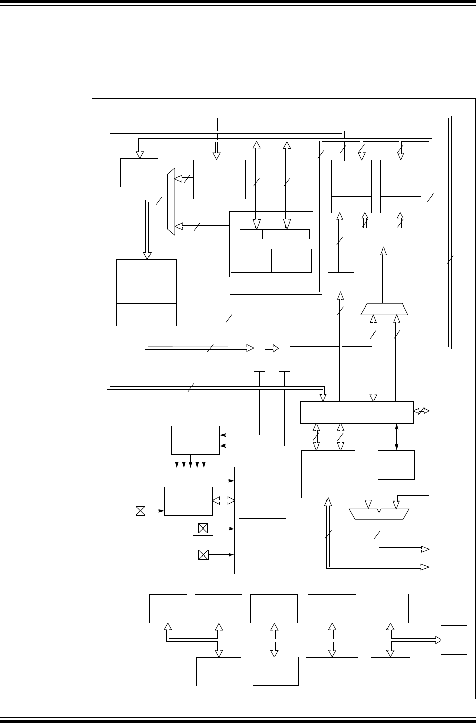
2.1.6 Exception Processing
The dsPIC33F/PIC24H CPU has a vectored exception scheme with up to eight sources of
non-maskable traps and 118 interrupt sources. Each interrupt source can be assigned to one of
the seven priority levels. Figure 2-1 shows the CPU block diagram.
Figure 2-1: dsPIC33F/PIC24H CPU Block Diagram
Power-up
Timer
Oscillator
Start-up Timer
Instruction
Decode and
Control
OSC1/CLKI
MCLR
VDD, VSS
UART1,
ECAN2
Timing
Generation
ECAN1,
16
PCH PCL
16
Program Counter (PC)
16-bit ALU
24
24
24
24
X Data Bus
IR
I2C™
DCI
PCU
10-bit or
Timers
Input
Capture
Module
Output
Compare
Module
16
16 16
16 x 16
W Reg Array
Divide
Support
Engine
DSP
ROM Latch
16
Y Data Bus
EA MUX
X RAGU
X WAGU
Y AGU
AVDD, AVSS
UART2
SPI2
16
16
16
16
16
16
16
16
16
8
Interrupt
Controller PSV and Table
Data Access
Control Block
Stack
Control
Logic
Loop
Control
Logic
Data LatchData Latch
Y Data
RAM X Data
RAM
Address
Latch
Address
Latch
Control Signals
to Various Blocks
16
SPI1,
Data Latch
I/O
16
16
16
X Address Bus
Y Address Bus
16
Literal Data
12-bit ADC
Program Memory
Watchdog
Timer
Reset
POR/BOR
Address Latch
Ports

© 2007-2011 Microchip Technology Inc. DS70204C-page 2-5
Section 2. CPU
CPU
2
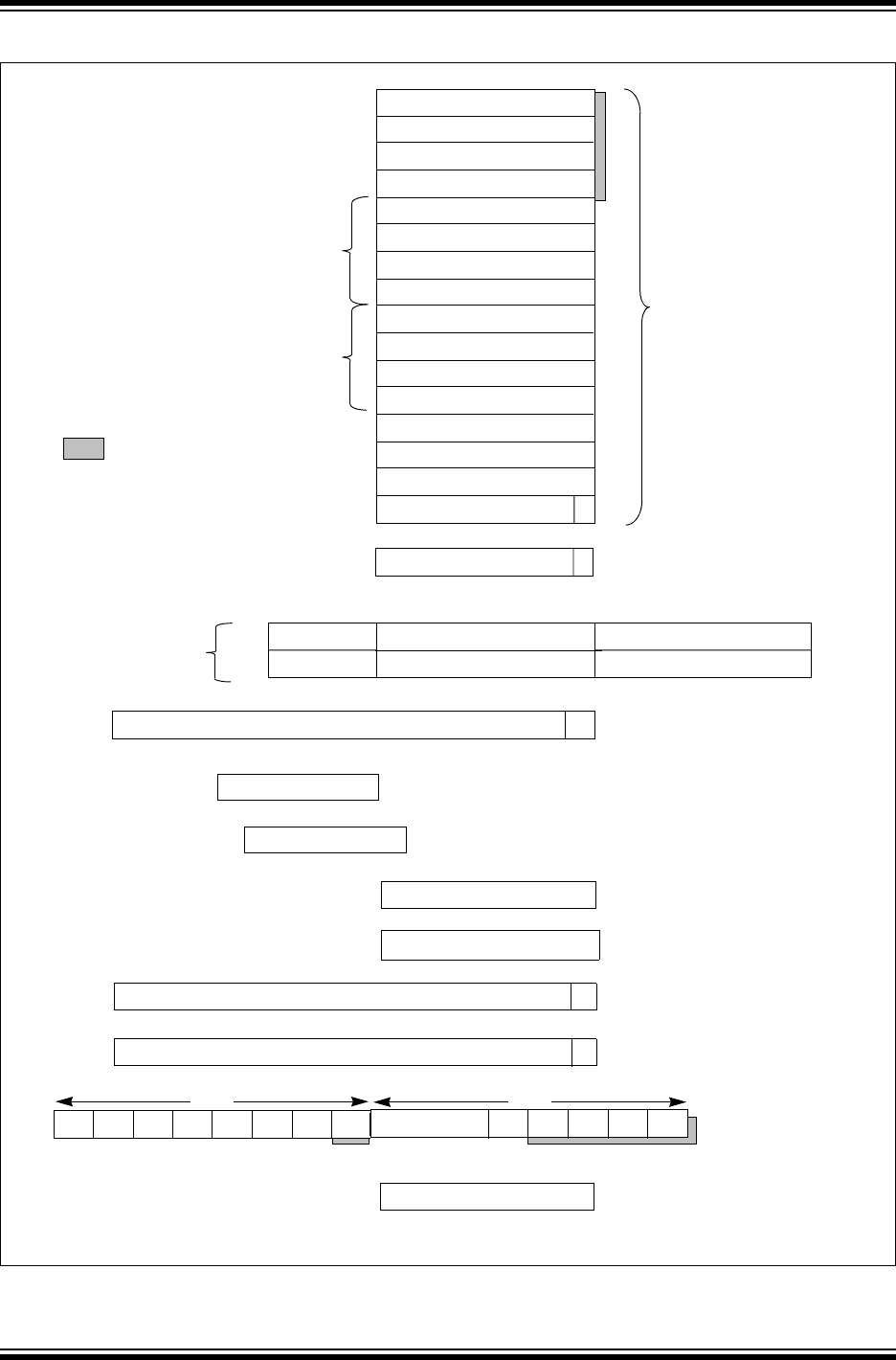
2.2 PROGRAMMER’S MODEL
The programmer’s model for the dsPIC33F/PIC24H CPU is shown in Figure 2-2. All registers in
the programmer’s model are memory mapped and can be manipulated directly using
instructions. Table 2-1 provides a description of each register.
In addition to the registers contained in the programmer’s model, the dsPIC33F/PIC24H contains
control registers for modulo addressing, bit-reversed addressing and interrupts. These registers
are described in the subsequent sections in this document. All registers associated with the
programmer’s model are memory mapped as shown in Table 2-3.
Table 2-1: Programmer’s Model Register Descriptions
Register Description
W0 through W15 Working register array
ACCA, ACCB 40-bit DSP Accumulators
PC 23-bit PC
SR ALU and DSP Engine Status register
SPLIM Stack Pointer Limit Value register
TBLPAG Table Memory Page Address register
PSVPAG Program Space Visibility Page Address register
RCOUNT REPEAT Loop Count register
DCOUNT DO Loop Count register
DOSTART DO Loop Start Address register
DOEND DO Loop End Address register
CORCON Contains DSP Engine and DO Loop control bits
dsPIC33F/PIC24H Family Reference Manual
DS70204C-page 2-6 © 2007-2011 Microchip Technology Inc.
Figure 2-2: Programmer’s Model
NOVZ C
TBLPAG
22 0
70
015
Program Counter
Data Table Page Address
STATUS Register
Working/Address
Registers
DSP Operand
Registers
W0 (WREG)
W1
W2
W3
W4
W5
W6
W7
W8
W9
W10
W11
W12
W13
Frame Pointer/W14
Stack Pointer/W15
DSP Address
Registers
39 031
DSP
Accumulators
PSVPAG
70Program Space Visibility
RA
0
OA OB SA SB
RCOUNT
15 0
32
DCOUNT(1)
15 0
DO Loop Counter
DOSTART(1)
22 0
DO Loop Start Address
DOEND(1) DO Loop End Address
IPL<2:0>
SPLIM Stack Pointer Limit
15
22 0
SRL
PUSH.S and POP.S Shadows
0
0
OAB SAB
Page Address
DA DC
CORCON
15 0
Core Control Register
ACCAH ACCAL
ACCAU
ACCBU ACCBH ACCBL
ACCA
ACCB
SRH
0
0
Note 1: DCOUNT, DOSTART and DOEND have one level of shadow registers (not shown) for nested DO loops.

© 2007-2011 Microchip Technology Inc. DS70204C-page 2-7
Section 2. CPU
CPU
2
2.2.1 Working Register Array
The 16 working (W) registers can function as data, address or address offset registers. The
function of a W register is determined by the addressing mode of the instruction that accesses it.
The dsPIC33F/PIC24H instruction set can be divided into two instruction types:
• Register instructions
• File register instructions
2.2.1.1 REGISTER INSTRUCTIONS
Register instructions can use each W register as a data value or an address offset value, as
shown in Example 2-1.
Example 2-1: Register Instructions
2.2.1.2 FILE REGISTER INSTRUCTIONS
File register instructions operate on a specific memory address contained in the instruction
opcode and W0 register. W0 is a special working register used in file register instructions.
Working registers W1-W15 cannot be specified as target registers in file register instructions.
The file register instructions provide backward compatibility with existing PIC® MCU devices that
have only one W register. The label “WREG” is used in the assembler syntax to denote W0 in a
file register instruction, as shown in Example 2-2.
Example 2-2: File Register Instructions
2.2.1.3 W REGISTER MEMORY MAPPING
Since the W registers are memory mapped, it is possible to access a W register in a file register
instruction, as shown in Example 2-3.
Example 2-3: Accessing W Register in File Register Instruction
Further, it is also possible to execute an instruction that uses a W register as both an address
pointer and operand destination, as shown in Example 2-4.
Example 2-4: W Register Used as Address Pointer and Operand Destination
In Example 2-4, the contents of W2 are 0x0004. As W2 is used as an address pointer, it points
to location 0x0004 in memory. W2 is also mapped to this address in memory. Even though this
is an unlikely event, it is impossible to detect until run time. The dsPIC33F/PIC24H CPU ensures
that the data write dominates, resulting in W2 = 0x1234 in this example.
Note: Refer to the “16-bit MCU and DSC Programmer’s Reference Manual” (DS70157),
for complete descriptions of addressing modes and instruction syntax.
MOV W0, W1 ; move contents of W0 to W1
MOV W0, [W1] ; move W0 to address contained in W1
ADD W0, [W4], W5 ; add contents of W0 to contents pointed
; to by W4. Place result in W5.
MOV WREG, 0x0100 ; move contents of W0 to address 0x0100
ADD 0x0100, WREG ; add W0 to address 0x0100, store in W0
MOV 0x0004, W10 ; equivalent to MOV W2, W10
where:
0x0004 is the memory address of W2
MOV W1, [W2++]
where:
W1 = 0x1234
W2 = 0x0004 ;[W2] addresses W2
dsPIC33F/PIC24H Family Reference Manual
DS70204C-page 2-8 © 2007-2011 Microchip Technology Inc.
2.2.1.4 W REGISTERS AND BYTE MODE INSTRUCTIONS
The byte instructions, which target the W register array, only affect the
Least Significant Byte (LSB) of the target register. As the working registers are memory mapped,
the LSB and Most Significant Byte (MSB) can be manipulated through byte wide data memory
space access.
2.2.2 Shadow Registers
Many of the registers in the programmer’s model have an associated shadow register, as shown
in Figure 2-2. None of the shadow registers are accessible directly. There are two types of
shadow registers:
• Used by PUSH.S and POP.S instructions
• Used by DO instruction
2.2.2.1 PUSH.S AND POP.S SHADOW REGISTERS
The PUSH.S and POP.S instructions are useful for fast context save/restore during a function call
or Interrupt Service Routine (ISR). The PUSH.S instruction transfers the following register values
into their respective shadow registers:
•W0...W3
• SR (N, OV, Z, C, DC bits only)
The POP.S instruction restores the values from the shadow registers into these register
locations. Example 2-5 shows a code example using the PUSH.S and POP.S instructions.
Example 2-5: PUSH.S and POP.S Instructions
The PUSH.S instruction overwrites the contents that are previously saved in the shadow
registers. The shadow registers are only one level in depth. Therefore, care must be taken if the
shadow registers are to be used for multiple software tasks.
The user-assigned application must ensure that any task using the shadow registers are not
interrupted by a higher priority task that also uses the shadow registers. If the higher priority task
is allowed to interrupt the lower priority task, the contents of the shadow registers saved in the
lower priority task are overwritten by the higher priority task.
2.2.2.2 DO LOOP SHADOW REGISTERS
The following registers are automatically saved in shadow registers when a DO instruction is
executed:
•DOSTART
•DOEND
• DCOUNT
The DO shadow registers are one level in depth, permitting two loops to be automatically nested.
Refer to 2.9.2.2 “DO Loop Nesting”, for more details on DO loop nesting.
2.2.3 Uninitialized W Register Reset
The W register array (with the exception of W15) is cleared during all resets and is considered
uninitialized until written to. An attempt to use an uninitialized register as an address pointer will
reset the device.
A word write must be performed to initialize a W register. A byte write will not affect the initialization
detection logic.
MyFunction:
PUSH.S ; Save W registers, MCU status
MOV #0x03,W0 ; load a literal value into W0
ADD RAM100 ; add W0 to contents of RAM100
BTSC SR,#Z ; is the result 0?
BSET Flags,#IsZero ; Yes, set a flag
POP.S ; Restore W regs, MCU status
RETURN

© 2007-2011 Microchip Technology Inc. DS70204C-page 2-9
Section 2. CPU
CPU
2
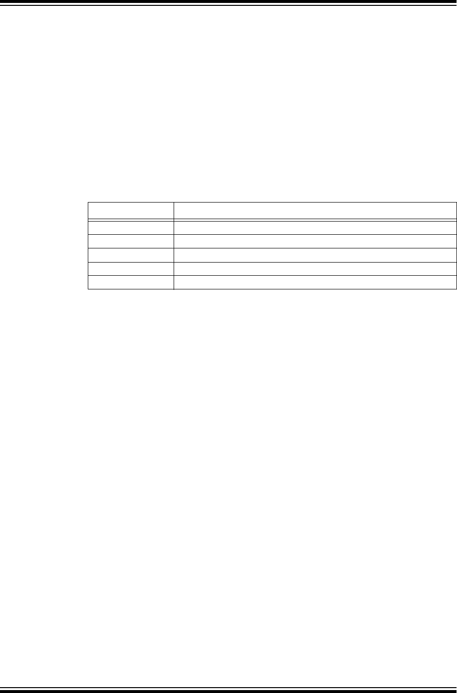
2.3 SOFTWARE STACK POINTER
The W15 register serves as a dedicated Software Stack Pointer (SSP) and is automatically
modified by exception processing, subroutine calls and returns. However, W15 can be
referenced by any instruction in the same manner as all other W registers. This simplifies
reading, writing and manipulating of the Stack Pointer (SP). For example, creating stack frames.
W15 is initialized to 0x0800 during all resets. This address ensures that the SP points to valid
RAM in all dsPIC33F/PIC24H devices and permits stack availability for non-maskable trap
exceptions. These can occur before the SP is initialized by the user-assigned application
software. The user can reprogram the SP during initialization to any location within data space.
The SP always points to the first available free word and fills the software stack, working from
lower toward higher addresses. Figure 2-3 shows how it pre-decrements for a stack pop (read)
and post-increments for a stack push (writes).
When the PC is pushed onto the stack, the PC<15:0> bits are pushed onto the first available
stack word, and then PC<22:16> bits are pushed onto the second available stack location. For
a PC push during any CALL instruction, the MSB of the PC is zero-extended before the push, as
shown in Figure 2-3. During exception processing, the MSB of the PC is concatenated with the
lower eight bits of the CPU status register, SR. This allows the contents of SRL to be preserved
automatically during interrupt processing.
Figure 2-3: Stack Operation for a CALL Instruction
2.3.1 Software Stack Examples
The software stack is manipulated using the PUSH and POP instructions. The PUSH and POP
instructions are the equivalent of a MOV instruction with W15 used as the destination pointer. The
contents of W0 can be pushed onto the stack as shown in Example 2-6.
Example 2-6: Software Stack Example
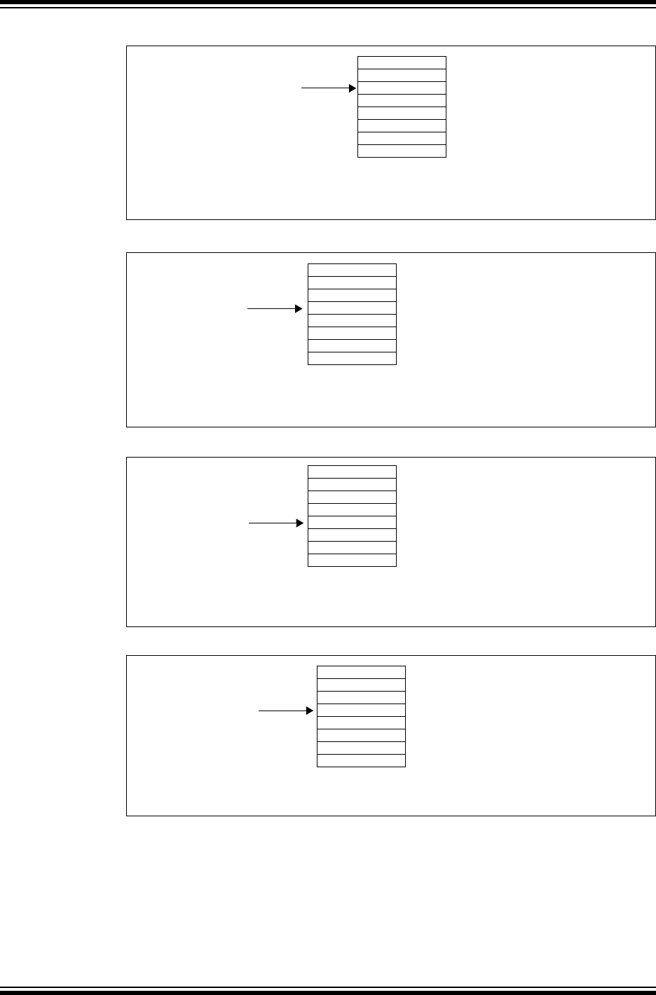
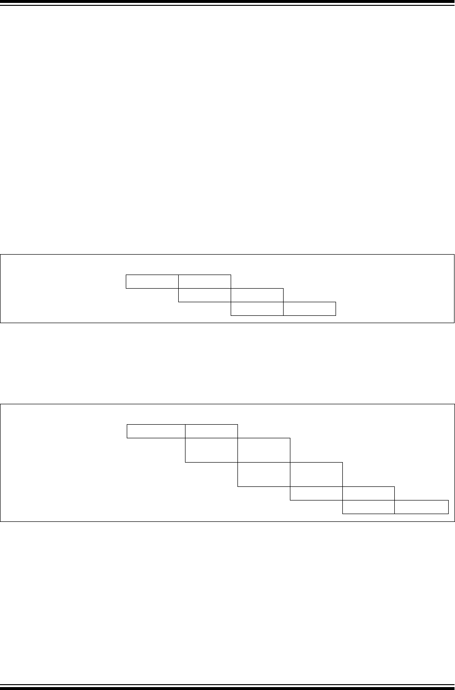
Figure 2-4 through Figure 2-7 show examples of how the software stack is used. Figure 2-4
shows the software stack at device initialization. W15 has been initialized to 0x0800. This
example assumes the values 0x5A5A and 0x3636 have been written to W0 and W1, respectively.
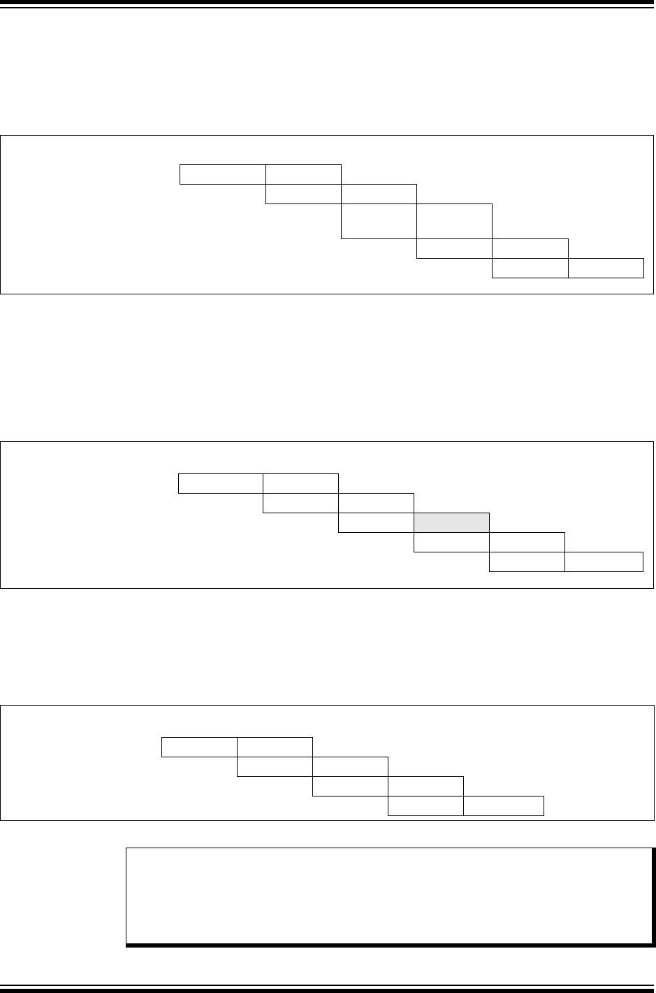
The stack is pushed for the first time in Figure 2-5 and the value contained in W0 is copied to the
stack. W15 is automatically updated to point to the next available stack location (0x0802). In
Figure 2-6, the contents of W1 are pushed onto the stack. Figure 2-7 shows how the stack is
popped and the Top-of-Stack (TOS) value (previously pushed from W1) is written to W3.
Note: To protect against misaligned stack access, W15<0> is set to ‘0’ by the hardware.
<Free Word>
PC<15:0>
PC<22:16>
015
W15 (before CALL)
W15 (after CALL)
Stack Grows Towards
Higher Address
B‘000000000’
CALL SUBR
PUSH W0
This syntax is equivalent to:
MOV W0,[W15++]
The contents of the top-of-stack can be returned to W0 by:
POP W0
This syntax is equivalent to:
MOV [--W15],W0
dsPIC33F/PIC24H Family Reference Manual
DS70204C-page 2-10 © 2007-2011 Microchip Technology Inc.
Figure 2-4: Stack Pointer at Device Reset
Figure 2-5: Stack Pointer After the First PUSH Instruction
Figure 2-6: Stack Pointer After the Second PUSH Instruction
Figure 2-7: Stack Pointer After a POP Instruction
2.3.2 W14 Software Stack Frame Pointer
A frame is a user-defined section of memory in the stack that is used by a single subroutine.
Working register W14 can be used as a stack frame pointer with the LNK (link) and ULNK (unlink)
instructions. W14 can be used in a normal working register by instructions when it is not used as
a frame pointer.
For software examples that use W14 as a stack frame pointer, refer to the “16-bit MCU and DSC
Programmer’s Reference Manual” (DS70157).
0x0000
0xFFFE
0x0800
W15
W15 = 0x0800
W0 = 0x5A5A
W1 = 0x3636
0x0000
0xFFFE
0x5A5A
W15 = 0x0802
W0 = 0x5A5A
W1 = 0x3636
0x0800 PUSH W0
0x0802
W15
0x0000
0xFFFE
0x5A5A
0x3636
W15 = 0x0804
W0 = 0x5A5A
W1 = 0x3636
0x0800 PUSH W1
0x0802
0x0804
W15
0x0000
0xFFFE
0x05A5A
0x03636
0x3636 → W3
W15 = 0x0802
POP W3
0x0802
0x0800
W15
© 2007-2011 Microchip Technology Inc. DS70204C-page 2-11
Section 2. CPU
CPU
2
2.3.3 Stack Pointer Overflow
The Stack Pointer Limit register (SPLIM) specifies the size of the stack buffer. The SPLIM register
is a 16-bit register, but SPLIM<0> is set to ‘0’ because all stack operations must be word-aligned.
The stack overflow check is not enabled until a word write to the SPLIM register occurs. After this
time it can only be disabled by a device Reset. All effective addresses generated using W15 as
a source or destination are compared against the value in SPLIM. If the contents of the
Stack Pointer (W15) exceed the contents of the SPLIM register by 2, and a Push operation is
performed, a stack error trap occurs on a subsequent Push operation. Thus, for example, if it is
desirable to cause a stack error trap when the stack grows beyond address 0x2000 in RAM,
initialize the SPLIM register with the value 0x1FFE.
If stack overflow checking is enabled, a stack error trap also occurs, if the W15 effective address
calculation wraps over the end of data space (0xFFFF).
Refer to Section 6. “Interrupts” (DS70184), for more details on stack error traps.
2.3.4 Stack Pointer Underflow
The stack is initialized to 0x0800 during a Reset. A stack error trap is initiated, if the Stack Pointer
address is less than 0x0800.
Note: A stack error trap can be caused by any instruction that uses the contents of the
W15 register to generate an Effective Address (EA). Thus, if the contents of W15
are greater than the contents of the SPLIM register by 2, and a CALL instruction is
executed, or if an interrupt occurs, a stack error trap is generated.
Note: A write to the SPLIM register should not be followed by an indirect read operation
using W15.
Note: Locations in data space between 0x0000 and 0x07FF are, in general, reserved for
core and peripheral Special Function Registers (SFRs).

dsPIC33F/PIC24H Family Reference Manual
DS70204C-page 2-12 © 2007-2011 Microchip Technology Inc.
2.4 CPU REGISTER DESCRIPTIONS
2.4.1 CPU Status Register: SR
The dsPIC33F/PIC24H CPU has a 16-bit Status Register (SR). A detailed description of the CPU
Status Register is shown in Register 2-1. The LSB of this register is referred to as the SRL (Status
Register, Lower Byte). The MSB is referred to as SRH (Status Register, Higher Byte).
The SRL register contains all of the MCU ALU operation Status flags, the CPU Interrupt Priority
Level Status bits (IPL<2:0>), and the REPEAT Loop Active Status bit, RA (SR<4>). During
exception processing, SRL is concatenated with the MSB of the PC, to form a complete word
value, which is then stacked.
The SRH register contains:
• The DSP Adder/Subtractor status bits
•The DO loop active bit, DA (SR<9>)
• The Digit Carry bit, DC (SR<8>)
The SR register bits are readable/writable with the following exceptions:
• The DA bit (SR<8>) is read-only
• The RA bit (SR<4>) is read-only
• The OA, OB (SR<15:14>) and OAB (SR<11>) bits are read-only and can only be modified
by the DSP engine hardware
• The SA, SB (SR<13:12>) and SAB (SR<10>) bits are read- and clear-only, and can only be
set by the DSP engine hardware. Once set, they remain set until cleared by the
user-assigned application, irrespective of the results from any subsequent DSP operations.
2.4.2 Core Control Register: CORCON
The CORCON register contains bits that control the operation of the DSP multiplier and DO loop
hardware. The CORCON register contains the IPL3 status bit, which is concatenated with
IPL<2:0> (SR<7:5>), to form the CPU Interrupt Priority Level (IPL). A detailed description of the
CORCON register is provided in Register 2-2.
Note 1: Clearing the SAB bit also clears both the SA and SB bits.
2: A description of the SR bits affected by each instruction is provided in the “16-bit
MCU and DSC Programmer’s Reference Manual” (DS70157).

© 2007-2011 Microchip Technology Inc. DS70204C-page 2-13
Section 2. CPU
CPU
2
Register 2-1: SR: CPU Status Register
R-0 R-0 R/C-0 R/C-0 R-0 R/C-0 R -0 R/W-0
OA OB SA(1) SB(2) OAB SAB(3) DA DC
bit 15 bit 8
R/W-0(4,5) R/W-0(4,5) R/W-0(4,5) R-0 R/W-0 R/W-0 R/W-0 R/W-0
IPL<2:0> RA N OV Z C
bit 7 bit 0
Legend: C = Clearable bit
R = Readable bit W = Writable bit U = Unimplemented bit, read as ‘0’
-n = Value at POR ‘1’ = Bit is set ‘0’ = Bit is cleared x = Bit is unknown
bit 15 OA: Accumulator A Overflow Status bit
1 = Accumulator A has overflowed
0 = Accumulator A has not overflowed
bit 14 OB: Accumulator B Overflow Status bit
1 = Accumulator B has overflowed
0 = Accumulator B has not overflowed
bit 13 SA: Accumulator A Saturation ‘Sticky’ Status bit(1)
1 = Accumulator A is saturated or has been saturated at some time
0 = Accumulator A is not saturated
bit 12 SB: Accumulator B Saturation ‘Sticky’ Status bit(2)
1 = Accumulator B is saturated or has been saturated at some time
0 = Accumulator B is not saturated
bit 11 OAB: OA || OB Combined Accumulator Overflow Status bit
1 = Accumulators A or B have overflowed
0 = Neither Accumulators A or B have overflowed
bit 10 SAB: SA || SB Combined Accumulator ‘Sticky’ Status bit(3)
1 = Accumulators A or B are saturated or have been saturated at some time
0 = Neither Accumulator A or B are saturated
bit 9 DA: DO Loop Active bit
1 = DO loop in progress
0 = DO loop not in progress
bit 8 DC: MCU ALU Half Carry/Borrow bit
1 = A carry-out from the 4th low order bit (for byte-sized data) or 8th low order bit (for word-sized data)
of the result occurred
0 = No carry-out from the 4th low order bit (for byte-sized data) or 8th low order bit (for word-sized data)
of the result occurred
Note 1: The SA bit can be read or cleared (not set).
2: The SB bit can be read or cleared (not set).
3: The SAB bit can be read or cleared (not set). Clearing this bit clears SA and SB.
4: The IPL<2:0> bits are concatenated with the IPL<3> bit (CORCON<3>) to form the CPU Interrupt Priority
Level. The value in parentheses indicates the IPL, if IPL<3> = 1. User interrupts are disabled when
IPL<3> = 1.
5: The IPL<2:0> status bits are read only when NSTDIS = 1 (INTCON1<15>).

dsPIC33F/PIC24H Family Reference Manual
DS70204C-page 2-14 © 2007-2011 Microchip Technology Inc.
bit 7-5 IPL<2:0>: CPU Interrupt Priority Level Status bits(4,5)
111 = CPU Interrupt Priority Level is 7 (15). User interrupts disabled
110 = CPU Interrupt Priority Level is 6 (14)
101 = CPU Interrupt Priority Level is 5 (13)
100 = CPU Interrupt Priority Level is 4 (12)
011 = CPU Interrupt Priority Level is 3 (11)
010 = CPU Interrupt Priority Level is 2 (10)
001 = CPU Interrupt Priority Level is 1 (9)
000 = CPU Interrupt Priority Level is 0 (8)
bit 4 RA: REPEAT Loop Active bit
1 = REPEAT loop in progress
0 = REPEAT loop not in progress
bit 3 N: MCU ALU Negative bit
1 = Result was negative
0 = Result was non-negative (zero or positive)
bit 2 OV: MCU ALU Overflow bit
This bit is used for signed arithmetic (2’s complement). It indicates an overflow of the magnitude that
causes the sign bit to change state.
1 = Overflow occurred for signed arithmetic (in this arithmetic operation)
0 = No overflow occurred
bit 1 Z: MCU ALU Zero bit
1 = An operation that affects the Z bit has set it at some time in the past
0 = The most recent operation that affects the Z bit has cleared it (i.e., a non-zero result)
bit 0 C: MCU ALU Carry/Borrow bit
1 = A carry-out from the Most Significant bit (MSb) of the result occurred
0 = No carry-out from the Most Significant bit (MSb) of the result occurred
Register 2-1: SR: CPU Status Register (Continued)
Note 1: The SA bit can be read or cleared (not set).
2: The SB bit can be read or cleared (not set).
3: The SAB bit can be read or cleared (not set). Clearing this bit clears SA and SB.
4: The IPL<2:0> bits are concatenated with the IPL<3> bit (CORCON<3>) to form the CPU Interrupt Priority
Level. The value in parentheses indicates the IPL, if IPL<3> = 1. User interrupts are disabled when
IPL<3> = 1.
5: The IPL<2:0> status bits are read only when NSTDIS = 1 (INTCON1<15>).

© 2007-2011 Microchip Technology Inc. DS70204C-page 2-15
Section 2. CPU
CPU
2
Register 2-2: CORCON: Core Control Register
U-0 U-0 U-0 R/W-0 R/W-0 R-0 R-0 R-0
— — —USEDT
(1) DL<2:0>
bit 15 bit 8
R/W-0 R/W-0 R/W-1 R/W-0 R/C-0 R/W-0 R/W-0 R/W-0
SATA SATB SATDW ACCSAT IPL3(2) PSV RND IF
bit 7 bit 0
Legend: C = Clearable bit
R = Readable bit W = Writable bit U = Unimplemented bit, read as ‘0’
-n = Value at POR ‘1’ = Bit is set ‘0’ = Bit is cleared x = Bit is unknown
bit 15-13 Unimplemented: Read as '0’
bit 12 US: DSP Multiply Unsigned/Signed Control bit
1 = DSP engine multiplies are unsigned
0 = DSP engine multiplies are signed
bit 11 EDT: Early DO Loop Termination Control bit(1)
1 = Terminate executing DO loop at end of current loop iteration
0 = No effect
bit 10-8 DL<2:0>: DO Loop Nesting Level Status bits
111 = 7 DO loops active
•
•
•
001 = 1 DO loop active
000 = 0 DO loop active
bit 7 SATA: ACCA Saturation Enable bit
1 = Accumulator A saturation enabled
0 = Accumulator A saturation disabled
bit 6 SATB: ACCB Saturation Enable bit
1 = Accumulator B saturation enabled
0 = Accumulator B saturation disabled
bit 5 SATDW: Data Space Write from DSP Engine Saturation Enable bit
1 = Data space write saturation enabled
0 = Data space write saturation disabled
bit 4 ACCSAT: Accumulator Saturation Mode Select bit
1 = 9.31 saturation (super saturation)
0 = 1.31 saturation (normal saturation)
bit 3 IPL3: CPU Interrupt Priority Level Status bit 3(2)
1 = CPU interrupt priority level is greater than 7
0 = CPU interrupt priority level is 7 or less
bit 2 PSV: Program Space Visibility in Data Space Enable bit
1 = Program space visible in data space
0 = Program space not visible in data space
bit 1 RND: Rounding Mode Select bit
1 = Biased (conventional) rounding enabled
0 = Unbiased (convergent) rounding enabled
bit 0 IF: Integer or Fractional Multiplier Mode Select bit
1 = Integer mode enabled for DSP multiply
0 = Fractional mode enabled for DSP multiply
Note 1: The EDT bit always reads as ‘0’.
2: The IPL3 bit is concatenated with the IPL<2:0> bits (SR<7:5>) to form the CPU interrupt priority level.

dsPIC33F/PIC24H Family Reference Manual
DS70204C-page 2-16 © 2007-2011 Microchip Technology Inc.
2.4.3 Other dsPIC33F/PIC24H CPU Control Registers
This section provides brief descriptions of additional registers that are associated with the
dsPIC33F/PIC24H CPU. These registers are described in greater detail in other sections of the
“dsPIC33F/PIC24H Family Reference Manual”.
•TBLPAG: Table Page Register
The TBLPAG register holds the upper eight bits of a program memory address during the
table read and write operations. Table instructions are used to transfer data between
program memory space and data memory space. Refer to Section 4. “Program
Memory” (DS70203), for more details.
• PSVPAG: Program Space Visibility Page Register
The PSVPAG register allows the user-assigned application to map a 32 Kbytes section of
the program memory space into the upper 32 Kbytes of data address space. This feature
allows transparent access to constant data through dsPIC33F/PIC24H instructions that
operate on data memory. The PSVPAG register selects the 32 Kbytes region of program
memory space that is mapped to the data address space. Refer to Section 4. “Program
Memory” (DS70203), for more details on the PSVPAG register.
• MODCON: Modulo Control Register
The MODCON register enables and configures modulo addressing (circular buffers). Refer
to Section 3. “Data Memory” (DS70202), for more details on modulo addressing.
• XMODSRT, XMODEND: X Modulo Start and End Address Registers
The XMODSRT and XMODEND registers hold the start and end addresses for
modulo (circular) buffers implemented in the X data memory address space. Refer to
Section 3. “Data Memory” (DS70202), for more details on modulo addressing.
• YMODSRT, YMODEND: Y Modulo Start and End Address Registers
The YMODSRT and YMODEND registers hold the start and end addresses for
modulo (circular) buffers implemented in the Y data memory address space. Refer to
Section 3. “Data Memory” (DS70202), for more details on modulo addressing.
• XBREV: X Modulo Bit-Reverse Register
The XBREV register sets the buffer size used for bit-reversed addressing. Refer to
Section 3. “Data Memory” (DS70202), for more details on modulo addressing.
• DISICNT: Disable Interrupts Count Register
The DISICNT register is used by the DISI instruction to disable interrupts of priority 1-6 for
a specified number of cycles. Refer to Section 6. “Interrupts” (DS70184), for more details
on interrupts.

© 2007-2011 Microchip Technology Inc. DS70204C-page 2-17
Section 2. CPU
CPU
2
2.5 ARITHMETIC LOGIC UNIT
The dsPIC33F/PIC24H Arithmetic Logic Unit (ALU) is 16 bits wide and is capable of addition,
subtraction, single bit shifts, and logic operations. Unless otherwise mentioned, arithmetic
operations are 2’s complement in nature. Depending on the operation, the ALU can affect the
values of these status bits in the SR register:
• Carry (C)
•Zero (Z)
• Negative (N)
• Overflow (OV)
• Digit Carry (DC)
The C and DC status bits operate as Borrow and Digit Borrow bits, respectively, for subtraction
operations.
The ALU can perform 8-bit or 16-bit operations, depending on the mode of the instruction used.
Data for the ALU operation can come from the W register array, or data memory, depending on
the addressing mode of the instruction. Likewise, output data from the ALU can be written to the
W register array or a data memory location.
Refer to the “16-bit MCU and DSC Programmer’s Reference Manual” (DS70157), for more
details on the SR bits affected by each instruction, addressing modes and 8-bit/16-bit instruction
modes.
2.5.1 Byte to Word Conversion
The dsPIC33F/PIC24H has two instructions that are helpful when mixing 8-bit and 16-bit ALU
operations:
• The Sign-Extend (SE) instruction takes a byte value in a W register or data memory and
creates a sign-extended word value that is stored in a W register.
• The Zero-Extend (ZE) instruction clears the 8 MSb of a word value in a W register or data
memory and places the result in a destination W register.
Note 1: Byte operations use the 16-bit ALU and can produce results in excess of eight bits.
However, to maintain backward compatibility with PIC MCU devices, the ALU result
from all of the byte operations is written back as a byte (i.e., MSB is not modified),
and the SR register is updated based only on the LSB state of the result.
2: All register instructions performed in Byte mode affect only the LSB of the
W registers. The MSB of any W register can be modified by using file register
instructions that access the memory mapped contents of the W registers.

dsPIC33F/PIC24H Family Reference Manual
DS70204C-page 2-18 © 2007-2011 Microchip Technology Inc.
2.6 DSP ENGINE
The DSP engine is a block of hardware that is fed with data from the W register array, but
contains its own specialized result registers. The DSP engine is driven from the same instruction
decoder that directs the MCU ALU. In addition, all operand Effective Addresses (EAs) are
generated in the W register array. Concurrent operation with MCU instruction flow is not possible,
though both the MCU ALU and DSP engine resources can be shared by all instructions in the
instruction set.
The DSP engine consists of the following components:
• High-speed 17-bit by 17-bit multiplier
• Barrel shifter
• 40-bit adder/subtractor
• Two target accumulator registers
• Rounding logic with selectable modes
• Saturation logic with selectable modes
Data input to the DSP engine is derived from one of the following sources:
• Directly from the W array (registers W4, W5, W6 or W7) for dual source operand DSP
instructions. Data values for the W4, W5, W6 and W7 registers are prefetched via the
X and Y memory data buses
• From the X memory data bus for all other DSP instructions
Data output from the DSP engine is written to one of the following destinations:
• The target accumulator, as defined by the DSP instruction being executed
• The X memory data bus to any location in the data memory address space
The DSP engine can perform inherent accumulator-to-accumulator operations that require no
additional data.
The MCU shift and multiply instructions use the DSP engine hardware to obtain their results. The
X memory data bus is used for data reads and writes in these operations.
Figure 2-8 shows the block diagram of the DSP engine.
Note: Refer to the “16-bit MCU and DSC Programmer’s Reference Manual” (DS70157),
for detailed code examples and instruction syntax related to this section.

© 2007-2011 Microchip Technology Inc. DS70204C-page 2-19
Section 2. CPU
CPU
2
Figure 2-8: DSP Engine Block Diagram
Zero Backfill
Sign-Extend
Barrel
Shifter
40-bit Accumulator A
40-bit Accumulator B
Round Logic
X Data Bus
To/From W Array
Adder
Saturate
Negate
32
32
32
16
16 16
16
40 40
40 40
Y Data Bus
40
16
40
Multiplier/Scaler
17-bit x 17-bit
16-bit to 17-bit
Conversion
Saturation Logic

dsPIC33F/PIC24H Family Reference Manual
DS70204C-page 2-20 © 2007-2011 Microchip Technology Inc.
2.6.1 Data Accumulators
Two 40-bit data accumulators, ACCA and ACCB, are the result registers for the DSP instructions
listed in Table 2-3. Each accumulator is memory mapped to these three registers, where ‘x’
denotes the particular accumulator:
• ACCxL: ACCx<15:0>
• ACCxH: ACCx<31:16>
• ACCxU: ACCx<39:32>
For fractional operations that use the accumulators, the radix point is located to the right of
bit 31. The range of fractional values that can be stored in each accumulator is -256.0 to
(256.0 – 2-31).
For integer operations that use the accumulators, the radix point is located to the right of bit 0.
The range of integer values that can be stored in each accumulator is -549,755,813,888 to
549,755,813,887.
2.6.2 Multiplier
The dsPIC33F/PIC24H CPU features a 17-bit by 17-bit multiplier (for 16-bit Signed
multiplication) shared by both the MCU ALU and the DSP engine. The multiplier is capable of
signed or unsigned operation and supports either 1.31 fractional (Q.31) or 32-bit integer results.
The multiplier takes in 16-bit input data and converts the data to 17 bits. Signed operands to the
multiplier are sign-extended. Unsigned input operands are zero-extended. The internal 17-bit
representation of data in the multiplier allows correct execution of mixed-sign and unsigned
16-bit by 16-bit multiplication operations.
The representation of data in hardware for Integer and Fractional Multiplier modes is as follows:
• Integer data is inherently represented as a signed 2’s complement value, where the Most
Significant bit is defined as a sign bit. Generally, the range of an N-bit 2’s complement
integer is -2N-1 to 2N-1 – 1
• Fractional data is represented as a 2’s complement fraction where the MSb is defined as a
sign bit and the radix point is implied to lie just after the sign bit (Q.X format). The range of
an N-bit 2’s complement fraction with this implied radix point is -1.0 to (1 – 21-N).
The range of data in both Integer and Fractional modes is listed in Table 2-2. Figure 2-9 and
Figure 2-10 illustrate how the multiplier hardware interprets data in Integer and Fractional modes.
The Integer or Fractional Multiplier Mode Select bit (IF) in the Core Control register
(CORCON<0>) determines integer/fractional operation for the instructions listed in Table 2-3.
The IF bit does not affect MCU multiply instructions listed in Table 2-4, which are always integer
operations. The multiplier scales the result one bit to the left for fractional operation. The Least
Significant bits (LSbs) of the result are always cleared. The multiplier defaults to Fractional mode
for DSP operations at a device Reset.
Table 2-2: dsPIC33F/PIC24H Data Ranges
Register
Size Integer Range Fraction Range Fraction
Resolution
16-bit -32768 to 32767 -1.0 to (1.0 – 2-15)
(Q.15 Format) 3.052 x 10⁻⁵
32-bit -2,147,483,648 to
2,147,483,647 -1.0 to (1.0 – 2-31)
(Q.31 Format) 4.657 x 10⁻¹⁰
40-bit -549,755,813,888 to
549,755,813,887 -256.0 to (256.0 – 2-31)
(Q.31 Format with eight guard bits) 4.657 x 10⁻¹⁰

© 2007-2011 Microchip Technology Inc. DS70204C-page 2-21
Section 2. CPU
CPU
2
Figure 2-9: Integer and Fractional Representation of 0x4001
Figure 2-10: Integer and Fractional Representation of 0xC002
Different Representations of 0x4001
Integer:
-215 214 213 212 . . . .
0x4001 = 214 + 20 = 16385
1.15 Fractional:
2-15
0
2-1 2-2 2-3 . . .
-20
20
0x4001 = 2-1 + 2-15 = 0.500030518
Implied Radix Point
.
1 10000000000000
01 10000000000000
Different Representations of 0xC002
Integer:
-215 214 213 212 . . . .
0xC002 = -215 + 214 + 20 = -32768 + 16384 + 2 = -16382
1.15 Fractional:
2-15
. 2-1 2-2 2-3 . . .
-20
20
0xC002 = -20 + 2-1 + 2-14 = -1 + 0.5 + 0.000061035 = -0.499938965
Implied Radix Point
11 00000000000001
11 00000000000001
dsPIC33F/PIC24H Family Reference Manual
DS70204C-page 2-22 © 2007-2011 Microchip Technology Inc.
2.6.2.1 DSP MULTIPLY INSTRUCTIONS
The DSP instructions that use the multiplier are summarized in Table 2-3.
Table 2-3: DSP Instructions that Use the Multiplier
The DSP Multiplier Unsigned/Signed Control bit (US) in the CORCON register determines
whether DSP multiply instructions are signed (default) or unsigned. The US bit does not influence
the MCU multiply instructions, which have specific instructions for signed or unsigned operation.
If the US bit is set, the input operands for instructions shown in Table 2-3 are considered as
unsigned values, which are always zero-extended into the seventeenth bit of the multiplier value.
2.6.2.2 MCU MULTIPLY INSTRUCTIONS
The same multiplier supports the MCU multiply instructions, which include integer 16-bit signed,
unsigned, and mixed sign multiplies as shown in Table 2-4. All multiplications performed by the
MUL instruction produce integer results. The MUL instruction can be directed to use byte-sized or
word-sized operands. Byte input operands produce a 16-bit result and word input operands
produce a 32-bit result to the specified register(s) in the W array.
Table 2-4: MCU Instructions that Utilize the Multiplier
Table 2-5: Multiplication Options
DSP Instruction Description Algebraic Equivalent
MAC Multiply and Add to Accumulator or
Square and Add to Accumulator
a = a + b * c
a = a + b2
MSC Multiply and Subtract from Accumulator a = a – b * c
MPY Multiply a = b * c
MPY.N Multiply and Negate Result a = -b * c
ED Partial Euclidean Distance a = (b – c)2
EDAC Add Partial Euclidean Distance to the
Accumulator a = a + (b – c)2
Note: DSP instructions using the multiplier can operate in Fractional (1.15) or Integer
modes.
MCU Instruction Description
MUL/MUL.UU Multiply two unsigned integers
MUL.SS Multiply two signed integers
MUL.SU/MUL.US Multiply a signed integer with an unsigned integer
Note 1: MCU instructions using the multiplier operate only in Integer mode.
2: Result of an MCU multiply is 32 bits long and is stored in a pair of W registers.
Instruction Class Signed x
Signed Unsigned x
Unsigned Unsigned x
Signed Signed x
Unsigned
MAC
(DSP Multiplication) Yes
(Integer or
Fractional)
Yes
(Integer or
Fractional)
No No
MUL
(MCU Multiplication) Yes
(Integer only) Yes
(Integer only) Yes
(Integer only) Yes
(Integer only)
© 2007-2011 Microchip Technology Inc. DS70204C-page 2-23
Section 2. CPU
CPU
2
2.6.3 Data Accumulator Adder/Subtractor
The data accumulators have a 40-bit adder/subtractor with automatic sign extension logic for the
multiplier result (if signed). It can select one of two accumulators (A or B) as its pre-accumulation
source and post-accumulation destination. For the ADD (accumulator) and LAC instructions, the
data to be accumulated or loaded can optionally be scaled via the barrel shifter prior to
accumulation.
The 40-bit adder/subtractor can optionally negate one of its operand inputs to change the sign of
the result (without changing the operands). The negate is used during multiply and subtract
(MSC), or multiply and negate (MPY.N) operations.
The 40-bit adder/subtractor has an additional saturation block that controls accumulator data
saturation, if enabled.
2.6.3.1 ACCUMULATOR STATUS BITS
Six STATUS register bits that support saturation and overflow are located in the CPU STATUS
register (SR), and are listed in Table 2-6:
Table 2-6: Accumulator Overflow and Saturation Status Bits
The OA and OB bits are read-only and are modified each time the data is passed through the
accumulator add/subtract logic. When set, they indicate that the most recent operation has
overflowed into the accumulator guard bits (bit 32 through bit 39). This type of overflow is not
catastrophic; the guard bits preserve the accumulator data. The OAB status bit is the logically
OR value of OA and OB.
The OA and OB bits, when set, can optionally generate an arithmetic error trap. The trap is
enabled by setting the corresponding Overflow Trap Flag Enable bit (OVATE or OVBTE) in
Interrupt Control Register 1 (INTCON1<10> or <9>) in the Interrupt controller. The trap event
allows the user to perform immediate corrective action, if desired.
The SA and SB bits can be set each time data passes through the accumulator saturation logic.
Once set, these bits remain set until cleared by the user-assigned application. The SAB status
bit indicates the logical OR value of SA and SB. The SA and SB bits are cleared when SAB is
cleared. When set, these bits indicate that the accumulator has overflowed its maximum range
(bit 31 for 32-bit saturation or bit 39 for 40-bit saturation) and are saturated (if saturation is
enabled).
When saturation is not enabled, the SA and SB bits indicate that a catastrophic overflow has
occurred (the sign of the accumulator has been destroyed). If the Catastrophic Overflow Trap
Enable bit (COVTE) in the INTCON1 register is set, SA and SB bits will generate an arithmetic
error trap when saturation is disabled.
Status Bit Location Description
OA SR<15> Accumulator A overflowed into guard bits (ACCA<39:32>)
OB SR<14> Accumulator B overflowed into guard bits (ACCB<39:32>)
SA SR<13> ACCA saturated (bit 31 overflow and saturation)
or
ACCA overflowed into guard bits and saturated
(bit 39 overflow and saturation)
SB SR<12> ACCB saturated (bit 31 overflow and saturation)
or
ACCB overflowed into guard bits and saturated
(bit 39 overflow and saturation)
OAB SR<11> OA logically ORed with OB
SAB SR<10> SA logically ORed with SB
Clearing SAB also clears SA and SB
Note 1: Refer to Section 6. “Interrupts” (DS70184), for more details on arithmetic warning
traps.
2: The SA, SB and SAB status bits can have different meaning depending on whether
accumulator saturation is enabled. The Accumulator Saturation mode is controlled
via the CORCON register.
dsPIC33F/PIC24H Family Reference Manual
DS70204C-page 2-24 © 2007-2011 Microchip Technology Inc.
2.6.3.2 SATURATION AND OVERFLOW MODES
The dsPIC33F/PIC24H CPU supports three saturation and overflow modes: Accumulator 39-bit
Saturation, Accumulator 31-bit Saturation and Accumulator Catastrophic Overflow.
• Accumulator 39-bit Saturation
In this mode, the saturation logic loads the maximally positive 9.31 value (0x7FFFFFFFFF),
or maximally negative 9.31 value (0x8000000000), into the target accumulator. The SA or
SB bit is set and remains set until cleared by the user-assigned application. This saturation
mode is useful for extending the dynamic range of the accumulator.
To configure for this mode of saturation, set the Accumulator Saturation Mode Select bit
(ACCSAT) in the CORCON register. Additionally, set the ACCA Saturation Enable bit (SATA)
in the CORCON register, and/or the ACCB Saturation Enable bit (SATB) in the CORCON
register to enable accumulator saturation.
• Accumulator 31-bit Saturation
In this mode, the saturation logic loads the maximally positive 1.31 value (0x007FFFFFFF)
or maximally negative 1.31 value (0xFF80000000) into the target accumulator. The SA or
SB bit is set and remains set until cleared by the user. When this saturation mode is in effect,
the guard bits 32 through 39 are not used except for sign-extension of the accumulator
value. Consequently, the OA, OB or OAB bits in SR are never set.
To configure for this mode of overflow and saturation, the ACCSAT bit (CORCON<4>) must
be cleared. Additionally, the SATA (CORCON<7>) and/or SATB (CORCON<6>) bits must be
set to enable accumulator saturation.
• Accumulator Catastrophic Overflow
If the SATA (CORCON<7>) and/or SATB (CORCON<6>) bits are not set, then no saturation
operation is performed on the accumulator, and the accumulator is allowed to overflow all
the way up to bit 39 (destroying its sign). If the Catastrophic Overflow Trap Enable bit
(COVTE) (INTCON1<8> in the interrupt controller) is set, a catastrophic overflow initiates an
arithmetic error trap.
Accumulator saturation and overflow detection can only result from the execution of a DSP
instruction that modifies one of the two accumulators via the 40-bit DSP ALU. Saturation and
overflow detection does not take place when the accumulators are accessed as memory mapped
registers through the MCU class instructions. Furthermore, the accumulator status bits shown in
Table 2-6 are not modified. However, the MCU status bits (Z, N, C, OV, DC) will be modified,
depending on the MCU instruction that accesses the accumulator.
2.6.3.3 DATA SPACE WRITE SATURATION
In addition to adder/subtractor saturation, writes to data space can be saturated without affecting
the contents of the source accumulator. This feature allows data to be limited, while not
sacrificing the dynamic range of the accumulator during intermediate calculation stages. Data
space write saturation is enabled by setting the Data Space Write from DSP Engine Saturation
Enable bit (SATDW) in the CORCON register. Data space write saturation is enabled by default
at a device Reset.
The data space write saturation feature works with the SAC and SAC.R instructions. The value
held in the accumulator is never modified when these instructions are executed. The hardware
performs the following steps to obtain the saturated write result:
1. The read data is scaled based upon the arithmetic shift value specified in the instruction.
2. The scaled data is rounded (SAC.R only).
3. The scaled/rounded value is saturated to a 16-bit result based on the value of the guard
bits. For data values greater than 0x007FFF, the data written to memory is saturated to
the maximum positive 1.15 value, 0x7FFF. For input data less than 0xFF8000, data written
to memory is saturated to the maximum negative 1.15 value, 0x8000.
Note: Refer to Section 6. “Interrupts” (DS70184), for more details on arithmetic error
traps.

© 2007-2011 Microchip Technology Inc. DS70204C-page 2-25
Section 2. CPU
CPU
2
2.6.3.4 ACCUMULATOR ‘WRITE BACK’
The MAC and MSC instructions can optionally write a rounded version of the accumulator that is
not the target of the current operation into data space memory. The write is performed across the
X bus into combined X and Y address space. This accumulator write-back feature is beneficial
in certain FFT and LMS algorithms.
The following addressing modes are supported by the accumulator write back hardware:
• W13, register direct: The rounded contents of the non-target accumulator are written into
W13 as a 1.15 fractional result
• [W13]+=2, register indirect with post-increment: The rounded contents of the non-target
accumulator are written into the address pointed to by W13 as a 1.15 fraction. W13 is then
incremented by 2.
2.6.4 Round Logic
The round logic can perform a conventional (biased) or convergent (unbiased) round function
during an accumulator write (store). The Round mode is determined by the state of the Rounding
Mode Select bit (RND) in the CORCON register. It generates a 16-bit, 1.15 data value, which is
passed to the data space write saturation logic. If rounding is not indicated by the instruction, a
truncated 1.15 data value is stored.
The two rounding modes are shown in Figure 2-11. Conventional rounding takes bit 15 of the
accumulator, zero-extends it and adds it to the most significant word (msw), excluding the guard
or overflow bits (bits 16 through 31). If the least significant word (lsw) of the accumulator is
between 0x8000 and 0xFFFF (0x8000 included), the msw is incremented. If the lsw of the
accumulator is between 0x0000 and 0x7FFF, the msw does not change. A consequence of this
algorithm is that over a succession of random rounding operations, the value tends to be biased
slightly positive.
Convergent (or unbiased) rounding operates in the same manner as conventional rounding
except when the lsw equals 0x8000. If this is the case, the LSb of the msw (bit 16 of the
accumulator) is examined. If it is ‘1’, the msw is incremented. If it is ‘0’, the msw is not modified.
Assuming that bit 16 is effectively random in nature, this scheme removes any rounding bias that
may accumulate.
The SAC and SAC.R instructions store either a truncated (SAC) or rounded (SAC.R) version of
the contents of the target accumulator to data memory via the X-bus (subject to data saturation).
Refer to 2.6.3.3 “Data Space Write Saturation”, for more details.
For the MAC class of instructions, the accumulator write-back data path is always subject to
rounding.
Figure 2-11: Conventional and Convergent Rounding Modes
01516
01516
01516
01516
1000 0000 0000 00001XXX XXXX XXXX XXXX
0XXX XXXX XXXX XXXX 1000 0000 0000 0000
1
0
Conventional (Biased) Convergent (Unbiased)
Round Up (add 1 to msw) when:
Round Down (add nothing) when:
Round Up (add 1 to msw) when:
1. lsw = 0x8000 and bit 16 = 1
2. lsw > 0x8000
lsw >= 0x8000
lsw < 0x8000
Round Down (add nothing) when:
1. lsw = 0x8000 and bit 16 = 0
2. lsw < 0x8000
msw
msw
msw
msw
dsPIC33F/PIC24H Family Reference Manual
DS70204C-page 2-26 © 2007-2011 Microchip Technology Inc.
2.6.5 Barrel Shifter
The barrel shifter can perform up to a 16-bit arithmetic right shift, or up to a 16-bit left shift, in a
single cycle. DSP or MSU instructions can use the barrel shifter for multi-bit shifts.
The shifter requires a signed binary value to determine both the magnitude (number of bits) and
direction of the shift operation:
• A positive value shifts the operand right
• A negative value shifts the operand left
• A value of ‘0’ does not modify the operand
The barrel shifter is 40 bits wide to accommodate the width of the accumulators. A 40-bit output
result is provided for DSP shift operations, and a 16-bit result is provided for MCU shift
operations.
Table 2-7 provides a summary of instructions that use the barrel shifter.
Table 2-7: Instructions that Use the DSP Engine Barrel Shifter
2.6.6 DSP Engine Mode Selection
The operational characteristics of the DSP engine discussed in previous sections can be
selected through the CPU Core Configuration register (CORCON):
• Fractional or integer multiply operation
• Conventional or convergent rounding
• Automatic saturation on/off for ACCA
• Automatic saturation on/off for ACCB
• Automatic saturation on/off for writes to data memory
• Accumulator saturation mode selection
2.6.7 DSP Engine Trap Events
The following arithmetic error traps can be generated for handling exceptions in the DSP engine
and are selected through the Interrupt Control register (INTCON1):
• Trap on ACCA overflow enable, using OVATE (INTCON1<10>)
• Trap on ACCB overflow enable, using OVBTE (INTCON1<9>)
• Trap on catastrophic ACCA and/or ACCB overflow enable, using COVTE (INTCON1<8>)
Occurrence of the traps is indicated by the following error status bits:
• OVAERR (INTCON1<14>)
• OVBERR (INTCON1<13>)
• COVAERR (INTCON1<12>)
• COVBERR (INTCON1<11>)
An arithmetic error trap is also generated when the user-assigned application attempts to shift a
value beyond the maximum allowable range (±16 bits) using the SFTAC instruction. This trap
source cannot be disabled, and is indicated by the Shift Accumulator Error Status bit
(SFTACERR) (INTCON1<7> in the Interrupt controller). The instruction will execute, but the
results of the shift are not written to the target accumulator. Refer to Section 6. “Interrupts”
(DS70184), for more details on bits in the INTCON1 register and arithmetic error traps.
Instruction Description
ASR Arithmetic multi-bit right shift of data memory location
LSR Logical multi-bit right shift of data memory location
SL Multi-bit shift left of data memory location
SAC Store DSP accumulator with optional shift
SFTAC Shift DSP accumulator

© 2007-2011 Microchip Technology Inc. DS70204C-page 2-27
Section 2. CPU
CPU
2
2.7 DIVIDE SUPPORT
The dsPIC33F/PIC24H supports the following types of division operations:
•DIVF: 16/16 signed fractional divide
•DIV.SD: 32/16 signed divide
•DIV.UD: 32/16 unsigned divide
•DIV.SW: 16/16 signed divide
•DIV.UW: 16/16 unsigned divide
The quotient for all divide instructions is placed in working register W0. The remainder is placed
in W1. The 16-bit divisor can be located in any W register. A 16-bit dividend can be located in
any W register and a 32-bit dividend must be located in an adjacent pair of W registers.
All divide instructions are iterative operations and must be executed 18 times within a REPEAT
loop. The developer is responsible for programming the REPEAT instruction. A complete divide
operation takes 19 instruction cycles to execute.
The divide flow is interruptible, just like any other REPEAT loop. All data is restored into the
respective data registers after each iteration of the loop. Therefore, the user-assigned application
is responsible for saving the appropriate W registers in the ISR. Although they are important to
the divide hardware, the intermediate values in the W registers have no meaning to the
user-assigned application. The divide instructions must be executed 18 times in a REPEAT loop
to produce a meaningful result.
A Divide-by-Zero error generates a math error trap. This condition is indicated by the Math Error
Status bit (DIV0ERR) (INTCON1<6> in the Interrupt controller). Refer to the “16-bit MCU and
DSC Programmer’s Reference Manual” (DS70157), for more details and programming examples
for the divide instructions.
dsPIC33F/PIC24H Family Reference Manual
DS70204C-page 2-28 © 2007-2011 Microchip Technology Inc.
2.8 INSTRUCTION FLOW TYPES
Most instructions in the dsPIC33F/PIC24H architecture occupy a single word of program memory
and execute in a single cycle. An instruction prefetch mechanism facilitates single cycle (1 TCY)
execution. However, some instructions take two or three instruction cycles to execute.
Consequently, there are seven different types of instruction flow in the dsPIC® DSC architecture,
which are listed below and are described in this section:
• 1 Instruction Word, 1 Instruction Cycle
• 1 Instruction Word, 2 Instruction Cycles
• 1 Instruction Word, 2 or 3 Instruction Cycles (Program Flow Changes)
• 1 Instruction Word, 3 Instruction Cycles (RETFIE, RETURN, RETLW)
• Table Read and Table Write Instructions
• 2 Instruction Words, 2 Instruction Cycles
• Address Register Dependencies
2.8.1 1 Instruction Word, 1 Instruction Cycle
These instructions take one instruction cycle to execute as shown in Figure 2-12. Most
instructions are one-word, one-cycle instructions.
Figure 2-12: Instruction Flow: One-Word, One-Cycle
2.8.2 1 Instruction Word, 2 Instruction Cycles
In these instructions, there is no prefetch flush. The only instructions of this type are the MOV.D
instructions (load and store double-word). Two cycles are required to complete these
instructions, as shown in Figure 2-13.
Figure 2-13: Instruction Flow: One-Word, Two-Cycle (MOV.D Operation)
TCY0TCY1TCY2TCY3TCY4TCY5
1. MOV #0x55AA,W0 Fetch 1 Execute 1
2. MOV W0,PORTA Fetch 2 Execute 2
3. MOV W0,PORTB Fetch 3 Execute 3
TCY0TCY1TCY2TCY3TCY4TCY5
1. MOV #0x1234,W0 Fetch 1 Execute 1
2. MOV.D [W0++],W1 Fetch 2 Execute 2
R/W Cycle 1
3. MOV #0x00AA,W1 Fetch 3 Execute 2
R/W Cycle 2
No Fetch Execute 3
4. MOV #0x00CC,W0 Fetch 4 Execute 4

© 2007-2011 Microchip Technology Inc. DS70204C-page 2-29
Section 2. CPU
CPU
2
2.8.3 1 Instruction Word, 2 or 3 Instruction Cycles (Program Flow
Changes)
These instructions include relative call and branch instructions, and skip instructions. When an
instruction changes the PC (other than to increment it), the program memory prefetch data must
be discarded. This makes the instruction take two effective cycles to execute, as shown in
Figure 2-14.
Figure 2-14: Instruction Flow: One-Word, Two-Cycle (Program Flow Change)
Three cycles are required when a two-word instruction is skipped. In this case, the program
memory prefetch data is discarded and the second word of the two-word instruction is fetched.
Figure 2-15 shows the second word of the instruction is executed as a NOP.
Figure 2-15: Instruction Flow: One-Word, Three-Cycle (Two-Word Instruction Skipped)
2.8.4 1 Instruction Word, 3 Instruction Cycles (RETFIE, RETURN,
RETLW)
Figure 2-16 shows the RETFIE, RETURN and RETLW instructions, used to return from a
subroutine call or an ISR, take three instruction cycles to execute.
Figure 2-16: Instruction Flow: One-Word, Three-Cycle (RETURN, RETFIE, RETLW)
TCY0TCY1TCY2TCY3TCY4TCY5
1. MOV.B #0x55,W0 Fetch 1 Execute 1
2. BTSC PORTA,#3 Fetch 2 Execute 2
Skip Taken
3. ADD.B PORTA (executed as NOP) Fetch 3 Forced NOP
4. BRA SUB_1 Fetch 4 Execute 4
5. ADD.B PORTB (executed as NOP) Fetch 5 Forced NOP
6. SUB_1: Instruction @ address SUB_1 Fetch SUB_1
TCY0TCY1TCY2TCY3TCY4TCY5
1. BTSC SR,#Z Fetch 1 Execute 1,
Skip Taken
2. GOTO LABEL Fetch 2 Forced NOP
(GOTO 2nd word) Fetch 2nd
word of
GOTO
2nd word
executed as
a NOP
3. BCLR PORTB,#3 Fetch 3 Execute 3
4. MOV W0,W1 Fetch 4 Execute 4
TCY0TCY1TCY2TCY3TCY4TCY5
1. MOV #0x55AA,W0 Fetch 1 Execute 1
2. RETURN Fetch 2 Execute 2
3. (instruction in old program flow) Fetch 3 Execute 2
4. MOV W0, W3 (instruction in new program flow) No Fetch Execute 2
5. MOV W3, W5 Fetch 4 Execute 4
Fetch 5
dsPIC33F/PIC24H Family Reference Manual
DS70204C-page 2-30 © 2007-2011 Microchip Technology Inc.
2.8.5 Table Read/Write Instructions
These instructions suspend fetching to insert a read or write cycle to the program memory.
Figure 2-17 shows the instruction fetched while executing the table operation is saved for one
cycle and executed in the cycle immediately after the table operation.
Figure 2-17: Instruction Pipeline Flow: Table Operations
2.8.6 2 Instruction Words, 2 Instruction Cycles
In these instructions, the fetch after the instruction contains data. This results in a two-cycle
instruction, as shown in Figure 2-18. The second word of a two-word instruction is encoded so
that it executes as a NOP if it is fetched by the CPU, when the CPU did not first fetch the first word
of the instruction. This is important when a two-word instruction is skipped by a skip instruction
(refer to Figure 2-15).
Figure 2-18: Instruction Pipeline Flow: Two-Word, Two-Cycle
2.8.7 Address Register Dependencies
These are instructions that are subject to a stall due to data address dependency between the
X-data space read and write operations. An additional cycle is inserted to resolve the resource
conflict, and is discussed in 2.10 “Address Register Dependencies”.
Figure 2-19: Instruction Pipeline Flow: One-Word, One-Cycle (With Instruction Stall)
TCY0TCY1TCY2TCY3TCY4TCY5
1. MOV #0x1234,W0 Fetch 1 Execute 1
2. TBLRDL.w [W0++],W1 Fetch 2 Execute 2
3. MOV #0x00AA,W1 Fetch 3 PM Data
Read Cycle
Bus Read Execute 3
4. MOV #0x00CC,W0 Fetch 4 Execute 4
TCY0TCY1TCY2TCY3TCY4TCY5
1. MOV #0xAA55,W0 Fetch 1 Execute 1
2. GOTO LABEL Fetch 2L Update PC
Fetch 2H Forced NOP
3. LABEL: MOV W0,W2 Fetch 3 Execute 3
4. BSET PORTA, #3 Fetch 4 Execute 4
TCY0TCY1TCY2TCY3TCY4TCY5
1. MOV W0,W1 Fetch 1 Execute 1
2. MOV [W1],[W4] Fetch 2 Execute 1
Stall Execute 2
3. MOV W2,W1 Fetch 3 Execute 3
Note: If the RETURN instruction is placed at the end of the program memory, the illegal
address error trap will be generated by the device during the run-time. This is due
to the prefetch operation that will try to preload the next two instructions from the
memory location, which in this case do not exist. The solution is to leave two extra
instruction words available after the RETURN instruction, so that the compiler can
place NOP and RESET instructions at the end of the program memory.

© 2007-2011 Microchip Technology Inc. DS70204C-page 2-31
Section 2. CPU
CPU
2
2.9 LOOP CONSTRUCTS
The dsPIC33F/PIC24H CPU supports both REPEAT and DO instruction constructs to provide
unconditional automatic program loop control. The REPEAT instruction implements a single
instruction program loop. The DO instruction implements a multiple instruction program loop. Both
instructions use control bits within the CPU Status register (SR) to temporarily modify the CPU
operation.
2.9.1 REPEAT Loop Construct
The REPEAT instruction causes the instruction that follows it to be repeated a specified number
of times. A literal value contained in the instruction or a value in one of the W registers can be
used to specify the REPEAT count value. The W register option enables the loop count to be a
software variable.
An instruction in a REPEAT loop is executed at least once. The number of iterations for a REPEAT
loop is the 14-bit literal value + 1, or Wn + 1.
The syntax for the two forms of the REPEAT instruction is as follows:
Example 2-7: REPEAT Instruction Syntax
2.9.1.1 REPEAT OPERATION
The loop count for REPEAT operations is held in the 14-bit REPEAT Loop Counter register
(RCOUNT), which is memory mapped. The RCOUNT register is initialized by the REPEAT
instruction. The REPEAT instruction sets the REPEAT Loop Active bit (RA) in the SR register to
‘1’, if the RCOUNT is a non-zero value.
The RA bit is read-only and cannot be modified through software. For REPEAT loop count values
greater than ‘0’, the PC is not incremented. Further, PC increments are inhibited until
RCOUNT = 0. For an instruction flow example of a REPEAT loop, refer to Figure 2-20.
For a loop count value equal to ‘0’, REPEAT has the effect of a NOP and the RA bit (SR<4>) is not
set. The REPEAT loop is essentially disabled before it begins, allowing the target instruction to
execute only once while prefetching the subsequent instruction (i.e., normal execution flow).
Figure 2-20: REPEAT Instruction Pipeline Flow
Note: The instruction immediately following the REPEAT instruction (i.e., the target
instruction) is always executed at least one time, and it is always executed one time
more than the value specified in the 14-bit literal or the W register operand.
REPEAT #lit14 ; RCOUNT <-- lit14
(Valid target Instruction)
or
REPEAT Wn ; RCOUNT <-- Wn
(Valid target Instruction)
TCY0TCY1TCY2TCY3TCY4TCY5
1.REPEAT #0x2 Fetch 1 Execute 1
2.MAC W4*W5,A,[W8]+=2,W4 Fetch 2 Execute 2
No Fetch Execute 2
No Fetch Execute 2
3.BSET PORTA,#3 Fetch 3 Execute 3
PC (at end of
instruction)
PC PC+2 PC+2 PC+2 PC+4 PC+6
RCOUNT
(at end of
instruction)
X210 0 0
RA (at end of
instruction)
0110 0 0

dsPIC33F/PIC24H Family Reference Manual
DS70204C-page 2-32 © 2007-2011 Microchip Technology Inc.
2.9.1.2 INTERRUPTING A REPEAT LOOP
A REPEAT instruction loop can be interrupted any time. The state of the RA bit is preserved on
the stack during exception processing to enable the user-assigned application to execute
further REPEAT loops from within any number of nested interrupts. After the SRL register is
stacked, the RA status bit is cleared to restore normal execution flow within the ISR.
Returning into a REPEAT loop from an ISR using the RETFIE instruction requires no special
handling. Interrupts prefetch the repeated instruction during the third cycle of the RETFIE
instruction. The stacked RA bit is restored when the SRL register is popped and, if set, the
interrupted REPEAT loop is resumed.
2.9.1.2.1 Early Termination of a REPEAT Loop
An interrupted REPEAT loop can be terminated earlier than normal in the ISR by clearing the
RCOUNT register in software.
2.9.1.3 RESTRICTIONS ON THE REPEAT INSTRUCTION
Any instruction can immediately follow a REPEAT except for the following:
• Program Flow Control instructions (any branch, compare and skip, subroutine calls,
returns, etc.)
• Another REPEAT or DO instruction
•DISI, ULNK, LNK, PWRSAV or RESET
•MOV.D instruction
Note 1: If a REPEAT loop has been interrupted, and an ISR is being processed, the
user-assigned application must stack the REPEAT Count register (RCOUNT)
before it executes another REPEAT instruction within an ISR.
2: If a REPEAT instruction is used within an ISR, the user-assigned application must
unstack the RCOUNT register before it executes the RETFIE instruction.
Note: When the repeated instruction (target instruction in the REPEAT loop) accesses the
data from Program Space (PS) using PSV, it will require two instruction cycles the
first time it is executed after a return from an exception. Similar to the first iteration
of a loop, the timing limitations do not allow the first instruction to access data
residing in Program Space in a single instruction cycle.
Note: Some instructions and/or instruction addressing modes can be executed within a
REPEAT loop, but it is not necessary to repeat all instructions.

© 2007-2011 Microchip Technology Inc. DS70204C-page 2-33
Section 2. CPU
CPU
2
2.9.2 DO Loop Construct
The DO instruction can execute a group of instructions that follow a specified number of times
without the software overhead. The set of instructions up to and including the end address are
repeated. The DO iteration count value for the DO instruction can be specified by a 14-bit literal or
by the contents of a W register declared within the instruction. The syntax for the 14-bit literal
form of the DO instruction is as shown in Example 2-8.
Example 2-8: Syntax for the 14-bit Literal Form of the DO Instruction
The syntax for the W register declared form of the DO instruction is as shown in Example 2-9:
Example 2-9: Syntax for the W Register Declared Form of the DO Instruction
The following features are provided in the DO loop construct:
• A W register can be used to specify the loop count, which allows the loop count to be
defined at run-time
• The instruction execution order need not be sequential (i.e., there can be branches,
subroutine calls, etc.)
• The loop end address need not be greater than the start address
2.9.2.1 DO LOOP REGISTERS AND OPERATION
The number of iterations executed by a DO loop will be the 14-bit literal value + 1 or the
Wn value + 1. If a W register is used to specify the number of iterations, the two Most Significant
bits are not used to specify the loop count. The operation of a DO loop is similar to the DO-WHILE
construct in the C programming language, because the instructions in the loop will always be
executed at least once.
The dsPIC33F/PIC24H CPU consists of the following three registers that are associated with DO
loops:
•The DO Loop Start Address register (DOSTART) is a 22-bit register that holds the starting
address of the DO loop
•The DO Loop End Address register (DOEND) is a 16-bit register that holds the end address
of the DO loop
•The DO Loop Counter register (DCOUNT) is a 16-bit register that holds the number of
iterations to be executed by the loop
These registers are memory mapped and are automatically loaded by the hardware when the DO
instruction is executed. The MSb and LSb of these registers are set to ‘0’. The LSb is not stored
in these registers because PC<0> is always forced to ‘0’.
The DO Loop Active bit (DA) in the SR register indicates that a single DO loop (or nested DO loops)
is active. When a DO instruction is executed, the DA bit is set, which enables the PC address to
be compared with the DOEND register on each subsequent instruction cycle. When the PC
matches the value in DOEND, DCOUNT is decremented.
DO #lit14,LOOP_END ; DCOUNT <-- lit14
Instruction1
Instruction2
:
:
LOOP_END: Instruction n
DO Wn,LOOP_END ; DCOUNT <-- Wn<13:0>
Instruction1
Instruction2
:
:
LOOP_END: Instruction n
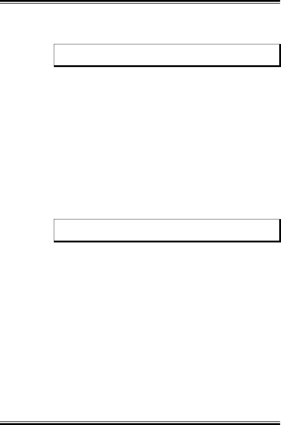
dsPIC33F/PIC24H Family Reference Manual
DS70204C-page 2-34 © 2007-2011 Microchip Technology Inc.
If the DCOUNT register is not zero, the PC is loaded with the address contained in the DOSTART
register to start another iteration of the DO loop. When DCOUNT reaches zero, the DO loop
terminates.
If no other nested DO loops are in progress, the DA bit is also cleared.
2.9.2.2 DO LOOP NESTING
The DOSTART, DOEND and DCOUNT registers each have an associated shadow register that
allows the DO loop hardware to support one level of automatic nesting. The DOSTART, DOEND
and DCOUNT registers are user accessible. They can be manually saved to permit additional
nesting, where required.
The DO Loop Nesting Level bits (DL<2:0>) in the CORCON register indicate the nesting level of
the DO loop currently being executed. When the first DO instruction is executed, DL<2:0> is set
to 'b001 to indicate that one level of the DO loop is underway. The DO Loop Active bit (DA) in the
SR register is also set.
When another DO instruction is executed within the first DO loop, the DOSTART, DOEND and
DCOUNT registers are transferred into the shadow registers before they are updated with the
new loop values. The DL<2:0> bits are set to 'b010 to indicate that a second, nested DO loop is
in progress. The DA bit (SR<9>) also remains set.
If no more than one level of DO loop nesting is required in the application, no special attention is
required. However, if the user-assigned application requires more than one level of DO loop
nesting, it can be achieved by saving the DOSTART, DOEND and DCOUNT registers before
executing the next DO instruction. These registers should be saved whenever DL<2:0> is 'b010
or greater.
The DOSTART, DOEND and DCOUNT registers are automatically restored from their shadow
registers when a DO loop terminates and DL<2:0> = 'b010.
2.9.2.3 INTERRUPTING A DO LOOP
DO loops can be interrupted at any time. If another DO loop is to be executed during the ISR, the
user-assigned application must check the DL<2:0> status bits and save the DOSTART, DOEND
and DCOUNT registers as required.
No special handling is required if the user-assigned application can ensure that only one level of
DO loop will be executed in:
• Both background and any one ISR handler (if interrupt nesting is enabled) or
• Both background and any ISR (if interrupt nesting is disabled)
Alternatively, up to two (nested) DO loops can be executed in either background or within:
•One ISR handler (if interrupt nesting is enabled) or
• Any ISR (if interrupt nesting is disabled)
It is assumed that no DO loops are used within any trap handlers.
Returning to a DO loop from an ISR using the RETFIE instruction requires no special handling.
Note: The group of instructions in a DO loop construct is always executed at least one
time. The DO loop is always executed one time more than the value specified in the
literal or W register operand.
Note: The DL<2:0> (CORCON<10:8>) bits are combined (logically ORed) to form the DA
bit (SR<9>). If nested DO loops are being executed, the DA bit is cleared only when
the loop count associated with the outermost loop expires.

© 2007-2011 Microchip Technology Inc. DS70204C-page 2-35
Section 2. CPU
CPU
2
2.9.2.4 EARLY TERMINATION OF THE DO LOOP
There are two ways to terminate a DO loop earlier than normal:
•The Early DO Loop Termination Control bit (EDT) in the CORCON register provides a
means for the user-assigned application to terminate a DO loop before it completes all
loops. Writing a ‘1’ to the EDT bit forces the loop to complete the iteration underway and
then terminate. If EDT is set during the next-to-last (pen-ultimate) or last instruction of the
loop, one more iteration of the loop occurs. EDT always reads as a ‘0’; clearing it has no
effect. After the EDT bit is set, the user can optionally branch out of the DO loop.
• Alternatively, the code can branch out of the loop at any point except from the last
instruction, which cannot be a flow-control instruction. Although the DA bit (SR<9>)
enables the DO loop hardware, it has no effect unless the address of the pen-ultimate
instruction is encountered during an instruction prefetch. This is not a recommended
method for terminating a DO loop.
2.9.2.5 DO LOOP RESTRICTIONS
The use of DO loops imposes restrictions such as:
• When the DOEND register can be read.
• A few instructions must not be used as the last instruction in the loop.
• Certain small loop lengths are prohibited, as listed in Table 2-8 (loop length refers to the
size of the block of instructions that is being repeated in the loop).
2.9.2.5.1 DOEND Register Restrictions
All DO loops must contain at least two instructions because the loop termination tests are
performed in the pen-ultimate instruction. REPEAT should be used for single instruction loops.
The DOEND Special Function Register (SFR), cannot be read by user software in the instruction
that immediately follows either a DO instruction or a file register write operation to the DOEND
SFR.
The instruction before the pen-ultimate instruction in a DO loop should not modify:
• CPU priority level governed by the CPU IPL status bits (SR<7:5>).
• Peripheral Interrupt Enable bits governed by Interrupt Enable Control registers IEC0, IEC1
and IEC2.
• Peripheral Interrupt Priority bits governed by Interrupt Priority Control registers IPC0
through IPC11.
If these restrictions are not observed, the DO loop may execute incorrectly.
2.9.2.5.2 Last Instruction Restrictions
The last instruction in a DO loop should not be any of the following:
• Flow control instruction (e.g., any branch, compare and skip, GOTO, CALL, RCALL, TRAP).
• Another REPEAT or DO instruction.
• Target instruction within a REPEAT loop. This restriction implies that the one before the last
instruction also cannot be a REPEAT.
• Any instruction that occupies two words in program space.
•DISI instruction.
RETURN, RETFIE and RETLW work correctly as the last instruction of a DO loop, but the
user-assigned application is responsible for returning to the loop to complete it.
Note: Exiting a DO loop without using EDT is not recommended, because the hardware
will continue to check for DOEND addresses.

dsPIC33F/PIC24H Family Reference Manual
DS70204C-page 2-36 © 2007-2011 Microchip Technology Inc.
2.9.2.5.3 Loop Length Restrictions
Loop length is defined as the signed offset of the last instruction from the first instruction in the
DO loop. The loop length, when added to the address of the first instruction in the loop, forms the
address of the last instruction of the loop. Table 2-8 lists the loop lengths to avoid.
Table 2-8: Loop Lengths to Avoid
Loop Length Reason to Avoid
-2 Execution starts at the first instruction in the loop (i.e., at the PC address) and continues until the
loop-end address (in this case [PC – 4]) is prefetched. As this is the first word of the DO instruction, it
executes the DO instruction again, re-initializing the DCOUNT and prefetching [PC]. This continues
forever as long as the loop end address [PC – 4] is prefetched. This value of n has the potential of
creating an infinite loop (subject to a Watchdog Timer Reset).
For example:
end_loop: DO #33, end_loop ;DO is a two-word instruction
NOP ;2nd word of DO executes as a NOP
ADD W2,W3,W4 ;First instruction in DO loop([PC])
-1 Execution starts at the first instruction in the loop (i.e., at [PC]) and continues until the loop end
address ([PC – 2]) is prefetched. Since the loop end address is the second word of the
DO instruction, it executes as a NOP but will still prefetch [PC]. The loop will then execute again. This
will continue as long as the loop end address [PC – 2] is prefetched and the loop does not terminate.
If the value in the DCOUNT register reaches zero and on a subsequent decrement generates a
borrow, the loop will terminate. However, in such a case the initial instruction outside the loop is
once again the first loop instruction.
For example:
DO #33, end_loop ;DO is a two-word instruction
end_loop: NOP ;2nd word of DO executes as a NOP
ADD W2,W3,W4 ;First instruction in DO loop([PC])
0Execution starts at the first instruction in the loop (i.e., at [PC]) and continues until the loop end
address ([PC]) is prefetched. If the loop continues, this prefetch causes the DO loop hardware to load
the DOEND address ([PC]) into the PC for the next fetch (which will be [PC] again). After the first true
iteration of the loop, the first instruction in the loop executes repeatedly until the loop count
underflows and the loop terminates. When this occurs, the initial instruction outside the loop is the
instruction after [PC].
For example:
DO #33, end_loop ;DO is a two-word instruction
NOP ;2nd word of DO executes as a NOP
end_loop: ADD W2,W3,W4 ;First instruction in DO loop([PC])

© 2007-2011 Microchip Technology Inc. DS70204C-page 2-37
Section 2. CPU
CPU
2
2.10 ADDRESS REGISTER DEPENDENCIES
The dsPIC33F/PIC24H architecture supports a data space read (source) and a data space write
(destination) for most MCU class instructions. The Effective Address (EA) calculation by the
AGU, and subsequent data space read or write, each take one instruction cycle to complete. This
timing causes the data space read and write operations for each instruction to partially overlap,
as shown in Figure 2-21. Because of this overlap, a Read-After-Write (RAW) data dependency
can occur across instruction boundaries. RAW data dependencies are detected and handled at
run-time by the dsPIC33F/PIC24H CPU.
Figure 2-21: Data Space Access Timing
2.10.1 Read-After-Write (RAW) Dependency Rules
If the W register is used as a write operation destination in the current instruction, and the
W register being read in the prefetched instruction are the same, the following rules apply:
• If the destination write (current instruction) does not modify the contents of Wn, no stalls will
occur
• If the source read (prefetched instruction) does not calculate an EA using Wn, no stalls will
occur
During each instruction cycle, the dsPIC33F/PIC24H hardware automatically checks to see if a
RAW data dependency is about to occur. If the conditions specified above are not satisfied, the
CPU automatically adds a one-instruction-cycle delay before executing the prefetched
instruction. The instruction stall provides enough time for the destination W register write to take
place before the next (prefetched) instruction uses the written data. Table 2-9 provides the RAW
dependency summary.
ADD MOV
[W7]
[W10] [W9]++
X-Space Address W7 W10 W8 W9
Add W0, [W7], [W10]
MOV [W8], [W9]++
[W8]
X-Space RAGU
Instruction Register
Contents
X-Space WAGU
1 Instruction Cycle (TCY)
TCY0TCY1TCY2
dsPIC33F/PIC24H Family Reference Manual
DS70204C-page 2-38 © 2007-2011 Microchip Technology Inc.
Table 2-9: Read-After-Write Dependency Summary
2.10.2 Instruction Stall Cycles
An instruction stall is essentially a one instruction cycle wait period appended in front of the read
phase of an instruction to allow the prior write to complete before the next read operation. For
the purposes of interrupt latency, the stall cycle is associated with the instruction following the
instruction where it was detected (i.e., stall cycles always precede instruction execution cycles).
If a RAW data dependency is detected, the dsPIC33F/PIC24H CPU begins an instruction stall.
During an instruction stall, the following events occur:
• The write operation underway (for the previous instruction) is allowed to complete as normal.
• Data space is not addressed until after the instruction stall.
• PC increment is inhibited until after the instruction stall.
• Further instruction fetches are inhibited until after the instruction stall.
2.10.2.1 INSTRUCTION STALL CYCLES AND INTERRUPTS
When an interrupt event coincides with two adjacent instructions that will cause an instruction
stall, one of two possible outcomes can occur:
• If the interrupt coincides with the first instruction, the first instruction is allowed to complete
while the second instruction is executed after the ISR completes. In this case, the stall
cycle is eliminated from the second instruction because the exception process provides
time for the first instruction to complete the write phase.
• If the interrupt coincides with the second instruction, the second instruction and the
appended stall cycle are allowed to execute before to the ISR. In this case, the stall cycle
associated with the second instruction executes normally. However, the stall cycle is
effectively absorbed into the exception process timing. The exception process proceeds as
if an ordinary one-cycle instruction or two-cycle instruction is interrupted.
Destination
Addressing Mode
Using Wn
Source
Addressing Mode
Using Wn Status Examples
(Wn = W2)
Direct Direct Allowed ADD.w W0, W1, W2
MOV.w W2, W3
Direct Indirect Stall ADD.w W0, W1, W2
MOV.w [W2], W3
Direct Indirect with
modification Stall ADD.w W0, W1, W2
MOV.w [W2++], W3
Indirect Direct Allowed ADD.w W0, W1, [W2]
MOV.w W2, W3
Indirect Indirect Allowed ADD.w W0, W1, [W2]
MOV.w [W2], W3
Indirect Indirect with
modification Allowed ADD.w W0, W1, [W2]
MOV.w [W2++], W3
Indirect with
modification Direct Allowed ADD.w W0, W1, [W2++]
MOV.w W2, W3
Indirect Indirect Stall ADD.w W0, W1, [W2]
MOV.w [W2], W3
; W2=0x0004 (mapped W2)
Indirect Indirect with
modification Stall ADD.w W0, W1, [W2]
MOV.w [W2++], W3
; W2=0x0004 (mapped W2)
Indirect with
modification Indirect Stall ADD.w W0, W1, [W2++]
MOV.w [W2], W3
Indirect with
modification Indirect with
modification Stall ADD.w W0, W1, [W2++]
MOV.w [W2++], W3

© 2007-2011 Microchip Technology Inc. DS70204C-page 2-39
Section 2. CPU
CPU
2
2.10.2.2 INSTRUCTION STALL CYCLES AND FLOW CHANGE INSTRUCTIONS
The CALL and RCALL instructions write to the stack using working register W15 and can,
therefore, force an instruction stall prior to the next instruction, if the source read of the next
instruction uses W15.
The RETFIE and RETURN instructions can never force an instruction stall prior to the next
instruction because they only perform read operations. However, the RETLW instruction can force
a stall, because it writes to a W register during the last cycle.
The GOTO and branch instructions can never force an instruction stall because they do not
perform write operations.
2.10.2.3 INSTRUCTION STALLS AND DO AND REPEAT LOOPS
Other than the addition of instruction stall cycles, RAW data dependencies do not affect the
operation of either DO or REPEAT loops.
The prefetched instruction within a REPEAT loop does not change until the loop is complete or
an exception occurs. Although register dependency checks occur across instruction boundaries,
the dsPIC33F/PIC24H CPU effectively compares the source and destination of the same
instruction during a REPEAT loop.
The last instruction of a DO loop will either prefetch the instruction at the loop start address or the
next instruction (outside the loop). The instruction stall decision is based on the last instruction
in the loop and the contents of the prefetched instruction.
2.10.2.4 INSTRUCTION STALLS AND PROGRAM SPACE VISIBILITY (PSV)
When Program Space (PS) is mapped to data space by enabling the PSV bit (CORCON<2>),
and the X space EA falls within the visible program space window, the read cycle redirects to the
address in program space. Accessing data from program space takes up to three instruction
cycles.
Instructions operating in PSV address space are subject to RAW data dependencies and
consequent instruction stalls, just like any other instruction. Consider the code segment, as
shown in Example 2-10.
Example 2-10: Code Example to Operate on the PSV
This sequence of instructions would take five instruction cycles to execute. Two instruction cycles
are added to perform the PSV access via W1. An instruction stall cycle is inserted to resolve the
RAW data dependency caused by W2.
ADD W0, [W1], [W2++] ; PSV = 1, W1=0x8000, PSVPAG=0xAA
MOV [W2], [W3]
dsPIC33F/PIC24H Family Reference Manual
DS70204C-page 2-40 © 2007-2011 Microchip Technology Inc.
2.11 REGISTER MAPS
A summary of the registers associated with the dsPIC33F/PIC24H CPU is provided in Table 2-3.
Table 2-10: CPU Register Map
Name Bit 15 Bit 14 Bit 13 Bit 12 Bit 11 Bit 10 Bit 9 Bit 8 Bit 7 Bit 6 Bit 5 Bit 4 Bit 3 Bit 2 Bit 1 Bit 0 All Resets
W0 W0 (WREG) 0000 0000 0000 0000
W1 W1 0000 0000 0000 0000
W2 W2 0000 0000 0000 0000
W3 W3 0000 0000 0000 0000
W4 W4 0000 0000 0000 0000
W5 W5 0000 0000 0000 0000
W6 W6 0000 0000 0000 0000
W7 W7 0000 0000 0000 0000
W8 W8 0000 0000 0000 0000
W9 W9 0000 0000 0000 0000
W10 W10 0000 0000 0000 0000
W11 W11 0000 0000 0000 0000
W12 W12 0000 0000 0000 0000
W13 W13 0000 0000 0000 0000
W14 W14 0000 0000 0000 0000
W15 W15 0000 0000 0000 0000
SPLIM SPLIM 0000 0000 0000 0000
ACCAL ACCAL 0000 0000 0000 0000
ACCAH ACCAH 0000 0000 0000 0000
ACCAU Sign-extension of ACCA<39> ACCAU 0000 0000 0000 0000
ACCBL ACCBL 0000 0000 0000 0000
ACCBH ACCBH 0000 0000 0000 0000
ACCBU Sign-extension of ACCB<39> ACCBU 0000 0000 0000 0000
PCL PCL 0000 0000 0000 0000
PCH — — — — — — — — — PCH 00000 0000 0000 0000
TBLPAG — — — — — — — — TBLPAG 0000 0000 0000 0000
PSVPAG — — — — — — — — PSVPAG 0000 0000 0000 0000
RCOUNT RCOUNT xxxx xxxx xxxx xxxx
DCOUNT DCOUNT xxxx xxxx xxxx xxxx
DOSTARTL DOSTARTL 0xxxx xxxx xxxx xxx0
DOSTARTH — — — — — — — — — — DOSTARTH 0000 0000 00xx xxxx
Legend: x = unknown value on Reset, — = unimplemented, read as ‘0’. Reset values are shown in hexadecimal.
Note: Refer to the device data sheet for more details on the specific core register map.
© 2007-2011 Microchip Technology Inc. DS70204C-page 2-41
Section 2. CPU
CPU
2
DOENDL DOENDL 0xxxx xxxx xxxx xxx0
DOENDH — — — — — — — — — — DOENDH 0000 0000 00xx xxxx
SR OA OB SA SB OAB SAB DA DC IPL2 IPL1 IPL0 RA NOV Z C 0000 0000 0000 0000
CORCON — — — US EDT DL<2:0> SATA SATB SATDW ACCSAT IPL3 PSV RND IF 0000 0000 0010 0000
MODCON XMODEN YMODEN — — BWM<3:0> YWM<3:0> XWM<3:0> 0000 0000 0000 0000
XMODSRT XMODSRT<15:0> 0xxxx xxxx xxxx xxx0
XMODEND XMODEND<15:0> 1xxxx xxxx xxxx xxx1
YMODSRT YMODSRT<15:0> 0xxxx xxxx xxxx xxx0
YMODEND YMODEND<15:0> 1xxxx xxxx xxxx xxx1
XBREV BREN XBREV<14:0> xxxx xxxx xxxx xxxx
DISICNT — — DISICNT<13:0> 0000 0000 0000 0000
Table 2-10: CPU Register Map (Continued)
Name Bit 15 Bit 14 Bit 13 Bit 12 Bit 11 Bit 10 Bit 9 Bit 8 Bit 7 Bit 6 Bit 5 Bit 4 Bit 3 Bit 2 Bit 1 Bit 0 All Resets
Legend: x = unknown value on Reset, — = unimplemented, read as ‘0’. Reset values are shown in hexadecimal.
Note: Refer to the device data sheet for more details on the specific core register map.

dsPIC33F/PIC24H Family Reference Manual
DS70204C-page 2-42 © 2007-2011 Microchip Technology Inc.
2.12 RELATED APPLICATION NOTES
This section lists application notes that are related to this section of the manual. These
application notes may not be written specifically for the dsPIC33F/PIC24H Product Family, but
the concepts are pertinent and could be used with modification and possible limitations. The
current application notes related to the CPU module include the following:
Title Application Note #
No related application notes at this time. N/A
Note: Please visit the Microchip web site (www.microchip.com) for additional Application
Notes and code examples for the dsPIC33F/PIC24H family of devices.

© 2007-2011 Microchip Technology Inc. DS70204C-page 2-43
Section 2. CPU
CPU
2
2.13 REVISION HISTORY
Revision A (April 2007)
This is the initial released version of this document.
Revision B (September 2009)
This revision incorporates the following updates:
• Note:
- Added a note on program memory error in 2.8.7 “Address Register Dependencies”
•Registers:
- Removed the Address column in Table 2-10 in 2.11 “Register Maps”
• Sections:
- Updated 2.1 “Introduction” with the following data: All instructions execute in a single
cycle, except the instructions that change the program flow, double-word move
(MOV.D) instruction, table instructions and also the instructions accessing Program
Space Visibility (PSV) take more than one cycle
- Updated the REPEAT count value as “DO iteration count value” in 2.9.2 “DO Loop
Construct”
- Updated the exception process in 2.10.2.1 “Instruction Stall Cycles and
Interrupts”as follows: The exception process proceeds as if an ordinary one-cycle
instruction or two-cycle instruction is interrupted
- Updated the read or write cycle as “read cycle” in 2.10.2.4 “Instruction Stalls and
Program Space Visibility (PSV)”
• Tables:
- Added a table (see Table 2-5) on Multiplication Options in 2.6.2.2 “MCU Multiply
Instructions”
• Updated the incorrect references to external documents specified in this document.
• Additional minor corrections such as language and formatting updates were incorporated
throughout the document
Revision C (September 2011)
This revision includes the following updates:
• All occurrences of dsPIC33F were changed to dsPIC33F/PIC24H
• The Preliminary document status was removed
• The STATUS register bit, shown as ‘SZ’, was corrected to ‘Z’ in the Programmer’s Model
(see Figure 2-2)
• Updated Accessing W Register in File Register Instruction (see Example 2-3)
• Added a sentence with a cross-reference to the CORCON register in 2.4.2 “Core Control
Register: CORCON”
• Minor corrections to text and formatting were incorporated throughout the document

dsPIC33F/PIC24H Family Reference Manual
DS70204C-page 2-44 © 2007-2011 Microchip Technology Inc.
NOTES:
© 2007-2011 Microchip Technology Inc. DS70204C-page 2 -45
Information contained in this publication regarding device
applications and the like is provided only for your convenience
and may be superseded by updates. It is your responsibility to
ensure that your application meets with your specifications.
MICROCHIP MAKES NO REPRESENTATIONS OR
WARRANTIES OF ANY KIND WHETHER EXPRESS OR
IMPLIED, WRITTEN OR ORAL, STATUTORY OR
OTHERWISE, RELATED TO THE INFORMATION,
INCLUDING BUT NOT LIMITED TO ITS CONDITION,
QUALITY, PERFORMANCE, MERCHANTABILITY OR
FITNESS FOR PURPOSE. Microchip disclaims all liability
arising from this information and its use. Use of Microchip
devices in life support and/or safety applications is entirely at
the buyer’s risk, and the buyer agrees to defend, indemnify and
hold harmless Microchip from any and all damages, claims,
suits, or expenses resulting from such use. No licenses are
conveyed, implicitly or otherwise, under any Microchip
intellectual property rights.
Trademarks
The Microchip name and logo, the Microchip logo, dsPIC,
KEELOQ, KEELOQ logo, MPLAB, PIC, PICmicro, PICSTART,
PIC32 logo, rfPIC and UNI/O are registered trademarks of
Microchip Technology Incorporated in the U.S.A. and other
countries.
FilterLab, Hampshire, HI-TECH C, Linear Active Thermistor,
MXDEV, MXLAB, SEEVAL and The Embedded Control
Solutions Company are registered trademarks of Microchip
Technology Incorporated in the U.S.A.
Analog-for-the-Digital Age, Application Maestro, chipKIT,
chipKIT logo, CodeGuard, dsPICDEM, dsPICDEM.net,
dsPICworks, dsSPEAK, ECAN, ECONOMONITOR,
FanSense, HI-TIDE, In-Circuit Serial Programming, ICSP,
Mindi, MiWi, MPASM, MPLAB Certified logo, MPLIB,
MPLINK, mTouch, Omniscient Code Generation, PICC,
PICC-18, PICDEM, PICDEM.net, PICkit, PICtail, REAL ICE,
rfLAB, Select Mode, Total Endurance, TSHARC,
UniWinDriver, WiperLock and ZENA are trademarks of
Microchip Technology Incorporated in the U.S.A. and other
countries.
SQTP is a service mark of Microchip Technology Incorporated
in the U.S.A.
All other trademarks mentioned herein are property of their
respective companies.
© 2007-2011, Microchip Technology Incorporated, Printed in
the U.S.A., All Rights Reserved.
Printed on recycled paper.
ISBN: 978-1-61341-659-4
Note the following details of the code protection feature on Microchip devices:
• Microchip products meet the specification contained in their particular Microchip Data Sheet.
• Microchip believes that its family of products is one of the most secure families of its kind on the market today, when used in the
intended manner and under normal conditions.
• There are dishonest and possibly illegal methods used to breach the code protection feature. All of these methods, to our
knowledge, require using the Microchip products in a manner outside the operating specifications contained in Microchip’s Data
Sheets. Most likely, the person doing so is engaged in theft of intellectual property.
• Microchip is willing to work with the customer who is concerned about the integrity of their code.
• Neither Microchip nor any other semiconductor manufacturer can guarantee the security of their code. Code protection does not
mean that we are guaranteeing the product as “unbreakable.”
Code protection is constantly evolving. We at Microchip are committed to continuously improving the code protection features of our
products. Attempts to break Microchip’s code protection feature may be a violation of the Digital Millennium Copyright Act. If such acts
allow unauthorized access to your software or other copyrighted work, you may have a right to sue for relief under that Act.
Microchip received ISO/TS-16949:2009 certification for its worldwide
headquarters, design and wafer fabrication facilities in Chandler and
Tempe, Arizona; Gresham, Oregon and design centers in California
and India. The Company’s quality system processes and procedures
are for its PIC® MCUs and dsPIC® DSCs, KEELOQ® code hopping
devices, Serial EEPROMs, microperipherals, nonvolatile memory and
analog products. In addition, Microchip’s quality system for the design
and manufacture of development systems is ISO 9001:2000 certified.

DS70204C-page -46 © 2007-2011 Microchip Technology Inc.
AMERICAS
Corporate Office
2355 West Chandler Blvd.
Chandler, AZ 85224-6199
Tel: 480-792-7200
Fax: 480-792-7277
Technical Support:
http://www.microchip.com/
support
Web Address:
www.microchip.com
Atlanta
Duluth, GA
Tel: 678-957-9614
Fax: 678-957-1455
Boston
Westborough, MA
Tel: 774-760-0087
Fax: 774-760-0088
Chicago
Itasca, IL
Tel: 630-285-0071
Fax: 630-285-0075
Cleveland
Independence, OH
Tel: 216-447-0464
Fax: 216-447-0643
Dallas
Addison, TX
Tel: 972-818-7423
Fax: 972-818-2924
Detroit
Farmington Hills, MI
Tel: 248-538-2250
Fax: 248-538-2260
Indianapolis
Noblesville, IN
Tel: 317-773-8323
Fax: 317-773-5453
Los Angeles
Mission Viejo, CA
Tel: 949-462-9523
Fax: 949-462-9608
Santa Clara
Santa Clara, CA
Tel: 408-961-6444
Fax: 408-961-6445
Toronto
Mississauga, Ontario,
Canada
Tel: 905-673-0699
Fax: 905-673-6509
ASIA/PACIFIC
Asia Pacific Office
Suites 3707-14, 37th Floor
Tower 6, The Gateway
Harbour City, Kowloon
Hong Kong
Tel: 852-2401-1200
Fax: 852-2401-3431
Australia - Sydney
Tel: 61-2-9868-6733
Fax: 61-2-9868-6755
China - Beijing
Tel: 86-10-8569-7000
Fax: 86-10-8528-2104
China - Chengdu
Tel: 86-28-8665-5511
Fax: 86-28-8665-7889
China - Chongqing
Tel: 86-23-8980-9588
Fax: 86-23-8980-9500
China - Hangzhou
Tel: 86-571-2819-3187
Fax: 86-571-2819-3189
China - Hong Kong SAR
Tel: 852-2401-1200
Fax: 852-2401-3431
China - Nanjing
Tel: 86-25-8473-2460
Fax: 86-25-8473-2470
China - Qingdao
Tel: 86-532-8502-7355
Fax: 86-532-8502-7205
China - Shanghai
Tel: 86-21-5407-5533
Fax: 86-21-5407-5066
China - Shenyang
Tel: 86-24-2334-2829
Fax: 86-24-2334-2393
China - Shenzhen
Tel: 86-755-8203-2660
Fax: 86-755-8203-1760
China - Wuhan
Tel: 86-27-5980-5300
Fax: 86-27-5980-5118
China - Xian
Tel: 86-29-8833-7252
Fax: 86-29-8833-7256
China - Xiamen
Tel: 86-592-2388138
Fax: 86-592-2388130
China - Zhuhai
Tel: 86-756-3210040
Fax: 86-756-3210049
ASIA/PACIFIC
India - Bangalore
Tel: 91-80-3090-4444
Fax: 91-80-3090-4123
India - New Delhi
Tel: 91-11-4160-8631
Fax: 91-11-4160-8632
India - Pune
Tel: 91-20-2566-1512
Fax: 91-20-2566-1513
Japan - Yokohama
Tel: 81-45-471- 6166
Fax: 81-45-471-6122
Korea - Daegu
Tel: 82-53-744-4301
Fax: 82-53-744-4302
Korea - Seoul
Tel: 82-2-554-7200
Fax: 82-2-558-5932 or
82-2-558-5934
Malaysia - Kuala Lumpur
Tel: 60-3-6201-9857
Fax: 60-3-6201-9859
Malaysia - Penang
Tel: 60-4-227-8870
Fax: 60-4-227-4068
Philippines - Manila
Tel: 63-2-634-9065
Fax: 63-2-634-9069
Singapore
Tel: 65-6334-8870
Fax: 65-6334-8850
Taiwan - Hsin Chu
Tel: 886-3-5778-366
Fax: 886-3-5770-955
Taiwan - Kaohsiung
Tel: 886-7-536-4818
Fax: 886-7-330-9305
Taiwan - Taipei
Tel: 886-2-2500-6610
Fax: 886-2-2508-0102
Thailand - Bangkok
Tel: 66-2-694-1351
Fax: 66-2-694-1350
EUROPE
Austria - Wels
Tel: 43-7242-2244-39
Fax: 43-7242-2244-393
Denmark - Copenhagen
Tel: 45-4450-2828
Fax: 45-4485-2829
France - Paris
Tel: 33-1-69-53-63-20
Fax: 33-1-69-30-90-79
Germany - Munich
Tel: 49-89-627-144-0
Fax: 49-89-627-144-44
Italy - Milan
Tel: 39-0331-742611
Fax: 39-0331-466781
Netherlands - Drunen
Tel: 31-416-690399
Fax: 31-416-690340
Spain - Madrid
Tel: 34-91-708-08-90
Fax: 34-91-708-08-91
UK - Wokingham
Tel: 44-118-921-5869
Fax: 44-118-921-5820
Worldwide Sales and Service
08/02/11
