DM74LS154 4 Line To 16 Decoder/Demultiplexer 74154
User Manual: 74154
Open the PDF directly: View PDF ![]() .
.
Page Count: 5
© 2000 Fairchild Semiconductor Corporation DS006394 www.fairchildsemi.com
August 1986
Revised March 2000
DM74LS154 4-Line to 16-Line Decoder/Demultiplexer
DM74LS154
4-Line to 16-Line Decoder/Demultiplexer
General Description
Each of these 4-line-to-16-line decoders utilizes TTL cir-
cuitry to decode four binary-coded inputs into one of six-
teen mutually exclusive outputs when both the strobe
inputs, G1 and G2, are LOW. The demultiplexing function
is performed by using the 4 input lines to address the out-
put line, passing data from one of the strobe inputs with the
other strobe input LOW. When either strobe input is HIGH,
all outputs are HIGH. These demultiplexers are ideally
suited for implementing high-performance memory decod-
ers. All inputs are buffered and input clamping diodes are
provided to minimize transmission-line effects and thereby
simplify system design.
Features
■Decodes 4 binary-coded inputs into one of 16 mutually
exclusive outputs
■Performs the demultiplexing function by distributing data
from one input line to any one of 16 outputs
■Input clamping diodes simplify system design
■High fan-out, low-impedance, totem-pole outputs
■Typical propagation delay
3 levels of logic 23 ns
Strobe 19 ns
■Typical power dissipation 45 mW
Ordering Code:
Devices also available in Tape and Reel. Specify by appending the suffix letter “X” to the ordering code.
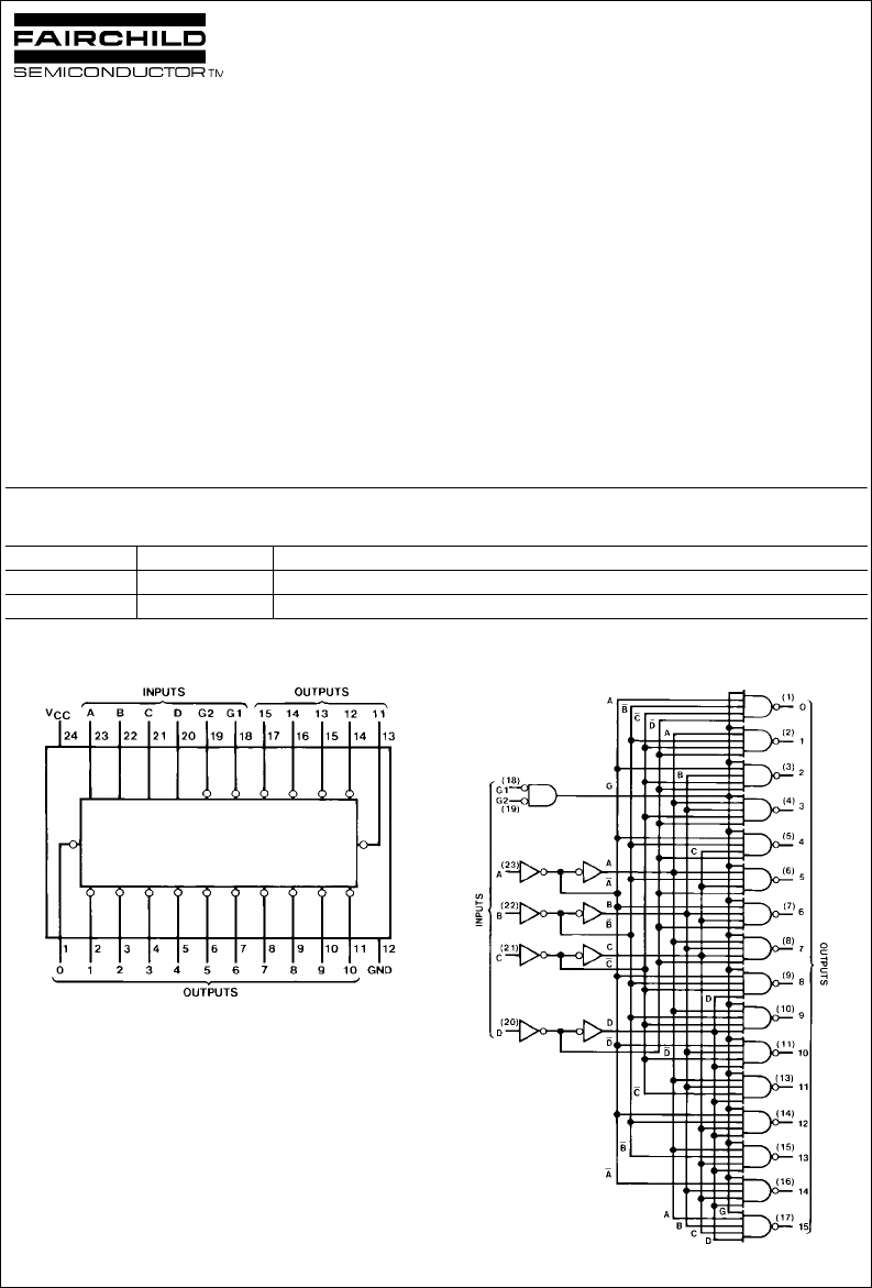
Connection Diagram Logic Diagram
Order Number Package Number Package Description
DM74LS154WM M24B 24-Lead Small Outline Integrated Circuit (SOIC), JEDEC MS-013, 0.300 Wide
DM74LS154N N24A 24-Lead Plastic Dual-In-Line Package (PDIP), JEDEC MS-010, 0.600 Wide
www.fairchildsemi.com 2
DM74LS154
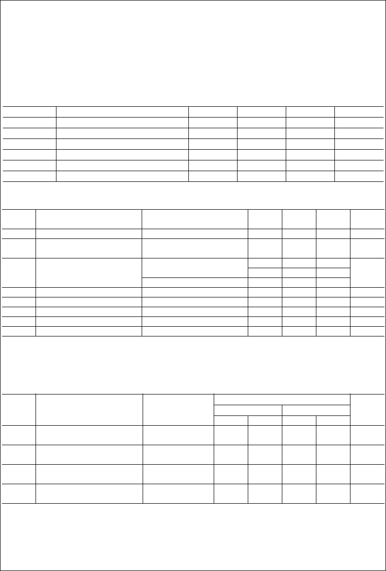
Function Table
H = HIGH Level
L = Low Level
X = Don’t Care
Inputs Outputs
G1G2DCBA0123456789101112131415
L L L L LL LHHHHHHHHH H H H H H H
L L L L LHHLHHHHHHHH H H H H H H
L L L LHLHHLHHHHHHH H H H H H H
L L L LHHHHHLHHHHHH H H H H H H
L L LHL LHHHHLHHHHH H H H H H H
L L LHLHHHHHHLHHHH H H H H H H
L L LHHLHHHHHHLHHH H H H H H H
L L LHHHHHHHHHHLHH H H H H H H
L L HL L LHHHHHHHHLH H H H H H H
L L HL LHHHHHHHHHHL H H H H H H
L L HLHLHHHHHHHHHH L H H H H H
L L HLHHHHHHHHHHHH H L H H H H
L L HHL LHHHHHHHHHH H H L H H H
L L HHLHHHHHHHHHHH H H H L H H
L L HHHLHHHHHHHHHH H H H H L H
L L HHHHHHHHHHHHHH H H H H H L
L H XXXXHHHHHHHHHH H H H H H H
H L XXXXHHHHHHHHHH H H H H H H
H H XXXXHHHHHHHHHH H H H H H H
3 www.fairchildsemi.com
DM74LS154
Absolute Maximum Ratings(Note 1)
Note 1: The “Absolute Maximum Ratings” are those values beyond which
the safety of the device cannot be guaranteed. The device should not be
operated at these limits. The parametric values defined in the Electrical
Characteristics tables are not guaranteed at the absolute maximum ratings.
The “Recommended Operating Conditions” table will define the conditions
for actual device operation.
Recommended Operating Conditions
Electrical Characteristics
over recommended operating free air temperature range (unless otherwise noted)
Note 2: All typicals are at VCC = 5V, TA = 25°C.
Note 3: Not more than one output should be shorted at a time, and the duration should not exceed one second.
Note 4: ICC is measured with all outputs OPEN and all inputs GROUNDED.
Switching Characteristics
at VCC = 5V and TA = 25°C
Supply Voltage 7V
Input Voltage 7V
Operating Free Air Temperature Range 0°C to +70°C
Storage Temperature Range −65°C to +150°C
Symbol Parameter Min Nom Max Units
VCC Supply Voltage 4.75 5 5.25 V
VIH HIGH Level Input Voltage 2 V
VIL LOW Level Input Voltage 0.8 V
IOH HIGH Level Output Current −0.4 mA
IOL LOW Level Output Current 8 mA
TAFree Air Operating Temperature 0 70 °C
Symbol Parameter Conditions Min Typ Max Units
(Note 2)
VIInput Clamp Voltage VCC = Min, II = −18 mA −1.5 V
VOH HIGH Level VCC = Min, IOH = Max 2.7 3.4 V
Output Voltage VIL = Max, VIH = Min
VOL LOW Level VCC = Min, IOL = Max 0.25 0.4
Output Voltage VIL = Max, VIH = Min 0.35 0.5 V
IOL = 4 mA, VCC = Min 0.25 0.4
IIInput Current @ Max Input Voltage VCC = Max, VI = 7V 0.1 mA
IIH HIGH Level Input Current VCC = Max, VI = 2.7V 20 µA
IIL LOW Level Input Current VCC = Max, VI = 0.4V −0.4 mA
IOS Short Circuit Output Current VCC = Max (Note 3) −20 −100 mA
ICC Supply Current VCC = Max (Note 4) 9 14 mA
From (Input) RL = 2 kΩ
Symbol Parameter To (Output) CL = 15 pF CL = 50 pF Units
Min Max Min Max
tPLH Propagation Delay Time Data to Output 30 35 ns
LOW-to-HIGH Level Output
tPHL Propagation Delay Time Data to Output 30 35 ns
HIGH-to-LOW Level Output
tPLH Propagation Delay Time Strobe to Output 20 25 ns
LOW-to-HIGH Level Output
tPHL Propagation Delay Time Strobe to Output 25 35 ns
HIGH-to-LOW Level Output
www.fairchildsemi.com 4
DM74LS154
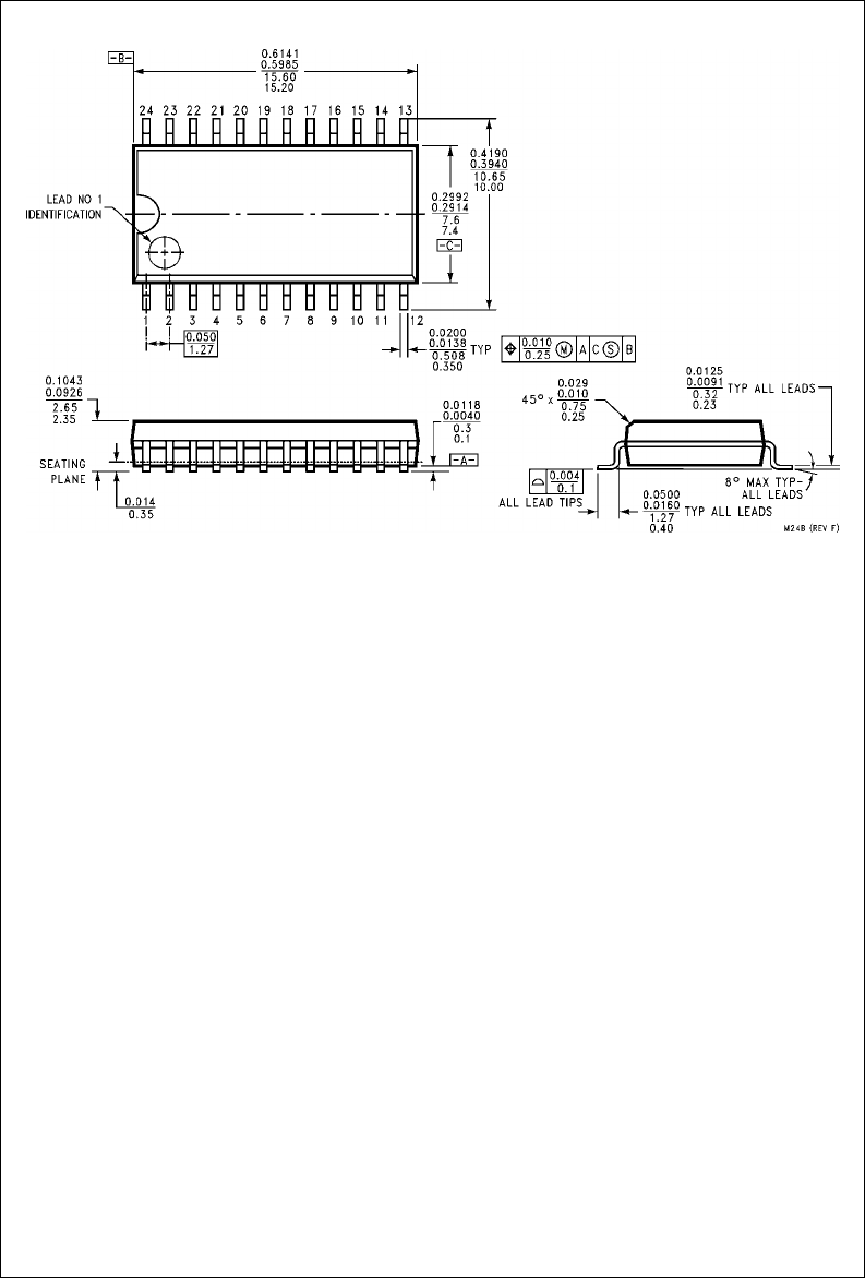
Physical Dimensions inches (millimeters) unless otherwise noted
24-Lead Small Outline Integrated Circuit (SOIC), JEDEC MS-013, 0.300 Wide
Package Number M24B
5 www.fairchildsemi.com
DM74LS154 4-Line to 16-Line Decoder/Demultiplexer
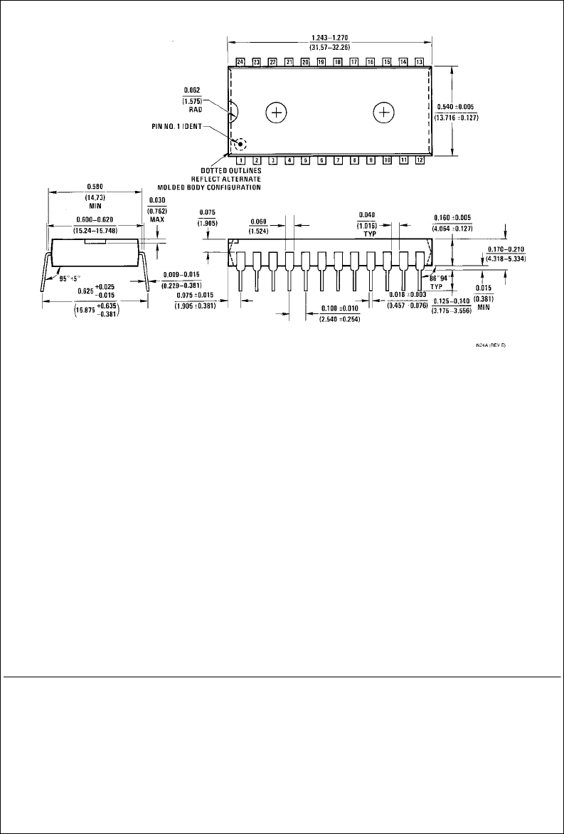
Physical Dimensions inches (millimeters) unless otherwise noted (Continued)
24-Lead Plastic Dual-In-Line Package (PDIP), JEDEC MS-010, 0.600 Wide
Package Number N24A
Fairchild does not assume any responsibility for use of any circuitry described, no circuit patent licenses are implied and
Fairchild reserves the right at any time without notice to change said circuitry and specifications.
LIFE SUPPORT POLICY
FAIRCHILD’S PRODUCTS ARE NOT AUTHORIZED FOR USE AS CRITICAL COMPONENTS IN LIFE SUPPORT
DEVICES OR SYSTEMS WITHOUT THE EXPRESS WRITTEN APPROVAL OF THE PRESIDENT OF FAIRCHILD
SEMICONDUCTOR CORPORATION. As used herein:
1. Life support devices or systems are devices or systems
which, (a) are intended for surgical implant into the
body, or (b) support or sustain life, and (c) whose failure
to perform when properly used in accordance with
instructions for use provided in the labeling, can be rea-
sonably expected to result in a significant injury to the
user.
2. A critical component in any component of a life support
device or system whose failure to perform can be rea-
sonably expected to cause the failure of the life support
device or system, or to affect its safety or effectiveness.
www.fairchildsemi.com
