800 8027 02_Sun 3_E_SCSI_Ethernet_Board_Hardware_Reference_Manual_Jun88 02 Sun 3 E SCSI Ethernet Board Hardware Reference Manual Jun88
800-8027-02_Sun-3_E_SCSI_Ethernet_Board_Hardware_Reference_Manual_Jun88 manual pdf -FilePursuit
800-8027-02_Sun-3_E_SCSI_Ethernet_Board_Hardware_Reference_Manual_Jun88 800-8027-02_Sun-3_E_SCSI_Ethernet_Board_Hardware_Reference_Manual_Jun88
User Manual: 800-8027-02_Sun-3_E_SCSI_Ethernet_Board_Hardware_Reference_Manual_Jun88
Open the PDF directly: View PDF ![]() .
.
Page Count: 56
Sun-3/E SCSI/Ethernet Board
Hardware
Reference
Manual
Sun Microsystems, Inc. • 2550 Garcia Avenue • Mountain View,
CA
94043 • 415-960-1300
Pan
No: 800-8027-02
Revision: A
of
June
1,
1988
Sun
Microsystems and
Sun
Workstation
are registered trademarlcs
of
Sun Microsystems. Incorporated. Sun-3,
Sun3,
Sun-3Inx,
SunOS,
and
DVMA
are trademarlcs
of
Sun Microsystems. Incor-
porated.
The
Sun logo • is a registered trademark.
of
Sun Microsystems. Inc.
Copyright © 1988
by
Sun Microsystems. Inc. -Printed
in
U.S.A.
This publication is protected by Federal Copyright Law, with all rights reserved.
No part
of
this publication may be reproduced, stored
in
a retrieval system,
translated, transcribed,
or
transmitted, in any form, or
by
any means: manual,
. electric. electronic. electromagnetic, mechanical, chemical, optical!
or
otherwise,
without prior explicit written permission from Sun Microsystems.
Contents
Chapter 1
Introduction
............................................................................
;.............................
3
1.1. Using This Manual
.........................................................................................................
3
Chapter 2
Unpackaging
and
Handling
.....................................................................
7
Chapter 3
Board
Architecture
.........................................................................................
11
3.1. Addressing and Jumpering
.........................................................................................
13
3.2. IntemIpts
...............................................................................................................................
15
3.3. Bandwidth and Capability
..........................................................................................
16
3.4. Cycle Priorities
.................................................................................................................
16
Chapter 4
SCSI
Interface
....................................................................................................
19
4.1. Control and Status Registers
.....................................................................................
19
4.2. SCSI Buffer
.........................................................................................................................
21
4.3. SCSI Reads and Writes
................................................................................................
21
Chapter 5
Ethernet
Interface
............................................................................................
25
5.1. Ethernet Address
........................................................................................
_
.....
;..............
26
5.2. Ethernet Transmits and Receives
........................................•...........
;
..............
;.......
26
5.3. Ethernet Buffer
..................................................................................................................
27
5.4. Thin Ethernet
.....................................................................................................................
27
5.5. External Transceiver
......................................................................................................
27
Chapter 6
VMEbus
InteIface
...........................................................................................
31
-
iii-
Cmtents -Continued
Appendix A Connectors
...............................................
_
......
_
.................................
_........
35
A.I.
Rear Edge Connectors
.....................................................
_.........................................
35
A2.
Front Panel Connectors
...............................................................................................
37
Appendix B System Design Considerations
.........................................................
45
B.I.
System Power Considerations
....
_
...
_....................................................................
45
B.2.
Environmental Characteristics
........................
_.....................................................
45
B.3.
P2
Bus Design
..................................................................................................................
45
Index
.......................................................................................................................................................
47
-iv-
Tables
Table
3-1
Address Switch Assignment
..............................................................................
13
Table 3-2 Board Device Addressing
....................................................................................
14
Table 3-3 Estimated Board Bandwidths
............................................................................
16
Table 4-1 SCSI Control and Status Register Bits
........................................................
20
Table 5-1 Ethernet Control and Status Register Bits
.................................................
25
Table
6-1
VMEbus ParaIIleters
...............................................................................................
31
Table A-I
PI
Connector Pins
..................................................................................................
35
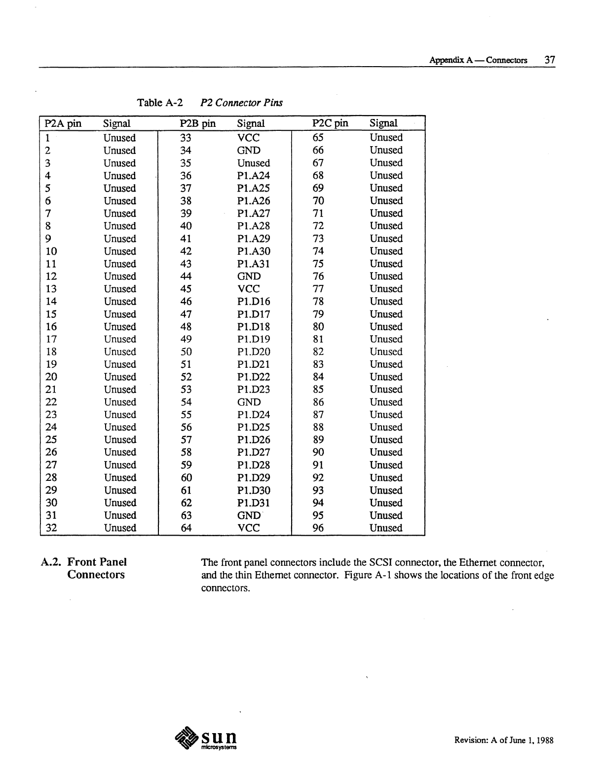
Table A-2 P2 Connector Pins
........................................
:.........................................................
37
Table
A-3
SCSI Connector Pins
............................................................................................
39
Table A-4 Ethernet Connector Pins
.....................................................................................
41
Table
B-1
Board Power Requirements
...............................................................................
45
-v-

Figures
Figure 2-1 Shipping Container
................................................................................................
8
Figure
3-1
S3SE Block Diagram
...........................................................................................
12
Figure 3-2 Switch Locations
....................................................................................................
15
Figure A-I Front Panel Connectors
.....................................................................................
38
Figure A-2 SCSI Connector Pins
...........................................................................................
40
-vii-

1
Introduction
Introduction
....
_.................................................................................................................................
3
1.1.
Using This
Manual
.........................................................................................................
3
Audience
............................................................................................................................
3
Fonts
in
Text
....................................................................................................................
3
Glossary
..............................................................................................................................
4
References
.........................................................................................................................
4

1
Introduction
This manual describes the Sun-3/E SCSI/Ethernet Controller Board (S3SE) for
system programmers and engineers who wish to integrate this board into their
systems.
The S3SE board (501-8027) is a standard double-height Revision B VMEBus
board that provides one Ethernet interface, and one SCSI interface.
1.1. Using This
Manual
This section provides infOlmation
to
help you use this manual.
It
includes a
description
of
the manual and the intended audience. a list
of
the different fonts.
a description
of
how the fonts
are
used. a glossary. and a list
of
references.
Audience
Fonts in
Text
Note that this board should be used with the Sun-3/E CPU. which is described in
the Sun-31E CPU Hardware Reference Manual (pn # 800-8028).
NOTE
This board does NOT include a licensed Ethernet address.
An
Ethernet address
must be downloaded
to
the Ethernet circuits in this board from the Sun-31E CPU
board, which includes a licensed Ethernet address,
or
from some other source.
The audience includes anyone interested in understanding the S3SE board archi-
tecture at a block level. This might include designers, engineers, programmers,
technicians, and anyone else who wants
or
needs to know how the S3SE works.
Note that this manual concerns itself with external signals and timings; for inter-
nal signals and timings. see the Sun S3SE Engineering Manual.
In
this manual, we use the following fonts to make things more clear:
o Roman font is the normal font used for text.
o Italic font is used for the proper name
of
a text
or
chapter to be referred to
for additional information. For example:
For more on loopback mode. see the Intel LAN Component User's
Manual.
o Bold font indicates that a word or phrase requires additional-emphasis. For
example:
The host
processor
uses the bits in this register
to
communicate with
the SCSI interface.
3 Revision: A
ofJune
1.
1988
4 Sun-3/E SCSI/Ethemet Board
Glossary
References
The
following paragraphs list and describe the words
and
acronyms used
in
this
manual:
o S3SE -
The
Sun-3/E SCSI/Ethemet Board.
o
SBC
-SCSI Bus Controller. This is the
NCR
5380
SCSI
Bus Controller
chip.
o
DMA
-Direct Memory Access. A method
of
transferring large blocks
of
data
o
EDLC
-Ethernet Data Link Controller.
The
Intel 85286 Ethernet chip.
For
additional information, see:
o Intel LAN Component User's
Manual-
For
programming information
on
the Inter 85286 Ethernet Controller chip.
o NCR 5380 SCSI Controller Design Manual -
For
information on program-
ming the
NCR
5380
SCSI Bus Controller.
o
The
Sun-31E
CPU Hardware Reference
Manual-
For
information about
the Sun-3/E
CPU
board. (The S3SE board is almost always used with a
Sun-3/E CPU.)
o Manual for
AMD
7990
Thin
Ethernet transceiver
Revision: A
ofJune
I, 1988
2
Unpackaging and Handling
U npackaging and Handling
..................................................................................................
7

2
Unpackaging
and
Handling
Sun-3/E boards are shipped in either individual containers
or
in
lO-board tote
boxes. Inside either. the
PC
board
is
wrapped
in
an
anti-static bag. Inside the
individual boxes.
it
is further protected by two pieces
of
anti-static foam. one
below
it
and one above. Inside the lO-board tote boxes. it is further protected
by
corregated partitions.
CAUTION To avoid damaging the board, keep it in its anti-static bag for as long as pos-
sible,
and
handle it only by its edges. Any
person
handling
the
board
when
it
is
not in its anti-static bag should
be
wearing grounding straps,
and
should
only handle the
board
by its edges.
A single-board container appears in the following figure:
7 Revision: A
of
June
1.
1988
8 Sun-3IE SCSI/Ethemet Board
PRINTED
CIRCUIT
llOARB
4QO-1469-01
fOAM
COLLAR
<ANTI-STATIC)
400-1315-01
I
SHIPPING
BOx
Figure
2-1
..
Shipping Container
2
400-IJ16-0(
CONVOLUTED
rOAN
SET
(ANTI-STAlIC)
/
STATIC
SHIELDING
BAG
TO
BE
PLAC£D
aVER
PCI
Revision: A
of
June
I,
1988
3
Board Architecture
Board
Architecture
......................................................................................................................
11
3.1. Addressing and Jumpering
.........................................................................................
13
3.2. Inteffilpts
...............................................................................................................................
15
3.3. Bandwidth and Capability
..........................................................................................
16
3.4. Cycle Priorities
.................................................................................................................
16

3
Board
Architecture
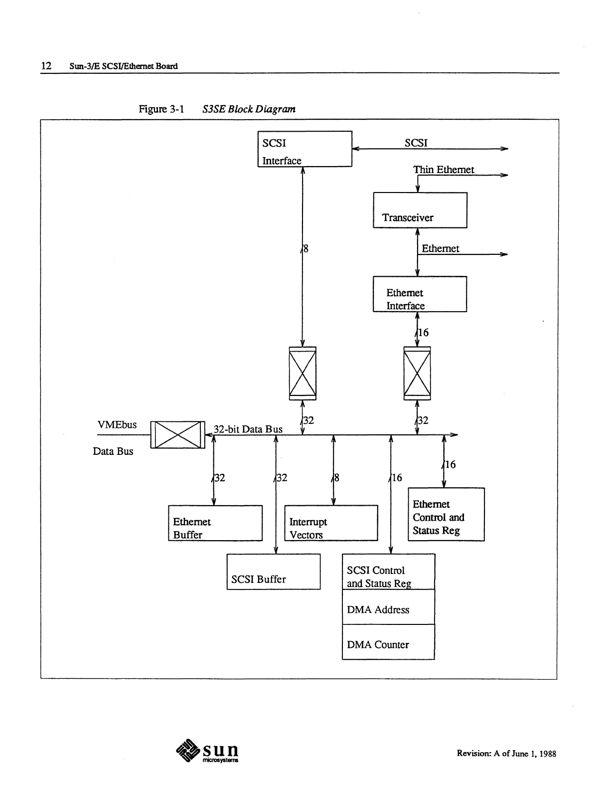
The Sun-3/E SCSI/Ethernet board
is
a dual-purpose VMEbus slave device that
provides a SCSI interface and an Ethernet interface.
The SCSI interface is similar to the SUN-3/50, except that
it
has a 64-kilobyte
buffer memory instead
of
a FIFO. It can transfer data at a maximum rate
of2.6
megabytes/sec.
The Ethernet interface is based on the Intel 82586 Ethernet Controller. It
features 128 kilobytes
of
on-board buffer memory, and can transfer data from the
Ethernet into the on-board buffer memory at a maximum (estimated) rate
of
5.3
megabytes/sec.
The Ethernet interface can also be switch-selected to support a "Thin Ethernet"
(cheapernet). The thin Ethernet interface includes a transceiver
on
the board.
NOTE This board does
NOT
include a licensed Ethernet address.
An
Ethernet address
must be downloaded to the Ethernet circuits in this board/rom the Sun-31E CPU
board. which includes a licensed Ethernet address.
or
from some other source.
A block diagram
of
the board appears in the following figure:
.~!!
11
Revision: A
ofJune
1.1988
12 Sun-3/E SCSI/Ethemet
Board
Figure 3-1 S3SE Block Diagram
SCSI
Interface
8
SCSI
Thin Ethernet
Transceiver
Ethernet
Ethernet
Interface
16
VMEbus
l~
11'Er3;;;..2-..;;.bl;;.;;;.·t.;;;;;.D=ata=B-TU~S
_.L.3_2_-r--
___
r--_
.....
/3_2_~
Data Bus
Ethernet
Buffer
~2
32
SCSI Buffer
.!!!!!
8
Interrupt
Vectors
16
16
Ethernet
Control
and
Status
Reg
SCSI Control
and Status Reg
DMAAddress
DMACounter
Revision: A
of
June
1,
1988
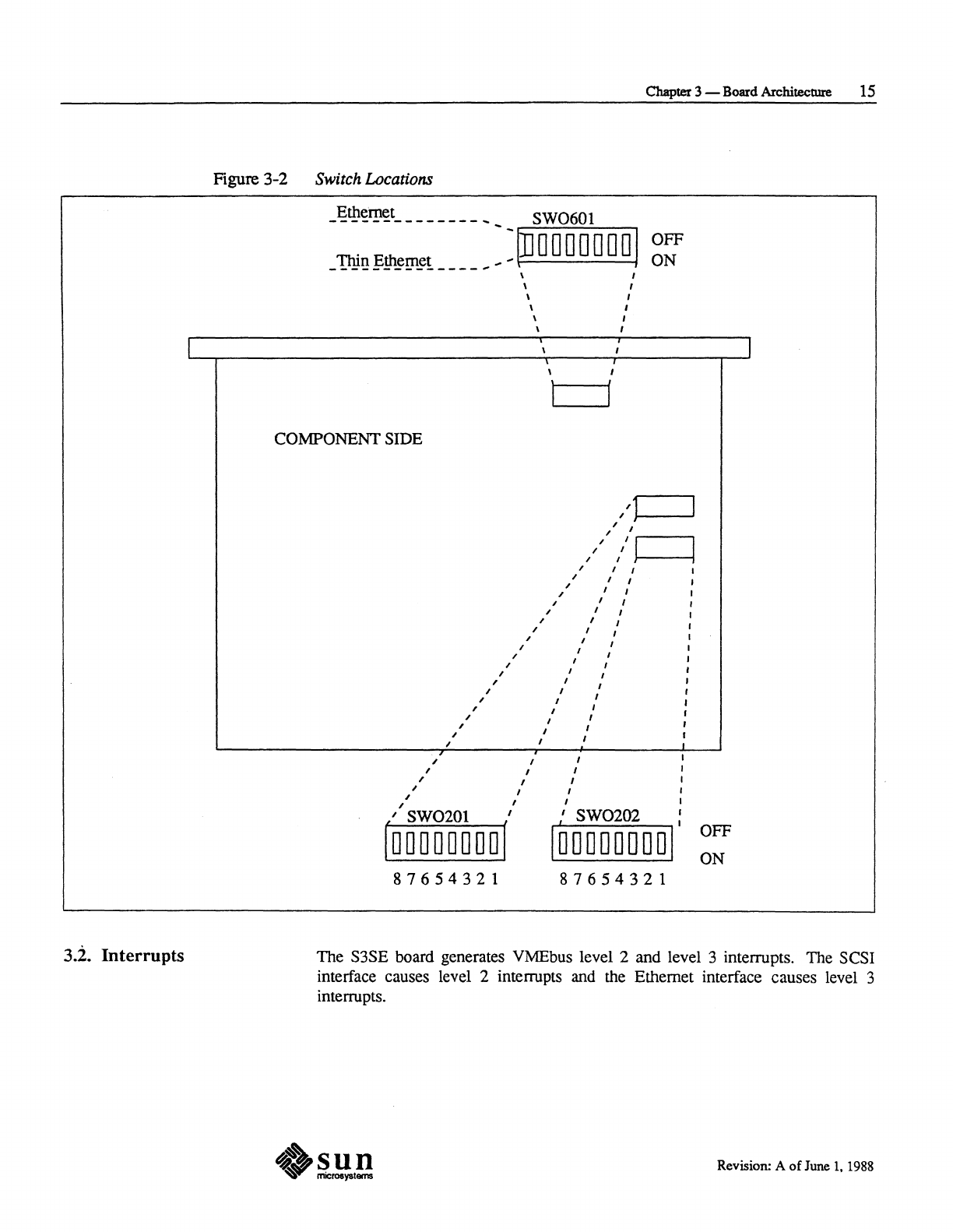
3.1. Addressing and
Jumpering
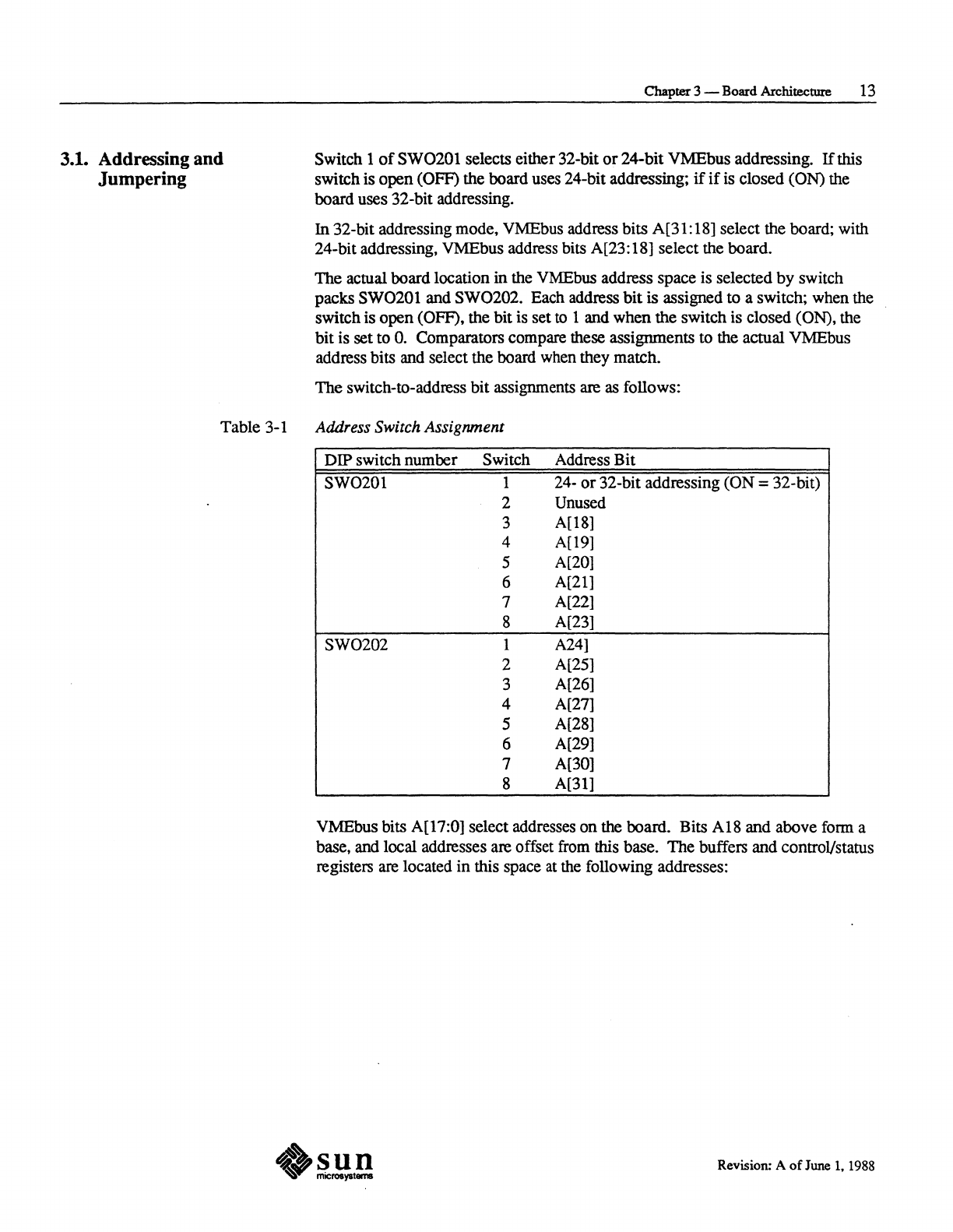
Chapter 3 - Board Architecture 13
Switch 1
of
SW0201
selects either 32-bit
or
24-bit
VMEbus
addressing.
If
this
switch is
open
(OFf)
the board uses 24-bit addressing;
if if
is closed (ON) the
board uses 32-bit addressing.
In
32-bit addressing mode, VMEbus address bits A[31:18] select the board; with
24-bit addressing, VMEbus address bits A[23: 18] select the board.
The
actual board location in the VMEbus address space is selected
by
switch
packs
SW0201
and
SW0202.
Each address
bit
is assigned
to
a switch; when the
switch is
open
(OFf),
the bit is set to 1 and
when
the
switch is closed (ON), the
bit
is set to
O.
Comparators compare these assignments to the actual VMEbus
address bits and select the board when they match.
The
switch-to-address
bit
assignments are as follows:
Table
3-1 Address Switch Assignment
DIP
switch
number
Switch Address
Bit
SW0201
1 24-
or
32-bit addressing (ON = 32-bit)
2 Unused
3 A[18]
4 A[19]
5 A[20]
6 A[21]
7 A[22]
8 A[23]
SW0202
I A24]
2 A[25]
3 A(26]
4 A(27]
5 A(28]
6 A[29]
7 A[30]
8 A[31]
VMEbus bits A[17:0] select addresses
on
the board. Bits A18 and above form a
base, and local addresses are offset from this base.
The
buffers
and
control/status
registers are located
in
this space
at
the following addresses:
Revision: A
of
June
1.
1988
14
SIUl-3/E SCSI/Ethemet Board
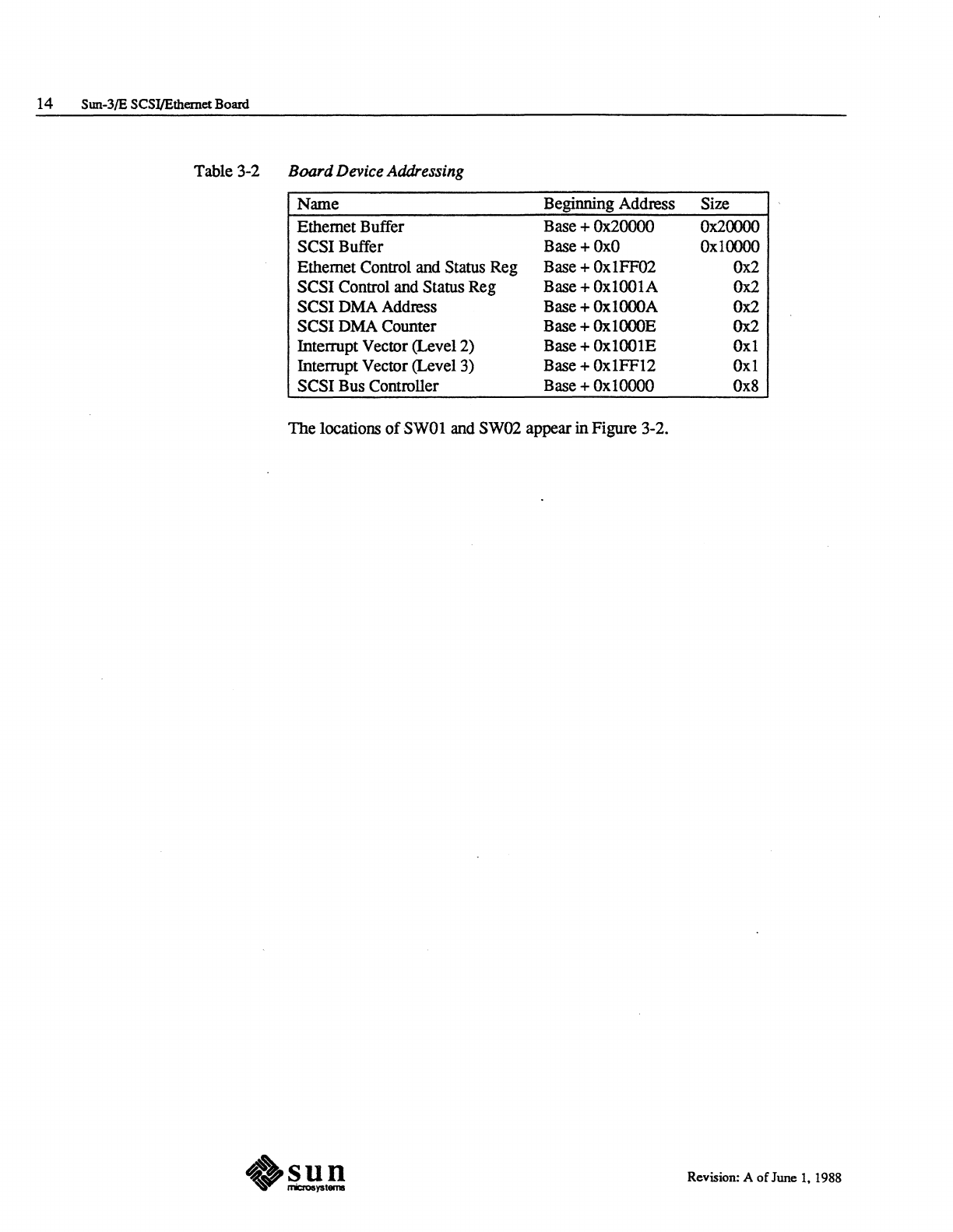
Table 3-2
Board
Device Addressing
Name
Beginning Address Size
Ethernet Buffer Base + Ox20000 0x20000
SCSI
Buffer Base +
OxO
Ox
10000
Ethernet Control and Status Reg Base + OxIFF02
Ox2
SCSI
Control and Status Reg Base + Ox1001A
Ox2
SCSI
DMA Address Base +
OxlOOOA
Ox2
SCSI
DMA Counter Base +
OxlOOOE
0x2
Interrupt Vector (Level 2) Base + OxlOOlE Oxl
Interrupt Vector (Level 3) Base + OxlFF12 Oxl
SCSI Bus Controller Base +
OxlOOOO
Ox8
The
locations
of
SWOl and SW02 appear in Figure 3-2.
Revision: A of June I, 1988
3.2.
Interrupts
Figure 3-2 Switch Locations
_
~t!?-~Ip~t
________
~
SW0601
Thin Ethernet
~
:
WOO
0 0 0 0 0 l
--------------,
\ I
\ I
\ I
I
I
Chapter 3 - Board Architecture
15
OFF
ON
COMPONENT SIDE
,')r--
" I
" ,'j r
----,
, I
, I I
/'
I I
, I I
, I I
, I I
, I I
" I I
, I I
I
,
,
,
,
,
,
,
,
,
,
,
,
,
,
, ,
I
, I
" SW0201 "
1000000001
87654321
I
I
I
I
I
I
I
I
I
I
I
I
,
I
I
I
I
I
I
"SW0202
I
1000000001
87654321
OFF
ON
The S3SE board generates VMEbus level 2 and level 3 interrupts. The SCSI
interface causes level 2 interrupts and the Ethernet interface causes level 3
interrupts.
Revision: A
of
June I, 1988
16
sun-3IE
SCSI/Ethemet Board
3.3. Bandwidth
and
Capability
Table 3-3
3.4. Cycle Priorities
The architecture provides two 8-bit registers, one for each intemtpt level.
The
host
processor must load these registers with the board statuS/lD bits as defined
by
the VMEbus specification,
then
when
an intemtpt occurs, the board outputs
the contents
of
these registers
on
D{07:00]. The intemtpt handler must
look
in
the appropriate SBC
or
Ethernet Interface internal register
to
learn the exact
cause
of
the interrupt.
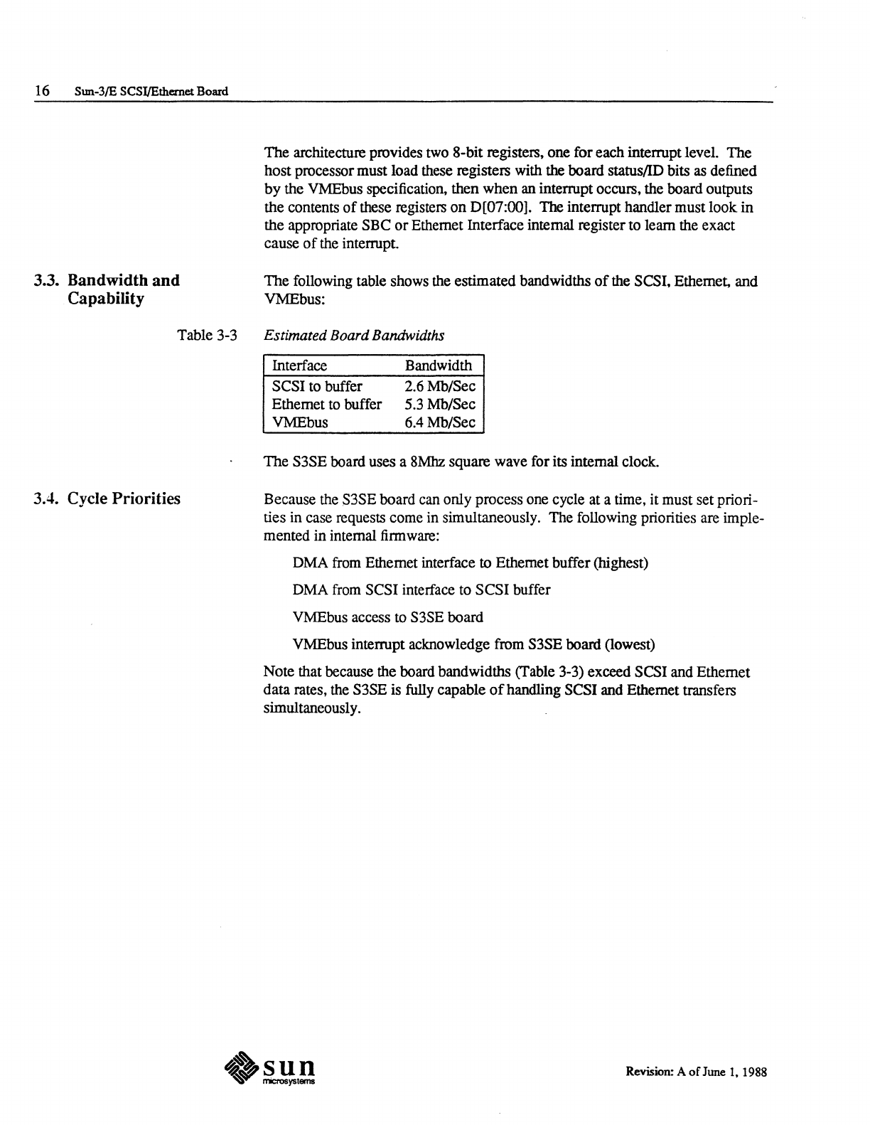
The
following table shows the estimated bandwidths
of
the SCSI, Ethernet, and
VMEbus:
Estimated Board Bandwidths
Interface
SCSI to buffer
Ethernet to buffer
VMEbus
Bandwidth
2.6 Mb/Sec
5.3 Mb/Sec
6.4 Mb/Sec
The
S3SE board uses a 8Mhz square wave for its internal clock.
Because the S3SE board can only process one cycle at a time, it must set priori-
ties in case requests come in simultaneously.
The
following priorities are imple-
mented in internal finnware:
DMA from Ethernet interface to Ethernet buffer (highest)
DMA from SCSI interface to
SCSI
buffer
VMEbus access to S3SE board
VMEbus interrupt acknowledge from S3SE board (lowest)
Note
that because the board bandwidths (Table 3-3) exceed SCSI and Ethernet
data rates, the S3SE is fully capable
of
handling SCSI and Ethernet transfers
simultaneously.
Revision: A
ofJune
I,
1988
4
SCSI Interface
SCSI
Interface
.............................
_
.............................................................
_...................................
19
4.1. Control and Status Registers
.....................................................................................
19
SCSI Control and Status Register
.............................................................
_........
19
SCSI DMA Address and SCSI DMA Counter
.....................................
_
..
_..
20
NCR 5380 Bus Controller Registers
..................................................................
21
Disk Controller Contiol Blocks
............................................................................
21
4.2. SCSI Buffer
....................................................................................................................
_...
21
4.3. SCSI Reads and Writes
................................................................................................
21

4.1.
Control and Status
Registers
NOTE
SCSI Control and Status
Register
4
SCSI Interface
The SCSI interface uses an NCR 5380 SCSI Bus Controller (SBC). It should be
programmed for non-block
DMA
transfer mode. causing the SBC to generate a
DRQ
for each byte transferred.
For additional information see NCR 5380 SCSI Interface Chip Design Manual.
the manual for disk drive (controller). and the Small Computer System Interface
(SCSI) Specification
The host processor communicates with the SBC through 1) the SCSI Control and
Status Register. 2) the SCSI DMA address register.
3)
the SCSI
DMA
address
counter, and 4) the NCR 5380 SBC's control registers. The following sections
describe each
of
these.
In this chapter,
we
assume that the SCSI interface supports a disk drive. Actu-
ally, it can control any device which conforms to the SCSI specification.
The SCSI Control and Status Register is located
in
the board's VMEbus space at
Ox1001A. The host processor writes information to this register to control the
SCSI interface, and it reads information from this register to learn the status
of
the SCSI interface.
The meaning
of
these bits changes depending
on
whether the register is read or
written. When
it
is written, the bits control the SCSI interface; when
it
is
read,
it
provides status information to the host processor. Both reads and writes must
be
16
bits.
The following table shows the bit values:
19
Revision: A
of
June
1.
1988
20
S\Dl-3/E
SCSI/Ethemet Board
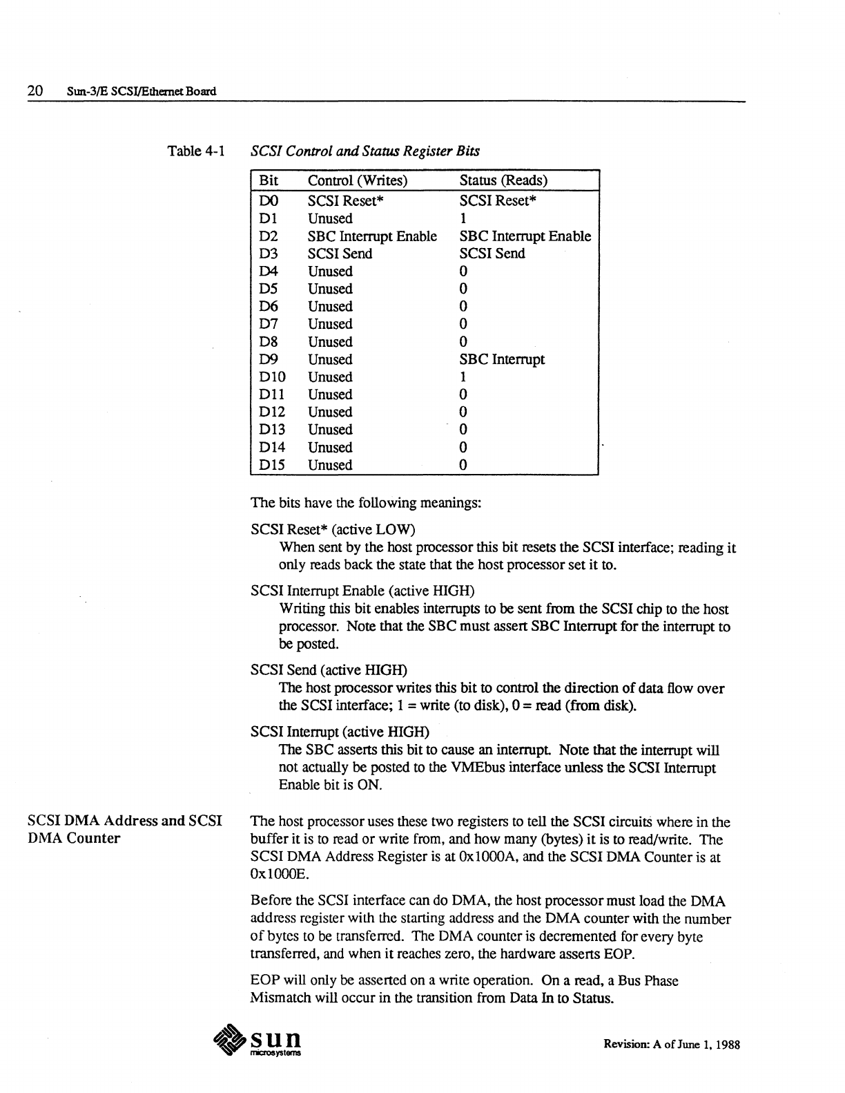
Table 4-1 SCSI Control
and
Status Register Bits
SCSI
DMA
Address
and
SCSI
DMA
Counter
Bit
Control (Writes) Status (Reads)
DO
SCSI Reset*
SCSI
Reset*
01
Unused 1
02
SBC Interrupt Enable
SBC
Interrupt Enable
03
SCSI Send
SCSI
Send
D4
Unused 0
05
Unused 0
D6
Unused 0
07
Unused 0
08
Unused 0
D9
Unused
SBC
Interrupt
010
Unused 1
011
Unused 0
012
Unused 0
013
Unused 0
014
Unused 0
015
Unused 0
The
bits have the following meanings:
SCSI
Reset* (active
LOW)
When sent
by
the host processor this bit resets
the
SCSI interface; reading
it
only reads
back
the state that the
host
processor
set
it
to.
SCSI
Interrupt Enable (active HIGH)
Writing this bit enables interrupts to be sent from the SCSI chip to the host
processor. Note that the
SBC
must
assert
SBC
Interrupt for the interrupt
to
be posted.
SCSI
Send (active HIGH)
The host processor writes this bit to control the direction
of
data flow
over
the SCSI interface; 1 = write (to disk), 0 = read (from disk).
SCSI
Interrupt (active HIGH)
The SBC asserts this bit to cause an interrupt
Note
that the interrupt will
not actually
be
posted to the VMEbus interface unless the SCSI Interrupt
Enable bit is ON.
The
host processor uses these two registers to tell the SCSI circuitS where
in
the
buffer it is to read
or
write from, and how many (bytes)
it
is to read/write.
The
SCSI
DMA Address Register is at
Ox
1
OOOA,
and the
SCSI
DMA
Counter is at
Ox
1
OOOE.
Before the SCSI interface can do DMA, the host processor must load the
DMA
address register with the starting address and the
DMA
counter with the number
of
bytes to be transferred. The DMA counter is decremented for every byte
transferred, and when
it
reaches zero, the hardware asserts EOP.
EOP
will only be asserted on a write operation.
On
a read, a Bus Phase
Mismatch will occur
in
the transition from Data In to Status.
Revision: A
of
June 1. 1988
NCR 5380 Bus Controller
Registers
Disk Controller Control
Blocks
4.2. SCSI
Buffer
4.3. SCSI Reads
and
Writes
Chapter 4 - SCSI Interface 21
These are both 16-bit read/write registers.
The NCR 5380 SCSI Bus Controller chip has eight internal registers that
it
uses
to receive instructions and report status. These are located at addresses
OxlOOOO
to
OxlOOO7
in
the board's VMEbus address space.
It
can be set up to interrupt
on
phase mismatch, EOP from DMA, and a number
of
other conditions, as specified
in
the NCR manual.
For
details about the contents
of
these registers, see the NCR 5380
SCSI
Inter/ace
Chip Manual.
Note that the NCR 5380 should be set up for for non-block DMA transfer mode
(this causes DRQ to be generated for every byte transferred).
The
SCSI interface requires control blocks to
be
sent to the disk controller as part
of
the data stream. These should be constructed
in
the SCSI buffer to be sent
with the data to the disk. Sun recommends that these blocks be sent to the SCSI
buffer as programmed I/O.
For
the contents and fonnat
of
these blocks, see the manual for the disk controller
being used.
The SCSI buffer is a 64-kilobyte block
of
memory located at addresses
OXO
to
OxOxOFFFF
in the
S3SE's
VMEbus address space.
It
is organized as 16K long-
words, but
it
can be accessed
by
the VMEBus as an 8-bit, 16-bit,
or
32-bit dev-
ice. It
is
accessed by the SCSI bus controller
in
8-bit DMA mode.
The SCSI circuits use the 64 kilobyte SCSI buffer to buffer data between the host
processor and the SCSI interface.
For
reads, the SCSI circuits load the infonna-
tion from the disk to the buffer, and the host processor must read the buffer. For
writes, the host processor must load the buffer, then tell the SCSI circuits to write
this information out
on
the SCSI interface.
Reads require the following sequence:
Set up the control/status register, the DMA address register, and the DMA
counter.
Program the SCSI chip and start the sequence as described
in
the NCR 5380
SCSI Inter/ace Chip Design Manual.
The SCSI/DMA circuits load the required infonnation from the disk to the
SCSI buffer.
When
it's
done, the hardware generates a level 2 interrupt.
The
host proces-
sor should respond to this interrupt by reading the data from the SCSI buffer.
The sequence for writes is similar to the sequence for reads. However, before the
sequence starts, the host processor must load the data
to
be written to the disk
into the SCSI buffer. Note that upon successful completion
of
a write, there is
one additional cycle, so that the DMA count register will not equal 0, but
OxFFFF,
and the DMA address register will be incremented by I more than the
actual count.
Revision: A
ofJune
1,
1988

5
~-::.,
•
••••
",
:,-.
•
'.
',.
,",
:.;
'"
• "
...
iI"
••
"Y ....
.....
Ethernet Interface
Ethernet Interface
..............................................................................................................
_........
2S
5.1. Ethernet Address
..............................................................................................................
26
5.2. Ethernet Transmits and Receives
...........................................................................
26
5.3. Ethernet Buffer
..................................................................................................................
27
5.4. Thin Ethernet
.....................................................................................................................
27
5.5. External Transceiver
......................................................................................................
27

Table
5-1
5
Ethernet Interface
The
Ethernet interface contains an Intel 82586
EDLC
Ethernet controller chip, a
128 kilobyte Ethernet buffer,
an
Ethernet control and status register, and a
jumper-selectable AMD 7995/6 Thin Ethernet transceiver.
Most communication with the Ethernet interface is through the control blocks in
the Ethernet buffer space.
The
first block, called the System Configuration
Pointer, lives
in
the 6 high bytes
of
the Ethernet
buffer
space (base + (Ox3FFF6
to Ox3FFFF). This block contains a pointer to the other Ethernet control blocks,
and a bit specifying the width
of
the bus from the Ethernet buffer to the Ethernet
interface (16 bits).
For
additional details see the Intel Local Area Network
(LAN)
Components
User'
s
Manual.
Another register, called the Ethernet Control and Status register, enables the host
processor to communicate with the board hardware.
It
is a 16-bit read/write
register located
at
address (base + Ox1FF02).
It
contains the following bits:
Ethernet Control and Status Register Bits
Bit
DO
through D7
D8
D9
010
011
012
013
014
015
Name
o
EDLC Interrupt
o
o
o
Interrupt Enable
Channel Attention
Loop Back
EDLCReset
These bits perfonn the following functions:
EDLC Interrupt (active HIGH
The 82586 activates this bit when it needs to interrupt the host processor.
Note that the interrupt is not actually posted unless the Interrupt Enable bit is
ON.
25
Revision: A
of
June
1,
1988
26
Sun~3/E
SCSI/Edlemet Board
5.1.
Ethernet
Address
5.2.
Ethernet
Transmits
and
Receives
Interrupt Enable (active
mGH)
This bit enables the EDLC to post an interrupt to the host processor. Only
the host processor can write this
bit
Channel Attention (active HIGH)
When the host processor writes this bit,
it
sends a channel attention to the
EDLC.
Loop
Back (active
mGH»
The
host processor writes this
bit
to place the Ethernet serial interface
adapter in loopback mode.
For
more on loopback mode, see the
LAN
Com-
ponent
User'
s Manual.
EDLC
Reset (active
maH)
This pin causes the hardware to reset the 82586.
The
S3SE board does
not
provide a fixed Ethernet address. A licensed Ethernet
address must be downloaded from the host processor into the control space
in
the
Ethernet buffer.
The
Sun-3/E CPU board contains a valid Ethernet address in its IDPROM. See
the
Sun-31E
CPU
Hardware Reference Manual (#800-8028) for more details.
The
Ethernet control registers are in the Ethernet buffer; there are no separate
Ethernet control registers.
Ethernet transmits take the following steps:
The
host processor must construct a control block in the Ethernet buffer
starting (base + 3FFF6). (This only needs to
be
done once, when the chip is
initialized) The contents
of
this buffer are described
in
the Intel Local Area
Network
(LAN)
Components User's Manual.
The
host processor must also load the data
it
wants to send over the Ethernet
into the Ethernet buffer.
When the Ethernet chip receives a channel attention,
it
fetches the control
block.
The
contents
of
the control block tell the 82586 chip the location
of
the data
in
the buffer. and where
to
send it. (Actually, the control block points to
other control blocks which contain the actual location).
The Ethernet circuits
do
DMA from the buffer to the Ethernet output, then
they update the control block.
When they are done, the Ethernet circuits interrupt the host processor with a
level 3 interrupt. The host processor should respond
by
reading the updated
control block.
Ethernet receives are similar
to
transmits:
Revision: A
ofJune
1.
1988
5.3. Ethernet
ButTer
5.4. Thin Ethernet
5.5. External Transceiver
Chapter 5 -
Ethernet
Interface 27
During power-up, the host processor should
load
the Ethernet control block
with the address where the Ethernet circuits are to place received data, then
it
should issue a channel attention to get the Ethernet circuits to read the
control block.
When packets come over the Ethernet, the Ethernet circuits use DMA to
write them into the address specified by the host processor
in
the control
block. Then the Ethernet circuits update the control block and post a level 3
interrupt to the host processor.
The host processor should read the contents
of
the Ethernet buffer over the
VMEBus.
The Ethernet buffer is a 128 kilobyte memory block located at addresses base +
(0x20000 to Ox3FFFF).
It
is organized as
32K
longwords, but it
can
be
addressed by the VMEbus as either an 8-bit, 16-bit,
or
a 32-bit device. The Eth-
ernet interface can access
it
in 16-bit DMA mode.
Note that the only hard assigned address in this space is the EDLC system
configuration pointer, which lives are base + (3FFF6 to 3FFFF).
This
behavior
is built into
the
EDLC chip. System software must assign all other locations.
and the system configuration pointer serves
as
a pointer to these.
Switch SW0601 switches the Ethernet signal from the Ethernet connector to the
Thin Ethernet connector. The AMD7995/6 transceiver drives a standard
50
ohm
coaxial cable directly. It is electrically compatible with the standard Ethernet but
it is spec'ed for one third the maximum length
of
standard Ethernet.
To switch from standard to thin Ethernet, set all switches
on
SW0601 ON
(CLOSED).
To
switch from thin Ethernet to standard Ethernet. set all the
switches
on
SW601 OFF (OPEN).
Figure 3-2 shows the location
of
SW0601.
The Sun-3/E SCSI/Ethernet board is designed to
be
used with a Level 2 external
Ethernet transceiver.
Revision: A
of
June
1.
1988

6
VMEbus Interface
VMEbus
Interface
........................................................................................................................
31

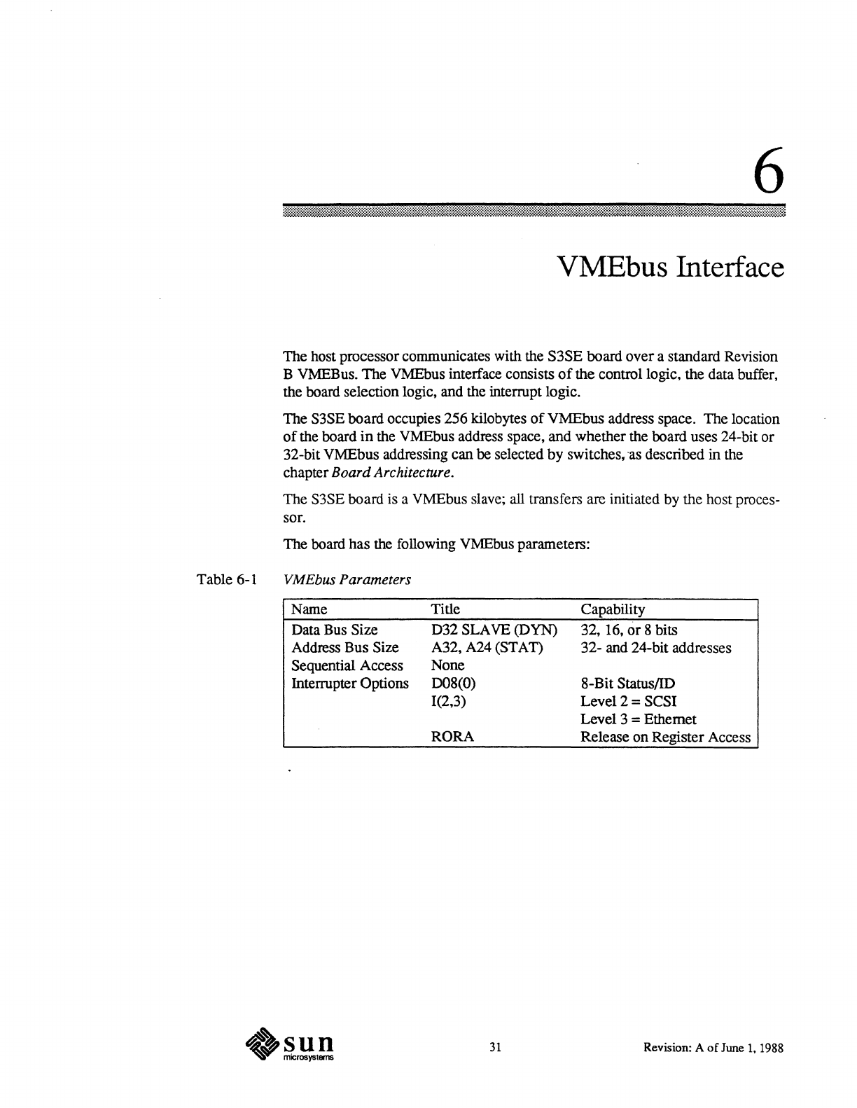
Table 6-1
6
VMEbus
Interface
The host processor communicates with the S3SE board over a standard Revision
B VMEBus.
The
VMEbus interface consists
of
the control logic, the data buffer,
the board selection logic, and the interrupt logic.
The S3SE board occupies 256 kilobytes
of
VMEbus address space. The location
of
the board
in
the VMEbus address space, and whether the board uses 24-bit or
32-bit VMEbus addressing can
be
selected
by
switches,
"as
described in the
chapter Board Architecture.
The S3SE board is a VMEbus slave; all transfers are initiated by the host proces-
sor.
The board has
the
following VMEbus parameters:
VMEbus Parameters
Name
Data Bus Size
Address Bus Size
Sequential Access
Interrupter Options
Title
032
SLAVE (DYN)
A32, A24
(STAn
None
008(0)
1(2,3)
RORA
31
Capability
32, 16,
or
8 bits
32- and 24-bit addresses
8-Bit Status!ID
Level 2 = SCSI
Level 3 = Ethernet
Release on Register Access
Revision: A
of
June
1.
1988

A
Connectors
Connectors
..................................................................................................................
_.....................
35
A.l.
Rear Edge Comectors
.................................................................................................
35
A.2. Front Panel Comectors
........................
_
............................................
_._
....
_..............
37
SCSI Comector
........
__
.........................................................................
_....................
38
Ethernet Comector
......................................................................................................
40
Thin Ethernet Comector
..........................................................................................
41

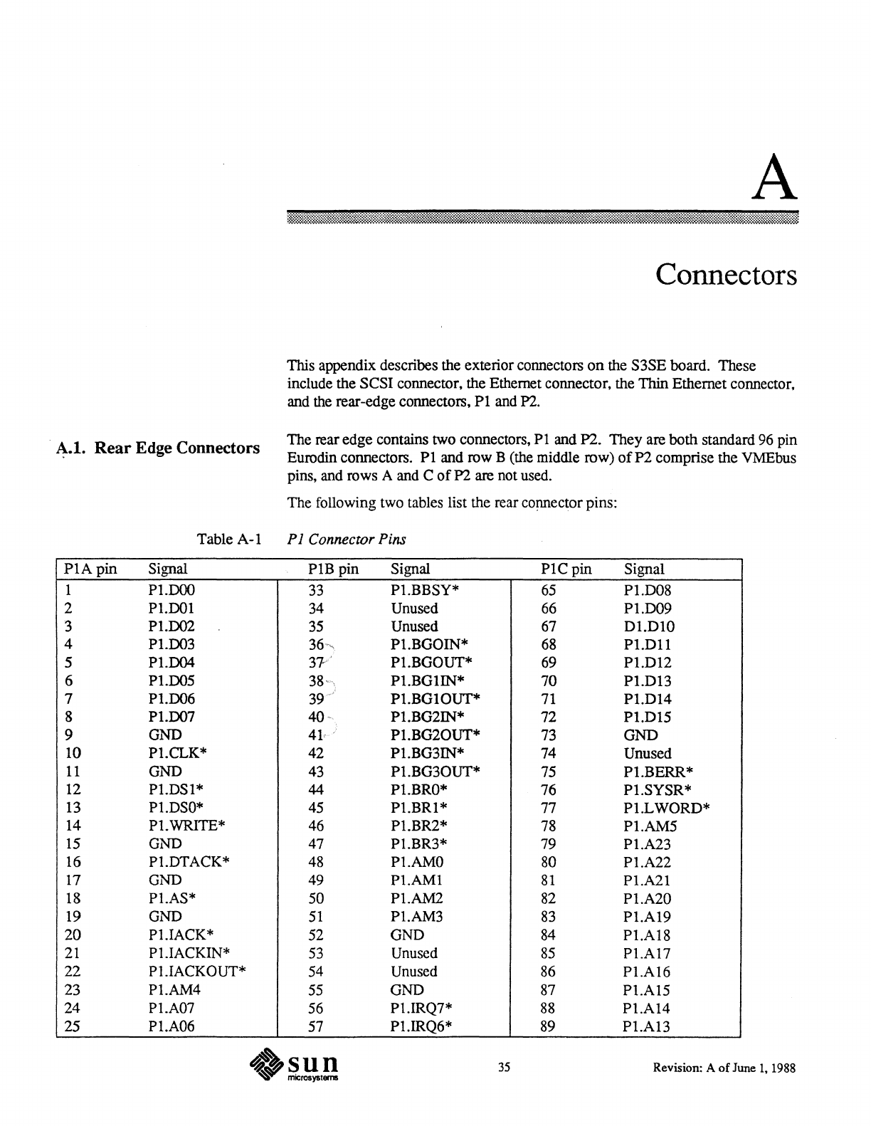
A.I.
Rear
Edge Connectors
A
Connectors
This appendix describes the exterior connectors
on
the S3SE board. These
include the SCSI connector, the Ethernet connector, the Thin Ethernet connector,
and the rear-edge connectors,
PI
and
n.
The rear edge contains two connectors,
PI
and P2. They are both standard
96
pin
Eurodin connectors.
PI
and row B (the middle row)
ofP2
comprise the VMEbus
pins, and rows A and C
of
P2 are not used.
The following two tables list the rear connector pins:
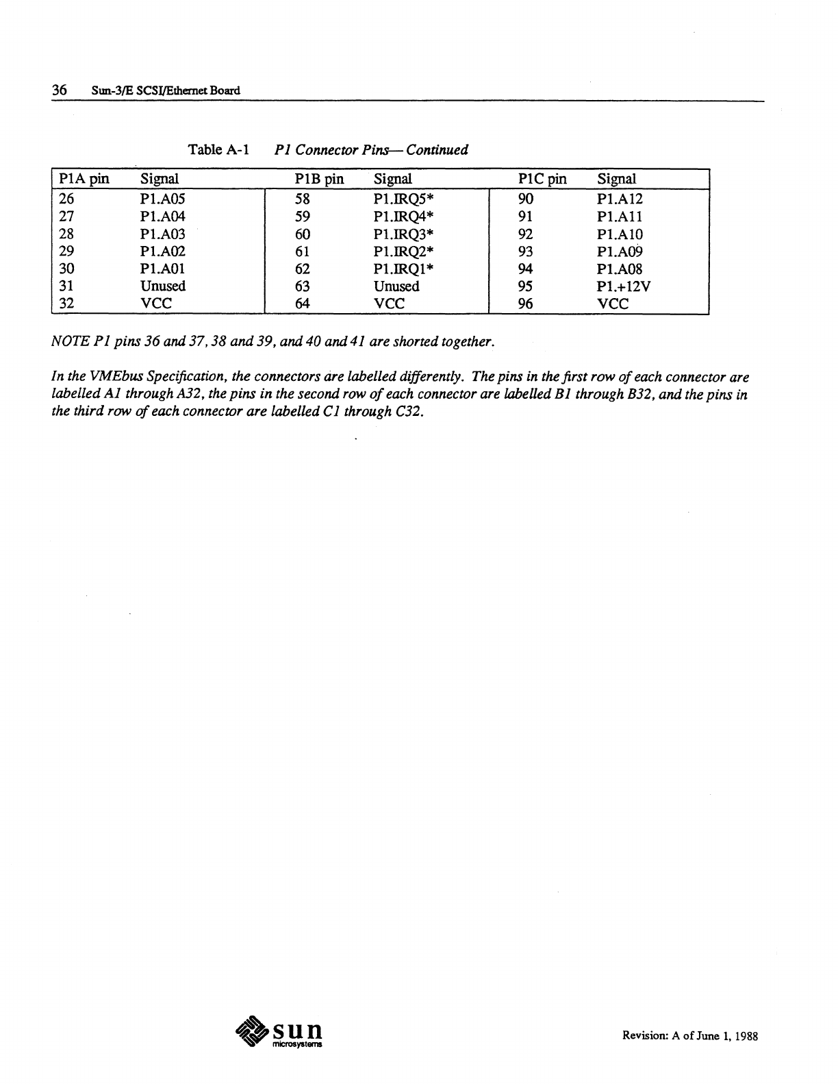
Table
A-I
P 1 Connector Pins
PIA
pin
Signal
PlB
pin Signal
PIC
pin Signal
1
P1.DOO
33
Pl.BBSY*
65
P1.D08
2 P1.DOl 34 Unused 66
Pl.D09
3 P1.D02
35
Unused 67 D1.DIO
4 P1.D03
36",.
Pl.BGOIN* 68
Pl.Dll
5 P1.D04
37
Pl.BGOUT* 69
Pl.D12
6 P1.D05
38
Pl.BGIIN*
70 P1.D13
7 Pl.D06 39
Pl.BGIOUT*
71
Pl.D14
8 Pl.D07 40 Pl.BG2IN* 72
Pl.D15
9 GND
41
Pl.BG20UT*
73 GND
10 P1.CLK* 42 Pl.BG3IN* 74 Unused
11
GND 43
Pl.BG30UT*
75 Pl.BERR*
12 P1.DSl* 44 Pl.BRO* 76
Pl.SYSR*
13 Pl.DSO* 45
Pl.BRl*
77 Pl.LWORD*
14 Pl.WRlTE* 46 Pl.BR2* 78
Pl.AM5
15 GND 47 Pl.BR3* 79 P1.A23
16 Pl.DTACK*
48
P1.AMO
80
Pl.A22
17 GND 49
Pl.AMl
81
P1.A21
18 Pl.AS* 50 Pl.AM2
82
Pl.A20
19 GND
51
Pl.AM3
83
Pl.AI9
20
P1.IACK* 52 GND
84
Pl.AI8
21
P1.IACKIN*
53
Unused
85
Pl.A17
22 Pl.IACKOUT* 54 Unused
86
Pl.A16
23 P1.AM4
55
GND
87
Pl.A15
24 Pl.A07 56 P1.IRQ7*
88
Pl.A14
25 P1.A06 57 Pl.IRQ6*
89
Pl.A13
35 Revision: A
of
June I, 1988
36
SIDl-3/E
SCSI/Ethemet Board
Table A-I
PI
Connector
Pi1l3-
Continued
PIA
pin Signal
PIB
pin Signal
PIe
pin Signal
26 P1.A05 58 PI.IRQ5* 90 P1.AI2
27
P1.A04 59 P1.IRQ4*
91
P1.All
28
P1.A03 60 P1.IRQ3* 92 P1.AlO
29 Pl.A02
61
Pl.IRQ2*
93
P1.A09
30 Pl.AOl
62
P1.IRQl*
94
P1.A08
31
Unused
63
Unused
95
P1.+l2V
32
vee
64
vee
96
vee
NOTE
PI
pins
36
and
37,38
and
39,
and
40
and
41
are shorted together.
In the
VMEbus
Specification,
the
connectors are labelled differently. The pins in the first
row
of
each connector are
labelled
Al
through A32, the
pins
in
the second row
of
each connector are labelled
Bl
through B32,
and
the
pins
in
the third
row
of
each connector
are
labelled
Cl
through C32.
Revision: A
of
June I, 1988
P2Apin
Signal
1 Unused
2 Unused
3 Unused
4 Unused
5 Unused
6 Unused
7 Unused
8 Unused
9 Unused
10 Unused
11
Unused
12 Unused
13 Unused
14 Unused
15 Unused
16 Unused
17 Unused
18 Unused
19 Unused
20
Unused
21 Unused
22
Unused
23
Unused
24
Unused
25 Unused
26
Unused
27
Unused
28
Unused
29
Unused
30
Unused
31 Unused
32
Unused
A.2. Front Panel
Connectors
Appendix A - Connectors 37
Table
A-2
P2
Connector
Pins
P2B pin Signal
P2Cpin
Signal
33
34
35
36
37
38
39
40
41
42
43
44
45
46
47
48
49
50
51
52
53
54
55
56
57
58
59
60
61
62
63
64
VCC 65 Unused
GND
66 Unused
Unused 67 Unused
P1.A24 68 Unused
P1.A25 69 Unused
P1.A26
70
Unused
P1.A27 71 Unused
P1.A28
72
Unused
P1.A29 73 Unused
P1.A30
74
Unused
P1.A31 75 Unused
GND
76
Unused
vce
77
Unused
P1.DI6 78 Unused
P1.DI7
79
Unused
P1.DI8 80 Unused
P1.DI9
81
Unused
P1.D20 82 Unused
P1.D21
83
Unused
P1.D22 84 Unused
P1.D23 85 Unused
GND
86 Unused
P1.D24 87 Unused
Pl.D25
88 Unused
P1.D26 89 Unused
P1.D27
90
Unused
P1.D28 91 Unused
P1.D29
92
Unused
P1.D30 93 Unused
P1.D31 94 Unused
GND'
95 Unused
vec 96 Unused
The front panel connectors include the SCSI connector, the Ethernet connector,
and the thin Ethernet connector. Figure A-I shows the locations
of
the front edge
connectors.
Revision: A
of
June 1.1988

38 Sun-3/E SCSI/Elhemet Board
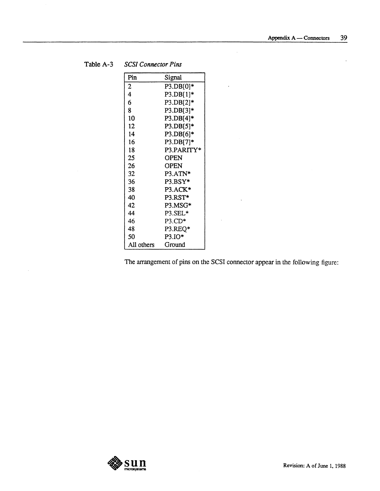
SCSI Connector
Figure A-I
Front
Panel
Connectors
Thin Ethernet
Connector
P5
Ethernet
Connector
P4
SCSI
Connector
P3
...........
,/'
COMPONENT SIDE
The
SCSI connector attaches to P3. It is a 50-pin female D-shell, with the pins
assigned as follows:
.2!!
Revision: A
of
June 1, 1988
Appendix A - Connectors 39
Table
A-3
SCSI Connector Pins
Pin Signal
2 P3.DB[O]*
4 P3.DB[I]*
6 P3.DB[2J*
8 P3.DB[3J*
10 P3.DB[4]*
12 P3.DB[5]*
14
P3.DB[6]*
16 P3.DB[7]*
18
P3.PARITY*
25 OPEN
26 OPEN
32 P3.ATN*
36 P3.BSY*
38 P3.ACK*
40
P3.RST*
42 P3.MSG*
44 P3.SEL*
46 P3.CD*
48 P3.REQ*
50
P3.10*
All others Ground
The arrangement
of
pins
on
the SCSI connector appear in the following figure:
Revision: A
of
June
1.
1988
40 Sun-3/E SCSI/Ethemet Board
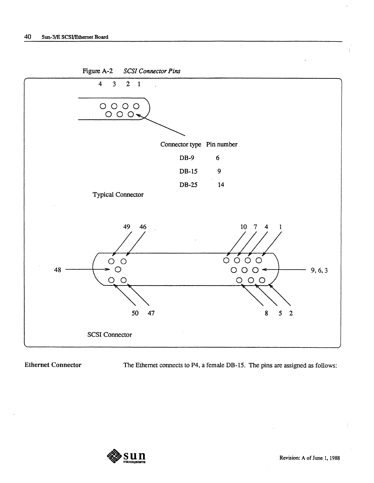
Figure A-2 SCSI Connector Pins
4 3 2 1
Connector type
Pin
number
DB-9 6
DB-15 9
DB-25
14
Typical Connector
49 46 10 7 4 1
48
9,6,3
50
47
8 5 2
SCSI Connector
Ethernet Connector The Ethernet connects to P4, a female DB-IS. The pins are assigned
as
follows:
.~!I!!
Revision: A
of
June I, 1988
Appendix A - COIUlectors
41
Table
A-4
Ethernet Connector Pins
Pin Signal
1 Open
2 P4.CLSN+
3 P4.TXD+
4 Open
5
P4.RXDt
(fused)
6 Gnd
7 V cc (jumpered)
8-
Open
9 P4.CLSN-
10
P4.TXD-
11
Open
12
P4.RXD-
13
12V (fused)
14
Open
15
Open
Thin
Ethernet
Connector
The thin ethemet connects to P5. It uses a single female BNC coaxial cable.
Revision: A
of
June
I,
1988

B
System Design Considerations
System Design Considerations
........................................................................
~..................
45
B.l.
System Power Considerations
.................................................................................
45
B.2. Environmental Characteristics
................................................................................
45
B.3. P2 Bus Design
..................................................................................................................
45

B.l. System Power
Considerations
Table B-1
B.2. Environmental
Characteristics
B.3. P2 Bus Design
B
System Design Considerations
This appendix lists various considerations that must be taken into account when
using the S3SE board. These include power requirements, environmental charac-
teristics, and backplane infonnation.
The following table lists the S3SE power supply requirements:
Board
Power
Requirements
+5V +12V -12V
4.0
amp±5%
1.0
amp±5%
N/A
The S3SE board requires the following environmental conditions:
Operating Temperature Range -10° to 50° C
Storage Temperature Range --40°
to
85° C
Humidity (non-condensing) -
0%
to
9%
The S3SE board is
not
P2
bus compatible; it
must
not
be used in a slot
reserved for
P2
bus
expansion.
45
Revision: A
of
June
1.
1988

Index
2
24-bit addressing,
13
3
32-bit addressing.
13
A
address bits,
13
address selection
board,
13
addressing
24-bit, 13
32-bit,
13
B
bandwidths
estimated. 16
board address selection,
13
buffer
Ethernet,
27
SCSI.
21
C
cheapernet, 27
connector
Ethernet,
40
SCSL38
thin Ethernet,
41
connectors
rear edge,
35
control and status register
Ethernet, 25
SCSI. 19
control block
Ethernet, 26
E
estimated bandwidths. 16
Ethernet
address, 26
buffer, 27
connector, 40
control block.
26
external transceiver.
27
system configuration pointer. 25
transmits,
26
Ethernet address
Ethernet address, continued
license.
11
Ethernet conlrol and starus register. 25
Ethernet extemallransceiver level.
T1
I
interrupt levels.
15
interrupt registers. 16
J
jumpers.
13
L
license
Ethernet address. 11. 26
N
NCR
5380 bus conlroller registers.
21
P
PI
and
P2
connectors, 35
parameters
VMEbus,31
priority
requests.
16
R
reads and writes
SCSI.
21
registers
interrupt.
16
request priorities.
16
s
SCSI
connector. 38
SCSI buffer.
21
SCSI
conlrOl
and status register,
19
SCSI reads and writes.
21
SCSI write procedure,
21
simultaneous requests.
16
system configuration pointer, 25
T
thin
Ethernet.
27
transmits
Ethernet. 26
V
VMEbus Parameters, 31
w
write
SCSI.
21
