PMIC GPIO And MPP Software User Guide 80 NV610 48
User Manual:
Open the PDF directly: View PDF ![]() .
.
Page Count: 31
- PMIC GPIO and MPP Software User Guide
- Revision history
- Contents
- Tables
- 1 Introduction
- 2 Hardware feature description
- 3 Software drivers
- 3.1 GPIO support in SBL
- 3.1.1 pm_gpio_status_get( )
- 3.1.2 pm_gpio_config_bias_voltage( )
- 3.1.3 pm_gpio_config_digital_input( )
- 3.1.4 pm_gpio_config_digital_output( )
- 3.1.5 pm_gpio_config_digital_input_output( )
- 3.1.6 pm_gpio_set_volt_source( )
- 3.1.7 pm_gpio_config_mode_selection( )
- 3.1.8 pm_gpio_set_output_buffer_configuration( )
- 3.1.9 pm_gpio_set_inversion_configuration( )
- 3.1.10 pm_gpio_set_current_source_pulls( )
- 3.1.11 pm_gpio_set_ext_pin_config( )
- 3.1.12 pm_gpio_set_output_buffer_drive_strength( )
- 3.1.13 pm_gpio_set_source_configuration( )
- 3.1.14 pm_gpio_set_mux_ctrl( )
- 3.1.15 Configure MPP as AI and setup ADC read
- 3.2 Linux kernel (LK)
- 3.3 Kernel DTSI properties
- 3.3.1 Required root node properties
- 3.3.2 Required child node properties
- 3.3.3 Optional child node properties
- 3.3.4 Configure GPIO04 as an interrupt wake-up resource with falling edge trigger
- 3.3.5 Configure PM8952/PM8956 GPIO02 as a sleep file
- 3.3.6 Configure PMI8952/PMI8956 MPP04 as a PWM output for blink LEDs
- 3.3.7 Configure PM8952/PM8956 MPP for ADC read through device tree
- 3.1 GPIO support in SBL
- 4 Debug
- A References

Qualcomm Technologies, Inc.
NO PUBLIC DISCLOSURE PERMITTED: Please report postings of this document on public servers or websites to:
DocCtrlAgent@qualcomm.com.
Restricted Distribution: Not to be distributed to anyone who is not an employee of either Qualcomm Technologies, Inc. or its
affiliated companies without the express approval of Qualcomm Configuration Management.
Not to be used, copied, reproduced, or modified in whole or in part, nor its contents revealed in any manner to others without the
express written permission of Qualcomm Technologies, Inc.
Qualcomm is a trademark of Qualcomm Incorporated, registered in the United States and other countries. Other product and brand
names may be trademarks or registered trademarks of their respective owners.
This technical data may be subject to U.S. and international export, re-export, or transfer (“export”) laws. Diversion contrary to U.S.
and international law is strictly prohibited.
Qualcomm Technologies, Inc.
5775 Morehouse Drive
San Diego, CA 92121
U.S.A.
© 2015-2016 Qualcomm Technologies, Inc. All rights reserved.
PMIC GPIO and MPP Software User Guide
80-NV610-48 H
September 15, 2016
80-NV610-48 H Confidential and Proprietary – Qualcomm Technologies, Inc. 2
MAY CONTAIN U.S. AND INTERNATIONAL EXPORT CONTROLLED INFORMATION
Revision history
Revision Date Description
A April 2015 Initial release
B December 2015 Updated the document title and Section 1.1
C February 2016 Added more examples to Sections 2.5, 2.6 and 2.7
D March 2016 Added Appendix A; Updated Section 2.6
E June 2016 Numerous changes were made to this document; it should be read in its
entirety.
F June 2016 Updated Section 3.3.4.3
G August 2016 Numerous changes were made to this document; it should be read in its
entirety.
H September 2016 Numerous changes were made to this document; it should be read in its
entirety.

80-NV610-48 H Confidential and Proprietary – Qualcomm Technologies, Inc. 3
MAY CONTAIN U.S. AND INTERNATIONAL EXPORT CONTROLLED INFORMATION
Contents
1 Introduction ...................................................................................................... 6
1.1 Purpose.......................................................................................................................... 6
1.2 Conventions .................................................................................................................. 6
1.3 Technical assistance ...................................................................................................... 6
2 Hardware feature description ......................................................................... 7
2.1 PMIC MPPs .................................................................................................................. 7
2.2 PMIC GPIO pins ......................................................................................................... 11
2.3 Register information ................................................................................................... 11
3 Software drivers ............................................................................................ 13
3.1 GPIO support in SBL .................................................................................................. 13
3.1.1 pm_gpio_status_get( ) ..................................................................................... 13
3.1.2 pm_gpio_config_bias_voltage( ) ..................................................................... 14
3.1.3 pm_gpio_config_digital_input( ) ..................................................................... 14
3.1.4 pm_gpio_config_digital_output( ) ................................................................... 15
3.1.5 pm_gpio_config_digital_input_output( ) ......................................................... 16
3.1.6 pm_gpio_set_volt_source( ) ............................................................................ 16
3.1.7 pm_gpio_config_mode_selection( ) ................................................................ 17
3.1.8 pm_gpio_set_output_buffer_configuration( ) .................................................. 17
3.1.9 pm_gpio_set_inversion_configuration( ) ......................................................... 18
3.1.10 pm_gpio_set_current_source_pulls( )............................................................ 18
3.1.11 pm_gpio_set_ext_pin_config( ) ..................................................................... 19
3.1.12 pm_gpio_set_output_buffer_drive_strength( ) .............................................. 19
3.1.13 pm_gpio_set_source_configuration( ) ........................................................... 20
3.1.14 pm_gpio_set_mux_ctrl( ) ............................................................................... 20
3.1.15 Configure MPP as AI and setup ADC read ................................................... 21
3.2 Linux kernel (LK) ....................................................................................................... 23
3.2.1 Configure MPP02 as CS .................................................................................. 23
3.3 Kernel DTSI properties ............................................................................................... 23
3.3.1 Required root node properties.......................................................................... 23
3.3.2 Required child node properties ........................................................................ 23
3.3.3 Optional child node properties ......................................................................... 24
3.3.4 Configure GPIO04 as an interrupt wake-up resource with falling edge trigger
.................................................................................................................................. 26
3.3.5 Configure PM8952/PM8956 GPIO02 as a sleep file ....................................... 27
3.3.6 Configure PMI8952/PMI8956 MPP04 as a PWM output for blink LEDs ...... 27
3.3.7 Configure PM8952/PM8956 MPP for ADC read through device tree ............ 28
4 Debug ............................................................................................................. 30

PMIC GPIO and MPP Software User Guide Contents
80-NV610-48 H Confidential and Proprietary – Qualcomm Technologies, Inc. 4
MAY CONTAIN U.S. AND INTERNATIONAL EXPORT CONTROLLED INFORMATION
4.1 ADB ............................................................................................................................ 30
4.2 Log messages .............................................................................................................. 30
A References ..................................................................................................... 31
A.1 Related documents ..................................................................................................... 31
A.2 Acronyms and terms .................................................................................................. 31

PMIC GPIO and MPP Software User Guide Contents
80-NV610-48 H Confidential and Proprietary – Qualcomm Technologies, Inc. 5
MAY CONTAIN U.S. AND INTERNATIONAL EXPORT CONTROLLED INFORMATION
Tables
Table 2-1 PM8952/PM8956 GPIO pin functionalities and features ............................................................ 8
Table 2-2 PM8952/PM8956 MPP pin functionalities and features ............................................................. 9
Table 2-3 PM8004 MPP pin functionalities and features ............................................................................ 9
Table 2-4 PMI8952/PMI8956 GPIO pin functionalities and features ....................................................... 10
Table 2-5 PMI8952/PMI8956 MPP pin functionalites and features .......................................................... 10
Table 2-6 PMI8952/PMI8956 MPP bits .................................................................................................... 11
Table 3-1 GPIO/MPP SBL files and locations .......................................................................................... 13
Table 3-2 GPIO/MPP HLOS files and locations ....................................................................................... 13

80-NV610-48 H Confidential and Proprietary – Qualcomm Technologies, Inc. 6
MAY CONTAIN U.S. AND INTERNATIONAL EXPORT CONTROLLED INFORMATION
1 Introduction
NOTE: Numerous changes were made to this document; it should be read in its entirety.
1.1 Purpose
This document provides the required multipurpose pins (MPP) and general-purpose input/output
(GPIO), and their configuration for the PM8952/ PM8956, PMI8952/PMI8956, and PM8004
devices.
1.2 Conventions
Function declarations, function names, type declarations, attributes, and code samples appear in a
different font, for example, #include.
Code variables appear in angle brackets, for example, <number>.
Commands to be entered appear in a different font, for example, copy a:*.* b:.
Button and key names appear in bold font, for example, click Save or press Enter.
Shading indicates content that has been added or changed in this revision of the document.
1.3 Technical assistance
For assistance or clarification on information in this document, submit a case to Qualcomm
Technologies, Inc. (QTI) at https://createpoint.qti.qualcomm.com/.
If you do not have access to the CDMATech Support website, register for access or send email to
support.cdmatech@qti.qualcomm.com.
80-NV610-48 H Confidential and Proprietary – Qualcomm Technologies, Inc. 7
MAY CONTAIN U.S. AND INTERNATIONAL EXPORT CONTROLLED INFORMATION
2 Hardware feature description
The following are the number of MPPs and GPIO pins for the PM8952/PM8956 and
PMI8952/PMI8956 devices:
Pin PM8952/PM8956 PMI8952/PMI8956
MPP 4 4
GPIO 8 2
2.1 PMIC MPPs
The MPPs are used for functions such as LED drivers, and analog/digital inputs or outputs.
The following configurations are available in MPPs:
Digital input (DI) is read through the software. It triggers an interrupt, or is routed to
another MPP.
Digital output (DO) is set through the software to LOW or HIGH.
NOTE: For both DI and DO configurations, the logic level is programmable, providing compliance
between inputs or outputs (I/O) that run using different power supplies.
Bidirectional I/O enables the two MPPs to make a complementary pair that is jointly
configured as a bidirectional, level-translating pair. The PMI8952/PMI8956 device does
not support bidirection I/O.
Analog input (AI) is routed to the analog multiplexer switch network. If selected, the
analog voltage is routed to the HK/XO ADC for digitization. The PMI8952/PMI8956
device only has one ADC input (MPP01), but this pin is occupied if parallel charging is
used.
Analog output (AO) is a buffered version of on-chip voltage reference (VREF). It is for
odd MPPs only.
Programmable current sink (CS) is to drive LEDs. It is for even-numbered MPPs only.

PMIC GPIO and MPP Software User Guide Hardware feature description
80-NV610-48 H Confidential and Proprietary – Qualcomm Technologies, Inc. 8
MAY CONTAIN U.S. AND INTERNATIONAL EXPORT CONTROLLED INFORMATION
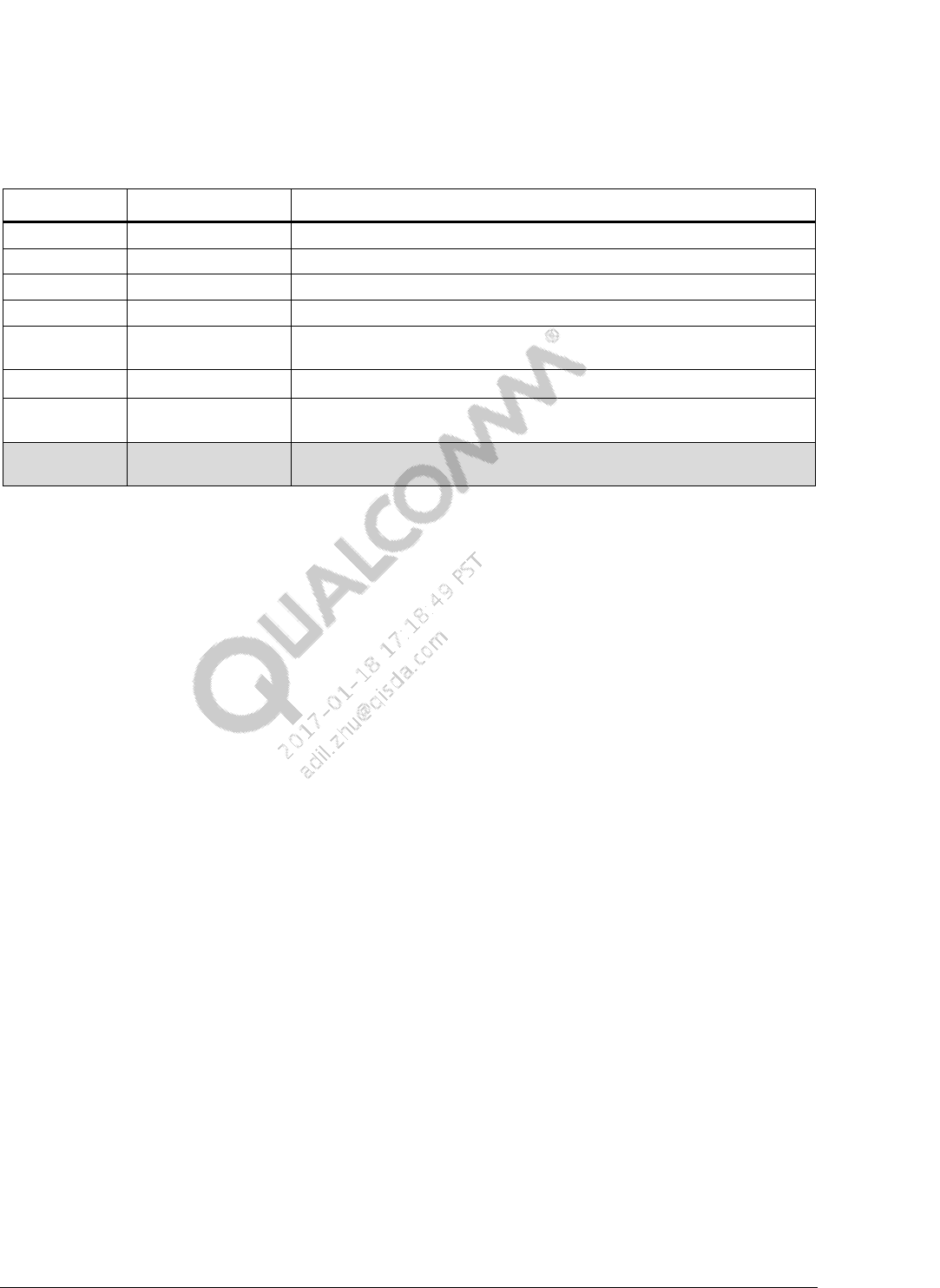
Table 2-1 PM8952/PM8956 GPIO pin functionalities and features
Pin Functionality Description Feature I/O GPIO
speed GPIO SF1 GPIO
digital
input
Default
state
GPIO01
(GPIOc)
CODEC_DIV_CLK
Or
EX_REG_CTRL1
Enables external regulator or Codec M
clock (9.6 MHz) DO O Low DIV_CLK2 – DIN
10 µA
pull-down
at pin
GPIO02
(GPIOc)
EX_REG_CTRL2
UIM 3_eLDO_EN
Controls external regulator (backup) DO O Low SLEEP_CLK2 DIVCLK_EN
GPIO03 BATT_UICC_ALARM Acts as the battery for UICC alarm
Acts as a UIM alarm only for PM8952/
PM8956
BUA I Low BATT_ALARM_
OUT
UICC_
ALARM_IN
GPIO04 BOOST_BYP_MODE_
CTL
Or
PM8004_PON_sync
If GPIO=1, then the external boost-bypass
is set to Auto boost/bypass
Or
Acts as a backup PM8004 PON sync if it is
enabled before LDO5
DO O Low GND –
GPIO05 NFC_CLK_REQ
(BBCLK2_ELN)
NFC_CLK enable request CLKS I Low GND BB
CLK2_EN
GPIO06 WLAN_SAD Switches antenna diversity for WLAN CLKS O Low PWM_LPG –
GPIO07 WCD9326 eLDO_EN
Or
BAT_ALARM_IN
Works as external codec eLDO EN (If
BAT_ALARM_IN is required, move this
function to GPIO02 and trade off
UIM 3)
Or
BAT_ALARM_IN is used to design with
external non-PMI chargers
BUA I/O Low GND –
GPIO08 WCN SSR eLDO_EN
Or
BAT_ALARM_IN
Disables or enables the external 1.325 V
LDO switch to support WLAN SSR while
RF common registers are corrupted.
Or
BKP_PM 8004_PPON_SEL drives the
PM8004 MPP01
DO O Low GND –
PMIC GPIO and MPP Software User Guide Hardware feature description
80-NV610-48 H Confidential and Proprietary – Qualcomm Technologies, Inc. 9
MAY CONTAIN U.S. AND INTERNATIONAL EXPORT CONTROLLED INFORMATION
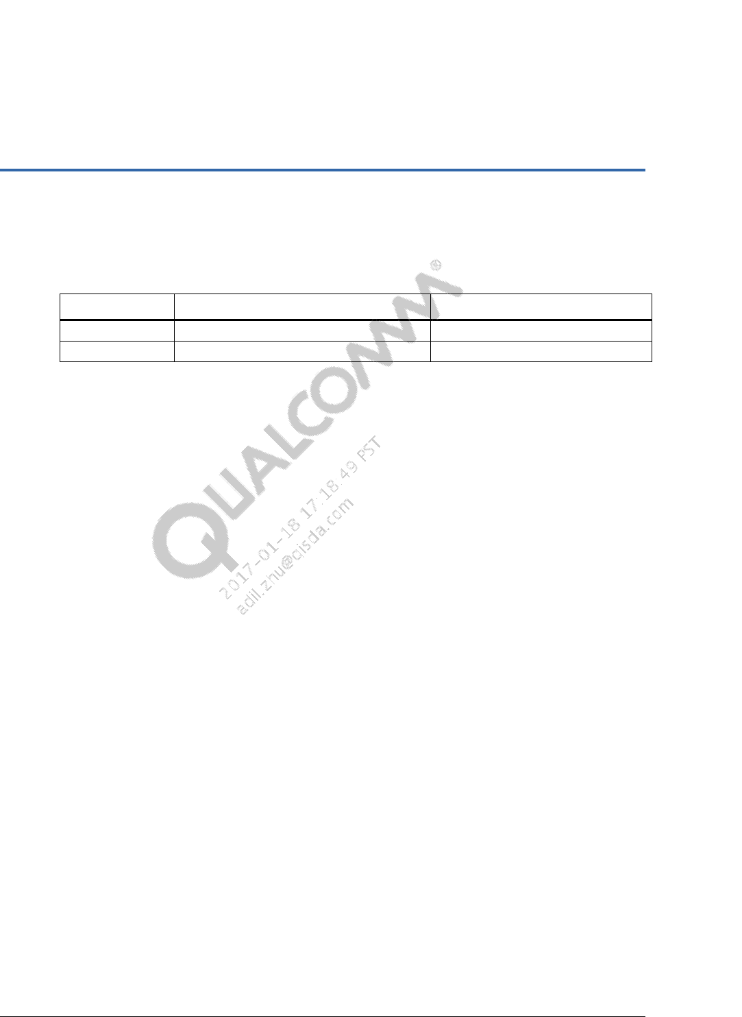
Table 2-2 PM8952/PM8956 MPP pin functionalities and features
Pin Functionality Description Feature I/O Default state
MPP01 VDD_PX_BIAS Provides 125 V reference voltage for MSM™ pads VREF AO
High-
impedance
state
(Hi-Z)
MPP02 PA_Therm2 Acts as the PA thermistor 2 – For the second WAN chain LED driver CS
MPP03 VREF_DAC Provides 125 V reference voltage for MPM and Qualcomm® Krait™
CPU LDOs VREF AO
MPP04 WLED_PWM_CTRL
Or
HR_LED_sink
Or
SMB_VCHG
Or
Skin_Therm
WLED controls PWM when PMI8952/PMI8956, home row, or
SMB_VCHG is not in use.
(As the signal must be accessible to ADC, the charger input current
for SMB during parallel charging must be on MPP).
Few designs use this function for Skin_Therm and move the
HR_LED_sink.
– DO
Table 2-3 PM8004 MPP pin functionalities and features
Pin Functionality Description Feature I/O Default
state
MPP01 SPON_trigger Synchronizes the power on signal between PM8004 and
PM8952/PM8956 PON DI
Hi-Z
MPP02
HR_LED_sink
Acts as the home run LED – AI
MPP03 WCN_SSR_eLDO_EN Initiates WCN subsystem restart – DO
MPP04 DSI_HDMI_Bridge_
eLDO_EN Supports or enables HDMI display bridge – DO
NOTE: There are two LV GPIOs and four MPPs in the PMI8952 device. Only even-numbered MPPs have the current sink capability.

PMIC GPIO and MPP Software User Guide Hardware feature description
80-NV610-48 H Confidential and Proprietary – Qualcomm Technologies, Inc. 10
MAY CONTAIN U.S. AND INTERNATIONAL EXPORT CONTROLLED INFORMATION
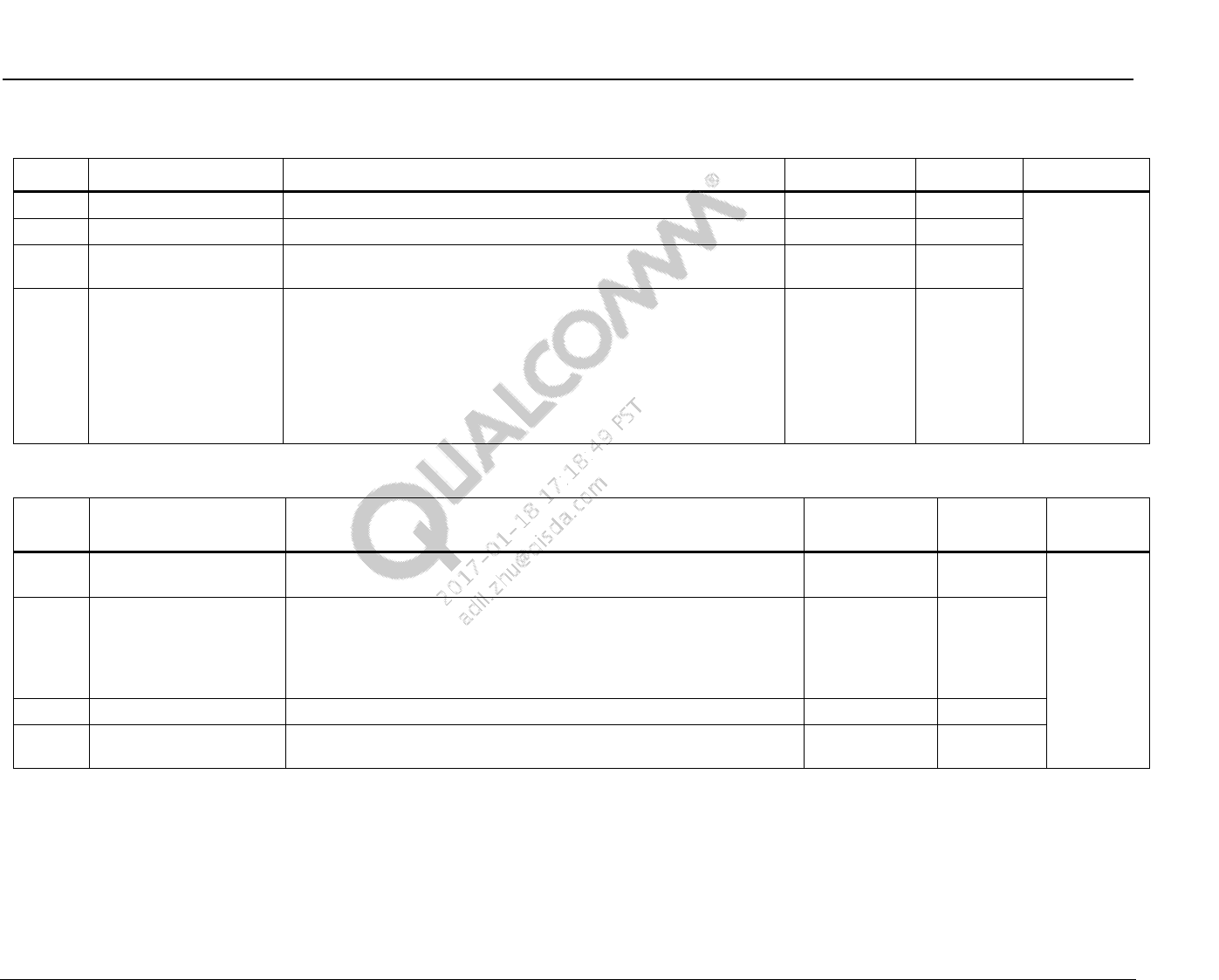
Table 2-4 PMI8952/PMI8956 GPIO pin functionalities and features
Pin Functionality Description Feature I/O GPIO
speed GPIO SF1 GPIO digital
input Default
state
GPIO01 WIPWR_LBE_CTL
(or PWM_OUT)
Controls signal for the Wireless
(Wi) power long beacon
extension
– O – PWM_OUT – Hi-Z
GPIO02 CHG_STAT Connects to the SMB_EN pin
for parallel charging – O – CHG_STAT –
Table 2-5 PMI8952/PMI8956 MPP pin functionalites and features
Pin Functionality Description Feature I/O Default
state
MPP01 SMB_VCHG Indicates that the charger input current is for SMB during the
PMI + SMB parallel charging. Because the signal must be accessible to
ADC, the indication must be on MPP01.
– AI
Hi-Z
MPP02 VSEL_EXT_BOOST_
BYP Controls the voltage set point of the external boost bypass for torch:
If VSEL = 0, then Vset = 3.15 V.
If VSEL = 1, then Vset = 3.6 V.
–
AO
MPP03 WLED_SHORT_DET Controls the external FET for the WLED short circuit protection – DO
MPP04 Flash Strobe Triggers and synchronizes flash with the Camera Sensor when Camera
sends a signal – DI

PMIC GPIO and MPP Software User Guide Hardware feature description
80-NV610-48 H Confidential and Proprietary – Qualcomm Technologies, Inc. 11
MAY CONTAIN U.S. AND INTERNATIONAL EXPORT CONTROLLED INFORMATION
2.2 PMIC GPIO pins
The GPIO pins are used for level shifting and other digital functions.
Standard GPIOs are the same on the PM8952/PM8956 devices
Special GPIOs are used to drive the clock outputs
Custom features share GPIO pins, and therefore have concurrency limitations
The following are the PM8952/PM8956 device custom GPIO features (Special connections
that can exist only in specific GPIO locations):
Sleep clock driver (four dedicated)
Divided clock for codec
Battery and UICC alarm
External regulator enable (two dedicated)
The following are the GPIO pairs:
Each GPIO pin is assigned as a member of a pair
Each pair is a combination of sequential odd and even GPIO pins (GPIO01 is paired with
GPIO02, and so on)
Each assigned member is a different supply, therefore, each pair is used as a
digital-level translator.
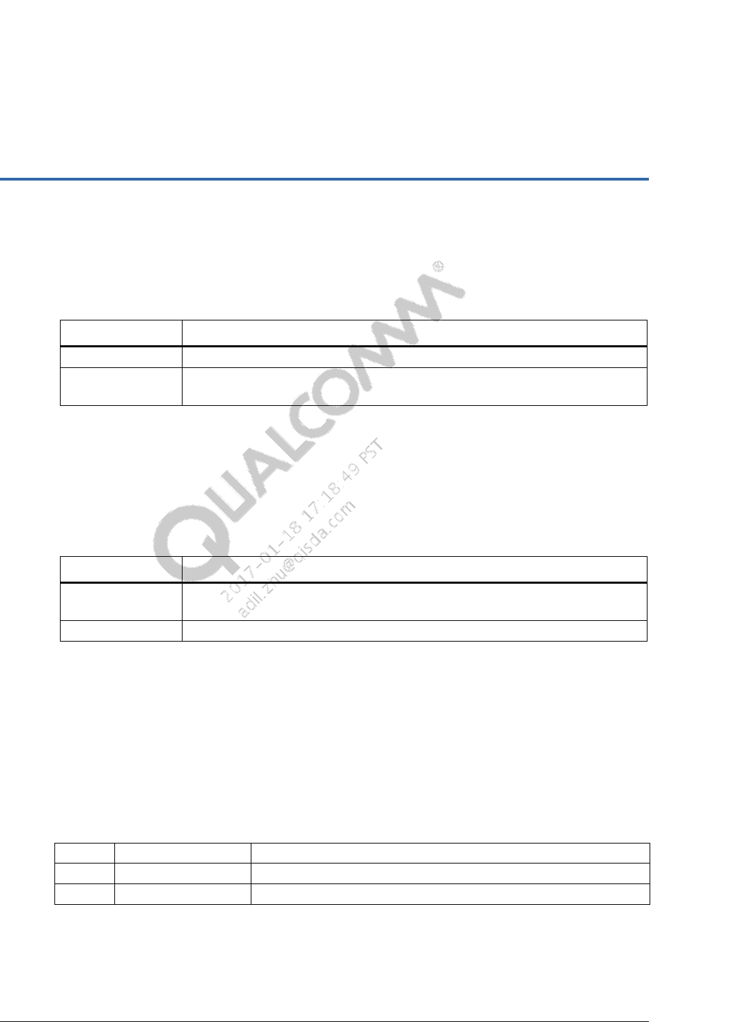
2.3 Register information
MODE_CTL register (address – 0×00000040, reset state – 0×00)
Table 2-6 PMI8952/PMI8956 MPP bits
Bit Bit name Description
7 RESERVED_BIT7 –
6:4 MODE MPP type:
0 – DI
1 – DO
2 – DI and DO
3 – Bidirectional logic
4 – AI
5 – AO
6 – CS
7 – Reserved

PMIC GPIO and MPP Software User Guide Hardware feature description
80-NV610-48 H Confidential and Proprietary – Qualcomm Technologies, Inc. 12
MAY CONTAIN U.S. AND INTERNATIONAL EXPORT CONTROLLED INFORMATION
Bit Bit name Description
3:0 EN_AND_SOURCE_SEL When configured as a digital output source, select:
0000 = 0
0001 = 1
0010 = paired MPP
0011 = inverted paired MPP
Enable control when configured as AO or current
sink. MPP is enabled when the selected condition
is true:
0000 = 0 (MPP is always disabled)
0001 = 1 (MPP is always enabled)
0010 = paired MPP
0011 = inverted paired MPP
Recommended defaults are listed in the table. However, the final values are device-specific and listed in the
device SPMI table in the PMI8952 Power Management IC Device Specification (80-NT391-1).
80-NV610-48 H Confidential and Proprietary – Qualcomm Technologies, Inc. 13
MAY CONTAIN U.S. AND INTERNATIONAL EXPORT CONTROLLED INFORMATION
3 Software drivers
The secondary boot loader (SBL) supports the GPIO/MPP module.
Table 3-1 GPIO/MPP SBL files and locations
File type Location
Header boot_images/core/api/systemdrivers/pmic/pm_gpio.h
Source boot_images/core/systemdrivers/pmic/drivers/gpio/src/pm_gpio.c
boot_images/core/systemdrivers/pmic/drivers/gpio/src/pm_gpio_driver.c
A qpnp-pin is a GPIO/MPP chip driver for the MSM SPMI implementation.
It creates spmi_device for every spmi-dev-container block of device_nodes
The device_nodes specify the PMIC pin number associated with each GPIO chip
The driver maps the PMIC GPIO pin numbers to the Linux GPIO pin numbers.
Table 3-2 GPIO/MPP HLOS files and locations
File type Location
dtsi kernel/arch/arm/boot/dts/qcom/msm-pm8950.dtsi
Kernel/Documentation/devicetree/bindings/gpio/ qpnp-pin.txt
Source kernel/drivers/gpio/ qpnp-pin.c
3.1 GPIO support in SBL
This section describes functions supporting the PMIC GPIO module in SBL.
3.1.1 pm_gpio_status_get( )
Returns the status of one of the PMIC GPIOs
Parameters
in pmic_chip Primary PMIC chip – 0; secondary PMIC chip – 1
in gpio GPIO identifier
out gpio_status Pointer to the GPIO status
Returns
SUCCESS or Error (pm_err_flag_type)
PMIC GPIO and MPP Software User Guide Software drivers
80-NV610-48 H Confidential and Proprietary – Qualcomm Technologies, Inc. 14
MAY CONTAIN U.S. AND INTERNATIONAL EXPORT CONTROLLED INFORMATION
Dependencies
Execute the pm_driver_init() function first
3.1.2 pm_gpio_config_bias_voltage( )
Configures the selected GPIO for bias voltage
Parameters
in pmic_chip Primary PMIC chip – 0; secondary PMIC chip – 1
in perph_index GPIO to configure for bias voltage
in volt_src GPIO voltage source
Returns
SUCCESS or Error (pm_err_flag_type)
Dependencies
Execute the pm_driver_init() function first
Example
Configure GPIO05 to HIGH, which indicates an analog (quiet) supply:
errFlag = pm_gpio_config_bias_voltage(PM_GPIO_5, PM_GPIO_VIN4);
3.1.3 pm_gpio_config_digital_input( )
Configures the selected GPIO as a digital input
Parameters
in pmic_chip Primary PMIC chip – 0; secondary PMIC chip – 1
in perph_index GPIO to configure as a digital input
in i_src_pulls Current source pulls
in volt_src GPIO voltage source
in out_buffer_strength GPIO output buffer strength
in src Selects the source
Returns
SUCCESS or Error (pm_err_flag_type)
Dependencies
Execute the pm_driver_init() function first
PMIC GPIO and MPP Software User Guide Software drivers
80-NV610-48 H Confidential and Proprietary – Qualcomm Technologies, Inc. 15
MAY CONTAIN U.S. AND INTERNATIONAL EXPORT CONTROLLED INFORMATION
Example
Ensure that GPIO is available to enable the keypad scan module to drive and sense the
keypad
Configure the keypad drive signal as an open_drain output with low drive strength
Configure the keypad sense module as an input with 1.5 µA pull-up + 30 µA boost. For
example, reference voltage VIN2 for both drive and sense lines.
Configure GPIO05 as a sense line:
errFlag = pm_gpio_config_digital_input(PM_GPIO_5,
PM_GPIO_I_SOURCE_PULL_UP_1_5uA_PLUS_30uA_BOOST,
PM_GPIO_VIN2,
PM_GPIO_OUT_BUFFER_OFF,
PM_GPIO_SOURCE_GND);
3.1.4 pm_gpio_config_digital_output( )
Configures the selected GPIO as a digital output
Parameters
in pmic_chip Primary PMIC chip – 0; secondary PMIC chip – 1
in perph_index GPIO configures as DO
in out_buffer_config GPIO output buffer configuration
in volt_src GPIO voltage source
in src Selects the source
in out_buffer_strength GPIO output buffer strength
in out_inversion Inverts the output of EXT_PIN
Returns
SUCCESS or Error (pm_err_flag_type)
Dependencies
Execute the pm_driver_init() function first
PMIC GPIO and MPP Software User Guide Software drivers
80-NV610-48 H Confidential and Proprietary – Qualcomm Technologies, Inc. 16
MAY CONTAIN U.S. AND INTERNATIONAL EXPORT CONTROLLED INFORMATION
Example
Ensure that GPIO is available to enable the keypad scan module to drive and sense the
keypad.
Configure the keypad drive signal as an open_drain output with low drive strength.
Configure the keypad sense module as an input with 1.5 μA pull-up + 30 μA boost. For
example, reference voltage VIN2 for both drive and sense lines.
Configure GPIO05 as a drive signal:
errFlag = pm_gpio_config_digital_output(PM_GPIO_5,
PM_GPIO_OUT_BUFFER_CONFIG_OPEN_DRAIN,
PM_GPIO_VIN2,
PM_GPIO_SOURCE_SPECIAL_FUNCTION1,
PM_GPIO_OUT_BUFFER_LOW,
FALSE);
3.1.5 pm_gpio_config_digital_input_output( )
Configures the selected GPIO as bidirectional
Parameters
in pmic_chip Primary PMIC chip – 0; secondary PMIC chip – 1
in perph_index GPIO to configure as a digital output
in src Selects the source
in i_src_pulls Current source pulls
in volt_src GPIO voltage source
in out_buffer_config GPIO output buffer configuration
in out_buffer_strength GPIO output buffer strength
Returns
SUCCESS or Error (pm_err_flag_type)
Dependencies
Execute the pm_driver_init() function first
3.1.6 pm_gpio_set_volt_source( )
Sets the voltage source
Parameters
in pmic_chip Primary PMIC chip – 0; secondary PMIC chip – 1
in perph_index GPIO configures the voltage source
in volt_src GPIO voltage source

PMIC GPIO and MPP Software User Guide Software drivers
80-NV610-48 H Confidential and Proprietary – Qualcomm Technologies, Inc. 17
MAY CONTAIN U.S. AND INTERNATIONAL EXPORT CONTROLLED INFORMATION
Returns
SUCCESS or Error (pm_err_flag_type)
Dependencies
Execute the pm_driver_init() function first
Example
Set voltage source to VIN2 for GPIO05:
errFlag = pm_gpio_set_volt_source(PM_GPIO_5, PM_GPIO_VIN2);
3.1.7 pm_gpio_config_mode_selection( )
Enables or disables the mode selection
Parameters
in pmic_chip Primary PMIC chip – 0; secondary PMIC chip – 1
in perph_index GPIO for which the mode selection is set
in enable_disable Possible values:
TRUE – Enable mode selection
FALSE – Disable mode selection
Returns
SUCCESS or Error (pm_err_flag_type)
Dependencies
Execute the pm_driver_init() function first
Example
Disable a mode selection:
errFlag = pm_gpio_config_mode_selection(PM_GPIO_1, FALSE);
3.1.8 pm_gpio_set_output_buffer_configuration( )
Sets the output buffer configuration
Parameters
in pmic_chip Primary PMIC chip – 0; secondary PMIC chip – 1
in perph_index GPIO for which the current source pulls are configured
in out_buffer_config GPIO output buffer configuration
Returns
SUCCESS or Error (pm_err_flag_type)
PMIC GPIO and MPP Software User Guide Software drivers
80-NV610-48 H Confidential and Proprietary – Qualcomm Technologies, Inc. 18
MAY CONTAIN U.S. AND INTERNATIONAL EXPORT CONTROLLED INFORMATION
Dependencies
Execute the pm_driver_init() function first
Example
For GPIO05, set the output buffer configuration to CMOS in the Bias mode:
errFlag = pm_gpio_set_output_buffer_configuration(PM_GPIO_5,
PM_GPIO_OUT_BUFFER_CONFIG_CMOS);
3.1.9 pm_gpio_set_inversion_configuration( )
Sets the inversion configuration
Parameters
in pmic_chip Primary PMIC chip – 0; secondary PMIC chip – 1
in perph_index GPIO for which the inversion configuration is set
in inversion Possible values:
TRUE – Enable inversion
FALSE – Disable inversion
Returns
SUCCESS or Error (pm_err_flag_type)
Dependencies
Execute the pm_driver_init() function first
Example
For GPIO05, set inversion to TRUE:
errFlag = pm_gpio_set_inversion_configuration(PM_GPIO_5, TRUE);
3.1.10 pm_gpio_set_current_source_pulls( )
Sets the current source pulls
Parameters
in pmic_chip Primary PMIC chip – 0; secondary PMIC chip – 1
in perph_index GPIO for which the current source pulls is configured
in i_src_pulls Current source pulls
Returns
SUCCESS or Error (pm_err_flag_type)

PMIC GPIO and MPP Software User Guide Software drivers
80-NV610-48 H Confidential and Proprietary – Qualcomm Technologies, Inc. 19
MAY CONTAIN U.S. AND INTERNATIONAL EXPORT CONTROLLED INFORMATION
Dependencies
Execute the pm_driver_init() function first
Example
For GPIO05, set the current source pulls to 1.5 μA + 30 μA boost:
errFlag = pm_gpio_set_current_src_pulls(PM_GPIO_5,
PM_GPIO_I_src_PULL_UP_1_5uA_PLUS_30uA_BOOST);
3.1.11 pm_gpio_set_ext_pin_config( )
Sets the EXT_PIN configuration
Parameters
in pmic_chip Primary PMIC chip – 0; secondary PMIC chip – 1
in gpio GPIO for which EXT_PIN is configured
in ext_pin_config Enable or disable the EXT_PIN.
Disable puts EXT_PIN in the Hi-Z state and disables the block
Returns
SUCCESS or Error (pm_err_flag_type)
Dependencies
Execute the pm_driver_init() function first
Example
Enable EXT_PIN:
errFlag = pm_gpio_set_ext_pin_config(PM_GPIO_5, PM_GPIO_EXT_PIN_ENABLE);
3.1.12 pm_gpio_set_output_buffer_drive_strength( )
Sets the output buffer drive strength
Parameters
in pmic_chip Primary PMIC chip – 0; secondary PMIC chip – 1
in perph_index GPIO for which the output buffer drive strength is configured
in out_buffer_strength GPIO output buffer drive strength.
Returns
SUCCESS or Error (pm_err_flag_type)
Dependencies
Execute the pm_driver_init() function first
PMIC GPIO and MPP Software User Guide Software drivers
80-NV610-48 H Confidential and Proprietary – Qualcomm Technologies, Inc. 20
MAY CONTAIN U.S. AND INTERNATIONAL EXPORT CONTROLLED INFORMATION
Example
For GPIO05, set the output buffer drive strength to HIGH:
errFlag = pm_gpio_set_output_buffer_drv_strength(PM_GPIO_5,
PM_GPIO_OUT_BUFFER_HIGH);
3.1.13 pm_gpio_set_source_configuration( )
Sets the source configuration
Parameters
in pmic_chip Primary PMIC chip – 0; secondary PMIC chip – 1
in perph_index GPIO for which the source configuration is selected
in src Selects the source
Returns
SUCCESS or Error (pm_err_flag_type)
Dependencies
The pm_driver_init() function is executed first
Example
To serve GPIO05 as an output in the Level Translator mode, select Pair In as the source:
errFlag = pm_gpio_set_src_configuration(PM_GPIO_5,
PM_GPIO_SOURCE_PAIRED_GPIO);
3.1.14 pm_gpio_set_mux_ctrl( )
Sets GPIO mux control
Parameters
in pmic_chip Primary PMIC chip – 0; secondary PMIC chip – 1
in uart_path Select the UART path
Returns
SUCCESS or Error (pm_err_flag_type)
Dependencies
Execute the pm_driver_init() function first

PMIC GPIO and MPP Software User Guide Software drivers
80-NV610-48 H Confidential and Proprietary – Qualcomm Technologies, Inc. 21
MAY CONTAIN U.S. AND INTERNATIONAL EXPORT CONTROLLED INFORMATION
3.1.15 Configure MPP as AI and setup ADC read
Sample code
The following are the required settings:
MPP05 on the PM8952/PM8956 devices:
Channel name – ADC_INPUT_MPP5
MPP05 corresponds to AMUX channel 5 (0×14) – Scaling used is 1/1. If 1/3 is used, it
corresponds to AMUX channel 5 (0×24)
ADC conversion speed – Normal
Hold off time – 100 μs
Voltage range – 0 V to 1.75 V (1/3 scaling is not required)
Voltage divider circuit – Use ratiometric calibration
NOTE: ADC samples averaging is not supported
To set up ADC read in SBL, do the following:
1. Add the channel name to AdcInputs.h.
File: boot_images\core\api\hwengines\AdcInputs.h
#define ADC_INPUT_MPP5 "MPP5"
2. Add the channel-specific properties.
File: boot_images/core/hwengines/adc/config/8952/VAdcBsp.c
static const VAdcChannelConfigType vAdcChannels_8952_PM8950[] = {
….
/* Channel 17: MPP5 */
{
/* .pName */ ADC_INPUT_MPP5,
/* .uAdcHardwareChannel */ 0x14,
/* .uConfigIdx */ VADC_CONFIG_NORMAL,
/* .eSettlingDelay */ VADC_SETTLING_DELAY_100_US,
/* .eFastAverageMode */ VADC_FAST_AVERAGE_NONE,
/* .bUseSequencer */ FALSE,
/* .uSequencerIdx */ 0,
/* .scalingFactor {num, den} */ {1, 1},
/* .eScalingMethod */ VADC_SCALE_TO_MILLIVOLTS,
/* .pInterpolationTable */ NULL,
/* .uInterpolationTableLength */ 0,
/* .eCalMethod */ VADC_CAL_METHOD_RATIOMETRIC,
/* .eMppConfig */ VADC_CHANNEL_MPP_CONFIG_STATIC,
/* .eMpp */ PM_MPP_5,
/* .eChSelect */ PM_MPP__AIN__CH_AMUX5
},
};

PMIC GPIO and MPP Software User Guide Software drivers
80-NV610-48 H Confidential and Proprietary – Qualcomm Technologies, Inc. 22
MAY CONTAIN U.S. AND INTERNATIONAL EXPORT CONTROLLED INFORMATION
NOTE: Ensure that you add the channels to the channel list and not the calibration channel list.
3. Read the VADC channel.
NOTE: For any dependencies, use the code after running pm_driver_init ().
uint32 test_adc_MPP_voltage(uint32* MPP_voltage)
{
AdcBootDeviceChannelType lchannel;
AdcBootResultType lresult;
DalResult error = 0x0;
if(NULL == MPP_voltage)
{ return ADC_ERROR;
}
/*Initialize the ADC*/
error = AdcBoot_Init();
if(DAL_SUCCESS != error) {
return ADC_ERROR;
}
/*Get the channel from where the data is needed*/
error = AdcBoot_GetChannel(ADC_INPUT_MPP5, &lchannel);
if(DAL_SUCCESS != error)
{ return ADC_ERROR; 1
}
/*Read the Voltage of the Battery*/
error = AdcBoot_Read(&lchannel, & lresult);
if(DAL_SUCCESS != error)
{
return ADC_ERROR;
}
/*Check for the result*/
if(ADC_RESULT_VALID == lresult.eStatus)
{
*MPP_voltage = (uint32)( lresult.nMicrovolts/1000);
}
else
{
return ADC_ERROR;
}
return error;
}

PMIC GPIO and MPP Software User Guide Software drivers
80-NV610-48 H Confidential and Proprietary – Qualcomm Technologies, Inc. 23
MAY CONTAIN U.S. AND INTERNATIONAL EXPORT CONTROLLED INFORMATION
3.2 Linux kernel (LK)
As there are no APIs in the LK boot loader to configure MPPs, LK requires direct register writes
to configure and enable MPP/GPIO.
3.2.1 Configure MPP02 as CS
Sample code
pm8x41_reg_write(0xA140, 0x60); //Configuring MPP Mode as Current Sink and
LOW
pm8x41_reg_write(0xA141, 0x02 //Selecting VIN2 as source
pm8x41_reg_write(0xA14C, 0x0); //Current Sink Control - 5mA
pm8x41_reg_write(0xA146, 0x80); //Enable MPP
3.3 Kernel DTSI properties
The succeeding sections provide the Kernel DTSI properties that are required to configure the
root node and child node.
3.3.1 Required root node properties
The spmi-dev-container specifies the following child nodes as part of the same SPMI device:
gpio-controller – Specify as gpio-controller; all child nodes belong to this gpio_chip
#gpio-cells – A PMIC pin number and a 32-bit flag field are encoded to specify the GPIO
configuration. Set the value to 2
#address-cells – Specifies one address field. Set the value to 1
#size-cells – Specifies one size-cell. Set the value to 1
compatible = "qcom,qpnp-pin" – Specifies driver matching for this driver
label – String giving the name for the gpio_chip device. This name must be unique on the
system and identify specifics of the device.
3.3.2 Required child node properties
Parameter Description
reg Specifies the SPMI offset and size for the pin device
qcom,pin-num Specifies the PMIC pin number for the device

PMIC GPIO and MPP Software User Guide Software drivers
80-NV610-48 H Confidential and Proprietary – Qualcomm Technologies, Inc. 24
MAY CONTAIN U.S. AND INTERNATIONAL EXPORT CONTROLLED INFORMATION
3.3.3 Optional child node properties
Parameter Description Example
qcom,mode Indicates whether the pin is input,
output, or both for GPIOs; MPP pins
also support bidirectional, analog in,
analog out, and current sink
Properties are bidirectional or
MPP-only as specified in the example
column
QPNP_PIN_MODE_DIG_IN= 0, (GPIO/MPP)
QPNP_PIN_MODE_DIG_OUT = 1, (GPIO/MPP)
QPNP_PIN_MODE_DIG_IN_OUT = 2, (GPIO/MPP)
QPNP_PIN_MODE_BIDIR = 3, (MPP)
QPNP_PIN_MODE_AIN = 4, (MPP)
QPNP_PIN_MODE_AOUT = 5, (MPP)
QPNP_PIN_MODE_SINK = 6 (MPP)
qcom,output-
type
Indicates whether GPIO is to be
configured as CMOS or open drain
Properties apply to GPIO only
QPNP_PIN_OUT_BUF_CMOS = 0
QPNP_PIN_OUT_BUF_OPEN_DRAIN_NMOS = 1
QPNP_PIN_OUT_BUF_OPEN_DRAIN_PMOS = 2
qcom,invert Inverts the signal of the GPIO line
Properties apply to GPIO or MPP
QPNP_PIN_INVERT_DISABLE = 0
QPNP_PIN_INVERT_ENABLE = 1
qcom,pull For GPIO, this parameter indicates
whether a pull-up or pull-down is to be
applied. Specify the current strength if
a pull-up is required
Current values of 30 µA, 1.5 µA,
31.5 µA, and 1.5 µA with 30 µA boost
are supported
Make this value as one of the
QPNP_PIN_GPIO_PULL_* properties
QPNP_PIN_PULL_UP_30 = 0
QPNP_PIN_PULL_UP_1P5 = 1
QPNP_PIN_PULL_UP_31P5 = 2
QPNP_PIN_PULL_UP_1P5_30 = 3
QPNP_PIN_PULL_DN = 4
QPNP_PIN_PULL_NO = 5
Note: Hardware ignores the configuration if the
GPIO is not set to input or output Open-drain mode.
For MPP, this parameter indicates
whether a pull-up is to be applied for
the Bidirectional mode only
The hardware ignores the
configuration when operating in other
modes
Make it one of the
QPNP_PIN_MPP_PULL_* values
QPNP_PIN_MPP_PULL_UP_0P6KOHM = 0,
QPNP_PIN_MPP_PULL_UP_OPEN = 1
QPNP_PIN_MPP_PULL_UP_10KOHM = 2
QPNP_PIN_MPP_PULL_UP_30KOHM = 3
qcom,vin-sel Specifies the voltage level when the
output is set to 1
For an input GPIO, it specifies the
voltage level at which the input is
interpreted as a logical 1
Properties apply to GPIO or MPP
QPNP_PIN_VIN0 = 0
QPNP_PIN_VIN1 = 1
QPNP_PIN_VIN2 = 2
QPNP_PIN_VIN3 = 3
QPNP_PIN_VIN4 = 4
QPNP_PIN_VIN5 = 5
QPNP_PIN_VIN6 = 6
QPNP_PIN_VIN7 = 7
qcom,out-
strength
The amount of current supplied for an
output GPIO
Properties apply to GPIO only
QPNP_PIN_OUT_STRENGTH_LOW = 1
QPNP_PIN_OUT_STRENGTH_MED = 2
QPNP_PIN_OUT_STRENGTH_HIGH = 3

PMIC GPIO and MPP Software User Guide Software drivers
80-NV610-48 H Confidential and Proprietary – Qualcomm Technologies, Inc. 25
MAY CONTAIN U.S. AND INTERNATIONAL EXPORT CONTROLLED INFORMATION
Parameter Description Example
qcom,src-sel Selects a function for the pin; certain
pins are paired (shorted) with each
other. A few GPIO pins can act as
alternate functions
GPIO – Source select
MPP – Enable select
QPNP_PIN_SEL_FUNC_CONSTANT = 0
QPNP_PIN_SEL_FUNC_PAIRED = 1
QPNP_PIN_SEL_FUNC_1 = 2
QPNP_PIN_SEL_FUNC_2 = 3
QPNP_PIN_SEL_DTEST1 = 4
QPNP_PIN_SEL_DTEST2 = 5
QPNP_PIN_SEL_DTEST3 = 6
QPNP_PIN_SEL_DTEST4 = 7
qcom,master-
en Properties apply to GPIO or MPP
1 – Enables features within the pin
block based on configuration
0 – Disables the block and lets the pin
float with high impedance regardless
of other settings
–
qcom,aout-ref Sets the AO reference
Properties apply to MPP only
QPNP_PIN_AOUT_1V25 = 0
QPNP_PIN_AOUT_0V625 = 1
QPNP_PIN_AOUT_0V3125 = 2
QPNP_PIN_AOUT_MPP = 3
QPNP_PIN_AOUT_ABUS1 = 4
QPNP_PIN_AOUT_ABUS2 = 5
QPNP_PIN_AOUT_ABUS3 = 6
QPNP_PIN_AOUT_ABUS4 = 7
qcom,ain-route Sets the destination for AI
Properties apply to MPP only
QPNP_PIN_AIN_AMUX_CH5 = 0
QPNP_PIN_AIN_AMUX_CH6 = 1
QPNP_PIN_AIN_AMUX_CH7 = 2
QPNP_PIN_AIN_AMUX_CH8 = 3
QPNP_PIN_AIN_AMUX_ABUS1 = 4
QPNP_PIN_AIN_AMUX_ABUS2 = 5
QPNP_PIN_AIN_AMUX_ABUS3 = 6
QPNP_PIN_AIN_AMUX_ABUS4 = 7
qcom,cs-out Sets the amount of output to sync in
mA units
Properties apply to MPP only
QPNP_PIN_CS_OUT_5MA = 0
QPNP_PIN_CS_OUT_10MA = 1
QPNP_PIN_CS_OUT_15MA = 2
QPNP_PIN_CS_OUT_20MA = 3
QPNP_PIN_CS_OUT_25MA = 4
QPNP_PIN_CS_OUT_30MA = 5
QPNP_PIN_CS_OUT_35MA = 6
QPNP_PIN_CS_OUT_40MA = 7

PMIC GPIO and MPP Software User Guide Software drivers
80-NV610-48 H Confidential and Proprietary – Qualcomm Technologies, Inc. 26
MAY CONTAIN U.S. AND INTERNATIONAL EXPORT CONTROLLED INFORMATION
3.3.4 Configure GPIO04 as an interrupt wake-up resource with falling
edge trigger
The following code samples show a recommended approach
1. Modify the GPIO status
gpio@c300 {
reg = <0xc300 0x100>;
qcom,pin-num = <4>;
qcom,mode = <0>; /* QPNP_PIN_MODE_DIG_IN */
qcom,invert = <0>; /* QPNP_PIN_INVERT_DISABLE */
qcom,pull = <0>; /* QPNP_PIN_PULL_UP_30 */
qcom,src-sel = <0>; /* QPNP_PIN_SEL_FUNC_CONSTANT */
qcom,master-en = <1>;/* enable this gpio */
};
2. Claim GPIO as an interrupt in driver-related DTSI file
test_func {
compatible = "qcom,test-gpio";
interrupt-parent = <&spmi_bus>;
/* Slave addr 0, peripheral addr 0xc3(GPIO_04) */
interrupts = <0x0 0xc3 0x0>;
interrupt-names = "test1";
};
3. Configure driver usage
unsigned int test_irq;
Int rc;
test_irq = platform_get_resource_byname(pdev,IORESOURCE_IRQ, "test1");
if (test_irq < 0) {
pr_err("Unable to get test_irq\n");
return -ENXIO;
}
rc = request_irq(test_irq, test_gpio_irq_handler, IRQ_TYPE_EDGE_FALLING,
"gpio_test_1", NULL);
enable_irq_wake(test_irq);
4. Handle a triggered interrupt
static irqreturn_t
test_gpio_irq_handler(int irq, void *dev_id)
{
//do what would you like to do
return IRQ_HANDLED;
}

PMIC GPIO and MPP Software User Guide Software drivers
80-NV610-48 H Confidential and Proprietary – Qualcomm Technologies, Inc. 27
MAY CONTAIN U.S. AND INTERNATIONAL EXPORT CONTROLLED INFORMATION
3.3.5 Configure PM8952/PM8956 GPIO02 as a sleep file
The following code sample shows the recommended approach to configure the PM8952/PM8956
GPIO02 as a sleep file in the msm-8952.dtsi file:
&pm8950_gpios {
gpio@c100 {
qcom,mode = <1>; // Digital output
qcom,pull = <5>; // No Pull up
qcom,vin-sel = <2>; // Vin select to 1 i.e., … V
qcom,src-sel = <2>; //special function 1
qcom,master-en = <1>; //enable MPP
qcom,out-strength = <2>; // Output strength medium
};
}
3.3.6 Configure PMI8952/PMI8956 MPP04 as a PWM output for blink
LEDs
This section provides the sample code to configure the PMI8952/PMI8956 MPP04 in the
msm-pmi8950.dtsi file.
NOTE: Ensure that MPP is not used by other processors to avoid changing the setting.
NOTE: Ensure that DTEST2 is used here. Do not use DTEST1 as it is used by other processors for
internal purposes.
qcom,leds@a300 {
compatible = "qcom,leds-qpnp";
reg = <0xa300 0x100>;
status = "okay";
qcom,led_mpp_4 {
label = "mpp";
linux,name = "red";
linux,default-trigger = "none";
qcom,default-state = "off";
qcom,max-current = <40>;
qcom,current-setting = <5>;
qcom,id = <6>;
qcom,mode = "pwm";
qcom,source-sel = <8>;
qcom,mode-ctrl = <0x60>;
qcom,pwm-channel = <0>;
qcom,pwm-us = <1000>;
pwms = <&pmi8950_pwm 0 0>;
pwm-names="red";
};
};

PMIC GPIO and MPP Software User Guide Software drivers
80-NV610-48 H Confidential and Proprietary – Qualcomm Technologies, Inc. 28
MAY CONTAIN U.S. AND INTERNATIONAL EXPORT CONTROLLED INFORMATION
pmi8950_pwm: pwm@b000 {
compatible = "qcom,qpnp-pwm";
reg = <0xb000 0x100>;
reg-names = "qpnp-lpg-channel-base";
qcom,channel-id = <0>;
qcom,supported-sizes = <6>, <9>;
qcom,period = <4000000>;
qcom,dtest-output = <2>;
#pwm-cells = <2>;
// Adds this line.
qcom,pwm {
qcom,duty = <2000000>; //PWM duty time in
microseconds
label = "pwm";
};
};
3.3.7 Configure PM8952/PM8956 MPP for ADC read through device
tree
The following settings are required for the configuration:
MPP – 2
Channel name – mpp2_adc
Input voltage range – 0 V to 3 V
Calibration type – Absolute
NOTE: Interpolation to other units is not supported
Recommended delay setting for MPP channels – 100 μs
Average ADC samples – 4
The following steps provide sample code for configuration of the MPP:
1. In the msm-pm8950.dtsi file, add or modify the MPP02 settings to configure it as an analog
input.
mpp@a100 {
reg = <0xa100 0x100>;
qcom,pin-num = <2>;
qcom,mode = <4>; // A-input
qcom,src-sel = <0>; //MPP Constant
qcom,ain-route = <1>; // QPNP_PIN_AIN_AMUX_CH6 = 1 for MPP2
qcom,master-en = <1>; //Enable MPP
};
2. In the msm-pm8950.dtsi file, set the ADC channel for MPP02.

PMIC GPIO and MPP Software User Guide Software drivers
80-NV610-48 H Confidential and Proprietary – Qualcomm Technologies, Inc. 29
MAY CONTAIN U.S. AND INTERNATIONAL EXPORT CONTROLLED INFORMATION
chan@11 {
label = "mpp2_adc";
reg = <0x21>; // channel for MPP2
qcom,decimation = <0>;
qcom,pre-div-channel-scaling = <1>; //Use 1:3 scaling to keep
input voltage within Max voltage: 1.8V
qcom,calibration-type = "absolute";
qcom,scale-function = <0>;
qcom,hw-settle-time = <1>;
qcom,fast-avg-setup = <2>;
};
3. Add to the client node that requires the VADC channel A/D.
client_node {
qcom,test-vadc = <&pm8950_vadc>;
};
NOTE: When the qpnp_get_vadc() function is called, the consumer name passed to the driver is used to
associate the consumer with the corresponding device.

80-NV610-48 H Confidential and Proprietary – Qualcomm Technologies, Inc. 30
MAY CONTAIN U.S. AND INTERNATIONAL EXPORT CONTROLLED INFORMATION
4 Debug
The following sections provide the different debug schemes/techniques for MPPs and GPIOs.
4.1 ADB
ADB shell method
The following procedure enables the MPP/GPIO dumps:
cd /sys/kernel/debug/spmi/spmi-0
echo 0xA000> address
echo 0x27FF > count
cat data
JTAG method (preferred)
(<RPM build location> is the location that contains the rpm_proc directory)
1. Set and hit a breakpoint in the software, or break using the TRACE32 Break command.
2. From the RPM TRACE32 window, run the following commands:
cd <RPM build location>/rpm_proc/core/systemdrivers/pmic/scripts
do PMICDump.cmm
3. In the UI prompt, enter the hardware revision of the PMIC on your device, and then specify
the file location to save the generated.xml register dump file (For example, C:\Temp).
4. Retrieve the .xml files from the directory specified in the UI, and then provide them in the
Salesforce case.
4.2 Log messages
Use one of the following procedures to enable log messages:
Add "#define DEBUG;" above the header #includes in the drivers/gpio/qpnp-pin.c file.
Use the following ADB shell commands to enable the kernel log messages:
adb root
adb wait-for-devices
adb shell mount -t debugfs none /sys/kernel/debug
adb shell "echo 8 > /proc/sys/kernel/printk"
adb shell "echo 'file qpnp-pin.c +p' >
/sys/kernel/debug/dynamic_debug/control"
To re-enable the logs, issue the ADB commands after each power cycle.

80-NV610-48 H Confidential and Proprietary – Qualcomm Technologies, Inc. 31
MAY CONTAIN U.S. AND INTERNATIONAL EXPORT CONTROLLED INFORMATION
A References
A.1 Related documents
Title Number
Qualcomm Technologies, Inc.
PMI8952 Power Management IC Device Specification 80-NT391-1
PM8952/PM8956 + PMI8952 Power Management IC Design
Guidelines/Training Slides 80-NT390-5
A.2 Acronyms and terms
Acronym or term Definition
ADB Android debug bridge
ADC Analog-to-digital conversion
AI or AIN Analog input
AO or AOUT Analog output
CS Current sink
DI Digital input
DO Digital output
FET Field effect transistor
GPIO General-purpose input/output
Hi-Z High impedence state
I/O Input/output
LDO Low drop out
MPP Multipurpose pin
MPM Modem power management
PA Power amplifier
PWM Pulse width modulation
SBL Secondary boot loader
VREF Voltage reference
Wi Wireless
