9 975 176 01_MP F53W_Product_Specifications_Sep85 01 MP F53W Product Specifications Sep85
9-975-176-01_MP-F53W_Product_Specifications_Sep85 9-975-176-01_MP-F53W_Product_Specifications_Sep85
User Manual: 9-975-176-01_MP-F53W_Product_Specifications_Sep85
Open the PDF directly: View PDF ![]() .
.
Page Count: 23

MODELS
MP-F53W·
MP-F53W-OOD
PRODUCT
SPECIFICATIONS
SON~
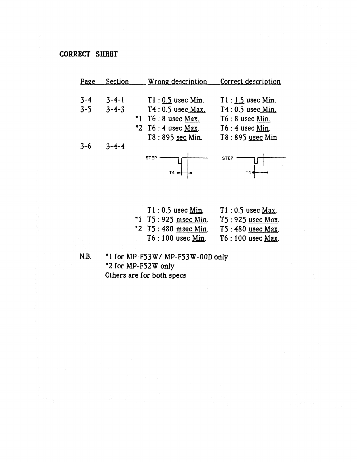
CORRECT
SHEET
Page
Section
3-4 3-4-1
3-5 3-4-3
3-6 3-4-4
Wrong
description
Tl :
II
usee
Min.
T4
:
0.5
usee
Max.
*1
T6
: 8
usee
Max.
*2
T6
: 4
usee
Max.
T8
:
895
see
Min.
STEP-:rr
T4
T 1 :
0.5
usee
Min.
* 1 T5:
925
msee
Min.
*2
T5:
480
msee
Min.
T6
:
100
usee
Min.
Correct
description
T 1
:.L.S.
usee
Min.
T4
:
0.5
usee
Min.
T6
: 8
usee
Min.
T6
: 4
usee
Min.
T8
:
895
usee
Min
STEP
T4
T 1 :
0.5
usee
Max.
T5
:
925
usee
Max.
T5
:
480
usee
Max.
T6
:
100
usee
Max.
N.B.
* 1 for
MP-F53W
/
MP-F53W
-OOD
only
*2
for
MP-F52W
only
Others are for both specs

PROPRIETARY NOTICE
This manual contains proprietary design information. Repro-
duction
or
dissemination
of
information provided herein, for
purposes other than operation and maintenance
of
the equip-
ment,
is
strictly prohibited without written consent from the
SONY Corporation.
I

RECORD OF REVISIONS
REVISION NOTES
1
ORIGINAL
ISSUE
September, 1985
[Serial number table]
Model Serial Numbers
MP-F53W 10,000,001 -
14,999,999
MP-F53W-00D 15,000,001 -
19,999,999
II
TABLE
OF
CONTENTS
Description
Page
SECTION
1.
INTRODUCTION......................................................
1-1
SECTION
2.
DRIVE
DIMENSION
AND
PERFORMANCE...................................
2-1
2-1.
CONFIGURATION
••••••••••••••••••••••••••••••••••••••••••••••••
2-1
2-2.
PHYSICAL
DIMENSIONS
••••••••••••••••••••••••••••••••••••••••••
2-1
2-3.
PERFORMANCE
••••••••••••••••••••••••••••••••••••••••••••••••••
2-2
2-3-1.
Capacity
••••••••••••••••••••••••••••••••••••••••••••••
2-2
2-3-2.
Transfer
Rate
•••••••••••••••••••••••••••••••••••••••••
2-2
2-3-3.
Access
Time
•••••••••••••••••••••••••••••••••••••••••••
2-2
2-3-4.
Functional............................................
2-2
2-3-5.
Reliability...........................................
2-2
2-4.
INPUT
POWER
REQUIREMENTS
•••••••••••••••••••••••••••••••••••••
2-2
274-1.
Power
Consumption
•••••••••••••••••••••••••••••••••••••
2-2
2-4-2.
Supply
Voltages.......................................
2-3
2-5.
ENVIRONMENTAL
LIMITS
•••••••••••••••••••••••••••••••••••••••••
2-3
2-5-1.
Temperature
Range
•••••••••••••••••••••••••••••••••••••
2-5-2.
Humidity
Range
••••••••••••••••••••••••••••••••••••••••
2-5-3.
Vibration
•••••••••••••••••••••••••••••••••••••••••••••
2-5-4.
Shock
•••••••••••••••••••••••••
,
••••••••••••••••••••••••
2-5-5.
Orientation
•••••••••••••••••••••••••••••••••••••••••••
SECT
I
ON
3.
SIGNAL
INTERFACE
•••••••••••••••••••••••••••••••••••••••••••••••••••
3-1.
CONNECTOR
AND
PIN
ASSIGNMENTS
••••••••••••••••••••••••••••••••
3-1-1.
Signal
Connector
Pin
Assignment
•••••••••••••••••••••••
3-1-2.
Power
Supply
Connector
••••••••••••••••••••••••••••••••
3-1-3.
Power
Supply'Connector
Pin
Assignment
•••••••••••••••••
3-1-4.
Power
and
Signal
Connection
Pin
Numbers
•••••••••••••••
3-1-5.
Signal
connector
••••••••••••••••••••••••••••••••••••••
3-1-6.
Drive
Select
Switch
•••••••••••••••••••••••••••••••••••
3-2.
DC
CHARACTERISTICS
OF
INTERFACE
SIGNALS
••••••••••••••••••••••
3-2-1.
Output
Signals
from
Drive
•••••••••••••••••••••••••••••
3-2-2.
Input
Signals
to
Drive
••••••••••••••••••••••••••••••••
3-2-3.
Recommended
Circuit
for
Signal
Interface
••••••••••••••
3-3.
SIGNAL
DEFINITIONS
•••••••••••••••••••••••••••••••••••••••••••
3-3-1.
DRIVE
SELECT
0,1,2,3
••••••••••••••.••••••••.•••••.••••
3-3-2.
STEP
••••••••••••••••••••••••••••••••••••••••••••••••••
3-3-3.
DIRECTION
•••••••••••••••••••••••••••••••••••••••••••••
3-3-4.
HEAD
SELECT
•••••••••••••••••••••••••••••••••••••••••••
3-3-5.
WRITE
GATE
••••••••••••••••••••••••••••••••••••••••••••
3-3-6.
WRITE
·DATA
3-3-7.
INDEX
•••••••••••••••••••••••••••••••••••••••••••••••••
3-3-8.
TRACK
00
•••••••••••••••••••••••••••.••••••••••••••••••
3-3-9,.
WRITE
PROTECT
•••••••••••••••••••••••••••••••••••••••••
3-3-10.
READ
DATA
••••••••••••••••••••••••••••••••••••••••••••
3-3-11.
DISK
CHANGE
••••••••••••••••••••••••••••••••••••••••••
3-3-12.
DISK
CHANGE
RESET
ill
2-3
2-3
2-3
2-4
2-4
3-1
3-1
3-1
3-1
3-1
3-1
3-1
3-1
3-1
3-1
3-2
3-2
3-3
3-3
3-3
3-3
3-3
3-3
3-3
3-3
3-3
3-3
3-3
3-3
3-4
TABLE
OF
CONTENTS
Description
Page
3-3-13.
READY
•••••••••••••••••••••••••••••••••••••••••••••••
3-4
3-3-14
•.
MOTOR
ON
••••••••••••••••••••••••••••••••••••••••••••
3-4
3-3-15.
IN
USE..............................................
3-4
3-4.
TIMING
REQUIREMENTS
••••••••••••••••••••••••••••••••.•••••••••
3-4
:1"-4-1. Head
Access
••••••••••••••••••••••••••••••••••••••••.•.
3-4
3-4-2.
TRACK
00
Signal
•••••••••••••••••••••••••••••••••••••••
3-5
3-4-3.
Write
Data
Timing
•••••••••••••••••••••••••••••••••••••
3-5
3-4-4.
Read
Data
Timing
••••••••••••••••••••••••••••••••••••••
3-6
3-4-5.
Index
Pulse
•••••••••••••••••••••••••••••••••••••••••••
3-6
3-4-6.
Disk
Change
•••••••••••••••••••••••••••••••••••••••••••
3-7
3-5.
POWER
ON
AND
POWER
OFF
REQUIREMENTS
••••••••••••••••••••••••••
3-7
3-5-1.
Data
Protection
•••••••••••••••••••••••••••••••••••••••
3-7
3-5-2.
Power
Supply
Sequencing
•••••••••••••••••••••••••••••••
3-7
3-5-3.
Power
On
Reset
Timing
3-7
3-6.
DISK
MOTOR
ROTATION
AND
DISK
INSERTION
•••••••••••••••••••••••
3-7
SECTION
4.
POWER
ON
INITIALIZATION...........................................
4-1
SECTION
5.
READY
SENSING
.METHOO
•••••.••••••••••••••••••••••••••••••••••••••••
5-1
SECTION
6.
SIGNAL
GROUND
TO
FRAME
GROUND
SHORT
•••••••••••••••••••••••••••••••
6-1
SECTION
7.
TEST
POINTS
........................................................
7-1
N
SECTION 1
INTRODUCTION
This
manual
covers
all
drives
with
the
model
number
of
MP-F53W
i.e.
the
MP-F53W-OOD
and
the
standard
MP-F53W. While
both
drives
are
completely
comprised
of
CMOS
circuitry,
the
MP-F53W-OOD
has
a
TIL
compatible
interface
while
the
standard
MP-F53W's
interface
is
CMOS.
The
specifications
for
these
drives
are
identical
except
where
indicated.
NB :
The
spe
cifications
defined
in
this
booklet
are
valid
if
the
drive
is
used
with
Sony
media
or
any
other
ANSI
specification
media
agreed
upon
by
Sony
and
the
drive
customer.
,-,
The
main
features
of
the
MP-F53W
series
are:
low
power
consumption,
low
height
and
high
reliability
with
simple me
chanism
and
ele
ctronic
circuit.
MP-F53W
series
also
complies
with
the
follow-
ing
product
safety
standards
:
U.L.
478
C.S.A.
C22.2
No.154
U.L.
94V-O
for
Front
Panel
(approved)
SECTION 2
DRIVE
DIMENSION
AND
PERFORMANCE
2-1.
CONFIGURATION
2-2.
PHYSICAL DIMENSIONS
The
dIive
consists
of
a
Read/Write
head,
head
positioning
mechanism,
disk
motor,
interface
logic
circuit
and R
ead/WIite
circuit.
The
detailed
physical
dimensions
are
shown
in
Figure
2-1.
The
main dimensions
are:
Height
Width
Depth
Weight
2-M3\
DEPTH 4
,r-----90-±-0-.2---t~lr---+-2-1
±_0_.3
-+
~
l
-r
~
~-----------------------u
7 (iNSERTED)
1 (EJECTED)
POWER
CONNECTOR
0'
o
:i
...
00
I
~
o
SIGNAL
INTERFACE
CONNECTOR
MEDIA
CENTER
44.5
iO
.3
MEDIA
CENTER
-1
I
I
I
...
00
I
<C
M
o
5
iO
.2
30mm
(l.18in.)
: 101.6mm (4.00in.)
: 150mm (5.91in.)
(
: 480g
(l.06
pounds) Max
•.
15
OPENED
AREA
FOR
MEDIA
INSERTION
...
00
t-l=~~~~======~==~~~~j=====~Jl~
N
o
+1
~
'--
21
iO.3
-.
31
=0.3
\;
~--t-
I
--
f---
1/4-~5
DIMENSION
UNIT
mm
(inch)
~
4M3
Figure
2-1_
PHYSICAL DIMENSIONS
2-1
2-3.
PERFORMANCE
2-3-1.
Capacity
Unformatted
Capacity
1.0MB/disk
for
MFM
0.5MB/surface
for
MFM
6.Z5KB/track
for
MFM
2-3-2.
Transfer
Rate
Burst
Transfer
Rate
2-3-3.
Access Time
Z50Kbits/sec
for
MFM
a.
Track
to
Track
Slew
Rate
:
6msec
Min.
b.
Track
to
Track
Step
Settling
Time
:
15msec
Max.
The
value
of
15msec
is
the
time
necessary
to
stabilize
the
head
within
0.035mm
of
its
absolute
position.
c.
Motor
Start
Time :
900msec
Max.
Motor
start
time
is
the
time
that
it
takes
for
the
READY
signal
to
become
true
(low)
after
the
MOTOR ON
siganal
has
been
activated.
2-3-4.
Functional
a.
Rotation
Speed
:
300rpm
The
continuous
speed
variation
is
within
+1:5%.
The
instantanuous
speed
variation
is
within
+1.0%.
b.
Recording
Density
c.
Track
Density
: 8717BPI
(Side 1,
Track
79)
: 0.1875mm
(7.38x10-
3
in.)
Track
-
Track
2-2
d.
Cylinders
e.
Tracks
f.
RfW
Heads
2-3-5.
Reliability
80
160
2
a.
Mean
Time
Between
Failures
(MTBF)
:
10,000
POH
b.
Mean
Time
to
Repair
(MTTR)
:
30minutes
c.
Preventive
Maintenance
(PM)
Not
Required
d.
Components
Life
5
years
or
15,000 POH
e.
Error
Rate
1-
Soft
Read
Error
1
per
10
9
bits
read
Z.
Hard
Read
Error
1
per
10
12
bits
re
ad
3.
Seek
Error
1
per
lOB
seeks
2-4.
INPUT
POWER
REQUIREMENTS
2-4-1.
Power- Consumption
Model
Name
MP-F53W
MP-F53W-OOO
Standby
50mW
255mW
Operation
2.BW
2.B5W
(Read/Write
mode)
2-4-2.
Supply Voltages
a.
For
Model MP-F53W
VoLtage
+12.0V+5%
+5.0V+5%
Max.
RippLe
O.1Vpp
O.1Vpp
[mAl
600
300
Current
Stand-by
10uA
Average
130mA
(Read)
Peak
700mA
(Motor
Start)
Peak
300mA
(Stepping
during Motor
On)
Stand-by
10mA
Operating
200mA
b.
For
Model MP-F53W-00D
Vo
L
tage
Mex.
Ri
pp
Le
Current
+12.0V+5%
0.1
Vpp
Stand-by
10uA
Average
130mA
(Read)
Peak
700mA
(Motor
Start)
Peak
300mA
(Stepping during Motor
On)
+5.0V+5%
O.1Vpp
Stand-by
51mA
Operating
241mA
LOW
POWER
TYPE
---+12
V
------+
5 V
r---.--------
----------,
r-----
MP-F53W-00D
I I I
r--J""---
----
--
---
---
------:
_____
,
__
-- -MP-F53W
I I I :
~
__
I
_____
I
________
I
L-
____
__
100 I
200 o 15
200220
o
20
[m secl
o
POWER
ON
STAND MOTOR READ
STEP
-BY
ON
Figure 2-2.
DC
CURRENT PROFILE (AVERAGE)
2-5.
ENVIRONMENTAL LIMITS
2-5-1.
Temperature Range
Operating
Transportation
5°
e
to
50°
e (400F
to
122°F)
ambient
-40
0e
to
60
0e
(-40°F
to
HOoF)
These
figures
are
valid
provided
that
there
is
no
condensation.
Storage
-200e
to
60
0e (_4°F
to
HOoF)
These
figures
are
valid
provided
that
there
is
no
condensation.
2-5-2.
Humidity
Range
Operating
8%
to
80%
relative
humidity
with
a
wet
bulb
temperature
of
29°
e (85 0F)
and
no
condensation.
Transportation
and
Storage
5%
to
95%
relative
humidity
and
no
condensation
2-3
2-5-3.
Vibration
Operating
The
unit
can
perform
Read/Write
operations
without
an
error
rate
beyond
that
specified
while
withstanding
continuous
vibrations
at
a
frequency
of
10
to
500Hz
with
an
acceleration
of
no
more
than
0.5G
along
each
of
the
three
mutually
perpendicular
axes.
Transportation
and
Storage
The
unit
can
withstand
continuous
vibrations
from
10Hz
to
300Hz
with
a maximum
acceleration
of
2.0 G
along
each
of
the
three
mutually
perpendicular
axes
without
any
degradation
of
any
characteristics
below
the
performance
specifications.
2-5-4.
Shock
Operating
The
unit
can
withstand
a 5.0 G
shock
for
llmsec
with
a
liZ
sine
wave
shape
in
each
of
the
three
mutually
perpendicular
aXiS
while
performing
normal
Read/Write
functions
without
damage
or
any
loss
of
data.
2-5-5.
Orientation
The
drive
does
not
necessarily
need
to
be
horizontally
positioned.
In
fact,
as
seen
in
figure
Z-3,
there
are
many
other
possible
orientations.
+/_5°
~
;J):/7/7;;3B/?/
r--
-,
I I
I
I
I
I
I
I
+/-
30°
Transportation
and
Storage
The
unit
when
unpacked
can
withstand
an
llmsec
with
a
liZ
sine wave
shock
of
60 G on
any
of
the
three
mutually
perpen-
dicular
axis.
(
J"mW/7/7///§$r/7/)/?
+/_30°
/
Figure 2-3.
ORIENTATIONS
2-4
SECTION 3
SIGNAL INTERFACE
3-1.
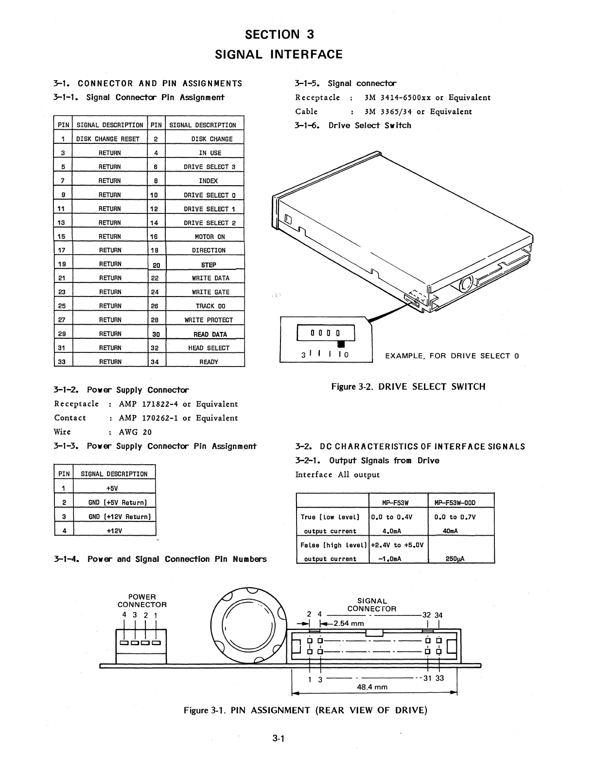
CONNECTOR AND PIN ASSIGNMENTS
3-1-1.
Signal Connecta- Pin Assignment
PIN
SIGNAL
DESCRIPTION
PIN
SIGNAL
DESCRIPTION
1
DISK
CHANGE
RESET
2
DISK
CHANGE
3
RETURN
4
IN
USE
5
RETURN
6
DRIVE
SELECT
3
7
RETURN
B
INDEX
9
RETURN
10
DRIVE
SELECT
0
11
RETURN
12
DRIVE
SELECT
1
13
RETURN
14
DRIVE
SELECT
2
15
RETURN
16
MOTOR
ON
17
RETURN
18
DIRECTION
19
RETURN
20,
STEP
21
RETURN
22
WRITE
DATA
23
RETURN
24
WRITE
GATE
25
RETURN
26
TRACK
00
27
RETURN
28
WRITE
PROTECT
29
RETURN
30
READ
DATA
31
RETURN
32
HEAD
SELECT
33
RETURN
34
READY
3-1-2.
Power Supply Connector
Receptacle
AMP
171822-4
or
Equivalent
Contact
Wire
:
AMP
170262-1
or
Equivalent
:
AWG
20
3-1-3.
Power Supply Connector Pin Assignment
PIN
SIGNAL
DESCRIPTION
1
+5V
2
GND
(+5V
Return)
3
GND
(+12V
Return)
4
+12V
3-1-4.
Power and Signal Connection Pin Numbers
POWER
CONNECTOR
4 3 2 1
3-1-5.
Signal
connecta-
Receptacle
Cable
3M
3414-6500xx
or
Equivalent
3M
3365/34
or
Equivalent
3-1-6.
Drive
Select
Switch
DOD
D
•
3
II
I
10
EXAMPLE,
FOR
DRIVE
SELECT 0
Figure 3-2. DRIVE SELECT SWITCH
3-2.
DC
CHARACTERISTICS
OF
INTERfACE
SIGNALS
3-2-1.
Output
Signals from
Drive
Interface
All
output
MP-F53W
MP-F53W-00D
True
(low
level) 0.0 to
0.4V
0.0 to
D.7V
output current
4.0mA
40mA
FelBe
[high lavel)
+2.4V
to
+5.DV
output current
-1.0mA
SIGNAL
2 4
CONNE_C'_ro_R
___
3234
__
I
~2.54
mm I I
o
a--.--------
0 C
I I . , I
t;J~-.--.----~
Q
3
--
-
-------31
33
48.4
mm
250uA
Figure 3-1.
PIN
ASSIGNMENT (REAR VIEW OF DRIVE)
3-1
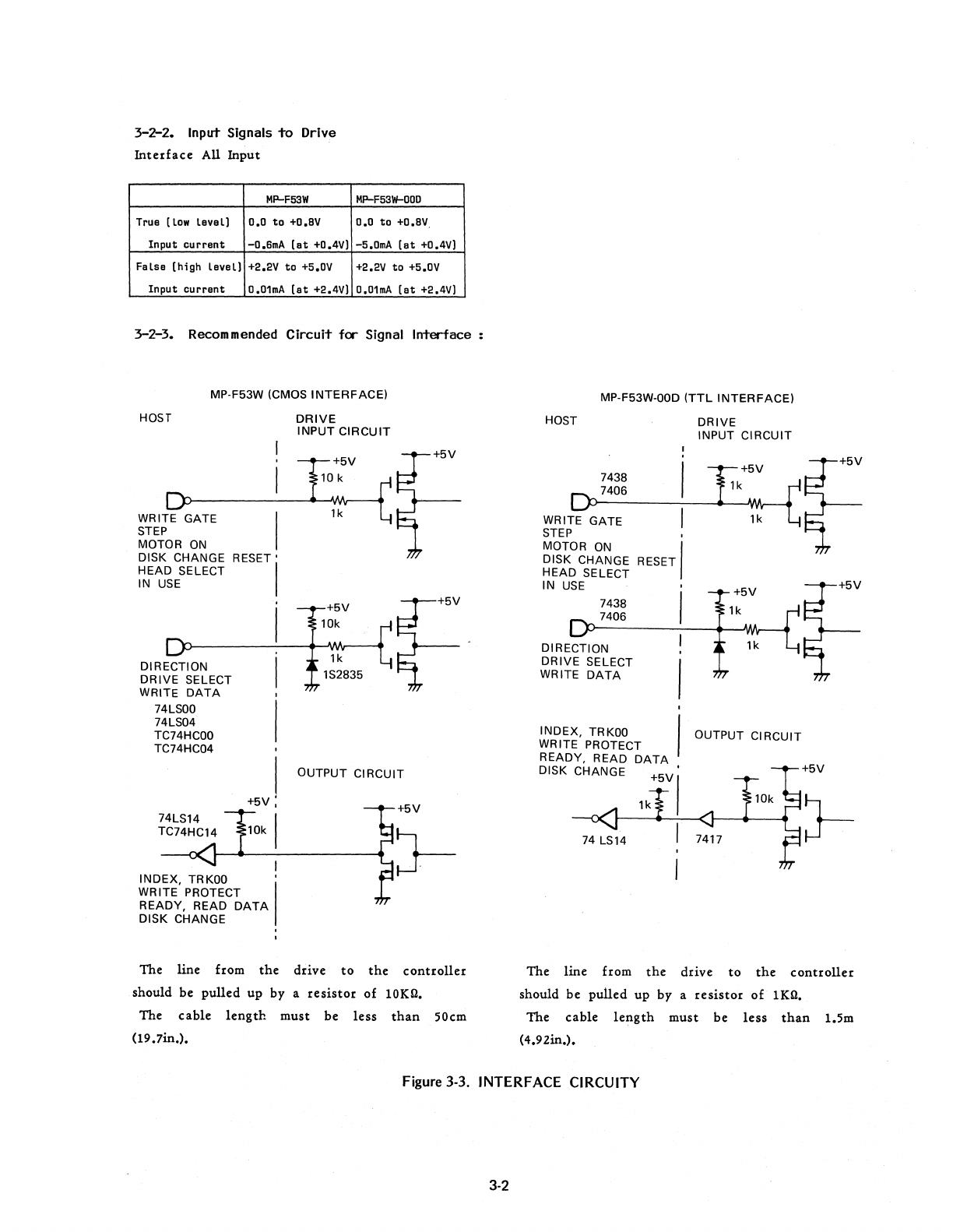
3-2-2.
Input
Signals
to
Drive
Interface
All
Input
MP-F53W
True (low
level)
0.0
to
+O.BV
MP-F53W-000
0.0
to
+O.BV
Input
current
-O.SmA
(et
+0.4V)
-5.0mA
(at
+0.4V)
False
(high
level)
+2.2V
to
+5.0V
+2.2V
to
+5.0V
Input
current
0.01mA
(at
+2.4V)
O.01mA
(at
+2.4V)
3-2-3.
Recommended
Circuit
for
Signal
Interface
HOST
MP-F53W (CMOS
INTERFACE)
DRIVE
WRITE GATE
STEP
MOTOR
ON
DISK CHANGE RESET
HEAD SELECT
IN
USE
DIRECTION
DRIVE SELECT
WRITE
DATA
74LSOO
74LS04
TC74HCOO
TC74HC04
74LS14
+5V
TC74HC14 10k
INDEX,
TRKOO
WRITE PROTECT
READY, READ
DATA
DISK CHANGE
INPUT
CIRCUIT
OUTPUT
CI
RCUIT
+5V
The line from
the
drive
to
the
controller
should be
pulled
up
by a
resistor
of
10KO.
The
cable
length
must
be
less
than
50cm
(19.7in.).
HOST
MP-F53W-00D
(TTL
INTERFACE)
DRIVE
7438
7406
WRITE GATE
STEP
,
MOTOR
ON
DISK CHANGE
HEAD SELECT
IN
USE
RESET I
7438
7406
DIRECTION
DRIVE SELECT
WRITE
DATA
INDEX,
TRKOO
WRITE PROTECT
READY, READ
DATA
DISK CHANGE
INPUT
CIRCUIT
OUTPUT CIRCUIT
+5V
The line from
the
drive
to
the
controller
should be
pulled
up
by a
resistor
of
1KO.
The
cable
length
must
be
less
than
1.5m
(4.92in.).
Figure 3-3. INTERFACE CIRCUITY
3-2
3-3.
SIGNAL DEFINITIONS
3-3-1.
DRIVE SELECT 0,1,2.3
The
SELECT
lines
are
used
to
enable
or
disable
all
other
interface
lines.
When
the
SELECT
line is
true
(low),
the
drive
is
enabled
and
considered
active.
When
the
SELECT
line
is
false
(high),
all
controller
inputs
are
ignored
and
all
drive
lines
are
disabled.
3-3-2.
STEP
A
true
(low) pulse
on
this
line
will
cause
the
Read/Write
head
to
move
to
the
adjacent
track.
The
direction
of
the
head
movement
is
deter-
mined
by
the
status
of
the
DIRECTION
signal
at
the
time
of
stepping.
The
step
operation
can
be
performed
even
if
there
is no
disk
inserted
in
the
drive.
3-3-3.
DIRECTION
A
false
(high)
level
on
this
input
will
cause
a
STEP
pulse
input
to
move
the
Read/Write
head
away
from
the
disk
spindle.
A
true
(low)
level
will
cause
a STEP
pulse
input
to
move
the
Read/Write
head
toward
the
drive
spindle.
3-3-4.
HEAD SELECT
A
true
(low)
level
on
this
input
will
cause
Head
1 (upper)
to
be
selected.
A
false
(high)
level
on
this
input
will
cause
Head
0 (lower)
to
be
selected.
If
the
HEAD
SELECT
signal
changes
during
either
a
write
or
erase
operation,
the
head
will
not
change
until
both
the
ERASE
GATE
and
the
WRITE GATE
signal
become
false
(high).
3-3-5.
WRITE GATE
When
this
line
is
made
true
(low),
the
write
current
circuits
are
enabled
and
information
may
be
written
under
control
of
the
WRITE DATA
input.
3-3
3-3-6.
WRITE
DATA
If
the
WRITE GATE
signal
is
true
(low), a
true
pulse
(low)
on
the
WRITE DATA
line
will
cause
a
bit
to
be
written
on
the
disk.·
However,
bits
cannot
be
written
from
pulses
on
this
line
if
the
WRITE GATE
signal
is
false
(high).
No
pre-compensation
is
required.
3-3-7.
INDEX
When
the
drive
is
selected
and
the
READY
signal
is
true
(low), a
true
(low)
pulse
is
gen-
erated
on
this
line
by
each
revolution
of
the
spindle.
3-3-8.
TRACK
00
This
line
is
true
(low) when
the
Read/Write
head
is
positioned
on
track
00
or
on
an
outer
positon
of
track
00.
At
all
other
times
it
is
false
(high).
The
TRACK
00
signal
derives
its
information
from
a
track
00
sensor,
not
from
the
track
position
counter.
3-3-9.
WRITE PROTECT
If
a
write
protected
disk
is
inserted,
this
line
will be
true
(low)
and
the
drive
will
not
be
able
to
write
data.
At
all
other
times
when
the
disk
is
ipserted,
this
line
will be
false
(high).
3-3-10.
READ
DATA
When
the
drive
is
selected
and
the
READY
signal
is
true
.(low), a
true
(low)
pulse
is
gen-
erated
on
this
line
every
time
a
bit
is
detected.
3-3-11.
DISK CHANGE
This
line
is
true
(low)
whenever
a
disk
is
removed
from
the
selected
drive.
The
line
will
remain
true
(low)
until
both
the
following
conditions
have
been
met:
a.
A
disk
is
inserted,
and
b.
A STEP
pulse
or
DISK CHANGE RESET
signal
has
been
received
when
the
drive
is
selected.
3-3-12.
DISK
CHANGE
RESET
If
the
DISK
CHANGE
RESET
signal
is
true
(low)
and
a
disk
is
inserted,
the
DISK
CHANGE
line
will be
false
(high).
3-3-13.
READY
This
line
is
true
(low)
when
all
of
the
following
conditions
are
met.
a.
The
drive
is
selected,
b.
A
disk
is
inserted,
c.
The
MOTOR ON
signal
is
true
(low),
and
d.
The
INDEX
period
of
the
disk
motor
settles
within
200msec:!:2.5%.
3-4.
TIMING REQUIREMENTS
3-4-1.
Head Access
DRIVE SELECT -
T1--
DIRECTION
~
T4
-
r--
J
STEP
T2 T8
T6
T3
T1
O.5J.lSec
Min.
T2
1.3J.lSec
Min.
T3
6.0msec
Min.
T4
2.4J.lSec
Min.
T5
W
3-3-14.
MOTOR
ON
When
this
line
is
true
(low)
and
a
disk
is
inserted,
the
spindle
motor
will
start
to
run.
If
this
line
is
made
false
(high)
or
a
disk
is
'ejected,
the
spindle
motor
will
stop.
However,
if
the
MOTOR ON
signal
becomes
false
(high)
during
either
a
write
or
erase
operation,
the
disk
motor
will
not
stop
rotating
until
both
the
ERASE
GATE
signal
and
the
WRITE GATE
signal
become
false
(high).
3-3-15.
IN
USE
When
this
line
is
low
and
the
drive
is
selected,
the
LED will
turn
on.
When
this
line
is
high
or
the
drive
is
not
selected,
the
LED is
off.
T7
U
T5
O.5J.lSec
Min.
T6
21.0msec
Min.
T7
O.5J.lSec
Min.
1'8
1.3J.lSec
Min.
Figure 3-4. HEAD
ACCESS
3-4
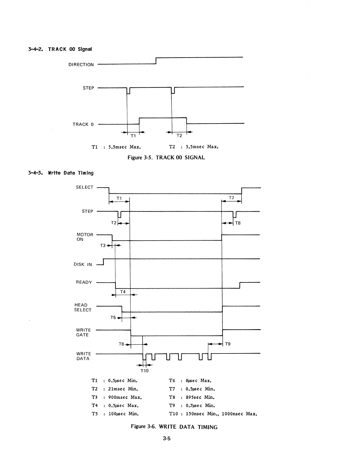
3-4-2.
TRACK 00
Signal
DIRECTION
STEP
TRACK
0
Tl
3-4-3.
Write Data Timing
SELECT
STEP
MOTOR
ON
DISK
IN
READY
HEAD
SELECT
WRITE
GATE
WRITE
DATA
Tl
TZ
T3
T4
T5
U J
I
I
T1
T2
5.5msec
Max.
TZ
5.5msec
Max.
Figure 3-5. TRACK 00 SIGNAL
Tl
T7
T2
T4
T5.r-t--
T6
T9
Tl0
o
.511Se
c Min.
T6
811Sec
Max.
Zimsec
Min.
T7
O.5I1SeC
Min.
900msec
Max.
T8
895sec
Min.
O.5l1Sec
Max.
T9
O.711Se
c Min.
IOOIISec
Min.
TlO
I50nsec
Min.,
IOOOnsec
Max.
Figure 3-6. WRITE DATA TIMING
3-5
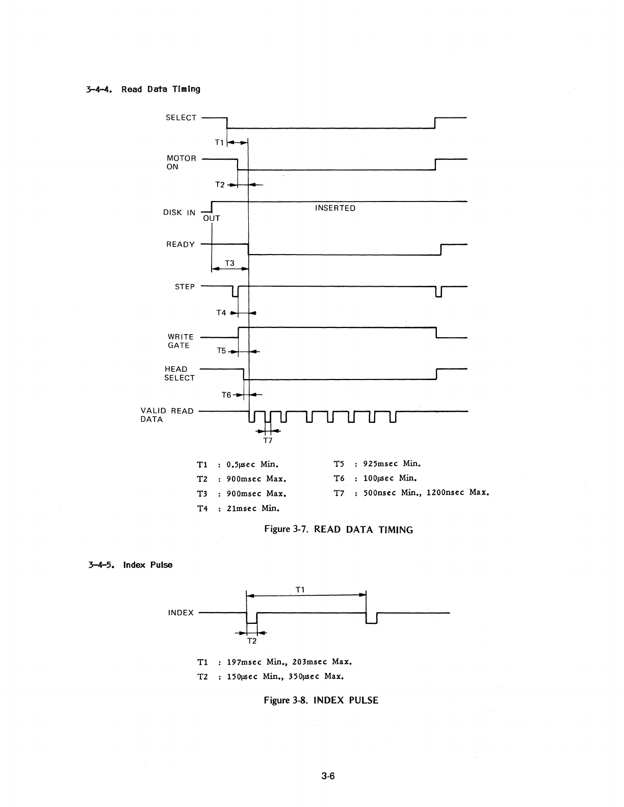
3-4-4.
Read
Data
TImIng
SELECT
MOTOR
ON
DISK IN
READY
STEP
WRITE
GATE
HEAD
SELECT
VALID
READ
DATA
3-4-5.
Index Pulse
T2~-+-
INSERTED
OUT
T3
T4
T5
T6
T7
Tl
O.5psec Min. T5 925msec Min.
T2
900msec Max.
T6
100psec Min.
T3 900msec Max.
T7
500nsec Min.,
1200nsec
Max.
T4
21msec Min.
Figure
3-7.
READ DATA TIMING
T1
I.
"L
INDEX
----
..
-IHr"
..
-----------I
r------
T2
Tl
197msec Min., 203msec Max.
T2
150psec Min., 350psec Max.
Figure
3-8.
INDEX
PULSE
3-6
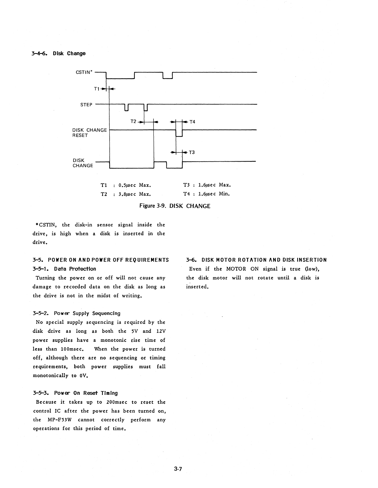
3-4-6.
Disk Change
CSTIN*
T1
STEP
--+--...,
T2
-.1--+4
T4
DISK CHANGE
t------+----i
RESET
T3
DISK
CHANGE
T1
O.5flSec
Max. T3 1.6flSec Max.
T2 3.8flSec Max.
T4
1.6flSe
c Min.
Figure 3-9. DISK CHANGE
*CSTIN,
the
disk-in
sensor
signal
inside
the
drive,
is
high
when
a
disk
is
inserted
in
the
drive.
3-5.
POWER
ON
AND
POWER
OFF REQUIREMENTS
3-5-1.
Data
Protection
Turning
the
power
on
or
off
will
not
cause
any
damage
to
recorded
data
on
the
disk
as long
as
the
drive
is
not
in
the
midst
of
writing.
3-5-2.
Power
Supply Sequencing
No
special
supply
sequencing
is
required
by
the
disk
drive
as
long
as
both
the
5V
and 12V
power
supplies
have
a
monotonic
rise
time
of
less
than
100msec.
When
the
power
is
turned
off,
although
there
are
no
sequencing
or
timing
requirements,
both
power
supplies
must
fall
monotonically
to
OV.
3-5-3.
Power
On
Reset Timing
Because
it
takes
up
to
200msec
to
reset
the
control
IC
after
the
power
has
been
turned
on,
the
MP-F53W
cannot
correctly
perform
any
operations
for
this
period
of
time.
3-7
3-6.
DISK MOTOR ROTATION AND DISK INSERTION
Even
if
the
MOTOR ON
signal
is
true
(low),
the
disk
motor
will
not
rotate
until
a
disk
is
inserted.
SECTION 4
POWER
ON
INITIALIZATION
In
order
to
reduce
the
peak
current
requirement
when
used
in
a
daisy
chain,
the
MP-F53W
has
been
designed
not
to
seek
track
00
automatically.
If
all
the
drives
connected
in
the
daisy
chain
sought
track
00
simultaneously,
this
would
place
a
significant
power
drain
on
the
host
system.
Thus,
the
host
system
must
perform
the
following
routine
just
after
power
on
in
order
to
reset
the
track
counter
inside
the
drive.
Power
On
Initialization
Start
Df
PDwer
Dn
initializatiDn
STEP
i
nwa
rds
un
til
TRACK
00
*
signal
bacDmes
Felse
(high)
•
STEP
outwarda
until
TRACK
00
Signal
becDmes
true.
End
of
rDutine
ND
*
Track
00
signal
becomes
false
(high) by sending
at
minimum 20
SfEP
pulses
(inwards)
to
the
drive.
4-1
SECTION 5
READY SENSING METHOD
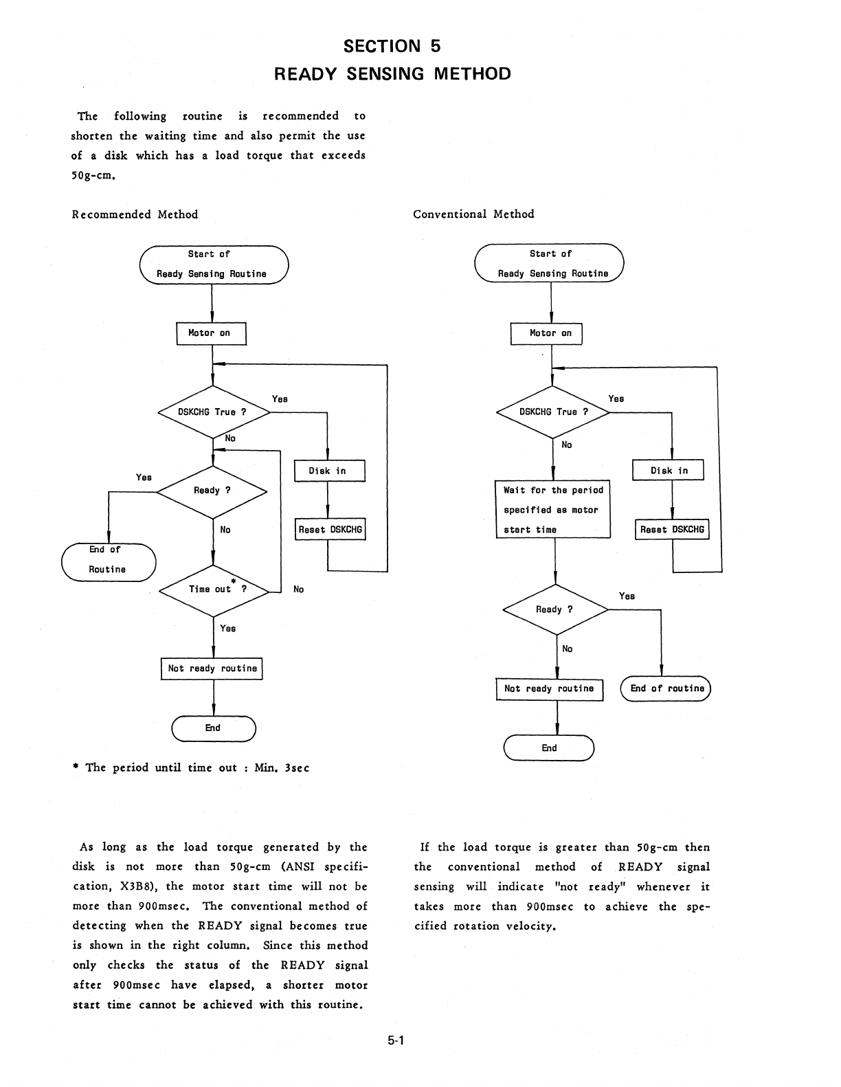
The
following
routine
is
recommended
to
shorten
the
waiting
time
and also
permit
the
use
of
a
disk
which
has
a
load
torque
that
exceeds
50g-cm.
Recommended
Method
Start
of
Ready
Sensing Routine
Yes
Yes
End
of
Routine
No
Yes
•
The
period
until
time
out
Min.
3sec
As
long
as
the
load
torque
generated
by
the
disk
is
not
more
than
50g-cm
(ANSI
specifi-
cation,
X3B8),
the
motor
start
time will
not
be
more
than
900msec.
The
conventional
method
of
detecting
when
the
READY
signal
becomes
true
is
shown
in
the
right
column. Since
this
method
only
checks
the
status
of
the
READY
signal
after
900msec
have
elapsed,
a
shorter
motor
start
time
cannot
be
achieved
with
this
routine.
5-1
Conventional
Method
Start
of
Ready
Sensing Routine
?
No
Weit
for
the
period
specified
es motor
start
time
No
End
Yas
Yes
End
of
routina
If
the
load
torque
is
greater
than
50g-cm
then
the
conventional
method
of
READY
signal
sensing will
indicate
"not
ready"
whenever
it
takes
more
than
900msec
to
achieve
the
spe-
cified
rotation
velocity.
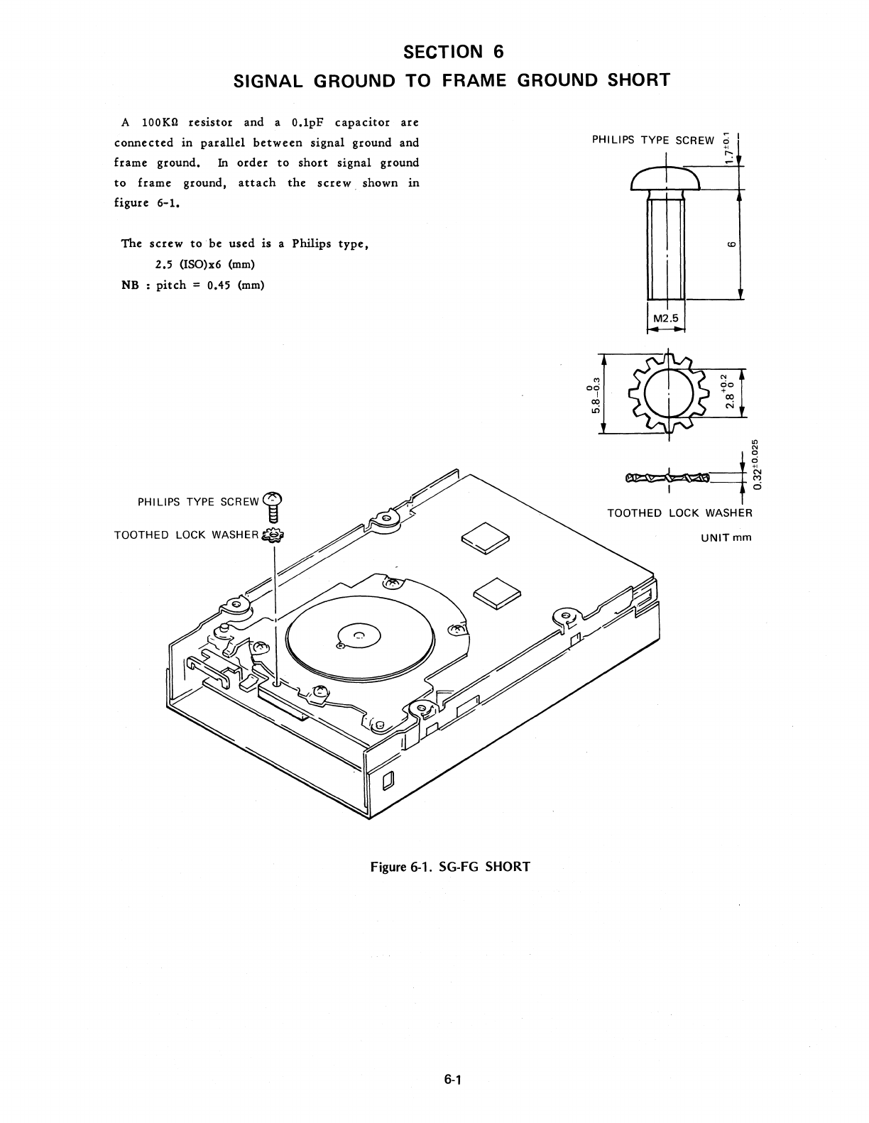
SECTION 6
SIGNAL GROUND TO FRAME GROUND SHORT
A 100KO
resistor
and
a O.lpF
capacitor
are
connected
in
parallel
between
signal
ground
and
frame
ground.
In
order
to
short
signal
ground
to
frame
ground,
attach
the
screw,
shown
in
figure
6-1.
The
screw
to
be
used
is
a Philips
type,
2.5
(ISO)x6
(mm)
NB
:
pitch
= 0.45
(mm)
PHILIPS TYPE
SCREW'i
TOOTHED LOCK
WASHER@
<>
<>
Figure
6-1_
SG-FG SHORT
6-1
PHILIPS TYPE SCREW
~
0
'"
00
I
co
Lri
I
r I
- -
,
M2.5
-
"\
+,
r-:
0-
cc
N
00
+
co
N
'"
~----f-t
I
'to
TOOTHED LOCK WASHER
UNITmm
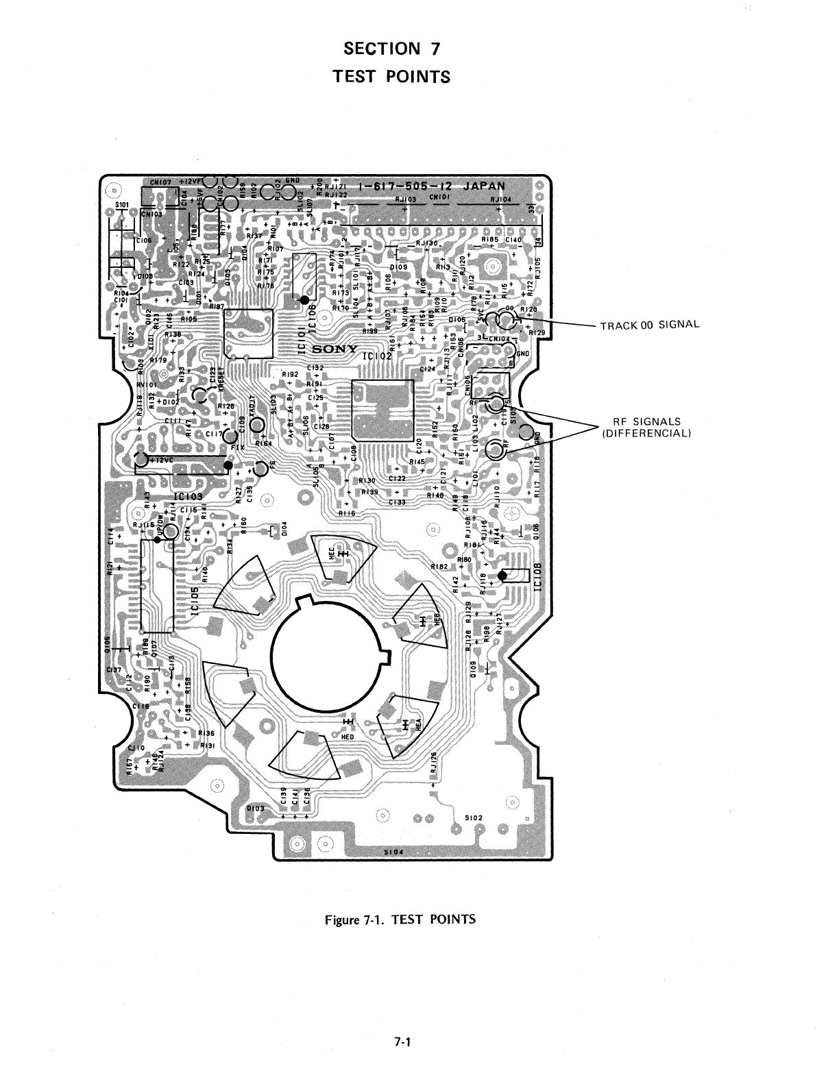
SECTION 7
TEST POINTS
Figure
7-1. TEST POINTS
7-1
~r--
__
TRACK
00
SIGNAL
RF
SIGNALS
(DIFFERENCIAL)

3.5inch
MICRO
FLOPPYDISK
DRIVE
II I
II I
•
~
•
•
-
Sony Corporation 8510510-1
9-975-176-01 Pri n
ted
in
Japan
© 1985
-
