A_83205 A 83205
User Manual: A_83205
Open the PDF directly: View PDF ![]() .
.
Page Count: 182 [warning: Documents this large are best viewed by clicking the View PDF Link!]
- HP 83205A Cellular Adapter
- Contents
- 1 Introduction
- 2 Troubleshooting
- 3 3 Disassembly and Replacement
- Disassembly of the HP 83205A Cellular Adapter
- Separating Units and Removing Cover
- Operation Without Cover
- Removing the A8 Power Supply Assembly
- Disconnecting Subassembly Power Connectors
- Removing the Front Panel
- Removing the Rear Panel
- Removing the A4 Gen/Ref Assembly
- Removing the A9 Reference/IQ Assembly
- Removing the A4 and A9 Assemblies as a Unit
- Removing the A10 Coupler & Switch Assembly and Sem...
- Removing the A11 CDPD Assembly
- Removing the A2 RX DSP and A5 Data Buffer Assembli...
- Removing the A3 Motherboard Assembly
- Disassembly of the HP 83205A Cellular Adapter
- 4 4 Modifications
- 5 5 Block Diagrams
- 6 Replaceable Parts
- Parts Identification
- Major Assemblies
- CDPD Components
- External Cables
- Front Panel Components
- Cover and Rear Panel Components
- Rear Panel Components
- Miscellaneous Components
- A4 Gen./Ref. Assembly and Components
- A9 Reference/IQ Assembly
- A10 Directional Coupler & Serial Switch Assembly
- A11 CDPD Assembly
- Semi-Rigid Cables & Components
- A2 RX DSP Assembly
- A5 Data Buffer Assembly
- A3 Motherboard Assembly
- Parts List
- Parts Identification
- 7 Periodic Calibration and Performance Tests
- 8 8 Specifications
- Glossary
- Index
1
HP 83205A
Cellular Adapter
Assembly Level Repair
for use with
HP 8921A Cell Site Test Set
This manual applies directly to the following instruments:
HP 83205A CDMA Cellular Adapter (Option 001)
HP 83205A CDPD Cellular Adapter (Option 002)
HP 83205A CDMA/CDPD Cellular Adapter (Option 003)
HP Part No. 83205-90009
Printed in U. S. A.
November 1996
Rev A
Option 003
PWR REF
UNLOCK
DIAGNOSTIC
MONITOR OUT 1.2288 MHz OUT
CHIP CLOCK 19.6608 MHz OUT
16 X CHIP CLOCK
RF IN/OUT
TO
TEST SET
RF IN/OUT
MAX.PWR 60W
CONTINUOUS
83205A
CDMA/CDPD CELLULAR ADAPTER
CDMA
TIMEBASE IN
EVEN SECOND /
SYNC IN
DATA
IN
TRIGGER/
QUALIFIER IN
Option 002
PWR REF
UNLOCK
DIAGNOSTIC
MONITOR OUT 1.2288 MH z OUT
CHIP CLOCK 19.6608 MHz OUT
16 X CHIP CLOCK
RF IN/OUT
TO
TEST SET
RF IN/OUT
MAX.PWR 60W
CONTINUOUS
83205A
CDPD CELLULAR ADAPT ER
CDMA
TIMEBASE IN
EVEN SECOND/
SYNC IN
DATA
IN
TRIGGER/
QUA LIFIER IN
Option 001
PWR REF
UNLOCK
DIAGNOSTIC
MONITOR OUT 1.2288 MH z OUT
CHIP CLOCK 19.6608 MH z OUT
16 X CHIP CLOCK
RF IN/OUT
TO
TEST SET
RF IN/OUT
MAX.PW R 60W
CONTINUOUS
83205A
CDMA CELLULAR ADAPTER
CDMA
TIMEBASE IN
EVEN SECOND/
SYNC IN
DATA
IN
TRIGGER/
QUA LIFIER IN

2
Copyright © Hewlett-Packard Company 1996

3
Notice
Information contained in this document is subject to change without notice.
All Rights Reserved. Reproduction, adaptation, or translation without prior written
permission is prohibited, except as allowed under the copyright laws.
This material may be reproduced by or for the U.S. Government pursuant to the
Copyright License under the clause at DFARS 52.227-7013 (APR 1988).
Hewlett-Packard Company
Learning Products Department
24001 E. Mission
Liberty Lake, WA 99019-9599
U.S.A.

4
Manufacturer’s Declaration
This statement is provided to comply with the requirements of the German Sound
Emission Directive, from 18 January 1991.
This product has a sound pressure emission (at the operator position) < 70 dB(A).
•Sound Pressure Lp < 70 dB(A).
• At Operator Position.
• Normal Operation.
• According to ISO 7779:1988/EN 27779:1991 (Type Test).
Herstellerbescheinigung
Diese Information steht im Zusammenhang mit den Anforderungen der
Maschinenlärminformationsverordnung vom 18 Januar 1991.
• Schalldruckpegel Lp < 70 dB(A).
• Am Arbeitsplatz.
• Normaler Betrieb.
• Nach ISO 7779:1988/EN 27779:1991 (Typprüfung).
5
Safety Considerations
GENERAL
This product and related documentation must be reviewed for familiarization with
safety markings and instructions before operation.
This product has been designed and tested in accordance with IEC Publication
1010, "Safety Requirements for Electronic Measuring Apparatus," and has been
supplied in a safe condition. This instruction documentation contains information
and warnings which must be followed by the user to ensure safe operation and to
maintain the product in a safe condition.
SAFETY EARTH GROUND
A uninterruptible safety earth ground must be provided from the main power
source to the product input wiring terminals, power cord, or supplied power cord
set.
CHASSIS GROUND TERMINAL
To prevent a potential shock hazard, always connect the rear-panel chassis ground
terminal to earth ground when operating this instrument from a D.C. power source.
SAFETY SYMBOLS
Indicates instrument damage can occur if indicated operating limits are exceeded.
Refer to instruction in this guide.
Indicates hazardous voltages.
Indicates earth (ground) terminal
WARNING: A WARNING note denotes a hazard. It calls attention to a procedure, practice, or the
like, which, if not correctly performed or adhered to, could result in personal injury.
Do not proceed beyond a WARNING sign until the indicated conditions are fully
understood and met.
CAUTION: A CAUTION note denotes a hazard. It calls attention to an operation procedure, practice,
or the like, which, if not correctly performed or adhered to, could result in damage to or
destruction of part or all of the product. Do not proceed beyond an CAUTION note until
the indicated conditions are fully understood and met.
!

6
Safety Considerations for this Instrument
WARNING This product is a Safety Class I instrument (provided with a protective
earthing ground incorporated in the power cord). The mains plug shall only
be inserted in a socket outlet provided with a protective earth contact. Any
interruption of the protective conductor inside or outside of the product is
likely to make the product dangerous. Intentional interruption is prohibited.
Whenever it is likely that the protection has been impaired, the instrument
must be made inoperative and be secured against any unintended operation.
If this instrument is to be energized via an autotransformer (for voltage
reduction), make sure the common terminal is connected to the earth
terminal of the power source.
If this product is not used as specified, the protection provided by the
equipment could be impaired. This product must be used in a normal
condition (in which all means for protection are intact) only.
No operator serviceable parts are in this product. Refer servicing to
qualified personnel. To prevent electrical shock, do not remove covers.
Servicing instructions are for use by qualified personnel only. To avoid
electrical shock, do not perform any servicing unless you are qualified to do
so.
The opening of covers or removal of parts is likely to expose dangerous
voltages. Disconnect the product from all voltage sources while it is being
opened.
Adjustments described in the manual are performed with power supplied to
the instrument while protective covers are removed. Energy available at
many points may, if contacted, result in personal injury.
The power cord is connected to internal capacitors that my remain live for
5 seconds after disconnecting the plug from its power supply.
For continued protection against fire hazard, replace the line fuse(s) only
with 250 V fuse(s) or the same current rating and type (for example, normal
blow or time delay). Do not use repaired fuses or short circuited fuseholders.

7
CAUTION: Always use the three-prong A.C. power cord supplied with this product. Failure to ensure
adequate earth grounding by not using this cord may cause product damage.
This product is designed for use in Installation Category II and Pollution Degree
2 per IEC 1010 and IEC 664 respectively. For indoor use only.
This product has autoranging line voltage input, be sure the supply voltage is within the
specified range.
Ventilation Requirements: When installing the product in a cabinet, the convection into
and out of the product must not be restricted. The ambient temperature (outside the
cabinet) must be less than the maximum operating temperature of the product by 4° C for
every 100 watts dissipated in the cabinet. If the total power dissipated in the cabinet is
greater than 800 watts, then forced convection must be used.
Product Markings
CE - the CE mark is a registered trademark of the European Community. A CE
mark accompanied by a year indicates the year the design was proven.
CSA - the CSA mark is a registered trademark of the Canadian Standards
Association.

8
CERTIFICATION
Hewlett-Packard Company certifies that this product met its published
specifications at the time of shipment from the factory. Hewlett-Packard further
certifies that its calibration measurements are traceable to the United States
National Institute of Standards and Technology, to the extent allowed by the
Institute’s calibration facility, and to the calibration facilities of other
International Standards Organization members.
WARRANTY
This Hewlett-Packard instrument product is warranted against defects in material
and workmanship for a period of one year from date of shipment. During the
warranty period, Hewlett-Packard Company will at its option, either repair or
replace products which prove to be defective.
For warranty service or repair, this product must be returned to a service facility
designated by HP. Buyer shall prepay shipping charges to HP and HP shall pay
shipping charges, duties, and taxes for products returned to HP from another
country.
HP warrants that its software and firmware designated by HP for use with an
instrument will execute its programming instructions when properly installed on
that instrument. HP does not warrant that the operation of the instrument, or
software, or firmware will be uninterrupted or error free.
LIMITATION OF WARRANTY
The foregoing warranty shall not apply to defects resulting from improper or
inadequate maintenance by Buyer, Buyer-supplied software or interfacing,
unauthorized modification or misuse, operation outside of the environmental
specifications for the product, or improper site preparation or maintenance.
NO OTHER WARRANTY IS EXPRESSED OR IMPLIED. HP SPECIFICALLY
DISCLAIMS THE IMPLIED WARRANTIES OF MERCHANTABILITY AND
FITNESS FOR A PARTICULAR PURPOSE.
EXCLUSIVE REMEDIES
THE REMEDIES PROVIDED HEREIN ARE BUYER’S SOLE AND
EXCLUSIVE REMEDIES. HP SHALL NOT BE LIABLE FOR ANY DIRECT,
INDIRECT, SPECIAL, INCIDENTAL, OR CONSEQUENTIAL DAMAGES,
WHETHER BASED ON CONTRACT, TORT, OR ANY OTHER LEGAL
THEORY.
ASSISTANCE
Product maintenance agreements and other customer assistance agreements are
available for Hewlett-Packard products. For any assistance, contact your nearest
Hewlett-Packard Sales and Service Office.

9
European Contact: Your local Hewlett-Packard Sales and Service Office or Hewlett-Packard GmbH,
Department ZQ/Standards Europe, Herrenberger Strasse 130, D-71034 B
ö
blinger, Germany (FAX+49-7031-14-3143)
DECLARATION OF CONFORMITY
according to ISO/IEC Guide 22 and EN 45014
Manufacturer’s Name:
Manufacturer’s Address:
declares that the product
Product Name:
Model Number:
Product Options:
Hewlett-Packard Co.
Spokane Division
24001 E. Mission Avenue
Liberty Lake, Washington 99019-9599
USA
CDMA, CDPD, CDMA/CDPD Cellular Adapter
HP 83205A
This declaration covers all options of the above
product.
conforms to the following Product specifications:
Safety: IEC 1010-1:1990+A1 / EN 61010-1:1993
EMC: CISPR 11:1990 / EN 55011:1991 Group 1, Class A
EN 50082-1 : 1992
IEC 801-2:1991- 4 kV CD, 8 kV AD
IEC 801-3:1984 - 3V/m
IEC 801-4:1988 - 0.5 kV Sig. Lines, 1 kV Power Lines
Supplementary Information:
This product herewith complies with the requirements of the Low Voltage Directive
73/23/EEC and the EMC Directive 89/336/EEC and carries the CE-marking accordingly.
Spokane, Washington USA, November 5, 1996
Vince Roland,
Reliability & Regulatory
Engineering Manager

10
HP Support Contacts
The documentation supplied with your Test Set and/or Cellular Adapter is an
excellent source of reference, applications, and service information. Please use
these manuals if you are experiencing technical problems:
•HP 8920, 8921A Cell Site Test Set’s Assembly Level Repair (ALR) manual, HP part
number 08920-90168
•HP 83205A CDMA Cellular Adapter User’s Guide, HP part number 83205-90008
•CDPD Software User’s Guide, HP part number 83204-90014 (for CDPD software kit,
HP part number 83204-61807)
If you have used the manuals and still have application questions, contact your
local HP Sales Representative.
Repair assistance is available for the HP 8921A Cell Site Test Set and HP 83205A
Cellular Adapter from the factory by phone and e-mail. Internal Hewlett-Packard users
can contact the factory through HP Desk or cc:Mail© (Lotus Corporation). Parts
information is also available from Hewlett-Packard.
When calling or writing for repair assistance, please have the following information ready:
• Instrument model number (HP 83205A)
• Instrument Serial Number (tag located on the rear panel).
• Installed options - if any (tag located on the rear panel).
• Instrument firmware revision (displayed at the top of the screen when the Test Set is
powered up, and is also displayed on the CONFIGURE screen).
Support Telephone Numbers:
1 800 827 3848 (Spokane Division Service Assistance, U.S. only)
1 509 921 3848 (Spokane Division Service Assistance, International)
1 800 227 8164 (HP Direct Parts Ordering, U.S. only)
1 916 783 0804 (HP Service Parts Identification, U.S. & Intl.)
Electronic mail (Internet): Spokane_Service@spk.hp.com
HP Desk: Spokane Service / HP1000/21
cc:Mail: SERVICE, SPOKANE /HP-Spokane,desk1

11
Table 1 Regional Sales and Service Offices
Eastern USA
Sales Office
Hewlett-Packard Company
2101 Gather Rd.
Rockville, MD 20850
Tel: (301) 258-2000
Eastern USA
Service Center
Hewlett-Packard Company
150 Green Pond Road
Rockaway, NJ 07866
Tel: (201) 586-5400
Midwestern USA
Sales and Service
Hewlett-Packard Company
5201 Tollview Drive
Rolling Meadows, IL 60008
Tel: (708) 342-2000
Southern USA
Sales and Service
Hewlett-Packard Company
1995 North Park Place
Atlanta, GA 30339
Sales
Tel: (404) 955-1500
Fax: (404) 980-7292
Service
Tel: (404) 850-2544
Fax: (404) 980-7292
Southern USA
Service Center
Hewlett-Packard Company
930 E. Campbell Road
Richardson, TX 75081
Tel: (214) 699-4331
Western USA
Service Center
Hewlett-Packard Company
301 E. Evelyn Avenue
Mountain View, CA 94041
Tel: (415) 694-2000
Fax: (415) 694-0601
Western USA
Sales and Service
Hewlett-Packard Company
24 Inverness Place East
Englewood, CO 80112
Sales
Tel: (303) 649-5000
Fax: (303) 649-5787
Service
Tel: (303) 649-5512
Fax: (303) 649-5787
Western USA
Sales and Service
Hewlett-Packard Company
1421 South Manhattan Avenue
Fullerton, CA 92631
Sales
Tel: (714) 999-6700
Fax: (714) 778-3033
Service
Tel: (714) 758-5490
Fax: (714) 778-3033
United States of America
Customer Information Center
Hewlett-Packard Company
Tel: (800) 752-0900
6:00 am to 5:00 pm Pacific Time
Parts Direct: 1-800-227-8164
South Eastern Europe
Sales and Service
Hewlett-Packard Ges. m.b.h.
Liebigasse 1
P.O. Box 72
A-1222 Vienna, Austria
Telephone: 43 222 2500 0
Telex: 13 4425
European Multicountry Region
Sales and Service
Hewlett-Packard S.A.
P.O. Box 95
150, Route dv Nant_dl_AVRIL
CH-1217 Meyrin 2
Geneva, Switzerland
Telephone: (41/22) 780-8111
Fax: (41/22) 780-8542
Northern Europe
Sales and Service
Hewlett-Packard Nederland B.V.
Startbaan 16
1187 XR
Amstelveen, The Netherlands
P.O. Box 667
Telephone: 31/20 5476911 X 6631
Fax: 31-20-6471825NL

12
Asia
Sales and Service
Hewlett-Packard Asia Ltd.
22-30/F Peregrine Tower
Lippo Center
89 Queensway, Central
Hong Kong
G.P.O. Box 863 Hong Kong
Telephone: 852-848-7777
Fax: 852-868-4997
Japan
Sales and Service
Yokogawa-Hewlett-Packard
Ltd.
3-29-21, Takaido-Higashi
Suginami-Ku, Tokyo 168
Telephone: 81 3 3331-6111
Fax: 81 3 3331-6631
International Sales Branch Headquarters
Sales and Service
Hewlett-Packard S.A.
39 Rue Veyrot
P.O. Box 365
1217 Meyrin 1
Geneva, Switzerland
Telephone: 41-22-780-4111
Fax: 41-22-780-4770
Australia, New Zealand
Sales and Service
Hewlett-Packard Ltd.
P.O. Box 221
31-41 Joseph Street
Blackburn, Victoria 3130
Telephone: (61/3) 895-2895
Fax: (61/3) 898-9257
Canada
Sales and Service
Hewlett-Packard (Canada) Ltd.
5150 Spectrum Way
Mississauga, Ontario L4W 5G1
Canada
Telephone: (416) 206-4725
Fax: (416) 206-4739
Canada
Service Center
Hewlett-Packard Company
17500 Transcanada Highway
S. Serv Road
Kirkland, Quebec H9J 2X8
Canada
Telephone: (416) 206-3295
Canada
Service Center
Hewlett-Packard Ltd.
11120 178 Street
Edmonton, Alberta T5S 1P2
Canada
Telephone: (403) 486-6666
Fax: (403) 489-8764
Latin America
Hewlett-Packard Company
LAHQ Mexico City
Col. Lomas de Virreyes
11000 Mexico D.F.
Mexico
Telephone: (52/5) 326-4000
Fax: (52/5) 202 7718
United Kingdom
Sales and Service
Hewlett-Packard Ltd.
Cain Road
Amen Corner
Bracknell, Berkshire
RG12 1HN
United Kingdom
Telephone: 44 344 360000
Fax: 44 344 363344
Table 1 Regional Sales and Service Offices (Continued)
13
Power Cables
Plug Type Plug Descriptions
male/female HP Part #
(cable &plug) Cable Descriptions
Straight/Straight 8120-0698 90 inches, black
Used in the following locations
Peru
14
Plug Type Plug Descriptions
male/female HP Part #
(cable &plug) Cable Descriptions
Straight/Straight
Straight/90º 8120-1689
8120-1692 79 inches, mint gray
79 inches, mint gray
Used in the following locations
Afghanistan, Albania, Algeria, Angola, Armenia, Austria, Azerbaijan, Azores
Bangladesh, Belgium, Benin, Bolivia, Boznia-Herzegovina, Bulgaria, Burkina Faso, Burma, Burundi,
Byelarus
Cameroon, Canary Islands, Central African Republic, Chad, Chile, Comoros, Congo, Croatia, Czech Republic,
Czechoslovakia
Denmark, Djibouti
East Germany, Egypt, Estonia, Ethiopia
Finland, France, French Guiana, French Indian Ocean Areas
Gabon, Gaza Strip, Georgia, Germany, Gozo, Greece
Hungary
Iceland, Indonesia, Iran, Iraq, Israel, Italy, Ivory Coast
Jordan
Kazakhstan, Korea, Kyrgystan
Latvia, Lebanon, Libya, Lithuania, Luxembourg
Macedonia, Madeira Islands, Malagasy Republic, Mali, Malta, Mauritania, Miquelon, Moldova, Mongolia,
Morocco, Mozambique
Nepal, Netherlands, Netherlands Antilles, Niger, Norway
Oman
Pakistan, Paraguay, Poland, Portugal
Rep. South Africa, Romania, Russia, Rwanda
Saudi Arabia (220V), Senegal, Slovak Republic, Slovenia, Somalia, Spain, Spanish Africa, Sri Lanka, St.
Pierre Islands
Sweden, Syria
Tajikistan, Thailand, Togo, Tunisia, Turkey, Turkmenistan
USSR, Ukraine, Uzbekistan
Western Africa, Western Sahara
Yugoslavia
Zaire
15
Plug Type Plug Descriptions
male/female HP Part #
(cable &plug) Cable Descriptions
Straight/Straight
Straight/90°8120-2104
8120-2296 79 inches, gray
79 inches, gray
Used in the following locations
Switzerland
16
Plug Type Plug Descriptions
male/female HP Part #
(cable &plug) Cable Descriptions
Straight/Straight
Straight/90º
Straight/Straight
8120-1378
8120-6177
8120-1751
90 inches, jade gray
90 inches, jade gray
90 inches, jade gray
Used in the following locations
American Samoa
Bahamas, Barbados, Belize, Bermuda, Brazil,
Caicos, Cambodia, Canada, Cayman Islands, Columbia, Costa Rica, Cuba
Dominican Republic
Ecuador, El Salvador
French West Indies
Guam, Guatemala, Guyana
Haiti, Honduras
Jamaica
Korea
Laos, Leeward and Windward Is., Liberia
Mexico, Midway Islands
Nicaragua
Other Pacific Islands
Panama, Philippines, Puerto Rico
Saudi Arabia (115V,127V), Surname
Taiwan, Tobago, Trinidad, Trust Territories of Pacific Islands
Turks Island
United States
Venezuela, Vietnam, Virgin Islands of the US
Wake Island
17
Plug Type Plug Descriptions
male/female HP Part #
(cable &plug) Cable Descriptions
Straight/Straight
Straight/90º 8120-4753
8120-4754 90 inches, dark gray
90 inches, dark gray
Used in the following locations
Japan
Plug Type Plug Descriptions
male/female HP Part #
(cable &plug) Cable Descriptions
90º/Straight
90º/90º
Straight/Straight
8120-2956
8120-2957
8120-3997
79 inches, gray
79 inches, gray
79 inches, gray
Used in the following locations
Denmark
Greenland
Plug Type Plug Descriptions
male/female HP Part #
(cable &plug) Cable Descriptions
Straight/Straight
Straight/90°8120-4211
8120-4600 79 inches, mint gray
79 inches, mint gray
Used in the following locations
Botswana
India
Lesotho
Malawi
South-West Africa (Namibia), Swaziland
Zambia, Zimbabwe
18
Plug Type Plug Descriptions
male/female HP Part #
(cable &plug) Cable Descriptions
Straight/Straight
Straight/Straight
Straight/90º
Straight/90º
8120-1860
8120-1575
8120-2191
8120-4379
60 inches, jade gray
30 inches, jade gray
60 inches, jade gray
15.5 inches, jade gray
Used in the following locations
System Cabinets
Plug Type (Male) Plug Descriptions
male/female HP Part #
(cable& plug) Cable Descriptions
90°/Straight 90°/
90°8120-1351
8120-1703 90 inches, mint gray
90 inches, mint gray
Used in the following locations
Bahrain, British Indian Ocean Territories, Brunei
Canton, Cyprus
Enderbury Island, Equatorial Guinea
Falkland Islands, French Pacific Islands
Gambia, Ghana, Gibraltar, Guinea
Hong Kong
Ireland
Kenya, Kuwait
Macao, Malaysia, Mauritius
Nigeria
Qatar
Seychelles, Sierra Leone, Singapore, Southern Asia, Southern Pacific Islands, St. Helena, Sudan
Tanzania
Uganda, United Arab Emirates, United Kingdom
Yeman (Aden & Sana)
19
Plug Type Plug Descriptions
male/female HP Part #
(cable &plug) Cable Descriptions
Straight/Straight
Straight/90°8120-1369
8120-0696 79 inches, gray
80 inches, gray
Used in the following locations
Argentina, Australia
China (People’s Republic)
New Zealand
Papua New Guinea
Uruguay
Western Samoa

20
ATTENTION
Static Sensitive Devices
This instrument was constructed in an ESD (electro-static discharge) protected environment. This is
because most of the semiconductor devices used in this instrument are susceptible to damage by static
discharge.
Depending on the magnitude of the charge, device substrates can be punctured or destroyed by
contact or mere proximity of a static charge. The result can cause degradation of device
performance, early failure, or immediate destruction.
These charges are generated in numerous ways such as simple contact, separation of materials, and
normal motions of persons working with static sensitive devices.
When handling or servicing equipment containing static sensitive devices, adequate precautions must
be taken to prevent device damage or destruction.
Only those who are thoroughly familiar with industry accepted techniques for handling static
sensitive devices should attempt to service circuitry with these devices.
In all instances, measures must be taken to prevent static charge build-up on work surfaces and
persons handling the devices.

21
In This Book
This manual contains the following information to help you repair, calibrate, and
verify correct operation of the HP 83205A Cellular Adapter.
Chapter 1, Introduction, on page 29. This chapter provides a general description
of the Cellular Adapter and general information concerning troubleshooting,
repair, and calibration of the Cellular Adapter. HP service and support information
is also provided.
Chapter 2, Troubleshooting, on page 37. This chapter contains the procedures
for isolating a failure to the faulty assembly. The Cellular Adapter’s automated
diagnostics are described and descriptions are provided to help you understand
what has been checked by the diagnostics in case the diagnostics cannot identify a
probable failure. Further investigation may require manually troubleshooting the
Cellular Adapter.
Chapter 3, Disassembly and Replacement, on page 61. This chapter provides
procedures and illustrations for disassembling the Cellular Adapter.
Chapter 4, Modifications, on page 85. This chapter explains how to verify
and/or upgrade the firmware in the Cellular Adapter.
Chapter 5, Block Diagrams, on page 89. Diagrams are provided illustrating the
general operation of the Cellular Adapter. This information is used to better
understand the operation of the Cellular Adapter when manually troubleshooting
the Test System (the attached Test Set and Cellular Adapter) in case the automated
diagnostics cannot identify a faulty assembly with high confidence.
Chapter 6, Replaceable Parts, on page 105. Contains illustrations for identifying
the various assemblies and components of the Cellular Adapter. Part numbers for
each replaceable part are also provided.
Chapter 7, Periodic Calibration and Performance Tests, on page 125. Contains
Cellular Adapter periodic calibration procedures and performance tests.
Chapter 8, Specifications, on page 139. Lists the warranted specifications of the
Cellular Adapter.
Glossary, on page 149. Provides a list of common acronyms, terms, and
definitions used in cellular communications.

22
Conventions Used in this Manual
The HP 83205A CDMA Cellular Adapter (Option 001), the HP 83205A CDPD
Cellular Adapter (Option 002), or the HP 83205A CDMA/CDPD Cellular Adapter
(Option 003) is referred to as the Cellular Adapter.
The HP 8921A Cell Site Test Set is referred to as the Test Set.
The Cellular Adapter combined with the Test Set is referred to as the Test System.
Other Manuals Required
In troubleshooting the Cellular Adapter it may be necessary to use the:
•HP 8921A Cell Site Test Set’s ALR manual, HP part number 08920-90168
•HP 83205A CDMA Cellular Adapter User’s Guide, HP part number 83205-90008
•CDPD Software User’s Guide, HP part number 83204-90014 (for CDPD software
kit, HP part number 83204-61807)

Contents
23
1 Introduction
Instrument Description 30
Firmware Compatibility 31
CDMA Cellular Adapters 32
CDPD Cellular Adapters 32
Troubleshooting 33
Repair Process 33
Periodic Calibration and Performance Tests 34
Service Tools and Equipment 34
Equipment 34
Tools 34
User’s Guides 35
Service Information 35
Test Set Documentation 35
Factory Support 35
Ordering Parts 35
2 Troubleshooting
Test System Troubleshooting 38
Test System Troubleshooting Flow Chart 39
Troubleshooting the PWR LED 42
Procedure 42
Troubleshooting the REF UNLOCK LED 43
Procedure 43
Power-Up Diagnostics 44
Test System Power-Up Diagnostics 44

Contents
24
Cellular Adapter Power-Up Diagnostics 45
Verifying Test Set Operation 49
Procedure 49
Verifying that the Test Set Recognizes the Cellular Adapter 51
Prerequisites 51
Procedure 51
CDMA Diagnostics 52
Prerequisites 52
CDMA_DIAG Procedure 52
CDMA_DIAG Tests Descriptions 54
CDPD Diagnostics 55
CDPD_DIAG Procedure 56
CDPD_DIAG Tests Descriptions 58
3 Disassembly and Replacement
Disassembly of the HP 83205A Cellular Adapter 62
Separating Units and Removing Cover 63
Operation Without Cover 65
Removing the A8 Power Supply Assembly 66
Disconnecting Subassembly Power Connectors 67
Removing the Front Panel 68
Removing the Rear Panel 70
Removing the A4 Gen/Ref Assembly 72
Removing the A9 Reference/IQ Assembly 74
Removing the A4 and A9 Assemblies as a Unit 76
Removing the A10 Coupler & Switch Assembly and Semi-Rigid Cables 78
Removing the A11 CDPD Assembly 80
Removing the A2 RX DSP and A5 Data Buffer Assemblies 81
Removing the A3 Motherboard Assembly 83

Contents
25
4 Modifications
Firmware Upgrades 86
Firmware Loading and Verification 87
Load the DSP Firmware 87
Load the CDPD Firmware 87
Verifying Firmware Version 88
5 Block Diagrams
Instrument Description 90
CDMA Cellular Adapter 91
CDPD Cellular Adapter 93
Assembly Descriptions 94
A2 RX DSP Assembly 96
A3 Motherboard 96
A4 Gen/Ref Assembly 96
A5 Data Buffer Modulator 98
A8 Power Supply 98
A9 Reference/ IQ 98
A10 Directional Coupler & Serial Switch 100
A11 CDPD Assembly 100
Power Supply and Voltage Distribution 102
6 Replaceable Parts
Parts Identification 106
Major Assemblies 106
CDPD Components 107
External Cables 108

Contents
26
Front Panel Components 109
Cover and Rear Panel Components 110
Rear Panel Components 111
Miscellaneous Components 112
A4 Gen./Ref. Assembly and Components 113
A9 Reference/IQ Assembly 114
A10 Directional Coupler & Serial Switch Assembly 115
A11 CDPD Assembly 116
Semi-Rigid Cables & Components 117
A2 RX DSP Assembly 118
A5 Data Buffer Assembly 118
A3 Motherboard Assembly 119
Parts List 120
7 Periodic Calibration and Performance Tests
Introduction 126
Periodic Calibration (for Options 001 & 003 only) 127
PER_CALD Calibration Procedure 127
EBNO_CAL Calibration Procedure 128
CDMA Performance Test (for Options 001 & 003 only) 129
Prerequisites 129
Equipment Setup 129
CDMA Performance Procedure 129
CDPD Performance Test (for Options 002 & 003 only) 131
Prerequisites 131
Equipment Set Up 131
Procedure 131
CDMA Performance Record 137
Rho Measurement 137
CDPD Performance Record 138

Contents
27
CDPD Generator Spectral Purity Measurement 138
CDPD Modulation Accuracy Measurement 138
CDPD Generator On/Off Level Measurement 138
8 Specifications
HP 83205A CDMA Specifications 140
CDMA Signal Generator 140
CDMA Analyzer 142
Code Domain Analyzer 144
RF Time Base 145
CDMA Reference 146
HP 83205A CDPD Specifications 147
CDPD Signal Generator 147
CDPD Analyzer 148
Physical Specifications 148
Glossary 149
Index 181

Contents
28

29
1
Introduction
This chapter contains a general description of the HP 83205A Cellular Adapter,
and general information about troubleshooting, calibrating, and servicing the
Cellular Adapter. Lists of equipment (including documentation) required to
service the Cellular Adapter are also provided.
30
Chapter 1, Introduction
Instrument Description
Instrument Description
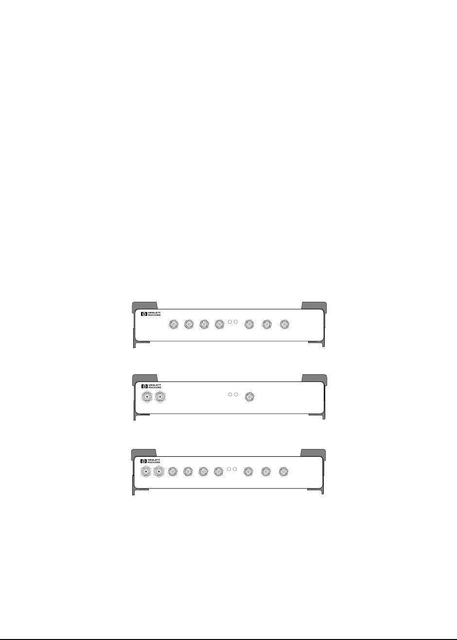
The HP 83205A Cellular Adapter (see figure 1) is an accessory to the
HP 8921A Cell Site Test Set. The Cellular Adapter and Test Set are connected
together via front-panel and rear-panel cables and work together to form a Test
System. The Cellular Adapter adds digital signal generation and analysis to the
Test Set’s analog test capabilities.
Figure 1 HP 83205A CDMA/CDPD Cellular Adapter and HP 8921ACell Site Test Set
The HP 83205A Cellular Adapter can be configured as one of three different
options (see figure 2 on page 31):
• HP 83205A CDMA Cellular Adapter, Option 001
• HP 83205A CDPD Cellular Adapter, Option 002
• HP 83205A CDMA/CDPD Cellular Adapter, Option 003
Each Cellular Adapter has the following major assemblies:
• A2 Receiver Digital Signal Processing (RX DSP)
• A3 Motherboard
• A4 Generator/Reference
• A5 Data Buffer (in Cellular Adapter Options 001 & 003 only)
• A8 Power Supply
• A9 Reference/IQ (This assembly includes the A6 LO/IF and A7 IQ Modulator
assemblies. These assemblies cannot be separately replaced.)
• A10 Directional Coupler & Serial Switch (in Cellular Adapter Options 002 & 003 only)
• A11 CDPD processor (in Cellular Adapter Options 002 & 003 only)
PWR REF
UNLOCK
DIAGNOSTIC
MONITOR OUT 1.2288 MHz OUT
CHIP CLOCK 19.6608 MHz OUT
16 X CHIP CLOCK
RF IN/OUT
TO
TEST SET
RF IN/OUT
MAX.PWR 60W
CONTINUOUS
83205A
CDMA/CDPD CELLULAR ADAPTER
CDMA
TIMEBASE IN
EVEN SECOND/
SYNC IN
DATA
IN
TRIGGER/
QUALIFIER IN
HP 83205A
CDMA/CDPD
HP 8921A Cell Site
Test Set
(Option 003)
Cellular Adapter
31
Chapter 1, Introduction
Instrument Description
Figure 2 HP 83205A Cellular Adapter Options
Firmware
Compatibility In order for the Cellular Adapter to operate properly, it is necessary that its companion
Test Set have the proper firmware installed. See "Verifying Firmware Version" on page
88 for the firmware requirements of the Test Set.
HP 83205A CDMA
Cellular Adapter, Option 001
HP 83205A CDPD
Cellular Adapter, Option 002
HP 83205A CDMA/CDPD
Cellular Adapter, Option 003
Front Back
114.3 MH z IF IN I BASEBAND OUT
AUX
CW
RF IN IQ
RF OUT OPTIONAL
SERIAL PORT
CONTROL I/O
SYNTH REF IN 10 MHz OUT
CDMA CLOCK OUTPUTS DSP IN
MOD OUT
10 MHz
REF OUT
Q BASEBAND OUT
PWR REF
UNLOCK
DIAGNOSTIC
MONITOR OUT 1.2288 MHz OUT
CHIP CLOCK 19.6608 MHz OUT
16 X CHIP CLOCK
RF IN/OUT
TO
TEST SET
RF IN/OUT
MAX.PWR 60W
CONTINUOUS
83205A
CDMA/CDPD CELLULAR ADAPTER
CDMA
TIMEBASE IN
EVEN SECOND/
SYNC IN
DATA
IN
TRIGGER/
QUALIFIER IN
Front Back
114.3 MHz IF IN I BASEBAND OUT
AUX
CW
RF IN IQ
RF OUT OPTIONAL
SERIAL PORT
CONTROL I/O
SYNTH REF IN 10 MHz OUT
CDMA CLOCK OUTPUTS DSP IN
MOD OUT
10 MHz
REF OUT
Q BASEBAND OUT
PWR REF
UNLOCK
DIAGNOSTIC
MONITOR OUT 1.2288 MH z OUT
CHIP CLOCK 19.6608 MH z OUT
16 X CHIP CLOCK
RF IN/OUT
TO
TEST SET
RF IN /OUT
MAX.PW R 60W
CONTINUOUS
83205A
CDPD CELLULAR ADAPTER
CDMA
TIMEBASE IN
EVEN SECOND/
SYNC IN
DATA
IN
TRIGGER/
QUA LIF IER IN
Front Back
114.3 MHz IF IN I BASEBAND OUT
AUX
CW
RF IN IQ
RF OUT OPTIONAL
SERIAL PORT
CONTROL I/O
SYNTH REF IN 10 MHz OUT
CDMA CLOCK OUTPUTS DSP IN
MOD OUT
10 MHz
REF OUT
Q BASEBAND OUT
PWR REF
UNLOCK
DIAGNOSTIC
MONITOR OUT 1.2288 MHz OUT
CHIP CLOCK 19.6608 MH z OUT
16 X CHIP CLOCK
RF IN/OUT
TO
TEST SET
RF IN/OUT
MAX.PWR 60W
CONTINUOUS
83205A
CDMA CELLULAR ADAPTER
CDMA
TIMEBASE IN
EVEN SECOND/
SYNC IN
DATA
IN
TRIGGER/
QUALIFIER IN

32
Chapter 1, Introduction
Instrument Description
CDMA Cellular
Adapters The HP 83205A CDMA Cellular Adapter (Option 001) and the HP 83205A
CDMA/CDPD Cellular Adapter (Option 003) include DSP (Digital Signal
Processing) hardware and firmware to test the transmitter and receiver portions of
Code Division Multiple Access (CDMA) base stations. Systems using the CDMA
format use encoders and decoders to digitize speech and add call processing
information.
CDMA digital cellular systems use frequency channelization (comparable to
current analog systems but with a much wider bandwidth) and correlative codes
to distinguish each user. This scheme allows communication in the presence of
interference (such as other users) resulting in a substantial increase in system
capacity.
CDPD Cellular
Adapters The HP 83205A CDPD Cellular Adapter (Option 002) and the HP 83205A
CDMA/CDPD Cellular Adapter (Option 003) include Cellular Digital Packet
Data (CDPD) digital signal generation and analysis. The CDPD assembly (A11)
found in Cellular Adapter Options 002 and 003 provides the hardware and
firmware to perform CDPD protocol processing.
CDPD is a packet data system which overlies the existing Advanced Mobile
Phone System (AMPS) voice system. CDPD is designed for small bursts of data
and is not efficient for large file transfer applications. CDPD uses a separate base
station (Mobile Data Base Station, MDBS) and is integrated into the antenna
system of a cell site. When there is no voice traffic on a designated AMPS voice
channel, the MDBS may transmit packet data to mobile end stations or fixed end
stations. When AMPS voice traffic is assigned to that channel, the MDBS must
power down and reacquire communications on another designated CDPD channel
if one is available.

33
Chapter 1, Introduction
Troubleshooting
Troubleshooting
The Cellular Adapter is normally sent in for service connected to its companion
Test Set. The Test Set’s internal ROM contains programs for verifying the
Cellular Adapter’s performance and for calibrating the Cellular Adapter and Test
Set interface.
Diagnostic programs for servicing the Cellular Adapter reside in the Test Set’s
firmware (ROM). Two types of built-in diagnostics are available to aid in
troubleshooting: power-up diagnostics which check the Test Set and Cellular
Adapter’s internal control circuitry, and CDMA and CDPD functional diagnostics
which check analog and digital signal generation and analysis.
Chapter 7, "Periodic Calibration and Performance Tests" on page 125 explains the
calibration and performance programs. Chapter 2, "Troubleshooting" on page 37
explains the power-up, CDMA, and CDPD diagnostic programs.
Repair Process Repair of the Cellular Adapter consists of the following steps:
1. Isolate the fault or problem to the Cellular Adapter or the Test Set (see chapter 2, "Trou-
bleshooting" on page 37). If the problem is with the Test Set, refer to the Test Set’s As-
sembly Level Repair Manual (08920-90168).
2. Isolate the problem to a faulty assembly within the Cellular Adapter (see chapter 2,
"Troubleshooting" on page 37).
3. Replace the faulty assembly (see chapter 3, "Disassembly and Replacement" on page
61).
4. Calibrate the Test System by regenerating calibration data (see chapter 7, "Periodic
Calibration and Performance Tests" on page 125).
5. Verify the performance of the Cellular Adapter (see chapter 7, "Periodic Calibration
and Performance Tests" on page 125).

34
Chapter 1, Introduction
Periodic Calibration and Performance Tests
Periodic Calibration and Performance Tests
Run the automatic self-calibration programs provided in the Test Set to calibrate
the Cellular Adapter. These programs, PER_CALD and EBNO_CAL, reside in
the Test Set’s ROM as part of its firmware. These calibration programs do not
require external equipment or manual adjustments. However, some external cable
connections are required. Performance tests are also provided in the Test Set.
Performance tests verify that the Cellular Adapter performs to its specifications.
For calibration and performance procedures, refer to chapter 7, "Periodic
Calibration and Performance Tests" on page 125.
NOTE:
CALIBRATION
INTERVAL
The calibration programs PER_CALD and EBNO_CAL, see "Periodic Calibration (for
Options 001 & 003 only)" on page 127, should be performed anytime the Cellular Adapter
is disconnected and re-attached to another Test Set, after any assembly is replaced, or at
least every 12 months.
NOTE
PERFORMANCE
TEST INTERVAL
The performance tests in chapter 7, "Periodic Calibration and Performance Tests" on page
125 should be performed anytime an assembly is replaced, or at least every 24 months.
Service Tools and Equipment
Equipment External equipment is not required for the periodic calibration of the Cellular
Adapter or for running the diagnostic routines. If diagnostic routines can not
isolate the problem, an oscilloscope, voltmeter, and spectrum analyzer may be
required for further troubleshooting. A second Cellular Adapter/Test Set is
helpful for troubleshooting performance test failures.
Tools The following tools are needed for assembly removal and replacement:
• TX-10 Torx screwdriver
• 1/4-inch socket wrench
• 5/16-inch open-end wrench (for SMC connectors)
• 15/64-inch open-end wrench (for SMA connectors)
• 9/16-inch open-end wrench (for BNC connectors)
• 3/4-inch open-end wrench (for Type-N connectors)

35
Chapter 1, Introduction
User’s Guides
User’s Guides
The CDMA test screens and the Cellular Adapter’s connections are documented
in the HP 83205A CDMA Cellular Adapter User’s Guide, HP part number
83205-90008.
CDPD software is documented in the CDPD Software User’s Guide, HP part
number 83204-90014.
Service Information
Test Set
Documentation The Cellular Adapter along with a Test Set form a Test System. Servicing the
Cellular Adapter is discussed in this manual. Servicing the Test Set is
documented in the HP 8920, 8921 Assembly Level Repair (ALR) manual, HP part
number 08920-90168.
Factory Support Troubleshooting assistance is available for Test Sets and Cellular Adapters by
email (electronic mail) or telephone:
• Internet e-mail address: spokane_service@spk.hp.com
• Spokane Division Website
WWW home page - HP personnel only: http://www.spk.hp.com
• U.S.A. and Canada only, M-F 8-5 PM PST,
toll free: 800-827-3848
• Outside North America, M-F 8-5 PM PST,
phone: 509-921-3848
• Application Support, M-F 8-5 PM PST,
phone: 800-922-8920
Ordering Parts To order parts, call HP Support Materials Organization (SMO):
• U.S.A only,
HP Direct Parts Ordering, phone: 800-227-8164
• U.S.A and international,
HP Service Parts Identification, phone: 916-783-8004

36
Chapter 1, Introduction
Service Information

37
2
Troubleshooting
This chapter contains troubleshooting procedures for the HP 83205A Cellular
Adapter.

38
Chapter 2, Troubleshooting
Test System Troubleshooting
Test System Troubleshooting
This section explains how to troubleshoot the Test System, that is, the HP 83205A
Cellular Adapter and the HP 8921A Cell Site Test Set attached together. Before
troubleshooting the Cellular Adapter, it is necessary to ensure that the Test Set is
operating correctly. You must first verify the proper operation of the Test Set
independently of the Cellular Adapter.
Built-in diagnostics (in ROM) are the primary troubleshooting tool. The Test Set
and Cellular Adapter have two types of diagnostics: power-up diagnostics which
run every time the instrument is powered on, and functional diagnostics which
you can run from the Test Set’s TESTS screen. In most cases, the diagnostic
programs help isolate failures to the defective assembly.
The Test Set has diagnostic programs resident in ROM to help you isolate a
failure in the Test Set and Cellular Adapter. These programs don't require external
equipment except for cabling. Refer to the Test Set’s Assembly Level Repair
manual, HP part number 08920-90168, for detailed troubleshooting procedures.
Manual troubleshooting procedures are included in this chapter to help isolate
problems the diagnostics cannot find. These procedures are supplemented by
chapter 5, "Block Diagrams," on page 89.
The flow charts starting with figure 3 on page 39 provide an overview of the
troubleshooting process. Procedures for each step of the troubleshooting process
follow the flow charts.
39
Chapter 2, Troubleshooting
Test System Troubleshooting
Test System Troubleshooting Flow Chart
Figure 3 HP 83205A Cellular Adapter Troubleshooting Procedure
START
Is the
Cellular Adapter’s
“PWR” LED on?
YES
Power on the Test Set.
NO
Is the
Cellular Adapter’s
“REF UNLOCK”
LED on?
NO
YES See "Troubleshooting the REF UNLOCK LED" on
page 43.
Does the
Test Set’s power-on
self-test pass?
YES
NO
BC
Cellular Adapter & Test Set
Troubleshooting Flow Diagram
Does the
Cellular Adapter
include CDMA
(Option 001 or 003)?
YES
NO
ASee CDMA Diagnostic
Path in figure 4 on
page 40.
See CDPD Diagnostic
Path in figure 5 on
page 41.
See Test Set Diagnostic
Path in figure 5 on
page 41.
Check the Cellular Adapter’s power cord and the
connections between Cellular Adapter and Test
Set. Also see "Troubleshooting the PWR LED" on
page 42.
NO
YES
See "Power-Up Diagnostics" on page 44.
Error message
displayed?
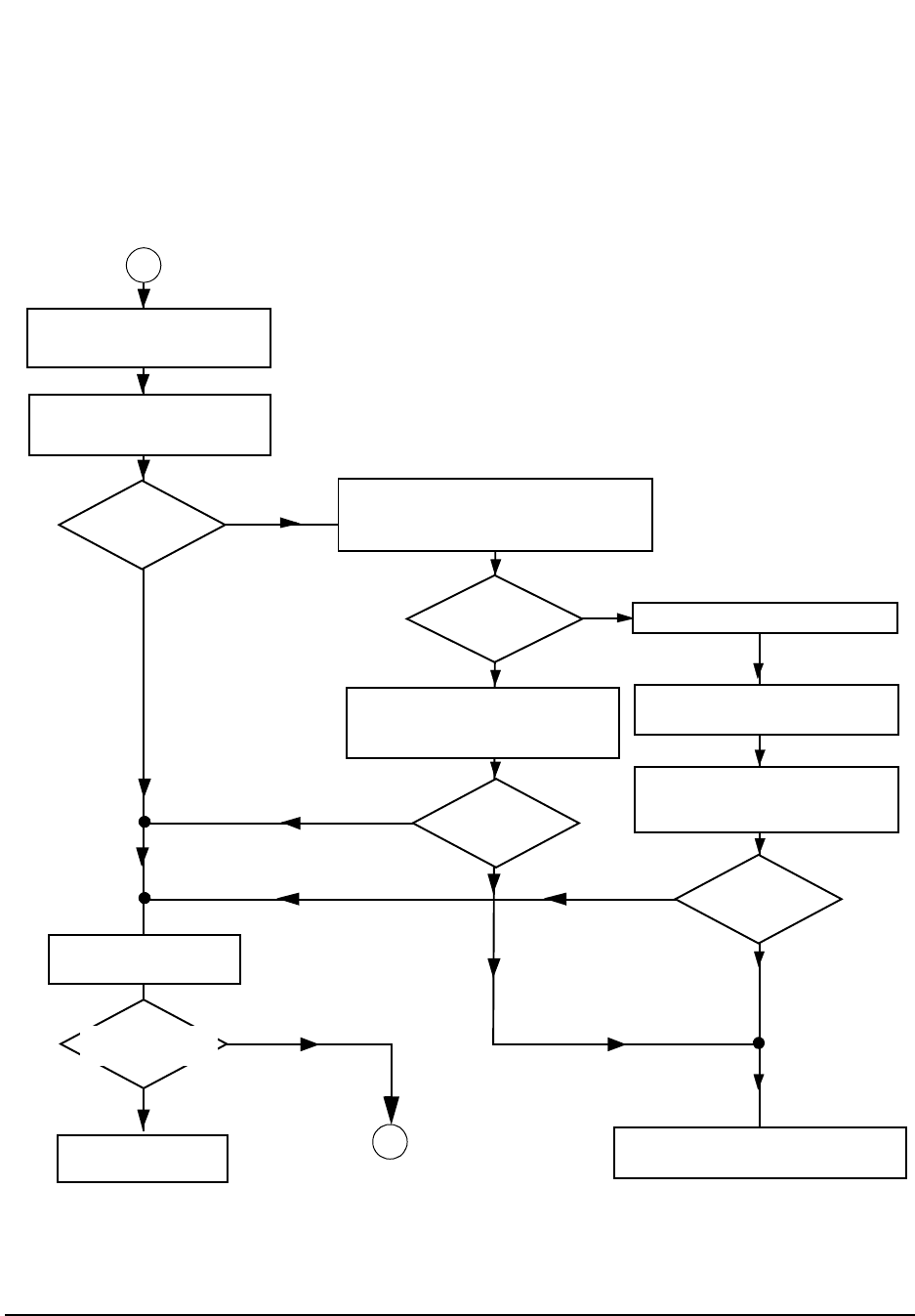
40
Chapter 2, Troubleshooting
Test System Troubleshooting
Figure 4 CDMA Cellular Adapter Troubleshooting Procedure
B
YES
Perform PER_CALD and EBNO_CAL
calibration procedures, see "Periodic
Calibration (for Options 001 & 003
NO
Perform the “Loopback Test” of the
CDMA_DIAG diagnostics, see
"CDMA Diagnostics" on page 52.
Does loopback
test pass?
A
The Cellular Adapter is
working properly.
Does the Cellular
Adapter include CDPD
(Option 002 or 003)?
See CDPD Diagnostic Path
in figure 5 on page 41.
CDMA Diagnostic Path
YES
NO
Perform the
“Gen/Ref (A4), IQ Mod and LO/IF Module (A9)”
test of the CDMA diagnostics, See "CDMA
Diagnostics" on page 52.
Replace defective assembly.
NO
YES
Does Gen/Ref
test pass?
Place the Test System in loopback mode:
select the “Loop” command of the
CDMA_DIAG “Loopback Test”, see
"CDMA Diagnostics" on page 52.
Does the
Loopback test
pass?
Perform CDMA_DIAG diagnostics, see
see "CDMA Diagnostics," in chapter 2,
on page 52.
Do diagnostics
pass?
Call Spokane HP Support for help, see
"Factory Support," in chapter 1, on page 35.
NO YES
NO
YES
The CDMA portion of the
Cellular Adapter is working
properly.
Perform the periodic calibration and
performance test procedures, see
chapter 7, "Periodic Calibration and
Performance Tests" on page 125.
41
Chapter 2, Troubleshooting
Test System Troubleshooting
Figure 5 CDPD Cellular Adapter and HP 8921A Test Set Troubleshooting Procedures
YES
Run CDPD_DIAG, see "CDPD
Diagnostics" on page 55.
NO Replace defective
assembly.
Did the
CDPD_DIAG tests
pass?
If the Cellular Adapter
includes CDMA, perform
"Periodic Calibration (for
Options 001 & 003 only)"
B
The Cellular Adapter
is working properly.
Call Spokane HP Support for
help, see "Service Information"
on page 35.
YES
NO
Perform CDPD
diagnostics, see "CDPD
Diagnostics" on page 55.
Did the
CDPD_DIAG tests
pass?
Is
the Test Set
operating properly?
YES
NO
C
Perform "Verifying that the Test
Set Recognizes the Cellular
Adapter" on page 51.
The Test Set is working
properly. Reattach the
Cellular Adapter.
Troubleshoot the
Test Set. Refer to its
Assembly Level Repair
Guide.
Does the Test Set
recognize the
Cellular Adapter?
YES
NO
Perform the Test Set’s
performance tests. Refer to the
Test Set’s ALR manual.
Does
the Test Set meet
all performance
specifications?
YES
NO
Verify that the Test Set is
operating properly, see "Verifying
Test Set Operation" on page 49.
CDPD Diagnostic Path Test Set Diagnostic Path

42
Chapter 2, Troubleshooting
Troubleshooting the PWR LED
Troubleshooting the PWR LED
The PWR LED is connected to the +5 V supply line on the A4 assembly. This
LED is normally ON.
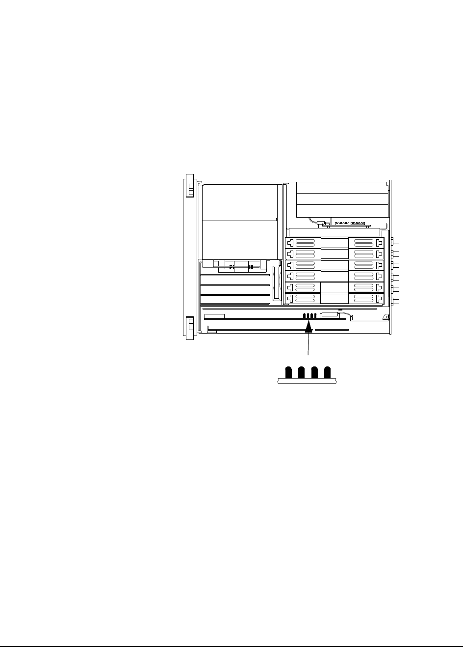
Procedure Step 1. Check fuse and cables
• Make sure power cords are connected to the Cellular Adapter and the Test Set.
• Check the fuse inside the Cellular Adapter. See "Separating Units and Removing Cov-
er" on page 63.
• Make sure the rear-panel CONTROL I/O cable is connected. The Cellular Adapter gets
its power-up command from this cable (+12 V on pin 40).
Step 2. Trace the +5 V line
Remove the Cellular Adapter’s cover and do the following:
• Check the fuse on the A8 power supply assembly. The fuse’s value is printed on the
power supply. This fuse is not available from Hewlett-Packard.
• Measure the +5 V output of the power supply at A4J9 pins 2 and 3 (referenced to
ground). The A4 assembly is shown in figure 25 on page 73.
If this doesn’t isolate the problem to the A4 or A8 assembly, refer to the power
supply and voltage distribution diagram, figure 38 on page 103.

43
Chapter 2, Troubleshooting
Troubleshooting the REF UNLOCK LED
Troubleshooting the REF UNLOCK LED
The REF UNLOCK LED is on the A4 assembly, but it is switched on and off by
an out-of-lock detector on the A9 Reference/IQ assembly. This LED is normally
OFF.
Procedure Step 1. Check the rear-panel connection.
The SYNTH REF IN connector on the Cellular Adapter must be connected to the
10 MHz REF OUTPUT connector on the Test Set.
Step 2. Check the Synth Ref and CDMA TB field settings.
a. Access the CDMA Generator screen, select More below the To Screen menu, then
select CDMA GEN.
b. The Synth Ref field should be set to 10 MHz when the 10MHz REF OUTPUT
from the Test Set is used as a reference.
c. The CDMA TB field should be set to Internal.
If you select the Synth Ref or CDMA TB field, you will see a list of other
reference frequency choices. The frequency in the Synth Ref field must match
the frequency of the reference signal connected to the rear-panel SYNTH REF IN
connector. Setting the CDMA TB field to Internal causes the A5 assembly to be
locked to the same SYNTH REF IN signal.
Step 3. Measure the reference signal.
Connect a BNC T-connector to the Test Set’s 10 MHz REF OUTPUT connector
and measure the 10 MHz signal level. It should be approximately +10 dBm.
Step 4. Check the LED.
Test the LED by unplugging the ribbon cable to J10 on the edge of the A4
assembly. The LED should go out. Grounding pin 11 of the ribbon cable’s
connector should make the LED come back on.
If all of the above steps test correctly, replace the A9 Reference/IQ assembly.

44
Chapter 2, Troubleshooting
Power-Up Diagnostics
Power-Up Diagnostics
Test System Power-
Up Diagnostics Use the table 2 below to interpret the Test System’s power-up failure message:
One or more self tests failed nnnn
where nnnn is the error code. Table 2 lists the possible error codes. Multiple
failures are indicated by the sum of the individual error code values. The Cellular
Adapter’s only self-test error code number is 1000. However this code can also be
a self-test error code for the Test Set. The Cellular Adapter’s power-up diagnostic
procedure is explained in "Cellular Adapter Power-Up Diagnostics" on page 45.
Table 2 Power-Up Self-Test Failure Error Codes
Detect Error Error Code
68000 Processor Failure 0002
ROM Checksum Failure 0004
Standard Non-Volatile System RAM Failure 0008
Optional Non-Volatile System RAM Failure 0010
68040 Timer Chip Failure 0020
Real-time Clock Chip Failure 0040
Keyboard Failure (stuck key) 0080
RS-232 Chip (I/O option installed and not functioning correctly) 0100
Serial Bus Communication Failure with a Standard Board 0200
Signaling Board Self-Test Failure 0400
CRT Controller Self-Test Failure 0800
HP 8921A Test Set (miscellaneous hardware failure) or
HP 83205A Cellular Adapter Self-test Failure 1000
45
Chapter 2, Troubleshooting
Power-Up Diagnostics
Cellular Adapter
Power-Up
Diagnostics
Power-up diagnostic information for the HP 83205A CDMA Cellular Adapter is
only interpretable through visual observation of the LEDs on the A7 assembly of
the Test Set. Observation of these LEDs requires removing the Test Set’s cover.
Accessing and interpreting the LEDs are explained in the following steps.
Step 1. Detach the Cellular Adapter from the Test Set.
Disconnect the cables between the Cellular Adapter and the Test Set, and then
remove the screws that attach the Cellular Adapter and Test Set together, see
figure 6.
Step 2. Removing the Test Set’s cover.
Remove the rear panel screws shown in figure 6 and slide the Test Set’s cover off.
For detailed instructions refer to the HP 8920, 8921 Test Set’s Assembly Level
Repair manual (HP part number 08920-90168).
Figure 6 Detaching the Cellular Adapter
Remove screws.
(3mm by 8mm) (3mm by 8mm)
PWR REF
UNLOCK
DIAGNOSTIC
MONITOR OUT 1.2288 MHz OUT
CHIP CLOCK 19.6608 MH z OUT
16 X CHIP CLOCK
RF IN/OUT
TO
TEST SET
RF IN/OUT
MAX.PWR 60W
CONTINUOUS
83205A
CDMA CELLULAR ADAP TER
CDMA
TIMEBASE IN
EVEN SECOND/
SYNC IN
DATA
IN
TRIGGER/
QUALIFIER IN
Remove screws.
114.3 MHz IF IN I BASEBAND OUT
AUX
CW
RF IN IQ
RF OUT OPTIONAL
SERIAL PORT
CONTROL I/O
SYNTH REF IN 10 MHz OUT
CDMA CLOCK OUTPUTS DSP IN
MOD O UT
10 MHz
REF OUT
Q BASEBAND OUT
Remove screws.
Mounting Plate
(3mm by 12mm)
Remove screw
Remove screw
Remove screw
Remove screw
46
Chapter 2, Troubleshooting
Power-Up Diagnostics
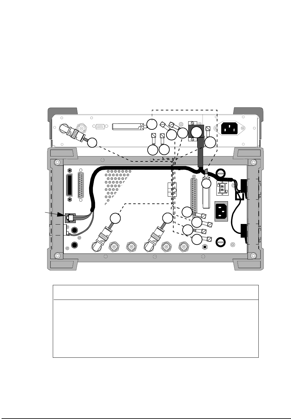
Step 3. Reconnect the cabling between the Test Set and Cellular Adapter.
See figure 7 below.
Figure 7 Test Set and Cellular Adapter Cabling
MODULATION
INPUT
EXT SCOPE
TRIGGER INPUT
CRT VIDEO
OUTPUT
10 MHz REF
OUTPUT
10 MHz REF
INPUT
AUDIO MONITOR
OUTPUT
DET OUT
IQ
RF IN
114.3 MHz
IF
OUT CW RF
OUT
HEADPHONE
AC FUSE
OPTION INTERFACE
CONTROL I/O
DC INPUT
PARALLEL PORT
HPIB (OPTION)
DC CURRENT
MEASUREMENT
+
-
SERIAL PORT
114.3 MHz IF IN I BASEBAND OUT
AUX
CW
RF IN
IQ
RF OUT OPTIONAL
SERIAL PORT
CONTROL I/O
SYNTH REF IN 10 MHz OUT
CDMA CLOCK OUTPUTS
DSP IN
MOD OUT
10 MHz
REF OUT
Q BASEBAND OUT
W6
W19
W17
W5
W4
W6
W17
HP 8921A Test Set Wire No. HP 83205A CDMA/CDPD
Cellular Adapter
10 MHz REF OUT W1 SYNTH REF IN
114.3 MHz IF OUT W2 114.3 MHz IF IN
DET OUT (DETECTOR) W3 AUX DSP IN
CW RF OUT W4 CW RF IN
IQ RF IN W5 IQ RF OUT
CONTROL I/O W6 CONTROL I/O
MODULATION INPUT W17* OPTIONAL MOD OUT
SERIAL PORT, A1, B1, A0/B0 W19* SERIAL PORT
SERIAL PORT
SERIAL PORT
A0/B0
SERIAL
PORT B1
SERIAL
PORT A1
* Options 002 & 003 only.
W2
W1
W3
W2 W3
W1
W4 W5
47
Chapter 2, Troubleshooting
Power-Up Diagnostics
Step 4. Power up the Test Set. Observe and record the patterns of the LEDs
on the A7 assembly of the Test Set.
See figure 8.
Figure 8 Test Set LEDs
Step 5. Interpret the A7 LEDs of the Test Set.
During initial power-up, all the LEDs will light for approximately 10 seconds and
then turn off. If a Cellular Adapter failure is detected after initial power-up, the
first LED pattern (See figure 9 on page 48) will blink rapidly and represent a
miscellaneous hardware pattern. The second and third LED patterns are non-
blinking and represent failure details.
0123
A7 Assembly
HP 8921A Test Set
Front Back
LEDs
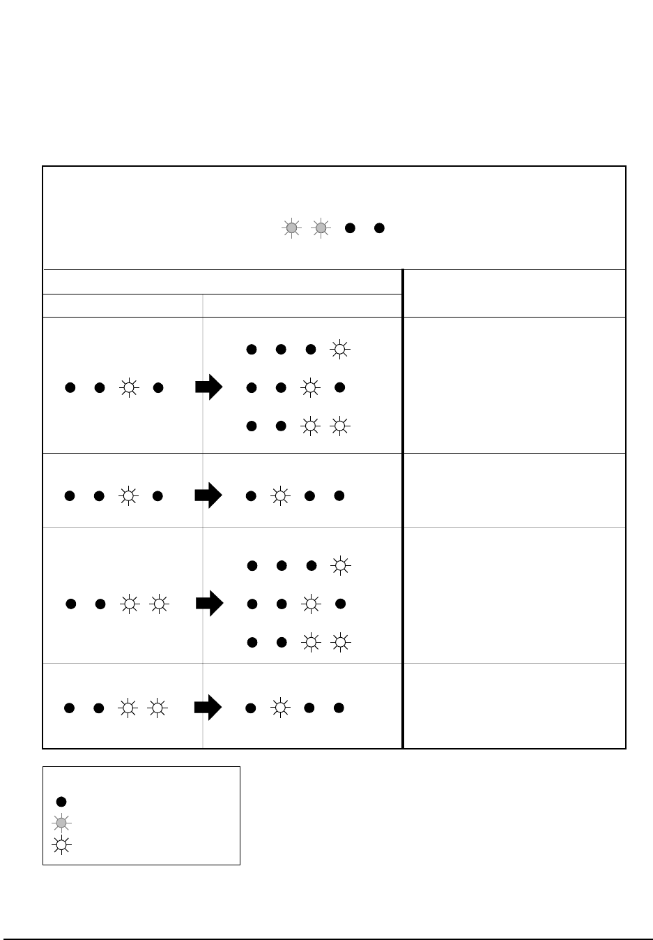
48
Chapter 2, Troubleshooting
Power-Up Diagnostics
Figure 9 Hardware Failure Table
3 2 1 0
= off
= rapid blink
= steady on or slow blink
LED Legend
3 2 1 0
3 2 1 0
3 2 1 0
if the last two non-blinking LED patterns displayed are ... ...then the failure is...
3 2 1 0 3 2 1 0
3 2 1 0
3 2 1 0
3 2 1 0
3 2 1 0
3 2 1 0 3 2 1 0
2nd LED Error Pattern 3rd LED Error Pattern
3 2 1 0
1st LED error pattern will blink rapidly and represent a miscellaneous failure...
the next two LED patterns are non-blinking and represent failure details...
HP 83205A’s (RX DSP)
A2 assembly
Check firmware, see "Verifying
Firmware Version" on page 88.
HP 83205A’s (Data Buffer)
A5 assembly
Check firmware, see "Verifying
Firmware Version" on page 88.
HP 83205A’s (RX DSP)
A2 assembly
Replace this assembly.
HP 83205A’s (Data Buffer)
A5 assembly
Replace this assembly.

49
Chapter 2, Troubleshooting
Verifying Test Set Operation
Verifying Test Set Operation
The Test Set must power up with no error messages and must run its functional
diagnostics with no failures before you proceed with Cellular Adapter
troubleshooting. Check this by disabling the Cellular Adapter, powering up the
Test Set and then running the Test Set’s diagnostics (AF, RF, and MS).
Procedure Step 1. Disable the Cellular Adapter.
Disconnect all of the rear-panel cables that connect the Test Set to the Cellular
Adapter. Disconnect the Cellular Adapter’s power cord. On the Test Set’s rear-
panel, connect the IQ RF IN connector to the CW RF OUT connector.
Step 2. Switch ON the Test Set.
When the Test Set powers up, a self-test is run. If no problems are detected, the
message All self tests passed will be displayed. If an error code is
displayed, you need to troubleshoot the Test Set before continuing with this
procedure. Refer to the Test Set’s Assembly Level Repair manual (HP part
number 08920-90168).
Step 3. Run the Test Set’s AF_DIAGS diagnostics.
a. Press the PRESET key.
b. Press the TESTS key.
c. Under Select Procedure Location: select ROM.
d. Under Select Procedure Filename: select AF_DIAGS.
e. Select the Run Test field.
f. Follow the instructions on the screen.
If all AF diagnostic tests pass, go on to the next step and run the RF diagnostics. If
a test fails, repair the Test Set before continuing.
Step 4. Run the Test Set’s RF_DIAGS diagnostics.
a. Press the PRESET key.
b. Press the TESTS key.
c. Under Select Procedure Location: select ROM.
d. Under Select Procedure Filename: select RF_DIAGS.
e. Select the Run Test field.

50
Chapter 2, Troubleshooting
Verifying Test Set Operation
f. Follow the instructions on the screen.
If all RF and AF diagnostic tests pass, you can go to the next step and run MS
diagnostics. If a test fails, repair the Test Set before continuing.
Step 5. Run the Test Set’s (Miscellaneous) MS_DIAGS diagnostics.
a. Press the PRESET key.
b. Press the TESTS key.
c. Under Select Procedure Location: select ROM
d. Under Select Procedure Filename: select MS_DIAGS.
e. Select the Run Test field.
f. Follow the instructions on the screen.
If all MS diagnostic tests pass, you can proceed with Cellular Adapter
troubleshooting. If a test fails, repair the Test Set before continuing.
Step 6. Reconnect the Cellular Adapter.
Turn Off the Test Set and reconnect the Cellular Adapter’s cables as shown in the
figure 7 on page 46. Reconnect the Cellular Adapter’s power cable.

51
Chapter 2, Troubleshooting
Verifying that the Test Set Recognizes the Cellular Adapter
Verifying that the Test Set Recognizes the Cellular Adapter
Prerequisites Before performing the following procedure you must verify that the Test Set
works and that the Test Set and the Cellular Adapter are connected correctly (see
the previous procedure). The Cellular Adapter’s PWR LED must be on.
Procedure 1. Attempt to access the CDMA ANL screen.
Select the More field, and choose CDMA ANL from the list of displayed choices.
If the CDMA ANALYZER screen appears, the Test Set recognizes the Cellular
Adapter. If not, continue with step 2 below.
2. Isolate the problem.
If the Test Set does not recognize the Cellular Adapter, the probable cause is the
A4 Gen/Ref Assembly. The A4 assembly has a serial I/O communication chip and
an EEPROM containing identification information. The Test Set’s controller
reads the contents of the EEPROM over the serial I/O bus when the Test System
powers up. If the serial I/O bus doesn’t work, the rest of the Cellular Adapter’s
power-up diagnostics will not run, and the Test Set will operate as if the Cellular
Adapter wasn’t there.
Before replacing the A4 assembly, it is a good idea to check the following:
• Check each pin of the CONTROL I/O cable for continuity. (Look for pins that have
been damaged or pushed in.)
• Remove the Cellular Adapter’s cover (see "Separating Units and Removing Cover" on
page 63) and check the power supply voltages on the A4 assembly. See figure 38, "Test
System Power Distribution," on page 103.

52
Chapter 2, Troubleshooting
CDMA Diagnostics
CDMA Diagnostics
Prerequisites Before running the CDMA diagnostics (CDMA_DIAG), you must verify that the
Test Set works and that it recognizes the Cellular Adapter. The Cellular Adapter’s
PWR LED must be on, the REF UNLOCK LED must be off, and the PER_CALD
calibration procedure must have run without error.
Functional diagnostics to isolate Cellular Adapter failures reside in the Test Set’s
ROM and are run from the TESTS screen. If diagnostics isolate a failure to an
assembly, the screen indicates the possible faulty assembly along with the
probability (high, medium, or low) of the diagnosis being correct.
CDMA_DIAG
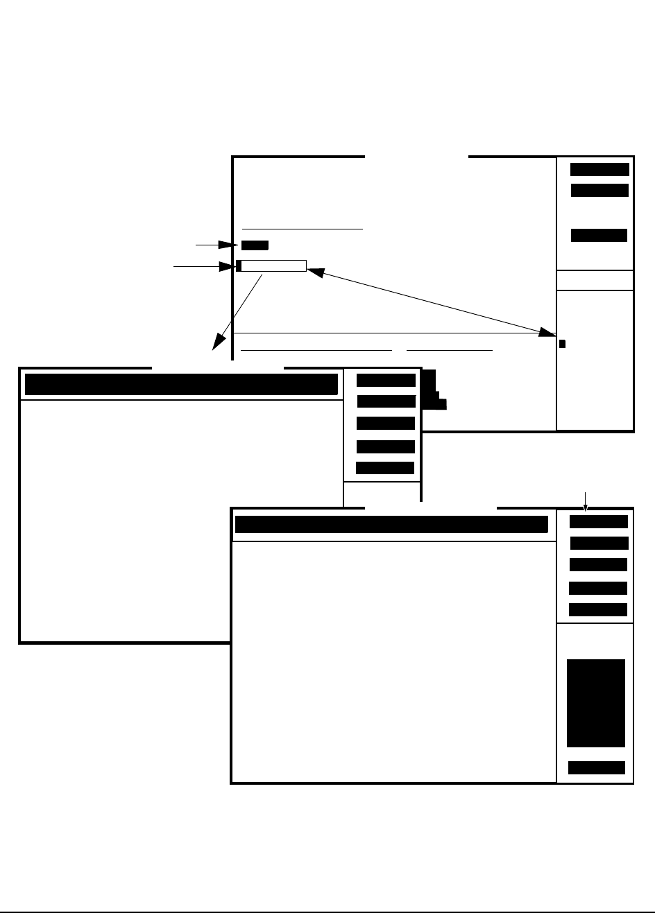
Procedure To run the CDMA_DIAG program:
1. Press the PRESET key.
2. Press the TESTS key.
3. Set the Select Procedure Location: field to ROM. (See figure 10 on page 53).
4. Set the Select Procedure Filename: field to CDMA_DIAG.
5. Press Run Test (k1) key. The CDMA_DIAG screen appears, see figure 10 on page
53.
6. Follow the instructions on the screen.
If a test fails, notice which assembly is the likely cause by its probability factor
(Low, Medium, or High). If more than one assembly is indicated, try replacing the
assemblies one at a time.
If the diagnostic tests intermittently fail, select the Loop (k1) function of the
LOOPBACK TEST screen (see figure 10 on page 53) to place the Test System in
a continuous test loop mode, then manually troubleshoot the Test System for
loose connections.
53
Chapter 2, Troubleshooting
CDMA Diagnostics
Figure 10 CDMA_DIAG Menu
1
Continue
2
Help4
RF GEN
To Screen
RF ANL
AF ANL
TESTS (Main Menu)
LOAD TEST PROCEDURE:
Select Procedure Location:
Select Procedure Filename:
Description:
Library: Program:
CUSTOMIZE TEST PROCEDURE: SET UP TEST SET:
Channel Information
Test Parameters
Order of Tests
Pass/Fail Limits
Save/Delete Procedure
External Devices
Printer Setup
IBASIC Cntrl
Freq
Parm
Seqn
Spec
Proc
Cnfg
Print
Exec Execution Cond
IBASIC
Please select a procedure to load.
Choices:
RF_DIAGS
MS_DIAGS
DMC_DIAGL
DMC_DIAGN
CDMA_DIAG
CDPD_DIAG
EDNO_CAL
PER_CAL
PER_CALD
RAM_MNG
ROM
Run Test
CDMA_DIAG
Select ROM as the location
of the diagnostic program.
Select the CDMA_DIAG
diagnostic program.
Up
Down
2
4
RF GEN
To Screen
RF ANL
AF ANL
SCOPE
SPEC ANL
ENCODER
DECODER
MORE
RADIO INT
TESTS (IBASIC Controller)
CDMA_DIAG INSTRUCTIONS: Position the menu pointer
in front of the desired test using the Up and Down
fields. Use the Select field to run the test.
Use the Exit field to leave the program.
=>
3
Exit
5
1
Loopback Test
Gen/Ref (A4), IQ Mod and LO/IF Module (A9)
CDMA_DIAG Menu
Select
Both of the following CDMA_DIAG Tests
Loop
2
4
RF GEN
To Screen
RF ANL
AF ANL
SCOPE
SPEC ANL
ENCODER
DECODER
MORE
RADIO INT
TESTS (IBASIC Controller)
3
Sgl Step
5
1
Resume
Test#: Measured Parameter
===========================
1: RHO
2: Frequency Error (Hz)
3: Time Offset (uSec)
4: Carrier Feedthru(dB)
Lower
Limit
=====
.95
-100.00
-5.00
-100.00
Upper
Limit
=====
1.00
100.00
5.00
-20.00
Actual
Limit
=====
1.00
-.62
.08
-59.29
LOOPBACK TEST
====================================================
End of Loopback Test
===================================================
Stop Fail
Loopable function
Loopback Test Screen

54
Chapter 2, Troubleshooting
CDMA Diagnostics
CDMA_DIAG
Tests Descriptions The CDMA diagnostics can be run as loopable tests. This means that either a
series of tests or an individual test can be set up to run repeatedly to aid in
troubleshooting intermittent problems. (To do this, select all of the CDMA_DIAG
tests from the menu after the program starts running, then press USER key (k1)
(this selects the Loop function). Descriptions of the individual tests follow.
Loopback Test
If this test passes, it is very probable that the Cellular Adapter works correctly. A
digital test pattern is generated, formatted, and timed in the A4 Gen/Ref assembly
and then sent to the IQ Modulator in the A9 assembly. The test pattern modulates
the RF carrier from the Test Set with Filtered Offset QPSK modulation.
The RF generator in the Test Set sets the level of the signal and loops it back to
the RF analyzer where it is downconverted to 114.3 MHz and sent to Cellular
Adapter’s LO/IF assembly in the A9 assembly. The LO/IF assembly
downconverts the signal to 4.9 MHz and sends it to the A2 RX DSP assembly.
The digital signal processor in the A2 assembly demodulates the signal and
measures the CDMA waveform quality (rho), the RMS Error Vector Magnitude
(EVM), amplitude error, frequency accuracy, and carrier feedthrough present in
the transmitted signal.
Gen/Ref (A4), IQ Mod and LO/IF Module (A9)
This test will help isolate a problem to the A4 assembly or the A9 assembly. The
A4 assembly is in the generator side of the Cellular Adapter and the A9 assembly
is in the analyzer side. The two are tested together because the test measures
similar parameters on each assembly.
These assemblies have multiplexers that select between grounds, power supplies,
VCO biases, tune-lines, detector voltages, and references, and routes the selection
to the front-panel DIAGNOSTIC MONITOR OUT connector. When this test is
run, the DIAGNOSTIC MONITOR OUT connector is connected externally to the
Test Set’s AUDIO IN HI connector. The selection is then measured by the Test
Set’s audio analyzer.
55
Chapter 2, Troubleshooting
CDPD Diagnostics
CDPD Diagnostics
The diagnostic software, CDPD_DIAG, resides in the ROM of the Test Set. This
software tests the CDPD function of the Cellular Adapter, Option 002 or 003. The
CDPD_DIAG diagnostic program consists of three tests for testing the CDPD
assembly and its connections. Before proceeding with the CDPD diagnostic tests,
you must verify that the Test Set is operating correctly.
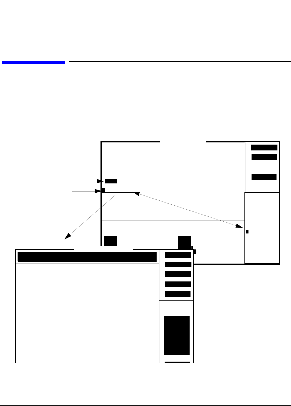
Figure 11 CDPD_DIAG Diagnostic Program
1
Continue
2
Help4
RF GEN
To Screen
RF ANL
AF ANL
TESTS (Main Menu)
LOAD TEST PROCEDURE:
Select Procedure Location:
Select Procedure Filename:
Description:
Library: Program:
CUSTOMIZE TEST PROCEDURE: SET UP TEST SET:
Channel Information
Test Parameters
Order of Tests
Pass/Fail Limits
Save/Delete Procedure
External Devices
Printer Setup
IBASIC Cntrl
Freq
Parm
Seqn
Spec
Proc
Cnfg
Print
Exec Execution Cond
IBASIC
Please select a procedure to load.
Choices:
AF_DIAGS
RF_DIAGS
MS_DIAGS
DMC_DIAGL
DMC_DIAGN
CDMA_DIAG
CDPD_DIAG
EDNO_CAL
PER_CAL
PER_CALD
ROM
Run Test
CDPD_DIAG
Select ROM as the location
of the diagnostic program.
Select the CDPD_DIAG
diagnostic program.
CDPD_DIAG Menu
Begin Tst
2
4
RF GEN
To Screen
RF ANL
AF ANL
SCOPE
SPEC ANL
ENCODER
DECODER
MORE
RADIO INT
TESTS (IBASIC Controller)
CDPDDIAG INSTRUCTIONS: Position the menu pointer
in front of the desired test using the Up and Down
fields. Use the Begin Tst field to run the test.
Use the Stop Tst field to leave this program.
=>
3
Stop Tst
5
1
CDPD Module Self Test
CDPD Digital Loop Back
CDPD RF Loop Back
Down
Up

56
Chapter 2, Troubleshooting
CDPD Diagnostics
CDPD_DIAG
Procedure See figure 11 on page 55 for an overview of this procedure. To access and
perform the CDPD_DIAG diagnostic program:
1. Press the TESTS key. The TESTS (Main Menu) appears.
2. Select ROM for the procedure location, and then select CDPD_DIAG from the
Choices: menu for the procedure filename.
3. Run the CDPD_DIAG program, press k1 (Run Test). The CDPD test options appear.
4. Select CDPD Module Self Test and then press k1 (Begin Tst).
Follow the instruction displayed. If an error message is encountered, see table 3 for the
probable cause of failures. If a Tests Passed response is received, go to step 5.
5. Select Digital Loop Back, and then press k1 (Begin Tst).
Follow the instructions displayed. If an error message is encountered, see table 3 for the
probable cause of failures. If a Valid response is displayed, go to step 6.
6. Select CDPD RF Loop Back, and then press k1 (Begin Tst).
Follow the instruction displayed. If an error message is encountered, see table 3 for the
probable cause of failures. If a Valid response is received, this concludes testing.

57
Chapter 2, Troubleshooting
CDPD Diagnostics
1. This table is based on the assumption that the diagnostic tests are performed in the order shown, that is, CDPD
assembly Self Test first, CDPD Digital Loop Back test second, CDPD RF Loop Back test last.
2. If all else fails, call HP Factory Support for assistance, see "Factory Support" on page 35.
Table 3 CDPD Diagnostic Tests Error-Messages and Probable Causes
CDPD Assembly
Self Test 1CDPD Digital
Loop Back Test CDPD RF
Loop Back Test Probable Cause
No response or
communication time out Check serial communication
path.
SRAM failure Failure in A11 CDPD assembly.
DSP failure Failure in A11 CDPD assembly.
Loopback failure Failure in A11 CDPD assembly.
Flash memory failure Failure in A11 CDPD assembly.
Synthesizer failure Failure in A11 CDPD assembly.
Test passed (PASS) Unable to put into
digital loopback mode. Cycle power to clear serial bus
then try again.
Test passed (PASS) Unable to transmit. Failure in A11 CDPD assembly.
Test passed (PASS) Status NOT VALID. Failure in A11 CDPD assembly.
Test passed (PASS) PASS (status VALID) Unable to put into
normal mode. Cycle power to clear the serial
bus then try again.
Test passed (PASS) PASS (status VALID) Unable to transmit. Failure in A11 CDPD assembly.
Test passed (PASS) PASS (status VALID) Unable to tune. Failure in A11 CDPD assembly.
Test passed (PASS) PASS (status VALID) Status NOT VALID. Faulty RF path in Cellular
Adapter and Test Set, or failure
in CDPD assembly.
Refer to chapter 5, "Block
Diagrams" on page 89 to aid you
in understanding and isolating
the problem.2
PASS PASS (status VALID) PASS (Status VALID) CDPD Tests successful.

58
Chapter 2, Troubleshooting
CDPD Diagnostics
CDPD_DIAG Tests
Descriptions CDPD Module Self Test
The “CDPD Module Self Test” of the CDPD_DIAG menu verifies that the base
CDPD hardware is operating correctly. This hardware includes the
communication link between the Test Set and the CDPD assembly, CDPD
processors, memory, synthesizer, and loopback hardware. The diagnostic program
will respond with “TESTS PASSED” or a failure message indicating which part
of the diagnostic routine failed, see table 3 on page 57 for error messages and
probable causes.
CDPD Digital Loop Back
The digital loop back test goes one step further than the self test and verifies some
of the functions of the A11 CDPD assembly. This assembly is set to operate in the
digital loopback mode when three predefined messages are sent and then received
and checked for a valid CDPD signal. This is all done in the digital portion of the
CDPD assembly. The RF circuits on the CDPD assembly and the RF path through
the rest of the Test Set are not checked with this test.
If all three messages are successfully looped back, then the user is notified that
CDPD status was VALID for all digital loops. If any one of these messages is not
successfully received or is corrupted, then the program stops and notifies the user
that the CDPD status was NOT VALID for the digital loop back test, and a failure
message is displayed indicating which part of the test failed. See table 3 on page
57 for error messages and probable causes.
RF Loop Back
The RF loop back test is similar to the digital loop back test except that the CDPD
assembly is used in normal mode and the entire RF path through the Test System
(Test Set and Cellular Adapter) is verified. Three predefined messages are sent,
then received, and checked for a valid CDPD signal. This test checks the function
of the CDPD assembly and the RF path through the Test Set.
If all three messages are successfully looped back, then the user is notified that
CDPD status was VALID for all digital loops. If any one of these messages is not
successfully received or is corrupted, then the program stops and notifies the user
that the CDPD status was NOT VALID for the RF loop back test, and a failure
message is displayed indicating which part of the RF loop failed. See table 3 on
page 57 for error messages and probable causes. See figure 12, "CDPD RF Loop
Back Test Path," on page 59, for a diagram of the loop back test path.
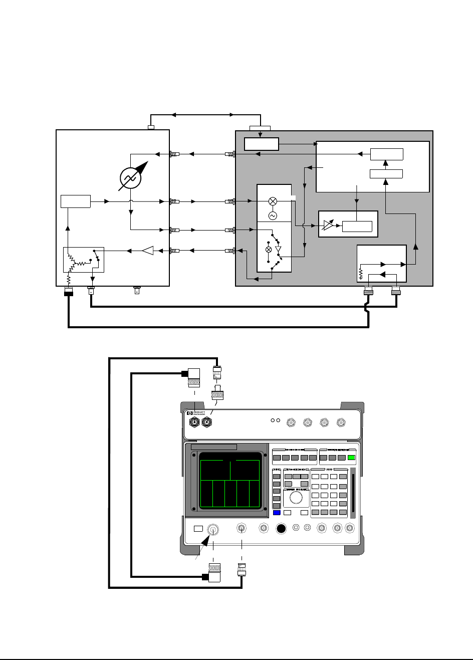
59
Chapter 2, Troubleshooting
CDPD Diagnostics
Figure 12 CDPD RF Loop Back Test Path
HP 83205A Cellular Adapter
DSP
0.5 GMSK
CDPD Valid
Amplitude
Control
Directional Coupler
HP 8921A
DC FM
114.3 MHz
RF IN/OUT DUPLEX ANT IN
OUT
CDPD
MOD OUT
114.3 MHz
IF OUT
114.3 MHz IF IN
700 kHz
CW RF OUT
RCVR
IQ
IQ RF IN
IQ RF OUT
IBASIC
RJ11 DB15
Serial Port
Serial Switch
CW RF IN
(SERIAL Cable)
RCVR
A9/A7
A9/A6
A10
A10
A11
A2
RX DSP
MOD IN
J4
J6
P3 J5
J6
J9
with CDPD
Test Set
PWR REF
UNLOCK ANALYZER ANALYZER ANALYZER GENERATOR
83205A
CDMA/CDPD CELLULAR ADAPTER
RF IN/OUT
DUPLEX OUT
RF IN/OUT
TO TEST SET
RF IN/OUT
TO TEST SET RF IN/OUT
RF IN/OUT

60
Chapter 2, Troubleshooting
CDPD Diagnostics

61
3
Disassembly and Replacement
This chapter explains how to disassemble the HP 83205A CDMA/CDPD Cellular
Adapter, Option 003, for the purpose of replacing failing assemblies. The
following instructions are applicable to Options 001 and 002 of the Cellular
Adapter. However, Option 001 will not have the CDPD assemblies and Option
002 will not have the (CDMA) A5 Data Buffer assembly.

62
Chapter 3, Disassembly and Replacement
Disassembly of the HP 83205A Cellular Adapter
Disassembly of the HP 83205A Cellular Adapter
Use table 4 below to help you access the main assemblies and sub components of
the HP 83205A Cellular Adapter.
NOTE: This chapter shows the disassembly of the HP 83205A CDMA/CDPD Cellular Adapter
Option 003. Options 001 and 002 are similar, however, Option 001 will not contain CDPD
assemblies and Option 002 will not contain the (CDMA) A5 Data Buffer assembly.
1. To remove the A4 and A9 assemblies as one unit, see "Removing the A4 and A9 Assemblies as a Unit" on
page 76.
Table 4 HP83205A Cellular Adapter Disassembly Table
To... see...
remove the adapter’s cover... "Separating Units and Removing Cover" on page 63.
operate the adapter without its cover... "Operation Without Cover" on page 65.
remove the A8 Power Supply assembly... "Removing the A8 Power Supply Assembly" on page 66.
remove the fuse holder, fan, or power supply cables... "Disconnecting Subassembly Power Connectors" on
page 67.
remove the front panel... "Removing the Front Panel" on page 68.
remove the rear panel... "Removing the Rear Panel" on page 70.
remove the A4 Generator/Reference assembly1... "Removing the A4 Gen/Ref Assembly" on page 72.
remove the A9 Reference/IQ assembly1... "Removing the A9 Reference/IQ Assembly" on page 74.
remove the A4 and A9 assemblies as a unit... "Removing the A4 and A9 Assemblies as a Unit" on
page 76.
remove the A10 Directional Coupler & Serial Switch
assembly or semi-rigid cables... "Removing the A10 Coupler & Switch Assembly and
Semi-Rigid Cables" on page 78.
remove the A11 CDPD assembly... "Removing the A11 CDPD Assembly" on page 80.
remove the A2 RX DSP or A5 Data Buffer assembly... "Removing the A2 RX DSP and A5 Data Buffer
Assemblies" on page 81.
remove the A3 Motherboard... "Removing the A3 Motherboard Assembly" on page 83.
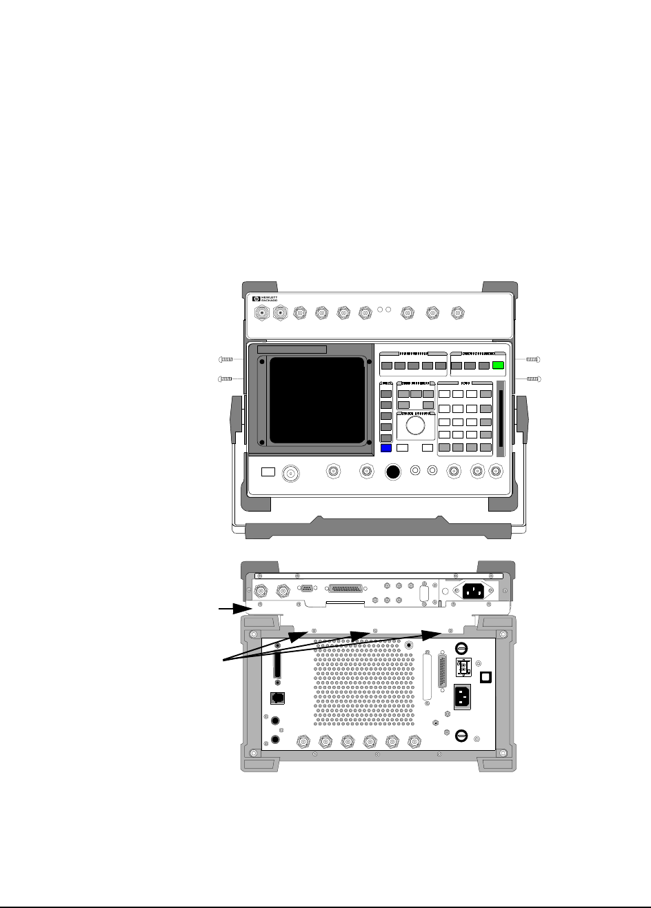
63
Chapter 3, Disassembly and Replacement
Disassembly of the HP 83205A Cellular Adapter
Separating Units
and Removing
Cover
To separate the HP 83205A Cellular Adapter from the Test Set, and to remove the
adapter’s cover:
1. Disconnect all power and interconnecting cables from the cellular adapter.
2. Remove the 7 screws that secure the Cellular Adapter and Test Set together, see figure
13:
• 4 screws from the side brackets
• 3 screws from the back mounting plate
Figure 13 Removing the Cellular Adapter’s Mounting Screws
114.3 MHz IF IN I BASEBAND OUT
AUX
CW
RF IN IQ
RF OUT OPTIONAL
SERIAL PORT
CONTROL I/O
SYNTH REF IN 10 MHz OUT
CDMA CLOCK OUTPUT S DSP IN
MOD OUT
10 MHz
REF OUT
Q BASEBAND OUT
Remove screws.
Remove screws.
Mounting Plate
(3mm by 8mm) (3mm by 8mm)
(3mm by 12mm)
PWR REF
UNLOCK
DIAGNOSTIC
MONITOR OUT 1.2288 MHz OUT
CHIP CLOCK 19.6608 MHz OUT
16 X CHIP CLOCK
RF IN/OUT
TO
TEST SE T
RF IN/OUT
MAX.PWR
60W
83205A
CDMA CELLULAR ADAPTER
CDMA
TIMEBASE IN
EVEN SECOND/
SYNC IN
DATA
IN
TRIGGER/
QUA LIFIER IN
Remove screws.
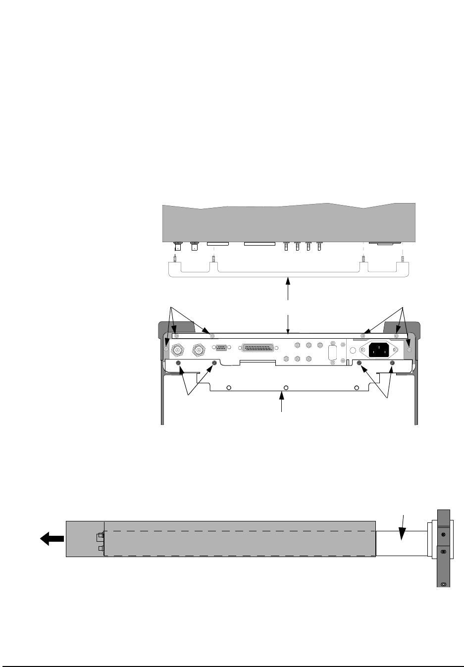
64
Chapter 3, Disassembly and Replacement
Disassembly of the HP 83205A Cellular Adapter
3. Remove the cross bar and mounting plate from the adapter by removing the screws
shown in figure 14.
4. Slide the cover from the adapter’s deck, see figure 15.
This concludes the procedure for removing the cover from the cellular adapter.
Figure 14 Removing the Cross Bar and Mounting Plate
Figure 15 Removing the Cover
114 .3 MH z IF IN I BASEBAND OUT
AUX
CW
RF IN
IQ
RF OUT OPTIONAL
SERIAL PORT
CONTROL I/O
SYNTH REF IN 10 MHz OUT
CDMA CLOCK OUTPUTS
DSP IN
MOD OUT
10 MHz
REF OUT
Q BASEBAND OUT
Remove screws.
Remove screws.
Cross Bar
Remove screws.
Mounting Plate
Remove screws.
All screws removed are 3mm by 12mm.
Top View
Cover (side view) Deck
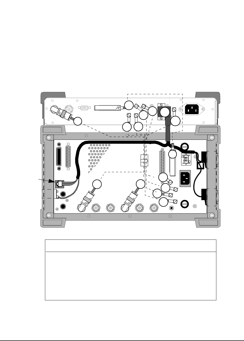
65
Chapter 3, Disassembly and Replacement
Disassembly of the HP 83205A Cellular Adapter
Operation Without
Cover To operate the Cellular Adapter without its cover, place the Cellular Adapter on
the Test Set without installing the screws that secure it to the Test Set, and then
reconnect the rear panel cables as shown in figure 16.
Figure 16 Rear Panel Cable Connections for HP 83205A CDMA/CDPD Cellular Adapter
MODULATION
INPUT
EXT SCOPE
TRIGGER INPUT
CRT VIDEO
OUTPUT
10 MHz REF
OUTPUT
10 MHz REF
INPUT
AUDIO MONITOR
OUTPUT
DET OUT
IQ
RF IN
114.3 MHz
IF
OUT CW RF
OUT
HEADPHONE
AC FUSE
OPTION INTERFACE
CONTROL I/O
DC INPUT
PARALLEL PORT
HPIB (OPTION)
DC CURRENT
MEASUREMENT
+
-
SERIAL PORT
114.3 MHz IF IN I BASEBAND OUT
AUX
CW
RF IN
IQ
RF OUT OPTIONAL
SERIAL PORT
CONTROL I/O
SYNTH REF IN 10 MHz OUT
CDMA CLOCK OUTPUTS
DSP IN
MOD OUT
10 MHz
REF OUT
Q BASEBAND OUT
W2 W3
W1
W4 W5
W19
W17
W5
W2
W4
W3
W6
W1
W17
HP 8921A Test Set Wire No. HP 83205A CDMA/CDPD
Cellular Adapter
10 MHz REF OUT W1 SYNTH REF IN
114.3 MHz IF OUT W2 114.3 MHz IF IN
DET OUT (DETECTOR) W3 AUX DSP IN
CW RF OUT W4 CW RF IN
IQ RF IN W5 IQ RF OUT
CONTROL I/O W6 CONTROL I/O
MODULATION INPUT W17* OPTIONAL MOD OUT
SERIAL PORT, A1, B1, A0/B0 W19* SERIAL PORT
SERIAL PORT
SERIAL PORT
A0/B0
SERIAL
PORT B1
SERIAL
PORT A1
* Options 002 & 003 only.
W6
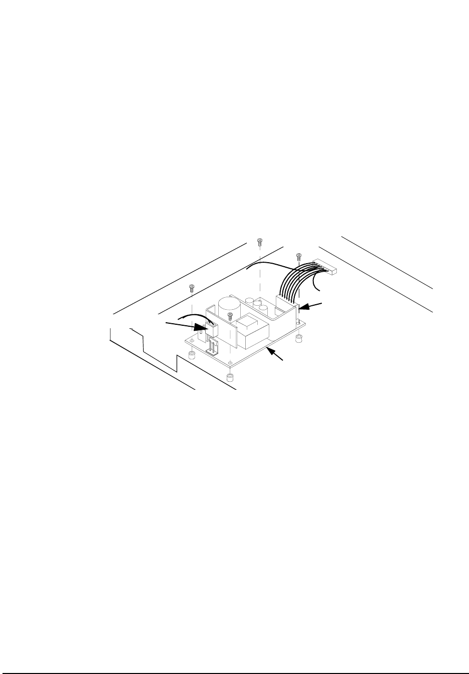
66
Chapter 3, Disassembly and Replacement
Disassembly of the HP 83205A Cellular Adapter
Removing the A8
Power Supply
Assembly
To remove the A8 power supply assembly:
1. Disconnect the output power connector to the A4 assembly, see figure 17.
2. Disconnect the primary power cable to the A8 assembly.
3. Remove 4 screws and lift the A8 power supply assembly from the deck.
This concludes the procedure for the removal of the A8 power supply assembly.
Figure 17 Removing the A8 Power Supply Assembly
Primary Power Cable
Output Power
A8 Power Supply
All screws removed are 3mm by 8mm.
Connector
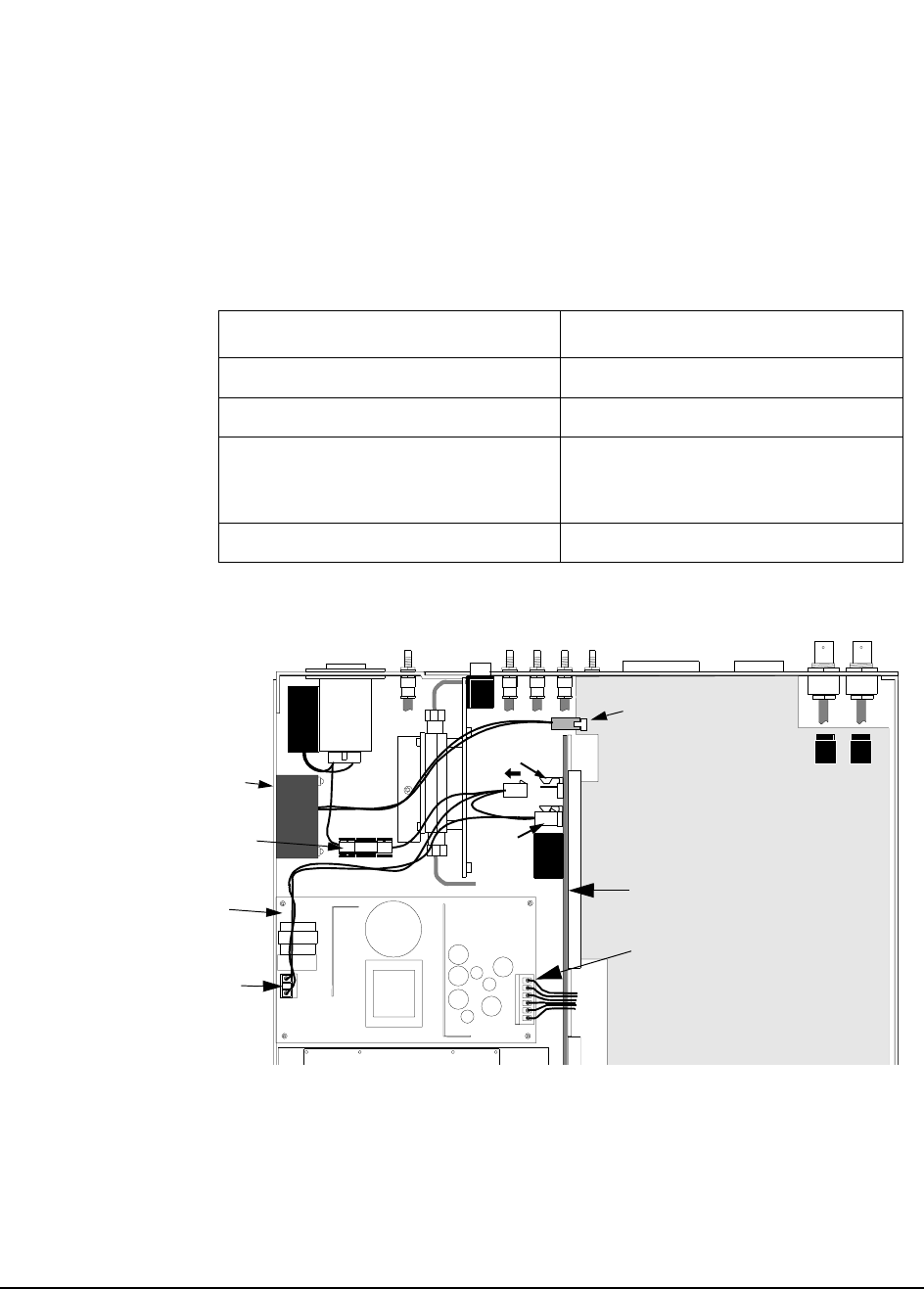
67
Chapter 3, Disassembly and Replacement
Disassembly of the HP 83205A Cellular Adapter
Disconnecting
Subassembly Power
Connectors
Disconnect the connectors shown in table 5 and figure 18 if you need to replace
the fan, fuse holder, A8 power supply assembly, or A3 motherboard.
Figure 18 Removing the Power Connectors
Table 5 Subassembly Connections
If replacing... Disconnect connector...
Fan (A4 assembly) J20 connector
Fuse holder (A3 assembly) J7 connector
Power supply assembly Primary and Output Power connectors
(Also see "Removing the A8 Power
Supply Assembly" on page 66.)
A3 motherboard (A3 assembly) J1 and J7 connectors
(A3) J7
(A4) J20
Rear Panel
Line Fuse Holder
Output Power Connector
A3 Motherboard
A8 Power Supply Assembly
Fan
(A3) J1
Primary Power Connector
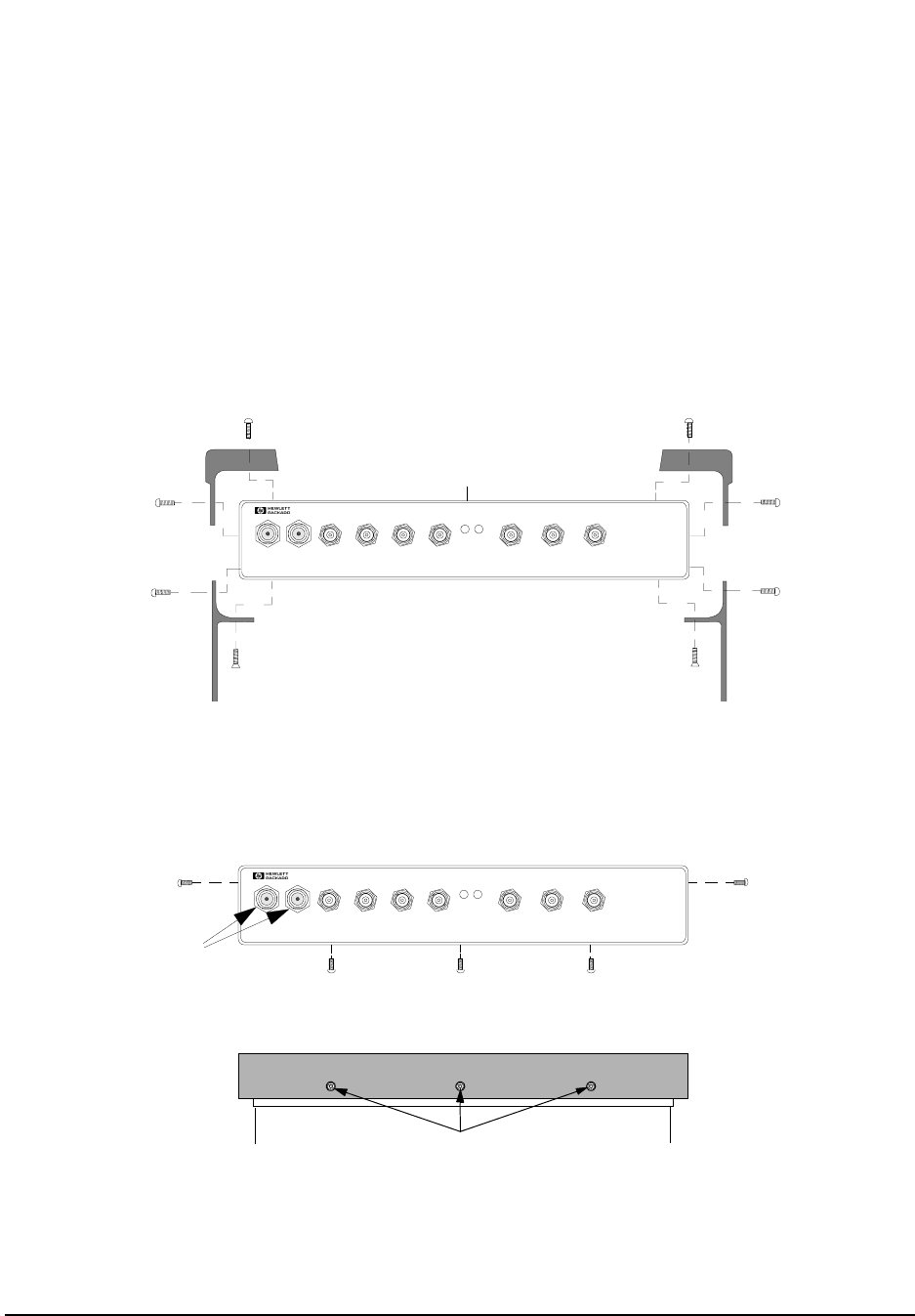
68
Chapter 3, Disassembly and Replacement
Disassembly of the HP 83205A Cellular Adapter
Removing the Front
Panel Removal of the front panel is necessary for access to or removal of the A2, A5
A11, or the A4/A9 assemblies of the Cellular Adapter.
1. Remove the Cellular Adapter’s cover, see "Separating Units and Removing Cover" on
page 63.
2. Remove the 2 bumpers and 2 brackets from the front frame as shown in figure 19.
3. Remove the 5 frame screws and the two 3/4-inch nuts shown in figure 20.
Figure 19 Removing the Bumpers and Brackets
Figure 20 Removing the Frame Screws
Pull the frame away from the deck and disconnect the coaxial cables from the A2 and
A4 assemblies, see figure 21.
PWR REF
UNLOCK
83205A
CDMA/CDPD CELLULAR ADAPTER
RF IN/OUT
TO
TEST SET
RF IN/OUT
MAX.PWR 60W
CONTINUOUS
Front Frame
Bumper
Bracket Flathead screw Flathead screw
DIAGNOSTIC
MONITOR OUT 1.2288 MHz OUT
CHIP CLOCK 19.6608 MHz OUT
16 X CHIP CLOCK
CDMA
TIMEBASE IN
EVEN SECOND/
SYNC IN
DATA
IN
TRIGGER/
QUALIFIER IN
3mm by 8mm
3mm by 8mm
3mm by 8mm
3mm by 8mm
3mm by 8mm 3mm by 8mm
3mm by 10mm 3mm by 10mm
Bottom View of Frame
Front View of Frame
Remove screws.
All screws removed are 3mm by
PWR REF
UNLOCK
83205A
CDMA/CDPD CELLULAR ADAPTER
RF IN/OUT
TO
TEST SET
RF IN/OUT
MAX.PWR 60W
CONTINUOUS
DIAGNOSTIC
MONITOR OUT 1.228 8 MHz OUT
CHIP CLOCK 19.6608 MHz OUT
16 X CHIP CLOCK
CDMA
TIMEBASE IN
EVEN SECOND/
SYNC IN
DATA
IN
TRIGGER/
QUA LIF IER IN
3/4-inch Nuts
(Options 002 & 003 only)
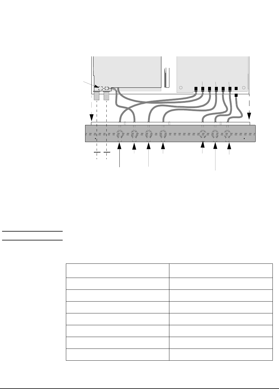
69
Chapter 3, Disassembly and Replacement
Disassembly of the HP 83205A Cellular Adapter
Figure 21 Disconnecting the Coaxial Cables from the A4 and A5 Assemblies
This completes the procedure for removing the front panel. When reassembling
the front panel frame, use table 6 below and figure 21 above to reconnect the
cables of the front panel to the A4 assembly.
NOTE: When reinstalling the front cover, route the cables carefully to avoid crimping them.
A4 Assembly
Coaxial Cables
Deck
Frame
DIAGNOSTIC
MONITOR OUT
1.2288 MHz OUT
CHIP CLOCK
19 6608 MHz OUT
16 X CHIP CLOCK
A2 or A11 Assembly
EVEN SECOND/
SYNC IN
CDMA
TIMEBASE IN
TRIGGER/
QUALIFIER IN
DATA IN
J702
J701J703J1 J707
J705
J706
J22 on A5 assembly
(under A2 assembly)
(Top View)
5/8-inch Nuts
(Options 002 & 003)
Table 6 Front Panel Connections
Connector/Cable of Front Panel goes to A4 or A5 connector...
TRIGGER/QUALIFIER IN (A4) J702
DATA IN (A5) J22
EVEN SECOND / SYNC IN (A4) J703
CDMA TIMEBASE IN (A4) J1
DIAGNOSTIC MONITOR OUT (A4) J707
1.2288 MHz OUT CHIP CLOCK (A4) J705
19.6608 MHz OUT 16 X CHIP CLOCK (A4) J706
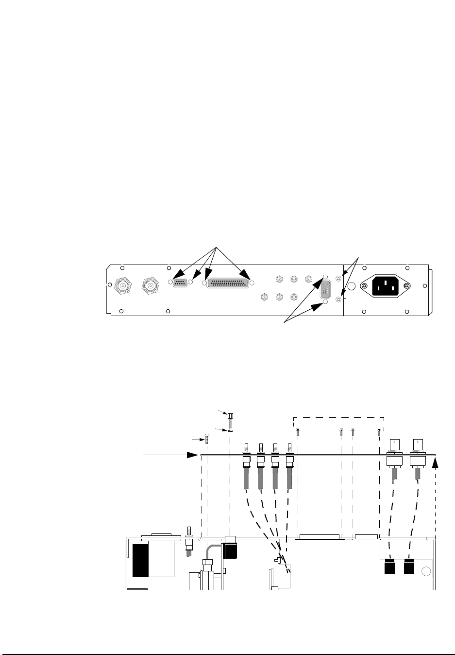
70
Chapter 3, Disassembly and Replacement
Disassembly of the HP 83205A Cellular Adapter
Removing the Rear
Panel In order to remove the A4 and/or A9 assembly of the Cellular Adapter, it is
necessary to remove the rear panel. Needed for this procedure is a 3/16-,
1/4-inch wrench or nut driver, and a 3mm Torx screwdriver.
1. Remove the Cellular Adapter’s cover, see "Separating Units and Removing Cover" on
page 63.
2. Remove the 3/16-inch connector locks and two 3mm screws shown in figure 22 and
figure 23.
3. Pull the rear panel away from the deck as shown in figure 23.
Figure 22 Removing the Rear Panel Screws and Connector Locks
Figure 23 Removing the Rear Panel
3/16-inch Connector Locks
114.3 MHz IF IN I BASEBAND OUT
AUX
CW
RF IN
IQ
RF OUT
SERIAL PORT
CONTROL I/O
SYNTH REF IN 10 MHz OUT
CDMA CLOCK OUTPUTS
DSP IN
MOD OUT
10 MHz
REF OUT
Q BASEBAND OUT
Remove screws.
3mm by 8mm
3/16-inch Connector Locks
(Options 002 & 003 only)
Deck
J5 J2
Rear Panel
3mm Screws (2x)
3/16-inch Connector Locks (2x)
Washers (2x)
3/16-inch Connector Locks
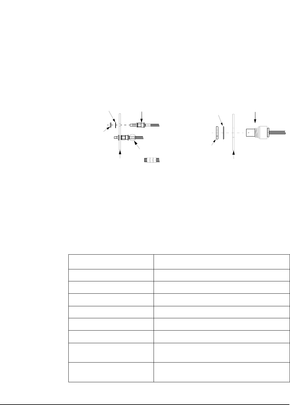
71
Chapter 3, Disassembly and Replacement
Disassembly of the HP 83205A Cellular Adapter
4. Access to other assemblies on the deck is now possible without removing the SMC
connectors from the rear panel. If complete removal of the rear panel is necessary, use
a 1/4-inch wrench or deep nut-driver to disconnect the SMC connectors and a 9/16-inch
wrench to disconnect the BNC connectors, see figure 24.
Figure 24 Rear Panel Connector Removal
This completes the removal of the rear panel. Cable clips identify the location of
the SMC connectors on the rear panel. When reinstalling the SMC and BNC
connectors, use figure 22 and figure 23 on page 70 and table 7 below for
identifying the location of the connectors.
0J3
0J7
1/4-inch Nut
Lock Washer
Rear Panel
Cable Clips
SMC Connector
9/16-inch Nut
Lock Washer
Rear Panel
BNC Connector
SMC Connector Removal BNC Connector Removal
0J3
Table 7 Rear Panel Connector Locations
Rear Panel Label Cable Clip Number (Connector Type)
114.3 MHz IF IN 0J1 (SMC)
AUX DSP IN 0J2 (SMC)
I BASEBAND OUT 0J3 (SMC)
CW RF IN 0J4 (SMC)
IQ RF OUT 0J5 (SMC)
Q BASEBAND OUT 0J6 (SMC)
SYNTH REF IN (BNC/cable goes to J2 on A4 assembly, see figure
23 on page 70.)
10 MHz OUT (BNC/cable goes to J5 on A4 assembly, see figure
23 on page 70.)

72
Chapter 3, Disassembly and Replacement
Disassembly of the HP 83205A Cellular Adapter
Removing the A4
Gen/Ref Assembly The following instructions remove the A4 Generator/Reference assembly from
the Cellular Adapter’s deck. An alternative to the following procedure is to
remove the A4 and A9 assemblies as a unit, see "Removing the A4 and A9
Assemblies as a Unit" on page 76.
NOTE: Perform the "PER_CALD Calibration Procedure" on page 127 and "EBNO_CAL
Calibration Procedure" on page 128 after replacing the A4 assembly.
To remove the A4 assembly:
1. Remove the Cellular Adapter’s cover, "Separating Units and Removing Cover" on
page 63.
2. Remove the Cellular Adapter’s front panel, see "Removing the Front Panel" on page
68.
3. Remove the rear panel, see "Removing the Rear Panel" on page 70.
4. Remove the 7 screws that secure the A4 assembly to the A9 assembly, see figure 25 on
page 73.
5. Disconnect from the A4 assembly: the fan, power, and ribbon cables, wires, and SMB
connectors shown in figure 25 on page 73. Cable clips identify each SMB connector.
6. Carefully unplug the A4 assembly from the A3 motherboard’s J2 connector. You will
have to lift the opposite side of the A4 assembly over the edge of the deck to unplug it.
This completes the removal of the A4 assembly. Use figure 25 on page 73 to
identify the location of the connectors and cables when reinstalling the A4
assembly.
73
Chapter 3, Disassembly and Replacement
Disassembly of the HP 83205A Cellular Adapter
Figure 25 Removing the A4 Assembly
A9 Assembly
J11
SMB Connector
Fan Connector
All screws removed are 3mm by 8mm.
J400
J500
J708
J401
J7
J9
J10
A4 Assembly
J20 J5 J2
J3
J709
J11
(4J11-10J2)
W22
W23
W7
(A4J5-[RP]10 MHz OUT)
(A4J2-[RP] SYNTH REF IN)
A1W7
A3J2 Connector
A1W6
A1W4
A1W5
A1W3
W9
A1W1
W16
(A8W1)
(A12B1)
W34
J20 J9
(J10) J709 J4
W33 W32
W31
W30
W29
(4J400-5J401)
(4J500-5J501) (4J708-5J4)
(4J401-7J5)
(4J3-6J2)
(4J7-2J4)
W28
Assembly A7, Connector J5
to Assembly A4, Connector J3
(7J5-4J3)
Wire
reference
designator
Cable Legend
J702
J701
J703J1
J707
J705
J706
W22
(4J11-10J2)
A1W7 (4J706- [FP]19.6608 MHz OUT)
A1W6 (4J705- [FP] 1.2288 MHz OUT CHIP CLOCK)
A1W4 (4J1- [FP] CDMA TIMEBASE IN)
A1W5 (4J707- [FP] DIAGNOSTIC MONITOR OUT)
A1W3 (4J703-[FP] EVEN SECOND/SYNC IN)
W9 (4J701-5J709)
A1W1 (4J702-[FP] TRIGGER/QUALIFIER IN)
Power Cable
Ribbon Cable
[RP] = Rear Panel
[FP] = Front Panel

74
Chapter 3, Disassembly and Replacement
Disassembly of the HP 83205A Cellular Adapter
Removing the A9
Reference/IQ
Assembly
The following instructions remove the A9 Reference/IQ assembly unit from the
Cellular Adapter’s deck. An alternative to this procedure is to remove the A4
assembly and the A9 assembly as a unit, see "Removing the A4 and A9
Assemblies as a Unit" on page 76.
NOTE: Perform the "PER_CALD Calibration Procedure" on page 127 and "EBNO_CAL
Calibration Procedure" on page 128 after replacing the A4 assembly.
1. Remove the cover from the Cellular Adapter. See "Separating Units and Removing
Cover" on page 63.
2. Remove the front panel. See "Removing the Front Panel" on page 68.
3. Remove the rear panel. See "Removing the Rear Panel" on page 70.
4. Remove the A4 Gen/Ref assembly. See "Removing the A4 Gen/Ref Assembly" on
page 72.
5. Remove the 6 screws that secure the A9 assembly to the deck, see figure 26 on page
75, and carefully lift the assembly from the deck.
6. Disconnect the SMB connectors from the A9 assembly, see figure 26. The SMB cables
are identified with cable clips.
This completes the removal and disassembly of the A9 assembly unit. When
reassembling the A9 assembly, use figure 26 on page 75 to help you determine
the location of the SMB coaxial cables which are identified with cable clips.
75
Chapter 3, Disassembly and Replacement
Disassembly of the HP 83205A Cellular Adapter
Figure 26 Removing the A9 Reference/IQ Assembly
A9 Assembly
All screws removed are 3mm by 30mm.
W37W24
W30
A6 SubassemblyA7 Subassembly
A9 Assembly
W27
W35
W28
W31
Ribbon Cable (W16)
(6J2-4J3)
W20
(6J6-11J3) (6J3-[RP]OJ1) (6J4-2J6)
(7J5-4J401)
(7J4-[RP]OJ5)
W36
(7J3-5J400)
W21
(7J6-11J4)
(7J2-5J500)
(7J1-[RP]OJ4)
SMB Coaxial Cable
W28
Assembly A7, Connector J5
to Assembly A4, Connector J3
(7J5-4J3)
Wire
reference
designator
Cable Legend
[RP] = Rear Panel
[FP] = Front Panel

76
Chapter 3, Disassembly and Replacement
Disassembly of the HP 83205A Cellular Adapter
Removing the A4
and A9 Assemblies
as a Unit
The following instructions remove the A4 Generator/Reference assembly and A9
Reference/IQ assembly as a unit from the Cellular Adapter’s deck.
NOTE: Perform the "PER_CALD Calibration Procedure" on page 127 and "EBNO_CAL
Calibration Procedure" on page 128 after replacing the A4 assembly.
1. Remove the cover from the Cellular Adapter. See "Separating Units and Removing
Cover" on page 63.
2. Remove the front panel. See "Removing the Front Panel" on page 68.
3. Remove the rear panel. See "Removing the Rear Panel" on page 70.
4. Remove the 6 screws that secure the A4 and A9 assemblies to the deck, see figure 27
on page 77.
5. Carefully pull the A4/A9 assembly away from theA3 motherboard and lift it over the
edge of the deck to disconnect the cables and connectors shown in figure 27 on page 77.
This completes the removal of the A4/A9 assembly unit.
Reinstalling the A4/A9 Assembly
To reinstall the A4/A9 assembly, reverse the steps of the previous section.
1. Reconnect the SMB connectors to their proper assemblies. Use figure 27 on page 77 to
help you determine the location of the cables and SMB coaxial connectors. The ends
of the coaxial cables are identified with cable clips.
2. Carefully plug the A4/A9 assembly into the A3 motherboard. Ensure that the assembly
is squarely plugged in and be sure not to get a cable caught under the A4/A9 assembly
or you will have difficulty trying to fasten down the assembly.
3. Secure the assembly with the 6 screws (3mm by 30mm) previously removed.
4. Reconnect all remaining cables and connectors to their proper assemblies as shown in
figure 27 on page 77.
5. Reinstall the back and front panels.
This concludes the procedure for reinstalling the A4/A9 assemblies.
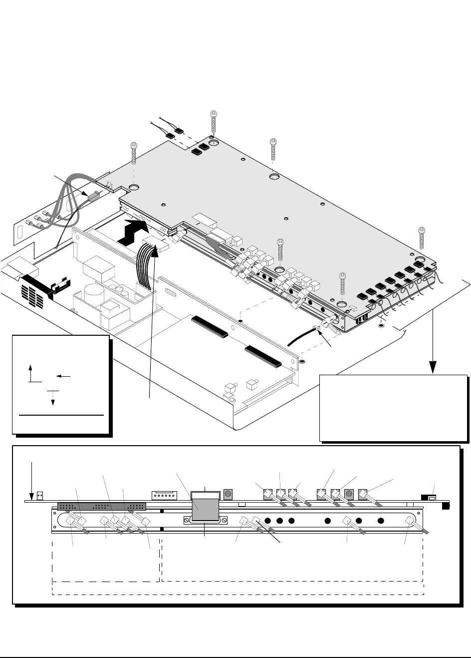
77
Chapter 3, Disassembly and Replacement
Disassembly of the HP 83205A Cellular Adapter
Figure 27 Removing the A4/A9 Assembly as a Unit
All screws removed are 3mm by 30mm.
A4 & A9 Assembly
Power Cable
W22
W37
W24
W30
A6 SubassemblyA7 Subassembly
A9 Assembly
W27
W35
W36
W28
W31
W21 SMB Coaxial Cables
J1
Ribbon Cable (W16)
J9J20
W30
W31
W32
A4 Assembly
W29
J9
A1W7
A1W6
A1W4
A1W5
J11
A1W7 (4J706- [FP]19.6608 MHz OUT)
A1W6 (4J705- [FP] 1.2288 MHz OUT CHIP CLOCK)
A1W4 (4J1- [FP] CDMA TIMEBASE IN)
A1W5 (4J707- [FP] DIAGNOSTIC MONITOR OUT)
A1W3 (4J703-[FP] EVEN SECOND/SYNC IN)
W9 (4J701-5J709)
A1W1 (4J702-[FP] TRIGGER/QUALIFIER IN)
(4J11-10J2)
A1W3
W9
A1W1
(7J5-4J401)
(7J4-[RP]OJ5)
(7J3-5J400)
(7J6-11J4)
(7J2-5J500)
(7J1-[RP]OJ4) (6J2-4J3) W20
(6J6-11J3) (6J4-2J6)
(6J3-[RP]OJ1)
J5 J2
W23
W7
(A4J5-[RP]10 MHz OUT)
(A4J2-[RP] SYNTH REF IN)
Fan Cable
W34
(4J400-5J401)
(4J500-5J501)
W33
(4J708-5J4) (4J7-2J4)
(4J3-6J2)
(4J401-7J5)
(4J11-10J2)
W22
J10
J702
J701J703 J1
J707
J705
J706
W28
Assembly A7, Connector J5
to Assembly A4, Connector J3
(7J5-4J3)
Wire
reference
designator
Cable Legend
[RP] = Rear Panel
[FP] = Front Panel
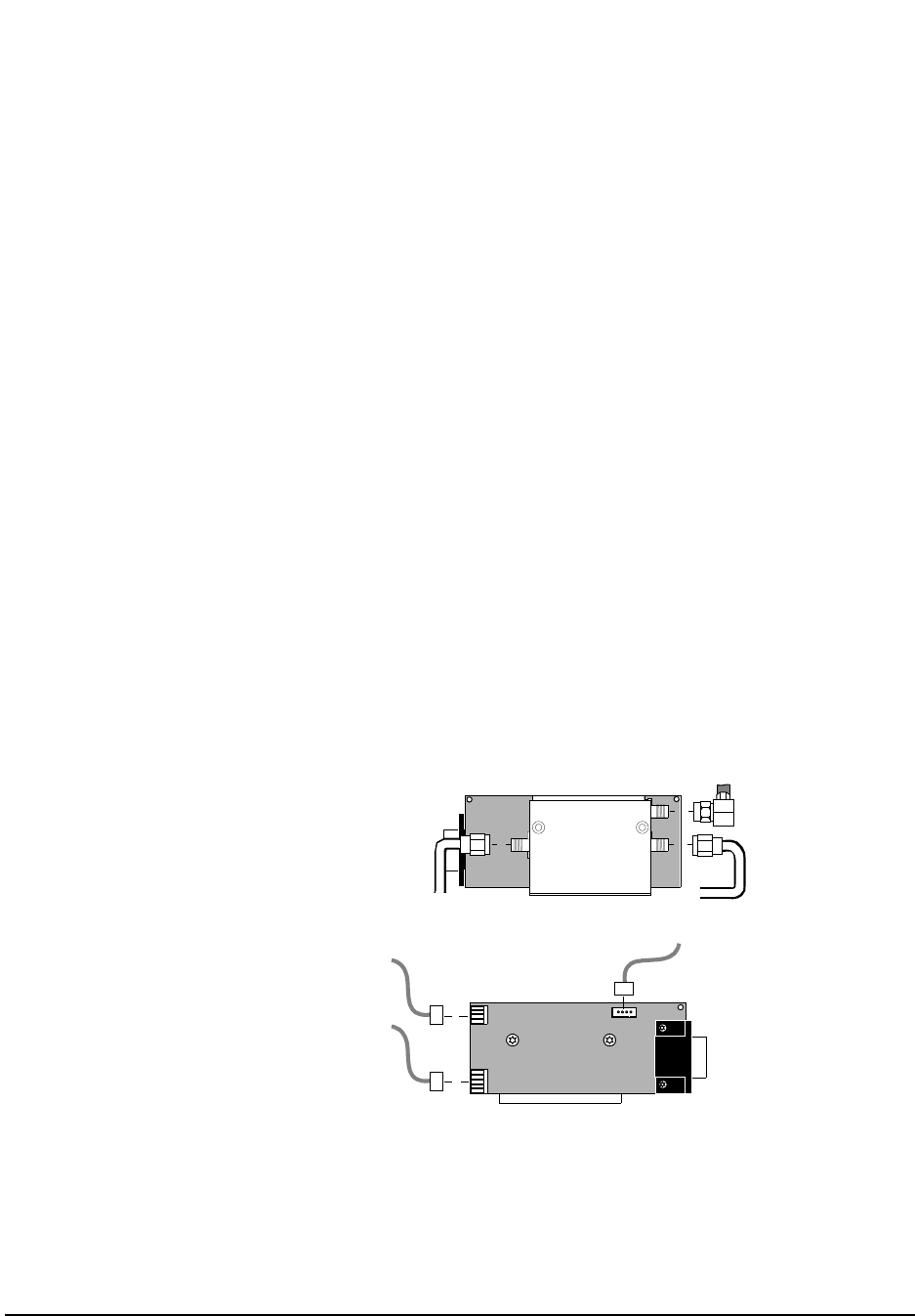
78
Chapter 3, Disassembly and Replacement
Disassembly of the HP 83205A Cellular Adapter
Removing the A10
Coupler & Switch
Assembly and
Semi-Rigid Cables
To remove the A10 Directional Coupler and Serial Switch assembly and semi-
rigid cables:
1. Remove the cover from the Cellular Adapter, see "Separating Units and Removing
Cover" on page 63.
2. Remove the front panel, see "Removing the Front Panel" on page 68.
3. Remove the rear panel, see "Removing the Rear Panel" on page 70.
4. Remove the A4/A9 assembly, see "Removing the A4 and A9 Assemblies as a Unit" on
page 76.
5. If you are replacing the semi-rigid cables W10 and W11, disconnect the W10 and W11
connectors on the A10 assembly, see figure 28.
6. To remove the semi-rigid cables, remove the cable clamps securing W10 and W11
semi-rigid cables to the chassis, see figure 29 on page 79.
7. If you are replacing the A10 assembly, disconnect the W10, W11, W14 connectors and
the connectors at J1, J2, J3, and J4 on the A10 assembly, see figure 28.
8. To remove the A10 assembly, remove the screw securing the A10 assembly to the deck,
see figure 29 on page 79.
This completes the procedure for removal of semi-rigid cables and the A10
assembly.
Figure 28 A10 Directional Coupler & Serial Switch Assembly
J1 J2
J4
J3
A10 Assembly
A10 Assembly
W10
W14
W11
Coupler Side
W12
(10J1-11P2)
P/O A8W1
(10J2-4J24)
W22
Switch Side
OUTPUT INPUT
−30dB (A10 “−30dB”-11J5)
(A10 “INPUT”-front panel
RF IN/OUT)
(A10 “OUTPUT”-
front panel RF IN/OUT TO TEST SET)
(10J3-4J9)
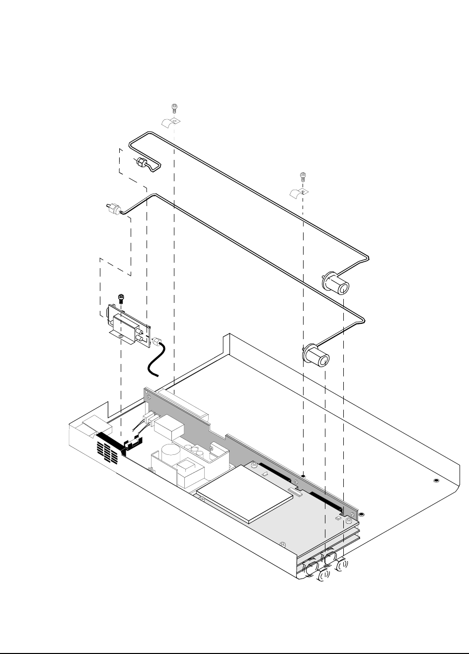
79
Chapter 3, Disassembly and Replacement
Disassembly of the HP 83205A Cellular Adapter
Figure 29 Removing the A10 Directional Coupler & Serial Switch Assembly & Semi-Rigid
Cables
A10 Assembly
Screws removed
are 3mm by 6mm.
W10 (Semi-rigid cable)
W11 (Semi-rigid cable)
Cable Clamp
Directional Coupler
W14
& Serial Switch
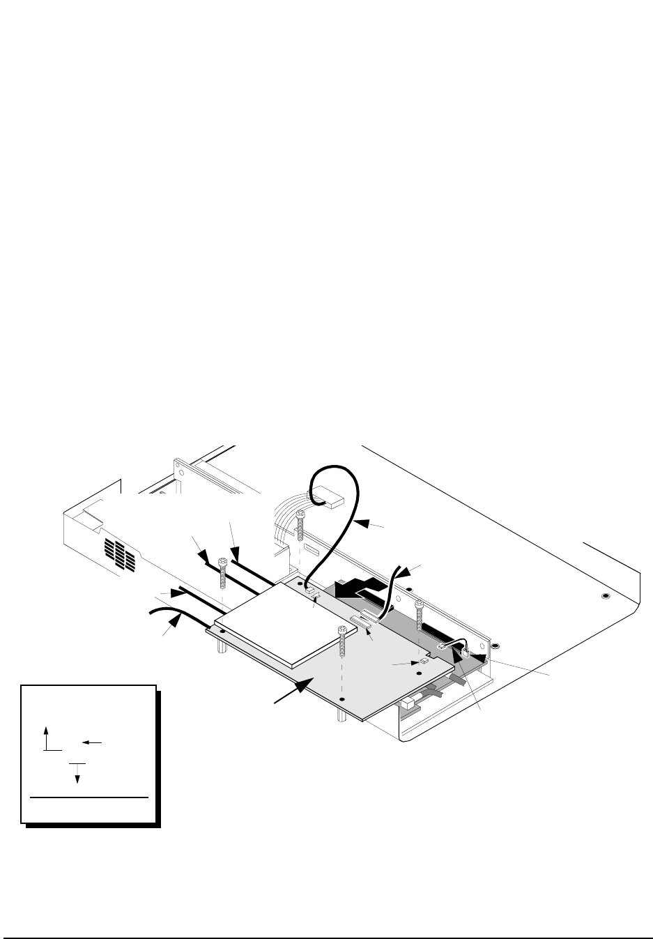
80
Chapter 3, Disassembly and Replacement
Disassembly of the HP 83205A Cellular Adapter
Removing the A11
CDPD Assembly If the Cellular Adapter is an Option 001 (CDMA only), the following instructions
do not apply since it does not contain the A11 CDPD assembly.
To remove the A11 CDPD assembly in Option 002 or 003:
1. Remove the cover from the Cellular Adapter, see "Separating Units and Removing
Cover" on page 63.
2. Remove the front panel, see "Removing the Front Panel" on page 68.
3. Remove the 4 machine screws securing the A11 assembly, see figure 30.
4. Disconnect the cables and connectors shown in figure 30 from the A11 assembly.
5. Carefully lift the A11 assembly over the edge of the Cellular Adapter and pull
it away from the A3 motherboard.
This completes the procedure for the removal of the A11 assembly.
Figure 30 Removing the A11 CDPD Assembly
W12 (11P2-10J1)
W13 (11P3-2J9)
A8W1-11J2
A11 Assembly
MP11
W21 (11J4-7J6)
W20 (11J3-6J6)
W15 (11J6-OPTIONAL
W14 (11J5-A10 “INPUT”)
A2J9
P3
P2
J2
MODE OUT)
W28
Assembly A7, Connector J5
to Assembly A4, Connector J3
(7J5-4J3)
Wire
reference
designator
Cable Legend
[RP] = Rear Panel
[FP] = Front Panel
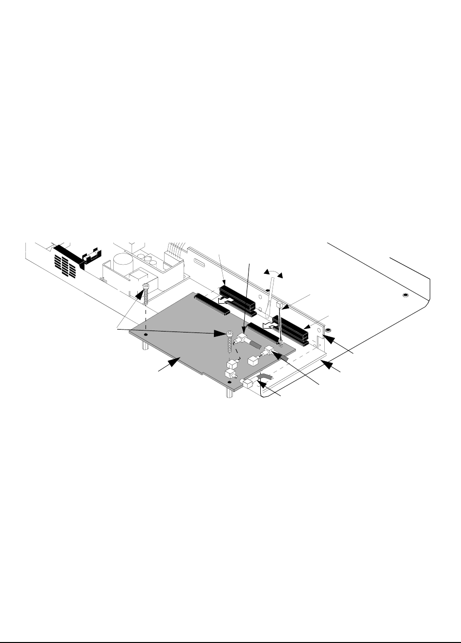
81
Chapter 3, Disassembly and Replacement
Disassembly of the HP 83205A Cellular Adapter
Removing the A2
RX DSP and A5
Data Buffer
Assemblies
To replace the A2 RX DSP or A5 Data Buffer assembly:
1. Remove the cover from the Cellular Adapter, see "Separating Units and Removing
Cover" on page 63.
2. Remove the front panel of the cellular adapter. See "Removing the Front Panel" on
page 68.
3. If the Cellular Adapter is an Option 002 or 003, remove the A11 CDPD assembly, see
see "Removing the A11 CDPD Assembly" on page 80.
4. If the Cellular Adapter is an Option 001, remove the 2 screws securing the A2 assem-
bly, see figure 31.
5. Disconnect the cables and SMB connectors shown in figure 31 from the A2 assembly.
Figure 31 Removing A2 RX DSP Assembly
6. With a flat blade screwdriver wedged between the A2 assembly and the A3 mother-
board assembly, carefully push and tilt the end of the A2 assembly over the edge of the
deck to unplug it from the J3 and J4 connectors of the motherboard, see figure 31.
A2 Assembly
W29
W37
A5 Assembly
A2
W25
Screws
W13
(Option 001 only)
(2J6-6J4)
(2J4-4J7)
(2J9-11P3)
(2J3-[RP]OJ2)
A3J3
A3J4
A3 Assembly
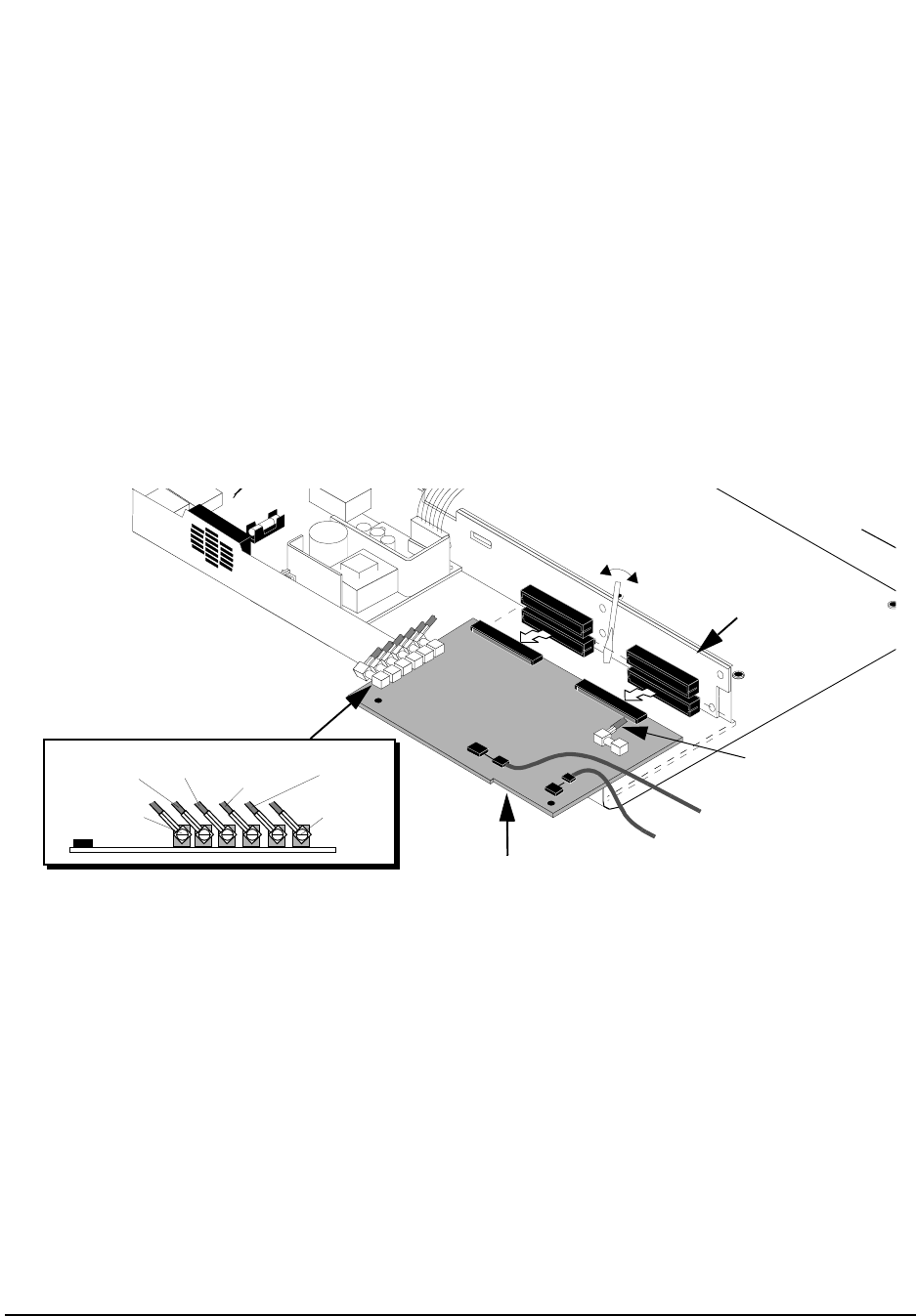
82
Chapter 3, Disassembly and Replacement
Disassembly of the HP 83205A Cellular Adapter
7. To remove the A5 Data Buffer assembly, disconnect the cables and connectors shown
in figure 32 from the A5 assembly.
8. Using the flat-blade screwdriver, carefully pry and tilt the end of the A5 assembly over
the edge of the deck and unplug it from the J5 and J6 connectors of the A3 assembly,
see figure 32.
This completes removal of the A2 and A5 assemblies. When reinstalling the A2
and A5 assemblies, use figure 31 on page 81 and figure 32 to identify the location
of the cables and connectors.
Figure 32 Removing the A5 Data Buffer Assembly
A5 Assembly
W9
W32
(J709)
(J22)
A1W2
(5J4-4J708)
(4J701-5J709)
(5J22 - front panel DATA IN.)
A5
W8
W35 W33 W34 W36
W26
(5J502-[RP]OJ6)
(5J500-7J2) (5J501-4J500) (5J401-4J400) (5J400-7J3)
(5J402-[RP]OJ3)
A3 Assembly
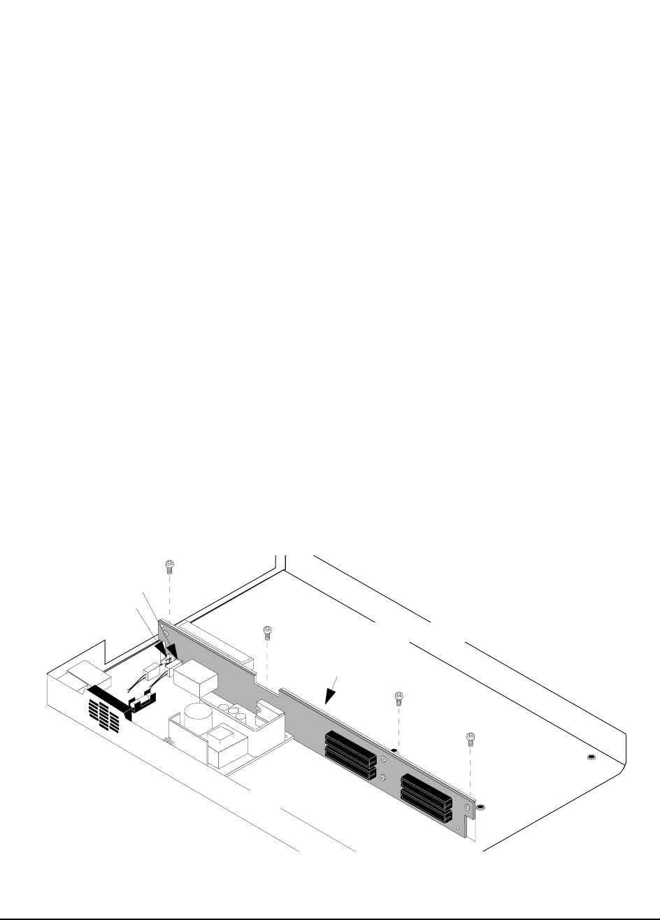
83
Chapter 3, Disassembly and Replacement
Disassembly of the HP 83205A Cellular Adapter
Removing the A3
Motherboard
Assembly
The following procedure removes and disassembles the A3 motherboard
assembly.
1. Remove the cover from the Cellular Adapter, see "Separating Units and Removing
Cover" on page 63.
2. Remove the front panel, see "Removing the Front Panel" on page 68.
3. Remove the rear panel, see "Removing the Rear Panel" on page 70.
4. Remove the A4 assembly, see "Removing the A4 Gen/Ref Assembly" on page 72.
5. Remove the A9 assembly, see "Removing the A9 Reference/IQ Assembly" on page 74.
6. If the Cellular Adapter is an option 002 or 003, remove the A11 assembly, see "Remov-
ing the A11 CDPD Assembly" on page 80.
7. Remove the A2 and A5 assemblies, see "Removing the A2 RX DSP and A5 Data Buff-
er Assemblies" on page 81.
8. Remove the power connectors from the J7 and J1 connectors on the A3 assembly, see
figure 33.
9. If the Cellular Adapter is an Option 001, remove the 4 screws securing the A3 assembly
to the deck, see figure 33. If the Cellular Adapter is an Option 002 or 003, two of the
screws secure the CDPD semi-rigid cables to the deck, see figure 29 on page 79.
This completes the procedure for the removal of the A3 assembly. To reassemble
the Cellular Adapter, follow the previous steps in reverse order.
Figure 33 Removing the A3 Motherboard Assembly
J7
J1
A3 Assembly
Screws removed are 3mm by 6mm.

84
Chapter 3, Disassembly and Replacement
Disassembly of the HP 83205A Cellular Adapter

85
4
Modifications
This chapter explains how to load and verify firmware upgrades on the
HP 83205A Cellular Adapter.

86
Chapter 4, Modifications
Firmware Upgrades
Firmware Upgrades
Firmware in the HP 83205A Cellular Adapter and its companion HP 8921A Cell
Site Test Set should be upgraded to the latest revision any time a repair is made or
a performance problem is discovered.
The Test Set’s firmware is upgraded by installing new PROMs. These are
available by ordering the HP 8921A Test Set firmware upgrade kit
(HP 8921A R98).
The Cellular Adapter’s firmware is upgraded by running a program that
downloads the new firmware files from a memory card and stores them in the
EEPROM’s on the A2 RX DSP assembly. Table 8 below lists the upgrade kits
available. For ordering information, see "Service Information," in chapter 1, on
page 35.
Table 8 Firmware Upgrade Kits
Kit Description
83205-61801 HP 83205A Cellular Adapter firmware
HP 8921A R98 HP 8921A Test Set firmware
83204-61807 CDPD application software
HP 83205A R99 All of the above.

87
Chapter 4, Modifications
Firmware Loading and Verification
Firmware Loading and Verification
NOTE: The DSP firmware download program in the following section checks the Test Set’s
firmware revision for compatibility. If the Test Set’s firmware is not compatible, order and
install the latest firmware revision. Order kit HP 8921A R98. For ordering information,
see "Service Information," in chapter 1, on page 35.
Load the DSP
Firmware The following procedure loads the Digital Signal Processor firmware.
1. Press the PRESET key.
2. Insert the 83205-10001 memory card into the Test Set.
3. Press the TESTS key.
4. Set the Select Procedure Location: field to Card.
5. Set the Select Procedure Filename field to DLFIRM.
6. Select Run Test (k1) key.
7. Follow the instructions on the screen.
After the firmware is downloaded, be sure to cycle the Test System’s power if
you are not loading CDPD firmware, otherwise, see the following procedure.
Load the CDPD
Firmware The following procedure loads the CDPD firmware.
1. Press the PRESET key.
2. Insert the 83205-10004 memory card into the Test Set.
3. Press the TESTS key.
4. Set the Select Procedure Location: field to Card.
5. Set the Select Procedure Filename field to CDPDULD.
6. Select Run Test (k1) key.
7. Follow the instructions on the screen.
After the firmware is downloaded, be sure to cycle the Test System’s power when
complete.

88
Chapter 4, Modifications
Firmware Loading and Verification
Verifying
Firmware Version The following procedure checks the current version of the firmware in the
HP 8921A Test Set and the Cellular Adapter.
1. Power on the Test System.
2. Check the firmware level of the Test Set, the firmware level appears in the upper part
of the RX TEST screen:
• For the HP 83205A CDMA Cellular Adapter (Option 001), the Test Set’s version
level must be A.16.00 or higher.
• For the HP 83205A CDPD Cellular Adapter (Option 002), the Test Set’s version
level must be A.17.00 or higher.
• For the HP 83205A CDMA/CDPD Cellular Adapter (Option 003), the Test Set’s
version level must be A.17.00 or higher.
If the Test Set does not have the proper firmware, see "Firmware Upgrades" on page
86 for ordering an upgrade kit.
3. Press the blue SHIFT key, then the DUPLEX (CONFIG) key. The Configure screen
appears.
4. Select SERVICE from the To Screen menu. The Service screen appears.
5. Select the Latch field.
6. Move the cursor to rx_dsp_revision under the Choices: menu and press the
knob.
7. Read the RX DSP firmware version from the Value field. The value is actually a date
in the form YYYYMMDD (Y=year, M=month, D=day).
Compare this date to the date on the new DSP firmware memory card.

89
5
Block Diagrams
This chapter provides information for helping you understand the operation of the
HP 83205A Cellular Adapter and its CDMA and CDPD options.

90
Chapter 5, Block Diagrams
Instrument Description
Instrument Description
The HP 83205A Cellular Adapter is an add-on-instrument for the HP 8921A Test
Set. The Cellular Adapter is controlled by the Test Set’s host processor through
the Test Set’s front-panel selections or HP-IB commands to the Test Set. The
Cellular Adapter mounts on top of the Test Set.
Adding the CDMA Cellular Adapter, Options 001 and 003, to the Test Set creates
a system for testing cellular base stations to the CDMA standard. The CDMA
standard uses digital compression to increase the number of channels over the old
AMPS system.
The CDPD Cellular Adapters, Options 002 and 003, include Cellular Digital
Packet Data (CDPD) digital signal generation and analysis. CDPD is a packet
data system which overlays the existing AMPS voice system, is designed for
sending packet data, and uses a separate base station (Mobile Data Base Station,
MDBS) which is integrated into the antenna system of a cell site. When there is
no voice traffic on a designated AMPS voice channel, the MDBS transmits packet
data to mobile end stations or fixed end stations. When AMPS voice traffic is
assigned to that channel, the MDBS must power down and reacquire
communications on another designated CDPD channel if available.
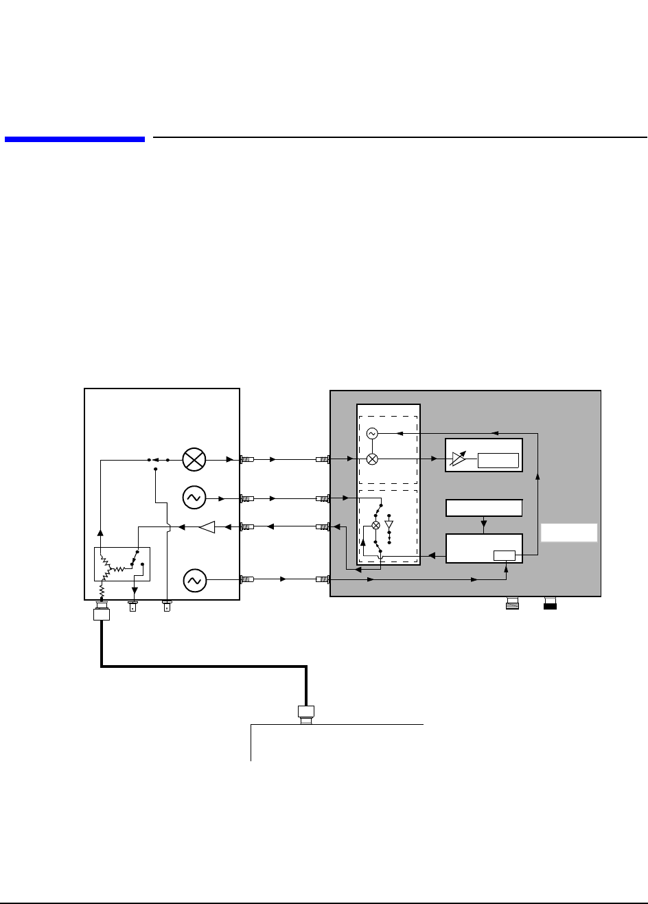
91
Chapter 5, Block Diagrams
CDMA Cellular Adapter
CDMA Cellular Adapter
Options 001 and 003 of the HP 83205A Cellular Adapter contain CDMA digital
signal processing hardware and firmware to test the transmitter and receiver
portions of CDMA base stations.
The Test Set’s CDMA Generator and CDMA ANL test screens have fields for
controlling the Cellular Adapter and for displaying measurement results. The
CONTROL I/O cable (not shown on the simplified block diagram below) passes
the digital control and data signals between the Test Set and the Cellular Adapter.
Figure 34 CDMA Test System Overview
CDMA Cellular Adapter
HP 8921A Test Set
Reference 10 MHz
Downconverter to IF
RF IN/OUT
DUPLEX OUT
REF IN
114.3 IF OUT
114.3 MHz IF IN
3.6864 MHz
CW RF OUT
IQ
IQ RF IN IQ RF OUT
CW RF IN A7
A6
A5 Data Buffer
A2 RX DSP
RX DSP
10 MHz
Radio Under Test
ANT
I/Q Mod
Ref/RX
ANT IN
A9
REF OUTPUT
A4 Gen/Ref
CW Source
PLL
Clock & Sampling
Signals
SYNTH

92
Chapter 5, Block Diagrams
CDMA Cellular Adapter
CDMA Analysis
The CDMA signal is down converted to 114.3 MHz IF by the Test Set before
being passed to the Cellular Adapter. The LO/IF (A6) downconverts the
114.3 MHz IF to a 3.6864 MHz IF before passing the signal on to the A2
Receiver DSP assembly for processing, see figure 34 on page 91.
CDMA Generation
The A5 Data Buffer assembly generates data that emulates a CDMA traffic
channel and provides a calibrated noise source. The Generator/Reference then
converts the data into I and Q drive signals. The signal is then passed to the I/Q
Modulation (A7 assembly) where it is modulated with the RF from the Test Set.
The signal is then passed to the Test Set for amplification.
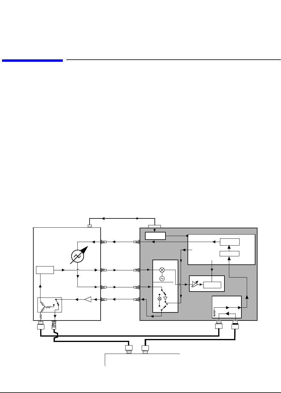
93
Chapter 5, Block Diagrams
CDPD Cellular Adapter
CDPD Cellular Adapter
Options 002 and 003 of the HP 83205A Cellular Adapter contain the hardware
and firmware for testing CDPD mobile data base stations (MDBS).
CDPD Analysis
The Test Set down converts the CDPD signal to 114.3 MHz IF, see figure 35.
This 114.3 MHz IF is passed to the Cellular Adapter’s receiver where it is
converted to 3.6864 MHz and passed to the RX DSP for analysis. The signal is
checked for valid CDPD data using the A10 Directional Coupler and the DSP on
the A11 CDPD assembly.
CDPD Generation
A CDPD data signal is generated by the DSP on the CDPD assembly, see figure
35. It is then encoded with 0.5 GMSK before being passed to the Test Set for
modulation. The signal is passed back to the Cellular Adapter’s I/Q modulator for
amplitude control before being amplified and transmitted by the Test Set.
Figure 35 CDPD Test System Overview
CDPD Cellular Adapter
DSP
0.5 GMSK
CDPD Valid
Amplitude
Control
Directional Coupler
HP 8921A Test Set
DC FM
114.3
RF IN/OUT DUPLEX OUT
CDPD
MOD OUT
114.3 IF OUT
114.3 MHz IF IN
3.6864 MHz
CW RF OUT
RCVR
IQ
IQ RF IN
SYNTH IQ RF OUT
IBASIC
RJ DB15
Serial Port
Serial Switch
CW RF IN
(SERIAL Cable)
RCVR
A9/A7
A9/A6
A10
A10
A11
A2
RX DSP
MOD IN
J4
J6
P3 J5
J6
J9
Mobile Data Base Station
TX
RX
RF IN/OUT
RF IN/OUT TO TEST SET

94
Chapter 5, Block Diagrams
Assembly Descriptions
Assembly Descriptions
Table 9 describes the major assemblies and subassemblies that make up the
Cellular Adapter. Use the diagram shown in figure 36 on page 95 for a visual
overview of the Test System.
Table 9 Quick Reference of Assemblies
Assembly
Designator Assembly Name Function
A2 Receiver DSP (Digital Signal Processor) Data analyzer
A4 Generator/Reference Encodes the I/Q channels
A5 Data Buffer Data generator
A9 Reference/IQ Houses the A6 & A7 assemblies
A9/A6 LO/IF Receiver and down converter
A9/A7 IQ Modulator Modulates the RF carrier with π/4 DQPSK
A10 CDPD Directional Coupler & Serial
Switch The directional coupler couples the CDPD signal for
verification. The serial switch switches Test Set
communication between the premod filter and the
CDPD assembly.
A11 CDPD module Provides CDPD protocol processing
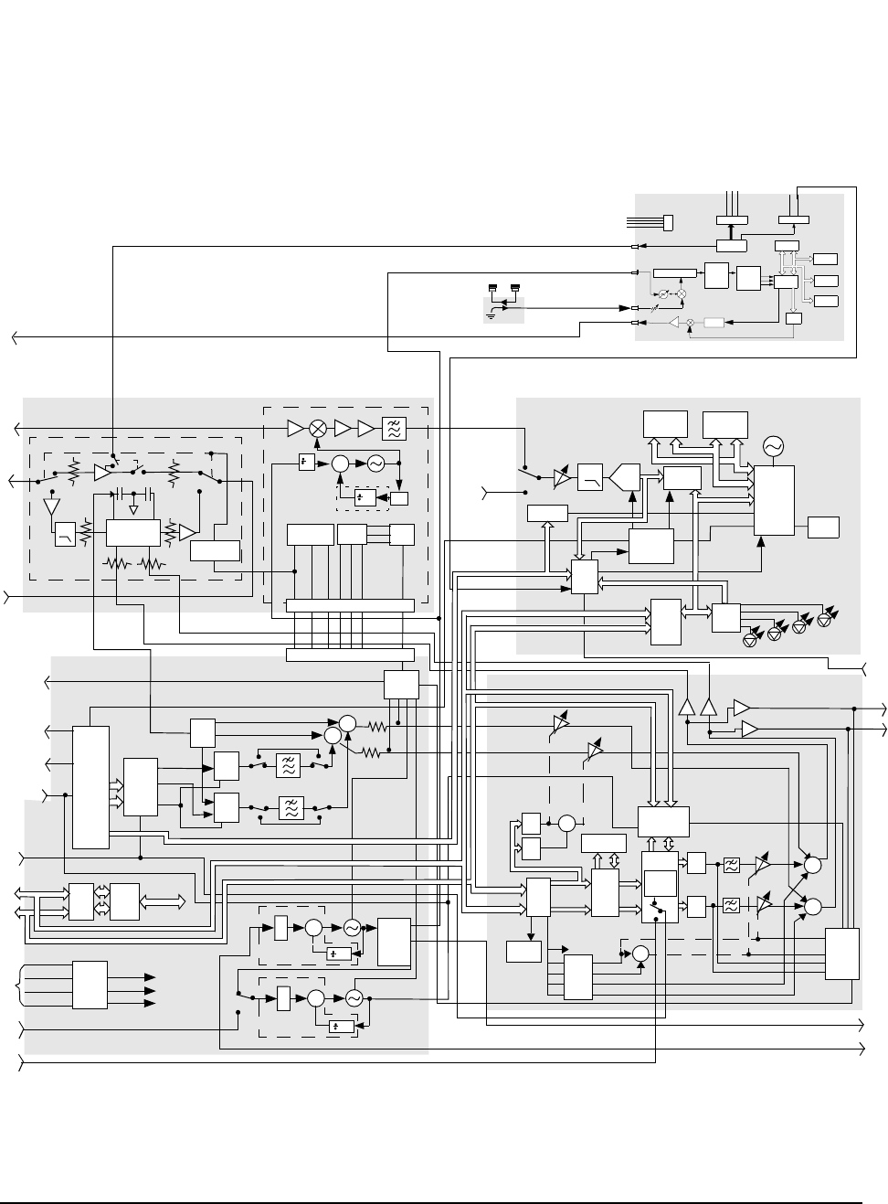
95
Chapter 5, Block Diagrams
Assembly Descriptions
Figure 36 Test System Block Diagram
A9 Ref/ IQ
114.3 MHz
IF IN (RP)
A6 LO/IF
A7 I/Q Modulator
A2 RX DSP
128K FLASH
EPROM 256K
Fast RAM
33 MHz
THS320C30
DSP
ADDR
Decode
12 BIT
ADC
8 MHz
-10 to +30 dB
IQ
CW RF
IN (RP)
I Q Mod
Assembly
1 GHz
RF In RF Out
I Drive Q Drive
10
DIAG
DIAGNOSTIC
A4 Gen/Ref Board
DATA IN
EVEN SEC/
GDATA
Data
Buffer
Parallel
To
Serial
Interface
CONTROL
U1
÷N
Σ
10MHz
OUT (RP)
TRIGGER/
QUALIFIER
Host
Inter-
Data
Latch
DIAG 0
DIAG 1
DIAG 2
DIAG 3
DE-MUX
12 TO 24
Trig
Circuit
Sample
Clock
Generator
MUX
Quad
Adjust
PWR
+12V, +12VAUX
110.6863 MHz
10 MHz
N.F. 8/9
Power
Regulation Serial
I/O MUX
MUX 0
MUX 1
MUX 2
J1
+12V
-12V
+5V
CLK
DATA
7,14 6 15 9 2 10 4
3,4 5 2 14 13 12 9
LO/IF DIAG
J10
RF OUT
(RP)
MONITOR
OUT (FP)
DIAG
MUX
B_CASSS
1.2288 MHz
CHIP CLOCK
OUT (FP)
19.6608 MHz
16xCHIP
CLOCKOUT
(FP)
SYNC IN
(FP)
I/Q
CAL
DAC
M_CASSS
I
DAC
Q
DAC
Σ
Q_OFFSET
I_OFFSET
I/R
I/R
GADDR
(FP)
CDMA
TIMEBASE
IN (RP)
Power
Sense/
Regulator
GND
+15V
+5V
-15V
+12V
+5V
-12V
3.6864 MHz IF
IN (RP)
A5 Data Buffer / Noise Source
I + Noise To IQ Modulator
Q + Noise To IQ Modulator
I Out
(RP)
Q Out
(RP)
Diag
MUX
Σ
Σ
Gaussian Table /
Buff / Mod noise
Config.
128K x 16 Flash
Q Signal
Control I Signal
Control
Σ
SYNTH
REF
INPUT
(RP)
I/0
Serial
IO
Q Offset
I Offset
Noise Gain Delta
Σ
Parallel
Outputs
Mod noise
CDMA
Reverse
Link
Modulator
DATA IN
(RP)
Serial Data
I Noise Control
Q Noise Control
I
DAC
Q
DAC
1 MHz
1 MHz
CAL
EEPROM
Data
Buffer
Control
Status/
Readback
Control
Serial
Data
Data Buffer
128K x 8 SRAM
Q
Gain
I
DAC
DAC
Gain I Signal
Gain Delta
GADDR
GDATA GADDR
GDATA
EN2
Serial
Bus
GADDR
GDATA
CONTROL
I/O
(RP)
TO
POWER
SUPPLY
Ø
Ø
Ø
N.F.
N.F.
AUX DSP
3 dB
3 dB
20.00 MHz
19.6608 MHz
IN (RP)
Buffer
Serial
J2 Power P3 CDPD VALID
FM DEMOD
AMPLITUDE CONTROL
10MHz REF IN
RX IN
BASEBAND
J4
J3
J5
J6
P2
Control
DSP
GMSK
Modem
0.5 GMSK
FPGA
µC
SRAM
OTP
FLASH
DAC (DC Offset
VCO
Serial
Control)
A10
30 dB
A11 CDPD
CAL
DAC
Coupler
Directional
OPTIONAL
MODE OUT
face
Dividers

96
Chapter 5, Block Diagrams
Assembly Descriptions
A2 RX DSP
Assembly The RX (Receiver) DSP board is the heart of the Cellular Adapter’s analyzer.
This board performs the complex BERT, EVM, and Adjacent Channel power
measurements functions using specialized DSP Firmware. The specialized DSP
firmware can be updated through the Test Set’s memory card reader. For
connector information, see table 10.
A3 Motherboard This assembly interconnects the premod filter and the DSP boards. It distributes
the AC/DC voltages and control signals. The Test Set has control over the A3
assembly’s power relay to apply or disconnect AC power to the Cellular Adapter.
A4 Gen/Ref
Assembly The Generator/Reference assembly converts the generated test signal to I and Q
drive signals through a process of buffering, differential encoding, and filtering.
This assembly uses a digital Nyquist filter. For connector information, see table
11 on page 97.
Table 10 A2 Receiver DSP
Description and/or Function
J6 3.6864 MHz input from the reference board. This IF is the downconverted 114.3 MHz IF
from the Cellular Adapter’s receiver.
Expected Frequency = 3.6864 MHz ±1 kHz
Input Level = 30 to 400 mV peak
Input impedance = 2kΩ
J3 Input for external IF signal bypassing the Cellular Adapter receiver’s 114.3 MHz IF.
Expected Frequency 3.6864 MHz ±1kHz
Input Level = 30 to 400 mV peak
Input Impedance = 2kΩ
J4 EXT_FS input from A4 FsClk (A4J7)
Expected Frequency 4.9152 MHz

97
Chapter 5, Block Diagrams
Assembly Descriptions
Table 11 A4 Generator/Reference Assembly
Description and/or Function
J1 CDMA TIMEBSE INPUT (front panel). This port is the CDMA timebase input to the CDMA
reference PPL. When the CDMA TB field is set to Internal, the CDMA frame clocks are
phase locked to the RF synthesizer’s 10 MHz reference. When one of the following frequencies
are chosen, the CDMA frame clocks are locked to the signal on this connector:
Expected Frequency = 1, 1.2288, 2, 2.4576, 4.9152, 5, 9.8304, 10, 15, 19.6608 MHz.
Accuracy = ±1 PPM.
Input Level = 0 to +23 dBm
Input Impedance = 50 Ω
J2 SYNTH REF IN (rear panel). Provides a phase reference for the RF synthesizer. Normally con-
nected to the Test Sets 10 MHz OUT. The REF UNLOCK LED will be on if none of the follow-
ing frequencies are present:
Expected Frequency = 1, 1.2288, 2, 2.4576, 4.9152, 5, 9.8304, 10, 15, 19.6608 MHz
Accuracy = ±5 PPM.
Input Level = 0 to + 23 dBm
Impedance = 50 Ω
J3 10 MHz LO. Provides a 10 MHz reference to the LO/IF board A6J2.
J5 10 MHz OUT (rear panel). Provides a 10 MHz reference output. This signal is phase locked to
the signal applied to the SYTH REF IN port.
Stability = same as Synth. REF. IN.
Input Level = > +5 dBm
Input Impedance = 50 Ω
J7 4.9152_OUT to EXT_FS (A2J4) input
Frequency = 4.9152 MHz
J20 Fan Drive > 12 vdc
J703 EVEN SECOND IN/SYNC IN (front panel). Input for the even second clock from the transmitter
under test.
Input Level = TTL
Input Impedance = 50 Ω
J400 I_OUT. I data drive to the IQ modulator, A5J401.
J500 Q_OUT. Q data drive to the IQ modulator, A5J501.
J701 DATA IN (front panel). Provides a data input to the CDMA Generator of the Cellular
Adapter.
Input Level = TTL
Data Rate = 1.2288 Mcps.
Input Impedance = 50 Ω

98
Chapter 5, Block Diagrams
Assembly Descriptions
A5 Data Buffer
Modulator The Data Buffer generates a signal that emulates a CDMA traffic channel and
provides a calibrated noise source.
A8 Power Supply This switching supply is a replaceable assembly and provides the +5 and +/−15
DC voltages for the Cellular Adapter. Replacement of the power supply fuse is
not supported. See "Power Supply and Voltage Distribution" on page 102 for
power distribution information.
A9 Reference/ IQ The A9 assembly contains both the LO/IF (A6) and IQ Modulator (A7) sub
assemblies. The IQ Modulator routes the source’s RF through the I and Q
modulator or through the bypass path. This circuit is controlled by the host Test
Set though the Gen/Ref board (A4). The LO/IF conditions and translates the
114.3 MHz received IF from the host Test Set and routes a translated IF to the
DSP board (A2). For connector information, see table 12 on page 99.
J702 TRIGGER QUALIFIER IN (front panel). Active when an external trigger qualifier is selected.
Input Level = TTL
Input Impedance = 50 Ω
J705 1.2288 MHz OUT CHIP CLOCK (front panel). Provides a 1.2288 MHz square wave output with
a 50% duty cycle. CDMA Chip Rate.
Input Level = CMOS
Input Impedance = 50 Ω
J706 19.6608 MHz OUT 16 X CHIP CLOCK (front panel). Provides a 19.6608 MHz square wave
output with a 50% duty cycle. (16 times the CDMA chip rate). This signal is derived from the
CDMA frame clocks.
Input Level = CMOS
Input Impedance = 50 Ω
J708 19.6_CHB. Provides digital timing to the Data Buffer board, A5J4.
Table 11 A4 Generator/Reference Assembly
Description and/or Function

99
Chapter 5, Block Diagrams
Assembly Descriptions
Table 12 A9 IQ Modulator and LO/IF Assembly Signals and Waveforms
Description and/or Function
A6J3 114.3 MHz Input. Downconverted IF with π/4 DQPSK modulation from the Test Set’s receiver.
Input Level = −15 dBm max. level, typical −53 to −25 dBm
A6J4 3.6864 MHz IF Output to A2J6. Downconverted from the 114.3 MHz IF with π/4 DQPSK
modulated carrier.
Input Level = −25.5 to 5.5 dBm into 50 Ω
A7J1 CW RF IN (rear panel) - CW RF to this port is from CW RF OUT of Test Set. If the CW
RF Path is set to IQ, the CW signal is modulated by the I and Q drive signals before being
routed to the rear panel IQ RF Out connector. In bypass, the CW RF signal is routed
around the IQ modulator to the IQ RF OUT connector.
Bypass path, 500 - 1000 MHz.
IQ Mod path, 810-956 MHz level, 0 dBm +/− 4 dB nominal, Max. +12 dBm.
Input Impedance = 50 Ω.
A7J4 IQ RF OUT (rear panel) - to IQ RF IN. RF output from the IQ Modulator or Bypass path.
Bypass, 500-1000 MHz @ Gain >2 dB
IQ Mod, 810-956 MHz @ Output level= −8 to −11 dBm.
Quadrature set a center, 859 MHz, typical spur level < − 45 dB @ Quad.
A7J2,
A7J3 I and Q Inputs
Input Level ≅ −2 dBm
Input Impedance = 50 Ω
A7J5 Quad Tune;
DC level from A4J401, Gen/Ref
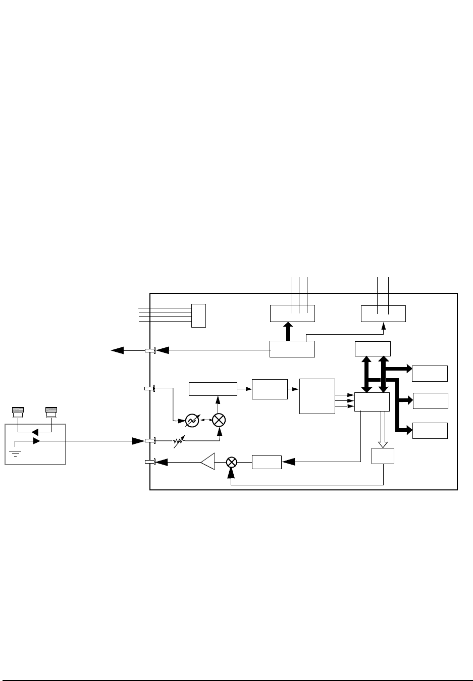
100
Chapter 5, Block Diagrams
Assembly Descriptions
A10 Directional
Coupler & Serial
Switch
The directional coupler passes part of the received CDPD signal to the CDPD
assembly while blocking the transmitted signal. This allows the CDPD module to
detect valid CDPD signals. The serial switch board allows the Test Set to send
commands to either the CDPD module or the Gen/Ref assembly.
A11 CDPD
Assembly The A11 CDPD assembly performs all of the CDPD signal generation and detects
a valid CDPD signal from the base station, see figure 37. The only way to control
the CDPD assembly is over the serial bus using the IBASIC controller built into
the Test Set. See table 13 on page 101 for a description of the signals and
waveforms expected from the connectors of the A11 assembly.
Figure 37 A11 CDPD Assembly Block Diagram
Buffer
Serial
J2
Power
P3 CDPD VALID
FM DEMOD
AMPLITUDE CONTROL
10 MHz REF IN
RX IN
BASEBAND
J4
J3
J5
J6
P2
Control
DSP
0/40 dB
GMSK
Modem
TO I/Q MOD ASSEMBLY
0.5 GMSK
FPGA
µC
SRAM
OTP
FLASH
DAC (DC Offset
VCO
Serial
Control)
Directional Coupler
30 dB

101
Chapter 5, Block Diagrams
Assembly Descriptions
Table 13 A11 Assembly Signals and Waveforms
Signal Description and/or Function
J2 Power −15V, GND, +5V, +15V
J3 10 MHz Reference Input - 10 MHz reference signal from the LO/IF module (A6 - part of A9
assembly).
J4 Amplitude Control - DC control signal for fast switching of the CDPD RF signal.
J5 Receiver Input - Modulated CDPD data signal received from the Directional Coupler (A10). Will
be active when running the RF loopback test in the diagnostics.
J6 Baseband 0.5 GMSK - Unmodulated CDPD data signal that is passed to the Test Set for
modulation and transmission. Will be active when running the RF Loopback Test in the
diagnostics.
P2 Serial Communications - Serial control bus to/from the serial switch board (A10).
P3 Valid CDPD - Notifies the DSP that a valid CDPD signal is being received. This is a DC signal.

102
Chapter 5, Block Diagrams
Power Supply and Voltage Distribution
Power Supply and Voltage Distribution
The Cellular Adapter does not have its own power-up switch. The power-up
command is received through the I/O CONTROL cable on the back panel. For an
overview of power distribution, see figure 38 on page 103.
WARNING: There are AC voltages present inside the instrument when the power cord is
connected to a power source. Extreme caution should be used when you are
working in the area of A3J1, A3J7, A3K1 on the A3 Motherboard, and the
fuse holder near the power cord. The A8 power supply assembly does not have
AC voltage present unless the POWER switch on the Test Set is pressed, the
Cellular Adapter is plugged in, and the digital IO cable is connected between
the Test Set and Cellular Adapter.
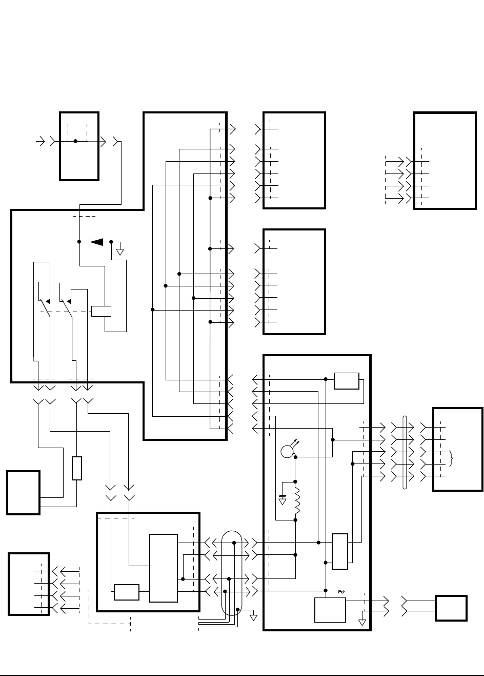
103
Chapter 5, Block Diagrams
Power Supply and Voltage Distribution
Figure 38 Test System Power Distribution
P/O A4 Gen/Ref
A3 Motherboard
A5 Data Buffer (Opt 001, 003)
A2 RX DSP
P/O A4 Gen/Ref
A9/A6 LO/IF
A8 Power Supply
Line Module
CONTROL I/O
A4J8, pin 48
+12V AUX
From
Test Set
+12 AUX
J6
10
J2
J1 J7
638
1
K1
NC
2
5
7
NC
4
131
3
FUSE
FUSE
J1
-15V
+5V
+15V
J2
6
5
4
1
1
3
2
6
A8W1 J9
FAN
DRIVER
43,44
45,46
47,48
49-50
51-54
J6 -5V Reg.
PWR
LED
+/- 12V
Reg.
+14V
2
1
J20
FAN
6
2
3
4
5
13
15
7
14
6
J1
+12 AUX
+5V
+12V
-12V
W16
+12 AUX
J10
J1
-15V
+15V
-5V
+5V
+5V
5
6
7,8
9,10
33-36
J2
5-8,
33-36
J2
J2
J6
J5 J1 -15V
+15V
-5V
+5V
+5V
5-8,
33-36
5
6
7,8
9,10
33-36
+5V
J3
J4
+5V +5V
+5V
CR1
A11 CDPD (Opt 002, 003)
J2
-15V
GND
+5V
+15V
A10 Serial IO
(Opt 002, 003)
J3
-15V
GND
+5V
+15V
Power Harness
To J2 of A11 Assembly &
To J3 of A10 Assembly
From A8W1
Power Harness
A4J6, pin 10
48
J8

104
Chapter 5, Block Diagrams
Power Supply and Voltage Distribution

105
6
Replaceable Parts
This chapter contains the replaceable assembly and component information for
the HP 83205A CDMA (Opt 001), CDPD (opt 002), and CDMA/CDPD (Opt
003) Cellular Adapters. Use the illustrations on the following pages to identify the
replaceable parts. See "Parts List" on page 120 for part numbers.
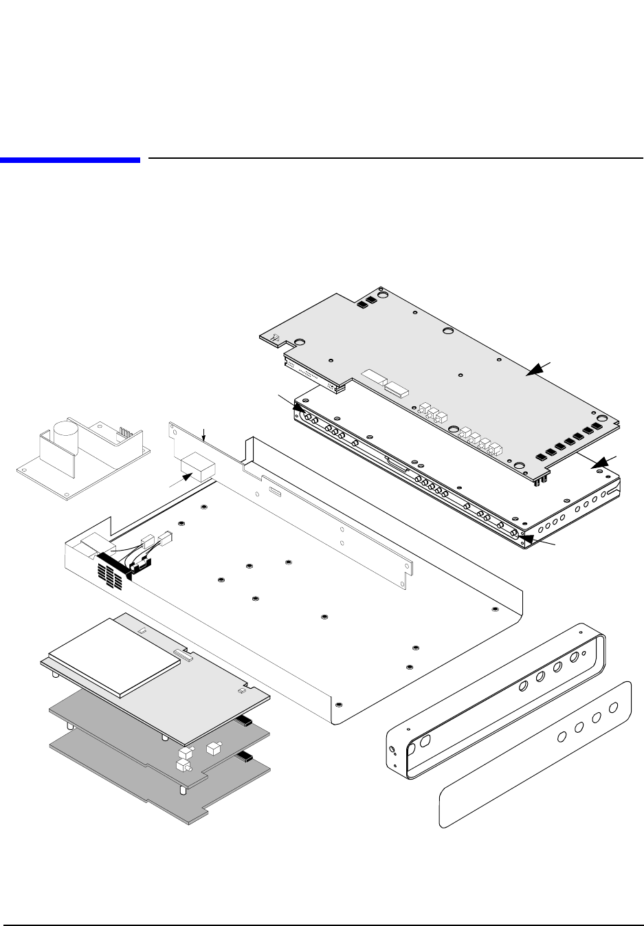
106
Chapter 6, Replaceable Parts
Parts Identification
Parts Identification
Major Assemblies Figure 39 below and figure 40 on page 107 identify the major assemblies for the
HP 83205A Cellular Adapter.
Figure 39 HP 83205A Cellular Adapter Major Assemblies
A9
A3
A1MP1
A7
A6
A12
A8
A4
A3K1
A1MP2 (Opt 001)
A5
A2
A11
(part of A9)
(part of A9)
(Opt 002/003)
(Opt 001/003)
(All options)
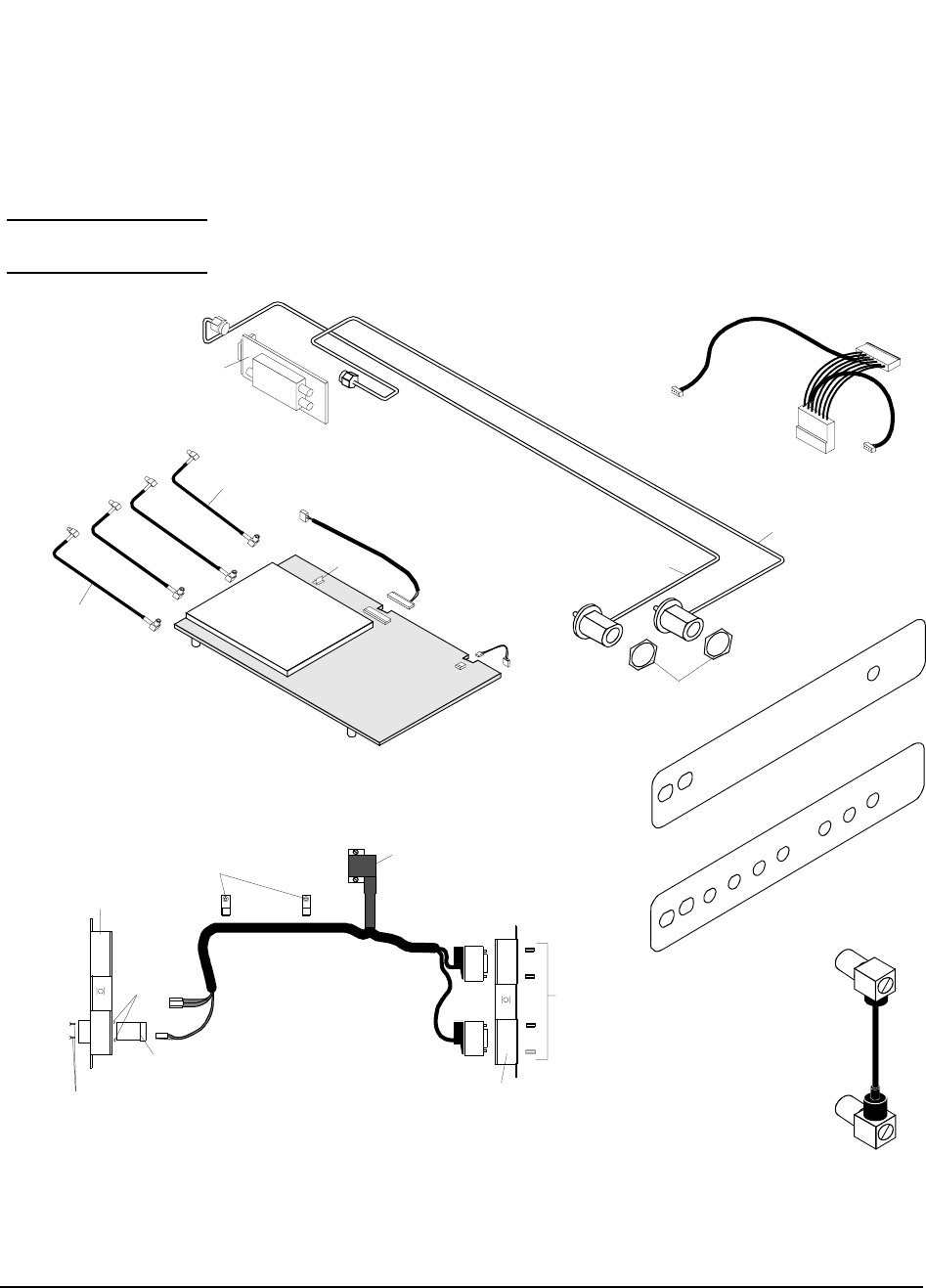
107
Chapter 6, Replaceable Parts
Parts Identification
CDPD Components
NOTE: The CDPD components shown below are installed in Options 002 and 003 of the
HP 83205A Cellular Adapter.
Figure 40 CDPD Assemblies and Components
A10
W11
A1MP2 (Opt 003)
A1MP2 (Opt 002)
A8W1
A11
W10
W19
MP21
MP29
MP30
J1
MP24
MP25
MP4
MP31
W13
W12 (11P2-10J1)
W18
W15
W14
W20
W21
([RP]OJ8)
(11J6)
(11J3)
(11J5)
(11J4)
(A10 “INPUT”)
(6J6)
(7J6)
J2
(to 10J3)
(to 11J2)
(to 4J9)
(11P3-2J9)
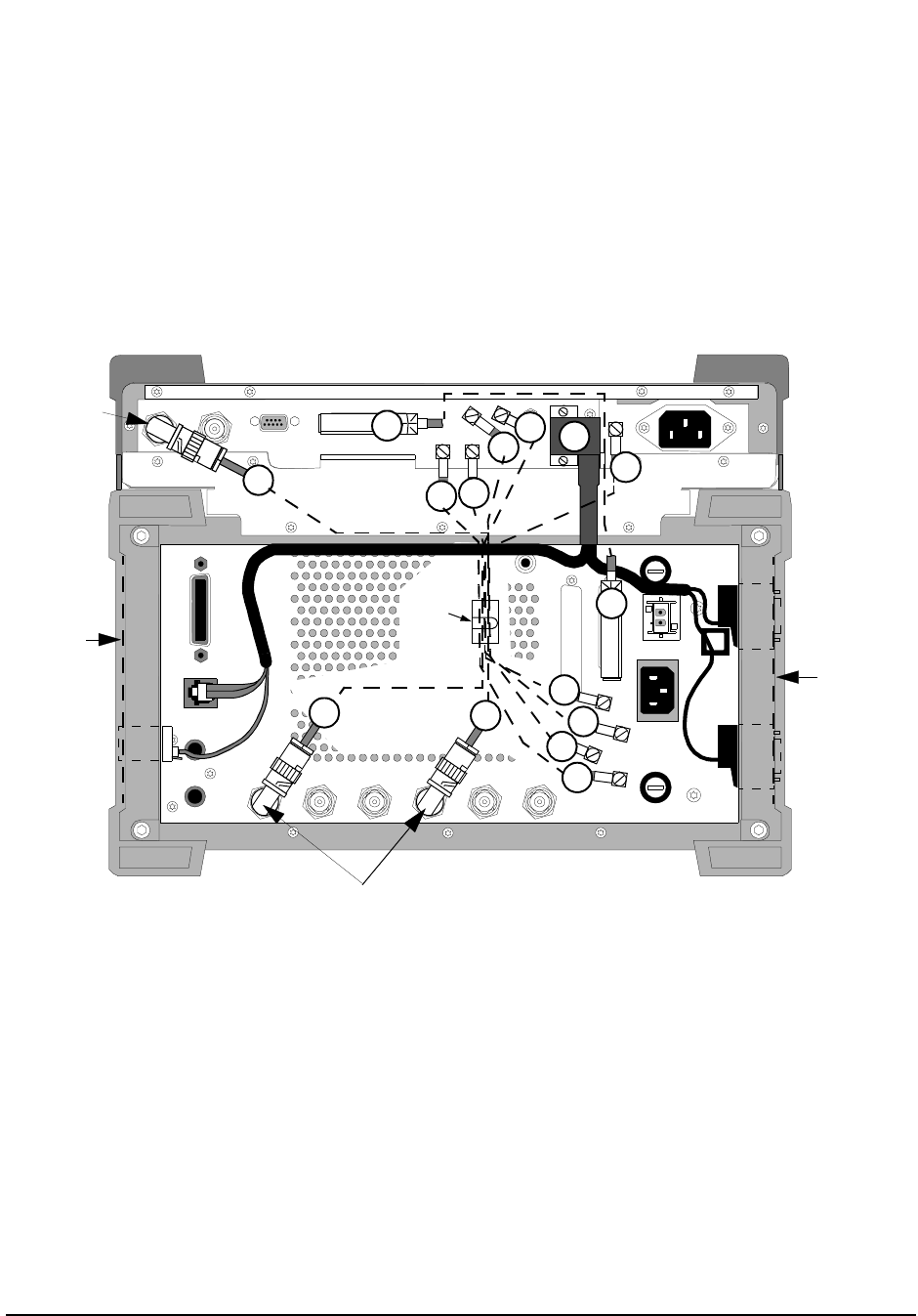
108
Chapter 6, Replaceable Parts
Parts Identification
External Cables
Figure 41 Rear Panel Cables of HP 83205A CDMA/CDPD Cellular Adapter (Option 003) and
HP 8921 Cell Site Test Set
114.3 MHz IF IN I BASEBAND OUT
AUX
CW
RF IN
IQ
RF OUT OPTIONAL
SERIAL PORT
CONTROL I/OSYNTH REF IN 10 MHz OUT
CDMA CLOCK OUTPUTS DSP IN
MOD OUT
10 MHz
REF OUT
Q BASEBAND OUT
W5
W2
W1
W3
MP13 W6
W5
W4
W2
W3
W1 W17
W6
W17
W19
MP1
MP1
MP29
MP30
(Options
002 & 003
only) (Options
002 & 003
only)
W4
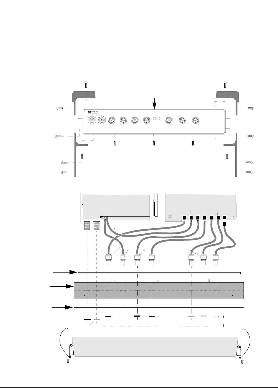
109
Chapter 6, Replaceable Parts
Parts Identification
Front Panel
Components
Figure 42 Front Panel Components
Frame
Top View
Front View
PWR REF
UNLOCK
83205A
CDMA CELLULAR ADAPTER
RF IN/OUT
TO
TEST SET
RF IN /OUT
MAX.PW R 60W
CONTINUOUS
DIAGNOSTIC
MONITOR OUT 1.2288 MHz O UT
CHIP CLOCK 19.6608 MHz OUT
16 X CHIP CLOCK
CDMA
TIMEBASE IN
EVEN SECOND/
SYNC IN
DATA
IN
TRIGGER/
QUALIFIER IN
A4 Assembly
A1W1
Deck
A2 Assembly
J702
J701
J703J1 J707
J705
J706
A1 Assembly
MP4
MP3
MP5 MP5
MP4
MP2
MP4
MP4
MP4
MP4
MP2
MP4
MP4
MP4
MP4
MP4
MP4
MP3
MP15
A1MP3
A1W5
A1MP1
A1MP2
A1MP4
A1W2
A1W4
A1W3
A1W7
A1W6
Dress Plate
RFI Braid
MP4
W9(4J701-5J709)
MP24
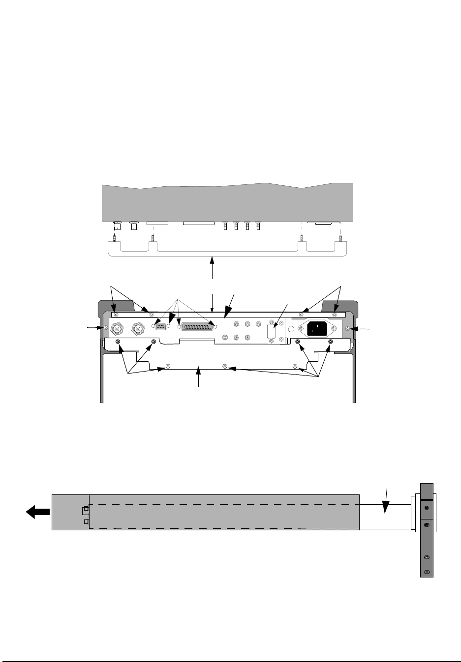
110
Chapter 6, Replaceable Parts
Parts Identification
Cover and Rear
Panel Components
Figure 43 Cover and Rear Panel Components
Deck
114.3 MHz IF IN I BASEBAND OUT
AUX
CW
RF IN
IQ
RF OUT OPTIONAL
SERIAL PORT
CONTROL I/O
SYNTH REF IN 10 MHz OUT
CDMA CLOCK OUTPUTS
DSP IN
MOD O UT
10 MHz
REF OUT
Q BASEBAND OUT
MP28
Top View
MP 18 (cover side view)
MP7
MP7 MP8 MP14
MP4 MP4
MP7
MP7
MP16
(Rear Panel)
(Mounting Plate)
(Option 001)
MP17
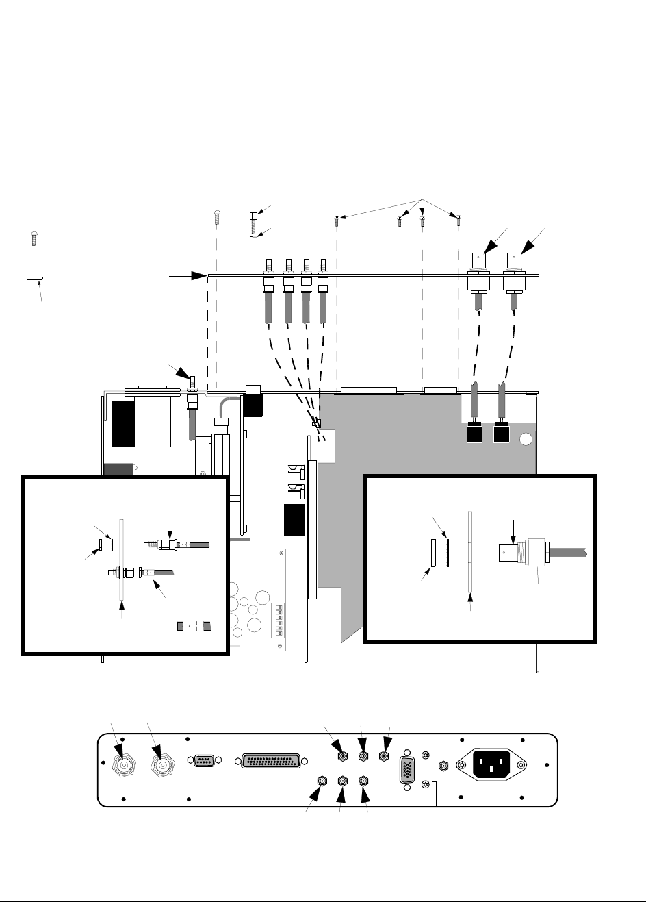
111
Chapter 6, Replaceable Parts
Parts Identification
Rear Panel
Components
Figure 44 Rear Panel Components
MP14
Deck
J5 J2
MP20
MP19 BNC Connector
MP16
MP17
MP14
W7 W23
W15
MP4
(Opt 001 only)
114.3 MHz IF IN I BASEBAND OUT
AUX
CW
RF IN
IQ
RF OUT
OPTIONAL
SERIAL PORT
CONTROL I/O
SYNTH REF IN 10 MHz OUT
CDMA CLOCK OUTPUTS
DSP IN
MOD OUT
10 MHz
REF OUT
Q BASEBAND OUT
W26
(OJ3)
W25
(OJ2)
W24
(OJ1)
W7
W23
W27
(OJ4) W28
(OJ5) W8
(OJ6)
(Lock Washer)
(9/16” Nut)
(Back Panel)
Drawing B
MP23
MP22
MP4
(Rear Panel)
0J3
0J7
MP27
MP26
MP14
Cable Clips
SMC Connector
0J3
(Lock Washer)
(1/4” Nut)
(Back Panel)
Drawing A
(OJ8 -11J6)
(See Drawing A)
(See Inset
Drawing A)
(See Drawing B)
(Opt 002/003)
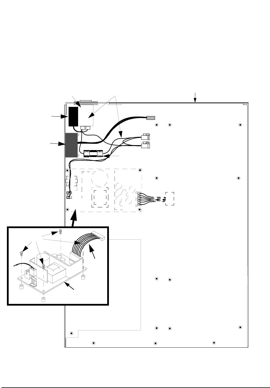
112
Chapter 6, Replaceable Parts
Parts Identification
Miscellaneous
Components
Figure 45 Miscellaneous Assemblies
A8
A12A8C3
A12A8MP1 A12A8
A12B1
A12
A12A8F1 (Fuse)
A12A9MP9 (Fuse Holder)
A8W1
MP4
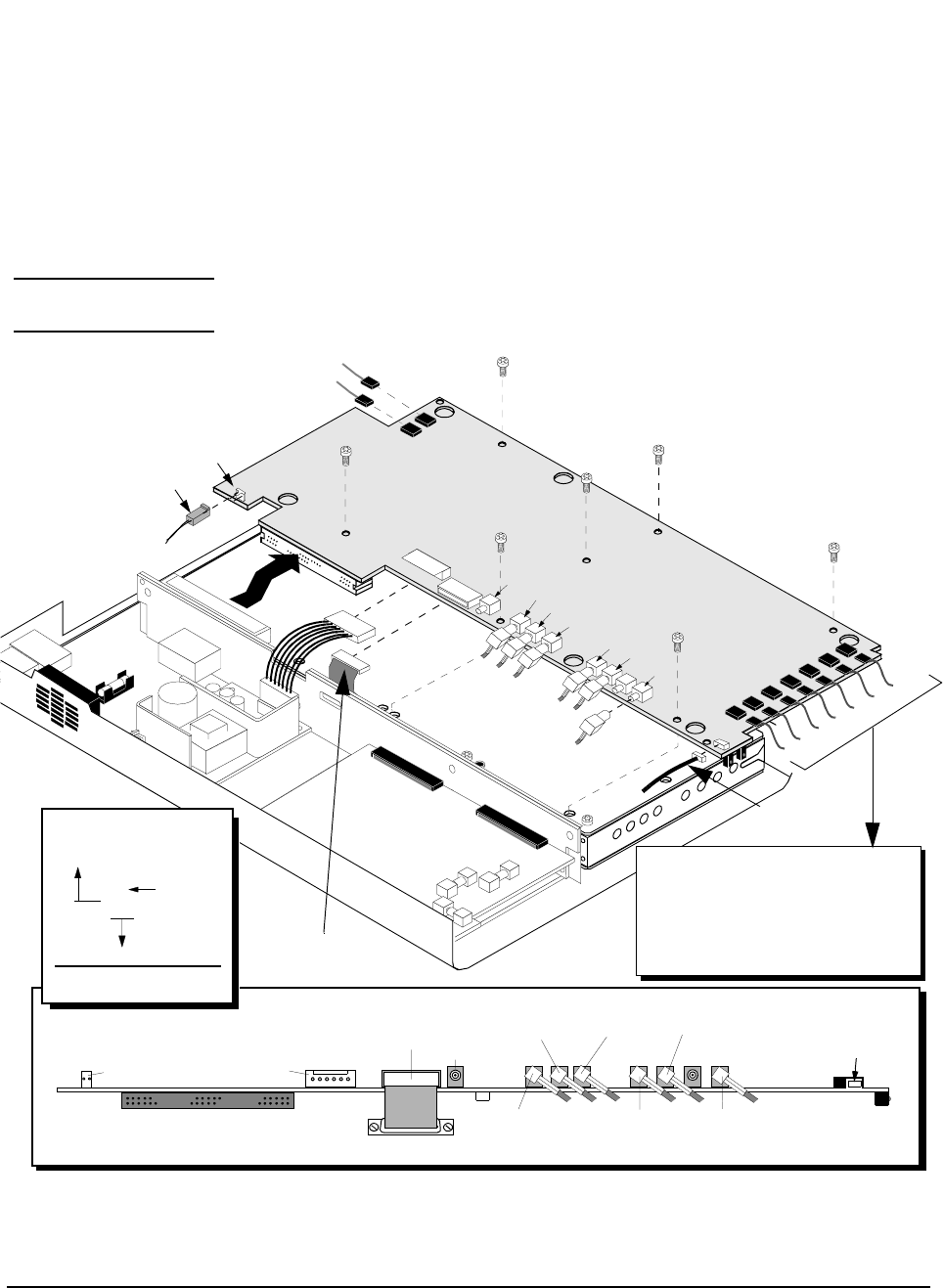
113
Chapter 6, Replaceable Parts
Parts Identification
A4 Gen./Ref.
Assembly and
Components
NOTE: Perform the PER_CALD and EBNO_CAL calibration procedures after replacing the A4
assembly, see "Periodic Calibration (for Options 001 & 003 only)" on page 127.
Figure 46 A4 Generator/Reference Assembly
J11
SMB Connector
P/O A12B1
J400
J500
J708
J401
J7
J9
J10
A4 Assembly
J20 J5 J2
J3
J709
J11
(4J11-10J2)
W22
W23
W7
(A4J5-[RP]10 MHz OUT)
(A4J2-[RP] SYNTH REF IN)
A1W7
A1W6
A1W4
A1W5
A1W3
W9
A1W1
W16
(A8W1)
(A12B1)
W34
J20 J9
(J10) J709 J4
W33 W32
W31
W30
W29
(4J400-5J401)
(4J500-5J501) (4J708-5J4)
(4J401-7J5)
(4J3-6J2)
(4J7-2J4)
J702
J701
J703J1
J707
J705
J706
J11 (W22)
(4J11-10J2)
A1W7 (4J706- [FP]19.6608 MHz OUT)
A1W6 (4J705- [FP] 1.2288 MHz OUT CHIP CLOCK)
A1W4 (4J1- [FP] CDMA TIMEBASE IN)
A1W5 (4J707- [FP] DIAGNOSTIC MONITOR OUT)
A1W3 (4J703-[FP] EVEN SECOND/SYNC IN)
W9 (4J701-5J709)
A1W1 (4J702-[FP] TRIGGER/QUALIFIER IN)
W16
MP4
MP4
MP4
MP4
MP4
MP4
MP4
W28
Assembly A7, Connector J5
to Assembly A4, Connector J3
(7J5-4J3)
Wire
reference
designator
Cable Legend
[RP] = Rear Panel
[FP] = Front Panel
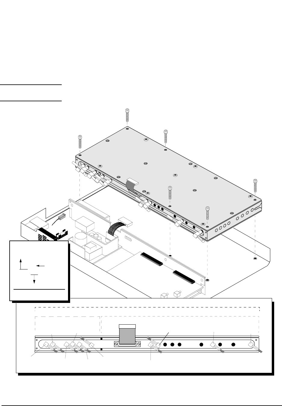
114
Chapter 6, Replaceable Parts
Parts Identification
A9 Reference/IQ
Assembly
NOTE: Perform the PER_CALD and EBNO_CAL calibration procedures after replacing the A4
assembly, see "Periodic Calibration (for Options 001 & 003 only)" on page 127.
Figure 47 A9 Reference/IQ Assembly
A9 Assembly
MP10
W37W24
W30
A6 SubassemblyA7 Subassembly
A9 Assembly
W27
W35
W28
W31
Ribbon Cable (W16)
(6J2-4J3)
W20
(6J6-11J3) (6J3-[RP]OJ1) (6J4-2J6)
(7J5-4J401)
(7J4-[RP]OJ5)
W36
(7J3-5J400)
W21
(7J6-11J4)
(7J2-5J500)
(7J1-[RP]OJ4)
MP10
MP10
MP10
MP10
MP10
W28
Assembly A7, Connector J5
to Assembly A4, Connector J3
(7J5-4J3)
Wire
reference
designator
Cable Legend
[RP] = Rear Panel
[FP] = Front Panel
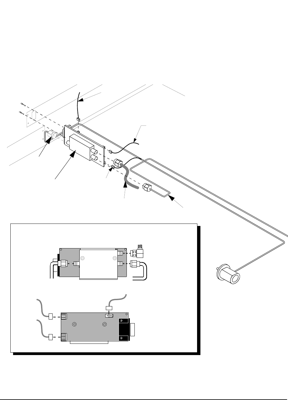
115
Chapter 6, Replaceable Parts
Parts Identification
A10 Directional
Coupler & Serial
Switch Assembly
Figure 48 A10 CDPD Directional Coupler and Serial Switch Assembly
A10
Rear Panel
A10 Assembly
W10
W11
W22
W12
P/O A8W1
W14
J1 J2
J4
J3
A10 Assembly
W10
W14
W11
Coupler Side
W12
(10J1-11P2)
P/O A8W1
(10J2-4J24)
W22
Switch Side
OUTPUT
INPUT
−30dB
(A10 “−30dB”-11J5)
(A10 “INPUT”-front panel
RF IN/OUT)
(A10 “OUTPUT”-
front panel RF IN/OUT TO TEST SET)
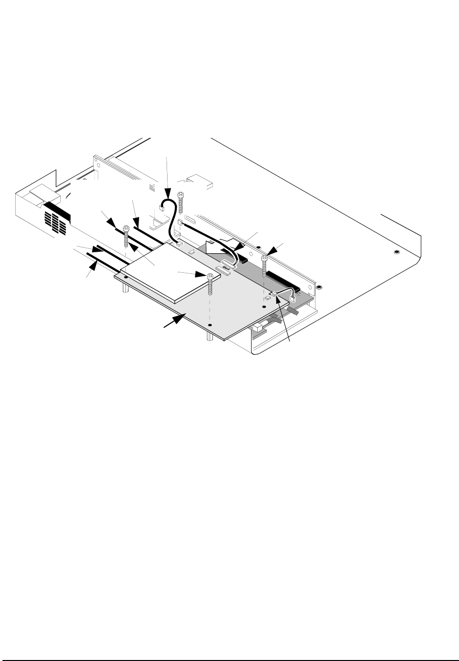
116
Chapter 6, Replaceable Parts
Parts Identification
A11 CDPD
Assembly
Figure 49 A11 CDPD Assembly (on Options 002 & 003 only)
W12 (11P2-10J1)
W13 (11P3-2J9)
W22 (11J2-10J2)
A11 Assembly
MP11
MP11
MP11
MP11
W21 (11J4-7J6)
W20 (11J3-6J14)
W15 (11J6-[RP]MODE OUT)
W14 (11J5-DIR. COUPL.)
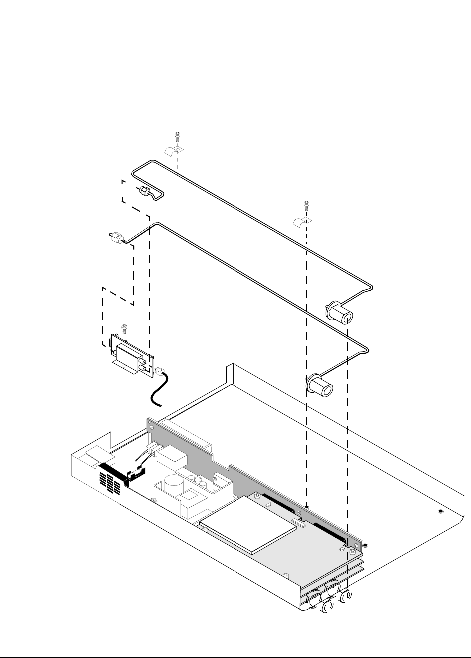
117
Chapter 6, Replaceable Parts
Parts Identification
Semi-Rigid Cables
& Components
Figure 50 Semi-Rigid Cables and Components
A10 Assembly
W10 (Semi-rigid cable)
W11 (Semi-rigid cable)
MP12
W14
MP12
MP13
MP13
MP12
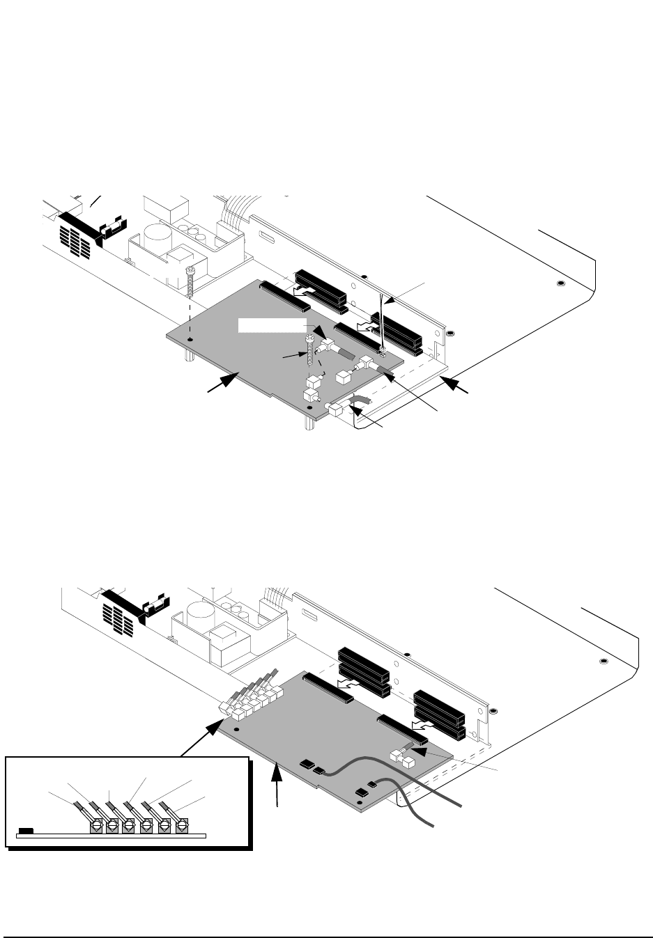
118
Chapter 6, Replaceable Parts
Parts Identification
A2 RX DSP
Assembly
Figure 51 A2 RX DSP Assembly
A5 Data Buffer
Assembly
Figure 52 A5 Data Buffer Assembly
A2 Assembly
W29 (2J4-4J7)
W37 (2J6-6J4)
A5
A2
MP11
MP11 W13 (2J9-11P3)
(2J3-OJ2)
W25
A5 Assembly
A5
W8
W35 W33 W34 W36
W26 W9 (4J701-5J709)
W32 (5J4-4J708)
(5J502-OJ6)
(5J500-7J2) (5J501-4J500)
(5J401-4J400) (5J400-7J3)
(5J402-OJ3)
(J709)
(J22)
A1W2 (to front panel DATA IN)
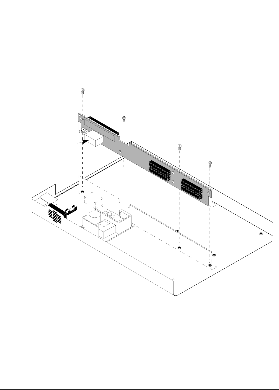
119
Chapter 6, Replaceable Parts
Parts Identification
A3 Motherboard
Assembly
Figure 53 A3 Motherboard Assembly
MP12
MP12
A3K1
A3
MP12
MP12

120
Chapter 6, Replaceable Parts
Parts List
Parts List
REFERENCE DESCRIPTION PART
DESIGNATOR NUMBER
ACC1 MANUAL ALR 83205-90009
ACC2 USER’S GUIDE 83205-90008
ACC3 SW USER GUIDE 83204-90014
ACC4 DSP/CDPD UPGRADE KIT 83205-61801
ACC5 CDPD SFTWARE KIT 83204-61807
ACC6 KIT-RACK MOUNT 08921-61037
ACC7 ACCESSORY KIT 83204-61008
ACC7AT1 ATTN COAX 6dB 1W 0955-0698
ACC7MP1 ADPT TEE FMF BNC 1250-0781
ACC7MP2 TERMINATION 0960-0053
ACC7MP3 ADPT M BNC F SMA 1250-1700
ACC7MP4 ADAPTER 1250-1250
ACC7W1 CA MCND RJ11-DB9 08921-61038
ACC7W2 CA CX ASSY 50Z 8120-2582
ACC7W4 CBL FLEX COAX 08921-61052
A1 (#001) AY FRNT PNL #001 83205-61005
A1 (#002) AY FRNT PNL #002 83205-61003
A1 (#003) AY FRNT PNL #003 83205-61001
A1MP1 (#001) FRAME FRONT 83201-21007
A1MP1 (#002/#003) FRAME FRONT MACH 83203-21003
A1MP2 (#001) PANEL DRESS 83205-00002
A1MP2 (#002) PANEL DRESS #002 83205-00001
A1MP2 (#003) PANEL DRESS 83203-00025

121
Chapter 6, Replaceable Parts
Parts List
A1MP3 RFI ROUND STRIP 8160-0520
A1MP4 NUT-HEX 15/32-32 2950-0035
A1W1-A1W7,W7,W23 CBL ASSY 83203-61005
A2 DSP RX KIT 83205-61807
A3 MOTHER BD KIT 83205-61803
A3K1 RLY ZC 12VDC 0490-1787
A4 NEW GEN REF KIT 83203-61813
A5 NEW DATA BFR KIT 83203-61808
A8 PWR SPLY 3 40W 0950-2023
A8W1 (#001) CA MCNDCT 6CKT 83201-61011
A8W1 (#002/#003) CBL POWER SUPPLY 83203-61042
A9 NEW REF IQ KIT 83203-61812
A10 DIRECT COUPLR KIT 83205-61802
A11 NEW CDPD KIT 83204-61805
A11 REST. CDPD KIT 83204-69805
A12 DECK 83203-00021
A12A8 CABLE MAIN HARNESS 83203-61058
A12A8C3 C MPAP .47U 250V 0160-7716
A12A8F1 FUSE 2A 250V 2110-0002
A12A8MP1 FLTR-LINE 250V 9135-0242
A12A8MP9 FUHLR 15A 250V 2110-0776
A12B1 FAN ASSY 83201-61046
J1 (#002/#003) ACCESS-TEL CONN 1252-7200
MP1 ADPT F BNC M BNC 1250-0076
MP2 BUMPER 5041-8928
MP3 BRACKET ATTACH 83201-21002
MP4 SMM3.0 8SEMPNTX 0515-0372

122
Chapter 6, Replaceable Parts
Parts List
MP5 SMM3.0 10 FL TX 0515-1103
MP7 SMM3.0 12SEMPNTX 0515-0664
MP8 BAR-CONNECTOR 83201-21004
MP10 SCRMACH M3 30MML 0515-1349
MP11 SCR-MACHINE 0515-1410
MP12 SMM3.0 6SEMPNTX 0515-2126
MP13 CLAMP-CABLE 1400-1391
MP14 PANEL REAR 83203-00024
MP15 AY-COVER,IMPACT 83201-61013
MP16 (#001) PLATE CONN 83204-00002
MP17 CONN LOCK SUB D 1251-0218
MP18 COVER AY 83203-61051
MP19 WSHR LK .472ID 2190-0102
MP20 NUT-HEX 15/32-32 2950-0035
MP21 (#002/#003) CLP CA .25D .37W 1400-0015
MP22 (#002/#003) WSHR-LK HLCL #4 2190-0003
MP23 (#002/#003) CONN SCREWLOCK F 0380-2079
MP24 NUT-HEX 5/8-24 2950-0213
MP25 (#002/#003) CONNECTOR SCREW LOCL 1252-7215
MP26 WSHR-LK IN T #10 2190-0124
MP27 NUT-HEX 10-32 2950-0078
MP28 PLATE RR MTG 83203-00020
MP29 (#002/#003) BRACKET SER PORT 83203-00028
MP30 (#002/#003) BRACKET SER PORT RJ-11 83203-00029
MP31 (#002/#003) NUTM- HX M3 0535-0031
W1,ACC7W3 CA CX AY 50Z 1FT 8120-1838
W2,W3,W4,W5,
W20,W21 CA CX A23A23 195 8120-5730

123
Chapter 6, Replaceable Parts
Parts List
W6 CA MCNDCT 37CKT 83201-61001
W8,W24,W25,W26 FLEX CABLE 83203-61013
W9 CABLE AY 3 PIN 83203-61020
W10 (#002/#003) CA SR-2.18 N-SMA 83203-61045
W11 (#002/#003) CA SR-2.18 N-SMA 83203-61046
W12 (#002/#003) CA ASSY 3COND 83203-61048
W13 (#002/#003) CBL RCV/CDPD 83203-61049
W14 (#002/#003) CA COAX SMA-SMC 83203-61047
W15,W27,W28
(#002/#003) CX F SMC-SMCBH 8 8120-5857
W16 RBN 15CNDCT 28AWG 83201-61004
W17 (#002/#003) CABLE 8120-6285
W18 (#002/#003) CX FLEX N-N 8120-8317
W19 (#002/#003) CBL SERIAL PORTS 83203-61044
W22, (#002/#003) CA ASSY 4-COND 83203-61043
W29,W30 COAX CABLE ASSY 8120-5017
W31 COAXIAL CBL ASSY 8120-5022
W32 CX F SMB-F SMB 83203-61017
W33,W34 CX F SMB-F SMB 83203-61018
W35,W36 FLEX CABLE 83203-61019
W37 CA CX A06A06 260 8120-5020

124
Chapter 6, Replaceable Parts
Parts List

125
7
Periodic Calibration and Performance Tests
This chapter contains the calibration procedures and the CDMA and CDPD
performance test procedures for the HP 83205A Cellular Adapter.

126
Chapter 7, Periodic Calibration and Performance Tests
Introduction
Introduction
NOTE: For Cellular Adapter Options 001 and 003, perform the "Periodic Calibration (for Options
001 & 003 only)" on page 127 before performing any of the performance tests.
The performance tests in this chapter verify that the Cellular Adapter performs to
its specifications. Use table 14 to determine the calibration and performance tests
to run for each of the following Cellular Adapters:
• HP 83205A CDMA Cellular Adapter Option 001
• HP 83205A CDPD Cellular Adapter Option 002
• HP 83205A CDMA/CDPD Cellular Adapter Option 003
The "CDMA Performance Record" on page 137 and "CDPD Performance
Record" on page 138 are provided for logging the results of these test routines.
Table 14 Calibration and Performance Tests
Performance Test Name HP 83205A Cellular Adapter
Option 001 Option 002 Option 003
"Periodic Calibration (for Options 001 & 003 only)" on
page 127 XX
"CDMA Performance Test (for Options 001 & 003
only)" on page 129
XX
"CDPD Performance Test (for Options 002 & 003
only)" on page 131
XX

127
Chapter 7, Periodic Calibration and Performance Tests
Periodic Calibration (for Options 001 & 003 only)
Periodic Calibration (for Options 001 & 003 only)
The following calibration procedures only apply to the Cellular Adapters
containing CDMA (Options 001 & 003). A CDMA Cellular Adapter is calibrated
by running the PER_CALD and EBNO_CAL calibration programs. These
programs are stored in the Test Set’s ROM and should be run at least every 12
months, or whenever the Test Set and Cellular Adapter are disconnected and
reassembled.
NOTE: Before calibrating the Test Set and CDMA Cellular Adapter as a Test System, ensure the
Test Set has been calibrated independently of the Cellular Adapter. Refer to the Test Set’s
ALR manual for calibrating the Test Set.
PER_CALD
Calibration
Procedure
1. Press TESTS to access the TESTS screen.
2. Select the Procedure Location: field.
3. Select ROM under the Choices: menu.
4. Select the Procedure Filename: field.
5. Select PER_CALD under the Choices: menu.
6. Select Run Test (k1 USER key).
7. Follow the instructions on the screen.
The end of the PER_CALD routine will instruct you to exit this program and
cycle the power Off and On.

128
Chapter 7, Periodic Calibration and Performance Tests
Periodic Calibration (for Options 001 & 003 only)
EBNO_CAL
Calibration
Procedure
This calibration procedure will take several minutes, and during calibration, you
will be required to disconnect and reconnect the Cellular Adapter’s IQ RF OUT
port to the Test Set.
NOTE: The preceding PER_CALD Calibration Procedure must be completed prior to performing
the following procedure.
1. Connect the Cellular Adapter’s IQ RF OUT to the Test Set’s ANT IN connector.
2. Press the TESTS to access the TESTS screen.
3. Select the Procedure Location: field.
4. Select ROM under the Choices: menu.
5. Select the Procedure Filename: field.
6. Select EBNO_CAL under the Choices: menu.
7. Select Run Test (k1 USER key).
8. Follow the instructions on the screen.
9. If the EBNO_CAL calibration corrections are less than 1.27dB, respond YES to use
these corrections as the new calibration factors.
The end of the EBNO_CAL routine will instruct you to exit this calibration
program and cycle the power Off and On.

129
Chapter 7, Periodic Calibration and Performance Tests
CDMA Performance Test (for Options 001 & 003 only)
CDMA Performance Test (for Options 001 & 003 only)
CDMA performance verification is done by setting the Test System into a loop
back state and using the CDMA analyzer to measure the CDMA generator. This
allows you to quickly and accurately verify that both the generator and analyzer
are working. No external test equipment is needed.
Prerequisites Perform the "Periodic Calibration (for Options 001 & 003 only)" on page 127
before performing the following performance procedure.
Equipment Setup Make sure the back panel connections between the Test Set and the Cellular
Adapter are properly connected. For reference, see figure 16, "Rear Panel Cable
Connections for HP 83205A CDMA/CDPD Cellular Adapter," on page 65.
CDMA
Performance
Procedure
Step 1. Connect the Test Set’s DUPLEX OUT to the ANT IN port.
Step 2. Press the PRESET key or cycle power to the Test System.
Verify the REF UNLOCK LED is not lit, otherwise, troubleshoot the Test
System, see "Test System Troubleshooting" on page 38.
Step 3. Set up the CDMA GENERATOR screen
• Select More: and then CDMA GEN from the Choices: menu. The CDMA GENER-
ATOR screen appears.
• Set the RF Gen Freq field to 850 MHz.
• Set the Amplitude field to −10 dBm.
• Set the CW RF Path field to IQ.
• Set the Output Port field to Dupl.
• Set the Gen Dir field to Fwd.
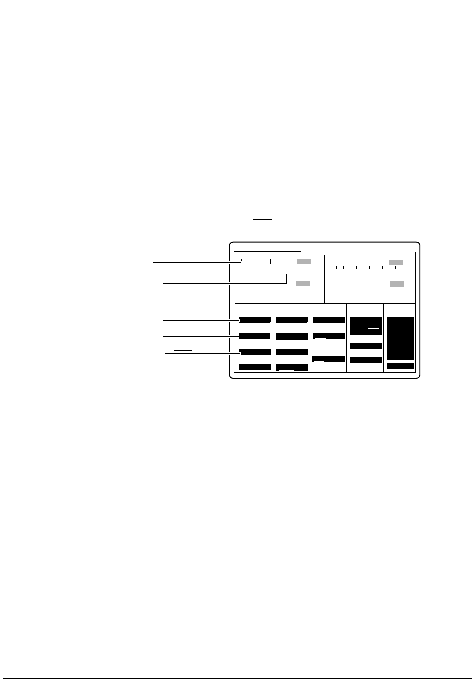
130
Chapter 7, Periodic Calibration and Performance Tests
CDMA Performance Test (for Options 001 & 003 only)
Step 4. Set up the CDMA ANALYZER screen
a. Select More:, and then CDMA ANL from the Choices: menu. The CDMA
ANALYZER screen appears.
b. Select the Measurement field and change it to Rho , see figure 54.
c. Set the Tune Freq field to 850 MHz.
d. Set the Input Atten field to 20 dB.
e. Set the Input Port field to Ant.
Figure 54 CDMA Analyzer Screen
Step 5. Read and record the Rho measurement, see figure 54.
a. This reading should be >0.96 and no error messages should appear.
b. Record the rho measurement in the "CDMA Performance Record" on page 137.
Tune Freq To Screen
CDMA ANALYZER
Frequency Error
Anl Special
Synth Ref
PN Offset
Meas Intvl
Gain
Analyzer
Qual Event
0
850.000000
MHz RF GEN
RF ANL
AF ANL
SCOPE
SPEC ANL
ENCODE
DECODE
RADIO INT
Rho
Even Sec In
Anl Dir
Set to 20 dB
Off
Hz
More
80 ms
Set to 850 MHz IQ
0.9903
Input Atten
20 dB
Input Port
RF In/Ant
CDMA TB
Internal
0.00
Enable/Not
0.50
Auto/Hold
Fwd/Rev
Arm Meas
Single/Cont
Disarm
12 dB
ms
Trig Event
Immed
Time Offset us Carrier Feedthru
-47.5 dB
-50 50
- - - -
Set Measurement field to Rho
Set to ANT
2.39
Read Rho measurement
131
Chapter 7, Periodic Calibration and Performance Tests
CDPD Performance Test (for Options 002 & 003 only)
CDPD Performance Test (for Options 002 & 003 only)
The spectral purity, modulation accuracy, and on/off level of the CDPD
Generator are measured directly with the CDPD analyzer.
Prerequisites Perform the "Periodic Calibration (for Options 001 & 003 only)" on page 127
before performing the following performance procedure.
Equipment Set Up No external test equipment is required.
Procedure Step 1. Load the CDPD MDBS Cell Site Test Software.
a. Press the PRESET key.
b. Insert the CDPD MDBS Cell Site Test Software card, HP 83204-61807.
c. Press the TESTS key.
d. Select Card for procedure location and CDPD for procedure filename.
e. Run the test, press k1 (Run Test). Wait (30 seconds to 2 minutes) for the (CDPD)
Main Menu to appear, see figure 55.
Figure 55 Main Menu (CDPD)
1
Continue
2
Help4
RF GEN
To Screen
RF ANL
AF ANL
TESTS (Main Menu)
LOAD TEST PROCEDURE:
Select Procedure Location:
Select Procedure Filename:
Description:
Library: Program:
CUSTOMIZE TEST PROCEDURE: SET UP TEST SET:
Channel Information
Test Parameters
Order of Tests
Pass/Fail Limits
Save/Delete Procedure
External Devices
Printer Setup
IBASIC Cntrl
Freq
Parm
Seqn
Spec
Proc
Cnfg
Print
Exec Execution Cond
IBASIC
RF parametric tests for CDPD MDBS equipment.
Choices:
CDPD
CALSL
DEMO
SEQN
Card
Run Test
CDPD
Select Card as the location
of the diagnostic program.
Select the CDPD diagnostic
program.
Main Menu (CDPD)
CDPD Card
Revision : A.00.11
CDPD MDBS CELL SITE TEST
TX Tests
RX Tests
2
4
3
End
5
1
MAIN MENU
==== ====
(1) Transmitter Tests
(2) Receiver Tests
(3) System Tests
(4) Calibrations
(5) End this Program
System
Use knob or softkeys to select from the menu.
Cals
TESTS (IBASIC Controller)
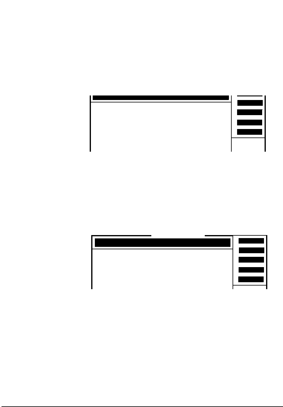
132
Chapter 7, Periodic Calibration and Performance Tests
CDPD Performance Test (for Options 002 & 003 only)
Step 2. Calibrate and record the GMSK Deviation.
a. From the MAIN MENU, select (4) Calibrations. The CALIBRATIONS menu
appears, see figure 56.
Figure 56 CALIBRATIONS Menu
b. From CALIBRATIONS menu, select (3) GMSK Deviation Calibration, an
equipment cable-hookup screen appears.
c. Connect Test Set and Cellular Adapter as shown on the screen, that is, connect the Test
Set’s RF IN/OUT to Cellular Adapter’s RF IN/OUT TO TEST SET.
d. Press the k2 (Continue). Wait for the GMSK Deviation Calibration mea-
sured value to appear, figure 57. WRITE DOWN the measured value for later use.
Figure 57 GMSK Deviation
e. Press k5 (Menu) to return to the CALIBRATIONS menu.
f. From the CALIBRATIONS menu, press k5 (Prev Menu) to return to the MAIN
MENU screen.
Power
2
4
To Screen
3
Prev Menu
5
CALIBRATIONS
============
(1) Cable Loss
(2) Power Measurement Calibration
(3) GMSK Deviation Calibration
(4) Center Frequency Calibration
(5) Previous Menu
GMSK Dev
Cntr Freq
2
4
3
Menu
5
1
RF parametric tests for CDPD MDBS equipment
====================================================
Test conditions Measured value P/F
====================================================
GMSK Deviation Calibration 8.52 kHz/V
TESTS (IBASIC Controller)

133
Chapter 7, Periodic Calibration and Performance Tests
CDPD Performance Test (for Options 002 & 003 only)
Step 3. Perform Transmitter Tests.
a. From the MAIN MENU, select (1) Transmitter Tests. The TRAMSMITTER
TESTS menu appears, see figure 58.
Figure 58 Transmitter Tests Menu
b. Select (1) RF Parameters, or press the k1 key.
c. Connect the Test Set and Cellular Adapter as shown on the screen. Do not connect the
Cellular Adapter to the base station. (Test Set’s RF IN/OUT is still connected to
Cellular Adapter’s RF IN/OUT TO TEST SET.)
d. Press k2 (Continue). The TESTS (IBASIC Controller) screen reports No signal
found.
e. Press SHIFT and CANCEL keys.
f. Connect the Test Set’s DUPLEX OUT connector to its ANT IN connector.
g. Move the cursor to the message block and enter OUTPUT 10;"XMIT_MDBS 2", see
figure 59. Use the Test Set’s cursor control knob to select each character from the
choices menu and then select DONE.
h. Change the output statement to OUTPUT 10;"WR_AMPL_OFF". After entering,
select DONE.
Figure 59
RF Parms
Pwr Cal
2
4
3
Prev Menu
5
1
TRANSMITTER TESTS
=========== =====
(1) RF Parameters (power, frequency, etc.)
(2) Power Measurement Calibration
(3) Previous Menu
Use knob or softkeys to select from the menu.
TESTS (IBASIC Controller)
2
3
1
OUTPUT 10;"XMIT_MDBS 2"
TESTS (IBASIC Controller)
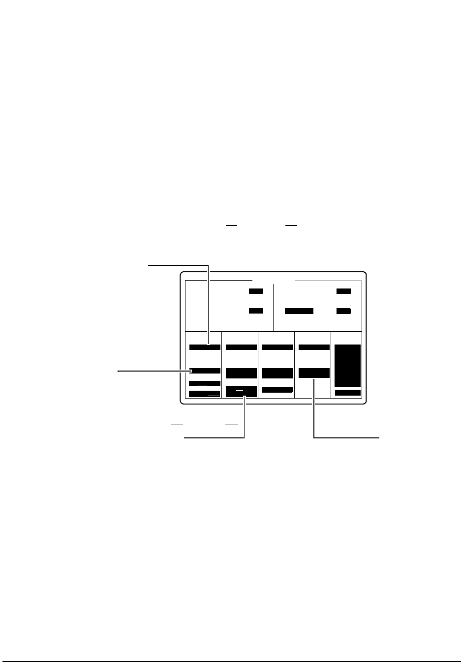
134
Chapter 7, Periodic Calibration and Performance Tests
CDPD Performance Test (for Options 002 & 003 only)
Step 4. Setup the RF GENERATOR screen.
a. Select RF GEN from the To Screen menu. The RF GENERATOR screen appears,
see figure 60.
b. Set RF Gen Freq to 870 MHz.
c. Set Amplitude to −20 dBm.
d. Turn ON the Mod In To, press the ON/OFF key. Verify that the value in this field is
the same as the GMSK Deviation Calibration value recorded in step 2d.
e. Change FM Coupling AC/DC to AC/DC and perform DC FM Zero by pressing
the Cursor Control knob.
Figure 60 Setting up the RF GENERATOR Screen for the CDPD Performance Test
RF Gen Freq To Screen
RF GENERATOR
FM Deviation
Amplitude
AFGen1 Freq
AFGen1 To
AFGen2 Freq
AFGen2 To
Mic Pre-Emp
Mod In To
-20.00
870.000000
dBm
RF GEN
RF ANL
AF ANL
SCOPE
SPEC ANL
ENCODE
DECODE
RADIO INT
TX Freq Frequency
TX Power
FM
FM Coupling Audio Out
Atten Hold
Output Port
MHz
RF Out/Dupl
OFF
Enter −20 dBm.
Enter 870 MHz.
On/Off
Off
Off SINAD Off
Off
More
AC/DC
DC FM Zero
FM (/Vpk)
8.52 kHz
Change AC/DC to AC/DC Turn ON (press the ON/OFF key)
and verify the value.
and perform DC FM Zero.
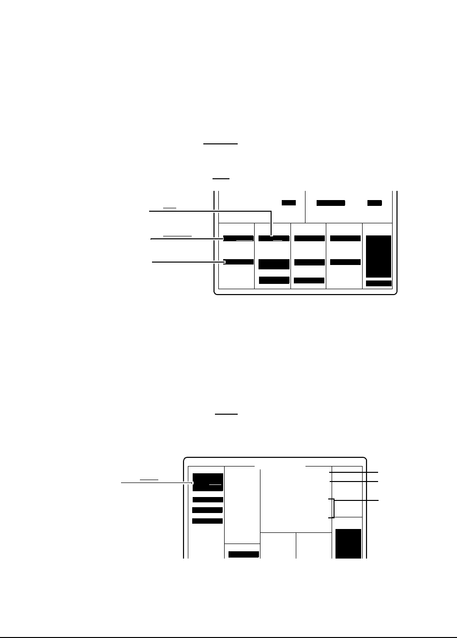
135
Chapter 7, Periodic Calibration and Performance Tests
CDPD Performance Test (for Options 002 & 003 only)
Step 5. Setup the RF ANALYZER screen.
a. Select RF ANL from the To Screen menu. The RF ANALYZER screen appears,
see figure 61.
b. Set Tune Mode to Manual.
c. Set Tune Freq to 870 MHz.
d. Set Input Port to Ant.
Figure 61 RF ANALYZER Screen
Step 6. Access the CDPD SCREEN.
a. Select More from the To Screen menu.
b. Select CDPD TEST. The CDPD SCREEN appears, see figure 62.
c. Set Digital Anl to Cont.
d. Verify Status is 3.000000.
Figure 62 CDPD SCREEN
Tune Mode To Screen
Tune Freq
Input port
Input Atten
IF Filter
Squelch
Ext TX Key
TX Pwr Zero
870.000000
Auto/Manual
MHz
RF GEN
RF ANL
AF ANL
SCOPE
SPEC ANL
ENCODE
DECODE
RADIO INT
TX Power
Sensitivity RF Cnt Gate
Set to 870 MHz.
Set to Ant.Off SINAD Off
More
Zero
Set to Manual.RF In/Ant
Digital Anl
To Screen
CDPD SCREEN
Measurement
Gain
Arms Meas
Special
RF GEN
RF ANL
AF ANL
SCOPE
SPEC ANL
ENCODE
Single/Cont
Disprm
Ampl Cntl
Dig An1:
Armed
Dig Gen:
Idle
Status
Freq Err
Mod Indx
Mod Indx
Incid FM
Mx Freq
Chan Pwr
Adj Pwr
Alt Pwr
Al2 Pwr
Max ADC
Gain Set
Hz
SD
Hz
Dev
dB
dBc
dBc
dBc
dBa
db
3.000000
-189.400000
0.500000
0.000223
57.356987
4556.40526
-18.128560
-34.478719
-70.270158
-73.895623
-6.200521
12.000000
Set to Cont.
Adj Pwr dBc
Alt Pwr dBc
Al2 Pwr dBc
Chan Pwr dB
RECORD:
Mod Indx
Status
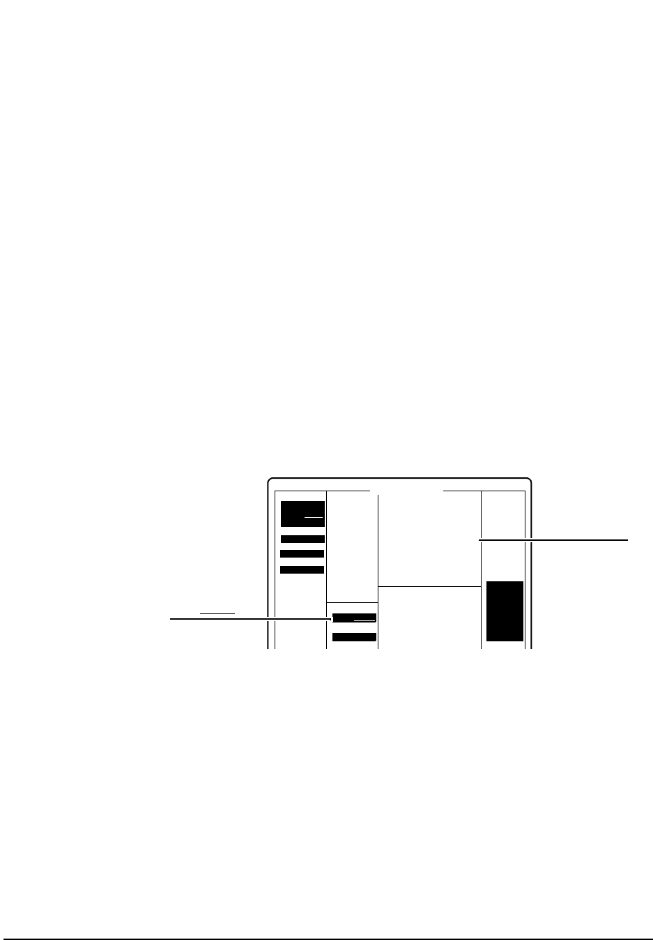
136
Chapter 7, Periodic Calibration and Performance Tests
CDPD Performance Test (for Options 002 & 003 only)
Step 7. Record CDPD SCREEN information.
a. Record the Adjacent Channel Power, Adj Pwr dBc (see figure 62 on page 135), in
the "CDPD Performance Record" on page 138.
b. Record the First Alternate Channel power, Alt Pwr dBc, in the "CDPD Performance
Record" on page 138.
c. Record the Second Alternate Channel power, Al2 Pwr dBc, in the "CDPD
Performance Record" on page 138.
d. Record the Modulation Index, Mod Indx, in the "CDPD Performance Record" on
page 138.
Step 8. Calculate On/Off Power Level
a. Record the present value for channel power, Chan Pwr dB, as ON POWER in the
equation below and in the "CDPD Performance Record" on page 138.
b. Change Ampl Cntrl to CDPD, see figure 63.
Figure 63 CDPD SCREEN
c. Record the Chan Pwr dB of the CDPD SCREEN as OFF POWER in the equation
below and in the "CDPD Performance Record" on page 138.
d. Calculate in the equation below the ON/OFF DIFFERENTIAL level and record it in
the "CDPD Performance Record" on page 138.
ON POWER − OFF POWER = ON/OFF DIFFERENTIAL
___________− ___________ = _________
Digital Anl
To Screen
CDPD SCREEN
Measurement
Gain
Arms Meas
Special
RF GEN
RF ANL
AF ANL
SCOPE
SPEC ANL
ENCODE
DECODE
RADIO INT
Single/Cont
Disprm
Ampl Cntl
Valid Check
Dig An1:
Armed
Dig Gen:
Idle
Status
Freq Err
Mod Indx
Mod Indx
Incid FM
Mx Freq
Chan Pwr
Adj Pwr
Alt Pwr
Al2 Pwr
Max ADC
Gain Set
Hz
SD
Hz
Dev
dB
dBc
dBc
dBc
dBa
db
3.000000
-192.400000
0.500000
0.000223
104.356987
5130.40526
-38.488560
-34.478719
-58.270158
-58.895623
-8.200521
30.000000
Set to CDPD.
Chan Pwr dB
Norm/CDPD

137
Chapter 7, Periodic Calibration and Performance Tests
CDMA Performance Record
CDMA Performance Record
Date _____________ Time_______________ Humidity ___________
Tested by: __________________________________________________
Cellular Adapter Serial Number: _________________________________
Test Set Serial Number ________________________________________
Test Set Last Calibration Date __________________
Rho Measurement
HP 83205A CDMA Cellular Adapter (Opt 001)
HP 83205A CDMA/CDPD Cellular Adapter (Opt 003)
Rho
Lower Limit Actual
0.96

138
Chapter 7, Periodic Calibration and Performance Tests
CDPD Performance Record
CDPD Performance Record
Date _____________ Time_______________ Humidity ___________
Tested by: __________________________________________________
Cellular Adapter Serial Number: _________________________________
Test Set Serial Number ________________________________________
Test Set Last Calibration Date __________________
CDPD Generator Spectral Purity Measurement
CDPD Modulation Accuracy Measurement
CDPD Generator On/Off Level Measurement
1. ON POWER − OFF POWER = ON/OFF DIFFERENTIAL
HP 83205A CDPD Cellular Adapter (Opt 002)
HP 83205A CDMA/CDPD Cellular Adapter (Opt 003)
Channel Power Upper Limit (dBc) Measured Spectral Purity
Actual (dBc)
Adjacent Channel Power (Adj Pwr dBc)−26
First Alternate Channel (Alt Pwr dBc)−45
Second Alternate Channel (Al2 Pwr dBc)−60
Upper Limit Lower Limit Modulation Index (Mod Indx)
0.525 0.475
Measured Values Calculated Value (dB)
ON POWER OFF POWER ON/OFF DIFFERENTIAL1
Actual Lower Limit
15


140
Chapter 8, Specifications
HP 83205A CDMA Specifications
HP 83205A CDMA Specifications
The following specifications describe the HP 83205A CDMA Cellular Adapter’s
warranted performance when operating with an HP 8921A Cell Site Test Set and
apply after a 30 minute warm-up. All specifications are valid over the unit’s entire
operating/environmental range unless otherwise noted.
Supplemental characteristics are intended to provide additional information
useful in applying the instrument by giving typical, but non-warranted
performance parameters. These are shown in italics or labeled as “typical”,
“usable to”, or “nominal”.
NOTE: The following specifications describe the CDMA Test Systems: HP 8921A Option 600
(HP 8921A Test Set & HP 83205A CDMA Cellular Adapter) and HP 8921A Option 603
(HP 8921A Test Set & HP 83205A CDMA/CDPD Cellular Adapter).
CDMA Signal
Generator Frequency & Amplitude
Frequency Range: 824 to 894 MHz, usable from 800 MHz to 1000 MHz and
from 4 MHz to 200 MHz with degraded ρ and carrier feedthrough
performance.
Frequency Resolution: 1 Hz
Output Level Range:
at Test Set’s RF IN/OUT: −19 dBm to −137 dBm
at Test Set’s DUPLEX OUT: +4 dBm to −127 dBm
Output Level Accuracy:
at Test Set’s RF IN/OUT: ±2.0 dB, typically ±1.0 dB
at Test Set’s DUPLEX OUT: ±1.7 dB, typically ±1.0 dB
Modulation
Reverse Link Source Modulation: OQPSK per TIA IS-95
Reverse Link Source Modulation Data: Internal data buffer, Idle (all zeroes)
NOTE: May also be modulated with external encoded data. External data must
be properly coded and ready for short sequence spreading at 1.2288 Mbit per
second.
Forward Link Source Modulation: QPSK per TIA IS-95

141
Chapter 8, Specifications
HP 83205A CDMA Specifications
Forward Link Source Modulation Data: Internal (Pilot channel)
NOTE: May also be modulated with external encoded data. External data must
be properly coded and ready for short sequence spreading at 1.2288 Mbit per
second.
Residual Rho (ρ): 0.96, typically >0.98 at 25°C ±15°C
Carrier Feedthrough: −30dBc, typically <−35 dBc at 25°C ±15°C
Adjacent Channel Noise: −45dBc, typically <−50 dBc; measured in a 30 kHz
BW filter relative to the total carrier power at fc ±900 kHz at 25°C ±15°C;
from RF IN/OUT connector <−29 dBm
from DUPLEX OUT connector <-3 dBm
PN Offset: Adjustable from 0 to 511 units (1 unit equals 64 chips)
PN Offset Resolution: 0.0156 units (1 chip)
Data Buffer
Size/Length: 5400 frames
Modes: Single, Continuous Looping, and Idle
Coding: IS-95 CDMA full rate reverse link channel coding, interleaving, and
spreading
Long Code Mask: 42 zeros
Input Data Rate: 9600 bps; 14,400 bps
Data Source: For each rate set, 300 frames factory loaded, 1800 frames
additional user definable data can be entered via HP-IB

142
Chapter 8, Specifications
HP 83205A CDMA Specifications
AWGN Source
(Added White Gaussian Noise)
Bandwidth: 2 MHz nominally, Gaussian to >3 sigma
Modes: Noise only, data only, and user selectable Eb/No settings
Eb/No Resolution: 0.1 dB
Eb/No Range: −5 to 25 dB
Eb/No Accuracy:
±0.5 dB, for Eb/No of 5 to 20 dB
typically ±1 dB for Eb/No of −5 to +5 dB and +20 dB to +25 dB
CDMA Analyzer Wave Quality Measurement Rho (ρ)
IS-95 forward or reverse link formats (QPSK or OQPSK)
Input and Level Range:
at Test Set’s RF IN/OUT: −10 dBm to +48 dBm
at Test Set’s ANT IN: −46 dBm to +17 dBm
Input Frequency Range: 4 MHz to 1000 MHz
Rho (ρ) Measurement Interval Range: 0.25 to 1.25 ms
Rho (ρ) Measurement Range: 0.50 to 1.00
Rho (ρ) Measurement Accuracy: <±0.005
Input Frequency Error Range: ±900 Hz
Frequency Error Measurement Accuracy: ±30 Hz using a measurement
interval ≥ 0.5 ms. NOTE: Accuracy can be improved by averaging a number of
measrements. Error is reduced by square root of the number of averages.
Other Reported Parameters: Pilot Time Offset, Carrier Feedthrough, Error
Vector Magnitude, Amplitude Error and Phase Error
Pilot Time Offset Measurement Accuracy: Typically <±500 ns from even-
second signal to start of PN sequence

143
Chapter 8, Specifications
HP 83205A CDMA Specifications
Average Power Measurement
Input Frequency Range: 30 MHz to 1000 MHz at RF IN/OUT only. (NOTE:
When measuring power at the RF IN/OUT port, the internal signal generator
level must be 60 dB below the measured power or less than −20 dBm at the
DUPLEX OUT port.)
Measurement Period: 0.25 ms to 5 ms
Measurement Bandwidth: Provides an accurate measure of the total power for
signals within 2 MHz of the operating frequency. If other signals are present
outside this frequency range, reduced measurement accuracy will result.
Maximum Input Level: 60 W continuous
Measurement Range: 1 mW to 60 W continuous (0 to +48 dBm)
Measurement Accuracy: ±5% ±1 µW, at 25°C ±10°C
±10% ±1 µW, from 0° to 55°C
Channel Power Measurement
Test Set’s RF IN/OUT (usable on ANT IN with reduced measurement accuracy)
Input Level Range: −10 dBm to +48 dBm
Input Frequency Range: 4 MHz to 1000 MHz
Measurement Bandwidth: Measures the total power in a 1.23 MHz bandwidth
centered on the selected frequency
Measurement Accuracy: ±1 dB over a range of ±5°C from the temperature of
last calibration. NOTE: When measuring power at the RF IN/OUT port, the
internal signal generator level must be 60 dB below the measured power or
less than −20 dBm at the DUPLEX OUT port.

144
Chapter 8, Specifications
HP 83205A CDMA Specifications
Code Domain
Analyzer Code Domain Power Measurement
Test Set’s RF IN/OUT or ANT IN
Input Frequency Range: 4 MHz to 1000 MHz
Input Frequency Error Range: ±900 Hz
Input Level Range:
Test Set’s RF IN/OUT: −10 dBm to +48 dBm
Test Set’s ANT IN: −46 dBm to +17 dBm
Measurement Dynamic Range: 40 dB
Measurement Accuracy: ±0.5 dB using a measurement interval ≥0.5 ms
Measurement Resolution: 0.01 dB
Carrier Frequency Offset Accuracy: ±30 Hz using a measurement interval ≥0.5
ms. NOTE: Accuracy can be improved by averaging a number of
measurements. Error is reduced by square root of the number of averages.
Pilot Time Offset Accuracy: Typically <±500 ns from even-second signal to
start of PN sequence
Code Domain Timing Measurement
(Pilot to Code Channel Time Tolerance)
at Test Set’s RF IN/OUT or ANT IN
Input Level Range:
Test Set’s RF IN/OUT: −10 dBm to +48 dBm
Test Set’s ANT IN: −46 dBm to +17 dBm
Input Frequency Range: 4 MHz to 1000 MHz
Input Frequency Error Range: ±900 Hz
Measurement Range: ±4 ns to ±200 ns
Measurement Accuracy: ±10 ns using a measurement interval of 1.25 ms and
≥10 averages
Measurement Resolution: 0.01 ns

145
Chapter 8, Specifications
HP 83205A CDMA Specifications
Code Domain Phase Measurement
(Pilot to Code Channel Time Tolerance)
at Test Set’s RF IN/OUT or ANT IN
Input Frequency Range: 4 MHz to 1000 MHz
Input Frequency Error Range: ±900 Hz
Input Level Range:
Test Set’s RF IN/OUT: −10 dBm to +48 dBm
Test Set’s ANT IN: −46 dBm to +17 dBm
Measurement Range: ±4 mrad to ±200 mrad
Measurement Accuracy: ±20 mrad using a measurement interval of 1.25 ms and
≥10 averages
Measurement Resolution: 10 mrad
RF Time Base For proper operation, this reference must be locked to an external, quality
reference.
Locking Range: ±10 ppm
Input Frequencies: 19.6608 MHz, 15 MHz, 10 MHz, 9.8304 MHz, 5 MHz,
4.9152 MHz, 2.4576 MHz, 1.2288 MHz, and 1 MHz
Input Level: ≥ 0 dBm (into 50 Ω)
Output Frequency: 10 MHz
Output Level: TTL

146
Chapter 8, Specifications
HP 83205A CDMA Specifications
CDMA Reference For proper operation, this reference must be locked to the internal RF time base or
an external, high quality reference.
Locking Range: ±10 ppm
Input Frequencies: 19.6608 MHz, 15 MHz, 10 MHz, 9.8304 MHz, 5 MHz,
4.9152 MHz, 2.4576 MHz, 1.2288 MHz, and 1 MHz
Even Second Sync Input: (BNC) accepts a rising edge to reset the internal short
sequences and CDMA clocks. Periodic inputs should have a period of two
seconds and a minimum pulse width of >50 ns.
Input Level: ≥0 dBm (into 50 Ω)
Outputs:
Coaxial BNC’s:
19.6608 MHz (TTL levels)
1.2288 MHz (TTL levels)
TTL Sub Mini D:
20 ms frame clock
26.67 ms short sequence clock
80 ms clock
Every even second

147
Chapter 8, Specifications
HP 83205A CDPD Specifications
HP 83205A CDPD Specifications
The following specifications apply to the HP 83205A CDPD (Opt 002) and
HP 83205A CDPD/TDMA (Opt 003) Cellular Adapter when fitted with the
HP 8921A Cell Site Test Set, and when running the provided CDPD MDBS Cell
Site test software (this software is included with each of these Cellular Adapters).
NOTE: The following specifications describe the CDPD Test Systems: HP 8921A Option 602
(HP 8921A Test Set & HP 83205A CDPD Cellular Adapter) and HP 8921A Option 603
(HP 8921A Test Set & HP 83205A CDMA/CDPD Cellular Adapter).
CDPD Signal
Generator The following specifications apply to the signal at the DUPLEX OUT port of the
HP 8921A Cell Site Test Set.
Output:
• Level and Range Accuracy: Same as HP 8921A Test Set
• Reverse Power: Same as HP 8921A Test Set
• Frequency Range: Same as HP 8921A Test Set
• Frequency Accuracy: ±500 Hz, typically ±50 Hz
Spectral Purity:
• Spurious Signals, Adjacent Channels: <−26 dBc
• Spurious Signals, First Alternate Channel: <−45 dBc
• Spurious Signals, Second Alternate Channel: <−60 dBc
Switching Speed: Typically <150 ms to be within 1 kHz
Transmitter On/Off Level and Timing: >15 dB down in <1 ms
Modulation Type: GMSK with BT = 0.5
Modulation Accuracy: <5% error in modulation index

148
Chapter 8, Specifications
Physical Specifications
CDPD Analyzer RF Frequency Range: Same as HP 8921A Test Set
Input Level Range: Same as HP 8921A Test Set
RF Power Measurement Accuracy:
• 5%, ±0.01 mW at RF IN/OUT, for single signal > 200 mW and at 25°C ± 10°
• 10% over full temperature range.
Frequency Error Accuracy: timebase accuracy ± 1 Hz
Modulation Index Accuracy: < 0.1% error in modulation index
Adjacent Channel Power measurement floor: Typically −45 dBc (NOTE: For RF
In signal level > −34 dBm.)
Alternate Channel Power measurement noise floor: Typically −55 dBc (NOTE:
For RF In signal level > −34 dBm.)
Second Alternate Channel Power measurement noise floor: Typically −60 dBc
(NOTE: For RF In signal levels > −34 dBm.)
Physical Specifications
Power requirements: 100 to 240 V; 50 to 60 Hz; 100 VA.
Operating temperature range: 0 to 55° C.
Leakage: Conducted and radiated interference meets CISPR 11.
Typical HP 8921A Option 60x radiated leakage at signal generator output
frequency is <2.0 µV induced in a resonant dipole antenna 25 mm (1 inch)
from any surface except the rear panel for RF output levels <−40 dBm.
Spurious leakage levels are typically <1µV in a resonant dipole antenna.
Weight: 4.5 kg (10 lbs) net, 6.8 kg (15 lbs) shipping.
Dimensions: 62 H × 330 W × 456 D mm (2.4 H × 13 W × 18 D in).

149
Glossary
active link A two-way connection with a
mobile phone. The Test Set provides a
froward channel to the phone and monitors
the reverse channel from the phone.
address (HP-IB) A means of identifying
the location of instruments in the system for
communication purposes.
abbreviated alert An abbreviated alert is
used to remind the mobile station user that
previously selected alternative routing
features are still active.
AC Authentication center
access attempt A sequence of one or more
access probe sequences on the access
channel. The same access channel message
is transmitted in every access probe of every
access probe sequence.
access channel (CDMA) A reverse
CDMA channel used by mobile stations for
communicating to the base station. The
access channel is used for short signaling
message exchanges such as call
originations, responses to pages, and
registrations. The access channel is a slotted
random access channel.
access channel (analog) A forward
control channel that is used to page a mobile
station and send orders.
ACK See acknowledgment.
acknowledgment (ACK) A layer 2
response by the mobile station or base
station confirming that a signaling message
was received correctly.
active set The set of pilots associated with
the CDMA channels containing forward
traffic channels assigned to a particular
mobile station.
advanced mobile phone system (AMPS)
The analog cellular system in use on the
North American continent and on other
continents.
aging A mechanism through which the
mobile station maintains in its neighbor set.
The pilots that have been recently sent to it
from the base station and the pilots whose
handoff drop-timers have recently expired.
amplitude accuracy The uncertainty of an
amplitude measurement, whether relative or
absolute.
AMPS See advanced mobile phone
system.
analog color code An analog signal (see
Supervisory Audio Tone) transmitted by a
base station on analog voice channel and
used to detect capture of a mobile station by
an interfering base station or the capture of
a base station by an interfering mobile
station.
analog control channel A channel used
for the transmission of digital control
information from a base station to a mobile
station or from a mobile station to a base
station.
analog paging channel A forward analog
control channel that is used to page mobile
stations and send orders.
analog voice channel A channel on which
a voice conversation occurs and on which
brief digital message may be sent from a

Glossary
150
base station to a mobile station or from a
mobile station to a base station .
analysis-by-synthesis A procedure to
select speech coder parameters by
synthesizing speech using all possible
values for the coder parameters and then
selecting the parameters which minimize an
error measure between the synthesized
speech and the original speech.
antenna bandwidth The definition for
bandwidth depends on the system
application, and in most cased, is the
narrowest of the relevant parameters.
Antenna performance is measured as RF
components; a radiator and a directive filter.
Each has a bandwidth of satisfactory
performance.
antenna radiation pattern The radiation
pattern of an antenna is a graphical
description of the intensity of its radiation,
in Watts per m2, as measured over a large
imaginary sphere around it and far away
from it, or over a circular cut of the sphere.
antenna directivity The ratio of its
maximal radiation intensity to its average
intensity over the radiation sphere. There
are 4π steradians in a sphere. The average
intensity is therefore P/4π, where P is the
transmitted power. Directivity is therefore
derived as D=\f(4π[maximum intensity],
P).
antenna gain The antenna is a passive
element and does not have any power gain.
The antenna gain is shorthand for antenna
directivity gain, which is a product of its
directivity, D, and its power efficiency ζ.
This latter is less than one, accounting for
losses in the antenna and its RF circuitry.
G=ζ.
ARQ See automatic repeat request.
authentication A procedure used by base
stations to validate a mobile station’s
identity.
automatic repeat request An error
control mechanism that automatically
requests retransmission of lost or corrupted
frames.
autostart The setup field in the TESTS
menu that enables the Test Set to
automatically run the designated Test
Procedure.
AWGN Additive White Gaussian Noise.
bad frames Frames classified as 9600 bps
primary traffic with probable bit errors
(category 9) or erasures (category 10).
bandwidth selectivity A measure of an
analyzer’s ability to resolve signals unequal
in amplitude. Also called shape factor,
bandwidth selectivity is the ratio of the
60dB bandwidth to the 3dB bandwidth for a
given resolution (IF) filter. For some
analyzers, the 6dB bandwidth is used in lieu
of the 3dB bandwidth. In either case,
bandwidth selectivity tells us how steep the
filter skirts are.
base station (1.) A station in the Domestic
Public Cellular Radio Telecommunications
Service, other than a mobile station, used
for communicating with the mobile. (2.) A
fixed-location transceiver in a
communications network. The land station
in a cellular or PCS network carrying on a
radio communication with mobile units.
BCH code See Bose-Chaudhuri-

151
Glossary
Hocquenghem code
beamwidth The angular separation
between the tow half-power points on the
major lobe of an antenna’s plane radiation
pattern, usually taken in one of the principal
planes.
bearer service (1.) A means to convey
information (speech, data, video, and so
forth) between users in real time and
without alteration of the content of the
message. (2.) Telecommunication services
providing the capability of transmissions of
signals between access points.
BER See bit error rate.
BFN Beam forming network.
bit error rate (BER) The number of
incorrectly received bits divided by the
number of bits sent.
blank-and-burst (1.) The process by
which the voice (in a voice channel) is
temporarily blanked and a burst of data is
transmitted. (2.) The preemption of an
entire traffic channel frame’s primary
traffic by signaling traffic or secondary
traffic. Bland-and-burst is performed on a
frame-by-frame basis.
block codes A class of codes that are
generated by the XORing of code words.
Bose-Chaudhuri-Hocquenghem code
(BCH code) A large class of error-
correcting cyclic codes. For any positive
integers m, m≥3 and t<2m −1, there is a
binary BCH code with a block length n
equal to 2m −1 and n-k ≤ mt parity check
bits, where k is the number of information
bits. The BCH code has a minimum
distance of at least 2t+1.
bps Bits per second.
burst errors White noise normally causes
a random distribution of bit errors. Other
sources of noise (such as lightning) are not
so random, and as such create bursts of bit
errors.
busy-idle bits The portion of the data
stream transmitted by a base station on a
forward analog control channel that is used
to indicate the current busy-idle status of the
corresponding reverse analog control
channel.
CAI See common air interface.
candidate set The set of pilots that have
been received with sufficient strength by the
mobile station to be successfully
demodulated, but have not been placed in
the active set by the base station. See also
Active Set, Neighbor Set, and Remaining
Set.
carrier A cellular company providing
cellular service, classified as either A or B,
depending on ownership.
carrier frequency A wave having at least
one characteristic that may be varied from a
known reference value by modulation.
That part of a modulated wave that
corresponds in a specified manner to the
unmodulated wave, having, for example,
the carrier frequency’s spectral
components.
carrier-to-interference ratio (C/I) C

Glossary
152
equals the received signal power from the
mobile station at the cell.
CDCC See coded digital color code.
CDMA See code division multiple access.
CDMA channel The set of channels
transmitted from the base station and the
mobile stations on a given frequency. See
also Forward CDMA Channel and Reverse
CDMA Channel.
CDMA channel number An 11-bit
number corresponding to the CDMA
frequency assignment. The number
specifies the channel number for the CDMA
channel center frequency.
CDMA frequency assignment A 1.23
MHz segment of spectrum centered on one
of the 30-kHz channels of the existing
analog system.
CDPD See cellular digital packet data.
cellular adapter The HP 83201, 83203,
83204, 83205, or 83206 Cellular Adapter.
cellular digital packet data (CDPD)
Packet data system which overlays an
existing AMPS voice system. It is designed
for small bursts of data; not efficient for
large file transfers. See mobile data base
station (MDBS - CDPD).
cellular geographic service area
(CGSA) The coverage area composed of
one or more counties in which a cellular
company provides service.
CELP See code excited linear predictive.
CGSA See cellular geographic service
area.
channel (1.) A transmission path between
two points. It is usually the smallest
subdivision of a particular transmission
system by means of which a single type of
communication service is provided. (2.) A
connection between two communication
entities.
channel bank Channel terminal
equipment used for multiplexing channels
on a time division basis.
cell The calling area surrounding a cell site,
usually one to eight miles in radius.
cell site The radio tower and transceiver
located at the center of each cell.
cell splitting Dividing one cell into two or
more cells for the purpose of expanding the
availability of frequencies used in a given
area.
C/I See carrier-to-interference ratio.
circuit switching A communication
technique where a dedicated path is
allocated exclusively for the use of
communication between two devices. Data
continuously flows in a circuit switched
connection. The advantage of circuit
switching is that it provides a low-latency
path because the connection is set up only
once. See Packet Switching and Message
Switching.
clearing house A central computer which
acts as a link between the noe and host
carriers when verifying roamers.

153
Glossary
CMAC See control mobile attenuation
code.
codebook A set of random vectors used by
the vocoder in Service Option 1. For each
vocoder codebook subframe, one particular
vector is chosen and used to excite the
vocoder’s filters. The codebook vector is
chosen to minimize the weighted error
between the original and synthesized
speech after the pitch and formant filter
coefficients have been determined.
code channel A subchannel of a forward
CDMA channel. A forward CDMA
Channel contains 64 code channels. Code
channel zero is assigned to the pilot
channel. Code channels 1 through 7 may be
assigned to either paging channels or traffic
channels. Code channel 32 may be assigned
to either a sync channel or a traffic channel.
The remaining code channels may be
assigned to traffic channels.
code division multiple access (CDMA)
A technique for spread-spectrum multiple-
access digital communications that creates
channels through the use of unique code
sequences.
coded digital color code (CDCC) A
seven bit code, transmitted by the mobile
station on a reverse control channel, that is
used to detect the correct link between a
base station and a mobile.
code excited linear predictive (CELP)
A speech coding algorithm. CELP coders
use random excitation, a long-term pitch
prediction filter, and a short-term formant
prediction filter.
code symbol The output of an error-
correcting encoder. Information bits are
input to the encoder and code symbols are
output from the encoder. See Convolutional
Code.
collinear dipole array An array of dipoles
stacked along a line. A vertical collinear
array forms a sharper beam in the vertical
plane yet omnidirectional in the azimuthal
plane.
common air interface (CAI) (1.) A radio
service built around a published set of
specifications or recommendations. A
common air interface encompasses the set
of protocols including layers 0 through 3.
DECT, CT2, GSM, CDMA are all instances
of common air interfaces. (2.) A proposed
EIA/TIA interim standard. Also known as
the Wideband Spread Spectrum Digital
Cellular Dual-Mode Mobile Station-Base
Station Compatibility Standard produced
by Qualcomm.
conference call A subscription feature that
allows three callers on one line
simultaneously.
connection oriented data transfer A
structured set of protocols between two
entities that have agreed to transfer that
data.
connectionless data transfer Data
transfers occurring between two entities
were no agreement has been made between
those entities to transfer the data. Often
called datagram transfers.
connectivity software A software
program that is used to verify that the
connections between equipment are correct
and that the connecting cables are intact.

Glossary
154
The program also checks the basic
functionality of each instrument in the Test
System.
connect time The period of time a cellular
phone is in contact with a cell site, from
when the IN USE light goes on until the
END button is pressed.
continuous transmission A mode of
operation in which discontinuous
transmission is not permitted.
continuous wave (CW) An RF carrier
with no modulation.
control channel A pair of channels,
forward and reverse, used for the
transmission of digital control information.
Typically used for call setup and system
administration.
control filler message A message sent in
the forward control channel whenever no
other overhead message is available. It may
indicate to the mobile station to change its
power level, or tell the mobile station to
wait for another overhead message before it
may access the system.
control mobile attenuation code
(CMAC) A 3-bit field in the control filler
message that specifies the maximum
authorized power level for a mobile
transmitting on an analog reverse control
channel.
convolutional code (1.) A type of error-
correcting code that is typically formed by
passing the data sequence through a shift
register. A code symbol is obtained by
performing the exclusive-or of a set of taps
on the shift register. A rate 1/n code with
constraint length of k has n sets of taps
(producing n code symbols for each
information bit) and can have a shift register
that is K-1 bits long.
(2.) An effective error correction code
whose output is dependent on the history of
the input data bits. The decoding process
utilizes that history in its correction
algorithm. A convolutional decoder
typically only determines the most probable
input pattern that produced the received bit
stream, so most systems that use
convolutional codes also follow it with a
CRC to tell if the best guess was the correct
one.
CRC See cyclic redundancy check, and
cyclic redundancy code.
CRT persistence An indication of the rate
at which the image fades on the display.
cursor Refers to the brightened region on
the Test Set’s screen used to indicate the
field/function currently being accessed.
CW See continuous wave.
cyclic code A class of error control codes
that can be implemented using shift
registers and appropriate feedback terms.
cyclic redundancy code (CRC) A class of
linear error detecting codes which generate
parity check bits by finding the remainder
of a polynomial division.
cyclic redundancy check (CRC) Used to
detect errors.
DAMPS digital advanced mobile phone
system.

155
Glossary
data burst randomizer (DBR) (1.) The
function that determines which power
control groups within a frame are
transmitted to the reverse traffic channel
when the data rate is lower than 9600 bps.
The data burst randomizer randomizes, for
each mobile station, the position of the
transmitted power control groups in the
frame while guaranteeing that every Walsh
symbol is transmitted exactly once. (2.)
Reduces the bit rate and power in the
reverse link, one symbol from each set of
repeated symbols transmitted using a
pseudorandom gating approach.
dBc The ratio (in dB) of the sideband
power of a signal, measured in a given
bandwidth at a given frequency offset from
the center frequency of the same signal, to
the total inband power of the signal. For
CDMA, the total inband power of the signal
is measured in a 1.23 MHz bandwidth
around the center frequency of the CDMA
signal.
dB-Hz Decibel-Hertz
dBm (1.) A measure of power expressed in
terms of its ratio (in dB) to one milliwatt.
(2.) The unit-of- measure for signal
strength, measured in decibels relative to
one milliWatt.
dBm/Hz A measure of power spectral
density. dBm/Hz is the power in 1 Hz of
bandwidth, where power in expressed in
units of dBm.
DBR See data burst randomizer.
dBW A measure of power expressed in
terms of its ratio (in dB) to one Watt.
dBµ A measure of electrical field strength
in terms of its ratio (in dB) to one
microvolt/meter.
DCC See digital color code.
DCCH digital control channel
DCS Digital Cross-Connect Switch.
dead spot A location where a cellular
signal cannot penetrate due to terrain,
weather, or the like.
DECT Digital European Cordless
Telecommunications.
dedicated control channel An analog
control channel used for the transmission of
digital control information from either a
base station or a mobile station.
deinterleaving The process of
unpermuting the code symbols that were
permuted by the interleaver. Deinterleaving
is performed on received code symbols
prior to decoding.
delta marker A mode in which a fixed,
reference marker has been established and a
second, active marker is available that can
be placed anywhere on the displayed trace.
A readout indicates the relative frequency
separation and amplitude difference
between the reference and active markers.
device-under-test (DUT) The device that
is being tested, usually mobile or base
station. Sometimes referred to as the UUT
(unit-under-test) or MSUT (mobile-station-
under-test).
diagnostic monitor Collects and displays

Glossary
156
information from the base station
processors. Used for individual device
monitoring and debugging. Features
include: logging of data packets, remote
processor peek/poke, status displays,
temporal analyzer displays, downloading to
channel elements and error reporting.
digital color code (DCC) [1.] A digital
signal transmitted by a base station on a
forward analog control channel that is used
to detect capture of a base station by an
interfering mobile station. [2.] One of four
digital values (00, 01, 10, 11) transmitted by
a base station on a forward control channel
that is used to detect the correct link
between a base station and a mobile station.
dim-and-burst A frame in which primary
traffic is multiplexed with either secondary
traffic or signaling traffic.
dipole antenna An antenna with two
radiators, or, one radiator where the tap is
typically connected in the center of the
radiator.
directional antenna An antenna designed
to optimally receive signals from less than
360°. It also provides gain with respect to an
omnidirectional antenna.
display dynamic range (Non-real time
spectrum analyzers) The maximum ratio of
two non-harmonically related sinusoids
each of which can be simultaneously
measured on the screen to a specified
accuracy.
discontinuous transmission (DTX) A
mode of operation in which a mobile station
transmitter autonomously switches between
tow transmitter power levels while the
mobile station is in the conversation state on
an analog voice channel.
distance-vased registration A
registration method in which the mobile
station registers whenever it enters a cell
whose distance form the cell in which the
mobile station last registered exceeds a
given threshold.
downconverter A device in which the
output frequency is the difference of the
input frequency and a local oscillator
frequency.
downlink Forward link.
drift An undesired change in output over a
period of time.
dropped call The complete loss of the
voice link. The call must be placed again.
DTMF See dual-tone multifrequency.
DTX See discontinuous transmission.
dual-tone multifrequency (DTMF)
Signaling by the simultaneous transmission
of two tones, one form a group of low
frequencies and another from a group of
high frequencies. Each group of frequencies
consists of four frequencies.
DUT See device-under-test.
dynamic range The ratio in dB between
the largest and smallest signals, present at
the input of an analyzer simultaneously, that
can be measured to a given degree of
accuracy. Dynamic range generally refers to
measurement of distortion or
intermodulation products.

157
Glossary
EAMPS
Eb The energy of an information bit.
EbNo The ratio between the energy of each
information bit (Eb) and the noise spectral
density (No). This ratio is usually expressed
in dB.
Ec/Io The ratio, in dB, between the pilot
energy accumulated over one PN chip
period (Ec) to the total power spectral
density in the received bandwidth (Io).
effective isotropic radiated power
(EIRP) When a dipole is sometimes used
as a point of reference instead of an
isotropic antenna. Sometimes the reference
to an isotropic antenna is also noted as ERP.
This is not always clearly specified.
effective radiated power (ERP) The
equivalent power that an isotropic antenna
would have to radiate to achieve the same
power density in the chosen direction at a
given point as another antenna.
EIRP See effective isotropic radiated
power.
electronic serial number (ESN) [1.] A
32-bit electronic serial number uniquely
identifying the mobile station. [2.] A
number unique to each cellular phone, sent
as part of a phone’s transmission when a
call is made. This number cannot be
changed or altered; it is part of the cellular
phone. [3.] The serial number assigned to a
mobile station. It uniquely identifies the
mobile station.
electrostatic discharge (ESD) A
transfer of electric charge from one place to
another. Devices can be damaged by the
energy transferred during the discharge.
encoder tail bits A fixed sequence of bits
added to the end of a block of data to reset
the convolutional encoder to a known state.
enhancers Also known as repeaters.
Radiating elements that uniformly
illuminate the designated coverage area by
proper distribution of radiating elements,
each illuminating a smaller locality.
envelope detector Also called a peak
detector. A circuit element whose output
follows the envelope, but not the
instantaneous variation, of its input signal.
Erlang capacity The average traffic load
in terms of average number of users
requesting service resulting in the
probability that a new user will find all
channels busy and accompanied by a busy
signal.
ERP See effective radiated power.
error vector magnitude The magnitude
of the vector which connects the ideal signal
phasor on the unity circle to the measured
signal phasor at the detection decision
point. The magnitude of this vector
represents the error between the ideal signal
and the measured signal.
ESD See electrostatic discharge.
ESN See electronic serial number.
ETSI European Telecommunications
Standards Institute
EVM See error vector magnitude.

Glossary
158
extended protocol. An optional expansion
of the signaling messages between the base
station and mobile station to allow for the
addition of new system features and
operational capabilities.
external mixer An independent mixer,
usually with a waveguide input port, used to
extend the frequency range of those
spectrum analyzers designed to utilize
them. The analyzer provides the LO signal
and, if needed, mixer bias, and mixing
products are returned to the analyzer’s IF
input.
FACCH See fast associated control
channel.
fade timer A timer kept by the mobile
station as a measure of forward traffic
channel continuity. If the fade timer expires,
the mobile station drops the call.
far field Far away from the antenna, it may
be considered a point source of radiation,
and the radiation field propagates radially
out. The radiation intensity may vary for
different directions, as expressed by the
radiation pattern, independent of the
distance from the antenna. The radiated
power density degrades as 1/r in the far
field. The criterion for the far field zone is:
where d is the dimension of the antenna,
perpendicular to the direction of
observation.
far zone Beyond the service area where
location is required for other cells or from
fixed sites.
r2d2
λ
--------
<
fast associated control channel
(FACCH) This is a logical control channel
that is associated with a TCH or SDCCH,
used to perform handovers and call
establishment/termination of a TCH or
SDCCH.
fast Fourier transform (FFT) Fast
Fourier Transform. A mathematical
operation performed on a time-domain
signal to yield the individual spectral
components that constitute the signal. See
also Spectrum.
fast Hadamard transformer (FHT) A
optimum receive filter for the Walsh
function used in the demodulation process.
FFT See fast Fourier transform.
FHT (Fast Hadamard Transformer)
See fast Hadamard transformer.
field An area on the CRT with an inverse
video display where entries can be made.
field A sequence of bits or bytes within a
frame, time slot, or field. Fields are groups
of bits that have a logical meaning as a
whole. A TDMA time slot is a field within
a frame. The time slot is composed of a
midamble and data fields. Each data field
might be composed of control and traffic
fields. In its most typical usage, the term
"field" applies to the lowest level fields that
cannot be decomposed into other logical
fields.
finite impulse response (FIR) filter A
filter for which the output, in response to an
impulse input, totally dies away after a
finite time interval. The term is usually used
in reference to a digital filter.

159
Glossary
fire code A cyclic code used to correct for
sequential bit errors.
FIR filter See finite impulse response
(FIR) filter.
firmware Program information hard-
coded into integrated circuits which
controls an instrument.
flash An indication sent on an analog voice
channel or CDMA traffic channel
indicating that the user directed the mobile
station to invoke special processing.
flatness See Frequency Response.
flash Request A message sent from the
mobile station which indicates the mobile
wants to invoke special processing.
flow control A technique for assuring that
transmitting entity does not overwhelm a
receiving entity with data.
FOCC See forward analog control
channel.
foreign NID roamer A mobile station
operating in the same system (SID) but a
different network (NID) from the one in
which service was subscribed. See also
Foreign SID Roamer and Roamer.
foreign SID roamer A mobile station
operating in the same network (NID) but a
different system (SID) from the one in
which service was subscribed. See also
Foreign NID Roamer and Roamer.
formant A peak in the speech frequency
spectrum caused by the shape of the vocal
tract.
forward analog control channel
(FOCC) An analog control channel used
from a base station to a mobile station.
forward analog voice channel See
forward voice channel.
forward CDMA channel A CDMA
channel from a base station to mobile
stations. The forward CDMA channel
contains one or more code channels that are
transmitted on a CDMA frequency
assignment using a particular pilot PN
offset. The code channels are associated
with the pilot channel, sync, channel,
paging channels and traffic channels. The
forward CDMA channel always carries a
pilot channel and may carry up to one sync
channel, up to seven paging channels, and
up to 63 traffic channels, as long as the total
number of channels, including the pilot
channel, is no greater than 64.
forward control channel (FOCC) A
control channel used to transmit digital
control information from a base station to a
mobile station.
forward link The link between the base
station and the mobile station. The base
station communicates to the mobile on this
link. Also referred to in satellite
communications technology as the
downlink.
forward traffic channel A code channel
used to transport primary traffic, secondary
traffic, and signaling traffic from the base
station to the mobile station.
forward voice channel (FVC) A voice
channel used from the base station to the
mobile. Carries the analog voice and blank-

Glossary
160
and-burst data.
Fourier transform The impulse response
in the amplitude spectrum (coherence
function) of the channel.
frame [1.] A sequence of bits or bytes of a
given format. Each frame is composed of 1
or more fields of data. Some fields can
contain fixed data patterns and other can
contain variable data intended for the
receiving entity. [2.] A basic timing
interval in the system. For the access
channel, paging channel, and traffic
channel, a frame is 20 ms long. For the sync
channel, a frame is 26.666...ms long. For
the vocoder used for Service Option 1, a
frame is 20 ms long. [3.] A basic timing
interval. For CDMA access, paging, and
traffic channels, a frame is 20 ms long; for
the sync channel, a frame is 26.666...ms
long. For TDMA a frame is 40 ms long.
frame category A classification of a
received traffic channel frame based upon
transmission data rate, the frame contents
(primary traffic, secondary traffic, or
signaling traffic), and whether there are
detected errors in the frame.
frame clock A phase-locked loop in the
Cellular Adapter that synchronizes the PCS
Interface with the Cellular Adapter. The
clock rate for CDMA and TDMA differ.
Refer to the Cellular Adapter’s user guide
for further information.
frame offset A time skewing of traffic
channel frames from system time in integer
multiples of 1.25 ms. The maximum frame
offset is 18.75 ms.
frame quality indicator A measure of the
quality of a frame. Frame quality
information can be obtained through the
CRC check applied to 4800 bps and
9600 bps traffic channel frames and through
other decoder metrics applicable to all rates.
The frame quality indicator is used for
classifying frames (that is, determining the
rate of the frame and whether the frame
contains errors). See also Good Frames and
Bad Frames.
frequency accuracy The uncertainty with
which the frequency of a signal or spectral
component is indicated, either in an
absolute sense or relative to some other
signal or spectral component. Absolute and
relative frequency accuracies are specified
independently.
frequency range The range of frequencies
over which instrument performance is
specified.
frequency resolution The ability of a
receiver or signal processing system to
detect or measure separately tow or more
signals which differ only in frequency. The
classic measure of frequency resolution is
the minimum frequency separation of two
otherwise identical signals which permits
the given system to distinguish that two
frequencies are present and to extract the
desired information from both of them.
When the separation is done by means of a
tunable bandpass filter system, the
resolution is often specified as the width of
the frequency response lobe measured at a
specific amount (such as 3 dB) down from
the peak response.
frequency response The variation in the
displayed amplitude of a signal as a
function of frequency. Typically specified
in terms of ±dB relative to the value

161
Glossary
midway between the extremes. Also may be
specified relative to the calibrator signal.
frequency stability The measure of a
transmitter’s ability to remain on its
assigned channel as determined on both
short-term (1 second) and a long-term (24-
hour) basis.
Fresnel zone The zone that connects the
near field and the far field. The induction
fields are negligible, but the antenna
dimensions are yet appreciable, as
compared to the distance of observation.
The intensity of radiation does not decrease
at the 1/r2 rate. Instead, the fields stay
collimated with only a small divergence to
about
until it begins to flare. This effect is
important both in considering antenna fields
and reflections by large structures.
FVC See forward voice channel.
Galois field A finite set of pm elements
where p is prime and m is a non-negative
integer.
global action overhead message A
message that may be attached to a system
parameter overhead message. It can control
a number of actions, including rescan,
change to a new access channel, and reroute
for overload control.
global positioning system (GPS) A U.S.
government satellite system that provides
location and time information to users.
r0.2 d2
λ
-----
⋅=
GPS See global positioning system
ground plane A flat surface perpendicular
to the antenna that enhances the transmitted
signal.
group identification A subset of the most
significant bits of the system identification
(SID) that is used to identify a group of
cellular systems.
GSM Global System for Mobile
communications. Also known as Special
Mobile Group.
guardband. The minimum separation in
frequency such that the level of interference
caused by one RM mobile is less than a
predetermined threshold.
guardzone The minimum distance
between the cell site and the mobile such
that the level of interference caused by one
FM mobile is less than a predetermined
threshold.
half frame A 10 ms interval on the paging
channel. Two half frames comprise a frame.
The first half frame begins at the same time
as the frame.
handoff [1.] The act of transferring
communication with a mobile station from
one base station to another (or from one
channel to another. [2.] The act of
transferring a cellular caller from one cell to
another during the course of a call, operated
by the MTSO.
handset The part of a mobile or
transportable phone you pick up and hold to
your ear, which usually includes a keypad
and display.

Glossary
162
hard handoff A handoff characterized by
a temporary disconnection of the traffic
channel. Hard handoffs occur when the
mobile station is transferred between
disjoint active sets, the CDMA frequency
assignment changes, the frame offset
changes, or the mobile station is directed
from a CDMA traffic channel to an analog
voice channel. See also Soft Handoff.
harmonic distortion Unwanted frequency
components added to a signal as the result
of the non-linear behavior of the device
through which the signal passes. These
unwanted components are harmonically
related to the original signal.
hash function A function used by the
mobile station to select one out of N
available resources. The hash function
distributes the available resources
uniformly among a random sample of
mobile stations.
Hewlett-Packard Interface Bus (HP-IB)
Hewlett-Packard’s implementation of
IEEE-488.2. Control of the PCS Interface is
done through HP-IB.
home mobile station A mobile station that
operates in the cellular system from which
service is subscribed.
home carrier The carrier that acts as a
cellular user’s base carrier, usually the
carrier the user originally signed on to.
home system [1.] The system transmitting
a SID which is recognized by the mobile
station as the "home" SID. [2.] The system
to which the mobile station has subscribed.
host carrier The carrier that acts as a
temporary cellular provider for a roaming
cellular caller.
HP-IB See Hewlett-Packard Interface
Bus.
IBASIC See instrument BASIC.
IBASIC controller Instrument BASIC is
the computer language used by the Test
Set’s built-in controller. The Test Set’s
built-in controller runs IBASIC programs to
control the PCS Interface and perform
automatic tests of radios.
idle handoff The act of transferring
reception of the paging channel from one
base station to another, when the mobile
station is in the mobile station idle state.
IIR filter See infinite-duration impulse
response (IIR) filter.
implied registration A registration
achieved by a successful use of the access
channel by the mobile station.
incidental FM Unwanted frequency
modulation on the output of a device (signal
source, amplifier) caused by some other
form of modulation such as AM.
infinite-duration impulse response (IIR)
filter An infinite-duration impulse
response filter is a filter for which the
output, in response to an impulse input,
never totally dies away. This term is usually
used in reference to digital filters.
initialize The process of formatting a card
or disk prior to storing data.
input impedance The impedance

163
Glossary
presented by a transducer device or network
to a source.
instrument BASIC (IBASIC) A
programming language used to control
many Hewlett-Packard Instruments.
interleaving [1.] The process of permuting
code symbols at the output of a coder. [2.]
A technique used to improve correction of
burst errors by interleaving a number of
non-adjacent bits between adjacent bits.
intermodulation distortion Unwanted
frequency components resulting from the
interaction of tow or more spectral
components passing through a device with
non-linear behavior (such as a mixer or
amplifier). The unwanted components are
related to the fundamental components by
sums and differences of the fundamentals
and various harmonics.
ISDN Integrated Services Digital
Network.
isotropic antenna An imaginary antenna
that radiates with a uniform intensity in all
directions. Its directivity D (x gain is used
loosely for directivity) is equal to 1. Since
there cannot be an isotropic antenna for
radio waves, the term is used for reference
only. A dipole has the smallest directivity.
For a half wavelength (λ/2) dipole,
D=1.643 (2.16 dB).
keypad The pad of buttons found on a
cellular phone used for dialing numbers and
programming the phone.
landline See wireline.
layer 1 See physical layer.
layer 2 In protocol architecture, layer 2 is
known as the data link layer. Its primary
purpose is to provide a reliable means to
transmit data across a physical link. Layer 2
provides for the correct transmission and
reception of signaling messages including
partial duplicate detection.
layer 3 In protocol architecture layer 3 is
know as the network layer. Its primary
purpose is to establish, maintain, and
terminate connections across the system.
Layer 3 provides the control of the cellular
telephone system. Signaling messages
originate and terminate at layer 3.
layering A method of organization for
communication protocols. A layer is
defined in terms of its communication
protocol to a peer layer in another entity and
the services it offers to the next higher layer
in its own entity.
linear predictive coding (LPC) A
method of predicting future samples of a
sequence by a linear combination of the
previous samples of the same sequence.
Linear predictive coding is used in
reference to a class of speech coders.
line spectral pair (LSP) A representation
of digital filter coefficients in a pseudo-
frequency domain. This representation has
good quantization and interpolation
properties.
local control An optional mobile station
feature used to perform manufacturer-
specific functions.
local control status A parameter that
indicates whether the mobile station must
respond to local control messages.

Glossary
164
local oscillator (LO) An oscillator whose
output is mixed with the received signal to
produce a sum or difference frequency
equal to the intermediate frequency of the
receiver.
logical channel A logically independent
channel that can be multiplexed with other
logical channels onto one physical channel.
A mobile-base physical channel might
contain both control and traffic logical
channels. There may be more than one
logical control channel if those control
channel functions can be logically
separated. For instance, there may be a
control channel dedicated to maintaining
proper timing and amplitude of the signal
from the mobile, and another control
channel dedicated to handovers and call
establishment.
logic unit The computer section of a
cellular phone, usually combined with the
transceiver.
long code A PN sequence with period 242-
1 that is used for scrambling on the forward
CDMA channel and spreading on the
reverse CDMA channel. The long code
uniquely identifies a mobile station or a
mobile station user (MIN) on both the
reverse traffic channel and the forward
traffic channel. The long code provides
limited privacy and prevents the accidental
reception of signals transmitted to another
mobile station. The long code also separates
multiple access channels on the same
CDMA channel. See also Public Long Code
and Private Long Code.
long code mask A 42-bit binary number
that contains system and mobile station
dependent values such as the mobile station
electronic serial number (ESN), mobile
station identifications number (MIN),
paging channel number and access channel
number. The long code mask creates the
unique identities of the long code. See also
Public Long code, Private Long Code,
Public Long Code Mask, and Private Long
Code Mask.
LNA Low Noise Amplifier
LO See local oscillator.
LOS Line-of-sight propagation. Free space
propagation typified by the R2 attenuation
profile.
LPC See Linear Predictive Coding.
LSB Least significant bit.
LSD Least significant digit.
LSP See Line Spectral Pair.
magnitude error An indication of the
quality of the amplitude component of a π/4
DQPSK signal. When converted to a
phasor, magnitude error is one of the
components of the error vector magnitude.
main service area The area where path
loss is desired to be low, and the loss
variations are minimal.
maximal length sequence
(m-Sequence) A binary sequence of
period 2n-1, n a positive integer, with no
internal periodicity. A maximal length
sequence can be generated by a tapped n-bit
shift register with linear feedback.
Mcps Megachips per second (one million

165
Glossary
chips per second).
MDBS See mobile data base station.
MD-IS See mobile data intermediate
station.
mean input power The total received
calorimetric power measured in a specified
bandwidth at the antenna connector when
the transmitter is active.
measurement range The ratio, expressed
in dB, of the maximum signal level that can
be measured (usually the maximum safe
input level) to the lowest achievable
average noise level. This ratio is almost
always much greater than can be realized in
a single measurement. See also Dynamic
Range.
M-ES See mobile end station.
message A data structure that conveys
control, signaling information, or limited
application information. A message
consists of a length field (MSG_LENGTH),
a message body (the part conveying the
information), and a CRC.
message switching A communication
technique were no dedicated path is
allocated between communicating entities.
Each message is routed independently of
other messages, utilizing bandwidth only
when bandwidth is needed. Each message
header contains the information needed to
identify the destination node, allowing
intermediate nodes to temporarily store and
the forward the message to another node. A
disadvantage of message switching is that it
provides a high-latency connection because
routing is established for each message and
the store and forward technique requires
that the entire message is received before it
is forwarded.
metropolitan service area (MSA) A
cellular service area covering a large city.
MIN See mobile station identification
number.
mobile data base station (MDBS) This
is the receiver/transmitter that relays data
between the M-ES and the MD-IS. It is
located at a fixed site; typically in a cellular
phone site.
mobile data base station (MDBS -
CDPD) CDPD uses a separate mobile data
base station which is integrated into the
antenna system of a cell site. When there is
no voice traffic on a designated AMPS
voice channel, the CDPD MDBS transmits
data to mobile-end or fixed-end stations.
When AMPS voice is assigned to that
channel, the CDPD MDBS powers down
and reacquires communication on another
designated CDPD channel.
mobile data intermediate station
(MD-IS) This is the point where data is
exchanged between the wire-line phone
system and the MDBS.
mobile end station (M-ES) This is the
receiver/transmitter that is the originator or
final receiver of the data. It may be at a fixed
location or installed in an automobile or
other mobile carrier.
mobile identification number (MIN)
[1.] The identification number assigned to a
mobile station. Analogous to a land-based
telephone number. [2.] The 34-bit number

Glossary
166
that is a digital representation of the 10-digit
directory telephone number assigned to a
mobile station.
mobile protocol capability indicator
(MPCI) A 2-bit field used to indicate the
mobile station’s capabilities.
mobile phone A cellular phone that is
permanently installed in a car. It is made up
of the power source, handset, transceiver,
and antenna.
mobile radio cell The geographical area
which is served by one cellular provider
using one base station. The provider uses a
network of cells to form a service area.
mobile station [1.] A station in the
Domestic Public Cellular Radio
Telecommunications Service intended to be
used while in motion or during halts at
unspecified points. Mobile stations include
portable units (such as hand-held personal
units) and units installed in vehicles. [2.] A
radio station designed to be installed in a
vehicle or carried by a person and normally
operated when in motion.
mobile station class Mobile station
classes define mobile station characteristics
such as slotted operation and transmission
power.
mobile-station-under-test (MSUT) The
device that is being tested, usually mobile or
base station. Sometimes referred to as the
DUT (device-under-test) or UUT (unit-
under-test).
mobile station originated call A call
originating from a mobile station.
mobile switching center (MSC) An
alternate name for Mobile Telephone
Switching Office.
mobile telephone switching office
(MTSO) The location that usually contains
the telephone switch, the system controller,
and the vocoders. Often called the mobile
switching center (MSC).
modulation symbol The output of the data
modulator before spreading. On the reverse
traffic channel, 64-ary orthogonal
modulation is used and six code symbols
are associated with one modulation symbol.
On the forward traffic channel, each code
symbol (when the data rate is 9600 bps) or
each repeated code symbol (when the data
rate is less than 9600 bps) is one modulation
symbol.
MPCI See mobile protocol capability
indicator.
MSA See metropolitan service area.
MSC See mobile switching center.
MSUT See mobile-station-under-test.
monopole antenna An antenna with only
one radiator, where the tap is attached to
one end of the pole.
MTSO See mobile telephone switching
office.
multiplex option The ability of the
multiplex sublayer and lower layers to be
tailored to provide special capabilities. A
multiplex option defines such
characteristics as the frame format and the
rate decision rules.

167
Glossary
multiplex sublayer One of the conceptual
layers of the system that multiplexes and
demultiplexes primary traffic, secondary
traffic, and signaling traffic.
NADC North American Dual-Mode
Cellular.
national negative file A file listing all of
the illegitimate roamers or fraudulent ESNs.
The file is used by the clearing house for
verification.
near field A field that is close to the
antenna in which the currents are inductive,
capacitive, and resonant. The near field
decays away from the antenna surface at a
rate of 1/r2 or higher (r being the distance)
and is negligible beyond five wavelengths.
Large antennas, measuring 4λ or more,
support an inductive field that is discernible
to
Any object located at shorter distances
interacts with the antenna, and changes its
impedance and radiation pattern. Close-in
objects and structures should thus be
avoided, or else be incorporated in the
antenna design and characterization.
near zone Part of the service area close to
the cell site antenna where excessive
coupling between the cell site and the users
antenna is of concern.
neighbor set The set of pilots associated
with the CDMA channels that are probable
candidates for handoff. Normally, the
neighbor set consists of the pilots associated
with CDMA channels that cover
r0.63 d3
λ
-----<
geographical areas near the mobile station.
See also Active Set, Candidate Set, and
Remaining Set.
network A network is a subset of a cellular
system, such as an area-wide cellular
network, a private group of base stations, or
a group of base stations set up to handle a
special requirement. A network can be as
small or large as needed, as long as it is fully
contained within a system. See also
System..
network identification (NID) A 16-bit
number that identifies a network within a
cellular system. See also System
Identification.
NID See network identification.
No One-sided power spectral density of
thermal noise.
noise figure The ratio, usually expressed
in dB, of the signal-to-noise ratio at the
input of a device (mixer, amplifier) to the
signal-to-noise ratio at the output of the
device.
non-autonomous registration a
registration method in which the base
station initiates registration.
non-slotted mode An operation mode of
the mobile station in which the mobile
station continuously monitors the paging
channel when in the mobile station idle
state.
non-wireline Refers to a carrier owned by
an independent investment company.
no service light A feature on the cellular

Glossary
168
phone which lights when there is no cellular
service available in a given area.
ns Nanosecond, one-billionth of one
second.
null traffic channel data A frame of 16
1’s followed by eight 0’s sent at the 1200
bps rate when the primary service option
and the secondary service option are not
active, and a signaling message is not being
sent. Null traffic channel data acts as a filler
for the frame and allows the system to
maintain synchronization and power
control.
number assignment module (NAM) A
set of parameters stored in the mobile
station.
numeric information Numeric
information consists of parameters that
appear as numeric fields in messages
exchanged by the base station and the
mobile station and information used to
describe the operation of the mobile station.
OCXO Ovenized Crystal Oscillator.
offset quadrature phase shift keying
(OQPSK) A form of modulation that
applies different data sequences to two
carriers separated by 90degrees. The two
different data sequences are staggered by
half a modulation symbol time. See also
Quadrature Phase Shift Keying.
OLC See overload control..
omnidirectional antenna An antenna
designed to optimally receive signals from a
full 360°.
one-time-programmable card (OTP
card) A card containing read-only
memory. Also known as ROM card.
optional field A field defined within a
message structure that is optionally
transmitted to the message recipient.
OQPSK See offset quadrature phase shift
keying.
order [1.] A command sent to a mobile
station from a base station. [2.] A type of
message that contains control codes for
either the mobile station or the base station.
ordered registration A registration
method in which the base station orders the
mobile station to send registration related
parameters.
OTP card See one-time-programmable
card.
overhead message [1.] One of four
messages sent by the base station on the
paging channel. These messages
communicate base-station-specific and
system-wide information to the mobile
station. [2.] The portion of the transmissions
in the control channel which relates to
control and communication with the mobile
station.
overload class The means used to control
system access by mobile stations, typically
in emergency or other overloaded
conditions. Mobile stations are assigned one
(or more) of sixteen overload classes.
Access to the CDMA system can then be
controlled on a per class basis by
persistence values transmitted by the base
station.

169
Glossary
overload control (OLC) A means to
restrict reverse control channel accesses by
mobile station. Mobile stations are assigned
one (or more) of sixteen control levels.
Access is selectively restricted by a base
station setting one or more OLC bits in the
overload control global action message.
over-the-air Using the Test Set’s protocol
capabilities to establish and maintain an
active voice/traffic channel (link).
packet [1.] The unit of information
exchanged between the service option
applications and the base station and the
mobile station. [2.] A message that is sent
from one entity to another, possibly by
breaking it up into smaller messages.
packet switching A communication
technique where lager packets are broken
up into smaller messages that re sent using
message switching.
padding A sequence of bits used to fill
from the end of a message to the end of a
message capsule, typically to the end of the
frame or half-frame.
paging [1.] The act of seeking a mobile
station when an incoming call has been
placed to it. [2.] The method by which a
base station makes contact with a mobile
station when a call has been placed to the
mobile station.
paging channel (analog) A forward
analog control channel that is used to page
mobile stations and send orders.
paging channel (CDMA) A code channel
in a forward CDMA channel used for
transmission of control information and
pages from a base station to a mobile
station.
paging channel slot A 200 ms interval on
the paging channel. Mobile stations
operating in the slotted mode are assigned
specific slots in which they monitor
messages from the base station.
parameter-change registration A
registration method in which the mobile
station registers if a change occurs in its
SCM, active MIN list, or preferred slot
cycle index.
parity check bits Bits added to a sequence
of information bits to provide redundancy.
Depending upon the method used to
produce the parity check bits, the receiving
decoder can detect, correct, or both detect
and correct certain errors.
PCM Pulse Code Modulation.
π/4 DQPSK See π/4 shifted differential
quadrature phase shift key modulation.
π/4 shifted differential quadrature phase
shift key modulation A modulation
format that uses two data bits to define a
symbol with one of four possible
I-Q plane locations. Odd symbols are
rotated in the I-Q plane by π/4 degrees.
PCMCIA media A type of mass storage
memory card. These cards can be static
random access memory, read-only memory,
or one-time programmable cards.
PCS Personal Communication Services
PCS frequency band The U.S. personal
communications service frequency band of

Glossary
170
1850 to 1990 MHz.
PCS Interface The HP 83236A.
persistence A probability measure used by
the mobile station to determine if it should
transmit in a given access channel slot.
phase error An indication of the quality of
the phase component of a π/4 DQPSK
signal. When converted to a phasor, phase
error is one of the components of the error
vector magnitude.
physical channel The portion of a
transmission media that is dedicated to a
particular transmitter-receiver pair.
physical layer The part of the
communication protocol between the
mobile station and the base station that is
responsible for the transmission and
reception of data. The physical layer in the
transmitting station is presented a frame by
the multiplex sublayer and transforms it into
an over-the-air waveform. The physical
layer in the receiving station transforms the
waveform back into a frame and presents it
to the submultiplex layer above it.
pilot channel An unmodulated, direct-
sequence, spread spectrum signal
transmitted continuously by each CDMA
base station. The pilot channel allows a
mobile station to acquire the timing of the
forward CDMA channel, provides a phase
reference for coherent demodulation, and
provides a means for signal strength
comparisons between base station for
determining when to handoff.
pilot PN sequence A pair of modified
maximal length PN Sequences with period
215 used to spread the forward CDMA
channel and the reverse CDMA channel.
Different base stations are identified by
different pilot PN sequence offsets.
pilot sequence offset index The PN
offset in units of 64 PN chips of a pilot,
relative to the zero offset pilot PM
sequence.
pilot strength The ratio of the received
pilot energy to overall received energy. See
also Ec/Io.
pitch The fundamental frequency in
speech caused by the periodic vibration of
the human vocal cords.
PN Pseudonoise.
PN chip The time duration of one binary
bit in the PN sequence, which is equal to the
reciprocal of the frequency at which the PN
sequence generator operates. For example,
if the PN generator operates at 1.2288 MHz,
then a PN chip is 813.802...ns.
PN sequence Literally, pseudonoise
sequence. A periodic binary sequence (with
0 mapped to 1 and 1 mapped to -1).
Typically a PN sequence has good
autocorrelation which (when normalized)
equals 1 for zero shift between the two
sequences and -1/N, where N is the period,
for all other shifts.
polarization The radio wave is polarized:
its electric field has a certain direction,
perpendicular to the direction of
propagation. A polarization may be linear,
when the direction of the field does not
change in time (except for change of sign at
twice the wave frequency). A polarization is

171
Glossary
circular when the field vector rotates at a
rate equal to the wave frequency. An
antenna is built to match a certain
polarization. Cellular communication
antennas are matched to vertical
polarization. The scattering of the waves
from objects on the way between the
transmitter and the receiver transform part
of the wave to horizontal polarization.
port A place of access to a device where
signals may be input, output, or measured.
Also known as a connector or terminal.
portable phone A hand held cellular
phone with typically low wattage.
power control bit A bit sent in every
1.25 ms interval on the forward traffic
channel to signal the mobile station to
increase or decrease its transmit power.
power control group A 1.25 ms interval
on the CDMA channel. During this interval,
the mobile station either transmits six
Walsh symbols or transmits nothing.
Nothing is transmitted when the data burst
randomizer specifies that the power control
group is not to be transmitted (this can only
occur at data rates lower than 9600 bps).
The base station estimates the received
power in a power control group in order to
determine the value of a corresponding
power control bit.
power-down registration A registration
method in which the mobile station registers
whenever it posers down if it has previously
registered in the current system (SID).
power-up registration A registration
method in which the mobile station registers
whenever it powers up.
preamble A sequence of frames
containing the Walsh symbol zero
transmitted by the mobile station at the
beginning of an access channel slot. The
preamble simplifies the task of detecting a
demodulating access channel transmissions
at the base station.
preamplifier An amplifier connected to a
low-level signal source to present suitable
input and output impedances and provide
gain so that the signal may be further
processed without appreciable degradation
in the signal-to-noise ratio. A preamplifier
may include provisions for equalizing or
mixing. Further processing frequently
includes further amplification in a main
amplifier.
preselector A device placed ahead of a
frequency converter or other device, that
passes signals of desired frequencies and
reduces others.
primary CDMA channel a CDMA
channel at a preassigned frequency
assignment used by the mobile station for
initial acquisition. See also secondary
CDMA channel.
primary paging channel (CDMA) The
default code channel (code channel 1)
assigned for paging on a CDMA channel.
primary traffic The main traffic stream
carried between the mobile station and the
base station on the traffic channel. See also
Secondary Traffic and Signaling Traffic.
private long code The long code
characterized by the private long code
mask. See also Long Code.

Glossary
172
private long code mask The long code
mask used to form the private long code.
The mask is unique for every MIN. See also
Public Long Code Mask and Long Code.
procedure A file that customizes HP test
software for a particular application.
propagation loss Attenuation with
distance. Ranges form the inverse square
low to an inverse fourth-power (or higher)
law.
propagation mode selection Involves a
proper choice of operating frequency and
antenna so that signals propagate between
the intended communications but not
between (very many) other communicators.
PSTN Public Switched Telephone
Network.
public long code The long code
characterized by the public long code mask.
public long code mask The long code
mask used to form the public long code. The
mask contains the ESN of the mobile
station. See also private long code mask and
long code.
punctured code A rate k/n error-
correcting code generated from a rate 1/n
error-correcting code by deleting
(puncturing) code symbols from the coder
input.
QPSK See quadrature phase shift keying.
quadrature phase shift keying (QPSK)
A form of modulation that applies different
data sequences to two carriers separated by
90°.
quick repeats Additional transmissions of
identical copies of a message within a short
interval to increase the probability that the
message is received correctly.
rake receiver Provides individually
tracking multiple multipath arrivals.
RAM Random access memory.
RAM card A memory card containing
non-volatile random-access memory,
frequently used to store configuration
information.
randomes Antenna covers designed to
protect the antenna from weather.
RANDU See unique random variable.
range The distance a cellular phone can be
used away from the cell site.
rate plan A billing system structured to
different subscriber’s needs and
specifications.
RCS Radar Cross Section
RECC See reverse control channel.
receive objective loudness rating
(ROLR) A perceptually weighted
transducer gain of telephone receivers
relating electrical excitation for a reference
generator to sound pressure at the earphone.
the receive objective loudness rating is
normally specified in dB relative to one
Pascal per millivolt.
reference channel A forward channel
used to provide a reference signal level to

173
Glossary
the M-ES. The moving M-ES uses this
signal to help it determine the best cell to
transfer to by making a signal strength
measurement of each of the surrounding
cells.
reference frequency A selected frequency
from which frequency departure is
measured. The reference frequency for the
PCS Interface is 10 MHz. An external
10 MHz reference signal must be input to
the PCS Interface’s REF IN port because
the interface does not have an internal
reference source.
reference timebase See Reference
Frequency.
REGID See registration ID..
registration The process by which a
mobile station identifies its location and
parameters to a base station.
registration zone A collection of one or
more base stations treated as a unit when
determining whether a mobile station
should perform zone-based registration.
registration ID (REGID) A message that
may be attached to a system parameter
overhead message. It contains the
registration ID information.
repeaters Also known as enhancers.
Radiating elements that uniformly
illuminate the designated coverage area by
proper distribution of radiating elements,
each illuminating a smaller locality.
release A process that the mobile station
and the base station use to inform each other
of a call disconnect.
release request A message sent from a
mobile station to a base station indicating
that the user desires to disconnect the call.
remaining set The set of all allowable
pilot offsets, excluding the pilot offsets of
the pilots in the active set, candidate set, and
neighbor set. See Also Active Set,
Candidate Set, and Neighbor Set.
remote inverse An option of the
CONFIGURE TEST SET which will
display (on the terminal only) the
highlighted text in inverse video.
request A layer 3 message generated by
either the mobile station or the base station
to retrieve information, ask for service, or
command an action.
reseller A company that independently
sells cellular service by purchasing blocks
of numbers from a carrier and selling them
as its own service.
residual FM The inherent short-term
frequency instability of an oscillator in the
absence of any other modulation.
response A layer 3 message generated as a
result of another message, typically a
request.
reverse analog control channel See
reverse control channel.
reverse analog voice channel (RVC) See
reverse voice channel.
reverse control channel (RECC) A
control channel used to transmit digital
control information from a mobile station
to a base station.

Glossary
174
reverse CDMA channel The CDMA
channel from the mobile station to the base
station. From the base station’s perspective,
the reverse CDMA channel is the sum of all
mobile station transmissions on a CDMA
frequency assignment.
reverse link The link between the mobile
unit and the base station. The mobile
transmits its data over this link to the base.
Also referred to in satellite communications
technology as the uplink.
reverse traffic channel A reverse CDMA
channel used to transport primary traffic,
secondary traffic, and signaling traffic from
a single mobile station to one or more base
stations.
reverse voice channel (RVC) A voice
channel used from the mobile station to the
base station. Carries the analog voice and
blank and burst data.
roam What the mobile station does when it
is operating outside of its home system.
roamer A mobile station operating in a
cellular system (or Network) other than the
one from which service was subscribed. See
also Foreign NID Roamer and Foreign SID
Roamer.
roamer fraud The illegal usage of another
carrier’s service without being charged.
roam light A feature on a cellular phone
that indicates, when steady, that a caller has
entered another carrier’s coverage on their
home carrier’s system, or when flashing, the
caller has entered another carrier’s coverage
on the opposite system from their home
carrier.
roaming The act of making cellular calls
through a host carrier when outside a home
carrier’s coverage.
roaming agreement A contract between
two carriers regarding the service provided
to roamers on each other’s system.
RMS Remote Monitoring System.
ROM Read-only memory.
ROM card A memory card containing
read-only memory, usually containing a
software such as C.A.L.M. Also called
OTP card (One-Time-Programmable card).
RSA Rural Service Area. A cellular service
area in less populated regions.
RVC See reverse voice channel.
RX Abbreviation for receiver.
RX TEST Receiver Test. Represents the
screen that controls the transmission aspects
of the Test Set.
SACCH See slow associated control
channel.
SAT See supervisory audio tone.
SCM See station class mark.
scan of channels The procedure by which
a mobile station examines the signal
strength of each forward analog control
channel.
scrambling A technique used to increase
the bit transitions ina communication

175
Glossary
channel by inverting a percentage of the
transmitted bits using and algorithm to
determine which bits are inverted.
SDCC1, SDCC2 See supplementary
digital color code.
search window The range of PN sequence
offsets that a mobile station searches for a
pilot. Search window sizes and search
window centers are specified independently
for pilots in the active set, candidate set,
neighbor set, and remaining set.
secondary CDMA channel A CDMA
channel at a preassigned frequency
assignment used by the mobile station for
initial acquisition. See also Primary CDMA
Channel.
secondary traffic An additional traffic
stream that can be carried between the
mobile station and the base station on the
traffic channel. See also Primary Traffic
and Signaling Traffic.
sector A partition of the cell using
directional antennas.
seizure precursor The initial digital
sequence transmitted by a mobile station to
a base station on a reverse analog control
channel.
sensitivity (antenna) The minimum signal
that an antenna receives that can be
detected.
sensitivity (receiver) The minimum signal
that can be detected and used within a
receiver.
service option A service capability of the
system. A service option comprises layer 2
and above of the system and connects to the
multiplex sublayer. Service option may be
applications such as voice, data, or
facsimile.
shared secret data (SSD) A 128-bit
pattern stored in the mobile station (in semi-
permanent memory) and known by the base
station. SSD is a concatenation of two 64-
bit subsets: SSD-A, which is used to support
the authentication procedures, and SSD-B,
which serves as one of the inputs to the
process generating the private long code.
Shared secret data is maintained during
power-off.
short message service SMS is a means of
sending short alphanumeric text message
over the network to and from a mobile.
SID See system identification.
signal strength The measure of a signal’s
received power, typically recorded in dBm.
(decibels relative to one milliWatt)
signaling tone (ST) A 10 kHz tone
transmitted by a mobile station to confirm
orders, signal flash requests, and signal
release requests. This signal can vary in
duration.
signaling traffic Control messages that are
carried between the mobile station and the
base station on the traffic channel. See also
Primary Traffic and Secondary Traffic.
slot cycle A sequence of consecutive slots
on the paging channel. A slot cycle lasting
2N seconds consists of 5 x 2N slots (5 slots
per second times 2N seconds) where N is an
integer from zero through seven. Each

Glossary
176
mobile station operating in the slotted mode
uses one of the eight slot cycles defined by
N and monitors a single slot in that cycle.
slotted mode An operation mode of the
mobile station in which the mobile station
monitors only selected slots on the paging
channel when in the mobile station idle
state.
slow associated control channel
(SACCH) This is a logical control channel
that is associated with a physical channel
used to maintain proper timing and power
between transmitter-receiver pairs
communicating on that channel.
SMS See short message service.
SMS Short Message Service. SMS is a
means of sending short alphanumeric text
message over the network to and from a
mobile.
SNR signal-to-noise ratio
soft handoff A handoff characterized by
commencing communications with a new
base station before terminating
communications with the old base station.
See also Hard Handoff.
softkey [1.] Any of the set of keys next to
the CRT display which can be assigned to
certain special actions. [2.] Five inverse
video fields that appear in the upper-right
side of the Test Set’s display. These fields
correspond the USER keys on the Test Set’s
front panel. The softkey’s function can be
activated by pressing its corresponding
USER key, or by positioning the knob at the
inverse video field, then pressing the knob.
spatial filtering Uses the properties of
directive antenna arrays to maximize
response in the direction of desired signals
and to minimize response in the direction of
interfering signals.
spectrum An array of sine waves of
differing frequencies and amplitudes and
properly related with respect to phase that
taken as a whole constitute a particular
time-domain signal.
SSD See shared secret data.
ST See signaling tone.
standby time Time when a cellular phone
is turned on listening for a call, using lower
power than when on talk time.
station class mark (SCM) An
identification of certain characteristics of a
mobile station.
Stream A The portion of the overhead
message which contains control data for
mobiles which have MINs that are even
numbered. Analogous to phone numbers
which end in even numbers.
Stream B The portion of the overhead
message which contains control data for
mobiles which have MINs that are odd
numbered. Analogous to phone numbers
which end in odd numbers.
subscriber A cellular user signed on to a
carrier’s service.
subscriber unit See mobile station.
subscription features Optional calling
features that can be subscribed to through a

177
Glossary
carrier.
supervisory audio tone (SAT) [1.] A tone
(one of three frequencies: 6000, 5970, or
6030 Hertz) which is transmitted by the
base station on the voice channel and
transponded by a mobile station. It is used
to confirm that the mobile station has
connected to the desired base station on the
voice channel. [2.] One of three tones in the
6 kHz region that is transmitted on the
forward analog voice channel by a base
station and transponded on the reverse
analog voice channel by a mobile station.
supplementary digital color code
(SDCC1, SDCC2) Additional bits
assigned to increase the number of color
codes from four to sixty four, transmitted on
the forward analog control channel.
symmetric block code A type of block
code where the input data bits are passed to
the output, and check bits are added to the
input bits to generate the block code’s
output.
sync channel A channel in the forward
CDMA channel that provides
synchronization to the mobile station.
system A system is a cellular telephone
service that covers a geographic area such
as a city, metropolitan region, county or
group of counties. See also Network.
System A or System B The two cellular
phone systems within any given area. The
frequency band allocated for cellular has
been split to allow for competition.
system identification (SID) [1.] An
identification associated with a cellular
system. [2.] System identification of the
service area. [3.] A digital code transmitted
to the mobile station by the base station in
the System Parameter Overhead Message
which identifies the home system of the
mobile.
system parameter overhead message A
message which must be sent at regular
intervals. It has two words, Word 1 and
Word 2, and contains SID and other
information.
system time The time reference used by
the system. System time is synchronous to
UTC time (except for leap seconds) and
uses the same time origin as GPS time. All
base stations use the same system time
(with a small error). Mobile stations use the
same system time, offset by the propagation
delay from the base station to the mobile
station. See also universal Coordinated
Time.
talk time Time when a call is in progress,
using more power than when on standby
time.
TDMA See time division multiple access.
TE See terminal equipment.
telescoping antenna An antenna, usually a
monopole or dipole, which can collapse to a
smaller length.
temperature compensation A method of
ensuring the accuracy of signal level and
power measurements in the presence of
fluctuating ambient temperatures.
terminal See port.

Glossary
178
terminal equipment (TE) Generally,
anything that exists at the end of a
communication channel.
Test Set The HP 8920, 8921, or 8924 Test
Set.
time division multiple access (TDMA)
A technique for increasing channel capacity
by allowing up to six phone calls to time-
share a channel.
time reference A reference established by
the mobile station that is synchronous with
the earliest arriving multipath component
used for demodulation. The time reference
is used to establish transmit time and the
location of zero in PN space.
timer-based registration A registration
method in which the mobile station registers
whenever a counted reaches a
predetermined value. The counter is
incremented an average of once per 200 ms
period.
TOLR See transmit objective loudness
rating.
traffic channel A communication path
between a mobile station and a base station
used primarily for communicating service-
option-related traffic. The term traffic
channel implies a forward traffic channel
and reverse traffic channel pair. See also
Froward Traffic Channel and Reverse
Traffic Channel.
traffic channel preamble A sequence of
all-zero frames that is sent at the 9600 bps
rate by the mobile station on the reverse
traffic channel. The traffic channel
preamble implies a forward traffic channel
and reverse traffic channel pair. See also
Forward Traffic Channel and Reverse
Traffic Channel.
transceiver Equipment that both receives
and transmits radio waves.
transceiver shelf Upconverts 4.950 MHz
IF signal out of the digital shelf to UHF and
downconverts UHF back to IF. Also allows
the noise form the Noise Box to be added to
both forward and reverse links.
transmit objective loudness rating
(TOLR) A perceptually weighted
transducer gain of telephone transmitters
relating sound pressure at the microphone to
voltage at a reference electrical termination.
It is normally specified in dB relative to one
millivolt per Pascal.
transportable phone A cellular phone
that can be used either car-mounted or
detached and removed. It can draw power
form a car battery or its own battery.
trigger A pulse used to initiate some
function, for this instrument, usually a
power measurement.
TWS Two-way Simultaneous. Duplex.
TX Abbreviation for transmitter.
unique challenge-response procedure
An exchange of information between a
mobile station and a base station for the
purpose of confirming the mobile station’s
identity. The procedure is initiated by the
base station and is characterized by the use
of a challenge-specific random number
(RANDU) instead of the random variable
broadcast globally (RAND).

179
Glossary
unique random variable (RANDU) A
24-bit random number generated by the
base station in support of the unique
challenge-response procedure.
unit-under-test (UUT) The device that is
being tested, usually mobile or base station.
Sometimes referred to as the DUT (device-
under-test) or MSUT (mobile-station-
under-test).
universal coordinated time (UTC) An
internationally agreed-upon time scale that
has the same rate as atomic time. UTC is
corrected by step adjustments of exactly one
second as needed to remain within 0.9
seconds of astronomical time.
upconverter A device in which the output
frequency is the sum of the input frequency
and a local oscillator frequency.
uplink Reverse link.
UMTS Universal Mobile
Telecommunications System
UUT See unit-under-test.
validation See verification.
verification Also called validation. The
process of confirming a roamer’s validity
with their home carrier.
VCA See voice channel assignment.
VMAC See voice mobile attenuation code.
vocoder Voice encoder/decoder.
voice channel A channel provided for
communication purposes. Used in either the
forward or reverse paths, the voice channel
typically carries analog voice and blank and
burst signals.
voice channel assignment (VCA) The
act of providing a voice channel (forward
and reverse) to a mobile station for
communication purposes. Voice channels
are typically assigned according to a pattern
(algorithm) chosen by the system provider.
voice following The process of tracking a
mobile station call as the mobile moves
from cell to cell.
voice channel A channel used for voice
communications in the analog cellular
system.
voice mobile attenuation code (VMAC)
[1.] A 3-bit field in the extended address
word commanding the initial mobile power
level when assigning a mobile station to an
analog voice channel. [2.] A code used to
define the initial mobile power level when
assigning a mobile station to a voice
channel.
voice privacy The process by which use
voice transmitted over a CDMA traffic
channel is afforded a modest degree of
protection against eavesdropping over the
air.
voltage standing wave ratio (VSWR)
the absolute value of the antenna
impedance, normalized to that of the RF
transmission line (50 ohms). Note that
because the impedance matching properties
of the antenna are important mainly for its
power matching, the phase information is of
less importance. Phase change with

Glossary
180
frequency, which is related to the group
delay and to the frequency dispersion, may
also be of importance for broadband
systems.
VSWR See voltage standing wave ratio.
Walsh chip The shortest identifiable
component of a Walsh function. There are
2N Walsh chips in one Walsh function were
N is the order of the Walsh function. On the
forward CDMA channel, one Walsh chip
equals 1/1.2288 MHz, or 813.802...ns. On
the reverse CDMA channel, one Walsh chip
equals 4/1.2288 MHz, or 3.255...µs.
Walsh cover A coding method that uses
Walsh functions to create a set of mutually
orthogonal CDMA signals. In the CDMA
system, code channel is formed by a Walsh
cover.
Walsh symbol The time necessary to
transmit one Walsh function on the reverse
CDMA channel.
wave field regions The region where
currents which generate electric and
magnetic fields around the antenna are
transformed into waves that propagate
radially from the antenna. There are three
wave field regions: the near-induction field,
the Fresnel zone or the near-radiation zone,
and the far field.
wireline Refers to a carrier owned by an
existing phone company.
Word 1 or Word 2 The two portions of
the system parameter overhead message.
Word 1 contains the system identification.
Word 2 contains registration fields and the
number of paging and access fields.
zero input response (ZIR) The filter
output caused by the non-zero initial state of
the filter when no input is present.
zero offset pilot PN sequence A pilot PN
sequence aligned with system time such that
the first chip on every even second mark is
the 1 following the fifteen consecutive 0’s.
ZIR See zero input response.
zone-based registration A registration
method in which the mobile station registers
whenever it enters a cell that is not in the
mobile station’s zone list.

181
A
A10 Dir. Coupler & Switch assembly
description, 100
parts, 115
removal, 78
A11 CDPD assembly
block diagram, 100
description, 100
parts, 116
removal, 80
A2 RX DSP assembly
description, 96
parts, 118
removal, 81
A3 Motherboard assembly
description, 96
parts, 119
removal, 83
A4 Gen/Ref assembly
description, 96
parts, 113
removal, 72, 76
A4/A9 removal, as a unit, 76
A5 Data Buffer assembly
description, 98
parts, 118
removal, 81, 82
A8 Power Supply
description, 98
misc. parts removal, 67
removal, 66
A9 IQ Mod/Ref assembly
description, 98
parts, 114
removal, 74, 76
AF diagnostics, 49
AF_DIAGS diagnostics, 49
B
back panel & components, 111
block diagram, 89
A11 CDPD assembly, 100
CDMA test system, 91
power distribution, 103
Test System, 95
C
cables, 59
A4, 68
A5, 68
front panel, 68
misc. assemblies, 67
rear panel, 65, 70
rear panel, external, 108
calibration, 34, 127
EBNO_CAL, 128
PER_CALD, 127
CDMA, 140
analyzer, 142
description, 90, 91
domain analyzer, 144
major assemblies, 106
parts, 106
performance test, 129
Performance test for Opts 001 & 003,
129
performance test record, 137
reference signal, 146
RF time base, 145
signal analysis, 92
signal generation, 92
signal generator, 140
specifications, 140
test system block diagram, 91
user guide, 35
CDMA ANL screen, 51
CDMA/CDPD performance tests, 126
CDPD
A11 CDPD assembly block diagram,
100
analyzer specifications, 148
description, 90
generator specifications, 147
part numbers, 107
performance record, 138
Performance Test for Opts 002 & 003,
131
signal analysis, 93
signal generation, 93
software user’s guide, 35
specifications, 147
Test System, 93
Test System block diagram, 93
CDPD/CDMA performance tests, 126
CDPD_DIAG, 55
Cellular Adapter
CDMA, 32
CDPD, 32
major assemblies, 30
options, 30
codes, failure, 44
D
diagnostic
AF_DIAGS, 49
MS_DIAGS, 50
RF_DIAGS, 49
dimensions, Cellular Adapter, 148
disassembly, 62–83
misc. assemblies, 67
rear panel, 70
removing A10 Dir. Coupler & Switch
assembly, 78
removing A3 Motherboard assembly,
83
removing A4 Gen/Ref assembly, 72
removing A4/A9 assembly, 76
removing A5 Data Buffer assembly,
81, 82
removing A8 power supply, 66
removing A9 IQ Mod/Ref assembly, 74
removing cover, 63
removing front panel, 68
removing semi-rigid cables, 78
removing the A11 CDPD assembly, 80
removing the A2 RX DSP assembly, 81
separating units, 63
documentation, 35
E
EBNO_CAL, 128
email, 35
error code LED patterns, 48
error codes, 44, 48
Error messages, CDPD, 55
F
factory support, 35
failure code format, 44
fan removal, 67
firmware compatibility, 31
Index

Index
182
firmware upgrades, 86
front panel part numbers, 109
fuse, 67
G
Gen/Ref(A4), IQ Mod & LO/IF Module
(A9) test description, 54
I
instrument description, 30
internet address, 35
M
major assemblies, 106
Mobile Data Base Station, 90
MS_DIAGS diagnostics, 50
O
operating temperature, 148
ordering parts, 35
P
part numbers list, 120
parts, 105
A10 Dir. Coupler & Swtich assembly,
115
A11 CDPD assembly, 116
A2 RX DSP assembly, 118
A3 Motherboard assembly, 119
A4 Gen/Ref assembly & misc. compo-
nents, 113
A5 Data Buffer assembly, 118
A9 IQ Mod/Ref assembly, 114
cables, 108
CDPD components, 107
cover & rear panel components, 110
front panel & components, 109
identification, 106
major assemblies, 106
ordering information, 35
part numbers list, 120
power supply, deck, & misc., 112
rear panel components, 111
PER_CALD, 127
performance test, 34
CDMA, 129
CDPD, 131
performance test record
CDMA, 137
CDPD, 138
power cables, 13
power distribution block diagram, 103
power requirements, Cellular Adapter,
148
power, block diagram, 103
power-up diagnostics, 38, 54
Cellular Adapter, 45
Test System, 44
power-up failure codes, 44
PWR LED, 42
R
rear panel & components, 110
REF UNLOCK LED, 43
repair process, 33
replaceable assemblies, 33
RF diagnostics, 49
RF_DIAGS diagnostics, 49
S
safety, 5
semi-rigid cables removal, 78
service equipment and tools, 34
service information, 35
signal analysis, CDMA, 92
signal generation
CDMA, 92, 140
CDPD, 93
specifications, 139
CDPD, 147
CDPD signal generator, 147
physical, 148
T
technical support, 35
temperature, Cellular Adapter, 148
test results, 56
Test Set
Assembly Level Repair manual, 35
firmware, 31
LEDs, 47
recognizes Cellular Adapter, 51
verifying operation, 49
Test System
block diagram, 95
description, 90
troubleshooting, 33
CDPD, 55
flow chart, 39
PWR LED, 42
REF UNLOCK LED, 43
troubleshooting process, 38
U
upgrading firmware, 86
user guide, 35
W
website, 35
weight, Cellular Adapter, 148
