AB53XX User Manual
AB53XX%20UserManual
AB53XX%20UserManual
User Manual:
Open the PDF directly: View PDF ![]() .
.
Page Count: 33

Bluetrum Technology
AB53XX
Audio Player Microcontroller User Manual
Versions: 0.0.7
2018/09/27
Declaration
Copyright © 2018, www. bluetrum.com.
All Rights Reserved. No Unauthorized Distribution.
Bluetrum reserves the right to make changes without further notice to any products herein
to improve reliability, function or design.
For further information on the technology, product and business term, please contact
Bluetrum Company.
For sales or technical support, please send email to the address:
Sales: sales@bluetrum.com
Technical: project@bluetrum.com

Bluetrum Technology
Appendix I Revision History
Date
Version
Comments
Revised by
2018-07-03
0.0.1
First draft
Leo
2018-07-12
0.0.2
Add PWM
Hugo
2018-08-13
0.0.3
Add RTC
Hugo
2018-08-24
0.0.5
Add QDID
Hugo
2018-09-11
0.0.6
Update uart0baud description
Leo
2018-09-27
0.0.7
Remove package
Leo

Table of content 3
Copyright © 2018, www. bluetrum.com. All Rights Reserved
3
Table of Contents
TABLE OF CONTENTS ............................................................................................................................................. 3
1 PRODUCT OVERVIEW.................................................................................................................................... 5
1.1 INTRODUCE .......................................................................................................................................................... 5
1.2 FEATURES ............................................................................................................................................................ 6
2 INTERRUPTS ................................................................................................................................................. 7
2.1 INTERRUPTS SPECIAL REGISTERS ............................................................................................................................... 8
3 GPIO MANAGEMENT .................................................................................................................................. 10
3.1 FEATURES .......................................................................................................................................................... 10
3.2 GPIO GENERAL CONTROL REGISTER ........................................................................................................................ 10
3.3 GPIO FUNCTION MAPPING ................................................................................................................................... 11
3.4 EXTERNAL PORT INTERRUPT WAKE UP ..................................................................................................................... 13
4 TIMER ......................................................................................................................................................... 15
4.1 FEATURES .......................................................................................................................................................... 15
4.2 TIMER0/1/2 SPECIAL FUNCTION REGISTERS ............................................................................................................ 15
4.3 TIMER3/4/5 SPECIAL FUNCTION REGISTERS ............................................................................................................ 16
5 PWM .......................................................................................................................................................... 18
5.1 FEATURES .......................................................................................................................................................... 18
5.2 SPECIAL FUNCTION REGISTERS ............................................................................................................................... 18
6 RTC ............................................................................................................................................................. 20
6.1 FEATURES .......................................................................................................................................................... 20
6.2 SPECIAL FUNCTION REGISTERS ............................................................................................................................... 20
6.3 INDEPENDENT POWER RTC REGISTERS .................................................................................................................... 21
7 UART0 ........................................................................................................................................................ 25
7.1 FEATURES .......................................................................................................................................................... 25
7.2 UART0 SPECIAL FUNCTION REGISTERS ................................................................................................................... 25
7.3 USER GUIDE ...................................................................................................................................................... 26
8 SPI1 ............................................................................................................................................................ 27
8.1 FEATURES .......................................................................................................................................................... 27
8.2 SPI1 SPECIAL FUNCTION REGISTERS ....................................................................................................................... 27
8.3 USER GUIDE ...................................................................................................................................................... 29
9 CHARACTERISTICS ....................................................................................................................................... 31
9.1 PMU PARAMETERS ............................................................................................................................................. 31

Table of content 4
Copyright © 2018, www. bluetrum.com. All Rights Reserved
4
9.2 IO PARAMETERS ................................................................................................................................................. 31
9.3 AUDIO DAC PARAMETERS .................................................................................................................................... 32
9.4 AUDIO ADC PARAMETERS .................................................................................................................................... 32
9.5 BT PARAMETERS ................................................................................................................................................. 32
9.6 CURRENT PARAMETERS ........................................................................................................................................ 33
1Product Overview 5
Copyright © 2018, www. bluetrum.com. All Rights Reserved
5
1 Product Overview
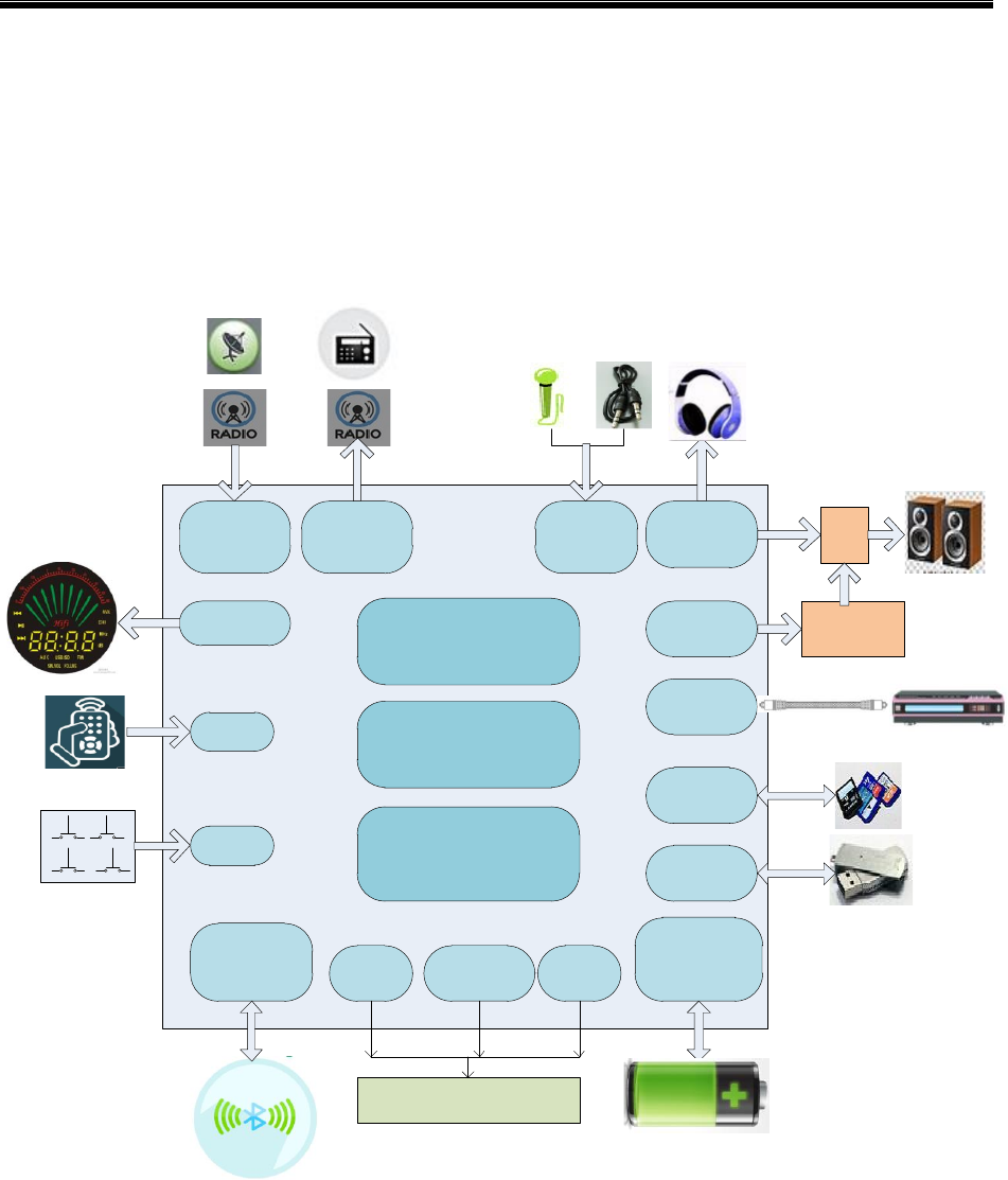
1.1 Introduce
AB53XX is a 32 bits RISC microcontroller. It integrates advanced digital and analog peripherals to audio player
applications.
PMU(Charger
/Buck)
CPU
Memory
Bluetooth
ADC DAC/PA
SPDIF RX
IIS
FM RX FM TX
SD/MMC
USB2.0
IR
KEY
SPI UARTGPIO/PWM
LED
PA
CODEC
Other Application
DSP ENGINE

1Product Overview 6
Copyright © 2018, www. bluetrum.com. All Rights Reserved
6
1.2 Features
CPU and Flexible IO
32bit High performance CPU with DSP
instruction
Flexible GPIO pins with Programmable pull-up and
pull-down resistors;
Support GPIO wakeup or interrupt;
Bluetooth Radio
Compliant to Bluetooth 5.0 and BLE
specification (QDID: 115952);
TX output power +2db in typical;
RX Sensitivity with -90.5dBm @Basic Rate;
FM Tuner
Support frequency band 76~108MHz;
Auto search tuning;
Programable de-emphasis(50/75uS);
Receive signal strength indicator (RSSI);
Audio Interface
Audio codec with 16bit stereo DAC and two
channel 16bit ADC;
Support flexible audio EQ adjust;
Support Sample rate 8, 11.025, 12, 16, 22.05, 32,
44.1 and 48KHz;
4 channel Stereo Analog MUX;
Two channel MIC amplifier input;
High performance Stereo audio ADC with 90dB
SNR;
High performance Stereo audio DAC with 95dB
SNR, with headphone amplifier output;
Peripheral and Interfaces
Three 32-bit timers;
Three multi-function 32-bit timers, support
Capture and PWM mode;
WatchDog;
Three full-duplex UART;
Two SPI;
IR controller;
SD Card Host controller;
SPDIF receiver;
Audio interface IIS;
Full speed USB 2.0 HOST/DEVICE controller;
Sixteen Channels 10-bit SARADC;
Integrate IRTC;
Build in PMU, such as charger/buck/LDO;
Package
LQFP48;
SSOP28L;
SSOP24L;
TSSOP24;
TSSOP20;
SOP16;
Temperature
Operating temperature: -40℃ to +85℃;
Storage temperature: -65℃ to +150℃;

2Interrupts 7
Copyright © 2018, www. bluetrum.com. All Rights Reserved
7
2 Interrupts
Support vectorized interrupts, exceptions on illegal instructions and exceptions on load and store instructions
to invalid addresses.
Exception vectors
Interrupt
number
Address
Description
0
0x00
Reset
1
0x10
2
0x20
3
0x30
4
0x40
Low priority interrupt
5
0x50
6
0x60
7
0x70
8
0x80~0x280
High priority interrupt(see the following table)
High priority interrupt vectors
Interrupt
number
Address
Description
0
0x80
1
0x90
2
0xa0
Software interrupt
3
0xb0
Timer0 interrupt
4
0xc0
Timer1 interrupt
5
0xd0
Timer2 interrupt
Timer4 interrupt
Timer5 interrupt
6
0xe0
Timer3 interrupt
IR receiver interrupt
7
0xf0
8
0x100
9
0x110
10
0x120
11
0x130
12
0x140
13
0x150
14
0x160
UART0 interrupt
UART1 interrupt
UART2 interrupt
15
0x170
16
0x180
17
0x190
18
0x1a0
Port interrupt
19
0x1b0
20
0x1c0
21
0x1d0
22
0x1e0
23
0x1f0
24
0x200
25
0x210
26
0x220
27
0x230
28
0x240
29
0x250

2Interrupts 8
Copyright © 2018, www. bluetrum.com. All Rights Reserved
8
Interrupt
number
Address
Description
30
0x260
31
0x270
2.1 Interrupts Special Registers
Register 2-1PICCON: Peripheral interrupt control Register
Bit
Name
Mode
Default
Description
31:17
-
-
-
Unused
16
GIEM
WR
1
Global interrupt enable mask bit
0: disable interrupt
1: enable interrupt
15:8
-
-
-
Unused
7:3
-
-
-
Unused
2
HPINTEN
WR
0
High priority interrupt enable bit
0: disable
1: enable
1
LPINTEN
WR
0
Low priority interrupt enable bit
0: disable
1: enable
0
GIE
WR
0
Global interrupt enable bit
0: disable interrupt
1: enable interrupt
Register 2-2PICCONSET: Peripheral interrupt control set Register
Bit
Name
Mode
Default
Description
31:17
-
-
-
Unused
16
GIEM
W
0
Write 1 enable Global interrupt enable mask
15:8
-
-
-
Unused
7:3
-
-
-
Unused
2
HPINTEN
W
0
Write 1 enable High priority interrupt
1
LPINTEN
W
0
Write 1 enable Low priority interrupt
0
GIE
W
0
Write 1 enable Global interrupt
Register 2-3PICCONCLR: Peripheral interrupt control clear Register
Bit
Name
Mode
Default
Description
31:17
-
-
-
Unused
16
GIEMDIS
W
0
Write 1 disable Global interrupt enable mask
15:8
-
-
-
Unused
7:3
-
-
-
Unused
2
HPINTDIS
W
0
Write 1 disable High priority interrupt
1
LPINTDIS
W
0
Write 1 disable Low priority interrupt
0
GIEDIS
W
0
Write 1 disable Global interrupt
Register 2-4PICEN: Peripheral interrupt enable Register
Bit
Name
Mode
Default
Description
31:0
IntEN
WR
0x0
Interrupt 31 to 0 enable bit
0: disable
1: enable
Register 2-5PICENSET: Peripheral interrupt enable set Register
Bit
Name
Mode
Default
Description
31:0
IntEN
W
0x0
Write 1 enable Interrupt 31 to 0
Register 2-6PICENCLR: Peripheral interrupt enable clear Register

0 9
Copyright © 2018, www. bluetrum.com. All Rights Reserved
9
Bit
Name
Mode
Default
Description
31:0
IntDIS
W
0x0
Write 1 disable Interrupt 31 to 0
Register 2-7PICPR: Peripheral high priority interrupt selection Register
Bit
Name
Mode
Default
Description
31:0
IntPR
WR
0x0
Interrupt 31 to 0 priority selection bit
0: low priority interrupt
1: high priority interrupt
Register 2-8PICADR: Peripheral interrupt address Register
Bit
Name
Mode
Default
Description
31:10
BADR
WR
0x40
Interrupt entry address
9:0
-
-
0x0
Register 2-9PICPND: Peripheral interrupt pending Register
Bit
Name
Mode
Default
Description
31:3
IntPND[31:4]
R
0x0
Interrupt 31 to 4 pending bit
0: no interrupt pending
1: interrupt pending
2
SWIPND
WR
0
Software interrupt pending. Write 1 will clear software interrupt pending
1:0
IntPND[2:0]
R
0x0
Interrupt 2 to 0 pending bit
0: no interrupt pending
1: interrupt pending

3GPIO Management 10
Copyright © 2018, www. bluetrum.com. All Rights Reserved
10
3 GPIO Management
3.1 Features
1. Control GPIO input/output direction by using direction register;
2. Internal pull-up/pull-down resistor by using pull-up/pull-down resistor control register;
3. Select suitable output driving current capability;
3.2 GPIO general control register
Register 3-1GPIOA: Port A data Register
Bit
Name
Mode
Default
Description
31:8
-
-
-
Unused
7:0
GPIOA
WR
0x00
PAx data. Valid when PAx is used as GPIO
0: PAx is input low state when read and output low at PAx when write;
1:PAx is input high state when read and output high at PAx when write
Register 3-2GPIOASET: Port A Set output data Register
Bit
Name
Mode
Default
Description
31:8
-
-
-
Unused
7:0
GPIOASET
WO
X
Set Pax output data. Write 1 set output data. Write 0 affect nothing.
Register 3-3GPIOACLR: Port A clear output data Register
Bit
Name
Mode
Default
Description
31:8
-
-
-
Unused
7:0
GPIOACLR
WO
X
Clear Pax output data. Write 1 clear output data. Write 0 affect nothing.
Register 3-4GPIOADIR: Port A direction Register
Bit
Name
Mode
Default
Description
31:8
-
-
-
Unused
7:0
GPIOADIR
WR
0xFF
PAx direction control
0: Output
1: Input
Register 3-5GPIOAPU: Port A pull-up Register
Bit
Name
Mode
Default
Description
31:8
-
-
-
Unused
7:0
GPIOAPU
WR
0x0
PAx 10KΩ pull-up resister control. Valid when PAx is used as input
0: disable
1: enable
Register 3-6GPIOAPD: Port A pull-down resister Register
Bit
Name
Mode
Default
Description
31:8
-
-
-
Unused
7:0
GPIOAPD
WR
0x0
PAx 10KΩ pull-down resister control. Valid when PAx is used as input
0: disable
1: enable
Register 3-7GPIOAPU200K: Port A pull-up resister Register

3GPIO Management 11
Copyright © 2018, www. bluetrum.com. All Rights Reserved
11
Bit
Name
Mode
Default
Description
31:8
-
-
-
Unused
7:0
GPIOAPU
WR
0x0
PAx 200KΩ pull-up resister control. Valid when PAx is used as input
0: disable
1: enable
Register 3-8GPIOAPD200K: Port A pull-down resister Register
Bit
Name
Mode
Default
Description
31:8
-
-
-
Unused
7:0
GPIOAPD
WR
0x0
PAx 200KΩ pull-down resister control. Valid when PAx is used as input
0: disable
1: enable
Register 3-9GPIOAPU300: Port A pull-up resister Register
Bit
Name
Mode
Default
Description
31:8
-
-
-
Unused
7:0
GPIOAPU
WR
0x0
PAx 300Ω pull-up resister control. Valid when PAx is used as input
0: disable
1: enable
Register 3-10GPIOAPD300: Port A pull-down resister Register
Bit
Name
Mode
Default
Description
31:8
-
-
-
Unused
7:0
GPIOAPD
WR
0x0
PAx 300Ω pull-down resister control. Valid when PAx is used as input
0: disable
1: enable
Register 3-11GPIOADE: Port A digital function enable register
Bit
Name
Mode
Default
Description
31:8
-
-
-
Unused
7:0
GPIOADE
WR
0xFF
PAx digital function enable
0: Port used as analog IO
1: Port used as digital IO
Register 3-12GPIOAFEN: Port A function mapping enable register
Bit
Name
Mode
Default
Description
31:8
-
-
-
Unused
7:0
GPIOAFEN
WR
0xFF
PAx function mapping enable
0: Port used as GPIO
1: Port used as function IO
Register 3-13GPIOADRV: Port A output driving select Register
Bit
Name
Mode
Default
Description
31:8
-
-
-
Unused
7:0
GPIOADRV
WR
0x0
PAx output driving select
0: 8mA
1: 32mA
3.3 GPIO function mapping
Register 3-14FUNCMCON0: Port function mapping control Register 0
Bit
Name
Mode
Default
Description
31:28
UT1RXMAP
WR
0x0
UART1 RX mapping
0000: no affect
0001: map to G1
0010: map to G2

3GPIO Management 12
Copyright © 2018, www. bluetrum.com. All Rights Reserved
12
Bit
Name
Mode
Default
Description
0011: map to TX pin by UT1TXMAP select
1111: Clear these bits
Others is reserved
27:24
UT1TXMAP
WR
0x0
UART1 TX mapping
0000: no affect
0001: map to G1
0010: map to G2
1111: Clear these bits
Others is reserved
23:20
19:16
15:12
UT0RXMAP
WR
0x0
UART0 RX mapping
0000: no affect
0001: map to G1
0010: map to G2
0011: map to G3
0100: map to G4
0101: map to G5
0110: map to G6
0111: map to TX pin by UT0TXMAP select
1111: Clear these bits
Others is reserved
11:8
UT0TXMAP
WR
0x0
UART0 TX mapping
0000: no affect
0001: map to G1
0010: map to G2
0011: map to G3
0100: map to G4
0101: map to G5
0110: map to G6
0111: map to G7
1111: Clear these bits
Others is reserved
7:4
SPI0MAP
WR
0x0
SPI0 mapping
0000: no affect
0001: map to G1
0010: map to G2
0011: map to G3
1111: Clear these bits
Others is reserved
3:0
SD0MAP
WR
0x0
SD0 mapping
0000: no affect
0001: map to G1
0010: map to G2
0011: map to G3
0100: map to G4
0101: map to G5
0110: map to G6
1111: Clear these bits
Others is reserved
Register 3-15FUNCMCON1: Port function mapping control Register 1
Bit
Name
Mode
Default
Description
31:28
27:24
23:20
19:16
15:12
11:8
UT2RXMAP
WR
0x0
UART2 RX mapping
0000: no affect

3GPIO Management 13
Copyright © 2018, www. bluetrum.com. All Rights Reserved
13
Bit
Name
Mode
Default
Description
0001: map to G1
0010: map to G2
0011: map to TX pin by UT2TXMAP select
1111: Clear these bits
Others is reserved
7:4
UT2TXMAP
WR
0x0
UART2 TX mapping
0000: no affect
0001: map to G1
0010: map to G2
1111: Clear these bits
Others is reserved
3:0
Register 3-16FUNCMCON2: Port function mapping control Register 2
Bit
Name
Mode
Default
Description
31:24
-
-
-
Unused
23:20
19:16
TMR5MAP
WR
0x0
Timer5 PWM mapping
0000: no affect
0001: map to G1
1111: Clear these bits
Others is reserved
15:12
TMR4MAP
WR
0x0
Timer4 PWM mapping
0000: no affect
0001: map to G1
1111: Clear these bits
Others is reserved
11:8
TMR3MAP
WR
0x0
Timer3 PWM mapping
0000: no affect
0001: map to G1
1111: Clear these bits
Others is reserved
7:4
TMR3CPTMAP
WR
0x0
Timer3 capture Pin mapping
0000: no affect
0001: map to G1
0010: map to G2
0011: map to G3
0100: map to G4
0101: map to G5
0110: map to G6
0111: map to G7
1111: Clear these bits
Others is reserved
3:0
3.4 External Port interrupt wake up
Support eight wakeup source input, as the following table.
Wakeup source
Wakeup circuit
PA7
Wakeup circuit 0
PB1
Wakeup circuit 1
PB2
Wakeup circuit 2
PB3
Wakeup circuit 3
PB4
Wakeup circuit 4
WKO
Wakeup circuit 5
PORT_INT_FALL
Wakeup circuit 6
PORT_INT_RISE
Wakeup circuit 7

3GPIO Management 14
Copyright © 2018, www. bluetrum.com. All Rights Reserved
14
Register 3-17WKUPCON: Wake up control Register
Bit
Name
Mode
Default
Description
31:17
-
-
-
Unused
16
WKIE
WR
0
Wake up interrupt enable
0: disable
1: enable
15:8
-
-
-
Unused
7:0
WKEN
WR
0x0
Wake up input 7~0 enable
0: disable
1: enable
Register 3-18WKUPEDG: Wake up edge select Register
Bit
Name
Mode
Default
Description
31:24
-
-
-
Unused
23:16
WKPND
R
0x0
Wake up input 7~0 pending
0: no pending
1: wake up pending
15:8
-
-
-
Unused
7:0
WKEDG
WR
0x0
Wake up input 7~0 wakeup edge select
0: rising edge
1: falling edge
Register 3-19WKUPCPND: Wake up clear pending Register
Bit
Name
Mode
Default
Description
31:8
-
-
-
Unused
23:16
WKCPND
W
0x0
Wake up input 7~0 clear pending
0: no affect
1: clear wake up pending
15:0
-
-
-
Unused
Register 3-20PORTINTEN: Port interrupt enable Register
Bit
Name
Mode
Default
Description
31:0
PORTINTEN
WR
0x0
Port interrupt 0~31 enable bit
0: disable
1: enable
Register 3-21PORTINTEDG: Port interrupt edge select Register
Bit
Name
Mode
Default
Description
31:0
PORTINTEDG
WR
0x0
Port interrupt 0~31 edge select bit
0: rise edge
1: fall edge

4Timer 15
Copyright © 2018, www. bluetrum.com. All Rights Reserved
15
4 Timer
4.1 Features
1. Timer0/1/2, only support 32bit timer function
2. Timer3/4/5, can be configured to Timer-mode, Counter-mode, Capture-mode and PWM-mode
4.2 Timer0/1/2 Special Function Registers
Register 4-1TMR0CON/TMR1CON/TMR2CON: Timer0/1/2 Control Register
Bit
Name
Mode
Default
Description
31:10
-
-
-
Unused
9
TPND
WR
0
Timer overflow pending
0: not overflow
1: overflow
8
-
-
-
Unused
7
TIE
WR
0
Timer overflow interrupt enable
0: disable
1: enable
6
INCSRC
WR
0
Increase source select
0: select TMR_INC
1: select external PIN
5:4
-
-
-
Unused
3:2
INCSEL
WR
0x0
Increase clock selection
00: System Clock
01: Counter input rising
10: Counter input falling
11: Counter input edge
1
-
-
-
Unused
0
TMREN
WR
0
Timer Enable Bit
0: Disable
1: Enable
Register 4-2TMR0CPND/TMR1CPND/TMR2CPND: Timer0/1/2 clear pending Register
Bit
Name
Mode
Default
Description
31:16
-
-
-
Unused
9
TPCLR
W
0
Timer overflow pending clear bit
0: inactive
1: clear pending
8:0
-
-
-
Unused
Register 4-3TMR0CNT/TMR1CNT/TMR2CNT: Timer0/1/2 counter Register
Bit
Name
Mode
Default
Description
31:0
TMRCNT
WR
0x0
Timer counter.
TMRCNT will increase when timer is enabled. It overflows when TMRCNT =
TMRPR, TMRCNT will be clear to 0x0000 when overflow, and the interrupt
flag will be set ‘1’.
Register 4-4TMR0PR/TMR1PR/TMR2PR: Timer0/1/2 period Register
Bit
Name
Mode
Default
Description
31:0
TMRPR
WR
0xffffffff
Timer period = TMRPR + 1

4Timer 16
Copyright © 2018, www. bluetrum.com. All Rights Reserved
16
4.3 Timer3/4/5 Special Function Registers
Register 4-5TMR3CON/TMR4CON/TMR5CON: Timer3/4/5 Control Register
Bit
Name
Mode
Default
Description
31:18
-
-
-
Unused
17
CPND
WR
0
Timer capture pending
0: not capture
1: capture
16
TPND
WR
0
Timer overflow pending
0: not overflow
1: overflow
15:12
-
-
-
Unused
11
PWM2EN
WR
0
Timer pwm2 enable bit
0: disable
1: enable
10
PWM1EN
WR
0
Timer pwm1 enable bit
0: disable
1: enable
9
PWM0EN
WR
0
Timer pwm0 enable bit
0: disable
1: enable
8
CIE
WR
0
Timer capture interrupt enable
0: disable
1: enable
7
TIE
WR
0
Timer overflow interrupt enable
0: disable
1: enable
6
INCSRC
WR
0
Increase source select
0: select TMR_INC
1: select external PIN
5:4
CPTEDSEL
WR
0x0
Timer Capture edge select
00: No Capture
01:Capture PIN rising edge
10: Capture PIN falling edge
11: Capture PIN edge
3:2
INCSEL
WR
0x0
Increase clock selection
00: System Clock
01: Counter input rising
10: Counter input falling
11: Counter input edge
1
CPTEN
WR
0
Timer capture Enable Bit
0: Disable
1: Enable
0
TMREN
WR
0
Timer Enable Bit
0: Disable
1: Enable
Register 4-6TMR3CPND/TMR4CPND/TMR5CPND: Timer3/4/5 clear pending Register
Bit
Name
Mode
Default
Description
31:18
-
-
-
Unused
17
CPCLR
W
0
Capture pending clear bit
0: inactive
1: clear pending
16
TPCLR
W
0
Timer overflow pending clear bit
0: inactive
1: clear pending
15:0
-
-
-
Unused
Register 4-7TMR3CNT/TMR4CNT/TMR5CNT: Timer3/4/5 counter Register

4Timer 17
Copyright © 2018, www. bluetrum.com. All Rights Reserved
17
Bit
Name
Mode
Default
Description
31:0
TMRCNT
WR
0x0
Timer counter.
TMRCNT will increase when timer is enabled. It overflows when TMRCNT =
TMRPR, TMRCNT will be clear to 0x0000 when overflow, and the interrupt
flag will be set ‘1’.
Register 4-8TMR3PR/TMR4PR/TMR5PR: Timer3/4/5 period Register
Bit
Name
Mode
Default
Description
31:0
TMRPR
WR
0xffffffff
Timer period = TMRPR + 1
Register 4-9TMR3CPT/TMR4CPT/TMR5CPT: Timer3/4/5 capture value Register
Bit
Name
Mode
Default
Description
31:0
TMRCPT
R
x
Timer capture value
Register 4-10TMR3DUTY0/TMR4DUTY0/TMR5DUTY0: Timer3/4/5 pwm0 duty Register
Bit
Name
Mode
Default
Description
31:16
-
-
-
Unused
15:0
TMRDUTY0
W
x
Timer pwm0 duty
PWM0 low level length is TMRDUTY0+1
PWM 0 high level length is TMRPR-TMRDUTY0+1
Register 4-11TMR3DUTY1/TMR4DUTY1/TMR5DUTY1: Timer3/4/5 pwm1 duty Register
Bit
Name
Mode
Default
Description
31:16
-
-
-
Unused
15:0
TMRDUTY1
W
x
Timer pwm1 duty
PWM1 low level length is TMRDUTY1+1
PWM1 high level length is TMRPR-TMRDUTY1+1
Register 4-12TMR3DUTY2/TMR4DUTY2/TMR5DUTY2: Timer3/4/5 pwm2 duty Register
Bit
Name
Mode
Default
Description
31:16
-
-
-
Unused
15:0
TMRDUTY2
W
x
Timer pwm2 duty
PWM2 low level length is TMRDUTY2+1
PWM2 high level length is TMRPR-TMRDUTY2+1

5PWM 18
Copyright © 2018, www. bluetrum.com. All Rights Reserved
18
5 PWM
5.1 Features
Four channel PWM for Breathing-lamp
5.2 Special Function Registers
Register 5-1 PWMCON: PMW Configure Register
Bit
Name
Mode
Default
Description
31:5
5
PWMIVN
WR
0
PWM invert enable
0: duty is high level 1: duty is low level
4
AUTOADJUST
WR
0
PWM Auto Adjust enable
0: disable 1: enable
3
PWM3EN
WR
0
PWM3 enable
0: disable 1: enable
2
PWM2EN
WR
0
PWM2 enable
0: disable 1: enable
1
PWM1EN
WR
0
PWM1 enable
0: disable 1: enable
0
PWM0EN
WR
0
PWM0 enable
0: disable 1: enable
Register 5-2 PWMPR: PMW period Register
Bit
Name
Mode
Default
Description
31:16
15:0
PWMPR
WR
0xffff
PWM period = (PWMPR+1) * Tpwmclk
Register 5-3 PWM01DUT: PWM0/1 duty registers
Bit
Name
Mode
Default
Description
31:16
PWM1DUT
WR
0x0
PWM1 duty register ; Duty = PWM1DUT/ PWMPR
15:0
PWM0DUT
WR
0x0
PWM0 duty register ; Duty = PWM0DUT/ PWMPR
Register 5-4 PWM23DUT: PWM2/3 duty registers
Bit
Name
Mode
Default
Description
31:16
PWM3DUT
WR
0x0
PWM3 duty register ; Duty = PWM3DUT/ PWMPR
15:0
PWM2DUT
WR
0x0
PWM2 duty register ; Duty = PWM2DUT/ PWMPR
Register 5-5 PWMCYCNUM: PWM adjust cycle number register
Bit
Name
Mode
Default
Description
31:24
PWM3CYCNUM
WR
0x0
PWM3 Duty adjust cycle num
When AUTOADJUST = 1, each PWM3CYCNUM Duty add
(PWM3STEP/ PWMPR)
23:16
PWM2CYCNUM
WR
0x0
PWM2 Duty adjust cycle num
When AUTOADJUST = 1, each PWM2CYCNUM Duty add
(PWM2STEP/ PWMPR)
15:8
PWM1CYCNUM
WR
0x0
PWM1 Duty adjust cycle num
When AUTOADJUST = 1, each PWM1CYCNUM Duty add
(PWM1STEP/ PWMPR)
7:0
PWM0CYCNUM
WR
0x0
PWM0 Duty adjust cycle num
When AUTOADJUST = 1, each PWM0CYCNUM Duty add

5PWM 19
Copyright © 2018, www. bluetrum.com. All Rights Reserved
19
Bit
Name
Mode
Default
Description
(PWM0STEP/ PWMPR)
Register 5-6 PWMSTEP: PWM Step register
Bit
Name
Mode
Default
Description
31:24
PWM3STEP
WR
0x0
PWM3 Duty adjust step
23:16
PWM2STEP
WR
0x0
PWM2 Duty adjust step
15:8
PWM1STEP
WR
0x0
PWM1 Duty adjust step
7:0
PWM0STEP
WR
0x0
PWM0 Duty adjust step

6RTC 20
Copyright © 2018, www. bluetrum.com. All Rights Reserved
20
6 RTC
6.1 Features
1. Support 32bit Independent power supply real time counter
2. Support alarm interrupt and second interrupt
6.2 Special Function Registers
Register 6-1RTCCON: RTC Control Register
Bit
Name
Mode
Default
Description
31:13
-
-
-
Unused
20
VUSBONLINE
R
0
VUSB online state
0: not online
1: online
19
RTCWKP
R
0
RTC WK pin state
0: WK pin state is 0
1: WK pin state is 1
18
RTC1SPND
R
0
RTC 1s pending
0: no pending
1: 1s pending
17
ALMPND
R
0
RTC alarm pending
0: no pending
1: alarm pending
16
RTCPND
R
0
RTC trans done
0: done
1:not done
15:9
-
-
-
Unused
8
ALM_WKEN
WR
0
RTC alarm wakeup enable
0: disable
1: enable
7
RTC1S_WKEN
WR
0
RTC 1S wakeup enable
0: disable
1: enable
6
VUSBRSTEN
WR
0
VUSB insert reset system enable
0: disable
1: enable
5
WKUPRSTEN
WR
0
RTC wake up power down mode reset system enable
0: disable
1: enable
4
ALMIE
WR
0
RTC alarm interrupt enable
0: disable
1: enable
3
RTC1SIE
WR
0
RTC 1S interrupt enable
0: disable
1: enable
2:1
BAUDSEL
WR
0x0
Increase clock selection
00: System Clock divide 4
01: System Clock divide 8
10: System Clock divide 16
11: System Clock divide 32
0
RTCCS
WR
0
RTC cs
0:disabled

6RTC 21
Copyright © 2018, www. bluetrum.com. All Rights Reserved
21
Bit
Name
Mode
Default
Description
1:enable
Register 6-2RTCDAT: RTC data Register
Bit
Name
Mode
Default
Description
31:10
-
-
-
Unused
9:8
RTCMD
W
0x0
RTC cmd
00: data
01: read command
10: write command
11: reserve
7:0
RTCDAT
WR
x
RTC data
Register 6-3RTCCPND: RTC clear pending Register
Bit
Name
Mode
Default
Description
31:19
-
-
-
Unused
18
C1SPND
R
0
Write 1 will clear RTC 1S pending
17
CALMPND
R
0
Write 1 will clear RTC alarm pending
16:0
-
-
-
Unused
6.3 Independent Power RTC Registers
Register 6-4 RTCCNT: RTC counter Register
Bit
Name
Mode
Default
Description
31:0
RTCCNT
WR
0x0
32bit RTC counter
Register 6-5 RTCALM: RTC alarm Register
Bit
Name
Mode
Default
Description
31:0
RTCALM
WR
0xffffffff
32bit RTC alarm
Register 6-6 RTCCON0: RTC control Register 0
Bit
Name
Mode
Default
Description
7
PWRUP1ST
WR
1
RTC first power up flag
0: not first power up
1: first power up
6
EXT32KS
WR
0
External 32K select
0: use RTC internal 32K osc
1: use external 32K osc
5
RSV
WR
1
Reserve, can’t be changed default value
4
RSV
WR
0
Reserve, can’t be changed default value
3
RSV
WR
0
Reserve, can’t be changed default value
2
RSV
WR
0
Reserve, can’t be changed default value
1
X32KEN
WR
0
XOSC32K enable bit
0: disable
1: enable
0
RSV
WR
0
Reserve, can’t be changed default value
Register 6-7 RTCCON1: RTC control Register 1
Bit
Name
Mode
Default
Description
7
-
-
-
Unused
6
VRTCEN
WR
0
VRTC enable bit, VRTC voltage for ADC
0: disable
1: enable
5
WKPAEN
WR
0
WK pin analog enable bit, output WKO voltage for ADC
0: disable
1: enable

6RTC 22
Copyright © 2018, www. bluetrum.com. All Rights Reserved
22
Bit
Name
Mode
Default
Description
4
WKPPUEN
WR
1
WK pin pull up enable bit
0: disable
1: enable
3:2
WKPPUS
WR
0x1
WK pin pull up select bit
00: 80K
01: 90K
10: 100K
11: 400K
1
WKPPD
WR
0
WK pin pull down 10K enable bit
0: disable
1: enable
0
WKPIE
WR
1
WK pin input enable bit
0: disable
1: enable
Register 6-8 RTCCON2: RTC control Register 2
Bit
Name
Mode
Default
Description
7
32KSEL
WR
0
32K osc select bit
0: 32.768K
1: 32K
6
SELVDDPU
WR
1
SEL VDD pullup enable
0: disable
1: enable
5:4
RSV
WR
0x0
Reserve, can’t be changed default value
3:2
RSV
WR
0x2
Reserve, can’t be changed default value
1:0
RSV
WR
0x2
Reserve, can’t be changed default value
Register 6-9 RTCCON3: RTC control Register 3
Bit
Name
Mode
Default
Description
7
RTC1S_WKEN
WR
0
RTC one second wakeup enable bit
0: disable
1: enable
6
ALM_WKEN
WR
0
RTC alarm wakeup enable bit
0: disable
1: enable
5
VSUB_WKEN
WR
0
VUSB wake up enable bit
0: disable
1: enable
4
WKP_WKEN
WR
0
WK pin wake up enable bit
0: disable
1: enable
3
-
-
-
Unused
2
VCOREEN
WR
1
VDDCORE enable bit
0: disable
1: enable
1
VIOEN
WR
1
VDDIO enable bit
0: disable
1: enable
0
BUCKEN
WR
1
BUCK enable bit
0: disable
1: enable
Register 6-10 RTCCON5: RTC control Register 5
Bit
Name
Mode
Default
Description
7
-
-
-
Unused
6
RSV
WR
0
Reserve, can’t be changed default value
5:4
RSV
WR
0x0
Reserve, can’t be changed default value
3:2
RSV
WR
0x0
Reserve, can’t be changed default value
1
BUCKLPM
WR
0
BUCK low power mode enable

6RTC 23
Copyright © 2018, www. bluetrum.com. All Rights Reserved
23
Bit
Name
Mode
Default
Description
0: disable
1: enable
0
LDOM
WR
1
BUCK LDO mode select bit
0: buck mode
1: LDO mode
Register 6-11 RTCCON7: RTC control Register 7
Bit
Name
Mode
Default
Description
7:5
-
-
-
Unused
4
WKOPRT
WR
0
WKO protect bit
3
LVDDETEN
WR
0
LVD detect enable after power up by wake up
0: disable
1:enable
2
WKPFEN
WR
0
WK pin filter enable bit
0: disable
1:enable
1:0
WKPFSEL
WR
0x0
WK pin filter select bit
00:8ms
01:32ms
10:128ms
11:512ms
Register 6-12 RTCCON8: RTC control Register 8
Bit
Name
Mode
Default
Description
7:5
-
-
-
Unused
4
VSUBP
R
0
VUSB wake up pending
0: no pending
1: pending
3
WKP
R
0
WK pin wake up pending
0: no pending
1: pending
2
RTC1SPC
WR
0
When write:
RTC 1 second pending clear
0: no affect
1: clear 1s pending
When read:
RTC 1 second pending
0: no second pending
1: second pending
1
ALMPC
WR
0
When write:
RTC alarm pending clear
0: no affect
1: clear alarm pending
When read:
Alarm pending
0: no alarm pending
1: alarm pending
0
WKP10SC
WR
0
When write
WK pin 10s pending clear
0: no affect
1: clear 10s pending
When read:
WK pin 10s pending
0: no 10s pending
1: 10s pending
Register 6-13 RTCCON9: RTC control Register 9
Bit
Name
Mode
Default
Description
7:4
-
-
-
Unused
3:0
WKP10SEN
W
0xa
WK pin 10s reset enable

6RTC 24
Copyright © 2018, www. bluetrum.com. All Rights Reserved
24
Bit
Name
Mode
Default
Description
0xa: disable
Others: enable
After enable, can’t disable.

7UART0 25
Copyright © 2018, www. bluetrum.com. All Rights Reserved
25
7 UART0
7.1 Features
1. UART is a serial port capable of asynchronous transmission.
2. The UART can function in full duplex mode.
7.2 UART0 Special Function Registers
Register 7-1UART0CON: UART Control Register
Bit
Name
Mode
Default
Description
31:10
-
-
-
Unused
9
RXPND
R
0
RX pending
0: RX one byte not finish
1: RX one byte finish
8
TXPND
R
0
TX pending
0: TX one byte not finish
1: TX one byte finish
7
RXEN
WR
0
RX enable
0: RX disable
1: RX enable
6
ONELINE
WR
0
One-line mode
0: TX/RX separate
1: TX/RX one line
5
CLKSRC
WR
0
Clock source select
0: system clock
1: uart_inc
4
SB2EN
WR
0
Two Stop Bit enable
0:1-bit Stop Bit
1: 2 bit Stop Bit
3
TXIE
WR
0
Transmit Interrupt Enable
0 = Transmit interrupt disable
1 = Transmit interrupt enable
2
RXIE
WR
0
Receive Interrupt Enable
0: Receiver interrupt disable
1: Receiver interrupt enable
1
BIT9EN
WR
0
BIT9 Enable Bit
0: Eight-bit mode
1: Nine-bit mode
0
UTEN
WR
0
UART Enable Bit
0: Disable UART module
1: Enable UART module
Register 7-2UART0CPND: UART0 clear pending Register
Bit
Name
Mode
Default
Description
31:18
-
-
-
Unused
17
CRSTKEYPND
W
0
Reset Key match pending clear
0: N/A
1: Clear Reset key match Pending
16
CKEYPND
W
0
Key match pending clear
0: N/A
1: Clear key match Pending

7UART0 26
Copyright © 2018, www. bluetrum.com. All Rights Reserved
26
Bit
Name
Mode
Default
Description
15:10
-
-
-
Unused
9
CRXPND
W
0
RX pending clear
0: N/A
1: Clear RX Pending
8
CTXPND
W
0
TX pending clear
0: N/A
1: Clear TX Pending. Writing data to UTBUF will clear TXPND
7:0
-
-
-
Unused
Register 7-3UART0BAUD: UART Baud Rate Register
Bit
Name
Mode
Default
Description
31:16
UART0RXBAUD
W
0
UART RX Baud Rate
Baud Rate =Fsys clock / (UART0RXBAUD + 1)
15:0
UART0TXBAUD
W
0
UART TX Baud Rate
Baud Rate =Fsys clock / (UART0TXBAUD + 1)
Register 7-4 UART0DATA: UART Data Register
Bit
Name
Mode
Default
Description
31:9
-
-
-
Unused
8
UART0BIT8
WR
x
UART Data bit 8
7:0
UART0DAT
WR
x
UART Data
Write this register will load the data to transmitter buffer.
Read this register will read the data from the receiver buffer..
7.3 User Guide
1. Set IO in the correct direction.
2. Configure UART0BAUD to choose sample rate
3. Enable UART0 by setting
4. Set TXIE or RXIE ‘to 1’ if needed
5. write data to UART0DATA
6. Wait for PND to change to ‘1’, or wait for interrupt
7. Read received data from UART0DATA if needed

8SPI1 27
Copyright © 2018, www. bluetrum.com. All Rights Reserved
27
8 SPI1
8.1 Features
SPI1 can support different mode
1. general 3 wire mode, 1-bit clock in/out, 1-bit data output, 1-bit data input
2. 2 wire mode, 1-bit clock in/out, 1-bit data output or input;
3. 2 data bus mode, 1-bit clock in/out, 2-bit data output or input;
8.2 SPI1 Special Function Registers
Register 8-1SPI1CON: SPI1 Control Register
Bit
Name
Mode
Default
Description
31:17
-
-
-
Unused
16
SPIPND
R
0
SPI pending
0: not finish SPI rx/tx
1: finish SPI rx/tx
15:11
-
-
-
Unused
10
SPIOSS
WR
0
SPI output data and sample data is at the same edge
0: disable
1: enable
9
SPIMBEN
WR
0
SPI multiple bit bus enable bit
0: disable
1: enable
8
SPILF_EN
WR
0
SPI LFSR enable bit
0: disable
1: enable
7
SPIIE
WR
0
SPI interrupt enable
0: disable
1: enable
6
SMPS
WR
0
SPI sampling edge select bit, when SPIOSS = 0, output data and
sample data is at different clock edge; when SPIOSS = 1, output
data and sample data is at the same clock edge
0: falling edge output data;
1: rising edge output data;
5
CLKIDS
WR
0
SPI clock state when idle
0: clock stay at 0
1: clock stay at 1
4
RXSEL
WR
0
When in DMA mode or 2-wire mode, configure SPI Receive or
Transmit select bit

8SPI1 28
Copyright © 2018, www. bluetrum.com. All Rights Reserved
28
Bit
Name
Mode
Default
Description
0: transmit
1: receive
3:2
BUSMODE
WR
0x0
Data bus width select bit
00:3-wire mode; 1bit data in, 1bit data out
01:2-wire mode; 1bit data in/out
10: 2bit bidirectional data bus
11: reserved
1
SPISM
WR
0
Slave mode select bit
0:master mode
1:slave mode
0
SPIEN
WR
0
SPI Enable Bit
0: Disable
1: Enable
Register 8-2SPI1BAUD: SPI Baud Rate Register
Bit
Name
Mode
Default
Description
31:16
-
-
-
Unused
15:0
SPI1BAUD
W
0
SPI Baud Rate
Baud Rate =Fsys clock / (SPI_BAUD+1)
Register 8-3SPI1CPND: SPI clear pending Register
Bit
Name
Mode
Default
Description
31:17
-
-
-
Unused
16
SPICPND
W
0
Write 1 will clear SPIpending

8SPI1 29
Copyright © 2018, www. bluetrum.com. All Rights Reserved
29
Bit
Name
Mode
Default
Description
15:0
-
-
-
Unused
Register 8-4 SPI1BUF: SPI1 receive/send Data Register
Bit
Name
Mode
Default
Description
31:8
-
-
-
Unused
7:0
SPI1BUF
WR
x
SPI Data
Write this register will load the data to transmitter buffer.
Read this register will read the data from the receiver buffer..
Register 8-5 SPI1DMACNT: SPI1 DMA counter Register
Bit
Name
Mode
Default
Description
31:16
-
-
-
Unused
15:0
SPI1DMACNT
W
x
SPIDMA byte counter
Write this register will kick start spi send/receive data
Total number of bytes received / send is SPI1DMACNT
Register 8-6 SPI1DMAADR: SPI1 DMA address Register
Bit
Name
Mode
Default
Description
31:21
-
-
-
Unused
20:0
SPI1DMAADR
W
x
SPIDMA byte address
8.3 User Guide
SPI Normal 1bit-Mode Operation Flow:
1. Set 3-wire mdoe or 2-wire mode and select the pin map
2. Select RXSEL for Transmit or receive
3. Configure clock frequency
4. Select one of the four timing mode
5. Enable SPI module by setting SPIEN ‘1’

8SPI1 30
Copyright © 2018, www. bluetrum.com. All Rights Reserved
30
6. Set SPIIE ‘1’ if needed
7. Write data to SPIBUF to kick-start the process
8. Wait for SPIPND to change to ‘1’, or wait for interrupt
9. Read received data from SPIBUF if needed
10. Go to Step 8 to start another process if needed or turn off SPI1by clearing SPIIE and SPIEN
SPI Normal multi-bit-Mode Operation Flow:
1. Set data bus width(bus 2) and select the pin map
2. Select RXSEL for Transmit or receive
3. Configure clock frequency
4. Select one of the four timing mode
5. Enable SPI module by setting SPIEN ‘1’
6. Set SPIIE ‘1’ if needed
7. Write data to SPIBUF to kick-start the process
8. If data bus width are 2 bit, write SPIBUF twice kick-start the transmission
9. However, when receive data, only need write once to kick-start receive process
10. Wait for SPIPND to change to ‘1’, or wait for interrupt
11. Read received data from SPIBUF if needed
12. Go to Step 8 to start another process if needed or turn off SPI by clearing SPIIE and SPIEN
SPI1 DMA Mode Operation Flow:
1. Set IO in the correct direction and data width mode.
2. Select RXSEL for DMA direction
3. Configure clock frequency
4. Select one of the four timing modes
5. Enable SPI module by setting SPIEN to ‘1’
6. Set SPIIE ‘1’ if needed
7. configure SPI1DMAADR;
8. Write data to SPI1_DMACNT to kick-start a DMA process
9. Wait for SPIPND to change to ‘1’, or wait for interrupt
10. Go to Step 8 to start another DMA process if needed or turn off SPI1 by clearing SPI1EN

9Characteristics 31
Copyright © 2018, www. bluetrum.com. All Rights Reserved
31
9 Characteristics
9.1 PMU Parameters
Table 9-1 PMU voltage input Parameters
Sym
Characteristics
Min
Typ
Max
Unit
Conditions
VUSB
Charger Voltage input
3.0
5.0
5.0
V
VBAT
Voltage input
3.0
3.7
5.0
V
Table 9-2 3.3V LDO Parameters
Sym
Characteristics
Min
Typ
Max
Unit
Conditions
VDDIO
3.3V LDO voltage output
3.0
3.3
3.6
V
Light Loading condition
△VVDDIO
Output Mismatch 1-sigma
-
56
-
mV
VDDIO=3.3v
ILOAD
Maximum output current
-
-
150
mA
@VBAT=3.6v
ISC
Short Circuit Current Limit
-
-
300
mA
@VBAT=3.8v
Table 9-3 1.6V LDO Parameters
Sym
Characteristics
Min
Typ
Max
Unit
Conditions
VDDBT
1.6V LDO voltage output
-
1.6
-
V
Light Loading condition
△VVDDBT
Output Mismatch 1-sigma
-
27
-
mV
VDDBT=1.6v
ILOAD
Maximum output current
-
-
100
mA
@VBAT=3.0v
ISC
Short Circuit Current Limit
-
-
200
mA
@VBAT=3.8v
Table 9-4 1.2V LDO Parameters
Sym
Characteristics
Min
Typ
Max
Unit
Conditions
VDDCORE
1.2V LDO voltage output
-
1.2
-
V
Light Loading condition
△VVDDCORE
Output Mismatch 1-sigma
-
20
-
mV
VDDCORE=1.2v
ILOAD
Maximum output current
-
-
80
mA
@VBAT=3.6v
ISC
Short Circuit Current Limit
-
-
120
mA
@VBAT=3.8v
9.2 IO Parameters
Table 9-5 I/O Parameters
GPIO—Electrical Characteristics
Symbol
Description
Related GPIO
Min
Typical
Max
Units
Conditions
VIL
Low-level input voltage
-0.3
1.27
V
VDDIO=3.3V
VIH
High-level input voltage
2.03
3.6
V
VDDIO=3.3V
Driver Ability 1
Output Driver Ability 1
32
mA
VDDIO=3.3V
Driver Ability 0
Output Driver Ability 0
8
mA
VDDIO=3.3V
RPUP0
Internal pull-up resister 0
8
10
12
KΩ
RPUP1
Internal pull-up resister 1
0.24
0.3
0.36
KΩ
RPUP2
Internal pull-up resister 2
160
200
240
KΩ
RPDN0
Internal pull-down resister 0
8
10
12
KΩ
RPDN1
Internal pull-down resister 1
0.24
0.3
0.36
KΩ
RPDN2
Internal pull-down resister 2
160
200
240
KΩ

9Characteristics 32
Copyright © 2018, www. bluetrum.com. All Rights Reserved
32
9.3 Audio DAC Parameters
Table 9-6 Audio DAC Parameters
Sym
Characteristics
Min
Typ
Max
Unit
Conditions
SNR
-
96
-
dB
VCM cap=1uF
VDDDAC cap=1uF
with A-wt filter
Output -3dBV
Fin=1KHz
THD+N
-
-86
-
dB
VCM cap=1uF
VDDDAC cap=1uF
with A-wt filter
Output -3dBV with 10K loading
Fin=1KHz
Output Range
Maximum output voltage
-
2.6
Vpeak-peak
32ohm Loading
9.4 Audio ADC Parameters
Table 9-7 Audio ADC Parameters
Sym
Characteristics
Min
Typ
Max
Unit
Conditions
SNR
-
90
-
dB
VCM cap=1uF
VDDDAC cap=1uF
with A-wt filter
Input sine amplitude, 850mV
RMS
Fin=1KHz
THD+N
-
-87
-
dB
VCM cap=1uF
VDDDAC cap=1uF
with A-wt filter
Input sine amplitude, 850mV
RMS
Fin=1KHz.
Input Range
Input sine wave peak amplitude
0
VCM
V
From aux input, aux 0db gain,
VCM represent VCM voltage.
9.5 BT Parameters
Table 9-8 BT Parameters
Characteristics
Min
Typical
Max
Unit
Conditions
Maximum Transmit Power
-
2
-
dBm
RMS DEVM
-
5.5
-
%
Maximum TX power
2-DH5 packet
Peak DEVM
-
12.5
%
EDR Relative Transmit Power
-0.2
dB
Sensitivity @ Basic Rate
-90.5
dBm
BER=0.1%, using DH5 packet
Sensitivity @ EDR
-89.5
dBm
BER=0.01%, using 2-DH5 packet

9Characteristics 33
Copyright © 2018, www. bluetrum.com. All Rights Reserved
33
9.6 Current Parameters
Table 9-9 Current Parameters
Sym
Characteristics
Min
Typ
Max
Unit
Conditions
IRTC
RTC mode current
-
4
-
uA
4.2V input, room temp.
Sleep
Sleep current
-
500
2000
uA
3.3V input, room temp
