PE2653_04 ADB340MP
User Manual: ADB340MP
Open the PDF directly: View PDF ![]() .
.
Page Count: 29
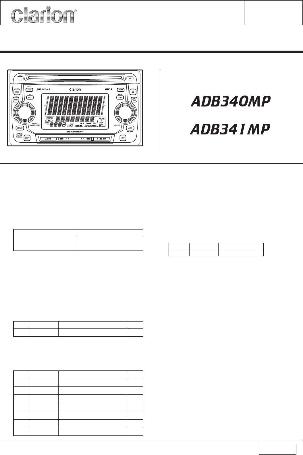
ADB340MP
ADB341MP
- 1 -
Service Manual
Published by Service Dept.
Printed in Japan
Clarion Co., Ltd.
50 Kamitoda, Toda-shi, Saitama 335-8511 Japan
Service Dept.: 5-66 Azuma , Kitamoto-shi, Saitama 364-0007 Japan
Tel: +81-48-541-2335 / 2432 FAX: +81-48-541-2703
298-6153-01 Mar.2006
Model
2DIN AM/FM
CD/MP3 Cassette Player
(PE-2652B / For U.S.A.)
Model
(PE-2653K / For other countries)
REISSUE NOTIFICATION /
REPLACEMENT REQUEST
ORIGINAL SERVICE MANUAL
This additional service manual is designed to be used to-
gether with the original manual.
Original model Manual No.
ADB340MP(PE-2652B) 298-6153-00
ADB341MP(PE-2653K)
EXPODED VIEW / PARTS LIST
Main section (cf.page 10)
* The following part was modified.
It is possible to use a new CD mechanism(P/No. 653-
0435-12) for an old unit. It is impossible to use a old CD
mechanism(P/No. 653-0428-10) for a new unit.
[Serial No.] ADB340MP : from 4817
ADB341MP : from 9864
ELECTRICAL PARTS LIST
Display PWB(B3) section (cf.page 17)
*The following part was modified.
[Serial No.] ADB340MP : from 5971
ADB341MP : from 14930
ADB340MP
NO. PART NO. DESCRIPTION Q'TY
11 653-0435-12 CD MECH(CDC03TL2) 1
CD mechanism section (cf.page 12-13)
*The following parts were modified.
[Serial No.] ADB340MP : from 4817
ADB341MP : from 9864
NO. PART NO. DESCRIPTION Q'TY
1 653-0435-18 CHASSIS 1
5 653-0435-19 TOP COVER 1
11 653-0435-20 DISC ARM L 1
12 653-0435-21 DISC ARM R 1
13 653-0435-22 TOP GUIDE 1
43 653-0435-23 CHACK SHEET 1
64 653-0435-24 MACHINE SCREW 5
REF No. PART No. DESCRIPTION
D902 653-0435-17 DI-HZM5.1-B1
ADB340MP
ADB341MP
- 1 -
Published by Service Dept.
Printed in Japan
Clarion Co., Ltd.
50 Kamitoda, Toda-shi, Saitama 335-8511 Japan
Service Dept.: 5-66 Azuma , Kitamoto-shi, Saitama 364-0007 Japan
Tel: +81-48-541-2335 / 2432 FAX: +81-48-541-2703
298-6153-00 Mar.2004 P
Service Manual
Model
2DIN AM/FM
CD/MP3 Cassette Player
SPECIFICATIONS
FM tuner section
Frequency range: 87.9MHz to 107.9MHz
(ADB340MP)
87.0MHz to 108MHz
(ADB341MP)
Usable sensitivity: 11dBf
50dB quieting sensitivity:17dBf
Alternate channel selectivity:
75dB
Stereo separation: 35dB (1kHz)
Frequency response: 30Hz to 15kHz (+/-3dB)
AM tuner section
Frequency range: 530kHz to 1710kHz (ADB340MP)
531kHz to 1629kHz (ADB341MP)
Usable sensitivity: 25uV
CD player section
Frequency response: 10Hz to 20kHz (+/-1dB)
S/N ratio: 100dB (1kHz)
Dynamic range: 95dB (1kHz)
Distortion: 0.01%
MP3 mode
MP3 sampling rate: 8kHz to 48kHz
MP3 bit rate: 8kbps to 320kbps/VBR
Logical format: ISO9660 level1,2
JOLIET or Romeo
Tape deck section
Wow & flutter: 0.06%(WRMS)
Channel separation: 45dB(1kHz)
Frequency response(+3/-3dB):
120us(normal); 30Hz to 18kHz
Audio section
Maximum power output: 50Wx4
Continous average power output:
17Wx4, into 4ohm, 20Hz to 20kHz,
1%THD
Bass control action: +/-10dB (100Hz)
Middle control action: +/-10dB (1kHz)
Treble control action: +/-10dB (10kHz)
Line output level: 18V (CD 1kHz)
EQ
4mode: Impact / B-boost / Accustic / Flat
General
Power supply voltage: 14.4V DC(10.8V to 15.6V allow-
able) negative ground
Current consumption: Less than 15A
Speaker impedance: 4ohm(4ohm to 8ohm allowable)
Dimensions(mm): 178(W)x100(H)x183(D)
Weight: 2.1kg
(PE-2652B-A / For U.S.A.)
NOTES
* In extreme cold, the screen movement may slow down
and the screen may darken, but this is normal.The screen
will recover when it returns to normal temperature.
* Use only compact discs bearing the or mark.
* Some CDs recorded in CD-R/CD-RW mode may not be
usable.
* We cannot supply PWB with component parts in principle.
When a circuit on PWB has failure, please repair it by
component parts base. Parts which are not mentioned in
service manual are not supplied.
* Specifications and design are subject to change without
notice for further improvement.
(PE-2653K-A / For other countries)
Model
ADB340MP
ADB341MP - 2 -
COMPONENTS
PE-2652B-A / PE-2653K-A
1. Main unit ----------- 1
2. Extension lead 653-0428-46 1
(15A Fuse 120-0150-00)
3. NISSAN install kit 653-0428-56 1
3-1. Finisher ----------- 1
3-2. Hexagon screw(M5x8) ----------- 8
3-3. Flat head screw(M5x8) ----------- 8
3-4. Spacer ----------- 4
3-5. Double-sided tape(4pce.) ----------- 1
To engineers in charge of repair or
inspection of our products.
If extended damage is caused due to negligence during
repair, the legal responsibility shall be with the repairing
company.
3. Check for safety after repair.
Check that the screws, parts and wires are put back se-
curely in their original position after repair. Ensure for safety
reasons there is no possibility of secondary ploblems
around the repaired spots.
If extended damage is caused due to negligence of repair,
the legal responsibility shall be with the repairing company.
4. Caution in removal and making wiring connection to the
parts for the automobile.
Disconnect the battery terminal after turning the ignition
key off. If wrong wiring connections are made with the bat-
tery connected, a short circuit and/or fire may occur. If ex-
tensive damage is caused due to negligence of repair, the
legal responsibility shall be with the repairing company.
5. Cautions regarding chips.
Do not reuse removed chips even when no abnormality is
observed in their appearance. Always replace them with
new ones. (The chip parts include resistors, capacitors,
diodes, transistors, etc). The negative pole of tantalum
capacitors is highly susceptible to heat, so use special care
when replacing them and check the operation afterwards.
6. Cautions in handling flexible PWB
Before working with a soldering iron, make sure that the
iron tip temperature is around 270 . Take care not to ap-
ply the iron tip repeatedly(more than three times)to the
same patterns. Also take care not to apply the tip with force.
7. Turn the unit OFF during disassembly and parts replace-
ment. Recheck all work before you apply power to the unit.
8. Cautions in checking that the optical pickup lights up.
The laser is focused on the disc reflection surface through
the lens of the optical pickup. When checking that the la-
ser optical diode lights up, keep your eyes more than 30cms
away from the lens. Prolonged viewing of the laser within
30cms may damage your eyesight.
9. Cautions in handling the optical pickup
The laser diode of the optical pickup can be damaged by
electrostatic charge caused by your clothes and body. Make
sure to avoid electrostatic charges on your clothes or body,
or discharge static electricity before handling the optical
pickup.
9-1. Laser diode
The laser diode terminals are shorted for transporta-
tion in order to prevent electrostatic damage. After
replacement, open the shorted circuit. When remov-
ing the pickup from the mechanism, short the termi-
nals by soldering them to prevent this damage.
9-2. Actuator
The actuator has a powerful magnetic circuit. If a
magnetic material is put close to it. Its characteris-
tics will change. Ensure that no foreign substances
enter through the ventilation slots in the cover.
9-3. Cleaning the lens
Dust on the optical lens affects performance. To
clean the lens, apply a small amount of isopropyl
alcohol to lens paper and wipe the lens gently.
CAUTION
Use of controls, adjustment or performance of procedures
other than those specified herein, may result in hazardous
radiation exposure.
The COMPACT DISC player should not be adjusted or re-
paired by anyone except properly qualified service person-
nel.
Before repair or inspection, make sure to follow the
instructions so that customers and Engineers in
charge of repair or inspection can avoid suffering
any risk or injury.
1. Use specified parts.
The system uses parts with special safety features against
fire and voltage. Use only parts with equivalent character-
istics when replacing them.
The use of unspecified parts shall be regarded as remod-
eling for which we shall not be liable. The onus of product
liability (PL) shall not be our responsibility in cases where
an accident or failure is as a result of unspecified parts
being used.
2. Place the parts and wiring back in their original positions
after replacement or re-wiring.
For proper circuit construction, use of insulation tubes,
bonding, gaps to PWB, etc, is involved. The wiring con-
nection and routing to the PWB are specially planned using
clamps to keep away from heated and high voltage parts.
Ensure that they are placed back in their original positions
after repair or inspection.
Top View of Source Unit
MODEL
12V GROUND
AM 530-1710kHz/FM 87.9- 107.9MHz
SERIAL No.
PE-2652B
28A51690
Clarion Co., Ltd.
MADE IN INDONESIA
THIS DEVICE COMPLIES WITH PART 15 OF THE FCC RULES.
OPERATION IS SUBJECT TO THE FOLLOWING TWO CONDITIONS:
(1) THIS DEVICE MAY NOT CAUSE HARMFUL INTERFERENCE, AND
(2) THIS DEVICE MUST ACCEPT ANY INTERFERENCE RECEIVED,
INCLUDING INTERFERENCE THAT MAY CAUSE UNDESIRED
OPERATION.
THIS PRODUCTION COMPLIES WITH DHHS RULES 21 CFR
SUBCHAPTER J APPLICABLE AT DATE OF MANUFACTURE.
CLARION CO., LTD.
50 KAMITODA, TODA-SHI, SAITAMA-KEN, JAPAN
MANUFACTURED:
ADB340MP
ADB341MP
- 3 -
TROUBLESHOOTING
Failure
phenomenon
Major
category
Intermediate
category
Minor
category
no operation no power-up microcomputer section:
no B/U power output Q621 collector :
14V output failure
Q621 collector :
normal 14V output B/U power failure B/U power circuit
Q621, D621
Failure
cause
Check
location
power input failure power input circuit
L601, J214, J215
B/U power : normal ACC ON failure ACC ON circuit
Q661, D662
microcomputer :
5V output failure
microcomputer IC701
failure microcomputer IC701
microcomputer :
5V output normal
microcomputer
oscillation failure
microcomputer
oscillation circuit F701,
C707 C708
microcomputer reset
failure
microcomputer reset
pin R781, R794
no sounding no function operated Q602 base :
5V output failure
microcomputer IC701
failure microcomputer IC701
Q602 base :
5V output normal
POWER ON circuit
failure
POWER ON circuit
Q601, Q602
normal operation IC501 PIN 4 :
5V output failure
microcomputer IC701
failure microcomputer IC701
mechanism
operation
cassette mechanism :
no operation
Q364 2 PIN :
5V output failure
microcomputer IC701
failure
IC501 PIN 22 :
0V output normal
power amp IC
IC501 failure power amp IC䇭IC501
microcomputer IC701
failure
Q612 emitter :
8.6V output failure
AUDIO 8V input power
failure
AUDIO8V power
D611, Q612
CD mechanism :
no operation
cassette 14V input
power failure
cassette 14V power
Q361, Q362
Q703 PIN 3 :
5V output failure
CD5V input power
failure
CD5V power
Q703, L701, D731
Q362 base :
5V output failure
Q703 PIN 2 :
5V output failure
microcomputer IC701
failure microcomputer IC701
cassette 5V power
Q363, Q364, Q366,
D363
IC631 OUT :
6V output failure
CD6V input power
failure
CD6V power
Q631, Q632, IC631
Q363 collector :
14V output failure
cassette 5V input
power failure
ADB340MP
ADB341MP - 4 -
Tape
Water droplets may form on the
internal lens when the car is parked in a
humid place.
File system is not correct.
Playback head is dirty.
Let dry for about 1 hour with the power on.
Use ISO9660 level 1, 2 or JOLIET or Romeo file system.
Use a cleaning tape,etc.,to clean the head.
Sound is bad directly after power
is turned on.
Wrong filename
Sound quality is poor.
Power does not turn on.
(No sound is produced.)
No sound output when operating
the unit with amplifiers or power
antenna attached.
Nothing happens when buttons
are pressed.
Display is not accurate.
No sound heard.
Sound skips or is noisy.
Sound is cut or skipped.
Noise is generated or noise is
mixed with sound.
Fuse is blown.
Incorrect wiring.
Power antenna lead is shorted to
ground or excessive current is required
for remote-on the amplifiers or power
The microprocessor has malfunctioned
due to noise,etc.
MP3 files are absent in a disc.
Files are not recognized as an MP3 file.
File system is not correct.
Disc is dirty.
Disc is heavily scratched or warped.
MP3 files are not encoded properly.
Replace with a fuse of the same amperage.
Wire properly.
1. Turn the unit off.
2. Remove all wires attached to the power antenna lead. Check
each wire for a possible short to ground using an ohm meter.
3. Turn the unit back on.
4. Reconnect each amplifier remote wire to the power antenna
lead one by one. If the amplifiers all wires are attached, use
an external relay to provide remote-on voltage(excessive
current required).
Write MP3 files onto the disc properly.
Use MP3 files encoded properly.
Use ISO9660 level 1, 2 or JOLIET or Romeo file system.
Clean the disc with a soft cloth.
Replace with a disc with no scratches.
Use MP3 files encoded properly.
General
Press the CD eject button for more than 10 seconds to reset.
Measure
CD/MP3
Problem Cause
antenna.
ERROR 2
ERROR 3
ERROR 6
ERROR
A DISC is caught inside the CD deck and is not ejected.
A DISC cannot be played due to scratches,etc.
A DISC is loaded upside-down inside the CD deck and does not
play.
Tape is caught and cannot be ejected.
This is a failure of CD deck's mechanism.
Replace with a non-scratched,non-warped-disc.
Eject the disc then reload it properly.
CD
Tape
Cause Measure
Error Display
This is a failure of Tape deck's mechanism.
*If an error display other than the ones described above appears, Press the CD eject button for more than 10 seconds to reset.
IN CASE OF DIFFICULTY
ERROR DISPLAYS
ADB340MP
ADB341MP
- 5 -
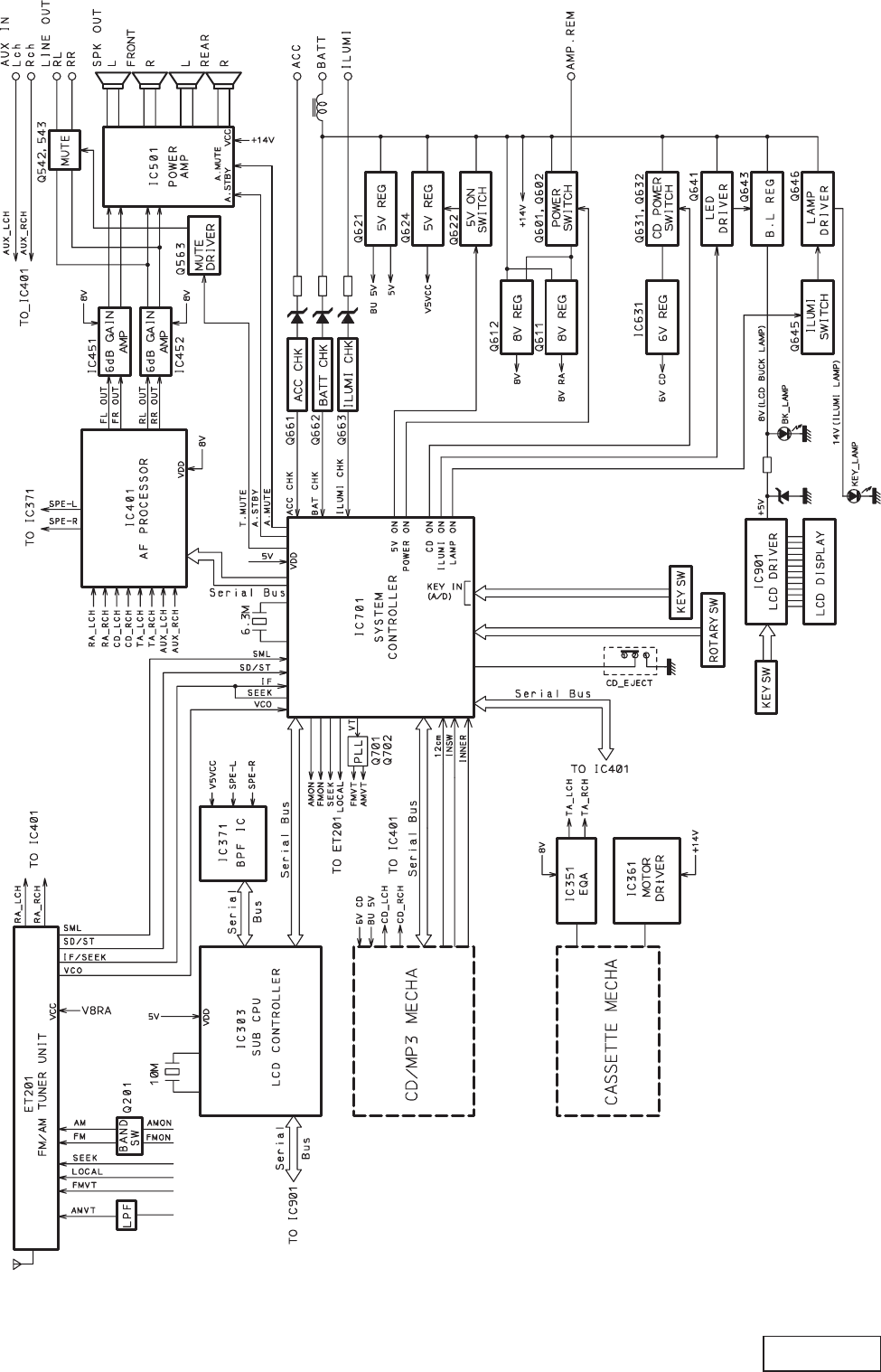
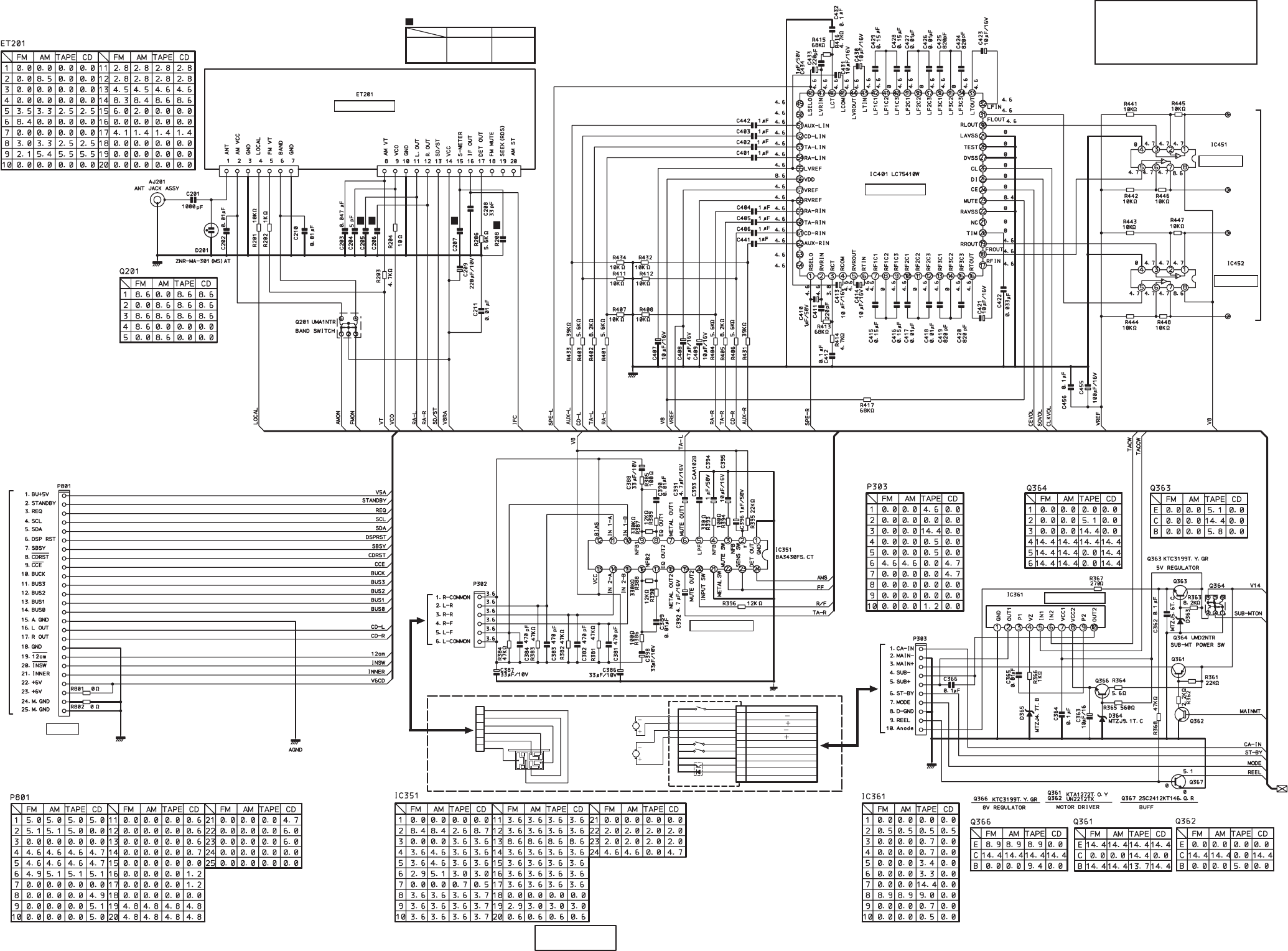
BLOCK DIAGRAM
ANT

ADB340MP
ADB341MP - 6 -
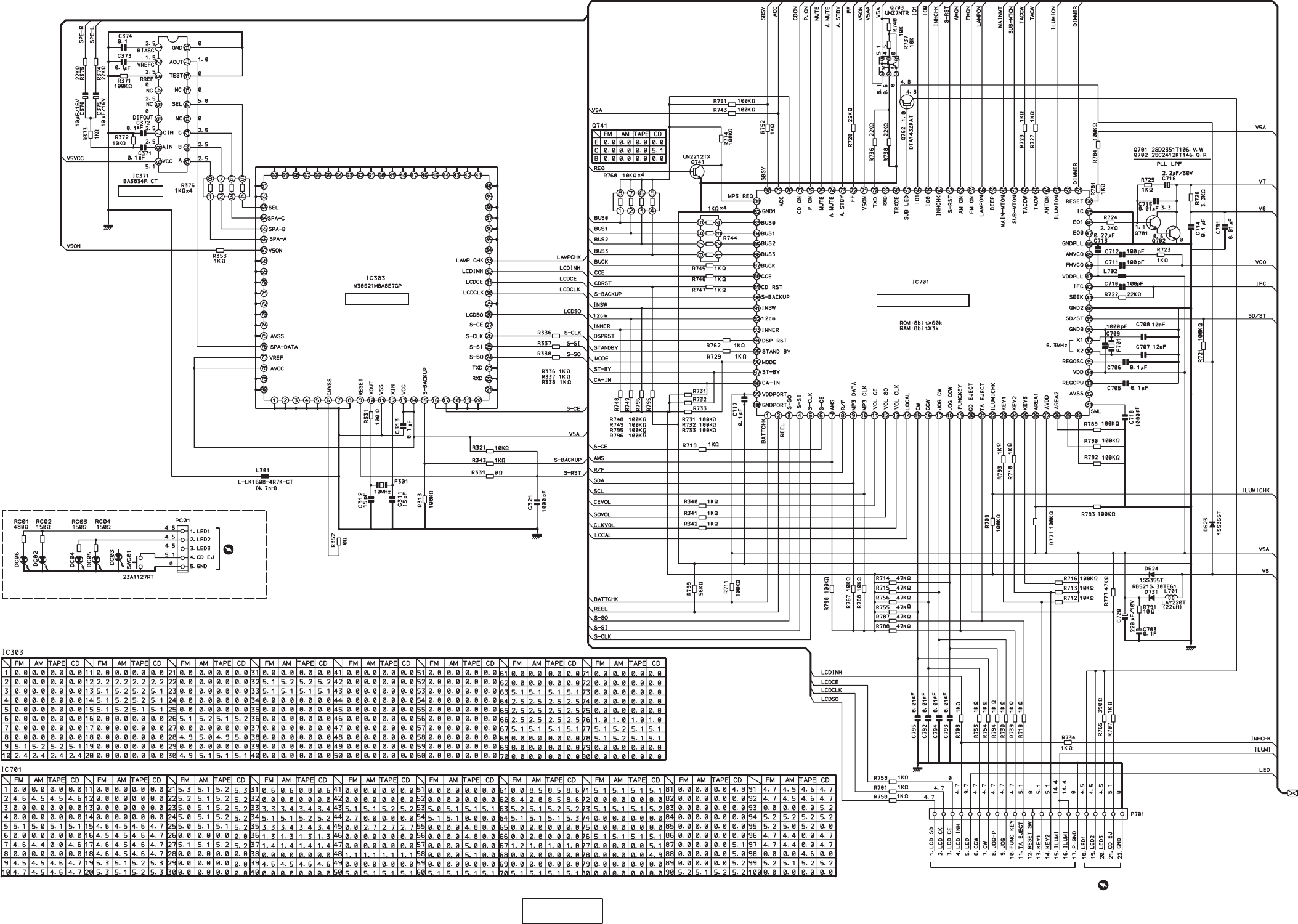
EXPLANATION OF IC
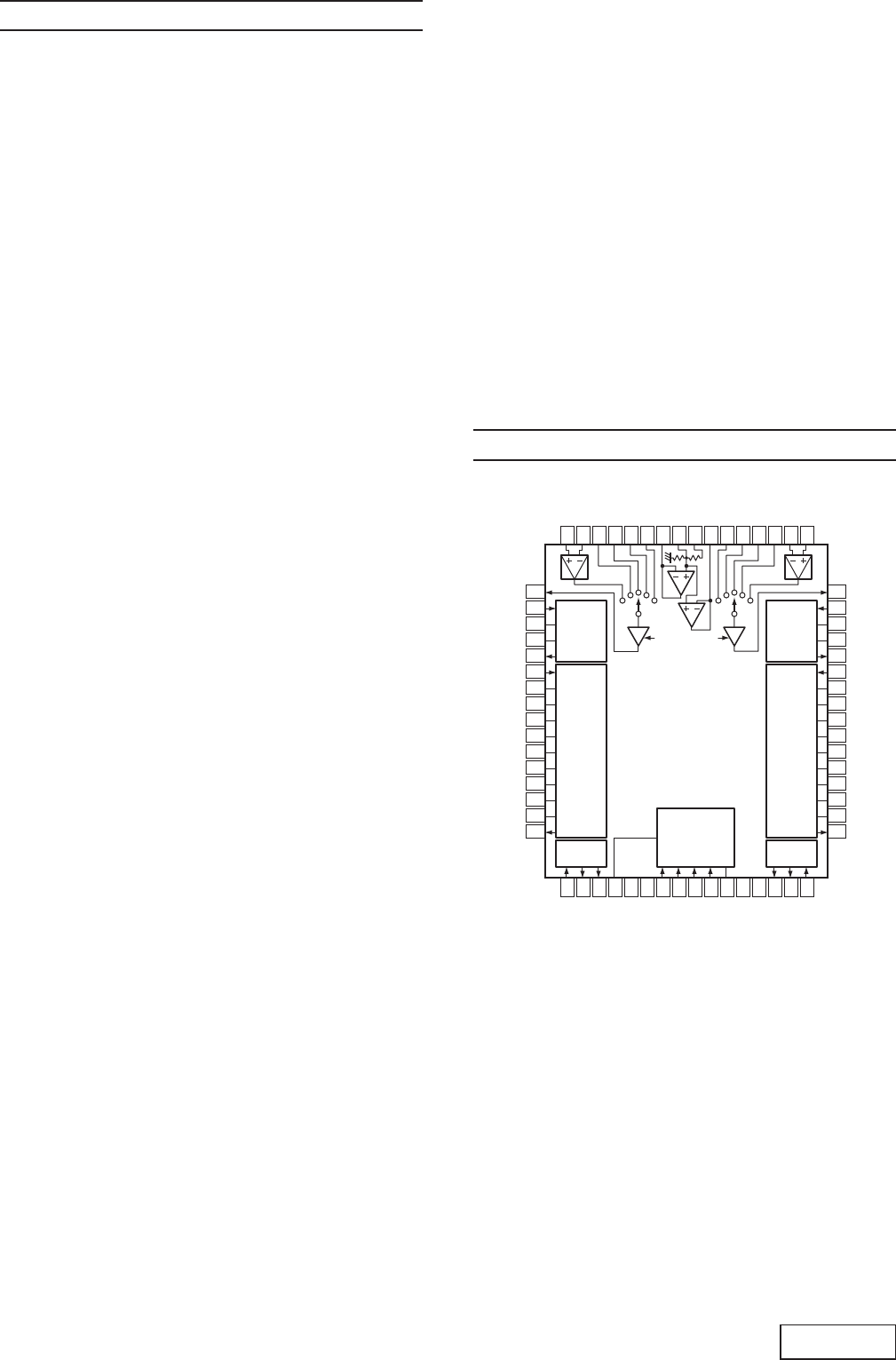
653-0429-22 uPD178078GF-667-3 Main Microcomputer
Terminal Description
pin 1: BATTCHK : IN : Detection of instantaneous interruption
(BATTERY OFF)
pin 2: REEL : IN : TAPE REEL input detection pin
pin 3: S-SI : IN : Serial In to SUB CPU
pin 4: S-SO : O : Serial Out to SUB CPU
pin 5: S-CLK : O : Serial CLK to SUB CPU
pin 6: S-CE : O : Serial CE Active "H" to SUB CPU
pin 7: AMS : IN: Heading search (pull up)
pin 8: R/F : O : 1;FORWARD 0;REVERSE
pin 9: MP3 DATA :I/O: TC94A20F data input/output pin (pull up)
pin 10: MP3CLK : O : TC94A20F clock output pin (pull up)
pin 11: VOL CE : O : Electronic volume IC latch output pin
pin 12: VOL SO : O : Electronic volume IC data output pin
pin 13: VOL CLK : O : Electronic volume IC clock output pin
pin 14: LOCAL : O : SEEK sensitivity 1; LOCAL 0;DX
pin 15: CW : IN : Preset Jog fetch (Up) (pull up)
pin 16: CCW : IN: Preset Jog fetch (Down) (pull up)
pin 17: JOG CW :IN: Volume Jog fetch (Up) (pull up)
pin 18: JOG CCW :IN: Volume Jog fetch (Down) (pull up)
pin 19: FUNCKEY : IN : Function Key input detection pin (pull up)
pin 20: CD EJECT : IN: CD Eject Key input detection pin (pull up)
pin 21: TA EJECT : IN: TAPE Eject Key input detection (pull up)
pin 22: ILUMICHK : IN : Illumination Check On (pull up)
pin 23: KEY1 : IN: Key input
pin 24: KEY2 : IN: Key input
pin 25: KEY3 : IN : Unused (pull up)
pin 26: CUSTOMER : IN : Usage setting initial
pin 27: AVDD : - : A/D converter power pin 5V±10%
pin 28: AREA : IN: Destination Setting
pin 29: NU : IN: Unused (PULL DOWN)
pin 30: NU : IN: Unused (PULL DOWN)
pin 31: SML : IN: S-Meter( Unused )
pin 32: AVSS : - : A/D converter power pin GND connection
pin 33: REGCPU : - : CPU core power pin
pin 34: VDD : - : Power pin 5V±10%
pin 35: REGOSC : - : OSC circuit power pin
pin 36: X2 : - : 6.3MHz crystal oscillator connection pin
pin 37: X1 : - : 6.3MHz crystal oscillator connection pin
pin 38: GND0 : - : Power pin GND connection
pin 39: SD/ST : IN: SD/ST On (pull up)
pin 40: GND2 : - : Power pin GND connection
pin 41: SEEK : O : Seek control output pin Seek On
pin 42: IFC : IN : IF frequency input
pin 43: VDDPLL : - : PLL power pin 5V±10%
pin 44: FM VCO : IN: FM VCO input pin
pin 45: AM VCO :IN : AM VCO input pin
pin 46: GNDPLL : - : PLL power pin GND connection
pin 47: EO0 : O : PLL error output pin
pin 48: EO1 : O : PLL error output pin
pin 49: IC : - : Internal connection pin GND connection
pin 50: RESET : IN: External reset signal input pin (L ; Reset)
pin 51: DIMMER : O : DIMMER ON
pin 52: NU : O : Unused
pin 53: ILUMION : O : Illumination on
pin 54: ANTON : O : Motor ANT on
pin 55: TACW : O : Motor Forward output control pin
pin 56: TACCW : O : Motor Reverse output control pin
pin 57: SUB-MTON : O : TAPE Sub Motor on
pin 58: MAIN-MTON : O : TAPE Main Motor on
pin 59: BEEP : O : BEEP output
pin 60: LAMPON : O : LAMP on control pin
pin 61: FM ON : O : FM power control output pin FM On
pin 62: AM ON : O : AM power control output pin AM On
pin 63: S-RST : O : SUB CPU reset output pin
pin 64: INHCHK : O : LCD Driver Inhibit
pin 65: IO0 : O : Motor drive mute output pin Mute off
pin 66: IO1 : O : Test Mode Gain control output pin CDRW
pin 67: SUB LED : O : SUB LED control output pin SUB LED On
pin 68: NU : O : Unused
pin 69: NU : O : Unused
pin 70: CDBACKUP : O : MP3 DSP Back up power control
pin 71: V5ON : O : Spectrum analyzer power control pin
pin 72: FF : O : FF/REW mode
pin 73: A STBY : O : Power IC Stby control output pin Audio
Standby On
pin 74: A MUTE : O : Power IC Mute control output pin Audio
Mute On
pin 75: MUTE : O : Line Out Mute control output pin Mute On
pin 76: P ON : O : Main power control output pin Power On
pin 77: CD ON : O : CD power control output pin CDP On
pin 78: CD PULL UP :I/O: CDPULL UP control
pin 79: ACC : IN: ACC OFF detection
pin 80: SBSY : IN : SUBQ read request from Tc9814F
pin 81: MP3 REQ : IN: Request from TC94A20F (Reversed by Tr)
pin 82: GND1 : - : Power pin GND connection
pin 83: BUS0 :I/O: TC94A14F Bus line (pull up)
pin 84: BUS1 :I/O: TC94A14F Bus line (pull up)
pin 85: BUS2 :I/O: TC94A14F Bus line (pull up)
pin 86: BUS3 :I/O: TC94A14F Bus line (pull up)
pin 87: BUCK : O : TC94A14F clock output pin
pin 88: CCE : O : TC94A14F data enable output pin
pin 89: CD RST : O : TC94A14F reset output pin
pin 90: S-BACKUP : O : SUB CPU Backup request output pin
pin 91: INSW :IN : Disc In detection pin (pull up)
pin 92: 12CM : IN : 12CM detection (pull up)
pin 93: INNER :IN : Inner SW On (pull up)
pin 94: DSP RST : O : TC94A20F reset output pin
pin 95: STAND BY : O : TC94A20F standby request output pin
pin 96: MODE : IN : TAPE mode SW input detection (pull up)
pin 97: ST-BV : IN: TAPE Standby state input pin (pull up)
pin 98: CA-IN : IN : Cassette in detection pin (pull up)
pin 99: VDDPORT : - : Port power pin 5V
pin100: GNDPORT : - : Port power pin GND connection
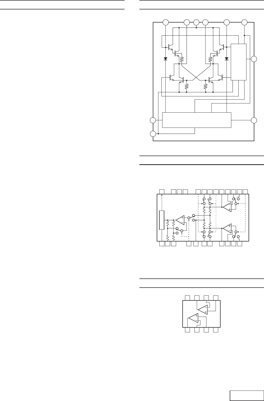
653-0429-20 TA8275H Quad Bridge Power Amplifiers
Terminal Description
pin 1: TAB : TAB
pin 2: 2 P GND : The power ground.
pin 3: 2 P OUT- : The negative power output.
pin 4: STANDBY : The standby signal input.
pin 5: 2 P OUT+ : The positive power output.
pin 6: VCC : Positive supply voltage.
pin 7: 1 P OUT- : The negative power output.
pin 8: 1 P GND : The power ground.
pin 9: 1 P OUT+ : The positive power output.
pin 10: RIPPLE : Connect the capacitor.
pin 11: 1 IN : The audio signal input.
pin 12: 2 IN : The audio signal input.
pin 13: S GND : The signal ground.
pin 14: 4 IN : The audio signal input.
pin 15: 3 IN : The audio signal input.
pin 16: AUX IN : Auxiliary input.
pin 17: 3 P OUT+ : The positive power output.
pin 18: 3 P GND : The power ground.
pin 19: 3 P OUT- : The negative power output.
pin 20: VCC : Positive supply voltage.
pin 21: 4 P OUT+ : The positive power output.
pin 22: MUTE : The muting signal input.
pin 23: 4 P OUT- : The negative power output.
pin 24: 4 P GND : The power ground.
pin 25: DIAGNOSIS : The diagnosis signal output.
ADB340MP
ADB341MP
- 7 -
653-0429-14 M30621M8A8E7GP Sub Microcomputer
Terminal Description
pin 1: NU :IN: Unused (GND)
pin 2: NU :IN: Unused (GND)
pin 3: NU :IN: Unused (GND)
pin 4: NU :IN: Unused (GND)
pin 5: NU :IN: Unused (GND)
pin 6: CNVSS : - : Processor Mode switching pin (Used for
FLASH write)
pin 7: NU :IN: Unused (GND)
pin 8: NU :IN: Unused (GND)
pin 9: RESET :IN : External reset signal input pin (external
pull-up)
pin 10: XOUT : - : Main clock oscillation circuit output pin
pin 11: VSS : - : Power input pin VSS
pin 12: XIN : - : Main clock oscillation circuit input pin
pin 13: VCC : - : Power input pin VCC 2.7V-5.5V
pin 14: NU :IN: Unused (GND)
pin 15: S-BACKUP : IN : MAIN CPU BACK UP request
pin 16: NU :IN: Unused (GND)
pin 17: S-CE : IN : SUB Serial transmit line CE with MAIN
CPU
pin 18: NU :IN: Unused (GND)
pin 19: NU :IN: Unused (GND)
pin 20: NU :IN: Unused (GND)
pin 21: NU :IN: Unused (GND)
pin 22: NU :IN: Unused (GND)
pin 23: NU :IN: Unused (GND)
pin 24: S-SO : O : SUB Serial transmit line SO with MAIN
CPU (also used for FLASH write)
pin 25: S-SI : IN : SUB Serial transmit line with MAIN CPU
(also used for FLASH write)
pin 26: S-CLK : IN : SUB Serial transmit line CLK with MAIN
CPU (also used for FLASH write ; Write
with external pull-up)
pin 27: S-CE : O : Used for BUSY FLASH write (OPEN)
pin 28: LCDSO : O : LCD driver-Control serial data output pin
pin 29: NU :IN: Unused (GND)
pin 30: LCDCLK : O : LCD driver-Control serial clock output pin
pin 31: LCDCE : O : LCD driver-Control chip enable pin
pin 32: LCDINH : O : LCD driver-Control Unlight Detect pin (L;
Indication prohibited)
pin 33: LAMPCHK : IN : LAMP CHK pin (L; Indication prohibited)
pin 34: EPM : O : Used for FLASH write (OPEN)
pin 35: NU :IN: Unused (GND)
pin 36: NU :IN: Unused (GND)
pin 37: NU :IN: Unused (GND)
pin 38: NU :IN: Unused (GND)
pin 39: CE : O : Used for FLASH write (OPEN)
pin 40: NU :IN: Unused (GND)
pin 41: NU :IN: Unused (GND)
pin 42: NU :IN: Unused (GND)
pin 43: NU :IN: Unused (GND)
pin 44: NU :IN: Unused (GND)
pin 45: NU :IN: Unused (GND)
pin 46: NU :IN: Unused (GND)
pin 47: NU :IN: Unused (GND)
pin 48: NU :IN: Unused (GND)
pin 49: NU :IN: Unused (GND)
pin 50: NU :IN: Unused (GND)
pin 51: NU :IN: Unused (GND)
pin 52: NU :IN: Unused (GND)
pin 53: NU :IN: Unused (GND)
pin 54: NU :IN: Unused (GND)
pin 55: NU :IN: Unused (GND)
pin 56: NU :IN: Unused (GND)
pin 57: NU :IN: Unused (GND)
pin 58: NU :IN: Unused (GND)
pin 59: NU :IN: Unused (GND)
pin 60: NU :IN: Unused (GND)
pin 61: NU :IN: Unused (GND)
pin 62: NU :IN: Unused (GND)
pin 63: SEL : O : Spectrum analyzer control pin
pin 64: SPA-C : O : Spectrum analyzer BAND select pin C
pin 65: SPA-B : O : Spectrum analyzer BAND select pin B
pin 66: SPA-A : O : Spectrum analyzer BAND select pin A
pin 67: V5ON : IN : Spectrum analyzer IC PWR ON monitor-pin
(H; monitor-permit)
pin 68: NU :IN: Unused (GND)
pin 69: NU :IN: Unused (GND)
pin 70: NU :IN: Unused (GND)
pin 71: NU :IN: Unused (GND)
pin 72: NU :IN: Unused (GND)
pin 73: NU :IN: Unused (GND)
pin 74: NU :IN: Unused (GND)
pin 75: AVSS : - : A-D Converter power input pin VSS con-
nection
pin 76: SPA-DATA : IN : Spectrum analyzer data monitor-pin (A/D
input )
pin 77: VREF : - : A-D Converter reference voltage input pin
pin 78: AVCC : - : A-D Converter power input pin VCC con-
nection
pin 79: NU :IN: Unused (GND)
pin 80: NU :IN: Unused (GND)
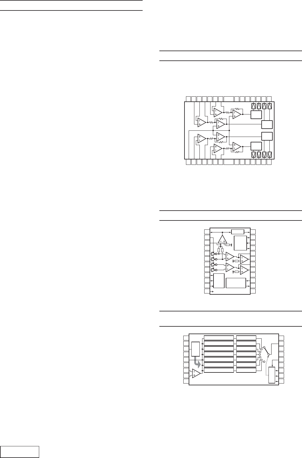
653-0429-18 LC75410WS Electric volume with Tone Controller
Gain adjust
49
50
51
52
53
54
55
56
57
58
59
60
61
62
63
64
L 5+
L 5-
L 4
L 3
L 2
L 1
L Vref
VDD
Vref
R Vref
R 1
R 2
R 3
R 4
R 5-
R 5+
R Sel out
R VR in
R CT
R COM
R VR out
R T in
R F1 C1
R F1 C2
R F1 C3
R F2 C1
R F2 C2
R F2 C3
R F3 C1
R F3 C2
R F3 C3
R T out
1
2
3
4
5
6
7
8
9
10
11
12
13
14
15
16
Volume
with
Loudness
Control
Tone Control
32
31
30
29
28
27
26
25
24
23
22
21
20
19
18
17
Fader
Control
Gain adjust
Volume
with
Loudness
Control
Tone Control
Fader
Control
48
47
46
45
44
43
42
41
40
39
38
37
36
35
34
33
L Sel out
L VR in
L CT
L COM
L VR out
L T in
L F1 C1
L F1 C2
L F1 C3
L F2 C1
L F2 C2
L F2 C3
L F3 C1
L F3 C2
L F3 C3
L T out
L Fader in
L Front out
L Rear out
L VSS
TEST
D VSS
Clock in
Data in
Chip Enable
Mute in
R VSS
NC
Time Set
R Rear out
R Front out
R Fader in
Digital
Controller
ADB340MP
ADB341MP - 8 -
653-0430-35 TC94A20F Digital Signal Processor
Terminal Description
pin 1: RESET : IN : Reset signal input.
pin 2: Micro MD : IN: Mode select for Microcomputer I/F.
pin 3: D-RAM WE : O : Write enable signal output to D-RAM.
pin 4: D-RAM RAS : O : Row address strobe output to D-RAM.
pin 5: Micro DIO :I/O: Serial data for Microcomputer I/F.
pin 6: Micro CK :IN: Clock pulse for Microcomputer I/F.
pin 7: D-RAM A 11 : O : Address output to D-RAM.
pin 8: VDD : - : Positive supply voltage.
pin 9: SDO : O : Serial data output.
pin 10: B CK O : O : Bit clock output.
pin 11: LR CK : O : LR clock output.
pin 12: S DATA :I/O: Serial data input/output.
pin 13: Bit clock A : IN: Bit clock input A.
pin 14: LR clock A : IN: LR clock input A.
pin 15: D-RAM A 0 : O : Address output to D-RAM.
pin 16: D-RAM A 1 : O : Address output to D-RAM.
pin 17: D-RAM A 2 : O : Address output to D-RAM.
pin 18: VDD : - : Positive supply voltage.
pin 19: STANDBY : IN : Stanby command input.
pin 20: VSS : - : Negative supply voltage.
pin 21: A VSS : - : Analog ground.
pin 22: A Vref : - : Reference voltage for the internal ADC.
pin 23: LO : O : Left channel audio signal output.
pin 24: A VDD : - : Positive supply voltage for the Analog sec-
tion.
pin 25: A VDD : - : Positive supply voltage for the Analog sec-
tion.
pin 26: RO : O : Right channel audio signal output.
pin 27: A Vref : IN: Reference voltage for the internal ADC.
pin 28: A VSS : - : Analog ground.
pin 29: TEST : - : For the Test.
pin 30: TX O : O : SPDIF output.
pin 31: D-RAM A 3 : O : Address output to D-RAM.
pin 32: D-RAM A 4 : O : Address output to D-RAM.
pin 33: D-RAM A 5 : O : Address output to D-RAM.
pin 34: D-RAM A 6 : O : Address output to D-RAM.
pin 35: VDD : - : Positive supply voltage.
pin 36: D-RAM A 7 : O : Address output to D-RAM.
pin 37: D-RAM A 8 : O : Address output to D-RAM.
pin 38: D-RAM A 9 : O : Address output to D-RAM.
pin 39: General port 7 : O : General-purpose output port.
pin 40: VSS : - : Negative supply voltage.
pin 41: D-RAM A 10 : O : Address output to D-RAM.
pin 42: VDD : - : Positive supply voltage.
pin 43: D-RAM OE : O : Output enable signal output to D-RAM.
pin 44: D-RAM CAS : O : Column address strobe output to D-RAM.
pin 45: VSS : - : Negative supply voltage.
pin 46: D-RAM D 0 :I/O: D-RAM Data input/output.
pin 47: D-RAM D 1 :I/O: D-RAM Data input/output.
pin 48: VSS : - : Negative supply voltage.
pin 49: D-RAM D 2 :I/O: D-RAM Data input/output.
pin 50: D-RAM D 3 :I/O: D-RAM Data input/output.
pin 51: D-RAM D 4 / Sub Ck
:I/O: D-RAM Data input/output.
Sub Code I/F Clock input/output.
pin 52: VDD : - : Positive supply voltage.
pin 53: D-RAM D 5 / Sub D
:I/O: D-RAM Data input/output.
Sub Code I/F Data input.
pin 54: D-RAM D 6 / Sub F
:I/O: D-RAM Data input/output.
Sub Code I/F Frame sync input.
pin 55: D-RAM D 7 / Sub B
:I/O: D-RAM Data input/output.
Sub Code I/F Block sync input.
pin 56: A VSS : - : Analog ground.
pin 57: PLL ERROR : O : PLL error signal output.
pin 58: VCO CNTRL : IN: VCO control signal input.
pin 59: A VDD : - : Positive supply voltage for the Analog sec-
tion.
pin 60: CKI/CKO/PO6 :I/O: External clock input. / Clock pulse output.
/ General-purpose output port.
pin 61: VDD : - : Positive supply voltage.
pin 62: X IN :IN : Crystal connection.
pin 63: X O : O : Crystal connection.
pin 64: VSS : - : Negative supply voltage.
653-0430-33 BA5983FM Quad Motor Drivers
1
2
3
4
5
6
7
8
9
10
11
12
13
14
Level
Shift
Level
Shift
28
27
26
25
24
23
22
21
20
19
18
17
16
15
Level
Shift
Level
Shift
Bias in
1ch OP in+
1ch OP in-
1ch OP out
2ch OP in+
2ch OP in-
2ch OP out
Ground
Standby1,2,3
Power VCC1,2
2ch drive out-
2ch drive out+
1ch drive out-
1ch drive out+
Pre VCC
4ch OP in+
4ch OP in-
4ch OP out
3ch OP in+
3ch OP in-
3ch OP out
Ground
Standby4
Power VCC3,4
3ch drive out-
3ch drive out+
4ch drive out-
4ch drive out+
653-0430-31 TA2157FN Head Amplifier for 3-beam Digital Servo
22
13
23
1
2
3
4
5
6
7
8
9
RF Out
Gain Adjust
RF N
VCC
Focus In N
Focus In P
Track In P
Track In N
APC Input
APC Output
APC Control
TE Balance
APC
12
19
20
21
16
15
10
11
24
18
17
14
RF DC
AGC Out
AGC Control
AGC In
FE Nega.
FE Out
TE Nega.
TE Out
Ground
RF Ripple In
RF Ripple Out
V Reference Out
PEAK
RF
AGC
Ripple
Generator
653-0429-17 BA3834F
Septet Band Pass Filters for Spectrum Analyzer
Bias
Vref
Rref
N.C.
Dif. out
N.C.
Cin
Ain
VCC
1
2
3
4
5
6
7
8
9
BPF 1(68Hz)
BPF 2(170Hz)
BPF 3(420Hz)
BPF 4(1kHz)
BPF 5(2.4kHz)
BPF 6(5.9kHz)
BPF 7(14.4kHz)
Peak Hold
Peak Hold
Peak Hold
Peak Hold
Peak Hold
Peak Hold
Peak Hold
18
17
16
15
14
13
12
11
10
Ground
A out
Test
N.C.
Select
N.C.
C
B
A
Control
Band
Shifter
ADB340MP
ADB341MP
- 9 -
653-0430-32 TC94A14FA Digital Servo Processor for CD
Terminal Description
pin 1: B CK O : O : Bit clock output.
pin 2: LR CK O : O : LR clock output.
pin 3: A DATA O : O : Audio data output.
pin 4: DIGI OUT : O : Digital data output
pin 5: IPF OUT : O : IP flag output.
pin 6: VDD : - : Positive supply voltage.
pin 7: VSS : - : Negative supply voltage.
pin 8: SB OK O : O : Sub code Q data CRCC OK signal output.
pin 9: SUB C CK :I/O: Sub code data P to W clock input/output.
pin 10: SUB C DATA : O : Sub code data P to Q output.
pin 11: SF SY O : O : Playback frame synchronize signal output.
pin 12: SB SY O : O : Sub code block synchronize signal output.
pin 13: IO0 :I/O: Universal input/output port.
pin 14: IO1 :I/O: Universal input/output port.
pin 15: P VDD : - : PLL positive supply voltage.
pin 16: PH DIF : O : EFM-PLCK Phase difference signal output.
pin 17: T MAX O : O : T max judgment output.
pin 18: PLL LPF NI : IN: PLL LPF inverted input.
pin 19: PLL LPF O : O : PLL LPF output.
pin 20: P Vref : - : PLL reference voltage.
pin 21: VCO FILTER : O : Loop filter for VCO.
pin 22: A VSS : - : Analog ground.
pin 23: SLCO : O : Output of internal DAC for data slice level
generation.
pin 24: RF IN : IN : RF signal input.
pin 25: A VDD : - : Positive supply voltage for the Analog sec-
tion.
pin 26: RF RP CT : IN : RERP center level input.
pin 27: RF RP Z IN :IN: RF RP signal input for zero cross.
pin 28: PR RP IN : IN : RF ripple signal input.
pin 29: F E :IN : Focusing error signal input.
pin 30: SBAD : IN : Sub beam add signal input.
pin 31: T E :IN : tracking error signal input.
pin 32: TE Z IN : IN : Tracking error signal inpur for zero cross.
pin 33: Fo EQ OUT : O : Focus equalizer output.
pin 34: T EQ OUT : O : Tracking equalizer output.
pin 35: Vref : - : Reference voltage.
pin 36: RF GAIN : O : RF gain control signal output.
pin 37: TR B CNT : O : Tracking balance control signal output.
pin 38: APC ON : O : APC ON signal output.
pin 39: A VDD : - : Positive supply voltage for the Analog sec-
tion.
pin 40: Fe EQ OUT : O : Feed equalizer output.
pin 41: DISC EQ O : O : Disc equalizer output.
pin 42: VSS : - : Negative supply voltage.
pin 43: VDD : - : Positive supply voltage.
pin 44: TEST : IN: For the test.
pin 45: X VSS : - : Master clock analog ground.
pin 46: X IN :IN : Crystal connection.
pin 47: X O : O : Crystal connection.
pin 48: X VDD : - : Clock power supply.
pin 49: VSS : - : Negative supply voltage.
pin 50: R CH OUT : O : Right channel data output.
pin 51: VDD : - : Positive supply voltage.
pin 52: Vref : - : Reference voltage.
pin 53: L CH OUT : O : Left channel data output.
pin 54: VSS : - : Negative supply voltage.
pin 55: Z DET O : O : 1bit DAC zero flag output.
pin 56: VSS : - : Negative supply voltage.
pin 57: BUS 0 :I/O: MPU Data input / output.
pin 58: BUS 1 :I/O: MPU Data input / output.
pin 59: BUS 2 :I/O: MPU Data input / output.
pin 60: BUS 3 :I/O: MPU Data input / output.
pin 61: BU CK IN :IN : MPU Data clodk input.
pin 62: CCEI : IN: Chip enable input.
pin 63: RSTI : IN: Reset signal input.
pin 64: VDD : - : Positive supply voltage.
653-0429-15 BA3430FS Tape Pre-amplifier with Blank Detector
24
23
2213 141516171819 202112
111098765432
1
COMPARE Detect Out
GND
Bias
VCC
Mute Sw
Mute Out 2
Metal Out 2
Metal Sw
Eq Out 2
NFB 2
Input B 2
Input A 2
Input Sw
Mute Out 1
Metal Out 1
Eq Out 1
NFB 1
Input B 1
Input A 1
Time Const
NFB
NFB
Sense Sw
LPF
LLL
L
IN2
VZ
VCC1
IN1
GND
6
4
7
P2
9
OUT2
10
VCC2
8
OUT1
2
P1
3
5
1
LOGIC CONTROL
PRE-DRIVWE
653-0429-16 LB1641 Bidirectional Motor Driver
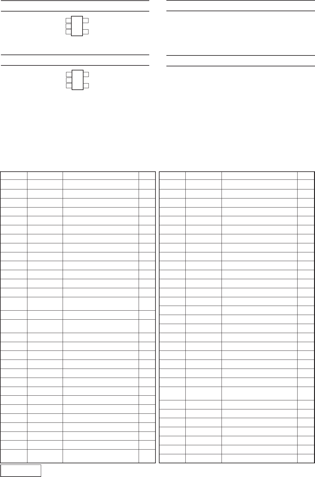
653-0429-19 LA6458M Dual Operational Amplifier
1
2
3
4VEE
VCC 8
7
6
5
ADB340MP
ADB341MP - 10 -
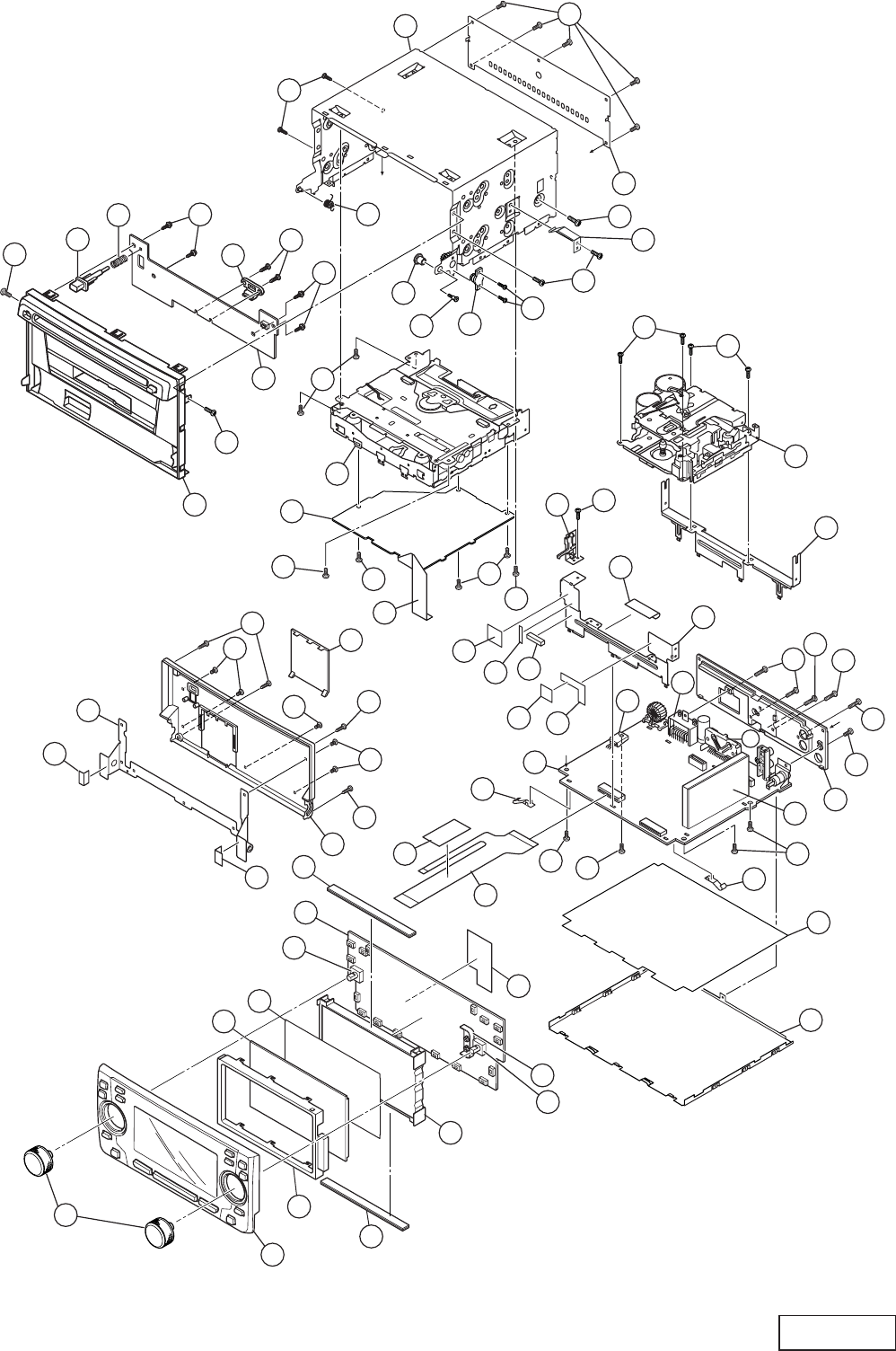
EXPLODED VIEW/PARTS LIST
Main section
NO. PART NO. DESCRIPTION Q'TYNO. PART NO. DESCRIPTION Q'TY
1 653-0428-01 FLEX PWB (DISP) 1
2 653-0428-02 CHASSIS ASSY 1
3 653-0428-03 BOTTOM COVER 1
4 653-0428-04 COVER (REAR) 1
5 653-0428-05 DECK BRACKET (FRONT) 1
6 653-0428-06 DECK BRACKET(REAR) 1
7 653-0428-07 HEATSINK (4P) 1
8 653-0428-08 BRACKET HOOK ASSY 1
9 653-0428-09 INDICATOR (CST) 1
10 653-0429-96 LCD 1
11 653-0428-10 CD MECH (CDC03TL1) 1
12 ----------- SERVO PWB 1
13 653-0428-11 SCREW (2X4) 3
14 653-0428-12 CASSETTE MECH 1
(CDS-802TL1)
15 ----------- MAIN PWB 1
16 653-0428-13 TUNER PACK (ADB340MP) 1
653-0434-01 TUNER PACK (ADB341MP
17 653-0428-14 SCREW (2.6X8) 1
18 653-0428-15 SCREW (2.6X6) 22
19 653-0428-16 SCREW (3X8) 1
20 653-0428-17 SCREW (2.6X12) 3
21 653-0428-18 SCREW (2X4X5) 4
22 653-0428-19 INSULATOR (PWB) 1
23 653-0428-20 SHIELD SHEET (DECK-L) 1
24 653-0428-21 SHIELD SHEET (DECK-R) 1
25 653-0428-22 INNER ES (FP ASSY-C) 1
26 653-0428-23 SCREW (2.6X3) 1
27 653-0428-24 SPACER (DECK BKT) 1
28 653-0428-25 SPACER (R) 1
29 653-0430-06 VOLUME (ENCODER) 2
30 653-0428-26 ESCUTCHEON (ADB340MP) 1
653-0434-02 ESCUTCHEON (ADB341MP)
31 653-0428-27 ESCUTCHEON COVER (B) 1
32 653-0428-28 COVER (B) 1
33 653-0428-29 KNOB 2
34 653-0428-30 SCREW (2X8) 4
35 653-0428-31 ES BRACKET ASSY (B) 1
36 653-0428-32 REFRECTION SHEET 2
37 ----------- DISPLAY PWB 1
38 653-0428-33 SCREW (2X2.5) 5
39 653-0428-34 BUTTON (OPEN) 1
40 653-0428-35 SPRING (BUTTON OPEN) 1
41 653-0428-36 SPRING (ES OPEN) 1
42 653-0428-37 SCREW (2X5) 2
43 653-0428-38 SCREW (2.6X5) 4
44 653-0428-39 PLATE SPRING (COVER) 2
45 653-0428-40 CUSHION (20X28) 1
46 653-0428-41 DAMPER (FRT-E2-300-G1) 1
47 653-0428-42 SCREW (2X6) 2
48 653-0428-43 CUSHION (B) 2
49 653-0428-44 SHIELD SHEET 1
50 653-0428-45 PLATE SPRING 1
51 653-0430-39 FLEX PWB(CD) 1
52 ----------- SUB PWB 1
53 653-0429-89 BRACKET (REG) 1
54 653-0429-90 IC BRACKET (ADB340MP) 1
653-0434-07 IC BRACKET (ADB341MP)
55 653-0429-91 BRACKET (CONN) 1
56 653-0430-10 BRACKET (LCD) 1
57 653-0430-11 HOLDER ASSY (LCD) 1
58 653-0430-12 HOLDER (LCD) 1
59 653-0430-13 CUSHION (30x18.5) 1
60 653-0430-14 INNER CONNECOR 2
61 653-0430-15 CLOR SHEET (LCD) 1
653-0429-21 KIA7806API 6V Voltage Regulator
Terminal Description
pin 1: Input
pin 2: Common
pin 3: Output
653-0430-34 BA033FP 3.3V Voltage Regulator
Terminal Description
pin 1 : V IN : Voltage input terminal.
pin 2 : GND : Ground terminal.
pin 3 : V OUT : Voltage output terminal.
653-0430-36 TAR5S33 Positive Voltage Regurator (3.3V)
1
2
3
5
4
OUTPUT
NOISE
INPUT
GND
Control(H=ON)
1
2
3
5
4
OUTPUT
NOISE
INPUT
GND
Control(H=ON)
653-0430-37 TAR5S25 Positive Voltage Regurator (2.5V)
ADB340MP
ADB341MP
- 11 -
A
B
32
38
38
34
34
31
36
35
36
34
38
18 18
18
23 27
48
48
18 17 18
7
16
15
22
3
49
1
24
53 55
54
45
44
44
14
8
20 20
19
18
18
6
5
A
B
18
18
18
50
18
41
39
18
18
25
21
21
52
43 13
11
13
12
43
43
9
40
46
26
28 42
4
2
47
51
33
30
56
37
60
57
10
61
60
59
58
29
29
ADB340MP
ADB341MP - 12 -
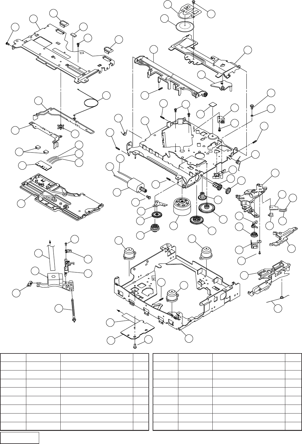
CD mechanism section
NO. PART NO. DESCRIPTION Q'TYNO. PART NO. DESCRIPTION Q'TY
1 653-0430-64 CHASSIS 1
2 653-0430-65 PICK BASE ASSY 1
3 653-0430-66 UP LEVER ASSY 1
4 653-0430-67 FEED SCREW ASSY 1
5 653-0430-68 TOP COVER 1
6 653-0430-69 FEED PLATE 1
7 653-0430-70 SHAFT GUIDE 1
8 653-0430-71 SWING PLATE 1
9 653-0430-72 CLAMPER PLATE 1
10 653-0430-73 CHUCK ARM 1
11 653-0430-74 DISC ARM L 1
12 653-0430-75 DISC ARM R 1
13 653-0430-76 TOP GUIDE 1
14 653-0430-77 SCREW HOLDER 1
15 653-0430-78 SCREW GUIDE 1
16 653-0430-79 SLIDER A 1
To PA02 of Servo PWB
To PA01 of Servo PWB
1
2
3
4
5
6
7
8
9
10
11
12
13
14
15 16
17 18
19
20
21 22
23 24
25
26
27
28
29
30
31
32
33
34 35
36
37
38
39
40
41
42
43
44 45
46
47
48
49
50
51
52
53
54
55
56
57
58
59
60
61
62
63
64
65
66
67
68
64
64
32
64
64
44
47
37
41
ADB340MP
ADB341MP
- 13 -
NO. PART NO. DESCRIPTION Q'TYNO. PART NO. DESCRIPTION Q'TY
17 653-0430-80 GEAR A 1
18 653-0430-81 GEAR B 1
19 653-0430-82 GEAR C 1
20 653-0430-83 GEAR D 1
21 653-0430-84 GEAR E 1
22 653-0430-85 GEAR F 1
23 653-0430-86 GEAR H 1
24 653-0430-87 GEAR I 1
25 653-0430-88 LOCK LEVER 1
26 653-0430-89 LEVER STOP 1
27 653-0430-90 CLAMPER 1
28 653-0430-91 SLIDER B 1
29 653-0430-92 GEAR D ARM 1
30 653-0430-93 PB LOCK 1
31 653-0430-94 SCREW HOLDER B 1
32 653-0430-95 HOLDER C ARM 2
33 653-0430-96 PICK SUB COVER 1
34 653-0430-97 DISC ARM SPG 1
35 653-0430-98 UP LEVER SPG 1
36 653-0430-99 CHUCK ARM SPG 1
37 653-0431-01 PICK BASE SPG 2
38 653-0431-02 SLIDER SPG A 1
39 653-0431-03 SUB SPG 1
40 653-0431-04 UP LEVER SUB SPG 1
41 653-0431-05 PICK BASE SPG B 2
42 653-0431-06 DISC SHEET 1
43 653-0431-07 CHACK SHEET 1
44 653-0431-08 DAMPER F 2
45 653-0431-09 DAMPER R 1
46 653-0431-10 PICK UP-ASSY 1
47 653-0431-11 SWITCH 3
48 ----------- MOTOR WIRE A (BLUE) 1
49 ----------- MOTOR WIRE B (WHITE) 1
50 ----------- SW WIRE A (YELLOW) 1
51 ----------- SW WIRE B (ORANGE) 1
52 ----------- SW WIRE C (BLACK) 1
53 ----------- SW WIRE D (RED) 1
54 ----------- SW WIRE E (BROWN) 1
55 653-0431-19 RELAY PWB 1
(WITH OUT COMPONENT)
56 ----------- SWITCH(A) PWB 1
57 ----------- SWITCH(B) PWB 1
58 653-0431-22 FPC (PICK UP) 1
59 653-0431-23 FFC (RELAY) 1
60 653-0431-24 SLED MOTOR-ASSY 1
61 653-0431-25 SPINDLE MOTOR-ASSY 1
62 653-0431-26 PRECISION SCREW 2
63 653-0431-27 MACHINE SCREW (SLED) 1
64 653-0431-28 MACHINE SCREW 5
65 653-0431-29 MACHINE SCREW (FLAT) 1
66 653-0431-30 MACHINE SCREW (PICK UP) 1
67 653-0431-31 SCREW 1
68 653-0431-32 COLLAR 1
STATIC ELECTRICITY
The CD pickup might suffer destruction by static electricity
during spare-parts maintenance or replacement, although it is
stable when connected to the circuit in the CD unit. The de-
struction might be caused because the laser diode terminal
will be electrically open. To prevent the terminal from being
open, do the following steps:
1.When you replace the CD pickup, or remove the CD unit
from the car stereo unit for any maintenance purpose, sol-
der the copper foil pattern indicated in Fig.1 below to short-
circuit the FPC of the CD unit.
Perform your intended maintenance work with the flexible
wire short-circuited.
2.If the original CD pickup may possibly be reused, make a
short circuit the land of FPC of CD Pickup bottom
side(Fig.2).Then remove the CD Pickup and perform the
work.
Servo PWB
FPC
Copper foil pattern
- Fig.1 -
3. The CD Pickup(P/No.653-0431-10), which is supplied as one
of the spare parts, is already short-circuited with the copper
foil pattern pre-soldered.
To handle this CD Pickup, keep the short circuit as it is. Then
attach the Pickup to the unit and connect the flexible wire to
the connector.
4. After performing the work, eliminate the short circuit by re-
moving the solder at its respective short-circuited area de-
scribed in 1, 2 and 3 above.
Short-land
Bottom side of pickup
- Fig.2 -
FPC
ADB340MP
ADB341MP - 14 -
NO. PART NO. DESCRIPTION Q'TYNO. PART NO. DESCRIPTION Q'TY
Cassette tape mechanism section
1
2
3
4
56
7
8
9
10
11
12
13
14
15
To P302 of Main PWB
To P303 of Main PWB
1 653-0431-33 SUB MOTOR ASSY 1
2 653-0431-34 MAIN MOTOR ASSY 1
3 653-0431-35 BELT 1
4 653-0431-36 AZIMUTH SCREW 2
5 ----------- REEL PWB 1
6 653-0431-40 SWITCH 1
(MODE)
7 653-0431-41 SWITCH 1
(CSST IN)
8 653-0431-42 FLAT CABLE 1
9 653-0431-43 PHOTP SENSOR 1
10 653-0431-44 SWITCH (STBY) 1
11 653-0431-37 HEAD 1
12 653-0431-47 EXTENSION LEAD 1
13 653-0431-27 SCREW (MAIN) 2
14 653-0431-45 SCREW (M2.0x2.5) 2
15 653-0431-38 SCREW (M1.7x3) 2
* Parts which are not mentioned in service manual are not supplied.
ADB340MP
ADB341MP
- 15 -
REF No. PART No. DESCRIPTION REF No. PART No. DESCRIPTION REF No. PART No. DESCRIPTION
ELECTRICAL PARTS LIST
Main PWB(B1) section
AJ201 653-0428-57 ANT JACK ASSY
C201 653-0428-58 1000PF 50V
C202 653-0428-59 0.01UF 50V
C203 653-0428-60 0.047UF 16V
C204 653-0428-61 5PF 50V
C205 653-0428-62 0.027UF 25V
(for ADB340MP)
653-0434-06 0.018UF 25V
(for ADB341MP)
C206 653-0428-62 0.027UF 25V
(for ADB340MP)
653-0434-06 0.018UF 25V
(for ADB341MP)
C207 653-0428-58 1000PF 50V
(for ADB340MP)
653-0428-96 0.22UF 25V
(for ADB341MP)
C208 653-0428-63 33PF 50V
C209 653-0428-64 220UF 10V
C210 653-0428-59 0.01UF 50V
C211 653-0428-59 0.01UF 50V
C311 653-0428-65 15PF 50V
C312 653-0428-65 15PF 50V
C313 653-0428-66 0.1UF 16V
C321 653-0428-58 1000PF 50V
C362 653-0428-67 0.1UF 16V
C363 653-0428-68 10UF 16V
C364 653-0428-67 0.1UF 16V
C365 653-0428-59 0.01UF 50V
C366 653-0428-67 0.1UF 16V
C371 653-0428-66 0.1UF 16V
C372 653-0428-66 0.1UF 16V
C373 653-0428-66 0.1UF 16V
C374 653-0428-66 0.1UF 16V
C375 653-0428-68 10UF 16V
C376 653-0428-68 10UF 16V
C381 653-0428-69 470PF 50V
C382 653-0428-69 470PF 50V
C383 653-0428-69 470PF 50V
C384 653-0428-69 470PF 50V
C386 653-0428-70 33UF 10V
C387 653-0428-70 33UF 10V
C388 653-0428-70 33UF 10V
C389 653-0428-59 0.01UF 50V
C390 653-0428-59 0.01UF 50V
C391 653-0428-71 4.7UF 16V
C392 653-0428-71 4.7UF 16V
C393 653-0428-58 1000PF 50V
C394 653-0428-72 0.1UF 50V
C395 653-0428-68 10UF 16V
C396 653-0428-73 1UF 50V
C398 653-0428-70 33UF 10V
C401 653-0428-74 1UF 10V
C402 653-0428-74 1UF 10V
C403 653-0428-74 1UF 10V
C404 653-0428-74 1UF 10V
C405 653-0428-74 1UF 10V
C406 653-0428-74 1UF 10V
C407 653-0428-68 10UF 16V
C408 653-0428-75 47UF 16V
C409 653-0428-68 10UF 16V
C410 653-0428-73 1UF 50V
C411 653-0428-76 220PF 50V
C412 653-0428-66 0.1UF 16V
C413 653-0428-68 10UF 16V
C414 653-0428-68 10UF 16V
C415 653-0428-77 0.15UF 10V
C416 653-0428-77 0.15UF 10V
C417 653-0428-59 0.01UF 50V
C418 653-0428-59 0.01UF 50V
C419 653-0428-78 820PF 50V
C420 653-0428-78 820PF 50V
C421 653-0428-68 10UF 16V
C422 653-0428-79 0.033UF
C423 653-0428-68 10UF 16V
C424 653-0428-78 820PF 50V
C425 653-0428-78 820PF 50V
C426 653-0428-59 0.01UF 50V
C427 653-0428-59 0.01UF 50V
C428 653-0428-77 0.15UF 10V
C429 653-0428-77 0.15UF 10V
C430 653-0428-68 10UF 16V
C431 653-0428-68 10UF 16V
C432 653-0428-66 0.1UF 16V
C433 653-0428-76 220PF 50V
C434 653-0428-73 1UF 50V
C441 653-0428-74 1UF 10V
C442 653-0428-74 1UF 10V
C455 653-0428-80 100UF 16V
C456 653-0428-67 0.1UF 16V
C501 653-0428-81 2.2UF 50V
C502 653-0428-81 2.2UF 50V
C503 653-0428-81 2.2UF 50V
C504 653-0428-81 2.2UF 50V
C505 653-0428-82 1UF 10V
C506 653-0428-82 1UF 10V
C507 653-0428-82 1UF 10V
C508 653-0428-82 1UF 10V
C509 653-0428-75 47UF 16V
C510 653-0428-83 22UF 16V
C511 653-0428-84 0.22UF 50V
C512 653-0428-85 0.1UF 50V
C513 653-0428-86 3300UF 16V
C551 653-0428-87 100PF 100V
C552 653-0428-88 0.1UF 50V
C561 653-0428-89 0.47UF 50V
C581 653-0428-90 2200PF 50V
C582 653-0428-90 2200PF 50V
C583 653-0428-90 2200PF 50V
C584 653-0428-90 2200PF 50V
C585 653-0428-90 2200PF 50V
C586 653-0428-90 2200PF 50V
C587 653-0428-90 2200PF 50V
C588 653-0428-90 2200PF 50V
C601 653-0428-85 0.1UF 50V
C611 653-0428-91 100UF 10V
C612 653-0428-67 0.1UF 16V
C622 653-0428-67 0.1UF 16V
C623 653-0428-91 100UF 10V
C624 653-0428-85 0.1UF 50V
C625 653-0428-67 0.1UF 16V
C627 653-0428-91 100UF 10V
C628 653-0428-67 0.1UF 16V
C631 653-0428-80 100UF 16V
C632 653-0428-67 0.1UF 16V
C633 653-0428-67 0.1UF 16V
C634 653-0428-80 100UF 16V
C641 653-0428-67 0.1UF 16V
C643 653-0428-67 0.1UF 16V
C652 653-0428-67 0.1UF 16V
C703 653-0428-92 0.1F
C705 653-0428-67 0.1UF 16V
C706 653-0428-67 0.1UF 16V
C707 653-0428-93 12PF 50V
C708 653-0428-94 10PF 50V
C709 653-0428-58 1000PF 50V
C710 653-0428-95 100PF 50V
C711 653-0428-95 100PF 50V
C712 653-0428-95 100PF 50V
C713 653-0428-96 0.22UF 25V
C714 653-0428-67 0.1UF 16V
C715 653-0428-59 0.01UF 50V
C716 653-0428-97 2.2UF 50V
C717 653-0428-67 0.1UF 16V
C718 653-0428-58 1000PF 50V
C720 653-0428-64 220UF 10V
C791 653-0428-59 0.01UF 50V
C792 653-0428-59 0.01UF 50V
C793 653-0428-59 0.01UF 50V
C794 653-0428-59 0.01UF 50V
C795 653-0428-59 0.01UF 50V
D201 653-0428-98 MA-301(MS)AT
D363 653-0428-99 MTZJ5.6T-C
D364 653-0429-01 MTZJ9.1T-C
D365 653-0429-02 MTZJ4.7T-B
D601 653-0429-03 1N5402
D602 653-0429-04 1SS244T
D611 653-0429-01 MTZJ9.1T-C
D621 653-0429-05 MTZJ6.2T-C
D622 653-0428-99 MTZJ5.6T-C
D623 653-0429-06 1SS355T
D624 653-0429-06 1SS355T
D641 653-0429-07 MTZJ10T-C
D642 653-0429-01 MTZJ9.1T-C
D662 653-0429-08 MTZJ8.2T-B
D664 653-0429-09 MTZJ7.5T-A
D665 653-0429-10 MTZJ6.8T-B
D731 653-0429-11 RB521S-30T
ET201 653-0428-13 TUNER PACK
(for ADB340MP)
653-0434-01 TUNER PACK
(for ADB341MP)
F301 653-0429-12 HQS-3H-10000-10
F701 653-0429-13 HQS-3H-06300-14
IC303 653-0429-14 M30621M8A8E7GP
IC351 653-0429-15 BA3430FS-CT
IC361 653-0429-16 LB1641
IC371 653-0429-17 BA3834F-CT
IC401 653-0429-18 LC75410W
IC451 653-0429-19 LA6458ML-CT
IC452 653-0429-19 LA6458ML-CT
IC501 653-0429-20 TA8275H
IC631 653-0429-21 KIA7806API
IC701 653-0429-22 UPD178078GF-667
J561 653-0429-23 0OHM 1/16W
J601 653-0429-23 0OHM 1/16W
J604 653-0429-23 0OHM 1/16W
J605 653-0429-24 0OHM 1/8W
J606 653-0429-24 0OHM 1/8W
J607 653-0429-24 0OHM 1/8W
J608 653-0429-24 0OHM 1/8W
J609 653-0429-24 0OHM 1/8W
J611 653-0429-24 0OHM 1/8W
J612 653-0429-24 0OHM 1/8W
J613 653-0429-23 0OHM 1/16W
L301 653-0429-25 LK1608-4R7K-CT
L601 653-0429-26 TT-OL-5047-R2
L701 653-0429-27 EL0305RA-220J-FT
L702 653-0429-28 FCM1608K-301T03
P302 653-0429-29 SOCKET(TA HEAD)
P303 653-0429-30 SOCKET(TAPE)
P501 653-0429-31 16P SOCKET
P502 653-0429-32 RCA SOCKET
P701 653-0429-33 SOCKET(DISP)
ADB340MP
ADB341MP - 16 -
REF No. PART No. DESCRIPTION REF No. PART No. DESCRIPTION REF No. PART No. DESCRIPTION
P801 653-0429-34 SOCKET(CD)
Q201 653-0429-35 UMA1NTR
Q361 653-0429-36 KTA1272T-O, Y
Q362 653-0429-37 UN2212TX
Q363 653-0429-38 KTC3199T-Y, GR
Q364 653-0429-39 UMD2NTR
Q366 653-0429-38 KTC3199T-Y, GR
Q367 653-0429-40 2SC2412KT-Q, R
Q542 653-0429-41 UN2216TX
Q543 653-0429-41 UN2216TX
Q563 653-0429-42 UN2112TX
Q601 653-0429-43 2SB1326T-Q, R
Q602 653-0429-37 UN2212TX
Q611 653-0429-44 2SD1858T-Q, R
Q612 653-0429-44 2SD1858T-Q, R
Q621 653-0429-45 2SD1861T
Q622 653-0429-39 UMD2NTR
Q624 653-0429-38 KTC3199T-Y, GR
Q631 653-0429-46 2SB1326T-R
Q632 653-0429-37 UN2212TX
Q641 653-0429-39 UMD2NTR
Q643 653-0429-44 2SD1858T-Q, R
Q644 653-0429-37 UN2212TX
Q645 653-0429-37 UN2212TX
Q646 653-0429-36 KTA1272T-O, Y
Q661 653-0429-40 2SC2412KT-Q, R
Q662 653-0429-40 2SC2412KT-Q, R
Q663 653-0429-40 2SC2412KT-Q, R
Q701 653-0429-47 2SD2351T106-V,
Q702 653-0429-40 2SC2412KT-Q, R
Q703 653-0429-48 UMZ7NTR
Q741 653-0429-37 UN2212TX
Q762 653-0429-49 DTA143ZKAT
R201 653-0429-50 10KOHM 1/16W
R202 653-0429-51 1KOHM 1/16W
R203 653-0429-52 4.7KOHM 1/16W
R204 653-0429-53 10OHM 1/16W
R206 653-0429-54 5.6KOHM 1/16W
R208 653-0429-55 0.022UF 25V
(for ADB340MP)
R313 653-0429-56 100KOHM 1/16W
R321 653-0429-50 10KOHM 1/16W
R331 653-0429-57 100OHM 1/16W
R336 653-0429-51 1KOHM 1/16W
R337 653-0429-51 1KOHM 1/16W
R338 653-0429-51 1KOHM 1/16W
R339 653-0429-23 0OHM 1/16W
R340 653-0429-51 1KOHM 1/16W
R341 653-0429-51 1KOHM 1/16W
R342 653-0429-51 1KOHM 1/16W
R343 653-0429-51 1KOHM 1/16W
R352 653-0429-23 0OHM 1/16W
R353 653-0429-51 1KOHM 1/16W
R361 653-0429-58 22KOHM 1/10W
R362 653-0429-59 2.2KOHM 1/10W
R363 653-0429-60 8.2KOHM 1/10W
R364 653-0429-61 5.6OHM 1/2W
R365 653-0429-62 560OHM 1/10W
R366 653-0429-63 1KOHM 1/6W
R367 653-0429-64 270OHM 1/10W
R368 653-0429-65 47KOHM 1/16W
R371 653-0429-56 100KOHM 1/16W
R372 653-0429-50 10KOHM 1/16W
R373 653-0429-51 1KOHM 1/16W
R374 653-0429-66 22KOHM 1/16W
R375 653-0429-66 22KOHM 1/16W
R376 653-0429-67 1KOHMX4
R381 653-0429-65 47KOHM 1/16W
R382 653-0429-65 47KOHM 1/16W
R383 653-0429-65 47KOHM 1/16W
R384 653-0429-65 47KOHM 1/16W
R385 653-0429-57 100OHM 1/16W
R386 653-0429-57 100OHM 1/16W
R387 653-0429-68 330KOHM 1/16W
R388 653-0429-68 330KOHM 1/16W
R389 653-0429-69 12KOHM 1/16W
R390 653-0429-69 12KOHM 1/16W
R393 653-0429-70 330OHM 1/16W
R394 653-0429-57 100OHM 1/16W
R395 653-0429-66 22KOHM 1/16W
R396 653-0429-69 12KOHM 1/16W
R401 653-0429-54 5.6KOHM 1/16W
R402 653-0429-71 8.2KOHM 1/16W
R403 653-0429-54 5.6KOHM 1/16W
R404 653-0429-54 5.6KOHM 1/16W
R405 653-0429-71 8.2KOHM 1/16W
R406 653-0429-54 5.6KOHM 1/16W
R407 653-0429-50 10KOHM 1/16W
R408 653-0429-50 10KOHM 1/16W
R411 653-0429-50 10KOHM 1/16W
R412 653-0429-50 10KOHM 1/16W
R413 653-0429-72 68KOHM 1/16W
R414 653-0429-52 4.7KOHM 1/16W
R415 653-0429-72 68KOHM 1/16W
R416 653-0429-52 4.7KOHM 1/16W
R417 653-0429-72 68KOHM 1/16W
R431 653-0429-73 39KOHM 1/16W
R432 653-0429-50 10KOHM 1/16W
R433 653-0429-73 39KOHM 1/16W
R434 653-0429-50 10KOHM 1/16W
R441 653-0429-50 10KOHM 1/16W
R442 653-0429-50 10KOHM 1/16W
R443 653-0429-50 10KOHM 1/16W
R444 653-0429-50 10KOHM 1/16W
R445 653-0429-50 10KOHM 1/16W
R446 653-0429-50 10KOHM 1/16W
R447 653-0429-50 10KOHM 1/16W
R448 653-0429-50 10KOHM 1/16W
R501 653-0429-51 1KOHM 1/16W
R502 653-0429-56 100KOHM 1/16W
R503 653-0429-56 100KOHM 1/16W
R504 653-0429-51 1KOHM 1/16W
R505 653-0429-51 1KOHM 1/16W
R506 653-0429-56 100KOHM 1/16W
R507 653-0429-56 100KOHM 1/16W
R508 653-0429-51 1KOHM 1/16W
R509 653-0429-51 1KOHM 1/16W
R543 653-0429-74 1KOHM 1/10W
R544 653-0429-74 1KOHM 1/10W
R545 653-0429-75 470OHM 1/10W
R546 653-0429-75 470OHM 1/10W
R547 653-0429-75 470OHM 1/10W
R548 653-0429-75 470OHM 1/10W
R561 653-0429-51 1KOHM 1/16W
R601 653-0429-65 47KOHM 1/16W
R602 653-0429-76 1.5KOHM 1/6W
R603 653-0429-77 1.8KOHM 1/6W
R604 653-0429-77 1.8KOHM 1/6W
R611 653-0429-78 470OHM 1/6W
R612 653-0429-70 330OHM 1/16W
R621 653-0429-79 18KOHM 1/16W
R622 653-0429-79 18KOHM 1/16W
R631 653-0429-77 1.8KOHM 1/6W
R632 653-0429-77 1.8KOHM 1/6W
R633 653-0429-77 1.8KOHM 1/6W
R634 653-0429-65 47KOHM 1/16W
R641 653-0429-80 680OHM 1/6W
R643 653-0429-65 47KOHM 1/16W
R644 653-0429-77 1.8KOHM 1/6W
R645 653-0429-77 1.8KOHM 1/6W
R647 653-0429-51 1KOHM 1/16W
R661 653-0429-81 12KOHM 1/10W
R662 653-0429-71 8.2KOHM 1/16W
R664 653-0429-81 12KOHM 1/10W
R665 653-0429-71 8.2KOHM 1/16W
R666 653-0429-81 12KOHM 1/10W
R667 653-0429-71 8.2KOHM 1/16W
R701 653-0429-51 1KOHM 1/16W
R707 653-0429-51 1KOHM 1/16W
R708 653-0429-51 1KOHM 1/16W
R709 653-0429-56 100KOHM 1/16W
R710 653-0429-51 1KOHM 1/16W
R711 653-0429-56 100KOHM 1/16W
R712 653-0429-50 10KOHM 1/16W
R713 653-0429-50 10KOHM 1/16W
R714 653-0429-65 47KOHM 1/16W
R715 653-0429-65 47KOHM 1/16W
R716 653-0429-56 100KOHM 1/16W
R718 653-0429-51 1KOHM 1/16W
R719 653-0429-51 1KOHM 1/16W
R720 653-0429-66 22KOHM 1/16W
R721 653-0429-56 100KOHM 1/16W
R722 653-0429-66 22KOHM 1/16W
R723 653-0429-51 1KOHM 1/16W
R724 653-0429-82 2.2KOHM 1/16W
R725 653-0429-51 1KOHM 1/16W
R726 653-0429-83 3.3KOHM 1/16W
R727 653-0429-51 1KOHM 1/16W
R728 653-0429-51 1KOHM 1/16W
R729 653-0429-63 1KOHM 1/6W
R730 653-0429-51 1KOHM 1/16W
R731 653-0429-56 100KOHM 1/16W
R732 653-0429-56 100KOHM 1/16W
R733 653-0429-56 100KOHM 1/16W
R734 653-0429-51 1KOHM 1/16W
R736 653-0429-66 22KOHM 1/16W
R737 653-0429-50 10KOHM 1/16W
R738 653-0429-66 22KOHM 1/16W
R739 653-0429-51 1KOHM 1/16W
R740 653-0429-50 10KOHM 1/16W
R743 653-0429-56 100KOHM 1/16W
R744 653-0429-67 1KOHMX4
R745 653-0429-51 1KOHM 1/16W
R746 653-0429-51 1KOHM 1/16W
R747 653-0429-51 1KOHM 1/16W
R748 653-0429-56 100KOHM 1/16W
R749 653-0429-56 100KOHM 1/16W
R751 653-0429-56 100KOHM 1/16W
R752 653-0429-51 1KOHM 1/16W
R753 653-0429-51 1KOHM 1/16W
R754 653-0429-51 1KOHM 1/16W
R755 653-0429-65 47KOHM 1/16W
R756 653-0429-65 47KOHM 1/16W
R758 653-0429-51 1KOHM 1/16W
R759 653-0429-51 1KOHM 1/16W
R760 653-0429-84 10KOHMX4
R762 653-0429-51 1KOHM 1/16W
R765 653-0429-85 390OHM 1/10W
R767 653-0429-50 10KOHM 1/16W
R768 653-0429-50 10KOHM 1/16W
R771 653-0429-56 100KOHM 1/16W
(for ADB341MP)
R774 653-0429-56 100KOHM 1/16W
R777 653-0429-65 47KOHM 1/16W
R781 653-0429-51 1KOHM 1/16W
R783 653-0429-56 100KOHM 1/16W
(for ADB340MP)
R784 653-0429-56 100KOHM 1/16W
R787 653-0429-65 47KOHM 1/16W
R788 653-0429-65 47KOHM 1/16W
ADB340MP
ADB341MP
- 17 -
REF No. PART No. DESCRIPTION REF No. PART No. DESCRIPTION REF No. PART No. DESCRIPTION
R789 653-0429-56 100KOHM 1/16W
R790 653-0429-56 100KOHM 1/16W
R791 653-0429-53 10OHM 1/16W
R792 653-0429-56 100KOHM 1/16W
R793 653-0429-51 1KOHM 1/16W
R794 653-0429-51 1KOHM 1/16W
R795 653-0429-56 100KOHM 1/16W
R796 653-0429-56 100KOHM 1/16W
R798 653-0429-56 100KOHM 1/16W
R799 653-0429-86 56KOHM 1/16W
R801 653-0429-24 0OHM 1/8W
R802 653-0429-23 0OHM 1/16W
TH651 653-0429-87 PTC-B59975-C120-
A54
PWB 653-0429-88 PWB(WITHOUT
COMPONENT)
Display PWB(B3) section
REF No. PART No. DESCRIPTION REF No. PART No. DESCRIPTION REF No. PART No. DESCRIPTION
C901 653-0428-58 1000PF 50V
C902 653-0428-67 0.1UF 16V
C903 653-0428-60 0.047UF 16V
C904 653-0428-60 0.047UF 16V
C905 653-0428-60 0.047UF 16V
D902 653-0429-92 BZX84-C5V1
D905 653-0429-93 UDZS8.2B
D912 653-0429-94 NSPW300BS-BR,
BS
D913 653-0429-94 NSPW300BS-BR,
BS
D914 653-0429-95 HPY1105W-TR-CT
H901 653-0429-96 LCD
IC901 653-0429-97 LC75878W
P901 653-0429-98 SOCKET(MAIN)
PL901 653-0429-99 PL ASSY 171
PL902 653-0429-99 PL ASSY 171
PL903 653-0429-99 PL ASSY 171
PL904 653-0429-99 PL ASSY 171
PL905 653-0429-99 PL ASSY 171
PL906 653-0429-99 PL ASSY 171
R901 653-0429-74 1KOHM 1/10W
R902 653-0429-74 1KOHM 1/10W
R903 653-0429-74 1KOHM 1/10W
R904 653-0429-74 1KOHM 1/10W
R905 653-0429-65 47KOHM 1/16W
R906 653-0429-56 100KOHM 1/16W
R907 653-0430-01 1.8KOHM 1/16W
R908 653-0429-74 1KOHM 1/10W
R911 653-0430-02 330OHM 1/10W
R913 653-0430-02 330OHM 1/10W
R919 653-0430-03 3.9KOHM 1/10W
R941 653-0430-04 1.2KOHM 1/16W
R942 653-0430-04 1.2KOHM 1/16W
R943 653-0430-01 1.8KOHM 1/16W
R944 653-0430-05 2.7KOHM 1/16W
R945 653-0429-52 4.7KOHM 1/16W
R946 653-0429-71 8.2KOHM 1/16W
R947 653-0429-79 18KOHM 1/16W
R948 653-0430-04 1.2KOHM 1/16W
R949 653-0430-04 1.2KOHM 1/16W
R950 653-0430-01 1.8KOHM 1/16W
R951 653-0430-05 2.7KOHM 1/16W
R952 653-0429-52 4.7KOHM 1/16W
R953 653-0429-71 8.2KOHM 1/16W
R954 653-0429-51 1KOHM 1/16W
R955 653-0429-51 1KOHM 1/16W
R956 653-0429-51 1KOHM 1/16W
R957 653-0429-51 1KOHM 1/16W
SW901 653-0430-06 VOLUME
SW902 653-0430-06 VOLUME
SW903 653-0430-07 DTSM-31S-T/R-CT
SW904 653-0430-07 DTSM-31S-T/R-CT
SW905 653-0430-07 DTSM-31S-T/R-CT
SW906 653-0430-07 DTSM-31S-T/R-CT
SW907 653-0430-07 DTSM-31S-T/R-CT
SW908 653-0430-07 DTSM-31S-T/R-CT
SW909 653-0430-07 DTSM-31S-T/R-CT
SW910 653-0430-07 DTSM-31S-T/R-CT
SW911 653-0430-07 DTSM-31S-T/R-CT
SW912 653-0430-07 DTSM-31S-T/R-CT
SW913 653-0430-07 DTSM-31S-T/R-CT
SW914 653-0430-07 DTSM-31S-T/R-CT
SW915 653-0430-07 DTSM-31S-T/R-CT
SW916 653-0430-07 DTSM-31S-T/R-CT
SW917 653-0430-07 DTSM-31S-T/R-CT
SW918 653-0430-07 DTSM-31S-T/R-CT
SW919 653-0430-08 SOT-152HST-CT
PWB 653-0430-09 PWB(WITHOUT
COMPONENT)
REF No. PART No. DESCRIPTION REF No. PART No. DESCRIPTION REF No. PART No. DESCRIPTION
CA01 653-0430-16 100uF 4V
CA02 653-0430-17 6800pF 50V
CA03 653-0428-74 1uF 10V
CA04 653-0428-66 0.1uF 16V
CA05 653-0428-66 0.1uF 16V
CA06 653-0430-18 4pF 50V
CA07 653-0430-19 56pF 50V
CA08 653-0428-67 0.1uF 16V
CA21 653-0428-67 0.1uF 16V
CA22 653-0428-67 0.1uF 16V
CA23 653-0430-20 47pF 50V
CA24 653-0430-21 0.015uF 25V
CA26 653-0428-59 0.01uF 50V
CA27 653-0430-22 2700pF 50V
CA28 653-0428-59 0.01uF 50V
CA29 653-0428-67 0.1uF 16V
CA31 653-0428-79 333 B
CA32 653-0428-79 333 B
CA33 653-0428-60 0.047uF 16V
CA34 653-0428-69 470pF 50V
CA35 653-0428-69 470pF 50V
CA36 653-0428-60 0.047uF 16V
CA37 653-0428-60 0.047uF 16V
CA38 653-0428-60 0.047uF 16V
CA39 653-0428-60 0.047uF 16V
CA40 653-0428-67 0.1uF 16V
CA41 653-0428-67 0.1uF 16V
CA44 653-0430-16 100uF 4V
CA45 653-0430-16 100uF 4V
CA46 653-0428-67 0.1uF 16V
CA47 653-0430-16 100uF 4V
CA48 653-0428-67 0.1uF 16V
CA50 653-0428-90 2200pF 50V
CA51 653-0428-90 2200pF 50V
CA61 653-0430-23 100uF 10V
CA62 653-0428-67 0.1uF 16V
CA68 653-0428-67 0.1uF 16V
CA72 653-0428-67 0.1uF 16V
CA73 653-0428-74 1uF 10V
CA74 653-0430-24 47uF 6.3V
CA75 653-0428-67 0.1uF 16V
CA77 653-0430-25 100uF 10V
CB02 653-0428-67 0.1uF 16V
CB03 653-0430-26 47uF 4V
CB04 653-0428-67 0.1uF 16V
CB05 653-0430-26 47uF 4V
CB06 653-0430-26 47uF 4V
CB07 653-0430-26 47uF 4V
CB08 653-0428-67 0.1uF 16V
CB09 653-0428-67 0.1uF 16V
CB10 653-0430-27 0.33uF 10V
CB11 653-0428-67 0.1uF 16V
CB14 653-0428-67 0.1uF 16V
CB16 653-0428-76 220pF 50V
CB51 653-0430-26 47uF 4V
CB52 653-0428-74 1uF 10V
CB53 653-0428-59 0.01uF 50V
CB54 653-0428-74 1uF 10V
CB55 653-0430-26 47uF 4V
CB56 653-0428-74 1uF 10V
CB57 653-0428-59 0.01uF 50V
CB58 653-0428-74 1uF 10V
CB59 653-0430-26 47uF 4V
CB60 653-0428-74 1uF 10V
CB61 653-0428-59 0.01uF 50V
CB62 653-0428-74 1uF 10V
Servo PWB(B4) section
REF No. PART No. DESCRIPTION REF No. PART No. DESCRIPTION REF No. PART No. DESCRIPTION
Sub PWB(B2) section
DC02 653-0429-95 HPY1105W-TR-CT
DC03 653-0429-95 HPY1105W-TR-CT
DC04 653-0429-95 HPY1105W-TR-CT
DC05 653-0429-95 HPY1105W-TR-CT
DC06 653-0429-95 HPY1105W-TR-CT
PC01 653-0430-60 SOCKET(MAIN)
RC01 653-0429-75 470OHM 1/10W
RC02 653-0430-61 150OHM 1/10W
RC03 653-0430-61 150OHM 1/10W
RC04 653-0430-61 150OHM 1/10W
SWC01 653-0430-62 SKQCAC-260G
PWB 653-0430-63 PWB(WITHOUT
COMPONENT)
ADB340MP
ADB341MP - 18 -
REF No. PART No. DESCRIPTION REF No. PART No. DESCRIPTION REF No. PART No. DESCRIPTION
DA01 653-0430-29 DAP202KT146
FB01 653-0430-30 RTSV16.93MG
ICA01 653-0430-31 TA2157FN-CT
ICA02 653-0430-32 TC94A14FA-CT
ICA03 653-0430-33 BA5983FM-CT
ICA04 653-0430-34 BA033FP-CT
ICB01 653-0430-35 TC94A20F-010-CT
ICB03 653-0430-36 TAR5S33-CT
ICB04 653-0430-37 TAR5S25-CT
ICB05 653-0430-37 TAR5S25-CT
JA23 653-0429-23 0ohm 1/16W
JA24 653-0430-38 0ohm 1/10W
JA32 653-0429-23 0ohm 1/16W
JB01 653-0429-23 0ohm 1/16W
LA01 653-0429-28 FCM1608K-301T03
LA21 653-0429-23 0ohm 1/16W
LA22 653-0429-28 FCM1608K-301T03
LB01 653-0429-28 FCM1608K-301T03
LB03 653-0429-28 FCM1608K-301T03
LB31 653-0429-23 0ohm 1/16W
NA01 653-0430-39 FLAT WIRE(25P)
PA01 653-0430-40 15P
PA02 653-0430-41 8P
QA01 653-0430-42 2SB815T-B6
QA02 653-0430-43 2SD2537T-V
RA01 653-0430-44 91ohm 1/16W
RA02 653-0430-45 10ohm 1/10W
RA03 653-0430-46 820ohm 1/16W
RA04 653-0429-66 22k ohm 1/16W
RA05 653-0430-47 120k ohm 1/16W
RA06 653-0430-47 120k ohm 1/16W
RA07 653-0429-56 100k ohm 1/16W
RA08 653-0429-56 100k ohm 1/16W
RA09 653-0429-73 39k ohm 1/16W
RA10 653-0429-57 100ohm 1/16W
RA11 653-0429-50 10k ohm 1/16W
RA12 653-0429-82 2.2k ohm 1/16W
RA13 653-0429-51 1k ohm 1/16W
RA14 653-0429-66 22k ohm 1/16W
RA21 653-0429-50 10k ohm 1/16W
RA22 653-0429-79 18k ohm 1/16W
RA23 653-0429-54 5.6k ohm 1/16W
RA24 653-0429-65 47k ohm 1/16W
RA25 653-0430-48 220k ohm 1/16W
RA26 653-0430-49 2.2Mohm 1/16W
RA27 653-0430-50 15k ohm 1/16W
RA28 653-0429-50 10k ohm 1/16W
RA29 653-0429-23 0ohm 1/16W
RA30 653-0429-23 0ohm 1/16W
RA31 653-0429-23 0ohm 1/16W
RA32 653-0429-23 0ohm 1/16W
RA33 653-0429-83 3.3k ohm 1/16W
RA37 653-0429-82 2.2k ohm 1/16W
RA41 653-0429-23 0ohm 1/16W
RA65 653-0430-50 15k ohm 1/16W
RA66 653-0430-50 15k ohm 1/16W
RA71 653-0430-51 82ohm 1/16W
RA72 653-0430-52 560ohm 1/16W
RA94 653-0429-23 0ohm 1/16W
RA95 653-0429-23 0ohm 1/16W
RB02 653-0430-53 MNR14E0ABJ184-
CT
RB03 653-0430-54 MNR14E0ABJ104-
CT
RB04 653-0430-53 MNR14E0ABJ184-
CT
RB05 653-0430-55 180k ohm 1/16W
RB06 653-0429-56 100k ohm 1/16W
RB07 653-0429-51 1k ohm 1/16W
RB08 653-0429-51 1k ohm 1/16W
RB09 653-0429-70 330ohm 1/16W
RB10 653-0429-70 330ohm 1/16W
RB11 653-0430-56 1M ohm 1/16W
RB12 653-0430-57 1.5k ohm 1/16W
RB13 653-0430-58 100k ohm 1/10W
RB14 653-0429-57 100ohm 1/16W
RB31 653-0430-54 MNR14E0ABJ104-
CT
RB32 653-0430-54 MNR14E0ABJ104-
CT
RB33 653-0430-54 MNR14E0ABJ104-
CT
PWB 653-0430-59 PWB(WITHOUT
COMPONENT)
Switch-A PWB(B5) section (CD mechanism)
REF No. PART No. DESCRIPTION REF No. PART No. DESCRIPTION
SW1 653-0431-11 INSW
SW2 653-0431-11 12CM
PWB 653-0431-20 PWB(WITHOUT
COMPONENT)
REF No. PART No. DESCRIPTION
Switch-B PWB(B6) section (CD mechanism)
SW3 653-0431-11 INNER
PWB 653-0431-21 PWB(WITHOUT
COMPONENT)
REF No. PART No. DESCRIPTION REF No. PART No. DESCRIPTION REF No. PART No. DESCRIPTION
Reel PWB(B7) section (Cassette tape mechanism)
Q1 653-0431-43 PH SENSOR
S1 653-0431-41 CA-IN
S2 653-0431-44 ST-BY
S3 653-0431-40 MODE
PWB 653-0431-39 PWB(WITHOUT
COMPONENT)
CIRCUIT DIAGRAM
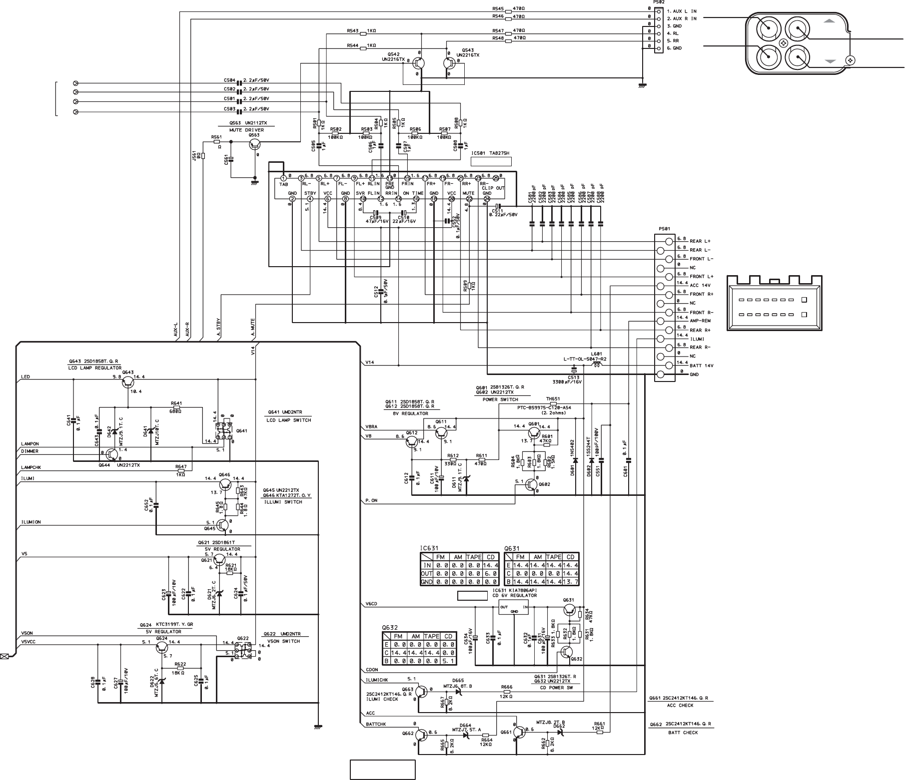
Main PWB(B1) section 1/3
Reel PWB(B7) section
- 19 - ADB340MP
ADB341MP
To Servo PWB (page 26)
To Tape head
(Cassette tape mech)
To Cassette
tape mech
Voltage measurement conditions:
FM 98.1MHz/66dBu Non-Mod Vol:1
BATT,ACC 14.4V
AM 999kHz/74dBu Non-Mod Vol:1
TAPE Test tape:MTT-212EN Vol:1
CD Test CD:YEDS-7 Vol:1
To Main PWB 3/3
(page 21)
RL
FR
RR
FL
To Main PWB 2/3,3/3
(page 20,21)
FM/AM Tuner
AF Processor
Motor Driver
Line AMP
Line AMP
LA6458ML
LA6458ML
LB1641
S1 CA-IN
S2 ST-BY
S3 MODE SW
Q1
M
M
1 CASSETTE IN SW
2 MAIN MOTOR
3 MAIN MOTOR
4 SUB MOTOR
5 SUB MOTOR
6 STAND BY POSITION SW
7 MODE SW
8 DIGITAL-GND
9 PHOTO TRNSISTOR
10 PHOTO DIODE ANODE
11 N.C.
Main motor ass'y
(653-0431-34)
Sub motor ass'y
(653-0431-33)
PHOTO SENSOR
6
5
4
3
2
1
Tape head
Extension lead
(653-0431-47)
BRN
RED
ORG
YEL
WHT
BLK
Cassette tape mechanism
Cassette tape mechanism
(V)
(V)
(V) (V) (V)
(V) (V) (V)
(V) (V) (V)
Tape Pre-AMP
CD I/F
Reel PWB(B7)
Reel PWB(B7)
C205,C206 0.027uF 0.018uF
C207 1000pF 0.22uF
R208 0.022uF Not use
ADB340MP ADB341MP
*1
*1
*1
*1
*1
- 20 -
Main PWB(B1) section 2/3
Sub PWB(B2) section
ADB340MP
ADB341MP
To P901 of Display PWB
(page 24)
To PC01 of Sub PWB
To Main PWB 1/3,3/3
(page 19,21)
Sub PWB(B2)
To P701
of Main PWB
LCD Controller System Controller/PLL
uPD178078GF-667-3
SPE ANA
(V)
(V)
(for ADB340MP)
(for ADB341MP)
(V)
Main PWB(B1) section 3/3
- 21 - ADB340MP
ADB341MP
To Main PWB 1/3
(page 19)
A
I
J
K
L
M
N
O
P
B
C
D
E
F
G
H
16P Socket (P501)
ABCDEFG H
IJKLMNO P
To Main PWB 1/3,2/3
(page 19,20)
RL
RR
FL
FR
Power AMP
RCA terminal
Line OUT Rch
(RED)
Line OUT Lch
(WHT)
AUX IN Rch
(RED)
AUX IN Lch
(WHT)
TOP SIDE
BOTTOM SIDE
6V Reg.
MUTE
MUTE
0.47uF/50V
0.47uF/50V
1K
1K
(V)
(V) (V)
- 22 - ADB340MP
ADB341MP
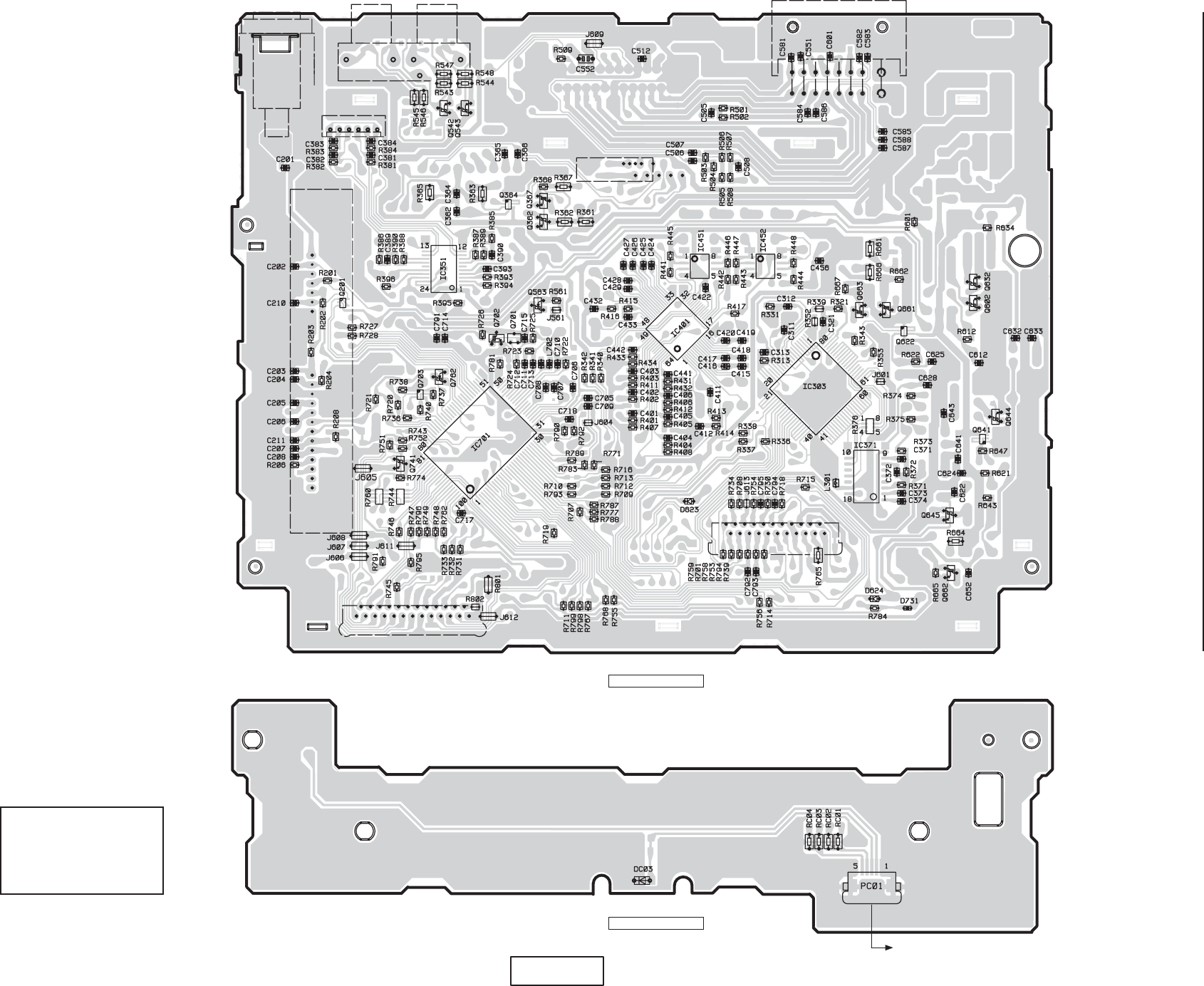
PRINTED WIRING BOARD
Main PWB(B1) section 1/2
Sub PWB(B2) section 1/2
SOLDER SIDE
Main PWB(B1)
SOLDER SIDE
Sub PWB(B2)
Caution:
COMPONENT SIDE: Parts on the
component side seen from the
component side are indicated.
SOLDER SIDE: Parts on the solder
side seen from the solder side are
indicated.
To P701 of Main PWB(page 23)
Q542
Q543
Q367
Q364
Q362
Q632
Q201
Q563
Q663
Q602
Q661
Q702
Q701
Q622
IC451
IC452
IC351
IC401
IC303
IC701
IC371
Q762
Q703
Q644
Q641
Q741
Q645
Q662
A
IP
H
L-IN R-IN RL RR
(for ADB340MP)
(for ADB341MP)
(for ADB340MP)
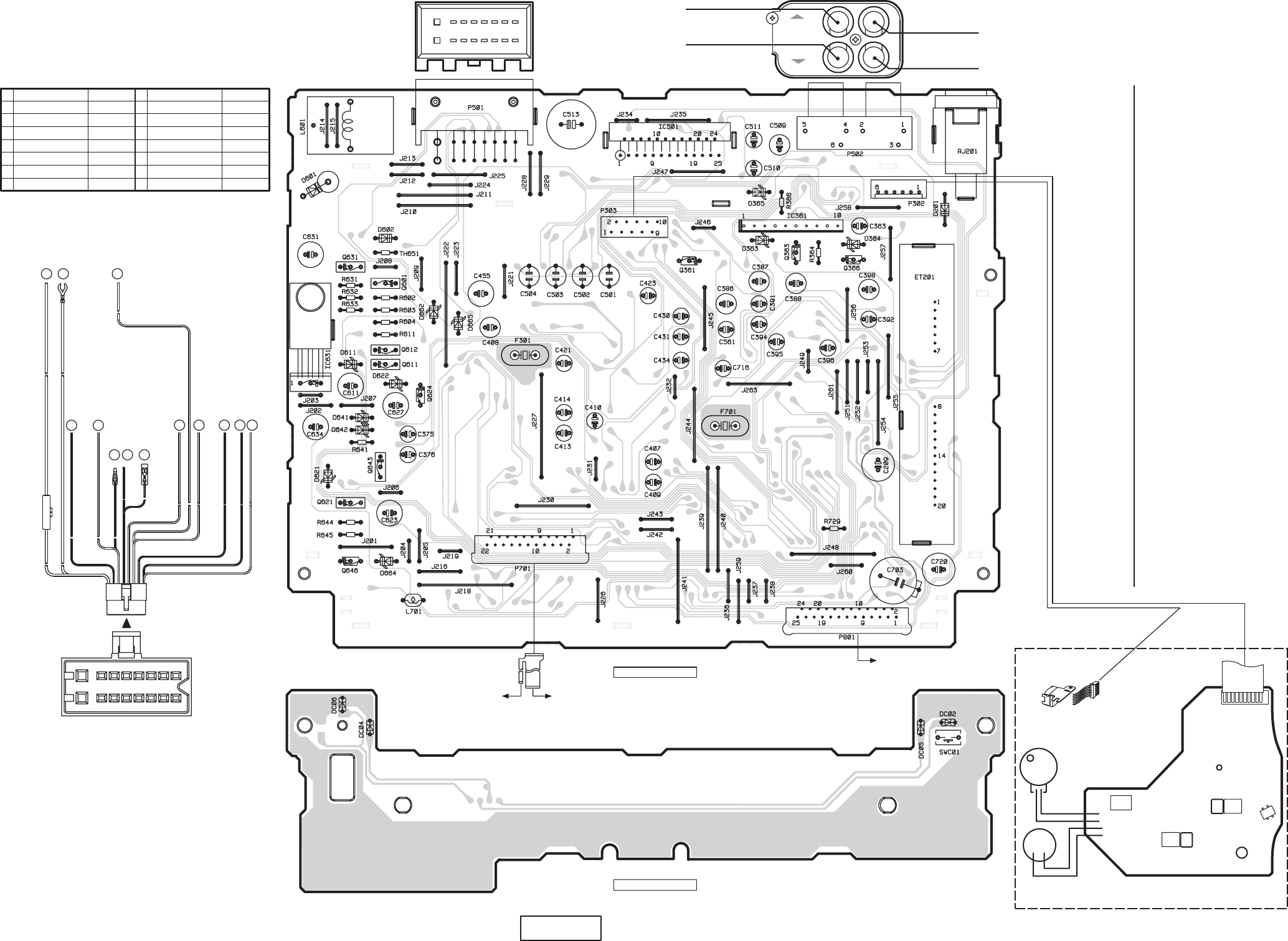
Main PWB(B1) section 2/2
- 23 - ADB340MP
ADB341MP
Main PWB(B1)
Sub PWB(B2)
16P Socket RCA terminal
Antenna recept.
Line OUT Rch(RED)
ABCDEFG
H
ABCDEFG
H
IJKLMNO
P
IJKLMNO
P
16P Socket (Extension lead)
I
J
K
L
M
N
O
P
REAR L-CH(-) GRN/BLK
NC ---
ACC RED
NC ---
REMOTE BLU/WHT
ILLUMI ORG/WHT
NC ---
GND BLK
A
B
C
D
E
F
G
H
REAR L-CH(+) GRN
FRONT L-CH(-) WHT/BLK
FRONT L-CH(+) WHT
FRONT R-CH(+) GRY
FRONT R-CH(-) GRY/BLK
REAR R-CH(+) PUR
REAR R-CH(-) PUR/BLK
BACK UP YEL
ABCDEFG
H
IJKLMNO
P
Extension lead
(653-0428-46)
FUSE(15A) 120-0150-00
BACK UP (YEL)H
GND (BLK)
REAR R-CH(+) (PUR)
FRONT R-CH(+) (GRY)
FRONT L-CH(+) (WHT)
FRONT L-CH(-) (WHT/BLK)
REAR L-CH(+) (GRN)
REAR L-CH(-) (GRN/BLK)
FRONT R-CH(-) (GRY/BLK)
REMOTE (BLU/WHT)
ILLUMI (ORG/WHT)
REAR R-CH(-) (PUR/BLK)
ACC (RED)
To PC01 of Sub PWB
(page 22)
Flex PWB
(653-0428-01)
To P901 of Display PWB
(page 25)
To Servo PWB
(page 27)
Line OUT Lch(WHT)
AUX IN Rch(RED)
AUX IN Lch(WHT)
TOP SIDE
BOTTOM SIDE
COMPONENT SIDE
COMPONENT SIDE
IC501
IC361
Q363
Q631
Q361
Q366
Q601
Q612
Q611
Q624
IC631
Q643
Q621
Q646
(L-IN)(R-IN)(RL)(RR)
P
K
G
F
N
E
M
D
C
B
I
A
MODE
ST-BY
CA-IN
Q1
S3
S2
S1
PHOTO
MAIN -
MAIN +
SUB -
SUB +
BLKRED
BLKRED
Flat cable
(653-0431-42)
Tape head
(653-0431-37)
Extension lead
(653-0431-47)
Main motor
(653-0431-34)
Sub motor
(653-0431-33)
CA-IN
MAIN +
SUB +
MODE
PHOTO
MAIN -
SUB -
ST-BY
D-GND
ANODE
110
Cassette tape mechanism
Cassette tape mechanism
Reel PWB(B7)
Sub PWB(B2) section 2/2
Reel PWB(B7) section
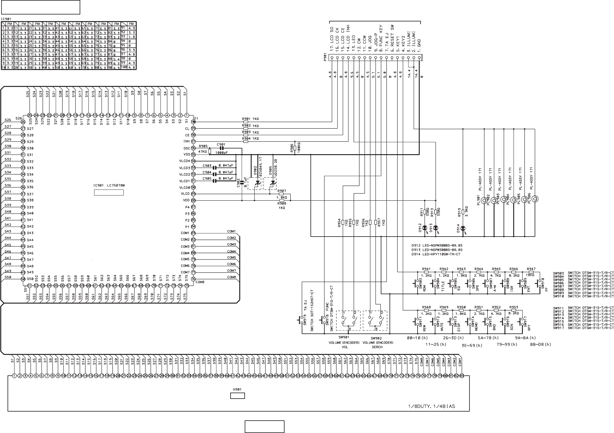
- 24 -
Display PWB(B3) section
ADB340MP
ADB341MP
CIRCUIT DIAGRAM
Voltage measurement conditions:
FM 98.1MHz/66dBu Non-Mod Vol:1
BATT,ACC 14.4V
To P701 of Main PWB 2/3(page 20)
LCD Driver
LCD
(V)
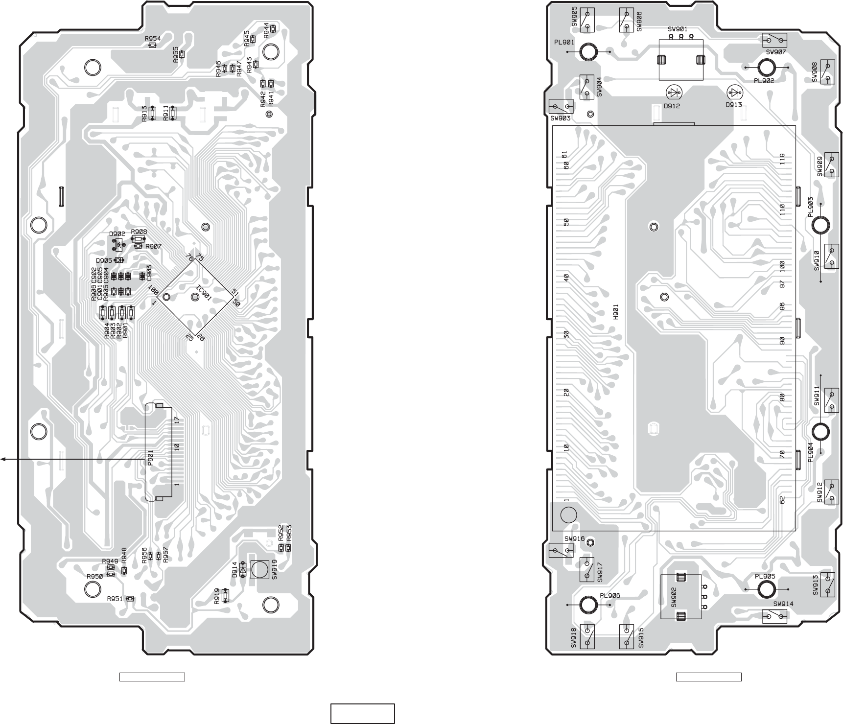
- 25 - ADB340MP
ADB341MP
Display PWB(B3)
To P701 of Main PWB
(page 23)
COMPONENT SIDE
Display PWB(B3)
SOLDER SIDE
PRINTED WIRING BOARD
Display PWB(B3) section
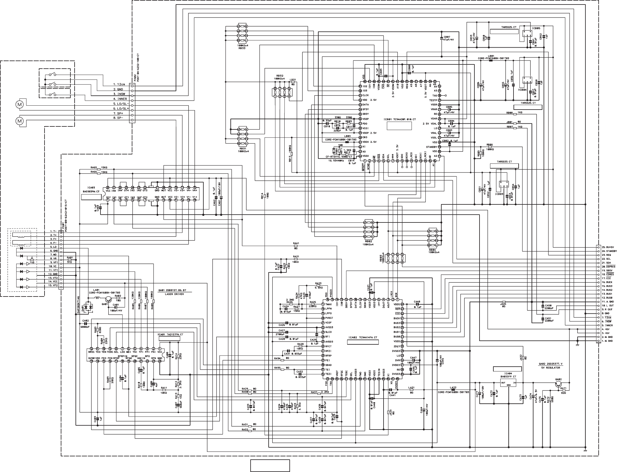
- 26 -
Servo PWB(B4) section
Switch-A PWB(B5) section
Switch-B PWB(B6) section
ADB340MP
ADB341MP
CIRCUIT DIAGRAM
To P801 of
Main PWB 1/3
(page 19)
Pick up ass'y
(653-0431-10)
TRACKING
FOCUS
Sled motor ass'y
(653-0431-24)
Spndle motor ass'y
(653-0431-25)
SW1
SW2
SW3
(Pin No.1)
(Pin No.2)
(Pin No.3)
(Pin No.4)
(Pin No.5)
(Pin No.6)
(Pin No.7)
(Pin No.8)
(Pin No.9)
(Pin No.10)
(Pin No.11)
(Pin No.12)
(Pin No.13)
(Pin No.14)
(Pin No.15)
(Pin No.16)
(Pin No.17)
(Pin No.18)
(Pin No.19)
(Pin No.20)
(Pin No.21)
(Pin No.22)
(Pin No.23)
(Pin No.24)
(Pin No.25)
(Pin No. of P801)
CD Driver
Head AMP Servo/DSP/DAC
MP3 DAC
1Mbits SRAM
2.5V Regulator
2.5V Regulator
3.3V Regulator
3.3V Regulator
CD mechanism
Swtch-A PWB(B5)
Swtch-B PWB(B6)
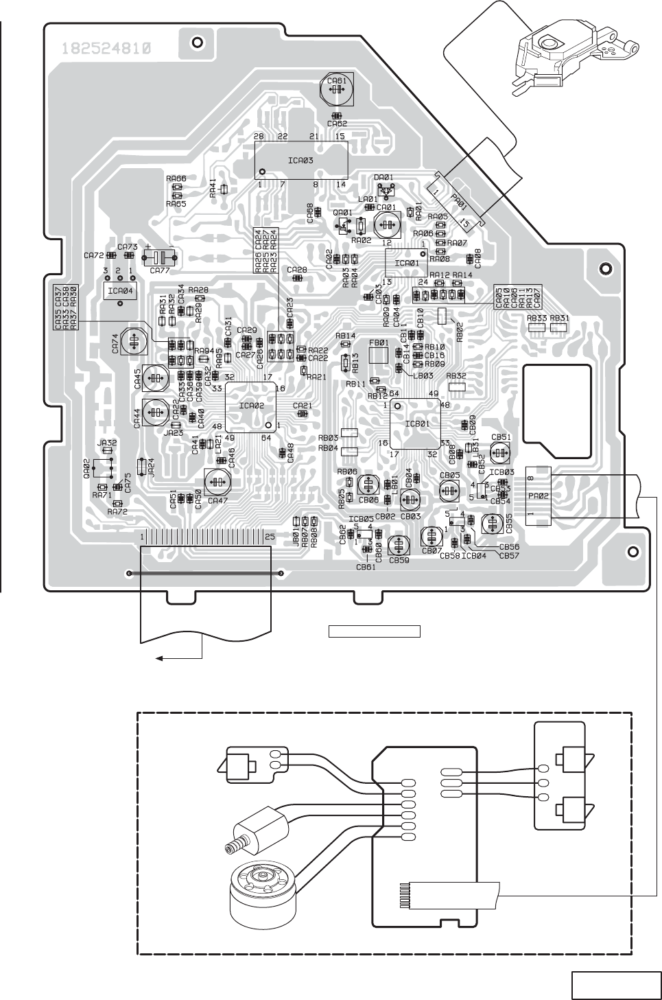
- 27 - ADB340MP
ADB341MP
To P801 of Main PWB
(page 21)
PRINTED WIRING BOARD
Pick up ass'y
(653-0431-10)
FPC
(653-0431-22)
SW1
SW2
SW3
YEL
ORG
BLU
WHT
RED
BLK
BRN
BLK
RED
Relay PWB
Flat wire
(653-0430-39)
18
ICA01
ICA02
ICA03
ICA04
ICB01
ICB03
ICB04
ICB05
QA01
QA02
Servo PWB(B4)
CD mechanism
COMPONENT SIDE
Sled motor ass'y
(653-0431-24)
Spndle motor ass'y
(653-0431-25)
FPC
(653-0431-23)
Servo PWB(B4) section 1/2
Switch-A PWB(B5) section
Switch-B PWB(B6) section
Switch-B PWB(B6)
Switch-A PWB(B5)
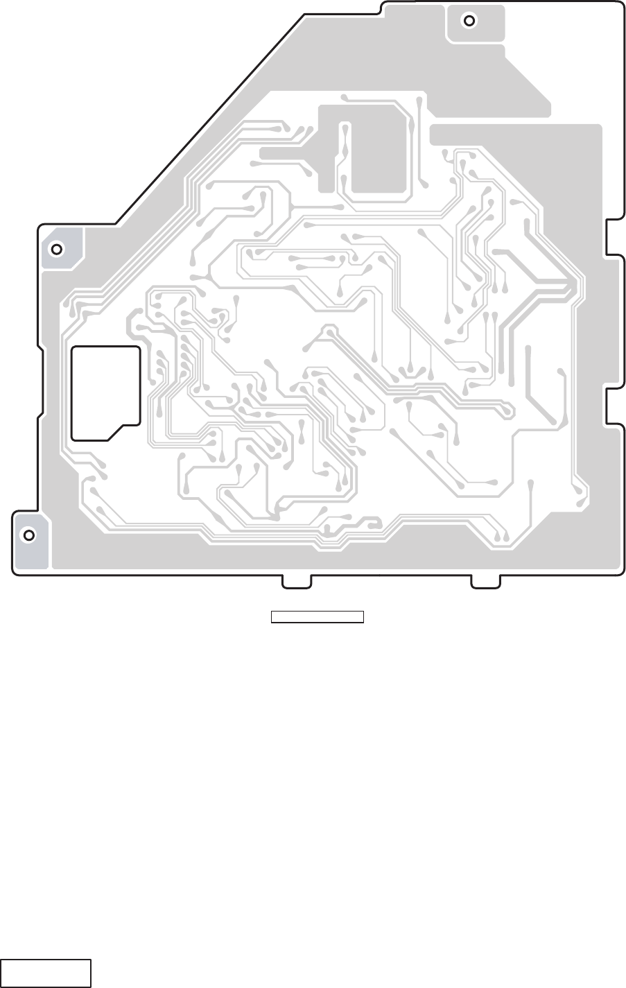
- 28 -
Servo PWB(B4) section 2/2
Servo PWB(B4)
SOLDER SIDE
ADB340MP
ADB341MP
