ADSP 2186
User Manual: ADSP-2186
Open the PDF directly: View PDF ![]() .
.
Page Count: 39
REV. B
Information furnished by Analog Devices is believed to be accurate and
reliable. However, no responsibility is assumed by Analog Devices for its
use, nor for any infringements of patents or other rights of third parties
which may result from its use. No license is granted by implication or
otherwise under any patent or patent rights of Analog Devices.
a
ADSP-2186
One Technology Way, P.O. Box 9106, Norwood, MA 02062-9106, U.S.A.
Tel: 781/329-4700 World Wide Web Site: http://www.analog.com
Fax: 781/326-8703 © Analog Devices, Inc., 2001
DSP Microcomputer
FUNCTIONAL BLOCK DIAGRAM
SERIAL PORTS
SPORT 1SPORT 0
MEMORY PROGRAMMABLE
I/O
AND
FLAGS
BYTE DMA
CONTROLLER
8K ⴛ 24
PROGRAM
MEMORY
8K ⴛ 16
DATA
MEMORY
TIMER
ADSP-2100 BASE
ARCHITECTURE
SHIFTER
MAC
ALU
ARITHMETIC UNITS
POWER-DOWN
CONTROL
PROGRAM
SEQUENCER
DAG 2DAG 1
DATA ADDRESS
GENERATORS
PROGRAM MEMORY ADDRESS
DATA MEMORY ADDRESS
PROGRAM MEMORY DATA
DATA MEMORY DATA
EXTERNAL
DATA
BUS
EXTERNAL
ADDRESS
BUS
INTERNAL
DMA
PORT
EXTERNAL
DATA
BUS
OR
FULL MEMORY
MODE
HOST MODE
FEATURES
PERFORMANCE
25 ns Instruction Cycle Time 40 MIPS Sustained
Performance
Single-Cycle Instruction Execution
Single-Cycle Context Switch
3-Bus Architecture Allows Dual Operand Fetches in
Every Instruction Cycle
Multifunction Instructions
Power-Down Mode Featuring Low CMOS Standby
Power Dissipation with 100 Cycle Recovery from
Power-Down Condition
Low Power Dissipation in Idle Mode
INTEGRATION
ADSP-2100 Family Code Compatible, with Instruction
Set Extensions
40K Bytes of On-Chip RAM, Configured as
8K Words On-Chip Program Memory RAM and
8K Words On-Chip Data Memory RAM
Dual Purpose Program Memory for Both Instruction
and Data Storage
Independent ALU, Multiplier/Accumulator and Barrel
Shifter Computational Units
Two Independent Data Address Generators
Powerful Program Sequencer Provides
Zero Overhead Looping Conditional Instruction
Execution
Programmable 16-Bit Interval Timer with Prescaler
100-Lead LQFP and 144-Ball Mini-BGA
SYSTEM INTERFACE
16-Bit Internal DMA Port for High Speed Access to
On-Chip Memory (Mode Selectable)
4 MByte Byte Memory Interface for Storage of Data
Tables and Program Overlays
8-Bit DMA to Byte Memory for Transparent Program
and Data Memory Transfers (Mode Selectable)
I/O Memory Interface with 2048 Locations Supports
Parallel Peripherals (Mode Selectable)
Programmable Memory Strobe and Separate I/O Memory
Space Permits “Glueless” System Design
(Mode Selectable)
Programmable Wait State Generation
Two Double-Buffered Serial Ports with Companding
Hardware and Automatic Data Buffering
Automatic Booting of On-Chip Program Memory from
Byte-Wide External Memory, e.g., EPROM, or
Through Internal DMA Port
Six External Interrupts
13 Programmable Flag Pins Provide Flexible System
Signaling
UART Emulation through Software SPORT Reconfiguration
ICE-Port™ Emulator Interface Supports Debugging
in Final Systems
GENERAL DESCRIPTION
The ADSP-2186 is a single-chip microcomputer optimized for
digital signal processing (DSP) and other high speed numeric
processing applications.
The ADSP-2186 combines the ADSP-2100 family base archi-
tecture (three computational units, data address generators and
a program sequencer) with two serial ports, a 16-bit internal
DMA port, a byte DMA port, a programmable timer, Flag I/O,
extensive interrupt capabilities and on-chip program and data
memory.
The ADSP-2186 integrates 40K bytes of on-chip memory con-
figured as 8K words (24-bit) of program RAM and 8K words
(16-bit) of data RAM. Power-down circuitry is also provided to
meet the low power needs of battery operated portable equip-
ment. The ADSP-2186 is available in 100-lead LQFP and
144-Ball Mini-BGA packages.
In addition, the ADSP-2186 supports new instructions, which
include bit manipulations—bit set, bit clear, bit toggle, bit test—
new ALU constants, new multiplication instruction (x squared),
biased rounding, result free ALU operations, I/O memory trans-
fers and global interrupt masking for increased flexibility.
ICE-Port is a trademark of Analog Devices, Inc.
All trademarks are the property of their respective holders.

ADSP-2186* PRODUCT PAGE QUICK LINKS
Last Content Update: 02/23/2017
COMPARABLE PARTS
View a parametric search of comparable parts.
EVALUATION KITS
•EZ-ICE® Serial Emulator for ADSP-218x Processor Family
•EZ-KIT Lite Evaluation Kit for ADSP-218x Processor
DOCUMENTATION
Application Notes
•AN-227: Digital Control System Design with the
ADSP-2100 Family
•AN-334: Digital Signal Processing Techniques
•AN-524: ADV601/ADV611 Bin Width Calculation in
ADSP-21xx DSP
•EE-06: ADSP-21xx Serial Port Startup Issues
•EE-100: ADSP-218x External Overlay Memory
•EE-102: Mode D and ADSP-218x Pin Compatibility - the
FAQs
•EE-11: ADSP-2181 Priority Chain & IDMA Holdoffs
•EE-115: ADSP-2189 IDMA Interface to Motorola MC68300
Family of Microprocessors
•EE-12: Interrupts and Programmable Flags on the
ADSP-2185/2186
•EE-121: Porting Code from ADSP-21xx to ADSP-219x
•EE-122: Coding for Performance on the ADSP-219x
•EE-123: An Overview of the ADSP-219x Pipeline
•EE-124: Booting up the ADSP-2192
•EE-125: ADSP-218x Embedded System Software
Management and In-System-Programming (ISP)
•EE-128: DSP in C++: Calling Assembly Class Member
Functions From C++
•EE-129: ADSP-2192 Interprocessor Communication
•EE-130: Making Fast Transition from ADSP-21xx to
ADSP-219x
•EE-131: Booting the ADSP-2191/95/96 DSPs
•EE-133: Converting From Legacy Architecture Files To
Linker Description Files for the ADSP-218x
•EE-139: Interfacing the ADSP-2191 to an AD7476 via the
SPI Port
•EE-142: Autobuffering, C and FFTs on the ADSP-218x
•EE-144: Creating a Master-Slave SPI Interface Between
Two ADSP-2191 DSPs
•EE-145: SPI Booting of the ADSP-2191 using the Atmel
AD25020N on an EZ-KIT Lite Evaluation Board
•EE-146: Implementing a Boot Manager for ADSP-218x
Family DSPs
•EE-152: Using Software Overlays with the ADSP-219x and
VisualDSP 2.0++
•EE-153: ADSP-2191 Programmable PLL

•EE-154: ADSP-2191 Host Port Interface
•EE-156: Support for the H.100 protocol on the ADSP-2191
•EE-158: ADSP-2181 EZ-Kit Lite IDMA to PC Printer Port
Interface
•EE-164: Advanced EPROM Boot and No-boot Scenarios
with ADSP-219x DSPs
•EE-168: Using Third Overtone Crystals with the ADSP-218x
DSP
•EE-17: ADSP-2187L Memory Organization
•EE-18: Choosing and Using FFTs for ADSP-21xx
•EE-188: Using C To Implement Interrupt-Driven Systems
On ADSP-219x DSPs
•EE-2: Using ADSP-218x I/O Space
•EE-226: ADSP-2191 DSP Host Port Booting
•EE-227: CAN Configuration Procedure for ADSP-21992
DSPs
•EE-249: Implementing Software Overlays on ADSP-218x
DSPs with VisualDSP++®
•EE-32: Language Extensions: Memory Storage Types, ASM
& Inline Constructs
•EE-35: Troubleshooting your ADSP-218x EZ-ICE
•EE-356: Emulator and Evaluation Hardware
Troubleshooting Guide for CCES Users
•EE-38: ADSP-2181 IDMA Port - Cycle Steal Timing
•EE-39: Interfacing 5V Flash Memory to an ADSP-218x (Byte
Programming Algorithm)
•EE-5: ADSP-218x Full Memory Mode vs. Host Memory
Mode
•EE-60: Simulating an RS-232 UART Using the Synchronous
Serial Ports on the ADSP-21xx Family DSPs
•EE-64: Setting Mode Pins on Reset
•EE-71: Minimum Rise Time Specs for Critical Interrupt and
Clock Signals on the ADSP-21x1/21x5
•EE-78: BDMA Usage on 100 pin ADSP-218x DSPs
Configured for IDMA Use
•EE-79: EPROM Booting In Host Mode with 100 Pin 218x
Processors
•EE-82: Using an ADSP-2181 DSP's IO Space to IDMA Boot
Another ADSP-2181
•EE-89: Implementing A Software UART on the ADSP-2181
EZ-Kit-Lite
•EE-96: Interfacing Two AD73311 Codecs to the ADSP-218x
Data Sheet
•ADSP-2186: 16-bit, 40 MIPS, 5v, 2 serial ports, host port, 40
KB RAM Data Sheet
Emulator Manuals
•ADSP-218X Family EZ-ICE Hardware Installation Guide
Integrated Circuit Anomalies
•ADSP-2186 Anomaly List for Revisions 0.0-2.0
Processor Manuals
•ADSP 21xx Processors: Manuals
•ADSP-218x DSP Hardware Reference
•ADSP-218x DSP Instruction Set Reference
•Using the ADSP-2100 Family Volume 2
Software Manuals
•CrossCore Embedded Studio 2.5.0 C/C++ Library Manual
for SHARC Processors
•VisualDSP++ 3.5 Assembler and Preprocessor Manual for
ADSP-218x and ADSP-219x DSPs
•VisualDSP++ 3.5 C Compiler and Library Manual for
ADSP-218x DSPs
•VisualDSP++ 3.5 C/C++ Compiler and Library Manual for
ADSP-219x Processors
•VisualDSP++ 3.5 Linker and Utilities Manual for 16-Bit
Processors
•VisualDSP++ 3.5 Loader Manual for 16-Bit Processors
SOFTWARE AND SYSTEMS REQUIREMENTS
•Software and Tools Anomalies Search
TOOLS AND SIMULATIONS
•Designing with BGA
•ADSP-21xx Processors: Software and Tools
REFERENCE MATERIALS
Product Selection Guide
•ADI Complementary Parts Guide - Supervisory Devices
and DSP Processors
DESIGN RESOURCES
•ADSP-2186 Material Declaration
•PCN-PDN Information
•Quality And Reliability
•Symbols and Footprints
DISCUSSIONS
View all ADSP-2186 EngineerZone Discussions.
SAMPLE AND BUY
Visit the product page to see pricing options.

TECHNICAL SUPPORT
Submit a technical question or find your regional support
number.
DOCUMENT FEEDBACK
Submit feedback for this data sheet.
This page is dynamically generated by Analog Devices, Inc., and inserted into this data sheet. A dynamic change to the content on this page will not
trigger a change to either the revision number or the content of the product data sheet. This dynamic page may be frequently modified.
ADSP-2186
–2– REV. B
Fabricated in a high speed, double metal, low power, CMOS
process, the ADSP-2186 operates with a 25 ns instruction cycle
time. Every instruction can execute in a single processor cycle.
The ADSP-2186’s flexible architecture and comprehensive
instruction set allow the processor to perform multiple opera-
tions in parallel. In one processor cycle the ADSP-2186 can:
• Generate the next program address
• Fetch the next instruction
• Perform one or two data moves
• Update one or two data address pointers
• Perform a computational operation
This takes place while the processor continues to:
• Receive and transmit data through the two serial ports
• Receive and/or transmit data through the internal DMA port
• Receive and/or transmit data through the byte DMA port
• Decrement timer
Development System
The ADSP-2100 Family Development Software, a complete set
of tools for software and hardware system development, sup-
ports the ADSP-2186. The System Builder provides a high level
method for defining the architecture of systems under develop-
ment. The Assembler has an algebraic syntax that is easy to
program and debug. The Linker combines object files into an
executable file. The Simulator provides an interactive instruction-
level simulation with a reconfigurable user interface to display
different portions of the hardware environment. A PROM
Splitter generates PROM programmer compatible files. The
C Compiler, based on the Free Software Foundation’s GNU
C Compiler, generates ADSP-2186 assembly source code.
The source code debugger allows programs to be corrected in
the C environment. The Runtime Library includes over 100
ANSI-standard mathematical and DSP-specific functions.
The EZ-KIT Lite is a hardware/software kit offering a complete
development environment for the ADSP-218x family: an ADSP-
218x-based evaluation board with PC monitor software plus
Assembler, Linker, Simulator and PROM Splitter software. The
ADSP-218x EZ-KIT Lite is a low cost, easy to use hardware
platform on which you can quickly get started with your DSP
software design. The EZ-KIT Lite includes the following features:
• 75 MHz ADSP-2189M
• Full 16-bit Stereo Audio I/O with AD73322 Codec
• RS-232 Interface
• EZ-ICE Connector for Emulator Control
• DSP Demo Programs
• Evaluation Suite of Visual DSP
The ADSP-218x EZ-ICE Emulator aids in the hardware debug-
ging of an ADSP-2186 system. The emulator consists of hard-
ware, host computer resident software, and the target board
connector. The ADSP-2186 integrates on-chip emulation sup-
port with a 14-pin ICE-Port interface. This interface provides a
simpler target board connection that requires fewer mechanical
clearance considerations than other ADSP-2100 Family EZ-
ICEs. The ADSP-2186 device need not be removed from the
target system when using the EZ-ICE, nor are any adapters
needed. Due to the small footprint of the EZ-ICE connector,
emulation can be supported in final board designs.
The EZ-ICE performs a full range of functions, including:
• In-target operation
• Up to 20 breakpoints
• Single-step or full-speed operation
• Registers and memory values can be examined and altered
• PC upload and download functions
• Instruction-level emulation of program booting and execution
• Complete assembly and disassembly of instructions
• C source-level debugging
See Designing An EZ-ICE-Compatible Target System in the
ADSP-2100 Family EZ-Tools Manual (ADSP-2181 sections), as
well as the Target Board Connector for EZ-ICE Probe section
of this data sheet, for the exact specifications of the EZ-ICE
target board connector.
Additional Information
This data sheet provides a general overview of ADSP-2186
functionality. For additional information on the architecture and
instruction set of the processor, refer to the ADSP-218x DSP
Hardware Reference. For more information about the develop-
ment tools, refer to the ADSP-2100 Family Development Tools
Data Sheet.
ARCHITECTURE OVERVIEW
The ADSP-2186 instruction set provides flexible data moves
and multifunction (one or two data moves with a computation)
instructions. Every instruction can be executed in a single
processor cycle. The ADSP-2186 assembly language uses an
algebraic syntax for ease of coding and readability. A compre-
hensive set of development tools supports program development.
SERIAL PORTS
SPORT 1SPORT 0
MEMORY PROGRAMMABLE
I/O
AND
FLAGS
BYTE DMA
CONTROLLER
8K ⴛ 24
PROGRAM
MEMORY
8K ⴛ 16
DATA
MEMORY
TIMER
ADSP-2100 BASE
ARCHITECTURE
SHIFTER
MAC
ALU
ARITHMETIC UNITS
POWER-DOWN
CONTROL
PROGRAM
SEQUENCER
DAG 2
DAG 1
DATA ADDRESS
GENERATORS
PROGRAM MEMORY ADDRESS
DATA MEMORY ADDRESS
PROGRAM MEMORY DATA
DATA MEMORY DATA
EXTERNAL
DATA
BUS
EXTERNAL
ADDRESS
BUS
INTERNAL
DMA
PORT
EXTERNAL
DATA
BUS
OR
FULL MEMORY
MODE
HOST MODE
Figure 1. Block Diagram
Figure 1 is an overall block diagram of the ADSP-2186. The
processor contains three independent computational units: the
ALU, the multiplier/accumulator (MAC) and the shifter. The
computational units process 16-bit data directly and have provi-
sions to support multiprecision computations. The ALU per-
forms a standard set of arithmetic and logic operations; division
primitives are also supported. The MAC performs single-cycle
multiply, multiply/add and multiply/subtract operations with
40 bits of accumulation. The shifter performs logical and arith-
metic shifts, normalization, denormalization and derive expo-
nent operations.
The shifter can be used to efficiently implement numeric
format control including multiword and block floating-point
representations.
SoundPort and EZ-ICE are registered trademarks of Analog Devices, Inc.

ADSP-2186
–3–
REV. B
The internal result (R) bus connects the computational units so
the output of any unit may be the input of any unit on the next
cycle.
A powerful program sequencer and two dedicated data address
generators ensure efficient delivery of operands to these compu-
tational units. The sequencer supports conditional jumps, sub-
routine calls and returns in a single cycle. With internal loop
counters and loop stacks, the ADSP-2186 executes looped code
with zero overhead; no explicit jump instructions are required to
maintain loops.
Two data address generators (DAGs) provide addresses for
simultaneous dual operand fetches from data memory and pro-
gram memory. Each DAG maintains and updates four address
pointers. Whenever the pointer is used to access data (indirect
addressing), it is post-modified by the value of one of four pos-
sible modify registers. A length value may be associated with
each pointer to implement automatic modulo addressing for
circular buffers.
Efficient data transfer is achieved with the use of five internal
buses:
• Program Memory Address (PMA) Bus
• Program Memory Data (PMD) Bus
• Data Memory Address (DMA) Bus
• Data Memory Data (DMD) Bus
• Result (R) Bus
The two address buses (PMA and DMA) share a single external
address bus, allowing memory to be expanded off-chip, and the
two data buses (PMD and DMD) share a single external data
bus. Byte memory space and I/O memory space also share the
external buses.
Program memory can store both instructions and data, permit-
ting the ADSP-2186 to fetch two operands in a single cycle, one
from program memory and one from data memory. The ADSP-
2186 can fetch an operand from program memory and the next
instruction in the same cycle.
When configured in host mode, the ADSP-2186 has a 16-bit
Internal DMA port (IDMA port) for connection to external
systems. The IDMA port is made up of 16 data/address pins and
five control pins. The IDMA port provides transparent, direct
access to the DSPs on-chip program and data RAM.
An interface to low cost byte-wide memory is provided by the
Byte DMA port (BDMA port). The BDMA port is bidirectional
and can directly address up to four megabytes of external RAM
or ROM for off-chip storage of program overlays or data tables.
The byte memory and I/O memory space interface supports
slow memories and I/O memory-mapped peripherals with
programmable wait state generation. External devices can gain
control of external buses with bus request/grant signals (BR,
BGH and BG). One execution mode (Go Mode) allows the
ADSP-2186 to continue running from on-chip memory. Normal
execution mode requires the processor to halt while buses are
granted.
The ADSP-2186 can respond to eleven interrupts. There are up
to six external interrupts (one edge-sensitive, two level-sensitive
and three configurable) and seven internal interrupts generated
by the timer, the serial ports (SPORTs), the Byte DMA port
and the power-down circuitry. There is also a master RESET
signal. The two serial ports provide a complete synchronous
serial interface with optional companding in hardware and a wide
variety of framed or frameless data transmit and receive modes of
operation.
Each port can generate an internal programmable serial clock or
accept an external serial clock.
The ADSP-2186 provides up to 13 general-purpose flag pins.
The data input and output pins on SPORT1 can be alternatively
configured as an input flag and an output flag. In addition, eight
flags are programmable as inputs or outputs, and three flags are
always outputs.
A programmable interval timer generates periodic interrupts. A
16-bit count register (TCOUNT) decrements every n processor
cycle, where n is a scaling value stored in an 8-bit register
(TSCALE). When the value of the count register reaches zero,
an interrupt is generated and the count register is reloaded from
a 16-bit period register (TPERIOD).
Serial Ports
The ADSP-2186 incorporates two complete synchronous serial
ports (SPORT0 and SPORT1) for serial communications and
multiprocessor communication.
Here is a brief list of the capabilities of the ADSP-2186 SPORTs.
For additional information on Serial Ports, refer to the ADSP-218x
DSP Hardware Reference.
• SPORTs are bidirectional and have a separate, double-buffered
transmit and receive section.
• SPORTs can use an external serial clock or generate their own
serial clock internally.
• SPORTs have independent framing for the receive and trans-
mit sections. Sections run in a frameless mode or with frame
synchronization signals internally or externally generated.
Frame sync signals are active high or inverted, with either of
two pulsewidths and timings.
• SPORTs support serial data word lengths from 3 to 16 bits and
provide optional A-law and µ-law companding according to
CCITT recommendation G.711.
• SPORT receive and transmit sections can generate unique
interrupts on completing a data word transfer.
• SPORTs can receive and transmit an entire circular buffer of
data with only one overhead cycle per data word. An interrupt
is generated after a data buffer transfer.
• SPORT0 has a multichannel interface to selectively receive and
transmit a 24- or 32-word, time-division multiplexed, serial
bitstream.
• SPORT1 can be configured to have two external interrupts
(IRQ0 and IRQ1) and the Flag In and Flag Out signals. The
internally generated serial clock may still be used in this
configuration.
PIN DESCRIPTIONS
The ADSP-2186 is available in a 100-lead LQFP package and a
144-Ball Mini-BGA package. In order to maintain maximum
functionality and reduce package size and pin count, some serial
port, programmable flag, interrupt and external bus pins have dual,
multiplexed functionality. The external bus pins are configured
during RESET only, while serial port pins are software config-
urable during program execution. Flag and interrupt function-
ality is retained concurrently on multiplexed pins. In cases

ADSP-2186
–4– REV. B
where pin functionality is reconfigurable, the default state is
shown in plain text; alternate functionality is shown in italics.
Common-Mode Pins
# Input/
Pin of Out-
Name(s) Pins put Function
RESET 1 I Processor Reset Input
BR 1 I Bus Request Input
BG 1 O Bus Grant Output
BGH 1 O Bus Grant Hung Output
DMS 1 O Data Memory Select Output
PMS 1 O Program Memory Select Output
IOMS 1 O Memory Select Output
BMS 1 O Byte Memory Select Output
CMS 1 O Combined Memory Select Output
RD 1 O Memory Read Enable Output
WR 1 O Memory Write Enable Output
IRQ2/ 1 I Edge- or Level-Sensitive
Interrupt Request
1
PF7 I/O Programmable I/O Pin
IRQL0/ 1 I Level-Sensitive Interrupt Requests
1
PF5 I/O Programmable I/O Pin
IRQL1/ 1 I Level-Sensitive Interrupt Requests
1
PF6 I/O Programmable I/O Pin
IRQE/ 1 I Edge-Sensitive Interrupt Requests
1
PF4 I/O Programmable I/O Pin
PF3 1 I/O Programmable I/O Pin
Mode C/ 1 I Mode Select Input—Checked
only During RESET
PF2 I/O Programmable I/O Pin During
Normal Operation
Mode B/ 1 I Mode Select Input—Checked
only During RESET
PF1 I/O Programmable I/O Pin During
Normal Operation
Mode A/ 1 I Mode Select Input—Checked
only During RESET
PF0 I/O Programmable I/O Pin During
Normal Operation
CLKIN, XTAL 2 I Clock or Quartz Crystal Input
CLKOUT 1 O Processor Clock Output
SPORT0 5 I/O Serial Port I/O Pins
SPORT1 5 I/O Serial Port I/O Pins
IRQ1:0 Edge- or Level-Sensitive Interrupts,
FI, FO Flag In, Flag Out
2
PWD 1 I Power-Down Control Input
PWDACK 1 O Power-Down Control Output
FL0, FL1, FL2 3 O Output Flags
V
DD
6 I Power (LQFP)
GND 10 I Ground (LQFP)
V
DD
11 I Power (Mini-BGA)
GND 20 I Ground (Mini-BGA)
EZ-Port 9 I/O For Emulation Use
NOTES
1
Interrupt/Flag pins retain both functions concurrently. If IMASK is set to
enable the corresponding interrupts, the DSP will vector to the appropriate
interrupt vector address when the pin is asserted, either by external devices or
set as a programmable flag.
2
SPORT configuration determined by the DSP System Control Register. Soft-
ware configurable.
Memory Interface Pins
The ADSP-2186 processor can be used in one of two modes:
Full Memory Mode, which allows BDMA operation with full
external overlay memory and I/O capability, or Host Mode,
which allows IDMA operation with limited external addressing
capabilities. The operating mode is determined by the state of
the Mode C pin during RESET and cannot be changed while
the processor is running.
Full Memory Mode Pins (Mode C = 0)
#
of Input/
Pin Name Pins Output Function
A13:0 14 O Address Output Pins for Pro-
gram, Data, Byte and I/O Spaces
D23:0 24 I/O Data I/O Pins for Program,
Data, Byte and I/O Spaces
(8 MSBs Are Also Used as
Byte Memory Addresses)
Host Mode Pins (Mode C = 1)
#
of Input/
Pin Name Pins Output Function
IAD15:0 16 I/O IDMA Port Address/Data Bus
A0 1 O Address Pin for External I/O,
Program, Data, or Byte Access
D23:8 16 I/O Data I/O Pins for Program,
Data Byte and I/O Spaces
IWR 1 I IDMA Write Enable
IRD 1 I IDMA Read Enable
IAL 1 I IDMA Address Latch Pin
IS 1 I IDMA Select
IACK 1 O IDMA Port Acknowledge
In Host Mode, external peripheral addresses can be decoded using the A0,
CMS, PMS, DMS, and IOMS signals.
Terminating Unused Pin
The following table shows the recommendations for terminating
unused pins.
Pin Terminations
I/O Hi-Z*
Pin 3-State Reset Caused Unused
Name (Z) State By Configuration
XTAL I I Float
CLKOUT O O Float
A13:1 or O (Z) Hi-Z BR, EBR Float
IAD12:0 I/O (Z) Hi-Z IS Float
A0 O (Z) Hi-Z BR, EBR Float
D23:8 I/O (Z) Hi-Z BR, EBR Float
D7 or I/O (Z) Hi-Z BR, EBR Float
IWR I I High (Inactive)
D6 or I/O (Z) Hi-Z BR, EBR Float
IRD IIBR, EBR High (Inactive)
D5 or I/O (Z) Hi-Z Float
IAL I I Low (Inactive)

ADSP-2186
–5–
REV. B
Pin Terminations (Continued)
I/O Hi-Z*
Pin 3-State Reset Caused Unused
Name (Z) State By Configuration
D4 or I/O (Z) Hi-Z BR, EBR Float
IS I I High (Inactive)
D3 or I/O (Z) Hi-Z BR, EBR Float
IACK Float
D2:0 or I/O (Z) Hi-Z BR, EBR Float
IAD15:13 I/O (Z) Hi-Z IS Float
PMS O (Z) O BR, EBR Float
DMS O (Z) O BR, EBR Float
BMS O (Z) O BR, EBR Float
IOMS O (Z) O BR, EBR Float
CMS O (Z) O BR, EBR Float
RD O (Z) O BR, EBR Float
WR O (Z) O BR, EBR Float
BR I I High (Inactive)
BG O (Z) O EE Float
BGH O O Float
IRQ2/PF7 I/O (Z) I Input = High (Inactive)
or Program as Output,
Set to 1, Let Float
IRQL1/PF6 I/O (Z) I Input = High (Inactive)
or Program as Output,
Set to 1, Let Float
IRQL0/PF5 I/O (Z) I Input = High (Inactive)
or Program as Output,
Set to 1, Let Float
IRQE/PF4 I/O (Z) I Input = High (Inactive)
or Program as Output,
Set to 1, Let Float
SCLK0 I/O I Input = High or Low,
Output = Float
RFS0 I/O I High or Low
DR0 I I High or Low
TFS0 I/O O High or Low
DT0 O O Float
SCLK1 I/O I Input = High or Low,
Output = Float
RFS1/IRQ0 I/O I High or Low
DR1/FI I I High or Low
TFS1/IRQ1 I/O O High or Low
DT1/FO O O Float
EE I I
EBR II
EBG OO
ERESET II
EMS OO
EINT II
ECLK I I
ELIN I I
ELOUT O O
NOTES
*Hi-Z = High Impedance.
1. If the CLKOUT pin is not used, turn it OFF, using CLKODIS in SPORT0
autobuffer control register.
2. If the Interrupt/Programmable Flag pins are not used, there are two options:
Option 1: When these pins are configured as INPUTS at reset and function as
interrupts and input flag pins, pull the pins High (inactive).
Option 2: Program the unused pins as OUTPUTS, set them to 1, and let them
float.
3. All bidirectional pins have three-stated outputs. When the pins are configured
as an output, the output is Hi-Z (high impedance) when inactive.
4. CLKIN, RESET, and PF3:0 are not included in the table because these pins
must be used.
Setting Memory Mode
Memory Mode selection for the ADSP-2186 is made during
chip reset through the use of the Mode C pin. This pin is multi-
plexed with the DSP’s PF2 pin, so care must be taken in how
the mode selection is made. The two methods for selecting the
value of Mode C are passive and active.
Passive configuration involves the use of a pull-up or pull-down
resistor connected to the Mode C pin. To minimize power
consumption, or if the PF2 pin is to be used as an output in the
DSP application, a weak pull-up or pull-down, on the order of
100 kΩ, can be used. This value should be sufficient to pull the
pin to the desired level and still allow the pin to operate as a
programmable flag output without undue strain on the processor’s
output driver. For minimum power consumption during
power-down, reconfigure PF2 to be an input, as the pull-up or
pull-down will hold the pin in a known state, and will not switch.
Active configuration involves the use of a three-stateable exter-
nal driver connected to the Mode C pin. A driver’s output en-
able should be connected to the DSP’s RESET signal such that
it only drives the PF2 pin when RESET is active (low). After
RESET is deasserted, the driver should three-state, thus allow-
ing full use of the PF2 pin as either an input or output.
To minimize power consumption during power-down, configure
the programmable flag as an output when connected to a three-
stated buffer. This ensures that the pin will be held at a constant
level and not oscillate should the three-state driver’s level hover
around the logic switching point.
Interrupts
The interrupt controller allows the processor to respond to the
eleven possible interrupts and reset with minimum overhead.
The ADSP-2186 provides four dedicated external interrupt
input pins, IRQ2, IRQL0, IRQL1 and IRQE (shared with the
PF7:4 pins). In addition, SPORT1 may be reconfigured for
IRQ0, IRQ1, FI and FO, for a total of six external interrupts.
The ADSP-2186 also supports internal interrupts from the
timer, the byte DMA port, the two serial ports, software and the
power-down control circuit. The interrupt levels are internally
prioritized and individually maskable (except power-down and
RESET). The IRQ2, IRQ0 and IRQ1 input pins can be pro-
grammed to be either level- or edge-sensitive. IRQL0 and IRQL1
are level-sensitive and IRQE is edge-sensitive. The priorities and
vector addresses of all interrupts are shown in Table I.
Table I. Interrupt Priority and Interrupt Vector Addresses
Source Of Interrupt Interrupt Vector Address (Hex)
Reset (or Power-Up with
PUCR = 1) 0000 (Highest Priority)
Power-Down (Nonmaskable) 002C
IRQ2 0004
IRQL1 0008
IRQL0 000C
SPORT0 Transmit 0010
SPORT0 Receive 0014
IRQE 0018
BDMA Interrupt 001C
SPORT1 Transmit or IRQ1 0020
SPORT1 Receive or IRQ0 0024
Timer 0028 (Lowest Priority)
ADSP-2186
–6– REV. B
Interrupt routines can either be nested, with higher priority
interrupts taking precedence, or processed sequentially. Inter-
rupts can be masked or unmasked with the IMASK register.
Individual interrupt requests are logically ANDed with the bits
in IMASK; the highest priority unmasked interrupt is then
selected. The power-down interrupt is nonmaskable.
The ADSP-2186 masks all interrupts for one instruction cycle
following the execution of an instruction that modifies the
IMASK register. This does not affect serial port autobuffering
or DMA transfers.
The interrupt control register, ICNTL, controls interrupt nest-
ing and defines the IRQ0, IRQ1 and IRQ2 external interrupts to
be either edge- or level-sensitive. The IRQE pin is an external
edge-sensitive interrupt and can be forced and cleared. The
IRQL0 and IRQL1 pins are external level-sensitive interrupts.
The IFC register is a write-only register used to force and clear
interrupts.
On-chip stacks preserve the processor status and are automati-
cally maintained during interrupt handling. The stacks are twelve
levels deep to allow interrupt, loop and subroutine nesting.
The following instructions allow global enable or disable servic-
ing of the interrupts (including power-down), regardless of the
state of IMASK. Disabling the interrupts does not affect serial
port autobuffering or DMA.
ENA INTS;
DIS INTS;
When the processor is reset, interrupt servicing is enabled.
LOW POWER OPERATION
The ADSP-2186 has three low power modes that significantly
reduce the power dissipation when the device operates under
standby conditions. These modes are:
• Power-Down
•Idle
• Slow Idle
The CLKOUT pin may also be disabled to reduce external
power dissipation.
Power-Down
The ADSP-2186 processor has a low power feature that lets the
processor enter a very low power dormant state through hard-
ware or software control. Following is a brief list of power-down
features. Refer to the ADSP-218x DSP Hardware Reference,
“System Interface” chapter, for detailed information about the
power-down feature.
• Quick recovery from power-down. The processor begins
executing instructions in as few as 200 CLKIN cycles.
• Support for an externally generated TTL or CMOS proces-
sor clock. The external clock can continue running during
power-down without affecting the lowest power rating and
200 CLKIN cycle recovery.
• Support for crystal operation includes disabling the oscillator
to save power (the processor automatically waits approxi-
mately 4096 CLKIN cycles for the crystal oscillator to start
or stabilize), and letting the oscillator run to allow 200 CLKIN
cycle start-up.
• Power-down is initiated by either the power-down pin (PWD)
or the software power-down force bit.
• Interrupt support allows an unlimited number of instructions
to be executed before optionally powering down. The
power-down interrupt also can be used as a nonmaskable,
edge- sensitive interrupt.
• Context clear/save control allows the processor to continue
where it left off or start with a clean context when leaving the
power-down state.
• The RESET pin also can be used to terminate power-down.
• Power-down acknowledge pin indicates when the processor
has entered power-down.
Idle
When the ADSP-2186 is in the Idle Mode, the processor waits
indefinitely in a low power state until an interrupt occurs. When
an unmasked interrupt occurs, it is serviced; execution then
continues with the instruction following the IDLE instruction.
In Idle mode IDMA, BDMA and autobuffer cycle steals still
occur.
Slow Idle
The IDLE instruction is enhanced on the ADSP-2186 to let the
processor’s internal clock signal be slowed, further reducing
power consumption. The reduced clock frequency, a pro-
grammable fraction of the normal clock rate, is specified by a
selectable divisor given in the IDLE instruction. The format of
the instruction is
IDLE (n);
where n = 16, 32, 64 or 128. This instruction keeps the proces-
sor fully functional, but operating at the slower clock rate. While
it is in this state, the processor’s other internal clock signals,
such as SCLK, CLKOUT and timer clock, are reduced by the
same ratio. The default form of the instruction, when no clock
divisor is given, is the standard IDLE instruction.
When the IDLE (n) instruction is used, it effectively slows down
the processor’s internal clock and thus its response time to
incoming interrupts. The one-cycle response time of the stan-
dard idle state is increased by n, the clock divisor. When an
enabled interrupt is received, the ADSP-2186 will remain in the
idle state for up to a maximum of n processor cycles (n = 16, 32,
64, or 128) before resuming normal operation.
When the IDLE (n) instruction is used in systems that have an
externally generated serial clock (SCLK), the serial clock rate
may be faster than the processor’s reduced internal clock rate.
Under these conditions, interrupts must not be generated at a
faster rate than can be serviced, due to the additional time the
processor takes to come out of the idle state (a maximum of n
processor cycles).
ADSP-2186
–7–
REV. B
SYSTEM INTERFACE
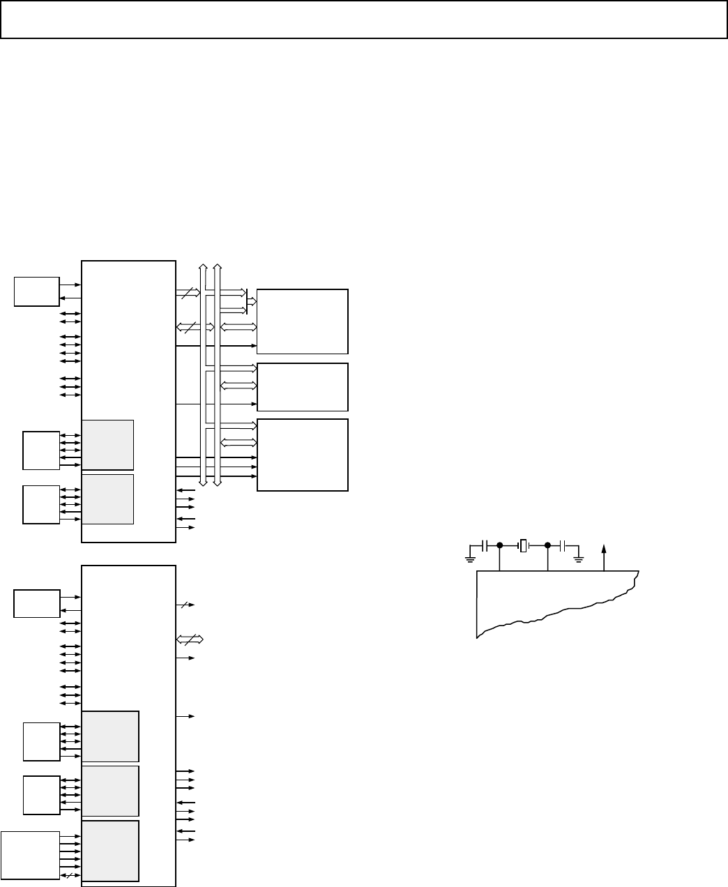
Figure 2 shows typical basic system configurations with the
ADSP-2186, two serial devices, a byte-wide EPROM and optional
external program and data overlay memories (mode selectable).
Programmable wait state generation allows the processor to
connect easily to slow peripheral devices. The ADSP-2186 also
provides four external interrupts and two serial ports or six
external interrupts and one serial port. Host Memory Mode
allows access to the full external data bus, but limits addressing
to a single address bit (A0). Additional system peripherals can
be added in this mode through the use of external hardware to
generate and latch address signals.
1/2x CLOCK
OR
CRYSTAL
SERIAL
DEVICE
SERIAL
DEVICE
SCLK1
RFS1 OR IRQ0
TFS1 OR IRQ1
DT1 OR FO
DR1 OR FI
SPORT1
SCLK0
RFS0
TFS0
DT0
DR0
SPORT0
A0–A21
DATA
CS
BYTE
MEMORY
I/O SPACE
(PERIPHERALS)
CS
DATA
ADDR
DATA
ADDR
2048 LOCATIONS
OVERLAY
MEMORY
TWO 8K
PM SEGMENTS
TWO 8K
DM SEGMENTS
D
23–0
A
13–0
D
23–8
A
10–0
D
15–8
D
23–16
A
13–0
14
24
FL0–2
PF3
CLKIN
XTAL ADDR13–0
DATA23–0
BMS
IOMS
PMS
DMS
CMS
BR
BG
BGH
PWD
ADSP-2186
SERIAL
DEVICE
SERIAL
DEVICE
SYSTEM
INTERFACE
OR
CONTROLLER
16
1
16
SCLK1
RFS1 OR IRQ0
TFS1 OR IRQ1
DT1 OR FO
DR1 OR FI
SPORT1
SCLK0
RFS0
TFS0
DT0
DR0
SPORT0
IRD/D6
IWR/D7
IS/D4
IAL/D5
IACK/D3
IAD15–0
IDMA PORT
FL0–2
PF3
CLKIN
XTAL ADDR0
DATA23–8
BMS
IOMS
PMS
DMS
CMS
BR
BG
BGH
PWD
PWDACK
ADSP-2186
IRQ2/PF7
IRQE/PF4
IRQL0/PF5
IRQL1/PF6
MODE C/PF2
MODE B/PF1
MODE A/PF0
HOST MEMORY MODE
IRQ2/PF7
IRQE/PF4
IRQL0/PF5
IRQL1/PF6
MODE C/PF2
MODE B/PF1
MODE A/PF0
FULL MEMORY MODE
1/2x CLOCK
OR
CRYSTAL
PWDACK
Figure 2. Basic System Configuration
Clock Signals
The ADSP-2186 can be clocked by either a crystal or a TTL-
compatible clock signal.
The CLKIN input cannot be halted, changed during operation
or operated below the specified frequency during normal operation.
The only exception is while the processor is in the power-down
state. For additional information on this power-down feature,
refer to the ADSP-218x DSP Hardware Reference.
If an external clock is used, it should be a TTL-compatible
signal running at half the instruction rate. The signal is con-
nected to the processor’s CLKIN input. When an external clock
is used, the XTAL input must be left unconnected.
The ADSP-2186 uses an input clock with a frequency equal to
half the instruction rate; a 20.00 MHz input clock yields a 25 ns
processor cycle (which is equivalent to 40 MHz). Normally,
instructions are executed in a single processor cycle. All device
timing is relative to the internal instruction clock rate, which is
indicated by the CLKOUT signal when enabled.
Because the ADSP-2186 includes an on-chip oscillator circuit,
an external crystal may be used. The crystal should be con-
nected across the CLKIN and XTAL pins, with two capacitors
connected as shown in Figure 3. Capacitor values are dependent
on crystal type and should be specified by the crystal manufacturer.
A parallel-resonant, fundamental frequency, microprocessor-
grade crystal should be used.
A clock output (CLKOUT) signal is generated by the proces-
sor at the processor’s cycle rate. This can be enabled and
disabled by the CLKODIS bit in the SPORT0 Autobuffer
Control Register.
CLKIN CLKOUTXTAL
DSP
Figure 3. External Crystal Connections
Reset
The RESET signal initiates a master reset of the ADSP-2186.
The RESET signal must be asserted during the power-up
sequence to assure proper initialization. RESET during initial
power-up must be held long enough to allow the internal clock
to stabilize. If RESET is activated any time after power-up, the
clock continues to run and does not require stabilization time.
The power-up sequence is defined as the total time required for
the crystal oscillator circuit to stabilize after a valid V
DD
is
applied to the processor, and for the internal phase-locked loop
(PLL) to lock onto the specific crystal frequency. A minimum of
2000 CLKIN cycles ensures that the PLL has locked, but does
not include the crystal oscillator start-up time. During this
power-up sequence the RESET signal should be held low. On
any subsequent resets, the RESET signal must meet the mini-
mum pulsewidth specification, t
RSP
.
The RESET input contains some hysteresis; however, if you use
an RC circuit to generate your RESET signal, the use of an
external Schmidt trigger is recommended.

ADSP-2186
–8– REV. B
The master reset sets all internal stack pointers to the empty
stack condition, masks all interrupts and clears the MSTAT
register. When RESET is released, if there is no pending bus
request and the chip is configured for booting, the boot-loading
sequence is performed. The first instruction is fetched from
on-chip program memory location 0x0000 once boot loading
completes.
MEMORY ARCHITECTURE
The ADSP-2186 provides a variety of memory and peripheral
interface options. The key functional groups are Program Memory,
Data Memory, Byte Memory and I/O.
Program Memory (Full Memory Mode) is a 24-bit-wide space
for storing both instruction opcodes and data. The ADSP-2186
has 8K words of Program Memory RAM on chip, and the capabil-
ity of accessing up to two 8K external memory overlay spaces using
the external data bus. Both an instruction opcode and a data value
can be read from on-chip program memory in a single cycle.
Data Memory (Full Memory Mode) is a 16-bit-wide space
used for the storage of data variables and for memory-mapped
control registers. The ADSP-2186 has 8K words on Data
Memory RAM on chip, consisting of 8160 user-accessible
locations and 32 memory-mapped registers. Support also exists
for up to two 8K external memory overlay spaces through the
external data bus.
Byte Memory (Full Memory Mode) provides access to an
8-bit wide memory space through the Byte DMA (BDMA) port.
The Byte Memory interface provides access to 4 MBytes of
memory by utilizing eight data lines as additional address lines.
This gives the BDMA Port an effective 22-bit address range. On
power-up, the DSP can automatically load bootstrap code from
byte memory.
I/O Space (Full Memory Mode) allows access to 2048 loca-
tions of 16-bit-wide data. It is intended to be used to communi-
cate with parallel peripheral devices such as data converters and
external registers or latches.
Program Memory
The ADSP-2186 contains an 8K × 24 on-chip program RAM.
The on-chip program memory is designed to allow up to two
accesses each cycle so that all operations can complete in a
single cycle. In addition, the ADSP-2186 allows the use of 8K
external memory overlays.
The program memory space organization is controlled by the
Mode B pin and the PMOVLAY register. Normally, the ADSP-
2186 is configured with Mode B = 0 and program memory
organized as shown in Figure 4.
EXTERNAL 8K
(PMOVLAY = 1 or 2,
MODE B = 0)
0x3FFF
0x2000
0x1FFF
8K INTERNAL
0x0000
PROGRAM MEMORY ADDRESS
Figure 4. Program Memory (Mode B = 0)
There are 8K words of memory accessible internally when the
PMOVLAY register is set to 0. When PMOVLAY is set to some-
thing other than 0, external accesses occur at addresses 0x2000
through 0x3FFF. The external address is generated as shown in
Table II.
Table II. PMOVLAY Addressing
PMOVLAY Memory A13 A12:0
0 Reserved Not Applicable Not Applicable
1 External 13 LSBs of Address
Overlay 1 0 Between 0x2000
and 0x3FFF
2 External 13 LSBs of Address
Overlay 2 1 Between 0x2000
and 0x3FFF
NOTE: Addresses 0x2000 through 0x3FFF should not be accessed when
PMOVLAY = 0.
This organization provides for two external 8K overlay segments
using only the normal 14 address bits, which allows for simple
program overlays using one of the two external segments in
place of the on-chip memory. Care must be taken in using this
overlay space in that the processor core (i.e., the sequencer)
does not take into account the PMOVLAY register value. For
example, if a loop operation is occurring on one of the external
overlays and the program changes to another external overlay or
internal memory, an incorrect loop operation could occur. In
addition, care must be taken in interrupt service routines as the
overlay registers are not automatically saved and restored on the
processor mode stack.
When Mode B = 1, booting is disabled and overlay memory is
disabled (PMOVLAY must be 0). Figure 5 shows the memory
map in this configuration.
RESERVED
0x3FFF
0x2000
0x1FFF
8K EXTERNAL
0x0000
PROGRAM MEMORY ADDRESS
Figure 5. Program Memory (Mode B = 1)
Data Memory
The ADSP-2186 has 8160 16-bit words of internal data memory.
In addition, the ADSP-2186 allows the use of 8K external memory
overlays. Figure 6 shows the organization of the data memory.
EXTERNAL 8K
(DMOVLAY = 1, 2)
INTERNAL
8160 WORDS
DATA MEMORY ADDRESS
32 MEMORY–
MAPPED REGISTERS
0x3FFF
0x3FEO
0x3FDF
0x2000
0x1FFF
0x0000
Figure 6. Data Memory
ADSP-2186
–9–
REV. B
There are 8160 words of memory accessible internally when the
DMOVLAY register is set to 0. When DMOVLAY is set to
something other than 0, external accesses occur at addresses
0x0000 through 0x1FFF. The external address is generated as
shown in Table III.
Table III. Addressing
DMOVLAY Memory A13 A12:0
0 Reserved Not Applicable Not Applicable
1 External 13 LSBs of Address
Overlay 1 0 Between 0x0000
and 0x1FFF
2 External 13 LSBs of Address
Overlay 2 1 Between 0x0000
and 0x1FFF
This organization allows for two external 8K overlays using only
the normal 14 address bits. All internal accesses complete in one
cycle. Accesses to external memory are timed using the wait states
specified by the DWAIT register.
I/O Space (Full Memory Mode)
The ADSP-2186 supports an additional external memory space
called I/O space. This space is designed to support simple con-
nections to peripherals or to bus interface ASIC data registers.
I/O space supports 2048 locations. The lower eleven bits of the
external address bus are used; the upper three bits are undefined.
Two instructions were added to the core ADSP-2100 Family
instruction set to read from and write to I/O memory space. The
I/O space also has four dedicated three-bit wait state registers,
IOWAIT0-3, that specify up to seven wait states to be automati-
cally generated for each of four regions. The wait states act on
address ranges as shown in Table IV.
Table IV.
Address Range Wait State Register
0x000–0x1FF IOWAIT0
0x200–0x3FF IOWAIT1
0x400–0x5FF IOWAIT2
0x600–0x7FF IOWAIT3
Composite Memory Select (CMS)
The ADSP-2186 has a programmable memory select signal that
is useful for generating memory select signals for memories
mapped to more than one space. The CMS signal is generated
to have the same timing as each of the individual memory select
signals (PMS, DMS, BMS, IOMS), but can combine their
functionality.
Each bit in the CMSSEL register, when set, causes the CMS
signal to be asserted when the selected memory select is asserted.
For example, to use a 32K word memory to act as both program
and data memory, set the PMS and DMS bits in the CMSSEL
register and use the CMS pin to drive the chip select of the
memory and use either DMS or PMS as the additional address bit.
The CMS pin functions as the other memory select signals, with
the same timing and bus request logic. A 1 in the enable bit
causes the assertion of the CMS signal at the same time as the
selected memory select signal. All enable bits, except the BMS
bit, default to 1 at reset.
Boot Memory Select (BMS) Disable
The ADSP-2186 also lets you boot the processor from one
external memory space while using a different external memory
space for BDMA transfers during normal operation. You can
use the CMS to select the first external memory space for BDMA
transfers and BMS to select the second external memory space
for booting. The BMS signal can be disabled by setting Bit 3 of
the System Control Register to 1. The System Control Register
is illustrated in Figure 7.
SYSTEM CONTROL REGISTER
PWAIT
PROGRAM MEMORY
WAIT STATES
BMS ENABLE
0 = ENABLED,
1 = DISABLED
DM (0ⴛ3FFF)
0000010000000111
1514131211109876543210
SPORT0 ENABLE
1 = ENABLED,
0 = DISABLED
SPORT1 ENABLE
1 = ENABLED,
0 = DISABLED
SPORT1 CONFIGURE
1 = SERIAL PORT
0 = FI, FO, IRQ0, IRQ1, SCLK
RESERVED
SET TO ZERO
RESERVED
SET TO ZERO
Figure 7. System Control Register
Byte Memory
The byte memory space is a bidirectional, 8-bit-wide, external
memory space used to store programs and data. Byte memory is
accessed using the BDMA feature. The BDMA Control Register is
shown in Figure 8. The byte memory space consists of 256 pages,
each of which is 16K × 8.
BDMA CONTROL
BMPAGE BTYPE
BDIR
0 = LOAD FROM BM
1 = STORE TO BM
BCR
0 = RUN DURING BDMA
1 = HALT DURING BDMA
0000000000001000
1514131211109876543210
DM (0ⴛ3FE3)
RESERVED
SET TO ZERO
Figure 8. BDMA Control Register
The byte memory space on the ADSP-2186 supports read and
write operations as well as four different data formats. The byte
memory uses data bits 15:8 for data. The byte memory uses
data bits 23:16 and address bits 13:0 to create a 22-bit address.
This allows up to a 4 meg × 8 (32 megabit) ROM or RAM to be
used without glue logic. All byte memory accesses are timed by
the BMWAIT register.

ADSP-2186
–10– REV. B
Byte Memory DMA (BDMA, Full Memory Mode)
The Byte memory DMA controller allows loading and storing of
program instructions and data using the byte memory space.
The BDMA circuit is able to access the byte memory space
while the processor is operating normally and steals only one
DSP cycle per 8-, 16- or 24-bit word transferred.
The BDMA circuit supports four different data formats that are
selected by the BTYPE register field. The appropriate number
of 8-bit accesses is done from the byte memory space to build
the word size selected. Table V shows the data formats supported
by the BDMA circuit.
Table V. BDMA Data Formats
Internal
BTYPE Memory Space Word Size Alignment
00 Program Memory 24 Full Word
01 Data Memory 16 Full Word
10 Data Memory 8 MSBs
11 Data Memory 8 LSBs
Unused bits in the 8-bit data memory formats are filled with 0s.
The BIAD register field is used to specify the starting address for
the on-chip memory involved with the transfer. The 14-bit BEAD
register specifies the starting address for the external byte memory
space. The 8-bit BMPAGE register specifies the starting page for
the external byte memory space. The BDIR register field selects
the direction of the transfer. The 14-bit BWCOUNT register
specifies the number of DSP words to transfer and initiates the
BDMA circuit transfers.
BDMA accesses can cross page boundaries during sequential
addressing. A BDMA interrupt is generated on the completion
of the number of transfers specified by the BWCOUNT register.
The BWCOUNT register is updated after each transfer so it can
be used to check the status of the transfers. When it reaches
zero, the transfers have finished and a BDMA interrupt is gener-
ated. The BMPAGE and BEAD registers must not be accessed
by the DSP during BDMA operations.
The source or destination of a BDMA transfer will always be
on-chip program or data memory, regardless of the values of
Mode B, PMOVLAY or DMOVLAY.
When the BWCOUNT register is written with a nonzero value,
the BDMA circuit starts executing byte memory accesses with
wait states set by BMWAIT. These accesses continue until the
count reaches zero. When enough accesses have occurred to
create a destination word, it is transferred to or from on-chip
memory. The transfer takes one DSP cycle. DSP accesses to
external memory have priority over BDMA byte memory
accesses.
The BDMA Context Reset bit (BCR) controls whether the
processor is held off while the BDMA accesses are occurring.
Setting the BCR bit to 0 allows the processor to continue opera-
tions. Setting the BCR bit to 1 causes the processor to stop
execution while the BDMA accesses are occurring, to clear the
context of the processor and start execution at address 0 when
the BDMA accesses have completed.
Internal Memory DMA Port (IDMA Port; Host Memory Mode)
The IDMA Port provides an efficient means of communication
between a host system and the ADSP-2186. The port is used to
access the on-chip program memory and data memory of the
DSP with only one DSP cycle per word overhead. The IDMA
port cannot, however, be used to write to the DSP’s memory-
mapped control registers.
The IDMA port has a 16-bit multiplexed address and data bus
and supports 24-bit program memory. The IDMA port is com-
pletely asynchronous and can be written to while the ADSP-2186
is operating at full speed.
The DSP memory address is latched and then automatically
incremented after each IDMA transaction. An external device
can therefore access a block of sequentially addressed memory
by specifying only the starting address of the block. This increases
throughput as the address does not have to be sent for each
memory access.
IDMA Port access occurs in two phases. The first is the IDMA
Address Latch cycle. When the acknowledge is asserted, a 14-bit
address and 1-bit destination type can be driven onto the bus by
an external device. The address specifies an on-chip memory
location, the destination type specifies whether it is a DM or
PM access. The falling edge of the address latch signal latches
this value into the IDMAA register.
Once the address is stored, data can then either be read from or
written to the ADSP-2186’s on-chip memory. Asserting the
select line (IS) and the appropriate read or write line (IRD and
IWR respectively) signals the ADSP-2186 that a particular
transaction is required. In either case, there is a one-processor-
cycle delay for synchronization. The memory access consumes
one additional processor cycle.
Once an access has occurred, the latched address is automati-
cally incremented and another access can occur.
Through the IDMAA register, the DSP can also specify the
starting address and data format for DMA operation.
Bootstrap Loading (Booting)
The ADSP-2186 has two mechanisms to allow automatic load-
ing of the internal program memory after reset. The method for
booting is controlled by the Mode A, B and C configuration bits
as shown in Table VI. These four states can be compressed into
two-state bits by allowing an IDMA boot with Mode C = 1.
However, three bits are used to ensure future compatibility with
parts containing internal program memory ROM.
BDMA Booting
When the MODE pins specify BDMA booting, the ADSP-2186
initiates a BDMA boot sequence when RESET is released.

ADSP-2186
–11–
REV. B
Table VI. Boot Summary Table
Mode C Mode B Mode A Booting Method
0 0 0 BDMA feature is used to load
the first 32 program memory
words from the byte memory
space. Program execution is
held off until all 32 words have
been loaded. Chip is config-
ured in Full Memory Mode.
0 1 0 No Automatic boot operations
occur. Program execution
starts at external memory
location 0. Chip is configured
in Full Memory Mode.
BDMA can still be used but
the processor does not auto-
matically use or wait for these
operations.
1 0 0 BDMA feature is used to load
the first 32 program memory
words from the byte memory
space. Program execution is
held off until all 32 words have
been loaded. Chip is config-
ured in Host Mode. Additional
interface hardware is required.
1 0 1 IDMA feature is used to load
any internal memory as de-
sired. Program execution is
held off until internal program
memory location 0 is written
to. Chip is configured in Host
Mode.
The BDMA interface is set up during reset to the following
defaults when BDMA booting is specified: the BDIR, BMPAGE,
BIAD and BEAD registers are set to 0; the BTYPE register is
set to 0 to specify program memory 24-bit words; and the
BWCOUNT register is set to 32. This causes 32 words of on-chip
program memory to be loaded from byte memory. These 32
words are used to set up the BDMA to load in the remaining
program code. The BCR bit is also set to 1, which causes pro-
gram execution to be held off until all 32 words are loaded into
on-chip program memory. Execution then begins at address 0.
The ADSP-2100 Family development software (Revision 5.02
and later) fully supports the BDMA booting feature and can
generate byte memory space compatible boot code.
The IDLE instruction can also be used to allow the processor
to hold off execution while booting continues through the
BDMA interface. For BDMA accesses while in Host Mode, the
addresses to boot memory must be constructed externally to
the ADSP-2186. The only memory address bit provided by
the processor is A0.
IDMA Port Booting
The ADSP-2186 can also boot programs through its Internal
DMA port. If Mode C = 1, Mode B = 0, and Mode A = 1, the
ADSP-2186 boots from the IDMA port. The IDMA feature can
load as much on-chip memory as desired. Program execution is
held off until on-chip program memory location 0 is written to.
Bus Request and Bus Grant
The ADSP-2186 can relinquish control of the data and address
buses to an external device. When the external device requires
access to memory, it asserts the bus request (BR) signal. If the
ADSP-2186 is not performing an external memory access, it
responds to the active BR input in the following processor cycle by:
• Three-stating the data and address buses and the PMS, DMS,
BMS, CMS, IOMS, RD, WR output drivers,
• Asserting the bus grant (BG) signal, and
• Halting program execution.
If Go Mode is enabled, the ADSP-2186 will not halt program
execution until it encounters an instruction that requires an
external memory access.
If the ADSP-2186 is performing an external memory access
when the external device asserts the BR signal, it will not three-
state the memory interfaces or assert the BG signal until the
processor cycle after the access completes. The instruction does
not need to be completed when the bus is granted. If a single
instruction requires two external memory accesses, the bus will
be granted between the two accesses.
When the BR signal is released, the processor releases the BG
signal, reenables the output drivers and continues program
execution from the point at which it stopped.
The bus request feature operates at all times, including when
the processor is booting and when RESET is active.
The BGH pin is asserted when the ADSP-2186 is ready to
execute an instruction but is stopped because the external bus is
already granted to another device. The other device can release
the bus by deasserting bus request. Once the bus is released, the
ADSP-2186 deasserts BG and BGH and executes the external
memory access.
Flag I/O Pins
The ADSP-2186 has eight general purpose programmable input/
output flag pins. They are controlled by two memory mapped
registers. The PFTYPE register determines the direction,
1 = output and 0 = input. The PFDATA register is used to read
and write the values on the pins. Data being read from a pin
configured as an input is synchronized to the ADSP-2186’s
clock. Bits that are programmed as outputs will read the value
being output. The PF pins default to input during reset.
In addition to the programmable flags, the ADSP-2186 has five
fixed-mode flags, FI, FO, FL0, FL1 and FL2. FL0–FL2 are
dedicated output flags. FI and FO are available as an alter-
nate configuration of SPORT1.
Note: Pins PF0, PF1 and PF2 are also used for device configu-
ration during reset.
ADSP-2186
–12– REV. B
BIASED ROUNDING
A mode is available on the ADSP-2186 to allow biased round-
ing in addition to the normal unbiased rounding. When the
BIASRND bit is set to 0, the normal unbiased rounding opera-
tions occur. When the BIASRND bit is set to 1, biased rounding
occurs instead of the normal unbiased rounding. When operat-
ing in biased rounding mode all rounding operations with MR0
set to 0x8000 will round up, rather than only rounding up odd
MR1 values.
For example:
Table VII. Biased Rounding Example
MR Value Biased Unbiased
Before RND RND Result RND Result
00-0000-8000 00-0001-8000 00-0000-8000
00-0001-8000 00-0002-8000 00-0002-8000
00-0000-8001 00-0001-8001 00-0001-8001
00-0001-8001 00-0002-8001 00-0002-8001
00-0000-7FFF 00-0000-7FFF 00-0000-7FFF
00-0001-7FFF 00-0001-7FFF 00-0001-7FFF
This mode only has an effect when the MR0 register contains
0x8000; all other rounding operations work normally. This
mode allows more efficient implementation of bit-specified
algorithms that use biased rounding, for example the GSM
speech compression routines. Unbiased rounding is preferred
for most algorithms.
Note: BIASRND bit is Bit 12 of the SPORT0 Autobuffer
Control register.
INSTRUCTION SET DESCRIPTION
The ADSP-2186 assembly language instruction set has an alge-
braic syntax that was designed for ease of coding and readability.
The assembly language, which takes full advantage of the
processor’s unique architecture, offers the following benefits:
• The algebraic syntax eliminates the need to remember cryptic
assembler mnemonics. For example, a typical arithmetic add
instruction, such as AR = AX0 + AY0, resembles a simple
equation.
• Every instruction assembles into a single, 24-bit word that
can execute in a single instruction cycle.
• The syntax is a superset ADSP-2100 Family assembly lan-
guage and is completely source and object code compatible
with other family members. Programs may need to be relo-
cated to utilize on-chip memory and conform to the ADSP-
2186’s interrupt vector and reset vector map.
• Sixteen condition codes are available. For conditional jump,
call, return or arithmetic instructions, the condition can be
checked and the operation executed in the same instruction
cycle.
• Multifunction instructions allow parallel execution of an
arithmetic instruction with up to two fetches or one write to
processor memory space during a single instruction cycle.
I/O Space Instructions
The instructions used to access the ADSP-2186’s I/O memory
space are as follows:
Syntax: IO(addr) = dreg
dreg = IO(addr);
where addr is an address value between 0 and 2047 and dreg is
any of the 16 data registers.
Examples: IO(23) = AR0;
AR1 = IO(17);
Description: The I/O space read and write instructions move
data between the data registers and the I/O
memory space.
DESIGNING AN EZ-ICE-COMPATIBLE SYSTEM
The ADSP-2186 has on-chip emulation support and an
ICE-Port, a special set of pins that interface to the EZ-ICE. These
features allow in-circuit emulation without replacing the target
system processor by using only a 14-pin connection from the
target system to the EZ-ICE. Target systems must have a 14-pin
connector to accept the EZ-ICE’s in-circuit probe, a 14-pin plug.
Emulation Reset and the Mode Pins
The Mode A, B, and C pins are located on the rising edge of the
RESET signal. However, when the emulator reset (ERESET) is
asserted by the EZ-ICE, the DSP performs a chip reset, and the
initial mode information is erased, and the logic values on the
mode pins are latched. You must take into consideration the
value of the mode pins before issuing a chip reset command
from the EZ-ICE user interface. If you are using a passive
method of maintaining mode information (as discussed in Set-
ting Memory Modes) then it does not matter that the mode
information is latched by an emulator reset. However, if you are
using the RESET pin as a method of setting the value of the
mode pins, then you have to take into consideration the effects
of an emulator reset.
One method of ensuring that the values located on the mode
pins is the one that is desired to construct a circuit like the one
shown in Figure 9. This circuit will force the value located on
the Mode C pin to zero; regardless if it latched via the RESET
or ERESET pin.
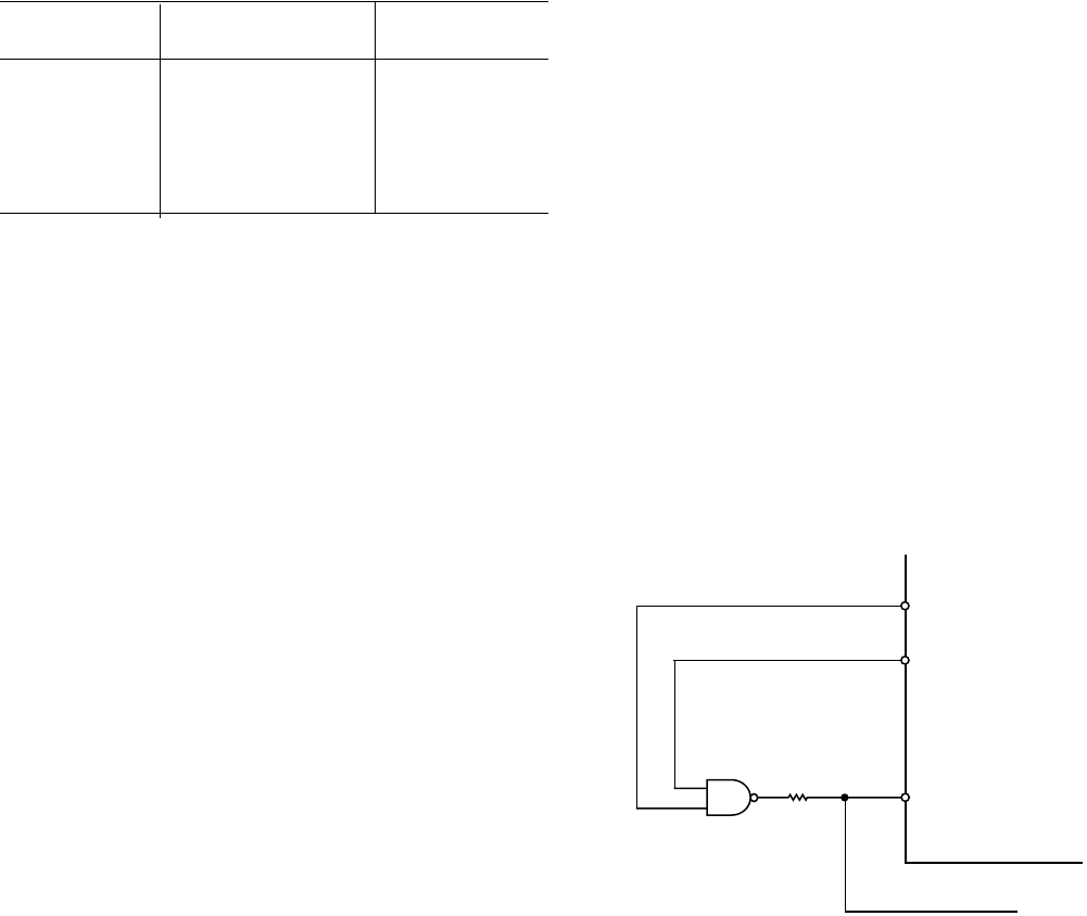
PROGRAMMABLE I/O
MODE A/PFO
RESET
ERESET
1k⍀
ADSP-2186
Figure 9. Boot Mode Circuit
See the ADSP-2100 Family EZ-Tools data sheet for complete
information on ICE products.
The ICE-Port interface consists of the following ADSP-2186
pins:
EBR EBG ERESET
EMS EINT ECLK
ELIN ELOUT EE
ADSP-2186
–13–
REV. B
These ADSP-2186 pins must be connected only to the EZ-ICE
connector in the target system. These pins have no function
except during emulation, and do not require pull-up or pull-
down resistors. The traces for these signals between the ADSP-
2186 and the connector must be kept as short as possible, no
longer than three inches.
The following pins are also used by the EZ-ICE:
BR BG
RESET GND
The EZ-ICE uses the EE (emulator enable) signal to take con-
trol of the ADSP-2186 in the target system. This causes the
processor to use its ERESET, EBR and EBG pins instead of
the RESET, BR and BG pins. The BG output is three-stated.
These signals do not need to be jumper-isolated in your system.
The EZ-ICE connects to your target system via a ribbon cable
and a 14-pin female plug. The female plug is plugged onto the
14-pin connector (a pin strip header) on the target board.
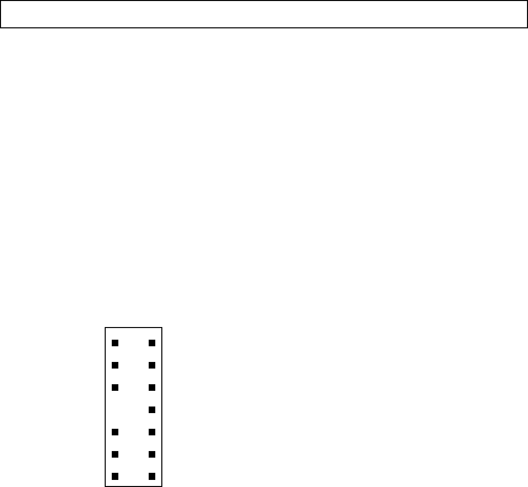
Target Board Connector for EZ-ICE Probe
The EZ-ICE connector (a standard pin strip header) is shown in
Figure 10. You must add this connector to your target board
design if you intend to use the EZ-ICE. Be sure to allow enough
room in your system to fit the EZ-ICE probe onto the 14-pin
connector.
1
3
5
7
9
11
13
2
4
6
8
10
12
14
GND
KEY (NO PIN)
RESET
BR
BG
TOP VIEW
EBG
EBR
ELOUT
EE
EINT
ELIN
ECLK
EMS
ERESET
ⴛ
Figure 10. Target Board Connector for EZ-ICE
The 14-pin, 2-row pin strip header is keyed at the Pin 7 loca-
tion—you must remove Pin 7 from the header. The pins must
be 0.025 inch square and at least 0.20 inch in length. Pin spac-
ing should be 0.1 × 0.1 inches. The pin strip header must have
at least 0.15-inch clearance on all sides to accept the EZ-ICE
probe plug. Pin strip headers are available from vendors such as
3M, McKenzie and Samtec.
Target Memory Interface
For your target system to be compatible with the EZ-ICE emu-
lator, it must comply with the memory interface guidelines listed
below.
PM, DM, BM, IOM, and CM
Design a Program Memory (PM), Data Memory (DM), Byte
Memory (BM), I/O Memory (IOM) and Composite Memory
(CM) external interfaces to comply with worst case device timing
requirements and switching characteristics as specified in this
DSP’s data sheet. The performance of the EZ-ICE may approach
published worst case specifications for some memory access
timing requirements and switching characteristics.
Note: If your target does not meet the worst case chip specifica-
tions for memory access parameters, you may not be able to
emulate your circuitry at the desired CLKIN frequency. Depend-
ing on the severity of the specification violation, you may have
trouble manufacturing your system as DSP components statisti-
cally vary in switching characteristics and timing requirements
within published limits.
Restriction: All memory strobe signals on the ADSP-2186 (RD,
WR, PMS, DMS, BMS, CMS and IOMS) used in your target
system must have 10 kΩ pull-up resistors connected when the
EZ-ICE is being used. The pull-up resistors are necessary
because there are no internal pull-ups to guarantee their state
during prolonged three-state conditions resulting from typical
EZ-ICE debugging sessions. These resistors may be removed at
your option when the EZ-ICE is not being used.
Target System Interface Signals
When the EZ-ICE board is installed, the performance on some
system signals change. Design your system to be compatible
with the following system interface signal changes introduced by
the EZ-ICE board:
• EZ-ICE emulation introduces an 8 ns propagation delay
between your target circuitry and the DSP on the RESET
signal.
• EZ-ICE emulation introduces an 8 ns propagation delay
between your target circuitry and the DSP on the BR signal.
• EZ-ICE emulation ignores RESET and BR when single-
stepping.
• EZ-ICE emulation ignores RESET and BR when in Emulator
Space (DSP halted).
• EZ-ICE emulation ignores the state of target BR in certain
modes. As a result, the target system may take control of the
DSP’s external memory bus only if bus grant (BG) is asserted
by the EZ-ICE board’s DSP.

–14– REV. B
ADSP-2186–SPECIFICATIONS
RECOMMENDED OPERATING CONDITIONS
K Grade B Grade
Parameter Min Max Min Max Unit
V
DD
4.5 5.5 4.5 5.5 V
T
AMB
0 +70 –40 +85 °C
ELECTRICAL CHARACTERISTICS
K/B Grades
Parameter Test Conditions Min Typ Max Unit
V
IH
Hi-Level Input Voltage
1, 2
@ V
DD
= max 2.0 V
V
IH
Hi-Level CLKIN Voltage @ V
DD
= max 2.2 V
V
IL
Lo-Level Input Voltage
1, 3
@ V
DD
= min 0.8 V
V
OH
Hi-Level Output Voltage
1, 4, 5
@ V
DD
= min
I
OH
= –0.5 mA 2.4 V
@ V
DD
= min
I
OH
= –100 µA
6
V
DD
– 0.3 V
V
OL
Lo-Level Output Voltage
1, 4, 5
@ V
DD
= min
I
OL
= 2 mA 0.4 V
I
IH
Hi-Level Input Current
3
@ V
DD
= max
V
IN
= V
DD
max 10 µA
I
IL
Lo-Level Input Current
3
@ V
DD
= max
V
IN
= 0 V 10 µA
I
OZH
Three-State Leakage Current
7
@ V
DD
= max
V
IN
= V
DD
max
8
10 µA
I
OZL
Three-State Leakage Current
7
@ V
DD
= max
V
IN
= 0 V
8
, t
CK
= 25 ns 10 µA
I
DD
Supply Current (Idle)
9
@ V
DD
= 5.0 14 mA
I
DD
Supply Current (Dynamic)
10, 11
@ V
DD
= 5.0
T
AMB
= +25°C
t
CK
= 34.7 ns 48 mA
t
CK
= 30 ns 55 mA
t
CK
= 25 ns 60 mA
C
I
Input Pin Capacitance
3, 6
@ V
IN
= 2.5 V,
f
IN
= 1.0 MHz,
T
AMB
= +25°C8pF
C
O
Output Pin Capacitance
6, 7, 12
@ V
IN
= 2.5 V,
f
IN
= 1.0 MHz,
T
AMB
= +25°C8pF
NOTES
1
Bidirectional pins: D0–D23, RFS0, RFS1, SCLK0, SCLK1, TFS0, TFS1, A1–A13, PF0–PF7.
2
Input only pins: RESET, BR, DR0, DR1, PWD.
3
Input only pins: CLKIN, RESET, BR, DR0, DR1, PWD.
4
Output pins: BG, PMS, DMS, BMS, IOMS, CMS, RD, WR, PWDACK, A0, DT0, DT1, CLKOUT, FL2–0, BGH.
5
Although specified for TTL outputs, all ADSP-2186 outputs are CMOS-compatible and will drive to V
DD
and GND, assuming no dc loads.
6
Guaranteed but not tested.
7
Three-statable pins: A0–A13, D0–D23, PMS, DMS, BMS, IOMS, CMS, RD, WR, DT0, DT1, SCLK0, SCLK1, TFS0, TFS1, RFS0, RFS1, PF0–PF7.
8
0 V on BR, CLKIN Inactive.
9
Idle refers to ADSP-2186 state of operation during execution of IDLE instruction. Deasserted pins are driven to either V
DD
or GND.
10
I
DD
measurement taken with all instructions executing from internal memory. 50% of the instructions are multifunction (types 1, 4, 5, 12, 13, 14), 30% are type 2
and type 6, and 20% are idle instructions.
11
V
IN
= 0 V and 3 V. For typical figures for supply currents, refer to Power Dissipation section.
12
Output pin capacitance is the capacitive load for any three-stated output pin.
Specifications subject to change without notice.
ADSP-2186
–15–
REV. B
ESD SENSITIVITY
ESD (electrostatic discharge) sensitive device. Electrostatic charges as high as 4000 V readily
accumulate on the human body and test equipment and can discharge without detection. Although
the ADSP-2186 features proprietary ESD protection circuitry, permanent damage may occur on
devices subjected to high-energy electrostatic discharges. Therefore, proper ESD precautions are
recommended to avoid performance degradation or loss of functionality.
ABSOLUTE MAXIMUM RATINGS*
Supply Voltage . . . . . . . . . . . . . . . . . . . . . . . . . –0.3 V to +7 V
Input Voltage . . . . . . . . . . . . . . . . . . . . –0.3 V to V
DD
+ 0.3 V
Output Voltage Swing . . . . . . . . . . . . . –0.3 V to V
DD
+ 0.3 V
Operating Temperature Range (Ambient) . . –40°C to +85°C
Storage Temperature Range . . . . . . . . . . . . –65°C to +150°C
Lead Temperature (5 sec) LQFP . . . . . . . . . . . . . . . . . 280°C
*Stresses above those listed under Absolute Maximum Ratings may cause perma-
nent damage to the device. These are stress ratings only; functional operation of
the device at these or any other conditions above those indicated in the operational
sections of this specification is not implied. Exposure to absolute maximum rating
conditions for extended periods may affect device reliability.
TIMING PARAMETERS
GENERAL NOTES
Use the exact timing information given. Do not attempt to
derive parameters from the addition or subtraction of others.
While addition or subtraction would yield meaningful results for
an individual device, the values given in this data sheet reflect
statistical variations and worst cases. Consequently, you cannot
meaningfully add up parameters to derive longer times.
TIMING NOTES
Switching characteristics specify how the processor changes its
signals. You have no control over this timing—circuitry external
to the processor must be designed for compatibility with these
signal characteristics. Switching characteristics tell you what the
processor will do in a given circumstance. You can also use
switching characteristics to ensure that any timing requirement
of a device connected to the processor (such as memory) is
satisfied.
Timing requirements apply to signals that are controlled by
circuitry external to the processor, such as the data input for a
read operation. Timing requirements guarantee that the proces-
sor operates correctly with other devices.
MEMORY TIMING SPECIFICATIONS
The table below shows common memory device specifications
and the corresponding ADSP-2186 timing parameters, for your
convenience.
Memory ADSP-2186 Timing
Device Timing Parameter
Specification Parameter Definition
Address Setup to t
ASW
A0–A13, xMS Setup
Write Start before WR Low
Address Setup to t
AW
A0–A13, xMS Setup
Write End before WR Deasserted
Address Hold Time t
WRA
A0–A13, xMS Hold before
WR Low
Data Setup Time t
DW
Data Setup before WR
High
Data Hold Time t
DH
Data Hold after WR High
OE to Data Valid t
RDD
RD Low to Data Valid
Address Access Time t
AA
A0–A13, xMS to Data
Valid
xMS = PMS, DMS, BMS, CMS, IOMS.
FREQUENCY DEPENDENCY FOR TIMING
SPECIFICATIONS
t
CK
is defined as 0.5 t
CKI
. The ADSP-2186 uses an input clock
with a frequency equal to half the instruction rate; for example,
a 20 MHz input clock (which is equivalent to 50 ns) yields a
25 ns processor cycle (equivalent to 40 MHz). t
CK
values within
the range of 0.5 t
CKI
period should be substituted for all relevant
timing parameters to obtain the specification value.
Example: t
CKH
= 0.5 t
CK
– 7 ns = 0.5 (25 ns) – 7 ns = 5.5 ns
WARNING!
ESD SENSITIVE DEVICE
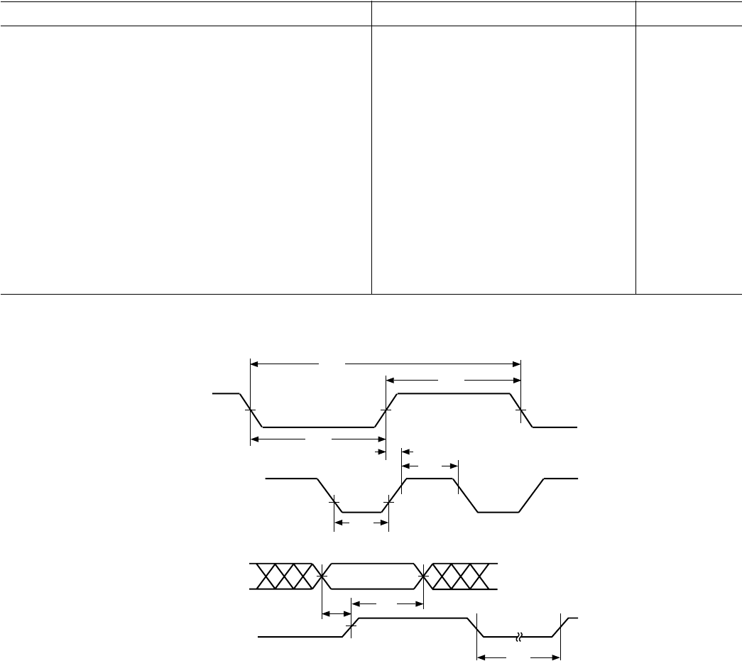
ADSP-2186
–16– REV. B
TIMING PARAMETERS
Parameter Min Max Unit
Clock Signals and Reset
Timing Requirements:
t
CKI
CLKIN Period 50 150 ns
t
CKIL
CLKIN Width Low 20 ns
t
CKIH
CLKIN Width High 20 ns
Switching Characteristics:
t
CKL
CLKOUT Width Low 0.5 t
CK
– 7 ns
t
CKH
CLKOUT Width High 0.5 t
CK
– 7 ns
t
CKOH
CLKIN High to CLKOUT High 0 20 ns
Control Signals
Timing Requirements:
t
RSP
RESET Width Low
1
5 t
CK
ns
t
MS
Mode Setup before RESET High 2 ns
t
MH
Mode Setup after RESET High 5 ns
NOTE
1
Applies after power-up sequence is complete. Internal phase lock loop requires no more than 2000 CLKIN cycles assuming stable CLKIN (not including crystal
oscillator start-up time).
t
RSP
t
CKOH
t
CKI
t
CKIH
t
CKIL
t
CKH
t
CKL
t
MH
t
MS
CLKIN
CLKOUT
PF(2:0)
*
RESET
*
PF2 IS MODE C, PF1 IS MODE B, PF0 IS MODE A
Figure 11. Clock Signals
ADSP-2186
–17–
REV. B
TIMING PARAMETERS
Parameter Min Max Unit
Interrupts and Flag
Timing Requirements:
t
IFS
IRQx, FI, or PFx Setup before CLKOUT Low
1, 2, 3, 4
0.25 t
CK
+ 15 ns
t
IFH
IRQx, FI, or PFx Hold after CLKOUT High
1, 2, 3, 4
0.25 t
CK
ns
Switching Characteristics:
t
FOH
Flag Output Hold after CLKOUT Low
5
0.25 t
CK
– 7 ns
t
FOD
Flag Output Delay from CLKOUT Low
5
0.5 t
CK
+ 5 ns
NOTES
1
If IRQx and FI inputs meet t
IFS
and t
IFH
setup/hold requirements, they will be recognized during the current clock cycle; otherwise the signals will be recognized on the
following cycle. (Refer to “Interrupt Controller Operation” in the Program Control chapter of the ADSP-218x DSP Hardware Reference, for further information on inter-
rupt servicing.)
2
Edge-sensitive interrupts require pulsewidths greater than 10 ns; level-sensitive interrupts must be held low until serviced.
3
IRQx = IRQ0, IRQ1, IRQ2, IRQL0, IRQL1, IRQE.
4
PFx = PF0, PF1, PF2, PF3, PF4, PF5, PF6, PF7.
5
Flag outputs = PFx, FL0, FL1, FL2, FO.
tFOD
tFOH
tIFH
tIFS
CLKOUT
FLAG
OUTPUTS
IRQx
FI
PFx
Figure 12. Interrupts and Flags
ADSP-2186
–18– REV. B
Parameter Min Max Unit
Bus Request–Bus Grant
Timing Requirements:
t
BH
BR Hold after CLKOUT High
1
0.25 t
CK
+ 2 ns
t
BS
BR Setup before CLKOUT Low
1
0.25 t
CK
+ 17 ns
Switching Characteristics:
t
SD
CLKOUT High to xMS, RD, WR Disable 0.25 t
CK
+ 10 ns
t
SDB
xMS, RD, WR Disable to BG Low 0 ns
t
SE
BG High to xMS, RD, WR Enable 0 ns
t
SEC
xMS, RD, WR Enable to CLKOUT High 0.25 t
CK
– 7 ns
t
SDBH
xMS, RD, WR Disable to BGH Low
2
0ns
t
SEH
BGH High to xMS, RD, WR Enable
2
0ns
NOTES
xMS = PMS, DMS, CMS, IOMS, BMS.
1
BR is an asynchronous signal. If BR meets the setup/hold requirements, it will be recognized during the current clock cycle; otherwise the signal will be recognized on
the following cycle. Refer to the ADSP-218x DSP Hardware Reference, for BR/BG cycle relationships.
2
BGH is asserted when the bus is granted and the processor requires control of the bus to continue.
CLKOUT
tSD
tSDB tSE
tSEC
t
SDBH
t
SEH
t
BS
BR
t
BH
CLKOUT
PMS, DMS
BMS, RD
WR
BG
BGH
Figure 13. Bus Request–Bus Grant
ADSP-2186
–19–
REV. B
TIMING PARAMETERS
Parameter Min Max Unit
Memory Read
Timing Requirements:
t
RDD
RD Low to Data Valid 0.5 t
CK
– 9 + w ns
t
AA
A0–A13, xMS to Data Valid 0.75 t
CK
– 12.5 + w ns
t
RDH
Data Hold from RD High 1 ns
Switching Characteristics:
t
RP
RD Pulsewidth 0.5 t
CK
– 5 + w ns
t
CRD
CLKOUT High to RD Low 0.25 t
CK
– 5 0.25 t
CK
+ 7 ns
t
ASR
A0–A13, xMS Setup before RD Low 0.25 t
CK
– 6 ns
t
RDA
A0–A13, xMS Hold after RD Deasserted 0.25 t
CK
– 3 ns
t
RWR
RD High to RD or WR Low 0.5 t
CK
– 5 ns
w = wait states × t
CK
.
xMS = PMS, DMS, CMS, IOMS, BMS.
CLKOUT
A0–A13
D0–D23
DMS, PMS,
BMS, IOMS,
CMS
RD
WR
tRDA
tRWR
tRP
tASR
tCRD
tRDD
tAA
tRDH
Figure 14. Memory Read
ADSP-2186
–20– REV. B
Parameter Min Max Unit
Memory Write
Switching Characteristics:
t
DW
Data Setup before WR High 0.5 t
CK
– 7+ w ns
t
DH
Data Hold after WR High 0.25 t
CK
– 2 ns
t
WP
WR Pulsewidth 0.5 t
CK
– 5 + w ns
t
WDE
WR Low to Data Enabled 0 ns
t
ASW
A0–A13, xMS Setup before WR Low 0.25 t
CK
– 6 ns
t
DDR
Data Disable before WR or RD Low 0.25 t
CK
– 7 ns
t
CWR
CLKOUT High to WR Low 0.25 t
CK
– 5 0.25 t
CK
+ 7 ns
t
AW
A0–A13, xMS, Setup before WR Deasserted 0.75 t
CK
– 9 + w ns
t
WRA
A0–A13, xMS Hold after WR Deasserted 0.25 t
CK
– 3 ns
t
WWR
WR High to RD or WR Low 0.5 t
CK
– 5 ns
w = wait states × t
CK
.
xMS = PMS, DMS, CMS, IOMS, BMS.
CLKOUT
A0–A13
D0–D23
DMS, PMS,
BMS, CMS,
IOMS
RD
WR
t
WP
t
AW
t
CWR
t
DH
t
WDE
t
DW
t
ASW
t
WWR
t
WRA
t
DDR
Figure 15. Memory Write
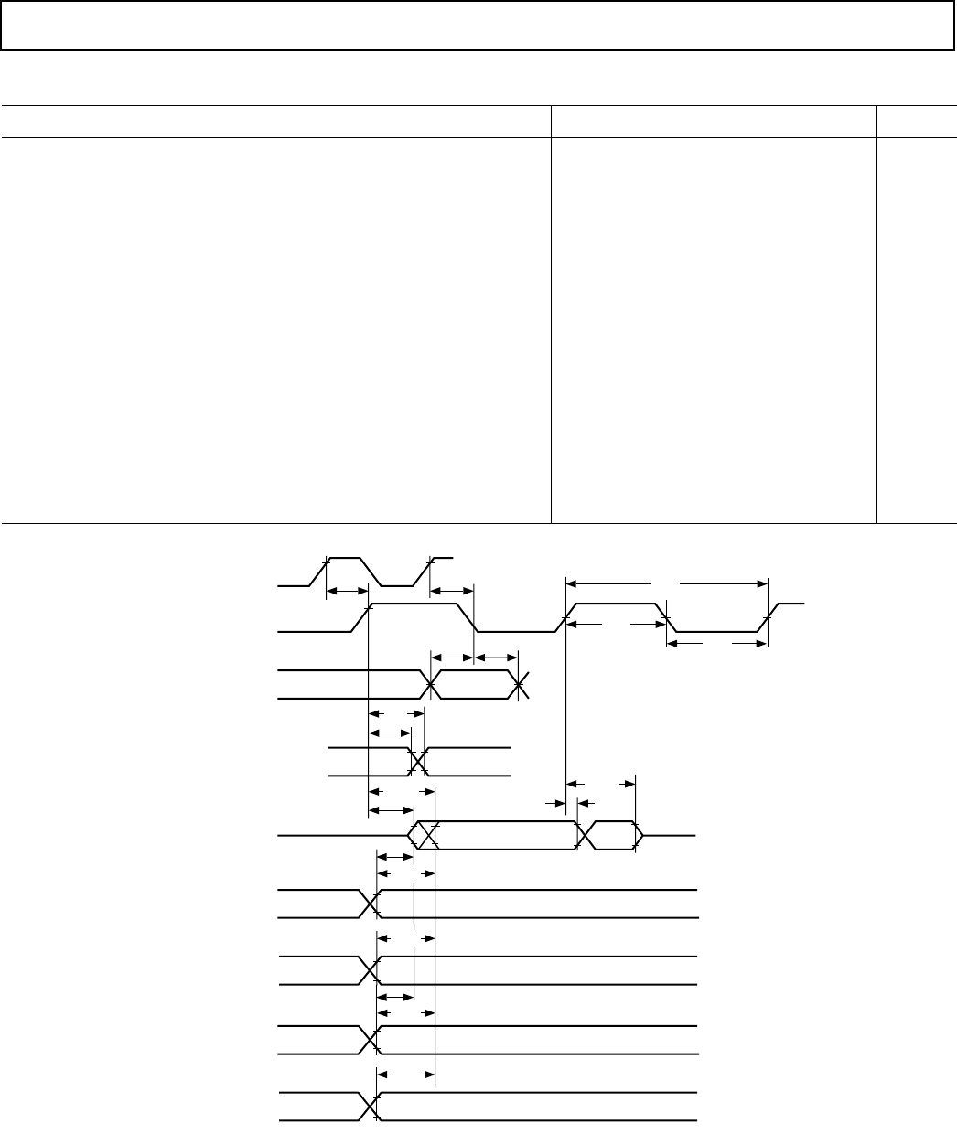
ADSP-2186
–21–
REV. B
TIMING PARAMETERS
Parameter Min Max Unit
Serial Ports
Timing Requirements:
t
SCK
SCLK Period 50 ns
t
SCS
DR/TFS/RFS Setup before SCLK Low 4 ns
t
SCH
DR/TFS/RFS Hold after SCLK Low 8 ns
t
SCP
SCLK
IN
Width 20 ns
Switching Characteristics:
t
CC
CLKOUT High to SCLK
OUT
0.25 t
CK
0.25 t
CK
+ 10 ns
t
SCDE
SCLK High to DT Enable 0 ns
t
SCDV
SCLK High to DT Valid 15 ns
t
RH
TFS/RFS
OUT
Hold after SCLK High 0 ns
t
RD
TFS/RFS
OUT
Delay from SCLK High 15 ns
t
SCDH
DT Hold after SCLK High 0 ns
t
TDE
TFS (Alt) to DT Enable 0 ns
t
TDV
TFS (Alt) to DT Valid 14 ns
t
SCDD
SCLK High to DT Disable 15 ns
t
RDV
RFS
(Multichannel, Frame Delay Zero) to DT Valid 15 ns
CLKOUT
SCLK
TFS
OUT
RFS
OUT
DT
ALTERNATE
FRAME MODE
t
CC
t
CC
t
SCS
t
SCH
t
RH
t
SCDE
t
SCDH
t
SCDD
t
TDE
t
RDV
MULTICHANNEL MODE,
FRAME DELAY 0
(MFD = 0)
DR
TFS
IN
RFS
IN
RFS
OUT
TFS
OUT
t
TDV
t
SCDV
t
RD
t
SCP
t
SCK
t
SCP
TFS
IN
RFS
IN
ALTERNATE
FRAME MODE
t
RDV
MULTICHANNEL MODE,
FRAME DELAY 0
(MFD = 0)
t
TDV
t
TDE
Figure 16. Serial Ports
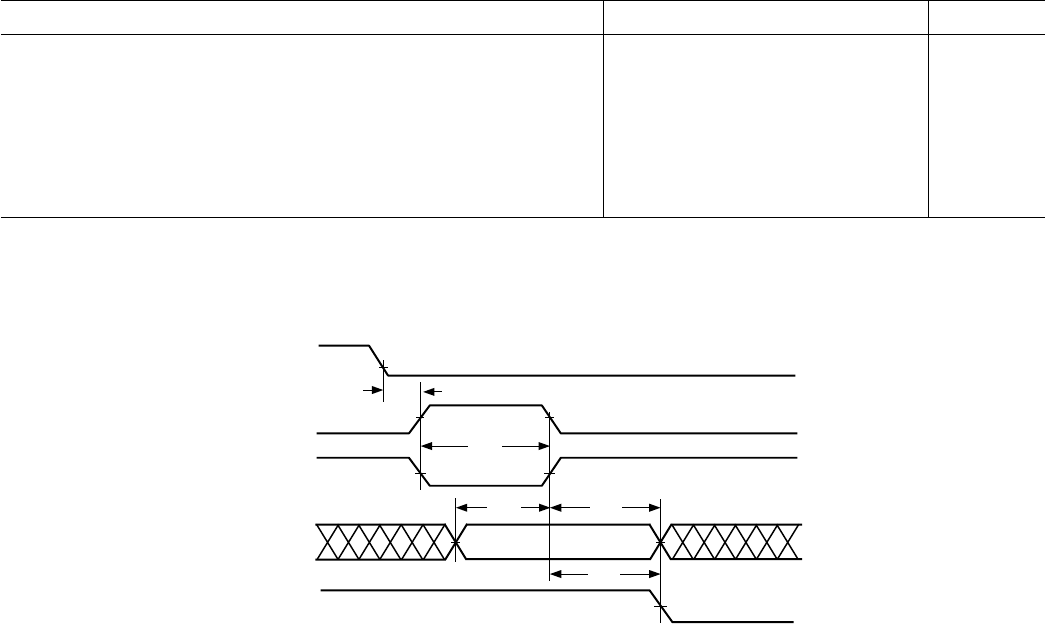
ADSP-2186
–22– REV. B
Parameter Min Max Unit
IDMA Address Latch
Timing Requirements:
t
IALP
Duration of Address Latch
1, 2
10 ns
t
IASU
IAD15–0 Address Setup before Address Latch End
2
5ns
t
IAH
IAD15–0 Address Hold after Address Latch End
2
3ns
t
IKA
IACK Low before Start of Address Latch
1, 2
0ns
t
IALS
Start of Write or Read after Address Latch End
2, 3
3ns
NOTES
1
Start of Address Latch = IS Low and IAL High.
2
End of Address Latch = IS High or IAL Low.
3
Start of Write or Read = IS Low and IWR Low or IRD Low.
tIKA
IAD15–0
IACK
IAL
IS
IRD OR
IWR
tIALP
tIASU tIAH
tIALS
Figure 17. IDMA Address Latch
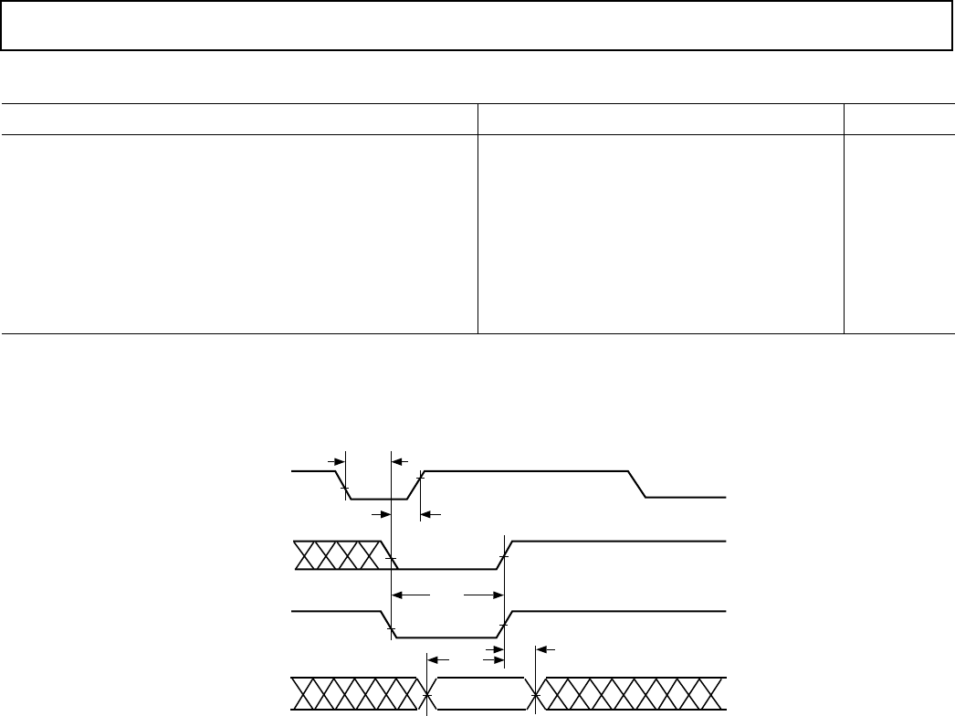
ADSP-2186
–23–
REV. B
TIMING PARAMETERS
Parameter Min Max Unit
IDMA Write, Short Write Cycle
Timing Requirements:
t
IKW
IACK Low before Start of Write
1
0ns
t
IWP
Duration of Write
1, 2
15 ns
t
IDSU
IAD15–0 Data Setup before End of Write
2, 3, 4
5ns
t
IDH
IAD15–0 Data Hold after End of Write
2, 3, 4
2ns
Switching Characteristics:
t
IKHW
Start of Write to IACK High 15 ns
NOTES
1
Start of Write = IS Low and IWR Low.
2
End of Write = IS High or IWR High.
3
If Write Pulse ends before IACK Low, use specifications t
IDSU
, t
IDH
.
4
If Write Pulse ends after IACK Low, use specifications t
IKSU
, t
IKH
.
IAD15–0DATA
tIKHW
tIKW
tIDSU
IACK
tIWP
tIDH
IS
IWR
Figure 18. IDMA Write, Short Write Cycle
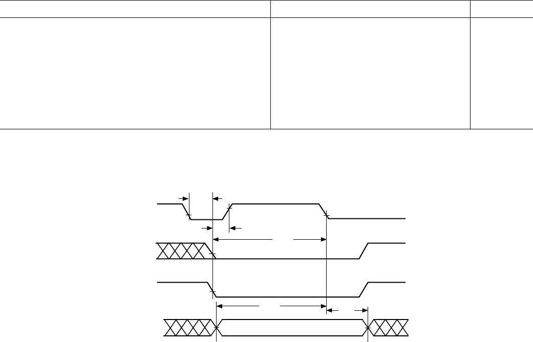
ADSP-2186
–24– REV. B
Parameter Min Max Unit
IDMA Write, Long Write Cycle
Timing Requirements:
t
IKW
IACK Low before Start of Write
1
0ns
t
IKSU
IAD15–0 Data Setup before IACK Low
2, 3, 4
0.5 t
CK
+ 10 ns
t
IKH
IAD15–0 Data Hold after IACK Low
2, 3, 4
2ns
Switching Characteristics:
t
IKLW
Start of Write to IACK Low
4
1.5 t
CK
ns
t
IKHW
Start of Write to IACK High 15 ns
NOTES
1
Start of Write = IS Low and IWR Low.
2
If Write Pulse ends before IACK Low, use specifications t
IDSU
, t
IDH
.
3
If Write Pulse ends after IACK Low, use specifications t
IKSU
, t
IKH
.
4
This is the earliest time for IACK Low from Start of Write. For IDMA Write cycle relationships, please refer to the ADSP-218x DSP Hardware Reference.
IAD15–0DATA
tIKHW
tIKW
IACK
IS
IWR
tIKLW
tIKH
tIKSU
Figure 19. IDMA Write, Long Write Cycle
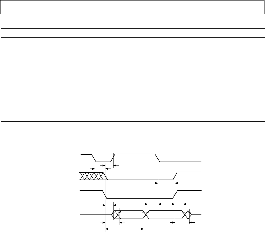
ADSP-2186
–25–
REV. B
TIMING PARAMETERS
Parameter Min Max Unit
IDMA Read, Long Read Cycle
Timing Requirements:
t
IKR
IACK Low before Start of Read
1
0ns
t
IRK
End Read after IACK Low
2
2ns
Switching Characteristics:
t
IKHR
IACK High after Start of Read
1
15 ns
t
IKDS
IAD15–0 Data Setup before IACK Low 0.5 t
CK
– 10 ns
t
IKDH
IAD15–0 Data Hold after End of Read
2
0ns
t
IKDD
IAD15–0 Data Disabled after End of Read
2
10 ns
t
IRDE
IAD15–0 Previous Data Enabled after Start of Read 0 ns
t
IRDV
IAD15–0 Previous Data Valid after Start of Read 15 ns
t
IRDH1
IAD15–0 Previous Data Hold after Start of Read (DM/PM1)
3
2 t
CK
– 5 ns
t
IRDH2
IAD15–0 Previous Data Hold after Start of Read (PM2)
4
t
CK
– 5 ns
NOTES
1
Start of Read = IS Low and IRD Low.
2
End of Read = IS High or IRD High.
3
DM read or first half of PM read.
4
Second half of PM read.
t
IKR
PREVIOUS
DATA
READ
DATA
t
IKHR
t
IKDS
t
IRDV
t
IRDH
t
IKDD
t
IRDE
t
IKDH
IAD15–0
IACK
IS
IRD
t
IRK
Figure 20. IDMA Read, Long Read Cycle
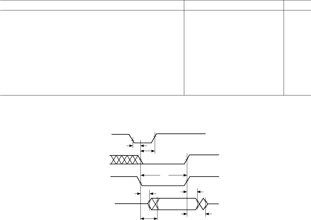
ADSP-2186
–26– REV. B
Parameter Min Max Unit
IDMA Read, Short Read Cycle
Timing Requirements:
t
IKR
IACK Low before Start of Read
1
0ns
t
IRP1
Duration of Read (DM, PM1)
2
15 2 t
CK
– 5 ns
t
IRP2
Duration of Read (PM2)
3
15 t
CK
– 5 ns
Switching Characteristics:
t
IKHR
IACK High after Start of Read
1
15 ns
t
IKDH
IAD15–0 Data Hold after End of Read
4
0ns
t
IKDD
IAD15–0 Data Disabled after End of Read
4
10 ns
t
IRDE
IAD15–0 Previous Data Enabled after Start of Read 0 ns
t
IRDV
IAD15–0 Previous Data Valid after Start of Read 15 ns
NOTES
1
Start of Read = IS Low and IRD Low.
2
DM Read or First Half of PM Read.
3
Second Half of PM Read.
4
End of Read = IS High or IRD High.
t
IRP
t
IKR
PREVIOUS
DATA
t
IKHR
t
IRDV
t
IKDD
t
IRDE
t
IKDH
IAD15–0
IACK
IS
IRD
Figure 21. IDMA Read, Short Read Cycle
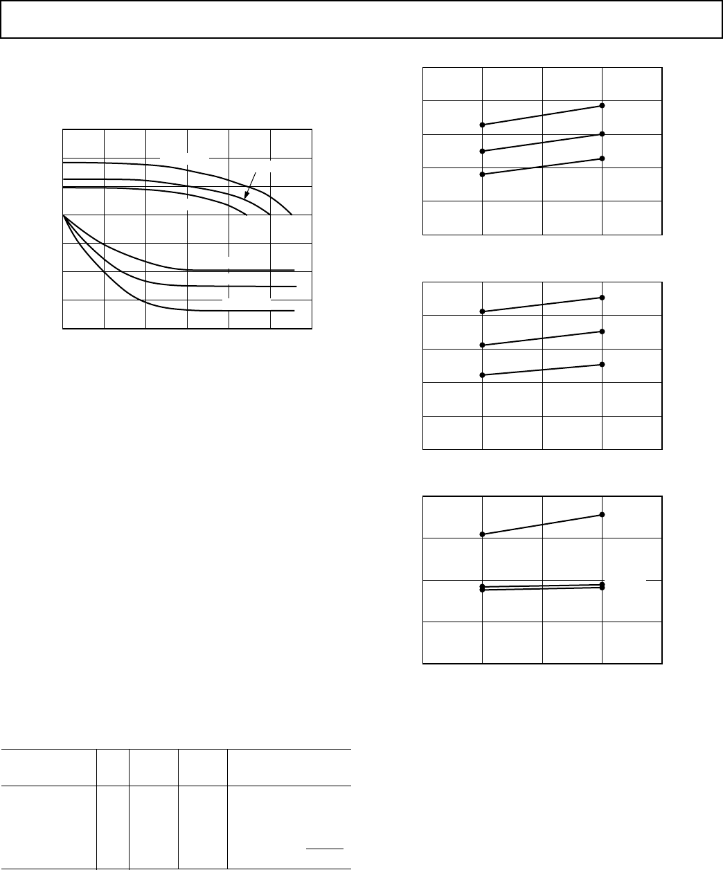
ADSP-2186
–27–
REV. B
OUTPUT DRIVE CURRENTS
Figure 22 shows typical I-V characteristics for the output drivers
of the ADSP-2186. The curves represent the current drive
capability of the output drivers as a function of output voltage.
SOURCE VOLTAGE – Volts
60
40
–60
061
SOURCE CURRENT – mA
2345
20
0
–20
–40
–80
5.5V, –40ⴗC
VOH
5.0V, +25ⴗC
4.5V, +85ⴗC
4.5V, +85ⴗC
5.0V, +25ⴗC
5.5V, –40ⴗC
VOL
Figure 22. Typical Drive Currents
POWER DISSIPATION
To determine total power dissipation in a specific application,
the following equation should be applied for each output:
C × V
DD2
× f
C = load capacitance, f = output switching frequency.
Example
In an application where external data memory is used and no
other outputs are active, power dissipation is calculated as follows:
Assumptions
• External data memory is accessed every cycle with 50% of the
address pins switching.
• External data memory writes occur every other cycle with
50% of the data pins switching.
• Each address and data pin has a 10 pF total load at the pin.
• The application operates at V
DD
= 5.0 V and t
CK
= 30 ns.
Total Power Dissipation = P
INT
+ (C × V
DD2
× f)
P
INT
= internal power dissipation from Power vs. Frequency
graph (Figure 23).
(C × V
DD2
× f) is calculated for each output:
# of
Pins ⴛ Cⴛ V
DD2
ⴛf
Address 7 × 10 pF × 5
2
V × 20 MHz = 35 mW
Data Output, WR 9× 10 pF × 5
2
V × 20 MHz = 45 mW
RD 1× 10 pF × 5
2
V × 20 MHz = 5 mW
CLKOUT, DMS 2× 10 pF × 5
2
V × 40 MHz = 20 mW
105 mW
Total power dissipation for this example is PINT + 105 mW.
80
20
0
60
40
POWER (P
IDLE
n) – mW
1/tcyc – MHz
33.33 40
IDLE (16)
IDLE (128)
IDLE
POWER, IDLE n MODES
2
0
80
40
20
60
POWER (P
IDLE
) – mW
1/tcyc – MHz
33.33 40
V
DD
= 5.5V
V
DD
= 5.0V
V
DD
= 4.5V
POWER, IDLE
1,2,4
100
1/tcyc – MHz
4033.33
100
300
200
500
400
POWER (P
INT
) – mW
0
V
DD
= 5.5V
V
DD
= 5.0V
V
DD
= 4.5V
2186 POWER, INTERNAL
1,2,3
385mW
300mW
225mW
330mW
250mW
180mW
91.5mW
70.5mW
52mW
82mW
62mW
45mW
70.5mW
36.6mW
34.3mW
62mW
34.7mW
32.8mW
POWER REFLECTS DEVICE OPERATING WITH NO OUTPUT LOADS.
TYPICAL POWER DISSIPATION AT 5.0V V
DD
AND T
A
= +25ⴗC EXCEPT WHERE SPECIFIED.
I
DD
MEASUREMENT TAKEN WITH ALL INSTRUCTIONS EXECUTING FROM INTERNAL
MEMORY. 50% OF THE INSTRUCTIONS ARE MULTIFUNCTION (TYPES 1, 4, 5, 12, 13, 14),
30% ARE TYPE 2 AND TYPE 6, AND 20% ARE IDLE INSTRUCTIONS.
IDLE REFERS TO ADSP-2186 STATE OF OPERATION DURING EXECUTION OF IDLE
INSTRUCTION. DEASSERTED PINS ARE DRIVEN TO EITHER V
DD
OR GND.
1
4
2
3
VALID FOR ALL TEMPERATURE GRADES.
Figure 23. Power vs. Frequency
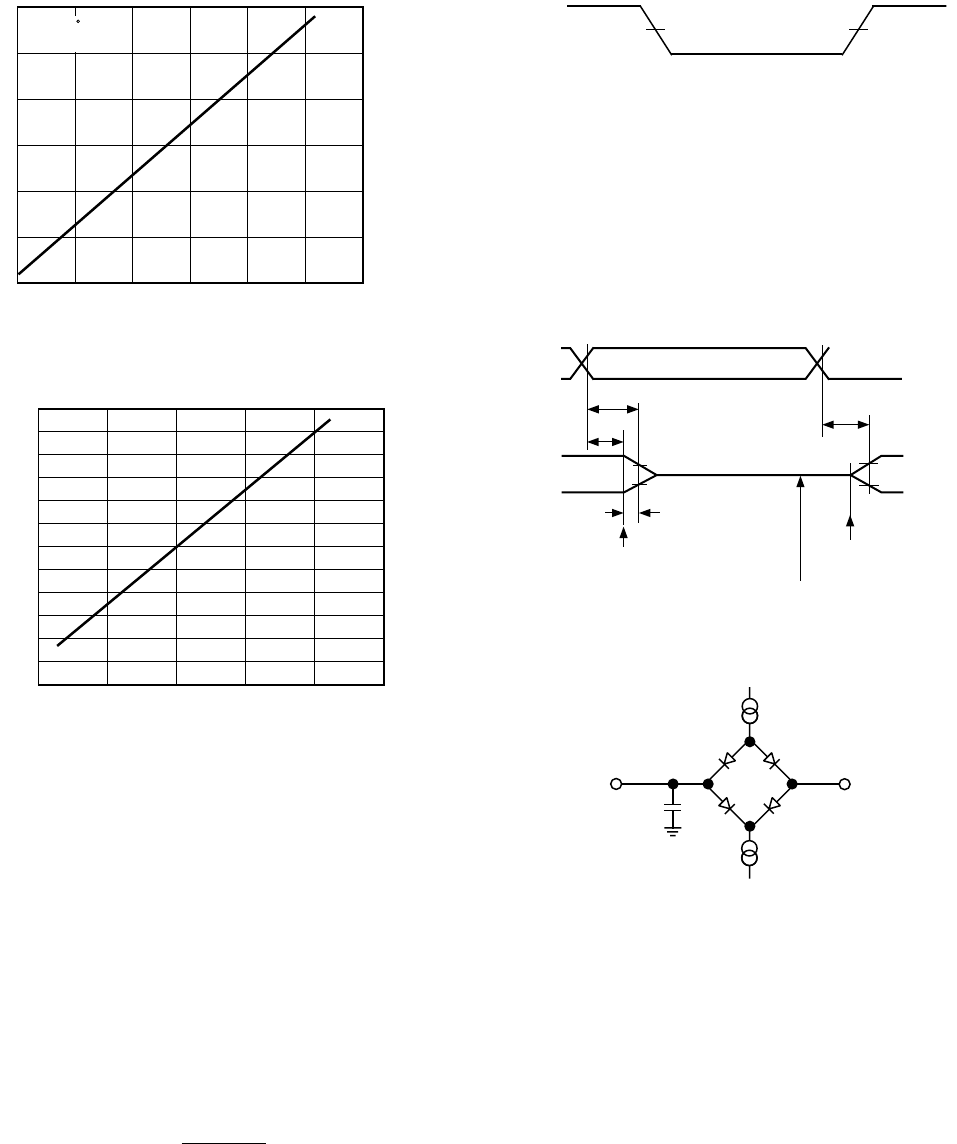
ADSP-2186
–28– REV. B
CAPACITIVE LOADING
Figures 24 and 25 show the capacitive loading characteristics of
the ADSP-2186.
CL – pF
RISE TIME (0.4V–2.4V) – ns
30
3000 50 100 150 200 250
25
15
10
5
0
20
T = +85 C
VDD = 4.5V
Figure 24. Typical Output Rise Time vs. Load Capacitance,
C
L
(at Maximum Ambient Operating Temperature)
C
L
– pF
14
0
VALID OUTPUT DELAY OR HOLD – ns
50 100 150 250200
12
4
2
–2
10
8
NOMINAL
16
18
6
–4
–6
Figure 25. Typical Output Valid Delay or Hold vs. Load
Capacitance, C
L
(at Maximum Ambient Operating
Temperature)
TEST CONDITIONS
Output Disable Time
Output pins are considered to be disabled when they have
stopped driving and started a transition from the measured
output high or low voltage to a high impedance state. The out-
put disable time (t
DIS
) is the difference of t
MEASURED
and t
DECAY
,
as shown in the Output Enable/Disable diagram. The time is the
interval from when a reference signal reaches a high or low
voltage level to when the output voltages have changed by 0.5 V
from the measured output high or low voltage. The decay time,
t
DECAY
, is dependent on the capacitive load, C
L
, and the current
load, i
L
, on the output pin. It can be approximated by the fol-
lowing equation:
tDECAY =CL×0.5 V
iL
from which
t
DIS
= t
MEASURED
– t
DECAY
is calculated. If multiple pins (such as the data bus) are dis-
abled, the measurement value is that of the last pin to stop
driving.
1.5V
INPUT
OR
OUTPUT
1.5V
Figure 26. Voltage Reference Levels for AC Measure-
ments (Except Output Enable/Disable)
Output Enable Time
Output pins are considered to be enabled when that have made
a transition from a high-impedance state to when they start
driving. The output enable time (t
ENA
) is the interval from when
a reference signal reaches a high or low voltage level to when the
output has reached a specified high or low trip point, as shown
in the Output Enable/Disable diagram. If multiple pins (such as
the data bus) are enabled, the measurement value is that of the
first pin to start driving.
2.0V
1.0V
tENA
REFERENCE
SIGNAL
OUTPUT
tDECAY
VOH
(MEASURED)
OUTPUT STOPS
DRIVING
OUTPUT STARTS
DRIVING
tDIS
tMEASURED
VOL
(MEASURED)
VOH (MEASURED) – 0.5V
VOL (MEASURED) + 0.5V
HIGH-IMPEDANCE STATE. TEST CONDITIONS CAUSE
THIS VOLTAGE LEVEL TO BE APPROXIMATELY 1.5V.
VOH
(MEASURED)
VOL
(MEASURED)
Figure 27. Output Enable/Disable
TO
OUTPUT
PIN
50pF
+1.5V
IOH
IOL
Figure 28. Equivalent Device Loading for AC Measure-
ments (Including All Fixtures)
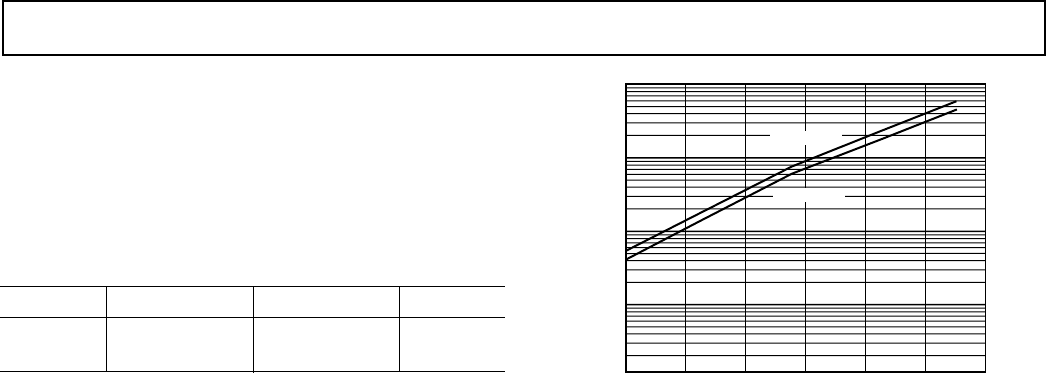
ADSP-2186
–29–
REV. B
ENVIRONMENTAL CONDITIONS
Ambient Temperature Rating:
T
AMB
=T
CASE
– (PD x θ
CA
)
T
CASE
= Case Temperature in °C
PD = Power Dissipation in W
θ
CA
= Thermal Resistance (Case-to-Ambient)
θ
JA
= Thermal Resistance (Junction-to-Ambient)
θ
JC
= Thermal Resistance (Junction-to-Case)
Package
JA
JC
CA
LQFP 50°C/W 2°C/W 48°C/W
Mini-BGA 70.7°C/W 7.4°C/W 63.3°C/W
0
TEMPERATURE – ⴗC
10
IDD – A
1
100
1k
10k
20 40 80 100
VDD @ 5.6V
VDD @ 5.0V
60 120
Figure 29. Power-Down Supply Current

ADSP-2186
–30– REV. B
100-Lead LQFP Package Pinout
5
4
3
2
7
6
9
8
1
D19
D18
D17
D16
IRQE+PF4
IRQL0+PF5
GND
IRQL1+PF6
DT0
TFS0
SCLK0
VDD
DT1/FO
TFS1/IRQ1
RFS1/IRQ0
DR1/FI
GND
SCLK1
ERESET
RESET
D15
D14
D13
D12
GND
D11
D10
D9
VDD
GND
D8
D7/IWR
D6/IRD
D5/IAL
D4/IS
GND
VDD
D3/IACK
D2/IAD15
D1/IAD14
D0/IAD13
BG
EBG
BR
EBR
A4/IAD3
A5/IAD4
GND
A6/IAD5
A7/IAD6
A8/IAD7
A9/IAD8
A10/IAD9
A11/IAD10
A12/IAD11
A13/IAD12
GND
CLKIN
XTAL
VDD
CLKOUT
GND
VDD
WR
RD
BMS
DMS
PMS
IOMS
CMS
71
72
73
74
69
70
67
68
65
66
75
60
61
62
63
58
59
56
57
54
55
64
52
53
51
100
99
98
97
96
95
94
93
92
91
90
89
88
87
86
85
84
83
82
81
80
79
78
77
76
PIN 1
IDENTIFIER
TOP VIEW
(Not to Scale)
26
27
28
29
30
31
32
33
34
35
36
37
38
39
40
41
42
43
44
45
46
47
48
49
50
11
10
16
15
14
13
18
17
20
19
22
21
12
24
23
25
ADSP-2186
IRQ2+PF7
RFS0
DR0
EMS
EE
ELOUT
ECLK
ELIN
EINT
A3/IAD2
A2/IAD1
A1/IAD0
A0
PWDACK
BGH
FL0
FL1
FL2
D23
D22
D21
D20
GND
PF1 [MODE B]
GND
PWD
VDD
PF0 [MODE A]
PF2 [MODE C]
PF3

ADSP-2186
–31–
REV. B
LQFP Pin Configurations
LQFP Pin LQFP Pin LQFP Pin LQFP Pin
Number Name Number Name Number Name Number Name
1 A4/IAD3 26 IRQE + PF4 51 EBR 76 D16
2 A5/IAD4 27 IRQL0 + PF5 52 BR 77 D17
3GND28GND53EBG 78 D18
4 A6/IAD5 29 IRQL1 + PF6 54 BG 79 D19
5 A7/IAD6 30 IRQ2 + PF7 55 D0/IAD13 80 GND
6 A8/IAD7 31 DT0 56 D1/IAD14 81 D20
7 A9/IAD8 32 TFS0 57 D2/IAD15 82 D21
8 A10/IAD9 33 RFS0 58 D3/IACK 83 D22
9 A11/IAD10 34 DR0 59 VDD 84 D23
10 A12/IAD11 35 SCLK0 60 GND 85 FL2
11 A13/IAD12 36 VDD 61 D4/IS 86 FL1
12 GND 37 DT1/FO 62 D5/IAL 87 FL0
13 CLKIN 38 TFS1/IRQ1 63 D6/IRD 88 PF3
14 XTAL 39 RFS1/IRQ0 64 D7/IWR 89 PF2 [Mode C]
15 VDD 40 DR1/FI 65 D8 90 VDD
16 CLKOUT 41 GND 66 GND 91 PWD
17 GND 42 SCLK1 67 VDD 92 GND
18 VDD 43 ERESET 68 D9 93 PF1 [Mode B]
19 WR 44 RESET 69 D10 94 PF0 [Mode A]
20 RD 45 EMS 70 D11 95 BGH
21 BMS 46 EE 71 GND 96 PWDACK
22 DMS 47 ECLK 72 D12 97 A0
23 PMS 48 ELOUT 73 D13 98 A1/IAD0
24 IOMS 49 ELIN 74 D14 99 A2/IAD1
25 CMS 50 EINT 75 D15 100 A3/IAD2
The ADSP-2186 package pinout is shown in the table below. Pin names in bold text replace the plain text named functions when
Mode C = 1. A + sign separates two functions when either function can be active for either major I/O mode. Signals enclosed in
brackets [ ] are state bits latched from the value of the pin at the deassertion of RESET.

ADSP-2186
–32– REV. B
ADSP-2186 Mini-BGA (CA) Package Pinout
Bottom View
121110987654321
A
B
C
D
E
F
G
H
J
K
L
M
GND GND D22 NC NC NC GND NC A0 GND A1/IAD0 A2/IAD1
D16 D17 D18 D20 D23 VDD GND NC NC GND A3/IAD2 A4/IAD3
D14 NC D15 D19 D21 VDD PWD A7/IAD6 A5/IAD4 RD A6/IAD5 PWDACK
GND NC D12 D13 NC PF2
[MODE C]
PF1
[MODE B] A9/IAD8 BGH NC WR NC
D10 GND VDD GND GND PF3 FL2 PF0
[MODE A] FL0 A8/IAD7 VDD VDD
D9 NC D8 D11 D7/IWR NC NC FL1 A11/
IAD10
A12/
IAD11 NC A13/
IAD12
D4/ IS NC NC D5/IAL D6/IRD NC NC NC A10/IAD9 GND NC XTAL
GND NC GND D3/IACK D2/IAD15 TFS0 DT0 VDD GND GND GND CLKIN
VDD VDD D1/IAD14 BG RFS1/
IRQ0 D0/IAD13 SCLK0 VDD VDD NC VDD CLKOUT
EBG BR EBR ERESET SCLK1 TFS1/
IRQ1 RFS0 DMS BMS NC NC NC
EINT ELOUT ELIN RESET GND DR0 PMS GND IOMS
IRQL1
+
PF6
NC
ECLK EE EMS NC GND DR1/FI DT1/FO GND CMS NC
IRQ2
+
PF7
IRQL0
+
PF5
IRQE
+
PF4

ADSP-2186
–33–
REV. B
The ADSP-2186 Mini-BGA package pinout is shown in the table below. Pin names in bold text replace the plain text named func-
tions when Mode C = 1. A + sign separates two functions when either function can be active for either major I/O mode. Signals
enclosed in brackets [ ] are state bits latched from the value of the pin at the deassertion of RESET.
Mini-BGA Package Pinout
Ball # Name Ball # Name Ball # Name Ball # Name
A01 A2/IAD1 D01 N/C G01 XTAL K01 N/C
A02 A1/IAD0 D02 WR G02 N/C K02 N/C
A03 GND D03 N/C G03 GND K03 N/C
A04 A0 D04 BGH G04 A10/IAD9 K04 BMS
A05 N/C D05 A9/IAD8 G05 N/C K05 DMS
A06 GND D06 PF1[MODE B] G06 N/C K06 RFS0
A07 N/C D07 PF2[MODE C] G07 N/C K07 TFS1/IRQ1
A08 N/C D08 N/C G08 D6/IRD K08 SCLK1
A09 N/C D09 D13 G09 D5/IAL K09 ERESET
A10 D22 D10 D12 G10 N/C K10 EBR
A11 GND D11 N/C G11 N/C K11 BR
A12 GND D12 GND G12 D4/IS K12 EBG
B01 A4/IAD3 E01 VDD H01 CLKIN L01 IRQE+PF4
B02 A3/IAD2 E02 VDD H02 GND L02 N/C
B03 GND E03 A8/IAD7 H03 GND L03 IRQL1+PF6
B04 N/C E04 FL0 H04 GND L04 IOMS
B05 N/C E05 PF0[MODE A] H05 VDD L05 GND
B06 GND E06 FL2 H06 DT0 L06 PMS
B07 VDD E07 PF3 H07 TFS0 L07 DR0
B08 D23 E08 GND H08 D2/IAD15 L08 GND
B09 D20 E09 GND H09 D3/IACK L09 RESET
B10 D18 E10 VDD H10 GND L10 ELIN
B11 D17 E11 GND H11 N/C L11 ELOUT
B12 D16 E12 D10 H12 GND L12 EINT
C01 PWDACK F01 A13/IAD12 J01 CLKOUT M01 IRQL0+PF5
C02 A6/IAD5 F02 N/C J02 VDD M02 IRQ2+PF7
C03 RD F03 A12/IAD11 J03 N/C M03 N/C
C04 A5/IAD4 F04 A11/IAD10 J04 VDD M04 CMS
C05 A7/IAD6 F05 FL1 J05 VDD M05 GND
C06 PWD F06 N/C J06 SCLK0 M06 DT1/FO
C07 VDD F07 N/C J07 D0/IAD13 M07 DR1/FI
C08 D21 F08 D7/IWR J08 RFS1/IRQ0 M08 GND
C09 D19 F09 D11 J09 BG M09 N/C
C10 D15 F10 D8 J10 D1/IAD14 M10 EMS
C11 N/C F11 N/C J11 VDD M11 EE
C12 D14 F12 D9 J12 VDD M12 ECLK
ADSP-2186
–34– REV. B
100-Lead Metric Thin Plastic Quad Flatpack (LQFP)
(ST-100)
TOP VIEW
(PINS DOWN)
1
25
26
51
50
75
76100
16.20
16.00 SQ
15.80
14.05
14.00 SQ
13.95
12.00
BSC
0.50 BSC
LEAD PITCH
0.27
0.22 TYP
0.17
LEAD WIDTH
7ⴗ
0ⴗ
1.60 MAX
SEATING
PLANE
12ⴗ
TYP
0.75
0.60 TYP
0.50
0.08
MAX LEAD
COPLANARITY 10ⴗ
6ⴗ
2ⴗ
0.15
0.05
NOTE:
THE ACTUAL POSITION OF EACH LEAD IS WITHIN 0.08 FROM ITS IDEAL
POSITION WHEN MEASURED IN THE LATERAL DIRECTION.
OUTLINE DIMENSIONS
Dimensions shown in millimeters.
ADSP-2186
–35–
REV. B
OUTLINE DIMENSIONS
Dimensions shown in millimeters.
144-Ball Mini-BGA
(CA-144)
SEATING
PLANE
1.00
0.85
DETAIL A
0.55
0.50
0.45
BALL DIAMETER
0.12
MAX
0.40
0.25
1.40
MAX
DETAIL A
0.80
BSC
8.80
BSC
0.80 BSC
8.80 BSC
A
B
C
D
E
F
G
H
J
K
L
M
12 11 10 9 8 7 6 5 4 3 2 1
TOP VIEW
10.10
10.00 SQ
9.90
10.10
10.00 SQ
9.90
NOTES:
THE ACTUAL POSITION OF THE BALL
POPULATION IS WITHIN 0.150 OF ITS
IDEAL POSITION RELATIVE TO THE
PACKAGE EDGES.
THE ACTUAL POSITION OF EACH BALL
IS WITHIN 0.08 OF ITS IDEAL POSITION
RELATIVE TO THE BALL POPULATION.
1.
2.
ORDERING GUIDE
Ambient Instruction
Temperature Rate Package Package
Part Number Range (MHz) Description Option*
ADSP-2186KST-115 0°C to 70°C 28.8 100-Lead LQFP ST-100
ADSP-2186BST-115 –40°C to +85°C 28.8 100-Lead LQFP ST-100
ADSP-2186KST-133 0°C to 70°C 33.3 100-Lead LQFP ST-100
ADSP-2186BST-133 –40°C to +85°C 33.3 100-Lead LQFP ST-100
ADSP-2186KST-160 0°C to 70°C 40.0 100-Lead LQFP ST-100
ADSP-2186BST-160 –40°C to +85°C 40.0 100-Lead LQFP ST-100
ADSP-2186BCA-160 –40°C to +85°C 40.0 144-Ball Mini-BGA CA-144
*ST = Plastic Thin Quad Flatpack (LQFP); CA = Mini-BGA.
–36–
C00190b–2.5–3/01(B)
PRINTED IN U.S.A.
