ADV1000
User Manual: ADV1000
Open the PDF directly: View PDF ![]() .
.
Page Count: 88
- ADV-1000
- COVER
- SPECIFICATIONS
- DIAGNOSTICS OF OPTICAL PICKUP AND REPLACING TRAVERSE UNIT
- DISASSEMBLY
- TRAVERSE UNIT DISASSEMBLY
- TROUBLESHOOTING
- BLOCK DIAGRAM
- LEVEL DIAGRAMS
- CLOCK FLOW
- SEMICONDUCTORS
- PRINTED WIRING BOARDS
- NOTE FOR PARTS LIST
- PARTS LIST OF P.W.B. UNIT ASS'Y
- EXPLODED VIEW OF CABINET
- PARTS LIST OF EXPLODED VIEW
- EXPLODED VIEW OF DVD MECHANISM
- PARTS LIST OF DVD MECHANISM UNIT
- POINTS OF GREASING
- PACKING VIEW/PARTS LIST OF PACKING & ACCESSORIES
- MEASURING METHOD AND WAVEFORMS
- WAVEFORMS
- WIRING DIAGRAM
- SCHEMATIC DAIGRAMS
- (1/10) 1U-3435-3 DSP/AUDIO (1/4)/AUDIO Section
- (2/10) 1U-3435-3 DSP/AUDIO (2/4)/DSP Section
- (3/10) 1U-3434-1 AMP UNIT
- (4/10) 1U-3435-3 DSP/AUDIO (3/4)/uCOM Section
- (5/10) 1U-3435-3 DSP/AUDIO UNIT (4/4)/DAC Section
- (6/10) 1U-3434-2 P. SUPPLY UNIT/1U-3434-3 SCART UNIT
- (7/10) 1U-3435-1 DISPLAY UNIT/1U-3435-2 H/P UNIT
- (8/10) 1U-3443-1 VIDEO UNIT
- (9/10) GU-3430 DVD MAIN UNIT (1/2)
- (10/10) GU-3430 DVD MAIN UNIT (2/2)
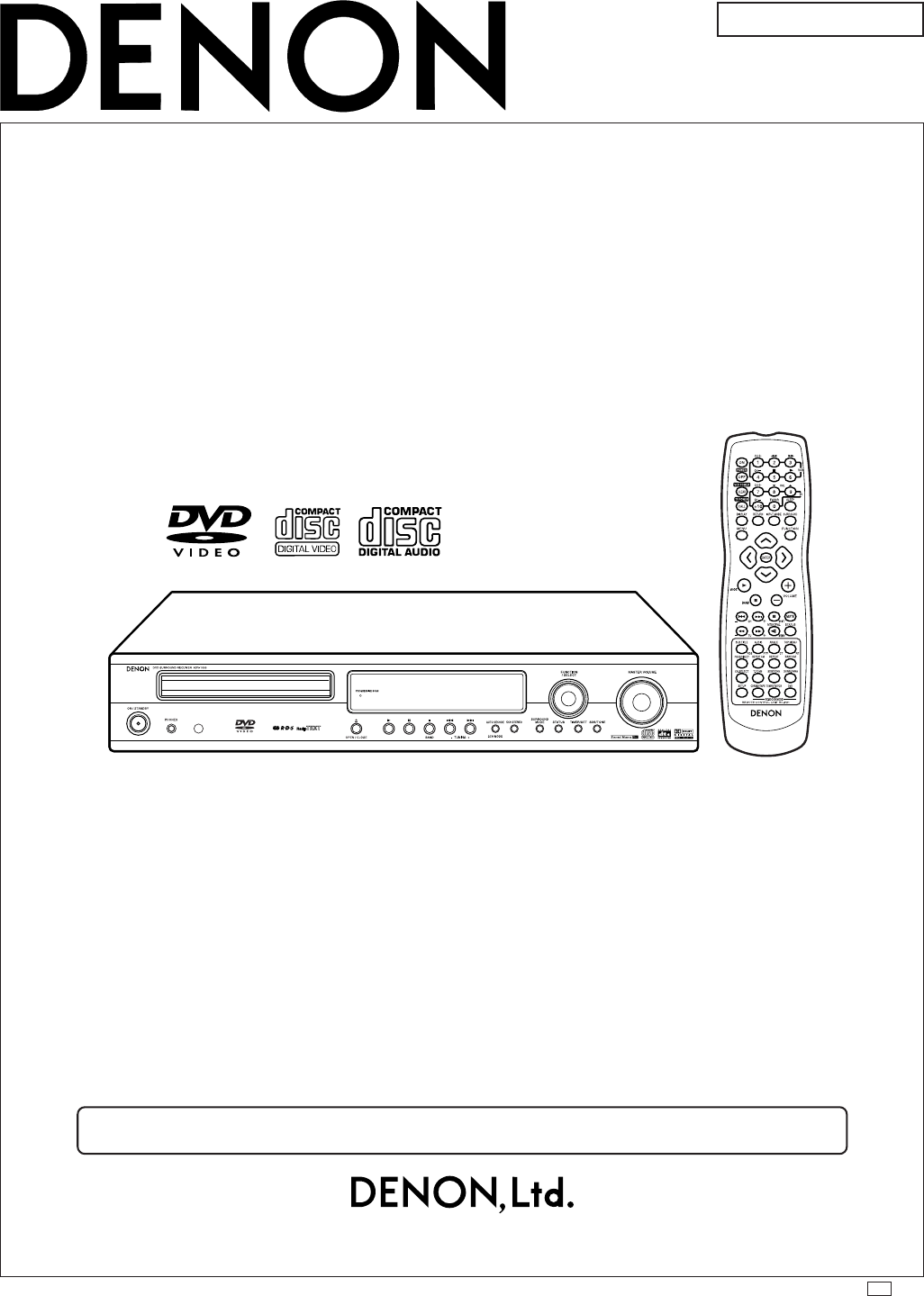
Hi-Fi Component
SERVICE MANUAL
MODEL
ADV-1000
DVD SURROUND RECEIVER
Some illustrations using in this service manual are slightly different from the actual set.
16-11, YUSHIMA 3-CHOME, BUNKYOU-KU, TOKYO 113-0034 JAPAN
Telephone: 03 (3837) 5321
For Europe model
X0146 NC 0207

ADV-1000
2
SPECIFICATIONS
Audio section
• Power amplifier
Output power: Front: 55 W + 55 W (6 Ω/ohms, 1 kHz with 10% T.H.D.)
Center: 55 W (6 Ω/ohms, 1 kHz with 10% T.H.D.)
Surround: 55 W + 55 W (6 Ω/ohms, 1 kHz with 10% T.H.D.)
Subwoofer: 55 W (6 Ω/ohms, 60 Hz with 10% T.H.D.)
Output terminals:
Front, Center, Subwoofer, Surround:
6 ~16 Ω/ohms
• Analog
Input sensitivity / input impedance: 200 mV / 47 kΩ/kohms
Frequency response: 10 Hz ~ 60 kHz: +1.5, −3 dB (DIRECT mode)
S / N : 94 dB (DIRECT mode)
Rated output: 1.2 V (Subwoofer preout, 20 Hz)
• Digital
Digital input / output: Format Digital audio interface
Video section
• Standard video jacks
Input / output level and inpedance: 1 Vp-p, 75 Ω/ohms
• S-video jacks
Input / output level and inpedance: Y (brightness) signal 1 Vp-p, 75 Ω/ohms
C (color) signal 0.3 Vp-p, 75 Ω/ohms
• AV1 connector
Video output: 1Vp-p, 75Ω/ohms
S-video output: Y (brightness) signal 1 Vp-p, 75 Ω/ohms
C (color) signal 0.3 Vp-p, 75 Ω/ohms
RGB output (DVD only): R/G/B signal 0.7 Vp-p, 75 Ω/ohms
Audio output: L/R (Fixed output)
Tuner section
[FM]
(note: µV at 75 Ω/ohms, 0 dBf=1×10-15 W)
[AM]
Receiving Range: 87.50 MHz~108.00 MHz 522 kHz~1611 kHz
Usable Sensitivity: 1.5 µV (14.8 dBf) 20 µV
DVD section
Signal Format: NTSC/PAL
Applicable discs: (1) DVD-Video discs
1-layer 12 cm single-sided discs, 2-layer 12 cm single-sided discs,
2-layer 12cm double-sided discs (1 layer per side)
1-layer 8 cm single-sided discs, 2-layer 8 cm single-sided discs,
2-layer 8 cm double-sided discs (1 layer per side)
(2) Compact discs (CD-DA, Video CD)
12 cm discs, 8 cm discs
Audio output: Fixed output level: 2 Vrms, (CDR/TYPE, VCR OUT)
Clock, Timer section
Clock system: Power source synchronous system
Timer functions: Everyday timer (DVD or Tuner): 1 setting
Sleep timer: maximum 120 min.
General
Power Supply: AC 230 V, 50 Hz
Power Consumption: 70 W (Stand-by 1 W)
Maximuim external
Dimensions: 434(W) × 80 (H) × 368 (D) mm
Mass: 6.0 kg
Remote Control Unit RC-901
Type: Infrared pulse
Power Supply: DC 3V, 2 R6P batteries
SAFETY PRECAUTIONS
The following check should be performed for the continued protection of the customer and service technician.
LEAKAGE CURRENT CHECK
Before returning the unit to the customer, make sure you make either (1) a leakage current check or (2) a line to
chassis resistance check. If the leakage current exceeds 0.5 milliamps, or if the resistance from chassis to either
side of the power cord is less than 460 kohms, the unit is defective.
This product incorporates copyright protection technology that is protected by method claims of certain U.S. patents and other intellectual property rights
owned by Macrovision Corporation and other rights owners. Use of this copyright protection technology must be authorized by Macrovision Corporation,
and is intended for home and other limited viewing uses only unless otherwise authorized by Macrovision Corporation. Reverse engineering or
disassembly is prohibited.
∗Design and specifications are subject to change without notice in the course of porduct improvement.
3
ADV-1000
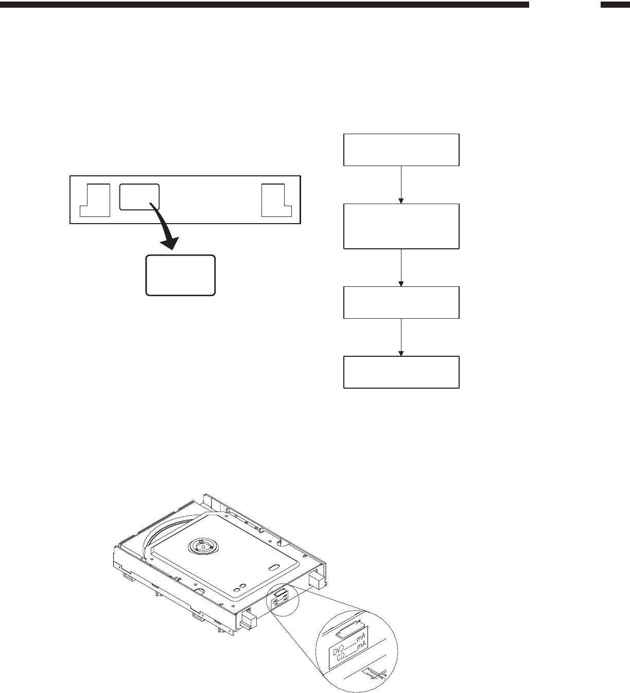
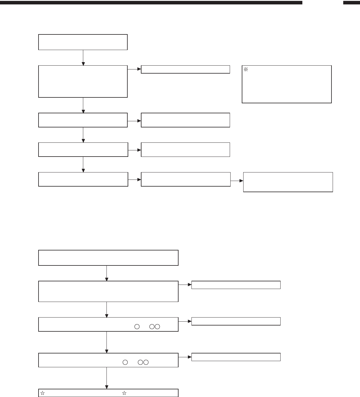
DIAGNOSTICS OF OPTICAL PICKUP AND REPLACING TRAVERSE UNIT
Make failure diagnostics of the Optical Pickup as follows.
If the laser drive current becomes more than 1.5 times of the initial value, the Optical Pickup should be replaced.
The laser drive current is registered on the seal attached to the rear of the Mecha. Unit.
In case of replacing the Pickup, change the whole part of the Traverse Unit.
No mechanical adjustment is necessary after the replacement.
Disc no read,
unsteady playback, etc.
Laser drive current check
HF wave form check
(Refer to page 76, 77)
Present value exceeds
the initial value by 1.5 times
Traverse Unit replacing
(See page 10 for details)
Laser current registering
after replacement
Step: Disc playback
Write the measured value
on the seal attached to the Mecha. Unit
* As to the measuring method, refer to page 4
Label Indication of DVD Mechanism
Laser current consumption value
ex) DVD ***mA, CD ***mA
Example:
DVD 30mA
CD 30mA
4
ADV-1000
C
B
E
C
B
E
C
B
E
C
B
E
1
114
15 28
114
15 28
LD4
(SIGNAL)
LD2
(SIGNAL)
LD1
(GND)
LD3
(GND)
Note for Handling the Laser Pick-up
The protection for the damage of laser diode.
If you want to change the optical device unit from any other units, you must keep the following.
(1) It should be done at the desk already took measures the static electricity in care of removing the OPU's
(Optical device unit) connector cable.
(2) Workers should be put on the "Earth Band".
(3) It shold be done to add the solder to the short land to prevent the broken Laser diode before removing the
24P FFC cable.
(4) Don't touch OPU's connector parts carelessly.
Replacement of the Laser Pick-up (Traverse Unit)
Check the Iop (Laser drive current).
If the present Iop (current) value exceeds +50% of the initial value, replace the Traverse unit (Laser Pick-up) with a new
one.
When measureing Laser drive current (Iop), playback the discs (CD, DVD) described below, measure Iop for CD Laser and
DVD Laser by the test point (LD1 ~ LD4) on the DVD Main P.W.B.
Test Disc : DVD/DVDT-S01 or commercially available discs.
: CD/TCD-784 (manufactured by ALMEDIO INC) or commercially available discs.
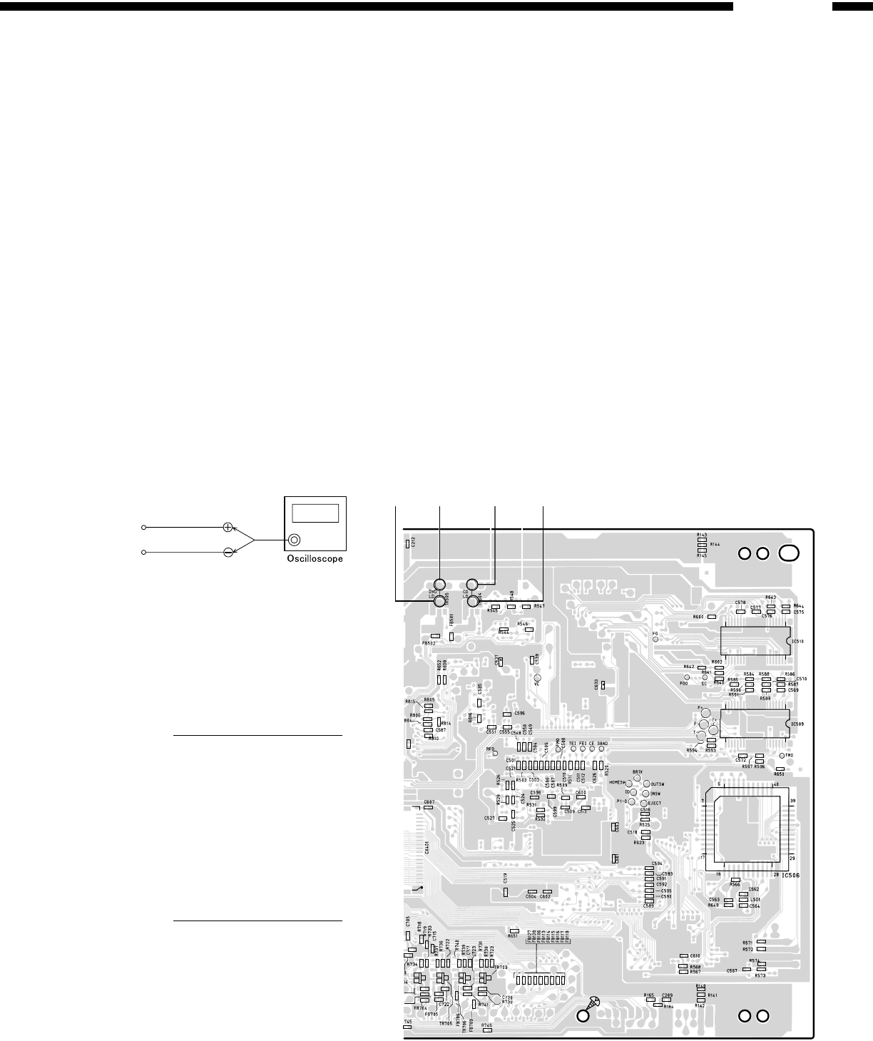
Iop Measurement Method
GU-3430 DVD Main Unit foil side
LD2
LD1
1. DVD Laser current measurement
(1) Connect the oscilloscope to LD1 of test point
for GND side and LD2 of test point for signal
side.
(2) Playback the title 1 / chapter 1 of the DVD
Test Disc.
(3) Measure the voltage between LD1 and LD2,
calculate Iop by the formula as shown below.
Iop= Measurement Voltage Value
39 (Resistance Value)
2. CD Laser current measurement
(1) Connect the oscilloscope to LD3 of test point
for GND side and LD4 of test point for signal
side.
(2) Playback the track 1 of the CD Test Disc.
(3) Measure the voltage between LD3 and LD4,
calculate Iop by the formula as shown below.
Iop= Measurement Voltage Value
39 (Resistance Value)
5
ADV-1000
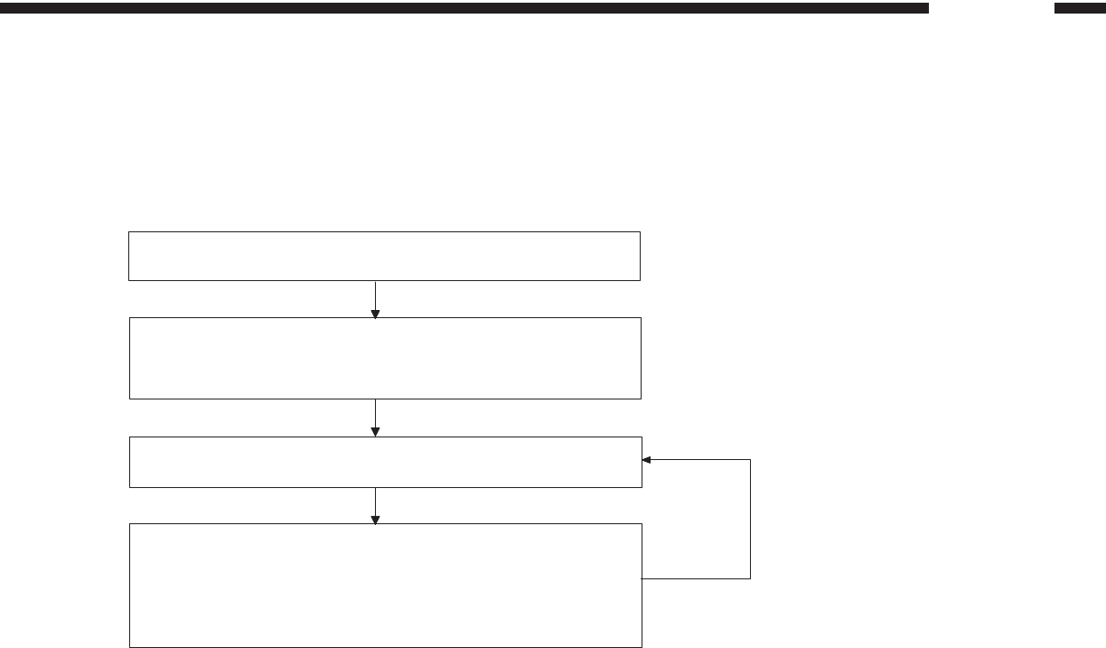
Optical Pick-up Diagnostics and Replacement
When repairing, carry out failure diagnostics by following the procedure described below.
If the present value of the laser drive current is 50% up to initial value, it is the point of the pickup replacement.
In case of the pickup replacement, replace the Traverse Unit with no adjustment.
The initial value is indicated on the label on back side of Mecha.
NO DISC indicated, Playback not smooth, etc.
Laser drive current check
HF signal check
Traverse Unit replacement (refer to page 10)
Present value: 50% up to initial value
Laser drive current check after replacement.
If the present value is less than 80mA, write on
the new label by hand, put on the new label over
the old label.
If the present value exceeds 80mA,
replace the Traverse Unit with a new one.
Cause: Damaged electrostatically when replaced.
6
ADV-1000
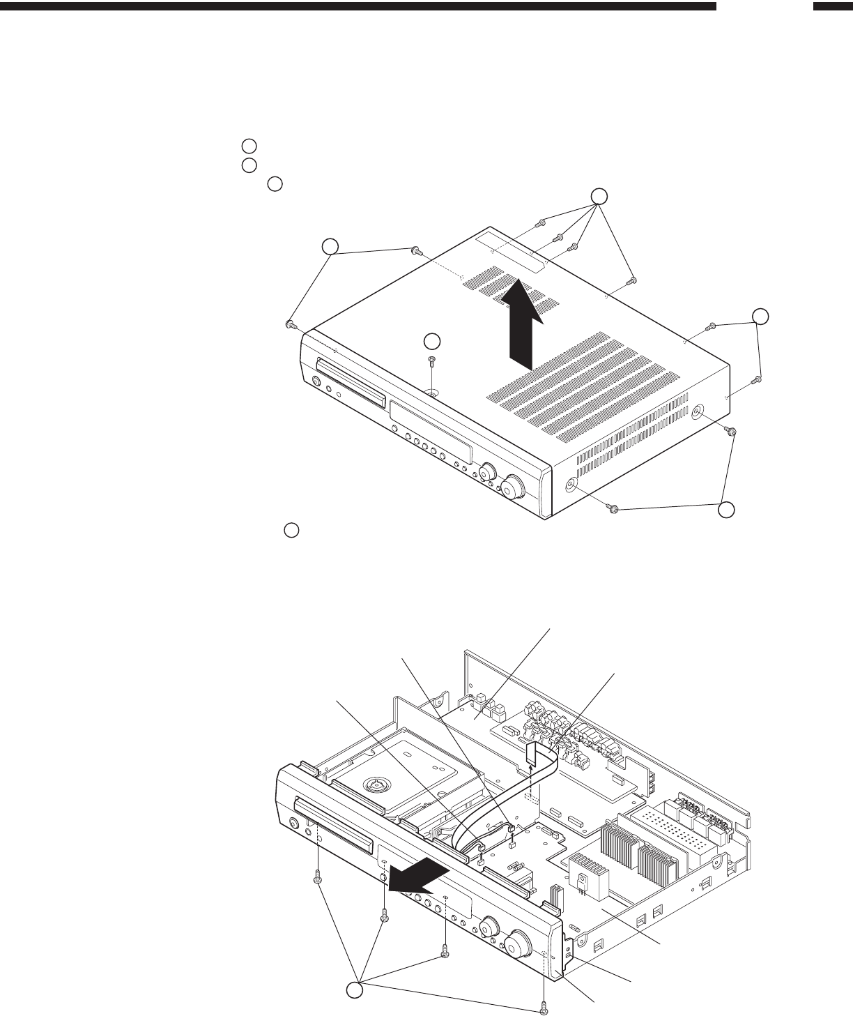
DISASSEMBLY
( Follow the procedure below in reverse order when reassembling )
2. Front Panel
(1) Remove 4 bottom screws 4 from the Front Panel.
(2) Disconnect FFC on the DSP Audio P.W.B. and 2
pcs of 3P connectors (white and blue) on the Power
Supply P.W.B.
(3) With releasing the hooks on both sides, detach the
Front Panel to the arrow direction together with the
Inner Panel.
1. Top Cover
(1) Remove 4 screws 1 on both sides.
(2) Remove 6 screws 2 on the rear panel.
(3) Remove the top screw 3.
(4) Detach the Top Cover to the arrow direction.
3
1
2
2
1
4
DSP Audio P.W.B.
Power Supply P.W.B.
3P connector (white)
3P connector (blue)
FFC
Inner Panel
Hook
7
ADV-1000
3. DVD Mecha. Unit
(1) Remove 4 top screws 5 on the DVD Mecha.
(2) Disconnect 2 FFCs and 2 pcs of 8P connectors
from the DVD Mecha.
5
8P connector
8P connector
FFC
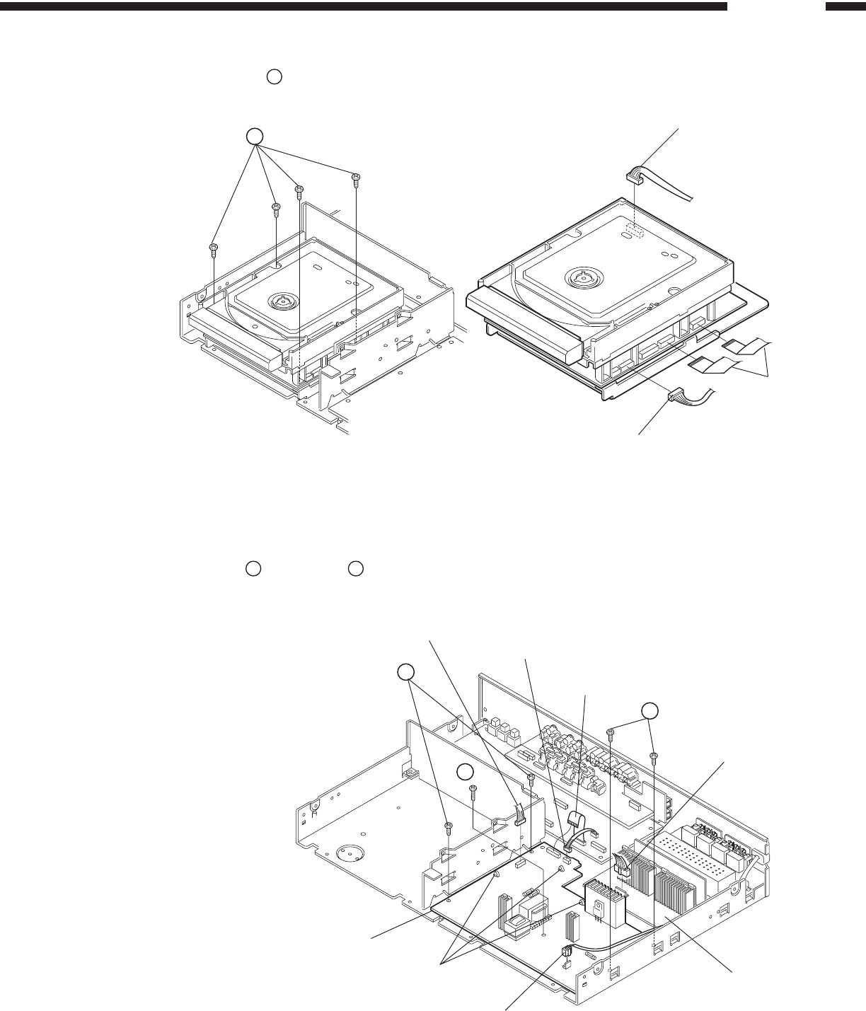
4. Power Supply P.W.B.
(1) Disconnect FFC, 2P connector, 3P connector, and
7P connector from the Power Supply P.W.B.
(2) Disconnect 6P connector from the Amp P.W.B.
(3) Remove 4 screws 7 and the screw 8 fixing the
Power Supply P.W.B.
(4) Release 3 P.W.B. supports.
3P connector
7P connector
FFC
6P connector
Amp P.W.B.
7
2P connector
P.W.B. support
Power Supply P.W.B.
7
8
8
ADV-1000
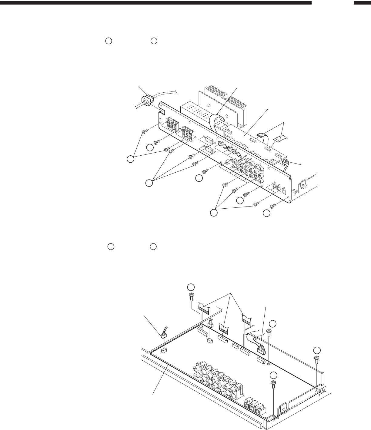
5. Back Panel
(1) Take off the cord bush.
(2) Remove 5 screws 9 and 23 screws .
6. Video P.W.B.
Disconnect 3 FFCs and 3P connector.
Cord bush
9
3P connector
FFC
FFC
Video P.W.B.
9
9
9
7. DSP Audio P.W.B.
(1) Remove the screw and 3 screws .
(2) Disconnect 3 FFCs, 3P connector, and 6P connector.
3P connector
6P connector
FFC
DSP Audio P.W.B.

9
ADV-1000
8. Amp P.W.B.
(1) Remove the screw ! and 4 screws " .
(2) Disconnect FFC and 6P connector.
"
6P connector
FFC
Amp P.W.B.
!
10
ADV-1000
1
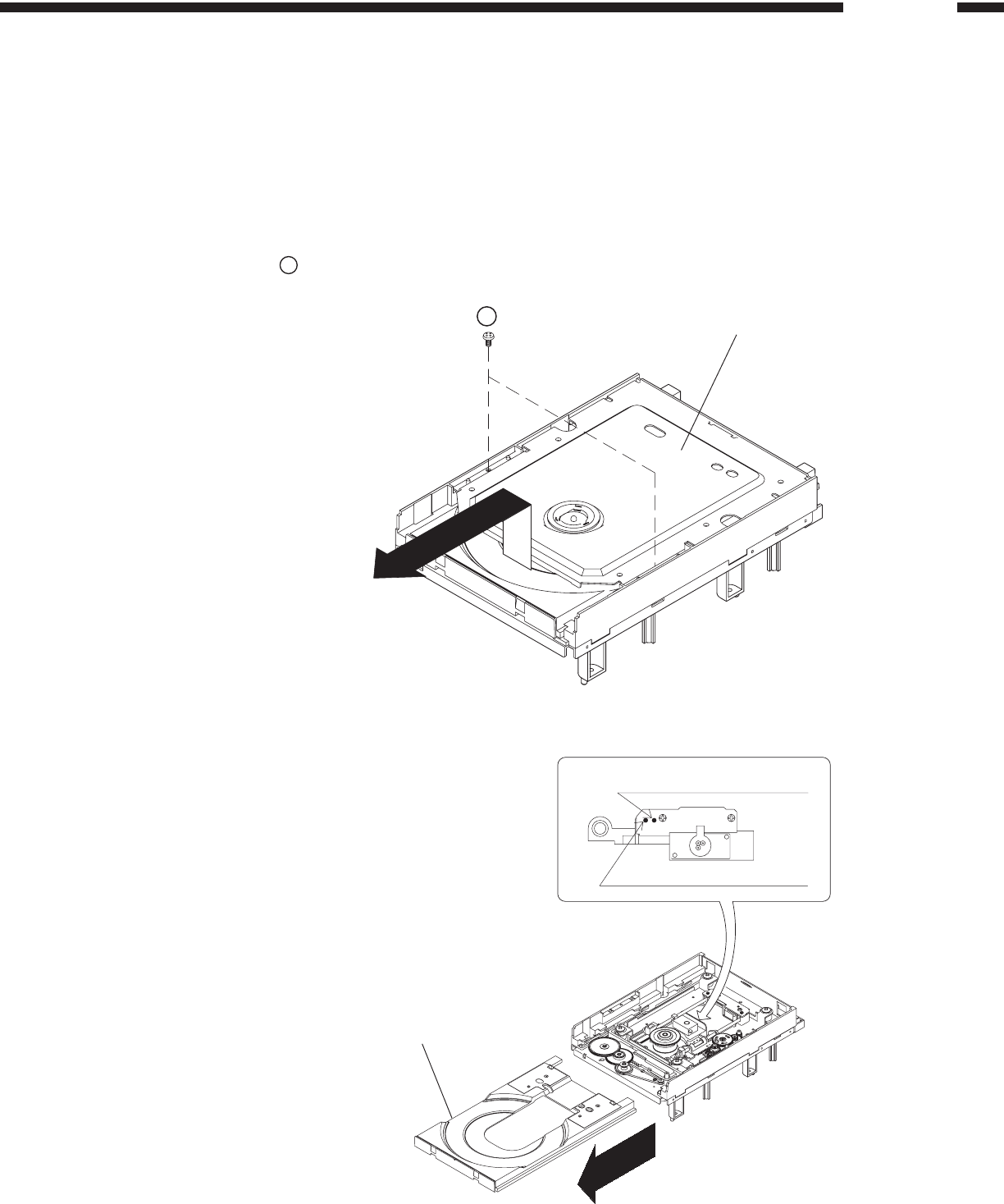
TRAVERSE UNIT DISASSEMBLY
(Follow the procedure below in reverse order when reassembling)
Caution: The optical pickup can be damaged easily by static electricity charged on human body. Take necessary anti-static
measures when repairing around the optical pickup.
1. Guide Clamp Bracket disassembly
(1) Remove 2 screws 1.
(2) Remove Guide Clamp Bracket to arrow direction.
2. Tray disassembly
(1) Remove to arrow direction.
(2) Solder the short-circuit (see in the frame).
Guide Clamp Bracket
Tr ay
Solder to Short-Circuit (DVD)
Solder to Short-Circuit (CD)

11
ADV-1000
CAUTION IN SERVICING
Initialization
Initialization should be performed when the µcom, peripheral parts of µcom, and DVD Main P.W.B. are replaced.
How to initialize
At the player is in the state of AC OFF, turn the AC ON with pressing the PLAY ( ) and STOP ( ) buttons simultaneously.
Check that the Standby LED lights orange and the initialization has been activated. (until "INITIALIZE" disappears from
the FL display).
Note: All user settings will be lost and its factory setting will be recovered when this initialization is made. So make sure to
memorize your setting for restoring after the initialization.
Note for disassembly Traverse Unit
(1) When assembling, reverse the order of the above.
(2) When inserting Tray, confirm boss on Slide Cam set to
ditch of the Tray (Compare with right drawing).
Slide gear
Tr ay
Boss
24P FFC (CX241)
3P PH WIRE (CX031)
Damper
15P FFC (CX151)
2
3. Traverse Unit disassembly
(1) Remove 24P FFC (CX241), 15P FFC (CX151), 5P
PH WIRE (CX051) and 3P PH WIRE (CX031)
connecting with from the DVD Main P.W.B.
(2) Remove 4 screws of 2 and 3 fixing Damper.
(3) Remove Traverse Unit to arrow direction.
DVD Main P.W.B.
3
12
ADV-1000
1. No power
(LED doesn't light.)
Check connector insertion.
P. SUPPLY (1U-3434-2):
[CX171/CX033]
DSP/AUDIO (1U-3435-3):
[CY171/CY191]
Re-insert the connector. When replacing µcom, µcom
peripheral parts, or Main P.W.B. in
servicing, perform initializing of the
DVD player. (AC power on while
pressing "STOP" and "PLAY" buttons
of the unit.)
Check voltage of IC907 input [+10V] on
P. SUPPLY P.W.B.
Check soldering of T901 secondary
circuit.
Check voltage of IC907 output [+5V] on
P. SUPPLY P.W.B.
Check short-circuit of power line further
CX171 connection.
Check voltage of IC303 (6)pin RESET
signal [+5V] on DSP/AUDIO P.W.B.
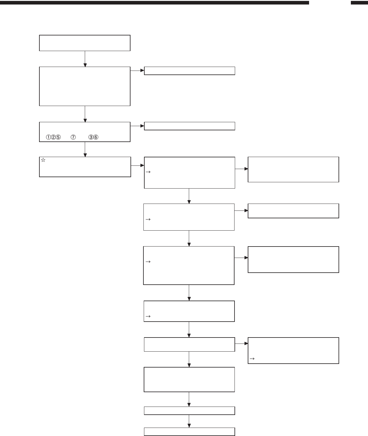
TROUBLESHOOTING
No
No Check soldering of IC302, IC303 on
DSP/AUDIO P.W.B. No Check after replacing IC303 on DSP/
AUDIO P.W.B. (1U-3435-3), then change
IC302 if still NG.
2. No power
(LED lights.)
Check connector insertion.
P. SUPPLY (1U-3434-2): [CX033]
DSP/AUDIO (1U-3435-3): [CY191]
Re-insert the connector.
Check voltage of FFC wire.
[CY191] 19P FFC for DSP/AUDIO P.W.B.:
3
+5V/
1 2
GND
Refer to "6. Switching power no output".
Check voltage of power wire.
[CX033] 3P PH for DISPLAY P.W.B.: 1+5V/ 2
3
GND
Refer to "6. Switching power no output".
Perform check from the step where is marked in the item 3.
No
No
No
No
No
13
ADV-1000
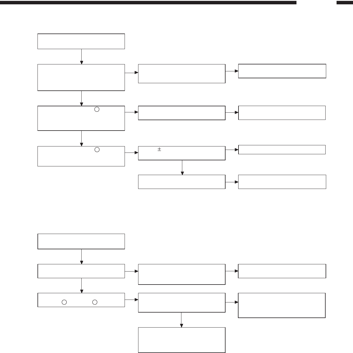
3. DVD no operation
(MECHA ERR display)
Check connector insertion.
P. SUPPLY (1U-3434-2):
[CX171/CW035]
DVD MAIN (GU-3430):
[CX081/CX082]
Mecha. Unit: [CX241/CX151/CX051]
Re-insert the connector.
Check voltage of power wire.
[CX071] 7P PH for P. SUPPLY P.W.B.:
+5V/ +12V/ GND]
Refer to "6. Switching power no output".
Perform operation check after
changing DVD MAIN P.W.B.
(GU-3430) with a perfect one.
There is something wrong in DVD MAIN
P.W.B. (GU-3430).
Check IC101(49)XIN, (105)CLK,
(116)PCLK2X 27MHz output on DVD
MAIN P.W.B.
No
No
No
After checking soldering of IC106 and
IC101 on DVD MAIN P.W.B. (GU-3430),
replace IC101 if NG. Then change IC106
if still NG.
There is something wrong in DVD MAIN
P.W.B. (GU-3430).
Check IC101(39)MCLK 94.5kHz
output on DVD MAIN P.W.B.
Change IC101 on DVD MAIN P.W.B.
(GU-3430).
There is something wrong in DVD MAIN
P.W.B. (GU-3430).
Check IC101(160)AUX0, (161)AUX1
on DVD MAIN P.W.B. whether SCK and
SDA signal of IIC BUS outputted when
power on.
After checking soldering of IC108,
IC701, and IC101 on DVD MAIN P.W.B.
(GU-3430), replace IC101 if NG. Change
IC108 then IC701 if still NG.
Check soldering of IC101 (208P IC) on
DVD MAIN P.W.B. (GU-3430).
Perform re-soldering.
Check IC501(50)IDERST +5V output on
DVD MAIN P.W.B. (GU-3430).
Check soldering of R522, RA127,
and IC101(145) on DVD MAIN
P.W.B. (GU-3430).
Perform re-soldering.
Check laser drive current and HF
waveform.
Criterion: Iop exceeds 1.5 times of the
initial value.
Replace the traverse unit.
Write laser current after the replacement.
No
No
No
No

14
ADV-1000
4. No video output (Interlace)
Check YUV signal.
Check if signals are output from
IC101(106, 107, 108, 109, 110, 113,
114, 115 pins) on P.W.B. (GU-3430).
Check soldering of RA125, RA126,
IC701, and IC101 on DVD MAIN P.W.B.
(GU-3430).
Check by replacing IC101 on DVD MAIN
P.W.B. (GU-3430).
Check analog video signal 1.
Check if signals are output from
IC701(24, 25, 29, 33, 35 pins) on
P.W.B. (GU-3430).
Check soldering of IC701 on DVD MAIN
P.W.B. (GU-3430).
No
No
Check by replacing IC701 on DVD
MAIN P.W.B. (GU-3430).
Check analog video signal 2.
Check if signals are inputted to
IC206(3)C, (5)Y, (8)PY, (12)Pb, and
(14)Pr on P.W.B. (1U-3443-1).
Check analog video signal
3
.
Check if signals are output from
IC206(17)Pr, (19)Pb, (21), (22)PY,
(24), (25)Y, (29), (30)Composite, and
(32)C on P.W.B. (1U-3443-1).
Check analog video signal 4.
Check if signals are output from 1-pin
of IC201 (Composite), IC202(C), and
IC203(Y) on P.W.B. (1U-3443-1).
No Check soldering of components (Tr, C,
R) in the Y-sig. Amp circuit, C-sig. Amp
circuit, and Component Amp circuit.
No Check soldering of IC206 on P.W.B.
(1U-3443-1).
Check soldering of IC201, IC202, or
IC203 causing NG on P.W.B. (1U-3443-1)
No
No
No
No Check by replacing NG IC (201 ~ 203)
on P.W.B. (1U-3443-1).
Check by replacing IC206 on P.W.B.
(1U-3443-1).
No
15
ADV-1000
5. No analog signal output (Audio)
Check audio digital signal.
Check if signals are output from
IC101(32)TWS, (33)TSD0, (39)MCLK,
and (40)TBCK.
Check soldering of chip emi-fil put in
series to IC101 on DVD MAIN P.W.B.
(GU-3430).
Check analog audio signal
1
.
Check if signals are output from IC401
(12)R-sig., (13)R-sig., (16)L-sig., and
(17)L-sig.
Check soldering of IC401 on DSP/
AUDIO P.W.B. (1U-3435-3).
Check analog audio signal
2
.
Check if signals are output from
IC404 (7)R-sig. and (1)L-sig.
Check if 12V power is supplied to
IC402 on DSP/AUDIO P.W.B. (1U-3435-3).
Check soldering of IC402 on DSP/
AUDIO P.W.B. (1U-3435-3).
6. Switching power no output
Check fuse
Check if F901 (6.3A/125V) is blown out.
Check soldering of IC201 and primary
rectifier diode on P. SUPPLY P.W.B.
(1U-3434-2).
Check by replacing IC901 on P. SUPPLY
P.W.B. (1U-3434-2).
Check actuating voltage.
[IC201]: 4+17~18VDC/5GND
Check if the secondary regulator circuit
in P. SUPPLY P.W.B. (1U-3434-2) is
shorted or solder-touched.
Check if the power lines of CX071,
CW035, CW061, CX171, and CX033 on
P. SUPPLY P.W.B. (1U-3434-2) are
short-circuited further their connections.
No
No
No
No
No
No
No
No
No
No
No Check by replacing IC101 on DVD MAIN
P.W.B. (GU-3430).
Check by replacing IC401 on DSP/
AUDIO P.W.B. (1U-3435-3).
Check by replacing IC402 on DSP/
AUDIO P.W.B. (1U-3435-3).
Refer to "6. Switching power no output".
Check by replacing shorted or solder-
touched element in the secondary
regulator circuit in P. SUPPLY P.W.B.
(1U-3434-2).
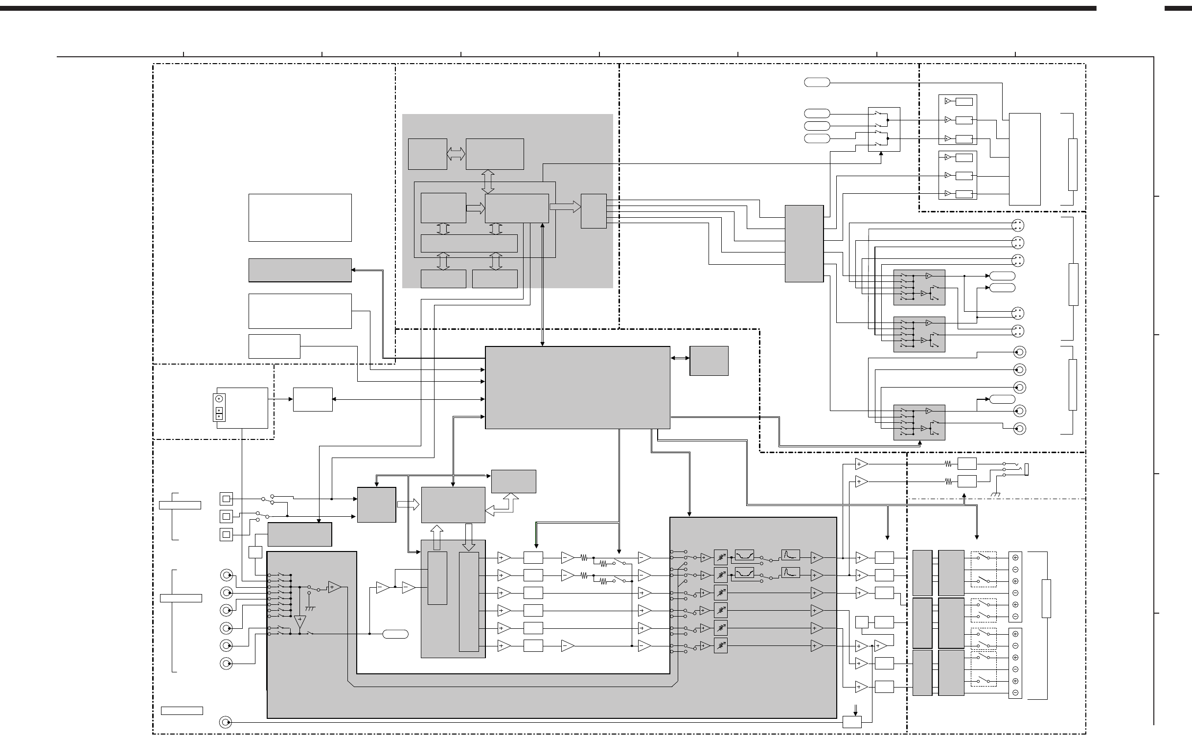
1U-3435-1
DISPLAY UNIT
FL TUBE
15-ST-36GN
FL DRIVER
M66005FP
KEY
REMOCON
RPM6938-V4
RDS
TUNER PACK
OPT OUT
OPT IN1
TV/DBS
OPT IN2
V.AUX
VCR IN
V.AUX IN
TV/DBS IN
L/R
VVCR OUT
DIGITAL IN/OUT
AUDIO IN/OUT
PRE OUT
ROTARY ENCODER
LC72720NM
SUB WOOFER OUT
DVD ENGINE UDVD-10
DVD MECHA FRONT-END CIRCUIT
ES4408
DVD DECODER DVD DSP VIDEO
D/A
AD7172
CPU
ROM RAM
DOWNMIX OUT
BITSTREAM OUT
CDR/TAPE IN
CDR/TAPE OUT
MUTE
1U-3435-3
AUDIO/DSP UNIT
ROM
2Mbit
DIR AUDIO DSP
LC89055W CS493292
CPU
M30624FGFP
MUTE
MUTE
MUTE
MUTE
MUTE
MUTE
FL
FR
C
SL
SR
LFE
[+6dB]
BA15218 BA15218
6ch D/A CONVERTER
CODEC
AK4527
A/D CONVERTER
BA15218
D/A CONVERTER
AD1854KSRL
MUTE
EEPROM
16k
S29590A
H/P MUTE 1U-3435-2
H/P UNIT
H/P
VR MUTE
PRE AMP
MUTE
MUTE
MUTE
LPF
ALC MUTE
MUTE
MUTE
SW MUTE
MUTE
C
Y
C
A
R
Y
C
G
B
Y
C
G
B
BH7862
VIDEO DRIVER
with Filter
BA7625
BA7626
1U-3434-1 RELAY FR
AMP UNIT RELAY C
RELAY SW
RELAY SR
CLASS-D POWER AMP
1U-3434-3
SCART UNIT
1U-3443-1
VIDEO UNIT
BA7660
BU4053
BA7660
AV1 VIDEO OUTPUT
SCART TERMINAL
MUTE
MUTE
MUTE
MUTE
MUTE
MUTE
Y
VCR IN
C
Y
TV/DBS IN
C
Y
V.AUX IN
C
Y
MONITOR OUT
C
Y
VCR OUT
C
VCR IN
TV/DBS IN
V.AUX IN
COMPOSITE VIDEO
S-VIDEO
C
Y
MONITOR OUT
VCR OUT
V
BA7625
V
H/P AMP
VR OUTPUT GAIN
SWITCHING0~+18dB
DSP/EXT/DIRECTBASS/TREBLE SDB 2dBstep
[0dB]
PASS
DATA
CLK
SUB SUM
BA15218
SP RELAY
SR
SL
SW
TC2000
PWM
Modulator
TP2050
FET
Driver
TC2000
PWM
Modulator
TP2050
FET
Driver
TC2000
PWM
Modulator
TP2050
FET
Driver
FL
SPEAKER OUT
FR
C
Max output
4.2Vrms
FUNCTION/VR/TONE/SDB
BD3811K1
[0dB]
INPUT GAIN AMP
0/+6dB
SPDIFSDATRA
LRCK
BCK
MCK
A
R
MUTE
MUTE
YUV DATA
BLOCK DIAGRAM
8
76
5
4
3
2
1
A
B
C
D
E
AVD-1000
16
17
ADV-1000
4
32
15678
D
C
B
A
E
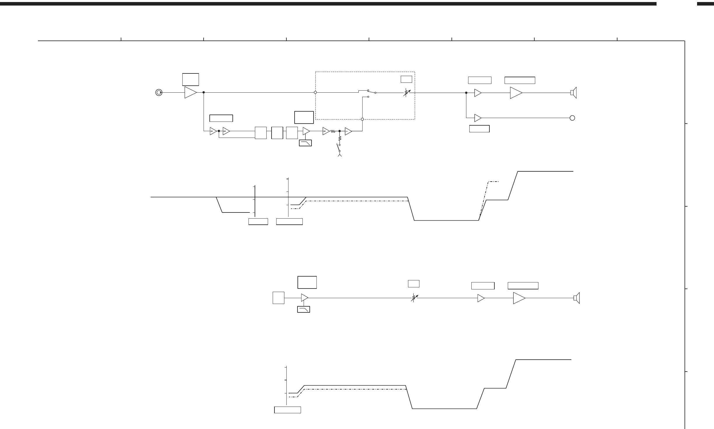
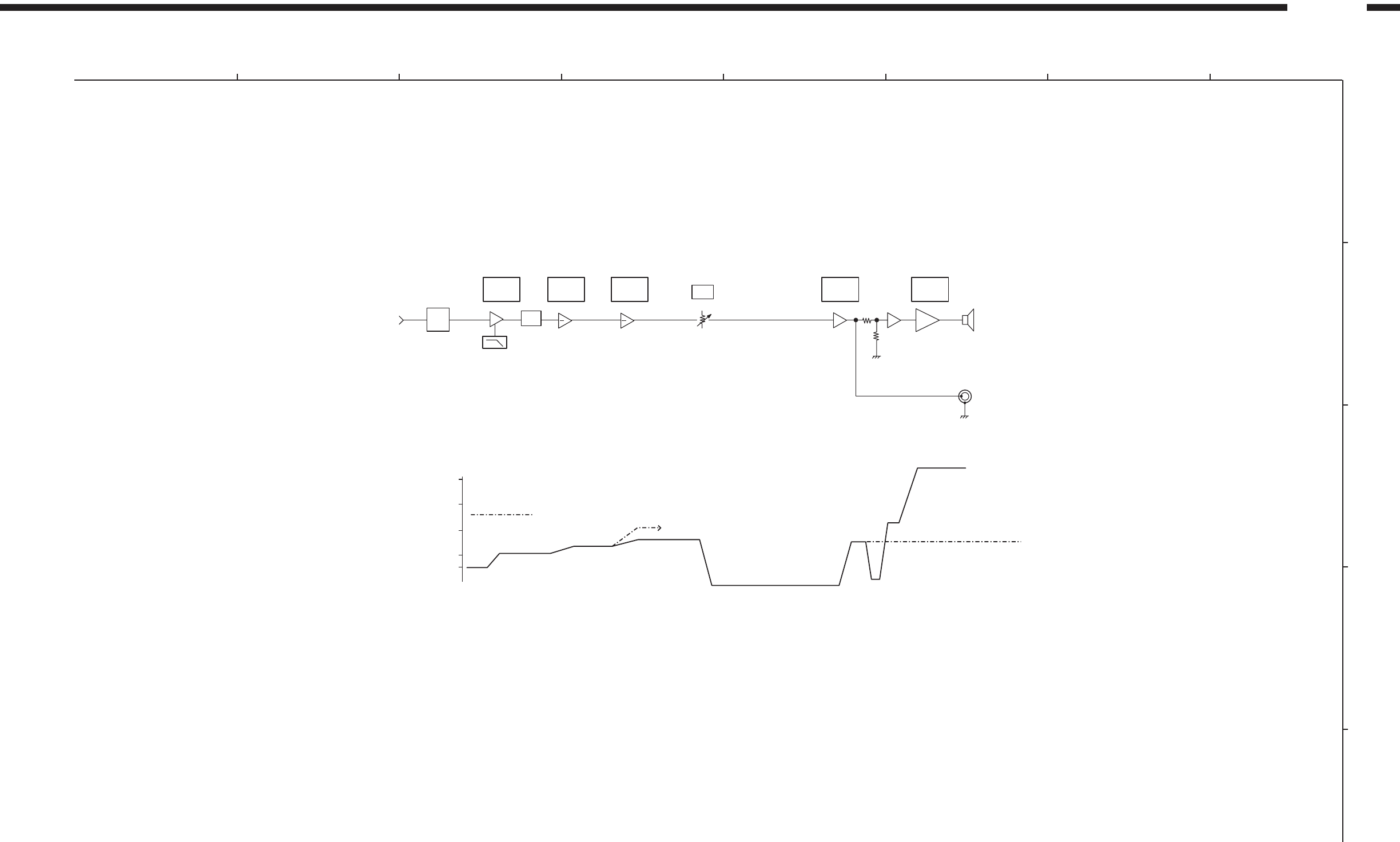
LEVEL DIAGRAMS
D/A
VR PRE AMP POWER AMP
+
+
SP OUT
+
D/AOUT
LPF
D/A OUT
0dBFS
-10dBFS
-20dBFS 6dB Vol:0: -18dB
(-15dB) 15.63dB
22.17dB
SP OUT
40W/6ohm
(15.5Vrms)
CENTER
REAR
Only when Dolby Prologic
ANALOG
IN
200mV
ANALOG
IN
200mVrms
+
BUFF.
AMP
D/AOUT
LPF
DIRECT
DSP
REV. AMP
A/D DSP D/A
VR PRE AMP POWER AMP
config1: OFF
config2: ON
FROM S.W
+
+
+
H/P AMP
+
SP OUT
H/P JACK
FRONT
-12dB
A/D IN D/A OUT
0dBFS
0dBFS
-10dBFS
-10dBFS
-20dBFS
-20dBFS 6dB Only when Dolby Prologic
H/P
30dB
15.63dB
22.17dB
SP OUT
40W/6ohm
(15.5Vrms)
18
ADV-1000
4
32
15678
D
C
B
A
E
VR
+
+ +
SP OUT
SW
PRE OUT
+
D/AOUT
FROM
DSP
LPF LINE
AMP LINE
AMP
0dBFS
-10dBFS
-20dBFS
-30dBFS
-35dBFS 6dB
Config-1
Config-2
2.85dB
(8.85)
Vol: 0
-18dB
3.31dB
(12.16)
7.5dB To FRONT CH 17.84dB
(30)
22.3dB
(37.2)
-15.1dB
(14.9)
22.17dB
SP OUT
SW
PRE OUT
40W/6ohm
(15.5Vrms)
VOLMAX: 0.55Vrms
VOL"00": 0.07Vrms
SUB
WOOFER
D/A
PRE
AMP
POWER
AMP
MUTE
19
ADV-1000
4
32
15678
D
C
B
A
E
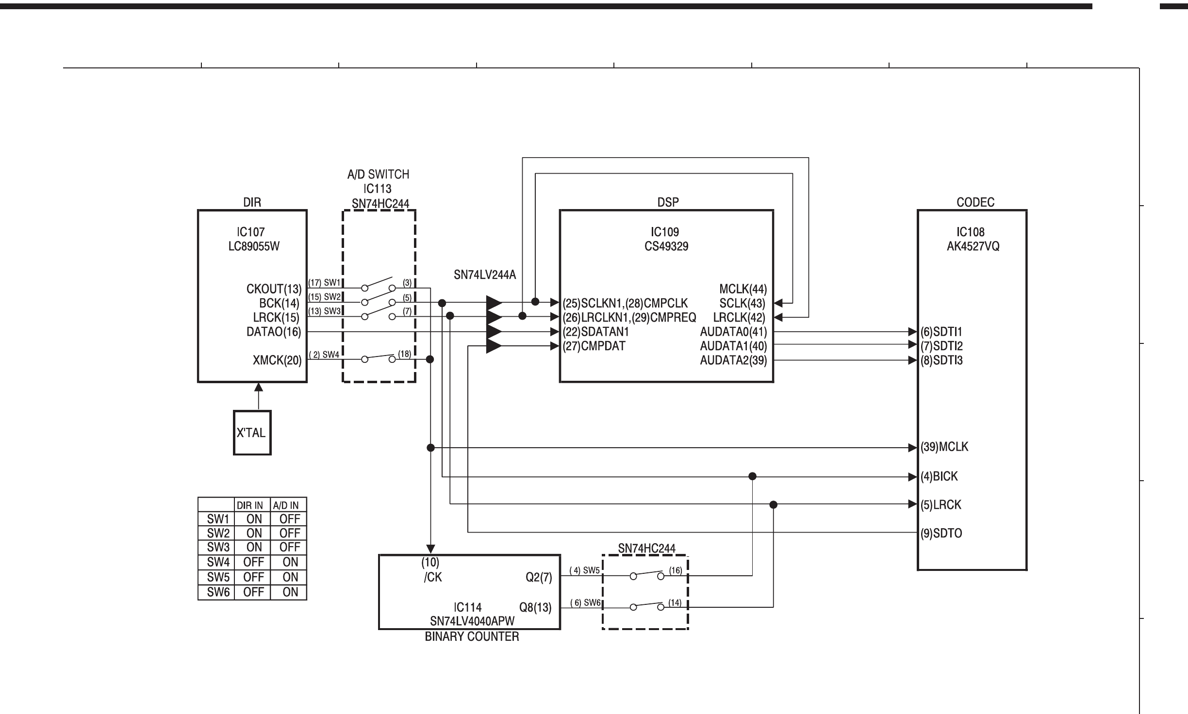
CLOCK FLOW
20
ADV-1000
1 P94 E2P CS Chip select signal to EEPROM
2 P93 62446 LATCH Serial data latch to E. VR IC
3 P92 62446 DATA, E2P DI, FUNC DA Serial data to EEPROM/E. VR IC/Input Switch IC
4 P91 E2P DO Serial data from EEPROM
5 P90 62446 CLK, E2P SK, FUNC CLK Serial clock to EEPROM/E. VR IC/Input Switching IC
6 BYTE (VSS) GND
7 CNVSS (PullDown), FLASH CNVss Flash write mode select input
8 P87 BUS ON/OFF Serial data/clock separate command output to E. VR IC
9 P86 FUNC CE(STB) Data latch to Input Switch IC
10 RESET RESET Reset input
11 XOUT XTAL(12.5MHz) Oscillator output (12.5 MHz)
12 VSS (VSS) GND
13 XIN XTAL(12.5MHz) Oscillator input (12.5 MHz)
14 VCC (VCC) Power supply
15 P85 (PullUp) NMI, not used
16 P84 PROTECT Speaker and Drive IC abnormal detect
17 P83 /CS Comm. chip select input with DVD
M30624FG Terminal Function
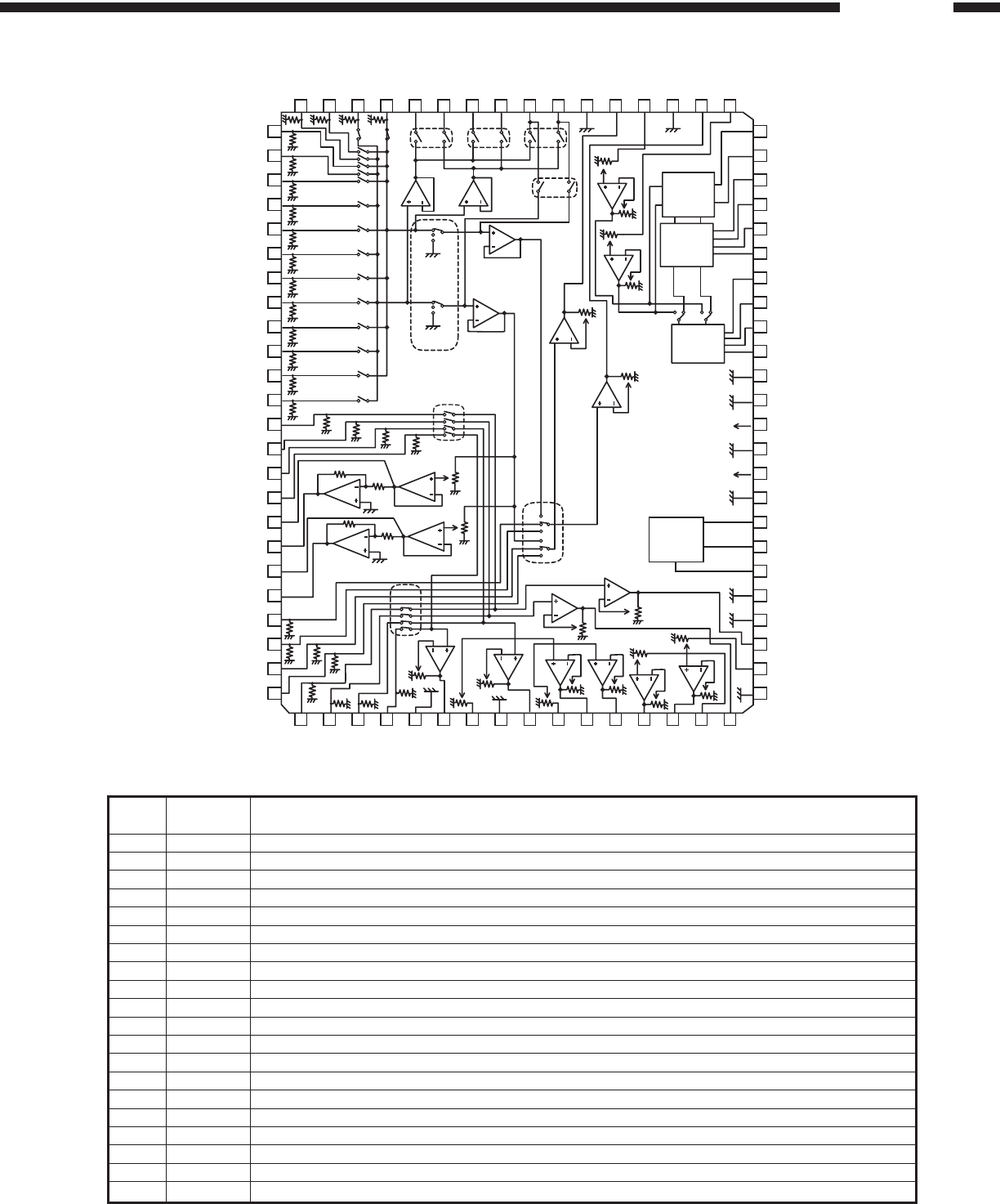
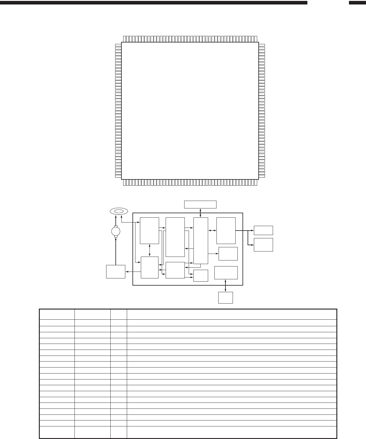
SEMICONDUCTORS
M30624FG (MA: IC302)
Port Name Function
Pin
No. Symbol
P1
2
/D
10
76
P1
2
/D
9
77
P1
0
/D
8
78
P0
7
/D
7
79
P0
6
/D
6
80
P0
5
/D
5
81
P0
4
/D
4
82
P0
3
/D
3
83
P0
2
/D
2
84
P0
1
/D
1
85
P0
0
/D
0
86
P10
7
/AN
7
/KI
3
87
P10
6
/AN
6
/KI
2
88
P10
5
/AN
5
/KI
1
89
P10
4
/AN
4
/KI
0
90
P10
3
/AN
3
91
P10
2
/AN
2
92
P10
1
/AN
1
93
AV
SS
94
P10
0
/AN
0
95
V
REF
96
AV
CC
97
P9
7
/AD
TRG
/S
IN
498
P9
6
/ANEX1/S
OUT
499
P9
5
/ANEX0/SLK4 100
P4
2
/A
18
50
P4
3
/A
19
49
P4
4
/CS0
48
P4
5
/CS1
47
P4
6
/CS2
46
P4
7
/CS3
45
P5
0
/WRL/WR
44
P5
1
/WRH/BHE
43
P5
2
/RD
42
P5
3
/BCLK
41
P5
4
/HLDA
40
P5
5
/HOLD
39
P5
6
/ALE
38
P5
7
/RDY/CLK
OUT
37
P6
0
/CTS
0
/RTS
0
36
P6
1
/CLK
0
35
P6
2
/RXD
0
34
P6
3
/TXD
0
33
P6
4
/CTS
1
/RTS
1
/CTS
0
/CLKS
1
32
P6
5
/CLK
1
31
P6
6
/RXD
1
30
P6
7
/TXD
1
29
P7
0
/RXD
2
/SDA/TA0
OUT
28
P7
1
/RXD
2
/SCL/TA0
IN
/TB5
IN
27
P7
2
/CLK
2
/TA1
OUT
/V
26
P1
3
/D
11
75
P1
4
/D
12
74
P1
5
/D
13
/INT
3
73
P1
6
/D
14
/INT
4
72
P1
7
/D
15
/INT
5
71
P2
0
/A
0
(/D
0
/-)
70
P2
1
/A
1
(/D
1
/D
0
)
69
P2
2
/A
2
(/D
2
/D
1
)
68
P2
3
/A
3
(/D
3
/D
2
)
67
P2
4
/A
4
(/D
4
/D
3
)
66
P2
5
/A
5
(/D
5
/D
4
)
65
P2
6
/A
6
(/D
6
/D
5
)
64
P2
7
/A
7
(/D
7
/D
6
)
63
V
SS
62
P3
0
/A
8
(/-/D
7
)
61
V
CC
60
P3
1
/A
9
59
P3
2
/A
10
58
P3
3
/A
11
57
P3
4
/A
12
56
P3
5
/A
13
55
P3
6
/A
14
54
P3
7
/A
15
53
P4
0
/A
16
52
P4
1
/A
17
51
P9
4
/DA
1
/TB4
IN
1
P9
3
/DA
0
/TB3
IN
2
P9
4
/TB2
IN
/S
OUT
33
P9
1
/TB1
IN
/S
IN
34
P9
0
/TB0
IN
/CLK3 5
BYTE 6
CNV
SS
7
P8
7
/X
CIN
8
P8
6
/X
COUT
9
RESET 10
X
OUT
11
V
SS
12
X
IN
13
V
CC
14
P8
5
/NMI 15
P8
4
/INT
2
16
P8
3
/INT
1
17
P8
2
/INT
0
18
P8
1
/TA4
IN
/U 19
P8
0
/TA4
out
/U 20
P7
7
/TA3
IN
21
P7
6
/TA3
OUT
22
P7
5
/TA2
IN
/W 23
P7
4
/TA2
out
/W 24
P7
3
/CTS
2
/RTS
2
/TA1
IN
/V 25
IC's
Note: Abbreviation ahead of IC No. indicates the name of P.W.B.
AP: AMP / Power P.W.B.
MA: Main P.W.B.
VO: Video / Out P.W.B.
DM: DVD Main P.W.B.

21
ADV-1000
18 P82 RESERVED(DENON BUS) Arbitration input on DENON BUS (same as serial data)
19 P81 50/60 Detect input of power pulse (50/60 Hz)
20 P80 FAN ON/OFF Fan motor drive output
21 P77 IN JOGB JOG pulse input B for function switching
22 P76 IN JOGA JOG pulse input A for function switching
23 P75 VOL JOGB JOG pulse input B for VOL
24 P74 VOL JOGA JOG pulse input A for VOL
25 P73 FLCS Chip select output to FL Driver IC
26 P72 RESERVED(DENON BUS) Serial sync clock output on DENON BUS
27 P71 RESERVED(DENON BUS) Serial data input on DENON BUS
28 P70 RESERVED(DENON BUS) Serial data output on DENON BUS
29 P67 FLDA, FLASH TxD Serial data output to FL Driver IC
30 P66 PULL DOWN, FLASH RxD Open pin, serial data input at flash write
31 P65 FLCK, FALSH MODE, FLASH CLK Serial clock output to FL Driver IC
32 P64 FL RESET, FLASH BUSY Reset output to FL Driver IC
33 P63 sDATAout(DVD) Serial comm. output with DVD
34 P62 sDATAin(DVD) Serial comm. input with DVD
35 P61 SCLK(DVD) Serial comm. clock input with DVD
36 P60 PWRON(DVD) Power control output for DVD unit
37 RDY/P57 /RESET Reset output to DVD unit
38 ALE/P56 H/P SW Headphone on/off detect input
39 HOLD/P55 LED G, FLASH EPM Control output to power indicator LED green
40 HLDA/P54 /DFRES Reset detect signal for DVD unit
41 BCLK/P53 DVD ON/OFF Power control output for DVD unit
42 RD/P52 RGB H Composite/S/RGB switching, aspect ratio switching
43 WRH/BHE/P51 VCNT1/YC H Aspect ratio switching input (16:9, 4:3LB, 4:3)
44 WRL/WR/P50 LED R, FLASH CE Control output to power indicator LED red
45 CS3/P47 VCNT2/WIDE Aspect ratio switching input (16:9, 4:3LB, 4:3), WIDE
46 CS2/P46 DSEL1 Digital in/out select output
47 CS1/P45 S-SEL Select output of monitor source internal/external
48 CS0/P44 A Select output A of external input source
49 A19/P43 B Select output B of external input source
50 A18/P42 C Select output C of external input source
51 A17/P41 SCART MUTE Mute output of SCART pin
52 A16/P40 TEMP Temp. sensor input
53 A15/P37 DSEL2 Open
54 A14/P36 SDB ON/OFF SDB ON/OFF output
55 A13/P35 FRT MUTE(VR MUTE) Mute output of all channel (mute output of front channel)
56 A12/P34 SW MUTE Mute output of sub-woofer channel
57 A11/P33 RL FRONT Speaker relay ON/OFF output of front channel
58 A10/P32 RL SURR Speaker relay ON/OFF output of surround channel
59 A9/P31 RL CENT Speaker relay ON/OFF output of center channel
60 VCC (VCC) Power supply
61 A8/P30 RL HP Headphone relay ON/OFF output
62 VSS (VSS) GND
63 A7/P27 OPEN Open
64 A6/P26 STEREO Tuner’s stereo indicator input
65 A5/P25 TUNED Tuner’s station detect input
66 A4/P24 T.MUTE Tuner’s mute output
67 A3/P23 SANYO CE Comm. chip enable output to PLL/RDS IC of tuner
68 A2/P22 SANYO DI Serial data output to PLL/RDS IC of tuner
69 A1/P21 SANYO CLK Serial clock output to PLL/RDS IC of tuner
70 A0/P20 SANYO DO Serial data input from PLL/RDS IC of tuner
71 D15/P17 INTREQ OUT Comm. request input from surround DSP
Port Name Function
Pin
No. Symbol

22
ADV-1000
72 D14/P16 89055 CSFLAG Signal change detect input from DIR
73 D13/P15 REMOTE IR remote control input
74 D12/P14 /SYR Reset output to RDS IC of tuner
75 D11/P13 INTREQ IN Open drain operation (L: output, H: switch to input)
76 D10/P12 4932 CE Serial comm. chip enable output to surround DSP
77 D9/P11 4932 RST Reset output to surround DSP
78 D8/P10 4527 CE Serial comm. chip enable output to CODEC(AD/DA)
79 D7/P07 ROM/RAM ROM/RAM used surround DSP select output
80 D6/P06 ROM2 ROM address used surround DSP select output
81 D5/P05 ROM3 ROM address used surround DSP select output
82 D4/P04 ROM30 ROM address used surround DSP select output
83 D3/P03 ERR MUTE Digital mute output when error
84 D2/P02 SEL CLK Data clock select output
85 D1/P01 4527 RST Reset output to CODEC
86 D0/P00 89055 CE Serial comm. enable output to DIR
87 P107 96 DET 96kHz sampling signal detect input from DIR
88 P106 89055 ERR Error input from DIR
89 P105 89055 RST Reset output to DIR
90 P104 P.ON/OFF Whole unit’s power ON/OFF (standby) output
91 P103 AAC AAC function on/off select input
92 P102 MODE1 Unit’s operation spec select input
93 P101 KEY 0 Button operation detect input
94 AVSS (VSS) GND
95 P100 KEY 1 Button operation detect input
96 VREF (VCC) Ref. V input for A/D conversion
97 AVCC (VCC) Power supply
98 P96 89055 DO, 4932 DO Serial data input from DIR/CODEC/DSP
99 P97 89055 DIN, 4527 DIN, 4932 DIN Serial data output to DIR/CODEC/DSP
100 P95 89055 CLK, 4527 CLK, 4932 CLK Serial clock output to DIR/CODEC/DSP
Port Name Function
Pin
No. Symbol
REFERENCE
VOLTAGE
ARI
DETECTOR
S
W
BIPHASE
DECODER
COMPARATOR
SC-BANDPASS
FILTER
(57kHz)
SMOOTHING
FILTER
RDS
DETECTOR
ANTI-
ALIASING
FILTER
D (
Ð 0
°)
26 BIT SHIFT
REGISTER x 2
GROUP
AND
BLOCK
SYNC DET
D-PLL
(D-YCO)
CLOCK
RECOVERY
(D-YCO)
PC
D (
Ð
90°)
DIFFRENTIAL
DECODER
FRAG RAM
16 BIT
TIMING
GENERATOR
AND SYSTEM
CONTROLLER
PARALLEL TO SERIAL
DATA RAM
16 BIT
BUFFER RAM (24 BLOCK)
SYNDROME REGISTER
AND ERROR CORRECTION CCB
INTERFACE
POWER ON
RESET
SOFT DECISION
XTAL OSC
AND
DIVIDER
11
10
9
13
12
20
21
22
23
24
1415
1965
1
2
8
7
16
17
18
4
3
LC72720NM (MA: IC511)
1
2
3
4
5
6
7
8
24
23
22
21
20
19
18
17
VREF
MPXIN
Vdda
Vssa
FLOUT
COIN
T1
T2
SYR
CE
D1
CL
D0
RDS-1D
SYNC
T7
916
T3 T6
10 15
T4 Vddd
11 14
T5 Vssd
12 13
XOUT XIN
ADV-1000
23
1
2
3
4
5
6
7
8
9
10
11
12
13
14
15
16
17
18
19
20
21
22
23
24
64
63
62
61
60
59
58
57
56
55
54
53
52
51
50
49
48
47
46
45
44
43
42
41
25 26
80 79 78 77 76 75 74 73 72 71 70 69 68 67 66 65
27 28 29 30 31 32 33 34 35 36 37 38 39 40
47k
47k
47k
47k
47k
47k
47k
47k
47k
47k
47k
47k
47k
47k
47k 47k
47k
47k
47k 47k 47k
47k
47k 47k
47k 47k
47k 47k
REC
INSW
REC
SW1
Input mute SW
5.1ch Mode SW2 DVD
5.1ch Mode SW1
LINE
R/L
MIX
LINE
R/L
MIX
5.1ch Mode SW2 DSP
RECSW
23
1
3
2
1
3
2
VCC
VEE
BASS
BOOST
LOGIC
TNF2
TNF1
BNF11
BNF21
BNF12
BNF22
BBNF2
OUT2
BBNF1
OUT1
AGND8
AGND7
VCC
AGND6
VEE
AGND5
MUTE
CL
DA
DGND
AGND4
GOUTSR
VINSR
AGND3
IN22
IN21
IN12
IN11
ROUT32
ROUT31
ROUT22
ROUT21
ROUT12
ROUT11
AGND10
GOUT2
VIN2
AGND9
GOUT1
VIN1
IN31
IN32
IN41
IN42
IN51
IN52
IN61
IN62
IN71
IN72
IN81
IN82
INDVDSR
INDVDSL
INDVDC
INDVDSW
OUT2(+)
OUT2(-)
OUT1(+)
OUT1(-)
IN1DSP
IN1MIX
IN2DSP
IN2MIX
INDSPSR
INDSPSL
INDSPC
INDSPSW
AGND1
GOUTSW
VINSW
AGND2
GOUTC
VINC
OUTSW
OUTC
OUTSL
OUTSR
VINSL
GOUTSL
RECSW
TREBLE
BASS
1 IN31 1ch input terminal 3
2 IN32 2ch input terminal 3
3 IN41 1ch input terminal 4
4 IN42 2ch input terminal 4
5 IN51 1ch input terminal 5
6 IN52 2ch input terminal 5
7 IN61 1ch input terminal 6
8 IN62 2ch input terminal 6
9 IN71 1ch input terminal 7
10 IN72 2ch input terminal 7
11 IN81 1ch input terminal 8
12 IN82 2ch input terminal 8
13 INDVDSR DVD surround Rch input terminal
14 INDVDSL DVD surround Lch input terminal
15 INDVDC DVD center speaker input terminal
16 INDVDSW DVD sub woofer input terminal
17 OUT2(+) 2ch (+) A/D output terminal
18 OUT2(-) 2ch (-) A/D output terminal
19 OUT1(+) 1ch (+) A/D output terminal
20 OUT1(-) 1ch (-) A/D output terminal
Pin No. DescriptionPin Name
BD3811K1 Pin Description
BD3811K1 (MA: IC504)

ADV-1000
24
Pin No. DescriptionPin Name
21 IN1DSP 1ch DSP input terminal
22 IN1MIX 1ch DSP MIX input terminal
23 IN2DSP 2ch DSP input terminal
24 IN2MIX 2ch DSP MIX input terminal
25 INDSPSR DSP surround Rch input terminal
26 INDSPSL DSP surround Lch input terminal
27 INDSPC DVD center speaker input terminal
28 INDSPSW DSP sub woofer input terminal
29 AGND1 Analog ground terminal
30 GOUTSW Sub woofer input gain output terminal
31 VINSW Sub woofer volume input terminal
32 AGND2 Analog ground terminal
33 GOUTC Center speaker input gain output terminal
34 VINC Center speaker volume input terminal
35 OUTSW Sub woofer output terminal
36 OUTC Center speaker output terminal
37 OUTSL Surround Lch output terminal
38 OUTSR Surround Rch output terminal
39 VINSL Surround Lch volume inut terminal
40 GOUTSL Surround Lch input gain output terminal
41 AGND3 Analog ground terminal
42 VINSR Surround Rch volume input terminal
43 GOUTSR Surround Rch input gain output terminal
44 AGND4 Analog ground terminal
45 DGND Ground terminal for comparator.
46 DA Serial data and latch input terminal
47 CL Serial clock input terminal
48 MUTE Mute terminal
49 AGND5 Analog ground terminal
50 VEE (-) Power supply terminal
51 AGND6 Analog ground terminal
52 VCC (+) Powr supply terminal
53 AGND7 Analog ground terminal
54 AGND8 Analog ground terminal
55 OUT1 1ch output terminal
56 BBNF1 1ch bass boost filter terminal
57 OUT2 2ch output terminal
58 BBNF2 2ch bass boost filter terminal
59 BNF22 2ch bass filter terminal 2
60 BNF12 2ch bass filter terminal 1
61 BNF21 1ch bass filter terminal 2
62 BNF11 1ch bass filter terminal 1
63 TNF1 1ch treble filter terminal
64 TNF2 2ch treble filter terminal
65 VIN1 1ch (Lch) volume input terminal
66 GOUT1 1ch (Lch) input gain output terminal
67 AGND9 Analog ground terminal
68 VIN2 2ch (Rch) volume input terminal
69 GOUT2 2ch (Rch) input gain output terminal
70 AGND10 Analog ground terminal
71 ROUT11 1ch REC input and output terminal 1
72 ROUT12 2ch REC input and output terminal 1
73 ROUT21 1ch REC output terminal 2
74 ROUT22 2ch REC output terminal 2
75 ROUT31 1ch REC output terminal 3
76 ROUT32 2ch REC output terminal 3
77 IN11 1ch input terminal 1
78 IN12 2ch input terminal 1
79 IN21 1ch input terminal 2
80 IN22 2ch input terminal 2
25
ADV-1000
1
2
3
4
5
6
7
8
9
10
11
12
13
14
15
16
17
18
19
20
21
22
23
24
25
26
27
28
29
30
31
32
33
34
35
36
37
38
39
40
41
42
43
44
45
46
47
48
49
50
51
52
53
54
55
56
57
58
59
60
61
62
63
64
65
66
67
68
69
70
71
72
73
74
75
76
77
78
79
80
81
82
83
84
85
86
87
88
89
90
91
92
93
94
95
96
97
98
99
100
101
102
103
104
156
155
154
153
152
151
150
149
148
147
146
145
144
143
142
141
140
139
138
137
136
135
134
133
132
131
130
129
128
127
126
125
124
123
122
121
120
119
118
117
116
115
114
113
112
111
110
109
108
107
106
105
208
207
206
205
204
203
202
201
200
199
198
197
196
195
194
193
192
191
190
189
188
187
186
185
184
183
182
181
180
179
178
177
176
175
174
173
172
171
170
169
168
167
166
165
164
163
162
161
160
159
158
157
Vcc
LA4
LA5
LA6
LA7
LA8
LA9
Vss
Vcc
LA10
LA11
LA12
LA13
LA14
LA15
LA16
Vss
Vcc
LA17
LA18
LA19
LA20
LA21
RESET#
TDMDX/RSEL
Vss
Vcc
TDMDR
TDMCLK
TDMFS
TDMTSC#
TWS/SEL_PLL1
TSD/SEL_PLL0
Vss
Vcc
TSD1
TSD2
TSD3
MCLK
TBCK
SPDIF_DOBM
NC
Vss
Vcc
RSD
RWS
RBCK
APLLCAP
XIN
XOUT
Vcc
Vss
DMA0
DMA1
DMA2
DMA3
DMA4
DMA5
Vcc
Vss
DMA6
DMA7
DMA8
DMA9
DMA10
DMA11
Vss
Vcc
DCAS#
DOE#/DSCK_EN
DWE#
DRAS0#
DRAS1#
DRAS2#
Vcc
Vss
DB0
DB1
DB2
DB3
DB4
DB5
Vcc
Vss
DB6
DB7
DB8
DB9
DB10
DB11
Vss
Vcc
DB12
DB13
DB14
DB15
DCS1#
Vss
Vcc
DCS0#
DQM
DSCK
Vss
Vcc
Vss
HA1
HA0
HCS3FX#
HCS1FX#
HIOCS16#
HRD#/DCI_ACK#
HWR#/DCI_CLK
Vcc
Vss
HIORDY
HRST#
HIRQ/DCI_ERR#
HRDQ#
HWRQ#/DCI_REQ#
HD15
HD14
Vcc
Vss
HD13
HD12
HD11
HD10
HD9
HD8/DCI_FDS#
HD7/DCI7
Vcc
Vss
HD6/DCI6
HD5/DCI5
HD4/DCI4
HD3/DCI3
HD2/DCI2
HD1/DCI1
HD0/DCI0
Vcc
Vss
HSYNCH#
VSYNCH#
PCLKQSCN
PCLK2XSCN
YUV7
YUV6
YUV5
Vss
Vcc
YUV4
YUV3
YUV2
YUV1
YUV0
DCLK
Vss
LA3
LA2
LA1
LA0
NC
NC
Vcc
Vss
LWRHL#
LWRLL#
LD15
LD14
LD13
LD12
Vcc
Vss
LD11
LD10
LD9
LD8
LD7
LD6
LD5
Vss
Vcc
LD4
LD3
LD2
LD1
LD0
Vss
LCS3#
LCS2#
LCS1#
LCS0#
Vcc
Vss
LOE#
AUX7
AUX6
AUX5
AUX4
AUX3
Vcc
Vss
AUX2
AUX1
AUX0
VPP
HA2
Vcc
Pin Name Function
ES4408F Terminal Function
Pin No. I/O
1 Vcc I 3.6V power supply
2 LA 4 O Device address output
3 LA 5 O Device address output
4 LA 6 O Device address output
5 LA 7 O Device address output
6 LA 8 O Device address output
7 LA 9 O Device address output
8 Vss I GND
9 Vcc I 3.6V power supply
10 LA 10 O Device address output
11 LA 11 O Device address output
12 LA 12 O Device address output
13 LA 13 O Device address output
14 LA 14 O Device address output
15 LA 15 O Device address output
16 LA 16 O Device address output
17 Vss I GND
18 Vcc I 3.6V power supply
19 LA 17 O Device address output
20 LA 18 O Device address output
21 LA 19 O Device address output
22 LA 20 O Device address output
23 LA 21 O Device address output
24 RESET# I Reset input, active low
25 TDMDX O TDM transmit data
RSEL I ROM select
26 Vss I GND
27 Vcc I 3.6V power supply
28 TDMDR I TDM receive data
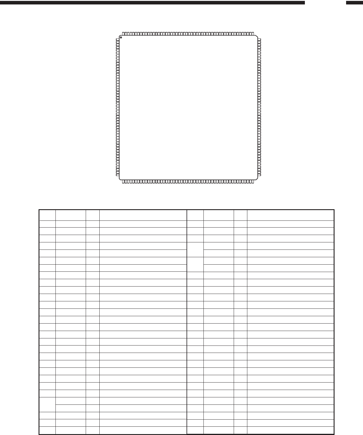
ES4408F (DM: IC101)
29 TDMCLK I TDM clock input
30 TDMFS I TDM frame sync
31 TDMTSC# O TDM output enable, active low
32 TWS O Audio transmit frame sync
SEL_PLL1 I Select PLL1
33 TSD0 O Audio transmit serial data port0
SEL_PLL0 I Select PLL0
34 Vss I GND
35 Vcc I 3.6V power supply
36 TSD1 O Audio transmit serial data port1
37 TSD2 O Audio transmit serial data port2
38 TSD3 O Audio transmit serial data port3
39 MCLK I/O Audio master clock for audio DAC
40 TBCK I/O Audio transmit bit clock
41
SPDIF_DOBM
O S/PDIF (IEC958) format output
42 NC No connect pin
43 Vss I GND
44 Vcc I 3.6V power supply
45 RSD I Audio receive serial data
46 RWS I Audio receive frame sync
47 RBCK I Audio receive bit clock
48 APLLCAP I Analog PLL capacitor
49 XIN I Crystal input
50 XOUT O Crystal output
51 Vcc I 3.6V power supply
52 Vss I GND
53 DMA 0 O DRAM address bus
54 DMA 1 O DRAM address bus
55 DMA 2 O DRAM address bus
Pin Name FunctionPin No. I/O

26
ADV-1000
Pin Name FunctionPin No. I/O Pin Name FunctionPin No. I/O
56 DMA 3 O DRAM address bus
57 DMA 4 O DRAM address bus
58 DMA 5 O DRAM address bus
59 Vcc I 3.6V power supply
60 Vss I GND
61 DMA 6 O DRAM address bus
62 DMA 7 O DRAM address bus
63 DMA 8 O DRAM address bus
64 DMA 9 O DRAM address bus
65 DMA 10 O DRAM address bus
66 DMA 11 O DRAM address bus
67 Vss I GND
68 Vcc I 3.6V power supply
69 DCAS# O Column address strobe, active low
70 DOE# O Output enable, active low
DSCK_EN I Clock enable, active low
71 DWE# O DRAM write enable, active low
72 DRAS 0# O Row address strobe, active low
73 DRAS 1# O Row address strobe, active low
74 DRAS 2# O Row address strobe, active low
75 Vcc I 3.6V power supply
76 Vss I GND
77 DB 0 I/O DRAM data bus
78 DB 1 I/O DRAM data bus
79 DB 2 I/O DRAM data bus
80 DB 3 I/O DRAM data bus
81 DB 4 I/O DRAM data bus
82 DB 5 I/O DRAM data bus
83 Vcc I 3.6V power supply
84 Vss I GND
85 DB 6 I/O DRAM data bus
86 DB 7 I/O DRAM data bus
87 DB 8 I/O DRAM data bus
88 DB 9 I/O DRAM data bus
89 DB 10 I/O DRAM data bus
90 DB 11 I/O DRAM data bus
91 Vss I GND
92 Vcc I 3.6V power supply
93 DB 12 I/O DRAM data bus
94 DB 13 I/O DRAM data bus
95 DB 14 I/O DRAM data bus
96 DB 15 I/O DRAM data bus
97 DCS 1# O SDRAM chip select [1], active low
98 Vss I GND
99 Vcc I 3.6V power supply
100 DCS 0# O SDRAM chip select [0], active low
101 DQM O Data input/output mask
102 DSCK O Clock to SDRAM
103 Vss I GND
104 Vcc I 3.6V power supply
105 DCLK I Clock input (27MHz)
106 YUV 0 O 8-bit YUV output
107 YUV 1 O 8-bit YUV output
108 YUV 2 O 8-bit YUV output
109 YUV 3 O 8-bit YUV output
110 YUV 4 O 8-bit YUV output
111 Vcc I 3.6V power supply
112 Vss I GND
113 YUV 5 O 8-bit YUV output
114 YUV 6 O 8-bit YUV output
115 YUV 7 O 8-bit YUV output
116
PCLK2XSCN
I/O 2X pixel clock
117
PCLKQSCN
I/O Pixel clock
118 VSYNCH# I/O
Vertical sync for screen video interface,
programmable for rising or falling edge,
active low
119 HSYNCH# I/O
Horizontal sync for screen video
interface, programmable for rising or
falling edge, active low
120 Vss I GND
121 Vcc I 3.6V power supply
122 HD 0 I/O Host data bus
123 HD 1 I/O Host data bus
124 HD 2 I/O Host data bus
125 HD 3 I/O Host data bus
126 HD 4 I/O Host data bus
127 HD 5 I/O Host data bus
128 HD 6 I/O Host data bus
129 Vss I GND
130 Vcc I 3.6V power supply
131 HD 7 I/O Host data bus
132 HD 8 I/O Host data bus
133 HD 9 I/O Host data bus
134 HD 10 I/O Host data bus
135 HD 11 I/O Host data bus
136 HD 12 I/O Host data bus
137 HD 13 I/O Host data bus
138 Vss I GND
139 Vcc I 3.6V power supply
140 HD 14 I/O Host data bus
141 HD 15 I/O Host data bus
142 HWRQ# O Host write request
143 HRDQ# O Host read request
144 HIRQ I/O Host interrupt
145 HRST# O Host reset
146 HIORDY I Host I/O ready
147 Vss I GND
148 Vcc I 3.6V power supply
149
HWR# O Host write request
HWR#/DCI_ACK#
I, I Host write / DCI interface acknowledge
signal, active low
150
HRD#/DCI_CLK
I, I Host read / DCI interface clock
151 HIOCS16# I Device 16-bit data transfer
152 HCS1FX# O Host select 1
153 HCS3FX# O Host select 3
154 HA 0 I/O Host address bus
155 HA 1 I/O Host address bus
27
ADV-1000
Pin Name FunctionPin No. I/O
156 Vss I GND
157 Vcc I 3.6V power supply
158 HA 2 I/O Host address bus
159 VPP I Peripheral protection voltage
160 AUX 0 I/O Auxiliary port, (SDATA) I/O
161 AUX 1 I/O Auxiliary port, (SCLK) O
162 AUX 2 I/O Auxiliary port, (VFD DATA) I/O
163 Vss I GND
164 Vcc I 3.6V power supply
165 AUX 3 I/O Auxiliary port, (AMUTE) O
166 AUX 4 I/O Auxiliary port, (IR) I
167 AUX 5 I/O Auxiliary port, (POWER) I
168 AUX 6 I/O Auxiliary port, (VFDCS) O
169 AUX 7 I/O Auxiliary port, (VFDCLK) O
170 LOE# O Device output enable, active low
171 Vss I GND
172 Vcc I 3.6V power supply
173 LCS 0# O Chip select [0], active low
174 LCS 1# O Chip select [1], active low
175 LCS 2# O Chip select [2], active low
176 LCS 3# O Chip select [3], active low
177 Vss I GND
178 LD 0 I/O Device data bus
179 LD 1 I/O Device data bus
180 LD 2 I/O Device data bus
181 LD 3 I/O Device data bus
182 LD 4 I/O Device data bus
183 Vcc I 3.6V power supply
184 Vss I GND
185 LD 5 I/O Device data bus
186 LD 6 I/O Device data bus
187 LD 7 I/O Device data bus
188 LD 8 I/O Device data bus
189 LD 9 I/O Device data bus
190 LD 10 I/O Device data bus
191 LD 11 I/O Device data bus
192 Vss I GND
193 Vcc I 3.6V power supply
194 LD 12 I/O Device data bus
195 LD 13 I/O Device data bus
196 LD 14 I/O Device data bus
197 LD 15 I/O Device data bus
198 LWRLL# O Device write enable, active low
199 LWRHL# O Device write enable, active low
200 Vss I GND
201 Vcc I 3.6V power supply
202 NC No connect pin
203 NC No connect pin
204 LA 0 O Device address output
205 LA 1 O Device address output
206 LA 2 O Device address output
207 LA 3 O Device address output
208 Vss I GND
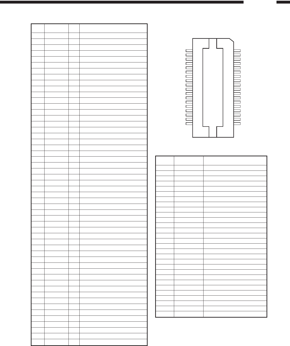
TP2050 (AP: IC102, 202, 302)
136 GNDSUBVCCSIGN
235 OUT2BVCCSIGN
334 OUT2BVSS
433 VCC2BVSS
532 GND2BIN2B
631 GND2AIN2A
730 VCC2AIN1B
829 OUT2AIN1A
928 OUT2ATH_WAR
1027 OUT1BFAULT
1126 OUT1BTRISTATE
1225 VCC1BPWRDN
1324 GND1BCONFIG
1423 GND1AIBIAS
1522 VCC1AVDD
1621 OUT1AVDD
1720 OUT1AGNDREG
1819 NCGNDCLEAN
Pin Function Description
1 GNDSUB Substrate ground
2,3 OUT2B Output half bridge 2B
4 VCC2B Positive supply
5 GND2B Negative supply
6 GND2A Negative supply
7 VCC2A Positive supply
8,9 OUT2A Output half bridge 2A
10,11 OUT1B Output half bridge 1B
12 VCC1B Positive supply
13 GND1B Negative supply
14 GND1A Negative supply
15 VCC1A Positive supply
16,17 OUT1A Output half bridge 1A
18 NC Not connected
19 GNDCLEAN Logic ground
20 GNDREG Ground for Vdd regulator
21,22 VDD
5V regulator referenced to ground
23 IBIAS Logic high voltage
24 CONFIG Config input
25 PWRDN Stand-by pin
26 TRISTATE Hi-Z pin
27 FAULT Fault output
28 TH_WAR Thermal warning output
29 IN1A Input half bridge 1A
30 IN1B Input half bridge 1B
31 IN2A Input half bridge 2A
32 IN2B Input half bridge 2B
33,34 VSS 5V regulator referenced to Vcc
35,36 VCCSIGN Signal positive supply
TP2050 Terminal Function
28
ADV-1000
1
2
3
4
5
6
7
8
9
10
11
12
13
14
15
16
17
18
19
20
21
42
41
40
39
38
37
36
35
34
33
32
31
30
29
28
27
26
25
24
23
22
43
44
45
46
47
48
49
50
A
9
V
DD
DQ
1
DQ
0
DQ
3
DQ
2
DQ
7
DQ
6
DQ
5
DQ
4
A
0
A
1
A
2
A
3
V
DD
V
SSQ
V
SSQ
LDQM
WE
CAS
RAS
CS
BA
A
10
/AP
V
SS
N.C
CKE
CLK
UDQM
N.C/RFU
V
SSQ
DQ
10
DQ
11
V
DDQ
V
SSQ
DQ
14
DQ
15
V
SS
DQ
13
DQ
12
V
DDQ
DQ
9
DQ
8
A
8
A
7
A
6
A
5
A
4
V
DDQ
V
DDQ
16M SDRAM (TSOP)-8 (DM: IC103, 104)
K4S161622D-TC80
W981616AH-8
Terminal Function
1VDD Power Supply/Ground Power and ground for the input buffer and the core logic
2DQ0Data Input/Output Data input/output are mutiplexed on the same pin
3DQ1Data Input/Output Data input/output are mutiplexed on the same pin
4VSSQ Data Output Power/Ground Isolated power supply and ground for the output buffer
5DQ2Data Input/Output Data input/output are mutiplexed on the same pin
6DQ3Data Input/Output Data input/output are mutiplexed on the same pin
7VDDQ Data Output Power/Ground Isolated power supply and ground for the output buffer
8DQ4Data Input/Output Data input/output are mutiplexed on the same pin
9DQ5Data Input/Output Data input/output are mutiplexed on the same pin
10 VSSQ Data Output Power/Ground Isolated power supply and ground for the output buffer
11 DQ6Data Input/Output Data input/output are multiplexed on the same pin
12 DQ7Data Input/Output Data input/output are multiplexed on the same pin
13 VDDQ Data Output Power/Ground Isolated power supply and ground for the output buffer
14 L DQM Data Input/Output Mask Blocks data input when active
15 WE Write Enable Enables write operation and row precharge
16 CAS Column Address Strobe Latches column address on the positive going edge of the CLK at low
17 RAS Row Address Strobe Latches row address on the positive going edge of the CLK at low
18 CS Chip Select Disables or enables device operation by masking or enabling all
inputs except CLK, CKE, and LDQM
19 BA Bank Select Address Selects bank to be activated during row address latch time
20 A10/AP Address Row/column addresses are multiplexed on the same pin
21 A0Address Row/column addresses are multiplexed on the same pin
22 A1Address Row/column addresses are multiplexed on the same pin
23 A2Address Row/column addresses are multiplexed on the same pin
24 A3Address Row/column addresses are multiplexed on the same pin
25 VDD Power Supply/Ground Power and ground for the input buffer and the core logic
26 VSS Power Supply/Ground Power and ground for the input buffer and the core logic
27 A4Address Row/column addresses are multiplexed on the same pin
28 A5Address Row/column addresses are multiplexed on the same pin
29 A6Address Row/column addresses are multiplexed on the same pin
30 A7Address Row/column addresses are multiplexed on the same pin
31 A8Address Row/column addresses are multiplexed on the same pin
32 A9Address Row/column addresses are multiplexed on the same pin
33 N. C No Connection No connect pin
34 CKE Clock Enable Masks system clock to freeze operation from the next clock cycle
35 CLK System Clock Active on the positive going edge to sample all inputs
36 U DQM Data Input/Output Mask Blocks data input when active
37 N. C/RFU NC/Reserved No connect pin
38 VDDQ Data Output Power/Ground Isolated power supply and ground for the output buffer
39 DQ8Data Input/Output Data input/output are multiplexed on the same pin
40 DQ9Data Input/Output Data input/output are multiplexed on the same pin
41 VSSQ Data Output Power/Ground Isolated power supply and ground for the output buffer
42 DQ10 Data Input/Output Data input/output are multiplexed on the same pin
43 DQ11 Data Input/Output Data input/output are multiplexed on the same pin
44 VDDQ Data Output Power/Ground Isolated power supply and ground for the output buffer
45 DQ12 Data Input/Output Data input/output are multiplexed on the same pin
46 DQ13 Data Input/Output Data input/output are multiplexed on the same pin
47 VSSQ Data Output Power/Ground Isolated power supply and ground for the output buffer
48 DQ14 Data Input/Output Data input/output are multiplexed on the same pin
49 DQ15 Data Input/Output Data input/output are multiplexed on the same pin
50 VSS Power Supply/Ground Power and ground for the input buffer and the core logic
Pin Name FunctionPin No. Symbol
29
ADV-1000
1
2
3
4
5
6
7
8
9
10
11
12
13
14
15
16
17
18
19
20
21
22
23
24
25
26
27
28
29
30
31
32
33
34
35
36
37
38
39
40
41
42
43
44
AVSS-DS
XSRFIN
XSIPIN
AVDD5-DS
XSDSSLV
XSRSLINT
VDD
XSAWRC
XSRFGC
XSEFGC
XSFOCUS
XSTRACK
XSSLEG
AVDD5-DA
XSMOTOR
AVSS-DA
XSRFRPLP
XSTELP
XSVREF2
XSRFRP
XSTEXI
AVSS-AD
XSTEI
XSFEI
XSAEI
AVDD5-AD
XSSBAD
GND
XSDFCT
XSCSJ
XSCLK
XSDATA
XSLDC
XSFGIN
XSSPDON
XSFLAG(3)
XSFLAG(2)
XSFLAG(1)
XSFLAG(0)
XMP1_7
XMP1_6
GND
NC
XMP1_4
132
131
130
129
128
127
126
125
124
123
122
121
120
119
118
117
116
115
114
113
112
111
110
109
108
107
106
105
104
103
102
101
100
99
98
97
96
95
94
93
92
91
90
89
XRD(3)
XRD(12)
GND
XRD(2)
XRD(13)
XRD(1)
XRD(14)
XRD(0)
XRD(15)
XHD(7)
XHD(8)
XHD(6)
XHD(9)
XHD(5)
XHD(10)
XHD(4)
XHD(11)
VDD
XHD(3)
XHD(12)
XHD(2)
XHD(13)
GND
XHD(1)
XHD(14)
XHD(0)
XHD(15)
XHDRQ
XHIOWJ
XHIORJ
XHIORDY
XHDACKJ
XHINT
XHCS16J
XHA(1)
XHPDIAGJ
XHA(0)
XHA(2)
XHCS1J
XHCS3J
XHDASPJ
XMA(15)
XMA(14)
XMA(13)
45
46
47
48
49
50
51
52
53
54
55
56
57
58
59
60
61
62
63
64
65
66
67
68
69
70
71
72
73
74
75
76
77
78
79
80
81
82
83
84
85
86
87
88
XMP1_3
XMFSCSJ
XMP1_2
XGPIO(2)
XMP1_1
XMRSTJ
XGPO(1)
XGPO(0)
XCRSTJ
XMPSENJ
VDD
XMALE
XMP1_0
VDD
XOSC1
XOSC2
GND
XMD(0)
XMD(1)
XMD(2)
XMD(3)
XMD(4)
XMD(5)
XMD(6)
XMD(7)
XMCSJ
XMRDJ
XMWRJ
XMINT1J
XMA(11)
XMA(10)
VDD
XMA(9)
XMA(8)
XMA(7)
XMA(6)
XMA(5)
XMA(4)
XMA(3)
XMA(2)
XMA(1)
XMA(0)
XMA(12)
GND
176
175
174
173
172
171
170
169
168
167
166
165
164
163
162
161
160
159
158
157
156
155
154
153
152
151
150
149
148
147
146
145
144
143
142
141
140
139
138
137
136
135
134
133
XSAWRCVCO
XSVREFO
XSPDOFTR2
XSVR_PLL
XSFTROPI
XSFDO
AVSS_PL
XSPLLFTR2
AVDD5_PL
XSFDIREF
XSPDIREF
GND
XTSLRF
XTPLCK
VDD
XRA(3)
XRA(2)
XRA(1)
XRA(0)
XRA(4)
XRA(5)
XRA(6)
GND
XRA(7)
XRA(10)
XRA(11)
VDD
XRA(8)
XRA(9)
XROEJ
VDD
XRCASJ
XRRASJ
XRSDCLK
XRWEJ
XRD(7)
XRD(8)
XRD(6)
GND
XRD(9)
XRD(5)
XRD(10)
XRD(4)
XRD(11)
Data
Separator
ATAPI
&
MPEG
I/F
Digital
Servo
DVD-DSP RAM
Arbiter
Target
Search
ROM
C3 ECC
EDC
MPEG
DEC.
Motor
Driver
PC
4M DRAM
CD-DSP MCU
M
M5705
M5705 Terminal Function
M5705 (DM: IC501)
DescriptionPin No. Pin Name Type
2 XSRFIN I/A Analog RF signal input after passing through the equalizer
3 XSIPIN I/A Inverting input pin of data slicer
5 XSDSSLV O/A Slice level output pin
6 XSRSLINT I/A Reference current setting pin for analog data slicer
8 XSAWRC O/A Output for enlarge VCO range. Analog output from DAC buffer
9 XSRFGC O/A RF gain control output
10 XSEFGC O/A E,F gain control output
11 XSFOCUS O/A Output voltage level for focusing buffer IC
12 XSTRACK O/A Output voltage level for tracking buffer IC
13 XSSLEG O/A Output voltage level for sledge buffer IC
15 XSMOTOR O/A Output voltage level for spindle motor buffer IC
17 XSRFRPLP I/A High bandwidth low pass filter input for RFRP
18 XSTELP I/A High bandwidth low pass filter input for TE
19 XSVREF2 I/A 2.1V reference voltage input
20 XSRFRP I/A RF ripple/envelope signal input
21 XSTEXI I/A Tracking zero crossing input signal
23 XSTEI I/A Tracking error input signal
24 XSFEI I/A Focus error input signal
25 XSCEI I/A 1. Center error input signal
2. Photo Interrupt input
30
ADV-1000
DescriptionPin No. Pin Name Type
27 XSSBAD I/A Sub-beam addition signal input
166 XSPDIREF I/A Phase detector reference current generator. Connect a resistor between this pin and
ground to set reference current
167 XSFDIREF I/A Frequency detector reference current generator. Connect a resistor between this pin and
ground to set reference current
169 XSPLLFTR2 I/A Data PLL loop filter pin#2
171 XSFDO O/A Output node of frequency detector charge pump circuit
172 XSFTROPI I/A Input node of loop filter OP circuit
173 XSVR_PLL I/A PLL reference voltage input
174 XSPDOFTR2 I/A Phase detector filter pin#1
175 XSVREFO O/A Reference voltage output
176 XSAWRCVCO I/A Auto Wide Range Control of VCO input pin. For enlarge VCO range in CAV mode
29 XSDFCT I Detect detection signal input
30 XSCSJ O Chip select signal for accessing control registers
31 XSCLK O Clock output for accessing control registers
32 XSDATA I/O Registers data input/output pin
33 XSLDC O Laser diode on/off control output for both CD/DVD
34 XSFGIN I Motor Hall sensor input
35 XSSPDON O Spindle motor on output
36, 37, 38, 39 XSFLAG[3:0] O These pins are used to monitor some status of servo control block
48, 51, 52 XGPIO[2:0] I/O 1. These pins are used as general purpose I/O bus
2. When use internal microcontroller, XGPIO[2] can be used as programmable I/O port 3.6.
40 XMP1_7 I/O Internal microcontroller programmable I/O port 1.7.
41 XMP1_6 I/O Internal microcontroller programmable I/O port 1.6.
43 XMP1_5 I/O This pin is now changed to be NC.
44 XMP1_4 I/O Internal microcontroller programmable I/O port 1.4.
45 XMP1_3 I/O Internal microcontroller programmable I/O port 1.3.
47 XMP1_2 I/O Internal microcontroller programmable I/O port 1.2.
49 XMP1_1 I/O Internal microcontroller programmable I/O port 1.1.
57 XMP1_0 I/O Internal microcontroller programmable I/O port 1.0.
This pin is default used as the A16 (microcontroller address line 16)
46 XMFSCSJ I/O Output chip select connected to external flash ROM chip enable pin
54 XMPSENJ I/O Output program store enable connected to external ROM PSENJ pin.
56 XMALE I/O This signal is used as address latch signal in address/data mux mode
70 XMCSJ I/O 1. This signal must be asserted for all microcontroller accesses to the register of this chip
2. When use internal microcontroller, this signal can be used as programmable I/O port 3.1
71 XMRDJ I/O 1. This signal is used as the Read Strobe signal
2. When use internal microcontroller, this signal can be used as programmable I/O port 3.0
72 XMWRJ I/O This signal is used as the Wire Strobe signal
73 XMINT1J I/O 1. This signal is an interrupt line to the microcontroller
2. When use internal microcontroller, this signal can be used as programmable I/O port 3.7
74, 75, 77, 78,
XMA[15:0] I/O These pins are used as address bus
79, 80, 81, 82,
83, 84, 85, 86,
87, 89, 90, 91
62, 63, 64, 65, XMD[7:0] I/O These pins are used as data bus for the 16-bit processor mode, or the address/data mux
66, 67, 68, 69 bus for the 8-bit processor mode.
163 XTPLCK I/O PLCK test pin
164 XTSLRF I/O SLRF test pin
59 XOSC1 I Crystal input/System clock. The input frequency from outside crystal or oscillator is 33.8688MHz
60 XOSC2 O Crystal output
53 XCRSTJ I Chip Reset. As asserted low input generates a component reset that stops all operations within
the chip and deasserts all output signals. All input/output signals are set to input.
94 XHCS1J I This pin is used to select the command block task file registers
93 XHCS3J I This pin is used to select the control block task file registers
103 XHIORJ I Asserted by the host during a host I/O read operation
104 XHIOWJ I Asserted by the host during a host I/O write operation
105 XHDRQ O
1.
DMA request. This pin is configured as the DMA request signal, and is used during DMA transfer
between the host and the controller. This pin is tri-stated when DMA transfers are not enabled.
2.
MPEG acknowledge. This pin is used as the ACKJ signal when MPEG interface mode is selected.
101 XHDACKJ I
1. DMA acknowledge. This pin is configured as DACKJ, and is used as the DMA acknowledge
signal during DMA data transfers.
2. MPEG request. This pin is used as the REQ signal when MPEG interface mode is selected
99 XHCS16J O
1. 16-bit data select. This signal indicates that a 16-bit data transfer is active on the host data
bus. This pin is open-drain tri-state output.
2. MPEG clock. This pin is used as the CLOCK signal when MPEG interface mode is selected.
50 XHRSTJ I Host Reset. The reset of ATA bus
100 XHINT O
1. Host interface request. This tri-state pin is the host interrupt request, and is asserted to
indicate to the host that the controller needs attention.
2. MPEG begin. This pin is used as the BEGIN signal when MPEG interface mode is selected
31
ADV-1000
DescriptionPin No. Pin Name Type
97 XHPDIAGJ I/O This pin is used as the Passed Diagnostics signal, and may be an input or an open-drain output
92 XHDASPJ I/O This pin is used as the Drive Active/Slave Present signal, and is an input or an open-drain
output. This pin is used for Master/Slave drive communication and/or for driving an LED
102 XHIORDY I/O
1. I/O channel ready. This signal is driven low to extend host transfer cycles when the controller
is not ready to respond. This pin will be tri-stated when a read or write is not in progress.
2. MPEG error. This pin is used as the ERROR signal when MPEG interface mode is selected
95, 96, 98 XHA[2:0] I Host address lines. The host address lines A[2:0] are used to access the various host control,
status, and data registers
XHD[15.0] I/O
1. Host data bus. This bus is used to transfer data and status between the host and the controller.
106, 107, 108, 2.
MPEG data bus 7-8. The HD[7:0] are used as the DATA [7:0] when MPEG interface mode is selected.
109, 111, 112, 3. VCD I/F. Bit3-0 are used as VCD I/F signal when VCD function is enabled. The relationship of
113, 114, 116, bit3-0 and VCD I/F is as follow
117, 118, 119, HD0—CD-DATA
120, 121, 122, HD1—CD-LRCK
123 HD2—CD-BCK
HD3—CD-C2PO
143 XRSDCLK O This signal is the clock output for SDRAM
147 XROEJ O This signal is used as the memory output enable for external DRAM buffers. After RSTJ is
asserted, this signal will be low
142 XRWEJ O This signal is asserted low when a buffer memory write operation is active
144 XRRASJ O This signal is used as Row address output to external DRAM buffer. After RSTJ is asserted, this
signal will be high
145 XRCASJ O This signal is used as column address output to external DRAM. After RSTJ is asserted, this
signal will be high
1. RAM address lines. These are bits11-0 for addressing the buffer memory.
2. Hardware setting. The bits6-0 are used as hardware setting for some functions.
RA[9] : FLASH size is 64K/128K
1: FLASH size is 64K
0: FLASH size is 128K
RA[8] : External CPU is 8032/H8
1: 8032
0: H8
RA[7] : Microcontroller programmable I/O port 1 pin control
1: By internal microcontroller
148, 149, 151, 0: By registers to decide input/output
152, 153, 155, RA[6] : System test pin output
156, 157, 158, XRA[11:0] O 1: Normal operation
159, 160, 161 0: System test pin output
RA[5] : For testing purpose, don’t need to set
RA[4] : IDE master/slave
1: Slave
0: Master
RA[3] : For testing purpose, don’t need to set
RA[2] : For testing purpose, don’t need to set
RA[1-0] : MCU Mode selection
11: Normal Mode (internal uP, internal address latch)
10: Outside uP Mode (ICE Mode)
01: Test mode for internal uP testing
00: Internal uP mode with external address latch
124, 125, 126,
XRD[15:0] I/O These signals are the 8-bit parallel data lines to/from the buffer memory.
127, 128, 129,
131, 132, 134,
135, 136, 137,
138, 139, 140,
141
4 AVDD5_DS Analog Power +5V for Data Slicer part
14 AVDD5_DA Analog Power +5V for DAC part
26 AVDD5_AD Analog Power +5V for ADC part
168 AVDD5_PL Analog Power +5V for Data PLL part
7, 55, 58, 76,
VDD Power +3.3V for digital core logic and pad
115, 146,
150, 162
1 AVSS_DS Analog Ground for Data Slicer part
16 AVSS_DA Analog Ground for DAC part
22 AVSS_AD Analog Ground for ADC part
170 AVSS_PL Analog Ground for Data PLL part
28, 42, 61,
GND Digital Ground core logic and pad.
88, 110, 130,
138, 154, 165

32
ADV-1000
SP3721A Terminal Function
SP3721A (DM: IC502)
DescriptionPin No. Pin Name Type
1, 2 DVDREP, DVDREN I RF Signal Inputs. Differential RF signal attenuator input pins
63 CDRF I RF Signal Inputs. Single-ended RF signal attenuator input pin
59, 60 AIP, AIN I AGC Amplifier Inputs. Differential AGC amplifier input pins
53, 54 DIP, DIN I Analog inputs for RF Single Buffer. Differential analog inputs to the RF single-ended output buffer
and full wave rectifier
32 FDCHG# I
Low Impedance Enable. A TTL compatible input pin that activates the FDCHG switches. A low
level activates the switches and the falling edge of the internal FDCHG triggers the fast decay for
the MIRR bottom hold circuit. (open high)
49 HOLD1 I Hold Control. A TLL compatible control pin which, when pulled high, disables the RF AGC charge
pump and holds the RF AGC amplifier gain at its present value. (open high)
11~14 D, C, B, A I Photo Detector Interface Inputs. Inputs from the main beam Photo detector matrix outputs
5~8 A2, B2, C2, D2 I Photo Detector Interface Inputs. AC coupled inputs for the DPD from the main beam Photo
detector matrix outputs
15~16 F, E I CD tracking Error Inputs. Inputs from the CD photo detector error outputs.
3~4 PD1, PD2 I CD Photo detector Interface Inputs. Inputs from the CD photo detector error outputs
40 MEI I Mirror Envelope Inputs. The SIGO envelope input pin
35 MIN I RF signal Input for Mirror. AC coupled inputs for the mirror detection circuit from the pull-in signal
output. (PI)
21 DVDPD I APC Input. DVD APC input pin from the monitor photo diode
23 CDPD I APC Input. CD APC input pin from the monitor photo diode
25 LDON# I APC Output On/Off. APC output control pin. A low level activates the LD output. (open high)
61, 62 ATON/ATOP O Differential Attenuator Output. Attenuator outputs
51, 52 FNN, FNP O Differential Normal Output. Filter normal outputs
57 SIGO O Single Ended Normal Output. Single-ended RF output
64 CDRFDC O CD RF Signal Output. Single ended CD RF summing output
42 FE O Focusing Error Signal Output. Focus error output reference to VCI
41 TE O Tracking Error Signal Output. Tracking error output reference to VCI
16
15
14
13
12
11
10
9
8
7
6
5
4
3
2
1
33
34
35
36
37
38
39
40
41
42
43
44
45
46
47
48
MLPF
MEVO
MIN
PI
DFT
TPH
MEV
MEI
TE
FE
CE
LCN
LCP
SCLK
SDATA
SDEN
E
F
A
B
C
D
CN
CP
D2
C2
B2
A2
PD2
PD1
DVDRFN
DVDRFP
32313029282726252423222120191817
49505152535455565758596061626364
HOLD1
VNA
FNN
FNP
DIP
DIN
RX
BYP
SIGO
VPA
AIP
AIN
ATON
ATOP
CDRF
CDRDDC
FDCHG#
VIB
VIP
VIIRR
VPB
VCI
VC
LDON#
CDLD
CDPD
DVDLD
DVDPD
VNB
NC
VCI2
CDTE
TOP VIEW
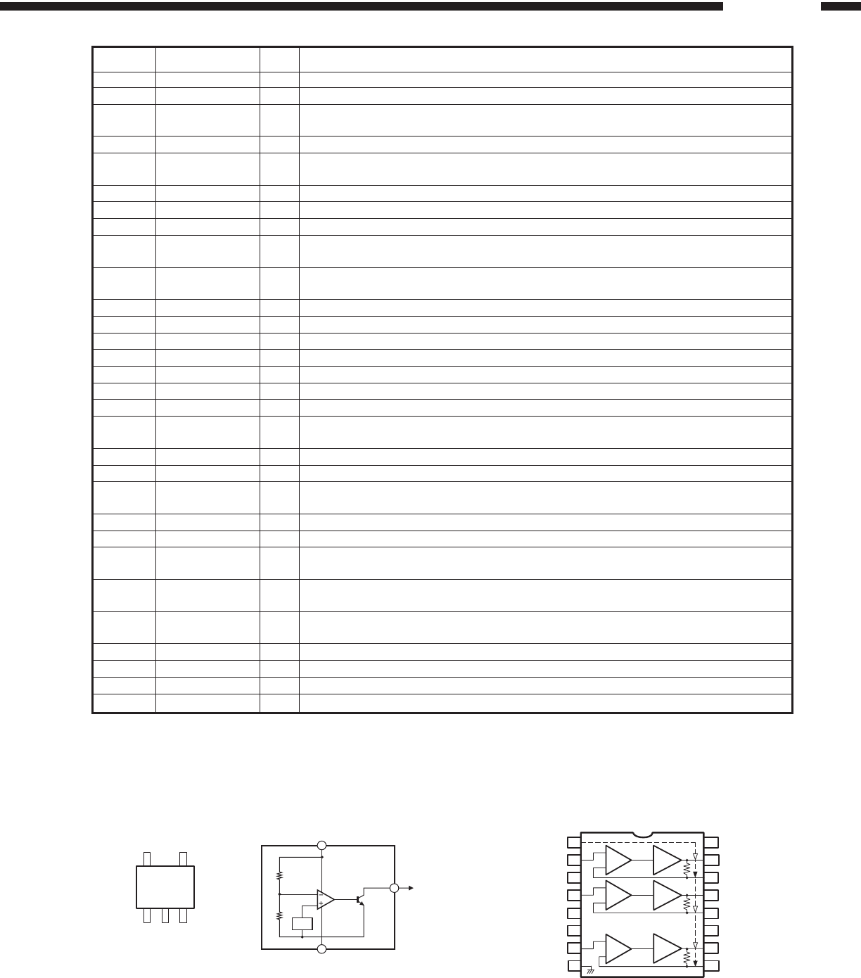
33
ADV-1000
DescriptionPin No. Pin Name Type
43 CE O Center Error Signal Output. Center error output reference to VCI
34 NEVO O SIGO Bottom Envelope Output. Bottom envelope for mirror detection
37 DFT O Defect Output. Pseudo CMOS output. When a defect is detected, the DFT output goes high. Also
the servo AGC output can be monitored at this pin, when CAR bits 7-4 are ‘0011’
29 MIRR O Mirror Detect Output. Mirror Detect comparator output. Pseudo CMOS output
36 PI O Pull-in Signal Output. The summing signal output of A, B, C, D or PD1, PD2 for mirror detection.
Reference to VCI
22 DVDLD O APC output. DVD APC output pin to control the laser power
24 CDLD O APC output. CD APC output pin to control the laser power
56 BYP I/O The RF AGC integration capacitor CBYP, is connected between BYP and VPA
9 CP I/O Differential Phase tracking LPF pin. An external capacitance is connected between this pin and
the CN pin
10 CN I/O Differential Phase tracking LPF pin. An external capacitance is connected between this pin and
the CP pin
45 LCP — Center Error LPF pin. An external capacitance is connected between this pin and the LCN pin
44 LCN — Center Error LPF pin. An external capacitance is connected between this pin and the LCP pin
30 MP — MIRR signal Peak hold pin. An external capacitance is connected to between this pin and VPB
31 MB — MIRR signal Bottom hold pin. An external capacitance is connected to between this pin and VPB
39 MEV — Sigo Bottom Envelope pin. An external capacitance is connected to between this pin and VPB
17 CDTE — CD Tracking. E-F Opamp output for feedback
38 TPH — PI Top Hold pin. An external capacitance is connected to between this pin and VPB
26 VC — Reference Voltage output. This pin provides the internal DC bias reference voltage (+2.5V lix).
Output Impedance is less than 50ohms
27 VCI — Reference Voltage input. DC bias voltage input for the servo input reference
18 VCI2 — Reference Voltage input. DC bias voltage input for the servo input reference
55 RX — Reference Resistor Input. An external 8.2kohm, 1% resistor is connected from this pin to ground
to establish a precise PTAT (proportional to absolute temperature) reference current for the filter
33 MLPF — MIRR signal LPF pin. An external capacitance is connected between this pin and VPB
19 NC — No Connect
48 SDEN I Serial Data Enable. Serial Enable CMOS input. A high level input enable the serial port (Not to be
left open)
47 SDATA I/O Serial Data. Serial data bi-directional CMOS pin. NRZ programming data for the internal registers
is applied to this input ( Not to be left open)
46 SCLK I Serial Clock. Serial Clock CMOS input. The clock applied to this pin is synchronized with the data
applied to SDATA (Not to be left open)
58 VPA Power. Power supply pin for the RF block and serial port
28 VPB Power. Power supply pin for the servo block
50 VNA Ground. Ground pin for the RF block and serial port
20 VNB Ground. Ground pin for the servo bolck
BD4745G (DM: IC109)
54
123
TOP
VIEW
VCC
VOUT
GND
µCOM RESET
Vref
BA7660FS (AP:IC801, 802)
GND
MUTE
INA
GND
INB
GND
N.C.
INC
1
2
3
4
5
6
7
8
16
15
14
13
12
11
10
9
V
CC
OUTA1
OUTA2
OUTB1
OUTB2
N.C.
OUTC1
OUTC2
6dB
6dB
6dB
75ohm
75ohm
75ohm
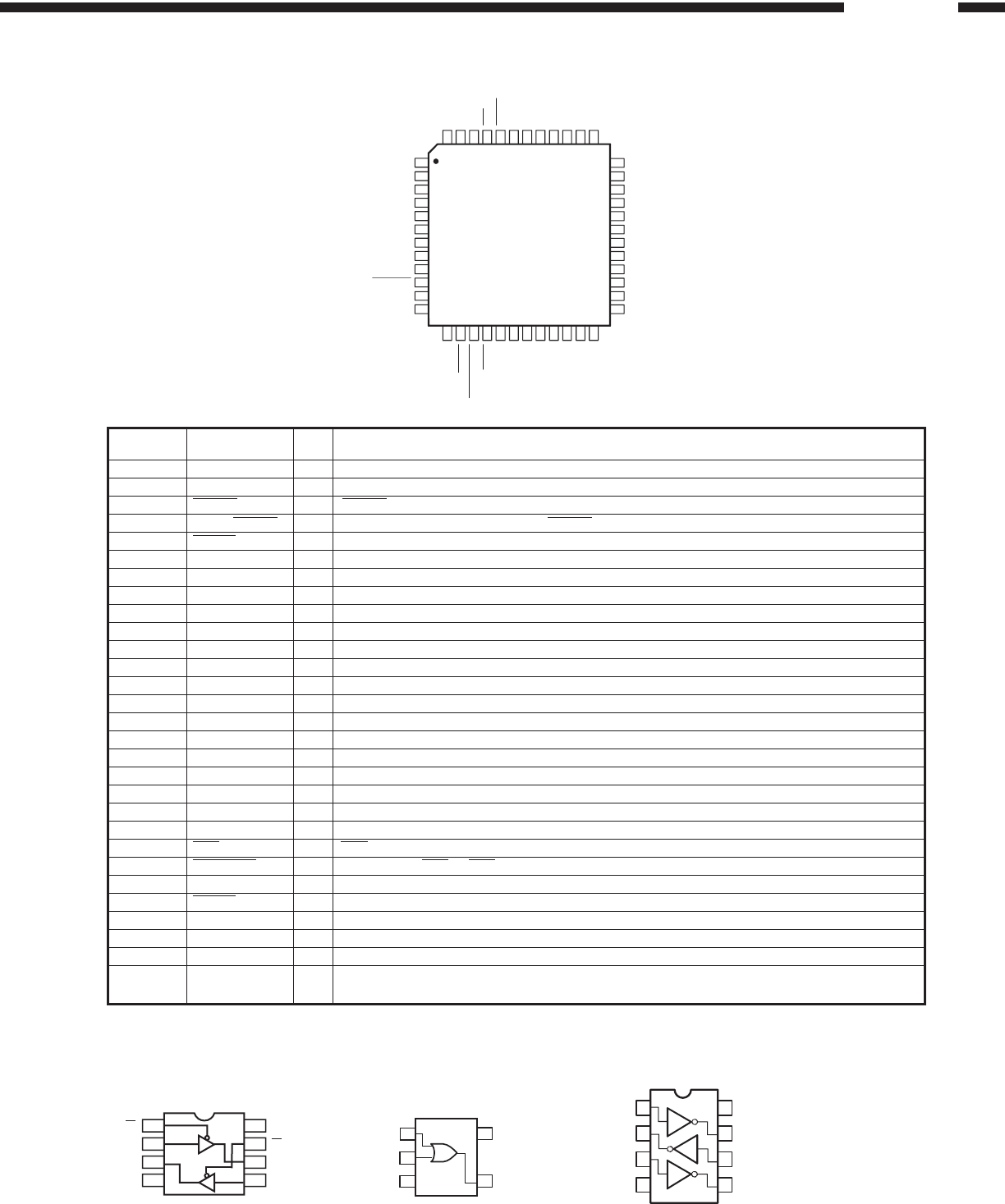
34
ADV-1000
ADV7172KST (DM: IC701)
ADV7172KST Terminal Function
COMP1
V
AA
DAC A
GND
V
AA
DAC E
GND
DAC D
DAC C
DAC B
V
AA
V
AA
36
35
34
33
32
31
30
29
28
27
26
25
1
2
3
4
5
6
7
8
9
10
11
12
V
AA
P1
P0
P4
P3
GND
V
AA
P7
P6
P2
CSO_HSO
P5
13
14
15
16
17
18
19
20
21
22
23
24
GND
FIELD/VSYNC
HSYNC
GND
ALSB
DAC F
COMP2
SD ATA
SCLOCK
BLANK
R
SET2
V
AA
48
47
46
45
44
43
42
41
40
39
38
37
CLOCK
V
AA
GND
PAL_NTSC
RESET
V
REF
R
SET1
TTXREQ
TTX
VSO
SCRESET/RT
C
CLAMP
TOP VIEW
2~9 P7-P0 I 8-Bit 4:2:2 Multiplexed YCrCb Pixel Port (P7-P0).
48 CLOCK I TTL Clock Input .(27 MHz reference clock)
14 HSYNC I/O HSYNC (Modes 1 and 2) Control Signal.
15 FIELD/VSYNC I/O Dual Function FIELD (Mode 1) and VSYNC (Mode 2) Control Signal.
16 BLANK I/O Video Blanking Control Singal.
39 SCRESET/RTC I Subcarrier reset pin, Real-Time Control (RTC) Input.
37 VREF I/O Voltage Reference Input for DACs or Voltage Reference Output (1.235V).
38 RSET1 I Control full-scale amplitudes of the Video Signals from DACs A, B and C.
22 RSET2 I Control full-scale amplitudes of the Video Signals from DACs D, E and F.
36 COMP1 O Compensation Pin for DACs A, B and C.
23 COMP2 O Compensation Pin for DACs D, E and F.
35 DAC A O GREEN/Composite/Y Analog Output.
33 DAC B O BLUE/S-Video Y/U Analog Output.
29 DAC C O RED/S-Video C/V Analog Output.
28 DAC D O GREEN/Composite/Y Analog Output.
25 DAC E O BLUE/S-Video Y/U Analog Output.
24 DAC F O RED/S-Video C/V Analog Output.
20 SCLOCK I MPU Port Serial Interface Clock Input.
21 SDATA I/O MPU Port Serial Data Input/Output.
42 CLAMP O TTL Output Signal to external circuitry.
43 PAL_NTSC I Input signal to select PAL or NTSC mode of operation.
45 VSO O VSO TTL Output Sync Signal.
10 CSO_HSO O Dual function CSO or HSO TTL Output Sync Signal.
17 ALSB I TTL Address Input.
44 RESET I On-chip timing generator reset pin.
41 TTX I Teletest Data Input Pin.
40 TTXREQ O Teletest Data Request output signal.
46 VAA P Power Supply (+3 V to +5 V).
12, 13, 18, GND G Ground Pin.
26, 31, 47
Pin Name FunctionPin No. I/O
TC7WT125FU
(DM: IC114, 115)
KIC7S32FU
(DM: IC110)
TC7WU04F
(DM: IC111)
5
4
1
2
3
Vcc
OUT Y
GND
IN A
IN B
TOP VIEW
1
A1
Y2
GND
2
3
4
8
7
6
5
G1
VCC
Y1
A2
G2
1
2
3
4
8
7
6
5
1A
3Y
2A
GND
Vcc
1Y
3A
2Y

35
ADV-1000
LC89055W (MA: IC713)
LC89055W Terminal Function
1 DISEL I Data input terminal (select input pin of DIN0, DIN1)
2 DOUT O Input bi-phase data through output terminal
3 DIN0 I Amp built-in coaxial/optical input correspond data input terminal
4 DIN1 I Amp built-in coaxial/optical input correspond data input terminal
5 DIN2 I Optical input correspond data input terminal
6 DGND Digital GND
7 DVDD Digital power supply
8 R I VCO gain control input terminal
9 VIN I VCO free-run frequency setting input terminal
10 LPF O PLL loop filter setting terminal
11 AVDD Analog power supply
12 AGND Analog GND
13 CKOUT O Clock output terminal (256fs, 384fs, 512fs, X’tal osc., VCO free-run osc.)
14 BCK O 64fs clock output terminal
15 LRCK O fs clock output terminal (L: Rch, H: Lch, I2S: Reverse)
16 DATAO O Data output terminal
17 XSTATE O Input data detecting result output terminal
18 DGND Digital GND
19 DVDD Digital power supply
20 XMCK O X’tal osc. clock output terminal (24.576MHz or 12.288MHz)
21 XOUT O X’tal osc. connection output terminal
22 XIN I X’tal osc. connection input terminal, external signal input possible (24.576MHz or 12.288MHz)
23 EMPHA O Emphasis information output terminal of channel status
24 AUDIO O Bit1 output terminal of channel status
25 CSFLAG O Top 40bit revise flag output terminal of channel status
26 F0/P0/C0 O Input fs cal. sig. out/data type out/input word inf. output terminal
27 F1/P1/C1 O Input fs cal. sig. out/data type out/input word inf. output terminal
28 F2/P2/C2 O Input fs cal. sig. out/data type out/input word inf. output terminal
29 VF/P3/C3 O Validity flag out/data type out/input word inf. output terminal
30 DVDD Digital power supply
31 DGND Digital GND
32 AUTO O Non PCM burst data transfer detect sig. output terminal
33 BPSYNC O Non PCM burst data preamble Pa, Pb, Pc, Pd sync sig. output terminal
34 ERROR O PLL lock error, data error flag output terminal
35 DO O CPU/IFD read data output terminal
36 DI I CPU I/F write data input terminal
37 CE I CPU I/F chip enable input terminal
38 CL I CPU I/F chip enable input terminal
39 XSEL I Frequency select input pin of XIN X’tal osc. (24.576MHz or 12.288MHz)
40 MODE0 I Mode setting input terminal
41 MODE1 I Mode setting input terminal
42 DGND Digital GND
43 DVDD Digital power supply
44 DOSEL0 I Data output format select input terminal
45 DOSEL1 I Data output format select input terminal
46 CKSEL0 I Output clock select input terminal
47 CKSEL1 I Output clock select input terminal
48 XMODE I Reset input terminal
Pin
No. Pin Name FunctionI/O
For latch-up countermeasure, set digital (DVDD) and analog (AVDD) power on/off in the same timing.

36
ADV-1000
1,12,23 VD1,2,3 Digital power supply (+)
2,13,24 DGND1,2,3 Digital GND
3 AUDATA3, XMT958 SPDIF transmitter output, Digital audio output 3
4 WR, DS, EMWR, GPIO10 Host write strobe, Host data strobe, External memory write enable,
General purpose in/output 10
5 RD, R/W, EMOE,GPIO11 Host parallel output enable, Host parallel R/W, External memory output enable,
General purpose in/output 11
6 A1,SCDIN Host address bit 1, SPI serial control data input
7 A0,SCCLK Host parallel address bit 0, Serial control port clock
8 DATA7, EMAD7, GPIO7 Bidirectional data bus 7, External memory address 7, General purpose in/output 7
9 DATA6, EMAD6, GPIO6 Bidirectional data bus 6, External memory address 6, General purpose in/output 6
10 DATA5, EMAD5, GPIO5 Bidirectional data bus 5, External memory address 5, General purpose in/output 5
11 DATA4, EMAD4, GPIO4 Bidirectional data bus 4, External memory address 4, General purpose in/output 4
14 DATA3, EMAD3, GPIO3 Bidirectional data bus 3, External memory address 3, General purpose in/output 3
15 DATA2, EMAD2, GPIO2 Bidirectional data bus 2, External memory address 2, General purpose in/output 2
16 DATA1, EMAD1, GPIO1 Bidirectional data bus 1, External memory address 1, General purpose in/output 1
17 DATA0, EMAD0, GPIO0 Bidirectional data bus 0, External memory address 0, General purpose in/output 0
18 CS Host parallel chip select, Host serial SPI chip select
19 SCDIO, SCDOUT, PSEL,GPIO9 Serial control port data in/output, Parallel port type select, General purpose in/output 9
20 INTREQ, ABOOT Control port interrupt request, Automatic boot enable
21 EXTMEM, GPIO8 External memory chip select, General purpose in/output 8
22 SDATAN1 PCM audio data input 1
25 SCLKN1, STCCLK2 PCM audio input bit clock
26 LRCLKN1 PCM audio input sample rate clock
27 CMPDAT, SDATAN2 PCM audio data input 2
28 CMPCLK, SCLKN2 PCM audio input bit clock
29 CMPREQ, LRCLKN2 PCM audio input sample rate clock
30 CLKIN Master clock input
31 CLKSEL DSP clock select
32 FILT2 PLL filter
33 FILT1 PLL filter
34 VA Analog power supply (+)
35 AGND Analog GND
36 RESET Master reset input
37 DD Reserved
38 DC Reserved
39 AUDATA2 Digital audio output 2
40 AUDATA1 Digital audio output 1
41 AUDATA0 Digital audio output 0
42 LRCLK Audio output sample rate clock
43 SCLK Audio output bit clock
44 MCLK Audio master clock
A0, SCCLK 7
DATA7, EMAD7, GPIO7 8
DATA6, EMAD6, GPIO6 9
DATA5, EMAD5, GPIO5 10
DATA4, EMAD4, GPIO4 11
VD2 12
DGND2 13
DATA3, EMAD3, GPIO3 14
DATA2, EMAD2, GPIO2 15
DATA1, EMAD1, GPIO1 16
DATA0, EMAD0, GPIO0
AUD ATA2
DC
DD
RESET
AGND
VA
FILT1
FILT2
CLKSEL
CLKIN
CMPREQ, LRCLKN217
CS 18
SCDIO, SCDOUT,PSEL, GPIO9 19
ABOOT, INTREQ 20
EXTMEM, GPIO8 21
SDATAN1 22
VD3 23
DGND3 24
SCLKN1, STCCLK2 25
LRCLKN1 26
CMPDAT,SDATAN2, RCV958 27
CMPCLK, SCLKN2 28
39
38
37
36
35
34
33
32
31
30
29
A1, SCDIN
RD, R/W, EMOE, GPIO11
WR/DS/EMWR, GPIO10
AUDATA3, XMT958
DGND1
VD1
MCLK
SCLK
LRCLK
AUD ATA0
AUD ATA1
6
5
4
3
2
1
44
43
42
41
40
Top View
CS493292-CL (MA: IC720)
CS493292-CL Terminal Funtion
Port Name FunctionPin No.
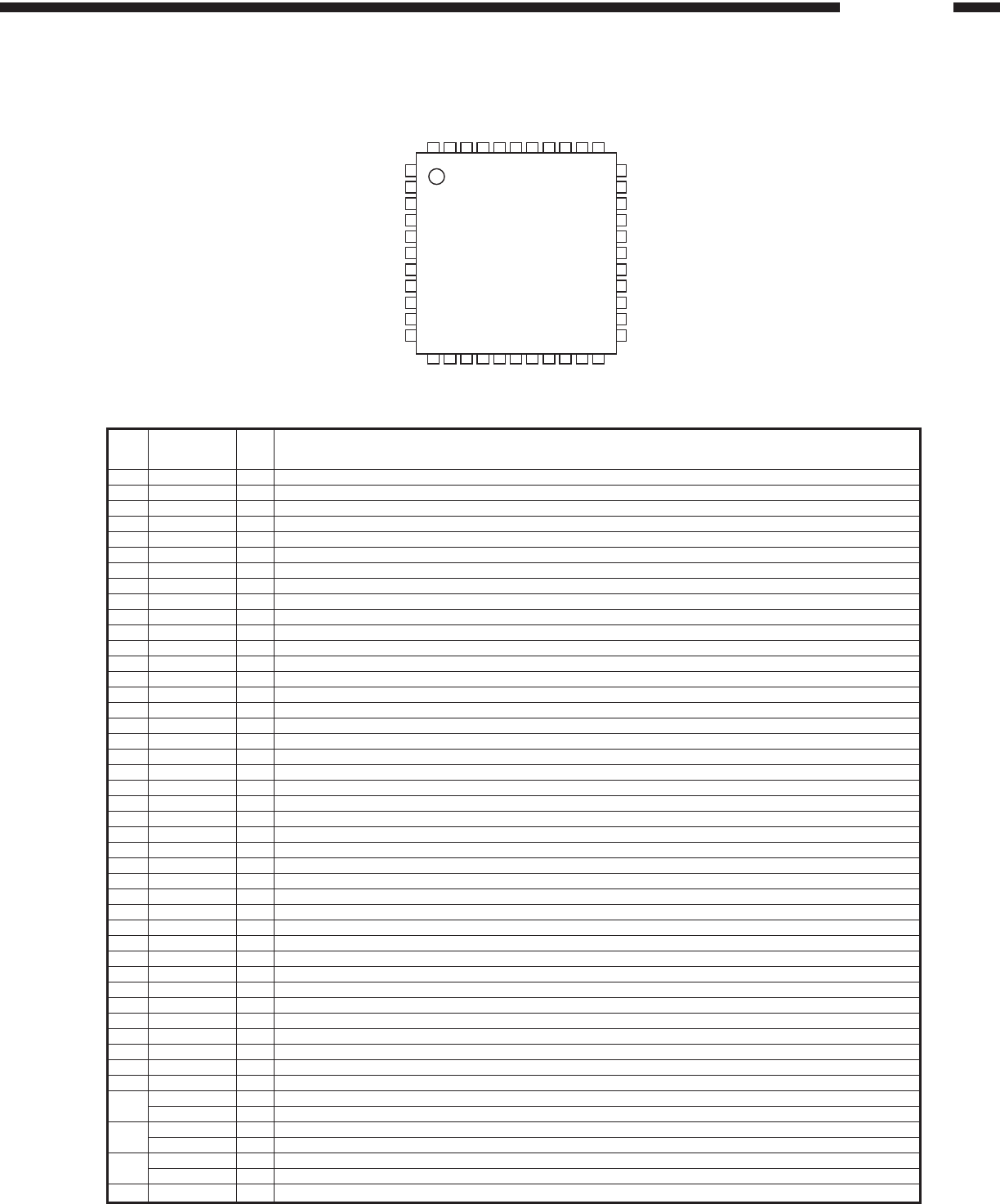
37
ADV-1000
SDOS 1
I2C 2
SMUTE 3
BICK 4
LRCK 5
SDTI1 6
SDTI2 7
SDTI3 8
SDTO 9
DAUX 10
DFS
DZF2/OVF
RIN+
RIN-
LIN+
LIN-
ROUT1
LOUT1
ROUT2
LOUT2
ROUT3
LOUT311
NC 12
DZFE 13
TVDD 14
DVDD 15
DVSS 16
PDN 17
TST 18
NC 19
ADIF 20
CAD1 21
CAD0 22
33
32
31
30
29
28
27
26
25
24
23
LOOP1
LOOP0/SDA/CDTI
DIF1/SCL/CCLK
DIF0/CSN
P/S
MCLK
DZF1
AVSS
AVDD
VREFH
VCOM
44
43
42
41
40
39
38
37
36
35
34
AK4527BVQ
Top View
AK4527BVQ Terminal Function
AK4527BVQ (MA: IC721)
1 SDOS I SDTO source select pin, L: Internal ADC output, H: DAUX input
2 I2C I Serial control mode select pin, L: 3-core serial, H: I2C bus
3 SMUTE I Soft mute pin, H: Soft mute start, L: Release
4 BICK I Audio serial data clock pin
5 LRCK I Input channel clock pin
6 SDTI1 I DAC1 audio serial data input pin
7 SDTI2 I DAC2 audio serial data input pin
8 SDTI3 I DAC3 audio serial data input pin
9 SDTO O Audio serial data output pin
10 DAUX I Auxiliary audio serial data input pin
11 DFS I Double speed sampling mode pin, L: Normal, H: Double
12 NC No connection
13 DZFE I Zero input detect function activate pin, L: Mode 7 at parallel, H: Mode 0
14 TVDD Power pin for output buffer, 2.7V~5.5V
15 DVDD Digital power pin, 4.5V~5.5V
16 DVss Digital GND pin, 0V
17 PDN I Power down & reset pin, L: Powered-down and register initialized, Reset with PDN when switching CAD0-1
18 TST I Test pin, connect to DVSS
19 NC No connection
20 ADIF I Analog input type select pin, H: Differential, L: Single-end
21 CAD1 I Chip address-1 pin
22 CAD0 I Chip address-0 pin
23 LOUT3 O DAC3L channel analog out pin
24 ROUT3 O DAC3R channel analog out pin
25 LOUT2 O DAC2L channel analog out pin
26 ROUT2 O DAC2R channel analog out pin
27 LOUT1 O DAC1L channel analog out pin
28 ROUT1 O DAC1R channel analog out pin
29 LIN- I L-ch analog inverted input pin
30 LIN+ I L-ch analog non-inverted input pin
31 RIN- I R-ch analog inverted input pin
32 RIN+ I R-ch analog non-inverted input pin
33 DZF2/OVF O
0 input detect 2 pin, H: Input data of G2 is 8192 times “0” in a raw or RSTN bit “0”, L: When P/S= “0” /Analog input overflow detect pin
34 VCOM O Common V-out pin, AVDD/2, connect large capacitor to avoid noise
35 VREFH I Ref. V input pin, AVDD
36 AVDD Analog GND pin, 4.5V~5.5V
37 AVss Analog GND pin, 0V
38 DZF1 O 0 input detect pin, H: Input data of G1 is 8192 times “0” in a raw or RSTN bit “0”, L: When P/S= “0”
39 MCLK I Master clock input pin
40 P/S I Parallel/Serial select pin, L: Serial control
41 DIF0 I Audio data I/F format 0 pin (parallel control)
CSN I Chip select pin (3-wire serial control), connect to DVDD when I2C bus control
42 DIF1 I Audio data I/F format 1 pin (parallel control)
SCL/CCLK I Control data clock pin (serial control), I2C=”L”: CCLK (3-wire serial), I2C=”H”: SCL (I2C bus)
43 LOOP0 I Loop back mode 0 pin (parallel control), effects digital loop back ADC to all DAC
SDA/CDTI I/O Control data input pin (serial control), I2C=”L”: CCTI (3-wire serial), I2C=”H” SDA (I2C bus)
44 LOOP1 I Loop back mode 1 pin, from SDT1 to all DAC
Port Name Function
Pin
No. I/O
ADV-1000
38
DescriptionPin No. Function
TC2000 Pin Description
TC2000 (AP: IC101, 201, 301)
BIASCAP
FDBKP2
DCMP
FDBKN2
VPWR
FDBKP1
FDBKN1
HMUTE
Y1
Y1B
Y2B
Y2
NC
OCD1
1
2
3
4
5
6
7
8
9
10
11
12
13
14
28
27
26
25
24
23
22
21
20
19
18
17
16
15
IN2
VP2
BBM1
BBM2
MUTE
IN1
VP1
V5
GND
VHI
OVRLDB
VLO
OCD0
REF
1 BIASCAP Bandgap reference times two (typically 2.5VDC). Used to set the common mode voltage for the
input op amps. This pin is not capable of driving external circuitry.
2,6 FDBKP2, FDBKP1 Positive switching feedback.
3 DCMP Delay compensation. Improves stability in systems with long loop delay. Enabled when the DCMP
pin is either floating or grounded; disabled when DCMP is tied to 5V.
4, 7 FDBKN2, FDBKN1 Negative switching feedback.
5 VPWR Test pin. Must be left floating.
8 HMUTE Logic output. A logic high indicates both amplifiers are muted, due to the mute pin state,
or a "fault".
9, 12 Y1, Y2 Non-inverted switching modulator outputs.
10, 11 Y1B, Y2B Inverted switching modulator outputs.
13 NC No connect.
14 OCD1 Over Current Detect.
15 REF Internal reference voltage; approximately 1.0VDC.
16 OCD0 Over Current Detect.
17 VLO Negative power stage over/under supply voltage sense resistor tie point.
18 OVRLDB A logic low output indicates the input signal has overloaded the amplifier.
19 VHI Positive power stage over/under supply voltage sense resistor tie point.
20 GND Ground.
21 V5 5 Volt power supply input.
22, 27 VP1, VP2 Input stage output pins.
23, 28 IN1, IN2 Single-ended inputs. Inputs are a "virtual" ground of an inverting opamp with approximately
2.4VDC bias.
24 MUTE
When set to logic high, both amplifiers are muted and in idle mode. When low (grounded),
both amplifiers are fully operational. If left floating, the device stays in the mute mode.
Ground if not used.
25, 26 BBM2, BBM1 Break-before-make timing control to prevent shoot-through in the output FETs.

ADV-1000
39
BH7862FS Terminal Function
BH7862FS (VO: IC206)
COUT
TEST
TEST
MIXOUT
MIXFB
GND
YTRAP
PYOUT
PYFB
GND
PbOUT
N.C.
PrOUT
01CTRAP
02MUTE1 MUTE1
03
20k
1.5-6M
BPF
20k
6M
LPF
6M
LPF 6dB
75ohm
6dB
6dB
75ohm
20k
6M
LPF
12M
LPF
CLAMP
CLAMP
CIN
04GND
05YIN
06VCC
07GND
08PYIN
09GND
10PYTRAP
11VCC
12PbIN
13GND
14PrIN
15MUTE2 MUTE2
16PrTRAP
32
31
30
29
28
27
GND26
YOUT25
YFB24
GND23
22
21
20
19
18
17
75ohm
6dB
75ohm
6dB
75ohm
6dB
75ohm
1 CTRAP
10 PYTRAP Pin for LC resonation
16 PrTRAP
27 YTRAP
2 MUTE1 Mute control pin, L: C, MIX, Y simultaneous mute
3 CIN
12 PbIN Signal input pin, chroma signal & color-difference signal
14 PrIN
4, 7, 9, 13, 20, 23, 26, 28
GND GND pin
5 YIN Signal input pin, luminance signal
8 PYIN
6VCC Power supply for C, MIX, Y
11 Power supply for PY, Pb, Pr
15 MUTE2 Mute control pin, L: PY, Pb, Pr simultaneous mute
17 PrOUT Signal output pin, color-difference signal
19 PbOUT
18 N.C.
21 PYFB Signal output pin, luminance signal (progressive)
22 PYOUT
24 YFB Signal output pin, luminance signal (interlace)
25 YOUT
29 MIXFB Signal output pin, Y/C MIX signal
30 MIXOUT
31 TEST TEST pin
32 COUT Signal output pin, chroma signal
Description
Pin No. Port
40
ADV-1000
1
2
3
4
5
6
7
8
9
10
11
12
13
14
28
27
26
25
24
23
22
21
20
19
18
17
16
15
DGND
MCLK
CLATCH
CCLK
CDATA
384/256
X2MCLK
ZEROR
DEEMP
96/48
AGND
OUTR+
OUTR
−
FILTR
DVDD
SDATA
BCLK
L/RCLK
PD/RST
MUTE
ZEROL
IDPM0
IDPM1
FILTB
AVDD
OUTL+
OUTL
−
AGND
AD1854 (MA: IC401)
SN74LV00APW
(MA: IC719, 726)
AT49LV002-70TC
(MA: IC708)
SN74LV4040APW
(MA: IC723)
TC74VHC123AFT
(MA: IC718)
1A
1B
1 CLR
1Q
2Q
2Cext
2Rext / Cext
GND
1
2
3
4
5
6
7
8
CLR
QQ
QQ
CLR
16
15
14
13
12
11
10
9
Vcc
1Rext/Cext
1Cext
1Q
2Q
2CLR
2B
2A
1A
1B
1Y
2A
2B
2Y
1
2
3
4
5
6
7
14
13
12
11
10
9
8
Vcc
4B
4A
4Y
3B
3A
3Y
GND
Outputs
QL
QF
QE
QG
QD
QC
QB
GND
1
2
3
4
5
6
7
8
16
15
14
13
12
11
10
9
Vcc
QK
QJ
QH
QI
CLR
CLK
Outputs
Output
QA
QL
QA
QF
QE
QG
QD
QC
QB
QK
QJ
QH
QI
CLR
CLK
M11B416256A-35J (DM: IC508)
V
CC
20 V
SS
V
CC
V
SS
V
CC
V
SS
21
A3 19 A422
A2 18 A523
A1 17 A624
A0 16 A725
NC 15 A826
RAS 14 OE27
WE 13 CASH28
NC 12 CASL29
NC 11 NC30
I/O7 10 I/O831
I/O6 9 I/O932
I/O5 8 I/O1033
I/O4 7 I/O1134
635
I/O3 5 I/O1236
I/O2 4 I/O1337
I/O1 3 I/O1438
I/O0 2 I/O1539
140
TOP VIEW
Terminal Function
Pin Name Function
Pin No. I/O
1 DGND I Digital Ground.
2 MCLK I Master Clock Input.
3 CLATCH I Latch input for control data.
4 CCLK I Control clock input for control data.
5 CDATA I Serial control input.
6 384/256 I Selects the master clock mode.
7 X2MCLK I Selects internal clock doubler (LO) or internal clock=MCLK (HI).
8 ZEROR O Right Channel Zero Flag Output.
9 DEEMP I De-Emphasis.
10 96/48 I Selects 48 kHz (LO) or 96 kHz Sample Frequency Control.
11,15 AGND I Analog Ground.
12 OUTR+ O Right Channel Positive line level analog output.
13 OUTR- O Right Channel Negative line level analog output.
14 FILTR O Voltage Reference Filter Capacitor Connection.
16 OUTL- O Left Channel Negative line level analog output.
17 OUTL+ O Left Channel Positive line level analog output.
18 AVDD I Analog Power supply.
19 FILTB O Filter Capacitor connection.
20 IDPM1 I Input serial data port mode control one.
21 IDPM0 I Input serial data port mode control zero.
22 ZEROL O Left Channel Zero Flag output.
23 MUTE I Mute. Assert HI to mute both stereo analog outputs.
24 PD/RST I Power-Down/Reset.
25 L/RCLK I Left/Right clock input for input data.
26 BCLK I Bit clock input for input data.
27 SDATA I Serial input.
28 DVDD I Digital Power Supply.
A11 32 OE1
A9 31 A102
A8 30 CE3
A13 29 I/O74
A14 28 I/O65
A17 27 I/O56
WE 26 I/O47
VCC 25 I/O38
*RESET 24 GND9
A16 23 I/O210
A15 22 I/O111
A12 21 I/O012
A7 20 A013
A6 19 A114
A5 18 A215
A4 17 A316
41
ADV-1000
logic symbol Function Table (each flip-flop)
INPUTS
OE CLK D Q
LHH
LLL
L H or L X Q0
HXX Z
OUTPUT
74LVX574MTC (MA: IC714)
SN74LVC574APW (MA: IC717)
logic symbol Function Table
INPUTS OUTPUT
GA Y
LH H
LL L
HX Z
MX29F080TC-90 (DM: IC102)
A19 1 NC40
A18 2 NC39
A17 3 WE38
A16 4 OE37
A15 5 RY/BY36
A14 6 Q735
A13 7 Q634
A12 8 Q533
CE 9 Q432
VCC 10 VCC31
NC 11 VSS30
RESET 12 VSS29
A11 13 Q328
A10 14 Q227
A9 15 Q126
A8 16 Q025
A7 17 A024
A6 18 A123
A8 19 A222
A4 20 A321
20
8
A0-A19 Q0-Q7
CE
OE
WE
RY/BY
RESET
PIN DESCRIPTION
Pin Name
Address input
Symbol
A0-A19
8 Data Inputs/Outputs
Q0-Q7
Chip Enable Input
CE
Write Enable Input
WE
Output Enable Input
OE
Hardware Reset Pin, Active Low
RESET
Read/Busy Output
RY/BY
+5.0V single power supply
VCC
Device Ground
VSS
Pin Not Connected InternallyNC
Truth Table
Input Function
Output
DCK QCLR
L
H
H
H
X
L
H
X
L
L
H
Qn
XClear
¾
¾
No change
X: Don't Care
Terminal Function
Name
Function
A0
A1
A2
GND
SDA
TEST/WP
Address input
GND
Serial data input/output
Test, connect to GND
Pin No.
1
2
3
4
5
6
7
8
SCL
Vcc
Address input
Address input
Serial clock input
Power supply
1
2
3
4
8
7
6
5
A0
A1
NC
GND
Vcc
TEST/WP
SCL
SDA
1
2
3
4
5
6
7
8
10
9
20
19
18
17
16
15
14
13
12
11
CLR
Q1
D1
D2
Q2
Q3
D3
D4
Q4
GND
Vcc
Q8
D8
D7
Q7
Q6
D6
D5
Q5
CK
SN74AHCT273PW (DM: IC105, 106) S-24C01B (DM: IC108)
SN74HCT244APW (MA: IC706, 724)
SN74LV244APW (MA: IC715)
SN74LVC244APW (MA: IC727)
42
ADV-1000
BD6670FM (DM: IC510)
BA5954FP (DM: IC509)
BA033FP (DM: IC113)
NJM2391DL1-25 (MA: IC722)
NJM2391DL1-33 (MA: IC725)
MJM7805DL1A (MA: IC734)
PQ070XZ01Z (DM: IC112)
IN OUT
GND
TOP
VIEW
GND
IN OUT
TOP
VIEW
123
3
TOP
VIEW
45
1 3
4
5
GND
DC output
(V
O
)
Output voltage
adjustment (V
ADJ
)
Specific IC
2
DC input
(V
IN
)
On/Off control
(V
O
)
SI-8050JF (AP: IC909~911, 913)
SE-B2 (AP: IC902)
FRONT
VIEW
REF
COLLECTOR
GROUND
V
IN
SW
OUT
GND
V
OS
ON/OFF
FRONT
VIEW
C
2
3
GND
1 REF
28
PVcc2
PVcc2
PVcc1
Vcc
PGNDPreGND
DET.AMP.
x2
DET.AMP.
x2
10k 15k
7.5k
7.5k
20k
10k
7.5k
7.5k
20k
10k
STAND
BY
THERMAL
SHUT DOWN
LOADING
DRIVER
ACTUATOR
DRIVER
Vcc PVcc1 PGND
25k
10k
SLED
DRIVER
ACTUATOR
DRIVER
1
27
2
26
3
25
4
24
5
23
6
22
7
15
14
16
13
17
12
18
11
19
10
20
9
21
8
1
2
3
4
5
6
7
8
9
10
11
12
13
14
28
27
26
25
24
23
22
21
20
19
18
17
16
15
H2-
H2+
H3-
H3+
GSW
GND
CP1
CP2
Vcc
VG
SB
CNF
Gain
control
Charge
Pump
Matrix
DQ
QB
REVERSE
DETECT
Current
Sense AMP
Torque
AMP
PS
CL
CK
OSC Matrix
TSD
Hall
bias
FG3
FG
A1
RNF1
A2
Driver
A3
PS
EC
ECR
VM
RNF1
RNF2
VH
VM
L-Pre
Driver
U-Pre
Driver
H1-
H1+ Hall comp
Comp
PWM
Hall Amo
EXOR
1 VINFC Focus driver input
2 CFCerr1 Cap. connection pin for error amp filter
3 CFCerr2 Cap. connection pin for error amp filter
4 VINSL+ Op. amp input (+) for sled driver
5 VINSL- Op. amp input (-) for sled driver
6 VOSL Op. amp output for sled driver
7 VNFFC Focus driver feedback pin
8 Vcc Pre Vcc, power Vcc for sled driver
9 PVcc1 Power Vcc for loading driver
10 PGND Power GND
11 VOSL- Output (-) of sled driver
12 VOSL+ Output (+) of sled driver
13 VOFC- Output (-) of focus driver
14 VOFC+ Output (+) of focus driver
Pin
No.
Pin
Name Function
BD6670FM Terminal Function
1 H1+ Hall input Amp 1 positive input
2 H1- Hall input Amp 1 negative input
3 H2+ Hall input Amp 2 positive input
4 H2- Hall input Amp 2 negative input
5 H3+ Hall input Amp 3 positive input
6 H3- Hall input Amp 3 negative input
7 GSW Gain switch pin
8 GND GND
9 CP1 Capacitor pin 1 for charge pump
10 CP2 Capacitor pin 2 for charge pump
11 VG Capacitor connection pin for charge pump
12 CNF Capacitor connection pin for phase compensation
13 SB Short Brake Pin
14 VCC Power supply for signal division
15 VM Power supply for driver
16 ECR Torque control standard voltage input terminal
17 EC Torque control voltage input terminal
18 PS Power Save in
19 RNF2 Resistor connection pin for current sense
20 A3 Output3 for motor
21 RNF1 Resistor connection pin for current sense
22 A2 Output2 for motor
23 RNF1 Resistor connection pin for current sense
24 A1 Output1 for motor
25 VM Power supply for driver
26 VH Hall bias pin
27 FG FG output pin
28 FG3 FG3 output pin
Pin
No.
Pin
Name Function
15 VOTK+ Output (+) of tracking driver
16 VOTK- Output (-) of tracking driver
17 VOLD+ Output (+) of loading driver
18 VOLD- Output (-) of loading driver
19 PGND Power GND
20 VNFTK Tracking driver feedback pin
21 PVcc2 Power Vcc for actuator driver
22 PreGND Pre GND
23 VINLD Loading driver input
24 CTKerr2 Cap. connection pin for error amp filter
25 CTKerr1 Cap. connection pin for error amp filter
26 VINTK Tracking driver input
27 BIAS Bias input
28 STBY Standby pin
Pin
No.
Pin
Name Function
BA5954FP Terminal Function
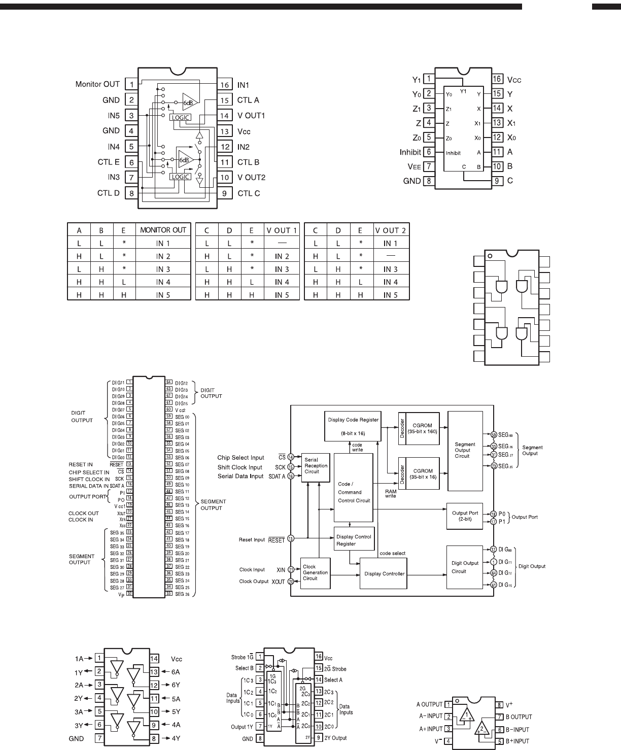
43
ADV-1000
TC74HCU04AF (MA: IC704) SN74HC153NS (MA: IC712)
M66005FP (MA: IC101)
BA7625 (VO: IC201, 203)
BA7626 (VO: IC202)
BA4510F (MA: IC710, 711)
BA15218F (MA: IC402, 501~503,
505~507, 512~514, 728~730)
LM358PT (AP: IC103, 203, 303)
TL3472 (DM: IC505)
BU4053BCF (VO: IC204)
MM74HC08MTC
(AP: IC401, 402)
1
2
3
4
5
6
7
14
13
12
11
10
9
8
1A
1B
1Y
2A
2B
2Y
GND
V
CC
4B
4A
4Y
3B
3A
3Y
Note1: *mark means that feasible for either H or L.
Note2: Each input terminal is provided with sink chip clamp (BA7625)/
Each input terminal takes 20kohm at the end (BA7626).
44
ADV-1000
SK
CS
DI
DO
NC
VCC
TEST
GND
1
2
3
45
7
8
6
BA05T (AP: IC907)
NJM7812FA(S) (AP: IC904)
BA12ST (AP: IC908)
FRONT
VIEW
Input
GND
Output
FRONT
VIEW
CTL
V
CC
GND
OUT
N.C.
NJM7912FA (AP: IC905)
RPM6938-V4 (MA: IC102)
FRONT
VIEW
Common
Input
Output
1
2
3
4
8
7
6
5
NC
Input
NC
GND
NC
Vcc
Output
Delay-Cap
Input
GND Delay-Cap
Output
Output: Open Collector
Vcc
25
µ
A5
5 4
26
7
µ
A
1.25 V
M51957BFP (MA: IC303)
S29590A (MA: IC301)
PC123 (AP: IC914)
COLLECTOR
EMITTER
ANODE
CATHODE
TOP VIEW
STR-F6667B (AP: IC901)
O.C.P./F.B.
S
D
VIN
GND
FRONT
VIEW
W29EE011P (DM: IC507)
A0 - A16
DQ0 - DQ7
CE
OE
WE
VDD
GND
NC
Terminal Function
Name Function
Address Inputs
Data Inputs/Outputs
Chip Enable
Output Enable
Write Enable
Power Supply
Ground
No Connection
1234
5
6
7
8
9
10
11
12
13
14 15 16 17 18 19 20
21
22
23
24
25
26
27
28
29
303132
A7
A6
A5
A4
A3
A2
A1
A0
DQ0
DQ1
DQ2
GND
DQ3
DQ4
DQ5
DQ6
A14
A13
A8
A9
OE
DQ7
A12
A15
A16
NC
VDD
WE
NC
A10
CE
A11
TOP
VIEW
CE
OE
WE
DQ0
:
DQ7
A0
.
.
.
.
.
.
.
A16
VDD
VSS
CONTROL OUTPUT
BUFFER
DECODER CORE
ARRAY
REMOTE CONTROL SENSOR
GND
VCC
ROUT
FRONT VIEW
OPTICAL
INPUT OUTPUT
VCC
GND
VOUT
V
CC
V
OUT
GND
GP1FA551RZ (MA: IC702, 703) GP1FA551TZ (MA: IC701)
FRONT VIEW
V
IN
V
CC
GND
FRONT VIEW
V
CC
V
IN
GND
DRIVE
IC
LED
V
IN
4
D
S
Vth(2)
Coap.1
Coap.2
START
REG.
T.S.D
O.V.P
Iconst
O.C.P/F.B
5
GND
R3
Vth(1)
R2
R1
DRIVE
LATCH
O. S. C
1
3
2

45
ADV-1000
2SA988
2SA1015
2SC1740S
2SC1815
2SC2458
2SC2412K
KTA1504
KTC2875B
DTA114EK
DTC114EK
DTC114YK
DTC323TK
TOP
VIEW
E
B
CTOP
VIEW
E
B
C
FRONT
VIEW
B
C
E
MTZJ5.6A
MTZJ7.5A
MTZJ10B
MTZJ20B
1SR139-400
1SR35-400A
1SS133
1SS270A
AG01Z
AK03
EK03
EK16
RK46F
SARS03
B
C
E
R1
R2
2SC3852A 2SK771
FRONT
VIEW
E
C
B
DTA Series DTC Series
DTA114EK
R1
10kohm
R2
10kohm
B
C
E
R1
R2
DTC114EK
DTC114YK
10kohm 10kohm
R1 R2
10kohm 47kohm
DTC323TK 2.2kohm
UDZS3.6B
TOP VIEW
TOP
VIEW
E
B
CC
2SB1132
2SC4672
S
D
G
TOP
VIEW
RBV-406
12341234
FRONT VIEW
SPR-54MVW
TOP VIEW
SIDE VIEW
Red Green
DAN202K
12
3
21
3
TOP
VIEW
1: Anode
2: Anode
3: Cathode
FRONT
VIEW
FML-G12S
DAP202K
12
3
1: Cathode
2: Cathode
3: Anode
21
3
TOP
VIEW
TRANSISTORS
DIODES (LED included)

46
ADV-1000
Pin Assignment
Grid Partition
Pin No,
Connection
Note: 1. Fn: Filament
2. nG: Grid
3. Pn: Anode
4. NP: No Pin
5. NX: No Connection
Pin No,
Connection
15ST36GN (MA: FL101)
45
46 90
FL TUBE
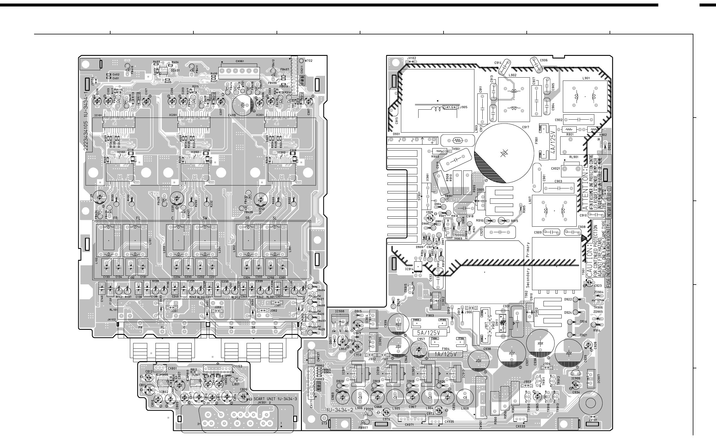
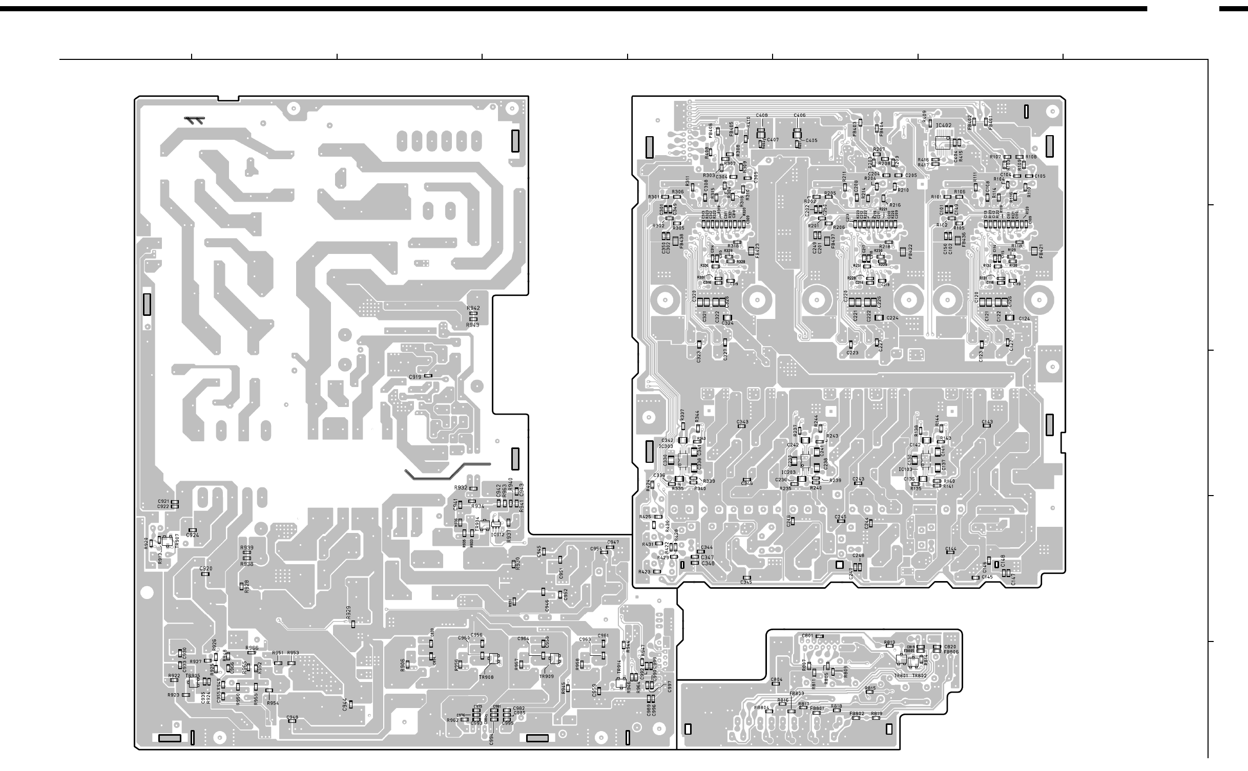
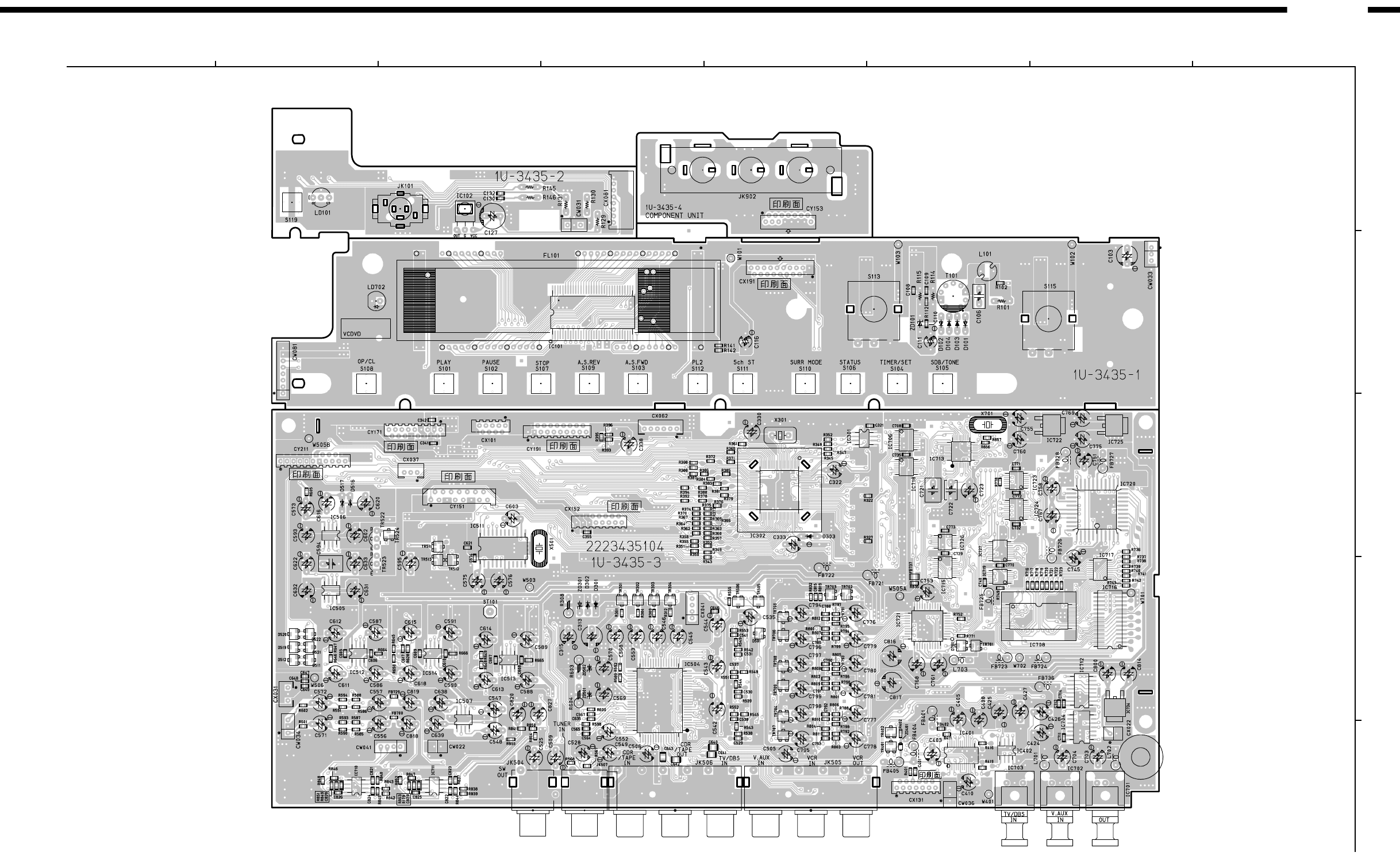
13
1
13
8
1 8
132
3364
119
18 2
2
114
15
2
114
15
2
2
1
1
14
15
2
1
14
15
2
16 1
18
19
2
1210
19
13
16
17
2
119
21
1 124
1
1
3
1 3
1 4
3
14
5 8
14
5 8
15
28
1 14
1 4
58
1 4
58
1 4
58
1
1
24
2540
41
64
65 80
4
58
1 12
13
24
1 4
58
1
45
81
45
8
1
25
26
50
51 75
76
100
11
112
13
24
2536
37
48
10 11
20
1
44
34
11
1222
23
33
1 32
17
16
1 6 7
1828
29
39
44
40
1
8 9
16
1
10
11
20
1
10
11
20
1
10
11
20
1
28
1
16
8
9
1
14
7
8
14
15
1
8
9
16
1
10 11
20
1
78
14
1
7
8
14
45
8
COMPONENT SIDE
8
76
5
4
3
2
1
A
B
C
D
E
ADV-1000
49
1U-3435A MAIN P.W.B. UNIT Ass'y
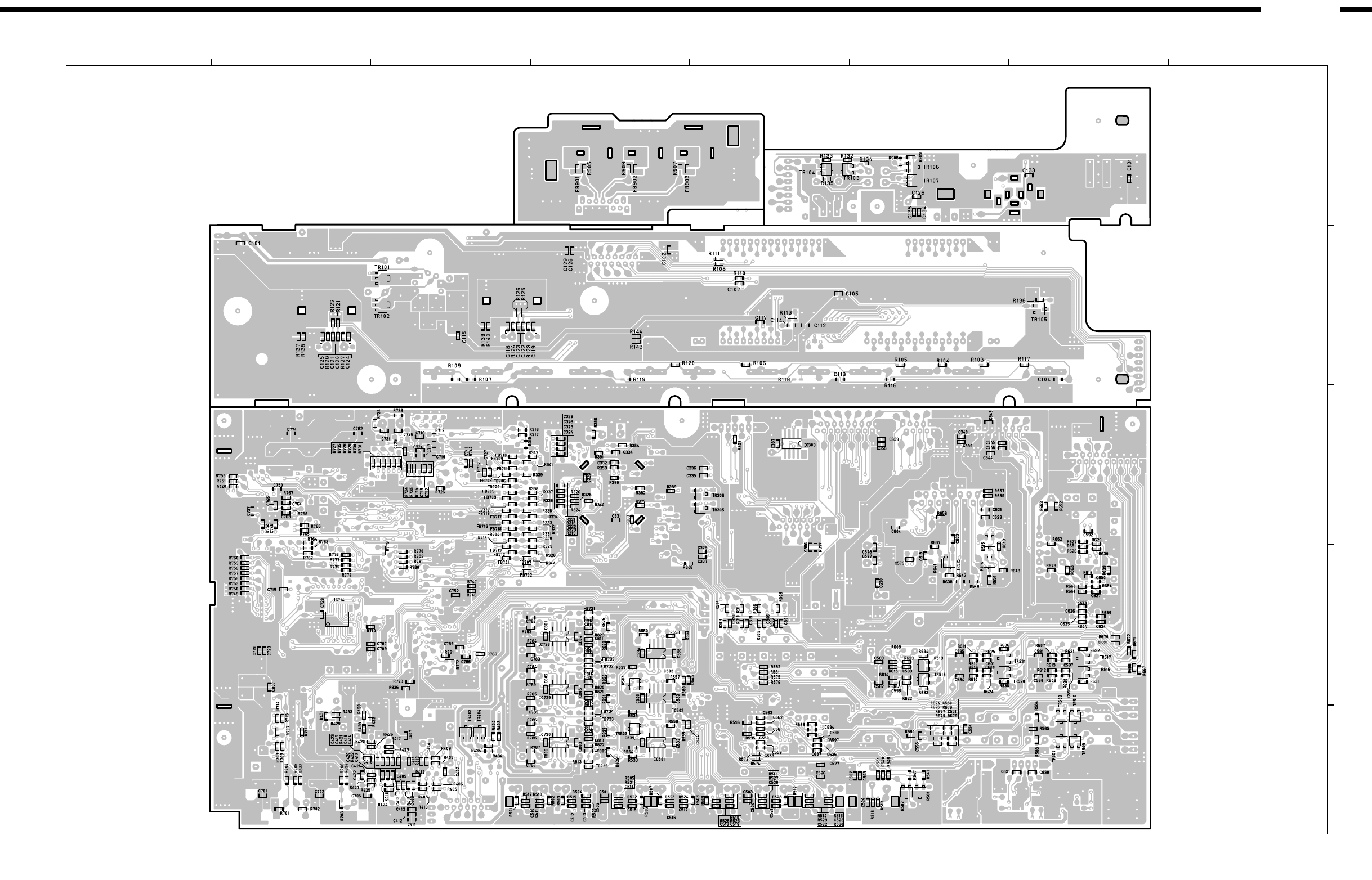
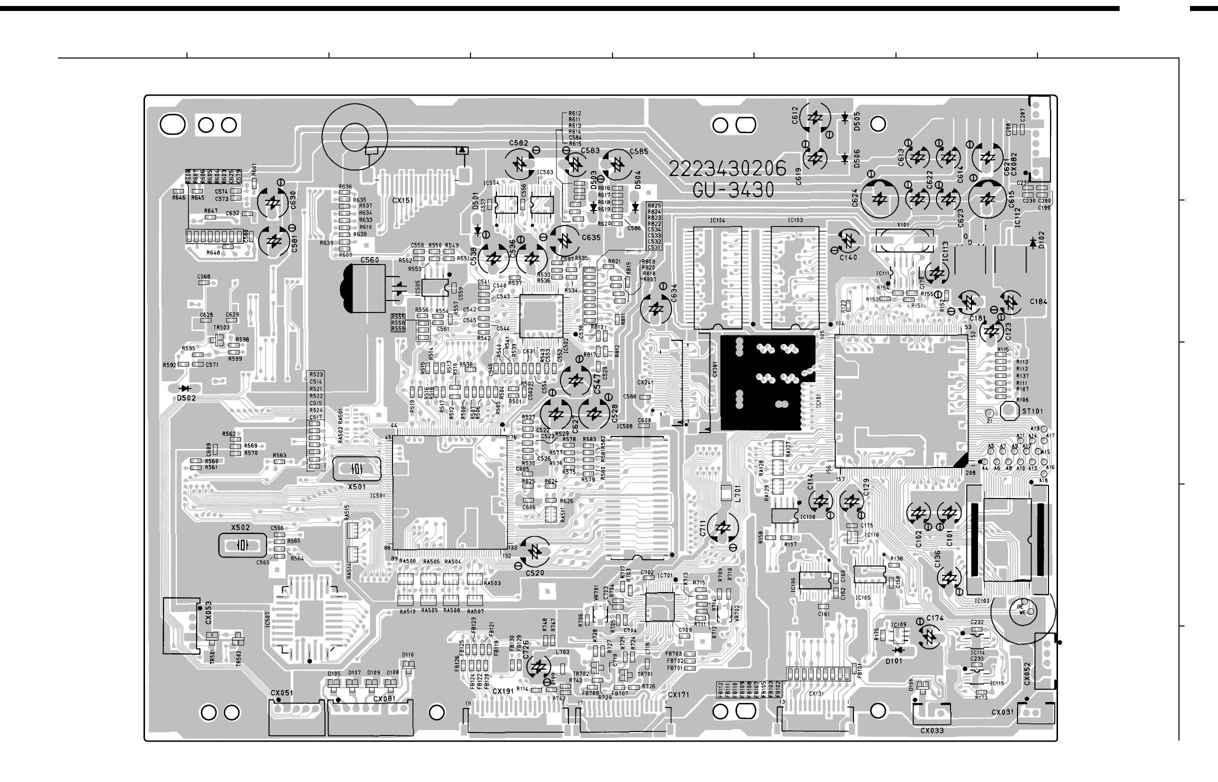
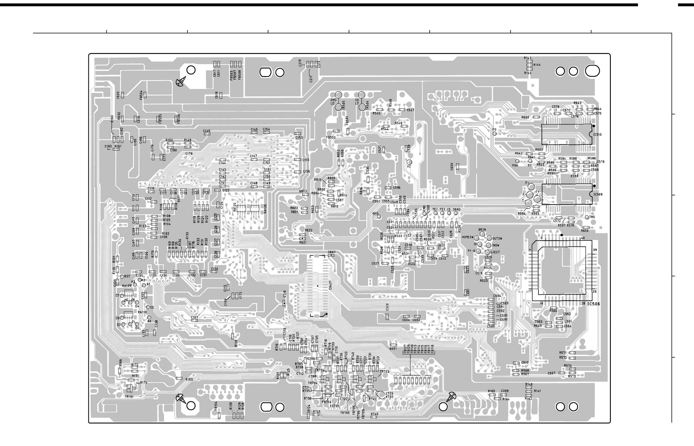
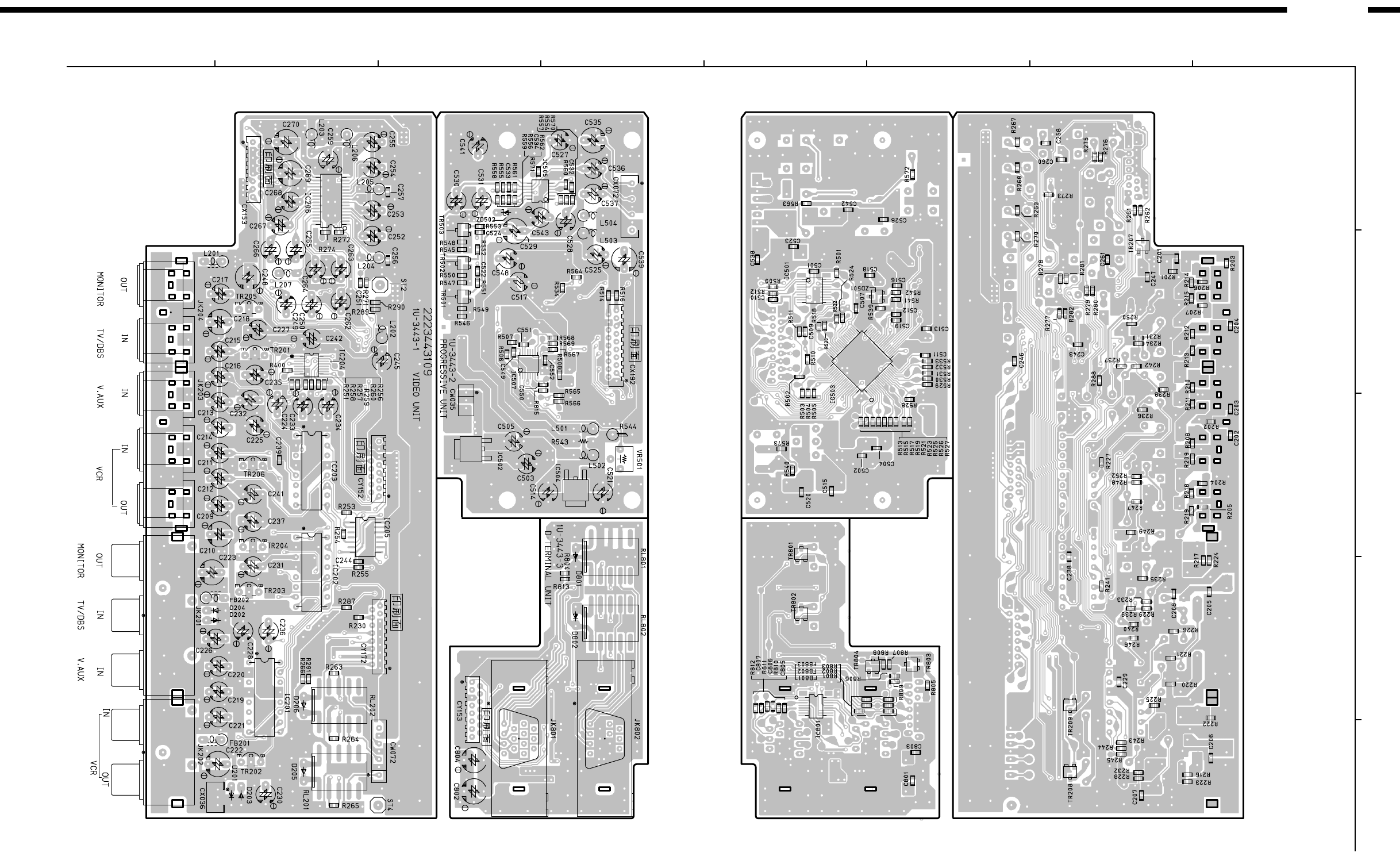
54
ADV-1000
tttt
ll
ll
lResistors
Ex.:RN 14K 2E 182 GFR
Type Shape Power Resist- Allowable Others
and per- ance error
formance
tt
tt
s
s
s
s
Resistance
1 8 2⇒1800 ohm = 1.8 kohm
Indicates number of zeros after effective number.
2-digit effective number.
• Units: ohm
1 R 2⇒1.2 ohm
1-digit effective number.
2-digit effective number, decimal point indicated by R.
• Units: ohm
ll
ll
lCapacitors
Ex.:CE 04W 1H 2R2 MBP
Type Shape Dielectric Capacity Allowable Others
and per- strength error
formance
s
s
s
s
ss
Capacity (electrolyte only)
2 2 2⇒2200µF
Indicates number of zeros after effective number.
2-digit effective number.
• Units: µF.
2 R 2⇒2.2µF
1-digit effective number.
2-digit effective number, decimal point indicated by R.
• Units: µF.
Capacity (except electrolyte)
2 2 2⇒2200pF=0.0022µF
(More than 2) Indicates number of zeros after effective number.
2-digit effective number.
• Units: pF.
2 2 1⇒220pF
(0 or 1) Indicates number of zeros after effective number.
2-digit effective number.
• Units: pF.
• When the dielectric strength is indicated in AC, "AC" is included after the dieelectric
strength value.
ss
NOTE FOR PARTS LIST
lPart indicated with the mark "" are not always in stock and possibly to take a long period of time for supplying, or in
some case supplying of part may be refused.
lWhen ordering of part, clearly indicate "1" and "I" (i) to avoid mis-supplying.
lOrdering part without stating its part number can not be supplied.
lPart indicated with the mark " " is not illustrated in the exploded view.
lNot including Carbon Film ±5%, 1/4W Type in the P.W.Board parts list. (Refer to the Schematic Diagram for those parts.)
WARNING:
Parts marked with this symbol have critical characteristics.
Use ONLY replacement parts recommended by the manufacturer.
RD : Carbon 2B : 1/8W F : ±1% P : Pulse-resistant type
RC : Composition 2E : 1/4W G : ±2% NL : Low noise type
RS : Metal oxide film 2H : 1/2W J : ±5% NB : Non-burning type
RW : Winding 3A : 1W K : ±10% FR : Fuse-resistor
RN : Metal film 3D : 2W M : ±20% F : Lead wire forming
RK : Metal mixture 3F : 3W
3H : 5W
CE : Aluminum foil 0J : 6.3V F : ±1% HS : High stability type
electrolytic
CA : Aluminum solid 1A : 10V G : ±2% BP : Non-polar type
electrolytic
CS : Tantalum electrolytic 1C : 16V J : ±5% HR: Ripple-resistant type
CQ : Film 1E : 25V K : ±10% DL : For change and discharge
CK : Ceramic 1V : 35V M : ±20% HF : For assuring high
requency
CC : Ceramic 1H : 50V Z : +80% U : UL part
CP : Oil 2A : 100V –20% C : CSA part
CM : Mica 2B : 125V P : +100% W : UL-CSA type
CF : Metallized 2C : 160V –0% F : Lead wire forming
CH : Metallized 2D : 200V C : ±0.25pF
2E : 250V D : ±0.5pF
2H : 500V = : Others
2J : 630V
55
ADV-1000
PARTS LIST OF P.W.B. UNIT ASS'Y
1U-3434A AMP/POWER P.W.B. UNIT ASS'Y
Ref. No. Part No. Part Name Remarks Ref. No. Part No. Part Name Remarks
SEMICONDUCTORS GROUP
IC101 262 3111 905 TA2025/TC2000
IC102 262 3112 904 TP2050
IC103 263 1175 904 LM358PT (STMICRO)
IC201 262 3111 905 TA2025/TC2000
IC202 262 3112 904 TP2050
IC203 263 1175 904 LM358PT (STMICRO)
IC301 262 3111 905 TA2025/TC2000
IC302 262 3112 904 TP2050
IC303 263 1175 904 LM358PT (STMICRO)
IC401,402 262 3131 901 MM74HC08MTC
IC801,802 262 2534 907 BA7660FS-E2
IC901 265 0114 001 STR-F6667B
IC902 263 1155 005 SE-B2
IC904 263 0801 004 NJM7812FA(S)
IC905 263 0641 002 NJM7912FA
IC907 263 1092 003 BA05T
IC908 263 1127 004 BA12ST-V5
IC909-911 263 1154 006 SI8050JF
IC913 263 1154 006 SI8050JF
IC914 262 3047 008 PC123 Y-22
TR403-406 273 0303 910 2SC1740S(S)-T
TR801 269 0082 902 DTC114EKT96
TR802 269 0083 901 DTA114EKT96
TR903 273 0369 006 2SC3852A
TR905 273 0384 900 2SC2412KT96(S)
TR906 273 0303 910 2SC1740S(S)-T
TR908,909 269 0082 902 DTC114EKT96
TR910-912 271 0131 924 2SA988-T(E/F)
TR913 273 0198 905 2SC1815(Y)TPE2
TR914 269 0082 902 DTC114EKT96
TR916 273 0198 905 2SC1815(Y)TPE2
D401-404 276 0432 903 1SS270A TE (TAPE)
D901 276 0767 005 RBV-406
D902 276 0730 919 AG01ZT (WK)
D904 276 0754 908 AK03T (WS)
D905 276 0758 001 SARS03
D906-909 276 0730 919 AG01ZT (WK)
D910 276 0757 002 FML-G12S
D911 276 0771 004 RK46F (LF015-302)
D912,913 276 0756 906 EK16T (V0)
D914 276 0704 903 1SR35-400A(T93X)
D915-917 276 0432 903 1SS270A TE (TAPE)
D918-920 276 0755 907 EK03T (W)
D921,922 276 0704 903 1SR35-400A(T93X)
D923 276 0432 903 1SS270A TE (TAPE)
D924 276 0704 903 1SR35-400A(T93X)
D926 276 0755 907 EK03T (W)
ZD902 276 0761 917 MTZJ10B T77
ZD903 276 0761 988 MTZJ20B T77
TH901 279 0045 001 NTPAJ6R0LDKB0
RESISTORS GROUP
R101,102 247 2013 908 RM73B--224JT
R103 247 2019 902 RM73B--102FT
R104 247 2010 956 RM73B--203JT
R105,106 247 2013 908 RM73B--224JT
R107,108 247 2014 965 RM73B--105JT
R109 247 2019 902 RM73B--102FT
R110 247 2010 956 RM73B--203JT
R111 247 2010 972 RM73B--243JT
R112 247 2019 931 RM73B--822FT
R113 247 2009 996 RM73B--113JT
R114 247 2010 956 RM73B--203JT
R115 247 2009 983 RM73B--103JT
R116 247 2010 956 RM73B--203JT
R117 247 2018 903 RM73B--0R0KT
R120-123 247 2019 902 RM73B--102FT
R124-127 247 2020 946 RM73B--133FT
R129 247 2019 902 RM73B--102FT
R130,131 247 2009 983 RM73B--103JT
R132,133 244 2050 904 RS14B3A220JNBST(S)
R135 247 2018 903 RM73B--0R0KT
R136,137 244 2671 930 RS14B3D200JNBST(S)
R138 247 2018 903 RM73B--0R0KT
R139 244 2671 930 RS14B3D200JNBST(S)
R140,141 247 2020 959 RM73B--474FT
R142 244 2671 930 RS14B3D200JNBST(S)
R143,144 247 2020 959 RM73B--474FT
R145 247 2018 903 RM73B--0R0KT
R201,202 247 2013 908 RM73B--224JT
R203 247 2019 902 RM73B--102FT
R204 247 2010 956 RM73B--203JT
R205,206 247 2013 908 RM73B--224JT
R207,208 247 2014 965 RM73B--105JT
R209 247 2019 902 RM73B--102FT
R210 247 2010 956 RM73B--203JT
R211 247 2010 972 RM73B--243JT
R212 247 2019 931 RM73B--822FT
R213 247 2009 996 RM73B--113JT
R214 247 2010 956 RM73B--203JT

56
ADV-1000
R216 247 2010 956 RM73B--203JT
R217 247 2018 903 RM73B--0R0KT
R220-223 247 2019 902 RM73B--102FT
R224-227 247 2020 946 RM73B--133FT
R228 247 2009 983 RM73B--103JT
R230 247 2019 902 RM73B--102FT
R231 247 2009 983 RM73B--103JT
R232,233 244 2050 904 RS14B3A220JNBST(S)
R235 247 2018 903 RM73B--0R0KT
R236 244 2671 930 RS14B3D200JNBST(S)
R237 247 2018 903 RM73B--0R0KT
R238 244 2671 930 RS14B3D200JNBST(S)
R239,240 247 2020 959 RM73B--474FT
R241,242 244 2671 930 RS14B3D200JNBST(S)
R243,244 247 2020 959 RM73B--474FT
R245 247 2018 903 RM73B--0R0KT
R301,302 247 2013 908 RM73B--224JT
R303 247 2019 902 RM73B--102FT
R304 247 2010 956 RM73B--203JT
R305,306 247 2013 908 RM73B--224JT
R307,308 247 2014 965 RM73B--105JT
R309 247 2019 902 RM73B--102FT
R310 247 2010 956 RM73B--203JT
R311 247 2010 972 RM73B--243JT
R312 247 2019 931 RM73B--822FT
R313 247 2009 996 RM73B--113JT
R315,316 247 2010 956 RM73B--203JT
R317 247 2018 903 RM73B--0R0KT
R320-323 247 2019 902 RM73B--102FT
R324-327 247 2020 946 RM73B--133FT
R329 247 2019 902 RM73B--102FT
R330,331 247 2009 983 RM73B--103JT
R332,333 244 2050 904 RS14B3A220JNBST(S)
R335 247 2018 903 RM73B--0R0KT
R336 244 2671 930 RS14B3D200JNBST(S)
R337 247 2018 903 RM73B--0R0KT
R338 244 2671 930 RS14B3D200JNBST(S)
R339,340 247 2020 959 RM73B--474FT
R341,342 244 2671 930 RS14B3D200JNBST(S)
R343,344 247 2020 959 RM73B--474FT
R345 247 2018 903 RM73B--0R0KT
R401 247 2009 983 RM73B--103JT
R403-405 247 2005 903 RM73B--101JT
R406-408 247 2018 903 RM73B--0R0KT
R409,410 247 2009 983 RM73B--103JT
R415-417 247 2018 903 RM73B--0R0KT
R420,421 244 2064 961 RS14B3A201JNBST(S)
R422 247 2009 909 RM73B--472JT (1608)
R423 247 2009 983 RM73B--103JT
R424 247 2009 909 RM73B--472JT (1608)
Ref. No. Part No. Part Name Remarks Ref. No. Part No. Part Name Remarks
R425 247 2009 983 RM73B--103JT
R426,427 244 2064 961 RS14B3A201JNBST(S)
R428 247 2009 909 RM73B--472JT (1608)
R429 247 2009 983 RM73B--103JT
R430 247 2009 909 RM73B--472JT (1608)
R431 247 2009 983 RM73B--103JT
R801-804 247 2005 945 RM73B--151JT
R805 247 2013 940 RM73B--334JT
R806 247 2011 968 RM73B--563JT
R807 247 2013 940 RM73B--334JT
R808 247 2011 968 RM73B--563JT
R809 247 2013 940 RM73B--334JT
R810 247 2011 968 RM73B--563JT
R811 247 2013 940 RM73B--334JT
R812 247 2011 968 RM73B--563JT
R813 247 2009 983 RM73B--103JT
R814 247 2012 925 RM73B--104JT
R815-819 247 2004 975 RM73B--750JT
R901 242 2009 001 RC05GF2H225K(UL)
R903 244 2679 000 RS14B3A104JNBF
R906 247 2018 903 RM73B--0R0KT
R907 244 2043 908 RS14B3A681JNBST(S)
R909,910 243 2094 019 RW99=3DR22JF
R913 247 2011 942 RM73B--473JT
R914 244 2043 937 RS14B3A100JNBST(S)
R915 244 2680 918 RS14B3D154JNBST(SPR)
R920 247 2008 900 RM73B--182JT
R921 241 2315 912 RD14B2E100GFRST
R922 247 2009 983 RM73B--103JT
R923 247 2009 909 RM73B--472JT (1608)
R924,925 247 2009 983 RM73B--103JT
R926 247 2009 954 RM73B--752JT
R927 247 2008 913 RM73B--202JT
R928-931 247 2009 983 RM73B--103JT
R932 247 2008 942 RM73B--272JT
R933 247 2008 926 RM73B--222JT
R935 247 2010 998 RM73B--303JT
R936 247 2008 926 RM73B--222JT
R938,939 247 2018 903 RM73B--0R0KT
R942,943 247 2018 903 RM73B--0R0KT
R944 247 2009 983 RM73B--103JT
R945 247 2009 909 RM73B--472JT (1608)
R946,947 247 2009 996 RM73B--113JT
R949 247 2009 996 RM73B--113JT
R950 247 2014 907 RM73B--564JT
R951 247 2008 900 RM73B--182JT
R952 247 2010 969 RM73B--223JT
R953 247 2004 975 RM73B--750JT
R954 247 2014 907 RM73B--564JT
R955 247 2009 954 RM73B--752JT
57
ADV-1000
Ref. No. Part No. Part Name Remarks Ref. No. Part No. Part Name Remarks
C224 257 0032 904 CK73F1H104ZT
C225 254 4618 901 CE04W1H101MT H12(LXZ)
C227 257 0507 976 CC73CH1H331JT
C230 253 1026 001 CK45F1H473Z
C231-234 256 1059 954 CF93A1H474JT (JL)
C235 256 1061 913 CF93A1J474JT(ECQV)
C236 257 0032 917 CK73F1H224ZT
C237 256 1061 900 CF93A1J104JT(ECQV)
C238 257 0032 917 CK73F1H224ZT
C239 256 1061 913 CF93A1J474JT(ECQV)
C240 256 1061 900 CF93A1J104JT(ECQV)
C241,242 257 0032 917 CK73F1H224ZT
C243-246 257 0511 904 CK73F1H103ZT
C247 257 0506 951 CC73CH1H101JT
C248 257 0510 934 CK73B1H472KT
C249,250 257 0512 903 CK73F1E104ZT
C301,302 257 0512 903 CK73F1E104ZT
C303 254 4524 956 CE04W1H2R2MT SMG/RE3
C304,305 257 0504 940 CC73CH1H330JT
C306 254 4524 956 CE04W1H2R2MT SMG/RE3
C307 254 4538 942 CE04W1C101MT SMG/RE3
C308,309 257 0512 903 CK73F1E104ZT
C310,311 257 0506 919 CC73CH1H680JT
C312,313 257 0506 922 CC73CH1H750JT
C314-316 257 0512 903 CK73F1E104ZT
C317,318 257 0032 904 CK73F1H104ZT
C319 257 0512 903 CK73F1E104ZT
C321,322 253 1181 917 CK45F1H223ZT(DD-3)
C323 257 0507 976 CC73CH1H331JT
C324 253 1026 001 CK45F1H473Z
C324 257 0032 904 CK73F1H104ZT
C325 254 4618 901 CE04W1H101MT H12(LXZ)
C327 257 0507 976 CC73CH1H331JT
C330 253 1026 001 CK45F1H473Z
C331-334 256 1059 954 CF93A1H474JT (JL)
C335 256 1061 913 CF93A1J474JT(ECQV)
C336 257 0032 917 CK73F1H224ZT
C337 256 1061 900 CF93A1J104JT(ECQV)
C338 257 0032 917 CK73F1H224ZT
C339 256 1061 913 CF93A1J474JT(ECQV)
C340 256 1061 900 CF93A1J104JT(ECQV)
C341,342 257 0032 917 CK73F1H224ZT
C343-346 257 0511 904 CK73F1H103ZT
C347 257 0506 951 CC73CH1H101JT
C348 257 0510 934 CK73B1H472KT
C349,350 257 0512 903 CK73F1E104ZT
C403,404 257 0511 904 CK73F1H103ZT
C409 254 4619 706 CE04W1H561MC K25(LXZ)
C801 257 0512 903 CK73F1E104ZT
R956-958 247 2018 903 RM73B--0R0KT
R960,961 243 2039 032 RW99=3H0R1K
R962 247 2018 903 RM73B--0R0KT
R964 247 2011 900 RM73B--333JT
R965 247 2018 903 RM73B--0R0KT
R966 247 2010 972 RM73B--243JT
CAPACITORS GROUP
C101,102 257 0512 903 CK73F1E104ZT
C103 254 4524 956 CE04W1H2R2MT SMG/RE3
C104,105 257 0504 940 CC73CH1H330JT
C106 254 4524 956 CE04W1H2R2MT SMG/RE3
C107 254 4538 942 CE04W1C101MT SMG/RE3
C108,109 257 0512 903 CK73F1E104ZT
C110,111 257 0507 950 CC73CH1H271JT
C112,113 257 0507 976 CC73CH1H331JT
C114-116 257 0512 903 CK73F1E104ZT
C117,118 257 0032 904 CK73F1H104ZT
C119 257 0512 903 CK73F1E104ZT
C121,122 253 1181 917 CK45F1H223ZT(DD-3)
C123 257 0507 976 CC73CH1H331JT
C124 253 1026 001 CK45F1H473Z
C124 257 0032 904 CK73F1H104ZT
C125 254 4618 901 CE04W1H101MT H12(LXZ)
C127 257 0507 976 CC73CH1H331JT
C130 253 1026 001 CK45F1H473Z
C131-134 256 1059 954 CF93A1H474JT (JL)
C135 257 0032 917 CK73F1H224ZT
C136 256 1061 900 CF93A1J104JT(ECQV)
C137 257 0032 917 CK73F1H224ZT
C138,139 256 1061 913 CF93A1J474JT(ECQV)
C140 256 1061 900 CF93A1J104JT(ECQV)
C141,142 257 0032 917 CK73F1H224ZT
C143-146 257 0511 904 CK73F1H103ZT
C147 257 0506 951 CC73CH1H101JT
C148 257 0510 934 CK73B1H472KT
C149,150 257 0512 903 CK73F1E104ZT
C201,202 257 0512 903 CK73F1E104ZT
C203 254 4524 956 CE04W1H2R2MT SMG/RE3
C204,205 257 0504 940 CC73CH1H330JT
C206 254 4524 956 CE04W1H2R2MT SMG/RE3
C207 254 4538 942 CE04W1C101MT SMG/RE3
C208,209 257 0512 903 CK73F1E104ZT
C210,211 257 0506 977 CC73CH1H121JT
C212,213 257 0506 993 CC73CH1H151JT
C214 257 0512 903 CK73F1E104ZT
C215,216 257 0032 904 CK73F1H104ZT
C217-219 257 0512 903 CK73F1E104ZT
C221,222 253 1181 917 CK45F1H223ZT(DD-3)
C223 257 0507 976 CC73CH1H331JT
C224 253 1026 001 CK45F1H473Z

58
ADV-1000
C802,803 254 4213 924 CE04W0J470MT (SRA)
C804,805 257 0512 903 CK73F1E104ZT
C806,807 254 4193 947 CE04W1C101MT (SRA)
C809 254 4193 947 CE04W1C101MT (SRA)
C810 254 4193 918 CE04W1C220MT (SRA)
C811 254 4193 947 CE04W1C101MT (SRA)
C812 254 4193 918 CE04W1C220MT (SRA)
C814 254 4193 947 CE04W1C101MT (SRA)
C815 254 4193 918 CE04W1C220MT (SRA)
C816 254 4193 947 CE04W1C101MT (SRA)
C817 254 4193 918 CE04W1C220MT (SRA)
C819,820 257 0506 951 CC73CH1H101JT
C834 257 0511 904 CK73F1H103ZT
C835 254 4607 909 CE04W1C471MT H20(LXV)
C901 253 8026 703 CK45E2EAC472MC
C902,903 256 8038 004 CF99--2EAC104M
C904-906 253 8022 710 CK45F2EAC222MC
C907 256 8038 004 CF99--2EAC104M
C908-910 253 8022 710 CK45F2EAC222MC
C911 256 8038 004 CF99--2EAC104M
C912-914 253 8022 710 CK45F2EAC222MC
C916 255 4249 739 CQ93P2J103KC(ECQF)
C917 254 6229 000 CE68W2G331M 35B(KMM)
C918 253 8030 003 CK45E3D681KC(ECKA)
C919 257 0508 917 CC73CH1H471JT
C920 257 0511 904 CK73F1H103ZT
C921 257 0512 903 CK73F1E104ZT
C922 257 0511 904 CK73F1H103ZT
C924 257 0511 904 CK73F1H103ZT
C925 255 4249 726 CQ93P2J472KC(ECQF)
C926 254 4618 914 CE04W1H220MT E11(LXZ)
C927 257 0507 934 CC73CH1H221JT
C929 254 4472 707 CE04W1C472MC (SMG)
C931 255 4249 726 CQ93P2J472KC(ECQF)
C933 257 0512 903 CK73F1E104ZT
C934 254 4538 900 CE04W1C100MT SMG/RE3
C935 257 0511 920 CK73F1H473ZT
C936,937 254 4611 717 CE04W1V222MC L35(LXV)
C938 254 4610 705 CE04W1E222MC K40(LXV)
C939,940 254 4611 704 CE04W1V102MC K30(LXV)
C941 257 0507 934 CC73CH1H221JT
C945-947 257 0511 904 CK73F1H103ZT
C948 257 0512 903 CK73F1E104ZT
C949,950 254 4541 942 CE04W1E101MT SMG/RE3
C951,952 257 0511 904 CK73F1H103ZT
C953 254 4541 942 CE04W1E101MT SMG/RE3
C954,955 257 0511 904 CK73F1H103ZT
C957 254 4608 908 CE04W1E221MT H15(LXV)
C960 257 0511 904 CK73F1H103ZT
C963,964 257 0511 904 CK73F1H103ZT
C965 254 4524 956 CE04W1H2R2MT SMG/RE3
Ref. No. Part No. Part Name Remarks Ref. No. Part No. Part Name Remarks
C966 257 0511 904 CK73F1H103ZT
C967-969 254 4607 909 CE04W1C471MT H20(LXV)
C975 257 0512 903 CK73F1E104ZT
C976 257 0501 901 CK73B1H103KT (1608)
C981,982 257 0512 903 CK73F1E104ZT
C984,985 257 0501 901 CK73B1H103KT (1608)
C989,990 257 0511 904 CK73F1H103ZT
C992 257 0511 904 CK73F1H103ZT
C993-995 257 0509 929 CK73B1H102KT
C996,997 257 0512 903 CK73F1E104ZT
C999 257 0512 903 CK73F1E104ZT
OTHER PARTS GROUP Q'ty
CW034 203 5287 016 3P PH-SAN CON.CORD 1
CW037 203 5288 002 3P PH-SAN CON.CORD 1
CW061 204 0564 009 6P VH-SDN CON.CORD 1
CX021 205 0581 001 2P VH CONNECTOR BASE 1
CX033 205 0343 032 3P CONN.BASE(KR-PH) 1
CX061 205 0653 065 6P VH CONNECTOR BASE 1
CX071 205 0321 070 7P CONNE BASE(RED) 1
CX171 205 1100 038 17P FFC BASE(P=1) 1
CX211 205 0892 062 21P FFC BASE (P=1) 1
CY153 205 1006 051 15P FFC BASE(P=1) 1
F901 206 1075 030 FUSE(2.0A) 1
F903 206 1075 072 FUSE (5A) 1
F904 206 1075 001 FUSE (1A) 1
FB401-408 235 0130 903 CHIP EMIFIL(11A121) 8
FB413 235 0130 903 CHIP EMIFIL(11A121) 1
FB414-420 235 0049 900 BEADS INDUCTOR TAPE 7
FB424-428 235 0049 900 BEADS INDUCTOR TAPE 5
FB432-435 235 0049 900 BEADS INDUCTOR TAPE 4
FB801-804 247 2018 903 RM73B--0R0KT 4
FB805,806 235 0130 903 CHIP EMIFIL(11A121) 2
FB901 235 0049 900 BEADS INDUCTOR TAPE 1
FB902-905 235 0130 903 CHIP EMIFIL(11A121) 4
FB906,907 235 0049 900 BEADS INDUCTOR TAPE 2
FF901 202 0040 909 FUSE CLIP (TAPE) 1
FF903,904 202 0040 909 FUSE CLIP (TAPE) 2
FH901 202 0040 909 FUSE CLIP (TAPE) 1
FH903,904 202 0040 909 FUSE CLIP (TAPE) 2
JK102 205 1200 006 6P SP TERMINAL(SGND) 1
JK302 205 1200 006 6P SP TERMINAL(SGND) 1
JK901 204 6686 004 RGB CONNECTOR(S-GND) 1
L101,102 235 0148 005 INDUCTOR 10UH (DAW) 2
59
ADV-1000
Ref. No. Part No. Part Name Remarks Q'ty Ref. No. Part No. Part Name Remarks
L201,202 235 0148 005 INDUCTOR 10UH (DAW) 2
L301,302 235 0148 005 INDUCTOR 10UH (DAW) 2
L801 235 0070 911 INDUCTOR(220)ST 1
L901,902 239 0034 001 LINE FILTER(HR-E122) 2
L904-906 235 0153 003 INDUCTOR 82UH(7210) 3
L907 239 0034 001 LINE FILTER(HR-E122) 1
L908 235 0153 003 INDUCTOR 82UH(7210) 1
RL101 214 0206 005 RELAY(PCI212DM) 1
RL201,202 214 0206 005 RELAY(PCI212DM) 2
RL301 214 0206 005 RELAY(PCI212DM) 1
RL901 214 0214 000 RELAY(SDT-S-109LMR) 1
ST3 205 0452 004 STYLE PIN 1
SY901 417 0622 026 HEAT SINK 1
SY902 417 0476 049 RADIATOR 1
T901 233 6424 002 POWER TRANS(SUB/E2) 1
T902 233 6425 001 SW TRANS(E2) 1
W701 001 0226 007 1P 3T LUG WIRE 1
W702 001 0227 006 1P 3T LUG WIRE 1
412 4822 005 EARTH PLATE(SP-L) 2
412 4823 004 EARTH PLATE(SP-R) 2
412 4974 005 LUG PLATE 3
414 0965 001 SHIELD BRACKET 1
415 0886 002 SHIELD SHEET 1
417 0476 065 RADIATOR 1
461 0415 007 RUBBER SHEET 12
471 3305 014 3X10 CBS-Z 3
513 3844 015 FUSE LABEL for F901 1
513 3844 028 FUSE LABEL for F903 1
513 3844 002 FUSE LABEL for F904 1
1U-3435A MAIN P.W.B. UNIT ASS'Y
SEMICONDUCTORS GROUP
IC101 262 2951 904 M66005FP
IC102 499 0301 006 RPM6938-V4 REMOTE SENSOR
IC301 262 2960 908 S29590ADFJA-TB
IC302 GEN 6110 ROM SUB(ADV1000) M30624FGAGP
IC303 263 0454 901 M51957BFP(TP1)
IC401 262 2768 906 AD1854KRSRL
IC402 263 0615 902 BA15218F-DXE2
IC501-503 263 0615 902 BA15218F-DXE2
IC504 263 1156 004 BD3811K1
IC505-507 263 0615 902 BA15218F-DXE2
IC511 262 2547 907 LC72720NM
IC512-514 263 0615 902 BA15218F-DXE2
IC701 269 0187 001 GP1FA551TZ
OPTICAL CONNECTOR
IC702,703 269 0194 007 GP1FA551RZ
OPTICAL CONNECTOR
IC704 262 1205 907 TC74HCU04AF(TP1)
IC706 262 2953 902 SN74HCT244APW
IC708 GEN 5928 ROM SUB(VER0.4) AT49LV002-70TC
IC710,711 263 0934 900 BA4510F-E2
IC712 262 2806 907 SN74HC153NS(TAPE)
IC713 262 2675 015 LC89055W-RA8
IC714 262 3138 904 74LVX574MTC
IC715 262 2959 906 SN74LV244APW
IC717 262 2954 901 SN74LVC574APW
IC718 262 2608 901 TC74VHC123AFT
IC719 262 2519 906 SN74LV00APW-EL2
IC720 262 2949 903 CS493292-CL
IC721 262 2950 002 AK4527BVQ
IC722 263 1129 905 NJM2391DL1-25-TE1
IC723 262 2781 909 SN74LV4040APW-EL2
IC724 262 2953 902 SN74HCT244APW
IC725 263 1130 907 NJM2391DL1-33-TE1
IC726 262 2519 906 SN74LV00APW-EL2
IC727 262 2446 901 SN74LVC244APW-EL1
IC728-730 263 0615 902 BA15218F-DXE2
IC734 263 1126 908 NJM7805DL1A-TE1
TR101,102 273 0463 902 2SC4672T100PQ
TR103,104 273 0460 905 KTC2875B-RTK
TR106,107 273 0460 905 KTC2875B-RTK
TR301-306 269 0083 901 DTA114EKT96
TR401 269 0083 901 DTA114EKT96
TR402 269 0082 902 DTC114EKT96
TR403,404 273 0460 905 KTC2875B-RTK
TR501,502 273 0460 905 KTC2875B-RTK
60
ADV-1000
Ref. No. Part No. Part Name RemarksRef. No. Part No. Part Name Remarks
TR503,504 275 0100 902 2SK771-5-TB
TR505 269 0144 905 DTC114YK-T146
TR506 269 0083 901 DTA114EKT96
TR507-510 273 0460 905 KTC2875B-RTK
TR511 269 0083 901 DTA114EKT96
TR512,513 269 0066 902 DTC323TKT96
TR514 269 0082 902 DTC114EKT96
TR515 273 0384 900 2SC2412KT96(S)
TR516-521 273 0460 905 KTC2875B-RTK
TR522,523 273 0360 908 2SC2458(Y) TPE4
TR524 269 0082 902 DTC114EKT96
TR701 269 0083 901 DTA114EKT96
TR702 269 0082 902 DTC114EKT96
TR703 269 0083 901 DTA114EKT96
TR704-709 273 0460 905 KTC2875B-RTK
D101-104 276 0432 903 1SS270A TE (TAPE)
D301-303 276 0432 903 1SS270A TE (TAPE)
D501 276 0560 901 DAN202KT146
D511 276 0560 901 DAN202KT146
D512 276 0559 909 DAP202KT146
D515 276 0560 901 DAN202KT146
D516,517 276 0432 903 1SS270A TE (TAPE)
D519,520 276 0559 909 DAP202KT146
D521,522 276 0560 901 DAN202KT146
D701 276 0560 901 DAN202KT146
ZD101 276 0643 996 MTZJ5.6A T77
ZD301 276 0643 996 MTZJ5.6A T77
ZD401 276 0683 943 UDZS3.6B-TE17
ZD501,502 276 0644 911 MTZJ7.5A T77
LD101 393 9587 002 SPR-54MVW RED/GREEN
RESISTORS GROUP
R103 247 2005 945 RM73B--151JT
R104 247 2005 961 RM73B--181JT
R105 247 2006 915 RM73B--271JT
R106 247 2006 944 RM73B--391JT
R107 247 2006 973 RM73B--511JT
R108 247 2018 903 RM73B--0R0KT
R109 247 2007 930 RM73B--911JT
R110,111 247 2018 903 RM73B--0R0KT
R112 247 2009 983 RM73B--103JT
R113 247 2010 985 RM73B--273JT
R116 247 2005 945 RM73B--151JT
R117 247 2005 961 RM73B--181JT
R118 247 2006 915 RM73B--271JT
R119 247 2006 944 RM73B--391JT
R120 247 2006 973 RM73B--511JT
R121,122 247 2009 983 RM73B--103JT
R123,124 247 2005 903 RM73B--101JT
R125,126 247 2009 983 RM73B--103JT
R127,128 247 2005 903 RM73B--101JT
R132,133 247 2007 943 RM73B--102JT
R134,135 247 2011 942 RM73B--473JT
R137-142 247 2018 903 RM73B--0R0KT
R179 247 2009 909 RM73B--472JT (1608)
R301 247 2007 943 RM73B--102JT
R302 247 2013 982 RM73B--474JT
R303 247 2009 983 RM73B--103JT
R304 247 2007 943 RM73B--102JT
R305 247 2013 982 RM73B--474JT
R306 247 2009 983 RM73B--103JT
R307 247 2018 903 RM73B--0R0KT
R308 244 2051 932 RS14B3A332JNBST(S)
R309 247 2007 943 RM73B--102JT
R310 247 2013 982 RM73B--474JT
R311 247 2009 983 RM73B--103JT
R312 247 2007 943 RM73B--102JT
R313 247 2013 982 RM73B--474JT
R314 247 2009 983 RM73B--103JT
R315 247 2018 903 RM73B--0R0KT
R318 247 2007 943 RM73B--102JT
R319 247 2010 985 RM73B--273JT
R320 247 2011 942 RM73B--473JT
R321 247 2007 943 RM73B--102JT
R322 247 2012 925 RM73B--104JT
R323 247 2011 926 RM73B--393JT
R324 247 2011 942 RM73B--473JT
R326 247 2011 942 RM73B--473JT
R327 247 2012 925 RM73B--104JT
R328-342 247 2018 903 RM73B--0R0KT
R343 247 2005 903 RM73B--101JT
R344,345 247 2018 903 RM73B--0R0KT
R347-358 247 2018 903 RM73B--0R0KT
R359 247 2011 942 RM73B--473JT
R360-384 247 2018 903 RM73B--0R0KT
R385 247 2007 943 RM73B--102JT
R386 247 2018 903 RM73B--0R0KT
R387,388 247 2005 903 RM73B--101JT
R389 247 2009 909 RM73B--472JT (1608)
R390 247 2012 925 RM73B--104JT
R391 247 2011 942 RM73B--473JT
R392 247 2006 902 RM73B--331JT (1608)
R393 247 2007 943 RM73B--102JT

61
ADV-1000
Ref. No. Part No. Part Name Remarks Ref. No. Part No. Part Name Remarks
R394 247 2005 987 RM73B--221JT
R395 247 2010 998 RM73B--303JT
R396 247 2010 901 RM73B--123JT
R398 247 2018 903 RM73B--0R0KT
R401 247 2018 903 RM73B--0R0KT
R402 247 2007 943 RM73B--102JT
R403 247 2009 954 RM73B--752JT
R404 247 2008 968 RM73B--332JT
R405 247 2018 903 RM73B--0R0KT
R406 247 2009 983 RM73B--103JT
R407 247 2008 913 RM73B--202JT
R408 247 2009 983 RM73B--103JT
R409 247 2007 943 RM73B--102JT
R410 247 2009 983 RM73B--103JT
R411 247 2018 903 RM73B--0R0KT
R412 247 2009 983 RM73B--103JT
R413 247 2018 903 RM73B--0R0KT
R414,415 247 2009 967 RM73B--822JT
R416-419 247 2009 909 RM73B--472JT (1608)
R420 247 2008 900 RM73B--182JT
R421,422 247 2009 912 RM73B--512JT
R423-425 247 2008 900 RM73B--182JT
R426,427 247 2009 912 RM73B--512JT
R428,429 247 2012 925 RM73B--104JT
R430,431 247 2006 960 RM73B--471JT
R434,435 247 2008 926 RM73B--222JT
R501-512 247 2006 960 RM73B--471JT
R513 247 2005 987 RM73B--221JT
R516 247 2012 925 RM73B--104JT
R517-528 247 2015 964 RM73B--275KT
R531 247 2012 925 RM73B--104JT
R533 247 2008 984 RM73B--392JT
R535 247 2008 984 RM73B--392JT
R537 247 2008 984 RM73B--392JT
R538,539 247 2009 909 RM73B--472JT (1608)
R540 247 2006 960 RM73B--471JT
R541 247 2010 969 RM73B--223JT
R542 247 2009 941 RM73B--682JT
R543,544 247 2010 927 RM73B--153JT
R545 247 2009 938 RM73B--622JT
R546 247 2006 960 RM73B--471JT
R547 247 2010 969 RM73B--223JT
R548 247 2009 938 RM73B--622JT
R549 247 2009 925 RM73B--562JT
R550 247 2009 983 RM73B--103JT
R551,552 247 2010 927 RM73B--153JT
R553 247 2009 967 RM73B--822JT
R555 247 2008 926 RM73B--222JT
R556-558 247 2005 903 RM73B--101JT
R559,560 247 2012 925 RM73B--104JT
R564 247 2012 925 RM73B--104JT
R565 247 2018 903 RM73B--0R0KT
R567,568 247 2018 903 RM73B--0R0KT
R573-576 247 2018 903 RM73B--0R0KT
R581,582 247 2018 903 RM73B--0R0KT
R583,584 247 2012 925 RM73B--104JT
R585,586 247 2006 960 RM73B--471JT
R587,588 247 2009 983 RM73B--103JT
R589 247 2018 903 RM73B--0R0KT
R590,591 247 2006 960 RM73B--471JT
R593,594 247 2009 983 RM73B--103JT
R595-597 247 2009 909 RM73B--472JT (1608)
R598 247 2018 903 RM73B--0R0KT
R599 247 2009 909 RM73B--472JT (1608)
R600 247 2018 903 RM73B--0R0KT
R601,602 247 2005 987 RM73B--221JT
R603,604 244 2051 961 RS14B3A101JNBST(S)
R605 247 2007 943 RM73B--102JT
R606,607 247 2012 925 RM73B--104JT
R608-611 247 2011 942 RM73B--473JT
R612-616 247 2007 998 RM73B--162JT
R617 247 2007 943 RM73B--102JT
R618 247 2011 942 RM73B--473JT
R619 247 2009 909 RM73B--472JT (1608)
R620-624 247 2009 967 RM73B--822JT
R625 247 2009 941 RM73B--682JT
R626 247 2010 914 RM73B--133JT
R627 247 2009 983 RM73B--103JT
R628 247 2012 925 RM73B--104JT
R629 247 2010 927 RM73B--153JT
R630 247 2009 983 RM73B--103JT
R631-635 247 2007 943 RM73B--102JT
R636 247 2018 903 RM73B--0R0KT
R637 247 2007 943 RM73B--102JT
R638 247 2009 983 RM73B--103JT
R639 247 2009 909 RM73B--472JT (1608)
R640 247 2009 983 RM73B--103JT
R641 247 2008 968 RM73B--332JT
R642 247 2014 923 RM73B--684JT
R643 247 2009 909 RM73B--472JT (1608)
R644 247 2007 943 RM73B--102JT
R645-650 247 2010 969 RM73B--223JT
R651 247 2008 913 RM73B--202JT
R652 247 2011 968 RM73B--563JT
R653 247 2009 983 RM73B--103JT
R654 247 2010 901 RM73B--123JT
R656,657 247 2011 942 RM73B--473JT
R658 247 2009 983 RM73B--103JT
R659 247 2012 983 RM73B--184JT
R660 247 2007 943 RM73B--102JT
R661 247 2009 909 RM73B--472JT (1608)
62
ADV-1000
Ref. No. Part No. Part Name Remarks Ref. No. Part No. Part Name Remarks
R662 247 2009 983 RM73B--103JT
R663 247 2010 969 RM73B--223JT
R664-666 247 2018 903 RM73B--0R0KT
R667-672 247 2010 969 RM73B--223JT
R673 247 2018 903 RM73B--0R0KT
R674,675 247 2012 925 RM73B--104JT
R676,677 247 2007 943 RM73B--102JT
R678,679 247 2010 998 RM73B--303JT
R680 247 2018 903 RM73B--0R0KT
R701-703 247 2018 903 RM73B--0R0KT
R704 247 2009 909 RM73B--472JT (1608)
R708 247 2006 960 RM73B--471JT
R709 247 2011 942 RM73B--473JT
R710 247 2009 983 RM73B--103JT
R712 247 2009 983 RM73B--103JT
R713 247 2018 903 RM73B--0R0KT
R715 247 2009 967 RM73B--822JT
R716-723 247 2005 903 RM73B--101JT
R724 247 2008 955 RM73B--302JT
R725 247 2009 912 RM73B--512JT
R726 247 2004 975 RM73B--750JT
R727-731 247 2004 920 RM73B--470JT
R732,733 247 2014 965 RM73B--105JT
R734 247 2007 901 RM73B--681JT
R735 247 2018 903 RM73B--0R0KT
R736-743 247 2005 903 RM73B--101JT
R744 247 2011 900 RM73B--333JT
R745 247 2009 983 RM73B--103JT
R748-751 247 2009 983 RM73B--103JT
R752 247 2004 920 RM73B--470JT
R753 247 2009 983 RM73B--103JT
R754 247 2009 909 RM73B--472JT (1608)
R755-760 247 2009 983 RM73B--103JT
R761 247 2018 903 RM73B--0R0KT
R762-764 247 2004 920 RM73B--470JT
R765,766 247 2009 909 RM73B--472JT (1608)
R767 247 2009 983 RM73B--103JT
R768 247 2011 900 RM73B--333JT
R770-772 247 2004 920 RM73B--470JT
R773 247 2018 903 RM73B--0R0KT
R774-782 247 2004 920 RM73B--470JT
R783-787 247 2012 925 RM73B--104JT
R788 247 2009 909 RM73B--472JT (1608)
R789 247 2012 925 RM73B--104JT
R790-812 247 2009 909 RM73B--472JT (1608)
R813-819 247 2007 943 RM73B--102JT
R820-825 247 2012 925 RM73B--104JT
R826-831 247 2008 926 RM73B--222JT
R832 247 2013 982 RM73B--474JT
R833,834 247 2018 903 RM73B--0R0KT
R836 247 2018 903 RM73B--0R0KT
R837 247 2011 942 RM73B--473JT
R839 247 2010 943 RM73B--183JT
R840 247 2011 942 RM73B--473JT
R841 247 2009 909 RM73B--472JT (1608)
R842 247 2010 943 RM73B--183JT
R844-847 247 2009 909 RM73B--472JT (1608)
R848 247 2006 960 RM73B--471JT
R849,850 247 2009 909 RM73B--472JT (1608)
R851-853 247 2006 960 RM73B--471JT
R854,855 247 2009 938 RM73B--622JT
R857 247 2018 903 RM73B--0R0KT
R908,909 247 2007 943 RM73B--102JT
CAPACITORS GROUP
C103 254 4196 986 CE04W1H100MT (SRA)
C104 257 0509 929 CK73B1H102KT
C105 257 0501 901 CK73B1H103KT (1608)
C106 256 1058 955 CF93A1H683JT (JL)
C107 257 0501 901 CK73B1H103KT (1608)
C108,109 257 0511 920 CK73F1H473ZT
C110 257 0512 903 CK73F1E104ZT
C111 254 4196 957 CE04W1H2R2MT (SRA)
C112 257 0512 903 CK73F1E104ZT
C113 257 0509 929 CK73B1H102KT
C114 257 0506 951 CC73CH1H101JT
C115 257 0512 903 CK73F1E104ZT
C116 254 4196 944 CE04W1H010MT (SRA)
C117-126 257 0501 901 CK73B1H103KT (1608)
C127 254 4213 940 CE04W0J221MT(SRA)
C128 257 0509 929 CK73B1H102KT
C129,130 257 0511 904 CK73F1H103ZT
C132-134 257 0511 904 CK73F1H103ZT
C301 257 0512 903 CK73F1E104ZT
C306 257 0512 903 CK73F1E104ZT
C313 254 4522 958 CE04W1V101MT SMG/RE3
C315 254 4522 916 CE04W1V100MT SMG/RE3
C319-321 257 0512 903 CK73F1E104ZT
C322 254 4536 928 CE04W1A101MT SMG/RE3
C323 257 0512 903 CK73F1E104ZT
C330 254 4536 928 CE04W1A101MT SMG/RE3
C331,332 257 0512 903 CK73F1E104ZT
C333 254 4536 928 CE04W1A101MT SMG/RE3
C335,336 257 0506 951 CC73CH1H101JT
C337 257 0512 903 CK73F1E104ZT
C338 254 4524 956 CE04W1H2R2MT SMG/RE3
C339 257 0511 904 CK73F1H103ZT
C340,341 257 0509 929 CK73B1H102KT
C342-345 257 0511 904 CK73F1H103ZT
C346 257 0509 929 CK73B1H102KT

63
ADV-1000
Ref. No. Part No. Part Name Remarks Ref. No. Part No. Part Name Remarks
C358 257 0511 904 CK73F1H103ZT
C359 257 0509 929 CK73B1H102KT
C402 257 0512 903 CK73F1E104ZT
C403 254 4536 928 CE04W1A101MT SMG/RE3
C404 257 0511 904 CK73F1H103ZT
C405 254 4538 900 CE04W1C100MT SMG/RE3
C407 257 0512 903 CK73F1E104ZT
C408 254 4536 928 CE04W1A101MT SMG/RE3
C409 257 0512 903 CK73F1E104ZT
C410 254 4538 900 CE04W1C100MT SMG/RE3
C414-417 257 0508 933 CC73CH1H561JT
C418-421 257 0507 918 CC73CH1H181JT
C422,423 257 0511 904 CK73F1H103ZT
C424,425 254 4538 942 CE04W1C101MT SMG/RE3
C426,427 254 4522 916 CE04W1V100MT SMG/RE3
C501-504 247 2018 903 RM73B--0R0KT
C507 257 0509 929 CK73B1H102KT
C508 257 0512 903 CK73F1E104ZT
C510-521 257 0507 934 CC73CH1H221JT
C524 257 0506 951 CC73CH1H101JT
C525 254 4538 913 CE04W1C220MT SMG/RE3
C529-531 257 0506 951 CC73CH1H101JT
C532-534 257 0511 920 CK73F1H473ZT
C535 254 4524 943 CE04W1H010MT SMG/RE3
C536 257 0511 920 CK73F1H473ZT
C537,538 257 0504 940 CC73CH1H330JT
C539,540 257 0511 920 CK73F1H473ZT
C541 257 0504 982 CC73CH1H470JT
C542-544 254 4522 916 CE04W1V100MT SMG/RE3
C545,546 254 4524 985 CE04W1H100MT SMG/RE3
C547,548 254 4522 916 CE04W1V100MT SMG/RE3
C549 254 4524 985 CE04W1H100MT SMG/RE3
C550,551 257 0506 951 CC73CH1H101JT
C552,553 254 4524 985 CE04W1H100MT SMG/RE3
C554,555 257 0511 917 CK73F1H223ZT
C556,557 254 4522 916 CE04W1V100MT SMG/RE3
C558,559 257 0510 934 CK73B1H472KT
C560-567 257 0516 954 CK73B1E104KT
C568 254 4524 985 CE04W1H100MT SMG/RE3
C569,570 254 4536 928 CE04W1A101MT SMG/RE3
C571-573 254 4522 916 CE04W1V100MT SMG/RE3
C574 257 0511 904 CK73F1H103ZT
C575 254 4538 900 CE04W1C100MT SMG/RE3
C576 254 4522 903 CE04W1V4R7MT SMG/RE3
C577,578 257 0504 908 CC73CH1H220JT
C579 257 0508 933 CC73CH1H561JT
C586-591 254 4522 916 CE04W1V100MT SMG/RE3
C593 254 4541 939 CE04W1E470MT SMG/RE3
C594 255 1265 936 CQ93M1H103JT(B)
C595 254 4538 900 CE04W1C100MT SMG/RE3
C596-601 257 0506 935 CC73CH1H820JT
C602 254 4541 939 CE04W1E470MT SMG/RE3
C603 254 4536 915 CE04W1A470MT SMG/RE3
C604 257 0511 904 CK73F1H103ZT
C605-610 257 0511 917 CK73F1H223ZT
C611-615 254 4522 916 CE04W1V100MT SMG/RE3
C616 254 4524 985 CE04W1H100MT SMG/RE3
C617 257 0506 951 CC73CH1H101JT
C618 254 4522 916 CE04W1V100MT SMG/RE3
C619 257 0507 976 CC73CH1H331JT
C620 254 4522 903 CE04W1V4R7MT SMG/RE3
C621 257 0501 901 CK73B1H103KT (1608)
C622 254 4522 903 CE04W1V4R7MT SMG/RE3
C623 257 0501 901 CK73B1H103KT (1608)
C624 257 0509 990 CK73B1H222KT
C625,626 247 2018 903 RM73B--0R0KT
C628,629 257 0501 901 CK73B1H103KT (1608)
C631,632 254 4541 939 CE04W1E470MT SMG/RE3
C633 254 4522 916 CE04W1V100MT SMG/RE3
C634-637 257 0516 954 CK73B1E104KT
C638,639 254 4541 939 CE04W1E470MT SMG/RE3
C640-643 257 0034 902 CK73B1C105KT
C701,702 257 0512 903 CK73F1E104ZT
C703,704 254 4538 939 CE04W1C470MT SMG/RE3
C705 257 0512 903 CK73F1E104ZT
C707,708 257 0511 904 CK73F1H103ZT
C709,710 257 0512 903 CK73F1E104ZT
C711 257 0511 904 CK73F1H103ZT
C712 257 0512 903 CK73F1E104ZT
C713-715 257 0511 904 CK73F1H103ZT
C716,717 257 0512 903 CK73F1E104ZT
C718 257 0511 904 CK73F1H103ZT
C721 256 1058 971 CF93A1H104JT (JL)
C722 255 1265 936 CQ93M1H103JT(B)
C723 254 4524 943 CE04W1H010MT SMG/RE3
C724,725 257 0512 903 CK73F1E104ZT
C726 257 0504 908 CC73CH1H220JT
C727 257 0509 929 CK73B1H102KT
C728 257 0501 901 CK73B1H103KT (1608)
C729 257 0511 904 CK73F1H103ZT
C731 257 0504 908 CC73CH1H220JT
C732 257 0512 903 CK73F1E104ZT
C735 257 0511 904 CK73F1H103ZT
C737 257 0512 903 CK73F1E104ZT
C740 257 0511 904 CK73F1H103ZT
C741 257 0507 976 CC73CH1H331JT
C745 254 4533 934 CE04W0J221MT SMG/RE3
C746 257 0512 903 CK73F1E104ZT
C750 257 0512 903 CK73F1E104ZT
C751 254 4524 943 CE04W1H010MT SMG/RE3

64
ADV-1000
Ref. No. Part No. Part Name Remarks Ref. No. Part No. Part Name Remarks Q'ty
CX152 205 1100 054 15P FFC BASE (P=1) 1
CX191 205 1006 006 19P FFC BASE (P=1) 1
CY151 205 0736 076 15P FFC CON.BASE 1
CY171 205 1100 038 17P FFC BASE(P=1) 1
CY191 205 0892 020 19P FFC BASE (P=1) 1
CY211 205 0892 062 21P FFC BASE (P=1) 1
FB401 235 0049 900 BEADS INDUCTOR TAPE 1
FB700-720 235 0130 903 CHIP EMIFIL(11A121) 21
FB721-723 235 0049 900 BEADS INDUCTOR TAPE 3
FB725-728 235 0049 900 BEADS INDUCTOR TAPE 4
FB729 235 0130 903 CHIP EMIFIL(11A121) 1
FB730-735 247 2018 903 RM73B--0R0KT 6
FB736 235 0049 900 BEADS INDUCTOR TAPE 1
FL101 393 8052 004 FL TUBE(15ST36GN) 1
JK101 204 8636 007 MINI JACK (ST.SW) 1
JK504 204 8642 004 1P P1N JACK BK 1
JK505,506 204 8543 006 6P PIN JACK 2
L101 235 0152 004 INDUCTOR 47UH(7206M) 1
L701,702 235 0060 918 INDUCTOR(4R7)ST 2
L703 235 0074 933 INDUCTOR(101)ST 1
S101-112 212 0467 000 TACT SW(H=5) 12
S113 212 0462 005 ROTARY ENCODER(F) 1
S115 212 0461 006 ROTARY ENCODER(V) 1
S119 212 0467 000 TACT SW(H=5) 1
ST101 205 0452 004 STYLE PIN 1
T101 231 0085 001 DC-DC TRANS(10RFG) 1
W505 001 0225 008 1P BOARD IN WIRE 1
X301 399 0532 902 CST12.5MTW-TF01 1
X501 399 0178 007 X-TAL(4.332MHZ) 1
X701 399 0219 021 X'TAL (12.288) 1
412 4974 005 LUG PLATE 3
449 0193 109 SENSOR HOLDER 1
461 1110 000 FL SPACER(D-SIDE) 2
C752 257 0512 903 CK73F1E104ZT
C753 254 4536 928 CE04W1A101MT SMG/RE3
C755 254 4538 900 CE04W1C100MT SMG/RE3
C758 254 4524 956 CE04W1H2R2MT SMG/RE3
C759 257 0512 903 CK73F1E104ZT
C760 254 4538 900 CE04W1C100MT SMG/RE3
C761 254 4536 928 CE04W1A101MT SMG/RE3
C762 257 0501 901 CK73B1H103KT (1608)
C763 257 0512 903 CK73F1E104ZT
C764 257 0508 917 CC73CH1H471JT
C765 257 0501 901 CK73B1H103KT (1608)
C766 257 0512 903 CK73F1E104ZT
C767 254 4538 939 CE04W1C470MT SMG/RE3
C768 254 4524 956 CE04W1H2R2MT SMG/RE3
C769 254 4538 900 CE04W1C100MT SMG/RE3
C770-774 257 0511 904 CK73F1H103ZT
C775 254 4538 900 CE04W1C100MT SMG/RE3
C776-781 254 4522 916 CE04W1V100MT SMG/RE3
C782-793 257 0508 959 CC73CH1E681JT
C794-799 254 4522 916 CE04W1V100MT SMG/RE3
C800 254 4536 928 CE04W1A101MT SMG/RE3
C801-806 257 0512 903 CK73F1E104ZT
C807 257 0511 904 CK73F1H103ZT
C808-813 257 0510 918 CK73B1H332KT
C814 254 4524 985 CE04W1H100MT SMG/RE3
C815 257 0512 903 CK73F1E104ZT
C816,817 254 4541 942 CE04W1E101MT SMG/RE3
C818-820 254 4522 916 CE04W1V100MT SMG/RE3
C821 257 0511 904 CK73F1H103ZT
C822 257 0506 951 CC73CH1H101JT
C823 257 0511 904 CK73F1H103ZT
C824 257 0506 951 CC73CH1H101JT
C825,826 257 0511 904 CK73F1H103ZT
C827 254 4522 916 CE04W1V100MT SMG/RE3
C828,829 257 0506 951 CC73CH1H101JT
C830-833 257 0509 929 CK73B1H102KT
OTHER PARTS GROUP Q'ty
CW022 203 2419 007 2P SAN-SAN CORD 1
CW031 203 5284 006 3P SHIELD WIRE 1
CW033 203 5285 005 3P PH-SAN CON.CORD 1
CW036 203 5287 003 3P PH-SAN CON.CORD 1
CW041 203 6586 004 4P SAN-SAN CORD 1
CW081 204 2933 007 8P PH-SAN CON.CORD 1
CX031 205 0321 038 3P CONNE.BASE(RED) 1
CX034 205 0343 032 3P CONN.BASE(KR-PH) 1
CX037 205 0323 036 3P CONNE.BASE(BLK) 1
CX062 205 0343 061 6P CONN.BASE(KR-PH) 1
CX081 205 0355 088 8P KR CON BASE(L) 1
CX131 205 0892 088 13P FFC CON. BASE 1
65
ADV-1000
Ref. No. Part No. Part Name Remarks Ref. No. Part No. Part Name Remarks
1U-3443A VIDEO/OUT P.W.B. UNIT ASS'Y
C211-216 254 4522 903 CE04W1V4R7MT SMG/RE3
C217 254 4533 934 CE04W0J221MT SMG/RE3
C218 254 4533 950 CE04W0J471MT SMG/RE3
C219-221 254 4524 972 CE04W1H4R7MT SMG/RE3
C222,223 254 4533 947 CE04W0J331MT SMG/RE3
C224 254 4524 972 CE04W1H4R7MT SMG/RE3
C225 254 4536 928 CE04W1A101MT SMG/RE3
C226 254 4524 943 CE04W1H010MT SMG/RE3
C227 254 4536 928 CE04W1A101MT SMG/RE3
C228 254 4538 900 CE04W1C100MT SMG/RE3
C229 257 0511 917 CK73F1H223ZT
C230 254 4538 900 CE04W1C100MT SMG/RE3
C231,232 254 4524 943 CE04W1H010MT SMG/RE3
C233,234 254 4524 972 CE04W1H4R7MT SMG/RE3
C235,236 254 4536 928 CE04W1A101MT SMG/RE3
C237 254 4538 942 CE04W1C101MT SMG/RE3
C238,239 257 0511 917 CK73F1H223ZT
C241 254 4538 942 CE04W1C101MT SMG/RE3
C242 254 4536 928 CE04W1A101MT SMG/RE3
C243 257 0512 903 CK73F1E104ZT
C245 254 4536 928 CE04W1A101MT SMG/RE3
C246 257 0512 903 CK73F1E104ZT
C247 257 0511 904 CK73F1H103ZT
C249,250 254 4536 915 CE04W1A470MT SMG/RE3
C251 257 0512 903 CK73F1E104ZT
C252,253 254 4524 943 CE04W1H010MT SMG/RE3
C254,255 254 4536 915 CE04W1A470MT SMG/RE3
C256 257 0504 995 CC73CH1H510JT
C257 257 0504 908 CC73CH1H220JT
C259 254 4536 928 CE04W1A101MT SMG/RE3
C260 257 0512 903 CK73F1E104ZT
C261 257 0504 995 CC73CH1H510JT
C262 254 4524 943 CE04W1H010MT SMG/RE3
C263 254 4536 928 CE04W1A101MT SMG/RE3
C264 254 4524 998 CE04W1H220MT SMG/RE3
C265 254 4536 928 CE04W1A101MT SMG/RE3
C266 254 4524 998 CE04W1H220MT SMG/RE3
C267 254 4536 928 CE04W1A101MT SMG/RE3
C268 254 4524 998 CE04W1H220MT SMG/RE3
C269 254 4533 947 CE04W0J331MT SMG/RE3
OTHER PARTS GROUP Q'ty
CX036 205 0343 032 3P CONN.BASE(KR-PH) 1
CX153 205 1100 054 15P FFC BASE (P=1) 1
CY152 205 1100 054 15P FFC BASE (P=1) 1
CY172 205 1100 038 17P FFC BASE(P=1) 1
JK201 204 8516 017 3P PIN JACK 1
JK202 204 8537 012 2P PIN JACK(GND) 1
JK203 204 8415 011 3P S-TERMINAL 1
JK204 204 8414 012 2P S-TERMINAL 1
SEMICONDUCTORS GROUP
IC201 263 0856 004 BA7625
IC202 263 0857 003 BA7626
IC203 263 0856 004 BA7625
IC204 263 1159 904 BU4053BCFV
IC206 263 1158 905 BH7862F
TR201-206 271 0102 908 2SA1015(Y)TPE2
TR207 269 0082 902 DTC114EKT96
RESISTORS GROUP
R201-203 247 2018 903 RM73B--0R0KT
R204-207 247 2004 962 RM73B--680JT
R208-213 247 2004 975 RM73B--750JT
R214,215 247 2009 983 RM73B--103JT
R216,217 247 2004 962 RM73B--680JT
R218,219 247 2009 983 RM73B--103JT
R220-222 247 2004 975 RM73B--750JT
R225 247 2018 903 RM73B--0R0KT
R226 247 2004 975 RM73B--750JT
R227 247 2018 903 RM73B--0R0KT
R228,229 247 2005 974 RM73B--201JT
R231-234 247 2005 974 RM73B--201JT
R235,236 247 2004 975 RM73B--750JT
R237 247 2013 908 RM73B--224JT
R238 247 2009 967 RM73B--822JT
R239 247 2013 908 RM73B--224JT
R240 247 2009 967 RM73B--822JT
R241 247 2018 903 RM73B--0R0KT
R242 247 2012 925 RM73B--104JT
R243-245 247 2009 983 RM73B--103JT
R247,248 247 2005 974 RM73B--201JT
R249 247 2005 903 RM73B--101JT
R250 247 2005 974 RM73B--201JT
R251 247 2005 945 RM73B--151JT
R252 247 2005 974 RM73B--201JT
R253-255 247 2018 903 RM73B--0R0KT
R256-260 247 2005 945 RM73B--151JT
R261,262 247 2007 943 RM73B--102JT
R263-265 247 2018 903 RM73B--0R0KT
R272 247 2018 903 RM73B--0R0KT
R274 247 2018 903 RM73B--0R0KT
R275-282 247 2005 945 RM73B--151JT
R287,288 247 2018 903 RM73B--0R0KT
R400 247 2018 903 RM73B--0R0KT
CAPACITORS GROUP
C208 257 0511 904 CK73F1H103ZT
C209 254 4533 934 CE04W0J221MT SMG/RE3
C210 254 4533 950 CE04W0J471MT SMG/RE3

66
ADV-1000
Ref. No. Part No. Part Name Remarks Q'ty Ref. No. Part No. Part Name Remarks
L202,203 235 0070 911 INDUCTOR(220)ST 2
L204 235 0074 991 INDUCTOR(R68)ST 1
L205 235 0074 988 INDUCTOR(R39)ST 1
L207 235 0074 991 INDUCTOR(R68)ST 1
ST2 205 0452 004 STYLE PIN 1
ST4 205 0452 004 STYLE PIN 1
GU-3430 DVD MAIN P.W.B. UNIT ASS'Y
SEMICONDUCTORS GROUP
IC101 262 2811 002 ES4408F
IC102 GEN 6084 B/E ROM SUB ASS'Y MX29F080TC-90
IC103,104 262 2875 006 16M SDRAM(TSOP)-8
IC105,106 262 2801 902 SN74AHCT273PW-EL2
IC108 262 3114 902 S-24C01BFJ-TB
IC109 262 3082 911 BD4745G
IC110 262 3118 908 KIC7S32FU-RTK
IC111 262 1953 903 TC7WU04F
IC112 263 1110 901 PQ070XZ01ZP
IC113 263 1079 903 BA033FP
IC114,115 262 2941 901 TC7WT125FU
IC501 262 3083 004 M5705
IC502 262 3084 003 SP-3721A
IC505 262 3085 905 TL3472
IC507 GEN 6073 F/E ROM SUB ASS'Y W29EE011P-90
IC508 262 3087 903 M11B416256A-35J
IC509 262 3088 902 BA5954FP
IC510 262 3089 901 BD6670FM
IC701 262 2799 904 ADV7172KST
TR101 269 0082 902 DTC114EKT96
TR504,505 272 0160 901 2SB1132T100Q
TR701-703 271 0305 909 KTA1504SY-RTK
TR705,706 271 0305 909 KTA1504SY-RTK
D101,102 276 0401 905 1SS133T77 (TAPE)
D501-504 276 0401 905 1SS133T77 (TAPE)
D505,506 276 0765 900 1SR139-400
RESISTORS GROUP
R101 247 2007 943 RM73B--102JT
R102-104 247 2009 909 RM73B--472JT (1608)
R106,107 247 2004 920 RM73B--470JT
R108 247 2009 909 RM73B--472JT (1608)
R110 247 2018 903 RM73B--0R0KT
R111-113 247 2004 920 RM73B--470JT
R115 247 2004 920 RM73B--470JT
R116-122 247 2009 941 RM73B--682JT
R123 247 2003 989 RM73B--330JT
R124,125 247 2018 903 RM73B--0R0KT
R127-129 247 2018 903 RM73B--0R0KT
R130 247 2011 942 RM73B--473JT
R132 247 2011 942 RM73B--473JT
R134,135 247 2011 942 RM73B--473JT
R136 247 2018 903 RM73B--0R0KT
R137 247 2004 920 RM73B--470JT

67
ADV-1000
Ref. No. Part No. Part Name Remarks Ref. No. Part No. Part Name Remarks
R558 247 2018 903 RM73B--0R0KT
R567 247 2018 903 RM73B--0R0KT
R573 247 2018 903 RM73B--0R0KT
R584 247 2003 989 RM73B--330JT
R585 247 2009 983 RM73B--103JT
R586 247 2011 900 RM73B--333JT
R587 247 2018 903 RM73B--0R0KT
R588 247 2010 901 RM73B--123JT
R589 247 2008 968 RM73B--332JT
R590,591 247 2018 916 RM73B--010KT
R592 247 2009 983 RM73B--103JT
R593,594 247 2018 916 RM73B--010KT
R595 247 2009 983 RM73B--103JT
R596 247 2011 900 RM73B--333JT
R597 247 2018 903 RM73B--0R0KT
R599 247 2018 903 RM73B--0R0KT
R601 247 2018 903 RM73B--0R0KT
R602 247 2003 989 RM73B--330JT
R603-606 247 2018 987 RM73B--2R0KT
R609,610 247 2005 929 RM73B--121JT
R611-614 247 2004 904 RM73B--390JT
R615 247 2009 912 RM73B--512JT
R616-619 247 2004 904 RM73B--390JT
R620 247 2007 943 RM73B--102JT
R621 247 2007 969 RM73B--122JT
R622 247 2006 960 RM73B--471JT
R625,626 247 2008 926 RM73B--222JT
R632 247 2001 949 RM73B--3R3KT
R633-636 247 2018 903 RM73B--0R0KT
R643,644 247 2018 903 RM73B--0R0KT
R647 247 2018 903 RM73B--0R0KT
R648 247 2009 983 RM73B--103JT
R652,653 247 2018 903 RM73B--0R0KT
R703 247 2004 920 RM73B--470JT
R704 247 2007 927 RM73B--821JT
R705 247 2007 956 RM73B--112JT
R707,708 247 2007 943 RM73B--102JT
R710 247 2007 956 RM73B--112JT
R711 247 2018 903 RM73B--0R0KT
R713 247 2011 942 RM73B--473JT
R715 247 2008 900 RM73B--182JT
R716 247 2008 968 RM73B--332JT
R717 247 2004 920 RM73B--470JT
R718 247 2018 903 RM73B--0R0KT
R720 247 2018 903 RM73B--0R0KT
R724 247 2005 987 RM73B--221JT
R725 247 2003 989 RM73B--330JT
R726 247 2007 943 RM73B--102JT
R727 247 2005 987 RM73B--221JT
R728 247 2003 989 RM73B--330JT
R138 247 2007 943 RM73B--102JT
R139-145 247 2018 903 RM73B--0R0KT
R149 247 2014 965 RM73B--105JT
R150 247 2006 902 RM73B--331JT (1608)
R151-154 247 2004 975 RM73B--750JT
R155 247 2002 964 RM73B--100JT
R157,158 247 2007 943 RM73B--102JT
R159 247 2005 987 RM73B--221JT
R160 247 2008 913 RM73B--202JT
R161 247 2007 943 RM73B--102JT
R166 247 2018 903 RM73B--0R0KT
R168-170 247 2009 941 RM73B--682JT
R174 247 2009 983 RM73B--103JT
R175,176 247 2007 943 RM73B--102JT
R502 247 2010 956 RM73B--203JT
R503 247 2011 955 RM73B--513JT
R504-507 247 2008 968 RM73B--332JT
R508 247 2009 983 RM73B--103JT
R509 247 2011 942 RM73B--473JT
R510 247 2003 989 RM73B--330JT
R511 247 2018 903 RM73B--0R0KT
R513 247 2007 998 RM73B--162JT
R514 247 2009 909 RM73B--472JT (1608)
R515 247 2009 912 RM73B--512JT
R516 247 2009 909 RM73B--472JT (1608)
R517,518 247 2018 903 RM73B--0R0KT
R520 247 2018 903 RM73B--0R0KT
R521,522 247 2002 964 RM73B--100JT
R523 247 2009 983 RM73B--103JT
R524 247 2002 964 RM73B--100JT
R525 247 2014 965 RM73B--105JT
R527 247 2009 909 RM73B--472JT (1608)
R528 247 2009 983 RM73B--103JT
R529 247 2009 912 RM73B--512JT
R530 247 2007 969 RM73B--122JT
R531 247 2012 925 RM73B--104JT
R532 247 2011 968 RM73B--563JT
R533 247 2009 996 RM73B--113JT
R534,535 247 2007 969 RM73B--122JT
R536 247 2009 996 RM73B--113JT
R538 247 2009 983 RM73B--103JT
R539-541 247 2003 989 RM73B--330JT
R542 247 2018 903 RM73B--0R0KT
R543 247 2019 931 RM73B--822FT
R544-549 247 2018 903 RM73B--0R0KT
R550 247 2007 985 RM73B--152JT
R552 247 2019 931 RM73B--822FT
R553 247 2018 903 RM73B--0R0KT
R554 247 2011 968 RM73B--563JT
R555 247 2009 983 RM73B--103JT
R556 247 2013 982 RM73B--474JT

68
ADV-1000
Ref. No. Part No. Part Name Remarks Ref. No. Part No. Part Name Remarks
C146 257 0509 929 CK73B1H102KT
C147-149 257 0512 903 CK73F1E104ZT
C150 257 0509 929 CK73B1H102KT
C151-153 257 0512 903 CK73F1E104ZT
C154 257 0509 929 CK73B1H102KT
C155,156 257 0512 903 CK73F1E104ZT
C157 257 0511 904 CK73F1H103ZT
C158 257 0512 903 CK73F1E104ZT
C159 257 0509 929 CK73B1H102KT
C161 257 0512 903 CK73F1E104ZT
C162 257 0509 929 CK73B1H102KT
C172 257 0512 903 CK73F1E104ZT
C174 254 4300 947 CE04W0J470MT(SRE)
C175,176 257 0512 903 CK73F1E104ZT
C177 257 0509 929 CK73B1H102KT
C178 254 4538 939 CE04W1C470MT SMG/RE3
C179,180 257 0502 984 CC73CH1H6R0DT
C181 254 4533 921 CE04W0J101MT SMG/RE3
C182,183 257 0512 903 CK73F1E104ZT
C184 254 4533 921 CE04W0J101MT SMG/RE3
C185,186 257 0512 903 CK73F1E104ZT
C199 257 0512 903 CK73F1E104ZT
C200 257 0509 929 CK73B1H102KT
C207 257 0512 903 CK73F1E104ZT
C208 257 0509 929 CK73B1H102KT
C209,210 257 0512 903 CK73F1E104ZT
C211 257 0511 904 CK73F1H103ZT
C212 257 0509 929 CK73B1H102KT
C230 257 0512 903 CK73F1E104ZT
C231 257 0509 929 CK73B1H102KT
C232,233 257 0512 903 CK73F1E104ZT
C502 257 0509 929 CK73B1H102KT
C503 257 0510 950 CK73B1H682KT
C504 257 0509 929 CK73B1H102KT
C505,506 257 0508 917 CC73CH1H471JT
C507,508 257 0516 941 CK73B1E473KT
C509,510 257 0516 954 CK73B1E104KT
C511,512 257 0509 929 CK73B1H102KT
C513 257 0516 954 CK73B1E104KT
C514,515 257 0504 982 CC73CH1H470JT
C516 257 0504 908 CC73CH1H220JT
C517 257 0504 982 CC73CH1H470JT
C518 257 0504 908 CC73CH1H220JT
C519 257 0512 903 CK73F1E104ZT
C520 254 4193 934 CE04W1C470MT (SRA)
C521-523 257 0516 954 CK73B1E104KT
C524 257 0504 982 CC73CH1H470JT
C525 257 0508 933 CC73CH1H561JT
C526 257 0516 941 CK73B1E473KT
C527 257 0512 903 CK73F1E104ZT
R729 247 2007 943 RM73B--102JT
R730 247 2005 987 RM73B--221JT
R731 247 2003 989 RM73B--330JT
R732 247 2007 943 RM73B--102JT
R733 247 2005 987 RM73B--221JT
R736 247 2005 987 RM73B--221JT
R737 247 2003 989 RM73B--330JT
R738 247 2007 943 RM73B--102JT
R739 247 2005 987 RM73B--221JT
R740 247 2003 989 RM73B--330JT
R741 247 2007 943 RM73B--102JT
R742,743 247 2018 903 RM73B--0R0KT
R745-748 247 2018 903 RM73B--0R0KT
R808,809 247 2018 903 RM73B--0R0KT
R814 247 2018 903 RM73B--0R0KT
R816-819 247 2018 903 RM73B--0R0KT
R822-825 247 2018 903 RM73B--0R0KT
RA109,110 247 9002 912 MNR14=682JEOAB CHIP NETWORK
RA125-129 247 9002 909 MNR14=330JE0AB CHIP NETWORK
RA501,502 247 9002 909 MNR14=330JE0AB CHIP NETWORK
RA503-506 247 9007 904 MNR14=101JE0 CHIP NETWORK
RA507-510 247 9007 917 MNR14=103JE0 CHIP NETWORK
RA511 247 9002 909 MNR14=330JE0AB CHIP NETWORK
RA514,515 247 9007 917 MNR14=103JE0 CHIP NETWORK
CAPACITORS GROUP
C101,102 254 4533 921 CE04W0J101MT SMG/RE3
C103,104 257 0512 903 CK73F1E104ZT
C105 257 0511 904 CK73F1H103ZT
C106 257 0509 929 CK73B1H102KT
C107 257 0512 903 CK73F1E104ZT
C108 257 0511 904 CK73F1H103ZT
C109-111 257 0512 903 CK73F1E104ZT
C112 257 0504 982 CC73CH1H470JT
C113 257 0512 903 CK73F1E104ZT
C114 254 4533 921 CE04W0J101MT SMG/RE3
C115-122 257 0512 903 CK73F1E104ZT
C123 254 4533 921 CE04W0J101MT SMG/RE3
C124-128 257 0512 903 CK73F1E104ZT
C129 254 4533 921 CE04W0J101MT SMG/RE3
C130-135 257 0512 903 CK73F1E104ZT
C136 254 4533 921 CE04W0J101MT SMG/RE3
C137 257 0509 929 CK73B1H102KT
C138 257 0512 903 CK73F1E104ZT
C139 257 0511 904 CK73F1H103ZT
C140 254 4533 921 CE04W0J101MT SMG/RE3
C141 257 0512 903 CK73F1E104ZT
C142 257 0509 929 CK73B1H102KT
C143-145 257 0512 903 CK73F1E104ZT
69
ADV-1000
Ref. No. Part No. Part Name Remarks Ref. No. Part No. Part Name Remarks
C528 254 4213 937 CE04W0J101MT (SRA)
C529 257 0508 959 CC73CH1E681JT
C530 257 0516 954 CK73B1E104KT
C531-534 257 0508 959 CC73CH1E681JT
C535 257 0506 951 CC73CH1H101JT
C536 254 4193 934 CE04W1C470MT (SRA)
C537 257 0512 903 CK73F1E104ZT
C538 254 4193 934 CE04W1C470MT (SRA)
C539 257 0512 903 CK73F1E104ZT
C540 257 0510 934 CK73B1H472KT
C541 257 0509 929 CK73B1H102KT
C543 257 0507 918 CC73CH1H181JT
C544 257 0509 929 CK73B1H102KT
C545 257 0516 954 CK73B1E104KT
C546 257 0516 941 CK73B1E473KT
C547 254 4193 947 CE04W1C101MT (SRA)
C548-550 257 0504 940 CC73CH1H330JT
C551-555 257 0516 954 CK73B1E104KT
C558,559 257 0512 903 CK73F1E104ZT
C560 256 1059 954 CF93A1H474JT (JL)
C561 257 0504 940 CC73CH1H330JT
C567,568 257 0512 903 CK73F1E104ZT
C569 257 0506 951 CC73CH1H101JT
C570 257 0510 934 CK73B1H472KT
C571,572 257 0506 951 CC73CH1H101JT
C573,574 257 0516 954 CK73B1E104KT
C575-577 257 0509 929 CK73B1H102KT
C578-580 257 0512 903 CK73F1E104ZT
C581,582 254 4193 947 CE04W1C101MT (SRA)
C583 254 4193 918 CE04W1C220MT (SRA)
C584 257 0509 929 CK73B1H102KT
C585 254 4193 947 CE04W1C101MT (SRA)
C586 257 0509 929 CK73B1H102KT
C587,588 257 0512 903 CK73F1E104ZT
C589,590 257 0503 925 CC73CH1H100DT
C592-595 257 0503 925 CC73CH1H100DT
C596 257 0512 903 CK73F1E104ZT
C598-608 257 0512 903 CK73F1E104ZT
C610,611 257 0512 903 CK73F1E104ZT
C612 254 4538 955 CE04W1C221MT SMG/RE3
C613 254 4541 900 CE04W1E100MT SMG/RE3
C615 254 4538 971 CE04W1C471MT SMG/RE3
C616 257 0508 917 CC73CH1H471JT
C617,618 257 0512 903 CK73F1E104ZT
C619 254 4538 942 CE04W1C101MT SMG/RE3
C620 257 0512 903 CK73F1E104ZT
C621 254 4538 955 CE04W1C221MT SMG/RE3
C623 254 4541 900 CE04W1E100MT SMG/RE3
C624 254 4538 971 CE04W1C471MT SMG/RE3
C625 257 0501 901 CK73B1H103KT (1608)
C626 257 0510 934 CK73B1H472KT
C627 254 4213 937 CE04W0J101MT (SRA)
C628,629 257 0512 903 CK73F1E104ZT
C630 254 4538 942 CE04W1C101MT SMG/RE3
C631 257 0508 959 CC73CH1E681JT
C632 257 0512 903 CK73F1E104ZT
C634,635 254 4193 947 CE04W1C101MT (SRA)
C701-710 257 0512 903 CK73F1E104ZT
C711 254 4213 937 CE04W0J101MT (SRA)
C712 257 0512 903 CK73F1E104ZT
C713 257 0511 904 CK73F1H103ZT
C714 257 0512 903 CK73F1E104ZT
C718-720 257 0512 903 CK73F1E104ZT
C722,723 257 0512 903 CK73F1E104ZT
C726 254 4533 934 CE04W0J221MT SMG/RE3
OTHER PARTS GROUP Q'ty
CX051 205 0355 059 5P KR CON BASE(L) 1
CX081 205 0355 088 8P KR CON BASE(L) 1
CX082 205 0321 083 8P CONNE.BASE (RED) 1
CX131 205 1174 954 13P FFC BASE(FMNSMT) 1
CX151 205 1232 906 15P FFC BASE(P=1.0)L 1
CX171 205 1174 909 17P FFC BASE(FMNSMT) 1
CX191 205 1174 912 19P FFC BASE(FMNSMT) 1
CX241 205 1225 900 24P FFC BASE(P=0.5)L 1
FB101-128 235 0130 903 CHIP EMIFIL(11A121) 28
FB501-508 235 0130 903 CHIP EMIFIL(11A121) 8
FB701-703 235 0130 903 CHIP EMIFIL(11A121) 3
FB705-709 235 0130 903 CHIP EMIFIL(11A121) 5
L701 235 0125 905 INDUCTOR(FLC32C220K) 1
L703 235 0125 905 INDUCTOR(FLC32C220K) 1
ST101 205 0452 017 STYLE PIN 1
X101 399 0619 906 X'TAL(27MHZ) 1
X501 399 0790 906 CSALS33M8X51-A0 1
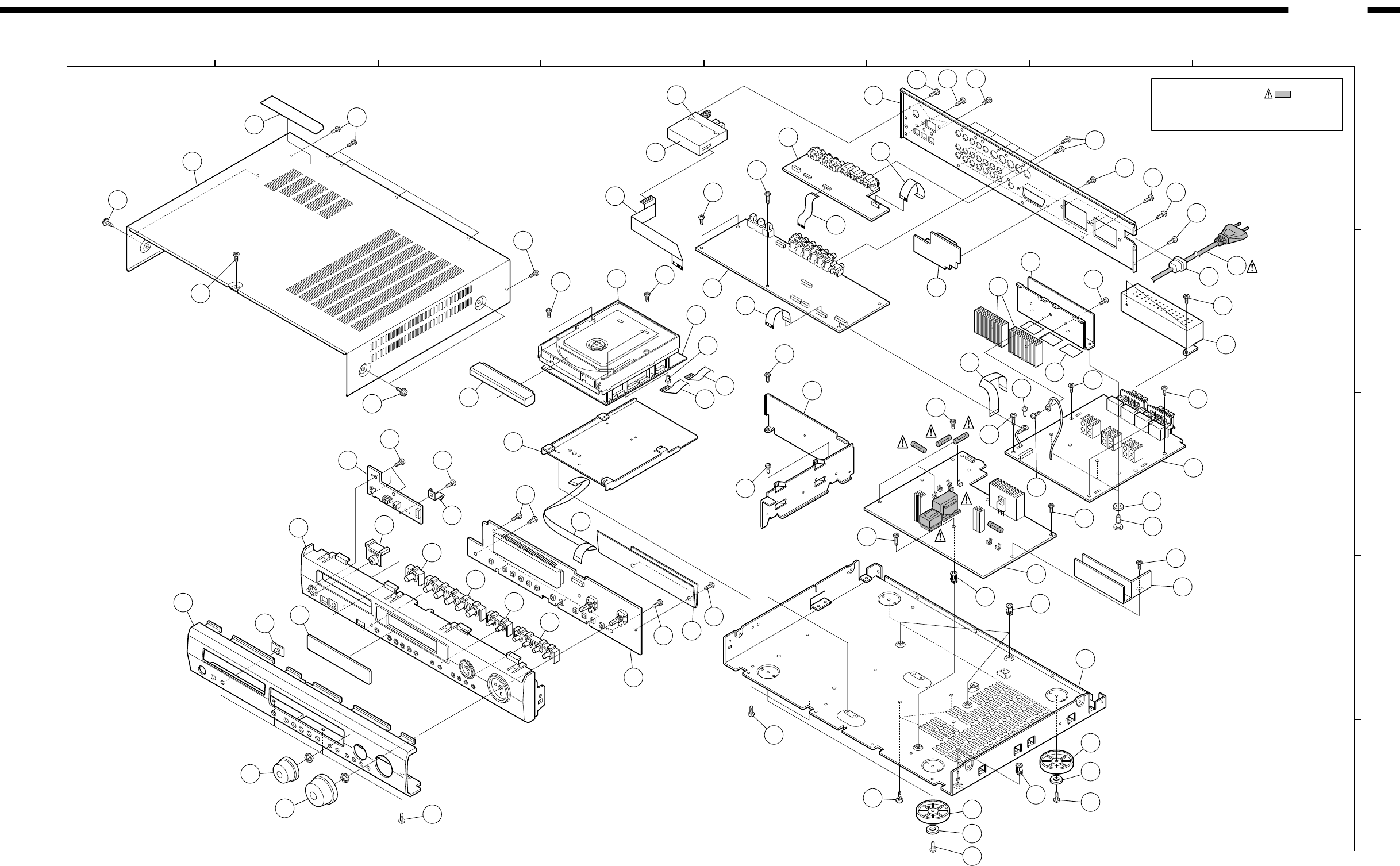
106
112
111
111
105
105
102 102
103
108
3-1
105 107
105
107
107 105
107
105
103
113
1-2
104
8
108
103
1-1
103
103
108
103
103
106
101
103
1-3
2-3
103
103
4
109
1102-2
106
2-1
106
106
105
5
6
7
104
105
6
9
7
39
28
16
25
24
26
14
15
13
8
8
12
25
10
11
27
17
19
20
47
18
52
45
48
49
43
36 31
30 37
34
32
33
35 40
42
14A
27C
27A
27D
EXPLODED VIEW OF CABINET
8
76
5
4
3
2
1
A
B
C
D
E
ADV-1000
70
Parts marked with this symbol have critical
characteristics.
Use ONLY replacement parts recommended by the
manufacturer.
WARNING:
71
ADV-1000
PARTS LIST OF EXPLODED VIEW
Ref. No. Part No. Part Name Remarks
Q'ty
Ref. No. Part No. Part Name Remarks
Q'ty
1 1U- 3434 A AMP/POWER UNIT 1
1-1 AMP UNIT
1-2 P.SUPPLY UNIT
1-3 SCART UNIT
2 1U- 3435 A MAIN UNIT 1
2-1 DISPLAY UNIT
2-2 H/P UNIT
2-3 DSP/AUDIO UNIT
3 1U- 3443 A VIDEO/OUT UNIT 1
3-1 VIDEO UNIT
4 GU- 3430 DVD MAIN UNIT 1
5 411 2008 006 MAIN CHASSIS 1
6 146 2242 007 FOOT 4
7 461 1066 002 FELT 4
8 443 9015 015 P.W.B SPACER 5
9 412 2741 078 P.W.B.HOLDER (H=10) 3
10 417 0622 039 HEAT SINK 2
11 412 4964 002 HEAT SINK BRAKET 1
12 415 0889 009 MICA SHEET 3
13 461 1124 009 RUBBER WASHER 4
14 412 4938 106 SHIELD PLATE 1
14A 415 0893 008 SAFETY SHEET 1
14B 001 9022 008 V.WIRE (BK) 1
15 009 0233 007 21P FFC CABLE 1
16 009 0229 008 17P FFC CABLE 1
17 337 0110 009
DVD DRIVE MECHA UNIT
1
18 412 4937 107 MECHA HOLDER 1
19 009 0227 000 13P FFC CABLE 1
20 009 0230 000 17P FFC CABLE 1
22 204 0565 008 6P PH-8P PH CON.CORD CX081 1
23 204 2934 006 7P PH-PH CON.CORD CX082 1
24 105 1405 116 BACK PANEL 1
25 009 0228 009 15P FFC CABLE 2
26 206 2089 106 AC CORD W/CON.E2 1
27 445 0056 008 CORD BUSH 1
27A 216 0114 009 AM FM TUNER(E2) 1
27B 009 9033 004 1P WIRE ASS'Y 1
27C 412 4986 006 TU EARTH PLATE 1
27D 009 0236 004 15P FFC CABLE 1
28 412 4939 105
MECHA SHIELD BRACKET
1
30 146 2284 007 INNER PANEL 1
31 143 1147 010 WINDOW 1
32 113 1928 005 KNOB(5P) 1
33 113 1929 004 KNOB(2P) 1
34 113 1930 006 KNOB(1P) 1
35 113 1931 005 KNOB(4P) 1
36 143 1086 003 REMOCON FILTER 1
37 113 1888 006 POWER KNOB ASS'Y 1
39 009 0232 008 19P FFC CABLE 1
40 415 0885 003 GUARD SHEET 1
41 445 8028 009 CORD HOLDER 1
42 412 4839 001 EARTH PLATE(H/P) 1
43 144 2802 014 FRONT PANEL 1
43A 513 3463 001 LABEL(LASER) 1
44 445 8004 007 WIRE CLAMPER 5
45 102 0660 005 TOP COVER 1
46 461 9012 016 CUSHION 2
47 146 2285 006 LOADER PANEL 1
48 112 0856 007 VOLUME KNOB ASS'Y 1
49 112 0883 009 VOLUME KNOB(S) ASS'Y 1
50 513 3771 007 RATING SHEET (E2) 1
51 513 1642 002 NO. SHEET 1
52 513 3629 007 NOTICE LABEL(E2) 1
53 513 3632 007 CAUTION LABEL 1
SCREWS
101 471 3305 014 3X10 CBS-Z 2
102 473 7001 048 2.6X8 CBTS (S)-Z 4
103 473 7002 005 3X6 CBTS(S)-Z 15
104 473 7002 034 3X6 CBTS (S)-B 4
105 473 7015 005 3X6 CBTS(S)-B 22
106 473 7500 015 3X8 CBTS (P)-Z 12
107 473 7500 044 3X8 CBTS (P)-B 20
108 473 7501 014 3X14 CBTS (P)-Z 3
109 473 7506 019 2X6 CBTS (P)-Z 3
110 473 7511 004 3X10 CFTS (P)-Z 1
111 477 0263 018 3P.SWELLING SCREW 4
112 477 0318 002 SPECIAL SCREW(TOP) 1
113 477 0319 001 SPECIAL SCREW H-SINK 4
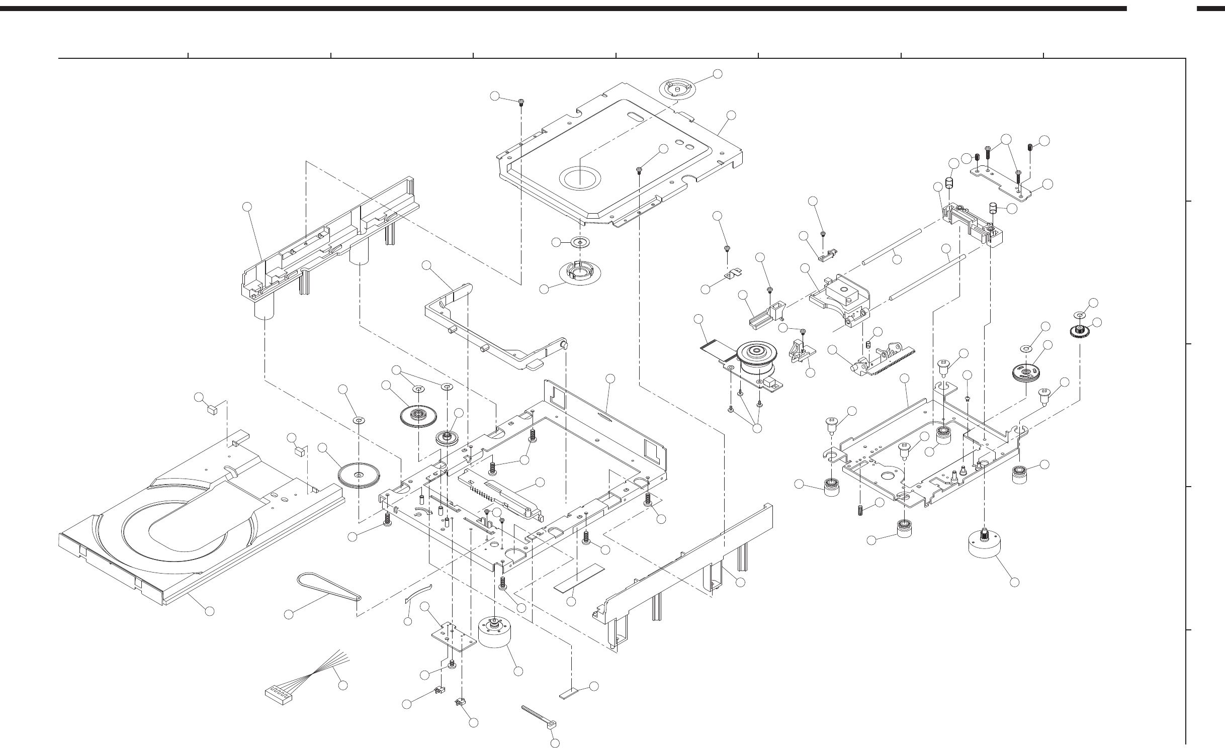

73
ADV-1000
PARTS LIST OF DVD MECHANISM UNIT
Ref. No. Part No. Part Name Remarks
Q'ty
1 9KC 1A01 7A MAIN CHASSIS ASS'Y 1
2 9KA 7P08 5A CLAMPER BRACKET 1
3 9KC 4P00 7F GUIDE CLAMP BRACKET 1
4 9KC 2A00 3B LOADING MOTOR ASS'Y 1
5 9KC 2G02 9A LOADING GEAR 1
6 9KB 9G03 0A LOADING GEAR 2ND 1
7 9KB 9G03 1A LOADING GEAR 3RD 1
8 9KA 2G66 9A SUB CHASSIS-L 1
9 9KA 2G41 8A SUB CHASSIS-R 1
10 9KA 2G39 9C TRAY 1
11 9KC 1G00 3B SLIDE-CAM 1
12 9KC 1G00 4B TRAVERSE ARM 1
14 9KA 7G20 2D CLAMPER H 1
15 9KA 7G20 3B CLAMPER L 1
16 9KB 9G01 5A LOADING BELT 1
17 9KC 1P01 4A SWITCH P.W.B. 1
18 9KC 2G04 3A 5P PH WIRE 1
19 9KS 01W2 04 SWITCH ESE22MH1 1
20 9KS 01W2 05 SWITCH ESE22MH3 1
21 9KP 26C6 25
POLY.SLIT WASHER 2.6X6X0.25C
3
22 445 8004 007 WIRE CLAMPER 1
23 9KS 17N0 22
PRECISION SCREW 1.7X2.2 TYPE3
7
24 9KB 26BK 06 SCREW 2.6X6 CBTS(B)-Z 6
25 9KS 20TK 33
PRECISION SCREW 2X3(S) TYPE3
1
26 9KB 20PK 06 SCREW 2X6 CBTS(P)-Z 2
27 9KC 2A00 7A PU CHASSIS ASS'Y 1
28 9KC 2G00 8B SHAFT HOLDER L 1
29 9KC 2G00 7B SHAFT HOLDER R 1
30 9KC 2G01 0A SHAFT TILT BASE 1
31 9KC 2P00 5A SHAFT TILT PLATE 1
32 9KB 7S00 3A TILT SPRING 2
33 9KC 2H00 1A MAIN SHAFT 1
34 9KC 2H00 2A SUB SHAFT 1
35 9KC 2G00 9C PU RACK GEAR 1
36 9KB 8A00 5D FEED GEAR 2ND ASS'Y 1
37 9KC 2G10 4A PICK UP HOP-1200 1
38 9KC 2G01 5A PU SPRING 1
39 9KC 2P01 6A SHAFT SPRING 1
40 9KC 2S00 5A RACK GEAR SPRING 1
41 9KC 2A02 3A FEED MOTOR ASS'Y 1
42 9KC 2A04 0A T/T MOTOR ASS'Y 1
43 9KB 26TK 06
SCREW 2.6X6 CBTS(S)-Z
2
44 9KB 26TK 04
SCREW 2.6X4 CBTS(S)-Z
1
46 9KH 26TK 15
SCREW 2.6X15 CFTS(S)-Z
2
47 9KB 7H00 8 SCREW 3X4 BSS 2
48 9KC 2H00 4A SCREW 3X8 BSS (A) 1
49 9KA 2G65 4A DAMPER 4
50 9KP 21C4 25
POLY.SLIT WASHER 2.1X4X0.25C
2
51
SPECIAL SCREW (FRONT)
2
52
SPECIAL SCREW (REAR) 2
53 9KC 4G00 5A FEED GEAR 3RD 1
59 9KB 7P02 4A TRAY-SPRING-VXF 1
63 9KS 17N0 35
PRECISION SCREW 1.7X3.5 TYPE3
1
64 9KC 1G04 2A RUBBER CUSHION 2
Ref. No. Part No. Part Name Remarks
Q'ty
68
TAPE W10X30 (NITTO NO.156)
1
70 9KC 2G08 5A CUSHION L 5X3.5Xt4 1
71 9KC 2G08 4A CUSHION R 5X3.5Xt2 1

Apply 12.5mm half-ball approx.
Main
Chassis Main Chassis
*As for greasing to the R rail
groove and groove's side edge,
apply grease to the outer face
"intentionally".
(Not only running a brush into
the groove, use it with pressing
to the outer face consciously.)
After attaching cushions, apply Cemedine
575 to the joint parts of the cushions and
tabs (both sides, left and right) from the tab's
back side. (0.1mg each x 4)
After applying , check especially for the front 3 ribs outer side
in order not to be insufficient greasing.
When greasing each rib, apply to
the rib's left, right, and top faces
properly with running a brush on both sides
of the rib.
With Cemedine 575, glue 3 joint parts of Clamper-L
and H hooks. (0.05mg each x 3)
Froil KG 423
After attaching plate spring,
apply to the TRAY side of
the plate spring.
POINTS OF GREASING
8
76
5
4
3
2
1
A
B
C
D
E
ADV-1000
74

75
ADV-1000
PACKING VIEW
PARTS LIST OF PACKING & ACCESSORIES
Ref. No. Part No. Part Name Remarks Q'tyRef. No. Part No. Part Name Remarks Q'ty
201 505 8092 010 LAMINATE ENVELOPE 1
202 504 0205 006 POLYETHYLENE SHEET 1
203 501 2202 008 CARTON CASE 1
204 502 1058 007 CUSHION(L) 1
207 502 1059 006 CUSHION(R) 1
209
E2 POS LABEL
210
CONT.CARD(L)
211 505 0038 030 POLY COVER 1
212 511 3919 009 INST. MANUAL(E2) 1
213 515 0921 005 S.S.LIST(EX) 1
214 511 3842 008 INST.SHEET 1
215 399 0746 002 RC-901
REMOTE CONTROLLER
1
216
BATTERY (R6P) ASS'Y
217 203 0380 002 1P PIN CORD (VIDEO) 1
218 231 0922 009 LOOP ANTENNA 1
219 395 0026 005 FM ANT. WIRE 1
204
211 219~
207
201
203
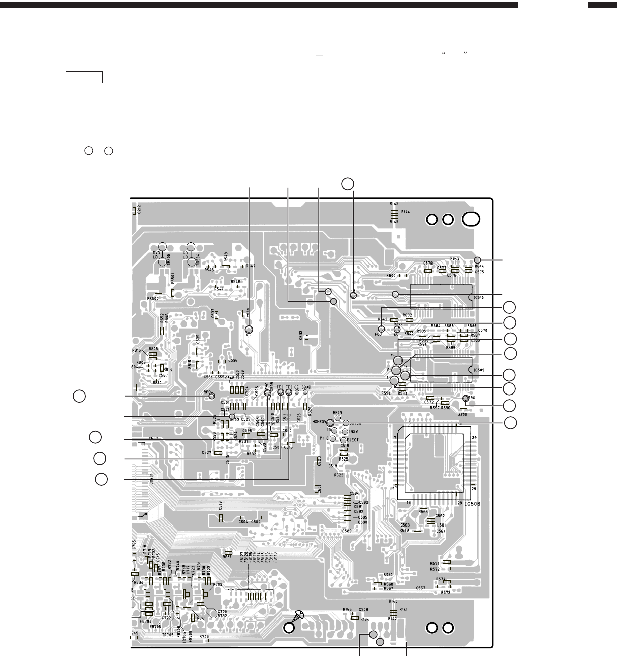
76
ADV-1000
MEASURING METHOD AND WAVEFORMS
To check the waveforms on the DVD Main P.W.B., the GND ( ) probe of the oscilloscope to Vref point.
NOTES
Measuring Disc: DVD/DVDT-S01
CD/TCD-784
(It is better to use wires for extending between the probe and test points.)
When watching the HF waveform, use the extending wire as short as possible.
When HF waveform is noisy or cannot discriminate the eye-pattern, replace the Traverse Unit after measuring the Iop.
1
~
!
points have the certain test points shown below.
GU-3430 DVD Main P.W.B. Unit foil side
C
B
E
C
B
E
C
B
E
C
B
E
1
114
15 28
114
15 28
HI+
AI
FOO
EC
F+
F-
T+
T-
TRO
HOMESW
LOAD+LOAD-
FG
SLEG-SLEG+
Vref
HF(RFO)
TRAYSW
FMO
TEI
FEI
13
12
11
10
9
8
7
6
5
4
3
2
1
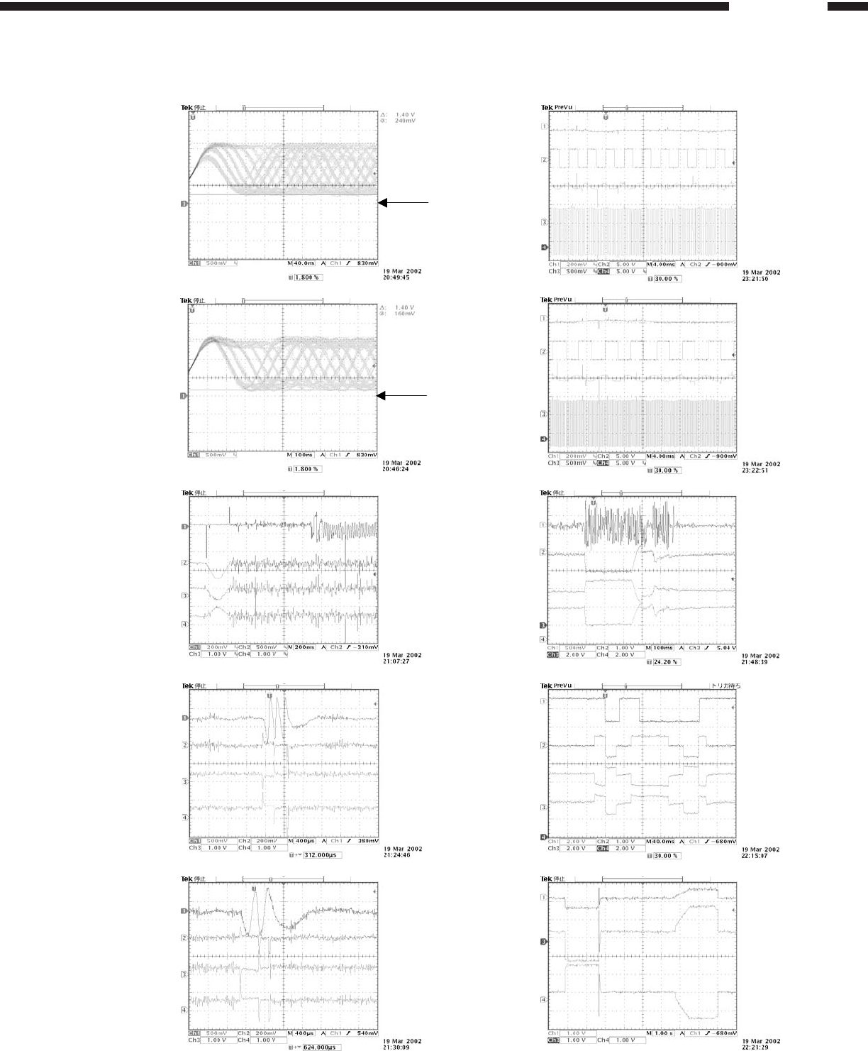
77
ADV-1000
WAVEFORMS
DVD MAIN P.W.B.
DVD PLAY Disk : TDV-520A DVD PLAY (INNER)
①HF(RFO)
CD PLAY Disk : TCD-784 CD PLAY (INNER)
①HF(RFO)
(DVD/CD) LOADING → PLAY SEARCH (INNER → OUTER)
DVD PLAY POWER ON (INSW ON)
CD PLAY LOADER OPEN → CLOSE
Verf
VerfVerf
Verf
Verf
VerfVerf
Verf
②FEI
③FOO
④F+
⑤F-
⑥TEI
⑦TRO
⑧T+
⑨T-
⑥TEI
⑦TRO
⑧T+
⑨T-
⑩EC
⑪FG
H1+
A1
⑩EC
⑪FG
H1+
A1
⑥TEI
⑫FMO
SLED+
SLED-
⑬HOMESW
⑫FMO
SLED+
SLED-
TRAYSW
LOAD+
LOAD-
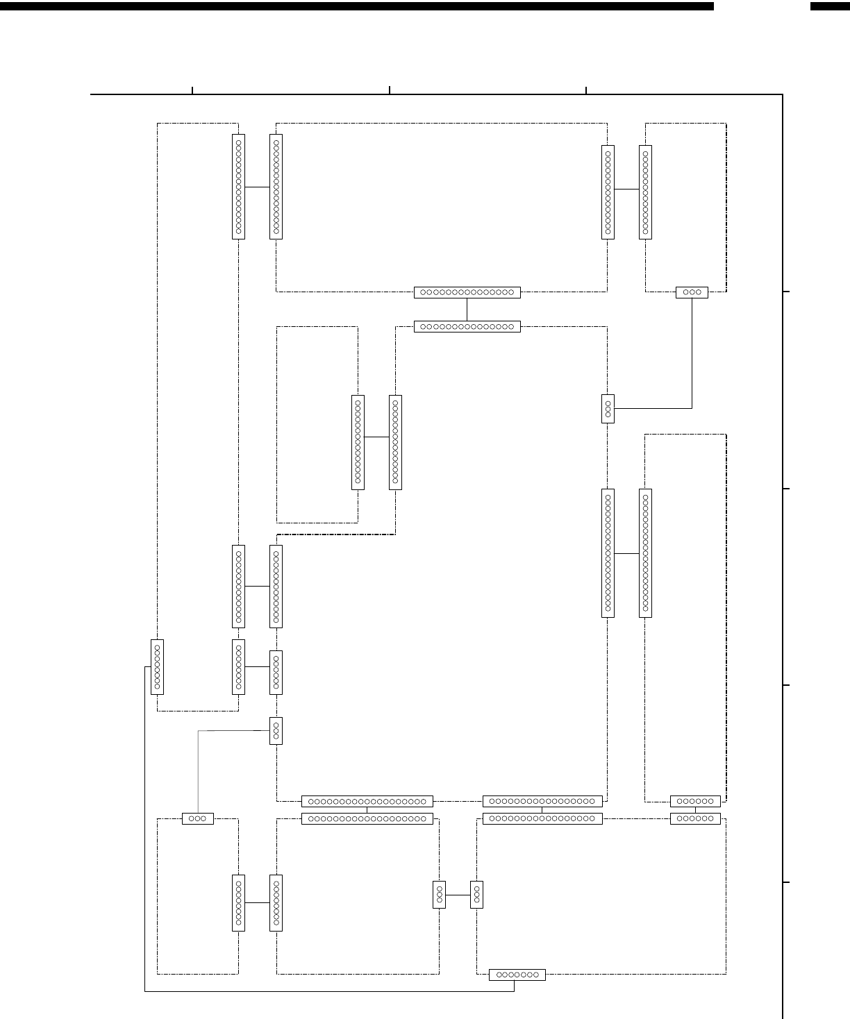
78
ADV-1000
D
C
B
A
4
32
E
1
CX171(FFC P=1.00)
RGB_H
VCNT1/YC_H
VCNT2/WIDE
+5V_V1
GND V1
N.C.
GND V1
Y
GND V1
C
8
10
GND V1
Y/G
GND V1
Cb/B
GND V1
Cr/R
GND V1
RGB_H
VCNT1/YC_H
VCNT2/WIDE
+5V_V1
GND V1
N.C.
GND V1
Y
GND V1
C
GND V1
Y/G
GND V1
Cb/B
GND V1
Cr/R
GND V1
CY172(FFC P=1.00)
2
3
4
5
6
7
9
11
12
13
14
15
16
17
1
STEREO
/TUNED
T.MUTE
R_OUT
GND_A1
L_OUT
FM_DET
+12V_A1
+5V_D4
FM_S.MATER
GND_A1
DO
CL
DI
CE
TUNER PACK
CY151(FFC P=1.25)
STEREO
/TUNED
T.MUTE
TU_R
GND_A1
TU_L
FM_DET
+12V_A1
+5V_D4
FM_S.MATER
GND_A1
SANYO_DO
SANYO_CL
SANYO_DI
SANYO_CE
CX152(FFC P=1.00)
S-SEL
RGB H
VCONT2
VCONT1
V.MUTE
D
C
B
A
IP-SEL
GND V1
GND V1
+5V V1
+5V V1
+12V A1
CY152(FFC P=1.00)
S-SEL
RGB H
VCONT2
VCONT1
V.MUTE
D
C
B
A
IP-SEL
GND V1
GND V1
+5V V1
+5V V1
+12V A1
CX153(FFC P=1.00)
RGB H
FUNC SW
GND V1
Y/V
GND V1
DVD-Y/G
GND V1
DVD-Cb
GND V1
DVD-Cr
+5V V1
WIDE
S-SEL
D-SEL
IP-SEL
CY153(FFC P=1.00)
RGB H
FUNC SW
GND V1
Y/V
GND V1
DVD-Y/G
GND V1
DVD-Cb
GND V1
DVD-Cr
+5V V1
WIDE
S-SEL
D-SEL
IP-SEL
CW034(SAN)
AUDIO R
GND A
AUDIO L
SCART UNIT
1U-3434-3
CX034(PH)
AUDIO R
GND A
AUDIO L
1U-3443-1
VIDEO UNIT
GU-3430
DVD MAIN UNIT
CX131(FFC P=1.00)
CX081(PH)
AMUTE
96K
DEEM
PRES
GND D1
SPDIF
BCK
MCLK
TSD0
LRCK
GND D1
TSD1
TSD2
CX131(FFC P=1.00)
CX082(PH/RED)
AMUTE
96K
DEEM
PRES
GND D1
SPDIF
BCK
MCLK
TSD0
LRCK
GND D1
TSD1
TSD2
CX062(PH)
SCLK
/CS
sDATA
DFPES
CY031(PH/RED)
GND
FR
FL
CY191(FFC P=1.00)
GND D2
GND D2
+5V D2
RESET
FLDA
FLCK
FLCS
FJOGA
FJOGB
VJOGA
VJOGB
KEY1
KEY0
REMOTE
LED R
LED G
H/P SW
H/P MUTE
N.C
CX191(FFC P=1.00)
GND D2
GND D2
+5V D2
RESET
FLDA
FLCK
FLCS
FJOGA
FJOGB
VJOGA
VJOGB
KEY1
KEY0
REMOTE
LED R
LED G
H/P SW
H/P MUTE
N.C
CW081(SAN)
KEY0
LED R
LED G
H/P SW
REMOTE
H/P MUTE
+5V D2
GND D2 1U-3435-1
DISPLAY UNIT
CW033(SAN)
+5V
GND D
GND D
CW031(SAN)
FL
GND
FR
CX081(PH)
KEY0
LED R
LED G
H/P SW
REMOTE
H/P MUTE
+5V D2
GND D2
+5V D3
+5V D1
+5V D2
+12V_A2
ON/ST
GND D1
GND D2
S.STANDBY
+5V D3
PWRON
SDATA
DFPES
/CS
SCLK
GND D1
IR
1U-3435-2
H/P UNIT
CX033(PH)
+5V
GND D
GND D
CX071(PH/RED)
+5V D3
+5V D1
GND D1
ON/ST
+5V D2
GND D2
+12V A2
1U-3434-2
P.SUPPLY UNIT
CX171(FFC P=1.00) CY171(FFC P=1.00)
CW061(SCN)
+B POWER
+B POWER
P.GND
P.GND
+5V D4
GND D4
CX061(VH)
+B POWER
+B POWER
P.GND
P.GND
+5V D4
GND D4
CY211(FFC P=1.00)
FL
GND
FR
F.GND
GND
SW
GND
SL
GND
SR
505P DOWN
2025MUTE
2025HMUTE
/PROTECT
RL FRONT
RL SURR
RL C
RL SW
+17V
GND RL
DSP/AUDIO UNIT
1U-3435-3
CX211(FFC P=1.00)
FL
GND
FR
F.GND
C C
GND
SW
GND
SL
GND
SR
505P DOWN
2025MUTE
2025HMUTE
/PROTECT
RL FRONT
RL SURR
RL C
RL SW
+17V
GND RL
AMP UNIT
1U-3434-1
8
10
2
3
4
5
6
7
9
11
12
13
1
8
10
2
3
4
5
6
7
9
11
12
13
1
8
2
3
4
5
6
7
1
8
2
3
4
5
6
7
1
2
3
4
5
6
1
2
3
1
2
3
1
2
3
1
2
3
1
8
2
3
4
5
6
7
1
8
2
3
4
5
6
7
1
1
2
3
4
5
6
7
1
2
3
4
5
6
7
8
9
10
11
12
13
14
15
16
17
18
19
1
2
3
4
5
6
7
8
9
10
11
12
13
14
15
16
17
18
19
1
2
3
4
5
6
7
8
9
11
10
12
13
14
15
16
17
1
2
3
4
5
6
1
2
3
4
5
6
1
2
3
4
5
6
7
8
9
11
10
12
13
14
15
16
17
+5V D4
GND D4
;5V D3
GND D3
;12V A
GND A
GND A
+12V_A
+17V RL
GND RL
LIMIT +
LIMIT -
DVD ON/OFF
P.ON/OFF
50/60
/OVER VOLT
N.C.
+5V D4
GND D4
;5V D3
GND D3
;12V A
GND A
GND A
+12V_A
+17V RL
GND RL
LIMIT +
LIMIT -
DVD ON/OFF
P.ON/OFF
50/60
/OVER VOLT
N.C.
1
2
3
4
5
6
7
8
9
10
11
12
13
14
15
1
2
3
4
5
6
7
8
9
10
11
12
13
14
15
1
2
3
4
5
6
7
8
9
10
11
12
13
14
15 1
2
3
4
5
6
7
8
9
10
11
12
13
14
15
1
2
3
4
5
6
7
8
9
10
11
12
13
14
15
1
2
3
1
2
3
1
2
3
4
5
6
7
8
9
10
11
12
13
14
15
1
2
3
4
5
6
7
8
9
10
11
12
13
14
15
16
17
18
19
20
21
1
2
3
4
5
6
7
8
9
10
11
12
13
14
15
16
17
18
19
20
21
1
2
3
4
5
6
7
8
9
10
11
12
13
14
15
16
17
WIRING DIAGRAM
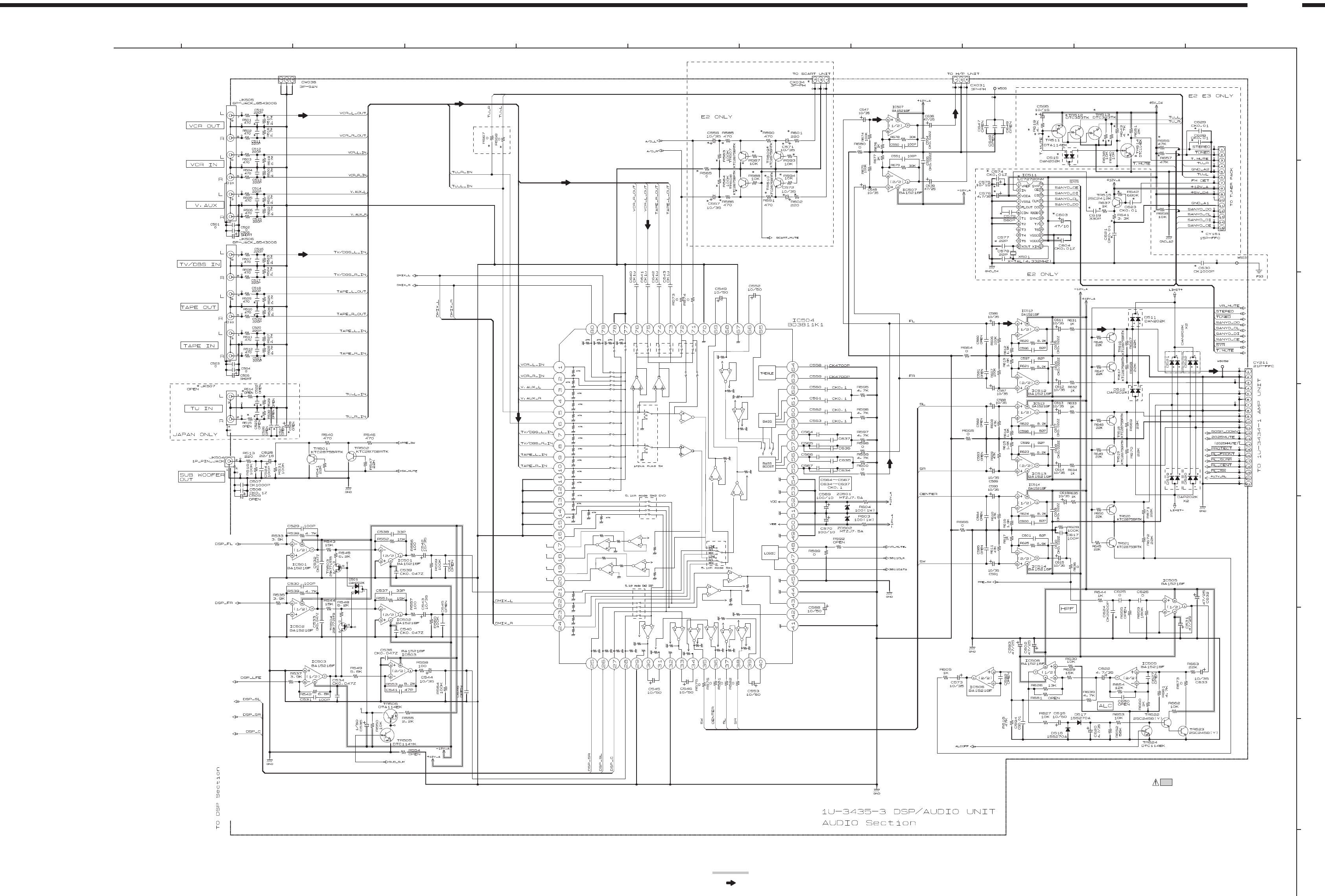
79
SCHEMATIC DIAGRAMS (1/10)
1U-3435-3 DSP/AUDIO (1/4)
AUDIO Section
SCHEMATIC DIAGRAMS (1/10)
1 2 3 4 5 6 7 8 9 10 11
A
B
C
D
E
F
G
H
NOTICE
ALL RESISTANCE VALUES IN OHM. k=1,000 OHM M=1,000,000 OHM
ALL CAPACITANCE VALUES IN MICRO FARAD. P=MICRO-MICRO FARAD
EACH VOLTAGE AND CURRENT ARE MEASUERD AT MO SIGNAL INPUT
CONDITION.
CIRCUIT AND PARTS ARE SUBJECT TO CHANGE WITHOUT PRIOR
NOTICE.
WARNING:
Parts marked with this symbol have critical characteristics.
Use ONLY replacement parts recommended by the manufacture.
CAUTION:
Before returning the unit to the customer, make sure you make either (1) a
leakage current check or (2) a line to chassis resistance check. If the leakage
current exceeds 0.5 milliamps, or if the resistance from chassis to either side
of the power card is less than 460kohms, the unit is defective.
WARNING:
DO NOT return the unit to the customer until the problem is located and
corrected.
SIGNAL LINE
ADV-1000
± B LINE
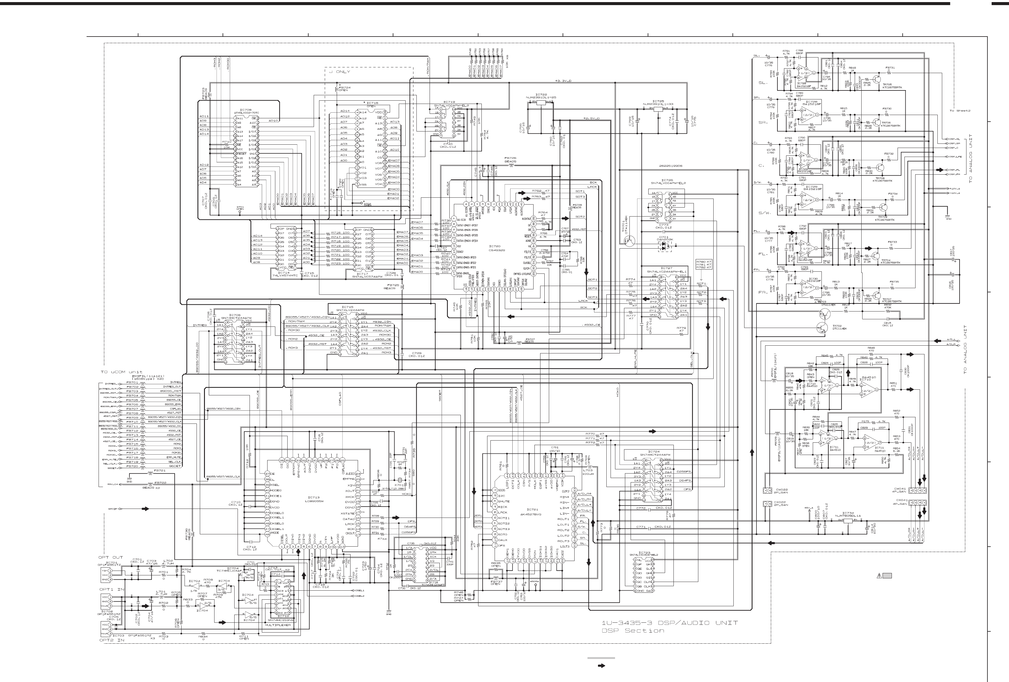
80
SCHEMATIC DIAGRAMS (2/10)
1U-3435-3 DSP/AUDIO (2/4)
DSP Section
SCHEMATIC DIAGRAMS (2/10)
1 2 3 4 5 6 7 8 9 10 11
A
B
C
D
E
F
G
H
NOTICE
ALL RESISTANCE VALUES IN OHM. k=1,000 OHM M=1,000,000 OHM
ALL CAPACITANCE VALUES IN MICRO FARAD. P=MICRO-MICRO FARAD
EACH VOLTAGE AND CURRENT ARE MEASUERD AT MO SIGNAL INPUT
CONDITION.
CIRCUIT AND PARTS ARE SUBJECT TO CHANGE WITHOUT PRIOR
NOTICE.
WARNING:
Parts marked with this symbol have critical characteristics.
Use ONLY replacement parts recommended by the manufacture.
CAUTION:
Before returning the unit to the customer, make sure you make either (1) a
leakage current check or (2) a line to chassis resistance check. If the leakage
current exceeds 0.5 milliamps, or if the resistance from chassis to either side
of the power card is less than 460kohms, the unit is defective.
WARNING:
DO NOT return the unit to the customer until the problem is located and
corrected.
ADV-1000
SIGNAL LINE
± B LINE
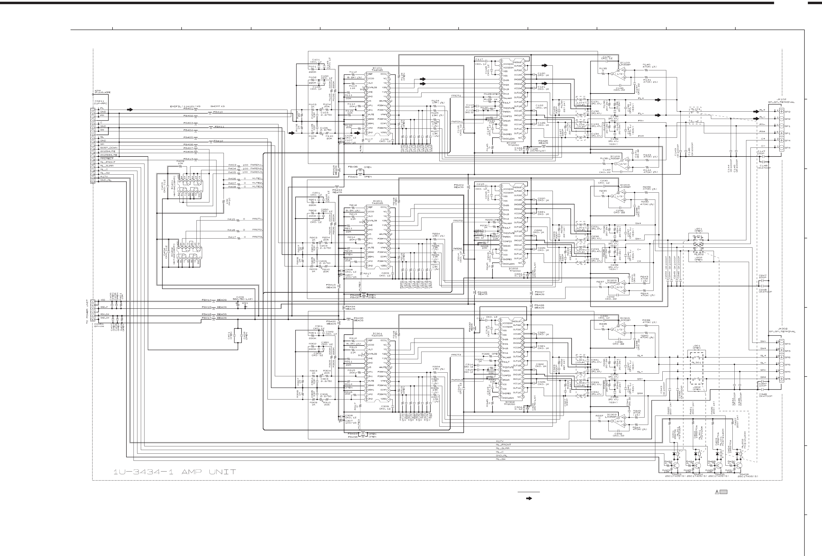
81
SCHEMATIC DIAGRAMS (3/10)
1U-3434-1 AMP UNIT
SCHEMATIC DIAGRAMS (3/10)
1 2 3 4 5 6 7 8 9 10 11
A
B
C
D
E
F
G
H
NOTICE
ALL RESISTANCE VALUES IN OHM. k=1,000 OHM M=1,000,000 OHM
ALL CAPACITANCE VALUES IN MICRO FARAD. P=MICRO-MICRO FARAD
EACH VOLTAGE AND CURRENT ARE MEASUERD AT MO SIGNAL INPUT
CONDITION.
CIRCUIT AND PARTS ARE SUBJECT TO CHANGE WITHOUT PRIOR
NOTICE.
WARNING:
Parts marked with this symbol have critical characteristics.
Use ONLY replacement parts recommended by the manufacture.
CAUTION:
Before returning the unit to the customer, make sure you make either (1) a
leakage current check or (2) a line to chassis resistance check. If the leakage
current exceeds 0.5 milliamps, or if the resistance from chassis to either side
of the power card is less than 460kohms, the unit is defective.
WARNING:
DO NOT return the unit to the customer until the problem is located and
corrected.
ADV-1000
SIGNAL LINE
± B LINE
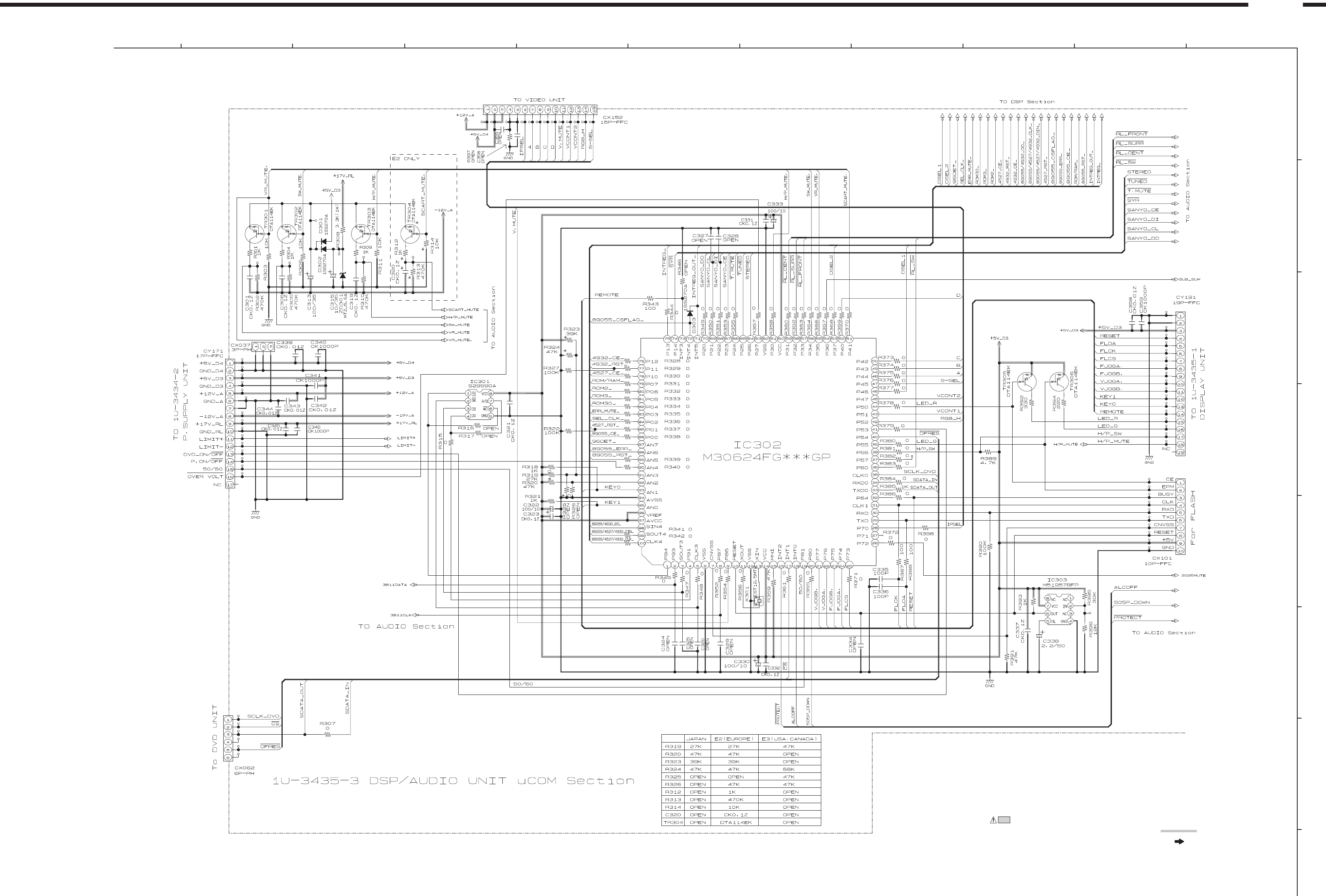
82
SCHEMATIC DIAGRAMS (4/10)
1U-3435-3 DSP/AUDIO (3/4)
µCOM Section
SCHEMATIC DIAGRAMS (4/10)
1 2 3 4 5 6 7 8 9 10 11
A
B
C
D
E
F
G
H
NOTICE
ALL RESISTANCE VALUES IN OHM. k=1,000 OHM M=1,000,000 OHM
ALL CAPACITANCE VALUES IN MICRO FARAD. P=MICRO-MICRO FARAD
EACH VOLTAGE AND CURRENT ARE MEASUERD AT MO SIGNAL INPUT
CONDITION.
CIRCUIT AND PARTS ARE SUBJECT TO CHANGE WITHOUT PRIOR
NOTICE.
WARNING:
Parts marked with this symbol have critical characteristics.
Use ONLY replacement parts recommended by the manufacture.
CAUTION:
Before returning the unit to the customer, make sure you make either (1) a
leakage current check or (2) a line to chassis resistance check. If the leakage
current exceeds 0.5 milliamps, or if the resistance from chassis to either side
of the power card is less than 460kohms, the unit is defective.
WARNING:
DO NOT return the unit to the customer until the problem is located and
corrected.
SIGNAL LINE
ADV-1000
± B LINE
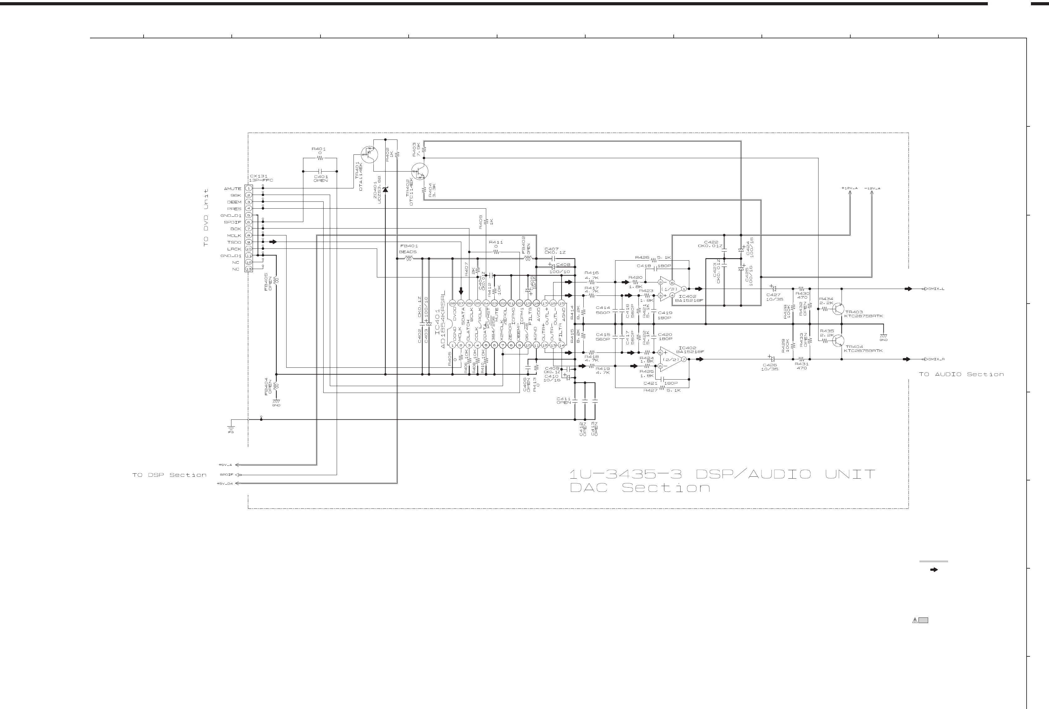
83
SCHEMATIC DIAGRAMS (5/10)
1U-3435-3 DSP/AUDIO UNIT (4/4)
DAC Section
SCHEMATIC DIAGRAMS (5/10)
1 2 3 4 5 6 7 8 9 10 11
A
B
C
D
E
F
G
H
NOTICE
ALL RESISTANCE VALUES IN OHM. k=1,000 OHM M=1,000,000 OHM
ALL CAPACITANCE VALUES IN MICRO FARAD. P=MICRO-MICRO FARAD
EACH VOLTAGE AND CURRENT ARE MEASUERD AT MO SIGNAL INPUT
CONDITION.
CIRCUIT AND PARTS ARE SUBJECT TO CHANGE WITHOUT PRIOR
NOTICE.
WARNING:
Parts marked with this symbol have critical characteristics.
Use ONLY replacement parts recommended by the manufacture.
CAUTION:
Before returning the unit to the customer, make sure you make either (1) a
leakage current check or (2) a line to chassis resistance check. If the leakage
current exceeds 0.5 milliamps, or if the resistance from chassis to either side
of the power card is less than 460kohms, the unit is defective.
WARNING:
DO NOT return the unit to the customer until the problem is located and
corrected.
SIGNAL LINE
ADV-1000
± B LINE
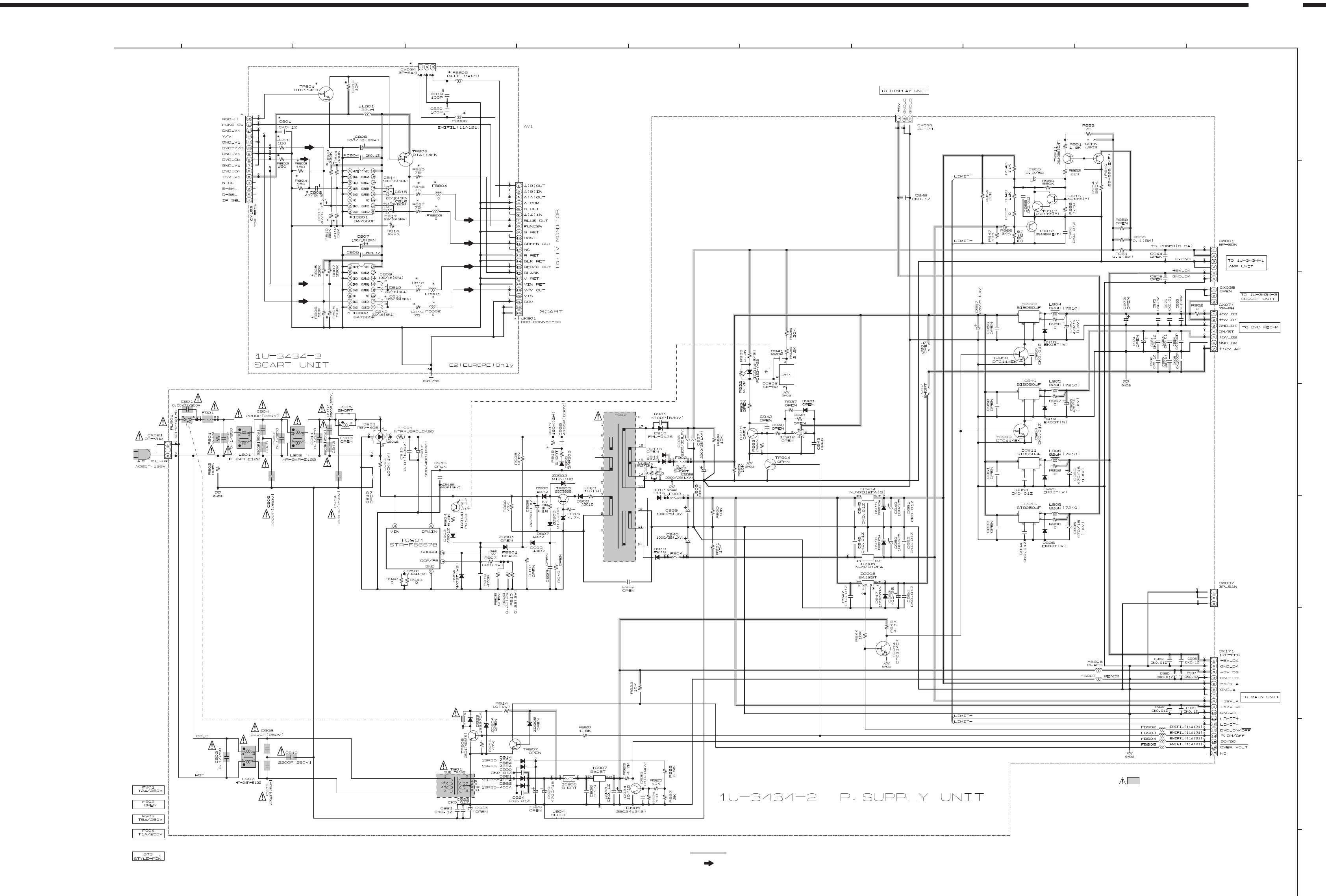
84
SCHEMATIC DIAGRAMS (6/10)
1 2 3 4 5 6 7 8 9 10 11
A
B
C
D
E
F
G
H
NOTICE
ALL RESISTANCE VALUES IN OHM. k=1,000 OHM M=1,000,000 OHM
ALL CAPACITANCE VALUES IN MICRO FARAD. P=MICRO-MICRO FARAD
EACH VOLTAGE AND CURRENT ARE MEASUERD AT MO SIGNAL INPUT
CONDITION.
CIRCUIT AND PARTS ARE SUBJECT TO CHANGE WITHOUT PRIOR
NOTICE.
WARNING:
Parts marked with this symbol have critical characteristics.
Use ONLY replacement parts recommended by the manufacture.
CAUTION:
Before returning the unit to the customer, make sure you make either (1) a
leakage current check or (2) a line to chassis resistance check. If the leakage
current exceeds 0.5 milliamps, or if the resistance from chassis to either side
of the power card is less than 460kohms, the unit is defective.
WARNING:
DO NOT return the unit to the customer until the problem is located and
corrected.
SIGNAL LINE
ADV-1000
± B LINE
SCHEMATIC DIAGRAMS (6/10)
1U-3434-2 P. SUPPLY UNIT
1U-3434-3 SCART UNIT
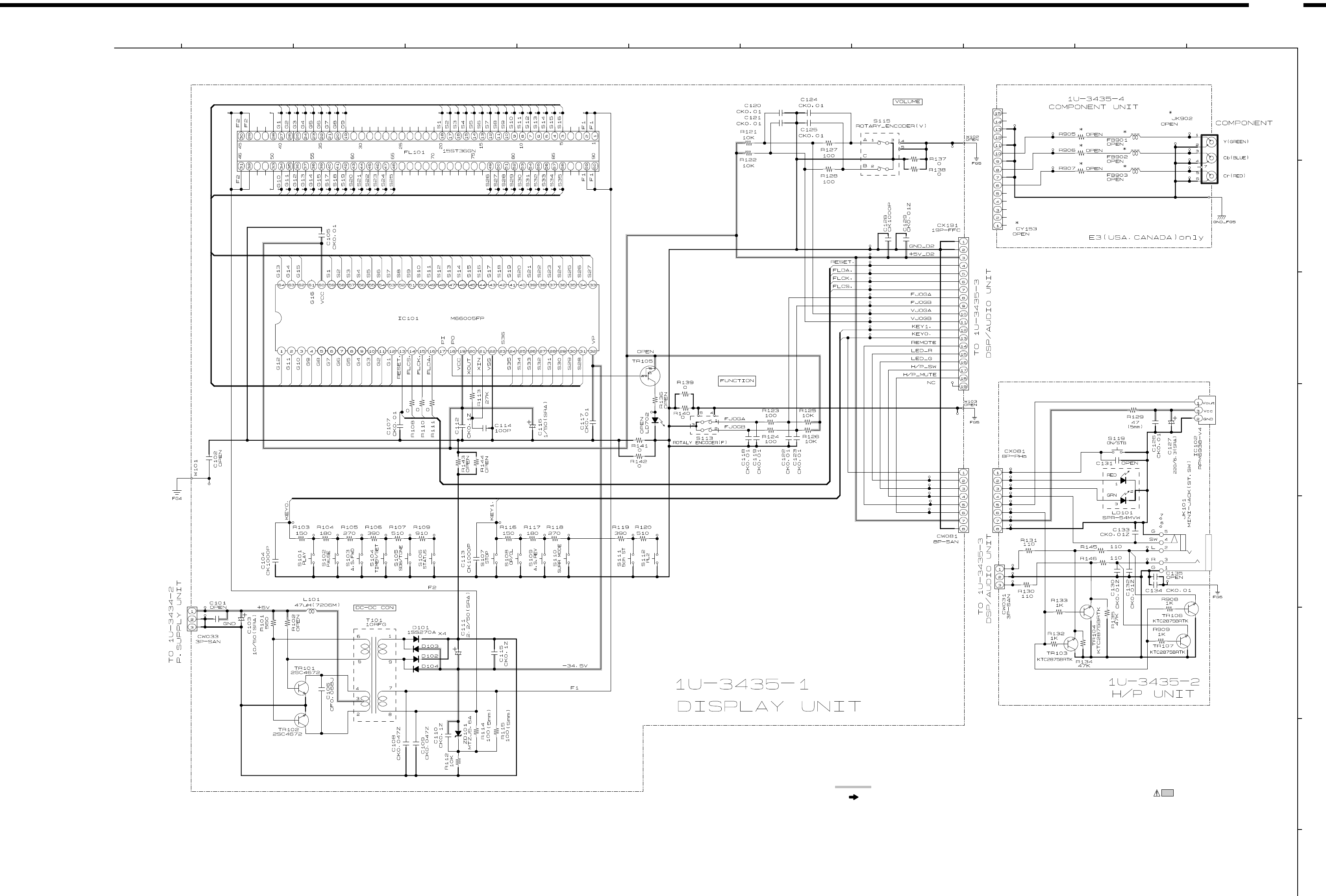
85
SCHEMATIC DIAGRAMS (7/10)
1U-3435-1 DISPLAY UNIT
1U-3435-2 H/P UNIT
SCHEMATIC DIAGRAMS (7/10)
1 2 3 4 5 6 7 8 9 10 11
A
B
C
D
E
F
G
H
NOTICE
ALL RESISTANCE VALUES IN OHM. k=1,000 OHM M=1,000,000 OHM
ALL CAPACITANCE VALUES IN MICRO FARAD. P=MICRO-MICRO FARAD
EACH VOLTAGE AND CURRENT ARE MEASUERD AT MO SIGNAL INPUT
CONDITION.
CIRCUIT AND PARTS ARE SUBJECT TO CHANGE WITHOUT PRIOR
NOTICE.
WARNING:
Parts marked with this symbol have critical characteristics.
Use ONLY replacement parts recommended by the manufacture.
CAUTION:
Before returning the unit to the customer, make sure you make either (1) a
leakage current check or (2) a line to chassis resistance check. If the leakage
current exceeds 0.5 milliamps, or if the resistance from chassis to either side
of the power card is less than 460kohms, the unit is defective.
WARNING:
DO NOT return the unit to the customer until the problem is located and
corrected.
ADV-1000
SIGNAL LINE
± B LINE
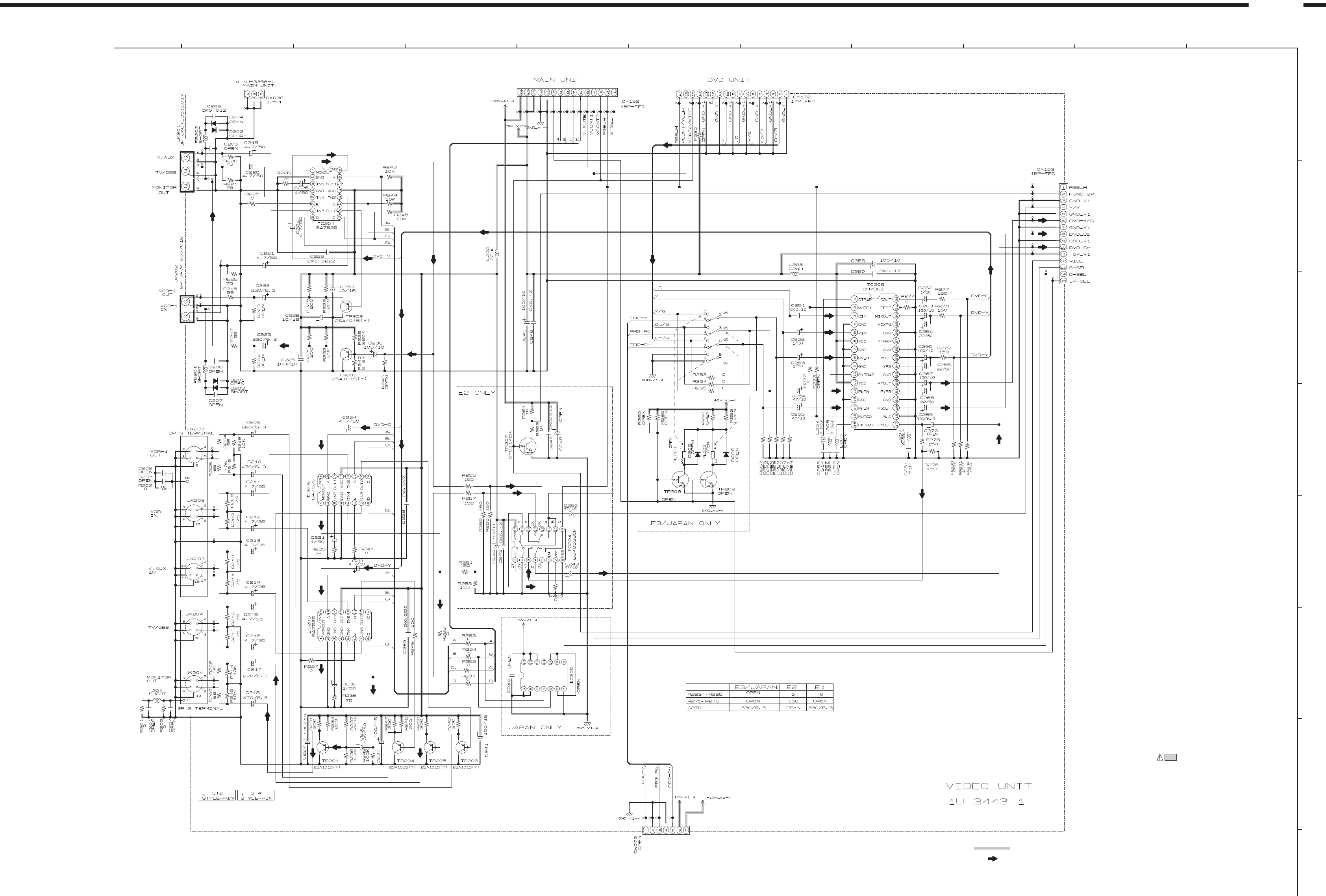
86
SCHEMATIC DIAGRAMS (8/10)
1U-3443-1 VIDEO UNIT
SCHEMATIC DIAGRAMS (8/10)
1 2 3 4 5 6 7 8 9 10 11
A
B
C
D
E
F
G
H
ADV-1000
NOTICE
ALL RESISTANCE VALUES IN OHM. k=1,000 OHM M=1,000,000 OHM
ALL CAPACITANCE VALUES IN MICRO FARAD. P=MICRO-MICRO FARAD
EACH VOLTAGE AND CURRENT ARE MEASUERD AT MO SIGNAL INPUT
CONDITION.
CIRCUIT AND PARTS ARE SUBJECT TO CHANGE WITHOUT PRIOR
NOTICE.
WARNING:
Parts marked with this symbol have critical characteristics.
Use ONLY replacement parts recommended by the manufacture.
CAUTION:
Before returning the unit to the customer, make sure you make either (1) a
leakage current check or (2) a line to chassis resistance check. If the leakage
current exceeds 0.5 milliamps, or if the resistance from chassis to either side
of the power card is less than 460kohms, the unit is defective.
WARNING:
DO NOT return the unit to the customer until the problem is located and
corrected.
SIGNAL LINE
± B LINE
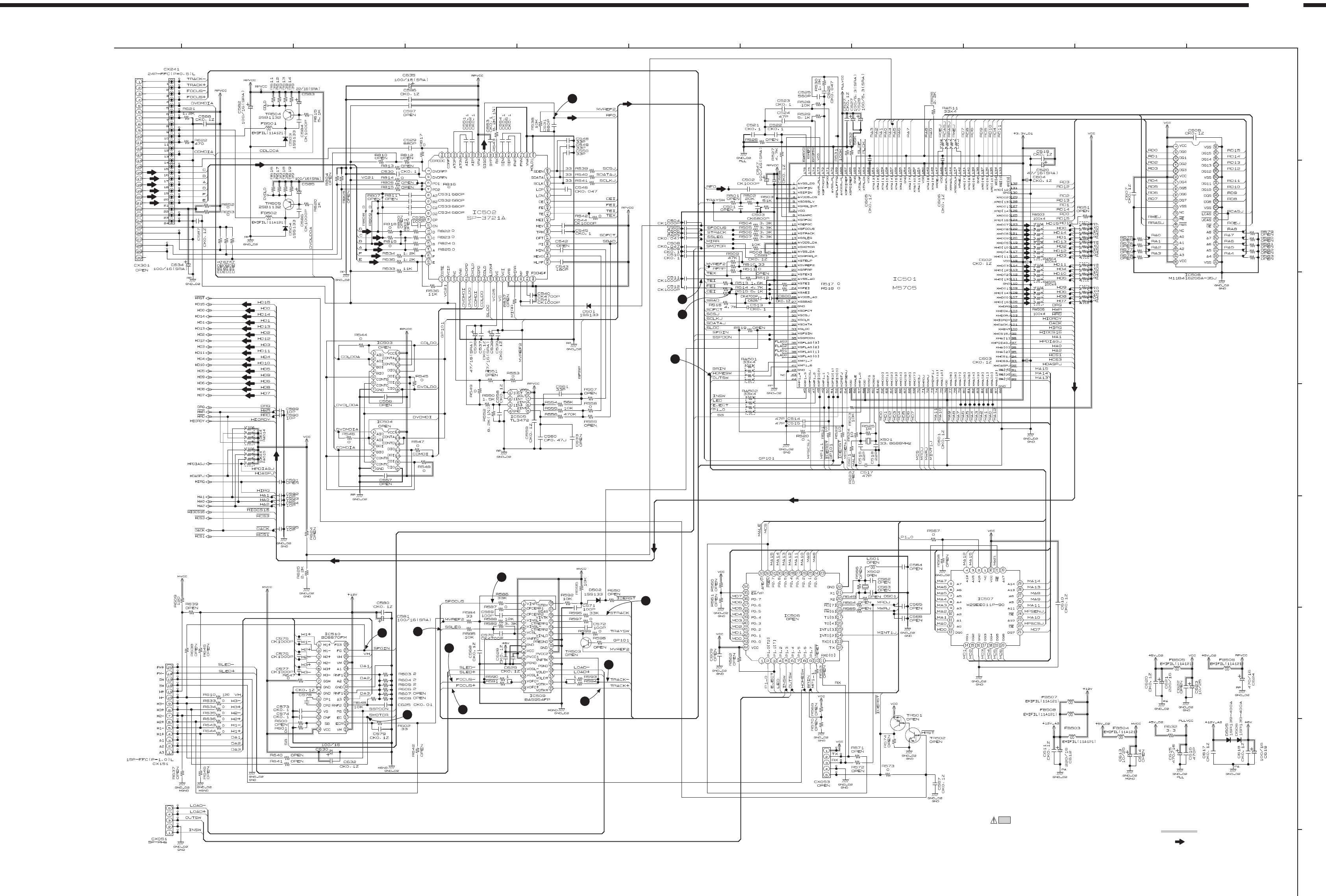
6
13
10
11 12
1
2
7
9
8
5
3
4
HF(RFO)
FEI
TEI
HOME SW
TRO
T+
T-
FOO
F-
F+
FMO
FG
EC
87
SCHEMATIC DIAGRAMS (9/10)
GU-3430 DVD MAIN UNIT (1/2)
SCHEMATIC DIAGRAMS (9/10)
1 2 3 4 5 6 7 8 9 10 11
A
B
C
D
E
F
G
H
NOTICE
ALL RESISTANCE VALUES IN OHM. k=1,000 OHM M=1,000,000 OHM
ALL CAPACITANCE VALUES IN MICRO FARAD. P=MICRO-MICRO FARAD
EACH VOLTAGE AND CURRENT ARE MEASUERD AT MO SIGNAL INPUT
CONDITION.
CIRCUIT AND PARTS ARE SUBJECT TO CHANGE WITHOUT PRIOR
NOTICE.
WARNING:
Parts marked with this symbol have critical characteristics.
Use ONLY replacement parts recommended by the manufacture.
CAUTION:
Before returning the unit to the customer, make sure you make either (1) a
leakage current check or (2) a line to chassis resistance check. If the leakage
current exceeds 0.5 milliamps, or if the resistance from chassis to either side
of the power card is less than 460kohms, the unit is defective.
WARNING:
DO NOT return the unit to the customer until the problem is located and
corrected.
SIGNAL LINE
ADV-1000
± B LINE
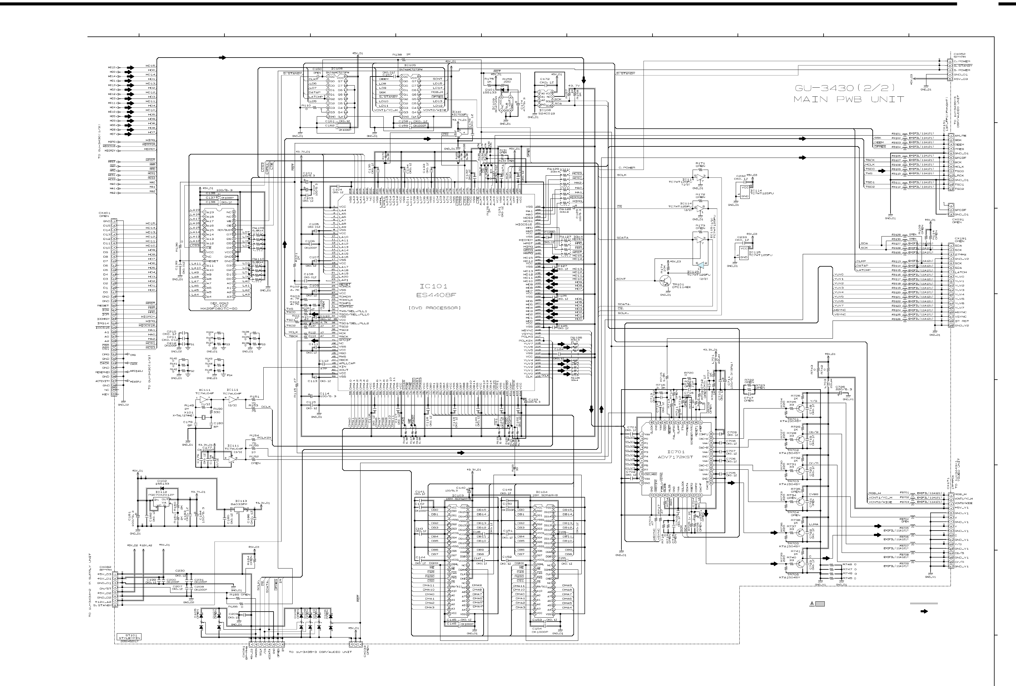
88
SCHEMATIC DIAGRAMS (10/10)
GU-3430 DVD MAIN UNIT (2/2)
SCHEMATIC DIAGRAMS (10/10)
1 2 3 4 5 6 7 8 9 10 11
A
B
C
D
E
F
G
H
NOTICE
ALL RESISTANCE VALUES IN OHM. k=1,000 OHM M=1,000,000 OHM
ALL CAPACITANCE VALUES IN MICRO FARAD. P=MICRO-MICRO FARAD
EACH VOLTAGE AND CURRENT ARE MEASUERD AT MO SIGNAL INPUT
CONDITION.
CIRCUIT AND PARTS ARE SUBJECT TO CHANGE WITHOUT PRIOR
NOTICE.
WARNING:
Parts marked with this symbol have critical characteristics.
Use ONLY replacement parts recommended by the manufacture.
CAUTION:
Before returning the unit to the customer, make sure you make either (1) a
leakage current check or (2) a line to chassis resistance check. If the leakage
current exceeds 0.5 milliamps, or if the resistance from chassis to either side
of the power card is less than 460kohms, the unit is defective.
WARNING:
DO NOT return the unit to the customer until the problem is located and
corrected.
SIGNAL LINE
ADV-1000
± B LINE
