FEATURES ADV7513 Hardware User's Guide R0
User Manual:
Open the PDF directly: View PDF ![]() .
.
Page Count: 46

Rev. 0| Page 1 of 46
ADV7513
Low-Power HDMI 1.4a Transmitter
HARDWARE USER’S
GUIDE
- Revision 0 –
November 2011

ADV7513 HARDWARE USER’S GUIDE
Rev.0
Rev. 0 | Page 2 of 46
REVISION HISTORY
11/11 Rev 0 Initial Release

ADV7513 ADI Confidential HARDWARE USER’S GUIDE
Rev. 0
Rev. 0| Page 3 of 46
TABLE OF CONTENTS
Section 1: Introduction ......................................................................................................................................................................................... 7
1.1Scope and Organization ....................................................................................................................................................................... 7
1.1.1Links ................................................................................................................................................................................................ 7
1.1.2Symbols ........................................................................................................................................................................................... 7
1.1.3Format Standards ........................................................................................................................................................................... 7
1.2Overview ................................................................................................................................................................................................ 8
1.3Hardware Features ................................................................................................................................................................................ 8
1.4Supported Input Formats .................................................................................................................................................................... 8
1.5Supported Output Formats ................................................................................................................................................................. 8
Section 2: Reference Documents ......................................................................................................................................................................... 9
2.1ADI Documents .................................................................................................................................................................................... 9
2.2Industry Specifications ......................................................................................................................................................................... 9
Section 3: Block diagram .................................................................................................................................................................................... 10
Section 4: Specifications...................................................................................................................................................................................... 11
4.1Explanation of Test Levels ................................................................................................................................................................. 15
4.2ESD Caution ........................................................................................................................................................................................ 15
Section 5: Pin and package information ........................................................................................................................................................... 16
5.1Mechanical Drawings and Outline Dimensions ............................................................................................................................ 19
Section 6: Functional Description ..................................................................................................................................................................... 20
6.1Input Connections .............................................................................................................................................................................. 20
6.1.1Unused Inputs .............................................................................................................................................................................. 20
6.1.2Video Data Capture Block .......................................................................................................................................................... 20
6.1.2.1Video Input Connections ................................................................................................................................................... 20
6.1.3Audio Data Capture Block ......................................................................................................................................................... 26
6.1.3.1Supported Audio Input Format and Implementation .................................................................................................... 26
6.1.3.2Inter-IC Sound (I2S) Audio ............................................................................................................................................... 28
6.1.3.3Sony/Philips Digital Interface (S/PDIF) ........................................................................................................................... 30
6.1.3.4HBR Audio............................................................................................................................................................................ 30
6.1.4Hot Plug Detect (HPD) pin ........................................................................................................................................................ 30
6.1.5Power Down / I2C Address (PD/AD) ...................................................................................................................................... 30
6.1.6Input Voltage Tolerance ............................................................................................................................................................. 31
6.2Output Connections ........................................................................................................................................................................... 31
6.2.1Output Formats Supported ........................................................................................................................................................ 31
6.2.2TMDS Outputs ............................................................................................................................................................................. 31
6.2.2.1ESD Protection ..................................................................................................................................................................... 31
6.2.2.2EMI Prevention .................................................................................................................................................................... 31
6.2.3Display Data Channel (DDC) pins ............................................................................................................................................ 31
6.2.4Interrupt Output (INT) .............................................................................................................................................................. 32
6.2.5PLL Circuit .................................................................................................................................................................................... 32
6.3Consumer Electronic Control (CEC) .............................................................................................................................................. 32
6.3.1Unused Inputs .............................................................................................................................................................................. 32
6.3.2CEC Function ............................................................................................................................................................................... 32
6.4Video Data Formatting ...................................................................................................................................................................... 33
6.4.1Supported 3D Formats ................................................................................................................................................................ 33
6.4.2DE, Hsync and Vsync Generation ............................................................................................................................................. 33
6.4.3Color Space Conversion (CSC) Matrix ..................................................................................................................................... 35
ADV7513 HARDWARE USER’S GUIDE
Rev.0
Rev. 0 | Page 4 of 46
6.4.44:2:2 to 4:4:4 and 4:4:4 to 4:2:2 Conversion Block ................................................................................................................... 36
6.5DDC Controller .................................................................................................................................................................................. 36
6.6Inter-IC Communications (I2C) ...................................................................................................................................................... 36
6.6.1Two-Wire Serial Control Port ................................................................................................................................................... 36
6.6.2Data Transfer via I2C .................................................................................................................................................................. 37
6.6.3Serial Interface Read/Write Examples ...................................................................................................................................... 38
6.7Power Domains ................................................................................................................................................................................... 39
6.7.1Power Supply Sequencing .......................................................................................................................................................... 40
6.7.2Power Consumption ................................................................................................................................................................... 40
Section 7: PCB Layout Recommendations ...................................................................................................................................................... 42
7.1Power Supply filtering ........................................................................................................................................................................ 42
7.2Video Clock and Data Inputs ............................................................................................................................................................ 43
7.3Audio Clock and Data Inputs ........................................................................................................................................................... 43
7.4SDA and SCL ....................................................................................................................................................................................... 43
7.5DDCSDA and DDCSCL .................................................................................................................................................................... 43
7.6Current Reference Pin: R_EXT ......................................................................................................................................................... 44
7.7CEC Implementation ......................................................................................................................................................................... 44
Section 8: Glossary .............................................................................................................................................................................................. 46

ADV7513 ADI Confidential HARDWARE USER’S GUIDE
Rev. 0
Rev. 0| Page 5 of 46
TABLE OF FIGURES
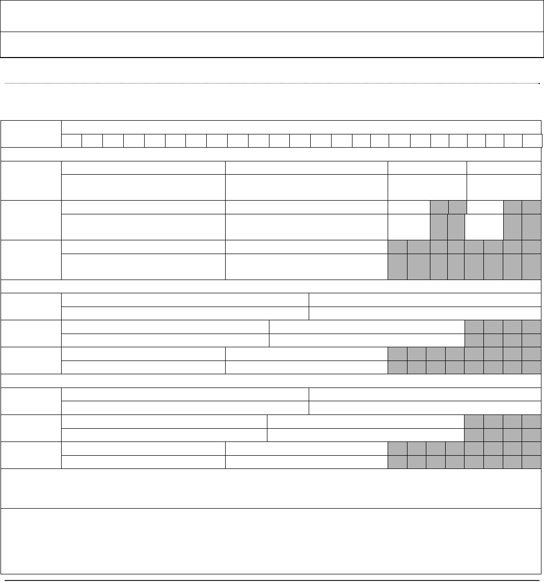
Figure 1ADV7513 Functional Block Diagram ........................................................................................................................................... 10
Figure 2Timing for Video Data Interface ................................................................................................................................................... 13
Figure 3Timing for I2S Audio Interface ..................................................................................................................................................... 13
Figure 4Timing for S/PDIF Audio Interface .............................................................................................................................................. 14
Figure 564-lead LQFP configuration (top view - not to scale) ................................................................................................................ 16
Figure 664-lead Low-Profile Quad Flat Pack [LQFP-SW64-2] ............................................................................................................... 19
Figure 72X Clock timing ............................................................................................................................................................................... 23
Figure 8DDR DE timing - Register 0x16[1] = 1 ......................................................................................................................................... 26
Figure 9DDR DE timing - Register 0x16[1] = 0 ......................................................................................................................................... 26
Figure 10I2S Standard Audio – Data width 16 to 24 bits per channel .................................................................................................. 28
Figure 11I2S Standard Audio – 16-bit samples only ............................................................................................................................... 29
Figure 12Serial Audio – Right-Justified .................................................................................................................................................... 29
Figure 13Serial Audio – Left-Justified ....................................................................................................................................................... 29
Figure 14AES3 Direct Audio ...................................................................................................................................................................... 30
Figure 15S/PDIF Data Timing .................................................................................................................................................................... 30
Figure 16Typical All-HDMI Home Theatre ............................................................................................................................................. 32
Figure 17Sync Processing Block Diagram ................................................................................................................................................ 34
Figure 18Single Channel of CSC (In_A) ................................................................................................................................................... 35
Figure 19Serial Port Read/Write Timing .................................................................................................................................................. 38
Figure 20Serial Interface—Typical Byte Transfer .................................................................................................................................... 39
Figure 21Power Supply Domains ............................................................................................................................................................... 40
Figure 22AVDD and PVDD Max Noise vs. Frequency .......................................................................................................................... 42
Figure 23LC Filter Transfer Curve ............................................................................................................................................................ 43
Figure 24CEC external connection ............................................................................................................................................................ 44
Figure 25Example Schematic ...................................................................................................................................................................... 45

ADV7513 HARDWARE USER’S GUIDE
Rev.0
Rev. 0 | Page 6 of 46
TABLE OF TABLES
Table 1Electrical Specifications .................................................................................................................................................................. 11
Table 2Absolute Maximum Ratings .......................................................................................................................................................... 14
Table 3Complete Pinout List ADV7513 .................................................................................................................................................... 17
Table 4Input ID Selection ........................................................................................................................................................................... 20
Table 5Normal RGB or YCbCr 4:4:4 (24 bits) with Separate Syncs; Input ID = 0 .............................................................................. 21
Table 6YCbCr 4:2:2 Formats (24, 20, or 16 bits) Input Data Mapping: 0x48[4:3]=‘00’ (evenly distributed) Input ID=1 or 2 ... 22
Table 7YCbCr 4:2:2 Formats (12, 10, or 8 bits) Input Data Mapping: 0x48[4:3]=‘00’ (evenly distributed) Input ID = 3,4,7,8 .. 23
Table 8YCbCr 4:2:2 (8 bits) DDR with Separate Syncs: Input ID = 6, right justified (R0x48[4:3] = ‘01’) ....................................... 24
Table 9YCbCr 4:2:2 (8 bits) DDR with Separate Syncs: Input ID = 6, left justified (R0x48[4:3] = ‘10’) .......................................... 24
Table 10YCbCr 4:2:2 (12, 10, 8 bits) DDR with Separate Syncs:Input ID = 6, evenly distributed (R0x48[4:3] = ‘00’) ................ 25
Table 11Audio input format summary .................................................................................................................................................... 27
Table 12SCLK Duty Cycle ......................................................................................................................................................................... 28
Table 13Some useful “End-User” CEC Features: ................................................................................................................................... 33
Table 14Supported 3D Formats ................................................................................................................................................................ 33
Table 15Channel Assignment for Color Space Converter (CSC) ........................................................................................................ 35
Table 16Serial Port Addresses ................................................................................................................................................................... 37
Table 17Maximum Power Consumption by Circuit – note these values will change after characterization ................................ 41

ADV7513 ADI Confidential HARDWARE USER’S GUIDE
Rev. 0
Rev. 0| Page 7 of 46
SECTION 1: INTRODUCTION
1.1 Scope and Organization
This document is intended to help the hardware designer understand what is necessary to design for the ADV7513 and
maintain the highest levels of performance. The ADV7513 Hardware User's Guide (HUG) provides guidelines to
design the schematics and board layout. Included are sections on the 64-lead LQFP package and an overview of the
functional blocks (including a brief description for each block) to provide an understanding of the ADV7513
functional and performance capabilities. The ADV7513 Programming Guide (PG) is available as a separate document
and should be used to gain a complete understanding on how to configure the ADV7513 within a system application.
It is divided into the following sections:
Section 2: Reference Documents is a list of other references, which will be helpful when designing with the
ADV7513 HDMI Transmitter.
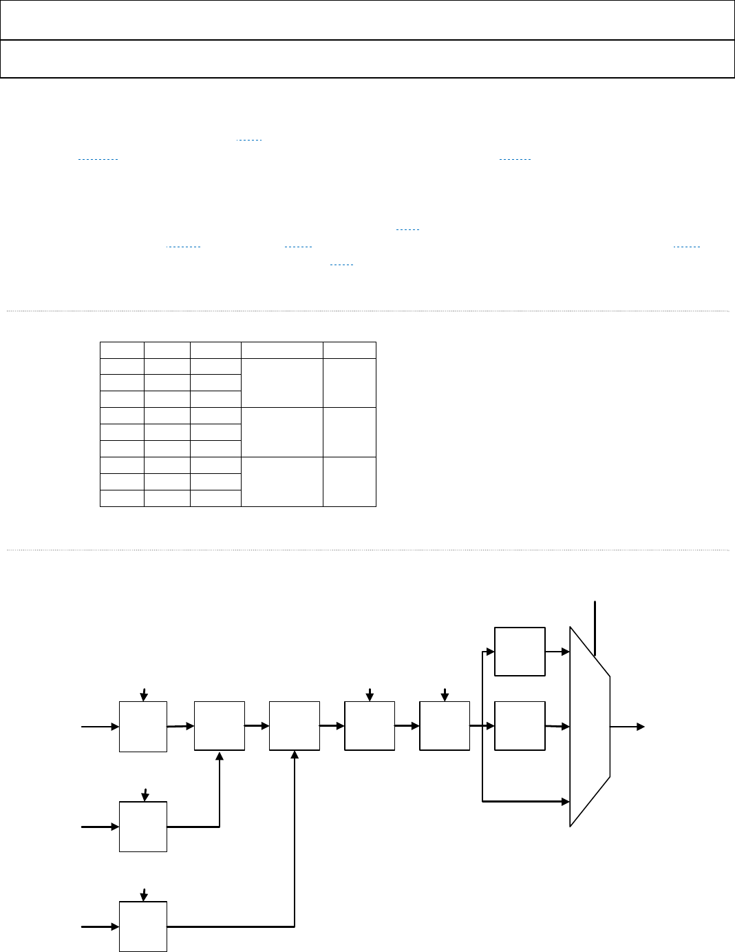
Section 3: Block Diagram gives an overall functional view of the HDMI transmitter.
Section 4:Specifications give all pertinent data such as: timing, power and testing.
Section 5:Pin and Package Information give the mechanical details of the interface.
Section 6:Functional Description serves to elaborate on input, output and internal operations.
Section 7: PCB Layout Recommendations are an aid to low noise operation.
1.1.1 Links
There are many links in this document to help with navigation. Use a mouse click to follow a link, and use the Alt key +
left arrow key to return. Active links can be identified by the dotted blue underline.
1.1.2 Symbols
Symbols are used to indicate internal and external document references as follows:
▶ Indicates a linked reference to another section of this document.
▷ Indicates a reference to another document, either an ADI document or an external specification.
1.1.3 Format Standards
In this document, ADI has chosen to represent data in the following ways:
0xNN Hexadecimal (base-16) numbers are represented using the “C” language notation, preceded by 0x.
0bNN Binary (base-2) numbers are represented using “C” language notation, preceded by 0b.
NN Decimal (base-10) numbers are represented using no additional prefixes or suffixes.
Bit Bits are numbered in little-endian format; i.e., the least-significant bit of a byte or word is referred to
as bit 0.

ADV7513 HARDWARE USER’S GUIDE
Rev.0
Rev. 0 | Page 8 of 46
1.2 Overview
The ADV7513 is a high speed High Definition Multimedia Interface (HDMI) transmitter that is capable of supporting
an input data rate up to 165MHz (1080p @ 60Hz, UXGA @ 60Hz). Careful hardware design (schematics and PCB
layout) is recommended to optimize the performance and to ensure HDMI compliance.
▷ The ADV7513 Programming Guide and ADV7513 Software Driver User Guide are also available if required.
1.3 Hardware Features
■ HDMI v1.4 features supported
3D video
Advanced Colorimetry
• sYCC601
• Adobe RGB
• Adobe YCC601
■ Operation up to 165MHz (TMDS link frequency)
■ Integrated CEC support with 3 message buffers
■ Supports x.v.Color™ (Gamut Metadata)
■ Internal HDCP key storage
■ Interrupt (INT) output pin eliminates constant I2C monitoring
■ Supports I2S, S/PDIF and HBR audio input formats
■ No audio Master Clock (MCLK) required for audio
■ Requires 1.8V and 3.3V supply
■ EDID buffered on chip
■ Color Space Converter (CSC) with video range clipping
■ 64-lead LQFP package
■ -25°C to +85°C temperature range
1.4 Supported Input Formats
■ 24 bit RGB 4:4:4 (separate syncs)
■ 24 bit YCbCr 4:4:4 (separate syncs)
■ 24, 20, or 16 bit YCbCr 4:2:2 (embedded or separate syncs)
■ 12, 10, or 8 bit YCbCr 4:2:2 (2x pixel clock with embedded or separate syncs)
■ 12, 10, or 8 bit YCbCr 4:2:2 (DDR with embedded or separate syncs)
1.5 Supported Output Formats
■ 24 bit RGB 4:4:4
■ 24 bit YCbCr 4:4:4
■ 24 bit YCbCr 4:2:2

ADV7513 ADI Confidential HARDWARE USER’S GUIDE
Rev. 0
Rev. 0| Page 9 of 46
SECTION 2: REFERENCE DOCUMENTS
2.1 ADI Documents
ADV7513 Data Sheet
ADV7513 Programming Guide
AN-810 - EDID/HDCP Controller Application Note
2.2 Industry Specifications
EIA/CEA-861-E
HDMI Specification 1.4
HDCP 1.4
ADV7513 HARDWARE USER’S GUIDE
Rev.0
Rev. 0 | Page 10 of 46
SECTION 3: BLOCK DIAGRAM
Figure 1 ADV7513 Functional Block Diagram
I2C
SLAVE
I2C
MASTER
SDA
SCL
INT
HPD
TX0+/TX0–
TX1+/TX1–
TX2+/TX2–
TXC+/TXC–
DDCSDA
DDCSCL
ADV7513
TMDS
OUTPUTS
CEC
CEC CONTROLLER/
BUFFER
SPDIF
I2S[3:0]
MCLK
LRCLK
SCLK
AUDIO
DATA
CAPTURE
D[23:0]
VSYNC
HSYNC
DE
CLK
VIDEO
DATA
CAPTURE
REGISTERS
AND
CONFIG.
LOGIC
4:2:2
4:4:4
AND
COLOR
SPACE
CONVERTER
HDCP
AND EDID
MICROCONTROLLER
HDCP KEYS
HDCP
ENCRYPTION
CEC_CLK
ADV7513 ADI Confidential HARDWARE USER’S GUIDE
Rev. 0
Rev. 0| Page 11 of 46
SECTION 4: SPECIFICATIONS
Table 1 Electrical Specifications
Parameter Conditions ADV7513
Temp Test Level1 Min Typ Max Unit
DIGITAL INPUTS
Data Inputs – Video, Audio and
CEC_CLK
Input Voltage, High (VIH) Full VI 1.35 3.5 V
Input Voltage, Low (VIL) Full VI -0.3 0.7 V
Input Capacitance 25°C VIII 1.0 1.5 pF
DDC I2C Lines (DDCSDA, DDCSCL)
Input Voltage, High VIH Full IV 1.4 5.5 V
Input Voltage, Low VIL Full IV −0.3 +0.7 V
I2C Lines (SDA, SCL)
Input Voltage, High VIH Full VI 1.4 5.5 V
Input Voltage, Low VIL Full VI −0.3 +0.7 V
CEC
Input Voltage, High (VIH) Full VI 2.0 V
Input Voltage, Low (VIL) Full VI 0.8 V
Output Voltage, High (VIH) Full VI 2.5 3.63 V
Output Voltage, Low (VIL) Full VI -0.3 0.6 V
HPD
Input Voltage, High (VIH) Full VI 1.3 5.5 V
Input Voltage, Low (VIL) Full VI -0.3 0.8 V
DIGITAL OUTPUTS
Output Voltage, High (VOH) Load = 5pF Full VI 0.8*DVdd V
Output Voltage, Low (VOL) Load = 5pF Full VI 0.2*DVdd V
THERMAL CHARACTERISTICS
Thermal Resistance
θJC Junction-to-Case Full V 20 °C/W
θJA Junction-to-Ambient Full V 43 °C/W
Ambient Temperature Full V -25 +25 +85 °C
DC SPECIFICATIONS
Input Leakage Current, IIL 25°C VI −1 +1 μA
POWER SUPPLY
1.8V Supply Voltage (DVdd, AVdd,
PVdd, BGVdd)
Full IV 1.71 1.8 1.90 V
1.8V Supply Voltage Noise Limit
DVdd – HDMI Digital Core Full V 64 mV RMS
AVdd – HDMI Analog Core Refer to ▶Section 7.1 Full V mV RMS
PLVdd – HDMI PLL – Analog Refer to ▶Section 7.1 Full V mV RMS
PVdd – HDMI PLL - Digital Full V 64 mV RMS
BGVdd - Band-gap Full V 64 mV RMS
3.3V Supply Voltage (DVdd_3V) Full 3.15 3.3 3.45 V
Power-Down Current – level 1 Refer to the ADV7513
Programming Guide
25°C IV 20 mA
Power-Down Current – level 2 Refer to the ADV7513 25°C IV 300 μA
ADV7513 HARDWARE USER’S GUIDE
Rev.0
Rev. 0 | Page 12 of 46
Parameter Conditions ADV7513
Temp Test Level1 Min Typ Max Unit
Programming Guide
Transmitter Total Power
1.8V power = 255mW
3.3V power = 1mW
1080p, 24 bit, typical
random pattern
Full VI 256 mW
AC SPECIFICATIONS
TMDS Output Clock Frequency 25°C IV 20 165 MHz
TMDS Output Clock Duty Cycle 25°C IV 48 52 %
Input Video Clock Frequency Full 165 MHz
Input Video Data Setup Time – tVSU Full IV 1 nS
Input Video Data Hold Time – tVHLD Full IV 0.7 nS
TMDS Differential Swing 25°C VII 800 1100 1200 mV
Differential Output Timing
Low-to-High Transition Time 25°C VII 75 95 pS
High-to-Low Transition Time 25°C VII 75 95 pS
VSYNC and HSYNC Delay from DE Falling
Edge
25°C IV 1 UI2
VSYNC and HSYNC Delay to DE Rising
Edge
25°C IV 1 UI
AUDIO AC TIMING (see ▶ Figure 3 to
▶ Figure 4
SCLK Duty Cycle See ▶ Table 12
When N/2 = even number Full IV 40 50 60 %
When N/2 = odd number Full IV 49 50 51 %
I2S[3:0], S/PDIF, LRCLK Setup – tASU Full IV 2 nS
I2S[3:0], S/PDIF, LRCLK Hold Time –
tAHLD
Full IV 2 nS
CEC
CEC_CLK Frequency Full VIII 3 123 100 MHz
CEC_CLK Accuracy Full VIII -2 +2 %
I2C Interface (see ▶ Figure 19)
SCL Clock Frequency Full 400 kHz
SDA Setup Time - tDSU Full 100 nS
SDA Hold Time – tDHO Full 100 nS
Setup for Start – tSTASU Full 0.6 uS
Hold Time for Start – tSTAH Full 0.6 uS
Setup for Stop – tSTOSU Full 0.6 uS
1. See Explanation of Test Levels section.
2. UI = unit interval.
3. 12MHz crystal oscillator for default register settings.
I2C data rates of 100KHz and 400KHz supported.
ADV7513 ADI Confidential HARDWARE USER’S GUIDE
Rev. 0
Rev. 0| Page 13 of 46
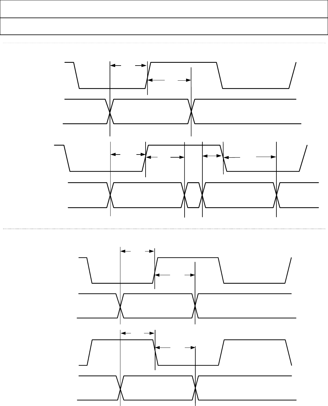
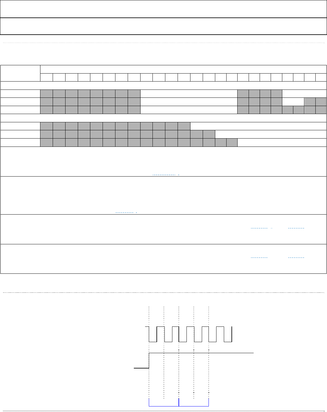
Figure 2 Timing for Video Data Interface
Figure 3 Timing for I2S Audio Interface
tVSU
Input data:
CLK
Rising Edge tVHLD
VHLD
tVHLD
t
tVSU
CLK
Dual Edge
Input DDR data:
tVSU
Valid Data
Valid Data Valid Data
D(23:0), DE,
HSYNC, VSYNC
D(23:0), DE,
HSYNC, VSYNC
tASU
Audio data:
I2S[3:0],
LRCLK
SCLK
Rising Edge tAHLD
Valid data
R0x0B[6] = 0
tASU
SCLK
Falling Edge
Valid data
R0x0B[6] = 1
tAHLD
Audio data:
I2S[3:0],
LRCLK
ADV7513 HARDWARE USER’S GUIDE
Rev.0
Rev. 0 | Page 14 of 46
Figure 4 Timing for S/PDIF Audio Interface
Table 2 Absolute Maximum Ratings
Parameter Rating
Digital Inputs – I2C, HPD and CEC 5.5V to -0.3V
Digital Inputs – video/audio inputs 3.63V to -0.3V
Digital Output Current 20 mA
Operating Temperature Range -40°C to +100°C
Storage Temperature Range -65°C to +150°C
Maximum Junction Temperature 150°C
Maximum Case Temperature 150°C
Stresses above those listed under Absolute Maximum Ratings may cause permanent damage to the device. This is a stress rating
only; functional operation of the device at these or any other conditions above those indicated in the operational section of this
specification is not implied. Exposure to absolute maximum rating conditions for extended periods may affect device reliability.
Voltage ratings assume that all power supplies are at nominal levels.
tASU
Audio data:
S/PDIF
MCLK
Rising Edge tAHLD
Valid data
R0x0B[6] = 0
tASU
MCLK
Falling Edge
Valid data
R0x0B[6] = 1
tAHLD
Audio data:
S/PDIF
ADV7513 ADI Confidential HARDWARE USER’S GUIDE
Rev. 0
Rev. 0| Page 15 of 46
4.1 Explanation of Test Levels
I. 100% production tested.
II. 100% production tested at 25°C and sample tested at specified temperatures.
III. Sample tested only.
IV. Parameter is guaranteed by design and characterization testing.
V. Parameter is a typical value only.
VI. 100% production tested at 25°C; guaranteed by design and characterization testing.
VII. Limits defined by HDMI specification; guaranteed by design and characterization testing.
VIII. Parameter is guaranteed by design.
4.2 ESD Caution
ADV7513 HARDWARE USER’S GUIDE
Rev.0
Rev. 0 | Page 16 of 46
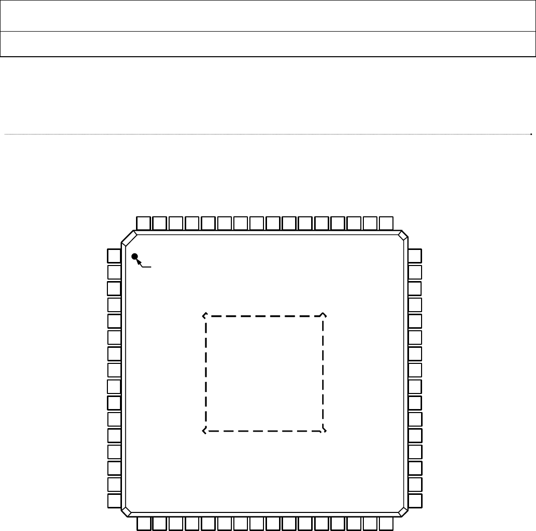
SECTION 5: PIN AND PACKAGE INFORMATION
This section shows the pinout of the ADV7513 64-lead LQFP package. This section also contains a brief description of the
different pins as well as the mechanical drawings
Figure 5 64-lead LQFP configuration (top view - not to scale)
2
VSYNC
3
SPDIF
4
MCLK
7
I2S2
6
I2S1
5
I2S0
1
DVDD
8
I2S3
9
SCLK
10
LRCLK
12
PVDD
13
BGVDD
14
R_EXT
15
AVDD
16
HPD
11
DVDD
47
46
45
42
43
44
48
41
40
D13
D14
D15
D18
D17
D16
D12
D19
D20
39 D21
37 D23
36 SDA
35 SCL
34 DDCSDA
33 DDCSCL
38 D22
17
TXC-
18
TXC+
19
AVDD
20
TX0-
21
TX0+
22
PD
23
TX1-
24
TX1+
25
AVDD
26
TX2-
27
TX2+
28
INT
29
DVDD_3V
30
CEC
31
DVDD
32
CEC_CLK
64
HSYNC
63
DE
62
D0
61
D1
60
D2
59
D3
58
D4
57
D5
56
D6
55
D7
54
D8
53
CLK
52
D9
51
DVDD
50
D10
49
D11
PIN 1
TOP VIEW
ADV7513
ADV7513 ADI Confidential HARDWARE USER’S GUIDE
Rev. 0
Rev. 0| Page 17 of 46
Table 3 Complete Pinout List ADV7513
Pin No. Mnemonic Type1 Description
37 to 44,
45 to 50, 52, 54
55 to 62
D[23:0] I Video Data Input. Digital input in RGB or YCbCr format. Supports typical CMOS logic
levels from1.8V up to 3.3V. See ▶ Figure 2 for timing details.
53 CLK I Video Clock Input. Supports typical CMOS logic levels from 1.8V up to 3.3V.
63 DE I
Data Enable signal input for Digital Video. Supports typical CMOS logic levels from
1.8V up to 3.3V.
64 HSYNC I Horizontal Sync Input. Supports typical CMOS logic levels from 1.8V up to 3.3V.
2 VSYNC I Vertical Sync Input. Supports typical CMOS logic levels from 1.8V up to 3.3V.
14 R_EXT I
Sets internal reference currents. Place 887 Ω resistor (1% tolerance) between this
pin and ground.
30 HPD I
Hot Plug Detect signal input. This indicates to the interface whether the sink is
connected. 1.8V to 5.0 V CMOS logic level.
3 S/PDIF I
S/PDIF (Sony/Philips Digital Interface) Audio Input. This pin is typically used as
the audio input from a Sony/Philips digital interface. Supports typical CMOS logic
levels from 1.8V up to 3.3V. See ▶ Figure 4 for timing details.
4 MCLK I
MCLK input for SPDIF and I2S audio. (See ▷ADV7513 Programming Guide for
details on the register bit that controls this). .Supports typical CMOS logic levels
from 1.8V up to 3.3V.
8-5 I2S[3:0] I I2S Audio Data Inputs. These represent the eight channels of audio (two per
input) available through I2S. Supports typical CMOS logic levels from 1.8V up to
3.3V. See Figure 3 for timing details.
9 SCLK I I2S Audio Clock input. Supports typical CMOS logic levels from 1.8V up to 3.3V.
10 LRCLK I
Left/Right Channel signal input. Supports typical CMOS logic levels from1.8V up to
3.3V.
22 PD/AD I
Power-Down Control and I2C Address Selection. The I2C address and the PD
polarity are set by the PD/AD pin state when the supplies are applied to the
ADV7513. Supports typical CMOS logic levels from 1.8V up to 3.3V.
17, 18 TxC−/TxC+ O Differential TMDS Clock Output. Differential clock output at pixel clock rate;
TMDS logic level.
26, 27 Tx2−/Tx2+ O Differential TMDS Output Channel 2. Differential output of the red data at 10×
the pixel clock rate; TMDS logic level.
23, 24 Tx1−/Tx1+ O Differential TMDS Output Channel 1. Differential output of the green data at 10×
the pixel clock rate; TMDS logic level.
20, 21 Tx0−/Tx0+ O Differential TMDS Output Channel 0. Differential output of the blue data at 10×
the pixel clock rate; TMDS logic level.
28 INT O
Interrupt signal output. CMOS logic level. A 2 kΩ pull-up resistor (10%) to
interrupt the microcontroller IO supply is recommended.
15, 19, 25 AVDD P 1.8V Power Supply for TMDS Outputs.
1, 11, 31, 51 DVDD P 1.8V Power Supply for Digital and I/O Power Supply. These pins supply power to
the digital logic and I/Os. They should be filtered and as quiet as possible.
12 PVDD P
1.8V PLL Power Supply. The most sensitive portion of the ADV7513 is the clock
generation circuitry. This pin provide power to the PLL clock. The designer
should provide quiet, noise-free power to these pins.
13 BGVDD P Band Gap Vdd.
29 DVDD_3V P 3.3V Power Supply.
PAD GND P
Ground. The ground return for all circuitry on-chip. It is recommended that the
ADV7513 be assembled on a single, solid ground plane with careful attention
given to ground current paths.

ADV7513 HARDWARE USER’S GUIDE
Rev.0
Rev. 0 | Page 18 of 46
36 SDA C
Serial Port Data I/O. This pin serves as the serial port data I/O slave for register
access. Supports CMOS logic levels from 1.8V to 3.3V.
35 SCL C
Serial Port Data Clock input. This pin serves as the serial port data clock slave for
register access. Supports CMOS logic levels from 1.8V to 3.3V.
34 DDCSDA C
Serial Port Data I/O to Sink. This pin serves as the master to the DDC bus. Tolerant
of 5 V CMOS logic levels.
33 DDCSCL C
Serial Port Data Clock to Sink. This pin serves as the master clock for the DDC
bus. Tolerant of 5 V CMOS logic levels.
32 CEC_CLK I CEC clock. From 3MHz to 100Mhz. Supports CMOS logic levels from 1.8V to 5V.
30 CEC I/O CEC data signal. Supports CMOS logic levels from 1.8V to 5V.
1. I = input, O = output, P = power supply, C = control
ADV7513 ADI Confidential HARDWARE USER’S GUIDE
Rev. 0
Rev. 0| Page 19 of 46
5.1 Mechanical Drawings and Outline Dimensions
Figure 6 64-lead Low-Profile Quad Flat Pack [LQFP-SW64-2]
COMPLIANT TO JEDEC STANDARDS MS-026-BCD-HD
1
16
17 32 32
49
64 48
33
12.20
12.00 SQ
11.80 10.20
10.00 SQ
9.80
1
16
17
49 64
48
33
PIN 1
TOP VIEW
(PINS DOWN)
BOTTOM VIEW
(PINS UP)
EXPOSED
PAD
03-16-2010-A
VIEW A
1.60
MAX
SEATING
PLANE
0.75
0.60
0.45
1.00 REF
0.15
0.05 0.08
COPLANARITY
7°
0°
0.20
0.09
VIEW A
ROTATED 90° CCW
1.45
1.40
1.35
0.27
0.22
0.17
0.50
LEAD PITCH
7.50
REF SQ
5.10
5.00 SQ
4.90
ADV7513 HARDWARE USER’S GUIDE
Rev.0
Rev. 0 | Page 20 of 46
SECTION 6: FUNCTIONAL DESCRIPTION
6.1 Input Connections
6.1.1 Unused Inputs
Any input data signals which are not used should be connected to ground.
6.1.2 Video Data Capture Block
The ADV7513 can accept video data from as few as eight pins (either YCbCr 4:2:2 double data rate [DDR] or YCbCr
4:2:2 with 2x pixel clock) to as many as 24 pins (RGB 4:4:4 or YCbCr 4:4:4). In addition it can accept HSYNC, VSYNC
and DE (Data Enable). The ADV7513 can detect all of the 59 video formats defined in the EIA/CEA-861E
specification. Either separate HSYNC, VSYNC, and DE, or embedded syncs in the style of the ITU BT.656, SMPTE
274M, and SMPTE 296M specifications are accepted. The alignment of the data can be defined as left or right justified
or as evenly distribution. In the case of even distribution, the channel data is left-justified in their respective 8-bit
fields. For timing details for video capture, see Figure 2. For complete details on how to set these, refer to the
ADV7513 Programming Guide.
The ADV7513 can accept HSYNC, VSYNC and DE (Data Enable) signals separately or as an embedded data (ITU 656
based) on the data inputs. If using separate syncs and DE is not available, the DE signal can be generated internally in
the ADV7513.
The tables in section 6.1.2.1 define how the many different formats are accepted on the input data lines.
6.1.2.1 Video Input Connections
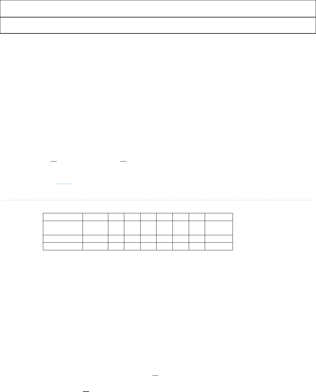
The following table is a summary of the input options which are shown in detail in Table 5 through Table 10.
Table 4 Input ID Selection
Input
ID
Bits per
Color
Pin Assignment Table Maximum
Input Clock
Format Name Sync Type
0 8 ▶ Table 5 165.0 MHz RGB 4:4:4, YCbCr 4:4:4 Separate syncs
1 8, 10, 12 ▶ Table 6
165.0 MHz YCbCr 4:2:2 (even dist.) Separate syncs
2 8, 10, 12 165.0 MHz YCbCr 4:2:2 (even dist.) Embedded syncs
3 8, 10, 12 ▶ Table 7 82.5 MHz YCbCr 4:2:2 2X cloc
k
(even
dist.)
Separate syncs
4 8, 10, 12 82.5 MHz YCbCr 4:2:2 2X cloc
k
(even
dist.)
Embedded syncs
6 8 ▶ Table 8 82.5 MHz YCbCr 4:2:2 DD
R
(right just.) Separate syncs
6 8 ▶ 0 82.5 MHz YCbCr 4:2:2 DDR (left just.) Separate syncs
6 8, 10, 12 ▶ Table 10 82.5 MHz YCbCr 4:2:2 DDR (even dist.) Separate syncs
7 8, 10, 12 ▶ Table 7 82.5 MHz YCbCr 4:2:2 DDR (even dist.) Separate syncs
8 8, 10, 12 82.5 MHz YCbCr 4:2:2 DD
R
(even dist.) Embedded syncs
ADV7513 ADI Confidential HARDWARE USER’S GUIDE
Rev. 0
Rev. 0| Page 21 of 46
Table 5 Normal RGB or YCbCr 4:4:4 (24 bits) with Separate Syncs; Input ID = 0
Input
Format
Data<23:0>
23 22 21 2019 18 17 16151413121110987 6 5 43210
RGB 444 R[7:0] G[7:0] B[7:0]
YCbCr 444 Cr[7:0] Y[7:0] Cb[7:0]
An input format of RGB 4:4:4 or YCbCr 4:4:4 can be selected by setting the input ID (R0x15 [3:1]) to 0b000. There is no need
to set the Input Style (R0x16[3:2]).
ADV7513 HARDWARE USER’S GUIDE
Rev.0
Rev. 0 | Page 22 of 46
Table 6 YCbCr 4:2:2 Formats (24, 20, or 16 bits) Input Data Mapping:
0x48[4:3]=‘00’ (evenly distributed) Input ID=1 or 2
Input
Format
Data<23:0>
23 22 21 20 19 18 17 16151413121110987 6 5 4 3210
Style 1
YCbCr422
Sep. Sync
(24 bit)
Cb[11:4] Y[11:4] Cb[3:0] Y[3:0]
Cr[11:4] Y[11:4] Cr[3:0] Y[3:0]
YCbCr422
Sep. Sync
(20 bit)
Cb[9:2] Y[9:2] Cb[1:0]
Y[1:0]
Cr[9:2] Y[9:2] Cr[1:0] Y[1:0]
YCbCr422
Sep. Sync
(16 bit)
Cb[7:0] Y[7:0]
Cr[7:0] Y[7:0]
Style 2
24 bit Cb[11:0] Y[11:0]
Cr[11:0] Y[11:0]
20 bit Cb[9:0] Y[9:0]
Cr[9:0] Y[9:0]
16 bit Cb[7:0] Y[7:0]
Cr[7:0] Y[7:0]
Style 3
24 bit Y[11:0] Cb[11:0]
Y[11:0] Cr[11:0]
20 bit Y[9:0] Cb[9:0]
Y[9:0] Cr[9:0]
16 bit Y[7:0] Cb[7:0]
Y[7:0] Cr[7:0]
Input ID = 1: An input with YCbCr 4:2:2 with separate syncs can be selected by setting the Input ID (R0x15[3:0]) to 0x1. The
data bit width (24, 20, or 16 bits) must be set with R0x16 [5:4]. The three input pin assignment styles are shown in the table. The
Input Style can be set in R0x16[3:2].
Input ID = 2: An input with YCbCr 4:2:2 with embedded syncs (SAV and EAV) can be selected by setting the Input ID
(R0x15[3:0]) to 0x2. The data bit width (24 = 12 bits, 20 = 10 bits, or 16 = 8 bits) must be set with R0x16 [5:4]. The three input pin
assignment styles are shown in the table. The Input Style can be set in R0x16[3:2]. The only difference between Input ID 1 and
Input ID 2 is that the syncs on ID 2 are embedded in the data much like an ITU 656 style bus running at 1X clock and double
width.
ADV7513 ADI Confidential HARDWARE USER’S GUIDE
Rev. 0
Rev. 0| Page 23 of 46
Table 7 YCbCr 4:2:2 Formats (12, 10, or 8 bits) Input Data Mapping:
0x48[4:3]=‘00’ (evenly distributed) Input ID = 3,4,7,8
Input
Format
Data <23:0>
23 22 21 20 19 18 17 16 15 14 13 12 11 10 9 8 7 6 5 4 3 2 1 0
Style 1
12 bit Cb/Y/Cr/Y[11:4] [3:0]
10 bit Cb/Y/Cr/Y[9:2] [1:0]
8 bit Cb/Y/Cr/Y[7:0]
Style 2
12 bit Cb/Y/Cr/Y[11:0]
10 bit Cb/Y/Cr/Y[9:0]
8 bit Cb/Y/Cr/Y[7:0]
Input ID = 3: An input with YCbCr 4:2:2 data and separate syncs can be selected by setting the Input ID (R0x15[3:0]) to 0x3. The data bit width
(12, 10, or 8 bits) must be set with R0x16 [5:4]. The two input pin assignment styles are shown in the table. The Input Style can be set in
R0x16[3:2]. Pixel 1 is the first pixel of the 4:2:2 word and should be where DE starts. This mode requires an input clock 2X the pixel rate. For
timing details, see the ▷ ADV7513 Hardware User’s Guide and ▶ Figure 7.
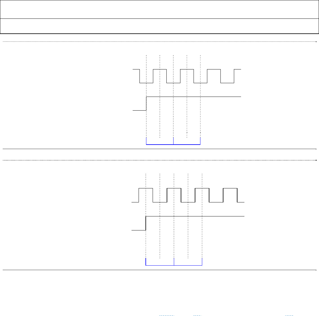
Input ID = 4: An input with YCbCr 4:2:2 and embedded syncs (ITU 656 based) can be selected by setting the Input ID (R0x15[3:0]) to 0x4. The
data bit width (12, 10, or 8 bits) must be set with R0x16 [5:4]. The two input pin assignment styles are shown in the table. The Input Style can be
set in R0x16[3:2]. The order of data input is the order in the table. For example, data is accepted as: Cb0, Y0, Cr0, Y1, Cb2, Y2, Cr2, Y3… Pixel 1
is the first pixel of the 4:2:2 word and should be where DE starts. This mode requires an input clock 2X the pixel rate. For timing details, see
the ▷ ADV7513 Hardware User’s Guide and ▶ Figure 7.
Input ID=7: This input format is the same as input ID 3 with the exception that the clock is not 2X the pixel rate, but is double data rate (DDR)
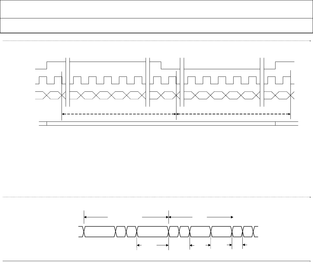
and the Input ID (R0x15[3:0]) is set to 0x7. For timing details, see the ▷ ADV7513 Hardware User’s Guide and ▶ Figure 8 and ▶ Figure 9. The
1st and the 2nd edge may be the rising or falling edge. The Data Input Edge is defined in R0x16 [1]. 0b1 = 1st edge rising edge; 0b0 = 1st edge falling
edge.
Input ID=8: This input format is the same as input ID 4 with the exception that the clock is not 2X the pixel rate, but is double data rate (DDR)
and the Input ID (R0x15[3:0]) is set to 0x8. For timing details, see the ▷ ADV7513 Hardware User’s Guide and ▶ Figure 8 and ▶ Figure 9. The
1st and the 2nd edge may be the rising or falling edge. The Data Input Edge is defined in R0x16 [1]. 0b1 = 1st edge rising edge; 0b0 = 1st edge falling
edge.
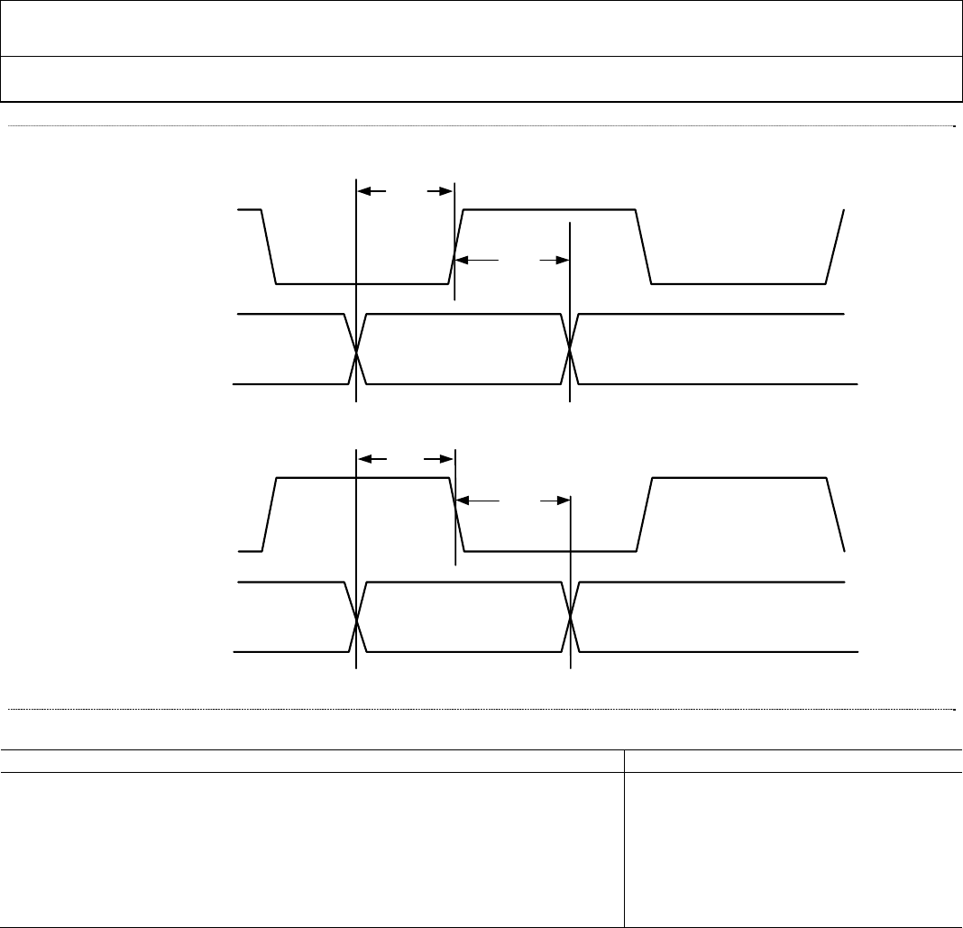
Figure 7 2X Clock timing
2nd
edge
1st
edge
2X CLK
DE
1st Pixel
Data On Input Bus
2nd Pixel
2nd
edge
1st
edge
ADV7513 HARDWARE USER’S GUIDE
Rev.0
Rev. 0 | Page 24 of 46
Table 8 YCbCr 4:2:2 (8 bits) DDR with Separate Syncs: Input ID = 6, right justified (R0x48[4:3] = ‘01’)
Input Format Data<23:0>
23 22 21 20 19 18 17 16 15 14 13 12 11 10 9 8 7 6 5 4 3 2 1 0
Style 1
YCrCB 422 Sep.
Syncs (DDR)
8 bit
Cb[3:0] Y[3:0]
Cb[7:4] Y[7:4]
Cr[3:0] Y[3:0]
Cr[7:4] Y[7:4]
Style 2
8 bit Y[7:0]
Cb[7:0]
Y[7:0]
Cr[7:0]
Style 3
8 bit Cb[7:0]
Y[7:0]
Cr[7:0]
Y[7:0]
An input format of YCbCr 4:2:2 DDR can be selected by setting the input ID (R0x15 [3:0]) to 0x6. The three different input pin assignment
styles are shown in the table. The Input Style can be set in R0x16[3:2]. The data bit width (8 bits) must be set with R0x16 [5:4]. The Data Input
Edge is defined in R0x16 [1]. The 1st and the 2nd edge may be the rising or falling edge. The Data Input Edge is defined in R0x16 [1]. 0b1 = 1st
edge rising edge; 0b0 = 1st edge falling edge. Pixel 0 is the first pixel of the 4:2:2 word and should be where DE starts.
Table 9 YCbCr 4:2:2 (8 bits) DDR with Separate Syncs: Input ID = 6, left justified (R0x48[4:3] = ‘10’)
Input Format Data<23:0>
23 22 21 20 19 18 17 16 15 14 13 12 11 10 9 8 7 6 5 4 3 2 1 0
Style 1
YCrCB 422 Sep.
Syncs (DDR)
8 bit
Cb[3:0] Y[3:0]
Cb[7:4] Y[7:4]
Cr[3:0] Y[3:0]
Cr[7:4] Y[7:4]
Style 2
8 bit Y[7:0]
Cb[7:0]
Y[7:0]
Cr[7:0]
Style 3
8 bit Cb[7:0]
Y[7:0]
Cr[7:0]
Y[7:0]
An input format of YCbCr 4:2:2 DDR can be selected by setting the input ID (R0x15 [3:0]) to 0x6. The three different input pin assignment
styles are shown in the table. The Input Style can be set in R0x16[3:2]. The data bit width (8 bits) must be set with R0x16 [5:4]. The Data Input
Edge is defined in R0x16 [1]. The 1st and the 2nd edge may be the rising or falling edge. The Data Input Edge is defined in R0x16 [1]. 0b1 = 1st
edge rising edge; 0b0 = 1st edge falling edge. Pixel 0 is the first pixel of the 4:2:2 word and should be where DE starts.
ADV7513 ADI Confidential HARDWARE USER’S GUIDE
Rev. 0
Rev. 0| Page 25 of 46
Table 10 YCbCr 4:2:2 (12, 10, 8 bits) DDR with Separate Syncs:Input ID = 6, evenly distributed (R0x48[4:3] = ‘00’)
Input Format Data<23:0>
23 22 21 20 19 18 17 16 15 14 13 12 11 10 9 8 7 6 5 4 3 2 1 0
Style 1
YCrCb422 Sep
Syncs (DDR)
12 bit
Y[7:4] Cb[3:0] Y[3:0]
Cb[11:8] Cb[7:4] Y[11:8]
Y[7:4] Cr[3:0] Y[3:0]
Cr[11:8] Cr[7:4] Y[11:8]
YCrCb422 Sep
Syncs (DDR)
10 bit
Y[5:4] Cb[3:2] Cb[1:0] Y[3:2] Y[1:0]
Cb[9:6] Cb[5:4] Y[9:8] Y[7:6]
Y[5:4] Cr[3:2] Cr[1:0] Y[3:2] Y[1:0]
Cr[9:6] Cr[5:4] Y[9:8] Y[7:6]
YCrCB 422
Sep. Syncs
(DDR)
8 bit
Cb[3:0] Y[3:0]
Cb[7:4] Y[7:4]
Cr[3:0] Y[3:0]
Cr[7:4] Y[7:4]
Style 2
12 bit Y[11:8] Y[7:4] Y[3:0]
Cb[11:8] Cb[7:4] Cb[3:0]
Y[11:8] Y[7:4] Y[3:0]
Cr[11:8] Cr[7:4] Cr[3:0]
10 bit Y[9:6] Y[5:2] Y[1:0]
Cb[9:6] Cb[5:2] Cb[1:0]
Y[9:6] Y[5:2] Y[1:0]
Cr[9:6] Cr[5:2] Cr[1:0]
8 bit Y[7:4] Y[3:0]
Cb[7:4] Cb[3:0]
Y[7:4] Y[3:0]
Cr[7:4] Cr[3:0]
Style 3
12 bit Cb[11:8] Cb[7:4] Cb[3:0]
Y[11:8] Y[7:4] Y[3:0]
Cr[11:8] Cr[7:4] Cr[3:0]
Y[11:8] Y[7:4] Y[3:0]
10 bit Cb[9:6] Cb[5:2] Cb[1:0]
Y[9:6] Y[5:2] Y[1:0]
Cr[9:6] Cr[5:2] Cr[1:0]
Y[9:6] Y[5:2] Y[1:0]
8 bit Cb[7:4] Cb[3:0]
Y[7:4] Y[3:0]
Cr[7:4] Cr[3:0]
Y[7:4] Y[3:0]
An input format of YCbCr 4:2:2 DDR can be selected by setting the input ID (R0x15 [3:0]) to 0x6. The three different input pin assignment
styles are shown in the table. The Input Style can be set in R0x16[3:2]. The data bit width (12, 10, or 8 bits) must be set with R0x16 [5:4]. The
Data Input Edge is defined in R0x16 [1]. The 1st and the 2nd edge may be the rising or falling edge. The Data Input Edge is defined in R0x16 [1].
0b1 = 1st edge rising edge; 0b0 = 1st edge falling edge. Pixel 0 is the first pixel of the 4:2:2 word and should be where DE starts.
ADV7513 HARDWARE USER’S GUIDE
Rev.0
Rev. 0 | Page 26 of 46
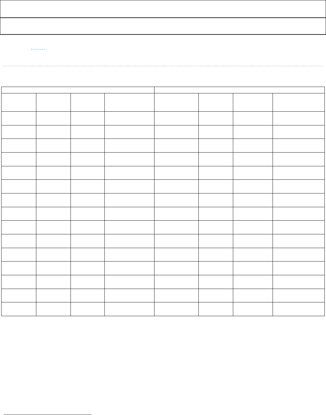
Figure 8 DDR DE timing - Register 0x16[1] = 1
Figure 9 DDR DE timing - Register 0x16[1] = 0
6.1.3 Audio Data Capture Block
The ADV7513 supports multiple audio interfaces and formats: I2S, S/PDIF and HBR. The ADV7513 supports audio
input frequencies of 32kHz, 44.1kHz, 48kHz, 88.2kHz, 96kHz, 176.4kHz, 192kHz, and higher (with use of HBR). The
MCLK signal is optional unless specifically listed in ▶ Table 11. The 1I2S Audio input can support standard 1I2S, left-
justified serial audio, right-justified serial audio and AES3 stream formats. The Audio Data Capture Block captures the
audio samples and converts them into audio packets which are sent through the HDMI link (if the ADV7513 is set in
HDMI mode). Please refer to the ADV7513 Programming Guide for more information.
6.1.3.1 Supported Audio Input Format and Implementation
ADV7513 is capable of receiving audio data for packetization and transmission over the HDMI interface in any of the
following formats:
■ Inter IC Sound (I2S)
■ Sony/Philips Digital Interface (S/PDIF)
■ High Bit-Rate (HBR)
2nd
edge
1st
edge
DDR CLK
DE
1st Pixel
Data On Input Bus
2nd Pixel
2nd
edge
1st
edge
2nd
edge
1st
edge
DDR CLK
DE
1st Pixel
Data On Input Bus
2nd Pixel
2nd
edge
1st
edge
ADV7513 ADI Confidential HARDWARE USER’S GUIDE
Rev. 0
Rev. 0| Page 27 of 46
Table 11 illustrates the many audio input and output options that are available with the ADV7513. Note ‘required’ and
‘optional’ clock notations.
Table 11 Audio input format summary
Input Output
Audio
Select
0x0A[6:4]
Audio
Mode
0x0A[3:2]
I2S Format
0x0C[1:0] Data Pins Clock Pins Encoding Format Packet Type
000 ** 00 I2S[3:0]
Required: SCLK
Optional: MCLK Normal1 Standard I2S Audio Sample Packet
000 ** 01 I2S[3:0]
Required: SCLK
Optional: MCLK Normal Right Justified Audio Sample Packet
000 ** 10 I2S[3:0]
Required: SCLK
Optional: MCLK Normal Left Justified Audio Sample Packet
000 ** 11 I2S[3:0]
Required: SCLK
Optional: MCLK Normal AES3 Direct Audio Sample Packet
001 00 ** SPDIF Optional: MCLK Biphase Mark IEC60958 or
IEC61937 Audio Sample Packet
011 00 ** I2S[3:0] Required: MCLK Biphase Mark IEC61937 HBR Audio Stream
Packet
011 01 00 I2S[3:0]
Required: SCLK
Optional: MCLK Normal Standard I2S
HBR Audio Stream
Packet
011 01 01 I2S[3:0]
Required: SCLK
Optional: MCLK Normal Right Justified
HBR Audio Stream
Packet
011 01 10 I2S[3:0]
Required: SCLK
Optional: MCLK Normal Left Justified
HBR Audio Stream
Packet
011 01 11 I2S[3:0]
Required: SCLK
Optional: MCLK Normal AES3 Direct
HBR Audio Stream
Packet
011 10 ** SPDIF Required: MCLK Biphase Mark IEC61937 HBR Audio Stream
Packet
011 11 00 SPDIF
Required: SCLK
Optional: MCLK Normal Standard I2S
HBR Audio Stream
Packet
011 11 01 I2S[3:0]
Required: SCLK
Optional: MCLK Normal Right Justified
HBR Audio Stream
Packet
011 11 10 I2S[3:0]
Required: SCLK
Optional: MCLK Normal Left Justified
HBR Audio Stream
Packet
011 11 11 I2S[3:0] Required: MCLK Normal IEC61937
HBR Audio Stream
Packet
1 Normal Encoding means data is captured on the rising edge of the data clock
ADV7513 HARDWARE USER’S GUIDE
Rev.0
Rev. 0 | Page 28 of 46
6.1.3.2 Inter-IC Sound (I2S) Audio
The ADV7513 can accommodate from two to eight channels of I2S audio at up to a 192KHz sampling rate. The
ADV7513 supports standard I2S, left-justified serial audio, right-justified serial audio and AES3 stream formats via
R0x0C[1:0] and sample word lengths between 16 bits and 24 bits (R0x14[3:0]).
If the I2S data changes on the rising clock edge it is recommended that it be latched into the ADV7513 on the falling
edge. If the I2S data changes on the falling clock edge, it is recommended that it be latched into the ADV7513 on the
rising edge. This can be specified by programming register R0x0B[6]. 0 = latch on the rising clock edge; 1 = latch on
the falling clock edge. For more information see the following figures:
▶ Figure 10 –▶ Figure 13 for format information
▶ Figure 3 for timing information
▷ Please refer to the ADV7513 Programming Guide for more information about configuring the audio.
The accurate transmission of audio depends upon an accurate SCLK and can be a function of the duty cycle of the
SCLK. ▶ Table 12 specifies this duty cycle dependency. ‘N’ and ‘CTS’ values are used to reconstruct the audio data and
if the ‘N’ value is an odd number, the SCLK duty cycle must be within the range of 49 – 51%; if the ‘N’ value is an even
number and the audio is in a 32 bit format the SCLK duty cycle requirements can be in a much wider range of 40 –
60%. For the case of 16 bit audio format, ‘N’ values which are not divisible by 4 restrict the duty cycle to 49-51% where
an ‘N’ value which is evenly divisible by 4 may have a duty cycle from 40% - 60%.
Table 12 SCLK Duty Cycle
SCLK DC requirementSCLK DC requirement
N value16 bit audio32 bit audio
N is oddNot supported49-51%
N is a even but not a multiple of 449-51%40-60%
N is even & a multiple of 440-60%40-60%
Figure 10 I2S Standard Audio – Data width 16 to 24 bits per channel
LRCLK
SCLK
I2S[3:0]
LEFT RIGHT
LSB
MSBleft MSB LSB
32 Clock Slots 32 Clock Slots
I2S Standard
R0x0C[1:0] = ‘00’
ADV7513 ADI Confidential HARDWARE USER’S GUIDE
Rev. 0
Rev. 0| Page 29 of 46
Figure 11 I2S Standard Audio – 16-bit samples only
Figure 12 Serial Audio – Right-Justified
Figure 13 Serial Audio – Left-Justified
LRCLK
SCLK
I2S[3:0]
LEFT RIGHT
LSBleft
MSBleft MSBright LSB
16 Clock Slots 16 Clock Slots
LSBright
I2S Standard 16-bit per
channel
R0x0C[1:0] = ‘00’
LRCLK
SCLK
I2S[3:0]
LEFT RIGHT
LSB
MSB MSB LSB
32 Clock Slots 32 Clock Slots
MSB MSB MSB MSB
MSB-1
MSB extended MSB extended
Serial Audio
Right Justified
R0x0C[1:0] = ‘01’
MSB-1
MSB MSB
LRCLK
SCLK
I2S[3:0]
LEFT RIGHT
LSB
MSB MSB LSB
32 Clock Slots 32 Clock Slots
Serial Audio
Left Justified
R0x0C[1:0] = ‘10’
ADV7513 HARDWARE USER’S GUIDE
Rev.0
Rev. 0 | Page 30 of 46
Figure 14 AES3 Direct Audio
6.1.3.3 Sony/Philips Digital Interface (S/PDIF)
The ADV7513 is capable of accepting two-channel linear pulse code modulation (LPCM) and encoded audio up to a 192KHz
sampling rate via the S/PDIF. S/PDIF audio input is selected by setting R0x0A[4] = ‘1’. The ADV7513 is capable of accepting
S/PDIF with or without an MCLK input. When no MCLK is present the ADV7513 generates its own MCLK. For timing
information see ▶ Figure 4.
Figure 15 S/PDIF Data Timing
6.1.3.4 HBR Audio
High Bit-Rate audio uses the HBR audio packets to transfer compressed data at rates greater than 6.144Mbps across
the TMDS link. For additional information, refer to IEC61937.
6.1.4 Hot Plug Detect (HPD) pin
The Hot Plug Detect (HPD) pin is an input which detects if a DVI or HDMI sink is connected. If the voltage on HPD
is greater than 1.2V, then the ADV7513 considers an HDMI/DVI sink is connected. If the voltage is below 1.2V, then
the ADV7513 considers no sink is connected. The HPD must be connected to the HDMI connector. A 10KΩ (+/-10%)
pull down resistor to ground is recommended: this ensures that 0V is present on the HPD pin when no sink is
connected.
6.1.5 Power Down / I2C Address (PD/AD)
The Power Down / Address (PD/AD) input pin can be connected to GND or AVDD (through a 2KΩ (+/-10%) resistor
or a control signal). The device address and power down polarity are set by the state of the PD/AD pin when the
ADV7513 supplies are applied. For example, if the PD/AD pin is low (when the supplies are turned on) then the device
address will be 0x72 and the power down will be active high. If the PD/AD pin is high (when the supplies are turned
I2S[3:0]
LRCLK
SCLK
Channel A Channel B
LSB LSB
32 Clock Slots 32 Clock Slots
MSB MSB V UCP
VUCP
Frame n + 1Frame n
AES3 Direct Audio
R0x0C[1:0] = ‘11’
Sync Impulse
S/PDIF
Data
1.5*TMCLK TMCLK
0.5*TMCLK

ADV7513 ADI Confidential HARDWARE USER’S GUIDE
Rev. 0
Rev. 0| Page 31 of 46
on), the device address will be 0x7A and the power down will be active low. The ADV7513 power state can also be
controlled via I2C registers (the PD pin and PD register bit are “or’ed” together). For further information, please refer
to the Power Management section of the ADV7513 Programming Guide.
6.1.6 Input Voltage Tolerance
The digital inputs (video, audio) on the ADV7513 work with 1.8V and 3.3V signal levels. The I2C ports
(DDCSDA/DDCSCL and SDA/SCL) and (Consumer Electronic Control) CEC port work with 1.8V and 3.3V and are
tolerant of 5V logic levels.
6.2 Output Connections
6.2.1 Output Formats Supported
The ADV7513 supports the following output formats:
■ 24 bit RGB 4:4:4
■ 24 bit YCbCr 4:4:4
■ 24 bit YCbCr 4:2:2
6.2.2 TMDS Outputs
The three TMDS output data channels have signals which can run up to 1.5GHz. It is highly recommended to match
the length of the traces in order to minimize the following:
Intra-pair skew (skew between + and - )
Inter-pair skew (skew between Channels 0, 1, and 2 and Clock)
The traces should also have a 50 Ohm transmission line impedance characteristic (100 Ohms differential). This is very
important to avoid any reflections, thus outputting the best Eye Diagram. Also minimize the trace length as much as
possible to minimize the resistance path. This is generally done by placing the ADV7513 close to the HDMI connector.
6.2.2.1 ESD Protection
In order to provide ESD protection to the TMDS differential pairs, it is recommended that low capacitance (<.6pF)
varistors are used, such as the Panasonic EZAEG2A device. Please refer to ▶ Figure 25 for connection of the varistors.
These should be placed as close to the TMDS lines as possible.
6.2.2.2 EMI Prevention
If it is necessary to reduce the EMI emissions (predominantly at higher frequencies), we recommend use of common
mode chokes placed in the TMDS lines as close to the ADV7513 as is possible. Two such options are the Murata
DLW21SN670HQ2L (67 ohm) or DLW21SN900SHQ2 (90 ohm).
6.2.3 Display Data Channel (DDC) pins
The Display Data Channel (DDCSCL and DDCSDA) pins need to have the minimum amount of capacitance loading
to ensure the best signal integrity. The DDCSCL and DDCSDA capacitance loading must be less than 50pF to meet the
HDMI compliance specification. The DDCSCL and DDCSDA must be connected to the HDMI connector and a pull-
up resistor to 5V is required. The pull-up resistor must have a value between 1.5KΩ and 2KΩ. The Enhanced Display
Identification Data (EDID) EEPROM on the HDMI/DVI sink is expected to have an address of 0xA0. It is
recommended to match the length of the DDCSCL and DDCSDA lines.
ADV7513 HARDWARE USER’S GUIDE
Rev.0
Rev. 0 | Page 32 of 46
6.2.4 Interrupt Output (INT)
The ADV7513 provides the INT (interrupt) pin in order to enable an interrupt driven system design. The interrupt pin
is an open drain output. It should be pulled to a logic high level (such as 1.8V or 3.3V depending on the high logic level
of the microcontroller) through a resistor (2kOhm to 5kOhm). It should also be connected to the input of the system’s
microcontroller. Refer to the ADV7513 Programming Guide for additional information.
6.2.5 PLL Circuit
The phase-locked loop (PLL) generates the TMDS output clock as well as clocks used internally by the ADV7513 to
serialize the data. The PLL filters high-frequency jitter components to minimize the output data clock jitter.
6.3 Consumer Electronic Control (CEC)
6.3.1 Unused Inputs
If the CEC function is not used, the CEC_IO and CEC_CLK pins should be connected to ground.
6.3.2 CEC Function
The ADV7513 has a Consumer Electronic Control (CEC) receiver/transmitter function which captures and buffers
three (3) command messages and passes them on to the host. CEC is a single-wire, bidirectional interface intended to
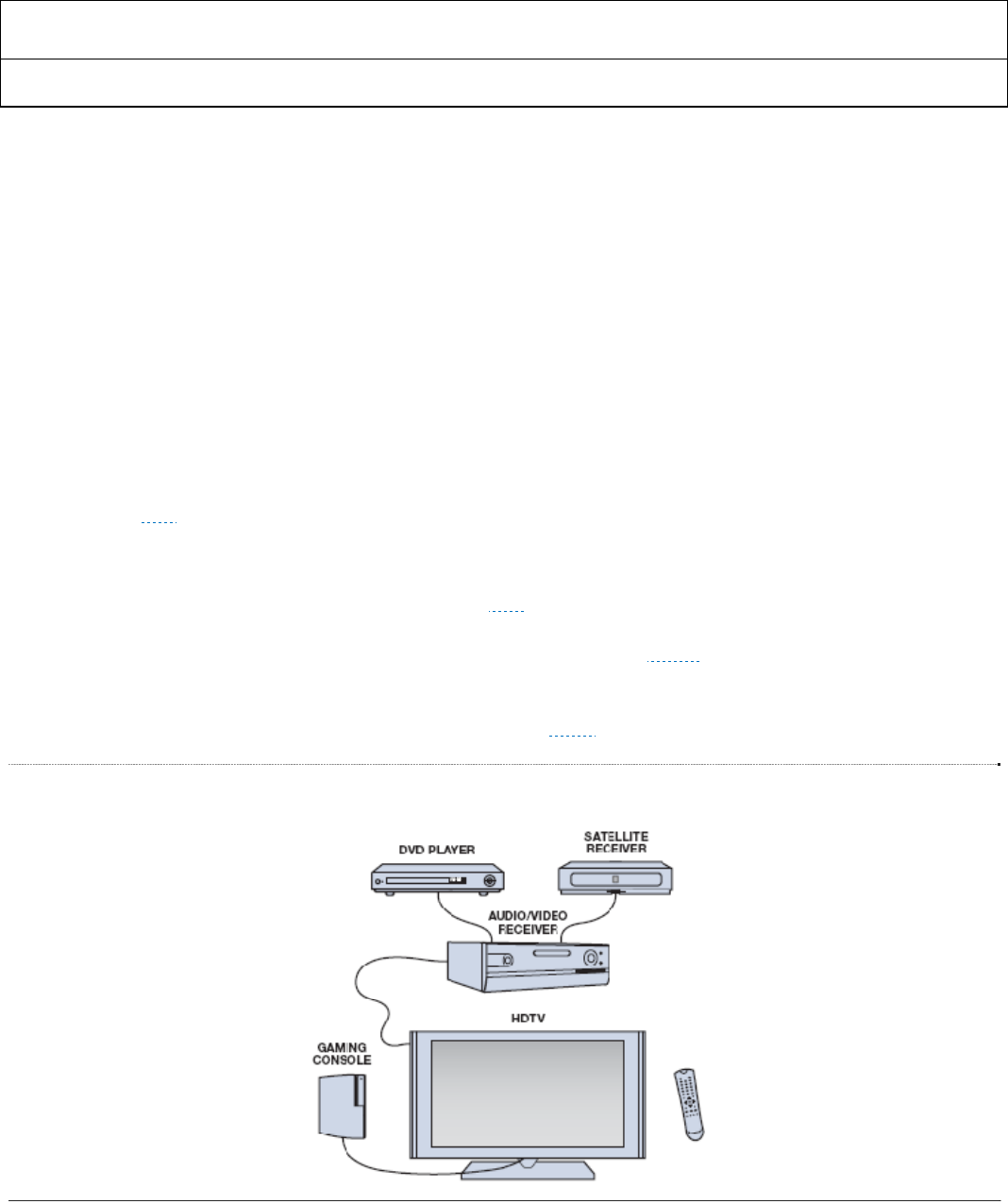
facilitate the control of any device on an HDMI network, as typified in ▶ Figure 16, with the remote control unit or on-
device control buttons of any other device connected to the network. Defined as an optional feature in the HDMI
specification, it is based on the AV Link function defined in the European SCART (Syndicat des Constructeurs
d'Appareils Radiorécepteurs et Téléviseurs) specification. ▶ Table 13 describes some typical end-user CEC features.
Figure 16 Typical All-HDMI Home Theatre
ADV7513 ADI Confidential HARDWARE USER’S GUIDE
Rev. 0
Rev. 0| Page 33 of 46
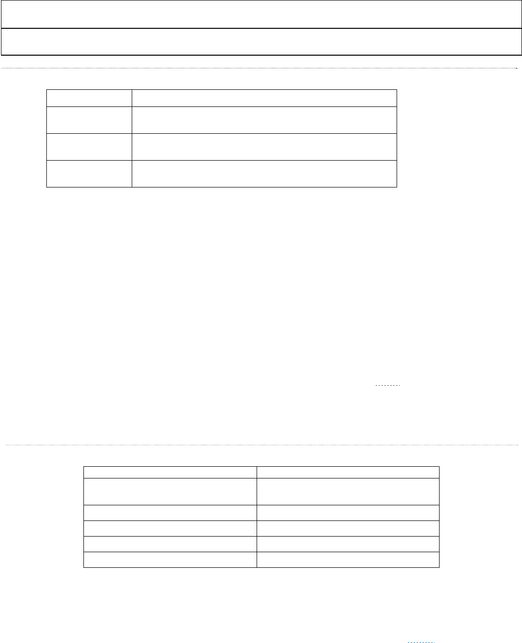
Table 13 Some useful “End-User” CEC Features:
Feature Description
One-Touch Play Pushing the “play” button commands a source to play and become the
active video source for the TV.
Stand-By Pushing the “power down” button of any active device commands all
devices on the HDMI network to shut down.
One-Touch Record Pushing the “record” button commands a recording device to power up
and record the content currently displayed on the TV.
Many of these end-user features require sending multiple messages over the CEC bus such as “Active Source,” and
“Routing Change,” which support the CEC feature “Routing Control.” This feature allows a device to play and become
the active source by switching the TV’s source input. If the TV is displaying another source at the time this command
is used, it may place the other source into “stand-by” mode, depending on the implementation.
6.4 Video Data Formatting
Following the Input Data Capture are the options for Color Space Conversion (CSC) and for formatting between 4:4:4
and 4:2:2. Taken together these can alter an input stream from: RGB to YCbCr (4:4:4 or 4:2:2) , or YCbCr to RGB.
Required video control signals such as Hsync, Vsync and Data Enable (DE) can be generated from different input
formats and can be adjusted for optimum position.
6.4.1 Supported 3D Formats
If an HDMI source has 3D format capability it must support at least one of the formats in Table 8-14 of the HDMI 1.4
specification. These include frame packing for 1080p 24, 720p 60, and 720p 50. ▶ Table 14 shows the 3D formats
supported by the ADV7524A.
▷ Please refer to the ADV7513 Programming Guide for more information about 3D support.
Table 14 Supported 3D Formats
Format
1080p 24 (Frame Packing) Supported (Sync Adjustment and Embedded
Sync Processing Not Supported for this mode)
1080i 25 (Frame Packing) Fully Supported
1080i 30 (Frame Packing) Fully Supported
720p 60 (Frame Packing) Fully Supported
720p 50 (Frame Packing) Fully Supported
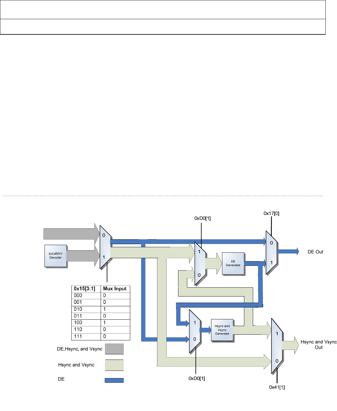
6.4.2 DE, Hsync and Vsync Generation
When transmitting video data across the TMDS interface, it is necessary to have an Hsync, Vsync, and Data Enable
(DE) defined for the image. There are three methods for sync input to the ADV7513. See ▶ Figure 17 for a block
diagram of the sync processing capabilities.
ADV7513 HARDWARE USER’S GUIDE
Rev.0
Rev. 0 | Page 34 of 46
Separate Hsync, Vsync, and DE
For this method, all necessary signals are provided so neither Sync generation nor DE generation is required. If
desired, the user can adjust the Hsync and Vsync timing relative to DE (refer to Hsync and Vsync adjustment section).
Also, the DE timing can be adjusted relative to Hsync and Vsync.
▷ Refer to the ADV7513 Programming Guide for details on how to adjust the DE and sync timing.
Embedded Syncs (SAV and EAV)
When embedded syncs are provided to the ADV7513 Hsync and Vsync need to be generated internally by the
ADV7513 hardware. Registers 0x30 through 0x34 and 0x17[6:5] contain the settings for Hsync and Vsync generation
in the embedded sync decoder section. The ADV7513 will use the signal generated by the EAV and SAV as the DE by
default, but a new DE can also be generated. Sync adjustment is also available.
▷ Refer to the ADV7513 Programming Guide for details on how to program the DE and sync generator when
embedded syncs are used.
Separate Hsync and Vsync only
This method requires that a DE be generated. Hsync and Vsync can also be adjusted based on the new DE if desired by
enabling the Hsync and Vsync generation and setting the order to DE generation then Hsync Vsync Generation.
▷ Refer to the ADV7513 Programming Guide for details on how to generate DE based on the incoming sync
signals.
Figure 17 Sync Processing Block Diagram
ADV7513 ADI Confidential HARDWARE USER’S GUIDE
Rev. 0
Rev. 0| Page 35 of 46
6.4.3 Color Space Conversion (CSC) Matrix
The Color Space Conversion (CSC) matrix in the ADV7513 consists of three identical processing channels (see
▶ Figure 18). In each channel, the three input values (R,G,B or Y,Cr,Cb - see ▶ Table 15) are multiplied by three
separate coefficients. In each CSC channel, the order of input remains the same – Out_A will have the same input
(In_A, In_B, In_C) as Out_B and Out_C. The coefficients will be different for each channel. Also included is an offset
value for each row of the matrix and a scaling multiple for all values. Each coefficient is 13 bit 2’s complement
resolution to ensure the signal integrity is maintained. The CSC is designed to run at speeds up to 165Mhz, supporting
resolutions up to 1080p at 60Hz and UXGA at 60Hz. With “any-to-any” color space support, formats such as RGB,
YUV, YCbCr, and others are supported by the CSC.
▷ Please refer to the ADV7513 Programming Guide for more information about this block.
Table 15 Channel Assignment for Color Space Converter (CSC)
Input RGB YCrCb Coefficients Output
In_A Red Cr
A1,A2,A3,A4 Out_A
In_B Green Y
In_C Blue Cb
In_A Red Cr
B1.B2.B3.B4 Out_B
In_B Green Y
In_C Blue Cb
In_A Red Cr
C1,C2,C3,C4 Out_C
In_B Green Y
In_C Blue Cb
Figure 18 Single Channel of CSC (In_A)
2x
4x
÷++
x+
x
x
2
1
0
CSC Mode 0x18[6:5]
A1[12:0]
A2[12:0]
A3[12:0]
A4[12:0]4096
In_A[11:0]
In_B[11:0]
In_C[11:0]
Out_A[11:0]

ADV7513 HARDWARE USER’S GUIDE
Rev.0
Rev. 0 | Page 36 of 46
6.4.4 4:2:2 to 4:4:4 and 4:4:4 to 4:2:2 Conversion Block
The 4:2:2 to 4:4:4 conversion block can convert 4:2:2 input signals into the 4:4:4 timing format. This is necessary, for
instance, if the ADV7513 is set in DVI mode and has 4:2:2 format as its video input. The ADV7513 is also capable of
performing 4:4:4 to 4:2:2 conversions.
▷ Please refer to Section 4.3.5 of the ADV7513 Programming Guide for more information about this block.
6.5 DDC Controller
The ADV7513 DDC Controller performs two main functions: support the system’s EDID and handle HDCP.
• The ADV7513 has the ability to read and buffer the sink EDID (one segment of 256 bytes at a time) via
the DDC lines. This feature eliminates the requirement for the source controller to interface directly to
the sink.
• The ADV7513 DDC controller provides the path through which HDCP content protection
authentication and communications occur. The ADV7513 has internal HDCP key storage (eliminating
the need for an external EEPROM) and a built-in micro-controller to handle HDCP transmitter states,
including handling down-stream HDCP repeaters. This provides content protection for video which
prevents unauthorized digital copying. Refer to Section ▶ for power consumption of HDCP.
▷ Please refer to Section 4.5 of the ADV7513 Programming Guide for more information about this block.
6.6 Inter-IC Communications (I2C)
6.6.1 Two-Wire Serial Control Port
The ADV7513’s registers must be programmed through the SDA and SCL pins using the Inter IC (IIC or I2C)
protocol. The ADV7513 uses four I2C register maps. The SDA/SCL programming address for the Main Register Map
is 0x72 or 0x7A, based on whether PD/AD is pulled high (I2C address = 0x7A) or pulled low (I2C address = 0x72)
when power is applied to the supplies. The user should wait 200ms for the address to be decided, after the power
supplies are high, before attempting to communicate with the ADV7511W using I2C
The device address for the Packet Memory is programmable and is controlled by register 0x45 of the Main Register
Map. The default setting is 0x70. The details of the Packet Memory Map can be found in ▷ ADV7513 Programming
Guide.
The EDID Memory address is programmable and controlled by register 0x43 of the Main Register Map. The default
setting is 0x7E. The details of the EDID Memory Map can be found in ▷ ADV7513 Programming Guide.
The CEC Memory address is programmable and controlled by register 0xE1 of the Main Register Map. The default
setting is 0x78. Unless otherwise stated, all register references in this document refer to the Main Register Map.
The Fixed I2C Address register 0xF9 needs to be set to an I2C address that does not conflict with any other address on
the board. 0x00 is an appropriate setting.
▷ The ADV7513 Programming Guide provides the information necessary for programming the transmitter.
Up to two ADV7513 devices can be connected to the two-wire serial interface, with a unique address for each device.
The two-wire serial interface comprises a clock (SCL) and a bidirectional data (SDA) pin. The ADV7513 interface acts
as a slave for receiving and transmitting data over the serial interface. When the serial interface is not active, the logic
levels on SCL and SDA are pulled high by external pull-up resistors.
ADV7513 ADI Confidential HARDWARE USER’S GUIDE
Rev. 0
Rev. 0| Page 37 of 46
Data received or transmitted on the SDA line must be stable for the duration of the positive-going SCL pulse. Data on
SDA must change only when SCL is low. If SDA changes state while SCL is high, the serial interface interprets that
action as a start or stop sequence.
There are six components to serial bus operation:
■ Start signal
■ Slave address byte
■ Base register address byte
■ Data byte to read or write
■ Stop signal
■ Acknowledge (Ack)
When the serial interface is inactive (SCL and SDA are high), communications are initiated by sending a start signal.
The start signal is a high-to-low transition on SDA while SCL is high. This signal alerts all slaved devices that a data
transfer sequence is coming.
The first eight bits of data transferred after a start signal comprise a seven bit slave address (the first seven bits) and a
single R/W bit (the eighth bit). The R/W bit indicates the direction of data transfer, read from (1) or write to (0) the
slave device. If the transmitted slave address matches the address of the device (set by the state of the A2 input pin as
shown in ▶ Table 16), the ADV7513 acknowledges by bringing SDA low on the 9th SCL pulse. If the addresses do not
match, the ADV7513 does not acknowledge.
Table 16 Serial Port Addresses
Bit 7 Bit 6 Bit 5 Bit 4 Bit 3 Bit 2 Bit 1 Hex Addr.
PD/AD pin
Power-up state
A6 (MSB) A5 A
4 A
3 A
2 A
1 A
0
0 0 1 1 1 0 0 1 0x72
1 0 1 1 1 1 0 1 0x7A
6.6.2 Data Transfer via I2C
For each byte of data read or written, the most significant bit (MSB) is the first bit of the sequence.
If the ADV7513 does not acknowledge the master device during a write sequence, the SDA remains high so the master
can generate a stop signal. If the master device does not acknowledge the ADV7513 during a read sequence, the
ADV7513 interprets this as end of data. The SDA remains high, so the master can generate a stop signal.
Writing data to specific control registers of the ADV7513 requires that the 8-bit address of the control register of
interest be written after the slave address has been established. This control register address is the base address for
subsequent write operations, however, it is reset after a STOP command. The base address auto-increments by one for
each byte of data written after the data byte intended for the base address. If more bytes are transferred than there are
available addresses, the address does not increment and remains at its maximum value. Any base address higher than
the maximum value does not produce an acknowledge signal.
Data are read from the control registers of the ADV7513 in a similar manner. Reading requires two data transfer
operations:
1. The base address must be written with the R/W bit of the slave address byte low to set up a sequential read
operation.
2. Reading (the R/W bit of the slave address byte high) begins at the previously established base address. The
address of the read register auto-increments after each byte is transferred.
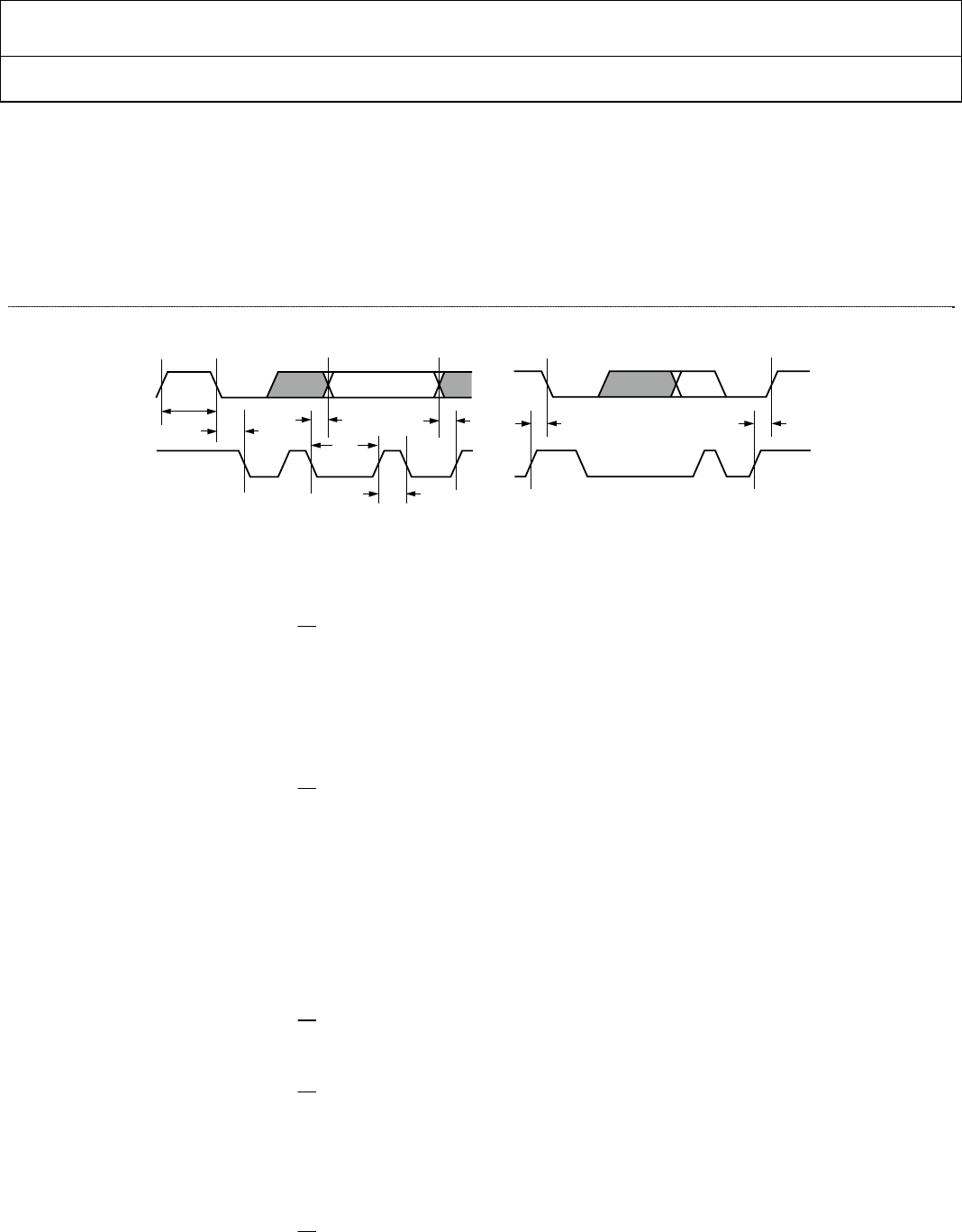
ADV7513 HARDWARE USER’S GUIDE
Rev.0
Rev. 0 | Page 38 of 46
To terminate a read/write sequence to the ADV7513, a stop signal must be sent. A stop signal comprises a low-to-high
transition of SDA while SCL is high. As in the write sequence, a STOP command resets the base address.
A repeated start signal occurs when the master device driving the serial interface generates a start signal without first
generating a stop signal to terminate the current communication. This is used to change the mode of communication
(read/write) between the slave and master without releasing the serial interface lines.
Figure 19 Serial Port Read/Write Timing
6.6.3 Serial Interface Read/Write Examples
Write to one control register:
■ Start signal
■ Slave address byte (R/W bit = low)
■ Base address byte
■ Data byte to base address
■ Stop signal
Write to four consecutive control registers:
■ Start signal
■ Slave address byte (R/W bit = LOW)
■ Base address byte
■ Data byte to base address
■ Data byte to (base address + 1)
■ Data byte to (base address + 2)
■ Data byte to (base address + 3)
■ Stop signal
Read from one control register:
■ Start signal
■ Slave address byte (R/W bit = low)
■ Base address byte
■ Start signal
■ Slave address byte (R/W bit = high)
■ Data byte from base address
■ Stop signal
Read from four consecutive control registers:
■ Start signal
■ Slave address byte (R/W bit = low)
SDA
SCL
t
BUFF
t
STAH
t
DHO
t
DSU
t
DAL
t
DAH
t
STASU
t
STOSU
05087-007
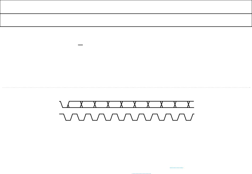
ADV7513 ADI Confidential HARDWARE USER’S GUIDE
Rev. 0
Rev. 0| Page 39 of 46
■ Base address byte
■ Start signal
■ Slave address byte (R/W bit = high)
■ Data byte from base address
■ Data byte from (base address + 1)
■ Data byte from (base address + 2)
■ Data byte from (base address + 3)
■ Stop signal
Figure 20 Serial Interface—Typical Byte Transfer
6.7 Power Domains
All power domains of the ADV7513 operate off of 1.8 volts, with the exception of the DVDD_3V which is 3.3 volts. It
is recommended that the ADV7513 has its own designated 1.8V linear regulator and that the PVDD, AVDD and
DVDD PCB power domains be segregated using inductors as illustrated in ▶ Figure 21. More detailed
recommendations for the PCB can be found in section ▶ Section 7:.
BIT 7 ACKBIT 6 BIT 5 BIT 4 BIT 3 BIT 2 BIT 1 BIT 0SDA
SCL
05087-008
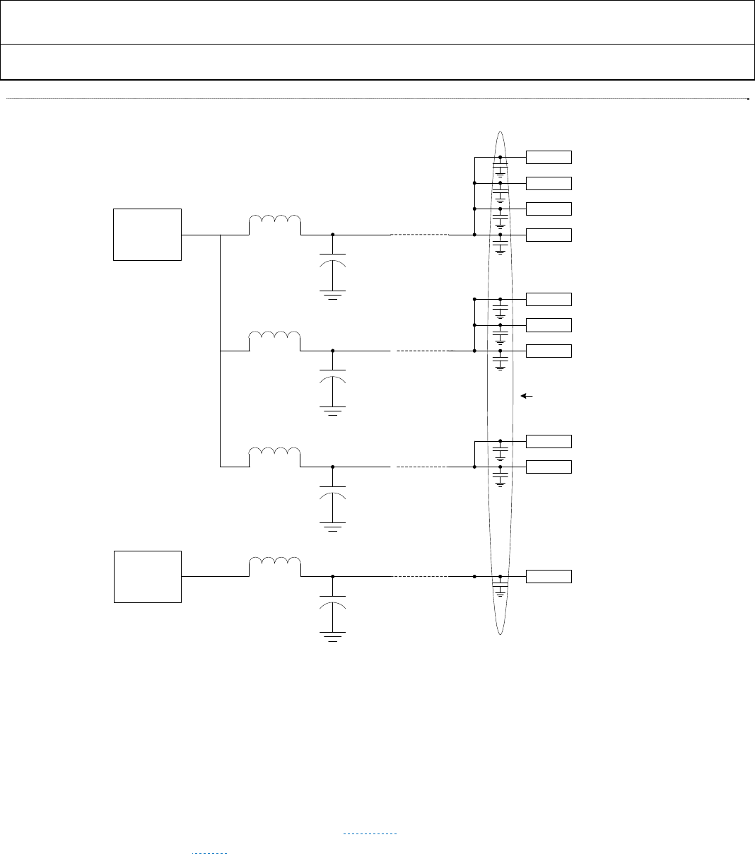
ADV7513 HARDWARE USER’S GUIDE
Rev.0
Rev. 0 | Page 40 of 46
Figure 21 Power Supply Domains
6.7.1 Power Supply Sequencing
There is no required sequence for turning on or turning off the power domains; all should be fully powered up or
down within 1 second of the others.
6.7.2 Power Consumption
The power consumption of the ADV7513 will vary depending upon: clock frequency, power supply domain voltages
and which functional blocks are being used. In Section 4: the specifications table lists the maximum power as 326mW
at 1080p, CSC off. ▶ Table 17illustrates the maximum power consumed by individual circuits in the ADV7513. All of
these entries are for worst case operations – 1080p output, and 192KHz audio sampling frequency.
1.8V
LDO
10uF
10uH
10uF
10uH
DVDD
AVDD
10uF
10uH
PVDD
Pin 51 DVDD
Pin 31 DVDD
Pin 11 DVDD
Pin 1 DVDD
Pin 19 AVDD
Pin 15 AVDD
PVDD
Pin 12
BGVDD
All bypass capacitors 0.1uF
3.3V
LDO
10uF
10uH Pin 29 DVDD_3V
Pin 25 AVDD
Pin 13
ADV7513 ADI Confidential HARDWARE USER’S GUIDE
Rev. 0
Rev. 0| Page 41 of 46
Table 17 Maximum Power Consumption by Circuit – note these values will change after characterization
Functional Block CSC HDCP CEC SPDIF high power
mode
SPDIF Low power
mode
Max Power1 25mW 30mW <1mW 40mW2 10m W3
Typical Power 16mW 25mW <1mW
1. At 1080p video resolution
2. At 192KHz audio sampling rate
3. At 32KHz sudio sampling rate
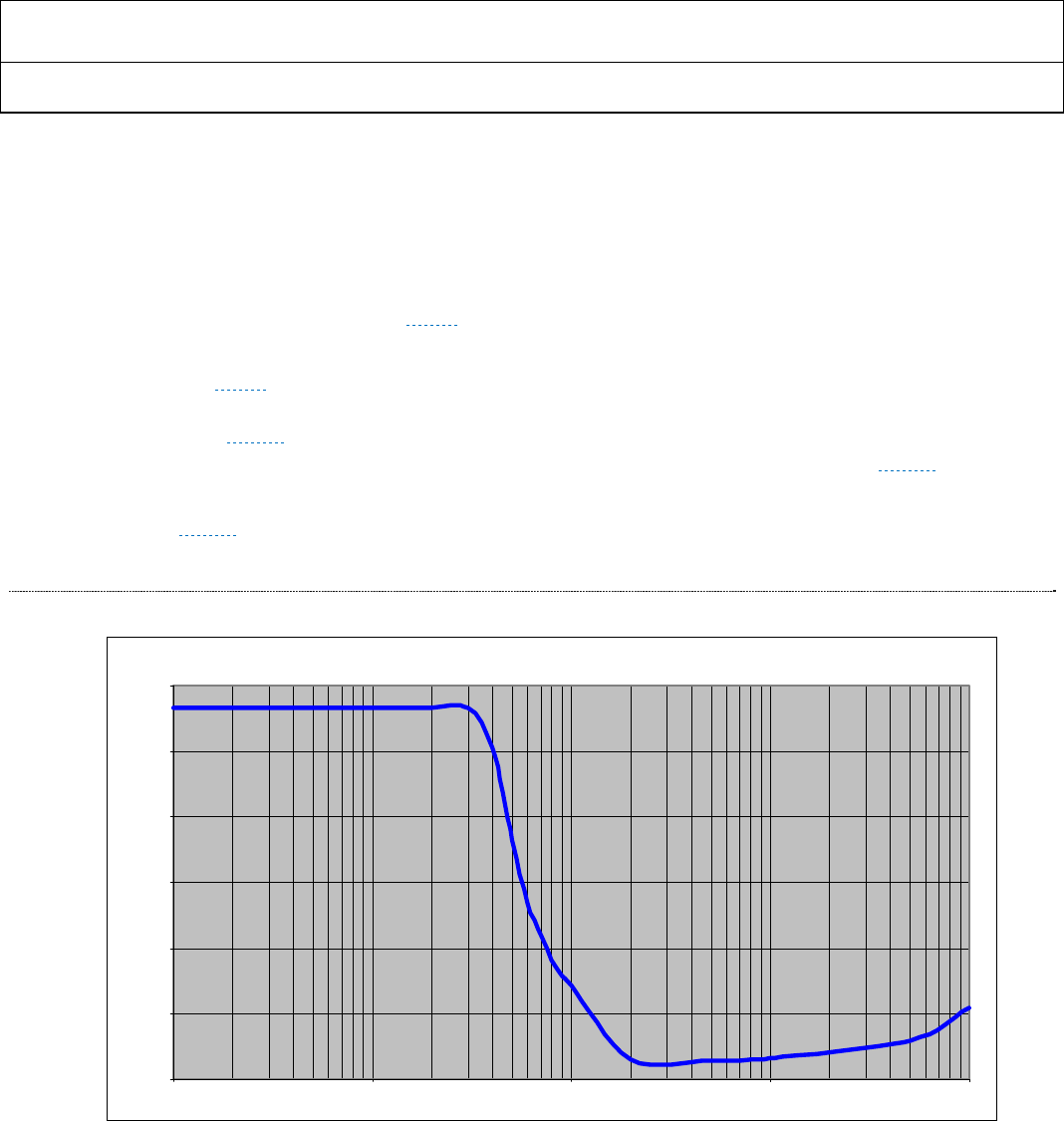
ADV7513 HARDWARE USER’S GUIDE
Rev.0
Rev. 0 | Page 42 of 46
SECTION 7: PCB LAYOUT RECOMMENDATIONS
7.1 Power Supply filtering
All of the ADV7513 supply domains are 1.8V with the exception of DVDD_3V which is 3.3V and need to remain as
noise-free as possible for the best operation. Power supply noise has a frequency component that affects performance,
and this is specified in Vrms terms. ▶ Figure 22 shows the maximum allowable noise in the ADV7513.
It is recommended to combine the four 1.8 volt power domains of the ADV7513 into 3 separate PCB power domains
as shown in ▶ Figure 21. An LC filter on the output of the power supply is recommended to attenuate the noise and
should be placed as close to the ADV7513 as possible. An effective LC filter for this is a 10 μH inductor and a 10μF
capacitor (see▶ Figure 21). This filter scheme will reduce any noise component over 20KHz to effectively 0. Using the
recommended LC filter with realistic load and series resistance yields the transfer curve shown in Figure 23.
Each of the power supply pins of the ADV7513 should also have a 0.1uF capacitor connected to the ground plane as
shown in Figure 21. The capacitor should be placed as close to the supply pin as possible. Adjacent power pins can
share a bypass capacitor. The ground pins of the ADV7513 should be connected to the GND plane using vias.
Figure 22 AVDD and PVDD Max Noise vs. Frequency
Max rms noise vs frequency (DC to 10MHz)
0.0
5.0
10.0
15.0
20.0
25.0
30.0
1 10 100 1000 10000
frequency (KHz)
Max rms noise (mV)
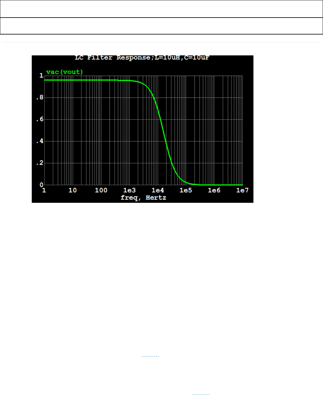
ADV7513 ADI Confidential HARDWARE USER’S GUIDE
Rev. 0
Rev. 0| Page 43 of 46
Figure 23 LC Filter Transfer Curve
7.2 Video Clock and Data Inputs
Any noise that that is coupled onto the CLK input trace will add jitter to the system. It is a recommended to control the
impedance of the CLK trace. If possible, using a solid ground or supply reference under the trace is a good way to
ensure the impedance remains constant over the entire length of the trace. Therefore, minimize the video input data
clock (pin 53) trace length and do not run any digital or other high frequency traces near it. Make sure to match the
length of the input data signals to optimize data capture especially for Double Data Rate (DDR) input formats.
7.3 Audio Clock and Data Inputs
The length of the input audio data signals should be matched as closely as possible to optimize audio data capture. It is
recommended to add series 50Ω resistors (+/-5%) as close as possible to the source of the audio data and clock signals
to minimize impedance mismatch.
7.4 SDA and SCL
The SDA and SCL pins should be connected to an I2C Master. A pull-up resistor of 2kΩ (+/-10%) to 1.8V or 3.3V is
recommended for each of these signals. See ▶ Figure 25.
7.5 DDCSDA and DDCSCL
The DDCSDA and DDCSCL pins should be connected to the HDMI connector. A pull-up resistor of 1.5 kΩ to 2kΩ
(+/-10%) to HDMI +5V is required for each of these signals. See ▶ Figure 25.
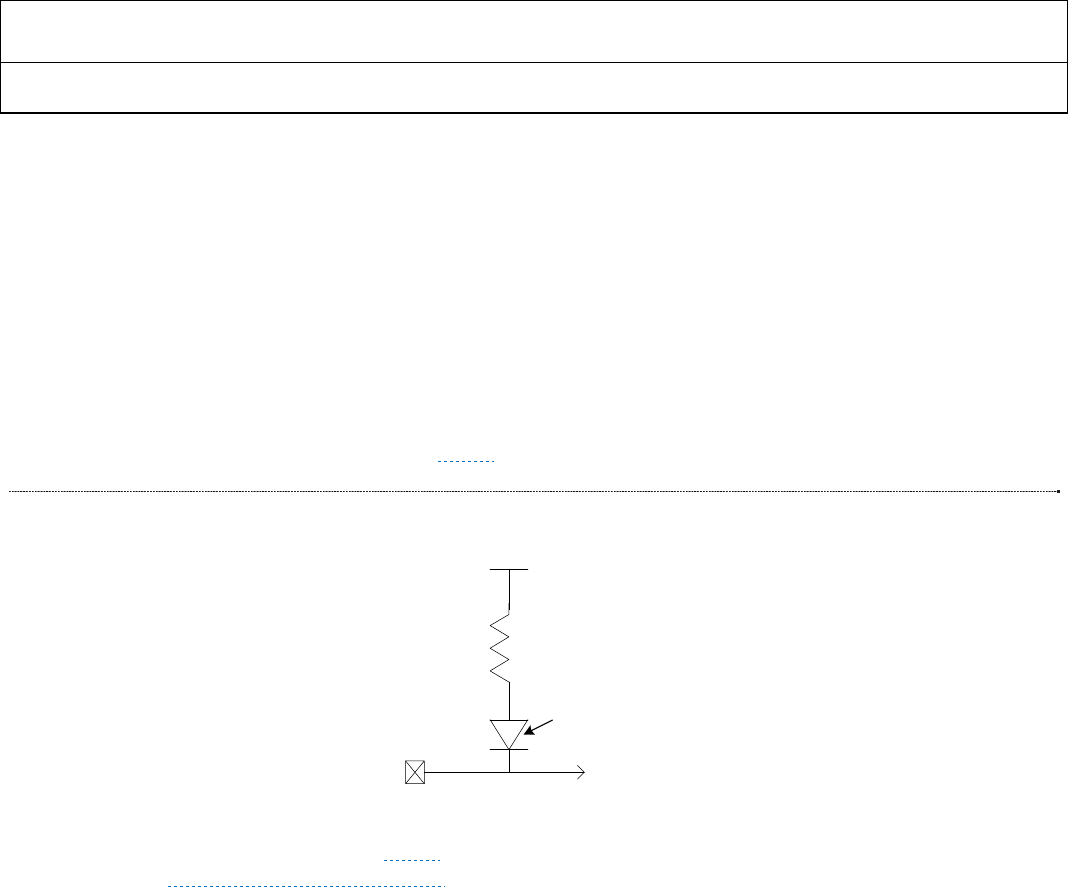
ADV7513 HARDWARE USER’S GUIDE
Rev.0
Rev. 0 | Page 44 of 46
7.6 Current Reference Pin: R_EXT
The external reference resistor should be connected between the R_EXT pin and ground with as short a trace as
possible. The external reference resistor must have a value of 887 Ohms (+/-1% tolerance). It is strongly recommended
to avoid running any high-speed AC or noisy signals next to the R_EXT line or close to it. Specifically it is
recommended that no switching signals – such as LRCLK (including vias) be routed close to R_EXT pin (14). Low-
level TMDS switching noise should have minimal impact on R_EXT. Therefore, it is acceptable to place a via for
R_EXT near TMDS signals such as TX0+ and TX0-
7.7 CEC Implementation
An external clock is required to drive the CEC_CLK input pin. Default frequency is 12MHz, but any clock between
3MHz and 100MHz (+/-2%) can be used. Figure 24 illustrates the recommended connection to the CEC line.
Figure 24 CEC external connection
An example schematic is shown in Figure 25. For a complete set of reference schematics and PCB layout example,
contact ATV_VideoTX_apps@analog.com.
CEC_IO
HDMI
Connector
27K ohms
VDD=3.3V
leakage < 1.8uA
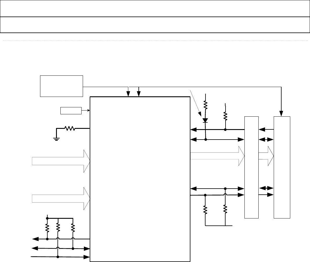
ADV7513 ADI Confidential HARDWARE USER’S GUIDE
Rev. 0
Rev. 0| Page 45 of 46
Figure 25 Example Schematic
ESD Protection
Video Data
Audio Data HDMI Data
CLK, DE, Vsync, Hsync
D[23:0]
HPD
CEC_CLK
CEC
Tx0
Tx1
Tx2
TxC
DDC_SCL
DDC_SDA
INT
SPDIF/I2S
LRCLK
SCLK/MCLK
R_EXT
887 ohms @ 1%
3.3V
27K GND
10K
+5V
2K 2K
ADV7513
1.8V
2K
SDA
XTAL Osc
Leakage < 1.8uA
HDMI Connection
2K
SCL
2K
Power Supply
5V,3.3V,1.8V
1.8V 3.3V +5V

ADV7513 HARDWARE USER’S GUIDE
Rev.0
Rev. 0 | Page 46 of 46
SECTION 8: GLOSSARY
480i, 480p, 576i,
576p, 720p,
1080i, 1080p
Common video modes.
▷ Refer to CEA-861E for more information.
VGA, SVGA,
XGA, SXGA,
UXGA
Common graphics modes.
▷ Refer to VESA.org for more information.
CEC Consumer Electronics Control is used to unify remotes of differing make to perform a given task with one-
button- touch.
CSC Colorspace Convert is used to convert RGB to YCbCbr or YCbCr to RGB. Adjustments can be factored in
for differing ranges.
DDC Display Data Channel is used to communicate between to the source and sink to determine sink
capabilities. It is also used as the HDCP key communications channel.
DDR Double Data Rate clocks capture data on both the rising and falling edge of the clock.
DVI Digital Visual Interface - uses TMDS to transmit RGB signals.
EDID Enhanced Display Identification Data is used to store monitor (sink) capabilities in an EEPROM.
HBR High Bit-Rate audio is used to define sample rates greater than 192Kbits.
HDCP High-bandwidth Digital Content Protection is a method of protecting content from unauthorized digital
copying.
HDMI High Definition Multimedia Interface is composed of three TMDS differential data channels and one
differential clock channel. It is defined to include video streams up to 3.7Gbps as well as audio.
HPD The Hot Plug Detect pin is an input which detects if a DVI or HDMI sink is connected.
I2C, IIC Inter-IC Communications is a Philips two-wire serial bus for lo
w
-speed (up to 400kHz) data.
I2S Inter-IC Sound is a serial Philips bus designed specifically for audio.
LPCM Linear Pulse-Code Modulation is a method of encoding audio samples.
LQFP Lo
w
-Profile Quad Flat Pack is the type of package for the ADV7513.
PLL Phase-Locked Loop.
RGB Red Green Blue is the standard definition for three-color graphics and video.
SPDIF Sony / Philips Digital Interface is a method of presenting audio data in a serial stream.
TMDS Transition Minimized Differential Signaling is the format used by the three data channels in HDMI. This
encodes 8 bits into 10 and serializes them.
x.v.Color™ This is feature of HDMI
v
.1.3 in which the color gamut may be extended or altered beyond the normal
range in order to accommodate a given sink.
YCbCr This is a common color format for video where the ‘Y’ component is luminance and the Cr and Cb signals
are color difference signals. 4:4:4 defines a Y, Cr, and Cb for each pixel; 4:2:2 defines a Y for each pixel and
a sharing of Cr and Cb between 2 sequential pixels. In this manner, compression of 33% is possible.
